ATSAMD20G17 - Electronic component Microchip - Free user manual and instructions
Find the device manual for free ATSAMD20G17 Microchip in PDF.

User questions about ATSAMD20G17 Microchip
0 question about this device. Answer the ones you know or ask your own.
Ask a new question about this device
Download the instructions for your Electronic component in PDF format for free! Find your manual ATSAMD20G17 - Microchip and take your electronic device back in hand. On this page are published all the documents necessary for the use of your device. ATSAMD20G17 by Microchip.
USER MANUAL ATSAMD20G17 Microchip
Operating Conditions
- 1.62V - 3.63V, -40°C to +85°C, DC up to 48 MHz
- 1.62V - 3.63V, -40°C to +105°C, DC up to 32 MHz
- 2.7V – 3.63V, -40°C to +125°C Extended Temperature with compliance to AEC-Q100, DC up to 32MHz
Core
- Arm ^ Cortex ^ -M0+ CPU running at up to 48 MHz
- Single-cycle hardware multiplier
Memories
• 16/32/64/128/256 KB in-system self-programmable Flash
• 2/4/8/16/32 KB SRAM
System
- Power-on Reset (POR) and Brown-out Detection (BOD)
- Internal and external clock options with 48 MHz Digital Frequency Locked Loop (DFLL48M)
• External Interrupt Controller (EIC) - Up to 16 external interrupts
• One non-maskable interrupt - Two-pin Serial Wire Debug (SWD) programming, test and debugging interface
Low-Power
- Idle and Stand-by Sleep modes
- SleepWalking peripherals
Peripherals
• 8-channel Event System
- Up to eight 16-bit Timer/Counters (TC), configurable as:
- One 16-bit TC with two compare/capture channels
- One 8-bit TC with two compare/capture channels
- One 32-bit TC with two compare/capture channels, by using two TCs
- 32-bit Real Time Counter (RTC) with clock/calendar function
- Watchdog Timer (WDT)
- CRC-32 generator
- Up to six Serial Communication Interfaces (SERCOM), each configurable to operate as either:
- USART with full-duplex and single-wire half-duplex configuration
- Inter-Integrated Circuit (I ^2 C) up to 400 kHz
- Serial Peripheral Interface (SPI)
• One 12-bit, 350 ksps Analog-to-Digital Converter (ADC) with up to 20 channels
– Differential and single-ended input
- 1/2x to 16x programmable gain stage
- Automatic offset and gain error compensation
- Oversampling and decimation in hardware to support 13-bit, 14-bit, 15-bit, or 16-bit resolution
• 10-bit, 350 ksps Digital-to-Analog Converter (DAC)
- Two Analog Comparators (AC) with Window Compare function
• Peripheral Touch Controller (PTC)
- Up to 256-channel capacitive touch and proximity sensing
I/O
- Up to 52 programmable I/O pins
Packages
• 64-pin TQFP, VQFN
- 64-ball UFBGA (not available in grades Extended Temperature and AEC-QA100)
• 48-pin TQFP, VQFN
• 45-ball WLCSP (not available in grades Extended Temperature and AEC-QA100)
• 32-pin TQFP, VQFN
• 27-ball WLCSP (not available in grades Extended Temperature and AEC-QA100)
Power Consumption
• Power Consumption
- Down to 50 μA/MHz in Active mode
- Down to 8 μA running the PTC
Table of Contents
Features....1
- Configuration Summary...... 11
- Ordering Information (1) 13
- Block Diagram....14
- Pinout....15
4.1. SAM D20J....15
4.2. SAM D20G....17
4.3. SAM D20E....19
- Signal Descriptions List....21
- I/O Multiplexing and Considerations....22
6.1. Multiplexed Signals....22
6.2. Other Functions.... 24
- Power Supply and Start-Up Considerations....26
7.1. Power Domain Overview.... 26
7.2. Power Supply Considerations.... 26
7.3. Power-Up....28
7.4. Power-On Reset and Brown-Out Detector....28
- Product Mapping....30
- Memories....31
9.1. Embedded Memories....31
9.2. Physical Memory Map....31
9.3. NVM Calibration and Auxiliary Space....31
9.4. NVM User Row Mapping....32
9.5. NVM Software Calibration Area Mapping....33
9.6. Serial Number.... 34
- Processor And Architecture.... 35
10.1. Cortex M0+ Processor....35
10.2. Nested Vector Interrupt Controller....36
10.3. High-Speed Bus System.... 37
10.4. AHB-APB Bridge 38
10.5. PAC - Peripheral Access Controller.... 40
10.6. Register Description....40
- Peripherals Configuration Summary....51
- DSU - Device Service Unit....53
12.1. Overview....53
12.2. Features....53
12.3. Block Diagram....53
12.4. Signal Description....54
12.5. Product Dependencies....54
12.6. Debug Operation....55
12.7. Chip Erase....56
12.8. Programming....57
12.9. Intellectual Property Protection....57
12.10. Device Identification....59
12.11. Functional Description....60
12.12. Register Summary....65
12.13. Register Description....66
- Clock System....89
13.1. Clock Distribution....89
13.2. Synchronous and Asynchronous Clocks....90
13.3. Register Synchronization....90
13.4. Enabling a Peripheral....94
13.5. Disabling a Peripheral....95
13.6. On-demand, Clock Requests....95
13.7. Power Consumption vs. Speed....96
13.8. Clocks after Reset....96
- GCLK - Generic Clock Controller....97
14.1. Overview....97
14.2. Features....97
14.3. Block Diagram....97
14.4. Signal Description....98
14.5. Product Dependencies....98
14.6. Functional Description.... 99
14.7. Register Summary.... 104
14.8. Register Description.... 105
- Power Manager (PM).... 116
15.1. Overview.... 116
15.2. Features.... 116
15.3. Block Diagram....117
15.4. Signal Description....117
15.5. Product Dependencies....117
15.6. Functional Description.... 119
15.7. Register Summary.... 126
15.8. Register Description.... 126
- SYSCTRL - System Controller....144
16.1. Overview....144
16.2. Features.... 144
16.3. Block Diagram.... 146
16.4. Signal Description....146
16.5. Product Dependencies....146
16.6. Functional Description.... 148
16.7. Register Summary.... 159
16.8. Register Description.... 160
17. WDT - Watchdog Timer....190
17.1. Overview....190
17.2. Features.... 190
17.3. Block Diagram....190
17.4. Signal Description.... 191
17.5. Product Dependencies....191
17.6. Functional Description.... 192
17.7. Register Summary.... 196
17.8. Register Description.... 197
18. RTC - Real-Time Counter 206
18.1. Overview....206
18.2. Features.... 206
18.3. Block Diagram....206
18.4. Signal Description....207
18.5. Product Dependencies....207
18.6. Functional Description....209
18.7. Register Summary.... 214
18.8. Register Description.... 216
19. EIC - External Interrupt Controller....248
19.1. Overview....248
19.2. Features.... 248
19.3. Block Diagram....248
19.4. Signal Description....248
19.5. Product Dependencies....249
19.6. Functional Description....250
19.7. Register Summary 254
19.8. Register Description.... 254
20. NVMCTRL - Nonvolatile Memory Controller....265
20.1. Overview....265
20.2. Features.... 265
20.3. Block Diagram....265
20.4. Signal Description.... 265
20.5. Product Dependencies....265
20.6. Functional Description.... 267
20.7. Register Summary.... 274
20.8. Register Description.... 274
21. PORT - I/O Pin Controller....286
21.1. Overview....286
21.2. Features.... 286
21.3. Block Diagram....287
21.4. Signal Description....287
21.5. Product Dependencies....287
21.6. Functional Description.... 289
21.7. Register Summary.... 295
21.8. PORT Pin Groups and Register Repetition....296
21.9. Register Description.... 296
22. Event System (EVSYS)....312
22.1. Overview....312
22.2. Features....312
22.3. Block Diagram....312
22.4. Signal Description....313
22.5. Product Dependencies....313
22.6. Functional Description....314
22.7. Register Summary.... 320
22.8. Register Description....320
23. SERCOM - Serial Communication Interface....330
23.1. Overview....330
23.2. Features.... 330
23.3. Block Diagram.... 330
23.4. Signal Description....331
23.5. Product Dependencies....331
23.6. Functional Description.... 332
24. SERCOM USART....338
24.1. Overview....338
24.2. USART Features....338
24.3. Block Diagram.... 339
24.4. Signal Description....339
24.5. Product Dependencies....339
24.6. Functional Description.... 341
24.7. Register Summary.... 349
24.8. Register Description....349
25. SERCOM SPI - SERCOM Serial Peripheral Interface 362
25.1. Overview....362
25.2. Features....362
25.3. Block Diagram.... 362
25.4. Signal Description....363
25.5. Product Dependencies....363
25.6. Functional Description.... 364
25.7. Register Summary.... 372
25.8. Register Description....372
26. SERCOM I²C – Inter-Integrated Circuit....386
26.1. Overview....386
26.2. Features....386
26.3. Block Diagram.... 387
26.4. Signal Description....387
26.5. Product Dependencies....387
26.6. Functional Description....389
26.7. Register Summary - I2C Client....401
26.8. Register Description - I ^2 C Client....401
26.9. Register Summary - I2C Host 413
26.10. Register Description - I ^2 C Host 413
27. TC - Timer/Counter....427
27.1. Overview....427
27.2. Features....427
27.3. Block Diagram....428
27.4. Signal Description....428
27.5. Product Dependencies....429
27.6. Functional Description....430
27.7. Register Summary for 8-bit Registers....440
27.8. Register Description for 8-bit Registers....440
27.9. Register Summary for 16-bit Registers....456
27.10. Register Description for 16-bit Registers....456
27.11. Register Summary for 32-bit Registers....471
27.12. Register Description for 32-bit Registers....471
28. Analog-to-Digital Converter (ADC)......486
28.1. Overview....486
28.2. Features....486
28.3. Block Diagram....487
28.4. Signal Description....487
28.5. Product Dependencies....487
28.6. Functional Description....489
28.7. Register Summary.... 498
28.8. Register Description....498
29. AC - Analog Comparators.... 522
29.1. Overview....522
29.2. Features....522
29.3. Block Diagram....523
29.4. Signal Description....523
29.5. Product Dependencies....523
29.6. Functional Description.... 525
29.7. Register Summary.... 535
29.8. Register Description....535
30. DAC – Digital-to-Analog Converter....550
30.1. Overview....550
30.2. Features....550
30.3. Block Diagram....550
30.4. Signal Description....550
30.5. Product Dependencies....550
30.6. Functional Description....552
30.7. Register Summary.... 555
30.8. Register Description....555
31. PTC - Peripheral Touch Controller....565
31.1. Overview....565
31.2. Features....565
31.3. Block Diagram....566
31.4. Signal Description....566
31.5. System Dependencies....567
31.6. Functional Description....568
- Electrical Characteristics at 85°C....569
32.1. Disclaimer....569
32.2. Absolute Maximum Ratings.... 569
32.3. General Operating Ratings.... 570
32.4. Supply Characteristics....570
32.5. Maximum Clock Frequencies.... 571
32.6. Power Consumption....572
32.7. Peripheral Power Consumption....576
32.8. I/O Pin Characteristics....577
32.9. Injection Current....579
32.10. Analog Characteristics.... 579
32.11. NVM Characteristics....591
32.12. Oscillators Characteristics....592
32.13. PTC Typical Characteristics....596
32.14. Timing Characteristics....599
- Electrical Characteristics at 105°C....604
33.1. Disclaimer....604
33.2. Absolute Maximum Ratings.... 604
33.3. General Operating Ratings....604
33.4. Maximum Clock Frequencies....605
33.5. Power Consumption....606
33.6. Injection Current....609
33.7. Analog Characteristics....610
33.8. NVM Characteristics....618
33.9. Oscillators Characteristics....618
- AEC-Q100 Electrical Characteristics at 125°C 623
34.1. Disclaimer....623
34.2. Absolute Maximum Ratings....623
34.3. General Operating Ratings....625
34.4. Supply Characteristics....625
34.5. Maximum Clock Frequencies....625
34.6. Power Consumption....626
34.7. Peripheral Power Consumption....629
34.8. I/O Pin Characteristics....630
34.9. Injection Current....631
34.10. Analog Characteristics....632
34.11. NVM Characteristics....639
34.12. Oscillators Characteristics....640
34.13. PTC Characteristics....644
34.14. Timing Characteristics....645
- Packaging Information....650
35.1. Thermal Considerations....650
35.2. Package Drawings....651
35.3. Soldering Profile....696
36. Schematic Checklist.... 697
36.1. Introduction....697
36.2. Power Supply....697
36.3. External Analog Reference Connections....699
36.4. External Reset Circuit....700
36.5. Clocks and Crystal Oscillators....701
36.6. Unused or Unconnected Pins....703
36.7. Programming and Debug Ports....703
37. Datasheet Revision History....707
37.1. Revision G - 08/2023....707
37.2. Revision F - 03/2022....707
37.3. Revision E - 11/2020....707
37.4. Revision D - 03/2020....708
37.5. Revision C - 11/2019....709
37.6. Rev. B - 11/2017....710
37.7. Rev. A - 08/2017....710
37.8. Rev. P - 09/2016....710
37.9. Rev. O - 08/2016....711
37.10. Rev. N - 01/2015....711
37.11. Rev. M - 12/2014....712
37.12. Rev. L - 09/2014....713
37.13. Rev. K - 05/2014....714
37.14. Rev. J - 12/2013....716
37.15. Rev. I 12/2013....716
37.16. Rev. H 10/2013....723
37.17. Rev. G - 10/2013....724
37.18. Rev. F - 10/2013....725
37.19. Rev. E - 09/2013....725
37.20. Rev. D - 08/2013....725
37.21. Rev. C - 07/2013.... 726
37.22. Rev. B - 07/2013....727
37.23. Rev. A - 06/2013....728
38. Conventions....729
38.1. Numerical Notation....729
38.2. Memory Size and Type....729
38.3. Frequency and Time....729
38.4. Registers and Bits....729
39. Acronyms and Abbreviations....731
The Microchip Website....733
Product Change Notification Service....733
Customer Support....733
Microchip Devices Code Protection Feature.... 733
Legal Notice....733
Trademarks....734
Quality Management System....735
Worldwide Sales and Service....736
1. Configuration Summary
Table 1-1. SAM D20 Device-Specific Features
| Device Flash (KB) SRAM (KB) | ||
| ATSAMD20E14 16 2 | ||
| ATSAMD20E15 32 4 | ||
| ATSAMD20E16 64 8 | ||
| ATSAMD20E17 128 16 | ||
| ATSAMD20E18 256 32 | ||
| ATSAMD20G14 16 2 | ||
| ATSAMD20G15 32 4 | ||
| ATSAMD20G16 64 8 | ||
| ATSAMD20G17 128 16 | ||
| ATSAMD20G18 256 32 | ||
| ATSAMD20J14 16 2 | ||
| ATSAMD20J15 32 4 | ||
| ATSAMD20J16 64 8 | ||
| ATSAMD20J17 128 16 | ||
| ATSAMD20J18 256 32 |
Table 1-2. SAM D20 Family Features
| Feature SAM D20J SAM 20G SAM D20E | |||||
| Packages | VQFN64/TQFP64/ UFBGA64 | VQFN48/TQFP48 | WLCSP45 | VQFN32/TQFP32 | WLCSP27 |
| Pins | 64 | 48 | 45 | 32 | 27 |
| General Purpose I/O pins (GPIOs) | 52 | 38 | 35 | 26 | 22 |
| Flash | 256/128/64/32/16 KB | 256/128 KB | 256/128/64/32/16 KB | 64/32 KB | |
| SRAM | 32/16/8/4/2 KB | 32/16 KB | 32/16/8/4/2 KB | 8/4 KB | |
| Timer Counter (TC) instances | 8 | 6 | |||
| Waveform output channels per TC instance | 2(1) | ||||
| Serial Communication Interface (SERCOM) instances | 6 | 4(2) | |||
| Analog-to-Digital Converter (ADC) channels | 20 14 | 10 | |||
| Analog Comparators (AC) | 2 | ||||
| Digital-to-Analog Converter (DAC) channels | 1 | ||||
| Real-Time Counter (RTC) | Yes | ||||
| RTC alarms | 1 | ||||
| RTC compare values | One 32-bit value or two 16-bit values | ||||
| External Interrupt lines | 16 | 14 | |||
| Peripheral Touch Controller (PTC) X and Y lines | 16x16 | 12x10 | 10x6 | 9x6 | |
| Maximum CPU frequency | 48MHz | ||||
| Packages | VQFN64/TQFP64/UFBGA64 | VQFN48/TQFP48 | WLCSP45 VQFN32/TQFP32 WLCSP27 | ||
| Oscillators | 32.768 kHz crystal oscillator (XOSC32K)0.4-32 MHz crystal oscillator (XOSC)32.768 kHz internal oscillator (OSC32K)32 kHz ultra low-power internal oscillator (OSCULP32K)8 MHz high-accuracy internal oscillator (OSC8M)48 MHz Digital Frequency Locked Loop (DFLL48M) | ||||
| Event System channels 8 | |||||
| SW Debug Interface Yes | |||||
| Watchdog Timer (WDT) Yes | |||||
Notes:
- The WLCSP27 package does not contain TC4/WO[1] and TC5/WO[0], TC5/WO[1] outputs.
- SERCOM4/SERCOM5 are not available on the VQFN32/TQFP32 and WLCSP27 packages.
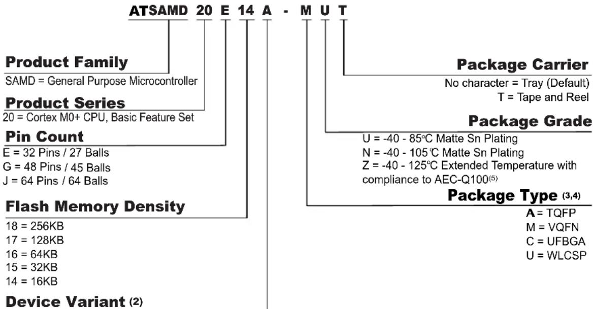
2. Ordering Information (1)
(1)
text_image
ATSAMD 20 E 14 A - M U T Product Family SAMD = General Purpose Microcontroller Product Series 20 = Cortex M0+ CPU, Basic Feature Set Pin Count E = 32 Pins / 27 Balls G = 48 Pins / 45 Balls J = 64 Pins / 64 Balls Flash Memory Density 18 = 256KB 17 = 128KB 16 = 64KB 15 = 32KB 14 = 16KB Device Variant (2) Package Carrier No character = Tray (Default) T = Tape and Reel Package Grade U = -40 - 85°C Matte Sn Plating N = -40 - 105°C Matte Sn Plating Z = -40 - 125°C Extended Temperature with compliance to AEC-Q100(5) Package Type (3,4) A = TQFP M = VQFN C = UFBGA U = WLCSPA = Default Variant
B = Improved Low Power
Note:
- Not all combinations are valid. The available device part numbers are listed in configuration Summary.
- Variant B is available only for Flash memory density of 64 KB, 32 KB, and 16 KB.
- Devices in the WLCSP45 package include a factory programmed Boot Loader. Contact your local Microchip sales office for additional information.
- Devices in the WLCSP27 package include a factory programmed Boot Loader. For additional information, refer to the MPLAB ^® Harmony v3 Boot Loader documentation.
-
AEC-Q100 grading is only available for Variant B.
-
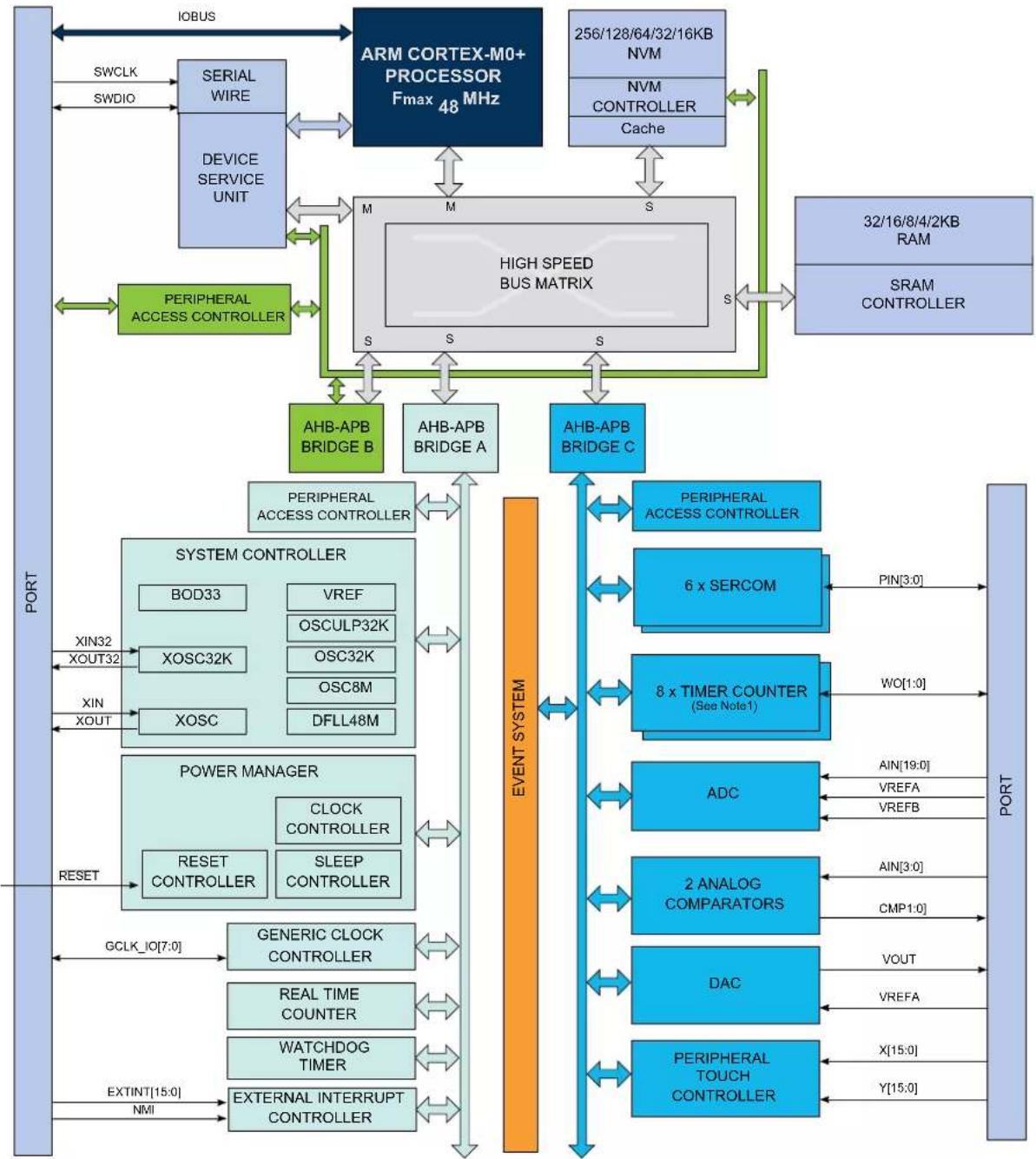
Block Diagram
flowchart
graph TD
    A["ARM CORTEX-M0+ PROCESSOR Fmax 48 MHz"] --> B["256/128/64/32/16KB NVM"]
    A --> C["NVM CONTROLLER Cache"]
    A --> D["32/16/8/4/2KB RAM"]
    A --> E["SRAM CONTROLLER"]
    A --> F["PERIPHERAL ACCESS CONTROLLER"]
    F --> G["AHB-APB BRIDGE A"]
    F --> H["AHB-APB BRIDGE B"]
    F --> I["AHB-APB BRIDGE C"]
    J["SYSTEM CONTROLLER"] --> K["BOD33"]
    J --> L["XOSC32K"]
    J --> M["XOSC"]
    J --> N["DFLL48M"]
    O["POWER MANAGER"] --> P["CLOCK CONTROLLER"]
    O --> Q["SLEEP CONTROLLER"]
    R["OUTPUT"] --> S["GCLK_IO[7:0"]]
    T["OUTPUT"] --> U["REAL TIME COUNTER"]
    T --> V["WATCHDOG TIMER"]
    T --> W["EXTERNAL INTERRUPT CONTROLLER"]
    X["OUTPUT"] --> Y["GCLK_IO[7:0"]]
    Z["OUTPUT"] --> AA["EXTINT[15:0"]]
    AB["OUTPUT"] --> AC["NMI"]
    AD["OUTPUT"] --> AE["GCLK_IO[7:0"]]
    AF["OUTPUT"] --> AG["REAL TIME COUNTER"]
    AF --> AH["WATCHDOG TIMER"]
    AF --> AI["EXTERNAL INTERRUPT CONTROLLER"]
    AJ["OUTPUT"] --> AK["GCLK_IO[7:0"]]
    AL["OUTPUT"] --> AM["REAL TIME COUNTER"]
    AL --> AN["WATCHDOG TIMER"]
    AL --> AO["EXTERNAL INTERRUPT CONTROLLER"]
    AP["OUTPUT"] --> AQ["GCLK_IO[7:0"]]
    AR["OUTPUT"] --> AS["GCLK_IO[7:0"]]
    AT["OUTPUT"] --> AU["GCLK_IO[7:0"]]
    AV["OUTPUT"] --> AW["GCLK_IO[7:0"]]
    AX["OUTPUT"] --> AY["GCLK_IO[7:0"]]
    AZ["OUTPUT"] --> BA["GCLK_IO[7:0"]]
    BB["OUTPUT"] --> BC["GCLK_IO[7:0"]]
    BD["OUTPUT"] --> BE["GCLK_IO[7:0"]]
    BF["OUTPUT"] --> BG["GCLK_IO[7:0"]]
    BH["OUTPUT"] --> BI["GCLK_IO[7:0"]]
    BJ["OUTPUT"] --> BK["GCLK_IO[7:0"]]
    BL["OUTPUT"] --> BM["GCLK_IO[7:0"]]
    BN["OUTPUT"] --> BO["GCLK_IO[7:0"]]
    BP["OUTPUT"] --> BQ["GCLK_IO[7:0"]]
    BR["OUTPUT"] --> BS["GCLK_IO[7:0"]]
    BT["OUTPUT"] --> BU["GCLK_IO[7:0"]]
    BV["OUTPUT"] --> BW["GCLK_IO[7:0"]]
    BX["OUTPUT"] --> BY["GCLK_IO[7:0"]]
    BZ["OUTPUT"] --> CA["GCLK_IO[7:0"]]
    CB["OUTPUT"] --> CC["GCLK_IO[7:0"]]
    DD["OUTPUT"] --> DE["GCLK_IO[7:0"]]
    DF["OUTPUT"] --> DG["GCLK_IO[7:0"]]
    DH["OUTPUT"] --> DI["GCLK_IO[7:0"]]
    DJ["OUTPUT"] --> DK["GCLK_IO[7:0"]]
    DL["OUTPUT"] --> DV["GCLK_IO[7:0"]]
    DW["OUTPUT"] --> DX["GCLK_IO[7:0"]]
    DX --> DW
    DX --> DX
    DX --> DX
Note: 1. Some products have different number of SERCOM instances, Timer/Counter instances, PTC signals and ADC signals. Refer to Peripherals Configuration Summary for details.
Related Links
- Peripherals Configuration Summary
4. Pinout
4.1 SAM D20J
4.1.1 VQFN64/TQFP64
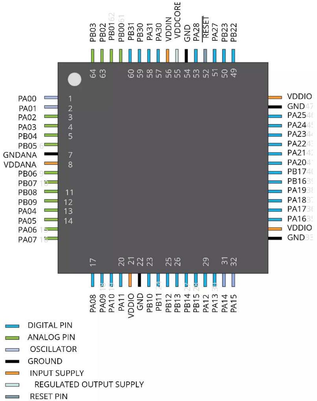
4.1.2 UFBGA64
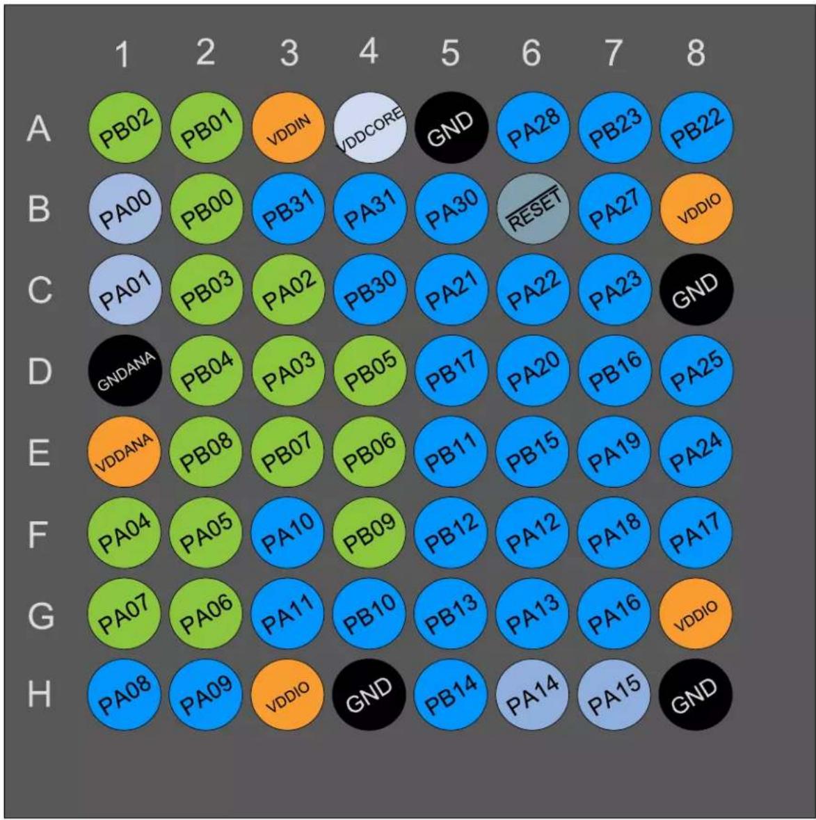
heatmap
| | 1 | 2 | 3 | 4 | 5 | 6 | 7 | 8 | |---|---|---|---|---|---|---|---|---| | A | PB02 | PB01 | VDDIN | VDDCORE | GND | PA28 | PB23 | PB22 | | B | PA00 | PB00 | PB31 | PA31 | PA30 | RESET | PA27 | VDDIO | | C | PA01 | PB03 | PA02 | PB30 | PA21 | PA22 | PA23 | GND | | D | GNDANA | PB04 | PA03 | PB05 | PB17 | PA20 | PB16 | PA25 | | E | VDDANA | PB08 | PB07 | PB06 | PB11 | PB15 | PA19 | PA24 | | F | PA04 | PA05 | PA10 | PB09 | PB12 | PA12 | PA18 | PA17 | | G | PA07 | PA06 | PA11 | PB10 | PB13 | PA13 | PA16 | VDDIO | | H | PA08 | PA09 | VDDIO | GND | PB14 | PA14 | PA15 | GND |DIGITAL PIN
ANALOG PIN
OSCILLATOR
GROUND
INPUT SUPPLY
REGULATED OUTPUT SUPPLY
RESET PIN
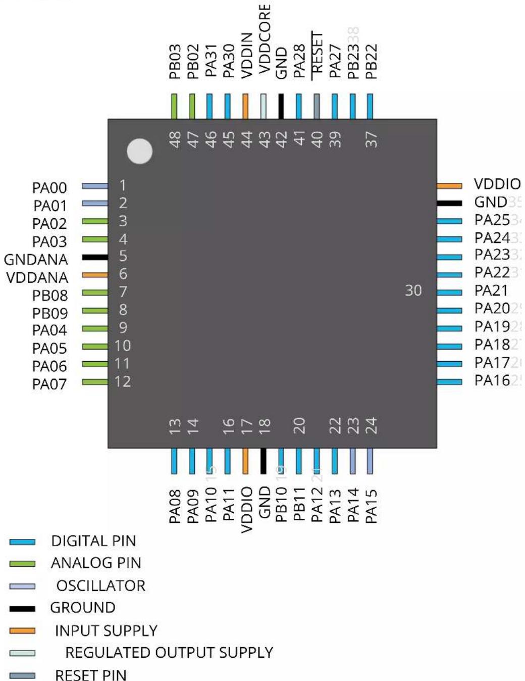
4.2 SAM D20G
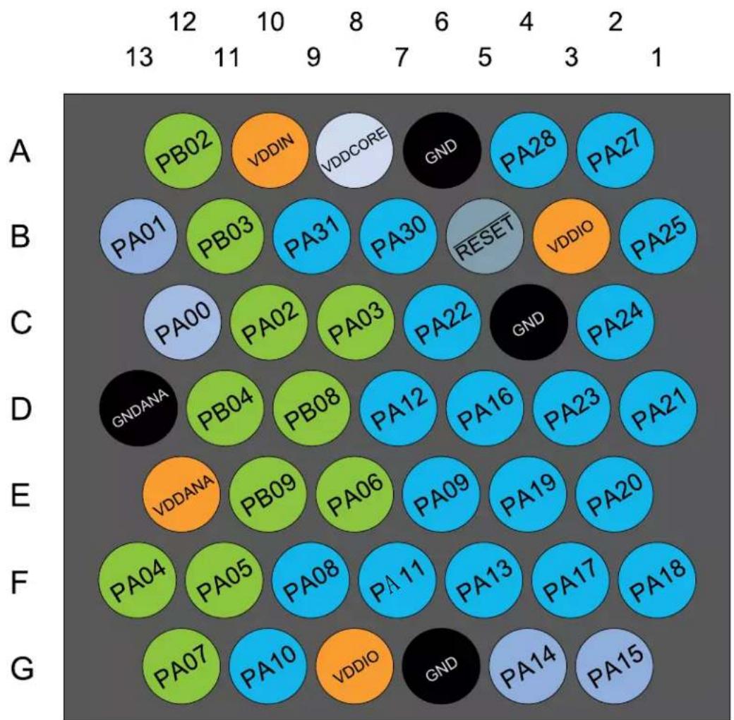
4.2.1 VQFN48/TQFP48
bar
| Pin | Pin Number | | --- | --- | | PA00 | 1 | | PA01 | 2 | | PA02 | 3 | | PA03 | 4 | | GNDANA | 5 | | VDDANA | 6 | | PB08 | 7 | | PB09 | 8 | | PA04 | 9 | | PA05 | 10 | | PA06 | 11 | | PA07 | 12 | | PB03 | 48 | | PB02 | 47 | | PA31 | 46 | | PA30 | 45 | | VDDIN | 44 | | VDDCORE | 43 | | GND | 42 | | PA28 | 41 | | RESET | 40 | | PA27 | 39 | | PB23 | 38 | | PB22 | 37 | | VDDIO | 35 | | GND | 34 | | PA25 | 33 | | PA24 | 32 | | PA23 | 31 | | PA22 | 30 | | PA21 | 29 | | PA20 | 28 | | PA19 | 27 | | PA18 | 26 | | PA17 | 25 | | PA16 | 24 | | VDDIO | 17 | | GND | 18 | | PB10 | 19 | | PB11 | 20 | | PA12 | 21 | | PA13 | 22 | | PA14 | 23 | | PA15 | 24 | | PA08 | 13 | | PA09 | 14 | | PA10 | 15 | | PA11 | 16 | | VDDIO | 17 | | GND | 18 | DIGITAL PIN ANALOG PIN OSCILLATOR GROUND INPUT SUPPLY REGULATED OUTPUT SUPPLY RESET PIN4.2.2 WLCSP45
DIGITAL PIN
ANALOG PIN
OSCILLATOR
GROUND
INPUT SUPPLY
REGULATED OUTPUT SUPPLY
RESET PIN
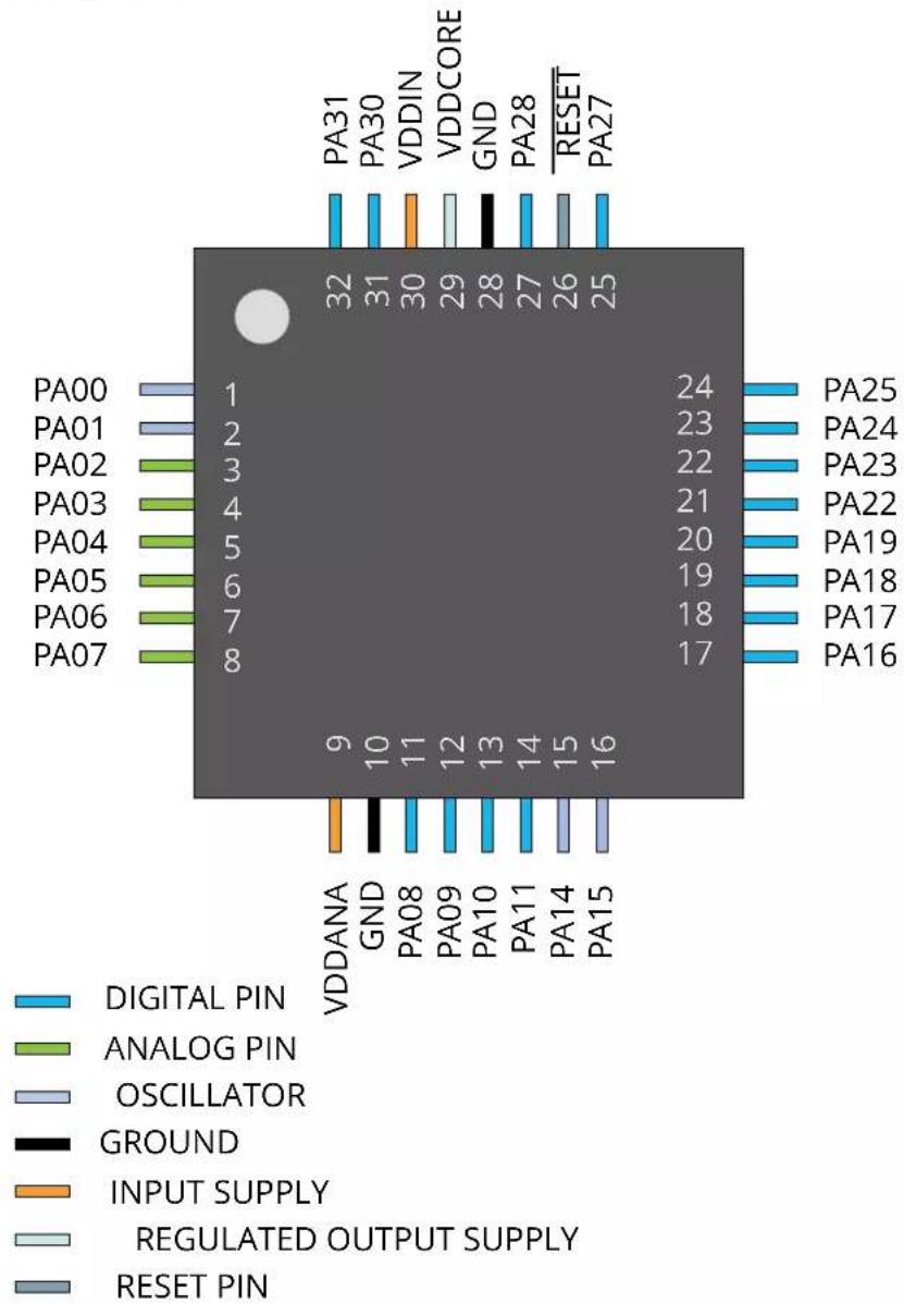
4.3 SAM D20E
4.3.1 VQFN32/TQFP32
other
| Pin Label | Pin Number | | --------- | ---------- | | PA00 | 1 | | PA01 | 2 | | PA02 | 3 | | PA03 | 4 | | PA04 | 5 | | PA05 | 6 | | PA06 | 7 | | PA07 | 8 | | VDDANA | 9 | | GND | 10 | | PA08 | 11 | | PA09 | 12 | | PA10 | 13 | | PA11 | 14 | | PA14 | 15 | | PA15 | 16 | | VDDIN | 30 | | VDDCORE | 29 | | GND | 28 | | PA28 | 27 | | RESET | 26 | | PA27 | 25 | | PA25 | 24 | | PA24 | 23 | | PA23 | 22 | | PA22 | 21 | | PA19 | 20 | | PA18 | 19 | | PA17 | 18 | | PA16 | 17 | DIGITAL PIN ANALOG PIN OSCILLATOR GROUND INPUT SUPPLY REGULATED OUTPUT SUPPLY RESET PINNote: In the VQFN32/TQFP32 package, both VDDIO and VDDANA are internally connected.
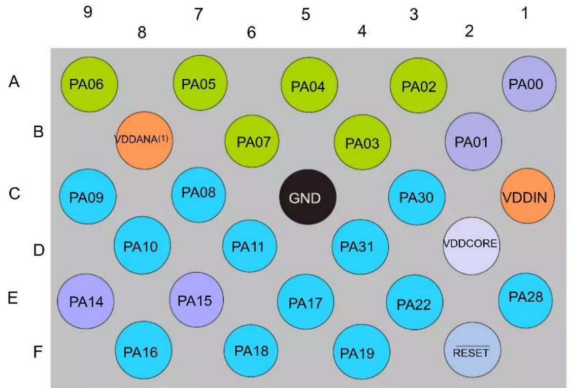
4.3.2 WLCSP27
text_image
DIGITAL PIN ANALOG PIN OSCILLATOR GROUND INPUT SUPPLY REGULATED OUTPUT SUPPLY RESET PINNote:
- In the WLCSP27 package, both VDDIO and VDDANA are internally connected.
5. Signal Descriptions List
The following table provides details on signal names classified by peripherals.
| Signal Name Function Type Active Level | |||
| Analog Comparators - AC | |||
| AIN[3:0] AC Analog Inputs Analog | |||
| CMP[1:0] AC Comparator Outputs Digital | |||
| Analog-to-Digital Converter (ADC) | |||
| AIN[19:0] ADC Analog Inputs Analog | |||
| VREFA ADC Voltage External Reference A Analog | |||
| VREFB ADC Voltage External Reference B Analog | |||
| Digital-to-Analog Converter (DAC) | |||
| VOUT DAC Voltage output Analog | |||
| VREFA DAC Voltage External Reference Analog | |||
| External Interrupt Controller | |||
| EXTINT[15:0] | External Interrupts | Input | |
| NMI | External Non-Maskable Interrupt | Input | |
| Generic Clock Generator - GCLK | |||
| GCLK_IO[7:0] | Generic Clock (source clock or generic clock generator output) | I/O | |
| Power Manager - PM | |||
| RESET | Reset | Input | Low |
| Serial Communication Interface - SERCOMx | |||
| PAD[3:0] | SERCOM I/O Pads | I/O | |
| System Control - SYSCTRL | |||
| XIN | Crystal Input | Analog/Digital | |
| XIN32 | 32 kHz Crystal Input | Analog/Digital | |
| XOUT Crystal Output Analog | |||
| XOUT32 | 32 kHz Crystal Output | Analog | |
| Timer Counter - TCx | |||
| WO[1:0] | Waveform Outputs | Output | |
| Peripheral Touch Controller - PTC | |||
| X[15:0] | PTC Output | Analog | |
| Y[15:0] | PTC Input/Output | Analog | |
| General Purpose I/O - PORT | |||
| PA25 - PA00 | Parallel I/O Controller I/O Port A | I/O | |
| PA28 - PA27 | Parallel I/O Controller I/O Port A | I/O | |
| PA31 - PA30 | Parallel I/O Controller I/O Port A | I/O | |
| PB17 - PB00 | Parallel I/O Controller I/O Port B | I/O | |
| PB23 - PB22 | Parallel I/O Controller I/O Port B | I/O | |
| PB31 - PB30 | Parallel I/O Controller I/O Port B | I/O | |
6. I/O Multiplexing and Considerations
Related Links
32.8.2. I2C Pins
6.1 Multiplexed Signals
Each pin is by default controlled by the PORT as a general purpose I/O and alternatively it can be assigned to one of the peripheral functions A, B, C, D, E, F, G, or H. To enable a peripheral function on a pin, the Peripheral Multiplexer Enable bit in the Pin Configuration register corresponding to that pin (PINCFGn.PMUXEN, n = 0-31) in the PORT must be written to one. The selection of peripheral function A to H is done by writing to the Peripheral Multiplexing Odd and Even bits in the Peripheral Multiplexing register (PMUXn.PMUXE/O) in the PORT.
This table describes the peripheral signals multiplexed to the PORT I/O pins.
Table 6-1. PORT Function Multiplexing
| Pin/Ball I/O | Pin | Supply Type A B | ^12 _ | C^13 _ | D^14 _ | E F G H | |||||||||||
| SAM D20E(VQFN32,TQFP32/WLCSP27) | SAM D20G(VQFN48,TQFP48/WLCSP45) | SAM D20J(VQFN64,TQFP64/UFBGA64) | EIC REF | ADC AC | PTC DAC | SERCOM | ^15 _ | SERCOM-ALT | TC^25 _ | COM | AC/GCLK | ||||||
| 1/A1 | 1/C12 | 1/B1 | PA00 | VDDANA | EXTINT[0] | SERCOM1/PAD[0] | TC2/WO[0] | ||||||||||
| 2/B2 | 2/B13 | 2/C1 | PA01 | VDDANA | EXTINT[1] | SERCOM1/PAD[1] | TC2/WO[1] | ||||||||||
| 3/A3 | 3/C10 | 3/C3 | PA02 | VDDANA | EXTINT[2] | AIN[0] | Y[0] | VOUT | |||||||||
| 4/B4 | 4/C8 | 4/D3 | PA03 | VDDANA | EXTINT[3] | ADC/VREFADAC/VREFA | AIN[1] | Y[1] | |||||||||
| /D11 | 5/D2 | PB04 | VDDANA | EXTINT[4] | AIN[12] | Y[10] | |||||||||||
| 6/D4 | PB05 | VDDANA | EXTINT[5] | AIN[13] | Y[11] | ||||||||||||
| 9/E4 | PB06 | VDDANA | EXTINT[6] | AIN[14] | Y[12] | ||||||||||||
| 10/E3 | PB07 | VDDANA | EXTINT[7] | AIN[15] | Y[13] | ||||||||||||
| 7/D9 | 11/E2 | PB08 | VDDANA | EXTINT[8] | AIN[2] | Y[14] | SERCOM4/PAD[0] | TC4/WO[0] | |||||||||
| 8/E10 | 12/F4 | PB09 | VDDANA | EXTINT[9] | AIN[3] | Y[15] | SERCOM4/PAD[1] | TC4/WO[1] | |||||||||
| 5/A5 | 9/F13 | 13/F1 | PA04 | VDDANA | EXTINT[4] | ADC/VREFB | AIN[4] | AIN[0] | Y[2] | SERCOM0/PAD[0] | TC0/WO[0] | ||||||
| 6/A7 | 10/F11 | 14/F2 | PA05 | VDDANA | EXTINT[5] | AIN[5] | AIN[1] | Y[3] | SERCOM0/PAD[1] | TC0/WO[1] | |||||||
| 7/A9 | 11/E8 | 15/G2 | PA06 | VDDANA | EXTINT[6] | AIN[6] | AIN[2] | Y[4] | SERCOM0/PAD[2] | TC1/WO[0] | |||||||
| 8/B6 | 12/G12 | 16/G1 | PA07 | VDDANA | EXTINT[7] | AIN[7] | AIN[3] | Y[5] | SERCOM0/PAD[3] | TC1/WO[1] | |||||||
| 11/C7 | 13/F9 | 17/H1 | PA08 | VDDIO | I °C NMI | AIN[16] X[0] | SERCOM0/ | PAD[0] | SERCOM2/PAD[0] | TC0/WO[0] | |||||||
| 12/C9 | 14/E6 | 18/H2 | PA09 | VDDIO | I °C EXTINT[9] | AIN[17] X[1] | SERCOM0/ | PAD[1] | SERCOM2/PAD[1] | TC0/WO[1] | |||||||
| 13/D8 | 15/G10 | 19/F3 | PA10 | VDDIO | EXTINT[10] | AIN[18] | X[2] | SERCOM0/PAD[2] | SERCOM2/PAD[2] | TC1/WO[0] | GCLK_IO[4] | ||||||
| 14/D6 | 16/F7 | 20/G3 | PA11 | VDDIO | EXTINT[11] | AIN[19] | X[3] | SERCOM0/PAD[3] | SERCOM2/PAD[3] | TC1/WO[1] | GCLK_IO[5] | ||||||
| Pin/Ball I/O | Pin | Supply Type A B | C_ | D_ | E F G H | ||||||||||||
| SAM D20E(VQFN32,TQFP32/WLCSP27) | SAM D20G(VQFN48,TQFP48/WLCSP45) | SAM D20J(VQFN64,TQFP64/UFBGA64) | EIC REF | ADC AC | PTC DAG | SERCOM | SERCOM-ALT | TC _5 | COM AC/GCLK | ||||||||
| 19 | 23/G4 | PB10 | VDDIO | EXTINT[10] | SERCOM4/PAD[2] | TC5/WO[0] | GCLK_IO[4] | ||||||||||
| 20 | 24/E5 | PB11 | VDDIO | EXTINT[11] | SERCOM4/PAD[3] | TC5/WO[1] | GCLK_IO[5] | ||||||||||
| 25/F5 | PB12 | VDDIO I | EXTINT[12] | X[12] | SERCOM4/PAD[0] | TC4/WO[0] | GCLK_IO[6] | ||||||||||
| 26/G5 | PB13 | VDDIO I | EXTINT[13] | X[13] | SERCOM4/PAD[1] | TC4/WO[1] | GCLK_IO[7] | ||||||||||
| 27/H5 | PB14 | VDDIO | EXTINT[14] | X[14] | SERCOM4/PAD[2] | TC5/WO[0] | GCLK_IO[0] | ||||||||||
| 28/E6 | PB15 | VDDIO | EXTINT[15] | X[15] | SERCOM4/PAD[3] | TC5/WO[1] | GCLK_IO[1] | ||||||||||
| 21/D7 | 29/F6 | PA12 | VDDIO I | EXTINT[12] | SERCOM2/PAD[0] | SERCOM4/PAD[0] | TC2/WO[0] | AC/CMP[0] | |||||||||
| 22/F5 | 30/G6 | PA13 | VDDIO I | EXTINT[13] | SERCOM2/PAD[1] | SERCOM4/PAD[1] | TC2/WO[1] | AC/CMP[1] | |||||||||
| 15/E9 | 23/G4 | 31/H6 | PA14 | VDDIO | EXTINT[14] | SERCOM2/PAD[2] | SERCOM4/PAD[2] | TC3/WO[0] | GCLK_IO[0] | ||||||||
| 16/E7 | 24/G2 | 32/H7 | PA15 | VDDIO | EXTINT[15] | SERCOM2/PAD[3] | SERCOM4/PAD[3] | TC3/WO[1] | GCLK_IO[1] | ||||||||
| 17/F8 | 25/D5 | 35/G7 | PA16 | VDDIO | I EXTINT[0] | X[4] | SERCOM1/PAD[0] | SERCOM3/PAD[0] | TC2/WO[0] | GCLK_IO[2] | |||||||
| 18/E5 | 26/F3 | 36/F8 | PA17 | VDDIO | I EXTINT[1] | X[5] | SERCOM1/PAD[1] | SERCOM3/PAD[1] | TC2/WO[1] | GCLK_IO[3] | |||||||
| 19/F6 | 27/F1 | 37/F7 | PA18 | VDDIO | EXTINT[2] | X[6] | SERCOM1/PAD[2] | SERCOM3/PAD[2] | TC3/WO[0] | AC/CMP[0] | |||||||
| 20/F4 | 28/E4 | 38/E7 | PA19 | VDDIO | EXTINT[3] | X[7] | SERCOM1/PAD[3] | SERCOM3/PAD[3] | TC3/WO[1] | AC/CMP[1] | |||||||
| 39/D7 | PB16 | VDDIO I | EXTINT[0] | SERCOM5/PAD[0] | TC6/WO[0] | GCLK_IO[2] | |||||||||||
| 40/D5 | PB17 | VDDIO I | EXTINT[1] | SERCOM5/PAD[1] | TC6/WO[1] | GCLK_IO[3] | |||||||||||
| 29/E2 | 41/D6 | PA20 | VDDIO | EXTINT[4] | X[8] | SERCOM5/PAD[2] | SERCOM3/PAD[2] | TC7/WO[0] | GCLK_IO[4] | ||||||||
| 30/D1 | 42/C5 | PA21 | VDDIO | EXTINT[5] | X[9] | SERCOM5/PAD[3] | SERCOM3/PAD[3] | TC7/WO[1] | GCLK_IO[5] | ||||||||
| 21/E3 | 31/C6 | 43/C6 | PA22 | VDDIO | I EXTINT[6] | X[10] | SERCOM3/PAD[0] | SERCOM5/PAD[0] | TC4/WO[0] | GCLK_IO[6] | |||||||
| 22 32/D3 | 44/C7 | PA23 VDDIO I | EXTINT[7] | X[11] | SERCOM3/PAD[1] | SERCOM5/PAD[1] | TC4/WO[1] | GCLK_IO[7] | |||||||||
| 23 | 33/C2 | 45/E8 | PA24 | VDDIO | EXTINT[12] | SERCOM3/PAD[2] | SERCOM5/PAD[2] | TC5/WO[0] | |||||||||
| 24 | 34/B1 | 46/D8 | PA25 | VDDIO | EXTINT[13] | SERCOM3/PAD[3] | SERCOM5/PAD[3] | TC5/WO[1] | |||||||||
| 37 | 49/A8 | PB22 | VDDIO | EXTINT[6] | SERCOM5/PAD[2] | TC7/WO[0] | GCLK_IO[0] | ||||||||||
| 38 | 50/A7 | PB23 | VDDIO | EXTINT[7] | SERCOM5/PAD[3] | TC7/WO[1] | GCLK_IO[1] | ||||||||||
| 25 | 39/A2 | 51/B7 | PA27 | VDDIO | EXTINT[15] | GCLK_IO[0] | |||||||||||
| 27/E1 | 41/A4 | 53/A6 | PA28 | VDDIO | EXTINT[8] | GCLK_IO[0] | |||||||||||
| Pin/Ball I/O | Pin | Supply Type A | B | 12 | C14 | D25 | E F G H | |||||||||
| SAM D20E(VQFN32,TQFP32/WLCSP27) | SAM D20G(VQFN48,TQFP48/WLCSP45) | SAM D20J(VQFN64,TQFP64/UFBGA64) | EIC REF | ADC AC | PTC DAC | SERCOM | 24 | SERCOM-ALT | TC66 | COM AC/GCLK | ||||||
| 31/C3 | 45/B7 | 57/B5 | PA30 | VDDIO | EXTINT[10] | SERCOM1/PAD[2] | TC1/WO[0] | SWCLK | GCLK_IO[0] | |||||||
| 32/D4 | 46/B9 | 58/B4 | PA31 | VDDIO | EXTINT[11] | SERCOM1/PAD[3] | TC1/WO[1] | SWDI0 | ||||||||
| 59/C4 PB30 VDDIO I | C EXTINT[14] | SERCOM5/PAD[0] | TC0/WO[0] | |||||||||||||
| 60/B3 PB31 VDDIO I | C EXTINT[15] | SERCOM5/PAD[1] | TC0/WO[1] | |||||||||||||
| 61/B2 | PB00 | VDDANA | EXTINT[0] | AIN[8] | Y[6] | SERCOM5/PAD[2] | TC7/WO[0] | |||||||||
| 62/A2 | PB01 | VDDANA | EXTINT[1] | AIN[9] | Y[7] | SERCOM5/PAD[3] | TC7/WO[1] | |||||||||
| 47/A12 | 63/A1 | PB02 | VDDANA | EXTINT[2] | AIN[10] | Y[8] | SERCOM5/PAD[0] | TC6/WO[0] | ||||||||
| 48/B11 | 64/C2 | PB03 | VDDANA | EXTINT[3] | AIN[11] | Y[9] | SERCOM5/PAD[1] | TC6/WO[1] | ||||||||
Notes:
- SERCOM4/SERCOM5 are not available on VQFN32/TQFP32 and WLCSP27 packages.
- All analog pin functions are on peripheral function B. Peripheral function B must be selected to disable the digital control of the pin.
- Only some pins can be used in SERCOM I²C mode. Refer to the Type column for using a SERCOM pin in I²C mode. Refer to "Electrical Characteristics" for details on the I²C pin characteristics.
- TC6 and TC7 are not supported on the SAM D20E and SAM D20G devices. Refer to the 1. Configuration Summary for details.
- The SWDIO function is only activated in the presence of a debugger.
Related Links
- PORT - I/O Pin Controller
- Electrical Characteristics at 85°C
32.8.2. I2C Pins
6.2 Other Functions
6.2.1 Oscillator Pinout
The oscillators are not mapped to the normal PORT functions and their multiplexing are controlled by registers in the System Controller (SYSCTRL).
Table 6-2. Oscillator Pinout
| Oscillator | Supply | Signal | I/O pin |
| XOSC | VDDIO | XIN | PA14 |
| XOUT | PA15 | ||
| XOSC32K | VDDANA | XIN32 | PA00 |
| XOUT32 | PA01 |
Related Links
- SYSCTRL - System Controller
6.2.2 Serial Wire Debug Interface Pinout
Only the SWCLK pin is mapped to the normal PORT functions. A debugger cold-plugging or hot-plugging detection will automatically switch the SWDIO port to the SWDIO function.
Table 6-3. Serial Wire Debug Interface Pinout
| Signal Supply I/O pin | ||
| SWCLK VDDIO PA30 | ||
| SWDIO VDDIO PA31 |
Related Links
- DSU - Device Service Unit
7. Power Supply and Start-Up Considerations
Related Links
32.4. Supply Characteristics
7.1 Power Domain Overview
flowchart
graph TD
    A["VDDANA"] --> B["ADC"]
    C["GNDANA"] --> D["AC"]
    E["VDDCORE"] --> F["DAC"]
    G["GND"] --> H["PTC"]
    I["VDDIN"] --> J["XOSC32K"]
    K["VDDIO"] --> L["Digital Logic (CPU, peripherals)"]
    M["PA[7:2"]] --> N["ADC"]
    O["PA[9:0"]] --> P["AC"]
    Q["PA[1:0"]] --> R["XOSC32K"]
    S["PA[1:0"]] --> T["POR"]
    U["PGD33"] --> V["OSCULP32K"]
    W["VOLTAGE REGULATOR BOD12"] --> X["OSC8M"]
    Y["XOSC"] --> Z["XOSC"]
    AA["DB"] --> AB["Digital Logic"]
    AC["DB"] --> AD["Digital Logic"]
    AE["DB"] --> AF["Digital Logic"]
7.2 Power Supply Considerations
7.2.1 Power Supplies
The device has the following power supply pins:
• VDDIO: Powers I/O lines, OSC8M and XOSC. Voltage is 1.62V to 3.63V.
• VDDIN: Powers I/O lines and the internal regulator. Voltage is 1.62V to 3.63V.
• VDDANA: Powers I/O lines and the ADC, AC, DAC, PTC, OSCULP32K, OSC32K, XOSC32K. Voltage is 1.62V to 3.63V.
- VDDCORE: Internal regulated voltage output. Powers the core, memories, peripherals, and DFLL48M. Voltage is 1.2V.
The same voltage must be applied to both VDDIN, VDDIO and VDDANA. This common voltage is referred to as V_DD in the data sheet.
The ground pins, GND, are common to VDDCORE, VDDIO and VDDIN. The ground pin for VDDANA is GNDANA.
For decoupling recommendations for the different power supplies. Refer to Schematic Checklist for details.
Related Links
36. Schematic Checklist
7.2.2 Voltage Regulator
The voltage regulator has two different modes:
- Normal mode: To be used when the CPU and peripherals are running
- Low-Power (LP) mode: To be used when the regulator draws small static current. It can be used in Standby mode
7.2.3 Typical Powering Schematics
The device uses a single main supply with a range of 1.62V - 3.63V.
The following figure shows the recommended power supply connection.
Figure 7-1. Power Supply Connection
text_image
Main Supply (1.62V — 3.63V) VDDIO VDDANA VDDIN VDDCORE GND GNDANA DEVICE7.2.4 Power-Up Sequence
7.2.4.1 Minimum Rise Rate
The integrated Power-on Reset (POR) circuitry monitoring the VDDANA power supply requires a minimum rise rate. Refer to the Electrical Characteristics for details.
Related Links
32. Electrical Characteristics at 85°C
7.2.4.2 Maximum Rise Rate
The rise rate of the power supply must not exceed the values described in Electrical Characteristics. Refer to the Electrical Characteristics for details.
Related Links
- Electrical Characteristics at 85°C
7.3 Power-Up
This section summarizes the power-up sequence of the device. The behavior after power-up is controlled by the Power Manager. Refer to PM - Power Manager for details.
Related Links
- Power Manager (PM)
7.3.1 Starting of Clocks
After power-up, the device is set to its initial state and kept in reset, until the power has stabilized throughout the device. Once the power has stabilized, the device will use a 1MHz clock. This clock is derived from the 8MHz Internal Oscillator (OSC8M), which is divided by eight and used as a clock source for generic clock generator 0. Generic clock generator 0 is the main clock for the Power Manager (PM).
Some synchronous system clocks are active, allowing software execution.
Refer to the "Clock Mask Register" section in PM - Power Manager for the list of default peripheral clocks running. Synchronous system clocks that are running are by default not divided and receive a 1MHz clock through generic clock generator 0. Other generic clocks are disabled except GCLK_WDT, which is used by the Watchdog Timer (WDT).
Related Links
- Power Manager (PM)
7.3.2 I/O Pins
After power-up, the I/O pins are tri-stated.
7.3.3 Fetching of Initial Instructions
After reset has been released, the CPU starts fetching PC and SP values from the reset address, which is 0x00000000. This address points to the first executable address in the internal Flash. The code read from the Internal Flash is free to configure the clock system and clock sources. Refer to PM – Power Manager, GCLK – Generic Clock Controller and SYSCTRL – System Controller for details. Refer to the ARM Architecture Reference Manual for more information on CPU startup (http://www.arm.com).
Related Links
- Power Manager (PM)
- SYSCTRL - System Controller
- GCLK - Generic Clock Controller
- Power Manager (PM)
7.4 Power-On Reset and Brown-Out Detector
The SAM D20 embeds three features to monitor, warn and/or reset the device:
- POR: Power-On Reset on VDDANA
• BOD33: Brown-Out Detector on VDDANA - BOD12: Voltage Regulator Internal Brown-Out Detector on VDDCORE. The Voltage Regulator Internal BOD is calibrated in production and its calibration configuration is stored in the NVM User Row. This configuration should not be changed if the user row is written to assure the correct behavior of the BOD12.
7.4.1 Power-On Reset on VDDANA
POR monitors VDDANA. It is always activated and monitors voltage at startup and also during all the sleep modes. If VDDANA goes below the threshold voltage, the entire chip is reset.
7.4.2 Brown-Out Detector on VDDANA
BOD33 monitors VDDANA. Refer to SYSCTRL – System Controller for details.
Related Links
- SYSCTRL - System Controller
7.4.3 Brown-Out Detector on VDDCORE
Once the device has started up, BOD12 monitors the internal VDDCORE.
8. Product Mapping
Figure 8-1. Product Mapping
This figure represents the full configuration of the SAM D20 device with maximum flash and SRAM capabilities and a full set of peripherals. Refer to the Configuration Summary for details.
9. Memories
9.1 Embedded Memories
- Internal high-speed Flash
- Internal high-speed RAM, single-cycle access at full speed
• Dedicated Flash area for EEPROM Emulation
9.2 Physical Memory Map
The high-speed bus is implemented as a Bus Matrix. All high-speed bus addresses are fixed, and they are never remapped in any way, even during boot. The 32-bit physical address space is mapped as given in the below table.
Table 9-1. Physical Memory Map
| Memory Start Address | Size (Kbytes) | |||||
| SAMD20x18 SA | MD20x17 SAMD | 20x16 SAMD20 | x15 SAMD20x14 | |||
| Internal Flash 0x00000000 | 256 128 64 32 | 16 | ||||
| Internal SRAM 0x20000000 | 32 16 8 4 2 | |||||
| Peripheral Bridge A 0x40000000 | 64 64 | 64 64 | ||||
| Peripheral Bridge B 0x41000000 | 64 64 | 64 64 | ||||
| Peripheral Bridge C 0x42000000 | 64 64 | 64 64 | ||||
Note: x = G, J or E. Refer to Ordering Information.
Table 9-2. Flash Memory Parameters
| Device | Flash Size | Number of Pages | Page Size | Row Size |
| SAMD20x18 256 Kbytes | 4096 | 64 bytes | 4 pages = 256 bytes | |
| SAMD20x17 128 Kbytes | 2048 | 64 bytes | 4 pages = 256 bytes | |
| SAMD20x16 64 Kbytes | 1024 | 64 bytes | 4 pages = 256 bytes | |
| SAMD20x15 32 Kbytes | 512 | 64 bytes | 4 pages = 256 bytes | |
| SAMD20x14 16 Kbytes | 256 | 64 bytes | 4 pages = 256 bytes |
Notes:
- x = G, I or E. Refer to Ordering Information.
- The number of pages (NVMP) and page size (PSZ) can be read from the NVM Pages and Page Size bits in the NVM Parameter register in the NVMCTRL (PARAM.NVMP and PARAM.PSZ, respectively). Refer to NVM Parameter (PARAM) register for details.
Related Links
10.3. High-Speed Bus System
- Ordering Information (1)
9.3 NVM Calibration and Auxiliary Space
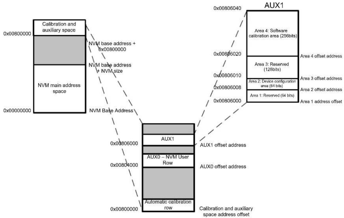
The device calibration data are stored in different sections of the NVM calibration and auxiliary space presented in the following figure.
Figure 9-1. Calibration and Auxiliary Space
flowchart
graph TD
    A["NVM main address space"] -->|NVM base address + NVM size| B["AUX1"]
    A -->|NVM base address + NVM size| C["AUX0 - NVM User Row"]
    B --> D["Calibration and auxiliary space"]
    C --> E["Automatic calibration row"]
    D --> F["Calibration and auxiliary space address offset"]
    E --> G["Calibration and auxiliary space address offset"]
    H["AUX1"] --> I["Aux1 offset address"]
    H --> J["AUX0 offset address"]
    H --> K["Aux0 - NVM User Row"]
    H --> L["AUX1 offset address"]
    H --> M["Aux0 offset address"]
    H --> N["Aux0 - NVM User Row"]
    O["Area 4: Software calibration area (256bits)"] --> P["Aux1"]
    Q["Area 3: Reserved (128bits)"] --> P
    R["Area 2: Device configuration area (64 bits)"] --> P
    S["Area 1: Reserved (64 bits)"] --> P
    T["Area 1 address offset"] --> P
    U["Area 4 offset address"] --> P
The values from the automatic calibration row are loaded into their respective registers at startup.
The first two 32-bit words of the NVM User Row contain calibration data that are automatically read at device power-on.
The NVM User Row can be read at address 0x804000.
To write the NVM User Row, refer to NVMCTRL - Non-Volatile Memory Controller.
When writing to the user row, the values do not get loaded by other modules on the device until a device Reset occurs.
Table 9-3. NVM User Row Mapping
| Bit Position | Name Usage | |
| 2:0 | BOOTPROT | Used to select one of eight different bootloader sizes. Refer to the “NVMCTRL – Non-Volatile Memory Controller”. Default value = 0x7 except for WLCSP45 that has default value = 0x3.Note:WLCSP27 devices boot ROM is not protected as the bootloader is self-upgradable through the I^2C interface. . |
| 3^(1) | Reserved | Do not modify the value of a reserved bit. Reading a reserved bit has no significance to the user application. |
| 6:4 | EEPROM | Used to select one of eight different EEPROM Emulation sizes. Refer to NVMCTRL – Non-Volatile Memory Controller. Default value = 7. |
| 7^(1) | Reserved | Do not modify the value of a reserved bit. Reading a reserved bit has no significance to the user application. |
| ......continued | ||
| Bit Position | Name Usage | |
| 13:8 | BOD33 Level | BOD33 Threshold Level at power on. Refer to SYSCTRL BOD33 register.Default value = 7 on all package grades except Extended Temperature with compliance to AEC-Q100 which has Default value = 34. |
| 14 | BOD33 Enable | BOD33 Enable at power on . Refer to SYSCTRL BOD33 register. Default value = 1. |
| 16:15 | BOD33 Action | BOD33 Action at power on. Refer to SYSCTRL BOD33 register. Default value = 1. |
| 24:17(1) | Reserved | Do not modify the value of a reserved bit. Reading a reserved bit has no significance to the user application. |
| 25 WDT Enable WDT Enable at power on. Refer to WDT CTRL register.Default value = 0. | ||
| 26 | WDT Always-On | WDT Always-On at power on. Refer to WDT CTRL register.Default value = 0. |
| 30:27 WDT Period WDT Period at power on. Refer to WDT CONFIG register.Default value = 0x0B. | ||
| 34:31 | WDT Window | WDT Window mode time-out at power on. Refer to WDT CONFIG register.Default value = 0x0B. |
| 38:35 | WDT EWOFFSET | WDT Early Warning Interrupt Time Offset at power on. Refer to WDT EWCTRL register.Default value = 0xB. |
| 39 | WDT WEN | WDT Timer Window Mode Enable at power on. Refer to WDT CTRL register. Default value = 0. |
| 40 | BOD33 Hysteresis | BOD33 Hysteresis configuration at power on. Refer to SYSCTRL BOD33 register.Default value = 1. |
| 47:41 | Reserved | Do not modify the value of a reserved bit. Reading a reserved bit has no significance to the user application. |
| 63:48 | LOCK | NVM Region Lock Bits. Refer to NVMCTRL - Non-Volatile Memory Controller.Default value = 0xFFFF. |
Note:
- It is required to preserve the value of a reserved bit while modifying the NVM User Row bits.
Related Links
- NVMCTRL - Nonvolatile Memory Controller
16.8.14. BOD33
17.8.1. CTRL
17.8.2. CONFIG
17.8.3. EWCTRL
32.10.3.1. BOD33
9.5 NVM Software Calibration Area Mapping
The NVM Software Calibration Area contains calibration data that are measured and written during production test. These calibration values should be read by the application software and written back to the corresponding register.
The NVM Software Calibration Area can be read at address 0x806020.
The NVM Software Calibration Area can not be written.
Table 9-4. NVM Software Calibration Area Mapping
| Bit Position | Name | Description |
| 26:0 | Reserved | |
| 34:27 | ADC LINEARITY | ADC Linearity Calibration. Should be written to ADC CALIB register. |
| 37:35 | ADC BIASCAL | ADC Bias Calibration. Should be written to ADC CALIB register. |
| 44:38 | OSC32K CAL | OSC32KCalibration. Should be written to SYSCTRL OSC32K register. |
| ......continued | ||
| Bit Position Name Description | ||
| 57:45 Reserved | ||
| 63:58 DFLL48M COARSE CAL 1) | DFLL48M Coarse calibration value, should be written to SYSCTRL DFLLVAL register. | |
| 73:64 DFLL48M fine CAL (1) | DFLL48M Fine calibration value, should be written to SYSCTRL.DFLLVAL register. | |
| 127:74 Reserved | ||
Note: 1. Not applicable for die rev. C and previous.
Related Links
28.8.19. CALIB
16.8.7. OSC32K
16.8.11. DFLLVAL
9.6 Serial Number
Each device has a unique 128-bit serial number which is a concatenation of four 32-bit words contained at the following addresses:
Word 0: 0x0080A00C
Word 1: 0x0080A040
Word 2: 0x0080A044
Word 3: 0x0080A048
The uniqueness of the serial number is guaranteed only when using all 128 bits.
10. Processor And Architecture
10.1 Cortex M0+ Processor
The SAM D20 implements the ARM ^® Cortex ^® -M0+ processor, based on the ARMv6 Architecture and Thumb ^® -2 ISA. The Cortex M0+ is 100% instruction set compatible with its predecessor, the Cortex-M0 core, and upward compatible to Cortex-M3 and M4 cores. The ARM Cortex-M0+ implemented is revision r0p1. For more information refer to www.arm.com.
10.1.1 Cortex M0+ Configuration
Table 10-1. Cortex M0+ Configuration
| Features Configurable option Device configuration | ||
| Interrupts External interrupts 0-32 28 | ||
| Data endianness Little-endian or big-endian Little-endian | ||
| SysTick timer Present or absent Present | ||
| Number of watchpoint comparators 0, 1, 2 2 | ||
| Number of breakpoint comparators 0, 1, 2, 3, 4 | 4 | |
| Halting debug support | Present or absent Present | |
| Multiplier | Fast or small | Fast (single cycle) |
| Single-cycle I/O port | Present or absent Present | |
| Wake-up interrupt controller | Supported or not supported | Not supported |
| Vector Table Offset Register | Present or absent Present | |
| Unprivileged/Privileged support | Present or absent Absent | (1) |
| Memory Protection Unit | Not present or 8-region | Not present |
| Reset all registers | Present or absent Absent | |
| Instruction fetch width | 16-bit only or mostly 32-bit | 32-bit |
Note:
- All software run in Privileged mode only.
The ARM Cortex-M0+ core has the following two bus interfaces:
- Single 32-bit AMBA-3 AHB-Lite system interface that provides connections to peripherals and all system memory, which includes Flash and RAM.
- Single 32-bit I/O port bus interfacing to the PORT with 1-cycle loads and stores.
10.1.2 Cortex-MO+ Peripherals
• System Control Space (SCS)
- The processor provides debug through registers in the SCS. Refer to the Cortex-M0+ Technical Reference Manual for details (www.arm.com).
• System Timer (SysTick)
- The System Timer is a 24-bit timer clocked by CLK_CPU that extends the functionality of both the processor and the NVIC. Refer to the Cortex-M0+ Technical Reference Manual for details (www.arm.com).
- Nested Vectored Interrupt Controller (NVIC)
- External interrupt signals connect to the NVIC, and the NVIC prioritizes the interrupts. Software can set the priority of each interrupt. The NVIC and the Cortex-M0+ processor core are closely coupled, providing low latency interrupt processing and efficient processing of late arriving interrupts. Refer to 10.2. Nested Vector Interrupt Controller and the Cortex-M0+ Technical Reference Manual for details (www.arm.com).
• System Control Block (SCB)
- The System Control Block provides system implementation information, and system control. This includes configuration, control, and reporting of the system exceptions. Refer to the Cortex-M0+ Devices Generic User Guide for details (www.arm.com).
10.1.3 Cortex-M0+ Address Map
Table 10-2. Cortex-M0+ Address Map
| Address Peripheral | |
| 0xE000E000 System Control Space (SCS) | |
| 0xE000E010 System Timer (SysTick) | |
| 0xE000E100 Nested Vectored Interrupt Controller (NVIC) | |
| 0xE000ED00 System Control Block (SCB) | |
10.1.4 I/O Interface
10.1.4.1 Overview
Because accesses to the AMBA ^® AHB-Lite ^™ and the single cycle I/O interface can be made concurrently, the Cortex-M0+ processor can fetch the next instructions while accessing the I/Os. This enables single cycle I/O accesses to be sustained for as long as needed. Refer to CPU Local Bus for more information.
Related Links
21.5.9. CPU Local Bus
10.1.4.2 Description
Direct access to PORT registers.
10.2 Nested Vector Interrupt Controller
10.2.1 Overview
The Nested Vectored Interrupt Controller (NVIC) in the SAM D20 supports 32 interrupt lines with four different priority levels. For more details, refer to the Cortex-M0+ Technical Reference Manual (www.arm.com).
10.2.2 Interrupt Line Mapping
Each of the 28 interrupt lines is connected to one peripheral instance, as shown in the table below. Each peripheral can have one or more interrupt flags, located in the peripheral's Interrupt Flag Status and Clear (INTFLAG) register. The interrupt flag is set when the interrupt condition occurs. Each interrupt in the peripheral can be individually enabled by writing a one to the corresponding bit in the peripheral's Interrupt Enable Set (INTENSET) register, and disabled by writing a one to the corresponding bit in the peripheral's Interrupt Enable Clear (INTENCLR) register. An interrupt request is generated from the peripheral when the interrupt flag is set and the corresponding interrupt is enabled. The interrupt requests for one peripheral are ORed together on system level, generating one interrupt request for each peripheral. An interrupt request will set the corresponding interrupt pending bit in the NVIC interrupt pending registers (SETPEND/CLRPEND bits in ISPR/ICPR). For the NVIC to activate the interrupt, it must be enabled in the NVIC interrupt enable register (SETENA/CLRENA bits in ISER/ICER). The NVIC interrupt priority registers IPR0-IPR7 provide a priority field for each interrupt.
Table 10-3. Interrupt Line Mapping
| Peripheral Source NVIC Line | |
| EIC NMI - External Interrupt Controller NMI | |
| PM - Power Manager 0 | |
| ......continued | |
| Peripheral Source NVIC Line | |
| SYSCTRL - System Control 1 | |
| WDT - Watchdog Timer 2 | |
| RTC - Real Time Counter 3 | |
| EIC - External Interrupt Controller 4 | |
| NVMCTRL - Non-Volatile Memory Controller 5 | |
| EVSYS - Event System 6 | |
| SERCOM0 - Serial Communication Interface 0 7 | |
| SERCOM1 - Serial Communication Interface 1 8 | |
| SERCOM2 - Serial Communication Interface 2 9 | |
| SERCOM3 - Serial Communication Interface 3 10 | |
| SERCOM4 - Serial Communication Interface 4 11 | |
| SERCOM5 - Serial Communication Interface 5 12 | |
| TC0 - Timer Counter 0 13 | |
| TC1 - Timer Counter 1 14 | |
| TC2 - Timer Counter 2 15 | |
| TC3 - Timer Counter 3 16 | |
| TC4 - Timer Counter 4 17 | |
| TC5 - Timer Counter 5 18 | |
| TC6 - Timer Counter 6 19 | |
| TC7 - Timer Counter 7 20 | |
| ADC - Analog-to-Digital Converter 21 | |
| AC - Analog Comparator 22 | |
| DAC - Digital-to-Analog Converter 23 | |
| PTC - Peripheral Touch Controller 24 | |
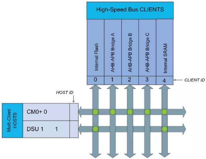
10.3 High-Speed Bus System
10.3.1 Features
High-Speed Bus Matrix has the following features:
• Symmetric crossbar bus switch implementation
- Allows concurrent accesses from different hosts to different clients
- 32-bit data bus
• Operation at a one-to-one clock frequency with the bus hosts
10.3.2 Configuration
flowchart
graph TD
    A["Multi-Client HOSTS"] --> B["CM0+ 0"]
    A --> C["DSU 1 1"]
    D["High-Speed Bus CLIENTS"] --> E["Internal Flash 0-4"]
    D --> F["AHB-APB Bridge A 1-2"]
    D --> G["AHB-APB Bridge B 2-3"]
    D --> H["AHB-APB Bridge C 3-4"]
    D --> I["Internal SRAM 4"]
    J["HOST ID"] --> A
    K["CLIENT ID"] --> D
Table 10-4. Bus Matrix Hosts
| Bus Matrix Hosts Host ID | |
| CM0+ - Cortex M0+ Processor 0 | |
| DSU - Device Service Unit 1 |
Table 10-5. Bus Matrix Clients
| Bus Matrix Clients Client ID | |
| Internal Flash Memory 0 | |
| AHB-APB Bridge A 1 | |
| AHB-APB Bridge B 2 | |
| AHB-APB Bridge C 3 | |
| Internal SRAM 4 |
Table 10-6. SRAM Port Connection
| SRAM Port Connection Port ID Connection Type | |||
| CM0+ - Cortex M0+ Processor 4 | Bus Matrix | ||
| DSU - Device Service Unit | 6 | Bus Matrix | |
10.4 AHB-APB Bridge
The AHB-APB bridge is an AHB Client, providing an interface between the high-speed AHB domain and the low-power APB domain. It is used to provide access to the programmable control registers of peripherals (see Product Mapping).
AHB-APB bridge is based on AMBA APB Protocol Specification V2.0 (ref. as APB4) including:
- Wait state support
- Error reporting
• Transaction protection - Sparse data transfer (byte, half-word and word)
Additional enhancements:
- Address and data cycles merged into a single cycle
- Sparse data transfer also apply to read access
to operate the AHB-APB bridge, the clock (CLK_HPBx_AHB) must be enabled. See PM - Power Manager for details.
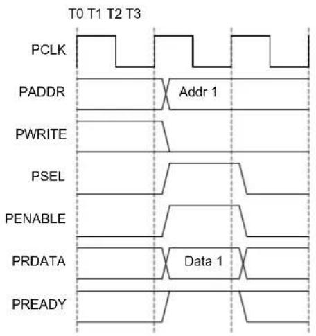
Figure 10-1. APB Write Access.
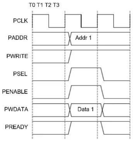
text_image
T0 T1 T2 T3 PCLK PADDR Addr 1 PWRITE PSEL PENABLE PWDATA Data 1 PREADY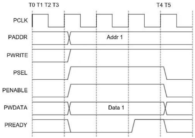
text_image
T0 T1 T2 T3 PCLK PADDR Addr 1 PWRITE PSEL PENABLE PWDATA Data 1 PREADY T4 T5Wait statesNo wait states
Figure 10-2. APB Read Access.
text_image
T0 T1 T2 T3 PCLK PADDR Addr 1 PWRITE PSEL PENABLE PRDATA Data 1 PREADY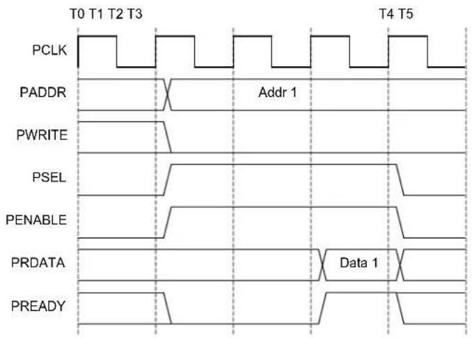
text_image
T0 T1 T2 T3 PCLK PADDR Addr 1 PWRITE PSEL PENABLE PRDATA Data 1 PREADY T4 T5Wait statesNo wait states
Related Links
- Power Manager (PM)
- Product Mapping
10.5 PAC - Peripheral Access Controller
10.5.1 Overview
One PAC is associated with each AHB-APB bridge and the PAC can provide write protection for registers of each peripheral connected on the same bridge.
The PAC peripheral bus clock (CLK_PACx_APB) can be enabled and disabled in the Power Manager. CLK_PAC0_APB and CLK_PAC1_APB are enabled are reset. CLK_PAC2_APB is disabled at reset. Refer to PM - Power Manager for details. The PAC will continue to operate in any Sleep mode where the selected clock source is running. Write-protection does not apply for debugger access. When the debugger makes an access to a peripheral, write-protection is ignored so that the debugger can update the register.
Write-protect registers allow the user to disable a selected peripheral's write-protection without doing a read-modify-write operation. These registers are mapped into two I/O memory locations, one for clearing and one for setting the register bits. Writing a one to a bit in the Write Protect Clear register (WPCLR) will clear the corresponding bit in both registers (WPCLR and WPSET) and disable the write-protection for the corresponding peripheral, while writing a one to a bit in the Write Protect Set (WPSET) register will set the corresponding bit in both registers (WPCLR and WPSET) and enable the write-protection for the corresponding peripheral. Both registers (WPCLR and WPSET) will return the same value when read.
If a peripheral is write-protected, and if a write access is performed, data will not be written, and the peripheral will return an access error (CPU exception).
The PAC also offers a safety feature for correct program execution, with a CPU exception generated on double write-protection or double unprotection of a peripheral. If a peripheral n is write-protected and a write to one in WPSET[n] is detected, the PAC returns an error. This can be used to ensure that the application follows the intended program flow by always following a write-protect with an unprotect, and vice versa. However, in applications where a write-protected peripheral is used in several contexts, for example, interrupts, care should be taken so that either the interrupt can not happen while the main application or other interrupt levels manipulate the write-protection status, or when the interrupt handler needs to unprotect the peripheral, based on the current protection status, by reading WPSET.
Related Links
- Power Manager (PM)
10.6 Register Description
Atomic 8-, 16- and 32-bit accesses are supported. In addition, the 8-bit quarters and 16-bit halves of a 32-bit register, and the 8-bit halves of a 16-bit register can be accessed directly. Refer to the Product Mapping for PAC locations.
Related Links
- Product Mapping
10.6.1 PACO Register Description
10.6.1.1 Write Protect Clear
Name: WPCLR
Offset: 0x00
Reset: 0x000000
Property: -
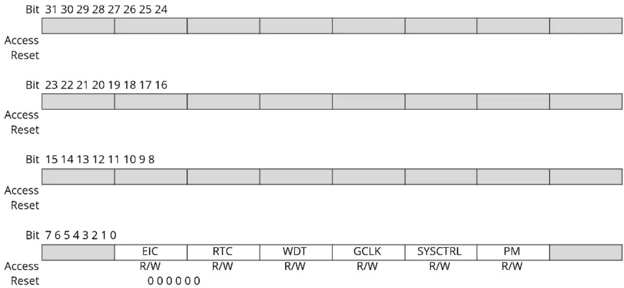
text_image
Bit 31 30 29 28 27 26 25 24 Access Reset Bit 23 22 21 20 19 18 17 16 Access Reset Bit 15 14 13 12 11 10 9 8 Access Reset Bit 7 6 5 4 3 2 1 0 Access Reset EIC RTC WDT GCLK SYSCTRL PM R/W R/W R/W R/W R/W R/W 0 0 0 0 0 0Bit 6 - EIC
Writing a zero to these bits has no effect.
Writing a one to these bits will clear the Write Protect bit for the corresponding peripherals.
| Value | Description |
| 0 | Write-protection is disabled. |
| 1 | Write-protection is enabled. |
Bit 5 - RTC
Writing a zero to these bits has no effect.
Writing a one to these bits will clear the Write Protect bit for the corresponding peripherals.
| Value | Description |
| 0 | Write-protection is disabled. |
| 1 | Write-protection is enabled. |
Bit 4 - WDT
Writing a zero to these bits has no effect.
Writing a one to these bits will clear the Write Protect bit for the corresponding peripherals.
| Value | Description |
| 0 | Write-protection is disabled. |
| 1 | Write-protection is enabled. |
Bit 3 - GCLK
Writing a zero to these bits has no effect.
Writing a one to these bits will clear the Write Protect bit for the corresponding peripherals.
| Value | Description |
| 0 | Write-protection is disabled. |
| 1 | Write-protection is enabled. |
Bit 2 - SYSCTRL
Writing a zero to these bits has no effect.
Writing a one to these bits will clear the Write Protect bit for the corresponding peripherals.
| Value Description | |
| 0 | Write-protection is disabled. |
| 1 | Write-protection is enabled. |
Bit 1 - PM
Writing a zero to these bits has no effect.
Writing a one to these bits will clear the Write Protect bit for the corresponding peripherals.
| Value Description | |
| 0 | Write-protection is disabled. |
| 1 | Write-protection is enabled. |
10.6.1.2 Write Protect Set
Name: WPSET
Offset: 0x04
Reset: 0x000000
Property: -

text_image
Bit 31 30 29 28 27 26 25 24 Access Reset Bit 23 22 21 20 19 18 17 16 Access Reset Bit 15 14 13 12 11 10 9 8 Access Reset Bit 7 6 5 4 3 2 1 0 Access Reset EIC RTC WDT GCLK SYSCTRL PM R/W R/W R/W R/W R/W R/W 0 0 0 0 0 0Bit 6 - EIC
Writing a zero to these bits has no effect.
Writing a one to these bits will clear the Write Protect bit for the corresponding peripherals.
| Value | Description |
| 0 | Write-protection is disabled. |
| 1 | Write-protection is enabled. |
Bit 5 - RTC
Writing a zero to these bits has no effect.
Writing a one to these bits will clear the Write Protect bit for the corresponding peripherals.
| Value | Description |
| 0 | Write-protection is disabled. |
| 1 | Write-protection is enabled. |
Bit 4 - WDT
Writing a zero to these bits has no effect.
Writing a one to these bits will clear the Write Protect bit for the corresponding peripherals.
| Value | Description |
| 0 | Write-protection is disabled. |
| 1 | Write-protection is enabled. |
Bit 3 - GCLK
Writing a zero to these bits has no effect.
Writing a one to these bits will clear the Write Protect bit for the corresponding peripherals.
| Value | Description |
| 0 | Write-protection is disabled. |
| 1 | Write-protection is enabled. |
Bit 2 - SYSCTRL
Writing a zero to these bits has no effect.
Writing a one to these bits will clear the Write Protect bit for the corresponding peripherals.
| Value Description | |
| 0 | Write-protection is disabled. |
| 1 | Write-protection is enabled. |
Bit 1 - PM
Writing a zero to these bits has no effect.
Writing a one to these bits will clear the Write Protect bit for the corresponding peripherals.
| Value Description | |
| 0 | Write-protection is disabled. |
| 1 | Write-protection is enabled. |
10.6.2 PAC1 Register Description
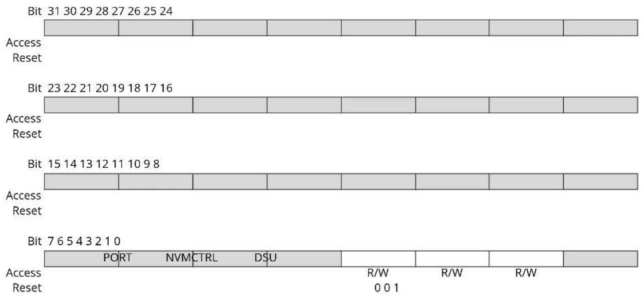
10.6.2.1 Write Protect Clear
Name: WPCLR
Offset: 0x00
Reset: 0x000002
Property: -

text_image
Bit 31 30 29 28 27 26 25 24 Access Reset Bit 23 22 21 20 19 18 17 16 Access Reset Bit 15 14 13 12 11 10 9 8 Access Reset Bit 7 6 5 4 3 2 1 0 PORT NVM CTRL DSU R/W R/W R/W Access Reset 0 0 1Bit 3 - PORT
Writing a zero to these bits has no effect.
Writing a one to these bits will clear the Write Protect bit for the corresponding peripherals.
| Value | Description |
| 0 | Write-protection is disabled. |
| 1 | Write-protection is enabled. |
Bit 2 - NVMCTRL
Writing a zero to these bits has no effect.
Writing a one to these bits will clear the Write Protect bit for the corresponding peripherals.
| Value | Description |
| 0 | Write-protection is disabled. |
| 1 | Write-protection is enabled. |
Bit 1 - DSU
Writing a zero to these bits has no effect.
Writing a one to these bits will clear the Write Protect bit for the corresponding peripherals.
| Value | Description |
| 0 | Write-protection is disabled. |
| 1 | Write-protection is enabled. |
10.6.2.2 Write Protect Set
Name: WPSET
Offset: 0x04
Reset: 0x000002
Property: -
text_image
Bit 31 30 29 28 27 26 25 24 Access Reset Bit 23 22 21 20 19 18 17 16 Access Reset Bit 15 14 13 12 11 10 9 8 Access Reset Bit 7 6 5 4 3 2 1 0 PORT NVM CTRL DSU R/W R/W R/W Access Reset 0 0 1Bit 3 - PORT
Writing a zero to these bits has no effect.
Writing a one to these bits will clear the Write Protect bit for the corresponding peripherals.
| Value | Description |
| 0 | Write-protection is disabled. |
| 1 | Write-protection is enabled. |
Bit 2 - NVMCTRL
Writing a zero to these bits has no effect.
Writing a one to these bits will clear the Write Protect bit for the corresponding peripherals.
| Value | Description |
| 0 | Write-protection is disabled. |
| 1 | Write-protection is enabled. |
Bit 1 - DSU
Writing a zero to these bits has no effect.
Writing a one to these bits will clear the Write Protect bit for the corresponding peripherals.
| Value | Description |
| 0 | Write-protection is disabled. |
| 1 | Write-protection is enabled. |
10.6.3 PAC2 Register Description
10.6.3.1 Write Protect Clear
Name: WPCLR
Offset: 0x00
Reset: 0x00800000
Property: -
Bit 31 30 29 28 27 26 25 24
| Access Reset |
Bit 23 22 21 20 19 18 17 16
| PTC DAC AC ADC | |||||||
| Access Reset | R/W R/W R/W R/W | ||||||
| 0 | 0 | 0 | 0 | ||||
| Bit 15 14 13 12 11 10 | 9 | 8 | ||||||
| TC7 | TC6 | TC5 | TC4 | TC3 | TC2 | TC1 | TC0 | |
| Access | R/W R/W | R/W R/W | R/W R/W | R/W R/W | R/W | |||
| Reset | 0 | 0 | 0 | 0 | 0 | 0 | 0 | 0 |
| Bit | 7 | 6 | 5 | 4 | 3 | 2 | 1 | 0 |
| SERCOM[5:0] | EVSYS | |||||||
| Access | R/W R/W | R/W R/W | R/W R/W | R/W R/W | ||||
| Reset | 0 | 0 | 0 | 0 | 0 | 0 | 0 | |
Bit 19 - PTC
Writing a zero to these bits has no effect.
Writing a one to these bits will clear the Write Protect bit for the corresponding peripherals.
| Value | Description |
| 0 | Write-protection is disabled. |
| 1 | Write-protection is enabled. |
Bit 18 - DAC
Writing a zero to these bits has no effect.
Writing a one to these bits will clear the Write Protect bit for the corresponding peripherals.
| Value | Description |
| 0 | Write-protection is disabled. |
| 1 | Write-protection is enabled. |
Bit 17 - AC
Writing a zero to these bits has no effect.
Writing a one to these bits will clear the Write Protect bit for the corresponding peripherals.
| Value | Description |
| 0 | Write-protection is disabled. |
| 1 | Write-protection is enabled. |
Bit 16 - ADC
Writing a zero to these bits has no effect.
Writing a one to these bits will clear the Write Protect bit for the corresponding peripherals.
| Value | Description |
| 0 | Write-protection is disabled. |
| 1 | Write-protection is enabled. |
Bits 8, 9, 10, 11, 12, 13, 14, 15 - TC
Writing a zero to these bits has no effect.
Writing a one to these bits will clear the Write Protect bit for the corresponding peripherals.
| Value Description | |
| 0 | Write-protection is disabled. |
| 1 | Write-protection is enabled. |
Bits 7:2 - SERCOM[5:0]
Writing a zero to these bits has no effect.
Writing a one to these bits will clear the Write Protect bit for the corresponding peripherals.
| Value Description | |
| 0 | Write-protection is disabled. |
| 1 | Write-protection is enabled. |
Bit 1 - EVSYS
Writing a zero to these bits has no effect.
Writing a one to these bits will clear the Write Protect bit for the corresponding peripherals.
| Value Description | |
| 0 | Write-protection is disabled. |
| 1 | Write-protection is enabled. |
10.6.3.2 Write Protect Set
Name: WPSET
Offset: 0x04
Reset: 0x00800000
Property: -
Bit 31 30 29 28 27 26 25 24
| Access Reset |
Bit 23 22 21 20 19 18 17 16
| PTC | DAC | AC | ADC | |||||||
| Access Reset | R/W | R/W | R/W | R/W | ||||||
| 0 | 0 | 0 |
| Bit 15 14 13 12 11 10 | 9 | 8 | ||||||
| TC7 | TC6 | TC5 | TC4 | TC3 | TC2 | TC1 | TC0 | |
| Access | R/W R/W | R/W R/W | R/W R/W | R/W R/W | R/W | |||
| Reset | 0 | 0 | 0 | 0 | 0 | 0 | 0 | 0 |
| Bit | 7 | 6 | 5 | 4 | 3 | 2 | 1 | 0 |
| SERCOM5 | SERCOM4 | SERCOM3 | SERCOM2 | SERCOM1 | SERCOM0 | EVSYS | ||
| Access | R/W R/W | R/W R/W | R/W R/W | |||||
| Reset | 0 | 0 | 0 | 0 | 0 | 0 | 0 | |
Bit 19 - PTC
Writing a zero to these bits has no effect.
Writing a one to these bits will clear the Write Protect bit for the corresponding peripherals.
| Value | Description |
| 0 | Write-protection is disabled. |
| 1 | Write-protection is enabled. |
Bit 18 - DAC
Writing a zero to these bits has no effect.
Writing a one to these bits will clear the Write Protect bit for the corresponding peripherals.
| Value | Description |
| 0 | Write-protection is disabled. |
| 1 | Write-protection is enabled. |
Bit 17 - AC
Writing a zero to these bits has no effect.
Writing a one to these bits will clear the Write Protect bit for the corresponding peripherals.
| Value | Description |
| 0 | Write-protection is disabled. |
| 1 | Write-protection is enabled. |
Bit 16 - ADC
Writing a zero to these bits has no effect.
Writing a one to these bits will clear the Write Protect bit for the corresponding peripherals.
| Value | Description |
| 0 | Write-protection is disabled. |
| 1 | Write-protection is enabled. |
Bits 8, 9, 10, 11, 12, 13, 14, 15 - TC
Writing a zero to these bits has no effect.
Writing a one to these bits will clear the Write Protect bit for the corresponding peripherals.
| Value Description | |
| 0 | Write-protection is disabled. |
| 1 | Write-protection is enabled. |
Bits 2, 3, 4, 5, 6, 7 - SERCOM
Writing a zero to these bits has no effect.
Writing a one to these bits will clear the Write Protect bit for the corresponding peripherals.
| Value Description | |
| 0 | Write-protection is disabled. |
| 1 | Write-protection is enabled. |
Bit 1 - EVSYS
Writing a zero to these bits has no effect.
Writing a one to these bits will clear the Write Protect bit for the corresponding peripherals.
| Value Description | |
| 0 | Write-protection is disabled. |
| 1 | Write-protection is enabled. |
11. Peripherals Configuration Summary
The following table shows an overview of all the peripherals in the device. The IRQ Line column shows the interrupt mapping, as described in "Nested Vector Interrupt Controller" on page 30. The AHB and APB clock indexes correspond to the bit in the AHBMASK and APBMASK (x = A, B or C) registers in the Power Manager, while the Enabled at Reset column shows whether the peripheral clock is enabled at reset (Y) or not (N). Refer to the Power Manager AHBMASK, APBAMASK, APBBMASK and APBCMASK registers for details. The Generic Clock Index column corresponds to the value of the Generic Clock Selection ID bits in the Generic Clock Control register (CLKCTRL.ID) in the Generic Clock Controller. Refer to the GCLK CLKCTRL register description for details. The PAC Index column corresponds to the bit in the PACi (i = 0, 1 or 2) registers, while the Prot at Reset column shows whether the peripheral is protected at reset (Y) or not (N). Refer to "PAC – Peripheral Access Controller" for details. The numbers in the Events User column correspond to the value of the User Multiplexer Selection bits in the User Multiplexer register (USER.USER) in the Event System. See the USER register description and Table 22-6 for details. The numbers in the Events Generator column correspond to the value of the Event Generator bits in the Channel register (CHANNEL.EVGEN) in the Event System. See the CHANNEL register description and Table 22-3 for details.
Table 11-1. Peripherals Configuration Summary
| Peripheral Name | Base Address | IRQ Line A | HB Clock APB Clock | Generic Clock PAC Events | ||||||||
| Index | Enabled at Reset | Index | Enabled at Reset | Index Index Prot at | Reset | User Generator | SleepWalking | |||||
| AHB-APBBridge A | 0x40000000 | Y | ||||||||||
| PAC0 0x40000000 | 0 Y | |||||||||||
| PM | 0x40000400 | 0 | 1 | Y | 1 | N | Y | |||||
| SYSCTRL | 0x40000800 | 1 | 2 | Y | 0: DFLL48M reference | 2 N | Y | |||||
| GCLK 0x40000C00 | 3 Y | 3 N | Y | |||||||||
| WDT | 0x40001000 | 2 | 4 | Y | 1 | 4 | N | |||||
| RTC | 0x40001400 | 3 | 5 | Y | 2 | 5 | N | 1: CMP0/ALARM02: CMP13: OVF4-11: PER0-7 | Y | |||
| EIC 0x40001800 | NMI,4 | 6 Y | 3 | 6 N | 12-27: EXTINT0-15 Y | |||||||
| AHB-APBBridge B | 0x41000000 | 1 Y | ||||||||||
| PAC1 0x41000000 | 0 Y | |||||||||||
| DSU | 0x41002000 | 3 Y | 1 Y | 1 Y | ||||||||
| NVMCTRL | 0x41004000 | 5 | 4 | Y | 2 | Y | 2 | N | ||||
| PORT | 0x41004400 | 3 Y | 3 N | |||||||||
| AHB-APBBridge C | 0x42000000 | 2 Y | ||||||||||
| PAC2 0x42000000 | 0 N | |||||||||||
| EVSYS | 0x42000400 | 6 | 1 | N | 4-11: one per CHANNEL | 1 N | Y | |||||
| SERCOM0 | 0x42000800 | 7 | 2 | N | 13: CORE12:SLOW | 2 N | Y | |||||
| SERCOM1 | 0x42000C00 | 8 | 3 | N | 14:CORE12:SLOW | 3 N | Y | |||||
| Peripheral Name | Base Address | IRQ Line A | HB Clock APB Clock | Generic Clock PAC Events | ||||||||
| Index | Enabled at Reset | Index | Enabled at Reset | Index Index Prot at | Reset | User Generator | SleepWalking | |||||
| SERCOM2 0x42001 | 1000 9 4 N 15:CORE | 12: SLOW | 4 N Y | |||||||||
| SERCOM3 0x42001 | 400 10 5 N 16:CORE | 12: SLOW | 5 N Y | |||||||||
| SERCOM4 0x42001 | 800 11 6 N 17:CORE | 12: SLOW | 6 N Y | |||||||||
| SERCOM5 0x42001 | C00 12 7 N 18:CORE | 12: SLOW | 7 N Y | |||||||||
| TC0 | 0x42002000 13 8 N 19 | 8 N 0: TC 28: OVF | 29-30: MC0-1 | Y | ||||||||
| TC1 | 0x42002400 14 9 N 19 | 9 N 1: TC 31: OVF | 32-33: MC0-1 | Y | ||||||||
| TC2 | 0x42002800 | 15 | 10 | N | 20 | 10 | N | 2: TC | 34: OVF35-36: MC0-1 | Y | ||
| TC3 | 0x42002C00 | 16 | 11 | N | 20 | 11 | N | 3: TC | 37: OVF38-39: MC0-1 | Y | ||
| TC4 | 0x42003000 | 17 | 12 | N | 21 | 12 | N | 4: TC | 40: OVF41-42: MC0-1 | Y | ||
| TC5 | 0x42003400 | 18 | 13 | N | 21 | 13 | N | 5: TC | 43: OVF44-45: MC0-1 | Y | ||
| TC6 | 0x42003800 | 19 | 14 | N | 22 | 14 | N | 6: TC | 46: OVF47-48: MC0-1 | Y | ||
| TC7 | 0x42003C00 | 20 | 15 | N | 22 | 15 | N | 7: TC | 49: OVF50-51: MC0-1 | Y | ||
| ADC | 0x42004000 | 21 | 16 | Y | 23 | 16 | N | 8: START9: SYNC | 52: RESRDY53: WINMON | Y | ||
| AC | 0x42004400 22 17 N 24: DIG | 25: ANA | 17 | N 10-11: | 54-55: COMPO-156: WINO | 54-55: COMPO-156: WINO | Y | |||||
| DAC | 0x42004800 | 23 | 18 | N | 26 | 18 | N | 12: START | 57: EMPTY | Y | ||
| PTC | 0x42004C00 | 24 | 19 | N | 27 | 19 | N | 13: STCONV | 58: EOC59:WCOMP | |||
12. DSU - Device Service Unit
12.1 Overview
The Device Service Unit (DSU) provides a means of detecting debugger probes. It enables the ARM Debug Access Port (DAP) to have control over multiplexed debug pads and CPU reset. The DSU also provides system-level services to debug adapters in an ARM debug system. It implements a CoreSight Debug ROM that provides device identification as well as identification of other debug components within the system. Hence, it complies with the ARM Peripheral Identification specification. The DSU also provides system services to applications that need memory testing, as required for IEC60730 Class B compliance, for example. The DSU can be accessed simultaneously by a debugger and the CPU, as it is connected on the High-Speed Bus Matrix. For security reasons, some of the DSU features will be limited or unavailable when the device is protected by the NVMCTRL security bit.
Related Links
- NVMCTRL - Nonvolatile Memory Controller
20.6.6. Security Bit
12.2 Features
• CPU reset extension
- Debugger probe detection (Cold- and Hot-Plugging)
- Chip-Erase command and status
- 32-bit cyclic redundancy check (CRC32) of any memory accessible through the bus matrix
• ARM ^® CoreSight ^TM compliant device identification
- Two debug communications channels
- Debug access port security filter
- Onboard memory built-in self-test (MBIST)
12.3 Block Diagram
Figure 12-1. DSU Block Diagram
flowchart
```mermaid
graph TD
    SWCLK --> RESET
    RESET --> DAP
    DAP --> AHB-AP
    AHB-AP --> PORT
    PORT --> SWDIO
    DAP --> DAP_SECURITY_FILTER
    DAP --> DAP_SECURITY_FILTER
    DAP --> CORESIGHT_ROM
    DAP --> CORESIGHT_ROM
    DAP --> CORESIGHT_ROM
    DAP --> CORESIGHT_ROM
    DAP --> CORESIGHT_ROM
    DAP --> CORESIGHT_ROM
    DAP --> CORESIGHT_ROM
    CPU --> DBG
    DBG --> M["HIGH-SPEED BUS MATRIX"]
    CPU --> S["NVMCTRL"]
    CPU --> M
    CPU --> M
    CPU --> M
    CPU --> M
    CPU --> M
    CPU --> M
    CPU --> M
    CPU --> M
    CPU --> M
    CPU --> M
    CPU --> M
    CPU --> M
    CPU --> M
    CPU --> M
    CPU --> M
    CPU --> M
    CPU --> M
    CPU --> M
    CPU --> M
    CPU --> M
    CPU --> M

    subgraph DSU
        DAP --> AHB-AP
        DAP --> CORESIGHT_ROM
        DAP --> CORESIGHT_ROM
        DAP --> CORESIGHT_ROM
        DAP --> CORESIGHT_ROM
        DAP --> CORESIGHT_ROM
        DAP --> CORESIGHT_ROM
        DAP --> CORESIGHT_ROM
        DAP --> CORESIGHT_ROM
        DAP --> CORESIGHT_ROM
        DAP --> CORESIGHT_ROM
        DAP --> CORESIGHT_ROM
        DAP --> CORESIGHT_ROM
12.4 Signal Description
The DSU uses three signals to function.
| Signal Name Type Description | ||
| RESET Digital Input External reset | ||
| SWCLK Digital Input SW clock | ||
| SWDIO Digital I/O SW bidirectional data pin |
Related Links
- I/O Multiplexing and Considerations
12.5 Product Dependencies
In order to use this peripheral, other parts of the system must be configured correctly, as described below.
12.5.1 I/O Lines
The SWCLK pin is by default assigned to the DSU module to allow debugger probe detection and to stretch the CPU reset phase. For more information, refer to 12.6.3. Debugger Probe Detection. The Hot-Plugging feature depends on the PORT configuration. If the SWCLK pin function is changed in the PORT or if the PORT_MUX is disabled, the Hot-Plugging feature is disabled until a power-reset or an external reset is performed.
12.5.2 Power Management
The DSU will continue to operate in Idle mode.
Related Links
- Power Manager (PM)
12.5.3 Clocks
The DSU bus clocks (CLK_DSU_APB and CLK_DSU_AHB) can be enabled and disabled by the Power Manager. Refer to PM - Power Manager
Related Links
- Power Manager (PM)
12.5.4 Interrupts
Not applicable.
12.5.5 Events
Not applicable.
12.5.6 Register Access Protection
Registers with write-access can be optionally write-protected by the Peripheral Access Controller (PAC), except for the following:
- Debug Communication Channel 0 register (DCC0)
- Debug Communication Channel 1 register (DCC1)
Note: Optional write-protection is indicated by the "PAC Write-Protection" property in the register description.
Write-protection does not apply for accesses through an external debugger.
Related Links
10.5. PAC - Peripheral Access Controller
12.5.7 Analog Connections
Not applicable.
12.6 Debug Operation
12.6.1 Principle of Operation
The DSU provides basic services to allow on-chip debug using the ARM Debug Access Port and the ARM processor debug resources:
- CPU reset extension
- Debugger probe detection
For more details on the ARM debug components, refer to the ARM Debug Interface v5 Architecture Specification.
12.6.2 CPU Reset Extension
"CPU reset extension" refers to the extension of the reset phase of the CPU core after the external reset is released. This ensures that the CPU is not executing code at startup while a debugger is connects to the system. The debugger is detected on a RESET release event when SWCLK is low. At startup, SWCLK is internally pulled up to avoid false detection of a debugger if the SWCLK pin is left unconnected. When the CPU is held in the reset extension phase, the CPU Reset Extension bit of the Status A register (STATUS.ACRSTEXT) is set. To release the CPU, write a '1' to STATUSA.CRSTEXT. STATUSA.CRSTEXT will then be set to '0'. Writing a '0' to STATUSA.CRSTEXT has no effect. For security reasons, it is not possible to release the CPU reset extension when the device is protected by the NVMCTRL security bit. Trying to do so sets the Protection Error bit (PERR) of the Status A register (STATUS.A.PERR).
Figure 12-2. Typical CPU Reset Extension Set and Clear Timing Diagram
text_image
SWCLK RESET DSU CRSTEXT Clear CPU reset extension CPU_STATE reset runningRelated Links
- NVMCTRL - Nonvolatile Memory Controller
20.6.6. Security Bit
12.6.3 Debugger Probe Detection
12.6.3.1 Cold Plugging
Cold-Plugging is the detection of a debugger when the system is in reset. Cold-Plugging is detected when the CPU reset extension is requested, as described above.
12.6.3.2 Hot Plugging
Hot-Plugging is the detection of a debugger probe when the system is not in reset. Hot-Plugging is not possible under reset because the detector is reset when POR or RESET are asserted. Hot-Plugging is active when a SWCLK falling edge is detected. The SWCLK pad is multiplexed with other functions and the user must ensure that its default function is assigned to the debug system. If the SWCLK function is changed, the Hot-Plugging feature is disabled until a power-reset or external reset occurs. Availability of the Hot-Plugging feature can be read from the Hot-Plugging Enable bit of the Status B register (STATUSB.HPE).
Figure 12-3. Hot-Plugging Detection Timing Diagram
text_image
SWCLK RESET CPU_STATE reset running Hot-PluggingThe presence of a debugger probe is detected when either Hot-Plugging or Cold-Plugging is detected. Once detected, the Debugger Present bit of the Status B register (STATUSB.DBGPRES) is set. For security reasons, Hot-Plugging is not available when the device is protected by the NVMCTRL security bit.
This detection requires that pads are correctly powered. Thus, at cold startup, this detection cannot be done until POR is released. If the device is protected, Cold-Plugging is the only way to detect a debugger probe, and so the external reset timing must be longer than the POR timing. If external reset is deasserted before POR release, the user must retry the procedure above until it gets connected to the device.
Related Links
- NVMCTRL - Nonvolatile Memory Controller
20.6.6. Security Bit
12.7 Chip Erase
Chip-Erase consists of removing all sensitive information stored in the chip and clearing the NVMCTRL security bit. Therefore, all volatile memories and the Flash memory (including the EEPROM Emulation area) will be erased. The Flash auxiliary rows, including the user row, will not be erased.
When the device is protected, the debugger must first reset the device in order to be detected. This ensures that internal registers are reset after the protected state is removed. The Chip-Erase operation is triggered by writing a '1' to the Chip-Erase bit in the Control register (CTRL.CE). This command will be discarded if the DSU is protected by the Peripheral Access Controller (PAC). Once issued, the module clears volatile memories prior to erasing the Flash array. To ensure that the Chip-Erase operation is completed, check the Done bit of the Status A register (STATUSA.DONE).
The Chip-Erase operation depends on clocks and power management features that can be altered by the CPU. For that reason, it is recommended to issue a Chip-Erase after a Cold-Plugging procedure to ensure that the device is in a known and safe state.
The recommended sequence is as follows:
- Issue the Cold-Plugging procedure (refer to 12.6.3.1. Cold Plugging). The device then:
a. Detects the debugger probe.
b. Holds the CPU in reset.
- Issue the Chip-Erase command by writing a '1' to CTRL.CE. The device then:
a. Clears the system volatile memories.
b. Erases the whole Flash array (including the EEPROM Emulation area, not including auxiliary rows).
c. Erases the lock row, removing the NVMCTRL security bit protection.
-
Check for completion by polling STATUSA.DONE (read as '1' when completed).
-
Reset the device to let the NVMCTRL update the fuses.
12.8 Programming
Programming the Flash or RAM memories is only possible when the device is not protected by the NVMCTRL security bit. The programming procedure is as follows:
- At power up, RESET is driven low by a debugger. The on-chip regulator holds the system in a POR state until the input supply is above the POR threshold (refer to Powe-On Reset (POR) characteristics). The system continues to be held in this static state until the internally regulated supplies have reached a safe operating state.
- The PM starts, clocks are switched to the slow clock (Core Clock, System Clock, Flash Clock and any Bus Clocks that do not have clock gate control). Internal resets are maintained due to the external reset.
- The debugger maintains a low level on SWCLK. RESET is released, resulting in a debugger Cold-Plugging procedure.
- The debugger generates a clock signal on the SWCLK pin, the Debug Access Port (DAP) receives a clock.
- The CPU remains in Reset due to the Cold-Plugging procedure; meanwhile, the rest of the system is released.
- A Chip-Erase is issued to ensure that the Flash is fully erased prior to programming.
- Programming is available through the AHB-AP.
- After the operation is completed, the chip can be restarted either by asserting RESET or toggling power. Make sure that the SWCLK pin is high when releasing RESET to prevent extending the CPU reset.
Related Links
- NVMCTRL - Nonvolatile Memory Controller
20.6.6. Security Bit
- Electrical Characteristics at 85°C
32.10.2. Power-On Reset (POR) Characteristics
12.9 Intellectual Property Protection
Intellectual property protection consists of restricting access to internal memories from external tools when the device is protected, and this is accomplished by setting the NVMCTRL security bit. This protected state can be removed by issuing a Chip-Erase (refer to 12.7. Chip Erase). When the device is protected, read/write accesses using the AHB-AP are limited to the DSU address range
and DSU commands are restricted. When issuing a Chip-Erase, sensitive information is erased from volatile memory and Flash.
The DSU implements a security filter that monitors the AHB transactions inside the DAP. If the device is protected, then AHB-AP read/write accesses outside the DSU external address range are discarded, causing an error response that sets the ARM AHB-AP sticky error bits (refer to the ARM Debug Interface v5 Architecture Specification on www.arm.com).
The DSU is intended to be accessed either:
- Internally from the CPU, without any limitation, even when the device is protected
- Externally from a debug adapter, with some restrictions when the device is protected
For security reasons, DSU features have limitations when used from a debug adapter. To differentiate external accesses from internal ones, the first 0x100 bytes of the DSU register map has been mirrored at offset 0x100:
- The first 0x100 bytes form the internal address range
- The next 0x100 bytes form the external address range
When the device is protected, the DAP can only issue MEM-AP accesses in the DSU range 0x0100-0x2000.
The DSU operating registers are located in the 0x0000-0x00FF area and remapped in 0x0100-0x01FF to differentiate accesses coming from a debugger and the CPU. If the device is protected and an access is issued in the region 0x0100-0x01FF, it is subject to security restrictions. For more information, refer to the Table 12-1.
Figure 12-4. APB Memory Mapping
| 0x0000 | DSU operating registers | Internal address range (cannot be accessed from debug tools when the device is protected by the NVMCTRL security bit) |
| 0x00FF | ||
| 0x0100 | Mirrored DSU operating registers | External address range (can be accessed from debug tools with some restrictions) |
| 0x01FF | Empty | |
| 0x1000 | DSU CoreSight ROM | |
| 0x1FFF |
Some features not activated by APB transactions are not available when the device is protected:
Table 12-1. Feature Availability Under Protection
| Features Availability when the device is protected | |
| CPU Reset Extension Yes | |
| ......continued | |
| Features Availability when the device is protected | |
| Clear CPU Reset Extension No | |
| Debugger Cold-Plugging Yes | |
| Debugger Hot-Plugging No | |
Related Links
- NVMCTRL - Nonvolatile Memory Controller
20.6.6. Security Bit
12.10 Device Identification
Device identification relies on the ARM CoreSight component identification scheme, which allows the chip to be identified as a SAM device implementing a DSU. The DSU contains identification registers to differentiate the device.
12.10.1 CoreSight Identification
A system-level ARM ^® CoreSight ^™ ROM table is present in the device to identify the vendor and the chip identification method. Its address is provided in the MEM-AP BASE register inside the ARM Debug Access Port. The CoreSight ROM implements a 64-bit conceptual ID composed as follows from the PID0 to PID7 CoreSight ROM Table registers:
Figure 12-5. Conceptual 64-bit Peripheral ID
text_image
Conceptual 64-bit Peripheral ID PID7 register PID6 register PID5 register PID4 register PID3 register PID2 register PID1 register PID0 register Reserved, RAZ 4KB count RevAnd Revision JEP 106 Continuation Code Customer modified JEP 106 code is used Part numberTable 12-2. Conceptual 64-Bit Peripheral ID Bit Descriptions
| Field Size Description | Location | ||
| JEP-106 CC code | 4 Continuation code: 0x0 PID4 | ||
| JEP-106 ID code | 7 Device ID: 0x1F PID1+PID2 | ||
| 4KB count | 4 Indicates that the CoreSight component is a ROM: 0x0 | PID4 | |
| RevAnd | 4 Not used; read as 0 | PID3 | |
| CUSMOD | 4 Not used; read as 0 | PID3 | |
| PARTNUM | 12 Contains 0xCD0 to indicate that DSU is present | PID0+PID1 | |
| REVISION | 4 DSU revision (starts at 0x0 and increments by 1 at both major and minor revisions). Identifies DSU identification method variants. If 0x0, this indicates that device identification can be completed by reading the Device Identification register (DID) | PID2 | |
For more information, refer to the ARM Debug Interface Version 5 Architecture Specification.
12.10.2 Chip Identification Method
The DSU DID register identifies the device by implementing the following information:
- Processor identification
• Product family identification
• Product series identification
- Device select
12.11 Functional Description
12.11.1 Principle of Operation
The DSU provides memory services, such as CRC32 or MBIST that require almost the same interface. Hence, the Address, Length and Data registers (ADDR, LENGTH, DATA) are shared. These shared registers must be configured first; then a command can be issued by writing the Control register. When a command is ongoing, other commands are discarded until the current operation is completed. Hence, the user must wait for the STATUSA.DONE bit to be set prior to issuing another one.
12.11.2 Basic Operation
12.11.2.1 Initialization
The module is enabled by enabling its clocks. For more details, refer to 12.5.3. Clocks. The DSU registers can be PAC write-protected.
Related Links
10.5. PAC - Peripheral Access Controller
12.11.2.2 Operation From a Debug Adapter
Debug adapters should access the DSU registers in the external address range 0x100 - 0x2000. If the device is protected by the NVMCTRL security bit, accessing the first 0x100 bytes causes the system to return an error. Refer to 12.9. Intellectual Property Protection.
Related Links
- NVMCTRL - Nonvolatile Memory Controller
20.6.6. Security Bit
12.11.2.3 Operation From the CPU
There are no restrictions when accessing DSU registers from the CPU. However, the user should access DSU registers in the internal address range (0x0 - 0x100) to avoid external security restrictions. Refer to 12.9. Intellectual Property Protection.
12.11.3 32-bit Cyclic Redundancy Check CRC32
The DSU unit provides support for calculating a cyclic redundancy check (CRC32) value for a memory area (including Flash and AHB RAM).
When the CRC32 command is issued from:
- The internal range, the CRC32 can be operated at any memory location
- The external range, the CRC32 operation is restricted; DATA, ADDR, and LENGTH values are forced (see below)
Table 12-3. AMOD Bit Descriptions when Operating CRC32
| AMOD[1:0] | Short name | External range restrictions |
| 0 ARRAY CRC32 is restricted to the full Flash array area (EEPROM Emulation area not included) DATA forced to 0xFFFFFFF before calculation (no seed) | ||
| 1 EEPROM CRC32 of the whole EEPROM Emulation area DATA forced to 0xFFFFFFF before calculation (no seed) | ||
| 2-3 Reserved | ||
The algorithm employed is the industry standard CRC32 algorithm using the generator polynomial 0xEDB88320 (reversed representation).
12.11.3.1 Starting CRC32 Calculation
CRC32 calculation for a memory range is started after writing the start address into the Address register (ADDR) and the size of the memory range into the Length register (LENGTH). Both must be word-aligned.
The initial value used for the CRC32 calculation must be written to the Data register (DATA). This value will usually be 0xFFFFFFF, but can be, for example, the result of a previous CRC32 calculation if generating a common CRC32 of separate memory blocks.
Once completed, the calculated CRC32 value can be read out of the Data register. The read value must be complemented to match standard CRC32 implementations or kept non-inverted if used as starting point for subsequent CRC32 calculations.
If the device is in protected state by the NVMCTRL security bit, it is only possible to calculate the CRC32 of the entire Flash array when operated from the external debug interface, where the Address, Length, and Data registers will be forced to predefined values once the CRC32 operation is started, and values written by the user are ignored. Such restriction is not applicable when the DSU is accessed by the CPU using the internal address range, as shown in Figure 12-4.
The actual test is started by writing a '1' in the 32-bit Cyclic Redundancy Check bit of the Control register (CTRL.CRC). A running CRC32 operation can be canceled by resetting the module (writing '1' to CTRL.SWRST).
Related Links
- NVMCTRL - Nonvolatile Memory Controller
20.6.6. Security Bit
12.11.3.2 Interpreting the Results
The user should monitor the Status A register. When the operation is completed, STATUSA.DONE is set. Then the Bus Error bit of the Status A register (STATUSA.BERR) must be read to ensure that no bus error occurred.
12.11.4 Debug Communication Channels
The Debug Communication Channels (DCCO and DCC1) consist of a pair of registers with associated handshake logic, accessible by both CPU and debugger even if the device is protected by the NVMCTRL security bit. The registers can be used to exchange data between the CPU and the debugger, during run time as well as in debug mode. This enables the user to build a custom debug protocol using only these registers.
The DCC0 and DCC1 registers are accessible when the protected state is active. When the device is protected, however, it is not possible to connect a debugger while the CPU is running (STATUS.CRSTEXT is not writable and the CPU is held under Reset).
Two Debug Communication Channel status bits in the Status B registers (STATUS.DCCDx) indicate whether a new value has been written in DCC0 or DCC1. These bits, DCC0D and DCC1D, are located in the STATUSB registers. They are automatically set on write and cleared on read.
Note: The DCC0 and DCC1 registers are shared with the on-board memory testing logic (MBIST). Accordingly, DCC0 and DCC1 must not be used while performing MBIST operations.
Related Links
- NVMCTRL - Nonvolatile Memory Controller
20.6.6. Security Bit
12.11.5 Testing of On-Board Memories MBIST
The DSU implements a feature for automatic testing of memory, also known as MBIST (memory built-in self test). This is primarily intended for production test of on-board memories. MBIST cannot be operated from the external address range when the device is protected by the NVMCTRL security
bit. If an MBIST command is issued when the device is protected, a protection error is reported in the Protection Error bit in the Status A register (STATUS.A.PERR).
1. Algorithm
The algorithm used for testing is a type of March algorithm called "March LR". This algorithm is able to detect a wide range of memory defects, while still keeping a linear run time. The algorithm is:
a. Write entire memory to '0', in any order.
b. Bit by bit read '0', write '1', in descending order.
c. Bit by bit read '1', write '0', read '0', write '1', in ascending order.
d. Bit by bit read '1', write '0', in ascending order.
e. Bit by bit read '0', write '1', read '1', write '0', in ascending order.
f. Read '0' from entire memory, in ascending order.
The specific implementation used as a run time which depends on the CPU clock frequency and the number of bytes tested in the RAM. The detected faults are:
- Address decoder faults
- Stuck-at faults
- Transition faults
- Coupling faults
- Linked Coupling faults
2. Starting MBIST
To test a memory, you need to write the start address of the memory to the ADDR.ADDR bit field, and the size of the memory into the Length register.
For best test coverage, an entire physical memory block should be tested at once. It is possible to test only a subset of a memory, but the test coverage will then be somewhat lower.
The actual test is started by writing a '1' to CTRL.MBIST. A running MBIST operation can be canceled by writing a '1' to CTRL.SWRST.
3. Interpreting the Results
The tester should monitor the STATUSA register. When the operation is completed, STATUSA.DONE is set. There are two different modes:
- ADDR.AMOD=0: exit-on-error (default)
In this mode, the algorithm terminates either when a fault is detected or on successful completion. In both cases, STATUSA.DONE is set. If an error was detected, STATUSA.FAIL will be set. User then can read the DATA and ADDR registers to locate the fault.
- ADDR.AMOD=1: pause-on-error
In this mode, the MBIST algorithm is paused when an error is detected. In such a situation, only STATUS.FAIL is asserted. The state machine waits for user to clear STATUS.FAIL by writing a '1' in STATUS.FAIL to resume. Prior to resuming, user can read the DATA and ADDR registers to locate the fault.
4. Locating Faults
If the test stops with STATUSA.FAIL set, one or more bits failed the test. The test stops at the first detected error. The position of the failing bit can be found by reading the following registers:
- ADDR: Address of the word containing the failing bit
- DATA: contains data to identify which bit failed, and during which phase of the test it failed. The DATA register will in this case contains the following bit groups:
Figure 12-6. DATA bits Description When MBIST Operation Returns an Error
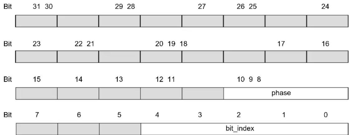
bar_stacked
| Bit | 31 | 30 | 29 | 28 | 27 | 26 | 25 | 24 | | --- | --- | --- | --- | --- | --- | --- | --- | --- | | Bit | 23 | 22 | 21 | 20 | 19 | 18 | 17 | 16 | | Bit | 15 | 14 | 13 | 12 | 11 | 10 | 9 | 8 | | Bit | 7 | 6 | 5 | 4 | 3 | 2 | 1 | 0 | | Bit | 0 | 0 | 0 | 0 | 0 | 0 | 0 | 0 | bit_index- bit_index: contains the bit number of the failing bit
- phase: indicates which phase of the test failed and the cause of the error, as listed in the following table.
Table 12-4. MBIST Operation Phases
| Phase Test actions | |
| 0 Write all bits to zero. This phase cannot fail. | |
| 1 Read '0', write '1', increment address | |
| 2 Read '1', write '0' | |
| 3 Read '0', write '1', decrement address | |
| 4 Read '1', write '0', decrement address | |
| 5 Read '0', write '1' | |
| 6 Read '1', write '0', decrement address | |
| 7 Read all zeros. bit_index is not used |
Table 12-5. AMOD Bit Descriptions for MBIST
| AMOD[1:0] Description | |
| 0x0 Exit on Error | |
| 0x1 Pause on Error | |
| 0x2, 0x3 | Reserved |
Related Links
- NVMCTRL - Nonvolatile Memory Controller
20.6.6. Security Bit
9.2. Physical Memory Map
12.11.6 System Services Availability when Accessed Externally and Device is Protected
External access: Access performed in the DSU address offset 0x200-0x1FFF range.
Internal access: Access performed in the DSU address offset 0x000-0x100 range.
Table 12-6. Available Features when Operated From The External Address Range and Device is Protected
| Features | Availability From The External Address Range and Device is Protected |
| Chip-Erase command and status | Yes |
| ......continued | |
| Features Availability From The External Address Range and Device is Protected | |
| CRC32 Yes, only full array (EEPROM Emulation area not included) or full EEPROM Emulation | |
| CoreSight Compliant Device identification Yes | |
| Debug communication channels Yes | |
| Testing of onboard memories (MBIST) No | |
| STATUS.ACRSTEXT clearing No (STATUS.PERR is set when attempting to do so) | |
12.12 Register Summary
| Offset | Name Bit Pos. 76543210 | |||||||||
| 0x00 CTRL 7:0 CE MBIST CRC SWRST | ||||||||||
| 0x01 | STATUS | 7:0 | PERR | FAIL | BERR | CRSTEXT | DONE | |||
| 0x02 | STATUS | 7:0 | HPE | DCCD1 | DCCD0 | DBG PRES | PROT | |||
| 0x03 | Reserved | |||||||||
| 0x04 | ADDR | 7:0 | ADDR[5:0] | AMOD[1:0] | ||||||
| 15:8 | ADDR[13:6] | |||||||||
| 23:16 | ADDR[21:14] | |||||||||
| 31:24 | ADDR[29:22] | |||||||||
| 0x08 LENGTH | 7:0 | LENGTH[5:0] | ||||||||
| 15:8 | LENGTH[13:6] | |||||||||
| 23:16 | LENGTH[21:14] | |||||||||
| 31:24 | LENGTH[29:22] | |||||||||
| 0x0C | DATA | 7:0 | DATA[7:0] | |||||||
| 15:8 | DATA[15:8] | |||||||||
| 23:16 | DATA[23:16] | |||||||||
| 31:24 | DATA[31:24] | |||||||||
| 0x10 DCC0 | 7:0 | DATA[7:0] | ||||||||
| 15:8 | DATA[15:8] | |||||||||
| 23:16 | DATA[23:16] | |||||||||
| 31:24 | DATA[31:24] | |||||||||
| 0x14 DCC1 | 7:0 | DATA[7:0] | ||||||||
| 15:8 | DATA[15:8] | |||||||||
| 23:16 | DATA[23:16] | |||||||||
| 31:24 | DATA[31:24] | |||||||||
| 0X18 | DID | 7:0 | DEVSEL[7:0] | |||||||
| 15:8 | DIE[3:0] | Revision[3:0] | ||||||||
| 23:16 | FAMILY[0] | SERIES[5:0] | ||||||||
| 31:24 | PROCESSOR[3:0] | FAMILY[4:1] | ||||||||
| 0x1C ... 0x0FFF | Reserved | |||||||||
| 0x1000 | ENTRY0 | 7:0 | FMT EPRES | |||||||
| 15:8 | ADDOFF[3:0] | |||||||||
| 23:16 | ADDOFF[11:4] | |||||||||
| 31:24 | ADDOFF[19:12] | |||||||||
| 0x1004 | ENTRY1 | 7:0 | FMT EPRES | |||||||
| 15:8 | ADDOFF[3:0] | |||||||||
| 23:16 | ADDOFF[11:4] | |||||||||
| 31:24 | ADDOFF[19:12] | |||||||||
| 0x1008 END | 7:0 | END[7:0] | ||||||||
| 15:8 | END[15:8] | |||||||||
| 23:16 | END[23:16] | |||||||||
| 31:24 | END[31:24] | |||||||||
| 0x100C ... 0x1FCB | Reserved | |||||||||
| 0x1FCC | MEMTYPE | 7:0 | SMEMP | |||||||
| 15:8 | ||||||||||
| 23:16 | ||||||||||
| 31:24 | ||||||||||
| 0x1FD0 | PID4 | 7:0 | FKBC[3:0] | JEPCC[3:0] | ||||||
| 15:8 | ||||||||||
| 23:16 | ||||||||||
| 31:24 | ||||||||||
| 0x1FD4 ... 0x1FDF | Reserved | |||||||||
| Offset | Name Bit Pos. 7 6 5 4 3 2 1 0 | ||||||||
| 0x1FE0 PID0 | 7:0 PARTNBL[7:0] | ||||||||
| 15:8 | |||||||||
| 23:16 | |||||||||
| 31:24 | |||||||||
| 0x1FE4 PID1 | 7:0 JEPIDCL[3:0] PARTNBH[3:0] | ||||||||
| 15:8 | |||||||||
| 23:16 | |||||||||
| 31:24 | |||||||||
| 0x1FE8 PID2 | 7:0 REVISION[3:0] JEPU JEPIDCH[2:0] | ||||||||
| 15:8 | |||||||||
| 23:16 | |||||||||
| 31:24 | |||||||||
| 0x1FEC PID3 | 7:0 REVAND[3:0] CUSMOD[3:0] | ||||||||
| 15:8 | |||||||||
| 23:16 | |||||||||
| 31:24 | |||||||||
| 0x1FF0 CID0 | 7:0 PREAMBLEB0[7:0] | ||||||||
| 15:8 | |||||||||
| 23:16 | |||||||||
| 31:24 | |||||||||
| 0x1FF4 CID1 | 7:0 | CCLASS[3:0] | PREAMBLE[3:0] | ||||||
| 15:8 | |||||||||
| 23:16 | |||||||||
| 31:24 | |||||||||
| 0x1FF8 CID2 | 7:0 PREAMBLEB2[7:0] | ||||||||
| 15:8 | |||||||||
| 23:16 | |||||||||
| 31:24 | |||||||||
| 0x1FFC CID3 | 7:0 PREAMBLEB3[7:0] | ||||||||
| 15:8 | |||||||||
| 23:16 | |||||||||
| 31:24 | |||||||||
12.13 Register Description
Registers can be 8, 16, or 32 bits wide. Atomic 8-, 16- and 32-bit accesses are supported. In addition, the 8-bit quarters and 16-bit halves of a 32-bit register, and the 8-bit halves of a 16-bit register can be accessed directly.
Some registers are optionally write-protected by the Peripheral Access Controller (PAC). Optional PAC write-protection is denoted by the "PAC Write-Protection" property in each individual register description. For details, refer to Register Access Protection.
12.13.1 Control
Name: CTRL
Offset: 0x0000
Reset: 0x00
Property: PAC Write-Protection
Bit 76543210
| CE MBIST CRC SW/RST | ||||||
| Access Reset | W | W | W | W | ||
| 0 0 0 | 0 |
Bit 4 - CE Chip-Erase
Writing a '0' to this bit has no effect.
Writing a '1' to this bit starts the Chip-Erase operation.
Bit 3 - MBIST Memory Built-In Self-Test
Writing a '0' to this bit has no effect.
Writing a '1' to this bit starts the memory BIST algorithm.
Bit 2 - CRC 32-bit Cyclic Redundancy Check
Writing a '0' to this bit has no effect.
Writing a '1' to this bit starts the cyclic redundancy check algorithm.
Bit 0 - SWRST Software Reset
Writing a '0' to this bit has no effect.
Writing a '1' to this bit resets the module.
12.13.2 Status A
Name: STATUSA
Offset: 0x0001
Reset: 0x00
Property: PAC Write-Protection
Bit 76543210
| PERR FAIL BERR CRSTEXT DONE | ||||||
| Access Reset | R/W0 0 0 0 0 | R/W | R/W | R/W | R/W |
Bit 4 - PERR Protection Error
Writing a '0' to this bit has no effect.
Writing a '1' to this bit clears the Protection Error bit.
This bit is set when a command that is not allowed in protected state is issued.
Bit 3 - FAIL Failure
Writing a '0' to this bit has no effect.
Writing a '1' to this bit clears the Failure bit.
This bit is set when a DSU operation failure is detected.
Bit 2 - BERR Bus Error
Writing a '0' to this bit has no effect.
Writing a '1' to this bit clears the Bus Error bit.
This bit is set when a bus error is detected.
Bit 1 - CRSTEXT CPU Reset Phase Extension
Writing a '0' to this bit has no effect.
Writing a '1' to this bit clears the CPU Reset Phase Extension bit.
This bit is set when a debug adapter Cold-Plugging is detected, which extends the CPU reset phase.
Bit 0 - DONE Done
Writing a '0' to this bit has no effect.
Writing a '1' to this bit clears the Done bit.
This bit is set when a DSU operation is completed.
12.13.3 Status B
Name: STATUSB
Offset: 0x0002
Reset: 0x1X
Property: PAC Write-Protection
Bit 76543210
| HPE | DCCD1 | DCCD0 | DBGPRES | PROT | ||||||
| Access Reset | R | R | R | |||||||
| 1 | 0 | 0 | 0 |
Bit 4 - HPE Hot-Plugging Enable
Writing a '0' to this bit has no effect.
Writing a '1' to this bit has no effect.
This bit is set when Hot-Plugging is enabled.
This bit is cleared when Hot-Plugging is disabled. This is the case when the SWCLK function is changed. Only a power-reset or a external reset can set it again.
Bits 2, 3 - DCCDx Debug Communication Channel x Dirty [x=1..0]
Writing a '0' to this bit has no effect.
Writing a '1' to this bit has no effect.
This bit is set when DCCx is written.
This bit is cleared when DCCx is read.
Bit 1 - DBGPRES Debugger Present
Writing a '0' to this bit has no effect.
Writing a '1' to this bit has no effect.
This bit is set when a debugger probe is detected.
This bit is never cleared.
Bit 0 - PROT Protected
Writing a '0' to this bit has no effect.
Writing a '1' to this bit has no effect.
This bit is set at power-up when the device is protected.
This bit is never cleared.
12.13.4 Address
Name: ADDR
Offset: 0x0004
Reset: 0x00000000
Property: PAC Write-Protection
Bit 31 30 29 28 27 26 25 24
| ADDR[29:22] |
Access R/W R/W R/W R/W R/W R/W R/W R/W
Reset 00000000
Bit 23 22 21 20 19 18 17 16
| ADDR[21:14] |
Access R/W R/W R/W R/W R/W R/W R/W R/W
Reset 00000000
Bit 15 14 13 12 11 10 9 8
| ADDR[13:6] |
Access R/W R/W R/W R/W R/W R/W R/W R/W
Reset 00000000
Bit 76543210
| ADDR[5:0] AMOD[1:0] |
Access R/W R/W R/W R/W R/W R/W R/W R/W
Reset 00000000
Bits 31:2 - ADDR[29:0] Address
Initial word start address needed for memory operations.
Bits 1:0 - AMOD[1:0] Access Mode
The functionality of these bits is dependent on the operation mode.
Bit description when operating CRC32: refer to 12.11.3. 32-bit Cyclic Redundancy Check CRC32
Bit description when testing onboard memories (MBIST): refer to 12.11.5. Testing of On-Board Memories MBIST
12.13.5 Length
Name: LENGTH
Offset: 0x0008
Reset: 0x00000000
Property: PAC Write-Protection
Bit 31 30 29 28 27 26 25 24
| LENGTH[29:22] |
Access R/W R/W R/W R/W R/W R/W R/W R/W
Reset 00000000
Bit 23 22 21 20 19 18 17 16
| LENGTH[21:14] |
Access R/W R/W R/W R/W R/W R/W R/W R/W
Reset 00000000
Bit 15 14 13 12 11 10 9 8
| LENGTH[13:6] |
Access R/W R/W R/W R/W R/W R/W R/W R/W
Reset 00000000
Bit 76543210
| LENGTH[5:0] |
Access R/W R/W R/W R/W R/W R/W
Reset 000000
Bits 31:2 - LENGTH[29:0] Length
Length in words needed for memory operations.
12.13.6 Data
Name: DATA
Offset: 0x000C
Reset: 0x00000000
Property: PAC Write-Protection
Bit 31 30 29 28 27 26 25 24
DATA[31:24]
Access R/W R/W R/W R/W R/W R/W R/W R/W
Reset 00000000
Bit 23 22 21 20 19 18 17 16
DATA[23:16]
Access R/W R/W R/W R/W R/W R/W R/W R/W
Reset 00000000
Bit 15 14 13 12 11 10 9 8
DATA[15:8]
Access R/W R/W R/W R/W R/W R/W R/W R/W
Reset 00000000
Bit 76543210
DATA[7:0]
Access R/W R/W R/W R/W R/W R/W R/W R/W
Reset 00000000
Bits 31:0 - DATA[31:0] Data
Memory operation initial value or result value.
12.13.7 Debug Communication Channel 0
Name: DCC0
Offset: 0x0010
Reset: 0x00000000
Property: -
Bit 31 30 29 28 27 26 25 24
DATA[31:24]
Access R/W R/W R/W R/W R/W R/W R/W R/W
Reset 00000000
Bit 23 22 21 20 19 18 17 16
DATA[23:16]
Access R/W R/W R/W R/W R/W R/W R/W R/W
Reset 00000000
Bit 15 14 13 12 11 10 9 8
DATA[15:8]
Access R/W R/W R/W R/W R/W R/W R/W R/W
Reset 00000000
Bit 76543210
DATA[7:0]
Access R/W R/W R/W R/W R/W R/W R/W R/W
Reset 00000000
Bits 31:0 - DATA[31:0] Data
Data register.
12.13.8 Debug Communication Channel 1
Name: DCC1
Offset: 0x0014
Reset: 0x00000000
Property: -
Bit 31 30 29 28 27 26 25 24
DATA[31:24]
Access R/W R/W R/W R/W R/W R/W R/W R/W
Reset 00000000
Bit 23 22 21 20 19 18 17 16
DATA[23:16]
Access R/W R/W R/W R/W R/W R/W R/W R/W
Reset 00000000
Bit 15 14 13 12 11 10 9 8
DATA[15:8]
Access R/W R/W R/W R/W R/W R/W R/W R/W
Reset 00000000
Bit 76543210
DATA[7:0]
Access R/W R/W R/W R/W R/W R/W R/W R/W
Reset 00000000
Bits 31:0 - DATA[31:0] Data
Data register.
12.13.9 Device Identification
Name: DID
Offset: 0x0018
Property: PAC Write-Protection
The information in this register is related to the Ordering Information.
Bit 31 30 29 28 27 26 25 24
| PROCESSOR[3:0] FAMILY[4:1] | ||
| Access | RRRRRRRR | |
| Reset | pp p f f f | |
Bit 23 22 21 20 19 18 17 16
| FAMILY[0] | SERIES[5:0] | |||||||
| Access | R | RRRRRR | ||||||
| Reset | f | S | S | S | S | S | S | |
Bit 15 14 13 12 11 10 9 8
| DIE[3:0] | Revision[3:0] | |||||||
| Access Reset | R R R R R R R | |||||||
| d | d | d | d | r | r | r | r | |
| Bit | 7 | 6 | 5 | 4 | 3 | 2 | 1 | 0 |
| DEVSEL[7:0] | ||||||||
| Access Reset | R R R R R R R | |||||||
| x | x | x | x | x | x | x | x | |
Bits 31:28 - PROCESSOR[3:0] Processor
The value of this field defines the processor used on the device. For this device, the value of this field is 0x1, corresponding to a microcontroller embedding an Arm Cortex-M0+ processor.
Bits 27:23 - FAMILY[4:0] Product Family
The value of this field corresponds to the product family part of the ordering code. For this device, the value of this field is 0x0, corresponding to the General Purpose Family.
Bits 21:16 - SERIES[5:0] Product Series
The value of this field corresponds to the product series part of the ordering code. For this device, the value of this field is 0x00 corresponding to an Arm Cortex-M0+ processor with basic feature set.
Bits 15:12 - DIE[3:0] Die Number
Identifies the die family.
For this device, the value of this field is 0x0 (for revisions B and C of Variant A) or 0x1.
Bits 11:8 - REVISION[3:0] Revision Number
Identifies the die revision number. 0x0=rev.A, 0x1=rev.B etc.
Note: The device variant (last letter of the ordering number) is independent of the die revision (DSU.DID.REVISION): The device variant denotes functional differences, whereas the die revision marks evolution of the die.
Bits 7:0 - DEVSEL[7:0] Device Selection
This bit field identifies a device within a product family and product series.
Refer to the SAM D20 Family Silicon Errata and Data Sheet Clarification document for matching the DEVSEL value with the associated part number.
12.13.10 CoreSight ROM Table Entry 0
Name: ENTRY0
Offset: 0x1000
Reset: 0xXXXXX00X
Property: PAC Write-Protection
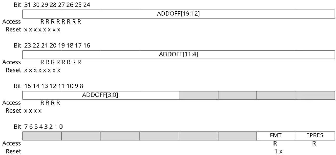
text_image
Bit 31 30 29 28 27 26 25 24 ADDOFF[19:12] Access R R R R R R R R Reset x x x x x x x x Bit 23 22 21 20 19 18 17 16 ADDOFF[11:4] Access R R R R R R R R Reset x x x x x x x x Bit 15 14 13 12 11 10 9 8 ADDOFF[3:0] Access R R R R Reset x x x x Bit 7 6 5 4 3 2 1 0 FMT EPRES Access R Reset 1 xBits 31:12 - ADDOFF[19:0] Address Offset
The base address of the component, relative to the base address of this ROM table.
Bit 1 - FMT Format
Always reads as '1', indicating a 32-bit ROM table.
Bit 0 - EPRES Entry Present
This bit indicates whether an entry is present at this location in the ROM table.
This bit is set at power-up if the device is not protected indicating that the entry is not present.
This bit is cleared at power-up if the device is not protected indicating that the entry is present.
12.13.11 CoreSight ROM Table Entry 1
Name: ENTRY1
Offset: 0x1004
Reset: 0xXXXXX00X
Property: PAC Write-Protection
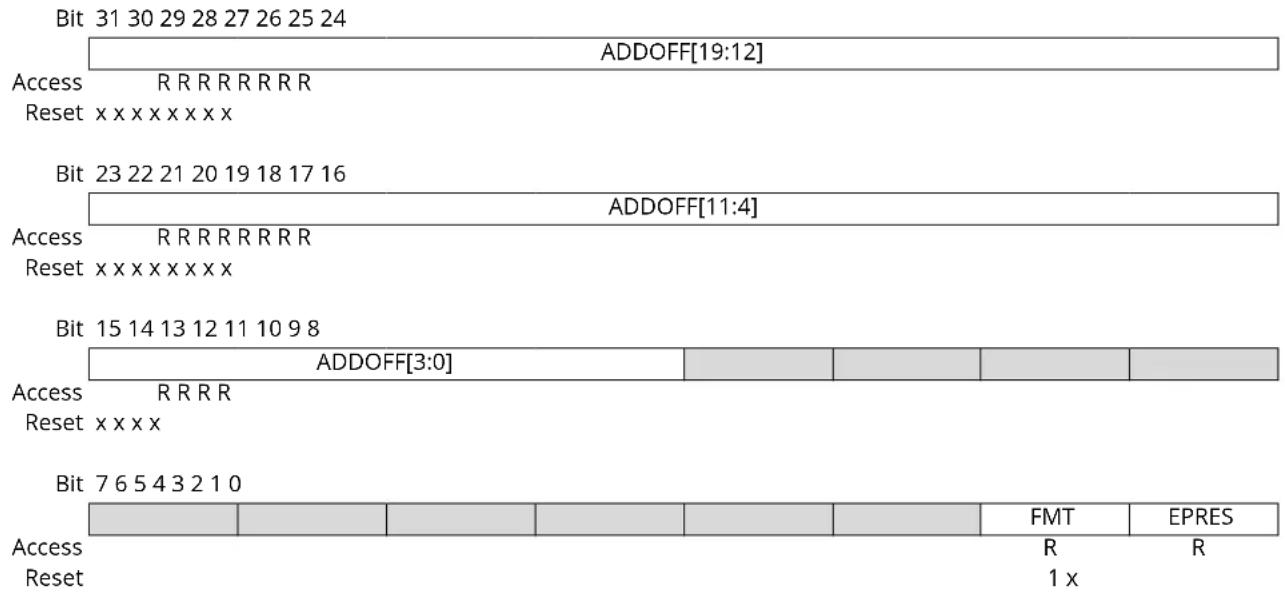
text_image
Bit 31 30 29 28 27 26 25 24 ADDOFF[19:12] Access R R R R R R R R Reset x x x x x x x x x Bit 23 22 21 20 19 18 17 16 ADDOFF[11:4] Access R R R R R R R R R Reset x x x x x x x x x Bit 15 14 13 12 11 10 9 8 ADDOFF[3:0] Access R R R R Reset x x x x Bit 7 6 5 4 3 2 1 0 FMT EPRES Access R Reset 1 xBits 31:12 - ADDOFF[19:0] Address Offset
The base address of the component, relative to the base address of this ROM table.
Bit 1 - FMT Format
Always read as '1', indicating a 32-bit ROM table.
Bit 0 - EPRES Entry Present
This bit indicates whether an entry is present at this location in the ROM table.
This bit is set at power-up if the device is not protected indicating that the entry is not present.
This bit is cleared at power-up if the device is not protected indicating that the entry is present.
12.13.12 CoreSight ROM Table End
Name: END
Offset: 0x1008
Reset: 0x00000000
Property: -
| Bit 31 30 29 28 27 26 25 24 | |
| END[31:24] | |
| Access R R R R R R R R Reset 0 0 0 0 0 0 0 0 | |
| Bit 23 22 21 20 19 18 17 16 | |
| END[23:16] | |
| Access R R R R R R R R Reset 0 0 0 0 0 0 0 0 | |
| Bit 15 14 13 12 11 10 9 8 | |
| END[15:8] | |
| Access R R R R R R R R Reset 0 0 0 0 0 0 0 0 | |
| Bit 7 6 5 4 3 2 1 0 | |
| END[7:0] | |
| Access R R R R R R R R R Reset 0 0 0 0 0 0 0 0 | |
Bits 31:0 - END[31:0] End Marker
Indicates the end of the CoreSight ROM table entries.
12.13.13 CoreSight ROM Table Memory Type
Name: MEMTYPE
Offset: 0x1FCC
Reset: 0x0000000x
Property: -
text_image
Bit 31 30 29 28 27 26 25 24 Access Reset Bit 23 22 21 20 19 18 17 16 Access Reset Bit 15 14 13 12 11 10 9 8 Access Reset Bit 7 6 5 4 3 2 1 0 Access Reset SMEMP R XBit 0 - SMEMP System Memory Present
This bit indicates whether system memory is present on the bus that connects to the ROM table. This bit is set at power-up if the device is not protected, indicating that the system memory is accessible from a debug adapter.
This bit is cleared at power-up if the device is protected, indicating that the system memory is not accessible from a debug adapter.
12.13.14 Peripheral Identification 4
Name: PID4
Offset: 0x1FD0
Reset: 0x00000000
Property: -
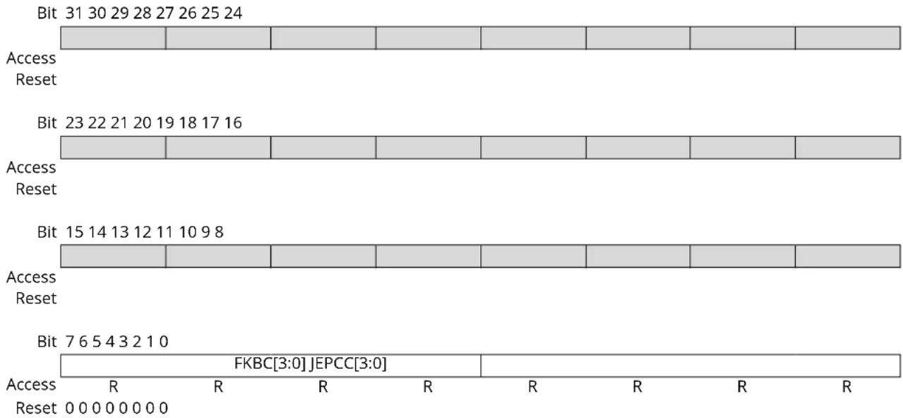
text_image
Bit 31 30 29 28 27 26 25 24 Access Reset Bit 23 22 21 20 19 18 17 16 Access Reset Bit 15 14 13 12 11 10 9 8 Access Reset Bit 7 6 5 4 3 2 1 0 FKBC[3:0] JEPCC[3:0] Access R R R R R R R Reset 0 0 0 0 0 0 0Bits 7:4 - FKBC[3:0] 4KB Count
These bits will always return zero when read, indicating that this debug component occupies one 4KB block.
Bits 3:0 - JEPCC[3:0] JEP-106 Continuation Code
These bits will always return zero when read.
12.13.15 Peripheral Identification 0
Name: PID0
Offset: 0x1FE0
Reset: 0x00000000
Property: -

text_image
Bit 31 30 29 28 27 26 25 24 Access Reset Bit 23 22 21 20 19 18 17 16 Access Reset Bit 15 14 13 12 11 10 9 8 Access Reset Bit 7 6 5 4 3 2 1 0 PARTNBL[7:0] Access R R R R R R R R Reset 0 0 0 0 0 0 0Bits 7:0 - PARTNBL[7:0] Part Number Low
These bits will always return 0xD0 when read, indicating that this device implements a DSU module instance.
12.13.16 Peripheral Identification 1
Name: PID1
Offset: 0x1FE4
Reset: 0x000000FC
Property: -
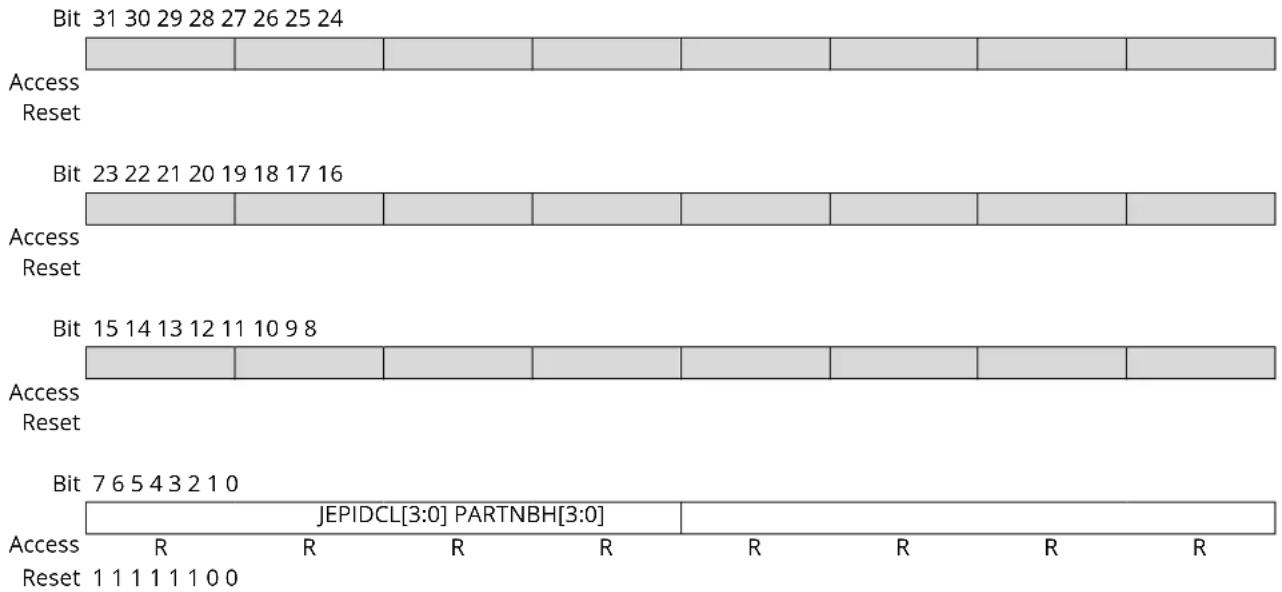
text_image
Bit 31 30 29 28 27 26 25 24 Access Reset Bit 23 22 21 20 19 18 17 16 Access Reset Bit 15 14 13 12 11 10 9 8 Access Reset Bit 7 6 5 4 3 2 1 0 JEPIDCL[3:0] PARTNBH[3:0] Access R R R R R R Reset 1 1 1 1 1 1 0 0Bits 7:4 - JEPIDCL[3:0] Low part of the JEP-106 Identity Code
These bits will always return 0xF when read (JEP-106 identity code is 0x1F).
Bits 3:0 - PARTNBH[3:0] Part Number High
These bits will always return 0xC when read, indicating that this device implements a DSU module instance.
12.13.17 Peripheral Identification 2
Name: PID2
Offset: 0x1FE8
Reset: 0x00000009
Property: -
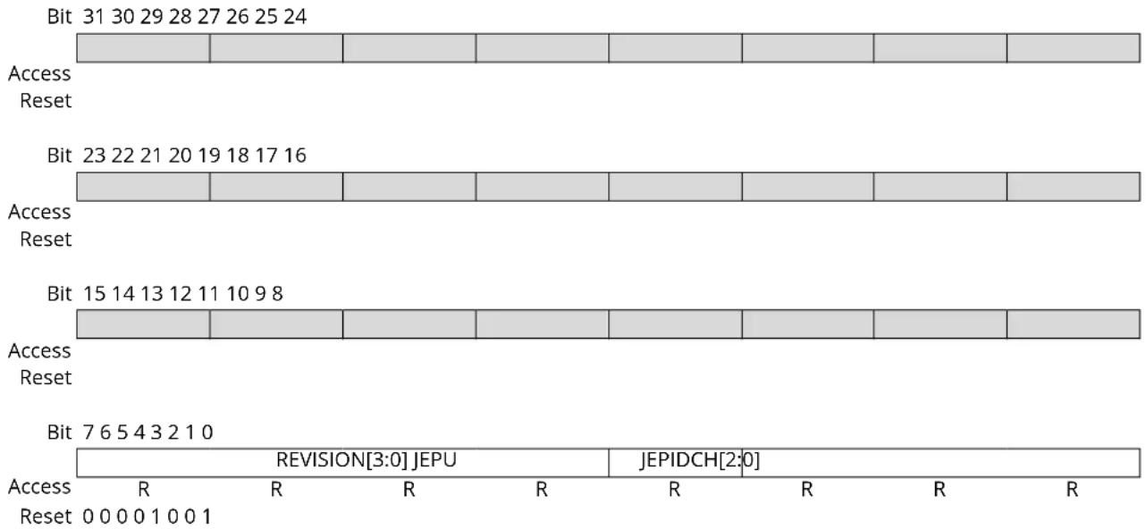
text_image
Bit 31 30 29 28 27 26 25 24 Access Reset Bit 23 22 21 20 19 18 17 16 Access Reset Bit 15 14 13 12 11 10 9 8 Access Reset Bit 7 6 5 4 3 2 1 0 REVISION[3:0] JEPU JEPIDCH[2:0] Access R R R R R R R Reset 0 0 0 0 1 0 0 1Bits 7:4 - REVISION[3:0] Revision Number
Revision of the peripheral. Starts at 0x0 and increments by one at both major and minor revisions.
Bit 3 - JEPU JEP-106 Identity Code is used
This bit will always return one when read, indicating that JEP-106 code is used.
Bits 2:0 - JEPIDCH[2:0] JEP-106 Identity Code High
These bits will always return 0x1 when read, (JEP-106 identity code is 0x1F).
12.13.18 Peripheral Identification 3
Name: PID3
Offset: 0x1FEC
Reset: 0x00000000
Property: -
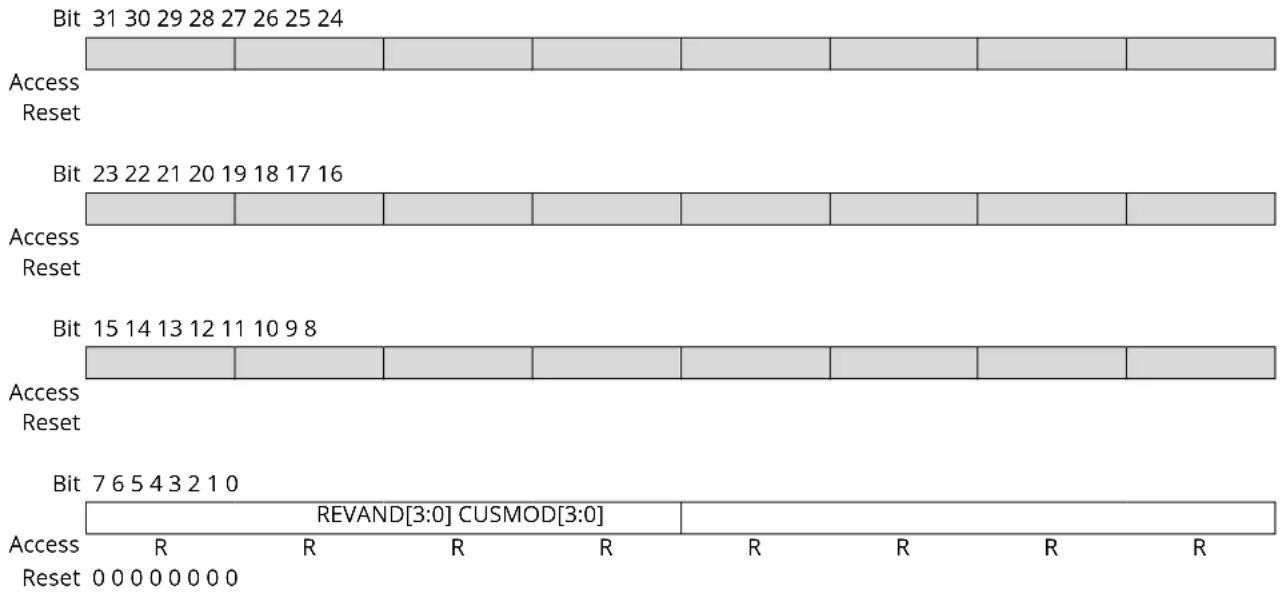
text_image
Bit 31 30 29 28 27 26 25 24 Access Reset Bit 23 22 21 20 19 18 17 16 Access Reset Bit 15 14 13 12 11 10 9 8 Access Reset Bit 7 6 5 4 3 2 1 0 REVAND[3:0] CUSMOD[3:0] Access R R R R R R R Reset 0 0 0 0 0 0 0Bits 7:4 - REVAND[3:0] Revision Number
These bits will always return 0x0 when read.
These bits will always return 0x0 when read.
Bits 3:0 - CUSMOD[3:0] ARM CUSMOD
12.13.19 Component Identification 0
Name: CID0
Offset: 0x1FF0
Reset: 0x0000000D
Property: -

text_image
Bit 31 30 29 28 27 26 25 24 Access Reset Bit 23 22 21 20 19 18 17 16 Access Reset Bit 15 14 13 12 11 10 9 8 Access Reset Bit 7 6 5 4 3 2 1 0 PREAMBLEB0[7:0] Access R R R R R R R R Reset 0 0 0 0 1 1 0 1Bits 7:0 - PREAMBLEB0[7:0] Preamble Byte 0
These bits will always return 0x0000000D when read.
12.13.20 Component Identification 1
Name: CID1
Offset: 0x1FF4
Reset: 0x00000010
Property: -
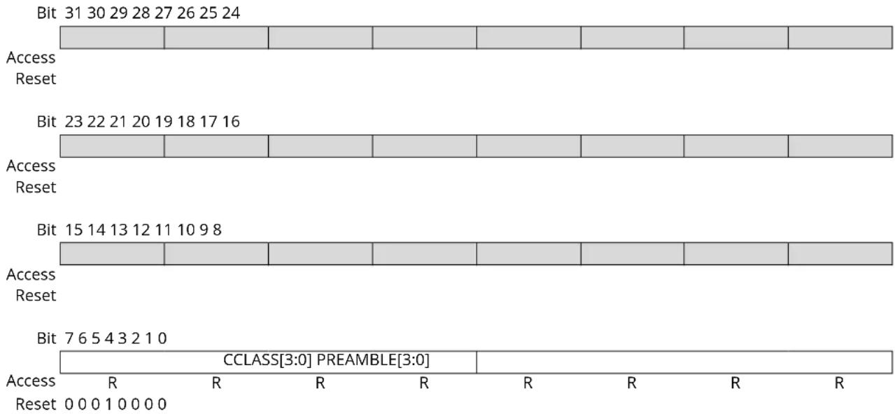
text_image
Bit 31 30 29 28 27 26 25 24 Access Reset Bit 23 22 21 20 19 18 17 16 Access Reset Bit 15 14 13 12 11 10 9 8 Access Reset Bit 7 6 5 4 3 2 1 0 CCLASS[3:0] PREAMBLE[3:0] Access R R R R R R R Reset 0 0 0 1 0 0 0 0Bits 7:4 - CCLASS[3:0] Component Class
These bits will always return 0x1 when read indicating that this ARM CoreSight component is ROM table (refer to the ARM Debug Interface v5 Architecture Specification at http://www.arm.com).
Bits 3:0 - PREAMBLE[3:0] Preamble
These bits will always return 0x00 when read.
12.13.21 Component Identification 2
Name: CID2
Offset: 0x1FF8
Reset: 0x00000005
Property: -

text_image
Bit 31 30 29 28 27 26 25 24 Access Reset Bit 23 22 21 20 19 18 17 16 Access Reset Bit 15 14 13 12 11 10 9 8 Access Reset Bit 7 6 5 4 3 2 1 0 PREAMBLEB2[7:0] Access R R R R R R R R Reset 0 0 0 0 0 1 0 1Bits 7:0 - PREAMBLEB2[7:0] Preamble Byte 2
These bits will always return 0x00000005 when read.
12.13.22 Component Identification 3
Name: CID3
Offset: 0x1FFC
Reset: 0x000000B1
Property: -
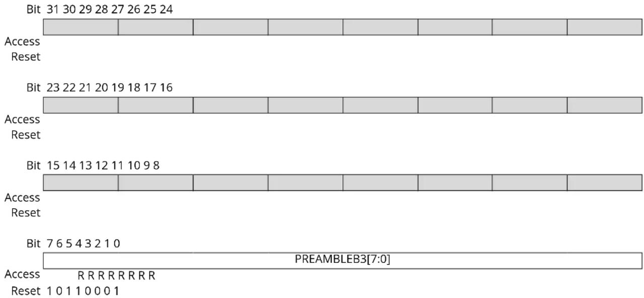
text_image
Bit 31 30 29 28 27 26 25 24 Access Reset Bit 23 22 21 20 19 18 17 16 Access Reset Bit 15 14 13 12 11 10 9 8 Access Reset Bit 7 6 5 4 3 2 1 0 PREAMBLEB3[7:0] Access R R R R R R R R Reset 1 0 1 1 0 0 0 1Bits 7:0 - PREAMBLEB3[7:0] Preamble Byte 3
These bits will always return 0x000000B1 when read.
13. Clock System
This chapter summarizes the clock distribution and terminology in the SAM D20 device. It will not explain every detail of its configuration. For in-depth documentation, see the respective peripherals descriptions and the Generic Clock documentation.
Related Links
- GCLK - Generic Clock Controller
13.1 Clock Distribution
Figure 13-1. Clock distribution
flowchart
graph LR
    A["SYSCTRL"] --> B["GCLK"]
    B --> C["GCLK Generator 0"]
    B --> D["GCLK Generator 1"]
    B --> E["GCLK Generator x"]
    C --> F["Generic Clock Multiplexer 0 (DFLL48M Reference)"]
    D --> G["Generic Clock Multiplexer 1"]
    E --> H["Generic Clock Multiplexer y"]
    F --> I["PM Main Clock Controller"]
    G --> J["Peripheral 0"]
    H --> K["Peripheral z"]
    L["XOSC"] --> B
    M["OSCULP32K"] --> B
    N["OSC32K"] --> B
    O["XOSCP32K"] --> B
    P["OSC8M"] --> B
    Q["DFLL48M"] --> B
    R["GCLK_DFLL48M_REF"] --> F
    S["GCLK_MAIN"] --> F
    T["AHBIAPB System Clocks"] --> U["Peripheral z"]
    style A fill:#99CCFF
    style B fill:#99CCFF
    style C fill:#99CCFF
    style D fill:#99CCFF
    style E fill:#99CCFF
    style F fill:#99CCFF
    style G fill:#99CCFF
    style H fill:#99CCFF
    style I fill:#99CCFF
    style J fill:#99CCFF
    style K fill:#99CCFF
    style L fill:#99CCFF
    style M fill:#99CCFF
    style N fill:#99CCFF
    style O fill:#99CCFF
    style P fill:#99CCFF
    style Q fill:#99CCFF
The clock system on the SAM D20 consists of:
- Clock sources, controlled by SYSCTRL
- A clock source provides a time base that is used by other components, such as Generic Clock Generators. Example clock sources are the internal 8MHz oscillator (OSC8M), External crystal oscillator (XOSC) and the Digital frequency locked loop (DFLL48M).
- Generic Clock Controller (GCLK) which controls the clock distribution system, made up of:
- Generic Clock Generators: These are programmable prescalers that can use any of the system clock sources as a time base. The Generic Clock Generator 0 generates the clock signal GCLK_MAIN, which is used by the Power Manager, which in turn generates synchronous clocks.
- Generic Clocks: These are clock signals generated by Generic Clock Generators and output by the Generic Clock Multiplexer, and serve as clocks for the peripherals of the system. Multiple instances of a peripheral will typically have a separate Generic Clock for each instance. Generic Clock 0 serves as the clock source for the DFLL48M clock input (when multiplying another clock source).
• Power Manager (PM)
- The PM generates and controls the synchronous clocks on the system. This includes the CPU, bus clocks (APB, AHB) as well as the synchronous (to the CPU) user interfaces of the peripherals. It contains clock masks that can turn on/off the user interface of a peripheral as well as prescalers for the CPU and bus clocks.
The next figure shows an example where SERCOM0 is clocked by the DFLL48M in open loop mode. The DFLL48M is enabled, the Generic Clock Generator 1 uses the DFLL48M as its clock source and feeds into Peripheral Channel 20. The Generic Clock 20, also called GCLK_SERCOM0_CORE,
is connected to SERCOM0. The SERCOM0 interface, clocked by CLK_SERCOM0_APB, has been unmasked in the APBC Mask register in the PM.
Figure 13-2. Example of SERCOM clock
flowchart
graph LR
    A["SYSCTRL DFLL48M"] --> B["GCLK Generic Clock Generator 1"]
    B --> C["Generic Clock Multiplexer 20"]
    C --> D["GCLK_SERCOM0_CORE"]
    E["PM Synchronous Clock Controller"] --> F["CLK_SERCOM0_APB"]
    F --> G["SERCOM 0"]
13.2 Synchronous and Asynchronous Clocks
As the CPU and the peripherals can be in different clock domains, i.e. they are clocked from different clock sources and/or with different clock speeds, some peripheral accesses by the CPU need to be synchronized. In this case the peripheral includes a SYNCBUSY status register that can be used to check if a sync operation is in progress.
For a general description, see 13.3. Register Synchronization. Some peripherals have specific properties described in their individual sub-chapter "Synchronization".
In the datasheet, references to Synchronous Clocks are referring to the CPU and bus clocks, while asynchronous clocks are generated by the Generic Clock Controller (GCLK).
13.3 Register Synchronization
There are two different register synchronization schemes implemented on this device: common synchronizer register synchronization and distributed synchronizer register synchronization.
The modules using a common synchronizer register synchronization are: GCLK, WDT, RTC, EIC, TC, ADC, AC and DAC.
The modules adopting a distributed synchronizer register synchronization are: SERCOM USART, SERCOM SPI, SERCOM I2C.
13.3.1 Common Synchronizer Register Synchronization
13.3.1.1 Overview
All peripherals are composed of one digital bus interface connected to the APB or AHB bus and running from a corresponding clock in the Main Clock domain, and one peripheral core running from the peripheral Generic Clock (GCLK).
Communication between these clock domains must be synchronized. This mechanism is implemented in hardware, so the synchronization process takes place even if the peripheral generic clock is running from the same clock source and on the same frequency as the bus interface.
All registers in the bus interface are accessible without synchronization. All registers in the peripheral core are synchronized when written. Some registers in the peripheral core are synchronized when read. Each individual register description will have the properties "Read-Synchronized" and/or "Write-Synchronized" if a register is synchronized.
As shown in the figure below, the common synchronizer is used for all registers in one peripheral. Therefore, status register (STATUS) of each peripheral can be synchronized at a time.
Figure 13-3. Synchronization
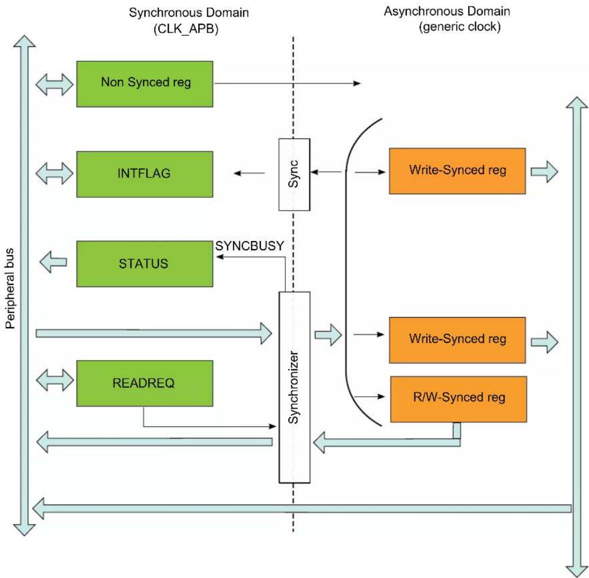
flowchart
graph TD
    subgraph_Synchronous_Domain["CLK_APB"]
        A["Non Synced reg"] --> B["Sync"]
        C["INTFLAG"] <-- B
        D["STATUS"] <--_E["SYNCBUSY"]
        F["READREQ"] <--_G["Synchronizer"]
    end
    subgraph_Asynchronous_Domain["generic clock"]
        H["Write-Synced reg"] --> I["Write-Synced reg"]
        J["R/W-Synced reg"] --> K["Write-Synced reg"]
        L["Sync"] --> M["Sync"]
    end
    B <--> H
    E <--> J
    G <--> K
    style Synchronous_Domain fill:#f9f9f9,stroke:#333
    style Asynchronous_Domain fill:#e0e0e0,stroke:#333
13.3.1.2 Write-Synchronization
Write-Synchronization is triggered by writing to a register in the peripheral clock domain. The Synchronization Busy bit in the Status register (STATUS.SYNCBUSY) will be set when the write-synchronization starts and cleared when the write-synchronization is complete. Refer to 13.3.1.8. Synchronization Delay for details on the synchronization delay.
When the write-synchronization is ongoing (STATUS.SYNCBUSY is one), any of the following actions will cause the peripheral bus to stall until the synchronization is complete:
- Writing a generic clock peripheral core register
- Reading a read-synchronized peripheral core register
- Reading the register that is being written (and thus triggered the synchronization)
Peripheral core registers without read-synchronization will remain static once they have been written and synchronized, and can be read while the synchronization is ongoing without causing
the peripheral bus to stall. APB registers can also be read while the synchronization is ongoing without causing the peripheral bus to stall.
Reading a read-synchronized peripheral core register will cause the peripheral bus to stall immediately until the read-synchronization is complete. STATUS.SYNCBUSY will not be set. Refer to 13.3.1.8. Synchronization Delay for details on the synchronization delay. Note that reading a read-synchronized peripheral core register while STATUS.SYNCBUSY is one will cause the peripheral bus to stall twice; first because of the ongoing synchronization, and then again because reading a read-synchronized core register will cause the peripheral bus to stall immediately.
13.3.1.4 Completion of synchronization
The user can either poll STATUS.SYNCBUSY or use the Synchronisation Ready interrupt (if available) to check when the synchronization is complete. It is also possible to perform the next read/write operation and wait, as this next operation will be started once the previous write/read operation is synchronized and/or complete.
13.3.1.5 Read Request
The read request functionality is only available to peripherals that have the Read Request register (READREQ) implemented. Refer to the register description of individual peripheral chapters for details.
To avoid forcing the peripheral bus to stall when reading read-synchronized peripheral core registers, the read request mechanism can be used.
Basic Read Request
Writing a '1' to the Read Request bit in the Read Request register (READREQ.RREQ) will request read-synchronization of the register specified in the Address bits in READREQ (READREQ.ADDR) and set STATUS.SYNCBUSY. When read-synchronization is complete, STATUS.SYNCBUSY is cleared. The read-synchronized value is then available for reading without delay until READREQ.RREQ is written to '1' again.
The address to use is the offset to the peripheral's base address of the register that should be synchronized.
Continuous Read Request
Writing a '1' to the Read Continuously bit in READREQ (READREQ.RCONT) will force continuous read-synchronization of the register specified in READREQ.ADDR. The latest value is always available for reading without stalling the bus, as the synchronization mechanism is continuously synchronizing the given value. The READREQ.RCONT prevents READREQ.RREQ from clearing automatically. For the continuous read mode, the RREQ bit is required to be set once the RCONT bit is set.
SYNCBUSY is set for the first synchronization, but not for the subsequent synchronizations. If another synchronization is attempted, i.e. by executing a write-operation of a write-synchronized register, the read request will be stopped, and will have to be manually restarted.
Note:
The continuous read-synchronization is paused in sleep modes where the generic clock is not running. This means that a new read request is required if the value is needed immediately after exiting sleep.
13.3.1.6 Enable Write-Synchronization
Writing to the Enable bit in the Control register (CTRL.ENABLE) will also trigger write-synchronization and set STATUS.SYNCBUSY. CTRL.ENABLE will read its new value immediately after being written. The Synchronisation Ready interrupt (if available) cannot be used for Enable write-synchronization.
When the enable write-synchronization is ongoing (STATUS.SYNCBUSY is one), attempt to do any of the following will cause the peripheral bus to stall until the enable synchronization is complete:
- Writing a peripheral core register
- Writing an APB register
- Reading a read-synchronized peripheral core register
APB registers can be read while the enable write-synchronization is ongoing without causing the peripheral bus to stall.
13.3.1.7 Software Reset Write-Synchronization
Writing a '1' to the Software Reset bit in CTRL (CTRL.SWRST) will also trigger write-synchronization and set STATUS.SYNCBUSY. When writing a '1' to the CTRL.SWRST bit it will immediately read as '1'. CTRL.SWRST and STATUS.SYNCBUSY will be cleared by hardware when the peripheral has been reset. Writing a zero to the CTRL.SWRST bit has no effect. The Synchronisation Ready interrupt (if available) cannot be used for Software Reset write-synchronization.
When the software reset is in progress (STATUS.SYNCBUSY and CTRL.SWRST are '1'), attempt to do any of the following will cause the peripheral bus to stall until the Software Reset synchronization and the reset is complete:
- Writing a peripheral core register
• Writing an APB register - Reading a read-synchronized register
APB registers can be read while the software reset is being write-synchronized without causing the peripheral bus to stall.
13.3.1.8 Synchronization Delay
The synchronization will delay write and read accesses by a certain amount. This delay D is within the range of:
$$ 5 \times P _ {\mathrm{GCLK}} + 2 \times P _ {\mathrm{APB}} < D < 6 \times P _ {\mathrm{GCLK}} + 3 \times P _ {\mathrm{APB}} $$
Where P_GCLK is the period of the generic clock and P_APB is the period of the peripheral bus clock. A normal peripheral bus register access duration is 2 × P_APB .
13.3.2 Distributed Synchronizer Register Synchronization
13.3.2.1 Overview
All peripherals are composed of one digital bus interface connected to the APB or AHB bus and running from a corresponding clock in the Main Clock domain, and one peripheral core running from the peripheral Generic Clock (GCLK).
Communication between these clock domains must be synchronized. This mechanism is implemented in hardware, so the synchronization process takes place even if the peripheral generic clock is running from the same clock source and on the same frequency as the bus interface.
All registers in the bus interface are accessible without synchronization. All registers in the peripheral core are synchronized when written. Some registers in the peripheral core are synchronized when read. Registers that need synchronization has this denoted in each individual register description.
13.3.2.2 General Write synchronization
Write-Synchronization is triggered by writing to a register in the peripheral clock domain. The respective bit in the Synchronization Busy register (SYNCBUSY) will be set when the write-synchronization starts and cleared when the write-synchronization is complete. Refer to 13.3.2.7. Synchronization Delay for details on the synchronization delay.
When write-synchronization is ongoing for a register, any subsequent write attempts to this register will be discarded, and an error will be reported.
Example:
REGA, REGB are 8-bit peripheral core registers. REGC is 16-bit peripheral core register.
| Offset Register | |
| 0x00 REGA | |
| 0x01 REGB | |
| 0x02 REGC | |
| 0x03 |
Synchronization is per register, so multiple registers can be synchronized in parallel. Consequently, after REGA (8-bit access) was written, REGB (8-bit access) can be written immediately without error.
REGC (16-bit access) can be written without affecting REGA or REGB. If REGC is written to in two consecutive 8-bit accesses without waiting for synchronization, the second write attempt will be discarded and an error is generated.
A 32-bit access to offset 0x00 will write all three registers. Note that REGA, REGB and REGC can be updated at different times because of independent write synchronization.
13.3.2.3 General read synchronization
Read-synchronized registers are synchronized when the register value is updated. During synchronization the corresponding bit in SYNCBUSY will be set. Reading a read-synchronized register will return its value immediately and the corresponding bit in SYNCBUSY will not be set.
13.3.2.4 Completion of synchronization
In order to check if synchronization is complete, the user can either poll the relevant bits in SYNCBUSY or use the Synchronisation Ready interrupt (if available). The Synchronization Ready interrupt flag will be set when all ongoing synchronizations are complete, i.e. when all bits in SYNCBUSY are '0'.
13.3.2.5 Enable Write-Synchronization
Setting the Enable bit in a module's Control register (CTRL.ENABLE) will also trigger write-synchronization and set SYNCBUSY.ENABLE. CTRL.ENABLE will read its new value immediately after being written. SYNCBUSY.ENABLE will be cleared by hardware when the operation is complete. The Synchronisation Ready interrupt (if available) cannot be used for Enable write-synchronization.
13.3.2.6 Software Reset Write-Synchronization
Setting the Software Reset bit in CTRLA (CTRLA.SWRST=1) will trigger write-synchronization and set SYNCBUSY.SWRST. When writing a '1' to the CTRLA.SWRST bit it will immediately read as '1'. CTRL.SWRST and SYNCBUSY.SWRST will be cleared by hardware when the peripheral has been reset. Writing a '0' to the CTRL.SWRST bit has no effect. The Ready interrupt (if available) cannot be used for Software Reset write-synchronization.
13.3.2.7 Synchronization Delay
The synchronization will delay write and read accesses by a certain amount. This delay D is within the range of:
$$ 5 \times P _ {\mathrm{GCLK}} + 2 \times P _ {\mathrm{APB}} < D < 6 \times P _ {\mathrm{GCLK}} + 3 \times P _ {\mathrm{APB}} $$
Where P_GCLK is the period of the generic clock and P_APB is the period of the peripheral bus clock. A normal peripheral bus register access duration is 2 × P_APB .
13.4 Enabling a Peripheral
In order to enable a peripheral that is clocked by a Generic Clock, the following parts of the system needs to be configured:
• A running Clock Source.
- A clock from the Generic Clock Generator must be configured to use one of the running Clock Sources, and the Generator must be enabled.
- The Generic Clock Multiplexer that provides the Generic Clock signal to the peripheral must be configured to use a running Generic Clock Generator, and the Generic Clock must be enabled.
- The user interface of the peripheral needs to be unmasked in the PM. If this is not done the peripheral registers will read all 0's and any writing attempts to the peripheral will be discarded.
13.5 Disabling a Peripheral
When disabling a peripheral and if a pin change interrupt is enabled on pins driven by the respective peripheral, a wake condition may be generated. If this happen the interrupt flag will not be set. As a consequence the system will not be able to identify the wake source. To avoid this, the interrupt enable register of the peripheral must be cleared (or the Nested Vectored Interrupt Controller (NVIC) Enable for the peripheral must be cleared) before disabling the peripheral.
Related Links
10.2. Nested Vector Interrupt Controller
13.6 On-demand, Clock Requests
Figure 13-4. Clock request routing
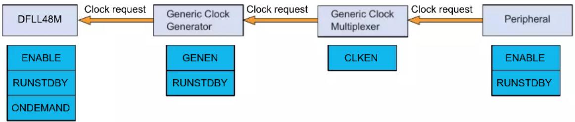
flowchart
graph LR
    A["DFLL48M"] -->|Clock request| B["Generic Clock Generator"]
    B -->|Clock request| C["Generic Clock Multiplexer"]
    C -->|Clock request| D["Peripheral"]
    E["ENABLE"] --> F["RUNSTDBY"]
    F --> G["ONDEMAND"]
    H["GENEN"] --> I["RUNSTDBY"]
    I --> J["CLKEN"]
    J --> C
    K["ENABLE"] --> L["RUNSTDBY"]
    L --> M["Peripheral"]
All clock sources in the system can be run in an on-demand mode: the clock source is in a stopped state unless a peripheral is requesting the clock source. Clock requests propagate from the peripheral, via the GCLK, to the clock source. If one or more peripheral is using a clock source, the clock source will be started/kept running. As soon as the clock source is no longer needed and no peripheral has an active request, the clock source will be stopped until requested again.
The clock request can reach the clock source only if the peripheral, the generic clock and the clock from the Generic Clock Generator in-between are enabled. The time taken from a clock request being asserted to the clock source being ready is dependent on the clock source startup time, clock source frequency as well as the divider used in the Generic Clock Generator. The total startup time Tstart from a clock request until the clock is available for the peripheral is between:
$$ T _ {\text { start_max }} = \text { Clock source startup time } + 2 \times \text { clock source periods } + 2 \times \text { divided clock source periods } $$
$$ T _ {\text { start_min }} = \text { Clock source startup time } + 1 \times \text { clock source period } + 1 \times \text { divided clock source period } $$
The time between the last active clock request stopped and the clock is shut down, T_stop , is between:
$$ T _ {\text { stop_min }} = 1 \times \text { divided clock source period } + 1 \times \text { clock source period } $$
$$ T _ {\text { stop_max }} = 2 \times \text { divided clock source periods } + 2 \times \text { clock source periods } $$
The On-Demand function can be disabled individually for each clock source by clearing the ONDEMAND bit located in each clock source controller. Consequently, the clock will always run whatever the clock request status is. This has the effect of removing the clock source startup time at the cost of power consumption.
The clock request mechanism can be configured to work in standby mode by setting the RUNSDTBY bits of the modules, see Figure 13-4.
13.7 Power Consumption vs. Speed
When targeting for either a low-power or a fast acting system, some considerations have to be taken into account due to the nature of the asynchronous clocking of the peripherals:
If clocking a peripheral with a very low clock, the active power consumption of the peripheral will be lower. At the same time the synchronization to the synchronous (CPU) clock domain is dependent on the peripheral clock speed, and will take longer with a slower peripheral clock. This will cause worse response times and longer synchronization delays.
13.8 Clocks after Reset
On any reset the synchronous clocks start to their initial state:
- OSC8M is enabled and divided by 8
- Generic Generator 0 uses OSC8M as source and generates GCLK_MAIN
• CPU and BUS clocks are undivided
On a Power Reset, the GCLK module starts to its initial state:
- All Generic Clock Generators are disabled except
- Generator 0 is using OSC8M as source without division and generates GCLK_MAIN
- Generator 2 uses OSCULP32K as source without division
- All Generic Clocks are disabled except: - WDT Generic Clock uses the Generator 2 as source
On a User Reset the GCLK module starts to its initial state, except for:
- Generic Clocks that are write-locked, i.e., the according WRTLOCK is set to 1 prior to Reset or WDT Generic Clock if the WDT Always-On at power on bit set in the NVM User Row
- Generic Clock is dedicated to the RTC if the RTC Generic Clock is enabled
On any reset the clock sources are reset to their initial state except the 32KHz clock sources which are reset only by a power reset.
14. GCLK - Generic Clock Controller
14.1 Overview
Depending on the application, peripherals may require specific clock frequencies to operate correctly. The Generic Clock controller GCLK provides nine Generic Clock Generators that can provide a wide range of clock frequencies.
Generators can be set to use different external and internal oscillators as source. The clock of each Generator can be divided. The outputs from the Generators are used as sources for the Generic Clock Multiplexers, which provide the Generic Clock (GCLK_PERIPHERAL) to the peripheral modules, as shown in Generic Clock Controller Block Diagram. The number of Peripheral Clocks depends on how many peripherals the device has.
Note: The Generator 0 is always the direct source of the GCLK_MAIN signal.
14.2 Features
- Provides Generic Clocks
- Wide frequency range
- Clock source for the generator can be changed on the fly
14.3 Block Diagram
The generation of Peripheral Clock signals (GCLK_PERIPHERAL) and the Main Clock (GCLK_MAIN) can be seen in the figure below.
Figure 14-1. Device Clocking Diagram
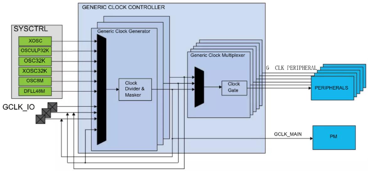
flowchart
graph TD
    A["SYSCTRL"] --> B["GCLK_IO"]
    B --> C["Clock Divider & Masker"]
    C --> D["Generic Clock Generator"]
    D --> E["Clock Gate"]
    E --> F["Generic Clock Multiplexer"]
    F --> G["PERIPHERALS"]
    G --> H["PM"]
    I["GCLK_MAIN"] --> F
    J["XOSC"] --> D
    K["OSCULP32K"] --> D
    L["OSC32K"] --> D
    M["XOSC32K"] --> D
    N["OSC8M"] --> D
    O["DFLL48M"] --> D
    P["GCLK_IO"] --> C
    Q["GCLK Main"] --> F
    R["GCLK PERIPHERAL"] --> G
The GCLK block diagram is shown in the next figure.
Figure 14-2. Generic Clock Controller Block Diagram ^(1)
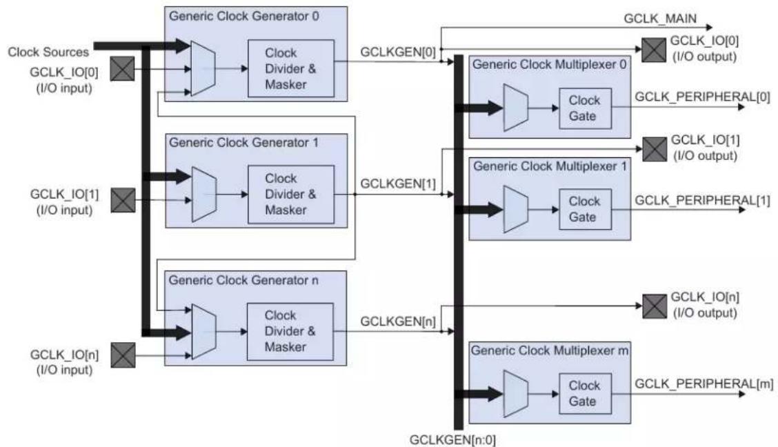
flowchart
graph TD
    A["Clock Sources GCLK_IO[0"] (I/O input)] --> B["Generic Clock Generator 0"]
    B --> C["Clock Divider & Masker"]
    C --> D["GCLKGEN[0"]]
    D --> E["Generic Clock Multiplexer 0"]
    E --> F["GCLK_MAIN"]
    F --> G["GCLK_IO[0"] (I/O output)]
    H["Clock Sources GCLK_IO[1"] (I/O input)] --> I["Generic Clock Generator 1"]
    I --> J["Clock Divider & Masker"]
    J --> K["GCLKGEN[1"]]
    K --> L["Generic Clock Multiplexer 1"]
    L --> M["GCLK_PERIPHERAL[1"]]
    N["Clock Sources GCLK_IO[n"] (I/O input)] --> O["Generic Clock Generator n"]
    O --> P["Clock Divider & Masker"]
    P --> Q["GCLKGEN[n"]]
    Q --> R["Generic Clock Multiplexer m"]
    R --> S["GCLK_PERIPHERAL[m"]]
    T["Clock Sources GCLK_IO[n"] (I/O input)] --> U["Generic Clock Generator n"]
    U --> V["Clock Divider & Masker"]
    V --> W["GCLKGEN[n"]]
    W --> X["Generic Clock Multiplexer m"]
    X --> Y["GCLK_PERIPHERAL[m"]]
Note: 1. If GENCTRL.SRC=0x01(GCLKIN), the GCLK_IO is set as an input.
14.4 Signal Description
Table 14-1. Signal Description
| Signal Name Type Description | |
| GCLK_IO[7:0] Digital I/O Clock source for Generators when input | |
| Generic Clock signal when output | |
Refer to PORT Function Multiplexing table in I/O Multiplexing and Considerations for details on the pin mapping for this peripheral.
Note: One signal can be mapped on several pins.
Related Links
- I/O Multiplexing and Considerations
14.5 Product Dependencies
In order to use this peripheral, other parts of the system must be configured correctly, as described below.
14.5.1 I/O Lines
Using the GCLK I/O lines requires the I/O pins to be configured.
Related Links
- PORT - I/O Pin Controller
14.5.2 Power Management
The GCLK can operate in sleep modes, if required. Refer to the sleep mode description in the Power Manager (PM) section.
Related Links
- Power Manager (PM)
14.5.3 Clocks
The GCLK bus clock (CLK_GCLK_APB) can be enabled and disabled in the Power Manager, and the default state of CLK_GCLK_APB can be found in the Peripheral Clock Masking section of PM – Power Manager.
Related Links
- Power Manager (PM)
15.8.8. APBAMASK
14.5.4 Interrupts
Not applicable.
14.5.5 Events
Not applicable.
14.5.6 Debug Operation
Not applicable.
Related Links
18.8.19. FREQCORR
14.5.7 Register Access Protection
All registers with write-access can be optionally write-protected by the Peripheral Access Controller (PAC).
Note: Optional write-protection is indicated by the "PAC Write-Protection" property in the register description.
Write-protection does not apply for accesses through an external debugger.
Related Links
10.5. PAC - Peripheral Access Controller
14.5.8 Analog Connections
Not applicable.
14.6 Functional Description
14.6.1 Principle of Operation
The GCLK module is comprised of eight Generic Clock Generators (Generators) sourcing m Generic Clock Multiplexers.
A clock source selected as input to a Generator can either be used directly, or it can be prescaled in the Generator. A generator output is used as input to one or more the Generic Clock Multiplexers to provide a peripheral (GCLK_PERIPHERAL). A generic clock can act as the clock to one or several of peripherals.
14.6.2 Basic Operation
14.6.2.1 Initialization
Before a Generator is enabled, the corresponding clock source should be enabled. The Peripheral clock must be configured as outlined by the following steps:
-
The Generic Clock Generator division factor must be set by performing a single 32-bit write to the Generic Clock Generator Division register (GENDIV):
-
The Generic Clock Generator that will be selected as the source of the generic clock by setting the ID bit group (GENDIV.ID).
- The division factor must be selected by the DIV bit group (GENDIV.DIV)
Note: Refer to Generic Clock Generator Division register (GENDIV) for details.
-
The generic clock generator must be enabled by performing a single 32-bit write to the Generic Clock Generator Control register (GENCTRL):
-
The Generic Clock Generator will be selected as the source of the generic clock by the ID bit group (GENCTRL.ID)
- The Generic Clock generator must be enabled (GENCTRL.GENEN=1)
Note: Refer to Generic Clock Generator Control register (GENCTRL) for details.
-
The generic clock must be configured by performing a single 16-bit write to the Generic Clock Control register (CLKCTRL):
-
The Generic Clock that will be configured via the ID bit group (CLKCTRL.ID)
- The Generic Clock Generator used as the source of the generic clock by writing the GEN bit group (CLKCTRL.GEN)
Note: Refer to Generic Clock Control register (CLKCTRL) for details.
Related Links
14.8.3. CLKCTRL
14.8.4. GENCTRL
14.8.5. GENDIV
14.6.2.2 Enabling, Disabling and Resetting
The GCLK module has no enable/disable bit to enable or disable the whole module.
The GCLK is reset by setting the Software Reset bit in the Control register (CTRL.SWRST) to 1. All registers in the GCLK will be reset to their initial state, except for Generic Clocks Multiplexer and associated Generators that have their Write Lock bit set to 1 (CLKCTRL.WRTLOCK). For further details, refer to 14.6.3.4. Configuration Lock.
14.6.2.3 Generic Clock Generator
Each Generator (GCLK_GEN) can be set to run from one of eight different clock sources except GCLKGEN[1], which can be set to run from one of seven sources. GCLKGEN[1] is the only Generator that can be selected as source to other Generators but can not act as source to itself.
Each generator GCLKGEN[x] can be connected to one specific pin GCLK_IO[x]. The GCLK_IO[x] can be set to act as source to GCLKGEN[x] or GCLK_IO[x] can be set up to output the clock generated by GCLKGEN[x].
The selected source can be divided. Each Generator can be enabled or disabled independently.
Each GCLKGEN clock signal can then be used as clock source for Generic Clock Multiplexers. Each Generator output is allocated to one or several Peripherals.
GCLKGEN[0], is used as GCLK_MAIN for the synchronous clock controller inside the Power Manager.
Refer to PM-Power Manager for details on the synchronous clock generation.
Figure 14-3. Generic Clock Generator
flowchart
graph LR
    A["Clock Sources"] --> B["GCLK_IO[x"]]
    C["GCLK GEN[x"]] --> B
    B --> D["GCLKGENSRC"]
    D --> E["DIVIDER"]
    E --> F["0"]
    E --> G["1"]
    F --> H["GCLKGENSRC"]
    G --> I["GCLKGEN[x"]]
    J["GENCTRL.SRC"] --> K["DIVSEL"]
    L["GENCTRL.DIVSEL"] --> K
    M["GENDIV.DIV"] --> K
    K --> N["0"]
    K --> O["1"]
    N --> P["Clock Gate"]
    O --> P
    P --> Q["GCLKGEN[x"]]
    R["GENCTRL.GENEN"] --> S["Clock Gate"]
Related Links
15. Power Manager (PM)
14.6.2.4 Enabling a Generic Clock Generator
A Generator is enabled by setting the Generic Clock Generator Enable bit in the Generic Clock Generator Control register (GENCTRL.GENEN=1).
14.6.2.5 Disabling a Generic Clock Generator
A Generator is disabled by clearing GENCTRL.GENEN. When GENCTRL.GENEN=0, the GCLKGEN clock is disabled and clock gated.
14.6.2.6 Selecting a Clock Source for the Generic Clock Generator
Each Generator can individually select a clock source by setting the Source Select bit group in GENCTRL (GENCTRL.SRC).
Changing from one clock source, for example A, to another clock source, B, can be done on the fly: If clock source B is not ready, the Generator will continue running with clock source A. As soon as clock source B is ready, however, the generic clock generator will switch to it. During the switching operation, the Generator holds clock requests to clock sources A and B and then releases the clock source A request when the switch is done.
The available clock sources are device dependent (usually the crystal oscillators, RC oscillators, PLL and DFLL). Only GCLKGEN[1] can be used as a common source for all other generators except Generator 1.
14.6.2.7 Changing Clock Frequency
The selected source (GENCLKSRC) for a Generator can be divided by writing a division value in the Division Factor bit group in the Generic Clock Generator Division register (GENDIV.DIV). How the actual division factor is calculated is depending on the Divide Selection bit in GENCTRL (GENCTRL.DIVSEL), it can be interpreted in two ways by the integer divider.
Note: The number of DIV bits for each Generator is device dependent.
Related Links
14.8.5. GENDIV
14.8.4. GENCTRL
14.6.2.8 Duty Cycle
When dividing a clock with an odd division factor, the duty-cycle will not be 50/50. Writing the Improve Duty Cycle bit in GENCTRL (GENCTRL.IDC=1) will result in a 50/50 duty cycle.
14.6.2.9 Generic Clock Output on I/O Pins
Each Generator's output can be directed to a GCLK_IO pin. If the Output Enable bit in GENCTRL is '1' (GENCTRL.OE=1) and the Generator is enabled (GENCTRL.GENEN=1), the Generator requests its clock source and the GCLKGEN clock is output to a GCLK_IO pin. If GENCTRL.OE=0, GCLK_IO is set according to the Output Off Value bit. If the Output Off Value bit in GENCTRL (GENCTRL.OOV) is zero, the output clock will be low when generic clock generator is turned off. If GENCTRL.OOV=1, the output clock will be high when Generator is turned off.
In standby mode, if the clock is output (GENCTRL.OE=1), the clock on the GCLK_IO pin is frozen to the OOV value if the Run In Standby bit in GENCTRL (GENCTRL.RUNSTDBY) is zero. If GENCTRL.RUNSTDBY=1, the GCLKGEN clock is kept running and output to GCLK_IO.
14.6.3 Generic Clock
Figure 14-4. Generic Clock Multiplexer
flowchart
graph TD
    A["GCLKGEN[0"]] --> B((Block))
    C["GCLKGEN[1"]] --> B
    D["GCLKGEN[2"]] --> B
    E["GCLKGEN[n"]] --> B
    B --> F["Clock Gate"]
    F --> G["GCLK_PERIPHERAL"]
    H["CLKCTRL.CLKEN"] --> F
    I["CLKCTRL.GEN"] --> B
14.6.3.1 Enabling a Generic Clock
Before a generic clock is enabled, one of the Generators must be selected as the source for the generic clock by writing to CLKCTRL.GEN. The clock source selection is individually set for each generic clock.
When a Generator has been selected, the generic clock is enabled by setting the Clock Enable bit in CLKCTRL (CLKCTRL.CLKEN=1). The CLKCTRL.CLKEN bit must be synchronized to the generic clock domain. CLKCTRL.CLKEN will continue to read as its previous state until the synchronization is complete.
14.6.3.2 Disabling a Generic Clock
A generic clock is disabled by writing CLKCTRL.CLKEN=0. The SYNCBUSY bit will be cleared when this write-synchronization is complete. CLKCTRL.CLKEN will stay in its previous state until the synchronization is complete. The generic clock is gated when disabled.
14.6.3.3 Selecting a Clock Source for the Generic Clock
When changing a generic clock source by writing to CLKCTRL.GEN, the generic clock must be disabled before being re-enabled with the new clock source setting. This prevents glitches during the transition:
- Write CLKCTRL.CLKEN=0
- Assert that CLKCTRL.CLKEN reads '0'
- Change the source of the generic clock by writing CLKCTRL.GEN
- Re-enable the generic clock by writing CLKCTRL.CLKEN=1
14.6.3.4 Configuration Lock
The generic clock configuration can be locked for further write accesses by setting the Write Lock bit in the CLKCTRL register (CLKCTRL.WRTLOCK). All writes to the CLKCTRL register will be ignored. It can only be unlocked by a Power Reset.
The Generator source of a locked generic clock are also locked, too: The corresponding GENCTRL and GENDIV are locked, and can be unlocked only by a Power Reset.
There is one exception concerning the GCLKGEN[0]. As it is used as GCLK_MAIN, it can not be locked. It is reset by any Reset and will start up in a known configuration. The software reset (CTRL.SWRST) can not unlock the registers.
14.6.4 Additional Features
14.6.4.1 Indirect Access
The Generic Clock Generator Control and Division registers (GENCTRL and GENDIV) and the Generic Clock Control register (CLKCTRL) are indirectly addressed as shown in the next figure.
Figure 14-5. GCLK Indirect Access
flowchart
graph LR
    A["User Interface"] --> B["GENCTRL"]
    A --> C["GENDIV"]
    A --> D["CLKCTRL"]
    B -->|GENCTRL.ID=i| E["Generic Clock Generator [i"]]
    C -->|GENDIV.ID=i| E
    D -->|CLKCTRL.ID=j| F["Generic Clock[j"]]
    E --> G["GENCTRL"]
    E --> H["GENDIV"]
    F --> I["CLKCTRL"]
Writing these registers is done by setting the corresponding ID bit group. To read a register, the user must write the ID of the channel, i, in the corresponding register. The value of the register for the corresponding ID is available in the user interface by a read access.
For example, the sequence to read the GENCTRL register of generic clock generator i is:
- Do an 8-bit write of the i value to GENCTRL.ID
- Read the value of GENCTRL
14.6.4.2 Generic Clock Enable after Reset
The Generic Clock Controller must be able to provide a generic clock to some specific peripherals after a reset. That means that the configuration of the Generators and generic clocks after Reset is device-dependent.
Refer to GENCTRL.ID for details on GENCTRL reset.
Refer to GENDIV.ID for details on GENDIV reset.
Refer to CLKCTRL.ID for details on CLKCTRL reset.
Related Links
14.8.3. CLKCTRL
14.8.4. GENCTRL
14.8.5. GENDIV
14.6.5 Sleep Mode Operation
14.6.5.1 Sleep Walking
The GCLK module supports the Sleep Walking feature. If the system is in a sleep mode where the Generic Clocks are stopped, a peripheral that needs its clock in order to execute a process must request it from the Generic Clock Controller.
The Generic Clock Controller receives this request, determines which Generic Clock Generator is involved and which clock source needs to be awakened. It then wakes up the respective clock source, enables the Generator and generic clock stages successively, and delivers the clock to the peripheral.
14.6.5.2 Run in Standby Mode
In standby mode, the GCLK can continuously output the generator output to GCLK_IO.
When set, the GCLK can continuously output the generator output to GCLK_IO.
Refer to 14.6.2.9. Generic Clock Output on I/O Pins for details.
14.6.6 Synchronization
Due to asynchronicity between the main clock domain and the peripheral clock domains, some registers need to be synchronized when written or read.
When executing an operation that requires synchronization, the Synchronization Busy bit in the Status register (STATUS.SYNCBUSY) will be set immediately, and cleared when synchronization is complete.
If an operation that requires synchronization is executed while STATUS.SYNCBUSY=1, the bus will be stalled. All operations will complete successfully, but the CPU will be stalled and interrupts will be pending as long as the bus is stalled.
The following registers are synchronized when written:
- Generic Clock Generator Control register (GENCTRL)
- Generic Clock Generator Division register (GENDIV)
• Control register (CTRL)
Required write-synchronization is denoted by the "Write-Synchronized" property in the register description.
Related Links
13.3. Register Synchronization
14.7 Register Summary
Table 14-2. Register Summary
| Offset | Name Bit | Pos. | ||||||||
| 0x0 CTRL 7:0 SWRST | ||||||||||
| 0x1 STATUS 7:0 SYNCBUSY | ||||||||||
| 0x2 | CLKCTRL | 7:0 ID[5:0] | ||||||||
| 0x3 15:8 WRTLOCK CLKEN GEN[3:0] | ||||||||||
| 0x4 | GENCTRL | 7:0 | ID[3:0] | |||||||
| 0x5 15:8 | SRC[4:0] | |||||||||
| 0x6 | 23:16 | RUNSTDBY | DIVSEL | OE | OOV | IDC | GENEN | |||
| 0x7 | 31:24 | |||||||||
| 0x8 | GENDIV | 7:0 | ID[3:0] | |||||||
| 0x9 15:8 | DIV[7:0] | |||||||||
| 0xA | 23:16 | DIV[15:8] | ||||||||
| 0xB | 31:24 | |||||||||
14.8 Register Description
Registers can be 8, 16, or 32 bits wide. Atomic 8-, 16-, and 32-bit accesses are supported. In addition, the 8-bit quarters and 16-bit halves of a 32-bit register, and the 8-bit halves of a 16-bit register can be accessed directly.
Some registers require synchronization when read and/or written. Synchronization is denoted by the "Read-Synchronized" and/or "Write-Synchronized" property in each individual register description.
Refer to 14.5.7. Register Access Protection for details.
Some registers are enable-protected, meaning they can only be written when the module is disabled. Enable-protection is denoted by the "Enable-Protected" property in each individual register description.
Refer to 14.6.6. Synchronization for details.
14.8.1 Control
Name: CTRL
Offset: 0x0
Reset: 0x00
Property: Write-Protected, Write-Synchronized
Bit 76543210
| SWRST | |||||||
| Access Reset 0 | R/W | ||||||
Bit 0 - SWRST Software Reset
Writing a zero to this bit has no effect.
Writing a one to this bit resets all registers in the GCLK to their initial state after a power reset, except for generic clocks and associated generators that have their WRTLOCK bit in CLKCTRL read as one.
Refer to GENCTRL.ID for details on GENCTRL reset.
Refer to GENDIV.ID for details on GENDIV reset.
Refer to CLKCTRL.ID for details on CLKCTRL reset.
Due to synchronization, there is a delay from writing CTRL.SWRST until the reset is complete. CTRL.SWRST and STATUS.SYNCBUSY will both be cleared when the reset is complete.
Value Description
| 0 | There is no reset operation ongoing. |
| 1 | There is a reset operation ongoing. |
14.8.2 Status
Name: STATUS
Offset: 0x1
Reset: 0x00
Property: -

text_image
Bit 7 6 5 4 3 2 1 0 SYNCBUSY Access R Reset 0Bit 7 - SYNCBUSY Synchronization Busy Status
This bit is cleared when the synchronization of registers between the clock domains is complete. This bit is set when the synchronization of registers between clock domains is started.
14.8.3 Generic Clock Control
Name: CLKCTRL
Offset: 0x2
Reset: 0x0000
Property: Write-Protected
Bit 15 14 13 12 11 10 9 8
| WRTLOCK CLKEN GEN[3:0] | |||||||
| Access | R/W | R/W | R/W | R/W | R/W | R/W | |
| Reset | 0 0 | 0 0 0 0 | |||||
| Bit | 7 6 5 4 3 2 1 0 | ||||||
| ID[5:0] | |||||||
| Access | R/W | R/W | R/W | R/W | R/W | ||
| Reset | 0 0 0 0 0 0 | ||||||
Bit 15 - WRTLOCK Write Lock
When this bit is written, it will lock from further writes the generic clock pointed to by CLKCTRL.ID, the generic clock generator pointed to in CLKCTRL.GEN and the division factor used in the generic clock generator. It can only be unlocked by a power reset.
One exception to this is generic clock generator 0, which cannot be locked.
| Value | Description |
| 0 | The generic clock and the associated generic clock generator and division factor are not locked. |
| 1 | The generic clock and the associated generic clock generator and division factor are locked. |
Bit 14 - CLKEN Clock Enable
This bit is used to enable and disable a generic clock.
| Value | Description |
| 0 | The generic clock is disabled. |
| 1 | The generic clock is enabled. |
Bits 11:8 - GEN[3:0] Generic Clock Generator
Table 14-3. Generic Clock Generator
| GEN[3:0] | Name | Description |
| 0x0 | GCLKGEN0 | Generic clock generator 0 |
| 0x1 | GCLKGEN1 | Generic clock generator 1 |
| 0x2 | GCLKGEN2 | Generic clock generator 2 |
| 0x3 | GCLKGEN3 | Generic clock generator 3 |
| 0x4 | GCLKGEN4 | Generic clock generator 4 |
| 0x5 | GCLKGEN5 | Generic clock generator 5 |
| 0x6 | GCLKGEN6 | Generic clock generator 6 |
| 0x7 | GCLKGEN7 | Generic clock generator 7 |
| 0x8-0xF | Reserved | Reserved |
Bits 5:0 - ID[5:0] Generic Clock Selection ID
These bits select the generic clock that will be configured. The value of the ID bit group versus module instance is shown in the table below.
A power reset will reset the CLKCTRL register for all IDs, including the RTC. If the WRTLOCK bit of the corresponding ID is zero and the ID is not the RTC, a user reset will reset the CLKCTRL register for this ID.
After a power reset, the reset value of the CLKCTRL register versus module instance is as shown in the next table.
Table 14-4. Generic Clock Selection ID and CLKCTRL value after Power Reset
| Module Instance Reset Value after Power Reset | |||
| CLKCTRL.GEN CLKCTRL.CLKEN CLKCTRL.WRTLOCK | |||
| RTC 0x00 0x00 0x00 | |||
| WDT 0x02 0x01 if WDT Enable bit in NVM | User Row written to one0x00 if WDT Enable bit in NVMUser Row written to zero | 0x01 if WDT Always-On bit inNVM User Row written to one0x00 if WDT Always-On bit inNVM User Row written to zero | |
| Others 0x00 0x00 0x00 | |||
After a user reset, the reset value of the CLKCTRL register versus module instance is as shown in the table below.
Table 14-5. Generic Clock Selection ID and CLKCTRL Value after User Reset
| Module Instance Reset Value after a User Reset | |||
| CLKCTRL.GEN CLCTRL.CLKEN | CLKCTRL.WRTLOCK | ||
| RTC 0x00 if WRTLOCK=0 and CLKEN=0No change if WRTLOCK=1 or CLKEN=1 | 0x00 if WRTLOCK=0 and CLKEN=0No change if WRTLOCK=1 or CLKEN=1 | No change | |
| WDT 0x02 if WRTLOCK=0No change if WRTLOCK=1 | If WRTLOCK=00x01 if WDT Enable bit in NVM UserRow written to one0x00 if WDT Enable bit in NVM UserRow written to zeroIf WRTLOCK=1 no change | No change | |
| Others 0x00 if WRTLOCK=0No change if WRTLOCK=1 | 0x00 if WRTLOCK=0No change if WRTLOCK=1 | No change | |
| Value | Name | Description |
| 0x00 | GCLK_DFLL48M_REF | DFLL48M Reference |
| 0x01 | GCLK_WDT | WDT |
| 0x02 | GCLK_RTC | RTC |
| 0x03 | GCLK_EIC | EIC |
| 0x04 | GCLK_EVSYS_CHANNEL_0 | EVSYS_CHANNEL_0 |
| 0x05 | GCLK_EVSYS_CHANNEL_1 | EVSYS_CHANNEL_1 |
| 0x06 | GCLK_EVSYS_CHANNEL_2 | EVSYS_CHANNEL_2 |
| 0x07 | GCLK_EVSYS_CHANNEL_3 | EVSYS_CHANNEL_3 |
| 0x08 | GCLK_EVSYS_CHANNEL_4 | EVSYS_CHANNEL_4 |
| 0x09 | GCLK_EVSYS_CHANNEL_5 | EVSYS_CHANNEL_5 |
| 0x0A | GCLK_EVSYS_CHANNEL_6 | EVSYS_CHANNEL_6 |
| 0x0B | GCLK_EVSYS_CHANNEL_7 | EVSYS_CHANNEL_7 |
| 0x0C | GCLK_SERCOMx_SLOW | SERCOMx_SLOW |
| 0x0D | GCLK_SERCOM0_CORE | SERCOM0_CORE |
| 0x0E | GCLK_SERCOM1_CORE | SERCOM1_CORE |
| 0x0F | GCLK_SERCOM2_CORE | SERCOM2_CORE |
| 0x10 | GCLK_SERCOM3_CORE | SERCOM3_CORE |
| 0x11 | GCLK_SERCOM4_CORE | SERCOM4_CORE |
| 0x12 | GCLK_SERCOM5_CORE | SERCOM5_CORE |
| 0x13 | GCLK_TC0, GCLK_TC1 | TC0, TC1 |
| 0x14 | GCLK_TC2, GCLK_TC3 | TC2, TC3 |
| 0x15 | GCLK_TC4, GCLK_TC5 | TC4, TC5 |
| 0x16 | GCLK_TC6, GCLK_TC7 | TC6, TC7 |
| 0x17 | GCLK_ADC | ADC |
| 0x18 | GCLK_AC_DIG | AC_DIG |
| 0x19 | GCLK_AC_ANA | AC_ANA |
| 0x1A | GCLK_DAC | DAC |
| Value Name | Description | |
| 0x1B | GCLK_PTC PTC | |
| 0x1C-0x3F | - Reserved | |
14.8.4 Generic Clock Generator Control
Name: GENCTRL
Offset: 0x4
Reset: 0x00000000
Property: Write-Protected, Write-Synchronized
other
Bit 31 30 29 28 27 26 25 24 Access Reset Bit 23 22 21 20 19 18 17 16 Access Reset Bit 15 14 13 12 11 10 Access Reset Bit 7 Access Reset Bit 23 22 21 20 19 18 17 16 RUN$TDBY DIVSEL OE OOV IDC GENEN R/W R/W R/W R/W R/W R/W R/W R/W R/W R/W R/W R/W R/W R/W R/W R/W R/W R/W R/W R/W R/W R/W R/W R/W R/W R/W R/W R/W R/W R/W R/W R/W R/W R/W R/W R/W R/W R/W R/W R/W R/W R/W R/W R/W R/W R/W R/W R/W R/W R/W R/0 R/W R/W R/W R/W R/W R/W R/W R/W R/W R/W R/W R/W R/W R/W R/W R/W R/W R/W R/W R/W R/W R/W R/W R/W R/W R/W R/W R/W R/W R/W R/W R/W R/W R/W R/W R/W R/W R/W R/W R/W R/W R/W R/W R/W R/W R/W R/W R/W R/W R/W R/W R/W R/W R/W R/W R/W R/W R/W R/W R/W D[3:0] R/W D[3:0] R/W D[3:0] R/W D[3:0] R/W D[3:0] R/W D[3:0] R/W D[3:0] R/W D[3:0] R/W D[3:0] R/W D[3:0] R/W D[3:0] R/W D[3:0] R/W D[3:0] R/W D [3:0] R/W D[3:0] R/W D[3:0] R/W D[3:0] R/0 R/0 R/0 R/0 R/0 R/0 R/0 R/0 R/0 R/0 R/0 R/0 R/0 R/0 R/0 R/0 R/0 R/0 R/0 R/0 R/0 R/0 R/0 R/0 R/0 R/0Bit 21 - RUNSTDBY Run in Standby
This bit is used to keep the generic clock generator running when it is configured to be output to its dedicated GCLK_IO pin. If GENCTRL.OE is zero, this bit has no effect and the generic clock generator will only be running if a peripheral requires the clock.
| Value | Description |
| 0 | The generic clock generator is stopped in standby and the GCLK_IO pin state (one or zero) will be dependent on the setting in GENCTRL.OOV. |
| 1 | The generic clock generator is kept running and output to its dedicated GCLK_IO pin during standby mode. |
Bit 20 - DIVSEL Divide Selection
This bit is used to decide how the clock source used by the generic clock generator will be divided. If the clock source should not be divided, the DIVSEL bit must be zero and the GENDIV.DIV value for the corresponding generic clock generator must be zero or one.
| Value | Description |
| 0 | The generic clock generator equals the clock source divided by GENDIV.DIV. |
| 1 | The generic clock generator equals the clock source divided by 2^(GENDIV.DIV+1). |
Bit 19 - OE Output Enable
This bit is used to enable output of the generated clock to GCLK_IO when GCLK_IO is not selected as a source in the GENCLK.SRC bit group.
| Value | Description |
| 0 | The generic clock generator is not output. |
| 1 | The generic clock generator is output to the corresponding GCLK_IO, unless the corresponding GCLK_IO is selected as a source in the GENCLK.SRC bit group. |
Bit 18 - OOV Output Off Value
This bit is used to control the value of GCLK_IO when GCLK_IO is not selected as a source in the GENCLK.SRC bit group.
| Value Description | |
| 0 | The GCLK_IO will be zero when the generic clock generator is turned off or when the OE bit is zero. |
| 1 | The GCLK_IO will be one when the generic clock generator is turned off or when the OE bit is zero. |
Bit 17 - IDC Improve Duty Cycle
This bit is used to improve the duty cycle of the generic clock generator when odd division factors are used.
| Value Description | |
| 0 | The generic clock generator duty cycle is not 50/50 for odd division factors. |
| 1 | The generic clock generator duty cycle is 50/50. |
Bit 16 - GENEN Generic Clock Generator Enable
This bit is used to enable and disable the generic clock generator.
| Value Description | |
| 0 | The generic clock generator is disabled. |
| 1 | The generic clock generator is enabled. |
Bits 12:8 - SRC[4:0] Source Select
These bits define the clock source to be used as the source for the generic clock generator, as shown in the table below.
| Value Name | Description | |
| 0x00 | XOSC XOSC oscillator output | |
| 0x01 | GCLKIN Generator input pad | |
| 0x02 | GCLKGEN1 Generic clock generator 1 output | |
| 0x03 | OSCULP32K OSCULP32K oscillator output | |
| 0x04 | OSC32K OSC32K oscillator output | |
| 0x05 | XOSC32K XOSC32K oscillator output | |
| 0x06 | OSC8M OSC8M oscillator output | |
| 0x07 | DFLL48M DFLL48M output | |
| 0x08-0x1F | Reserved Reserved for future use |
Bits 3:0 - ID[3:0] Generic Clock Generator Selection
These bits select the generic clock generator that will be configured or read. The value of the ID bit group versus which generic clock generator is configured is shown in the next table.
A power reset will reset the GENCTRL register for all IDs, including the generic clock generator used by the RTC. If a generic clock generator ID other than generic clock generator 0 is not a source of a "locked" generic clock or a source of the RTC generic clock, a user reset will reset the GENCTRL for this ID.
| Values Names Description | ||
| 0x0 GCLKGEN0 Generic clock generator 0 | ||
| 0x1 GCLKGEN0 Generic clock generator 0 | ||
| 0x2 GCLKGEN0 Generic clock generator 0 | ||
| 0x3 GCLKGEN0 Generic clock generator 0 | ||
| 0x4 GCLKGEN0 Generic clock generator 0 | ||
| 0x5 GCLKGEN0 Generic clock generator 0 | ||
| 0x6 GCLKGEN0 Generic clock generator 0 | ||
| 0x7 GCLKGEN0 Generic clock generator 0 | ||
| 0x8-0xF | - | Reserved for future use |
After a power reset, the reset value of the GENCTRL register is as shown in the next table.
| GCLK Generator ID | Reset Value after a Power Reset |
| 0x00 | 0x00010600 |
| GCLK Generator ID Reset Value after a Power Reset | |
| 0x01 0x00000001 | |
| 0x02 0x00010302 | |
| 0x03 0x00000003 | |
| 0x04 0x00000004 | |
| 0x05 0x00000005 | |
| 0x06 0x00000006 | |
| 0x07 0x00000007 | |
After a user reset, the reset value of the GENCTRL register is as shown in the table below.
| GCLK Generator ID Reset Value after a User Reset | |
| 0x00 0x00010600 | |
| 0x01 0x00000001 if the generator is not used by the RTC and not a source of a 'locked' generic clockNo change if the generator is used by the RTC or used by a GCLK with a WRTLOCK as one | |
| 0x02 0x00010302 if the generator is not used by the RTC and not a source of a 'locked' generic clockNo change if the generator is used by the RTC or used by a GCLK with a WRTLOCK as one | |
| 0x03 0x00000003 if the generator is not used by the RTC and not a source of a 'locked' generic clockNo change if the generator is used by the RTC or used by a GCLK with a WRTLOCK as one | |
| 0x04 0x00000004 if the generator is not used by the RTC and not a source of a 'locked' generic clockNo change if the generator is used by the RTC or used by a GCLK with a WRTLOCK as one | |
| 0x05 0x00000005 if the generator is not used by the RTC and not a source of a 'locked' generic clockNo change if the generator is used by the RTC or used by a GCLK with a WRTLOCK as one | |
| 0x06 0x00000006 if the generator is not used by the RTC and not a source of a 'locked' generic clockNo change if the generator is used by the RTC or used by a GCLK with a WRTLOCK as one | |
| 0x07 0x00000007 if the generator is not used by the RTC and not a source of a 'locked' generic clockNo change if the generator is used by the RTC or used by a GCLK with a WRTLOCK as one | |
14.8.5 Generic Clock Generator Division
Name: GENDIV
Offset: 0x8
Reset: 0x00000000
Property: Write-Synchronized
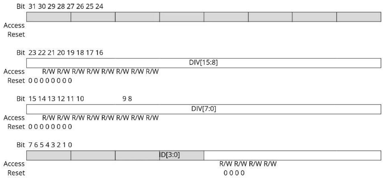
text_image
Bit 31 30 29 28 27 26 25 24 Access Reset Bit 23 22 21 20 19 18 17 16 DIV[15:8] Access R/W R/W R/W R/W R/W R/W R/W Reset 0 0 0 0 0 0 0 Bit 15 14 13 12 11 10 9 8 DIV[7:0] Access R/W R/W R/W R/W R/W R/W R/W Reset 0 0 0 0 0 0 0 Bit 7 6 5 4 3 2 1 0 Access |D[3:0] | R/W R/W R/W R/W Reset 0 0 0 0Bits 23:8 - DIV[15:0] Division Factor
These bits apply a division on each selected generic clock generator. The number of DIV bits each generator has can be seen in the table below. Writes to bits above the specified number will be ignored.
| Generator | Division Factor Bits | Maximum Division Factor |
| Generic clock generator 0 | 8 division factor bits - DIV[7:0] | 512 |
| Generic clock generator 1 | 16 division factor bits - DIV[15:0] | 131072 |
| Generic clock generators 2 | 5 division factor bits - DIV[4:0] | 64 |
| Generic clock generators 3-8 | 8 division factor bits - DIV[7:0] | 512 |
Bits 3:0 - ID[3:0] Generic Clock Generator Selection
These bits select the generic clock generator on which the division factor will be applied, as shown in the table below.
| Values | Description |
| 0x0 | Generic clock generator 0 |
| 0x1 | Generic clock generator 1 |
| 0x2 | Generic clock generator 2 |
| 0x3 | Generic clock generator 3 |
| 0x4 | Generic clock generator 4 |
| 0x5 | Generic clock generator 5 |
| 0x6 | Generic clock generator 6 |
| 0x7 | Generic clock generator 7 |
| 0x8-0xF | Reserved |
A power reset will reset the GENDIV register for all IDs, including the generic clock generator used by the RTC. If a generic clock generator ID, other than generic clock generator '0', is not a source of locked generic clock or a source of the RTC generic clock. A user reset will reset the GENDIV register for this ID. After a power reset, the reset value of the GENDIV register is as shown in the table below.
| GCLK Generator ID Reset Value after a Power Reset | |
| 0x00 0x00000000 | |
| 0x01 0x00000001 | |
| 0x02 0x00000002 | |
| 0x03 0x00000003 | |
| 0x04 0x00000004 | |
| 0x05 0x00000005 | |
| 0x06 0x00000006 | |
| 0x07 0x00000007 | |
After a user reset, the reset value of the GENDIV register is as shown in the table below.
| GCLK Generator ID Reset Value after a User Reset | |
| 0x00 0x00000000 | |
| 0x01 0x00000001, if the generator is not used by the RTC and not a source of locked generic clock. No change if the generator is used by the RTC or used by a GCLK with a WRTLOCK as one. | |
| 0x02 0x00000002, if the generator is not used by the RTC and not a source of locked generic clock. No change if the generator is used by the RTC or used by a GCLK with a WRTLOCK as one. | |
| 0x03 0x00000003, if the generator is not used by the RTC and not a source of locked generic clock. No change if the generator is used by the RTC or used by a GCLK with a WRTLOCK as one. | |
| 0x04 0x00000004, if the generator is not used by the RTC and not a source of locked generic clock. No change if the generator is used by the RTC or used by a GCLK with a WRTLOCK as one. | |
| 0x05 0x00000005, if the generator is not used by the RTC and not a source of locked generic clock. No change if the generator is used by the RTC or used by a GCLK with a WRTLOCK as one. | |
| 0x06 0x00000006, if the generator is not used by the RTC and not a source of locked generic clock. No change if the generator is used by the RTC or used by a GCLK with a WRTLOCK as one. | |
| 0x07 0x00000007, if the generator is not used by the RTC and not a source of locked generic clock. No change if the generator is used by the RTC or used by a GCLK with a WRTLOCK as one. |
15. Power Manager (PM)
15.1 Overview
The Power Manager (PM) controls the reset, clock generation and sleep modes of the device.
Utilizing a main clock chosen from a large number of clock sources from the GCLK, the clock controller provides synchronous system clocks to the CPU and the modules connected to the AHB and the APBx bus. The synchronous system clocks are divided into a number of clock domains; one for the CPU and AHB and one for each APBx. Any synchronous system clock can be changed at run-time during normal operation. The clock domains can run at different speeds, enabling the user to save power by running peripherals at a relatively low clock frequency, while maintaining high CPU performance. In addition, the clock can be masked for individual modules, enabling the user to minimize power consumption. If for some reason the main clock stops oscillating, the clock failure detector allows switching the main clock to the safe OSC8M clock.
Before entering the STANDBY sleep mode the user must make sure that a significant amount of clocks and peripherals are disabled, so that the voltage regulator is not overloaded. This is because during STANDBY sleep mode the internal voltage regulator will be in low power mode.
Various sleep modes are provided in order to fit power consumption requirements. This enables the PM to stop unused modules in order to save power. In active mode, the CPU is executing application code. When the device enters a sleep mode, program execution is stopped and some modules and clock domains are automatically switched off by the PM according to the sleep mode. The application code decides which sleep mode to enter and when. Interrupts from enabled peripherals and all enabled reset sources can restore the device from a sleep mode to active mode.
The PM also contains a reset controller to collect all possible reset sources. It issues a device reset and sets the device to its initial state, and allows the reset source to be identified by software.
15.2 Features
- Reset control
- Reset the microcontroller and set it to an initial state according to the reset source
- Multiple reset sources
• Power reset sources: POR, BOD12, BOD33
- User reset sources: External reset (RESET), Watchdog Timer reset, software reset
- Reset status register for reading the reset source from the application code
- Clock control
- Controls CPU, AHB and APB system clocks
- Multiple clock sources and division factor from GCLK
- Clock prescaler with 1x to 128x division
- Safe run-time clock switching from GCLK
- Module-level clock gating through maskable peripheral clocks
- Clock failure detector
• Power management control
– Sleep modes: IDLE, STANDBY
- SleepWalking support on GCLK clocks
15.3 Block Diagram
Figure 15-1. PM Block Diagram
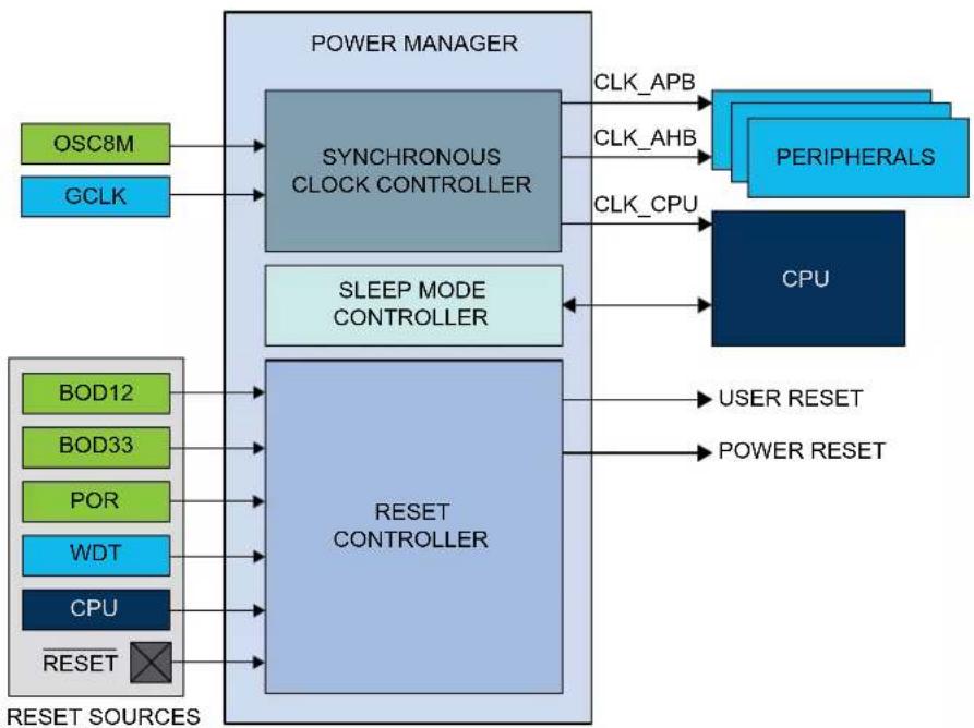
flowchart
graph TD
    A["OSC8M"] --> B["SYNCHRONOUS CLOCK CONTROLLER"]
    C["GCLK"] --> B
    D["BOD12"] --> E["RESET CONTROLLER"]
    F["BOD33"] --> E
    G["POR"] --> E
    H["WDT"] --> E
    I["CPU"] --> E
    J["RESET"] --> E
    K["POWER MANAGER"] --> B
    L["SLEEP MODE CONTROLLER"] --> E
    M["PERIPHERALS"] --> N["CPU"]
    O["USER RESET"] --> E
    P["POWER RESET"] --> E
    B --> Q["CLK_APB"]
    B --> R["CLK_AHB"]
    B --> S["CLK_CPU"]
    E --> T["RESET CONTROLLER"]
    style B fill:#99ccff,stroke:#333
    style E fill:#99ccff,stroke:#333
    style N fill:#66ccff,stroke:#333
    style O fill:#99ccff,stroke:#333
    style P fill:#99ccff,stroke:#333
15.4 Signal Description
| Signal Name Type Description | ||
| RESET Digital input External reset |
Refer to I/O Multiplexing and Considerations for details on the pin mapping for this peripheral. One signal can be mapped on several pins.
Related Links
- I/O Multiplexing and Considerations
15.5 Product Dependencies
In order to use this peripheral, other parts of the system must be configured correctly, as described below.
15.5.1 I/O Lines
Not applicable.
15.5.2 Power Management
Not applicable.
15.5.3 Clocks
The PM bus clock (CLK_PM_APB) can be enabled and disabled in the Power Manager, and the default state of CLK_PM_APB can be found in Peripheral Clock Default State table in the Peripheral Clock Masking section. If this clock is disabled in the Power Manager, it can only be re-enabled by a reset.
A generic clock (GCLK_MAIN) is required to generate the main clock. The clock source for GCLK_MAIN is configured by default in the Generic Clock Controller, and can be reconfigured by the user if needed. Refer to GCLK - Generic Clock Controller for details.
Related Links
15.6.2.6. Peripheral Clock Masking
- GCLK - Generic Clock Controller
15.5.3.1 Main Clock
The main clock (CLK_MAIN) is the common source for the synchronous clocks. This is fed into the common 8-bit prescaler that is used to generate synchronous clocks to the CPU, AHB and APBx modules.
15.5.3.2 CPU Clock
The CPU clock (CLK_CPU) is routed to the CPU. Halting the CPU clock inhibits the CPU from executing instructions.
15.5.3.3 AHB Clock
The AHB clock (CLK_AHB) is the root clock source used by peripherals requiring an AHB clock. The AHB clock is always synchronous to the CPU clock and has the same frequency, but may run even when the CPU clock is turned off. A clock gate is inserted from the common AHB clock to any AHB clock of a peripheral.
15.5.3.4 APBx Clocks
The APBx clock (CLK_APBX) is the root clock source used by modules requiring a clock on the APBx bus. The APBx clock is always synchronous to the CPU clock, but can be divided by a prescaler, and will run even when the CPU clock is turned off. A clock gater is inserted from the common APB clock to any APBx clock of a module on APBx bus.
15.5.4 Interrupts
The interrupt request line is connected to the Interrupt Controller. Using the PM interrupt requires the Interrupt Controller to be configured first. Refer to Nested Vector Interrupt Controller for details.
Related Links
10.2. Nested Vector Interrupt Controller
15.5.5 Events
Not applicable.
15.5.6 Debug Operation
When the CPU is halted in debug mode, the PM continues normal operation. In sleep mode, the clocks generated from the PM are kept running to allow the debugger accessing any modules. As a consequence, power measurements are not possible in debug mode.
15.5.7 Register Access Protection
Registers with write-access can be optionally write-protected by the Peripheral Access Controller (PAC), except for the following:
- Interrupt Flag register (INTFLAG).
- Reset Cause register (RCAUSE).
Note: Optional write-protection is indicated by the "PAC Write-Protection" property in the register description.
Write-protection does not apply for accesses through an external debugger. Refer to PAC - Peripheral Access Controller for details.
Related Links
10.5. PAC - Peripheral Access Controller
15.8.13. INTFLAG
15.8.14. RCAUSE
15.5.8 Analog Connections
Not applicable.
15.6 Functional Description
15.6.1 Principle of Operation
15.6.1.1 Synchronous Clocks
The GCLK_MAIN clock from GCLK module provides the source for the main clock, which is the common root for the synchronous clocks for the CPU and APBx modules. The main clock is divided by an 8-bit prescaler, and each of the derived clocks can run from any tapping off this prescaler or the undivided main clock, as long as f_CPU ≥ f_APBx . The synchronous clock source can be changed on the fly to respond to varying load in the application. The clocks for each module in each synchronous clock domain can be individually masked to avoid power consumption in inactive modules. Depending on the sleep mode, some clock domains can be turned off (see Table 15-4).
15.6.1.2 Reset Controller
The Reset Controller collects the various reset sources and generates reset for the device. The device contains a power-on-reset (POR) detector, which keeps the system reset until power is stable. This eliminates the need for external reset circuitry to guarantee stable operation when powering up the device.
15.6.1.3 Sleep Mode Controller
In ACTIVE mode, all clock domains are active, allowing software execution and peripheral operation. The PM Sleep Mode Controller allows the user to choose between different sleep modes depending on application requirements, to save power (see Table 15-4).
15.6.2 Basic Operation
15.6.2.1 Initialization
After a power-on reset, the PM is enabled and the Reset Cause register indicates the POR source (RCAUSE.POR). The default clock source of the GCLK_MAIN clock is started and calibrated before the CPU starts running. The GCLK_MAIN clock is selected as the main clock without any division on the prescaler. The device is in the ACTIVE mode.
By default, only the necessary clocks are enabled (see Table 1).
Related Links
15.8.14. RCAUSE
15.6.2.2 Enabling, Disabling and Resetting
The PM module is always enabled and can not be reset.
15.6.2.3 Selecting the Main Clock Source
Refer to GCLK - Generic Clock Controller for details on how to configure the main clock source.
Related Links
- GCLK - Generic Clock Controller
15.6.2.4 Selecting the Synchronous Clock Division Ratio
The main clock feeds an 8-bit prescaler, which can be used to generate the synchronous clocks. By default, the synchronous clocks run on the undivided main clock. The user can select a prescaler
division for the CPU clock by writing the CPU Prescaler Selection bits in the CPU Select register (CPUSEL.CPUDIV), resulting in a CPU clock frequency determined by this equation:
$$ f _ {\mathrm{CPU}} = \frac {f _ {\mathrm{main}}}{2 ^ {\mathrm{CPUDIV}}} $$
Similarly, the clock for the APBx can be divided by writing their respective registers (APBxSEL.APBxDIV). To ensure correct operation, frequencies must be selected so that f_CPU ≥ f_APBx . Also, frequencies must never exceed the specified maximum frequency for each clock domain.
Note: The AHB clock is always equal to the CPU clock.
CPUSEL and APBxSEL can be written without halting or disabling peripheral modules. Writing CPUSEL and APBxSEL allows a new clock setting to be written to all synchronous clocks at the same time. It is possible to keep one or more clocks unchanged. This way, it is possible to, for example, scale the CPU speed according to the required performance, while keeping the APBx frequency constant.
Figure 15-2. Synchronous Clock Selection and Prescaler
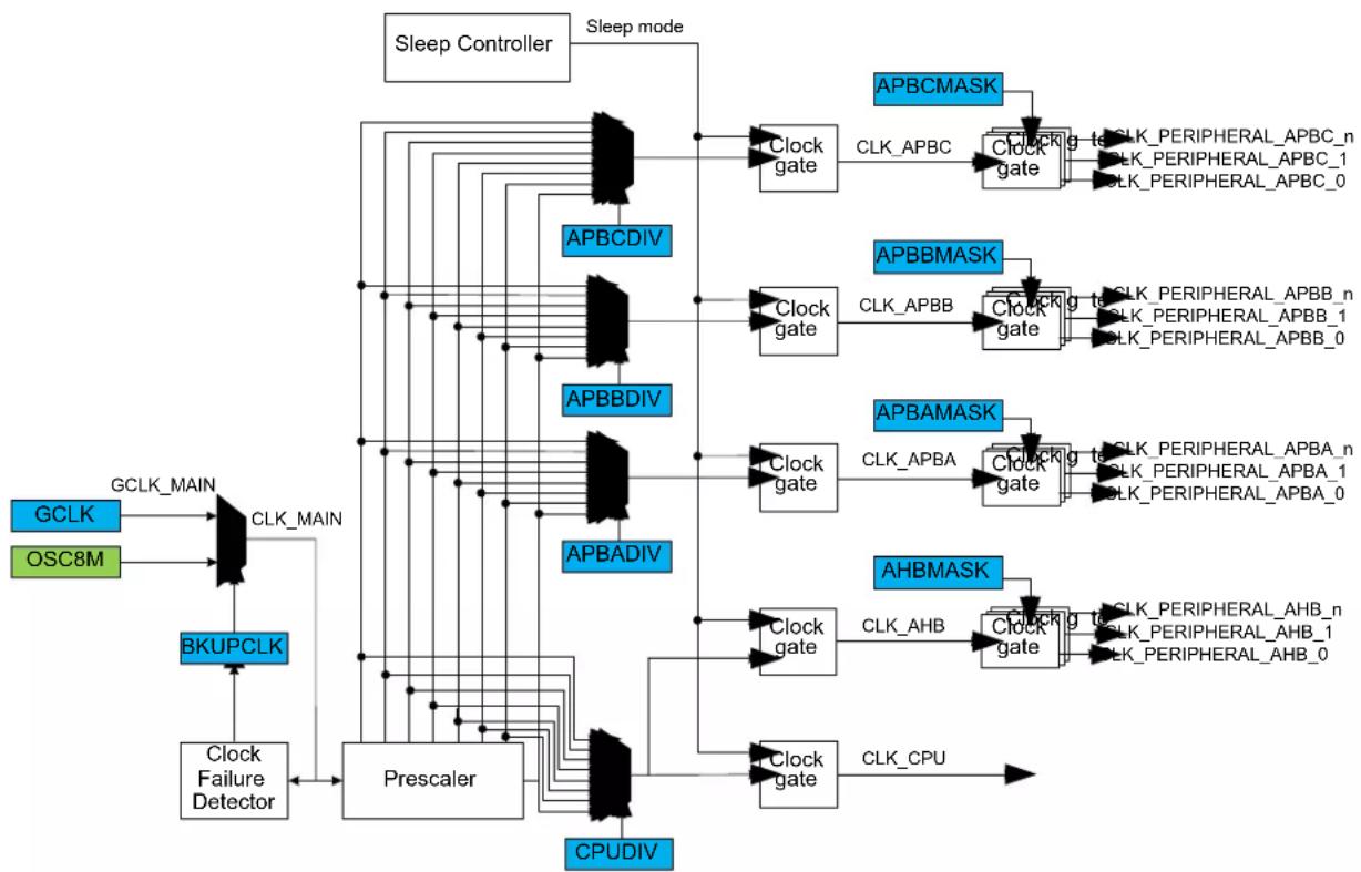
flowchart
graph TD
    subgraph GCLK
        GCLK_MAIN --> CLK_MAIN
        OSC8M --> GCLK
        GCLK --> BKUPCLK
        BKUPCLK --> Clock_Failure_Detector
    end

    subgraph OSC8M
        GCLK --> BKUPCLK
        BKUPCLK --> Clock_Failure_Detector
    end

    subgraph BKUPCLK
        Clock_Failure_Detector --> Prescaler
    end

    subgraph Prescaler
        Clock_APUBDIV --> APBCDIV
        Clock_APUBDIV --> APBBDIV
        Clock_APUBDIV --> APBADIV
    end

    subgraph Prescaler
        Clock_APUBDIV --> APBCDIV
        Clock_APUBDIV --> APBBDIV
        Clock_APUBDIV --> APBADIV
    end

    subgraph Prescaler
        Clock_APUBDIV --> APBCDIV
        Clock_APUBDIV --> APBBDIV
        Clock_APUBDIV --> APBADIV
    end

    subgraph Prescaler
        Clock_APUBDIV --> APBCDIV
       Clock_APUBDIV --> APBBDIV
        Clock_APUBDIV --> APBADIV
    end

    subgraph Prescaler
        Clock_APUBDIV --> APBCDIV
        Clock_APUBDIV --> APBBDIV
        Clock_APUBDIV --> APBADIV
    end

    subgraph Prescaler
        Clock_APUBDIV --> APBCDIV
        Clock_APUBDIV --> APBBDIV
        Clock_APUBDIV --> APBADIV
    end


    subgraph Prescaler
        Clock_APUBDIV --> APBCDIV
        Clock_APUBDIV --> APBBDIV
        Clock_APUBDIV --> APBADIV
    end

    subgraph Prescaler
        Clock_APUBDIV --> APBCDIV
        Clock_APUBDIV --> APBBDIV
        Clock_APUBDIV --> APBADIV
    end

    subgraph Prescaler
        Clock_APUBDIV --> APBCDIV
        Clock_APUBDIV <--> APBCDIV & APBBDIV & APBADIV & APBADIV & APBCDIV & APBBDIV & APBADIV & APBCDIV & APBBDIV & APBADIV & APBCDIV & APBBDIV & APBADIV & APBCDIV & APBBDIV & APBADIV & APBCDIV & APBBDIV & APBADIV & APBCDIV & APBBDIV & APBADIV & APBCDIV & APBBDIV & APBADIV & APBCDIV & APBBDIV & APBADIV & APBCDIV & APBBDIV & APBAD IV]
    end

    subgraph Prescaler
        Clock_APUBDIV --> APBCDIV
        Clock_APUBDIV --> APBBDIV
        Clock_APUBDIV --> APBADIV
        Clock_APUBDIV --> CPUDIV
    end

    subgraph Prescaler
        Clock_APUBDIV --> APBCDIV
        Clock_APUBDIV --> APBBDIV
        Clock_APUBDIV --> APBADIV
        Clock_APUBDIV --> CPUDIV
    end

    subgraph Prescaler
        Clock_APUBDIV --> APBCDV
        Clock_APUBDIV --> APBBDV
        Clock_APUBDIV --> APBADDV
        Clock_APUBDIV --> CPUDIV
    end

    subgraph Prescaler
        Clock_APUBDIV --> APBCDV
        Clock_APUBDIV --> APBBDV
        Clock_APUBDIV --> APBADDV
        Clock_APUBDIV --> CPUDIV
    end

    subgraph Prescaler
        Clock_APUBDIV --> APBCDV
        Clock_APUBDIV --> APBBDV
        Clock_APUBDIV --> APBADDV
    end

    subgraph Prescaler
        Clock_APUBDIV --> APBCDV
        Clock_APUBDIV --> APBBDV
        Clock_APUBDIV --> APBADDV
        Clock_APUBDIV --> CPUDIV
    end

    subgraph Prescaler
        Clock_APUBDIV --> APBCDV
        Clock_APUBDIV --> APBBDV
        Clock_APUBDIV --> APBADDV
        Clock_APUBDIV --> CPUDIV
15.6.2.5 Clock Ready Flag
There is a slight delay from when CPUSEL and APBxSEL are written until the new clock setting becomes effective. During this interval, the Clock Ready flag in the Interrupt Flag Status and Clear register (INTFLAG.CKRDY) will read as zero. If CKRDY in the INTENSET register is written to one, the Power Manager interrupt can be triggered when the new clock setting is effective. CPUSEL must not be re-written while CKRDY is zero, or the system may become unstable or hang.
Related Links
15.8.3. CPUSEL
15.8.12. INTENSET
15.6.2.6 Peripheral Clock Masking
It is possible to disable or enable the clock for a peripheral in the AHB or APBx clock domain by writing the corresponding bit in the Clock Mask register (APBxMASK - refer to APBAMASK register for details) to zero or one. Refer to the table below for the default state of each of the peripheral clocks.
Table 15-1. Peripheral Clock Default State
| Peripheral Clock Default State | |
| CLK_PAC0_APB Enabled | |
| CLK_PM_APB Enabled | |
| CLK_SYSCTRL_APB Enabled | |
| CLK_GCLK_APB Enabled | |
| CLK_WDT_APB Enabled | |
| CLK_RTC_APB Enabled | |
| CLK_EIC_APB Enabled | |
| CLK_PAC1_APB Enabled | |
| CLK_DSU_APB Enabled | |
| CLK_NVMCTRL_APB Enabled | |
| CLK_PORT_APB Enabled | |
| CLK_PAC2_APB Disabled | |
| CLK_SERCOMx_APB Disabled | |
| CLK_TCx_APB Disabled | |
| CLK_ADC_APB Enabled | |
| CLK_AC_APB Disabled | |
| CLK_DAC_APB Disabled | |
| CLK_PTC_APB Disabled |
When the APB clock for a module is not provided its registers cannot be read or written. The module can be re-enabled later by writing the corresponding mask bit to one.
A module may be connected to several clock domains (for instance, AHB and APB), in which case it will have several mask bits.
Note: Clocks should only be switched off if it is certain that the module will not be used. Switching off the clock for the NVM Controller (NVMCTRL) will cause a problem if the CPU needs to read from the flash memory. Switching off the clock to the Power Manager (PM), which contains the mask registers, or the corresponding APBx bridge, will make it impossible to write the mask registers again. In this case, they can only be re-enabled by a system reset.
Related Links
15.8.8. APBAMASK
15.6.2.7 Clock Failure Detector
This mechanism allows the main clock to be switched automatically to the safe OSC8M clock when the main clock source is considered off. This may happen for instance when an external crystal oscillator is selected as the clock source for the main clock and the crystal fails. The mechanism is to designed to detect, during a OSCULP32K clock period, at least one rising edge of the main clock. If no rising edge is seen, the clock is considered failed.
The clock failure detector is enabled by writing a '1' to the Clock Failure Detector Enable bit in CTRL (CFDEN_CTRL).
As soon as the Clock Failure Detector Enable bit (CTRL.CFDEN) is one, the clock failure detector (CFD) will monitor the undivided main clock. When a clock failure is detected, the main clock automatically switches to the OSC8M clock and the Clock Failure Detector flag in the interrupt Flag Status and
Clear register (INTFLAG.CFD) is set and the corresponding interrupt request will be generated if enabled. The BKUPCLK bit in the CTRL register is set by hardware to indicate that the main clock comes from OSC8M. The GCLK_MAIN clock source can be selected again by writing a zero to the CTRL.BKUPCLK bit. However, writing the bit does not fix the failure.
Notes:
- The detector does not monitor while the main clock is temporarily unavailable (start-up time after a wake-up, etc.) or in sleep mode. The Clock Failure Detector must be disabled before entering standby mode.
- The clock failure detector must not be enabled if the source of the main clock is not significantly faster than the OSCULP32K clock. For instance, if GCLK_MAIN is the internal 32kHz RC, then the clock failure detector must be disabled.
- The OSC8M internal oscillator should be enabled to allow the main clock switching to the OSC8M clock.
Related Links
15.8.1. CTRL
15.6.2.8 Reset Controller
The latest reset cause is available in RCAUSE, and can be read during the application boot sequence in order to determine proper action.
There are two groups of reset sources:
- Power Reset: Resets caused by an electrical issue.
- User Reset: Resets caused by the application.
The table below lists the parts of the device that are reset, depending on the reset type.
Table 15-2. Effects of the Different Reset Events
| Power Reset User Reset | |||
| POR, BOD12, BOD33 External Reset WDT Reset, SysResetReq | |||
| RTCAll the 32kHz sourcesWDT with ALWAYSON featureGeneric Clock with WRTLOCK feature | Y N N | ||
| Debug logic Y Y N | |||
| Others Y Y Y | |||
The external reset is generated when pulling the RESET pin low. This pin has an internal pull-up, and does not need to be driven externally during normal operation.
The POR, BOD12 and BOD33 reset sources are generated by their corresponding module in the System Controller Interface (SYSCTRL).
The WDT reset is generated by the Watchdog Timer.
The System Reset Request (SysResetReq) is a software reset generated by the CPU when asserting the SYSRESETREQ bit located in the Reset Control register of the CPU (See the ARM® Cortex®
Technical Reference Manual on http://www.arm.com).
Figure 15-3. Reset Controller
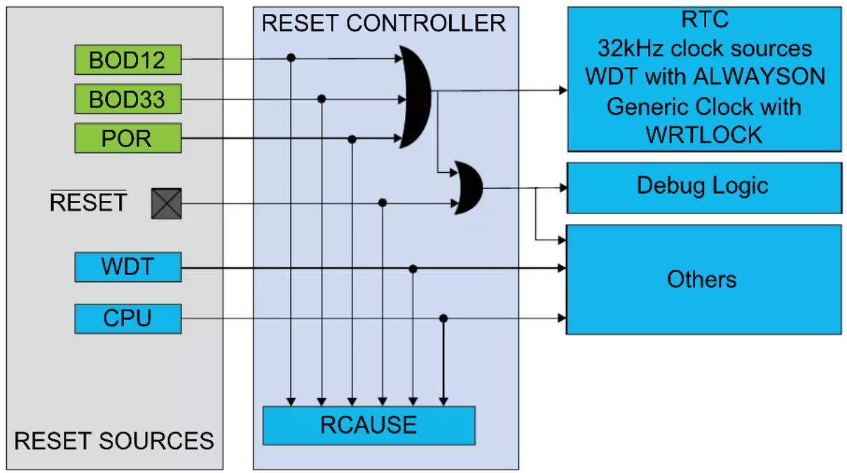
flowchart
graph TD
    subgraph RESET Sources
        BOD12["BOD12"]
        BOD33["BOD33"]
        POR["POR"]
        RESET["RESET"]
        WDT["WDT"]
        CPU["CPU"]
    end

    RESET CONTROLLER --> RTC["RTC 32kHz clock sources\nWDT with ALWAYSON\nGeneric Clock with WRTLOCK"]
    RESET CONTROLLER --> DebugLogic["Debug Logic"]
    RESET CONTROLLER --> Others["Others"]

    RESET CONTROLLER --> RCAUSE["RCAUSE"]
    style RESET CONTROLLER fill:#f9f9f9,stroke:#333
    style RESET SOURCES fill:#e6f7ff,stroke:#333
    style RTC fill:#cce5ff,stroke:#333
    style DebugLogic fill:#cce5ff,stroke:#333
    style Others fill:#cce5ff,stroke:#333
15.6.2.9 Sleep Mode Controller
Sleep mode is activated by the Wait For Interrupt instruction (WFI). The Idle bits in the Sleep Mode register (SLEEP.IDLE) and the SLEEPDEEP bit of the System Control register of the CPU should be used as argument to select the level of the sleep mode.
There are two main types of sleep mode:
- IDLE mode: The CPU is stopped. Optionally, some synchronous clock domains are stopped, depending on the IDLE argument. Regulator operates in normal mode.
- STANDBY mode: All clock sources are stopped, except those where the RUNSTDBY bit is set. Regulator operates in low-power mode. Before entering standby mode the user must make sure that a significant amount of clocks and peripherals are disabled, so that the voltage regulator is not overloaded.
Table 15-3. Sleep Mode Entry and Exit Table
| Mode Level Mode Entry Wake-Up Sources | ||
| IDLE 0 SCR.SLEEPDEEP = 0 | Synchronous ^(2) (APB, AHB), asynchronous ^(1) | |
| STANDBY SCR.SLEEPDEEP = 1WFI | Asynchronous | |
Notes:
- Asynchronous: interrupt generated on generic clock or external clock or external event.
- Synchronous: interrupt generated on the APB clock.
Table 15-4. Sleep Mode Overview
| Sleep Mode | CPU Clock | AHB Clock | APB Clock | Oscillators Main | Clock | Regulator Mode | RAM Mode | |||
| ONDEMAND = 0 ONDEMAND = 1 | ||||||||||
| RUNSTDBY=0 RUNSTDBY=1 RUN | STDBY=0 RUNSTDBY=1 | |||||||||
| Idle 0 Stop Run Run Run Run if requested Run if requested Run Normal Normal | ||||||||||
| Idle 1 Stop Stop Run Run Run Run if requested Run if requested Run Normal Normal | ||||||||||
| Idle 2 Stop Stop Stop Run Run Run if requested Run if requested Run Normal Normal | ||||||||||
| Standby Stop Stop Stop Stop Run Stop Run if requested Stop Low power Low power | ||||||||||
15.6.2.9.1 IDLE Mode
The IDLE modes allow power optimization with the fastest wake-up time.
The CPU is stopped. To further reduce power consumption, the user can disable the clocking of modules and clock sources by configuring the SLEEP.IDLE bit group. The module will be halted regardless of the bit settings of the mask registers in the Power Manager (PM.AHBMASK, PM.APBxMASK).
Regulator operates in normal mode.
- Entering IDLE mode: The IDLE mode is entered by executing the WFI instruction. Additionally, if the SLEEPONEXIT bit in the ARM Cortex System Control register (SCR) is set, the IDLE mode will also be entered when the CPU exits the lowest priority ISR. This mechanism can be useful for applications that only require the processor to run when an interrupt occurs. Before entering the IDLE mode, the user must configure the IDLE mode configuration bit group and must write a zero to the SCR.SLEEPDEEP bit.
- Exiting IDLE mode: The processor wakes the system up when it detects the occurrence of any interrupt that is not masked in the NVIC Controller with sufficient priority to cause exception entry. The system goes back to the ACTIVE mode. The CPU and affected modules are restarted.
15.6.2.9.2 STANDBY Mode
The STANDBY mode allows achieving very low power consumption.
In this mode, all clocks are stopped except those which are kept running if requested by a running module or have the ONDEMAND bit set to zero. For example, the RTC can operate in STANDBY mode. In this case, its Generic Clock clock source will also be enabled.
The regulator and the RAM operate in low-power mode.
A SLEEPONEXIT feature is also available.
- Entering STANDBY mode: This mode is entered by executing the WFI instruction with the SCR.SLEEPDEEP bit of the CPU is written to 1.
- Exiting STANDBY mode: Any peripheral able to generate an asynchronous interrupt can wake up the system. For example, a module running on a Generic clock can trigger an interrupt. When the enabled asynchronous wake-up event occurs and the system is woken up, the device will either execute the interrupt service routine or continue the normal program execution according to the Priority Mask Register (PRIMASK) configuration of the CPU.
15.6.3 SleepWalking
SleepWalking is the capability for a device to temporarily wake-up clocks for the peripheral to perform a task without waking-up the CPU in STANDBY sleep mode. At the end of the sleepwalking task, the device can either be awakened by an interrupt (from a peripheral involved in SleepWalking) or enter into STANDBY sleep mode again.
In this device, SleepWalking is supported only on GCLK clocks by using the on-demand clock principle of the clock sources. Refer to On-demand, Clock Requests for more details.
Related Links
13.6. On-demand, Clock Requests
15.6.4 Interrupts
The peripheral has the following interrupt sources:
- Clock Ready flag
- Clock failure detector
Each interrupt source has an interrupt flag associated with it. The interrupt flag in the Interrupt Flag Status and Clear (INTFLAG) register is set when the interrupt condition occurs. Each interrupt can be individually enabled by writing a one to the corresponding bit in the Interrupt Enable Set (INTENSET) register, and disabled by writing a one to the corresponding bit in the Interrupt Enable Clear (INTENCLR) register. An interrupt request is generated when the interrupt flag is set and the corresponding interrupt is enabled. The interrupt request remains active until the interrupt flag is cleared, the interrupt is disabled or the peripheral is reset. An interrupt flag is cleared by writing a one to the corresponding bit in the INTFLAG register. Each peripheral can have one interrupt request line per interrupt source or one common interrupt request line for all the interrupt sources. Refer to Nested Vector Interrupt Controller for details. If the peripheral has one common interrupt request line for all the interrupt sources, the user must read the INTFLAG register to determine which interrupt condition is present.
Related Links
10.2. Nested Vector Interrupt Controller
15.6.5 Events
Not applicable.
15.6.6 Sleep Mode Operation
In all IDLE sleep modes, the power manager is still running on the selected main clock.
In STANDDBY sleep mode, the power manager is frozen and is able to go back to ACTIVE mode upon any asynchronous interrupt.
15.7 Register Summary
| Offset | Name Bit Pos. 76 | 543210 | ||||||||
| 0x00 CTRL 7:0 | BKUPCLK | CFDEN | ||||||||
| 0x01 SLEEP 7:0 | IDLE[1:0] | |||||||||
| 0x02 ... 0x07 | Reserved | |||||||||
| 0x08 | CPUSEL 7:0 | CPUDIV[2:0] | ||||||||
| 0x09 | APBASEL | 7:0 | APBADIV[2:0] | |||||||
| 0x0A | APBBSEL | 7:0 | APBBDIV[2:0] | |||||||
| 0x0B | APBCSEL | 7:0 | APBCDIV[2:0] | |||||||
| 0x0C ... 0x13 | Reserved | |||||||||
| 0x14 | AHBMASK | 7:0 | NVMCTRL | DSU | HPB2 | HPB1 | HPB0 | |||
| 15:8 | ||||||||||
| 23:16 | ||||||||||
| 31:24 | ||||||||||
| 0x18 APBAMASK | 7:0 | EIC | RTC | WDT | GCLK | SYSCTRL | PM | PAC0 | ||
| 15:8 | ||||||||||
| 23:16 | ||||||||||
| 31:24 | ||||||||||
| 0x1C | APBBMASK | 7:0 | PORT | NVMCTRL | DSU | PAC1 | ||||
| 15:8 | ||||||||||
| 23:16 | ||||||||||
| 31:24 | ||||||||||
| 0x20 APBCMASK | 7:0 | SERCOM5 | SERCOM4 | SERCOM3 | SERCOM2 | SERCOM1 | SERCOM0 | EVSYS | PAC2 | |
| 15:8 | TC7 | TC6 | TC5 | TC4 | TC3 | TC2 | TC1 | TC0 | ||
| 23:16 | PTC DAC AC ADC | |||||||||
| 31:24 | ||||||||||
| 0x24 ... 0x33 | Reserved | |||||||||
| 0x34 | INTENCLR | 7:0 | CFD | CKRDY | ||||||
| 0x35 | INTENSET | 7:0 | CFD | CKRDY | ||||||
| 0x36 | INTFLAG | 7:0 | CFD | CKRDY | ||||||
| 0x37 | Reserved | |||||||||
| 0x38 | RCAUSE | 7:0 | SYST | WDT | EXT | BOD33 | BOD12 | POR | ||
15.8 Register Description
Registers can be 8, 16, or 32 bits wide. Atomic 8-, 16-, and 32-bit accesses are supported. In addition, the 8-bit quarters and 16-bit halves of a 32-bit register, and the 8-bit halves of a 16-bit register can be accessed directly.
Exception for APBASEL, APBBSEL and APBCSEL: These registers must only be accessed with 8-bit access.
Optional write-protection by the Peripheral Access Controller (PAC) is denoted by the "PAC Write-Protection" property in each individual register description.
15.8.1 Control
Name: CTRL
Offset: 0x00
Reset: 0x00
Property: Write-Protected
Bit 76543210
| BKUPCLK CFDEN | |||||||
| Access Reset 0 0 | R/W R/W | ||||||
Bit 4 - BKUPCLK Backup Clock Select
This bit is set by hardware when a clock failure is detected.
| Value | Description |
| 0 | The GCLK_MAIN clock is selected for the main clock. |
| 1 | The OSC8M backup clock is selected for the main clock. |
Bit 2 - CFDEN Clock Failure Detector Enable
This bit is set by hardware when a clock failure is detected.
| Value | Description |
| 0 | The clock failure detector is disabled. |
| 1 | The clock failure detector is enabled. |
15.8.2 Sleep Mode
Name: SLEEP
Offset: 0x01
Reset: 0x00
Property: Write-Protected
Bit 76543210
| IDLE[1:0] | ||||||
| Access Reset 0 0 | R/W R/W | |||||
Bits 1:0 - IDLE[1:0] Idle Mode Configuration
These bits select the Idle mode configuration after a WFI instruction.
| IDLE[1:0] Name | Description | |
| 0x0 CPU | The CPU clock domain is stopped | |
| 0x1 AHB | The CPU and AHB clock domains are stopped | |
| 0x2 APB | The CPU, AHB and APB clock domains are stopped | |
| 0x3 | Reserved | |
15.8.3 CPU Clock Select
Name: CPUSEL
Offset: 0x08
Reset: 0x00
Property: Write-Protected
Bit 76543210
| CPUDIV[2:0] | |||||
| Access Reset 0 0 0 | R/W R/W R/W | ||||
Bits 2:0 - CPUDIV[2:0] CPU Prescaler Selection
These bits define the division ratio of the main clock prescaler ( 2^n ).
| CPUDIV[2:0] Name Description | ||
| 0x0 | DIV1 | Divide by 1 |
| 0x1 | DIV2 | Divide by 2 |
| 0x2 | DIV4 | Divide by 4 |
| 0x3 | DIV8 | Divide by 8 |
| 0x4 | DIV16 | Divide by 16 |
| 0x5 | DIV32 | Divide by 32 |
| 0x6 | DIV64 | Divide by 64 |
| 0x7 | DIV128 | Divide by 128 |
15.8.4 APBA Clock Select
Name: APBASEL
Offset: 0x09
Reset: 0x00
Property: Write-Protected
Bit 76543210
| APBADIV[2:0] | |||||
| Access Reset 0 0 0 | R/W R/W R/W | ||||
Bits 2:0 - APBADIV[2:0] APBA Prescaler Selection
These bits define the division ratio of the APBA clock prescaler ( 2^n ).
| APBADIV[2:0] Name Description | ||
| 0x0 | DIV1 | Divide by 1 |
| 0x1 | DIV2 | Divide by 2 |
| 0x2 | DIV4 | Divide by 4 |
| 0x3 | DIV8 | Divide by 8 |
| 0x4 | DIV16 | Divide by 16 |
| 0x5 | DIV32 | Divide by 32 |
| 0x6 | DIV64 | Divide by 64 |
| 0x7 | DIV128 | Divide by 128 |
15.8.5 APBB Clock Select
Name: APBBSEL
Offset: 0x0A
Reset: 0x00
Property: Write-Protected
Bit 76543210
| APBBDIV[2:0] | |||||
| Access Reset 0 0 0 | R/W R/W R/W | ||||
Bits 2:0 - APBBDIV[2:0] APBB Prescaler Selection
These bits define the division ratio of the APBB clock prescaler ( 2^n ).
| APBBDIV[2:0] Name Description | ||
| 0x0 | DIV1 | Divide by 1 |
| 0x1 | DIV2 | Divide by 2 |
| 0x2 | DIV4 | Divide by 4 |
| 0x3 | DIV8 | Divide by 8 |
| 0x4 | DIV16 | Divide by 16 |
| 0x5 | DIV32 | Divide by 32 |
| 0x6 | DIV64 | Divide by 64 |
| 0x7 | DIV128 | Divide by 128 |
15.8.6 APBC Clock Select
Name: APBCSEL
Offset: 0x0B
Reset: 0x00
Property: Write-Protected
Bit 76543210
| APBCDIV[2:0] | |||||
| Access Reset 0 0 0 | R/W R/W R/W | ||||
Bits 2:0 - APBCDIV[2:0] APBC Prescaler Selection
These bits define the division ratio of the APBC clock prescaler ( 2^n ).
| APBCDIV[2:0] Name Description | ||
| 0x0 | DIV1 | Divide by 1 |
| 0x1 | DIV2 | Divide by 2 |
| 0x2 | DIV4 | Divide by 4 |
| 0x3 | DIV8 | Divide by 8 |
| 0x4 | DIV16 | Divide by 16 |
| 0x5 | DIV32 | Divide by 32 |
| 0x6 | DIV64 | Divide by 64 |
| 0x7 | DIV128 | Divide by 128 |
15.8.7 AHB Mask
Name: AHBMASK
Offset: 0x14
Reset: 0x0000007F
Property: Write-Protected
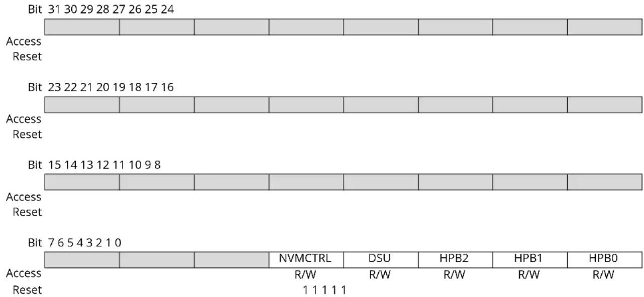
text_image
Bit 31 30 29 28 27 26 25 24 Access Reset Bit 23 22 21 20 19 18 17 16 Access Reset Bit 15 14 13 12 11 10 9 8 Access Reset Bit 7 6 5 4 3 2 1 0 Access Reset NVMCTRL DSU HPB2 HPB1 HPB0 R/W R/W R/W R/W R/W 1 1 1 1 1Bit 4 - NVMCTRL NVMCTRL AHB Clock Mask
| Value | Description |
| 0 | The AHB clock for the NVMCTRL is stopped. |
| 1 | The AHB clock for the NVMCTRL is enabled. |
Bit 3 - DSU DSU AHB Clock Mask
| Value | Description |
| 0 | The AHB clock for the DSU is stopped. |
| 1 | The AHB clock for the DSU is enabled. |
Bit 2 - HPB2 HPB2 AHB Clock Mask
| Value | Description |
| 0 | The AHB clock for the HPB2 is stopped. |
| 1 | The AHB clock for the HPB2 is enabled. |
Bit 1 - HPB1 HPB1 AHB Clock Mask
| Value | Description |
| 0 | The AHB clock for the HPB1 is stopped. |
| 1 | The AHB clock for the HPB1 is enabled. |
Bit 0 - HPB0 HPB0 AHB Clock Mask
| Value | Description |
| 0 | The AHB clock for the HPB0 is stopped. |
| 1 | The AHB clock for the HPB0 is enabled. |
15.8.8 APBA Mask
Name: APBAMASK
Offset: 0x18
Reset: 0x0000007F
Property: Write-Protected
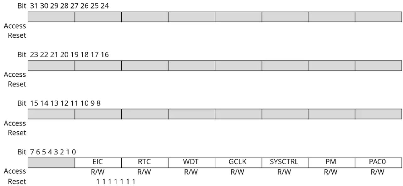
text_image
Bit 31 30 29 28 27 26 25 24 Access Reset Bit 23 22 21 20 19 18 17 16 Access Reset Bit 15 14 13 12 11 10 9 8 Access Reset Bit 7 6 5 4 3 2 1 0 Access Reset EIC RTC WDT GCLK SYSCTRL PM PAC0 R/W R/W R/W R/W R/W R/W R/W 1 1 1 1 1 1 1Bit 6 - EIC EIC APB Clock Enable
| Value | Description |
| 0 | The APBA clock for the EIC is stopped. |
| 1 | The APBA clock for the EIC is enabled. |
Bit 5 - RTC RTC APB Clock Enable
| Value | Description |
| 0 | The APBA clock for the RTC is stopped. |
| 1 | The APBA clock for the RTC is enabled. |
Bit 4 - WDT WDT APB Clock Enable
| Value | Description |
| 0 | The APBA clock for the WDT is stopped. |
| 1 | The APBA clock for the WDT is enabled. |
Bit 3 - GCLK GCLK APB Clock Enable
| Value | Description |
| 0 | The APBA clock for the GCLK is stopped. |
| 1 | The APBA clock for the GCLK is enabled. |
Bit 2 - SYSCTRL SYSCTRL APB Clock Enable
| Value | Description |
| 0 | The APBA clock for the SYSCTRL is stopped. |
| 1 | The APBA clock for the SYSCTRL is enabled. |
| Value Description | |
| 0 | The APBA clock for the PM is stopped. |
| 1 | The APBA clock for the PM is enabled. |
Bit 1 - PM PM APB Clock Enable
Bit 0 - PAC0 PAC0 APB Clock Enable
| Value Description | |
| 0 | The APBA clock for the PAC0 is stopped. |
| 1 | The APBA clock for the PAC0 is enabled. |
15.8.9 APBB Mask
Name: APBBMASK
Offset: 0x1C
Reset: 0x0000007F
Property: Write-Protected
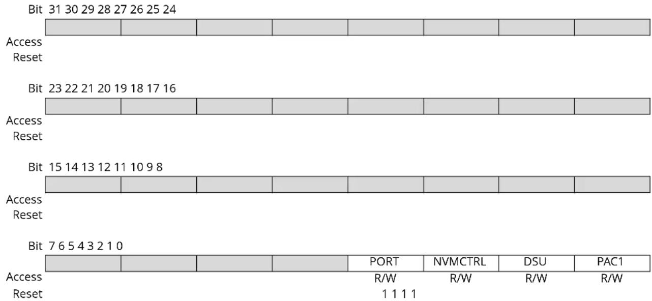
text_image
Bit 31 30 29 28 27 26 25 24 Access Reset Bit 23 22 21 20 19 18 17 16 Access Reset Bit 15 14 13 12 11 10 9 8 Access Reset Bit 7 6 5 4 3 2 1 0 Access Reset PORT NVMCTRL DSU PAC1 R/W R/W R/W R/W 1 1 1 1Bit 3 - PORT PORT APB Clock Enable
| Value | Description |
| 0 | The APBB clock for the PORT is stopped. |
| 1 | The APBB clock for the PORT is enabled. |
Bit 2 - NVMCTRL NVMCTRL APB Clock Enable
| Value | Description |
| 0 | The APBB clock for the NVMCTRL is stopped. |
| 1 | The APBB clock for the NVMCTRL is enabled. |
Bit 1 - DSU DSU APB Clock Enable
| Value | Description |
| 0 | The APBB clock for the DSU is stopped. |
| 1 | The APBB clock for the DSU is enabled. |
Bit 0 - PAC1 PAC1 APB Clock Enable
| Value | Description |
| 0 | The APBB clock for the PAC1 is stopped. |
| 1 | The APBB clock for the PAC1 is enabled. |
15.8.10 APBC Mask
Name: APBCMASK
Offset: 0x20
Reset: 0x00010000
Property: Write-Protected
| Bit 31 30 29 28 27 26 25 24 | |||||||
| Access Reset | |||||||
| Bit 23 22 21 20 19 18 17 16 | |||||||
| PTC DAC AC ADC | |||||||
| Access Reset | R/W0 | R/W0 | R/W0 | R/W1 | |||
| Bit 15 14 13 12 11 10 | 9 | 8 | |||||
| TC7 | TC6 | TC5 | TC4 | TC3 | TC2 | TC1 | TC0 |
| Access Reset | R/W0 | R/W0 | R/W0 | R/W0 | R/W0 | R/W0 | R/W0 |
| Bit | 7 | 6 | 5 | 4 | 3 | 2 | 1 |
| SERCOM5 | SERCOM4 | SERCOM3 | SERCOM2 | SERCOM1 | SERCOM0 | EVSYS | PAC2 |
| Access Reset | R/W0 | R/W0 | R/W0 | R/W0 | R/W0 | R/W0 | R/W0 |
Bit 19 - PTC PTC APB Clock Enable
| Value | Description |
| 0 | The APBC clock for the PTC is stopped. |
| 1 | The APBC clock for the PTC is enabled. |
Bit 18 - DAC DAC APB Clock Enable
| Value | Description |
| 0 | The APBC clock for the DAC is stopped. |
| 1 | The APBC clock for the DAC is enabled. |
Bit 17 - AC AC APB Clock Enable
| Value | Description |
| 0 | The APBC clock for the AC is stopped. |
| 1 | The APBC clock for the AC is enabled. |
Bit 16 - ADC ADC APB Clock Enable
| Value | Description |
| 0 | The APBC clock for the ADC is stopped. |
| 1 | The APBC clock for the ADC is enabled. |
Bit 15 - TC7 TC7 APB Clock Enable
| Value | Description |
| 0 | The APBC clock for the TC7 is stopped. |
| 1 | The APBC clock for the TC7 is enabled. |
| Value Description | |
| 0 | The APBC clock for the TC6 is stopped. |
| 1 | The APBC clock for the TC6 is enabled. |
Bit 14 - TC6 TC6 APB Clock Enable
Bit 13 - TC5 TC5 APB Clock Enable
| Value Description | |
| 0 | The APBC clock for the TC5 is stopped. |
| 1 | The APBC clock for the TC5 is enabled. |
Bit 12 - TC4 TC4 APB Clock Enable
| Value Description | |
| 0 | The APBC clock for the TC4 is stopped. |
| 1 | The APBC clock for the TC4 is enabled. |
Bit 11 - TC3 TC3 APB Clock Enable
| Value Description | |
| 0 | The APBC clock for the TC3 is stopped. |
| 1 | The APBC clock for the TC3 is enabled. |
Bit 10 - TC2 TC2 APB Clock Enable
| Value Description | |
| 0 | The APBC clock for the TC2 is stopped. |
| 1 | The APBC clock for the TC2 is enabled. |
Bit 9 - TC1 TC1 APB Clock Enable
| Value Description | |
| 0 | The APBC clock for the TC1 is stopped. |
| 1 | The APBC clock for the TC1 is enabled. |
Bit 8 - TC0 TC0 APB Clock Enable
| Value Description | |
| 0 | The APBC clock for the TC0 is stopped. |
| 1 | The APBC clock for the TC0 is enabled. |
Bit 7 - SERCOM5 SERCOM5 APB Clock Enable
| Value Description | |
| 0 | The APBC clock for the SERCOM5 is stopped. |
| 1 | The APBC clock for the SERCOM5 is enabled. |
Bit 6 - SERCOM4 SERCOM4 APB Clock Enable
| Value Description | |
| 0 | The APBC clock for the SERCOM4 is stopped. |
| 1 | The APBC clock for the SERCOM4 is enabled. |
Bit 5 - SERCOM3 SERCOM2 APB Clock Enable
| Value Description | |
| 0 | The APBC clock for the SERCOM3 is stopped. |
| 1 | The APBC clock for the SERCOM3 is enabled. |
Bit 4 - SERCOM2 SERCOM2 APB Clock Enable
| Value Description | |
| 0 | The APBC clock for the SERCOM2 is stopped. |
| 1 | The APBC clock for the SERCOM2 is enabled. |
Bit 3 - SERCOM1 SERCOM1 APB Clock Enable
| Value Description | |
| 0 | The APBC clock for the SERCOM1 is stopped. |
Value Description
| 1 | The APBC clock for the SERCOM1 is enabled. |
Bit 2 - SERCOM0 SERCOM0 APB Clock Enable
Value Description
| 0 | The APBC clock for the SERCOM0 is stopped. |
| 1 | The APBC clock for the SERCOM0 is enabled. |
Bit 1 - EVSYS EVSYS APB Clock Enable
Value Description
| 0 | The APBC clock for the EVSYS is stopped. |
| 1 | The APBC clock for the EVSYS is enabled. |
Bit 0 - PAC2 PAC2 APB Clock Enable
Value Description
| 0 | The APBC clock for the PAC2 is stopped. |
| 1 | The APBC clock for the PAC2 is enabled. |
15.8.11 Interrupt Enable Clear
Name: INTENCLR
Offset: 0x34
Reset: 0x00
Property: Write-Protected
Bit 76543210
| CFD CKRDY | |||||||
| Access Reset 0 0 | R/W R/W | ||||||
Bit 1 - CFD Clock Failure Detector Interrupt Enable
Writing a zero to this bit has no effect.
Writing a one to this bit will clear the Clock Failure Detector Interrupt Enable bit and the corresponding interrupt request.
| Value Description | |
| 0 | The Clock Failure Detector interrupt is disabled. |
| 1 | The Clock Failure Detector interrupt is enabled and will generate an interrupt request when the Clock Failure Detector Interrupt flag is set. |
Bit 0 - CKRDY Clock Ready Interrupt Enable
Writing a zero to this bit has no effect.
Writing a one to this bit will clear the Clock Ready Interrupt Enable bit and the corresponding interrupt request.
| Value Description | |
| 0 | The Clock Ready interrupt is disabled. |
| 1 | The Clock Ready interrupt is enabled and will generate an interrupt request when the Clock Ready Interrupt flag is set. |
15.8.12 Interrupt Enable Set
Name: INTENSET
Offset: 0x35
Reset: 0x00
Property: Write-Protected
Bit 76543210
| CFD CKRDY | |||||||
| Access Reset 0 0 | R/W R/W | ||||||
Bit 1 - CFD Clock Failure Detector Interrupt Enable
Writing a zero to this bit has no effect.
Writing a one to this bit will clear the Clock Failure Detector Interrupt Enable bit and the corresponding interrupt request.
| Value Description | |
| 0 | The Clock Failure Detector interrupt is disabled. |
| 1 | The Clock Failure Detector interrupt is enabled and will generate an interrupt request when the Clock Failure Detector Interrupt flag is set. |
Bit 0 - CKRDY Clock Ready Interrupt Enable
Writing a zero to this bit has no effect.
Writing a one to this bit will set the Clock Ready Interrupt Enable bit and enable the Clock Ready interrupt.
| Value Description | |
| 0 | The Clock Ready interrupt is disabled. |
| 1 | The Clock Ready interrupt is enabled. |
15.8.13 Interrupt Flag Status and Clear
Name: INTFLAG
Offset: 0x36
Reset: 0x00
Property: -
Bit 76543210
| CFD CKRDY | |||||||
| Access Reset 0 0 | R/W R/W | ||||||
Bit 1 - CFD Clock Failure Detector Interrupt Enable
Writing a zero to this bit has no effect.
Writing a one to this bit will clear the Clock Failure Detector Interrupt Enable bit and the corresponding interrupt request.
| Value Description | |
| 0 | The Clock Failure Detector interrupt is disabled. |
| 1 | The Clock Failure Detector interrupt is enabled and will generate an interrupt request when the Clock Failure Detector Interrupt flag is set. |
Bit 0 - CKRDY Clock Ready
This flag is cleared by writing a one to the flag.
This flag is set when the synchronous CPU and APBx clocks have frequencies as indicated in the CPUSEL and APBxSEL registers, and will generate an interrupt if INTENCLR/SET.CKRDY is one.
Writing a zero to this bit has no effect.
Writing a one to this bit clears the Clock Ready Interrupt flag.
15.8.14 Reset Cause
Name: RCAUSE
Offset: 0x38
Reset: 0x01
Property: -
Bit 76543210
| SYST WDT EXT BOD33 BOD12 | POR | ||||||
| Access | R | R | R | R | R | R | |
| Reset | 0 0 0 | 0 0 1 | |||||
Bit 6 - SYST System Reset Request
This bit is set if a system reset request has been performed. Refer to the Cortex processor documentation for more details.
Bit 5 - WDT Watchdog Reset
This flag is set if a Watchdog Timer reset occurs.
Bit 4 - EXT External Reset
This flag is set if an external reset occurs.
Bit 2 - BOD33 Brown Out 33 Detector Reset
This flag is set if a BOD33 reset occurs.
Bit 1 - BOD12 Brown Out 12 Detector Reset
This flag is set if a BOD12 reset occurs.
Bit 0 - POR Power On Reset
This flag is set if a POR occurs.
16. SYSCTRL – System Controller
16.1 Overview
The System Controller (SYSCTRL) provides a user interface to the clock sources, brown out detectors, on-chip voltage regulator and voltage reference of the device.
Through the interface registers, it is possible to enable, disable, calibrate and monitor the SYSCTRL sub-peripherals.
All sub-peripheral statuses are collected in the Power and Clocks Status register (PCLKSR). They can additionally trigger interrupts upon status changes via the INTENSET (INTENSET), INTENCLR (INTENCLR) and INTFLAG (INTFLAG) registers.
Additionally, BOD33 interrupts can be used to wake up the device from standby mode upon a programmed brown-out detection.
Related Links
16.8.4. PCLKSR
16.8.2. INTENSET
16.8.3. INTFLAG
16.8.14. BOD33
16.8.1. INTENCLR
16.2 Features
• 0.4-32MHz Crystal Oscillator (XOSC)
- Tunable gain control
- Programmable start-up time
- Crystal or external input clock on XIN I/O
• 32.768kHz Crystal Oscillator (XOSC32K)
- Automatic or manual gain control
- Programmable start-up time
- Crystal or external input clock on XIN32 I/O
• 32.768kHz High Accuracy Internal Oscillator (OSC32K)
- Frequency fine tuning
- Programmable start-up time
• 32.768kHz Ultra Low Power Internal Oscillator (OSCULP32K)
- Ultra low power, always-on oscillator
- Frequency fine tuning
– Calibration value loaded from Flash Factory Calibration at reset
• 8MHz Internal Oscillator (OSC8M)
- Fast startup
- Output frequency fine tuning
- 4/2/1MHz divided output frequencies available
- Calibration value loaded from Flash Factory Calibration at reset
• Digital Frequency Locked Loop (DFLL48M)
- Internal oscillator with no external components
-
48MHz output frequency
-
Operates standalone as a high-frequency programmable oscillator in open loop mode
- Operates as an accurate frequency multiplier against a known frequency in closed loop mode
• 3.3V Brown-Out Detector (BOD33)
- Programmable threshold
- Threshold value loaded from Flash User Calibration at startup
- Triggers resets or interrupts
- Operating modes:
- Continuous mode
- Sampled mode for low power applications (programmable refresh frequency)
- Hysteresis
- Internal Voltage Regulator system (VREG)
- Operating modes:
- Normal mode
- Low-power mode
- With an internal non-configurable Brown-out detector (BOD12)
• Voltage Reference System (VREF)
- Bandgap voltage generator with programmable calibration value
- Temperature sensor
- Bandgap calibration value loaded from Flash Factory Calibration at start-up
16.3 Block Diagram
Figure 16-1. SYSCTRL Block Diagram
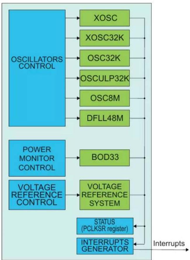
flowchart
graph TD
    A["OSCILLATORS CONTROL"] --> B["XOSC"]
    A --> C["XOSC32K"]
    A --> D["OSC32K"]
    A --> E["OSCULP32K"]
    A --> F["OSC8M"]
    A --> G["DFLL48M"]
    H["POWER MONITOR CONTROL"] --> I["BOD33"]
    J["VOLTAGE REFERENCE CONTROL"] --> K["VOLTAGE REFERENCE SYSTEM"]
    L["STATUS (PCLKSR register)"] --> M["INTERRUPTS GENERATOR"]
    M --> N["Interrupts"]
16.4 Signal Description
| Signal Name Types Description | |
| XIN Analog Input Multipurpose Crystal Oscillator or external clock generator input | |
| XOUT Analog Output External Multipurpose Crystal Oscillator output | |
| XIN32 Analog Input 32kHz Crystal Oscillator or external clock generator input | |
| XOUT32 Analog Output 32kHz Crystal Oscillator output | |
The I/O lines are automatically selected when XOSC or XOSC32K are enabled. Refer to Oscillator Pinout.
Related Links
- I/O Multiplexing and Considerations
6.2.1. Oscillator Pinout
16.5 Product Dependencies
In order to use this peripheral, other parts of the system must be configured correctly, as described below.
16.5.1 I/O Lines
I/O lines are configured by SYSCTRL when either XOSC or XOSC32K are enabled, and need no user configuration.
16.5.2 Power Management
The BOD33 and BOD12 can trigger resets when the I/O supply or core supply voltages drop below the programmed threshold value. BOD33 and BOD12 can additionally wake up the system from standby mode when I/O or core supply failure is detected. However, BOD33 and BOD12 cannot be used in continuous mode when the system is in standby mode, and will, therefore, be automatically disabled until the system is woken up. Only sampled mode operation is allowed when the system is in standby mode.
All oscillators except XOSC32K, OSC32K and OSCULP32K are turned off in some sleep modes and turned automatically on when the chip wakes up.
The SYSCTRL can continue to operate in any sleep mode where the selected source clock is running. The SYSCTRL interrupts can be used to wake up the device from sleep modes. The events can trigger other operations in the system without exiting sleep modes. Refer to PM - Power Manager on the different sleep modes.
Related Links
15. Power Manager (PM)
16.5.3 Clocks
The SYSCTRL gathers controls for all device oscillators and provides clock sources to the Generic Clock Controller (GCLK). The available clock sources are: XOSC, XOSC32K, OSC32K, OSCULP32K, OSC8M and DFLL48M.
The SYSCTRL bus clock (CLK_SYSCTRL_APB) can be enabled and disabled in the Power Manager, and the default state of CLK_SYSCTRL_APB can be found in the Peripheral Clock Masking section in the PM - Power Manager.
The clock used by BOD33in sampled mode is asynchronous to the user interface clock (CLK_SYSCTRL_APB). Likewise, the DFLL48M control logic uses the DFLL oscillator output, which is also asynchronous to the user interface clock (CLK_SYSCTRL_APB). Due to this asynchronicity, writes to certain registers will require synchronization between the clock domains. Refer to 16.6.12. Synchronization for further details.
16.5.4 Interrupts
The interrupt request line is connected to the Interrupt Controller. Using the SYSCTRL interrupts requires the Interrupt Controller to be configured first. Refer to Nested Vector Interrupt Controller for details.
Related Links
10.2. Nested Vector Interrupt Controller
16.5.5 Debug Operation
When the CPU is halted in debug mode, the SYSCTRL continues normal operation. If the SYSCTRL is configured in a way that requires it to be periodically serviced by the CPU through interrupts or similar, improper operation or data loss may result during debugging.
If debugger cold-plugging is detected by the system, BOD33 reset will be masked. The BOD resets keep running under hot-plugging. This allows to correct a BOD33 user level too high for the available supply.
16.5.6 Register Access Protection
Registers with write-access can be optionally write-protected by the Peripheral Access Controller (PAC), except for the following:
- Interrupt Flag Status and Clear register (INTFLAG)
Note: Optional write-protection is indicated by the "PAC Write-Protection" property in the register description.
Write-protection does not apply for accesses through an external debugger.
Related Links
10.5. PAC - Peripheral Access Controller
16.8.3. INTFLAG
16.5.7 Analog Connections
When used, the 32.768kHz crystal must be connected between the XIN32 and XOUT32 pins, and the 0.4-32MHz crystal must be connected between the XIN and XOUT pins, along with any required load capacitors. For details on recommended oscillator characteristics and capacitor load, refer to the Electrical Characteristics for details.
Related Links
32. Electrical Characteristics at 85°C
16.6 Functional Description
16.6.1 Principle of Operation
XOSC, XOSC32K, OSC32K, OSCULP32K, OSC8M, DFLL48M, BOD33, and VREF are configured via SYSCTRL control registers. Through this interface, the sub-peripherals are enabled, disabled or have their calibration values updated.
The Power and Clocks Status register gathers different status signals coming from the sub-peripherals controlled by the SYSCTRL. The status signals can be used to generate system interrupts, and in some cases wake up the system from standby mode, provided the corresponding interrupt is enabled.
The oscillator must be enabled to run. The oscillator is enabled by writing a one to the ENABLE bit in the respective oscillator control register, and disabled by writing a zero to the oscillator control register. In idle mode, the default operation of the oscillator is to run only when requested by a peripheral. In standby mode, the default operation of the oscillator is to stop. This behavior can be changed by the user, see below for details.
The behavior of the oscillators in the different sleep modes is shown in the table below.
Table 16-1. Behavior of the Oscillators
| Oscillator Idle 0, 1, 2 Standby | ||
| XOSC Run on request Stop | ||
| XOSC32K Run on request Stop | ||
| OSC32K Run on request Stop | ||
| OSCULP32K Run Run | ||
| OSC8M Run on request Stop | ||
| DFLL48M Run on request Stop |
To force an oscillator to always run in idle mode, and not only when requested by a peripheral, the oscillator ONDEMAND bit must be written to zero. The default value of this bit is one, and thus the default operation in idle mode is to run only when requested by a peripheral.
To force the oscillator to run in standby mode, the RUNSTDBY bit must be written to one. The oscillator will then run in standby mode when requested by a peripheral (ONDEMAND is one). To force an oscillator to always run in standby mode, and not only when requested by a peripheral, the ONDEMAND bit must be written to zero and RUNSTDBY must be written to one.
The next table shows the behavior in the different sleep modes, depending on the settings of ONDEMAND and RUNSTDBY.
Table 16-2. Behavior in the different sleep modes
| Sleep mode ONDEM AND RUNSTDBY Behavior | |||
| Idle 0, 1, 2 0 X Run | |||
| Idle 0, 1, 2 1 X Run when requested by a peripheral | |||
| Standby 0 0 Stop | |||
| Standby 0 1 Run | |||
| Standby 1 0 Stop | |||
| Standby 1 1 Run when requested by a peripheral | |||
Note: This does not apply to the OSCULP32K oscillator, which is always running and cannot be disabled.
16.6.2 External Multipurpose Crystal Oscillator (XOSC) Operation
The XOSC can operate in two different modes:
- External clock, with an external clock signal connected to the XIN pin
• Crystal oscillator, with an external 0.4-32MHz crystal
The XOSC can be used as a clock source for generic clock generators, as described in the GCLK - Generic Clock Controller.
At reset, the XOSC is disabled, and the XIN/XOUT pins can be used as General Purpose I/O (GPIO) pins or by other peripherals in the system. When XOSC is enabled, the operating mode determines the GPIO usage. When in crystal oscillator mode, the XIN and XOUT pins are controlled by the SYSCTRL, and GPIO functions are overridden on both pins. When in external clock mode, only the XIN pin will be overridden and controlled by the SYSCTRL, while the XOUT pin can still be used as a GPIO pin.
The XOSC is enabled by writing a one to the Enable bit in the External Multipurpose Crystal Oscillator Control register (XOSC.ENABLE). To enable the XOSC as a crystal oscillator, a one must be written to the XTAL Enable bit (XOSC.XTALEN). If XOSC.XTALEN is zero, external clock input will be enabled.
When in crystal oscillator mode (XOSC.XTALEN is one), the External Multipurpose Crystal Oscillator Gain (XOSC.GAIN) must be set to match the external crystal oscillator frequency. If the External Multipurpose Crystal Oscillator Automatic Amplitude Gain Control (XOSC.AMPGC) is one, the oscillator amplitude will be automatically adjusted, and in most cases result in a lower power consumption.
The XOSC will behave differently in different sleep modes based on the settings of XOSC.RUNSTDBY, XOSC.ONDEMAND and XOSC.ENABLE:
| XOSC.RUNSTDBY | XOSC.ONDEMAND | XOSC.ENABLE Sleep Behavior | |
| -- 0 Disabled | |||
| 0 | 0 | 1 | Always run in IDLE sleep modes. Disabled in STANDBY sleep mode. |
| 0 | 1 | 1 | Only run in IDLE sleep modes if requested by a peripheral. Disabled in STANDBY sleep mode. |
| 1 | 0 | 1 Always run in IDLE and STANDBY sleep modes. | |
| 1 | 1 | 1 Only run in IDLE or STANDBY sleep modes if requested by a peripheral. | |
After a hard reset, or when waking up from a sleep mode where the XOSC was disabled, the XOSC will need a certain amount of time to stabilize on the correct frequency. This start-up time can be configured by changing the Oscillator Start-Up Time bit group (XOSC.STARTUP) in the External Multipurpose Crystal Oscillator Control register. During the start-up time, the oscillator output is masked to ensure that no unstable clock propagates to the digital logic. The External Multipurpose Crystal Oscillator Ready bit in the Power and Clock Status register (PCLKSR.XOSCRDY) is set when the user-selected start-up time is over. An interrupt is generated on a zero-to-one transition on PCLKSR.XOSCRDY if the External Multipurpose Crystal Oscillator Ready bit in the Interrupt Enable Set register (INTENSET.XOSCRDY) is set.
Note: Do not enter standby mode when an oscillator is in start-up: Wait for the OSCxRDY bit in SYSCTRL.PCLKSR register to be set before going into standby mode.
Related Links
14. GCLK - Generic Clock Controller
16.6.3 32kHz External Crystal Oscillator (XOSC32K) Operation
The XOSC32K can operate in two different modes:
- External clock, with an external clock signal connected to XIN32
- Crystal oscillator, with an external 32.768kHz crystal connected between XIN32 and XOUT32
The XOSC32K can be used as a source for generic clock generators, as described in the GCLK - Generic Clock Controller.
At power-on reset (POR) the XOSC32K is disabled, and the XIN32/XOUT32 pins can be used as General Purpose I/O (GPIO) pins or by other peripherals in the system. When XOSC32K is enabled, the operating mode determines the GPIO usage. When in crystal oscillator mode, XIN32 and XOUT32 are controlled by the SYSCTRL, and GPIO functions are overridden on both pins. When in external clock mode, only the XIN32 pin will be overridden and controlled by the SYSCTRL, while the XOUT32 pin can still be used as a GPIO pin.
The external clock or crystal oscillator is enabled by writing a one to the Enable bit (XOSC32K. ENABLE) in the 32kHz External Crystal Oscillator Control register. To enable the XOSC32K as a crystal oscillator, a one must be written to the XTAL Enable bit (XOSC32K.XTALEN). If XOSC32K.XTALEN is zero, external clock input will be enabled.
The oscillator is disabled by writing a zero to the Enable bit (XOSC32K.ENABLE) in the 32kHz External Crystal Oscillator Control register while keeping the other bits unchanged. Writing to the XOSC32K.ENABLE bit while writing to other bits may result in unpredictable behavior. The oscillator remains enabled in all sleep modes if it has been enabled beforehand. The start-up time of the 32kHz External Crystal Oscillator is selected by writing to the Oscillator Start-Up Time bit group (XOSC32K.STARTUP) in the in the 32kHz External Crystal Oscillator Control register. The SYSCTRL masks the oscillator output during the start-up time to ensure that no unstable clock propagates to the digital logic. The 32kHz External Crystal Oscillator Ready bit (PCLKSR.XOSC32KRDY) in the Power and Clock Status register is set when the user-selected startup time is over. An interrupt is generated on a zero-to-one transition of PCLKSR.XOSC32KRDY if the 32kHz External Crystal Oscillator Ready bit (INTENSET.XOSC32KRDY) in the Interrupt Enable Set Register is set.
As a crystal oscillator usually requires a very long start-up time (up to one second), the 32kHz External Crystal Oscillator will keep running across resets, except for power-on reset (POR).
XOSC32K can provide two clock outputs when connected to a crystal. The XOSC32K has a 32.768kHz output enabled by writing a one to the 32kHz External Crystal Oscillator 32kHz Output Enable bit (XOSC32K.EN32K) in the 32kHz External Crystal Oscillator Control register. XOSC32K.EN32K is only usable when XIN32 is connected to a crystal, and not when an external digital clock is applied on XIN32.
Note: Do not enter standby mode when an oscillator is in start-up:
Wait for the OSCxRDY bit in SYSCTRL.PCLKSR register to be set before going into standby mode.
Related Links
- GCLK - Generic Clock Controller
16.6.4 32kHz Internal Oscillator (OSC32K) Operation
The OSC32K provides a tunable, low-speed and low-power clock source.
The OSC32K can be used as a source for the generic clock generators, as described in the GCLK - Generic Clock Controller.
The OSC32K is disabled by default. The OSC32K is enabled by writing a one to the 32kHz Internal Oscillator Enable bit (OSC32K.ENABLE) in the 32kHz Internal Oscillator Control register. It is disabled by writing a zero to OSC32K.ENABLE. The OSC32K has a 32.768kHz output enabled by writing a one to the 32kHz Internal Oscillator 32kHz Output Enable bit (OSC32K.EN32K).
The frequency of the OSC32K oscillator is controlled by the value in the 32kHz Internal Oscillator Calibration bits (OSC32K.CALIB) in the 32kHz Internal Oscillator Control register. The OSC32K.CALIB value must be written by the user. Flash Factory Calibration values are stored in the NVM Software Calibration Area (refer to NVM Software Calibration Area Mapping). When writing to the Calibration bits, the user must wait for the PCLKSR.OSC32KRDY bit to go high before the value is committed to the oscillator.
Related Links
- GCLK - Generic Clock Controller
9.5. NVM Software Calibration Area Mapping
16.6.5 32kHz Ultra Low Power Internal Oscillator (OSCULP32K) Operation
The OSCULP32K provides a tunable, low-speed and ultra-low-power clock source. The OSCULP32K is factory-calibrated under typical voltage and temperature conditions. The OSCULP32K should be preferred to the OSC32K whenever the power requirements are prevalent over frequency stability and accuracy.
The OSCULP32K can be used as a source for the generic clock generators, as described in the GCLK - Generic Clock Controller.
The OSCULP32K is enabled by default after a power-on reset (POR) and will always run except during POR. The OSCULP32K has a 32.768kHz output and a 1.024kHz output that are always running.
The frequency of the OSCULP32K oscillator is controlled by the value in the 32kHz Ultra Low Power Internal Oscillator Calibration bits (OSCULP32K.CALIB) in the 32kHz Ultra Low Power Internal Oscillator Control register. OSCULP32K.CALIB is automatically loaded from Flash Factory Calibration during startup, and is used to compensate for process variation, as described in the Electrical Characteristics. The calibration value can be overridden by the user by writing to OSCULP32K.CALIB.
Related Links
- Electrical Characteristics at 85°C
- GCLK - Generic Clock Controller
16.6.6 8MHz Internal Oscillator (OSC8M) Operation
OSC8M is an internal oscillator operating in open-loop mode and generating an 8MHz frequency. The OSC8M is factory-calibrated under typical voltage and temperature conditions.
OSC8M is the default clock source that is used after a power-on reset (POR). The OSC8M can be used as a source for the generic clock generators, as described in the GCLK - Generic Clock Controller.
In order to enable OSC8M, the Oscillator Enable bit in the OSC8M Control register (OSC8M. ENABLE) must be written to one. OSC8M will not be enabled until OSC8M. ENABLE is set. In order to disable OSC8M, OSC8M. ENABLE must be written to zero. OSC8M will not be disabled until OSC8M is cleared.
The frequency of the OSC8M oscillator is controlled by the value in the calibration bits (OSC8M.CALIB) in the OSC8M Control register. CALIB is automatically loaded from Flash Factory Calibration during start-up, and is used to compensate for process variation, as described in the Electrical Characteristics.
The user can control the oscillation frequency by writing to the Frequency Range (FRANGE) and Calibration (CALIB) bit groups in the 8MHz RC Oscillator Control register (OSC8M). It is not recommended to update the FRANGE and CALIB bits when the OSC8M is enabled. As this is in open-loop mode, the frequency will be voltage, temperature and process dependent. Refer to the Electrical Characteristics for details.
OSC8M is automatically switched off in certain sleep modes to reduce power consumption, as described in the PM - Power Manager.
Related Links
- Power Manager (PM)
- Electrical Characteristics at 85°C
- GCLK - Generic Clock Controller
16.6.7 Digital Frequency Locked Loop (DFLL48M) Operation
The DFLL48M can operate in both open-loop mode and closed-loop mode. In closed-loop mode, a low-frequency clock with high accuracy can be used as the reference clock to get high accuracy on the output clock (CLK_DFLL48M).
The DFLL48M can be used as a source for the generic clock generators, as described in the GCLK - Generic Clock Controller.
Related Links
- GCLK - Generic Clock Controller
16.6.7.1 Basic Operation
16.6.7.1.1 Open-Loop Operation
After any reset, the open-loop mode is selected. When operating in open-loop mode, the output frequency of the DFLL48M will be determined by the values written to the DFLL Coarse Value bit group and the DFLL Fine Value bit group (DFLLVAL.COARSE and DFLLVAL.FINE) in the DFLL Value register. Using "DFLL48M COARSE CAL" value from NVM Software Calibration Area Mapping in DFLL.COARSE helps to output a frequency close to 48 MHz.
It is possible to change the values of DFLLVAL.COARSE and DFLLVAL.FINE and thereby the output frequency of the DFLL48M output clock, CLK_DFLL48M, while the DFLL48M is enabled and in use. CLK_DFLL48M is ready to be used when PCLKSR.DFLLRDY is set after enabling the DFLL48M.
Related Links
9.5. NVM Software Calibration Area Mapping
16.6.7.1.2 Closed-Loop Operation
In closed-loop operation, the output frequency is continuously regulated against a reference clock. Once the multiplication factor is set, the oscillator fine tuning is automatically adjusted. The DFLL48M must be correctly configured before closed-loop operation can be enabled. After enabling the DFLL48M, it must be configured in the following way:
-
Enable and select a reference clock (CLK_DFLL48M_REF). CLK_DFLL48M_REF is Generic Clock Channel 0 (GCLK_DFLL48M_REF). Refer to GCLK - Generic Clock Controller for details.
-
Select the maximum step size allowed in finding the Coarse and Fine values by writing the appropriate values to the DFLL Coarse Maximum Step and DFLL Fine Maximum Step bit groups (DFLLMUL.CSTEP and DFLLMUL.FSTEP) in the DFLL Multiplier register. A small step size will ensure low overshoot on the output frequency, but will typically result in longer lock times. A high value might give a large overshoot, but will typically provide faster locking. DFLLMUL.CSTEP and DFLLMUL.FSTEP should not be higher than 50% of the maximum value of DFLLVAL.COARSE and DFLLVAL.FINE, respectively.
- Select the multiplication factor in the DFLL Multiply Factor bit group (DFLLMUL.MUL) in the DFLL Multiplier register. Care must be taken when choosing DFLLMUL.MUL so that the output frequency does not exceed the maximum frequency of the DFLL. If the target frequency is below the minimum frequency of the DFLL48M, the output frequency will be equal to the DFLL minimum frequency.
- Start the closed loop mode by writing a one to the DFLL Mode Selection bit (DFLLCTRL.MODE) in the DFLL Control register.
The frequency of CLK_DFLL48M ( F_clkdfll48m ) is given by:
$$ F _ {\text { clkdfll48m }} = \text { DFLLMUL } \cdot \text { MUL } \times F \quad \text { clkdfll48mref } $$
where F_clkdfll48mref is the frequency of the reference clock (CLK_DFLL48M_REF). DFLLVAL.COARSE and DFLLVAL.FINE are read-only in closed-loop mode, and are controlled by the frequency tuner to meet user specified frequency. In closed-loop mode, the value in DFLLVAL.COARSE is used by the frequency tuner as a starting point for Coarse. Writing DFLLVAL.COARSE to a value close to the final value before entering closed-loop mode will reduce the time needed to get a lock on Coarse.
Using "DFLL48M COARSE CAL" from NVM Software Calibration Area Mapping for DFLL.COARSE will start DFLL with a frequency close to 48 MHz.
Following Software sequence should be followed while using the same.
- load "DFLL48M COARSE CAL" from NVM User Row Mapping in DFLL.COARSE register
- Set DFLLCTRL.BPLCKC bit
- Start DFLL close loop
This procedure will reduce DFLL Lock time to DFLL Fine lock time.
Related Links
- GCLK - Generic Clock Controller
9.5. NVM Software Calibration Area Mapping
16.6.7.1.3 Frequency Locking
The locking of the frequency in closed-loop mode is divided into two stages. In the first, coarse stage, the control logic quickly finds the correct value for DFLLVAL.COARSE and sets the output frequency to a value close to the correct frequency. On coarse lock, the DFLL Locked on Coarse Value bit (PCLKSR.DFLLLOCKC) in the Power and Clocks Status register will be set.
In the second, fine stage, the control logic tunes the value in DFLLVAL.FINE so that the output frequency is very close to the desired frequency. On fine lock, the DFLL Locked on Fine Value bit (PCLKSR.DFLLLOCKF) in the Power and Clocks Status register will be set.
Interrupts are generated by both PCLKSR.DFLLLOCKC and PCLKSR.DFLLLOCKF if INTENSET.DFLLLOCKC or INTENSET.DFLLLOCKF are written to one.
CLK_DFLL48M is ready to be used when the DFLL Ready bit (PCLKSR.DFLLRDY) in the Power and Clocks Status register is set, but the accuracy of the output frequency depends on which locks are set. For lock times, refer to the Electrical Characteristics.
Related Links
- Electrical Characteristics at 85°C
16.6.7.1.4 Frequency Error Measurement
The ratio between CLK_DFLL48M_REF and CLK48M_DFLL is measured automatically when the DFLL48M is in closed-loop mode. The difference between this ratio and the value in DFLLMUL.MUL is stored in the DFLL Multiplication Ratio Difference bit group(DFLLVAL.DIFF) in the DFLL Value register. The relative error on CLK_DFLL48M compared to the target frequency is calculated as follows:
$$ \mathrm{ERROR} = \frac {\mathrm{DIFF}}{\mathrm{MUL}} $$
16.6.7.1.5 Drift Compensation
If the Stable DFLL Frequency bit (DFLLCTRL.STABLE) in the DFLL Control register is zero, the frequency tuner will automatically compensate for drift in the CLK_DFLL48M without losing either of the locks. This means that DFLLVAL.FINE can change after every measurement of CLK_DFLL48M.
The DFLLVAL.FINE value overflows or underflows can occur in close loop mode when the clock source reference drifts or is unstable. This will set the DFLL Out Of Bounds bit (PCLKSR.DFLLOOB) in the Power and Clocks Status register.
To avoid this error, the reference clock in close loop mode must be stable, an external oscillator is recommended and internal oscillator forbidden. The better choice is to use an XOSC32K.
16.6.7.1.6 Reference Clock Stop Detection
If CLK_DFLL48M_REF stops or is running at a very low frequency (slower than CLK_DFLL48M/(2 * MUL _MAX )), the DFLL Reference Clock Stopped bit (PCLKSR.DFLLRCS) in the Power and Clocks Status register will be set. Detecting a stopped reference clock can take a long time, on the order of 217 CLK_DFLL48M cycles. When the reference clock is stopped, the DFLL48M will operate as if in open-loop mode. Closed-loop mode operation will automatically resume if the CLK_DFLL48M_REF is restarted. An interrupt is generated on a zero-to-one transition on PCLKSR.DFLLRCS if the DFLL Reference Clock Stopped bit (INTENSET.DFLLRCS) in the Interrupt Enable Set register is set.
16.6.7.2 Additional Features
16.6.7.2.1 Dealing with Delay in the DFLL in Closed-Loop Mode
The time from selecting a new CLK_DFLL48M frequency until this frequency is output by the DFLL48M can be up to several microseconds. If the value in DFLLMUL.MUL is small, this can lead to instability in the DFLL48M locking mechanism, which can prevent the DFLL48M from achieving locks. To avoid this, a chill cycle, during which the CLK_DFLL48M frequency is not measured, can be enabled. The chill cycle is enabled by default, but can be disabled by writing a one to the DFLL Chill Cycle Disable bit (DFLLCTRL.CCDIS) in the DFLL Control register. Enabling chill cycles might double the lock time.
Another solution to this problem consists of using less strict lock requirements. This is called Quick Lock (QL), which is also enabled by default, but it can be disabled by writing a one to the Quick Lock Disable bit (DFLLCTRL.QLDIS) in the DFLL Control register. The Quick Lock might lead to a larger spread in the output frequency than chill cycles, but the average output frequency is the same.
16.6.7.2.2 Wake from Sleep Modes
DFLL48M can optionally reset its lock bits when it is disabled. This is configured by the Lose Lock After Wake bit (DFLLCTRL.LLAW) in the DFLL Control register. If DFLLCTRL.LLAW is zero, the DFLL48M will be re-enabled and start running with the same configuration as before being disabled, even if the reference clock is not available. The locks will not be lost. When the reference clock has restarted, the Fine tracking will quickly compensate for any frequency drift during sleep if DFLLCTRL.STABLE is zero. If DFLLCTRL.LLAW is one when the DFLL is turned off, the DFLL48M will lose all its locks, and needs to regain these through the full lock sequence.
16.6.7.2.3 Accuracy
There are three main factors that determine the accuracy of F_clkdfll48m . These can be tuned to obtain maximum accuracy when fine lock is achieved.
- Fine resolution: The frequency step between two Fine values. This is relatively smaller for high output frequencies.
- Resolution of the measurement: If the resolution of the measured F_clkdfll48m is low, i.e., the ratio between the CLK_DFLL48M frequency and the CLK_DFLL48M_REF frequency is small, then the DFLL48M might lock at a frequency that is lower than the targeted frequency. It is recommended to use a reference clock frequency of 32kHz or lower to avoid this issue for low target frequencies.
• The accuracy of the reference clock.
16.6.8 3.3V Brown-Out Detector Operation
The 3.3V BOD monitors the 3.3V VDDANA supply (BOD33). It supports continuous or sampling modes.
The threshold value action (reset the device or generate an interrupt), the Hysteresis configuration, as well as the enable/disable settings are loaded from Flash User Calibration at startup, and can be overridden by writing to the corresponding BOD33 register bit groups.
16.6.8.1 3.3V Brown-Out Detector (BOD33)
The 3.3V Brown-Out Detector (BOD33) monitors the VDDANA supply and compares the voltage with the brown-out threshold level set in the BOD33 Level bit group (BOD33.LEVEL) in the BOD33 register. The BOD33 can generate either an interrupt or a reset when VDDANA crosses below the brown-out threshold level. The BOD33 detection status can be read from the BOD33 Detection bit (PCLKSR.BOD33DET) in the Power and Clocks Status register.
At start-up or at power-on reset (POR), the BOD33 register values are loaded from the Flash User Row. Refer to NVM User Row Mapping for more details.
Related Links
16.6.8.2 Continuous Mode
When the BOD33 Mode bit (BOD33.MODE) in the BOD33 register is written to zero and the BOD33 is enabled, the BOD33 operates in continuous mode. In this mode, the BOD33 is continuously monitoring the VDDANA supply voltage.
Continuous mode is the default mode for BOD33.
16.6.8.3 Sampling Mode
The sampling mode is a low-power mode where the BOD33 is being repeatedly enabled on a sampling clock's ticks. The BOD33 will monitor the supply voltage for a short period of time and then go to a low-power disabled state until the next sampling clock tick.
Sampling mode is enabled by writing one to BOD33.MODE. The frequency of the clock ticks ( F_clksampling ) is controlled by the BOD33 Prescaler Select bit group (BOD33.PSEL) in the BOD33 register.
$$ F _ {\mathrm{clksampling}} = \frac {F _ {\mathrm{clkprescaler}}}{2 ^ {(\mathrm{PSEL} + 1)}} $$
The prescaler signal ( F_clkprescaler ) is a 1kHz clock, output from the32kHz Ultra Low Power Oscillator, OSCULP32K.
As the sampling mode clock is different from the APB clock domain, synchronization among the clocks is necessary. The next figure shows a block diagram of the sampling mode. The BOD33Synchronization Ready bits (PCLKSR.B33SRDY) in the Power and Clocks Status register show the synchronization ready status of the synchronizer. Writing attempts to the BOD33 register are ignored while PCLKSR.B33SRDY is zero.
Figure 16-2. Sampling Mode Block diagram
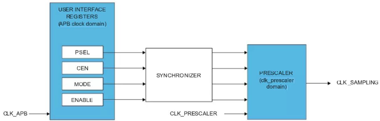
flowchart
graph LR
    A["USER INTERFACE REGISTERS (APB clock domain)"] --> B["PSEL"]
    A --> C["CEN"]
    A --> D["MODE"]
    A --> E["ENABLE"]
    B --> F["SYNCHRONIZER"]
    C --> F
    D --> F
    E --> F
    F --> G["PREScaler (clk_prescaler domain)"]
    G --> H["CLK_SAMPLING"]
    I["CLK_APB"] --> A
    J["CLK_PRESCALER"] --> G
The BOD33 Clock Enable bit (BOD33.CEN) in the BOD33 register should always be disabled before changing the prescaler value. To change the prescaler value for the BOD33 during sampling mode, the following steps need to be taken:
- Wait until the PCLKSR.B33SRDY bit is set.
- Write the selected value to the BOD33.PSEL bit group.
16.6.8.4 Hysteresis
The hysteresis functionality can be used in both continuous and sampling mode. Writing a one to the BOD33 Hysteresis bit (BOD33.HYST) in the BOD33 register will add hysteresis to the BOD33 threshold level.
16.6.9 Voltage Reference System Operation
The Voltage Reference System (VREF) consists of a Bandgap Reference Voltage Generator and a temperature sensor.
The Bandgap Reference Voltage Generator is factory-calibrated under typical voltage and temperature conditions.
At reset, the VREF.CAL register value is loaded from Flash Factory Calibration.
The temperature sensor can be used to get an absolute temperature in the temperature range of CMIN to CMAX degrees Celsius. The sensor will output a linear voltage proportional to the temperature. The output voltage and temperature range are located in the Electrical Characteristics. To calculate the temperature from a measured voltage, the following formula can be used:
$$ C _ {\mathrm{MIN}} + \left(\text { V m e s } + - \text { V o u t } \quad \text { M A X }\right) \frac {\Delta \text { t e m p e r a t u r e }}{\Delta \text { v o l t a g e }} $$
Related Links
32. Electrical Characteristics at 85°C
16.6.9.1 User Control of the Voltage Reference System
To enable the temperature sensor, write a one the Temperature Sensor Enable bit (VREF.TSEN) in the VREF register.
The temperature sensor can be redirected to the ADC for conversion.
The Bandgap Reference Voltage Generator output can also be routed to the ADC if the Bandgap Output Enable bit (VREF.BGOUTEN) in the VREF register is set.
The Bandgap Reference Voltage Generator output level is determined by the CALIB bit group (VREF.CALIB) value in the VREF register. The default calibration value can be overridden by the user by writing to the CALIB bit group.
16.6.10 Voltage Regulator System Operation
The embedded Voltage Regulator (VREG) is an internal voltage regulator that provides the core logic supply (VDDCORE).
16.6.11 Interrupts
The SYSCTRL has the following interrupt sources:
- XOSCRDY - Multipurpose Crystal Oscillator Ready: A "0-to-1" transition on the PCLKSR.XOSCRDY bit is detected
- XOSC32KRDY - 32kHz Crystal Oscillator Ready: A "0-to-1" transition on the PCLKSR.XOSC32KRDY bit is detected
- OSC32KRDY - 32kHz Internal Oscillator Ready: A "0-to-1" transition on the PCLKSR.OSC32KRDY bit is detected
- OSC8MRDY - 8MHz Internal Oscillator Ready: A "0-to-1" transition on the PCLKSR.OSC8MRDY bit is detected
- DFLLRDY - DFLL48M Ready: A "0-to-1" transition on the PCLKSR.DFLLRDY bit is detected
- DFLLOOB - DFLL48M Out Of Boundaries: A "0-to-1" transition on the PCLKSR.DFLLOOB bit is detected
- DFLLLOCKF - DFLL48M Fine Lock: A "0-to-1" transition on the PCLKSR.DFLLLOCKF bit is detected
- DFLLLOCKC - DFLL48M Coarse Lock: A "0-to-1" transition on the PCLKSR.DFLLLOCKC bit is detected
- DFLLRCS - DFLL48M Reference Clock has Stopped: A "0-to-1" transition on the PCLKSR.DFLLRCS bit is detected
- BOD33RDY - BOD33 Ready: A "0-to-1" transition on the PCLKSR.BOD33RDY bit is detected
- BOD33DET - BOD33 Detection: A "0-to-1" transition on the PCLKSR.BOD33DET bit is detected. This is an asynchronous interrupt and can be used to wake-up the device from any sleep mode.
- B33SRDY - BOD33 Synchronization Ready: A "0-to-1" transition on the PCLKSR.B33SRDY bit is detected
Each interrupt source has an interrupt flag associated with it. The interrupt flag in the Interrupt Flag Status and Clear (INTFLAG) register is set when the interrupt condition occurs. Each interrupt can be individually enabled by writing a one to the corresponding bit in the Interrupt Enable Set (INTENSET) register, and disabled by writing a one to the corresponding bit in the Interrupt Enable Clear (INTENCLR) register. An interrupt request is generated when the interrupt flag is set and the corresponding interrupt is enabled. The interrupt request remains active until the interrupt flag is cleared, the interrupt is disabled, or the SYSCTRL is reset. See Interrupt Flag Status and Clear (INTFLAG) register for details on how to clear interrupt flags.
All interrupt requests from the peripheral are ORed together on system level to generate one combined interrupt request to the NVIC. Refer to Nested Vector Interrupt Controller for details. The user must read the INTFLAG register to determine which interrupt condition is present.
Note: Interrupts must be globally enabled for interrupt requests to be generated. Refer to Nested Vector Interrupt Controller for details.
Related Links
10.2. Nested Vector Interrupt Controller
16.6.12 Synchronization
Due to the multiple clock domains, values in the DFLL48M control registers need to be synchronized to other clock domains. The status of this synchronization can be read from the Power and Clocks Status register (PCLKSR). Before writing to any of the DFLL48M control registers, the user must check that the DFLL Ready bit (PCLKSR.DFLLRDY) in PCLKSR is set to one. When this bit is set, the DFLL48M
can be configured and CLK_DFLL48M is ready to be used. Any write to any of the DFLL48M control registers while DFLLRDY is zero will be ignored. An interrupt is generated on a zero-to-one transition of DFLLRDY if the DFLLRDY bit (INTENSET.DFLLDY) in the Interrupt Enable Set register is set.
In order to read from any of the DFLL48M configuration registers, the user must request a read synchronization by writing a one to DFLLSYNC.READREQ. The registers can be read only when PCLKSR.DFLLRDY is set. If DFLLSYNC.READREQ is not written before a read, a synchronization will be started, and the bus will be halted until the synchronization is complete. Reading the DFLL48M registers when the DFLL48M is disabled will not halt the bus.
The prescaler counter used to trigger one-shot brown-out detections also operates asynchronously from the peripheral bus. As a consequence, the prescaler registers require synchronization when written or read. The synchronization results in a delay from when the initialization of the write or read operation begins until the operation is complete.
The write-synchronization is triggered by a write to the BOD33 control register. The Synchronization Ready bit (PCLKSR.B33SRDY) in the PCLKSR register will be cleared when the write-synchronization starts and set when the write-synchronization is complete. When the write-synchronization is ongoing (PCLKSR.B33SRDYis zero), an attempt to do any of the following will cause the peripheral bus to stall until the synchronization is complete:
- Writing to the BOD33control register
- Reading the BOD33 control register that was written
The user can either poll PCLKSR.B33SRDY or use the INTENSET.B33SRDY interrupts to check when the synchronization is complete. It is also possible to perform the next read/write operation and wait, as this next operation will be completed after the ongoing read/write operation is synchronized.
16.7 Register Summary
| Offset | Name Bit Pos. 7 6 | 5 4 3 2 1 | 0 | |||||||
| 0x00 INTENCLR | 7:0 DFLLLCKC DFLLLCKF DFLLOOB DFLRDY OSC8MRDY OSC32KRDY XOSC32KRDY XOSCRDY | |||||||||
| 15:8 | B33SRDY | BOD33DET | BOD33RDY | DFLLRCS | ||||||
| 23:16 | ||||||||||
| 31:24 | ||||||||||
| 0x04 | INTENSET | 7:0 DFLLLCKC DFLLLCKF DFLLOOB DFLRDY OSC8MRDY OSC32KRDY XOSC32KRDY XOSCRDY | ||||||||
| 15:8 | B33SRDY | BOD33DET | BOD33RDY | DFLLRCS | ||||||
| 23:16 | ||||||||||
| 31:24 | ||||||||||
| 0x08 | INTFLAG | 7:0 DFLLLCKC DFLLLCKF DFLLOOB DFLRDY OSC8MRDY OSC32KRDY XOSC32KRDY XOSCRDY | ||||||||
| 15:8 | [3:0] | B33SRDY | BOD33DET | BOD33RDY | DFLLRCS | |||||
| 23:16 | [11:4] | |||||||||
| 31:24 | [19:12] | |||||||||
| 0x0C | PCLKSR | 7:0 DFLLLCKC DFLLLCKF DFLLOOB DFLRDY OSC8MRDY OSC32KRDY XOSC32KRDY XOSCRDY | ||||||||
| 15:8 | B33SRDY | BOD33DET | BOD33RDY | DFLLRCS | ||||||
| 23:16 | STARTUP[2:0] | |||||||||
| 31:24 | ||||||||||
| 0x10 | XOSC | 7:0 | ONDEMAND | RUNSTDBY | XTALEN | ENABLE | ||||
| 15:8 | STARTUP[3:0] | AMPGC | GAIN[2:0] | |||||||
| 0x12 ... 0x13 | Reserved | |||||||||
| 0x14 | XOSC32K | 7:0 | ONDEMAND | RUNSTDBY | AAMPEN | EN32K | XTALEN | ENABLE | ||
| 15:8 | WRTLOCK | STARTUP[2:0] | ||||||||
| 0x16 ... 0x17 | Reserved | |||||||||
| 0x18 | OSC32K | 7:0 | ONDEMAND | RUNSTDBY | EN32K | ENABLE | ||||
| 15:8 | WRTLOCK | STARTUP[2:0] | ||||||||
| 23:16 | CALIB[6:0] | |||||||||
| 31:24 | ||||||||||
| 0x1C | OSCULP32K | 7:0 | WRTLOCK | CALIB[4:0] | ||||||
| 0x1D ... 0x1F | Reserved | |||||||||
| 0x20 | OSC8M | 7:0 | ONDEMAND | RUNSTDBY | ENABLE | |||||
| 15:8 | PRESC[1:0] | |||||||||
| 23:16 | CALIB[7:0] | |||||||||
| 31:24 | FRANGE[1:0] | CALIB[11:8] | ||||||||
| 0x24 | DFLLCTRL | 7:0 | ONDEMAND | LLAW | STABLE | MODE | ENABLE | |||
| 15:8 | QLDIS CCDIS | |||||||||
| 0x26 ... 0x27 | Reserved | |||||||||
| 0x28 | DFLLVAL | 7:0 | FINE[7:0] | |||||||
| 15:8 | COARSE[5:0] | FINE[9:8] | ||||||||
| 23:16 | DIFF[7:0] | |||||||||
| 31:24 | DIFF[15:8] | |||||||||
| 0x2C | DFLLMUL | 7:0 | MUL[7:0] | |||||||
| 15:8 | MUL[15:8] | |||||||||
| 23:16 | FSTEP[7:0] | |||||||||
| 31:24 | CSTEP[5:0] | FSTEP[9:8] | ||||||||
| 0x30 | DFLLSYNC | 7:0 | READREQ | |||||||
| 0x31 ... 0x33 | Reserved | |||||||||
| 0x34 | BOD33 | 7:0 | RUNSTDBY | ACTION[1:0] | HYST | ENABLE | ||||
| 15:8 | PSEL[3:0] | CEN | MODE | |||||||
| 23:16 | LEVEL[5:0] | |||||||||
| 31:24 | ||||||||||
| ......continued | ||||||||||
| Offset | Name Bit Pos. 7 6 5 4 3 2 1 0 | |||||||||
| 0x38...0x3B | Reserved | |||||||||
| 0x3C VREG | 7:0 RUNSTDBY ENABLE | |||||||||
| 15:8 FORCELDO | ||||||||||
| 0x3E...0x3F | Reserved | |||||||||
| 0x40 VREF | 7:0 | BGOUTEN TSEN | ||||||||
| 15:8 | ||||||||||
| 23:16 CALIB[7:0] | ||||||||||
| 31:24 | CALIB[10:8] | |||||||||
16.8 Register Description
Registers can be 8, 16, or 32 bits wide. Atomic 8-, 16-, and 32-bit accesses are supported. In addition, the 8-bit quarters and 16-bit halves of a 32-bit register, and the 8-bit halves of a 16-bit register can be accessed directly.
Some registers require synchronization when read and/or written. Synchronization is denoted by the "Read-Synchronized" and/or "Write-Synchronized" property in each individual register description.
Optional write-protection by the Peripheral Access Controller (PAC) is denoted by the "PAC Write-Protection" property in each individual register description.
16.8.1 Interrupt Enable Clear
Name: INTENCLR
Offset: 0x00
Reset: 0x00000000
Property: Write-Protected

Bit 11 - B33SRDY BOD33 Synchronization Ready Interrupt Enable
Writing a zero to this bit has no effect.
Writing a one to this bit will clear the BOD33 Synchronization Ready Interrupt Enable bit, which disables the BOD33 Synchronization Ready interrupt.
| Value | Description |
| 0 | The BOD33 Synchronization Ready interrupt is disabled. |
| 1 | The BOD33 Synchronization Ready interrupt is enabled, and an interrupt request will be generated when the BOD33 Synchronization Ready Interrupt flag is set. |
Bit 10 - BOD33DET BOD33 Detection Interrupt Enable
Writing a zero to this bit has no effect.
Writing a one to this bit will clear the BOD33 Detection Interrupt Enable bit, which disables the BOD33 Detection interrupt.
| Value | Description |
| 0 | The BOD33 Detection interrupt is disabled. |
| 1 | The BOD33 Detection interrupt is enabled, and an interrupt request will be generated when the BOD33 Detection Interrupt flag is set. |
Bit 9 - BOD33RDY BOD33 Ready Interrupt Enable
Writing a zero to this bit has no effect.
Writing a one to this bit will clear the BOD33 Ready Interrupt Enable bit, which disables the BOD33
Ready interrupt.
| Value | Description |
| 0 | The BOD33 Ready interrupt is disabled. |
| 1 | The BOD33 Ready interrupt is enabled, and an interrupt request will be generated when the BOD33 Ready Interrupt flag is set. |
Bit 8 - DFLLRCS DFLL Reference Clock Stopped Interrupt Enable
Writing a zero to this bit has no effect.
Writing a one to this bit will clear the DFLL Reference Clock Stopped Interrupt Enable bit, which disables the DFLL Reference Clock Stopped interrupt.
| Value Description | |
| 0 | The DFLL Reference Clock Stopped interrupt is disabled. |
| 1 | The DFLL Reference Clock Stopped interrupt is enabled, and an interrupt request will be generated when the DFLL Reference Clock Stopped Interrupt flag is set. |
Bit 7 - DFLLLCKC DFLL Lock Coarse Interrupt Enable
Writing a zero to this bit has no effect.
Writing a one to this bit will clear the DFLL Lock Coarse Interrupt Enable bit, which disables the DFLL Lock Coarse interrupt.
| Value Description | |
| 0 | The DFLL Lock Coarse interrupt is disabled. |
| 1 | The DFLL Lock Coarse interrupt is enabled, and an interrupt request will be generated when the DFLL Lock Coarse Interrupt flag is set. |
Bit 6 - DFLLLCKF DFLL Lock Fine Interrupt Enable
Writing a zero to this bit has no effect.
Writing a one to this bit will clear the DFLL Lock Fine Interrupt Enable bit, which disables the DFLL Lock Fine interrupt.
| Value Description | |
| 0 | The DFLL Lock Fine interrupt is disabled. |
| 1 | The DFLL Lock Fine interrupt is enabled, and an interrupt request will be generated when the DFLL Lock Fine Interrupt flag is set. |
Bit 5 - DFLLOOB DFLL Out Of Bounds Interrupt Enable
Writing a zero to this bit has no effect.
Writing a one to this bit will clear the DFLL Out Of Bounds Interrupt Enable bit, which disables the DFLL Out Of Bounds interrupt.
| Value Description | |
| 0 | The DFLL Out Of Bounds interrupt is disabled. |
| 1 | The DFLL Out Of Bounds interrupt is enabled, and an interrupt request will be generated when the DFLL Out Of Bounds Interrupt flag is set. |
Bit 4 - DFLLRDY DFLL Ready Interrupt Enable
Writing a zero to this bit has no effect.
Writing a one to this bit will clear the DFLL Ready Interrupt Enable bit, which disables the DFLL Ready interrupt.
| Value Description | |
| 0 | The DFLL Ready interrupt is disabled. |
| 1 | The DFLL Ready interrupt is enabled, and an interrupt request will be generated when the DFLL Ready Interrupt flag is set. |
Bit 3 - OSC8MRDY OSC8M Ready Interrupt Enable
Writing a zero to this bit has no effect.
Writing a one to this bit will clear the OSC8M Ready Interrupt Enable bit, which disables the OSC8M Ready interrupt.
| Value Description | |
| 0 | The OSC8M Ready interrupt is disabled. |
| 1 | The OSC8M Ready interrupt is enabled, and an interrupt request will be generated when the OSC8M Ready Interrupt flag is set. |
Bit 2 - OSC32KRDY OSC32K Ready Interrupt Enable
Writing a zero to this bit has no effect.
Writing a one to this bit will clear the OSC32K Ready Interrupt Enable bit, which disables the OSC32K Ready interrupt.
| Value Description | |
| 0 | The OSC32K Ready interrupt is disabled. |
| 1 | The OSC32K Ready interrupt is enabled, and an interrupt request will be generated when the OSC32K Ready Interrupt flag is set. |
Bit 1 - XOSC32KRDY XOSC32K Ready Interrupt Enable
Writing a zero to this bit has no effect.
Writing a one to this bit will set the XOSC32K Ready Interrupt Enable bit, which enables the XOSC32K Ready interrupt.
| Value Description | |
| 0 | The XOSC32K Ready interrupt is disabled. |
| 1 | The XOSC32K Ready interrupt is enabled, and an interrupt request will be generated when the XOSC32K Ready Interrupt flag is set. |
Bit 0 - XOSCRDY XOSC Ready Interrupt Enable
Writing a zero to this bit has no effect.
Writing a one to this bit will set the XOSC Ready Interrupt Enable bit, which enables the XOSC Ready interrupt.
| Value Description | |
| 0 | The XOSC Ready interrupt is disabled. |
| 1 | The XOSC Ready interrupt is enabled, and an interrupt request will be generated when the XOSC Ready Interrupt flag is set. |
16.8.2 Interrupt Enable Set
Name: INTENSET
Offset: 0x04
Reset: 0x00000000
Property: Write-Protected
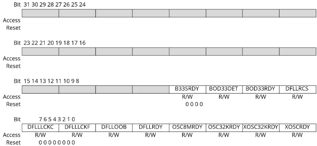
Bit 11 - B33SRDY BOD33 Synchronization Ready Interrupt Enable
Writing a zero to this bit has no effect.
Writing a one to this bit will set the BOD33 Synchronization Ready Interrupt Enable bit, which enables the BOD33 Synchronization Ready interrupt.
| Value | Description |
| 0 | The BOD33 Synchronization Ready interrupt is disabled. |
| 1 | The BOD33 Synchronization Ready interrupt is enabled, and an interrupt request will be generated when the BOD33 Synchronization Ready Interrupt flag is set. |
Bit 10 - BOD33DET BOD33 Detection Interrupt Enable
Writing a zero to this bit has no effect.
Writing a one to this bit will set the BOD33 Detection Interrupt Enable bit, which enables the BOD33 Detection interrupt.
| Value | Description |
| 0 | The BOD33 Detection interrupt is disabled. |
| 1 | The BOD33 Detection interrupt is enabled, and an interrupt request will be generated when the BOD33 Detection Interrupt flag is set. |
Bit 9 - BOD33RDY BOD33 Ready Interrupt Enable
Writing a zero to this bit has no effect.
Writing a one to this bit will set the BOD33 Ready Interrupt Enable bit, which enables the BOD33
Ready interrupt.
| Value | Description |
| 0 | The BOD33 Ready interrupt is disabled. |
| 1 | The BOD33 Ready interrupt is enabled, and an interrupt request will be generated when the BOD33 Ready Interrupt flag is set. |
Bit 8 - DFLLRCS DFLL Reference Clock Stopped Interrupt Enable
Writing a zero to this bit has no effect.
Writing a one to this bit will set the DFLL Reference Clock Stopped Interrupt Enable bit, which enables the DFLL Reference Clock Stopped interrupt.
| Value Description | |
| 0 | The DFLL Reference Clock Stopped interrupt is disabled. |
| 1 | The DFLL Reference Clock Stopped interrupt is enabled, and an interrupt request will be generated when the DFLL Reference Clock Stopped Interrupt flag is set. |
Bit 7 - DFLLLCKC DFLL Lock Coarse Interrupt Enable
Writing a zero to this bit has no effect.
Writing a one to this bit will set the DFLL Lock Coarse Interrupt Enable bit, which enables the DFLL Lock Coarse interrupt.
| Value Description | |
| 0 | The DFLL Lock Coarse interrupt is disabled. |
| 1 | The DFLL Lock Coarse interrupt is enabled, and an interrupt request will be generated when the DFLL Lock Coarse Interrupt flag is set. |
Bit 6 - DFLLLCKF DFLL Lock Fine Interrupt Enable
Writing a zero to this bit has no effect.
Writing a one to this bit will set the DFLL Lock Fine Interrupt Disable/Enable bit, disable the DFLL Lock Fine interrupt and set the corresponding interrupt request.
| Value Description | |
| 0 | The DFLL Lock Fine interrupt is disabled. |
| 1 | The DFLL Lock Fine interrupt is enabled, and an interrupt request will be generated when the DFLL Lock Fine Interrupt flag is set. |
Bit 5 - DFLLOOB DFLL Out Of Bounds Interrupt Enable
Writing a zero to this bit has no effect.
Writing a one to this bit will set the DFLL Out Of Bounds Interrupt Enable bit, which enables the DFLL Out Of Bounds interrupt.
| Value Description | |
| 0 | The DFLL Out Of Bounds interrupt is disabled. |
| 1 | The DFLL Out Of Bounds interrupt is enabled, and an interrupt request will be generated when the DFLL Out Of Bounds Interrupt flag is set. |
Bit 4 - DFLLRDY DFLL Ready Interrupt Enable
Writing a zero to this bit has no effect.
Writing a one to this bit will set the DFLL Ready Interrupt Enable bit, which enables the DFLL Ready interrupt and set the corresponding interrupt request.
| Value Description | |
| 0 | The DFLL Ready interrupt is disabled. |
| 1 | The DFLL Ready interrupt is enabled, and an interrupt request will be generated when the DFLL Ready Interrupt flag is set. |
Bit 3 - OSC8MRDY OSC8M Ready Interrupt Enable
Writing a zero to this bit has no effect.
Writing a one to this bit will set the OSC8M Ready Interrupt Enable bit, which enables the OSC8M Ready interrupt.
| Value Description | |
| 0 | The OSC8M Ready interrupt is disabled. |
| 1 | The OSC8M Ready interrupt is enabled, and an interrupt request will be generated when the OSC8M Ready Interrupt flag is set. |
Bit 2 - OSC32KRDY OSC32K Ready Interrupt Enable
Writing a zero to this bit has no effect.
Writing a one to this bit will set the OSC32K Ready Interrupt Enable bit, which enables the OSC32K Ready interrupt.
| Value Description | |
| 0 | The OSC32K Ready interrupt is disabled. |
| 1 | The OSC32K Ready interrupt is enabled, and an interrupt request will be generated when the OSC32K Ready Interrupt flag is set. |
Bit 1 - XOSC32KRDY XOSC32K Ready Interrupt Enable
Writing a zero to this bit has no effect.
Writing a one to this bit will set the XOSC32K Ready Interrupt Enable bit, which enables the XOSC32K Ready interrupt.
| Value Description | |
| 0 | The XOSC32K Ready interrupt is disabled. |
| 1 | The XOSC32K Ready interrupt is enabled, and an interrupt request will be generated when the XOSC32K Ready Interrupt flag is set. |
Bit 0 - XOSCRDY XOSC Ready Interrupt Enable
Writing a zero to this bit has no effect.
Writing a one to this bit will set the XOSC Ready Interrupt Enable bit, which enables the XOSC Ready interrupt.
| Value Description | |
| 0 | The XOSC Ready interrupt is disabled. |
| 1 | The XOSC Ready interrupt is enabled, and an interrupt request will be generated when the XOSC Ready Interrupt flag is set. |
16.8.3 Interrupt Flag Status and Clear
Name: INTFLAG
Offset: 0x08
Reset: 0x00000000
Property: -
| Bit 31 30 29 28 27 26 25 24 | |||||||
| [19:12] | |||||||
| Access R R R R R R R R Reset 0 0 0 0 0 0 0 0 | |||||||
| Bit 23 22 21 20 19 18 17 16 | |||||||
| [11:4] | |||||||
| Access R R R R R R R R Reset 0 0 0 0 0 0 0 0 | |||||||
| Bit 15 14 13 12 11 10 9 8 | |||||||
| [3:0] B33SRDY | BOD33DET | BOD33RDY | DFLLRCS | ||||
| Access R Reset 0 0 0 0 0 0 0 0 | R | R | R | R/W | R/W | R/W | R/W |
| Bit 7 6 5 4 3 2 1 0 | |||||||
| DFLLLCKC | DFLLLCKF | DFLLOOB | DFLLRDY | OSC8MRDY | OSC32KRDY | XOSC32KRDY | XOSCRDY |
| Access R/W Reset 0 0 0 0 0 0 0 0 | R/W | R/W | R/W | R/W | R/W | R/W | R/W |
Bits 31:12 - [19:0] Reserved
These bits are unused and reserved for future use. For compatibility with future devices, always write these bits to zero when this register is written. These bits will always return zero when read.
Bit 11 - B33SRDY BOD33 Synchronization Ready
This flag is cleared by writing a one to it.
This flag is set on a zero-to-one transition of the BOD33 Synchronization Ready bit in the Status register (PCLKSR.B33SRDY) and will generate an interrupt request if INTENSET.B33SRDY is one.
Writing a zero to this bit has no effect.
Writing a one to this bit clears the BOD33 Synchronization Ready interrupt flag
Bit 10 - BOD33DET BOD33 Detection
This flag is cleared by writing a one to it.
This flag is set on a zero-to-one transition of the BOD33 Detection bit in the Status register (PCLKSR.BOD33DET) and will generate an interrupt request if INTENSET.BOD33DET is one.
Writing a zero to this bit has no effect.
Writing a one to this bit clears the BOD33 Detection interrupt flag.
Bit 9 - BOD33RDY BOD33 Ready
This flag is cleared by writing a one to it.
This flag is set on a zero-to-one transition of the BOD33 Ready bit in the Status register (PCLKSR.BOD33RDY) and will generate an interrupt request if INTENSET.BOD33RDY is one.
Writing a zero to this bit has no effect.
Writing a one to this bit clears the BOD33 Ready interrupt flag.
Bit 8 - DFLLRCS DFLL Reference Clock Stopped
This flag is cleared by writing a one to it.
This flag is set on a zero-to-one transition of the DFLL Reference Clock Stopped bit in the Status register (PCLKSR.DFLLRCS) and will generate an interrupt request if INTENSET.DFLLRCS is one.
Writing a zero to this bit has no effect.
Writing a one to this bit clears the DFLL Reference Clock Stopped interrupt flag.
Bit 7 - DFLLLCKC DFLL Lock Coarse
This flag is cleared by writing a one to it.
This flag is set on a zero-to-one transition of the DFLL Lock Coarse bit in the Status register (PCLKSR.DFLLLCKC) and will generate an interrupt request if INTENSET.DFLLLCKC is one.
Writing a zero to this bit has no effect.
Writing a one to this bit clears the DFLL Lock Coarse interrupt flag.
Bit 6 - DFLLLCKF DFLL Lock Fine
This flag is cleared by writing a one to it.
This flag is set on a zero-to-one transition of the DFLL Lock Fine bit in the Status register (PCLKSR.DFLLLCKF) and will generate an interrupt request if INTENSET.DFLLLCKF is one.
Writing a zero to this bit has no effect.
Writing a one to this bit clears the DFLL Lock Fine interrupt flag.
Bit 5 - DFLLOOB DFLL Out Of Bounds
This flag is cleared by writing a one to it.
This flag is set on a zero-to-one transition of the DFLL Out Of Bounds bit in the Status register (PCLKSR.DFLLOOB) and will generate an interrupt request if INTENSET.DFLLOOB is one.
Writing a zero to this bit has no effect.
Writing a one to this bit clears the DFLL Out Of Bounds interrupt flag.
Bit 4 - DFLLRDY DFLL Ready
This flag is cleared by writing a one to it.
This flag is set on a zero-to-one transition of the DFLL Ready bit in the Status register (PCLKSR.DFLLRDY) and will generate an interrupt request if INTENSET.DFLLRDY is one.
Writing a zero to this bit has no effect.
Writing a one to this bit clears the DFLL Ready interrupt flag.
Bit 3 - OSC8MRDY OSC8M Ready
This flag is cleared by writing a one to it.
This flag is set on a zero-to-one transition of the OSC8M Ready bit in the Status register (PCLKSR.OSC8MRDY) and will generate an interrupt request if INTENSET.OSC8MRDY is one.
Writing a zero to this bit has no effect.
Writing a one to this bit clears the OSC8M Ready interrupt flag.
Bit 2 - OSC32KRDY OSC32K Ready
This flag is cleared by writing a one to it.
This flag is set on a zero-to-one transition of the OSC32K Ready bit in the Status register (PCLKSR.OSC32KRDY) and will generate an interrupt request if INTENSET.OSC32KRDY is one.
Writing a zero to this bit has no effect.
Writing a one to this bit clears the OSC32K Ready interrupt flag.
Bit 1 - XOSC32KRDY XOSC32K Ready
This flag is cleared by writing a one to it.
This flag is set on a zero-to-one transition of the XOSC32K Ready bit in the Status register (PCLKSR.XOSC32KRDY) and will generate an interrupt request if INTENSET.XOSC32KRDY is one.
Writing a zero to this bit has no effect.
Writing a one to this bit clears the XOSC32K Ready interrupt flag.
Bit 0 - XOSCRDY XOSC Ready
This flag is cleared by writing a one to it.
This flag is set on a zero-to-one transition of the XOSC Ready bit in the Status register
(PCLKSR.XOSCRDY) and will generate an interrupt request if INTENSET.XOSCRDY is one.
Writing a zero to this bit has no effect.
Writing a one to this bit clears the XOSC Ready interrupt flag.
16.8.4 Power and Clocks Status
Name: PCLKSR
Offset: 0x0C
Reset: 0x00000000
Property: -
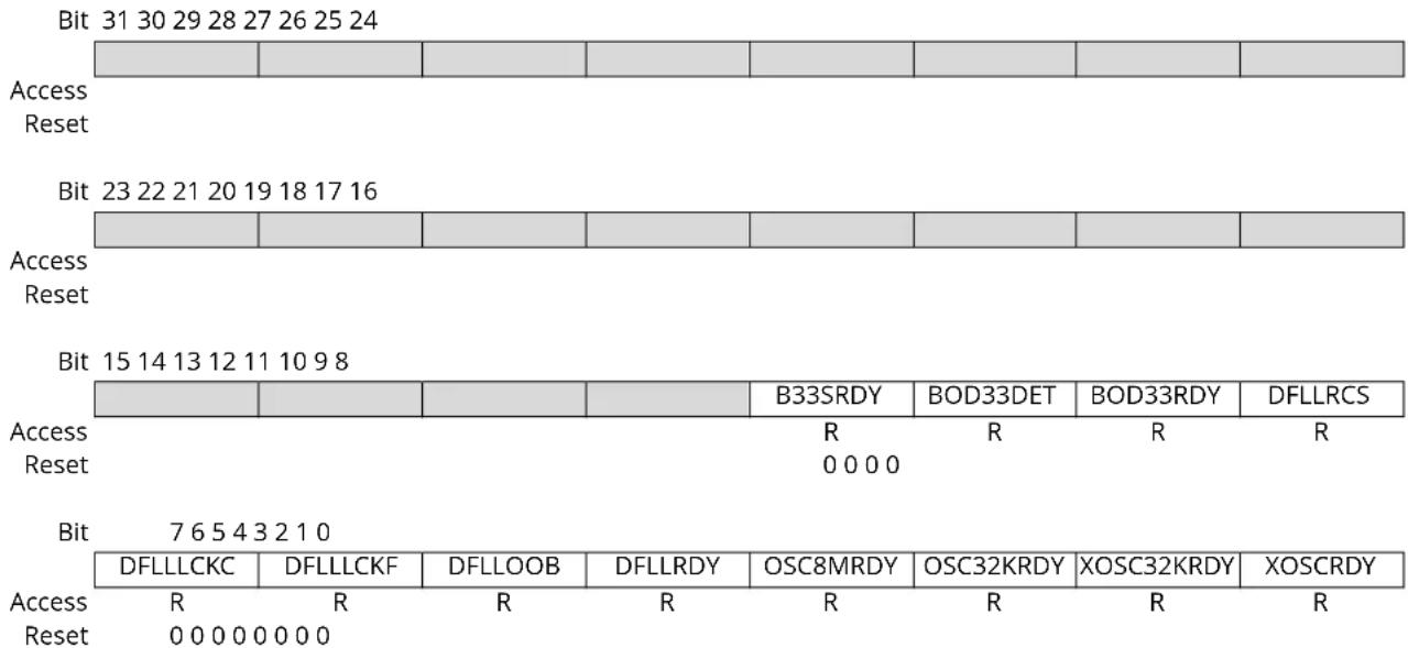
text_image
Bit 31 30 29 28 27 26 25 24 Access Reset Bit 23 22 21 20 19 18 17 16 Access Reset Bit 15 14 13 12 11 10 9 8 Access Reset R R R R 0 0 0 0 Bit 7 6 5 4 3 2 1 0 DFLLLCKC DFLLLCKF DFLLOOB DFLLRDY OSC8MRDY OSC32KRDY XOSC32KRDY XOSCRDY Access R R R R R R Reset 0 0 0 0 0 0 0Bit 11 - B33SRDY BOD33 Synchronization Ready
| Value | Description |
| 0 | BOD33 synchronization is complete. |
| 1 | BOD33 synchronization is ongoing. |
Bit 10 - BOD33DET BOD33 Detection
| Value | Description |
| 0 | No BOD33 detection. |
| 1 | BOD33 has detected that the I/O power supply is going below the BOD33 reference value. |
Bit 9 - BOD33RDY BOD33 Ready
| Value | Description |
| 0 | BOD33 is not ready. |
| 1 | BOD33 is ready. |
Bit 8 - DFLLRCS DFLL Reference Clock Stopped
| Value | Description |
| 0 | DFLL reference clock is running. |
| 1 | DFLL reference clock has stopped. |
Bit 7 - DFLLLCKC DFLL Lock Coarse
| Value | Description |
| 0 | No DFLL coarse lock detected. |
| 1 | DFLL coarse lock detected. |
Bit 6 - DFLLLCKF DFLL Lock Fine
| Value Description | |
| 0 | No DFLL fine lock detected. |
| 1 | DFLL fine lock detected. |
Bit 5 - DFLLOOB DFLL Out Of Bounds
| Value Description | |
| 0 | No DFLL Out Of Bounds detected. |
| 1 | DFLL Out Of Bounds detected. |
Bit 4 - DFLLRDY DFLL Ready
This bit is cleared when the synchronization of registers between clock domains is complete. This bit is set when the synchronization of registers between clock domains is started.
| Value Description | |
| 0 | The Synchronization is ongoing. |
| 1 | The Synchronization is complete. |
Bit 3 - OSC8MRDY OSC8M Ready
| Value Description | |
| 0 | OSC8M is not ready. |
| 1 | OSC8M is stable and ready to be used as a clock source. |
Bit 2 - OSC32KRDY OSC32K Ready
| Value Description | |
| 0 | OSC32K is not ready. |
| 1 | OSC32K is stable and ready to be used as a clock source. |
Bit 1 - XOSC32KRDY XOSC32K Ready
| Value Description | |
| 0 | XOSC32K is not ready. |
| 1 | XOSC32K is stable and ready to be used as a clock source. |
Bit 0 - XOSCRDY XOSC Ready
| Value Description | |
| 0 | XOSC is not ready. |
| 1 | XOSC is stable and ready to be used as a clock source. |
16.8.5 External Multipurpose Crystal Oscillator (XOSC) Control
Name: XOSC
Offset: 0x10
Reset: 0x0080
Property: Write-Protected
Bit 15 14 13 12 11 10 9 8
| STARTUP[3:0] AMPGC GAIN[2:0] |
Access R/W R/W R/W R/W R/W R/W R/W R/W
Reset 00000000
Bit 76543210
| ONDEMAND | RUNSTDBY | XTALEN | ENABLE |
Access R/W R/W R/W R/W
Reset 10 00
Bits 15:12 - STARTUP[3:0] Start-Up Time
These bits select start-up time for the oscillator according to the table below.
The OSCULP32K oscillator is used to clock the start-up counter.
| STARTUP[3:0] | Number of OSCULP32K Clock Cycles | Number of XOSC Clock Cycles | Approximate Equivalent Time ^(1)(2)(3) |
| 0x0 | 1 | 3 | 31 μs |
| 0x1 | 2 | 3 | 61 μs |
| 0x2 | 4 | 3 | 122 μs |
| 0x3 | 8 | 3 | 244 μs |
| 0x4 | 16 | 3 | 488 μs |
| 0x5 | 32 | 3 | 977 μs |
| 0x6 | 64 | 3 | 1953 μs |
| 0x7 | 128 | 3 | 3906 μs |
| 0x8 | 256 | 3 | 7813 μs |
| 0x9 | 512 | 3 | 15625 μs |
| 0xA | 1024 | 3 | 31250 μs |
| 0xB | 2048 | 3 | 62500 μs |
| 0xC | 4096 | 3 | 125000 μs |
| 0xD | 8192 | 3 | 250000 μs |
| 0xE | 16384 | 3 | 500000 μs |
| 0xF | 32768 | 3 | 1000000 μs |
Notes:
- Number of cycles for the start-up counter
- Number of cycles for the synchronization delay, before PCLKSR.XOSCRDY is set.
- Actual start-up time is n OSCULP32K cycles + 3 XOSC cycles, but given the time neglects the three XOSC cycles.
Bit 11 - AMPGC Automatic Amplitude Gain Control
Note: The configuration of the oscillator gain is mandatory even if AMPGC feature is enabled at startup.
| Value | Description |
| 0 | The automatic amplitude gain control is disabled |
| 1 | The automatic amplitude gain control is enabled. Amplitude gain will be automatically adjusted during Crystal Oscillator operation. |
Bits 10:8 - GAIN[2:0] Oscillator Gain
These bits select the gain for the oscillator. The listed maximum frequencies are recommendations, and might vary based on capacitive load and crystal characteristics. These bits must be properly configured even when the Automatic Amplitude Gain Control is active.
| GAIN[2:0] Recommended Max Frequency | |
| 0x0 2 MHz | |
| 0x1 4 MHz | |
| 0x2 8 MHz | |
| 0x3 16 MHz | |
| 0x4 30 MHz | |
| 0x5-0x7 Reserved | |
Bit 7 - ONDEMAND On Demand Control
The On Demand operation mode allows an oscillator to be enabled or disabled, depending on peripheral clock requests.
In On Demand operation mode (i.e., if the XOSC.ONDEMAND bit has been previously written to one), the oscillator will be running only when requested by a peripheral. If there is no peripheral requesting the oscillator's clock source, the oscillator will be in a disabled state.
If On Demand is disabled, the oscillator will always be running when enabled.
In Standby Sleep mode, the On Demand operation is still active if the XOSC.RUNSTDBY bit is one. If XOSC.RUNSTDBY is zero, the oscillator is disabled.
| Value Description | |
| 0 | The oscillator is always on, if enabled |
| 1 | The oscillator is enabled when a peripheral is requesting the oscillator to be used as a clock source. The oscillator is disabled if no peripheral is requesting the clock source. |
Bit 6 - RUNSTDBY Run in Standby
This bit controls how the XOSC behaves during Standby Sleep mode:
| Value Description | |
| 0 | The oscillator is disabled in Standby Sleep mode. |
| 1 | The oscillator is not stopped in Standby Sleep mode. If XOSC.ONDEMAND is one, the clock source will be running when a peripheral is requesting the clock. If XOSC.ONDEMAND is zero, the clock source will always be running in Standby Sleep mode. |
Bit 2 - XTALEN Crystal Oscillator Enable
This bit controls the connections between the I/O pads and the external clock or crystal oscillator:
| Value Description | |
| 0 | External clock connected on XIN. XOUT can be used as general purpose I/O. |
| 1 | Crystal connected to XIN/XOUT |
Bit 1 - ENABLE Oscillator Enable
| Value Description | |
| 0 | The oscillator is disabled |
| 1 | The oscillator is enabled |
16.8.6 32kHz External Crystal Oscillator (XOSC32K) Control
Name: XOSC32K
Offset: 0x14
Reset: 0x0080
Property: Write-Protected
Bit 15 14 13 12 11 10 9 8
| WRTLOCK STARTUP[2:0] | ||||
| Access Reset | R/W R/W 0 | R/W | R/W 0 0 0 |
Bit 76543210
| ONDEMAND | RUNSTDBY | AAMPEN | EN32K | XTALEN | ENABLE | |||
| Access | R/W | R/W | R/W | R/W | R/W | R/W | ||
| Reset | 1 0 0 | 0 0 0 |
Bit 12 - WRTLOCK Write Lock
This bit locks the XOSC32K register for future writes to fix the XOSC32K configuration.
| Value | Description |
| 0 | The XOSC32K configuration is not locked. |
| 1 | The XOSC32K configuration is locked. |
Bits 10:8 - STARTUP[2:0] Oscillator Start-Up Time
These bits select the start-up time for the oscillator.
The OSCULP32K oscillator is used to clock the start-up counter.
Table 16-3. Start-Up Time for 32kHz External Crystal Oscillator
| STARTUP[2:0] | Number of OSCULP32K Clock Cycles | Number of XOSC32K Clock Cycles | Approximate Equivalent Time (OSCULP = 32kHz) ^(1)(2)(3) |
| 0x0 | 1 | 3 | 122μs |
| 0x1 | 32 | 3 | 1068μs |
| 0x2 | 2048 | 3 | 62592μs |
| 0x3 | 4096 | 3 | 125092μs |
| 0x4 | 16384 | 3 | 500092μs |
| 0x5 | 32768 | 3 | 1000092μs |
| 0x6 | 65536 | 3 | 2000092μs |
| 0x7 | 131072 | 3 | 4000092μs |
Notes: 1. Number of cycles for the start-up counter.
2. Number of cycles for the synchronization delay, before PCLKSR.XOSC32KRDY is set.
3. Start-up time is n OSCULP32K cycles + 3 XOSC32K cycles.
Bit 7 - ONDEMAND On Demand Control
The On Demand operation mode allows an oscillator to be enabled or disabled depending on peripheral clock requests.
In On Demand operation mode, i.e., if the ONDEMAND bit has been previously written to one, the oscillator will only be running when requested by a peripheral. If there is no peripheral requesting the oscillator's clock source, the oscillator will be in a disabled state.
If On Demand is disabled the oscillator will always be running when enabled.
In standby sleep mode, the On Demand operation is still active if the XOSC32K.RUNSTDBY bit is one. If XOSC32K.RUNSTDBY is zero, the oscillator is disabled.
| Value | Description |
| 0 | The oscillator is always on, if enabled. |
Value Description
| 1 | The oscillator is enabled when a peripheral is requesting the oscillator to be used as a clock source. The oscillator is disabled if no peripheral is requesting the clock source. |
Bit 6 - RUNSTDBY Run in Standby
This bit controls how the XOSC32K behaves during standby sleep mode:
Value Description
| 0 | The oscillator is disabled in standby sleep mode. |
| 1 | The oscillator is not stopped in standby sleep mode. If XOSC32K.ONDEMAND is one, the clock source will be running when a peripheral is requesting the clock. If XOSC32K.ONDEMAND is zero, the clock source will always be running in standby sleep mode. |
Bit 5 - AAMPEN Automatic Amplitude Control Enable
Value Description
| 0 | The automatic amplitude control for the crystal oscillator is disabled. |
| 1 | The automatic amplitude control for the crystal oscillator is enabled. |
Bit 3 - EN32K 32kHz Output Enable
This bit controls the connections between the I/O pads and the external clock or crystal oscillator:
Value Description
| 0 | The 32kHz output is disabled. |
| 1 | The 32kHz output is enabled. |
Bit 2 - XTALEN Crystal Oscillator Enable
This bit controls the connections between the I/O pads and the external clock or crystal oscillator:
Value Description
| 0 | External clock connected on XIN32. XOUT32 can be used as general-purpose I/O. |
| 1 | Crystal connected to XIN32/XOUT32. |
Bit 1 - ENABLE Oscillator Enable
Value Description
| 0 | The oscillator is disabled. |
| 1 | The oscillator is enabled. |
16.8.7 32kHz Internal Oscillator (OSC32K) Control
Name: OSC32K
Offset: 0x18
Reset: 0x003F0080
Property: Write-Protected
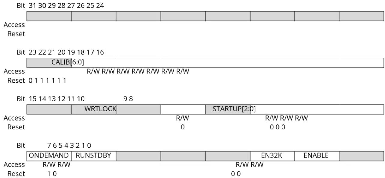
text_image
Bit 31 30 29 28 27 26 25 24 Access Reset Bit 23 22 21 20 19 18 17 16 CALIB[6:0] Access R/W R/W R/W R/W R/W R/W R/W Reset 0 1 1 1 1 1 1 Bit 15 14 13 12 11 10 9 8 WRTLOCK R/W R/W R/W R/W Reset 0 0 0 0 Bit 7 6 5 4 3 2 1 0 ONDEMAND RUNSTDBY Access R/W R/W R/W R/W Reset 1 0 0 0 STARTUP[2:0] EN32K ENABLEBits 22:16 - CALIB[6:0] Oscillator Calibration
These bits control the oscillator calibration.
This value must be written by the user.
Factory calibration values can be loaded from the non-volatile memory.
Bit 12 - WRTLOCK Write Lock
This bit locks the OSC32K register for future writes to fix the OSC32K configuration.
| Value | Description |
| 0 | The OSC32K configuration is not locked. |
| 1 | The OSC32K configuration is locked. |
Bits 10:8 - STARTUP[2:0] Oscillator Start-Up Time
These bits select start-up time for the oscillator.
The OSCULP32K oscillator is used as input clock to the startup counter.
Table 16-4. Start-Up Time for 32kHz Internal Oscillator
| STARTUP[2:0] | Number of OSC32K clock cycles | Approximate Equivalent Time (OSCULP= 32 kHz) ^(1)(2)(3) |
| 0x0 | 3 | 92μs |
| 0x1 | 4 | 122μs |
| 0x2 | 6 | 183μs |
| 0x3 | 10 | 305μs |
| 0x4 | 18 | 549μs |
| 0x5 | 34 | 1038μs |
| 0x6 | 66 | 2014μs |
| 0x7 | 130 | 3967μs |
Notes: 1. Number of cycles for the start-up counter.
- Number of cycles for the synchronization delay, before PCLKSR.OSC32KRDY is set.
- Start-up time is n OSC32K cycles + 2 OSC32K cycles.
Bit 7 - ONDEMAND On Demand Control
The On Demand operation mode allows an oscillator to be enabled or disabled depending on peripheral clock requests.
In On Demand operation mode, i.e., if the ONDEMAND bit has been previously written to one, the oscillator will only be running when requested by a peripheral. If there is no peripheral requesting the oscillator's clock source, the oscillator will be in a disabled state.
If On Demand is disabled the oscillator will always be running when enabled.
In standby sleep mode, the On Demand operation is still active if the OSC32K.RUNSTDBY bit is one.
If OSC32K.RUNSTDBY is zero, the oscillator is disabled.
| Value Description | |
| 0 | The oscillator is always on, if enabled. |
| 1 | The oscillator is enabled when a peripheral is requesting the oscillator to be used as a clock source. The oscillator is disabled if no peripheral is requesting the clock source. |
Bit 6 - RUNSTDBY Run in Standby
This bit controls how the OSC32K behaves during standby sleep mode:
| Value Description | |
| 0 | The oscillator is disabled in standby sleep mode. |
| 1 | The oscillator is not stopped in standby sleep mode. If OSC32K.ONDEMAND is one, the clock source will be running when a peripheral is requesting the clock. If OSC32K.ONDEMAND is zero, the clock source will always be running in standby sleep mode. |
Bit 2 - EN32K 32kHz Output Enable
| Value Description | |
| 0 | The 32kHz output is disabled. |
| 1 | The 32kHz output is enabled. |
| 0 | The oscillator is disabled. |
| 1 | The oscillator is enabled. |
Bit 1 - ENABLE Oscillator Enable
| Value Description | |
| 0 | The oscillator is disabled. |
| 1 | The oscillator is enabled. |
16.8.8 32kHz Ultra Low Power Internal Oscillator (OSCULP32K) Control
Name: OSCULP32K
Offset: 0x1C
Reset: 0xXX
Property: Write-Protected
Bit 76543210
| WRTLOCK | CALIB[4:0] | |||||||
| Access | R/W | R/W | R/W | R/W | R/W | R/W | ||
| Reset | 0 | x | x | x | ||||
Bit 7 - WRTLOCK Write Lock
This bit locks the OSCULP32K register for future writes to fix the OSCULP32K configuration.
| Value | Description |
| 0 | The OSCULP32K configuration is not locked. |
| 1 | The OSCULP32K configuration is locked. |
Bits 4:0 - CALIB[4:0] Oscillator Calibration
These bits control the oscillator calibration.
These bits are loaded from Flash Calibration at startup.
16.8.9 8MHz Internal Oscillator (OSC8M) Control
Name: OSC8M
Offset: 0x20
Reset: 0xXXXX0382
Property: Write-Protected
Bit 31 30 29 28 27 26 25 24
| FRANGE[1:0] CALIB[11:8] | |||||||
| Access | R/W | R/W | R/W | R/W | R/W | R/W | R/W |
| Reset | x | x | 0 | 0 | |||
Bit 23 22 21 20 19 18 17 16
| CALIB[7:0] | ||||||||
| Access | R/W | R/W | R/W | R/W | R/W | R/W | R/W | |
| Reset | 0 | 0 | 0 | 0 | 0 | 0 | 0 | x |
Bit 15 14 13 12 11 10 9 8
| PRESC[1:0] | ||||||
| Access Reset | R/W R/W 1 1 |
Bit 7 6 5 4 3 2 1 0
| ONDEMAND RUNSTDBY | ENABLE | ||||||
| Access | R/W R/W | R/W | |||||
| Reset | 1 | 0 | 1 |
Bits 31:30 - FRANGE[1:0] Oscillator Frequency Range
These bits control the oscillator frequency range according to the table below. These bits are loaded from Flash Calibration at startup.
| FRANGE[1:0] | Description |
| 0x0 | 4 to 6MHz |
| 0x1 | 6 to 8MHz |
| 0x2 | 8 to 11MHz |
| 0x3 | 11 to 15MHz |
Bits 27:16 - CALIB[11:0] Oscillator Calibration
These bits control the oscillator calibration. The calibration field is split in two:
CALIB[11:6] is for temperature calibration
CALIB[5:0] is for overall process calibration
These bits are loaded from Flash Calibration at startup.
Bits 9:8 - PRESC[1:0] Oscillator Prescaler
These bits select the oscillator prescaler factor setting according to the table below.
| PRESC[1:0] | Description |
| 0x0 | 1 |
| 0x1 | 2 |
| 0x2 | 4 |
| 0x3 | 8 |
Bit 7 - ONDEMAND On Demand Control
The On Demand operation mode allows an oscillator to be enabled or disabled depending on peripheral clock requests.
In On Demand operation mode, i.e., if the ONDEMAND bit has been previously written to one, the oscillator will only be running when requested by a peripheral. If there is no peripheral requesting the oscillator's clock source, the oscillator will be in a disabled state.
If On Demand is disabled the oscillator will always be running when enabled.
In standby sleep mode, the On Demand operation is still active if the OSC8M.RUNSTDBY bit is one. If OSC8M.RUNSTDBY is zero, the oscillator is disabled.
| Value Description | |
| 0 | The oscillator is always on, if enabled. |
| 1 | The oscillator is enabled when a peripheral is requesting the oscillator to be used as a clock source. The oscillator is disabled if no peripheral is requesting the clock source. |
Bit 6 - RUNSTDBY Run in Standby
This bit controls how the OSC8M behaves during standby sleep mode:
| Value Description | |
| 0 | The oscillator is disabled in standby sleep mode. |
| 1 | The oscillator is not stopped in standby sleep mode. If OSC8M.ONDEMAND is one, the clock source will be running when a peripheral is requesting the clock. If OSC8M.ONDEMAND is zero, the clock source will always be running in standby sleep mode. |
Bit 1 - ENABLE Oscillator Enable
The user must ensure that the OSC8M is fully disabled before enabling it, and that the OSC8M is fully enabled before disabling it by reading OSC8M. ENABLE.
| Value Description | |
| 0 | The oscillator is disabled or being enabled. |
| 1 | The oscillator is enabled or being disabled. |
16.8.10 DFLL48M Control
Name: DFLLCTRL
Offset: 0x24
Reset: 0x0080
Property: Write-Protected, Write-Synchronized
Bit 15 14 13 12 11 10 9 8
| QLDIS CCDIS | |||||||
| Access Reset | R/W R/W0 0 |
Bit 76543210
| ONDEMAND | LLAW | STABLE | MODE | ENABLE | ||||
| Access | R/W | R/W R/W R/W R/W | ||||||
| Reset | 1 | 0 0 0 0 | ||||||
Bit 9 - QLDIS Quick Lock Disable
| Value | Description |
| 0 | Quick Lock is enabled. |
| 1 | Quick Lock is disabled. |
Bit 8 - CCDIS Chill Cycle Disable
| Value | Description |
| 0 | Chill Cycle is enabled. |
| 1 | Chill Cycle is disabled. |
Bit 7 - ONDEMAND On Demand Control
The On Demand operation mode allows an oscillator to be enabled or disabled depending on peripheral clock requests.
In On Demand operation mode, i.e., if the ONDEMAND bit has been previously written to one, the oscillator will only be running when requested by a peripheral. If there is no peripheral requesting the oscillator's clock source, the oscillator will be in a disabled state.
If On Demand is disabled the oscillator will always be running when enabled.
In standby sleep mode, the On Demand operation is still active if the DFLLCTRL.RUNSTDBY bit is one. If DFLLCTRL.RUNSTDBY is zero, the oscillator is disabled.
| Value | Description |
| 0 | The oscillator is always on, if enabled. |
| 1 | The oscillator is enabled when a peripheral is requesting the oscillator to be used as a clock source. The oscillator is disabled if no peripheral is requesting the clock source. |
Bit 4 - LLAW Lose Lock After Wake
| Value | Description |
| 0 | Locks will not be lost after waking up from sleep modes if the DFLL clock has been stopped. |
| 1 | Locks will be lost after waking up from sleep modes if the DFLL clock has been stopped. |
Bit 3 - STABLE Stable DFLL Frequency
| Value | Description |
| 0 | FINE calibration tracks changes in output frequency. |
| 1 | FINE calibration register value will be fixed after a fine lock. |
Bit 2 - MODE Operating Mode Selection
| Value | Description |
| 0 | The DFLL operates in open-loop operation. |
| 1 | The DFLL operates in closed-loop operation. |
Bit 1 - ENABLE DFLL Enable
Due to synchronization, there is delay from updating the register until the peripheral is enabled/disabled. The value written to DFLLCTRL. ENABLE will read back immediately after written.
| Value Description | |
| 0 | The DFLL oscillator is disabled. |
| 1 | The DFLL oscillator is enabled. |
16.8.11 DFLL48M Value
Name: DFLLVAL
Offset: 0x28
Reset: 0x00000000
Property: Read-Synchronized, Write-Protected
| Bit 31 30 29 28 27 26 25 24 | ||||||||
| DIFF[15:8] | ||||||||
| Access | RR RRR RRR | |||||||
| Reset | 0 0 0 0 0 0 0 0 | |||||||
| Bit 23 22 21 20 19 18 17 16 | ||||||||
| DIFF[7:0] | ||||||||
| Access | RR RRR RRR | |||||||
| Reset | 0 0 0 0 0 0 0 0 | |||||||
| Bit 15 14 13 12 11 10 9 8 | ||||||||
| COARSE[5:0] FINE[9:8] | ||||||||
| Access | R/W | R/W | R/W | R/W | R/W | R/W | R/W | R/W |
| Reset | 0 0 0 0 0 0 0 0 | |||||||
| Bit 7 6 5 4 3 2 1 0 | ||||||||
| FINE[7:0] | ||||||||
| Access | R/W | R/W | R/W | R/W | R/W | R/W | R/W | R/W |
| Reset | 0 0 0 0 0 0 0 0 | |||||||
Bits 31:16 - DIFF[15:0] Multiplication Ratio Difference
In closed-loop mode (DFLLCTRL.MODE is written to one), this bit group indicates the difference between the ideal number of DFLL cycles and the counted number of cycles. This value is not updated in open-loop mode, and should be considered invalid in that case.
Bits 15:10 - COARSE[5:0] Coarse Value
Set the value of the Coarse Calibration register. In closed-loop mode, this field is read-only.
Bits 9:0 - FINE[9:0] Fine Value
Set the value of the Fine Calibration register. In closed-loop mode, this field is read-only.
16.8.12 DFLL48M Multiplier
Name: DFLLMUL
Offset: 0x2C
Reset: 0x00000000
Property: Write-Protected
| Bit 31 30 29 28 27 26 25 24 | ||
| CSTEP[5:0] FSTEP[9:8] | ||
| Access Reset | R/W R/W R/W R/W R/W R/W R/W R/W | |
| 0 0 0 0 0 0 0 0 | ||
| Bit 23 22 21 20 19 18 17 16 | ||
| FSTEP[7:0] | ||
| Access Reset | R/W R/W R/W R/W R/W R/W R/W R/W | |
| 0 0 0 0 0 0 0 0 | ||
| Bit 15 14 13 12 11 10 9 8 | ||
| MUL[15:8] | ||
| Access Reset | R/W R/W R/W R/W R/W R/W R/W R/W | |
| 0 0 0 0 0 0 0 0 | ||
| Bit 7 6 5 4 3 2 1 0 | ||
| MUL[7:0] | ||
| Access Reset | R/W R/W R/W R/W R/W R/W R/W R/W | |
| 0 0 0 0 0 0 0 0 | ||
Bits 31:26 - CSTEP[5:0] Coarse Maximum Step
This bit group indicates the maximum step size allowed during coarse adjustment in closed-loop mode. When adjusting to a new frequency, the expected output frequency overshoot depends on this step size.
Bits 25:16 - FSTEP[9:0] Fine Maximum Step
This bit group indicates the maximum step size allowed during fine adjustment in closed-loop mode. When adjusting to a new frequency, the expected output frequency overshoot depends on this step size.
Bits 15:0 - MUL[15:0] DFLL Multiply Factor
This field determines the ratio of the CLK_DFLL output frequency to the CLK_DFLL_REF input frequency. Writing to the MUL bits will cause locks to be lost and the fine calibration value to be reset to its midpoint.
16.8.13 DFLL48M Synchronization
Name: DFLLSYNC
Offset: 0x30
Reset: 0x00
Property: Write-Protected
Bit 76543210
| READREQ | ||||||||
| Access | W | |||||||
| Reset | 0 |
Bit 7 - READREQ Read Request
To be able to read the current value of DFLLVAL in closed-loop mode, this bit should be written to one. The updated value is available in DFLLVAL when PCLKSR.DFLLRDY is set.
16.8.14 3.3V Brown-Out Detector (BOD33) Control
Name: BOD33
Offset: 0x34
Reset: 0x00XX00XX
Property: Write-Protected, Write-Synchronized
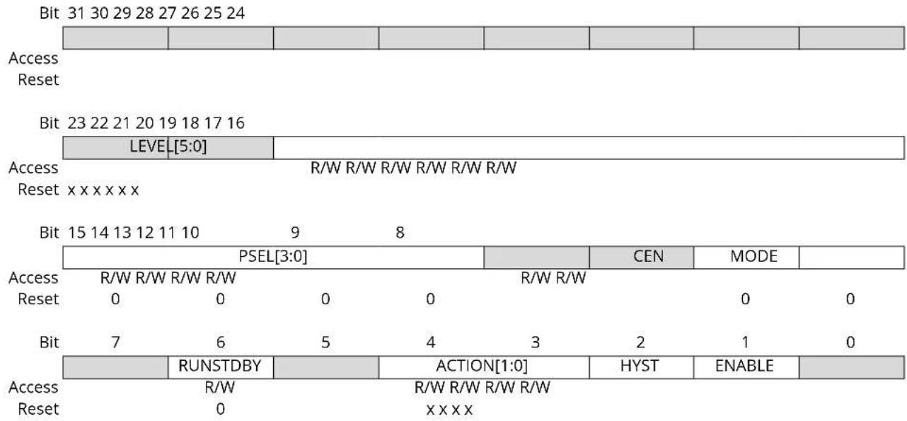
text_image
Bit 31 30 29 28 27 26 25 24 Access Reset Bit 23 22 21 20 19 18 17 16 LEVEL[5:0] Access R/W R/W R/W R/W R/W R/W Reset x x x x x x Bit 15 14 13 12 11 10 9 8 PSEL[3:0] CEN MODE Access R/W R/W R/W R/W R/W R/W Reset 0 0 0 0 0 0 0 Bit 7 6 5 4 3 2 1 0 RUNSTDBY ACTION[1:0] HYST ENABLE Access R/W R/W R/W R/W Reset 0 x x x xBits 21:16 - LEVEL[5:0] BOD33 Threshold Level
This field sets the triggering voltage threshold for the BOD33. See the Electrical Characteristics for actual voltage levels. Note that any change to the LEVEL field of the BOD33 register should be done when the BOD33 is disabled in order to avoid spurious resets or interrupts.
These bits are loaded from Flash User Row at start-up. Refer to NVM User Row Mapping for more details.
Bits 15:12 - PSEL[3:0] Prescaler Select
Selects the prescaler divide-by output for the BOD33 sampling mode according to the table below. The input clock comes from the OSCULP32K 1kHz output.
| PSEL[3:0] | Name | Description |
| 0x0 | DIV2 | Divide clock by 2 |
| 0x1 | DIV4 | Divide clock by 4 |
| 0x2 | DIV8 | Divide clock by 8 |
| 0x3 | DIV16 | Divide clock by 16 |
| 0x4 | DIV32 | Divide clock by 32 |
| 0x5 | DIV64 | Divide clock by 64 |
| 0x6 | DIV128 | Divide clock by 128 |
| 0x7 | DIV256 | Divide clock by 256 |
| 0x8 | DIV512 | Divide clock by 512 |
| 0x9 | DIV1K | Divide clock by 1024 |
| 0xA | DIV2K | Divide clock by 2048 |
| 0xB | DIV4K | Divide clock by 4096 |
| 0xC | DIV8K | Divide clock by 8192 |
| 0xD | DIV16K | Divide clock by 16384 |
| 0xE | DIV32K | Divide clock by 32768 |
| ......continued | ||
| PSEL[3:0] Name Description | ||
| 0xF DIV64K Divide clock by 65536 | ||
Bit 9 - CEN Clock Enable
Writing a zero to this bit will stop the BOD33 sampling clock.
Writing a one to this bit will start the BOD33 sampling clock.
| Value Description | |
| 0 | The BOD33 sampling clock is either disabled and stopped, or enabled but not yet stable. |
| 1 | The BOD33 sampling clock is either enabled and stable, or disabled but not yet stopped. |
Bit 8 - MODE Operation Mode
| Value Description | |
| 0 | The BOD33 operates in continuous mode. |
| 1 | The BOD33 operates in sampling mode. |
Bit 6 - RUNSTDBY Run in Standby
| Value Description | |
| 0 | The BOD33 is disabled in standby sleep mode. |
| 1 | The BOD33 is enabled in standby sleep mode. |
Bits 4:3 - ACTION[1:0] BOD33 Action
These bits are used to select the BOD33 action when the supply voltage crosses below the BOD33 threshold.
These bits are loaded from Flash User Row at start-up.
| ACTION[1:0] Name Description | |
| 0x0 NONE No action | |
| 0x1 RESET The BOD33 generates a reset | |
| 0x2 INTERRUPT The BOD33 generates an interrupt | |
| 0x3 Reserved |
Bit 2 - HYST Hysteresis
This bit indicates whether hysteresis is enabled for the BOD33 threshold voltage: This bit is loaded from Flash User Row at start-up. Refer to NVM User Row Mapping for more details.
| Value Description | |
| 0 | No hysteresis. |
| 1 | Hysteresis enabled. |
Bit 1 - ENABLE Enable
This bit is loaded from Flash User Row at startup. Refer to NVM User Row Mapping for more details.
| Value Description | |
| 0 | BOD33 is disabled. |
| 1 | BOD33 is enabled. |
Related Links
- Electrical Characteristics at 85°C
9.4. NVM User Row Mapping
16.8.15 Voltage Regulator System (VREG) Control
Name: VREG
Offset: 0x3C
Reset: 0x0X02
Property: Write-Protected
text_image
Bit 15 14 13 12 11 10 9 8 FORCELDO Access R/W Reset 0 Bit 7 6 5 4 3 2 1 0 RUNSTDBY ENABLE Access R/W Reset 0 R/W 1Bit 13 - FORCELDO Force LDO Voltage Regulator
| Value | Description |
| 0 | The voltage regulator is in low-power and low-drive configuration in Standby Sleep mode |
| 1 | The voltage regulator is in low-power and high-drive configuration in Standby Sleep mode |
Bit 6 - RUNSTDBY Run in Standby
| Value | Description |
| 0 | The voltage regulator is in low-power configuration in Standby Sleep mode |
| 1 | The voltage regulator is in normal configuration in Standby Sleep mode |
Bit 1 - ENABLE
Must be set to 1.
16.8.16 Voltage References System (VREF) Control
Name: VREF
Offset: 0x40
Reset: 0x0XXX0000
Property: Write-Protected
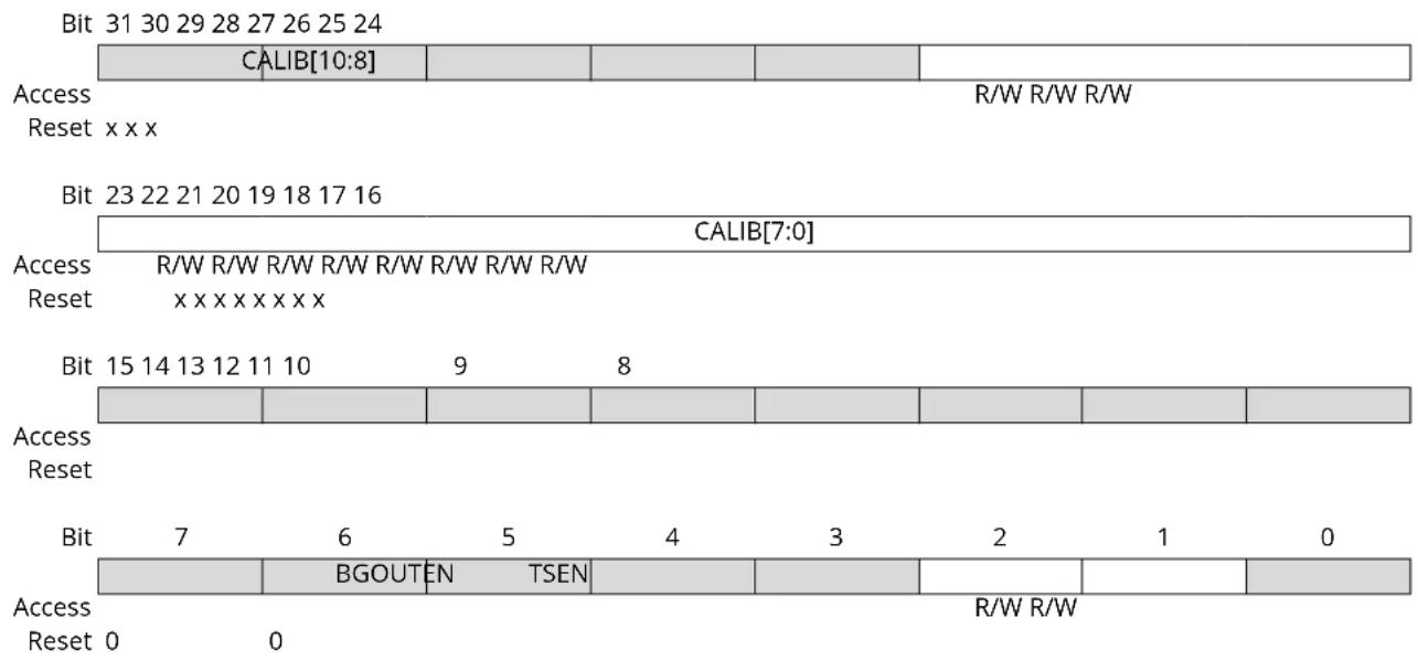
text_image
Bit 31 30 29 28 27 26 25 24 CALIB[10:8] Access R/W R/W R/W Reset xxx Bit 23 22 21 20 19 18 17 16 CALIB[7:0] Access R/W R/W R/W R/W R/W R/W R/W Reset xxxxxxxx Bit 15 14 13 12 11 10 9 8 Access Reset Bit 7 6 5 4 3 2 1 0 BGOUTEN TSEN Access R/W R/W Reset 0 0Bits 26:16 - CALIB[10:0] Bandgap Voltage Generator Calibration
These bits are used to calibrate the output level of the bandgap voltage reference. These bits are loaded from Flash Calibration Row at start-up.
Bit 2 - BGOUTEN Bandgap Output Enable
| Value | Description |
| 0 | The bandgap output is not available as an ADC input channel |
| 1 | The bandgap output is routed to an ADC input channel |
Bit 1 - TSEN Temperature Sensor Enable ^(1)
Note: As explained in the Disclaimer for the AEC-Q100 Electrical characteristics at 125^ C, the Temperature Sensor (TSENS) feature must not be used with AECQ100 parts.
| Value | Description |
| 0 | Temperature sensor is disabled |
| 1 | Temperature sensor is enabled and routed to an ADC input channel |
17. WDT – Watchdog Timer
17.1 Overview
The Watchdog Timer (WDT) is a system function for monitoring correct program operation. It makes it possible to recover from error situations such as runaway or deadlocked code. The WDT is configured to a predefined time-out period, and is constantly running when enabled. If the WDT is not cleared within the time-out period, it will issue a system reset. An early-warning interrupt is available to indicate an upcoming watchdog time-out condition.
The window mode makes it possible to define a time slot (or window) inside the total time-out period during which the WDT must be cleared. If the WDT is cleared outside this window, either too early or too late, a system reset will be issued. Compared to the normal mode, this can also catch situations where a code error causes the WDT to be cleared frequently.
When enabled, the WDT will run in active mode and all sleep modes. It is asynchronous and runs from a CPU-independent clock source. The WDT will continue operation and issue a system reset or interrupt even if the main clocks fail.
17.2 Features
- Issues a system reset if the Watchdog Timer is not cleared before its time-out period
- Early Warning interrupt generation
- Asynchronous operation from dedicated oscillator
-
Two types of operation:
-
Normal mode
- Window mode
- Selectable time-out periods
- From 8 cycles to 16,000 cycles in normal mode
- From 16 cycles to 32,000 cycles in window mode
• Always-on capability
17.3 Block Diagram
Figure 17-1. WDT Block Diagram
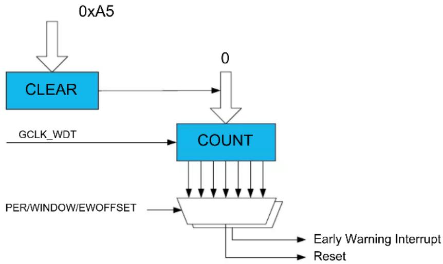
flowchart
graph TD
    A["0xA5"] --> B["CLEAR"]
    B --> C["0"]
    C --> D["COUNT"]
    D --> E["PER/WINDOW/EWOFFSET"]
    E --> F["Early Warning Interrupt Reset"]
    F --> G["Reset"]
    H["GCLK_WDT"] --> D
17.4 Signal Description
Not applicable.
17.5 Product Dependencies
In order to use this peripheral, other parts of the system must be configured correctly, as described below.
17.5.1 I/O Lines
Not applicable.
17.5.2 Power Management
The WDT can continue to operate in any sleep mode where the selected source clock is running. The WDT interrupts can be used to wake up the device from sleep modes. The events can trigger other operations in the system without exiting sleep modes.
Related Links
- Power Manager (PM)
17.5.3 Clocks
The WDT bus clock (CLK_WDT_APB) is enabled by default, and can be enabled and disabled in the Power Manager. Refer to PM - Power Manager for details.
A generic clock (GCLK_WDT) is required to clock the WDT. This clock must be configured and enabled in the Generic Clock Controller before using the WDT. Refer to GCLK - Generic Clock Controller for details. This generic clock is asynchronous to the user interface clock (CLK_WDT_APB). Due to this asynchronicity, accessing certain registers will require synchronization between the clock domains. Refer to Synchronization for further details.
GCLK_WDT is intended to be sourced from the clock of the internal ultra-low-power (ULP) oscillator. Due to the ultralow-power design, the oscillator is not very accurate, and so the exact time-out period may vary from device to device. This variation must be kept in mind when designing software that uses the WDT to ensure that the time-out periods used are valid for all devices. For more information on ULP oscillator accuracy, consult the Ultra Low Power Internal 32kHz RC Oscillator (OSCULP32K) Characteristics.
GCLK_WDT can also be clocked from other sources if a more accurate clock is needed, but at the cost of higher power consumption.
Related Links
- Power Manager (PM)
- GCLK - Generic Clock Controller
16.6.5. 32kHz Ultra Low Power Internal Oscillator (OSCULP32K) Operation
17.6.5. Synchronization
17.5.4 Interrupts
The interrupt request line is connected to the interrupt controller. Using the WDT interrupt(s) requires the interrupt controller to be configured first.
Related Links
10.2. Nested Vector Interrupt Controller
17.5.5 Events
Not applicable.
17.5.6 Debug Operation
When the CPU is halted in debug mode the WDT will halt normal operation.
17.5.7 Register Access Protection
Registers with write-access can be optionally write-protected by the Peripheral Access Controller (PAC), except for the following:
- Interrupt Flag Status and Clear register (INTFLAG)
Note: Optional write-protection is indicated by the "PAC Write-Protection" property in the register description.
Related Links
10.5. PAC - Peripheral Access Controller
17.5.8 Analog Connections
Not applicable.
17.6 Functional Description
17.6.1 Principle of Operation
The Watchdog Timer (WDT) is a system for monitoring correct program operation, making it possible to recover from error situations such as runaway code, by issuing a Reset. When enabled, the WDT is a constantly running timer that is configured to a predefined time-out period. Before the end of the time-out period, the WDT should be set back, or else, a system Reset is issued.
The WDT has two modes of operation, Normal mode and Window mode. Both modes offer the option of Early Warning interrupt generation. The description for each of the basic modes is given below. The settings in the Control register (CTRL) and the Interrupt Enable register (handled by INTENCLR/SET) determine the mode of operation:
Table 17-1. WDT Operating Modes
| CTRL.ENABLE CTRL.WEN INTENSET.EW Mode | |||
| 0 x x Stopped | |||
| 1 0 0 Normal | |||
| 1 0 1 Normal with Early Warning interrupt | |||
| 1 1 0 Window | |||
| 1 1 1 Window with Early Warning interrupt | |||
17.6.2 Basic Operation
17.6.2.1 Initialization
The following bits are enable-protected:
- Window Mode Enable in the Control register (CTRL.WEN)
• Always-On in the Control register (CTRL-ALWAYSON)
The following registers are enable-protected:
- Configuration register (CONFIG)
- Early Warning Interrupt Control register (EWCTRL)
Any writes to these bits or registers when the WDT is enabled or is being enabled (CTRL.ENABLE=1) will be discarded. Writes to these registers while the WDT is being disabled will be completed after the disabling is complete.
Enable-protection is denoted by the Enable-Protected property in the register description.
Initialization of the WDT can be done only while the WDT is disabled. The WDT is configured by defining the required Time-Out Period bits in the Configuration register (CONFIG.PER). If window-mode operation is required, the Window Enable bit in the Control register (CTRL.WEN) must be
written to one and the Window Period bits in the Configuration register (CONFIG.WINDOW) must be defined.
Normal Mode
- Defining the required Time-Out Period bits in the Configuration register (CONFIG.PER).
Normal Mode with Early Warning interrupt
- Defining the required Time-Out Period bits in the Configuration register (CONFIG.PER).
- Defining Early Warning Interrupt Time Offset bits in the Early Warning Interrupt Control register (EWCTRL. EWOFFSET).
- Setting Early Warning Interrupt Enable bit in the Interrupt Enable Set register (INTENSET.EW).
Window Mode
- Defining Time-Out Period bits in the Configuration register (CONFIG.PER).
- Defining Window Mode Time-Out Period bits in the Configuration register (CONFIG.WINDOW).
- Setting Window Enable bit in the Control register (CTRL.WEN).
Window Mode with Early Warning interrupt
- Defining Time-Out Period bits in the Configuration register (CONFIG.PER).
- Defining Window Mode Time-Out Period bits in the Configuration register (CONFIG.WINDOW).
- Setting Window Enable bit in the Control register (CTRL.WEN).
- Defining Early Warning Interrupt Time Offset bits in the Early Warning Interrupt Control register (EWCTRL. EWOFFSET).
- Setting Early Warning Interrupt Enable bit in the Interrupt Enable Set register (INTENSET.EW).
17.6.2.2 Configurable Reset Values
After a Power-on Reset, some registers will be loaded with initial values from the NVM User Row. Refer to NVM User Row Mapping for more details.
This encompasses the following bits and bit groups:
- Enable bit in the Control register, CTRL.ENABLE
- Always-On bit in the Control register, CTRL.ALWAYSON
- Watchdog Timer Windows Mode Enable bit in the Control register, CTRL.WEN
- Watchdog Timer Windows Mode Time-Out Period bits in the Configuration register, CONFIG.WINDOW
- Time-Out Period in the Configuration register, CONFIG.PER
- Early Warning Interrupt Time Offset bits in the Early Warning Interrupt Control register, EWCTRL.EWOFFSET
For more information about fuse locations, see NVM User Row Mapping.
Related Links
17.6.2.3 Enabling and Disabling
The WDT is enabled by writing a '1' to the Enable bit in the Control register (CTRL.ENABLE). The WDT is disabled by writing a '0' to CTRL.ENABLE.
The WDT can be disabled only if the Always-On bit in the Control register (CTRL.ALWAYSON) is '0'.
17.6.2.4 Normal Mode
In Normal mode operation, the length of a time-out period is configured in CONFIG.PER. The WDT is enabled by writing a '1' to the Enable bit in the Control register (CTRL.ENABLE). Once enabled, the
WDT will issue a system reset if a time-out occurs. This can be prevented by clearing the WDT at any time during the time-out period.
The WDT is cleared and a new WDT time-out period is started by writing 0xA5 to the Clear register (CLEAR). Writing any other value than 0xA5 to CLEAR will issue an immediate system reset.
There are 12 possible WDT time-out ( TO_WDT ) periods, selectable from 8ms to 16s.
By default, the early warning interrupt is disabled. If it is desired, the Early Warning Interrupt Enable bit in the Interrupt Enable register (INTENSET.EW) must be written to '1'. The Early Warning Interrupt is disabled again by writing a '1' to the Early Warning Interrupt bit in the Interrupt Enable Clear register (INTENCLR.EW). If the Early Warning Interrupt is enabled, an interrupt is generated prior to a WDT time-out condition. In Normal mode, the Early Warning Offset bits in the Early Warning Interrupt Control register, EWCTRL.EWOFFSET, define the time when the early warning interrupt occurs. The Normal mode operation is illustrated in the figure Normal-Mode Operation.
Figure 17-2. Normal-Mode Operation
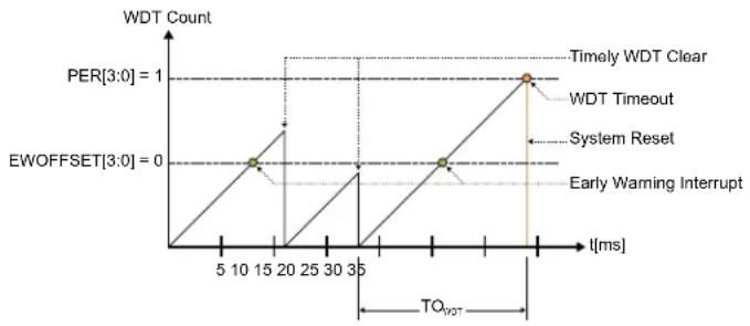
line
| Time [ms] | WDT Count | | --------- | --------- | | 15 | 0 | | 35 | 0 | | 35 | 1 |17.6.2.5 Window Mode
In Window mode operation, the WDT uses two different time specifications: the WDT can only be cleared by writing 0xA5 to the CLEAR register after the closed window time-out period (TO WDTW ), during the subsequent Normal time-out period (TO WDTW ). If the WDT is cleared before the time window opens (before TO WDTW is over), the WDT will issue a system reset. Both parameters TO WDTW and TO _WDT are periods in a range from 8ms to 16s, so the total duration of the WDT time-out period is the sum of the two parameters. The closed window period is defined by the Window Period bits in the Configuration register (CONFIG.WINDOW), and the open window period is defined by the Period bits in the Configuration register (CONFIG.PER).
By default, the Early Warning interrupt is disabled. If it is desired, the Early Warning Interrupt Enable bit in the Interrupt Enable register (INTENSET.EW) must be written to '1'. The Early Warning Interrupt is disabled again by writing a '1' to the Early Warning Interrupt bit in the Interrupt Enable Clear (INTENCLR.EW) register. If the Early Warning interrupt is enabled in Window mode, the interrupt is generated at the start of the open window period, i.e. after TO_WDTW . The Window mode operation is illustrated in figure Window-Mode Operation.
Figure 17-3. Window-Mode Operation
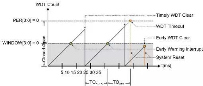
line
| t[ms] | WDT Count | |-------|-----------| | 0 | 0 | | 5 | Closed Gp | | 10 | Closed Gp | | 15 | Closed Gp | | 20 | Closed Gp | | 25 | Closed Gp | | 30 | Closed Gp | | 35 | Closed Gp | | 40 | Closed Gp | | 45 | Closed Gp | | 50 | Closed Gp | | 55 | Closed Gp | | 60 | Closed Gp | | 65 | Closed Gp | | 70 | Closed Gp | | 75 | Closed Gp | | 80 | Closed Gp | | 85 | Closed Gp | | 90 | Closed Gp | | 95 | Closed Gp | | 100 | Closed Gp | | 105 | Closed Gp | | 110 | Closed Gp | | 115 | Closed Gp | | 120 | Closed Gp | | 125 | Closed Gp | | 130 | Closed Gp | | 135 | Closed Gp | | 140 | Closed Gp | | 145 | Closed Gp | | 150 | Closed Gp | | 155 | Closed Gp | | 160 | Closed Gp | | 165 | Closed Gp | | 170 | Closed Gp | | 175 | Closed Gp | | 180 | Closed Gp | | 185 | Closed Gp | | 190 | Closed Gp | | 195 | Closed Gp | | 200 | Closed Gp | | 205 | Closed Gp | | 210 | Closed Gp | | 215 | Closed Gp | | 220 | Closed Gp | | 225 | Closed Gp | | 230 | Closed Gp | | 235 | Closed Gp | | 240 | Closed Gp | | 245 | Closed Gp | | 250 | Closed Gp | | 255 | Closed Gp | | 260 | Closed Gp | | 265 | Closed Gp | | 270 | Closed Gp | | 275 | Closed Gp | | 280 | Closed Gp | | 285 | Closed Gp | | 290 | Closed Gp | | 295 | Closed Gp | | 300 | Closed Gp | | 305 | Closed Gp | | 310 | Closed Gp | | 315 | Closed Gp | | 320 | Closed Gp | | 325 | Closed Gp | | 330 | Closed Gp | | 335 | Closed Gp | | 340 | Closed Gp | | 345 | Closed Gp | | 350 | Closed Gp | | 355 | Closed Gp | | 360 | Closed Gp | | 365 | Closed Gp | | 370 | Closed Gp | | 375 | Closed Gp | | 380 | Closed Gp | | 385 | Closed Gp | | 390 | Closed Gp | | 395 | Closed Gp | | 400 | Closed Gp | | 405 | Closed Gp | | 410 | Closed Gp | | 415 | Closed Gp | | 420 | Closed Gp | | 425 | Closed Gp | | 430 | Closed Gp | | 435 | Closed Gp | | 440 | Closed Gp | | 445 | Closed Gp | | 450 | Closed Gp | | 455 | Closed Gp | | 460 | Closed Gp | | 465 | Closed Gp | | 470 | Closed Gp | | 475 | Closed Gp | | 480 | Closed Gp | | 485 | Closed Gp | | 490 | Closed Gp | | 495 | Closed Gp | | 500 | Closed Gp | | 505 | Closed Gp | | 510 | Closed Gp | | 515 | Closed Gp | | 520 | Closed Gp | | 525 | Closed Gp | | 530 | Closed Gp | | 535 | Closed Gp | | 540 | Closed Gp | | 545 | Closed Gp | | 550 | Closed Gp | | 555 | Closed Gp | | 560 | Closed Gp | | 565 | Closed Gp | | 570 | Closed Gp | | 575 | Closed Gp | | 580 | Closed Gp | | 585 | Closed Gp | | 590 | Closed Gp | | 595 | Closed Gp | | 600 | Closed Gp | | 605 | Closed Gp | | 610 | Closed Gp | | 615 | Closed Gp | | 620 | Closed Gp | | 625 | Closed Gp | | 630 | Closed Gp | | 635 | Closed Gp | | 640 | Closed Gp | | 645 | Closed Gp | | 650 | Closed Gp | | 655 | Closed Gp | | 660 | Closed Gp | | 665 | Closed Gp | | 670 | Closed Gp | | 675 | Closed Gp | | 680 | Closed Gp | | 685 | Closed Gp | | 690 | Closed Gp | | 695 | Closed Gp | | 700 | Closed Gp | | 705 | Closed Gp | | 710 | Closed Gp | | 715 | Closed Gp | | 720 | Closed Gp | | 725 | Closed Gp | | 730 | Closed Gp | | 735 | Closed Gp | | 740 | Closed Gp | | 745 | Closed Gp | | 750 | Closed Gp | | 755 | Closed Gp | | 760 | Closed Gp | | 765 | Closed Gp | | 770 | Closed Gp | | 775 | Closed Gp | | 780 | Closed Gp | | 785 | Closed Gp | | 790 | Closed Gp | | 795 | Closed Gp | | 800 | Closed Gp | | 805 | Closed Gp | | 810 | Closed Gp | | 815 | Closed Gp | | 820 | Closed Gp | | 825 | Closed Gp | | 830 | Closed Gp | | 835 | Closed Gp | | 840 | Closed Gp | | 845 | Closed Gp | | 850 | Closed Gp | | 855 | Closed Gp | | 860 | Closed Gp | | 865 | Closed Gp | | 870 | Closed Gp | | 875 | Closed Gp | | 880 | Closed Gp | | 885 | Closed Gp | | 890 | Closed Gp | | 895 | Closed Gp | | 900 | Closed Gp | | Note: The data is extracted from the code and presented in the following table above: Per[3:0] = zero, Window[3:0] = zero, Early WDT Clear, Early WDT Timeout, Early WDT Clear, Early Warning Interrupt, System Reset, TO_ADI, TO_ADIT. The values for each event are labeled on the chart.17.6.3 Additional Features
17.6.3.1 Always-On Mode
The Always-On mode is enabled by setting the Always-On bit in the Control register (CTRLA.ALWAYSON=1). When the Always-On mode is enabled, the WDT runs continuously, regardless of the state of CTRL.ENABLE. Once written, the Always-On bit can only be cleared by a power-on reset. The Configuration (CONFIG) and Early Warning Control (EWCTRL) registers are read-only registers while the CTRL.ALWAYSON bit is set. Thus, the time period configuration bits (CONFIG.PER, CONFIG.WINDOW, EWCTRL.EWOFFSET) of the WDT cannot be changed.
Enabling or disabling Window mode operation by writing the Window Enable bit (CTRLA.WEN) is allowed while in Always-On mode, but note that CONFIG.PER cannot be changed.
The CTRL.ALWAYSON bit must never be set to one by software if any of the following conditions is true:
- The GCLK_WDT is disabled
- The clock generator for the GCLK_WDT is disabled
- The source clock of the clock generator for the GCLK_WDT is disabled or off
The Interrupt Clear and Interrupt Set registers are accessible in the Always-On mode. The Early Warning interrupt can still be enabled or disabled while in the Always-On mode, but note that EWCTRL.EWOFFSET cannot be changed.
Table 17-2. WDT Operating Modes With Always-On
| WEN Interrupt enable Mode | |
| 0 0 Always-on and normal mode | |
| 0 1 Always-on and normal mode with Early Warning interrupt | |
| 1 0 Always-on and window mode | |
| 1 1 Always-on and window mode with Early Warning interrupt | |
17.6.4 Interrupts
The WDT has the following interrupt source:
- Early Warning (EW)
Each interrupt source has an interrupt flag associated with it. The interrupt flag in the Interrupt Flag Status and Clear (INTFLAG) register is set when the interrupt condition occurs. Each interrupt can be individually enabled by writing a '1' to the corresponding bit in the Interrupt Enable Set (INTENSET) register, and disabled by writing a '1' to the corresponding bit in the Interrupt Enable Clear (INTENCLR) register.
An interrupt request is generated when the interrupt flag is set and the corresponding interrupt is enabled. The interrupt request remains active until the interrupt flag is cleared, the interrupt
is disabled, or the WDT is reset. See the INTFLAG register description for details on how to clear interrupt flags.
The WDT has one common interrupt request line for all the interrupt sources. The user must read the INTFLAG register to determine which interrupt condition is present.
Note: Interrupts must be globally enabled for interrupt requests to be generated.
The Early Warning interrupt behaves differently in normal mode and in window mode. In normal mode, the Early Warning interrupt generation is defined by the Early Warning Offset in the Early Warning Control register (EWCTRL.EWOFFSET). The Early Warning Offset bits define the number of GCLK_WDT clocks before the interrupt is generated, relative to the start of the watchdog time-out period. For example, if the WDT is operating in normal mode with CONFIG.PER = 0x2 and EWCTRL.EWOFFSET = 0x1, the Early Warning interrupt is generated 16 GCLK_WDT clock cycles from the start of the watchdog time-out period, and the watchdog time-out system reset is generated 32 GCLK_WDT clock cycles from the start of the watchdog time-out period. The user must take caution when programming the Early Warning Offset bits. If these bits define an Early Warning interrupt generation time greater than the watchdog time-out period, the watchdog time-out system reset is generated prior to the Early Warning interrupt. Thus, the Early Warning interrupt will never be generated.
In window mode, the Early Warning interrupt is generated at the start of the open window period. In a typical application where the system is in sleep mode, it can use this interrupt to wake up and clear the Watchdog Timer, after which the system can perform other tasks or return to sleep mode.
17.6.5 Synchronization
Due to asynchronicity between the main clock domain and the peripheral clock domains, some registers need to be synchronized when written or read.
When executing an operation that requires synchronization, the Synchronization Busy bit in the Status register (STATUS.SYNCBUSY) will be set immediately, and cleared when synchronization is complete.
If an operation that requires synchronization is executed while STATUS.SYNCBUSY='1', the bus will be stalled. All operations will complete successfully, but the CPU will be stalled and interrupts will be pending as long as the bus is stalled.
The following registers are synchronized when written:
• Control register (CTRL)
- Clear register (CLEAR)
Required write-synchronization is denoted by the "Write-Synchronized" property in the register description.
Related Links
13.3. Register Synchronization
17.7 Register Summary
Register summary
| Offset | Name Bit | Pos. | ||||||||
| 0x0 | CTRL 7:0 ALWAYSON WEN ENABLE | |||||||||
| 0x1 | CONFIG 7:0 WINDOW[3:0] PER[3:0] | |||||||||
| 0x2 | EWCTRL | 7:0 | EWOFFSET[3:0] | |||||||
| 0x3 | Reserved | |||||||||
| 0x4 | INTENCLR | 7:0 | EW | |||||||
| 0x5 | INTENSET | 7:0 | EW | |||||||
| 0x6 | INTFLAG | 7:0 | EW | |||||||
| ......continued | |||||||||
| Offset | Name Bit | Pos. | |||||||
| 0x7 STATUS 7:0 SYNCBUSY | |||||||||
| 0x8 CLEAR 7:0 CLEAR[7:0] | |||||||||
17.8 Register Description
Registers can be 8, 16, or 32 bits wide. Atomic 8-, 16-, and 32-bit accesses are supported. In addition, the 8-bit quarters and 16-bit halves of a 32-bit register, and the 8-bit halves of a 16-bit register can be accessed directly.
Some registers require synchronization when read and/or written. Synchronization is denoted by the "Read-Synchronized" and/or "Write-Synchronized" property in each individual register description.
Some registers are enable-protected, meaning they can only be written when the module is disabled. Enable-protection is denoted by the "Enable-Protected" property in each individual register description.
Optional write-protection by the Peripheral Access Controller (PAC) is denoted by the "PAC Write-Protection" property in each individual register description.
17.8.1 Control
Name: CTRL
Offset: 0x0
Reset: N/A - Loaded from NVM User Row at start-up
Property: Write-Protected, Enable-Protected, Write-Synchronized
Bit 76543210
| ALWAYSON | WEN ENABLE | ||||||
| Access | R/W R/W | R/W | |||||
| Reset x | x | x |
Bit 7 - ALWAYSON Always-On
This bit allows the WDT to run continuously. After being written to one, this bit cannot be written to zero, and the WDT will remain enabled until a power-on reset is received. When this bit is one, the Control register (CTRL), the Configuration register (CONFIG) and the Early Warning Control register (EWCTRL) will be read-only, and any writes to these registers are not allowed. Writing a zero to this bit has no effect.
This bit is not enable-protected.
These bits are loaded from NVM User Row at start-up. Refer to NVM User Row Mapping for more details.
| Value | Description |
| 0 | The WDT is enabled and disabled through the ENABLE bit. |
| 1 | The WDT is enabled and can only be disabled by a power-on reset (POR). |
Bit 2 - WEN Watchdog Timer Window Mode Enable
The initial value of this bit is loaded from Flash Calibration.
This bit is loaded from NVM User Row at start-up. Refer to NVM User Row Mapping for more details.
| Value | Description |
| 0 | Window mode is disabled (normal operation). |
| 1 | Window mode is enabled. |
Bit 1 - ENABLE Enable
This bit enables or disables the WDT. Can only be written while CTRL.ALWAYSON is zero.
Due to synchronization, there is delay from writing CTRL. ENABLE until the peripheral is enabled/ disabled. The value written to CTRL. ENABLE will read back immediately, and the Synchronization Busy bit in the Status register (STATUS.SYNCBUSY) will be set. STATUS.SYNCBUSY will be cleared when the operation is complete.
This bit is not enable-protected.
This bit is loaded from NVM User Row at start-up. Refer to NVM User Row Mapping for more details.
| Value | Description |
| 0 | The WDT is disabled. |
| 1 | The WDT is enabled. |
Related Links
Reset: N/A - Loaded from NVM User Row at startup
Property: Write-Protected, Enable-Protected, Write-Synchronized
Bit 76543210
| WINDOW[3:0] PER[3:0] | ||
| Access | R/W R/W R/W R/W R/W R/W R/W R/W | |
| Reset | xxxxxxx | |
Bits 7:4 - WINDOW[3:0] Window Mode Time-Out Period
In window mode, these bits determine the watchdog closed window period as a number of oscillator cycles.
These bits are loaded from NVM User Row at start-up. Refer to NVM User Row Mapping for more details.
| Value Description | |
| 0x0 | 8 clock cycles |
| 0x1 | 16 clock cycles |
| 0x2 | 32 clock cycles |
| 0x3 | 64 clock cycles |
| 0x4 | 128 clock cycles |
| 0x5 | 256 clocks cycles |
| 0x6 | 512 clocks cycles |
| 0x7 | 1024 clock cycles |
| 0x8 | 2048 clock cycles |
| 0x9 | 4096 clock cycles |
| 0xA | 8192 clock cycles |
| 0xB | 16384 clock cycles |
| 0xC-0xF | Reserved |
Bits 3:0 - PER[3:0] Time-Out Period
These bits determine the watchdog time-out period as a number of GCLK_WDT clock cycles. In window mode operation, these bits define the open window period.
These bits are loaded from NVM User Row at start-up. Refer to NVM User Row Mapping for more details.
| Value Description | |
| 0x0 | 8 clock cycles |
| 0x1 | 16 clock cycles |
| 0x2 | 32 clock cycles |
| 0x3 | 64 clock cycles |
| 0x4 | 128 clock cycles |
| 0x5 | 256 clocks cycles |
| 0x6 | 512 clocks cycles |
| 0x7 | 1024 clock cycles |
| 0x8 | 2048 clock cycles |
| 0x9 | 4096 clock cycles |
| 0xA | 8192 clock cycles |
| 0xB | 16384 clock cycles |
| 0xC-0xF | Reserved |
Related Links
Reset: N/A - Loaded from NVM User Row at start-up
Property: Write-Protected, Enable-Protected
Bit 76543210
| EWOFFSET[3:0] | ||||
| Access Reset x x x x | R/W R/W R/W R/W | |||
Bits 3:0 - EWOFFSET[3:0] Early Warning Interrupt Time Offset
These bits determine the number of GCLK_WDT clocks in the offset from the start of the watchdog time-out period to when the Early Warning interrupt is generated. These bits are loaded from NVM User Row at start-up. Refer to NVM User Row Mapping for more details.
| Value Description | |
| 0x0 | 8 clock cycles |
| 0x1 | 16 clock cycles |
| 0x2 | 32 clock cycles |
| 0x3 | 64 clock cycles |
| 0x4 | 128 clock cycles |
| 0x5 | 256 clocks cycles |
| 0x6 | 512 clocks cycles |
| 0x7 | 1024 clock cycles |
| 0x8 | 2048 clock cycles |
| 0x9 | 4096 clock cycles |
| 0xA | 8192 clock cycles |
| 0xB | 16384 clock cycles |
| 0xC-0xF | Reserved |
Related Links
Property: Write-Protected
Bit 76543210
Writing a zero to this bit has no effect.
Writing a one to this bit disables the Early Warning interrupt.
| Value Description | |
| 0 | The Early Warning interrupt is disabled. |
| 1 | The Early Warning interrupt is enabled. |
17.8.5 Interrupt Enable Set
Name: INTENSET
Offset: 0x5
Reset: 0x00
Property: Write-Protected
Bit 76543210
Writing a zero to this bit has no effect.
Writing a one to this bit enables the Early Warning interrupt.
| Value Description | |
| 0 | The Early Warning interrupt is disabled. |
| 1 | The Early Warning interrupt is enabled. |
17.8.6 Interrupt Flag Status and Clear
Name: INTFLAG
Offset: 0x6
Reset: 0x00
Property: -
Bit 76543210
This flag is set when an Early Warning interrupt occurs, as defined by the EWOFFSET bit group in EWCTRL.
Writing a zero to this bit has no effect.
Writing a one to this bit clears the Early Warning interrupt flag.
17.8.7 Status
Name: STATUS
Offset: 0x7
Reset: 0x00
Property: -

text_image
Bit 7 6 5 4 3 2 1 0 SYNCBUSY Access R Reset 0Bit 7 - SYNCBUSY Synchronization Busy
This bit is cleared when the synchronization of registers between clock domains is complete. This bit is set when the synchronization of registers between clock domains is started.
17.8.8 Clear
Name: CLEAR
Offset: 0x8
Reset: 0x00
Property: Write-Protected, Write-Synchronized
Bit 76543210
CLEAR[7:0]
Access WWWWWW
Reset 00000000
Bits 7:0 - CLEAR[7:0] Watchdog Clear
Writing 0xA5 to this register will clear the Watchdog Timer and the watchdog time-out period is restarted. Writing any other value will issue an immediate system reset.
18. RTC – Real-Time Counter
18.1 Overview
The Real-Time Counter (RTC) is a 32-bit counter with a 10-bit programmable prescaler that typically runs continuously to keep track of time. The RTC can wake up the device from sleep modes using the alarm/compare wake up, periodic wake up, or overflow wake up mechanisms.
The RTC can be clocked from several clock sources selectable through the Generic Clock module (GCLK). This GCLK_RTC clock can then be divided with CTRLA.PRESCALER to achieve the required resolution.
The RTC can generate periodic peripheral events from outputs of the prescaler, as well as alarm/compare interrupts and peripheral events, which can trigger at any counter value. Additionally, the timer can trigger an overflow interrupt and peripheral event, and can be reset on the occurrence of an alarm/compare match. This allows periodic interrupts and peripheral events at very long and accurate intervals.
The 10-bit programmable prescaler can scale down the clock source. By this, a wide range of resolutions and time-out periods can be configured. With a 32.768kHz clock source, the minimum counter tick interval is 30.5 s, and time-out periods can range up to 36 hours. For a counter tick interval of 1s, the maximum time-out period is more than 136 years.
18.2 Features
• 32-bit counter with 10-bit prescaler
- Multiple clock sources
• 32-bit or 16-bit Counter mode
- One 32-bit or two 16-bit compare values
- Clock/Calendar mode
– Time in seconds, minutes and hours (12/24)
– Date in day of month, month and year
- Leap year correction
• Digital prescaler correction/tuning for increased accuracy
• Overflow, alarm/compare match and prescaler interrupts and events
- Optional clear on alarm/compare match
18.3 Block Diagram
Figure 18-1. RTC Block Diagram (Mode 0 — 32-Bit Counter)
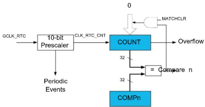
flowchart
graph TD
    A["GCLK_RTC"] --> B["10-bit Prescaler"]
    B --> C["CLK_RTC_CNT"]
    C --> D["COUNT"]
    D --> E["32"]
    D --> F["32"]
    F --> G["COMPn"]
    H["0"] --> I["MATCHCLR"]
    I --> D
    D --> J["Overflow"]
    K["Periodic Events"] --> B
    L["= Compare n"] --> D
Figure 18-2. RTC Block Diagram (Mode 1 — 16-Bit Counter)
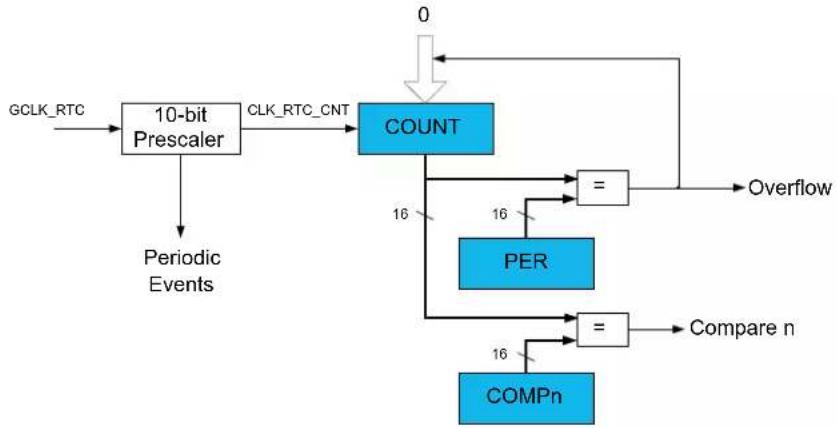
flowchart
graph TD
    A["GCLK_RTC"] --> B["10-bit Prescaler"]
    B --> C["CLK_RTC_CNT"]
    C --> D["COUNT"]
    D --> E["="]
    E --> F["Overflow"]
    D --> G["PER"]
    G --> H["="]
    H --> I["Compare n"]
    G --> J["16"]
    J --> K["COMPn"]
    K --> L["16"]
    L --> M["Periodic Events"]
    M --> B
    D --> N["0"]
Figure 18-3. RTC Block Diagram (Mode 2 — Clock/Calendar)
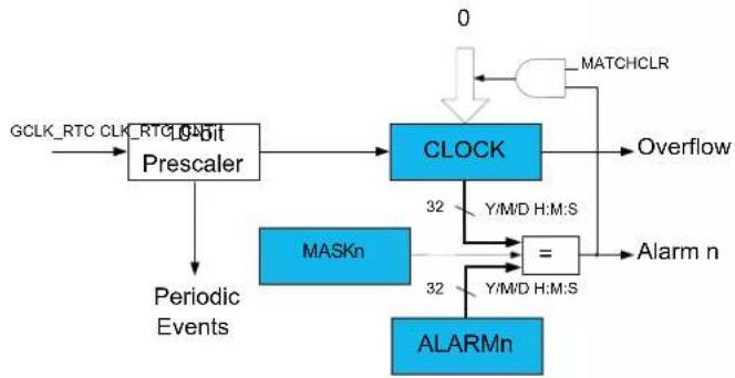
flowchart
graph TD
    A["GCLK_RTC CLK_RTC Prescaler"] --> B["10-bit Prescaler"]
    B --> C["CLOCK"]
    C --> D["Overflow"]
    C --> E["32 Y/M/D H:M:S"]
    E --> F["="]
    F --> G["Alarm n"]
    C --> H["32 Y/M/D H:M:S"]
    H --> I["ALARMn"]
    I --> J["Periodic Events"]
    J --> B
    K["0"] --> L["MATCHCLR"]
    L --> C
18.4 Signal Description
Not applicable.
18.5 Product Dependencies
In order to use this peripheral, other parts of the system must be configured correctly, as described below.
18.5.1 I/O Lines
Not applicable.
18.5.2 Power Management
The RTC will continue to operate in any sleep mode where the selected source clock is running. The RTC interrupts can be used to wake up the device from sleep modes. Events connected to the event system can trigger other operations in the system without exiting sleep modes. Refer to the Power Manager for details on the different sleep modes.
The RTC will be reset only at power-on (POR) or by setting the Software Reset bit in the Control register (CTRL.SWRST=1).
Related Links
- Power Manager (PM)
18.5.3 Clocks
The RTC bus clock (CLK_RTC_APB) can be enabled and disabled in the Power Manager, and the default state of CLK_RTC_APB can be found in the Peripheral Clock Masking section.
A generic clock (GCLK_RTC) is required to clock the RTC. This clock must be configured and enabled in the Generic Clock Controller before using the RTC. Refer to GCLK - Generic Clock Controller for details.
This generic clock is asynchronous to the user interface clock (CLK_RTC_APB). Due to this asynchronicity, accessing certain registers will require synchronization between the clock domains. Refer to 18.6.8. Synchronization for further details.
The RTC should not work with the Generic Clock Generator 0.
Related Links
- GCLK - Generic Clock Controller
18.5.4 DMA
Not applicable.
18.5.5 Interrupts
The interrupt request line is connected to the Interrupt Controller. Using the RTC interrupts requires the Interrupt Controller to be configured first. Refer to Nested Vector Interrupt Controller for details.
Related Links
10.2. Nested Vector Interrupt Controller
18.5.6 Events
The events are connected to the Event System.
Related Links
- Event System (EVSYS)
18.5.7 Debug Operation
When the CPU is halted in debug mode the RTC will halt normal operation. The RTC can be forced to continue operation during debugging. Refer to the Debug Control (DBGCTRL) register for details.
18.5.8 Register Access Protection
Registers with write-access can be optionally write-protected by the Peripheral Access Controller (PAC), except for the following:
- Interrupt Flag Status and Clear register (INTFLAG)
- Read Request register (READREQ)
- Status register (STATUS)
- Debug register (DBGCTRL)
Note: Optional write-protection is indicated by the "PAC Write-Protection" property in the register description.
Write-protection does not apply for accesses through an external debugger.
Related Links
18.8.17. STATUS
18.8.18. DBGCTRL
18.8.4. READREQ
18.8.15. INTFLAG
10.5. PAC - Peripheral Access Controller
18.5.9 Analog Connections
A 32.768kHz crystal can be connected to the XIN32 and XOUT32 pins, along with any required load capacitors. For details on recommended crystal characteristics and load capacitors, refer to Electrical Characteristics for details.
Related Links
- Electrical Characteristics at 85°C
18.6 Functional Description
18.6.1 Principle of Operation
The RTC keeps track of time in the system and enables periodic events, as well as interrupts and events at a specified time. The RTC consists of a 10-bit prescaler that feeds a 32-bit counter. The actual format of the 32-bit counter depends on the RTC operating mode.
The RTC can function in one of these modes:
- Mode 0 - COUNT32: RTC serves as 32-bit counter
- Mode 1 - COUNT16: RTC serves as 16-bit counter
- Mode 2 - CLOCK: RTC serves as clock/calendar with alarm functionality
18.6.2 Basic Operation
18.6.2.1 Initialization
The following bits are enable-protected, meaning that they can only be written when the RTC is disabled (CTRL.ENABLE=0):
- Operating Mode bits in the Control register (CTRL.MODE)
- Prescaler bits in the Control register (CTRL.PRESCALER)
- Clear on Match bit in the Control register (CTRL.MATCHCLR)
- Clock Representation bit in the Control register (CTRL.CLKREP)
The following register is enable-protected:
• Event Control register (EVCTRL)
Any writes to these bits or registers when the RTC is enabled or being enabled (CTRL.ENABLE=1) will be discarded. Writes to these bits or registers while the RTC is being disabled will be completed after the disabling is complete.
Enable-protection is denoted by the "Enable-Protected" property in the register description.
Before the RTC is enabled, it must be configured, as outlined by the following steps:
- RTC operation mode must be selected by writing the Operating Mode bit group in the Control register (CTRL.MODE)
- Clock representation must be selected by writing the Clock Representation bit in the Control register (CTRL.CLKREP)
- Prescaler value must be selected by writing the Prescaler bit group in the Control register (CTRL.PRESCALER)
The RTC prescaler divides the source clock for the RTC counter.
Note: In Clock/Calendar mode, the prescaler must be configured to provide a 1Hz clock to the counter for correct operation.
The frequency of the RTC clock (CLK_RTC_CNT) is given by the following formula:
$$ f _ {\mathrm {CLK_RTC_CNT}} = \frac {f _ {\mathrm {GCLK_RTC}}}{2 ^ {\mathrm{PRESCALER}}} $$
The frequency of the generic clock, GCLK_RTC, is given by f_GCLK_RTC , and f_CLK_RTC_CNT is the frequency of the internal prescaled RTC clock, CLK_RTC_CNT.
Related Links
18.8.5. EVCTRL
18.8.1. CTRL
18.6.2.2 Enabling, Disabling and Resetting
The RTC is enabled by setting the Enable bit in the Control register (CTRL.ENABLE=1). The RTC is disabled by writing CTRL.ENABLE=0.
The RTC is reset by setting the Software Reset bit in the Control register (CTRL.SWRST=1). All registers in the RTC, except DEBUG, will be reset to their initial state, and the RTC will be disabled. The RTC must be disabled before resetting it.
Related Links
18.8.1. CTRL
18.6.3 Operating Modes
The RTC counter supports three RTC operating modes: 32-bit Counter, 16-bit Counter and Clock/ Calendar. The operating mode is selected by writing to the Operating Mode bit group in the Control register (CTRL.MODE).
18.6.3.1 32-Bit Counter (Mode 0)
When the RTC Operating Mode bits in the Control register are zero (CTRL.MODE=00), the counter operates in 32-bit Counter mode. The block diagram of this mode is shown in Figure 18-1. When the RTC is enabled, the counter will increment on every 0-to-1 transition of CLK_RTC_CNT. The counter will increment until it reaches the top value of 0xFFFFFFF, and then wrap to 0x00000000. This sets the Overflow Interrupt flag in the Interrupt Flag Status and Clear register (INTFLAG.OVF).
The RTC counter value can be read from or written to the Counter Value register (COUNT) in 32-bit format.
The counter value is continuously compared with the 32-bit Compare register (COMP). When a compare match occurs, the Compare interrupt flag in the Interrupt Flag Status and Clear register (INTFLAG.CMP) is set on the next 0-to-1 transition of CLK_RTC_CNT.
If the Clear on Match bit in the Control register (CTRL.MATCHCLR) is '1', the counter is cleared on the next counter cycle when a compare match with COMP occurs. This allows the RTC to generate periodic interrupts or events with longer periods than are possible with the prescaler events. Note that when CTRL.MATCHCLR is '1', INTFLAG.CMP and INTFLAG.OVF will both be set simultaneously on a compare match with COMP.
18.6.3.2 16-Bit Counter (Mode 1)
When the RTC Operating Mode bits in the Control register (CTRL.MODE) are 1, the counter operates in 16-bit Counter mode as shown in Figure 18-2. When the RTC is enabled, the counter will increment on every 0-to-1 transition of CLK_RTC_CNT. In 16-bit Counter mode, the 16-bit Period register (PER) holds the maximum value of the counter. The counter will increment until it reaches the PER value, and then wrap to 0x0000. This sets the Overflow interrupt flag in the Interrupt Flag Status and Clear register (INTFLAG.OVF).
The RTC counter value can be read from or written to the Counter Value register (COUNT) in 16-bit format.
The counter value is continuously compared with the 16-bit Compare registers (COMPn, n=0-). When a compare match occurs, the Compare n interrupt flag in the Interrupt Flag Status and Clear register (INTFLAG.CMPn, n=0-) is set on the next 0-to-1 transition of CLK_RTC_CNT.
18.6.3.3 Clock/Calendar (Mode 2)
When CTRL.MODE is two, the counter operates in Clock/Calendar mode, as shown in Figure 18-3. When the RTC is enabled, the counter will increment on every 0-to-1 transition of CLK_RTC_CNT. The selected clock source and RTC prescaler must be configured to provide a 1Hz clock to the counter for correct operation in this mode.
The time and date can be read from or written to the Clock Value register (CLOCK) in a 32-bit time/date format. Time is represented as:
- Seconds
- Minutes
- Hours
Hours can be represented in either 12- or 24-hour format, selected by the Clock Representation bit in the Control register (CTRL.CLKREP). This bit can be changed only while the RTC is disabled.
Date is represented as:
• Day as the numeric day of the month (starting at 1)
- Month as the numeric month of the year (1 = January, 2 = February, etc.)
• Year as a value counting the offset from a reference value that must be defined in software
The date is automatically adjusted for leap years, assuming every year divisible by 4 is a leap year. Therefore, the reference value must be a leap year, e.g. 2000. The RTC will increment until it reaches the top value of 23:59:59 December 31st of year 63, and then wrap to 00:00:00 January 1st of year 0. This will set the Overflow interrupt flag in the Interrupt Flag Status and Clear registers (INTFLAG.OVF).
The clock value is continuously compared with the 32-bit Alarm register (ALARM). When an alarm match occurs, the Alarm Interrupt flag in the Interrupt Flag Status and Clear registers (INTFLAG.ALARMn0) is set on the next 0-to-1 transition of CLK_RTC_CNT. E.g. For a 1Hz clock counter, it means the Alarm 0 Interrupt flag is set with a delay of 1s after the occurrence of alarm match. A valid alarm match depends on the setting of the Alarm Mask Selection bits in the Alarm
A valid alarm match depends on the setting of the Alarm Mask Selection bits in the Alarm Mask register (MASK.SEL). These bits determine which time/date fields of the clock and alarm values are valid for comparison and which are ignored.
If the Clear on Match bit in the Control register (CTRL.MATCHCLR) is one, the counter is cleared on the next counter cycle when an alarm match with ALARM occurs. This allows the RTC to generate periodic interrupts or events with longer periods than are possible with the prescaler events (see 18.6.9.1. Periodic Events). Note that when CTRL.MATCHCLR is '1', INTFLAG.ALARM0 and INTFLAG.OVF will both be set simultaneously on an alarm match with ALARM.
18.6.4 DMA Operation
Not applicable.
18.6.5 Interrupts
The RTC has the following interrupt sources which are asynchronous interrupts and can wake-up the device from any sleep mode.:
- Overflow (INTFLAG.OVF): Indicates that the counter has reached its top value and wrapped to zero.
- Compare n (INTFLAG.CMPn): Indicates a match between the counter value and the compare register.
- Alarm n (INTFLAG.ALARMn): Indicates a match between the clock value and the alarm register.
- Synchronization Ready (INTFLAG.SYNCRDY): Indicates an operation requires synchronization.
Each interrupt source has an interrupt flag associated with it. The interrupt flag in the Interrupt Flag Status and Clear (INTFLAG) register is set when the interrupt condition occurs. Each interrupt can be individually enabled by setting the corresponding bit in the Interrupt Enable Set register (INTENSET=1), and disabled by setting the corresponding bit in the Interrupt Enable Clear register (INTENCLR=1). An interrupt request is generated when the interrupt flag is raised and the corresponding interrupt is enabled. The interrupt request remains active until either the interrupt flag is cleared, the interrupt is disabled or the RTC is reset. See the description of the INTFLAG registers for details on how to clear interrupt flags. All interrupt requests from the peripheral are ORed together on system level to generate one combined interrupt request to the NVIC. Refer to the Nested Vector Interrupt Controller for details. The user must read the INTFLAG register to determine which interrupt condition is present.
Note: Interrupts must be globally enabled for interrupt requests to be generated. Refer to the Nested Vector Interrupt Controller for details.
Related Links
10.2. Nested Vector Interrupt Controller
10.2. Nested Vector Interrupt Controller
18.6.6 Events
The RTC can generate the following output events, which are generated in the same way as the corresponding interrupts:
- Overflow (OVF): Indicates that the counter has reached its top value and wrapped to zero.
- Period n (PERn): The corresponding bit in the prescaler has toggled. Refer to 18.6.9.1. Periodic Events for details.
- Compare n (CMPn): Indicates a match between the counter value and the compare register.
- Alarm n (ALARMn): Indicates a match between the clock value and the alarm register.
Setting the Event Output bit in the Event Control Register (EVCTRL.xxxEO=1) enables the corresponding output event. Writing a zero to this bit disables the corresponding output event. Refer to the EVSYS - Event System for details on configuring the event system.
Related Links
- Event System (EVSYS)
18.6.7 Sleep Mode Operation
The RTC will continue to operate in any sleep mode where the source clock is active. The RTC interrupts can be used to wake up the device from a sleep mode. RTC events can trigger other operations in the system without exiting the sleep mode.
An interrupt request will be generated after the wake-up if the Interrupt Controller is configured accordingly. Otherwise the CPU will wake up directly, without triggering any interrupt. In this case, the CPU will continue executing right from the first instruction that followed the entry into sleep.
The periodic events can also wake up the CPU through the interrupt function of the Event System. In this case, the event must be enabled and connected to an event channel with its interrupt enabled. See Event System for more information.
Related Links
- Event System (EVSYS)
18.6.8 Synchronization
Due to asynchronicity between the main clock domain and the peripheral clock domains, some registers need to be synchronized when written or read.
When executing an operation that requires synchronization, the Synchronization Busy bit in the Status register (STATUS.SYNCBUSY) will be set immediately, and cleared when synchronization is complete. The Synchronization Ready interrupt can be used to signal when synchronization is complete. This can be accessed via the Synchronization Ready Interrupt Flag in the Interrupt Flag Status and Clear register (INTFLAG.SYNCRDY). If an operation that requires synchronization is executed while STATUS.SYNCBUSY is one, the bus will be stalled. All operations will complete successfully, but the CPU will be stalled and interrupts will be pending as long as the bus is stalled.
The following bits are synchronized when written:
- Software Reset bit in the Control register (CTRL.SWRST)
- Enable bit in the Control register (CTRL.ENABLE)
The following registers are synchronized when written:
- Counter Value register (COUNT)
- Clock Value register (CLOCK)
• Counter Period register (PER)
• Compare n Value registers (COMPn)
• Alarm n Value registers (ALARMn)
• Frequency Correction register (FREQCORR) - Alarm n Mask register (MASKn)
Required write-synchronization is denoted by the "Write-Synchronized" property in the register description.
The following registers are synchronized when read:
• The Counter Value register (COUNT)
• The Clock Value register (CLOCK)
Required read-synchronization is denoted by the "Read-Synchronized" property in the register description.
Related Links
13.3. Register Synchronization
18.6.9 Additional Features
18.6.9.1 Periodic Events
The RTC prescaler can generate events at periodic intervals, allowing flexible system tick creation. Any of the upper eight bits of the prescaler (bits 2 to 9) can be the source of an event. When one of the eight Periodic Event Output bits in the Event Control register (EVCTRL.PEREO[n=0..7]) is '1', an event is generated on the 0-to-1 transition of the related bit in the prescaler, resulting in a periodic event frequency of:
$$ f _ {P E R I O D I C} = \frac {f _ {\mathrm{GCLK} _ \mathrm{RTC}}}{2 ^ {n + 3}} $$
f_GCLK_RTC is the frequency of the internal prescaler clock, GCLK_RTC, and n is the position of the EVCTRL.PEREOn bit. For example, PER0 will generate an event every eight CLK_RTC_OSC cycles, PER1 every 16 cycles, etc. This is shown in the figure below. Periodic events are independent of the prescaler setting used by the RTC counter, except if CTRL.PRESCALER is zero. Then, no periodic events will be generated.
Figure 18-4. Example Periodic Events
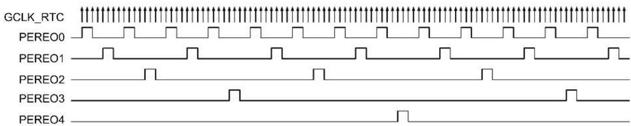
text_image
GCLK_RTC PEREO0 PEREO1 PEREO2 PEREO3 PEREO418.6.9.2 Frequency Correction
The RTC Frequency Correction module employs periodic counter corrections to compensate for a too-slow or too-fast oscillator. Frequency correction requires that CTRL.PRESCALER is greater than 1.
The digital correction circuit adds or subtracts cycles from the RTC prescaler to adjust the frequency in approximately 1 ppm steps. Digital correction is achieved by adding or skipping a single count in the prescaler once every 4096 GCLK_RTC_OSC cycles. The Value bit group in the Frequency Correction register (FREQCORR.VALUE) determines the number of times the adjustment is applied over 240 of these periods. The resulting correction is as follows:
Correction in ppm = (FREQCORR.VALUE / 4096 * 240) * 10 ^6ppm
This results in a resolution of 1.017 PPM.
The Sign bit in the Frequency Correction register (FREQCORR.SIGN) determines the direction of the correction. A positive value will add counts and increase the period (reducing the frequency), and a negative value will reduce counts per period (speeding up the frequency). Digital correction also affects the generation of the periodic events from the prescaler. When the correction is applied at the end of the correction cycle period, the interval between the previous periodic event and the next occurrence may also be shortened or lengthened depending on the correction value.
18.7 Register Summary
The register mapping depends on the Operating Mode bits in the Control register (CTRL.MODE). The register summary is presented for each of the three modes.
Table 18-1. MODE0 - Mode Register Summary
| Offset | Name Bit | Pos. | ||||||||
| 0x00 | CTRL | 7:0 MATCHCLR MODE[1:0] ENABLE SWRST | ||||||||
| 0x01 15:8 PRESCALER[3:0] | ||||||||||
| 0x02 | READREQ | 7:0 ADDR[5:0] | ||||||||
| 0x03 15:8 RREQ RCONT | ||||||||||
| 0x04 | EVCTRL | 7:0 PEREO7 PEREO6 PEREO5 PEREO4 PEREO3 PEREO2 PEREO1 PEREO0 | ||||||||
| 0x05 15:8 OVFEO | CMPEO0 | |||||||||
| 0x06 | INTENCLR | 7:0 | OVF | SYNCRDY | CMP0 | |||||
| 0x07 | INTENSET | 7:0 | OVF | SYNCRDY | CMP0 | |||||
| 0x08 | INTFLAG | 7:0 | OVF | SYNCRDY | CMP0 | |||||
| 0x09 | Reserved | |||||||||
| 0x0A | STATUS | 7:0 | SYNCBUSY | |||||||
| 0x0B | DBGCTRL | 7:0 | DBGRUN | |||||||
| 0x0C | FREQCORR | 7:0 | SIGN | VALUE[6:0] | ||||||
| 0x0D ... | Reserved | |||||||||
| 0x0F | ||||||||||
| ......continued | ||||||||||
| Offset | Name Bit | Pos. | ||||||||
| 0x10 | 7:0 COUNT[7:0] | |||||||||
| 0x11 15:8 COUNT[15:8]COUNT | ||||||||||
| 0x12 23:16 COUNT[23:16] | ||||||||||
| 0x13 31:24 COUNT[31:24] | ||||||||||
| 0x14...0x17 | Reserved | |||||||||
| 0x18 | 7:0 COMP[7:0] | |||||||||
| 0x19 15:8 COMP[15:8]COMPU | ||||||||||
| 0x1A 23:16 COMP[23:16] | ||||||||||
| 0x1B 31:24 COMP[31:24] | ||||||||||
Table 18-2. MODE1 - Mode Register Summary
| Offset | Name Bit | Pos. | ||||||||
| 0x00 | CTRL | 7:0 MODE[1:0] ENABLE SWRST | ||||||||
| 0x01 15:8 | PRESCALER[3:0] | |||||||||
| 0x02 | READREQ | 7:0 | ADDR[5:0] | |||||||
| 0x03 15:8 | RREQ | RCONT | ||||||||
| 0x04 | EVCTRL | 7:0 | PEREO7 | PEREO6 | PEREO5 | PEREO4 | PEREO3 | PEREO2 | PEREO1 | PEREO0 |
| 0x05 15:8 | OVFEO | CMPEO1 | CMPEO0 | |||||||
| 0x06 | INTENCLR | 7:0 | OVF | SYNCRDY | CMP1 | CMP0 | ||||
| 0x07 | INTENSET | 7:0 | OVF | SYNCRDY | CMP1 | CMP0 | ||||
| 0x08 | INTFLAG | 7:0 | OVF | SYNCRDY | CMP1 | CMP0 | ||||
| 0x09 | Reserved | |||||||||
| 0x0A | STATUS | 7:0 | SYNCBUSY | |||||||
| 0x0B | DBGCTRL | 7:0 | DBGRUN | |||||||
| 0x0C | FREQCORR | 7:0 | SIGN | VALUE[6:0] | ||||||
| 0x0D | Reserved | |||||||||
| ... | ||||||||||
| 0x0F | ||||||||||
| 0x10 | COUNT | 7:0 COUNT[7:0] | ||||||||
| 0x11 15:8 COUNT[15:8] | ||||||||||
| 0x12 | Reserved | |||||||||
| 0x13 | Reserved | |||||||||
| 0x14 | PER | 7:0 | PER[7:0] | |||||||
| 0x15 15:8 PER[15:8] | ||||||||||
| 0x16 | Reserved | |||||||||
| 0x17 | Reserved | |||||||||
| 0x18 | COMP0 | 7:0 COMP[7:0] | ||||||||
| 0x19 15:8 COMP[15:8] | ||||||||||
| 0x1A | COMP1 | 7:0 COMP[7:0] | ||||||||
| 0x1B | 15:8 COMP[15:8] | |||||||||
Table 18-3. MODE2 - Mode Register Summary
| Offset | Name Bit | Pos. | ||||||||
| 0x00 | CTRL | 7:0 | MATCHCLR | CLKREP | MODE[1:0] | ENABLE | SWRST | |||
| 0x01 15:8 | PRESCALER[3:0] | |||||||||
| 0x02 | READREQ RREQ | 7:0 | ADDR[5:0] | |||||||
| 0x03 15:8 | RCONT | |||||||||
| 0x04 | EVCTRL OVFEO | 7:0 | PEREO7 | PEREO6 | PEREO5 | PEREO4 | PEREO3 | PEREO2 | PEREO1 | PEREO0 |
| 0x05 15:8 | ALARMEO0 | |||||||||
| 0x06 | INTENCLR | 7:0 | OVF | SYNCRDY | ALARM0 | |||||
| 0x07 | INTENSET | 7:0 | OVF | SYNCRDY | ALARM0 | |||||
| 0x08 | INTFLAG | 7:0 | OVF | SYNCRDY | ALARM0 | |||||
| 0x09 | Reserved | |||||||||
| 0x0A | STATUS | 7:0 | SYNCBUSY | |||||||
| ......continued | ||||||||||
| Offset | Name Bit | Pos. | ||||||||
| 0x0B DBGCTRL 7:0 DBGRUN | ||||||||||
| 0x0C FREQCORR 7:0 SIGN VALUE[6:0] | ||||||||||
| 0x0D ... 0x0F | Reserved | |||||||||
| 0x10 | 7:0 MINUTE[1:0] SECOND[5:0] | |||||||||
| 0x11 15:8 HOUR[3:0] MINUTE[5:2] | ||||||||||
| 0x12 23:16 MONTH[1:0] | DAY[4:0] | HOUR[4] | ||||||||
| 0x13 31:24 | YEAR[5:0] | MONTH[3:2] | ||||||||
| 0x14 ... 0x17 | Reserved | |||||||||
| 0x18 | 7:0 MINUTE[1:0] SECOND[5:0] | |||||||||
| 0x19 15:8 HOUR[3:0] MINUTE[5:2] | ||||||||||
| 0x1A 23:16 MONTH[1:0] | DAY[4:0] | HOUR[4] | ||||||||
| 0x1B | 31:24 | YEAR[5:0] | MONTH[3:2] | |||||||
| 0x1C | MASK | 7:0 | SEL[2:0] | |||||||
18.8 Register Description
Registers can be 8, 16, or 32 bits wide. Atomic 8-, 16-, and 32-bit accesses are supported. In addition, the 8-bit quarters and 16-bit halves of a 32-bit register, and the 8-bit halves of a 16-bit register can be accessed directly.
Optional write-protection by the Peripheral Access Controller (PAC) is denoted by the "PAC Write-Protection" property in each individual register description.
Some registers require synchronization when read and/or written. Synchronization is denoted by the "Read-Synchronized" and/or "Write-Synchronized" property in each individual register description.
Some registers are enable-protected, meaning they can only be written when the module is disabled. Enable-protection is denoted by the "Enable-Protected" property in each individual register description.
18.8.1 Control - MODE0
Name: CTRL
Offset: 0x00
Reset: 0x0000
Property: Enable-Protected, Write-Protected, Write-Synchronized
Bit 15 14 13 12 11 10 9 8
| PRESCALER[3:0] | ||||
| Access Reset 0 0 0 0 | R/W R/W R/W R/W | |||
Bit 76543210
| MATCHCLR | MODE[1:0] | ENABLE | SWRST | ||||
| Access | R/W | R/W R/W R/W | W | ||||
| Reset | 0 | 0 0 0 0 |
Bits 11:8 - PRESCALER[3:0] Prescaler
These bits define the prescaling factor for the RTC clock source (GCLK_RTC) to generate the counter clock (CLK_RTC_CNT).
These bits are not synchronized.
| PRESCALER[3:0] | Name | Description |
| 0x0 | DIV1 | CLK_RTC_CNT = GCLK_RTC/1 |
| 0x1 | DIV2 | CLK_RTC_CNT = GCLK_RTC/2 |
| 0x2 | DIV4 | CLK_RTC_CNT = GCLK_RTC/4 |
| 0x3 | DIV8 | CLK_RTC_CNT = GCLK_RTC/8 |
| 0x4 | DIV16 | CLK_RTC_CNT = GCLK_RTC/16 |
| 0x5 | DIV32 | CLK_RTC_CNT = GCLK_RTC/32 |
| 0x6 | DIV64 | CLK_RTC_CNT = GCLK_RTC/64 |
| 0x7 | DIV128 CLK_RTC_CNT = GCLK_RTC/128 | |
| 0x8 | DIV256 CLK_RTC_CNT = GCLK_RTC/256 | |
| 0x9 | DIV512 CLK_RTC_CNT = GCLK_RTC/512 | |
| 0xA | DIV1024 | CLK_RTC_CNT = GCLK_RTC/1024 |
| 0xB-0xF | Reserved | |
Bit 7 - MATCHCLR Clear on Match
This bit is valid only in Mode 0 and Mode 2.
This bit is not synchronized.
| Value | Description |
| 0 | The counter is not cleared on a Compare/Alarm 0 match. |
| 1 | The counter is cleared on a Compare/Alarm 0 match. |
Bits 3:2 - MODE[1:0] Operating Mode
These bits define the operating mode of the RTC.
These bits are not synchronized.
| MODE[1:0] | Name | Description |
| 0x0 | COUNT32 | Mode 0: 32-bit Counter |
| 0x1 | COUNT16 | Mode 1: 16-bit Counter |
| 0x2 | CLOCK | Mode 2: Clock/Calendar |
| 0x3 | Reserved |
Bit 1 - ENABLE Enable
Due to synchronization, there is delay from writing CTRL. ENABLE until the peripheral is enabled/ disabled. The value written to CTRL. ENABLE will read back immediately, and the Synchronization Busy bit in the Status register (STATUS.SYNCBUSY) will be set. STATUS.SYNCBUSY will be cleared when the operation is complete.
This bit is not enable-protected.
| Value Description | |
| 0 | The peripheral is disabled or being disabled. |
| 1 | The peripheral is enabled or being enabled. |
Bit 0 - SWRST Software Reset
Writing a zero to this bit has no effect.
Writing a one to this bit resets all registers in the RTC, except DBGCTRL, to their initial state, and the RTC will be disabled.
Writing a one to CTRL.SWRST will always take precedence, meaning that all other writes in the same write-operation will be discarded.
Due to synchronization, there is a delay from writing CTRL.SWRST until the reset is complete.
CTRL.SWRST and STATUS.SYNCBUSY will both be cleared when the reset is complete.
This bit is not enable-protected.
| Value Description | |
| 0 | There is no reset operation ongoing. |
| 1 | The reset operation is ongoing. |
18.8.2 Control - MODE1
Name: CTRL
Offset: 0x00
Reset: 0x0000
Property: Enable-Protected, Write-Protected, Write-Synchronized
Bit 15 14 13 12 11 10 9 8
| PRESCALER[3:0] | ||||
| Access Reset 0 0 0 0 | R/W R/W R/W R/W | |||
Bit 76543210
| MODE[1:0] | ENABLE | SWRST | |||
| Access Reset 0 0 0 0 | R/W R/W R/W | W | |||
Bits 11:8 - PRESCALER[3:0] Prescaler
These bits define the prescaling factor for the RTC clock source (GCLK_RTC) to generate the counter clock (CLK_RTC_CNT).
These bits are not synchronized.
| PRESCALER[3:0] | Name | Description |
| 0x0 | DIV1 | CLK_RTC_CNT = GCLK_RTC/1 |
| 0x1 | DIV2 | CLK_RTC_CNT = GCLK_RTC/2 |
| 0x2 | DIV4 | CLK_RTC_CNT = GCLK_RTC/4 |
| 0x3 | DIV8 | CLK_RTC_CNT = GCLK_RTC/8 |
| 0x4 | DIV16 | CLK_RTC_CNT = GCLK_RTC/16 |
| 0x5 | DIV32 | CLK_RTC_CNT = GCLK_RTC/32 |
| 0x6 | DIV64 | CLK_RTC_CNT = GCLK_RTC/64 |
| 0x7 | DIV128 CLK_RTC_CNT = GCLK_RTC/128 | |
| 0x8 | DIV256 CLK_RTC_CNT = GCLK_RTC/256 | |
| 0x9 | DIV512 CLK_RTC_CNT = GCLK_RTC/512 | |
| 0xA | DIV1024 | CLK_RTC_CNT = GCLK_RTC/1024 |
| 0xB-0xF | Reserved | |
Bits 3:2 - MODE[1:0] Operating Mode
These bits define the operating mode of the RTC.
These bits are not synchronized.
| MODE[1:0] | Name | Description |
| 0x0 | COUNT32 | Mode 0: 32-bit Counter |
| 0x1 | COUNT16 | Mode 1: 16-bit Counter |
| 0x2 | CLOCK | Mode 2: Clock/Calendar |
| 0x3 | Reserved |
Bit 1 - ENABLE Enable
Due to synchronization, there is delay from writing CTRL. ENABLE until the peripheral is enabled/ disabled. The value written to CTRL. ENABLE will read back immediately, and the Synchronization Busy bit in the Status register (STATUS.SYNCBUSY) will be set. STATUS.SYNCBUSY will be cleared when the operation is complete.
This bit is not enable-protected.
| Value | Description |
| 0 | The peripheral is disabled or being disabled. |
| 1 | The peripheral is enabled or being enabled. |
Bit 0 - SWRST Software Reset
Writing a zero to this bit has no effect.
Writing a one to this bit resets all registers in the RTC, except DBGCTRL, to their initial state, and the RTC will be disabled.
Writing a one to CTRL.SWRST will always take precedence, meaning that all other writes in the same write-operation will be discarded.
Due to synchronization, there is a delay from writing CTRL.SWRST until the reset is complete.
CTRL.SWRST and STATUS.SYNCBUSY will both be cleared when the reset is complete.
This bit is not enable-protected.
Value Description
| 0 | There is no reset operation ongoing. |
| 1 | The reset operation is ongoing. |
18.8.3 Control - MODE2
Name: CTRL
Offset: 0x00
Reset: 0x0000
Property: Enable-Protected, Write-Protected, Write-Synchronized
Bit 15 14 13 12 11 10 9 8
| PRESCALER[3:0] | ||||
| Access Reset 0 0 0 0 | R/W R/W R/W R/W | |||
Bit 76543210
| MATCHCLR | CLKREP | MODE[1:0] | ENABLE | SWRST | |||
| Access | R/W R/W | R/W R/W R/W | W | ||||
| Reset | 0 0 | 0 0 0 0 | |||||
Bits 11:8 - PRESCALER[3:0] Prescaler
These bits define the prescaling factor for the RTC clock source (GCLK_RTC) to generate the counter clock (CLK_RTC_CNT).
These bits are not synchronized.
| PRESCALER[3:0] | Name | Description |
| 0x0 | DIV1 | CLK_RTC_CNT = GCLK_RTC/1 |
| 0x1 | DIV2 | CLK_RTC_CNT = GCLK_RTC/2 |
| 0x2 | DIV4 | CLK_RTC_CNT = GCLK_RTC/4 |
| 0x3 | DIV8 | CLK_RTC_CNT = GCLK_RTC/8 |
| 0x4 | DIV16 | CLK_RTC_CNT = GCLK_RTC/16 |
| 0x5 | DIV32 | CLK_RTC_CNT = GCLK_RTC/32 |
| 0x6 | DIV64 | CLK_RTC_CNT = GCLK_RTC/64 |
| 0x7 | DIV128 CLK_RTC_CNT = GCLK_RTC/128 | |
| 0x8 | DIV256 CLK_RTC_CNT = GCLK_RTC/256 | |
| 0x9 | DIV512 CLK_RTC_CNT = GCLK_RTC/512 | |
| 0xA | DIV1024 | CLK_RTC_CNT = GCLK_RTC/1024 |
| 0xB-0xF | Reserved | |
Bit 7 - MATCHCLR Clear on Match
This bit is valid only in Mode 0 and Mode 2. This bit can be written only when the peripheral is disabled.
This bit is not synchronized.
| Value | Description |
| 0 | The counter is not cleared on a Compare/Alarm 0 match. |
| 1 | The counter is cleared on a Compare/Alarm 0 match. |
Bit 6 - CLKREP Clock Representation
This bit is valid only in Mode 2 and determines how the hours are represented in the Clock Value (CLOCK) register. This bit can be written only when the peripheral is disabled.
This bit is not synchronized.
| Value | Description |
| 0 | 24 Hour |
| 1 | 12 Hour (AM/PM) |
Bits 3:2 - MODE[1:0] Operating Mode
These bits define the operating mode of the RTC.
These bits are not synchronized.
| MODE[1:0] Name Description | |
| 0x0 COUNT32 Mode 0: 32-bit Counter | |
| 0x1 COUNT16 Mode 1: 16-bit Counter | |
| 0x2 CLOCK Mode 2: Clock/Calendar | |
| 0x3 Reserved |
Bit 1 - ENABLE Enable
Due to synchronization, there is delay from writing CTRL. ENABLE until the peripheral is enabled/ disabled. The value written to CTRL. ENABLE will read back immediately, and the Synchronization Busy bit in the Status register (STATUS.SYNCBUSY) will be set. STATUS.SYNCBUSY will be cleared when the operation is complete.
This bit is not enable-protected.
| Value Description | |
| 0 | The peripheral is disabled or being disabled. |
| 1 | The peripheral is enabled or being enabled. |
Bit 0 - SWRST Software Reset
Writing a zero to this bit has no effect.
Writing a one to this bit resets all registers in the RTC, except DBGCTRL, to their initial state, and the RTC will be disabled.
Writing a one to CTRL.SWRST will always take precedence, meaning that all other writes in the same write-operation will be discarded.
Due to synchronization, there is a delay from writing CTRL.SWRST until the reset is complete.
CTRL.SWRST and STATUS.SYNCBUSY will both be cleared when the reset is complete.
This bit is not enable-protected.
| Value Description | |
| 0 | There is no reset operation ongoing. |
| 1 | The reset operation is ongoing. |
18.8.4 Read Request
Name: READREQ
Offset: 0x02
Reset: 0x0010
Property: -
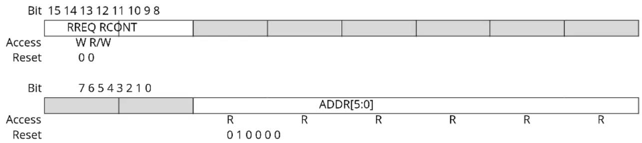
text_image
Bit 15 14 13 12 11 10 9 8 RREQ RCONT Access W R/W Reset 0 0 Bit 7 6 5 4 3 2 1 0 ADDR[5:0] Access R R R R R Reset 0 1 0 0 0 0Bit 15 - RREQ Read Request
Writing a zero to this bit has no effect.
Writing a one to this bit requests synchronization of the register pointed to by the Address bit group (READREQ.ADDR) and sets the Synchronization Busy bit in the Status register (STATUS.SYNCBUSY).
Bit 14 - RCONT Read Continuously
Writing a zero to this bit disables continuous synchronization.
Writing a one to this bit enables continuous synchronization of the register pointed to by READREQ.ADDR. The register value will be synchronized automatically every time the register is updated. READREQ.RCONT prevents READREQ.RREQ from clearing automatically. For the continuous read mode, RREQ bit is required to be set once the RCONT bit is set.
This bit is cleared when an RTC register is written.
Note: Once the continuous synchronization is enabled, the first write in the COUNT/CLOCK register will be stalled for a maximum of 6 APB + 6 RTC clock cycles (the time for the on-going read synchronization to complete).
Bits 5:0 - ADDR[5:0] Address
These bits select the offset of the register that needs read synchronization. In the RTC only COUNT and CLOCK, which share the same address, are available for read synchronization. Therefore, ADDR is a read-only constant of 0x10.
18.8.5 Event Control - MODE0
Name: EVCTRL
Offset: 0x04
Reset: 0x0000
Property: Enable-Protected, Write-Protected
Bit 15 14 13 12 11 10 9 8
| OVFEO | CMPEO0 | |||||||
| Access | R/W | R/W | ||||||
| Reset | 0 | 0 |
Bit 76543210
| PEREOx | PEREOx | PEREOx | PEREOx | PEREOx | PEREOx | PEREOx | PEREOx | |
| Access | R/W | R/W | R/W | R/W | R/W | R/W | R/W | R/W |
| Reset | 0 0 0 0 0 0 0 0 | |||||||
Bit 15 - OVFEO Overflow Event Output Enable
| Value | Description |
| 0 | Overflow event is disabled and will not be generated. |
| 1 | Overflow event is enabled and will be generated for every overflow. |
Bit 8 - CMPEO0 Compare 0 Event Output Enable
| Value | Description |
| 0 | Compare 0 event is disabled and will not be generated. |
| 1 | Compare 0 event is enabled and will be generated for every compare match. |
Bits 7,6,5,4,3,2,1,0 - PEREOx Periodic Interval x Event Output Enable [x=7:0]
| Value | Description |
| 0 | Periodic Interval x event is disabled and will not be generated. |
| 1 | Periodic Interval x event is enabled and will be generated. |
18.8.6 Event Control - MODE1
Name: EVCTRL
Offset: 0x04
Reset: 0x0000
Property: Enable-Protected, Write-Protected
Bit 15 14 13 12 11 10 9 8
| OVFEO | CMPEOx CMPEOx | ||||||
| Access | R/W | R/W | R/W | ||||
| Reset | 0 | 0 0 |
Bit 76543210
| PEREOx | PEREOx | PEREOx | PEREOx | PEREOx | PEREOx | PEREOx | PEREOx | |
| Access | R/W | R/W | R/W | R/W | R/W | R/W | R/W | R/W |
| Reset | 0 0 0 0 0 0 0 0 | |||||||
Bit 15 - OVFEO Overflow Event Output Enable
| Value | Description |
| 0 | Overflow event is disabled and will not be generated. |
| 1 | Overflow event is enabled and will be generated for every overflow. |
Bits 9,8 - CMPEOx Compare x Event Output Enable [x=1:0]
| Value | Description |
| 0 | Compare x event is disabled and will not be generated. |
| 1 | Compare x event is enabled and will be generated for every compare match. |
Bits 7,6,5,4,3,2,1,0 - PEREOx Periodic Interval x Event Output Enable [x=7:0]
| Value | Description |
| 0 | Periodic Interval x event is disabled and will not be generated. |
| 1 | Periodic Interval x event is enabled and will be generated. |
18.8.7 Event Control - MODE2
Name: EVCTRL
Offset: 0x04
Reset: 0x0000
Property: Enable-Protected, Write-Protected
Bit 15 14 13 12 11 10 9 8
| OVFEO | ALARMEOD | ||||||
| Access | R/W R/W | ||||||
| Reset | 0 | 0 |
Bit 76543210
| PEREOx | PEREOx | PEREOx | PEREOx | PEREOx | PEREOx | PEREOx | PEREOx | |
| Access | R/W | R/W | R/W | R/W | R/W | R/W | R/W | R/W |
| Reset | 0 0 0 0 0 0 0 0 | |||||||
Bit 15 - OVFEO Overflow Event Output Enable
| Value | Description |
| 0 | Overflow event is disabled and will not be generated. |
| 1 | Overflow event is enabled and will be generated for every overflow. |
Bit 8 - ALARMEO0 Alarm 0 Event Output Enable
| Value | Description |
| 0 | Alarm 0 event is disabled and will not be generated. |
| 1 | Alarm 0 event is enabled and will be generated for every alarm. |
Bits 7,6,5,4,3,2,1,0 - PEREOx Periodic Interval x Event Output Enable [x=7:0]
| Value | Description |
| 0 | Periodic Interval x event is disabled and will not be generated. |
| 1 | Periodic Interval x event is enabled and will be generated. |
18.8.8 Interrupt Enable Clear - MODE0
Name: INTENCLR
Offset: 0x06
Reset: 0x00
Property: Write-Protected
Bit 76543210
| OVF SYNCRDY | CMP0 | ||||||
| Access | R/W R/W R/W | ||||||
| Reset 0 0 | 0 | ||||||
Bit 7 - OVF Overflow Interrupt Enable
Writing a zero to this bit has no effect.
Writing a one to this bit will clear the Overflow Interrupt Enable bit and disable the corresponding interrupt.
| Value | Description |
| 0 | The Overflow interrupt is disabled. |
| 1 | The Overflow interrupt is enabled, and an interrupt request will be generated when the Overflow interrupt flag is set. |
Bit 6 - SYNCRDY Synchronization Ready Interrupt Enable
Writing a zero to this bit has no effect.
Writing a one to this bit will clear the Synchronization Ready Interrupt Enable bit and disable the corresponding interrupt.
| Value | Description |
| 0 | The Synchronization Ready interrupt is disabled. |
| 1 | The Synchronization Ready interrupt is enabled, and an interrupt request will be generated when the Synchronization Ready interrupt flag is set. |
Bit 0 - CMP0 Compare 0 Interrupt Enable
Writing a zero to this bit has no effect.
Writing a one to this bit will clear the Compare 0 Interrupt Enable bit and disable the corresponding interrupt.
| Value | Description |
| 0 | The Compare 0 interrupt is disabled. |
| 1 | The Compare 0 interrupt is enabled, and an interrupt request will be generated when the Compare x interrupt flag is set. |
18.8.9 Interrupt Enable Clear - MODE1
Name: INTENCLR
Offset: 0x06
Reset: 0x00
Property: Write-Protected
Bit 76543210
| OVF SYNCRDY | CMPx CMPx | ||||||
| Access | R/W R/W | R/W R/W | |||||
| Reset 0 0 | 0 0 | ||||||
Bit 7 - OVF Overflow Interrupt Enable
Writing a zero to this bit has no effect.
Writing a one to this bit will clear the Overflow Interrupt Enable bit and disable the corresponding interrupt.
| Value | Description |
| 0 | The Overflow interrupt is disabled. |
| 1 | The Overflow interrupt is enabled, and an interrupt request will be generated when the Overflow interrupt flag is set. |
Bit 6 - SYNCRDY Synchronization Ready Interrupt Enable
Writing a zero to this bit has no effect.
Writing a one to this bit will clear the Synchronization Ready Interrupt Enable bit and disable the corresponding interrupt.
| Value | Description |
| 0 | The Synchronization Ready interrupt is disabled. |
| 1 | The Synchronization Ready interrupt is enabled, and an interrupt request will be generated when the Synchronization Ready interrupt flag is set. |
Bits 1,0 - CMPx Compare x Interrupt Enable [x=1:0]
Writing a zero to this bit has no effect.
Writing a one to this bit will clear the Compare x Interrupt Enable bit and disable the corresponding interrupt.
| Value | Description |
| 0 | The Compare x interrupt is disabled. |
| 1 | The Compare x interrupt is enabled, and an interrupt request will be generated when the Compare x interrupt flag is set. |
18.8.10 Interrupt Enable Clear - MODE2
Name: INTENCLR
Offset: 0x06
Reset: 0x00
Property: Write-Protected
Bit 76543210
| OVF SYNCRDY | ALARM0 | ||||||
| Access | R/W R/W R/W | ||||||
| Reset 0 0 | 0 | ||||||
Bit 7 - OVF Overflow Interrupt Enable
Writing a zero to this bit has no effect.
Writing a one to this bit will clear the Overflow Interrupt Enable bit and disable the corresponding interrupt.
| Value | Description |
| 0 | The Overflow interrupt is disabled. |
| 1 | The Overflow interrupt is enabled, and an interrupt request will be generated when the Overflow interrupt flag is set. |
Bit 6 - SYNCRDY Synchronization Ready Interrupt Enable
Writing a zero to this bit has no effect.
Writing a one to this bit will clear the Synchronization Ready Interrupt Enable bit and disable the corresponding interrupt.
| Value | Description |
| 0 | The synchronization ready interrupt is disabled. |
| 1 | The synchronization ready interrupt is enabled, and an interrupt request will be generated when the Synchronization Ready interrupt flag is set. |
Bit 0 - ALARM0 Alarm 0 Interrupt Enable
Writing a zero to this bit has no effect.
Writing a one to this bit disables the Alarm 0 interrupt.
| Value | Description |
| 0 | The Alarm 0 interrupt is disabled. |
| 1 | The Alarm 0 interrupt is enabled, and an interrupt request will be generated when the Alarm 0 interrupt flag is set. |
18.8.11 Interrupt Enable Set - MODE0
Name: INTENSET
Offset: 0x07
Reset: 0x00
Property: Write-Protected
Bit 76543210
| OVF SYNCRDY | CMP0 | ||||||
| Access | R/W R/W R/W | ||||||
| Reset 0 0 | 0 | ||||||
Bit 7 - OVF Overflow Interrupt Enable
Writing a zero to this bit has no effect.
Writing a one to this bit will set the Overflow Interrupt Enable bit and enable the Overflow interrupt.
| Value | Description |
| 0 | The overflow interrupt is disabled. |
| 1 | The overflow interrupt is enabled. |
Bit 6 - SYNCRDY Synchronization Ready Interrupt Enable
Writing a zero to this bit has no effect.
Writing a one to this bit will set the Synchronization Ready Interrupt Enable bit and enable the Synchronization Ready interrupt.
| Value | Description |
| 0 | The synchronization ready interrupt is disabled. |
| 1 | The synchronization ready interrupt is enabled. |
Bit 0 - CMP0 Compare 0 Interrupt Enable
Writing a zero to this bit has no effect.
Writing a one to this bit will set the Compare 0 Interrupt Enable bit and enable the Compare 0 interrupt.
| Value | Description |
| 0 | The compare 0 interrupt is disabled. |
| 1 | The compare 0 interrupt is enabled. |
18.8.12 Interrupt Enable Set - MODE1
Name: INTENSET
Offset: 0x07
Reset: 0x00
Property: Write-Protected
Bit 76543210
| OVF SYNCRDY | CMPx CMPx | ||||||
| Access | R/W R/W | R/W R/W | |||||
| Reset 0 0 | 0 0 | ||||||
Bit 7 - OVF Overflow Interrupt Enable
Writing a zero to this bit has no effect.
Writing a one to this bit will set the Overflow interrupt bit and enable the Overflow interrupt.
| Value | Description |
| 0 | The overflow interrupt is disabled. |
| 1 | The overflow interrupt is enabled. |
Bit 6 - SYNCRDY Synchronization Ready Interrupt Enable
Writing a zero to this bit has no effect.
Writing a one to this bit will set the Synchronization Ready Interrupt Enable bit and enable the Synchronization Ready interrupt.
| Value | Description |
| 0 | The synchronization ready interrupt is disabled. |
| 1 | The synchronization ready interrupt is enabled. |
Bits 1,0 - CMPx Compare x Interrupt Enable [x=1:0]
Writing a zero to this bit has no effect.
Writing a one to this bit will set the Compare x Interrupt Enable bit and enable the Compare x interrupt.
| Value | Description |
| 0 | The compare x interrupt is disabled. |
| 1 | The compare x interrupt is enabled. |
18.8.13 Interrupt Enable Set - MODE2
Name: INTENSET
Offset: 0x07
Reset: 0x00
Property: Write-Protected
Bit 76543210
| OVF SYNCRDY | ALARM0 | ||||||
| Access | R/W R/W R/W | ||||||
| Reset 0 0 | 0 | ||||||
Bit 7 - OVF Overflow Interrupt Enable
Writing a zero to this bit has no effect.
Writing a one to this bit will set the Overflow Interrupt Enable bit and enable the Overflow interrupt.
| Value | Description |
| 0 | The overflow interrupt is disabled. |
| 1 | The overflow interrupt is enabled. |
Bit 6 - SYNCRDY Synchronization Ready Interrupt Enable
Writing a zero to this bit has no effect.
Writing a one to this bit will set the Synchronization Ready Interrupt bit and enable the Synchronization Ready interrupt.
| Value | Description |
| 0 | The synchronization ready interrupt is disabled. |
| 1 | The synchronization ready interrupt is enabled. |
Bit 0 - ALARM0 Alarm 0 Interrupt Enable
Writing a zero to this bit has no effect.
Writing a one to this bit will set the Alarm 0 Interrupt Enable bit and enable the Alarm 0 interrupt.
| Value | Description |
| 0 | The alarm 0 interrupt is disabled. |
| 1 | The alarm 0 interrupt is enabled. |
18.8.14 Interrupt Flag Status and Clear - MODE0
Name: INTFLAG
Offset: 0x08
Reset: 0x00
Property: -
Bit 76543210
| OVF SYNCRDY | CMP0 | ||||||
| Access | R/W R/W R/W | ||||||
| Reset 0 0 | 0 | ||||||
Bit 7 - OVF Overflow
This flag is cleared by writing a one to the flag.
This flag is set on the next CLK_RTC_CNT cycle after an overflow condition occurs, and an interrupt request will be generated if INTENCLR/SET.OVF is one.
Writing a zero to this bit has no effect.
Writing a one to this bit clears the Overflow interrupt flag.
Bit 6 - SYNCRDY Synchronization Ready
This flag is cleared by writing a one to the flag.
This flag is set on a 1-to-0 transition of the Synchronization Busy bit in the Status register (STATUS.SYNCBUSY), except when caused by enable or software reset, and an interrupt request will be generated if INTENCLR/SET.SYNCRDY is one.
Writing a zero to this bit has no effect.
Writing a one to this bit clears the Synchronization Ready interrupt flag.
Bit 0 - CMP0 Compare 0
This flag is cleared by writing a one to the flag.
This flag is set on the next CLK_RTC_CNT cycle after a match with the compare condition, and an interrupt request will be generated if INTENCLR/SET.CMP0 is one.
Writing a zero to this bit has no effect.
Writing a one to this bit clears the Compare 0 interrupt flag.
18.8.15 Interrupt Flag Status and Clear - MODE1
Name: INTFLAG
Offset: 0x08
Reset: 0x00
Property: -
Bit 76543210
| OVF SYNCRDY | CMPx CMPx | ||||||
| Access | R/W R/W | R/W R/W | |||||
| Reset 0 0 | 0 0 | ||||||
Bit 7 - OVF Overflow
This flag is cleared by writing a one to the flag.
This flag is set on the next CLK_RTC_CNT cycle after an overflow condition occurs, and an interrupt request will be generated if INTENCLR/SET.OVF is one.
Writing a zero to this bit has no effect.
Writing a one to this bit clears the Overflow interrupt flag.
Bit 6 - SYNCRDY Synchronization Ready
This flag is cleared by writing a one to the flag.
This flag is set on a 1-to-0 transition of the Synchronization Busy bit in the Status register (STATUS.SYNCBUSY), except when caused by enable or software reset, and an interrupt request will be generated if INTENCLR/SET.SYNCRDY is one.
Writing a zero to this bit has no effect.
Writing a one to this bit clears the Synchronization Ready interrupt flag.
Bits 1,0 - CMPx Compare x [x=1:0]
This flag is cleared by writing a one to the flag.
This flag is set on the next CLK_RTC_CNT cycle after a match with the compare condition and an interrupt request will be generated if INTENCLR/SET.CMPx is one.
Writing a zero to this bit has no effect.
Writing a one to this bit clears the Compare x interrupt flag.
18.8.16 Interrupt Flag Status and Clear - MODE2
Name: INTFLAG
Offset: 0x08
Reset: 0x00
Property: -
Bit 76543210
| OVF SYNCRDY | ALARM0 | ||||||
| Access | R/W R/W R/W | ||||||
| Reset 0 0 | 0 | ||||||
Bit 7 - OVF Overflow
This flag is cleared by writing a one to the flag.
This flag is set on the next CLK_RTC_CNT cycle after an overflow condition occurs, and an interrupt request will be generated if INTENCLR/SET.OVF is one.
Writing a zero to this bit has no effect.
Writing a one to this bit clears the Overflow interrupt flag.
Bit 6 - SYNCRDY Synchronization Ready
This flag is cleared by writing a one to the flag.
This flag is set on a 1-to-0 transition of the Synchronization Busy bit in the Status register (STATUS.SYNCBUSY), except when caused by enable or software reset, and an interrupt request will be generated if INTENCLR/SET.SYNCRDY is one.
Writing a zero to this bit has no effect.
Writing a one to this bit clears the Synchronization Ready interrupt flag.
Bit 0 - ALARM0 Alarm 0
This flag is cleared by writing a one to the flag.
This flag is set on the next CLK_RTC_CNT cycle after a match with ALARM0 condition occurs, and an interrupt request will be generated if INTENCLR/SET.ALARM0 is also one.
Writing a zero to this bit has no effect.
Writing a one to this bit clears the Alarm 0 interrupt flag.
18.8.17 Status
Name: STATUS
Offset: 0x0A
Reset: 0x00
Property: -

text_image
Bit 7 6 5 4 3 2 1 0 SYNCBUSY Access R Reset 0Bit 7 - SYNCBUSY Synchronization Busy
This bit is cleared when the synchronization of registers between the clock domains is complete. This bit is set when the synchronization of registers between clock domains is started.
18.8.18 Debug Control
Name: DBGCTRL
Offset: 0x0B
Reset: 0x00
Property: -
Bit 76543210
| DBGRUN | |||||||
| Access Reset 0 | R/W | ||||||
Bit 0 - DBGRUN Run During Debug
This bit is not reset by a software reset.
Writing a zero to this bit causes the RTC to halt during debug mode.
Writing a one to this bit allows the RTC to continue normal operation during debug mode.
18.8.19 Frequency Correction
Name: FREQCORR
Offset: 0x0C
Reset: 0x00
Property: Write-Protected, Write-Synchronized
Bit 76543210
| SIGN VALUE[6:0] | |
| Access | R/W R/W R/W R/W R/W R/W R/W R/W |
| Reset | 0 0 0 0 0 0 0 |
Bit 7 - SIGN Correction Sign
| Value Description | |
| 0 | The correction value is positive, i.e., frequency will be decreased. |
| 1 | The correction value is negative, i.e., frequency will be increased. |
Bits 6:0 - VALUE[6:0] Correction Value
These bits define the amount of correction applied to the RTC prescaler.
1-127: The RTC frequency is adjusted according to the value.
| Value Description | |
| 0 | Correction is disabled and the RTC frequency is unchanged. |
18.8.20 Counter Value - MODE0
Name: COUNT
Offset: 0x10
Reset: 0x00000000
Property: Read-Synchronized, Write-Protected, Write-Synchronized
| Bit 31 30 29 28 27 26 25 24 | |
| COUNT[31:24] | |
| Access R/W R/W R/W R/W R/W R/W R/W R/W Reset 0 0 0 0 0 0 0 0 | |
| Bit 23 22 21 20 19 18 17 16 | |
| COUNT[23:16] | |
| Access R/W R/W R/W R/W R/W R/W R/W R/W Reset 0 0 0 0 0 0 0 0 | |
| Bit 15 14 13 12 11 10 9 8 | |
| COUNT[15:8] | |
| Access R/W R/W R/W R/W R/W R/W R/W R/W Reset 0 0 0 0 0 0 0 0 | |
| Bit 7 6 5 4 3 2 1 0 | |
| COUNT[7:0] | |
| Access R/W R/W R/W R/W R/W R/W R/W R/W Reset 0 0 0 0 0 0 0 0 | |
Bits 31:0 - COUNT[31:0] Counter Value
These bits define the value of the 32-bit RTC counter.
18.8.21 Counter Value - MODE1
Name: COUNT
Offset: 0x10
Reset: 0x0000
Property: Read-Synchronized, Write-Protected, Write-Synchronized
Bit 15 14 13 12 11 10 9 8
COUNT[15:8]
Access R/W R/W R/W R/W R/W R/W R/W R/W
Reset 00000000
Bit 76543210
COUNT[7:0]
Access R/W R/W R/W R/W R/W R/W R/W R/W
Reset 00000000
Bits 15:0 - COUNT[15:0] Counter Value
These bits define the value of the 16-bit RTC counter.
18.8.22 Clock Value - MODE2
Name: CLOCK
Offset: 0x10
Reset: 0x00000000
Property: Read-Synchronized, Write-Protected, Write-Synchronized
| Bit 31 30 29 28 27 26 25 24 | |||
| YEAR[5:0] MONTH[3:2] | |||
| Access Reset | R/W R/W R/W R/W R/W R/W R/W R/W | ||
| 0 0 0 0 0 0 0 0 | |||
| Bit 23 22 21 20 19 18 17 16 | |||
| MONTH[1:0] DAY[4:0] | HOUR[4] | ||
| Access Reset | R/W R/W R/W R/W R/W R/W R/W R/W | ||
| 0 0 0 0 0 0 0 0 | |||
| Bit 15 14 13 12 11 10 | 9 8 | ||
| HOUR[3:0] | MINUTE[5:2] | ||
| Access Reset | R/W R/W R/W R/W R/W R/W R/W R/W | ||
| 0 0 0 0 0 0 0 0 | |||
| Bit 7 6 5 4 3 2 1 0 | |||
| MINUTE[1:0] | SECOND[5:0] | ||
| Access Reset | R/W R/W R/W R/W R/W R/W R/W R/W | ||
| 0 0 0 0 0 0 0 0 | |||
Bits 31:26 - YEAR[5:0] Year
The year offset with respect to the reference year (defined in software).
The year is considered a leap year if YEAR[1:0] is zero.
Bits 25:22 - MONTH[3:0] Month
1 - January
2 - February
...
12 - December
Bits 21:17 - DAY[4:0] Day
Day starts at 1 and ends at 28, 29, 30 or 31, depending on the month and year.
Bits 16:12 - HOUR[4:0] Hour
When CTRL.CLKREP is zero, the Hour bit group is in 24-hour format, with values 0-23. When CTRL.CLKREP is one, HOUR[3:0] has values 1-12 and HOUR[4] represents AM (0) or PM (1).
Table 18-4. Hour
| HOUR[4:0] | CLOCK.HOUR[4] | CLOCK.HOUR[3:0] | Description |
| 0 | 0x00 - 0x17 | Hour (0 - 23) | |
| 0x18 - 0x1F | Reserved | ||
| ......continued | |||
| HOUR[4:0] CLOCK.HOUR[4] CLOCK.HOUR[3:0] Description | |||
| 1 0 0x0 Reserved | |||
| 0x1 - 0xC AM Hour (1 - 12) | |||
| 0xD - 0xF Reserved | |||
| 1 0x0 Reserved | |||
| 0x1 - 0xC PM Hour (1 - 12) | |||
| 0xF - 0xF Reserved | |||
Bits 11:6 - MINUTE[5:0] Minute 0 - 59.
Bits 5:0 - SECOND[5:0] Second 0-59.
18.8.23 Counter Period - MODE1
Name: PER
Offset: 0x14
Reset: 0x0000
Property: Write-Protected, Write-Synchronized
| Bit 15 14 13 12 11 10 9 8 | |
| PER[15:8] | |
| Access R/W R/W R/W R/W R/W R/W R/W R/W Reset 0 0 0 0 0 0 0 0 | |
| Bit 7 6 5 4 3 2 1 0 | |
| PER[7:0] | |
| Access R/W R/W R/W R/W R/W R/W R/W R/W Reset 0 0 0 0 0 0 0 0 | |
Bits 15:0 - PER[15:0] Counter Period
These bits define the value of the 16-bit RTC period.
18.8.24 Compare n Value - MODE0
Name: COMP
Offset: 0x18
Reset: 0x00000000
Property: Write-Protected, Write-Synchronized
| Bit 31 30 29 28 27 26 25 24 | |
| COMP[31:24] | |
| Access R/W R/W R/W R/W R/W R/W R/W R/W Reset 0 0 0 0 0 0 0 0 | |
| Bit 23 22 21 20 19 18 17 16 | |
| COMP[23:16] | |
| Access R/W R/W R/W R/W R/W R/W R/W R/W Reset 0 0 0 0 0 0 0 0 | |
| Bit 15 14 13 12 11 10 9 8 | |
| COMP[15:8] | |
| Access R/W R/W R/W R/W R/W R/W R/W R/W Reset 0 0 0 0 0 0 0 0 | |
| Bit 7 6 5 4 3 2 1 0 | |
| COMP[7:0] | |
| Access R/W R/W R/W R/W R/W R/W R/W R/W Reset 0 0 0 0 0 0 0 0 | |
Bits 31:0 - COMP[31:0] Compare Value
The 32-bit value of COMPn is continuously compared with the 32-bit COUNT value. When a match occurs, the Compare n interrupt flag in the Interrupt Flag Status and Clear register (INTFLAG.CMPn) is set on the next counter cycle, and the counter value is cleared if CTRL.MATCHCLR is one.
18.8.25 Compare n Value - MODE1
Name: COMPn
Offset: 0x18+n*0x2 [n=0..1]
Reset: 0x0000
Property: Write-Protected, Write-Synchronized
| Bit 15 14 13 12 11 10 9 8 | |
| COMP[15:8] | |
| Access R/W R/W R/W R/W R/W R/W R/W R/W Reset 0 0 0 0 0 0 0 0 | |
| Bit 7 6 5 4 3 2 1 0 | |
| COMP[7:0] | |
| Access R/W R/W R/W R/W R/W R/W R/W R/W Reset 0 0 0 0 0 0 0 0 | |
Bits 15:0 - COMP[15:0] Compare Value
The 16-bit value of COMPn is continuously compared with the 16-bit COUNT value. When a match occurs, the Compare n interrupt flag in the Interrupt Flag Status and Clear register (INTFLAG.CMPn) is set on the next counter cycle.
18.8.26 Alarm 0 Value - MODE2
Name: ALARM0
Offset: 0x18
Reset: 0x00000000
Property: Write-Protected, Write-Synchronized
The 32-bit value of ALARM0 is continuously compared with the 32-bit CLOCK value, based on the masking set by MASKn.SEL. When a match occurs, the Alarm 0 interrupt flag in the Interrupt Flag Status and Clear register (INTFLAG.ALARMn) is set on the next counter cycle, and the counter is cleared if CTRL.MATCHCLR is one.
Bit 31 30 29 28 27 26 25 24
| YEAR[5:0] MONTH[3:2] | ||
| Access | R/W R/W R/W R/W R/W R/W R/W R/W | |
| Reset | 0 0 0 0 0 0 0 | |
Bit 23 22 21 20 19 18 17 16
| MONTH[1:0] DAY[4:Φ] | HOUR[4] | ||
| Access | R/W R/W R/W R/W R/W R/W R/W R/W | ||
| Reset | 0 0 0 0 0 0 0 | ||
Bit 15 14 13 12 11 10 98
| HOUR[3:0] | MINUTE[5:2] | |
| Access | R/W R/W R/W R/W R/W R/W R/W R/W | |
| Reset | 0 0 0 0 0 0 0 | |
Bit 76543210
| MINUTE[1:0] | SECOND[5:0] | |
| Access | R/W R/W R/W R/W R/W R/W R/W R/W | |
| Reset | 0 0 0 0 0 0 0 | |
Bits 31:26 - YEAR[5:0] Year
The alarm year. Years are only matched if MASKn.SEL is 6.
Bits 25:22 - MONTH[3:0] Month
The alarm month. Months are matched only if MASKn.SEL is greater than 4.
Bits 21:17 - DAY[4:0] Day
The alarm day. Days are matched only if MASKn.SEL is greater than 3.
Bits 16:12 - HOUR[4:0] Hour
The alarm hour. Hours are matched only if MASKn.SEL is greater than 2.
Bits 11:6 - MINUTE[5:0] Minute
The alarm minute. Minutes are matched only if MASKn.SEL is greater than 1.
Bits 5:0 - SECOND[5:0] Second
The alarm second. Seconds are matched only if MASKn.SEL is greater than 0.
18.8.27 Alarm n Mask - MODE2
Name: MASK
Offset: 0x1C
Reset: 0x00
Property: Write-Protected, Write-Synchronized
Bit 76543210
| SEL[2:0] | |||||
| Access Reset 0 0 0 | R/W R/W R/W | ||||
Bits 2:0 - SEL[2:0] Alarm Mask Selection
These bits define which bit groups of Alarm n are valid.
| SEL[2:0] Name Description | ||
| 0x0 | OFF | Alarm Disabled |
| 0x1 | SS Match seconds only | |
| 0x2 | MMSS Match seconds and minutes only | |
| 0x3 | HHMMSS | Match seconds, minutes, and hours only |
| 0x4 | DDHHMMSS | Match seconds, minutes, hours, and days only |
| 0x5 | MMDDHHMMSS | Match seconds, minutes, hours, days, and months only |
| 0x6 | YYMMDDHHMMSS | Match seconds, minutes, hours, days, months, and years |
| 0x7 | Reserved | |
19. EIC – External Interrupt Controller
19.1 Overview
The External Interrupt Controller (EIC) allows external pins to be configured as interrupt lines. Each interrupt line can be individually masked and can generate an interrupt on rising, falling, or both edges, or on high or low levels. Each external pin has a configurable filter to remove spikes. Each external pin can also be configured to be asynchronous in order to wake up the device from sleep modes where all clocks have been disabled. External pins can also generate an event.
A separate non-maskable interrupt (NMI) is also supported. It has properties similar to the other external interrupts, but is connected to the NMI request of the CPU, enabling it to interrupt any other interrupt mode.
19.2 Features
- Up to 16 external pins (EXTINTx), plus one non-maskable pin (NMI)
• Dedicated, individually maskable interrupt for each pin - Interrupt on rising, falling, or both edges
- Interrupt on high or low levels
- Asynchronous interrupts for sleep modes without clock
• Filtering of external pins
• Event generation from EXTINTx
19.3 Block Diagram
Figure 19-1. EIC Block Diagram
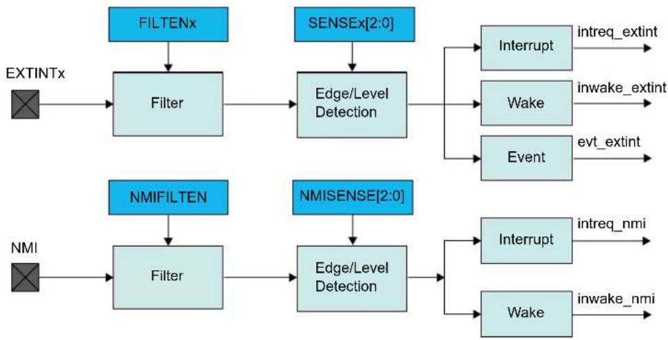
flowchart
graph TD
    A["EXTINTx"] --> B["Filter"]
    B --> C["Edge/Level Detection"]
    C --> D["Interrupt intreq_extint"]
    C --> E["Wake inwake_extint"]
    C --> F["Event evt_extint"]
    G["NMI"] --> H["Filter"]
    H --> I["Edge/Level Detection"]
    I --> J["Interrupt intreq_nmi"]
    I --> K["Wake inwake_nmi"]
19.4 Signal Description
| Signal Name Type Description | |
| EXTINT[15..0] Digital Input External interrupt pin | |
| NMI Digital Input Non-maskable interrupt pin |
One signal may be available on several pins.
Related Links
- I/O Multiplexing and Considerations
19.5 Product Dependencies
In order to use this EIC, other parts of the system must be configured correctly, as described below.
19.5.1 I/O Lines
Using the EIC's I/O lines requires the I/O pins to be configured.
Related Links
- PORT - I/O Pin Controller
19.5.2 Power Management
All interrupts are available down to STANDBY sleep mode, but the EIC can be configured to automatically mask some interrupts in order to prevent device wake-up.
The EIC will continue to operate in any sleep mode where the selected source clock is running. The EIC's interrupts can be used to wake up the device from sleep modes. Events connected to the Event System can trigger other operations in the system without exiting sleep modes.
Related Links
- Power Manager (PM)
- GCLK - Generic Clock Controller
19.5.3 Clocks
The EIC bus clock (CLK_EIC_APB) can be enabled and disabled in the Power Manager, and the default state of CLK_EIC_APB can be found in the Peripheral Clock Masking section in PM – Power Manager.
A generic clock (GCLK_EIC) is required to clock the peripheral. This clock must be configured and enabled in the Generic Clock Controller before using the peripheral. Refer to GCLK - Generic Clock Controller.
This generic clock is asynchronous to the user interface clock (CLK_EIC_APB). Due to this asynchronicity, writes to certain registers will require synchronization between the clock domains. Refer to 19.6.8. Synchronization for further details.
Related Links
19.6.8. Synchronization
14. GCLK - Generic Clock Controller
19.5.4 Interrupts
There are several interrupt request lines, at least one for the external interrupts (EXTINT) and one for non-maskable interrupt (NMI).
The EXTINT interrupt request line is connected to the interrupt controller. Using the EIC interrupt requires the interrupt controller to be configured first.
The NMI interrupt request line is also connected to the interrupt controller, but does not require the interrupt to be configured.
Related Links
10.2. Nested Vector Interrupt Controller
19.5.5 Events
The events are connected to the Event System. Using the events requires the Event System to be configured first.
Related Links
- Event System (EVSYS)
19.5.6 Debug Operation
When the CPU is halted in debug mode, the EIC continues normal operation. If the EIC is configured in a way that requires it to be periodically serviced by the CPU through interrupts or similar, improper operation or data loss may result during debugging.
19.5.7 Register Access Protection
All registers with write-access can be write-protected optionally by the Peripheral Access Controller (PAC), except for the following registers:
- Interrupt Flag Status and Clear register (INTFLAG)
• Non-Maskable Interrupt Flag Status and Clear register (NMIFLAG)
Optional write-protection by the Peripheral Access Controller (PAC) is denoted by the "PAC Write-Protection" property in each individual register description.
PAC write-protection does not apply to accesses through an external debugger.
Related Links
10.5. PAC - Peripheral Access Controller
19.5.8 Analog Connections
Not applicable.
19.6 Functional Description
19.6.1 Principle of Operation
The EIC detects edge or level condition to generate interrupts to the CPU interrupt controller or events to the Event System. Each external interrupt pin (EXTINT) can be filtered using majority vote filtering, clocked by GCLK_EIC
19.6.2 Basic Operation
19.6.2.1 Initialization
The EIC must be initialized in the following order:
- Enable CLK_EIC_APB
- If edge detection or filtering is required, GCLK_EIC must be enabled
- Write the EIC configuration registers (EVCTRL, WAKEUP, CONFIGy)
- Enable the EIC
To use NMI, GCLK_EIC must be enabled after EIC configuration (NMICTRL).
19.6.2.2 Enabling, Disabling and Resetting
The EIC is enabled by writing a '1' the Enable bit in the Control register (CTRL.ENABLE). The EIC is disabled by writing CTRL.ENABLE to '0'.
The EIC is reset by setting the Software Reset bit in the Control register (CTRL.SWRST). All registers in the EIC will be reset to their initial state, and the EIC will be disabled.
Refer to the CTRL register description for details.
19.6.3 External Pin Processing
Each external pin can be configured to generate an interrupt/event on edge detection (rising, falling or both edges) or level detection (high or low). The sense of external interrupt pins is configured by writing the Input Sense x bits in the Config n register (CONFIGn.SENSEx). The corresponding interrupt flag (INTFLAG.EXTINT[x]) in the Interrupt Flag Status and Clear register (INTFLAG) is set when the interrupt condition is met.
When the interrupt flag has been cleared in edge-sensitive mode, INTFLAG.EXTINT[x] will only be set if a new interrupt condition is met. In level-sensitive mode, when interrupt has been cleared, INTFLAG.EXTINT[x] will be set immediately if the EXTINTx pin still matches the interrupt condition.
Each external pin can be filtered by a majority vote filtering, clocked by GCLK_EIC. Filtering is enabled if bit Filter Enable x in the Configuration n register (CONFIGn.FILTENx) is written to '1'. The majority vote filter samples the external pin three times with GCLK_EIC and outputs the value when two or more samples are equal.
Table 19-1. Majority Vote Filter
| Samples [0, 1, 2] Filter Output | |
| [0,0,0] 0 | |
| [0,0,1] 0 | |
| [0,1,0] 0 | |
| [0,1,1] 1 | |
| [1,0,0] 0 | |
| [1,0,1] 1 | |
| [1,1,0] 1 | |
| [1,1,1] 1 |
When an external interrupt is configured for level detection, or if filtering is disabled, detection is made asynchronously, and GCLK_EIC is not required.
If filtering or edge detection is enabled, the EIC automatically requests the GCLK_EIC to operate (GCLK_EIC must be enabled in the GCLK module, see GCLK - Generic Clock Controller for details). If level detection is enabled, GCLK_EIC is not required, but interrupt and events can still be generated.
When an external interrupt is configured for level detection and when filtering is disabled, detection is done asynchronously. Asynchronous detection does not require GCLK_EIC, but interrupt and events can still be generated. If filtering or edge detection is enabled, the EIC automatically requests GCLK_EIC to operate. GCLK_EIC must be enabled in the GCLK module.
Figure 19-2. Interrupt Detections
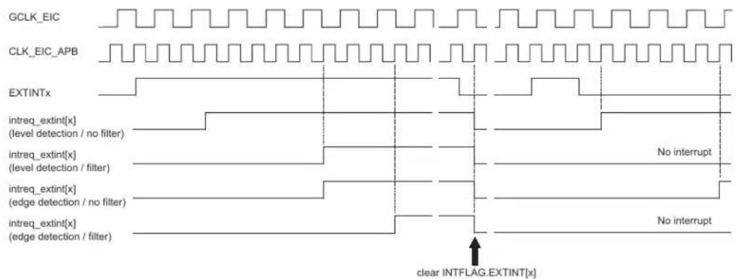
text_image
GCLK_EIC CLK_EIC_APB EXTINTx intreq_extint[x] (level detection / no filter) intreq_extint[x] (level detection / filter) intreq_extint[x] (edge detection / no filter) intreq_extint[x] (edge detection / filter) No interrupt No interrupt clear INTFLAG.EXTINT[x]The detection delay depends on the detection mode.
Table 19-2. Interrupt Latency
| Detection mode Latency (worst case) |
| Level without filter Three CLK_EIC_APB periods |
| Level with filter Four GCLK_EIC periods + Three CLK_EIC_APB periods |
Edge without filter Four GCLK_EIC periods + Three CLK_EIC_APB periods
Edge with filter Six GCLK_EIC periods + Three CLK_EIC_APB periods
Related Links
14. GCLK - Generic Clock Controller
19.6.4 Additional Features
19.6.4.1 Non-Maskable Interrupt (NMI)
The non-maskable interrupt pin can also generate an interrupt on edge or level detection, but it is configured with the dedicated NMI Control register (NMICTRL). To select the sense for NMI, write to the NMISENSE bit group in the NMI Control register (NMICTRL.NMISENSE). NMI filtering is enabled by writing a '1' to the NMI Filter Enable bit (NMICTRL.NMIFILTEN).
If edge detection or filtering is required, enable GCLK_EIC or CLK_ULP32K.
NMI detection is enabled only by the NMICTRL.NMISENSE value, and the EIC is not required to be enabled.
When an NMI is detected, the non-maskable interrupt flag in the NMI Flag Status and Clear register is set (NMIFLAG.NMI). NMI interrupt generation is always enabled, and NMIFLAG.NMI generates an interrupt request when set.
19.6.5 Interrupts
The EIC has the following interrupt sources:
- External interrupt pins (EXTINTx). See 19.6.2. Basic Operation.
• Non-maskable interrupt pin (NMI). See 19.6.4. Additional Features.
Each interrupt source has an associated interrupt flag. The interrupt flag in the Interrupt Flag Status and Clear register (INTFLAG) is set when an interrupt condition occurs (NMIFLAG for NMI). Each interrupt, except NMI, can be individually enabled by setting the corresponding bit in the Interrupt Enable Set register (INTENSET=1), and disabled by setting the corresponding bit in the Interrupt Enable Clear register (INTENCLR=1).
An interrupt request is generated when the interrupt flag is set and the corresponding interrupt is enabled. The interrupt request remains active until the interrupt flag is cleared, the interrupt is disabled, or the EIC is reset. See the INTFLAG register for details on how to clear interrupt flags. The EIC has one interrupt request line for each external interrupt (EXTINTx) and one line for NMI. The user must read the INTFLAG (or NMIFLAG) register to determine which interrupt condition is present.
Notes:
- Interrupts must be globally enabled for interrupt requests to be generated.
- If an external interrupts (EXTINT) is common on two or more I/O pins, only one will be active (the first one programmed).
Related Links
10. Processor And Architecture
19.6.6 Events
The EIC can generate the following output events:
- External event from pin (EXTINTx).
Setting an Event Output Control register (EVCTRL.EXTINTEO) enables the corresponding output event. Clearing this bit disables the corresponding output event. Refer to Event System for details on configuring the Event System.
When the condition on pin EXTINTx matches the configuration in the CONFIGn register, the corresponding event is generated, if enabled.
Related Links
22. Event System (EVSYS)
19.6.7 Sleep Mode Operation
In sleep modes, an EXTINTx pin can wake up the device if the corresponding condition matches the configuration in CONFIGy register. Writing a one to a Wake-Up Enable bit (WAKEUP.WAKEUPEN[x]) enables the wake-up from pin EXTINTx. Writing a zero to a Wake-Up Enable bit (WAKEUP.WAKEUPEN[x]) disables the wake-up from pin EXTINTx.
Using WAKEUPEN[x]=1 with INTENSET=0 is not recommended.
In sleep modes, an EXTINTx pin can wake up the device if the corresponding condition matches the configuration in CONFIGn register, and the corresponding bit in the Interrupt Enable Set register (INTENSET) is written to '1'. WAKEUP.WAKEUPEN[x]=1 can enable the wake-up from pin EXTINTx.
Figure 19-3. Wake-Up Operation Example (High-Level Detection, No Filter, WAKEUPEN[x]=1)
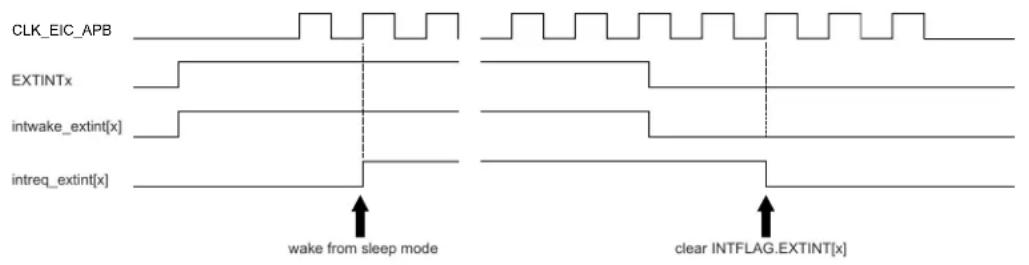
text_image
CLK_EIC_APB EXTINTx intwake_extint[x] intreq_extint[x] wake from sleep mode clear INTFLAG.EXTINT[x]19.6.8 Synchronization
Due to asynchronicity between the main clock domain and the peripheral clock domains, some registers need to be synchronized when written or read.
When executing an operation that requires synchronization, the Synchronization Busy bit in the Status register (STATUS.SYNCBUSY) will be set immediately, and cleared when synchronization is complete.
If an operation that requires synchronization is executed while STATUS.SYNCBUSY is one, the bus will be stalled. All operations will complete successfully, but the CPU will be stalled, and interrupts will be pending as long as the bus is stalled.
The following bits are synchronized when written:
- Software Reset bit in the Control register (CTRL.SWRST)
- Enable bit in the Control register (CTRL.ENABLE)
Related Links
13.3. Register Synchronization
19.7 Register Summary
| Offset | Name Bit Pos. 76543210 | ||||||||||
| 0x00 CTRL 7:0 ENABLE SWRST | |||||||||||
| 0x01 STATUS 7:0 SYNCBUSY | |||||||||||
| 0x02 NMICTRL 7:0 NMIFILTEN | NMISENSE[2:0] | ||||||||||
| 0x03 NMIFLAG 7:0 | NMI | ||||||||||
| 0x04 | EVCTRL | 7:0 | EXTINTEO7 | EXTINTEO6 | EXTINTEO5 | EXTINTEO4 | EXTINTEO3 | EXTINTEO2 | EXTINTEO1 | EXTINTEO0 | |
| 15:8 | EXTINTEO15 | EXTINTEO14 | EXTINTEO13 | EXTINTEO12 | EXTINTEO11 | EXTINTEO10 | EXTINTEO9 | EXTINTEO8 | |||
| 23:16 | |||||||||||
| 31:24 | |||||||||||
| 0x08 | INTENCLR | 7:0 | EXTINT7 | EXTINT6 | EXTINT5 | EXTINT4 | EXTINT3 | EXTINT2 | EXTINT1 | EXTINT0 | |
| 15:8 | EXTINT15 | EXTINT14 | EXTINT13 | EXTINT12 | EXTINT11 | EXTINT10 | EXTINT9 | EXTINT8 | |||
| 23:16 | |||||||||||
| 31:24 | |||||||||||
| 0x0C | INTENSET | 7:0 | EXTINT7 | EXTINT6 | EXTINT5 | EXTINT4 | EXTINT3 | EXTINT2 | EXTINT1 | EXTINT0 | |
| 15:8 | EXTINT15 | EXTINT14 | EXTINT13 | EXTINT12 | EXTINT11 | EXTINT10 | EXTINT9 | EXTINT8 | |||
| 23:16 | |||||||||||
| 31:24 | |||||||||||
| 0x10 | INTFLAG | 7:0 | EXTINT7 | EXTINT6 | EXTINT5 | EXTINT4 | EXTINT3 | EXTINT2 | EXTINT1 | EXTINT0 | |
| 15:8 | EXTINT15 | EXTINT14 | EXTINT13 | EXTINT12 | EXTINT11 | EXTINT10 | EXTINT9 | EXTINT8 | |||
| 23:16 | |||||||||||
| 31:24 | |||||||||||
| 0x14 | WAKEUP | 7:0 | WAKEUPEN7 | WAKEUPEN6 | WAKEUPEN5 | WAKEUPEN4 | WAKEUPEN3 | WAKEUPEN2 | WAKEUPEN1 | WAKEUPENO | |
| 15:8 | WAKEUPEN15 | WAKEUPEN14 | WAKEUPEN13 | WAKEUPEN12 | WAKEUPEN11 | WAKEUPEN10 | WAKEUPEN9 | WAKEUPEN8 | |||
| 23:16 | |||||||||||
| 31:24 | |||||||||||
| 0x18 | CONFIG0 | 7:0 | FILTENx | SENSEX[2:0] | FILTENx | SENSEX[2:0] | |||||
| 15:8 | FILTENx | SENSEX[2:0] | FILTENx | SENSEX[2:0] | |||||||
| 23:16 | FILTENx | SENSEX[2:0] | FILTENx | SENSEX[2:0] | |||||||
| 31:24 | FILTENx | SENSEX[2:0] | FILTENx | SENSEX[2:0] | |||||||
| 0x1C CONFIG1 | 7:0 | FILTENx | SENSEX[2:0] | FILTENx | SENSEX[2:0] | ||||||
| 15:8 | FILTENx | SENSEX[2:0] | FILTENx | SENSEX[2:0] | |||||||
| 23:16 | FILTENx | SENSEX[2:0] | FILTENx | SENSEX[2:0] | |||||||
| 31:24 | FILTENx | SENSEX[2:0] | FILTENx | SENSEX[2:0] | |||||||
19.8 Register Description
Registers can be 8, 16, or 32 bits wide. Atomic 8-, 16-, and 32-bit accesses are supported. In addition, the 8-bit quarters and 16-bit halves of a 32-bit register, and the 8-bit halves of a 16-bit register can be accessed directly.
Some registers require synchronization when read and/or written. Synchronization is denoted by the "Read-Synchronized" and/or "Write-Synchronized" property in each individual register description.
Some registers are enable-protected, meaning they can only be written when the module is disabled. Enable-protection is denoted by the "Enable-Protected" property in each individual register description.
19.8.1 Control
Name: CTRL
Offset: 0x00
Reset: 0x00
Property: Write-Protected, Write-Synchronized
Bit 76543210
| ENABLE SWRST | ||||||
| Access Reset 0 0 | R/W R/W | |||||
Bit 1 - ENABLE Enable
Due to synchronization, there is delay from writing CTRL. ENABLE until the peripheral is enabled/ disabled. The value written to CTRL. ENABLE will read back immediately, and the Synchronization Busy bit in the Status register (STATUS.SYNCBUSY) will be set. STATUS.SYNCBUSY will be cleared when the operation is complete.
| Value Description | |
| 0 | The EIC is disabled. |
| 1 | The EIC is enabled. |
Bit 0 - SWRST Software Reset
Writing a zero to this bit has no effect.
Writing a one to this bit resets all registers in the EIC to their initial state, and the EIC will be disabled. Writing a one to CTRL.SWRST will always take precedence, meaning that all other writes in the same write operation will be discarded.
Due to synchronization, there is a delay from writing CTRL.SWRST until the reset is complete.
CTRL.SWRST and STATUS.SYNCBUSY will both be cleared when the reset is complete.
| Value Description | |
| 0 | There is no ongoing reset operation. |
| 1 | The reset operation is ongoing. |
19.8.2 Status
Name: STATUS
Offset: 0x01
Reset: 0x00
Property: -

text_image
Bit 7 6 5 4 3 2 1 0 SYNCBUSY Access R Reset 0Bit 7 - SYNCBUSY Synchronization Busy
This bit is cleared when the synchronization of registers between the clock domains is complete. This bit is set when the synchronization of registers between clock domains is started.
19.8.3 Non-Maskable Interrupt Control
Name: NMICTRL
Offset: 0x02
Reset: 0x00
Property: Write-Protected
Bit 76543210
| NMIFILTEN NMISENSE[2:0] | ||||
| Access Reset 0 0 0 0 | R/W R/W R/W R/W | |||
Bit 3 - NMIFILTEN Non-Maskable Interrupt Filter Enable
| Value Description | |
| 0 | NMI filter is disabled. |
| 1 | NMI filter is enabled. |
Bits 2:0 - NMISENSE[2:0] Non-Maskable Interrupt Sense
These bits define on which edge or level the NMI triggers.
| NMISENSE[2:0] | Name | Description |
| 0x0 | NONE | No detection |
| 0x1 | RISE | Rising-edge detection |
| 0x2 | FALL Falling-edge detection | |
| 0x3 | BOTH | Both-edges detection |
| 0x4 | HIGH | High-level detection |
| 0x5 | LOW Low-level detection | |
| 0x6-0x7 | Reserved | |
19.8.4 Non-Maskable Interrupt Flag Status and Clear
Name: NMIFLAG
Offset: 0x03
Reset: 0x00
Property: -
Bit 76543210
| NMI | |||||||
| Access Reset 0 | R/W | ||||||
Bit 0 - NMI Non-Maskable Interrupt
This flag is cleared by writing a one to it.
This flag is set when the NMI pin matches the NMI sense configuration, and will generate an
interrupt request.
Writing a zero to this bit has no effect.
Writing a one to this bit clears the non-maskable interrupt flag.
19.8.5 Event Control
Name: EVCTRL
Offset: 0x04
Reset: 0x00000000
Property: Write-Protected
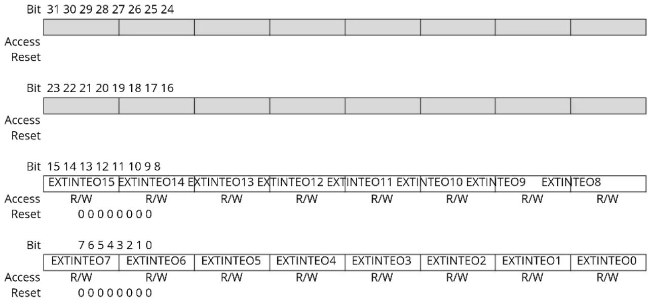
text_image
Bit 31 30 29 28 27 26 25 24 Access Reset Bit 23 22 21 20 19 18 17 16 Access Reset Bit 15 14 13 12 11 10 9 8 EXTINTEO15 EXTINTEO14 EXTINTEO13 EXTINTEO12 EXTINTEO11 EXTINTEO10 EXTINTEO9 EXTINTEO8 Access R/W R/W R/W R/W R/W R/W R/W R/W Reset 0 0 0 0 0 0 0 0 Bit 7 6 5 4 3 2 1 0 EXTINTEO7 EXTINTEO6 EXTINTEO5 EXTINTEO4 EXTINTEO3 EXTINTEO2 EXTINTEO1 EXTINTEO0 Access R/W R/W R/W R/W R/W R/W R/W R/W Reset 0 0 0 0 0 0 0 0Bits 0, 1, 2, 3, 4, 5, 6, 7, 8, 9, 10, 11, 12, 13, 14, 15 - EXTINTEO External Interrupt x Event Output Enable [x=15..0]
These bits indicate whether the event associated with the EXTINTx pin is enabled or not to generate for every detection.
| Value | Description |
| 0 | Event from pin EXTINTx is disabled. |
| 1 | Event from pin EXTINTx is enabled. |
19.8.6 Interrupt Enable Clear
Name: INTENCLR
Offset: 0x08
Reset: 0x00000000
Property: Write-Protected
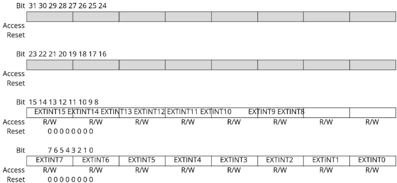
other
Bit 31 30 29 28 27 26 25 24 Access Reset Bit 23 22 21 20 19 18 17 16 Access Reset Bit 15 14 13 12 11 10 9 8 EXTINT15 EXTINT14 EXTINT13 EXTINT12 EXTINT11 EXTINT10 EXTINT9 EXTINT8 Access R/W R/W R/W R/W R/W R/W R/W R/W Reset 0 0 0 0 0 0 0 Bit 7 6 5 4 3 2 1 0 EXTINT7 EXTINT6 EXTINT5 EXTINT4 EXTINT3 EXTINT2 EXTINT1 EXTINT0 Access R/W R/W R/W R/W R/W R/W R/W R/W Reset 0 0 0 0 0 0 0Bits 0, 1, 2, 3, 4, 5, 6, 7, 8, 9, 10, 11, 12, 13, 14, 15 - EXTINT External Interrupt x Enable [x=15..0]
Writing a zero to this bit has no effect.
Writing a one to this bit will clear the External Interrupt x Enable bit, which disables the external interrupt.
| Value | Description |
| 0 | The external interrupt x is disabled. |
| 1 | The external interrupt x is enabled. |
19.8.7 Interrupt Enable Set
Name: INTENSET
Offset: 0x0C
Reset: 0x00000000
Property: Write-Protected

bar_stacked
| Bit | Access Reset | Access Reset | | --- | --- | --- | | 31 | R/W | 00000000 | | 29 | R/W | 00000000 | | 28 | R/W | 00000000 | | 27 | R/W | 00000000 | | 26 | R/W | 00000000 | | 25 | R/W | 00000000 | | 24 | R/W | 00000000 |Bits 0, 1, 2, 3, 4, 5, 6, 7, 8, 9, 10, 11, 12, 13, 14, 15 - EXTINT External Interrupt x Enable [x=15..0]
Writing a zero to this bit has no effect.
Writing a one to this bit will set the External Interrupt x Enable bit, which enables the external interrupt.
| Value | Description |
| 0 | The external interrupt x is disabled. |
| 1 | The external interrupt x is enabled. |
19.8.8 Interrupt Flag Status and Clear
Name: INTFLAG
Offset: 0x10
Reset: 0x00000000
Property: -
| Bit 31 30 29 28 27 26 25 24 | |||||||
| Access Reset | |||||||
| Bit 23 22 21 20 19 18 17 16 | |||||||
| Access Reset | |||||||
| Bit 15 14 13 12 11 10 9 8 | |||||||
| EXTINT15 EXTINT14 EXTINT13 EXTINT12 EXTINT11 EXTINT10 EXTINT9 EXTINT8 | |||||||
| Access Reset | R/W | R/W | R/W | R/W | R/W | R/W | R/W |
| 0 0 0 0 0 0 0 0 | |||||||
| Bit | 7 6 5 4 3 2 1 0 | ||||||
| EXTINT7 | EXTINT6 | EXTINT5 | EXTINT4 | EXTINT3 | EXTINT2 | EXTINT1 | EXTINT0 |
| Access Reset | R/W | R/W | R/W | R/W | R/W | R/W | R/W |
| 0 0 0 0 0 0 0 0 | |||||||
Bits 0, 1, 2, 3, 4, 5, 6, 7, 8, 9, 10, 11, 12, 13, 14, 15 - EXTINT External Interrupt x [x=15..0]
This flag is cleared by writing a one to it.
This flag is set when EXTINTx pin matches the external interrupt sense configuration and will generate an interrupt request if INTENCLR/SET.EXTINT[x] is one.
Writing a zero to this bit has no effect.
Writing a one to this bit clears the External Interrupt x flag.
19.8.9 Wake-Up Enable
Name: WAKEUP
Offset: 0x14
Reset: 0x00000000
Property: Write-Protected
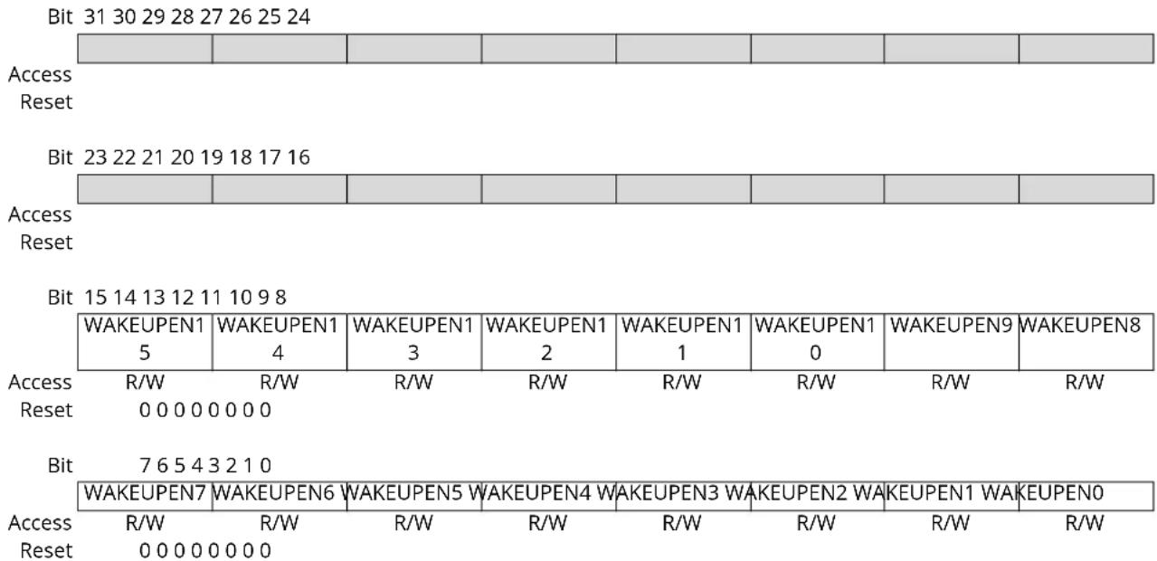
Bits 0, 1, 2, 3, 4, 5, 6, 7, 8, 9, 10, 11, 12, 13, 14, 15 - WAKEUPEN External Interrupt x Wake-up Enable [x=15..0]
This bit enables or disables wake-up from sleep modes when the EXTINTx pin matches the external interrupt sense configuration.
| Value | Description |
| 0 | Wake-up from the EXTINTx pin is disabled. |
| 1 | Wake-up from the EXTINTx pin is enabled. |
19.8.10 Configuration n
Name: CONFIG
Offset: 0x18 + n*0x04 [n=0..1]
Reset: 0x00000000
Property: Write-Protected
Bit 31 30 29 28 27 26 25 24
| FILTENx SENSEx[2:0] FILTENx SENSEx[2:0] |
Access RRRRRRRR
Reset 00000000
Bit 23 22 21 20 19 18 17 16
| FILTENx SENSEx[2:0] FILTENx SENSEx[2:0] |
Access RRRRRRRR
Reset 00000000
Bit 15 14 13 12 11 10 9 8
| FILTENx SENSEx[2:0] FILTENx SENSEx[2:0] |
Access RRRRRRRR
Reset 00000000
Bit 76543210
| FILTENx SENSEx[2:0] FILTENx SENSEx[2:0] |
Access RRRRRRRR
Reset 00000000
Bits 31, 27, 23, 19, 15, 11, 7,3 - FILTENx Filter 0 Enable [x=7..0]
0: Filter is disabled for EXTINT[n*8+x] input.
1: Filter is enabled for EXTINT[n*8+x] input.
Bits 30:28, 26:24, 22:20, 18:16, 14:12, 10:8, 6:4, 2:0 - SENSEx Input Sense 0 Configuration [x=7..0]
| SENSE0[2:0] | Name | Description |
| 0x0 | NONE | No detection |
| 0x1 | RISE | Rising-edge detection |
| 0x2 | FALL | Falling-edge detection |
| 0x3 | BOTH | Both-edges detection |
| 0x4 | HIGH | High-level detection |
| 0x5 | LOW | Low-level detection |
| 0x6-0x7 | Reserved |
20. NVMCTRL – Nonvolatile Memory Controller
20.1 Overview
Non-Volatile Memory (NVM) is a reprogrammable Flash memory that retains program and data storage even with power off. The NVM Controller (NVMCTRL) connects to the AHB and APB bus interfaces for system access to the NVM block. The AHB interface is used for reads and writes to the NVM block, while the APB interface is used for commands and configuration.
20.2 Features
• 32-bit AHB interface for reads and writes
• 32-bit APB interface for commands and control
- Programmable wait states for read optimization
• 16 regions can be individually protected or unprotected
• Additional protection for boot loader
• Supports device protection through a security bit
- Can optionally wake up on exit from sleep or on first access
- Direct-mapped cache
- All NVM sections are memory mapped to the AHB, including calibration and system configuration
- Interface to Power Manager for power-down of Flash blocks in sleep modes
Note: A register with property "Enable-Protected" may contain bits that are not enable-protected.
20.3 Block Diagram
Figure 20-1. Block Diagram
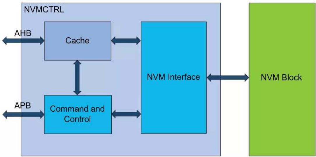
flowchart
graph TD
    A["NVMCTRL"] -->|AHB| B["Cache"]
    B <--> C["NVM Interface"]
    C <--> D["NVM Block"]
    C --> E["Command and Control"]
    E --> F["APB"]
    F --> G["Control Unit"]
    style A fill:#e6f7ff,stroke:#333
    style B fill:#e6f7ff,stroke:#333
    style C fill:#e6f7ff,stroke:#333
    style D fill:#e6f7ff,stroke:#333
    style E fill:#e6f7ff,stroke:#333
    style F fill:#e6f7ff,stroke:#333
    style G fill:#e6f7ff,stroke:#333
20.4 Signal Description
Not applicable.
20.5 Product Dependencies
In order to use this peripheral, other parts of the system must be configured correctly, as described in the following sections.
20.5.1 Power Management
The NVMCTRL will continue to operate in any sleep mode where the selected source clock is running. The NVMCTRL interrupts can be used to wake up the device from sleep modes.
The Power Manager will automatically put the NVM block into a low-power state when entering sleep mode. This is based on the Control B register (CTRLB) SLEEPPRM bit setting. Refer to the 20.8.2. CTRLB. SLEEPPRM register description for more details. The NVM block goes into low-power mode automatically when the device enters STANDBY mode regardless of SLEEPPRM. The NVM Page Buffer is lost when the NVM goes into low power mode therefore a write command must be issued prior entering the NVM low power mode. NVMCTRL SLEEPPRM can be disabled to avoid such loss when the CPU goes into sleep except if the device goes into STANDBY mode for which there is no way to retain the Page Buffer.
Related Links
15. Power Manager (PM)
20.5.2 Clocks
Two synchronous clocks are used by the NVMCTRL. One is provided by the AHB bus (CLK_NVMCTRL_AHB) and the other is provided by the APB bus (CLK_NVMCTRL_APB). For higher system frequencies, a programmable number of wait states can be used to optimize performance. When changing the AHB bus frequency, the user must ensure that the NVM Controller is configured with the proper number of wait states. Refer to the Electrical Characteristics for the exact number of wait states to be used for a particular frequency range.
Related Links
32. Electrical Characteristics at 85°C
20.5.3 Interrupts
The NVM Controller interrupt request line is connected to the interrupt controller. Using the NVMCTRL interrupt requires the interrupt controller to be programmed first.
Related Links
10.2. Nested Vector Interrupt Controller
20.5.4 Debug Operation
When an external debugger forces the CPU into debug mode, the peripheral continues normal operation.
Access to the NVM block can be protected by the security bit. In this case, the NVM block will not be accessible. See the section on the NVMCTRL 20.6.6. Security Bit for details.
20.5.5 Register Access Protection
All registers with write-access are optionally write-protected by the Peripheral Access Controller (PAC), except the following registers:
- Interrupt Flag Status and Clear register (INTFLAG)
- Status register (STATUS)
Optional write-protection by the Peripheral Access Controller (PAC) is denoted by the "PAC Write-Protection" property in each individual register description.
Related Links
10.5. PAC - Peripheral Access Controller
20.5.6 Analog Connections
Not applicable.
20.6 Functional Description
20.6.1 Principle of Operation
The NVM Controller is a client on the AHB and APB buses. It responds to commands, read requests and write requests, based on user configuration.
20.6.1.1 Initialization
After power up, the NVM Controller goes through a power-up sequence. During this time, access to the NVM Controller from the AHB bus is halted. Upon power-up completion, the NVM Controller is operational without any need for user configuration.
20.6.2 Memory Organization
Refer to the Physical Memory Map for memory sizes and addresses for each device.
The NVM is organized into rows, where each row contains four pages, as shown in the figure below. The NVM has a row-erase granularity, while the write granularity is by page. In other words, a single row erase will erase all four pages in the row, while four write operations are used to write the complete row.
Figure 20-2. NVM Row Organization
| Row n | Page (n*4) + 3 | Page (n*4) + 2 | Page (n*4) + 1 | Page (n*4) + 0 |
The NVM block contains a calibration and auxiliary space. Refer to the NVM Organization figure below for details.
The calibration and auxiliary space contains factory calibration and system configuration information. These spaces can be read from the AHB bus in the same way as the main NVM main address space.
In addition, a boot loader section can be allocated at the beginning of the main array, and an EEPROM Emulation section can be allocated at the end of the NVM main address space.
Figure 20-3. NVM Memory Organization
| Calibration and Auxiliary Space | NVM Base Address + 0x00800000 |
| NVM Base Address + NVM Size | |
| NVM Main Address Space | NVM Base Address |
The lower rows in the NVM main address space can be allocated as a boot loader section by using the BOOTPROT fuses, and the upper rows can be allocated to EEPROM Emulation, as shown in the figure below.
The boot loader section is protected by the lock bit(s) corresponding to this address space and by the BOOTPROT[2:0] fuse. The EEPROM Emulation rows can be written regardless of the region lock status.
The number of rows protected by BOOTPROT is given in Boot Loader Size, the number of rows allocated to the EEPROM Emulation are given in EEPROM Size.
Figure 20-4. EEPROM Emulation and Boot Loader Allocation
| EEPROM Emulation allocation | NVM Base Address + NVM size |
| Program allocation | NVM Base Address + NVM size - EEPROM size |
| BOOT allocation | NVM Base Address + BOOTPROT size |
| NVM Base Address |
20.6.3 Region Lock Bits
The NVM block is grouped into 16 equally sized regions. The region size is dependent on the Flash memory size, and is given in the table below. Each region has a dedicated lock bit preventing writing and erasing pages in the region. After production, all regions will be unlocked.
Table 20-1. Region Size
| Memory Size [KB] Region Size [KB] | |
| 256 16 | |
| 128 8 | |
| 64 | 4 |
| 32 | 2 |
To lock or unlock a region, the Lock Region and Unlock Region commands are provided. Writing one of these commands will temporarily lock/unlock the region containing the address loaded in the ADDR register. ADDR can be written by software, or the automatically loaded value from a write operation can be used. The new setting will stay in effect until the next Reset, or until the setting is changed again using the Lock and Unlock commands. The current status of the lock can be determined by reading the LOCK register.
To change the default lock/unlock setting for a region, the user configuration section of the auxiliary space must be written using the Write Auxiliary Page command. Writing to the auxiliary space will take effect after the next Reset. Therefore, a boot of the device is needed for changes in the lock/unlock setting to take effect. Refer to the Physical Memory Map for calibration and auxiliary space address mapping.
Related Links
9.2. Physical Memory Map
20.6.4 Command and Data Interface
The NVM Controller is addressable from the APB bus, while the NVM main address space is addressable from the AHB bus. Read and automatic page write operations are performed by addressing the NVM main address space directly, while other operations such as manual page writes and row erases must be performed by issuing commands through the NVM Controller.
When performing a write operation the flash will be stalled during the whole operation. If running code from the flash, the next instruction will not be executed until after the operation has completed.
To issue a command, the CTRLA.CMD bits must be written along with the CTRLA.CMDEX value. When a command is issued, INTFLAG.READY will be cleared until the command has completed. Any commands written while INTFLAG.READY is low will be ignored.
The CTRLB register must be used to control the power reduction mode, read wait states, and the write mode.
20.6.4.1 NVM Read
Reading from the NVM main address space is performed via the AHB bus by addressing the NVM main address space or auxiliary address space directly. Read data is available after the configured number of read wait states (CTRLB.RWS) set in the NVM Controller.
The number of cycles data are delayed to the AHB bus is determined by the read wait states. Examples of using zero and one wait states are shown in Figure Read Wait State Examples below.
Reading the NVM main address space while a programming or erase operation is ongoing on the NVM main array results in an AHB bus stall until the end of the operation.
Figure 20-5. Read Wait State Examples
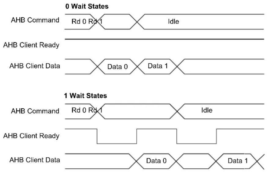
flowchart
graph TD
    subgraph "0 Wait States"
        A["AHB Command"] --> B["Rd 0 Rd 1"]
        B --> C["Idle"]
    end
    subgraph "1 Wait States"
        D["AHB Command"] --> E["Rd 0 Rd 1"]
        E --> F["Idle"]
        G["AHB Client Ready"] --> H["Data 0"]
        I["AHB Client Data"] --> J["Data 0"]
        K["AHB Client Data"] --> L["Data 1"]
    end
20.6.4.2 NVM Write
The NVM Controller requires that an erase must be done before programming. The entire NVM main address space can be erased by a debugger Chip Erase command. Alternatively, rows can be individually erased by the Erase Row command.
After programming the NVM main array, the region that the page resides in can be locked to prevent spurious write or erase sequences. Locking is performed on a per-region basis, and so, locking a region will lock all pages inside the region.
Data to be written to the NVM block are first written to and stored in an internal buffer called the page buffer. The page buffer contains the same number of bytes as an NVM page. Writes to the page buffer must be 16 or 32 bits. 8-bit writes to the page buffer are not allowed and will cause a system exception.
Writing to the NVM block via the AHB bus is performed by a load operation to the page buffer.
For each AHB bus write, the address is stored in the ADDR register. After the page buffer has been loaded with the required number of bytes, the page can be written to the NVM main array by setting CTRLA.CMD to 'Write Page' and setting the key value to CMDEX. The LOAD bit in the STATUS register indicates whether the page buffer has been loaded or not. Before writing the page to memory, the accessed row must be erased.
Automatic page writes are enabled by writing the manual write bit to zero (CTRLB.MANW=0). This will trigger a write operation to the page addressed by ADDR when the last location of the page is written.
Because the address is automatically stored in ADDR during the I/O bus write operation, the last given address will be present in the ADDR register. There is no need to load the ADDR register manually, unless a different page in memory is to be written.
20.6.4.2.1 Procedure for Manual Page Writes (CTRLB.MANW=1)
The row to be written to must be erased before the write command is given.
- Write to the page buffer by addressing the NVM main address space directly
- Write the page buffer to memory: CTRL.CMD='Write Page' and CMDEX
- The READY bit in the INTFLAG register will be low while programming is in progress, and access through the AHB will be stalled
20.6.4.2.2 Procedure for Automatic Page Writes (CTRLB.MANW=0)
The row to be written to must be erased before the last write to the page buffer is performed.
Note that partially written pages must be written with a manual write.
- Write to the page buffer by addressing the NVM main address space directly.
When the last location in the page buffer is written, the page is automatically written to NVM main address space. - INTFLAG.READY will be zero while programming is in progress and access through the AHB will be stalled.
20.6.4.3 Page Buffer Clear
The page buffer is automatically set to all '1' after a page write is performed. If a partial page has been written and it is desired to clear the contents of the page buffer, the Page Buffer Clear command can be used.
20.6.4.4 Erase Row
Before a page can be written, the row containing that page must be erased. The Erase Row command can be used to erase the desired row in the NVM main address space. Erasing the row sets all bits to '1'. If the row resides in a region that is locked, the erase will not be performed and the Lock Error bit in the Status register (STATUS.LOCKE) will be set.
20.6.4.4.1 Procedure for Erase Row
- Write the address of the row to erase to ADDR. Any address within the row can be used.
- Issue an Erase Row command.
Note: The NVM Address bit field in the Address register (ADDR.ADDR) uses 16-bit addressing.
20.6.4.5 Lock and Unlock Region
These commands are used to lock and unlock regions as detailed in section 20.6.3. Region Lock Bits.
20.6.4.6 Set and Clear Power Reduction Mode
The NVM Controller and block can be taken in and out of power reduction mode through the Set and Clear Power Reduction Mode commands. When the NVM Controller and block are in power reduction mode, the Power Reduction Mode bit in the Status register (STATUS.PRM) is set.
20.6.5 NVM User Configuration
The NVM user configuration resides in the auxiliary space. Refer to the Physical Memory Map of the device for calibration and auxiliary space address mapping.
The bootloader resides in the main array starting at offset zero. The allocated boot loader section is write-protected.
Table 20-2. Boot Loader Size
| BOOTPROT [2:0] Rows | Protected by BOOTPROT Boot Loader Size in Bytes | |
| 0x7^(1) | None 0 | |
| 0x6 2 512 | ||
| 0x5 4 1024 | ||
| 0x4 8 2048 | ||
| 0x3 16 4096 | ||
| 0x2 32 8192 | ||
| 0x1 64 16384 | ||
| 0x0 128 32768 |
Note:
- Default value is 0x7 for all variants, except for the WLCSP45 package, where the default value is 0x3. The WLCSP27 devices boot ROM is not protected as the bootloader is self-upgradable through the I²C interface.
The EEPROM[2:0] bits indicate the EEPROM Emulation size, see the table below. The EEPROM Emulation resides in the upper rows of the NVM main address space and is writable, regardless of the region lock status.
Table 20-3. EEPROM Emulation Size
| EEPROM[2:0] Rows Allocated to EEPROM Emulation | EEPROM Emulation Size in Bytes | |
| 7 | None | 0 |
| 6 | 1 | 256 |
| 5 | 2 | 512 |
| 4 | 4 | 1024 |
| 3 | 8 | 2048 |
| 2 | 16 | 4096 |
| 1 | 32 | 8192 |
| 0 | 64 | 16384 |
Related Links
9.2. Physical Memory Map
20.6.6 Security Bit
The security bit allows the entire chip to be locked from external access for code security. The security bit can be written by a dedicated command, Set Security Bit (SSB). Once set, the only way to clear the security bit is through a debugger Chip Erase command. After issuing the SSB command, the PROGE error bit can be checked.
In order to increase the security level it is recommended to enable the internal BOD33 when the security bit is set.
Related Links
- DSU - Device Service Unit
20.6.7 Cache
The NVM Controller cache reduces the device power consumption and improves system performance when wait states are required. Only the NVM main array address space is cached. It is a direct-mapped cache that implements . NVM Controller cache can be enabled by writing a '0' to the Cache Disable bit in the Control B register (CTRLB.CACHEDIS).
The cache can be configured to three different modes using the Read Mode bit group in the Control B register (CTRLB.READMODE).
The INVALL command can be issued using the Command bits in the Control A register to invalidate all cache lines (CTRLA.CMD=INVALL). Commands affecting NVM content automatically invalidate cache lines.
20.7 Register Summary
| Offset | Name Bit Pos. 7 | 6 | 5 | 4 | 3 | 2 | 1 | 0 | |||||||||||
| 0x00 | CTRLA | 7:0 | CMD[6:0] | ||||||||||||||||
| 15:8 | CMDEX[7:0] | ||||||||||||||||||
| 0x02...0x03 | Reserved | ||||||||||||||||||
| 0x04 | CTRLB | 7:0 | MANW | RWS[3:0] | |||||||||||||||
| 15:8 | SLEEPPRM[1:0] | ||||||||||||||||||
| 23:16 | CACHEDIS | READMODE[1:0] | |||||||||||||||||
| 31:24 | |||||||||||||||||||
| 0x08 | PARAM | 7:0 | NVMP[7:0] | ||||||||||||||||
| 15:8 | NVMP[15:8] | ||||||||||||||||||
| 23:16 | PSZ[2:0] | ||||||||||||||||||
| 31:24 | |||||||||||||||||||
| 0x0C | INTENCLR | 7:0 | ERROR | READY | |||||||||||||||
| 0x0D...0x0F | Reserved | ||||||||||||||||||
| 0x10 | INTENSET | 7:0 | ERROR | READY | |||||||||||||||
| 0x11...0x13 | Reserved | ||||||||||||||||||
| 0x14 | INTFLAG | 7:0 | ERROR | READY | |||||||||||||||
| 0x15...0x17 | Reserved | ||||||||||||||||||
| 0x18 | STATUS | 7:0 | NVME LOCKE | PROGE LOAD | PRM | ||||||||||||||
| 15:8 | SB | ||||||||||||||||||
| 0x1A...0x1B | Reserved | ||||||||||||||||||
| 0x1C | ADDR | 7:0 | ADDR[7:0] | ||||||||||||||||
| 15:8 | ADDR[15:8] | ||||||||||||||||||
| 23:16 | ADDR[21:16] | ||||||||||||||||||
| 31:24 | |||||||||||||||||||
| 0x20 | LOCK | 7:0 | LOCK[7:0] | ||||||||||||||||
| 15:8 | LOCK[15:8] | ||||||||||||||||||
20.8 Register Description
Registers can be 8, 16, or 32 bits wide. Atomic 8-, 16-, and 32-bit accesses are supported. In addition, the 8-bit quarters and 16-bit halves of a 32-bit register, and the 8-bit halves of a 16-bit register can be accessed directly.
Some registers require synchronization when read and/or written. Synchronization is denoted by the "Read-Synchronized" and/or "Write-Synchronized" property in each individual register description.
Some registers are enable-protected, meaning they can only be written when the module is disabled. Enable-protection is denoted by the "Enable-Protected" property in each individual register description.
20.8.1 Control A
Name: CTRLA
Offset: 0x00
Reset: 0x0000
Property: PAC Write-Protection
Bit 15 14 13 12 11 10 9 8
CMDEX[7:0]
Access R/W R/W R/W R/W R/W R/W R/W R/W
Reset 00000000
Bit 76543210
CMD[6:0]
Access R/W R/W R/W R/W R/W R/W R/W
Reset 0000000
Bits 15:8 - CMDEX[7:0] Command Execution
When this bit group is written to the key value 0xA5, the command written to CMD will be executed. If a value different from the key value is tried, the write will not be performed and the Programming Error bit in the Status register (STATUS.PROGE) will be set. PROGE is also set if a previously written command is not completed yet.
The key value must be written at the same time as CMD. If a command is issued through the APB bus on the same cycle as an AHB bus access, the AHB bus access will be given priority. The command will then be executed when the NVM block and the AHB bus are idle.
INTFLAG.READY must be '1' when the command is issued.
Bit 0 of the CMDEX bit group will read back as '1' until the command is issued.
Note: The NVM Address bit field in the Address register (ADDR.ADDR) uses 16-bit addressing.
Bits 6:0 - CMD[6:0] Command
These bits define the command to be executed when the CMDEX key is written.
| CMD[6:0] | Group Configuration | Description |
| 0x00-0x01 | - | Reserved |
| 0x02 | ER | Erase Row - Erases the row addressed by the ADDR register in the NVM main array. |
| 0x03 | - | Reserved |
| 0x04 | WP | Write Page - Writes the contents of the page buffer to the page addressed by the ADDR register. |
| 0x05 | EAR | Erase Auxiliary Row - Erases the auxiliary row addressed by the ADDR register. This command can be given only when the security bit is not set and only to the User Configuration Row. |
| 0x06 | WAP | Write Auxiliary Page - Writes the contents of the page buffer to the page addressed by the ADDR register. This command can be given only when the security bit is not set and only to the User Configuration Row. |
| 0x07-0x3F | - | Reserved |
| 0x40 | LR | Lock Region - Locks the region containing the address location in the ADDR register. |
| 0x41 | UR | Unlock Region - Unlocks the region containing the address location in the ADDR register. |
| 0x42 | SPRM | Sets the Power Reduction Mode. |
| 0x43 | CPRM | Clears the Power Reduction Mode. |
| 0x44 | PBC | Page Buffer Clear - Clears the page buffer. |
| 0x45 | SSB | Set Security Bit - Sets the security bit by writing 0x00 to the first byte in the lockbit row. |
| 0x46 | INVALL | Invalidates all cache lines. |
| 0x47-0x7F | - | Reserved |
20.8.2 Control B
Name: CTRLB
Offset: 0x04
Reset: 0x00000080
Property: PAC Write-Protection
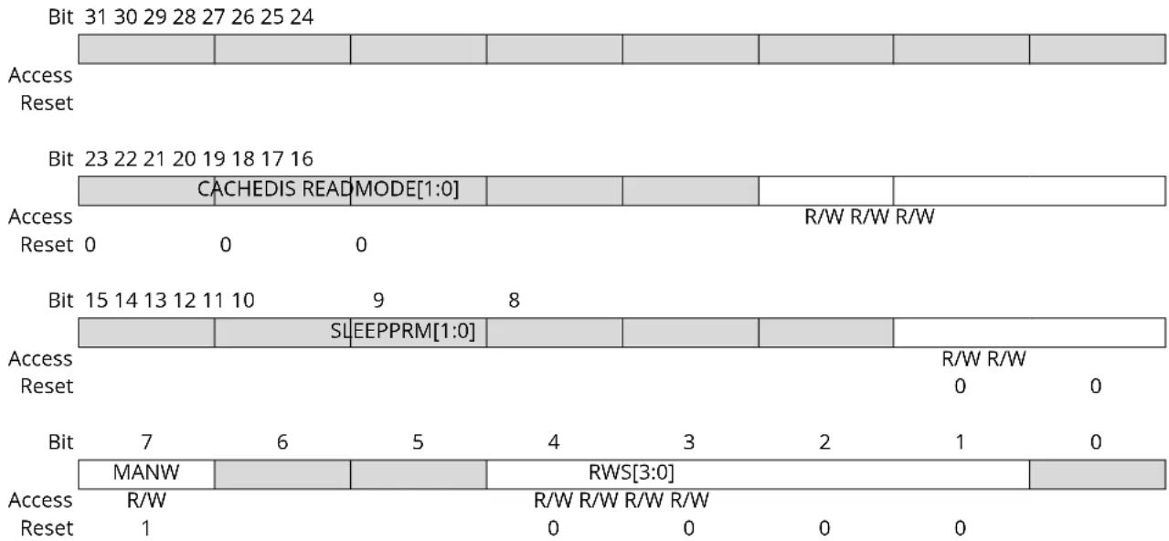
text_image
Bit 31 30 29 28 27 26 25 24 Access Reset Bit 23 22 21 20 19 18 17 16 CACHEDIS READ MODE[1:0] R/W R/W R/W Access Reset 0 0 0 Bit 15 14 13 12 11 10 9 8 SL EEPPRM[1:0] R/W R/W Reset R/W R/W 0 0 Bit 7 6 5 4 3 2 1 0 MANW R/W R/W R/W R/W Reset 1 0 0 0Bit 18 - CACHEDIS Cache Disable
This bit is used to disable the cache.
| Value | Description |
| 0 | The cache is enabled |
| 1 | The cache is disabled |
Bits 17:16 - READMODE[1:0] NVMCTRL Read Mode
| Value | Name | Description |
| 0x0 | NO_MISS_PENALTY | The NVM Controller (cache system) does not insert wait states on a cache miss. Gives the best system performance. |
| 0x1 | LOW_POWER | Reduces power consumption of the cache system, but inserts a wait state each time there is a cache miss. This mode may not be relevant if CPU performance is required, as the application will be stalled and may lead to increased run time. |
| 0x2 | DETERMINISTIC | The cache system ensures that a cache hit or miss takes the same amount of time, determined by the number of programmed Flash wait states. This mode can be used for real-time applications that require deterministic execution timings. |
| 0x3 | Reserved |
Bits 9:8 – SLEEPPRM[1:0] Power Reduction Mode during Sleep Indicates the Power Reduction Mode during sleep.
| Value | Name | Description |
| 0x0 | WAKEUPACCESS NVM block | enters low-power mode when entering sleep. |
| NVM block exits low-power mode upon first access. | ||
| 0x1 | WAKEUPINSTANT | NVM block enters low-power mode when entering sleep. |
| NVM block exits low-power mode when exiting sleep. | ||
| 0x2 | Reserved | |
| 0x3 | DISABLED | Auto power reduction disabled. |
Bit 7 - MANW Manual Write
Note that reset value of this bit is '1'.
| Value Description | |
| 0 | Writing to the last word in the page buffer will initiate a write operation to the page addressed by the last write operation. This includes writes to memory and auxiliary rows. |
| 1 | Write commands must be issued through the CTRLA.CMD register. |
Bits 4:1 - RWS[3:0] NVM Read Wait States
These bits control the number of wait states for a read operation. '0' indicates zero wait states, '1' indicates one wait state, etc., up to 15 wait states.
This register is initialized to 0 wait states. Software can change this value based on the NVM access time and system frequency.
20.8.3 NVM Parameter
Name: PARAM
Offset: 0x08
Reset: 0x000XXXXX
Property: PAC Write-Protection
| Bit 31 30 29 28 27 26 25 24 | |||||||
| Access Reset | |||||||
| Bit 23 22 21 20 19 18 17 16 | |||||||
| P$Z[2:0] | |||||||
| Access Reset x x x | R R R | ||||||
| Bit 15 14 13 12 11 10 | 9 | 8 | |||||
| NVMP[15:8] | |||||||
| Access Reset | R R R R R R R R x x x x x x x x x | ||||||
| Bit | 7 | 6 | 5 | 4 | 3 | 2 | 1 |
| NVMP[7:0] | |||||||
| Access Reset | R R R R R R R R R x x x x x x x x x | ||||||
Bits 18:16 - PSZ[2:0] Page Size
Indicates the page size. Not all devices of the device families will provide all the page sizes indicated in the table.
| Value | Name | Description |
| 0x0 | 8 | 8 bytes |
| 0x1 | 16 | 16 bytes |
| 0x2 | 32 | 32 bytes |
| 0x3 | 64 | 64 bytes |
| 0x4 | 128 | 128 bytes |
| 0x5 | 256 | 256 bytes |
| 0x6 | 512 | 512 bytes |
| 0x7 | 1024 | 1024 bytes |
Bits 15:0 - NVMP[15:0] NVM Pages
Indicates the number of pages in the NVM main address space.
20.8.4 Interrupt Enable Clear
Name: INTENCLR
Offset: 0x0C
Reset: 0x00
Property: PAC Write-Protection
This register allows the user to disable an interrupt without doing a read-modify-write operation. Changes in this register will also be reflected in the Interrupt Enable Set register (INTENSET).
Bit 76543210
| ERROR READY | |||||||
| Access Reset 0 0 | R/W R/W | ||||||
Bit 1 - ERROR Error Interrupt Enable
Writing a '0' to this bit has no effect.
Writing a '1' to this bit clears the ERROR interrupt enable.
This bit will read as the current value of the ERROR interrupt enable.
Bit 0 - READY NVM Ready Interrupt Enable
Writing a '0' to this bit has no effect.
Writing a '1' to this bit clears the READY interrupt enable.
This bit will read as the current value of the READY interrupt enable.
20.8.5 Interrupt Enable Set
Name: INTENSET
Offset: 0x10
Reset: 0x00
Property: PAC Write-Protection
This register allows the user to enable an interrupt without doing a read-modify-write operation.
Changes in this register will also be reflected in the Interrupt Enable Clear register (INTENCLR).
Bit 76543210
| ERROR READY | |||||||
| Access Reset 0 0 | R/W R/W | ||||||
Bit 1 - ERROR Error Interrupt Enable
Writing a '0' to this bit has no effect.
Writing a '1' to this bit sets the ERROR interrupt enable.
This bit will read as the current value of the ERROR interrupt enable.
Bit 0 - READY NVM Ready Interrupt Enable
Writing a '0' to this bit has no effect.
Writing a '1' to this bit sets the READY interrupt enable.
This bit will read as the current value of the READY interrupt enable.
20.8.6 Interrupt Flag Status and Clear
Name: INTFLAG
Offset: 0x14
Reset: 0x00
Property: -
Bit 76543210
| ERROR READY | |||||||
| Access Reset 0 0 | R/W R | ||||||
Bit 1 - ERROR Error
This flag is set on the occurrence of an NVME, LOCKE or PROGE error.
This bit can be cleared by writing a '1' to its bit location.
| Value Description | |
| 0 | No errors have been received since the last clear. |
| 1 | At least one error has occurred since the last clear. |
Bit 0 - READY NVM Ready
| Value Description | |
| 0 | The NVM controller is busy programming or erasing. |
| 1 | The NVM controller is ready to accept a new command. |
20.8.7 Status
Name: STATUS
Offset: 0x18
Reset: 0x0X00
Property: -
Bit 15 14 13 12 11 10 9 8
| SB | |||||||
| Access Reset x | R |
Bit 76543210
| NVME | LOCKE | PROGE | LOAD | PRM | |||
| Access Reset | R/W | R/W | R/W | R/W | R | ||
| 0 0 0 0 0 |
Bit 8 - SB Security Bit Status
| Value | Description |
| 0 | The Security bit is inactive. |
| 1 | The Security bit is active. |
Bit 4 - NVME NVM Error
This bit can be cleared by writing a '1' to its bit location.
| Value | Description |
| 0 | No programming or erase errors have been received from the NVM controller since this bit was last cleared. |
| 1 | At least one error has been registered from the NVM Controller since this bit was last cleared. |
Bit 3 - LOCKE Lock Error Status
This bit can be cleared by writing a '1' to its bit location.
| Value | Description |
| 0 | No programming of any locked lock region has happened since this bit was last cleared. |
| 1 | Programming of at least one locked lock region has happened since this bit was last cleared. |
Bit 2 - PROGE Programming Error Status
This bit can be cleared by writing a '1' to its bit location.
| Value | Description |
| 0 | No invalid commands or bad keywords were written in the NVM Command register since this bit was last cleared. |
| 1 | An invalid command and/or a bad keyword was/were written in the NVM Command register since this bit was last cleared. |
Bit 1 - LOAD NVM Page Buffer Active Loading
This bit indicates that the NVM page buffer has been loaded with one or more words. Immediately after an NVM load has been performed, this flag is set. It remains set until a page write or a page buffer clear (PBCLR) command is given.
This bit can be cleared by writing a '1' to its bit location.
Bit 0 - PRM Power Reduction Mode
This bit indicates the current NVM power reduction state. The NVM block can be set in power reduction mode in two ways: through the command interface or automatically when entering sleep with SLEEPPRM set accordingly.
PRM can be cleared in three ways: through AHB access to the NVM block, through the command interface (SPRM and CPRM) or when exiting sleep with SLEEPPRM set accordingly.
Value Description
| 0 | NVM is not in power reduction mode. |
| 1 | NVM is in power reduction mode. |
20.8.8 Address
Name: ADDR
Offset: 0x1C
Reset: 0x00000000
Property: PAC Write-Protection
| Bit 31 30 29 28 27 26 25 24 | |||||||
| Access Reset | |||||||
| Bit 23 22 21 20 19 18 17 16 | |||||||
| ADDR[21:16] | |||||||
| Access Reset 0 0 0 0 0 0 | R/W R/W R/W R/W R/W R/W | ||||||
| Bit 15 14 13 12 11 10 | 9 8 | ||||||
| ADDR[15:8] | |||||||
| Access Reset | R/W R/W R/W R/W R/W R/W R/W | ||||||
| 0 0 0 0 0 0 0 0 | |||||||
| Bit | 7 6 5 4 3 2 1 0 | ||||||
| ADDR[7:0] | |||||||
| Access Reset | R/W R/W R/W R/W R/W R/W R/W R/W | ||||||
| 0 0 0 0 0 0 0 0 | |||||||
Bits 21:0 - ADDR[21:0] NVM Address
ADDR drives the hardware half-word offset from the start address of the corresponding NVM section when a command is executed using CMDEX. This register is also automatically updated when writing to the page buffer. The effective address for the operation is Start address of the section + 2*ADDR.
Example:
For erasing the 3rd row in the Flash memory, spanning from 0x00000200 to 0x000002FF, ADDR must be written with the half-word offset address of any half-word within this range, that is any value between 0x100 and 0x17F.
20.8.9 Lock Section
Name: LOCK
Offset: 0x20
Reset: 0xXXXX
Property: -
Bit 15 14 13 12 11 10 9 8
LOCK[15:8]
Access RRRRRRRR
Reset xxxxxxxx
Bit 76543210
LOCK[7:0]
Access RRRRRRRR
Reset xxxxxxxx
Bits 15:0 - LOCK[15:0] Region Lock Bits
To set or clear these bits, the CMD register must be used.
Default state after erase will be unlocked (0xFFFF).
Default state after reset will be loaded from the NVM User Row.
| Value Description | |
| 0 | The corresponding lock region is locked. |
| 1 | The corresponding lock region is not locked. |
21. PORT - I/O Pin Controller
21.1 Overview
The IO Pin Controller (PORT) controls the I/O pins of the device. The I/O pins are organized in a series of groups, collectively referred to as a PORT group. Each PORT group can have up to 32 pins that can be configured and controlled individually or as a group. The number of PORT groups on a device may depend on the package/number of pins. Each pin may either be used for general-purpose I/O under direct application control or be assigned to an embedded device peripheral. When used for general-purpose I/O, each pin can be configured as input or output, with highly configurable driver and pull settings.
All I/O pins have true read-modify-write functionality when used for general-purpose I/O; the direction or the output value of one or more pins may be changed (set, reset or toggled) explicitly without unintentionally changing the state of any other pins in the same port group by a single, atomic 8-, 16- or 32-bit write.
The PORT is connected to the high-speed bus matrix through an AHB/APB bridge. The Pin Direction, Data Output Value and Data Input Value registers may also be accessed using the low-latency CPU local bus (IOBUS; ARM ^® single-cycle I/O port).
21.2 Features
- Selectable input and output configuration for each individual pin
- Software-controlled multiplexing of peripheral functions on I/O pins
- Flexible pin configuration through a dedicated Pin Configuration register
-
Configurable output driver and pull settings:
-
Totem-pole (push-pull)
- Pull configuration
- Driver strength
- Configurable input buffer and pull settings:
- Internal pull-up or pull-down
- Input sampling criteria
- Input buffer can be disabled if not needed for lower power consumption
21.3 Block Diagram
Figure 21-1. PORT Block Diagram
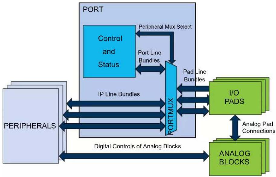
flowchart
graph TD
    A["PORT"] -->|Peripheral Mux Select| B["Control and Status"]
    B -->|Port Line Bundles| C["PortMUX"]
    C -->|Pad Line Bundles| D["I/O PADS"]
    D -->|Analog Pad Connections| E["ANALOG BLOCKS"]
    E -->|Digital Controls of Analog Blocks| F["PERIPHERALS"]
    F -->|IP Line Bundles| C
    C -->|IP Line Bundles| G["PortMUX"]
21.4 Signal Description
Table 21-1. Signal description for PORT
| Signal name Type Description | |
| Pxy Digital I/O General-purpose I/O pin y in group x | |
Refer to the I/O Multiplexing and Considerations for details on the pin mapping for this peripheral. One signal can be mapped on several pins.
Related Links
- I/O Multiplexing and Considerations
21.5 Product Dependencies
In order to use this peripheral, other parts of the system must be configured correctly as follows.
21.5.1 I/O Lines
The I/O lines of the PORT are mapped to pins of the physical device. The following naming scheme is used:
Each line bundle with up to 32 lines is assigned an identifier 'xy', with letter x=A, B, C... and two-digit number y=00, 01, ...31. Examples: A24, C03.
PORT pins are labeled 'Pxy' accordingly, for example PA24, PC03. This identifies each pin in the device uniquely.
Each pin may be controlled by one or more peripheral multiplexer settings, which allow the pad to be routed internally to a dedicated peripheral function. When the setting is enabled, the selected peripheral has control over the output state of the pad, as well as the ability to read the current physical pad state. Refer to I/O Multiplexing and Considerations for details.
Device-specific configurations may cause some lines (and the corresponding Pxy pin) not to be implemented.
Related Links
- I/O Multiplexing and Considerations
21.5.2 Power Management
During Reset, all PORT lines are configured as inputs with input buffers, output buffers and pull disabled.
The PORT peripheral will continue operating in any sleep mode where its source clock is running.
21.5.3 Clocks
The PORT bus clock (CLK_PORT_APB) can be enabled and disabled in the Power Manager, and the default state of CLK_PORT_APB can be found in the Peripheral Clock Masking section in PM - Power Manager.
The PORT requires an APB clock, which may be divided from the CPU main clock and allows the CPU to access the registers of PORT through the high-speed matrix and the AHB/APB bridge.
The PORT also requires an AHB clock for CPU IOBUS accesses to the PORT. That AHB clock is the internal PORT clock.
The priority of IOBUS accesses is higher than APB accesses. One clock cycle latency can be observed on the APB access in case of concurrent PORT accesses.
Related Links
- Power Manager (PM)
21.5.4 Interrupts
Not applicable.
21.5.5 Events
The events of this peripheral are connected to the Event System.
Related Links
- Event System (EVSYS)
21.5.6 Debug Operation
When the CPU is halted in debug mode, this peripheral will continue normal operation.
21.5.7 Register Access Protection
All registers with write-access can be optionally write-protected by the Peripheral Access Controller (PAC).
Note: Optional write-protection is indicated by the "PAC Write-Protection" property in the register description.
Write-protection does not apply for accesses through an external debugger.
Related Links
10.5. PAC - Peripheral Access Controller
21.5.8 Analog Connections
Analog functions are connected directly between the analog blocks and the I/O pads using analog buses. However, selecting an analog peripheral function for a given pin will disable the corresponding digital features of the pad.
21.5.9 CPU Local Bus
The CPU local bus (IOBUS) is an interface that connects the CPU directly to the PORT. It is a single-cycle bus interface, which does not support wait states. It supports 8-bit, 16-bit and 32-bit sizes.
This bus is generally used for low latency operation. The Data Direction (DIR) and Data Output Value (OUT) registers can be read, written, set, cleared or be toggled using this bus, and the Data Input Value (IN) registers can be read.
Since the IOBUS cannot wait for IN register resynchronization, the Control register (CTRL) must be configured to continuous sampling of all pins that need to be read via the IOBUS in order to prevent stale data from being read.
Note: Refer to the Product Mapping chapter for the IOBUS address.
Related Links
21.9.1. DIR
21.9.9. IN
21.9.1. DIR
21.9.10. CTRL
21.6 Functional Description
Figure 21-2. Overview of the PORT
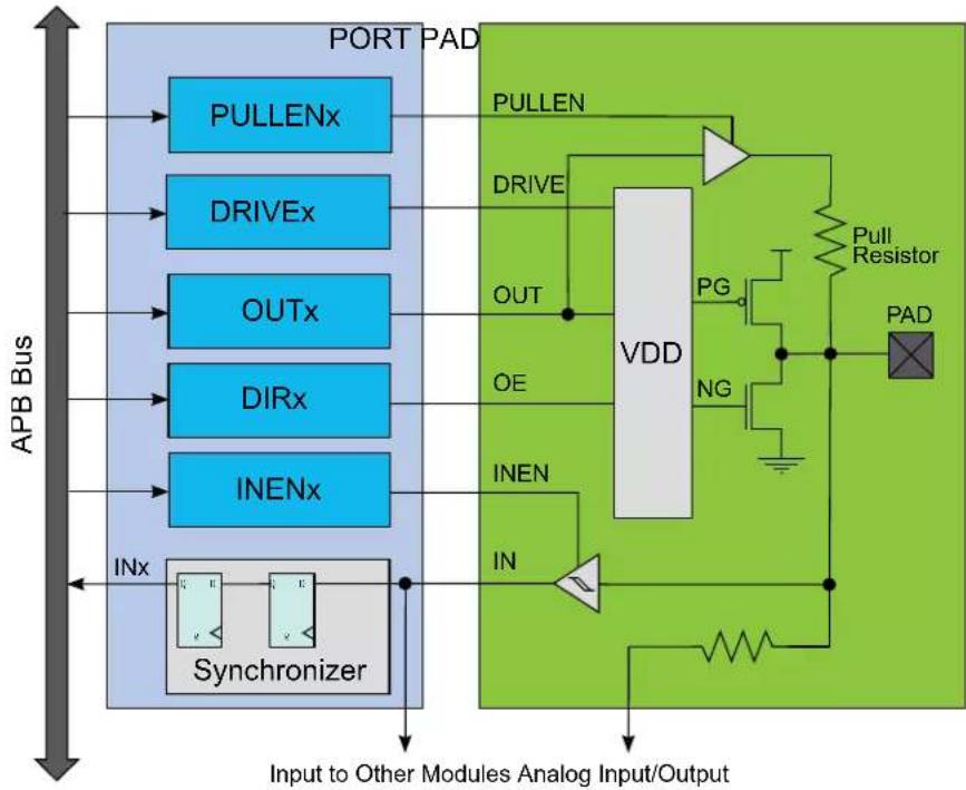
flowchart
graph TD
    A["APB Bus"] --> B["PULLENx"]
    A --> C["DRIVEx"]
    A --> D["OUTx"]
    A --> E["DIRx"]
    A --> F["INENx"]
    B --> G["Synchronizer"]
    C --> G
    D --> G
    E --> G
    F --> G
    G --> H["Input to Other Modules Analog Input/Output"]
    H --> I["VDD"]
    I --> J["OUT"]
    I --> K["OE"]
    I --> L["INEN"]
    I --> M["IN"]
    I --> N["PULLEN"]
    I --> O["DRIVE"]
    I --> P["VDD"]
    P --> Q["PG"]
    P --> R["NG"]
    P --> S["Pull Resistor"]
    P --> T["PAD"]
    P --> U["Ground"]
    style A fill:#f9f,stroke:#333
    style I fill:#ccf,stroke:#333
21.6.1 Principle of Operation
Each PORT group of up to 32 pins is controlled by the registers in PORT, as described in the figure. These registers in PORT are duplicated for each PORT group, with increasing base addresses. The number of PORT groups may depend on the package/number of pins.
Figure 21-3. Overview of the peripheral functions multiplexing
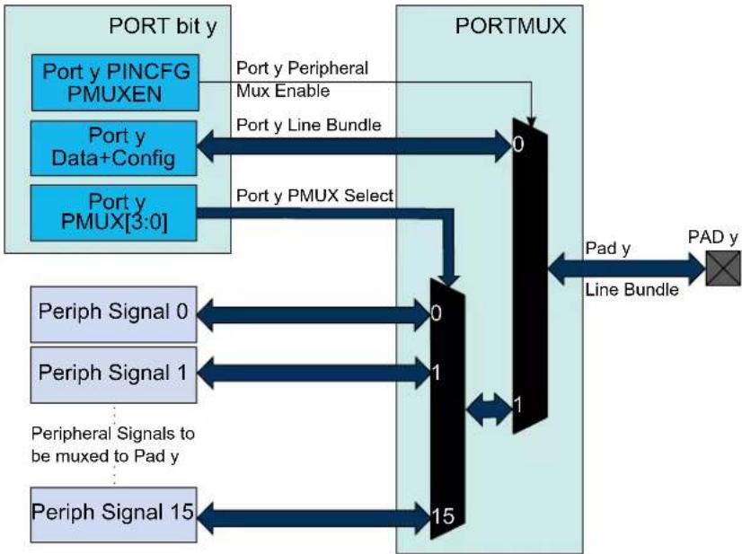
flowchart
graph TD
    A["Port bit y"] --> B["Port y PINCFG PMUXEN"]
    A --> C["Port y Data+Config"]
    A --> D["Port y PMUX[3:0"]]
    B --> E["0"]
    C --> F["1"]
    D --> G["15"]
    H["Periph Signal 0"] --> I["0"]
    J["Periph Signal 1"] --> K["1"]
    L["Peripheral Signals to be muxed to Pad y"] --> M["15"]
    N["Periph Signal 15"] --> O["15"]
    P["Port y Peripheral Mux Enable"] --> Q["0"]
    R["Port y Line Bundle"] --> Q
    S["Port y PMUX Select"] --> Q
    T["Pad y Line Bundle"] --> U["1"]
    V["Pad y"] --> W["PAD y"]
The I/O pins of the device are controlled by PORT peripheral registers. Each port pin has a corresponding bit in the Data Direction (DIR) and Data Output Value (OUT) registers to enable that pin as an output and to define the output state.
The direction of each pin in a PORT group is configured by the DIR register. If a bit in DIR is set to '1', the corresponding pin is configured as an output pin. If a bit in DIR is set to '0', the corresponding pin is configured as an input pin.
When the direction is set as output, the corresponding bit in the OUT register will set the level of the pin. If bit y in OUT is written to '1', pin y is driven HIGH. If bit y in OUT is written to '0', pin y is driven LOW. Pin configuration can be set by Pin Configuration (PINCFGy) registers, with y=00, 01, ..31 representing the bit position.
The Data Input Value (IN) is set as the input value of a port pin with resynchronization to the PORT clock. To reduce power consumption, these input synchronizers can be clocked only when system requires reading the input value, as specified in the SAMPLING field of the Control register (CTRL). The value of the pin can always be read, whether the pin is configured as input or output. If the Input Enable bit in the Pin Configuration registers (PINCFGy.INEN) is '0', the input value will not be sampled.
In PORT, the Peripheral Multiplexer Enable bit in the PINCFGy register (PINCFGy.PMUXEN) can be written to '1' to enable the connection between peripheral functions and individual I/O pins. The Peripheral Multiplexing n (PMUXn) registers select the peripheral function for the corresponding pin. This will override the connection between the PORT and that I/O pin, and connect the selected peripheral signal to the particular I/O pin instead of the PORT line bundle.
Related Links
21.9.1. DIR
21.9.9. IN
21.9.1. DIR
21.9.13. PINCFG
21.9.12. PMUX
21.6.2 Basic Operation
21.6.2.1 Initialization
After reset, all standard function device I/O pads are connected to the PORT with outputs tri-stated and input buffers disabled, even if there is no clock running.
However, specific pins, such as those used for connection to a debugger, may be configured differently, as required by their special function.
21.6.2.2 Operation
Each I/O pin Pxy can be controlled by the registers in PORT. Each PORT group x has its own set of PORT registers, with a base address at byte address (PORT + 0x80 * group index) (A corresponds to group index 0, B to 1, etc...). Within that set of registers, the pin index is y, from 0 to 31.
Refer to I/O Multiplexing and Considerations for details on available pin configuration and PORT groups.
Configuring Pins as Output
To use pin Pxy as an output, write bit y of the DIR register to '1'. This can also be done by writing bit y in the DIRSET register to '1' - this will avoid disturbing the configuration of other pins in that group. The y bit in the OUT register must be written to the desired output value.
Similarly, writing an OUTSET bit to '1' will set the corresponding bit in the OUT register to '1'. Writing a bit in OUTCLR to '1' will set that bit in OUT to zero. Writing a bit in OUTTGL to '1' will toggle that bit in OUT.
Configuring Pins as Input
To use pin Pxy as an input, bit y in the DIR register must be written to '0'. This can also be done by writing bit y in the DIRCLR register to '1' - this will avoid disturbing the configuration of other pins in that group. The input value can be read from bit y in register IN as soon as the INEN bit in the Pin Configuration register (PINCFGy.INEN) is written to '1'.
By default, the input synchronizer is clocked only when an input read is requested. This will delay the read operation by two cycles of the PORT clock. To remove the delay, the input synchronizers for each PORT group of eight pins can be configured to be always active, but this will increase power consumption. This is enabled by writing '1' to the corresponding SAMPLINGn bit field of the CTRL register, see CTRL.SAMPLING for details.
Using Alternative Peripheral Functions
To use pin Pxy as one of the available peripheral functions, the corresponding PMUXEN bit of the PINCFGy register must be '1'. The PINCFGy register for pin Pxy is at byte offset (PINCFG0 + y).
The peripheral function can be selected by setting the PMUXO or PMUXE in the PMUXn register. The PMUXO/PMUXE is at byte offset PMUX0 + (y/2). The chosen peripheral must also be configured and enabled.
Related Links
- I/O Multiplexing and Considerations
21.6.3 I/O Pin Configuration
The Pin Configuration register (PINCFGy) is used for additional I/O pin configuration. A pin can be set in a totem-pole or pull configuration.
As pull configuration is done through the Pin Configuration register, all intermediate PORT states during switching of pin direction and pin values are avoided.
The I/O pin configurations are described further in this chapter, and summarized in Table 21-2.
21.6.3.1 Pin Configurations Summary
Table 21-2. Pin Configurations Summary
| DIR INEN PULLEN OUT Configuration | ||||
| 0 0 0 X Reset or analog I/O: all digital disabled | ||||
| 0 0 1 0 Pull-down; input disabled | ||||
| 0 0 1 1 Pull-up; input disabled | ||||
| 0 1 0 X Input | ||||
| 0 1 1 0 Input with pull-down | ||||
| 0 1 1 1 Input with pull-up | ||||
| 1 0 XX Output; input disabled | ||||
| 1 1 XX Output; input enabled | ||||
21.6.3.2 Input Configuration
Figure 21-4. I/O configuration - Standard Input
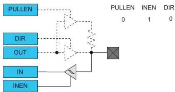
flowchart
graph TD
    A["PULLEN"] --> B["Comparator"]
    C["DIR"] --> B
    D["OUT"] --> B
    E["IN"] --> F["Comparator"]
    G["INEN"] --> F
    B --> H["Summing Junction"]
    F --> H
    style B fill:#f9f,stroke:#333
    style H fill:#ccf,stroke:#333
Figure 21-5. I/O Configuration - Input with Pull
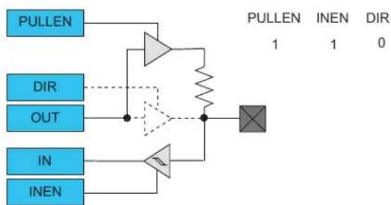
flowchart
graph TD
    A["PULLEN"] --> B["Amplifier"]
    C["DIR"] --> B
    D["OUT"] --> B
    E["IN"] --> F["Amplifier"]
    G["INEN"] --> F
    B --> H["Multiplier"]
    F --> H
    H --> I["Output"]
Note: When pull is enabled, the pull value is defined by the OUT value.
21.6.3.3 Totem-Pole Output
When configured for totem-pole (push-pull) output, the pin is driven low or high according to the corresponding bit setting in the OUT register. In this configuration there is no current limitation for sink or source other than what the pin is capable of. If the pin is configured for input, the pin will float if no external pull is connected.
Note: Enabling the output driver will automatically disable pull.
Figure 21-6. I/O Configuration - Totem-Pole Output with Disabled Input
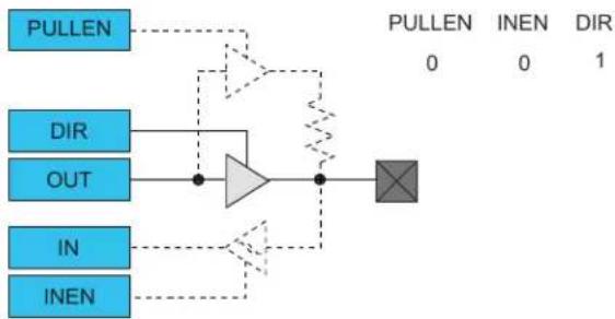
flowchart
graph TD
    A["PULLEN"] --> B["AND"]
    C["DIR"] --> B
    D["OUT"] --> B
    E["IN"] --> B
    F["INEN"] --> B
    B --> G["OR"]
    G --> H["Summing Junction"]
    style G fill:#f9f,stroke:#333
Figure 21-7. I/O Configuration - Totem-Pole Output with Enabled Input
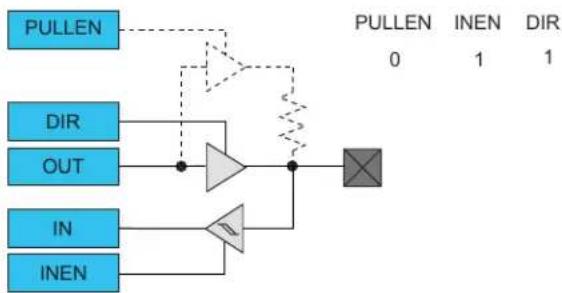
flowchart
graph TD
    A["PULLEN"] --> B["OUT"]
    B --> C["NOT"]
    D["IN"] --> E["NOT"]
    F["INEN"] --> E
    E --> G["OR"]
    G --> H["OR"]
    I["PULLEN 0"] --> J["INEN 1"]
    J --> K["DIR 1"]
    L["OR"] --> M["AND"]
    N["NOT"] --> O["AND"]
    style A fill:#4CAF50,stroke:#388E3C
    style D fill:#4CAF50,stroke:#388E3C
    style F fill:#4CAF50,stroke:#388E3C
    style I fill:#FFA500,stroke:#388E3C
    style L fill:#FFA500,stroke:#388E3C
    style N fill:#FFA500,stroke:#388E3C
    style L fill:#FFA500,stroke:#388E3C
Figure 21-8. I/O Configuration - Output with Pull
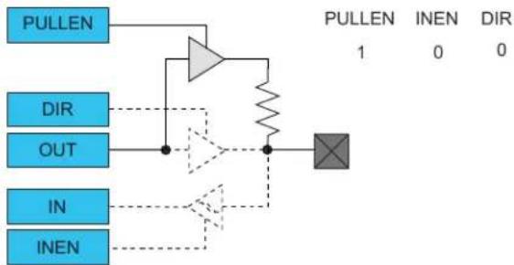
flowchart
graph TD
    A["PULLEN"] --> B["NOT"]
    C["DIR"] --> B
    D["OUT"] --> B
    E["IN"] --> F["NOT"]
    G["INEN"] --> F
    B --> H["Comparator"]
    F --> H
    H --> I["PULLEN 1 INEN DIR 0 0"]
21.6.3.4 Digital Functionality Disabled
Neither Input nor Output functionality are enabled.
Figure 21-9. I/O Configuration - Reset or Analog I/O: Digital Output, Input and Pull Disabled
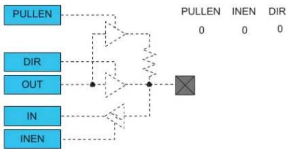
flowchart
graph TD
    A["PULLEN"] --> B["OUT"]
    B --> C["IN"]
    C --> D["INEN"]
    E["0"] --> F["Processing Block"]
    G["0"] --> F
    H["0"] --> F
    I["0"] --> F
    J["0"] --> F
    K["0"] --> F
    L["0"] --> F
    M["0"] --> F
    N["0"] --> F
    O["0"] --> F
    P["PULLEN"] --> Q["INEN"]
    Q --> R["DIR"]
21.6.4 PORT Access Priority
The PORT is accessed by different systems:
- The ARM ^ CPU through the ARM ^ single-cycle I/O port (IOBUS)
- The ARM ^ CPU through the high-speed matrix and the AHB/APB bridge (APB)
The following priority is adopted:
- ARM ^® CPU IOBUS (No wait tolerated)
- APB
21.7 Register Summary
| Offset | Name Bit Pos. 76543210 | |||||||||
| 0x00 DIR | 7:0 DIR[7:0] | |||||||||
| 15:8 DIR[15:8] | ||||||||||
| 23:16 DIR[23:16] | ||||||||||
| 31:24 DIR[31:24] | ||||||||||
| 0x04 DIRCLR | 7:0 DIRCLR[7:0] | |||||||||
| 15:8 DIRCLR[15:8] | ||||||||||
| 23:16 DIRCLR[23:16] | ||||||||||
| 31:24 DIRCLR[31:24] | ||||||||||
| 0x08 DIRSET | 7:0 DIRSET[7:0] | |||||||||
| 15:8 | DIRSET[15:8] | |||||||||
| 23:16 | DIRSET[23:16] | |||||||||
| 31:24 | DIRSET[31:24] | |||||||||
| 0x0C DIRTGL | 7:0 DIRTGL[7:0] | |||||||||
| 15:8 DIRTGL[15:8] | ||||||||||
| 23:16 DIRTGL[23:16] | ||||||||||
| 31:24 DIRTGL[31:24] | ||||||||||
| 0x10 | OUT | 7:0 | OUT[7:0] | |||||||
| 15:8 | OUT[15:8] | |||||||||
| 23:16 | OUT[23:16] | |||||||||
| 31:24 | OUT[31:24] | |||||||||
| 0x14 | OUTCLR | 7:0 | OUTCLR[7:0] | |||||||
| 15:8 | OUTCLR[15:8] | |||||||||
| 23:16 | OUTCLR[23:16] | |||||||||
| 31:24 | OUTCLR[31:24] | |||||||||
| 0x18 | OUTSET | 7:0 | OUTSET[7:0] | |||||||
| 15:8 | OUTSET[15:8] | |||||||||
| 23:16 | OUTSET[23:16] | |||||||||
| 31:24 | OUTSET[31:24] | |||||||||
| 0x1C | OUTTGL | 7:0 OUTTGL[7:0] | ||||||||
| 15:8 | OUTTGL[15:8] | |||||||||
| 23:16 | OUTTGL[23:16] | |||||||||
| 31:24 | OUTTGL[31:24] | |||||||||
| 0x20 | IN | 7:0 | IN[7:0] | |||||||
| 15:8 | IN[15:8] | |||||||||
| 23:16 IN[23:16] | ||||||||||
| 31:24 IN[31:24] | ||||||||||
| 0x24 | CTRL | 7:0 | SAMPLING[7:0] | |||||||
| 15:8 | SAMPLING[15:8] | |||||||||
| 23:16 | SAMPLING[23:16] | |||||||||
| 31:24 | SAMPLING[31:24] | |||||||||
| 0x28 WRCONFIG | 7:0 | PINMASK[7:0] | ||||||||
| 15:8 | PINMASK[15:8] | |||||||||
| 23:16 | DRVSTR | PULLEN | INEN | PMUXEN | ||||||
| 31:24 | HWSEL | WRPINCFG | WRPMUX | PMUX[3:0] | ||||||
| 0x2C...0x2F | Reserved | |||||||||
| 0x30 | PMUX0 | 7:0 | PMUXO[3:0] | PMUXE[3:0] | ||||||
| ... | ||||||||||
| 0x3F | PMUX15 | 7:0 | PMUXO[3:0] | PMUXE[3:0] | ||||||
| 0x40 | PINCFG0 | 7:0 | DRVSTR | PULLEN | INEN | PMUXEN | ||||
| ... | ||||||||||
| 0x5F | PINCFG31 | 7:0 | DRVSTR | PULLEN | INEN | PMUXEN | ||||
21.8 PORT Pin Groups and Register Repetition

Tip: The I/O pins are assembled in pin groups ("PORT groups") with up to 32 pins. Group 0 consists of the PA pins, group 1 is for the PB pins, etc. Each pin group has its own PORT registers, with a 0x80 address spacing. For example, the register address offset for the Data Direction (DIR) register for group 0 (PA00 to PA31) is 0x00, and the register address offset for the DIR register for group 1 (PB00 to PB31) is 0x80.
21.9 Register Description
Registers can be 8, 16, or 32 bits wide. Atomic 8-, 16- and 32-bit accesses are supported. In addition, the 8-bit quarters and 16-bit halves of a 32-bit register, and the 8-bit halves of a 16-bit register can be accessed directly.
Some registers are optionally write-protected by the Peripheral Access Controller (PAC). Optional PAC write-protection is denoted by the "PAC Write-Protection" property in each individual register description. For details, refer to Register Access Protection.
21.9.1 Data Direction
Name: DIR
Offset: 0x00
Reset: 0x00000000
Property: PAC Write-Protection
This register allows the user to configure one or more I/O pins as an input or output. This register can be manipulated without doing a read-modify-write operation by using the Data Direction Toggle (DIRTGL), Data Direction Clear (DIRCLR) and Data Direction Set (DIRSET) registers.

Tip: The I/O pins are assembled in pin groups ("PORT groups") with up to 32 pins. Group 0 consists of the PA pins, group 1 is for the PB pins, etc. Each pin group has its own PORT registers, with a 0x80 address spacing. For example, the register address offset for the Data Direction (DIR) register for group 0 (PA00 to PA31) is 0x00, and the register address offset for the DIR register for group 1 (PB00 to PB31) is 0x80.
| Bit 31 30 29 28 27 26 25 24 | |
| DIR[31:24] | |
| Access RW RW RW RW RW RW RW | |
| Reset 0 0 0 0 0 0 0 0 | |
| Bit 23 22 21 20 19 18 17 16 | |
| DIR[23:16] | |
| Access RW RW RW RW RW RW RW | |
| Reset 0 0 0 0 0 0 0 0 | |
| Bit 15 14 13 12 11 10 9 8 | |
| DIR[15:8] | |
| Access RW RW RW RW RW RW RW | |
| Reset 0 0 0 0 0 0 0 0 | |
| Bit 7 6 5 4 3 2 1 0 | |
| DIR[7:0] | |
| Access RW RW RW RW RW RW RW | |
| Reset 0 0 0 0 0 0 0 0 | |
Bits 31:0 - DIR[31:0] Port Data Direction
These bits set the data direction for the individual I/O pins in the PORT group.
| Value Description | |
| 0 | The corresponding I/O pin in the PORT group is configured as an input. |
| 1 | The corresponding I/O pin in the PORT group is configured as an output. |
21.9.2 Data Direction Clear
Name: DIRCLR
Offset: 0x04
Reset: 0x00000000
Property: PAC Write-Protection
This register allows the user to set one or more I/O pins as an input, without doing a read-modify-write operation. Changes in this register will also be reflected in the Data Direction (DIR), Data Direction Toggle (DIRTGL) and Data Direction Set (DIRSET) registers.

Tip: The I/O pins are assembled in pin groups ("PORT groups") with up to 32 pins. Group 0 consists of the PA pins, group 1 is for the PB pins, etc. Each pin group has its own PORT registers, with a 0x80 address spacing. For example, the register address offset for the Data Direction (DIR) register for group 0 (PA00 to PA31) is 0x00, and the register address offset for the DIR register for group 1 (PB00 to PB31) is 0x80.
| Bit 31 30 29 28 27 26 25 24 | |
| DIRCLR[31:24] | |
| Access RW RW RW RW RW RW RW RW Reset 0 0 0 0 0 0 0 0 | |
| Bit 23 22 21 20 19 18 17 16 | |
| DIRCLR[23:16] | |
| Access RW RW RW RW RW RW RW RW Reset 0 0 0 0 0 0 0 0 | |
| Bit 15 14 13 12 11 10 9 8 | |
| DIRCLR[15:8] | |
| Access RW RW RW RW RW RW RW RW Reset 0 0 0 0 0 0 0 0 | |
| Bit 7 6 5 4 3 2 1 0 | |
| DIRCLR[7:0] | |
| Access RW RW RW RW RW RW RW RW Reset 0 0 0 0 0 0 0 0 | |
Bits 31:0 - DIRCLR[31:0] Port Data Direction Clear
Writing a '0' to a bit has no effect.
Writing a '1' to a bit will clear the corresponding bit in the DIR register, which configures the I/O pin as an input.
| Value Description | |
| 0 | The corresponding I/O pin in the PORT group will keep its configuration. |
| 1 | The corresponding I/O pin in the PORT group is configured as input. |
21.9.3 Data Direction Set
Name: DIRSET
Offset: 0x08
Reset: 0x00000000
Property: PAC Write-Protection
This register allows the user to set one or more I/O pins as an output, without doing a read-modify-write operation. Changes in this register will also be reflected in the Data Direction (DIR), Data Direction Toggle (DIRTGL) and Data Direction Clear (DIRCLR) registers.

Tip: The I/O pins are assembled in pin groups ("PORT groups") with up to 32 pins. Group 0 consists of the PA pins, group 1 is for the PB pins, etc. Each pin group has its own PORT registers, with a 0x80 address spacing. For example, the register address offset for the Data Direction (DIR) register for group 0 (PA00 to PA31) is 0x00, and the register address offset for the DIR register for group 1 (PB00 to PB31) is 0x80.
| Bit 31 30 29 28 27 26 25 24 | |
| DIRSET[31:24] | |
| Access RW RW RW RW RW RW RW RW Reset 0 0 0 0 0 0 0 0 | |
| Bit 23 22 21 20 19 18 17 16 | |
| DIRSET[23:16] | |
| Access RW RW RW RW RW RW RW RW Reset 0 0 0 0 0 0 0 0 | |
| Bit 15 14 13 12 11 10 9 8 | |
| DIRSET[15:8] | |
| Access RW RW RW RW RW RW RW RW Reset 0 0 0 0 0 0 0 0 | |
| Bit 7 6 5 4 3 2 1 0 | |
| DIRSET[7:0] | |
| Access RW RW RW RW RW RW RW RW Reset 0 0 0 0 0 0 0 0 | |
Bits 31:0 - DIRSET[31:0] Port Data Direction Set
Writing '0' to a bit has no effect.
Writing '1' to a bit will set the corresponding bit in the DIR register, which configures the I/O pin as an output.
| Value Description | |
| 0 | The corresponding I/O pin in the PORT group will keep its configuration. |
| 1 | The corresponding I/O pin in the PORT group is configured as an output. |
21.9.4 Data Direction Toggle
Name:DIRTGL
Offset: 0x0C
Reset: 0x00000000
Property: PAC Write-Protection
This register allows the user to toggle the direction of one or more I/O pins, without doing a read-modify-write operation. Changes in this register will also be reflected in the Data Direction (DIR), Data Direction Set (DIRSET) and Data Direction Clear (DIRCLR) registers.

Tip: The I/O pins are assembled in pin groups ("PORT groups") with up to 32 pins. Group 0 consists of the PA pins, group 1 is for the PB pins, etc. Each pin group has its own PORT registers, with a 0x80 address spacing. For example, the register address offset for the Data Direction (DIR) register for group 0 (PA00 to PA31) is 0x00, and the register address offset for the DIR register for group 1 (PB00 to PB31) is 0x80.
| Bit 31 30 29 28 27 26 25 24 | |
| DIRTGL[31:24] | |
| Access RW RW RW RW RW RW RW RW Reset 0 0 0 0 0 0 0 0 | |
| Bit 23 22 21 20 19 18 17 16 | |
| DIRTGL[23:16] | |
| Access RW RW RW RW RW RW RW RW Reset 0 0 0 0 0 0 0 0 | |
| Bit 15 14 13 12 11 10 9 8 | |
| DIRTGL[15:8] | |
| Access RW RW RW RW RW RW RW RW Reset 0 0 0 0 0 0 0 0 | |
| Bit 7 6 5 4 3 2 1 0 | |
| DIRTGL[7:0] | |
| Access RW RW RW RW RW RW RW RW Reset 0 0 0 0 0 0 0 0 | |
Bits 31:0 - DIRTGL[31:0] Port Data Direction Toggle
Writing '0' to a bit has no effect.
Writing '1' to a bit will toggle the corresponding bit in the DIR register, which reverses the direction of the I/O pin.
| Value | Description |
| 0 | The corresponding I/O pin in the PORT group will keep its configuration. |
| 1 | The direction of the corresponding I/O pin is toggled. |
21.9.5 Data Output Value
Name: OUT
Offset: 0x10
Reset: 0x00000000
Property: PAC Write-Protection
This register sets the data output drive value for the individual I/O pins in the PORT.
This register can be manipulated without doing a read-modify-write operation by using the Data Output Value Clear (OUTCLR), Data Output Value Set (OUTSET), and Data Output Value Toggle (OUTTGL) registers.

Tip: The I/O pins are assembled in pin groups ("PORT groups") with up to 32 pins. Group 0 consists of the PA pins, group 1 is for the PB pins, etc. Each pin group has its own PORT registers, with a 0x80 address spacing. For example, the register address offset for the Data Direction (DIR) register for group 0 (PA00 to PA31) is 0x00, and the register address offset for the DIR register for group 1 (PB00 to PB31) is 0x80.
| Bit 31 30 29 28 27 26 25 24 | |
| OUT[31:24] | |
| Access RW RW RW RW RW RW RW | |
| Reset 0 0 0 0 0 0 0 0 | |
| Bit 23 22 21 20 19 18 17 16 | |
| OUT[23:16] | |
| Access RW RW RW RW RW RW RW | |
| Reset 0 0 0 0 0 0 0 0 | |
| Bit 15 14 13 12 11 10 9 8 | |
| OUT[15:8] | |
| Access RW RW RW RW RW RW RW | |
| Reset 0 0 0 0 0 0 0 0 | |
| Bit 7 6 5 4 3 2 1 0 | |
| OUT[7:0] | |
| Access RW RW RW RW RW RW RW | |
| Reset 0 0 0 0 0 0 0 0 | |
Bits 31:0 - OUT[31:0] PORT Data Output Value
For pins configured as outputs via the Data Direction register (DIR), these bits set the logical output drive level.
For pins configured as inputs via the Data Direction register (DIR) and with pull enabled via the Pull Enable bit in the Pin Configuration register (PINCFG.PULLEN), these bits will set the input pull direction.
Value Description
| 0 | The I/O pin output is driven low, or the input is connected to an internal pull-down. |
| 1 | The I/O pin output is driven high, or the input is connected to an internal pull-up. |
21.9.6 Data Output Value Clear
Name: OUTCLR
Offset: 0x14
Reset: 0x00000000
Property: PAC Write-Protection
This register allows the user to set one or more output I/O pin drive levels low, without doing a read-modify-write operation. Changes in this register will also be reflected in the Data Output Value (OUT), Data Output Value Toggle (OUTTGL) and Data Output Value Set (OUTSET) registers.

Tip: The I/O pins are assembled in pin groups ("PORT groups") with up to 32 pins. Group 0 consists of the PA pins, group 1 is for the PB pins, etc. Each pin group has its own PORT registers, with a 0x80 address spacing. For example, the register address offset for the Data Direction (DIR) register for group 0 (PA00 to PA31) is 0x00, and the register address offset for the DIR register for group 1 (PB00 to PB31) is 0x80.
| Bit 31 30 29 28 27 26 25 24 | |
| OUTCLR[31:24] | |
| Access RW RW RW RW RW RW RW RW Reset 0 0 0 0 0 0 0 0 | |
| Bit 23 22 21 20 19 18 17 16 | |
| OUTCLR[23:16] | |
| Access RW RW RW RW RW RW RW RW Reset 0 0 0 0 0 0 0 0 | |
| Bit 15 14 13 12 11 10 9 8 | |
| OUTCLR[15:8] | |
| Access RW RW RW RW RW RW RW RW Reset 0 0 0 0 0 0 0 0 | |
| Bit 7 6 5 4 3 2 1 0 | |
| OUTCLR[7:0] | |
| Access RW RW RW RW RW RW RW RW Reset 0 0 0 0 0 0 0 0 | |
Bits 31:0 - OUTCLR[31:0] PORT Data Output Value Clear
Writing '0' to a bit has no effect.
Writing '1' to a bit will clear the corresponding bit in the OUT register. Pins configured as outputs via the Data Direction register (DIR) will be set to low output drive level. Pins configured as inputs via DIR and with pull enabled via the Pull Enable bit in the Pin Configuration register (PINCFG.PULLEN) will set the input pull direction to an internal pull-down.
| Value Description | |
| 0 | The corresponding I/O pin in the PORT group will keep its configuration. |
| 1 | The corresponding I/O pin output is driven low, or the input is connected to an internal pull-down. |
21.9.7 Data Output Value Set
Name: OUTSET
Offset: 0x18
Reset: 0x00000000
Property: PAC Write-Protection
This register allows the user to set one or more output I/O pin drive levels high, without doing a read-modify-write operation. Changes in this register will also be reflected in the Data Output Value (OUT), Data Output Value Toggle (OUTTGL) and Data Output Value Clear (OUTCLR) registers.

Tip: The I/O pins are assembled in pin groups ("PORT groups") with up to 32 pins. Group 0 consists of the PA pins, group 1 is for the PB pins, etc. Each pin group has its own PORT registers, with a 0x80 address spacing. For example, the register address offset for the Data Direction (DIR) register for group 0 (PA00 to PA31) is 0x00, and the register address offset for the DIR register for group 1 (PB00 to PB31) is 0x80.
| Bit 31 30 29 28 27 26 25 24 | |
| OUTSET[31:24] | |
| Access RW RW RW RW RW RW RW RW Reset 0 0 0 0 0 0 0 0 | |
| Bit 23 22 21 20 19 18 17 16 | |
| OUTSET[23:16] | |
| Access RW RW RW RW RW RW RW RW Reset 0 0 0 0 0 0 0 0 | |
| Bit 15 14 13 12 11 10 9 8 | |
| OUTSET[15:8] | |
| Access RW RW RW RW RW RW RW RW Reset 0 0 0 0 0 0 0 0 | |
| Bit 7 6 5 4 3 2 1 0 | |
| OUTSET[7:0] | |
| Access RW RW RW RW RW RW RW RW Reset 0 0 0 0 0 0 0 0 | |
Bits 31:0 - OUTSET[31:0] PORT Data Output Value Set
Writing '0' to a bit has no effect.
Writing '1' to a bit will set the corresponding bit in the OUT register, which sets the output drive level high for I/O pins configured as outputs via the Data Direction register (DIR). For pins configured as inputs via Data Direction register (DIR) with pull enabled via the Pull Enable register (PULLEN), these bits will set the input pull direction to an internal pull-up.
| Value Description | |
| 0 | The corresponding I/O pin in the group will keep its configuration. |
| 1 | The corresponding I/O pin output is driven high, or the input is connected to an internal pull-up. |
21.9.8 Data Output Value Toggle
Name: OUTTGL
Offset: 0x1C
Reset: 0x00000000
Property: PAC Write-Protection
This register allows the user to toggle the drive level of one or more output I/O pins, without doing a read-modify-write operation. Changes in this register will also be reflected in the Data Output Value (OUT), Data Output Value Set (OUTSET) and Data Output Value Clear (OUTCLR) registers.

Tip: The I/O pins are assembled in pin groups ("PORT groups") with up to 32 pins. Group 0 consists of the PA pins, group 1 is for the PB pins, etc. Each pin group has its own PORT registers, with a 0x80 address spacing. For example, the register address offset for the Data Direction (DIR) register for group 0 (PA00 to PA31) is 0x00, and the register address offset for the DIR register for group 1 (PB00 to PB31) is 0x80.
| Bit 31 30 29 28 27 26 25 24 | |
| OUTTGL[31:24] | |
| Access RW RW RW RW RW RW RW RW Reset 0 0 0 0 0 0 0 0 | |
| Bit 23 22 21 20 19 18 17 16 | |
| OUTTGL[23:16] | |
| Access RW RW RW RW RW RW RW RW Reset 0 0 0 0 0 0 0 0 | |
| Bit 15 14 13 12 11 10 9 8 | |
| OUTTGL[15:8] | |
| Access RW RW RW RW RW RW RW RW Reset 0 0 0 0 0 0 0 0 | |
| Bit 7 6 5 4 3 2 1 0 | |
| OUTTGL[7:0] | |
| Access RW RW RW RW RW RW RW RW Reset 0 0 0 0 0 0 0 0 | |
Bits 31:0 - OUTTGL[31:0] PORT Data Output Value Toggle
Writing '0' to a bit has no effect.
Writing '1' to a bit will toggle the corresponding bit in the OUT register, which inverts the output drive level for I/O pins configured as outputs via the Data Direction register (DIR). For pins configured as inputs via Data Direction register (DIR) with pull enabled via the Pull Enable register (PULLEN), these bits will toggle the input pull direction.
| Value | Description |
| 0 | The corresponding I/O pin in the PORT group will keep its configuration. |
| 1 | The corresponding OUT bit value is toggled. |
21.9.9 Data Input Value
Name: IN
Offset: 0x20
Reset: 0x40000000

Tip: The I/O pins are assembled in pin groups ("PORT groups") with up to 32 pins. Group 0 consists of the PA pins, group 1 is for the PB pins, etc. Each pin group has its own PORT registers, with a 0x80 address spacing. For example, the register address offset for the Data Direction (DIR) register for group 0 (PA00 to PA31) is 0x00, and the register address offset for the DIR register for group 1 (PB00 to PB31) is 0x80.
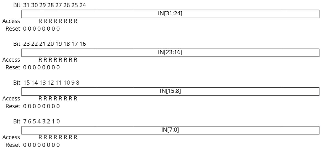
text_image
Bit 31 30 29 28 27 26 25 24 IN[31:24] Access R R R R R R R R Reset 0 0 0 0 0 0 0 0 Bit 23 22 21 20 19 18 17 16 IN[23:16] Access R R R R R R R R Reset 0 0 0 0 0 0 0 0 Bit 15 14 13 12 11 10 9 8 IN[15:8] Access R R R R R R R R Reset 0 0 0 0 0 0 0 0 Bit 7 6 5 4 3 2 1 0 IN[7:0] Access R R R R R R R R Reset 0 0 0 0 0 0 0 0Bits 31:0 - IN[31:0] PORT Data Input Value
These bits are cleared when the corresponding I/O pin input sampler detects a logical low level on the input pin.
These bits are set when the corresponding I/O pin input sampler detects a logical high level on the input pin.
21.9.10 Control
Name: CTRL
Offset: 0x24
Reset: 0x00000000
Property: PAC Write-Protection

Tip: The I/O pins are assembled in pin groups ("PORT groups") with up to 32 pins. Group 0 consists of the PA pins, group 1 is for the PB pins, etc. Each pin group has its own PORT registers, with a 0x80 address spacing. For example, the register address offset for the Data Direction (DIR) register for group 0 (PA00 to PA31) is 0x00, and the register address offset for the DIR register for group 1 (PB00 to PB31) is 0x80.
| Bit 31 30 29 28 27 26 25 24 | |
| SAMPLING[31:24] | |
| Access RW RW RW RW RW RW RW RW Reset 0 0 0 0 0 0 0 0 | |
| Bit 23 22 21 20 19 18 17 16 | |
| SAMPLING[23:16] | |
| Access RW RW RW RW RW RW RW RW Reset 0 0 0 0 0 0 0 0 | |
| Bit 15 14 13 12 11 10 9 8 | |
| SAMPLING[15:8] | |
| Access RW RW RW RW RW RW RW RW Reset 0 0 0 0 0 0 0 0 | |
| Bit 7 6 5 4 3 2 1 0 | |
| SAMPLING[7:0] | |
| Access RW RW RW RW RW RW RW RW Reset 0 0 0 0 0 0 0 0 | |
Bits 31:0 - SAMPLING[31:0] Input Sampling Mode
Configures the input sampling functionality of the I/O pin input samplers, for pins configured as inputs via the Data Direction register (DIR).
The input samplers are enabled and disabled in sub-groups of eight. Thus if any pins within a byte request continuous sampling, all pins in that eight pin sub-group will be continuously sampled.
| Value Description | |
| 0 | On demand sampling of I/O pin is enabled. |
| 1 | Continuous sampling of I/O pin is enabled. |
21.9.11 Write Configuration
Name: WRCONFIG
Offset: 0x28
Reset: 0x00000000
Property: PAC Write-Protection

Tip: The I/O pins are assembled in pin groups ("PORT groups") with up to 32 pins. Group 0 consists of the PA pins, group 1 is for the PB pins, etc. Each pin group has its own PORT registers, with a 0x80 address spacing. For example, the register address offset for the Data Direction (DIR) register for group 0 (PA00 to PA31) is 0x00, and the register address offset for the DIR register for group 1 (PB00 to PB31) is 0x80.
This write-only register is used to configure several pins simultaneously with the same configuration and/or peripheral multiplexing.
In order to avoid side effect of non-atomic access, 8-bit or 16-bit writes to this register will have no effect. Reading this register always returns zero.
Bit 31 30 29 28 27 26 25 24
| HWSEL WRPINCFG WRP | MUX PMUX[3]0 | ||||||
| Access | WWWWWWW | ||||||
| Reset | 0 | 0 | 0 | 0 | 0 | 0 | 0 |
Bit 23 22 21 20 19 18 17 16
| DRVSTR | PULLEN | INEN | PMUXEN | ||||
| Access | W | WWW | |||||
| Reset | 0 | 0 | 0 | 0 |
Bit 15 14 13 12 11 10 9 8
| PINMASK[15:8] | ||||||||
| Access Reset | WWWWWWWW | |||||||
| 0 | 0 | 0 | 0 | 0 | 0 | 0 | 0 | |
| Bit | 7 | 6 | 5 | 4 | 3 | 2 | 1 | 0 |
| PINMASK[7:0] | ||||||||
| Access Reset | WWWWWWWW | |||||||
| 0 | 0 | 0 | 0 | 0 | 0 | 0 | 0 | |
Bit 31 - HWSEL Half-Word Select
This bit selects the half-word field of a 32-PORT group to be reconfigured in the atomic write operation.
This bit will always read as zero.
| Value | Description |
| 0 | The lower 16 pins of the PORT group will be configured. |
| 1 | The upper 16 pins of the PORT group will be configured. |
Bit 30 - WRPINCFG Write PINCFG
This bit determines whether the atomic write operation will update the Pin Configuration register (PINCFGy) or not for all pins selected by the WRCONFIG.PINMASK and WRCONFIG.HWSEL bits. Writing '0' to this bit has no effect.
Writing '1' to this bit updates the configuration of the selected pins with the written WRCONFIG.DRVSTR, WRCONFIG.PULLEN, WRCONFIG.INEN, WRCONFIG.PMUXEN, and WRCONFIG.PINMASK values.
This bit will always read as zero.
| Value Description | |
| 0 | The PINCFGy registers of the selected pins will not be updated. |
| 1 | The PINCFGy registers of the selected pins will be updated. |
Bit 28 - WRPMUX Write PMUX
This bit determines whether the atomic write operation will update the Peripheral Multiplexing register (PMUXn) or not for all pins selected by the WRCONFIG.PINMASK and WRCONFIG.HWSEL bits. Writing '0' to this bit has no effect.
Writing '1' to this bit updates the pin multiplexer configuration of the selected pins with the written WRCONFIG. PMUX value.
This bit will always read as zero.
| Value Description | |
| 0 | The PMUXn registers of the selected pins will not be updated. |
| 1 | The PMUXn registers of the selected pins will be updated. |
Bits 27:24 - PMUX[3:0] Peripheral Multiplexing
These bits determine the new value written to the Peripheral Multiplexing register (PMUXn) for all pins selected by the WRCONFIG.PINMASK and WRCONFIG.HWSEL bits, when the WRCONFIG.WRPMUX bit is set.
These bits will always read as zero.
Bit 22 - DRVSTR Output Driver Strength Selection
This bit determines the new value written to PINCFGy.DRVSTR for all pins selected by the WRCONFIG.PINMASK and WRCONFIG.HWSEL bits, when the WRCONFIG.WRPINCFG bit is set. This bit will always read as zero.
Bit 18 - PULLEN Pull Enable
This bit determines the new value written to PINCFGy.PULLEN for all pins selected by the WRCONFIG.PINMASK and WRCONFIG.HWSEL bits, when the WRCONFIG.WRPINCFG bit is set. This bit will always read as zero.
Bit 17 - INEN Input Enable
This bit determines the new value written to PINCFGy.INEN for all pins selected by the WRCONFIG.PINMASK and WRCONFIG.HWSEL bits, when the WRCONFIG.WRPINCFG bit is set. This bit will always read as zero.
Bit 16 - PMUXEN Peripheral Multiplexer Enable
This bit determines the new value written to PINCFGy.PMUXEN for all pins selected by the WRCONFIG.PINMASK and WRCONFIG.HWSEL bits, when the WRCONFIG.WRPINCFG bit is set. This bit will always read as zero.
Bits 15:0 - PINMASK[15:0] Pin Mask for Multiple Pin Configuration
These bits select the pins to be configured within the half-word group selected by the WRCONFIG.HWSEL bit.
These bits will always read as zero.
| Value Description | |
| 0 | The configuration of the corresponding I/O pin in the half-word group will be left unchanged. |
| 1 | The configuration of the corresponding I/O pin in the half-word PORT group will be updated. |
21.9.12 Peripheral Multiplexing n
Name: PMUX
Offset: 0x30 + n*0x01 [n=0..15]
Property: PAC Write-Protection

Tip: The I/O pins are assembled in pin groups ("PORT groups") with up to 32 pins. Group 0 consists of the PA pins, group 1 is for the PB pins, etc. Each pin group has its own PORT registers, with a 0x80 address spacing. For example, the register address offset for the Data Direction (DIR) register for group 0 (PA00 to PA31) is 0x00, and the register address offset for the DIR register for group 1 (PB00 to PB31) is 0x80.
There are up to 16 Peripheral Multiplexing registers in each group, one for every set of two subsequent I/O lines. The 'n' denotes the number of the set of I/O lines.
Bit 76543210
| PMUXO[3:0] PMUXE[3:0] | ||
| Access | RW RW RW RW RW RW RW RW | |
| Reset | 0 0 0 0 0 0 0 | |
Bits 7:4 - PMUXO[3:0] Peripheral Multiplexing for Odd-Numbered Pin
These bits select the peripheral function for odd-numbered pins (2*n + 1) of a PORT group, if the corresponding PINCFGy.PMUXEN bit is '1'.
Not all possible values for this selection may be valid. For more details, refer to the I/O Multiplexing and Considerations.
| PMUXO[3:0] Name Description | ||
| 0x0 A Peripheral function A selected | ||
| 0x1 B Peripheral function B selected | ||
| 0x2 C Peripheral function C selected | ||
| 0x3 D | Peripheral function D selected | |
| 0x4 | E | Peripheral function E selected |
| 0x5 | F | Peripheral function F selected |
| 0x6 G | Peripheral function G selected | |
| 0x7 H | Peripheral function H selected | |
| 0x8 | I | Peripheral function I selected |
| 0x9 - 0xF | - | Reserved |
Bits 3:0 - PMUXE[3:0] Peripheral Multiplexing for Even-Numbered Pin
These bits select the peripheral function for even-numbered pins (2*n) of a PORT group, if the corresponding PINCFGy.PMUXEN bit is '1'.
Not all possible values for this selection may be valid. For more details, refer to the I/O Multiplexing and Considerations.
| PMUXE[3:0] Name Description | ||
| 0x0 | A | Peripheral function A selected |
| 0x1 | B Peripheral function B selected | |
| 0x2 | C | Peripheral function C selected |
| 0x3 | D Peripheral function D selected | |
| 0x4 | E | Peripheral function E selected |
| 0x5 | F | Peripheral function F selected |
| 0x6 | G Peripheral function G selected | |
| 0x7 | H | Peripheral function H selected |
| 0x8 I | Peripheral function I selected | |
......continued
PMUXE[3:0] Name Description
0x9 - 0xF - Reserved
Related Links
- I/O Multiplexing and Considerations
21.9.13 Pin Configuration
Name: PINCFG
Offset: 0x40 + n*0x01 [n=0..31]
Reset: 0x00
Property: PAC Write-Protection

Tip: The I/O pins are assembled in pin groups ("PORT groups") with up to 32 pins. Group 0 consists of the PA pins, group 1 is for the PB pins, etc. Each pin group has its own PORT registers, with a 0x80 address spacing. For example, the register address offset for the Data Direction (DIR) register for group 0 (PA00 to PA31) is 0x00, and the register address offset for the DIR register for group 1 (PB00 to PB31) is 0x80.
There are up to 32 Pin Configuration registers in each PORT group, one for each I/O line.
Bit 76543210
| DRVSTR | PULLEN | INEN PMUXEN | |||||
| Access Reset | RW RW RW RW 0 | 0 0 0 | |||||
Bit 6 - DRVSTR Output Driver Strength Selection
This bit controls the output driver strength of an I/O pin configured as an output.
| Value | Description |
| 0 | Pin drive strength is set to normal drive strength. |
| 1 | Pin drive strength is set to stronger drive strength. |
Bit 2 - PULLEN Pull Enable
This bit enables the internal pull-up or pull-down resistor of an I/O pin configured as an input.
| Value | Description |
| 0 | Internal pull resistor is disabled, and the input is in a high-impedance configuration. |
| 1 | Internal pull resistor is enabled, and the input is driven to a defined logic level in the absence of external input. |
Bit 1 - INEN Input Enable
This bit controls the input buffer of an I/O pin configured as either an input or output.
Writing a zero to this bit disables the input buffer completely, preventing read-back of the physical pin state when the pin is configured as either an input or output.
| Value | Description |
| 0 | Input buffer for the I/O pin is disabled, and the input value will not be sampled. |
| 1 | Input buffer for the I/O pin is enabled, and the input value will be sampled when required. |
Bit 0 - PMUXEN Peripheral Multiplexer Enable
This bit enables or disables the peripheral multiplexer selection set in the Peripheral Multiplexing register (PMUXn) to enable or disable alternative peripheral control over an I/O pin direction and output drive value.
Writing a zero to this bit allows the PORT to control the pad direction via the Data Direction register (DIR) and output drive value via the Data Output Value register (OUT). The peripheral multiplexer value in PMUXn is ignored. Writing '1' to this bit enables the peripheral selection in PMUXn to control the pad. In this configuration, the physical pin state may still be read from the Data Input Value register (IN) if PINCFGn.INEN is set.
| Value | Description |
| 0 | The peripheral multiplexer selection is disabled, and the PORT registers control the direction and output drive value. |
| 1 | The peripheral multiplexer selection is enabled, and the selected peripheral function controls the direction and output drive value. |
22. Event System (EVSYS)
22.1 Overview
The Event System (EVSYS) allows autonomous, low-latency and configurable communication between peripherals.
Several peripherals can be configured to generate and/or respond to signals known as events. The exact condition to generate an event, or the action taken upon receiving an event, is specific to each peripheral. Peripherals that respond to events are called event users. Peripherals that generate events are called event generators. A peripheral can have one or more event generators and can have one or more event users.
Communication is made without CPU intervention and without consuming system resources such as bus or RAM bandwidth. This reduces the load on the CPU and other system resources, compared to a traditional interrupt-based system.
22.2 Features
- 8 configurable event channels:
- Can be connected to any event generator
- Can provide a pure asynchronous, resynchronized, or synchronous path
• 59 Event Generators
• 14 Event Users
- Configurable Edge Detector
- Peripherals can be Event Generators, Event Users, or both
- SleepWalking and interrupt for operation in sleep modes
- Software Event Generation
• Each Event User can choose which channel to respond to
• Each Event User can choose which channel to respond to, and several Event Users can share the same channel and therefore answer to the same event
22.3 Block Diagram
Figure 22-1. Event System Block Diagram
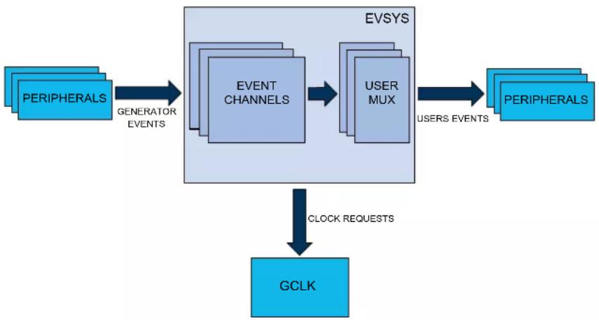
flowchart
graph TD
    A["PERIPHERALS"] -->|GENERATOR EVENTS| B["EVENT CHANNELS"]
    B --> C["USER MUX"]
    C -->|USERS EVENTS| D["PERIPHERALS"]
    D -->|CLOCK REQUESTS| E["GCLK"]
22.4 Signal Description
Not applicable.
22.5 Product Dependencies
In order to use this peripheral, other parts of the system must be configured correctly, as described below.
22.5.1 I/O Lines
Not applicable.
22.5.2 Power Management
The EVSYS can be used to wake up the CPU from all sleep modes, even if the clock used by the EVSYS channel and the EVSYS bus clock are disabled. Refer to the PM - Power Manager for details on the different sleep modes.
In all sleep modes, although the clock for the EVSYS is stopped, the device still can wake up the EVSYS clock. Some event generators can generate an event when their clocks are stopped.
Related Links
- Power Manager (PM)
22.5.3 Clocks
The EVSYS bus clock (CLK_EVSYS_APB) can be enabled and disabled in the Main Clock module, and the default state of CLK_EVSYS_APB can be found in Peripheral Clock Masking.
Each EVSYS channel has a dedicated generic clock (GCLK_EVSYS_CHANNEL_n). These are used for event detection and propagation for each channel. These clocks must be configured and enabled in the generic clock controller before using the EVSYS. Refer to GCLK - Generic Clock Controller for details.
Related Links
- GCLK - Generic Clock Controller
22.5.4 Interrupts
The interrupt request line is connected to the Interrupt Controller. Using the EVSYS interrupts requires the interrupt controller to be configured first. Refer to Nested Vector Interrupt Controller for details.
Related Links
10.2. Nested Vector Interrupt Controller
22.5.5 Events
Not applicable.
22.5.6 Debug Operation
When the CPU is halted in debug mode, this peripheral will continue normal operation. If the peripheral is configured to require periodical service by the CPU through interrupts or similar, improper operation or data loss may result during debugging. This peripheral can be forced to halt operation during debugging.
22.5.7 Register Access Protection
Registers with write-access can be optionally write-protected by the Peripheral Access Controller (PAC), except for the following:
- Interrupt Flag Status and Clear register (INTFLAG)
Note: Optional write-protection is indicated by the "PAC Write-Protection" property in the register description.
Write-protection does not apply for accesses through an external debugger.
Related Links
10.5. PAC - Peripheral Access Controller
22.5.8 Analog Connections
Not applicable.
22.6 Functional Description
22.6.1 Principle of Operation
The Event System consists of several channels which route the internal events from peripherals (generators) to other internal peripherals or IO pins (users). Each event generator can be selected as source for multiple channels, but a channel cannot be set to use multiple event generators at the same time.
22.6.2 Basic Operation
22.6.2.1 Initialization
Before enabling events routing within the system, the User Multiplexer (USER) and Channel (CHANNEL) register must be configured. The User Multiplexer (USER) must be configured first.
Configure the User Multiplexer (USER) register:
- The channel to be connected to a user is written to the Channel bit group (USER.CHANNEL)
- The user to connect the channel is written to the User bit group (USER.USER)
Configure the Channel (CHANNEL) register: - The channel to be configured is written to the Channel Selection bit group (CHANNEL.CHANNEL)
- The path to be used is written to the Path Selection bit group (CHANNEL.PATH)
- The type of edge detection to use on the channel is written to the Edge Selection bit group (CHANNEL.EDGSEL)
- The event generator to be used is written to the Event Generator bit group (CHANNEL.EVGEN)
22.6.2.2 Enabling, Disabling and Resetting
The EVSYS is always enabled.
The EVSYS is reset by writing a '1' to the Software Reset bit in the Control register (CTRL.SWRST). All registers in the EVSYS will be reset to their initial state and all ongoing events will be canceled. Refer to CTRL.SWRST register for details.
22.6.2.3 User Multiplexer Setup
The user multiplexer defines the channel to be connected to which event user. Each user multiplexer is dedicated to one event user. A user multiplexer receives all event channels output and must be configured to select one of these channels, as shown in the next figure. The channel is selected with the Channel bit group in the USER register (USER.CHANNEL). The user multiplexer must always be configured before the channel. A full list of selectable users can be found in the User Multiplexer register (USER) description. Refer to UserList for details.
To configure a user multiplexer, the USER register must be written in a single 16-bit write. It is possible to read out the configuration of a user by first selecting the user by writing to USER.USER using an 8-bit write and then performing a read of the 16-bit USER register.
Figure 22-2. User MUX
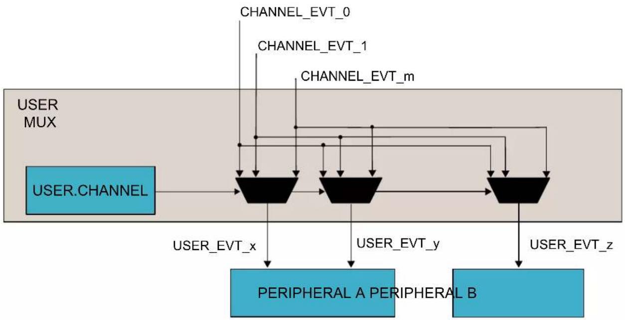
flowchart
graph TD
    A["USER MUX"] --> B["CHANNEL"]
    B --> C["PERIPHERAL A PERIPHERAL B"]
    C --> D["CHANNEL_EVT_x"]
    C --> E["CHANNEL_EVT_y"]
    C --> F["CHANNEL_EVT_z"]
    B --> G["CHANNEL_EVT_0"]
    B --> H["CHANNEL_EVT_1"]
    B --> I["CHANNEL_EVT_m"]
22.6.2.4 Channel Setup
An event channel can select one event from a list of event generators. Depending on configuration, the selected event could be synchronized, resynchronized or asynchronously sent to the users. When synchronization or resynchronization is required, the channel includes an internal edge detector, allowing the Event System to generate internal events when rising, falling or both edges are detected on the selected event generator. An event channel is able to generate internal events for the specific software commands. All these configurations are available in the Channel register (CHANNEL).
To configure a channel, the Channel register must be written in a single 32-bit write. It is possible to read out the configuration of a channel by first selecting the channel by writing to CHANNEL.CHANNEL using a, 8-bit write, and then performing a read of the CHANNEL register.
22.6.2.5 Channel Path
There are three different ways to propagate the event provided by an event generator:
- Asynchronous path
- Synchronous path
- Resynchronized path
Figure 22-3. Channel
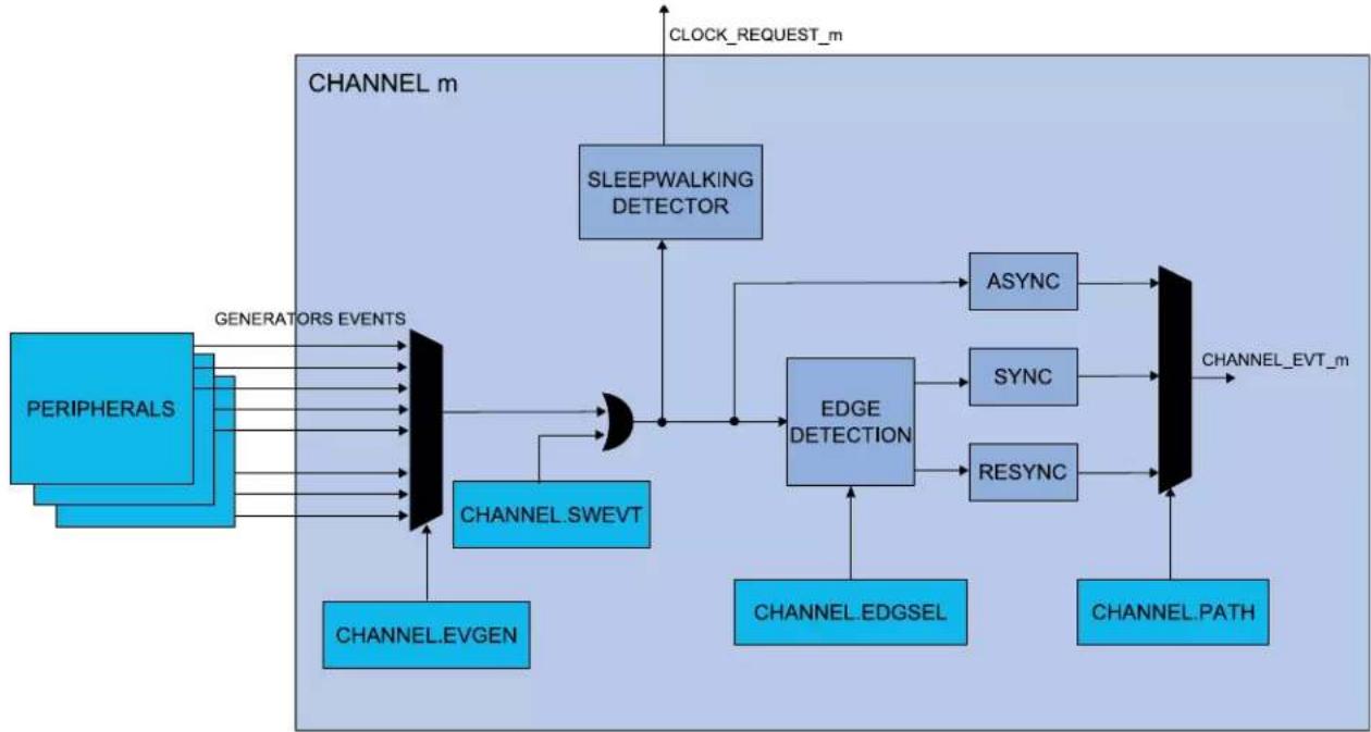
flowchart
graph TD
    A["PERIPHERALS"] -->|GENERATORS EVENTS| B["CHANNEL_m"]
    B --> C["SLEEPWALKING DETECTOR"]
    C --> D["CHANNEL.m"]
    D --> E["CHANNEL.SWEVT"]
    E --> F["CHANNEL.EVGEN"]
    F --> G["CHANNEL.EVT_m"]
    G --> H["CHANNEL.PATH"]
    H --> I["CHANNEL.EDGSEL"]
    I --> J["EDGE DETECTION"]
    J --> K["ASYNC"]
    J --> L["SYNC"]
    J --> M["RESYNC"]
    K --> N["CHANNEL.m"]
    L --> O["CHANNEL.m"]
    M --> P["CHANNEL.m"]
The path is selected by writing to the Path Selection bit group in the Channel register (CHANNEL.PATH).
22.6.2.5.1 Asynchronous Path
When using the asynchronous path, the events are propagated from the event generator to the event user without intervention from the Event System. The GCLK for this channel (GCLK_EVSYS_CHANNEL_n) is not mandatory, meaning that an event will be propagated to the user without any clock latency.
When the asynchronous path is selected, the channel cannot generate any interrupts, and the Channel Status register (CHSTATUS) is always zero. No edge detection is available; this must be handled in the event user. When the event generator and the event user share the same generic clock, using the asynchronous path will propagate the event with the least amount of latency.
22.6.2.5.2 Synchronous Path
The synchronous path should be used when the event generator and the event channel share the same generator for the generic clock and also if event user supports synchronous path. If event user doesn't support synchronous path, asynchronous path has to be selected. If they do not share the same clock, a logic change from the event generator to the event channel might not be detected in the channel, which means that the event will not be propagated to the event user. For details on generic clock generators, refer to GCLK - Generic Clock Controller.
When using the synchronous path, the channel is able to generate interrupts. The channel status bits in the Channel Status register (CHSTATUS) are also updated and available for use.
If the Generic Clocks Request bit in the Control register (CTRL.GCLKREQ) is zero, the channel operates in SleepWalking mode and request the configured generic clock only when an event is to be propagated through the channel. If CTRL.GCLKREQ is one, the generic clock will always be on for the configured channel.
Related Links
- GCLK - Generic Clock Controller
22.6.2.5.3 Resynchronized Path
The resynchronized path should be used when the event generator and the event channel do not share the same generic clock generator. When the resynchronized path is used, resynchronization of the event from the event generator is done in the channel. For details on generic clock generators, refer to GCLK - Generic Clock Controller.
When the resynchronized path is used, the channel is able to generate interrupts. The channel status bits in the Channel Status register (CHSTATUS) are also updated and available for use.
If the Generic Clocks Request bit in the Control register is zero (CTRL.GCLKREQ=0), the channel operates in SleepWalking mode and requests the configured generic clock only when an event is to be propagated through the channel. If CTRL.GCLKREQ=1, the generic clock will always be on for the configured channel.
Related Links
14. GCLK - Generic Clock Controller
When synchronous or resynchronized paths are used, edge detection must be used. The event system can perform edge detection in three different ways:
- Generate an event only on the rising edge
- Generate an event only on the falling edge
- Generate an event on rising and falling edges
Edge detection is selected by writing to the Edge Selection bit group in the Channel register (CHANNEL.EDGSEL).
If the generator event is a pulse, both edges cannot be selected. Use the rising edge or falling edge detection methods, depending on the generator event default level.
22.6.2.7 Event Generators
Each event channel can receive the events form all event generators. All event generators are listed in the statement of CHANNEL.EVGEN. For details on event generation, refer to the corresponding module chapter. The channel event generator is selected by the Event Generator bit group in the Channel register (CHANNEL.EVGEN). By default, the channels are not connected to any event generators (ie, CHANNEL.EVGEN = 0)
22.6.2.8 Channel Status
The Channel Status register (CHSTATUS) shows the status of the channels when using a synchronous or resynchronized path. There are two different status bits in CHSTATUS for each of the available channels:
- The CHSTATUS.CHBUSYn bit will be set when an event on the corresponding channel n has not been handled by all event users connected to that channel.
- The CHSTATUS.USRRDYn bit will be set when all event users connected to the corresponding channel are ready to handle incoming events on that channel.
22.6.2.9 Software Event
A software event can be initiated on a channel by setting the Software Event bit in the Channel register (CHANNEL.SWEVT) to '1' at the same time as writing the Channel bits (CHANNEL.CHANNEL). This will generate a software event on the selected channel.
The software event can be used for application debugging, and functions like any event generator. To use the software event, the event path must be configured to either a synchronous path or resynchronized path (CHANNEL.PATH = 0x0 or 0x1), edge detection must be configured to rising-edge detection (CHANNEL.EDGSEL=0x1) and the Generic Clock Request bit must be set to '1' (CTRL.GCLKREQ=0x1).
22.6.3 Interrupts
The EVSYS has the following interrupt sources:
- Overrun Channel n (OVRn): for details, refer to The Overrun Channel n Interrupt section.
- Event Detected Channel n (EVDn): for details, refer to The Event Detected Channel n Interrupt section.
These interrupts events are asynchronous wake-up sources. See Sleep Mode Controller.
Each interrupt source has an interrupt flag which is in the Interrupt Flag Status and Clear (INTFLAG) register. The flag is set when the interrupt is issued. Each interrupt event can be individually enabled by setting a '1' to the corresponding bit in the Interrupt Enable Set (INTENSET) register, and disabled by setting a '1' to the corresponding bit in the Interrupt Enable Clear (INTENCLR) register.
An interrupt event is generated when the interrupt flag is set and the corresponding interrupt is enabled. The interrupt event works until the interrupt flag is cleared, the interrupt is disabled, or the Event System is reset. See INTFLAG for details on how to clear interrupt flags.
All interrupt events from the peripheral are ORed together on system level to generate one combined interrupt request to the NVIC. Refer to the Nested Vector Interrupt Controller for details. The event user must read the INTFLAG register to determine what the interrupt condition is.
Note that interrupts must be globally enabled for interrupt requests to be generated. Refer to Nested Vector Interrupt Controller for details.
Related Links
10.2. Nested Vector Interrupt Controller
15.6.1.3. Sleep Mode Controller
22.6.3.1 The Overrun Channel n Interrupt
The Overrun Channel n interrupt flag in the Interrupt Flag Status and Clear register (CHINTFLAGn.OVR) will be set, and the optional interrupt will be generated in the following cases:
- One or more event users on channel n is not ready when there is a new event.
- An event occurs when the previous event on channel m has not been handled by all event users connected to that channel.
The flag will only be set when using resynchronized paths. In the case of asynchronous path, the CHINTFLAGn.OVR is always read as zero.
Related Links
10.2. Nested Vector Interrupt Controller
22.6.3.2 The Event Detected Channel n Interrupt
The Event Detected Channel n interrupt flag in the Interrupt Flag Status and Clear register (CHINTFLAGn.EVD) is set when an event coming from the event generator configured on channel n is detected.
The flag will only be set when using a resynchronized path. In the case of asynchronous path, the CHINTFLAGn.EVD is always zero.
Related Links
10.2. Nested Vector Interrupt Controller
22.6.4 Sleep Mode Operation
The EVSYS can generate interrupts to wake up the device from any sleep mode.
Some event generators can generate an event when the system clock is stopped. The generic clock (GCLK_EVSYS_CHANNELx) for this channel will be restarted if the channel uses a synchronized path or a resynchronized path, without waking the system from sleep. The clock remains active only as
long as necessary to handle the event. After the event has been handled, the clock will be turned off and the system will remain in the original sleep mode. This is known as SleepWalking. When an asynchronous path is used, there is no need for the clock to be activated for the event to be propagated to the user.
On a software reset, all registers are set to their reset values and any ongoing events are canceled.
22.7 Register Summary
| Offset | Name Bit Pos. 76543210 | ||||||||||
| 0x00 CTRL 7:0 GCLKREQ | SWRST | ||||||||||
| 0x01 ... 0x03 | Reserved | ||||||||||
| 0x04 CHANNEL | 7:0 CHANNEL[7:0] | ||||||||||
| 15:8 | SWEVT | ||||||||||
| 23:16 | EVGEN[7:0] | ||||||||||
| 31:24 | EDGSEL[1:0] | PATH[1:0] | |||||||||
| 0x08 | USER | 7:0 | USER[7:0] | ||||||||
| 15:8 | CHANNEL[7:0] | ||||||||||
| 0x0A ... 0x0B | Reserved | ||||||||||
| 0x0C | CHSTATUS | 7:0 | USRRDYn | USRRDYn | USRRDYn | USRRDYn | USRRDYn | USRRDYn | USRRDYn | USRRDYn | USRRDYn |
| 15:8 | CHBUSYn | CHBUSYn | CHBUSYn | CHBUSYn | CHBUSYn | CHBUSYn | CHBUSYn | CHBUSYn | CHBUSYn | ||
| 23:16 | |||||||||||
| 31:24 | |||||||||||
| 0x10 | INTENCLR | 7:0 | OVRn | OVRn | OVRn | OVRn | OVRn | OVRn | OVRn | OVRn | OVRn |
| 15:8 | EVDn | EVDn | EVDn | EVDn | EVDn | EVDn | EVDn | EVDn | EVDn | ||
| 23:16 | |||||||||||
| 31:24 | |||||||||||
| 0x14 INTENSET | 7:0 | OVRn | OVRn | OVRn | OVRn | OVRn | OVRn | OVRn | OVRn | OVRn | |
| 15:8 | EVDn | EVDn | EVDn | EVDn | EVDn | EVDn | EVDn | EVDn | EVDn | ||
| 23:16 | |||||||||||
| 31:24 | |||||||||||
| 0x18 | INTFLAG | 7:0 | OVRn | OVRn | OVRn | OVRn | OVRn | OVRn | OVRn | OVRn | OVRn |
| 15:8 | EVDn | EVDn | EVDn | EVDn | EVDn | EVDn | EVDn | EVDn | EVDn | ||
| 23:16 | |||||||||||
| 31:24 | |||||||||||
22.8 Register Description
Registers can be 8, 16, or 32 bits wide. Atomic 8-, 16-, and 32-bit accesses are supported. In addition, the 8-bit quarters and 16-bit halves of a 32-bit register, and the 8-bit halves of a 16-bit register can be accessed directly.
Some registers are enable-protected, meaning they can only be written when the module is disabled. Enable-protection is denoted by the "Enable-Protected" property in each individual register description.
Refer to 22.5.7. Register Access Protection.
22.8.1 Control
Name: CTRL
Offset: 0x00
Reset: 0x00
Property: Write-Protected
Bit 76543210
| GCLKREQ | SWRST | ||||||
| Access Reset 0 0 | R/W W | ||||||
Bit 4 - GCLKREQ Generic Clock Requests
This bit is used to determine whether the generic clocks used for the different channels should be on all the time or only when an event needs the generic clock. Events propagated through asynchronous paths will not need a generic clock.
| Value | Description |
| 0 | Generic clock is requested and turned on only if an event is detected. |
| 1 | Generic clock for a channel is always on. |
Bit 0 - SWRST Software Reset
Writing a zero to this bit has no effect.
Writing a one to this bit resets all registers in the EVSYS to their initial state.
Writing a one to CTRL.SWRST will always take precedence, meaning that all other writes in the same write-operation will be discarded.
Note: Before applying a Software Reset it is recommended to disable the event generators.
22.8.2 Channel
Name: CHANNEL
Offset: 0x04
Reset: 0x00000000
Property: Write-Protected
Bit 31 30 29 28 27 26 25 24
| EDGSEL[1:0] PATH[1:0] | ||||
| Access Reset 0 0 0 0 | R/W R/W R/W R/W | |||
Bit 23 22 21 20 19 18 17 16
| EVGEN[7:0] | |
| Access | R/W R/W R/W R/W R/W R/W R/W R/W |
| Reset | 0 0 0 0 0 0 0 |
Bit 15 14 13 12 11 10 98
| SW#VT | ||||||
| Access | R/W | |||||
| Reset | 0 |
Bit 76543210
| CHANNEL[7:0] | |
| Access | R/W R/W R/W R/W R/W R/W R/W R/W |
| Reset | 0 0 0 0 0 0 0 |
Bits 27:26 - EDGSEL[1:0] Edge Detection Selection
These bits set the type of edge detection to be used on the channel.
These bits must be written to zero when using the asynchronous path.
| EDGSEL[1:0] | Name | Description |
| 0x0 | NO_EVT_OUTPUT | No event output when using the resynchronized or synchronous path |
| 0x1 | RISING_EDGE | Event detection only on the rising edge of the signal from the event generator when using the resynchronized or synchronous path |
| 0x2 | FALLING_EDGE | Event detection only on the falling edge of the signal from the event generator when using the resynchronized or synchronous path |
| 0x3 | BOTH_EDGES | Event detection on rising and falling edges of the signal from the event generator when using the resynchronized or synchronous path |
Bits 25:24 - PATH[1:0] Path Selection
These bits are used to choose the path to be used by the selected channel.
The path choice can be limited by the channel source.
| PATH[1:0] | Name | Description |
| 0x0 | SYNCHRONOUS | Synchronous path |
| 0x1 | RESYNCHRONIZED | Resynchronized path |
| 0x2 | ASYNCHRONOUS | Asynchronous path |
| 0x3 | - | Reserved |
Bits 23:16 - EVGEN[7:0] Event Generator Selection
These bits are used to choose which event generator to connect to the selected channel.
| Value | Event Generator | Description |
| 0x00 | NONE | No event generator selected |
......continued
| Value Event Generator Description | |
| 0x01 RTC CMP0 Compare 0 (mode 0 and 1) or Alarm 0 (mode 2) | |
| 0x02 RTC CMP1 Compare 1 | |
| 0x03 RTC OVF Overflow | |
| 0x04 RTC PER0 Period 0 | |
| 0x05 RTC PER1 Period 1 | |
| 0x06 RTC PER2 Period 2 | |
| 0x07 RTC PER3 Period 3 | |
| 0x08 RTC PER4 Period 4 | |
| 0x09 RTC PER5 Period 5 | |
| 0x0A RTC PER6 Period 6 | |
| 0x0B RTC PER7 Period 7 | |
| 0x0C EIC EXTINT0 External Interrupt 0 | |
| 0x0D EIC EXTINT1 External Interrupt 1 | |
| 0x0E EIC EXTINT2 External Interrupt 2 | |
| 0x0F EIC EXTINT3 External Interrupt 3 | |
| 0x10 EIC EXTINT4 External Interrupt 4 | |
| 0x11 EIC EXTINT5 External Interrupt 5 | |
| 0x12 EIC EXTINT6 External Interrupt 6 | |
| 0x13 EIC EXTINT7 External Interrupt 7 | |
| 0x14 EIC EXTINT8 External Interrupt 8 | |
| 0x15 EIC EXTINT9 External Interrupt 9 | |
| 0x16 EIC EXTINT10 External Interrupt 10 | |
| 0x17 EIC EXTINT11 External Interrupt 11 | |
| 0x18 EIC EXTINT12 External Interrupt 12 | |
| 0x19 EIC EXTINT13 External Interrupt 13 | |
| 0x1A EIC EXTINT14 External Interrupt 14 | |
| 0x1B EIC EXTINT15 External Interrupt 15 | |
| 0x1C TC0 OVF Overflow/Underflow | |
| 0x1D TC0 MC0 Match/Capture 0 | |
| 0x1E TC0 MC1 Match/Capture 1 | |
| 0x1F TC1 OVF Overflow/Underflow | |
| 0x20 TC1 MC0 Match/Capture 0 | |
| 0x21 TC1 MC1 Match/Capture 1 | |
| 0x22 TC2 OVF Overflow/Underflow | |
| 0x23 TC2 MC0 Match/Capture 0 | |
| 0x24 TC2 MC1 Match/Capture 1 | |
| 0x25 TC3 OVF Overflow/Underflow | |
| 0x26 TC3 MC0 Match/Capture 0 | |
| 0x27 TC3 MC1 Match/Capture 1 | |
| 0x28 TC4 OVF Overflow/Underflow | |
| 0x29 TC4 MC0 Match/Capture 0 | |
| 0x2A TC4 MC1 Match/Capture 1 | |
| 0x2B TC5 OVF Overflow/Underflow | |
| 0x2C TC5 MC0 Match/Capture 0 | |
| 0x2D TC5 MC1 Match/Capture 1 | |
| 0x2E TC6 OVF Overflow/Underflow | |
| 0x2F TC6 MC0 Match/Capture 0 | |
| 0x30 TC6 MC1 Match/Capture 1 | |
| 0x31 TC7 OVF Overflow/Underflow | |
| 0x32 TC7 MC0 Match/Capture 0 | |
| 0x33 TC7 MC1 Match/Capture 1 | |
| 0x34 ADC RESRDY Result Ready | |
| 0x35 ADC WINMON Window Monitor | |
| 0x36 AC COMP0 Comparator 0 | |
| 0x37 AC COMP1 Comparator 1 | |
| 0x38 AC WIN0 Window 0 | |
| 0x39 DAC EMPTY Data Buffer Empty | |
| 0x3A PTC EOC End of Conversion | |
| 0x3B PTC WCOMP Window Comparator | |
| 0x3C-0x7F Reserved - | |
Bit 8 - SWEVT Software Event
This bit is used to insert a software event on the channel selected by the CHANNEL.CHANNEL bit group.
This bit has the same behavior similar to an event.
This bit must be written together with CHANNEL.CHANNEL using a 16-bit write.
Writing a zero to this bit has no effect.
Writing a one to this bit will trigger a software event for the corresponding channel.
This bit will always return zero when read.
Bits 7:0 - CHANNEL[7:0] Channel Selection
These bits are used to select the channel to be set up or read from.
| Value Channel number | |
| 0x00 0 | |
| 0x01 1 | |
| 0x02 2 | |
| 0x03 3 | |
| 0x04 4 | |
| 0x05 5 | |
| 0x06 6 | |
| 0x07 7 | |
| 0x08-0xFF Reserved |
22.8.3 User Multiplexer
Name: USER
Offset: 0x08
Reset: 0x0000
Property: Write-Protected
Bit 15 14 13 12 11 10 9 8
CHANNEL[7:0]
Access R/W R/W R/W R/W R/W R/W R/W R/W
Reset 00000000
Bit 76543210
USER[7:0]
Access R/W R/W R/W R/W R/W R/W R/W R/W
Reset 00000000
Bits 15:8 - CHANNEL[7:0] Channel Event Selection
These bits are used to select the channel to connect to the event user.
Note that to select channel n, the value (n+1) must be written to the USER.CHANNEL bit group.
| CHANNEL[7:0] Channel Number | |
| 0x0 No Channel Output Selected | |
| 0x1-0x08 | Channel n-1 selected |
| 0x09-0xFF | Reserved |
Bits 7:0 - USER[7:0] User Multiplexer Selection
These bits select the event user to be configured with a channel, or the event user to read the channel value from.
Table 22-1. User Multiplexer Selection
| USER[7:0] | User Multiplexer | Description | Path Type |
| 0x00 | TC0 | Asynchronous, synchronous and resynchronized paths | |
| 0x01 | TC1 | Asynchronous, synchronous and resynchronized paths | |
| 0x02 | TC2 | Asynchronous, synchronous and resynchronized paths | |
| 0x03 | TC3 | Asynchronous, synchronous and resynchronized paths | |
| 0x04 | TC4 | Asynchronous, synchronous and resynchronized paths | |
| 0x05 | TC5 | Asynchronous, synchronous and resynchronized paths | |
| 0x06 | TC6 | Asynchronous, synchronous and resynchronized paths | |
| 0x07 | TC7 | Asynchronous, synchronous and resynchronized paths | |
| 0x08 | ADC START | ADC start conversion Asynchronous path only | |
| 0x09 | ADC SYNC | Flush ADC | Asynchronous path only |
| 0x0A | AC COMP0 | Start comparator 0 | Asynchronous path only |
| 0x0B | AC COMP1 | Start comparator 1 | Asynchronous path only |
| 0x0C | DAC START | DAC start conversion Asynchronous path only | |
| 0x0D | PTC STCONV | PTC start conversion | Asynchronous path only |
| 0x0E-0xFF | Reserved | - | Reserved |
22.8.4 Channel Status
Name: CHSTATUS
Offset: 0x0C
Reset: 0x000F00FF
Property: -
| Bit 31 30 29 28 27 26 25 24 | |||||||
| Access Reset | |||||||
| Bit 23 22 21 20 19 18 17 16 | |||||||
| Access Reset | |||||||
| Bit 15 14 13 12 11 10 9 8 | |||||||
| CHBUSYn CHBUSYn CHBUSYn CHBUSYn CHBUSYn CHBUSYn CHBUSYn | |||||||
| Access Reset | R R R R R R R | ||||||
| 0 0 0 0 0 0 0 0 | |||||||
| Bit | 7 6 5 4 3 2 1 0 | ||||||
| USRRDYn | USRRDYn | USRRDYn | USRRDYn | USRRDYn | USRRDYn | USRRDYn | USRRDYn |
| Access Reset | R R R R R R R | ||||||
| 0 0 0 0 0 0 0 0 | |||||||
Bits 15,14,13,12,11,10,9,8 - CHBUSYn Channel n Busy [n=7..0]
This bit is cleared when channel n is idle
This bit is set if an event on channel n has not been handled by all event users connected to channel n.
Bits 7,6,5,4,3,2,1,0 - USRRDYn Channel n User Ready [n=7..0]
This bit is cleared when at least one of the event users connected to the channel is not ready.
This bit is set when all event users connected to channel n are ready to handle incoming events on channel n.
22.8.5 Interrupt Enable Clear
Name: INTENCLR
Offset: 0x10
Reset: 0x00000000
Property: Write-Protected
| Bit 31 30 29 28 27 26 25 24 | |||||||
| Access Reset | |||||||
| Bit 23 22 21 20 19 18 17 16 | |||||||
| Access Reset | |||||||
| Bit 15 14 13 12 11 10 9 8 | |||||||
| EVDn EVDn EVDn EVDn EVDn EVDn | |||||||
| Access Reset | R/W | R/W | R/W | R/W | R/W | R/W | R/W |
| 0 0 0 0 0 0 0 0 | |||||||
| Bit | 7 6 5 4 3 2 1 0 | ||||||
| Access Reset | OVRn | OVRn | OVRn | OVRn | OVRn | OVRn | OVRn |
| R/W | R/W | R/W | R/W | R/W | R/W | R/W | |
| 0 0 0 0 0 0 0 0 | |||||||
Bits 15,14,13,12,11,10,9,8 - EVDn Channel n Event Detection Interrupt Enable [n=7..0]
Writing a zero to this bit has no effect.
Writing a one to this bit will clear the Event Detected Channel n Interrupt Enable bit, which disables the Event Detected Channel n interrupt.
| Value | Description |
| 0 | The Event Detected Channel n interrupt is disabled. |
| 1 | The Event Detected Channel n interrupt is enabled. |
Bits 7,6,5,4,3,2,1,0 - OVRn Channel n Overrun Interrupt Enable [n=7..0]
Writing a zero to this bit has no effect.
Writing a one to this bit will clear the Overrun Channel n Interrupt Enable bit, which disables the Overrun Channel n interrupt.
| Value | Description |
| 0 | The Overrun Channel n interrupt is disabled. |
| 1 | The Overrun Channel n interrupt is enabled. |
22.8.6 Interrupt Enable Set
Name: INTENSET
Offset: 0x14
Reset: 0x00000000
Property: Write-Protected
| Bit 31 30 29 28 27 26 25 24 | |||||||
| Access Reset | |||||||
| Bit 23 22 21 20 19 18 17 16 | |||||||
| Access Reset | |||||||
| Bit 15 14 13 12 11 10 9 8 | |||||||
| EVDn EVDn EVDn EVDn EVDn EVDn | |||||||
| Access Reset | R/W | R/W | R/W | R/W | R/W | R/W | R/W |
| 0 0 0 0 0 0 0 0 | |||||||
| Bit | 7 6 5 4 3 2 1 0 | ||||||
| OVRn | OVRn | OVRn | OVRn | OVRn | OVRn | OVRn | |
| Access Reset | R/W | R/W | R/W | R/W | R/W | R/W | R/W |
| 0 0 0 0 0 0 0 0 | |||||||
Bits 15,14,13,12,11,10,9,8 - EVDn Channel n Event Detection Interrupt Enable [n=7..0]
Writing a zero to this bit has no effect.
Writing a one to this bit will set the Event Detected Channel n Interrupt Enable bit, which enables the Event Detected Channel n interrupt.
| Value | Description |
| 0 | The Event Detected Channel n interrupt is disabled. |
| 1 | The Event Detected Channel n interrupt is enabled. |
Bits 7,6,5,4,3,2,1,0 - OVRn Channel n Overrun Interrupt Enable [n=7..0]
Writing a zero to this bit has no effect.
Writing a one to this bit will set the Overrun Channel n Interrupt Enable bit, which enables the Overrun Channel n interrupt.
| Value | Description |
| 0 | The Overrun Channel n interrupt is disabled. |
| 1 | The Overrun Channel n interrupt is enabled. |
22.8.7 Interrupt Flag Status and Clear
Name: INTFLAG
Offset: 0x18
Reset: 0x00000000
Property: -
| Bit 31 30 29 28 27 26 25 24 | |||||||
| Access Reset | |||||||
| Bit 23 22 21 20 19 18 17 16 | |||||||
| Access Reset | |||||||
| Bit 15 14 13 12 11 10 9 8 | |||||||
| EVDn EVDn EVDn EVDn EVDn EVDn | |||||||
| Access Reset | R/W | R/W | R/W | R/W | R/W | R/W | R/W |
| 0 0 0 0 0 0 0 0 | |||||||
| Bit | 7 6 5 4 3 2 1 0 | ||||||
| Access Reset | OVRn | OVRn | OVRn | OVRn | OVRn | OVRn | OVRn |
| R/W | R/W | R/W | R/W | R/W | R/W | R/W | |
| 0 0 0 0 0 0 0 0 | |||||||
Bits 15,14,13,12,11,10,9,8 - EVDn Channel n Event Detection [n=7..0]
This flag is set on the next CLK_EVSYS_APB cycle when an event is being propagated through the channel, and an interrupt request will be generated if INTENCLR/SET.EVDn is one.
When the event channel path is asynchronous, the EVDn interrupt flag will not be set.
Writing a zero to this bit has no effect.
Writing a one to this bit will clear the Event Detected Channel n interrupt flag.
Bits 7,6,5,4,3,2,1,0 - OVRn Channel n Overrun [n=7..0]
This flag is set on the next CLK_EVSYS cycle after an overrun channel condition occurs, and an interrupt request will be generated if INTENCLR/SET.OVRn is one.
When the event channel path is asynchronous, the OVRn interrupt flag will not be set.
Writing a zero to this bit has no effect.
Writing a one to this bit will clear the Overrun Channel n interrupt flag.
23. SERCOM – Serial Communication Interface
23.1 Overview
There are up to six instances of the serial communication interface (SERCOM) peripheral.
A SERCOM can be configured to support a number of modes: I2C, SPI, and USART. When an instance of SERCOM is configured and enabled, all of the resources of that SERCOM instance will be dedicated to the selected mode.
The SERCOM serial engine consists of a transmitter and receiver, baud-rate generator and address matching functionality. It can use the internal generic clock or an external clock. Using an external clock allows the SERCOM to be operated in all Sleep modes.
Related Links
- SERCOM USART
- SERCOM SPI - SERCOM Serial Peripheral Interface
- SERCOM I2C - Inter-Integrated Circuit
23.2 Features
- Interface for configuring into one of the following:
- ^12 C - Two-wire serial interface SMBus™ compatible
- SPI - Serial peripheral interface
-
USART - Universal synchronous and asynchronous serial receiver and transmitter
-
Single transmit buffer and double receive buffer
- Baud-rate generator
- Address match/mask logic
- Operational in all sleep modes
See the Related Links for full feature lists of the interface configurations.
23.3 Block Diagram
Figure 23-1. SERCOM Block Diagram
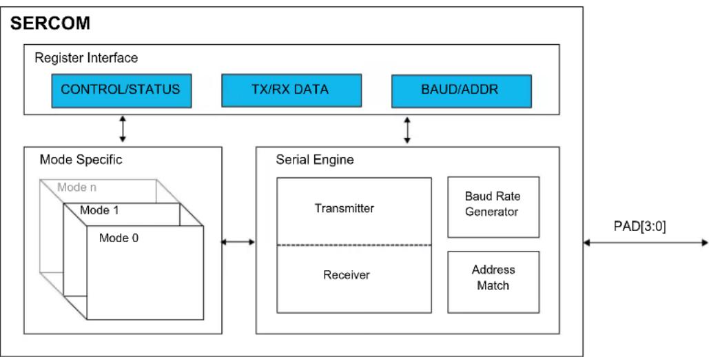
flowchart
graph TD
    A["Register Interface"] --> B["CONTROL/STATUS"]
    A --> C["TX/RX DATA"]
    A --> D["BAUD/ADDR"]
    B <--> E["Mode Specific"]
    C <--> E
    D <--> E
    E --> F["Serial Engine"]
    F --> G["Transmitter"]
    F --> H["Receiver"]
    F --> I["Baud Rate Generator"]
    F --> J["Address Match"]
    G <--> K["Pad[3:0"]]
    H <--> K
    I <--> K
    J <--> K
23.4 Signal Description
See the respective SERCOM mode chapters for details.
Related Links
- SERCOM USART
- SERCOM SPI - SERCOM Serial Peripheral Interface
- SERCOM I2C - Inter-Integrated Circuit
23.5 Product Dependencies
In order to use this peripheral, other parts of the system must be configured correctly, as described below.
23.5.1 I/O Lines
Using the SERCOM I/O lines requires the I/O pins to be configured using port configuration (PORT).
The SERCOM has four internal pads, PAD[3:0], and the signals from I2C, SPI and USART are routed through these SERCOM pads via a multiplexer. The configuration of the multiplexer is available from the different SERCOM modes. Refer to the mode specific chapters for details.
Related Links
- SERCOM USART
- SERCOM SPI - SERCOM Serial Peripheral Interface
- SERCOM I2C - Inter-Integrated Circuit
- PORT - I/O Pin Controller
24.3. Block Diagram
23.5.2 Power Management
The SERCOM can operate in any Sleep mode provided the selected clock source is running. SERCOM interrupts can be configured to wake the device from Sleep modes.
Related Links
- Power Manager (PM)
23.5.3 Clocks
The SERCOM bus clock (CLK_SERCOMx_APB) can be enabled and disabled in the Power Manager. Refer to Peripheral Clock Masking for details and default status of this clock.
The SERCOM uses two generic clocks: GCLK_SERCOMx_CORE and GCLK_SERCOMx_SLOW. The core clock (GCLK_SERCOMx_CORE) is required to clock the SERCOM while working as a host. The slow clock (GCLK_SERCOMx_SLOW) is only required for certain functions. See specific mode chapters for details.
These clocks must be configured and enabled in the Generic Clock Controller (GCLK) before using the SERCOM.
The generic clocks are asynchronous to the user interface clock (CLK_SERCOMx_APB). Due to this asynchronicity, writing to certain registers will require synchronization between the clock domains. Refer to 23.6.7. Synchronization for details.
Related Links
- GCLK - Generic Clock Controller
23.5.4 Interrupts
The interrupt request line is connected to the Interrupt Controller (NVIC). The NVIC must be configured before the SERCOM interrupts are used.
Related Links
10.2. Nested Vector Interrupt Controller
23.5.5 Events
Not applicable.
23.5.6 Debug Operation
When the CPU is halted in debug mode, this peripheral will continue normal operation. If the peripheral is configured to require periodical service by the CPU through interrupts or similar, improper operation or data loss may result during debugging. This peripheral can be forced to halt operation during debugging - refer to the Debug Control (DBGCTRL) register for details.
23.5.7 Register Access Protection
All registers with write-access can be write-protected optionally by the Peripheral Access Controller (PAC), except for the following registers:
- Interrupt Flag Clear and Status register (INTFLAG)
- Status register (STATUS)
• Data register (DATA) - Address register (ADDR)
Optional write-protection by the Peripheral Access Controller (PAC) is denoted by the "PAC Write-Protection" property in each individual register description.
PAC write-protection does not apply to accesses through an external debugger.
Related Links
10.5. PAC - Peripheral Access Controller
23.5.8 Analog Connections
Not applicable.
23.6 Functional Description
23.6.1 Principle of Operation
The basic structure of the SERCOM serial engine is shown in Figure 23-2. Labels in capital letters are synchronous to the system clock and accessible by the CPU; labels in lowercase letters can be configured to run on the GCLK_SERCOMx_CORE clock or an external clock.
Figure 23-2. SERCOM Serial Engine
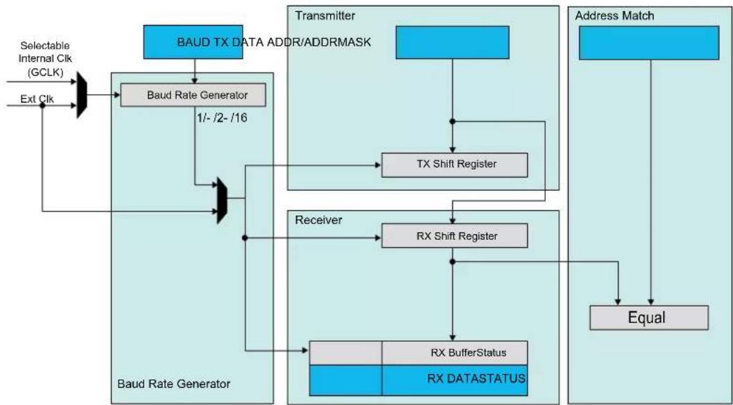
flowchart
graph TD
    A["Selectable Internal Clk (GCLK)"] --> B["Baud Rate Generator"]
    C["Ext Clk"] --> B
    B --> D["BAUD TX DATA ADDR/ADDRMASK"]
    D --> E["TX Shift Register"]
    E --> F["RX Shift Register"]
    F --> G["RX BufferStatus"]
    G --> H["RX DATASTATUS"]
    I["Address Match"] --> J["Equal"]
    J --> G
    K["Receiver"] --> F
    L["Baud Rate Generator"] --> M["Baud Rate Generator"]
    M --> N["BAUD TX DATA ADDR/ADDRMASK"]
    N --> O["TX Shift Register"]
    O --> P["RX Shift Register"]
    P --> Q["RX BufferStatus"]
    Q --> R["RX DATASTATUS"]
The transmitter consists of a single write buffer and a shift register.
The receiver consists of a one-level ( I^2C ), two-level (USART, SPI) receive buffer and a shift register.
The baud-rate generator is capable of running on the GCLK_SERCOMx_CORE clock or an external clock.
Address matching logic is included for SPI and I ^2 C operation.
23.6.2 Basic Operation
23.6.2.1 Initialization
The SERCOM must be configured to the desired mode by writing the Operating Mode bits in the Control A register (CTRLA.MODE) as shown in the table below.
Table 23-1. SERCOM Modes
| CTRLA.MODE Description | |
| 0x0 USART with external clock | |
| 0x1 USART with internal clock | |
| 0x2 SPI in client operation | |
| 0x3 SPI in host operation | |
| 0x4 I | ^2C client operation |
| 0x5 I | ^2C host operation |
| 0x6-0x7 Reserved |
For further initialization information, see the respective SERCOM mode chapters:
Related Links
- SERCOM USART
- SERCOM SPI - SERCOM Serial Peripheral Interface
- SERCOM I2C - Inter-Integrated Circuit
23.6.2.2 Enabling, Disabling, and Resetting
This peripheral is enabled by writing '1' to the Enable bit in the Control A register (CTRLA.ENABLE), and disabled by writing '0' to it.
Writing '1' to the Software Reset bit in the Control A register (CTRLA.SWRST) will reset all registers of this peripheral to their initial states, except the DBGCTRL register, and the peripheral is disabled.
Refer to the CTRLA register description for details.
23.6.2.3 Clock Generation - Baud-Rate Generator
The baud-rate generator, as shown in Figure 23-3, generates internal clocks for asynchronous and synchronous communication. The output frequency ( f_BAUD ) is determined by the Baud register (BAUD) setting and the baud reference frequency ( f_ref ). The baud reference clock is the serial engine clock, and it can be internal or external.
For asynchronous communication, the /16 (divide-by-16) output is used when transmitting, whereas the /1 (divide-by-1) output is used while receiving.
For synchronous communication, the /2 (divide-by-2) output is used.
This functionality is automatically configured, depending on the selected operating mode.
Figure 23-3. Baud Rate Generator
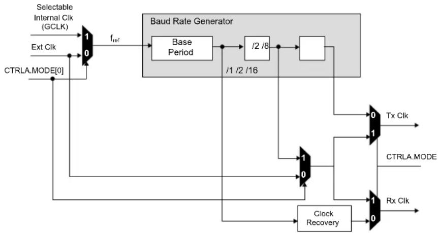
flowchart
graph TD
    A["Selectable Internal Cik (GCLK)"] --> B["1"]
    C["Ext Cik"] --> D["0"]
    D --> E["f_ref"]
    E --> F["Base Period"]
    F --> G["/2 /8"]
    G --> H["/1 /2 /16"]
    H --> I["Square Block"]
    I --> J["Tx Cik"]
    J --> K["1"]
    K --> L["Tx Cik"]
    M["CTRLA.MODE[0"]] --> N["Clock Recovery"]
    N --> O["1"]
    O --> P["Tx Cik"]
    Q["Rx Cik"] --> R["1"]
    R --> S["Tx Cik"]
    T["Baud Rate Generator"] --> U["/1 /2 /16"]
    U --> V["/2 /8"]
    V --> W["/1 /2 /16"]
    W --> X["Tx Cik"]
    Y["CTRLA.MODE"] --> Z["1"]
    Z --> AA["Tx Cik"]
Table 23-2 contains equations for the baud rate (in bits per second) and the BAUD register value for each operating mode.
For asynchronous operation, the BAUD register value is 16 bits (0 to 65,535).
For synchronous operation, the BAUD register value is 8 bits (0 to 255).
Table 23-2. Baud Rate Equations
| Operating Mode Condition Baud Rate (Bits Per Second) BAUD Register Value Calculation | |||
| Asynchronous Arithmetic | f_BAUD ≤ _ref16 | f_BAUD = _ref16(1 - 65536) | BAUD=65536·1-(16·_BAUDf_ref) |
| Synchronous | f_BAUD ≤ _ref2 | f_BAUD = _ref2· B(AUD+1) | BAUD= _ref2· f_BAUD-1 |
The baud rate error is represented by the following formula:
$$ \text { Error } = 1 - \left(\frac {\text { ExpectedBaudRate }}{\text { ActualBaudRate }}\right) $$
Asynchronous Arithmetic Mode BAUD Value Selection
The formula given for f_BAUD calculates the average frequency over 65536 f_ref cycles. Although the BAUD register can be set to any value between 0 and 65536, the actual average frequency of f_BAUD over a single frame is more granular. The BAUD register values that will affect the average frequency over a single frame lead to an integer increase in the cycles per frame (CPF)
where
$$ C P F = \frac {f _ {r e f}}{f _ {B A U D}} (D + S) $$
- D represent the data bits per frame
- S represent the sum of start and first stop bits, if present.
Table below shows the BAUD register value versus baud frequency f_BAUD at a serial engine frequency of 48 MHz. This assumes a D value of 8 bits and an S value of 2 bits (10 bits, including start and stop bits).
Table 23-3. BAUD Register Value vs. Baud Frequency
| BAUD Register Value Serial Engine CPF f | _BAUD at 48MHz Serial Engine Frequency ( f_REF ) |
| 0 – 406 160 3MHz | |
| 407 – 808 161 2.981MHz | |
| 809 – 1205 162 2.963MHz | |
| ... ... ... | |
| 65206 31775 15.11kHz | |
| 65207 31871 15.06kHz | |
| 65208 31969 15.01kHz |
23.6.3 Additional Features
23.6.3.1 Address Match and Mask
The SERCOM address match and mask feature is capable of matching either one address, two unique addresses, or a range of addresses with a mask, based on the mode selected. The match uses seven or eight bits, depending on the mode.
Address With Mask
An address written to the Address bits in the Address register (ADDR.ADDR), and a mask written to the Address Mask bits in the Address register (ADDR.ADDRMASK) will yield an address match. All bits that are masked are not included in the match. Note that writing the ADDR.ADDRMASK to 'all zeros' will match a single unique address, while writing ADDR.ADDRMASK to 'all ones' will result in all addresses being accepted.
Figure 23-4. Address With Mask
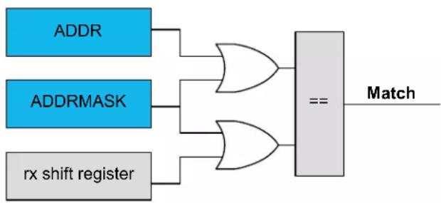
flowchart
graph LR
    A["ADDR"] --> C["AND"]
    B["ADDRMASK"] --> C
    D["rx shift register"] --> E["AND"]
    C --> F["=="]
    E --> F
    F --> G["Match"]
Two Unique Addresses
The two addresses written to ADDR and ADDRMASK will cause a match.
Figure 23-5. Two Unique Addresses
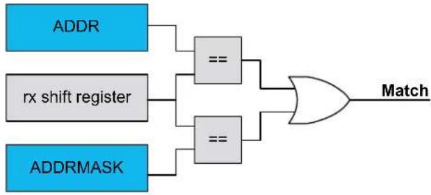
flowchart
graph LR
    A["ADDR"] --> B["=="]
    C["rx shift register"] --> D["=="]
    E["ADDRMASK"] --> F["=="]
    B --> G["OR"]
    D --> G
    F --> G
    G --> H["Match"]
Address Range
The range of addresses between and including ADDR.ADDR and ADDR.ADDRMASK will cause a match. ADDR.ADDR and ADDR.ADDRMASK can be set to any two addresses, with ADDR.ADDR acting as the upper limit and ADDR.ADDRMASK acting as the lower limit.
Figure 23-6. Address Range

flowchart
graph LR
    A["ADDRMASK rx shift register ADDR"] --> B["== Match"]
23.6.4 Interrupts
Interrupt sources are mode-specific. See the respective SERCOM mode chapters for details.
Each interrupt source has its own interrupt flag.
The interrupt flag in the Interrupt Flag Status and Clear register (INTFLAG) will be set when the interrupt condition is met.
Each interrupt can be individually enabled by writing '1' to the corresponding bit in the Interrupt Enable Set register (INTENSET), and disabled by writing '1' to the corresponding bit in the Interrupt Enable Clear register (INTENCLR).
An interrupt request is generated when the interrupt flag is set and the corresponding interrupt is enabled. The interrupt request remains active until either the interrupt flag is cleared, the interrupt is disabled, or the SERCOM is reset. For details on clearing interrupt flags, refer to the INTFLAG register description.
The value of INTFLAG indicates which interrupt condition occurred. The user must read the INTFLAG register to determine which interrupt condition is present.
Note: Interrupts must be globally enabled for interrupt requests.
Related Links
10.2. Nested Vector Interrupt Controller
23.6.5 Events
Not applicable.
23.6.6 Sleep Mode Operation
The peripheral can operate in any sleep mode where the selected serial clock is running. This clock can be external or generated by the internal baud-rate generator.
The SERCOM interrupts can be used to wake up the device from sleep modes. Refer to the different SERCOM mode chapters for details.
23.6.7 Synchronization
Due to asynchronicity between the main clock domain and the peripheral clock domains, some registers need to be synchronized when written or read.
Required write-synchronization is denoted by the "Write-Synchronized" property in the register description.
Required read-synchronization is denoted by the "Read-Synchronized" property in the register description.
Related Links
13.3. Register Synchronization
24. SERCOM USART
24.1 Overview
The Universal Synchronous and Asynchronous Receiver and Transmitter (USART) is one of the available modes in the Serial Communication Interface (SERCOM).
The USART uses the SERCOM transmitter and receiver, see 24.3. Block Diagram. Labels in uppercase letters are synchronous to CLK_SERCOMx_APB and accessible for CPU. Labels in lowercase letters can be programmed to run on the internal generic clock or an external clock.
The transmitter consists of a single write buffer, a Shift register, and control logic for different frame formats. The write buffer support data transmission without any delay between frames. The receiver consists of a two-level receive buffer and a Shift register. Status information of the received data is available for error checking. Data and clock recovery units ensure robust synchronization and noise filtering during asynchronous data reception.
Related Links
23. SERCOM - Serial Communication Interface
24.2 USART Features
• Full-duplex operation
- Asynchronous (with clock reconstruction) or synchronous operation
- Internal or external clock source for asynchronous and synchronous operation
- Baud-rate generator
• Supports serial frames with 5, 6, 7, 8 or 9 data bits and 1 or 2 stop bits
- Odd or even parity generation and parity check
- Selectable LSB- or MSB-first data transfer
- Buffer overflow and frame error detection
- Noise filtering, including false start-bit detection and digital low-pass filter
- Can operate in all sleep modes
- Operation at speeds up to half the system clock for internally generated clocks
- Operation at speeds up to the system clock for externally generated clocks
- Start-of-frame detection
24.3 Block Diagram
Figure 24-1. USART Block Diagram
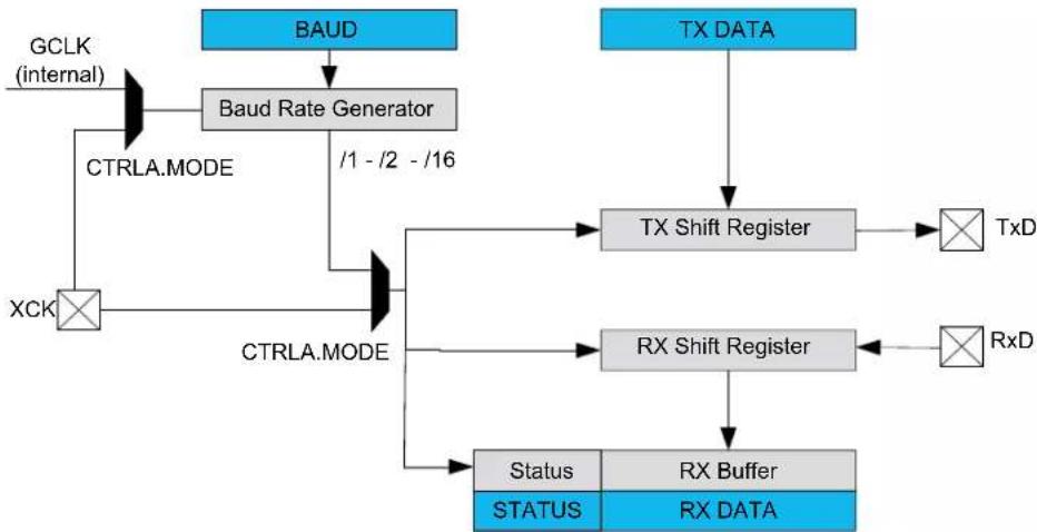
flowchart
graph TD
    A["BAUD"] --> B["Baud Rate Generator"]
    B --> C["XCK"]
    C --> D["CTRLA.MODE"]
    D --> E["CTRLA.MODE"]
    E --> F["Status"]
    E --> G["STATUS"]
    H["TX DATA"] --> I["TX Shift Register"]
    I --> J["TxD"]
    I --> K["RxD"]
    I --> L["RxD"]
    M["BAUD"] --> N["CTRLA.MODE"]
    N --> O["/1 - /2 - /16"]
    O --> P["CTRLA.MODE"]
    P --> Q["Status"]
    P --> R["STATUS"]
    S["TA"] --> T["TxD"]
    U["TRD"] --> V["RxD"]
24.4 Signal Description
Table 24-1. SERCOM USART Signals
| Signal Name Type Description | ||
| PAD[3:0] Digital I/O General SERCOM pins |
One signal can be mapped to one of several pins.
Related Links
- I/O Multiplexing and Considerations
24.5 Product Dependencies
In order to use this peripheral, other parts of the system must be configured correctly, as described below.
24.5.1 I/O Lines
Using the USART's I/O lines requires the I/O pins to be configured using the I/O Pin Controller (PORT).
When the SERCOM is used in USART mode, the SERCOM controls the direction and value of the I/O pins according to the table below. If the receiver or transmitter is disabled, these pins can be used for other purposes.
Table 24-2. USART Pin Configuration
| Pin Pin Configuration | |
| TxD Output | |
| RxD Input | |
| XCK Output or input |
The combined configuration of PORT and the Transmit Data Pinout and Receive Data Pinout bit fields in the Control A register (CTRLA.TXPO and CTRLA.RXPO, respectively) will define the physical position of the USART signals in Table 24-2.
Related Links
- PORT - I/O Pin Controller
24.5.2 Power Management
This peripheral can continue to operate in any sleep mode where its source clock is running. The interrupts can wake up the device from sleep modes.
Related Links
- Power Manager (PM)
24.5.3 Clocks
The SERCOM bus clock (CLK_SERCOMx_APB) can be enabled and disabled in the Power Manager. Refer to Peripheral Clock Masking for details and default status of this clock.
A generic clock (GCLK_SERCOMx_CORE) is required to clock the SERCOMx_CORE. This clock must be configured and enabled in the Generic Clock Controller before using the SERCOMx_CORE. Refer to GCLK - Generic Clock Controller for details.
This generic clock is asynchronous to the bus clock (CLK_SERCOMx_APB). Therefore, writing to certain registers will require synchronization to the clock domains. Refer to Synchronization for further details.
Related Links
- GCLK - Generic Clock Controller
23.6.7. Synchronization
15.6.2.6. Peripheral Clock Masking
24.5.4 Interrupts
The interrupt request line is connected to the Interrupt Controller. In order to use interrupt requests of this peripheral, the Interrupt Controller (NVIC) must be configured first. Refer to Nested Vector Interrupt Controller for details.
Related Links
10.2. Nested Vector Interrupt Controller
24.5.5 Events
Not applicable.
24.5.6 Debug Operation
When the CPU is halted in debug mode, this peripheral will continue normal operation. If the peripheral is configured to require periodical service by the CPU through interrupts or similar, improper operation or data loss may result during debugging. This peripheral can be forced to halt operation during debugging - refer to the Debug Control (DBGCTRL) register for details.
Related Links
24.8.3. DBGCTRL
24.5.7 Register Access Protection
Registers with write-access can be write-protected optionally by the peripheral access controller (PAC).
PAC Write-Protection is not available for the following registers:
- Interrupt Flag Clear and Status register (INTFLAG)
- Status register (STATUS)
• Data register (DATA)
Optional PAC Write-Protection is denoted by the "PAC Write-Protection" property in each individual register description.
Write-protection does not apply to accesses through an external debugger.
Related Links
10.5. PAC - Peripheral Access Controller
24.5.8 Analog Connections
Not applicable.
24.6 Functional Description
24.6.1 Principle of Operation
The USART uses the following lines for data transfer:
- RxD for receiving
- TxD for transmitting
- XCK for the transmission clock in synchronous operation
USART data transfer is frame based. A serial frame consists of:
- 1 start bit
• From 5 to 9 data bits (MSB or LSB first)
• No, even or odd parity bit
- 1 or 2 stop bits
A frame starts with the start bit followed by one character of data bits. If enabled, the parity bit is inserted after the data bits and before the first stop bit. After the stop bit(s) of a frame, either the next frame can follow immediately, or the communication line can return to the idle (high) state. The figure below illustrates the possible frame formats. Brackets denote optional bits.
Figure 24-2. Frame Formats
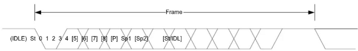
text_image
(IDLE) St 0 1 2 3 4 [5] [6] [7] [8] [P] Sp1 [Sp2] [St/IDL]St Start bit. Signal is always low.
n, [n] Data bits. 0 to [5..9]
[P] Parity bit. Either odd or even.
Sp, [Sp] Stop bit. Signal is always high.
IDLE No frame is transferred on the communication line. Signal is always high in this state.
24.6.2 Basic Operation
24.6.2.1 Initialization
The following registers are enable-protected, meaning they can only be written when the USART is disabled (CTRL.ENABLE=0):
- Control A register (CTRLA), except the Enable (ENABLE) and Software Reset (SWRST) bits.
- Control B register (CTRLB), except the Receiver Enable (RXEN) and Transmitter Enable (TXEN) bits.
• Baud register (BAUD)
When the USART is enabled or is being enabled (CTRLA.ENABLE=1), any writing attempt to these registers will be discarded. If the peripheral is being disabled, writing to these registers will be
executed after disabling is completed. Enable-protection is denoted by the "Enable-Protection" property in the register description.
Before the USART is enabled, it must be configured by these steps:
- Select either external (0x0) or internal clock (0x1) by writing the Operating Mode value in the CTRLA register (CTRLA.MODE).
- Select either asynchronous (0) or or synchronous (1) communication mode by writing the Communication Mode bit in the CTRLA register (CTRLA.CMODE).
- Select pin for receive data by writing the Receive Data Pinout value in the CTRLA register (CTRLA.RXPO).
- Select pads for the transmitter and external clock by writing the Transmit Data Pinout bit in the CTRLA register (CTRLA.TXPO).
- Configure the Character Size field in the CTRLB register (CTRLB.CHSIZE) for character size.
- Set the Data Order bit in the CTRLA register (CTRLA.DORD) to determine MSB- or LSB-first data transmission.
- To use parity mode:
a. Enable parity mode by writing 0x1 to the Frame Format field in the CTRLA register (CTRLA.FORM).
b. Configure the Parity Mode bit in the CTRLB register (CTRLB.PMODE) for even or odd parity.
-
Configure the number of stop bits in the Stop Bit Mode bit in the CTRLB register (CTRLB.SBMODE).
-
When using an internal clock, write the Baud register (BAUD) to generate the desired baud rate.
-
Enable the transmitter and receiver by writing '1' to the Receiver Enable and Transmitter Enable bits in the CTRLB register (CTRLB.RXEN and CTRLB.TXEN).
24.6.2.2 Enabling, Disabling, and Resetting
This peripheral is enabled by writing '1' to the Enable bit in the Control A register (CTRLA.ENABLE), and disabled by writing '0' to it.
Writing '1' to the Software Reset bit in the Control A register (CTRLA.SWRST) will reset all registers of this peripheral to their initial states, except the DBGCTRL register, and the peripheral is disabled.
Refer to the CTRLA register description for details.
24.6.2.3 Clock Generation and Selection
For both synchronous and asynchronous modes, the clock used for shifting and sampling data can be generated internally by the SERCOM baud-rate generator or supplied externally through the XCK line.
The synchronous mode is selected by writing a '1' to the Communication Mode bit in the Control A register (CTRLA.CMODE), the asynchronous mode is selected by writing a zero to CTRLA.CMODE.
The internal clock source is selected by writing 0x1 to the Operation Mode bit field in the Control A register (CTRLA.MODE), the external clock source is selected by writing 0x0 to CTRLA.MODE.
The SERCOM baud-rate generator is configured as in the figure below.
In asynchronous mode (CTRLA.CMODE=0), the 16-bit Baud register value is used.
In synchronous mode (CTRLA.CMODE=1), the eight LSBs of the Baud register are used. Refer to Clock Generation – Baud-Rate Generator for details on configuring the baud rate.
Figure 24-3. Clock Generation
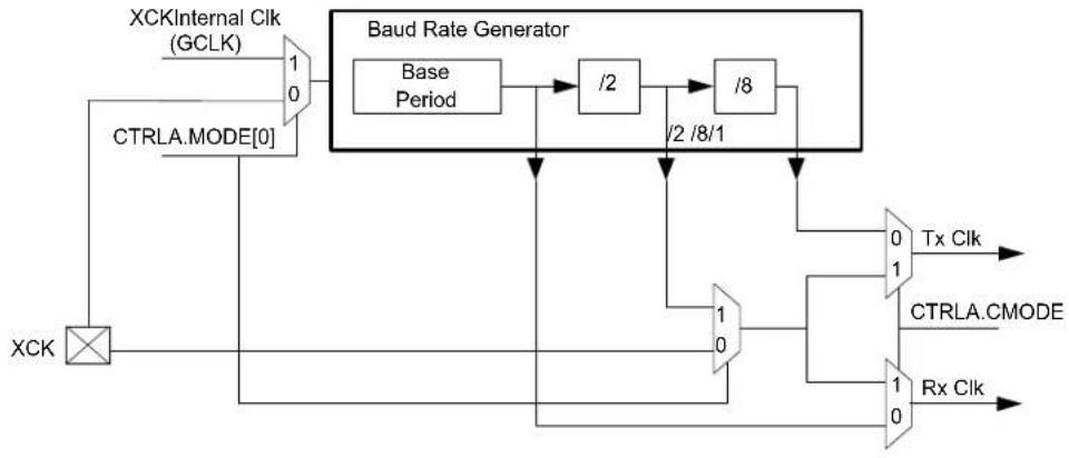
flowchart
graph TD
    A["XCK"] --> B["CTRLA.MODE[0"]]
    B --> C["1/0"]
    C --> D["Baud Rate Generator"]
    D --> E["Base Period"]
    E --> F["/2"]
    F --> G["/8"]
    G --> H["/2 /8/1"]
    H --> I["1"]
    I --> J["Tx Clk"]
    I --> K["CTRLA.CMODE"]
    I --> L["Rx Clk"]
    M["XCKInternal Clk (GCLK)"] --> C
Related Links
23.6.2.3. Clock Generation - Baud-Rate Generator
24.6.2.3.1 Synchronous Clock Operation
In synchronous mode, the CTRLA.MODE bit field determines whether the transmission clock line (XCK) serves either as input or output. The dependency between clock edges, data sampling, and data change is the same for internal and external clocks. Data input on the RxD pin is sampled at the opposite XCK clock edge when data is driven on the TxD pin.
The Clock Polarity bit in the Control A register (CTRLA.CPOL) selects which XCK clock edge is used for RxD sampling, and which is used for TxD change:
When CTRLA.CPOL is '0', the data will be changed on the rising edge of XCK, and sampled on the falling edge of XCK.
When CTRLA.CPOL is '1', the data will be changed on the falling edge of XCK, and sampled on the rising edge of XCK.
Figure 24-4. Synchronous Mode XCK Timing
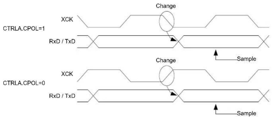
text_image
CTRLA.CPOL=1 XCK RxD / TxD Change Sample CTRLA.CPOL=0 XCK RxD / TxD Change SampleWhen the clock is provided through XCK (CTRLA.MODE=0x0), the shift registers operate directly on the XCK clock. This means that XCK is not synchronized with the system clock and, therefore, can operate at frequencies up to the system frequency.
24.6.2.4 Data Register
The USART Transmit Data register (TxDATA) and USART Receive Data register (RxDATA) share the same I/O address, referred to as the Data register (DATA). Writing the DATA register will update the TxDATA register. Reading the DATA register will return the contents of the RxDATA register.
24.6.2.5 Data Transmission
Data transmission is initiated by writing the data to be sent into the DATA register. Then, the data in TxDATA will be moved to the Shift register when the Shift register is empty and ready to send a new frame. After the Shift register is loaded with data, the data frame will be transmitted.
When the entire data frame including Stop bit(s) has been transmitted and no new data was written to DATA, the Transmit Complete Interrupt flag in the Interrupt Flag Status and Clear register (INTFLAG.TXC) will be set, and the optional interrupt will be generated.
The Data Register Empty flag in the Interrupt Flag Status and Clear register (INTFLAG.DRE) indicates that the register is empty and ready for new data. The DATA register should only be written to when INTFLAG.DRE is set.
Disabling the Transmitter
The transmitter is disabled by writing '0' to the Transmitter Enable bit in the CTRLB register (CTRLB.TXEN).
Disabling the transmitter will complete only after any ongoing and pending transmissions are completed, i.e., there is no data in the transmit shift register and TxDATA to transmit.
24.6.2.6 Data Reception
The receiver accepts data when a valid Start bit is detected. Each bit following the Start bit will be sampled according to the baud rate or XCK clock, and shifted into the receive Shift register until the first Stop bit of a frame is received. The second Stop bit will be ignored by the receiver.
When the first Stop bit is received and a complete serial frame is present in the Receive Shift register, the contents of the Shift register will be moved into the two-level receive buffer. Then, the Receive Complete Interrupt flag in the Interrupt Flag Status and Clear register (INTFLAG.RXC) will be set, and the optional interrupt will be generated.
The received data can be read from the DATA register when the Receive Complete Interrupt flag is set.
Disabling the Receiver
Writing '0' to the Receiver Enable bit in the CTRLB register (CTRLB.RXEN) will disable the receiver, flush the two-level receive buffer, and data from ongoing receptions will be lost.
Error Bits
The USART receiver has three error bits in the Status (STATUS) register: Frame Error (FERR), Buffer Overflow (BUFOVF), and Parity Error (PERR). Once an error happens, the corresponding error bit will be set until it is cleared by writing '1' to it. These bits are also cleared automatically when the receiver is disabled.
There are two methods for buffer overflow notification, selected by the Immediate Buffer Overflow Notification bit in the Control A register (CTRLA.IBON):
When CTRLA.IBON=1, STATUS.BUFOVF is raised immediately upon buffer overflow. Software can then empty the receive FIFO by reading RxDATA, until the receiver complete interrupt flag (INTFLAG.RXC) is cleared.
When CTRLA.IBON=0, the buffer overflow condition is attending data through the receive FIFO. After the received data is read, STATUS.BUFOVF will be set along with INTFLAG.RXC.
Asynchronous Data Reception
The USART includes a clock recovery and data recovery unit for handling asynchronous data reception.
The clock recovery logic can synchronize the incoming asynchronous serial frames at the RxD pin to the internally generated baud-rate clock.
The data recovery logic samples and applies a low-pass filter to each incoming bit, thereby improving the noise immunity of the receiver.
Asynchronous Operational Range
The operational range of the asynchronous reception depends on the accuracy of the internal baud-rate clock, the rate of the incoming frames, and the frame size (in number of bits). In addition, the operational range of the receiver is depending on the difference between the received bit rate and the internally generated baud rate. If the baud rate of an external transmitter is too high or too low compared to the internally generated baud rate, the receiver will not be able to synchronize the frames to the start bit.
There are two possible sources for a mismatch in baud rate: First, the reference clock will always have some minor instability. Second, the baud-rate generator cannot always do an exact division of the reference clock frequency to get the baud rate desired. In this case, the BAUD register value should be set to give the lowest possible error. Refer to Clock Generation - Baud-Rate Generator for details.
Recommended maximum receiver baud-rate errors for various character sizes are shown in the table below.
Table 24-3. Asynchronous Receiver Error for 16-fold Oversampling
| D(Data bits+Parity) | R_SLOW [%] R | FAST [%] Max. total error [%] Recommended max. Rx error [%] | |
| 5 91.42 107.69 +5.88/-7.69 ±2.5 | |||
| 6 94.92 106.67 +5.08/-6.67 ±2.0 | |||
| 7 95.52 105.88 +4.48/-5.88 ±2.0 | |||
| 8 96.00 105.26 +4.00/-5.26 ±2.0 | |||
| 9 96.39 104.76 +3.61/-4.76 ±1.5 | |||
| 10 96.70 104.35 +3.30/-4.35 ±1.5 | |||
The following equations calculate the ratio of the incoming data rate and internal receiver baud rate:
$$ R _ {\mathrm{SLOW}} = \frac {1 6 (p + 1)}{1 6 (p + 1 + 6)}, R \quad \text {FAST} = \frac {1 6 (p + 2)}{1 6 (p + 1 + 8)} $$
- R_SLOW is the ratio of the slowest incoming data rate that can be accepted in relation to the receiver baud rate
- R_FAST is the ratio of the fastest incoming data rate that can be accepted in relation to the receiver baud rate
- D is the sum of character size and parity size ( D = 5 to 10 bits)
The recommended maximum Rx Error assumes that the receiver and transmitter equally divide the maximum total error. Its connection to the SERCOM Receiver error acceptance is depicted in this figure:
Figure 24-5. USART Rx Error Calculation
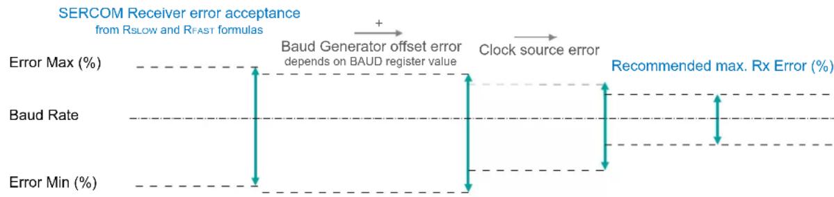
line
| Metric | Value | | ------------------ | ----- | | Error Max (%) | - | | Baud Rate | - | | Error Min (%) | - |The recommendation values in the table above accommodate errors of the clock source and the baud generator. The following figure gives an example for a baud rate of 3Mbps:
Figure 24-6. USART Rx Error Calculation Example
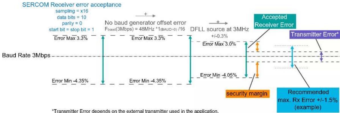
line
| Metric | Value | | --- | --- | | Error Max | 3.3% | | Error Min | -4.35% | | No baud generator offset error F_baud(3Mbps) | 48MHz *1(BAUD=0)/16 | | DFLL source at 3MHz | +/-0.3% | | Error Max | 3.0% | | Error Min | -4.05% | | Accepted Receiver Error | | | Transmitter Error* | | | Recommended max. Rx Error +/-1.5% (example) | |^a Transmitter Error depends on the external transmitter used in the application. It is advised that it is within the Recommended max. Rx Error (+/-1.5% in this example). Larger Transmitter Errors are acceptable but must lie within the Accepted Receiver Error.
Related Links
23.6.2.3. Clock Generation - Baud-Rate Generator
24.6.3 Additional Features
24.6.3.1 Parity
Even or odd parity can be selected for error checking by writing 0x1 to the Frame Format bit field in the Control A register (CTRLA.FORM).
If even parity is selected (CTRLB.PMODE=0), the parity bit of an outgoing frame is '1' if the data contains an odd number of bits that are '1', making the total number of '1' even.
If odd parity is selected (CTRLB.PMODE=1), the parity bit of an outgoing frame is '1' if the data contains an even number of bits that are '0', making the total number of '1' odd.
When parity checking is enabled, the parity checker calculates the parity of the data bits in incoming frames and compares the result with the parity bit of the corresponding frame. If a parity error is detected, the Parity Error bit in the Status register (STATUS.PERR) is set.
24.6.3.2 Loop-Back Mode
For loop-back mode, configure the Receive Data Pinout (CTRLA.RXPO) and Transmit Data Pinout (CTRLA.TXPO) to use the same data pins for transmit and receive. The loop-back is through the pad, so the signal is also available externally.
24.6.3.3 Start-of-Frame Detection
The USART start-of-frame detector can wake up the CPU when it detects a start bit. In standby sleep mode, the internal fast startup oscillator must be selected as the GCLK_SERCOMx_CORE source.
When a 1-to-0 transition is detected on RxD, the 8MHz Internal Oscillator is powered up and the USART clock is enabled. After startup, the rest of the data frame can be received, provided that the baud rate is slow enough in relation to the fast startup internal oscillator start-up time. Refer to Electrical Characteristics for details. The start-up time of this oscillator varies with supply voltage and temperature.
The USART start-of-frame detection works both in asynchronous and synchronous modes. It is enabled by writing '1' to the Start of Frame Detection Enable bit in the Control B register (CTRLB.SFDE).
If the Receive Start Interrupt Enable bit in the Interrupt Enable Set register (INTENSET.RXS) is set, the Receive Start interrupt is generated immediately when a start is detected.
When using start-of-frame detection without the Receive Start interrupt, start detection will force the 8MHz Internal Oscillator and USART clock active while the frame is being received. In this case, the CPU will not wake up until the Receive Complete interrupt is generated.
Related Links
32. Electrical Characteristics at 85°C
24.6.4 Interrupts
The USART has the following interrupt sources. These are asynchronous interrupts, and can wake up the device from any sleep mode:
• Data Register Empty (DRE)
- Receive Complete (RXC)
• Transmit Complete (TXC)
- Receive Start (RXS)
Each interrupt source has its own interrupt flag. The interrupt flag in the Interrupt Flag Status and Clear register (INTFLAG) will be set when the interrupt condition is met. Each interrupt can be individually enabled by writing '1' to the corresponding bit in the Interrupt Enable Set register (INTENSET), and disabled by writing '1' to the corresponding bit in the Interrupt Enable Clear register (INTENCLR).
An interrupt request is generated when the interrupt flag is set and if the corresponding interrupt is enabled. The interrupt request remains active until either the interrupt flag is cleared, the interrupt is disabled, or the USART is reset. For details on clearing interrupt flags, refer to the INTFLAG register description.
The USART has one common interrupt request line for all the interrupt sources. The value of INTFLAG indicates which interrupt is executed. Note that interrupts must be globally enabled for interrupt requests. Refer to Nested Vector Interrupt Controller for details.
Related Links
10.2. Nested Vector Interrupt Controller
24.6.5 Sleep Mode Operation
The behavior in sleep mode is depending on the clock source and the Run In Standby bit in the Control A register (CTRLA.RUNSTDBY):
- Internal clocking, CTRLA.RUNSTDBY=1: GCLK_SERCOMx_CORE can be enabled in all sleep modes. Any interrupt can wake up the device.
- External clocking, CTRLA.RUNSTDBY=1: The Receive Complete interrupt(s) can wake up the device.
- Internal clocking, CTRLA.RUNSTDBY=0: Internal clock will be disabled, after any ongoing transfer was completed. The Receive Complete interrupt(s) can wake up the device.
- External clocking, CTRLA.RUNSTDBY=0: External clock will be disconnected, after any ongoing transfer was completed. All reception will be dropped.
24.6.6 Synchronization
Due to asynchronicity between the main clock domain and the peripheral clock domains, some registers need to be synchronized when written or read.
Required write-synchronization is denoted by the "Write-Synchronized" property in the register description.
Required read-synchronization is denoted by the "Read-Synchronized" property in the register description.
Related Links
13.3. Register Synchronization
24.7 Register Summary
| Offset | Name Bit Pos. 76 | 543210 | ||||||||
| 0x00 CTRLA | 7:0 RUNSTDBY MODE[2:0] ENABLE SWRST | |||||||||
| 15:8 | IBON | |||||||||
| 23:16 | RXPO[1:0] | TXPO | ||||||||
| 31:24 | DORD CPOL CMODE | FORM[3:0] | ||||||||
| 0x04 CTRLB | 7:0 | SBMODE | CHSIZE[2:0] | |||||||
| 15:8 | PMODE | SFDE | ||||||||
| 23:16 | RXEN | TXEN | ||||||||
| 31:24 | ||||||||||
| 0x08 | DBGCTRL | 7:0 | DBGSTOP | |||||||
| 0x09 | Reserved | |||||||||
| 0x0A | BAUD | 7:0 | BAUD[7:0] | |||||||
| 15:8 | BAUD[15:8] | |||||||||
| 0x0C | INTENCLR | 7:0 | RXS | RXC | TXC | DRE | ||||
| 0x0D | INTENSET | 7:0 | RXS | RXC | TXC | DRE | ||||
| 0x0E | INTFLAG | 7:0 | RXS | RXC | TXC | DRE | ||||
| 0x0F | Reserved | |||||||||
| 0x10 | STATUS | 7:0 | BUFOVF FERR | PERR | ||||||
| 15:8 | SYNCBUSY | |||||||||
| 0x12 ... 0x17 | Reserved | |||||||||
| 0x18 | DATA | 7:0 | DATA[7:0] | |||||||
| 15:8 | DATA[8] | |||||||||
24.8 Register Description
Registers can be 8, 16, or 32 bits wide. Atomic 8-, 16-, and 32-bit accesses are supported. In addition, the 8-bit quarters and 16-bit halves of a 32-bit register, and the 8-bit halves of a 16-bit register can be accessed directly.
Some registers require synchronization when read and/or written. Synchronization is denoted by the "Read-Synchronized" and/or "Write-Synchronized" property in each individual register description.
Optional write-protection by the Peripheral Access Controller (PAC) is denoted by the "PAC Write-Protection" property in each individual register description.
Some registers are enable-protected, meaning they can only be written when the module is disabled. Enable-protection is denoted by the "Enable-Protected" property in each individual register description.
24.8.1 Control A
Name: CTRLA
Offset: 0x00
Reset: 0x00000000
Property: PAC Write-Protection, Enable-Protected, Write-Synchronized
Bit 31 30 29 28 27 26 25 24
| DORD | CPOL | CMODE | FORM[3:0] | |||||
| Access Reset | R/W 0 | R/W 0 | R/W 0 | R/W 0 | ||||
Bit 23 22 21 20 19 18 17 16
| RXPO[1:0] | TXPO | |||||
| Access Reset | R/W R/W | R/W | ||||
| 0 | 0 | 0 | ||||
Bit 15 14 13 12 11 10 9 8
| IBON | |||||||
| Access | R | ||||||
| Reset | 0 |
Bit 7 6 5 4 3 2 1 0
| RUNSTDBY | MODE[2:0] | ENABLE | SWRST | |||||
| Access | R/W | R/W | R/W | R/W R/W R/W | ||||
| Reset | 0 | 0 | 0 | 0 | 0 | |||
Bit 30 - DORD Data Order
This bit selects the data order when a character is shifted out from the Data register.
This bit is not synchronized.
| Value | Description |
| 0 | MSB is transmitted first. |
| 1 | LSB is transmitted first. |
Bit 29 - CPOL Clock Polarity
This bit selects the relationship between data output change and data input sampling in synchronous mode.
This bit is not synchronized.
| CPOL | TxD Change | RxD Sample |
| 0x0 | Rising XCK edge | Falling XCK edge |
| 0x1 | Falling XCK edge | Rising XCK edge |
Bit 28 - CMODE Communication Mode
This bit selects asynchronous or synchronous communication.
This bit is not synchronized.
| Value | Description |
| 0 | Asynchronous communication. |
| 1 | Synchronous communication. |
Bits 27:24 - FORM[3:0] Frame Format
These bits define the frame format.
These bits are not synchronized.
| FORM[3:0] Description | |
| 0x0 USART frame | |
| 0x1 USART frame with parity | |
| 0x2-0x0xF Reserved |
Bits 21:20 - RXPO[1:0] Receive Data Pinout
These bits define the receive data (RxD) pin configuration.
These bits are not synchronized.
| RXPO[1:0] Name Description | |
| 0x0 PAD[0] SERCOM PAD[0] is used for data reception | |
| 0x1 PAD[1] SERCOM PAD[1] is used for data reception | |
| 0x2 PAD[2] SERCOM PAD[2] is used for data reception | |
| 0x3 PAD[3] SERCOM PAD[3] is used for data reception | |
Bit 16 - TXPO Transmit Data Pinout
These bits define the transmit data (TxD) and XCK pin configurations.
This bit is not synchronized.
| TXPO TxD Pin Location XCK Pin Location (When Applicable) | |
| 0x0 SERCOM PAD[0] SERCOM PAD[1] | |
| 0x1 SERCOM PAD[2] SERCOM PAD[3] | |
Bit 8 - IBON Immediate Buffer Overflow Notification
This bit controls when the buffer overflow status bit (STATUS.BUFOVF) is asserted when a buffer overflow occurs.
| Value Description | |
| 0 | STATUS.BUFOVF is asserted when it occurs in the data stream. |
| 1 | STATUS.BUFOVF is asserted immediately upon buffer overflow. |
Bit 7 - RUNSTDBY Run In Standby
This bit defines the functionality in standby sleep mode.
This bit is not synchronized.
| RUNSTDBY | External Clock Internal Clock | |
| 0x0 | External clock is disconnected when ongoing transfer is finished. All reception is dropped. | Generic clock is disabled when ongoing transfer is finished. The device can wake up on Receive Start or Transfer Complete interrupt. |
| 0x1 | Wake on Receive Start or Receive Complete interrupt. | Generic clock is enabled in all sleep modes. Any interrupt can wake up the device. |
Bits 4:2 - MODE[2:0] Operating Mode
These bits select the USART serial communication interface of the SERCOM.
These bits are not synchronized.
| Value Description | |
| 0x0 | USART with external clock |
| 0x1 | USART with internal clock |
Bit 1 - ENABLE Enable
Due to synchronization, there is delay from writing CTRLA. ENABLE until the peripheral is enabled/disabled. The value written to CTRLA. ENABLE will read back immediately and the Enable Synchronization Busy bit in the Synchronization Busy register (SYNCBUSY. ENABLE) will be set. SYNCBUSY. ENABLE is cleared when the operation is complete.
This bit is not enable-protected.
| Value Description | |
| 0 | The peripheral is disabled or being disabled. |
| 1 | The peripheral is enabled or being enabled. |
Bit 0 - SWRST Software Reset
Writing '0' to this bit has no effect.
Writing '1' to this bit resets all registers in the SERCOM, except DBGCTRL, to their initial state, and the SERCOM will be disabled.
Writing '1' to CTRLA.SWRST will always take precedence, meaning that all other writes in the same write-operation will be discarded. Any register write access during the ongoing reset will result in an APB error. Reading any register will return the reset value of the register.
Due to synchronization, there is a delay from writing CTRLA.SWRST until the reset is complete.
CTRLA.SWRST and SYNCBUSY.SWRST will both be cleared when the reset is complete.
This bit is not enable-protected.
| Value Description | |
| 0 | There is no reset operation ongoing. |
| 1 | The reset operation is ongoing. |
24.8.2 Control B
Name: CTRLB
Offset: 0x04
Reset: 0x00000000
Property: PAC Write-Protection, Enable-Protected, Write-Synchronized
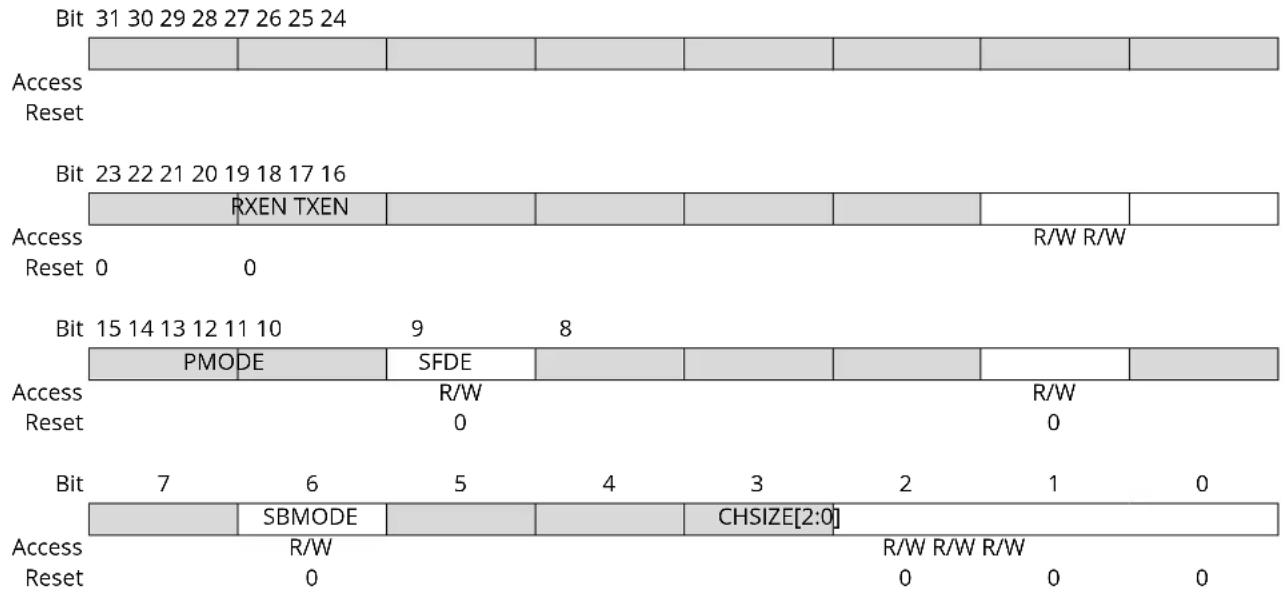
text_image
Bit 31 30 29 28 27 26 25 24 Access Reset Bit 23 22 21 20 19 18 17 16 RXEN TXEN Access Reset 0 0 R/W R/W Bit 15 14 13 12 11 10 9 8 PMODE SFDE Access Reset R/W R/W 0 0 Bit 7 6 5 4 3 2 1 0 SBMODE CHSIZE[2:0] Access Reset R/W R/W R/W R/W 0 0 0 0Bit 17 - RXEN Receiver Enable
Writing '0' to this bit will disable the USART receiver. Disabling the receiver will flush the receive buffer and clear the FERR, PERR and BUFOVF bits in the STATUS register.
Writing '1' to CTRLB.RXEN when the USART is disabled will set CTRLB.RXEN immediately. When the USART is enabled, CTRLB.RXEN will be cleared, and SYNCBUSY.CTRLB will be set and remain set until the receiver is enabled. When the receiver is enabled, CTRLB.RXEN will read back as '1'.
Writing '1' to CTRLB.RXEN when the USART is enabled will set SYNCBUSY.CTRLB, which will remain set until the receiver is enabled, and CTRLB.RXEN will read back as '1'.
This bit is not enable-protected.
| Value | Description |
| 0 | The receiver is disabled or being enabled. |
| 1 | The receiver is enabled or will be enabled when the USART is enabled. |
Bit 16 - TXEN Transmitter Enable
Writing '0' to this bit will disable the USART transmitter. Disabling the transmitter will not become effective until ongoing and pending transmissions are completed.
Writing '1' to CTRLB.TXEN when the USART is disabled will set CTRLB.TXEN immediately. When the USART is enabled, CTRLB.TXEN will be cleared, and SYNCBUSY.CTRLB will be set and remain set until the transmitter is enabled. When the transmitter is enabled, CTRLB.TXEN will read back as '1'.
Writing '1' to CTRLB.TXEN when the USART is enabled will set SYNCBUSY.CTRLB, which will remain set until the receiver is enabled, and CTRLB.TXEN will read back as '1'.
This bit is not enable-protected.
| Value | Description |
| 0 | The transmitter is disabled or being enabled. |
| 1 | The transmitter is enabled or will be enabled when the USART is enabled. |
Bit 13 - PMODE Parity Mode
This bit selects the type of parity used when parity is enabled (CTRLA.FORM is '1'). The transmitter will automatically generate and send the parity of the transmitted data bits within each frame. The receiver will generate a parity value for the incoming data and parity bit, compare it to the parity mode and, if a mismatch is detected, STATUS.PERR will be set.
This bit is not synchronized.
| Value Description | |
| 0 | Even parity. |
| 1 | Odd parity. |
Bit 9 - SFDE Start of Frame Detection Enable
This bit controls whether the start-of-frame detector will wake up the device when a start bit is detected on the RxD line.
This bit is not synchronized.
| SFDE | INTENSET.RXS | INTENSET.RXC | Description |
| 0 X X | Start-of-frame detection disabled. | ||
| 1 0 0 | Reserved | ||
| 1 0 1 | Start-of-frame detection enabled. RXC wakes up the device from all sleep modes. | ||
| 1 1 0 | Start-of-frame detection enabled. RXS wakes up the device from all sleep modes. | ||
| 1 1 1 | Start-of-frame detection enabled. Both RXC and RXS wake up the device from all sleep modes. | ||
Bit 6 - SBMODE Stop Bit Mode
This bit selects the number of stop bits transmitted.
This bit is not synchronized.
| Value Description | |
| 0 | One stop bit. |
| 1 | Two stop bits. |
Bits 2:0 - CHSIZE[2:0] Character Size
These bits select the number of bits in a character.
These bits are not synchronized.
| CHSIZE[2:0] Description | |
| 0x0 8 bits | |
| 0x1 9 bits | |
| 0x2-0x4 Reserved | |
| 0x5 5 bits | |
| 0x6 6 bits | |
| 0x7 7 bits |
24.8.3 Debug Control
Name: DBGCTRL
Offset: 0x08
Reset: 0x00
Property: PAC Write-Protection
Bit 76543210
| DBGSTOP | |||||||
| Access Reset 0 | R/W | ||||||
Bit 0 - DBGSTOP Debug Stop Mode
This bit controls the baud-rate generator functionality when the CPU is halted by an external debugger.
| Value Description | |
| 0 | The baud-rate generator continues normal operation when the CPU is halted by an external debugger. |
| 1 | The baud-rate generator is halted when the CPU is halted by an external debugger. |
24.8.4 Baud
Name: BAUD
Offset: 0x0A
Reset: 0x0000
Property: Enable-Protected, PAC Write-Protection
Bit 15 14 13 12 11 10 9 8
BAUD[15:8]
Access R/W R/W R/W R/W R/W R/W R/W R/W
Reset 00000000
Bit 76543210
BAUD[7:0]
Access R/W R/W R/W R/W R/W R/W R/W R/W
Reset 00000000
Bits 15:0 - BAUD[15:0] Baud Value
These bits control the clock generation, as described in the SERCOM Baud Rate section.
- Bits 15:0 - BAUD[15:0]: Baud Value
These bits control the clock generation, as described in the SERCOM Clock Generation – Baud-Rate Generator section.
24.8.5 Interrupt Enable Clear
Name: INTENCLR
Offset: 0x0C
Reset: 0x00
Property: PAC Write-Protection
This register allows the user to disable an interrupt without read-modify-write operation. Changes in this register will also be reflected in the Interrupt Enable Set register (INTENSET).
This register allows the user to disable an interrupt without doing a read-modify-write operation. Changes in this register will also be reflected in the Interrupt Enable Set register (INTENSET).
Bit 76543210
| RX$ RXC TXC DRE | ||||||
| Access Reset 0 0 0 0 | R/W R/W R/W R/W | |||||
Bit 3 - RXS Receive Start Interrupt Enable
Writing '0' to this bit has no effect.
Writing '1' to this bit will clear the Receive Start Interrupt Enable bit, which disables the Receive Start interrupt.
| Value | Description |
| 0 | Receive Start interrupt is disabled. |
| 1 | Receive Start interrupt is enabled. |
Bit 2 - RXC Receive Complete Interrupt Enable
Writing '0' to this bit has no effect.
Writing '1' to this bit will clear the Receive Complete Interrupt Enable bit, which disables the Receive Complete interrupt.
| Value | Description |
| 0 | Receive Complete interrupt is disabled. |
| 1 | Receive Complete interrupt is enabled. |
Bit 1 - TXC Transmit Complete Interrupt Enable
Writing '0' to this bit has no effect.
Writing '1' to this bit will clear the Transmit Complete Interrupt Enable bit, which disables the Receive Complete interrupt.
| Value | Description |
| 0 | Transmit Complete interrupt is disabled. |
| 1 | Transmit Complete interrupt is enabled. |
Bit 0 - DRE Data Register Empty Interrupt Enable
Writing '0' to this bit has no effect.
Writing '1' to this bit will clear the Data Register Empty Interrupt Enable bit, which disables the Data Register Empty interrupt.
| Value | Description |
| 0 | Data Register Empty interrupt is disabled. |
| 1 | Data Register Empty interrupt is enabled. |
24.8.6 Interrupt Enable Set
Name: INTENSET
Offset: 0x0D
Reset: 0x00
Property: PAC Write-Protection
This register allows the user to enable an interrupt without read-modify-write operation. Changes in this register will also be reflected in the Interrupt Enable Clear register (INTENCLR).
This register allows the user to disable an interrupt without doing a read-modify-write operation. Changes in this register will also be reflected in the Interrupt Enable Clear register (INTENCLR).
Bit 76543210
| RX$ RXC TXC DRE | ||||||
| Access Reset 0 0 0 0 | R/W R/W R/W R/W | |||||
Bit 3 - RXS Receive Start Interrupt Enable
Writing '0' to this bit has no effect.
Writing '1' to this bit will set the Receive Start Interrupt Enable bit, which enables the Receive Start interrupt.
| Value | Description |
| 0 | Receive Start interrupt is disabled. |
| 1 | Receive Start interrupt is enabled. |
Bit 2 - RXC Receive Complete Interrupt Enable
Writing '0' to this bit has no effect.
Writing '1' to this bit will set the Receive Complete Interrupt Enable bit, which enables the Receive Complete interrupt.
| Value | Description |
| 0 | Receive Complete interrupt is disabled. |
| 1 | Receive Complete interrupt is enabled. |
Bit 1 - TXC Transmit Complete Interrupt Enable
Writing '0' to this bit has no effect.
Writing '1' to this bit will set the Transmit Complete Interrupt Enable bit, which enables the Transmit Complete interrupt.
| Value | Description |
| 0 | Transmit Complete interrupt is disabled. |
| 1 | Transmit Complete interrupt is enabled. |
Bit 0 - DRE Data Register Empty Interrupt Enable
Writing '0' to this bit has no effect.
Writing '1' to this bit will set the Data Register Empty Interrupt Enable bit, which enables the Data Register Empty interrupt.
| Value | Description |
| 0 | Data Register Empty interrupt is disabled. |
| 1 | Data Register Empty interrupt is enabled. |
24.8.7 Interrupt Flag Status and Clear
Name: INTFLAG
Offset: 0x0E
Reset: 0x00
Property: -
Bit 76543210
| RX$ RXC TXC DRE | ||||||
| Access Reset 0 0 0 0 | R/W R R/W R | |||||
Bit 3 - RXS Receive Start
This flag is cleared by writing '1' to it.
This flag is set when a start condition is detected on the RxD line and start-of-frame detection is enabled (CTRLB.SFDE is '1').
Writing '0' to this bit has no effect.
Writing '1' to this bit will clear the Receive Start interrupt flag.
Bit 2 - RXC Receive Complete
This flag is cleared by reading the Data register (DATA) or by disabling the receiver.
This flag is set when there are unread data in DATA.
Writing '0' to this bit has no effect.
Writing '1' to this bit has no effect.
Bit 1 - TXC Transmit Complete
This flag is cleared by writing '1' to it or by writing new data to DATA.
This flag is set when the entire frame in the transmit shift register has been shifted out and there are no new data in DATA.
Writing '0' to this bit has no effect.
Writing '1' to this bit will clear the flag.
Bit 0 - DRE Data Register Empty
This flag is cleared by writing new data to DATA.
This flag is set when DATA is empty and ready to be written.
Writing '0' to this bit has no effect.
Writing '1' to this bit has no effect.
24.8.8 Status
Name: STATUS
Offset: 0x10
Reset: 0x0000
Property: -
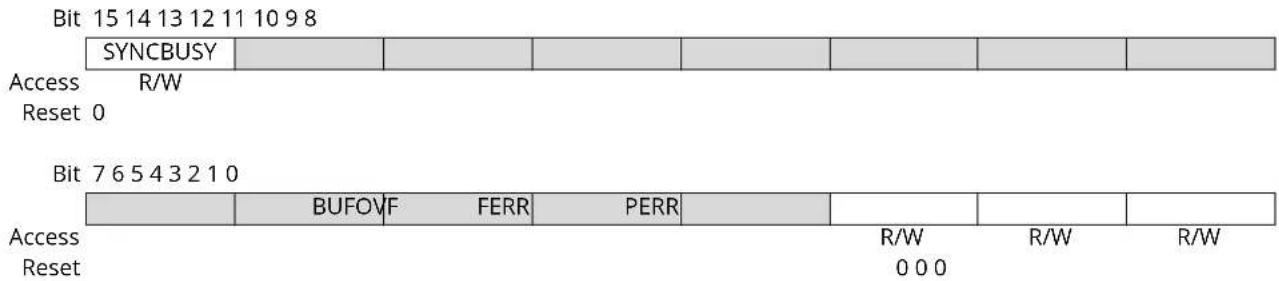
text_image
Bit 15 14 13 12 11 10 9 8 SYNCBUSY Access R/W Reset 0 Bit 7 6 5 4 3 2 1 0 BUFOVF FERR PERR R/W R/W R/W Access Reset 0 0 0Bit 15 - SYNCBUSY Synchronization Busy
This bit is cleared when the synchronization of registers between the clock domains is complete. This bit is set when the synchronization of registers between clock domains is started.
Bit 2 - BUFOVF Buffer Overflow
Reading this bit before reading the Data register will indicate the error status of the next character to be read.
This bit is cleared by writing '1' to the bit or by disabling the receiver.
This bit is set when a buffer overflow condition is detected. A buffer overflow occurs when the receive buffer is full, there is a new character waiting in the receive shift register and a new start bit is detected.
| Value | Description |
| 0 | Writing '0' to this bit has no effect. |
| 1 | Writing '1' to this bit will clear it. |
Bit 1 - FERR Frame Error
Reading this bit before reading the Data register will indicate the error status of the next character to be read.
This bit is cleared by writing '1' to the bit or by disabling the receiver.
This bit is set if the received character had a frame error, i.e., when the first stop bit is zero.
| Value | Description |
| 0 | Writing '0' to this bit has no effect. |
| 1 | Writing '1' to this bit will clear it. |
Bit 0 - PERR Parity Error
Reading this bit before reading the Data register will indicate the error status of the next character to be read.
This bit is cleared by writing '1' to the bit or by disabling the receiver.
This bit is set if parity checking is enabled (CTRLA.FORM is 0x1) and a parity error is detected.
| Value | Description |
| 0 | Writing '0' to this bit has no effect. |
| 1 | Writing '1' to this bit will clear it. |
24.8.9 Data
Name: DATA
Offset: 0x18
Reset: 0x0000
Property: -
Bit 15 14 13 12 11 10 9 8
| DATA[8] | |||||||
| Access Reset 0 | R/W | ||||||
Bit 76543210

text_image
DATA[7:0] Access R/W R/W R/W R/W R/W R/W R/W Reset 0 0 0 0 0 0 0Bits 8:0 - DATA[8:0] Data
Reading these bits will return the contents of the Receive Data register. The register should be read only when the Receive Complete Interrupt Flag bit in the Interrupt Flag Status and Clear register (INTFLAG.RXC) is set. The status bits in STATUS should be read before reading the DATA value in order to get any corresponding error.
Writing these bits will write the Transmit Data register. This register should be written only when the Data Register Empty Interrupt Flag bit in the Interrupt Flag Status and Clear register (INTFLAG.DRE) is set.
25. SERCOM SPI – SERCOM Serial Peripheral Interface
25.1 Overview
The Serial Peripheral Interface (SPI) is one of the available modes in the Serial Communication Interface (SERCOM).
The SPI uses the SERCOM transmitter and receiver configured as shown in 25.3. Block Diagram. Each side, host and client, depicts a separate SPI containing a Shift register, a transmit buffer and a two-level receive buffer. In addition, the SPI host uses the SERCOM baud-rate generator, while the SPI client can use the SERCOM address match logic. Labels in capital letters are synchronous to CLK_SERCOMx_APB and accessible by the CPU, while labels in lowercase letters are synchronous to the SCK clock.
Related Links
23. SERCOM - Serial Communication Interface
25.2 Features
SERCOM SPI includes the following features:
• Full-duplex, four-wire interface (MISO, MOSI, SCK, SS)
- Single-buffered transmitter, double-buffered receiver
• Supports all four SPI modes of operation
- Single data direction operation allows alternate function on MISO or MOSI pin
- Selectable LSB- or MSB-first data transfer
- Host operation:
- Serial clock speed, f_SCK = 1 / t_SCK^(1)
- 8-bit clock generator
- Client operation:
- Serial clock speed, f_SCK = 1 / t_SSCK^(1)
- Optional 8-bit address match operation
- Operation in all sleep modes
Note:
- For t_SCK and t_SSCK values, refer to SPI Timing Characteristics.
Related Links
- SERCOM - Serial Communication Interface
25.3 Block Diagram
Figure 25-1. Full-Duplex SPI Host Client Interconnection
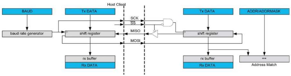
flowchart
graph TD
    A["BAUD"] --> B["baud rate generator"]
    B --> C["shift register"]
    C --> D["rx buffer"]
    C --> E["Rx DATA"]
    F["Tx DATA"] --> G["shift register"]
    G --> H["MOSI"]
    H --> I["OR"]
    I --> J["shift register"]
    J --> K["rx buffer"]
    J --> L["Rx DATA"]
    M["Tx DATA"] --> N["shift register"]
    N --> O["Address Match"]
    P["ADDR/ADDRMASK"] --> Q["=="]
    Q --> J
    style A fill:#4A90E2,stroke:#333
    style F fill:#4A90E2,stroke:#333
    style M fill:#4A90E2,stroke:#333
    style P fill:#4A90E2,stroke:#333
    style Q fill:#4A90E2,stroke:#333
    style B fill:#FFA500,stroke:#333
    style C fill:#FFA500,stroke:#333
    style G fill:#FFA500,stroke:#333
    style J fill:#FFA500,stroke:#333
    style N fill:#FFA500,stroke:#333
    style L fill:#FFA500,stroke:#333
    style H fill:#FFA500,stroke:#333
    style I fill:#FFA500,stroke:#333
    style O fill:#FFA500,stroke:#333
    style K fill:#FFA500,stroke:#333
25.4 Signal Description
Table 25-1. SERCOM SPI Signals
| Signal Name Type Description | ||
| PAD[3:0] Digital I/O General SERCOM pins | ||
One signal can be mapped to one of several pins.
Related Links
- I/O Multiplexing and Considerations
25.5 Product Dependencies
In order to use this peripheral, other parts of the system must be configured correctly, as described below.
25.5.1 I/O Lines
In order to use the SERCOM's I/O lines, the I/O pins must be configured using the IO Pin Controller (PORT).
When the SERCOM is configured for SPI operation, the SERCOM controls the direction and value of the I/O pins according to the table below. Both PORT control bits PINCFGn.PULLEN and PINCFGn.DRVSTR are still effective. If the receiver is disabled, the data input pin can be used for other purposes. In Host mode, the Client select line (SS) is controlled by software.
Table 25-2. SPI Pin Configuration
| Pin Host SPI Client SPI | |
| MOSI Output Input | |
| MISO Input Output | |
| SCK Output Input | |
| SS User defined output enable Input |
The combined configuration of PORT, the Data In Pinout and the Data Out Pinout bit groups in the Control A register (CTRLA.DIPO and CTRLA.DOPO) define the physical position of the SPI signals in the table above.
Related Links
- PORT - I/O Pin Controller
25.5.2 Power Management
This peripheral can continue to operate in any sleep mode where its source clock is running. The interrupts can wake up the device from sleep modes.
Related Links
- Power Manager (PM)
25.5.3 Clocks
The SERCOM bus clock (CLK_SERCOMx_APB) can be enabled and disabled in the Power Manager. Refer to Peripheral Clock Masking for details and default status of this clock.
A generic clock (GCLK_SERCOMx_CORE) is required to clock the SPI. This clock must be configured and enabled in the Generic Clock Controller before using the SPI.
This generic clock is asynchronous to the bus clock (CLK_SERCOMx_APB). Therefore, writes to certain registers will require synchronization to the clock domains.
Related Links
- GCLK - Generic Clock Controller
25.6.6. Synchronization
25.5.4 Interrupts
The interrupt request line is connected to the Interrupt Controller. In order to use interrupt requests of this peripheral, the Interrupt Controller (NVIC) must be configured first. Refer to Nested Vector Interrupt Controller for details.
Related Links
10.2. Nested Vector Interrupt Controller
25.5.5 Events
Not applicable.
25.5.6 Debug Operation
When the CPU is halted in debug mode, this peripheral will continue normal operation. If the peripheral is configured to require periodical service by the CPU through interrupts or similar, improper operation or data loss may result during debugging. This peripheral can be forced to halt operation during debugging - refer to the Debug Control (DBGCTRL) register for details.
25.5.7 Register Access Protection
Registers with write-access can be write-protected optionally by the peripheral access controller (PAC).
PAC Write-Protection is not available for the following registers:
- Interrupt Flag Clear and Status register (INTFLAG)
- Status register (STATUS)
• Data register (DATA)
Optional PAC Write-Protection is denoted by the "PAC Write-Protection" property in each individual register description.
Write-protection does not apply to accesses through an external debugger.
Related Links
10.5. PAC - Peripheral Access Controller
25.5.8 Analog Connections
Not applicable.
25.6 Functional Description
25.6.1 Principle of Operation
The SPI is a high-speed synchronous data transfer interface. It allows high-speed communication between the device and peripheral devices.
The SPI can operate as host or client. As host, the SPI initiates and controls all data transactions. The SPI is single buffered for transmitting and double buffered for receiving.
When transmitting data, the Data register can be loaded with the next character to be transmitted during the current transmission.
When receiving, the data is transferred to the two-level receive buffer, and the receiver is ready for a new character.
The SPI transaction format is shown in SPI Transaction Format. Each transaction can contain one or more characters. The character size is configurable, and can be either 8 or 9 bits.
Figure 25-2. SPI Transaction Format
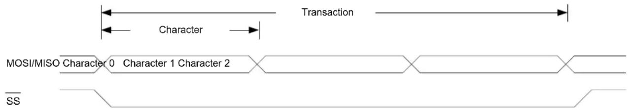
flowchart
graph LR
    A["Character"] --> B["Transaction"]
    B --> C["MOSI/MISO Character 0"]
    C --> D["Character 1 Character 2"]
    D --> E["SS"]
The SPI host must pull the SPI select line (SS) of the desired client low to initiate a transaction if multiple clients are connected to the bus. The SPI select line can be wired low if there is only one SPI client on the bus. The host and client prepare data to send via their respective Shift registers, and the host generates the serial clock on the SCK line.
Data is always shifted from host to client on the Host Output Client Input line (MOSI); data is shifted from client to host on the Host Input Client Output line (MISO).
Each time character is shifted out from the host, a character will be shifted out from the client simultaneously. To signal the end of a transaction, the host will pull the SS line high.
25.6.2 Basic Operation
25.6.2.1 Initialization
The following registers are enable-protected, meaning that they can only be written when the SPI is disabled (CTRL.ENABLE=0):
- Control A register (CTRLA), except Enable (CTRLA.ENABLE) and Software Reset (CTRLA.SWRST)
• Control B register (CTRLB), except Receiver Enable (CTRLB.RXEN)
• Baud register (BAUD) - Address register (ADDR)
When the SPI is enabled or is being enabled (CTRLA.ENABLE=1), any writing to these registers will be discarded.
when the SPI is being disabled, writing to these registers will be completed after the disabling.
Enable-protection is denoted by the Enable-Protection property in the register description.
Initialize the SPI by following these steps:
- Select SPI mode in Host / Client operation in the Operating Mode bit group in the CTRLA register (CTRLA.MODE=0x2 or 0x3).
- Select transfer mode for the Clock Polarity bit and the Clock Phase bit in the CTRLA register (CTRLA.CPOL and CTRLA.CPHA) if desired.
- Select the Frame Format value in the CTRLA register (CTRLA.FORM).
- Configure the Data In Pinout field in the Control A register (CTRLA.DIPO) for SERCOM pads of the receiver.
- Configure the Data Out Pinout bit group in the Control A register (CTRLA.DOPO) for SERCOM pads of the transmitter.
- Select the Character Size value in the CTRLB register (CTRLB.CHSIZE).
- Write the Data Order bit in the CTRLA register (CTRLA.DORD) for data direction.
- If the SPI is used in Host mode:
a. Select the desired baud rate by writing to the Baud register (BAUD).
- Enable the receiver by writing the Receiver Enable bit in the CTRLB register (CTRLB.RXEN=1).
25.6.2.2 Enabling, Disabling, and Resetting
This peripheral is enabled by writing '1' to the Enable bit in the Control A register (CTRLA.ENABLE), and disabled by writing '0' to it.
Writing '1' to the Software Reset bit in the Control A register (CTRLA.SWRST) will reset all registers of this peripheral to their initial states, except the DBGCTRL register, and the peripheral is disabled.
Refer to the CTRLA register description for details.
25.6.2.3 Clock Generation
In the SPI host operation (CTRLA.MODE=0x3), the serial clock (SCK) is generated internally by the SERCOM Baud Rate Generator (BRG).
In SPI mode, the BRG is set to Synchronous mode. The 8-bit Baud register (BAUD) value is used for generating SCK and clocking the Shift register. Refer to Clock Generation – Baud-Rate Generator for more details.
In SPI client operation (CTRLA.MODE is 0x2), the clock is provided by an external host on the SCK pin. This clock is used to clock the SPI Shift register.
Related Links
23.6.2.3. Clock Generation - Baud-Rate Generator
25.6.2.4 Data Register
The SPI Transmit Data register (TxDATA) and SPI Receive Data register (RxDATA) share the same I/O address, referred to as the SPI Data register (DATA). Writing DATA register will update the Transmit Data register. Reading the DATA register will return the contents of the Receive Data register.
25.6.2.5 SPI Transfer Modes
There are four combinations of SCK phase and polarity to transfer serial data. The SPI Data Transfer modes are shown in SPI Transfer Modes (Table) and SPI Transfer Modes (Figure).
SCK phase is configured by the Clock Phase bit in the CTRLA register (CTRLA.CPHA). SCK polarity is programmed by the Clock Polarity bit in the CTRLA register (CTRLA.CPOL). Data bits are shifted out and latched in on opposite edges of the SCK signal. This ensures sufficient time for the data signals to stabilize.
Table 25-3. SPI Transfer Modes
| Mode CPOL CPHA Leading Edge Trailing Edge | ||
| 0 0 0 Rising, sample Falling, setup | ||
| 1 0 1 Rising, setup Falling, sample | ||
| 2 1 0 Falling, sample Rising, setup | ||
| 3 1 1 Falling, setup Rising, sample |
Note:
Leading edge is the first clock edge in a clock cycle.
Trailing edge is the second clock edge in a clock cycle.
Figure 25-3. SPI Transfer Modes

text_image
Mode 0 Mode 2 SAMPLE I MOSI/MISO CHANGE 0 MOSI PIN CHANGE 0 MISO PIN SS MSB first (DORD = 0) MSB Bit 6 Bit 5 Bit 4 Bit 3 Bit 2 Bit 1 LSB LSB first (DORD = 1) LSB Bit 1 Bit 2 Bit 3 Bit 4 Bit 5 Bit 6 MSB Mode 1 Mode 3 SAMPLE I MOSI/MISO CHANGE 0 MOSI PIN CHANGE 0 MISO PIN SS MSB first (DORD = 0) MSB Bit 6 Bit 5 Bit 4 Bit 3 Bit 2 Bit 1 LSB LSB first (DORD = 1) LSB Bit 1 Bit 2 Bit 3 Bit 4 Bit 5 Bit 6 MSB25.6.2.6 Transferring Data
Host
In Host mode (CTRLA.MODE=0x3), the SS line must be configured as an output. SS can be assigned to any general purpose I/O pin. When the SPI is ready for a data transaction, software must pull the SS line low.
When writing a character to the Data register (DATA), the character will be transferred to the shift register. Once the content of TxDATA has been transferred to the shift register, the Data Register Empty flag in the Interrupt Flag Status and Clear register (INTFLAG.DRE) will be set. And a new character can be written to DATA.
Each time one character is shifted out from the Host, another character will be shifted in from the Client simultaneously. If the receiver is enabled (CTRLA.RXEN=1), the contents of the shift register will be transferred to the two-level receive buffer. The transfer takes place in the same clock cycle as the last data bit is shifted in. And the Receive Complete Interrupt flag in the Interrupt Flag Status and Clear register (INTFLAG.RXC) will be set. The received data can be retrieved by reading DATA.
When the last character has been transmitted and there is no valid data in DATA, the Transmit Complete Interrupt flag in the Interrupt Flag Status and Clear register (INTFLAG.TXC) will be set. When the transaction is finished, the Host must pull the line high to notify the Client.
Client
In Client mode (CTRLA.MODE=0x2), the SPI interface will remain inactive with the MISO line tri-stated as long as the SS pin is pulled high. Software may update the contents of DATA at any time as long as the Data Register Empty flag in the Interrupt Status and Clear register (INTFLAG.DRE) is set.
When is pulled low and SCK is running, the Client will sample and shift out data according to the transaction mode set. When the content of TxDATA has been loaded into the shift register, INTFLAG.DRE will be set, and new data can be written to DATA.
Similar to the Host, the Client will receive one character for each character transmitted. A character will be transferred into the two-level receive buffer within the same clock cycle its last data bit is received. The received character can be retrieved from DATA when the Receive Complete interrupt flag (INTFLAG.RXC) is set.
When the Host pulls the line high, the transaction is done and the Transmit Complete Interrupt flag in the Interrupt Flag Status and Clear register (INTFLAG.TXC) will be set.
After DATA is written it takes up to three SCK clock cycles until the content of DATA is ready to be loaded into the shift register on the next character boundary. As a consequence, the first character transferred in a SPI transaction will not be the content of DATA. This can be avoided by using the preloading feature. Refer to 25.6.3.2. Preloading of the Client Shift Register.
When transmitting several characters in one SPI transaction, the data has to be written into DATA register with at least three SCK clock cycles left in the current character transmission. If this criteria is not met, the previously received character will be transmitted.
Once the DATA register is empty, it takes three CLK_SERCOM_APB cycles for INTFLAG.DRE to be set.
25.6.2.7 Receiver Error Bit
The SPI receiver has one error bit: the Buffer Overflow bit (BUFOVF), which can be read from the Status register (STATUS). Once an error happens, the bit will stay set until it is cleared by writing '1' to it. The bit is also automatically cleared when the receiver is disabled.
There are two methods for buffer overflow notification, selected by the immediate buffer overflow notification bit in the Control A register (CTRLA.IBON):
If CTRLA.IBON=1, STATUS.BUFOVF is raised immediately upon buffer overflow. Software can then empty the receive FIFO by reading RxDATA until the receiver complete interrupt flag in the Interrupt Flag Status and Clear register (INTFLAG.RXC) goes low.
If CTRLA.IBON=0, the buffer overflow condition travels with data through the receive FIFO. After the received data is read, STATUS.BUFOVF will be set along with INTFLAG.RXC, and RxDATA will be zero.
25.6.3 Additional Features
25.6.3.1 Address Recognition
When the SPI is configured for client operation (CTRLA.MODE=0x2) with address recognition (CTRLA.FORM is 0x2), the SERCOM address recognition logic is enabled: the first character in a transaction is checked for an address match.
If there is a match, the Receive Complete Interrupt flag in the Interrupt Flag Status and Clear register (INTFLAG.RXC) is set, the MISO output is enabled, and the transaction is processed. If the device is in Sleep mode, an address match can wake-up the device in order to process the transaction.
If there is no match, the complete transaction is ignored.
If a 9-bit frame format is selected, only the lower 8 bits of the Shift register are checked against the Address register (ADDR).
Preload must be disabled (CTRLB.PLOADEN=0) in order to use this mode.
Related Links
23.6.3.1. Address Match and Mask
25.6.3.2 Preloading of the Client Shift Register
When starting a transaction, the client will first transmit the contents of the shift register before loading new data from DATA. The first character sent can be either the reset value of the shift register (if this is the first transmission since the last reset) or the last character in the previous transmission.
Preloading can be used to preload data into the shift register while is high: this eliminates sending a dummy character when starting a transaction. If the shift register is not preloaded, the current contents of the shift register will be shifted out.
Only one data character will be preloaded into the shift register while the synchronized signal is high. If the next character is written to DATA before is pulled low, the second character will be stored in DATA until transfer begins.
For proper preloading, sufficient time must elapse between going low and the first SCK sampling edge, as in Timing Using Preloading. See also the Electrical Characteristics chapters for timing details.
Preloading is enabled by writing '1' to the Client Data Preload Enable bit in the CTRLB register (CTRLB.PLOADEN).
Figure 25-4. Timing Using Preloading
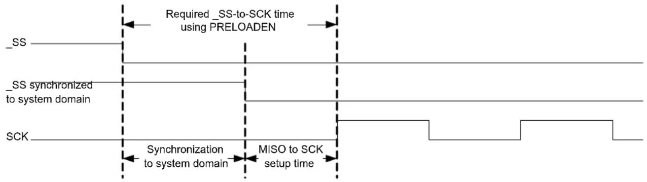
flowchart
graph LR
    A["_SS"] --> B["Required_SS-to-SCK time using PRELOADEN"]
    C["_SS synchronized to system domain"] --> B
    D["SCK"] --> E["Synchronization to system domain"]
    E --> F["MISO to SCK setup time"]
25.6.3.3 Host with Several Clients
If the bus consists of several SPI clients, a SPI host can use general purpose I/O pins to control the SS line to each of the clients on the bus, as shown in the following figure. In this configuration, the single selected SPI client will drive the tri-state MISO line.
Figure 25-5. Multiple Clients in Parallel
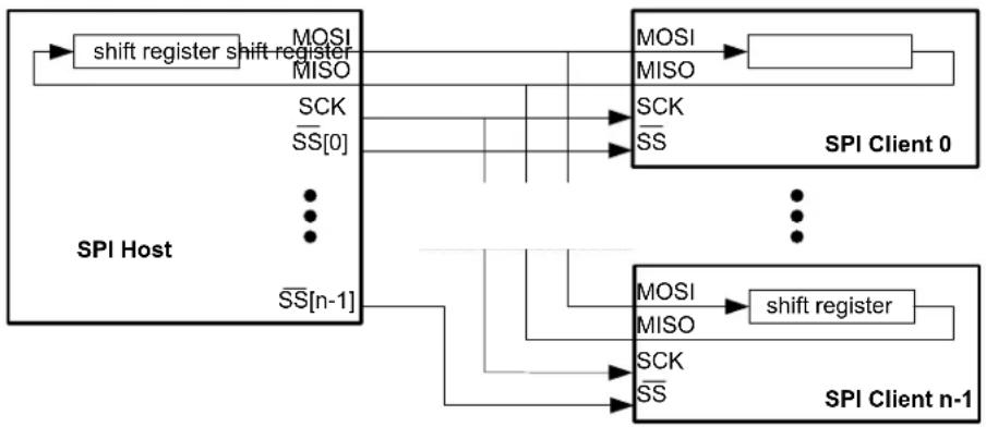
flowchart
graph TD
    A["SPI Host"] -->|MOSI MISO| B["SPI Client 0"]
    A -->|SCK_SS["0"]| B
    A -->|SS["n-1"]| B
    B -->|MOSI MISO| C["SPI Client n-1"]
    B -->|SCK SS| C
    B -->|MOSI MISO| D["SPI Client n-1"]
    B -->|MOSI MISO| E["SPI Client n-1"]
Another configuration is multiple clients in series, as shown in the following figure. In this configuration, all n attached clients are connected in series. A common SS line is provided to all clients, enabling them simultaneously. The host must shift n characters for a complete transaction. The SS line is controlled by a normal GPIO.
Figure 25-6. Multiple Clients in Series

flowchart
graph TD
    A["SPI Host"] --> B["shift register"]
    B --> C["MOSI"]
    B --> D["MISO"]
    B --> E["SCK"]
    B --> F["SS"]
    C --> G["MOSI"]
    D --> H["MISO"]
    E --> I["SCK"]
    F --> J["SS"]
    G --> K["SPI Client 0"]
    H --> K
    I --> K
    J --> K
    K --> L["..."]
    L --> M["MOSI"]
    L --> N["MISO"]
    L --> O["SCK"]
    L --> P["SS"]
    M --> Q["shift register"]
    N --> Q
    O --> Q
    P --> Q
    Q --> R["SPI Client n-1"]
25.6.3.4 Loop-Back Mode
For loop-back mode, configure the Data In Pinout (CTRLA.DIPO) and Data Out Pinout (CTRLA.DOPO) to use the same data pins for transmit and receive. The loop-back is through the pad, so the signal is also available externally.
25.6.4 Interrupts
The SPI has the following interrupt sources. These are asynchronous interrupts, and can wake up the device from any sleep mode:
• Data Register Empty (DRE)
- Receive Complete (RXC)
• Transmit Complete (TXC)
Each interrupt source has its own interrupt flag. The interrupt flag in the Interrupt Flag Status and Clear register (INTFLAG) will be set when the interrupt condition is met. Each interrupt can be individually enabled by writing '1' to the corresponding bit in the Interrupt Enable Set register (INTENSET), and disabled by writing '1' to the corresponding bit in the Interrupt Enable Clear register (INTENCLR).
An interrupt request is generated when the interrupt flag is set and if the corresponding interrupt is enabled. The interrupt request remains active until either the interrupt flag is cleared, the interrupt is disabled, or the SPI is reset. For details on clearing interrupt flags, refer to the INTFLAG register description.
The SPI has one common interrupt request line for all the interrupt sources. The value of INTFLAG indicates which interrupt is executed. Note that interrupts must be globally enabled for interrupt requests. Refer to Nested Vector Interrupt Controller for details.
Related Links
10.2. Nested Vector Interrupt Controller
25.6.5 Sleep Mode Operation
The behavior in Sleep mode is depending on the host/client configuration and the Run In Standby bit in the Control A register (CTRLA.RUNSTDBY):
- Host operation, CTRLA.RUNSTDBY=1: The peripheral clock GCLK_SERCOMx_CORE will continue to run in Idle Sleep mode and in Standby Sleep mode. Any interrupt can wake-up the device.
- Host operation, CTRLA.RUNSTDBY=0: GLK_SERCOMx_CORE will be disabled after the ongoing transaction is finished. Any interrupt can wake up the device.
- Client operation, CTRLA.RUNSTDBY=1: The Receive Complete interrupt can wake-up the device.
- Client operation, CTRLA.RUNSTDBY=0: All reception will be dropped, including the ongoing transaction.
25.6.6 Synchronization
Due to asynchronicity between the main clock domain and the peripheral clock domains, some registers need to be synchronized when written or read.
The following bits are synchronized when written:
- Software Reset bit in the CTRLA register (CTRLA.SWRST)
- Enable bit in the CTRLA register (CTRLA.ENABLE)
- Receiver Enable bit in the CTRLB register (CTRLB.RXEN)
Note: CTRLB.RXEN is write-synchronized somewhat differently. See also CTRLB register for details.
Required write-synchronization is denoted by the "Write-Synchronized" property in the register description.
Related Links
13.3. Register Synchronization
25.8.2. CTRLB
25.7 Register Summary
| Offset | Name Bit Pos. 7 | 6 | 5 | 4 | 3 | 2 | 1 | 0 | |||||||
| 0x00 | CTRLA | 7:0 RUNSTDBY MODE[2:0] ENABLE SWRST | |||||||||||||
| 15:8 IBON | |||||||||||||||
| 23:16 DIPO[1:0] | DOPO[1:0] | ||||||||||||||
| 31:24 DORD CPOL | CPHA | FORM[3:0] | |||||||||||||
| 0x04 | CTRLB | 7:0 | PLOADEN | CHSIZE[2:0] | |||||||||||
| 15:8 | AMODE[1:0] | ||||||||||||||
| 23:16 RXEN | |||||||||||||||
| 31:24 | |||||||||||||||
| 0x08 | DBGCTRL | 7:0 | DBGSTOP | ||||||||||||
| 0x09 | Reserved | ||||||||||||||
| 0x0A | BAUD | 7:0 | BAUD[7:0] | ||||||||||||
| 0x0B | Reserved | ||||||||||||||
| 0x0C | INTENCLR | 7:0 | RXC | TXC | DRE | ||||||||||
| 0x0D | INTENSET | 7:0 | RXC | TXC | DRE | ||||||||||
| 0x0E | INTFLAG | 7:0 | RXC | TXC | DRE | ||||||||||
| 0x0F | Reserved | ||||||||||||||
| 0x10 | STATUS | 7:0 | BUFOVF | ||||||||||||
| 15:8 | SYNCBUSY | ||||||||||||||
| 0x12 ... 0x13 | Reserved | ||||||||||||||
| 0x14 | ADDR | 7:0 | ADDR[7:0] | ||||||||||||
| 15:8 | |||||||||||||||
| 23:16 | ADDRMASK[7:0] | ||||||||||||||
| 31:24 | |||||||||||||||
| 0x18 | DATA | 7:0 | DATA[7:0] | ||||||||||||
| 15:8 | DATA[8] | ||||||||||||||
25.8 Register Description
Registers can be 8, 16, or 32 bits wide. Atomic 8-, 16-, and 32-bit accesses are supported. In addition, the 8-bit quarters and 16-bit halves of a 32-bit register, and the 8-bit halves of a 16-bit register can be accessed directly.
Some registers require synchronization when read and/or written. Synchronization is denoted by the "Read-Synchronized" and/or "Write-Synchronized" property in each individual register description.
Refer to 25.6.6. Synchronization
Some registers are enable-protected, meaning they can only be written when the module is disabled. Enable-protection is denoted by the "Enable-Protected" property in each individual register description.
Optional write-protection by the Peripheral Access Controller (PAC) is denoted by the "PAC Write-Protection" property in each individual register description.
Refer to 25.5.7. Register Access Protection.
25.8.1 Control A
Name: CTRLA
Offset: 0x00
Reset: 0x00000000
Property: PAC Write-Protection, Enable-Protected, Write-Synchronized
Bit 31 30 29 28 27 26 25 24
| DORD | CPOL | CPHA | FORM[3:0] | |||||
| Access | R/W R/W R/W R/W R/W R/W | |||||||
| Reset | 0 | 0 | 0 | 0 | 0 | |||
Bit 23 22 21 20 19 18 17 16
| DIPO[1:0] | DOPO[1:0] | ||||
| Access Reset | R/W R/W | R/W R/W | |||
| 0 | 0 | 0 |
Bit 15 14 13 12 11 10 9 8
| IBON | |||||||
| Access | R/W | ||||||
| Reset | 0 |
Bit 7 6 5 4 3 2 1 0
| RUNSTDBY | MODE[2:0] | ENABLE | SWRST | |||||
| Access | R/W | R/W | R/W | R/W R/W R/W | ||||
| Reset | 0 | 0 | 0 | 0 | 0 | |||
Bit 30 - DORD Data Order
This bit selects the data order when a character is shifted out from the shift register.
This bit is not synchronized.
| Value | Description |
| 0 | MSB is transferred first. |
| 1 | LSB is transferred first. |
Bit 29 - CPOL Clock Polarity
In combination with the Clock Phase bit (CPHA), this bit determines the SPI transfer mode.
This bit is not synchronized.
| Value | Description |
| 0 | SCK is low when idle. The leading edge of a clock cycle is a rising edge, while the trailing edge is a falling edge. |
| 1 | SCK is high when idle. The leading edge of a clock cycle is a falling edge, while the trailing edge is a rising edge. |
Bit 28 - CPHA Clock Phase
In combination with the Clock Polarity bit (CPOL), this bit determines the SPI transfer mode.
This bit is not synchronized.
| Mode | CPOL | CPHA | Leading Edge | Trailing Edge |
| 0x0 | 0 | 0 | Rising, sample | Falling, change |
| 0x1 | 0 | 1 | Rising, change | Falling, sample |
| 0x2 | 1 | 0 | Falling, sample | Rising, change |
| 0x3 | 1 | 1 | Falling, change | Rising, sample |
Value Description
| 0 | The data is sampled on a leading SCK edge and changed on a trailing SCK edge. |
| 1 | The data is sampled on a trailing SCK edge and changed on a leading SCK edge. |
Bits 27:24 - FORM[3:0] Frame Format
This bit field selects the various frame formats supported by the SPI in client mode. When the 'SPI frame with address' format is selected, the first byte received is checked against the ADDR register.
| FORM[3:0] Name Description | ||
| 0x0 SPI SPI frame | ||
| 0x1 - Reserved | ||
| 0x2 SPI_ADDR SPI frame with address | ||
| 0x3-0xF - Reserved |
Bits 21:20 - DIPO[1:0] Data In Pinout
These bits define the data in (DI) pad configurations.
In host operation, DI is MISO.
In client operation, DI is MOSI.
These bits are not synchronized.
| DIPO[1:0] Name Description | |
| 0x0 PAD[0] SERCOM PAD[0] is used as data input | |
| 0x1 PAD[1] SERCOM PAD[1] is used as data input | |
| 0x2 PAD[2] SERCOM PAD[2] is used as data input | |
| 0x3 PAD[3] SERCOM PAD[3] is used as data input |
Bits 17:16 - DOPO[1:0] Data Out Pinout
This bit defines the available pad configurations for data out (DO), the serial clock (SCK) and the SPI select ( ). In Client operation, the SPI Select line ( ) is controlled by DOPO.
In host operation, DO is MOSI.
In client operation, DO is MISO.
These bits are not synchronized.
| DOPO DO SCK Client | SS Host SS | — | — | |
| 0x0 PAD[0] | PAD[1] | PAD[2] | PAD[2] | |
| 0x1 PAD[2] | PAD[3] | PAD[1] | PAD[1] | |
| 0x2 PAD[3] | PAD[1] | PAD[2] | PAD[2] | |
| 0x3 PAD[0] | PAD[3] | PAD[1] | PAD[1] |
Bit 8 - IBON Immediate Buffer Overflow Notification
This bit controls when the buffer overflow status bit (STATUS.BUFOVF) is set when a buffer overflow occurs.
This bit is not synchronized.
| Value | Description |
| 0 | STATUS.BUFOVF is set when it occurs in the data stream. |
| 1 | STATUS.BUFOVF is set immediately upon buffer overflow. |
Bit 7 - RUNSTDBY Run In Standby
This bit defines the functionality in standby sleep mode.
These bits are not synchronized.
| RUNSTDBY | Client | Host |
| 0x0 | Disabled. All reception is dropped, including the ongoing transaction. | Generic clock is disabled when ongoing transaction is finished. All interrupts can wake up the device. |
| 0x1 | Ongoing transaction continues, wake on Receive Complete interrupt. | Generic clock is enabled while in sleep modes. All interrupts can wake up the device. |
Bits 4:2 - MODE[2:0] Operating Mode
These bits must be written to 0x2 or 0x3 to select the SPI serial communication interface of the SERCOM.
0x2: SPI client operation
0x3: SPI host operation
These bits are not synchronized.
Bit 1 - ENABLE Enable
Due to synchronization, there is delay from writing CTRLA. ENABLE until the peripheral is enabled/disabled. The value written to CTRL. ENABLE will read back immediately and the Synchronization Enable Busy bit in the Synchronization Busy register (SYNCBUSY. ENABLE) will be set. SYNCBUSY. ENABLE is cleared when the operation is complete.
This bit is not enable-protected.
| Value Description | |
| 0 | The peripheral is disabled or being disabled. |
| 1 | The peripheral is enabled or being enabled. |
Bit 0 - SWRST Software Reset
Writing '0' to this bit has no effect.
Writing '1' to this bit resets all registers in the SERCOM, except DBGCTRL, to their initial state, and the SERCOM will be disabled.
Writing "1" to CTRL.SWRST will always take precedence, meaning that all other writes in the same write-operation will be discarded. Any register write access during the ongoing reset will result in an APB error. Reading any register will return the reset value of the register.
Due to synchronization, there is a delay from writing CTRLA.SWRST until the reset is complete.
CTRLA.SWRST and SYNCBUSY. SWRST will both be cleared when the reset is complete.
This bit is not enable-protected.
| Value Description | |
| 0 | There is no reset operation ongoing. |
| 1 | The reset operation is ongoing. |
25.8.2 Control B
Name: CTRLB
Offset: 0x04
Reset: 0x00000000
Property: PAC Write-Protection, Enable-Protected
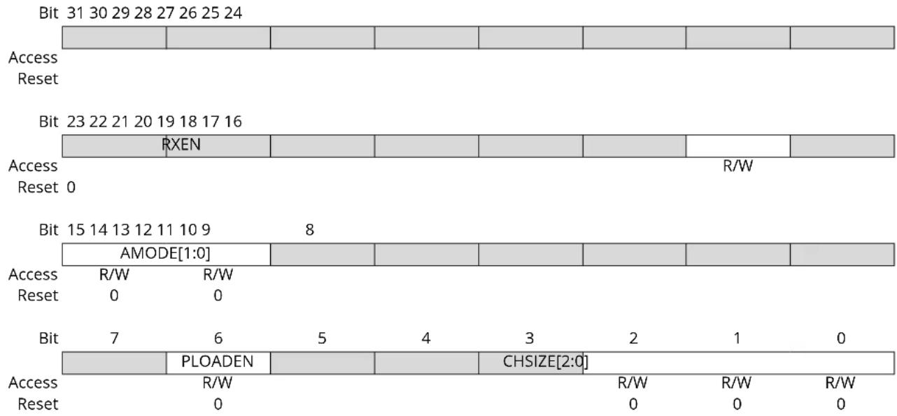
bar_stacked
| Bit | Access | Reset | | :--- | :--- | :--- | | 31 | 31 | 0 | | 29 | 29 | 0 | | 28 | 28 | 0 | | 27 | 27 | 0 | | 26 | 26 | 0 | | 25 | 25 | 0 | | 24 | 24 | 0 | | RXEN | RXEN | RXEN | | 15 | 15 | 15 | | 14 | 14 | 14 | | 13 | 13 | 13 | | 12 | 12 | 12 | | 11 | 11 | 11 | | 10 | 10 | 10 | | 9 | 9 | 9 | | 8 | 8 | 8 | | AMODE[1:0] | AMODE[1:0] | AMODE[1:0] | | R/W | R/W | R/W | | Reset | Reset | Reset | | 0 | 0 | 0 | | | | | | | | | | | | | | | | | | | | | | | | | | | | | | | | | | | | | | | | | | | | | | | | | | | | | | | | | | | | | | | | | | | | | | | | | | | | | | | | | | | | | | | | | | | | | | | | | | | | | | | | | | | | | | | | | | | | | | | | | | | | | | | | | | | | | | | | | | | | | | | | | | | | | | | | | | | | | | | | | | | | | | | | | | | | | | | | nan | | | | nan | | | | nan | | | | nan | | | | nan | | | | nan | | | | nan | | | | nan | | | | nan | | | | nan | | | | nan | | | | nan | | | | nan | | | / / / / / / / / / / / / / / / / / / / / / / / / / / / / / / / / / / / / / / / / / / / / / / / / / / / | Access Reset Bit Access Reset Bit Access Reset Bit Access Reset Bit Access Reset Bit Access Reset Bit Access Reset Bit Access Reset Bit Access Reset Bit Access Reset Bit Access Reset Bit Access Reset Bit Access Reset Bit Access Reset Bit Access Reset Bit Access Reset Bit Access Reset Bit Access ResetBit 17 - RXEN Receiver Enable
Writing '0' to this bit will disable the SPI receiver immediately. The receive buffer will be flushed, data from ongoing receptions will be lost and STATUS.BUFOVF will be cleared.
Writing '1' to CTRLB.RXEN when the SPI is disabled will set CTRLB.RXEN immediately. When the SPI is enabled, CTRLB.RXEN will be cleared, SYNCBUSY.CTRLB will be set and remain set until the receiver is enabled. When the receiver is enabled CTRLB.RXEN will read back as '1'.
Writing '1' to CTRLB.RXEN when the SPI is enabled will set SYNCBUSY.CTRLB, which will remain set until the receiver is enabled, and CTRLB.RXEN will read back as '1'.
This bit is not enable-protected.
| Value | Description |
| 0 | The receiver is disabled or being enabled. |
| 1 | The receiver is enabled or it will be enabled when SPI is enabled. |
Bits 15:14 - AMODE[1:0] Address Mode
These bits set the Client addressing mode when the frame format (CTRLA.FORM) with address is used. They are unused in Host mode.
| AMODE[1:0] | Name | Description |
| 0x0 | MASK ADDRMASK is used as a mask to the ADDR register | |
| 0x1 | 2_ADDRS | The Client responds to the two unique addresses in ADDR and ADDRMASK |
| 0x2 | RANGE | The Client responds to the range of addresses between and including ADDR and ADDRMASK. ADDR is the upper limit |
| 0x3 | - | Reserved |
Bit 6 - PLOADEN Client Data Preload Enable
Setting this bit will enable preloading of the Client shift register when there is no transfer in progress. If the line is high when DATA is written, it will be transferred immediately to the shift register.
Bits 2:0 - CHSIZE[2:0] Character Size
| CHSIZE[2:0] Name Description | ||
| 0x0 8BIT 8 bits | ||
| 0x1 9BIT 9 bits | ||
| 0x2-0x7 - Reserved |
25.8.3 Debug Control
Name: DBGCTRL
Offset: 0x08
Reset: 0x00
Property: PAC Write-Protection
Bit 76543210
| DBGSTOP | |||||||
| Access Reset 0 | R/W | ||||||
Bit 0 - DBGSTOP Debug Stop Mode
This bit controls the functionality when the CPU is halted by an external debugger.
| Value Description | |
| 0 | The baud-rate generator continues normal operation when the CPU is halted by an external debugger. |
| 1 | The baud-rate generator is halted when the CPU is halted by an external debugger. |
25.8.4 Baud Rate
Name: BAUD
Offset: 0x0A
Reset: 0x00
Property: PAC Write-Protection, Enable-Protected
Bit 76543210
BAUD[7:0]
Access R/W R/W R/W R/W R/W R/W R/W R/W
Reset 00000000
Bits 7:0 - BAUD[7:0] Baud Register
These bits control the clock generation, as described in the SERCOM Clock Generation – Baud-Rate Generator.
25.8.5 Interrupt Enable Clear
Name: INTENCLR
Offset: 0x0C
Reset: 0x00
Property: PAC Write-Protection
This register allows the user to disable an interrupt without read-modify-write operation. Changes in this register will also be reflected in the Interrupt Enable Set register (INTENSET).
Bit 76543210
| RXC TXC DRE | |||||||
| Access Reset 0 0 0 | R/W R/W R/W | ||||||
Bit 2 - RXC Receive Complete Interrupt Enable
Writing '0' to this bit has no effect.
Writing '1' to this bit will clear the Receive Complete Interrupt Enable bit, which disables the Receive Complete interrupt.
| Value | Description |
| 0 | Receive Complete interrupt is disabled. |
| 1 | Receive Complete interrupt is enabled. |
Bit 1 - TXC Transmit Complete Interrupt Enable
Writing '0' to this bit has no effect.
Writing '1' to this bit will clear the Transmit Complete Interrupt Enable bit, which disable the Transmit Complete interrupt.
| Value | Description |
| 0 | Transmit Complete interrupt is disabled. |
| 1 | Transmit Complete interrupt is enabled. |
Bit 0 - DRE Data Register Empty Interrupt Enable
Writing '0' to this bit has no effect.
Writing '1' to this bit will clear the Data Register Empty Interrupt Enable bit, which disables the Data Register Empty interrupt.
| Value | Description |
| 0 | Data Register Empty interrupt is disabled. |
| 1 | Data Register Empty interrupt is enabled. |
25.8.6 Interrupt Enable Set
Name: INTENSET
Offset: 0x0D
Reset: 0x00
Property: PAC Write-Protection
This register allows the user to disable an interrupt without read-modify-write operation. Changes in this register will also be reflected in the Interrupt Enable Clear register (INTENCLR).
Bit 76543210
| RXC TXC DRE | |||||||
| Access Reset 0 0 0 | R/W R/W R/W | ||||||
Bit 2 - RXC Receive Complete Interrupt Enable
Writing '0' to this bit has no effect.
Writing '1' to this bit will set the Receive Complete Interrupt Enable bit, which enables the Receive Complete interrupt.
| Value | Description |
| 0 | Receive Complete interrupt is disabled. |
| 1 | Receive Complete interrupt is enabled. |
Bit 1 - TXC Transmit Complete Interrupt Enable
Writing '0' to this bit has no effect.
Writing '1' to this bit will set the Transmit Complete Interrupt Enable bit, which enables the Transmit Complete interrupt.
| Value | Description |
| 0 | Transmit Complete interrupt is disabled. |
| 1 | Transmit Complete interrupt is enabled. |
Bit 0 - DRE Data Register Empty Interrupt Enable
Writing '0' to this bit has no effect.
Writing '1' to this bit will set the Data Register Empty Interrupt Enable bit, which enables the Data Register Empty interrupt.
| Value | Description |
| 0 | Data Register Empty interrupt is disabled. |
| 1 | Data Register Empty interrupt is enabled. |
25.8.7 Interrupt Flag Status and Clear
Name: INTFLAG
Offset: 0x0E
Reset: 0x00
Property: -
Bit 76543210
| RXC TXC DRE | |||||||
| Access Reset 0 0 0 | R R/W R | ||||||
Bit 2 - RXC Receive Complete
This flag is cleared by reading the Data (DATA) register or by disabling the receiver.
This flag is set when there are unread data in the receive buffer. If address matching is enabled, the first data received in a transaction will be an address.
Writing '0' to this bit has no effect.
Writing '1' to this bit has no effect.
Bit 1 - TXC Transmit Complete
This flag is cleared by writing '1' to it or by writing new data to DATA.
In Host mode, this flag is set when the data have been shifted out and there are no new data in DATA.
In Client mode, this flag is set when the pin is pulled high. If address matching is enabled, this flag is only set if the transaction was initiated with an address match.
Writing '0' to this bit has no effect.
Writing '1' to this bit will clear the flag.
Bit 0 - DRE Data Register Empty
This flag is cleared by writing new data to DATA.
This flag is set when DATA is empty and ready for new data to transmit.
Writing '0' to this bit has no effect.
Writing '1' to this bit has no effect.
25.8.8 Status
Name: STATUS
Offset: 0x10
Reset: 0x0000
Property: -
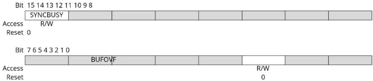
text_image
Bit 15 14 13 12 11 10 9 8 SYNCBUSY Access R/W Reset 0 Bit 7 6 5 4 3 2 1 0 BUFOVF Access R/W Reset 0Bit 15 - SYNCBUSY Synchronization Busy
This bit is cleared when the synchronization of registers between the clock domains is complete. This bit is set when the synchronization of registers between clock domains is in progress.
Bit 2 - BUFOVF Buffer Overflow
Reading this bit before reading DATA will indicate the error status of the next character to be read.
This bit is cleared by writing '1' to the bit or by disabling the receiver.
This bit is set when a buffer overflow condition is detected. See also CTRLA.IBON for overflow handling.
When set, the corresponding RxDATA will be zero.
Writing '0' to this bit has no effect.
Writing '1' to this bit will clear it.
| Value | Description |
| 0 | No Buffer Overflow has occurred. |
| 1 | A Buffer Overflow has occurred. |
25.8.9 Address
Name: ADDR
Offset: 0x14
Reset: 0x00000000
Property: PAC Write-Protection, Enable-Protected
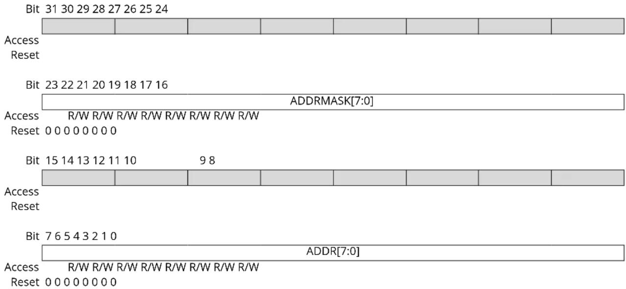
text_image
Bit 31 30 29 28 27 26 25 24 Access Reset Bit 23 22 21 20 19 18 17 16 ADDRMASK[7:0] Access R/W R/W R/W R/W R/W R/W R/W R/W Reset 0 0 0 0 0 0 0 0 Bit 15 14 13 12 11 10 9 8 Access Reset Bit 7 6 5 4 3 2 1 0 ADDR[7:0] Access R/W R/W R/W R/W R/W R/W R/W R/W Reset 0 0 0 0 0 0 0 0Bits 23:16 - ADDRMASK[7:0] Address Mask
These bits hold the address mask when the transaction format with address is used (CTRLA.FORM, CTRLB.AMODE).
Bits 7:0 - ADDR[7:0] Address
These bits hold the address when the transaction format with address is used (CTRLA.FORM, CTRLB.AMODE).
25.8.10 Data
Name: DATA
Offset: 0x18
Reset: 0x0000
Property: -
Bit 15 14 13 12 11 10 9 8
| DATA[8] | |||||||
| Access Reset 0 | R/W | ||||||
Bit 76543210

text_image
DATA[7:0] Access R/W R/W R/W R/W R/W R/W R/W Reset 0 0 0 0 0 0 0Bits 8:0 - DATA[8:0] Data
Reading these bits will return the contents of the receive data buffer. The register should be read only when the Receive Complete Interrupt Flag bit in the Interrupt Flag Status and Clear register (INTFLAG.RXC) is set.
Writing these bits will write the transmit data buffer. This register should be written only when the Data Register Empty Interrupt Flag bit in the Interrupt Flag Status and Clear register (INTFLAG.DRE) is set.
26. SERCOM I ^2 C – Inter-Integrated Circuit
26.1 Overview
The inter-integrated circuit (I²C) interface is one of the available modes in the serial communication interface (SERCOM).
The I ^2 C interface uses the SERCOM transmitter and receiver configured as shown in Figure 26-1. Labels in capital letters are registers accessible by the CPU, while lowercase labels are internal to the SERCOM.
A SERCOM instance can be configured to be either an I2C host or an I2C client. Both host and client have an interface containing a shift register, a transmit buffer and a receive buffer. In addition, the I2C host uses the SERCOM baud-rate generator, while the I2C client uses the SERCOM address match logic.
Related Links
- SERCOM - Serial Communication Interface
26.2 Features
SERCOM I ^2 C includes the following features:
- Host or Client operation
• Philips I ^2 C compatible - SMBus ^TM compatible
-
Support of 100 kHz and 400 kHz I ^2 C mode low system clock frequencies
• Physical interface includes: -
Slew-rate limited outputs
- Filtered inputs
- Client operation:
- Operation in all sleep modes
- Wake-up on address match
- 7-bit Address match in hardware for:
-
• Unique address and/or 7-bit general call address
-
Address range
- Two unique addresses
26.3 Block Diagram
Figure 26-1. I²C Single-Host Single-Client Interconnection
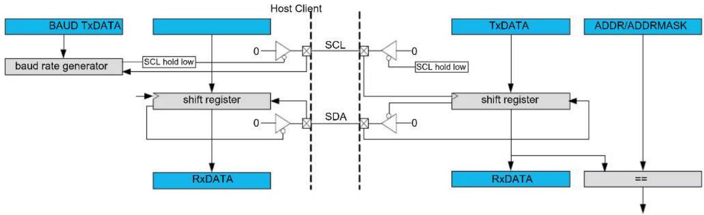
flowchart
graph TD
    A["BAUD TxDATA"] --> B["baud rate generator"]
    B --> C["shift register"]
    C --> D["RxDATA"]
    E["Host Client"] --> F["SCL hold low"]
    F --> G["0"]
    G --> H["×"]
    H --> I["SCL"]
    I --> J["×"]
    J --> K["0"]
    K --> L["SCL hold low"]
    L --> M["shift register"]
    M --> N["0"]
    N --> O["×"]
    O --> P["SDA"]
    P --> Q["0"]
    Q --> R["×"]
    R --> S["0"]
    S --> T["shift register"]
    T --> U["RxDATA"]
    V["TxDATA"] --> W["shift register"]
    X["ADDR/ADDRMASK"] --> Y["=="]
    Y --> Z["->"]
26.4 Signal Description
| Signal Name Type Description | |
| PAD[0] Digital I/O SDA | |
| PAD[1] Digital I/O SCL | |
| PAD[2] Digital I/O SDA_OUT (4-wire operation) | |
| PAD[3] Digital I/O SCL_OUT (4-wire operation) | |
One signal can be mapped on several pins.
Not all the pins are I²C pins. The pins supporting the 400 kHz I²C mode are detailed in Table 6-1. PORT Function Multiplexing (see column "type").
Related Links
- I/O Multiplexing and Considerations
26.5 Product Dependencies
In order to use this peripheral, other parts of the system must be configured correctly, as described below.
26.5.1 I/O Lines
In order to use the I/O lines of this peripheral, the I/O pins must be configured using the I/O Pin Controller (PORT).
When the SERCOM is used in I²C mode, the SERCOM controls the direction and value of the I/O pins. Both PORT control bits PINCFGn.PULLEN and PINCFGn.DRVSTR are still effective. If the receiver or transmitter is disabled, these pins can be used for other purposes.
Related Links
- PORT - I/O Pin Controller
26.5.2 Power Management
This peripheral can continue to operate in any sleep mode where its source clock is running. The interrupts can wake up the device from sleep modes.
Related Links
- Power Manager (PM)
26.5.3 Clocks
The SERCOM bus clock (CLK_SERCOMx_APB) can be enabled and disabled in the Power Manager. Refer to Peripheral Clock Masking for details and default status of this clock.
Two generic clocks are used by SERCOM: GCLK_SERCOMx_CORE and GCLK_SERCOM_SLOW. The core clock (GCLK_SERCOMx_CORE) can clock the I²C when working as a host. The slow clock (GCLK_SERCOM_SLOW) is required only for certain functions, e.g. SMBus timing. These two clocks must be configured and enabled in the Generic Clock Controller (GCLK) before using the I²C.
These generic clocks are asynchronous to the bus clock (CLK_SERCOMx_APB). Due to this asynchronicity, writes to certain registers will require synchronization between the clock domains. Refer to 26.6.6. Synchronization for further details.
Related Links
- GCLK - Generic Clock Controller
- Power Manager (PM)
26.5.4 Interrupts
The interrupt request line is connected to the Interrupt Controller. In order to use interrupt requests of this peripheral, the Interrupt Controller (NVIC) must be configured first. Refer to Nested Vector Interrupt Controller for details.
Related Links
10.2. Nested Vector Interrupt Controller
26.5.5 Events
Not applicable.
26.5.6 Debug Operation
When the CPU is halted in debug mode, this peripheral will continue normal operation. If the peripheral is configured to require periodical service by the CPU through interrupts or similar, improper operation or data loss may result during debugging. This peripheral can be forced to halt operation during debugging - refer to the Debug Control (DBGCTRL) register for details.
Related Links
26.10.3. DBGCTRL
26.5.7 Register Access Protection
Registers with write-access can be write-protected optionally by the peripheral access controller (PAC).
PAC Write-Protection is not available for the following registers:
- Interrupt Flag Clear and Status register (INTFLAG)
- Status register (STATUS)
• Data register (DATA) - Address register (ADDR)
Optional PAC Write-Protection is denoted by the "PAC Write-Protection" property in each individual register description.
Write-protection does not apply to accesses through an external debugger.
Related Links
10.5. PAC - Peripheral Access Controller
26.5.8 Analog Connections
Not applicable.
26.6 Functional Description
26.6.1 Principle of Operation
The I ^2 C interface uses two physical lines for communication:
- Serial Data Line (SDA) for data transfer
- Serial Clock Line (SCL) for the bus clock
A transaction starts with the I^2C host sending the Start condition, followed by a 7-bit address and a direction bit (read or write to/from the client).
The addressed I ^2 C client will then Acknowledge (ACK) the address, and data packet transactions can begin. Every 9-bit data packet consists of 8 data bits followed by a one-bit reply indicating whether the data was acknowledged or not.
If a data packet is Not Acknowledged (NACK), whether by the I²C client or host, the I²C host takes action by either terminating the transaction by sending the Stop condition, or by sending a repeated start to transfer more data.
The figure below illustrates the possible transaction formats and Transaction Diagram Symbols explains the transaction symbols. These symbols will be used in the following descriptions.
Figure 26-2. Transaction Diagram Symbols
Bus Driver Special Bus Conditions

Host driving bus

Client driving bus

Either Host or Client driving bus
Data Package Direction Acknowledge

Host Read

Host Write

START condition

repeated START condition

STOP condition

Acknowledge (ACK)

Not Acknowledge (NACK)
Figure 26-3. Basic I²C Transaction Diagram
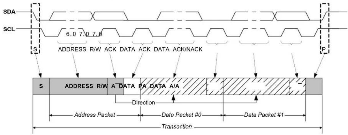
text_image
SDA SCL 6..0 7..0 7..0 ADDRESS R/W ACK DATA ACK DATA ACK/NACK S P S ADDRESS R/W A DATA PA DATA A/A Direction Address Packet Data Packet #0 Data Packet #1 Transaction26.6.2 Basic Operation
26.6.2.1 Initialization
The following registers are enable-protected, meaning they can be written only when the I²C interface is disabled (CTRLA. ENABLE is '0'):
• Control A register (CTRLA), except Enable (CTRLA.ENABLE) and Software Reset (CTRLA.SWRST) bits
- Control B register (CTRLB), except Acknowledge Action (CTRLB.ACKACT) and Command (CTRLB.CMD) bits
• Baud register (BAUD)
- Address register (ADDR) in client operation.
When the I ^2 C is enabled or is being enabled (CTRLA.ENABLE=1), writing to these registers will be discarded. If the I ^2 C is being disabled, writing to these registers will be completed after the disabling.
Enable-protection is denoted by the "Enable-Protection" property in the register description.
Before the I2C is enabled it must be configured as outlined by the following steps:
- Select I²C Host or Client mode by writing 0x4 (Client mode) or 0x5 (Host mode) to the Operating Mode bits in the CTRLA register (CTRLA.MODE).
- If desired, select the SDA Hold Time value in the CTRLA register (CTRLA.SDAHOLD).
- If desired, enable smart operation by setting the Smart Mode Enable bit in the CTRLB register (CTRLB.SMEN).
- If desired, enable SCL low time-out by setting the SCL Low Time-Out bit in the Control A register (CTRLA.LOWTOUTEN).
- In Host mode:
a. Select the inactive bus time-out in the Inactive Time-Out bit group in the CTRLA register (CTRLA.INACTOUT).
b. Write the Baud Rate register (BAUD) to generate the desired baud rate.
In Client mode:
a. Configure the address match configuration by writing the Address Mode value in the CTRLB register (CTRLB.AMODE).
b. Set the Address and Address Mask value in the Address register (ADDR.ADDR and ADDR.ADDRMASK) according to the address configuration.
26.6.2.2 Enabling, Disabling, and Resetting
This peripheral is enabled by writing '1' to the Enable bit in the Control A register (CTRLA.ENABLE), and disabled by writing '0' to it.
Refer to CTRLA registers for details.
Related Links
26.10.1. CTRLA
26.6.2.3 I²C Bus State Logic
The Bus state logic includes several logic blocks that continuously monitor the activity on the I2C bus lines in all Sleep modes with running GCLK_SERCOM_x clocks. The start and stop detectors and the bit counter are all essential in the process of determining the current Bus state. The Bus state is determined according to Bus State Diagram. Software can get the current Bus state by reading the Host Bus State bits in the Status register (STATUS.BUSSTATE). The value of STATUS.BUSSTATE in the figure is shown in binary.
Figure 26-4. Bus State Diagram
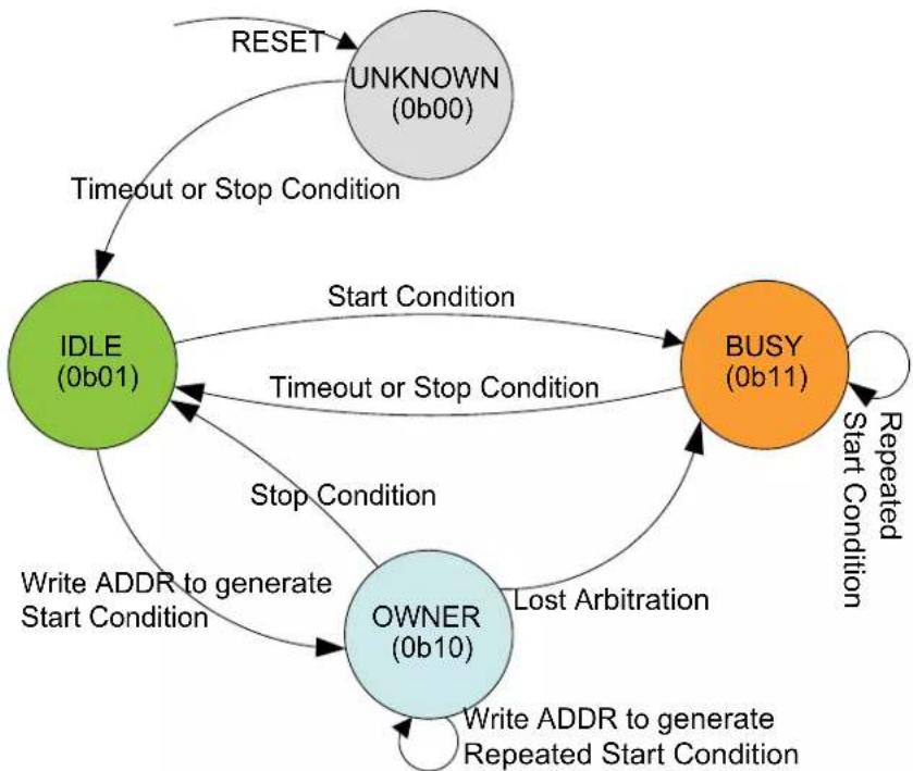
flowchart
graph TD
    A["IDLE (0b01)"] -->|Timeout or Stop Condition| B["UNKNOWN (0b00)"]
    A -->|Start Condition| C["BUSY (0b11)"]
    A -->|Stop Condition| D["OWNER (0b10)"]
    D -->|Write ADDR to generate Start Condition| A
    D -->|Write ADDR to generate Repeated Start Condition| A
    B -->|Repeated Start Condition| C
    C -->|Lost Arbitration| D
    D -->|Write ADDR to generate Stop Condition| A
    E["RESET"] --> A
The Bus state machine is active when the I²C host is enabled.
After the I ^2 C host has been enabled, the Bus state is UNKNOWN (0b00). From the UNKNOWN state, the bus will transition to IDLE (0b01) by either:
- Forcing by writing 0b01 to STATUS.BUSSTATE
• A Stop condition is detected on the bus
- If the inactive bus time-out is configured for SMBus compatibility (CTRLA.INACTOUT) and a time-out occurs.
Note: Once a known Bus state is established, the Bus state logic will not re-enter the UNKNOWN state.
When the bus is IDLE it is ready for a new transaction. If a Start condition is issued on the bus by another I²C host in a multi-host setup, the bus becomes BUSY (0b11). The bus will re-enter IDLE
either when a Stop condition is detected, or when a time-out occurs (inactive bus time-out needs to be configured).
If a Start condition is generated internally by writing the Address bit group in the Address register (ADDR.ADDR) while IDLE, the OWNER state (0b10) is entered. If the complete transaction was performed without interference, i.e., arbitration was not lost, the I ^2 C host can issue a Stop condition, which will change the Bus state back to IDLE.
However, if a packet collision is detected while in OWNER state, the arbitration is assumed lost and the Bus state becomes BUSY until a Stop condition is detected. A repeated Start condition will change the Bus state only if arbitration is lost while issuing a repeated start.
Note: Violating the protocol may cause the I ^2 C to hang. If this happens it is possible to recover from this state by a software Reset (CTRLA.SWRST='1').
Related Links
26.10.1. CTRLA
26.6.2.4 I²C Host Operation
The I ^2 C Host is byte-oriented and interrupt based. The number of interrupts generated is kept at a minimum by automatic handling of most incidents. The software driver complexity and code size are reduced by auto-triggering of operations, and a Special Smart mode, which can be enabled by the Smart Mode Enable bit in the Control B register (CTRLB.SMEN).
When SCL Stretch Mode (CTRLA.SCLSM) is '0', SCL is stretched before or after the Acknowledge bit. In this mode the I²C Host operates according to Host Behavioral Diagram (SCLSM=0). The circles labeled "Mn" (M1, M2..) indicate the nodes the bus logic can jump to, based on software or hardware interaction.
This diagram is used as reference for the description of the I ^2 C Host operation throughout the document.
Figure 26-5. I²C Host Behavioral Diagram
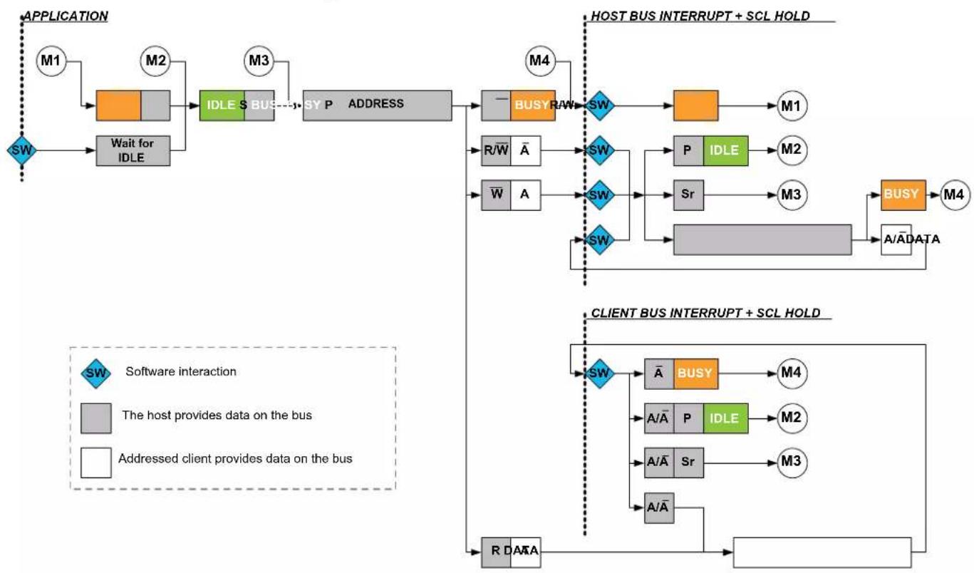
flowchart
graph TD
    A["APPLICATION"] --> B["M1"]
    B --> C["Wait for IDLE"]
    C --> D["IDLE S BUS"]
    D --> E["SY P ADDRESS"]
    E --> F["— BUSY RAW"]
    F --> G["SW"]
    G --> H[" "] --> I["M1"]
    F --> J["R/W̅ A̅"]
    J --> K["SW"]
    K --> L["P IDLE"]
    L --> M["M2"]
    K --> N["W̅ A"]
    N --> O["SW"]
    O --> P["Sr"]
    P --> Q["M3"]
    K --> R["SW"]
    R --> S[" "] --> T["BUSY"]
    T --> U["M4"]
    F --> V[" "] --> W["A/ĀDATA"]
    W --> X[" "] --> Y["A/ĀDATA"]
    F --> Z[" "] --> AA[" "] --> AB[" "] --> AC[" "] --> AD[" "] --> AE[" "] --> AF[" "] --> AG[" "] --> AH[" "] --> AI[" "] --> AJ[" "] --> AK[" "] --> AL[" "] --> AM[" "] --> AN[" "] --> AO[" "] --> AP[" "] --> AQ[" "] --> AR[" "] --> AS[" "] --> AT[" "] --> AU[" "] --> AV[" "] --> AW[" "] --> AX[" "] --> AY[" "] --> AZ[" "] --> BA[" "] --> BB[" "] --> BC[" "] --> BD[" "] --> BE[" "] --> BF[" "] --> BG[" "] --> BH[" "] --> BI[" "] --> BJ[" "] --> BK[" "] --> BL[" "] --> BM[" "] --> BN[" "] --> BO[" "] --> BP[" "] --> BQ[" "] --> BR[" "] --> BS[" "] --> BT[" "] --> BU[" "] --> BV[" "] --> BW[" "] --> BX[" "] --> BY[" "] --> BZ[" "] --> CA[" "] --> CB[" "] --> CC[" "] --> CD[" "] --> CE[" "] --> CF[" "] --> CG[" "] --> CH[" "] --> CI[" "] --> CJ[" "] --> CK[" "] --> CR[" "] --> CS[" "] --> CT[" "] --> CU[" "] --> CV[" "] --> CW[" "] --> CX[" "] --> CY[" "] --> CZ[" "] --> DA[" "] --> DB[" "] --> DC[" "] --> DV[" "] --> DW[" "] --> DX[" "] --> DXB[" "] --> DXC[" "] --> DXD[" "] --> DXE[" "] --> DXF[" "] --> DXG[" "] --> DXH[" "] --> DXI[" "] --> DXJ[" "] --> DXK[" "] --> DXL[" "] --> DXM[" "] --> DXN[" "] --> DXO[" "] --> DXP[" "] --> DXQ[" "] --> DXR[" "] --> DXS[" "] --> DXT[" "] --> DXU[" "] --> DXV[" "] --> DXW[" "] --> DXX[" "] --> DXY[" "] --> DXZ[" "] --> DXW
    subgraph HOST_BUS_INTERRUPT + SCL_HOLD
        F
        G
        H
        I
        J
        K
        L
        M
        N
        P
        Q
        R
        S
        T
        U
        V
        W
        X
        Y
        Z
        AA
        AB
        AC
        AD
        AE
        AF
        AG
        AH
        AI
        AJ
        AK
        AL
        AM
        AN
        AO
        AP
        AQ
        AR
        AS
        AT
        AU
        AV
        AW
        AX
        AY
        AZ
        BA
        BB
        BC
        BD
        BE
        BF
        BG
        BH
        BI
        BJ
        BK
        BL
        BM
        BN
        BO
        BP
        BPB
        BPCC
        BPCCB
        BPCCD
        BPCCD
        BPCCD
    end

    subgraph CLIENT_BUS_INTERRUPT + SCL_HOLD
        F
        G
        H
        I
        J
        K
        L
        M
        N
        P
        Q
        R
        S
        T
        U
        V
        W
        X
        Y
        Z
        AA
        AB
        AC
        AD
    end

    SW["SW"]
    SWA["Software interaction"]
    SWB["The host provides data on the bus"]
    SWC["Addressed client provides data on the bus"]
    SWD["The host provides data on the bus"]
    SWE["Addressed client provides data on the bus"]
    SWF["The host provides data on the bus"]
    SWG["Addressed client provides data on the bus"]
    SWH["The host provides data on the bus"]
    SWI["Addressed client provides data on the bus"]
    SWJ["The host provides data on the bus"]
    SWK["Addressed client provides data on the bus"]
    SWL["The host provides data on the bus"]
    SWM["Addressed client provides data on the bus"]
    SWN["The host provides data on the bus"]
    SWO["Addressed client provides data on the bus"]
    SWP["The host provides data on the bus"]
    SWQ["Addressed client provides data on the bus"]
    SWR["The host provides data on the bus"]
    SWS["Addressed client provides data on the bus"]
    SWT["The host provides data on the bus"]
    SWU["Addressed client provides data on the bus"]
    SWV["Addressed client provides data on the bus"]
    SWW["Addressed client provides data on the bus"]
    SWX["Addressed client provides data on the bus"]
    SWY["Addressed client provides data on the bus"]
    SWZ["Addressed client provides data on the bus"]
    SWW["Addressed client provides data on the bus"]
    SWX["Addressed client provides data on the bus"]
    SWY["Addressed client provides data on the bus"]
    SWZ["Addressed client provides data on the bus"]
    SWW["Addressed client provides data on the bus"]
    SWX["Addressed client provides data on the bus"]
    SWY["Addressed client provides data on the Bus"]
Host Clock Generation
The SERCOM peripheral supports several I²C bidirectional modes:
• Standard mode (Sm) up to 100 kHz
- Fast mode (Fm) up to 400 kHz
The Host clock configuration for Sm and Fm are described as follows:
Clock Generation (Standard-Mode, Fast-Mode, and Fast-Mode Plus)
In I²C Sm and Fm mode, the Host clock (SCL) frequency is determined as described in this section:
The low ( T_LOW ) and high ( T_HIGH ) times are determined by the Baud Rate register (BAUD), while the rise ( T_RISE ) and fall ( T_FALL ) times are determined by the bus topology. Because of the wired-AND logic of the bus, T_FALL will be considered as part of T_LOW . Similarly, T_RISE will be in a state between T_LOW and T_HIGH until a high state has been detected.
Figure 26-6. SCL Timing
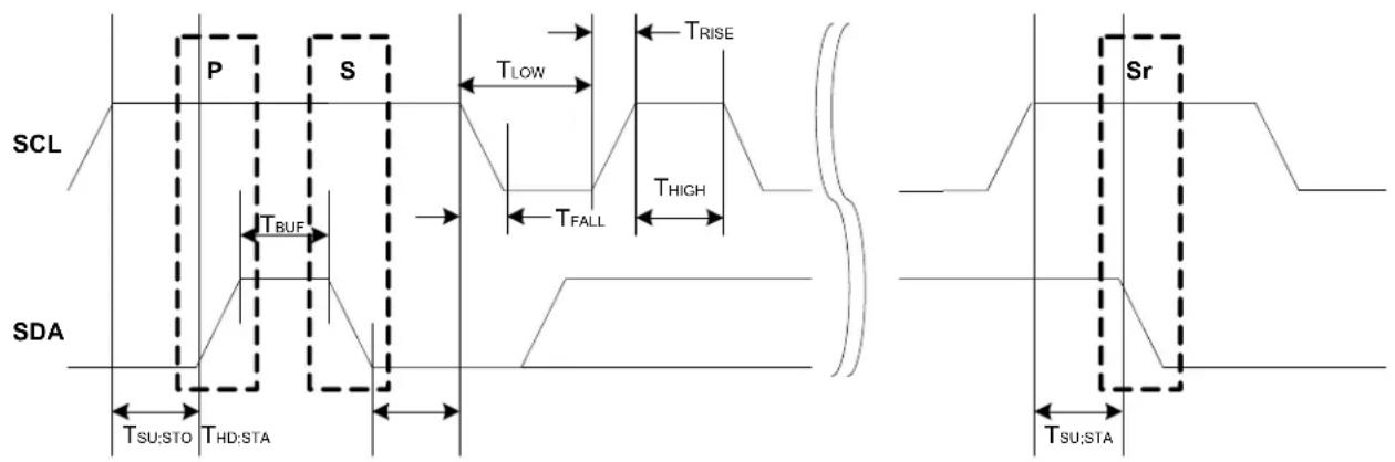
text_image
SCL P S T_Low T_RISE T_HIGH T_RUF T_FALL T_SU:STO THD:STA SDA Sr T_SU:STAThe following parameters are timed using the SCL low time period T_LOW . This comes from the Host Baud Rate Low bit group in the Baud Rate register (BAUD.BAUDLOW). When BAUD.BAUDLOW=0, or the Host Baud Rate bit group in the Baud Rate register (BAUD.BAUD) determines it.
- T_LOW - Low period of SCL clock
- T_SU;STO - Set-up time for stop condition
- T_BUF - Bus free time between stop and start conditions
- T_HD;STA - Hold time (repeated) start condition
- T_SU;STA - Set-up time for repeated start condition
- T_HIGH is timed using the SCL high time count from BAUD.BAUD
- T_RISE is determined by the bus impedance; for internal pull-ups. Refer to Electrical Characteristics.
- T_FALL is determined by the open-drain current limit and bus impedance; can typically be regarded as zero. Refer to Electrical Characteristics for details.
The SCL frequency is given by:
$$ f _ {\mathrm{SCL}} = \frac {1}{T _ {\mathrm{LOW}} + T _ {\mathrm{HIGH}} + T _ {\mathrm{RISE}}} $$
When BAUD.BAUDLOW is zero, the BAUD.BAUD value is used to time both SCL high and SCL low. In this case the following formula will give the SCL frequency:
$$ f _ {\mathrm{SCL}} = \frac {f _ {\mathrm{GCLK}}}{1 0 + 2 B A U D + f _ {\mathrm{GCLK}} \cdot T _ {\mathrm{RISE}}} $$
When BAUD.BAUDLOW is non-zero, the following formula determines the SCL frequency:
$$ f _ {\mathrm{SCL}} = \frac {f _ {\mathrm{GCLK}}}{1 0 + B A U D + B A U D L O W + f _ {\mathrm{GCLK}} \cdot T _ {\mathrm{RISE}}} $$
The following formulas can determine the SCL T_LOW and T_HIGH times:
$$ T _ {\mathrm{LOW}} = \frac {B A U D L O W + 5}{f _ {\mathrm{GCLK}}} $$
$$ T _ {\mathrm{HIGH}} = \frac {B A U D + 5}{f _ {\mathrm{GCLK}}} $$
Startup Timing The minimum time between SDA transition and SCL rising edge is 6 APB cycles when the DATA register is written in smart mode. If a greater startup time is required due to long rise times, the time between DATA write and IF clear must be controlled by software.
Note: When timing is controlled by user, the Smart Mode cannot be enabled.
Transmitting Address Packets
The I ^2 C Host starts a bus transaction by writing the I ^2 C Client address to ADDR.ADDR and the direction bit, as described in 26.6.1. Principle of Operation. If the bus is busy, the I ^2 C Host will wait until the bus becomes idle before continuing the operation. When the bus is idle, the I ^2 C Host will issue a start condition on the bus. The I ^2 C Host will then transmit an address packet using the address written to ADDR.ADDR. After the address packet has been transmitted by the I ^2 C Host, one of four cases will arise according to arbitration and transfer direction.
Case 1: Arbitration lost or bus error during address packet transmission
If arbitration was lost during transmission of the address packet, the Host on Bus bit in the Interrupt Flag Status and Clear register (INTFLAG.MB) and the Arbitration Lost bit in the Status register (STATUS.ARBLOST) are both set. Serial data output to SDA is disabled, and the SCL is released, which disables clock stretching. In effect the I²C Host is no longer allowed to execute any operation on the bus until the bus is idle again. A bus error will behave similarly to the arbitration lost condition. In this case, the MB interrupt flag and Host Bus Error bit in the Status register (STATUS.BUSERR) are both set in addition to STATUS.ARBLOST.
The Host Received Not Acknowledge bit in the Status register (STATUS.RXNACK) will always contain the last successfully received acknowledge or not acknowledge indication.
In this case, software will typically inform the application code of the condition and then clear the interrupt flag before exiting the interrupt routine. No other flags have to be cleared at this moment, because all flags will be cleared automatically the next time the ADDR.ADDR register is written.
Case 2: Address packet transmit complete – No ACK received
If there is no I²C Client device responding to the address packet, then the INTFLAG.MB interrupt flag and STATUS.RXNACK will be set. The clock hold is active at this point, preventing further activity on the bus.
The missing ACK response can indicate that the I²C Client is busy with other tasks or sleeping. Therefore, it is not able to respond. In this event, the next step can be either issuing a stop condition (recommended) or resending the address packet by a repeated start condition. When using SMBus logic, the Client must ACK the address. If there is no response, it means that the Client is not available on the bus.
Case 3: Address packet transmit complete – Write packet, Host on Bus set
If the I ^2 C Host receives an acknowledge response from the I ^2 C Client, INTFLAG.MB will be set and STATUS.RXNACK will be cleared. The clock hold is active at this point, preventing further activity on the bus.
In this case, the software implementation becomes highly protocol dependent. Three possible actions can enable the I ^2 C operation to continue:
- Initiate a data transmit operation by writing the data byte to be transmitted into DATA.DATA.
- Transmit a new address packet by writing ADDR.ADDR. A repeated start condition will automatically be inserted before the address packet.
- Issue a stop condition, consequently terminating the transaction.
Case 4: Address packet transmit complete – Read packet, Client on Bus set
If the I ^2 C Host receives an ACK from the I ^2 C Client, the I ^2 C Host proceeds to receive the next byte of data from the I ^2 C Client. When the first data byte is received, the Client on Bus bit in the Interrupt Flag register (INTFLAG.SB) will be set and STATUS.RXNACK will be cleared. The clock hold is active at this point, preventing further activity on the bus.
In this case, the software implementation becomes highly protocol dependent. Three possible actions can enable the I ^2 C operation to continue:
- Let the I ^2 C Host continue to read data by acknowledging the data received. ACK can be sent by software, or automatically in smart mode.
- Transmit a new address packet.
- Terminate the transaction by issuing a stop condition.
Note: An ACK or NACK will be automatically transmitted if smart mode is enabled. The Acknowledge Action bit in the Control B register (CTRLB.ACKACT) determines whether ACK or NACK should be sent.
Transmitting Data Packets
When an address packet with direction Host Write (see Figure 26-3) was transmitted successfully, INTFLAG.MB will be set. The I²C Host will start transmitting data via the I²C bus by writing to DATA.DATA, and monitor continuously for packet collisions.
If a collision is detected, the I ^2 C Host will lose arbitration and STATUS.ARBLOST will be set. If the transmit was successful, the I ^2 C Host will receive an ACK bit from the I ^2 C Client, and STATUS.RXNACK will be cleared. INTFLAG.MB will be set in both cases, regardless of arbitration outcome.
It is recommended to read STATUS.ARBLOST and handle the arbitration lost condition in the beginning of the I ^2 C Host on Bus interrupt. This can be done as there is no difference between handling address and data packet arbitration.
STATUS.RXNACK must be checked for each data packet transmitted before the next data packet transmission can commence. The I²C Host is not allowed to continue transmitting data packets if a NACK is received from the I²C Client.
Receiving Data Packets
When INTFLAG.SB is set, the I²C Host will already have received one data packet. The I²C Host must respond by sending either an ACK or NACK. Sending a NACK may be unsuccessful when arbitration is lost during the transmission. In this case, a lost arbitration will prevent setting INTFLAG.SB. Instead, INTFLAG.MB will indicate a change in arbitration. Handling of lost arbitration is the same as for data bit transmission.
26.6.2.5 I²C Client Operation
The I ^2 C Client is byte-oriented and interrupt-based. The number of interrupts generated is kept at a minimum by automatic handling of most events. The software driver complexity and code size are reduced by auto-triggering of operations, and a special smart mode, which can be enabled by the Smart Mode Enable bit in the Control B register (CTRLB.SMEN).
This diagram is used as reference for the description of the I ^2 C Client operation throughout the document.
Figure 26-7. I²C Client Behavioral Diagram
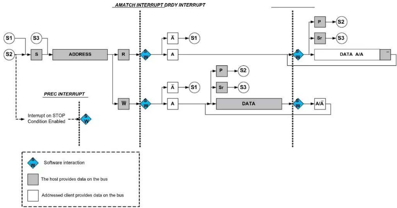
flowchart
graph TD
    subgraph "AMATCH INTERRUPT DRDY INTERRUPT"
        S1["S1"] --> S3["S3"]
        S2["S2"] --> S3["S3"]
        S3 --> ADDRESS["ADDRESS"]
        R["R"] --> SW1["SW"]
        SW1 --> A["A"]
        A --> S1["S1"]
        SW1 --> SW2["SW"]
        S1 --> S2["P"]
        S2 --> S2["S2"]
        S2 --> Sr["Sr"]
        Sr --> S3["S3"]
        S3 --> DATA["DATA A/A"]
    end

    subgraph "PREC INTERRUPT"
        W["W"] --> SW3["SW"]
        SW3 --> A["A"]
        A --> S1["S1"]
        S1 --> P["P"]
        S1 --> Sr["Sr"]
        Sr --> S3["S3"]
        S3 --> DATA["DATA"]
        P --> S2["S2"]
        Sr --> S3["S3"]
        S3 --> DATA["DATA"]
    end

    style S1 fill:#f9f,stroke:#333
    style S2 fill:#f9f,stroke:#333
    style S3 fill:#f9f,stroke:#333
    style W fill:#ccf,stroke:#333
    style S1 fill:#dfd,stroke:#333
    style S2 fill:#dfd,stroke:#333
    style S3 fill:#dfd,stroke:#333
    style S1 fill:#dfd,stroke:#333
    style S2 fill:#dfd,stroke:#333
    style S3 fill:#dfd,stroke:#333
    style S1 fill:#dfd,stroke:#333
    style S2 fill:#dfd,stroke:#333
    style S3 fill:#dfd,stroke:#333
    style S1 fill:#dfd, stroke:#000
    style S2 fill:#dfd, stroke:#000
    style S3 fill:#dfd, stroke:#000
    style S1 fill:#dfd, stroke:#000
    style S2 fill:#dfd, stroke:#000
    style S3 fill:#dfd, stroke:#000
    style S1 fill:#dfd, stroke:#000
    style S2 fill:#dfd, stroke:#000
    style S3 fill:#dfd, stroke:#000
    style S1 fill:#dfd, stroke:#000


Receiving Address Packets
When a start condition is detected, the successive address packet will be received and checked by the address match logic. If the received address is not a match, the packet will be rejected, and the I²C Client will wait for a new start condition. If the received address is a match, the Address Match bit in the Interrupt Flag register (INTFLAG.AMATCH) will be set.
SCL will be stretched until the I²C Client clears INTFLAG.AMATCH. As the I²C Client holds the clock by forcing SCL low, the software has unlimited time to respond.
The direction of a transaction is determined by reading the Read / Write Direction bit in the Status register (STATUS.DIR). This bit will be updated only when a valid address packet is received.
If the Transmit Collision bit in the Status register (STATUS.COLL) is set, this indicates that the last packet addressed to the I²C Client had a packet collision. A collision causes the SDA and SCL lines to be released without any notification to software. Therefore, the next AMATCH interrupt is the first indication of the previous packet's collision. Collisions are intended to follow the SMBus Address Resolution Protocol (ARP).
After the address packet has been received from the I²C Host, one of two cases will arise based on transfer direction.
Case 1: Address packet accepted - Read flag set
The STATUS.DIR bit is '1', indicating an I²C Host read operation. The SCL line is forced low, stretching the bus clock. If an ACK is sent, I²C Client hardware will set the Data Ready bit in the Interrupt Flag register (INTFLAG.DRDY), indicating data are needed for transmit. If a NACK is sent, the I²C Client will wait for a new start condition and address match.
Typically, software will immediately acknowledge the address packet by sending an ACK/NACK bit. The I²C Client Command bit field in the Control B register (CTRLB.CMD) can be written to '0x3' for both read and write operations as the command execution is dependent on the STATUS.DIR
bit. Writing '1' to INTFLAG.AMATCH will also cause an ACK/NACK to be sent corresponding to the CTRLB.ACKACT bit.
Case 2: Address packet accepted - Write flag set
The STATUS.DIR bit is cleared, indicating an I²C Host write operation. The SCL line is forced low, stretching the bus clock. If an ACK is sent, the I²C Client will wait for data to be received. Data, repeated start or stop can be received.
If a NACK is sent, the I²C Client will wait for a new start condition and address match. Typically, software will immediately acknowledge the address packet by sending an ACK/NACK. The I²C Client command CTRLB.CMD = 3 can be used for both read and write operation as the command execution is dependent on STATUS.DIR.
Writing '1' to INTFLAG.AMATCH will also cause an ACK/NACK to be sent corresponding to the CTRLB.ACKACT bit.
Receiving and Transmitting Data Packets
After the I ^2 C Client has received an address packet, it will respond according to the direction either by waiting for the data packet to be received or by starting to send a data packet by writing to DATA.DATA. When a data packet is received or sent, INTFLAG.DRDY will be set. After receiving data, the I ^2 C Client will send an acknowledge according to CTRLB.ACKACT.
Case 1: Data received
INTFLAG.DRDY is set, and SCL is held low, pending for SW interaction.
Case 2: Data sent
When a byte transmission is successfully completed, the INTFLAG.DRDY interrupt flag is set. If NACK is received, indicated by STATUS.RXNACK=1, the I²C Client must expect a stop or a repeated start to be received. The I²C Client must release the data line to allow the I²C Host to generate a stop or repeated start. Upon detecting a stop condition, the Stop Received bit in the Interrupt Flag register (INTFLAG.PREC) will be set and the I²C Client will return to IDLE state.
26.6.3 Additional Features
26.6.3.1 SMBus
The I ^2 C includes three hardware SCL low time-outs which allow a time-out to occur for SMBus SCL low time-out, host extend time-out, and client extend time-out. This allows for SMBus functionality These time-outs are driven by the GCLK_SERCOM_SLOW clock. The GCLK_SERCOM_SLOW clock is used to accurately time the time-out and must be configured to use a 32.768 kHz oscillator. The I ^2 C interface also allows for a SMBus compatible SDA hold time.
- T_TIMEOUT : SCL low time of 25..35ms - Measured for a single SCL low period. It is enabled by CTRLA.LOWTOUTEN.
- T_LOW:SEXT : Cumulative clock low extend time of 25 ms – Measured as the cumulative SCL low extend time by a client device in a single message from the initial START to the STOP. It is enabled by CTRLA.SEXTTOEN.
- T_LOW:MEXT : Cumulative clock low extend time of 10 ms – Measured as the cumulative SCL low extend time by the host device within a single byte from START-to-ACK, ACK-to-ACK, or ACK-to-STOP. It is enabled by CTRLA.MEXTTOEN.
26.6.3.2 Smart Mode
The I ^2 C interface has a smart mode that simplifies application code and minimizes the user interaction needed to adhere to the I ^2 C protocol. The smart mode accomplishes this by automatically issuing an ACK or NACK (based on the content of CTRLB.ACKACT) as soon as DATA.DATA is read.
26.6.3.3 4-Wire Mode
Writing a '1' to the Pin Usage bit in the Control A register (CTRLA.PINOUT) will enable 4-Wire mode operation. In this mode, the internal I²C tri-state drivers are bypassed, and an external I²C compliant tri-state driver is needed when connecting to an I²C bus.
Figure 26-8. I²C Pad Interface
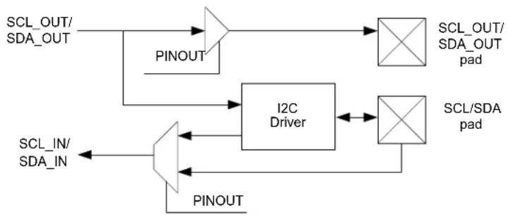
flowchart
graph TD
    A["SCL_OUT/SDA_OUT"] --> B["Pinout"]
    B --> C["I2C Driver"]
    C --> D["SCL_OUT/SDA_OUT pad"]
    C --> E["SCL/SDA pad"]
    F["SCL_IN/SDA_IN"] --> G["Pinout"]
    G --> H["I2C Driver"]
    H --> I["SCL_OUT/SDA_OUT pad"]
    H --> J["SCL/SDA pad"]
26.6.3.4 Quick Command
Setting the Quick Command Enable bit in the Control B register (CTRLB.QCEN) enables quick command. When quick command is enabled, the corresponding Interrupt flag (INTFLAG.SB or INTFLAG.MB) is set immediately after the client acknowledges the address. At this point, the software can either issue a Stop command or a repeated start by writing CTRLB.CMD or ADDR.ADDR.
26.6.4 Interrupts
The I ^2 C Client has the following interrupt sources. These are asynchronous interrupts. They can wake-up the device from any sleep mode:
- Data Ready (DRDY)
- Address Match (AMATCH)
- Stop Received (PREC)
The I ^2 C Host has the following interrupt sources. These are asynchronous interrupts. They can wake-up the device from any sleep mode:
- Client on Bus (SB)
- Host on Bus (MB)
Each interrupt source has its own interrupt flag. The interrupt flag in the Interrupt Flag Status and Clear register (INTFLAG) will be set when the interrupt condition is meet. Each interrupt can be individually enabled by writing '1' to the corresponding bit in the Interrupt Enable Set register (INTENSET), and disabled by writing '1' to the corresponding bit in the Interrupt Enable Clear register (INTENCLR). An interrupt request is generated when the interrupt flag is set and the corresponding interrupt is enabled. The interrupt request active until the interrupt flag is cleared, the interrupt is disabled or the I2C is reset. Refer to INTFLAG register for details on how to clear interrupt flags.
The I ^2 C has one common interrupt request line for all the interrupt sources. The value of INTFLAG indicates which interrupt is executed. Note that interrupts must be globally enabled for interrupt requests. Refer to Nested Vector Interrupt Controller for details.
Related Links
10.2. Nested Vector Interrupt Controller
26.10.7. INTFLAG
26.6.5 Sleep Mode Operation
I²C Host Operation
The generic clock (GCLK_SERCOMx_CORE) will continue to run in idle sleep mode. If the Run In Standby bit in the Control A register (CTRLA.RUNSTDBY) is '1', the GLK_SERCOMx_CORE will also run in Standby Sleep mode. Any interrupt can wake-up the device.
If CTRLA.RUNSTDBY=0, the GLK_SERCOMx_CORE will be disabled after any ongoing transaction is finished. Any interrupt can wake-up the device.
I²C Client Operation
Writing CTRLA.RUNSTDBY=1 will allow the Address Match interrupt to wake-up the device.
When CTRLA.RUNSTDBY=0, all receptions will be dropped.
26.6.6 Synchronization
Due to asynchronicity between the main clock domain and the peripheral clock domains, some registers need to be synchronized when written or read.
The following bits are synchronized when written:
- Software Reset bit in the CTRLA register (CTRLA.SWRST)
- Enable bit in the CTRLA register (CTRLA.ENABLE)
- Command bits in CTRLB register (CTRLB.CMD)
- Write to Bus State bits in the Status register (STATUS.BUSSTATE)
- Address bits in the Address register (ADDR.ADDR) when in host operation.
The following registers are synchronized when written:
• Data (DATA) when in host operation
Required write-synchronization is denoted by the "Write-Synchronized" property in the register description.
Related Links
13.3. Register Synchronization
26.7 Register Summary - I2C Client
| Offset | Name Bit Pos. 76 | 543210 | ||||||||
| 0x00 CTRLA | 7:0 RUNSTDBY MODE[2:0] ENABLE SWRST | |||||||||
| 15:8 | ||||||||||
| 23:16 | SDAHOLD[1:0] PINOUT | |||||||||
| 31:24 | LOWTOUT | |||||||||
| 0x04 CTRLB | 7:0 | |||||||||
| 15:8 | AMODE[1:0] | SMEN | ||||||||
| 23:16 | ACKACT CMD[1:0] | |||||||||
| 31:24 | ||||||||||
| 0x08 ... 0x0B | Reserved | |||||||||
| 0x0C | INTENCLR | 7:0 | DRDY | AMATCH | PREC | |||||
| 0x0D | INTENSET | 7:0 | DRDY | AMATCH | PREC | |||||
| 0x0E | INTFLAG | 7:0 | DRDY | AMATCH | PREC | |||||
| 0x0F | Reserved | |||||||||
| 0x10 | STATUS | 7:0 | CLKHOLD | LOWTOUT | SR | DIR | RXNACK | COLL | BUSERR | |
| 15:8 | SYNCBUSY | |||||||||
| 0x12 ... 0x13 | Reserved | |||||||||
| 0x14 ADDR | 7:0 | ADDR[6:0] | GENCEN | |||||||
| 15:8 | ADDR[7] | |||||||||
| 23:16 | ADDRMASK[6:0] | |||||||||
| 31:24 | ||||||||||
| 0x18 | DATA | 7:0 | DATA[7:0] | |||||||
| 15:8 | ||||||||||
26.8 Register Description - I ^2 C Client
Registers can be 8, 16, or 32 bits wide. Atomic 8-, 16- and 32-bit accesses are supported. In addition, the 8-bit quarters and 16-bit halves of a 32-bit register, and the 8-bit halves of a 16-bit register can be accessed directly.
Some registers are optionally write-protected by the Peripheral Access Controller (PAC). Optional PAC write-protection is denoted by the "PAC Write-Protection" property in each individual register description. For details, refer to Register Access Protection.
Some registers are synchronized when read and/or written. Synchronization is denoted by the "Write-Synchronized" or the "Read-Synchronized" property in each individual register description. For details, refer to 26.6.6. Synchronization.
Some registers are enable-protected, meaning they can only be written when the peripheral is disabled. Enable-protection is denoted by the "Enable-Protected" property in each individual register description.
26.8.1 Control A
Name: CTRLA
Offset: 0x00
Reset: 0x00000000
Property: PAC Write-Protection, Enable-Protected, Write-Synchronized
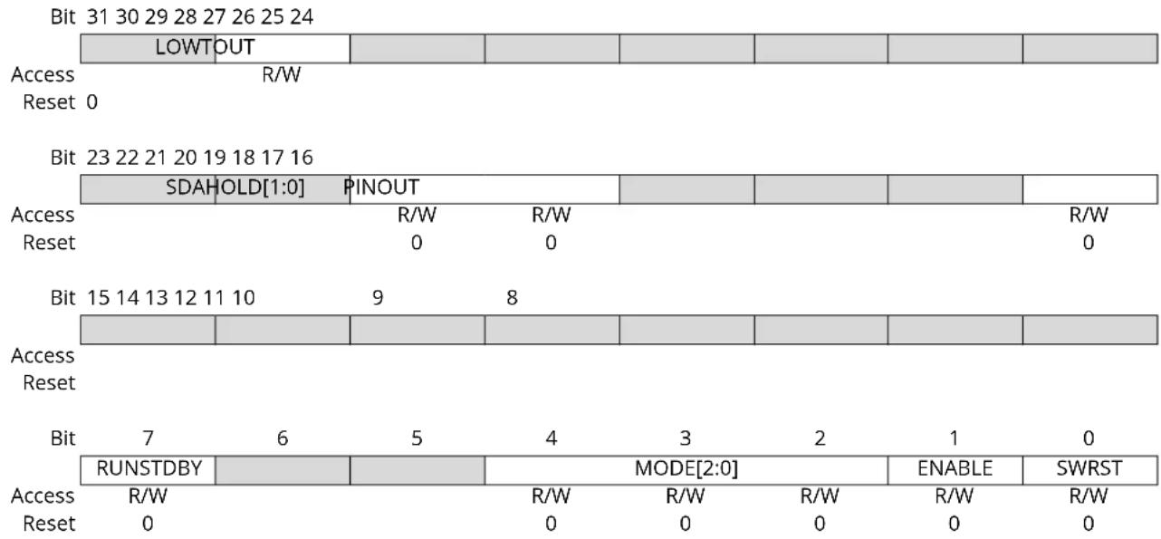
Bit 30 - LOWTOUT SCL Low Time-Out
This bit enables the SCL low time-out. If SCL is held low for 25ms-35ms, the Client will release its clock hold, if enabled, and reset the internal state machine. Any interrupt flags set at the time of time-out will remain set.
| Value | Description |
| 0 | Time-out disabled. |
| 1 | Time-out enabled. |
Bits 21:20 - SDAHOLD[1:0] SDA Hold Time
These bits define the SDA hold time with respect to the negative edge of SCL.
These bits are not synchronized.
| Value | Name | Description |
| 0x0 | DIS | Disabled |
| 0x1 | 75NS | 50-100ns hold time |
| 0x2 | 450NS 300-600ns hold time | |
| 0x3 | 600NS 400-800ns hold time |
Bit 16 - PINOUT Pin Usage
This bit sets the pin usage to either two- or four-wire operation:
This bit is not synchronized.
| Value | Description |
| 0 | 4-wire operation disabled |
| 1 | 4-wire operation enabled |
Bit 7 - RUNSTDBY Run in Standby
This bit defines the functionality in standby sleep mode.
This bit is not synchronized.
| Value Description | |
| 0 | Disabled - All reception is dropped. |
| 1 | Wake on address match, if enabled. |
Bits 4:2 - MODE[2:0] Operating Mode
These bits must be written to 0x04 to select the I ^2 C Client serial communication interface of the SERCOM.
These bits are not synchronized.
Bit 1 - ENABLE Enable
Due to synchronization, there is delay from writing CTRLA. ENABLE until the peripheral is enabled/disabled. The value written to CTRL. ENABLE will read back immediately and the Enable Synchronization Busy bit in the Synchronization Busy register (SYNCBUSY. ENABLE) will be set. SYNCBUSY. ENABLE will be cleared when the operation is complete.
This bit is not enable-protected.
| Value Description | |
| 0 | The peripheral is disabled or being disabled. |
| 1 | The peripheral is enabled. |
Bit 0 - SWRST Software Reset
Writing '0' to this bit has no effect.
Writing '1' to this bit resets all registers in the SERCOM, except DBGCTRL, to their initial state, and the SERCOM will be disabled.
Writing '1' to CTRLA.SWRST will always take precedence, meaning that all other writes in the same write-operation will be discarded. Any register write access during the ongoing reset will result in an APB error. Reading any register will return the reset value of the register.
Due to synchronization, there is a delay from writing CTRLA.SWRST until the reset is complete.
CTRLA.SWRST and SYNCBUSY.SWRST will both be cleared when the reset is complete.
This bit is not enable-protected.
| Value Description | |
| 0 | There is no reset operation ongoing. |
| 1 | The reset operation is ongoing. |
26.8.2 Control B
Name: CTRLB
Offset: 0x04
Reset: 0x00000000
Property: PAC Write-Protection, Enable-Protected, Write-Synchronized
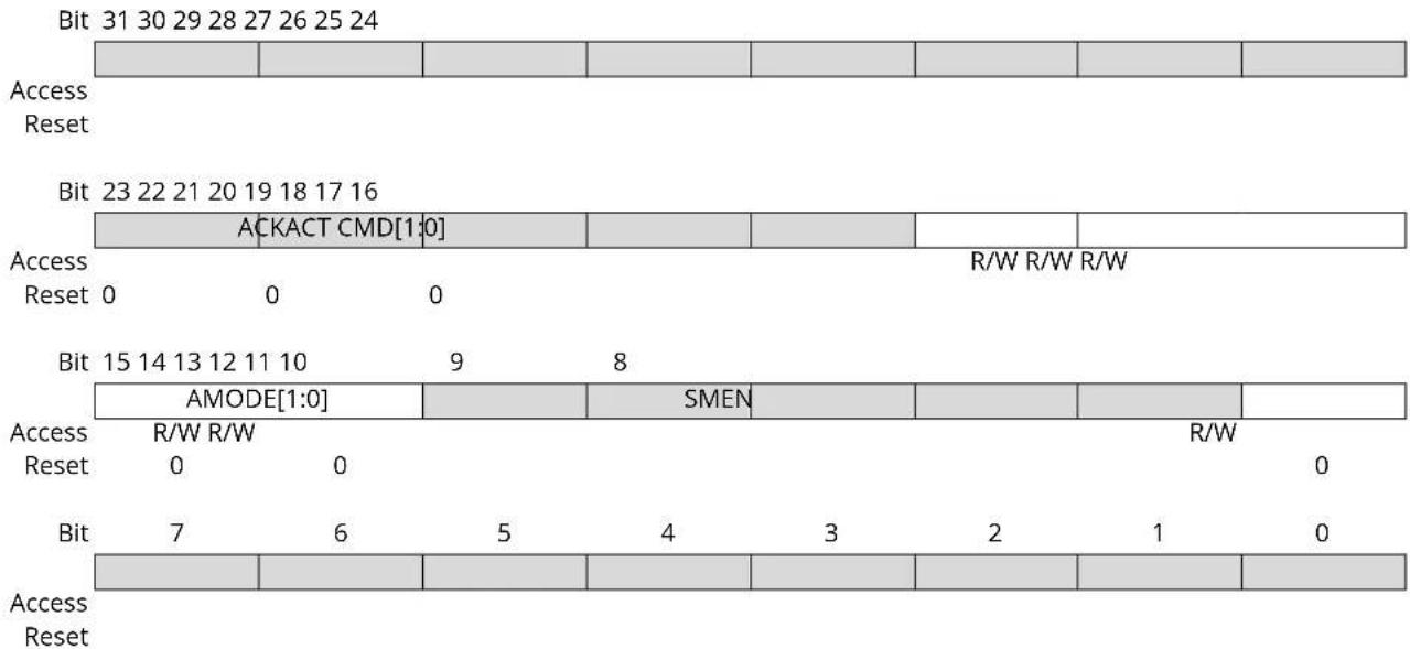
text_image
Bit 31 30 29 28 27 26 25 24 Access Reset Bit 23 22 21 20 19 18 17 16 ACKACT CMD[1:0] Access R/W R/W R/W Reset 0 0 0 Bit 15 14 13 12 11 10 9 8 AMODE[1:0] SMEN R/W Access R/W R/W Reset 0 0 Bit 7 6 5 4 3 2 1 0 Access ResetBit 18 - ACKACT Acknowledge Action
This bit defines the Client's acknowledge behavior after an address or data byte is received from the Host. The acknowledge action is executed when a command is written to the CMD bits. If smart mode is enabled (CTRLB.SMEN=1), the acknowledge action is performed when the DATA register is read.
This bit is not enable-protected.
| Value | Description |
| 0 | Send ACK |
| 1 | Send NACK |
Bits 17:16 - CMD[1:0] Command
This bit field triggers the Client operation as the below. The CMD bits are strobe bits, and always read as zero. The operation is dependent on the Client interrupt flags, INTFLAG.DRDY and INTFLAG.AMATCH, in addition to STATUS.DIR.
All interrupt flags (INTFLAG.DRDY, INTFLAG.AMATCH and INTFLAG.PREC) are automatically cleared when a command is given.
This bit is not enable-protected.
Table 26-1. Command Description
| CMD[1:0] | DIR | Action |
| 0x0 | X | (No action) |
| 0x1 | X | (Reserved) |
| 0x2 | Used to complete a transaction in response to a data interrupt (DRDY) | |
| 0 (Host write) | Execute acknowledge action succeeded by waiting for any start (S/Sr) condition | |
| 1 (Host read) | Wait for any start (S/Sr) condition | |
| ......continued | ||
| CMD[1:0] | DIR Action | |
| 0x3 Used in response to an address interrupt (AMATCH) | ||
| 0 (Host write) Execute acknowledge action succeeded by reception of next byte | ||
| 1 (Host read) Execute acknowledge action succeeded by Client data interrupt | ||
| Used in response to a data interrupt (DRDY) | ||
| 0 (Host write) Execute acknowledge action succeeded by reception of next byte | ||
| 1 (Host read) Execute a byte read operation followed by ACK/NACK reception | ||
Bits 15:14 - AMODE[1:0] Address Mode
These bits set the addressing mode.
These bits are not write-synchronized.
| Value Name | Description |
| 0x0 | MASK The Client responds to the address written in ADDR.ADDR masked by the value in ADDR.ADDRMASK.See SERCOM - Serial Communication Interface for additional information. |
| 0x1 | 2_ADDRS The Client responds to the two unique addresses in ADDR.ADDR and ADDR.ADDRMASK. |
| 0x2 | RANGE The Client responds to the range of addresses between and including ADDR.ADDR andADDR.ADDRMASK. ADDR.ADDR is the upper limit. |
| 0x3 | - Reserved. |
Bit 8 - SMEN Smart Mode Enable
When smart mode is enabled, data is acknowledged automatically when DATA.DATA is read.
This bit is not write-synchronized.
| Value Description | |
| 0 | Smart mode is disabled. |
| 1 | Smart mode is enabled. |
26.8.3 Interrupt Enable Clear
Name: INTENCLR
Offset: 0x0C
Reset: 0x00
Property: PAC Write-Protection
This register allows the user to disable an interrupt without doing a read-modify-write operation. Changes in this register will also be reflected in the Interrupt Enable Set register (INTENSET).
Bit 76543210
| DRDY AMATCH | PREC | ||||||
| Access Reset 0 0 0 | R/W R/W R/W | ||||||
Bit 2 - DRDY Data Ready Interrupt Enable
Writing '0' to this bit has no effect.
Writing '1' to this bit will clear the Data Ready bit, which disables the Data Ready interrupt.
| Value | Description |
| 0 | The Data Ready interrupt is disabled. |
| 1 | The Data Ready interrupt is enabled. |
Bit 1 - AMATCH Address Match Interrupt Enable
Writing '0' to this bit has no effect.
Writing '1' to this bit will clear the Address Match Interrupt Enable bit, which disables the Address Match interrupt.
| Value | Description |
| 0 | The Address Match interrupt is disabled. |
| 1 | The Address Match interrupt is enabled. |
Bit 0 - PREC Stop Received Interrupt Enable
Writing '0' to this bit has no effect.
Writing '1' to this bit will clear the Stop Received Interrupt Enable bit, which disables the Stop Received interrupt.
| Value | Description |
| 0 | The Stop Received interrupt is disabled. |
| 1 | The Stop Received interrupt is enabled. |
26.8.4 Interrupt Enable Set
Name: INTENSET
Offset: 0x0D
Reset: 0x00
Property: PAC Write-Protection
This register allows the user to enable an interrupt without doing a read-modify-write operation. Changes in this register will also be reflected in the Interrupt Enable Clear register (INTENCLR).
Bit 76543210
| DRDY AMATCH | PREC | ||||||
| Access Reset 0 0 0 | R/W R/W R/W | ||||||
Bit 2 - DRDY Data Ready Interrupt Enable
Writing '0' to this bit has no effect.
Writing '1' to this bit will set the Data Ready bit, which enables the Data Ready interrupt.
| Value | Description |
| 0 | The Data Ready interrupt is disabled. |
| 1 | The Data Ready interrupt is enabled. |
Bit 1 - AMATCH Address Match Interrupt Enable
Writing '0' to this bit has no effect.
Writing '1' to this bit will set the Address Match Interrupt Enable bit, which enables the Address Match interrupt.
| Value | Description |
| 0 | The Address Match interrupt is disabled. |
| 1 | The Address Match interrupt is enabled. |
Bit 0 - PREC Stop Received Interrupt Enable
Writing '0' to this bit has no effect.
Writing '1' to this bit will set the Stop Received Interrupt Enable bit, which enables the Stop Received interrupt.
| Value | Description |
| 0 | The Stop Received interrupt is disabled. |
| 1 | The Stop Received interrupt is enabled. |
26.8.5 Interrupt Flag Status and Clear
Name: INTFLAG
Offset: 0x0E
Reset: 0x00
Property: -
Bit 76543210
| DRDY AMATCH PREC | ||||||
| Access Reset 0 0 0 | R/W R/W R/W | |||||
Bit 2 - DRDY Data Ready
This flag is set when a I²C Client byte transmission is successfully completed.
The flag is cleared by hardware when either:
• Writing to the DATA register.
- Reading the DATA register with smart mode enabled.
• Writing a valid command to the CMD register.
Writing '0' to this bit has no effect.
Writing '1' to this bit will clear the Data Ready interrupt flag.
Bit 1 - AMATCH Address Match
This flag is set when the I ^2 C Client address match logic detects that a valid address has been received.
The flag is cleared by hardware when CTRL.CMD is written.
Writing '0' to this bit has no effect.
Writing '1' to this bit will clear the Address Match interrupt flag. When cleared, an ACK/NACK will be sent according to CTRLB.ACKACT.
Bit 0 - PREC Stop Received
This flag is set when a stop condition is detected for a transaction being processed. A stop condition detected between a bus Host and another Client will not set this flag, unless the PMBus Group Command is enabled in the Control B register (CTRLB.GCMD=1).
This flag is cleared by hardware after a command is issued on the next address match.
Writing '0' to this bit has no effect.
Writing '1' to this bit will clear the Stop Received interrupt flag.
26.8.6 Status
Name: STATUS
Offset: 0x10
Reset: 0x0000
Property: -
| Bit 15 14 13 12 11 10 9 8 | |||||||
| SYNCBUSY | |||||||
| Access Reset 0 | R/W | ||||||
| Bit 76543210 | ||||||||
| CLKHOLD | LOWTOUT | SR | DIR | RXNACK | COLL | BUSERR | ||
| Access | R/W | R/W | R | R | R | R/W | R/W | |
| Reset 00 | 00000 | |||||||
Bit 15 - SYNCBUSY Synchronization Busy
This bit is set when the synchronization of registers between clock domains is started.
This bit is cleared when the synchronization of registers between the clock domains is complete.
Bit 7 - CLKHOLD Clock Hold
The Client Clock Hold (STATUS.CLK HOLD) bit is set when the Client is holding the SCL line low, stretching the I ^2 C clock. Software must consider this bit a read-only status flag that is set when INTFLAG.DRDY or INTFLAG.AMATCH is set.
This bit is cleared when the corresponding interrupt is cleared. If this bit is written as '1' while the SCL line is held low, the SCL line will be released. Writing '0' to this bit has no effect.
Bit 6 - LOWTOUT SCL Low Time-out
This bit is set if an SCL low time-out occurs.
This bit is cleared automatically if responding to a new start condition with ACK or NACK (write 3 to CTRLB.CMD) or when INTFLAG.AMATCH is cleared.
Writing a '0' to this bit has no effect.
Writing a '1' to this bit will clear the status.
| Value | Description |
| 0 | No SCL low time-out has occurred. |
| 1 | SCL low time-out has occurred. |
Bit 4 - SR Repeated Start
When INTFLAG.AMATCH is raised due to an address match, SR indicates a repeated start or start condition.
This flag is only valid while the INTFLAG.AMATCH flag is one.
| Value | Description |
| 0 | Start condition on last address match |
| 1 | Repeated start condition on last address match |
Bit 3 - DIR Read / Write Direction
The Read/Write Direction (STATUS.DIR) bit stores the direction of the last address packet received from a Host.
| Value | Description |
| 0 | Host write operation is in progress. |
| 1 | Host read operation is in progress. |
Bit 2 - RXNACK Received Not Acknowledge
This bit indicates whether the last data packet sent was acknowledged or not.
| Value Description | |
| 0 | Host responded with ACK. |
| 1 | Host responded with NACK. |
Bit 1 - COLL Transmit Collision
If set, the I ^2 C Client was not able to transmit a high data or NACK bit, the Client will immediately release the SDA and SCL lines and wait for the next packet addressed to it.
This flag is intended for the SMBus address resolution protocol (ARP). A detected collision in non-ARP situations indicates that there has been a protocol violation, and should be treated as a bus error.
This status will not trigger any interrupt, and should be checked by software to verify that the data were sent correctly. This bit is cleared automatically if responding to an address match with an ACK or a NACK (writing 0x3 to CTRLB.CMD), or INTFLAG.AMATCH is cleared.
Writing a '0' to this bit has no effect.
Writing a '1' to this bit will clear the status.
| Value Description | |
| 0 | No collision detected on last data byte sent. |
| 1 | Collision detected on last data byte sent. |
Bit 0 - BUSERR Bus Error
The Bus Error bit (STATUS.BUSERR) indicates that an illegal bus condition has occurred on the bus, regardless of bus ownership. An illegal bus condition is detected if a protocol violating start, repeated start or stop is detected on the I^2C bus lines. A start condition directly followed by a stop condition is one example of a protocol violation. If a time-out occurs during a frame, this is also considered a protocol violation, and will set STATUS.BUSERR.
This bit is cleared automatically if responding to an address match with an ACK or a NACK (writing 0x3 to CTRLB.CMD) or INTFLAG.AMATCH is cleared.
Writing a '1' to this bit will clear the status.
Writing a '0' to this bit has no effect.
| Value Description | |
| 0 | No bus error detected. |
| 1 | Bus error detected. |
26.8.7 Address
Name: ADDR
Offset: 0x14
Reset: 0x00000000
Property: PAC Write-Protection, Enable-Protected
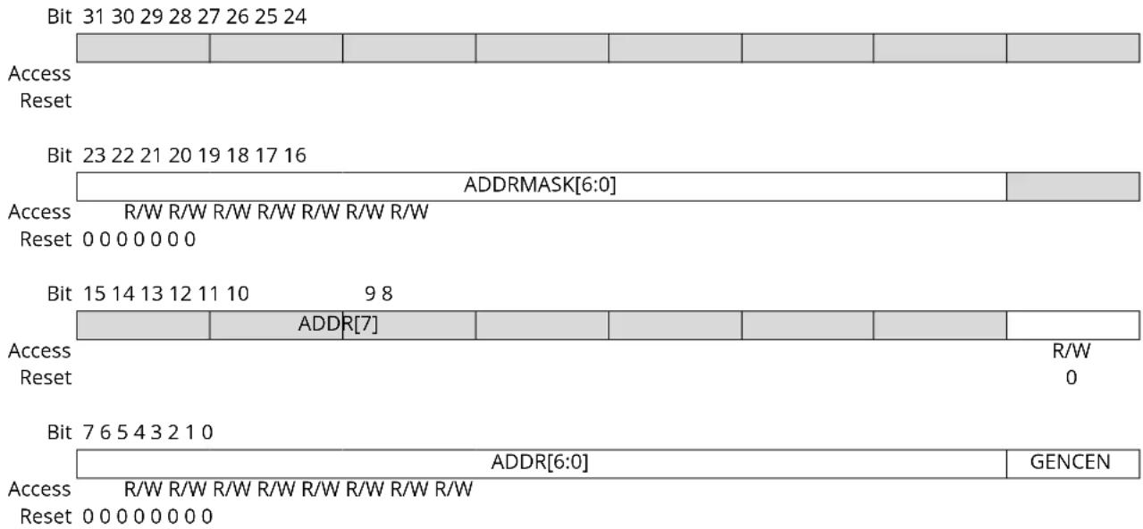
text_image
Bit 31 30 29 28 27 26 25 24 Access Reset Bit 23 22 21 20 19 18 17 16 ADDRMASK[6:0] Access R/W R/W R/W R/W R/W R/W R/W Reset 0 0 0 0 0 0 0 Bit 15 14 13 12 11 10 9 8 ADDR[7] Access R/W Reset 0 Bit 7 6 5 4 3 2 1 0 ADDR[6:0] Access R/W R/W R/W R/W R/W R/W R/W Reset 0 0 0 0 0 0 0 GENCENBits 23:17 - ADDRMASK[6:0] Address Mask
These bits act as a second address match register, an address mask register or the lower limit of an address range, depending on the CTRLB.AMODE setting.
Bits 8:1 - ADDR[7:0] Address
These bits contain the I ^2 C Client address used by the Client address match logic to determine if a Host has addressed the Client.
When using 7-bit addressing, the Client address is represented by ADDR[6:0].
When the address match logic detects a match, INTFLAG.AMATCH is set and STATUS.DIR is updated to indicate whether it is a read or a write transaction.
Bit 0 - GENCEN General Call Address Enable
A general call address is an address consisting of all-zeroes, including the direction bit (Host write).
| Value | Description |
| 0 | General call address recognition disabled. |
| 1 | General call address recognition enabled. |
26.8.8 Data
Name: DATA
Offset: 0x18
Reset: 0x0000
The Client data register I/O location (DATA.DATA) provides access to the Host transmit and receive data buffers. Reading valid data or writing data to be transmitted can be successfully done only when SCL is held low by the Client (STATUS.CLK HOLD is set). An exception occurs when reading the last data byte after the stop condition has been received.
Accessing DATA.DATA auto-triggers PC bus operations. The operation performed depends on the state of CTRLB.ACKACT, CTRLB.SMEN and the type of access (read/write).
Writing or reading DATA.DATA when not in smart mode does not require synchronization.
26.9 Register Summary - I2C Host
| Offset | Name Bit Pos. 76 | 543210 | |||||||
| 0x00 CTRLA | 7:0 RUNSTDBY MODE[2:0] ENABLE SWRST | ||||||||
| 15:8 | |||||||||
| 23:16 | SDAHOLD[1:0] PINOUT | ||||||||
| 31:24 | LOWTOUT INACTOUT[1:0] | ||||||||
| 0x04 CTRLB | 7:0 | ||||||||
| 15:8 | QCEN SMEN | ||||||||
| 23:16 | ACKACT CMD[1:0] | ||||||||
| 31:24 | |||||||||
| 0x08 | DBGCTRL | 7:0 | DBGSTOP | ||||||
| 0x09 | Reserved | ||||||||
| 0x0A | BAUD | 7:0 | BAUD[7:0] | ||||||
| 15:8 | BAUDLOW[7:0] | ||||||||
| 0x0C | INTENCLR | 7:0 | SB | MB | |||||
| 0x0D | INTENSET | 7:0 | SB | MB | |||||
| 0x0E | INTFLAG | 7:0 | SB | MB | |||||
| 0x0F | Reserved | ||||||||
| 0x10 | STATUS | 7:0 | CLKHOLD LOWTOUT | BUSSTATE[1:0] | RXNACK | ARBLOST | BUSERR | ||
| 15:8 | SYNCBUSY | ||||||||
| 0x12 ... 0x13 | Reserved | ||||||||
| 0x14 | ADDR | 7:0 | ADDR[7:0] | ||||||
| 15:8 | |||||||||
| 0x16 ... 0x17 | Reserved | ||||||||
| 0x18 | DATA | 7:0 | DATA[7:0] | ||||||
| 15:8 | |||||||||
26.10 Register Description - I²C Host
Registers can be 8, 16, or 32 bits wide. Atomic 8-, 16- and 32-bit accesses are supported. In addition, the 8-bit quarters and 16-bit halves of a 32-bit register, and the 8-bit halves of a 16-bit register can be accessed directly.
Some registers are optionally write-protected by the Peripheral Access Controller (PAC). Optional PAC write-protection is denoted by the "PAC Write-Protection" property in each individual register description. For details, refer to 26.5.7. Register Access Protection.
Some registers are synchronized when read and/or written. Synchronization is denoted by the "Write-Synchronized" or the "Read-Synchronized" property in each individual register description. For details, refer to 26.6.6. Synchronization.
Some registers are enable-protected, meaning they can only be written when the peripheral is disabled. Enable-protection is denoted by the "Enable-Protected" property in each individual register description.
26.10.1 Control A
Name: CTRLA
Offset: 0x00
Reset: 0x00000000
Property: PAC Write-Protection, Enable-Protected, Write-Synchronized
| Bit 31 30 29 28 27 26 25 24 | ||||||||
| LOWTOUT INACTOUT[1:0] | ||||||||
| Access Reset | R/W R/W R/W | |||||||
| 0 | 0 | 0 | ||||||
| Bit 23 22 21 20 19 18 17 16 | ||||||||
| SDAHOLD[1:0] | PINOUT | |||||||
| Access Reset | R/W R/W | R/W | ||||||
| 0 | 0 | 0 | ||||||
| Bit 15 14 13 12 11 10 | 9 | 8 | ||||||
| Access Reset | ||||||||
| Bit | 7 | 6 | 5 | 4 | 3 | 2 | 1 | 0 |
| RUNSTDBY | MODE[2:0] | ENABLE | SWRST | |||||
| Access Reset | R/W | R/W R/W R/W R/W R/W | ||||||
| 0 | 0 | 0 | 0 | 0 | ||||
Bit 30 - LOWTOUT SCL Low Time-Out
This bit enables the SCL low time-out. If SCL is held low for 25ms-35ms, the Host will release its clock hold, if enabled, and complete the current transaction. A stop condition will automatically be transmitted.
INTFLAG.SB or INTFLAG.MB will be set as normal, but the clock hold will be released. The STATUS.LOWTOUT and STATUS.BUSERR status bits will be set.
This bit is not synchronized.
| Value | Description |
| 0 | Time-out disabled. |
| 1 | Time-out enabled. |
Bits 29:28 - INACTOUT[1:0] Inactive Time-Out
If the inactive bus time-out is enabled and the bus is inactive for longer than the time-out setting, the bus state logic will be set to idle. An inactive bus arise when either an I ^2 C Host or Client is holding the SCL low.
Enabling this option is necessary for SMBus compatibility, but can also be used in a non-SMBus set-up.
Calculated time-out periods are based on a 100kHz baud rate.
These bits are not synchronized.
| Value | Name | Description |
| 0x0 | DIS | Disabled |
| 0x1 | 55US | 5-6 SCL cycle time-out (50-60μs) |
| 0x2 | 105US | 10-11 SCL cycle time-out (100-110μs) |
| 0x3 | 205US | 20-21 SCL cycle time-out (200-210μs) |
Bits 21:20 - SDAHOLD[1:0] SDA Hold Time
These bits define the SDA hold time with respect to the negative edge of SCL.
These bits are not synchronized.
| Value Name | Description | |
| 0x0 | DIS Disabled | |
| 0x1 | 75NS 50-100ns hold time | |
| 0x2 | 450NS 300-600ns hold time | |
| 0x3 | 600NS 400-800ns hold time | |
Bit 16 - PINOUT Pin Usage
This bit set the pin usage to either two- or four-wire operation:
This bit is not synchronized.
| Value Description | |
| 0 | 4-wire operation disabled. |
| 1 | 4-wire operation enabled. |
Bit 7 - RUNSTDBY Run in Standby
This bit defines the functionality in standby sleep mode.
This bit is not synchronized.
| Value Description | |
| 0 | GCLK_SERCOMx_CORE is disabled and the I^2C Host will not operate in standby sleep mode. |
| 1 | GCLK_SERCOMx_CORE is enabled in all sleep modes. |
Bits 4:2 - MODE[2:0] Operating Mode
These bits must be written to 0x5 to select the I ^2 C Host serial communication interface of the SERCOM.
These bits are not synchronized.
Bit 1 - ENABLE Enable
Due to synchronization, there is delay from writing CTRLA. ENABLE until the peripheral is enabled/disabled. The value written to CTRL. ENABLE will read back immediately and the Synchronization Enable Busy bit in the Synchronization Busy register (SYNCBUSY. ENABLE) will be set. SYNCBUSY. ENABLE will be cleared when the operation is complete.
This bit is not enable-protected.
| Value Description | |
| 0 | The peripheral is disabled or being disabled. |
| 1 | The peripheral is enabled. |
Bit 0 - SWRST Software Reset
Writing '0' to this bit has no effect.
Writing '1' to this bit resets all registers in the SERCOM, except DBGCTRL, to their initial state, and the SERCOM will be disabled.
Writing '1' to CTRLA.SWRST will always take precedence, meaning that all other writes in the same write-operation will be discarded. Any register write access during the ongoing reset will result in an APB error. Reading any register will return the reset value of the register.
Due to synchronization there is a delay from writing CTRLA.SWRST until the reset is complete.
CTRLA.SWRST and SYNCBUSY.SWRST will both be cleared when the reset is complete.
This bit is not enable-protected.
| Value Description | |
| 0 | There is no reset operation ongoing. |
| 1 | The reset operation is ongoing. |
26.10.2 Control B
Name: CTRLB
Offset: 0x04
Reset: 0x00000000
Property: PAC Write-Protection, Enable-Protected, Write-Synchronized
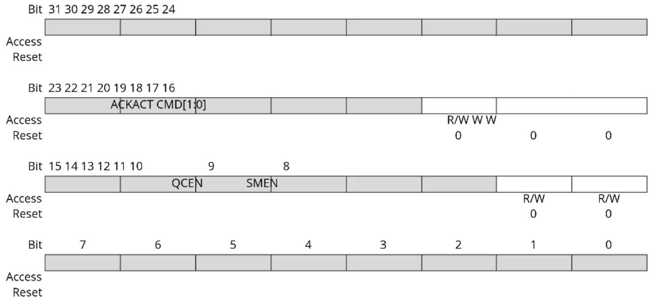
Bit 18 - ACKACT Acknowledge Action
This bit defines the I²C Host's acknowledge behavior after a data byte is received from the I²C Client. The acknowledge action is executed when a command is written to CTRLB.CMD, or if Smart mode is enabled (CTRLB.SMEN is written to one), when DATA.DATA is read.
This bit is not enable-protected.
This bit is not write-synchronized.
| Value | Description |
| 0 | Send ACK. |
| 1 | Send NACK. |
Bits 17:16 - CMD[1:0] Command
Writing these bits triggers a Host operation as described below. The CMD bits are strobe bits, and always read as zero. The acknowledge action is only valid in Host Read mode. In Host Write mode, a command will only result in a repeated Start or Stop condition. The CTRLB.ACKACT bit and the CMD bits can be written at the same time, and then the acknowledge action will be updated before the command is triggered.
Commands can only be issued when either the Client on Bus Interrupt flag (INTFLAG.SB) or Host on Bus Interrupt flag (INTFLAG.MB) is '1'.
If CMD 0x1 is issued, a repeated start will be issued followed by the transmission of the current address in ADDR.ADDR. If another address is desired, ADDR.ADDR must be written instead of the CMD bits. This will trigger a repeated start followed by transmission of the new address.
Issuing a command will set the System Operation bit in the Synchronization Busy register (SYNCBUSY.SYSOP).
Table 26-2. Command Description
| CMD[1:0] | Direction | Action |
| 0x0 | X (No action) | |
| ......continued | ||
| CMD[1:0] Direction Action | ||
| 0x1 X Execute acknowledge action succeeded by repeated Start | ||
| 0x2 0 (Write) No operation | ||
| 1 (Read) Execute acknowledge action succeeded by a byte read operation | ||
| 0x3 X Execute acknowledge action succeeded by issuing a Stop condition | ||
These bits are not enable-protected.
Bit 9 - QCEN Quick Command Enable
This bit is not write-synchronized.
| Value Description | |
| 0 | Quick Command is disabled. |
| 1 | Quick Command is enabled. |
Bit 8 - SMEN Smart Mode Enable
When Smart mode is enabled, acknowledge action is sent when DATA.DATA is read. This bit is not write-synchronized.
| Value Description | |
| 0 | Smart mode is disabled. |
| 1 | Smart mode is enabled. |
26.10.3 Debug Control
Name: DBGCTRL
Offset: 0x08
Reset: 0x00
Property: PAC Write-Protection
Bit 76543210
| DBGSTOP | |||||||
| Access Reset 0 | R/W | ||||||
Bit 0 - DBGSTOP Debug Stop Mode
This bit controls functionality when the CPU is halted by an external debugger.
| Value Description | |
| 0 | The baud-rate generator continues normal operation when the CPU is halted by an external debugger. |
| 1 | The baud-rate generator is halted when the CPU is halted by an external debugger. |
26.10.4 Baud Rate
Name: BAUD
Offset: 0x0A
Reset: 0x0000
Property: PAC Write-Protection, Enable-Protected
Bit 15 14 13 12 11 10 9 8
BAUDLOW[7:0]
Access R/W R/W R/W R/W R/W R/W R/W R/W
Reset 00000000
Bit 76543210
BAUD[7:0]
Access R/W R/W R/W R/W R/W R/W R/W R/W
Reset 00000000
Bits 15:8 - BAUDLOW[7:0] Host Baud Rate Low
If this bit field is non-zero, the SCL low time will be described by the value written.
For more information on how to calculate the frequency, see SERCOM 23.6.2.3. Clock Generation – Baud-Rate Generator.
Bits 7:0 - BAUD[7:0] Host Baud Rate
This bit field is used to derive the SCL high time if BAUD.BAUDLOW is non-zero. If BAUD.BAUDLOW is zero, BAUD will be used to generate both high and low periods of the SCL.
For more information on how to calculate the frequency, see SERCOM 23.6.2.3. Clock Generation - Baud-Rate Generator.
26.10.5 Interrupt Enable Clear
Name: INTENCLR
Offset: 0x0C
Reset: 0x00
Property: PAC Write-Protection
This register allows the user to disable an interrupt without doing a read-modify-write operation. Changes in this register will also be reflected in the Interrupt Enable Set register (INTENSET).
Bit 76543210
| $B MB | |||||||
| Access Reset 0 0 | R/W R/W | ||||||
Bit 1 - SB Client on Bus Interrupt Enable
Writing '0' to this bit has no effect.
Writing '1' to this bit will clear the Client on Bus Interrupt Enable bit, which disables the Client on Bus interrupt.
| Value Description | |
| 0 | The Client on Bus interrupt is disabled. |
| 1 | The Client on Bus interrupt is enabled. |
Bit 0 - MB Host on Bus Interrupt Enable
Writing '0' to this bit has no effect.
Writing '1' to this bit will clear the Host on Bus Interrupt Enable bit, which disables the Host on Bus interrupt.
| Value Description | |
| 0 | The Host on Bus interrupt is disabled. |
| 1 | The Host on Bus interrupt is enabled. |
26.10.6 Interrupt Enable Clear
Name: INTENSET
Offset: 0x0D
Reset: 0x00
Property: PAC Write-Protection
This register allows the user to enable an interrupt without doing a read-modify-write operation. Changes in this register will also be reflected in the Interrupt Enable Clear register (INTENCLR).
Bit 76543210
| $B MB | |||||||
| Access Reset 0 0 | R/W R/W | ||||||
Bit 1 - SB Client on Bus Interrupt Enable
Writing '0' to this bit has no effect.
Writing '1' to this bit will set the Client on Bus Interrupt Enable bit, which enables the Client on Bus interrupt.
| Value Description | |
| 0 | The Client on Bus interrupt is disabled. |
| 1 | The Client on Bus interrupt is enabled. |
Bit 0 - MB Host on Bus Interrupt Enable
Writing '0' to this bit has no effect.
Writing '1' to this bit will set the Host on Bus Interrupt Enable bit, which enables the Host on Bus interrupt.
| Value Description | |
| 0 | The Host on Bus interrupt is disabled. |
| 1 | The Host on Bus interrupt is enabled. |
26.10.7 Interrupt Flag Status and Clear
Name: INTFLAG
Offset: 0x0E
Reset: 0x00
Property: -
Bit 76543210
| $B MB | |||||||
| Access Reset 0 0 | R/W R/W | ||||||
Bit 1 - SB Client on Bus
The Client on Bus flag (SB) is set when a byte is successfully received in Host read mode, i.e., no arbitration lost or bus error occurred during the operation. When this flag is set, the Host forces the SCL line low, stretching the I²C clock period. The SCL line will be released and SB will be cleared on one of the following actions:
- Writing to ADDR.ADDR
- Writing to DATA.DATA
- Reading DATA.DATA when smart mode is enabled (CTRLB.SMEN)
- Writing a valid command to CTRLB.CMD
Writing '1' to this bit location will clear the SB flag. The transaction will not continue or be terminated until one of the above actions is performed.
Writing '0' to this bit has no effect.
Bit 0 - MB Host on Bus
This flag is set when a byte is transmitted in Host write mode. The flag is set regardless of the occurrence of a bus error or an arbitration lost condition. MB is also set when arbitration is lost during sending of NACK in Host read mode, or when issuing a start condition if the bus state is unknown. When this flag is set and arbitration is not lost, the Host forces the SCL line low, stretching the I²C clock period. The SCL line will be released and MB will be cleared on one of the following actions:
- Writing to ADDR.ADDR
- Writing to DATA.DATA
- Reading DATA.DATA when smart mode is enabled (CTRLB.SMEN)
- Writing a valid command to CTRLB.CMD
Writing '1' to this bit location will clear the MB flag. The transaction will not continue or be terminated until one of the above actions is performed.
Writing '0' to this bit has no effect.
26.10.8 Status
Name: STATUS
Offset: 0x10
Reset: 0x0000
Property: Write-Synchronized
Bit 15 14 13 12 11 10 9 8
| SYNCBUSY | |||||||
| Access Reset 0 | R/W | ||||||
Bit 76543210
| CLKHOLD | LOWTOUT | BUSSTATE[1:0] | RXNACK | ARBLOST | BUSERR | ||
| Access | R | R/W | R | R | R | R/W | R/W |
| Reset | 0 0 0 0 | 0 0 0 |
Bit 10 - SYNCBUSY Synchronization Busy
This bit is cleared when the synchronization of registers between the clock domains is complete. This bit is set when the synchronization of registers between clock domains is started.
Bit 7 - CLKHOLD Clock Hold
This bit is set when the Host is holding the SCL line low, stretching the I²C clock. Software should consider this bit when INTFLAG.SB or INTFLAG.MB is set.
This bit is cleared when the corresponding interrupt flag is cleared and the next operation is given. If this bit is written while the SCL line is held low, the SCL line will be released.
This bit is not write-synchronized.
Bit 6 - LOWTOUT SCL Low Time-Out
This bit is set if an SCL low time-out occurs.
Writing '1' to this bit location will clear this bit. This flag is automatically cleared when writing to the ADDR register.
Writing '0' to this bit has no effect.
This bit is not write-synchronized.
Bits 5:4 - BUSSTATE[1:0] Bus State
These bits indicate the current I^2C bus state.
When in UNKNOWN state, writing 0x1 to BUSSTATE forces the bus state into the IDLE state. The bus state cannot be forced into any other state.
Writing BUSSTATE to idle will set SYNCBUSY.SYSOP.
| Value | Name | Description |
| 0x0 | UNKNOWN | The bus state is unknown to the I^2C Host and will wait for a stop condition to be detected or wait to be forced into an idle state by software |
| 0x1 | IDLE | The bus state is waiting for a transaction to be initialized |
| 0x2 | OWNER | The I^2C Host is the current owner of the bus |
| 0x3 | BUSY | Some other I^2C Host owns the bus |
Bit 2 - RXNACK Received Not Acknowledge
This bit indicates whether the last address or data packet sent was acknowledged or not.
Writing '0' to this bit has no effect.
Writing '1' to this bit has no effect.
This bit is not write-synchronized.
| Value | Description |
| 0 | Client responded with ACK. |
Value Description
1 Client responded with NACK.
Bit 1 - ARBLOST Arbitration Lost
This bit is set if arbitration is lost while transmitting a high data bit or a NACK bit, or while issuing a start or repeated start condition on the bus. The Host on Bus interrupt flag (INTFLAG.MB) will be set when STATUS.ARBLOST is set.
Writing the ADDR.ADDR register will automatically clear STATUS.ARBLOST.
Writing '0' to this bit has no effect.
Writing '1' to this bit will clear it.
This bit is not write-synchronized.
Bit 0 - BUSERR Bus Error
This bit indicates that an illegal bus condition has occurred on the bus, regardless of bus ownership. An illegal bus condition is detected if a protocol violating start, repeated start or stop is detected on the I^2C bus lines. A start condition directly followed by a stop condition is one example of a protocol violation. If a time-out occurs during a frame, this is also considered a protocol violation, and will set BUSERR.
If the I ^2 C Host is the bus owner at the time a bus error occurs, STATUS.ARBLOST and INTFLAG.MB will be set in addition to BUSERR.
Writing the ADDR.ADDR register will automatically clear the BUSERR flag.
Writing '0' to this bit has no effect.
Writing '1' to this bit will clear it.
This bit is not write-synchronized.
26.10.9 Address
Name: ADDR
Offset: 0x14
Reset: 0x0000
Property: Write-Synchronized
Bit 15 14 13 12 11 10 9 8
Access Reset
Bit 76543210
Access R/W R/W R/W R/W R/W R/W R/W R/W
Reset 00000000
ADDR[7:0]
Bits 7:0 - ADDR[7:0] Address
When ADDR is written, the consecutive operation will depend on the bus state:
UNKNOWN: INTFLAG.MB and STATUS.BUSERR are set, and the operation is terminated.
BUSY: The I²C Host will await further operation until the bus becomes IDLE.
IDLE: The I²C Host will issue a start condition followed by the address written in ADDR. If the address is acknowledged, SCL is forced and held low, and STATUS.CLKHOLD and INTFLAG.MB are set.
OWNER: A repeated start sequence will be performed. If the previous transaction was a read, the acknowledge action is sent before the repeated start bus condition is issued on the bus. Writing ADDR to issue a repeated start is performed while INTFLAG.MB or INTFLAG.SB is set.
STATUS.BUSERR, STATUS.ARBLOST, INTFLAG.MB and INTFLAG.SB will be cleared when ADDR is written.
The ADDR register can be read at any time without interfering with ongoing bus activity, as a read access does not trigger the Host logic to perform any bus protocol related operations.
The I ^2 C Host control logic uses bit 0 of ADDR as the bus protocol's read/write flag (R/W); 0 for write and 1 for read.
26.10.10 Data
Name: DATA
Offset: 0x18
Reset: 0x0000
The Host data register I/O location (DATA) provides access to the Host transmit and receive data buffers. Reading valid data or writing data to be transmitted can be successfully done only when SCL is held low by the Host (STATUS.CLKHOLD is set). An exception is reading the last data byte after the stop condition has been sent.
Accessing DATA.DATA auto-triggers bus operations. The operation performed depends on the state of CTRLB.ACKACT, CTRLB.SMEN and the type of access (read/write).
Writing or reading DATA.DATA when not in smart mode does not require synchronization.
27. TC - Timer/Counter
27.1 Overview
The TC consists of a counter, a prescaler, compare/capture channels and control logic. The counter can be set to count events, or it can be configured to count clock pulses. The counter, together with the compare/capture channels, can be configured to timestamp input events, allowing capture of frequency and pulse width. It can also perform waveform generation, such as frequency generation and pulse-width modulation (PWM).
27.2 Features
- Selectable configuration:
- Up to eight 16-bit Timer/Counters (TC), each configurable as:
- 8-bit TC with two compare/capture channels
• 16-bit TC with two compare/capture channels - 32-bit TC with two compare/capture channels, by using two TCs
- Waveform Generation:
- Frequency generation
– Single-slope pulse-width modulation
- Input capture:
- Event capture
- Frequency capture
-
Pulse-width capture
-
One input event
- Interrupts/output events on:
- Counter overflow/underflow
- Compare match or capture
- Internal prescaler
27.3 Block Diagram
Figure 27-1. Timer/Counter Block Diagram
flowchart
graph TD
    A["PER"] --> B["Counter"]
    B --> C["COUNT"]
    C --> D["=0"]
    D --> E["STOP"]
    E --> F["control"]
    F --> G["PRESCALER"]
    G --> H["CONTROL LOGIC"]
    H --> I["OVF/UNF (INT Req.)"]
    H --> J["ERR (INT Req.)"]
    K["CC0"] --> L["Comparison / Capture"]
    L --> M["control"]
    M --> N["WAVEFORM GENERATION"]
    N --> O["WOx Out"]
    N --> P["MCx (INT Req.)"]
    Q["match"] --> R["="]
    R --> S["Output"]
    T["Zero"] --> U["Event"]
    U --> V["Update"]
    V --> W["Control Logic"]
    W --> X["Waveform Generation"]
27.4 Signal Description
| Signal Name Type Description | ||
| WO[1:0] Digital output Waveform output |
Refer to I/O Multiplexing and Considerations for details on the pin mapping for this peripheral. One signal can be mapped on several pins.
Related Links
- I/O Multiplexing and Considerations
27.5 Product Dependencies
In order to use this peripheral, other parts of the system must be configured correctly, as described below.
27.5.1 I/O Lines
In order to use the I/O lines of this peripheral, the I/O pins must be configured using the I/O Pin Controller (PORT).
Related Links
- PORT - I/O Pin Controller
27.5.2 Power Management
This peripheral can continue to operate in any sleep mode where its source clock is running. The interrupts can wake up the device from sleep modes. Events connected to the event system can trigger other operations in the system without exiting sleep modes.
Related Links
- Power Manager (PM)
27.5.3 Clocks
The TC bus clock (CLK_TCx_APB, where x represents the specific TC instance number) can be enabled and disabled in the Power Manager, and the default state of CLK_TCx_APB can be found in the Peripheral Clock Masking section in "PM - Power Manager".
The different TC instances are paired, even and odd, starting from TC, and use the same generic clock, GCLK_TCx. This means that the TC instances in a TC pair cannot be set up to use different GCLK_TCx clocks.
This generic clock is asynchronous to the user interface clock (CLK_TCx_APB). Due to this asynchronicity, accessing certain registers will require synchronization between the clock domains. Refer to 27.6.5. Synchronization for further details.
27.5.4 Interrupts
The interrupt request line is connected to the Interrupt Controller. In order to use interrupt requests of this peripheral, the Interrupt Controller (NVIC) must be configured first. Refer to Nested Vector Interrupt Controller for details.
Related Links
10.2. Nested Vector Interrupt Controller
27.5.5 Events
The events of this peripheral are connected to the Event System.
Related Links
- Event System (EVSYS)
27.5.6 Debug Operation
When the CPU is halted in debug mode, this peripheral will halt normal operation. This peripheral can be forced to continue operation during debugging - refer to the Debug Control (DBGCTRL) register for details.
27.5.7 Register Access Protection
Registers with write-access can be optionally write-protected by the Peripheral Access Controller (PAC), except for the following:
- Interrupt Flag register (INTFLAG)
• Status register (STATUS) - Read Request register (READREQ)
- Count register (COUNT)
- Period register (PER)
- Compare/Capture Value registers (CCx)
Note: Optional write-protection is indicated by the "PAC Write-Protection" property in the register description.
Write-protection does not apply for accesses through an external debugger.
27.5.8 Analog Connections
Not applicable.
27.6 Functional Description
27.6.1 Principle of Operation
The following definitions are used throughout the documentation:
Table 27-1. Timer/Counter Definitions
| Name Description | |
| TOP The counter reaches TOP when it becomes equal to the highest value in the count sequence. The TOP value can be the same as Period (PER) or the Compare Channel 0 (CC0) register value depending on the waveform generator mode in Waveform Output Operations. | |
| ZERO The counter is ZERO when it contains all zeroes | |
| MAX The counter reaches MAX when it contains all ones | |
| UPDATE The timer/counter signals an update when it reaches ZERO or TOP, depending on the direction settings. | |
| Timer The timer/counter clock control is handled by an internal source | |
| Counter The clock control is handled externally (e.g. counting external events) | |
| CC For compare operations, the CC are referred to as “compare channels” | |
The counter in the TC can either count events from the Event System, or clock ticks of the GCLK_TCx clock, which may be divided by the prescaler.
The counter value is passed to the CCx where it can be either compared to user-defined values or captured.
The compare and capture registers (CCx) and counter register (COUNT) can be configured as 8-, 16- or 32-bit registers, with according MAX values. Mode settings determine the maximum range of the counter.
In 8-bit mode, Period Value (PER) is also available. The counter range and the operating frequency determine the maximum time resolution achievable with the TC peripheral.
The TC can be set to count up or down. Under normal operation, the counter value is continuously compared to the TOP or ZERO value to determine whether the counter has reached that value.
In compare operation, the counter value is continuously compared to the values in the CCx registers. In waveform generator mode, these comparisons are used to set the waveform period or pulse width.
Capture operation can be enabled to perform input signal period and pulse width measurements, or to capture selectable edges from an internal event from Event System.
27.6.2 Basic Operation
27.6.2.1 Initialization
The following registers are enable-protected, meaning that they can only be written when the TC is disabled (CTRLA.ENABLE =0):
- Control A register (CTRLA), except the Run Standby (RUNSTDBY), Enable (ENABLE) and Software Reset (SWRST) bits
Enable-protected bits in the CTRLA register can be written at the same time as CTRLA.ENABLE is written to '1', but not at the same time as CTRLA.ENABLE is written to '0'. Enable-protection is denoted by the "Enable-Protected" property in the register description. The following bits are enable-protected:
- Event Action bits in the Event Control register (EVCTRL.EVACT)
Before enabling the TC, the peripheral must be configured by the following steps:
- Enable the TC bus clock (CLK_TCx_APB).
- Select 8-, 16- or 32-bit counter mode via the TC Mode bit group in the Control A register (CTRLA.MODE). The default mode is 16-bit.
- Select one wave generation operation in the Waveform Generation Operation bit group in the Control A register (CTRLA.WAVEGEN).
- If desired, the GCLK_TCx clock can be prescaled via the Prescaler bit group in the Control A register (CTRLA.PRESCALER).
-
If the prescaler is used, select a prescaler synchronization operation via the Prescaler and Counter Synchronization bit group in the Control A register (CTRLA.PRESYNC).
-
Select one-shot operation by writing a '1' to the One-Shot bit in the Control B Set register (CTRLBSET.ONESHOT).
-
If desired, configure the counting direction 'down' (starting from the TOP value) by writing a '1' to the Counter Direction bit in the Control B register (CTRLBSET.DIR).
-
For capture operation, enable the individual channels to capture in the Capture Channel x Enable bit group in the Control C register (CTRLC.CAPTEN).
-
If desired, enable inversion of the waveform output or IO pin input signal for individual channels via the Waveform Output Invert Enable bit group in the Control C register (CTRLC.INVEN).
27.6.2.2 Enabling, Disabling and Resetting
The TC is enabled by writing a '1' to the Enable bit in the Control A register (CTRLA.ENABLE). The TC is disabled by writing a zero to CTRLA.ENABLE.
The TC is reset by writing a one to the Software Reset bit in the Control A register (CTRLA.SWRST). All registers in the TC, except DBGCTRL, will be reset to their initial state, and the TC will be disabled. Refer to the CTRLA register for details.
The TC should be disabled before the TC is reset in order to avoid undefined behavior.
27.6.2.3 Prescaler Selection
The GCLK_TCx is fed into the internal prescaler.
The prescaler consists of a counter that counts up to the selected prescaler value, whereupon the output of the prescaler toggles.
If the prescaler value is higher than one, the counter update condition can be optionally executed on the next GCLK_TCx clock pulse or the next prescaled clock pulse. For further details, refer to Prescaler (CTRLA.PRESCALER) and Counter Synchronization (CTRLA.PRESYNC) description.
Prescaler outputs from 1 to 1/1024 are available. For a complete list of available prescaler outputs, see the register description for the Prescaler bit group in the Control A register (CTRLA.PRESCALER).
Note: When counting events, the prescaler is bypassed.
The joint stream of prescaler ticks and event action ticks is called CLK_TC_CNT.
Figure 27-2. Prescaler
flowchart
graph LR
    A["GCLK_TC"] --> B["Prescaler"]
    B --> C["GCLK_TC / (1,2,4,8,64,256,1024)"]
    C --> D["PREScaler"]
    D --> E["EVACT"]
    D --> F["EVENT"]
    F --> G["CLK_TC_CNT"]
    G --> H["COUNT"]
27.6.2.4 Counter Mode
The Counter mode is selected by the Mode bit group in the Control A register (CTRLA.MODE). By default, the counter is enabled in the 16-bit counter resolution. The following three counter resolutions are available:
- COUNT8: The 8-bit TC has its own Period register (PER). This register is used to store the period value that can be used as the top value for waveform generation.
• COUNT16: 16-bit is the default Counter mode. There is no dedicated Period register in this mode. - COUNT32: This mode is achieved by pairing two 16-bit TC peripherals. In this mode, TC0 is paired with TC1, TC2 is paired with TC3, TC4 is paired with TC5, and TC6 is paired with TC7.
When paired, the TC peripherals are configured using the registers of the even-numbered TC. The odd-numbered partner will act as Client, and the Client bit in the Status register (STATUS.Client) will be set. The register values of a Client will not reflect the registers of the 32-bit counter. Writing to any of the Client registers will not affect the 32-bit counter. Normal access to the Client COUNT and CCx registers is not allowed.
27.6.2.5 Counter Operations
The counter can be set to count up or down. When the counter is counting up and the top value is reached, the counter will wrap around to zero on the next clock cycle. When counting down, the counter will wrap around to the top value when zero is reached. In one-shot mode, the counter will stop counting after a wraparound occurs.
The counting direction is set by the Direction bit in the Control B register (CTRLB.DIR). If this bit is zero the counter is counting up, and counting down if CTRLB.DIR=1. The counter will count up or down for each tick (clock or event) until it reaches TOP or ZERO. When it is counting up and TOP is reached, the counter will be set to zero at the next tick (overflow) and the Overflow Interrupt Flag in the Interrupt Flag Status and Clear register (INTFLAG.OVF) will be set. It is also possible to generate an event on overflow or underflow when the Overflow/Underflow Event Output Enable bit in the Event Control register (EVCTRL.OVFEO) is one.
It is possible to change the counter value (by writing directly in the COUNT register) even when the counter is running. When starting the TC, the COUNT value will be either ZERO or TOP (depending on the counting direction set by CTRLBSET.DIR or CTRLBCLR.DIR), unless a different value has been written to it, or the TC has been stopped at a value other than ZERO. The write access has higher priority than count, clear, or reload. The direction of the counter can also be changed during normal operation. See also the figure below.
Figure 27-3. Counter Operation
flowchart
graph TD
    A["COUNT"] --> B["TOP"]
    B --> C["ZERO"]
    C --> D["DIR"]
    style A fill:#f9f,stroke:#333
    style B fill:#ccf,stroke:#333
    style C fill:#cfc,stroke:#333
    style D fill:#fcc,stroke:#333
    note1[""RELOAD" update"] --> B
    note2["CLEAR"] --> B
    note3["COUNT writtenDirection Change"] --> B
    note4["period (T)"] --> B
    note5["COUNT writtenDirection Change"] --> B
27.6.2.5.1 Stop Command and Event Action
A Stop command can be issued from software by using Command bits in the Control B Set register (CTRLBSET.CMD = 0x2, STOP). When a Stop is detected while the counter is running, the counter will be loaded with the starting value (ZERO or TOP, depending on direction set by CTRLBSET.DIR or CTRLBCLR.DIR). All waveforms are cleared and the Stop bit in the Status register is set (STATUS.STOP).
27.6.2.5.2 Re-Trigger Command and Event Action
A re-trigger command can be issued from software by writing the Command bits in the Control B Set register (CTRLBSET.CMD = 0x1, RETRIGGER), or from event when a re-trigger event action is configured in the Event Control register (EVCTRL.EVACT = 0x1, RETRIGGER).
When the command is detected during counting operation, the counter will be reloaded or cleared, depending on the counting direction (CTRLBSET.DIR or CTRLBCLR.DIR). When the re-trigger command is detected while the counter is stopped, the counter will resume counting from the current value in the COUNT register.
Note: When a re-trigger event action is configured in the Event Action bits in the Event Control register (EVCTRL.EVACT=0x1, RETRIGGER), enabling the counter will not start the counter. The counter will start on the next incoming event and restart on corresponding following event.
27.6.2.5.3 Count Event Action
The TC can count events. When an event is received, the counter increases or decreases the value, depending on direction settings (CTRLBSET.DIR or CTRLBCLR.DIR). The count event action can be selected by the Event Action bit group in the Event Control register (EVCTRL.EVACT=0x2, COUNT).
27.6.2.5.4 Start Event Action
The TC can start counting operation on an event when previously stopped. In this configuration, the event has no effect if the counter is already counting. When the peripheral is enabled, the counter operation starts when the event is received or when a re-trigger software command is applied.
The Start TC on Event action can be selected by the Event Action bit group in the Event Control register (EVCTRL.EVACT=0x3, START).
27.6.2.6 Compare Operations
By default, the Compare/Capture channel is configured for compare operations.
When using the TC and the Compare/Capture Value registers (CCx) for compare operations, the counter value is continuously compared to the values in the CCx registers. This can be used for timer or for waveform operation.
27.6.2.6.1 Waveform Output Operations
The compare channels can be used for waveform generation on output port pins. To make the waveform available on the connected pin, the following requirements must be fulfilled:
- Choose a waveform generation mode in the Waveform Generation Operation bit in Waveform register (CTRLA.WAVEGEN).
- Optionally invert the waveform output by writing the corresponding Waveform Output Invert Enable bit in the Control C register (CTRLC.INVx).
- Configure the pins with the I/O Pin Controller. Refer to PORT - I/O Pin Controller for details.
The counter value is continuously compared with each CCx value. On a comparison match, the Match or Capture Channel x bit in the Interrupt Flag Status and Clear register (INTFLAG.MCx) will be set on the next zero-to-one transition of CLK_TC_CNT (see the next figure). An interrupt/and or event can be generated on comparison match when INTENSET.MCx=1 and/or EVCTRL.MCEOx=1.
There are four waveform configurations for the Waveform Generation Operation bit group in the Control A register (CTRLA.WAVEGEN). This will influence how the waveform is generated and impose restrictions on the top value. The configurations are:
• Normal frequency (NFRQ)
- Match frequency (MFRQ)
• Normal pulse-width modulation (NPWM)
- Match pulse-width modulation (MPWM)
When using NPWM or NFRQ configuration, the TOP will be determined by the counter resolution. In 8-bit counter mode, the Period register (PER) is used as TOP, and the TOP can be changed by writing to the PER register. In 16- and 32-bit counter mode, TOP is fixed to the maximum (MAX) value of the counter.
Related Links
21. PORT - I/O Pin Controller
27.6.2.6.2 Frequency Operation
Normal Frequency Generation (NFRQ)
For Normal Frequency Generation, the period time (T) is controlled by the period register (PER) for 8-bit counter mode and MAX for 16- and 32-bit mode. The waveform generation output (WO[x]) is toggled on each compare match between COUNT and CCx, and the corresponding Match or Capture Channel x Interrupt Flag (INTFLAG.MCx) will be set.
Figure 27-4. Normal Frequency Operation
flowchart
graph TD
    A["MINIMUM"] --> B["TOP"]
    B --> C["CCx"]
    C --> D["ZERO"]
    D --> E["WO[x"]]
    F["Direction Change Period (T) COUNT Written"] --> G[""reload" update"]
    F --> H[""clear" update"]
    F --> I["match"]
    style A fill:#f9f,stroke:#333
    style B fill:#ccf,stroke:#333
    style C fill:#cfc,stroke:#333
    style D fill:#fcc,stroke:#333
    style E fill:#ffc,stroke:#333
    style F fill:#fff,stroke:#333
    style G fill:#fff,stroke:#333
    style H fill:#fff,stroke:#333
    style I fill:#fff,stroke:#333
Match Frequency Generation (MFRQ)
For Match Frequency Generation, the period time (T) is controlled by the CC0 register instead of PER or MAX. WO[0] toggles on each update condition.
Figure 27-5. Match Frequency Operation
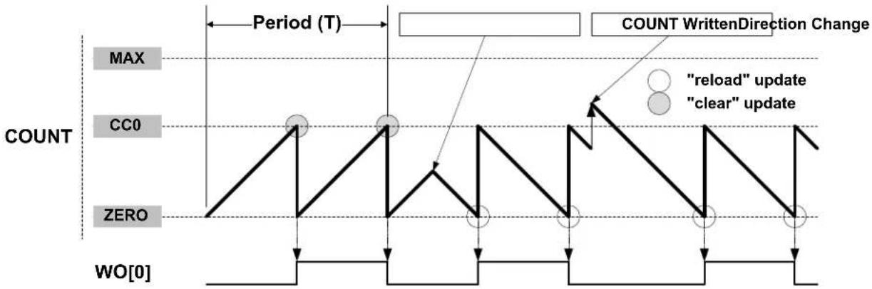
flowchart
graph TD
    A["Period (T)"] --> B["COUNT"]
    B --> C[""RELOAD" update"]
    B --> D[""CLEAR" update"]
    C --> E["Count WrittenDirection Change"]
    D --> E
    style A fill:#f9f,stroke:#333
    style B fill:#ccf,stroke:#333
    style C fill:#cfc,stroke:#333
    style D fill:#fcc,stroke:#333
    style E fill:#ffc,stroke:#333
27.6.2.6.3 PWM Operation
Normal Pulse-Width Modulation Operation (NPWM)
NPWM uses single-slope PWM generation.
For single-slope PWM generation, the period time (T) is controlled by the TOP value, and CCx controls the duty cycle of the generated waveform output. When up-counting, the WO[x] is set at start or compare match between the COUNT and TOP values, and cleared on compare match between COUNT and CCx register values. When down-counting, the WO[x] is cleared at start or compare match between the COUNT and ZERO values, and set on compare match between COUNT and CCx register values.
The following equation calculates the exact resolution for a single-slope PWM ( R_PWM_SS ) waveform:
$$ R _ {\mathrm {PWM_SS}} = \frac {\log (\mathrm{TOP} + 1)}{\log (2)} $$
The PWM frequency ( f_PWM_ss ) depends on TOP value and the peripheral clock frequency ( f_GCLK_TC ), and can be calculated by the following equation:
$$ f _ {\text { PWM_SS }} = \frac {f _ {\text { GCLK_TC }}}{\mathrm{N} (\mathrm{TOP} + 1)} $$
Where N represents the prescaler divider used (1, 2, 4, 8, 16, 64, 256, 1024).
Match Pulse-Width Modulation Operation (MPWM)
In MPWM, the output of WO[1] is depending on CC1 as shown in the figure below. On every overflow/underflow, a one-TC-clock-cycle negative pulse is put out on WO[0] (not shown in the figure).
Figure 27-6. Match PWM Operation
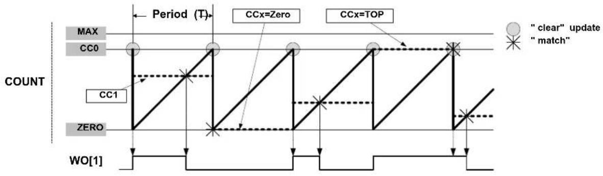
flowchart
graph TD
    A["CC0"] --> B["CC1"]
    B --> C["CCx=Zero"]
    C --> D["CCx=TOP"]
    D --> E["WO[1"]]
    style A fill:#f9f,stroke:#333
    style B fill:#ccf,stroke:#333
    style C fill:#cfc,stroke:#333
    style D fill:#fcc,stroke:#333
    subgraph COUNT
        A
        B
        C
        D
    end
    subgraph Period (T)
        A
        B
        C
        D
    end
    note right of A "clear" update
    note left of A "match"
    note right of C "CCx=Zero"
    note right of D "CCx=TOP"
The table below shows the update counter and overflow event/interrupt generation conditions in different operation modes.
Table 27-2. Counter Update and Overflow Event/interrupt Conditions in TC
| Name Operation TOP Update Output Waveform | OVFIF/Event | ||||||
| On Match On Update Up Down | |||||||
| NFRQ Normal Frequency PER TOP/ ZERO Toggle Stable TOP ZERO | |||||||
| MFRQ | Match Frequency | CC0 | TOP/ ZERO | Toggle | Stable | TOP | ZERO |
| NPWM | Single-slope PWM | PER | TOP/ ZERO | See description above. | TOP | ZERO | |
| MPWM | Single-slope PWM | CC0 | TOP/ ZERO | Toggle | Toggle | TOP | ZERO |
27.6.2.6.4 Changing the Top Value
The counter period is changed by writing a new TOP value to the Period register (PER or CC0, depending on the waveform generation mode). If a new TOP value is written when the counter value is close to zero and counting down, the counter can be reloaded with the previous TOP value, due to synchronization delays. Then, the counter will count one extra cycle before the new TOP value is used.
COUNT and TOP are continuously compared, so when a new TOP value that is lower than current COUNT is written to TOP, COUNT will wrap before a compare match.
A counter wraparound can occur in any operation mode when up-counting without buffering, see the figure below.
Figure 27-7. Changing the Top value with Up-Counting Operation
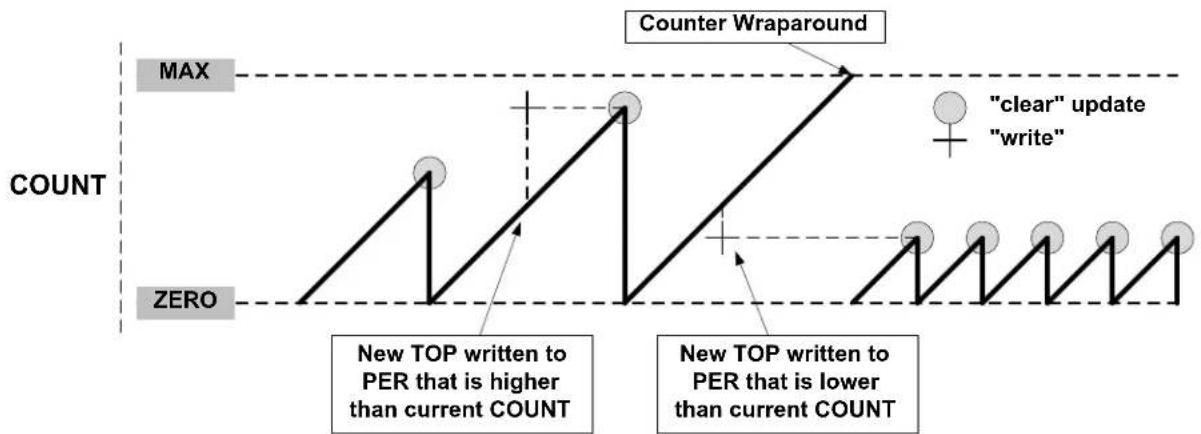
line
| Time/Event | Count | | ---------- | ----- | | NEW TOP written to PER that is higher than current COUNT | 100 | | New TOP written to PER that is lower than current COUNT | 50 | | "clear" update | 100 | | "write" | 50 |Figure 27-8. Changing the Top Value with Down-Counting Operation
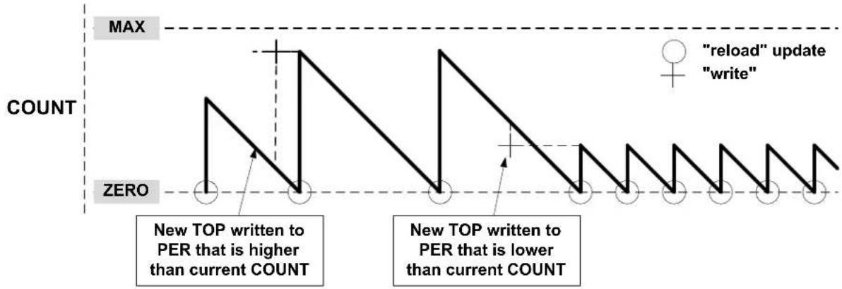
line
| Time Point | Event Type | Count | | ---------- | ---------------- | ----- | | 1 | "reload" update | 0 | | 2 | "write" | 0 | | 3 | "reload" update | 0 | | 4 | "write" | 0 | | 5 | "reload" update | 0 | | 6 | "write" | 0 | | 7 | "reload" update | 0 | | 8 | "write" | 0 | | 9 | "reload" update | 0 | | 10 | "write" | 0 |27.6.2.7 Capture Operations
To enable and use capture operations, the event line into the TC must be enabled using the TC Event Input bit in the Event Control register (EVCTRL.TCEI). The capture channels to be used must also be enabled in the Capture Channel x Enable bit group in the Control C register (CTRLC.CPTENx) before capture can be performed.
To enable and use capture operations, the corresponding Capture Channel x Enable bit in the Control C register (CTRLC.CAPTENx) must be written to '1'.
Note: The RETRIGGER, COUNT and START event actions are available only on an event from the Event System.
27.6.2.7.1 Event Capture Action
The compare/capture channels can be used as input capture channels to capture events from the Event System and give them a timestamp. The following figure shows four capture events for one capture channel.
Figure 27-9. Input Capture Timing
flowchart
graph TD
    A["events"] --> B["TOP"]
    B --> C["COUNT"]
    C --> D["ZERO"]
    D --> E["Capture 0"]
    E --> F["Capture 1"]
    F --> G["Capture 2"]
    G --> H["Capture 3"]
The TC can detect capture overflow of the input capture channels: When a new capture event is detected while the Capture Interrupt flag (INTFLAG.MCx) is still set, the new timestamp will not be stored and INTFLAG.ERR will be set.
27.6.2.7.2 Period and Pulse-Width (PPW) Capture Action
The TC can perform two input captures and restart the counter on one of the edges. This enables the TC to measure the pulse width and period and to characterize the frequency f and duty cycle of an input signal:
$$ f = \frac {1}{T} $$
$$ \text { dutyCycle } = \frac {t _ {p}}{T} $$
Selecting PWP (pulse-width, period) in the Event Action bit group in the Event Control register (EVCTRL.EVACT) enables the TC to perform one capture action on the rising edge and the other one on the falling edge. The period T will be captured into CC1 and the pulse width t_p in CC0. EVCTRL.EVACT=PPW (period and pulse-width) offers identical functionality, but will capture T into CC0 and t_p into CC1.
The TC Event Input Invert Enable bit in the Event Control register (EVCTRL.TCINV) is used to select whether the wraparound should occur on the rising edge or the falling edge. If EVCTRL.TCINV=1, the wraparound will happen on the falling edge.
To fully characterize the frequency and duty cycle of the input signal, activate capture on CC0 and CC1 by writing 0x3 to the Capture Channel x Enable bit group in the Control C register (CTRLC.CPTEN). When only one of these measurements is required, the second channel can be used for other purposes.
The TC can detect capture overflow of the input capture channels: When a new capture event is detected while the Capture Interrupt flag (INTFLAG.MCx) is still set, the new timestamp will not be stored and INTFLAG.ERR will be set.
Figure 27-10. PWP Capture
line
| Event Type | Event Description | Value | | ---------------- | ------------------------- | ----- | | external signal | Pulsewidth (tₚ) | Peak | | external signal | Pulsewidth (tₚ) | Max | | external signal | Event | Zero | | external signal | Event | Zero | | external signal | Event | Zero | | external signal | Event | Zero | | external signal | Event | Zero | | external signal | Event | Zero | | external signal | Event | Zero | | external signal | Event | Zero | | external signal | Event | Zero | | external signal | Event | Zero |27.6.3 Additional Features
27.6.3.1 One-Shot Operation
When one-shot is enabled, the counter automatically stops on the next counter overflow or underflow condition. When the counter is stopped, the Stop bit in the Status register (STATUS.STOP) is automatically set and the waveform outputs are set to zero.
One-shot operation is enabled by writing a '1' to the One-Shot bit in the Control B Set register (CTRLBSET.ONESHOT), and disabled by writing a '1' to CTRLBCLR.ONESHOT. When enabled, the TC will count until an overflow or underflow occurs and stops counting operation. The one-shot operation can be restarted by a re-trigger software command, a re-trigger event, or a start event. When the counter restarts its operation, STATUS.STOP is automatically cleared.
27.6.4 Sleep Mode Operation
The TC can be configured to operate in any sleep mode. To be able to run in standby, the RUNSTDBY bit in the Control A register (CTRLA.RUNSTDBY) must be written to one. The TC can wake up the device using interrupts from any sleep mode or perform actions through the Event System.
27.6.5 Synchronization
Due to asynchronicity between the main clock domain and the peripheral clock domains, some registers need to be synchronized when written or read.
The following bits are synchronized when written:
- Software Reset bit in the Control A register (CTRLA.SWRST)
- Enable bit in the Control A register (CTRLA.ENABLE)
Required write-synchronization is denoted by the "Write-Synchronized" property in the register description.
The following registers are synchronized when written:
• Control B Clear register (CTRLBCLR)
• Control B Set register (CTRLBSET)
• Control C register (CTRLC)
• Count Value register (COUNT)
• Period Value register (PERIOD)
- Compare/Capture Value registers (CCx)
Required write-synchronization is denoted by the "Write-Synchronized" property in the register description.
The following registers are synchronized when read:
• Control B Clear register (CTRLBCLR)
• Control B Set register (CTRLBSET)
• Control C register (CTRLC)
• Count Value register (COUNT)
• Period Value register (PERIOD)
- Compare/Capture Value registers (CCx)
Required read-synchronization is denoted by the "Read-Synchronized" property in the register description.
Related Links
13.3. Register Synchronization
27.7 Register Summary for 8-bit Registers
| Offset | Name Bit Pos. 76 | 543210 | ||||||||
| 0x00 CTRL | 7:0 | WAVEGEN[1:0] | MODE[1:0] ENABLE SWRST | |||||||
| 15:8 | PRESCSYNC[1:0] | RUNSTDBY PRESCALER[2:0] | ||||||||
| 0x02 READREQ | 7:0 | ADDR[4:0] | ||||||||
| 15:8 | RREQ | RCONT | ||||||||
| 0x04 | CTRLBCLR | 7:0 | CMD[1:0] | ONESHOT | DIR | |||||
| 0x05 | CTRLBSET | 7:0 | CMD[1:0] | ONESHOT | DIR | |||||
| 0x06 | CTRLC | 7:0 | CPTEN1 | CPTENO | INVEN1 | INVEN0 | ||||
| 0x07 | Reserved | |||||||||
| 0x08 | DBGCTRL | 7:0 | DBGRUN | |||||||
| 0x09 | Reserved | |||||||||
| 0x0A | EVCTRL | 7:0 | TCEI | TCINV | EVACT[2:0] | |||||
| 15:8 | MCEO1 MCEO0 | OVFEO | ||||||||
| 0x0C | INTENCLR | 7:0 | MC1 | MC0 | SYNCRDY | ERR | OVF | |||
| 0x0D | INTENSET | 7:0 | MC1 | MC0 | SYNCRDY | ERR | OVF | |||
| 0x0E | INTFLAG | 7:0 | MC1 | MC0 | SYNCRDY | ERR | OVF | |||
| 0x0F | STATUS | 7:0 | SYNCBUSY | SLAVE | STOP | |||||
| 0x10 | COUNT | 7:0 | COUNT[7:0] | |||||||
| 0x11 | Reserved | |||||||||
| ... | ||||||||||
| 0x13 | ||||||||||
| 0x14 | PER | 7:0 | PER[7:0] | |||||||
| 0x15 | Reserved | |||||||||
| ... | ||||||||||
| 0x17 | ||||||||||
| 0x18 | CC0 | 7:0 | CC[7:0] | |||||||
| 0x19 | CC1 | 7:0 | CC[7:0] | |||||||
27.8 Register Description for 8-bit Registers
Registers can be 8, 16, or 32 bits wide. Atomic 8-, 16- and 32-bit accesses are supported. In addition, the 8-bit quarters and 16-bit halves of a 32-bit register, and the 8-bit halves of a 16-bit register can be accessed directly.
Some registers are optionally write-protected by the Peripheral Access Controller (PAC). Optional PAC write-protection is denoted by the "PAC Write-Protection" property in each individual register description. For details, refer to 27.5.7. Register Access Protection
Some registers are synchronized when read and/or written. Synchronization is denoted by the "Write-Synchronized" or the "Read-Synchronized" property in each individual register description. For details, refer to 27.6.5. Synchronization.
Some registers are enable-protected, meaning they can only be written when the peripheral is disabled. Enable-protection is denoted by the "Enable-Protected" property in each individual register description.
27.8.1 Control A
Name: CTRLA
Offset: 0x00
Reset: 0x00000000
Property: PAC Write-Protection, Write-Synchronized bits, Enable-Protected bits
Bit 15 14 13 12 11 10 9 8
| PRESCSYNC[1:0] RUNSTDBY PRESCALER[2:0] | ||||||
| Access | R/W | R/W | R/W | R/W | R/W | R/W |
| Reset | 0 0 0 0 0 0 | |||||
Bit 76543210
| WAVEGEN[1:0] | MODE[1:0] | ENABLE | SWRST | |||||
| Access | R/W | R/W | R/W | R/W | R/W | R/W | ||
| Reset | 0 0 | 0 0 0 0 | ||||||
Bits 13:12 - PRESCSYNC[1:0] Prescaler and Counter Synchronization
These bits select whether the counter should wrap around on the next GCLK_TCx clock or the next prescaled GCLK_TCx clock. It also makes it possible to reset the prescaler.
These bits are not write-synchronized, but are enable-protected.
| Value | Name | Description |
| 0x0 | GCLK | Reload or reset the counter on next generic clock |
| 0x1 | PRESC | Reload or reset the counter on next prescaler clock |
| 0x2 | RESYNC | Reload or reset the counter on next generic clock. Reset the prescaler counter |
| 0x3 | - | Reserved |
Bit 11 - RUNSTDBY Run in Standby
This bit is used to keep the TC running in Standby mode.
This bit is not write-synchronized, but is enable-protected.
| Value | Description |
| 0 | The TC is halted in standby. |
| 1 | The TC continues to run in standby. |
Bits 10:8 - PRESCALER[2:0] Prescaler
These bits select the counter prescaler factor.
These bits are not write-synchronized, but are enable protected.
| Value | Name | Description |
| 0x0 | DIV1 | Prescaler: GCLK_TC |
| 0x1 | DIV2 | Prescaler: GCLK_TC/2 |
| 0x2 | DIV4 | Prescaler: GCLK_TC/4 |
| 0x3 | DIV8 | Prescaler: GCLK_TC/8 |
| 0x4 | DIV16 | Prescaler: GCLK_TC/16 |
| 0x5 | DIV64 | Prescaler: GCLK_TC/64 |
| 0x6 | DIV256 | Prescaler: GCLK_TC/256 |
| 0x7 | DIV1024 | Prescaler: GCLK_TC/1024 |
Bits 6:5 - WAVEGEN[1:0] Waveform Generation Operation
These bits select the waveform generation operation. They affect the top value, as shown in "Waveform Output Operations". It also controls whether frequency or PWM waveform generation should be used. How these modes differ can also be seen from "Waveform Output Operations". These bits are not write-synchronized, but are enable-protected.
Table 27-3. Waveform Generation Operation
| Value Name Operation Top Value Waveform Output | on Match | Waveform Output on Wraparound | |||
| 0x0 NFRQ Normal frequency PER | (1)/Max Toggle No action | ||||
| 0x1 MFRQ Match frequency CC0 Toggle No action | |||||
| 0x2 NPWM Normal PWM PER | (1)/Max Clear when counting up Set when counting down | Set when counting up Clear when counting down | |||
| 0x3 MPWM Match PWM | CC0 Clear when | counting up Set when counting down | Set when counting up Clear when counting down | ||
Note:
- This depends on the TC mode. In 8-bit mode, the top value is the Period Value register (PER). In 16-bit and 32-bit modes it is the maximum value.
Bits 3:2 - MODE[1:0] Timer Counter Mode
These bits select the Counter mode.
These bits are not write-synchronized, but are enable protected.
| Value Name | Description | |
| 0x0 | COUNT16 | Counter in 16-bit mode |
| 0x1 | COUNT8 | Counter in 8-bit mode |
| 0x2 | COUNT32 | Counter in 32-bit mode |
| 0x3 | - | Reserved |
Bit 1 - ENABLE Enable
Due to synchronization, there is delay from writing CTRLA. ENABLE until the peripheral is enabled/disabled. The value written to CTRLA. ENABLE will read back immediately, and the ENABLE Synchronization Busy bit in the SYNCBUSY register (SYNCBUSY. ENABLE) will be set. SYNCBUSY. ENABLE will be cleared when the operation is complete.
This bit is not enable protected.
| Value Description | |
| 0 | The peripheral is disabled. |
| 1 | The peripheral is enabled. |
Bit 0 - SWRST Software Reset
Writing a '0' to this bit has no effect.
Writing a '1' to this bit resets all registers in the TC, except DBGCTRL, to their initial state, and the TC will be disabled.
Writing a '1' to CTRLA.SWRST will always take precedence; all other writes in the same write-operation will be discarded.
Due to synchronization there is a delay from writing CTRLA.SWRST until the reset is complete.
CTRLA.SWRST and SYNCBUSY.SWRST will both be cleared when the reset is complete.
This bit is not enable protected.
| Value Description | |
| 0 | There is no reset operation ongoing. |
| 1 | The reset operation is ongoing. |
27.8.2 Read Request
Name: READREQ
Offset: 0x02
Reset: 0x0000
text_image
Bit 15 14 13 12 11 10 9 8 RREQ RCONT Access W R/W Reset 0 0 Bit 7 6 5 4 3 2 1 0 ADDR[4:0] Access R/W R/W R/W R/W R/W Reset 0 0 0 0 0Bit 15 - RREQ Read Request
Writing a zero to this bit has no effect.
This bit will always read as zero.
Writing a one to this bit requests synchronization of the register pointed to by the Address bit group (READREQ. ADDR) and sets the Synchronization Busy bit in the Status register (STATUS.SYNCBUSY).
Bit 14 - RCONT Read Continuously
When continuous synchronization is enabled, the register pointed to by the Address bit group (READREQ.ADDR) will be synchronized automatically every time the register is updated. READREQ.RCONT prevents READREQ.RREQ from clearing automatically. For the continuous read mode, the RREQ bit is required to be set once the RCONT bit is set.
| Value | Description |
| 0 | Continuous synchronization is disabled. |
| 1 | Continuous synchronization is enabled. |
Bits 4:0 - ADDR[4:0] Address
These bits select the offset of the register that needs read synchronization. In the TC, only COUNT and CCx are available for read synchronization.
27.8.3 Control B Clear
Name: CTRLBCLR
Offset: 0x04
Reset: 0x00
Property: PAC Write-Protection, Read-Synchronized, Write-Synchronized
This register allows the user to clear bits in the CTRLB register without doing a read-modify-write operation. Changes in this register will also be reflected in the Control B Set register (CTRLBSET).
Bit 76543210
| CMD[1:0] | ONESHOT | DIR | ||||||
| Access | R/W | R/W | R/W | |||||
| Reset | 0 | 0 | 0 | 0 |
Bits 7:6 - CMD[1:0] Command
These bits are used for software control of the TC. The commands are executed on the next prescaled GCLK_TC clock cycle. When a command has been executed, the CMD bit group will be read back as zero.
Writing 0x0 to these bits has no effect.
Writing a '1' to any of these bits will clear the pending command.
Table 27-4. Command
| Value | Name | Description |
| 0x0 | NONE | No action |
| 0x1 | RETRIGGER | Force a start, restart or retrigger |
| 0x2 | STOP | Force a stop |
| 0x3 | - | Reserved |
Bit 2 - ONESHOT One-Shot on Counter
This bit controls one-shot operation of the TC.
Writing a '0' to this bit has no effect
Writing a '1' to this bit will disable one-shot operation.
| Value | Description |
| 0 | The TC will wrap around and continue counting on an Overflow/Underflow condition. |
| 1 | The TC will wrap around and stop on the next Underflow/Overflow condition. |
Bit 0 - DIR Counter Direction
This bit is used to change the direction of the counter.
Writing a '0' to this bit has no effect.
Writing a '1' to this bit will clear the bit and make the counter count up.
| Value | Description |
| 0 | The timer/counter is counting up (incrementing). |
| 1 | The timer/counter is counting down (decrementing). |
27.8.4 Control B Set
Name: CTRLBSET
Offset: 0x05
Reset: 0x00
Property: PAC Write-Protection, Read-synchronized, Write-Synchronized
This register allows the user to set bits in the CTRLB register without doing a read-modify-write operation. Changes in this register will also be reflected in the Control B Clear register (CTRLBCLR).
Bit 76543210
| CMD[1:0] | ONESHOT | DIR | ||||||
| Access | R/W | R/W | R/W | |||||
| Reset | 0 | 0 | 0 | 0 |
Bits 7:6 - CMD[1:0] Command
These bits are used for software control of the TC. The commands are executed on the next prescaled GCLK_TC clock cycle. When a command has been executed, the CMD bit group will be read back as zero.
Writing 0x0 to these bits has no effect.
Writing a '1' to one of these bits will set a command.
Table 27-5. Command
| Value | Name | Description |
| 0x0 | NONE | No action |
| 0x1 | RETRIGGER | Force a start, restart or retrigger |
| 0x2 | STOP | Force a stop |
| 0x3 | - | Reserved |
Bit 2 - ONESHOT One-Shot on Counter
This bit controls one-shot operation of the TC.
Writing a '0' to this bit has no effect
Writing a '1' to this bit will enable one-shot operation.
| Value | Description |
| 0 | The TC will wrap around and continue counting on an Overflow/Underflow condition. |
| 1 | The TC will wrap around and stop on the next Underflow/Overflow condition. |
Bit 0 - DIR Counter Direction
This bit is used to change the direction of the counter.
Writing a '0' to this bit has no effect.
Writing a '1' to this bit will make the counter count down.
| Value | Description |
| 0 | The timer/counter is counting up (incrementing). |
| 1 | The timer/counter is counting down (decrementing). |
27.8.5 Control C
Name: CTRLC
Offset: 0x06
Reset: 0x00
Property: PAC Write-Protection, Read-synchronized, Write-Synchronized
Bit 76543210
| CPTEN1 CPTENO | INVEN1 INVENO | |||||
| Access Reset 0 0 0 0 | R/W R/W R/W R/W | |||||
Bits 4, 5 - CPTENx Capture Channel x Enable
These bits are used to select the capture or compare operation on channel x.
Writing a '1' to CPTENx enables capture on channel x.
Writing a '0' to CPTENx disables capture on channel x.
Bits 0, 1 - INVENx Waveform Output x Inversion Enable
These bits are used to select inversion on the output of channel x.
Writing a '1' to INVENx inverts output from WO[x].
Writing a '0' to INVENx disables inversion of output from WO[x].
27.8.6 Debug Control
Name: DBGCTRL
Offset: 0x08
Reset: 0x00
Property: PAC Write-Protection
Bit 76543210
| DBGRUN | |||||||
| Access Reset 0 | R/W | ||||||
Bit 0 - DBGRUN Debug Run Mode
This bit is not affected by a software Reset, and should not be changed by software while the TC is enabled.
| Value Description | |
| 0 | The TC is halted when the device is halted in Debug mode. |
| 1 | The TC continues normal operation when the device is halted in Debug mode. |
27.8.7 Event Control
Name: EVCTRL
Offset: 0x0A
Reset: 0x0000
Property: PAC Write-Protection, Enable-Protected
Bit 15 14 13 12 11 10 9 8
| MCEΦ1 MCEO0 | OVFEO | ||||||
| Access Reset | R/W 0 0 | R/W | R/W 0 |
Bit 76543210
| TCEI | TCINV | EVACT[2:0] | ||||||
| Access Reset | R/W | R/W | R/W | R/W | R/W | |||
| 0 0 | 0 0 0 | |||||||
Bits 12, 13 - MCEOx Match or Capture Channel x Event Output Enable [x = 1..0]
These bits enable the generation of an event for every match or capture on channel x.
| Value | Description |
| 0 | Match/Capture event on channel x is disabled and will not be generated. |
| 1 | Match/Capture event on channel x is enabled and will be generated for every compare/capture. |
Bit 8 - OVFEO Overflow/Underflow Event Output Enable
This bit enables the Overflow/Underflow event. When enabled, an event will be generated when the counter overflows/underflows.
| Value | Description |
| 0 | Overflow/Underflow event is disabled and will not be generated. |
| 1 | Overflow/Underflow event is enabled and will be generated for every counter overflow/underflow. |
Bit 5 - TCEI TC Event Enable
This bit is used to enable asynchronous input events to the TC.
| Value | Description |
| 0 | Incoming events are disabled. |
| 1 | Incoming events are enabled. |
Bit 4 - TCINV TC Inverted Event Input Polarity
This bit inverts the asynchronous input event source.
| Value | Description |
| 0 | Input event source is not inverted. |
| 1 | Input event source is inverted. |
Bits 2:0 - EVACT[2:0] Event Action
These bits define the event action the TC will perform on an event.
| Value | Name | Description |
| 0x0 | OFF | Event action disabled |
| 0x1 | RETRIGGER Start, restart or retrigger TC on event | |
| 0x2 | COUNT | Count on event |
| 0x3 | START | Start TC on event |
| 0x4 | ||
| 0x5 | PPW | Period captured in CC0, pulse width in CC1 |
| 0x6 | PWP | Period captured in CC1, pulse width in CC0 |
| 0x7 | ||
27.8.8 Interrupt Enable Clear
Name: INTENCLR
Offset: 0x0C
Reset: 0x00
Property: PAC Write-Protection
This register allows the user to disable an interrupt without doing a read-modify-write operation. Changes in this register will also be reflected in the Interrupt Enable Set register (INTENSET).
Bit 76543210
| MC1 | MC0 | SYNCRDY | ERR | OVF | |||||
| Access Reset | R/W | R/W | R/W | R/W | R/W | ||||
| 0 0 0 | 0 0 |
Bits 4, 5 - MCx Match or Capture Channel x Interrupt Enable [x = 1..0]
Writing a '0' to these bits has no effect.
Writing a '1' to MCx will clear the corresponding Match or Capture Channel x Interrupt Enable bit, which disables the Match or Capture Channel x interrupt.
| Value | Description |
| 0 | The Match or Capture Channel x interrupt is disabled. |
| 1 | The Match or Capture Channel x interrupt is enabled. |
Bit 3 - SYNCRDY Synchronization Ready Interrupt Enable
Writing a '0' to this bit has no effect.
Writing a one to this bit will clear the Synchronization Ready Interrupt Disable/Enable bit, which disables the Synchronization Ready interrupt.
| Value | Description |
| 0 | The Synchronization Ready interrupt is disabled. |
| 1 | The Synchronization Ready interrupt is enabled. |
Bit 1 - ERR Error Interrupt Enable
Writing a '0' to this bit has no effect.
Writing a '1' to this bit will clear the Error Interrupt Enable bit, which disables the Error interrupt.
| Value | Description |
| 0 | The Error interrupt is disabled. |
| 1 | The Error interrupt is enabled. |
Bit 0 - OVF Overflow Interrupt Enable
Writing a '0' to this bit has no effect.
Writing a '1' to this bit will clear the Overflow Interrupt Enable bit, which disables the Overflow interrupt request.
| Value | Description |
| 0 | The Overflow interrupt is disabled. |
| 1 | The Overflow interrupt is enabled. |
27.8.9 Interrupt Enable Set
Name: INTENSET
Offset: 0x0D
Reset: 0x00
Property: PAC Write-Protection
This register allows the user to enable an interrupt without doing a read-modify-write operation. Changes in this register will also be reflected in the Interrupt Enable Clear register (INTENCLR).
Bit 76543210
| MC1 | MC0 | SYNCRDY | ERR | OVF | |||||
| Access Reset | R/W | R/W | R/W | R/W | R/W | ||||
| 0 0 0 | 0 0 |
Bits 4, 5 - MCx Match or Capture Channel x Interrupt Enable [x = 1..0]
Writing a '0' to these bits has no effect.
Writing a '1' to MCx will set the corresponding Match or Capture Channel x Interrupt Enable bit, which enables the Match or Capture Channel x interrupt.
| Value | Description |
| 0 | The Match or Capture Channel x interrupt is disabled. |
| 1 | The Match or Capture Channel x interrupt is enabled. |
Bit 3 - SYNCRDY Synchronization Ready Interrupt Enable
Writing a '0' to this bit has no effect.
Writing a one to this bit will clear the Synchronization Ready Interrupt Disable/Enable bit, which disables the Synchronization Ready interrupt.
| Value | Description |
| 0 | The Synchronization Ready interrupt is disabled. |
| 1 | The Synchronization Ready interrupt is enabled. |
Bit 1 - ERR Error Interrupt Enable
Writing a '0' to this bit has no effect.
Writing a '1' to this bit will set the Error Interrupt Enable bit, which enables the Error interrupt.
| Value | Description |
| 0 | The Error interrupt is disabled. |
| 1 | The Error interrupt is enabled. |
Bit 0 - OVF Overflow Interrupt Enable
Writing a '0' to this bit has no effect.
Writing a '1' to this bit will set the Overflow Interrupt Enable bit, which enables the Overflow interrupt request.
| Value | Description |
| 0 | The Overflow interrupt is disabled. |
| 1 | The Overflow interrupt is enabled. |
27.8.10 Interrupt Flag Status and Clear
Name: INTFLAG
Offset: 0x0E
Reset: 0x00
Property: -
Bit 76543210
| MC1 | MC0 | SYNCRDY | ERR | OVF | |||||
| Access Reset | R/W | R/W | R/W | R/W | R/W | ||||
| 0 0 0 | 0 0 |
Bits 4, 5 - MCx Match or Capture Channel x [x = 1..0]
This flag is set on a comparison match, or when the corresponding CCx register contains a valid capture value. This flag is set on the next CLK_TC_CNT cycle, and will generate an interrupt request if the corresponding Match or Capture Channel x Interrupt Enable bit in the Interrupt Enable Set register (INTENSET.MCx) is '1'.
Writing a '0' to one of these bits has no effect.
Writing a '1' to one of these bits will clear the corresponding Match or Capture Channel x Interrupt flag
In capture operation, this flag is automatically cleared when CCx register is read.
Bit 3 - SYNCRDY Synchronization Ready Interrupt Enable
Writing a '0' to this bit has no effect.
Writing a one to this bit will clear the Synchronization Ready Interrupt Disable/Enable bit, which disables the Synchronization Ready interrupt.
| Value | Description |
| 0 | The Synchronization Ready interrupt is disabled. |
| 1 | The Synchronization Ready interrupt is enabled. |
Bit 1 - ERR Error Interrupt Flag
This flag is set when a new capture occurs on a channel while the corresponding Match or Capture Channel x Interrupt flag is set, in which case there is nowhere to store the new capture.
Writing a '0' to this bit has no effect.
Writing a '1' to this bit clears the Error Interrupt flag.
Bit 0 - OVF Overflow Interrupt Flag
This flag is set on the next CLK_TC_CNT cycle after an Overflow condition occurs, and will generate an interrupt request if INTENCLR.OVF or INTENSET.OVF is '1'.
Writing a '0' to this bit has no effect.
Writing a '1' to this bit clears the Overflow Interrupt flag.
27.8.11 Status
Name: STATUS
Offset: 0x0F
Reset: 0x08
Property: -
Bit 76543210
| SYNCBUSY | SLAVE STOP | |||||||
| Access | R R R | |||||||
| Reset | 0 | 0 1 | ||||||
Bit 7 - SYNCBUSY Synchronization Busy
This bit is cleared when the synchronization of registers between the clock domains is complete. This bit is set when the synchronization of registers between clock domains is started.
Bit 4 - SLAVE Client Status Flag
This bit is only available in 32-bit mode on the Client TC (i.e., and/or). The bit is set when the associated Host TC (, respectively) is set to run in 32-bit mode.
Bit 3 - STOP Stop Status Flag
This bit is set when the TC is disabled, on a Stop command, or on an overflow/underflow condition when the One-Shot bit in the Control B Set register (CTRLBSET.ONESHOT) is '1'.
| Value | Description |
| 0 | Counter is running. |
| 1 | Counter is stopped. |
27.8.12 Counter Value, 8-bit Mode
Name: COUNT
Offset: 0x10
Reset: 0x00
Property: PAC Write-Protection, Write-Synchronized
Bit 76543210
COUNT[7:0]
Access R/W R/W R/W R/W R/W R/W R/W R/W
Reset 00000000
Bits 7:0 - COUNT[7:0] Counter Value
These bits contain the current counter value.
Note: Prior to any read access, this register must be synchronized by the user by writing
CTRLA.COUNTSYNC = 1.
27.8.13 Period Value, 8-bit Mode
Name: PER
Offset: 0x14
Reset: 0xFF
Property: Write-Synchronized
Bit 76543210
PER[7:0]
Access R/W R/W R/W R/W R/W R/W R/W R/W
Reset 00000001
Bits 7:0 - PER[7:0] Period Value
These bits hold the value of the Period Buffer register PERBUF. The value is copied to PER register on UPDATE condition.
27.8.14 Channel x Compare/Capture Value, 8-bit Mode
Name: CCx
Offset: 0x18 + x*0x01 [x=0..1]
Reset: 0x00
Property: Write-Synchronized
Bit 76543210
CC[7:0]
Access R/W R/W R/W R/W R/W R/W R/W R/W
Reset 00000000
Bits 7:0 - CC[7:0] Channel x Compare/Capture Value
These bits contain the compare/capture value in 8-bit TC mode. In Match frequency (MFRQ) or Match PWM (MPWM) waveform operation (CTRLA.WAVEGEN), the CC0 register is used as a period register.
27.9 Register Summary for 16-bit Registers
| Offset | Name Bit Pos. 76 | 543210 | ||||||||
| 0x00 CTRL | 7:0 | WAVEGEN[1:0] | MODE[1:0] ENABLE SWRST | |||||||
| 15:8 | PRESCSYNC[1:0] | RUNSTDBY | PRESCALER[2:0] | |||||||
| 0x02 READREQ | 7:0 | ADDR[4:0] | ||||||||
| 15:8 | RREQ | RCONT | ||||||||
| 0x04 | CTRLBCLR | 7:0 | CMD[1:0] | ONESHOT | DIR | |||||
| 0x05 | CTRLBSET | 7:0 | CMD[1:0] | ONESHOT | DIR | |||||
| 0x06 | CTRLC | 7:0 | CPTEN1 | CPTENO | INVEN1 | INVEN0 | ||||
| 0x07 | Reserved | |||||||||
| 0x08 | DBGCTRL | 7:0 | DBGRUN | |||||||
| 0x09 | Reserved | |||||||||
| 0x0A | EVCTRL | 7:0 | TCEI | TCINV | EVACT[2:0] | |||||
| 15:8 | MCEO1 | MCEO0 | OVFEO | |||||||
| 0x0C | INTENCLR | 7:0 | MC1 | MC0 | SYNCRDY | ERR | OVF | |||
| 0x0D | INTENSET | 7:0 | MC1 | MC0 | SYNCRDY | ERR | OVF | |||
| 0x0E | INTFLAG | 7:0 | MC1 | MC0 | SYNCRDY | ERR | OVF | |||
| 0x0F | STATUS | 7:0 | SYNCBUSY | SLAVE | STOP | |||||
| 0x10 | COUNT | 7:0 | COUNT[7:0] | |||||||
| 15:8 | COUNT[15:8] | |||||||||
| 0x12 ... 0x17 | Reserved | |||||||||
| 0x18 | CC0 | 7:0 | CC[7:0] | |||||||
| 15:8 | CC[15:8] | |||||||||
| 0x1A | CC1 | 7:0 | CC[7:0] | |||||||
| 15:8 | CC[15:8] | |||||||||
27.10 Register Description for 16-bit Registers
Registers can be 8, 16, or 32 bits wide. Atomic 8-, 16- and 32-bit accesses are supported. In addition, the 8-bit quarters and 16-bit halves of a 32-bit register, and the 8-bit halves of a 16-bit register can be accessed directly.
Some registers are optionally write-protected by the Peripheral Access Controller (PAC). Optional PAC write-protection is denoted by the "PAC Write-Protection" property in each individual register description. For details, refer to 27.5.7. Register Access Protection
Some registers are synchronized when read and/or written. Synchronization is denoted by the "Write-Synchronized" or the "Read-Synchronized" property in each individual register description. For details, refer to 27.6.5. Synchronization.
Some registers are enable-protected, meaning they can only be written when the peripheral is disabled. Enable-protection is denoted by the "Enable-Protected" property in each individual register description.
27.10.1 Control A
Name: CTRLA
Offset: 0x00
Reset: 0x00000000
Property: PAC Write-Protection, Write-Synchronized bits, Enable-Protected bits
Bit 15 14 13 12 11 10 9 8
| PRESCSYNC[1:0] RUNSTDBY PRESCALER[2:0] | ||||||
| Access | R/W | R/W | R/W | R/W | R/W | R/W |
| Reset | 0 0 0 0 0 0 | |||||
Bit 76543210
| WAVEGEN[1:0] | MODE[1:0] | ENABLE | SWRST | |||||
| Access | R/W | R/W | R/W | R/W | R/W | R/W | ||
| Reset | 0 0 | 0 0 0 0 | ||||||
Bits 13:12 - PRESCSYNC[1:0] Prescaler and Counter Synchronization
These bits select whether the counter should wrap around on the next GCLK_TCx clock or the next prescaled GCLK_TCx clock. It also makes it possible to reset the prescaler.
These bits are not write-synchronized, but are enable-protected.
| Value | Name | Description |
| 0x0 | GCLK | Reload or reset the counter on next generic clock |
| 0x1 | PRESC | Reload or reset the counter on next prescaler clock |
| 0x2 | RESYNC | Reload or reset the counter on next generic clock. Reset the prescaler counter |
| 0x3 | - | Reserved |
Bit 11 - RUNSTDBY Run in Standby
This bit is used to keep the TC running in Standby mode.
This bit is not write-synchronized, but is enable-protected.
| Value | Description |
| 0 | The TC is halted in standby. |
| 1 | The TC continues to run in standby. |
Bits 10:8 - PRESCALER[2:0] Prescaler
These bits select the counter prescaler factor.
These bits are not write-synchronized, but are enable protected.
| Value | Name | Description |
| 0x0 | DIV1 | Prescaler: GCLK_TC |
| 0x1 | DIV2 | Prescaler: GCLK_TC/2 |
| 0x2 | DIV4 | Prescaler: GCLK_TC/4 |
| 0x3 | DIV8 | Prescaler: GCLK_TC/8 |
| 0x4 | DIV16 | Prescaler: GCLK_TC/16 |
| 0x5 | DIV64 | Prescaler: GCLK_TC/64 |
| 0x6 | DIV256 | Prescaler: GCLK_TC/256 |
| 0x7 | DIV1024 | Prescaler: GCLK_TC/1024 |
Bits 6:5 - WAVEGEN[1:0] Waveform Generation Operation
These bits select the waveform generation operation. They affect the top value, as shown in "Waveform Output Operations". It also controls whether frequency or PWM waveform generation should be used. How these modes differ can also be seen from "Waveform Output Operations". These bits are not write-synchronized, but are enable-protected.
Table 27-6. Waveform Generation Operation
| Value Name Operation Top Value Waveform Output | on Match | Waveform Output on Wraparound | |||
| 0x0 NFRQ Normal frequency PER | (1)/Max Toggle No action | ||||
| 0x1 MFRQ Match frequency CC0 Toggle No action | |||||
| 0x2 NPWM Normal PWM PER | (1)/Max Clear when counting up Set when counting down | Set when counting up Clear when counting down | |||
| 0x3 MPWM Match PWM | CC0 Clear when | counting up Set when counting down | Set when counting up Clear when counting down | ||
Note:
- This depends on the TC mode. In 8-bit mode, the top value is the Period Value register (PER). In 16-bit and 32-bit modes it is the maximum value.
Bits 3:2 - MODE[1:0] Timer Counter Mode
These bits select the Counter mode.
These bits are not write-synchronized, but are enable protected.
| Value Name | Description | |
| 0x0 | COUNT16 | Counter in 16-bit mode |
| 0x1 | COUNT8 | Counter in 8-bit mode |
| 0x2 | COUNT32 | Counter in 32-bit mode |
| 0x3 | - | Reserved |
Bit 1 - ENABLE Enable
Due to synchronization, there is delay from writing CTRLA. ENABLE until the peripheral is enabled/disabled. The value written to CTRLA. ENABLE will read back immediately, and the ENABLE Synchronization Busy bit in the SYNCBUSY register (SYNCBUSY. ENABLE) will be set. SYNCBUSY. ENABLE will be cleared when the operation is complete.
This bit is not enable protected.
| Value Description | |
| 0 | The peripheral is disabled. |
| 1 | The peripheral is enabled. |
Bit 0 - SWRST Software Reset
Writing a '0' to this bit has no effect.
Writing a '1' to this bit resets all registers in the TC, except DBGCTRL, to their initial state, and the TC will be disabled.
Writing a '1' to CTRLA.SWRST will always take precedence; all other writes in the same write-operation will be discarded.
Due to synchronization there is a delay from writing CTRLA.SWRST until the reset is complete.
CTRLA.SWRST and SYNCBUSY.SWRST will both be cleared when the reset is complete.
This bit is not enable protected.
| Value Description | |
| 0 | There is no reset operation ongoing. |
| 1 | The reset operation is ongoing. |
27.10.2 Read Request
Name: READREQ
Offset: 0x02
Reset: 0x0000

text_image
Bit 15 14 13 12 11 10 9 8 RREQ RCONT Access W R/W Reset 0 0 Bit 7 6 5 4 3 2 1 0 ADDR[4:0] Access R/W R/W R/W R/W R/W Reset 0 0 0 0 0Bit 15 - RREQ Read Request
Writing a zero to this bit has no effect.
This bit will always read as zero.
Writing a one to this bit requests synchronization of the register pointed to by the Address bit group (READREQ. ADDR) and sets the Synchronization Busy bit in the Status register (STATUS.SYNCBUSY).
Bit 14 - RCONT Read Continuously
When continuous synchronization is enabled, the register pointed to by the Address bit group (READREQ.ADDR) will be synchronized automatically every time the register is updated. READREQ.RCONT prevents READREQ.RREQ from clearing automatically. For the continuous read mode, the RREQ bit is required to be set once the RCONT bit is set.
| Value | Description |
| 0 | Continuous synchronization is disabled. |
| 1 | Continuous synchronization is enabled. |
Bits 4:0 - ADDR[4:0] Address
These bits select the offset of the register that needs read synchronization. In the TC, only COUNT and CCx are available for read synchronization.
This register allows the user to clear bits in the CTRLB register without doing a read-modify-write operation. Changes in this register will also be reflected in the Control B Set register (CTRLBSET).
Bit 76543210
| CMD[1:0] | ONESHOT | DIR | ||||||
| Access | R/W | R/W | R/W | |||||
| Reset | 0 | 0 | 0 | 0 |
Bits 7:6 - CMD[1:0] Command
These bits are used for software control of the TC. The commands are executed on the next prescaled GCLK_TC clock cycle. When a command has been executed, the CMD bit group will be read back as zero.
Writing 0x0 to these bits has no effect.
Writing a '1' to any of these bits will clear the pending command.
Table 27-7. Command
| Value | Name | Description |
| 0x0 | NONE | No action |
| 0x1 | RETRIGGER | Force a start, restart or retrigger |
| 0x2 | STOP | Force a stop |
| 0x3 | - | Reserved |
Bit 2 - ONESHOT One-Shot on Counter
This bit controls one-shot operation of the TC.
Writing a '0' to this bit has no effect
Writing a '1' to this bit will disable one-shot operation.
| Value | Description |
| 0 | The TC will wrap around and continue counting on an Overflow/Underflow condition. |
| 1 | The TC will wrap around and stop on the next Underflow/Overflow condition. |
Bit 0 - DIR Counter Direction
This bit is used to change the direction of the counter.
Writing a '0' to this bit has no effect.
Writing a '1' to this bit will clear the bit and make the counter count up.
| Value | Description |
| 0 | The timer/counter is counting up (incrementing). |
| 1 | The timer/counter is counting down (decrementing). |
This register allows the user to set bits in the CTRLB register without doing a read-modify-write operation. Changes in this register will also be reflected in the Control B Clear register (CTRLBCLR).
Bit 76543210
| CMD[1:0] | ONESHOT | DIR | ||||||
| Access | R/W | R/W | R/W | |||||
| Reset | 0 | 0 | 0 | 0 |
Bits 7:6 - CMD[1:0] Command
These bits are used for software control of the TC. The commands are executed on the next prescaled GCLK_TC clock cycle. When a command has been executed, the CMD bit group will be read back as zero.
Writing 0x0 to these bits has no effect.
Writing a '1' to one of these bits will set a command.
Table 27-8. Command
| Value | Name | Description |
| 0x0 | NONE | No action |
| 0x1 | RETRIGGER | Force a start, restart or retrigger |
| 0x2 | STOP | Force a stop |
| 0x3 | - | Reserved |
Bit 2 - ONESHOT One-Shot on Counter
This bit controls one-shot operation of the TC.
Writing a '0' to this bit has no effect
Writing a '1' to this bit will enable one-shot operation.
| Value | Description |
| 0 | The TC will wrap around and continue counting on an Overflow/Underflow condition. |
| 1 | The TC will wrap around and stop on the next Underflow/Overflow condition. |
Bit 0 - DIR Counter Direction
This bit is used to change the direction of the counter.
Writing a '0' to this bit has no effect.
Writing a '1' to this bit will make the counter count down.
| Value | Description |
| 0 | The timer/counter is counting up (incrementing). |
| 1 | The timer/counter is counting down (decrementing). |
27.10.5 Control C
Name: CTRLC
Offset: 0x06
Reset: 0x00
Property: PAC Write-Protection, Read-synchronized, Write-Synchronized
Bit 76543210
| CPTEN1 CPTENO | INVEN1 INVENO | |||||
| Access Reset 0000 | R/W R/W R/W R/W | |||||
Bits 4, 5 - CPTENx Capture Channel x Enable
These bits are used to select the capture or compare operation on channel x.
Writing a '1' to CPTENx enables capture on channel x.
Writing a '0' to CPTENx disables capture on channel x.
Bits 0, 1 - INVENx Waveform Output x Inversion Enable
These bits are used to select inversion on the output of channel x.
Writing a '1' to INVENx inverts output from WO[x].
Writing a '0' to INVENx disables inversion of output from WO[x].
27.10.6 Debug Control
Name: DBGCTRL
Offset: 0x08
Reset: 0x00
Property: PAC Write-Protection
Bit 76543210
| DBGRUN | |||||||
| Access Reset 0 | R/W | ||||||
Bit 0 - DBGRUN Debug Run Mode
This bit is not affected by a software Reset, and should not be changed by software while the TC is enabled.
| Value Description | |
| 0 | The TC is halted when the device is halted in Debug mode. |
| 1 | The TC continues normal operation when the device is halted in Debug mode. |
27.10.7 Event Control
Name: EVCTRL
Offset: 0x0A
Reset: 0x0000
Property: PAC Write-Protection, Enable-Protected
Bit 15 14 13 12 11 10 9 8
| MCEΦ1 MCEO0 | OVFEO | ||||||
| Access Reset | R/W 0 0 | R/W | R/W 0 |
Bit 76543210
| TCEI | TCINV | EVACT[2:0] | ||||||
| Access Reset | R/W | R/W | R/W | R/W | R/W | |||
| 0 0 | 0 0 0 | |||||||
Bits 12, 13 - MCEOx Match or Capture Channel x Event Output Enable [x = 1..0]
These bits enable the generation of an event for every match or capture on channel x.
| Value | Description |
| 0 | Match/Capture event on channel x is disabled and will not be generated. |
| 1 | Match/Capture event on channel x is enabled and will be generated for every compare/capture. |
Bit 8 - OVFEO Overflow/Underflow Event Output Enable
This bit enables the Overflow/Underflow event. When enabled, an event will be generated when the counter overflows/underflows.
| Value | Description |
| 0 | Overflow/Underflow event is disabled and will not be generated. |
| 1 | Overflow/Underflow event is enabled and will be generated for every counter overflow/underflow. |
Bit 5 - TCEI TC Event Enable
This bit is used to enable asynchronous input events to the TC.
| Value | Description |
| 0 | Incoming events are disabled. |
| 1 | Incoming events are enabled. |
Bit 4 - TCINV TC Inverted Event Input Polarity
This bit inverts the asynchronous input event source.
| Value | Description |
| 0 | Input event source is not inverted. |
| 1 | Input event source is inverted. |
Bits 2:0 - EVACT[2:0] Event Action
These bits define the event action the TC will perform on an event.
| Value | Name | Description |
| 0x0 | OFF | Event action disabled |
| 0x1 | RETRIGGER Start, restart or retrigger TC on event | |
| 0x2 | COUNT | Count on event |
| 0x3 | START | Start TC on event |
| 0x4 | ||
| 0x5 | PPW | Period captured in CC0, pulse width in CC1 |
| 0x6 | PWP | Period captured in CC1, pulse width in CC0 |
| 0x7 | ||
27.10.8 Interrupt Enable Clear
Name: INTENCLR
Offset: 0x0C
Reset: 0x00
Property: PAC Write-Protection
This register allows the user to disable an interrupt without doing a read-modify-write operation. Changes in this register will also be reflected in the Interrupt Enable Set register (INTENSET).
Bit 76543210
| MC1 | MC0 | SYNCRDY | ERR | OVF | |||||
| Access Reset | R/W | R/W | R/W | R/W | R/W | ||||
| 0 0 0 | 0 0 |
Bits 4, 5 - MCx Match or Capture Channel x Interrupt Enable [x = 1..0]
Writing a '0' to these bits has no effect.
Writing a '1' to MCx will clear the corresponding Match or Capture Channel x Interrupt Enable bit, which disables the Match or Capture Channel x interrupt.
| Value | Description |
| 0 | The Match or Capture Channel x interrupt is disabled. |
| 1 | The Match or Capture Channel x interrupt is enabled. |
Bit 3 - SYNCRDY Synchronization Ready Interrupt Enable
Writing a '0' to this bit has no effect.
Writing a one to this bit will clear the Synchronization Ready Interrupt Disable/Enable bit, which disables the Synchronization Ready interrupt.
| Value | Description |
| 0 | The Synchronization Ready interrupt is disabled. |
| 1 | The Synchronization Ready interrupt is enabled. |
Bit 1 - ERR Error Interrupt Enable
Writing a '0' to this bit has no effect.
Writing a '1' to this bit will clear the Error Interrupt Enable bit, which disables the Error interrupt.
| Value | Description |
| 0 | The Error interrupt is disabled. |
| 1 | The Error interrupt is enabled. |
Bit 0 - OVF Overflow Interrupt Enable
Writing a '0' to this bit has no effect.
Writing a '1' to this bit will clear the Overflow Interrupt Enable bit, which disables the Overflow interrupt request.
| Value | Description |
| 0 | The Overflow interrupt is disabled. |
| 1 | The Overflow interrupt is enabled. |
27.10.9 Interrupt Enable Set
Name: INTENSET
Offset: 0x0D
Reset: 0x00
Property: PAC Write-Protection
This register allows the user to enable an interrupt without doing a read-modify-write operation. Changes in this register will also be reflected in the Interrupt Enable Clear register (INTENCLR).
Bit 76543210
| MC1 | MC0 | SYNCRDY | ERR | OVF | |||||
| Access Reset | R/W | R/W | R/W | R/W | R/W | ||||
| 0 0 0 | 0 0 |
Bits 4, 5 - MCx Match or Capture Channel x Interrupt Enable [x = 1..0]
Writing a '0' to these bits has no effect.
Writing a '1' to MCx will set the corresponding Match or Capture Channel x Interrupt Enable bit, which enables the Match or Capture Channel x interrupt.
| Value | Description |
| 0 | The Match or Capture Channel x interrupt is disabled. |
| 1 | The Match or Capture Channel x interrupt is enabled. |
Bit 3 - SYNCRDY Synchronization Ready Interrupt Enable
Writing a '0' to this bit has no effect.
Writing a one to this bit will clear the Synchronization Ready Interrupt Disable/Enable bit, which disables the Synchronization Ready interrupt.
| Value | Description |
| 0 | The Synchronization Ready interrupt is disabled. |
| 1 | The Synchronization Ready interrupt is enabled. |
Bit 1 - ERR Error Interrupt Enable
Writing a '0' to this bit has no effect.
Writing a '1' to this bit will set the Error Interrupt Enable bit, which enables the Error interrupt.
| Value | Description |
| 0 | The Error interrupt is disabled. |
| 1 | The Error interrupt is enabled. |
Bit 0 - OVF Overflow Interrupt Enable
Writing a '0' to this bit has no effect.
Writing a '1' to this bit will set the Overflow Interrupt Enable bit, which enables the Overflow interrupt request.
| Value | Description |
| 0 | The Overflow interrupt is disabled. |
| 1 | The Overflow interrupt is enabled. |
27.10.10 Interrupt Flag Status and Clear
Name: INTFLAG
Offset: 0x0E
Reset: 0x00
Property: -
Bit 76543210
| MC1 | MC0 | SYNCRDY | ERR OVF | ||||||
| Access Reset | R/W | R/W | R/W | R/W | R/W | ||||
| 0 0 0 | 0 0 |
Bits 4, 5 - MCx Match or Capture Channel x [x = 1..0]
This flag is set on a comparison match, or when the corresponding CCx register contains a valid capture value. This flag is set on the next CLK_TC_CNT cycle, and will generate an interrupt request if the corresponding Match or Capture Channel x Interrupt Enable bit in the Interrupt Enable Set register (INTENSET.MCx) is '1'.
Writing a '0' to one of these bits has no effect.
Writing a '1' to one of these bits will clear the corresponding Match or Capture Channel x Interrupt flag
In capture operation, this flag is automatically cleared when CCx register is read.
Bit 3 - SYNCRDY Synchronization Ready Interrupt Enable
Writing a '0' to this bit has no effect.
Writing a one to this bit will clear the Synchronization Ready Interrupt Disable/Enable bit, which disables the Synchronization Ready interrupt.
| Value | Description |
| 0 | The Synchronization Ready interrupt is disabled. |
| 1 | The Synchronization Ready interrupt is enabled. |
Bit 1 - ERR Error Interrupt Flag
This flag is set when a new capture occurs on a channel while the corresponding Match or Capture Channel x Interrupt flag is set, in which case there is nowhere to store the new capture.
Writing a '0' to this bit has no effect.
Writing a '1' to this bit clears the Error Interrupt flag.
Bit 0 - OVF Overflow Interrupt Flag
This flag is set on the next CLK_TC_CNT cycle after an Overflow condition occurs, and will generate an interrupt request if INTENCLR.OVF or INTENSET.OVF is '1'.
Writing a '0' to this bit has no effect.
Writing a '1' to this bit clears the Overflow Interrupt flag.
27.10.11 Status
Name: STATUS
Offset: 0x0F
Reset: 0x08
Property: -
Bit 76543210
| SYNCBUSY | SLAVE STOP |
Access RRR
Reset 0 0 1
Bit 7 - SYNCBUSY Synchronization Busy
This bit is cleared when the synchronization of registers between the clock domains is complete. This bit is set when the synchronization of registers between clock domains is started.
Bit 4 - SLAVE Client Status Flag
This bit is only available in 32-bit mode on the Client TC (i.e., and/or). The bit is set when the associated Host TC (, respectively) is set to run in 32-bit mode.
Bit 3 - STOP Stop Status Flag
This bit is set when the TC is disabled, on a Stop command, or on an overflow/underflow condition when the One-Shot bit in the Control B Set register (CTRLBSET.ONESHOT) is '1'.
| Value | Description |
| 0 | Counter is running. |
| 1 | Counter is stopped. |
27.10.12 Counter Value, 16-bit Mode
Name: COUNT
Offset: 0x10
Reset: 0x00
Property: PAC Write-Protection, Write-Synchronized
Bit 15 14 13 12 11 10 9 8
COUNT[15:8]
Access R/W R/W R/W R/W R/W R/W R/W R/W
Reset 00000000
Bit 76543210
COUNT[7:0]
Access R/W R/W R/W R/W R/W R/W R/W R/W
Reset 00000000
Bits 15:0 - COUNT[15:0] Counter Value
These bits contain the current counter value.
Note: Prior to any read access, this register must be synchronized by the user by writing
CTRLA.COUNTSYNC = 1.
27.10.13 Channel x Compare/Capture Value, 16-bit Mode
Name: CCx
Offset: 0x18 + x*0x02 [x=0..1]
Reset: 0x0000
Property: Write-Synchronized
Bit 15 14 13 12 11 10 9 8
CC[15:8]
Access R/W R/W R/W R/W R/W R/W R/W R/W
Reset 00000000
Bit 76543210
CC[7:0]
Access R/W R/W R/W R/W R/W R/W R/W R/W
Reset 00000000
Bits 15:0 - CC[15:0] Channel x Compare/Capture Value
These bits contain the compare/capture value in 16-bit TC mode. In Match frequency (MFRQ) or Match PWM (MPWM) waveform operation (CTRLA.WAVEGEN), the CC0 register is used as a period register.
27.11 Register Summary for 32-bit Registers
| Offset | Name Bit Pos. 76 | 543210 | ||||||||
| 0x00 CTRL | 7:0 WAVEGEN[1:0] MODE[1:0] ENABLE SWRST | |||||||||
| 15:8 PRESCSYNC[1:0] RUNSTDBY PRESCALER[2:0] | ||||||||||
| 0x02 READREQ | 7:0 | ADDR[4:0] | ||||||||
| 15:8 | RREQ | RCONT | ||||||||
| 0x04 | CTRLBCLR | 7:0 | CMD[1:0] | ONESHOT | DIR | |||||
| 0x05 | CTRLBSET | 7:0 | CMD[1:0] | ONESHOT | DIR | |||||
| 0x06 | CTRLC | 7:0 | CPTEN1 | CPTENO | INVEN1 | INVEN0 | ||||
| 0x07 | Reserved | |||||||||
| 0x08 DBGCTRL 7:0 | DBGRUN | |||||||||
| 0x09 | Reserved | |||||||||
| 0x0A | EVCTRL | 7:0 | TCEI | TCINV | EVACT[2:0] | |||||
| 15:8 | MCEO1 MCEO0 | OVFEO | ||||||||
| 0x0C | INTENCLR | 7:0 | MC1 | MC0 | SYNCRDY | ERR | OVF | |||
| 0x0D | INTENSET | 7:0 | MC1 | MC0 | SYNCRDY | ERR | OVF | |||
| 0x0E | INTFLAG | 7:0 | MC1 | MC0 | SYNCRDY | ERR | OVF | |||
| 0x0F | STATUS | 7:0 | SYNCBUSY | SLAVE | STOP | |||||
| 0x10 | COUNT | 7:0 | COUNT[7:0] | |||||||
| 15:8 | COUNT[15:8] | |||||||||
| 23:16 | COUNT[23:16] | |||||||||
| 31:24 | COUNT[31:24] | |||||||||
| 0x14 ... 0x17 | Reserved | |||||||||
| 0x18 | CC0 | 7:0 | CC[7:0] | |||||||
| 15:8 | CC[15:8] | |||||||||
| 23:16 | CC[23:16] | |||||||||
| 31:24 | CC[31:24] | |||||||||
| 0x1C | CC1 | 7:0 | CC[7:0] | |||||||
| 15:8 | CC[15:8] | |||||||||
| 23:16 | CC[23:16] | |||||||||
| 31:24 | CC[31:24] | |||||||||
27.12 Register Description for 32-bit Registers
Registers can be 8, 16, or 32 bits wide. Atomic 8-, 16- and 32-bit accesses are supported. In addition, the 8-bit quarters and 16-bit halves of a 32-bit register, and the 8-bit halves of a 16-bit register can be accessed directly.
Some registers are optionally write-protected by the Peripheral Access Controller (PAC). Optional PAC write-protection is denoted by the "PAC Write-Protection" property in each individual register description. For details, refer to 27.5.7. Register Access Protection
Some registers are synchronized when read and/or written. Synchronization is denoted by the "Write-Synchronized" or the "Read-Synchronized" property in each individual register description. For details, refer to 27.6.5. Synchronization.
Some registers are enable-protected, meaning they can only be written when the peripheral is disabled. Enable-protection is denoted by the "Enable-Protected" property in each individual register description.
27.12.1 Control A
Name: CTRLA
Offset: 0x00
Reset: 0x00000000
Property: PAC Write-Protection, Write-Synchronized bits, Enable-Protected bits
Bit 15 14 13 12 11 10 9 8
| PRESCSYNC[1:0] RUNSTDBY PRESCALER[2:0] | ||||||
| Access | R/W | R/W | R/W | R/W | R/W | R/W |
| Reset | 0 0 0 0 0 0 | |||||
Bit 76543210
| WAVEGEN[1:0] | MODE[1:0] | ENABLE | SWRST | |||||
| Access | R/W | R/W | R/W | R/W | R/W | R/W | ||
| Reset | 0 0 | 0 0 0 0 | ||||||
Bits 13:12 - PRESCSYNC[1:0] Prescaler and Counter Synchronization
These bits select whether the counter should wrap around on the next GCLK_TCx clock or the next prescaled GCLK_TCx clock. It also makes it possible to reset the prescaler.
These bits are not write-synchronized, but are enable-protected.
| Value | Name | Description |
| 0x0 | GCLK | Reload or reset the counter on next generic clock |
| 0x1 | PRESC | Reload or reset the counter on next prescaler clock |
| 0x2 | RESYNC | Reload or reset the counter on next generic clock. Reset the prescaler counter |
| 0x3 | - | Reserved |
Bit 11 - RUNSTDBY Run in Standby
This bit is used to keep the TC running in Standby mode.
This bit is not write-synchronized, but is enable-protected.
| Value | Description |
| 0 | The TC is halted in standby. |
| 1 | The TC continues to run in standby. |
Bits 10:8 - PRESCALER[2:0] Prescaler
These bits select the counter prescaler factor.
These bits are not write-synchronized, but are enable protected.
| Value | Name | Description |
| 0x0 | DIV1 | Prescaler: GCLK_TC |
| 0x1 | DIV2 | Prescaler: GCLK_TC/2 |
| 0x2 | DIV4 | Prescaler: GCLK_TC/4 |
| 0x3 | DIV8 | Prescaler: GCLK_TC/8 |
| 0x4 | DIV16 | Prescaler: GCLK_TC/16 |
| 0x5 | DIV64 | Prescaler: GCLK_TC/64 |
| 0x6 | DIV256 | Prescaler: GCLK_TC/256 |
| 0x7 | DIV1024 | Prescaler: GCLK_TC/1024 |
Bits 6:5 - WAVEGEN[1:0] Waveform Generation Operation
These bits select the waveform generation operation. They affect the top value, as shown in "Waveform Output Operations". It also controls whether frequency or PWM waveform generation should be used. How these modes differ can also be seen from "Waveform Output Operations". These bits are not write-synchronized, but are enable-protected.
Table 27-9. Waveform Generation Operation
| Value Name Operation Top Value Waveform Output | on Match | Waveform Output on Wraparound | |||
| 0x0 NFRQ Normal frequency PER | (1)/Max Toggle No action | ||||
| 0x1 MFRQ Match frequency CC0 Toggle No action | |||||
| 0x2 NPWM Normal PWM PER | (1)/Max Clear when counting up Set when counting down | Set when counting up Clear when counting down | |||
| 0x3 MPWM Match PWM | CC0 Clear when | counting up Set when counting down | Set when counting up Clear when counting down | ||
Note:
- This depends on the TC mode. In 8-bit mode, the top value is the Period Value register (PER). In 16-bit and 32-bit modes it is the maximum value.
Bits 3:2 - MODE[1:0] Timer Counter Mode
These bits select the Counter mode.
These bits are not write-synchronized, but are enable protected.
| Value Name | Description | |
| 0x0 | COUNT16 | Counter in 16-bit mode |
| 0x1 | COUNT8 | Counter in 8-bit mode |
| 0x2 | COUNT32 | Counter in 32-bit mode |
| 0x3 | - | Reserved |
Bit 1 - ENABLE Enable
Due to synchronization, there is delay from writing CTRLA. ENABLE until the peripheral is enabled/disabled. The value written to CTRLA. ENABLE will read back immediately, and the ENABLE Synchronization Busy bit in the SYNCBUSY register (SYNCBUSY. ENABLE) will be set. SYNCBUSY. ENABLE will be cleared when the operation is complete.
This bit is not enable protected.
| Value Description | |
| 0 | The peripheral is disabled. |
| 1 | The peripheral is enabled. |
Bit 0 - SWRST Software Reset
Writing a '0' to this bit has no effect.
Writing a '1' to this bit resets all registers in the TC, except DBGCTRL, to their initial state, and the TC will be disabled.
Writing a '1' to CTRLA.SWRST will always take precedence; all other writes in the same write-operation will be discarded.
Due to synchronization there is a delay from writing CTRLA.SWRST until the reset is complete.
CTRLA.SWRST and SYNCBUSY.SWRST will both be cleared when the reset is complete.
This bit is not enable protected.
| Value Description | |
| 0 | There is no reset operation ongoing. |
| 1 | The reset operation is ongoing. |
27.12.2 Read Request
Name: READREQ
Offset: 0x02
Reset: 0x0000
text_image
Bit 15 14 13 12 11 10 9 8 RREQ RCONT Access W R/W Reset 0 0 Bit 7 6 5 4 3 2 1 0 ADDR[4:0] Access R/W R/W R/W R/W R/W Reset 0 0 0 0 0Bit 15 - RREQ Read Request
Writing a zero to this bit has no effect.
This bit will always read as zero.
Writing a one to this bit requests synchronization of the register pointed to by the Address bit group (READREQ. ADDR) and sets the Synchronization Busy bit in the Status register (STATUS.SYNCBUSY).
Bit 14 - RCONT Read Continuously
When continuous synchronization is enabled, the register pointed to by the Address bit group (READREQ.ADDR) will be synchronized automatically every time the register is updated. READREQ.RCONT prevents READREQ.RREQ from clearing automatically. For the continuous read mode, the RREQ bit is required to be set once the RCONT bit is set.
| Value | Description |
| 0 | Continuous synchronization is disabled. |
| 1 | Continuous synchronization is enabled. |
Bits 4:0 - ADDR[4:0] Address
These bits select the offset of the register that needs read synchronization. In the TC, only COUNT and CCx are available for read synchronization.
27.12.3 Control B Clear
Name: CTRLBCLR
Offset: 0x04
Reset: 0x00
Property: PAC Write-Protection, Read-Synchronized, Write-Synchronized
This register allows the user to clear bits in the CTRLB register without doing a read-modify-write operation. Changes in this register will also be reflected in the Control B Set register (CTRLBSET).
Bit 76543210
| CMD[1:0] | ONESHOT | DIR | ||||||
| Access | R/W | R/W | R/W | |||||
| Reset | 0 | 0 | 0 | 0 |
Bits 7:6 - CMD[1:0] Command
These bits are used for software control of the TC. The commands are executed on the next prescaled GCLK_TC clock cycle. When a command has been executed, the CMD bit group will be read back as zero.
Writing 0x0 to these bits has no effect.
Writing a '1' to any of these bits will clear the pending command.
Table 27-10. Command
| Value | Name | Description |
| 0x0 | NONE | No action |
| 0x1 | RETRIGGER | Force a start, restart or retrigger |
| 0x2 | STOP | Force a stop |
| 0x3 | - | Reserved |
Bit 2 - ONESHOT One-Shot on Counter
This bit controls one-shot operation of the TC.
Writing a '0' to this bit has no effect
Writing a '1' to this bit will disable one-shot operation.
| Value | Description |
| 0 | The TC will wrap around and continue counting on an Overflow/Underflow condition. |
| 1 | The TC will wrap around and stop on the next Underflow/Overflow condition. |
Bit 0 - DIR Counter Direction
This bit is used to change the direction of the counter.
Writing a '0' to this bit has no effect.
Writing a '1' to this bit will clear the bit and make the counter count up.
| Value | Description |
| 0 | The timer/counter is counting up (incrementing). |
| 1 | The timer/counter is counting down (decrementing). |
This register allows the user to set bits in the CTRLB register without doing a read-modify-write operation. Changes in this register will also be reflected in the Control B Clear register (CTRLBCLR).
Bit 76543210
| CMD[1:0] | ONESHOT | DIR | ||||||
| Access | R/W | R/W | R/W | |||||
| Reset | 0 | 0 | 0 | 0 |
Bits 7:6 - CMD[1:0] Command
These bits are used for software control of the TC. The commands are executed on the next prescaled GCLK_TC clock cycle. When a command has been executed, the CMD bit group will be read back as zero.
Writing 0x0 to these bits has no effect.
Writing a '1' to one of these bits will set a command.
Table 27-11. Command
| Value | Name | Description |
| 0x0 | NONE | No action |
| 0x1 | RETRIGGER | Force a start, restart or retrigger |
| 0x2 | STOP | Force a stop |
| 0x3 | - | Reserved |
Bit 2 - ONESHOT One-Shot on Counter
This bit controls one-shot operation of the TC.
Writing a '0' to this bit has no effect
Writing a '1' to this bit will enable one-shot operation.
| Value | Description |
| 0 | The TC will wrap around and continue counting on an Overflow/Underflow condition. |
| 1 | The TC will wrap around and stop on the next Underflow/Overflow condition. |
Bit 0 - DIR Counter Direction
This bit is used to change the direction of the counter.
Writing a '0' to this bit has no effect.
Writing a '1' to this bit will make the counter count down.
| Value | Description |
| 0 | The timer/counter is counting up (incrementing). |
| 1 | The timer/counter is counting down (decrementing). |
27.12.5 Control C
Name: CTRLC
Offset: 0x06
Reset: 0x00
Property: PAC Write-Protection, Read-synchronized, Write-Synchronized
Bit 76543210
| CPTEN1 CPTENO | INVEN1 INVENO | |||||
| Access Reset 0000 | R/W R/W R/W R/W | |||||
Bits 4, 5 - CPTENx Capture Channel x Enable
These bits are used to select the capture or compare operation on channel x.
Writing a '1' to CPTENx enables capture on channel x.
Writing a '0' to CPTENx disables capture on channel x.
Bits 0, 1 - INVENx Waveform Output x Inversion Enable
These bits are used to select inversion on the output of channel x.
Writing a '1' to INVENx inverts output from WO[x].
Writing a '0' to INVENx disables inversion of output from WO[x].
27.12.6 Debug Control
Name: DBGCTRL
Offset: 0x08
Reset: 0x00
Property: PAC Write-Protection
Bit 76543210
| DBGRUN | |||||||
| Access Reset 0 | R/W | ||||||
Bit 0 - DBGRUN Debug Run Mode
This bit is not affected by a software Reset, and should not be changed by software while the TC is enabled.
| Value Description | |
| 0 | The TC is halted when the device is halted in Debug mode. |
| 1 | The TC continues normal operation when the device is halted in Debug mode. |
27.12.7 Event Control
Name: EVCTRL
Offset: 0x0A
Reset: 0x0000
Property: PAC Write-Protection, Enable-Protected
Bit 15 14 13 12 11 10 9 8
| MCEΦ1 MCEO0 | OVFEO | ||||||
| Access Reset | R/W 0 0 | R/W | R/W 0 |
Bit 76543210
| TCEI | TCINV | EVACT[2:0] | ||||||
| Access Reset | R/W | R/W | R/W | R/W | R/W | |||
| 0 0 | 0 0 0 | |||||||
Bits 12, 13 - MCEOx Match or Capture Channel x Event Output Enable [x = 1..0]
These bits enable the generation of an event for every match or capture on channel x.
| Value | Description |
| 0 | Match/Capture event on channel x is disabled and will not be generated. |
| 1 | Match/Capture event on channel x is enabled and will be generated for every compare/capture. |
Bit 8 - OVFEO Overflow/Underflow Event Output Enable
This bit enables the Overflow/Underflow event. When enabled, an event will be generated when the counter overflows/underflows.
| Value | Description |
| 0 | Overflow/Underflow event is disabled and will not be generated. |
| 1 | Overflow/Underflow event is enabled and will be generated for every counter overflow/underflow. |
Bit 5 - TCEI TC Event Enable
This bit is used to enable asynchronous input events to the TC.
| Value | Description |
| 0 | Incoming events are disabled. |
| 1 | Incoming events are enabled. |
Bit 4 - TCINV TC Inverted Event Input Polarity
This bit inverts the asynchronous input event source.
| Value | Description |
| 0 | Input event source is not inverted. |
| 1 | Input event source is inverted. |
Bits 2:0 - EVACT[2:0] Event Action
These bits define the event action the TC will perform on an event.
| Value | Name | Description |
| 0x0 | OFF | Event action disabled |
| 0x1 | RETRIGGER Start, restart or retrigger TC on event | |
| 0x2 | COUNT | Count on event |
| 0x3 | START | Start TC on event |
| 0x4 | ||
| 0x5 | PPW | Period captured in CC0, pulse width in CC1 |
| 0x6 | PWP | Period captured in CC1, pulse width in CC0 |
| 0x7 | ||
27.12.8 Interrupt Enable Clear
Name: INTENCLR
Offset: 0x0C
Reset: 0x00
Property: PAC Write-Protection
This register allows the user to disable an interrupt without doing a read-modify-write operation. Changes in this register will also be reflected in the Interrupt Enable Set register (INTENSET).
Bit 76543210
| MC1 | MC0 | SYNCRDY | ERR | OVF | |||||
| Access Reset | R/W | R/W | R/W | R/W | R/W | ||||
| 0 0 0 | 0 0 |
Bits 4, 5 - MCx Match or Capture Channel x Interrupt Enable [x = 1..0]
Writing a '0' to these bits has no effect.
Writing a '1' to MCx will clear the corresponding Match or Capture Channel x Interrupt Enable bit, which disables the Match or Capture Channel x interrupt.
| Value | Description |
| 0 | The Match or Capture Channel x interrupt is disabled. |
| 1 | The Match or Capture Channel x interrupt is enabled. |
Bit 3 - SYNCRDY Synchronization Ready Interrupt Enable
Writing a '0' to this bit has no effect.
Writing a one to this bit will clear the Synchronization Ready Interrupt Disable/Enable bit, which disables the Synchronization Ready interrupt.
| Value | Description |
| 0 | The Synchronization Ready interrupt is disabled. |
| 1 | The Synchronization Ready interrupt is enabled. |
Bit 1 - ERR Error Interrupt Enable
Writing a '0' to this bit has no effect.
Writing a '1' to this bit will clear the Error Interrupt Enable bit, which disables the Error interrupt.
| Value | Description |
| 0 | The Error interrupt is disabled. |
| 1 | The Error interrupt is enabled. |
Bit 0 - OVF Overflow Interrupt Enable
Writing a '0' to this bit has no effect.
Writing a '1' to this bit will clear the Overflow Interrupt Enable bit, which disables the Overflow interrupt request.
| Value | Description |
| 0 | The Overflow interrupt is disabled. |
| 1 | The Overflow interrupt is enabled. |
27.12.9 Interrupt Enable Set
Name: INTENSET
Offset: 0x0D
Reset: 0x00
Property: PAC Write-Protection
This register allows the user to enable an interrupt without doing a read-modify-write operation. Changes in this register will also be reflected in the Interrupt Enable Clear register (INTENCLR).
Bit 76543210
| MC1 | MC0 | SYNCRDY | ERR | OVF | |||||
| Access Reset | R/W | R/W | R/W | R/W | R/W | ||||
| 0 0 0 | 0 0 |
Bits 4, 5 - MCx Match or Capture Channel x Interrupt Enable [x = 1..0]
Writing a '0' to these bits has no effect.
Writing a '1' to MCx will set the corresponding Match or Capture Channel x Interrupt Enable bit, which enables the Match or Capture Channel x interrupt.
| Value | Description |
| 0 | The Match or Capture Channel x interrupt is disabled. |
| 1 | The Match or Capture Channel x interrupt is enabled. |
Bit 3 - SYNCRDY Synchronization Ready Interrupt Enable
Writing a '0' to this bit has no effect.
Writing a one to this bit will clear the Synchronization Ready Interrupt Disable/Enable bit, which disables the Synchronization Ready interrupt.
| Value | Description |
| 0 | The Synchronization Ready interrupt is disabled. |
| 1 | The Synchronization Ready interrupt is enabled. |
Bit 1 - ERR Error Interrupt Enable
Writing a '0' to this bit has no effect.
Writing a '1' to this bit will set the Error Interrupt Enable bit, which enables the Error interrupt.
| Value | Description |
| 0 | The Error interrupt is disabled. |
| 1 | The Error interrupt is enabled. |
Bit 0 - OVF Overflow Interrupt Enable
Writing a '0' to this bit has no effect.
Writing a '1' to this bit will set the Overflow Interrupt Enable bit, which enables the Overflow interrupt request.
| Value | Description |
| 0 | The Overflow interrupt is disabled. |
| 1 | The Overflow interrupt is enabled. |
27.12.10 Interrupt Flag Status and Clear
Name: INTFLAG
Offset: 0x0E
Reset: 0x00
Property: -
Bit 76543210
| MC1 | MC0 | SYNCRDY | ERR OVF | ||||||
| Access Reset | R/W | R/W | R/W | R/W | R/W | ||||
| 0 0 0 | 0 0 |
Bits 4, 5 - MCx Match or Capture Channel x [x = 1..0]
This flag is set on a comparison match, or when the corresponding CCx register contains a valid capture value. This flag is set on the next CLK_TC_CNT cycle, and will generate an interrupt request if the corresponding Match or Capture Channel x Interrupt Enable bit in the Interrupt Enable Set register (INTENSET.MCx) is '1'.
Writing a '0' to one of these bits has no effect.
Writing a '1' to one of these bits will clear the corresponding Match or Capture Channel x Interrupt flag
In capture operation, this flag is automatically cleared when CCx register is read.
Bit 3 - SYNCRDY Synchronization Ready Interrupt Enable
Writing a '0' to this bit has no effect.
Writing a one to this bit will clear the Synchronization Ready Interrupt Disable/Enable bit, which disables the Synchronization Ready interrupt.
| Value | Description |
| 0 | The Synchronization Ready interrupt is disabled. |
| 1 | The Synchronization Ready interrupt is enabled. |
Bit 1 - ERR Error Interrupt Flag
This flag is set when a new capture occurs on a channel while the corresponding Match or Capture Channel x Interrupt flag is set, in which case there is nowhere to store the new capture.
Writing a '0' to this bit has no effect.
Writing a '1' to this bit clears the Error Interrupt flag.
Bit 0 - OVF Overflow Interrupt Flag
This flag is set on the next CLK_TC_CNT cycle after an Overflow condition occurs, and will generate an interrupt request if INTENCLR.OVF or INTENSET.OVF is '1'.
Writing a '0' to this bit has no effect.
Writing a '1' to this bit clears the Overflow Interrupt flag.
27.12.11 Status
Name: STATUS
Offset: 0x0F
Reset: 0x08
Property: -
Bit 76543210
| SYNCBUSY | SLAVE STOP |
Access RRR
Reset 0 0 1
Bit 7 - SYNCBUSY Synchronization Busy
This bit is cleared when the synchronization of registers between the clock domains is complete. This bit is set when the synchronization of registers between clock domains is started.
Bit 4 - SLAVE Client Status Flag
This bit is only available in 32-bit mode on the Client TC (i.e., and/or). The bit is set when the associated Host TC (, respectively) is set to run in 32-bit mode.
Bit 3 - STOP Stop Status Flag
This bit is set when the TC is disabled, on a Stop command, or on an overflow/underflow condition when the One-Shot bit in the Control B Set register (CTRLBSET.ONESHOT) is '1'.
| Value | Description |
| 0 | Counter is running. |
| 1 | Counter is stopped. |
27.12.12 Counter Value, 32-bit Mode
Name: COUNT
Offset: 0x10
Reset: 0x00
Property: PAC Write-Protection, Write-Synchronized
Bit 31 30 29 28 27 26 25 24
COUNT[31:24]
Access R/W R/W R/W R/W R/W R/W R/W R/W
Reset 00000000
Bit 23 22 21 20 19 18 17 16
COUNT[23:16]
Access R/W R/W R/W R/W R/W R/W R/W R/W
Reset 00000000
Bit 15 14 13 12 11 10 9 8
COUNT[15:8]
Access R/W R/W R/W R/W R/W R/W R/W R/W
Reset 00000000
Bit 76543210
COUNT[7:0]
Access R/W R/W R/W R/W R/W R/W R/W R/W
Reset 00000000
Bits 31:0 - COUNT[31:0] Counter Value
These bits contain the current counter value.
Note: Prior to any read access, this register must be synchronized by the user by writing CTRLA.COUNTSYNC=1.
27.12.13 Channel x Compare/Capture Value, 32-bit Mode
Name: CCx
Offset: 0x18 + x*0x04 [x=0..1]
Reset: 0x00000000
Property: Write-Synchronized
Bit 31 30 29 28 27 26 25 24
CC[31:24]
Access R/W R/W R/W R/W R/W R/W R/W R/W
Reset 00000000
Bit 23 22 21 20 19 18 17 16
CC[23:16]
Access R/W R/W R/W R/W R/W R/W R/W R/W
Reset 00000000
Bit 15 14 13 12 11 10 9 8
CC[15:8]
Access R/W R/W R/W R/W R/W R/W R/W R/W
Reset 00000000
Bit 76543210
CC[7:0]
Access R/W R/W R/W R/W R/W R/W R/W R/W
Reset 00000000
Bits 31:0 - CC[31:0] Channel x Compare/Capture Value
These bits contain the compare/capture value in 32-bit TC mode. In Match frequency (MFRQ) or Match PWM (MPWM) waveform operation (CTRLA.WAVEGEN), the CC0 register is used as a period register.
28. Analog-to-Digital Converter (ADC)
28.1 Overview
The ADC converts analog signals to digital values. The ADC has 12-bit resolution and is capable of converting up to 350 ksps. The input selection is flexible as both differential and single-ended measurements can be performed. An optional gain stage is available to increase the dynamic range. In addition, several internal signal inputs are available. The ADC can provide both signed and unsigned results.
ADC measurements can be started by either application software or an incoming event from another peripheral in the device. ADC measurements can be started with predictable timing and without software intervention.
Both internal and external reference voltages can be used.
An integrated temperature sensor is available for use with the ADC. The bandgap voltage as well as the scaled I/O and core voltages can also be measured by the ADC.
The ADC has a compare function for accurate monitoring of user-defined thresholds with minimum software intervention required.
The ADC can be configured for 8-bit, 10-bit, or 12-bit results, reducing the conversion time. ADC conversion results are provided left or right adjusted, which eases calculation when the result is represented as a signed value.
28.2 Features
- 8-bit, 10-bit, or 12-bit resolution
- Up to 350,000 samples per second (350 ksps)
• Differential and single-ended inputs: - Up to 32 analog input
- 25 positive and 10 negative, including internal and external
- Five internal inputs
- Bandgap
- Temperature sensor
- DAC
- Scaled core supply
-
Scaled I/O supply
-
1/2x to 16x gain
- Single, Continuous and Pin-scan Conversion Options
-
Windowing Monitor with Selectable Channel
-
Conversion Range:
- V_ref [1v to V_DDANA - 0.6V ]
- ADCx * GAIN [0V to -V ref]
- Built-in Internal Reference and External Reference Options: - Four bits for reference selection
- Event-triggered Conversion for Accurate Timing (One Event Input)
- Hardware Gain and Offset Compensation
- Averaging and Oversampling with Decimation to Support, up to 16-bit Result
- Selectable Sampling Time
28.3 Block Diagram
Figure 28-1. ADC Block Diagram
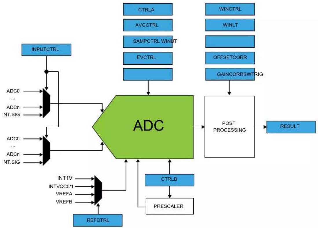
flowchart
graph TD
    A["INPUTCTRL"] --> B["ADC0"]
    A --> C["ADCn"]
    A --> D["INT.SIG"]
    B --> E["AND"]
    C --> E
    D --> E
    E --> F["ADC"]
    F --> G["POST PROCESSING"]
    G --> H["RESULT"]
    I["CTRLA"] --> G
    J["AVGCTRL"] --> G
    K["SAMPCTRL WINUT"] --> G
    L["EVCTRL"] --> G
    M["WINCTRL"] --> G
    N["WINLT"] --> G
    O["OFFSETCORR"] --> G
    P["GAINCORRSWTRIG"] --> G
    Q["INT1V"] --> R["AND"]
    S["INTVCC0/1"] --> R
    T["VREFA"] --> R
    U["VREFB"] --> R
    V["REFCTRL"] --> R
    W["CTRLB"] --> X["PREScaler"]
    Y["AND"] --> F
Note: INT1V is the buffered internal reference of 1.0V, derived from the internal 1.1V bandgap reference.
28.4 Signal Description
| Signal Name Type Description | ||
| VREFA Analog input External reference voltage A | ||
| VREFB Analog input External reference voltage B | ||
| ADC[19..0](1) | Analog input Analog input channels | |
Note: Refer to Configuration Summary for details on exact number of analog input channels.
Note: Refer to I/O Multiplexing and Considerations for details on the pin mapping for this peripheral. One signal can be mapped on several pins.
Related Links
-
I/O Multiplexing and Considerations
-
Configuration Summary
28.5 Product Dependencies
In order to use this peripheral, other parts of the system must be configured correctly, as described below.
28.5.1 I/O Lines
Using the ADC's I/O lines requires the I/O pins to be configured using the port configuration (PORT).
Related Links
- PORT - I/O Pin Controller
28.5.2 Power Management
The ADC will continue to operate in any Sleep mode where the selected source clock is running. The ADC's interrupts, except the OVERRUN interrupt, can be used to wake up the device from sleep modes. Events connected to the event system can trigger other operations in the system without exiting sleep modes.
Related Links
- Power Manager (PM)
28.5.3 Clocks
The ADC can be enabled in the Main Clock, which also defines the default state.
This clock must be configured and enabled in the Generic Clock Controller (GCLK) before using the ADC.
A generic clock is asynchronous to the bus clock. Due to this asynchronicity, writes to certain registers will require synchronization between the clock domains. Refer to Synchronization for further details.
Related Links
- GCLK - Generic Clock Controller
28.5.4 Interrupts
The interrupt request line is connected to the interrupt controller. Using the ADC interrupt requires the interrupt controller to be configured first.
Related Links
10.2. Nested Vector Interrupt Controller
28.5.5 Events
The events are connected to the Event System.
Related Links
- Event System (EVSYS)
28.5.6 Debug Operation
When the CPU is halted in Debug mode the ADC will halt normal operation. The ADC can be forced to continue operation during debugging.
28.5.7 Register Access Protection
All registers with write-access are optionally write-protected by the peripheral access controller (PAC), except the following register:
- Interrupt Flag Status and Clear (INTFLAG) register
Optional write-protection by the Peripheral Access Controller (PAC) is denoted by the "PAC Write-Protection" property in each individual register description.
PAC write-protection does not apply to accesses through an external debugger.
Related Links
10.5. PAC - Peripheral Access Controller
28.5.8 Analog Connections
I/O-pins AIN0 to AIN19 as well as the VREFA/VREFB reference voltage pin are analog inputs to the ADC.
28.5.9 Calibration
The values BIAS_CAL and LINEARITY_CAL from the production test must be loaded from the NVM Software Calibration Area into the ADC Calibration register (CALIB) by software to achieve specified accuracy.
28.6 Functional Description
28.6.1 Principle of Operation
By default, the ADC provides results with 12-bit resolution. 8-bit or 10-bit results can be selected in order to reduce the conversion time.
The ADC has an oversampling with decimation option that can extend the resolution to 16 bits. The input values can be either internal (e.g., internal temperature sensor) or external (connected I/O pins). The user can also configure whether the conversion should be single-ended or differential.
28.6.2 Basic Operation
28.6.2.1 Initialization
Before enabling the ADC, the asynchronous clock source must be selected and enabled, and the ADC reference must be configured. The first conversion after the reference is changed must not be used. All other configuration registers must be stable during the conversion. The source for GCLK_ADC is selected and enabled in the System Controller (SYSCTRL). Refer to SYSCTRL – System Controller for more details.
When GCLK_ADC is enabled, the ADC can be enabled by writing a one to the Enable bit in the Control Register A (CTRLA.ENABLE).
Related Links
- SYSCTRL - System Controller
28.6.2.2 Enabling, Disabling and Reset
The ADC is enabled by writing a '1' to the Enable bit in the Control A register (CTRLA.ENABLE). The ADC is disabled by writing CTRLA.ENABLE=0. The ADC is reset by writing a '1' to the Software Reset bit in the Control A register (CTRLA.SWRST). All registers in the ADC, except DBGCTRL, will be reset to their initial state, and the ADC will be disabled.
The ADC must be disabled before it is reset.
28.6.2.3 Operation
In the most basic configuration, the ADC samples values from the configured internal or external sources (INPUTCTRL register). The rate of the conversion depends on the combination of the GCLK_ADCx frequency and the clock prescaler.
To convert analog values to digital values, the ADC needs to be initialized first, as described in 28.6.2.1. Initialization. Data conversion can be started either manually by setting the Start bit in the Software Trigger register (SWTRIG.START=1), or automatically by configuring an automatic trigger to initiate the conversions. A free-running mode can be used to continuously convert an input channel. When using free-running mode the first conversion must be started, while subsequent conversions will start automatically at the end of previous conversions.
The automatic trigger can be configured to trigger on many different conditions.
The result of the conversion is stored in the Result register (RESULT) overwriting the result from the previous conversion.
To avoid data loss if more than one channel is enabled, the conversion result must be read as soon as it is available (INTFLAG.RESRDY). Failing to do so will result in an overrun error condition, indicated by the OVERRUN bit in the Interrupt Flag Status and Clear register (INTFLAG.OVERRUN). When the RESRDY interrupt flag is set, the new result has been synchronized to the RESULT register.
To enable one of the available interrupts sources, the corresponding bit in the Interrupt Enable Set register (INTENSET) must be written to '1'.
28.6.3 Prescaler
The ADC is clocked by GCLK_ADC. There is also a prescaler in the ADC to enable conversion at lower clock rates.
Refer to CTRLB for details on prescaler settings.
Figure 28-2. ADC Prescaler
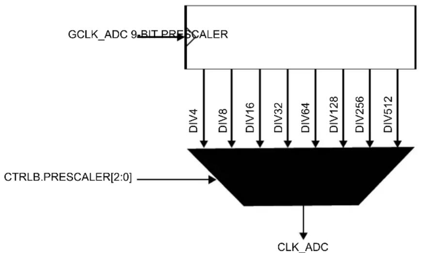
flowchart
graph TD
    A["GCLK_ADC 9-BIT PRESCALER"] --> B["DIV4"]
    A --> C["DIV8"]
    A --> D["DIV16"]
    A --> E["DIV32"]
    A --> F["DIV64"]
    A --> G["DIV128"]
    A --> H["DIV256"]
    A --> I["DIV512"]
    J["CTRLB.PRESCALER[2:0"]] --> K
    L["CLK_ADC"] --> M
The propagation delay of an ADC measurement depends on the selected mode and is given by:
- Single-shot mode:
$$ \text { PropagationDelay } = \frac {1 + \frac {\text { Resolution }}{2} + \text { DelayGain }}{f _ {\mathrm{CLK} + - \mathrm{ADC}}} $$
- Free-running mode:
$$ \text { PropagationDelay } = \frac {\frac {\text { Resolution }}{2} + \text { DelayGain }}{f _ {\mathrm{CLK} + - \mathrm{ADC}}} $$
Table 28-1. Delay Gain
| Delay Gain (in CLK_ADC Period) | |||||
| INTPUTCTRL.GAIN[3:0] Free-running mode Single shot mode | |||||
| Name | Differential Mode | Single-Ended Mode | |||
| 1X 0x0 0 0 | 0 | 1 | |||
| 2X 0x1 0 1 | 0.5 | 1.5 | |||
| 4X 0x2 1 1 | 1 | 2 | |||
| 8X 0x3 1 2 | 1.5 | 2.5 | |||
| 16X | 0x4 2 2 2 | 3 | |||
| Reserved | 0x5 ... 0xE | Reserved | Reserved | Reserved | Reserved |
| DIV2 | 0xF | 0 1 0.5 | 1.5 | ||
28.6.4 ADC Resolution
The ADC supports 8-bit, 10-bit or 12-bit resolution. Resolution can be changed by writing the Resolution bit group in the Control B register (CTRLB.RESSEL). By default, the ADC resolution is set to 12 bits.
28.6.5 Differential and Single-Ended Conversions
The ADC has two conversion options: differential and single-ended:
- If the positive input may go below the negative input, the differential mode should be used in order to get correct results.
- If the positive input is always positive, the single-ended conversion should be used in order to have full 12-bit resolution in the conversion.
The negative input must be connected to ground. This ground could be the internal GND, IOGND or an external ground connected to a pin. Refer to the Control B (CTRLB) register for selection details.
If the positive input may go below the negative input, creating some negative results, the differential mode should be used in order to get correct results. The differential mode is enabled by setting DIFFMODE bit in the Control B register (CTRLB.DIFFMODE). Both conversion types could be run in single mode or in free-running mode. When the free-running mode is selected, an ADC input will continuously sample the input and performs a new conversion. The INTFLAG.RESRDY bit will be set at the end of each conversion.
28.6.5.1 Conversion Timing
The following figure shows the ADC timing for one single conversion. A conversion starts after the software or event start are synchronized with the GCLK_ADC clock. The input channel is sampled in the first half CLK_ADC period.
Figure 28-3. ADC Timing for One Conversion in Differential Mode without Gain
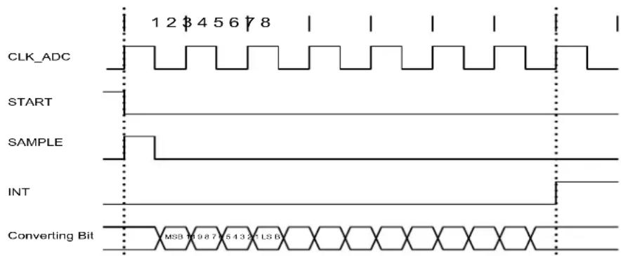
text_image
CLK_ADC START SAMPLE INT Converting Bit MSB 10 9 8 7 6 5 4 3 2 1 LS BThe sampling time can be increased by using the Sampling Time Length bit group in the Sampling Time Control register (SAMPCTRL.SAMPLEN). As example, the next figure is showing the timing conversion.
Figure 28-4. ADC Timing for One Conversion in Differential Mode without Gain, but with Increased Sampling Time
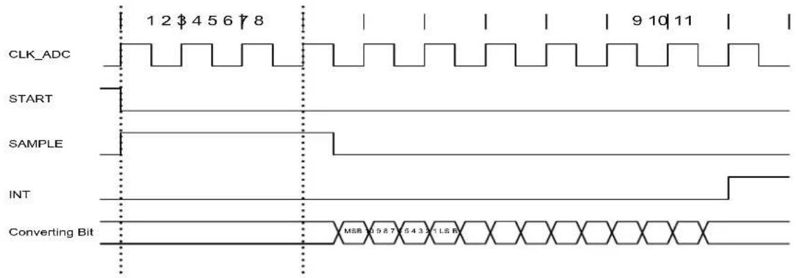
text_image
CLK_ADC START SAMPLE INT Converting Bit 1 2 $ 4 5 6 7 8 9 10 11 MSB 10 9 8 7 5 4 3 2 1 LS BFigure 28-5. ADC Timing for Free Running in Differential Mode without Gain
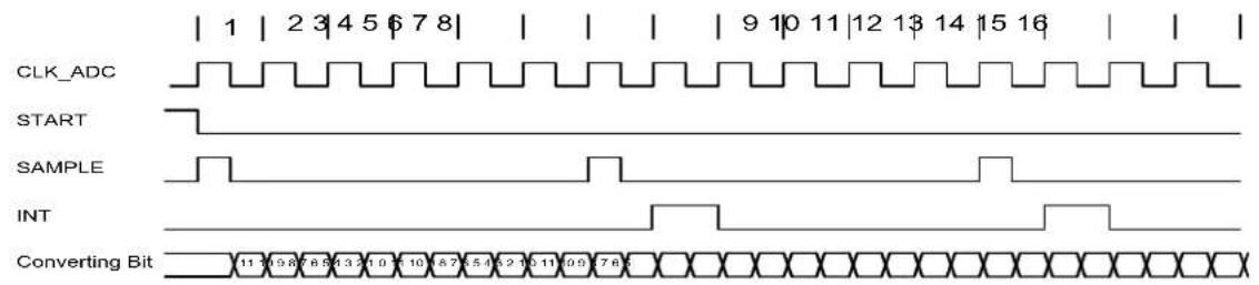
text_image
CLK_ADC START SAMPLE INT Converting BitFigure 28-6. ADC Timing for One Conversion in Single-Ended Mode without Gain
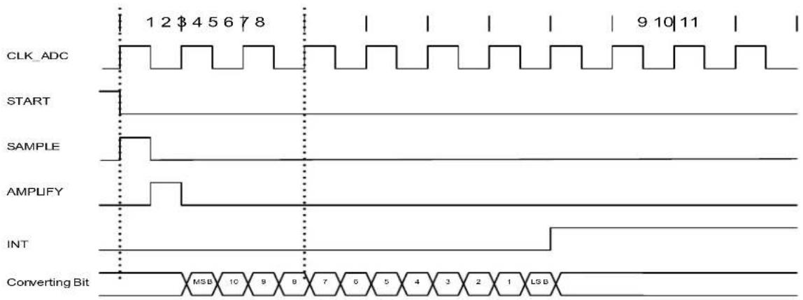
other
| Signal | Value | | ------------- | ----- | | CLK_ADC | 12$45678 | | START | 12$45678 | | SAMPLE | 12$45678 | | AMPUFY | 12$45678 | | INT | 12$45678 | | Converting Bit | MSB 10 9 8 7 6 5 4 3 2 1 LSB |Figure 28-7. ADC Timing for Free Running in Single-Ended Mode without Gain
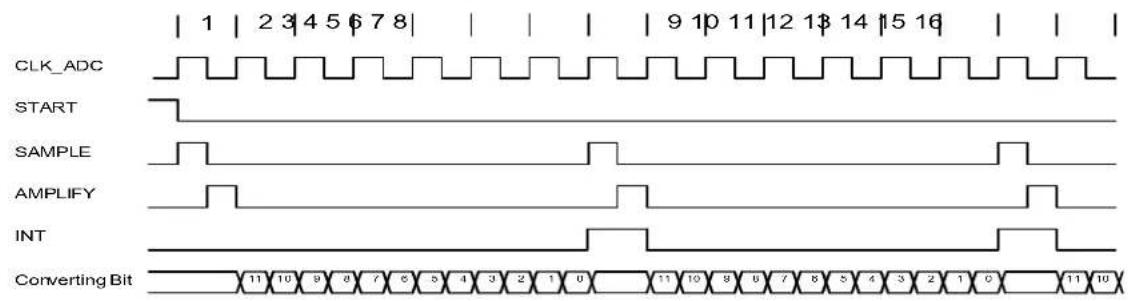
text_image
CLK_ADC START SAMPLE AMPLIFY INT Converting Bit28.6.6 Accumulation
The result from multiple consecutive conversions can be accumulated. The number of samples to be accumulated is specified by the Number of Samples to be Collected field in the Average Control register (AVGCTRL.SAMPLENUM). When accumulating more than 16 samples, the result will be too large to match the 16-bit RESULT register size. To avoid overflow, the result is right shifted automatically to fit within the available register size. The number of automatic right shifts is specified in the table below.
Note: To perform the accumulation of two or more samples, the Conversion Result Resolution field in the Control B register (CTRLB.RESSEL) must be set.
Table 28-2. Accumulation
| Number of Accumulated Samples | AVGCTRL. SAMPLENUM | Intermediate Result Precision | Number of Automatic Right Shifts | Final Result Precision | Automatic Division Factor |
| 1 0x0 12 bits 0 12 bits 0 | |||||
| 2 0x1 13 bits 0 13 bits 0 | |||||
| 4 0x2 14 bits 0 14 bits 0 | |||||
| 8 0x3 15 bits 0 15 bits 0 | |||||
| 16 0x4 16 bits 0 16 bits 0 | |||||
| 32 0x5 17 bits 1 16 bits 2 | |||||
| 64 0x6 18 bits 2 16 bits 4 | |||||
| 128 0x7 19 bits 3 16 bits 8 | |||||
| 256 0x8 20 bits 4 16 bits 16 | |||||
| 512 0x9 21 bits 5 16 bits 32 | |||||
| 1024 0xA 22 bits 6 16 bits 64 | |||||
| Reserved 0xB - 0xF 12 bits 12 bits 0 |
28.6.7 Averaging
Averaging is a feature that increases the sample accuracy, at the cost of a reduced sampling rate. This feature is suitable when operating in noisy conditions.
Averaging is done by accumulating m samples, as described in 28.6.6. Accumulation, and dividing the result by m. The averaged result is available in the RESULT register. The number of samples to be accumulated is specified by writing to AVGCTRL.SAMPLENUM.
The division is obtained by a combination of the automatic right shift described above, and an additional right shift that must be specified by writing to the Adjusting Result/Division Coefficient field in AVGCTRL (AVGCTRL.ADJRES).
Note: To perform the averaging of two or more samples, the Conversion Result Resolution field in the Control B register (CTRLB.RESSEL) must be set to '1'.
Averaging AVGCTRL.SAMPLENUM samples will reduce the un-averaged sampling rate by a factor 1
AVGCTRL.SAMPLENUM
When the averaged result is available, the INTFLAG.RESRDY bit will be set.
Table 28-3. Averaging
| Number of Accumulated Samples | AVGCTRL.SAMPLENUM | Intermediate Result Precision | Number of Automatic Right Shifts | Division Factor | AVGCTRL.ADJRES | Total Number of Right Shifts | Final Result Precision | Automatic Division Factor |
| 1 | 0x0 | 12 bits | 0 | 1 | 0x0 | 12 bits | 0 | |
| 2 | 0x1 | 13 | 0 | 2 | 0x1 | 1 | 12 bits | 0 |
| ......continued | ||||||||
| Number of Accumulated Samples | AVGCTRL.SAMPLENUM | Intermediate Result Precision | Number of Automatic Right Shifts | Division Factor | AVGCTRL.ADJRES | Total Number of Right Shifts | Final Result Precision | Automatic Division Factor |
| 4 0x2 14 0 4 0x2 2 12 bits 0 | ||||||||
| 8 0x3 15 0 8 0x3 3 12 bits 0 | ||||||||
| 16 0x4 16 0 16 0x4 4 12 bits 0 | ||||||||
| 32 0x5 17 1 16 0x4 5 12 bits 2 | ||||||||
| 64 0x6 18 2 16 0x4 6 12 bits 4 | ||||||||
| 128 0x7 19 3 16 0x4 7 12 bits 8 | ||||||||
| 256 0x8 20 4 16 0x4 8 12 bits 16 | ||||||||
| 512 0x9 21 5 16 0x4 9 12 bits 32 | ||||||||
| 1024 0xA 22 6 16 0x4 10 12 bits 64 | ||||||||
| Reserved 0xB-0xF | 0x0 | 12 bits 0 | ||||||
28.6.8 Oversampling and Decimation
By using oversampling and decimation, the ADC resolution can be increased from 12 bits up to 16 bits, for the cost of reduced effective sampling rate.
To increase the resolution by n bits, 4 samples must be accumulated. The result must then be right-shifted by n bits. This right-shift is a combination of the automatic right-shift and the value written to AVGCTRL.ADJRES. To obtain the correct resolution, the ADJRES must be configured as described in the table below. This method will result in n bit extra LSB resolution.
Table 28-4. Configuration Required for Oversampling and Decimation
| Result Resolution | Number of Samples to Average | AVGCTRL.SAMPLENUM[3:0] | Number of Automatic Right Shifts | AVGCTRL.ADJRES[2:0] |
| 13 bits 4 | ^1 = 4 | 0x2 | 0 | 0x1 |
| 14 bits 4 | ^2 = 16 | 0x4 | 0 | 0x2 |
| 15 bits 4 | ^3 = 64 | 0x6 | 2 | 0x1 |
| 16 bits 4 | ^4 = 256 | 0x8 | 4 | 0x0 |
28.6.9 Window Monitor
The window monitor feature allows the conversion result in the RESULT register to be compared to predefined threshold values. The window mode is selected by setting the Window Monitor Mode bits in the Window Monitor Control register (WINCTRL.WINMODE[2:0]). Threshold values must be written in the Window Monitor Lower Threshold register (WINLT) and Window Monitor Upper Threshold register (WINUT).
If differential input is selected, the WINLT and WINUT are evaluated as signed values. Otherwise they are evaluated as unsigned values. The significant WINLT and WINUT bits are given by the precision selected in the Conversion Result Resolution bit group in the Control B register (CTRLB.RESSEL). This means that e.g. in 8-bit mode, only the eight lower bits will be considered. In addition, in differential mode, the eighth bit will be considered as the sign bit, even if the ninth bit is zero.
The INTFLAG.WINMON interrupt flag will be set if the conversion result matches the window monitor condition.
28.6.10 Offset and Gain Correction
Inherent gain and offset errors affect the absolute accuracy of the ADC.
The offset error is defined as the deviation of the actual ADC transfer function from an ideal straight line at zero input voltage. The offset error cancellation is handled by the Offset Correction register
(OFFSETCORR). The offset correction value is subtracted from the converted data before writing to the Result register (RESULT).
The gain error is defined as the deviation of the last output step's midpoint from the ideal straight line, after compensating for offset error. The gain error cancellation is handled by the Gain Correction register (GAINCORR).
To correct these two errors, the Digital Correction Logic Enabled bit in the Control B register (CTRLB.CORREN) must be set to '1'.
Offset and gain error compensation results are both calculated according to:
Result=Conversion value+−OFFSETCORR·GAINCORR
The correction will introduce a latency of 13 CLK_ADC clock cycles. In Free-running mode this latency is introduced on the first conversion only because the duration is always less than the propagation delay. In Single Conversion mode this latency is introduced for each conversion.
Figure 28-8. ADC Timing Correction Enabled
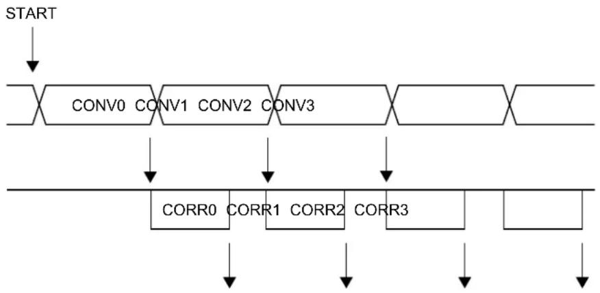
flowchart
graph TD
    A["START"] --> B["CONV0"]
    B --> C["CONV1"]
    C --> D["CONV2"]
    D --> E["CONV3"]
    E --> F["..."]
    F --> G["..."]
    G --> H["CORR0"]
    H --> I["CORR1"]
    I --> J["CORR2"]
    J --> K["CORR3"]
    K --> L["..."]
    L --> M["..."]
28.6.11 Interrupts
The ADC has the following interrupt sources:
• Result Conversion Ready: RESRDY
• Window Monitor: WINMON
- Overrun: OVERRUN
Each interrupt source has an interrupt flag associated with it. The interrupt flag in the Interrupt Flag Status and Clear (INTFLAG) register is set when the interrupt condition occurs. Each interrupt can be individually enabled by writing a one to the corresponding bit in the Interrupt Enable Set (INTENSET) register, and disabled by writing a one to the corresponding bit in the Interrupt Enable Clear (INTENCLR) register. An interrupt request is generated when the interrupt flag is set and the corresponding interrupt is enabled. The interrupt request remains active until the interrupt flag is cleared, the interrupt is disabled, or the ADC is reset. An interrupt flag is cleared by writing a one to the corresponding bit in the INTFLAG register. Each peripheral can have one interrupt request line per interrupt source or one common interrupt request line for all the interrupt sources. This is device dependent.
Refer to Nested Vector Interrupt Controller for details. The user must read the INTFLAG register to determine which interrupt condition is present.
Related Links
10.2. Nested Vector Interrupt Controller
28.6.12 Events
The ADC can generate the following output events:
- Result Ready (RESRDY): Generated when the conversion is complete and the result is available.
- Window Monitor (WINMON): Generated when the window monitor condition match.
Setting an Event Output bit in the Event Control Register (EVCTRL.xxEO=1) enables the corresponding output event. Clearing this bit disables the corresponding output event. Refer to the Event System chapter for details on configuring the event system.
The peripheral can take the following actions on an input event:
- Start conversion (START): Start a conversion.
- Conversion flush (FLUSH): Flush the conversion.
Setting an Event Input bit in the Event Control register (EVCTRL.xxEI=1) enables the corresponding action on input event. Clearing this bit disables the corresponding action on input event.
Note: If several events are connected to the ADC, the enabled action will be taken on any of the incoming events. The events must be correctly routed in the Event System.
Related Links
22. Event System (EVSYS)
28.6.13 Sleep Mode Operation
The run in the Standby bit in the Control A register (CTRLA.RUNSTDBY) controls the behavior of the ADC during Standby Sleep mode. When CTRLA.RUNSTDBY = 0, the ADC is disabled during sleep, but maintains its current configuration. When CTRLA.RUNSTDBY = 1, the ADC continues to operate during sleep. When CTRLA.RUNSTDBY = 0, the analog blocks are powered off for the lowest power consumption. This necessitates a start-up time delay when the system returns from sleep.
When CTRLA.RUNSTDBY = 1, any enabled ADC interrupt source can wake-up the CPU, except the OVERRUN interrupt.. While the CPU is sleeping, ADC conversion can only be triggered by events.
28.6.14 Synchronization
Due to asynchronicity between the main clock domain and the peripheral clock domains, some registers need to be synchronized when written or read.
When executing an operation that requires synchronization, the Synchronization Busy bit in the Status register (STATUS.SYNCBUSY) will be set immediately, and cleared when synchronization is complete. The Synchronization Ready interrupt can be used to signal when synchronization is complete.
If an operation that requires synchronization is executed while STATUS.SYNCBUSY=1, the bus will be stalled. All operations will complete successfully, but the CPU will be stalled and interrupts will be pending as long as the bus is stalled.
The following bits are synchronized when written:
- Software Reset bit in the Control A register (CTRLA.SWRST)
- Enable bit in the Control A register (CTRLA.ENABLE)
The following registers are synchronized when written:
- Control B (CTRLB)
- Software Trigger (SWTRIG)
• Window Monitor Control (WINCTRL) - Input Control (INPUTCTRL)
- Window Upper/Lower Threshold (WINUT/WINLT)
Required write-synchronization is denoted by the "Write-Synchronized" property in the register description.
The following registers are synchronized when read:
- Software Trigger (SWTRIG)
- Input Control (INPUTCTRL)
Required read-synchronization is denoted by the "Read-Synchronized" property in the register description.
Related Links
13.3. Register Synchronization
28.7 Register Summary
| Offset | Name Bit Pos. 76543210 | |||||||||
| 0x00 | CTRLA 7:0 RUNSTDBY ENABLE SWRST | |||||||||
| 0x01 | REFCTRL 7:0 REFCOMP | REFSEL[3:0] | ||||||||
| 0x02 | AVGCTRL | 7:0 | ADJRES[2:0] | SAMPLENUM[3:0] | ||||||
| 0x03 | SAMPCTRL | 7:0 | SAMPLEN[5:0] | |||||||
| 0x04 | CTRLB | 7:0 | RESSEL[1:0] | CORREN | FREERUN | LEFTADJ | DIFFMODE | |||
| 15:8 | PRESCALER[2:0] | |||||||||
| 0x06 | ||||||||||
| ... | Reserved | |||||||||
| 0x07 | ||||||||||
| 0x08 | WINCTRL | 7:0 | WINMODE[2:0] | |||||||
| 0x09 | ||||||||||
| ... | Reserved | |||||||||
| 0x0B | ||||||||||
| 0x0C | SWTRIG | 7:0 | START | FLUSH | ||||||
| 0x0D | ||||||||||
| ... | Reserved | |||||||||
| 0x0F | ||||||||||
| 0x10 | INPUTCTRL | 7:0 | MUXPOS[4:0] | |||||||
| 15:8 | MUXNEG[4:0] | |||||||||
| 23:16 | INPUTOFFSET[3:0] | INPUTSCAN[3:0] | ||||||||
| 31:24 | GAIN[3:0] | |||||||||
| 0x14 | EVCTRL | 7:0 | WINMONEO | RESRDYEO | SYNCEI | STARTEI | ||||
| 0x15 | Reserved | |||||||||
| 0x16 | INTENCLR | 7:0 | SYNCRDY | WINMON | OVERRUN | RESRDY | ||||
| 0x17 | INTENSET | 7:0 | SYNCRDY | WINMON | OVERRUN | RESRDY | ||||
| 0x18 | INTFLAG | 7:0 | SYNCRDY | WINMON | OVERRUN | RESRDY | ||||
| 0x19 | STATUS | 7:0 | SYNCBUSY | |||||||
| 0x1A | RESULT | 7:0 | RESULT[7:0] | |||||||
| 15:8 | RESULT[15:8] | |||||||||
| 0x1C | WINLT | 7:0 | WINLT[7:0] | |||||||
| 15:8 | WINLT[15:8] | |||||||||
| 0x1E | ||||||||||
| ... | Reserved | |||||||||
| 0x1F | ||||||||||
| 0x20 | WINUT | 7:0 | WINUT[7:0] | |||||||
| 15:8 | WINUT[15:8] | |||||||||
| 0x22 | ||||||||||
| ... | Reserved | |||||||||
| 0x23 | ||||||||||
| 0x24 | GAINCORR | 7:0 | GAINCORR[7:0] | |||||||
| 15:8 | GAINCORR[11:8] | |||||||||
| 0x26 | OFFSETCORR | 7:0 | OFFSETCORR[7:0] | |||||||
| 15:8 | OFFSETCORR[11:8] | |||||||||
| 0x28 | CALIB | 7:0 | LINEARITY_CAL[7:0] | |||||||
| 15:8 | BIAS_CAL[2:0] | |||||||||
| 0x2A | DBGCTRL | 7:0 | DBGRUN | |||||||
28.8 Register Description
Registers can be 8, 16 or 32 bits wide. Atomic 8-, 16- and 32-bit accesses are supported. In addition, the 8-bit quarters and 16-bit halves of a 32-bit register and the 8-bit halves of a 16-bit register can be accessed directly.
Some registers are optionally write-protected by the Peripheral Access Controller (PAC). Write-protection is denoted by the Write-Protected property in each individual register description.
Some registers require synchronization when read and/or written. Synchronization is denoted by the Write-Synchronized or the Read-Synchronized property in each individual register description.
Some registers are enable-protected, meaning they can be written only when the ADC is disabled. Enable-protection is denoted by the Enable-Protected property in each individual register description.
28.8.1 Control A
Name: CTRLA
Offset: 0x00
Reset: 0x00
Property: Write-Protected
Bit 76543210
Access
Reset 0 0 0
| RUNSTDBY ENABLE SWRST |
R/W R/W R/W
Bit 2 - RUNSTDBY Run in Standby
This bit indicates whether the ADC will continue running in standby sleep mode or not:
| Value | Description |
| 0 | The ADC is halted during standby sleep mode. |
| 1 | The ADC continues normal operation during standby sleep mode. |
Bit 1 - ENABLE Enable
Due to synchronization, there is a delay from writing CTRLA. ENABLE until the peripheral is enabled/ disabled. The value written to CTRL. ENABLE will read back immediately and the Synchronization Busy bit in the Status register (STATUS.SYNCBUSY) will be set. STATUS.SYNCBUSY will be cleared when the operation is complete.
| Value | Description |
| 0 | The ADC is disabled. |
| 1 | The ADC is enabled. |
Bit 0 - SWRST Software Reset
Writing a zero to this bit has no effect.
Writing a one to this bit resets all registers in the ADC, except DBGCTRL, to their initial state, and the ADC will be disabled.
Writing a one to CTRL.SWRST will always take precedence, meaning that all other writes in the same write-operation will be discarded.
Due to synchronization, there is a delay from writing CTRLA.SWRST until the reset is complete.
CTRLA.SWRST and STATUS.SYNCBUSY will both be cleared when the reset is complete.
| Value | Description |
| 0 | There is no reset operation ongoing. |
| 1 | The reset operation is ongoing. |
28.8.2 Reference Control
Name: REFCTRL
Offset: 0x01
Reset: 0x00
Property: Write-Protected
Bit 76543210
| REFCOMP | REFSEL[3:0] | ||||
| Access | R/W | R/W | R/W | R/W | R/W |
| Reset | 0 | 0 | 0 | 0 | 0 |
Bit 7 - REFCOMP Reference Buffer Offset Compensation Enable
The accuracy of the gain stage can be increased by enabling the reference buffer offset compensation. This will decrease the input impedance and thus increase the start-up time of the reference.
| Value | Description |
| 0 | Reference buffer offset compensation is disabled. |
| 1 | Reference buffer offset compensation is enabled. |
Bits 3:0 - REFSEL[3:0] Reference Selection
These bits select the reference for the ADC.
Table 28-5. Reference Selection
| REFSEL[3:0] | Name | Description |
| 0x0 | INT1V | 1.0V voltage reference |
| 0x1 | INTVCC0 | 1/1.48 VDDANA |
| 0x2 | INTVCC1 | 1/2 VDDANA (only for VDDANA > 2.0V) |
| 0x3 | VREFA | External reference |
| 0x4 | VREFB | External reference |
| 0x5-0xF | Reserved |
Note: INT1V is the buffered internal reference of 1.0V, derived from the internal 1.1V bandgap reference.
28.8.3 Average Control
Name: AVGCTRL
Offset: 0x02
Reset: 0x00
Property: Write-Protected
Bit 76543210
| ADJRES[2:0] SAMPLENUM[3:0] |
Access
R/W R/W R/W R/W R/W R/W R/W
Reset 0000000
Bits 6:4 - ADJRES[2:0] Adjusting Result / Division Coefficient
These bits define the division coefficient in 2n steps.
Bits 3:0 - SAMPLENUM[3:0] Number of Samples to be Collected
These bits define how many samples should be added together. The result will be available in the Result register (RESULT). Note: if the result width increases, CTRLB.RESSEL must be changed.
| SAMPLENUM[3:0] Name Description | ||
| 0x0 | 1 | 1 sample |
| 0x1 | 2 | 2 samples |
| 0x2 | 4 | 4 samples |
| 0x3 | 8 | 8 samples |
| 0x4 | 16 | 16 samples |
| 0x5 | 32 | 32 samples |
| 0x6 | 64 | 64 samples |
| 0x7 | 128 | 128 samples |
| 0x8 | 256 | 256 samples |
| 0x9 | 512 | 512 samples |
| 0xA | 1024 | 1024 samples |
| 0xB-0xF | Reserved |
28.8.4 Sampling Time Control
Name: SAMPCTRL
Offset: 0x03
Reset: 0x00
Property: Write-Protected
Bit 76543210
| SAMPLEN[5:0] | |
| Access | R/W R/W R/W R/W R/W R/W |
| Reset 0 0 0 0 0 0 | |
Bits 5:0 - SAMPLEN[5:0] Sampling Time Length
These bits control the ADC sampling time in number of half CLK_ADC cycles, depending on the prescaler value, thus controlling the ADC input impedance. Sampling time is set according to the equation:
$$ \text { Sampling time } = \text { SAMPLEN } + 1 \cdot) \left(\frac {\mathrm{CLK} _ {\mathrm{ADC}}}{2}\right) $$
28.8.5 Control B
Name: CTRLB
Offset: 0x04
Reset: 0x0000
Property: Write-Protected, Write-Synchronized
Bit 15 14 13 12 11 10 9 8
| PRESCALER[2:0] | |||||
| Access Reset 0 0 0 | R/W R/W R/W | ||||
Bit 76543210
| RESSEL[1:0] | CORREN | FREERUN | LEFTADJ | DIFFMODE | ||
| Access Reset | R/W R/W R/W R/W R/W R/W | |||||
| 0 0 0 0 0 0 | ||||||
Bits 10:8 - PRESCALER[2:0] Prescaler Configuration
These bits define the ADC clock relative to the peripheral clock.
| PRESCALER[2:0] | Name | Description |
| 0x0 | DIV4 | Peripheral clock divided by 4 |
| 0x1 | DIV8 | Peripheral clock divided by 8 |
| 0x2 | DIV16 | Peripheral clock divided by 16 |
| 0x3 | DIV32 | Peripheral clock divided by 32 |
| 0x4 | DIV64 | Peripheral clock divided by 64 |
| 0x5 | DIV128 | Peripheral clock divided by 128 |
| 0x6 | DIV256 | Peripheral clock divided by 256 |
| 0x7 | DIV512 | Peripheral clock divided by 512 |
Bits 5:4 - RESSEL[1:0] Conversion Result Resolution
These bits define whether the ADC completes the conversion at 12-, 10- or 8-bit result resolution.
| RESSEL[1:0] | Name Description | |
| 0x0 | 12BIT | 12-bit result |
| 0x1 | 16BIT | For averaging mode output |
| 0x2 | 10BIT | 10-bit result |
| 0x3 | 8BIT | 8-bit result |
Bit 3 - CORREN Digital Correction Logic Enabled
| Value | Description |
| 0 | Disable the digital result correction. |
| 1 | Enable the digital result correction. The ADC conversion result in the RESULT register is then corrected for gain and offset based on the values in the GAINCAL and OFFSETCAL registers. Conversion time will be increased by X cycles according to the value in the Offset Correction Value bit group in the Offset Correction register. |
Bit 2 - FREERUN Free Running Mode
| Value | Description |
| 0 | The ADC run is single conversion mode. |
| 1 | The ADC is in free running mode and a new conversion will be initiated when a previous conversion completes. |
Bit 1 - LEFTADJ Left-Adjusted Result
| Value | Description |
| 0 | The ADC conversion result is right-adjusted in the RESULT register. |
Value Description
| 1 | The ADC conversion result is left-adjusted in the RESULT register. The high byte of the 12-bit result will be present in the upper part of the result register. Writing this bit to zero (default) will right-adjust the value in the RESULT register. |
Bit 0 - DIFFMODE Differential Mode
Value Description
| 0 | The ADC is running in singled-ended mode. |
| 1 | The ADC is running in differential mode. In this mode, the voltage difference between the MUXPOS and MUXNEG inputs will be converted by the ADC. |
28.8.6 Window Monitor Control
Name: WINCTRL
Offset: 0x08
Reset: 0x00
Property: Write-Protected, Write-Synchronized
Bit 76543210
| WINMODE[2:0] | |||||
| Access Reset 0 0 0 | R/W R/W R/W | ||||
Bits 2:0 - WINMODE[2:0] Window Monitor Mode
These bits enable and define the window monitor mode.
| WINMODE[2:0] Name Description | ||
| 0x0 | DISABLE | No window mode (default) |
| 0x1 | MODE1 | Mode 1: RESULT > WINLT |
| 0x2 | MODE2 | Mode 2: RESULT < WINUT |
| 0x3 | MODE3 | Mode 3: WINLT < RESULT < WINUT |
| 0x4 | MODE4 | Mode 4: !(WINLT < RESULT < WINUT) |
| 0x5-0x7 | Reserved | |
28.8.7 Software Trigger
Name: SWTRIG
Offset: 0x0C
Reset: 0x00
Property: Write-Protected, Write-Synchronized
Bit 76543210
| $START FLUSH | |||||||
| Access Reset 0 0 | R/W R/W | ||||||
Bit 1 - START ADC Start Conversion
Writing this bit to zero will have no effect.
| Value Description | |
| 0 | The ADC will not start a conversion. |
| 1 | The ADC will start a conversion. The bit is cleared by hardware when the conversion has started. Setting this bit when it is already set has no effect. |
Bit 0 - FLUSH ADC Conversion Flush
After the flush, the ADC will resume where it left off; i.e., if a conversion was pending, the ADC will start a new conversion.
Writing this bit to zero will have no effect.
| Value Description | |
| 0 | No flush action. |
| 1 | "Writing a '1' to this bit will flush the ADC pipeline. A flush will restart the ADC clock on the next peripheral clock edge, and all conversions in progress will be aborted and lost. This bit will be cleared after the ADC has been flushed.After the flush, the ADC will resume where it left off; i.e., if a conversion was pending, the ADC will start a new conversion. |
28.8.8 Input Control
Name: INPUTCTRL
Offset: 0x10
Reset: 0x00000000
Property: Write-Protected, Write-Synchronized
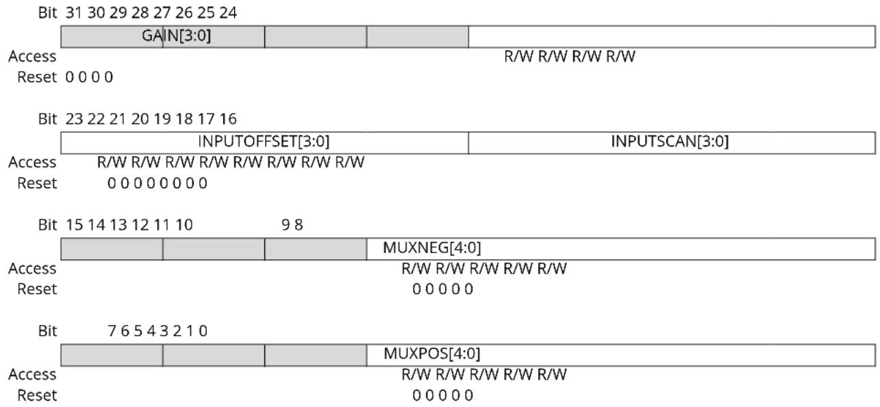
text_image
Bit 31 30 29 28 27 26 25 24 GAIN[3:0] R/W R/W R/W R/W Access Reset 0 0 0 0 R/W R/W R/W R/W R/W R/W R/W R/W R/W R/W R/W R/W R/W R/W R/W R/W R/W R/W R/W R/W R/W R/W R/W R/W R/W R/W R/W R/W R/W R/W R/W R/W R/W R/W R/W R/W R/W R/W R/W R/W R/W R/W R/W R/W R/W R/W R/W R/W R/W R/W R/W R/0 0 0 0 0 0 0 0 R/W R/W R/W R/W R/W R/W R/W R/W R/W R/W R/W R/W R/W R/W R/W R/W R/W R/W R/W R/W R/W R/W R/W R/W R/W R/W R/W R/W R/W R/W R/W R/W R/W R/W R/W R/W R/W R/W R/W R/W R/W R/W R/W R/W R/W R/W R/W R/W R/W R/W R/W R/0 0 0 0 0 0 0 R/0 0 0 0 0 0 0 R/0 0 0 0 0 0 0 R/0 0 0 0 0 0 0 R/0 0 0 0 0 0 0 R/0 0 0 0 0 0 0 R/0 0 0 0 0 0 0 R/6 5 4 3 2 1 0 MUXNEG[4:0] R/W R/W R/W R/W R/W R/W R/W R/W R/W R/W R/W R/W R/W R/W R/W R/0 0 0 0 0 0 MUXPOS[4:0] R/W R/W R/W R/W R/W R/0 0 0 0 0 0 R/6 5 4 3 2 1 0 MUXPOS[4:0] R/6 5 4 3 2 1 0 MUXPOS[4:0] R/6 5 4 3 2 1 0 MUXPOS[4:0] R/6 5 4 3 2 1 0 MUXPOS[4:0]Bits 27:24 - GAIN[3:0] Gain Factor Selection
These bits set the gain factor of the ADC gain stage.
| GAIN[3:0] | Name | Description |
| 0x0 | 1X | 1x |
| 0x1 | 2X | 2x |
| 0x2 | 4X | 4x |
| 0x3 | 8X | 8x |
| 0x4 | 16X | 16x |
| 0x5-0xE | - | Reserved |
| 0xF | DIV2 | 1/2x |
Bits 23:20 - INPUTOFFSET[3:0] Positive Mux Setting Offset
The pin scan is enabled when INPUTSCAN != 0. Writing these bits to a value other than zero causes the first conversion triggered to be converted using a positive input equal to MUXPOS + INPUTOFFSET. Setting this register to zero causes the first conversion to use a positive input equal to MUXPOS.
After a conversion, the INPUTOFFSET register will be incremented by one, causing the next conversion to be done with the positive input equal to MUXPOS + INPUTOFFSET. The sum of MUXPOS and INPUTOFFSET gives the input that is actually converted.
Bits 19:16 - INPUTSCAN[3:0] Number of Input Channels Included in Scan
This register gives the number of input sources included in the pin scan. The number of input sources included is INPUTSCAN + 1. The input channels included are in the range from MUXPOS + INPUTOFFSET to MUXPOS + INPUTOFFSET + INPUTSCAN.
The range of the scan mode must not exceed the number of input channels available on the device.
Bits 12:8 - MUXNEG[4:0] Negative Mux Input Selection
These bits define the Mux selection for the negative ADC input selections.
| Value Name | Description | |
| 0x00 | PIN0 ADC AIN0 pin | |
| 0x01 | PIN1 ADC AIN1 pin | |
| 0x02 | PIN2 ADC AIN2 pin | |
| 0x03 | PIN3 ADC AIN3 pin | |
| 0x04 | PIN4 ADC AIN4 pin | |
| 0x05 | PIN5 ADC AIN5 pin | |
| 0x06 | PIN6 ADC AIN6 pin | |
| 0x07 | PIN7 ADC AIN7 pin | |
| 0x08-0x17 | - Reserved | |
| 0x18 | GND Internal ground | |
| 0x19 | IOGND I/O ground | |
| 0x1A-0x1F | - Reserved | |
Bits 4:0 - MUXPOS[4:0] Positive Mux Input Selection
These bits define the Mux selection for the positive ADC input. The following table shows the possible input selections. If the internal bandgap voltage or temperature sensor input channel is selected, then the Sampling Time Length bit group in the SamplingControl register must be written.
| MUXPOS[4:0] Group configuration Description | ||
| 0x00 PIN0 ADC AIN0 pin | ||
| 0x01 PIN1 ADC AIN1 pin | ||
| 0x02 PIN2 ADC AIN2 pin | ||
| 0x03 PIN3 ADC AIN3 pin | ||
| 0x04 PIN4 ADC AIN4 pin | ||
| 0x05 PIN5 ADC AIN5 pin | ||
| 0x06 PIN6 ADC AIN6 pin | ||
| 0x07 PIN7 ADC AIN7 pin | ||
| 0x08 PIN8 ADC AIN8 pin | ||
| 0x09 PIN9 ADC AIN9 pin | ||
| 0x0A PIN10 ADC AIN10 pin | ||
| 0x0B PIN11 ADC AIN11 pin | ||
| 0x0C PIN12 ADC AIN12 pin | ||
| 0x0D PIN13 ADC AIN13 pin | ||
| 0x0E PIN14 ADC AIN14 pin | ||
| 0x0F PIN15 ADC AIN15 pin | ||
| 0x10 PIN16 ADC AIN16 pin | ||
| 0x11 PIN17 ADC AIN17 pin | ||
| 0x12 PIN18 ADC AIN18 pin | ||
| 0x13 PIN19 ADC AIN19 pin | ||
| 0x14-0x17 Reserved | ||
| 0x18 TEMP | Temperature reference | |
| 0x19 BANDGAP | Bandgap voltage | |
| 0x1A SCALEDCOREVCC | 1/4 scaled core supply | |
| 0x1B SCALEDIOVCC | 1/4 scaled I/O supply | |
| 0x1C DAC | DAC output | |
| 0x1D-0x1F | Reserved | |
28.8.9 Event Control
Name: EVCTRL
Offset: 0x14
Reset: 0x00
Property: Write-Protected
Bit 76543210
| WINMONEO RESRD | YEO | SYNCE | STARTEI | |||||
| Access Reset | R/W | R/W | R/W | R/W | ||||
| 0 0 | 0 0 | |||||||
Bit 5 - WINMONEO Window Monitor Event Out
This bit indicates whether the Window Monitor event output is enabled or not and an output event will be generated when the window monitor detects something.
| Value | Description |
| 0 | Window Monitor event output is disabled and an event will not be generated. |
| 1 | Window Monitor event output is enabled and an event will be generated. |
Bit 4 - RESRDYEO Result Ready Event Out
This bit indicates whether the Result Ready event output is enabled or not and an output event will be generated when the conversion result is available.
| Value | Description |
| 0 | Result Ready event output is disabled and an event will not be generated. |
| 1 | Result Ready event output is enabled and an event will be generated. |
Bit 1 - SYNCEI Synchronization Event In
| Value | Description |
| 0 | A flush and new conversion will not be triggered on any incoming event. |
| 1 | A flush and new conversion will be triggered on any incoming event. |
Bit 0 - STARTEI Start Conversion Event In
| Value | Description |
| 0 | A new conversion will not be triggered on any incoming event. |
| 1 | A new conversion will be triggered on any incoming event. |
28.8.10 Interrupt Enable Clear
Name: INTENCLR
Offset: 0x16
Reset: 0x00
Property: Write-Protected
Bit 76543210
| SYNCRDY WINMON OVERRUN RESRDY | |||||
| Access Reset | R/W R/W R/W R/W0 0 0 0 | ||||
Bit 3 - SYNCRDY Synchronization Ready Interrupt Enable
Writing a zero to this bit has no effect.
Writing a one to this bit will clear the Synchronization Ready Interrupt Enable bit and the corresponding interrupt request.
| Value | Description |
| 0 | The Synchronization Ready interrupt is disabled. |
| 1 | The Synchronization Ready interrupt is enabled, and an interrupt request will be generated when the Synchronization Ready interrupt flag is set. |
Bit 2 - WINMON Window Monitor Interrupt Enable
Writing a zero to this bit has no effect.
Writing a one to this bit will clear the Window Monitor Interrupt Enable bit and the corresponding interrupt request.
| Value | Description |
| 0 | The window monitor interrupt is disabled. |
| 1 | The window monitor interrupt is enabled, and an interrupt request will be generated when the Window Monitor interrupt flag is set. |
Bit 1 - OVERRUN Overrun Interrupt Enable
Writing a zero to this bit has no effect.
Writing a one to this bit will clear the Overrun Interrupt Enable bit and the corresponding interrupt request.
| Value | Description |
| 0 | The Overrun interrupt is disabled. |
| 1 | The Overrun interrupt is enabled, and an interrupt request will be generated when the Overrun interrupt flag is set. |
Bit 0 - RESRDY Result Ready Interrupt Enable
Writing a zero to this bit has no effect.
Writing a one to this bit will clear the Result Ready Interrupt Enable bit and the corresponding interrupt request.
| Value | Description |
| 0 | The Result Ready interrupt is disabled. |
| 1 | The Result Ready interrupt is enabled, and an interrupt request will be generated when the Result Ready interrupt flag is set. |
28.8.11 Interrupt Enable Set
Name: INTENSET
Offset: 0x17
Reset: 0x00
Property: Write-Protected
Bit 76543210
| SYNCRDY WINMON OVERRUN RESRDY | |||||
| Access Reset | R/W R/W R/W R/W0 0 0 0 | ||||
Bit 3 - SYNCRDY Synchronization Ready Interrupt Enable
Writing a zero to this bit has no effect.
Writing a one to this bit will set the Synchronization Ready Interrupt Enable bit, which enables the Synchronization Ready interrupt.
| Value | Description |
| 0 | The Synchronization Ready interrupt is disabled. |
| 1 | The Synchronization Ready interrupt is enabled. |
Bit 2 - WINMON Window Monitor Interrupt Enable
Writing a zero to this bit has no effect.
Writing a one to this bit will set the Window Monitor Interrupt bit and enable the Window Monitor interrupt.
| Value | Description |
| 0 | The Window Monitor interrupt is disabled. |
| 1 | The Window Monitor interrupt is enabled. |
Bit 1 - OVERRUN Overrun Interrupt Enable
Writing a zero to this bit has no effect.
Writing a one to this bit will set the Overrun Interrupt bit and enable the Overrun interrupt.
| Value | Description |
| 0 | The Overrun interrupt is disabled. |
| 1 | The Overrun interrupt is enabled. |
Bit 0 - RESRDY Result Ready Interrupt Enable
Writing a zero to this bit has no effect.
Writing a one to this bit will set the Result Ready Interrupt bit and enable the Result Ready interrupt.
| Value | Description |
| 0 | The Result Ready interrupt is disabled. |
| 1 | The Result Ready interrupt is enabled. |
28.8.12 Interrupt Flag Status and Clear
Name: INTFLAG
Offset: 0x18
Reset: 0x00
Property: -
Bit 76543210
| SYNCRDY WINM∅N OVERRUN RESRDY | |||||
| Access Reset | R/W R/W R/W R/W | ||||
| 0 0 0 0 | |||||
Bit 3 - SYNCRDY Synchronization Ready
This flag is cleared by writing a one to the flag.
This flag is set on a one-to-zero transition of the Synchronization Busy bit in the Status register (STATUS.SYNCBUSY), except when caused by an enable or software reset, and will generate an interrupt request if INTENCLR/SET.SYNCRDY is one.
Writing a zero to this bit has no effect.
Writing a one to this bit clears the Synchronization Ready interrupt flag.
Bit 2 - WINMON Window Monitor
This flag is cleared by writing a one to the flag or by reading the RESULT register.
This flag is set on the next GCLK_ADC cycle after a match with the window monitor condition, and an interrupt request will be generated if INTENCLR/SET.WINMON is one.
Writing a zero to this bit has no effect.
Writing a one to this bit clears the Window Monitor interrupt flag.
Bit 1 - OVERRUN Overrun
This flag is cleared by writing a one to the flag.
This flag is set if RESULT is written before the previous value has been read by CPU, and an interrupt request will be generated if INTENCLR/SET.OVERRUN is one.
Writing a zero to this bit has no effect.
Writing a one to this bit clears the Overrun interrupt flag.
Bit 0 - RESRDY Result Ready
This flag is cleared by writing a one to the flag or by reading the RESULT register.
This flag is set when the conversion result is available, and an interrupt will be generated if INTENCLR/SET.RESRDY is one.
Writing a zero to this bit has no effect.
Writing a one to this bit clears the Result Ready interrupt flag.
28.8.13 Status
Name: STATUS
Offset: 0x19
Reset: 0x00
Property: -
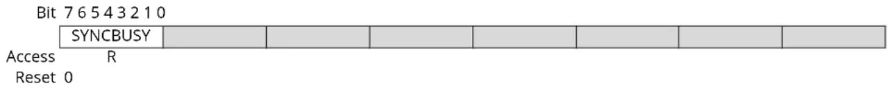
text_image
Bit 7 6 5 4 3 2 1 0 SYNCBUSY Access R Reset 0Bit 7 - SYNCBUSY Synchronization Busy
This bit is cleared when the synchronization of registers between the clock domains is complete. This bit is set when the synchronization of registers between clock domains is started.
28.8.14 Result
Name: RESULT
Offset: 0x1A
Reset: 0x0000
These bits will hold up to a 16-bit ADC result, depending on the configuration.
In single conversion mode without averaging, the ADC conversion will produce a 12-bit result, which can be left- or right-shifted, depending on the setting of CTRLB.LEFTADJ.
If the result is left-adjusted (CTRLB.LEFTADJ), the high byte of the result will be in bit position [15:8], while the remaining 4 bits of the result will be placed in bit locations [7:4]. This can be used only if an 8-bit result is required; i.e., one can read only the high byte of the entire 16-bit register.
If the result is not left-adjusted (CTRLB.LEFTADJ) and no oversampling is used, the result will be available in bit locations [11:0], and the result is then 12 bits long.
If oversampling is used, the result will be located in bit locations [15:0], depending on the settings of the Average Control register (AVGCTRL).
28.8.15 Window Monitor Lower Threshold
Name: WINLT
Offset: 0x1C
Reset: 0x0000
Property: Write-Protected, Write-Synchronized
Bit 15 14 13 12 11 10 9 8
WINLT[15:8]
Access R/W R/W R/W R/W R/W R/W R/W R/W
Reset 00000000
Bit 76543210
WINLT[7:0]
Access R/W R/W R/W R/W R/W R/W R/W R/W
Reset 00000000
Bits 15:0 - WINLT[15:0] Window Lower Threshold
If the window monitor is enabled, these bits define the lower threshold value.
28.8.16 Window Monitor Upper Threshold
Name: WINUT
Offset: 0x20
Reset: 0x0000
Property: Write-Protected, Write-Synchronized
Bit 15 14 13 12 11 10 9 8
WINUT[15:8]
Access R/W R/W R/W R/W R/W R/W R/W R/W
Reset 00000000
Bit 76543210
WINUT[7:0]
Access R/W R/W R/W R/W R/W R/W R/W R/W
Reset 00000000
Bits 15:0 - WINUT[15:0] Window Upper Threshold
If the window monitor is enabled, these bits define the upper threshold value.
28.8.17 Gain Correction
Name: GAINCORR
Offset: 0x24
Reset: 0x0000
Property: Write-Protected
Bit 15 14 13 12 11 10 9 8
| GA|NCORR[11:8] |
Access
Reset 0000
Bit 76543210
| GAINCORR[7:0] |
Access R/W R/W R/W R/W R/W R/W R/W R/W
Reset 00000000
Bits 11:0 - GAINCORR[11:0] Gain Correction Value
If the CTRLB.CORREN bit is one, these bits define how the ADC conversion result is compensated for gain error before being written to the result register. The gain-correction is a fractional value, a 1-bit integer plus an 11-bit fraction, and therefore 1/2 <= GAINCORR < 2 . GAINCORR values range from 0.10000000000 to 1.11111111111.
28.8.18 Offset Correction
Name: OFFSETCORR
Offset: 0x26
Reset: 0x0000
Property: Write-Protected
Bit 15 14 13 12 11 10 9 8
| OFFSETCORR[11:8] | |||
| Access Reset 0 0 0 0 | R/W R/W R/W R/W | ||
Bit 76543210
| OFFSETCORR[7:0] | |
| Access | R/W R/W R/W R/W R/W R/W R/W R/W |
| Reset | 0 0 0 0 0 0 0 |
Bits 11:0 - OFFSETCORR[11:0] Offset Correction Value
If the CTRLB.CORREN bit is one, these bits define how the ADC conversion result is compensated for offset error before being written to the Result register. This OFFSETCORR value is in two's complement format.
28.8.19 Calibration
Name: CALIB
Offset: 0x28
Reset: 0x0000
Property: Write-Protected
Bit 15 14 13 12 11 10 9 8
| BIAS_CAL[2:0] | |||||
| Access Reset 0 0 0 | R/W R/W R/W | ||||
Bit 76543210
| LINEARITY_CAL[7:0] | |
| Access | R/W R/W R/W R/W R/W R/W R/W R/W |
| Reset | 0 0 0 0 0 0 0 |
Bits 10:8 - BIAS\_CAL[2:0] Bias Calibration Value
This value from production test must be loaded from the NVM software calibration area into the CALIB register by software to achieve the specified accuracy.
The value must be copied only, and must not be changed.
Bits 7:0 - LINEARITY\_CAL[7:0] Linearity Calibration Value
This value from production test must be loaded from the NVM software calibration area into the CALIB register by software to achieve the specified accuracy.
The value must be copied only, and must not be changed.
28.8.20 Debug Control
Name: DBGCTRL
Offset: 0x2A
Reset: 0x00
Property: Write-Protected
Bit 76543210
| DBGRUN | |||||||
| Access Reset 0 | R/W | ||||||
Bit 0 - DBGRUN Debug Run
This bit can be changed only while the ADC is disabled.
This bit should be written only while a conversion is not ongoing.
| Value Description | |
| 0 | The ADC is halted during debug mode. |
| 1 | The ADC continues normal operation during debug mode. |
29. AC – Analog Comparators
29.1 Overview
The Analog Comparator (AC) supports two individual comparators. Each comparator (COMP) compares the voltage levels on two inputs, and provides a digital output based on this comparison. Each comparator may be configured to generate interrupt requests and/or peripheral events upon several different combinations of input change.
Hysteresis can be adjusted to achieve the optimal operation for each application.
The input selection includes four shared analog port pins and several internal signals. Each comparator output state can also be output on a pin for use by external devices.
The comparators are grouped in pairs on each port. The AC peripheral implements one pair of comparators. These are called Comparator 0 (COMP0) and Comparator 1 (COMP1). They have identical behaviors, but separate control registers. The pair can be set in window mode to compare a signal to a voltage range instead of a single voltage level.
29.2 Features
- Two individual comparators
- Analog comparator outputs available on pins
- Asynchronous or synchronous
- Flexible input selection:
- Four pins selectable for positive or negative inputs
- Ground (for zero crossing)
- Bandgap reference voltage
- 64-level programmable VDD scaler per comparator
- DAC
- Interrupt generation on:
- Rising or falling edge
- Toggle
- End of comparison
- Window function interrupt generation on:
- Signal above window
- Signal inside window
- Signal below window
- Signal outside window
• Event generation on:
- Comparator output
- Window function inside/outside window
- Optional digital filter on comparator output
29.3 Block Diagram
Figure 29-1. Analog Comparator Block Diagram
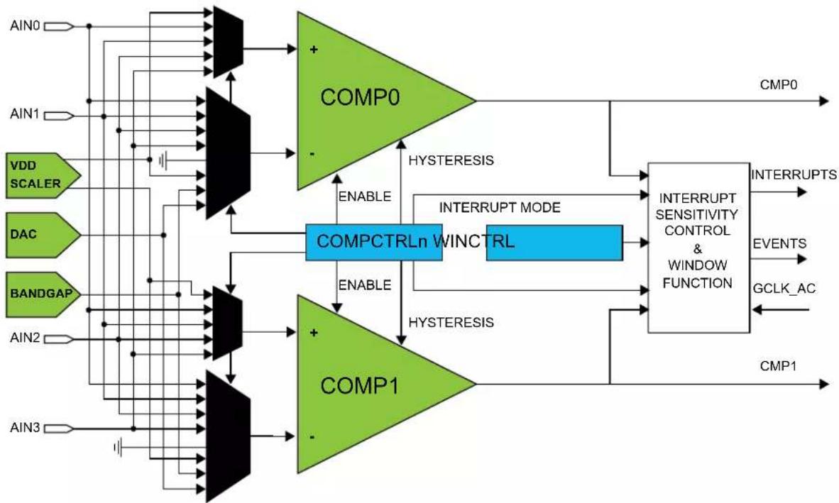
flowchart
graph TD
    A["AIN0"] --> B["COMP0"]
    C["AIN1"] --> B
    D["VDD SCALER"] --> E["COMPCTRLn WINCTRL"]
    F["DAC"] --> E
    G["BANDGAP"] --> H["COMP1"]
    I["AIN2"] --> H
    J["AIN3"] --> K["COMP1"]
    B --> L["INTERRUPT SENSITIVITY CONTROL & WINDOW FUNCTION"]
    E --> L
    H --> L
    L --> M["CMP0"]
    L --> N["Interrupts"]
    L --> O["EVENTS"]
    L --> P["GCLK_AC"]
    L --> Q["CMP1"]
    B --> R["HYSTERESIS"]
    E --> S["ENABLE"]
    H --> T["ENABLE"]
    B --> U["HYSTERESIS"]
    E --> V["INTERRUPT MODE"]
    H --> W["ENABLE"]
    B --> X["HYSTERESIS"]
    E --> Y["INTERRUPT MODE"]
    H --> Z["INTERRUPT MODE"]
    L --> AA["INTERRUPT MODE"]
    M --> AB["CMP0"]
    N --> AC["CMP0"]
    O --> AD["CMP0"]
    P --> AE["CMP0"]
29.4 Signal Description
| Signal Description Type | ||
| AIN[3..0] Analog input Comparator inputs | ||
| CMP[1..0] Digital output Comparator outputs | ||
Refer to I/O Multiplexing and Considerations for details on the pin mapping for this peripheral. One signal can be mapped on several pins.
29.5 Product Dependencies
In order to use this peripheral, other parts of the system must be configured correctly, as described below.
29.5.1 I/O Lines
Using the AC's I/O lines requires the I/O pins to be configured. Refer to PORT - I/O Pin Controller for details.
Related Links
- PORT - I/O Pin Controller
29.5.2 Power Management
The AC will continue to operate in any sleep mode where the selected source clock is running. The AC's interrupts can be used to wake up the device from sleep modes. Events connected to the event system can trigger other operations in the system without exiting sleep modes.
Related Links
- Power Manager (PM)
29.5.3 Clocks
The AC bus clock (CLK_AC_APB) can be enabled and disabled in the Main Clock module, MCLK (see MCLK - Main Clock, and the default state of CLK_AC_APB can be found in Peripheral Clock Masking.
Two generic clocks (GCLK_AC_DIG and GCLK_AC_ANA) are used by the AC. The digital clock (GCLK_AC_DIG) is required to provide the sampling rate for the comparators, while the analog clock (GCLK_AC_ANA) is required for low voltage operation (VDDANA < 2.5V) to ensure that the resistance of the analog input multiplexors remains low. These clocks must be configured and enabled in the Generic Clock Controller before using the peripheral.
This generic clock is asynchronous to the bus clock (CLK_AC_APB). Due to this asynchronicity, writes to certain registers will require synchronization between the clock domains. Refer to 29.6.15. Synchronization for further details.
Related Links
- Power Manager (PM)
29.5.4 DMA
Not applicable.
29.5.5 Interrupts
The interrupt request lines are connected to the interrupt controller. Using the AC interrupts requires the interrupt controller to be configured first. Refer to Nested Vector Interrupt Controller for details.
Related Links
10.2. Nested Vector Interrupt Controller
29.5.6 Events
The events are connected to the Event System. Refer to EVSYS – Event System for details on how to configure the Event System.
Related Links
- Event System (EVSYS)
29.5.7 Debug Operation
When the CPU is halted in debug mode, this peripheral will continue normal operation. If the peripheral is configured to require periodical service by the CPU through interrupts or similar, improper operation or data loss may result during debugging. This peripheral can be forced to halt operation during debugging.
29.5.8 Register Access Protection
All registers with write-access can be write-protected optionally by the Peripheral Access Controller (PAC), except for the following registers:
• Control B register (CTRLB)
- Interrupt Flag register (INTFLAG)
Optional write-protection by the Peripheral Access Controller (PAC) is denoted by the "PAC Write-Protection" property in each individual register description.
PAC write-protection does not apply to accesses through an external debugger.
Related Links
10.5. PAC - Peripheral Access Controller
29.5.9 Analog Connections
Each comparator has up to four I/O pins that can be used as analog inputs. Each pair of comparators shares the same four pins. These pins must be configured for analog operation before using them as comparator inputs.
Any internal reference source, such as a bandgap voltage reference, or DAC must be configured and enabled prior to its use as a comparator input.
29.6 Functional Description
29.6.1 Principle of Operation
Each comparator has one positive input and one negative input. Each positive input may be chosen from a selection of analog input pins. Each negative input may be chosen from a selection of both analog input pins and internal inputs, such as a bandgap voltage reference.
The digital output from the comparator is '1' when the difference between the positive and the negative input voltage is positive, and '0' otherwise.
The individual comparators can be used independently (normal mode) or paired to form a window comparison (window mode).
29.6.2 Basic Operation
29.6.2.1 Initialization
Before enabling the AC, the input and output events must be configured in the Event Control register (EVCTRL). These settings cannot be changed while the AC is enabled.
29.6.2.2 Enabling, Disabling and Resetting
The AC is enabled by writing a '1' to the Enable bit in the Control A register (CTRLA.ENABLE). The AC is disabled writing a '0' to CTRLA.ENABLE.
The AC is reset by writing a '1' to the Software Reset bit in the Control A register (CTRLA.SWRST). All registers in the AC will be reset to their initial state, and the AC will be disabled. Refer to CTRLA for details.
The individual comparators must be also enabled by writing a '1' to the Enable bit in the Comparator x Control registers (COMPCTRLx.ENABLE). However, when the AC is disabled, this will also disable the individual comparators, but will not clear their COMPCTRLx.ENABLE bits.
Related Links
29.8.1. CTRLA
29.6.2.3 Comparator Configuration
Each individual comparator must be configured by its respective Comparator Control register (COMPCTRLx) before that comparator is enabled. These settings cannot be changed while the comparator is enabled.
- Select the desired measurement mode with COMPCTRLx.SINGLE. See Starting a Comparison for more details.
- Select the desired hysteresis with COMPCTRLx.HYSTEN. See Input Hysteresis for more details.
- Select the comparator speed versus power with COMPCTRLx.SPEED. See Propagation Delay vs. Power Consumption for more details.
- Select the interrupt source with COMPCTRLx.INTSEL.
- Select the positive and negative input sources with the COMPCTRLx.MUXPOS and COMPCTRLx.MUXNEG bits. See Selecting Comparator Inputs for more details.
- Select the filtering option with COMPCTRLx.FLEN.
- Select standby operation with Run in Standby bit (COMPCTRLx.RUNSTDBY).
The individual comparators are enabled by writing a '1' to the Enable bit in the Comparator x Control registers (COMPCTRLx.ENABLE). The individual comparators are disabled by writing a '0' to COMPCTRLx.ENABLE. Writing a '0' to CTRLA.ENABLE will also disable all the comparators, but will not clear their COMPCTRLx.ENABLE bits.
29.6.2.4 Starting a Comparison
Each comparator channel can be in one of two different measurement modes, determined by the Single bit in the Comparator x Control register (COMPCTRLx.SINGLE):
• Continuous measurement
- Single-shot
After being enabled, a start-up delay is required before the result of the comparison is ready. This start-up time is measured automatically to account for environmental changes, such as temperature or voltage supply level, and is specified in Electrical Characteristics. During the start-up time, the COMP output is not available.
The comparator can be configured to generate interrupts when the output toggles, when the output changes from '0' to '1' (rising edge), when the output changes from '1' to '0' (falling edge) or at the end of the comparison. An end-of-comparison interrupt can be used with the single-shot mode to chain further events in the system, regardless of the state of the comparator outputs. The interrupt mode is set by the Interrupt Selection bit group in the Comparator Control register (COMPCTRLx.INTSEL). Events are generated using the comparator output state, regardless of whether the interrupt is enabled or not.
Related Links
32. Electrical Characteristics at 85°C
29.6.2.4.1 Continuous Measurement
Continuous measurement is selected by writing COMPCTRLx.SINGLE to zero. In continuous mode, the comparator is continuously enabled and performing comparisons. This ensures that the result of the latest comparison is always available in the Current State bit in the Status A register (STATUSA.STATEx).
After the start-up time has passed, a comparison is done and STATUSA is updated. The Comparator x Ready bit in the Status B register (STATUSB.READYx) is set, and the appropriate peripheral events and interrupts are also generated. New comparisons are performed continuously until the COMPCTRLx. ENABLE bit is written to zero. The start-up time applies only to the first comparison.
In continuous operation, edge detection of the comparator output for interrupts is done by comparing the current and previous sample. The sampling rate is the CLK_AC_DIG frequency. An example of continuous measurement is shown in the next figure.
Figure 29-2. Continuous Measurement Example
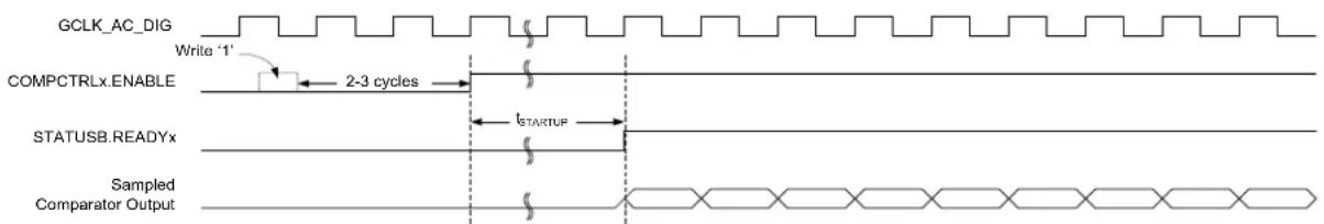
text_image
GCLK_AC_DIG Write '1' COMPCTRLx.ENABLE 2-3 cycles STATUSB.READYx t_STARTUP Sampled Comparator OutputFor low-power operation, comparisons can be performed during sleep modes without a clock. The comparator is enabled continuously, and changes of the comparator state are detected asynchronously. When a toggle occurs, the Power Manager will start CLK_AC_DIG to register the appropriate peripheral events and interrupts. The CLK_AC_DIG clock is then disabled again automatically, unless configured to wake up the system from sleep.
Related Links
32. Electrical Characteristics at 85°C
29.6.2.4.2 Single-Shot
Single-shot operation is selected by writing COMPCTRLx.SINGLE to '1'. During single-shot operation, the comparator is normally idle. The user starts a single comparison by writing '1' to the respective Start Comparison bit in the write-only Control B register (CTRLB.STARTx). The comparator is enabled, and after the start-up time has passed, a single comparison is done and STATUSA is updated. Appropriate peripheral events and interrupts are also generated. No new comparisons will be performed.
Writing '1' to CTRLB.STARTx also clears the Comparator x Ready bit in the Status B register (STATUSB.READYx). STATUSB.READYx is set automatically by hardware when the single comparison has completed.
To remove the need for polling, an additional means of starting the comparison is also available. A read of the Status C register (STATUSC) will start a comparison on all comparators currently configured for single-shot operation. The read will stall the bus until all enabled comparators are ready. If a comparator is already busy with a comparison, the read will stall until the current comparison is compete, and a new comparison will not be started.
A single-shot measurement can also be triggered by the Event System. Setting the Comparator x Event Input bit in the Event Control Register (EVCTRL.COMPEIx) enables triggering on incoming peripheral events. Each comparator can be triggered independently by separate events. Event-triggered operation is similar to user-triggered operation; the difference is that a peripheral event from another hardware module causes the hardware to automatically start the comparison and clear STATUSB.READYx.
To detect an edge of the comparator output in single-shot operation for the purpose of interrupts, the result of the current measurement is compared with the result of the previous measurement (one sampling period earlier). An example of single-shot operation is shown in the figure below.
Figure 29-3. Single-Shot Example
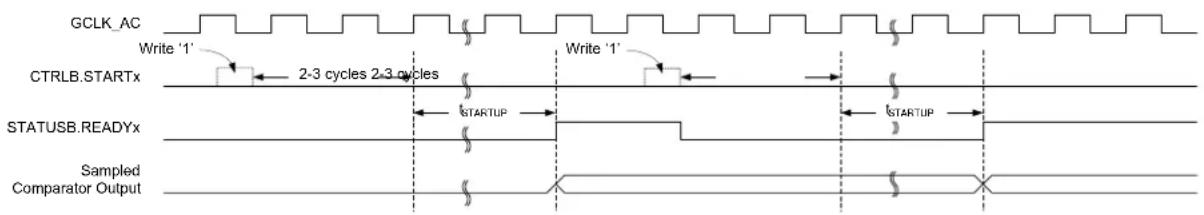
text_image
GCLK_AC Write '1' CTRLB.STARTx 2-3 cycles 2-3 cycles t_STARTUP Write '1' STATUSB.READYx t_STARTUP Sampled Comparator OutputFor low-power operation, event-triggered measurements can be performed during sleep modes. When the event occurs, the Power Manager will start CLK_AC_DIG. The comparator is enabled, and after the startup time has passed, a comparison is done and appropriate peripheral events and interrupts are also generated. The comparator and CLK_AC_DIG are then disabled again automatically, unless configured to wake up the system from sleep.
Related Links
32. Electrical Characteristics at 85°C
29.6.3 Selecting Comparator Inputs
Each comparator has one positive and one negative input. The positive input is one of the external input pins (AlNx). The negative input can be fed either from an external input pin (AlNx) or from one of the several internal reference voltage sources common to all comparators. The user selects the input source as follows:
- The positive input is selected by the Positive Input MUX Select bit group in the Comparator Control register (COMPCTRLx.MUXPOS)
- The negative input is selected by the Negative Input MUX Select bit group in the Comparator Control register (COMPCTRLx.MUXNEG)
In the case of using an external I/O pin, the selected pin must be configured for analog use in the PORT Controller by disabling the digital input and output. The switching of the analog input multiplexers is controlled to minimize crosstalk between the channels. The input selection must be changed only while the individual comparator is disabled.
Note: For internal use of the comparison results by the CCL, this bit must be 0x1 or 0x2.
29.6.4 Window Operation
Each comparator pair can be configured to work together in window mode. In this mode, a voltage range is defined, and the comparators give information about whether an input signal is within this range or not. Window mode is enabled by the Window Enable x bit in the Window Control register (WINCTRL.WENx). Both comparators in a pair must have the same measurement mode setting in their respective Comparator Control Registers (COMPCTRLx.SINGLE).
To physically configure the pair of comparators for window mode, the same I/O pin must be chosen as positive input for each comparator, providing a shared input signal. The negative inputs define the range for the window. In Figure 29-4, COMP0 defines the upper limit and COMP1 defines the lower limit of the window, as shown but the window will also work in the opposite configuration with COMP0 lower and COMP1 higher. The current state of the window function is available in the Window x State bit group of the Status register (STATUS.WSTATEx).
Window mode can be configured to generate interrupts when the input voltage changes to below the window, when the input voltage changes to above the window, when the input voltage changes into the window or when the input voltage changes outside the window. The interrupt selections are set by the Window Interrupt Selection bit field in the Window Control register (WINCTRL.WINTSEL). Events are generated using the inside/outside state of the window, regardless of whether the interrupt is enabled or not. Note that the individual comparator outputs, interrupts and events continue to function normally during window mode.
When the comparators are configured for window mode and single-shot mode, measurements are performed simultaneously on both comparators. Writing '1' to either Start Comparison bit in the Control B register (CTRLB.STARTx) will start a measurement. Likewise either peripheral event can start a measurement.
Figure 29-4. Comparators in Window Mode
flowchart
graph TD
    A["UPPER LIMIT OF WINDOW"] --> B["COMP0"]
    C["INPUT SIGNAL"] --> D["COMP1"]
    E["LOWER LIMIT OF WINDOW"] --> F["COMP1"]
    B --> G["STATE0"]
    D --> H["INTERRUPT SENSITIVITY CONTROL & WINDOW FUNCTION"]
    F --> I["STATE1"]
    G --> J["WSTATE[1:0"]]
    H --> K["INTERRUPTS"]
    H --> L["EVENTS"]
29.6.5 Voltage Doubler
The AC contains a voltage doubler that can reduce the resistance of the analog multiplexors when the supply voltage is below 2.5V. The voltage doubler is normally switched on/off automatically based on the supply level. When enabling the comparators, additional start-up time is required for the voltage doubler to settle. If the supply voltage is guaranteed to be above 2.5V, the voltage doubler can be disabled by writing the Low-Power Mux bit in the Control A register (CTRLA.LPMUX) to one. Disabling the voltage doubler saves power and reduces the start-up time.
29.6.6 V DDANA Scaler
The V_DDANA scaler generates a reference voltage that is a fraction of the device's supply voltage, with 64 levels. One independent voltage channel is dedicated for each comparator. The scaler of a comparator is enabled when the Negative Input Mux bit field in the respective Comparator Control register (COMPCTRLx.MUXNEG) is set to 0x5 and the comparator is enabled. The voltage of each channel is selected by the Value bit field in the Scaler x registers (SCALERx.VALUE).
Figure 29-5. V_DDANA Scaler
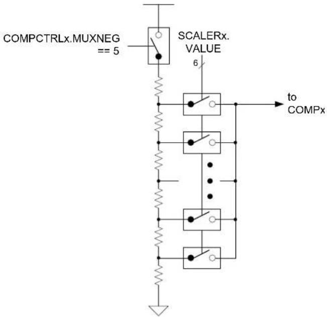
Application software can selectively enable/disable hysteresis for the comparison. Applying hysteresis will help prevent constant toggling of the output, which can be caused by noise when the input signals are close to each other.
Hysteresis is enabled for each comparator individually by the Hysteresis Enable bit in the Comparator x Control register (COMPCTRLx.HYSTEN). Hysteresis is available only in continuous mode (COMPCTRLx.SINGLE=0).
29.6.8 Propagation Delay vs. Power Consumption
It is possible to trade off comparison speed for power efficiency to get the shortest possible propagation delay or the lowest power consumption. The speed setting is configured for each comparator individually by the Speed bit group in the Comparator x Control register (COMPCTRLx.SPEED). The Speed bits select the amount of bias current provided to the comparator, and as such will also affect the start-up time.
29.6.9 Filtering
The output of the comparators can be filtered digitally to reduce noise. The filtering is determined by the Filter Length bits in the Comparator Control x register (COMPCTRLx.FLEN), and is independent for each comparator. Filtering is selectable from none, 3-bit majority (N=3) or 5-bit majority (N=5) functions. Any change in the comparator output is considered valid only if N/2+1 out of the last N samples agree. The filter sampling rate is the GCLK_AC frequency.
Note that filtering creates an additional delay of N-1 sampling cycles from when a comparison is started until the comparator output is validated. For continuous mode, the first valid output will occur when the required number of filter samples is taken. Subsequent outputs will be generated every cycle based on the current sample plus the previous N-1 samples, as shown in Figure 29-6. For single-shot mode, the comparison completes after the Nth filter sample, as shown in Figure 29-7.
Figure 29-6. Continuous Mode Filtering
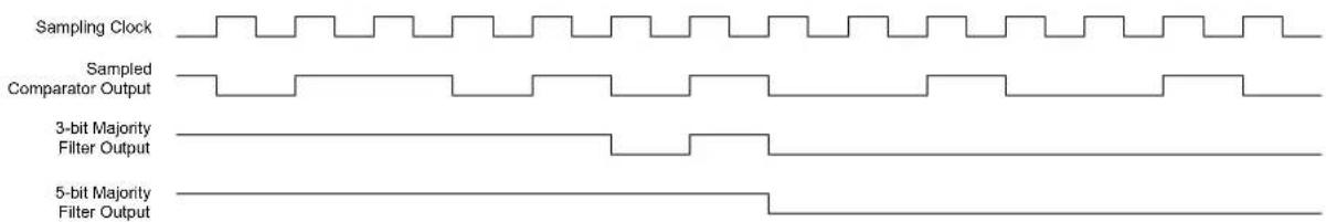
text_image
Sampling Clock Sampled Comparator Output 3-bit Majority Filter Output 5-bit Majority Filter OutputFigure 29-7. Single-Shot Filtering
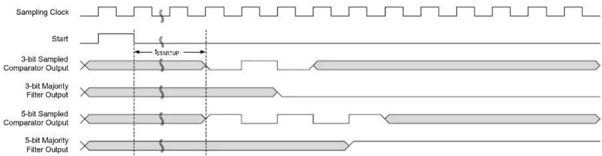
text_image
Sampling Clock Start tSTARTUP 3-bit Sampled Comparator Output 3-bit Majority Filter Output 5-bit Sampled Comparator Output 5-bit Majority Filter OutputDuring sleep modes, filtering is supported only for single-shot measurements. Filtering must be disabled if continuous measurements will be done during sleep modes, or the resulting interrupt/event may be generated incorrectly.
29.6.10 Comparator Output
The output of each comparator can be routed to an I/O pin by setting the Output bit group in the Comparator Control x register (COMPCTRLx.OUT). This allows the comparator to be used by external circuitry. Either the raw, non-synchronized output of the comparator or the CLK_AC-synchronized version, including filtering, can be used as the I/O signal source. The output appears on the corresponding CMP[x] pin.
29.6.11 Offset Compensation
The Swap bit in the Comparator Control registers (COMPCTRLx.SWAP) controls switching of the input signals to a comparator's positive and negative terminals. When the comparator terminals are swapped, the output signal from the comparator is also inverted, as shown in Figure 29-8. This allows the user to measure or compensate for the comparator input offset voltage. As part of the input selection, COMPCTRLx.SWAP can be changed only while the comparator is disabled.
Figure 29-8. Input Swapping for Offset Compensation
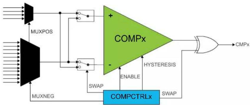
flowchart
graph TD
    A["Input"] --> B["MUXPOS"]
    C["Input"] --> D["MUXNEG"]
    B --> E["COMPx"]
    D --> F["COMPCTRLx"]
    E --> G["HYSTERESIS"]
    F --> H["SWAP"]
    G --> I["+"]
    H --> J["-"]
    I --> K["SWAP"]
    J --> L["ENABLE"]
    K --> M["CMPx"]
29.6.12 Interrupts
The AC has the following interrupt sources:
- Comparator (COMP0, COMP1): Indicates a change in comparator status.
- Window (WIN0): Indicates a change in the window status.
Comparator interrupts are generated based on the conditions selected by the Interrupt Selection bit group in the Comparator Control registers (COMPCTRLx.INTSEL). Window interrupts are generated based on the conditions selected by the Window Interrupt Selection bit group in the Window Control register (WINCTRL.WINTSEL[1:0]).
Each interrupt source has an interrupt flag associated with it. The interrupt flag in the Interrupt Flag Status and Clear (INTFLAG) register is set when the interrupt condition occurs. Each interrupt can be individually enabled by writing a one to the corresponding bit in the Interrupt Enable Set (INTENSET) register, and disabled by writing a one to the corresponding bit in the Interrupt Enable Clear (INTENCLR) register. An interrupt request is generated when the interrupt flag is set and the corresponding interrupt is enabled. The interrupt request remains active until the interrupt flag is cleared, the interrupt is disabled, or the AC is reset. See INFLAG register for details on how to clear interrupt flags. All interrupt requests from the peripheral are ORed together on system level to generate one combined interrupt request to the NVIC. The user must read the INTFLAG register to determine which interrupt condition is present.
Note that interrupts must be globally enabled for interrupt requests to be generated.
Related Links
10.2. Nested Vector Interrupt Controller
29.6.13 Events
The AC can generate the following output events:
- Comparator (COMP0, COMP1): Generated as a copy of the comparator status
- Window (WIN0): Generated as a copy of the window inside/outside status
Output events must be enabled to be generated. Writing a one to an Event Output bit in the Event Control register (EVCTRL.COMPEOx) enables the corresponding output event. Writing a zero to this bit disables the corresponding output event. The events must be correctly routed in the Event System.
The AC can take the following action on an input event:
- Single-shot measurement
- Single-shot measurement in window mode
Writing a one to an Event Input bit into the Event Control register (EVCTRL.COMPEIx) enables the corresponding action on input event. Writing a zero to this bit disables the corresponding action on input event. Note that if several events are connected to the AC, the enabled action will be taken on any of the incoming events. Refer to the Event System chapter for details on configuring the event system.
When EVCTRL.COMPEIx is one, the event will start a comparison on COMPx after the start-up time delay. In normal mode, each comparator responds to its corresponding input event independently. For a pair of comparators in window mode, either comparator event will trigger a comparison on both comparators simultaneously.
29.6.14 Sleep Mode Operation
The Run in Standby bits in the Comparator x Control registers (COMPCTRLx.RUNSTDBY) control the behavior of the AC during standby sleep mode. Each RUNSTDBY bit controls one comparator. When the bit is zero, the comparator is disabled during sleep, but maintains its current configuration. When the bit is one, the comparator continues to operate during sleep. Note that when RUNSTDBY
is zero, the analog blocks are powered off for the lowest power consumption. This necessitates a start-up time delay when the system returns from sleep.
When RUNSTDBY is one, any enabled AC interrupt source can wake up the CPU. While the CPU is sleeping, single-shot comparisons are only triggerable by events. The AC can also be used during sleep modes where the clock used by the AC is disabled, provided that the AC is still powered (not in shutdown). In this case, the behavior is slightly different and depends on the measurement mode.
Table 29-1. Sleep Mode Operation
| COMPCTRLx.MODE | RUNSTDBY=0 | RUNSTDBY=1 |
| 0 (Continuous) COMPx disabled GCLK_AC_DIG stopped, COMPx enabled | ||
| 1 (Single-shot) COMPx disabled GCLK_AC_DIG stopped, COMPx enabled only when triggered by an input event | ||
29.6.14.1 Continuous Measurement during Sleep
When a comparator is enabled in continuous measurement mode and GCLK_AC_DIG is disabled during sleep, the comparator will remain continuously enabled and will function asynchronously. The current state of the comparator is asynchronously monitored for changes. If an edge matching the interrupt condition is found, GCLK_AC_DIG is started to register the interrupt condition and generate events. If the interrupt is enabled in the Interrupt Enable registers (INTENCLR/SET), the AC can wake up the device; otherwise GCLK_AC_DIG is disabled until the next edge detection. Filtering is not possible with this configuration.
Figure 29-9. Continuous Mode SleepWalking
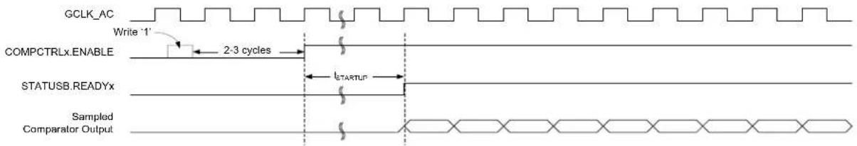
text_image
GCLK_AC Write '1' COMPCTRLx.ENABLE 2-3 cycles STATUSB.READYx t_STARTUP Sampled Comparator Output29.6.14.2 Single-Shot Measurement during Sleep
For low-power operation, event-triggered measurements can be performed during sleep modes. When the event occurs, the Power Manager will start GCLK_AC_DIG. The comparator is enabled, and after the start-up time has passed, a comparison is done, with filtering if desired, and the appropriate peripheral events and interrupts are also generated, as the figure below. The comparator and GCLK_AC_DIG are then disabled again automatically, unless configured to wake the system from sleep. Filtering is allowed with this configuration.
Figure 29-10. Single-Shot SleepWalking
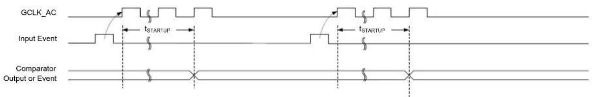
text_image
GCLK_AC Input Event Comparator Output or Event29.6.15 Synchronization
Due to asynchronicity between the main clock domain and the peripheral clock domains, some registers need to be synchronized when written or read.
The following bits are synchronized when written:
- Software Reset bit in control register (CTRLA.SWRST)
- Enable bit in control register (CTRLA.ENABLE)
- Enable bit in Comparator Control register (COMPCTRLn.ENABLE)
The following registers are synchronized when written:
• Window Control register (WINCTRL)
Required write-synchronization is denoted by the "Write-Synchronized" property in the register description.
Related Links
13.3. Register Synchronization
29.7 Register Summary
| Offset | Name Bit Pos. 76 | 543210 | ||||||||
| 0x00 | CTRLA 7:0 LPMUX | RUNSTDBY | ENABLE SWRST | |||||||
| 0x01 | CTRLB 7:0 | STARTx STARTx | ||||||||
| 0x02 | EVCTRL | 7:0 | WINEO0 | COMPEOx | COMPEOx | |||||
| 15:8 | COMPEIx | COMPEIx | ||||||||
| 0x04 | INTENCLR | 7:0 | WINO | COMPx | COMPx | |||||
| 0x05 | INTENSET | 7:0 | WINO | COMPx | COMPx | |||||
| 0x06 | INTFLAG | 7:0 | WINO | COMPx | COMPx | |||||
| 0x07 | Reserved | |||||||||
| 0x08 | STATUS | 7:0 | WSTATE0[1:0] | STATEx | STATEx | |||||
| 0x09 | STATUS | 7:0 | SYNCBUSY | READYx | READYx | |||||
| 0x0A | STATUS | 7:0 | WSTATE0[1:0] | STATEx | STATEx | |||||
| 0x0B | Reserved | |||||||||
| 0x0C | WINCTRL | 7:0 | WINTSEL0[1:0] | WENO | ||||||
| 0x0D...0x0F | Reserved | |||||||||
| 0x10 | COMPCTRL0 | 7:0 | INTSEL[1:0] | SPEED[1:0] | SINGLE | ENABLE | ||||
| 15:8 | SWAP | MUXPOS[1:0] | MUXNEG[2:0] | |||||||
| 23:16 | HYST | OUT[1:0] | ||||||||
| 31:24 | FLEN[2:0] | |||||||||
| 0x14 | COMPCTRL1 | 7:0 | INTSEL[1:0] | SPEED[1:0] | SINGLE | ENABLE | ||||
| 15:8 | SWAP | MUXPOS[1:0] | MUXNEG[2:0] | |||||||
| 23:16 | HYST | OUT[1:0] | ||||||||
| 31:24 | FLEN[2:0] | |||||||||
| 0x18...0x1F | Reserved | |||||||||
| 0x20 | SCALER0 | 7:0 | VALUE[5:0] | |||||||
| 0x21 | SCALER1 | 7:0 | VALUE[5:0] | |||||||
29.8 Register Description
Registers can be 8, 16, or 32 bits wide. Atomic 8-, 16- and 32-bit accesses are supported. In addition, the 8-bit quarters and 16-bit halves of a 32-bit register, and the 8-bit halves of a 16-bit register can be accessed directly.
Some registers are optionally write-protected by the Peripheral Access Controller (PAC). Optional PAC write-protection is denoted by the "PAC Write-Protection" property in each individual register description. For details, refer to 27.5.7. Register Access Protection.
Some registers are synchronized when read and/or written. Synchronization is denoted by the "Write-Synchronized" or the "Read-Synchronized" property in each individual register description. For details, refer to 27.6.5. Synchronization.
Some registers are enable-protected, meaning they can only be written when the peripheral is disabled. Enable-protection is denoted by the "Enable-Protected" property in each individual register description.
29.8.1 Control A
Name: CTRLA
Offset: 0x00
Reset: 0x00
Property: PAC Write-Protection, Write-Synchronized
Bit 76543210
| LPMUX | RUNSTDBY ENABLE SWRST | ||||||
| Access | R/W R/W | R/W | R/W | ||||
| Reset 0 | 0 0 0 | ||||||
Bit 7 - LPMUX Low-Power Mux
This bit is not synchronized
| Value | Description |
| 0 | The analog input muxes have low resistance, but consume more power at lower voltages (e.g., are driven by the voltage doubler). |
| 1 | The analog input muxes have high resistance, but consume less power at lower voltages (e.g., the voltage doubler is disabled). |
Bit 2 - RUNSTDBY Run in Standby
This bit controls the behavior of the comparators during standby sleep mode.
This bit is not synchronized
| Value | Description |
| 0 | The comparator pair is disabled during sleep. |
| 1 | The comparator pair continues to operate during sleep. |
Bit 1 - ENABLE Enable
Due to synchronization, there is a delay from the time when the register is updated until the peripheral is enabled/disabled. The value written to CTRL. ENABLE will read back immediately after being written. STATUS.SYNCBUSY is set. STATUS.SYNCBUSY is cleared when the peripheral is enabled/disabled
| Value | Description |
| 0 | The AC is disabled. |
| 1 | The AC is enabled. Each comparator must also be enabled individually by the Enable bit in the Comparator Control register (COMPCTRLn.ENABLE). |
Bit 0 - SWRST Software Reset
Writing a '0' to this bit has no effect.
Writing a '1' to this bit resets all registers in the AC to their initial state, and the AC will be disabled. Writing a '1' to CTRLA.SWRST will always take precedence, meaning that all other writes in the same write-operation will be discarded.
Due to synchronization, there is a delay from writing CTRLA.SWRST until the reset is complete. CTRLA.SWRST and STATUS.SYNCBUSY will both be cleared when the reset is complete.
| Value | Description |
| 0 | There is no reset operation ongoing. |
| 1 | The reset operation is ongoing. |
29.8.2 Control B
Name: CTRLB
Offset: 0x01
Reset: 0x00
Property: -
Bit 76543210
| $TARTx START* | ||||||
| Access Reset 0 0 | R/W R/W | |||||
Bits 1,0 - STARTx Comparator x Start Comparison
Writing a '0' to this field has no effect.
Writing a '1' to STARTx starts a single-shot comparison on COMPx if both the Single-Shot and Enable bits in the Comparator x Control Register are '1' (COMPCTRLx.SINGLE and COMPCTRLx.ENABLE). If comparator x is not implemented, or if it is not enabled in single-shot mode, Writing a '1' has no effect.
This bit always reads as zero.
29.8.3 Event Control
Name: EVCTRL
Offset: 0x02
Reset: 0x0000
Property: PAC Write-Protection, Enable-Protected
Bit 15 14 13 12 11 10 9 8
| COMPEIx COMPEIx | ||||||
| Access Reset | R/W R/W0 0 |
Bit 76543210
| WINE00 | COMPEOx | COMPEOx | |||||
| Access Reset | R/W 0 | R/W R/W 0 0 |
Bits 9,8 - COMPEIX Comparator x Event Input
Note that several actions can be enabled for incoming events. If several events are connected to the peripheral, the enabled action will be taken for any of the incoming events. There is no way to tell which of the incoming events caused the action.
These bits indicate whether a comparison will start or not on any incoming event.
| Value | Description |
| 0 | Comparison will not start on any incoming event. |
| 1 | Comparison will start on any incoming event. |
Bit 4 - WINEO0 Window 0 Event Output Enable
These bits indicate whether the window 0 function can generate a peripheral event or not.
| Value | Description |
| 0 | Window 0 Event is disabled. |
| 1 | Window 0 Event is enabled. |
Bits 1,0 - COMPEOx Comparator x Event Output Enable
These bits indicate whether the comparator x output can generate a peripheral event or not.
| Value | Description |
| 0 | COMPx event generation is disabled. |
| 1 | COMPx event generation is enabled. |
29.8.4 Interrupt Enable Clear
Name: INTENCLR
Offset: 0x04
Reset: 0x00
Property: PAC Write-Protection
This register allows the user to disable an interrupt without doing a read-modify-write operation. Changes in this register will also be reflected in the Interrupt Enable Set register (INTENSET).
Bit 76543210
| WIN0 | COMPx | COMPx | ||||||
| Access Reset | R/W | R/W | R/W | |||||
| 0 | 0 0 |
Bit 4 - WIN0 Window 0 Interrupt Enable
Reading this bit returns the state of the Window 0 interrupt enable.
Writing a '0' to this bit has no effect.
Writing a '1' to this bit disables the Window 0 interrupt.
| Value | Description |
| 0 | The Window 0 interrupt is disabled. |
| 1 | The Window 0 interrupt is enabled. |
Bits 1,0 - COMPx Comparator x Interrupt Enable
Reading this bit returns the state of the Comparator x interrupt enable.
Writing a '0' to this bit has no effect.
Writing a '1' to this bit disables the Comparator x interrupt.
| Value | Description |
| 0 | The Comparator x interrupt is disabled. |
| 1 | The Comparator x interrupt is enabled. |
29.8.5 Interrupt Enable Set
Name: INTENSET
Offset: 0x05
Reset: 0x00
Property: PAC Write-Protection
This register allows the user to enable an interrupt without doing a read-modify-write operation.
Changes in this register will also be reflected in the Interrupt Enable Clear register (INTENCLR).
Bit 76543210
| WIN0 | COMPx | COMPx | ||||||
| Access Reset | R/W | R/W | R/W | |||||
| 0 | 0 0 |
Bit 4 - WIN0 Window 0 Interrupt Enable
Reading this bit returns the state of the Window 0 interrupt enable.
Writing a '0' to this bit has no effect.
Writing a '1' to this bit enables the Window 0 interrupt.
| Value | Description |
| 0 | The Window 0 interrupt is disabled. |
| 1 | The Window 0 interrupt is enabled. |
Bits 1,0 - COMPx Comparator x Interrupt Enable
Reading this bit returns the state of the Comparator x interrupt enable.
Writing a '0' to this bit has no effect.
Writing a '1' to this bit will set the Ready interrupt bit and enable the Ready interrupt.
| Value | Description |
| 0 | The Comparator x interrupt is disabled. |
| 1 | The Comparator x interrupt is enabled. |
29.8.6 Interrupt Flag Status and Clear
Name: INTFLAG
Offset: 0x06
Reset: 0x00
Property: -
Bit 76543210
| WIN0 | COMPx | COMPx | ||||||
| Access Reset | R/W | R/W | R/W | |||||
| 0 | 0 0 |
Bit 4 - WIN0 Window 0
This flag is set according to the Window 0 Interrupt Selection bit group in the WINCTRL register (WINCTRL.WINTSELx) and will generate an interrupt if INTENCLR/SET.WINx is also one.
Writing a '0' to this bit has no effect.
Writing a '1' to this bit clears the Window 0 interrupt flag.
Bits 1,0 - COMPx Comparator x
Reading this bit returns the status of the Comparator x interrupt flag. If comparator x is not implemented, COMPx always reads as zero.
This flag is set according to the Interrupt Selection bit group in the Comparator x Control register (COMPCTRLx.INTSEL) and will generate an interrupt if INTENCLR/SET.COMPx is also one.
Writing a '0' to this bit has no effect.
Writing a '1' to this bit clears the Comparator x interrupt flag.
29.8.7 Status A
Name: STATUSA
Offset: 0x08
Reset: 0x00
Property: -
Bit 76543210
| WSTATE0[1:0] | STATEx STATEx | |||||
| Access Reset | R R R R | |||||
| 0 0 | 0 0 |
Bits 5:4 - WSTATE0[1:0] Window 0 Current State
These bits show the current state of the signal if the window 0 mode is enabled.
| Value | Name | Description |
| 0x0 | ABOVE | Signal is above window |
| 0x1 | INSIDE | Signal is inside window |
| 0x2 | BELOW | Signal is below window |
| 0x3 | Reserved |
Bits 1,0 - STATEx Comparator x Current State
This bit shows the current state of the output signal from COMPx. STATEx is valid only when STATUSB.READYx is one.
29.8.8 Status B
Name: STATUSB
Offset: 0x09
Reset: 0x00
Property: -
Bit 76543210
| SYNCBUSY | READYx | READYx | ||||||
| Access | R R R | |||||||
| Reset | 0 | 0 0 | ||||||
Bit 7 - SYNCBUSY Synchronization Busy
This bit is cleared when the synchronization of registers between the clock domains is complete.
This bit is set when the synchronization of registers between clock domains is started.
Bits 1,0 - READYx Comparator x Ready
This bit is cleared when the comparator x output is not ready.
This bit is set when the comparator x output is ready.
29.8.9 Status C
Name: STATUSC
Offset: 0x0A
Reset: 0x00
Property: -
STATUSC is a copy of STATUSA (see STATUSA register), with the additional feature of automatically starting single-shot comparisons. A read of STATUSC will start a comparison on all comparators currently configured for single-shot operation. The read will stall the bus until all enabled comparators are ready. If a comparator is already busy with a comparison, the read will stall until the current comparison is compete, and a new comparison will not be started.
Bit 76543210
| WSTATE0[1:0] | STATEx STATEx | |||||
| Access Reset | RRRR0 0 | 0 0 |
Bits 5:4 - WSTATE0[1:0] Window 0 Current State
These bits show the current state of the signal if the window 0 mode is enabled.
| Value | Name | Description |
| 0x0 | ABOVE | Signal is above window |
| 0x1 | INSIDE | Signal is inside window |
| 0x2 | BELOW | Signal is below window |
| 0x3 | Reserved |
Bits 1,0 - STATEx Comparator x Current State
This bit shows the current state of the output signal from COMPx. STATEx is valid only when STATUSB.READYx is one.
29.8.10 Window Control
Name: WINCTRL
Offset: 0x0C
Reset: 0x00
Property: PAC Write-Protection, Write-Synchronized
Bit 76543210
| WINTSELO[1:0] WENO | |||||
| Access Reset 0 0 0 | R/W R/W R/W | ||||
Bits 2:1 - WINTSEL0[1:0] Window 0 Interrupt Selection
These bits configure the interrupt mode for the comparator window 0 mode.
| Value Name | Description | |
| 0x0 | ABOVE | Interrupt on signal above window |
| 0x1 | INSIDE | Interrupt on signal inside window |
| 0x2 | BELOW | Interrupt on signal below window |
| 0x3 | OUTSIDE | Interrupt on signal outside window |
Bit 0 - WENO Window 0 Mode Enable
| Value Description | |
| 0 | Window mode is disabled for comparators 0 and 1. |
| 1 | Window mode is enabled for comparators 0 and 1. |
29.8.11 Comparator Control n
Name: COMPCTRL
Offset: 0x10 + n*0x04 [n=0..1]
Reset: 0x00000000
Property: PAC Write-Protection, Write-Synchronized
| Bit 31 30 29 28 27 26 25 24 | ||||||
| FLEN[2:0] | ||||||
| Access Reset | R/W R/W R/W | |||||
| Bit 23 22 21 20 19 18 17 16 | ||||||
| HYST | QUT[1:0] | |||||
| Access Reset | R/W 0 | R/W R/W 0 0 | ||||
| Bit 15 14 13 12 11 10 | 9 8 | |||||
| SWAP | MUXPOS[1:0] | MUXNEG[2:0] | ||||
| Access Reset | R/W 0 | R/W R/W 0 0 | R/W R/W R/W 0 0 0 | |||
| Bit 7 6 5 4 3 2 1 0 | ||||||
| INTSEL[1:0] | SPEED[1:0] | SINGLE | ENABLE | |||
| Access Reset | R/W R/W 0 0 | R/W R/W R/W R/W 0 0 0 0 | ||||
Bits 26:24 - FLEN[2:0] Filter Length
These bits configure the filtering for comparator n. COMPCTRLn.FLEN can only be written while COMPCTRLn.ENABLE is zero.
These bits are not synchronized.
| Value | Name | Description |
| 0x0 | OFF | No filtering |
| 0x1 | MAJ3 | 3-bit majority function (2 of 3) |
| 0x2 | MAJ5 | 5-bit majority function (3 of 5) |
| 0x3-0x7 | N/A | Reserved |
Bit 19 - HYST Hysteresis Enable
This bit indicates the hysteresis mode of comparator n. Hysteresis is available only for continuous mode (COMPCTRLn. SINGLE=0). COMPCTRLn.HYST can be written only while COMPCTRLn. ENABLE is zero.
This bit is not synchronized.
These bits are not synchronized.
| Value | Name |
| 0 | Hysteresis is disabled. |
| 1 | Hysteresis is enabled. |
Bits 17:16 - OUT[1:0] Output
These bits configure the output selection for comparator n. COMPCTRLn.OUT can be written only while COMPCTRLn.ENABLE is zero.
These bits are not synchronized.
| Value | Name | Description |
| 0x0 | OFF | The output of COMPn is not routed to the COMPn I/O port |
| 0x1 | ASYNC | The asynchronous output of COMPn is routed to the COMPn I/O port |
| Value Name | Description |
| 0x2 | SYNC The synchronous output (including filtering) of COMPn is routed to the COMPn I/O port |
| 0x3 | N/A Reserved |
Bit 15 - SWAP Swap Inputs and Invert
This bit swaps the positive and negative inputs to COMPn and inverts the output. This function can be used for offset cancellation. COMPCTRLn.SWAP can be written only while COMPCTRLn.ENABLE is zero.
These bits are not synchronized.
| Value Description | |
| 0 | The output of MUXPOS connects to the positive input, and the output of MUXNEG connects to the negative input. |
| 1 | The output of MUXNEG connects to the positive input, and the output of MUXPOS connects to the negative input. |
Bits 13:12 - MUXPOS[1:0] Positive Input Mux Selection
These bits select which input will be connected to the positive input of comparator n.
COMPCTRLn.MUXPOS can be written only while COMPCTRLn.ENABLE is zero.
These bits are not synchronized.
| Value Name | Description | |
| 0x0 | PIN0 I/O pin 0 | |
| 0x1 | PIN1 I/O pin 1 | |
| 0x2 | PIN2 I/O pin 2 | |
| 0x3 | PIN3 I/O pin 3 |
Bits 10:8 - MUXNEG[2:0] Negative Input Mux Selection
These bits select which input will be connected to the negative input of comparator n.
COMPCTRLn.MUXNEG can only be written while COMPCTRLn.ENABLE is zero.
These bits are not synchronized.
| Value Name | Description | |
| 0x0 | PIN0 I/O pin 0 | |
| 0x1 | PIN1 I/O pin 1 | |
| 0x2 | PIN2 I/O pin 2 | |
| 0x3 | PIN3 I/O pin 3 | |
| 0x4 | GND Ground | |
| 0x5 | VSCALE VDD scaler | |
| 0x6 | BANDGAP Internal bandgap voltage | |
| 0x7 | DAC DAC output |
Bits 6:5 - INTSEL[1:0] Interrupt Selection
These bits select the condition for comparator n to generate an interrupt or event.
COMPCTRLn.INTSEL can be written only while COMPCTRLn.ENABLE is zero.
These bits are not synchronized.
| Value Name | Description | |
| 0x0 | TOGGLE Interrupt on comparator output toggle | |
| 0x1 | RISING Interrupt on comparator output rising | |
| 0x2 | FALLING | Interrupt on comparator output falling |
| 0x3 | EOC | Interrupt on end of comparison (single-shot mode only) |
Bits 3:2 - SPEED[1:0] Speed Selection
This bit indicates the speed/propagation delay mode of comparator n. COMPCTRLn.SPEED can be written only while COMPCTRLn. ENABLE is zero.
These bits are not synchronized.
| Value Name | Description | |
| 0x0 | LOW Low speed | |
| 0x1 | HIGH | High speed |
| 0x2-0x3 | N/A Reserved |
Bit 1 - SINGLE Single-Shot Mode
This bit determines the operation of comparator n. COMPCTRLn.SINGLE can be written only while COMPCTRLn.ENABLE is zero.
These bits are not synchronized.
| Value Description | |
| 0 | Comparator n operates in continuous measurement mode. |
| 1 | Comparator n operates in single-shot mode. |
Bit 0 - ENABLE Enable
Writing a zero to this bit disables comparator n.
Writing a one to this bit enables comparator n. After writing to this bit, the value read back will not change until the action initiated by the writing is complete.
Due to synchronization, there is a latency of at least two GCLK_AC_DIG clock cycles from updating the register until the comparator is enabled/disabled. The bit will continue to read the previous state while the change is in progress. Writing a one to COMPCTRLn. ENABLE will prevent further changes to the other bits in COMPCTRLn. These bits remain protected until COMPCTRLn. ENABLE is written to zero and the write is synchronized.
29.8.12 Scaler n
Name: SCALER
Offset: 0x20 + n*0x01 [n=0..1]
Reset: 0x00
Property: PAC Write-Protection
Bit 76543210
| VALUE[5:0] | |
| Access Reset 0 0 0 0 0 0 | R/W R/W R/W R/W R/W R/W |
Bits 5:0 - VALUE[5:0] Scaler Value
These bits define the scaling factor for channel n of the V_DD voltage scaler. The output voltage, V_SCALE , is:
$$ V _ {\mathrm{SCALE}} = \frac {V _ {\mathrm{DD}} \cdot (\text { VALUE } + 1)}{6 4} $$
30. DAC – Digital-to-Analog Converter
30.1 Overview
The Digital-to-Analog Converter (DAC) converts a digital value to a voltage. The DAC has one channel with 10-bit resolution, and it is capable of converting up to 350,000 samples per second (350 ksps).
30.2 Features
• DAC with 10-bit Resolution
- Up to 350 ksps Conversion Rate
• Multiple Trigger Sources
• High-drive Capabilities
- Output can be used as Input to the Analog Comparator (AC)
30.3 Block Diagram
Figure 30-1. DAC Block Diagram
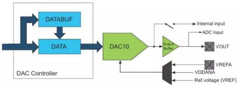
flowchart
graph TD
    A["DATABUF"] --> B["DATA"]
    C["VOUT"] --> D["Output Buffer"]
    E["VDDANA"] --> D
    F["Internal input"] --> D
    G["ADC Input"] --> D
    H["Ref. voltage (VREF)"] --> D
    I["DAC10"] --> D
    style A fill:#333,stroke:#fff,color:#fff
    style C fill:#333,stroke:#fff,color:#fff
    style B fill:#333,stroke:#fff,color:#fff
    style D fill:#333,stroke:#fff,color:#fff
    style E fill:#333,stroke:#fff,color:#fff
    style F fill:#333,stroke:#fff,color:#fff
    style G fill:#333,stroke:#fff,color:#fff
    style H fill:#333,stroke:#fff,color:#fff
    style I fill:#333,stroke:#fff,color:#fff
30.4 Signal Description
| Signal Name Type Description | |
| VOUT Analog output DAC output | |
| VREFA Analog input External reference |
Related Links
- I/O Multiplexing and Considerations
30.5 Product Dependencies
In order to use this peripheral, other parts of the system must be configured correctly, as described below.
30.5.1 I/O Lines
Using the DAC Controller's I/O lines requires the I/O pins to be configured using the port configuration (PORT).
Related Links
- PORT - I/O Pin Controller
30.5.2 Power Management
The DAC will continue to operate in any Sleep mode where the selected source clock is running.
The DAC interrupts can be used to wake up the device from sleep modes.
Events connected to the event system can trigger other operations in the system without exiting sleep modes.
Related Links
15. Power Manager (PM)
30.5.3 Clocks
The DAC bus clock (CLK_DAC_APB) can be enabled and disabled by the Power Manager, and the default state of CLK_DAC_APB can be found in the Peripheral Clock Masking section.
A generic clock (GCLK_DAC) is required to clock the DAC Controller. This clock must be configured and enabled in the Generic Clock Controller before using the DAC Controller. Refer to GCLK – Generic Clock Controller for details.
This generic clock is asynchronous to the bus clock (CLK_DAC_APB). Due to this asynchronicity, writes to certain registers will require synchronization between the clock domains. Refer to 30.6.6. Synchronization for further details.
Related Links
14. GCLK - Generic Clock Controller
30.5.4 Interrupts
The interrupt request line is connected to the interrupt controller. Using the DAC Controller interrupt(s) requires the interrupt controller to be configured first.
Related Links
10.2. Nested Vector Interrupt Controller
30.5.5 Events
The events are connected to the Event System.
Related Links
22. Event System (EVSYS)
30.5.6 Debug Operation
When the CPU is halted in debug mode the DAC will halt normal operation. Any on-going conversions will be completed. The DAC can be forced to continue normal operation during debugging. If the DAC is configured in a way that requires it to be periodically serviced by the CPU through interrupts or similar, improper operation or data loss may result during debugging.
30.5.7 Register Access Protection
All registers with write-access can be write-protected optionally by the Peripheral Access Controller (PAC), except the following registers:
- Interrupt Flag Status and Clear (INTFLAG) register
• Data Buffer (DATABUF) register
Optional write-protection by the Peripheral Access Controller (PAC) is denoted by the "PAC Write-Protection" property in each individual register description.
PAC write-protection does not apply to accesses through an external debugger
Related Links
10.5. PAC - Peripheral Access Controller
30.5.8 Analog Connections
The DAC has one output pin (VOUT) and one analog input pin (VREFA) that must be configured first.
When internal input is used, it must be enabled before DAC Controller is enabled.
30.6 Functional Description
30.6.1 Principle of Operation
The DAC converts the digital value located in the Data register (DATA) into an analog voltage on the DAC output (VOUT).
A conversion is started when new data is written to the Data register. The resulting voltage is available on the DAC output after the conversion time. A conversion can also be started by input events from the Event System.
30.6.2 Basic Operation
30.6.2.1 Initialization
The following registers are enable-protected, meaning they can only be written when the DAC is disabled (CTRLA. ENABLE is zero):
• Control B register (CTRLB)
• Event Control register (EVCTRL)
Enable-protection is denoted by the Enable-Protected property in the register description.
Before enabling the DAC, it must be configured by selecting the voltage reference using the Reference Selection bits in the Control B register (CTRLB.REFSEL).
30.6.2.2 Enabling, Disabling and Resetting
The DAC Controller is enabled by writing a '1' to the Enable bit in the Control A register (CTRLA.ENABLE). The DAC Controller is disabled by writing a '0' to CTRLA.ENABLE.
The DAC Controller is reset by writing a '1' to the Software Reset bit in the Control A register (CTRLA.SWRST). All registers in the DAC will be reset to their initial state, and the DAC Controller will be disabled. Refer to the CTRLA register for details.
30.6.2.3 Enabling the Output Buffer
To enable the DAC output on the V_OUT pin, the output driver must be enabled by writing a one to the External Output Enable bit in the Control B register (CTRLB.EOEN).
The DAC output buffer provides a high-drive-strength output, and is capable of driving both resistive and capacitive loads. To minimize power consumption, the output buffer should be enabled only when external output is needed.
30.6.2.4 Digital to Analog Conversion
The DAC converts a digital value (stored in the DATA register) into an analog voltage. The conversion range is between GND and the selected DAC voltage reference. The default voltage reference is the internal reference voltage. Other voltage reference options are the analog supply voltage (VDDANA) and the external voltage reference (VREFA). The voltage reference is selected by writing to the Reference Selection bits in the Control B register (CTRLB.REFSEL).
The output voltage from the DAC can be calculated using the following formula:
$$ V _ {\mathrm{OUT}} = \frac {\mathrm{DATA}}{0 x 3 \mathrm{FF}} \cdot \mathrm{VREF} $$
A new conversion starts as soon as a new value is loaded into DATA. DATA can either be loaded via the APB bus during a CPU write operation, or from the DATABUF register when a START event occurs. Refer to 30.6.4. Events for details. As there is no automatic indication that a conversion is done, the sampling period must be greater than or equal to the specified conversion time.
30.6.3 Interrupts
The DAC Controller has the following interrupt sources:
- Data Buffer Empty (EMPTY): Indicates that the internal data buffer of the DAC is empty.
- Underrun (UNDERRUN): Indicates that the internal data buffer of the DAC is empty and a DAC start of conversion event occurred. Refer to 30.6.4. Events for details.
Each interrupt source has an interrupt flag associated with it. The interrupt flag in the Interrupt Flag Status and Clear register (INTFLAG) is set when the interrupt condition occurs. Each interrupt can be individually enabled by writing a one to the corresponding bit in the Interrupt Enable Set register (INTENSET), and disabled by writing a one to the corresponding bit in the Interrupt Enable Clear register (INTENCLR).
An interrupt request is generated when the interrupt flag is set and the corresponding interrupt is enabled. The interrupt request remains active until the interrupt flag is cleared, the interrupt is disabled or the DAC is reset. See INTFLAG register for details on how to clear interrupt flags.
All interrupt requests from the peripheral are ORed together on system level to generate one combined interrupt request to the NVIC. The user must read the INTFLAG register to determine which interrupt condition is present.
Note that interrupts must be globally enabled for interrupt requests to be generated..
Related Links
10.2. Nested Vector Interrupt Controller
30.6.4 Events
The DAC Controller can generate the following output events:
- Data Buffer Empty (EMPTY): Generated when the internal data buffer of the DAC is empty.
Writing a '1' to an Event Output bit in the Event Control register (EVCTRL.EMPTYEO) enables the corresponding output event. Writing a '0' to this bit disables the corresponding output event.
The DAC can take the following action on an input event:
- Start Conversion (START): DATABUF value is transferred into DATA as soon as the DAC is ready for the next conversion, and then conversion is started. START is considered as asynchronous to GCLK_DAC thus it is resynchronized in DAC Controller. Refer to 30.6.2.4. Digital to Analog Conversion for details.
Writing a '1' to an Event Input bit in the Event Control register (EVCTRL.STARTEI) enables the corresponding action on an input event. Writing a '0' to this bit disables the corresponding action on input event.
Note: When several events are connected to the DAC Controller, the enabled action will be taken on any of the incoming events.
By default, DAC Controller detects rising edge events. Falling edge detection can be enabled by writing a '1' to EVCTRL.INVEIx.
Related Links
22. Event System (EVSYS)
30.6.5 Sleep Mode Operation
The generic clock for the DAC is running in idle sleep mode. If the Run In Standby bit in the Control A register (CTRLA.RUNSTDBY) is one, the DAC output buffer will keep its value in standby sleep mode. If CTRLA.RUNSTDBY is zero, the DAC output buffer will be disabled in standby sleep mode.
30.6.6 Synchronization
Due to the asynchronicity between main clock domain and the peripheral clock domains, some registers need to be synchronized when written or read. A register can require:
• Synchronization when written
- Synchronization when read
- Synchronization when written and read
- No synchronization
When executing an operation that requires synchronization, the will be set immediately, and cleared when synchronization is complete.
If an operation that requires synchronization is executed while its busy bit is one, the operation is discarded and an error is generated.
The following bits need synchronization when written:
- Software Reset bit in the Control A register (CTRLA.SWRST)
- Enable bit in the Control A register (CTRLA.ENABLE)
- All bits in the Data register (DATA)
- All bits in the Data Buffer register (DATABUF)
Write-synchronization is denoted by the Write-Synchronized property in the register description.
30.6.7 Additional Features
30.6.7.1 DAC as an Internal Reference
The DAC output can be internally enabled as input to the analog comparator. This is enabled by writing a one to the Internal Output Enable bit in the Control B register (CTRLB.IOEN). It is possible to have the internal and external output enabled simultaneously.
The DAC output can also be enabled as input to the Analog-to-Digital Converter. In this case, the output buffer must be enabled.
30.6.7.2 Data Buffer
The Data Buffer register (DATABUF) and the Data register (DATA) are linked together to form a two-stage FIFO. The DAC uses the Start Conversion event to load data from DATABUF into DATA and start a new conversion. The Start Conversion event is enabled by writing a one to the Start Event Input bit in the Event Control register (EVCTRL.STARTEI). If a Start Conversion event occurs when DATABUF is empty, an Underrun interrupt request is generated if the Underrun interrupt is enabled.
The DAC can generate a Data Buffer Empty event when DATABUF becomes empty and new data can be loaded to the buffer. The Data Buffer Empty event is enabled by writing a one to the Empty Event Output bit in the Event Control register (EVCTRL.EMPTYEO). A Data Buffer Empty interrupt request is generated if the Data Buffer Empty interrupt is enabled.
30.6.7.3 Voltage Pump
When the DAC is used at operating voltages lower than 2.5V, the voltage pump must be enabled. This enabling is done automatically, depending on operating voltage.
The voltage pump can be disabled by writing a one to the Voltage Pump Disable bit in the Control B register (CTRLB.VPD). This can be used to reduce power consumption when the operating voltage is above 2.5V.
The voltage pump uses the asynchronous GCLK_DAC clock, and requires that the clock frequency be at least four times higher than the sampling period.
30.7 Register Summary
| Offset | Name Bit Pos. 76543210 | ||||||||
| 0x00 CTRLA 7:0 RUNSTDBY ENABLE SWRST | |||||||||
| 0x01 CTRLB 7:0 REFSEL[1:0] | VPD LEFTADJ IOEN EOEN | ||||||||
| 0x02 | EVCTRL | 7:0 | EMPTYEO | STARTEI | |||||
| 0x03 | Reserved | ||||||||
| 0x04 | INTENCLR | 7:0 | SYNCRDY | EMPTY | UNDERRUN | ||||
| 0x05 | INTENSET | 7:0 | SYNCRDY | EMPTY | UNDERRUN | ||||
| 0x06 | INTFLAG | 7:0 | SYNCRDY | EMPTY | UNDERRUN | ||||
| 0x07 | STATUS | 7:0 | SYNCBUSY | ||||||
| 0x08 | DATA | 7:0 | DATA[7:0] | ||||||
| 15:8 | DATA[15:8] | ||||||||
| 0x0A ... 0x0B | Reserved | ||||||||
| 0x0C | DATABUF | 7:0 | DATABUF[7:0] | ||||||
| 15:8 | DATABUF[15:8] | ||||||||
30.8 Register Description
Registers can be 8, 16, or 32 bits wide. Atomic 8-, 16- and 32-bit accesses are supported. In addition, the 8-bit quarters and 16-bit halves of a 32-bit register, and the 8-bit halves of a 16-bit register can be accessed directly.
Some registers are optionally write-protected by the Peripheral Access Controller (PAC). Optional PAC write-protection is denoted by the "PAC Write-Protection" property in each individual register description. For details, refer to 30.5.7. Register Access Protection.
Some registers are synchronized when read and/or written. Synchronization is denoted by the "Write-Synchronized" or the "Read-Synchronized" property in each individual register description. For details, refer to 30.6.6. Synchronization.
Some registers are enable-protected, meaning they can only be written when the peripheral is disabled. Enable-protection is denoted by the "Enable-Protected" property in each individual register description.
30.8.1 Control A
Name: CTRLA
Offset: 0x00
Reset: 0x00
Property: PAC Write-Protection, Write-Synchronized
Bit 76543210
Access
Reset 000
| RUNSTDBY ENABLE SWRST |
R/W R/W R/W
Bit 2 - RUNSTDBY Run in Standby
This bit is not synchronized
| Value | Description |
| 0 | The DAC output buffer is disabled in standby sleep mode. |
| 1 | The DAC output buffer can be enabled in standby sleep mode. |
Bit 1 - ENABLE Enable DAC Controller
Due to synchronization there is delay from writing CTRLA. ENABLE until the peripheral is enabled/ disabled. The value written to CTRLA. ENABLE will read back immediately and the corresponding bit in the Synchronization Busy register (SYNCBUSY. ENABLE) will be set. SYNCBUSY. ENABLE will be cleared when the operation is complete.
| Value | Description |
| 0 | The peripheral is disabled or being disabled. |
| 1 | The peripheral is enabled or being enabled. |
Bit 0 - SWRST Software Reset
Writing '0' to this bit has no effect.
Writing '1' to this bit resets all registers in the DAC to their initial state, and the DAC will be disabled. Writing a '1' to CTRLA.SWRST will always take precedence, meaning that all other writes in the same write-operation will be discarded.
Due to synchronization there is a delay from writing CTRLA.SWRST until the reset is complete. CTRLA.SWRST and SYNCBUSY.SWRST will both be cleared when the reset is complete.
| Value | Description |
| 0 | There is no reset operation ongoing. |
| 1 | The reset operation is ongoing. |
30.8.2 Control B
Name: CTRLB
Offset: 0x01
Reset: 0x00
Property: PAC Write-Protection, Enable-Protected
Bit 76543210
| REFSEL[1:0] VPD LEFTADJ IOEN EOEN | |||||||
| Access | R/W | R/W | R/W | R/W | R/W | R/W | |
| Reset 0 0 | 0 0 0 0 | ||||||
Bits 7:6 - REFSEL[1:0] Reference Selection
This bit field selects the Reference Voltage for the DAC.
| Value | Name | Description |
| 0x0 | INT1V | Internal voltage reference |
| 0x1 | VDDANA | Analog voltage supply |
| 0x2 | VREFA | External reference |
| 0x3 | - | Reserved |
Note: INT1V is the buffered internal reference of 1.0V, derived from the internal 1.1V bandgap reference.
Bit 3 - VPD Voltage Pump Disabled
This bit controls the behavior of the voltage pump.
| Value | Description |
| 0 | Voltage pump is turned on/off automatically |
| 1 | Voltage pump is disabled. |
Bit 2 - LEFTADJ Left-Adjusted Data
This bit controls how the 10-bit conversion data is adjusted in the Data and Data Buffer registers.
| Value | Description |
| 0 | DATA and DATABUF registers are right-adjusted. |
| 1 | DATA and DATABUF registers are left-adjusted. |
Bit 1 - IOEN Internal Output Enable
| Value | Description |
| 0 | Internal DAC output not enabled. |
| 1 | Internal DAC output enabled to be used by the AC. |
Bit 0 - EOEN External Output Enable
| Value | Description |
| 0 | The DAC output is turned off. |
| 1 | The high-drive output buffer drives the DAC output to the internal ADC Positive Mux Input Selection and to the V_OUT pin. |
30.8.3 Event Control
Name: EVCTRL
Offset: 0x02
Reset: 0x00
Property: PAC Write-Protection
Bit 76543210
| EMPTYEO STARTEI | ||||||
| Access Reset 0 0 | R/W R/W | |||||
Bit 1 - EMPTYEO Data Buffer Empty Event Output
This bit indicates whether or not the Data Buffer Empty event is enabled and will be generated when the Data Buffer register is empty.
| Value Description | |
| 0 | Data Buffer Empty event is disabled and will not be generated. |
| 1 | Data Buffer Empty event is enabled and will be generated. |
Bit 0 - STARTEI Start Conversion Event Input
This bit indicates whether or not the Start Conversion event is enabled and data are loaded from the Data Buffer register to the Data register upon event reception.
| Value Description | |
| 0 | A new conversion will not be triggered on any incoming event. |
| 1 | A new conversion will be triggered on any incoming event. |
30.8.4 Interrupt Enable Clear
Name: INTENCLR
Offset: 0x04
Reset: 0x00
Property: PAC Write-Protection
This register allows the user to disable an interrupt without doing a read-modify-write operation. Changes in this register will also be reflected in the Interrupt Enable Set register (INTENSET).
Bit 76543210
| SYNCRDY EMPTY UNDERRUN | ||||||
| Access Reset 0 0 0 | R/W R/W R/W | |||||
Bit 2 - SYNCRDY Synchronization Ready Interrupt Enable
Writing a '0' to this bit has no effect.
Writing a '1' to this bit will clear the Synchronization Ready Interrupt Enable bit, which disables the Synchronization Ready interrupt.
| Value | Description |
| 0 | The Synchronization Ready interrupt is disabled. |
| 1 | The Synchronization Ready interrupt is enabled. |
Bit 1 - EMPTY Data Buffer Empty Interrupt Enable
Writing a '0' to this bit has no effect.
Writing a '1' to this bit will clear the Data Buffer Empty Interrupt Enable bit, which disables the Data Buffer Empty interrupt.
| Value | Description |
| 0 | The Data Buffer Empty interrupt is disabled. |
| 1 | The Data Buffer Empty interrupt is enabled. |
Bit 0 - UNDERRUN Underrun Interrupt Enable
Writing a '0' to this bit has no effect.
Writing a '1' to this bit will clear the Data Buffer Underrun Interrupt Enable bit, which disables the Data Buffer Underrun interrupt.
| Value | Description |
| 0 | The Data Buffer Underrun interrupt is disabled. |
| 1 | The Data Buffer Underrun interrupt is enabled. |
30.8.5 Interrupt Enable Set
Name: INTENSET
Offset: 0x05
Reset: 0x00
Property: PAC Write-Protection
This register allows the user to disable an interrupt without doing a read-modify-write operation. Changes in this register will also be reflected in the Interrupt Enable Clear register (INTENCLR).
Bit 76543210
| SYNCRDY EMPTY UNDERRUN | ||||||
| Access Reset 0 0 0 | R/W R/W R/W | |||||
Bit 2 - SYNCRDY Synchronization Ready Interrupt Enable
Writing a '0' to this bit has no effect.
Writing a '1' to this bit will clear the Synchronization Ready Interrupt Enable bit, which disables the Synchronization Ready interrupt.
| Value | Description |
| 0 | The Synchronization Ready interrupt is disabled. |
| 1 | The Synchronization Ready interrupt is enabled. |
Bit 1 - EMPTY Data Buffer Empty Interrupt Enable
Writing a '0' to this bit has no effect.
Writing a '1' to this bit will set the Data Buffer Empty Interrupt Enable bit, which enables the Data Buffer Empty interrupt.
| Value | Description |
| 0 | The Data Buffer Empty interrupt is disabled. |
| 1 | The Data Buffer Empty interrupt is enabled. |
Bit 0 - UNDERRUN Underrun Interrupt Enable
Writing a '0' to this bit has no effect.
Writing a '1' to this bit will set the Data Buffer Underrun Interrupt Enable bit, which enables the Data Buffer Underrun interrupt.
| Value | Description |
| 0 | The Data Buffer Underrun interrupt is disabled. |
| 1 | The Data Buffer Underrun interrupt is enabled. |
30.8.6 Interrupt Flag Status and Clear
Name: INTFLAG
Offset: 0x06
Reset: 0x00
Property: PAC Write-Protection
Bit 76543210
| SYNCRDY EMPTY UNDERRUN | ||||||
| Access Reset 0 0 0 | R/W R/W R/W | |||||
Bit 2 - SYNCRDY Synchronization Ready Interrupt Enable
Writing a '0' to this bit has no effect.
Writing a '1' to this bit will clear the Synchronization Ready Interrupt Enable bit, which disables the Synchronization Ready interrupt.
| Value | Description |
| 0 | The Synchronization Ready interrupt is disabled. |
| 1 | The Synchronization Ready interrupt is enabled. |
Bit 1 - EMPTY Data Buffer Empty
This flag is cleared by writing a '1' to it or by writing new data to DATABUF.
This flag is set when data is transferred from DATABUF to DATA, and the DAC is ready to receive new data in DATABUF, and will generate an interrupt request if INTENCLR/SET.EMPTY is one.
Writing a '0' to this bit has no effect.
Writing a '1' to this bit will clear the Data Buffer Empty interrupt flag.
Bit 0 - UNDERRUN Underrun
This flag is cleared by writing a '1' to it.
This flag is set when a start conversion event occurs when DATABUF is empty, and will generate an interrupt request if INTENCLR/SET.UNDERRUN is one.
Writing a '0' to this bit has no effect.
Writing a '1' to this bit will clear the Underrun interrupt flag.
30.8.7 Status
Name: STATUS
Offset: 0x07
Reset: 0x00
Property: -

text_image
Bit 7 6 5 4 3 2 1 0 SYNCBUSY Access R Reset 0Bit 7 - SYNCBUSY Synchronization Busy Status
This bit is cleared when the synchronization of registers between the clock domains is complete. This bit is set when the synchronization of registers between clock domains is started.
30.8.8 Data DAC
Name: DATA
Offset: 0x08
Reset: 0x0000
Property: PAC Write-Protection, Write-Synchronized
Bit 15 14 13 12 11 10 9 8
| DATA[15:8] |
Access W W W W W W W W W
Reset 00000000
Bit 76543210
| DATA[7:0] |
Access W W W W W W W W
Reset 00000000
Bits 15:0 - DATA[15:0] Data value to be converted
DATA register contains the 10-bit value that is converted to a voltage by the DAC. The adjustment of these 10 bits within the 16-bit register is controlled by CTRLB.LEFTADJ.
Table 30-1. Valid Data Bits
| CTRLB.LEFTADJ DATA Description | |
| 0 DATA[9:0] | Right adjusted, 10-bits |
| 1 DATA[15:6] | Left adjusted, 10-bits |
30.8.9 Data Buffer
Name: DATABUF
Offset: 0x0C
Reset: 0x0000
Property: Write-Synchronized
Bit 15 14 13 12 11 10 9 8
DATABUF[15:8]
Access W W W W W W W W
Reset 00000000
Bit 76543210
DATABUF[7:0]
Access W W W W W W W W
Reset 00000000
Bits 15:0 - DATABUF[15:0] Data Buffer
DATABUF contains the value to be transferred into DATA register.
31. PTC - Peripheral Touch Controller
31.1 Overview
The Peripheral Touch Controller (PTC) acquires signals in order to detect touch on capacitive sensors. The external capacitive touch sensor is typically formed on a PCB, and the sensor electrodes are connected to the analog front end of the PTC through the I/O pins in the device. The PTC supports both self- and mutual-capacitance sensors.
In the mutual-capacitance mode, sensing is done using capacitive touch matrices in various X-Y configurations, including indium tin oxide (ITO) sensor grids. The PTC requires one pin per X-line and one pin per Y-line.
In the self-capacitance mode, the PTC requires only one pin (Y-line) for each touch sensor.
The number of available pins and the assignment of X- and Y-lines is depending on both package type and device configuration. Refer to the Configuration Summary and I/O Multiplexing table for details.
31.2 Features
- Low-Power, High-Sensitivity, Environmentally Robust Capacitive Touch Buttons, Sliders, and Wheels
- Down to 8 μA with 200 ms scan rate
• Supports Wake-up on Touch from Stand-by Sleep mode
• Supports Mutual Capacitance and Self Capacitance Sensing
- Up to 16 buttons in self-capacitance mode
- Up to 256 buttons in mutual-capacitance mode
- Mix-and-Match Mutual and Self Capacitance Sensors
- One Pin per Electrode – No External Components
- Load Compensating Charge Sensing
- Parasitic capacitance compensation and adjustable gain for superior sensitivity
- Zero Drift Over the Temperature and VDDANA Range
- Auto calibration and recalibration of sensors
- Single-shot Charge Measurement
- Hardware Noise Filtering and Noise Signal Desynchronization for High Conducted Immunity
- Selectable channel change delay allows choosing the settling time on a new channel, as required
• Acquisition-start triggered by command or through auto-triggering feature
- Low CPU utilization through interrupt on acquisition-complete
31.3 Block Diagram
Figure 31-1. PTC Block Diagram Mutual-Capacitance
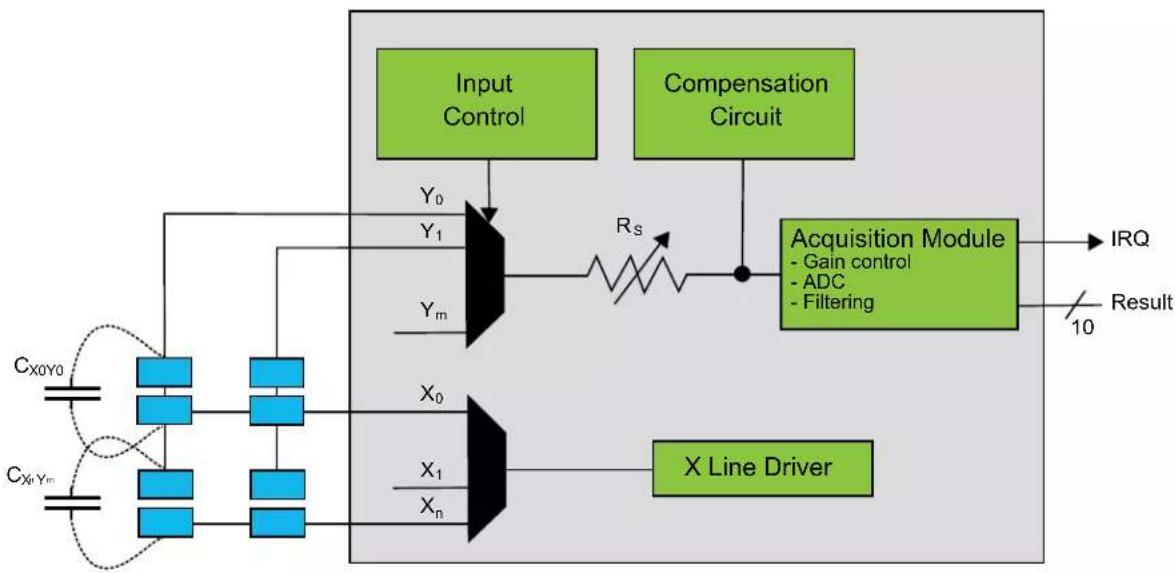
flowchart
graph TD
    A["Input Control"] --> B["Compensation Circuit"]
    B --> C["Acquisition Module"]
    C --> D["Result"]
    E["Cx0y0"] --> F["X0"]
    G["CxnYm"] --> H["X1"]
    I["Xn"] --> J["X0"]
    K["Y0"] --> L["Y1"]
    M["Ym"] --> N["Y0"]
    O["Rs"] --> P["Switch"]
    P --> C
    Q["IRQ"] --> C
    R["10"] --> C
Figure 31-2. PTC Block Diagram Self-Capacitance
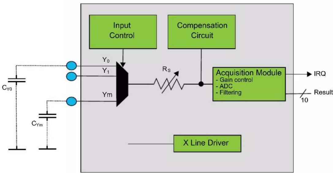
flowchart
graph TD
    A["Input Control"] --> B["Compensation Circuit"]
    B --> C["Acquisition Module"]
    C --> D["Result"]
    E["X Line Driver"] --> C
    F["C_Y0"] --> G["Y_0"]
    H["C_Ym"] --> I["Y_1"]
    J["R_S"] --> C
    K["- Gain control"] --> C
    L["- ADC"] --> C
    M["- Filtering"] --> C
    N["IRQ"] --> C
    O["10"] --> C
31.4 Signal Description
Table 31-1. Signal Description for PTC
| Name Type Description | |
| Y[m:0] Analog Y-line (Input/Output) |
| ......continued | ||
| Name Type Description | ||
| X[n:0] Digital X-line (Output) | ||
Note: The number of X- and Y-lines are device dependent. Refer to Configuration Summary for details.
Refer to I/O Multiplexing and Considerations for details on the pin mapping for this peripheral. One signal can be mapped on several pins.
31.5 System Dependencies
In order to use this Peripheral, configure the other components of the system as described in the following sections.
31.5.1 I/O Lines
The I/O lines used for analog X-lines and Y-lines must be connected to external capacitive touch sensor electrodes. External components are not required for normal operation. However, to improve the EMC performance, a series resistor of 1 kΩ or more can be used on X-lines and Y-lines.
31.5.1.1 Mutual-Capacitance Sensor Arrangement
A mutual-capacitance sensor is formed between two I/O lines - an X electrode for transmitting and Y electrode for sensing. The mutual capacitance between the X and Y electrode is measured by the Peripheral Touch Controller.
Figure 31-3. Mutual Capacitance Sensor Arrangement
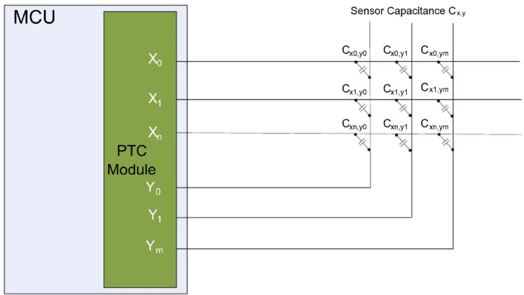
flowchart
graph LR
    MCU["MCU"] --> PTCModule["PTC Module"]
    PTCModule -->|X₀, X₁, Xₙ| SensorCapacitance["Cₓ,y"]
    PTCModule -->|Y₀, Y₁, Yₘ| SensorCapacitance
    SensorCapacitance -->|Cₓ₀,y₀, Cₓ₀,y₁, Cₓ₀,yₘ| Output1
    SensorCapacitance -->|Cₓ₁,y₀, Cₓ₁,y₁, Cₓ₁,yₘ| Output2
    SensorCapacitance -->|Cₓₙ,y₀, Cₓₙ,y₁, Cₓₙ,yₘ| Output3
31.5.1.2 Self-Capacitance Sensor Arrangement
A self-capacitance sensor is connected to a single pin on the Peripheral Touch Controller through the Y electrode for sensing the signal. The sense electrode capacitance is measured by the Peripheral Touch Controller.
Figure 31-4. Self-Capacitance Sensor Arrangement
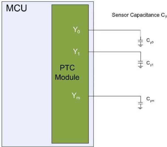
text_image
MCU Y₀ Y₁ PTC Module Yₘ Sensor Capacitance Cᵧ Cᵧ₀ Cᵧ₁ CᵧₘFor more information about designing the touch sensor, refer to Buttons, Sliders and Wheels Touch Sensor Design Guide.
31.6 Functional Description
In order to access the PTC, the user must use the Atmel Start QTouch Configurator to configure and link the QTouch Library firmware with the application software. QTouch Library can be used to implement buttons, sliders, and wheels in a variety of combinations on a single interface.
Figure 31-5. QTouch Library Usage
flowchart
graph TD
    A["Custom Code"] --> B["Compiler"]
    B --> C["Link"]
    C --> D["Application"]
    B --> E["QTouch Library"]
For more information about QTouch Library, refer to the QTouch Library Peripheral Touch Controller User Guide.
32. Electrical Characteristics at 85°C
32.1 Disclaimer
All typical values are measured at T = 25^ unless otherwise specified. All minimum and maximum values are valid across operating temperature and voltage unless otherwise specified.
32.2 Absolute Maximum Ratings
Stresses beyond those listed in the following table may cause permanent damage to the device. This is a stress rating only and functional operation of the device at these or other conditions beyond those indicated in the operational sections of this specification is not implied. Exposure to absolute maximum rating conditions for extended periods may affect device reliability.
Table 32-1. Absolute maximum ratings
| Symbol Parameter Min. Max. Units | ||||
| V_DD | Power supply voltage 0 3.8 V | |||
| I_VDD | Current into a V_DD pin - 92 | (1) | mA | |
| I_GND | Current out of a GND pin - 130 | (1) | mA | |
| V_PIN | Pin voltage with respect to GND and V_DD | GND-0.6V V | _DD+0.6V V | |
| T_storage | Storage temp | -60 | 150 | °C |
Note:
- Maximum source current is 46 mA and maximum sink current is 65 mA per cluster. A cluster is a group of GPIOs as shown in the following table. Each V_DD/GND pair is connected to 2 clusters, hence current consumption through the pair will be a sum of the clusters source/sink currents.
Table 32-2. GPIO Clusters
| PACKAGE | CLUSTER | GPIO | SUPPLY PINS CONNECTED TO THE CLUSTER | ||||||||||||||
| 64pins TQFP and VQFN | 1 | PB31 | PB30 | PA31 | PA30 | VDDIN pin56/GND pin54 | |||||||||||
| 2 PA28 | PA27 | PB23 | PB22 | VDDIN pin56/GND pin54 and VDDIO pin 48/GND pin47 | |||||||||||||
| 3 | PA25 | PA24 | PA23 | PA22 | PA21 | PA20 | PB17 | PB16 | PA19 | PA18 | PA17 | PA16 | VDDIO pin 48/GND pin47 and VDDIO pin34/GND pin33 | ||||
| 4 | PA15 | PA14 | PA13 | PA12 | PB15 | PB14 | PB13 | PB12 | PB11 | PB10 | VDDIO pin 34/GND pin33 and VDDIO pin21/GND pin22 | ||||||
| 5 | PA11 | PA10 | PA09 | PA08 | VDDIO pin21/GND pin22 | ||||||||||||
| 6 | PA07 | PA06 | PA05 | PA04 | PB09 | PB08 | PB07 | PB06 | VDDANA pin 8/GNDANA pin7 | ||||||||
| 7 | PB05 | PB04 | PA03 | PA02 | PA01 | PA00 | PB03 | PB02 | PB01 | PB00 | VDDANA pin 8/GNDANA pin7 | ||||||
| 64 balls UFBGA | 1 | PB31 | PB30 | PA31 | PA30 | VDDIN pin A3, GND pin A5 | |||||||||||
| 2 PA28 | PA27 | PB23 | PB22 | VDDIN pin A3, GND pin A5 VDD pin B8, GND pin C8 | |||||||||||||
| 3 | PA25 | PA24 | PA23 | PA22 | PA21 | PA20 | PB17 | PB16 | PA19 | PA18 | PA17 | PA16 | VDD pin B8, GND pin C8 VDD pin G8, GND pin H8 | ||||
| 4 | PA15 | PA14 | PA13 | PA12 | PB15 | PB14 | PB13 | PB12 | PB11 | PB10 | VDD pin G8, GND pin H8 VDD pin H3, GND pin H4 | ||||||
| 5 | PA11 | PA10 | PA09 | PA08 | VDD pin H3, GND pin H4 | ||||||||||||
| 6 | PA07 | PA06 | PA05 | PA04 | PB09 | PB08 | PB07 | PB06 | VDDANA pin E1, GNDANA pin D1 | ||||||||
| 7 | PB05 | PB04 | PA03 | PA02 | PA01 | PA00 | PB03 | PB02 | PB01 | PB00 | VDDANA pin E1, GNDANA pin D1 | ||||||
| P A K G A L E C L U S T E R | SUPPLY PINS CONNECTED TO THE CLUSTER | ||||||||||||||||||||
| 48pins TQFP and VQFN | 1 PA31 | PA30 VDDIN pin44/GND pin42 | |||||||||||||||||||
| 2 PA28 | PA27 PB23 PB22 | VDDIN pin44/GND pin42 and VDDIO pin36/GND pin35 | |||||||||||||||||||
| 3 PA25 | PA24 PA23 PA22 | PA21 PA20 PA19 | PA18 PA17 | PA16 PA15 | PA14 PA13 | PA12 PB11 | PB10 | VDDIO pin36/GND pin35 and VDDIO pin17/GND pin18 | |||||||||||||
| 4 PA11 | PA10 PA09 PA08 | VDDIO pin17/GND pin18 | |||||||||||||||||||
| 5 PA07 | PA06 PA05 PA04 | PB09 PB08 | VDDANA pin6/GNDANA pin5 | ||||||||||||||||||
| 6 PA03 | PA02 PA01 PA00 | PB03 PB02 | VDDANA pin6/GNDANA pin5 | ||||||||||||||||||
| 45 pins WLCSP | 1 PA31 | PA30 VDDIN pin A10, GND pin A6 | |||||||||||||||||||
| 2 PA28 | PA27 | VDDIN pin A10, GND pin A6 VDD pin B3, GND pin C4 | |||||||||||||||||||
| 3 PA25 | PA24 PA23 PA22 | PA21 PA19 | PA18 PA17 | PA16 PA15 | PA14 PA13 | PA12 | VDD pin B3, GND pin C4 VDD pin G8, GND pin G6 | ||||||||||||||
| 4 PA11 | PA10 PA09 PA08 | VDD pin G8, GND pin G6 | |||||||||||||||||||
| 5 PA07 | PA06 PA05 PA04 | PB09 PB08 | VDDANA pin E12, GNDANA pin D13 | ||||||||||||||||||
| 6 PB04 | PA03 PA02 PA01 | PA00 PB03 | PB02 | VDDDANA pin E12, GNDANA pin D13 | |||||||||||||||||
| 32pins TQFP and VQFN | 1 PA31 | PA30 VDDIN pin30/GND pin 28 | |||||||||||||||||||
| 2 PA28 | PA27 PA25 PA24 | PA23 PA22 PA19 | PA18 PA17 | PA16 PA15 | PA14 PA11 | PA10 PA09 | PA08 | VDDIN pin30/GND pin 28 and VDDANA pin9/GND pin10 | |||||||||||||
| 3 PA07 | PA06 PA05 PA04 | PA03 PA02 PA01 | PA00 | VDDANA pin9/GND pin10 | |||||||||||||||||
| 27 balls WLCSP | 1 PA31 | PA30 VDDIN pin C1, GND pin C5 | |||||||||||||||||||
| 2 PA28 | PA19 PA18 PA17 | PA16 PA15 | PA14 | PA11 PA10 | PA09 | PA08 | VDDIN pin C1, GND pin C5 VDDANA pin B6, GND pin C5 | ||||||||||||||
| 3 PA07 | PA06 PA05 PA04 | PA03 PA02 PA01 | PA00 | VDDANA pin B6, GND pin C5 | |||||||||||||||||
32.3 General Operating Ratings
The device must operate within the ratings listed in the table in order for all other electrical characteristics and typical characteristics of the device to be valid.
Table 32-3. General operating conditions
| Symbol | Parameter | Min. | Typ. | Max. | Units |
| V_DD | Power supply voltage | 1.62(1) | 3.3 | 3.63 | V |
| V_DDANA | Analog supply voltage | 1.62(1) | 3.3 | 3.63 | V |
| T_A | Temperature range | -40 | 25 | 85 | °C |
| T_J | Junction temperature | - | - | 100 | °C |
Note: 1. With BOD33 disabled. If the BOD33 is enabled, check BOD LEVEL value Table 32-19.
Note: 2. In debugger cold-plugging mode, NVM erase operations are not protected by the BOD33 and BOD12. NVM erase operation at supply voltages below specified minimum can cause corruption of NVM areas that are mandatory for correct device behavior.
32.4 Supply Characteristics
The following characteristics are applicable to the operating temperature range: T_A = -40^ to 85^ , unless otherwise specified and are valid for a junction temperature up to T_J = 100^ .
Table 32-4. Supply Characteristics
| Symbol Conditions Voltage | |||
| Min. Max. Units | |||
| V_DDIO | Full Voltage Range 1.62 3.63 V | ||
| V_DDIN | |||
| V_DDANA | |||
Table 32-5. Supply Rise Rates
| Symbol Parameter Rise Rate Units | |||
| Max. | |||
| V_DDIO V_DDIN V_DDANA | DC supply peripheral I/Os, internal regulator and analog supply voltage 0.1 V/μs | ||
Related Links
7. Power Supply and Start-Up Considerations
32.5 Maximum Clock Frequencies
Table 32-6. Maximum GCLK Generator Output Frequencies
| Symbol Description | Max. | Units | ||
| f_GCLKGEN0/f_GCLK\_MAIN | GCLK Generator Output Frequency | 48 | MHz | |
| f_GCLKGEN1 | ||||
| f_GCLKGEN2 | ||||
| f_GCLKGEN3 | ||||
| f_GCLKGEN4 | ||||
| f_GCLKGEN5 | ||||
| f_GCLKGEN6 | ||||
| f_GCLKGEN7 | ||||
Table 32-7. Maximum Peripheral Clock Frequencies
| Symbol | Description | Max. | Units |
| f_CPU | CPU clock frequency | 48 | MHz |
| f_AHB | AHB clock frequency | 48 | MHz |
| f_APBA | APBA clock frequency | 48 | MHz |
| f_APBB | APBB clock frequency | 48 | MHz |
| f_APBC | APBC clock frequency | 48 | MHz |
| f_GCLK\_DFLL48M\_REF | DFLL48M Reference clock frequency | 35.1 | kHz |
| f_GCLK\_WDT | WDT input clock frequency | 48 | MHz |
| f_GCLK\_RTC | RTC input clock frequency | 48 | MHz |
| f_GCLK\_EIC | EIC input clock frequency | 48 | MHz |
| f_GCLK\_EVSYS\_CHANNEL\_0 | EVSYS channel 0 input clock frequency | 48 | MHz |
| f_GCLK\_EVSYS\_CHANNEL\_1 | EVSYS channel 1 input clock frequency | 48 | MHz |
| f_GCLK\_EVSYS\_CHANNEL\_2 | EVSYS channel 2 input clock frequency | 48 | MHz |
| f_GCLK\_EVSYS\_CHANNEL\_3 | EVSYS channel 3 input clock frequency | 48 | MHz |
| f_GCLK\_EVSYS\_CHANNEL\_4 | EVSYS channel 4 input clock frequency | 48 | MHz |
| f_GCLK\_EVSYS\_CHANNEL\_5 | EVSYS channel 5 input clock frequency | 48 | MHz |
| f_GCLK\_EVSYS\_CHANNEL\_6 | EVSYS channel 6 input clock frequency | 48 | MHz |
| f_GCLK\_EVSYS\_CHANNEL\_7 | EVSYS channel 7 input clock frequency | 48 | MHz |
| f_GCLK\_SERCOMx\_SLOW | Common SERCOM slow input clock frequency | 48 | MHz |
| f_GCLK\_SERCOM0\_CORE | SERCOM0 input clock frequency | 48 | MHz |
| f_GCLK\_SERCOM1\_CORE | SERCOM1 input clock frequency | 48 | MHz |
| Symbol Description Max. Units | |||
| f_GCLK\_SERCOM2\_CORE | SERCOM2 input clock frequency 48 MHz | ||
| f_GCLK\_SERCOM3\_CORE | SERCOM3 input clock frequency 48 MHz | ||
| f_GCLK\_SERCOM4\_CORE | SERCOM4 input clock frequency 48 MHz | ||
| f_GCLK\_SERCOM5\_CORE | SERCOM5 input clock frequency 48 MHz | ||
| f_GCLK\_TC0, GCLK\_TC1 | TC0,TC1 input clock frequency 48 MHz | ||
| f_GCLK\_TC2, GCLK\_TC3 | TC2,TC3 Input clock frequency 48 MHz | ||
| f_GCLK\_TC4, GCLK\_TC5 | TC4,TC5 input clock frequency 48 MHz | ||
| f_GCLK\_TC6, GCLK\_TC7 | TC6,TC7 input clock frequency 48 MHz | ||
| f_GCLK\_ADC | ADC input clock frequency 48 MHz | ||
| f_GCLK\_AC\_DIG | AC digital input clock frequency 48 MHz | ||
| f_GCLK\_AC\_ANA | AC analog input clock frequency 64 kHz | ||
| f_GCLK\_DAC | DAC input clock frequency 48 MHz | ||
| f_GCLK\_PTC | PTC input clock frequency 48 MHz |
32.6 Power Consumption
The values provided in the following table are measured values of power consumption under the following conditions, except where noted:
- Operating conditions
- V_VDDIN = 3.3V
- Wake up time from Sleep mode is measured from the edge of the wakeup signal to the execution of the first instruction fetched in Flash.
- Oscillators
- XOSC (crystal oscillator) stopped
- XOSC32K (32 kHz crystal oscillator) running with external 32 kHz crystal
- DFLL48M using XOSC32K as reference and running at 48 MHz
- Clocks
- DFLL48M used as main clock source, except otherwise specified.
- CPU, AHB clocks undivided
- APBA clock divided by 4
- APBB and APBC bridges off
• The following AHB module clocks are running: NVMCTRL, APBA bridge
- All other AHB clocks stopped
• The following peripheral clocks running: PM, SYSCTRL, RTC
- All other peripheral clocks stopped
• I/Os are inactive with internal pull-up
• CPU is running on Flash with 1 wait states
• NVMCTRL cache enabled
• BOD33 disabled
Table 32-8. Current Consumption - Device Variant A
| Mode Conditions T | A | Min. | Typ. Max. Units | |||
| ACTIVE | CPU running a While(1) algorithm | 25°C | 2.13 2.33 | 2.52 | mA | |
| 85°C | 2.24 2.44 | 2.63 | ||||
| CPU running a While(1) algorithm V_DDIN =1.8V, CPU is running on Flash with 3 wait states | 25°C | 2.13 2.34 | 2.53 | |||
| 85°C | 2.26 2.45 | 2.64 | ||||
| CPU running a While(1) algorithm, CPU is running on Flash with 3 wait states with GCLKIN as reference | 25°C | -42*freq | +118 - | μA(with freq in MHz) | ||
| 85°C | -42*freq | +208 - | ||||
| CPU running a Fibonacci algorithm | 25°C | 3.63 4.03 | 4.37 | mA | ||
| 85°C | 3.74 4.12 | 4.44 | ||||
| CPU running a Fibonacci algorithm V_DDIN =1.8V, CPU is running on Flash with 3 wait states | 25°C | 3.64 4.03 | 4.37 | |||
| 85°C | 3.76 4.13 | 4.44 | ||||
| CPU running a Fibonacci algorithm, CPU is running on Flash with 3 wait states with GCLKIN as reference | 25°C | -80*freq | +118 - | μA(with freq in MHz) | ||
| 85°C | -80*freq | +208 - | ||||
| CPU running a CoreMark algorithm | 25°C | 5.22 5.72 | 6.16 | mA | ||
| 85°C | 5.36 5.89 | 6.37 | ||||
| CPU running a CoreMark algorithm V_DDIN =1.8V, CPU is running on Flash with 3 wait states | 25°C | 4.58 4.95 | 5.27 | |||
| 85°C | 4.74 5.10 | 5.42 | ||||
| CPU running a CoreMark algorithm, CPU is running on Flash with 3 wait states with GCLKIN as reference | 25°C | -94*freq | +118 - | μA(with freq in MHz) | ||
| 85°C | -96 * freq | +210 - | ||||
| IDLE0 | 25°C | 1.24 1.35 | 1.45 | mA | ||
| 85°C | 1.31 1.45 | 1.57 | ||||
| IDLE1 | 25°C | 0.87 0.95 | 1.03 | |||
| 85°C | 0.91 1.03 | 1.13 | ||||
| IDLE2 | 25°C | 0.72 0.78 | 0.85 | |||
| 85°C | 0.76 0.86 | 0.96 | ||||
| STANDBY | XOSC32K runningRTC running at 1 kHz(1) | 25°C | -3.80 11.95 | μA | ||
| 85°C | 39.91 | 100 | ||||
| XOSC32K and RTC stopped(1) | 25°C | -2.46 11.13 | ||||
| 85°C | 38.23 | 100 | ||||
Note:
- Measurements were done with SYSCTRL->VREG.bit.RUNSTDBY = 0.
Table 32-9. Current Consumption - Device Variant B
| Mode Conditions T | A | Vcc | Min. Typ. | Max. Units | |||
| ACTIVE | CPU running a While(1) algorithm | 25°C | 3.3V - 2.27 | 2.30 | mA | ||
| 85°C | 3.3V - 2.32 | 2.36 | |||||
| CPU running a While(1) algorithm | 25°C | 1.8V - 2.27 | 2.30 | ||||
| 85°C | 1.8V - 2.33 | 2.37 | |||||
| CPU running a While(1) algorithm, with GCLKIN as reference | 25°C | 3.3V - 43*freq | +108 | 44*freq +108 | μA(with freq in MHz) | ||
| 85°C | 3.3V - 44*freq | +148 | 45*freq +147 | ||||
| CPU running a Fibonacci algorithm | 25°C | 3.3V - 3.04 | 3.07 | mA | |||
| 85°C | 3.3V - 3.09 | 3.12 | |||||
| CPU running a Fibonacci algorithm | 25°C | 1.8V - 3.04 | 3.08 | ||||
| 85°C | 1.8V - 3.09 | 3.12 | |||||
| CPU running a Fibonacci algorithm, with GCLKIN as reference | 25°C | 3.3V - 59*freq | +109 | 60*freq +109 | μA(with freq in MHz) | ||
| 85°C | 3.3V - 60*freq | +149 | 60*freq +149 | ||||
| CPU running a CoreMark algorithm | 25°C | 3.3V - 3.90 | 3.95 | mA | |||
| 85°C | 3.3V - 4.03 | 4.07 | |||||
| CPU running a CoreMark algorithm | 25°C | 1.8V - 3.51 | 3.55 | ||||
| 85°C | 1.8V - 3.59 | 3.63 | |||||
| CPU running a CoreMark algorithm, with GCLKIN as reference | 25°C | 3.3V - 77* | freq +108 | 78* freq +110 | μA(with freq in MHz) | ||
| 85°C | 3.3V - | 79 * freq + 146 | 80* freq +147 | ||||
| IDLE0 | 25°C | 3.3V - 1.28 | 1.29 | mA | |||
| 85°C | 3.3V - 1.32 | 1.34 | |||||
| IDLE1 | 25°C | 3.3V - 0.95 | 0.98 | ||||
| 85°C | 3.3V - 0.99 | 1.01 | |||||
| IDLE2 | 25°C | 3.3V - 0.76 | 0.76 | ||||
| 85°C | 3.3V - 0.78 | 0.79 | |||||
| STANDBY | XOSC32K runningRTC running at 1 kHz(2) | 25°C | 3.3V - 2.47 | - | μA | ||
| 85°C | 3.3V | - | 17.74 | 94 | |||
| XOSC32K and RTC stopped(2) | 25°C | 3.3V - 1.35 | |||||
| 85°C | 3.3V - | 16.38 | 90 | ||||
Notes:
- These values are based on characterization.
- Measurements were done with SYSCTRL->VREG.bit.RUNSTDBY = 0.
Table 32-10. Wake-up Time
| Mode | Conditions | T_A | Min. | Typ. | Max. Units |
| IDLE0 | OSC8M used as main clock source, cache disabled | 25°C | 3.3 | 4.0 | 4.5 |
| 85°C | 3.4 | 4.0 | 4.5 | ||
| IDLE1 | OSC8M used as main clock source, cache disabled | 25°C | 10.5 12.1 | 13.7 | |
| 85°C | 12.1 13.6 | 15.0 | |||
| IDLE2 | OSC8M used as main clock source, cache disabled | 25°C | 11.7 13.0 | 14.3 | |
| 85°C | 13.0 14.5 | 15.9 | |||
| STANDBY | OSC8M used as main clock source, cache disabled | 25°C | 17.5 19.6 | 21.4 | |
| 85°C | 18.0 19.7 | 21.4 |
Figure 32-1. Measurement Schematic
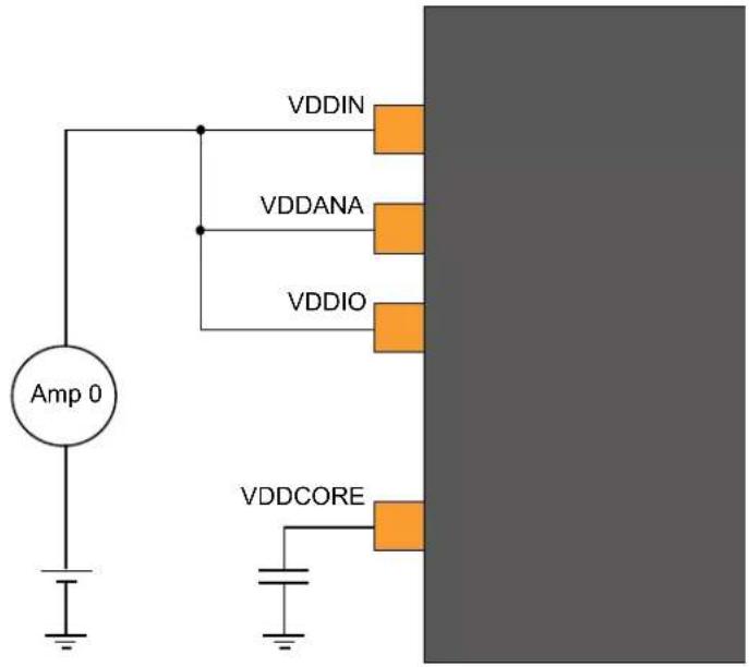
text_image
VDDIN VDDANA VDDIO Amp 0 VDDCORE32.7 Peripheral Power Consumption
Default conditions, except where noted:
- Operating conditions
$$ - \mathrm{V} _ {\text { VDDIN }} = 3. 3 \mathrm{V} $$
- Oscillators
- XOSC (crystal oscillator) stopped
- XOSC32K (32 kHz crystal oscillator) running with external 32kHz crystal
- OSC8M at 8MHz
- Clocks
- OSC8M used as main clock source
- CPU, AHB and APBn clocks undivided
- The following AHB module clocks are running: NVMCTRL, HPB2 bridge, HPB1 bridge, HPB0 bridge – All other AHB clocks stopped
- The following peripheral clocks running: PM, SYSCTRL – All other peripheral clocks stopped
• I/Os are inactive with internal pull-up
- CPU in IDLE0 mode
- Cache enabled
- BOD33 disabled
In this default conditions, the power consumption I_default is measured.
Operating mode for each peripheral in turn:
- Configure and enable the peripheral GCLK (When relevant, see conditions)
- Unmask the peripheral clock
- Enable the peripheral (when relevant)
- Set CPU in IDLE0 mode
- Measurement I periph
- Wake-up CPU via EIC (async: level detection, filtering disabled)
- Disable the peripheral (when relevant)
- Mask the peripheral clock
- Disable the peripheral GCLK (when relevant, see conditions)
Each peripheral power consumption provided in table x-9 is the value ( I_periph - I_default ), using the same measurement method as for global power consumption measurement.
Table 32-11. Typical Peripheral Power Consumption
| Peripheral Conditions Typ. Units | |||
| RTC f | _GCLK\_RTC = 32kHz, 32 bit counter mode 5.6 μA | ||
| WDT f | _GCLK\_WDT = 32kHz, normal mode with EW 4.2 | ||
| AC Both f | _GCLK = 8MHz, Enable both COMP 25.8 | ||
| TCx(1) | f_GCLK = 8MHz, Enable + COUNTER in 8 bit mode 41.5 | ||
| SERCOMx.I2CM(2) | f_GCLK = 8MHz, Enable | 50.3 | |
| SERCOMx.I2CS(2) | f_GCLK = 8MHz, Enable | 23.6 | |
| SERCOMx.SPI(2) | f_GCLK = 8MHz, Enable | 47.9 | |
| SERCOMx.USART(2) | f_GCLK = 8MHz, Enable | 47.6 | |
Notes: 1. All TCs share the same power consumption values.
- All SERCOMs share the same power consumption values.
32.8 I/O Pin Characteristics
32.8.1 Normal I/O Pins
Table 32-12. RevD and later normal I/O Pins Characteristics
| Symbol | Parameter Conditions Min. Typ. Max. Units | |||||
| R_PULL | Pull-up - Pull-down resistance 20 40 60 kΩ | |||||
| V_IL | Input low-level voltage V | _DD=1.62V-2.7V--0.25*V | _DD | V | ||
| V_DD=2.7V-3.63V--0.3*V | _DD | |||||
| V_IH | Input high-level voltage | V_DD=1.62V-2.7V 0.7*V | _DD | - | - | |
| V_DD=2.7V-3.63V 0.55*V | _DD | - | - | |||
| V_OL | Output low-level voltage | V_DD>1.6V, I_OLmax | -0.1*V | _DD | 0.2* V_DD | |
| V_OH | Output high-level voltage | V_DD>1.6V, I_OHmax | 0.8* V_DD | 0.9* V_DD | - | |
| I_OL | Output low-level current | V_DD=1.62V-3V, PORT.PINCFG.DRVSTR=0 | -- | 1 | mA | |
| V_DD=3V-3.63V, PORT.PINCFG.DRVSTR=0 | -- | 2.5 | ||||
| V_DD=1.62V-3V, PORT.PINCFG.DRVSTR=1 | -- | 3 | ||||
| V_DD=3V-3.63V, PORT.PINCFG.DRVSTR=1 | -- | 10 | ||||
| I_OH | Output high-level current | V_DD=1.62V-3V, PORT.PINCFG.DRVSTR=0 | -- | 0.7 | ||
| V_DD=3V-3.63V, PORT.PINCFG.DRVSTR=0 | -- | 2 | ||||
| V_DD=1.62V-3V, PORT.PINCFG.DRVSTR=1 | -- | 2 | ||||
| V_DD=3V-3.63V, PORT.PINCFG.DRVSTR=1 | -- | 7 | ||||
| t_RISE | Rise time(1) | PORT.PINCFG.DRVSTR=0 load = 5pF, V_DD=3.3V | -- | 15 ns | ||
| PORT.PINCFG.DRVSTR=1 load = 20pF, V_DD=3.3V | -- | 15 | ||||
| t_FALL | Fall time(1) | PORT.PINCFG.DRVSTR=0 load = 5pF, V_DD=3.3V | -- | 15 | ||
| PORT.PINCFG.DRVSTR=1 load = 20pF, V_DD=3.3V | -- | 15 | ||||
| I_LEAK | Input leakage current | Pull-up resistors disabled | -1 | +/-0.015 | 1 | μA |
Note: 1. These values are based on simulation. These values are not covered by test limits in production or characterization.
Table 32-13. SAMD20 revC/revB Normal I/O Pins Characteristics
| Symbol | Parameter | Conditions | Min. | Typ. | Max. | Units |
| R_PULL | Pull-up - Pull-down resistance | 20 | 40 | 60 | kΩ | |
| Symbol | Parameter Conditions Min. Typ. Max. Units | |||||
| V_IL | Input low-level voltage V | _DD=1.62V-2.7V--0.25*V | _DD | V | ||
| V_DD=2.7V-3.63V--0.3*V | _DD | |||||
| V_IH | Input high-level voltage V | _DD=1.62V-2.7V 0.7*V | _DD | - | - | |
| V_DD=2.7V-3.63V 0.55*V | _DD | - | - | |||
| V_OL | Output low-level voltage V | _DD>1.6V, I_OLmax - 0.1*V | _DD | 0.2*V_DD | ||
| V_OH | Output high-level voltage V | _DD>1.6V, I_OHmax | 0.8*V_DD | 0.9*V_DD | - | |
| I_OL | Output low-level current | V_DD=1.6V-3V | --8 | mA | ||
| V_DD=3V-3.63V | --20 | |||||
| I_OH | Output high-level current V | _DD=1.6V-3V | --4.5 | |||
| V_DD=3V-3.63V | --10 | |||||
| t_RISE | Rise time(1) | load = 30pF, V_DD=3.3V ,slope range [10%-90%] | -7 | -ns | ||
| t_FALL | Fall time(1) | -9.5 | - | |||
| I_LEAK | Input leakage current(2) | Pull-up resistorsdisabled | -1 +/-0.015 | 1 | μA | |
Notes:
- These values are based on simulation. These values are not covered by test limits in production or characterization.
- For PA22 of WLCSP27 Package -2 A <= I _LEAK <= 2 A .
32.8.2 I²C Pins
Refer to I/O Multiplexing and Considerations to get the list of I²C pins.
Table 32-14. I²C Pins Characteristics in I²C configuration
| Symbol | Parameter | Condition | Min. | Typ. | Max. | Units |
| R_PULL | Pull-up - Pull-down resistance | 20 | 40 | 60 | kΩ | |
| V_IL | Input low-level voltage | V_DD=1.62V-2.7V | - | - | 0.25* V_DD | V |
| V_DD=2.7V-3.63V | - | - | 0.3* V_DD | |||
| V_IH | Input high-level voltage | V_DD=1.62V-2.7V | 0.7* V_DD | - | - | |
| V_DD=2.7V-3.63V | 0.55* V_DD | - | - | |||
| V_HYS | Hysteresis of Schmitt trigger inputs | 0.08* V_DD | - | - | ||
| V_OL | Output low-level voltage | V_DD>2.0V I_OL=3mA | - | - | 0.4 | |
| V_DD≤ 2.0V I_OL=2mA | - | - | 0.2* V_DD | |||
| I_OL | Output low-level current | V_OL=0.4V | 3 | - | - | mA |
| V_OL=0.6V | 6 | - | - | |||
| f_SCL | SCL clock frequency | - | - | 400 | kHz |
I^2C pins timing characteristics can be found in 32.14.3. SERCOM in I2C Mode Timing
Related Links
- I/O Multiplexing and Considerations
32.8.3 XOSC Pin
XOSC pins behave as normal pins when used as normal I/Os. Refer to Table 32-12
32.8.4 XOSC32 Pin
XOSC32 pins behave as normal pins when used as normal I/Os. Refer to Table 32-12.
32.8.5 External Reset Pin
Reset pin has the same electrical characteristics as normal I/O pins. Refer to Table 32-12.
32.9 Injection Current
Stresses beyond those listed in the table below may cause permanent damage to the device. This is a stress rating only and functional operation of the device at these or other conditions beyond those indicated in the operational sections of this specification is not implied. Exposure to absolute maximum rating conditions for extended periods may affect device reliability.
Table 32-15. Injection Current ^(1)
| Symbol Description min max Unit | ||||
| linj1^(2) | IO pin injection current -1 +1 mA | |||
| linj2^(3) | IO pin injection current -15 +15 mA | |||
| linjtotal | Sum of IO pins injection current -45 +45 mA | |||
Notes:
- Injecting current may have an effect on the accuracy of Analog blocks
- Conditions for V_pin : V_pin < GND - 0.6V or 3.6V < V_pin ≤ 4.2V .
Conditions for V_DD : 3V < V_DD ≤ 3.6V .
If V_pin is lower than GND-0.6V, then a current limiting resistor is required. The negative DC injection current limiting resistor R is calculated as R = | (GND - 0.6V - V_pin) / I_inj1 | .
If V_pin is greater than V_DD+0.6V , a current limiting resistor is required. The positive DC injection current limiting resistor R is calculated as R = (V_pin - (V_DD + 0.6V)) / I_inj1 .
- Conditions for V_pin : V_pin < GND-0.6V or V_pin ≤ 3.6V .
Conditions for V_DD : V_DD ≤ 3V .
If V_pin is lower than GND-0.6V, a current limiting resistor is required. The negative DC injection current limiting resistor R is calculated as R = | (GND - 0.6V - V_pin)/I_inj2 | .
If V_pin is greater than V_DD+0.6V , a current limiting resistor is required. The positive DC injection current limiting resistor R is calculated as R = (V_pin-(V_DD+0.6V))/I_inj2 .
32.10 Analog Characteristics
32.10.1 Voltage Regulator Characteristics
Table 32-16. Voltage Regulator Electrical Characteristics
| Symbol | Parameter | Conditions | Min. | Typ. | Max. | Units |
| V_DDCORE | DC calibrated output voltage | Voltage regulator normal mode | 1.1 | 1.23 | 1.30 | V |
Note: Supplying any external components using V_DDCORE pin is not allowed to assure the integrity of the core supply voltage.
Table 32-17. Decoupling Requirements
| Symbol | Parameter | Conditions | Min. | Typ. | Max. | Units |
| C_IN | Input regulator capacitor, between V_DDIN and GND | - | 1 | - μF | ||
| C_OUT | Output regulator capacitor, between V_DDCORE and GND | 0.8 | 1 | - μF |
32.10.2 Power-On Reset (POR) Characteristics
Table 32-18. POR Characteristics
| Symbol Parameter Conditions Min. Typ. Max. Units | ||||||
| V_POT+ | Voltage threshold on V_DD rising V | _DD falls at 1V/ms or slower 1.27 1.45 1.58 V | ||||
| V_POT- | Voltage threshold on V_DD falling 0.72 0.99 1.32 V | |||||
Figure 32-2. POR Operating Principle
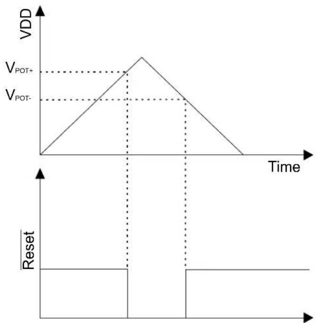
line
| Time | VDD | |------|-----| | 0 | 0 | | Peak | V_POT+ | | Peak | V_POT- | | Final | 0 |32.10.3 Brown-Out Detectors Characteristics
32.10.3.1 BOD33
Figure 32-3. BOD33 Hysteresis OFF
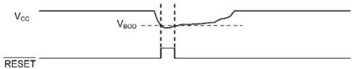
text_image
VCC VBOD RESETFigure 32-4. BOD33 Hysteresis ON
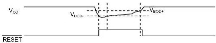
text_image
VCC VBOD- VBD+ RESETTable 32-19. BOD33 LEVEL Value
| Symbol BOD33.LEVEL Conditions Min. Typ. Max. Units | ||||||
| V_BOD+ | 6 | Hysteresis ON | -1.715 1.745 | V | ||
| 7 - 1.750 1.779 | ||||||
| 39 - 2.84 2.92 | ||||||
| 48 - 3.2 3.3 | ||||||
| V_BOD- or V_BOD | 6 | Hysteresis ON or Hysteresis OFF | 1.62 1.64 1.67 | |||
| 7 | 1.64 | 1.675 | 1.71 | |||
| 39 | 2.72 2.77 2.81 | |||||
| 48 | 3.0 3.07 | 3.2 | ||||
Note: Refer to NVM User Row Mapping for the BOD33 in the Memories chapter for the BOD33 default value settings.
Table 32-20. BOD33 Characteristics
| Symbol | Parameter | Conditions | Min. | Typ. | Max. | Units | |
| Step size, between adjacent values in BOD33.LEVEL | - | 34 | - | mV | |||
| V_HYST | V_BOD+-V_BOD- | Hysteresis ON | 35 | - | 170 | mV | |
| t_DET | Detection time | Time with V_DDANA| - | 0.9(1) | - | μs | | |
| t_{STARTUP} | Startup time | - | 2.2(1) | - | μs | ||
| I_{IdleBOD33} | Current consumption in Active/Idle Mode | Continuous mode | 25°C | 25 | 48 | μA | |
| -40 to 85°C | - | 50 | |||||
| Sampling mode | 25°C | 0.034 | 0.21 | ||||
| -40 to 85°C | - | 1.62 | |||||
| I_{SbyBOD33}$ | Current Consumption in Standby mode | Sampling mode | 25°C | 0.132 | 0.38 | μA | |
| -40 to 85°C | - | 1 |
Note:
- These values are based on simulation. These values are not covered by test limits in production or characterization.
Related Links
Table 32-21. Operating Conditions
| Symbol | Parameter | Conditions | Min. | Typ. | Max. | Units |
| RES | Resolution | 8 | - | 12 | bits | |
| _CLK\_ADC | ADC Clock frequency | 30 | - | 2100 | kHz | |
| Sample rate (1) | Single shot | 5 | - | 300 | ksps | |
| Free running | 5 | - | 350 (3) | ksps | ||
| Sampling time (1) | - | 250 - | - ns | |||
| Sampling time with DAC as input(2) | - | 3 | - | - μs | ||
| Sampling time with Temp sens as Input (2) | - | 10 | - | - μs | ||
| Sampling time with Bandgap as input (2) | - | 10 | - | - μs | ||
| Symbol Parameter Conditions Min. Typ. Max. Units | ||||||
| Conversion time (1) | 1x Gain - 6 - cycles | |||||
| V_REF | Voltage reference range, (VREFA or VREFB) - 1.0 - V | DDANA-0.6 V | ||||
| INT1V | Internal 1V reference (2,4) | -1.0 | - | V | ||
| INTVCC0 Internal ratiometric reference 0 | - | V | DDANA/1.48 | - | V | |
| INTVCC0 Voltage Error | Internal ratiometric reference 0 error(2) | -1.0 | - | +1.0 | % | |
| INTVCC1 Internal ratiometric reference 1 | 2.0V < V | DDANA<3.63V | - | V_DDANA/2 | - | V |
| V_INTVCC1 Voltage Error | Internal ratiometric reference 1 error(2) | 2.0V < V_DDANA <3.63V | -1.0 | - | +1.0 | % |
| Conversion range(1) | Differential mode | - V_REF/GAIN | - | + V_REF/GAIN | V | |
| Single-ended mode 0.0 - +V | REF/GAIN | V | ||||
| C_SAMPLE | Sampling capacitance (2) | -3.5 | -pF | |||
| R_SAMPLE | Input channel source resistance (2) | -- | 3.5 | kΩ | ||
| I_DD | DC supply current(1) | f_CLK\_ADC = 2.1 MHz^(3) | - | 1.25 | 1.79 | mA |
Notes:
-
These values are based on characterization. These values are not covered by test limits in production.
-
These values are based on simulation. These values are not covered by test limits in production or characterization.
-
In this condition and for a sample rate of 350 ksps, a conversion takes 6 clock cycles of the ADC clock (conditions: 1X gain, 12-bit resolution, differential mode, free-running).
-
It is the buffered internal reference of 1.0V derived from the internal 1.1V bandgap reference.
Table 32-22. Differential Mode (Device Variant A) ^1,2,3,4
| Symbol | Parameter | Conditions | Min. | Typ. | Max. | Units |
| ENOB | Effective Number Of Bits | With gain compensation | - | 10.5 | 11.1 | bits |
| TUE | Total Unadjusted Error | 1x Gain | 1.5 | 4.3 | 15.0 | LSB |
| INL | Integral Non Linearity | 1x Gain | 1.0 | 1.3 | 4.5 | LSB |
| DNL | Differential Non Linearity | 1x Gain | ±0.3 | ±0.5 | ±0.95 | LSB |
| GE | Gain Error | Ext. Ref 1x | -10.0 | 2.5 | +10.0 | mV |
| V_REF = V_DDANA/1.48 -15.0 | -1.5 +10.0 | mV | ||||
| V_REF = INT1V | -20.0 | -5.0 +20.0 | mV | |||
| Gain Accuracy (5) | Ext. Ref. 0.5x | ±0.1 | ±0.2 | ±0.45 | % | |
| Ext. Ref. 2x to 16x ±0.05 | ±0.1 | ±0.11 | % | |||
| OE | Offset Error | Ext. Ref. 1x | -5.0 | -1.5 | +5.0 | mV |
| V_REF = V_DDANA/1.48 | -5.0 | 0.5 | +5.0 | mV | ||
| V_REF = INT1V | -5.0 | 3.0 | +5.0 | mV | ||
| SFDR Spurious Free Dynamic Range | 1x Gain | 62.7 | 70.0 | 75.0 | dB | |
| SINAD | Signal-to-Noise and Distortion | F_CLK\_ADC=2.1 MHz | 54.1 | 65.0 | 68.5 | dB |
| SNR | Signal-to-Noise Ratio | F_IN=40 kHz | 54.5 | 65.5 | 68.6 | dB |
| THD | Total Harmonic Distortion | A_IN=95% FSR | -77.0 | -64.0 | -63.0 | dB |
| Noise RMS | T=25°C | 0.6 | 1.0 | 1.6 | mV | |
Table 32-23. Differential Mode (Device Variant B) ^1,2,3,4
| Symbol | Parameter | Conditions | Min. | Typ. | Max. | Units |
| ENOB | Effective Number Of Bits | With gain compensation | - | 10.5 | 11.1 | bits |
| TUE | Total Unadjusted Error | 1x Gain | 1.5 | 4.3 | 15 | LSB |
| Symbol | Parameter Conditions Min. Typ. Max. Units | |||||
| INL Integral Non Linearity 1x Gain 1 1.3 4.5 LSB | ||||||
| DNL | Differential Non Linearity | 1x Gain | ±0.3 | ±0.5 | ±0.95 | LSB |
| GE | Gain Error | Ext. Ref 1x | -10 | 2.5 | 10 mV | |
| VREF = VDDANA/1.48 | -15 | -1.5 10 | mV | |||
| VREF = INT1V | -20 | -5 | 20 | mV | ||
| Gain Accuracy^(5) | Ext. Ref. 0.5x | - | ±0.1 | ±0.8 % | ||
| Ext. Ref. 2x to 16x | - | ±0.03 | ±0.5 % | |||
| OE | Offset Error | Ext. Ref. 1x | -5 | -1.5 | 5 | mV |
| VREF=VDDANA/1.48 | -5 | -0.5 | 5 | mV | ||
| VREF = INT1V | -15 | 3 | 20 | mV | ||
| SFDR | Spurious Free Dynamic Range | 1x Gain | 62.7 | 70 | 75 | dB |
| SINAD | Signal-to-Noise and Distortion | F_CLK\_ADC = 2.1 MHz | 54.1 | 65 | 68.5 | dB |
| SNR | Signal-to-Noise Ratio | F_IN = 40 kHz | 54.5 | 65.5 | 68.6 | dB |
| THD | Total Harmonic Distortion | A_IN = 95% FSR | -77 | -64 | -63 | dB |
| Noise RMS | T = 25°C | 0.6 | 1 | 1.6 | mV | |
Notes:
- Maximum numbers are based on characterization and not tested in production, and valid for 5% to 95% of the input voltage range.
- Dynamic parameter numbers are based on characterization and not tested in production.
- Respect the input common mode voltage through the following equations (where VCM_IN is the Input channel common mode voltage):
a. If |V_IN| > V_REF/4
• V_CM_IN < 0.95 * V_DDANA + V_REF/4 - 0.75V
• V_CM_IN > V_REF/4 -0.05 * V_DDANA -0.1V
b. If |V_IN| < V_REF/4
• V_CM_IN < 1.2 × V_DDANA - 0.75V
• V_CM_IN > 0.2 × V_DDANA - 0.1V
-
The ADC channels on pins PA08, PA09, PA10, PA11 are powered from the VDDIO power supply. The ADC performance of these pins will not be the same as all the other ADC channels on pins powered from the VDDANA power supply.
-
The gain accuracy represents the gain error expressed in percent. Gain accuracy (\%) = (Gain Error in V x 100) / (2*VREF/GAIN)
Table 32-24. Single-Ended Mode (Device Variant A) ^1,2,3
| Symbol | Parameter | Conditions | Min. | Typ. | Max. | Units |
| ENOB | Effective Number of Bits | With gain compensation | - | 9.5 | 9.8 | Bits |
| TUE | Total Unadjusted Error | 1x gain | - | 10.5 | 14.0 | LSB |
| INL | Integral Non-Linearity | 1x gain | 1.0 | 1.6 | 3.5 | LSB |
| DNL | Differential Non-Linearity | 1x gain | ±0.5 | ±0.6 | ±0.95 | LSB |
| GE | Gain Error | Ext. Ref. 1x | -5.0 | 0.7 | +5.0 | mV |
| Gain Accuracy^(4) | Ext. Ref. 0.5x ±0.2 ±0.34 ±0.4 % | |||||
| Ext. Ref. 2x to 16X | ±0.01 | ±0.1 | ±0.2 | % | ||
| OE | Offset Error | Ext. Ref. 1x | -5.0 | 1.5 | +5.0 | mV |
| Symbol Parameter Conditions Min. Typ. Max. Units | ||||||
| SFDR Spurious Free Dynamic Range | 1x Gain F_CLK\_ADC = 2.1 MHz F_IN = 40 kHz A_IN = 95% FSR | 63.1 65.0 67.0 dB | ||||
| SINAD Signal-to-Noise and Distortion 47.5 59.5 61.0 dB | ||||||
| SNR Signal-to-Noise Ratio 48.0 60.0 64.0 dB | ||||||
| THD | Total Harmonic Distortion | -65.4 | -63.0 | -62.1 | dB | |
| Noise RMS | T = 25°C | - | 1.0 | - | mV | |
Table 32-25. Single-Ended Mode (Device Variant B) ^(1,2,3)
| Symbol Parameter Conditions Min. Typ. Max. Units | ||||||
| ENOB | Effective Number of Bits | With gain compensation | - | 9.5 | 9.8 | Bits |
| TUE | Total Unadjusted Error | 1x gain | - | 10.5 | 27 | LSB |
| INL | Integral Non-Linearity | 1x gain | 1 | 1.6 | 5 | LSB |
| DNL | Differential Non-Linearity | 1x gain | ±0.5 | ±0.6 | ±0.95 | LSB |
| GE | Gain Error | Ext. Ref. 1x | -5 | 0.7 | 5 | mV |
| Gain Accuracy^(4) | Ext. Ref. 0.5x | ±0.2 | ±0.34 | ±0.6 | % | |
| Ext. Ref. 2x to 16X ±0.01 | ±0.1 ±0.3 | % | ||||
| OE | Offset Error | Ext. Ref. 1x | -5 | 1.5 | 10 | mV |
| SFDR Spurious Free Dynamic Range | 1x Gain | 63.1 | 65 | 67 | dB | |
| SINAD Signal-to-Noise and Distortion 47.5 59.5 61 | dBF_CLK\_ADC = 2.1 MHz | |||||
| SNR | Signal-to-Noise Ratio | F_IN = 40 kHz | 48 | 60 | 64 | dB |
| THD | Total Harmonic Distortion | A_IN = 95% FSR | -65.4 | -63 | -62.1 | dB |
| Noise RMS | T = 25°C | - | 1 | - | mV | |
Notes:
- Maximum numbers are based on the characterization and not tested in production, and for 5% to 95% of the input voltage range.
-
Respect the input common mode voltage through the following equations. Where, VCM_IN is the Input channel common mode voltage for all VIN:
-
VCM_IN < 0.7*VDDANA + VREF/4 - 0.75V
-
VCM_IN > VREF/4 - 0.3*VDDANA - 0.1V
-
The ADC channels on the PA08, PA09, PA10, PA11 pins are powered from the VDDIO power supply. The ADC performance of these pins will not be the same as all the other ADC channels on pins powered from the VDDANA power supply.
- The gain accuracy represents the gain error expressed in percent. Gain accuracy (\%) = (Gain Error in V x 100) / (VREF/GAIN).
32.10.4.1 Performance with the Averaging Digital Feature
Averaging is a feature which increases the sample accuracy. ADC automatically computes an average value of multiple consecutive conversions. The numbers of samples to be averaged is specified by the Number-of-Samples-to-be-collected bit group in the Average Control register (AVGCTRL.SAMPLENUM[3:0]) and the averaged output is available in the Result register (RESULT).
Table 32-26. Averaging feature
| Average Number | Conditions | SNR (dB) | SINAD (dB) | SFDR (dB) | ENOB (bits) |
| 1 | In differential mode, 1x gain, V_DDANA =3.0V, V_REF =1.0V, 350 kspsT=25°C | 66.0 | 65.0 | 72.8 | 9.75 |
| 8 | 67.6 | 65.8 | 75.1 | 10.62 | |
| 32 | 69.7 | 67.1 | 75.3 | 10.85 | |
| 128 | 70.4 | 67.5 | 75.5 | 10.91 |
32.10.4.2 Performance with the hardware offset and gain correction
Inherent gain and offset errors affect the absolute accuracy of the ADC. The offset error cancellation is handled by the Offset Correction register (OFFSETCORR) and the gain error cancellation, by the Gain Correction register (GAINCORR). The offset and gain correction value is subtracted from the converted data before writing the Result register (RESULT).
Table 32-27. Offset and Gain correction feature
| Gain Factor Conditions Offset Error (mV) Gain Error (mV) Total Unadjusted Error (LSB) | |||
| 0.5x In differential mode, 1x gain, V_DDANA = 3.0V , V_REF = 1.0V , 350 kspsT=25°C | 0.25 1.0 2.4 | ||
| 1x 0.20 0.10 1.5 | |||
| 2x 0.15 -0.15 2.7 | |||
| 8x -0.05 0.05 3.2 | |||
| 16x 0.10 -0.05 6.1 | |||
32.10.4.3 Inputs and Sample and Hold Acquisition Times
The analog voltage source must be able to charge the sample and hold (S/H) capacitor in the ADC in order to achieve maximum accuracy. Seen externally the ADC input consists of a resistor ( R_SAMPLE ) and a capacitor ( C_SAMPLE ). In addition, the source resistance ( R_SOURCE ) must be taken into account when calculating the required sample and hold time. The figure below shows the ADC input channel equivalent circuit.
Figure 32-5. ADC Input
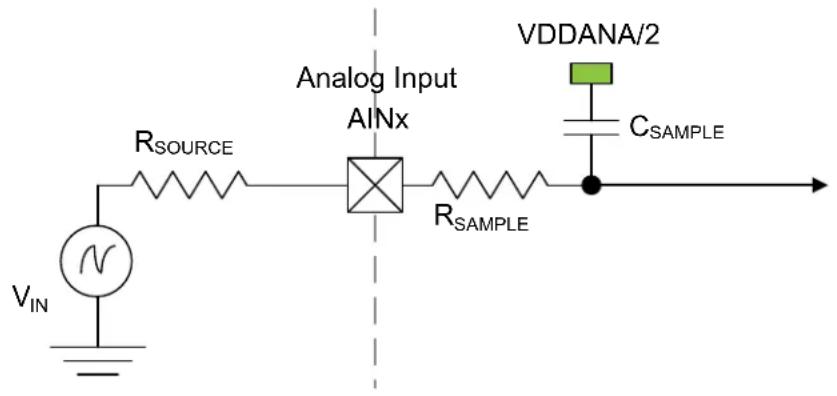
text_image
Analog Input AINx R_SOURCE VDDANA/2 R_SAMPLE C_SAMPLE VIN NTo achieve n bits of accuracy, the C_SAMPLE capacitor must be charged at least to a voltage of
$$ V _ {\text { CSAMPLE }} \geq V _ {\text { IN }} \times 1 (- 2 ^ {- (n + 1)}) $$
The minimum sampling time t_SAMPLEHOLD for a given R_SOURCE can be found using this formula:
$$ t _ {\text { SAMPLEHOLD }} \geq (R _ {\text { SAMPLE }} + R _ {\text { SOURCE }}) \times (C _ {\text { SAMPLE }}) \times (n + 1) \times \ln 2 (\quad) $$
for a 12 bits accuracy: t_SAMPLEHOLD ≥ (R_SAMPLE + R_SOURCE) × (C_SAMPLE) × 9.02
where
$$ t _ {\text { SAMPLEHOLD }} = \frac {1}{2 \times f _ {\mathrm{ADC}}} $$
32.10.5 Digital to Analog Converter (DAC) Characteristics
Table 32-28. Operating Conditions
| Symbol | Parameter Conditions Min. Typ. Max. Units | |||||
| V_DDANA | Analog supply voltage 1.62 - 3.63 V | |||||
| AV_REF | External reference voltage 1.0 - V | DDANA-0.6 | V | |||
| INT1V^(2) | -1 | - | V | |||
| VDDANA | - | V_DDANA | - | V | ||
| Linear output voltage range | 0.05 - V | DDANA-0.05 | V | |||
| Minimum resistive load | 5 - | - kΩ | ||||
| Maximum capacitance load | - | - | 100 | pF | ||
| I_DD | DC supply current (1) | Voltage pump disabled | - | 160 | 230 | μA |
Notes:
- These values are based on characterization, and are not covered by test limits in production.
- It is the buffered internal reference of 1.0V derived from the internal 1.1V bandgap reference.
Table 32-29. Clock and Timing
| Symbol | Parameter | Conditions | Min. | Typ. | Max. | Units | |
| Conversion rate | C_load = 100pF R_load > 5k | Normal mode | -- | 350 | ksps | ||
| For _DATA = +/-1 | - | - | 1000 | ||||
| Startup time | V_DDNA > 2.6V | - | -2.85 | μs | |||
| V_DDNA < 2.6V | - | - | 10 | μs | |||
Note: The values in this table are based on simulation, and are not covered by test limits in production or characterization.
Table 32-30. Accuracy Characteristics (Device Variant A)
| Symbol | Parameter | Conditions (1) | Min. | Typ. | Max. | Units | |
| RES | Input resolution | - | - | 10 | Bits | ||
| INL | Integral non-linearity | V_REF = Ext 1.0V | V_DD = 1.6V | 0.75 | 1.1 | 2.5 | LSB |
| V_DD = 3.6V | 0.6 | 1.2 | 1.5 | ||||
| V_REF = V_DDANA | V_DD = 1.6V | 1.4 | 2.2 | 2.5 | |||
| V_DD = 3.6V | 0.9 | 1.4 | 1.5 | ||||
| V_REF = INT1V | V_DD = 1.6V | 0.75 | 1.3 | 1.5 | |||
| V_DD = 3.6V | 0.8 | 1.2 | 1.5 | ||||
| DNL | Differential non-linearity | V_REF = Ext 1.0V | V_DD = 1.6V | ±0.9 | ±1.2 | ±1.5 | LSB |
| V_DD = 3.6V | ±0.9 | ±1.1 | ±1.2 | ||||
| V_REF = V_DDANA | V_DD = 1.6V | ±1.1 | ±1.5 | ±1.7 | |||
| V_DD = 3.6V | ±1.0 | ±1.1 | ±1.2 | ||||
| V_REF = INT1V | V_DD = 1.6V | ±1.1 | ±1.4 | ±1.5 | |||
| V_DD = 3.6V | ±1.0 | ±1.5 | ±1.6 | ||||
| GE | Gain error | Ext. V_REF | ±1.5 | ±5 | ±10 | mV | |
| OE | Offset error | Ext. V_REF | ±2 | ±3 | ±6 mV | ||
Note:
- All values are measured using a conversion rate of 35 ksps.
Table 32-31. Accuracy Characteristics (Device Variant B)
| Symbol Parameter Conditions | (1) | Min. Typ. Max. | Units | ||||
| RES Input resolution ---- 10 Bits | |||||||
| INL Integral non-linearity | VREF = Ext 1.0V | VDD = 1.6V 0.75 | 1.1 | 2.5 | LSB | ||
| VDD = 3.6V 0.6 | 1.2 | 1.5 | |||||
| VREF = VDDANA | VDD = 1.6V 1.4 | 2.2 | 2.5 | ||||
| VDD = 3.6V 0.9 | 1.4 | 1.5 | |||||
| VREF = INT1V | VDD = 1.6V 0.75 | 1.3 | 3.1 | ||||
| VDD = 3.6V 0.8 | 1.2 | 2.7 | |||||
| DNL | Differential non-linearity | VREF = Ext 1.0V | VDD = 1.6V ±0.9 ±1.2 | ±1.5 | LSB | ||
| VDD = 3.6V ±0.9 ±1.1 | ±1.2 | ||||||
| VREF = VDDANA | VDD = 1.6V ±1.1 ±1.5 | ±1.7 | |||||
| VDD = 3.6V ±1.0 ±1.1 | ±1.2 | ||||||
| VREF = INT1V | VDD = 1.6V ±1.1 ±1.4 | ±3.0 | |||||
| VDD = 3.6V ±1.0 ±1.5 | ±2.9 | ||||||
| GE | Gain error | Ext. VREF | ±1.5 | ±5 | ±10 | mV | |
| OE | Offset error | Ext. VREF | ±2 | ±3 | ±6 | mV | |
Note:
- All values are measured using a conversion rate of 35 ksps.
32.10.6 Analog Comparator Characteristics
Table 32-32. Electrical and Timing (Device Variant A)
| Symbol | Parameter | Conditions | Min. | Typ. | Max. | Units |
| Positive input voltage range | 0 | - | V_DDANA | V | ||
| Negative input voltage range | 0 | - | V_DDANA | |||
| Offset | Hysteresis = 0, Fast mode | -15 | 0.0 | +15 | mV | |
| Hysteresis = 0, Low power mode | -25 | 0.0 | +25 | mV | ||
| Hysteresis | Hysteresis = 1, Fast mode | 20 | 50 | 80 | mV | |
| Hysteresis = 1, Low power mode | 15 | 40 | 75 | mV | ||
| Propagation delay | Changes for V_ACM = V_DDANA/2 100 mV overdrive, Fast mode | - | 60 | 116 | ns | |
| Changes for V_ACM = V_DDANA/2 100 mV overdrive, Low power mode | - | 225 | 370 | ns | ||
| t_STARTUP | Startup time | Enable to ready delayFast mode | - | 1 | 2 | μs |
| Enable to ready delayLow power mode | - | 12 | 19 | μs | ||
| V_SCALE | INL (3) | -1.4 | 0.75 | +1.4 | LSB | |
| DNL (3) | -0.9 | 0.25 | +0.9 | LSB | ||
| Offset Error (1,2) | -0.200 | 0.260 | +0.920 LSB | |||
| Gain Error (1,2) | -0.89 | 0.215 | 0.89 LSB | |||
Notes:
- According to the standard equation V(X)=V_LSB*(X+1) ; V_LSB=V_DDANA/64 .
- Data computed with the Best Fit method.
- Data computed using histogram.
Table 32-33. Electrical and Timing (Device Variant B)
| Symbol | Parameter Conditions Min. | Typ. Max. Units | ||||
| Positive input voltage range 0 - VDDANA | V | |||||
| Negative input voltage range 0 - VDDANA | ||||||
| Offset | Hysteresis = 0, Fast mode -15 0 15 mV | |||||
| Hysteresis = 0, Low power mode -25 0 25 mV | ||||||
| Hysteresis | Hysteresis = 1, Fast mode 20 50 80 mV | |||||
| Hysteresis = 1, Low power mode | 15 | 40 | 75 | mV | ||
| Propagation delay | Changes for VACM=VDDANA/2 100 mV overdrive, Fast mode | - | 90 | 180 | ns | |
| Changes for VACM=VDDANA/2 100 mV overdrive, Low power mode | -282 | 520 ns | ||||
| tSTARTUP | Startup time | Enable to ready delay Fast mode | - | 1 | 2.6 | μs |
| Enable to ready delay Low power mode | - | 12 | 22 | μs | ||
| V_SCALE | INL (3) | -1.4 | 0.75 | 1.4 | LSB | |
| DNL (3) | -0.9 | 0.25 | 0.9 | LSB | ||
| Offset Error (1,2) | -0.2 | 0.26 | 0.92 | LSB | ||
| Gain Error (1,2) | -0.89 | 0.215 | 0.89 | LSB | ||
Notes:
- According to the standard equation V(X)=V_LSB*(X+1) ; V_LSB=V_DDANA/64 .
- Data computed with the Best Fit method.
- Data computed using histogram.
32.10.7 Bandgap and Internal 1.0V Reference Characteristics
Table 32-34. Bandgap and Internal 1.0V Reference Characteristics
| Symbol | Parameter | Conditions | Min. | Typ. | Max. | Units |
| BANDGAP | Bandgap reference | Over voltage and [-40°C, +85°C] | 1.08 | 1.1 | 1.12 | V |
| Over voltage at 25°C | 1.09 | 1.1 1.11 | ||||
| INT1V | Internal 1.0V reference voltage^(1) | Over voltage and [-40°C, +85°C] | 0.98 | 1 | 1.02 | |
| Over voltage at 25°C | 0.99 | 1 | 1.01 |
Note:
- These values are based on simulation and are not covered by production test limits.
32.10.8 Temperature Sensor Characteristics
32.10.8.1 Temperature Sensor Characteristics
Table 32-35. Temperature Sensor Characteristics ^(1)
| Symbol | Parameter | Conditions | Min. | Typ. | Max. | Units |
| Temperature sensor output voltage | T=25°C, VDDANA=3.3V | - | 0.667 | - | V | |
| Temperature sensor slope | 2.3 | 2.4 | 2.5 | mV/°C | ||
| Variation over VDDANA voltage | VDDANA=1.62V to 3.6V | -1.7 | 1 | 3.7 | mV/V | |
| Temperature Sensor accuracy | Using the method described in the following section | -10 | - | 10 | °C |
Note: 1. These values are based on characterization. These values are not covered by test limits in production.
- See also rev C errata concerning the temperature sensor.
32.10.8.2 Software-based Refinement of the Actual Temperature
The temperature sensor behavior is linear but it depends on several parameters such as the internal voltage reference which itself depends on the temperature. To take this into account, each device contains a Temperature Log row with data measured and written during the production tests. These calibration values should be read by software to infer the most accurate temperature readings possible.
This Software Temperature Log row can be read at address 0x00806030. The Software Temperature Log row cannot be written.
This section specifies the Temperature Log row content and explains how to refine the temperature sensor output using the values in the Temperature Log row.
32.10.8.2.1 Temperature Log Row
All values in this row were measured in the following conditions:
• V_DDIN = V_DDIO = V_DDANA = 3.3V
• ADC Clock speed = 1MHz
- ADC mode: Free running mode, ADC averaging mode with 4 averaged samples
- ADC voltage reference = 1.0V internal reference (INT1V)
- ADC input = Temperature sensor
Table 32-36. Temperature Log Row Content
| Bit position | Name Description | |
| 7:0 ROOM_TEMP_VAL_INT Integer part of room temperature in °C | ||
| 11:8 ROOM_TEMP_VAL_DEC Decimal part of room temperature | ||
| 19:12 HOT_TEMP_VAL_INT Integer part of hot temperature in °C | ||
| 23:20 HOT_TEMP_VAL_DEC Decimal part of hot temperature | ||
| 31:24 ROOM_INT1V_VAL 2's complement of the internal 1V reference drift at room temperature (versus a 1.0 centered value) | ||
| 39:32 HOT_INT1V_VAL 2's complement of the internal 1V reference drift at hot temperature (versus a 1.0 centered value) | ||
| 51:40 ROOM_ADC_VAL 12-bit ADC conversion at room temperature | ||
| 63:52 HOT_ADC_VAL 12-bit ADC conversion at hot temperature | ||
The temperature sensor values are logged during test production flow for Room and Hot insertions:
- ROOM_TEMP_VAL_INT and ROOM_TEMP_VAL_DEC contains the measured temperature at room insertion (e.g. for ROOM_TEMP_VAL_INT=25 and ROOM_TEMP_VAL_DEC=2, the measured temperature at room insertion is 25.2°C).
- HOT_TEMP_VAL_INT and HOT_TEMP_VAL_DEC contains the measured temperature at hot insertion (e.g. for HOT_TEMP_VAL_INT=83 and HOT_TEMP_VAL_DEC=3, the measured temperature at room insertion is 83.3°C).
The temperature log row also contains the corresponding 12-bit ADC conversions of both Room and Hot temperatures:
- ROOM_ADC_VAL contains the 12-bit ADC value corresponding to (ROOM_TEMP_VAL_INT, ROOM_TEMP_VAL_DEC)
- HOT_ADC_VAL contains the 12-bit ADC value corresponding to (HOT_TEMP_VAL_INT, HOT_TEMP_VAL_DEC)
The temperature log row also contains the corresponding 1V internal reference of both Room and Hot temperatures:
- ROOM_INT1V_VAL is the 2's complement of the internal 1V reference value corresponding to (ROOM_TEMP_VAL_INT, ROOM_TEMP_VAL_DEC)
- HOT_INT1V_VAL is the 2's complement of the internal 1V reference value corresponding to (HOT_TEMP_VAL_INT, HOT_TEMP_VAL_DEC)
- ROOM_INT1V_VAL and HOT_INT1V_VAL values are centered around 1V with a 0.001V step. In other words, the range of values [0,127] corresponds to [1V, 0.873V] and the range of values [-1, -127] corresponds to [1.001V, 1.127V]. INT1V == 1 - (VAL/1000) is valid for both ranges.
32.10.8.2.2 Using Linear Interpolation
For concise equations, we'll use the following notations:
- (ROOM_TEMP_VAL_INT, ROOM_TEMP_VAL_DEC) is denoted temp _R
- (HOT_TEMP_VAL_INT, HOT_TEMP_VAL_DEC) is denoted temp H
- ROOM_ADC_VAL is denoted ADC R , its conversion to Volt is denoted VADCR
- HOT_ADC_VAL is denoted ADC H , its conversion to Volt is denoted VADCH
- ROOM_INT1V_VAL is denoted INT1V _R
• HOT_INT1V_VAL is denoted INT1V H
Using the (temp,ADC) and (temp,ADC) points, using a linear interpolation we have the following equation:
$$ \left(\frac {V _ {\mathrm{ADC}} - V _ {\mathrm{ADCR}}}{\text { temp } - \text { temp } _ {R}}\right) = \left(\frac {V _ {\mathrm{ADCH}} - V _ {\mathrm{ADCR}}}{\text { temp } _ {H} - \text { temp } _ {R}}\right) $$
Given a temperature sensor ADC conversion value ADC_m , we can infer a coarse value of the temperature temp_C as:
[Equation 1]
$$ \operatorname{temp} _ {C} = \operatorname{temp} _ {R} + \left[ \frac {\left{\left(\mathrm{ADC} _ {m} \cdot \frac {1}{(2 ^ {1 2} - 1)}\right) - \left(\mathrm{ADC} _ {R} \cdot \frac {\text {INT1V} _ {R}}{(2 ^ {1 2} - 1)}\right) \right} \cdot \text {temp} _ {H} - \text {temp} _ {R})}{\left{\left(\mathrm{ADC} _ {H} \cdot \frac {\text {INT1V} _ {H}}{(2 ^ {1 2} - 1)}\right) - \left(\mathrm{ADC} _ {R} \cdot \frac {\text {INT1V} _ {R}}{(2 ^ {1 2} - 1)}\right) \right}} \right] $$
Note 1: in the previous expression, we've added the conversion of the ADC register value to be expressed in V
Note 2: this is a coarse value because we assume INT1V=1V for this ADC conversion.
Using the (temp_R, INT1V_R) and (temp_H, INT1V_H) points, using a linear interpolation we have the following equation:
$$ \left(\frac {\text { INT1V } - \text { INT1V } _ {R}}{\text { temp } - \text { temp } _ {R}}\right) = \left(\frac {\text { INT1V } _ {H} - \text { INT1V } _ {R}}{\text { temp } _ {H} - \text { temp } _ {R}}\right) $$
Then using the coarse temperature value, we can infer a closer to reality INT1V value during the ADC conversion as:
$$ \operatorname{INT1} V _ {m} = \operatorname{INT1} V _ {R} + \left(\frac {\left(\operatorname{INT1} V _ {H} - \operatorname{INT1} V _ {R}\right) \cdot \text {temp} _ {C} - \text {temp} _ {R})}{\left(\text {temp} _ {H} - \text {temp} _ {R}\right)}\right) $$
Back to [Equation 1], we replace INT1V=1V by INT1V = INT1V _m , we can then deduce a finer temperature value as:
[Equation 1bis]
$$ \operatorname{temp} _ {f} = \operatorname{temp} _ {R} + \left[ \frac {\left{\left(\mathrm{ADC} _ {m} \cdot \frac {\mathrm{INT1V} _ {m}}{\left(2 ^ {1 2} - 1\right)}\right) - A \left(\mathrm{DC} _ {R} \cdot \frac {\mathrm{INT1V} _ {R}}{\left(2 ^ {1 2} - 1\right)}\right) \right} \cdot \left(\operatorname{temp} _ {H} - \operatorname{temp} _ {R}\right)}{\left{\left(\mathrm{ADC} _ {H} \cdot \frac {\mathrm{INT1V} _ {H}}{\left(2 ^ {1 2} - 1\right)}\right) - A \left(\mathrm{DC} _ {R} \cdot \frac {\mathrm{INT1V} _ {R}}{\left(2 ^ {1 2} - 1\right)}\right) \right}} \right] $$
32.11 NVM Characteristics
Table 32-37. Maximum Operating Frequency
| V_DD range NVM Wait States Maximum Operating Frequency Units | |||
| 1.62V to 2.7V 0 14 MHz | |||
| 1 | 28 | ||
| 2 | 42 | ||
| 3 | 48 | ||
| 2.7V to 3.63V 0 24 | |||
| 1 | 48 | ||
Note: On this Flash technology, a maximum number of 8 consecutive write is allowed per row. Once this number is reached, a row erase is mandatory.
Table 32-38. Flash Endurance and Data Retention
| Symbol | Parameter | Conditions | Min. | Typ. | Max. | Units |
| Ret_NVM25k | Retention after up to 25k cycles | Average ambient 55°C | 10 | 50 | - | Years |
| Ret_NVM2.5k | Retention after up to 2.5k cycles | Average ambient 55°C | 20 | 100 | - | Years |
| Ret_NVM100 | Retention after up to 100 cycles | Average ambient 55°C | 25 | >100 | - | Years |
| Cyc_NVM | Cycling Endurance(1) | -40°C < Ta < 85°C | 25k | 150k | - | Cycles |
Note:
- An endurance cycle is a write and an erase operation.
Table 32-39. EEPROM Emulation ^(1) Endurance and Data Retention
| Symbol | Parameter | Conditions | Min. | Typ. | Max. | Units |
| Ret_EEPROM100k | Retention after up to 100k cycles | Average ambient 55°C | 10 | 50 | - | Years |
| Ret_EEPROM10k | Retention after up to 10k cycles | Average ambient 55°C | 20 | 100 | - | Years |
| Cyc_EEPROM | Cycling Endurance^(2) | -40°C < Ta < 85°C | 100k | 600k | - | Cycles |
Notes:
- The EEPROM Emulation is a software emulation described in the "Application Note AT03265".
- An endurance cycle is a write and an erase operation.
Table 32-40. NVM Characteristics
| Symbol | Parameter | Conditions | Min. | Typ. | Max. | Units |
| t_FPP | Page programming time | - | - | - | 2.5 | ms |
| t_FRE | Row erase time | - | -- | 6 ms | ||
| t_FCE | DSU chip erase time (CHIP_ERASE) | - | - | - | 240 | ms |
32.12 Oscillators Characteristics
32.12.1 Crystal Oscillator (XOSC) Characteristics
32.12.1.1 Digital Clock Characteristics
The following table describes the characteristics for the oscillator when a digital clock is applied on XIN.
Table 32-41. Digital Clock Characteristics
| Symbol Parameter Conditions Min. Typ. Max. Units | |||||
| f_CPXIN | XIN clock frequency Digital mode -- 32 MHz |
32.12.1.2 Crystal Oscillator Characteristics
The following table describes the characteristics for the oscillator when a crystal is connected between XIN and XOUT as shown in the figure Oscillator Connection. The user must choose a crystal oscillator where the crystal load capacitance C_L is within the range given in the table. The exact value of C_L can be found in the crystal data sheet. The capacitance of the external capacitors ( C_LEXT ) can then be computed as follows:
Load Capacitance Equation
$$ C _ {\text {LOAD}} = \left(\left[ C _ {\text {XIN}} + C _ {\text {LEXT}} \right] * \left[ C _ {\text {XOUT}} + C _ {\text {LEXT}} \right]\right) / \left(\left[ C _ {\text {XIN}} + C _ {\text {LEXT}} + C _ {\text {LEXT}} + C _ {\text {XOUT}} \right]\right) + C _ {\text {STRAY}} $$
Where:
$$ C _ {\text { LOAD }} = \text { Crystal Mfg. } C _ {\text { LOAD }} \text { specification } $$
$$ C _ {X I N} = X O S C X I N \text { pin data sheet specification } $$
$$ C _ {X O U T} = X O S C X O U T \text { pin data sheet specification } $$
$$ C _ {\text { LEXT }} = \text { Required external crystal load capacitor } $$
$$ \begin{array}{l} C _ {S T R A Y} (\text {Osc PCB capacitance}) = 1. 5 \mathrm{pfper} 1 2. 5 \mathrm{mm(0.5inches)} (\text {TRACE W} = 0. 1 7 5 \mathrm{mm}, H = 3 6 \mu \mathrm{m}, T = \ 1 1 3 \mu \mathrm{m}) \end{array} $$
For C_XIN and C_XOUT within 4 pf of each other, assume C_XIN = C_XOUT = C_XTAL_EFF = ((C_XIN + C_XOUT) / 2) (Averaging C_XIN and C_XOUT will effect final calculated C_LOAD value by less than 0.25 pf.)
The load capacitance equation can then be simplified as follows:
$$ C _ {L E X T} = 2 ^ {} C _ {L O A D} - C _ {X T A L _ E F F} - 2 ^ {} C _ {S T R A Y} $$
Table 32-42. Crystal Oscillator Characteristics
| Symbol | Parameter | Conditions | Min. | Typ. | Max. | Units |
| f_OUT | Crystal oscillator frequency | 0.4 | - | 32 | MHz | |
| ESR | Crystal Equivalent Series ResistanceSafety Factor = 3The AGC doesn't have any noticeable impact on these measurements. | f = 0.455 MHz, C_L = 100 pF,XOSC.GAIN = 0 | - | - | 5.6K | Ω |
| f = 2 MHz, C_L = 20 pF,XOSC.GAIN = 0 | - | - | 416 | |||
| f = 4 MHz, C_L = 20 pF,XOSC.GAIN = 1 | - | - | 243 | |||
| f = 8 MHz, C_L = 20 pF,XOSC.GAIN = 2 | - | - | 138 | |||
| f = 16 MHz, C_L = 20 pF,XOSC.GAIN = 3 | - | - | 66 | |||
| f = 32 MHz, C_L = 18 pF,XOSC.GAIN = 4 | - | - | 56 | |||
| ......continued | ||||||
| Symbol | Parameter Conditions Min. Typ. Max. Units | |||||
| C_XIN | Parasitic capacitor load - 5.9 - pF | |||||
| C_XOUT | Parasitic capacitor load - 3.2 - pF | |||||
| Current Consumption f = 2 MHz, C | L=20 pF, XOSC.GAIN = 0, AGC off 276585 A | |||||
| f = 2 MHz, C_L=20 pF, XOSC.GAIN = 0, AGC on 145273 | ||||||
| f = 4MHz, C_L=20 pF, XOSC.GAIN = 1, AGC off 61117150 | ||||||
| f = 4MHz, C_L=20 pF, XOSC.GAIN = 1, AGC on 2374100 | ||||||
| f = 8 MHz, C_L=20 pF, XOSC.GAIN = 2, AGC off 131226296 | ||||||
| f = 8 MHz, C_L=20 pF, XOSC.GAIN = 2, AGC on 56128172 | ||||||
| f = 16 MHz, C_L=20 pF, XOSC.GAIN = 3, AGC off 305502687 | ||||||
| f = 16 MHz, C_L=20 pF, XOSC.GAIN = 3, AGC on 116307552 | ||||||
| f = 32 MHz, C_L=18 pF, XOSC.GAIN = 4, AGC off 103116222200 | ||||||
| f = 32 MHz, C_L=18 pF, XOSC.GAIN = 4, AGC on 2786151200 | ||||||
| t_STARTUP | Startup time | f = 2 MHz, C_L=20 pF, XOSC.GAIN = 0, ESR = 600 | -14K 48K cycles | |||
| f = 4 MHz, C_L=20 pF, XOSC.GAIN = 1, ESR = 100 | -6800 19.5K | |||||
| f = 8 MHz, C_L=20 pF, XOSC.GAIN = 2, ESR = 35 | -5550 13K | |||||
| f = 16 MHz, C_L=20 pF, XOSC.GAIN = 3, ESR = 25 | -6750 14.5K | |||||
| f = 32 MHz, C_L=18 pF, XOSC.GAIN = 4, ESR = 40 | -5.3K 9.6K | |||||
Figure 32-6. Oscillator Connection
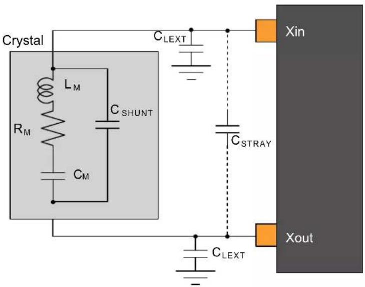
text_image
Crystal L_M R_M C_SHUNT C_M C_LEXT C_STRAY C_LEXT Xin Xout32.12.2 External 32 kHz Crystal Oscillator (XOSC32K) Characteristics
32.12.2.1 Digital Clock Characteristics
The following table describes the characteristics for the oscillator when a digital clock is applied on the XIN32 pin.
Table 32-43. Digital Clock Characteristics ^(1)
| Symbol Parameter Conditions Min. Typ. Max. Units | |||||
| f_CPXIN32 | XIN32 clock frequency Digital mode - 32.768 - kHz | ||||
| DCxin XIN32 clock duty cycle Digital mode - 50 - % | |||||
Note:
- These values are based on simulation. These values are not covered by test or characterization.
32.12.2.2 Crystal Oscillator Characteristics
Figure 32-6 and the equation in 32.12.1.2. Crystal Oscillator Characteristics also applied to the 32 kHz oscillator connection. The user must choose a crystal oscillator where the crystal load capacitance C_L is within the range given in the table. The value of C_L can be found in the crystal data sheet.
For the computation of the external capacitors ( C_LEXT ) value, refer to the logic detailed in XOSC Crystal Oscillator Characteristics.
Table 32-44. 32 kHz Crystal Oscillator Characteristics
| Symbol | Parameter | Conditions | Min. | Typ. | Max. | Units |
| f_OUT | Crystal oscillator frequency | - | 32768 | - | Hz | |
| t_STARTUP | Startup time | ESR_XTAL= 39.9 kΩ, C_L= 12.5 pF - | 28K | 30K | cycles | |
| C_L | Crystal load capacitance | - | - | 12.5 | pF | |
| C_SHUNT | Crystal shunt capacitance | - | 0.1 | - | ||
| C_XIN32 | Parasitic capacitor load | - | 3.1 | - | ||
| C_XOUT32 | Parasitic capacitor load | - | 3.3 | - | ||
| I_XOSC32K | Current consumption | AGC off | - | 1.22 | 2.19 | μA |
| AGC on^(1) | - | - | - | |||
| ESR | Crystal equivalent series resistance f = 32.768 kHz Safety Factor = 3 | C_L= 12.5 pF | - | - | 141 | kΩ |
Note:
- Refer to the Revision D/Revision C/Revision B errata related to the XOSC32K.
32.12.3 Digital Frequency Locked Loop (DFLL48M) Characteristics
Table below provides the characteristics of the DFLL48M.
Table 32-45. DFLL48M Characteristics - Closed Loop Mode ^(1)(2)
| Symbol | Parameter | Conditions | Min. | Typ. | Max. | Units |
| f_OUT | Average Output frequency | f_REF = XOSC32K 32.768 kHz | 47 | 48 | 49 | MHz |
| f_REF | Reference frequency | 0.732 | 32.768 | 35.1 | kHz | |
| Jitter | Period jitter | f_REF = XOSC32K 32.768 kHz | - | - | 0.42 | ns |
| I_DFLL | Power consumption on V_DDIN | f_REF = XOSC32K 32.768 kHz. For SAMD20 revision C devices | - | 397 | - | μA |
| f_REF = XOSC32K 32.768 kHz. For SAMD20 revision D devices and later. | - | 292 | - | |||
| ......continued | ||||||
| Symbol | Parameter Conditions Min. | Typ. Max. Units | ||||
| t_LOCK | Lock time f | REF= XOSC32K 32.768 kHzDFLLVAL.COARSE =DFLL48M COARSE CALDFLLVAL.FINE = 512DFLLCTRL.BPLCKC = 1DFLLCTRL.QLDIS = 0DFLLCTRL.CCDIS = 1DFLLMUL.FSTEP = 10 | 100 200 500 μs | |||
| Quick lock disabled,Chill cycle disabled,CSTEP = 3, FSTEP = 1, f_REF = XOSC32K 32.768 kHz | -600 - | |||||
Notes:
- Refer to the revision C/revision B errata related to the DFLL48M.
- All parts are tested in production to be able to use the DFLL as main CPU clock whether in DFLL Closed Loop mode with an external OSC reference or in DFLL Closed Loop mode using the internal OSC8M (Only applicable for revision C).
32.12.4 32.768kHz Internal oscillator (OSC32K) Characteristics
Table 32-46. 32kHz RC Oscillator Characteristics
| Symbol | Parameter Conditions | Min. Typ. Max. Units | ||||
| f_OUT | Output frequency | Calibrated against a 32.768kHz reference at 25°C, over [-40, +85]°C, over [1.62, 3.63]V | 28.508 | 32.768 | 34.734 | kHz |
| Calibrated against a 32.768kHz reference at 25°C, at V_DD=3.3V | 32.276 | 32.768 | 33.260 | |||
| Calibrated against a 32.768kHz reference at 25°C, over [1.62, 3.63]V | 31.457 | 32.768 | 34.079 | |||
| I_OSC32K | Current consumption | - | 0.67 | 1.31 μA | ||
| t_STARTUP | Startup time | - | 1 | 2 | cycle | |
| Duty | Duty Cycle | - | 50 | - | % |
32.12.5 Ultra Low Power Internal 32kHz RC Oscillator (OSCULP32K) Characteristics
Table 32-47. Ultra Low Power Internal 32kHz RC Oscillator Characteristics
| Symbol | Parameter | Conditions | Min. | Typ. | Max. | Units |
| f_OUT | Output frequency | Calibrated against a 32.768kHz reference at 25°C, over [-40, +85]C, over [1.62, 3.63]V | 25.559 | 32.768 | 38.011 | kHz |
| Calibrated against a 32.768kHz reference at 25°C, at V_DD = 3.3V | 31.293 | 32.768 | 34.570 | |||
| Calibrated against a 32.768kHz reference at 25°C, over [1.62, 3.63]V | 31.293 | 32.768 | 34.570 | |||
| I_OSCULP32K^(1)(2) | - | - | 125 nA | |||
| t_STARTUP | Startup time | - | 10 | - | cycles | |
| Duty | Duty Cycle | - | 50 | - | % |
Notes: 1. These values are based on simulation. These values are not covered by test limits in production or characterization.
2. This oscillator is always on.
32.12.6 8MHz RC Oscillator (OSC8M) Characteristics
Table 32-48. Internal 8MHz RC Oscillator Characteristics
| Symbol | Parameter Conditions | Min. Typ. Max. Units | ||||
| f_OUT | Output frequency Calibrated against a 8MHz reference at 25°C, over [-40, +85]C, over [1.62, 3.63]V 7.8 8 | 8.16 MHz | ||||
| Calibrated against a 8MHz reference at 25°C, at V_DD=3.3V 7.94 8 8.06 | ||||||
| Calibrated against a 8MHz reference at 25°C, over [1.62, 3.63]V 7.92 8 8.08 | ||||||
| I_OSC8M | Current consumption IDLE2 on OSC32K versus IDLE2 on calibrated OSC8M enabled at 8MHz (FRANGE=1, PRESC=0) | 34.5 | 71 | 96 | μA | |
| t_STARTUP | Startup time | - | 2.1 | 3 | μs | |
| Duty | Duty cycle | - | 50 | - | % |
32.13 PTC Typical Characteristics
32.13.1
Figure 32-7. Power Consumption [μA]
1 sensor, noise countermeasures disabled, f=48MHz, Vcc=3.3V
line
| Sample averaging | Scan rate 10ms | Scan rate 50ms | Scan rate 100ms | Scan rate 200ms | | ---------------- | -------------- | -------------- | --------------- | --------------- | | 1 | 88 | 24 | 12 | 6 | | 2 | 92 | 24 | 13 | 6 | | 4 | 94 | 24 | 13 | 7 | | 8 | 97 | 26 | 14 | 7 | | 16 | 101 | 26 | 14 | 7 | | 32 | 114 | 29 | 15 | 7 | | 64 | 132 | 32 | 17 | 9 |Figure 32-8. Power Consumption [μA]
1 sensor, noise countermeasures Enabled, f=48MHz, Vcc=3.3V
line
| Sample averaging | Scan rate 10ms | Scan rate 50ms | Scan rate 100ms | Scan rate 200ms | | ---------------- | -------------- | -------------- | --------------- | --------------- | | 1 | 95 | 25 | 12 | 8 | | 2 | 98 | 26 | 13 | 9 | | 4 | 99 | 27 | 14 | 10 | | 8 | 103 | 28 | 15 | 11 | | 16 | 115 | 30 | 16 | 12 | | 32 | 135 | 33 | 18 | 13 | | 64 | 175 | 42 | 20 | 14 |Figure 32-9. Power Consumption [μA]
10 sensors, noise countermeasures disabled, f=48MHz, Vcc=3.3V
line
| Sample averaging | Scan rate 10ms | Scan rate 50ms | Scan rate 100ms | Scan rate 200ms | Linear (Scan rate 50ms) | | ---------------- | -------------- | -------------- | --------------- | --------------- | ----------------------- | | 1 | 580 | 130 | 50 | 20 | 120 | | 2 | 590 | 135 | 55 | 25 | 130 | | 4 | 610 | 140 | 60 | 30 | 140 | | 8 | 640 | 145 | 65 | 35 | 150 | | 16 | 700 | 150 | 70 | 40 | 160 | | 32 | 800 | 170 | 80 | 45 | 180 | | 64 | 1000 | 210 | 100 | 50 | 200 |Figure 32-10. Power Consumption [μA]
10 sensors, noise countermeasures Enabled, f=48MHz, Vcc=3.3V
line
| Sample averaging | Scan rate 10ms | Scan rate 50ms | Scan rate 100ms | Scan rate 200ms | | ---------------- | -------------- | -------------- | --------------- | --------------- | | 1 | 650 | 140 | 70 | 30 | | 2 | 680 | 145 | 75 | 35 | | 4 | 720 | 150 | 80 | 40 | | 8 | 720 | 160 | 85 | 45 | | 16 | 830 | 180 | 95 | 50 | | 32 | - | 230 | 110 | 60 | | 64 | - | 320 | 160 | 75 |Figure 32-11. Power Consumption [μA]
100 sensors, noise countermeasures disabled, f=48MHz, Vcc=3.3V
line
| Sample averaging | Scan rate 10ms | Scan rate 50ms | Scan rate 100ms | Scan rate 200ms | | ---------------- | -------------- | -------------- | --------------- | --------------- | | 1 | 4700 | 1300 | 650 | 350 | | 2 | - | 1300 | 650 | 350 | | 4 | - | 1350 | 680 | 360 | | 8 | - | 1400 | 720 | 380 | | 16 | - | 1500 | 750 | 400 | | 32 | - | - | 850 | 450 | | 64 | - | - | - | 550 |Figure 32-12. Power Consumption [μA]
100 sensors, noise countermeasures Enabled, f=48MHz, Vcc=3.3V

line
| Sample averaging | Scan rate 10ms | Scan rate 50ms | Scan rate 100ms | Scan rate 200ms | | ---------------- | -------------- | -------------- | --------------- | --------------- | | 1 | - | 1400 | 700 | 350 | | 2 | - | 1380 | 700 | 350 | | 4 | - | 1380 | 700 | 350 | | 8 | - | 1450 | 750 | 370 | | 16 | - | 1580 | 850 | 420 | | 32 | - | - | 920 | 470 | | 64 | - | - | - | 570 |Figure 32-13. CPU Utilization
line
| x | Channel count 1 | Channel count 10 | Channel count 100 | | ---- | --------------- | ---------------- | ----------------- | | 10 | 20% | 25% | 70% | | 50 | 5% | 5% | 15% | | 100 | 2% | 2% | 7% | | 200 | 1% | 1% | 3% |32.14 Timing Characteristics
32.14.1 External Reset
Table 32-49. External reset characteristics
| Symbol Parameter Condition Min. Typ. Max. Units | ||||||
| t_EXT | Minimum reset pulse width 10 -- ns | |||||
32.14.2 SERCOM in SPI Mode Timing
Figure 32-14. SPI timing requirements in Host mode

text_image
SS SCK (CPOL = 0) SCK (CPOL = 1) MISO (Data Input) MOSI (Data Output) MSB LSB tMOS tMIS tMIH tMOH tSCKR tSCKW tSCKW tSCKW tMOH BSLBSMFigure 32-15. SPI timing requirements in Client mode

text_image
SS SCK (CPOL = 0) SCK (CPOL = 1) MOSI (Data Input) tSIS tIH MSB LSB tSOS tSOSH MISO (Data Output) BSLBSMTable 32-50. SPI timing characteristics and requirements ^(1)
| Symbol | Parameter Conditions Min. Typ. Max. Units | ||||||
| t_SCK | SCK period Host 84 ns | ||||||
| t_SCKW | SCK high/low width Host - 0.5*t | SCK | - | ||||
| t_SCKR | SCK rise time^(2) | Host --- | |||||
| t_SCKF | SCK fall time^(2) | Host --- | |||||
| t_MIS | MISO setup to SCK Host - 29 | - | |||||
| t_MIH | MISO hold after SCK | Host - 8 - | |||||
| t_MOS | MOSI setup SCK | Host - t | SCK/2 - 16 | - | |||
| t_MOH | MOSI hold after SCK | Host - 16 | - | ||||
| t_SSCK | Client SCK Period | Client | 1*t_CLK\_APB | - | - | ||
| t_SSCKW | SCK high/low width Client | 0.5*t | SSCK | - | - | ||
| t_SSCKR | SCK rise time^(2) | Client | --- | ||||
| t_SSCKF | SCK fall time ^(2) | Client | --- | ||||
| t_SIS | MOSI setup to SCK Client | t | SSCK/2 - 19 | -- | |||
| t_SIH | MOSI hold after SCK | Client | t_SSCK/2 - 5 | -- | |||
| t_SSS | SS setup to SCK Client PRELOADEN=1 | 2*t | CLK APB + tsos | - | - | ||
| PRELOADEN=0 | t_SOS+7 | -- | |||||
| t_SSH | SS hold after SCK | Client | t_SIH-4 | -- | |||
| t_SOS | MISO setup SCK | Client | -t | ssck/2 - 20 | - | ||
| t_SOH | MISO hold after SCK | Client | -20 | - | |||
| t_SOSS | MISO setup after SS low | Client | -16 | - | |||
| t_SOSH | MISO hold after SS high | Client | -11 | - | |||
Notes:
- These values are based on simulation. These values are not covered by test limits in production.
- See 32.8. I/O Pin Characteristics.
32.14.3 SERCOM in I²C Mode Timing
The following table describes the requirements for devices connected to the I²C Interface Bus. Timing symbols refer to the figure below.
Figure 32-16. I²C Interface Bus Timing

text_image
SCL tSU;STA SDA tOF tLOW tHIGH tLOW tR tHD;STA tHD;DAT tSU;DAT tSU;STO tBUFTable 32-51. I²C Interface Timing ^(1)
| Symbol | Parameter Conditions Min. Typ. Max. Units | |||||
| t_R | Rise time for both SDA and SCL^(3) | -- 300 ns | ||||
| t_OF | Output fall time from V_IHmin to V_ILmax^(3) | 10pF < C_b^(2) < 400pF 7.0 | 10.0 | 50.0 | ||
| t_HD;STA | Hold time (repeated) START condition f | sCL > 100kHz, Host t | LOW-9 -- | |||
| t_LOW | Low period of SCL Clock | f_SCL > 100kHz | 113 -- | |||
| t_BUF | Bus free time between a STOP and a START condition | f_SCL > 100kHz | tLOW | - | - | |
| t_SU;STA | Setup time for a repeated START condition | f_SCL > 100kHz, Host t | LOW+7 | -- | ||
| t_HD;DAT | Data hold time | f_SCL > 100kHz, Host 9 | - 12 | |||
| t_SU;DAT | Data setup time | f_SCL > 100kHz, Host 104 -- | ||||
| t_SU;STO | Setup time for STOP condition | f_SCL > 100kHz, Host t | LOW+9 | -- | ||
| t_SU;DAT;rx | Data setup time (receive mode) | f_SCL > 100kHz, Client 51 | - 56 | |||
| t_HD;DAT;tx | Data hold time (send mode) | f_SCL > 100kHz, Client 71 | 90 | 138 |
Notes:
- These values are based on simulation. These values are not covered by test limits in production.
- Cb = Capacitive load on each bus line. Otherwise noted, value of C_b set to 20pF.
- These values are based on characterization. These values are not covered by test limits in production.
32.14.4 SWD Timing
Figure 32-17. SWD Interface Signals
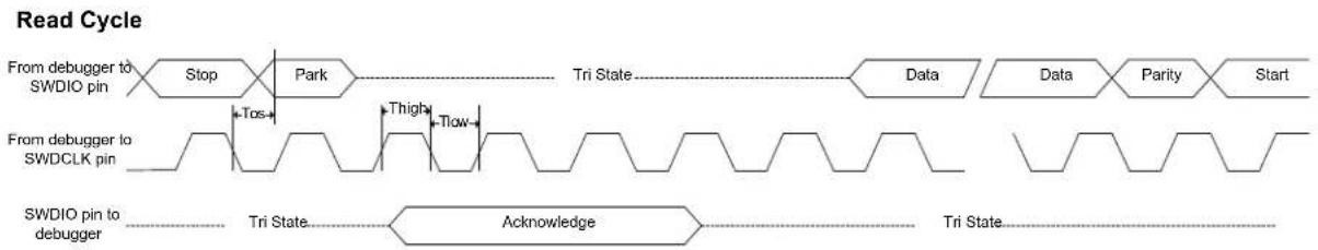
flowchart
graph LR
    A["Stop"] --> B["Park"]
    B --> C["Tri State"]
    C --> D["Data"]
    D --> E["Data"]
    E --> F["Parity"]
    F --> G["Start"]

    H["From debugger to SWDIO pin"] --> I["Tos"]
    I --> J["Thigh"]
    J --> K["Tow"]

    L["From debugger to SWDCLK pin"] --> M["Tri State"]
    M --> N["Acknowledge"]
    N --> O["Tri State"]
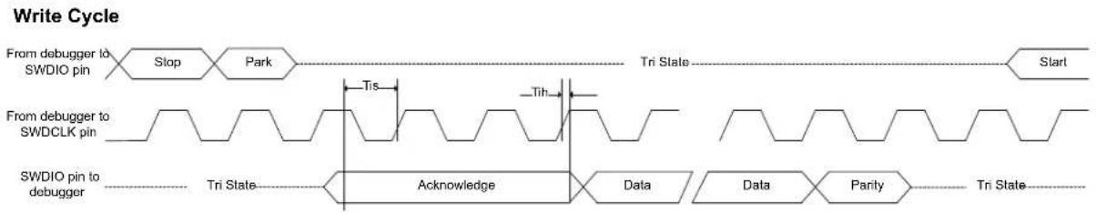
flowchart
graph LR
    A["From debugger to SWDIO pin"] --> B["Stop"]
    B --> C["Park"]
    C --> D["Tri State"]
    D --> E["Start"]
    F["From debugger to SWDCLK pin"] --> G["Tri State"]
    G --> H["Acknowledge"]
    H --> I["Data"]
    I --> J["Data"]
    J --> K["Parity"]
    K --> L["Tri State"]
Table 32-52. SWD Timings ^(1)
| Symbol | Parameter | Conditions | Min. | Max. | Units |
| Thigh | SWDCLK High period | V_VDDIO from 3.0 V to 3.6 V, maximum external capacitor = 40 pF | 10 | 500000 | ns |
| Tlow SWDCLK Low period | 10 | 500000 | |||
| Tos | SWDIO output skew to falling edge SWDCLK | -5 | 5 | ||
| Tis Input Setup time required between SWDIO | 4 | - | |||
| Tih | Input Hold time required between SWDIO and rising edge SWDCLK | 1 | - | ||
Note: 1. These values are based on simulation. These values are not covered by test limits in production or characterization.
33. Electrical Characteristics at 105°C
33.1 Disclaimer
All typical values are measured at T = 25^ unless otherwise specified. All minimum and maximum values are valid across operating temperature and voltage unless otherwise specified.
These electrical characteristics are relevant for SAMD20 revision D and later.
This chapter contains only Electrical Characteristics specific for the SAM D20 at 105^ C. For all other values or missing characteristics, refer to the SAM D20 Electrical Characteristics at 85^ C chapter.
33.2 Absolute Maximum Ratings
Stresses beyond those listed in the following table may cause permanent damage to the device. This is a stress rating only and functional operation of the device at these or other conditions beyond those indicated in the operational sections of this specification is not implied. Exposure to absolute maximum rating conditions for extended periods may affect device reliability.
Table 33-1. Absolute Maximum Ratings
| Symbol Parameter Min. Max. Units | ||||
| V_DD | Power supply voltage 0 3.8 V | |||
| I_VDD | Current into a V_DD pin - 48 | (1) | mA | |
| I_GND | Current out of a GND pin - 68 | (1) | mA | |
| V_PIN | Pin voltage with respect to GND and V_DD | GND-0.6V V | _DD+0.6V V | |
| T_storage | Storage temperature -60 150 °C | |||
Note:
- The maximum source current is 24 mA and maximum sink current is 34 mA per cluster. A cluster is a group of GPIOs as shown in GPIO Clusters table. Each V_DD/GND pair is connected to 2 clusters, hence current consumption through the pair will be a sum of the clusters source/sink currents.
33.3 General Operating Ratings
The device must operate within the ratings listed in the following table in order for all other electrical characteristics and typical characteristics of the device to be valid.
Table 33-2. General operating conditions
| Symbol | Parameter | Min. | Typ. | Max. | Units |
| V_DD | Power supply voltage | 1.62(1) | 3.3 | 3.63 | V |
| V_DDANA | Analog supply voltage 1.62 | (1) | 3.3 | 3.63 | V |
| T_A | Temperature range | -40 | 25 | 105 | °C |
| T_J | Junction temperature | - | - | 125 | °C |
Notes:
- With BOD33 disabled. If the BOD33 is enabled, check BOD33 LEVEL ValueTable 33-10.
- In debugger cold-plugging mode, NVM erase operations are not protected by the BOD33 and BOD12. NVM erase operation at supply voltages below specified minimum can cause corruption of NVM areas that are mandatory for correct device behavior.
Related Links
32.10.3.1. BOD33
33.4 Maximum Clock Frequencies
Table 33-3. Maximum GCLK Generator Output Frequencies
| Symbol Description Conditions | Max. Units | |||
| f_GCLKGEN0 / f_GCLK\_MAIN | GCLK Generator Output Frequency Undivided 48 | |||
| f_GCLKGEN1 | ||||
| f_GCLKGEN2 | ||||
| f_GCLKGEN3 | Divided 32 MHz | |||
| f_GCLKGEN4 | ||||
| f_GCLKGEN5 | ||||
| f_GCLKGEN6 | ||||
| f_GCLKGEN7 |
Table 33-4. Maximum Peripheral Clock Frequencies
| Symbol Description Max. Units | |||
| f_CPU | CPU clock frequency 32 MHz | ||
| f_AHB | AHB clock frequency | 32 MHz | |
| f_APBA | APBA clock frequency | 32 MHz | |
| f_APBB | APBB clock frequency | 32 MHz | |
| f_APBC | APBC clock frequency | 32 MHz | |
| f_GCLK\_DFLL48M\_REF | DFLL48M Reference clock frequency | 35.1 | kHz |
| f_GCLK\_WDT | WDT input clock frequency | 48 MHz | |
| f_GCLK\_RTC | RTC input clock frequency | 48 MHz | |
| f_GCLK\_EIC | EIC input clock frequency | 48 MHz | |
| f_GCLK\_EVSYS\_CHANNEL\_0 | EVSYS channel 0 input clock frequency | 48 MHz | |
| f_GCLK\_EVSYS\_CHANNEL\_1 | EVSYS channel 1 input clock frequency | 48 MHz | |
| f_GCLK\_EVSYS\_CHANNEL\_2 | EVSYS channel 2 input clock frequency | 48 MHz | |
| f_GCLK\_EVSYS\_CHANNEL\_3 | EVSYS channel 3 input clock frequency | 48 MHz | |
| f_GCLK\_EVSYS\_CHANNEL\_4 | EVSYS channel 4 input clock frequency | 48 MHz | |
| f_GCLK\_EVSYS\_CHANNEL\_5 | EVSYS channel 5 input clock frequency | 48 MHz | |
| f_GCLK\_EVSYS\_CHANNEL\_6 | EVSYS channel 6 input clock frequency | 48 MHz | |
| f_GCLK\_EVSYS\_CHANNEL\_7 | EVSYS channel 7 input clock frequency | 48 MHz | |
| f_GCLK\_SERCOMx\_SLOW | Common SERCOM slow input clock frequency | 48 MHz | |
| f_GCLK\_SERCOM0\_CORE | SERCOM0 input clock frequency | 48 MHz | |
| f_GCLK\_SERCOM1\_CORE | SERCOM1 input clock frequency | 48 MHz | |
| f_GCLK\_SERCOM2\_CORE | SERCOM2 input clock frequency | 48 MHz | |
| f_GCLK\_SERCOM3\_CORE | SERCOM3 input clock frequency | 48 MHz | |
| f_GCLK\_SERCOM4\_CORE | SERCOM4 input clock frequency | 48 MHz | |
| f_GCLK\_SERCOM5\_CORE | SERCOM5 input clock frequency | 48 MHz | |
| f_GCLK\_TC0, GCLK\_TC1 | TC0,TC1 input clock frequency | 48 MHz | |
| f_GCLK\_TC2, GCLK\_TC3 | TC2,TC3 input clock frequency | 48 MHz | |
| f_GCLK\_TC4, GCLK\_TC5 | TC4,TC5 input clock frequency | 48 MHz | |
| f_GCLK\_TC6, GCLK\_TC7 | TC6,TC7 input clock frequency | 48 MHz | |
| f_GCLK\_ADC | ADC input clock frequency | 48 MHz | |
| f_GCLK\_AC\_DIG | AC digital input clock frequency | 48 MHz | |
| f_GCLK\_AC\_ANA | AC analog input clock frequency | 64 kHz | |
| f_GCLK\_DAC | DAC input clock frequency | 48 MHz | |
| f_GCLK\_PTC | PTC input clock frequency | 48 MHz |
33.5 Power Consumption
The values provided in the Current Consumption table are measured values of power consumption under the following conditions, except where noted:
- Operating conditions
$$ - \mathrm{V} _ {\text { VDDIN }} = 3. 3 \mathrm{V} $$
- Wake up time from Sleep mode is measured from the edge of the wake up signal to the execution of the first instruction fetched in Flash.
- Oscillators
- XOSC (crystal oscillator) with an external 32 MHz clock on XIN
- XOSC32K (32 kHz crystal oscillator) stopped
- DFLL48M stopped
- Clocks
- XOSC used as main clock source, except otherwise specified
- CPU, AHB clocks undivided
- APBA clock divided by 4
-
APBB and APBC bridges off
-
The following AHB module clocks are running: NVMCTRL, APBA bridge
- All other AHB clocks stopped
- The following peripheral clocks running: PM, SYSCTRL, RTC
- All other peripheral clocks stopped
• I/Os are inactive with internal pull-up
• CPU is running on Flash with 1 wait states - Low-power cache enabled
- BOD33 disabled
Table 33-5. Current Consumption - Variant A
| Mode Conditions T | A | Min. | Typ. Max. Units | ||
| ACTIVE | CPU running a While (1) algorithm | 105°C | -2.55 2.75 | mA | |
| CPU running a while (1) algorithm V_DDIN = 1.8V , CPU is running on Flash with 3 Wait states | -2.56 2.82 | ||||
| CPU running a while (1) algorithm, CPU is running on Flash with 3 Wait states with GCLKIN as reference | -42*freq +318 42*freq +432 | μA(with freq. in MHz) | |||
| CPU running a Fibonacci algorithm - 4.21 4.59 | mA | ||||
| CPU running a Fibonacci algorithm V_DDIN = 1.8V , CPU is running on Flash with 3 Wait states | -4.23 4.57 | ||||
| CPU running a Fibonacci algorithm, CPU is running on Flash with 3 Wait states with GCLKIN as reference | -80*freq +320 82*freq +432 | μA(with freq. in MHz) | |||
| CPU running a CoreMark algorithm - 6.02 6.54 | mA | ||||
| CPU running a CoreMark algorithm V_DDIN = 1.8V , CPU is running on Flash with 3 Wait states | -5.21 5.57 | ||||
| CPU running a CoreMark algorithm, CPU is running on Flash with 3 Wait states with GCLKIN as reference | -96*freq +322 98*freq +432 | μA(with freq in MHz) | |||
| IDLE0 - 1.55 1.62 | mAIDLE1 - 1.13 1.18 | ||||
| IDLE2 - 0.96 1.01 | |||||
| STANDBY | XOSC32K running RTC running at 1 kHz(1) | 25°C - 71.3 | - | μA | |
| 105°C | - 214 | 627 | |||
| XOSC32K and RTC stopped(1) | 25°C - 69.8 | - | |||
| 105°C | - 212 | 624 | |||
Note:
- Measurements were done with SYSCTRL->VREG.bit.RUNSTDBY = 1.
Table 33-6. Current Consumption - Variant B
| Mode Conditions T | A | Min. | Typ. Max. Units | ||
| ACTIVE | CPU running a While(1) algorithm | 105°C - 2.37 | 2.41 | mA | |
| CPU running a while(1) algorithm V_DDIN = 1.8V ,CPU is running on Flash with 3 Wait states | 105°C - 2.37 | 2.41 | |||
| CPU running a while(1) algorithm, CPU is running on Flash with 3 Wait states with GCLKIN as reference | 105°C - 44*freq +187 | 45*freq +189 | μA(with freq. in MHz) | ||
| CPU running a Fibonacci algorithm 105°C - 3.13 | 3.16 | mA | |||
| CPU running a Fibonacci algorithm V_DDIN = 1.8V , CPU is running on Flash with 3 Wait states | 105°C - 3.13 | 3.17 | |||
| CPU running a Fibonacci algorithm, CPU is running on Flash with 3 Wait states with GCLKIN as reference | 105°C - 60*freq +188 | 60*freq +191 | μA(with freq. in MHz) | ||
| CPU running a CoreMark algorithm 105°C - 4.09 | 4.13 | mA | |||
| CPU running a CoreMark algorithm V_DDIN = 1.8V , CPU is running on Flash with 3 Wait states | 105°C - 3.65 | 3.68 | |||
| CPU running a CoreMark algorithm, CPU is running on Flash with 3 Wait states with GCLKIN as reference | 105°C - 80*freq +185 | 80*freq +186 | μA(with freq in MHz) | ||
| IDLE0 105°C - 1.36 | 1.38 | mAIDLE1 105°C - 1.03 | |||
| IDLE2 105°C - 0.81 | 1.82 | ||||
| STANDBY | XOSC32K runningRTC running at 1 kHz(1) | 25°C - | - | - | μA |
| 105°C - | - | 244 | |||
| XOSC32K and RTC stopped(1) | 25°C - | 59.81 | - | ||
| 105°C - | 120.57 | 240 | |||
| XOSC32K runningRTC running at 1 kHz(2) | 25°C - 2.47 | - | |||
| 105°C - | 41.79 | 163 | |||
| XOSC32K and RTC stopped(2) | 25°C | 1.35 | |||
| 105°C | 40.40 | 160 | |||
Notes:
- Measurements were done with SYSCTRL->VREG.bit.RUNSTDBY = 1.
- Measurements were done with SYSCTRL->VREG.bit.RUNSTDBY = 0.
Table 33-7. Wake-up Time
| Mode | Conditions | T_A | Min. | Typ. | Max. | Units |
| IDLE0 | OSC8M used as main clock source, low power cache disabled | 105°C | 3.8 | 4 | 4.1 | μs |
| IDLE1 | 12.8 | 14.3 | 15.7 | |||
| IDLE2 | 13.7 | 15.2 | 16.6 | |||
| STANDBY | 18.7 | 20.1 | 21.6 |
Figure 33-1. Measurement Schematic

text_image
VDDIN VDDANA VDDIO Amp 0 VDDCORE33.6 Injection Current
Stresses beyond those listed in the table below may cause permanent damage to the device. This is a stress rating only and functional operation of the device at these or other conditions beyond those indicated in the operational sections of this specification is not implied. Exposure to absolute maximum rating conditions for extended periods may affect device reliability.
Table 33-8. Injection Current ^(1)
| Symbol Description min. max. Unit | ||||
| I_inj1^(2) | I/O pin injection current -1 +1 mA | |||
| I_inj2^(3) | I/O pin injection current -15 +15 mA | |||
| I_injtotal | Sum of I/O pins injection current -45 +45 mA | |||
Notes:
-
Injecting current may have an effect on the accuracy of analog blocks
-
Conditions for V_pin : V_pin < GND - 0.6V or 3.6V < V_pin ≤ 4.2V .
Conditions for V_DD : 3V < V_DD ≤ 3.6V .
If V_pin is lower than GND-0.6V, then a current limiting resistor is required. The negative DC injection current limiting resistor R is calculated as R = | (GND - 0.6V - V_pin)/I_inj1 | .
If V_pin is greater than V_DD+0.6V , a current limiting resistor is required. The positive DC injection current limiting resistor R is calculated as R = (V_pin - (V_DD + 0.6V)) / I_inj1 .
- Conditions for V_pin : V_pin < GND-0.6V or V_pin ≤ 3.6V .
Conditions for V_DD : V_DD ≤ 3V .
If V_pin is lower than GND-0.6V, a current limiting resistor is required. The negative DC injection current limiting resistor R is calculated as R = | (GND-0.6V - V_pin)/I_inj2 | .
If V_pin is greater than V_DD+0.6V , a current limiting resistor is required. The positive DC injection current limiting resistor R is calculated as R = (V_pin - (V_DD + 0.6V)) / I_inj2 .
33.7 Analog Characteristics
33.7.1 Power-On Reset (POR) Characteristics
Table 33-9. POR Characteristics
| Symbol Parameter Conditions Min. Typ. Max. Units | ||||||
| V_POT+ | Voltage threshold on V_DD rising V | _DD falls at 1V/ms or slower 1.27 1.45 1.60 V | ||||
| V_POT- | Voltage threshold on V_DD falling 0.72 0.99 1.32 V | |||||
Figure 33-2. POR Operating Principle
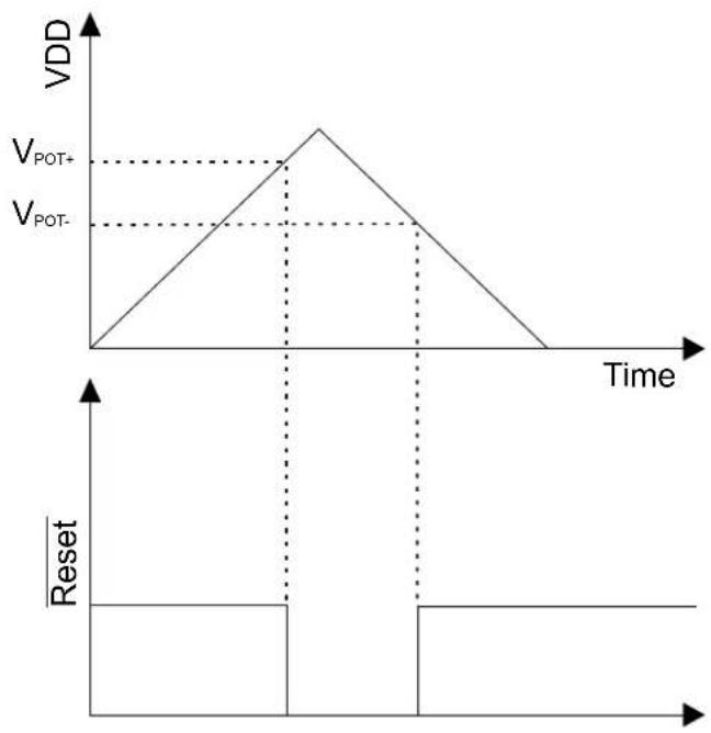
line
| Time | VDD | |------|-----| | 0 | 0 | | Peak | V_POT+ | | Peak | V_POT- | | Final | 0 |33.7.2 Brown-Out Detectors Characteristics
33.7.2.1 BOD33
Table 33-10. BOD33 Characteristics
| Symbol | Parameter | Conditions | Min. | Typ. | Max. | Units | |
| Step size, between adjacent values in BOD33.LEVEL | - | 34 | - | mV | |||
| V_HYST | Hysteresis | 35 | - | 170 mV | |||
| t_DET | Detection time | Time with V_DDANA < V_TH necessary to generate a reset signal | - | 0.9^(1) | - | μs | |
| t_STARTUP | Startup time | - | 2.2^(1) | - | μs | ||
| Symbol | Parameter Conditions Min. Typ. Max. Units | ||||||
| I_IdleBOD33 | Current consumption in Active/Idle Mode | Continuous mode | 25°C 25 48 | μA | |||
| -40°C to 105°C - 51 | |||||||
| Sampling mode | 25°C 0.034 0.21 | ||||||
| -40°C to 105°C - 2.45 | |||||||
| I_SbyBOD33 | Current Consumption in Standby mode Sampling mode | 25°C 0.132 0.38 | μA | ||||
| -40°C to 105°C - 1.5 | |||||||
Note:
- These values are based on simulation. These values are not covered by test limits in production or characterization.
33.7.3 Analog-to-Digital (ADC) characteristics
Table 33-11. Operating Conditions
| Symbol | Parameter | Conditions | Min. | Typ. | Max. | Units |
| RES | Resolution | 8 | - | 12 | bits | |
| f_CLK\_ADC | ADC Clock frequency | 30 | - | 2100 | kHz | |
| Sample rate (1) | Single shot (with V_DDANA > 2.7V ) (4) | 5 - | 300 ksps | |||
| Free running | 5 - | 350 | (3) | ksps | ||
| Sampling time (1) | 250 | -- | ns | |||
| Sampling time with DAC as input(2) | - | 3 -- | μs | |||
| Sampling time with Temp sens as Input(2) | - | 10 | -- | μs | ||
| Sampling time with Bandgap as input(2) | - | 10 | -- | μs | ||
| Conversion time (1) | 1x Gain | -6 | - | cycles | ||
| V_REF | Voltage reference range, (VREFA or VREFB) | 1.0 | - | V_DDANA-0.6 | V | |
| INT1V | Internal 1V reference (2,5) | - | 1.0 | - | V | |
| INTVCC0 | Internal ratiometric reference 0 (2) | - | V_DDANA/1.48 | - | V | |
| INTVCC0 Voltage Error | Internal ratiometric reference 0 error(2) | -1.0 | - | +1.0 | % | |
| INTVCC1 | Internal ratiometric reference 1 (2) | V_DDANA>2.0V | - | V_DDANA/2 | - | V |
| INTVCC1 Voltage Error | Internal ratiometric reference 1 error(2) | 2.0V < V_DDANA < 3.63V | -1.0 | - | +1.0 | % |
| Conversion range (1) | Differential mode | - V_REF/GAIN | - | + V_REF/GAIN | V | |
| Single-ended mode | 0.0 | - | + V_REF/GAIN | V | ||
| C_SAMPLE | Sampling capacitance (2) | - | 3.5 | - | pF | |
| R_SAMPLE | Input channel source resistance (2) | - | - | 3.5 | kΩ | |
| I_DD | DC supply current(1) | f_CLK\_ADC = 2.1MHz (3) | - | 1.25 | 2.78 mA | |
Notes:
-
These values are based on characterization. These values are not covered by test limits in production.
-
These values are based on simulation. These values are not covered by test limits in production or characterization.
-
In this condition and for a sample rate of 350 ksps, a conversion takes 6 clock cycles of the ADC clock (conditions: 1X gain, 12-bit resolution, differential mode, free-running).
-
All single-shot measurements are performed with V DDANA > 2.7V (cf. ADC errata).
-
It is the buffered internal reference of 1.0V derived from the internal 1.1V bandgap reference.
Table 33-12. Differential Mode (Device Variant A) ^(1,2,3,4)
| Symbol | Parameter Conditions Min. Typ. Max. Units | |||||
| ENOB Effective Number Of Bits With gain compensation - 10.5 10.7 bits | ||||||
| TUE | Total Unadjusted Error | 1x Gain | 1.5 | 4.3 | 17.0 | LSB |
| INL | Integral Non Linearity | 1x Gain | 1.0 | 1.3 | 6.3 | LSB |
| DNL | Differential Non Linearity | 1x Gain | ±0.3 | ±0.5 | ±0.95 | LSB |
| GE | Gain Error | Ext. Ref 1x | -15.0 | 2.5 +20.0 | mV | |
| V_REF = V_DDANA/1.48 | -20.0 -1.5 | +10.0 | mV | |||
| V_REF = INT1V | -15.0 -5.0 | +10.0 | mV | |||
| Gain Accuracy (5) | Ext. Ref. 0.5x | ±0.1 ±0.2 ±0.45 | % | |||
| Ext. Ref. 2x to 16x | ±0.1 ±0.2 ±2.0 | % | ||||
| OE | Offset Error | Ext. Ref. 1x | -10.0 -1.5 | +10.0 | mV | |
| V_REF = V_DDANA/1.48 | -10.0 | 0.5 +10.0 | mV | |||
| V_REF = INT1V | -10.0 | 3.0 +10.0 | mV | |||
| SFDR | Spurious Free Dynamic Range | 1x Gain | 64.2 | 70.0 | 78.9 | dB |
| SINAD | Signal-to-Noise and Distortion | F_CLK\_ADC = 2.1 MHz | 61.4 | 65.0 | 66.0 | dB |
| SNR | Signal-to-Noise Ratio | F_IN = 40 kHz | 64.3 | 65.5 | 66.0 | dB |
| THD | Total Harmonic Distortion | A_IN = 95% FSR | -74.8 | -64.0 | -65.0 | dB |
| Noise RMS | T=25°C | 0.6 | 1.0 | 1.6 | mV | |
Table 33-13. Differential Mode (Device Variant B) ^(1,2,3,4)
| Symbol | Parameter | Conditions | Min. | Typ. | Max. | Units |
| ENOB | Effective Number Of Bits | With gain compensation | - | 10.5 | 10.9 | bits |
| TUE | Total Unadjusted Error | 1x Gain | 1.5 | 4.3 | 17 | LSB |
| INL | Integral Non Linearity | 1x Gain | 1 | 1.3 | 6.3 | LSB |
| DNL | Differential Non Linearity | 1x Gain | ±0.3 | ±0.5 | ±0.95 | LSB |
| GE | Gain Error | Ext. Ref 1x | -15 | 2.5 | 20 | mV |
| V_REF = V_DDANA/1.48 | -20 -1.5 | 10 | mV | |||
| V_REF = INT1V | -40 | -5 | 40 | mV | ||
| Gain Accuracy (5) | Ext. Ref. 0.5x | ±0.1 | ±0.2 | ±0.45 | % | |
| Ext. Ref. 2x to 16x | ±0.1 | ±0.2 ±2.0 | % | |||
| OE | Offset Error | Ext. Ref. 1x -20 -1.5 20 | mV | |||
| V_REF = V_DDANA/1.48 | -20 | 0.5 | 20 | mV | ||
| V_REF = INT1V | -40 | 3 | 40 | mV | ||
| Symbol | Parameter Conditions Min. Typ. Max. Units | |||||
| SFDR Spurious Free Dynamic Range | 1x Gain F_CLK\_ADC = 2.1 MHz F_IN = 40 kHz A_IN = 95% FSR | 64.2 70 78.9 dB | ||||
| SINAD Signal-to-Noise and Distortion 61.4 65 66 dB | ||||||
| SNR | Signal-to-Noise Ratio | 64.3 65.5 66 dB | ||||
| THD | Total Harmonic Distortion | -74.8 | -64 | -65 | dB | |
| Noise RMS | T = 25°C | 0.6 | 1 | 1.6 | mV | |
Notes:
- Maximum numbers are based on characterization and not tested in production, and valid for 5% to 95% of the input voltage range.
- Dynamic parameter numbers are based on characterization and not tested in production.
- Respect the input common mode voltage through the following equations (where VCM_IN is the Input channel common mode voltage):
a. If |V_IN| > V_REF/4
- V_CM_IN < 0.95 * V_DDANA + V_REF/4 - 0.75V
- V_CM_IN > V_REF/4 - 0.05 * V_DDANA - 0.1V
b. If |V_IN| < V_REF/4
- V_CM_IN < 1.2^* V_DDANA - 0.75 V
- V_CM_IN > 0.2^* V_DDANA - 0.1 V
-
The ADC channels on pins PA08, PA09, PA10, PA11 are powered from the VDDIO power supply. The ADC performance of these pins will not be the same as all the other ADC channels on pins powered from the VDDANA power supply.
-
The gain accuracy represents the gain error expressed in percent. Gain accuracy (%) = (Gain Error in V × 100) / (2^*VREF/GAIN)
Table 33-14. Single-Ended Mode (Device Variant A) ^(1,2,3)
| Symbol | Parameter | Conditions | Min. | Typ. | Max. | Units |
| ENOB | Effective Number of Bits | With gain compensation | - | 9.5 | 9.8 | Bits |
| TUE | Total Unadjusted Error | 1x gain | - | 10.5 | 40.0 | LSB |
| INL | Integral Non-Linearity | 1x gain | 1.0 | 1.6 | 7.5 | LSB |
| DNL | Differential Non-Linearity | 1x gain | ±0.5 | ±0.6 | ±0.95 | LSB |
| GE | Gain Error | Ext. Ref. 1x | -5.0 | 0.7 | +5.0 | mV |
| Gain Accuracy^(4) | Ext. Ref. 0.5x | ±0.1 | ±0.34 | ±0.4 | % | |
| Ext. Ref. 2x to 16X ±0.01 | ±0.1 | ±0.15 | % | |||
| OE | Offset Error | Ext. Ref. 1x | -5.0 | 1.5 | +10.0 | mV |
| SFDR | Spurious Free Dynamic Range | 1x Gain | 63.1 | 65.0 | 66.5 | dB |
| SINAD | Signal-to-Noise and Distortion | F_CLK\_ADC = 2.1 MHz | 50.7 | 59.5 | 61.0 | dB |
| SNR | Signal-to-Noise Ratio | F_IN = 40 kHz | 49.9 | 60.0 | 64.0 | dB |
| THD | Total Harmonic Distortion | A_IN = 95% FSR | -65.4 | -63.0 | -62.1 | dB |
| Noise RMS | T = 25°C | - | 1.0 | - | mV |
Table 33-15. Single-Ended Mode (Device Variant B) ^(1,2,3)
| Symbol | Parameter | Conditions | Min. | Typ. | Max. | Units |
| ENOB | Effective Number of Bits | With gain compensation | - | 9.5 | 9.9 | Bits |
| TUE | Total Unadjusted Error | 1x gain | - | 10.5 | 45 | LSB |
| INL | Integral Non-Linearity | 1x gain | 1 | 1.6 | 7.5 | LSB |
| DNL | Differential Non-Linearity | 1x gain | ±0.5 | ±0.6 | ±0.95 | LSB |
| Symbol | Parameter Conditions Min. Typ. Max. Units | |||||
| GE | Gain Error Ext. Ref. 1x -15 0.7 15 mV | |||||
| Gain Accuracy^(4) | Ext. Ref. 0.5x ±0.2 ±0.34 ±0.6 % | |||||
| Ext. Ref. 2x to 16X ±0.01 ±0.1 ±0.3 % | ||||||
| OE | Offset Error | Ext. Ref. 1x -15 1.5 25 mV | ||||
| SFDR Spurious Free Dynamic Range | 1x Gain | 63.1 | 65 | 66.5 | dB | |
| SINAD | Signal-to-Noise and Distortion | F_CLK\_ADC = 2.1 MHz | 50.7 | 59.5 | 61 | dB |
| SNR | Signal-to-Noise Ratio | F_IN = 40 kHz | 49.9 | 60 | 64 | dB |
| THD | Total Harmonic Distortion | A_IN = 95% FSR | -65.4 | -63 | -62.1 | dB |
| Noise RMS | T = 25°C | - | 1 | - | mV | |
Notes:
- Maximum numbers are based on the characterization and not tested in production, and for 5% to 95% of the input voltage range.
-
Respect the input common mode voltage through the following equations (where VCM_IN is the Input channel common mode voltage) for all VIN:
-
VCM_IN < 0.7*VDDANA + VREF/4 - 0.75V
-
VCM_IN > VREF/4 - 0.3*VDDANA - 0.1V
-
The ADC channels on pins PA08, PA09, PA10, PA11 are powered from the VDDIO power supply. The ADC performance of these pins will not be the same as all the other ADC channels on pins powered from the VDDANA power supply.
- The gain accuracy represents the gain error expressed in percent. Gain accuracy (\%) = (Gain Error in V x 100) / (VREF/GAIN).
33.7.3.1 Inputs and Sample and Hold Acquisition Times
The analog voltage source must be able to charge the sample and hold (S/H) capacitor in the ADC in order to achieve maximum accuracy. Seen externally the ADC input consists of a resistor ( R_SAMPLE ) and a capacitor ( C_SAMPLE ). In addition, the source resistance ( R_SOURCE ) must be taken into account when calculating the required sample and hold time. The figure below shows the ADC input channel equivalent circuit.
Figure 33-3. ADC Input
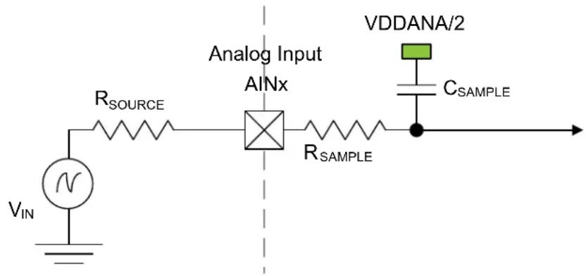
text_image
Analog Input AINx R_SOURCE VDDANA/2 R_SAMPLE C_SAMPLE VIN NTo achieve n bits of accuracy, the C_SAMPLE capacitor must be charged at least to a voltage of
$$ V _ {\text { CSAMPLE }} \geq V _ {\text { IN }} \times \left(1 - 2 ^ {- (n + 1)}\right) $$
The minimum sampling time t_SAMPLEHOLD for a given R_SOURCE can be found using this formula:
$$ t _ {\text { SAMPLEHOLD }} \geq (R _ {\text { SAMPLE }} + R _ {\text { SOURCE }}) \times q (\text { SAMPLE }) \times n (+ 1 \times \ln) 2 \tag {()} $$
for a 12 bits accuracy: t_SAMPLEHOLD ≥ (R_SAMPLE + R_SOURCE) × Q(SAMPLE) × 9.02
where
$$ t _ {\text { SAMPLEHOLD }} = \frac {1}{2 \times f _ {\mathrm{ADC}}} $$
33.7.4 Digital-to-Analog Converter (DAC) Characteristics
Table 33-16. Operating Conditions
| Symbol | Parameter Conditions Min. Typ. Max. Units | ||||||
| V_DDANA | Analog supply voltage - 1.62 - | 3.63 | V | ||||
| External reference voltage | - | 1.0 | - | V_DDANA-0.6 | V | ||
| AV_REF | INT1V | - | - | 1 | - | V | |
| VDDANA | - | - | V_DDANA | - | V | ||
| Linear output voltage range | - 0.05 - V | _DDANA-0.05 | V | ||||
| Minimum resistive load | - | 5 | - | - | kΩ | ||
| Maximum capacitance load | - | - | - | 100 | pF | ||
| I_DD | DC supply current (1) | Voltage pump disabled | - | 160 | 378 | μA | |
Note:
- These values are based on characterization and are not covered by test limits in production.
Table 33-17. Clock and Timing
| Symbol | Parameter | Conditions | Min. | Typ. | Max. | Units | |
| Conversion rate | C_load=100pF | Normal mode | - | - | 350 | ksps | |
| R_load>5kΩ | For Δ_DATA=±1 | - | - | 1000 | |||
| tSTARTUP | Startup time | V_DDNA>2.6V | - | - | 2.85 | μs | |
| V_DDNA<2.6V | - | - | 10 μs | ||||
Note: These values are based on simulation and are not covered by test limits in production or characterization.
Table 33-18. Accuracy Characteristics (Device Variant A)
| Symbol | Parameter | Conditions (1) | Min. | Typ. | Max. | Units | |
| RES | Input resolution | - | - | - | 10 | Bits | |
| INL | Integral non-linearity | V_REF = Ext 1.0V | V_DD = 1.6V | 0.75 | 1.1 | 2.0 | LSB |
| V_DD = 3.6V | 0.6 | 1.2 | 2.5 | ||||
| V_REF = V_DDANA | V_DD = 1.6V | 1.4 | 2.2 | 3.5 | |||
| V_DD = 3.6V | 0.9 | 1.4 | 1.5 | ||||
| V_REF = INT1V | V_DD = 1.6V | 0.75 | 1.3 | 2.5 | |||
| V_DD = 3.6V | 0.8 | 1.2 | 1.5 | ||||
| DNL | Differential non-linearity | V_REF = Ext 1.0V | V_DD = 1.6V | ±0.9 | ±1.2 | ±2.0 | LSB |
| V_DD = 3.6V | ±0.9 | ±1.1 | ±1.5 | ||||
| V_REF = V_DDANA | V_DD = 1.6V | ±1.1 | ±1.7 | ±3.0 | |||
| V_DD = 3.6V | ±1.0 | ±1.1 | ±1.6 | ||||
| V_REF = INT1V | V_DD = 1.6V | ±1.1 | ±1.4 | ±2.5 | |||
| V_DD = 3.6V | ±1.0 | ±1.5 | ±1.8 | ||||
| GE | Gain error | Ext. V_REF | ±1.0 | ±5 | ±10 | mV | |
| Symbol Parameter Conditions | (1) | Min. Typ. Max. | Units | |
| OE Offset error Ext. V | REF | ±2 ±3 ±8 mV |
Note:
- All values are measured using a conversion rate of 35 ksps.
Table 33-19. Accuracy Characteristics (Device Variant B)
| Symbol Parameter Conditions | (1) | Min. Typ. | Max. Units | ||||
| RES | Input resolution | - | - | 10 | Bits | ||
| INL | Integral non-linearity | VREF = Ext 1.0V | VDD = 1.6V | 0.75 | 1.1 2 LSB | ||
| VDD = 3.6V 0.6 | 1.2 2.5 | ||||||
| VREF = VDDANA | VDD = 1.6V 1.4 | 2.2 3.5 | |||||
| VDD = 3.6V 0.9 | 1.4 1.5 | ||||||
| VREF = INT1V | VDD = 1.6V | 0.75 | 1.3 3.1 | ||||
| VDD = 3.6V 0.8 | 1.2 2.7 | ||||||
| DNL | Differential non-linearity | VREF = Ext 1.0V | VDD = 1.6V | ±0.9 | ±1.2 | ±2.0 | LSB |
| VDD = 3.6V | ±0.9 | ±1.1 | ±1.5 | ||||
| VREF = VDDANA | VDD = 1.6V | ±1.1 + -1.7 | ±3.0 | ||||
| VDD = 3.6V | ±1.0 | ±1.1 | ±1.6 | ||||
| VREF = INT1V | VDD = 1.6V | ±1.1 | ±1.5 | ±3.0 | |||
| VDD = 3.6V | ±1.0 | ±1.5 | ±2,9 | ||||
| GE | Gain error | Ext. VREF | ±1.0 | ±5 | ±12 | mV | |
| OE | Offset error | Ext. VREF | ±2 | ±3 | ±8 | mV | |
Note:
- All values measured using a conversion rate of 35 ksps.
33.7.5 Analog Comparator Characteristics
Table 33-20. Electrical and Timing (Device Variant A)
| Symbol | Parameter | Conditions | Min. | Typ. | Max. | Units |
| Positive input voltage range | 0 | - | V_DDANA | V | ||
| Negative input voltage range | 0 | - | V_DDANA | |||
| Offset | Hysteresis = 0, Fast mode | -15 | 0.0 | +15 | mV | |
| Hysteresis = 0, Low power mode | -25 | 0.0 | +25 | mV | ||
| Hysteresis | Hysteresis = 1, Fast mode | 20 | 50 | 80 | mV | |
| Hysteresis = 1, Low power mode | 15 | 40 | 75 | mV | ||
| Propagation delay | Changes for V_ACM=V_DDANA/2 100mV overdrive, Fast mode | - | 60 | 116 | ns | |
| Changes for V_ACM=V_DDANA/2 100mV overdrive, Low power mode | - | 225 | 370 | ns | ||
| t_STARTUP | Startup time | Enable to ready delayFast mode | - | 1 | 2 | μs |
| Enable to ready delayLow power mode | - | 12 | 19 | μs | ||
| V_SCALE | INL(3) | -1.4 | 0.75 | +1.4 | LSB | |
| DNL(3) | -0.9 | 0.25 | +0.9 | LSB | ||
| Offset Error(1,2) | -0.200 | 0.260 | +0.920 | LSB | ||
| Gain Error(1,2) | -0.89 | 0.215 | 0.89 LSB |
Notes:
- According to the standard equation V(X) = V_LSB * (X + 1); V_LSB = V_DDANA / 64 .
- Data computed with the Best Fit method.
- Data computed using histogram.
Table 33-21. Electrical and Timing (Device Variant B)
| Symbol | Parameter Conditions Min. Typ. Max. | Units | ||||
| Positive input voltage range 0 - V | DDANA | V | ||||
| Negative input voltage range 0 - V | DDANA | |||||
| Offset | Hysteresis = 0, Fast mode -15 0.0 +15 mV | |||||
| Hysteresis = 0, Low power mode | -25 0.0 +25 mV | |||||
| Hysteresis | Hysteresis = 1, Fast mode | 20 | 50 | 80 | mV | |
| Hysteresis = 1, Low power mode | 15 | 40 | 75 | mV | ||
| Propagation delay | Changes for V_ACM = V_DDANA/2 100mV overdrive, Fast mode | - | 90 | 180 | ns | |
| Changes for V_ACM = V_DDANA/2 100mV overdrive, Low power mode | - | 282 | 520 | ns | ||
| t_STARTUP | Startup time | Enable to ready delayFast mode | -1 | 2.6 | μs | |
| Enable to ready delayLow power mode | - | 12 | 22 | μs | ||
| V_SCALE | INL(3) | -1.4 | 0.75 | +1.4 | LSB | |
| DNL(3) | -0.9 | 0.25 | +0.9 | LSB | ||
| Offset Error (1,2) | -0.200 | 0.260 | +0.920 LSB | |||
| Gain Error (1,2) | -0.89 | 0.215 0.89 | LSB | |||
Notes:
- According to the standard equation V(X) = V_LSB * (X + 1) ; V_LSB = V_DDANA / 64 .
- Data computed with the Best Fit method.
- Data computed using histogram.
33.7.6 Temperature Sensor Characteristics
Table 33-22. Temperature Sensor Characteristics ^(1)
| Symbol | Parameter | Conditions | Min. | Typ. | Max. | Units |
| Temperature sensor output voltage | T = 25^, V_DDANA = 3.3V | -0.667 | - | V | ||
| Temperature sensor slope | 2.3 | 2.4 | 2.5 | mV/°C | ||
| Variation over V_DDANA voltage | V_DDANA = 1.62V to 3.6V | -4 | 1 | 6 | mV/V | |
| Temperature sensor accuracy | Using the method described in section 32.9.8.2 | -10 | - | 10 | °C |
Note: 1. These values are based on characterization. These values are not covered by test limits in production.
Related Links
32.10.8.2. Software-based Refinement of the Actual Temperature
33.8 NVM Characteristics
Table 33-23. Maximum Operating Frequency
| V_DD range NVM Wait States Maximum Operating Frequency Units | |||
| 1.62V to 2.7V 0 14 MHz | |||
| 1 | 28 | ||
| 2 | 32 | ||
| 2.7V to 3.63V 0 20 | |||
| 1 | 32 | ||
Note: On this flash technology, a max number of 4 consecutive write is allowed per row. Once this number is reached, a row erase is mandatory.
Table 33-24. Flash Endurance and Data Retention
| Symbol Parameter Conditions Min. Typ. Max. Units | ||||||
| Ret_NVM25k | Retention after up to 25k cycles | Average ambient 55°C | 10 | 50 | - | Years |
| Ret_NVM2.5k | Retention after up to 2.5k cycles | Average ambient 55°C | 20 | 100 | - | Years |
| Ret_NVM100 | Retention after up to 100 cycles | Average ambient 55°C | 25 | >100 | - | Years |
| Cyc_NVM | Cycling Endurance(1) | -40°C < Ta < 105°C | 25k | 150k | - | Cycles |
Note:
- An endurance cycle is a write and an erase operation.
Table 33-25. EEPROM Emulation ^(1) Endurance and Data Retention
| Symbol | Parameter | Conditions | Min. | Typ. | Max. | Units |
| Ret_EEPROM100k | Retention after up to 100k cycles | Average ambient 55°C | 10 | 50 | - | Years |
| Ret_EEPROM10k | Retention after up to 10k cycles | Average ambient 55°C | 20 | 100 | - | Years |
| Cyc_EEPROM | Cycling Endurance^(2) | -40°C < Ta < 105°C | 100k | 600k | - | Cycles |
Notes:
- The EEPROM Emulation is a software emulation described in the App note AT03265.
- An endurance cycle is a write and an erase operation.
Table 33-26. NVM Characteristics
| Symbol | Parameter | Conditions | Min. | Typ. | Max. | Units |
| t_FPP | Page programming time | - | - | - | 2.5 | ms |
| t_FRE | Row erase time | - | - | - | 6 | ms |
| t_FCE | DSU chip erase time (CHIP_ERASE) | -- | 240 | ms |
33.9 Oscillators Characteristics
33.9.1 Crystal Oscillator (XOSC) Characteristics
33.9.1.1 Digital Clock Characteristics
The following table provides the characteristics for the oscillator when a digital clock is applied on XIN.
Table 33-27. Digital Clock Characteristics
| Symbol | Parameter | Conditions | Min. | Typ. | Max. | Units |
| f_CPXIN | XIN clock frequency | - | - | - | 32 | MHz |
33.9.1.2 Crystal Oscillator Characteristics
The following table provides the characteristics for the oscillator when a crystal is connected between XIN and XOUT as shown in the figure Oscillator Connection. The user must choose a crystal oscillator where the crystal load capacitance C_L is within the range given in the table below. The exact value of C_L can be found in the crystal data sheet. The capacitance of the external capacitors ( C_LEXT ) can then be computed as follows:
Load Capacitance Equation:
$$ C _ {\text { LOAD }} = \left(\left[ C _ {\mathrm{XIN}} + C _ {\mathrm{LEXT}} \right] * \left[ C _ {\mathrm{XOUT}} + C _ {\mathrm{LEXT}} \right]\right) / \left(\left[ C _ {\mathrm{XIN}} + C _ {\mathrm{LEXT}} + C _ {\mathrm{LEXT}} + C _ {\mathrm{XOUT}} \right]\right) + C _ {\text { STRAY }} $$
Where:
C_LOAD = Crystal Mfg. C_LOAD specification
C_XIN = XOSC XIN pin data sheet specification
C_XOUT = XOSC XOUT pin data sheet specification
C_LEXT = Required external crystal load capacitor
C_STRAY (Osc PCB capacitance) = 1.5 pF per 12.5 mm (0.5 inches) (TRACE W = 0.175 mm, H = 36 μm, T = 113 μm)
For C_XIN and C_XOUT within 4 pF of each other, assume C_XIN = C_XOUT = C_XTAL_EFF = ((C_XIN + C_XOUT) / 2) (Averaging C_XIN and C_XOUT will effect final calculated C_LOAD value by less than 0.25 pF.)
The load capacitance equation can then be simplified as follows:
$$ C _ {L E X T} = 2 ^ {} C _ {L O A D} - C _ {X T A L _ E F F} - 2 ^ {} C _ {S T R A Y} $$
Table 33-28. Crystal Oscillator Characteristics
| Symbol | Parameter Conditions Min. Typ. Max. Units | |||||
| f_OUT | Crystal oscillator frequency - 0.4 - 32 MHz | |||||
| ESR Crystal Equivalent Series Resistance Safety Factor = 3 The AGC doesn't have any noticeable impact on these measurements. | f = 0.455 MHz, C_L = 100 pFXOSC.GAIN = 0 | -- 5.6K Ω | ||||
| f = 2 MHz, C_L = 20 pFXOSC.GAIN = 0 | -- 416 | |||||
| f = 4 MHz, C_L = 20 pFXOSC.GAIN = 1 | -- 243 | |||||
| f = 8 MHz, C_L = 20 pFXOSC.GAIN = 2 | -- 138 | |||||
| f = 16 MHz, C_L = 20 pFXOSC.GAIN = 3 | -- 66 | |||||
| f = 32 MHz, C_L = 18 pFXOSC.GAIN = 4 | -- 56 | |||||
| C_XIN | Parasitic capacitor load - 5.9 - pF | |||||
| C_XOUT | Parasitic capacitor load - 3.2 - pF | |||||
| Current Consumption f = 2 MHz, C | L = 20 pF, XOSC.GAIN = 0, AGC off | 27 | 65 | 87 | μA | |
| f = 2 MHz, C_L = 20 pF, XOSC.GAIN = 0, AGC on | 14 | 52 | 76 | |||
| f = 4 MHz, C_L = 20 pF, XOSC.GAIN = 1, AGC off | 61 | 117 | 155 | |||
| f = 4 MHz, C_L = 20 pF, XOSC.GAIN = 1, AGC on | 23 | 74 | 104 | |||
| f = 8 MHz, C_L = 20 pF, XOSC.GAIN = 2, AGC off | 131 | 226 | 308 | |||
| f = 8 MHz, C_L = 20 pF, XOSC.GAIN = 2, AGC on | 56 | 128 | 181 | |||
| f = 16 MHz, C_L = 20 pF, XOSC.GAIN = 3, AGC off | 305 | 502 | 714 | |||
| f = 16 MHz, C_L = 20 pF, XOSC.GAIN = 3, AGC on | 116 | 307 | 590 | |||
| f = 32 MHz, C_L = 18 pF, XOSC.GAIN = 4, AGC off | 1031 | 1622 | 2260 | |||
| f = 32 MHz, C_L = 18 pF, XOSC.GAIN = 4, AGC on | 278 | 615 | 1280 | |||
| t_STARTUP | Startup time f = 2MHz,C | L = 20pF , XOSC.GAIN = 0,ESR = 600 | - 14K 48K cycles | |||
| f = 4MHz,C_L = 20pF , XOSC.GAIN = 1,ESR = 100 | - 6800 19.5K | |||||
| f = 8 MHz,C_L = 20pF , XOSC.GAIN = 2,ESR = 35 | - 5550 13K | |||||
| f = 16 MHz,C_L = 20pF , XOSC.GAIN = 3,ESR = 25 | - 6750 14.5K | |||||
| f = 32MHz,C_L = 18pF , XOSC.GAIN = 4,ESR = 40 | - 5.3K 9.6K | |||||
Figure 33-4. Oscillator Connection
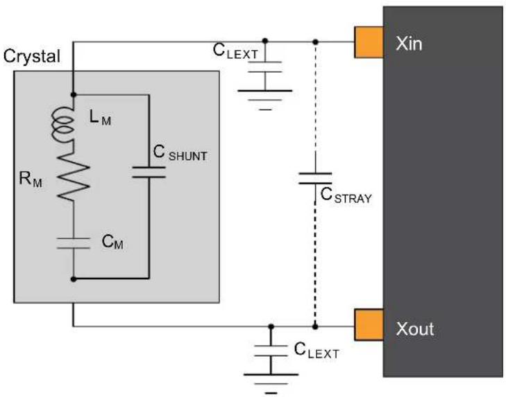
text_image
Crystal L_M R_M C_SHUNT C_M C_LEXT C_STRAY Xin Xout C_LEXT33.9.2 External 32 kHz Crystal Oscillator (XOSC32K) Characteristics
33.9.2.1 Digital Clock Characteristics
The following table describes the characteristics for the oscillator when a digital clock is applied on the XIN32 pin.
Table 33-29. Digital Clock Characteristics ^(1)
| Symbol | Parameter | Conditions | Min. | Typ. | Max. | Units |
| f_CPXIN32 | XIN32 clock frequency | - | - | 32.768 | - | kHz |
| DCxin | XIN32 clock duty cycle | - | - | 50 | - | % |
Note:
- These values are based on simulation and not covered by the test or characterization.
33.9.2.2 Crystal Oscillator Characteristics
Figure 32-6 and the equation in 32.12.1.2. Crystal Oscillator Characteristics also applies to the 32kHz oscillator connection. The user must choose a crystal oscillator where the crystal load capacitance C_L is within the range given in the table. The exact value of C_L can be found in the crystal data sheet.
For the computation of the external capacitors ( C_LEXT ) value, refer to the logic detailed in XOSC Crystal Oscillator Characteristics.
Table 33-30. 32 kHz Crystal Oscillator Characteristics
| Symbol | Parameter Conditions Min. Typ. Max. Units | ||||||
| f_OUT | Crystal oscillator frequency -- 32768 - Hz | ||||||
| t_STARTUP | Startup time ESR | XTAL = 39.9 k, C_L = 12.5 pF - 28K 30K cycles | |||||
| C_L | Crystal load capacitance | -- | -12.5 | pF | |||
| C_SHUNT | Crystal shunt capacitance | -- | 0.1 | - | |||
| C_XIN32 | Parasitic capacitor load | -- | 3.1 | - | |||
| C_XOUT32 | Parasitic capacitor load | - | 3.3 | - | |||
| I_XOSC32K | Current consumption | AGC off | - | 1.22 | 2.25 | μA | |
| AGC on^(1) | - | - | - | ||||
| ESR | Crystal equivalent series resistance F = 32.768 kHzSafety Factor = 3 | C_L=12.5 pF | - | - | 141 | kΩ | |
Note: 1. Refer to the revision D/revision C/revision B errata related to the XOSC32K.
33.9.3 Digital-Frequency Locked Loop (DFLL48M) Characteristics
Table 33-31. DFLL48M Characteristics - Closed Loop Mode ^(1)
| Symbol | Parameter | Conditions | Min. | Typ. | Max. | Units |
| f_OUT | Average Output frequency | f_REF = XOSC32K 32.768 kHz | 47 | 48 | 49 | MHz |
| f_REF | Reference frequency | - | 0.732 | 32.768 | 35.1 | kHz |
| Jitter | Period jitter | f_REF = XOSC32K 32.768 kHz | - | - | 0.84 | ns |
| I_DFLL | Power consumption on V_DDIN | f_REF = XOSC32K 32.768 kHz | - | 292 | - | μA |
| t_LOCK | Lock time | f_REF = XOSC32K 32.768 kHz DFLLVAL.COARSE =DFLL48M COARSE CALDFLLVAL.FINE = 512DFLLCTRL.BPLCKC = 1DFLLCTRL.QLDIS = 0DFLLCTRL.CCDIS = 1DFLLMUL.FSTEP = 10 | 100 | 200 | 500 | μs |
| Quick lock disabled,Chill cycle disabled,CSTEP = 3,FSTEP = 1, f_REF = XOSC32K 32.768 kHz | - | 600 | - |
Note: 1. Refer to the revision C/revision B errata pertaining to the DFLL48M.
2. All parts are tested in production to be able to use the DFLL as main CPU clock whether in DFLL closed-loop mode with an external OSC reference or in DFLL closed-loop mode using the internal OSC8M (only applicable for revision C).
33.9.4 32.768 kHz Internal oscillator (OSC32K) Characteristics
Table 33-32. 32 kHz RC Oscillator Characteristics
| Symbol Parameter Conditions Min. Typ. Max. Units | ||||||
| f_OUT | Output frequency Calibrated against a 32.768 kHz reference at 25°C, over [-40, +105]C, over [1.62, 3.63]V | 28.508 32.768 35.062 kHz | ||||
| Calibrated against a 32.768 kHz reference at 25°C, at V_DD=3.3V | 32.276 32.768 33.260 | |||||
| Calibrated against a 32.768 kHz reference at 25°C, over [1.62, 3.63]V | 31.457 32.768 34.079 | |||||
| I_OSC32K | Current consumption -- 0.67 1.62 μA | |||||
| t_STARTUP | Startup time -- 1 2 | cycle | ||||
| Duty | Duty Cycle | -- 50 - % | ||||
33.9.5 Ultra-Low Power Internal 32 kHz RC Oscillator (OSCULP32K) Characteristics
Table 33-33. Ultra-Low Power Internal 32 kHz RC Oscillator Characteristics
| Symbol | Parameter | Conditions | Min. | Typ. | Max. | Units |
| f_OUT | Output frequency | Calibrated against a 32.768 kHz reference at 25°C, over [-40,+105]C, over [1.62, 3.63]V | 25.559 | 32.768 | 39.016 | kHz |
| Calibrated against a 32.768 kHz reference at 25°C, at V_DD = 3.3V | 31.293 | 32.768 | 34.570 | |||
| Calibrated against a 32.768 kHz reference at 25°C, over[1.62, 3.63]V | 31.293 | 32.768 | 34.570 | |||
| I_OSCULP32K^(1)(2) | - | - | - | - | 180 | nA |
| t_STARTUP | Startup time | - | - | 10 | - | cycles |
| Duty | Duty Cycle | - | - | 50 | - | % |
Notes: 1. These values are based on simulation and not covered by test limits in production or characterization.
2. This oscillator is always on.
33.9.6 8 MHz RC Oscillator (OSC8M) Characteristics
Table 33-34. Internal 8 MHz RC Oscillator Characteristics
| Symbol | Parameter | Conditions | Min. | Typ. | Max. | Units |
| f_OUT | Output frequency | Calibrated against a 8 MHz reference at 25°C, over [-40, +105]C, over [1.62, 3.63]V | 7.65 | 8 8.17 | MHz | |
| Calibrated against a 8 MHz reference at 25°C, at V_DD = 3.3V | 7.94 | 8 8.06 | ||||
| Calibrated against a 8 MHz reference at 25°C, over [1.62, 3.63]V | 7.92 | 8 | 8.08 | |||
| I_OSC8M | Current consumption | IDLEIDLE2 on OSC32K versus IDLE2 on calibrated OSC8M enabled at 8 MHz (FRANGE = 1, PRESC = 0) | - | 71 | 168 | μA |
| t_STARTUP | Startup time | - | - | 2.1 | 3 | μs |
| Duty | Duty cycle | - | - | 50 | - | % |
34. AEC-Q100 Electrical Characteristics at 125°C
34.1 Disclaimer
The AEC-Q100 Electrical Characteristics described in this chapter only apply to the Device Variant B. The electrical characteristics for Device Variant B described in chapters "32. Electrical Characteristics at 85°C" and "33. Electrical Characteristics at 105°C" do not meet the requirements of AEC-Q100.
All typical values are measured at T = 25^ unless otherwise specified. All minimum and maximum values are valid across operating temperature and voltage unless otherwise specified.
The BOD33 must always be activated (SYSCTRL.BOD33[ENABLE] = 1) when the device is used under the AEC-Q100 grading. This secures power-up, startup sequence, and power-down events. It will participate in protecting the data and code loaded into the embedded Flash memory. Usage of the BOD33 in sampled mode (SYSCTRL.BOD33[MODE] = 1) is discouraged. BOD33 must be kept in continuous mode (SYSCTRL.BOD33[MODE] = 0) whenever power consumption is not a concern.
The temperature readings achieved through the Temperature Sensor (TSENS) feature do not meet the requirements of AEC-Q100. No specifications can be defined for the Temperature Sensor (TSENS). This feature must not be used with AEC-Q100 parts.
The Low-Power mode of the regulator cannot be used while entering the STANDBY power-saving configuration with AEC-Q100 parts. Such configuration will not meet the Safety definitions and requirements of the AEC-Q100. SYSCTRL VREG.RUNSTDBY = 1 must always be set before entering the STANDY power-saving configuration.
34.2 Absolute Maximum Ratings
Stresses beyond those listed in the following table, may cause permanent damage to the device. This is a stress rating only and functional operation of the device at these or other conditions beyond those indicated in the operational sections of this specification is not implied. Exposure to absolute maximum rating conditions for extended periods may affect device reliability.
Table 34-1. Absolute maximum ratings
| Symbol Parameter Min. Max. Units | ||||
| V_DD | Power supply voltage 0 3.8 V | |||
| I_VDD | Current into a V_DD pin - 28 | (1) | mA | |
| I_GND | Current out of a GND pin - 39 | (1) | mA | |
| V_PIN | Pin voltage with respect to GND and V_DD | GND-0.3V V | _DD+0.3V V | |
| T_storage | Storage temp -60 150 °C | |||
Note:
- Maximum source current is 14 mA and maximum sink current is 19.5 mA per cluster. A cluster is a group of GPIOs as shown in the following table. Each V_DD/GND pair is connected to 2 clusters, hence current consumption through the pair will be a sum of the clusters source or sink currents.
Table 34-2. GPIO Clusters
| PACKAGE CLUSTER GPIO | SUPPLY PINS CONNECTED TO THE CLUSTER | ||||||||||||||||
| 64 pins TQFP and VQFN | 1 PB31 | PB30 | PA31 | PA30 | VDDIN pin56/GND | pin54 | |||||||||||
| 2 PA28 | PA27 | PB23 | PB22 | VDDIN pin56/GND pin54 and VDDIO pin 48/GND pin47 | |||||||||||||
| 3 PA25 | PA24 | PA23 | PA22 | PA21 | PA20 | PB17 | PB16 | PA19 | PA18 | PA17 | PA16 | VDDIO pin 48/GND pin47 and VDDIO pin34/GND pin33 | |||||
| 4 PA15 | PA14 | PA13 | PA12 | PB15 | PB14 | PB13 | PB12 | PB11 | PB10 | VDDIO pin 34/GND pin33 and VDDIO pin21/GND pin22 | |||||||
| 5 PA11 | PA10 | PA09 | PA08 | VDDIO pin21/GND pin22 | |||||||||||||
| 6 PA07 | PA06 | PA05 | PA04 | PB09 | PB08 | PB07 | PB06 | VDDANA pin 8/GNDANA pin7 | |||||||||
| 7 PB05 | PB04 | PA03 | PA02 | PA01 | PA00 | PB03 | PB02 | PB01 | PB00 | VDDANA pin 8/GNDANA pin7 | |||||||
| 48 pins TQFP and VQFN | 1 PA31 | PA30 | VDDIN pin44/GND pin42 | ||||||||||||||
| 2 PA28 | PA27 | PB23 | PB22 | VDDIN pin44/GND pin42 and VDDIO pin36/GND pin35 | |||||||||||||
| 3 PA25 | PA24 | PA23 | PA22 | PA21 | PA20 | PA19 | PA18 | PA17 | PA16 | PA15 | PA14 | PA13 | PA12 | PB11 | PB10 | ||
| 4 PA11 | PA10 | PA09 | PA08 | VDDIO pin17/GND pin18 | |||||||||||||
| 5 PA07 | PA06 | PA05 | PA04 | PB09 | PB08 | VDDANA pin6/GNDANA pin5 | |||||||||||
| 6 PA03 | PA02 | PA01 | PA00 | PB03 | PB02 | VDDANA pin6/GNDANA pin5 | |||||||||||
| 32 pins TQFP and VQFN | 1 PA31 | PA30 | VDDIN pin30/GND pin 28 | ||||||||||||||
| 2 PA28 | PA27 | PA25 | PA24 | PA23 | PA22 | PA19 | PA18 | PA17 | PA16 | PA15 | PA14 | PA11 | PA10 | PA09 | PA08 | ||
| 3 PA07 | PA06 | PA05 | PA04 | PA03 | PA02 | PA01 | PA00 | VDDANA pin9/GND pin10 | |||||||||
34.3 General Operating Ratings
The device must operate within the ratings listed in the table in order for all other electrical characteristics and typical characteristics of the device to be valid.
Table 34-3. General operating conditions
| Symbol Parameter Min. Typ. Max. Units | |||||
| V_DD | Power-supply voltage 2.7 3.3 3.63 V | ||||
| V_DDANA | Analog-supply voltage 2.7 3.3 3.63 V | ||||
| T_A | Temperature range -40 25 125 °C | ||||
| T_J | Junction temperature | - | - | 145 °C | |
Note:
- In debugger Cold-Plugging mode, the NVM erase operations are not protected by the BOD33 and BOD12. NVM erase operation at supply voltages below specified minimum can cause corruption of NVM areas that are mandatory for correct device behavior.
34.4 Supply Characteristics
The following supply characteristics are applicable to the operating temperature range: T_A = -40^ to 125^ , unless otherwise specified and are valid for a junction temperature up to T_J = 145^ .
Table 34-4. Supply Characteristics
| Symbol | Conditions | Voltage | ||
| Min. | Max. | Units | ||
| V_DDIO | Full-Voltage Range | 2.7 | 3.63 | V |
| V_DDIN | ||||
| V_DDANA | ||||
Table 34-5. Supply Rise Rates
| Symbol | Conditions | Fall Rate | Rise Rate | Units | |
| Max. | Min.(1) | Max. | |||
| VDDIO | DC supply peripheral I/Os, internal regulator, and analog-supply voltage | 50E-3 | 430E-6 | 0.1 | V/us |
| VDDIN | |||||
| VDDANA | |||||
Note:
- The Minimum Supply Rise Rate does not apply if the voltage on the Reset pin is lower than VIL.max (see 34.8.5 External Reset Pin) until VDD reaches a minimum voltage of 1.73V.
34.5 Maximum Clock Frequencies
Table 34-6. Maximum GCLK Generator Output Frequencies
| Symbol | Description | Conditions | Max. | Units |
| f_GCLKGENO/f_GCLK\_MAIN | GCLK Generator Output Frequency | Undivided | 48 | MHz |
| f_GCLKGEN1 | ||||
| f_GCLKGEN2 | ||||
| f_GCLKGEN3 | Divided | 32 | ||
| f_GCLKGEN4 | ||||
| f_GCLKGEN5 | ||||
| f_GCLKGEN6 | ||||
| f_GCLKGEN7 |
Table 34-7. Maximum Peripheral Clock Frequencies
| Symbol Description | Max. Units | ||
| f_CPU | CPU clock frequency 32 MHz | ||
| f_AHB | AHB clock frequency 32 MHz | ||
| f_APBA | APBA clock frequency 32 MHz | ||
| f_APBB | APBB clock frequency 32 MHz | ||
| f_APBC | APBC clock frequency 32 MHz | ||
| f_GCLK\_DFLL48M\_REF | DFLL48M Reference clock frequency 33 kHz | ||
| f_GCLK\_WDT | WDT input clock frequency 48 MHz | ||
| f_GCLK\_RTC | RTC input clock frequency 48 MHz | ||
| f_GCLK\_EIC | EIC input clock frequency 48 MHz | ||
| f_GCLK\_EVSYS\_CHANNEL\_0 | EVSYS channel 0 input clock frequency 48 MHz | ||
| f_GCLK\_EVSYS\_CHANNEL\_1 | EVSYS channel 1 input clock frequency 48 MHz | ||
| f_GCLK\_EVSYS\_CHANNEL\_2 | EVSYS channel 2 input clock frequency 48 MHz | ||
| f_GCLK\_EVSYS\_CHANNEL\_3 | EVSYS channel 3 input clock frequency 48 MHz | ||
| f_GCLK\_EVSYS\_CHANNEL\_4 | EVSYS channel 4 input clock frequency 48 MHz | ||
| f_GCLK\_EVSYS\_CHANNEL\_5 | EVSYS channel 5 input clock frequency 48 MHz | ||
| f_GCLK\_EVSYS\_CHANNEL\_6 | EVSYS channel 6 input clock frequency 48 MHz | ||
| f_GCLK\_EVSYS\_CHANNEL\_7 | EVSYS channel 7 input clock frequency 48 MHz | ||
| f_GCLK\_SERCOMX\_SLOW | Common SERCOM slow Input clock frequency 48 MHz | ||
| f_GCLK\_SERCOM0\_CORE | SERCOM0 input clock frequency | 48 MHz | |
| f_GCLK\_SERCOM1\_CORE | SERCOM1 input clock frequency | 48 MHz | |
| f_GCLK\_SERCOM2\_CORE | SERCOM2 input clock frequency | 48 MHz | |
| f_GCLK\_SERCOM3\_CORE | SERCOM3 input clock frequency | 48 MHz | |
| f_GCLK\_SERCOM4\_CORE | SERCOM4 input clock frequency | 48 MHz | |
| f_GCLK\_SERCOM5\_CORE | SERCOM5 input clock frequency | 48 MHz | |
| f_GCLK\_TC0, GCLK\_TC1 | TC0, TC1 input clock frequency | 48 MHz | |
| f_GCLK\_TC2, GCLK\_TC3 | TC2, TC3 input clock frequency | 48 MHz | |
| f_GCLK\_TC4, GCLK\_TC5 | TC4, TC5 input clock frequency | 48 MHz | |
| f_GCLK\_TC6, GCLK\_TC7 | TC6, TC7 input clock frequency | 48 MHz | |
| f_GCLK\_ADC | ADC input clock frequency | 48 MHz | |
| f_GCLK\_AC\_DIG | AC digital input clock frequency | 48 MHz | |
| f_GCLK\_AC\_ANA | AC analog input clock frequency | 48 MHz | |
| f_GCLK\_DAC | DAC input clock frequency | 48 MHz | |
| f_GCLK\_PTC | PTC input clock frequency 48 MHz |
Note:
- These values are based on simulation and not covered by production test limits or characterization.
34.6 Power Consumption
The values provided in the table Current Consumption are measured values of power consumption under the following conditions, except where noted:
• Operating conditions:
$$ - V _ {V D D I N} = 3. 3 \mathrm{V} $$
- Wake up time from Sleep mode is measured from the edge of the wakeup signal to the execution of the first instruction fetched in Flash.
- Oscillators
- XOSC (crystal oscillator) stopped
- XOSC32K (32 kHz crystal oscillator) running with external 32 kHz crystal
- DFLL48M using XOSC32K as reference and running at 48 MHz
- Clocks
- DFLL48M used as main clock source, except otherwise specified.
- CPU, AHB clocks undivided
- APBA clock divided by 4
- APBB and APBC bridges off
• The following AHB module clocks are running: NVMCTRL, APBA bridge
- All other AHB clocks stopped
• The following peripheral clocks running: PM, SYSCTRL, RTC
- All other peripheral clocks stopped
• I/Os are inactive with internal pull-up
• CPU is running on Flash with 1 wait states
- NVMCTRL cache enabled
Table 34-8. Current Consumption ^(2)
| Mode Conditions T | A | Vcc | Min. | Typ. | Max. | Units | |||
| ACTIVE | CPU running a While(1) algorithm | 25°C 3.3V - 2.27 2.48 | mA | ||||||
| 125°C 3.3V - 2.41 3.32 | |||||||||
| CPU running a While(1) algorithm, with GCLKIN as reference | 25°C 3.3V - 43*freq +108 | 52*freq +135 | μA(with freq in MHz) | ||||||
| 125°C 3.3V - 44*freq +276 | 50*freq +949 | ||||||||
| CPU running a Fibonacci algorithm | 25°C 3.3V - 3.04 3.26 | mA | |||||||
| 125°C 3.3V - 3.19 3.76 | |||||||||
| CPU running a Fibonacci algorithm, with GCLKIN as reference | 25°C 3.3V - 59*freq +109 | 62*freq +133 | μA(with freq in MHz) | ||||||
| 125°C 3.3V - 60*freq +276 | 58*freq +953 | ||||||||
| CPU running a CoreMark algorithm | 25°C 3.3V - 3.90 4.42 | mA | |||||||
| 125°C 3.3V - 4.34 4.81 | |||||||||
| CPU running a CoreMark algorithm, with GCLKIN as reference | 25°C 3.3V - | 77* freq +108 | 85* freq +130 | μA(with freq in MHz) | |||||
| 125°C 3.3V - | 83 * freq + 288 | 81* freq +974 | |||||||
| IDLE0 | - | 25°C 3.3V - 1.28 1.37 | mA | ||||||
| 125°C 3.3V - 1.44 2.05 | |||||||||
| IDLE1 | - | 25°C 3.3V - 0.97 1.05 | |||||||
| 125°C 3.3V - 1.09 1.70 | |||||||||
| IDLE2 | - | 25°C 3.3V - 0.76 0.83 | |||||||
| 125°C 3.3V - 0.88 1.50 | |||||||||
| STANDBY | XOSC32K runningRTC running at 1 kHz ^(1) | 25°C 3.3V - | 62.00 | 85.00 | μA | ||||
| 125°C | 3.3.V - | 198.00 | 442.00 | ||||||
| XOSC32K and RTC stopped ^(1) | 25°C 3.3V - | 61.00 | 84.00 | ||||||
| 125°C ^(3) | 3.3V - | 196.00 | 438 | ||||||
Notes:
- Measurements were done with SYSCTRL->VREG.bit.RUNSTDBY = 1.
- These values are based on characterization and not covered by test limits in production unless otherwise specified.
- These values are screened during production.
Table 34-9. Wake-up Time
| Mode Conditions T | A | Min. | Typ. | Max. | Units | ||
| IDLE0 OSC8M used as main clock source, cache disabled | 25°C - 4.0 - | μs | |||||
| 125°C - 4.0 - | |||||||
| IDLE1 OSC8M used as main clock source, cache disabled | 25°C - 12.1 - | ||||||
| 125°C - 14.9 - | |||||||
| IDLE2 OSC8M used as main clock source, cache disabled | 25°C - 13.0 - | ||||||
| 125°C - 15.8 - | |||||||
| STANDBY OSC8M used as main clock source, cache disabled | 25°C - 19.6 - | ||||||
| 125°C - 20.6 - | |||||||
Figure 34-1. Measurement Schematic
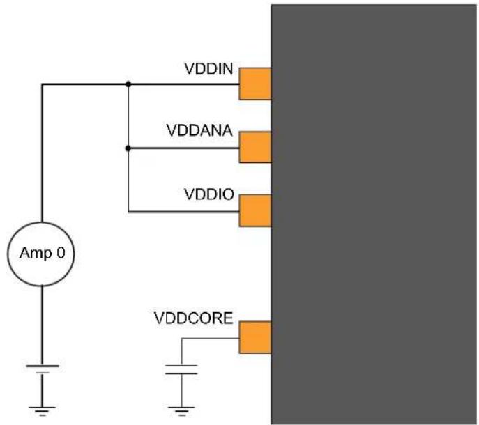
text_image
VDDIN VDDANA VDDIO VDDCORE Amp 034.7 Peripheral Power Consumption
Default conditions, except where noted:
- Operating conditions
$$ - V _ {V D D I N} = 3. 3 \mathrm{V} $$
- Oscillators
- XOSC (crystal oscillator) stopped
- XOSC32K (32 kHz crystal oscillator) running with external 32 kHz crystal
- OSC8M at 8 MHz
- Clocks
- OSC8M used as main clock source
-
CPU, AHB, and APBn clocks undivided
-
The following AHB module clocks are running: NVMCTRL, HPB2 bridge, HPB1 bridge, HPB0 bridge – All other AHB clocks stopped
- The following peripheral clocks running: PM, SYSCTRL – All other peripheral clocks stopped
• I/Os are inactive with internal pull-up - CPU in IDLE0 mode
- Cache enabled
• BOD33 disabled
In this default conditions, the power consumption I_default is measured.
Operating mode for each peripheral in turn:
- Configure and enable the peripheral GCLK (When relevant, see conditions)
- Unmask the peripheral clock
- Enable the peripheral (when relevant)
- Set CPU in IDLE0 mode
• Measurement I periph - Wake-up CPU through EIC (async: level detection, filtering disabled)
- Disable the peripheral (when relevant)
- Mask the peripheral clock
- Disable the peripheral GCLK (when relevant, see conditions)
Each peripheral power consumption details provided in table x-9 is the value ( I_periph - I_default ), using the same measurement method as for global power consumption measurement.
Table 34-10. Typical Peripheral Power Consumption
| Peripheral Conditions Typ. Units | |||
| RTC f | _GCLK\_RTC = 32 kHz, 32 bit counter mode 6.2 | μA | |
| WDT f | _GCLK\_WDT = 32 kHz, normal mode with EW 3.4 | ||
| AC Both f | _GCLK = 8 MHz, Enable both COMP 116.0 | ||
| TCx(1) | f_GCLK = 8 MHz, Enable + COUNTER in 8 bit mode 42.3 | ||
| SERCOMx.I2CM(2) | f_GCLK = 8 MHz, Enable 76.9 | ||
| SERCOMx.I2CS(2) | f_GCLK = 8 MHz, Enable 36.5 | ||
| SERCOMx.SPI(2) | f_GCLK = 8 MHz, Enable 70.6 | ||
| SERCOMx.USART(2) | f_GCLK = 8 MHz, Enable 88.0 | ||
Notes:
- All TCs share the same power consumption values.
- All SERCOMs share the same power consumption values.
34.8 I/O Pin Characteristics
34.8.1 Normal I/O Pins
Table 34-11. Normal I/O Pin Characteristics
| Symbol | Parameter Conditions Min. Typ. Max. Units | |||||
| R_PULL | Pull-up and Pull-down resistance - 20 40 60 kΩ | |||||
| V_IL | Input low-level voltage | V_DD=2.7V-3.63V | - | - | 0.3* V_DD | V |
| V_IH | Input high-level voltage | V_DD=2.7V-3.63V | 0.55* V_DD | - | - | |
| V_OL | Output low-level voltage | V_DD>2.7V, I_OLmax. | - | 0.1* V_DD | 0.2* V_DD | |
| V_OH | Output high-level voltage | V_DD>2.7V, I_OHmax. 0.8*V | DD | 0.9* V_DD | - | |
| I_OL | Output low-level current | V_DD=2.7V-3.63V, PORT.PINCFG.DRVSTR=0 | - | - | 2.5 | mA |
| V_DD=2.7V-3.63V, PORT.PINCFG.DRVSTR=1 | - | - | 10 | |||
| I_OH | Output high-level current | V_DD=2.7V-3.63V, PORT.PINCFG.DRVSTR=0 | - | - | 2 | |
| V_DD=2.7V-3.63V, PORT.PINCFG.DRVSTR=1 | - | - | 7 | |||
| t_RISE | Rise time(1) | PORT.PINCFG.DRVSTR=0 load=5 pF, V_DD=3.3V | - | - | 15 | ns |
| PORT.PINCFG.DRVSTR=1 load=20 pF, V_DD=3.3V | - | - | 15 | |||
| t_FALL | Fall time(1) | PORT.PINCFG.DRVSTR=0 load=5 pF, V_DD=3.3V | - | - | 15 | |
| PORT.PINCFG.DRVSTR=1 load=20 pF, V_DD=3.3V | - | - | 15 | |||
| t_LEAK | Input leakage current | Pull-up resistors disabled | -1 | +/-0.015 | 1 | μA |
Note:
- These values are based on simulation and not covered by test limits in production or characterization.
34.8.2 I ^2 C Pins
Refer to I/O Multiplexing and Considerations to obtain the list of I²C pins.
Table 34-12. I²C Pins Characteristics in I²C configuration
| Symbol | Parameter | Condition | Min. | Typ. | Max. | Units |
| R_PULL | Pull-up - Pull-down resistance | 20 | 40 | 60 | kΩ | |
| V_IL | Input low-level voltage | V_DD=2.7V-3.63V | - | - | 0.3*V_DD | |
| V_IH | Input high-level voltage | V_DD=2.7V-3.63V | 0.55*V_DD | - | - | V |
| V_HYS | Hysteresis of Schmitt trigger inputs | 0.08*V_DD | - | - | ||
| V_OL | Output low-level voltage | V_DD>2.7V I_OL=3mA | - | - | 0.4 | |
| I_OL | Output low-level current | V_OL=0.4V | 3 | - | - | mA |
| V_OL=0.6V | 6 | - | - | |||
| f_SCL | SCL clock frequency | - | - | 400 | kHz |
I ^2 C pins timing characteristics can be found in 32.14.3. SERCOM in I2C Mode Timing.
34.8.3 XOSC Pin
The XOSC pins behave as normal pins when used as normal I/Os. For additional information, refer to the Table 32-12.
34.8.4 XOSC32 Pin
The XOSC32 pins behave as normal pins when used as normal I/Os. For additional information, refer to the Table 32-12.
34.8.5 External Reset Pin
The External Reset pin has the same electrical characteristics as normal I/O pins. For additional information, refer to the Table 32-12.
34.9 Injection Current
Stresses beyond those listed in the table below may cause permanent damage to the device. This is a stress rating only and functional operation of the device at these or other conditions beyond those indicated in the operational sections of this specification is not implied. Exposure to absolute maximum rating conditions for extended periods may affect device reliability.
Table 34-13. Injection Current ^(1)
| Symbol Description min. max. Unit | ||||
| linj1^(2) | I/O pin injection current -1 +1 mA | |||
| linjtotal | Sum of I/O pins injection current -45 +45 mA | |||
Notes:
- Injecting current may have an effect on the accuracy of analog blocks.
- Conditions for V_pin : V_pin < GND-0.3V or 3.6V < V_pin ≤ 3.9V .
Conditions for V_DD : 2.7V< V_DD ≤3.6V.
If V_pin is lower than GND-0.3V, then a current limiting resistor is required. The negative DC injection current limiting resistor R is calculated as R = | (GND-0.3V - V_pin)/I_inj1 | .
If V_pin is greater than V_DD+0.3V , a current limiting resistor is required. The positive DC injection current limiting resistor R is calculated as R = (V_pin - (V_DD + 0.3V)) / I_inj1 .
34.10 Analog Characteristics
34.10.1 Voltage Regulator Characteristics
Table 34-14. Voltage Regulator Electrical Characteristics
| Symbol | Parameter Conditions Min. Typ. Max. Units | ||||
| V_DDCORE | DC calibrated output voltage Voltage regulator normal mode 1.1 1.23 1.30 V |
Note: Supplying any external components using the V_DDCORE pin is not allowed to assure the integrity of the core supply voltage.
Table 34-15. Decoupling Requirements
| Symbol | Parameter | Conditions | Min. | Typ. | Max. | Units |
| C_IN | Input regulator capacitor, between VDDIN and GND | - | 10 | - | μF | |
| - | 100 | - | nF | |||
| - | 10 | - | nF | |||
| C_OUT | Output regulator capacitor, between VDDCORE and GND | Require ESR 0.5 ohms | 0.8 | 1 | - | μF |
34.10.2 Power-On Reset (POR) Characteristics
Table 34-16. POR Characteristics
| Symbol | Parameter | Conditions | Min. | Typ. | Max. | Units |
| V_POT+ | Voltage threshold on V_DD rising | V_DD rise/fall at 1V/ms or slower | 1.27 | 1.45 | 1.62 | V |
| V_POT- | Voltage threshold on V_DD falling | 0.72 | 0.99 | 1.32 | V |
Figure 34-2. POR Operating Principle

line
| Time | VDD | |------|-----| | 0 | 0 | | Peak | V_POT+ | | Peak | V_POT- | | Final | 0 |34.10.3 Brown-Out Detectors (BOD) Characteristics
34.10.3.1 BOD33
Figure 34-3. BOD33 Hysteresis OFF
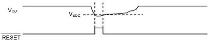
text_image
Vcc VBOD RESETFigure 34-4. BOD33 Hysteresis ON
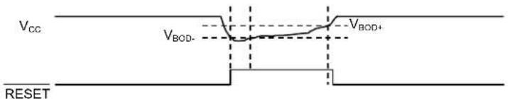
text_image
VCC VBOD- VBD+ RESETTable 34-17. BOD33 LEVEL Value
| Symbol BOD33.LEVEL Conditions Min. Typ. Max. Units | ||||||
| V_BOD+ | 34 Hysteresis ON - 2.68 2.74 | V | ||||
| V_BOD- or V_BOD | 34 | Hysteresis ONorHysteresis OFF | 2.51 2.59 2.65 | |||
Note: Refer to the NVM User Row Mapping for the BOD33 for the BOD33 default value settings.
Table 34-18. BOD33 Characteristics
| Symbol | Parameter | Conditions | Ta | Min. | Typ. | Max. | Units |
| - | Step size, between adjacent values in BOD33.LEVEL | - | - | - | 34 | - | mV |
| V_HYST | V_BOD+-V_BOD- | Hysteresis ON | - | 35 | - | 170 | mV |
| t_DET | Detection time(1) | Time with V_DDANA| - | - | 0.9 | - | μs | |
| t_{STARTUP} | Startup time(1) | - | - | - | 2.2 | - | μs |
| I_{IdleBOD33} | Current consumption in Active mode or Idle mode | Continuous mode | 25°C - | 33 | 48 | μA | |
| -40 to 125°C | - | - | 53 | ||||
| Sampling mode | 25°C - | 0.034 | 0.50 | ||||
| -40 to 125°C | - | - | 3.00 | ||||
| I_{SbyBOD33}$ | Current Consumption in Standby mode | Sampling mode | 25°C - | 0.130 | 0.50 | μA | |
| -40 to 125°C | - | - | 1.7 |
Note:
- These values are based on simulation and not covered by test limits in production or characterization.
34.10.4 Analog-to-Digital (ADC) Characteristics
Table 34-19. Operating Conditions
| Symbol Parameter Conditions Min. Typ. Max. Units | ||||||
| RES Resolution - 8 - 12 bits | ||||||
| f_CLK\_ADC | ADC Clock frequency - 120 | - 2100 | kHz | |||
| Sample rate (1) | Single shot | 20 | - | 300 | ksps | |
| Free running | 20 | - | 350^(3) | ksps | ||
| Sampling time (1) | - 250 | - | - ns | |||
| Sampling time with DAC as input (2) | - 3 - | - μs | ||||
| Sampling time with Temp sens as input (2) | - | 10 | - | - μs | ||
| Sampling time with Bandgap as input (2) | - | 10 | - | - μs | ||
| Conversion time - Differential mode | Gain: x1 (1) | - 6 | - | cycles | ||
| Gain: x0.5, x2, x4 (2) | - 7 | - | ||||
| Gain: x8, x16 (2) | 8 | - | ||||
| Conversion time - Single Ended mode | Gain: x1 (1) | - 7 | - | cycles | ||
| Gain: x0.5, x2, x4 (2) | - 8 | - | ||||
| Gain: x8, x16 (2) | - 9 | - | ||||
| V_REF | Voltage reference range (VREFA or VREFB) | - | 2.0 | - | V_DDANA-0.6 | V |
| INT1V | Internal 1V reference (2,4) | - | - | 1.0 | - | V |
| INTVCC0 | Internal ratiometric reference 0 (2) | 2.7V < V_DDANA<3.63V | - | V_DDANA/1.48 | - | V |
| INTVCC0 Voltage Error | Internal ratiometric reference 0 error (2) | 2.7V < V_DDANA<3.63V | -1.0 | - | +1.0 % | |
| INTVCC1 | Internal ratiometric reference 1 (2) | 2.7V < V_DDANA<3.63V | - | V_DDANA/2 | - | V |
| INTVCC1 Voltage Error | Internal ratiometric reference 1 error (2) | 2.7V < V_DDANA<3.63V | -1.0 | - | +1.0 % | |
| Conversion range (1) | Differential mode | - V_REF/GAIN | - | + V_REF/GAIN | V | |
| Single-ended mode | 0.0 | - | + V_REF/GAIN | V | ||
| C_SAMPLE | Sampling capacitance (2) | - | 3.5 | - pF | ||
| R_SAMPLE | Input channel source resistance (2) | - | - | 3.5 | kΩ | |
| I_DD | DC supply current (1) | f_CLK\_ADC=2.1 MHz^(3) | - | 1.25 | 4.7 | mA |
Notes:
- These values are based on characterization and not covered by test limits in production.
- These values are based on simulation, are not covered by test limits in production or characterization.
- In this condition and for a sample rate of 350 ksps, a conversion takes 6 clock cycles of the ADC clock (conditions: 1X gain, 12-bit resolution, differential mode, free-running).
- It is the buffered internal reference of 1.0V derived from the internal 1.1V bandgap reference.
Table 34-20. Differential Mode ^(2,4)
| Symbol | Parameter | Conditions | Min. | Typ. | Max. | Units |
| ENOB | Effective Number Of Bits | 1x Gain, Ext. Ref. 2V ≤ VREF ≤ 3V(1) | 9.9 | 10.7 | 10.8 | bits |
| TUE | Total Unadjusted Error | 1x Gain, Ext. Ref. 2V ≤ VREF ≤ 3V(1) | 0.8 | 3.1 | 9.9 | LSB |
| 1x Gain, VREF = VDDANA/1.48(1) | 2.3 | 6.9 | 15 | LSB | ||
| 1x Gain, VREF = INT1V | 4.0 | 8.6 | 32 | LSB | ||
| INL | Integral Non Linearity | 1x Gain, Ext. Ref. 2V ≤ VREF ≤ 3V(1) | 0.67 | 0.98 | 1.6 | LSB |
| 1x Gain, VREF = VDDANA/1.48(1) | 0.70 | 1.1 | 1.7 | LSB | ||
| 1x Gain, VREF = INT1V | 1.2 | 1.8 | 3 | LSB | ||
| Symbol | Parameter Conditions Min. Typ. Max. Units | |||||
| DNL Differential Non Linearity | 1x Gain, Ext. Ref. 2V ≤ VREF ≤ 3V(1) | +/-0.4 +/-0.6 +/-0.8 LSB | ||||
| 1x Gain, VREF = VDDANA/1.48(1) | +/-0.5 +/-0.7 +/-0.9 LSB | |||||
| 1x Gain, VREF = INT1V +/-0.6 +/-0.8 +/-3 LSB | ||||||
| GE | Gain Error | 1x Gain, Ext. Ref. 2V ≤ VREF ≤ 3V(1) | -13 -3.6 +9 mV | |||
| 1x Gain, VREF = VDDANA/1.48(1) | -36 -10.6 +22 mV | |||||
| 1x Gain, VREF = INT1V | -29 -2.7 +18 mV | |||||
| Gain Accuracy(3) | 0.5x Gain, Ext. Ref. 2V ≤ VREF ≤ 3V(1) | +/-0.1 +/-0.2 +/-0.3 % | ||||
| 2x to 16x Gain, Ext. Ref. 2V ≤ VREF ≤ 3V(1) | +/-0.1 +/-0.4 +/-0.6 % | |||||
| OE | Offset Error | 1x Gain, Ext. Ref. 2V ≤ VREF ≤ 3V(1) | -6 | 2.3 | +10 | mV |
| 1x Gain, VREF = VDDANA/1.48(1) | -5 | 1.6 | +10 | mV | ||
| 1x Gain, VREF = INT1V | -4 | 2.1 | +10 | mV | ||
| SFDR | Spurious Free Dynamic Range | 1x Gain Ext. Ref 2V ≤ VREF ≤ 3V | 77 | 85 | 87 | dB |
| SINAD | Signal-to-Noise and Distortion | FCLK_ADC = 2.1 MHz | 61 | 53 | 67 | dB |
| SNR | Signal-to-Noise Ratio | FIN = 40 kHz | 63 | 54 | 69 | dB |
| THD | Total Harmonic Distortion | AIN = 95% FSR | -73 | -71 | -64 | dB |
| Noise RMS | Ta = 25°C | 0.6 | 1 | 2.5 | mV | |
Notes:
- Specifications are based on characterization and not covered by production screening.
- Respect the input common mode voltage through the following equations (where, VCM_IN is the input channel common mode voltage):
a. If |VIN| > VREF/4
$$ \mathrm {VCM_IN} < 0. 9 5 ^ {*} \mathrm{VDDANA} + \mathrm{VREF/4-0.75V} $$
$$ \mathrm {VCM_IN} > \mathrm{VREF/4-0.05*VDDANA-0.1V} $$
b. If |VIN| < VREF/4
$$ \mathrm {VCM_IN} < 1. 2 * \text { VDDANA } - 0. 7 5 \mathrm{V} $$
$$ \mathrm {VCM_IN} > 0. 2 * \text { VDDANA } - 0. 1 \mathrm{V} $$
- The gain accuracy represents the gain error expressed in percent. Gain accuracy (\%) = (Gain Error in V x 100) / (2*Vref/GAIN).
- With gain compensation enabled (REFCTRL.REFCOMP = 1).
Table 34-21. Single-Ended Mode (1,2,4)
| Symbol | Parameter | Conditions | Min. | Typ. | Max. | Units |
| ENOB | Effective Number of Bits | 1x Gain, Ext. Ref. 2V ≤ VREF≤ 3V | 8.9 | 9.9 | 10.1 | Bits |
| TUE | Total Unadjusted Error | 1x Gain, Ext. Ref. 2V ≤ VREF ≤ 3V | 1.6 | 7 | 22 | LSB |
| INL | Integral Non-Linearity | 1x Gain, Ext. Ref. 2V ≤ VREF ≤ 3V | 1.0 | 1.5 | 3.0 | LSB |
| DNL | Differential Non-Linearity | 1x Gain, Ext. Ref. 2V ≤ VREF≤ 3V | ±0.5 | ±0.8 | ±0.95 | LSB |
| GE | Gain Error | 1x Gain, Ext. Ref. 2V ≤ VREF ≤ 3V | -7.1 | -0.3 | 7.1 | mV |
| Gain Accuracy (3) | 0.5x Gain, Ext. Ref. 2V ≤ VREF≤ 3V | ±0.1 | ±0.2 | ±0.4 | % | |
| 2x to 16x Gain, Ext. Ref. 2V ≤ VREF≤ 3V | ±0.2 | ±0.6 | ±0.9 | % | ||
| OE | Offset Error | 1x Gain, Ext. Ref. 2V ≤ VREF ≤ 3V | -9 | 5.5 | 28 | mV |
| SFDR | Spurious Free Dynamic Range | 1x GainExt. Ref. 2V ≤ VREF ≤ 3VFCLK_ADC= 2.1 MHz | 70 | 80 84 | dB | |
| SINAD | Signal-to-Noise and Distortion | 56 | 61 | 62 | dB | |
| SNR | Signal-to-Noise Ratio | F_IN = 40 kHz | 58 | 63 | 64 | dB |
| THD | Total Harmonic Distortion | A_IN = 95% FSR | -68 | -67 | -59 | dB |
| ......continued | ||||||
| Symbol | Parameter Conditions Min. Typ. Max. Units | |||||
| Noise RMS T = 25°C - 16 mV | ||||||
Notes:
- Specifications are based on characterization and not covered by production screening.
- Respect the input common mode voltage through the following equations (where VCM_IN is the Input channel common mode voltage) for all VIN:
$$ \mathrm {VCM_IN} < 0. 7 ^ {*} \mathrm{VDDANA} + \mathrm{VREF/4} - 0. 7 5 \mathrm{V} $$
$$ \mathrm {VCM_IN} > \mathrm{VREF/4-0.3*VDDANA-0.1V} $$
- The gain accuracy represents the gain error expressed in percent. Gain accuracy (\%) = (Gain Error in V x 100) / (V _REF /GAIN).
- With gain compensation enabled (REFCTRL.REFCOMP = 1)
34.10.4.1 Performance with the Averaging Digital Feature
Averaging is a feature which increases the sample accuracy. ADC automatically computes an average value of multiple consecutive conversions. The numbers of samples to be averaged is specified by the Number-of-Samples-to-be-Collected bit group in the Average Control register (AVGCTRL.SAMPLENUM[3:0]) and the averaged output is available in the Result register (RESULT).
Table 34-22. Averaging feature
| Average Number | Conditions | SNR (dB) | SINAD (dB) | SFDR (dB) | ENOB (bits) |
| 1 | In Differential mode, 1x gain, V_DDANA = 3.0V , V_REF = 2.0V , 350 kspsT = 25°C | 66 | 65 | 85 | 10.5 |
| 8 | 68 | 66 | 87 | 11.4 | |
| 32 | 70 | 67 | 88 | 11.6 | |
| 128 | 71 | 67 | 88 | 11.7 |
34.10.4.2 Performance with the Hardware Offset and Gain Correction
Inherent gain and offset errors affect the absolute accuracy of the ADC. The offset error cancellation is handled by the Offset Correction register (OFFSETCORR) and the gain error cancellation, by the Gain Correction register (GAINCORR). The offset and gain correction value is subtracted from the converted data before writing the Result register (RESULT).
Table 34-23. Offset and Gain correction features
| Gain Factor | Conditions | Offset Error (mV) | Gain Error (mV) | Total Unadjusted Error (LSB) |
| 0.5x | In differential mode, 1x gain, V_DDANA = 3.0V , V_REF = 2.0V , 350 kspsT = 25°C | 0.25 | 1.0 | 2.4 |
| 1x | 0.20 | 0.10 | 1.5 | |
| 2x | 0.15 | -0.15 | 2.7 | |
| 8x | -0.05 | 0.05 | 3.2 | |
| 16x | 0.10 | -0.05 | 6.1 |
34.10.4.3 Inputs and Sample and Hold Acquisition Times
The analog voltage source must be able to charge the Sample-and-Hold (S/H) capacitor in the ADC to achieve maximum accuracy. Seen externally the ADC input consists of a resistor ( R_SAMPLE ) and a capacitor ( C_SAMPLE ). In addition, the source resistance ( R_SOURCE ) must be considered when calculating the required S/H time. The figure below shows the ADC input channel equivalent circuit.
Figure 34-5. ADC Input
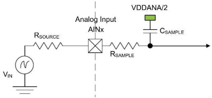
text_image
V_{IN} R_{SOURCE} Analog Input AINx R_{SAMPLE} VDDANA/2 C_{SAMPLE}To achieve 'n' bits of accuracy, the C_SAMPLE capacitor must be charged at least to a voltage of
$$ V _ {\text { CSAMPLE }} \geq V _ {\mathrm{IN}} \times 1 (- 2 ^ {- n + 1}) $$
The minimum sampling time t_SAMPLEHOLD for a given R_SOURCE can be calculated using this formula:
$$ t _ {\text { SAMPLEHOLD }} \geq (R _ {\text { SAMPLE }} + R _ {\text { SOURCE }}) \times q (\text { SAMPLE }) \times n (+ 1 \times \ln 2 \tag {1} $$
For a 12 bits accuracy: t_SAMPLEHOLD ≥ (R_SAMPLE + R_SOURCE) × Q(SAMPLE) × 9.02
where,
$$ t _ {\mathrm{SAMPLEHOLD}} = \frac {1}{2 \times f _ {\mathrm{ADC}}} $$
34.10.5 Digital-to-Analog Converter (DAC) Characteristics
Table 34-24. Operating Conditions
| Symbol | Parameter Conditions Min. Typ. Max. Units | ||||||
| V_DDANA | Analog supply voltage - | 2.7 - | 3.63 | V | |||
| AV_REF | External reference voltage | - | 2.0 - | V | _DDANA-0.6 | V | |
| INT1V | - | - | 1 | - | V | ||
| VDDANA | - | - | V_DDANA | - | V | ||
| - | Linear output voltage range | - | 0.1 | - | V_DDANA-0.1 | V | |
| - | Minimum resistive load | - | 5 | - | - | kΩ | |
| - | Maximum capacitance load | - | - | - | 100 | pF | |
| I_DD | DC supply current(1) | Voltage pump disabled | - | 160 | 290 | μA | |
Note:
- These values are based on characterization and are not covered by test limits in production.
Table 34-25. Clock and Timing
| Symbol | Parameter | Conditions | Min. | Typ. | Max. | Units | |
| Conversion rate | C_load = 100 pF R_load > 5k | Normal mode | - | - | 350 | ksps | |
| Startup time | V_DDNA > 2.7V | - | - | 2.85 | μs | ||
Note: The values in this table are based on simulation and are not covered by test limits in production or characterization.
Table 34-26. Accuracy Characteristics
| Symbol Parameter Conditions | (1) | VDD Min. Typ. Max. Units | |||||
| RES Input resolution -- 10 Bits | |||||||
| INL Integral non-linearity | VREF = EXT. Vol. Ref. [2.7 - 3.6] V -1.3 ±0.6 | 1.3 | LSB | ||||
| VREF = VDDANA | [2.7 - 3.6] V | -2 | ±1 | 2 | |||
| VREF = INT1V | [2.7 - 3.6] V -3.7 ±0.7 | 3.7 | |||||
| DNL | Differential non-linearity | VREF = EXT. Vol. Ref. [2.7 - 3.6] V -0.7 ±0.3 | 0.7 | ||||
| VREF = VDDANA | [2.7 - 3.6] V -0.5 ±0.3 | 0.5 | |||||
| VREF = INT1V | [2.7 - 3.6] V -3.9 ±0.6 | 3.9 | |||||
| GE | Gain error | VREF = EXT. Vol. Ref. | [2.7 - 3.6] V | -14 | -6.7 | 1.8 | mV |
| VREF = INT1V | [2.7 - 3.6] V | -24 | -5.4 | 12 | |||
| VREF = VDDANA | [2.7 - 3.6] V | -52 | -30 | -7 | |||
| OE | Offset error | VREF = EXT. Vol. Ref. [2.7 - 3.6] V -12 | 1.2 13 | mV | |||
| VREF = INT1V | [2.7 - 3.6] V | -16 | -0.4 | 12 | |||
| VREF = VDDANA | [2.7 - 3.6] V -5.5 | 4 | 15 | ||||
Note:
- All values are measured using a conversion rate of 35 ksps.
34.10.6 Analog Comparator Characteristics
Table 34-27. Electrical and Timing
| Symbol | Parameter | Conditions | Min. | Typ. | Max. | Units |
| Positive input voltage range | - | 0 | - | VDDANA | V | |
| Negative input voltage range | - | 0 | - | VDDANA | ||
| Offset | Hysteresis = 0, Fast mode | -26 | 0 26 | mV | ||
| Hysteresis = 0, Low-Power mode | -28 | 0 | 28 | mV | ||
| Hysteresis | Hysteresis = 1, Fast mode | 8 | 50 | 102 | mV | |
| Hysteresis = 1, Low-Power mode | 14 | 40 | 75 | mV | ||
| Propagation delay | Changes for VACM = VDDANA/2 100 mV overdrive, Fast mode | - | 90 | 180 | ns | |
| Changes for VACM = VDDANA/2 100 mV overdrive, Low-Power mode | - | 282 | 534 | ns | ||
| tSTARTUP | Startup time | Enable to ready delay Fast mode | - | 1 3 μs | ||
| Enable to ready delay Low-Power mode | - | 14 | 23 | μs | ||
| V_SCALE | INL (3) | - | -1.6 | 0.75 | 1.6 | LSB |
| DNL (3) | - | -0.95 | 0.25 | 0.95 LSB | ||
| Offset Error (1,2) | - | -0.2 | 0.26 | 1.04 LSB | ||
| Gain Error (1,2) | - | -0.89 | 0.215 | 2 | LSB | |
Notes:
- According to the standard equation, V(X) = V_LSB * (X + 1) ; V_LSB = V_DDANA / 64 .
- Data computed with the Best Fit method.
- Data computed using histogram.
34.10.7 Bandgap and Internal 1.0V Reference Characteristics
Table 34-28. Bandgap and Internal 1.0V Reference Characteristics
| Symbol Parameter Conditions Min. Typ. Max. Units | ||||||
| BANDGAP Bandgap reference Over voltage and [-40°C, +125°C] 1.06 1.1 1.12 V | ||||||
| Over voltage at 25°C 1.07 1.1 1.12 | ||||||
| INT1V | Internal 1.0V reference voltage^(1) | Over voltage and [-40°C, +125°C] 0.96 1 | 1.02 | |||
| Over voltage at 25°C 0.97 1 1.02 | ||||||
Note:
- These values are based on simulation and are not covered by production test limits.
34.11 NVM Characteristics
Table 34-29. Maximum Operating Frequency
| V_DD range | NVM Wait States | Maximum Operating Frequency | Units |
| 2.7V to 3.63V | 0 | 20 | MHz |
| 1 | 32 |
Note: On this Flash technology, a maximum number of 8 consecutive write is allowed per row. Once this number is reached, a row erase is mandatory.
Table 34-30. Flash Endurance and Data Retention
| Symbol | Parameter | Conditions | Min. | Typ. | Max. | Units |
| Ret_NVM25k | Retention after up to 25k cycles | Average ambient 55°C | 10 | 50 | - | Years |
| Ret_NVM2.5k | Retention after up to 2.5k cycles | Average ambient 55°C | 20 | 100 | - | Years |
| Ret_NVM100 | Retention after up to 100 cycles | Average ambient 55°C | 25 | >100 | - | Years |
| Cyc_NVM | Cycling Endurance^(1) | -40°C < Ta < 125°C | 25k | - | - | Cycles |
Note:
- An endurance cycle is a write and an erase operation.
Table 34-31. EEPROM Emulation ^(1) Endurance and Data Retention
| Symbol | Parameter | Conditions | Min. | Typ. | Max. | Units |
| Ret_EEPROM100k | Retention after up to 100k cycles | Average ambient 55°C | 10 | 50 | - | Years |
| Ret_EEPROM10k | Retention after up to 10k cycles | Average ambient 55°C | 20 | 100 | - | Years |
| Cy_CEEPROM | Cycling Endurance^(2) | -40°C < Ta < 125°C | 100k | - | - | Cycles |
Notes:
- The EEPROM Emulation is a software emulation as described in the Application Note "AT03265".
- An endurance cycle is a write and an erase operation.
Table 34-32. NVM Characteristics
| Symbol | Parameter | Conditions | Min. | Typ. | Max. | Units |
| t_FPP | Page programming time | - | - | - | 2.5 | ms |
| t_FRE | Row erase time | - | - | - | 6 | ms |
| t_FCE | DSU chip erase time (CHIP_ERASE) | - | - | - | 240 | ms |
34.12 Oscillators Characteristics
34.12.1 Crystal Oscillator (XOSC) Characteristics
34.12.1.1 Digital Clock Characteristics
The following table describes the oscillator characteristics when a digital clock is applied on XIN.
Table 34-33. Digital Clock Characteristics
| Symbol Parameter Conditions Min. Typ. Max. Units | |||||
| f_CPXIN | XIN clock frequency Digital mode -- 32 MHz | ||||
34.12.1.2 Crystal Oscillator Characteristics
The following table describes the oscillator characteristics when a crystal is connected between XIN and XOUT as shown in the following figure. The user must choose a crystal oscillator where the crystal load capacitance C_L is within the range given in the table. The exact value of C_L can be found in the crystal data sheet. The capacitance of the external capacitors ( C_LEXT ) can then be computed as follows:
Load Capacitance Equation
$$ C _ {\text {LOAD}} = \left(\left[ C _ {\text {XIN}} + C _ {\text {LEXT}} \right] * \left[ C _ {\text {XOUT}} + C _ {\text {LEXT}} \right]\right) / \left(\left[ C _ {\text {XIN}} + C _ {\text {LEXT}} + C _ {\text {LEXT}} + C _ {\text {XOUT}} \right]\right) + C _ {\text {STRAY}} $$
Where:
$$ C _ {\text { LOAD }} = \text { Crystal Mfg. } C _ {\text { LOAD }} \text { specification } $$
$$ C _ {X I N} = X O S C X I N \text { pin data sheet specification } $$
$$ C _ {X O U T} = X O S C X O U T \text { pin data sheet specification } $$
$$ C _ {\text { LEXT }} = \text { Required external crystal load capacitor } $$
$$ \begin{array}{l} C _ {S T R A Y} (\text {Osc PCB capacitance}) = 1. 5 \mathrm{pFper} 1 2. 5 \mathrm{mm(0.5inches)} (\text {TRACE W} = 0. 1 7 5 \mathrm{mm}, H = 3 6 \mu \mathrm{m}, T = \ 1 1 3 \mu \mathrm{m}) \end{array} $$
For C_XIN and C_XOUT within 4 pF of each other, assume C_XIN = C_XOUT = C_XTAL_EFF = ((C_XIN + C_XOUT) / 2) (Averaging C_XIN and C_XOUT will effect final calculated C_LOAD value by less than 0.25 pF.)
The load capacitance equation can then be simplified as follows:
$$ C _ {L E X T} = 2 ^ {} C _ {L O A D} - C _ {X T A L _ E F F} - 2 ^ {} C S T R A Y $$
Table 34-34. Crystal Oscillator Characteristics
| Symbol | Parameter | Conditions | Min. | Typ. | Max. | Units |
| f_OUT | Crystal oscillator frequency | - | 0.4 | - | 32 | MHz |
| ESR | Crystal Equivalent Series Resistance Safety Factor = 3The AGC doesn't have any noticeable impact on these measurements. | f = 0.455 MHz, C_L = 100 pF,XOSC.GAIN = 0 | - | - | 5.6K | Ω |
| f = 2 MHz, C_L = 20 pF,XOSC.GAIN = 0 | - | - | 330 | |||
| f = 4 MHz, C_L = 20 pF,XOSC.GAIN = 1 | - | - | 240 | |||
| f = 8 MHz, C_L = 20 pF,XOSC.GAIN = 2 | - | - | 105 | |||
| f = 16 MHz, C_L = 20 pF,XOSC.GAIN = 3 | - | - | 60 | |||
| f = 32 MHz, C_L = 18 pF,XOSC.GAIN = 4 | - | - | 55 | |||
| C_XIN | Parasitic capacitor load | - | - | 5.9 | - | pF |
| C_XOUT | Parasitic capacitor load | - | 3.2 | - | pF | |
| ......continued | ||||||
| Symbol | Parameter Conditions Min. Typ. Max. Units | |||||
| Current Consumption | f = 2 MHz, C_L = 20 pF, XOSC.GAIN = 0, AGC off | -65 240 | μA | |||
| f = 2 MHz, C_L = 20 pF, XOSC.GAIN = 0, AGC on | -52 240 | |||||
| f = 4 MHz, C_L = 20 pF, XOSC.GAIN = 1, AGC off | -117 309 | |||||
| f = 4 MHz, C_L = 20 pF, XOSC.GAIN = 1, AGC on | -74 281 | |||||
| f = 8 MHz, C_L = 20 pF, XOSC.GAIN = 2, AGC off | -226 435 | |||||
| f = 8 MHz, C_L = 20 pF, XOSC.GAIN = 2, AGC on | -128 356 | |||||
| f = 16 MHz, C_L = 20 pF, XOSC.GAIN = 3, AGC off | -502 748 | |||||
| f = 16MHz, C_L = 20 pF, XOSC.GAIN = 3, AGC on | -307 627 | |||||
| f = 32 MHz, C_L = 18 pF, XOSC.GAIN = 4, AGC off | -1622 2344 | |||||
| f = 32 MHz, C_L = 18pF, XOSC.GAIN = 4, AGC on | -615 1422 | |||||
| t_STARTUP | Startup time | f = 2 MHz, C_L = 20 pF,XOSC.GAIN = 0, ESR = 600Ω | -15.6K 51.0K | cycles | ||
| f = 4MHz, C_L = 20 pF,XOSC.GAIN = 1, ESR = 100Ω | -6.3K 20.1K | |||||
| f = 8 MHz, C_L = 20 pF,XOSC.GAIN = 2, ESR = 35Ω | -6.2K 20.3K | |||||
| f = 16 MHz, C_L = 20 pF,XOSC.GAIN = 3, ESR = 25Ω | -7.7K 21.2K | |||||
| f = 32 MHz, C_L = 18 pF,XOSC.GAIN = 4, ESR = 40Ω | -6.0K 14.2K | |||||
Figure 34-6. Oscillator Connection
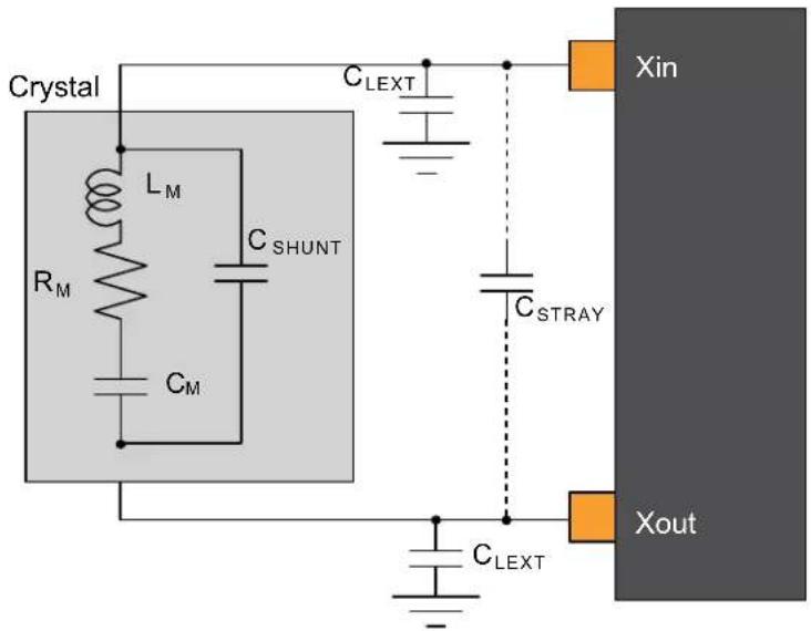
text_image
Crystal L_M R_M C_SHUNT C_M C_LEXT C_STRAY Xin C_LEXT Xout34.12.2 External 32 kHz Crystal Oscillator (XOSC32K) Characteristics
34.12.2.1 Digital Clock Characteristics
The following table describes the characteristics for the oscillator when a digital clock is applied on the XIN32 pin.
Table 34-35. Digital Clock Characteristics ^(1)
| Symbol | Parameter | Conditions | Min. | Typ. | Max. | Units |
| f_CPXIN32 | XIN32 clock frequency | Digital mode | - | 32.768 | - | kHz |
| ......continued | |||||
| Symbol Parameter Conditions Min. Typ. Max. Units | |||||
| DCxin XIN32 clock duty cycle Digital mode - 50 - % | |||||
Note:
- These values are based on simulation. These values are not covered by test or characterization.
34.12.2.2 Crystal Oscillator Characteristics
Figure 32-6 and the equation in 32.12.1.2. Crystal Oscillator Characteristics also applied to the 32kHz oscillator connection. The user must choose a crystal oscillator where the crystal load capacitance C_L is within the range given in the table. The value of C_L can be found in the crystal data sheet.
For the computation of the external capacitors ( C_LEXT ) value, refer to the logic detailed in XOSC Crystal Oscillator Characteristics.
Table 34-36. 32 kHz Crystal Oscillator Characteristics
| Symbol | Parameter | Conditions | Min. | Typ. | Max. | Units |
| f_OUT | Crystal oscillator frequency | - | 32768 | - | Hz | |
| t_STARTUP | Startup time | ESR_XTAL=39.9 k, C_L=12.5 pF | - | 28K | 31K | cycles |
| C_L | Crystal load capacitance | -- | 12.5 | pF | ||
| C_SHUNT | Crystal shunt capacitance | - | 0.1 | - | ||
| C_XIN32 | Parasitic capacitor load | TQFP64/48/32 packages | - | 3.1 | - | |
| C_XOUT32 | Parasitic capacitor load | - | 3.3 | - | ||
| I_XOSC32K | Current consumption | VDD = 3.0V, AGC off - 1.22 2.33 | μA | |||
| VDD = 3.0V, AGC on(1) | -- | - | ||||
| ESR | Crystal equivalent series resistance f = 32.768 kHzSafety Factor = 3 | C_L=12.5 pF | -- | 100 | kΩ | |
Note:
- Refer to the Errata and Data Sheet Clarification document regarding the AGC feature of XOSC32K.
34.12.3 Digital-Frequency Locked Loop (DFLL48M) Characteristics
The following tables provide the characteristics of the DFLL48M.
Table 34-37. DFLL48M Characteristics - Open Loop Mode
| Symbol | Parameter | Conditions | Min. | Typ. | Max. | Units |
| f_OUT | Output frequency | DFLLVAL.COARSE = DFLL48M COARSE CAL DFLLVAL.FINE = 512 over [-40, +125]C, over [2.7, 3.6]V | 44.50 | 48.00 | 51.75 | MHz |
| f_OUT | Output frequency | DFLLVAL.COARSE = DFLL48M COARSE CAL DFLLVAL.FINE = 512 at Ta = 25°C, over [2.7, 3.6]V | 46.60 | 48.00 | 49.40 | MHz |
| I_DFLL | Power consumption on VDDIN | DFLLVAL.COARSE = DFLL48M COARSE CAL DFLLVAL.FINE = 512 | - | 403 | 457 | μA |
| t_STARTUP | Startup time | DFLLVAL.COARSE = DFLL48M COARSE CAL DFLLVAL.FINE = 512 f_OUT within 90 % of final value | - | 8 | 12 | μs |
Table 34-38. DFLL48M Characteristics - Closed-Loop Mode ^(1)(2)
| Symbol | Parameter | Conditions | Min. | Typ. | Max. | Units |
| f_OUT | Average Output frequency | f_REF = XOSC32K 32.768 kHz, 100 ppm DFLLMUL = 1464 | 47.50 | 48.00 | 48.44 | MHz |
| f_REF | Reference frequency | 0.732 | 32.768 | 33 | kHz | |
| I_DFLL | Power consumption on V_DDIN | f_REF = XOSC32K 32.768 kHz, 100 ppm | - | 457 | - | μA |
| ......continued | ||||||
| Symbol | Parameter | Conditions | Min. | Typ. | Max. | Units |
| t_LOCK | Lock time | f_REF = XOSC32K 32.768 kHz , 100 ppmDFLLMUL = 1464DFLLVAL.COARSE =DFLL48M COARSE CALDFLLVAL.FINE = 512DFLLCTRL.BPLCKC = 1DFLLCTRL.QLDIS = 0DFLLCTRL.CCDIS = 1DFLLMUL.FSTEP = 10 | ||||
Notes:
- Refer to the revision C/revision B errata related to the DFLL48M.
- All parts are tested in production to be able to use the DFLL as the main CPU clock in DFLL Closed Loop mode with an external XOSC32K reference.
34.12.4 32.768 kHz Internal oscillator (OSC32K) Characteristics
Table 34-39. 32 kHz RC Oscillator Characteristics
| Symbol | Parameter Conditions | Min. Typ. Max. Units | ||||
| f_OUT | Output frequency | Calibrated against a 32.768 kHz reference at 25°C, over [-40, +125]°C, over [2.7, 3.63]V | 26.214 | 32.768 | 39.321 | kHz |
| Calibrated against a 32.768 kHz reference at 25°C, at V_DD = 3.3V | 32.113 | 32.768 | 33.423 | |||
| Calibrated against a 32.768 kHz reference at 25°C, over [2.7, 3.63]V | 31.457 | 32.768 | 34.079 | |||
| I_OSC32K | Current consumption - | - 0.675 μA | ||||
| tSTARTUP | Startup time | - | - | 1 | 2 | cycle |
| Duty | Duty Cycle | - | - | 50 | - | % |
34.12.5 Ultra-Low Power Internal 32 kHz RC Oscillator (OSCULP32K) Characteristics
Table 34-40. Ultra-Low Power Internal 32kHz RC Oscillator Characteristics
| Symbol | Parameter | Conditions | Min. | Typ. | Max. | Units |
| f_OUT | Output frequency | Calibrated against a 32.768 kHz reference at 25°C, over [-40, +125]C, over [2.7, 3.63]V | 24.576 | 32.768 | 40.960 | kHz |
| Calibrated against a 32.768 kHz reference at 25°C, at V_DD = 3.3V | 30.474 | 32.768 | 35.061 | |||
| Calibrated against a 32.768 kHz reference at 25°C, over [2.7, 3.63]V | 30.146 | 32.768 | 35.389 | |||
| Duty | Duty Cycle | - | 50 | - | % |
34.12.6 8 MHz RC Oscillator (OSC8M) Characteristics
Table 34-41. Internal 8 MHz RC Oscillator Characteristics
| Symbol | Parameter | Conditions | Min. | Typ. | Max. | Units |
| f_OUT | Output frequency | Calibrated against a 8 MHz reference at 25°C, over [-40, +125]C, over [2.7, 3.63]V | 7.57 | 8 | 8.36 | MHz |
| Calibrated against a 8 MHz reference at 25°C, at V_DD = 3.3V | 7.88 | 8 | 8.10 | |||
| Calibrated against a 8 MHz reference at 25°C, over [2.7, 3.63]V | 7.87 | 8 | 8.10 | |||
| I_OSC8M | Current consumption | With default SYSCTRL.OSC8M[FRANGE, CALIB] loaded from Flash at startup and SYSCTRL.OSC8M[PRES C] = 0 | -- | 78 | μA | |
| t_STARTUP | Startup time | - | - | 2.4 | 3.9 | μs |
| Duty | Duty cycle | - | - | 50 | - | % |
34.13 PTC Characteristics
Table 34-42. Sensor Load Capacitance
| Symbol Mode PTC channel Max Sensor Load | (1) | Units | ||
| C_LOAD | Self-capacitance | Y0 15 | 22 | pf |
| Y1 22 | ||||
| Y2 18 | ||||
| Y3 | ||||
| Y4 | ||||
| Y5 | ||||
| Y6 | ||||
| Y7 | ||||
| Y8 | ||||
| Y9 | ||||
| Y10 | ||||
| Y11 | ||||
| Y12 | ||||
| Y13 | ||||
| Y14 | ||||
| Y15 | ||||
| Mutual-capacitance All 29 | ||||
Note:
- Capacitance load that the PTC circuitry can compensate for each channel.
Table 34-43. Analog Gain Settings (1,2)
| Symbol Setting Average | ||
| Gain | GAIN_1 1.0 | |
| GAIN_2 2.0 | ||
| GAIN_4 3.8 | ||
| GAIN_8 7.8 | ||
| GAIN_16 12.8 | ||
| GAIN_32 - |
Notes:
-
Analog Gain is a parameter of the QTouch Library. Refer to the QTouch Library Peripheral Touch Controller User Guide.
-
GAIN_16 and GAIN_32 settings are not recommended, otherwise the PTC measurements might get unstable.
Power Consumption
The values provided in the Power Consumption table below are measured values of power consumption under the following conditions:
Operating Conditions:
$$ \mathrm{VDD} = 3. 3 \mathrm{V} $$
Clocks:
OSC8M used as main clock source, running undivided at 8 MHz.
CPU is running on flash with 0 wait states, at 8 MHz.
PTC running at 4 MHz.
PTC Configuration:
Mutual-Capacitance mode
One touch channel
System Configuration:
Standby Sleep mode enabled.
RTC running on OSCULP32K: used to define the PTC scan rate through the event system.
Drift Calibration disabled: no interrupts, PTC scans are performed in Standby mode.
Drift Calibration enabled: RTC interrupts (wakeup) the CPU to perform PTC scans. PTC drift calibration is performed every 1.5 sec.
Table 34-44. Power Consumption ^(1)
| Symbol | Parameters Drift Calibration | PTC scan rate | (msec) Oversamples Ta | Typ. Max. Units | |||
| IDD^(2) | Current Consumption | Disabled | 10 | 4 | Max. 125°C Typ. 25°C | 67 487 | μA |
| 16 75 498 | |||||||
| 50 | 4 62 481 | ||||||
| 16 64 484 | |||||||
| 100 | 4 62 481 | ||||||
| 16 63 482 | |||||||
| 200 | 4 61 481 | ||||||
| 16 62 482 | |||||||
| Enabled | 10 | 4 71 495 | |||||
| 16 79 507 | |||||||
| 50 | 4 64 485 | ||||||
| 16 65 489 | |||||||
| 100 | 4 63 485 | ||||||
| 16 64 487 | |||||||
| 200 | 4 62 484 | ||||||
| 16 63 484 |
Notes:
- These values are based on characterization.
- On this table, the LDO Voltage Regulator is enabled in Standby mode (SYSCTRL.VREG.RUNSTDBY = 1).
34.14 Timing Characteristics
34.14.1 External Reset
Table 34-45. External Reset Characteristics ^(1)
| Symbol | Parameter | Condition | Min. | Typ. | Max. | Units |
| t_EXT | Minimum reset pulse width | 10 | - | - | ns |
Note:
- These values are based on simulation. These values are not covered by test limits in production or characterization.
34.14.2 SERCOM in SPI Mode Timing
Figure 34-7. SPI Timing Requirements in Host Mode
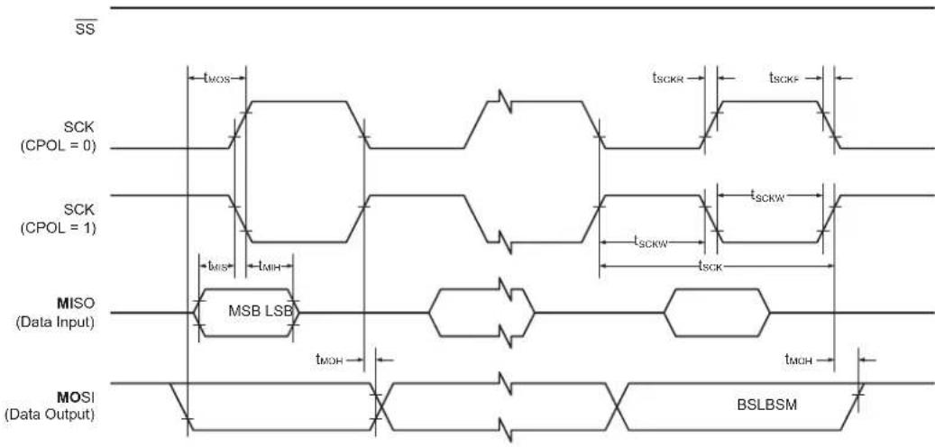
text_image
SS SCK (CPOL = 0) SCK (CPOL = 1) MISO (Data Input) MOSI (Data Output) tMOS tMIS tMIH MSB LSB tMOH tSCKR tSCKW tSCKW tMOH tMOH BSLBSMFigure 34-8. SPI Timing Requirements in Client Mode
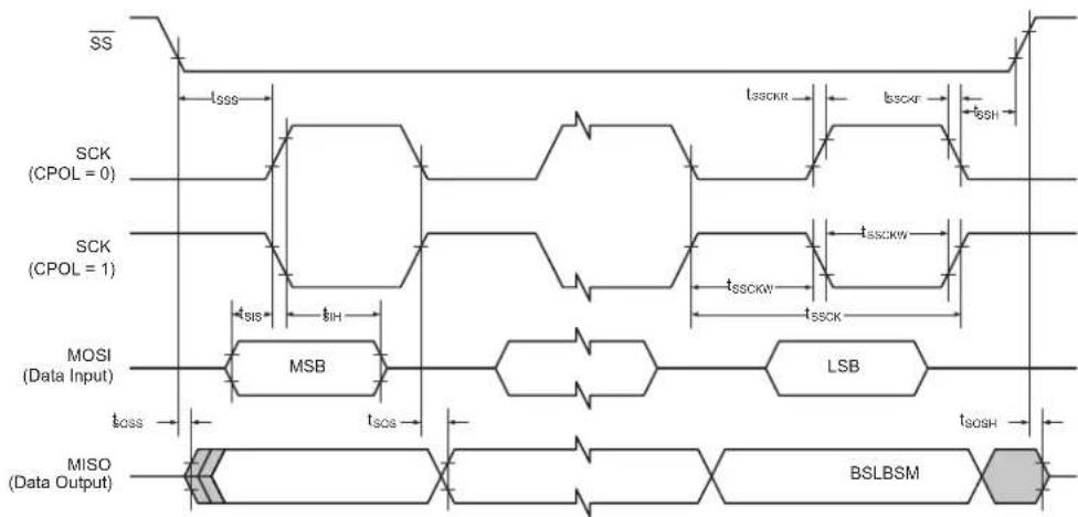
text_image
SS SCK (CPOL = 0) SCK (CPOL = 1) MOSI (Data Input) tSIS tIH MSB LSB tSOS tSOSH MISO (Data Output) BSLBSMTable 34-46. SPI Timing Characteristics and Requirements ^(1)
| Symbol | Parameter Conditions Min. Typ. Max. Units | ||||||
| t_SCK | SCK period Host 84 ns | ||||||
| t_SCKW | SCK high/low width Host - 0.5*t | SCK | - | ||||
| t_SCKR | SCK rise time(2) | Host --- | |||||
| t_SCKF | SCK fall time(2) | Host --- | |||||
| t_MIS | MISO setup to SCK Host - 29 | - | |||||
| t_MIH | MISO hold after SCK | Host - 8 - | |||||
| t_MOS | MOSI setup SCK | Host - t | SCK/2 - 16 | - | |||
| t_MOH | MOSI hold after SCK | Host - 16 | - | ||||
| t_SSCK | Client SCK Period | Client | 1*tCLK_APB | - | - | ||
| t_SSCKW | SCK high/low width Client | 0.5*t | SSCK | - | - | ||
| t_SSCKR | SCK rise time(2) | Client | --- | ||||
| t_SSCKF | SCK fall time(2) | Client | --- | ||||
| t_SIS | MOSI setup to SCK Client | t | SSCK/2 - 19 | -- | |||
| t_SIH | MOSI hold after SCK | Client | tssck/2 - 5 | -- | |||
| t_SSS | SS setup to SCK Client PRELOADEN=1 | 2*t | CLK_APB + tsos | - | - | ||
| PRELOADEN=0 | tsos+7 | -- | |||||
| t_SSH | SS hold after SCK | Client | tsih - 4 | -- | |||
| t_SOS | MISO setup SCK | Client | -t | ssck/2 - 20 | - | ||
| t_SOH | MISO hold after SCK | Client | -20 | - | |||
| t_SOSS | MISO setup after SS low | Client | -16 | - | |||
| t_SOSH | MISO hold after SS high | Client | -11 | - | |||
Notes:
- These values are based on simulation. These values are not covered by test limits in production.
- See 32.8. I/O Pin Characteristics.
34.14.3 SERCOM in I²C Mode Timing
The following table describes the requirements for devices connected to the I²C Interface Bus. Timing symbols refer to the figure below.
Figure 34-9. I²C Interface Bus Timing
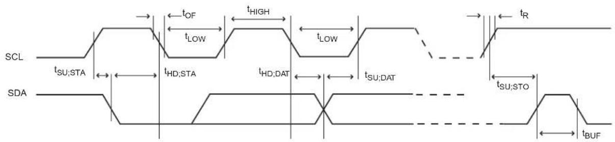
text_image
SCL tSU;STA tHD;STA tHD;DAT tSU;DAT tSU;STO tBUF tOF tLOW tHIGH tLOW tRTable 34-47. I²C Interface Timing ^(1)
| Symbol | Parameter Conditions Min. Typ. Max. Units | |||||
| t_R | Rise time for both SDA and SCL^(3) | -- 300 | ns | |||
| t_OF | Output fall time from V_IHmin to V_ILmax^(3) | 10 pF < C_b^(2) < 400 pF 7.0 | 10.0 | 50.0 | ||
| t_HD;STA | Hold time (repeated) START condition f | s_CL > 100 kHz, Host t | LOW-9 | -- | ||
| t_LOW | Low period of SCL Clock | f_SCL > 100 kHz | 113 | -- | ||
| t_BUF | Bus free time between a STOP and a START condition | f_SCL > 100 kHz | t_LOW | - | - | |
| t_SU;STA | Setup time for a repeated START condition | f_SCL > 100 kHz, Host | t_LOW+7 | -- | ||
| t_HD;DAT | Data hold time f | s_CL > 100 kHz, Host | 9 | - 12 | ||
| t_SU;DAT | Data setup time | f_SCL > 100 kHz, Host | 104 | -- | ||
| t_SU;STO | Setup time for STOP condition | f_SCL > 100 kHz, Host | t_LOW+9 | -- | ||
| t_SU;DAT;rx | Data setup time (receive mode) | f_SCL > 100 kHz, Client | 51 | - 56 | ||
| t_HD;DAT;tx | Data hold time (send mode) | f_SCL > 100 kHz, Client | 71 | 90 | 138 | |
Notes:
- These values are based on simulation and not covered by test limits in production.
- C_b = Capacitive load on each bus line . Otherwise noted, value of C_b set to 20 pF.
- These values are based on characterization and not covered by test limits in production.
34.14.4 SWD Timing
Figure 34-10. SWD Interface Signals
Read Cycle
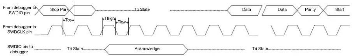
flowchart
graph LR
    A["From debugger to SWDIO pin"] --> B["Stop Park"]
    B --> C["Tri State"]
    C --> D["Data"]
    D --> E["Data"]
    E --> F["Parity"]
    F --> G["Start"]
    H["From debugger to SWDCLK pin"] --> I["Tos"]
    I --> J["Thigh"]
    J --> K["Tlow"]
    K --> L["Data"]
    L --> M["Data"]
    M --> N["Parity"]
    N --> O["Start"]
    P["SWDIO pin to debugger"] --> Q["Tri State"]
    Q --> R["Acknowledge"]
    R --> S["Tri State"]
Write Cycle
flowchart
graph LR
    A["Stop Park"] --> B["Tri State"]
    B --> C["Start"]
    D["From debugger to SWDIO pin"] --> E["Tis"]
    E --> F["Tih"]
    F --> G["Data"]
    G --> H["Parity"]
    H --> I["Tri State"]
    J["From debugger to SWDCLK pin"] --> K["Tri State"]
    K --> L["Acknowledge"]
    L --> M["Data"]
    M --> N["Parity"]
    N --> O["Tri State"]
Table 34-48. SWD Timings ^(1)
| Symbol | Parameter | Conditions | Min. | Max. | Units |
| Thigh | SWDCLK High period | V_VDDIO from 3.0 V to 3.6 V, maximum external capacitor = 40 pF | 10 | 500000 | ns |
| Tlow | SWDCLK Low period | 10 | 500000 | ||
| Tos | SWDIO output skew to falling edge SWDCLK | -5 | 5 | ||
| Tls | Input Setup time required between SWDIO | 4 | - | ||
| Tih | Input Hold time required between SWDIO and rising edge SWDCLK | 1 | - |
Note:
- These values are based on simulation. These values are not covered by test limits in production or characterization.
35. Packaging Information
35.1 Thermal Considerations
Related Links
35.1.2. Junction Temperature
35.1.1 Thermal Resistance Data
The following table summarizes the thermal resistance data for non-AEC-Q100 packages..
Table 35-1. Thermal Resistance Data for non-AEC-Q100 packages
| Package Type θ | JA | _JC |
| 32-pin TQFP 68.0°C/W 25.8°C/W | ||
| 48-pin TQFP 78.8°C/W 12.3°C/W | ||
| 64-pin TQFP 66.7°C/W 11.9°C/W | ||
| 32-pin VQFN 37.2°C/W 13.1°C/W | ||
| 48-pin VQFN 33.0°C/W 11.4°C/W | ||
| 64-pin VQFN 33.5°C/W 11.2°C/W | ||
| 64-ball UFBGA 67.4°C/W 12.4°C/W | ||
| 45-ball WLCSP 37.0°C/W 0.36°C/W | ||
| 27-ball WLCSP 84.54°C/W 16.86°C/W |
The following table summarizes the thermal resistance data for AEC-Q100 packages.
Table 35-2. Thermal Resistance Data for AEC-Q100 packages
| Package Type θ | JA | _JC |
| 64-pin TQFP 53.7 15.4 | ||
| 48-pin TQFP 58.6 16.1 | ||
| 32-pin TQFP 58.2 18.8 | ||
| 64-pin VQFN 28.4 12 | ||
| 48-pin VQFN 27.6 12.7 | ||
| 32-pin VQFN 29.8 15.9 |
35.1.2 Junction Temperature
The average chip-junction temperature, T_J , in °C can be obtained from the following:
- T_J=T_A+(P_D×_JA)
- T_J = T_A + (P_D × (_HEATSINK + _JC))
where:
- _JA = Package thermal resistance, Junction-to-ambient (°C/W), see Thermal Resistance Data
- _JC = Package thermal resistance, Junction-to-case thermal resistance ( ^ C/W), see Thermal Resistance Data
- _HEATSINK = Thermal resistance (°C/W) specification of the external cooling device
• P_D = Device power consumption (W)
• T_A = Ambient temperature (°C)
From the first equation, the user can derive the estimated lifetime of the chip and decide if a cooling device is necessary or not. If a cooling device has to be fitted on the chip, the second equation should be used to compute the resulting average chip-junction temperature T_j in °C.
Related Links
35.1. Thermal Considerations
35.2 Package Drawings
Note: For the most current package drawings, please see the Microchip Packaging Specification located at http://www.microchip.com/packaging.
35.2.1 64-Pin TQFP for Industrial and AEC-Q100 Variants
64-Lead Plastic Thin Quad Flatpack (PT)-10x10x1 mm Body, 2.00 mm Footprint [TQFP]
Note: For the most current package drawings, please see the Microchip Packaging Specification located at http://www.microchip.com/packaging
![Microchip ATSAMD20G17 - 64-Lead Plastic Thin Quad Flatpack (PT)-10x10x1 mm Body, 2.00 mm Footprint [TQFP] - 1](/content/2026/06/1221663/images/ed0bbc96c8350041d579f00ec18be76f1ed3305d2f8148e7a07fac1810116397.jpg)
text_image
D D1 D1/2 D NOTE 2 A B E1/2 E1 E SEE DETAIL 1 N A A 4X N/4 TIPS 0.20 C A-B D NOTE 1 1 2 3 4X 0.20 H A-B DTOP VIEW
![Microchip ATSAMD20G17 - 64-Lead Plastic Thin Quad Flatpack (PT)-10x10x1 mm Body, 2.00 mm Footprint [TQFP] - 2](/content/2026/06/1221663/images/779a86ba75d919d7c3a444c96d35f58dfb831e7061161e1b6fd67135410024e0.jpg)
text_image
SEATING PLANE A C 0.05 64 X b A1 e 0.08 C 0.08 M A-B DSIDE VIEW
Microchip Technology Drawing C04-085C Sheet 1 of 2
64-Lead Plastic Thin Quad Flatpack (PT)-10x10x1 mm Body, 2.00 mm Footprint [TQFP]
Note: For the most current package drawings, please see the Microchip Packaging Specification located at http://www.microchip.com/packaging
![Microchip ATSAMD20G17 - 64-Lead Plastic Thin Quad Flatpack (PT)-10x10x1 mm Body, 2.00 mm Footprint [TQFP] - 1](/content/2026/06/1221663/images/a10f3077847014b25b9377a1e10c4ad906fae851ad01247bf0933aae3c3a1248.jpg)
text_image
H α β L (L1) θ C X=A-BSECTION A-A
![Microchip ATSAMD20G17 - 64-Lead Plastic Thin Quad Flatpack (PT)-10x10x1 mm Body, 2.00 mm Footprint [TQFP] - 2](/content/2026/06/1221663/images/213932228fd9717477004810a534768b9ff823e687fa75053f2f39476dc5bed6.jpg)
natural_image
Isometric line drawing of an integrated circuit chip with multiple pins (no text or symbols)![Microchip ATSAMD20G17 - 64-Lead Plastic Thin Quad Flatpack (PT)-10x10x1 mm Body, 2.00 mm Footprint [TQFP] - 3](/content/2026/06/1221663/images/9d73a8e721ca191b7207db6f30d61ae9e252435306e47d0376503499e345c1b3.jpg)
text_image
X=A—B OR D e/2DETAIL 1
| Units | MILLIMETERS | |||
| Dimension Limits | MIN | NOM | MAX | |
| NNumber of Leads 64 | ||||
| Lead Pitch | e | 0.50 BSC | ||
| 1.20--AOOverall Height | ||||
| 1.051.000.95A2Molded Package | ||||
| 0.15-0.05A1Standoff | ||||
| 0.750.600.45LFoot Length | ||||
| Footprint | L1 | 1.00 REF | ||
| Foot Angle | 7°3.5°0' | |||
| 12.00 BSCEOverall Width | ||||
| 12.00 BSCDOverall Length | ||||
| 10.00 BSCE1Molded Package Width | ||||
| Molded Package Length | D1 | 10.00 BSC | ||
| Lead Thickness | c | 0.20-0.09 | ||
| Lead Width | b | 0.270.220.17 | ||
| Mold Draft Angle Top | 13°12°11° | |||
| Mold Draft Angle Bottom | 13°12°11° | |||
Notes:
- Pin 1 visual index feature may vary, but must be located within the hatched area.
- Chamfers at corners are optional; size may vary.
- Dimensions D1 and E1 do not include mold flash or protrusions. Mold flash or protrusions shall not exceed 0.25mm per side.
- Dimensioning and tolerancing per ASME Y14.5M
BSC: Basic Dimension. Theoretically exact value shown without tolerances.
REF: Reference Dimension, usually without tolerance, for information purposes only.
Microchip Technology Drawing C04-085C Sheet 2 of 2
64-Lead Plastic Thin Quad Flatpack (PT)-10x10x1 mm Body, 2.00 mm Footprint [TQFP]
Note: For the most current package drawings, please see the Microchip Packaging Specification located at http://www.microchip.com/packaging
![Microchip ATSAMD20G17 - 64-Lead Plastic Thin Quad Flatpack (PT)-10x10x1 mm Body, 2.00 mm Footprint [TQFP] - 1](/content/2026/06/1221663/images/13a99e715d73e6b94e610e1e9c07c1f08ae8d5f24d0bc921667af95809b68605.jpg)
text_image
C1 C2 E G Y1 X1RECOMMENDED LAND PATTERN
| Units | MILLIMETERS | |||
| Dimension Limits | MIN | NOM | MAX | |
| Contact Pitch | E | 0.50 BSC | ||
| C1Contact Pad Spacing 40 | ||||
| Contact Pad Spacing | C2 | 11.40 | ||
| Contact Pad Width (X28) | X1 | 0.30 | ||
| Contact Pad Length (X28) | Y1 | 1.50 | ||
| GDistance Between Pads 0.20 | ||||
Notes:
1. Dimensioning and tolerancing per ASME Y14.5M
BSC: Basic Dimension. Theoretically exact value shown without tolerances.
Microchip Technology Drawing C04-2085B Sheet 1 of 1
Table 35-3. Device and Package Maximum Weight
| 300 mg |
Table 35-4. Package Reference
| Package Outline Drawing MCHP reference C04-00085 |
35.2.2 64-Pin VQFN for Industrial Variants
64-Lead Very Thin Plastic Quad Flat, No Lead Package (TMB) - 9x9 mm Body [VQFN] Atmel Legacy Global Package Code ZST
Note: For the most current package drawings, please see the Microchip Packaging Specification located at http://www.microchip.com/packaging
![Microchip ATSAMD20G17 - 64-Lead Very Thin Plastic Quad Flat, No Lead Package (TMB) - 9x9 mm Body [VQFN] Atmel Legacy Global Package Code ZST - 1](/content/2026/06/1221663/images/badad10881e35e0f3461d0c60e1a32758c561d69bde703e482bb2f9f268f4684.jpg)
text_image
64X 0.08 C // 0.10 C NOTE 1 1 2 (DATUM B) (DATUM A) E 2X 0.15 C 2X 0.15 C TOP VIEW A B E2 NOTE 1 2 1 K L e 64X b BOTTOM VIEW A1 (A3) SEATING PLANE C SIDE VIEW 0.10 M A B 0.10 M A B 0.10 M A B 0.10 M A B 0.05 MMicrochip Technology Drawing C04-21441-TMB Rev A Sheet 1 of 2
64-Lead Very Thin Plastic Quad Flat, No Lead Package (TMB) - 9x9 mm Body [VQFN] Atmel Legacy Global Package Code ZST
Note: For the most current package drawings, please see the Microchip Packaging Specification located at http://www.microchip.com/packaging
![Microchip ATSAMD20G17 - 64-Lead Very Thin Plastic Quad Flat, No Lead Package (TMB) - 9x9 mm Body [VQFN] Atmel Legacy Global Package Code ZST - 1](/content/2026/06/1221663/images/161b8e3c442d3bbfcc7bc795ef4c5a6ef823093a41029b22e67c07dd57a84641.jpg)
natural_image
Isometric line drawing of two rectangular electronic components with a central square and coiled pins (no text or symbols)| Units | MILLIMETERS | |||
| Dimension Limits | MIN | NOM | MAX | |
| Number of Terminals | N | 64 | ||
| Pitch | e | 0.50 BSC | ||
| Overall Height | A | 0.80 | 0.90 | 1.00 |
| Standoff | A1 | 0.00 | 0.02 | 0.05 |
| Terminal Thickness | A3 | 0.203 REF | ||
| Overall Length | D | 9.00 BSC | ||
| Exposed Pad Length | D2 4 | 60 | 4.70 4.80 | |
| Overall Width | E | 9.00 BSC | ||
| Exposed Pad Width | E2 | 4.60 | 4.70 4.80 | |
| Terminal Width | b | 0.15 | 0.20 | 0.25 |
| Terminal Length | L | 0.30 | 0.40 | 0.55 |
| K | - | |||
0.20 -Terminal-to-Expos
Notes:
- Pin 1 visual index feature may vary, but must be located within the hatched area.
- Package is saw singulated
- Dimensioning and tolerancing per ASME Y14.5M
BSC: Basic Dimension. Theoretically exact value shown without tolerances.
REF: Reference Dimension, usually without tolerance, for information purposes only.
Microchip Technology Drawing C04-21441-TMB Rev A Sheet 2 of 2
64-Lead Very Thin Plastic Quad Flat, No Lead Package (TMB) - 9x9 mm Body [VQFN] Atmel Legacy Global Package Code ZST
Note: For the most current package drawings, please see the Microchip Packaging Specification located at http://www.microchip.com/packaging
![Microchip ATSAMD20G17 - 64-Lead Very Thin Plastic Quad Flat, No Lead Package (TMB) - 9x9 mm Body [VQFN] Atmel Legacy Global Package Code ZST - 1](/content/2026/06/1221663/images/c693d6bb064da15909c4bfeec28b9132b28c553877d02e7fc311b87add8ffde0.jpg)
text_image
C1 X2 EV 64 ØV G2 C2 Y2 EV G1 Y1 X1 SILK SCREEN ERECOMMENDED LAND PATTERN
| Units | MILLIMETERS | |||
| Dimension Limits | MIN | NOM | MAX | |
| Contact Pitch | E | 0.50 BSC | ||
| Optional Center Pad Width | X2 | 4.80 | ||
| Optional Center Pad Length | Y2 | 4.80 | ||
| C1 | Contact Pad Spacing 8.90 | |||
| Contact Pad Spacing | C2 | 8.90 | ||
| Contact Pad Width (X64) | X1 | 0.30 | ||
| Contact Pad Length (X64) | Y1 | 0.90 | ||
| Contact Pad to Center Pad (X64) G1 | 1.60 | |||
| Contact Pad to Contact Pad (X60) G2 | 0.20 | |||
| Thermal Via Diameter V | 0.30 | |||
| Thermal Via Pitch EV | 1.00 | |||
Notes:
- Dimensioning and tolerancing per ASME Y14.5M
BSC: Basic Dimension. Theoretically exact value shown without tolerances.
- For best soldering results, thermal vias, if used, should be filled or tented to avoid solder loss during reflow process
Microchip Technology Drawing C04-21441-TMB Rev A Sheet 1 of 2
Note: The exposed die attach pad is not connected electrically inside the device.
Table 35-5. Device and Package Maximum Weight
| 200 mg |
Table 35-6. Package Reference
| Package Outline Drawing MCHP reference C04-21441 | |
| JESD97 Classification E3 |
35.2.3 64 pin VQFN for AEC-Q100 Variants
64-Lead Very Thin Plastic Quad Flat, No Lead Package (5LX) - 9x9x1.0 mm Body [VQFN] With 5.4 mm Exposed Pad and Stepped Wettable Flanks
Note: For the most current package drawings, please see the Microchip Packaging Specification located at http://www.microchip.com/packaging
![Microchip ATSAMD20G17 - 64-Lead Very Thin Plastic Quad Flat, No Lead Package (5LX) - 9x9x1.0 mm Body [VQFN] With 5.4 mm Exposed Pad and Stepped Wettable Flanks - 1](/content/2026/06/1221663/images/4e8906cc3a1927ed494d3699b22b38e4473a6b9d574b4ad8b05d727b8d80bf2f.jpg)
text_image
NOTE 1 N 1 2 (DATUM B) (DATUM A) 2X 0.10 C 2X 0.10 C TOP VIEW 64X 0.08 C // 0.10 C A1 (A3) A SEATING PLANE SIDE VIEW D2 0.10 M A B (K) A A E2 e2 NOTE 1 2 1 L N e 64X b A4 D3 SECTION A-A STEPPED WETTABLE FLANK 0.10 M A B 0.05 M BOTTOM VIEWMicrochip Technology Drawing C04-483 Rev D Sheet 1 of 2
64-Lead Very Thin Plastic Quad Flat, No Lead Package (5LX) - 9x9x1.0 mm Body [VQFN] With 5.4 mm Exposed Pad and Stepped Wettable Flanks
Note: For the most current package drawings, please see the Microchip Packaging Specification located at http://www.microchip.com/packaging
![Microchip ATSAMD20G17 - 64-Lead Very Thin Plastic Quad Flat, No Lead Package (5LX) - 9x9x1.0 mm Body [VQFN] With 5.4 mm Exposed Pad and Stepped Wettable Flanks - 1](/content/2026/06/1221663/images/0b4cc2fb6e6cc84d643841ae5401e07b281e0e32801ffe592b30dd6b5261b3a5.jpg)
natural_image
Isometric line drawing of two rectangular electronic components with coiled edges and a central square (no text or symbols)| Units | MILLIMETERS | |||
| Dimension Limits | MIN | NOM | MAX | |
| Number of Terminals | N | 64 | ||
| Pitch | e | 0.50 BSC | ||
| Overall Height | A | 0.80 | 0.90 | 1.00 |
| Standoff | A1 | 0.00 | 0.02 | 0.05 |
| Terminal Thickness | A3 | 0.203 REF | ||
| Overall Length | D | 9.00 BSC | ||
| Exposed Pad Length | D2 | 5.30 5.40 | 5.50 | |
| Overall Width | E | 9.00 BSC | ||
| Exposed Pad Width | E2 | 5.30 | 5.40 | 5.50 |
| Terminal Width | b | 0.20 | 0.25 | 0.30 |
| Terminal Length | L | 0.30 | 0.40 | 0.50 |
| K 1.40 REFTerminal-to-Exposed-Pad | ||||
| Wettable Flank Step Length | D3 | 0.0600.0 | 85 0.085 | |
| Wettable Flank Step Height | A4 | 0.10 - 0.19 | ||
Notes:
- Pin 1 visual index feature may vary, but must be located within the hatched area.
- Package is saw singulated
- Dimensioning and tolerancing per ASME Y14.5M BSC: Basic Dimension. Theoretically exact value shown without tolerances. REF: Reference Dimension, usually without tolerance, for information purposes only.
Microchip Technology Drawing C04-483 Rev D Sheet 2 of 2
64-Lead Very Thin Plastic Quad Flat, No Lead Package (5LX) - 9x9x1.0 mm Body [VQFN] With 5.4 mm Exposed Pad and Stepped Wettable Flanks
Note: For the most current package drawings, please see the Microchip Packaging Specification located at http://www.microchip.com/packaging
![Microchip ATSAMD20G17 - 64-Lead Very Thin Plastic Quad Flat, No Lead Package (5LX) - 9x9x1.0 mm Body [VQFN] With 5.4 mm Exposed Pad and Stepped Wettable Flanks - 1](/content/2026/06/1221663/images/c9d9e7e7948fc851d199115c67228e29b19cc37eecf700e1409c26b4c564eeaf.jpg)
text_image
C1 X2 EV 64 1 2 C2 Y2 EV ØV G2 G1 Y1 X1 SILK SCREEN ERECOMMENDED LAND PATTERN
| Units | MILLIMETERS | |||
| Dimension Limits | MIN | NOM | MAX | |
| Contact Pitch | E | 0.50 BSC | ||
| Optional Center Pad Width | X2 | 8.90 | ||
| Optional Center Pad Length | Y2 | 8.90 | ||
| C1Contact Pad Spacing 5.50 | ||||
| Contact Pad Spacing | C2 | 5.50 | ||
| Contact Pad Width (X64) | X1 | 0.30 | ||
| Contact Pad Length (X64) | Y1 | 0.85 | ||
| Contact Pad to Center Pad (X64) G1 | 1.28 | |||
| Contact Pad to Contact Pad (X60) G2 | 0.20 | |||
| Thermal Via Diameter V | 0.33 | |||
| Thermal Via Pitch EV | 1.20 | |||
Notes:
- Dimensioning and tolerancing per ASME Y14.5M
BSC: Basic Dimension. Theoretically exact value shown without tolerances.
- For best soldering results, thermal vias, if used, should be filled or tented to avoid solder loss during reflow process
Microchip Technology Drawing C04-2483 Rev D
Table 35-7. Device and Package Maximum Weight
200 mg
Table 35-8. Package Reference
| Package Outline Drawing MCHP reference C04-00483 | |
| JESD97 Classification E3 |
35.2.4 64-ball UFBGA
64-Ball Ultra Thin Fine-Pitch Ball Grid Array Package (BQB) - 5x5x0.65 mm Body [UFBGA]; Atmel Legacy Global Package Code CAH
Note: For the most current package drawings, please see the Microchip Packaging Specification located at http://www.microchip.com/packaging
![Microchip ATSAMD20G17 - 64-Ball Ultra Thin Fine-Pitch Ball Grid Array Package (BQB) - 5x5x0.65 mm Body [UFBGA]; Atmel Legacy Global Package Code CAH - 1](/content/2026/06/1221663/images/6b9ef2451e4415b3119580d25a2378412f6066f0b21e40fd4a6c2f14cf4e6c1e.jpg)
Sheet 1 of 2Micro
64-Ball Ultra Thin Fine-Pitch Ball Grid Array Package (BQB) - 5x5x0.65 mm Body [UFBGA]; Atmel Legacy Global Package Code CAH
Note: For the most current package drawings, please see the Microchip Packaging Specification located at http://www.microchip.com/packaging
![Microchip ATSAMD20G17 - 64-Ball Ultra Thin Fine-Pitch Ball Grid Array Package (BQB) - 5x5x0.65 mm Body [UFBGA]; Atmel Legacy Global Package Code CAH - 1](/content/2026/06/1221663/images/2916c0c13a640296c031b9d4909be7c2a3cf8ea5e083beca13f32b94fdc7654c.jpg)
natural_image
Two isometric diagrams of a grid-patterned plate, one with circular holes and the other flat base (no text or symbols)| Units | MILLIMETERS | |||
| Dimension Limits | MIN NOM | MAX | ||
| Number of Terminals | N | 64 | ||
| Pitch | e | 0.50 BSC | ||
| Overall Height | A | - | - | 0.65 |
| Ball Height | A1 | 0.14 | 0.19 | 0.24 |
| Mold Thickness M 0.25 REF | ||||
| Substrate Thickness | S | 1.36 REF | ||
| Overall Length | D | 5.00 BSC | ||
| Ball Array Length | D2 | 3.50 BSC | ||
| Overall Width | E | 5.00 BSC | ||
| Ball Array Width | E2 | 3.50 BSC | ||
| Ball Width | b | 0.20 | 0.25 | 0.3 |
Notes:
- Pin 1 visual index feature may vary, but must be located within the hatched area.
- Dimensioning and tolerancing per ASME Y14.5M BSC: Basic Dimension. Theoretically exact value shown without tolerances. REF: Reference Dimension, usually without tolerance, for information purposes only.
Microchip Technology Drawing C04-21153 Rev A Sheet 2 of 2
64-Ball Ultra Thin Fine-Pitch Ball Grid Array Package (BQB) - 5x5x0.65 mm Body [UFBGA]; Atmel Legacy Global Package Code CAH
Note: For the most current package drawings, please see the Microchip Packaging Specification located at http://www.microchip.com/packaging
![Microchip ATSAMD20G17 - 64-Ball Ultra Thin Fine-Pitch Ball Grid Array Package (BQB) - 5x5x0.65 mm Body [UFBGA]; Atmel Legacy Global Package Code CAH - 1](/content/2026/06/1221663/images/adc9c5572c41997edf009d758eb6664901d89681e59bc5659da1d2cbd855199c.jpg)
text_image
12345678 A B C D E F G H SILK SCREEN E C1 ØX G C2RECOMMENDED LAND PATTERN
| Units | MILLIMETERS | |||
| Dimension Limits | MIN | NOM | MAX | |
| Contact Pitch | E | 0.50 BSC | ||
| C1Contact Pad Spacing 3.50 BSC | ||||
| C2Contact Pad Spacing BSC | ||||
| Contact Pad Width (Xnn) X 0.20 | ||||
| Contact Pad to Contact Pad (Xnn) G 0.30 | ||||
Notes:
Dimensioning and tolerancing per ASME Y14.5M1.
BSC: Basic Dimension. Theoretically exact value shown without tolerances.
Microchip Technology Drawing C04-23153 Rev A
Table 35-9. Device and Package Maximum Weight
27.4 mg
Table 35-10. Package Reference
| Package Outline Drawing MCHP reference C04-21153 | |
| JESD97 Classification E8 |
35.2.5 48-Pin TQFP for Industrial and AEC-Q100 Variants
48-Lead Plastic Thin Quad Flatpack (Y8) - 7x7x1.0 mm Body [TQFP]
Note: For the most current package drawings, please see the Microchip Packaging Specification located at http://www.microchip.com/packaging
![Microchip ATSAMD20G17 - 48-Lead Plastic Thin Quad Flatpack (Y8) - 7x7x1.0 mm Body [TQFP] - 1](/content/2026/06/1221663/images/bf88c8c0c195a8a5044f0e58d8dd35519856c68577a712f1dc3e9dfe58136ee0.jpg)
text_image
D D1 D1/2 D2 D A B E1/2 E1 E2/2 NOTE 1 N/4 TIPS 0.20 C A-B D 1 2 3 e 0.20 C A-B D 4XTOP VIEW
![Microchip ATSAMD20G17 - 48-Lead Plastic Thin Quad Flatpack (Y8) - 7x7x1.0 mm Body [TQFP] - 2](/content/2026/06/1221663/images/c645d8c421a36a23b6812c4bdd54d87ea51085e05f5c65f210b55d6b9091121c.jpg)
text_image
SEATING PLANE A A2 A1 48X b 48X 0.08 C Ø 0.08 Ⓜ A-B DSIDE VIEW
Microchip Technology Drawing C04-300-Y8 Rev D Sheet 1 of 2
48-Lead Plastic Thin Quad Flatpack (Y8) - 7x7x1.0 mm Body [TQFP]
Note: For the most current package drawings, please see the Microchip Packaging Specification located at http://www.microchip.com/packaging
![Microchip ATSAMD20G17 - 48-Lead Plastic Thin Quad Flatpack (Y8) - 7x7x1.0 mm Body [TQFP] - 1](/content/2026/06/1221663/images/feb747222998932c245eb2c92fa58fa0a17615aeb9398c23a2bfaab922372cbc.jpg)
text_image
H θ2 θ1 R2 R1 c θ θ2 L (L1)SECTION A-A
| Units | MILLIMETERS | |||
| Dimension Limits | MIN | NOM | MAX | |
| Number of Terminals | N | 48 | ||
| Pitch | e | 0.50 BSC | ||
| Overall Height | A | - | - | 1.20 |
| Standoff | A1 | 0.05 | - | 0.15 |
| Molded Package Thickness | A2 | 0.95 1.05 | 1.00 | |
| Overall Length | D | 9.00 BSC | ||
| Molded Package Length | D1 | 7.00 BSC | ||
| Overall Width | E | 9.00 BSC | ||
| Molded Package Width | E1 | 7.00 BSC | ||
| Terminal Width | b | 0.17 | 0.22 | 0.27 |
| Terminal Thickness | c | 0.09 - 0.16 | ||
| Terminal Length | L | 0.45 | 0.60 | 0.75 |
| L1 1.00 REFFootprint | ||||
| R1 | -0.08 - | Lead Bend R | ||
| R2 | -0.08 0 | .20Lead Ben | ||
| 3.5°0° 7° | Foot Angle | |||
| 1 | -0° -Lead Angle | |||
| Mold Draft Angle | 2 | 11° | 12° | 13° |
Radius and Radius
Notes:
- Pin 1 visual index feature may vary, but must be located within the hatched area.
- Dimensioning and tolerancing per ASME Y14.5M
BSC: Basic Dimension. Theoretically exact value shown without tolerances.
REF: Reference Dimension, usually without tolerance, for information purposes only.
Microchip Technology Drawing C04-300-Y8 Rev D Sheet 2 of 2
48-Lead Plastic Thin Quad Flatpack (Y8) - 7x7x1.0 mm Body [TQFP]
Note: For the most current package drawings, please see the Microchip Packaging Specification located at http://www.microchip.com/packaging
![Microchip ATSAMD20G17 - 48-Lead Plastic Thin Quad Flatpack (Y8) - 7x7x1.0 mm Body [TQFP] - 1](/content/2026/06/1221663/images/a1ac765560409d36598041d59e878ac3a589435bc96e5a9b04850360376d0a66.jpg)
text_image
C1 C2 48 SILK SCREEN G Y1 1 2 X1 ERECOMMENDED LAND PATTERN
| Units | MILLIMETERS | |||
| Dimension Limits | MIN | NOM | MAX | |
| Contact Pitch | E | 0.50 BSC | ||
| C1Contact Pad Spacing 8.40 | ||||
| C2Contact Pad Spacing 8.40 | ||||
| Contact Pad Width (X48) | X1 | 0.30 | ||
| Contact Pad Length (X48) | Y1 | 1.50 | ||
| Distance Between Pads G 0.20 | ||||
Notes:
1. Dimensioning and tolerancing per ASME Y14.5M
BSC: Basic Dimension. Theoretically exact value shown without tolerances.
2. For best soldering results, thermal vias, if used, should be filled or tented to avoid solder loss during reflow process
Microchip Technology Drawing C04-2300-Y8 Rev D
Table 35-11. Device and Package Maximum Weight
| 140 mg |
Table 35-12. Package Reference
| Package Outline Drawing MCHP reference C04-00300 | |
| JESD97 Classification E3 |
35.2.6 48-Pin VQFN for Industrial Variants
48-Lead Very Thin Quad Flat Pack No-Leads (T3B) 7x7x0.9 mm [VQFN] With 5.15x5.15 mm Exposed Pad; Atmel Legacy Global Package Code ZLG
Note: For the most current package drawings, please see the Microchip Packaging Specification located at http://www.microchip.com/packaging
![Microchip ATSAMD20G17 - 48-Lead Very Thin Quad Flat Pack No-Leads (T3B) 7x7x0.9 mm [VQFN] With 5.15x5.15 mm Exposed Pad; Atmel Legacy Global Package Code ZLG - 1](/content/2026/06/1221663/images/10a7823b38f58be133a525d96f913354ace66896042f4d5df330e0489c86aa41.jpg)
Microchip Technology Drawing C04-21425 Rev A Sheet 1 of 2
48-Lead Very Thin Quad Flat Pack No-Leads (T3B) 7x7x0.9 mm [VQFN] With 5.15x5.15 mm Exposed Pad; Atmel Legacy Global Package Code ZLG
Note: For the most current package drawings, please see the Microchip Packaging Specification located at http://www.microchip.com/packaging
![Microchip ATSAMD20G17 - 48-Lead Very Thin Quad Flat Pack No-Leads (T3B) 7x7x0.9 mm [VQFN] With 5.15x5.15 mm Exposed Pad; Atmel Legacy Global Package Code ZLG - 1](/content/2026/06/1221663/images/fd42c277b5327ec5bac23b55c2913ccc8b890af220997dc84a3a16b802dbb15c.jpg)
natural_image
Isometric line drawing of two rectangular electronic components with square holes, no text or symbols present| Units | MILLIMETERS | |||
| Dimension Limits | MIN | NOM | MAX | |
| Number of Terminals | N | 48 | ||
| Pitch | e | 0.50 BSC | ||
| Overall Height | A | 0.80 | 0.85 | 0.90 |
| Standoff | A1 | 0.00 | 0.02 | 0.05 |
| Terminal Thickness | A3 | 0.20 REF | ||
| Overall Length | D | 7.00 BSC | ||
| Exposed Pad Length | D2 5.05 | 5.15 5.25 | ||
| Overall Width | E | 7.00 BSC | ||
| Exposed Pad Width | E2 | 5.05 | 5.15 | 5.25 |
| Terminal Width | b | 0.18 | 0.25 | 0.30 |
| Terminal Length | L | 0.30 | 0.40 | 0.50 |
| K | - | |||
0.20 -Terminal-to-Expos
Notes:
- Pin 1 visual index feature may vary, but must be located within the hatched area.
- Package is saw singulated
- Dimensioning and tolerancing per ASME Y14.5M BSC: Basic Dimension. Theoretically exact value shown without tolerances. REF: Reference Dimension, usually without tolerance, for information purposes only.
Microchip Technology Drawing C04-21425 Rev A Sheet 2 of 2
48-Lead Very Thin Quad Flat Pack No-Leads (T3B) 7x7x0.9 mm [VQFN] With 5.15x5.15 mm Exposed Pad; Atmel Legacy Global Package Code ZLG
Note: For the most current package drawings, please see the Microchip Packaging Specification located at http://www.microchip.com/packaging
![Microchip ATSAMD20G17 - 48-Lead Very Thin Quad Flat Pack No-Leads (T3B) 7x7x0.9 mm [VQFN] With 5.15x5.15 mm Exposed Pad; Atmel Legacy Global Package Code ZLG - 1](/content/2026/06/1221663/images/3a2bb6f6645d2e210f252d335b706803c7f6383192ae22f60b9845f7d2b6217f.jpg)
text_image
C1 X2 48 EV 1 2 C2 Y2 EV ØV G2 G1 Y1 SILK SCREEN E X1RECOMMENDED LAND PATTERN
| Units | MILLIMETERS | |||
| Dimension Limits | MIN | NOM | MAX | |
| Contact Pitch | E | 0.50 BSC | ||
| Optional Center Pad Width | X2 | 5.15 | ||
| Optional Center Pad Length | Y2 | 5.15 | ||
| C1Contact Pad Spacing 6.90 | ||||
| Contact Pad Spacing | C2 | 6.90 | ||
| Contact Pad Width (X20) | X1 | 0.30 | ||
| Contact Pad Length (X20) | Y1 | 0.90 | ||
| Contact Pad to Center Pad (X48) G1 | 0.20 | |||
| Contact Pad to Contact Pad (X44) G2 | 0.20 | |||
| Thermal Via Diameter V | 0.33 | |||
| Thermal Via Pitch EV | 1.20 | |||
Notes:
- Dimensioning and tolerancing per ASME Y14.5M
BSC: Basic Dimension. Theoretically exact value shown without tolerances.
- For best soldering results, thermal vias, if used, should be filled or tented to avoid solder loss during reflow process
Microchip Technology Drawing C04-23425 Rev A
Note: The exposed die attach pad is not connected electrically inside the device.
Table 35-13. Device and Package Maximum Weight
| 140 mg |
Table 35-14. Package Reference
| Package Outline Drawing MCHP reference C04-21425 | |
| JESD97 Classification E3 |
35.2.7 48 pin VQFN for AEC-Q100 Variants
48-Lead Very Thin Plastic Quad Flat, No Lead Package (U5B) - 7x7 mm Body [VQFN] With 5.15 mm Exposed Pad and Stepped Wettable Flanks; Atmel Legacy ZLH
Note: For the most current package drawings, please see the Microchip Packaging Specification located at http://www.microchip.com/packaging
![Microchip ATSAMD20G17 - 48-Lead Very Thin Plastic Quad Flat, No Lead Package (U5B) - 7x7 mm Body [VQFN] With 5.15 mm Exposed Pad and Stepped Wettable Flanks; Atmel Legacy ZLH - 1](/content/2026/06/1221663/images/3b03710ee2f3cdd13f4d7fc5de031d7bd56484623fa8c72b9539151daa908851.jpg)
text_image
NOTE 1 (DATUM B) (DATUM A) 2X 0.10 C 2X 0.10 C TOP VIEW DETAIL A e/2 2/1 L N e 48X 0.08 C B A E D D2 0.10 C A B A A E2 (K) 48X b BOTTOM VIEW 48X 0.10 A B 0.05 M // 0.10 C A1 (A3) SEATING PLANE C SIDE VIEW A4 D3 SECTION A-AMicrochip Technology Drawing C04-21493 Rev A Sheet 1 of 2
48-Lead Very Thin Plastic Quad Flat, No Lead Package (U5B) - 7x7 mm Body [VQFN] With 5.15 mm Exposed Pad and Stepped Wettable Flanks; Atmel Legacy ZLH
Note: For the most current package drawings, please see the Microchip Packaging Specification located at http://www.microchip.com/packaging
![Microchip ATSAMD20G17 - 48-Lead Very Thin Plastic Quad Flat, No Lead Package (U5B) - 7x7 mm Body [VQFN] With 5.15 mm Exposed Pad and Stepped Wettable Flanks; Atmel Legacy ZLH - 1](/content/2026/06/1221663/images/425397c391f3cdf57f22db7730564a8c20a0e43f2e02fe8905d9c8722d866bb5.jpg)
![Microchip ATSAMD20G17 - 48-Lead Very Thin Plastic Quad Flat, No Lead Package (U5B) - 7x7 mm Body [VQFN] With 5.15 mm Exposed Pad and Stepped Wettable Flanks; Atmel Legacy ZLH - 2](/content/2026/06/1221663/images/9f9da9ece047cf705bcbd7f0c5f43717f160a092df19567407e0e928c5b52ce6.jpg)
DETAIL 1
ALTERNATE TERMINAL
CONFIGURATIONS
![Microchip ATSAMD20G17 - 48-Lead Very Thin Plastic Quad Flat, No Lead Package (U5B) - 7x7 mm Body [VQFN] With 5.15 mm Exposed Pad and Stepped Wettable Flanks; Atmel Legacy ZLH - 3](/content/2026/06/1221663/images/430f53b3c686269a0c8cd6a94d549a9db0181e9b1f3ead20eadb5bb1870df339.jpg)
natural_image
Isometric line drawing of two rectangular electronic components with pins, no text or symbols present| Units | MILLIMETERS | |||
| Dimension Limits | MIN | NOM | MAX | |
| Number of Terminals | N | 48 | ||
| Pitch | e | 0.50 BSC | ||
| Overall Height | A | 0.80 | 0.85 | 0.90 |
| Standoff | A1 | 0.00 | 0.02 | 0.05 |
| Terminal Thickness | A3 | 0.203 REF | ||
| Overall Length | D | 7.00 BSC | ||
| Exposed Pad Length | D2 | 5.05 | 5.15 5.25 | |
| Overall Width | E | 7.00 BSC | ||
| Exposed Pad Width | E2 | 5.05 | 5.15 5.25 | |
| Terminal Width | b | 0.20 | 0.25 | 0.30 |
| Terminal Length | L | 0.35 | 0.40 | 0.45 |
| K 0.53 REFTerminal-to-Exposed-Pad | ||||
| Wettable Flank Step Length | D3 | -- 0.085 | ||
| A4 -0.10 0.19 Wettable Flank Step Height | ||||
Notes:
- Pin 1 visual index feature may vary, but must be located within the hatched area.
- Package is saw singulated
- Dimensioning and tolerancing per ASME Y14.5M BSC: Basic Dimension. Theoretically exact value shown without tolerances. REF: Reference Dimension, usually without tolerance, for information purposes only.
Microchip Technology Drawing C04-21493 Rev A Sheet 2 of 2
48-Lead Very Thin Plastic Quad Flat, No Lead Package (U5B) - 7x7 mm Body [VQFN] With 5.15 mm Exposed Pad and Stepped Wettable Flanks; Atmel Legacy ZLH
Note: For the most current package drawings, please see the Microchip Packaging Specification located at http://www.microchip.com/packaging
![Microchip ATSAMD20G17 - 48-Lead Very Thin Plastic Quad Flat, No Lead Package (U5B) - 7x7 mm Body [VQFN] With 5.15 mm Exposed Pad and Stepped Wettable Flanks; Atmel Legacy ZLH - 1](/content/2026/06/1221663/images/36cde2420b0b5063763bda11a2c23f361fe4b54935d7099cbc8cb16e6ce466ed.jpg)
text_image
C1 X2 EV 48 1 2 C2 Y2 EV ØV G2 G1 Y1 X1 SILK SCREEN ERECOMMENDED LAND PATTERN
| Units | MILLIMETERS | |||
| Dimension Limits | MIN | NOM | MAX | |
| Contact Pitch | E | 0.50 BSC | ||
| Optional Center Pad Width | X2 | 5.25 | ||
| Optional Center Pad Length | Y2 | 5.25 | ||
| C1 | Contact Pad Spacing 6.90 | |||
| Contact Pad Spacing | C2 | 6.90 | ||
| Contact Pad Width (X48) | X1 | 0.30 | ||
| Contact Pad Length (X48) | Y1 | 0.85 | ||
| Contact Pad to Center Pad (X48) G1 | 0.20 | |||
| Contact Pad to Center Pad (X44) G2 | 0.40 | |||
| Thermal Via Diameter V | 0.30 | |||
| Thermal Via Pitch EV | 1.00 | |||
Notes:
- Dimensioning and tolerancing per ASME Y14.5M
BSC: Basic Dimension. Theoretically exact value shown without tolerances.
- For best soldering results, thermal vias, if used, should be filled or tented to avoid solder loss during reflow process
Microchip Technology Drawing C04-23493 Rev A
Table 35-15. Device and Package Maximum Weight
140 mg
Table 35-16. Package Reference
| Package Outline Drawing MCHP reference C04-21493 |
| JESD97 Classification E3 |
35.2.8 45-ball WLCSP
45-Ball Wafer Level Chip Scale Package (FSB) - 2.944x2.699 mm Body [WLCSP]
Note: For the most current package drawings, please see the Microchip Packaging Specification located at http://www.microchip.com/packaging
![Microchip ATSAMD20G17 - 45-Ball Wafer Level Chip Scale Package (FSB) - 2.944x2.699 mm Body [WLCSP] - 1](/content/2026/06/1221663/images/a0ee7027434bef846a652fe062004ff3fffe2e65210616aa485a12b37df71f12.jpg)
text_image
NOTE 1 1 2 3 4 5 6 7 8 9 10 11 12 13 A B 2X 0.03 C C D E F G (DATUM A) (DATUM B) E 2X 0.03 C TOP VIEW SEE DETAIL A SEATING PLANE SIDE VIEW![Microchip ATSAMD20G17 - 45-Ball Wafer Level Chip Scale Package (FSB) - 2.944x2.699 mm Body [WLCSP] - 2](/content/2026/06/1221663/images/cfcb75b1702ab888f0df23c7dd22f96ffe1c1dc5b99b701e70b3429623c3abf2.jpg)
text_image
D1 1 2 3 4 5 6 7 8 9 10 11 12 13 G E1 F E φ D C B A NOTE 1 e e2 45X Øb ∅ 0.15 M A B ∅ 0.05 M e BOTTOM VIEWMicrochip Technology Drawing C04-21247 Rev A Sheet 1 of 2
45-Ball Wafer Level Chip Scale Package (FSB) - 2.944x2.699 mm Body [WLCSP]
Note: For the most current package drawings, please see the Microchip Packaging Specification located at http://www.microchip.com/packaging
![Microchip ATSAMD20G17 - 45-Ball Wafer Level Chip Scale Package (FSB) - 2.944x2.699 mm Body [WLCSP] - 1](/content/2026/06/1221663/images/ee44686db308299f4824601a2b8905ff7da11d64496c8a1a5d7f5a3c779e7a4f.jpg)
text_image
(A3) A2 0.10 C A1 45X 0.075 C DETAIL A| Units | MILLIMETERS | |||
| Dimension Limits | MIN | NOM | MAX | |
| Number of Terminals | N | 45 | ||
| Pitch | e | 0.40 BSC | ||
| Overall Height | A | - | - | 0.483 |
| Bump Height | A1 | 0.17 | 0.20 | 0.23 |
| Die Thickness 0.178 0.203 0.228 | A2 | |||
| Backside Coating | A3 | 0.04 REF | ||
| Overall Length D 2.944 BSC | ||||
| Overall Bump Pitch D1 | 2.40 | |||
| Overall Width | E | 2.699 BSC | ||
| Overall Bump Pitch E1 | 2.079 BSC | |||
| Terminal Width | b | 0.23 | 0.26 | 0.29 |
N otes:
1. Pin 1 visual index feature may vary, but must be located within the hatched area.
2. Package is saw singulated
3. Dimensioning and tolerancing per ASME Y14.5M
BSC: Basic Dimension. Theoretically exact value shown without tolerances.
REF: Reference Dimension, usually without tolerance, for information purposes only.
Microchip Technology Drawing C04-21247 Rev A Sheet 2 of 2
45-Ball Wafer Level Chip Scale Package (FSB) - 2.944x2.699 mm Body [WLCSP]
Note: For the most current package drawings, please see the Microchip Packaging Specification located at http://www.microchip.com/packaging
![Microchip ATSAMD20G17 - 45-Ball Wafer Level Chip Scale Package (FSB) - 2.944x2.699 mm Body [WLCSP] - 1](/content/2026/06/1221663/images/8c874a0d534b8c4b6eea73c1964858b0c63e4dc367e21f812f0c6f81eca104d3.jpg)
text_image
1 2 3 4 5 6 7 8 9 10 11 12 13 A B C D E F G C1 E ØX SILK SCREEN C2RECOMMENDED LAND PATTERN
| Units | MILLIMETERS | |||
| Dimension Limits | MIN | NOM | MAX | |
| Contact Pitch | E | 0.40 BSC | ||
| C1Contact Pad Spacing 2.079 BSC | ||||
| C2Contact Pad SpacingBSC | ||||
| Contact Pad Diameter (X45) X 0.26 | ||||
Notes:
Dimensioning and tolerancing per ASME Y14.5M1.
BSC: Basic Dimension. Theoretically exact value shown without tolerances.
Microchip Technology Drawing C04-23247 Rev A
Table 35-17. Device and Package Maximum Weight
7.3 mg
Table 35-18. Package Reference
| Package Outline Drawing MCHP reference C04-21247 |
| JESD97 Classification E1 |
35.2.9 32-Pin TQFP for Industrial and AEC-Q100 Variants
32-Lead Plastic Thin Quad Flatpack (PT) - 7x7x1.0 mm Body [TQFP] 2.00 mm Footprint; Also Atmel Legacy Global Package Code AUT
Note: For the most current package drawings, please see the Microchip Packaging Specification located at http://www.microchip.com/packaging
![Microchip ATSAMD20G17 - 32-Lead Plastic Thin Quad Flatpack (PT) - 7x7x1.0 mm Body [TQFP] 2.00 mm Footprint; Also Atmel Legacy Global Package Code AUT - 1](/content/2026/06/1221663/images/d77c066d2add99f6ba39cbbda0dc9505d58c87a45abeee4138e6b4988c6ab74c.jpg)
text_image
32X TIPS 0.20 C A-B D A B E1 E N NOTE 1 1 2 4X 0.20 H A-B D 32X b ⊕ 0.20 Ⓜ A-B D e TOP VIEW![Microchip ATSAMD20G17 - 32-Lead Plastic Thin Quad Flatpack (PT) - 7x7x1.0 mm Body [TQFP] 2.00 mm Footprint; Also Atmel Legacy Global Package Code AUT - 2](/content/2026/06/1221663/images/0deb19508d665bd6237a21833023c43f785fba851f0e4d943b18e8092f0adb3b.jpg)
text_image
SEATING PLANE C A A2 A1 SIDE VIEW // 0.10 C 32X 0.10 CMicrochip Technology Drawing C04-074 Rev C Sheet 1 of 2
32-Lead Plastic Thin Quad Flatpack (PT) - 7x7x1.0 mm Body [TQFP] 2.00 mm Footprint; Also Atmel Legacy Global Package Code AUT
Note: For the most current package drawings, please see the Microchip Packaging Specification located at http://www.microchip.com/packaging
![Microchip ATSAMD20G17 - 32-Lead Plastic Thin Quad Flatpack (PT) - 7x7x1.0 mm Body [TQFP] 2.00 mm Footprint; Also Atmel Legacy Global Package Code AUT - 1](/content/2026/06/1221663/images/715de027ba107f29e545c0144a9dc75884bb6992edeefa93b37ee24bd6a644bd.jpg)
text_image
H α θ L (L1)![Microchip ATSAMD20G17 - 32-Lead Plastic Thin Quad Flatpack (PT) - 7x7x1.0 mm Body [TQFP] 2.00 mm Footprint; Also Atmel Legacy Global Package Code AUT - 2](/content/2026/06/1221663/images/7f2f95850120e08f128ef5b0d686dc4d657a065e7c1cc8b0fa1ccf18e22e46a4.jpg)
natural_image
Isometric line drawing of an integrated circuit chip with multiple pins (no text or symbols)SECTION A-A
| Units | MILLIMETERS | |||
| Dimension Limits | MIN | NOM | MAX | |
| Number of Leads | N | 32 | ||
| Lead Pitch | e | 0.80 BSC | ||
| Overall Height | A | - | - | 1.20 |
| Standoff | A1 | 0.05 | - | 0.15 |
| Molded Package Thickness | A2 | 0.95 | 1.00 | 1.05 |
| Foot Length | 0.750.60 | |||
| Footprint | L1 | 1.00 REF | ||
| Foot Angle | θ | 0° | - | 7° |
| Overall Width | E | 9.00 BSC | ||
| Overall Length | D | 9.00 BSC | ||
| Molded Package Width | E1 | 7.00 BSC | ||
| Molded Package Length | D1 | 7.00 BSC | ||
| Lead Width | b | 0.30 | 0.37 | 0.45 |
| Mold Draft Angle Top | α | 11° | - | 13° |
Notes:
1. Pin 1 visual index feature may vary, but must be located within the hatched area.
2. Dimensioning and tolerancing per ASME Y14.5M
BSC: Basic Dimension. Theoretically exact value shown without tolerances.
REF: Reference Dimension, usually without tolerance, for information purposes only.
Microchip Technology Drawing C04-074 Rev C Sheet 2 of 2
32-Lead Thin Plastic Quad Flatpack (PT) - 7x7 mm Body [TQFP] 2.00 mm Footprint; Also Atmel Legacy Global Package Code AUT
Note: For the most current package drawings, please see the Microchip Packaging Specification located at http://www.microchip.com/packaging
![Microchip ATSAMD20G17 - 32-Lead Thin Plastic Quad Flatpack (PT) - 7x7 mm Body [TQFP] 2.00 mm Footprint; Also Atmel Legacy Global Package Code AUT - 1](/content/2026/06/1221663/images/8ed8b88824276571f41abdff445cdf30e01513e2428e669761a018c2854bf7b5.jpg)
text_image
C1 C2 G Y X E SILK SCREENRECOMMENDED LAND PATTERN
| Units | MILLIMETERS | |||
| Dimension Limits | MIN | NOM | MAX | |
| Contact Pitch | E | 0.80 BSC | ||
| C1Contact Pad Spacing 8.40 | ||||
| C2Contact Pad Spacing 0 | ||||
| Contact Pad Width (Xnn) | X | 0.55 | ||
| Contact Pad Length (Xnn) | Y | 1.55 | ||
| Contact Pad to Contact Pad (Xnn) G | 0.25 | |||
Notes:
Dimensioning and tolerancing per ASME Y14.5M1.
BSC: Basic Dimension. Theoretically exact value shown without tolerances.
Microchip Technology Drawing C04-2074 Rev C
Table 35-19. Device and Package Maximum Weight
| 100 mg |
Table 35-20. Package Reference
| Package Outline Drawing MCHP reference C04-00074 | |
| JESD97 Classification E3 |
35.2.10 32-Pin VQFN for Industrial Variants
32-Lead Very Thin Plastic Quad Flat, No Lead Package (S8B) - 5x5 mm Body [VQFN] With 3.60 mm Exposed Pad; Atmel Legacy Global Package Code ZKV
Note: For the most current package drawings, please see the Microchip Packaging Specification located at http://www.microchip.com/packaging
![Microchip ATSAMD20G17 - 32-Lead Very Thin Plastic Quad Flat, No Lead Package (S8B) - 5x5 mm Body [VQFN] With 3.60 mm Exposed Pad; Atmel Legacy Global Package Code ZKV - 1](/content/2026/06/1221663/images/cd803d2dcc806a0147eb7171fcb5aae21f373f40f1a1df12ec30a6a72f6c5fc3.jpg)
text_image
NOTE 1 N 1 2 (DATUM B) (DATUM A) 2X 0.15 C 2X 0.15 C TOP VIEW 32X 0.08 C // 0.10 C A B E D2 0.10 A B A1 (A3) SEATING PLANE C SIDE VIEW E2 K 2 1 NOTE 1 L N e 32X b 0.10 A B 0.05 M BOTTOM VIEWMicrochip Technology Drawing C04-21402 Rev A Sheet 1 of 2
32-Lead Very Thin Plastic Quad Flat, No Lead Package (S8B) - 5x5 mm Body [VQFN] With 3.60 mm Exposed Pad; Atmel Legacy Global Package Code ZKV
Note: For the most current package drawings, please see the Microchip Packaging Specification located at http://www.microchip.com/packaging
![Microchip ATSAMD20G17 - 32-Lead Very Thin Plastic Quad Flat, No Lead Package (S8B) - 5x5 mm Body [VQFN] With 3.60 mm Exposed Pad; Atmel Legacy Global Package Code ZKV - 1](/content/2026/06/1221663/images/3c7c54d6d9a5660b640112262eb5fa78e8e224b1a0007ec02e85e095436ff343.jpg)
natural_image
Technical line drawing of two integrated circuit chips with pinouts (no text or symbols)| Units | MILLIMETERS | |||
| Dimension Limits | MIN | NOM | MAX | |
| Number of Terminals | N | 32 | ||
| Pitch | e | 0.50 BSC | ||
| Overall Height | A | 0.80 | 0.90 | 1.00 |
| Standoff | A1 | 0.00 | 0.02 | 0.05 |
| Terminal Thickness | A3 | 0.20 REF | ||
| Overall Length | D | 5.00 BSC | ||
| Exposed Pad Length | D2 3 | 50 | 3.60 3.70 | |
| Overall Width | E | 5.00 BSC | ||
| Exposed Pad Width | E2 | 3.50 | 3.60 3.70 | |
| Terminal Width | b | 0.18 | 0.25 | 0.30 |
| Terminal Length | L | 0.30 | 0.40 | 0.50 |
| K | - | |||
0.20 -Terminal-to-Exposed
Notes:
- Pin 1 visual index feature may vary, but must be located within the hatched area.
- Package is saw singulated
- Dimensioning and tolerancing per ASME Y14.5M BSC: Basic Dimension. Theoretically exact value shown without tolerances. REF: Reference Dimension, usually without tolerance, for information purposes only.
Microchip Technology Drawing C04-21402 Rev A Sheet 1 of 2
32-Lead Very Thin Plastic Quad Flat, No Lead Package (S8B) - 5x5 mm Body [VQFN] With 3.60 mm Exposed Pad; Atmel Legacy Global Package Code ZKV
Note: For the most current package drawings, please see the Microchip Packaging Specification located at http://www.microchip.com/packaging
![Microchip ATSAMD20G17 - 32-Lead Very Thin Plastic Quad Flat, No Lead Package (S8B) - 5x5 mm Body [VQFN] With 3.60 mm Exposed Pad; Atmel Legacy Global Package Code ZKV - 1](/content/2026/06/1221663/images/e157c8cdcb4859dba0b1ff09a786b3cbb2b55994c58df952f6b5e64ca8a3c61f.jpg)
text_image
C1 X2 EV 32 1 2 C2 Y2 EV ØV G2 G1 Y1 X1 SILK SCREEN ERECOMMENDED LAND PATTERN
| Units | MILLIMETERS | |||
| Dimension Limits | MIN | NOM | MAX | |
| Contact Pitch | E | 0.50 BSC | ||
| Optional Center Pad Width | X2 | 3.70 | ||
| Optional Center Pad Length | Y2 | 3.70 | ||
| C1Contact Pad Spacing 5.00 | ||||
| Contact Pad Spacing | C2 | 5.00 | ||
| Contact Pad Width (X32) | X1 | 0.30 | ||
| Contact Pad Length (X32) | Y1 | 0.85 | ||
| Contact Pad to Center Pad (X32) G1 | 0.23 | |||
| Contact Pad to Contact Pad (X28) G2 | 0.20 | |||
| Thermal Via Diameter V | 0.30 | |||
| Thermal Via Pitch EV | 1.00 | |||
Notes:
- Dimensioning and tolerancing per ASME Y14.5M
BSC: Basic Dimension. Theoretically exact value shown without tolerances.
- For best soldering results, thermal vias, if used, should be filled or tented to avoid solder loss during reflow process
Microchip Technology Drawing C04-23402 Rev A
Note: The exposed die attach pad is connected inside the device to GND and GNDANA.
Table 35-21. Device and Package Maximum Weight
| 90 mg |
Table 35-22. Package Reference
| Package Outline Drawing MCHP reference C04-21402 | |
| JESD97 Classification E3 |
35.2.11 32 pin VQFN for AEC-Q100 Variants
32-Lead Very Thin Plastic Quad Flat, No Lead Package (RTB) - 5x5 mm Body [VQFN] With 3.6x3.6 mm Exposed Pad and Stepped Wettable Flanks; Atmel Legacy ZBS
Note: For the most current package drawings, please see the Microchip Packaging Specification located at http://www.microchip.com/packaging
![Microchip ATSAMD20G17 - 32-Lead Very Thin Plastic Quad Flat, No Lead Package (RTB) - 5x5 mm Body [VQFN] With 3.6x3.6 mm Exposed Pad and Stepped Wettable Flanks; Atmel Legacy ZBS - 1](/content/2026/06/1221663/images/54886c70471690e9e7771268b696acf5de2d90dd8b612e67f94a536a057110b9.jpg)
Microchip Technology Drawing C04-21391 Rev E Sheet 1 of 2
32-Lead Very Thin Plastic Quad Flat, No Lead Package (RTB) - 5x5 mm Body [VQFN] With 3.6x3.6 mm Exposed Pad and Stepped Wettable Flanks; Atmel Legacy ZBS
Note: For the most current package drawings, please see the Microchip Packaging Specification located at http://www.microchip.com/packaging
![Microchip ATSAMD20G17 - 32-Lead Very Thin Plastic Quad Flat, No Lead Package (RTB) - 5x5 mm Body [VQFN] With 3.6x3.6 mm Exposed Pad and Stepped Wettable Flanks; Atmel Legacy ZBS - 1](/content/2026/06/1221663/images/87c101f343e2012b397940f33b633db13bc9efdea10bf20204e639e7a666933c.jpg)
![Microchip ATSAMD20G17 - 32-Lead Very Thin Plastic Quad Flat, No Lead Package (RTB) - 5x5 mm Body [VQFN] With 3.6x3.6 mm Exposed Pad and Stepped Wettable Flanks; Atmel Legacy ZBS - 2](/content/2026/06/1221663/images/c1bc691feb90cc02ca872e0d864c893417270093b9c2aef34a9adfd191342bc7.jpg)
DETAIL 1
ALTERNATE TERMINAL
CONFIGURATIONS
![Microchip ATSAMD20G17 - 32-Lead Very Thin Plastic Quad Flat, No Lead Package (RTB) - 5x5 mm Body [VQFN] With 3.6x3.6 mm Exposed Pad and Stepped Wettable Flanks; Atmel Legacy ZBS - 3](/content/2026/06/1221663/images/51e5f9f4c27d86661931d40e129978baeb5872712192ee6a2405ab5fa97465eb.jpg)
natural_image
Two isometric diagrams of an integrated circuit chip with a square base and a circular top, showing internal structure (no text or symbols)| Units | MILLIMETERS | |||
| Dimension Limits | MIN | NOM | MAX | |
| Number of Terminals | N | 32 | ||
| Pitch | e | 0.50 BSC | ||
| Overall Height | A | 0.80 | 0.90 | 1.00 |
| Standoff | A1 | 0.00 | 0.035 | 0.05 |
| Terminal Thickness | A3 | 0.203 REF | ||
| Overall Length | D | 5.00 BSC | ||
| Exposed Pad Length | D2 | 3.50 | 3.60 3.70 | |
| Overall Width | E | 5.00 BSC | ||
| Exposed Pad Width | E2 | 3.50 | 3.60 | 3.70 |
| Terminal Width | b | 0.20 | 0.25 | 0.30 |
| Terminal Length | L | 0.35 | 0.40 | 0.45 |
| K | - | |||
| D3 | -- | |||
| Wettable Flank Step Cut Depth A4 | 0.10 - 0.19 | |||
0.20 -Terminal-to-Expos 0
Dimensions D3 and A4 above apply to all new products released after November 1, and all products shipped after January 1, 2019, and supersede dimensions D3 and A4 below. No physical changes are being made to any package; this update is to align cosmetic and tolerance variations from existing suppliers.
| Wettable Flank Step Length | D3 | 0.035 0.06 | 0.085 | |
| Wettable Flank Step Height | A4 | 0.10 | - | 0.19 |
Notes:
- Pin 1 visual index feature may vary, but must be located within the hatched area.
- Package is saw singulated
- Dimensioning and tolerancing per ASME Y14.5M BSC: Basic Dimension. Theoretically exact value shown without tolerances. REF: Reference Dimension, usually without tolerance, for information purposes only.
Microchip Technology Drawing C04-21391 Rev E Sheet 2 of 2
32-Lead Very Thin Plastic Quad Flat, No Lead Package (RTB) - 5x5 mm Body [VQFN] With 3.6x3.6 mm Exposed Pad and Stepped Wettable Flanks; Atmel Legacy ZBS
Note: For the most current package drawings, please see the Microchip Packaging Specification located at http://www.microchip.com/packaging
![Microchip ATSAMD20G17 - 32-Lead Very Thin Plastic Quad Flat, No Lead Package (RTB) - 5x5 mm Body [VQFN] With 3.6x3.6 mm Exposed Pad and Stepped Wettable Flanks; Atmel Legacy ZBS - 1](/content/2026/06/1221663/images/cce27baaa8074e39a69991b5d67dea3de61131645adcb1beaa8242fa2dfdb73f.jpg)
text_image
C1 X2 EV 32 CH 2 C2 EV G1 ØV G2 Y2 X1 X1 SILK SCREEN ERECOMMENDED LAND PATTERN
| Units | MILLIMETERS | |||
| Dimension Limits | MIN | NOM | MAX | |
| Contact Pitch | E | 0.50 BSC | ||
| Optional Center Pad Width | X2 | 3.70 | ||
| Optional Center Pad Length | Y2 | 3.70 | ||
| CHEkposed Pad 45° Corner Chamfer 0.25 | ||||
| C1Contact Pad Spacing 5.00 | ||||
| Contact Pad Spacing | C2 | 5.00 | ||
| Contact Pad Width (X32) | X1 | 0.30 | ||
| Contact Pad Length (X32) | Y1 | 0.80 | ||
| Contact Pad to Center Pad (X32) G1 | 0.25 | |||
| Contact Pad to Contact Pad (X28) G2 | 0.20 | |||
| Thermal Via Diameter V | 0.30 | |||
| Thermal Via Pitch EV | 1.00 | |||
Notes:
- Dimensioning and tolerancing per ASME Y14.5M
BSC: Basic Dimension. Theoretically exact value shown without tolerances. - For best soldering results, thermal vias, if used, should be filled or tented to avoid solder loss during reflow process
Microchip Technology Drawing C04-23391 Rev. E
Table 35-23. Device and Package Maximum Weight
90 mg
Table 35-24. Package Reference
| Package Outline Drawing MCHP reference C04-21391 | |
| JESD97 Classification E3 |
Note: For the most current package drawings, please see the Microchip Packaging Specification located at http://www.microchip.com/packaging
text_image
NOTE1 (DATUM B) (DATUM A) 2X 0.03 C 2X 0.03 C TOP VIEW eD 1 2 3 4 5 6 7 8 9 eE e5 eE e2 e3 e4 27X Øb 0.015 M A B 0.007 M A1 A2 A3 SEATING PLANE C SIDE VIEW BOTTOM VIEWMicrochip Technology Drawing C04-21517 Rev C Sheet 1 of 2
27-Ball Wafer Level Chip Scale Package (CS) - 2.199x2.215x0.483 mm Body [WLCSP]
Note: For the most current package drawings, please see the Microchip Packaging Specification located at http://www.microchip.com/packaging
![Microchip ATSAMD20G17 - 27-Ball Wafer Level Chip Scale Package (CS) - 2.199x2.215x0.483 mm Body [WLCSP] - 1](/content/2026/06/1221663/images/85a8fa2d23563f2c2ea01a98429161210054a9d9454b3078c989401f3c867b8c.jpg)
natural_image
Two isometric diagrams of rectangular blocks: one with a grid of circular holes, the other plain (no text or symbols)| Units | MILLIMETERS | |||
| Dimension Limits | MIN | NOM | MAX | |
| Number of Terminals | N | 27 | ||
| Terminal Pitch | e | 0.40 BSC | ||
| Terminal Pitch e2 0.35 BSC | ||||
| Terminal Pitch | e3 | 0.20 BSC | ||
| Terminal Offset | e4 | 0.191 BSC | ||
| Terminal Offset | e5 | 0.177 BSC | ||
| Overall Terminal itch eD 1.60 BSC | ||||
| Overall Terminal Pitch | eE | 1.73 BSC | ||
| Overall Height | A | 0.403 | 0.443 | 0.483 |
| Standoff | A1 | 0.17 | - | 0.23 |
| Terminal Thickness | A3 | 0.036 0.0 | 44 0.040 | |
| Overall Length D 2.199 BSC | ||||
| Overall Width | E | 2.215 BSC | ||
| Ball Width | b | 0.24 | - | 0.30 |
Notes:
- Pin 1 visual index feature may vary, but must be located within the hatched area.
- Package is saw singulated
- Dimensioning and tolerancing per ASME Y14.5M BSC: Basic Dimension. Theoretically exact value shown without tolerances. REF: Reference Dimension, usually without tolerance, for information purposes only.
Microchip Technology Drawing C04-21517 Rev C Sheet 2 of 2
27-Ball Wafer Level Chip Scale Package (CS) - 2.199x2.215x0.483 mm Body [WLCSP]
Note: For the most current package drawings, please see the Microchip Packaging Specification located at http://www.microchip.com/packaging
![Microchip ATSAMD20G17 - 27-Ball Wafer Level Chip Scale Package (CS) - 2.199x2.215x0.483 mm Body [WLCSP] - 1](/content/2026/06/1221663/images/81130f68e79c5fbd1ee58235fe4124c9d61c2f9f15d7d461fd400dea19425947.jpg)
text_image
C1 G 1 2 3 4 5 6 7 8 9 A B C E5 EDGE OF PACKAGE CENTER OF PACKAGE D E2 F X E3 E4 C2 SILK SCREEN CENTER OF PACKAGERECOMMENDED LAND PATTERN
| Units | MILLIMETERS | |||
| Dimension Limits | MIN | NOM | MAX | |
| Contact Pitch | E | 0.40 BSC | ||
| Contact Pitch | E2 | 0.35 BSC | ||
| Contact Pitch | E3 | 0.20 BSC | ||
| Contact Offset E4 0.191 BSC | ||||
| Contact Offset | E5 | 0.169BSC | ||
| Contact Diameter X 0.24 | ||||
| C1Contact Pad Spacing 1.60 BSC | ||||
| Contact Pad Spacing | C2 | 1.73 BSC | ||
| Contact Pad to Contact Pad (Xnn) G2 | 0.16 | |||
Notes:
- Dimensioning and tolerancing per ASME Y14.5M
BSC: Basic Dimension. Theoretically exact value shown without tolerances.
- Ball pattern is not centered on the package.
Microchip Technology Drawing C04-23517 Rev C
Table 35-25. Device and Package Maximum Weight
| 3.9 mg |
Table 35-26. Package Reference
| Package Outline Drawing MCHP reference C04-21517 | |
| JESD97 Classification E1 |
35.3 Soldering Profile
The following table gives the recommended soldering profile from J-STD-20.
Table 35-27. Recommended Soldering Profile
| Profile Feature Green Package | |
| Average Ramp-up Rate (217°C to peak) 3°C/s max. | |
| Preheat Temperature 175°C ±25°C 150-200°C | |
| Time Maintained Above 217°C 60-150s | |
| Time within 5°C of Actual Peak Temperature 30s | |
| Peak Temperature Range 260°C | |
| Ramp-down Rate 6°C/s max. | |
| Time 25°C to Peak Temperature 8 minutes max. |
A maximum of three reflow passes is allowed per component.
36. Schematic Checklist
36.1 Introduction
This chapter describes a common checklist which should be used when starting and reviewing the schematics for a SAM D20 design. This chapter illustrates a recommended power supply connection, how to connect external analog references, programmer, debugger, oscillator and crystal.
36.1.1 Operation in Noisy Environment
If the device is operating in an environment with much electromagnetic noise it must be protected from this noise to ensure reliable operation. In addition to following best practice EMC design guidelines, the recommendations listed in the schematic checklist sections must be followed. In particular placing decoupling capacitors very close to the power pins, a RC-filter on the RESET pin, and a pull-up resistor on the SWCLK pin is critical for reliable operations. It is also relevant to eliminate or attenuate noise in order to avoid that it reaches supply pins, I/O pins and crystals.
36.2 Power Supply
The SAM D20 supports a single power supply from 1.62V - 3.63V.
36.2.1 Power Supply Connections
Figure 36-1. Power Supply Schematic (1)
text_image
1.62V-3.63V Close to device (for every pin) 10μF 100nF VDDANA GNDANA VDDIO 100nF VDDIN (2) (2) VDDCORE 1μF GNDNotes:
- VDDANA and VDDIO were shorted during characterization and a Ferrite bead was not used.
- Not all capacitors are required. Refer to electrical characteristics tables 32.17 and 34.15 to know which capacitors are mandatory and their values.
Table 36-1. Power Supply Connections, V_DDCORE From Internal Regulator
| Signal Name | Recommended Pin Connection Description | |
| V_DDIO | 1.62V - 3.63VDecoupling/filtering capacitors 100nF^(1)(2) and 10 F^(1) Decoupling/filtering inductor 10 H^(1)(3) | Digital supply voltage |
| V_DDIN | 1.62V - 3.63VDecoupling/filtering capacitors:cf electrical characteristics tables 32.17 and 34.15 to know which capacitors are mandatory and their values. | Core supply voltage |
| V_DDANA | 1.62V - 3.63VDecoupling/filtering capacitors 100nF^(1)(2) and 10 F^(1) Ferrite bead ^(4) prevents the V_DD noise interfering the V_DDANA | Analog supply voltage |
| V_DDCORE | 1.6V to 1.8VDecoupling/filtering capacitor 1 F^(1)(2) | Core supply voltage / external decoupling pin |
| GND Ground | ||
| GND_ANA | Ground for the analog power domain |
Notes:
- These values are only given as typical examples.
- Decoupling capacitor should be placed close to the device for each supply pin pair in the signal group, low ESR caps should be used for better decoupling.
- An inductor should be added between the external power and the V_DD for power filtering.
- Ferrite bead has better filtering performance than the common inductor at high frequencies. It can be added between V_DD and V_DDANA for preventing digital noise from entering the analog power domain. The bead should provide enough impedance (e.g. 50Ω at 20MHz and 220Ω at 100MHz) for separating the digital power from the analog power domain. Make sure to select a ferrite bead designed for filtering applications with a low DC resistance to avoid a large voltage drop across the ferrite bead.
36.3 External Analog Reference Connections
The following schematic checklist is only necessary if the application is using one or more of the external analog references. If the internal references are used instead, the following circuits are not necessary.
Figure 36-2. External Analog Reference Schematic With Two References

text_image
Close to device (for every pin) VREFA 4.7µF 100nF GND VREFB 4.7µF 100nF GND EXTERNAL REFERENCE 1 EXTERNAL REFERENCE 2Figure 36-3. External Analog Reference Schematic With One Reference
text_image
EXTERNAL REFERENCE 4.7μF 100nF Close to device (for every pin) VREFA GND VREFB 100nF GNDTable 36-2. External Analog Reference Connections
| Signal Name Recommended Pin Connection Description | ||
| VREFx 1.0V to V | _DDANA - 0.6V for ADC1.0V to V_DDANA - 0.6V for DACDecoupling/filtering capacitors100nF ^(1)(2) and 4.7μF ^(1) | External reference from VREFx pin on the analog port |
| GND Ground | ||
-
These values are given as a typical example.
-
Decoupling capacitor should be placed close to the device for each supply pin pair in the signal group.
36.4 External Reset Circuit
The external Reset circuit is connected to the RESET pin when the external Reset function is used. The circuit is not necessary when the RESET pin is not driven low externally by the application circuitry.
The reset switch can also be removed, if a manual reset is not desired. The RESET pin itself has an internal pull-up resistor, hence it is optional to add any external pull-up resistor.
A pull-up resistor makes sure that the reset does not go low and unintentionally cause a device reset. An additional resistor has been added in series with the switch to safely discharge the filtering capacitor, that is, preventing a current surge when shorting the filtering capacitor, which again can cause a noise spike that can have a negative effect on the system.
Figure 36-4. External Reset Circuit Schematic
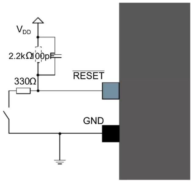
text_image
VDD 2.2kΩ 100pF 330Ω RESET GNDFigure 36-5. External Reset Circuit Schematic (EFT Immunity Enhancement)
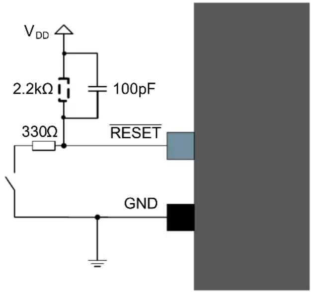
text_image
VDD 2.2kΩ 100pF 330Ω RESET GNDNote: This reset circuit is intended to improve EFT immunity, but does not filter low-frequency glitches, which makes it not suitable as an example for applications requiring debouncing on a reset button.
Table 36-3. Reset Circuit Connections
| Signal Name | Recommended Pin Connection Description | |
| RESET Reset | low-level threshold voltage V_DDIO = 1.6V - 2.0V : Below 0.33 * V_DDIOV_DDIO = 2.7V - 3.6V : Below 0.36 * V_DDIODecoupling/filter capacitor 100 pF^(1)Pull-up resistor 2.2 k^(1)(2)Resistor in series with the switch \( 330^(1) | Reset pin |
- These values are given as a typical example.
- The SAM D20 features an internal pull-up resistor on the RESET pin, hence an external pull-up is optional.
36.5 Clocks and Crystal Oscillators
The SAM D20 can be run from internal or external clock sources, or a mix of internal and external sources. An example of usage will be to use the internal 8MHz oscillator as source for the system clock, and an external 32.768kHz watch crystal as clock source for the Real-Time counter (RTC).
36.5.1 External Clock Source
Figure 36-6. External Clock Source Example Schematic
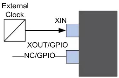
flowchart
graph LR
    A["External Clock"] --> B["XIN"]
    A --> C["XOUT/GPIO"]
    C --> D["Output Block"]
    D --> E["NC/GPIO"]
Table 36-4. External Clock Source Connections
| Signal Name Recommended Pin Connection Description | |
| XIN XIN is used as input for an external clock signal Input for inverting oscillator pin | |
| XOUT/GPIO Can be left unconnected or used as normal GPIO |
36.5.2 Crystal Oscillator
Figure 36-7. Crystal Oscillator Example Schematic
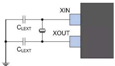
text_image
XIN CLEXT CLEXT XOUTThe crystal should be located as close to the device as possible. Long signal lines may cause a load too high to operate the crystal, and cause crosstalk to other parts of the system.
Table 36-5. Crystal Oscillator Checklist
| Signal Name Recommended Pin Connection Description | ||
| XIN Load capacitor C | LEXT^(1)(2) | External crystal between 0.4 to 30 MHz |
| XOUT Load capacitor C | LEXT^(1)(2) | |
-
Use the equation in Crystal Oscillator Characteristics to calculate C LETT.
-
Decoupling capacitor should be placed close to the device for each supply pin pair in the signal group.
36.5.3 External Real Time Oscillator
The low-frequency crystal oscillator is optimized for use with a 32.768 kHz watch crystal. When selecting crystals, load capacitance and crystal's Equivalent Series Resistance (ESR) must be considered. Both of these values are specified by the crystal vendor.
The SAM D20 oscillator is optimized for very low-power consumption, hence the user must pay close attention while selecting crystals. Refer to the table below for maximum ESR recommendations on 9 pF and 12.5 pF crystals.
The low-frequency crystal oscillator provides an internal load capacitance of typical values available in Table 32 kHz Crystal Oscillator Characteristics. This internal load capacitance and PCB capacitance can use a crystal inferior to 12.5 pF load capacitance without external capacitors as shown in the following figure.
Table 36-6. Maximum ESR Recommendation for 32.768 kHz Crystal
| Crystal G_L (pF) Maximum ESR [kΩ] | |
| 12.5 313 |
Note: Maximum ESR is typical value based on characterization. These values are not covered by test limits in production.
Figure 36-8. External Real Time Oscillator without Load Capacitor
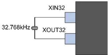
text_image
32.768kHz XIN32 XOUT32However, to improve crystal accuracy and safety factor, it has been recommended to add external capacitors as shown in the figure below.
To find suitable load capacitance for a 32.768 kHz crystal, refer to the crystal data sheet.
Figure 36-9. External Real Time Oscillator with Load Capacitor
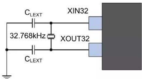
text_image
C_{LEXT} 32.768kHz XIN32 XOUT32 C_{LEXT}Table 36-7. External Real Time Oscillator Checklist
| Signal Name Recommended Pin Connection Description | ||
| XIN32 Load capacitor C | LEXT^(1)(2) | Timer oscillator input |
| XOUT32 Load capacitor C | LEXT^(1)(2) | Timer oscillator output |
- Use the equation in Crystal Oscillator Characteristics to calculate C LETT.
- Decoupling capacitor must be placed close to the device for each supply pin pair in the signal group.
Note:
To minimize the cycle-to-cycle jitter of the external oscillator, keep the neighboring pins as steady as possible. For neighboring pin details, refer to the Oscillator Pinout section.
36.5.4 Calculating the Correct Crystal Decoupling Capacitor
To calculate correct load capacitor for a given crystal, refer to Oscillator Characteristics for parasitic load capacitance values and equation to calculate C_LEXT .
36.6 Unused or Unconnected Pins
For unused pins, the default state of the pins will give the lowest current leakage. Therefore, no need to configure unused pins to lower the power consumption.
36.7 Programming and Debug Ports
For programming and/or debugging the SAM D20 the device should be connected using the Serial Wire Debug, SWD, interface. Currently the SWD interface is supported by several Microchip and third party programmers and debuggers, like the JTAGICE3, SAM-ICE, ATMEL_ICE or SAM D20 Xplained Pro (SAM D20 evaluation kit) Embedded Debugger.
Refer to the JTAGICE3, SAM-ICE, ATMEL_ICE or SAM D20 Xplained Pro user guides for details on debugging and programming connections and options. For connecting to any other programming or debugging tool, refer to that specific programmer or debugger's user guide.
The SAM D20 Xplained Pro evaluation board for the SAM D20 supports programming and debugging through the onboard embedded debugger so no external programmer or debugger is needed.
Note that a pull-up resistor on the SWCLK pin is critical for reliable operations. Refer to related link for more information.
Figure 36-10. SWCLK Circuit Connections

text_image
VDD 1kΩ SWCLKTable 36-8. SWCLK Circuit Connections
| Pin Name Description Recommended Pin Connection | |
| SWCLK Serial wire clock pin Pull-up resistor 1kΩ |
Related Links
36.1.1. Operation in Noisy Environment
36.7.1 Cortex Debug Connector (10-pin)
For debuggers and/or programmers that support the Cortex Debug Connector (10-pin) interface the signals should be connected as shown in the figure below with details described in the next table.
Figure 36-11. Cortex Debug Connector (10-pin)
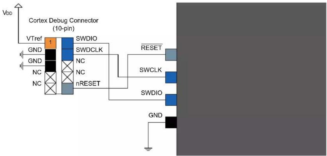
flowchart
graph TD
    A["VDD"] --> B["Cortex Debug Connector (10-pin)"]
    B --> C["VTref"]
    C --> D["GND"]
    C --> E["GND"]
    C --> F["NC"]
    C --> G["NC"]
    C --> H["SWDIO"]
    C --> I["SWDCLK"]
    C --> J["nRESET"]
    J --> K["RESET"]
    J --> L["SWCLK"]
    J --> M["SWDIO"]
    J --> N["GND"]
Table 36-9. Cortex Debug Connector (10-pin)
| Header Signal Name | Description Recommended Pin Connection | |
| SWDCLK Serial wire clock pin Pull-up resistor 1kΩ | ||
| SWDIO Serial wire bidirectional data pin | ||
| RESET Target device reset pin, active lowRefer to 36.4.External Reset Circuit. | ||
| VTref Target voltage sense, should be connected to the device V | DD | |
| GND Ground | ||
36.7.2 10-pin JTAGICE3 Compatible Serial Wire Debug Interface
The JTAGICE3 debugger and programmer does not support the Cortex Debug Connector (10-pin) directly, hence a special pinout is needed to directly connect the SAM D20 to the JTAGICE3, alternatively one can use the JTAGICE3 squid cable and manually match the signals between the JTAGICE3 and SAM D20. The following figure describes how to connect a 10-pin header that supports connecting the JTAGICE3 directly to the SAM D20 without the need for a squid cable.
To connect the JTAGICE3 programmer and debugger to the SAM D20, one can either use the JTAGICE3 squid cable, or use a 10-pin connector as shown in the figure below with details given in the next table to connect to the target using the JTAGICE3 50 mil cable directly.
Figure 36-12. 10-pin JTAGICE3 Compatible Serial Wire Debug Interface
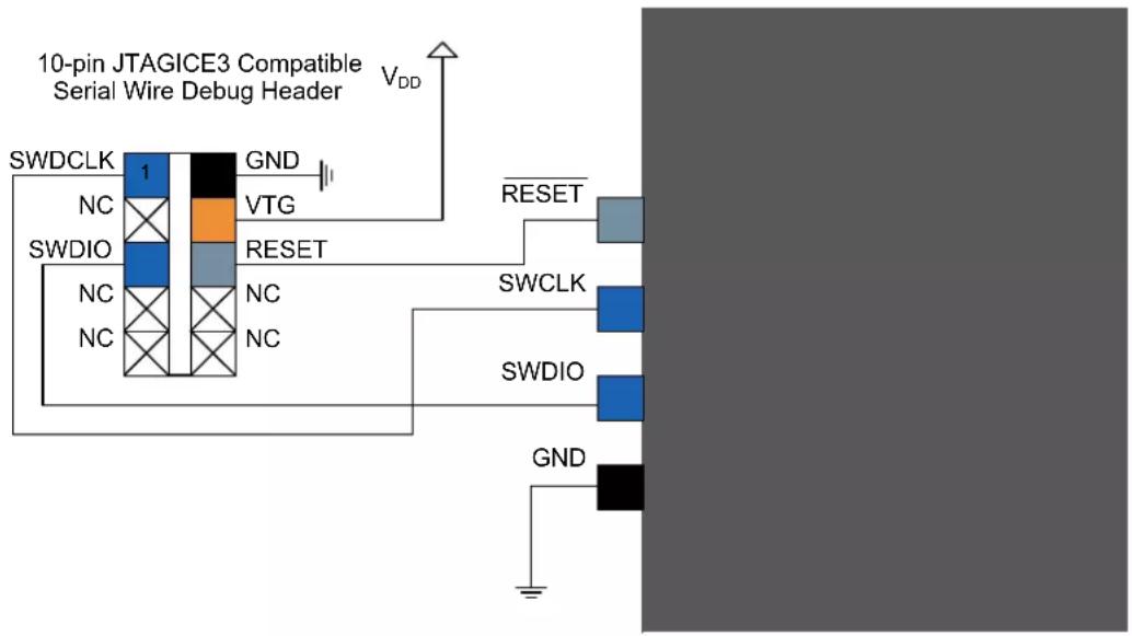
flowchart
graph TD
    A["10-pin JTAGICE3 Compatible Serial Wire Debug Header"] --> B["SWDCLK"]
    A --> C["SWDIO"]
    A --> D["GND"]
    B --> E["1"]
    C --> F["NC"]
    C --> G["NC"]
    C --> H["NC"]
    D --> I["GND"]
    E --> J["VTG"]
    F --> K["RESET"]
    G --> L["VTG"]
    H --> M["RESET"]
    I --> N["RESET"]
    J --> O["SWCLK"]
    K --> P["SWDIO"]
    L --> Q["SWDIO"]
    M --> R["SWDIO"]
    N --> S["SWDIO"]
    O --> T["SWDIO"]
    P --> U["SWDIO"]
    Q --> V["SWDIO"]
    R --> W["SWDIO"]
    S --> X["SWDIO"]
    T --> Y["SWDIO"]
    U --> Z["SWDIO"]
    V --> AA["SWDIO"]
    W --> AB["SWDIO"]
    X --> AC["SWDIO"]
    Y --> AD["SWDIO"]
    Z --> AE["SWDIO"]
    AA --> AF["SWDIO"]
    AB --> AG["SWDIO"]
    AC --> AH["SWDIO"]
    AD --> AI["SWDIO"]
    AE --> AJ["SWDIO"]
    AF --> AK["SWDIO"]
    AG --> AL["SWDIO"]
    AH --> AM["SWDIO"]
    AI --> AN["SWDIO"]
    AJ --> AO["SWDIO"]
    AK --> AP["SWDIO"]
    AL --> AQ["SWDIO"]
    AM --> AR["SWDIO"]
    AN --> AS["SWDIO"]
Table 36-10. 10-pin JTAGICE3 Compatible Serial Wire Debug Interface
| Header Signal Name Description | |
| SWDCLK Serial wire clock pin | |
| SWDIO Serial wire bidirectional data pin | |
| RESET Target device reset pin, active low | |
| VTG Target voltage sense, should be connected to the device V | DD |
| GND | Ground |
36.7.3 20-pin IDC JTAG Connector
For debuggers and/or programmers that support the 20-pin IDC JTAG Connector, e.g. the SAM-ICE, the signals should be connected as shown in the next figure with details described in the table.
Figure 36-13. 20-pin IDC JTAG Connector
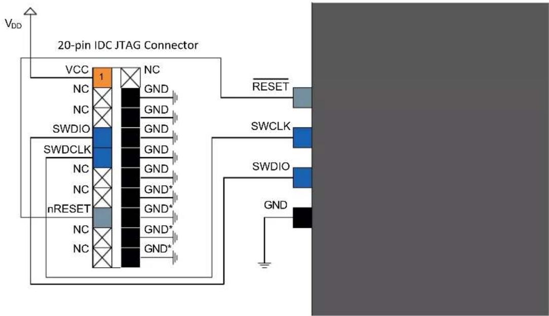
text_image
VDD 20-pin IDC JTAG Connector VCC 1 NC NC GND NC GND SWDIO GND SWDCLK GND NC GND NC GND* nRESET GND* NC GND* NC GND* RESET SWCLK SWDIO GNDTable 36-11. 20-pin IDC JTAG Connector
| Header Signal Name | Description |
| SWDCLK Serial wire clock pin | |
| SWDIO Serial wire bidirectional data pin | |
| RESET Target device reset pin, active low | |
| VCC Target voltage sense, should be connected to the device V | DD |
| GND Ground | |
| GND* | These pins are reserved for firmware extension purposes. They can be left open or connected to GND in normal debug environment. They are not essential for SWD in general. |
37. Datasheet Revision History
The referring page numbers in this section are referred to this datasheet. The referring revision in this section are referring to the datasheet revision.
37.1 Revision G - 08/2023
No content changes compared with the previous revision.
37.2 Revision F - 03/2022
This revision includes numerous typographical corrections throughout the document. All other changes are described as follows:
| Section Description | |
| General The SPI and I | ^2C standards use the terminology "Master" and "Slave". The equivalent Microchip terminology, "Host" and "Client," is used in this document. This terminology has been updated throughout this document for this revision. |
| RTC | Added a note to the RCONT bitfield in the READREQ Register. |
| SERCOM SPI | Removed erroneous text in Host with Several Clients. |
| TC | Updated the CTRLA Register with a new Register property for 8-bit, 16-bit and 32-bit RegistersUpdated the 8-bit COUNT Register with a new note and an updated Register PropertyUpdated the 16-bit COUNT Register with a new note and an updated Register PropertyUpdated the 32-bit COUNT Register with a new note and an updated Register Property |
| Electrical Characteristics at 85°C | In SERCOM in SPI Mode Timing the table had minor formatting updates applied, and the typical and maximum values for t_SCK switchedIn SERCOM in I ^2C Mode Timing minor formatting updates were applied to the table |
| AEC-Q100 Electrical Characteristics at 125°C | In SERCOM in SPI Mode Timing the table had minor formatting updates applied, and the typical and maximum values for t_SCK switched. |
| Acronyms and Abbreviations | Removed references to the TCC as this product does not contain a TCC. |
37.3 Revision E - 11/2020
This revision includes numerous typographical corrections throughout the document. All other changes are described as follows:
| Section Description | |
| Pinout | Updated the pinout for UFBGA64 to show the GND pins as black in color. |
| GCLK | Updated the GENDIV register with a Write-Synchronized property and added a new column to the table under the DIV bit field |
| SYSCTRL | Updated the AMPGC and GAIN bits of the XOSC register with a new text |
| EVSYS Updated the Features with a new text for the last line item | |
| NVMCTRL Updated the LOCK register with a new reset value | |
| ADC | Updated Power Management and Sleep Mode Operation. ADC OVERRUN interrupt cannot wake up the device from Sleep mode. |
| DAC | • Updated the Block Diagram to represent ADC input• Updated the CTRLB Register with a new table value for the EOEN bit |
| Electrical Specifications at 85°C | The following updates were performed:Under Absolute Maximum Ratings, the GPIO Clusters table was updated with revised information for new packagesAdded Note 1 to Current Consumption - Device Variant AAdded Note 2 to Current Consumption - Device Variant BUpdated the Maximum Peripheral Clock Frequencies table in Maximum Clock FrequenciesUpdated the POR Operating Principle Diagram in Power-On Reset (POR) CharacteristicsUpdated the Operating Conditions table in Digital-to-Analog Converter (DAC) Characteristics with a new noteUpdated the equation in XOSC Crystal Oscillator CharacteristicsUpdated XOSC32K Digital Clock Characteristics with a new noteUpdated XOSC32K Crystal Oscillator Characteristics with a new text |
| Electrical Specifications at 105°C | The following updates were performed:Under Absolute Maximum Ratings, a new information was addedUpdated the Maximum Peripheral Clock Frequencies table in Maximum Clock FrequenciesUpdated the POR Operating Principle Diagram in Power-On Reset (POR) CharacteristicsUpdated the Operating Conditions table in Digital-to-Analog Converter (DAC) Characteristics with a new noteUpdated the equation in XOSC Crystal Oscillator CharacteristicsUpdated XOSC32K Digital Clock Characteristics with a new noteUpdated XOSC32K Crystal Oscillator Characteristics with a new text |
| AEC-Q100 Electrical Specifications | Added Electrical Specifications chapter for AEC-Q100 |
| Packaging Information | Removed references to moisture sensitivity for each packageUpdated the Package Drawings to the latest version |
37.4 Revision D - 03/2020
This revision includes typographical corrections throughout the document. For a list of other items, refer to the following table:
| Section Updates | |
| Features Added 27-ball WLCSP package | |
| Configuration Summary | Updated the SAM D20 Family Features table, and added WLCSP27 package |
| Ordering Information | • Updated Pin Count field for 27-pin and 45-pin WLCSP packages• Added Note 3 and 4 |
| Pinout | • A note is added for the QFN32/TQFP32 package• WLCSP27 pinout added |
| I/O Multiplexing and Considerations | Ball number is added for WLCSP27, WLCSP45 and UFBGA packages in PORT Function Multiplexing |
| SERCOM ^12C | • Updated the CLKHOLD bit description in STATUS Slave Register• Updated ADDR bits from 7 to 8 in the Master Address register, ADDR |
| SYSCTRL | Updated the VREG Register with a new Reserved bit and new note. |
| TC - Timer/Counter | • Updated number of timers from five to eight in Features sub-section• Updated Counter Mode sub-section for 32-bit Counter mode (COUNT32) |
| AC | Updated Figure 29-2 Continuous Measurement Example with a new name for first signal. |
| Packaging Information | • Updated Thermal Resistance Data for 27-ball WLCSP package• Added WLCSP27 package drawing for the 27-ball WLCSP package |
37.5 Revision C - 11/2019
This revision includes typographical corrections throughout the document. For a list of other items, refer to the following table:
| Section Updates | |
| PORT | Updated the PMUX Register with information for 0x5 for the PMUXO and PMUXE bits. |
| SERCOM I^2C Updated the Diagram I ^2C Master Behavioral Diagram in I^2C Master Operation. | |
| SERCOM I^2C Updated the chapter to remove the following duplicate sections:Receiving Data PacketsHigh Speed Mode10 Bit AddressingReceiving Address Packets | |
| SERCOM I^2C Updated the Diagram I ^2C Slave Behavioral Diagram in I^2C Slave Operation. | |
| SERCOM I^2C Updated the following Registers:STATUS Slave Register With R/W information for the CLKHOLD bitSTATUS Master Register was updated with information for the SCL line | |
| Electrical Characteristics at 85°C | Updated the Equation in Crystal Oscillator Characteristics |
| Electrical Characteristics at 105°C | Updated the Equation in Crystal Oscillator Characteristics |
| Schematic Checklist | Updated Crystal Oscillator with C _LEXT information in the figure and table replacing 15pFUpdated External Real Time Oscillator with information for C _LEXT in the figure and table replacing 22pFUpdated Calculating the Correct Crystal Decoupling Capacitor with a new reference to Oscillator Characteristics for an updated equationUpdated External Reset Circuit with a new diagram |
| Power Domain Overview Corrected the color of the pins on the right side of the diagram to blue. | |
37.6 Rev. B - 11/2017
| General update | This revision contains updates to restore content that was omitted in the previous version of the document, and to remove content that is not applicable to this device family.The following content was restored:Column Fin Table 6-17.1. Power Domain OverviewPower Supply Connection (see Figure 7-1)PAC2 Write Protect Clear register bits (see 10.6.3.1. WPCLR)PAC2 Write Protect Set register bits (see 10.6.3.2. WPSET)DSU Block Diagram (see Figure 12-1)Analog Comparator Block Diagram (see 29.3. Block Diagram)The following content was removed:DMAC and DMA references were removed throughout the documentRWW and RWWEE references were removed throughout the Non-Volatile Memory Controller chapter and elsewhere in the documentAsynchronous Fractional Mode and related references were removed from the Baud Rate Equation table (see Table 23-2) |
| Features The number of Timer/Counters (TC) was updated to eight. | |
| 1. Configuration Summary | The Flash size was updated to include 16 KB. |
| 9.4. NVM User Row Mapping | The NVM User Row Mapping table was updated (see Table 9-3). |
| 19. EIC – External Interrupt Controller | Removed the CONFIG2 register (see 19.8. Register Description). |
| Electrical Characteristics at 85°C | The Bandgap (Internal 1.1V reference) Characteristics were updated (see Table 32-34). |
| 35. Packaging Information | The WLCSP packaging information was updated (see 35.2.8. 45-ball WLCSP). |
37.7 Rev. A - 08/2017
| General updates | • Updated the document from Atmel to Microchip style and template• The literature number changed from the Atmel 42129 to the Microchip DS60001504.• The Data Sheet revision letter was restarted to A• An ISBN number was added |
37.8 Rev. P - 09/2016
| 9. Memories | Updated the BOOTPROT default value in NVM User Row Mapping: default value = 0x7 except for WLCSP that has default value = 0x3 |
| 12. DSU - Device Service Unit Updated the Registers "Reset Value" | |
| 13. Clock System Added the section: 13.5. Disabling a Peripheral | |
| 16. SYSCTRL - System Controller | Description added on setting up AMPGC bit in XOSC register |
| 22. Event System (EVSYS) 22.8.1. CTRL.SWRST: Added recommendation when doing a software reset | |
| 18. RTC - Real-Time Counter | Updated the description in 18.6.3.3. Clock/Calendar (Mode 2): Example added on how the clock counter works in calendar mode |
| 27. TC - Timer/Counter | The ENABLE and SWRST bits in 27.8.1. CTRLA register are not enable protected |
| 36. Schematic Checklist | Updated External Real Time Oscillator: Added note on how to minimize jitter |
| 32. Electrical Characteristics at 85°C at 85°C | • Editing update• Updated General Operating Ratings- Added note about the NVM erase operations in debugger cold-plugging mode• Updated Crystal Oscillator Characteristics- Removed the package condition from the Table 32-44 |
| Electrical Characteristics at 105°C | • - Updated 33.6. Injection Current• Updated 33.3. General Operating Ratings- Added note about the NVM erase operations in debugger cold-plugging mode• Updated Crystal Oscillator Characteristics- Removed the package condition from the Table 32-44 |
37.9 Rev. O - 08/2016
| Description Description: Updated CoreMark score from 2.14 to 2.46 CoreMark/MHz. | |
| Block Diagram Updated Block Diagram. | |
| Power Manager Updated description for bits [31:4] in 15.8.9. APBBMASK. | |
| System Control Updated description in Drift Compensation. | |
| 32. Electrical Characteristics at 85°C | 32.10.3. Brown-Out Detectors Characteristics: Updated Table 32-19.32.12.3. Digital Frequency Locked Loop (DFLL48M) Characteristics: Note 2 in Table 32-45 updated to only be applicable for die revision C. |
| Schematic Checklist | Updated the content in section Unused or Unconnected Pins.Power Supply Schematic: V_DDCORE decoupling capacitor value updated from 100nF to 1nF. |
| 32. Electrical Characteristics at 85°C at 85°C | • Updated 32.2. Absolute Maximum Ratings– V_pin : min and max changed respectively from GND-0.3V to GND-0.6V and from GND+0.3V to GND+0.6V• Added 32.9. Injection Current |
| Electrical Characteristics at 105°C | • Updated 33.2. Absolute Maximum Ratings– V_pin : min and max changed respectively from GND-0.3V to GND-0.6V and from GND+0.3V to GND+0.6V• – Added 33.6. Injection Current• 32.10.3.1. BOD33: Updated Table 32-20. |
37.10 Rev. N - 01/2015
| Electrical Characteristics | Updated Table 32-21 in the 32.10.4. Analog-to-Digital (ADC) Characteristics- added two rows. One for Internal ratiometric reference 0 error and the other for Internal ratiometric reference 1 error- added more details in Conditions of V_REFINTVCC0 and V_REFINTVCC1 |
| Errata | Added Errata revision EUpdated Errata revision D:- Added new Errata references: 12290; 13950 and 13951- Updated Errata reference 13574: The software workaround: In I2C Slave mode, writing the CTRLB register when in the AMATCH or DRDY interrupt service routines can cause the state machine to reset- Updated Errata reference 13276 Workaround 2: At 105°C, use the ADC in single shot mode only with VDDANA > 2.7VUpdated Errata revision C:- Added new Errata reference:13951- Updated Errata reference 10537Updated Errata revision B:- Added new Errata reference:13951 |
| Appendix | Added 33.Electrical Characteristics at 105°C |
37.11 Rev. M - 12/2014
| Signal Description List | • VREFP renamed VREFA and VREFB in the 5. Signal Descriptions List |
| Memories | • Added a table note to the Table 9-4 |
| 12. DSU - Device Service Unit | • Updated the Register Summary- Added register bit AMOD[1:0]• Updated the register ADDR- Added the description of "Bits 1:0 - AMOD[1:0]" |
| System Controller | • Removed all references to 1khz from 16.6.3. 32kHz External Crystal Oscillator (XOSC32K) Operation, 16.6.4. 32kHz Internal Oscillator (OSC32K) Operation and 16.6.5. 32kHz Ultra Low Power Internal Oscillator (OSCULP32K) Operation• Changed EN1K bits to "Reserved" in 16.8.6. XOSC32K and in 16.8.7. OSC32K |
| PORT | • Updated 21.6.3. I/O Pin Configuration- Removed reference to Open-drain |
| ADC - Analog-to-Digital Converte | • Replaced AREFA/AREFB by VREFA/VREFB in 28.5.8. Analog Connections |
| DAC - Digital -to-Analog Converter | • Replaced VREFP by VREFA in 30.6.2.4. Digital to Analog Conversion and in 30.6.7.1. DAC as an Internal Reference |
| Electrical Characteristics | • 32.10.3. Brown-Out Detectors Characteristics:- Added Figure 32-3, Figure 32-4 and clarifications.- Updated conditions in the Table 32-19 and in the Table 32-20.• 32.10.4. Analog-to-Digital (ADC) Characteristics:- Updated conditions in the Table 32-26 and in the Table 32-27.• Updated the table Table 32-45 in 32.12.3. Digital Frequency Locked Loop (DFLL48M) Characteristics:- Renamed "Power consumption on V_DDANA " to "Power consumption on V_DDIN "- Added I _DFLL specific typical value for revD and later• Updated the table Table 32-50 in 32.14.2. SERCOM in SPI Mode Timing:- The value of t SCK SCK period updated from 42 to 84 |
| Package Information | • Updated 35.1. Thermal Considerations:- Added ThetaJA and Theta_JC values for the packages: 64-ball UFBGA and 45-ball WLCSP |
| Schematic Checklist | • Updated the Introduction Content• Replaced AREFA/AREFB by VREFA/VREFB in the content• Updated the content in the36.7. Programming and Debug Ports– Updated all sub-sections, tables and figures |
| Errata | • Updated Errata revision D:– Added Errata reference 13574 related to CTRLB register / I^2C in Slave Mode. |
37.12 Rev. L - 09/2014
| Features | Added UFBGA64 and WLCSP45 packagesIntroduced the 105°C devices |
| Pinout | Added two more pinouts: 4.1.2. UFBGA64 and 4.2.2. WLCSP45 |
| Configuration Summary | Updated1. Configuration Summary to include UFBGA64 and WLCSP45 packages |
| Ordering Information | Updated 2. Ordering Information (1) to include UFBGA64, WLCSP45 packages and the ordering codes for 105°C devices |
| Peripheral Configuration | Updated 11. Peripherals Configuration Summary- Added one column “SleepWalking” in the Table 11-1 |
| 15. Power Manager (PM) | Updated the table note 1 of the Table 15-3 |
| System Controller | Updated 16.5.4. Interrupts- Interrupt source “BOD33DET - BOD33 Detection” is an Asynchronous interrupt that can be used to wake-up the device from any sleep mode |
| Watchdog Timer | Updated 17.6.3.1. Always-On Mode- Added conditions for which CTRL.ALWAYSON bit must never be set to one by softwareUpdated 17.6.4. Interrupts- Early Warning (EW) is an asynchronous interrupt that can be used to wake-up the device from any sleep mode |
| 18. RTC - Real-Time Counter | Updated the section Interrupts- Overflow (INTFLAG.OVF), Compare n (INTFLAG.CMPn), Alarm 0 (INTFLAG.ALARMn) and Synchronization Ready (INTFLAG.SYNCRDY) are all asynchronous and can be used to wake-up the device from any sleep mode |
| 19. EIC - External Interrupt Controller | Updated the section Interrupts- External interrupt pins (EXTINTx) and Non-maskable interrupt pin (NMI) are both asynchronous and can be used to wake-up the device from any sleep mode |
| 21. PORT - I/O Pin Controller | Updated the Basic Operation section- Instances “pad” changed to “pin”- Edited the content in the section |
| 22. Event System (EVSYS) | Updated the section Interrupts- Overrun Channel x (OVRx) and Event Detected Channel x (EVDx) are asynchronous and can be used to wake-up the device from any sleep modeUpdated the section Sleep Mode Operations |
| SERCOM USART | Updated the section Interrupts- RXS, RXC, TXC and DRE interrupts are asynchronous and can be used to wake-up the device from any sleep mode. |
| 28. Analog-to-Digital Converter (ADC) | • Fix a typo in the description of the bitfield MUXPOS of the register INPUTCTRL• Added more info to the table “Delay Gain” and about the propagation delay in sub-section 7.3 “Prescaler” |
| Electrical Characteristics | • Updated the Maximum Clock Frequencies- Added the Table 32-6- Renamed the Table 32-7 to "Maximum Peripheral Clock Frequencies" and updated the whole table content including the symbols and descriptions• Added the section Peripheral Power Consumption• Updated the section I/O Pin Characteristics- Updated the table Table 32-11For t_RISE and t_FALL added different load conditions depending on DVRSTR value• Updated SERCOM in SPI Mode Timing- Added typical t _SCK in the table Table 32-44• Updated Voltage Regulator Characteristics- Added minimum value to the C _out parameter in the Table 32-15• Updated Digital Frequency Locked Loop (DFLL48M) Characteristics- Renamed the Table 32-39 to DFLL48M Characteristics - Closed Loop Mode- Updated the content and the table note of the Table 32-39• Updated the Analog-to-Digital (ADC) Characteristics- Table 32-19. Operating ConditionsUpdated Single rate (single shot) maximum value to 300 kspsUpdated the table note 3- Updated Table 32-20 and Table 32-21:Added definition of the gain accuracy parameter• Updated Temperature Sensor Characteristics- Updated the table Table 32-29. Temperature Sensor CharacteristicsAdded temperature sensor accuracy parameters and its condition |
| Schematic Checklist | • Added link for the values of XIN32/XOUT32 pins parasitic capacitance in the Table 32-38. 32kHz Crystal Oscillator Characteristics |
| Package Information | • Added two more packages: 64UFBGA and 45WLCSP |
| Errata | • Updated errata for revision B, C and D. Added errata references: 10805, 12015, 12499, 13140, 13140 and 13268 |
37.13 Rev. K - 05/2014
| Description | • Updated the content in the Description |
| Block Diagram | • VREFP on DAC renamed VREFA |
| Memories | • Updated the tableNVM User Row Mapping- Changed the WDT window default value, WINDOW_1 to 0x5 |
| DSU - Device Service Unit | • Updated DSU Chip Identification Method:- “Family” renamed “Product family” and subfamily became “Product series”• Updated the protection state of the device in Starting CRC32 Calculation |
| SYSCTRL - System Controller | Updated 8MHz Internal Oscillator (OSC8M) Operation- Updated the description of writing to FRANGE and CALIBUpdated the table Behavior of the Oscillators- DFLL renamed DFLL48MAdded Note on how to enter standby mode in:- External Multipurpose Crystal Oscillator (XOSC) Operation- 32kHz External Crystal Oscillator (XOSC32K) OperationAdded VREG register- Added VREG register in Register Summary- Updated the description of Bit 6 - RUNSTDBY and Bit 13 - FORCELDOUpdated the description of InterruptsUpdated OSC8M-Bits 11:0 - CALIB has two calibration fields CALIB[11-6] and CALIB[5:0] |
| RTC - Real-Time Counter | Updated Analog Connections-TOSC1 and TOSC2 renamed respectively XIN32 and XOUT32 |
| PORT | Updated Principle of Operation-The reference for Pin Configuration registers changed to PINCFGy |
| SERCOM SPI | Updated CTRLB register-Bit 17 - RXEN is R/W |
| TC - Timer/Counter | Updated the table Waveform Generation OperationUpdated CTRLC register-Bits 1:0 - INVENx: Waveform Output x Invert Enable |
| AC - Analog Comparators | Added Bit 7 - LPMUX in CTRLA register and updated Register Summary |
| DAC - Digital -to-Analog Converter | Added a new DAC in the Block Diagram with VREFP replaced by VREFAUpdated Signal Description-VREFP renamed VREFA |
| Electrical Characteristics | Updated the table Absolute maximum ratings- Updated I VDD and IGND max values- Added a detailed table note for I VDD and IGNDAdded the table GPIO ClustersUpdated the table General operating conditions- Removed table note (1) related to the operating conditionsUpdated the table Current Consumption- Updated values in ACTIVE and IDLE0/1/2 modes- Updated the max values @ 85°C in STANDBY modesI Max values updated to 100μA both for RTC stopped and RTC runningUpdated I/O Pin Characteristics section- Updated title of the table to RevD and later normal I/O Pins Characteristics- Updated I OL and IOH values in the table RevD and later normal I/O Pins Characteristics- Updated I OL and IOH in the table I2C Pins Characteristics in I2C configurationTable note (1) on C OUT removed from the table Decoupling requirementsUpdated the content in Analog Characteristics- Updated max value of V POT in the table POR Characteristics. New max value is 1.32V- Updated table note 3 in Differential Mode- Updated table note 2 in Single-Ended Mode- Updated R SAMPLE in the table Operating ConditionsAdded conversion rate for max 1000ksps in the table Clock and TimingUpdated the table Accuracy Characteristics- Added table note "All values measured using a conversion rate of 350ksps"Updated Software-based Refinement of the Actual Temperature- Added the address of the temperature log rowUpdated the table DELL48M Characteristics - Closed Loop Mode- Removed the Tlcoarse parameter as it is already set from calibration- Updated I DELL and tSTARTU typical valuesUpdated Crystal Oscillator Characteristics section:- Updated the max values of ESR- Updated the typical values of C XIN and CXOUTUpdated the table 32kHz Crystal Oscillator Characteristics:- Updated the table noteUpdated the max value of ESR to 141kΩ, the typical values of C XIN32 and CXOUT32 to respectively 3.1 and 3.3pFUpdated the table I 2C Interface Timing- Added table note (3) to t R and toF |
| ERRATA | Added Errata Revision DUpdated Errata Revision CUpdated Errata Revision B |
37.14 Rev. J - 12/2013
NVMCTRL - Non-Volatile Memory Controller
Updated the NVM NVMCTRL.CTRLB register.
37.15 Rev. I 12/2013
General Removed Preliminary
| Description | • Updated the description |
| Features | • Power Consumption has been updated to Down to 8μA running the Peripheral Touch Controller |
| Configuration Summary | Updated the Configuration Summary |
| Ordering Information | Updated Ordering Information• Added AT prefix at the start of the ordering codes |
| Block Diagram | • Added the description of the connection between PORT and ARM CORTEX-M0+ CPU: ARM SINGLE CYCLE IOBUS• Renamed GENERIC CLOCK to GENERIC CLOCK CONTROLLER |
| I/O Multiplexing and Considerations | Updated the Table 5-1. PORT Function Multiplexing• Renamed all GCLK/IO[x] to GCLK_IO[x]• Updated the description of the Serial Wire Debug Interface Pinout section• Added SWDIO to PA31 column G in the Table 5-1 and added a footnote |
| Product Mapping Changed Peripheral to AHB-APB | |
| Signal Description | • Removed GCLK from the heading “Generic Clock Generator”• Renamed IO[7:0] to GCLK_IO[7:0] |
| Memories | • Added a new section Serial Number• Software Calibration Row changed to Software Calibration Area• Added Figure 9-1. Calibration and Auxiliary space• Updated the Table 9-4. NVM Software Calibration Area Mapping- Added the BOD33 and BOD12 default settings- Added DFLL48M COARSE CAL and DFLL48M FINE CAL- Added table notes on rev C (Bit 40 and Bit 41) to the Table 9-3. NVM User Row Mapping |
| 12. DSU - Device Service Unit | • Updated the Table 12-7. Register Summary- Redefined DID register. FAMILY changed from 4 bits to 5 bits and SERIES from 8 bits to 6 bits• Updated the Device Identification- DID register- Updated Family and Series bit registers- Updated the Table 12-8. Device Selection. Added ATSAMD20E18A device at 0xA. |
| Clock System | • Updated the clock names in the Figure 13-1. Clock distribution• Updated the description of Generic Clock generators and Generic Clocks in the Clock Distribution• Updated the Figure 13-2. Example of SERCOM clock- Synchronous Clock Controller renamed to Main clock controller• Updated the descriptive content of the Read-Synchronization section• Changed the title “Enable Write-Synchronization” to Write-Synchronization of CTRL ENABLE• Updated the content in Clocks after Resetsection- Renamed GCLKMAIN to GCLK_MAIN |
| Generic Clock Controller | Updated the Overview section and renamed GCLK_PERIPH to GCLK_PERIPHERAL throughout the datasheetUpdated the Features listUpdated Figure 14-1. Device Clocking Diagram and added a figure noteUpdated links in the sections: Power Manageme and in ClocksUpdated the content in the Functional DescriptionAdded links in the section Initialization for GENDIV, GENCTRL and CLKCTRLUpdated the Figure 14-3.Generic Clock GeneratorRenamed “External Clock” to Generic Clock Output on I/O Pins and updated the descriptionUpdated the Figure 14-4.Generic Clock MultiplexerUpdated the descriptive content in the Disabling a Generic Clock” sectionUpdated the Figure 14-5. GCLK Indirect Access. GCLK becomes Generic ClockUpdated links in the sections: Run in Standby Mode and SynchronizationAdded a table note on the Reset of GENCTRL registerAdded a third column “Generator Clock Source” in the tableGENCTRL Reset Value after a Power ResetUpdated the content and replaced the text “if the generator is not used by the RTC” by the “if the generator is not used by the RTC and not a source of a 'locked' generic clock” in two tables:GENCTRL Reset Value after a User Reset and GENDIV Reset Value after a User Reset |
Power Manager
- Updated the content Overview
- "power save modes" is changed to "sleep modes"
- A new line is added: "This is because during STANDBY sleep mode the internal voltage regulator will be in low power mode"
- Updated Featureslist
- Clock control: "Generates" is changed to "Controls"
- Updated le content in the Clockssection
- "This clock" is changed to "The clock source for GCLK_MAIN"
- Updated the content in Interrupts section
- Added: "Refer to Nested Vector Interrupt Controller"
- Updated Register Access Protection
- Added: "Refer to Interrupt Flag Status and Clear - INTFLAG register for details"
- Added: "Refer to Reset Cause - RCAUSE register for details"
- Updated the sections: Synchronous Clocks and Sleep Mode Controller
- Added: "see Table 15-4. Sleep Mode Overview"
- Updated Reset Controller section
- "resets" corrected to "reset"
- Updated Initialization section
- Added: "- refer to Reset Cause - RCAUSE register for details"
- Updated Selecting the Synchronous Clock Division Ratio
- Added: "(APBxSEL.APBxDIV)"
- Updated the figure Synchronous Clock Selection and Prescaler
- Updated Clock Ready Flag section
- "CKSEL" is changed to "CPUSEL"
- Updated the Peripheral Clock Masking section
- Added: "refer to APBA Mask - APBAMASK register for details"
- The first sentence below the figure has been changed to: "When the APB clock for a module is not provided its registers cannot be read or written."
- Updated the content Clock Failure Detector section
- "CFDEN.CTRL" has been changed to "CTRL.CFDEN"
- Added: "Refer to Control - CTRL register for details"
- "divided" has been changed to "undivided"
- "is generated, if enabled" has been changed to "is set and the corresponding interrupt request will be generated if enabled"
- "GCLKMAIN" has been changed to "GCLK_MAIN"
- Added: Note 3
• Updated the table Effects of the Different Reset Events - "GCLK" has been changed to "Generic Clock"
- Updated the figure Reset Controller
- Updated the table Sleep Mode Entry and Exit
- Two notes ("Synchronous" and "Asynchronous") are added below the table
- Updated the Sleep Mode Controller section
- Updated the text in STANDBY mode
| Power Manager (cont.) | Updated the table Sleep Mode Overview- Replaced the table with an accurate oneUpdated IDLE Mode section- Second bullet: "any non-masked interrupt" changed to "the occurrence of any interrupt that is not masked in the NVIC Controller"Updated STANDBY Mode section- "GCLK" is changed to "Generic Clock"Added: SleepWalking sectionUpdated Bit 4 - BKUPCLK: Backup Clock Select"- "GCLKMAIN" is changed to "GCLK_MAIN" |
| 16. SYSCTRL - System Controller | Updated the content in Overview section- "XOSC, XOSC32K, OSC32K, OSCULP32K, OSC8M, DFLL48M, BOD33, BOD12, VREG and VREF" is changed to "clock sources, brown out detectors, on-chip voltage regulator and voltage reference of the device."- Added:" refer to Power and Clocks Status - PCLKSR register"- Added: "(INTENSET)"- Added: "(INTENCLR)"- Added: "(INTFLAG)"Updated the content in Principle of Operationsection- Added two tables for the behavior of Oscillators and Sleep modesUpdated Register Access Protection- Added: "- refer to INFLAGUpdated Analog Connections section- Changed "load. Refer" to "load, refer"Updated External Multipurpose Crystal Oscillator (XOSC) Operation section- Changed "the only" to "only the"- "the XTAL Enable bit (XOSC.XTALEN) must written to one" is changed to "a one must be written to the XTAL Enable bit (XOSC.XTALEN)."Updated the content in 32kHz External Crystal Oscillator (XOSC32K) Operation section- "power-on, reset" is changed to "power-on reset (POR)"- Added: "XOSC32K can provide two clock outputs when connected to a crystal."Updated the content in 8MHz Internal Oscillator (OSC8M) Operation sectionUpdated the content in 32kHz Internal Oscillator (OSC32K) Operation section- Changed "CALIB" to "OSC32K.CALIB"- Changed "non-volatile memory" to "NVM Software Calibration ROW"- Added: "(refer to NVM Software Calibration Area MappingUpdated the content in 32kHz Ultra Low Power Internal Oscillator (OSCULP32K) Operation section- Added: 32kHz Ultra Low Power Internal Oscillator (OSCULP32K) Control - OSCULP32K registerUpdated the content in Closed-Loop Operation section- List #3: Changed "device" to "DFLL"- Below "Drift Compensation": "set" has been replaced by "triggered"- The text "shown in the SYSCTRL Block Diagram" has been removed |
| SYSCTRL - System Control (cont.) | Updated Additional Features- The text “when disabling the DFLL48M” below “Wake from Sleep Modes” has been replaced by the text “when the DFLL is turned off”Updated 3.3V Brown-Out Detector (BOD33) section- “Brown-Out Detector” is replaced by “BOD33”Updated 32kHz Internal Oscillator (OSC32K) Control - OSC32K register- The reference for Bits 22:16 - CALIB[6:0] has been correctedUpdated the table Start-Up Time for External Multipurpose Crystal Oscillator- Both notes for this table has been updated/changed- New “Note 3” is addedUpdated the table Start-Up Time for 32kHz External Crystal Oscillator- Both notes for this table has been updated/changed- New “Note 3” is addedUpdated the table Start-Up Time for 32kHz Internal Oscillator- New column for “Number of OSC32K Clock Cycles” is added- The values in the column for the “old” “Number of OSC32K Clock Cycles” has been corrected- Both notes for this table has been updated/changed- New “Note 3” is addedUpdated DFLL48M Control - DFLLCTRL register- For “Property” the following has been added: ", Write-Synchronized"- Removed RUNSTDBYUpdated DFLL48M Value - DFLLVAL register- For “Property” the following has been added: ", Read-Synchronized"Updated Register Access Protection register- In the bullet point the following is added: " refer to Interrupt Flag Status and Clear - INTFLAG register"Updated Principle of Operation section- Added: "- refer to Control - CTRL register "and "- refer to Interrupt Enable Clear - INTENCLR register"Updated the Default Reset value in 8MHz Internal Oscillator (OSC8M) Control - OSC8M register and fixed the RANGE bitfieldUpdated the description of the Bit 4 DFLL Ready in Power and Clocks Status - PCLKSR register and updated Bit 11 BOD33 Synchronization Ready |
| 17. WDT - Watchdog Timer | Updated Initialization- Added: "- refer to CTRL register", "- refer to CONFIG register", and "- refer to EWCTRL register"Updated Normal Mode- Added: "- refer to Clear - CLEAR register"Updated the description of the Bit 2 (CTRL.WEN) in the Control - CTRL registerRemoved “Asynchronous Watchdog Clock Characterization” |
| 25. SERCOM SPI - SERCOM Serial Peripheral Interface | Updated the description of the SPI Transfer Modes section |
| RTC - Real-Time Counter | Updated Register Access Protection section- Added: "- refer to INTFLAG register", "- refer to READREQ register", "- refer to STATUS register", and "- refer to DBGCTRL register"Updated the content in Initialization section- Added: "- refer to Event Control - EVCTRL register" |
| EIC - External Interrupt Controller | ·Updated the content in Events section- Added text “External Interrupt Controller generates events as pulses”·Updated the content Sleep Mode Operation section- Added text “Using WAKEUPEN[x]=1 with INTENSET=0 is not recommended”·Updated the content Register Access Protection- Added: “- refer to INTFLAG register” and “- refer to NMIFLAG register”·Updated Additional Features- Added: “- refer to NMICTRL register” |
| NVMCTRL - Non-Volatile Memory Controller | ·Updated Power Management section- Added: “- refer to CTRLB register”·Added Basic Operations section·Updated Interrupts section- Added a reference link to Nested Vector Interrupt Controller·Updated the description of NVM Read section·Updated the content in Register Access Protection section·Added: “- refer to INTFLAG register” and “- refer to STATUS register”·Updated the description of MANW bit in CTRLB register·Updated the description of ERROR and READY bits in INTENCLR register |
| PORT | ·Updated CPU Local Bus section- Added: “- refer to DIR register”, “- refer to OUT register”, “- refer to IN register”, and “- refer to CTRL register”·Updated Principle of Operation section- Added: “- refer to DIR register”, “- refer to OUT register”, “- refer to PINCFG0 register”, “- refer to IN register”, and “- refer to PMUX0 register” |
| TC | ·Updated the table Waveform Generation Operation. Switched “Clear” and “Set” for CCO value (MPWM). |
| ADC | ·Updated the content in Sleep Mode Operation section- Added “While the CPU is sleeping, ADC conversion can only be triggered by vents”·Software Calibration Row changed to Software Calibration Area |
| AC | ·Updated the content in Sleep Mode Operation section- Added “While the CPU is sleeping, single-shot comparisons are only triggerable by events” |
| Electrical Characteristics | Updated Disclaimer section. Removed the preliminary disclaimerUpdated the table Absolute maximum ratings- Updated I_VDD and I_GND max values- Added T_STORAGE Updated the table General operating conditions- Added V_DDIO - V_DDANA Updated the table Current Consumption- Added min and max values- Added consumption dataUpdated I_OL and I_OH in the table RevD and later normal I/O Pins CharacteristicsUpdated V_HYS min value in I^2C Pins Characteristics in I^2C configurationDuplicated all tables in the table I/O Pin Characteristics" to differentiate rev D (the table RevD and later normal I/O Pins Characteristics) from rev C (the table RevC and later normal I/O Pins Characteristics)Updated the table and renamed to Voltage Regulator Electrical Characteristics- Added condition to V_DDCORE characteristicsUpdated the table BOD33 LEVEL Value- Added a table note to specify BOD33.LEVEL default production settingsUpdated the table BOD33 Characteristics- Added current consumption data ( I_BOD33 )ADC Characteristics: Removed the min value of I_DD from the table Operating ConditionsUpdated the Bandgap Gain Error min and max values in the table Differential ModeDAC characteristics: Updated I_DD values and conditions in the table Operating ConditionsRemoved the table note from the table Bandgap (Internal 1.1V reference) characteristicsUpdated the Accuracy unit in the table Accuracy CharacteristicsRemoved t_FFP from the tableNVM CharacteristicsUpdated the table Temperature Sensor CharacteristicsUpdated the content in Crystal Oscillator (SOSC) Characteristics section- Added new characterization data- Removed f_CPXIN min value from Digital Clock Characteristics tableChanged the title to Digital Frequency Locked Loop (DFLL48M) Characteristics and added table note to DFLL48M Characteristics - Closed Loop ModeUpdated the table 32kHz Crystal Oscillator Characteristics- Updated I_XOSC32K - Added a table note for "AGC on": data are not yet available for rev DAdded current consumption data ( I_OSC32K ) in the table 32kHz RC Oscillator CharacteristicsUpdated I_OSC8M In the table Internal 8MHz RC Oscillator Characteristics |
| Package | Added notes to 64QFN, 48QFN and to 32QFN packagesUpdated Device and Package Maximum Weight for 32-pin TQFP and for 32-pin QFN- Device and Package Maximum Weight is 100mg for TQFP32 and 90mg for QFN32 |
37.16 Rev. H 10/2013
| Configuration Summary | Added 256KB Flash and 32KB SRAM to the SAM D20E |
| Ordering Information | Added ATSAMD20E18 ordering code |
| SYSCTRL Added note to INFLAG register | |
| NVMCTRL Updated links to theFlash size for EEPROM emulation table | |
| SERCOM USART | Updated the table Transmit Data Pinout. SERCOM PAD[X] renamed PAD[X] |
| ADC | • Updated the Features list. Added "Up to 350,000 samples per second (350ksps)"• Updated the broken link for INPUTCTRL register• Removed "Additional Features" |
| Schematic Checklist | • Added information about JTAGICE3 compatible SWD connector• Updated connector names to match the names used by ARM• Added information about general debugging and programming to Programming and Debug Ports |
| Electrical Characteristics | • Updated the table General operating conditions. Added table note related to BOD33• Updated I/O Pin Characteristics. All V DDANA ranges are 1.62V - 2.7V and 2.7V - 3.63V• Updated Digital Frequency Locked Loop (DFLL48M) Characteristics• Updated the table Supply Rise Rates- Replaced the Maximum value that was based on simulation by the actual measurement value- Removed the unused columns• Updated the typical values of while(1) at 1.8V in the table Current Consumption• Updated the table Decoupling requirements- Used measurement values- Removed the min and max values- Added values for C IN and COUT- Added a table note• Updated the table ADC: Operating Conditions- Added min and max values for I DD- Updated typical values• Updated the table Single-Ended Mode- Added min and max values- Added characteristics for ENOB, SFDR, SINAD and THD |
| Electrical Characteristics | • Replaced V DD by VDDANA in the table Clock and Timing• Updated the table Electrical and Timing- Added min and max values- Added characterization data for V SCALE• Updated the tables: Differential Mode, Accuracy Characteristics and Temperature Sensor Characteristics- Added min and max values• Updated the tableFlash Endurance and Data Retention and EEPROM Emulation Endurance and Data Retention . Added table note related to the cycling endurance• Added output frequency characteristics data to the tables: 32kHz RC Oscillator Characteristics, Ultra Low Power Internal 32kHz RC Oscillator Characteristics and Internal 8MHz RC Oscillator Characteristics• Updated all tables in I/O Pin Characteristics section. Added new characterization data• Added V DDCORE characteristics to the Voltage Regulator Electrical Characteristics• Updated the tables: POR Characteristics, Bandgap (Internal 1.1V reference) characteristics, BOD33 LEVEL Value and BOD33 Characteristics. Added new characterization data• Updated all tables in Oscillators Characteristics section. Added new characterization data |
ERRATA Added Errata Revision C
37.17 Rev. G - 10/2013
Features Added the Power Consumption
GCLK Updated Division Factor
- Generic clock generator 0 has 8 division factor bits - DIV[7:0]
| NVMCTRL Updated the table Flash size for EEPROM emulation | |
| Electrical characteristics | Updated the table Current Consumption. Added values of CPU running a “While(1)” algorithmMoved the PTC typical figures from the Typical characteristics into the Electrical CharacteristicsUpdated the Analog Characteristics Cout max value in the Decoupling requirements table is 1000nF instead of 200nFUpdated the NVM Characteristics:- Added note about the max number of consecutive write in a row before an erase becomes mandatory- Removed all “based on simulation” notes- Updated the tables: Maximum Operating Frequency, Flash Endurance and Data Retention and EEPROM Emulation Endurance and Data Retention |
37.18 Rev. F - 10/2013
| I/O Multiplexing and Considerations | Updated the table PORT Function Multiplexing• PA16 and PA17 are I ^2C pins in SERCOM1 |
| Memories Updated the table NVM Software Calibration Area Mapping• Bit Positions [14:3] and [26:15] are “Reserved” | |
| ADC | Updated the Calibration according to the update done in the NVM Software Calibration Area Mapping |
| Typical Characteristics Added the PTC in the Typical Characteristics | |
| ERRATA Added PTC in Errata Revision B | |
37.19 Rev. E - 09/2013
| Ordering Information | Updated the figure of the Ordering InformationRemoved “H = -40 - 85C NiPdAu Plating” from the Package GradeRenamed “Product Variant” to “Device variant” in the figure of the Ordering Information |
| DSU Updated the DID register | • Renamed SUBFAMILY [7:0] bits to SERIES [7:0] bits• The whole description of the DID bit registers updated• Added Device (all products in the SAM D20 family) column in Device Selection table (DEVSEL) |
| SYSCTRL Added ENABLE bits for the BODs and oscillators | |
| Electrical characteristics | Updated Supply Characteristics• Updated the table Supply Rise RatesUpdated the I/O Pin Characteristics• Fixed typos in the tables RevD and later normal I/O Pins Characteristics, SAMD20 revC/revB Normal I/O Pins Characteristics and I^2C Pins Characteristics in I^2C configuration: “Vdd” was missing in some cells of the tables. |
37.20 Rev. D - 08/2013
| Description The content updated | |
| General | Fixed different typos throughout the datasheet and applied correctly the template |
| Block Diagram | • Added 2KB RAM and 16KB FLASH |
| DSU Updated the Block Diagram | • Removed HRAM from the block diagram |
| Clock System | • The description of the Basic Read Request has been updated• Updated the figure Synchronization |
| SYSCTRL | • Updated the writing of the interrupt sources in theInterruptssection• Added the reference toINFLAGregister |
| NVMCTRL Updated the figureRow Organization | • Removed the blue mark from the figure |
| PORT | • IOBUS address 0x60000000 added inCPU Local Bussection• Removed RWM from the description |
| EVSYS Updated theCHANNELregister: | • Bits 25:24: CHANNEL:PATH description updated. |
| Schematic Checklist | • Updated theIntroductioncontent• Replaced all TDB by their respective values• Corrected the typo: the Ohm symbol inExternal Reset Circuit |
| Electrical Characteristics | • Removed the colors fromElectrical Characteristics• Added footnote in the tableOperating Conditions, f_ADC = 6 * CLK_ADC |
| Table Of Contents | • Applied correctly the template for the TOC |
37.21 Rev. C - 07/2013
| Description Updated the front page:• Removed the “Embedded Flash” from the title and from the description on the page 1• Replaced “speeds” by “frequencies” on the page 1• Added a sub-bullet on PTC in feature list (256-Channel capacitive touch and proximity sensing) on the page 2• Replaced IO lines by IO pins on the page 2 | |
| Configuration Summary | Updated the table• The RTC• I/O lines changed to I/O pins• Changed 32.768kHz high-accuracy oscillator to 32.768kHz oscillator• Changed 32.768kHz ultra-low power internal oscillator to 32kHz ULP oscillator• Changed 8MHz internal oscillator to 8MHz high-accuracy internal oscillator• Updated SW Debug Interface• Updated the WDT |
| Ordering information | • Replaced “base line” by “general purpose”• Centered the tables except the ordering code table. |
| About the Document | • Renamed the chapter to Appendix A and Appendix B• Moved the two Appendixes at the end of the datasheet• Changed the tag of the tables to the tag of appendix tables |
| Pinout | • Updated the description of “Multiplexing Signals”• Replaced “PORT controller” by “PORT”• Set the table PORT Function Multiplexing as a continuing table and updated the table notes• Replaced I/O lines by I/O pins |
| Signal Description | • Removed the column “Comment” from the table |
| Power Supply | Removed “nominal” from power suppliesUpdated the description of vector regulatorAdded link to the “Schematic Checklist” |
| Clock System Added the link in the description of Write-Synchronization | |
| Power Manager Updated the table Sleep Mode Overview:The column “Clock Sources” has been updated with new commandsThe table note 2 replaced by a reference to On-demand, Clock Requests | |
| ADC Updated the content in Interrupt Flag Status and Clear - INFLAG register:Bit 2: INTFLAG.WINMON description updatedBit 1: INTFLAG.OVERRUN description updatedBit 0: INTFLAG.RESRDY description updated | |
| DAC | Register Summary: DATA and DATABUF register bit fields updated.DATA register: Bit fields and description updated.DATABUF register: Bit fields and description updated. |
| 32. Electrical Characteristics at 85°CElectrical Chara | Added Electrical Characteristicsat 85°C |
| Package Information Corrected the 64 pins QFN drawing | |
37.22 Rev. B - 07/2013
| Block Diagram Added | output from Analog Comparator block |
| Signal Description Updated the content in Signal Description table | |
| Memories | Added OSC32K Calibration (bit position 44:38) in the table NVM Software Calibration Area Mapping |
| DSU Updated the content in Die Identification - DID register:Bit 15:12: Added DIE[3:0] bit groupBit 11:8: Added REVISION[3:0] bit group | |
| EVSYS Updated Features: Number of event generators updated from 59 to 58 | |
| SERCOM SPI Updated Control A - CTRLA register:Bit 16: CTRLA.DOPO updated to Bit17:16: CTRLA.DOPO[1:0]Bit 17:16 - DOPO[1:0] description updatedUpdated Status - STATUSregister:Bit 2 - STATUS.BUFOVF description updated | |
| ADC Added Accumulation sectionUpdated Averaging sectionUpdated Oversampling and Decimation section | |
| AC Heading updated from Basic Operation to Starting a Comparison.Updated the list of write-synchronized bits and registers in Synchronization sectionRegister property updated to “Write-Synchronized” in registers:Control A - CTRLA and Comparator Control n - COMPCTRLn | |
| SYSCTRL | Removed VDDMON and ENABLE bits from registers.Updated start-up time tables for XOSC32K and OSC32K:XOSC register: Table Start-UpTime for External Multipurpose Crystal OscillatorXOSC32K register: Table Start-Up Time for 32kHz External Crystal OscillatorOSC32K register: TableStart-Up Time for 32kHz Internal Oscillator |
Errata Rev. B Errata Revision B updates:
• Device: Two errata added (10988 and 10537)
• PM: Two errata added (10858 and 11012)
• XOSC32K: One errata added (10933)
- DFLL48M: Two errata added (10634, 10537), one errata updated (10669)
• EVSYS: One errata added (10895)
• SERCOM: Two errata added (10812 and 10563), one errata removed (10563)
• ADC: One errata updated (10530)
• Flash: One errata updated (10804)
Errata Rev. A Status changed to "Not Sampled"
37.23 Rev. A - 06/2013
- Initial revision
38. Conventions
38.1 Numerical Notation
Table 38-1. Numerical Notation
| Symbol Description | |
| 165 Decimal number | |
| 0b0101 Binary number (example 0b0101 = 5 decimal) | |
| '0101' Binary numbers are given without prefix if unambiguous | |
| 0x3B24 Hexadecimal number | |
| X Represents an unknown or don't care value | |
| Z Represents a high-impedance (floating) state for either a signal or a bus |
38.2 Memory Size and Type
Table 38-2. Memory Size and Bit Rate
| Symbol Description | |
| KB (kbyte) kilobyte (2 | ^10 = 1024 |
| MB (Mbyte) megabyte (2 | ^20 = 1024*1024 |
| GB (Gbyte) gigabyte (2 | ^30 = 1024*1024*1024 |
| b bit (binary '0' or '1') | |
| B byte (8 bits) | |
| 1kbit/s 1,000 bit/s rate (not 1,024 bit/s) | |
| 1Mbit/s 1,000,000 bit/s rate | |
| 1Gbit/s 1,000,000,000 bit/s rate | |
| word | 32 bit |
| half-word | 16 bit |
38.3 Frequency and Time
Table 38-3. Frequency and Time
| Symbol Description | |
| kHz 1 kHz = 10 | ^3 Hz = 1,000 Hz |
| KHz | 1 KHz = 1,024 Hz, 32 KHz = 32,768 Hz |
| MHz | 1 MHz = 10^6 Hz = 1,000,000 Hz |
| GHz | 1 GHz = 10^9 Hz = 1,000,000,000 Hz |
| s | second |
| ms | millisecond |
| μs | microsecond |
| ns | nanosecond |
38.4 Registers and Bits
Table 38-4. Register and Bit Mnemonics
| Symbol | Description |
| R/W | Read/Write accessible register bit. The user can read from and write to this bit. |
| R | Read-only accessible register bit. The user can only read this bit. Writes will be ignored. |
| Symbol Description | |
| W Write-only accessible register bit. The user can only write this bit. Reading this bit will return an undefined value. | |
| BIT Bit names are shown in uppercase. (Example ENABLE) | |
| FIELD[n:m] A set of bits from bit n down to m. (Example: PINA[3:0] = {PINA3, PINA2, PINA1, PINA0} | |
| Reserved Reserved bits are unused and reserved for future use. For compatibility with future devices, always write reserved bits to zero when the register is written. Reserved bits will always return zero when read. Reserved bit field values must not be written to a bit field. A reserved value won't be read from a read-only bit field. | |
| PERIPHERALi | If several instances of a peripheral exist, the peripheral name is followed by a number to indicate the number of the instance in the range 0-n. PERIPHERAL0 denotes one specific instance. |
| Reset Value of a register after a power Reset. This is also the value of registers in a peripheral after performing a software Reset of the peripheral, except for the Debug Control registers. | |
| SET/CLR | Registers with SET/CLR suffix allows the user to clear and set bits in a register without doing a read-modify-write operation. These registers always come in pairs. Writing a '1' to a bit in the CLR register will clear the corresponding bit in both registers, while writing a '1' to a bit in the SET register will set the corresponding bit in both registers. Both registers will return the same value when read. If both registers are written simultaneously, the write to the CLR register will take precedence. |
39. Acronyms and Abbreviations
The below table contains acronyms and abbreviations used in this document.
Table 39-1. Acronyms and Abbreviations
| Abbreviation Description | |
| AC Analog Comparator | |
| ADC Analog-to-Digital Converter | |
| ADDR Address | |
| AES Advanced Encryption Standard | |
| AHB Advanced High-performance Bus | |
| AMBA Advanced Microcontroller Bus Architecture | |
| APB AMBA Advanced Peripheral Bus | |
| AREF Analog Reference Voltage | |
| BOD Brown-out Detector | |
| CAL Calibration | |
| CC Compare/Capture | |
| CCL Configurable Custom Logic | |
| CLK Clock | |
| CRC Cyclic Redundancy Check | |
| CTRL Control | |
| DAC Digital-to-Analog Converter | |
| DAP Debug Access Port | |
| DFLL Digital Frequency Locked Loop | |
| DPLL Digital Phase Locked Loop | |
| DSU Device Service Unit | |
| EEPROM | Electrically Erasable Programmable Read-Only Memory |
| EIC | External Interrupt Controller |
| EVSYS Event System | |
| FDPLL | Fractional Digital Phase Locked Loop, also DPLL |
| GCLK | Generic Clock Controller |
| GND | Ground |
| GPIO General Purpose Input/Output | |
| I^2C | Inter-Integrated Circuit |
| IF | Interrupt Flag |
| INT | Interrupt |
| MBIST | Memory Built-In Self-Test |
| MEM-AP | Memory Access Port |
| MTB | Micro Trace Buffer |
| NMI Non-maskable Interrupt | |
| NVIC Nested Vector Interrupt Controller | |
| NVM Nonvolatile Memory | |
| NVMCTRL | Nonvolatile Memory Controller |
| OSC Oscillator | |
| PAC | Peripheral Access Controller |
| PC Program Counter | |
| PER Period | |
| ......continued | |
| Abbreviation Description | |
| PM Power Manager | |
| POR Power-on Reset | |
| PORT I/O Pin Controller | |
| PTC Peripheral Touch Controller | |
| PWM Pulse-Width Modulation | |
| RAM Random-Access Memory | |
| REF Reference | |
| RTC Real-Time Counter | |
| RX Receiver/Receive | |
| SEEP SmartEEPROM Page | |
| SERCOM Serial Communication Interface | |
| SMBus System Management Bus | |
| SP Stack Pointer | |
| SPI Serial Peripheral Interface | |
| SRAM | Static Random Access Memory |
| SUPC | Supply Controller |
| SWD | Serial Wire Debug |
| TC Timer/Counter | |
| TRNG | True Random Number Generator |
| TX Transmitter/Transmit | |
| ULP | Ultra Low-Power |
| USART | Universal Synchronous and Asynchronous Serial Receiver and Transmitter |
| V_DD | Common voltage to be applied to VDDIO and VDDANA |
| V_DDIO | Digital Supply Voltage |
| V_DDANA | Analog Supply Voltage |
| VREF Voltage Reference | |
| WDT | Watchdog Timer |
| XOSC Crystal Oscillator | |
The Microchip Website
Microchip provides online support via our website at www.microchip.com/. This website is used to make files and information easily available to customers. Some of the content available includes:
- Product Support – Data sheets and errata, application notes and sample programs, design resources, user's guides and hardware support documents, latest software releases and archived software
- General Technical Support – Frequently Asked Questions (FAQs), technical support requests, online discussion groups, Microchip design partner program member listing
- Business of Microchip – Product selector and ordering guides, latest Microchip press releases, listing of seminars and events, listings of Microchip sales offices, distributors and factory representatives
Product Change Notification Service
Microchip's product change notification service helps keep customers current on Microchip products. Subscribers will receive email notification whenever there are changes, updates, revisions or errata related to a specified product family or development tool of interest.
To register, go to www.microchip.com/pcn and follow the registration instructions.
Customer Support
Users of Microchip products can receive assistance through several channels:
• Distributor or Representative
- Local Sales Office
- Embedded Solutions Engineer (ESE)
- Technical Support
Customers should contact their distributor, representative or ESE for support. Local sales offices are also available to help customers. A listing of sales offices and locations is included in this document.
Technical support is available through the website at: www.microchip.com/support
Microchip Devices Code Protection Feature
Note the following details of the code protection feature on Microchip products:
- Microchip products meet the specifications contained in their particular Microchip Data Sheet.
- Microchip believes that its family of products is secure when used in the intended manner, within operating specifications, and under normal conditions.
- Microchip values and aggressively protects its intellectual property rights. Attempts to breach the code protection features of Microchip product is strictly prohibited and may violate the Digital Millennium Copyright Act.
- Neither Microchip nor any other semiconductor manufacturer can guarantee the security of its code. Code protection does not mean that we are guaranteeing the product is "unbreakable". Code protection is constantly evolving. Microchip is committed to continuously improving the code protection features of our products.
Legal Notice
This publication and the information herein may be used only with Microchip products, including to design, test, and integrate Microchip products with your application. Use of this information
in any other manner violates these terms. Information regarding device applications is provided only for your convenience and may be superseded by updates. It is your responsibility to ensure that your application meets with your specifications. Contact your local Microchip sales office for additional support or, obtain additional support at www.microchip.com/en-us/support/design-help/client-support-services.
THIS INFORMATION IS PROVIDED BY MICROCHIP "AS IS". MICROCHIP MAKES NO REPRESENTATIONS OR WARRANTIES OF ANY KIND WHETHER EXPRESS OR IMPLIED, WRITTEN OR ORAL, STATUTORY OR OTHERWISE, RELATED TO THE INFORMATION INCLUDING BUT NOT LIMITED TO ANY IMPLIED WARRANTIES OF NON-INFRINGEMENT, MERCHANTABILITY, AND FITNESS FOR A PARTICULAR PURPOSE, OR WARRANTIES RELATED TO ITS CONDITION, QUALITY, OR PERFORMANCE.
IN NO EVENT WILL MICROCHIP BE LIABLE FOR ANY INDIRECT, SPECIAL, PUNITIVE, INCIDENTAL, OR CONSEQUENTIAL LOSS, DAMAGE, COST, OR EXPENSE OF ANY KIND WHATSOEVER RELATED TO THE INFORMATION OR ITS USE, HOWEVER CAUSED, EVEN IF MICROCHIP HAS BEEN ADVISED OF THE POSSIBILITY OR THE DAMAGES ARE FORESEEABLE. TO THE FULLEST EXTENT ALLOWED BY LAW, MICROCHIP'S TOTAL LIABILITY ON ALL CLAIMS IN ANY WAY RELATED TO THE INFORMATION OR ITS USE WILL NOT EXCEED THE AMOUNT OF FEES, IF ANY, THAT YOU HAVE PAID DIRECTLY TO MICROCHIP FOR THE INFORMATION.
Use of Microchip devices in life support and/or safety applications is entirely at the buyer's risk, and the buyer agrees to defend, indemnify and hold harmless Microchip from any and all damages, claims, suits, or expenses resulting from such use. No licenses are conveyed, implicitly or otherwise, under any Microchip intellectual property rights unless otherwise stated.
Trademarks
The Microchip name and logo, the Microchip logo, Adaptec, AnyRate, AVR, AVR logo, AVR Freaks, BesTime, BitCloud, chipKIT, chipKIT logo, CryptoMemory, CryptoRF, dsPIC, FlashFlex, flexPWR, HELDO, IGLOO, JukeBlox, KeeLoq, Kleer, LANCheck, LinkMD, maXStylus, maXTouch, MediaLB, megaAVR, Microsemi, Microsemi logo, MOST, MOST logo, MPLAB, OptoLyzer, PackeTime, PIC, picoPower, PICSTART, PIC32 logo, PolarFire, Prochip Designer, QTouch, SAM-BA, SenGenuity, SpyNIC, SST, SST Logo, SuperFlash, Symmetricom, SyncServer, Tachyon, TempTrackr, TimeSource, tinyAVR, UNI/O, Vectron, and XMEGA are registered trademarks of Microchip Technology Incorporated in the U.S.A. and other countries.
APT, ClockWorks, The Embedded Control Solutions Company, EtherSynch, FlashTec, Hyper Speed Control, HyperLight Load, IntelliMOS, Libero, motorBench, mTouch, Powermite 3, Precision Edge, ProASIC, ProASIC Plus, ProASIC Plus logo, Quiet-Wire, SmartFusion, SyncWorld, Temux, TimeCesium, TimeHub, TimePictra, TimeProvider, Vite, WinPath, and ZL are registered trademarks of Microchip Technology Incorporated in the U.S.A.
Adjacent Key Suppression, AKS, Analog-for-the-Digital Age, Any Capacitor, AnyIn, AnyOut, BlueSky, BodyCom, CodeGuard, CryptoAuthentication, CryptoAutomotive, CryptoCompanion, CryptoController, dsPICDEM, dsPICDEM.net, Dynamic Average Matching, DAM, ECAN, EtherGREEN, In-Circuit Serial Programming, ICSP, INICnet, Inter-Chip Connectivity, JitterBlocker, KleerNet, KleerNet logo, memBrain, Mindi, MiWi, MPASM, MPF, MPLAB Certified logo, MPLIB, MPLINK, MultiTRAK, NetDetach, Omniscient Code Generation, PICDEM, PICDEM.net, PICkit, PICtail, PowerSmart, PureSilicon, QMatrix, REAL ICE, Ripple Blocker, SAM-ICE, Serial Quad I/O, SMART-I.S., SQI, SuperSwitcher, SuperSwitcher II, Total Endurance, TSHARC, USBCheck, VariSense, ViewSpan, WiperLock, Wireless DNA, and ZENA are trademarks of Microchip Technology Incorporated in the U.S.A. and other countries.
SQTP is a service mark of Microchip Technology Incorporated in the U.S.A.
The Adaptec logo, Frequency on Demand, Silicon Storage Technology, and Symmcom are registered trademarks of Microchip Technology Inc. in other countries.
GestIC is a registered trademark of Microchip Technology Germany II GmbH & Co. KG, a subsidiary of Microchip Technology Inc., in other countries.
All other trademarks mentioned herein are property of their respective companies.
© 2019, Microchip Technology Incorporated, Printed in the U.S.A., All Rights Reserved.
ISBN: 978-1-6683-2932-0
Quality Management System
For information regarding Microchip's Quality Management Systems, please visit www.microchip.com/quality.
AMERICAS ASIA/PACIFIC ASIA/PACIFIC EUROPE
| Corporate Office | Australia - Sydney | India - Bangalore | Austria - Wels |
| 2355 West Chandler Blvd. | Tel: 61-2-9868-6733 | Tel: 91-80-3090-4444 | Tel: 43-7242-2244-39 |
| Chandler, AZ 85224-6199 | China - Beijing | India - New Delhi | Fax: 43-7242-2244-393 |
| Tel: 480-792-7200 | Tel: 86-10-8569-7000 | Tel: 91-11-4160-8631 | Denmark - Copenhagen |
| Fax: 480-792-7277 | China - Chengdu | India - Pune | Tel: 45-4485-5910 |
| Technical Support: | Tel: 86-28-8665-5511 | Tel: 91-20-4121-0141 | Fax: 45-4485-2829 |
| www.microchip.com/support | China - Chongqing | Japan - Osaka | Finland - Espoo |
| Web Address: | Tel: 86-23-8980-9588 | Tel: 81-6-6152-7160 | Tel: 358-9-4520-820 |
| www.microchip.com | China - Dongguan | Japan - Tokyo | France - Paris |
| Atlanta | Tel: 86-769-8702-9880 | Tel: 81-3-6880-3770 | Tel: 33-1-69-53-63-20 |
| Duluth, GA | China - Guangzhou | Korea - Daegu | Fax: 33-1-69-30-90-79 |
| Tel: 678-957-9614 | Tel: 86-20-8755-8029 | Tel: 82-53-744-4301 | Germany - Garching |
| Fax: 678-957-1455 | China - Hangzhou | Korea - Seoul | Tel: 49-8931-9700 |
| Austin, TX | Tel: 86-571-8792-8115 | Tel: 82-2-554-7200 | Germany - Haan |
| Tel: 512-257-3370 | China - Hong Kong SAR | Malaysia - Kuala Lumpur | Tel: 49-2129-3766400 |
| Boston | Tel: 852-2943-5100 | Tel: 60-3-7651-7906 | Germany - Heilbronn |
| Westborough, MA | China - Nanjing | Malaysia - Penang | Tel: 49-7131-72400 |
| Tel: 774-760-0087 | Tel: 86-25-8473-2460 | Tel: 60-4-227-8870 | Germany - Karlsruhe |
| Fax: 774-760-0088 | China - Qingdao | Philippines - Manila | Tel: 49-721-625370 |
| Chicago | Tel: 86-532-8502-7355 | Tel: 63-2-634-9065 | Germany - Munich |
| Itasca, IL | China - Shanghai | Singapore | Tel: 49-89-627-144-0 |
| Tel: 630-285-0071 | Tel: 86-21-3326-8000 | Tel: 65-6334-8870 | Fax: 49-89-627-144-44 |
| Fax: 630-285-0075 | China - Shenyang | Taiwan - Hsin Chu | Germany - Rosenheim |
| Dallas | Tel: 86-24-2334-2829 | Tel: 886-3-577-8366 | Tel: 49-8031-354-560 |
| Addison, TX | China - Shenzhen | Taiwan - Kaohsiung | Israel - Ra'anana |
| Tel: 972-818-7423 | Tel: 86-755-8864-2200 | Tel: 886-7-213-7830 | Tel: 972-9-744-7705 |
| Fax: 972-818-2924 | China - Suzhou | Taiwan - Taipei | Italy - Milan |
| Detroit | Tel: 86-186-6233-1526 | Tel: 886-2-2508-8600 | Tel: 39-0331-742611 |
| Novi, MI | China - Wuhan | Thailand - Bangkok | Fax: 39-0331-466781 |
| Tel: 248-848-4000 | Tel: 86-27-5980-5300 | Tel: 66-2-694-1351 | Italy - Padova |
| Houston, TX | China - Xian | Vietnam - Ho Chi Minh | Tel: 39-049-7625286 |
| Tel: 281-894-5983 | Tel: 86-29-8833-7252 | Tel: 84-28-5448-2100 | Netherlands - Drunen |
| Indianapolis | China - Xiamen | Tel: 31-416-690399 | |
| Noblesville, IN | Tel: 86-592-2388138 | Fax: 31-416-690340 | |
| Tel: 317-773-8323 | China - Zhuhai | Norway - Trondheim | |
| Fax: 317-773-5453 | Tel: 86-756-3210040 | Tel: 47-72884388 | |
| Tel: 317-536-2380 | Poland - Warsaw | ||
| Los Angeles | Tel: 48-22-3325737 | ||
| Mission Viejo, CA | Romania - Bucharest | ||
| Tel: 949-462-9523 | Tel: 40-21-407-87-50 | ||
| Fax: 949-462-9608 | Spain - Madrid | ||
| Tel: 951-273-7800 | Tel: 34-91-708-08-90 | ||
| Raleigh, NC | Fax: 34-91-708-08-91 | ||
| Tel: 919-844-7510 | Sweden - Gothenberg | ||
| New York, NY | Tel: 46-31-704-60-40 | ||
| Tel: 631-435-6000 | Sweden - Stockholm | ||
| San Jose, CA | Tel: 46-8-5090-4654 | ||
| Tel: 408-735-9110 | UK - Wokingham | ||
| Tel: 408-436-4270 | Tel: 44-118-921-5800 | ||
| Canada - Toronto | Fax: 44-118-921-5820 | ||
| Tel: 905-695-1980 | |||
| Fax: 905-695-2078 |