34AA02 - Electronic component Microchip - Free user manual and instructions
Find the device manual for free 34AA02 Microchip in PDF.

User questions about 34AA02 Microchip
0 question about this device. Answer the ones you know or ask your own.
Ask a new question about this device
Download the instructions for your Electronic component in PDF format for free! Find your manual 34AA02 - Microchip and take your electronic device back in hand. On this page are published all the documents necessary for the use of your device. 34AA02 by Microchip.
USER MANUAL 34AA02 Microchip
2-Kbit I²C Serial EEPROM Software Write-Protect
Device Selection Table
| Part Number | Vcc Range | Max. Clock Frequency | Temp. Ranges | Packages |
| 34AA02 1.7V-5.5V | 400 kHz | (1) | I, E MS, P. | SN, OT, MNY, ST |
| 34LC02 2.2V-5.5V | 1 MHz | I, E MS, P. SN, OT, | MNY, ST |
Note 1: 100 kHz for Vcc <1.8V.
Features
- Permanent and Resettable Software Write-Protect for Lower Half of the Array (00h-7Fh)
• Single Supply with Operation Down to 1.7V - Low-Power CMOS Technology: - Read current: 1 mA, typical
- Standby current: 100 nA, typical
- Two-Wire Serial Interface Bus, I ^2 C Compatible
• Cascadable Up to Eight Devices
• Schmitt Trigger Inputs for Noise Suppression - Output Slope Control to Eliminate Ground Bounce
• 100 kHz and 400 kHz Compatibility
• 1 MHz Clock for LC Versions
• Page Write Time: 5 ms, Maximum - Self-Timed Erase/Write Cycle
• 16-Byte Page Write Buffer
• ESD Protection > 4,000V - Software Write Protection for Lower 128 Bytes
- Hardware Write Protection for Entire Array
• More than 1 Million Erase/Write Cycles
• Data Retention > 200 Years - RoHS Compliant
• Available for Extended Temperature Ranges: - Industrial (I): -40°C to +85°C
- Extended (E): -40°C to +125°C
• Automotive AEC-Q100 Qualified
Packages
- 8-Lead MSOP, 8-Lead PDIP, 8-Lead SOIC, 6-Lead SOT-23, 8-Lead TDFN and 8-Lead TSSOP
Description
The Microchip Technology Inc. 34XX02 ^(1) is a 2-Kbit Electrically Erasable PROM (EEPROM). This device has two software write-protect features for the lower half of the array, as well as an external pin that can be used to write-protect the entire array. This allows the system designer to protect none, half or all of the array, depending on the application. The device is organized as one block of 256 x 8-bit memory with a two-wire serial interface. Its low-voltage design permits operation down to 1.7V, with standby and active currents of only 100 nA and 1 mA, respectively. The 34XX02 also has a page write capability for up to 16 bytes of data.
Note 1: 34XX02 is used in this document as a generic part number for the 34AA02/34LC02 devices.
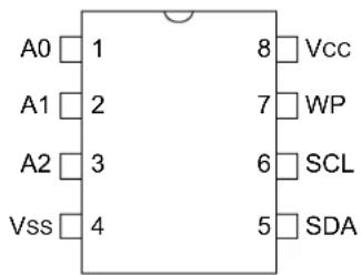
Package Types
MSOP/PDIP/SOIC/TSSOP
text_image
A0 1 A1 2 A2 3 Vss 4 8 Vcc 7 WP 6 SCL 5 SDASOT-23
text_image
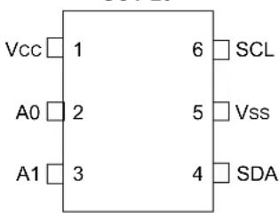
Vcc 1 A0 2 A1 3 6 SCL 5 Vss 4 SDATDFN

text_image
A0 1 ● 8 Vcc A1 2 7 WP A2 3 6 SCL Vss 4 5 SDABlock Diagram
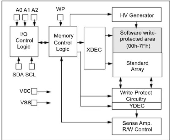
flowchart
graph TD
    A["A0 A1 A2"] --> B["I/O Control Logic"]
    C["SDA SCL"] --> B
    D["VCC"] --> E["Memory Control Logic"]
    F["VSS"] --> E
    B --> G["XDEC"]
    E --> G
    G --> H["HV Generator"]
    H --> I["Software write-protected area (00h-7Fh)"]
    I --> J["Standard Array"]
    J --> K["Write-Protect Circuitry YDEC"]
    K --> L["Sense Amp. R/W Control"]
    M["WP"] --> G
1.0 ELECTRICAL CHARACTERISTICS
Absolute Maximum Ratings ^()
Vcc....6.5V
All inputs and outputs w.r.t. Vss....-0.3V to Vcc +1.0V
Storage temperature....-65°C to +150°C
Ambient temperature with power applied....-40°C to +125°C
ESD protection on all pins ≥ 4 kV
† NOTICE: Stresses above those listed under “Absolute Maximum Ratings” may cause permanent damage to the device. These are stress ratings only and functional operation of the device at these or any other conditions above those indicated in the operation sections of the specifications is not implied. Exposure to Absolute Maximum Rating conditions for extended periods may affect device reliability.
TABLE 1-1: DC SPECIFICATIONS
| DC CHARACTERISTICS | Electrical Characteristics:Industrial (I): TA = -40°C to +85°CExtended (E): TA = -40°C to +125°C | ||||||
| Param.No. | Symbol | Characteristic Min. Typical | Max. Units | Conditions | |||
| D1 | VIH | High-Level Input Voltage | 0.7 Vcc | — | — | V | |
| D2 | VIL | Low-Level Input Voltage | — | — | 0.3 Vcc | V | 0.2 Vcc for Vcc < 2.5V |
| D3 | VHYS | Hysteresis of Schmitt Trigger Inputs | 0.05 Vcc | — | — | V | Note 1 |
| D4 | VOL | Low-Level Output Voltage | — | — | 0.40 | V | IOL = 3.0 mA, Vcc = 2.5V |
| D5 | VHV | High-Voltage Detect | 7 | — 10 | V | A0 Pin | only, V cc < 2.2V |
| Vcc + 4.8 | — | 10 | V | A0 Pin only, Vcc ≥ 2.2V | |||
| 10 — V | cc + 4.8 | V | A0 Pin only, Vcc > 5.2V | ||||
| D6 | ILI | Input Leakage Current | — | — | ±1 | μA | VIN = Vss or Vcc |
| D7 | ILO | Output Leakage Current | — | — | ±1 | μA | VOUT = Vss or Vcc |
| D8 | CIN,COUT | Pin Capacitance(all inputs/outputs) | — | — | 10 | pF | Vcc = 5.5V (Note 1)TA = +25°C, FCLK = 1 MHz |
| D9 | Icc Write | Operating Current | — | 0.1 | 3 | mA | Vcc = 5.5V, SCL = 1 MHz |
| D10 I | cc Read | — | 0.05 | 1 | mA | Vcc = 5.5V, SCL = 1 MHz | |
| D11 | Iccs | Standby Current | — | 0.01 | 1 | μA | SDA = SCL = Vcc,A0, A1, A2, WP = Vss,I-Temp. |
| — | — | 5 | μA | SDA = SCL = Vcc,A0, A1, A2, WP = Vss,E-Temp. | |||
Note 1: This parameter is periodically sampled and not 100% tested.
TABLE 1-2: AC SPECIFICATIONS
| AC CHARACTERISTICS | Electrical Characteristics:Industrial (I): TA = -40°C to +85°CExtended (E): TA = -40°C to +125°C | |||||
| Param.No. | Symbol | Characteristic Min. Max. Units | Conditions | |||
| 1 | FCLK Clock | Frequency | — 100 kHz 1.7V ≤ V | cc < 1.8V | ||
| — 400 kHz 1.8V ≤ V | cc ≤ 5.5V | |||||
| — | 1000 | kHz | 2.5V ≤ Vcc ≤ 5.5V (34LC02) | |||
| 2 | THIGH Clock | High Time | 4000 | — | ns | 1.7V ≤ Vcc < 1.8V |
| 600 | — | ns | 1.8V ≤ Vcc ≤ 5.5V | |||
| 500 | — | ns | 2.5V ≤ Vcc ≤ 5.5V (34LC02) | |||
| 3 | TLOW | Clock Low Time | 4700 | — | ns | 1.7V ≤ Vcc < 1.8V |
| 1300 | — | ns | 1.8V ≤ Vcc ≤ 5.5V | |||
| 500 | — | ns | 2.5V ≤ Vcc ≤ 5.5V (34LC02) | |||
| 4 | TR | SDA and SCL Rise Time | — | 1000 | ns | 1.7V ≤ Vcc < 1.8V (Note 1) |
| — 300 ns | 1.8V ≤ V | cc ≤ 5.5V (Note 1) | ||||
| — 300 ns | 2.5V ≤ Vcc ≤ 5.5V (34LC02)(Note 1) | |||||
| 5 | TF | SDA and SCL Fall Time | — | 1000 | ns | 1.7V ≤ Vcc < 1.8V (Note 1) |
| — | 300 | ns | 1.8V ≤ Vcc ≤ 5.5V (Note 1) | |||
| — 300 ns | 2.5V ≤ Vcc ≤ 5.5V (34LC02)(Note 1) | |||||
| 6 | Thd:sta Start Condition Hold Time | 4000 | — | ns | 1.7V ≤ Vcc < 1.8V | |
| 600 | — | ns | 1.8V ≤ Vcc ≤ 5.5V | |||
| 250 | — | ns | 2.5V ≤ Vcc ≤ 5.5V (34LC02) | |||
| 7 | TSU:STA | Start Condition Setup Time | 4700 | — | ns | 1.7V ≤ Vcc < 1.8V |
| 600 | — | ns | 1.8V ≤ Vcc ≤ 5.5V | |||
| 250 | — | ns | 2.5V ≤ Vcc ≤ 5.5V (34LC02) | |||
| 8 | THD:DAT | Data Input Hold Time | 0 | — | ns | Note 2 |
| 9 | TSU:DAT | Data Input Setup Time | 250 | — | ns | 1.7V ≤ Vcc < 1.8V |
| 100 | — | ns | 1.8V ≤ Vcc ≤ 5.5V | |||
| 100 | — | ns | 2.5V ≤ Vcc ≤ 5.5V (34LC02) | |||
| 10 | TSU:STO | Stop Condition Setup Time | 4000 | — | ns | 1.7V ≤ Vcc < 1.8V |
| 600 | — | ns | 1.8V ≤ Vcc ≤ 5.5V | |||
| 250 | — | ns | 2.5V ≤ Vcc ≤ 5.5V (34LC02) | |||
| 11 | TSU:WP WP Setup Time | 4000 | — | ns | 1.7V ≤ Vcc < 1.8V | |
| 600 | — | ns | 1.8V ≤ Vcc ≤ 5.5V | |||
| 600 | — | ns | 2.5V ≤ Vcc ≤ 5.5V (34LC02) | |||
| 12 | THD:WP WP Hold Time | 4700 | — | ns | 1.7V ≤ Vcc < 1.8V | |
| 600 | — | ns | 1.8V ≤ Vcc ≤ 5.5V | |||
| 600 | — | ns | 2.5V ≤ Vcc ≤ 5.5V (34LC02) | |||
Note 1: Not 100% tested. CB = total capacitance of one bus line in pF.
2: As a transmitter, the device must provide an internal minimum delay time to bridge the undefined region (minimum 300 ns) of the falling edge of SCL to avoid unintended generation of Start or Stop conditions.
3: The combined TSP and VHYS specifications are due to new Schmitt Trigger inputs, which provide improved noise spike suppression. This eliminates the need for a TI specification for standard operation.
4: This parameter is not tested but ensured by characterization.
TABLE 1-2: AC SPECIFICATIONS
| AC CHARACTERISTICS | Electrical Characteristics:Industrial (I): TA = -40°C to +85°CExtended (E): TA = -40°C to +125°C | |||||
| Param.No. | Symbol | Characteristic | Min. | Max. | Units | Conditions |
| 13 TAA Output Valid from cloCk | — 3500 | ns 1.7V ≤ V | cc < 1.8V (Note 2) | |||
| — | 900 | ns | 1.8V ≤ Vcc ≤ 5.5V (Note 2) | |||
| — 400 ns | 2.5V ≤ Vcc ≤ 5.5V (34LC02)(Note 2) | |||||
| 14 | TBUF | Bus Free Time: The time the bus must be free before a new transmission can start | 4700 — ns | 1.7V ≤ V | cc < 1.8V | |
| 1300 — ns | 1.8V ≤ V | cc ≤ 5.5V | ||||
| 500 — ns | 2.5V ≤ V | cc ≤ 5.5V (34LC02) | ||||
| 15 | TSP | Input Filter Spike Suppression (SDA and SCL pins) | — | 5 | 0 | 34AA02 n Note 1and Note 3 |
| 16 | TWC | Write Cycle Time (byte or page) | — | 5 | ms | |
| 17 Endurance | 1,000,000 | — cycles | +25°C, 5.5V, Page Mode(Note 4) | |||
Note 1: Not 100% tested. CB = total capacitance of one bus line in pF.
2: As a transmitter, the device must provide an internal minimum delay time to bridge the undefined region (minimum 300 ns) of the falling edge of SCL to avoid unintended generation of Start or Stop conditions.
3: The combined TSP and VHYS specifications are due to new Schmitt Trigger inputs, which provide improved noise spike suppression. This eliminates the need for a TI specification for standard operation.
4: This parameter is not tested but ensured by characterization.
FIGURE 1-1: BUS TIMING DATA
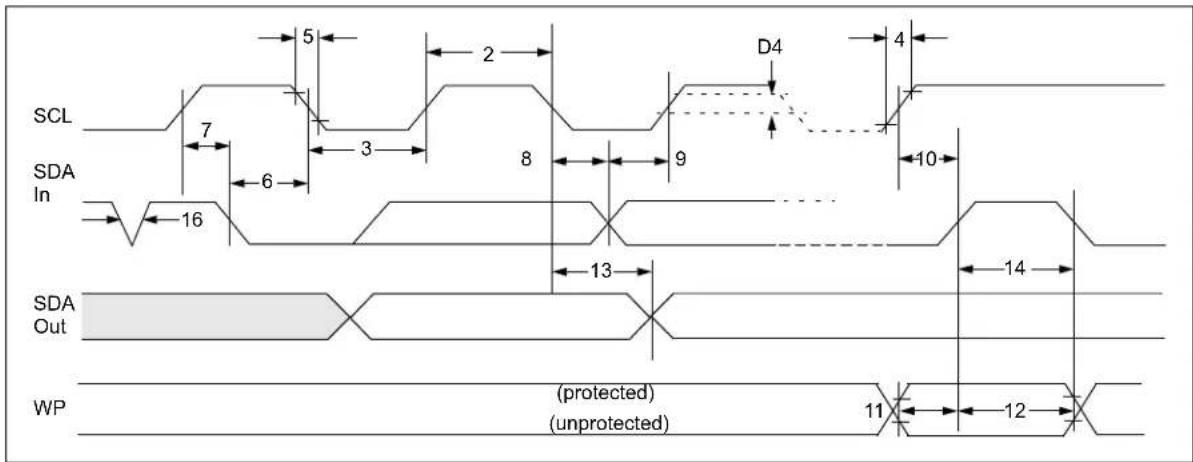
text_image
SCL 7 5 2 D4 4 SDA In 6 3 8 9 10 16 SDA Out 13 14 WP (protected) (unprotected) 11 122.0 PIN DESCRIPTIONS
The descriptions of the pins are listed in Table 2-1.
TABLE 2-1: PIN FUNCTION TABLE
| Name MSOP PDIP SOIC SOT-23 TDFN TSSOP Description | |||||||
| A0 | 1 | 1 | 1 | 5 | 1 | 1 | Chip Address Input |
| A1 | 2 | 2 | 2 | 4 | 2 | 2 | Chip Address Input |
| A2 | 3 | 3 | 3 | — | 3 | 3 | Chip Address Input |
| Vss | 4 | 4 | 4 | 2 | 4 | 4 | Ground |
| SDA | 5 | 5 | 5 | 3 | 5 | 5 | Serial Address/Data I/O |
| SCL | 6 | 6 | 6 | 1 | 6 | 6 | Serial Clock |
| WP | 7 | 7 | 7 | — | 7 | 7 | Write-Protect Input |
| Vcc | 8 | 8 | 8 | 6 | 8 | 8 | Power Supply |
2.1 A0, A1, A2 Chip Address Inputs
The levels on these inputs are compared with the corresponding bits in the client address. The chip is selected if the compare is true.
Up to eight 34XX02 devices (four for the SOT-23 package) may be connected to the same bus by using different Chip Select bit combinations. These inputs must be connected to either Vss or Vcc. The A0 pin is also used to detect VHv.
2.2 Serial Address/Data Input/Output (SDA)
This is a bidirectional pin used to transfer addresses and data into and data out of the device. It is an open-drain terminal. Therefore, the SDA bus requires a pull-up resistor to Vcc (typical 10 kΩ for 100 kHz, 2 kΩ for 400 kHz and 1 MHz).
For normal data transfer, SDA is allowed to change only during SCL low. Changes during SCL high are reserved for indicating the Start and Stop conditions.
2.3 Serial Clock (SCL)
This input is used to synchronize the data transfer to and from the device.
2.4 Write-Protect (WP)
This is the hardware write-protect pin. It can be tied to Vcc or Vss. If tied to Vcc, the hardware write protection is enabled. If the WP pin is tied to Vss, the hardware write protection is disabled.
3.0 FUNCTIONAL DESCRIPTION
The 34XX02 has two Software Write-Protect features that allow the user to protect half of the array from being written (Addresses 00h-7Fh). One command, Software Write-Protect (SWP) will prevent writes to half of the array and is resettable by using the Clear Software Write-Protect (CSWP) command. The other command is Permanent Software Write-Protect (PSWP), which is not resettable and will permanently lock half the array from being written to. The device still has an external pin (WP) that allows the user to protect the entire array if so desired.
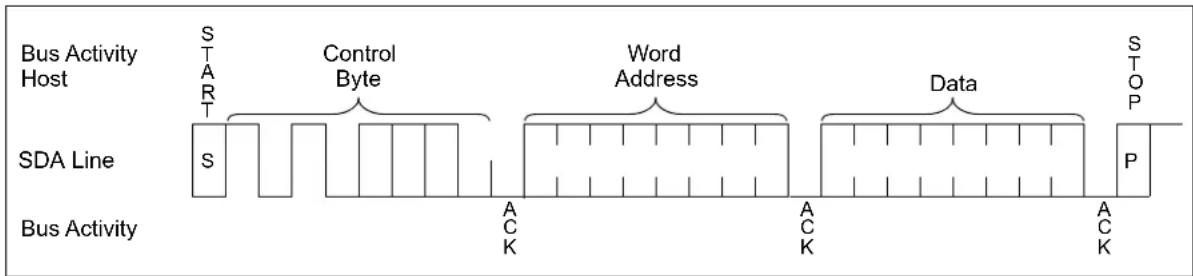
The 34XX02 supports a bidirectional two-wire bus and data transmission protocol. A device that sends data onto the bus is defined as a transmitter and a device receiving data, as a receiver. The bus has to be controlled by a host device, which generates the Serial Clock (SCL), controls the bus access and generates the Start and Stop conditions, while the 34XX02 works as client. Both host and client can operate as transmitter or receiver, but the host device determines which mode is activated.
4.0 BUS CHARACTERISTICS
The following bus protocol has been defined:
- Data transfer may be initiated only when the bus is not busy
- During data transfer, the data line must remain stable whenever the clock line is high. Changes in the data line while the clock line is high will be interpreted as a Start or Stop condition
Accordingly, the following bus conditions have been defined (Figure 4-1).
4.1 Bus Not Busy (A)
Both data and clock lines remain high.
4.2 Start Data Transfer (B)
A high-to-low transition of the SDA line while the clock (SCL) is high determines a Start condition. All commands must be preceded by a Start condition.
4.3 Stop Data Transfer (C)
A low-to-high transition of the SDA line while the clock (SCL) is high determines a Stop condition. All operations must be ended with a Stop condition.
4.4 Data Valid (D)
The state of the data line represents valid data when, after a Start condition, the data line is stable for the duration of the high period of the clock signal. The data on the line must be changed during the low period of clock signal. There is one clock pulse per bit of data.
Each data transfer is initiated with a Start condition and terminated with a Stop condition. The number of data bytes transferred between the Start and Stop conditions is determined by the host device and is, theoretically, unlimited; although only the last 16 bytes will be stored when doing a write operation. When an overwrite does occur, it will replace data in a First-In First-Out (FIFO) principle.
4.5 Acknowledge
Each receiving device, when addressed, is obliged to generate an Acknowledge after the reception of each byte. Exceptions to this rule relating to software write protection are described in Section 7.0 "Write Protection". The host device must generate an extra clock pulse which is associated with this Acknowledge bit.
Note: The 34XX02 does not generate any Acknowledge bits if an internal programming cycle is in progress.
The device that acknowledges has to pull down the SDA line during the Acknowledge clock pulse in such a way that the SDA line is stable-low during the high period of the Acknowledge-related clock pulse. Moreover, setup and hold times must be taken into account. During reads, a host must signal an end-of-data to the client by not generating an Acknowledge bit on the last byte that has been clocked out of the client. In this case, the client (34XX02) will leave the data line high to enable the host to generate the Stop condition.
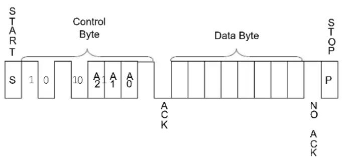
FIGURE 4-1: DATA TRANSFER SEQUENCE ON THE SERIAL BUS

text_image
SCL (A) (B) (DCID) (A) SDA Start Condition Address or Acknowledge Valid Data Allowed to Change Stop Condition5.0 DEVICE ADDRESSING
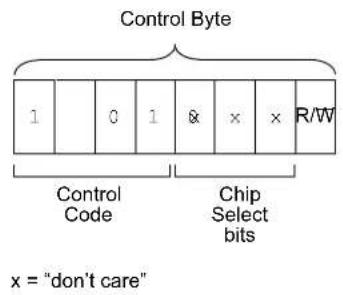
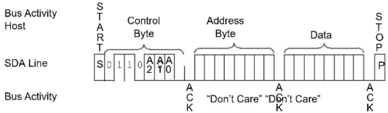
A control byte is the first byte received following the Start condition from the host device. The first part of the control byte consists of a 4-bit control code which is set to '1010' for normal read and write operations and '0110' for writing to the write-protect register. The control byte is followed by three Chip Select bits (A2, A1, A0). The Chip Select bits allow the use of up to eight 34XX02 devices on the same bus and are used to determine which device is accessed. The Chip Select bits in the control byte must correspond to the logic levels on the corresponding A2, A1 and A0 pins for the device to respond. These bits are in effect the three Most Significant bits of the word address. The combination of the 4-bit control code and the next three bits are called the client address.
For the SOT-23 package, the A2 pin is not connected. During device addressing, the A2 Chip Select bit should be set to '0'. Only four 34XX02 SOT-23 packages can be connected to the same bus.
The last bit of the control byte is the Read/Write (R/W) bit and it defines the operation to be performed. When set to a '1', a read operation is selected. When set to a '0', a write operation is selected. Following the Start condition, the 34XX02 monitors the SDA bus, checking the device type identifier being transmitted. Upon receiving a valid client address and the R/W bit, the client device outputs an Acknowledge signal on the SDA line. Depending on the state of the R/W bit, the 34XX02 will select a read or write operation.
The next byte received defines the address of the first data byte within the selected block (Figure 5-2). The word address byte uses all eight bits.
| Operation | Control Code | Chip Select | R/W |
| Read | 1010 | A2 A1 A0 | 1 |
| Write | 1010 | A2 A1 A0 | 0 |
| Write-Protect Register | 0110 | A2 A1 A0 | 0 |
FIGURE 5-1: CONTROL BYTE FORMAT

flowchart
graph TD
    A["Start Read/Write"] --> B["Client Address"]
    B --> C["R/W"]
    B --> D["A"]
    E["OR"] --> F["1 0 1 0 A2 A1 A0"]
    G["OR"] --> H["0 1 1 0 A2 A1 A0"]
FIGURE 5-2: ADDRESS SEQUENCE BIT ASSIGNMENTS
text_image
Control Byte 1 0 1 & x x R/W Control Code Chip Select bits x = "don't care"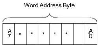
text_image
Word Address Byte A7 • • • • • A06.0 WRITE OPERATIONS
6.1 Byte Write
Following the Start signal from the host, the device code(4 bits), the Chip Select bits (3 bits) and the R/W bit, which is a logic-low, are placed onto the bus by the host transmitter. This indicates to the addressed client receiver that a byte with a word address will follow, once it has generated an Acknowledge bit during the ninth clock cycle. Therefore, the next byte transmitted by the host is the word address and will be written into the Address Pointer of the 34XX02. After receiving another Acknowledge signal from the 34XX02, the host device will transmit the data word to be written into the addressed memory location. The 34XX02 acknowledges again and the host generates a Stop condition. This initiates the internal write cycle, which means that during this time, the 34XX02 will not generate Acknowledge signals (Figure 6-1).
If an attempt is made to write to the array when the software or hardware write protection has been enabled, the device will acknowledge the command, but no data will be written. The write cycle time must be observed even if the write protection is enabled.
6.2 Page Write
The write control byte, word address and the first data byte are transmitted to the 34XX02 in the same way as in a byte write. Instead of generating a Stop condition, the host transmits up to 15 additional data bytes to the 34XX02, which are temporarily stored in the on-chip page buffer and will be written into the memory after the host has transmitted a Stop condition.
Upon receipt of each word, the four lower order Address Pointer bits, which form the byte counter, are internally incremented by one. The higher order four bits of the word address remain constant. If the host should transmit more than 16 bytes prior to generating the Stop condition, the Address Pointer will roll over and the previously received data will be overwritten. As with the byte write operation, once the Stop condition is received, an internal write cycle will begin (Figure 6-2).
If an attempt is made to write to the array when the hardware write protection has been enabled, the device will acknowledge the command, but no data will be written. The write cycle time must be observed even if the write protection is enabled.
Note: Page write operations are limited to writing bytes within a single physical page, regardless of the number of bytes actually being written. Physical page boundaries start at addresses that are integer multiples of the page buffer size (or 'page size') and end at addresses that are integer multiples of page size - 1. If a page write command attempts to write across a physical page boundary, the result is that the data wrap around to the beginning of the current page (overwriting data previously stored there), instead of being written to the next page, as might be expected. It is therefore necessary for the application software to prevent page write operations that would attempt to cross a page boundary.
FIGURE 6-1: BYTE WRITE
flowchart
graph LR
    A["Start"] --> B["Control Byte"]
    B --> C["Word Address"]
    C --> D["Data"]
    D --> E["STOP"]
    style A fill:#f9f,stroke:#333
    style B fill:#ccf,stroke:#333
    style C fill:#cfc,stroke:#333
    style D fill:#fcc,stroke:#333
    style E fill:#cff,stroke:#333
FIGURE 6-2: PAGE WRITE

flowchart
graph LR
    A["Start"] --> B["Control Byte"]
    B --> C["Word Address (n)"]
    C --> D["Data (n) Data (n + 1)"]
    D --> E["STOP"]
    style A fill:#f9f,stroke:#333
    style B fill:#ccf,stroke:#333
    style C fill:#cfc,stroke:#333
    style D fill:#fcc,stroke:#333
    style E fill:#cff,stroke:#333
7.0 WRITE PROTECTION
The 34XX02 has two software write-protect features (SWP and PSWP) that allows the lower half of the array (addresses 00h-7Fh) to be write-protected, as well as a WP pin that can be used to protect the entire array. The permanent software write-protect feature is enabled by sending the device a special command. Once this feature has been enabled, it cannot be reversed. The resettable software write-protect feature is also enabled by sending the device a special command but can be reset by issuing another special command. In addition to the software protect features, there is a WP pin that can be used to write-protect the entire array, regardless of whether the software write-protect register has been written or not.
Table 7-2 and Table 7-3 describe how the 34XX02 will acknowledge specific commands under various circumstances.
7.1 Hardware Write Protection
The WP pin allows the user to write-protect the entire array (00-FF) when the pin is tied to Vcc. If the pin is tied to Vss, the write protection is disabled.
7.2 Software Write Protection (SWP) and Clear Software Write Protection (CSWP)
In addition to hardware write-protect, the 34XX02 has an additional software write-protect feature that, when set, protects the first 128 bytes (00-7Fh) of the array from being written.
Setting the software write protection is done by sending the SWP instruction. SWP can also then be cleared by issuing a CSWP instruction (see Figure 7-1).
These two instructions follow the same format as the Byte Write instruction with the exception of the Device Type Identifier, (typically '1010', instead changes to '0110'). Once this identifier is recognized by the device, the rest of the Byte Write command, address and data are "don't cares". In addition to the identifier, high voltage must be applied to the A0 pin of the device and specific levels must be present on A1 and A2. See Table 7-1 for the available commands.
7.3 Permanent Software Write-Protect (PSWP)
The Permanent Software Write Protect (PSWP) is another instruction that may be used to permanently protect the first 128 byte of the array. Once this command is issued, the user will no longer have the ability to clear this feature regardless of instruction, power cycling or state of the WP pin. Also, once this instruction has been executed, the device will no longer acknowledge the device identifier '0110'.
FIGURE 7-1: SOFTWARE WRITE PROTECTION FOR SWP, CSWP, PSWP OR CPSWP
flowchart
graph TD
    A["Start"] --> B["Control Byte"]
    B --> C["Address Byte"]
    C --> D["Data"]
    D --> E["STOP"]
    style A fill:#f9f,stroke:#333
    style B fill:#ccf,stroke:#333
    style C fill:#cfc,stroke:#333
    style D fill:#fcc,stroke:#333
    style E fill:#cff,stroke:#333
TABLE 7-1: SOFTWARE WRITE PROTECTION INSTRUCTION SET WP = 0
| Instruction | Address Pins Device Type Identifier Chip Select Bits R/W | — | |||||||||
| A2 A1 | A0 | (1) | B7 B6 | B5 B4 | B3 | (2) | B2(2) | B1(2) | B0 | ||
| SWP V | ss | Vss | VHV | 0 | 1 | 1 | 0 | 0 | 0 | 1 | 0 |
| CSWP | Vss | Vcc | VHV | 0 | 1 | 1 | 0 | 0 | 1 | 1 | 0 |
| PSWP | A2 | A1 | A0 | 0 | 1 | 1 | 0 | A2 | A1 | A0 | 0 |
| Read SWP | Vss | Vss | VHV | 0 | 1 | 1 | 0 | 0 | 0 | 1 | 1 |
| Read CSWP | Vss | Vcc | VHV | 0 | 1 | 1 | 0 | 0 | 1 | 1 | 1 |
| Read PSWP | A2 | A1 | A0 | 0 | 1 | 1 | 0 | A2 | A1 | A0 | 1 |
Note 1: A0 is used to detect VHV for the SWP and CSWP commands.
2: B3, B2 and B1 are compared to the A2, A1 and A0 external pins, respectively.
TABLE 7-2: ACKNOWLEDGE TABLE FOR WRITE OR WRITE PROTECTION WITH R/W = 0
| Status | Write- Protect | Instruction | ACK | Address | ACK | Data Byte | ACK | Write Cycle |
| Permanently Protected | x | PSWP, SWP, CSWP | No ACK | Don't Care | No ACK | Don't Care | No ACK | No |
| Page or Byte Write in lower 128 bytes | ACK Address ACK | Data No | ACK No | |||||
| Protected with SWP | 0 | SWP | No ACK | Don't Care | No ACK | Don't Care | No ACK | No |
| CSWP | ACK | Don't Care | ACK | Don't Care | ACK | Yes | ||
| PSWP | ACK | Don't Care | ACK | Don't Care | ACK | Yes | ||
| Page or Byte Write in lower 128 bytes | ACK Address ACK | Data No | ACK No | |||||
| 1 | SWP | No ACK | Don't Care | No ACK | Don't Care | No ACK | No | |
| CSWP | ACK | Don't Care | ACK | Don't Care | No ACK | No | ||
| PSWP | ACK | Don't Care | ACK | Don't Care | No ACK | No | ||
| Page or Byte Write | ACK | Address | ACK | Data | No ACK | No | ||
| Not Protected | 0 | PSWP, SWP or CSWP | ACK | Don't Care | ACK | Don't Care | ACK | Yes |
| Page or Byte Write | ACK | Address | ACK | Data | ACK | Yes | ||
| 1 | PSWP, SWP or CSWP | ACK | Don't Care | ACK | Don't Care | No ACK | No | |
| Page or Byte Write | ACK | Address | ACK | Address | No ACK | No | ||
TABLE 7-3: ACKNOWLEDGE TABLE FOR WRITE OR WRITE PROTECTION WITH R/W = 1
| Status | Instruction | ACK |
| Permanently Protected | PSWP, SWP, CSWP | No ACK |
| Protected with SWP | SWP | No ACK |
| CSWP | ACK | |
| PSWP | ACK | |
| Not protected | PSWP, SWP, CSWP | ACK |
8.0 ACKNOWLEDGE POLLING
Since the device will not acknowledge during a write cycle, this can be used to determine when the cycle is complete (this feature can be used to maximize bus throughput). Once the Stop condition for a write command has been issued from the host, the device initiates the internally timed write cycle. ACK polling can be initiated immediately. This involves the host sending a Start condition followed by the control byte for a write command (R/W = 0). If the device is still busy with the write cycle, then no ACK will be returned. If the cycle is complete, then the device will return the ACK and the host can then proceed with the next read or write operation. See Figure 8-1 for flow diagram.
FIGURE 8-1: ACKNOWLEDGE
POLLING FLOW

flowchart
graph TD
    A["Send Write Command"] --> B["Send Stop Condition to Initiate Write Cycle"]
    B --> C["Send Start"]
    C --> D["Send Control Byte with R/W = 0"]
    D --> E{Did Device Acknowledge (ACK = 0)?}
    E -->|No| C
    E -->|Yes| F["Next Operation"]
9.0 READ OPERATION
Read operations are initiated in the same way as write operations, with the exception that the R/W bit of the client address is set to '1'. There are three basic types of read operations: current address read, random read and sequential read.
9.1 Current Address Read
The 34XX02 contains an Address Pointer that maintains the address of the last word accessed, internally incremented by one. Therefore, if the previous access (either a read or write operation) was to address 'n', the next current address read operation would access data from address n+1.
Upon receipt of the client address with R/W bit set to '1', the 34XX02 issues an Acknowledge and transmits the 8-bit data word. The host will not acknowledge the transfer, but does generate a Stop condition and the 34XX02 discontinues transmission (Figure 9-1).
9.2 Random Read
Random read operations allow the host to access any memory location in a random manner. To perform this type of read operation, the word address must first be set. This is done by sending the word address to the 34XX02 as part of a write operation. Once the word address is sent, the host generates a Start condition following the Acknowledge. This terminates the write operation, but not before the internal Address Pointer is set. The host then issues the control byte again, but with the R/W bit set to a '1'. The 34XX02 then issues an Acknowledge and transmits the 8-bit data word. The host will not acknowledge the transfer, but does generate a Stop condition and the 34XX02 discontinues transmission (Figure 9-2).
9.3 Sequential Read
Sequential reads are initiated in the same way as a random read, with the exception that after the 34XX02 transmits the first data byte, the host issues an Acknowledge, as opposed to a Stop condition in a random read. This directs the 34XX02 to transmit the next sequentially addressed 8-bit word (Figure 9-3).
To provide sequential reads, the 34XX02 contains an internal Address Pointer, which is incremented by one at the completion of each operation. This Address Pointer allows the entire memory contents to be serially read during one operation.
9.4 Contiguous Addressing Across Multiple Devices
The Chip Select bits (A2, A1, A0) can be used to expand the contiguous address space for up to 16K bits by adding up to eight 34XX02 devices on the same bus. In this case, the software can use A0 of the control byte as address bit A8, A1 as address bit A9 and A2 as address bit A10. It is not possible to sequentially read across device boundaries.
9.5 Noise Protection and Brown-Out
The 34XX02 employs a Vcc threshold detector circuit which disables the internal erase/write logic if the Vcc is below 1.35V at nominal conditions.
The SCL and SDA inputs have Schmitt Trigger and filter circuits which suppress noise spikes to assure proper device operation, even on a noisy bus.
FIGURE 9-1: CURRENT ADDRESS READ
Bus Activity Host
SDA Line
Bus Activity
flowchart
graph LR
    START["START"] --> S["S 1 0"]
    S --> A2["A 1 1 A 0"]
    A2 --> DataByte["Data Byte"]
    DataByte --> P["P"]
    DataByte --> ACK["ACK"]
    DataByte --> NO["NO"]
    DataByte --> ACK["ACK"]
    Control["Control Byte"] --> S
    Control --> A2
    Control --> A1
    DataByte --> DataByte
    DataByte --> STOP["STOP"]
FIGURE 9-2: RANDOM READ

text_image
Bus Activity Host START Control Byte Word Address (n) START Control Byte Data (n) STOP SDA Line S P 0 1 0 A A A A 0 ACK ACK ACK N BUS Activity ACKFIGURE 9-3: SEQUENTIAL READ
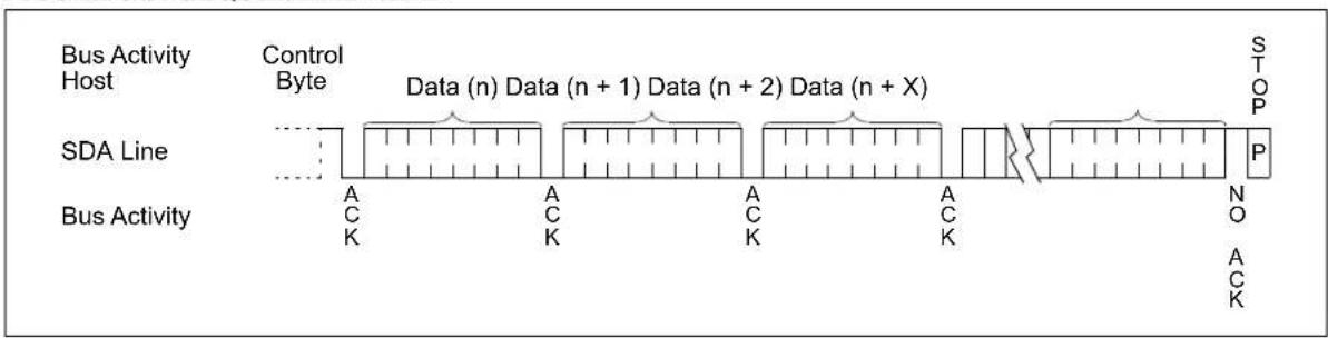
text_image
Bus Activity Host Control Byte Data (n) Data (n + 1) Data (n + 2) Data (n + X) SDA Line Bus Activity ACK ACK ACK ACK N ACK STOP P10.0 PACKAGING INFORMATION
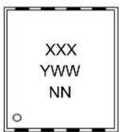
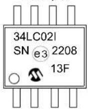
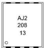
10.1 Package Marking Information
8-Lead MSOP Example

8-Lead PDIP (300 mil)
8-Lead SOIC

6-Lead SOT-23
8-Lead 2x3 TDFN Example
8-Lead TSSOP


Example

Example
Example

Example
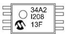
| Part Number | 1^st Line Marking Codes | |||||||
| MSOP PDIP SOIC | SOT-23 TDFN | TSSOP | ||||||
| I-Temp. E- | Temp. I-Temp. E-Temp. | |||||||
| 34AA02 34AA2T (1) | 34AA02 34AA02T (1) | SKNN(2) | SLNN(2) | AJ2 AJ3 | 34A2 | |||
| 34LC02 34LC2T (1) | 34LC02 34LC02T (1) | STNN(2) | SUNN(2) | AJ5 AJ6 | 34L2 | |||
Note 1: T = Temperature grade (I, E)
2: NN = Alphanumeric traceability code
Legend: XX...X Part number or part number code
T Temperature (I, E)
Y Year code (last digit of calendar year)
YY Year code (last 2 digits of calendar year)
WW Week code (week of January 1 is week '01')
NNN Alphanumeric traceability code (2 characters for small packages)
e3 JEDEC® designator for Matte Tin (Sn)
* Standard OTP marking consists of Microchip part number, year code, week code and traceability code.
Note: For very small packages with no room for the JEDEC® designator e3, the marking will only appear on the outer carton or reel label.
Note: In the event the full Microchip part number cannot be marked on one line, it will be carried over to the next line, thus limiting the number of available characters for customer-specific information.
8-Lead Plastic Micro Small Outline Package (MS) - 3x3 mm Body [MSOP]
Note: For the most current package drawings, please see the Microchip Packaging Specification located at http://www.microchip.com/packaging
![Microchip 34AA02 - 8-Lead Plastic Micro Small Outline Package (MS) - 3x3 mm Body [MSOP] - 1](/content/2026/06/1221637/images/adab92c91173cf9c6570d188a066b60d207490d13ce1b8a495b07c06f595ba62.jpg)
text_image
2X 0.20 H D D/2 A N E1/2 E1 2X 0.20 H NOTE 1 1 2 e B D E2 E 2X 4 TIPS 0.25 CTOP VIEW
![Microchip 34AA02 - 8-Lead Plastic Micro Small Outline Package (MS) - 3x3 mm Body [MSOP] - 2](/content/2026/06/1221637/images/2ddeaf8ea14ec002d71dc3c8f2f2d73eb4d532472ef32a5b0e0c93f1d7af4ba9.jpg)
text_image
A A2 A1 8X 0.10 C SEATING PLANE C 8X b ⊕ 0.25 M A-B D ASIDE VIEW
![Microchip 34AA02 - 8-Lead Plastic Micro Small Outline Package (MS) - 3x3 mm Body [MSOP] - 3](/content/2026/06/1221637/images/4f67ad5efeaa59dd8d1a29b337687f606e3529c72e1ea14755896ff2b9f79769.jpg)
text_image
H SEE DETAIL BVIEW A-A
Microchip Technology Drawing C04-111-MS Rev D Sheet 1 of 2
8-Lead Plastic Micro Small Outline Package (MS) - 3x3 mm Body [MSOP]
Note: For the most current package drawings, please see the Microchip Packaging Specification located at http://www.microchip.com/packaging
![Microchip 34AA02 - 8-Lead Plastic Micro Small Outline Package (MS) - 3x3 mm Body [MSOP] - 1](/content/2026/06/1221637/images/7a0f46f37e036ba8ede5584350100d66d19633756faa9c9a5f35587b01b8d8f6.jpg)
text_image
4X θ1 R1 H R SEATING PLANE C L (L1) c θ 4X θ1![Microchip 34AA02 - 8-Lead Plastic Micro Small Outline Package (MS) - 3x3 mm Body [MSOP] - 2](/content/2026/06/1221637/images/dc7d9fab3da494d6a368419ab824771ed1b1b7832833418f812dfb8aac4d95f4.jpg)
natural_image
Isometric line drawing of an integrated circuit chip with multiple pins (no text or symbols)DETAIL B
| Units | MILLIMETERS | |||
| Dimension Limits | MIN | NOM | MAX | |
| Number of Terminals | N | 8 | ||
| Pitch | e | 0.65 BSC | ||
| Overall Height | A | - | - | 1.10 |
| Standoff | A1 | 0.00 | - | 0.15 |
| Molded Package Thickness | A2 | 0.75 0.95 | 0.85 | |
| Overall Length D 3.00 BSC | ||||
| Overall Width | E | 4.90 BSC | ||
| Molded Package Width | E1 | 3.00 BSC | ||
| Terminal Width | b | 0.22 | - | 0.40 |
| Terminal Thickness | c | 0 | . | 0 8 |
| Terminal Length | L | 0.40 | 0.60 | 0.80 |
| L1 0 | 95 REFFootprint | |||
| R | -0.07 | -Lead Bend | ||
| R1 | -0.07 | -Lead Bend | ||
| θ | -0° 8° | Foot Angle | ||
| θ1 | -5° 15° | Mold Draft A | ||
Notes:
1. Pin 1 visual index feature may vary, but must be located within the hatched area.
2. Dimensions D and E1 do not include mold flash or protrusions. Mold flash or protrusions shall not exceed 0.15mm per side.
3. Dimensioning and tolerancing per ASME Y14.5M
BSC: Basic Dimension. Theoretically exact value shown without tolerances.
REF: Reference Dimension, usually without tolerance, for information purposes only.
Microchip Technology Drawing C04-111-MS Rev D Sheet 2 of 2
8-Lead Plastic Micro Small Outline Package (MS) - 3x3 mm Body [MSOP]
Note: For the most current package drawings, please see the Microchip Packaging Specification located at http://www.microchip.com/packaging
![Microchip 34AA02 - 8-Lead Plastic Micro Small Outline Package (MS) - 3x3 mm Body [MSOP] - 1](/content/2026/06/1221637/images/cf6edb4815b9a3b7f596c69183ff2e11343ee3554ec388ab5059d2fcbd331617.jpg)
text_image
GX C G1 SILK SCREEN Y X ERECOMMENDED LAND PATTERN
| Units | MILLIMETERS | |||
| Dimension Limits | MIN | NOM | MAX | |
| Contact Pitch | E | 0.65 BSC | ||
| CContact Pad Spacing 4.40 | ||||
| Contact Pad Width (X8) | X | 0.45 | ||
| Contact Pad Length (X8) | Y | 1.45 | ||
| Contact Pad to Contact Pad (X4) G | 2.95 | |||
| Contact Pad to Contact Pad (X6) GX | 0.20 | |||
Notes:
Dimensioning and tolerancing per ASME Y14.5M1.
BSC: Basic Dimension. Theoretically exact value shown without tolerances.
Microchip Technology Drawing C04-2111-MS Rev D
8-Lead Plastic Dual In-Line (P) - 300 mil Body [PDIP]
Note: For the most current package drawings, please see the Microchip Packaging Specification located at http://www.microchip.com/packaging
![Microchip 34AA02 - 8-Lead Plastic Dual In-Line (P) - 300 mil Body [PDIP] - 1](/content/2026/06/1221637/images/bcc778411f26d1962fa54abe3a8000fa39111b0507ad7b88b2ca4ffd1de10991.jpg)
text_image
D A N B E1 NOTE 1 1 2TOP VIEW
![Microchip 34AA02 - 8-Lead Plastic Dual In-Line (P) - 300 mil Body [PDIP] - 2](/content/2026/06/1221637/images/df21b56dac0020971b251b3c596df7376364d4d4bdb4bd34e65e1e860d17b524.jpg)
natural_image
Line drawing of an integrated circuit chip with six pins (no text or symbols)![Microchip 34AA02 - 8-Lead Plastic Dual In-Line (P) - 300 mil Body [PDIP] - 3](/content/2026/06/1221637/images/4450800076c82ba2a4c53206c535495b1eae72b87a607f38f67ad65d88a21999.jpg)
text_image
PLANE A C A1 A2 L 8X b1 8X b .010®![Microchip 34AA02 - 8-Lead Plastic Dual In-Line (P) - 300 mil Body [PDIP] - 4](/content/2026/06/1221637/images/07fdfeff9b2f12900d0924a0c3baa7c6908549d3ae475b4a27294f6e62986126.jpg)
text_image
E c eBEND VIEWSIDE VIEW
Microchip Technology Drawing No. C04-018-P Rev E Sheet 1 of 2
8-Lead Plastic Dual In-Line (P) - 300 mil Body [PDIP]
Note: For the most current package drawings, please see the Microchip Packaging Specification located at http://www.microchip.com/packaging
![Microchip 34AA02 - 8-Lead Plastic Dual In-Line (P) - 300 mil Body [PDIP] - 1](/content/2026/06/1221637/images/368d02d46ba7b211532e1afcfc22a8f79f6ebf207d495da6151865a4312230d8.jpg)
text_image
ALTERNATE LEAD DESIGN (NOTE 5) DATUM A DATUM A b e N/2 b e N/2| Units | NCHES | |||
| Dimension Limits | MIN NOM MAX | |||
| Number of Pins N 8 | ||||
| Pitch | e | .100 BSC | ||
| Top to Seating Plane A - - .210 | ||||
| Molded Package Thickness | A2 | .115 .130 | .195 | |
| Base to Seating Plane A1 .015 | - | - | ||
| Shoulder to Shoulder Width | E | .290 .310 | .325 | |
| Molded Package Width | E1 .240 .250 .280 | |||
| Overall Length | D | .348 .365 | .400 | |
| Tip to Seating Plane | L | .115 .130 | .150 | |
| Lead Thickness | c | .008 .010 | .015 | |
| Upper Lead Width | b1 | .040 .060 | .070 | |
| Lower Lead Width | b | .014 .018 | .022 | |
| Overall Row Spacing § | eB | - | - | .430 |
Notes:
- Pin 1 visual index feature may vary, but must be located within the hatched area.
- § Significant Characteristic
- Dimensions D and E1 do not include mold flash or protrusions. Mold flash or protrusions shall not exceed .010" per side.
- Dimensioning and tolerancing per ASME Y14.5M BSC: Basic Dimension. Theoretically exact value shown without tolerances.
- Lead design above seating plane may vary, based on assembly vendor.
Microchip Technology Drawing No. C04-018-P Rev E Sheet 2 of 2
8-Lead Plastic Small Outline (SN) - Narrow, 3.90 mm (.150 In.) Body [SOIC]
Note: For the most current package drawings, please see the Microchip Packaging Specification located at http://www.microchip.com/packaging
![Microchip 34AA02 - 8-Lead Plastic Small Outline (SN) - Narrow, 3.90 mm (.150 In.) Body [SOIC] - 1](/content/2026/06/1221637/images/acd36cb992a61aa986f055b13eba4d08ba474628627bb8e8ef1a454e93db546a.jpg)
text_image
2X 0.10 C A-B A D NOTE 5 E1 E1/2 N E2 E 2X 0.10 C A-B NOTE 1 1 2 e B NOTE 5 NX b ⊕ 0.25@A-B DTOP VIEW
![Microchip 34AA02 - 8-Lead Plastic Small Outline (SN) - Narrow, 3.90 mm (.150 In.) Body [SOIC] - 2](/content/2026/06/1221637/images/0b5e74ea5d8a889de0ce9bbce8f0d2a872826698125ba9e5271c7eab887e8363.jpg)
text_image
SEATING PLANE C A A2 A1 SIDE VIEW // 0.10 C 8X 0.10 C![Microchip 34AA02 - 8-Lead Plastic Small Outline (SN) - Narrow, 3.90 mm (.150 In.) Body [SOIC] - 3](/content/2026/06/1221637/images/a92350b22f7528a04f892fb7b54f4050460b386125def3f6db8185e7fac90e72.jpg)
text_image
H 0.23 h h SEE VIEW C VIEW A-A α θ R0.13 R0.13 L (L1) φ βVIEW C
Microchip Technology Drawing No. C04-057-SN Rev F Sheet 1 of 2
8-Lead Plastic Small Outline (SN) - Narrow, 3.90 mm (.150 In.) Body [SOIC]
Note: For the most current package drawings, please see the Microchip Packaging Specification located at http://www.microchip.com/packaging
![Microchip 34AA02 - 8-Lead Plastic Small Outline (SN) - Narrow, 3.90 mm (.150 In.) Body [SOIC] - 1](/content/2026/06/1221637/images/3b2d8473231edb7b26e2d5f90cfbb159b6f6a29990b715334f21dbb5dca26193.jpg)
natural_image
Isometric line drawing of an integrated circuit chip with four pins (no text or symbols)| Units | MILLIMETERS | |||
| Dimension Limits | MIN | NOM | MAX | |
| NNumber of Pins 8 | ||||
| Pitch | e | 1.27 BSC | ||
| AOvera15Heig | ||||
| --1.25 | ||||
| Standoff § | A1 | 0.25-0.1 | ||
| 6.00 BSCEOverall Wid | ||||
| 3.90 BSCE1Molded Pa | ||||
| 4.90 BSCDOverall Leng | ||||
| Chamfer (Optional) | h | 0.25 | - | 0.50 |
| Foot Length | L | 0.40 | - | 1.27 |
| Footprint | L1 | 1.04 REF | ||
| Foot Angle 0° - 8° | φ | |||
| Lead Thickness | c | 0.25-0.1 | ||
| Lead Width | b | 0.51-0.3 | ||
| Mold Draft Angle Top | α | 15°-5° | ||
| Mold Draft Angle Bottom | β | 15°-5° | ||
A2Molded Package Thickness
Notes:
- Pin 1 visual index feature may vary, but must be located within the hatched area.
- § Significant Characteristic
- Dimensions D and E1 do not include mold flash or protrusions. Mold flash or protrusions shall not exceed 0.15mm per side.
- Dimensioning and tolerancing per ASME Y14.5M BSC: Basic Dimension. Theoretically exact value shown without tolerances. REF: Reference Dimension, usually without tolerance, for information purposes only.
- Datums A & B to be determined at Datum H.
Microchip Technology Drawing No. C04-057-SN Rev F Sheet 2 of 2
8-Lead Plastic Small Outline (SN) - Narrow, 3.90 mm (.150 In.) Body [SOIC]
Note: For the most current package drawings, please see the Microchip Packaging Specification located at http://www.microchip.com/packaging
![Microchip 34AA02 - 8-Lead Plastic Small Outline (SN) - Narrow, 3.90 mm (.150 In.) Body [SOIC] - 1](/content/2026/06/1221637/images/1b1a25efbe03965f3fb1d3b256baa5463a4d20a8d7ac2b825ea9c66538952781.jpg)
text_image
SILK SCREEN C Y1 X1 ERECOMMENDED LAND PATTERN
| Units | MILLIMETERS | |||
| Dimension Limits | MIN | NOM | MAX | |
| Contact Pitch | E | 1.27 BSC | ||
| CContact Pad Spacif5p40 | ||||
| Contact Pad Width (X8) | X1 | 0.60 | ||
| Contact Pad Length (X8) | Y1 | 1.55 | ||
Notes:
Dimensioning and tolerancing per ASME Y14.5M1.
BSC: Basic Dimension. Theoretically exact value shown without tolerances.
Microchip Technology Drawing C04-2057-SN Rev F
6-Lead Plastic Small Outline Transistor (OT, OTY) [SOT-23]
Note: For the most current package drawings, please see the Microchip Packaging Specification located at http://www.microchip.com/packaging
![Microchip 34AA02 - 6-Lead Plastic Small Outline Transistor (OT, OTY) [SOT-23] - 1](/content/2026/06/1221637/images/9681f10829a02cde1ba05e42585d600799c162f1d4094e9b339fd8eb8cf1b6ad.jpg)
text_image
2X 0.15 C A-B D e1 A D E1/2 EE1 2X 0.15 C D E1/2 e B 6X b Φ 0.20@A-B DTOP VIEW
![Microchip 34AA02 - 6-Lead Plastic Small Outline Transistor (OT, OTY) [SOT-23] - 2](/content/2026/06/1221637/images/0ddd70cb7a2ad315bd88e862c52cf44cba6da8a3e1e0bed3e5f90d7414bc459c.jpg)
text_image
SEATING PLANE A A2 A1 SIDE VIEW 6X 0.10 C![Microchip 34AA02 - 6-Lead Plastic Small Outline Transistor (OT, OTY) [SOT-23] - 3](/content/2026/06/1221637/images/1ce23da4e342a53ece9e49c1fa6aaf643ec2f1e33f343343662f63e362f173ea.jpg)
text_image
c R1 R L (L1) θEND VIEW
Microchip Technology Drawing C04-028D (OT) Sheet 1 of 2
6-Lead Plastic Small Outline Transistor (OT, OTY) [SOT-23]
Note: For the most current package drawings, please see the Microchip Packaging Specification located at http://www.microchip.com/packaging
![Microchip 34AA02 - 6-Lead Plastic Small Outline Transistor (OT, OTY) [SOT-23] - 1](/content/2026/06/1221637/images/06cbe0be0f5de9e5750f828e6e2e63cfcd1a247a7b8c0a249bfe454ec37b2e14.jpg)
natural_image
Isometric line drawing of an integrated circuit chip with four pins (no text or symbols)| Units | MILLIMETERS | |||
| Dimension Limits | MIN | NOM | MAX | |
| Number of Leads | N | 6 | ||
| Pitch | e | 0.95 BSC | ||
| Outside lead pitch | e1 | 1.90 BSC | ||
| Overall Height | A | 0.90 | - | 1.45 |
| Molded Package Thickness | A2 | 0.89 | 1.15 | 1.30 |
| Standoff | A1 | 0.00 | - | 0.15 |
| Overall Width | E | 2.80 BSC | ||
| Molded Package Width | E1 | 1.60 BSC | ||
| Overall Length | D | 2.90 BSC | ||
| Foot Length | L | 0.30 | 0.45 | 0.60 |
| Footprint | L1 | 0.60 REF | ||
| Foot Angle | 0° | - | 10° | |
| Lead Thickness | c | 0.08 | - | 0.26 |
| Lead Width | b | 0.20 - | 0.51 | |
Notes:
1. Dimensions D and E1 do not include mold flash or protrusions. Mold flash or protrusions shall not exceed 0.25mm per side.
2. Dimensioning and tolerancing per ASME Y14.5M
BSC: Basic Dimension. Theoretically exact value shown without tolerances.
REF: Reference Dimension, usually without tolerance, for information purposes only.
Microchip Technology Drawing C04-028D (OT) Sheet 2 of 2
6-Lead Plastic Small Outline Transistor (OT, OTY) [SOT-23]
Note: For the most current package drawings, please see the Microchip Packaging Specification located at http://www.microchip.com/packaging
![Microchip 34AA02 - 6-Lead Plastic Small Outline Transistor (OT, OTY) [SOT-23] - 1](/content/2026/06/1221637/images/d09029f3e1f404afa2ea330f889d14d29e58c8cab43d2b541ba5ff49d01359cf.jpg)
text_image
GX Y Z G GC SILK SCREEN X ERECOMMENDED LAND PATTERN
| Units | MILLIMETERS | |||
| Dimension Limits | NOM | MAXMIN | ||
| Contact Pitch | E | 0.95 BSC | ||
| Contact Pad Spacing | C | 2.80 | ||
| Contact Pad Width (X3) | X | 0.60 | ||
| Contact Pad Length (X3) | Y | 1.10 | ||
| Distance Between Pads | G | 1.70 | ||
| Distance Between Pads GX 0.35 | ||||
| Overall Width | Z | 3.90 | ||
Notes:
- Dimensioning and tolerancing per ASME Y14.5M
BSC: Basic Dimension. Theoretically exact value shown without tolerances.
Microchip Technology Drawing No. C04-2028D (OT)
8-Lead Plastic Dual Flat, No Lead Package (MN) - 2x3x0.8 mm Body [TDFN] With 1.4x1.3 mm Exposed Pad (JEDEC Package type WDFN)
Note: For the most current package drawings, please see the Microchip Packaging Specification located at http://www.microchip.com/packaging
![Microchip 34AA02 - 8-Lead Plastic Dual Flat, No Lead Package (MN) - 2x3x0.8 mm Body [TDFN] With 1.4x1.3 mm Exposed Pad (JEDEC Package type WDFN) - 1](/content/2026/06/1221637/images/585e13017f10f5b3904d15e986a62cd66bb3398496a3c2e6144f4114dba4d953.jpg)
text_image
(DATUM A) (DATUM B) NOTE 1 2X 0.15 C 1 2 2X 0.15 C TOP VIEW C A SEATING PLANE A1 // 0.10 C 8X 0.08 C (A3) SIDE VIEW L D2 NOTE 1 E2 K N e 8X b BOTTOM VIEW 0.10 A B 0.10 A B 0.05 BMicrochip Technology Drawing No. C04-129-MN Rev E Sheet 1 of 2
8-Lead Plastic Dual Flat, No Lead Package (MN) - 2x3x0.8 mm Body [TDFN] With 1.4x1.3 mm Exposed Pad (JEDEC Package type WDFN)
Note: For the most current package drawings, please see the Microchip Packaging Specification located at http://www.microchip.com/packaging
![Microchip 34AA02 - 8-Lead Plastic Dual Flat, No Lead Package (MN) - 2x3x0.8 mm Body [TDFN] With 1.4x1.3 mm Exposed Pad (JEDEC Package type WDFN) - 1](/content/2026/06/1221637/images/76131f1cd81b5211519ba1e0c9eea0320cc5966847cc2331b48aa775700c6cd3.jpg)
natural_image
Technical line drawing of two electronic components with pins, one rectangular and one rectangular (no text or symbols)| Units | MILLIMETERS | |||
| Dimension Limits | MIN | NOM | MAX | |
| Number of Pins | N | 8 | ||
| Pitch | e | 0.50 BSC | ||
| Overall Height | A | 0.70 | 0.75 | 0.80 |
| Standoff | A1 | 0.00 | 0.02 | 0.05 |
| Contact Thickness | A3 | 0.20 REF | ||
| Overall Length | D | 2.00 BSC | ||
| Overall Width | E | 3.00 BSC | ||
| Exposed Pad Length | D2 | 1.35 | 1.40 | 1.45 |
| Exposed Pad Width | E2 | 1.25 | 1.30 | 1.35 |
| Contact Width | b | 0.20 | 0.25 | 0.30 |
| Contact Length | L | 0.25 | 0.30 | 0.45 |
| Contact-to-Exposed Pad | K 0.20 | - | - | |
Notes:
- Pin 1 visual index feature may vary, but must be located within the hatched area.
- Package may have one or more exposed tie bars at ends.
- Package is saw singulated
- Dimensioning and tolerancing per ASME Y14.5M
BSC: Basic Dimension. Theoretically exact value shown without tolerances.
REF: Reference Dimension, usually without tolerance, for information purposes only.
Microchip Technology Drawing No. C04-129-MN Rev E Sheet 2 of 2
8-Lead Plastic Dual Flat, No Lead Package (MN) - 2x3x0.8 mm Body [TDFN] With 1.4x1.3 mm Exposed Pad (JEDEC Package type WDFN)
Note: For the most current package drawings, please see the Microchip Packaging Specification located at http://www.microchip.com/packaging
![Microchip 34AA02 - 8-Lead Plastic Dual Flat, No Lead Package (MN) - 2x3x0.8 mm Body [TDFN] With 1.4x1.3 mm Exposed Pad (JEDEC Package type WDFN) - 1](/content/2026/06/1221637/images/37245455fc15126e168c5c56b7321ee73f6de8e3de888507e3d9b4b315640717.jpg)
text_image
X2 EV 8 ØV C Y2 EV Y1 SILK SCREEN 1 2 X1 ERECOMMENDED LAND PATTERN
| Units | MILLIMETERS | |||
| Dimension Limits | MIN | NOM | MAX | |
| Contact Pitch | E | 0.50 BSC | ||
| Optional Center Pad Width | X2 | 1.60 | ||
| Optional Center Pad Length | Y2 | 1.50 | ||
| CContact Pad Spacing 2.90 | ||||
| Contact Pad Width (X8) | X1 | 0.25 | ||
| Contact Pad Length (X8) | Y1 | 0.85 | ||
| Thermal Via Diameter V | 0.30 | |||
| Thermal Via Pitch EV | 1.00 | |||
Notes:
- Dimensioning and tolerancing per ASME Y14.5M
BSC: Basic Dimension. Theoretically exact value shown without tolerances.
- For best soldering results, thermal vias, if used, should be filled or tented to avoid solder loss during reflow process
Microchip Technology Drawing No. C04-129-MN Rev. B
8-Lead Plastic Thin Shrink Small Outline (ST) - 4.4 mm Body [TSSOP]
Note: For the most current package drawings, please see the Microchip Packaging Specification located at http://www.microchip.com/packaging
![Microchip 34AA02 - 8-Lead Plastic Thin Shrink Small Outline (ST) - 4.4 mm Body [TSSOP] - 1](/content/2026/06/1221637/images/58ea9e74243e2e9a15e7345498855dfccdc49e83dd37bef1a0d0fef25492244b.jpg)
text_image
(DATUM A) (DATUM B) D A B N E1 E 1 2 8X b e 0.20 C E A ⊕ 0.10 MC B A TOP VIEW![Microchip 34AA02 - 8-Lead Plastic Thin Shrink Small Outline (ST) - 4.4 mm Body [TSSOP] - 2](/content/2026/06/1221637/images/ad520c924dc44b8763e4229f0b8028f96cebafdf7db449f23f30b1b0190bb351.jpg)
text_image
SEATING PLANE A A2 0.05 C A1 8X 0.10 C SIDE VIEW![Microchip 34AA02 - 8-Lead Plastic Thin Shrink Small Outline (ST) - 4.4 mm Body [TSSOP] - 3](/content/2026/06/1221637/images/4b07d952fe83bceba989b167bf3a7c1fa09ddb64438325bbfed1ff106bb4829c.jpg)
text_image
H c φ L (L1) VIEW A-AMicrochip Technology Drawing C04-086 Rev C Sheet 1 of 2
8-Lead Plastic Thin Shrink Small Outline (ST) - 4.4 mm Body [TSSOP]
Note: For the most current package drawings, please see the Microchip Packaging Specification located at http://www.microchip.com/packaging
![Microchip 34AA02 - 8-Lead Plastic Thin Shrink Small Outline (ST) - 4.4 mm Body [TSSOP] - 1](/content/2026/06/1221637/images/eba97f6a4ba73a335299dc70bdd83c475f115459bdb3c984e04fe49738ed7e51.jpg)
natural_image
Isometric line drawing of an integrated circuit chip with four pins (no text or symbols)| Units | MILLIMETERS | |||
| Dimension Limits | MIN | NOM | MAX | |
| 8NNumber of Pins | ||||
| Pitch | e | 0.65 BSC | ||
| 1.20--A0 | ||||
| 1.051.00 | ||||
| --0.05A | ||||
| 6.40 BSCE | Overall Width | |||
| 4.504.40 | ||||
| 3.103.00 | ||||
| 0.750.60 | ||||
| Footprint | L1 | 1.00 REF | ||
| Lead Thickness | c | 0.25-0.05 | ||
| Foot Angle | φ | 8°4°0° | ||
| Lead Width | b | 0.30-0.15 | ||
overall Height 0.80A2Molded F 1Standoff
4.30E1Molded F 2.90DOverall Le 0.45LFoot Leng
Notes:
- Pin 1 visual index feature may vary, but must be located within the hatched area.
- Dimensions D and E1 do not include mold flash or protrusions. Mold flash or protrusions shall not exceed 0.20mm per side.
- Dimensioning and tolerancing per ASME Y14.5M
BSC: Basic Dimension. Theoretically exact value shown without tolerances.
REF: Reference Dimension, usually without tolerance, for information purposes only.
Microchip Technology Drawing C04-086 Rev C Sheet 2 of 2
8-Lead Plastic Thin Shrink Small Outline (ST) - 4.4 mm Body [TSSOP]
Note: For the most current package drawings, please see the Microchip Packaging Specification located at http://www.microchip.com/packaging
![Microchip 34AA02 - 8-Lead Plastic Thin Shrink Small Outline (ST) - 4.4 mm Body [TSSOP] - 1](/content/2026/06/1221637/images/749a5009aa5b70faf01d82dd6405e1a92fbd8473f7dc13a208c71c20583f9689.jpg)
text_image
G1 8 C SILK SCREEN Y1 1 2 X1 ERECOMMENDED LAND PATTERN
| Units | MILLIMETERS | |||
| Dimension Limits | MIN | NOM | MAX | |
| Contact Pitch | E | 0.65 BSC | ||
| CContact Pad Spacing 5.80 | ||||
| Contact Pad Width (X8) | X1 | 0.45 | ||
| Contact Pad Length (X8) | Y1 | 1.50 | ||
| Contact Pad to Center Pad (X6) G1 0.20 | ||||
Notes:
- Dimensioning and tolerancing per ASME Y14.5M
BSC: Basic Dimension. Theoretically exact value shown without tolerances.
- For best soldering results, thermal vias, if used, should be filled or tented to avoid solder loss during reflow process
Microchip Technology Drawing C04-2086 Rev B
APPENDIX A: REVISION HISTORY
Revision G (04/2022)
Added Automotive Product Identification System section; Fixed TBUF typo and added 1 MHz spec; Updated MSOP, PDIP, SOIC, SOT-23, TDFN and TSSOP package drawings; Replaced terminology "Master" and "Slave" with "Host" and "Client", respectively; Reformatted some sections for better readability.
Revision F (03/2011)
Revised Section 3.6; Updated spec to new template.
Revision E (01/2010)
Revised SOT-23 and TDFN marking codes.
Revision D (04/2008)
Updated Product Identification System section.
Revision C (02/2008)
Added TDFN and SOT-23 Package info; Removed "VL" Part.
Revision B (02/2007)
Replaced Package Drawings.
Revision A (01/2007)
Initial release of this document.
THE MICROCHIP WEBSITE
Microchip provides online support via our website at www.microchip.com. This website is used as a means to make files and information easily available to customers. Accessible by using your favorite Internet browser, the website contains the following information:
- Product Support – Data sheets and errata, application notes and sample programs, design resources, user's guides and hardware support documents, latest software releases and archived software
- General Technical Support – Frequently Asked Questions (FAQ), technical support requests, online discussion groups, Microchip consultant program member listing
- Business of Microchip – Product selector and ordering guides, latest Microchip press releases, listing of seminars and events, listings of Microchip sales offices, distributors and factory representatives
CUSTOMER CHANGE NOTIFICATION SERVICE
Microchip's customer notification service helps keep customers current on Microchip products. Subscribers will receive e-mail notification whenever there are changes, updates, revisions or errata related to a specified product family or development tool of interest.
To register, access the Microchip website at www.microchip.com. Under "Support", click on "Customer Change Notification" and follow the registration instructions.
CUSTOMER SUPPORT
Users of Microchip products can receive assistance through several channels:
• Distributor or Representative
- Local Sales Office
• Field Application Engineer (FAE)
- Technical Support
Customers should contact their distributor, representative or Field Application Engineer (FAE) for support. Local sales offices are also available to help customers. A listing of sales offices and locations is included in the back of this document.
Technical support is available through the website at: http://microchip.com/support
PRODUCT IDENTIFICATION SYSTEM (NON-AUTOMOTIVE)
To order or obtain information, e.g., on pricing or delivery, refer to the factory or the listed sales office.

Device

Option

Temperature Range

PackageTap
Device: 34AA02 =
1.7V, 2-Kbit ^2 C Serial EEPROM
34LC02 =
2.2V, 2-Kbit ^2 C Serial EEPROM
Tape and Reel
Blank =
Tape and Reef ^(1)
Temperature
|
-40°C to +85°C (Industrial)
Range:
-40°C to +125°C (Extended)
Package: MS =
[Non-Text]
Plastic Micro Small Outline - 8-Lead (MSOP)
P
Plastic Dual In-Line - 300 mil Body, 8-Lead (PDIP)
SN
Plastic Small Outline - Narrow, 3.90 mm Body, 8-Lead (SOIC)
OT
Plastic Small Outline Transistor - 5-Lead (SOT-23) (Tape and Reel only)
MNY
Plastic Dual Flat, No Lead Package –
[Non-Text]
2x3x0.8 mm Body, 8-Lead (TDFN)
ST
Plastic Thin Shrink Small Outline - 4.4 mm
Body, 8-Lead (TSSOP)
Examples
eaandReel02-I/P:
1.7V, 2-Kbit fC Serial EEPROM,
Industrial temp., PDIP package.
b) 34AA02-I/SN: 1.7V, 2-Kbit ^2 C Serial EEPROM, Industrial temp., SOIC package.
c) 34AA02T-E/MS: 1.7V, 2-Kbit ^2 C Serial EEPROM, Tape and Reel, Extended temp., MSOP package.
d) 34LC02-I/P: 2.2V, 2-Kbit fC Serial EEPROM, Industrial temp., PDIP package.
e) 34LC02-I/MNY: 2.2V, 2-Kbit ^1 C Serial EEPROM, Industrial temp., TDFN package.
f) 34LC02T-E/MS: 2.2V, 2-Kbit, I²C Serial EEPROM, Tape and Reel, Extended temp., MSOP package.
g) 34AA02T-I/OT: 1.7V, 2-Kbit, 1C Serial EEPROM, Tape and Reel, Industrial temp., SOT-23 package.
Note 1: Tape and Reel identifier only appears in the catalog part number description. This identifier is used for ordering purposes and is not printed on the device package. Check with your Microchip Sales Office for package availability with the Tape and Reel option.
PRODUCT IDENTIFICATION SYSTEM (AUTOMOTIVE)
To order or obtain information, e.g., on pricing or delivery, refer to the factory or the listed sales office.
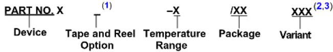
text_image
PART NO. X Device Tape and Reel Option (1) -Temperature Range -XX /XX Package XXX (2,3) VariantDevice: 34AA02 = 2-Kbit I²C Serial EEPROM 34LC02 = 2-Kbit I²C Serial EEPROM
Tape and Reel Blank = Standard packaging (tube) Option: T = Tape and Reel ^(1)
Temperature I = -40°C to +85°C (AEC-Q100 Grade 3) Range: E = -40°C to +125°C (AEC-Q100 Grade 1)
Package: OT = MNY = Plastic Small Outline Transistor - 5-Lead (SOT-23) (Tape and Reel only) Plastic Dual Flat, No Lead Package - 2x3x0.8 mm Body, 8-Lead (TDFN)
Variant: ^(2,3) 16KVAO = Standard Automotive, 16K Process 16KVXX = Customer-Specific Automotive, 16K Process
Examples
a) 34LC02T-I/MNY16KVAO: 2-Kbit I ^2 C Serial EEPROM, Tape and Reel, Automotive Grade 3, TDFN package.
Note 1: Tape and Reel identifier only appears in the catalog part number description. This identifier is used for ordering purposes and is not printed on the device package. Check with your Microchip Sales Office for package availability with the Tape and Reel option.
2: The VAO/VXX automotive variants have been designed, manufactured, tested and qualified in accordance with AEC-Q100 requirements for automotive applications.
3: For customers requesting a PPAP, a customer-specific part number will be generated and provided. A PPAP is not provided for VAO part numbers.
Note the following details of the code protection feature on Microchip products:
• Microchip products meet the specifications contained in their particular Microchip Data Sheet.
- Microchip believes that its family of products is secure when used in the intended manner, within operating specifications, and under normal conditions.
- Microchip values and aggressively protects its intellectual property rights. Attempts to breach the code protection features of Microchip product is strictly prohibited and may violate the Digital Millennium Copyright Act.
- Neither Microchip nor any other semiconductor manufacturer can guarantee the security of its code. Code protection does not mean that we are guaranteeing the product is “unbreakable”. Code protection is constantly evolving. Microchip is committed to continuously improving the code protection features of our products.
This publication and the information herein may be used only with Microchip products, including to design, test, and integrate Microchip products with your application. Use of this information in any other manner violates these terms. Information regarding device applications is provided only for your convenience and may be superseded by updates. It is your responsibility to ensure that your application meets with your specifications. Contact your local Microchip sales office for additional support or, obtain additional support at https://www.microchip.com/en-us/support/design-help/client-support-services.
THIS INFORMATION IS PROVIDED BY MICROCHIP "AS IS". MICROCHIP MAKES NO REPRESENTATIONS OR WARRANTIES OF ANY KIND WHETHER EXPRESS OR IMPLIED, WRITTEN OR ORAL, STATUTORY OR OTHERWISE, RELATED TO THE INFORMATION INCLUDING BUT NOT LIMITED TO ANY IMPLIED WARRANTIES OF NON-INFRINGEMENT, MERCHANTABILITY, AND FITNESS FOR A PARTICULAR PURPOSE, OR WARRANTIES RELATED TO ITS CONDITION, QUALITY, OR PERFORMANCE.
IN NO EVENT WILL MICROCHIP BE LIABLE FOR ANY INDIRECT, SPECIAL, PUNITIVE, INCIDENTAL, OR CONSEQUENTIAL LOSS, DAMAGE, COST, OR EXPENSE OF ANY KIND WHATSOEVER RELATED TO THE INFORMATION OR ITS USE, HOWEVER CAUSED, EVEN IF MICROCHIP HAS BEEN ADVISED OF THE POSSIBILITY OR THE DAMAGES ARE FORESEEABLE. TO THE FULLEST EXTENT ALLOWED BY LAW, MICROCHIP'S TOTAL LIABILITY ON ALL CLAIMS IN ANY WAY RELATED TO THE INFORMATION OR ITS USE WILL NOT EXCEED THE AMOUNT OF FEES, IF ANY, THAT YOU HAVE PAID DIRECTLY TO MICROCHIP FOR THE INFORMATION.
Use of Microchip devices in life support and/or safety applications is entirely at the buyer's risk, and the buyer agrees to defend, indemnify and hold harmless Microchip from any and all damages, claims, suits, or expenses resulting from such use. No licenses are conveyed, implicitly or otherwise, under any Microchip intellectual property rights unless otherwise stated.
For information regarding Microchip's Quality Management Systems, please visit www.microchip.com/quality.
Trademarks
The Microchip name and logo, the Microchip logo, Adaptec, AnyRate, AVR, AVR logo, AVR Freaks, BesTime, BitCloud, CryptoMemory, CryptoRF, dsPIC, flexPWR, HELDO, IGLOO, JukeBlox, KeeLoq, Kleer, LANCheck, LinkMD, maXStylus, maXTouch, MediaLB, megaAVR, Microsemi, Microsemi logo, MOST, MOST logo, MPLAB, OptoLyzer, PIC, picoPower, PICSTART, PIC32 logo, PolarFire, Prochip Designer, QTouch, SAM-BA, SenGenuity, SpyNIC, SST, SST Logo, SuperFlash, Symmetricom, SyncServer, Tachyon, TimeSource, tinyAVR, UNI/O, Vectron, and XMEGA are registered trademarks of Microchip Technology Incorporated in the U.S.A. and other countries.
AgileSwitch, APT, ClockWorks, The Embedded Control Solutions Company, EtherSynch, Flashtec, Hyper Speed Control, HyperLight Load, IntelliMOS, Libero, motorBench, mTouch, Powermite 3, Precision Edge, ProASIC, ProASIC Plus, ProASIC Plus logo, Quiet-Wire, SmartFusion, SyncWorld, Temux, TimeCesium, TimeHub, TimePictra, TimeProvider, TrueTime, WinPath, and ZL are registered trademarks of Microchip Technology Incorporated in the U.S.A.
Adjacent Key Suppression, AKS, Analog-for-the-Digital Age, Any Capacitor, AnyIn, AnyOut, Augmented Switching, BlueSky, BodyCom, CodeGuard, CryptoAuthentication, CryptoAutomotive, CryptoCompanion, CryptoController, dsPICDEM, dsPICDEM.net, Dynamic Average Matching, DAM, ECAN, Espresso T1S, EtherGREEN, GridTime, IdealBridge, In-Circuit Serial Programming, ICSP, INICnet, Intelligent Paralleling, Inter-Chip Connectivity, JitterBlocker, Knob-on-Display, maxCrypto, maxView, memBrain, Mindi, MiWi, MPASM, MPF, MPLAB Certified logo, MPLIB, MPLINK, MultiTRAK, NetDetach, NVM Express, NVMe, Omniscient Code Generation, PICDEM, PICDEM.net, PICkit, PICtail, PowerSmart, PureSilicon, QMatrix, REAL ICE, Ripple Blocker, RTAX, RTG4, SAM-ICE, Serial Quad I/O, simpleMAP, SimpliPHY, SmartBuffer, SmartHLS, SMART-I.S., storClad, SQI, SuperSwitcher, SuperSwitcher II, Switchtec, SynchroPHY, Total Endurance, TSHARC, USBCheck, VariSense, VectorBlox, VeriPHY, ViewSpan, WiperLock, XpressConnect, and ZENA are trademarks of Microchip Technology Incorporated in the U.S.A. and other countries.
SQTP is a service mark of Microchip Technology Incorporated in the U.S.A.
The Adaptec logo, Frequency on Demand, Silicon Storage Technology, Symmcom, and Trusted Time are registered trademarks of Microchip Technology Inc. in other countries.
GestIC is a registered trademark of Microchip Technology Germany II GmbH & Co. KG, a subsidiary of Microchip Technology Inc., in other countries.
All other trademarks mentioned herein are property of their respective companies.
© 2007-2022, Microchip Technology Incorporated and its subsidiaries.
All Rights Reserved.
ISBN: 978-1-5224-9990-9
Worldwide Sales and Service
AMERICAS
Corporate Office
2355 West Chandler Blvd.
Chandler, AZ 85224-6199
Tel: 480-792-7200
Fax: 480-792-7277
Technical Support:
http://www.micro-
chip.com/support
Web Address:
www.microchip.com
Atlanta
Duluth, GA
Tel: 678-957-9614
Fax: 678-957-1455
Austin, TX
Tel: 512-257-3370
Boston
Westborough, MA
Tel: 774-760-0087
Fax: 774-760-0088
Chicago
Itasca, IL
Tel: 630-285-0071
Fax: 630-285-0075
Dallas
Addison, TX
Tel: 972-818-7423
Fax: 972-818-2924
Detroit
Novi, MI
Tel: 248-848-4000
Houston, TX
Tel: 281-894-5983
Indianapolis
Noblesville, IN
Tel: 317-773-8323
Fax: 317-773-5453
Tel: 317-536-2380
Los Angeles
Mission Viejo, CA
Tel: 949-462-9523
Fax: 949-462-9608
Tel: 951-273-7800
Raleigh, NC
Tel: 919-844-7510
New York, NY
Tel: 631-435-6000
San Jose, CA
Tel: 408-735-9110
Tel: 408-436-4270
Canada - Toronto
Tel: 905-695-1980
Fax: 905-695-2078
ASIA/PACIFIC
Australia - Sydney
Tel: 61-2-9868-6733
China - Beijing
Tel: 86-10-8569-7000
China - Chengdu
Tel: 86-28-8665-5511
China - Chongqing
Tel: 86-23-8980-9588
China - Dongguan
Tel: 86-769-8702-9880
China - Guangzhou
Tel: 86-20-8755-8029
China - Hangzhou
Tel: 86-571-8792-8115
China - Hong Kong SAR
Tel: 852-2943-5100
China - Nanjing
Tel: 86-25-8473-2460
China - Qingdao
Tel: 86-532-8502-7355
China - Shanghai
Tel: 86-21-3326-8000
China - Shenyang
Tel: 86-24-2334-2829
China - Shenzhen
Tel: 86-755-8864-2200
China - Suzhou
Tel: 86-186-6233-1526
China - Wuhan
Tel: 86-27-5980-5300
China - Xian
Tel: 86-29-8833-7252
China - Xiamen
Tel: 86-592-2388138
China - Zhuhai
Tel: 86-756-3210040
ASIA/PACIFIC
India - Bangalore
Tel: 91-80-3090-4444
India - New Delhi
Tel: 91-11-4160-8631
India - Pune
Tel: 91-20-4121-0141
Japan - Osaka
Tel: 81-6-6152-7160
Japan - Tokyo
Tel: 81-3-6880-3770
Korea - Daegu
Tel: 82-53-744-4301
Korea - Seoul
Tel: 82-2-554-7200
Malaysia - Kuala Lumpur
Tel: 60-3-7651-7906
Malaysia - Penang
Tel: 60-4-227-8870
Philippines - Manila
Tel: 63-2-634-9065
Singapore
Tel: 65-6334-8870
Taiwan - Hsin Chu
Tel: 886-3-577-8366
Taiwan - Kaohsiung
Tel: 886-7-213-7830
Taiwan - Taipei
Tel: 886-2-2508-8600
Thailand - Bangkok
Tel: 66-2-694-1351
Tel: 43-7242-2244-39
Fax: 43-7242-2244-393
Denmark - Copenhagen
Tel: 45-4485-5910
Fax: 45-4485-2829
Finland - Espoo
Tel: 358-9-4520-820
France - Paris
Tel: 33-1-69-53-63-20
Fax: 33-1-69-30-90-79
Germany - Garching
Tel: 49-8931-9700
Germany - Haan
Tel: 49-2129-3766400
Germany - Heilbronn
Tel: 49-7131-72400
Germany - Karlsruhe
Tel: 49-721-625370
Germany - Munich
Tel: 49-89-627-144-0
Fax: 49-89-627-144-44
Germany - Rosenheim
Tel: 49-8031-354-560
Israel - Ra'anana
Tel: 972-9-744-7705
Italy - Milan
Tel: 39-0331-742611
Fax: 39-0331-466781
Italy - Padova
Tel: 39-049-7625286
Netherlands - Drunen
Tel: 31-416-690399
Fax: 31-416-690340
Norway - Trondheim
Tel: 47-7288-4388
Poland - Warsaw
Tel: 48-22-3325737
Romania - Bucharest
Tel: 40-21-407-87-50
Spain - Madrid
Tel: 34-91-708-08-90
Fax: 34-91-708-08-91
Sweden - Gothenberg
Tel: 46-31-704-60-40
Sweden - Stockholm
Tel: 46-8-5090-4654
UK - Wokingham
Tel: 44-118-921-5800
Fax: 44-118-921-5820