MCP3462R - Scale Microchip - Free user manual and instructions
Find the device manual for free MCP3462R Microchip in PDF.

User questions about MCP3462R Microchip
0 question about this device. Answer the ones you know or ask your own.
Ask a new question about this device
Download the instructions for your Scale in PDF format for free! Find your manual MCP3462R - Microchip and take your electronic device back in hand. On this page are published all the documents necessary for the use of your device. MCP3462R by Microchip.
USER MANUAL MCP3462R Microchip
Weight Scale Application using MCP3564 24-Bit Delta-Sigma ADC
Author: Dana Diaconu, Microchip Technology Inc.
INTRODUCTION
This application note describes a weight scale design using Microchip's MCP3564 24-bit Delta-Sigma Analog-to-Digital Converter (ADC) and PIC24 microcontroller. The weight scale uses an automatic calibration process and techniques to minimize power consumption. The design takes advantage of the ADC's dynamic reconfigurability features of oversampling ratio (OSR) and Gain settings to demonstrate the impact of certain configurations on the precision and the accuracy of the device. These settings can be made from a dedicated graphical user interface (GUI) which also allows the calibration of the weight scale and much more.
Starting from the sensor (the load cell) and its specifications and ending with the digital filter implementation, this application note provides information about each feature of the weight scale and their importance in the application.
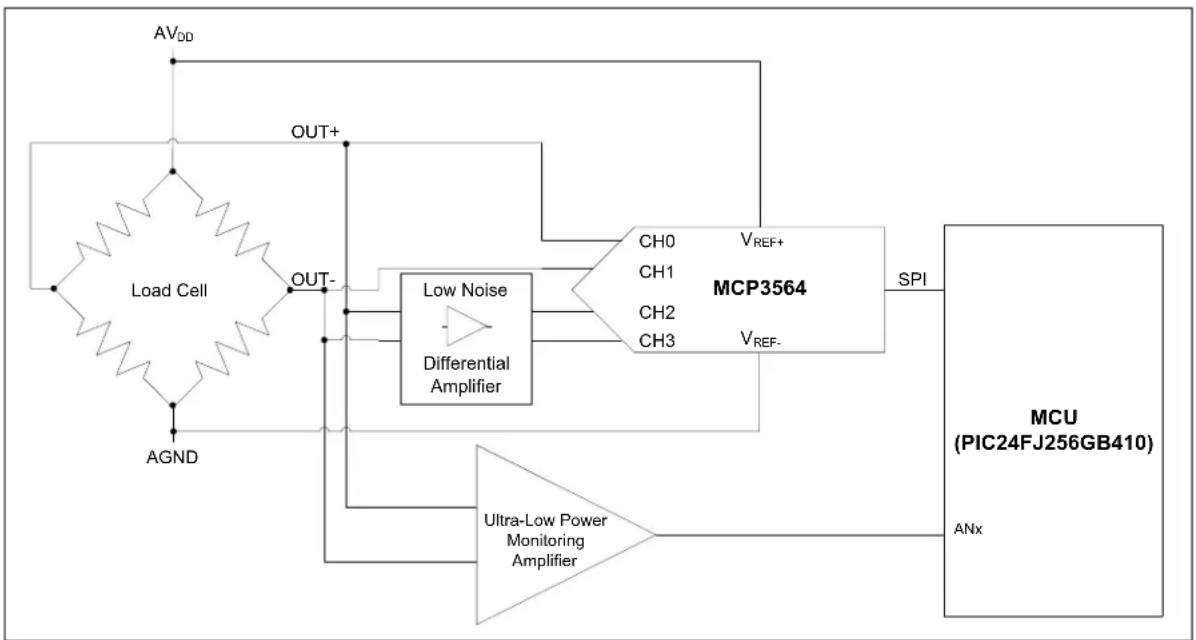
WEIGHT SCALE SYSTEM DIAGRAM
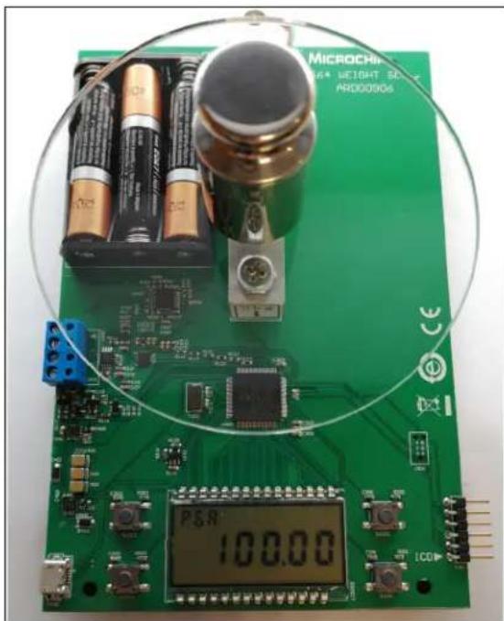
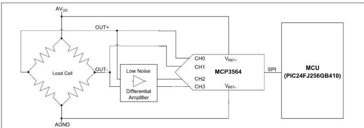
Figure 1 shows the weight scale demo using the MCP3564 24-bit Delta-Sigma ADC. Figure 2 shows an example of weight scale system diagram, containing the front end load cell circuit, gain amplifier, MCP3564 Delta-Sigma ADC and PIC24 16-bit microcontroller (MCU).
text_image
MICROCHIN 264* WEIGHT SET AR000506 PSR 100.00FIGURE 1: Photo of the MCP3564 Weight Scale Demo, P/N ARD00906.
flowchart
graph LR
    A["Load Cell"] -->|OUT+| B["Differential Amplifier"]
    A -->|OUT-| B
    B --> C["MCP3564"]
    C -->|SPI| D["MCU (PIC24FJ256GB410)"]
    E["AGND"] --> A
    F["AV_DD"] --> A
    G["CH0 CH1 CH2 CH3"] --> C
    H["V_REF+"] --> C
    I["V_REF-"] --> C
FIGURE 2: Weight Scale Block Schematic.
Load Cell
The most popular type of sensor for weight scales is the strain gauge load cell. The load cell is a transducer which converts an applied mechanical force into an electrical signal directly proportional with the magnitude of the force. The resistive load cell used in this application is composed of four strain gauges: two that measure tension and two that measure compression. These four strain gauges correspond to four resistors organized in a Wheatstone Bridge type of circuit, shown in Figure 3.

text_image
R₁ - ΔR₁ VOUT R₂ + ΔR₂ (tension) R₃ - ΔR₃ (compression) R₄ + ΔR₄ (tension)(com) + - VₑFIGURE 3: Wheatstone Bridge Resistive Load Cell.
The four strain gauges sense the bending contortion of the load cell under load translating to changes in the electrical resistances.
Power to the Wheatstone Bridge is supplied by a known excitation voltage ( V_E ) and its output voltage is defined by Equation 1.
EQUATION 1: WHEATSTONE BRIDGE OUTPUT VOLTAGE
$$ V _ {O U T} = \left[ \frac {R _ {3}}{R _ {3} + R _ {4}} \quad \frac {R _ {2}}{R _ {2} + R _ {1}} \right] \times E $$
The bridge reaches a balanced state ( V_OUT = 0 ) when no strain is applied (i.e. no load conditions). In this case, Equation 1 shows that the output voltage is null if: (R1/R2) = (R4/R3).
Any resistance variation in any arm of the bridge leads to an unbalanced state and to a nonzero output voltage. Ideally, if no strain is applied there is no variation in the resistances ( R_1-4 = 0 ). In practice, these variations can occur due to changes in temperature load cell manufacturing imperfections and aging. These changes can lead to an offset output voltage which needs to be calibrated out of the system.
Other types of load cells have different strain gauge configurations. The one presented in Figure 3 is called a Full Bridge Configuration because it has four active elements (the strain gauges) which form the entire Wheatstone Bridge. There are two other types: quarter bridge and half bridge. The quarter bridge configuration has a single active strain gauge element, while the half bridge has two elements. The downside of these configurations is that additional passive elements (resistors) are required in order to complete the bridge.
The full bridge configuration load cell is more sensitive to bending contortion and less sensitive to temperature changes. The temperature change effect is more visible in the quarter and half bridge designs because the additional resistors used to complete the bridge will react to the temperature variation differently than the strain gauges, as they are made of different materials with different temperature tolerances.
One method of minimizing temperature effects is using the full bridge configuration where the strain gauges respond to temperature variations with the same change in resistance. This means that the ratios of the resistances are kept constant. Some load cells even have an additional resistive element which is not used for measuring the applied force. However, it is used in an instrumentation amplifier configuration as a gain setting resistor. This resistor will have a similar thermal coefficient as the resistive bridge and the temperature variation effect on output voltage will be minimized. This method was not investigated in this application note.
Another solution is to implement temperature drift correction using software, but the necessity of this software correction depends on the chosen load cell's specifications and the conditions in which the sensor is used. For instance, it is important to know the temperature operating range of the load cell and how thermally unstable the environment in which it is used/integrated will be. Also, the temperature effect on output is often specified in the sensor's specifications table and this gives the maximum difference in the output caused by a change in temperature of ±1^ , when the load remains constant. In addition, even using a high excitation voltage for the load cell could cause the sensor to overheat and affect the accuracy of the measurement. These aspects should be taken into consideration when deciding if a temperature drift software correction is required.
Table 1 shows the key specifications of the load cell used for this application.
TABLE 1: LOAD CELL SPECIFICATIONS
| Specification Description Specification Value | Specification Value for a Load Cell with a 2 kg Capacity | |
| Output Sensitivity 1.0 ± 15% mV/V | ||
| Safe Overload 150 %F.S | (1) | 3 kg |
| Maximum Overload | 200 %F.S | 4 kg |
| Nonlinearity | ±0.05 %F.S | ±1g |
| Non-repeatability | ||
| Hysteresis | ||
| Creep (5 min.) | ||
| Temperature Effect on Output | ±0.05 %F.S/°C | ±1g/°C |
| Temperature Effect on Zero | ±2.0 %F.S/°C | ±40g/°C |
| Zero Balance | ±10 %F.S/°C | ±0.2 kg |
| Input/Output Resistance | 1000 ± 10Ω | |
| Excitation Voltage | ≤ 6V | |
| Operating Temperature Range | -10°C to +40°C | |
Note 1: Where F.S is full scale.
The output of the Wheatstone Bridge composed of strain gauges is a very low-level voltage signal (typically in the range of V to mV) which needs to be gain amplified before feeding into the ADC.
Equation 2 can be used to estimate the load cell output voltage range using Table 1. For example, the output sensitivity of the load cell used in this application is 1 mV/V. This means that when the excitation voltage is 3.3V, the output signal will be 3.3 mV at full load. Full load is the maximum capacity of the sensor, in this case 2 kg. Equation 2 shows that for a 1 gram load change the output will vary with 1.65 μV. This is a quick estimation before selecting a right load cell based on system requirements.
EQUATION 2: LOAD CELL OUTPUT VOLTAGE
$$ \begin{array}{l} V _ {O U T} = \frac {\text { Output Sensitivity } [ m V / N ] \times \text { Excitation Voltage } [ V ]}{\text { Maximum Capacity } [ g ]} \times \text { Load } [ g ] \ V _ {O U T} = \frac {1 m V / V \times 3 . 3 V}{2 0 0 0 g} \times I g = 1. 6 5 \mu V \end{array} $$
Also, the capacity of the load cell should be selected carefully. If the maximum overload limit of the sensor is exceeded, it can be permanently damaged.
As mentioned before, a balanced state of the bridge is achieved when an excitation voltage is applied and there is no load. Under these conditions the output voltage of the bridge would ideally be 0V. In practice, the maximum output voltage deviation of the load cell from 0 is given by the Zero Balance and the Temperature Effect on Zero specifications of the sensor (See Table 1). This deviation can be corrected through offset calibration.
Sensor temperature drift can be corrected in software using a digital temperature sensor and a compensation algorithm which accounts for variation of the sensor output voltage over temperature. The Temperature Effect on Zero and Temperature Effect on Output specifications are key to implementing a compensation algorithm for the output voltage variation over temperature.
For adding extra precision and accuracy to a weight scale, a thermocouple can be used together with the digital temperature sensor. The thermocouple provides a voltage which is dependent on the temperature difference between its hot and its cold junction, but its output is in the V range. Therefore, it requires amplification before converting the output to digital data. The digital temperature sensor can be used to measure the cold junction temperature. There are ADCs which provide both an analog gain stage and an internal temperature sensor, such as the MCP3564 ADC used in this application. The thermocouple can be connected directly to the converter without additional circuitry and the cold junction temperature can be estimated with this internal temperature sensor. However, an external digital temperature sensor, such as Microchip's MCP9800, is highly recommended as it increases the accuracy of the measurement.
Table 1 shows four other specifications which represent errors that can appear in the output of a non-ideal sensor.
- The nonlinearity parameter indicates the maximum deviation of the output curve from the ideal curve over the entire operating range.
- The non-repeatability specification is the maximum difference between load cell outputs for repeated measurements of the same weight and under the same conditions.
- The hysteresis effect can be observed by checking the difference in the output, measured once when the load increases from 0 up to a certain value and once when the load decreases from the maximum capacity down to that same value. There will be a difference between the two readings caused by hysteresis. It is important to note that the maximum value of this error is seen over the full range of the sensor and it decreases with smaller weight changes.
- Creep is defined as the change in the output when the load cell is under a fixed load for a certain period of time.
For the load cell used in this application, creep is computed over five minutes, as indicated in Table 1. This effect appears as a result of the load cell's material stretching over time while under the same load. Depending on the load and how deformable the material is, it may take a while for the load cell to recover after the load is removed assuming it hasn't been damaged. This change in output after the removal of the load is known as creep recovery and is specified in the specifications table for some load cells.
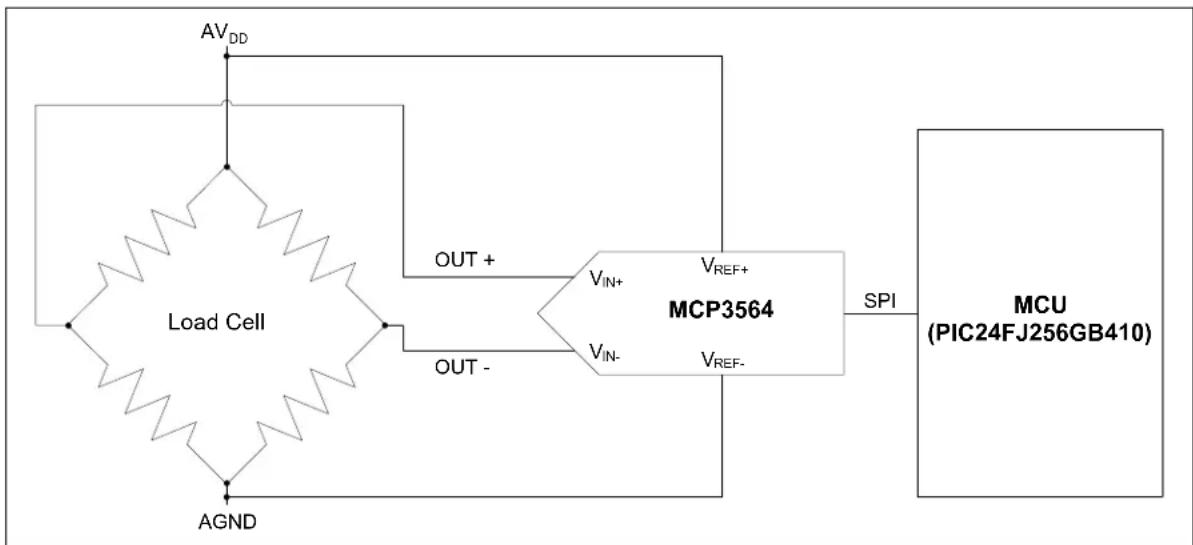
The simplest Wheatstone Bridge circuit is shown in Figure 4. The load cell output voltage needs to be converted to a digital value such that the data can be acquired and processed by the microcontroller. However, to get the best precision and ensure the accuracy of this measuring process other important aspects must be considered.
As previously stated, the load cell's output voltage needs to be amplified in order to take advantage of the full input span of the ADC and to get more accurate results. Since the bridge output is differential, a differential amplifier can be used prior to the ADC's input. Another option is using a high resolution ADC, such as the MCP3564, which can be connected directly to the Wheatstone Bridge without using additional front-end circuitry. The differential input and the on-board programmable gain amplifier (PGA) of the MCP3564 make it ideal for this application as it eliminates any external circuitry which may be needed for Common-mode noise rejection or signal amplification on the front-end of the ADC.
flowchart
graph TD
    A["AV_DD"] --> B["Load Cell"]
    B --> C["OUT +"]
    B --> D["OUT -"]
    C --> E["MCP3564"]
    D --> E
    E --> F["SPI"]
    F --> G["MCU (PIC24FJ256GB410)"]
    H["AGND"] --> B
    I["VIN+"] --> E
    J["VIN-"] --> E
    K["VREF+"] --> E
    L["VREF-"] --> E
FIGURE 4: Simplified Block Diagram of Weight Scale Measurement System.
MCP3564 Delta-Sigma ADC Features
The MCP3564 Analog-to-Digital Converter utilizes an oversampling Delta-Sigma architecture to achieve a 24-bit resolution.
The MCP3564 offers eight single-ended and four differential analog input channels with a programmable gain stage with gain factors from 1/3x to 64x. In addition, the device has the option for differential reference voltage input. It also includes an internal oscillator, an internal temperature sensor and a burnout current source used for open/short circuit detection of external sensors.
When using differential inputs, the input signal is defined by Equation 3.
EQUATION 3: DIFFERENTIAL INPUT VOLTAGE
$$ V _ {I N} \quad V _ {I N +} - \nexists V _ {I N -} $$
Ideally, only the differential voltage seen between the V_IN^+ and V_IN^- inputs would be amplified and converted and any Common-mode voltage seen at these inputs would be rejected. In reality, however, this is not the case. Any unwanted Common-mode voltages seen at the inputs would also be amplified before differentially converted. The Common-Mode Rejection Ratio (CMRR) of the device is an important specification which indicates a device's ability to reject these Common-mode voltages.
The Common-mode input voltage is defined by Equation 4.
EQUATION 4: COMMON-MODE INPUT VOLTAGE
$$ V _ {I N C O M} \quad \frac {V _ {I N +} + V _ {I N -}}{2} = $$
EQUATION 5: COMMON-MODE REJECTION RATIO
$$ C M R R (d B) 2 \theta \log \left(\frac {\Delta V _ {O U T}}{\Delta V _ {I N C O M}}\right) $$
Where:
$$ \begin{array}{l} V _ {O U T} = \text { the equivalent voltage of the ADC output } \ \text { code obtained with the ADC transfer } \ \text { function. } \end{array} $$
The CMRR specification values of the MCP3564 ADC are presented in Table 2. The DC CMRR is computed for a Common-mode input voltage which takes multiple DC values and the AC CMRR is computed for a Common-mode input voltage which is a sine wave.
TABLE 2: COMMON-MODE REJECTION
| Parameters | Sym. | Min. | Typ. | Max. | Units | Conditions |
| DC Common-mode Rejection Ratio | DC CMRR | — | -126 | — | dB | V_INCOM varies from 0V to AVDD V_IN = 0V |
| AC Common-mode Rejection Ratio | AC CMRR | -122 | V_INCOM = 0 dB at 50 Hz V_IN = 0V |
The MCP3564 also has configurable Oversampling Ratio (OSR), from 32 to 98304. This provides a method of trading data conversion speed for precision. Lower OSR is used for applications which need fast data rates but do not require high accuracy. Higher OSR values are used when the application requires higher accuracy but doesn't need high conversion speed.
Table 3 shows how the noise is influenced by the OSR and the GAIN values. Table 4 shows their impact on the Effective Number of Bits (ENOB). Here the results are not presented for all the possible OSR values, but only for some values distributed over its entire range.
The MCP3564 has an analog gain stage which can be configured from 1/3x to 16x, and a digital gain with a range between 1x and 4x. When gain values larger than 16x are selected, the analog gain stage stays constant at 16x and the extra gain is added in the digital domain. In Table 3 and Table 4, the gain is considered only up to 16x, because the digital gain does not change the noise performance significantly.
TABLE 3: NOISE RMS LEVEL VS. GAIN VS. OSR
| Total OSR | RMS (Peak-to-Peak) Noise ( V ) | |||||
| GAIN = 0.33 | GAIN = 1 | GAIN = 2 | GAIN = 4 | GAIN = 8 | GAIN = 16 | |
| 32 365.02 | (2932.548) | 120.80(981.899) | 60.79(489.771) | 30.70(243.707) | 15.69(125.985) | 8.23(65.940) |
| 256 24.83 | (212.312) | 8.94(73.354) | 4.94(40.625) | 2.94(23.384) | 1.88(15.173) | 1.29(10.109) |
| 2048 11.47 | (91.513) | 4.08(32.008) | 2.26(18.037) | 1.34(10.693) | 0.86(6.795) | 0.59(4.575) |
| 16384 4.16 | (30.557) | 1.50(10.805) | 0.84(6.122) | 0.50(3.650) | 0.32(2.285) | 0.22(1.596) |
| 40960 2.70 | (18.794) | 0.98(6.528) | 0.55(3.829) | 0.32(2.222) | 0.20(1.407) | 0.14(0.956) |
| 98304 1.94 | (12.198) | 0.68(4.367) | 0.38(2.387) | 0.22(1.370) | 0.14(0.893) | 0.09(0.588) |
TABLE 4: EFFECTIVE NUMBER OF BITS
| Total OSR | ENOB (Peak-to-Peak) RMS (bits) | |||||
| GAIN = 0.33 | GAIN = 1 | GAIN = 2 | GAIN = 4 | GAIN = 8 | GAIN = 16 | |
| 32 15.7 | (12.7) | 15.7(12.7) | 15.7(12.7) | 15.7(12.7) | 15.7(12.7) | 15.6(12.6) |
| 256 19.6 | (16.5) | 19.5(16.5) | 19.4(16.3) | 19.1(16.1) | 18.7(15.7) | 18.3(15.3) |
| 2048 20.7 | (17.7) | 20.6(17.7) | 20.5(17.5) | 20.2(17.2) | 19.9(16.9) | 19.4(16.5) |
| 16384 22.2 | (19.3) | 22.1(19.2) | 21.9(19.0) | 21.6(18.8) | 21.3(18.5) | 20.9(18.0) |
| 40960 22.8 | (20.0) | 22.7(20.0) | 22.5(19.7) | 22.3(19.5) | 21.9(19.2) | 21.5(18.7) |
| 98304 23.3 | (20.6) | 23.2(20.5) | 23.1(20.4) | 22.8(20.2) | 22.5(19.8) | 22.1(19.4) |
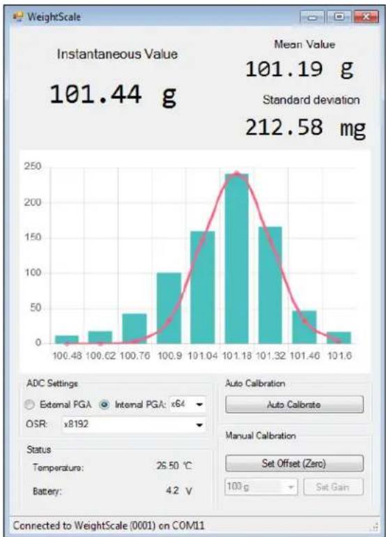
Figure 5, Figure 6 and Figure 7 show the measurement distributions with different OSR settings. It can be easily noticed that the standard deviation (or random noises) decreases significantly with the increase of the Oversampling Ratio.
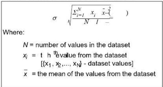
Using the weight scale's dedicated graphical user interface (GUI), the gain stage of the ADC and the OSR can be dynamically reconfigured and their effect on measurements can be analyzed. One of the most important parameters is the standard deviation. Standard Deviation quantifies the dispersion of the data values from a dataset and shows how the precision of the weight scale is influenced by the oversampling ratio with a fixed gain of 64x.
Equation 6 shows how the standard deviation is computed:
EQUATION 6: STANDARD DEVIATION
text_image
σ √Σi=1N xi x̄-2 Where: N = number of values in the dataset xi = t h th evalue from the dataset [ {x₁, x₂,..., xₙ} - dataset values] x̄ = the mean of the values from the dataset
histogram
| Statistic | Value | | --------------- | --------- | | Constant Value | 106.25 g | | Mean Value | 103.45 g | | Standard Deviation | 2579.35 mg | | ADC Settings | External PGA | | OSR | <32 | | Status | Temperature | | Battery | 4.3 V | | Auto Calibration | Auto Calibrate | | Manual Calibration | Set Offset (Zero) | | Connected to WeightScale (0001) on COM11FIGURE 5: PGA Gain = x64, OSR = 32.
histogram
| Statistic | Value | | --------- | --------- | | Constant | 101.44 g | | Mean | 101.19 g | | Standard deviation | 212.58 mg | | ADC Settings | External PGA: x64 | | OSR | x8192 | | Status | Temperature: 26.50 °C | | Battery | 4.2 V |FIGURE 6: PGA Gain = x64, OSR = 8192.
histogram
| Statistic | Value | | --------- | --------- | | Constant | 100.24 g | | Mean | 100.12 g | | Standard deviation | 76.27 mg | | ADC Settings | External PGA, Internal PGA: x64, OSR: x98304 | | Status | Temperature: 27.06 °C, Battery: 4.2 V | | Manual Calibration | Auto Calibration, Set Offset (Zarc), 100 g, Set Gain | | Connected to WeightScale (0001) on COM19FIGURE 7: PGA Gain = x64, OSR = 98304.
Ratiometric Measurement
A ratiometric measurement is more suitable for a bridge-based sensor as it can improve the stability of the measurement and eliminates the problems introduced by a noisy voltage source.
The reference voltage of the ADC should be the same as the excitation voltage applied to the load cell. With this configuration the ADC output code will be a digital ratiometric representation of the input voltage relative to the ADC reference voltage (excitation voltage).
The advantage of a ratiometric measurement is that when the supply voltage varies, the output sensitivity mV/V ratio will remain constant. If the output sensitivity is 1 mV/V for a supply voltage of 3V, the output will be a 3 mV signal at full load (2 kg for the chosen load cell). Therefore, the fact that the output is ratiometric (the mV/V ratio is kept constant) implies a certain measurement stability. Any noise from the voltage supply, be it due to temperature variations or any other noise source, will not affect the measurement significantly.

text_image
AVDD Load Cell OUT + VIN+ VREF+ MCP3564 OUT - VIN- VREF- AGNDFIGURE 8: Ratiometric Measurement Schematic.
The ADC itself also has a Power Supply Rejection Ratio (PSRR) specification which characterizes the influence of the power supply noise on the ADC output codes.
EQUATION 7: POWER SUPPLY REJECTION RATIO
$$ P S R R (d B) 2 \theta l o g \left(\frac {\Delta V _ {O U T}}{\Delta A V _ {D D}}\right) $$
Where:
$$ \begin{array}{r l} {V _ {O U T}} & {= \text { the equivalent voltage of the ADC }} \ & {\quad \text { output code obtained with the }} \ & {\quad \text { ADC transfer function }} \end{array} $$
The PSRR is measured for multiple AC and DC values of the power supply. For AC measurements, a sine wave is used with its amplitude representing possible changes in the power supply. See Table 5 for more information regarding how the AC and DC PSRR values are determined.
TABLE 5: POWER SUPPLY REJECTION
| Parameters Sym. | Min. Typ. | Max. | Units Conditions | |||
| AV_DD Power Supply Rejection Ratio | DC PSRR | — | -76 dB + 20 x LOG(GAIN) | — | dB | |
| DV_DD Power Supply Rejection Ratio | DC PSRR | -110 | DV_DD varies from 2.7V to 3.6V V_IN=0V | |||
| AC Power Supply Rejection Ratio | AC PSRR | -75 dB - 20 x LOG(GAIN) | DV_DD=3.3V AV_DD=3.3V+0.3VP,50Hz V_IN=0V |
For example, using the formula shown in Table5 an AC PSRR of 99.08 dB can be calculated when assuming a gain of 16x is used:
$$ \mathrm{ACPSRR} = - 7 5 \mathrm{dB} - 2 0 \times \log (1 6) = - 9 9. 0 8 \mathrm{dB} $$
Assuming a variation in the power supply of 100 V, Equation 7 shows that:
$$ \Delta V _ {O U T} = 1 0 ^ {(P S R R (d B) / 2 0)} \times \Delta A V _ {D D} (\mu V) $$
$$ \Delta V _ {\text { OUT }} = 1 0 ^ {(- 9 9. 0 8 \mathrm{dB} / 2 0)} \times 1 0 0 \mu \mathrm{V} = 1. 1 \mathrm{nV} $$
This voltage is significantly lower than the amplified load cell's output voltage. Therefore, the measurement is not notably affected by the power supply noise.
NOTES:
FEATURES OF THE MCP3564 WEIGHT SCALE DEMO
External Low-Noise Differential Amplifier
To improve the accuracy and the precision of the measurement, the weight scale board demo includes an external low-noise differential amplifier (Figure 2). The external differential amplifier offers the ability to amplify the input signal (load cell output voltage) beyond the capability of the programmable gain stage of the ADC. The ADC's amplifier has a configurable gain range from 1/3x to 64x, whereas the external amplifier has a fixed gain of 100x. The differential amplifier uses the MCP6492 Zero Drift Op Amp for its high PSRR and CMRR capabilities. The MCP6V92 also provides input offset voltage correction, which improves the noise rejection.
Using the GUI, the external amplifier can be enabled or disabled to demonstrate its impact on the application measurements. The accuracy and the precision of the measurements can be compared while using the external or the internal amplifier. The results at different OSR values (when using the external amplifier) can also be compared.
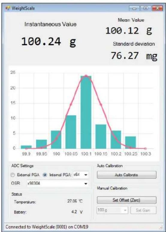
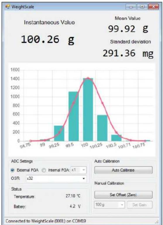
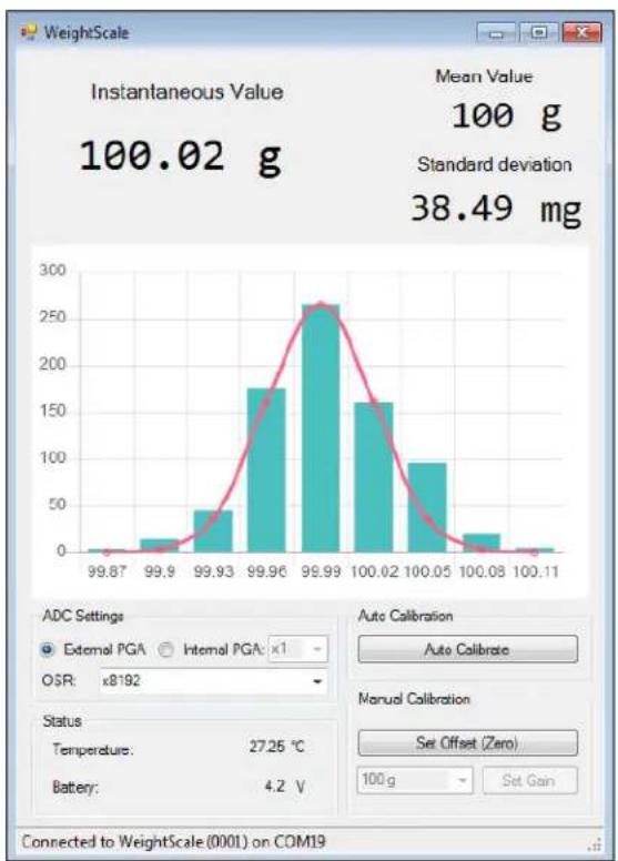
Figure 9, Figure 10 and Figure 11 show how the standard deviation varies when using the external amplifier with an OSR of 32, 8192 and 98304 respectively. The offset and gain of the system were calibrated using a 100g load.
When comparing standard deviation values of Figures 5, 6 and 7 where the internal PGA setting of the ADC is used versus the external amplifier (Figures 9, 10 and 11) it can be seen the results are improved considerably when using the external amplifier.
histogram
| Statistic | Value | | --------- | --------- | | Constant | 100.26 g | | Mean | 99.92 g | | Standard | 291.36 mg | | ADC Settings | External PGA, Internal PGA: x1, OSR: x32 | | Status | Temperature: 27.18 °C, Battery: 4.2 V | | Auto Calibration | Auto Calibration | | Manual Calibration | Set Offset (Zero) | | Connected to WeightScale (0001) on COM19 | 100 g |FIGURE 9: External Amplifier, OSR = 32.
histogram
| Statistic | Value | | --------- | --------- | | Constant | 100.02 g | | Mean | 100 g | | Standard deviation | 38.49 mg | | ADC Settings | External PGA, Internal PGA: x1 | | OSR | x8192 | | Status | Temperature: 27.25 °C | | Battery | 4.2 V | | Connected to WeightScale (0001) on COM19FIGURE 10: External Amplifier, OSR = 8192.

histogram
| Statistic | Value | | --------- | ----- | | Constant | 99.99 g | | Mean | 100 g | | Standard deviation | 9.09 mg | | ADC Settings | External PGA: κ1 - OSR: κ98304 | | Status | Temperature: 27.37 °C, Battery: 4.2 V | | Auto Calibration | Auto Calibrate | | Manual Calibration | Set Offset (Zero) | | Connected to WeightScale (0001) on COM19 | 100 g |FIGURE 11: External Amplifier, OSR = 98304.
Ultra-Low Power Monitoring Amplifier
The ADC and the external low-noise op amp have significant current consumption during normal operation which will affect the lifetime of the battery. To minimize power consumption, the weight scale will enter a Low Power mode when not performing active weight measurements. In this mode, the weight scale will monitor if a mass is present by performing low-accuracy measurements periodically.
The weight scale has two operating modes: Run mode and Sleep mode. When the weight scale enters into Sleep mode, the microcontroller is awakened by the watchdog timer (WDT) at a predetermined time period to check if there was any load change using the "low-power" monitoring amplifier. If there is a significant change, the weight scale enters the Run mode. Otherwise, it goes back into Sleep mode.
When the weight scale enters Sleep mode, the ADC is disconnected. Instead of waking up the ADC, when checking for load variation, an ultra-low power monitoring amplifier is used.
flowchart
graph TD
    A["Load Cell"] -->|AV_DD| B["OUT+"]
    A -->|AGND| C["OUT-"]
    A --> D["Differential Amplifier"]
    D --> E["MCP3564"]
    E -->|SPI| F["MCU (PIC24FJ256GB410)"]
    F --> G["ANx"]
    E --> H["CH0 CH1 CH2 CH3"]
    E --> I["VREF+ VREF-"]
    D --> J["Ultra-Low Power Monitoring Amplifier"]
    J --> D
FIGURE 12: Block Schematic with Ultra-Low Power Monitoring Amplifier.
The Monitoring Amplifier uses the Microchip MCP6444 operational amplifier in an Instrumentation Amplifier configuration. The MCP6444 is a quad op amp with a quiescent current of 450 nA/op amp, suitable for usage in low power applications. The monitoring amplifier has a single ended output and can be connected directly to an analog input pin of the microcontroller. Its output voltage is converted using the PIC24's internal 12-bit ADC and compared to the value acquired at the previous wake-up event of the microcontroller. If there is a significant difference between the two values, the weight scale enters Run mode. Otherwise, the microcontroller goes back to Deep Sleep mode. For storing the measured value at each microcontroller wake-up, the Deep Sleep Semaphore registers (DSGPR0 and DSGPR1) are used since they are the only registers preserved in Deep Sleep. One is used for saving the value and the other is used as a flag to indicate if there was a previous measurement or not. These registers are reset every time the weight scale goes from Run mode to Sleep mode.
Another design option is to connect the amplifier to a comparator input. PIC24F devices include three dual-input comparators with selectable inputs from the analog inputs multiplexed with the I/O pins, as well as the on-chip voltage reference.
Even though the SAR ADC of the PIC24F devices is less accurate and less precise than using the MCP3564 ADC, it is good enough to detect a load change and to decide whether the entire device should wake up and get into the Run mode or if it should go back into Sleep mode.
The biggest advantage of using this monitoring amplifier is that it draws less current than the MCP3564 ADC (when in the Conversion operating mode), which leads to extended battery life.
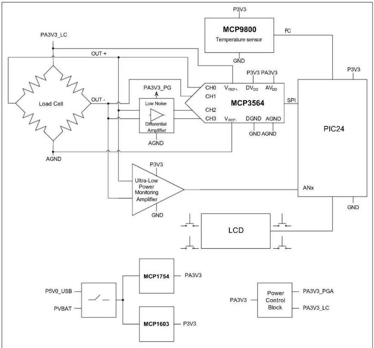
Figure 13 shows the final block schematic of the MCP3564 Weight Scale Demo.
flowchart
graph TD
    A["Load Cell"] --> B["Out +"]
    B --> C["PA3V3_LC"]
    C --> D["OUT -"]
    D --> E["Low Noise"]
    E --> F["Differential Amplifier"]
    F --> G["AGND"]
    G --> H["P3V3_PG"]
    H --> I["MCPC9800 Temperature sensor"]
    I --> J["FC"]
    J --> K["MCP3564"]
    K --> L["SPI"]
    L --> M["PIC24"]
    M --> N["ANx"]
    N --> O["GND"]
    O --> P["LCD"]
    P --> Q["PG"]
    Q --> R["Power Control Block"]
    R --> S["PA3V3_PGA"]
    R --> T["PA3V3_LC"]
    U["P3V0_USB"] --> V["MCP1754"]
    W["PVBAT"] --> X["MCP1603"]
    Y["Ch0 CH1 CH2 CH3"] --> Z["V_REF+ DV_DD AV_DD"]
    AA["CH0 CH1 CH2 CH3"] --> AB["V_REF+ DGND AGND"]
    AC["CH0 CH1 CH2 CH3"] --> AD["V_REF+ DGND AGND"]
FIGURE 13: Final Block Schematic.
Temperature Sensor
Microchip's MCP9800 is a digital temperature sensor which allows the configuration of the temperature measurement resolution, the operating modes or the specification of both temperature alert output and hysteresis limits.
The MCP9800 has two power-saving operating modes: Shutdown and One-shot (single conversion on command then returns into Shutdown mode), both useful for keeping the weight scale's power usage low. The MCP9800 communicates with the microcontroller through the I^2C interface.
The measured temperature can be seen on the LCD by parsing through the menu or by checking it in the GUI. This sensor can be used to observe if and how the weight measurement noise is affected by the increase or decrease in temperature.
For a high precision weight scale design, the data from the MCP9800 can be used to compensate the temperature drift of the load cell's output. As previously discussed, a more accurate temperature drift correction is obtained when using a thermocouple together with this digital temperature sensor (used for cold junction measurement).
Microcontroller - PIC24FJ256GB410
The microcontroller used in this application is Microchip's PIC24FJ256GB410, a 16-bit microcontroller which offers some key features for this application.
The Extreme Low Power (XLP) Features, more specifically the extreme low power current consumption for Deep Sleep, is very useful as the power consumption can be minimized while the weight scale is not actively performing measurements. The XLP features are therefore excellent for extending battery life in battery powered applications.
The on-chip Watchdog Timer (WDT) is needed to wake up the microcontroller from Deep Sleep to check if there is any change in the load cell output. Another key feature of this microcontroller is the Liquid Crystal Display (LCD) module which allows choosing a low power LCD without a dedicated driver.
The MCP3564 is initialized, reconfigured, and read via the SPI interface using the PIC24F microcontroller.
LCD Glass
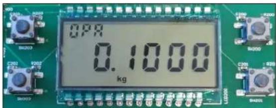
Using the LCD module of the microcontroller is very convenient for a low power application. By using a simple LCD glass, instead of a display with its own driver, power consumption can be significantly lowered. The LCD driver module can be used to generate the timing control to drive static or multiplexed LCD panels with up to 8 Commons and up to 64 Segments. The LCD glass used in this application uses 4 Commons and 25 Segments to display 6 main, and 4 secondary, digits along with the units of measurement, i.e. g or kg.
The LCD is used to display a menu. By navigating through this menu, the user can see:
• the measured weight in grams (Figure 14) and in kilograms (Figure 15),
• the calibration menu option (Figure 16),
• the temperature (Figure 17),
• the power supply voltage (Figure 18).

text_image
OPA 100.03 gFIGURE 14: LCD Menu - Grams.
text_image
0.79 0.1000 kgFIGURE 15: LCD Menu - Kilograms.

text_image
OPA CAL 18FIGURE 16: LCD Menu - Calibration.
The power supply voltage is measured using a resistive divider and the microcontroller's internal SAR ADC. It is useful for checking if the batteries should be replaced.
The bottom right (SW201) and left (SW202) push-buttons can be used to navigate through the menu. The top left button (SW203) is used for choosing between the external or the ADC's internal amplifier. The top-right push-button (SW200) is used for auto-calibration when in the Calibration Menu state or, otherwise, only for offset calibration.

text_image
0P8 26.404 °CFIGURE 17: LCD Menu - Temperature.

text_image
QPR 8A6 mV QPR 4251 mVFIGURE 18: LCD Menu - Power Supply Voltage.
Power
The weight scale can be powered using the on-board triple-A battery socket or by way of the USB connector at J400.
An alternative to triple-A batteries could be a rechargeable lithium-polymer (LiPo) battery with a better weight-to-power ratio. A drawback to this alternative, however, is an increased cost which may be undesirable depending on the design constraints. For recharging the LiPo battery when the USB is connected, a battery charge management controller can be integrated in the design. For example, Microchip's MCP73830 provides specific algorithms developed to achieve optimal capacity and safety and to shorten the charging time as much as possible.
To reduce the overall system noise, separate analog and digital power supplies should be used. Microchip's MCP1754 is used for the analog circuitry and the MCP1603 is dedicated to the digital section. The MCP1754 is a low-dropout (LDO) voltage regulator with a typical quiescent current of 56 uA and a typical 300 mV dropout voltage. The MCP1603 is a synchronous buck regulator with a 2.7V to 5.5V input range and a typical quiescent current of 45 μA. Both regulators have shutdown control pins, another feature that makes them suitable for battery powered applications.
Due to the inherent sensitivity of analog circuitry, an LDO with high PSRR is highly desirable. For this reason the MCP1754 was selected for this application. The MCP1754 LDO has a typical PSSR of 72 dB at 1 kHz and a low output noise of 3 V/ .
A Power Control Block has been implemented to enable or disable the power supply to the load cell and external amplifier as needed. It can be controlled by the microcontroller in order to lower the power consumption when these components are not in use.
NOTES:
OFFSET AND GAIN ERROR CALIBRATION
In addition to the inherent offset of the sensor previously discussed, the design of the weight scale also implies an offset introduced by the weight tray. Furthermore, both the ADC itself and the external differential amplifier introduce additional offset and gain errors. Regarding the ADC, these errors vary with the GAIN and OSR settings and they have different values from device to device.
The gain error indicates the difference between the slope of the actual transfer function compared to the ideal one, defined by Equation 8.
EQUATION 8: ADC OUTPUT
$$ A D C _ {-} O U T P U T L S B (= \left(\frac {V _ {I N +} - V _ {I N -}}{V _ {R E F +} - V _ {R E F -}}\right) \times 8 3 8 8 6 0 8 \times G A I N $$
A significant advantage of the MCP3564 ADC is that it provides digital calibration for offset and gain errors. This considerably reduces the amount of computations done in the microcontroller.
Equation 9 shows how the ADC output code (stored in the ADCDATA register) is modified with the offset and gain calibration values. These values are computed in the microcontroller and then written in the ADC's OFFSETCAL and GAINCAL 24-bit registers.
EQUATION 9: CALIBRATED ADC DATA
$$ \begin{array}{r l} A D C D A T A \text { post - calibration } (\quad) & = \ & = [ A D C D A T A (\text { pre - calibration }) + O F F S E T C A L ] \times G A I N C A L \end{array} $$
The MCP3564 also has two calibration control bits: EN_OFFCAL and EN_GAINCAL (see CONFIG3 register in the MCP3564 data sheet). When these bits are enabled, the values stored in the OFFSETCAL and GAINCAL registers are used to adjust the ADC output code. Otherwise, the calibration is not performed. One can choose to use only offset or only gain calibration and this can be done by enabling the corresponding control bit.
There are two ways to calibrate the weight scale: Manual or Auto-Calibration. Auto-Calibration can be done either by using the LCD menu and the physical buttons on the board or by using the GUI. For Auto-Calibration the user has to place the standard 100g weight on the weight scale tray.
If another weight value for gain calibration is preferable, manual calibration can be used and this is available only via the GUI. For manual calibration, there are two buttons, one for setting the offset and one for setting the gain. In this case, the gain calibration weight value can be chosen from a drop-down list (50g, 100g, 200g, 500g, 1000g) (see Figure 19).

text_image
Auto Calibration Auto Calibrate Manual Calibration Set Offset (Zero) 100 g Set GainFIGURE 19: Calibration Options.
When the weight scale is powered up for the very first time, it requires gain and offset calibration. The message printed on the LCD is shown in Figure 20.
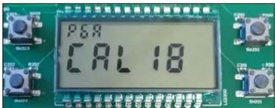
text_image
PSA CAL 18FIGURE 20: Auto-Calibration - Start.
The auto-calibration process can be started by pressing the top right button (SW200) on the board or the "Auto Calibrate" button from the GUI. The algorithm starts with the offset calibration. Two messages are displayed on the LCD to let the user know that the offset calibration has begun and the tray should be empty (see Figure 21).
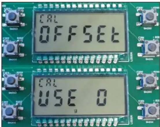
text_image
CAL OFFSET CAL USE 0FIGURE 21: Auto-Calibration - Offset.
The algorithm detects when the load cell signal is stable enough in order to compute the offset and correspondingly set the ADC's offset calibration register. During this time, the display shows a loading bar to indicate that the offset calibration is still in progress (see Figure 22).
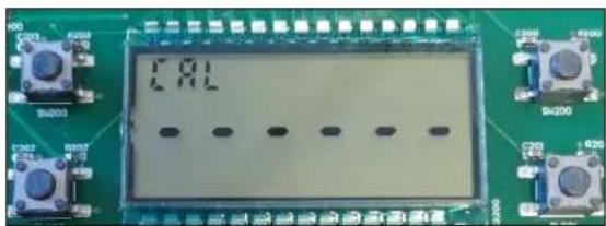
text_image
1.8LFIGURE 22: Auto-Calibration -
In Progress.
After the stability detection is done and after the OFFSETCAL register is set, the process continues with the gain calibration. Two messages are displayed on the LCD to inform the user that the gain calibration process has begun and that the standard 100g weight needs to be placed on the tray (see Figure 23).
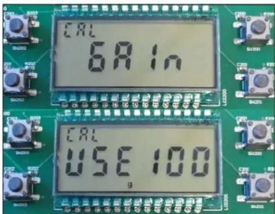
text_image
CAL 6A In CAL USE 100FIGURE 23: Auto-Calibration - Gain.
The next steps are signal stability detection and computation of the gain calibration value. Finally, after setting the gain calibration register (GAINCAL), the auto-calibration algorithm is done and the display will show the weight in grams.
After the initial calibration, the offset and gain calibration values are kept in the flash memory of the microcontroller, so the device does not need to be calibrated at each power up. Nevertheless, weight scale offset and gain calibration can be done at any time, either by using the LCD menu and the physical buttons or by using the user interface.
DIGITAL LOW-PASS FILTER
In order to reduce the noise level in the measurements even further, a software digital filter is implemented. The Low-Pass Filter (LPF) does a weighted average of the current input values and the previous ones. The implementation of its discrete form is based on Equation 10.
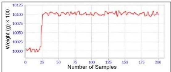
Depending on the Low-Pass Filter coefficient value, the previous values have a higher or a lower impact on the current output. Figures 24 to 29 show a comparison between filter outputs for different LPF coefficients when the load changes by 1 gram. For a low LPF coefficient (Figure 23 and Figure 24) the input variations are slightly attenuated, while for a higher value, it can be noticed that the filter smooths out the noisy input. As the coefficient increases, the current input value has a smaller impact on the output.
This is why the slope at the rising edge is less and less steep. This increases the precision, but the disadvantage of a high LPF coefficient is that it takes a longer time to notice load changes and for the output of the filter to increase or decrease to a certain value (Figure 27 and Figure 28). It also increases the time of the calibration process, as the algorithm waits for the signal to become stable.
Figure 25 and Figure 26 show an example of input filtering based on a good trade-off between the steepness of the slope (how fast the device reacts to load changes) and the precision of the measurement.
EQUATION 10: LOW-PASS FILTER EQUATION
$$ y (n) = y (n - 1) + \left(\frac {1}{2 ^ {L P F _ {-} c o e f f i c i e n t}}\right) \times [ x (n) + x (n - 1) - 2 \times y (n - 1) ] $$
Where:
$$ \begin{array}{l} y (n) = \text { filter output value } \ y (n - 1) = \text { previous filter output value } \ x (n) = \text { current weight value } \ x (n - 1) = \text { previous weight value } \ \end{array} $$

line
| Number of Samples | Weight(g) × 100 | | ----------------- | --------------- | | 0 | 10000 | | 25 | 10025 | | 50 | 10100 | | 75 | 10100 | | 100 | 10100 | | 125 | 10100 | | 150 | 10100 | | 175 | 10100 | | 200 | 10100 |FIGURE 24: Unfiltered Data, LPF Coefficient = 2.

line
| Number of Samples | Weight (g) × 100 | | ----------------- | ---------------- | | 0 | 10000 | | 25 | 10000 | | 50 | 10100 | | 75 | 10100 | | 100 | 10100 | | 125 | 10100 | | 150 | 10100 | | 175 | 10100 | | 200 | 10100 |FIGURE 27: Filtered Data, LPF Coefficient = 2.
line
| Number of Samples | Weight (g) × 100 | | ----------------- | ---------------- | | 0 | 10000 | | 25 | 10000 | | 50 | 10100 | | 75 | 10100 | | 100 | 10100 | | 125 | 10100 | | 150 | 10100 | | 175 | 10100 | | 200 | 10100 |FIGURE 25: Unfiltered Data, LPF Coefficient = 4.

line
| Number of Samples | Weight (g) × 100 | | ----------------- | ---------------- | | 0 | 10000 | | 25 | 10000 | | 50 | 20100 | | 75 | 20100 | | 100 | 20100 | | 125 | 20100 | | 150 | 20100 | | 175 | 20100 | | 200 | 20100 |FIGURE 28: Filtered Data, LPF Coefficient = 4.

line
| Number of Samples | Weight (g) × 100 | | ----------------- | ---------------- | | 0 | 10000 | | 25 | 10100 | | 50 | 10120 | | 75 | 10110 | | 100 | 10115 | | 125 | 10110 | | 150 | 10115 | | 175 | 10110 | | 200 | 10115 |FIGURE 26: Unfiltered Data, LPF Coefficient = 6.
line
| Number of Samples | Weight (g) × 100 | | ----------------- | ---------------- | | 0 | 10000 | | 25 | 10000 | | 50 | 10050 | | 75 | 10075 | | 100 | 10087.5 | | 125 | 10093.75 | | 150 | 10096.875 | | 175 | 10098.3875 | | 200 | 10099.69375 |FIGURE 29: Filtered Data, LPF Coefficient = 6.
OPERATING MODES
The weight scale has two power modes: USB and Low Power Battery mode. When the USB is connected, it supplies the entire board and the device is up and running at all times. When the USB is disconnected, the batteries supply the device. In this case, good power management is required in the interest of prolonging the batteries' lifespan.
The operating states of the weight scale are:
- Run mode
- Sleep mode
Run Mode
Figure 30 represents the flowchart of the Run mode. The first step is to check whether the USB is connected or not in order to establish which power mode the device is using.
In both power modes, the weight scale acquires data (weight, temperature, power supply voltage) and displays it on the LCD, depending on the state in which the LCD menu is in. If any button event occurs, the corresponding command is executed.
In USB Power mode, the acquired data is not only displayed on the LCD, but also sent to the GUI. As shown before, by using this graphical user interface the user can monitor the instantaneous, mean and standard deviation weight values. Additionally, the temperature and battery voltage are shown. The Oversampling-Ratio (OSR) of the ADC can also be set via the user interface (GUI). The user can choose between the external or the internal amplifier. When using the internal amplifier the gain can be selected from the list of available values.
In Low Power Battery mode a timer is used to know how much time has passed since the last event has occurred, be it a button press or a significant load change. If the device has had no activity for 60 seconds, it enters into Sleep mode.

flowchart
graph TD
    A["START"] --> B{USB Plugged In?}
    B -->|No| C["Switch to Low Power Battery mode (if the device is in USB Power mode)"]
    B -->|Yes| D["Switch to USB Power mode (if the device is in Low Power Battery mode)"]
    C --> E{Counter = 60s?}
    D --> F["Gain/Offset Calibration, Menu Navigation, etc."]
    E -->|No| G{Any buttons pushed?}
    F -->|Yes| G
    G -->|No| H["Measure Weight"]
    G -->|Yes| I["Gain/Offset Calibration, ADC registers update, etc."]
    H --> J["Measure Temperature"]
    J --> K["Measure Power Supply Voltage"]
    K --> L["Send data to the LCD"]
    I --> M{Any GUI commands?}
    M -->|Yes| N["Gain/Offset Calibration, ADC registers update, etc."]
    M -->|No| O{Any buttons pushed?}
    O -->|Yes| P["Switch to Internal/External Amplifier, Auto-Calibration, Menu Navigation, etc."]
    O -->|No| Q["Measure Weight"]
    Q --> R["Measure Temperature"]
    R --> S["Measure Power Supply Voltage"]
    S --> T["Send data to GPU and LCD"]
    P --> U["End"]
    Q --> V["End"]
FIGURE 30: Run Operating Mode Flowchart.
Sleep Mode
Figure 31 shows the flowchart for the Sleep mode. When the device is in Sleep mode, the MCP9800 temperature sensor and the MCP3564 ADC stay in shutdown, along with the MCP1754 LDO and the MCP1603 buck regulator. After this step, the microcontroller enters into Deep Sleep mode.
The Deep Sleep watchdog timer uses the MCU's internal low power RC oscillator and is configured to wake up the MCU after approximately 500 ms of Deep Sleep. Even if MCP1603 is shut down and there is no power to the MCU, its output capacitor does not allow the MCU supply voltage to decrease below the lowest accepted V_DD value. The MCU is awakened by the watchdog timer, which in turn wakes up the buck regulator before the voltage on the output capacitor becomes too depleted.
When the PIC24 is in the Run mode, it also enables the LDO and the power control block in order to supply power to the load cell. The monitoring amplifier is used to check if there is any significant change in the load cell output voltage, in which case the device enters the Run Mode. Otherwise, the load cell's power supply is switched off, the buck regulator is shut down and the MCU goes back into Deep Sleep again, with the entire system remaining in Sleep mode.
flowchart
graph TD
    A["START"] --> B["MCU in Deep Sleep"]
    B --> C{Watchdog timer triggered?}
    C -->|No| B
    C -->|Yes| D["Check the load using the Monitoring Amplifier"]
    D --> E{Significant load change?}
    E -->|Yes| F["Enter Run Mode"]
    E -->|No| B
FIGURE 31: Sleep Operating Mode Flowchart.
NOTES:
CONCLUSION
This application note emphasizes the factors which impact the precision and the accuracy of a weight scale and provides solutions and methods for obtaining low noise measurements and a low power consumption of the entire system.
The load cell's specifications need to be well understood in order to appropriately decide what type of ADC should be used and whether the design requires an external amplifier or temperature compensation.
The weight scale application is based on the MCP3564 ADC, which has several advantages for weight scale type system design:
- configurable OSR and gain
• high PSRR and CMRR - differential analog inputs (this allows direct connection of the Wheatstone Bridge)
• differential reference voltage inputs - on-chip offset and gain calibration.
High OSR and gain values, as well as using the external low-noise differential amplifier, increase the precision and the accuracy of the measurements. Furthermore, by implementing and using the digital low-pass filter, a standard deviation of 0.02g can easily be achieved.
Using the PIC24FJ256GB410 microcontroller, with its XLP features proved advantageous for obtaining low power consumption. To save battery power, this application also includes an algorithm which switches the weight scale operating mode from Run mode to Sleep mode and an ultra-low power monitoring amplifier. At the expense of increasing the overall cost, using a LiPo battery and a charger are recommended for a different design if a better weight/power ratio is desired.
REFERENCES
[1] MCP3561/2/4 Data Sheet, "Two/ Four/ Eight-Channel, 153.6 kSPS, Low-Noise 24-bit Delta-Sigma ADCs", 2019 Microchip Technology, Inc.
[2] PIC24FJ256GA412/GB412 FAMILY Data Sheet, "16-Bit Flash Microcontrollers with Dual Partition Flash Memory, XLP, LCD, Cryptographic Engine and USB On-The-Go", 2015-2016 Microchip Technology Inc.
[3] MCP6V91/1U/2/4 Data Sheet, "10 MHz, Zero-Drift Op Amps", 2015-2016 Microchip Technology Inc.
[4] MCP6441/2/4 Data Sheet, "450 nA, 9 kHz Op Amp", 2010-2012 Microchip Technology Inc.
[5] MCP9800/1/2/3 Data Sheet, "2-Wire High-Accuracy Temperature Sensor", 2010 Microchip Technology Inc.
[6] MCP1603/B/L Data Sheet, "2.0 MHz, 500 mA Synchronous Buck Regulator", 2007-2012 Microchip Technology Inc.
[7] MCP1754/MCP1754S Data Sheet, "150 mA, 16V, High-Performance LDO", 2011-2013 Microchip Technology Inc.
NOTES:
APPENDIX A: SCHEMATICS AND
LAYOUT
This appendix contains the schematic and the layout of the MCP3564 Weight Scale Board.
A.1 Weight Scale Board - Schematic 1

A.2 Weight Scale Board - Schematic 2
A.3 Weight Scale Board - Schematic 3
ULTRA LOW POWER MONITORING AMPLIFIER

text_image
LOAD_CELL_PLUS U500B 5 1B OUTB 7 R500 100k 0603 1% R501 100k 0603 1% U500D 13-D OUTD 14 LOW POWER ON C501 1000pF 50V 0603 GND P3V3 U500A 2-A 4 VDD OUTA 1 VSS 3 +A 11 MCP6444 P3V3 P3V3 R507 GND U500C 10-C OUTC 8 C500 0.1uF 16V 0603 GND R508 1M 0603 1% 9-C MCP6444 R509 1k 1% 0603A.4 Weight Scale Board - Schematic 4
text_image
Driverless LCD LCD200 LCD 2001 LCD 2002 LCD 2003 LCD 2004 LCD 2005 LCD 2006 LCD 2007 LCD 2008 LCD 2009 LCD 2010 LCD 2011 LCD 2012 LCD 2013 LCD 2014 LCD 2015 LCD 2016 LCD 2017 LCD 2018 LCD 2019 LCD 2020 LCD 2021 LCD 2022 LCD 2023 LCD 2024 LCD 2025 LCD 2026 LCD 2027 LCD 2028 LCD 2029 LCD 2030 LCD 2031 LCD 2032 LCD 2033 LCD 2034 LCD 2035 LCD 2036 LCD 2037 LCD 2038 LCD 2039 LCD 2040 LCD 2041 LCD 2042 LCD 2043 LCD 2044 LCD 2045 LCD 2046 LCD 2047 LCD 2048 LCD 2049 LCD 2050 LCD 2051 LCD 2052 LCD 2053 LCD 2054 LCD 2055 LCD 2056 LCD 2057 LCD 2058 LCD 2059 LCD 2060 LCD 2061 LCD 2062 LCD 2063 Button 1 PZW1 R230 1kV 1kV 1kV DTN1 SWW201 PTB48E4A4E7E5LFS C290 LIC 1kV 1kV 1kV CND R7X1 R7X3 R7X1 R7X3 R7X1 R7X3 R7X1 R7X3 R7X1 R7X3 R7X1 R7X3 R7X1 R7X3 R7X1 R7X3 R7X1 R7X3 R7X1 R7X3 R7X1 R7X1 R7X3 Button 2 PZW1 R261 A/A A/A DTN2 SWW201 PTB48E4A4E7E5LFS C291 LIC 1kV 1kV 1kV CND R7X3 R7X1 R7X3 R7X1 R7X3 R7X1 R7X3 Button 3 PZW1 R262 A/A A/A DTN3 SWW201 PTB48E4A4E7E5LFS C291 LIC 1kV 1kV 1kVA.5 Weight Scale Board - Schematic 5

text_image
Microcontroller F12 F13 F14 F15 F16 SE1R SE1T VREF VREF VREF VREF VREF VREF VREF VREF VREF VREF VREF VREF VREF VREF VREF VREF VREF VREF VREF VREF VREF VREF VREF VREF VREF VREF VREF VREF VREF VREF VREF VREF VREF VREF
text_image
ICSP P2V3 P2V3 K300 1 500 MTR 2 100 3 100 LED P2V3 P2V3 Q00 Q01 Q02 Q03 LED P2V3 P2V3 Q01 Q02 Q03 LED P2V3 P2V3 LCD Module hissings capacitors LC185A50 LC185A51 LC185A52 LC185A53 LC185A54 C300 2474 99 960 C301 2474 99 960 C302 2474 99 960 C303 2474 99 960 C304 2474 99 960 C305 2474 99 960 C306 2474 99 960 C307 2474 99 960 C308 2474 99 960 C309 2474 99 960 C310 2474 99 960 C311 2474 99 960 C312 2474 99 960 C313 2474 99 960 C314 2474 99 960 C315 2474 99 960 C316 2474 99 960 C317 2474 99 960 C318 2474 99 960 C319 2474 99 960 C320 2474 99 960 C321 2474 99 960 C322 2474 99 960 C323 2474 99 960 C324 2474 99 960 C325 2474 99 960 C326 2474 99 960 C327 2474 99 960 C328 2474 99 960 C329 2474 99 960 C330 2474 99 960 C331 2474 99 960 C332 2474 99 960 C333 2474 99 960 C334 2474 99 960 C335 2474 99 960 C336 2474 99 960 C337 2474 99 960 C338 2474 99 960 C339 2474 99 960 C340 2474 99 960 C341 2474 99 960 C342 2474 99 960 C343 2474 99 960 C344 2474 99 960 C345 2474 99 960 C346 2474 99 960 C347 2474 99 960 C348 2474 99 960 C349 2474 99 960 C350 2474 99 960 C351 2474 99 960 C352 2474 99 960 C353 2474 99 960 C354 2474 99 960 C355 2474 99 960 C356 2474 99 960 C357 2474 99 960 C358 2474 99 960 C359 2474 99 960 C360 2474 99 960 C361 2474 99 960 C362 2474 99 960 C363 2474 99 960 C364 2474 99 960 C365 2474 99.55 C366-1 PCC-1 PCC-1 PCC-1 PCC-1 PCC-1 PCC-1 PCC-1 PCC-1 PCC-1 PCC-1 PCC-1 PCC-1 PCC-1 PCC-1 PCC-1 PCC-1 PCC-1 PCC-1 PCC-1 PCC-1 PCC-1 PCC-1 PCC-1 PCC-1 PCC-1 Pcc-1 Pcc-1 Pcc-1 Pcc-1 Pcc-1 Pcc-1 Pcc-1 Pcc-1 Pcc-1 Pcc-1 Pcc-1 Pcc-1 Pcc-1 Pcc-1 Pcc-1 Pcc-1 Pcc-1 Pcc-1 Pcc-1 Pcc-1 Pcc-1 Pcc-1 Pcc-1 Pcc-1 Pcc-1 Ppc-1 Pcc-1 Pcc-1 Pcc-1 Pcc-1 Pcc-1 Pcc-1 Pcc-1 Pcc-1 Pcc-1 Pcc-1 Pcc-1 Pcc-1 Pcc-1 Pcc-1 Pcc-1 Pcc-1 Pcc-1 Pcc-1 Pcc-1 Pcc-1 Pcc-1 Pcc-1 Pcc-1 Pcc-1 Pp-p-p-p-p-p-p-p-p-p-p-p-p-p-p-p-p-p-p-p-p-p-p-p-p-p-p-p-p-p-p-p-p-p-p-p-p-p-p-p-p-p-p-p-p-p-p-p-p-p-p-p-p-p-p-p-p-p-p-p-p-p-p-p-p-p-p-p-p-p-p-p-p-p-p-p-p-p-p-p-p-p-p-p-p-p-p-p-p-p-p-p-p-p-p-p-p-p-p-p-p-per- IPOV IPOV IPOV IPOV IPOV IPOV IPOV IPOV IPOV IPOV IPOV IPOV IPOV IPOV IPOV IPOV IPOV IPOV IPOV IPOV IPOV IPOV IPOV IPOV IPOV IPOV IPOV IPOV IPOV IPOV IPOV IPOV IPOV IPOV I POV IPOV IPOV IPOV IPOV IPOV IPOV IPOV IPOV IPOV IPOV IPOV IPOV IPOV IPOV IPOV IPOV IPOV IPOV IPOV IPOV IPOV IPOV IPOV IPOV IPOV IPOV I PO V IPO V IPO V IPO V IPO V IPO V IPO V IPO V IPO V IPO V IPO V IPO V IPO V IPO V IPO V IPO V IPO V IPO V IPO V IPO V IPO V IPO V IPO V IPO V IPO V I PO V I PO V I PO V I PO V I PO V I PO V I PO V I PO V I PO V I PO V I PO V I PO V I PO V I PO V I PO V I PO V I PO V I PO V I PO V I PO V I PO V I PO V I PO V I PO V I PO V I PO V I PO V I PO V I PO V | GND GND GND GND GND GND GND GND GND GND GND GND GND GND GND GND GND GND GND GND GND GND GND GND GND GND GND GND GND GND GND GND GND GND GND GND GND GND GND GND GND GND GND GND GND GND GND GND GND GND GND CNTD CNTD CNTD CNTD CNTD CNTD CNTD CNTD CNTD CNTD CNTD CNTD CNTD CNTD CNTD CNTD CNTD CNTD CNTD CNTD CNTD CNTD CNTD CNTD CNTD CNTD CNTD CNTD CNTD CNTD CNTD CNTD CNTD CNTD BCTD BCTD BCTD BCTD BCTD BCTD BCTD BCTD BCTD BCTD BCTD BCTD BCTD BCTD BCTD BCTD BCTD BCTD BCTD BCTD BCTD BCTD BCTD BCTD BCTD BCTD BCTD BCTD BCTD BCTD BCTD BCTD BCTD BCTT BCTT BCTT BCTT BCTT BCTT BCTT BCTT BCTT BCTT BCTT BCTT BCTT BCTT BCTT BCTT BCTT BCTT BCTT BCTT BCTT BCTT BCTT BCTT BCTT BCTT BCTT BCTT BCTT BCTT BCTT BCTT BCTT BCTT APTB APTB APTB APTB APTB APTB APTB APTB APTB APTB APTB APTB APTB APTB APTB APTB APTB APTB APTB APTB APTB APTB APTB APTB APTB APTB APTB APTB APTB APTB APTB APTB APTB APTB APPTA APPTA APPTA APPTA APPTA APPTA APPTA APPTA APPTA APPTA APPTA APPTA APPTA APPTA APPTA APPTA APPTA APPTA APPTA APPTA APPTA APPTA APPTA APPTA APPTA APPTA APPTA APPTA APPTA APPTA APPTA APPTA APPTA APPTAAPPTA APPTA APPTA APPTA APPTA APPTA APPTA APPTA APPTA APPTA APPTA APPTA APPTA APPTA APPTA APPTA APPTA APPTA APPTA APPTA APPTA APPTA APPTA APPTA APPTA APPTA APPTA APPTA APPTA APPTA APPTA APPTA APPTA APMTABPAPPAPPAPPAPPAPPAPPAPPAPPAPPAPPAPPAPPAPPAPPAPPAPPAPPAPPAPPAPPAPPAPPAPPAPPAPPAPPAPPAPPAPPAPPAPPAPPAPPAPPAPPAPPAPPAPPAPPAPPAPPAPPAPPAPPAPPAPPAPPAPPAPPAPPAPPAPPAPPAPPAPPAPPAPPAPPAPPAPPAPPAPPAPPAPPAPPAPPAPPAPPAPPAPPAPPAPPAPPAPPAPPAPPAPPAPPAPPAPPAPPAPPAPPAPPAPPAPPAPPAPPAPPAPPAPPAPPAPPAPPAPPAPPAPPAPPAPPAPPAPRAPPAPRAPPAPRAPPAPRAPPAPRAPPAPRAPPAPRAPPAPRAPPAPRAPPAPRAPPAPRAPPAPRAPPAPRAPPAPRAPPAPRAPPAPRAPPAPRAPPAPRAPPAPRAPPAVPPARPPARPPARPPARPPARPPARPPARPPARPPARPPARPPARPPARPPARPPARPPARPPARPPARPPARPPARPPARPPARPPARPPARPPARPPARPPARPPARPPARPPARPPARPPARPPARPPARPPARPPARPPARPPARPPARPPARPPARPPARPPARPPARPPARPPARPPARPPARPPARPPARPPARPPARPAPPARPPARPAPPARPAPPARPAPPARPAPPARPAPPARPAPPARPAPPARPAPPARPAPPARPAPPARPAPPARPAPPARPAPPARPAPPARPAPPARPAPPARPAPPARPAPPARPAPPARPAPPARPAPPARPAPPARPAPPARPAPPARPAPPARPAPPARPAPPARPAPPARPAPPARPAPPARPAPPARPAPPARPAPPARPAPPARPAPPARPAPPARPAPPARPAPPARPAPPARPAPPARPAPPARPAPPARPAPPARPAPPARPAPPARPAPPARPAPPARPAPPARPAPPARPAPPARPIPPARPAPPARPAPPARPAPPARPAPPARPAPPARPAPPARPAPPARPAPPARPAPPARPAPPARPAPPARPAPPARPAPPARPAPPARPAPPARPAPPARPAPPARPAPPARPAPPARPAPPARPAPPARPAPPARPAPPARPAPPARPAPPARPAPPARPAPPARPAPPARPAPPARPAPPARPAPPARPAPPARPAPPARPAPPARPAPPARPAPPARPAPPARPAPPARPAPPARPAPPARPAPPARPAPPARPAPPARPAPPARPAPPARPAPPARPAPPARPAPPARPAPPARPATT ARPATT ARPATT ARPATT ARPATT ARPATT ARPATT ARPATT ARPATT ARPATT ARPATT ARPATT ARPATT ARPATT ARPATT ARPATT ARPATT ARPATT ARPATT ARPATT ARPATT ARPATT ARPATT ARPATT ARPATT ARPATT ARPATT ARPATT ARPATT ARPATT ARPATT ARPATT ARPATT ARPATT ARPATT ARPATT ARPATT ARPATT ARPATT ARPATT ARPATT ARPATT ARPATT ARPATT ARPATT ARPATT ARPATT ARPATT ARPATT ARPATT ARPATT EVPATRPATRPATRPATRPATRPATRPATRPATRPATRPATRPATRPATRPATRPATRPATRPATRPATRPATRPATRPATRPATRPATRPATRPATRPATRPATRPATRPATRPATRPATRPATRPATRPATRPATRPATRPATRPATRPATRPATRPATRPATRPATRPATRPATRPATRPATRPATRPATRPATRPATRPAT RPATRPATRPATRPATRPATRPATRPATRPATRPATRPATRPATRPATRPATRPATRPATRPATRPATRPATRPATRPATRPATRPATRPATRPATRPATRPATRPATRPATRPATRPATRPATRPATRPATRPATRPATRPATRPATRPATRPATRPATRPATRPATRPATRPATRPATRPATRPATRPATRPATRPATROP RAMP RAMP RAMP RAMP RAMP RAMP RAMP RAMP RAMP RAMP RAMP RAMP RAMP RAMP RAMP RAMP RAMP RAMP RAMP RAMP RAMP RAMP RAMP RAMP RAMP RAMP RAMP RAMP RAMP RAMP RAMP RAMP RAMP RAMP RAMP RAMP RAMP RAMP RAMP RAMP RAMP RAMP RAMP RAMP RAMP RAMP RAMP RAMP RAMP RAMP RWP ARTPR ATPR ATPR ATPR ATPR ATPR ATPR ATPR ATPR ATPR ATPR ATPR ATPR ATPR ATPR ATPR ATPR ATPR ATPR ATPR ATPR ATPR ATPR ATPR ATPR ATPR ATPR ATPR ATPR ATPR ATPR ATPR ATPR ATPR ATPR ATPR ATPR ATPR ATPR ATPR ATPR ATPR ATPR ATPR ATPR ATPR ATPR ATPR ATPR ATPR ATPR EPRTN NPRTN NPRTN NPRTN NPRTN NPRTN NPRTN NPRTN NPRTN NPRTN NPRTN NPRTN NPRTN NPRTN NPRTN NPRTN NPRTN NPRTN NPRTN NPRTN NPRTN NPRTN NPRTN NPRTN NPRTN NPRTN NPRTN NPRTN NPRTN NPRTN NPRTN NPRTN NPRTN NPRTN NPFTN NPFTN NPFTN NPFTN NPFTN NPFTN NPFTN NPFTN NPFTN NPFTN NPFTN NPFTN NPFTN NPFTN NPFTN NPFTN NPFTN NPFTN NPFTN NPFTN NPFTN NPFTN NPFTN NPFTN NPFTN NPFTN NPFTN NPFTN NPFTN NPFTN NPFTN NPFTN NPFTN NPFTS NIP FAN FAN FAN FAN FAN FAN FAN FAN FAN FAN FAN FAN FAN FAN FAN FAN FAN FAN FAN FAN FAN FAN FAN FAN FAN FAN FAN FAN FAN FAN FAN FAN FAN FAN FAN FAN FAN FAN FAN FAN FAN FAN FAN FAN FAN FAN FAN FAN FAN FAN F ANF ANF ANF ANF ANF ANF ANF ANF ANF ANF ANF ANF ANF ANF ANF ANF ANF ANF ANF ANF ANF ANF ANF ANF ANF ANF ANF ANF ANF ANF ANF ANF ANF ANF ANF ANF ANF ANF ANF ANF ANF ANF ANF ANF ANF ANF ANF ANF ANF ANF ANf ANF ANF ANF ANF ANF ANF ANF ANF ANF ANF ANF ANF ANF ANF ANF ANF ANF ANF ANF ANF ANF ANF ANF ANF ANF ANF ANF ANF ANF ANF ANF ANF ANF ANF ANF ANF ANF ANF ANF ANF ANF ANF ANF ANF ANF ANF ANF ANF ANF ANrNP ARTPARFPARFPARFPARFPARFPARFPARFPARFPARFPARFPARFPARFPARFPARFPARFPARFPARFPARFPARFPARFPARFPARFPARFPARFPARFPARFPARFPARFPARFPARFPARFPARFPARFPARFPARFPARFPARFPARFPARFPARFPARFPARFPARFPARFPARFPARFPARFPARFPARFPARFPARTPARGRAFPARGRAFPARGRAFPARGRAFPARGRAFPARGRAFPARGRAFPARGRAFPARGRAFPARGRAFPARGRAFPARGRAFPARGRAFPARGRAFPARGRAFPARGRAFPARGRAFPARGRAFPARGRAFPARGRAFPARGRAFPARGRAFPARGRAFPARGRAFPARGRAFPARGRAFPARGRAFPARGRAFPARGRAFPARGRAFPARGRAFPARGRAFPARGRAFPARGRAFPARKRAFPARGRAFPARGRAFPARGRAFPARGRAFPARGRAFPARGRAFPARGRAFPARGRAFPARGRAFPARGRAFPARGRAFPARGRAFPARGRAFPARGRAFPARGRAFPARGRAFPARGRAFPARGRAFPARGRAFPARGRAFPARGRAFPARGRAFPARGRAFPARGRAFPARGRAFPARGRAFPARGRAFPARGRAFPARGRAFPARGRAFPARGRAFPARGRAFPARGAAFLPGARRPGARRPGARRPGARRPGARRPGARRPGARRPGARRPGARRPGARRPGARRPGARRPGARRPGARRPGARRPGARRPGARRPGARRPGARRPGARRPGARRPGARRPGARRPGARRPGARRPGARRPGARRPGARRPGARRPGARRPGARRPGARRPGARRPGARRPGARRPGARRPGARRPGARRPGARRPGARRPGARRPGARRPGARRPGARRPGARRPGARRPGARRPGARRPGARRPGARRPGARNRGPAEPAAEPAAEPAAEPAAEPAAEPAAEPAAEPAAEPAAEPAAEPAAEPAAEPAAEPAAEPAAEPAAEPAAEPAAEPAAEPAAEPAAEPAAEPAAEPAAEPAAEPAAEPAAEPAAEPAAEPAAEPAAEPAAEPAAEPAAEPAAEPAAEPAAEPAAEPAAEPAAEPAAEPAAEPAAEPAAEPAAEPAAEPAAEPAAEPAAEPAAEPAAAFFAAAAFAEFAEFAEFAEFAEFAEFAEFAEFAEFAEFAEFAEFAEFAEFAEFAEFAEFAEFAEFAEFAEFAEFAEFAEFAEFAEFAEFAEFAEFAEFAEFAEFAEFAEFAEFAEFAEFAEFAEAPEAFAEFAEFAEFAEFAEFAEFAEFAEFAEFAEFAEFAEFAEFAEFAEAPEAFAEFAEFAEFAEFAEFAEFAEFAEFAEFAEAPEAFAEFAEFAEFAEFAEFAEFAEAPEAFAEFAEEFEFEFEFEFEFEFEFEFEFEFEFEFEFEFEFEFEFEFEFEFEFEFEFEFEFEFEFEFEFEFEFEFEFEFEFEFEFEFEFEFEFEFEFEFEFEFEFEFEFEFEFEFEFEFEFEFEFEFEFEFEFEFEFEFEFEFEFEFEFEFEFEFEFEFEFEFEFEFEFEFEFEFEFEFEFEFEFEFEFEFEFEFEFEFEFEFEFEFEFE FEEFCEFFCEFFCEFFCEFFCEFFCEFFCEFFCEFFCEFFCEFFCEFFCEFFCEFFCEFFCEFFCEFFCEFFCEFFCEFFCEFFCEFFCEFFCEFFCEFFCEFFCEFFCEFFCEFFCEFFCEFFCEFFCEFFCEFFCEFFCEFFCEFFCEFFCEFFCEFFCEFFCEFFCEFFCEFFCEFFCEFFCEFFCEFFCEFFCEFFCEFFCEEFCEFFCEFFCEFFCEFFCEFFCEFFCEFFCEFFCEFFCEFFCEFFCEFFCEFFCEFFCEFFCEFFCEFFCEFFCEFFCEFFCEFFCEFFCEFFCEFFCEFFCEFFCEFFCEFFCEFFCEFFCEFFCEFFCEFFCEFFCEFFCEFFCEFFCEFFCEFFCEFFCEFFCEFFCEFFCEFFCEFFCEFFCEFFCEFFCEFFCFECFCFCFCFCFCFCFCFCFCFCFCFCFCFCFCFCFCFCFCFCFCFCFCFCFCFCFCFCFCFCFCFCFCFCFCFCFCFCFCFCFCFCFCFCFCFCFCFCFCFCFCFCFCFCFCFCFCFCFCFCFCFCFCFCFCFCFCFCFCFCFCFCFCFCFCFCFCFCFCFCFCFCFCFCFCFCFCFCFCFCFCFCFCFCFCFCFCFCFCFCFGACCGACCGACCGACCGACCGACCGACCGACCGACCGACCGACCGACCGACCGACCGACCGACCGACCGACCGACCGACCGACCGACCGACCGACCGACCGACCGACCGACCGACCGACCGACCGACCGACCGACCGACCGACCGACCGACCGACCGACCGACCGACCGACCGACCGACCGACCGACCGACCGACCGACCGACGTCBCDCDCDCDCDCDCDCDCDCDCDCDCDCDCDCDCDCDCDCDCDCDCDCDCDCDCDCDCDCDCDCDCDCDCDCDCDCDCDCDCDCDCDCDCDCDCDCDCDCDCDCDCDCDCDCDCDCDCDCDCDCDCDCDCDCDCDCDCDCDCDCDCDCDCDCDCDCDCDCDCDCDCDCDCDCDCDCDCDCDCDCDCDCDCDCDCDCDCDCDC DCPC DPC DPC DPC DPC DPC DPC DPC DPC DPC DPC DPC DPC DPC DPC DPC DPC DPC DPC DPC DPC DPC DPC DPC DPC DPC DPC DPC DPC DPC DPC DPC DPC DPC DPC DPC DPC DPC DPC DPC DPC DPC DPC DPC DPC DPC DPC DPC DPC DPC DPC ECP ACP ACP ACP ACP ACP ACP ACP ACP ACP ACP ACP ACP ACP ACP ACP ACP ACP ACP ACP ACP ACP ACP ACP ACP ACP ACP ACP ACP ACP ACP ACP ACP ACP ACP ACP ACP ACP ACP ACP ACP ACP ACP ACP ACP ACP ACP ACP ACP ACP ACP ABTP ACSP ACSP ACSP ACSP ACSP ACSP ACSP ACSP ACSP ACSP ACSP ACSP ACSP ACSP ACSP ACSP ACSP ACSP ACSP ACSP ACSP ACSP ACSP ACSP ACSP ACSP ACSP ACSP ACSP ACSP ACSP ACSP ACSP ACSP ACSP ACSP ACSP ACSP ACSP ACSP ACSP ACSP ACSP ACSP ACSP ACSP ACSP ACSP ACSP ACSP AC SP AC SP AC SP AC SP AC SP AC SP AC SP AC SP AC SP AC SP AC SP AC SP AC SP AC SP AC SP AC SP AC SP AC SP AC SP AC SP AC SP AC SP AC SP AC SP AC SP AC SP AC SP AC SP AC SP AC SP AC SP AC SP AC SP AC SP AC SP AC SP AC SP AC SP AC SP AC SP AC SP AC SP AC SP AC SP AC SP AC SP AC SP AC SP AC SP AC SP AC Sp AC Sp AC Sp AC Sp AC Sp AC Sp AC Sp AC Sp AC Sp AC Sp AC Sp AC Sp AC Sp AC Sp AC Sp AC Sp AC Sp AC Sp AC Sp AC Sp AC Sp AC Sp AC Sp AC Sp AC Sp AC Sp AC Sp AC Sp AC Sp AC Sp AC Sp AC Sp AC Sp AC Sp AC Sp AC Sp AC Sp AC Sp AC Sp AC Sp AC Sp AC Sp AC Sp AC Sp AC Sp AC Sp AC Sp AC Sp AC Sp AC Sp SCVCVCVCVCVCVCVCVCVCVCVCVCVCVCVCVCVCVCVCVCVCVCVCVCVCVCVCVCVCVCVCVCVCVCVCVCVCVCVCVCVCVCVCVCVCVCVCVCVCVCVCVCVCVCVCVCVCVCVCVCVCVCVCVCVCVCVCVCVCVCVCVCVCVCVCVCVCVCVCVCVCVCVCVCVCVCVCVCVCVCVCVCVCVCVCVCVCVCVCVCOCUCUCUCUCUCUCUCUCUCUCUCUCUCUCUCUCUCUCUCUCUCUCUCUCUCUCUCUCUCUCUCUCUCUCUCUCUCUCUCUCUCUCUCUCUCUCUCUCUCUCUCUCUCUCUCUCUCUCUCUCUCUCUCUCUCUCUCUCUCUCUCUCUCUCUCUCUCUCUCUCUCUCUCUCUCUCUCUCUCUCUCUCUCUCUCCUCCUCCUCCUCCUCCUCCUCCUCCUCCUCCUCCUCCUCCUCCUCCUCCUCCUCCUCCUCCUCCUCCUCCUCCUCCUCCUCCUCCUCCUCCUCCUCCUCCUCCUCCUCCUCCUCCUCCUCCUCCUCCUCCUCCUCCUCCUCCUCCUCCUACC UCCC UCCC UCCC UCCC UCCC UCCC UCCC UCCC UCCC UCCC UCCC UCCC UCCC UCCC UCCC UCCC UCCC UCCC UCCC UCCC UCCC UCCC UCCC UCCC UCCC UCCC UCCC UCCC UCCC UCCC UCCC UCCC UCCC UCCC UCCC UCCC UCCC UCCC UCCC UCCC UCCC UCCC UCCC UCCC UCCC UCCC UCCC UCCC UCCC UCCC UCCCC UCCC UCCC UCCC UCCC UCCC UCCC UCCC UCCC UCCC UCCC UCCC UCCC UCCC UCCC UCCC UCCC UCCC UCCC UCCC UCCC UCCC UCCC UCCC UCCC UCCC UCCC UCCC UCCC UCCC UCCC UCCC UCCC UCCC UCCC UCCC UCCC UCCC UCCC UCCC UCCC UCCC UCCC UCCC UCCC UCCC UCCC UCCC UCCC UCCC UPPP ARTP ARTP ARTP ARTP ARTP ARTP ARTP ARTP ARTP ARTP ARTP ARTP ARTP ARTP ARTP ARTP ARTP ARTP ARTP ARTP ARTP ARTP ARTP ARTP ARTP ARTP ARTP ARTP ARTP ARTP ARTP ARTP ARTP ARTP ARTP ARTP ARTP ARTP ARTP ARTP ARTP ARTP ARTP ARTP ARTP ARTP ARTP ARTP ARTP ARTP AR TP AU CC CC CC CC CC CC CC CC CC CC CC CC CC CC CC CC CC CC CC CC CC CC CC CC CC CC CC CC CC CC CC CC CC CC CC CC CC CC CC CC CC CC CC CC CC CC CC CC CC CC CC CC CC CC CC CC CC CC CC CC CC CC CC CC CC CC CC CC CC CC CC CC CC CC CC CC CC CC CC CC CC CC CC CC CC CC CC CC CC CC CC CC CC CC CC CC CC CC CC CC CTTCAUU CAUU CAUU CAUU CAUU CAUU CAUU CAUU CAUU CAUU CAUU CAUU CAUU CAUU CAUU CAUU CAUU CAUU CAUU CAUU CAUU CAUU CAUU CAUU CAUU CAUU CAUU CAUU CAUU CAUU CAUU CAUU CAUU CAUU CAUU CAUU CAUU CAUU CAUU CAUU CAUU CAUU CAUU CAUU CAUU CAUU CAUU CAUU CAUU CAUU CAUUCAUU CAUU CAUU CAUU CAUU CAUU CAUU CAUU CAUU CAUU CAUU CAUU CAUU CAUU CAUU CAUU CAUU CAUU CAUU CAUU CAUU CAUU CAUU CAUU CAUU CAUU CAUU CAUU CAUU CAUU CAUU CAUU CAUU CAUU CAUU CAUU CAUU CAUU CAUU CAUU CAUU CAUU CAUU CAUU CAUU CAUU CAUU CAUU CAUU CAUUA GAUA GAUA GAUA GAUA GAUA GAUA GAUA GAUA GAUA GAUA GAUA GAUA GAUA GAUA GAUA GAUA GAUA GAUA GAUA GAUA GAUA GAUA GAUA GAUA GAUA GAUA GAUA GAUA GAUA GAUA GAUA GAUA GAUA GAUA GAUA GAUA GAUA GAUA GAUA GAUA GAUA GAUA GAUA GAUA GAUA GAUA GAUA GAUA GAUA GAUA GOYA GAUA GOYA GOYA GOYA GOYA GOYA GOYA GOYA GOYA GOYA GOYA GOYA GOYA GOYA GOYA GOYA GOYA GOYA GOYA GOYA GOYA GOYA GOYA GOYA GOYA GOYA GOYA GOYA GOYA GOYA GOYA GOYA GOYA GOYA GOYA GOYA GOYA GOYA GOYA GOYA GOYA GOYA GOYA GOYA GOYA GOYA GOYA GOYA GOYA GOYA GOYA GOYGA GOYA GOYA GOYA GOYA GOYA GOYA GOYA GOYA GOYA GOYA GOYA GOYA GOYA GOYA GOYA GOYA GOYA GOYA GOYA GOYA GOYA GOYA GOYA GOYA GOYA GOYA GOYA GOYA GOYTGA GOYTGA GOYTGA GOYTGA GOYTGA GOYTGA GOYTGA GOYTGA GOYTGA GOYTGA GOYTGA GOYTGA GOYTGA GOYTGA GOYTGA GOYTGA GOYTGA GOYTGA GOYTGA GOYTGA GOYTGA GOYTGA GOYTGA GOYTGA GOYTGA GOYTGA GOYTGA GOYTGA GOYTGA GOYTGA GOYTGA GOYTGA GOYTGA GOYTGA NOVA NOVA NOVA NOVA NOVA NOVA NOVA NOVA NOVA NOVA NOVA NOVA NOVA NOVA NOVA NOVA NOVA NOVA NOVA NOVA NOVA NOVA NOVA NOVA NOVA NOVA NOVA NOVA NOVA NOVA NOVA NOVA NOVA NOVA NOVA NOVA NOVA NOVA NOVA NOVA NOVA NOVA NOVA NOVA NOVA NOVA NOVA NOVA NOVA NOVA NOBA NOVA NOVA NOVA NOVA NOVA NOVA NOVA NOVA NOVA NOVA NOVA NOVA NOVA NOVA NOVA NOVA NOVA NOVA NOVA NOVA NOVA NOVA NOVA NOVA NOVA NOVA NOVA NOVA NOVA NOVA NOVA NOVA NOVA NOVA NOVA NOVA NOVA NOVA NOVA NOVA NOVA NOVA NOVA NOVA NOVA NOVA NOVA NOVA NOVA NoVA NOVA NoVA NoVA NoVA NoVA NoVA NoVA NoVA NoVA NoVA NoVA NoVA NoVA NoVA NoVA NoVA NoVA NoVA NoVA NoVA NoVA NoVA NoVA NoVA NoVA NoVA NoVA NoVA NoVA NoVA NoVA NoVA NoVA NoVA NoVA NoVA NoVA NoVA NoVA NoVA NoVA NoVA NoVA NoVA NoVA NoVA NoVA NoVA NoVA NoVA NoVANo VA VA VA VA VA VA VA VA VA VA VA VA VA VA VA VA VA VA VA VA VA VA VA VA VA VA VA VA VA VA VA VA VA VA VA VA VA VA VA VA VA VA VA VA VA VA VA VA VA VA VA VA VA VA VA VA VA VA VA VA VA VA VA VA VA VA VA VA VA VA VA VA VA VA VA VA VA VA VA SA
text_image
OSCILLATOR OSC1 VCC N2F NV 60Ω C312 C513 22F 22F 6Ω GNDA.6 Weight Scale Board - Top Silk
text_image
CELL1 BT400 AAA + AAA AAA MICROCHIP MCP3564 WEIGHT SCALE ARD00906 GND - + 3V3 R111 J1 C110 R115 R112 R116 R400 C400 U400 D401 C405 C404 C403 C402 U401 D400 S4203 C203 R203 C202 R202 S4202 LCD200 C200 R200 S4200 C201 R201 S4201 ICD▶ J301A.7 Weight Scale Board - Top Copper and Silk
text_image
CELL1 MICROCHIP MCP3564 WEIGHT SCALE ARD00906 ST400 AAA AAA AAA R505 R504 U500 R501 C501 R503 C108 R111 R107 C108 R502 R500 R501 R507 C500 GND U100 R106 R104 R103 R102 R101 R100 R109 R108 C107 R118 R119 R120 R121 R122 R123 C303 Y300 U300 C300 C301 C302 J300 C405 D401 C404 C403 C402 L400 HCHS D400 C203 R203 S4203 C202 R202 SH202 LQ200 S4201 ICD J301A.8 Weight Scale Board - Top Copper

natural_image
Illustration of a printed circuit board with traces and components, set against a teal background with scattered dots and a starry sky (no text or symbols)A.9 Weight Scale Board - Bottom Copper

natural_image
Pure electrical circuit lines without any symbols or text, rendered in teal on a light blue background (no readable text or labels)A.10 Weight Scale Board - Bottom Copper and Silk

text_image
PA05 04-10840-R2 PA04 PA01 R406 R408 C308 C305 C311 C304 R301 P403 P402 C307 C308 C306 C310 C35-4A.11 Weight Scale Board - Bottom Silk
text_image
PA05 PA04 PA01 R406 R408 C308 C309 C305 C311 C304 P402 R401 C307 C308 C306 C314 C310 R301 N102 PA03 PA02NOTES:
Note the following details of the code protection feature on Microchip devices:
• Microchip products meet the specification contained in their particular Microchip Data Sheet.
- Microchip believes that its family of products is one of the most secure families of its kind on the market today, when used in the intended manner and under normal conditions.
- There are dishonest and possibly illegal methods used to breach the code protection feature. All of these methods, to our knowledge, require using the Microchip products in a manner outside the operating specifications contained in Microchip's Data Sheets. Most likely, the person doing so is engaged in theft of intellectual property.
- Microchip is willing to work with the customer who is concerned about the integrity of their code.
- Neither Microchip nor any other semiconductor manufacturer can guarantee the security of their code. Code protection does not mean that we are guaranteeing the product as "unbreakable."
Code protection is constantly evolving. We at Microchip are committed to continuously improving the code protection features of our products. Attempts to break Microchip's code protection feature may be a violation of the Digital Millennium Copyright Act. If such acts allow unauthorized access to your software or other copyrighted work, you may have a right to sue for relief under that Act.
Information contained in this publication regarding device applications and the like is provided only for your convenience and may be superseded by updates. It is your responsibility to ensure that your application meets with your specifications. MICROCHIP MAKES NO REPRESENTATIONS OR WARRANTIES OF ANY KIND WHETHER EXPRESS OR IMPLIED, WRITTEN OR ORAL, STATUTORY OR OTHERWISE, RELATED TO THE INFORMATION, INCLUDING BUT NOT LIMITED TO ITS CONDITION, QUALITY, PERFORMANCE, MERCHANTABILITY OR FITNESS FOR PURPOSE. Microchip disclaims all liability arising from this information and its use. Use of Microchip devices in life support and/or safety applications is entirely at the buyer's risk, and the buyer agrees to defend, indemnify and hold harmless Microchip from any and all damages, claims, suits, or expenses resulting from such use. No licenses are conveyed, implicitly or otherwise, under any Microchip intellectual property rights unless otherwise stated.
Trademarks
The Microchip name and logo, the Microchip logo, Adaptec, AnyRate, AVR, AVR logo, AVR Freaks, BesTime, BitCloud, chipKIT, chipKIT logo, CryptoMemory, CryptoRF, dsPIC, FlashFlex, flexPWR, HELDO, IGLOO, JukeBlox, KeeLoq, Kleer, LANCheck, LinkMD, maXStylus, maXTouch, MediaLB, megaAVR, Microsemi, Microsemi logo, MOST, MOST logo, MPLAB, OptoLyzer, PackeTime, PIC, picoPower, PICSTART, PIC32 logo, PolarFire, Prochip Designer, QTouch, SAM-BA, SenGenuity, SpyNIC, SST, SST Logo, SuperFlash, Symmetricom, SyncServer, Tachyon, TempTrackr, TimeSource, tinyAVR, UNI/O, Vectron, and XMEGA are registered trademarks of Microchip Technology Incorporated in the U.S.A. and other countries.
APT, ClockWorks, The Embedded Control Solutions Company, EtherSynch, FlashTec, Hyper Speed Control, HyperLight Load, IntelliMOS, Libero, motorBench, mTouch, Powermite 3, Precision Edge, ProASIC, ProASIC Plus, ProASIC Plus logo, Quiet-Wire, SmartFusion, SyncWorld, Temux, TimeCesium, TimeHub, TimePictra, TimeProvider, Vite, WinPath, and ZL are registered trademarks of Microchip Technology Incorporated in the U.S.A.
Adjacent Key Suppression, AKS, Analog-for-the-Digital Age, Any Capacitor, AnyIn, AnyOut, BlueSky, BodyCom, CodeGuard, CryptoAuthentication, CryptoAutomotive, CryptoCompanion, CryptoController, dsPICDEM, dsPICDEM.net, Dynamic Average Matching, DAM, ECAN, EtherGREEN, In-Circuit Serial Programming, ICSP, INICnet, Inter-Chip Connectivity, JitterBlocker, KleerNet, KleerNet logo, memBrain, Mindi, MiWi, MPASM, MPF, MPLAB Certified logo, MPLIB, MPLINK, MultiTRAK, NetDetach, Omniscient Code Generation, PICDEM, PICDEM.net, PICKit, PICtail, PowerSmart, PureSilicon, QMatrix, REAL ICE, Ripple Blocker, SAM-ICE, Serial Quad I/O, SMART-I.S., SQI, SuperSwitcher, SuperSwitcher II, Total Endurance, TSHARC, USBCheck, VariSense, ViewSpan, WiperLock, Wireless DNA, and ZENA are trademarks of Microchip Technology Incorporated in the U.S.A. and other countries.
SQTP is a service mark of Microchip Technology Incorporated in the U.S.A.
The Adaptec logo, Frequency on Demand, Silicon Storage Technology, and Symmcom are registered trademarks of Microchip Technology Inc. in other countries.
GestIC is a registered trademark of Microchip Technology Germany II GmbH & Co. KG, a subsidiary of Microchip Technology Inc., in other countries.
All other trademarks mentioned herein are property of their respective companies.
© 2019, Microchip Technology Incorporated, All Rights Reserved.
ISBN: 978-1-5224-5214-0
For information regarding Microchip's Quality Management Systems, please visit www.microchip.com/quality.
Worldwide Sales and Service
AMERICAS
Corporate Office
2355 West Chandler Blvd.
Chandler, AZ 85224-6199
Tel: 480-792-7200
Fax: 480-792-7277
Technical Support:
http://www.microchip.com/
support
Web Address:
www.microchip.com
Atlanta
Duluth, GA
Tel: 678-957-9614
Fax: 678-957-1455
Austin, TX
Tel: 512-257-3370
Boston
Westborough, MA
Tel: 774-760-0087
Fax: 774-760-0088
Chicago
Itasca, I
Tel: 630-285-0071
Fax: 630-285-0075
Dallas
Addison, TX
Tel: 972-818-7423
Fax: 972-818-2924
Detroit
Novi, MI
Tel: 248-848-4000
Houston, TX
Tel: 281-894-5983
Indianapolis
Noblesville, IN
Tel: 317-773-8323
Fax: 317-773-5453
Tel: 317-536-2380
Los Angeles
Mission Viejo, CA
Tel: 949-462-9523
Fax: 949-462-9608
Tel: 951-273-7800
Raleigh, NC
Tel: 919-844-7510
New York, NY
Tel: 631-435-6000
San Jose, CA
Tel: 408-735-9110
Tel: 408-436-4270
Canada - Toronto
Tel: 905-695-1980
Fax: 905-695-2078
ASIA/PACIFIC
Australia - Sydney
Tel: 61-2-9868-6733
China - Beijing
Tel: 86-10-8569-7000
China - Chengdu
Tel: 86-28-8665-5511
China - Chongqing
Tel: 86-23-8980-9588
China - Dongguan
Tel: 86-769-8702-9880
China - Guangzhou
Tel: 86-20-8755-8029
China - Hangzhou
Tel: 86-571-8792-8115
China - Hong Kong SAR
Tel: 852-2943-5100
China - Nanjing
Tel: 86-25-8473-2460
China - Qingdao
Tel: 86-532-8502-7355
China - Shanghai
Tel: 86-21-3326-8000
China - Shenyang
Tel: 86-24-2334-2829
China - Shenzhen
Tel: 86-755-8864-2200
China - Suzhou
Tel: 86-186-6233-1526
China - Wuhan
Tel: 86-27-5980-5300
China - Xian
Tel: 86-29-8833-7252
China - Xiamen
Tel: 86-592-2388138
China - Zhuhai
Tel: 86-756-3210040
ASIA/PACIFIC
India - Bangalore
Tel: 91-80-3090-4444
India - New Delhi
Tel: 91-11-4160-8631
India - Pune
Tel: 91-20-4121-0141
Japan - Osaka
Tel: 81-6-6152-7160
Japan - Tokyo
Tel: 81-3-6880-3770
Korea - Daegu
Tel: 82-53-744-4301
Korea - Seoul
Tel: 82-2-554-7200
Malaysia - Kuala Lumpur
Tel: 60-3-7651-7906
Malaysia - Penang
Tel: 60-4-227-8870
Philippines - Manila
Tel: 63-2-634-9065
Singapore
Tel: 65-6334-8870
Taiwan - Hsin Chu
Tel: 886-3-577-8366
Taiwan - Kaohsiung
Tel: 886-7-213-7830
Taiwan - Taipei
Tel: 886-2-2508-8600
Thailand - Bangkok
Tel: 66-2-694-1351
Tel: 43-7242-2244-39
Fax: 43-7242-2244-393
Denmark - Copenhagen
Tel: 45-4450-2828
Fax: 45-4485-2829
Finland - Espoo
Tel: 358-9-4520-820
France - Paris
Tel: 33-1-69-53-63-20
Fax: 33-1-69-30-90-79
Germany - Garching
Tel: 49-8931-9700
Germany - Haan
Tel: 49-2129-3766400
Germany - Heilbronn
Tel: 49-7131-72400
Germany - Karlsruhe
Tel: 49-721-625370
Germany - Munich
Tel: 49-89-627-144-0
Fax: 49-89-627-144-44
Germany - Rosenheim
Tel: 49-8031-354-560
Israel - Ra'anana
Tel: 972-9-744-7705
Italy - Milan
Tel: 39-0331-742611
Fax: 39-0331-466781
Italy - Padova
Tel: 39-049-7625286
Netherlands - Drunen
Tel: 31-416-690399
Fax: 31-416-690340
Norway - Trondheim
Tel: 47-7288-4388
Poland - Warsaw
Tel: 48-22-3325737
Romania - Bucharest
Tel: 40-21-407-87-50
Spain - Madrid
Tel: 34-91-708-08-90
Fax: 34-91-708-08-91
Sweden - Gothenberg
Tel: 46-31-704-60-40
Sweden - Stockholm
Tel: 46-8-5090-4654
UK - Wokingham
Tel: 44-118-921-5800
Fax: 44-118-921-5820