MCP37211-200 - Electronic component Microchip - Free user manual and instructions
Find the device manual for free MCP37211-200 Microchip in PDF.

User questions about MCP37211-200 Microchip
0 question about this device. Answer the ones you know or ask your own.
Ask a new question about this device
Download the instructions for your Electronic component in PDF format for free! Find your manual MCP37211-200 - Microchip and take your electronic device back in hand. On this page are published all the documents necessary for the use of your device. MCP37211-200 by Microchip.
USER MANUAL MCP37211-200 Microchip
200 Msps, 12-Bit Low-Power ADC with 8-Channel MUX
Features
- Sample Rates:
- 200 Msps for single-channel mode
- 200 Msps/number of channels used
- SNR with f_IN = 15 MHz and -1 dBFS:
- 71.3 dBFS (typical) at 200 Msps
- SFDR with f_IN = 15 MHz and -1 dBFS:
- 90 dBc (typical) at 200 Msps
• Power Dissipation with LVDS Digital I/O:
- 468 mW at 200 Msps
• Power Dissipation with CMOS Digital I/O:
- 436 mW at 200 Msps, Output Clock = 100 MHz
• Power Dissipation Excluding Digital I/O:
- 387 mW at 200 Msps
• Power-Saving Modes:
- 144 mW during Standby
- 28 mW during Shutdown
• Supply Voltage:
- Digital Section: 1.2V, 1.8V
- Analog Section: 1.2V, 1.8V
- Selectable Full-Scale Input Range: up to 2.975 V P-P
- Input Channel Bandwidth: 500 MHz
- Channel-to-Channel Crosstalk in Multi-Channel
Mode (Input = 15 MHz, -1 dBFS): >95 dB
- Output Data Format:
Parallel CMOS, DDR LVDS
- Optional Output Data Randomizer
• Built-In ADC Linearity Calibration Algorithms:
- Harmonic Distortion Correction (HDC)
- DAC Noise Cancellation (DNC)
- Dynamic Element Matching (DEM)
- Flash Error Calibration
• Digital Signal Post-Processing (DSPP) Options:
- Decimation filters for improved SNR
- Fractional Delay Recovery (FDR) for time-delay corrections in multi-channel operations (dual-/octal-channel modes)
- Noise-Shaping Requantizer (NSR)
- Phase, Offset and Gain adjust of individual channels
- Digital Down-Conversion (DDC) with I/Q or f_S/8 output (MCP37D11-200)
- Continuous wave beamforming for octal-channel mode (MCP37D11-200)
- Serial Peripheral Interface (SPI)
- AutoSync Mode to Synchronize Multiple Devices to the Same Clock
• AEC-Q100 Qualified (Automotive Applications)
- Package Options:
(a) TFBGA-121 (8 mm x 8 mm x 1.08 mm):
- AEC-Q100 qualified
- Temperature Grade 1: -40°C to +125°C
- Includes embedded decoupling capacitors for reference pins and bandgap output pin
(b) VTLA-124 (9 mm x 9 mm x 0.9 mm)
- Temperature Range: -40°C to +85°C
Typical Applications
• Communication Instruments
• Microwave Digital Radio
- Cellular Base Stations
- Lidar and Radar
• Ultrasound and Sonar Imaging
- Low-Power High-Speed Instruments
MCP372X1/MCP37DX1-200 Family Comparison (1)
| Part Number | Sample Rate Resolution | Digital Decimation(2) | Digital Down-Conversion(3) | CW Beamforming(4) | Noise-Shaping Requantizer(2) | |
| MCP37231-200 | 200 Msps | 16 | Yes | No | No | No |
| MCP37221-200 | 200 Msps | 14 | Yes | No | No | No |
| MCP37211-200 | 200 Msps | 12 | Yes | No | No | Yes |
| MCP37D31-200 | 200 Msps | 16 | Yes | Yes | Yes | No |
| MCP37D21-200 | 200 Msps | 14 | Yes | Yes | Yes | No |
| MCP37D11-200 | 200 Msps | 12 | Yes | Yes | Yes | Yes |
Note 1: Devices in the same package type are pin-to-pin compatible.
2: Available in single- and dual-channel modes.
3: Available in single- and dual-channel modes, and octal-channel mode when CW beamforming is enabled.
4: Available in octal-channel mode.
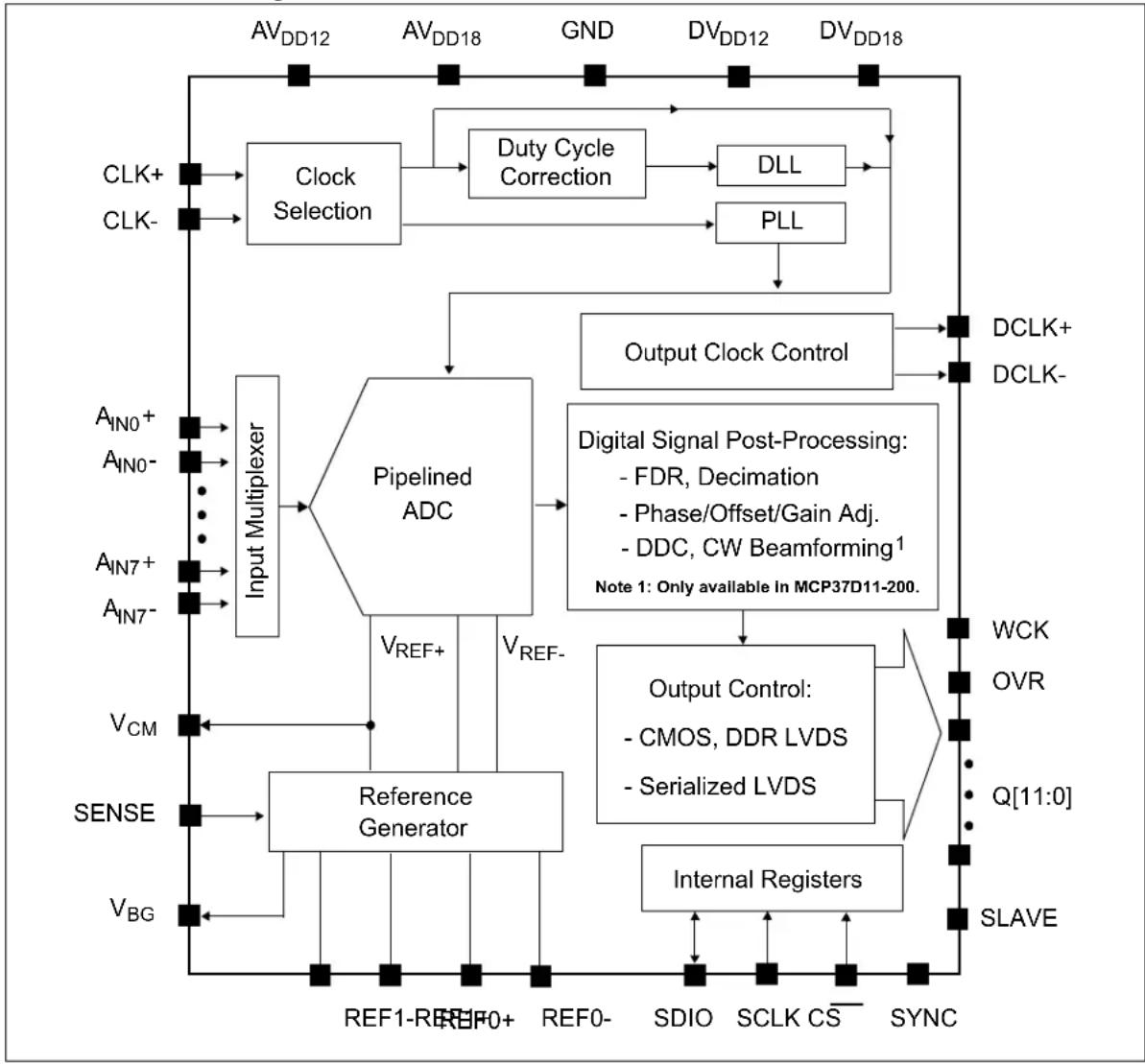
Functional Block Diagram
flowchart
graph TD
    A["Clock Selection"] --> B["Duty Cycle Correction"]
    B --> C["DLL"]
    C --> D["PLL"]
    D --> E["Output Clock Control"]
    E --> F["DCLK+"]
    E --> G["DCLK-"]
    H["Input Multiplexer"] --> I["Pipelined ADC"]
    I --> J["Digital Signal Post-Processing: FDR, Decimation; Phase/Offset/Gain Adj.; DDC, CW Beamforming¹"]
    J --> K["Output Control: CMOS, DDR LVDS; Serialized LVDS"]
    K --> L["WCK"]
    K --> M["OVR"]
    K --> N["Q[11:0"]]
    O["Reference Generator"] --> P["Input Multiplexer"]
    P --> I
    Q["VCM"] --> R["Input Multiplexer"]
    R --> I
    S["SENSE"] --> T["Input Multiplexer"]
    T --> I
    U["V_BG"] --> V["Input Multiplexer"]
    V --> I
    W["REF1-REF0+"] --> X["REF1-REF0-"]
    X --> Y["REF0-"]
    Y --> Z["SDIO"]
    Z --> AA["SCLK CS"]
    AA --> AB["SYNC"]
    AC["DV_DD12"] --> AD["DCLK+"]
    AE["DV_DD18"] --> AF["DCLK-"]
    AG["CLK+"] --> AH["Clock Selection"]
    AH --> AI["Duty Cycle Correction"]
    AI --> AJ["DLL"]
    AJ --> AK["PLL"]
    AK --> AL["Output Clock Control"]
    AL --> AM["DCLK+"]
    AL --> AN["DCLK-"]
    AO["VREF+"] --> AP["Reference Generator"]
    AP --> AQ["V_REF-"]
    AQ --> AR["Input Multiplexer"]
    AR --> AS["Pipelined ADC"]
    AS --> AT["Digital Signal Post-Processing: FDR, Decimation; Phase/Offset/Gain Adj.; DDC, CW Beamforming¹"]
    AT --> AU["Output Control: CMOS, DDR LVDS; Serialized LVDS"]
    AU --> AV["SLAVE"]
    AW["V_BG"] --> AX["Reference Generator"]
    AX --> AY["V_REF-"]
    AY --> AZ["Input Multiplexer"]
    AZ --> BA["Pipelined ADC"]
    BA --> BB["V_REF+"]
    BB --> BC["V_REF-"]
    BC --> BD["Internal Registers"]
Description
The MCP37211-200 is Microchip's baseline 12-bit 200 Msps pipelined ADC, featuring built-in high-order digital decimation filters, noise-shaping requantizer, gain and offset adjustment per channel and fractional delay recovery.
The MCP37D11-200 device features digital down-conversion and CW beamforming capability, in addition to the features offered by the MCP37211-200.
All devices feature harmonic distortion correction and DAC noise cancellation that enable high-performance specifications with SNR of 71.3 dBFS (typical) and SFDR of 90 dBc (typical).
These A/D converters exhibit industry-leading low-power performance with only 468 mW operation while using the LVDS interface at 200 Msps. This superior low-power operation coupled with high dynamic performance makes these devices ideal for various high-performance, high-speed data acquisition systems, including communications equipment, radar and portable instrumentation.
In single or dual-channel mode, the Noise-Shaping Requantizer (NSR) feature can allow the ADC to improve SNR beyond a conventional 11- or 12-bit ADC. The NSR reshapes the quantization noise, such that most of the noise power is pushed outside the frequency of interest. As a result, SNR is improved significantly within a selected frequency band of interest while SFDR is not affected.
The digital down-conversion option in the MCP37D10-200 can be utilized with the decimation and quadrature output (I and Q data) option, and offers great flexibility in various digital communication system designs, including cellular base-stations and narrow-band communication systems.
The output decimation filter option improves SNR performance up to 73.7 dBFS. The digital down-conversion option, in conjunction with the decimation and quadrature output options, offers great flexibility in digital communication system design, including cellular base-stations and narrow-band communications.
These devices can have up to eight differential input channels through an input MUX. The sampling rate is up to 200 Msps when a single channel is used, or 25 Msps per channel when all eight input channels are used.
In dual or octal-channel mode, the Fractional Delay Recovery (FDR) feature digitally corrects the difference in sampling instance between different channels, so that all inputs appear to have been sampled at the same time.
AutoSync mode offers a great design flexibility when multiple devices are used in applications. It allows multiple devices to sample input synchronously at the same clock.
The differential full-scale analog input range is programmable up to 2.975 V _P-P . The ADC output data can be coded in two's complement or offset binary representation, with or without the data randomizer option. The output data is available as full-rate CMOS or Double-Data-Rate (DDR) LVDS.
These devices also include various features designed to maximize flexibility in the user's applications and minimize system cost, such as a programmable PLL clock, output data rate control and phase alignment and programmable digital pattern generation. The device's operational modes and feature sets are configured by setting up the user-programmable registers.
The device is available in Pb-free TFBGA-121 and VTLA-124 packages. The device with a TFBGA-121 package is AEC-Q100 qualified for automotive applications and operates over the extended temperature range of -40^ to +125^ .
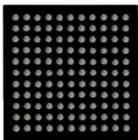
Package Types
Bottom View
natural_image
Grid of uniform gray dots on a black background, no text or symbols presentDimension: 8mm× 8mm× 1.08mm
Ball Pitch: 0.65 mm
Ball Diameter: 0.4 mm
(a) TFBGA-121 Package (AEC-Q100 Qualified).
Bottom View
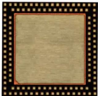
natural_image
Decorative square frame with black border and gold dots, no text or symbols presentDimension: 9mm× 9mm× 0.9mm
Note 1: Contact Microchip Technology Inc. for the VTLA-124 package availability.
(b) VTLA-124 Package ^1 .
NOTES:
1.0 PACKAGE PIN CONFIGURATIONS AND FUNCTION DESCRIPTIONS
Top View
(Not to Scale)
| 1 | 2 | 3 | 4 | 5 | 6 | 7 | 8 | 9 | 10 | 11 | |
| A | SDIO V | CM | REF1+ | REF1- | REF2G | REF0- A | GND | GND | IN4- | AIN2+ | |
| B | SCLK | CS | GND | GND | SENSE | AVDD12 | AVDD12 | AVDD18 | AVDD18 | AIN4+ | AIN2- |
| C | WCK/OVR-(WCK) | WCK/OVR+(OVR) | GND | GND | AVDD12 | AVDD12 | AVDD12 | GND | GND | AIN6- | AIN0+ |
| D | Q10/Q5- | Q11/Q5+ | GND | GND | AVDD12 | AVDD12 | AVDD12 | GND | GND | AIN6+ | AIN0- |
| E | Q8/Q4- | Q9/Q4+ | GND | GND | AVDD12 | AVDD12 | AVDD12 | GND | GND | AIN5+ | AIN1+ |
| F | Q6/Q3- | Q7/Q3+ | DVDD18 | DVDD18 | AVDD12 | AVDD12 | AVDD12 | GND | GND | AIN5- | AIN1- |
| G | Q4/Q2- | Q5/Q2+ | DVDD18 | DVDD18 | GND | GND | AVDD12 | AVDD12 | GND | AIN7- | AIN3+ |
| H | Q2/Q1- | Q3/Q1+ | DVDD12 | DVDD12 | GND | GND | GND | GND | GND | AIN7+ | AIN3- |
| J | Q0/Q0- | Q1/Q0+ | DVDD12 | DVDD12 | GNDGN | GND | GND | GND | VCMIN+ | VCMIN- | |
| K | TP | TP | TP | DCLK- | CAL | GND | SLAVE | ADR0 | ADR1 | GND | GND |
| L | TP | TP | TP | DCLK+ | RESET | SYNC | GND | CLK+ | CLK- | GND | AVDD18 |

Analog
Digital
All others: Supply Voltage
Notes:
• Die dimension: 8 mm x 8 mm x 1.08 mm.
- Ball dimension: (a) Ball Pitch = 0.65 mm, (b) Ball Diameter = 0.4 mm.
- Flip-chip solder ball composition: Sn with Ag 1.8%.
- Solder sphere composition: SAC-405 (Sn/Au 4%/Cu 0.5%).
FIGURE 1-1: TFBGA-121 Package. See Table 1-1 for the pin descriptions. Decoupling capacitors for reference pins and V_BG are embedded in the package. Leave TP pins floating always.
TABLE 1-1: PIN FUNCTION TABLE FOR TFBGA-121
| Ball No. | Name I/O Type | Description | ||
| A1 SD | O Digital Input/Output | SPI data input/output | ||
| A2 | V_CM | Analog Output | Common-mode output voltage (900 mV) for analog input signal Connect a decoupling capacitor ( 0.1 F ) ^(1) | |
| A3 REF1+ Differential reference voltage 1 (+/-). Decoupling capacitors are embedded in the TFBGA package. Leave these pins floating. | ||||
| A4 REF1- | ||||
| A5 | V_BG | |||
| A6 REF0+ Differential reference 0 (+/-) voltage. Decoupling capacitors are embedded in the TFBGA package. Leave these pins floating. | ||||
| A7 REF0- | ||||
| A8 GND Supply Common ground for analog and digital sections | ||||
| A9 | ||||
| A10 | A_IN4- | Analog Input | Channel 4 differential analog input (-) | |
| A11 A | IN2+ | Channel 2 differential analog input (+) | ||
| B1 | SCLK Digital Input SPI serial clock input | |||
| B2 | SPI Chip Select input | |||
| B3 GND Supply Common ground for analog and digital sections | ||||
| B4 | ||||
| B5 | SENSE | Analog Input | Analog input range selection. See Table 4-2 for SENSE voltage settings. | |
| B6 | AV_DD12 | Supply | Supply voltage input (1.2V) for analog section | |
| B7 | ||||
| B8 | AV_DD18 | Supply voltage input (1.8V) for analog section | ||
| B9 | ||||
| B10 | A_IN4+ | Analog Input | Channel 4 differential analog input (+) | |
| B11 | A_IN2- | Channel 2 differential analog input (-) | ||
| C1 | WCK/OVR-(WCK) | Digital Output | WCK: Word clock sync digital outputOVR: Input overrange indication digital output ^(2) | |
| C2 | WCK/OVR+(OVR) | |||
| C3 | GND | Supply | Common ground for analog and digital sections | |
| C4 | ||||
| C5 | AV_DD12 | Supply voltage input (1.2V) for analog section | ||
| C6 | ||||
| C7 | ||||
| C8 | GND | Common ground pin for analog and digital sections | ||
| C9 | ||||
| C10 | A_IN6- | Analog Input | Channel 6 differential analog input (-) | |
| C11 A | IN0+ | Channel 0 differential analog input (+) | ||
| D1 Q10/Q5- Digital | Output | Digital data output ^(3) CMOS = Q10DDR LVDS = Q5- | ||
| D2 | Q11/Q5+ | Digital data output ^(3) CMOS = Q11DDR LVDS = Q5+ | ||
| D3 | GND | Supply | Common ground for analog and digital sections | |
| D4 | ||||
| Ball No. | Name | I/O Type | Description | |
| D5 AV | DD12 | Supply Supply voltage input (1.2V) for analog section | ||
| D6 | ||||
| D7 | ||||
| D8 GND Common ground for analog and digital sections | ||||
| D9 | ||||
| D10 A | IN6+ | Analog Input | Channel 6 differential analog input (+) | |
| D11 A | IN0- | Channel 0 differential analog input (-) | ||
| E1 Q8/Q4- Digital | Output | Digital data output(3)CMOS = Q8DDR LVDS = Q4- | ||
| E2 Q9/Q4+ Digital data output | (3)CMOS = Q9DDR LVDS = Q4+ | |||
| E3 GND Supply common ground for analog and digital sections | ||||
| E4 | ||||
| E5 AV | DD12 | Supply voltage input (1.2V) for analog section | ||
| E6 | ||||
| E7 | ||||
| E8 GND Common ground for analog and digital sections | ||||
| E9 | ||||
| E10 A | IN5+ | Analog Input | Channel 5 differential analog input (+) | |
| E11 | AIN1+ | Channel 1 differential analog input (+) | ||
| F1 Q6/Q3- Digital | Output | Digital data output(3)CMOS = Q6DDR LVDS = Q3- | ||
| F2 Q7/Q3+ Digital data output | (3)CMOS = Q7DDR LVDS = Q3+ | |||
| F3 DV | DD18 | Supply Supply voltage input (1.8V) for digital section. All digital input pins are driven by the same DVDDD18potential. | ||
| F4 | ||||
| F5 AV | DD12 | Supply voltage input (1.2V) for analog section | ||
| F6 | ||||
| F7 | ||||
| F8 GND Common ground for analog and digital sections | ||||
| F9 | ||||
| F10 A | IN5- | Analog Input | Channel 5 differential analog input (-) | |
| F11 | AIN1- | Channel 1 differential analog input (-) | ||
| G1 Q4/Q2- Digital | Output | Digital data output(3)CMOS = Q4DDR LVDS = Q2- | ||
| G2 | Q5/Q2+ D | digital data output | (3)CMOS = Q5DDR LVDS = Q2+ | |
| G3 DV | DD18 | Supply Supply voltage input (1.8V) for digital sectionAll digital input pins are driven by the same DVDDD18potential | ||
| G4 | ||||
| G5 | GND Common ground for analog and digital sections | |||
| G6 | ||||
| G7 AV | DD12 | Supply Sup- ground for anal- | Supply voltage input (1.2V) for analog section | |
| G8 | ||||
| G9 GND Common ground and digital sections | ||||
| G10 A | IN7- | Analog Input | Channel 7 differential analog input (-) | |
| G11 A | IN3+ | Channel 3 differential analog input (+) | ||
| H1 Q2/Q1- Digital | Output data output | Digital data output^(3) CMOS = Q2DDR LVDS = Q1- | ||
| H2 Q3/Q1+ Digital | (3)CMOS = Q3DDR LVDS = Q1+ | |||
| H3 DV | DD12 | Supply Sup- ground for anal- | Supply voltage input (1.2V) for digital section | |
| H4 | ||||
| H5 GND Common ground and digital sections | ||||
| H6 | ||||
| H7 | ||||
| H8 | ||||
| H9 | ||||
| H10 A | IN7+ | Analog Input | Channel 7 differential analog input (+) | |
| H11 | A_IN3- | Channel 3 differential analog input (-) | ||
| J1 | Q0/Q0-Digital Output data output | Digital data output^(3) CMOS = Q0DDR LVDS = Q0- | ||
| J2 Q1/Q0+ Digital | (3)CMOS = Q1DDR LVDS = Q0+ | |||
| J3 DV | DD12 | Supply common ground for analog and digital sections | DC supply voltage input pin for digital section (1.2V) | |
| J4 | ||||
| J5 | GND Common ground for analog and digital sections | |||
| J6 | ||||
| J7 | ||||
| J8 | ||||
| J9 | ||||
| J10 | V_CMIN+ | Analog Input | Common-mode voltage input for auto-calibration(4)These two pins should be tied together and connected to V_CM voltage. | |
| J11 | V_CMIN- | |||
| K1 | TP | Digital Output | Output test pints. Leave these pins floating always(8) | |
| K2 | ||||
| K3 | ||||
| K4 | DCLK- | LVDS: Differential digital clock output (-)CMOS: Not used (leave floating) | ||
| K5 | CAL | Digital Output | Calibration status flag digital output^(5) High: Calibration is completeLow: Calibration is not complete | |
| K6 | GND | Supply | Common ground pin for analog and digital sections | |
| K7 | SLAVE | Digital Input | Slave or Master selection pin in AutoSync^(10) . If not used, tie to GND. | |
| K8 | ADR0 | SPI address selection pin (A0 bit). Tie to GND or DVDD18(6) | ||
| K9 | ADR1 | SPI address selection pin (A1 bit). Tie to GND or DVDD18(6) | ||
| K10 GND Supply Common ground for analog and digital sections | ||||
| K11 | ||||
| L1 TP | Digital Output | Output test pints. Leave these pins floating always (8) | ||
| L2 | ||||
| L3 | ||||
| L4 | DCLK- | LVDS: Differential digital clock output (+)CMOS: Digital clock output (7) | ||
| L5 | Digital Input | Reset control input:High: Normal operating modeLow: Reset mode(9) | ||
| L6 | SYNC | Digital Input/Output | Digital synchronization pin for AutoSync.(10)If not used, leave it floating. | |
| L7 | GND Supply Common ground for analog and digital sections | |||
| L8 | CLK+ | Analog Input | Differential clock input (+) | |
| L9 | CLK- | Differential clock input (-) | ||
| L10 | GND Supply Common ground for analog and digital sections | |||
| L11 | AV_DD18 | Analog Input | Supply voltage input (1.8V) for analog section | |
Notes:
- When the V_CM output is used for the common-mode voltage of analog inputs (i.e. by connecting to the center-tap of a balun), the V_CM pin should be decoupled with a 0.1 F capacitor, and should be directly tied to the V_CMIN+ and V_CMIN- pins.
- CMOS output mode: WCK/OVR- is WCK and WCK/OVR+ is OVR.
DDR LVDS output mode: The rising edge of DCLK+ is WCK and the falling edge is OVR.
OVR: OVR will be held "High" when analog input overrange is detected. Digital signal post-processing will cause OVR to assert early relative to the output data. See Figure 2-2 for LVDS timing of these bits.
WCK: WCK is normally “Low”. WCK is “High” while data from the first channel is sent out. In single-channel mode, WCK stays “High” except when in I/Q output mode. See Section 4.12.4 “Word Clock (WCK)” for further WCK description.
- DDR LVDS: Two data bits are multiplexed onto each differential output pair. The output pins shown here are for the "Even bit first", which is the default setting of OUTPUT_MODE<1:0> in Address 0x62 (Register 5-20). The even data bits (Q0, Q2, Q4, Q6, Q8, Q10) appear when DCLK+ is "High". The odd data bits (Q1, Q3, Q5, Q7, Q9, Q11) appear when DCLK+ is "Low". See Addresses 0x65 (Register 5-23) and 0x68 (Register 5-26) for output polarity control. See Figure 2-2 for LVDS output timing diagram.
- V_CMIN is used for Auto-Calibration only. V_CMIN+ and V_CMIN- should be tied together always. There should be no voltage difference between the two pins. Typically both V_CMIN+ and V_CMIN- are tied to the V_CM output pin together, but they can be tied to another common-mode voltage if external V_CM is used. This pin has High Z input in Shutdown, Standby and Reset modes.
- CAL pin stays "Low" at power-up until the first power-up calibration is completed. When the first calibration has completed, this pin has "High" output. It stays "High" until the internal calibration is restarted by hardware or a soft reset command. In Reset mode, this pin is "Low". In Standby and Shutdown modes, this pin will maintain the prior condition.
- If the SPI address is dynamically controlled, the Address pin must be held constant while is "Low".
- The phase of DCLK relative to the data output bits may be adjusted depending on the operating mode. This is controlled differently depending on the configuration of the digital signal post-processing, PLL and/or DLL. Also see Addresses 0x52, 0x64 and 0x6D (Registers 5-7, 5-22 and 5-28) for more details.
- Do not tie to ground or supply.
- The device is in Reset mode while this pin stays "Low". On the rising edge of RESET, the device exits Reset mode, initializes all internal user registers to default values, and begins power-up calibration.
- a) SLAVE = "High": The device is selected as slave and the SYNC pin becomes input pin.
(b) SLAVE = "Low": The device is selected as master and the SYNC pin becomes output pin. In SLAVE/SYNC operation, master and slave devices are synchronized to the same clock.
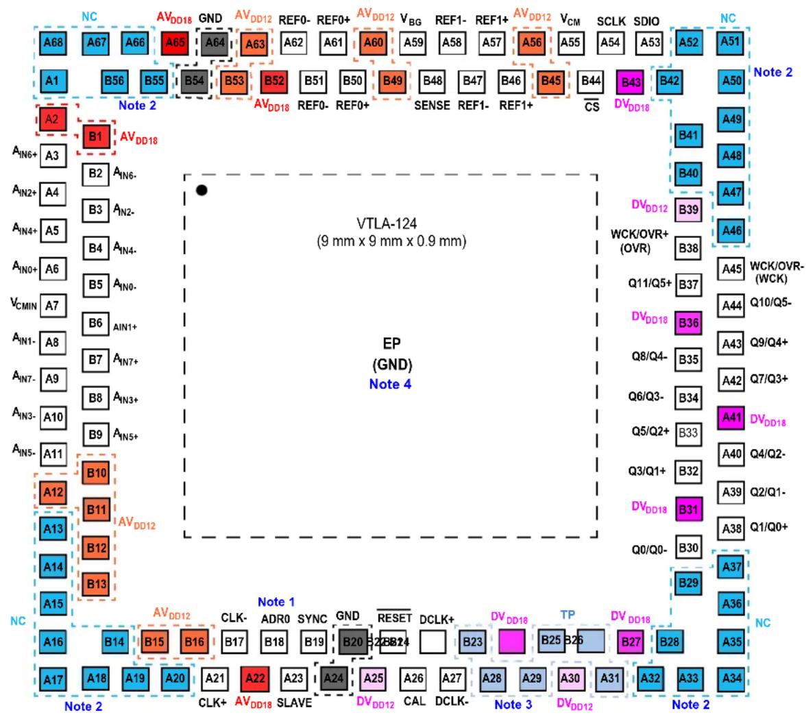
Top View
(Not to Scale)
flowchart
graph TD
    A["NC"] --> B["A68"]
    A --> C["A67"]
    A --> D["A66"]
    B --> E["A65"]
    C --> F["A64"]
    D --> G["A63"]
    E --> H["B56"]
    F --> I["B55"]
    G --> J["B54"]
    H --> K["B53"]
    I --> L["B52"]
    J --> M["B51"]
    K --> N["B50"]
    L --> O["B49"]
    M --> P["B48"]
    N --> Q["B47"]
    O --> R["B46"]
    P --> S["B45"]
    Q --> T["B44"]
    R --> U["B43"]
    S --> V["B42"]
    T --> W["B41"]
    U --> X["B40"]
    V --> Y["B39"]
    W --> Z["WCK/OVR+ (OVR)"]
    X --> AA["WCK/OVR- (WCK)"]
    Y --> AB["Q11/Q5+"]
    Z --> AC["Q10/Q5-"]
    AA --> AD["Q9/Q4+"]
    AB --> AE["Q8/Q4-"]
    AC --> AF["Q7/Q3+"]
    AD --> AG["Q6/Q3-"]
    AE --> AH["Q5/Q2+"]
    AF --> AI["Q4/Q2-"]
    AG --> AJ["Q3/Q1+"]
    AH --> AK["Q2/Q1-"]
    AI --> AL["Q1/Q0+"]
    AJ --> AM["Q0/Q0-"]
    AK --> AN["Q0/Q0-"]
    AL --> AO["Q0/Q0-"]
    AM --> AP["Q0/Q0-"]
    AN --> AQ["Q0/Q0-"]
    AP --> AR["Q0/Q0-"]
    AQ --> AS["Q0/Q0-"]

    subgraph "VTLA-124 (9 mm x 9 mm x 0.9 mm)"
        B -->|Note 2| B
        C -->|Note 2| C
        D -->|Note 2| D
        E -->|Note 2| E
        F -->|Note 2| F
        G -->|Note 2| G
        H -->|Note 2| H
        I -->|Note 2| I
        J -->|Note 2| J
        K -->|Note 2| K
        L -->|Note 2| L
        M -->|Note 2| M
        N -->|Note 2| N
        O -->|Note 2| O
        P -->|Note 2| P
        Q -->|Note 2| Q
        R -->|Note 2| R
        S -->|Note 2| S
        T -->|Note 2| T
        U -->|Note 2| U
        V -->|Note 2| V
        W -->|Note 2| W
        X -->|Note 2| X
        Y -->|Note 2| Y
        Z -->|Note 2| Z
        AA -->|Note 2| AA
        AB -->|Note 2| AB
        AC -->|Note 2| AC
        AD -->|Note 2| AD
        AE -->|Note 2| AE
        AF -->|Note 2| AF
        AG -->|Note 2| AG
        AH -->|Note 2| AH
        AI -->|Note 2| AI
        AJ -->|Note 2| AJ
        AK -->|Note 2| AK
        AL -->|Note 2| AL
        AM -->|Note 2| AM
        AN -->|Note 2| AN
        AO -->|Note 2| AO
        AP -->|Note 2| AP
        AQ -->|Note 2| AQ
        AR -->|Note 2| AR
        AS -->|Note 2| AS
        AT -->|Note 2| AT
        AU -->|Note 2| AU
        AV -->|Note 2| AV

    %% Note 4 is highlighted in a box.
    note right of AP: EP (GND)
    note left of AP: Note 4
Note 1: Tie to GND or DV _DD18 . ADR1 is internally bonded to GND.
2: NC – Not connected pins. These pins can float or be tied to ground.
3: TP – Test pins. Leave these pins floating and do not tie to ground or supply.
4: Exposed pad (EP – back pad of the package) is the common ground (GND) for analog and digital supplies. Connect this pad to a clean ground reference on the PCB.
FIGURE 1-2: VTLA-124 Package. See Table 1-2 for the pin descriptions. Decoupling capacitors for reference pins and V_BG are embedded in the package. Leave TP pins floating always.
TABLE 1-2: PIN FUNCTION TABLE FOR VTLA-124
| Pin No. Name | I/O Type Description | ||
| Power Supply Pins | |||
| A2, A22, A65, B1, B52 | AV_DD18 | Supply Sup- | Supply voltage input (1.8V) for analog section |
| A12, A56, A60, A63, B10, B11, B12, B13, B15, B16, B45, B49, B53 | AV_DD12 | Supply voltage input (1.2V) for analog section | |
| A25, A30, B39 | DV_DD12 | Supply voltage input (1.2V) for digital section | |
| A41, B24, B27, B31, B36, B43 | DV_DD18 | Supply voltage input (1.8V) for digital section and all digital I/O | |
| EP | GND Exposed pad: Com | Common ground pin for digital and analog sections | |
| ADC Analog Input Pins | |||
| A3 | A_IN6+ | Analog Input | Channel 6 differential analog input (+) |
| B2 | A_IN6- | Channel 6 differential analog input (-) | |
| A4 | A_IN2+ | Channel 2 differential analog input (+) | |
| B3 | A_IN2- | Channel 2 differential analog input (-) | |
| A5 | A_IN4+ | Channel 4 differential analog input (+) | |
| B4 | A_IN4- | Channel 4 differential analog input (-) | |
| A6 | A_IN0+ | Channel 0 differential analog input (+) | |
| B5 | A_IN0- | Channel 0 differential analog input (-) | |
| B6 | A_IN1+ | Channel 1 differential analog input (+) | |
| A8 | A_IN1- | Channel 1 differential analog input (-) | |
| B7 | A_IN7+ | Channel 7 differential analog input (+) | |
| A9 | A_IN7- | Channel 7 differential analog input (-) | |
| B8 | A_IN3+ | Channel 3 differential analog input (+) | |
| A10 | A_IN3- | Channel 3 differential analog input (-) | |
| B9 | A_IN5+ | Channel 5 differential analog input (+) | |
| A11 | A_IN5- | Channel 5 differential analog input (-) | |
| A21 | CLK+ Differential clock input (+) | ||
| B17 | CLK-Differential clock input (-) | ||
| Reference Pins(1) | |||
| A57, B46 | REF1+ Analog Output | Differential reference 1 (+) voltage | |
| A58, B47 | REF1-Differential reference 1 (-) voltage | ||
| A61, B50 | REF0+ Differential reference 0 (+) voltage | ||
| A62, B51 | REF0-Differential reference 0 (-) voltage | ||
| SENSE, Bandgap and Common-Mode Voltage Pins | |||
| B48 | SENSE | Analog Input | Analog input full-scale range selection. See Table 4-2 for SENSE voltage settings. |
| A59 | V_BG | Analog Output | Internal bandgap output voltage Connect a decoupling capacitor (2.2 μF) |
| A7 | V_CMIN | Analog Input | Common-mode voltage input for auto-calibration Connect V_CM voltage(2) |
| A55 | V_CM | Common-mode output voltage (900 mV) for analog input signal Connect a decoupling capacitor (0.1 μF)(3) | |
| Pin No. | Name | I/O Type | Description |
| Digital I/O Pins | |||
| B18 | ADR0 Digital Input SPI | Address selection pin (A0 bit). Tie to GND or DV DD18.(4) | |
| A23 | SLAVE Slave or Master | selection pin in AutoSync (11)If not used, tie to GND. | |
| B19 | SYNC Digital Input/Output | Digital synchronization pin for AutoSync^(11) If not used, leave it floating. | |
| B21 | RESET Digital Input | Reset control input:High: Normal operating modeLow: Reset mode(5) | |
| A26 | CAL Digital Output | Calibration status flag digital output:High: Calibration is completeLow: Calibration is not complete(5) | |
| B22 | DCLK+ LVDS: Differential | digital clock output (+)CMOS: Digital clock output(7) | |
| A27 | DCLK- LVDS: Differential | digital clock output (-)CMOS: Unused (leave floating) | |
| ADC Output Pins^(8) | |||
| B30 | Q0/Q0- Digital Output | Digital data output: CMOS = Q0, DDR LVDS = Q0- | |
| A38 | Q1/Q0+ | ||
| A39 | Q2/Q1- | Digital data output: CMOS = Q1, DDR LVDS = Q0+ | |
| B32 | Q3/Q1+ | Digital data output: CMOS = Q2, DDR LVDS = Q1- | |
| A40 | Q4/Q2- | Digital data output: CMOS = Q3, DDR LVDS = Q1+ | |
| B33 | Q5/Q2+ | Digital data output: CMOS = Q4, DDR LVDS = Q2- | |
| B34 | Q6/Q3- | Digital data output: CMOS = Q5, DDR LVDS = Q2+ | |
| A42 | Q7/Q3+ | Digital data output: CMOS = Q6, DDR LVDS = Q3- | |
| B35 | Q8/Q4- | Digital data output: CMOS = Q7, DDR LVDS = Q3+ | |
| A43 | Q9/Q4+ | Digital data output: CMOS = Q8, DDR LVDS = Q4- | |
| A44 | Q10/Q5- | Digital data output: CMOS = Q9, DDR LVDS = Q4+ | |
| B37 | Q11/Q5+ | Digital data output: CMOS = Q10, DDR LVDS = Q5- | |
| B38 | WCK/OVR+(OVR) | Digital data output: CMOS = Q11, DDR LVDS = Q5+ | |
| A45 | WCK/OVR-(WCK) | WCK: Word clock sync digital outputOVR: Input over-range indication digital output^(10) | |
| SPI Interface Pins | |||
| A53 | SDIO Digital Input/Output | SPI data input/output | |
| A54 | SCLK Digital Input | SPI serial clock input | |
| B44 | SPI Chip Select input | ||
| Not Connected Pins | |||
| A1, A13 - A20, A32 - A37, A46 - A52, A66 - A68, B14, B28, B29, B40, B41, B42, B55, B56 | NC | These pins can be tied to ground or left floating. | |
| Pins that need to be grounded | |||
| A24, A64, B20, B54 | GND | These pins are not supply pins, but need to be tied to ground. | |
| Output Test Pins | |||
| A28, A29, A31, B23, B25, B26 | TP | Digital Output | Output test pins. Do not use. Always Leave these pins floating^(9) |
Notes:
- These pins are for the internal reference voltage outputs. They should not be driven. External decoupling circuits are required. See Section 4.5.3, "Decoupling Circuits for Internal Voltage Reference and Bandgap Output" for details.
- V_CMIN is used for Auto-Calibration only. V_CMIN^+ and V_CMIN^- should be tied together always. There should be no voltage difference between the two pins. Typically both V_CMIN^+ and V_CMIN^- are tied to the V_CM output pin together, but they can be tied to another common-mode voltage if external V_CM is used. This pin has High Z input in Shutdown, Standby and Reset modes.
- When the V_CM output is used for the common-mode voltage of analog inputs (i.e. by connecting to the center-tap of a balun), the V_CM pin should be decoupled with a 0.1 F capacitor, and should be directly tied to the V_CMIN^+ and V_CMIN^- pins.
- ADR1 (for A1 bit) is internally bonded to GND ('0'). If ADR0 is dynamically controlled, ADR0 must be held constant while is "Low".
- The device is in Reset mode while this pin stays "Low". On the rising edge of RESET, the device exits Reset mode, initializes all internal user registers to default values, and begins power-up calibration.
- CAL pin stays "Low" at power-up until the first power-up calibration is completed. When the first calibration has completed, this pin has "High" output. It stays "High" until the internal calibration is restarted by hardware or a soft reset command. In Reset mode, this pin is "Low". In Standby and Shutdown modes, this pin will maintain the prior condition.
- The phase of DCLK relative to the data output bits may be adjusted depending on the operating mode. This is controlled differently depending on the configuration of the digital signal post-processing, PLL and/or DLL. Also see Addresses 0x52, 0x64 and 0x6D (Registers 5-7, 5-22 and 5-28) for more details.
- DDR LVDS: Two data bits are multiplexed onto each differential output pair. The output pins shown here are for the "Even bit first", which is the default setting of OUTPUT_MODE<1:0> in Address 0x62 (Register 5-20). The even data bits (Q0, Q2, Q4, Q6, Q8, Q10) appear when DCLK+ is "High". The odd data bits (Q1, Q3, Q5, Q7, Q9, Q11) appear when DCLK+ is "Low". See Addresses 0x65 (Register 5-23) and 0x68 (Register 5-26) for output polarity control. See Figure 2-2 for LVDS output timing diagram.
- Do not tie to ground or supply.
- CMOS output mode: WCK/OVR- is WCK and WCK/OVR+ is OVR.
DDR LVDS output mode: The rising edge of DCLK+ is WCK and the falling edge is OVR.
OVR: OVR will be held "High" when analog input overrange is detected. Digital signal post-processing will cause OVR to assert early relative to the output data. See Figure 2-2 for LVDS timing of these bits.
WCK: WCK is normally "Low". WCK is "High" while data from the first channel is sent out. In single-channel mode, WCK stays "High" except when in I/Q output mode. See Section 4.12.4 "Word Clock (WCK)" for further WCK description. - (a) SLAVE = "High": The device is selected as slave and the SYNC pin becomes input pin. (b) SLAVE = "Low": The device is selected as master and the SYNC pin becomes output pin. In SLAVE/SYNC operation, master and slave devices are synchronized to the same clock.
NOTES:
2.0 ELECTRICAL SPECIFICATIONS
2.1 Absolute Maximum Ratings†
| Analog and Digital Supply Voltage (AVDD12, DVDD12) | -0.3V to 1.32V |
| Analog and Digital Supply Voltage (AVDD18, DVDD18) | -0.3V to 1.98V |
| All Inputs and Outputs with respect to GND | -0.3V to AVDD18+0.3V |
| Differential Input Voltage | |AVDD18-GND| |
| Current at Input Pins | ±2 mA |
| Current at Output and Supply Pins | ±250 mA |
| Storage Temperature | -65°C to +150°C |
| Ambient Temperature with Power Applied (TA) | -55°C to +125°C |
| Maximum Junction Temperature (TJ) | +150°C |
| ESD Protection | 2kV HBM on all pins, CDM: 750V on corner pins and 250V on all other pins |
| Solder Reflow Profile | See Microchip Application Note AN233 (DS00233) |
Notice†: Stresses above those listed under “Maximum Ratings” may cause permanent damage to the device. This is a stress rating only and functional operation of the device at those or any other conditions above those indicated in the operational listings of this specification is not implied. Exposure to maximum rating conditions for extended periods may affect device reliability.
2.2 Electrical Specifications
TABLE 2-1: ELECTRICAL CHARACTERISTICS
| Electrical Specifications: Unless otherwise specified, all parameters apply for T_A = -40°C to +125°C, AV _DD18 = DV _DD18 = 1.8 V, AV _DD12 = DV _DD12 = 1.2V, GND = 0V, SENSE = AV _DD12 , Single-channel mode, Differential Analog Input (A _IN ) = Sine wave with amplitude of -1 dBFS, f _IN = 70 MHz, Clock Input = 200 MHz, f _S = 200 Msps (ADC Core), PLL and decimation filters are disabled, Output load: CMOS data pin = 10 pF, LVDS = 100Ω termination, LVDS driver current setting = 3.5 mA, +25°C is applied for typical value. | ||||||
| Parameters | Sym. | Min. | Typ. | Max. | Units | Conditions |
| Power Supply Requirements | ||||||
| Analog Supply Voltage | AV _DD18 | 1.71 | 1.8 | 1.89 | V | |
| AV _DD12 | 1.14 | 1.2 | 1.26 | V | ||
| Digital Supply Voltage | DV _DD18 | 1.71 | 1.8 | 1.89 | V | Note 1 |
| DV _DD12 | 1.14 | 1.2 | 1.26 | V | ||
| Analog Supply Current During Conversion | ||||||
| At AV _DD18 Pin | I _DD\_A18 | — | 27 | 46 | mA | T_A = -40°C to +85°C T_A = -40°C to +125°C |
| — | 27 | 50 | ||||
| At AV _DD12 Pin | I _DD\_A12 | — | 185 | 252 | mA | T_A = -40°C to +85°C T_A = -40°C to +125°C |
| — | 185 | 300 | ||||
| Digital Supply Current | ||||||
| Digital Supply CurrentDuring Conversionat DV _DD12 Pin | I _DD\_D12 | — | 97 | 226 | mA | T_A = -40°C to +85°C T_A = -40°C to +125°C |
| — | 97 | 232 | ||||
| Digital I/O Current inCMOS Output Mode | I _DD\_D18 | — | 27 | — | mA | at DV _DD18 pinDCLK = 100 MHz |
| Digital I/O Current inLVDS Mode | I _DD\_D18 | Measured at DV _DD18 Pin | ||||
| — | 45 | 66 | mA | 3.5 mA mode | ||
| 33 | — | mA | 1.8 mA mode | |||
| 57 | 5.4 mA mode | |||||
| Supply Current during Power-Saving Modes | ||||||
| During Standby Mode | I _STANDBY\_AN | — | 84 | — | mA | Address 0x00<4:3> = 1,1(2) |
| I _STANDBY\_DIG | — | 36 | — | |||
| During Shutdown Mode | I _DD\_SHDN | — | 23 | — | mA | Address 0x00<7,0> = 1,1(3) |
| Electrical Specifications: Unless otherwise specified, all parameters apply for TA = -40°C to +125°C, AVDD18 = DVDD18 = 1.8V, AVDD12 = DVDD12 = 1.2V, GND = 0V, SENSE = AVDD12, Single-channel mode, Differential Analog Input (AIN) = Sine wave with amplitude of -1 dBFS, fIN = 70 MHz, Clock Input = 200 MHz, fs = 200 Msps (ADC Core), PLL and decimation filters are disabled, Output load: CMOS data pin = 10 pF, LVDS = 100Ω termination, LVDS driver current setting = 3.5 mA, +25°C is applied for typical value. | ||||||
| Parameters | Sym. | Min. | Typ. | Max. | Units | Conditions |
| PLL Circuit | ||||||
| PLL Circuit Current I | DD_PLL | -17 | mA PLL enabled. Included in | analog supply current specification. | ||
| Total Power Dissipation(4) | ||||||
| Power Dissipation During Conversion, Excluding Digital I/O | PDISS_ADC | -387 | -mW | |||
| Total Power Dissipation During Conversion with CMOS Output Mode | PDISS_CMOS | -436 | -mW f | S=200 Msps, DCLK=100 MHz | ||
| Total Power Dissipation During Conversion with LVDS Output Mode | PDISS_LVDS | - | 468-mW 3.5 mA mode | |||
| 446-1.8 mA mode | ||||||
| 490 | 5.4 mA mode | |||||
| During Standby Mode | PDISS_STANDBY | - | 144 | - | mW | Address 0x00<4:3> = 1, 1(2) |
| During Shutdown Mode | PDISS_SHDN | - | 27.6 | - | mW | Address 0x00<7,0> = 1, 1(3) |
| Power-on Reset (POR) Voltage | ||||||
| Threshold Voltage | VPOR | - | 800 | - | mV | Applicable to AVDD12 only (POR tracks AVDD12) |
| Hysteresis | VPOR_HYST | - | 40 | - | mV | |
| Power-on Reset Stabilization Time | TPOR-S | - | 2^18 | - | Clocks | 2^18 sample clocks after Power-on Reset |
| SENSE Input(5,7) | ||||||
| SENSE Input Voltage | VSENSE | GND | - | AVDD12 | V | VSENSE selects reference |
| SENSE Pin Input Resistance | RIN_SENSE | - | 500 | - | Ω | To virtual ground at 0.55V. 400 mV < VSENSE < 800 mV |
| Current Sink into SENSE Pin | ISENSE | - | 4.5 | - | μA | SENSE = 1.2V |
| 636 | SENSE = 0.8V | |||||
| -2 | SENSE = 0V | |||||
| Reference and Common-Mode Voltages | ||||||
| Internal Reference Voltage (Selected by VSENSE) | VREF | - | 0.74 | - | V | VSENSE = GND |
| - | 1.49 | - | VSENSE = AVDD12 | |||
| - | 1.86 x VSENSE | - | 400 mV < VSENSE < 800 mV | |||
| Common-Mode Voltage Output | VCM | - | 0.9 | - | V | Available at VCM pin |
| Reference Voltage Output(7,8) | VREF1 | - | 0.4 | - | V | VSENSE = GND |
| - | 0.8 | - | VSENSE = AVDD12 | |||
| - | 0.4 - 0.8 | - | 400 mV < VSENSE < 800 mV | |||
| VREF0 | - | 0.7 | - | V | VSENSE = GND | |
| - | 1.4 | - | VSENSE = AVDD12 | |||
| - | 0.7 - 1.4 | - | 400 mV < VSENSE < 800 mV | |||
| Bandgap Voltage Output | VBG | - | 0.55 | - | V | Available at VBG pin |
| Electrical Specifications: Unless otherwise specified, all parameters apply for T_A = -40°C to +125°C, AV_DD18 = DV_DD18 = 1.8V, AV_DD12 = DV_DD12 = 1.2V, GND = 0V, SENSE = AV_DD12 , Single-channel mode, Differential Analog Input ( A_IN ) = Sine wave with amplitude of -1 dBFS, f_IN = 70 MHz, Clock Input = 200 MHz, f_S = 200 Msps (ADC Core), PLL and decimation filters are disabled, Output load: CMOS data pin = 10 pF, LVDS = 100Ω termination, LVDS driver current setting = 3.5 mA, +25°C is applied for typical value. | ||||||
| Parameters | Sym. | Min. | Typ. | Max. | Units | Conditions |
| Analog Inputs | ||||||
| Full-Scale Differential Analog Input Range ^(5,7) | A_FS | — 1.48 | 75 — V | P-P7 | V_SENSE = GND | |
| — | 2 | 9 | S_SENSE = AVDD42 | |||
| — 3.71 | 875 x V_SENSE | — | 400 mV < V_SENSE < 800 mV | |||
| Analog Input Bandwidth f | IN_3dB | — 500 | — | MHz A | IN= -3 dBFS | |
| Differential Input Capacitance | C_IN | 5 | 6 | 7 | pF | Note 5, Note 9 |
| Analog Input Channel Cross-Talk | XTALK | — | 100 | — | dBc | Note 10 |
| Analog Input Leakage Current ( A_IN +, A_IN - Pins) | I_LI\_AH | — | — | +1 | μA | V_IH = AV_DD12 |
| I_LI\_AL | -1 | — | — | μA | V_IL = GND | |
| ADC Conversion Rate ^(11) | ||||||
| Conversion Rate | f_S | 40 | — | 200 | Msps | Tested at 200 Msps |
| Clock Inputs (CLK+, CLK- ^(12) ) | ||||||
| Clock Input Frequency | f_CLK | — | — | 250 | MHz | Note 5 |
| Differential Input Voltage | V_CLK\_IN | 300 — | 800 | mV | P-P | Note 5 |
| Clock Jitter | CLK_JITTER | — 175 | — | f | SRMS | Note 5 |
| Clock Input Duty Cycle ^(5) | 49 | 50 | 51 | % | Duty cycle correction disabled | |
| 30 | 50 | 70 | % | Duty cycle correction enabled | ||
| Input Leakage Current at CLK Input Pin | I_LI\_CLKH | — | — | +180 | μA | V_IH = AV_DD12 |
| I_LI\_CLKL | -20-30 | — | — | μA | V_IL = GND T_A = -40°C to +85°CT_A= -40°C to +125°C | |
| Converter Accuracy ^(6) | ||||||
| ADC Resolution (with no missing code) | — | — | 12 | bits | ||
| Offset Error | — | ±0.31 | ±3.8 | LSb | ||
| Gain Error | G_ER | — | ±0.5 | — | % of FS | |
| Integral Nonlinearity | INL | — | ±0.125 | — | LSb | |
| Differential Nonlinearity | DNL | — | ±0.03 | — | LSb | |
| Analog Input Common-Mode Rejection Ratio | CMRR_DC | — | 70 | — | dB | DC measurement |
| Electrical Specifications: Unless otherwise specified, all parameters apply for TA = -40°C to +125°C, AVDD18 = DVDD18 = 1.8V, AVDD12 = DVDD12 = 1.2V, GND = 0V, SENSE = AVDD12, Single-channel mode, Differential Analog Input (AIN) = Sine wave with amplitude of -1 dBFS, fIN = 70 MHz, Clock Input = 200 MHz, fS = 200 Msps (ADC Core), PLL and decimation filters are disabled, Output load: CMOS data pin = 10 pF, LVDS = 100Ω termination, LVDS driver current setting = 3.5 mA, +25°C is applied for typical value. | ||||||
| Parameters | Sym. | Min. | Typ. | Max. | Units | Conditions |
| Dynamic Accuracy(6,15) | ||||||
| Spurious Free Dynamic Range | SFDR 78 | 90 — dBc f | IN= 15 MHz | |||
| 77 85 — dBc f | IN= 70 MHz | |||||
| Signal-to-Noise Ratio SNR | 70.63 71.33 — | dBFS f | IN= 15 MHz | |||
| SNR — 7 | 1.09 — dBFS f | IN= 70 MHz | ||||
| Effective Number of Bits (ENOB)(13) | ENOB | 11.44 | 11.56 | — | bits | fIN= 15 MHz |
| ENOB | — | 11.52 | — | bits | fIN= 70 MHz | |
| Total Harmonic Distortion (for all resolutions, first 13 harmonics) | THD 78 89 | — dBc f | IN= 15 MHz | |||
| 77 82 — dBc f | IN= 70 MHz | |||||
| Worst Second or Third Harmonic Distortion | HD2 or HD3 | — | 90 — dBc f | IN= 15 MHz | ||
| — | 83 | — | dBc | fIN= 70 MHz | ||
| Two-Tone Intermodulation Distortion f_IN_1 = 17.6 MHz, f_IN_2 = 20.6 MHz | IMD | — | 90.5 — dBc | AIN= -7 dBFS,with two input frequencies | ||
| Digital Logic Input and Output (Except LVDS Output) | ||||||
| Schmitt Trigger High-Level Input Voltage | V_IH | 0.7DVDD18 | — | DVDD18 | V | |
| Schmitt Trigger Low-Level Input Voltage | V_IL | GND | — 0.3 | DVDD18 | V | |
| Hysteresis of Schmitt Trigger Inputs(All Digital Inputs) | V_HYST | — | 0.05DVDD18 | — | V | |
| Low-Level Output Voltage | V_OL | — | — | 0.3 | V | IOL= -3 mA, all digital I/O pins |
| High-Level Output Voltage | V_OH | DVDD18-0.5 | 1.8 | — | V | IOL= +3 mA, all digital I/O pins |
| Digital Data Output (CMOS Mode) | ||||||
| Maximum External Load Capacitance | C_LOAD | — | 10 | — | pF | From output pin to GND |
| Internal I/O Capacitance | C_INT | — | 4 | — | pF | Note 5 |
| Digital Data Output (LVDS Mode)(5) | ||||||
| LVDS High-Level Differential Output Voltage | V_H\_LVDS | 200 | 300 | 400 | mV | 100Ω differential termination,LVDS bias = 3.5 mA |
| LVDS Low-Level Differential Output Voltage | V_L\_LVDS | -400 | -300 | -200 | mV | 100Ω differential termination,LVDS bias = 3.5 mA |
| LVDS Common-Mode Voltage | V_CM\_LVDS | 1 | 1.15 | 1.4 | V | |
| Output Capacitance | C_INT\_LVDS | — | 4 | — | pF | Internal capacitance from output pin to GND |
| Differential Load Resistance (LVDS) | R_LVDS | — | 100 | — | Ω | Across LVDS output pairs |
| Electrical Specifications: Unless otherwise specified, all parameters apply for T_A = -40°C to +125°C, AV_DD18 = DV_DD18 = 1.8V, AV_DD12 = DV_DD12 = 1.2V, GND = 0V, SENSE = AV_DD12 , Single-channel mode, Differential Analog Input ( A_IN ) = Sine wave with amplitude of -1 dBFS, f_IN = 70 MHz, Clock Input = 200 MHz, f_S = 200 Msps (ADC Core), PLL and decimation filters are disabled, Output load: CMOS data pin = 10 pF, LVDS = 100Ω termination, LVDS driver current setting = 3.5 mA, +25°C is applied for typical value. | ||||||
| Parameters | Sym. | Min. | Typ. | Max. | Units | Conditions |
| Input Leakage Current on Digital I/O Pins | ||||||
| Data Output Pins I | LI_DH | — | — | + | 1 | I_H = PVD_DD18 A V |
| I_LI\_DL | -1-1.2 | — | — | μA | V_IL =GND T_A = -40°C to +85°CT_A= -40°C to +125°C | |
| I/O Pins except Data Output Pins | I_LI\_DH | — | — | + | 6 | I_H = PVD_DD18 A V |
| I_LI\_DL | -35 — | — | μA | V | I_L =GND(14) | |
Notes:
- This 1.8V digital supply voltage is used for the digital I/O circuit, including SPI, CMOS and LVDS data output drivers.
- Standby Mode: Most of the internal circuits are turned off, except the internal reference, clock, bias circuits and SPI interface.
- Shutdown Mode: All circuits including reference and clock are turned off except the SPI interface.
- Power dissipation (typical) is calculated by using the following equation:
(a) During operation:
P_DISS = V_DD18 × (I_DD_A18 + I_DD_D18) + V_DD12 × (I_DD_A12 + I_DD_D12) , where I_DD_D18 is the digital I/O current for LVDS or CMOS output. V_DD18 = 1.8V and V_DD12 = 1.2V are used for typical value calculation.
(b) During Standby mode:
P_DISS_STANDBY = (I_STANDBY_AN + I_STANDBY_DIG) × 1.2V
(c) During Shutdown mode:
P_DISS_SHDN = I_DD_SHDN × 1.2V
- This parameter is ensured by design, but not 100% tested in production.
- This parameter is ensured by characterization, but not 100% tested in production.
- See Table 4-2 for details.
- Differential reference voltage output at REF1+/- and REF0+/- pins. V_REF1 = V_REF1^+ - V_REF1^- . V_REF0 = V_REF0^+ - V_REF0^- . These references should not be driven.
- Input capacitance refers to the effective capacitance between one differential input pin pair.
- Channel cross-talk is measured when A_IN = -1 dBFS at 12 MHz is applied on one channel while other channel(s) are terminated with 50Ω. See Figure 3-45 for details.
- The ADC core conversion rate. In multi-channel mode, the conversion rate of an individual channel is f_S/N , where N is the number of input channels used.
- See Figure 4-8 for the details of the clock input circuit.
- ENOB = (SINAD - 1.76)/6.02.
- This leakage current is due to the internal pull-up resistor.
- Dynamic performance is characterized with CH(n)_DIG_GAIN<7:0> = 0011-1000.
TABLE 2-2: TIMING REQUIREMENTS - LVDS AND CMOS OUTPUTS
| Electrical Specifications: Unless otherwise specified, all parameters apply for T_A = -40°C to +125°C, AV_DD18= DV_DD18= 1.8 V AV_DD12= DV_DD12= 1.2V, GND = 0V, SENSE = AV_DD12, Single-channel mode, Differential Analog Input (AIN) = Sine wave with amplitude of -1 dBFS, fIN= 70 MHz, Clock Input = 200 MHz, fs= 200 Msps (ADC Core), PLL and decimation filters are disabled, Output load: CMOS data pin = 10 pF, LVDS = 100Ω termination, LVDS driver current setting = 3.5 mA, +25°C is applied for typical value. | ||||||
| Parameters Sym. Min. Typ. Max. Units Conditions | ||||||
| Aperture Delay | t_A | — | 1 | — | ns | Note 1 |
| Out-of-Range Recovery Time | t_OVR | — | 1 | — | Clocks | Note 1 |
| Output Clock Duty Cycle | — | 50 | — | % | Note 1 | |
| Pipeline Latency | T_LATENCY | — | 28 | — | Clocks | Note 2, Note 4 |
| System Calibration(1) | ||||||
| Power-Up Calibration Time | T_PCAL | — | 2^27 | — | Clocks | First 2^27 sample clocks after T_POR-S |
| Background Calibration Update Rate | T_BCAL | — | 2^30 | — | Clocks | Per 2^30 sample clocks after T_PCAL |
| Low Time | T_RESET | 5 | — | — | ns | See Figure 2-6 for details(1) |
| AutoSync(1,6) | ||||||
| Sync Output Time Delay | T_SYNC\_OUT | — | 1 | — | Clocks | |
| Maximum Recommended ADC Clock Rate for AutoSync | — | 200 | — | MHz | Single-Channel mode T_A = -40°C to +85°CTA= -40°C to +125°C | |
| — | 160 | — | ||||
| — | 160 | — | Multi-Channel mode | |||
| LVDS Data Output Mode(1,5) | ||||||
| Input Clock to Output Clock Propagation Delay | t_CPD | — | 5.7 | — | ns | |
| Output Clock to Data Propagation Delay | t_DC | — | 0.5 | — | ns | |
| Input Clock to Output Data Propagation Delay | t_PD | — | 5.8 | — | ns | |
| CMOS Data Output Mode | ||||||
| Input Clock to Output Clock Propagation Delay | t_CPD | — | 3.8 | — | ns | |
| Output Clock to Data Propagation Delay | t_DC | — | 0.7 | — | ns | |
| Input Clock to Output Data Propagation Delay | t_PD | — | 4.5 | — | ns | |
Note 1: This parameter is ensured by design, but not 100% tested in production.
2: This parameter is ensured by characterization, but not 100% tested in production.
3: t_RISE = approximately less than 10% of duty cycle.
4: Output latency is measured without using fractional delay recovery (FDR), decimation filter or digital down-converter options.
5: The time delay can be adjusted with the DCLK_PHDLY_DLL<2:0> setting.
6: Characterized with a single slave device. The maximum ADC sample rate for AutoSync mode may be reduced if multiple slave devices are used. See Figure 2-7 - Figure 2-9, and Figure 4-28 for details.
text_image
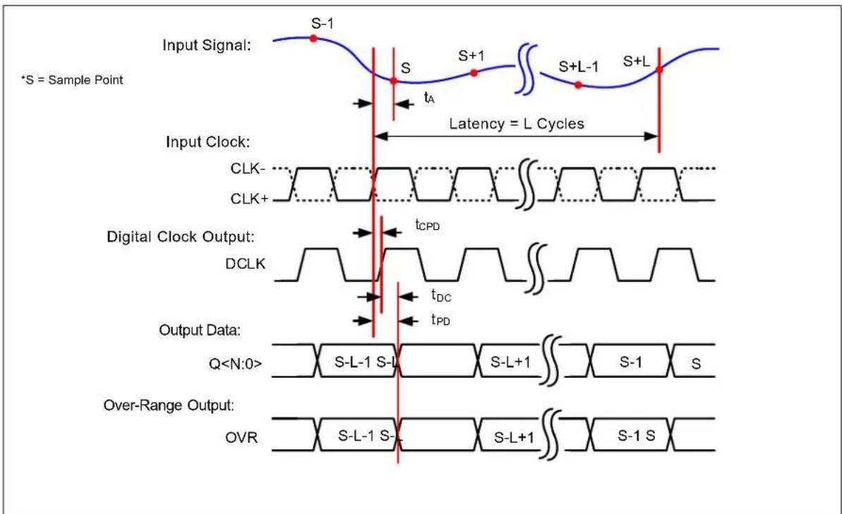
Input Signal: *S = Sample Point S-1 S S+1 S+L-1 S+L tA Latency = L Cycles Input Clock: CLK- CLK+ Digital Clock Output: DCLK tCPD tDC tPD Output Data: QFIGURE 2-1: Timing Diagram - CMOS Output.
flowchart
graph TD
    A["Input Signal: S-1"] --> B["S"]
    B --> C["S+1"]
    C --> D["S+L-1"]
    D --> E["S+L"]
    F["*S = Sample Point"] --> G["tA"]
    G --> H["Latency = L Cycles"]
    I["Input Clock: CLK-"] --> J["Digital Clock Output: tCRD"]
    K["Digital Clock Output: DCLK-"] --> L["Digital Clock Output: tDC"]
    M["Digital Clock Output: DCLK+"] --> N["Digital Clock Output: tPD"]
    O["Output Data: Q-[N:0"] --> P["Word-CLK/Over-Range Output: Q+[N:0"] --> Q["Word-CLK/Over-Range Output: WCK/OVR-"] --> R["Word-CLK/Over-Range Output: WCK/OVR+"] --> S["Word-CLK/Over-Range Output: WCK/OVR-"] --> T["Word-CLK/Over-Range Output: WCK/OVR+"] --> U["Word-CLK/Over-Range Output: WCK/OVR+"] --> V["Word-CLK/Over-Range Output: WCK/OVR-"] --> W["Word-CLK/Over-Range Output: WCK/OVR+"] --> X["Word-CLK/Over-Range Output: WCK/OVR-"] --> Y["Word-CLK/Over-Range Output: WCK/OVR+"] --> Z["Word-CLK/Over-Range Output: WCK/OVR-"] --> AA["Word-CLK/Over-Range Output: WCK/OVR+"] --> AB["Word-CLK/Over-Range Output: WCK/OVR-"] --> AC["Word-CLK/Over-Range Output: WCK/OVR+"] --> AD["Word-CLK/Over-Range Output: WCK/OVR-"] --> AE["Word-CLK/Over-Range Output: WCK/OVR+"] --> AF["Word-CLK/Over-Range Output: WCK/OVR-"] --> AG["Word-CLK/Over-Range Output: WCK/OVR+"] --> AH["Word-CLK/Over-Range Output: WCK/OVR-"] --> AI["Word-CLK/Over-Range Output: WCK/OVR+"] --> AJ["Word-CLK/Over-Range Output: WCK/OVR-"] --> AK["Word-CLK/Over-Range Output: WCK/OVR+"] --> AL["Word-CLK/Over-Range Output: WCK/OVR-"] --> AM["Word-CLK/Over-Range Output: WCK/OVR+"] --> AN["Word-CLK/Over-Range Output: WCK/OVR-"] --> AO["Word-CLK/Over-Range Output: WCK/OVR+"] --> AP["Word-CLK/Over-Range Output: WCK/OVR-"] --> AQ["Word-CLK/Over-Range Output: WCK/OVR+"] --> AR["Word-CLK/Over-Range Output: WCK/OVR-"] --> AS["Word-CLK/Over-Range Output: WCK/OVR+"] --> AT["Word-CLK/Over-Range Output: WCK/OVR-"] --> AU["Word-CLK/Over-Range Output: WCK/OVR+"] --> AV["Word-CLK/Over-Range Output: WCK/OVR-"] --> AW["Word-CLK/Over-Range Output: WCK/OVR+"] --> AX["Word-CLK/Over-Range Output: WCK/OVR-"] --> AY["Word-CLK/Over-Range Output: WCK/OVR+"] --> AZ["Word-CLK/Over-Range Output: WCK/OVR-"] --> BA["Word-CLK/Over-Range Output: WCK/OVR+"] --> BB["Word-CLK/Over-Range Output: WCK/OVR-"] --> BC["Word-CLK/Over-Range Output: WCK/OVR+"] --> BD["Word-CLK/Over-Range Output: WCK/OVR-"] --> BE["Word-CLK/Over-Range Output: WCK/OVR+"] --> BF["Word-CLK/Over-Range Output: WCK/OVR-"] --> BG["Word-CLK/Over-Range Output: WCK/OVR+"] --> BH["Word-CLK/Over-Range Output: WCK/OVR-"] --> BI["Word-CLK/Over-Range Output: WCK/OVR+"] --> BJ["Word-CLK/Over-Range Output: WCK/OVR-"] --> BK["Word-CLK/Over-Range Output: WCK/OVR+"] --> BL["Word-CLK/Over-Range Output: WCK/OVR-"] --> BM["Word-CLK/Over-Range Output: WCK/OVR+"] --> BN["Word-CLK/Over-Range Output: WCK/OVR-"] --> BO["Word-CLK/Over-Range Output: WCK/OVR+"] --> BP["Wacktime"]
    style A fill:#f9f,stroke:#333
    style B fill:#ccf,stroke:#333
    style C fill:#ccf,stroke:#333
    style D fill:#ccf,stroke:#333
    style E fill:#ccf,stroke:#333
    style F fill:#cfc,stroke:#333
    style G fill:#cfc,stroke:#333
    style H fill:#cfc,stroke:#333
    style I fill:#cfc,stroke:#333
    style J fill:#cfc,stroke:#333
    style K fill:#cfc,stroke:#333
    style L fill:#cfc,stroke:#333
    style M fill:#cfc,stroke:#333
    style N fill:#cfc,stroke:#333
    style O fill:#cfc,stroke:#333
    style P fill:#cfc,stroke:#333
    style Q fill:#cfc,stroke:#333
    style R fill:#cfc,stroke:#333
    style S fill:#cfc,stroke:#333
    style T fill:#cfc,stroke:#333
    style U fill:#cfc,stroke:#333
    style V fill:#cfc,stroke:#333
    style W fill:#cfc,stroke:#333
    style X fill:#cfc,stroke:#333
    style Y fill:#cfc,stroke:#333
    style Z fill:#cfc,stroke:#333
    style AA fill:#cfc,stroke:#333
    style AB fill:#cfc,stroke:#333
    style AC fill:#cfc,stroke:#333
    style AD fill:#cfc,stroke:#333
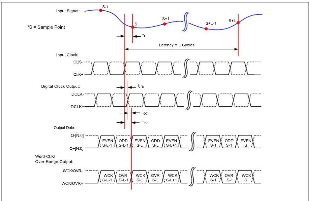
FIGURE 2-2: Timing Diagram - LVDS Output with Even Bit First Option.
TABLE 2-3: SPI SERIAL INTERFACE TIMING SPECIFICATIONS
| Electrical Specifications: Unless otherwise specified, all parameters apply for T_A = -40°C to +125°C, AVDD18= DVDD18= 1.8 V, AVDD12= DVDD12= 1.2V, GND = 0V, SENSE = AVDD12, Single-channel mode, Differential Analog Input (AIN) = Sine wave with amplitude of -1 dBFS, fIN= 70 MHz, Clock Input = 200 MHz, fs= 200 Msps (ADC Core), PLL and decimation filters are disabled, Output load: CMOS data pin = 10 pF, LVDS = 100Ω termination, LVDS driver current setting = 3.5 mA, +25°C is applied for typical value. All timings are measured at 50%. | ||||||
| Parameters Sym. Min. | Typ. Max. | Units Conditions | ||||
| Serial Clock frequency, fsCK= 50 MHz | ||||||
| CS Setup Time t | CSS | 10 | — | — | ns | |
| CS Hold Time | tCSH | 20 | — | — | ns | |
| CS Disable Time | tCSD | 20 | — | — | ns | |
| Data Setup Time | tsU | 2 | — | — | ns | |
| Data Hold Time | tHD | 4 | — | — | ns | |
| Serial Clock High Time | tHI | 8 | — | — | ns | |
| Serial Clock Low Time | tLO | 8 | — | — | ns | Note 1 |
| Serial Clock Delay Time | tCLD | 20 | — | — | ns | |
| Serial Clock Enable Time | tCLE | 20 | — | — | ns | |
| Output Valid from SCK Low | tBO | — | — | 20 | ns | |
| Output Disable Time | tDIS | — | — | 10 | ns | Note 1 |
Note 1: This parameter is ensured by design, but not 100% tested.

text_image
CS tCSS tSCK tHI tLO tCSH tCSD tCLE sCLK tSU tHD SDIO (SDI) MSb in LSb inFIGURE 2-3: SPI Serial Input Timing Diagram.

text_image
CS SCLK tSCK tHI tLO tDO tCSH tDIS SDIO (SDO) MSb out LSb outFIGURE 2-4: SPI Serial Output Timing Diagram.
text_image
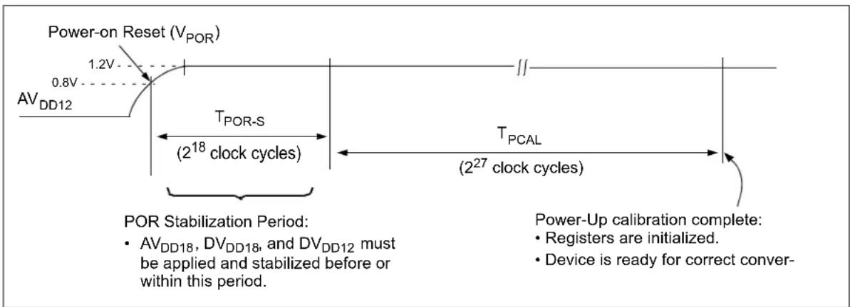
Power-on Reset (V_{POR}) 1.2V 0.8V AV_{DD12} T_{POR-S} (2^{18} clock cycles) T_{PCAL} (2^{27} clock cycles) POR Stabilization Period: • AV_{DD18}, DV_{DD18}, and DV_{DD12} must be applied and stabilized before or within this period. Power-Up calibration complete: • Registers are initialized. • Device is ready for correct conver-FIGURE 2-5: Internal Power-Up Sequence Events.
flowchart
graph LR
    A["RESET Pin"] --> B["t_RESET"]
    B --> C["Stop ADC conversion"]
    C --> D["Start register initialization and ADC recalibration"]
    D --> E["Power-Up Calibration Time (T_PCAL)"]
    E --> F["Recalibration complete: CAL Pin: High ADC_CAL_STAT = 1"]
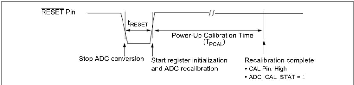
FIGURE 2-6: RESET Pin Timing Diagram.
flowchart
graph TD
    subgraph_Master_Device["Master Device (SLAVE Pin = 0)"]
        A["POR (Power-On Reset) (~2^20 clock cycles)"] --> B["T_SYNC_OUT"]
        B --> C["Toggle to High at the 2nd rising edge of Clock Input"]
    end

    subgraph_Slave_Device["Slave Device(s) (SLAVE Pin = 1)"]
        D["SYNC Input"] --> E["Invalid Data"]
        F["CAL Pin (Output)"] --> G["Invalid Data"]
        H["Data Output"] --> I["Invalid Data"]
        J["Clock Input"] --> K["1"]
        L["Clock Input"] --> M["2"]
        N["Clock Input"] --> O["..."]
    end

    A --> P["SYNC Output"]
    P --> Q["CAL Pin (Output)"]
    Q --> R["Data Output"]
    R --> S["Invalid Data"]
    S --> T["Valid Data"]
    T --> U["..."]
    V["Clock Input"] --> W["1"]
        X["Clock Input"] --> Y["2"]
        Z["Clock Input"] --> AA["..."]
    end

    style Master_Device fill:#f9f,stroke:#333
    style Slave_Device fill:#bbf,stroke:#333
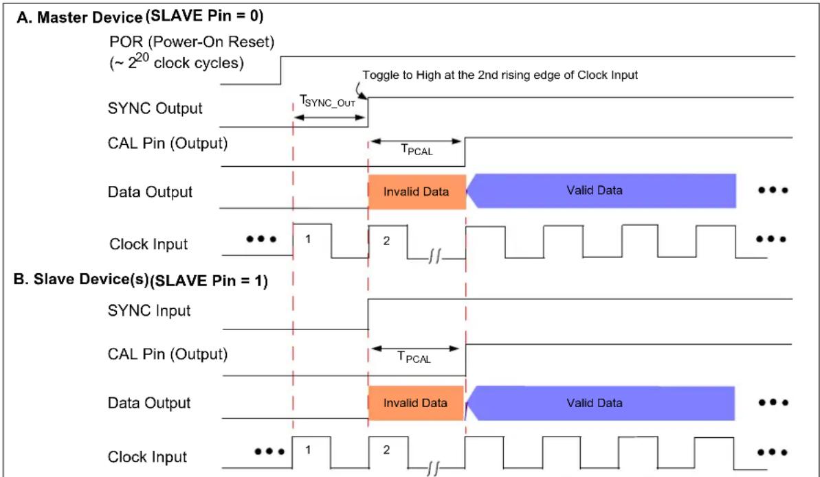
FIGURE 2-7: Figure 2-5 Sync Timing Diagram with Power-On Reset.
flowchart
graph TD
    subgraph_Master_Device["Master Device (SLAVE Pin = 0)"]
        A1["RESET Pin"] --> B1["T_SYNC_Out"]
        B1 --> C1["SYNC Output"]
        C1 --> D1["CAL Pin (Output)"]
        D1 --> E1["Data Output"]
        E1 --> F1["Clock Input"]
        F1 --> G1["1"]
        G1 --> H1["2"]
        H1 --> I1["..."]
        I1 --> J1["..."]
        J1 --> K1["..."]
        K1 --> L1["..."]
    end

    subgraph_Slave_Device["Slave Device(s) (SLAVE Pin = 1)"]
        M1["SYNC Input"] --> N1["CAL Pin (Output)"]
        N1 --> O1["Data Output"]
        O1 --> P1["Clock Input"]
        P1 --> Q1["..."]
        Q1 --> R1["..."]
        R1 --> S1["..."]
        S1 --> T1["..."]
        T1 --> U1["..."]
        U1 --> V1["..."]
        V1 --> W1["..."]
        W1 --> X1["..."]
        X1 --> Y1["..."]
        Y1 --> Z1["..."]
        Z1 --> AA["..."]
        AA --> AB["..."]
        AB --> AC["..."]
        AC --> AD["..."]
        AD --> AE["..."]
    end
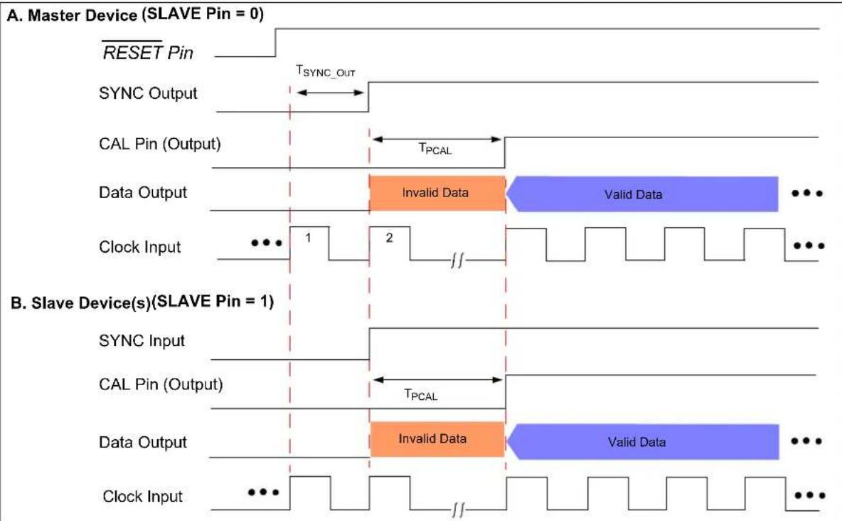
FIGURE 2-8: Sync Timing Diagram with RESET Pin Operation.
flowchart
graph TD
    subgraph A. Master Device (SLAVE Pin = 0)
        A1["POR (~2^20 clock cycles)"] --> B1["T_SYNC_OUT"]
        B1 --> C1["Toggle to High at the 2nd rising edge of Clock Input after POR"]
        C1 --> D1["SOFT_RESET = 1"]
        D1 --> E1["SPI SOFT RESET Control"]
        E1 --> F1["SOFT_RESET = 0"]
        F1 --> G1["SOFT_RESET = 1"]
        G1 --> H1["Cal Pin (Output)"]
        H1 --> I1["T_PCAL"]
        I1 --> J1["Data Output"]
        J1 --> K1["Invalid Data"]
        K1 --> L1["Valid Data"]
        L1 --> M1["No Output"]
        M1 --> N1["Invalid Data"]
        N1 --> O1["Valid Data"]
        O1 --> P1["Clock Input"]
        P1 --> Q1["1"]
        Q1 --> R1["2"]
        R1 --> S1["1"]
        S1 --> T1["2"]
        T1 --> U1["Clock Input"]
    end

    subgraph B. Slave Device(s) (SLAVE Pin = 1)
        B1 --> C1
        C1 --> D1
        D1 --> E1
        E1 --> F1
        F1 --> G1
        G1 --> H1
        H1 --> I1
        I1 --> J1
        J1 --> K1
        K1 --> L1
        L1 --> M1
        M1 --> N1
        N1 --> O1
        O1 --> P1
        P1 --> Q1
        Q1 --> R1
        R1 --> S1
        S1 --> T1
        T1 --> U1
        U1 --> V1["Clock Input"]
        V1 --> W1["..."]
        W1 --> X1["2"]
        X1 --> Y1["..."]
    end

    style A. Master Device fill:#f9f,stroke:#333
    style B. Slave Device fill:#bbf,stroke:#333
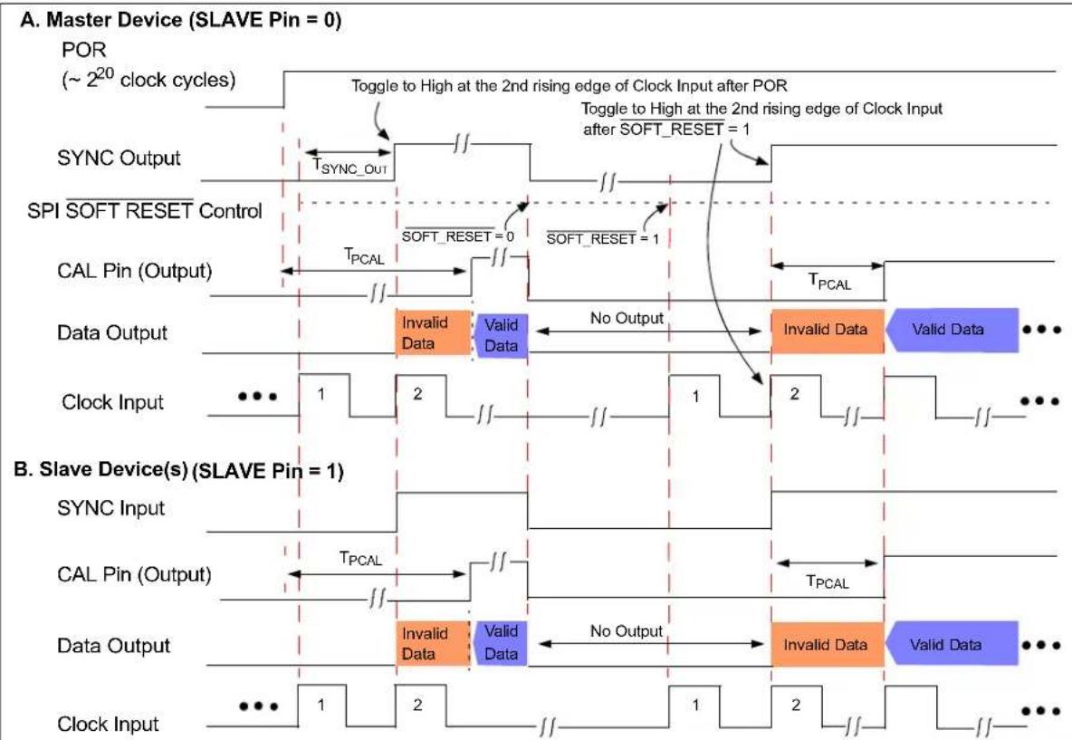
FIGURE 2-9: Sync Timing Diagram with SOFT_RESET Bit Setting.
TABLE 2-4: TEMPERATURE CHARACTERISTICS
| Electrical Specifications: Unless otherwise specified, all parameters apply for T_A = -40°C to +125°C, AVDD18= DVDD18= 1.8 V, AVDD12= DVDD12= 1.2V, GND = 0V, SENSE = AVDD12, Single-channel mode, Differential Analog Input (AIN)= Sine wave with amplitude of -1 dBFS, fIN= 70 MHz, Clock Input = 200 MHz, fs= 200 Msps (ADC Core), PLL and decimation filters are disabled, Output load: CMOS data pin = 10 pF, LVDS = 100Ω termination, LVDS driver current setting = 3.5 mA, +25°C is applied for typical value. | ||||||
| Parameters Sym. Min. Typ. Max. Units Conditions | ||||||
| Temperature Ranges(1) | ||||||
| Operating Temperature Range | T_A | -40 | — | +125 | °C | |
| Thermal Package Resistances(2) | ||||||
| 121L Ball-TFBGA(8 mm x 8 mm) | Junction-to-Ambient Thermal Resistance | _JA | — | 40.2 | — | °C/W |
| Junction-to-Case Thermal Resistance | _JC | — | 8.4 | — | °C/W | |
| 124L – VTLA(9 mm x 9 mm) | Junction-to-Ambient Thermal Resistance | _JA | — | 21 | — | °C/W |
| Junction-to-Case (top) Thermal Resistance | _JC | — | 8.7 | — | °C/W | |
Note 1: Maximum allowed power-dissipation ( P_DMAX ) = ( T_JMAX - T_A )/ _JA .
2: This parameter value is achieved by package simulations.
NOTES:
3.0 TYPICAL PERFORMANCE CURVES
Note: The graphs and tables provided following this note are a statistical summary based on a limited number of samples and are provided for informational purposes only. The performance characteristics listed herein are not tested or guaranteed. In some graphs or tables, the data presented may be outside the specified operating range (e.g., outside specified power supply range) and therefore outside the warranted range.
Note: Unless otherwise specified, all plots are at +25°C, AV_DD18 = DV_DD18 = 1.8 V , dV_D2 = DV_DD12 = 1.2 V , GND = 0 V, SENS = A V Single-channel mode, Differential Analog Input ( A_IN ) = Sine wave with amplitude of -1 dBFS, f_N = 70 MHz , Clock Input = 200 MHz, f_S = 200 Msps (ADC Core), PLL and decimation filters are disabled. When NSR option is used, 12-bit mode is applied and the noise is calculated within the NSR bandwidth (25% of sampling frequency).

line
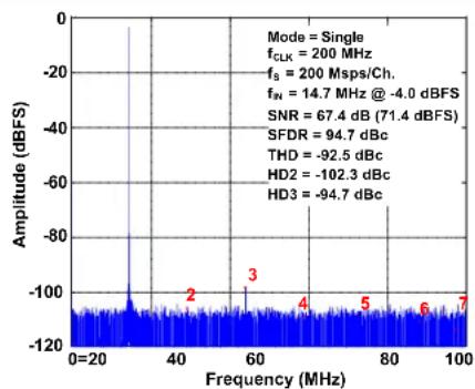
| Frequency (MHz) | Amplitude (dBFS) | | --------------- | ---------------- | | 2 | -100 | | 3 | -80 | | 4 | -100 | | 5 | -100 | | 6 | -100 | | 7 | -100 |FIGURE 3-1: FFT for 14.7 MHz Input
Signal: f_S = 200 Msps/Ch., A_IN = -1 dBFS.

line
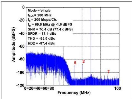
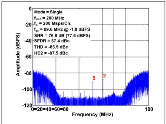
| Frequency (MHz) | Amplitude (dBFS) | | --------------- | ---------------- | | 10 | -80 | | 20 | -60 | | 40 | -100 | | 50 | -100 | | 60 | -100 | | 70 | -100 | | 80 | -100 | | 90 | -100 | | 100 | -100 |FIGURE 3-2: FFT for 69.6 MHz Input Signal: f_S = 200 Msps/Ch., A_IN = -1 dBFS.

line
| Frequency (MHz) | Amplitude (dBFS) | | --------------- | ---------------- | | 20 | -100 | | 40 | -100 | | 60 | -80 | | 80 | -100 | | 100 | -80 |FIGURE 3-3: FFT for 151 MHz Input Signal: f_S = 200 Msps/Ch., A_IN = -1 dB F S.
line
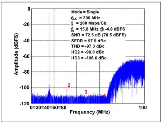
| Frequency (MHz) | Amplitude (dBFS) | | --------------- | ---------------- | | 20 | -100 | | 40 | -100 | | 60 | -100 | | 80 | -100 | | 100 | -100 |FIGURE 3-4: FFT for 14.7 MHz Input Signal: f_S = 200 Msps/Ch., A_IN = -4 d B F S.

line
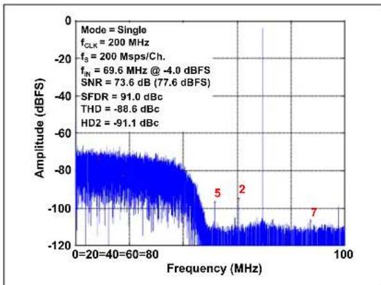
| Frequency (MHz) | Amplitude (dBFS) | | --------------- | ---------------- | | 20 | -100 | | 30 | -100 | | 40 | -100 | | 50 | -100 | | 60 | -100 | | 70 | -100 | | 80 | -100 | | 90 | -100 | | 100 | -100 |FIGURE 3-5: FFT for 69.6 MHz Input Signal: f_S = 200 Msps/Ch., A_IN = -4 dB F S.

line
| Frequency (MHz) | Amplitude (dBFS) | | --------------- | ---------------- | | 60 | -86.3 | | 70 | -80.3 | | 80 | -83.3 | | 90 | -86.3 | | 100 | -83.3 |FIGURE 3-6: FFT for 151 MHz Input Signal: f_S = 200 Msps/Ch., A_IN = -4 dBFS.

line
| Frequency (MHz) | Amplitude (dBFS) | | --------------- | ---------------- | | 0 | -100 | | 30 | -100 | | 50 | -100 | | 40 | -100 |FIGURE 3-7: FFT for 14.7 MHz Input Signal: f_S = 100 Msps/Ch., Dual, A_IN = -1 dBFS.

line
| Frequency (MHz) | Amplitude (dBFS) | | --------------- | ---------------- | | 0 | -100 | | 30 | -100 | | 40 | -100 | | 50 | -100 |FIGURE 3-10: FFT for 14.7 MHz Input Signal: f_S = 100 Msps/Ch., Dual, A_IN = -4 dB F S.

line
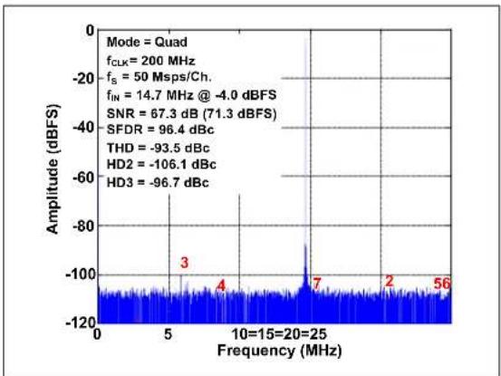
| Frequency (MHz) | Amplitude (dBFS) | | --------------- | ---------------- | | 0 | -100 | | 10 | -100 | | 15 | -100 | | 20 | -100 | | 25 | -100 |FIGURE 3-8: FFT for 14.7 MHz Input Signal: f_S = 50 Msps/Ch., Quad, A_IN = -1 d B F S.
line
| Frequency (MHz) | Amplitude (dBFS) | | --------------- | ---------------- | | 5 | -100 | | 10 | -80 | | 20 | -100 | | 25 | -100 | | 30 | -100 | | 35 | -100 | | 40 | -100 | | 45 | -100 | | 50 | -100 | | 55 | -100 | | 60 | -100 | | 65 | -100 | | 70 | -100 | | 75 | -100 | | 80 | -100 | | 85 | -100 | | 90 | -100 | | 95 | -100 | | 100 | -100 | | 105 | -100 | | 110 | -100 | | 115 | -100 | | 120 | -100 | | 125 | -100 | | 130 | -100 | | 135 | -100 | | 140 | -100 | | 145 | -100 | | 150 | -100 | | 155 | -100 | | 160 | -100 | | 165 | -100 | | 170 | -100 | | 175 | -100 | | 180 | -100 | | 185 | -100 | | 190 | -100 | | 195 | -100 | | 200 | -100 | | 205 | -100 | | 210 | -100 | | 215 | -100 | | 220 | -100 | | 225 | -100 | | 230 | -100 | | 235 | -100 | | 240 | -100 | | 245 | -100 | | 250 | -100 | | 255 | -100 | | 260 | -100 | | 265 | -100 | | 270 | -100 | | 275 | -100 | | 280 | -100 | | 285 | -100 | | 290 | -100 | | 295 | -100 | | 300 | -100 | | 305 | -100 | | 310 | -100 | | 315 | -100 | | 320 | -100 | | 325 | -100 | | 330 | -100 | | 335 | -100 | | 340 | -100 | | 345 | -100 | | 350 | -100 | | 355 | -100 | | 360 | -100 | | 365 | -100 | | 370 | -100 | | 375 | -100 | | 380 | -100 | | 385 | -100 | | 390 | -100 | | 395 | -100 | | 400 | -100 | | 405 | -100 | | 410 | -100 | | 415 | -100 | | 420 | -100 | | 425 | -100 | | 430 | -100 | | 435 | -100 | | 440 | -100 | | 445 | -100 | | 450 | -100 | | 455 | -100 | | 460 | -100 | | 465 | -100 | | 470 | -100 | | 475 | -100 | | 480 | -100 | | 485 | -100 | | 490 | -100 | | 495 | -100 | | 50 | -99.7 |FIGURE 3-11: FFT for 14.7 MHz Input Signal: f_S = 50 Msps/Ch., Quad, A_IN = -4 dBFS.

line
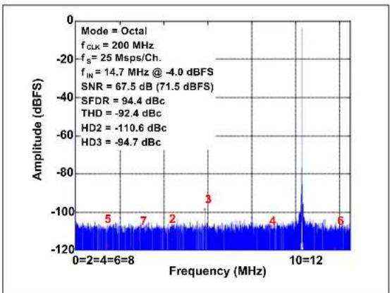
| Frequency (MHz) | Amplitude (dBFS) | | --------------- | ---------------- | | 0 | -100 | | 2 | -100 | | 4 | -100 | | 6 | -100 | | 8 | -100 | | 10 | -100 |FIGURE 3-9: FFT for 14.7 MHz Input Signal: f_S = 25 Msps/Ch., Octal, A_IN = -1 dBFS.
line
| Frequency (MHz) | Amplitude (dBFS) | | --------------- | ---------------- | | 0 | -100 | | 2 | -100 | | 4 | -100 | | 6 | -100 | | 8 | -100 | | 10 | -100 | | 12 | -100 |FIGURE 3-12: FFT for 14.7 MHz Input Signal: f_S = 25 Msps/Ch., Octal, A_IN = -4 dBFS.

line
| Frequency (MHz) | Amplitude (dBFS) | | --------------- | ---------------- | | 69.6 | -80 | | 70.1 | -80 | | 78.6 | -80 | | -98.3 | -100 | | -78.1 | -100 | | -78.6 | -100 |FIGURE 3-13: FFT for 69.6 MHz Input Signal: f_S = 25 Msps/Ch., Octal, A_IN = -1 dBFS.

line
| Frequency (MHz) | Amplitude (dBFS) | | --------------- | ---------------- | | 10 | -97.7 | | 12 | -90.0 | | 14 | -88.2 | | 16 | -80.0 | | 18 | -67.2 | | 20 | -4.0 | | 22 | -25.0 | | 24 | -100.0 | | 26 | -80.0 | | 28 | -67.2 | | 30 | -4.0 | | 32 | -25.0 | | 34 | -100.0 | | 36 | -80.0 | | 38 | -67.2 | | 40 | -4.0 | | 42 | -25.0 | | 44 | -100.0 | | 46 | -80.0 | | 48 | -67.2 | | 50 | -4.0 | | 52 | -25.0 | | 54 | -100.0 | | 56 | -80.0 | | 58 | -67.2 | | 60 | -4.0 | | 62 | -25.0 | | 64 | -100.0 | | 66 | -80.0 | | 68 | -67.2 | | 70 | -4.0 | | 72 | -25.0 | | 74 | -100.0 | | 76 | -80.0 | | 78 | -67.2 | | 80 | -4.0 | | 82 | -25.0 | | 84 | -100.0 | | 86 | -80.0 | | 88 | -67.2 | | 90 | -4.0 | | 92 | -25.0 | | 94 | -100.0 | | 96 | -80.0 | | 98 | -67.2 | | 100 | -4.0 |FIGURE 3-16: FFT for 69.6 MHz Input Signal: f_S = 25 Msps/Ch., Octal, A_IN = -4 dBFS.
line
| Frequency (MHz) | Amplitude (dBFS) | | --------------- | ---------------- | | 0 | -80 | | 20 | -85 | | 40 | -90 | | 60 | -100 | | 80 | -110 | | 100 | -120 |FIGURE 3-14: FFT for 69.6 MHz Input Signal with NSR enabled: NSR = 20, f_S = 200 Msps/Ch., A_IN = -1 dBFS.
line
| Frequency (MHz) | Amplitude (dBFS) | | --------------- | ---------------- | | 0 | -80 | | 20 | -85 | | 40 | -90 | | 60 | -95 | | 80 | -100 | | 100 | -110 |FIGURE 3-17: FFT for 69.6 MHz Input Signal with NSR enabled: NSR = 20, f_S = 200 Msps/Ch., A_IN = -4 dBFS.

line
| Frequency (MHz) | Amplitude (dBFS) | | --------------- | ---------------- | | 0 | -100 | | 40 | -100 | | 60 | -100 | | 80 | -100 | | 100 | -60 |FIGURE 3-15: FFT for 20.3 MHz Input Signal with NSR enabled: NSR = 27, f_S = 200 Msps/Ch., A_IN = -1 dBFS.

line
| Frequency (MHz) | Amplitude (dBFS) | | --------------- | ---------------- | | 0 | -100 | | 60 | -100 | | 80 | -100 | | 100 | -60 |FIGURE 3-18: FFT for 20.3 MHz Input Signal with NSR enabled: NSR = 27, f_S = 200 Msps/Ch., A_IN = -4 dBFS.
line
| Frequency (MHz) | Amplitude (dBFS) | | --------------- | ---------------- | | 0 | -80 | | 20 | -100 | | 40 | -120 | | 60 | -100 | | 80 | -80 | | 100 | -60 |FIGURE 3-19: FFT for 69.6 MHz Input Signal with NSR enabled: NSR = 52, f_S = 200 Msps/Ch., A_IN = -1 dBFS.

line
| Frequency (MHz) | Amplitude (dBFS) | | --------------- | ---------------- | | 0 | -80 | | 20 | -100 | | 40 | -100 | | 60 | -100 | | 80 | -100 | | 100 | -80 |FIGURE 3-22: FFT for 69.6 MHz Input Signal with NSR enabled: NSR = 52, f_S = 200 Msps/Ch., A_IN = -4 dBFS.

line
| Frequency (MHz) | Amplitude (dBFS) | | --------------- | ---------------- | | 0 | -120 | | 40 | -100 | | 80 | -100 | | 100 | -100 | | 120 | -100 |FIGURE 3-20: FFT for 15.8 MHz Input Signal with NSR enabled: NSR = 63, f_S = 200 Msps/Ch., A_IN = -1 dBFS.
line
| Frequency (MHz) | Amplitude (dBFS) | | --------------- | ---------------- | | 0 | 0 | | 20 | -100 | | 40 | -100 | | 60 | -100 | | 80 | -100 | | 100 | -60 |FIGURE 3-23: FFT for 15.8 MHz Input Signal with NSR enabled: NSR = 63, f_S = 200 Msps/Ch., A_IN = -4 dBFS.
line
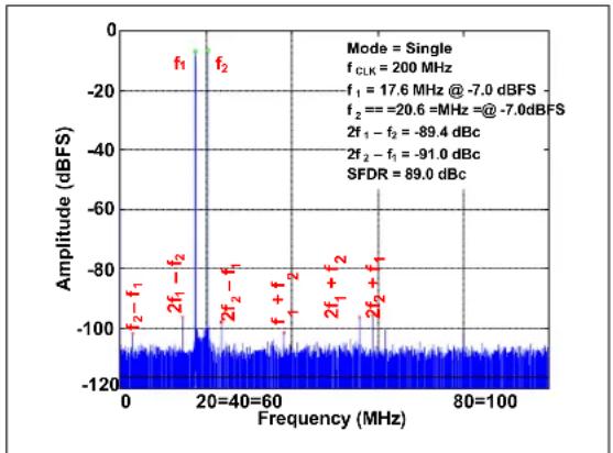
| Frequency (MHz) | Amplitude (dBFS) | | --------------- | ---------------- | | 0 | -100 | | 20 | -100 | | 40 | -100 | | 60 | -100 | | 80 | -100 |FIGURE 3-21: Two-Tone FFT: f_IN1 = 17.6MHz and f_IN2 = 20.6MHz , A_IN = -7 dBFS per Tone, f_S = 200 Ms p s.
line
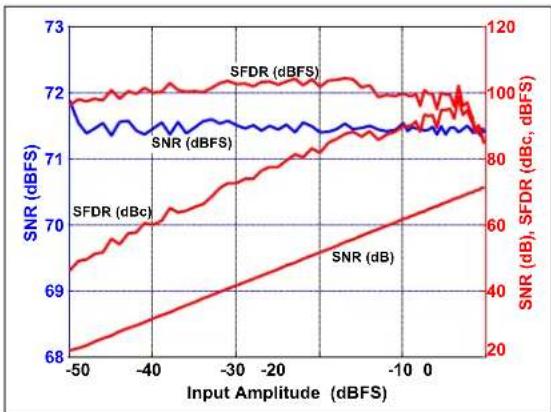
| Input Amplitude (dBFS) | SNR (dBFS) | SFDR (dBFS) | SNR (dB) | | ---------------------- | ---------- | ----------- | -------- | | -50 | 71.8 | 72.0 | 68.0 | | -40 | 71.5 | 72.0 | 69.0 | | -30 | 71.3 | 72.0 | 70.0 | | -20 | 71.2 | 72.0 | 71.0 | | -10 | 71.1 | 72.0 | 72.0 | | 0 | 71.0 | 72.0 | 73.0 |FIGURE 3-24: SNR/SFDR vs. Analog Input Amplitude: f_S = 200 M s p f_N = f15 MHz , High-Reference Mode (SENSE = AV _DD12 ).

line
| Input Amplitude (dBFS) | SNR (dBFS) | SNR (dBc) | | ---------------------- | ---------- | --------- | | -50 | 71.5 | 68 | | -40 | 71.2 | 69 | | -30 | 71.0 | 70 | | -20 | 70.8 | 71 | | -10 | 70.5 | 72 | | 0 | 70.0 | 73 |FIGURE 3-27: SNR/SFDR vs. Analog Input Amplitude: f_S = 200 M s p_IN = f70 MHz , High-Reference Mode (SENSE = AV _DD12 ).
line
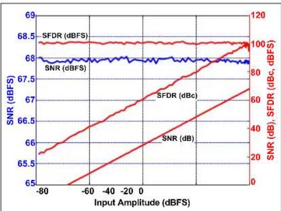
| Input Amplitude (dBFS) | SFDR (dBFS) | SNR (dB) | | ---------------------- | ----------- | -------- | | -80 | 68.5 | 65.5 | | -60 | 68.5 | 66.5 | | -40 | 68.5 | 67.5 | | -20 | 68.5 | 68.5 | | 0 | 68.5 | 69.5 | | 20 | 68.5 | 70.5 | | 40 | 68.5 | 71.5 | | 60 | 68.5 | 72.5 | | 80 | 68.5 | 73.5 |FIGURE 3-25: SNR/SFDR vs. Analog Input Amplitude: f_S = 200 M s p_IN = f15 MHz , Low-Reference Mode (SENSE = GND).

line
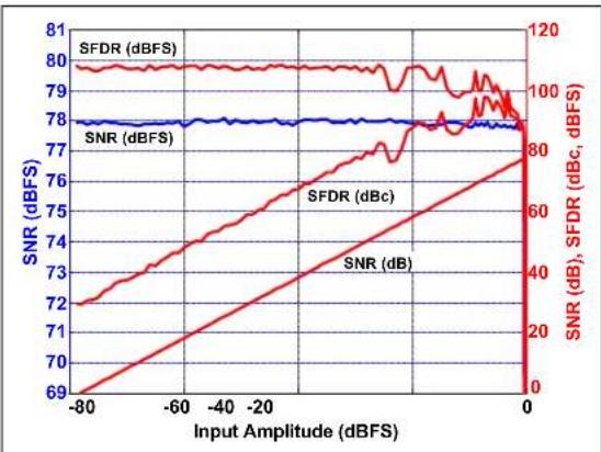
| Input Amplitude (dBFS) | SFDR (dBFS) | SNR (dBc) | SFDR (dBc) | SNR (dB) | | ---------------------- | ----------- | --------- | ---------- | -------- | | -100 | 68.5 | 80.0 | 65.0 | 0.0 | | -80 | 68.5 | 80.0 | 66.0 | 20.0 | | -60 | 68.5 | 80.0 | 67.0 | 40.0 | | -40 | 68.5 | 80.0 | 68.0 | 60.0 | | -20 | 68.5 | 80.0 | 69.0 | 80.0 | | 0 | 68.5 | 80.0 | 70.0 | 100.0 | | 20 | 68.5 | 80.0 | 71.0 | 120.0 | | 40 | 68.5 | 80.0 | 72.0 | 140.0 | | 60 | 68.5 | 80.0 | 73.0 | 160.0 | | 80 | 68.5 | 80.0 | 74.0 | 180.0 | | 100 | 68.5 | 80.0 | 75.0 | 200.0 |FIGURE 3-28: SNR/SFDR vs. Analog Input Amplitude: f_S = 200 M sp p_N, = f70 MHz , Low-Reference Mode (SENSE = GND).
line
| Input Amplitude (dBFS) | SFDR (dBFS) | SNR (dB) | | ---------------------- | ----------- | -------- | | -80 | 79 | 69 | | -60 | 79 | 71 | | -40 | 79 | 73 | | -20 | 79 | 75 | | 0 | 79 | 77 | | 0 | 80 | 80 |FIGURE 3-26: SNR/SFDR vs. Analog Input Amplitude: f_S = 200 M s p s_N = f15 M Hz , High-Reference Mode (SENSE = AV DD12 ) with NSR enabled. AIN ≤ 0.8 dBFS for NSR.
line
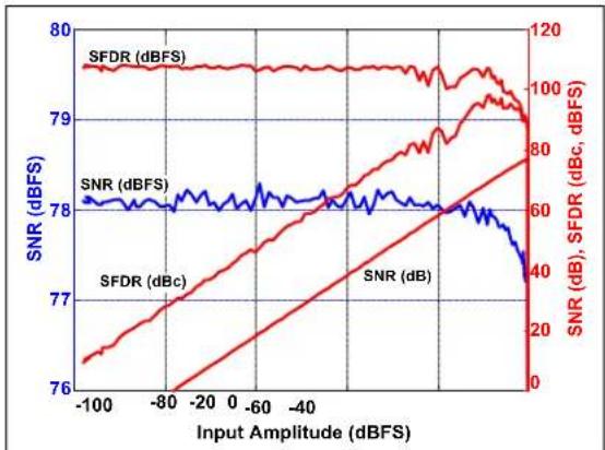
| Input Amplitude (dBFS) | SFDR (dBFS) | SFDR (dBc) | SNR (dB) | | ---------------------- | ----------- | ---------- | -------- | | -100 | 79.5 | 60 | 10 | | -80 | 79.5 | 60 | 20 | | -60 | 79.5 | 60 | 30 | | -40 | 79.5 | 60 | 40 | | -20 | 79.5 | 60 | 50 | | 0 | 79.5 | 60 | 60 | | 20 | 79.5 | 60 | 70 | | 40 | 79.5 | 60 | 80 | | 60 | 79.5 | 60 | 90 | | 80 | 79.5 | 60 | 100 | | 100 | 79.5 | 60 | 110 |FIGURE 3-29: SNR/SFDR vs. Analog Input Amplitude: f_S = 200 M s p N = f70 M Hz , High-Reference Mode (SENSE = AV DD12 ) with NSR enabled. A_IN ≤ 0.8 dBFS for NSR.
line
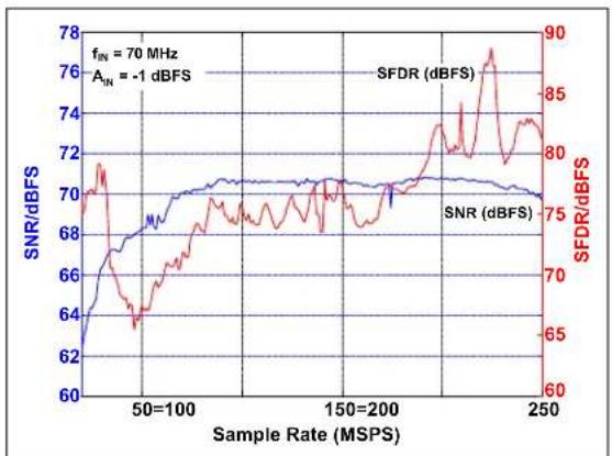
| Sample Rate (MSPS) | SNR (dBFS) | SFDR (dBFS) | | ------------------ | ---------- | ----------- | | 0 | 64 | 70 | | 50=100 | 68 | 75 | | 150=200 | 70 | 80 | | 250 | 72 | 85 |FIGURE 3-30: SNR/SFDR vs. Sample Rate (Msps): f_IN = 70 MHz .
line
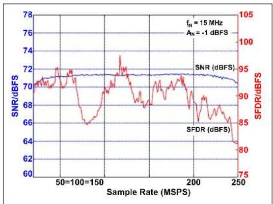
| Sample Rate (MSPS) | SNR (dBFS) | SFDR (dBFS) | | ------------------ | ---------- | ----------- | | 50=100=150 | 72 | 66 | | 200 | 95 | 85 | | 250 | 95 | 80 |FIGURE 3-33: SNR/SFDR vs. Sample Rate (Msps): f_IN = 15 MHz .
line
| SENSE Pin Voltage | SNR (dBFS) | SFDR (dBFS) | | ----------------- | ---------- | ----------- | | BG-LOW | 68 | 95 | | 0.2 | 65 | 90 | | 0.4=0.6=0.8=1.0=BG-HIGH | 70 | 85 |FIGURE 3-31: SNR/SFDR vs. SENSE Pin Voltage: f_S = 200 Msps, f_IN = 70 MHz.

line
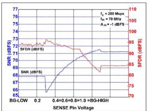
| SENSE Pin Voltage | SNR (dBFS) | SFDR (dBFS) | | ----------------- | ---------- | ----------- | | BG-LOW | 68 | 95 | | 0.2 | 65 | 100 | | 0.4=0.6 | 70 | 95 | | 0.8 | 72 | 85 | | 1.0=BG-HIGH | 72 | 85 |FIGURE 3-34: SNR/SFDR vs. SENSE Pin Voltage: f_S = 200M s p_IN = f15MHz .
line
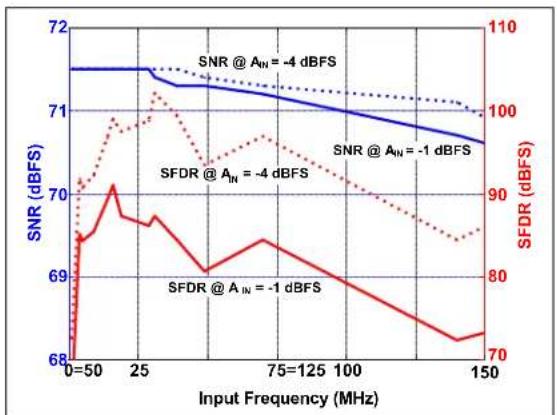
| Input Frequency (MHz) | SNR @ A_IN = -4 dBFS | SFDR @ A_IN = -4 dBFS | SNR @ A_IN = -1 dBFS | SFDR @ A_IN = -1 dBFS | | --------------------- | ------------------- | -------------------- | ------------------- | -------------------- | | 0 | 71.5 | 70.0 | 71.5 | 70.0 | | 25 | 71.3 | 70.5 | 71.3 | 70.5 | | 75 | 71.0 | 69.5 | 71.0 | 69.5 | | 150 | 70.5 | 68.5 | 70.5 | 68.5 |FIGURE 3-32: SNR/SFDR vs. Input Frequency.
line
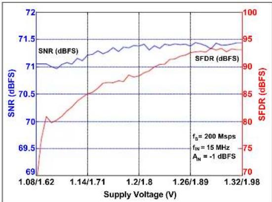
| Supply Voltage (V) | SNR (dBFS) | SFDR (dBFS) | | ------------------ | ---------- | ----------- | | 1.08/1.62 | 71.0 | 70.0 | | 1.14/1.71 | 71.2 | 75.0 | | 1.2/1.8 | 71.3 | 80.0 | | 1.26/1.89 | 71.4 | 85.0 | | 1.32/1.98 | 71.5 | 90.0 |FIGURE 3-35: SNR/SFDR vs. Supply Voltage: f_S = 200 Msps, f_IN = 15 MHz.

line
| Supply Voltage (V) | HD2 (dBFS) | HD3 (dBFS) | | ------------------ | ---------- | ---------- | | 1.08/1.62 | -90 | -70 | | 1.14/1.71 | -95 | -85 | | 1.2/1.8 | -105 | -90 | | 1.26/1.89 | -100 | -95 | | 1.32/1.98 | -105 | -95 |FIGURE 3-38: HD2/HD3 vs. Supply Voltage: f_S = 200M sp, =f1 5 MHz.
line
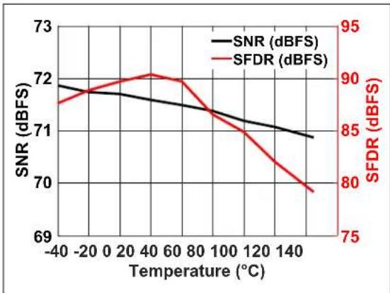
| Temperature (°C) | SNR (dBFS) | SFDR (dBFS) | | ---------------- | ---------- | ----------- | | -40 | 72.0 | 88.0 | | 0 | 71.8 | 90.0 | | 20 | 71.6 | 91.0 | | 40 | 71.4 | 92.0 | | 60 | 71.2 | 91.5 | | 80 | 71.0 | 90.0 | | 100 | 70.8 | 88.0 | | 120 | 70.6 | 85.0 | | 140 | 70.4 | 82.0 | | 150 | 70.2 | 79.0 |FIGURE 3-36: SNR/SFDR vs. Temperature: f_S = 200 Msps, f_IN = 20 MHz, V_SENSE = AV_DD12, A_IN = -1 dBFS.
line
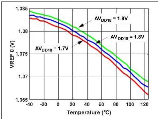
| Temperature (°C) | VREF 0 (V) for AV_DD18 = 1.7V | VREF 0 (V) for AV_DD18 = 1.8V | | ---------------- | ----------------------------- | ----------------------------- | | -40 | ~1.385 | ~1.385 | | 0 | ~1.383 | ~1.384 | | 20 | ~1.380 | ~1.382 | | 40 | ~1.377 | ~1.380 | | 60 | ~1.374 | ~1.377 | | 80 | ~1.371 | ~1.374 | | 100 | ~1.369 | ~1.372 | | 120 | ~1.366 | ~1.369 |FIGURE 3-39: V REF0 vs. Temperature.
line
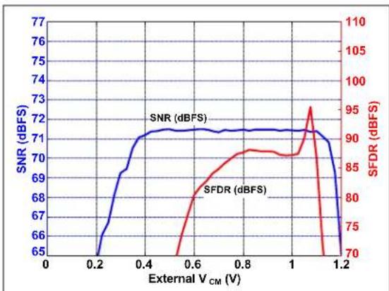
| External V_CM (V) | SNR (dBFS) | SFDR (dBFS) | | ----------------- | ---------- | ----------- | | 0.2 | 65 | 70 | | 0.4 | 71 | 85 | | 0.6 | 71 | 90 | | 0.8 | 71 | 90 | | 1.0 | 71 | 95 | | 1.2 | 65 | 70 |FIGURE 3-37: SNR/SFDR vs. V CM Voltage (Externally Applied): f_S = 200 Msps, f_IN = 15 MHz.

line
| Temperature (°C) | Gain Error (dB) | Offset Error (LSB) | | ---------------- | --------------- | ------------------ | | -40 | 0.0 | 0.6 | | -20 | 0.0 | 0.4 | | 0 | 0.0 | 0.2 | | 20 | 0.0 | 0.0 | | 40 | 0.0 | -0.2 | | 60 | 0.0 | -0.4 | | 80 | 0.0 | -0.6 | | 100 | 0.0 | -0.4 | | 120 | 0.0 | -0.2 |FIGURE 3-40: Gain and Offset Error Drifts vs. Temperature Using Internal Reference, with Respect to +25°C: f_S = 200 M s p s.
line
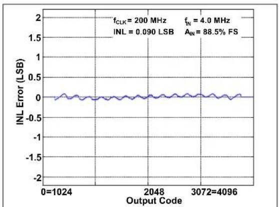
| Output Code | INL Error (LSB) | | ----------- | --------------- | | 0 | 0.090 | | 2048 | ~0.0 | | 3072 | ~0.0 | | 4096 | ~0.0 |FIGURE 3-41: INL Error vs. Output Code: f_S = 200 Msps, f_IN = 4 MHz.
line
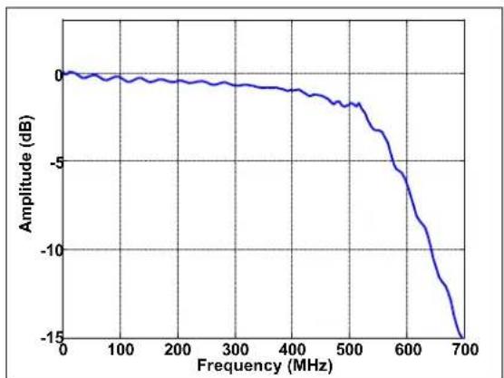
| Frequency (MHz) | Amplitude (dB) | | --------------- | -------------- | | 0 | 0 | | 100 | -0.5 | | 200 | -0.8 | | 300 | -1.0 | | 400 | -1.5 | | 500 | -2.5 | | 600 | -7.0 | | 700 | -15.0 |FIGURE 3-44: Input Bandwidth.

line
| Output Code | DNL Error (LSB) | | ----------- | --------------- | | 0 | 0.1 | | 2048 | ~0.0 | | 3072 | ~-0.1 | | 4096 | ~-0.15 |FIGURE 3-42: DNL Error vs. Output Code: f_S = 200 Msps, f_IN = 4 MHz.

line
| Input Frequency (MHz) | Crosstalk (dB) - CH2 to CH3 | Crosstalk (dB) - CH3 to CH2 | | --------------------- | --------------------------- | --------------------------- | | 0 | ~107 | ~107 | | 50 | ~106 | ~106 | | 100 | ~95 | ~102 | | 150 | ~90 | ~92 | | 200 | ~87 | ~88 |FIGURE 3-45: Input Channel Crosstalk.
bar
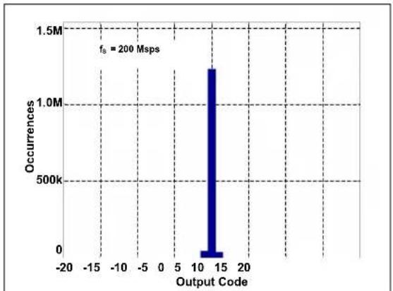
| Output Code | Occurrences | |---|---| | 15 | 1250000 | | 10 | 125000 | | -15 | 0 | | -20 | 0 | | -15 | 0 | | -10 | 0 | | -5 | 0 | | 0 | 0 | | 5 | 0 | | 10 | 0 | | 15 | 0 | | 20 | 0 | fs = 200 MspsFIGURE 3-43: Shorted Input Histogram.
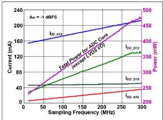
line
| Sampling Frequency (MHz) | I_DD_A12 (mA) | I_DD_D12 (mA) | I_DD_D18 (mA) | I_DD_A18 (mA) | | ------------------------ | ------------- | ------------- | ------------- | ------------- | | 0 | 160 | 40 | 40 | 0 | | 50 | 170 | 60 | 40 | 10 | | 100 | 180 | 80 | 40 | 20 | | 150 | 190 | 100 | 40 | 30 | | 200 | 200 | 120 | 40 | 40 | | 250 | 210 | 140 | 40 | 50 | | 300 | 220 | 160 | 40 | 60 |FIGURE 3-46: Power Consumption vs. Sampling Frequency (LVDS Mode).
The MCP37211-200 and MCP37D11-200 device family is a low-power, 12-bit, 200 Msps Analog-to-Digital Converter (ADC) with built-in features including Harmonic Distortion Correction (HDC), DAC Noise Cancellation (DNC), Dynamic Element Matching (DEM) and flash error calibration.
The devices offer various built-in digital signal post-processing features. Both the MCP37211-200 and MCP37D11-200 offer high-order FIR digital decimation filters, noise-shaping requantizer (NSR), gain and offset adjustment per channel and fractional delay recovery (FDR). The MCP37D11-200 includes additional features such as digital down-conversion (DDC) and CW beamforming capability. These built-in advanced digital signal post-processing sub-blocks, which are individually controlled using Configuration register bit settings, can be used for various special applications such as I/Q demodulation, digital down-conversion and ultrasound imaging.
When the device is first powered-up, it performs internal calibrations by itself and runs with default settings. From this point, the user can configure the device registers using the SPI command.
In multi-channel mode, the input channel selection and MUX scan order are user-configurable, and the inputs are sequentially multiplexed by the input MUX defined by the scan order.
The device samples the analog input on the rising edge of the clock. The digital output code is available after 28 clock cycles of data latency. Latency will increase if any of the various digital signal post-processing (DSPP) options are enabled.
The output data can be coded in two's complement or offset binary format, and randomized using the user option. Data can be output using either the CMOS or LVDS (Low-Voltage Differential Signaling) interface.
4.1 ADC Core Architecture
Figure 4-1 shows the simplified block diagram of the ADC core. The first stage consists of a 17-level flash ADC, multi-level Digital-to-Analog Converter (DAC) and a residue amplifier with a gain of 8. Stages 2 to 6 consist of a 9-level (3-bit) flash ADC, multi-level DAC and a residue amplifier with a gain of 4. The last stage is a 9-level 3-bit flash ADC. Dither is added in each of the first three stages. The digital outputs from all seven stages are combined in a digital error correction logic block and digitally processed for the final output.
The first three stages include patented digital calibration features:
- Harmonic Distortion Correction (HDC) algorithm that digitally measures and cancels ADC errors arising from distortions introduced by the residue amplifiers
- DAC Noise Cancellation (DNC) algorithm that corrects DAC's nonlinearity errors
- Dynamic Element Matching (DEM) which randomizes DAC errors, thereby converting harmonic distortion to white noise
These digital correction algorithms are first applied during the Power-on Reset sequence and then operate in the background during normal operation of the pipelined ADC. These algorithms automatically track and correct any environmental changes in the ADC. More details of the system correction algorithms are shown in Section 4.13 "System Calibration".

flowchart
graph TD
    A["Reference Generator"] --> B["Input MUX"]
    C["Clock Generation"] --> D["Pipeline Stage 1 (3-bit)"]
    C --> E["Pipeline Stage 2 (2-bit)"]
    C --> F["Pipeline Stage 3 (2-bit)"]
    C --> G["Pipeline Stage 4 (2-bit)"]
    C --> H["Pipeline Stage 5 (2-bit)"]
    C --> I["Pipeline Stage 6 (2-bit)"]
    C --> J["3-bit Flash Stage 7 (3-bit)"]
    B --> K["HDC1, DNC1"]
    D --> L["REF0"]
    E --> M["REF1"]
    F --> N["REF1"]
    G --> O["REF1"]
    H --> P["REF1"]
    I --> Q["REF1"]
    K --> R["Digital Error Correction"]
    L --> R
    M --> R
    N --> R
    O --> R
    P --> R
    Q --> R
    R --> S["User-Programmable Options"]
    S --> T["Programmable Digital Signal Post-Processing (DSPP)"]
    T --> U["12-Bit Digital Output"]
FIGURE 4-1: ADC Core Block Diagram.
4.2 Supply Voltage (DV DD, AVDD, GND)
The device operates from two sets of supplies and a common ground:
- Digital Supplies (DV _DD ) for the digital section: 1.8V and 1.2V
- Analog Supplies (AV _DD ) for the analog section: 1.8V and 1.2V
- Ground (GND): Common ground for both digital and analog sections.
The supply pins require an appropriate bypass capacitor (ceramic) to attenuate the high-frequency noise present in most application environments. The ground pins provide the current return path. These ground pins must connect to the ground plane of the PCB through a low-impedance connection. A ferrite bead can be used to separate analog and digital supply lines if a common power supply is used for both analog and digital sections.
The voltage regulators for each supply need to have sufficient output current capabilities to support a stable ADC operation.
Figure 2-5 shows the internal power-up sequence events of the device. The power-up sequence of the device is initiated by a Power-on reset (POR) circuit which monitors the analog 1.2V supply voltage (AV _DD12 ):
(a) Once the AV_DD12 reaches the Power-on Reset threshold ( 0.8V ), there will be a Power-on Reset stabilization period ( 2^18 clock cycles) before triggering the power-up calibration ( T_PCAL ).
(b) All other supply voltages (AV DD18 , DV DD18 , DV DD12 ) must be stabilized before or within the POR stabilization period (T POR-S ). The order that these supply voltages are applied and stabilized will not affect the power-up sequence.
4.3 Input Sample Rate
In single-channel mode, the device samples the input at full speed. In multi-channel mode, the core ADC is multiplexed between the selected channels. The resulting effective sample rate per channel is shown in Equation 4-1.
For example, with 200 Msps operation, the input is sampled at the full 200 Msps rate if a single channel is used, or at 25 Msps per channel if all eight channels are used.
EQUATION 4-1: SAMPLE RATE PER CHANNEL
Sample Rate/Channel ADC Sample Rate fs( of Channel Used)Number of Channel Used
4.4 Analog Input Channel Selection
The analog input is auto-multiplexed sequentially as defined by the channel-order selection bit setting. The user can configure the input MUX using the following registers:
- SEL_NCH<2:0> in Address 0x01 (Register 5-2): Select the total number of input channels to be used.
- Addresses 0x7D – 0x7F (Registers 5-38–5-40): Select auto-scan channel order.
The user can select up to eight input channels. If all eight input channels are to be used, SEL_NCH<2:0> is set to 000 and the input channel sampling order is set using Addresses 0x7D - 0x7F (Registers 5-38-5-40).
Regardless of how many channels are selected, all eight channels must be programmed in Addresses 0x7D - 0x7F (Registers 5-38-5-40) without duplication. Program the addresses of the selected channels in sequential order, followed by the unused channels. The order of the unused channels has no effect. The device samples the first N-Channels listed in Addresses 0x7D - 0x7F (Registers 5-38-5-40) sequentially, where N is the total number of channels to be used, defined by the SEL_NCH<2:0>. Table 4-1 shows examples of input channel selection using Addresses 0x7D - 0x7F (Registers 5-38-5-40).
TABLE 4-1: EXAMPLE: CHANNEL ORDER SELECTION USING ADDRESSES 0X7D - 0X7F
| No. of Channels(1) | Selected Channels | Channel Order(2) | Address 0x7F Address | b 0 | b 7 | b 0 | b 7 | b 0 | ||||||||||||||||||||
| b 7 | b 0 | b 7 | b 0 | b 7 | b 0 | |||||||||||||||||||||||
| 8 | Channel Order Bit Settings | |||||||||||||||||||||||||||
| 5th Ch. | 4th Ch. | 6th Ch. | 3rd Ch. | 7th Ch. | 2nd Ch. | 8th Ch. | 1st Ch. | |||||||||||||||||||||
| [0 1 2 3 4 5 6 7] | [0 1 2 3 4 5 6 7] (Default) | 1 | 0 | 0 | 0 | 1 | 1 | 1 | 0 | 1 | 0 | 1 | 0 | 0 | 0 | 1 | 1 | 1 | 0 | 0 | 0 | |||||||
| [7 6 5 4 3 2 1 0] | [7 6 5 4 3 2 1 0] | 0 | 1 | 1 | 1 | 0 | 0 | 0 | 1 | 0 | 1 | 0 | 1 | 1 | 1 | 0 | 0 | 0 | 1 | 1 | 1 | |||||||
| [0 2 4 6 1 3 5 7] | [0 2 4 6 1 3 5 7] | 0 | 0 | 1 | 1 | 1 | 0 | 0 | 1 | 1 | 0 | 0 | 1 | 0 | 1 | 0 | 1 | 1 | 0 | 0 | 0 | |||||||
| [1 3 5 7 0 2 4 6] | [1 3 5 7 0 2 4 6] | 0 | 0 | 0 | 1 | 1 | 1 | 0 | 1 | 0 | 1 | 1 | 0 | 0 | 1 | 1 | 1 | 0 | 0 | 0 | 1 | |||||||
| 7 | Channel Order Bit Settings | |||||||||||||||||||||||||||
| Unused | 4th Ch. | 5th Ch. | 3rd Ch. | 6th Ch. | 2nd Ch. | 7th Ch. | 1st Ch. | |||||||||||||||||||||
| [0 1 2 3 4 5 6] | [0 1 2 3 4 5 6 7] | 1 | 1 | 1 | 0 | 1 | 1 | 1 | 0 | 0 | 0 | 1 | 0 | 1 | 0 | 0 | 1 | 1 | 0 | 0 | 0 | |||||||
| [0 2 4 6 1 3 5] | [0 2 4 6 1 3 5 7] | 1 | 1 | 1 | 1 | 1 | 0 | 0 | 0 | 1 | 1 | 0 | 0 | 0 | 1 | 0 | 1 | 0 | 1 | 0 | 0 | |||||||
| 6 | Channel Order Bit Settings | |||||||||||||||||||||||||||
| Unused | Unused | 4th Ch. | 3rd Ch. | 5th Ch. | 2nd Ch. | 6th Ch. | 1st Ch. | |||||||||||||||||||||
| [0 1 2 3 4 5] | [0 1 2 3 4 5 6 7] | 1 | 1 | 1 | 1 | 1 | 0 | 0 | 1 | 1 | 0 | 1 | 0 | 0 | 0 | 0 | 1 | 1 | 0 | 1 | 0 | 0 | ||||||
| [0 2 4 6 1 3] | [0 2 4 6 1 3 5 7] | 1 | 1 | 1 | 1 | 0 | 1 | 1 | 1 | 0 | 1 | 0 | 0 | 0 | 1 | 0 | 1 | 0 | 0 | 1 | 0 | 0 | ||||||
| 5 | Channel Order Bit Settings | |||||||||||||||||||||||||||
| Unused | Unused | Unused | 3rd Ch. | 4th Ch. | 2nd Ch. | 5th Ch. | 1st Ch. | |||||||||||||||||||||
| [0 1 2 3 4] | [0 1 2 3 4 5 6 7] | 1 | 1 | 0 | 1 | 0 | 1 | 1 | 1 | 1 | 0 | 1 | 0 | 0 | 1 | 1 | 0 | 0 | 1 | 1 | 0 | 0 | 0 | |||||
| [0 2 4 6 1] | [0 2 4 6 1 3 5 7] | 1 | 0 | 1 | 0 | 1 | 1 | 1 | 1 | 1 | 1 | 0 | 0 | 1 | 1 | 0 | 0 | 1 | 0 | 0 | 0 | 1 | 0 | 0 | ||||
| 4 | Channel Order Bit Settings | |||||||||||||||||||||||||||
| Unused | Unused | Unused | Unused | 3rd Ch. | 2nd Ch. | 4th Ch. | 1st Ch. | |||||||||||||||||||||
| [0 1 2 3] | [0 1 2 3 4 5 6 7] | 1 | 1 | 0 | 1 | 0 | 1 | 1 | 1 | 1 | 1 | 0 | 0 | 0 | 1 | 0 | 0 | 0 | 1 | 0 | 1 | 1 | 0 | 0 | ||||
| [4 5 6 7] [4 5] | [4 5 6 7 0 1 2 3] | 0 | 1 | 0 | 0 | 0 | 1 | 0 | 1 | 1 | 0 | 0 | 0 | 1 | 1 | 0 | 1 | 0 | 1 | 1 | 1 | 1 | 0 | 0 | ||||
| [0 2 4 6] [0 2] | [0 2 4 6 1 3 5 7] | 1 | 0 | 1 | 0 | 1 | 1 | 1 | 1 | 1 | 0 | 0 | 1 | 1 | 0 | 0 | 0 | 1 | 0 | 1 | 1 | 0 | 0 | 0 | ||||
| [1 3 5 7] [1 3] | [5 7 0 2 4 6] | 1 | 0 | 0 | 0 | 1 | 0 | 1 | 1 | 0 | 0 | 0 | 0 | 1 | 0 | 1 | 0 | 1 | 1 | 1 | 1 | 0 | 0 | 1 | ||||
| 3 | Channel Order Bit Settings | |||||||||||||||||||||||||||
| Unused | Unused | Unused | Unused | Unused | 2nd Ch. | 3rd Ch. | 1st Ch. | |||||||||||||||||||||
| [0 1 2] | [0 1 2 3 4 5 6 7] | 1 | 0 | 1 | 1 | 0 | 0 | 1 | 1 | 0 | 0 | 1 | 1 | 1 | 1 | 1 | 0 | 0 | 1 | 0 | 1 | 0 | 0 | 0 | ||||
| [0 2 4] | [0 2 4 6 1 3 5 7] | 0 | 1 | 1 | 0 | 0 | 1 | 1 | 0 | 1 | 1 | 1 | 0 | 1 | 1 | 1 | 0 | 1 | 0 | 1 | 0 | 0 | 0 | 0 | ||||
| 2 | Channel Order Bit Settings | |||||||||||||||||||||||||||
| Unused | Unused | Unused | Unused | Unused | Unused | 2nd Ch. | 1st Ch. | |||||||||||||||||||||
| [0 1] | [0 1 2 3 4 5 6 7] | 1 | 0 | 1 | 1 | 0 | 0 | 1 | 1 | 0 | 0 | 1 | 1 | 1 | 1 | 1 | 0 | 1 | 0 | 0 | 0 | 1 | 0 | 0 | ||||
| [2 3] | [2 3 0 1 4 5 6 7] | 1 | 0 | 1 | 1 | 0 | 0 | 1 | 1 | 0 | 0 | 0 | 1 | 1 | 1 | 1 | 0 | 0 | 0 | 0 | 1 | 1 | 0 | 1 | ||||
| [4 5] | [4 5 0 1 2 3 6 7] | 0 | 1 | 1 | 0 | 1 | 0 | 1 | 1 | 0 | 0 | 0 | 1 | 1 | 0 | 1 | 0 | 0 | 0 | 1 | 0 | 1 | 0 | 0 | ||||
| [6 7] | [6 7 0 1 2 3 4 5] | 0 | 1 | 1 | 0 | 1 | 0 | 1 | 0 | 0 | 0 | 0 | 1 | 1 | 0 | 1 | 0 | 0 | 0 | 1 | 1 | 1 | 1 | 0 | ||||
Note 1: Defined by SEL_NCH<2:0> in Address 0x01 (Register 5-2).
2: Individual channel order should not be repeated. Unused channels are still assigned after the selected channel address. The order of the unused channel addresses has no meaning since they are not used.
TABLE 4-1: EXAMPLE: CHANNEL ORDER SELECTION USING ADDRESSES 0X7D - 0X7F
| No. of Channels(1) | Selected Channels | Channel Order(2) | Address 0x7F Address | 0x7E Address 0x7D | ||||||||||||||||||||||
| b7 | b0 | b7 | b0 | b7 | b0 | |||||||||||||||||||||
| 1 | Channel Order Bit Settings | |||||||||||||||||||||||||
| Unused | Unused | Unused | Unused | Unused | Unused | Unused | Unused | 1st Ch. | ||||||||||||||||||
| [0] [0 1 2 3 4 5 6 7] | 1 | 0 | 0 | 0 | 1 | 1 | 1 | 0 | 1 | 0 | 1 | 0 | 1 | 0 | 0 | 0 | 1 | 1 | 1 | 1 | 0 | 0 | 0 | |||
| [1] [1 0 2 3 4 5 6 7] | 1 | 0 | 0 | 0 | 1 | 1 | 1 | 0 | 1 | 0 | 1 | 0 | 1 | 0 | 0 | 0 | 0 | 1 | 1 | 1 | 0 | 0 | 1 | |||
| [2] [2 0 1 3 4 5 6 7] | 1 | 0 | 0 | 0 | 1 | 1 | 1 | 0 | 1 | 0 | 0 | 1 | 1 | 0 | 0 | 0 | 0 | 1 | 1 | 1 | 0 | 1 | 0 | |||
| [3] [3 0 1 2 4 5 6 7] | 1 | 0 | 0 | 0 | 1 | 0 | 1 | 0 | 1 | 0 | 0 | 1 | 1 | 0 | 0 | 0 | 0 | 1 | 1 | 1 | 0 | 1 | 1 | |||
| [4] [4 0 1 2 3 5 6 7] | 0 | 1 | 1 | 0 | 1 | 0 | 1 | 0 | 1 | 0 | 0 | 1 | 1 | 0 | 0 | 0 | 0 | 1 | 1 | 1 | 1 | 0 | 0 | |||
| [5] [5 0 1 2 3 4 6 7] | 0 | 1 | 1 | 0 | 1 | 0 | 1 | 0 | 0 | 0 | 0 | 1 | 1 | 0 | 0 | 0 | 0 | 1 | 1 | 1 | 1 | 0 | 1 | |||
| [6] [6 0 1 2 3 4 5 7] | 0 | 1 | 1 | 0 | 1 | 0 | 1 | 0 | 0 | 0 | 0 | 1 | 1 | 0 | 1 | 0 | 0 | 1 | 1 | 1 | 1 | 1 | 0 | |||
| [7] [7 0 1 2 3 4 5 6] | 0 | 1 | 1 | 0 | 1 | 0 | 1 | 0 | 0 | 0 | 0 | 1 | 1 | 0 | 1 | 0 | 0 | 1 | 1 | 0 | 1 | 1 | 1 | |||
Note 1: Defined by SEL_NCH<2:0> in Address 0x01 (Register 5-2).
2: Individual channel order should not be repeated. Unused channels are still assigned after the selected channel address. The order of the unused channel addresses has no meaning since they are not used.
4.5 Analog Input Circuit
The analog input ( A_IN ) of all MCP37XXX devices is a differential, CMOS switched capacitor sample-and-hold circuit. Figure 4-2 shows the equivalent input structure of the device.
The input impedance of the device is mostly governed by the input sampling capacitor ( C_S = 6 pF) and input sampling frequency ( f_S ). The performance of the device can be affected by the input signal conditioning network (see Figure 4-3). The analog input signal source must have sufficiently low output impedance to charge the sampling capacitors ( C_S = 6 pF) within one clock cycle. A small external resistor (e.g., 5Ω) in series with each input is recommended, as it helps reduce transient currents and dampens ringing behavior. A small differential shunt capacitor at the chip side of the resistors may be used to provide dynamic charging currents and may improve performance. The resistors form a low-pass filter with the capacitor and their values must be determined by application requirements and input frequency.
The V_CM pin provides a common-mode voltage reference (0.9V), which can be used for a center-tap voltage of an RF transformer or balun. If the V_CM pin voltage is not used, the user may create a common-mode voltage at mid-supply level ( AV_DD18/2 ).
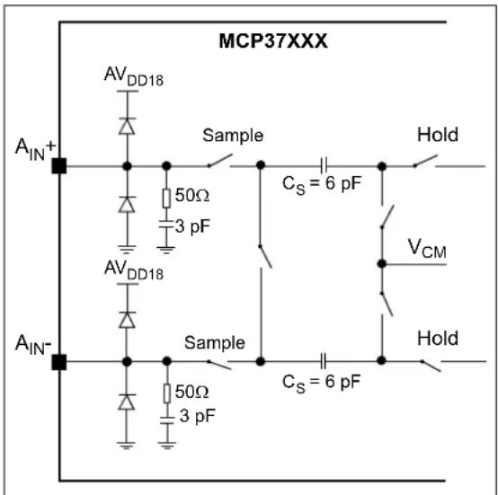
text_image
MCP37XXX AV_DD18 Sample Hold A_IN+ 50Ω 3 pF C_S = 6 pF V_CM AV_DD18 Sample C_S = 6 pF Hold A_IN- 50Ω 3 pFFIGURE 4-2: Equivalent Input Circuit.
4.5.1 ANALOG INPUT DRIVING CIRCUIT
4.5.1.1 Differential Input Configuration
The device achieves optimum performance when the input is driven differentially, where common-mode noise immunity and even-order harmonic rejection are significantly improved. If the input is single-ended, it must be converted to a differential signal in order to properly drive the ADC input. The differential conversion and common-mode application can be accomplished by using an RF transformer or balun with a center-tap. Additionally, one or more anti-aliasing filters may be added for optimal noise performance and should be tuned such that the corner frequency is appropriate for the system.
Figure 4-3 shows an example of the differential input circuit with transformer. Note that the input-driving circuits are terminated by 50Ω near the ADC side through a pair of 25Ω resistors from each input to the common-mode ( V_CM ) from the device. The RF transformer must be carefully selected to avoid artificially high harmonic distortion. The transformer can be damaged if a strong RF input is applied or an RF input is applied while the MCP37XXX is powered-off. The transformer has to be selected to handle sufficient RF input power.
Figure 4-4 shows an input configuration example when a differential output amplifier is used.

text_image
Analog Input 3 1 MABAES0060 4 6 6 4 1 3 MABAES0060 1Ω VCM 0.1 μF 5Ω AIN+ 25Ω 50Ω 3.3 pF 0.1 μF 25Ω 50Ω AIN- MCP37XXXFIGURE 4-3: Transformer Coupled Input Configuration.
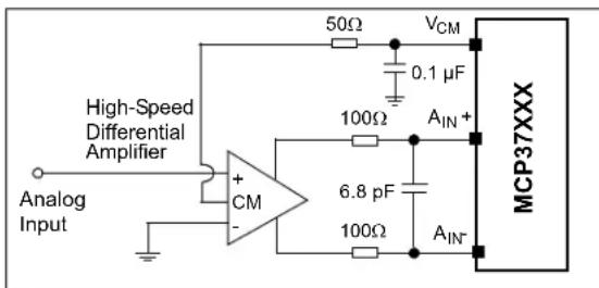
text_image
High-Speed Differential Amplifier Analog Input + CM - 50Ω VCM 0.1 μF 100Ω AIN + 6.8 pF AIN- MCP37XXXFIGURE 4-4: DC-Coupled Input Configuration with Preamplifier: the external signal conditioning circuit and associated component values are for reference only. Typically, the amplifier manufacturer provides reference circuits and component values.
4.5.1.2 Single-Ended Input Configuration
Figure 4-5 shows an example of a single-ended input configuration. This single-ended input configuration is not recommended for the best performance. SNR and SFDR performance degrades significantly when the device is operated in a single-ended configuration. The unused negative side of the input should be AC-coupled to ground using a capacitor.

text_image
Input 50Ω 10 μF 0.1 μF VCM 1 k ΩAnalog R AIN+ VCM 1 k Ω C AIN- MCP37XXX 10 μF 0.1 μFFIGURE 4-5: Singled-Ended Input Configuration.
4.5.2 SENSE VOLTAGE AND INPUT FULL-SCALE RANGE
The device has a bandgap-based differential internal reference voltage. The SENSE pin voltage is used to select the reference voltage source and configure the input full-scale range. A comparator detects the SENSE pin voltage and configures the full-scale input range into one of the three possible modes which are summarized in Table 4-2. Figure 4-6 shows an example of how the SENSE pin should be driven.
The SENSE pin can sink or source currents as high as 500 A across all operational conditions. Therefore, it may require a driver circuit, unless the SENSE reference source provides sufficient output current.

text_image
MCP1700 0.1 µF R₁ R₂ (Note 1) SENSE 0.1 µF MCP37XXXNote 1: This voltage buffer can be removed if the SENSE reference is coming from a stable source (such as MCP1700) which can provide a sufficient output current to the SENSE pin.
FIGURE 4-6: SENSE Pin Voltage Setup.
TABLE 4-2: SENSE PIN VOLTAGE AND INPUT FULL-SCALE RANGE
| SENSE Pin Voltage (VSENSE) | Selected Reference Voltage (VREF) | Full-Scale Input Voltage Range (AFS) | LSb Size (Calculated with AFS) | Condition |
| Tied to GND | 0.7V | 1.4875 V _P-P (1) | 363.16 μV | Low-Reference Mode(4) |
| 0.4V – 0.8V | 0.7V – | 1.4V P-P1487.975 V _P-P V(2) | Adjustable | Sense Mode(5) |
| Tied to AVDD12 | 1.4875V | 2.975 V _P-P (3) | 726.32 μV | High-Reference Mode(4) |
Note 1: A_FS = (17/16) × 1.4 V_P-P = 1.487 V_P-P
2: A_FS = (17/16) × 2.8 V_P-P × (V_SENSE)/0.8 = 1.4875 V_P-P to 2.975 V_P-P
3: A_FS = (17/16) × 2.8 V_P-P = 2.975 V_P-P
4: Based on internal bandgap voltage.
5: Based on V_SENSE .
4.5.2.1 SENSE Selection Vs. SNR/SFDR Performance
The SENSE pin is used to configure the full-scale input range of the ADC. Depending on the application conditions, the SNR, SFDR and dynamic range performance are affected by the SENSE pin configuration. Table4-3 summarizes these settings.
• High-Reference Mode
This mode is enabled by setting the SENSE pin to AV_DD12 (1.2V). This mode provides the highest input full-scale range (2.975 _-P ) and the highest SNR performance. In this mode, the internal thermal noise is less than 1 LSb of the 12-bit ADC (726 V). This has the consequence of making it difficult to resolve small input signals unless some dither is added to the ADC input. In typical applications, thermal noise generated by the system driving the ADC will provide the necessary dithering effect. Figure 3-24 and Figure 3-27 show SNR/SFDR versus input amplitude in High-Reference mode.
Note: Adding dither to the ADC has a negative side effect of reducing the maximum achievable SNR.
- Low-Reference Mode
This mode is enabled by setting the SENSE pin to ground. This mode is suitable for applications which have a smaller input full-scale range. This mode provides improved SFDR characteristics, but SNR is reduced by -3 dB compared to the High-Reference Mode.
- SENSE Mode
This mode is enabled by driving the SENSE pin with an external voltage source between 0.4V and 0.8V. This mode allows the user to adjust the input full-scale range such that SNR and dynamic range are optimized in a given application system environment.
- NSR Mode
The use of the Noise-Shaping Requantizer (NSR), further described in Section 4.8.2 "Noise-Shaping Requantizer (NSR)", is best suited for applications which require a high SNR and a wide dynamic range as well as a relatively narrow bandwidth.
When the NSR is enabled, the noise level in a selected portion of the frequency band is reduced to a level below that of a conventional 12-bit ADC, while the noise level outside of this band remains significantly higher. The SNR achievable in this mode is about 78 dBFS when integrated across 50% of the Nyquist bandwidth. This is an optimum selection for applications where the full Nyquist bandwidth of the ADC is not needed, and where the digital signal post-processing of the ADC data is capable of removing the out-of-band noise added by the NSR.
Figures 3-26 and 3-29 show the SNR/SFDR versus input amplitude with NSR enabled.
TABLE 4-3: SENSE VS. SNR/SFDR PERFORMANCE
| SENSE | Descriptions |
| High-Reference Mode (SENSE pin = AV_DD12 ) | High-input full-scale range (2.975 V_P-P ) and optimized SNR |
| Low-Reference Mode (SENSE pin = ground) | Low-input full-scale range (1.4875 V_P-P ) and reduced SNR, but optimized SFDR |
| Sense Mode (SENSE pin = 0.4V to 0.8V) | Adjustable-input full-scale range (1.4875 V_P-P - 2.975 V_P-P ). Dynamic trade-off between High-Reference and Low-Reference modes can be used. |
| Noise-Shaping Requantizer (NSR) | Optimized SNR, but reduced usable bandwidth.NSR can be employed in any SENSE pin configuration. |
4.5.3 DECOUPLING CIRCUITS FOR INTERNAL VOLTAGE REFERENCE AND BANDGAP OUTPUT
4.5.3.1 Decoupling Circuits for REF1 and REF0 Pins
The device has two internal voltage references, and these references are available at pins REF0 and REF1. REF0 is the internal voltage reference for the ADC input stage, while REF1 is for all remaining stages.
VTLA-124 Package Device: Figure 4-7 shows the recommended circuit for the REF1 and REF0 pins for the VTLA-124 package. Placing a 2.2 F ceramic capacitor with two additional optional capacitors (22 nF and 220 nF) between the positive and negative reference pins is recommended. The negative reference pin is then grounded through a 220 nF capacitor. The capacitors should be placed as close to the ADC as possible with short and thick traces. Vias on the PCB are not recommended for this reference pin circuit.
TFBGA-121 Package Device: The decoupling capacitor is embedded in the package. Therefore, no external circuit is required on the PCB.
4.5.3.2 Decoupling Circuit for V BG Pin
The bandgap circuit is a part of the reference circuit and the output is available at the V_BG pin.
VTLA-124 Package Device: V_BG pin needs an external decoupling capacitor (2.2 F) as shown in Figure 4-7.
TFBGA-121 Package Device: The decoupling capacitor is embedded in the package. Therefore, no external circuit is required on the PCB.

text_image
REF1+ REF1- 2.2 µF 22 nF 220 nF 220 nF (optional) 220 nF 220 nF REF0+ REF0- V_BG 2.2 µF 22 nF 220 nF 220 nFFIGURE 4-7: External Circuit for Voltage Reference and V_BG pins for the VTLA-124 Package. Note that this external circuit is not required for the TFBGA-121 package.
4.6 External Clock Input
For optimum performance, the MCP37XXX requires a low-jitter differential clock input at the CLK+ and CLK-pins. Figure 4-8 shows the equivalent clock input circuit.
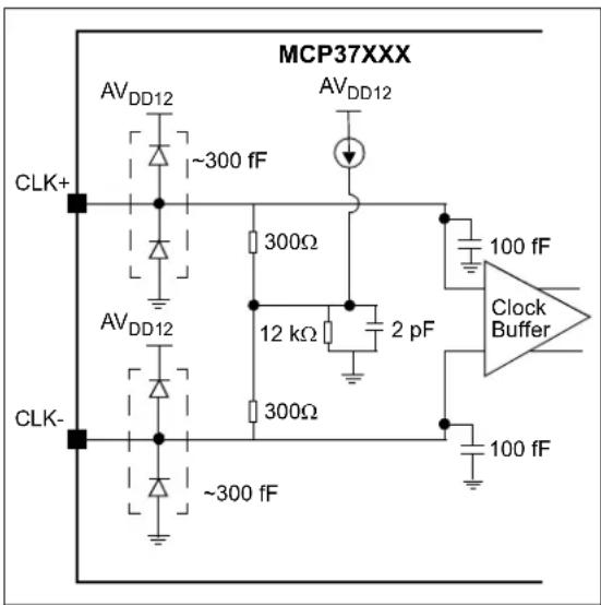
text_image
MCP37XXX AV_DD12 ~300 fF AV_DD12 CLK+ 300Ω AV_DD12 12 kΩ 2 pF Clock Buffer AV_DD12 300Ω ~300 fF 100 fF 100 fFFIGURE 4-8: Equivalent Clock Input Circuit.
The clock input amplitude range is between 300 mV P-P and 800 mV P-P . When a single-ended clock source is used, an RF transformer or balun can be used to convert the clock into a differential signal for the best ADC performance. Figure 4-9 shows an example clock input circuit. The common-mode voltage is internally generated and a center-tap is not required. The back-to-back Schottky diodes across the transformer's secondary current limit the clock amplitude to approximately 0.8 V _P-P differential. This limiter helps prevent large voltage swings of the input clock while preserving the high slew rate that is critical for low jitter.
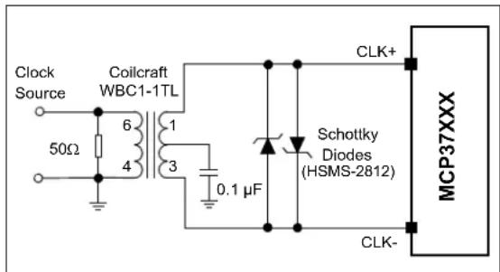
text_image
Clock Source 50Ω Coilcraft WBC1-1TL 6 4 1 3 0.1 μF CLK+ Schottky Diodes (HSMS-2812) MCP37XXX CLK- CLK-FIGURE 4-9: Transformer-Coupled Differential Clock Input Configuration.
4.6.1 CLOCK JITTER AND SNR
PERFORMANCE
In a high-speed pipelined ADC, the SNR performance is directly limited by thermal noise and clock jitter. Thermal noise is independent of input clock and dominant term at low-input frequency. On the other hand, the clock jitter becomes a dominant term as input frequency increases. Equation 4-2 shows the SNR jitter component, which is expressed in terms of the input frequency ( f_IN ) and the total amount of clock jitter ( T_Jitter ), where T_Jitter is a sum of the following two components:
- Input clock jitter (phase noise)
- Internal aperture jitter (due to noise of the clock input buffer).
EQUATION 4-2: SNR VS.CLOCK JITTER
$$ S N R _ {J i t t e r} d B c (\quad \rightarrow 2 \times \quad_ {1 0} (2 0 \log f _ {I N} \times T _ {J i t t e r}) $$
where the total jitter term ( T_jitter ) is given by:
$$ T _ {J i t t e r} = \sqrt {\left(t _ {J i t t e r , C l o c k I n p u l}\right) ^ {2} + \left(t _ {A p e r t u r e , A D C}\right) ^ {2}} $$
The clock jitter can be minimized by using a high-quality clock source and jitter cleaners as well as a band-pass filter at the external clock input, while a faster clock slew rate improves the ADC aperture jitter.
With a fixed amount of clock jitter, the SNR degrades as the input frequency increases. This is illustrated in Figure 4-10. If the input frequency increases from 10 MHz to 20 MHz, the maximum achievable SNR degrades about 6 dB. For every decade (e.g. 10 MHz to 100 MHz), the maximum achievable SNR due to clock jitter is reduced by 20 dB.
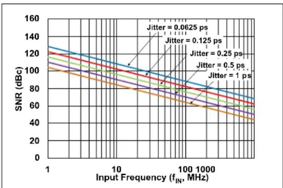
line
| Input Frequency (f_IN, MHz) | Jitter = 0.0625 ps | Jitter = 0.125 ps | Jitter = 0.25 ps | Jitter = 0.5 ps | Jitter = 1 ps | | --------------------------- | ------------------ | ----------------- | ---------------- | --------------- | ------------- | | 1 | 130 | 125 | 120 | 115 | 110 | | 10 | 110 | 105 | 100 | 95 | 90 | | 100 | 80 | 75 | 70 | 65 | 60 | | 1000 | 60 | 55 | 50 | 45 | 40 |FIGURE 4-10: SNR vs. Clock Jitter.
4.7 ADC Clock Selection
This section describes the ADC clock selection and how to use the built-in Delay-Locked Loop (DLL) and Phase-Locked Loop (PLL) blocks.
When the device is first powered-up, the external clock input (CLK+/-) is directly used for the ADC timing as default. After this point, the user can enable the DLL or PLL circuit by setting the register bits. Figure 4-11 shows the clock control blocks. Table4-4 shows an example of how to select the ADC clock depending on the operating conditions.
TABLE 4-4: ADC CLOCK SELECTION (EXAMPLE)
| Operating Conditions Control Bit Settings (1) | Features | ||
| Input Clock Duty Cycle Correction | DCLK Output Phase Delay Control | ||
| CLK_SOURCE = 0 (Default)(2) | |||
| · DLL output is not used · Decimation is not used (Default)(3) | EN_DLL = 0EN_DLL_DCLK = 0EN_PHDLY = 0 | Not Available Not | Available |
| EN_DLL = 1EN_DLL_DCLK = 0EN_PHDLY = 0 | Available | ||
| · DLL output is used · Decimation is not used | EN_DLL = 1EN_DLL_DCLK = 1EN_PHDLY = 1 | Available Available | Available |
| · DLL output is not used · Decimation is used (4) | EN_DLL = 0EN_DLL_DCLK = XEN_PHDLY = 1 | Not Available | |
| EN_DLL = 1EN_DLL_DCLK = 0EN_PHDLY = 1 | Available | ||
| CLK_SOURCE = 1(5) | |||
| · Decimation is not used EN_DLL | = XEN_DLL_DCLK = XEN_PHDLY = 0 | Not Available Available | Available |
| · Decimation is used (4) | EN_DLL = XEN_DLL_DCLK = XEN_PHDLY = 1 | ||
Note 1: See Addresses 0x52, 0x53, and 0x64 for bit settings.
2: The sampling frequency ( f_S ) of the ADC core comes directly from the input clock buffer
3: Output data is synchronized with the output data clock (DCLK), which comes directly from the input clock buffer.
4: While using decimation, output clock rate and phase delay are controlled by the digital clock output control block
5: The sampling frequency ( f_S ) is generated by the PLL circuit. The external clock input is used as the reference input clock for the PLL block.
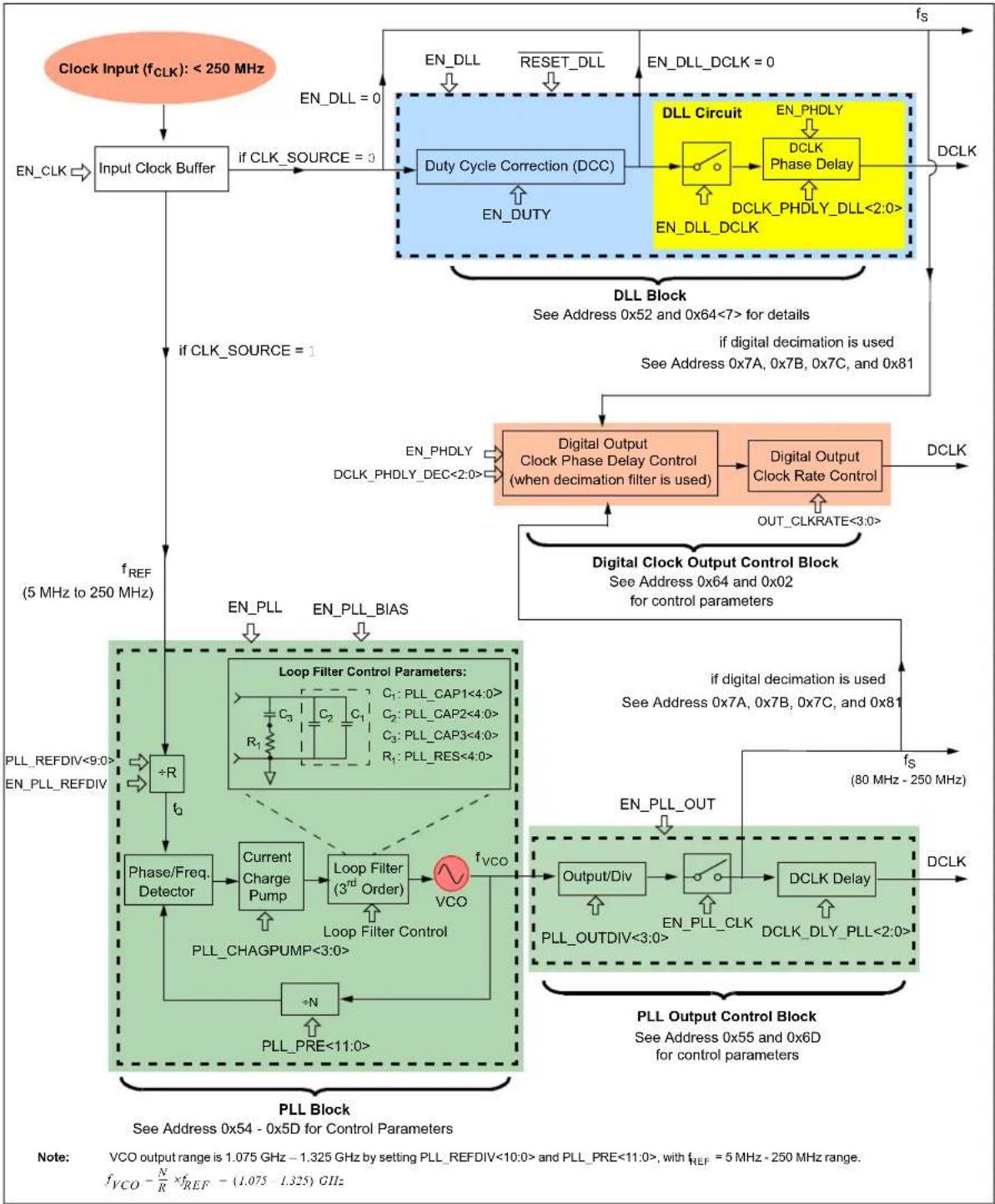
flowchart
graph TD
    A["Clock Input (f_CLK): < 250 MHz"] --> B["Input Clock Buffer"]
    B --> C{if CLK_SOURCE = 0}
    C -->|EN_DLL = 0| D["Duty Cycle Correction (DCC)"]
    D --> E["DLL Circuit"]
    E --> F["DCLK Phase Delay"]
    F --> G["DCLK_DCLK"]
    G --> H["DCLK"]
    H --> I["Digital Output Clock Phase Delay Control (when decimation filter is used)"]
    I --> J["Digital Output Clock Rate Control"]
    J --> K["Digital Clock Output Control Block"]
    K --> L["Digital Output Control Block"]
    L --> M["PLL Block: See Address 0x54 - 0x5D for Control Parameters"]
    M --> N["PLL_REFDIV<9:0>, EN_PLL_REFDIV"]
    N --> O["Phase/Freq Detector"]
    O --> P["Current Charge Pump"]
    P --> Q["Loop Filter (3rd Order)"]
    Q --> R["VCO"]
    R --> S["Loop Filter Control"]
    S --> T["PLL_CHAGPUMP<3:0>"]
    T --> U["N"]
    U --> V["PLL_PRE<11:0>"]
    V --> W["EN_PLL"]
    W --> X["EN_PLL_BIAS"]
    X --> Y["EN_PLL"]
    Y --> Z["EN_PLL"]
    Z --> AA["EN_PLL"]
    AA --> AB["EN_PLL"]
    AB --> AC["EN_PLL"]
    AC --> AD["EN_PLL"]
    AD --> AE["EN_PLL"]
    AE --> AF["EN_PLL"]
    AF --> AG["EN_PLL"]
    AG --> AH["EN_PLL"]
    AH --> AI["EN_PLL"]
    AI --> AJ["EN_PLL"]
    AJ --> AK["EN_PLL"]
    AK --> AL["EN_PLL"]
    AL --> AM["EN_PLL"]
    AM --> AN["EN_PLL"]
    AN --> AO["EN_PLL"]
    AO --> AP["EN_PLL"]
    AP --> AQ["EN_PLL"]
    AQ --> AR["EN_PLL"]
    AR --> AS["EN_PLL"]
    AS --> AT["EN_PLL"]
    AT --> AU["EN_PLL"]
    AU --> AV["EN_PLL"]
    AV --> AW["EN_PLL"]
    AW --> AX["EN_PLL"]
    AX --> AY["EN_PLL"]
FIGURE 4-11: Timing Clock Control Blocks.
4.7.1 USING DLL MODE
Using the DLL block is the best option when output clock phase control is needed while the clock multiplication and digital decimation are not required. When the DLL block is enabled, the user can control the input clock Duty Cycle Correction (DCC) and the output clock phase delay.
See the DLL block in Figure 4-11 for details. Table 4-5 summarizes the DLL control register bits. In addition, see Table 4-24 for the output clock phase control.
TABLE 4-5: DLL CONTROL REGISTER BITS
| Control Parameter Register | Descriptions | |
| CLK_SOURCE | 0x53 | CLK_SOURCE = 0: external clock input becomes input of the DLL block |
| EN_DUTY | 0x52 | Input clock duty cycle correction control bit ^(1) |
| EN_DLL | 0x52 | EN_DLL = 1: enable DLL block |
| EN_DLL_DCLK | 0x52 | DLL output clock enable bit |
| EN_PHDLY<2:0> | 0x52 | Phase delay control bits of digital output clock (DCLK) when DLL or decimation filter is used ^(2) |
| RESET_DLL | 0x52 | Reset control bit for the DLL block |
Note 1: Duty cycle correction is not recommended when a high-quality external clock is used.
2: If decimation is used, the output clock phase delay is controlled using DCLK_PHDLY_DEC<2:0> in Address 0x64.
4.7.1.1 Input Clock Duty Cycle Correction
The ADC performance is sensitive to the clock duty cycle. The ADC achieves optimum performance with 50% duty cycle, and all performance characteristics are ensured when the duty cycle is 50% with ±1% tolerance.
When CLK_SOURCE = 0, the external clock is used as the sampling frequency ( f_S ) of the ADC core. When the external input clock is not high-quality (for example, duty cycle is not 50%), the user can enable the internal clock duty cycle correction circuit by setting the EN_DUTY bit in Address 0x52 (Register 5-7). When duty cycle correction is enabled (EN_DUTY=1), only the falling edge of the clock signal is modified (rising edge is unaffected).
Because the duty cycle correction process adds additional jitter noise to the clock signal, this option is recommended only when an asymmetrical input clock source causes significant performance degradation or when the input clock source is not stable.
Note: The clock duty cycle correction is only applicable when the DLL block is enabled (EN_DLL = 1). It is not applicable for the PLL output.
4.7.1.2 DLL Block Reset Event
The DLL must be reset if the clock frequency is changed. The DLL reset is controlled by using the RESET_DLL bit in Address 0x52 (Register 5-7). The DLL has an automatic reset with the following events:
- During power-up: Stay in reset until the RESET_DLL bit is cleared.
- When a SOFT_RESET command is issued while the DLL is enabled: the RESET_DLL bit is automatically cleared after reset.
4.7.2 USING PLL MODE
The PLL block is mainly used when clock multiplication is needed. When CLK_SOURCE = 1, the sampling frequency ( f_S ) of the ADC core is coming from the internal PLL block.
The recommended PLL output clock range is from 80 MHz to 250 MHz. The external clock input is used as the PLL reference frequency. The range of the clock input frequency is from 5 MHz to 250 MHz.
Note: The PLL mode is only supported for sampling frequencies between 80 MHz and 250 MHz.
4.7.2.1 PLL Output Frequency and Output Control Parameters
The internal PLL can provide a stable timing output ranging from 80 MHz to 250 MHz. Figure 4-11 shows the PLL block using a charge-pump-based integer N PLL and the PLL output control block. The PLL block includes various user control parameters for the desired output frequency. Table 4-6 summarizes the PLL control register bits and Table 4-7 shows an example of register bit settings for the PLL charge pump and loop filter.
The PLL block consists of:
• Reference Frequency Divider (R)
- Prescaler - which is a feedback divider (N)
• Phase/Frequency Detector (PFD)
- Current Charge Pump
- Loop Filter - a 3^rd order RC low-pass filter
• Voltage-Controlled Oscillator (VCO)
The external clock at the CLK+ and CLK- pins is the input frequency to the PLL. The range of input frequency ( f_REF ) is from 5MHz to 250 MHz. This frequency is divided by the reference frequency divider (R) which is controlled by the 10-bit-wide PLL_REFDIV<9:0> setting. In the feedback loop, the VCO frequency is divided by the prescaler (N) using PLL_PRE<11:0>.
The ADC core sampling frequency ( f_S ), ranging from 80 MHz to 250 MHz, is obtained after the output frequency divider (PLL_OUTDIV<3:0>). For stable operation, the user needs to configure the PLL with the following limits:
- Input clock frequency (f _REF ) = 5 MHz to 250 MHz
- Charge pump input frequency = 4 MHz to 50 MHz (after PLL reference divider)
• VCO output frequency = 1.075 to 1.325 GHz - PLL output frequency after = 80 MHz to 250 MHz output divider
The charge pump is controlled by the PFD, and forces sink (DOWN) or source (UP) current pulses onto the loop filter. The charge pump bias current is controlled by the PLL_CHAGPUMP<3:0> bits, approximately 25 A per step. The loop filter consists of a 3 ^rd order passive RC filter. Table 4-7 shows the recommended settings of the charge pump and loop filter parameters, depending on the charge pump input frequency range (output of the reference frequency divider).
When the PLL is locked, it tracks the input frequency ( f_REF ) with the ratio of dividers (N/R). The PLL operating status is monitored by the PLL status indication bits:
Equation 4-3 shows the VCO output frequency ( f_VCO ) as a function of the two dividers and reference frequency:
EQUATION 4-3: VCO OUTPUT FREQUENCY
$$ \begin{array}{l} f _ {V C O} = \left(\frac {N}{R}\right) f _ {R E F} = 1. 0 7 5 (G H z) t o 1. 3 2 5 (G H z) \ N = 1 \text { to } 4 0 9 5 \text { controlled by PLL_PRE } < 1 1: 0 > \ R = 1 \text { to } 1 0 2 3 \text { controlled by PLL_REFDIV< 9:0> } \ \end{array} $$
Where:
$$ \begin{array}{l} N = 1 \text { to } 4 0 9 5 \text { controlled by PLL_PRE } < 1 1: 0 > \ R = 1 \text { to } 1 0 2 3 \text { controlled by PLL_REFDIV< 9:0> } \ \end{array} $$
See Addresses 0x54 to 0x57 (Registers 5-9 - 5-12) for these bits settings.
The tuning range of the VCO is 1.075 GHz to 1.325 GHz. N and R values must be chosen so the VCO is within this range. In general, lower values of the VCO frequency ( f_VCO ) and higher values of the charge pump frequency ( f_Q ) should be chosen to optimize the clock jitter. Once the VCO output frequency is determined to be within this range, set the final ADC sampling frequency ( f_S ) with the PLL output divider using PLL_OUTDIV<3:0>. Equation 4-4 shows how to obtain the ADC core sampling frequency:
EQUATION 4-4: SAMPLING FREQUENCY
$$ f _ {S} = \left(\frac {f _ {V C O}}{P L L _ O U T D I V}\right) = 8 0 M H z t o 2 5 0 M H z $$
Table 4-8 shows an example of generating f_S = 200 MHz output using the PLL control parameters.
4.7.2.2 PLL Calibration
The PLL should be recalibrated following a change in clock input frequency or in the PLL Configuration register bit settings (Addresses 0x54 - 0x57; Registers 5-9 - 5-12).
The PLL can be calibrated by toggling the PLL_CAL_TRIG bit in Address 0x6B (Register 5-27) or by sending a SOFT_RESET command (See Address 0x00, Register 5-1). The PLL calibration status is observed by the PLL_CAL_STAT bit in Address 0xD1 (Register 5-81).
4.7.2.3 Monitoring of PLL Drifts
The PLL drifts can be monitored using the status monitoring bits in Address 0xD1 (Register 5-81). Under normal operation, the PLL maintains a lock across all temperature ranges. It is not necessary to actively monitor the PLL unless extreme variations in the supply voltage are expected or if the input reference clock frequency has been changed.
TABLE 4-6: PLL CONTROL REGISTER BITS
| Control Parameter Register Descriptions | ||
| PLL Global Control Bits | ||
| EN_PLL 0x59 Master enable bit for the PLL circuit | ||
| EN_PLL_OUT 0x5F Master enable bit for the PLL output | ||
| EN_PLL_BIAS 0x5F Master enable bit for the PLL bias | ||
| EN_PLL_REFDIV 0x59 Master enable bit for the PLL reference divider | ||
| PLL Block Setting Bits | ||
| PLL_REFDIV<9:0> | 0x54-0x55 | PLL reference divider (R) (See Table 4-8) |
| PLL_PRE<11:0> | 0x56-0x57 | PLL prescaler (N) (See Table 4-8) |
| PLL_CHAGPUMP<3:0> | 0x58 | PLL charge pump bias current control: from 25 μA to 375 μA, 25 μA per step |
| PLL_RES<4:0> | 0x5A | PLL loop filter resistor value selection (See Table 4-7) |
| PLL_CAP3<4:0> | 0x5B | PLL loop filter capacitor 3 value selection (See Table 4-7) |
| PLL_CAP2<4:0> | 0x5D | PLL loop filter capacitor 2 value selection (See Table 4-7) |
| PLL_CAP1<4:0> | 0x5C | PLL loop filter capacitor 1 value selection (See Table 4-7) |
| PLL Output Control Bits | ||
| PLL_OUTDIV<3:0> | 0x55 | PLL output divider (See Table 4-8) |
| DCLK_DLY_PLL<2:0> | 0x6D | Delay DCLK output up to 15 cycles of VCO clocks |
| EN_PLL_CLK | 0x6D | EN_PLL_CLK = 1 enable PLL output clock to the ADC circuits |
| PLL Drift Monitoring Bits | ||
| PLL_VCOL_STAT | 0xD1 | PLL drift status monitoring bit |
| PLL_VCOH_STAT | 0xD1 | PLL drift status monitoring bit |
| PLL Block Calibration Bits | ||
| PLL_CAL_TRIG | 0x6B | Forcing recalibration of the PLL |
| SOFT_RESET | 0x00 | PLL is calibrated when exiting soft reset mode |
| PLL_CAL_STAT | 0xD1 | PLL auto-calibration status indication |
TABLE 4-7: RECOMMENDED PLL CHARGE PUMP AND LOOP FILTER BIT SETTINGS
| PLL Charge Pump and Loop Filter Parameter | f_Q = f_REF/PLL\_REFDIV | ||
| f_Q < 5 MHz 5 MHz ≤ f | q < 2.5 MHz f | q ≥ 25 MHz | |
| PLL_CHAGPUMP<3:0> 0x04 0x04 0x04 | |||
| PLL_RES<4:0> 0x1F 0x1F | 0x07 | ||
| PLL_CAP3<4:0> | 0x07 | 0x02 | 0x07 |
| PLL_CAP2<4:0> | 0x07 | 0x01 | 0x08 |
| PLL_CAP1<4:0> | 0x07 | 0x01 | 0x08 |
TABLE 4-8: EXAMPLE OF PLL CONTROL BIT SETTINGS FOR f S = 200 MHz WITH f REF = 100 MHz
| PLL Control Parameter | Value | Descriptions |
| f_REF | 100 MHz | f_REF is coming from the external clock input |
| Target f_S^(1) | 200 MHz | ADC sampling frequency |
| Target f_VCO^(2) | 1.2 GHz | Range of f_VCO = 1.0375 GHz - 1.325 GHz |
| Target f_Q^(3) | 10 MHz | f_Q = f_REF/PLL\_REFDIV (See Table 4-7) |
| PLL Reference Divider (R) | 10 | PLL_REFDIV<9:0> = 0x0A |
| PLL Prescaler (N) | 120 | PLL_PRE<11:0> = 0x78 |
| PLL Output Divider | 6 | PLL_OUTDIV<3:0> = 0x06 |
Note 1: f_S = f_VCO / PLL_OUTDIV = 1.2 GHz/6 = 200 MHz
2: f_VCO = (N/R) × f_REF = (12) × 100 MHz = 1.2 GHz
3: f_Q should be maximized for the best noise performance.
4.8 Digital Signal Post-Processing (DSPP) Options
While the device converts the analog input signals to digital output codes, the user can enable various digital signal post-processing (DSPP) options for special applications. These options are individually enabled or disabled by setting the Configuration bits. Table 4-9 summarizes the digital signal post-processing (DSPP) options that are available for each device family.
TABLE 4-9: DIGITAL SIGNAL POST PROCESSING (DSPP) OPTIONS
| Digital Signal Post Processing Option Available Operating Mode | |
| Fractional Delay Recovery (FDR) | Dual and octal-channel modes |
| FIR Decimation Filters | Single and dual-channel modesCW octal-channel modeDDC for I and Q data |
| Noise-Shaping Requantizer (NSR) | Single and dual-channel modes |
| Digital Gain and Offset correction per channel | Available for all channels |
| Digital-Down Conversion (DDC) | Single and dual-channel modesCW octal-channel mode |
| Continuous Wave (CW) Beamforming | CW octal-channel mode |
4.8.1 FRACTIONAL DELAY RECOVERY FOR DUAL- AND OCTAL-CHANNEL MODES
The FDR feature is available in dual and octal-channel modes only. When FDR is enabled, the built-in high-order, band-limited interpolation filter compensates for the time delay between input samples of different channels. Due to the finite bandwidth of the interpolation filter, the fractional delay recovery is not guaranteed for input frequencies near the Nyquist frequency ( f_S/2 ). For example, in dual-channel mode, FDR can operate correctly for input frequencies in the range from 0 to 0.45* f_S (or from 0.55*fs to f_S if the input is in the 2nd Nyquist band). In octal-channel mode, FDR can operate correctly for input frequencies in the range from 0 to 0.38* f_S . See Table 4-11 for the summary of the input bandwidth requirement for FDR. The FDR process takes place in the digital domain and requires 59 clock cycles of processing time. Therefore, the output data latency is also increased by 59 clock periods.
Figure 4-12 shows the simplified block diagram for the ADC output data path with FDR. The related Configuration register bits are listed in Table4-10. Table 4-11 shows the input bandwidth limits of the FDR feature for distortion less than 0.1 m dB ( 0.1 × 10^-3 dB), where f_S is the sampling frequency per channel. Figures 4-13 and 4-14 show the responses of the dual-channel and octal-channel FDRs, respectively.
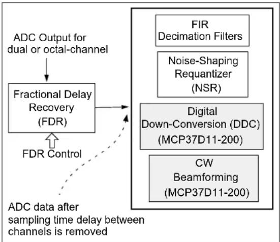
flowchart
graph TD
    A["ADC Output for dual or octal-channel"] --> B["Fractional Delay Recovery (FDR)"]
    B --> C["FDR Control"]
    C --> D["Digital Down-Conversion (DDC) (MCP37D11-200)"]
    D --> E["CW Beamforming (MCP37D11-200)"]
    E --> F["FIR Decimation Filters"]
    F --> G["Noise-Shaping Requantizer (NSR)"]
    G --> B
    style B fill:#f9f,stroke:#333
    style D fill:#ccf,stroke:#333
    style E fill:#cfc,stroke:#333
FIGURE 4-12: Simplified Block Diagram for ADC Output Data Path with Fractional Delay Recovery Option. Note that Fractional Delay Recovery occurs prior to other DSPP features.
TABLE 4-10: CONTROL PARAMETERS FOR FRACTIONAL DELAY RECOVERY (FDR)
| Channel Operation Control Parameter Register Descriptions | |||
| Global control for both dual and octal-channel modes | EN_FDR = 1 0x7A Enable FDR features | ||
| FDR_BAND | 0x81 | Selectbr 2^nd Njquist band | |
| Dual-channel | SEL_FDR = 0 | 0x81 | Select FDR for dual-channel mode |
| EN_DSPP_8 = 0 | 0x81 | Select digital signal post-processing feature for dual-channel mode | |
| EN_DSPP_2 = 1 | 0x79 | Enable all digital post-processing functions for dual-channel operation | |
| Octal-channel | SEL_FDR = 1 | 0x81 | Select FDR for octal-channel mode |
| EN_DSPP_8 = 1 | 0x81 | Select digital signal post-processing feature for octal-channel operation | |
TABLE 4-11: INPUT BANDWIDTH REQUIREMENT FOR FDR
| Bandwidth in percentage of f_S^(1) | Nyquist Band (2) |
| Dual-Channel Mode | |
| 0 – 45% | 1^st Nyquist Band (FDR_BAND = 0) |
| 55 – 100% | 2^nd Nyquist Band (FDR_BAND = 1) |
| 45 – 55% | Avoid |
| Octal-Channel Mode | |
| 0 – 38% | 1^st Nyquist Band (FDR_BAND = 0) |
Note 1: f_s is sampling frequency per channel. Distortion is less than 0.1 mdB.
2: See Address 0x81 for FDR_BAND bit setting

line
| Frequency | Amplitude (dBc) | | --------- | --------------- | | 0 | 0.0005 | | f_s/2 | -0.0005 | | f_s | -120 |FIGURE 4-13: Response of the Dual-Channel Fractional Delay Recovery ( 1^st Nyquist Band). f_S is the Sampling Frequency.
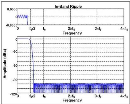
line
| Frequency | Amplitude (dBc) | | --------- | --------------- | | 0 | 0 | | fs/2 | -120 | | fs | -100 | | 2×fs | -100 | | 3×fs | -100 | | 4×fs | -100 |FIGURE 4-14: Response of the Octal-Channel Fractional Delay Recovery ( 1^st Nyquist Band). f_S is the Sampling Frequency.
4.8.2 NOISE-SHAPING REQUANTIZER (NSR)
The device includes 11-bit and 12-bit digital Noise-Shaping Requantizer (NSR) options. When this function is enabled (see Register 5-33), output data is requantized to 11-bit or 12-bit, respectively. The NSR reshapes the requantization noise function and pushes most of the noise outside the frequency band of interest. As a result, the noise floor within the selected bandwidth is substantially lower than that of a typical 12-bit ADC.
To ensure the stability of the NSR, the input signal to the NSR should be limited to less than -0.8 dBFS (\~90% of full scale). This can be achieved either by limiting the analog input level or by adjusting the digital gain control. See Section 4.9 "Digital Offset and Digital Gain Settings" and Registers 5-63 to 5-70 for details on the digital gain control. Input levels higher than -0.8 dBFS may corrupt the NSR output and should be avoided.
The NSR feature is available only for the single- and dual-channel modes and can be independently controlled per channel via the register settings. Two NSRs are used:
• NSRA for channel A
- NSRB for channel B
In single-channel mode, only NSRA is used. In dual-channel mode, both NSRA and NSRB are used: NSRA is used for the first selected channel, and NSRB is used for the second selected channel. Both have 11-bit and 12-bit options. Each NSR block consists of a series of filters which are selectable using the NSRA<6:0> and NSRB<6:0> register bit settings. Each filter is defined by a specific percentage bandwidth and center frequency. The available percentage bandwidths are:
• 11-bit mode: 22% and 25% of the sampling frequency
• 12-bit mode: 25% and 29% of the sampling frequency
The center frequency of the band is tunable such that the frequency band of interest can be placed anywhere within the Nyquist band. Table 4-12 lists all the NSR-related registers. Equations 4-5 and 4-6 describe the NSR bandwidth of the 11-bit and 12-bit options, respectively.
EQUATION 4-5: NSR BANDWIDTH FOR 11-BIT OPTION
(a) 22% BW:
$$ \frac {f _ {\text { Center }}}{f _ {S}} = 0 + \frac {0 . 2 6}{2 0} \text { INSR } 2 $$
$$ w h e r e 0 \leq N S R \leq 2 0 $$
(b) 25% BW:
$$ \frac {f _ {\text { Center }}}{f _ {S}} = 0. + \frac {0 . 2 5}{2 0} \times (N S R 5. 2 1) $$
$$ w h e r e 2 1 \leq N S R \leq 4 1 $$
NSR represents the NSR filter number. See Tables 4-13 and 4-14 for details.
EQUATION 4-6: NSR BANDWIDTH FOR 12-BIT OPTION
(a) 25% BW:
$$ \frac {f _ {\text { Center }}}{f _ {S}} = 0 \quad . + \frac {0 . 2 5}{2 0} \times (\mathfrak {N} S R - 4 2) $$
$$ w h e r e 4 2 \leq N S R \leq 6 2 $$
(b) 29% BW:
$$ \frac {f _ {\text { Center }}}{f _ {S}} = 0 + \frac {0 . 2}{1 2} \kappa (N S R - 6 3) $$
$$ w h e r e 6 3 \leq N S R \leq 7 6 $$
NSR represents the NSR filter number. See Tables 4-13 and 4-14 for details.
The center frequency of the band is tuned such that the frequency spectrum of interest can be placed anywhere within the Nyquist band. Figure 4-15 shows a graphical demonstration of the NSR bandwidth, which is a percentage of the ADC sampling frequency.

line
| Frequency | Amplitude (dBFS) | | --------- | ---------------- | | 0 | -100 | | fs/4 | -120 | | fs/2 | -60 |FIGURE 4-15: Graphical demonstration of the NSR filter's transfer function. Note that f_B is controlled as a percentage of the sampling frequency ( f_S ).
Tables 4-13 and 4-14 show the NSR filter selections. The selectable filters (tuning word) for each mode are:
- 11-bit mode: 0 to 41
• 12-bit mode: 42 to 76
NSR does not affect harmonic distortion. Various FFT spectrum plots when NSR is applied are shown in Figures 3-14 to 3-15, Figures 3-17 to 3-20 and Figures 3-22 to 3-23. SNR and SFDR performance versus input amplitude when NSR is enabled is shown in Figures 3-26 and 3-29.
In this case, SNR and SFDR are measured within the 12-bit mode NSR bandwidth (25% of the sampling frequency). When the NSR block is disabled, the ADC data is provided directly to the output.
TABLE 4-12: REGISTER CONTROL PARAMETERS FOR NSR
| Control Parameter Register Descriptions | ||
| NSR Enable bits | ||
| 0x7A Enable 11-bit NSR for channel A | ||
| 0x7A Enable 12-bit NSR for channel A | ||
| 0x7A Enable 11-bit NSR for channel B | ||
| 0x7A Enable 12-bit NSR for channel B | ||
| NSR Settings | ||
| NSRA<6:0> 0x78 NSR | A settings for single-channel or channel A for dual-channel mode | |
| NSRB<6:0> 0x79 NSR | B settings for channel B in dual-channel mode | |
| NSR Block Reset Control | ||
| 0x78 | Resets NSR in the event of overload | |
| Digital Post Processing (DPP) Function Block Settings | ||
| EN_DPPDUAL | 0x79 | Enable DPP block for dual-channel mode |
TABLE 4-13: 11-BIT NSR FILTER SELECTION ^(1)
| NSR Filter No. (Tuning Word) | f_Center/f_S | f_B (% of f_S ) | NSRA<6:0> NSRB<6:0> |
| 0 | 0.12 | 22 | 000-0000 |
| 1 | 0.133 | 22 | 000-0001 |
| 2 | 0.146 | 22 | 000-0010 |
| — | |||
| — | |||
| 19 | 0.367 | 22 | 001-0011 |
| 20 | 0.38 | 22 | 001-0100 |
| 21 | 0.125 | 25 | 001-0101 |
| 22 | 0.1375 | 25 | 001-0110 |
| 23 | 0.15 | 25 | 001-0111 |
| — | |||
| — | |||
| 40 | 0.3625 | 25 | 010-1000 |
| 41 | 0.375 | 25 | 010-1001 |
Note 1: Filters 0 - 41 are used for 11-bit mode only. If these are used for 12-bit mode, the output becomes unknown state.
TABLE 4-14: 12-BIT NSR FILTER SELECTION ^(1)
| NSR Filter No. (Tuning Word) | f_Center/f_S | f_B (% of f_S ) | NSRA<6:0> NSRB<6:0> |
| 42 | 0.125 | 25 | 010-1010 |
| 43 | 0.1375 | 25 010-1011 | |
| 44 | 0.15 | 25 | 010-1100 |
| — | |||
| 61 | 0.3625 | 25 011-1101 | |
| 62 | 0.375 | 25 | 011-1110 |
| 63 | 0.15 | 29 | 011-1111 |
| 64 | 0.1667 | 29 100-0000 | |
| 65 | 0.1833 | 29 100-0001 | |
| — | |||
| — | |||
| 75 | 0.35 | 29 | 100-1011 |
| 76 | 0.3667 | 29 100-1100 | |
Note 1: Filters 42 - 76 are used for 12-bit mode only. If these are used for 11-bit mode, the output becomes unknown state.
4.8.3 DECIMATION FILTERS
The decimation feature is available in single and dual-channel modes and CW octal-channel mode. Figure 4-16 shows a simplified decimation filter block, and Table4-16 shows the register settings. The decimation rate is controlled by FIR_A<8:0> and FIR_B<7:0> register settings (Addresses 0x7A - 0x7C: Registers 5-35 - 5-37). These registers are thermometer encoded.
In single-channel mode, FIR B is disabled and only FIR A is used. In this mode, the maximum programmable decimation rate is 512x using nine cascaded decimation stages.
In dual-channel mode or when using the Digital Down-Conversion (DDC) in I/Q mode, both FIR A and FIR B are used (see Figure 4-16). In this case, both channels are set to the same decimation rate. Note that stage 1A in FIR A is unused: the user must clear FIR_A<0> in Address 0x7A (Register 5-35). In dual-channel mode, the maximum programmable decimation rate is up to 256x, which is half the single-channel decimation rate (512x).
The overall SNR performance can be improved with higher decimation rate, but limited to about 73.7 dBFS after 16x. This limitation is mainly due to the relative quantization noise level with respect to the 12-bit LSB size. Decimation rates beyond 16x do not further improve SNR but do serve to filter the output data and reduce the overall output data rate. Table 4-15 summarizes decimation rate versus SNR.
TABLE 4-15: DECIMATION RATE VS. SNR PERFORMANCE
| Decimation Rate | SNR (dBFS) |
| 2x | 71.4 |
| 4x | 72.2 |
| 8x | 72.9 |
| 16x | 73.3 |
| 32x | 73.7 |
| 64x | |
| 128x | |
| 256x | |
| 512x |
Note: The above data is validated with f_S = 200 Msps, f_IN = 5 MHz, A_IN = -1 dBFS.
4.8.3.1 Output Data Rate and Clock Phase Control When Decimation is Used
When decimation is used, it also reduces the output clock rate and output bandwidth by a factor equal to the decimation rate applied: the output clock rate is therefore no longer equal to the ADC sampling clock. The user needs to adjust the output clock and data rates in Address 0x02 (Register 5-3) based on the decimation applied. This allows the output data to be synchronized to the output data clock.
Phase shifts in the output clock can be achieved using DCLK_PHDLY_DEC<2:0> in Address 0x64 (Register 5-22). Only four output sampling phases are available when a decimation rate of 2x is used, while all eight clock phases are available for other decimation rates. See Section 4.12.8 "Output Data and Clock Rates" for more details.
4.8.3.2 Using Decimation with CW Beamforming and Digital Down-Conversion
Decimation can be used in conjunction with CW octal-channel mode or DDC. In CW octal-channel mode operation, the eight input channels are summed into a single channel prior to entering the decimation filters. When DDC is enabled, the I and Q outputs can be decimated using the same signal path for the dual-channel mode: I and Q data are fed into Channel A and B, respectively.
In DDC mode, the half-band filter already includes a 2x decimation rate. Therefore, the maximum decimation rate setting for I/Q filtering is 128x for the FIR_A<8:1> and FIR_B<7:0>. See Section 4.8.4 "Digital Down-Conversion (MCP37D11-200 only)" for details.
| Note: | Fractional Delay Recovery, Digital Gain/Offset adjustment and DDC for I/Q data options occur prior to the decimation filters if they are enabled. |
TABLE 4-16: REGISTER CONTROL PARAMETERS FOR USING DECIMATION FILTERS
| Control Parameter Register Descriptions | ||
| Decimation Filter Settings | ||
| FIR_A<8:0> 0x7A, 0x7B Channel A FIR configuration for single- or dual-channel mode | ||
| FIR_B<7:0> 0x7C Channel B FIR configuration for single- or dual-channel mode | ||
| Output Data Rate and Clock Rate Settings(1) | ||
| OUT_DATARATE<3:0> 0x02 | Output data rate: Equal to decimation rate | |
| OUT_CLKRATE<3:0> | 0x02 | Output clock rate: Equal to decimation rate |
| Output Clock Phase Control Settings(2) | ||
| EN_PHDLY | 0x64 | Enable digital output phase delay when decimation filter is used |
| DCLK_PHDLY_DEC<2:0> | 0x64 | Digital output clock phase delay control |
| Digital Signal Post-Processing (DSPP) Function Block Settings | ||
| EN_DSPP_2 = 1 | 0x79 | Enable dual-channel decimation |
Note 1: The output data and clock rates must be updated when decimation rates are changed.
2: Output clock (DCLK) phase control is used when the output clock is divided by OUT_CLKRATE<3:0> bit settings.

flowchart
graph TD
    A["Single Channel Input"] --> B["Stage 1A FIR"]
    B --> C["↓2"]
    C --> D["Stage 2A FIR"]
    D --> E["↓2"]
    E --> F["Stage 3A FIR"]
    F --> G["↓2"]
    G --> H["Stage 9A FIR"]
    H --> I["↓2"]
    I --> J["D512 Single"]
    K["Dual Channel Input"] --> L["Input DeMUX (Note 1)"]
    L --> M["Ch. A"]
    M --> N["Stage 2B FIR (Note 2)"]
    N --> O["↓2"]
    O --> P["Stage 3B FIR"]
    P --> Q["↓2"]
    Q --> R["Stage 9B FIR"]
    R --> S["↓2"]
    S --> T["Output MUX"]
    T --> U["D4 Dual"]
    U --> V["Output MUX"]
    V --> W["D128 I/Q"]
    X["Input for DDC"] --> Y["Input DeMUX"]
    Y --> Z["Ch. A"]
    Z --> AA["Ch. B"]
    AA --> AB["D2 Single"]
    AC["Dual-channel operation"] --> AD["Input DeMUX"]
    AE["Dual-channel operation"] --> AF["Input DeMUX (Note 1)"]
    AG["Dual-channel operation"] --> AH["Input DeMUX (Note 2)"]
    AI["Dual-channel operation"] --> AJ["Input DeMUX (Note 3)"]
    AK["Dual-channel operation"] --> AL["Input DeMUX (Note 4)"]
    AM["Dual-channel operation"] --> AN["Input DeMUX (Note 5)"]
    AO["Dual-channel operation"] --> AP["Input DeMUX (Note 6)"]
    AQ["Dual-channel operation"] --> AR["Input DeMUX (Note 7)"]
    AS["Dual-channel operation"] --> AT["Input DeMUX (Note 8)"]
    AU["Dual-channel operation"] --> AV["Input DeMUX (Note 9)"]
    AW["Dual-channel operation"] --> AX["Input DeMUX (Note 10)"]
Note 1: Stage 1A FIR is the first stage of the FIR A filter.
2: (a) Single-channel mode: Only Channel A is used and controlled by FIR_A<8:0>.
(b) Dual-channel mode or I/Q filtering in DDC mode: Both Channel A and Channel B are used: Channel A is used for the first channel or I data, and Channel B is used for the second channel or Q data.
3: Maximum decimation rate:
(a) When I/Q filtering in DDC mode is not used: 512x for single-channel and 256x for dual-channel mode.
(b) I/Q filtering in DDC mode: 128x each for FIR_A<8:1> and FIR_B<7:0>.
FIGURE 4-16: Simplified Block Diagram of Decimation Filters.
4.8.4 DIGITAL DOWN-CONVERSION (MCP37D11-200 ONLY)
The Digital Down-Conversion (DDC) feature is available in single-, dual- and CW octal-channel modes in the MCP37D11-200. This feature can be optionally combined with the decimation filter and used to:
• translate the input frequency spectrum to a lower frequency band
- remove the unwanted out-of-band portion
- output the resulting signal as either I/Q data or as a real signal centered at 25% of the output data rate.
Figure 4-17 and Figure 4-18 show the DDC configuration for single- and dual-channel DDC mode, respectively. The DDC includes a 32-bit, complex numerically controlled oscillator (NCO), a selectable (high/low) half-band filter, optional decimation, and two output modes (I/Q or f_S/8 ).
Frequency translation is accomplished with the NCO. The NCO frequency is programmable from 0 Hz to f_S . Phase and amplitude dither can be enabled to improve spurious performance of the NCO.
This DDC feature can be used in a variety of high-speed signal-processing applications, including digital radio, wireless base stations, radar, cable modems, digital video, MRI imaging, etc.
Example:
If the ADC is sampling an input at 200 Msps, but the user is only interested in a 5 MHz span which is centered at 67 MHz, the digital down-conversion may be used to mix the sampled ADC data with 67 MHz to convert it to DC. The resulting signal can then be decimated by 16x such that the bandwidth of the ADC output is 6.25 MHz (200 Msps/16x decimation gives 12.5 Msps with 6.25 MHz Nyquist bandwidth). If fs/8 mode is selected, then a single 25 Msps channel is output, where 6.25 MHz in the output data corresponds to 67 MHz at the ADC input. If I/Q mode is selected, then two 12.5 Msps channels are output, where DC corresponds to 67 MHz and the channels represent in-phase (I) and quadrature (Q) components of the down-conversion.
Figure 4-17 shows the single-channel DDC configuration. Each of these processing sub-blocks are individually controlled. Examples of setting registers for selected output type are shown in Tables 4-17 and 4-18.

flowchart
graph TD
    A["CH. A ADC DATA"] --> B["×"]
    B --> C["×"]
    C --> D["Half-Band Filter A LP/HP"]
    D --> E["×"]
    E --> F["FIR_A Decimation Filter"]
    F --> G["NCO (fS/8 DER)"]
    G --> H["+"]
    H --> I["Real or Real_DEC"]
    I --> J["Q or Q_DEC"]
    J --> K["I or I_DEC"]
    L["COS SIN"] --> M["NCO (32-bit) (Note 2)"]
    M --> N["EN_NCO"]
    N --> O["EN_DDC1"]
    P["HBFILTER_A"] --> Q["×"]
    Q --> R["FIR_B Decimation Filter"]
    R --> S["FIR_A<8:1>"]
    T["FIR_B<7:0> (Note 4)"] --> U["×"]
    U --> V["NCO (fS/8 DER)"]
    V --> W["EN_DDC_FS/8"]
    X["EN_DDC1"] --> Y["×"]
    Y --> Z["EN_DDC2"]
    style A fill:#f9f,stroke:#333
    style B fill:#ccf,stroke:#333
    style C fill:#ccf,stroke:#333
    style D fill:#cfc,stroke:#333
    style E fill:#cfc,stroke:#333
    style F fill:#cfc,stroke:#333
    style G fill:#cfc,stroke:#333
    style H fill:#cfc,stroke:#333
    style I fill:#fcc,stroke:#333
    style J fill:#fcc,stroke:#333
    style K fill:#fcc,stroke:#333
    style L fill:#fcc,stroke:#333
    style M fill:#fcc,stroke:#333
    style N fill:#fcc,stroke:#333
    style O fill:#fcc,stroke:#333
    style Q fill:#fcc,stroke:#333
    style R fill:#fcc,stroke:#333
    style S fill:#fcc,stroke:#333
    style T fill:#fcc,stroke:#333
    style U fill:#fcc,stroke:#333
    style V fill:#fcc,stroke:#333
    style W fill:#fcc,stroke:#333
    style X fill:#fcc,stroke:#333
FIGURE 4-17: Simplified DDC Block Diagram for Single-Channel Mode. See Tables 4-17 and 4-18 for Using This DDC Block.
Figure 4-18 shows the dual-channel DDC configuration. Each channel includes the same processing elements as shown in the single-channel DDC, however the I/Q outputs cannot be separately decimated since the device only supports two channels of decimation (four would be required for I/Q of Channel A and I/Q of Channel B). The decimation option can be used if the DDC output after the half-band filter is up-converted by
f_S/8 for each channel. Otherwise, I/Q of each channel will be output separately, similar to a four-channel input device with the WCK output pin toggling synchronously with the I-data of Channel A. Note that the NCO phase can be adjusted uniquely for each of the two input channels (see Figure 4-19). Examples of setting registers for selected output type are shown in Tables 4-19 and 4-20.
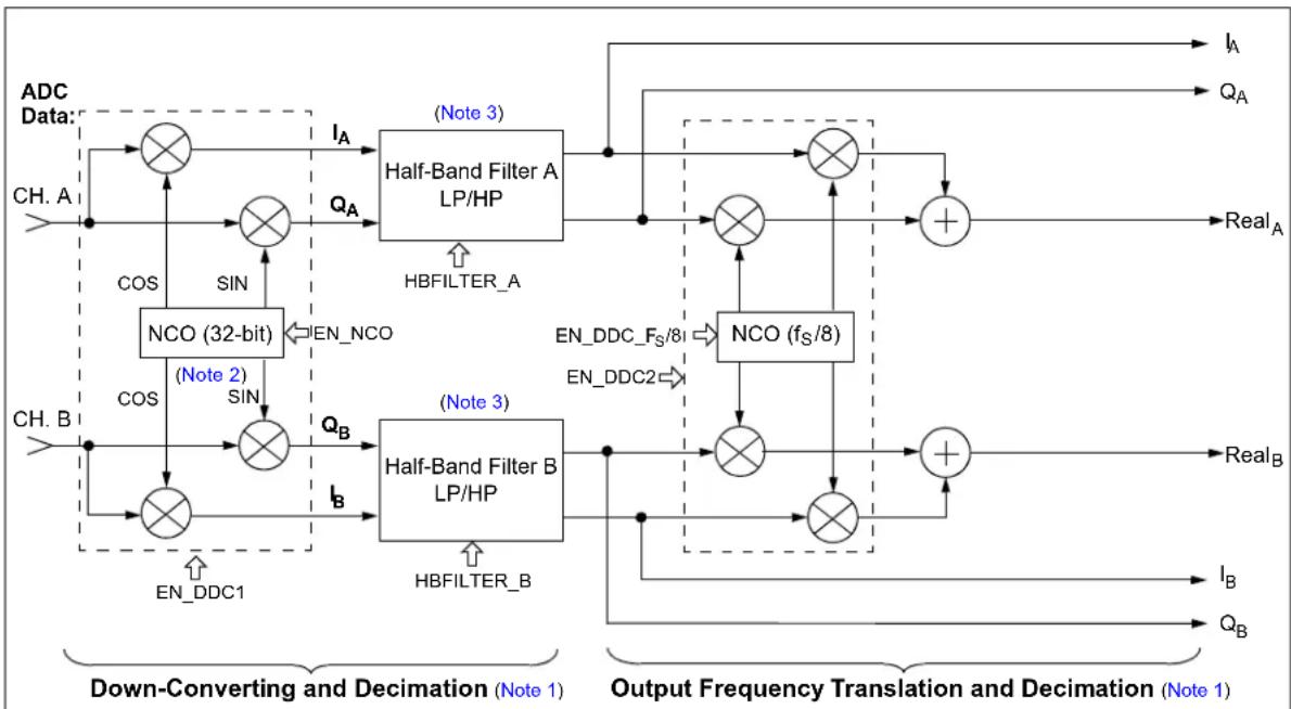
flowchart
graph TD
    subgraph_ADC_Data["ADC Data"]
        A1["CH. A"] --> B1["×"]
        A2["CH. B"] --> B2["×"]
        B1 --> C1["Half-Band Filter A LP/HP"]
        B2 --> C2["Half-Band Filter B LP/HP"]
        C1 --> D1["+"]
        C2 --> D2["+"]
        D1 --> E1["Real_A"]
        D2 --> E2["Real_B"]
    end

    subgraph_Down_Converting["Down-Converting and Decimation (Note 1)"]
        A3["CH. A"] --> B3["×"]
        A4["CH. B"] --> B4["×"]
        B3 --> C3["Half-Band Filter B LP/HP"]
        B4 --> C4["Half-Band Filter B LP/HP"]
        C3 --> D3["+"]
        C4 --> D4["+"]
        D3 --> E3["Real_A"]
        D4 --> E5["Real_B"]
    end

    subgraph_Output_Frequency["Output Frequency Translation and Decimation (Note 1)"]
        A5["CH. A"] --> B5["×"]
        A6["CH. B"] --> B6["×"]
        B5 --> C5["Half-Band Filter A LP/HP"]
        B6 --> C6["Half-Band Filter A LP/HP"]
        C5 --> D5["+"]
        C6 --> D6["+"]
        D5 --> E7["Real_A"]
        D6 --> E8["Real_B"]
    end

    B1 --> F1["I_A"]
        B2 --> F2["SIN"]
        B3 --> F3["COS"]
        B4 --> F4["SIN"]
        B5 --> F5["COS"]
        B6 --> F6["SIN"]
        F1 --> G1["EN_NCO"]
        F2 --> G2["EN_DDC1"]
        F3 --> G3["EN_DDC2"]
        F4 --> G4["EN_DDC1"]
        F5 --> G5["EN_DDC2"]
        F6 --> G6["EN_DDC1"]
    end

    style ADC_Data fill:#f9f,stroke:#333
    style Down_Converting fill:#ccf,stroke:#333
    style Output_Frequency fill:#cfc,stroke:#333
Note 1: See Address 0x80 - 0x81 for the Control Parameters.
2: See Figure 4-19 for details of NCO control block.
3: Half-band Filter A and B include a single-stage decimation filter.
FIGURE 4-18: Simplified DDC Block Diagram for Dual-Channel Mode. See Tables 4-19 and 4-20 for Using this DDC Block.
4.8.4.3 Numerically Controlled Oscillator (NCO)
The on-board Numerically Controlled Oscillator (NCO) provides the frequency reference for the in-phase and quadrature mixers in the digital down-converter (DDC).
The NCO serves as a quadrature local oscillator, capable of producing an NCO frequency of between 0 Hz and f_S with a resolution of f_S/2^32 , where f_S is the ADC core sampling frequency.
Figure 4-19 shows the control signals associated with the NCO. In octal- or dual-channel mode, the NCO allows the output phase to be adjusted on a per-channel basis.
Note: The NCO is only used for DDC or CW octal-channel mode. It should be disabled when not in use.
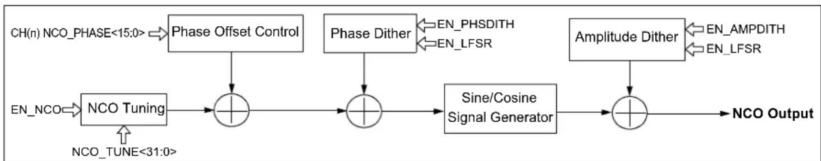
flowchart
graph LR
    A["EN_NCO"] --> B["NCO Tuning"]
    C["EN_NCO"] --> B
    B --> D["+"]
    E["Phase Offset Control"] --> D
    F["Phase Dither"] --> G["+"]
    H["Sine/Cosine Signal Generator"] --> G
    I["Amplitude Dither"] --> J["+"]
    K["EN_PHSDITH"] --> G
    L["EN_LFSR"] --> G
    M["EN_AMPDITH"] --> J
    N["EN_LFSR"] --> J
    O["NCO_TUNE<31:0>"] --> P["+"]
    Q["CH(n) NCO_PHASE<15:0>"] --> R["Phase Offset Control"]
    S["NCO Output"] --> T["+"]
FIGURE 4-19: NCO Block Diagram.
• NCO Frequency Control:
The NCO frequency is programmed from 0 Hz to f_S , using the 32-bit-wide unsigned register variable NCO_TUNE<31:0> in Addresses 0x82 - 0x85 (Registers 5-43 - 5-46).
The following equation is used to set the NCO_TUNE<31:0> register:
EQUATION 4-7: NCO FREQUENCY
$$ \begin{array}{l} N C O _ T U N E < 3 1: 0 > = r o u n d 2 \left(^ {3 2} \times \frac {\operatorname{Mod} \left(f _ {N C O} f _ {S}\right)}{f _ {S}}\right) \ \text {Where:} \end{array} $$
$$ f _ {S} = \text { sampling frequency(Hz) } $$
$$ f _ {N C O} = \text { desired NCO frequency (Hz) } $$
$$ \text { Mod } \left(f _ {\mathrm{NCO}}, f _ {\mathrm{S}}\right) = \text { gives the remainder of } f _ {\mathrm{NCO}} / f _ {\mathrm{S}} $$
Mod() is a remainder function. For example, Mod(5,2) = 1 and Mod(1.999, 2) = 1.999.
Example 1:
If f_NCO is 100 MHz and f_S is 200 MHz:
$$ \operatorname{Mod} (f _ {N C O}, f _ {S}) = \operatorname{Mod} (1 0 0, 2 0 0) = 1 0 0 $$
$$ \begin{array}{r l} N C O _ {-} T U N E < 3 1: 0 > = & \text { round } \left(2 ^ {3 2} \times \frac {\operatorname{Mod} (1 0 0 , 2 0 0)}{2 0 0}\right) \ = & 0 \times 8 0 0 0 0 0 0 0 \end{array} $$
Example 2:
If f_NCO is 199.99999994 MHz and f_S is 200 MHz:
$$ \operatorname{Mod} \left(f _ {N C O}, f _ {S}\right) = \operatorname{Mod} (1 9 9. 9 9 9 9 9 9 9 4, 2 0 0) = 1 9 9. 9 9 9 9 9 9 9 4 $$
$$ \begin{array}{r l} N C O _ T U N E < 3 1: 0 > & r o u n \left(2 ^ {3 2} \times \frac {\text { Mod } (1 9 9 . 9 9 9 9 9 9 9 4 2 0 0)}{2 0 0}\right) \ = & 0 \times F F F F F F F F F F \end{array} $$
4.8.4.4 NCO Amplitude and Phase Dither
The EN_AMPDITH and EN_PHSDITH parameters in Address 0x80 (Register 5-41) can be used for amplitude and phase dithering, respectively. In principle, these will dither the quantization error created by the use of digital circuits in the mixer and local oscillator, thus reducing spurs at the expense of noise. In practice, the DDC circuitry has been designed with sufficient noise and spurious performance for most applications. In the worst-case scenario, the NCO has an SFDR of greater than 116 dB when the amplitude dither is enabled, and 112 dB when disabled. Although the SNR ( ≈ 93 dB) of the DDC is not significantly affected by the dithering option, using the NCO with dithering options enabled is always recommended for the best performance.
4.8.4.5 NCO for f s/8 and f_S/(8 × DER)
The output of the first down-conversion block (DDC1) is a complex signal (comprising I and Q data) which can then be optionally decimated further up to 128x to provide both a lower output data rate and input channel filtering. If f_S/8 mode is enabled, a second mixer stage (DDC2) will convert the I/Q signals to a real signal centered at half of the current Nyquist frequency; i.e., if the output data rate in I/Q mode is 25 Msps per channel (12.5 MHz Nyquist), then in f_S/8 mode the output data rate would be 50 Msps (25 Msps each for I and Q), and the signal would be re-centered around 12.5 MHz. In single-channel mode, this is done at the output of the decimation filters (if used). In dual-channel mode, this must be done prior to the decimation.
When decimation is enabled, the I/Q outputs are up-converted by f_S/(8 × DER) , where DER is the additional decimation rate added by the FIR decimation filters. This provides a decimated output signal centered at f_S/8 or f_S/(8 × DER) in the frequency domain.
4.8.4.6 NCO Phase Offset Control
The user can add phase offset to the NCO frequency using the NCO phase offset control registers (Addresses 0x86 to 0x95, Registers 5-47 - 5-62). CH(n)_NCO_PHASE<15:0> is the 16-bit-wide NCO phase offset control parameter for Channel n. A 0x0000 value in the register corresponds to no offset, and a 0xFFFF corresponds to an offset of 359.995°. The phase offset can be controlled with 0.005° per step. The following equation is used to program the NCO phase offset register:
EQUATION 4-8: NCO PHASE OFFSET
$$ C H (n) _ N C O _ P H A S E < 1 5: 0 > \frac {2}{3} \times \frac {1 6 \text { Offset Value } (\phi)}{3 6 0} $$
Where:
$$ n = \text { channel number } $$
$$ \begin{array}{c} \text {Offset Value (\phi) = desired phase offset value in} \ \text {degrees} \end{array} $$
A decimal number is used for the binary contents of CH(n)_NCO_PHASE<15:0>.
4.8.4.7 In-Phase and Quadrature Signals
When the first down-conversion is enabled, it produces In-phase (I) and Quadrature (Q) components as shown in Equation 4-9:
EQUATION 4-9: I AND Q SIGNALS
$$ I = A \quad D \quad C (\pi f _ {N C O} ^ {C} t \Theta \phi) S 2 \tag {a} $$
$$ Q = A \quad D \quad C \pi f _ {N C O} t + 4 \phi) N 2 \tag {b} $$
where:
$$ \phi = 3 6 0 \times \frac {C H (n) _ N C O _ P H A S E < 1 5 : 0 >}{2 ^ {1 6}} \tag {c} $$
$$ = 0. 0 0 5 4 9 3 1 6 4 ^ {\circ} \times C H (n) _ {N C O P H A S E} < 1 5: 0 > $$
where:
ADC = output of the ADC block
= NCO phase offset of selected channel, which is defined by CH(n)_NCO_PHASE<15:0> in Addresses 0x86 - 0x95
t = k / f_S with k = 1,2,3, ,n
f_NCO = NCO frequency
I and Q outputs are interleaved where I data is output on the rising edge of the WCK. If I and Q outputs are selected in dual-channel mode with DDC enabled, I data of Channel 0 is output at the rising edge of WCK, followed by Q data of Channel 0, then I and Q data of Channel 1 in the same way.
4.8.4.8 Half-Band Filter
The frequency translation is followed by a half-band digital filter, which is used to reduce the sample rate by a factor of two while rejecting aliases that fall into the band of interest.
The user can select high- or low-pass half-band filter using the HBFILTER_A and HBFILTER_B bits in Address 0x80 (Register 5-41). These filters provide greater than 90 dB of attenuation in the attenuation band and less than 1 mdB ( 10^-3 dB) of ripple in the passband region of 20% of the input sampling rate. For example, for an ADC sample rate of 200 MSPS, these filters provide less than 1 mdB of ripple over a bandwidth of 40 MHz.
The filter responses shown in Figures 4-16 and 4-17 indicate a ripple of 0.5 mdB and an alias rejection of 90 dB. The output of the half-band filter is a DC-centered complex signal (I and Q). This I and Q signal is then carried to the next down-conversion stage (DDC2) for frequency translation (up-conversion), if the DDC is enabled.
Note: The half-band filter delays the data output by 80 clock cycles: 2 (due to decimation) x 40 cycles (due to group delay)
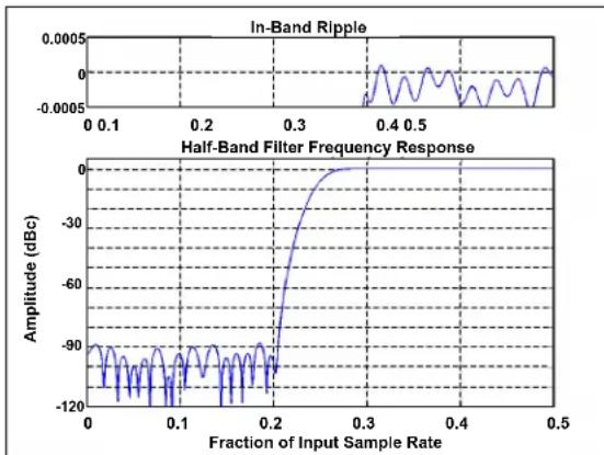
FIGURE 4-20: High-Pass (HP) Response of Half-Band Filter.

FIGURE 4-21: Low-Pass (LP) Response of Half-Band Filter.
4.8.5 EXAMPLES OF REGISTER
SETTINGS FOR USING DDC AND
DECIMATION
The following tables show examples of setting registers for using decimation and digital down-conversion (DDC) depending on the output type selection. This feature is available in the MCP37D11-200 device only.
TABLE 4-17: REGISTER SETTINGS FOR DECIMATION AND DDC OPTIONS FOR SINGLE-CHANNEL MODE – EXAMPLE
| Decimation Rate (by FIR A and FIR B)(1) | DDC Mode | Addr. 0x02(2) | FIR A Filter FIR | B Filter DDC1 DDC2 | Dual-Channel DSPP Control | Output | |||
| 0x7A<6>(FIR_A<0>) | 0x7B(FIR_A<8:1>) | 0x7C(FIR_B<7:0>) | 0x80<5,1,0>(3) | 0x81<6,3,2>(4) | 0x79<7>(EN_DSPP_2) | ||||
| 0 | Disabled | 0x00 | 0 | 0x00 | 0x00 | 0,0,0 | 0,0,0 | 0 | ADC |
| 8 | Disabled | 0x33 | 1 | 0x03 | 0x00 | 0,0,0 | 0,0,0 | 0 | ADC with decimation (+8) |
| 512 | Disabled | 0x99 | 1 | 0xFF | 0x00 | 0,0,0 | 0,0,0 | 0 | ADC with decimation (+512) |
| 0 | I/Q | 0x00(5) | 0 0x00 | 0x00 1, | 0,1 0,0,0 | 0 | I/Q Data | ||
| 8 | I/Q | 0x33 | 0 | 0x07 | 0x07 | 1,0,1 | 0,0,0 | 0 | Decimated I/Q (+8) |
| 0 | fS/8 | 0x11(6) | 0 0x00 | 0x00 1, | 1,1 0,0,0 | 0 | Real without additional decimation | ||
| 8 | fS/8 | 0x44 | 0 | 0x07 | 0x07 | 1,0,1 | 1,0,0 | 0 | Real with decimation (+16) |
Note 1: When DDC is used, the actual total decimation is 2x larger since 2x is included from the DDC Half-Band Filter. Example: Decimation = 8x with DDC-I/Q option actually has 16x decimation with 8x provided by the decimation filter and 2x from the DDC Half-Band Filter.
2: Output data and clock rate control register.
3: 0x80<5,1,0> =
4: 0x81<6,3,2> =
5: Each of I/Q has 1/2 of f_S bandwidth. The combined bandwidth is the same as the f_S bandwidth. Therefore the data rate adjustment is not needed.
6: The Half-Band Filter A includes decimation of 2.
TABLE 4-18: OUTPUT TYPE VS. CONTROL PARAMETERS FOR SINGLE-CHANNEL DDC (EXAMPLE)
| Output Type Control Parameter Register | Descriptions | ||
| Complex: I and Q | EN_DDC1 = 1 | 0x80 Enable DDC1 block | |
| EN_NCO = 1 0 | x80 Enable 32-bit NCO | ||
| HBFILTER_A = 1 | 0x80 | Enable Half-Band Filter A, includes 2x decimation | |
| EN_DDC_FS/8 = 0 | 0x80 | NCO( f_S /8/DER) is disabled | |
| EN_DDC2 = 0 | 0x81 | DDC2 is disabled | |
| FIR_A<8:1> = 0x00 | 0x7B | FIR A decimation filter is disabled | |
| FIR_B<7:0> = 0x00 | 0x7C | FIR B decimation filter is disabled | |
| OUT_CLKRATE<3:0> | 0x02 | Output clock rate is not affected (no need to change) | |
| Decimated I and Q: I_DEC , Q_DEC | EN_DDC1 = 1 | 0x80 | Enable DDC1 block |
| EN_NCO = 1 | 0x80 | Enable 32-bit NCO | |
| HBFILTER_A = 1 0 | x80 Enable Half-Band Filter A, includes 2x decimation | ||
| EN_DDC_FS/8 = 0 | 0x80 | NCO( f_S /8/DER) is disabled | |
| EN_DDC2 = 0 | 0x81 | DDC2 is disabled | |
| FIR_A<8:1> | 0x7B | Program FIR A filter for extra decimation ^(1) | |
| FIR_B<7:0> | 0x7C | Program FIR B filter for extra decimation ^(1) | |
| OUT_CLKRATE<3:0> | 0x02 | Adjust the output clock rate to the decimation rate | |
| Real: RealA after DDC( f_S /8/DER) without using Decimation Filter | EN_DDC1 = 1 0 | x80 Enable DDC1 block | |
| EN_NCO = 1 | 0x80 | Enable 32-bit NCO | |
| HBFILTER_A = 1 | 0x80 | Enable Half-Band Filter A, includes 2x decimation | |
| EN_DDC_FS/8 = 1 0 | x80 NCO( f_S /8/DER) is enabled. This translates the input signal from dc to f_S /8 ^(2) | ||
| EN_DDC2 = 1 | 0x81 | DDC2 is enabled | |
| FIR_A<8:1> = 0x00 | 0x7B | Decimation filter FIR A is disabled | |
| FIR_B<7:0> = 0x00 | 0x7C | Decimation filter FIR B is disabled | |
| OUT_CLKRATE<3:0> = 0001 | 0x02 Adjust the output clock rate to divided by 2 ^(3) | ||
| Decimated Real: RealA_DEC after Decimation Filter and DDC( f_S /8/DER) | EN_DDC1 = 1 0 | x80 Enable DDC1 block | |
| EN_NCO = 1 | 0x80 | Enable 32-bit NCO | |
| HBFILTER_A = 1 0 | x80 Enable Half-Band Filter A, includes 2x decimation | ||
| EN_DDC_FS/8 = 1 | 0x80 | NCO( f_S /8/DER) is enabled. This translates the input signal from dc to f_S /8/DER ^(2) | |
| EN_DDC2 = 1 | 0x81 | DDC2 is enabled | |
| FIR_A<8:1> | 0x7B | Program FIR B filter for extra decimation ^(4) | |
| FIR_B<7:0> | 0x7C | Program FIR B filter for extra decimation ^(4) | |
| OUT_CLKRATE<3:0> | 0x02 | Adjust the output clock rate to the total decimation rate including the 2x decimation by the Half-Band Filter A | |
Note 1: For I/Q decimation, the maximum decimation rate for the FIR A and FIR B filters is 128x each since the input is already decimated by 2x in the Half-Band Filter. See Figure 4-16 for details.
2: DER is the decimation rate setting of the FIR A and FIR B filters.
3: Divided by 2 is due to the 2x decimation included in the Half-Band Filter A.
4: When this filter is used, the up-conversion frequency is reduced by the extra decimation rates (DER).
TABLE 4-19: REGISTER SETTINGS FOR DECIMATION AND DDC OPTIONS FOR DUAL-CHANNEL MODE EXAMPLE
| Decimation Rate (by FIR A and FIR B)(1) | DDC-Mode | Address 0x02(2) | FIR A Filter FIR | B Filter DDC1 DDC2 | Dual-Channel DSPP Control | Output | |||
| 0x7A<6>(FIR_A<0>) | 0x7B(FIR_A<8:1>) | 0x7C(FIR_B<7:0>) | 0x80<5,1,0>(3) | 0x81<6,3,2>(4) | 0x79<7>(EN_DSPP_2) | ||||
| 0 | Disabled | 0x00 | 0 | 0x00 | 0x00 | 0,0,0 | 0,0,0 | 0 | ADC |
| 8 | Disabled | 0x33 | 0 | 0x07 | 0x07 | 0,0,0 | 0,0,0 | 0 | ADC with decimation ( ÷ 8) |
| 256 | Disabled | 0x88 | 0 | 0xFF | 0xFF | 0,0,0 | 0,0,0 | 0 | ADC with decimation ( ÷ 256) |
| 0 | I/Q | 0x00(5) | 0 | 0x00 | 0x00 | 1,0,1 | 0,0,0 | 1 | I/Q data |
| 0 | fS/8 | 0x11(6) | 0 | 0x00 | 0x00 | 1,1,1 | 0,0,0 | 1 | Real without additional decimation |
| 8 | fS/8 | 0x44 | 0 | 0x0E | 0x0E(7) | 1,1,1 | 0,0,0 | 1 | Real with decimation filter ( ÷ 16) |
Note 1: When DDC is used, the actual total decimation is 2x larger since 2x is included from the DDC Half-Band Filter. Example: Decimation = 8x with DDC-fS/2 option actually has 16x decimation with 8x provided by the decimation filter and 2x from the DDC Half-Band Filter.
2: Output data and clock rate control register.
3: 0x80<5,1,0> =
4: 0x81<6,3,2> =
5: Each of I/Q has 1/2 of f_S bandwidth. The combined bandwidth is the same as the f_S bandwidth. Therefore the data rate adjustment is not needed.
6: The Half-Band Filter A/B includes decimation of 2.
7: 0x0E takes into account the stages 1 and 2 are bypassed. See Figure 4-16 for "dual-channel Input" for DDC.
TABLE 4-20: OUTPUT TYPE VS. CONTROL PARAMETERS FOR DUAL-CHANNEL DDC EXAMPLE
| Output Type Control Parameter Register Descriptions | |||
| Complex: I and Q | EN_DSPP_2 = 1 | 0x79 Enable all digital post-processing functions for dual-channel operations | |
| EN_DDC1 = 1 0 | x80 Enable DDC1 block | ||
| EN_NCO = 1 0 | x80 Enable 32-bit NCO | ||
| HBFILTER_A = 1 | 0x80 Enable Half-Band Filter A, includes 2x decimation | ||
| HBFILTER_B = 1 | 0x80 Enable Half-Band Filter B, includes 2x decimation | ||
| EN_DDC_FS/8 = 0 | 0x80 | NCO( f_S /8/DER) is disabled | |
| EN_DDC2 = 0 | 0x81 | DDC2 is disabled | |
| FIR_A<8:1> = 0x00 | 0x7B | FIR A decimation filter is disabled | |
| FIR_B<7:0> = 0x00 | 0x7C | FIR B decimation filter is disabled | |
| OUT_CLKRATE<3:0> | 0x02 | Output clock rate is not affected (no need to change) | |
| Real: RealAfor Channel A and RealBfor Channel B after NCO( f_S /8/DER) Without Using Decimation Filter | EN_DSPP_2 = 1 0 | x79 Enable all digital post-processing functions for dual-channel operations | |
| EN_DDC1 = 1 0 | x80 Enable DDC1 block | ||
| EN_NCO = 1 | 0x80 | Enable 32-bit NCO | |
| HBFILTER_A = 1 | 0x80 Enable Half-Band Filter A, includes 2x decimation | ||
| HBFILTER_B = 1 | 0x80 | Enable Half-Band Filter B, includes 2x decimation | |
| EN_DDC_FS/8 = 1 | 0x80 | NCO( f_S /8/DER) is enabled. This translates the input signal from DC to f_S / 8^(1) | |
| EN_DDC2 = 1 | 0x81 | DDC2 is enabled | |
| FIR_A<8:1> = 0x00 | 0x7B | Decimation filter FIR A is disabled | |
| FIR_B<7:0> = 0x00 | 0x7C | Decimation filter FIR B is disabled | |
| OUT_CLKRATE<3:0> = 0001 | 0x02 Adjust the output clock rate to divided by 2 ^(2) | ||
| Decimated Real: RealA_DEC for Channel A and RealB_DEC for Channel B after NCO( f_S /8/DER) and Decimation Filter | EN_DSPP_2 = 1 | 0x79 | Enable all digital signal post-processing functions for dual-channel operation |
| EN_DDC1 = 1 0 | x80 Enable DDC1 block | ||
| EN_NCO = 1 0 | x80 Enable 32-bit NCO | ||
| HBFILTER_A = 1 | 0x80 | Enable Half-Band Filter A, includes 2x decimation | |
| HBFILTER_B = 1 | 0x80 | Enable Half-Band Filter B, includes 2x decimation | |
| EN_DDC_FS/8 = 1 | 0x80 NCO(f S /8/DER) is enabled. This translates the input signal from DC to f_S / 8^(1) | ||
| EN_DDC2 = 1 | 0x81 | DDC2 is enabled | |
| FIR_A<8:1> | 0x7B | Program FIR A filter for extra decimation ^(3) | |
| FIR_B<7:0> | 0x7C | Program FIR B filter for extra decimation ^(3) | |
| OUT_CLKRATE<3:0> | 0x02 | Adjust the output clock rate to the total decimation rate including the 2x decimation by the Half-Band Filter A | |
Note 1: DER is the decimation rate setting of the FIR A and FIR B filters.
2: Divided by 2 is due to the 2x decimation included in the Half-Band Filter A.
3: When this filter is used, the up-conversion frequency is reduced by the extra decimation rates (DER).
4.9 Digital Offset and Digital Gain Settings
Figure 4-22 shows a simplified block diagram of the digital offset and gain settings. Offset is applied prior to the gain. Offset and gain adjustments occur prior to DDC, Decimation or FDR when these features are used.
4.9.1 DIGITAL OFFSET SETTINGS
The offset can be corrected using a 16-bit-wide global offset correction register (0x66) for all channels, offset correction registers for individual channels (0x9E-0xA7) or by combining both global and individual offset correction registers. The offset control for individual channels can be used with DIG_OFFSET_WEIGHT <1:0> in 0xA7. The corresponding registers for each correction are shown in Figure 4-22.
Note that, except for the octal-channel mode, the offset setting registers for individual channels, 0x9E-0xA7 (Registers 5-71 - 5-79), do not sequentially correspond to the channel order defined by CH_ORDER<23:0>. Table4-21 shows the details of the offset registers that correspond to the actual channels, depending on the number of channels used.
4.9.2 DIGITAL GAIN SETTINGS
CH(N)_DIG_GAIN<7:0> in Addresses 0x96 - 0x9D (Registers 5-63 - 5-70) is used to adjust the digital gain per channel.
Note 1: Digital Offset Setting: Register mapping (0x9E - 0xA7) to the corresponding channel is not sequential to the channel order defined by CH_ORDER<23:0>, except for the octal-channel mode. See Table 4-21 for details.
2: Gain and NCO Phase Offset: Register mapping to the corresponding channel is sequential to the channel order defined by CH_ORDER<23:0>.

flowchart
graph LR
    A["ADC Output"] --> B["⊕"]
    B --> C["⊕"]
    C --> D["×"]
    D --> E["Corrected ADC Output"]

    F["Global Digital Offset Control for all channels\nDIG_OFFSET_GLOBAL<15:0>(See Address 0x66)"] --> B
    G["Digital Offset Control for individual channel\nCH(n)_DIG_OFFSET<7:0>(See Addresses 0x9E - 0xA5)\nDIG_OFFSET_WEIGHT<1:0>(See Address 0xA7)"] --> C
    H["Digital Gain Control for individual channel\nCH(n)_DIG_GAIN<7:0>(See Addresses 0x96 - 0x9D)"] --> D
FIGURE 4-22: Simplified Block Diagram for Digital Offset and Gain Settings.
TABLE 4-21: REGISTER ASSIGNMENT FOR OFFSET SETTING
| Number of Channel Used | Register Address for Offset Setting | |||||||
| 1^st Channel 2 | nd Channel | 3^rd Channel | 4^th Channel | 5^th Channel 6 | th Channel | 7^th Channel 8 | th Channel | |
| 1 | 0x9F | — | — | — | — | — | — | — |
| 2 | 0xA0 | 0x9F | — | — | — | — | — | — |
| 3 | 0xA1 | 0x9F | 0xA0 | — | — | — | — | — |
| 4 | 0xA2 | 0x9F | 0xA0 | 0xA1 | — | — | — | — |
| 5 | 0xA3 | 0x9F | 0xA0 | 0xA1 | 0xA2 | — | — | — |
| 6 | 0xA4 | 0x9F | 0xA0 | 0xA1 | 0xA2 | 0xA3 | — | — |
| 7 | 0xA5 | 0x9F | 0xA0 | 0xA1 | 0xA2 | 0xA3 | 0xA4 | — |
| 8 | 0x9E | 0x9F | 0xA0 | 0xA1 | 0xA2 | 0xA3 | 0xA4 | 0xA5 |
4.10 Continuous Wave (CW)
Beamforming and Ultrasound Doppler Signal Processing Using CW Octal-Channel Mode (MCP37D11-200 only)
In modern ultrasound medical applications, large numbers of transducers are often used. The signals from these sensors are then coherently combined for higher transducer gain and directivity. The signals from each sensor arrive at the detection device with a different time delay. Also, in multi-channel scanning operations using the MUX, there is a time delay between acquiring input signals (see Section 4.8.1 "Fractional Delay Recovery for Dual- and Octal-Channel Modes"). These time delays may need to be corrected before all input signals are combined for the signal processing.
Digital beamforming is a digital signal processing technique that requires summing all input signals from different channels after correcting for time delay. The time-delay correction involves the phase alignment of the detected signals with respect to a reference.
Along with beamforming, many modern medical ultrasound devices support Doppler imaging, which processes phase information in addition to the classical magnitude detection (for brightness imaging). Ultrasound Doppler signal processing is used to determine movement in the body as represented by blood flow, which can help diagnose the functioning of a heart valve or blood vessel, etc. In a traditional ultrasound system, all of these functions are typically accomplished with discrete components. Figure 4-24 shows an example of an ultrasound system implementation using various specialized components.
The MCP37D11-200 device has a built-in feature that can perform some of the functions that are done traditionally using extra components. Continuous wave (CW) digital beamforming and Doppler signal processing features are available, but these are offered in octal-channel operation only.
Figure 4-23 shows a simplified block diagram for the ultrasound CW beamforming with DDC I/Q decimation. Note that the sub-blocks shown after the MUX are commonly used for all input channels.

flowchart
graph TD
    A["Transducer Array"] --> B["HV MUX and T/R Switches"]
    B --> C["T/R Switcher"]
    C --> D["LNA"]
    D --> E["VGA"]
    E --> F["AAF"]
    F --> G["ADC"]
    G --> H["Digital RX Beamformer"]
    H --> I["Image and Motion Processing (B Mode)"]
    H --> J["Color Doppler Processing (F Mode)"]
    I --> K["Video Compression"]
    J --> K
    K --> L["Audio DAC"]
    L --> M["Amp"]
    D --> N["I/Q Processing"]
    N --> O["Amp"]
    O --> P["ADC"]
    P --> Q["CW Doppler Processing"]
    Q --> R["Clocks"]
    R --> G
    S["HV Amp"] --> T["DAC"]
    T --> U["Isolation"]
    U --> V["Beamformer Central Control Processor"]
    V --> W["LNA-VGA-ADC Array (up to 256 Channels)"]
    W --> X["LNA-VGA-ADC Array"]
    X --> Y["Digital RX Beamformer"]
    Y --> Z["Video DAC/Video Encoder"]
    Z --> AA["Audio DAC"]
    AA --> AB["Amp"]
FIGURE 4-23: Example of Ultrasound System Building Block.
4.10.1 BEAMFORMING
Beamforming is achieved by scanning all inputs while correcting the phase of each channel with respect to a reference. This can be done using:
• Fractional Delay Recovery (FDR)
- Phase offset settings of each individual channel
- Gain setting per channel
While the CW input channel is multiplexed sequentially, the phase offset can be added to the NCO output (each channel individually). CH(n)_NCO_PHASE<15:0>, in Addresses 0x86 to 0x95 (Registers 5-47 - 5-62), corrects the time delay of the incoming signals with respect to the reference.
The phase-compensated input signal is then down-converted by a wide dynamic range I/Q demodulator. The digital beamforming of the inputs is then obtained by summing I and Q data from individual channels. The combined I and Q data are fed to the half-band filter. Equation 4-10 shows the I and Q data of an individual channel with phase correction (phase offset), and the resulting digital beamforming signal.
The processing blocks after the digital beamforming are the same as the sub-blocks used in single-channel operation described in Section 4.8.4.1 "Single-Channel DDC", except only limited decimation rates of the FIR A and FIR B filters are used due to the processing time requirement for summing the input signals from all channels.
EQUATION 4-10: BEAMFORMING SIGNALS
I_CH n( ) = ADC 2( f_NCO t + (n)) Q_CH n( ) = ADC 2( f_NCO t + (n)) I = _n=0^N I_CH(n) Q = _n=0^N Q_CH n( ) n( ) = 360 × (n) NCO_PHASE < 15:0 >2^16 = 0.005493164^ × CH(n) NCO_PHASE < 15:0> Where: (n) = NCO phase offset of channel n ADC = the output of the ADC block
The NCO phase offset can be controlled by 0.005493164° per step. See Section 4.8.4.6 "NCO Phase Offset Control" for details.
4.10.2 ULTRASOUND DOPPLER SIGNAL PROCESSING
Doppler shift measurement requires summing the input signals from multiple transducer channels and mixing them with a phase-controlled local oscillator frequency. The resulting low-frequency output is then centered near DC and can measure a Doppler shift produced by moving objects, such as blood flow and changes in blood pressure in arteries, etc. In traditional Doppler measurement, many discrete analog components are typically used along with a high-resolution ADC (\~18-bit range).
This device has unique built-in features that are suitable for ultrasound Doppler shift measurements. By utilizing these features, system engineers can reduce many discrete components which are otherwise necessary for an ultrasound Doppler measurement system.
The following built-in digital signal post-processing (DSPP) features in the MCP37D11-200 can be effectively used for the ultrasound Doppler signal processing applications:
- Fractional Delay Recovery (FDR): Correct the time delay of signal sampled between channels. See details in Section 4.8.1 "Fractional Delay Recovery for Dual- and Octal-Channel Modes".
- Digital Gain and Offset adjustment for each channel: See details in Section 4.9 "Digital Offset and Digital Gain Settings".
- Down-Conversion for each channel with a unique phase of the same NCO frequency prior to summing the eight channels as shown in Figure 4-24.
- After down-conversion by the DDC, the resulting signal can then be decimated to achieve very high SNR in a narrow bandwidth.
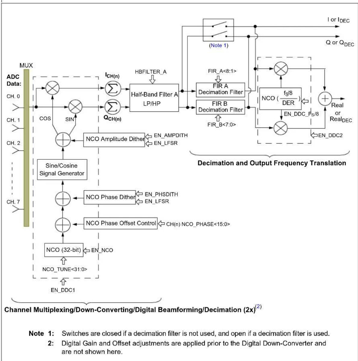
flowchart
graph TD
    A["ADC Data: CH. 0"] --> B["COS"]
    C["ADC Data: CH. 1"] --> D["SIN"]
    E["ADC Data: CH. 2"] --> F["NCO Amplitude Dither"]
    G["ADC Data: CH. 7"] --> H["Sine/Cosine Signal Generator"]
    I["I_CH(n)"] --> J["Σ"]
    K["Q_CH(n)"] --> L["Σ"]
    M["HBFILTER_A"] --> N["Half-Band Filter A LP/HP"]
    O["FIR_A<8:1>"] --> P["FIR A Decimation Filter"]
    Q["FIR_B Decimation Filter"] --> R["FIR B Decimation Filter"]
    S["NCO (32-bit)"] --> T["NCO Phase Offset Control"]
    U["EN_NCO"] --> V["NCO Phase Dither"]
    W["EN_DDC1"] --> X["EN_DDC2"]
    Y["EN_AMPDITH EN_LFSR"] --> Z["EN_AMPDITH EN_LFSR"]
    AA["NCO Phase Dither"] --> AB["EN_PHSDITH EN_LFSR"]
    AC["NCO Phase Offset Control"] --> AD["CH(n) NCO_PHASE<15:0>"]
    AE["NCO Amplitude Dither"] --> AF["EN_AMPDITH EN_LFSR"]
    AG["NCO (f_g/8 DER)"] --> AH["EN_DDC_F_S/8"]
    AI["Real or Real_DEC"] --> AJ["+"]
    AK["I or I_DEC"] --> AL["(Note 1)"]
    AM["Q or Q_DEC"] --> AN["Decimation and Output Frequency Translation"]
    AO["Channel Multiplexing/Down-Converting/Digital Beamforming/Decimation (2x)(2)"] --> AP["Note 1: Switches are closed if a decimation filter is not used, and open if a decimation filter is used; Digital Gain and Offset adjustments are applied prior to the Digital Down-Converter and are not shown here."]
FIGURE 4-24: Simplified Block Diagram of CW Beamforming and I/Q Signal Processing - Available in MCP37D11-200 Only.
4.11 Output Data format
The device can output the ADC data in offset binary or two's complement. The data format is selected by the DATA_FORMAT bit in Address 0x62 (Register 5-20).
Table 4-22 shows the relationship between the analog input voltage, the digital data output bits and the overrange bit. By default, the output data format is two's complement.
TABLE 4-22: ADC OUTPUT CODE VS. INPUT VOLTAGE (12-BIT MODE)
| Input Range Offset | Binary (1) | Two's Complement(1) | Overrange (OVR) |
| A_IN > A_FS | 1111-1111-1111 0111 | -1111-1111 | 1 |
| A_IN = A_FS | 1111-1111-1111 0111 | -1111-1111 | 0 |
| A_IN = A_FS - 1 LSb | 1111-1111-1110 | 0111-1111-1110 | 0 |
| A_IN = A_FS - 2 LSb | 1111-1111-1100 | 0111-1111-1100 | 0 |
| : | |||
| A_IN = A_FS/2 1100-0 | 000-0000 0100-0000-0000 | 0 | |
| A_IN = 0 | 1000-0000-0000 | 0000-0000-0000 | 0 |
| A_IN = -A_FS/2 | 0011-1111-1111 1011 | -1111-1111 | 0 |
| : | |||
| A_IN = -A_FS + 2 LSb | 0000-0000-0010 | 1000-0000-0010 | 0 |
| A_IN = -A_FS + 1 LSb | 0000-0000-0001 | 1000-0000-0001 | 0 |
| A_IN = -A_FS | 0000-0000-0000 1000 | -0000-0000 | 0 |
| A_IN < -A_FS | 0000-0000-0000 1000 | -0000-0000 | 1 |
Note 1: MSb is sign bit
4.12 Digital Output
The device can operate in one of the following two digital output modes:
- Full-Rate CMOS
• Double-Data-Rate (DDR) LVDS
The outputs are powered by DV _DD18 and GND. LVDS mode is recommended for data rates above 80 Msps. The digital output mode is selected by the OUTPUT_MODE<1:0> bits in Address 0x62 (Register 5-20). Figures 2-1 – 2-2 show the timing diagrams of the digital output.
4.12.1 FULL RATE CMOS MODE
In full-rate CMOS mode, the data outputs (Q11 to Q0, overrange indicator (OVR), word clock (WCK) and the data output clock (DCLK+, DCLK−) have CMOS output levels. The digital output should drive minimal capacitive loads. If the load capacitance is larger than 10 pF, a digital buffer should be used.
4.12.2 DOUBLE DATA RATE LVDS MODE
In double-data-rate LVDS mode, the output is a parallel data stream which changes on each edge of the output clock. See Figure 2-2 for details.
In multi-channel configuration, the data is output sequentially with the WCK that is synchronized to the first sampled channel.
The device outputs the following LVDS output pairs:
- Output Data: Q5+/Q5- through Q0+/Q0-
• O V R / W C K - DCLK+/DCLK-
A 100Ω differential termination resistor is required for each LVDS output pin pair. The termination resistor should be located as close as possible to the LVDS receiver. By default, the outputs are standard LVDS levels: 3.5 mA output current with a 1.15V output common-mode voltage on a 100Ω differential load. See Address 0x63 (Register 5-21) for more details of the LVDS mode control.
Note: Output Data Rate in LVDS Mode: In octal-channel mode, the input sample rate per channel is f_S/8 . Therefore, the output data rate required to shift out all 12 bits in DDR is still equivalent to f_S . For example, if f_S = 200 Msps, each channel's sample rate is f_S/8 = 25 Msps, and the output clock rate (DCLK) for 12-bit DDR output is 200 MHz.
4.12.3 OVERRANGE BIT (OVR)
The input overrange status bit is asserted (logic high) when the analog input has exceeded the full-scale range of the ADC in either the positive or negative direction. In LVDS DDR Output mode, the OVR bit is multiplexed with the word clock (WCK) output bit such that OVR is output on the falling edge of the data output clock and WCK on the rising edge.
The OVR bit has the same pipeline latency as the ADC data bits. In multi-channel mode, the OVR is output independently for each input channel and is synchronized to the data. See Address 0x68 (Register 5-26) for OVR and WCK control options.
If DSPP options are enabled, OVR pipeline latency will be unaffected; however, the data will incur additional delay. This has the effect of allowing the OVR indicator to precede the affected data.
4.12.4 WORD CLOCK (WCK)
The word clock output bit indicates the start of a new data set. In single-channel mode, this bit is disabled except for I/Q output mode. In DDR output with multi-channel mode, it is always asserted coincidentally with the data from the first sampled channel, and multiplexed with the OVR bit. See Address 0x07 (Register 5-5) and Address 0x68 (Register 5-26) for OVR and WCK control options.
4.12.5 LVDS OUTPUT POLARITY CONTROL
In LVDS mode, the output polarity can be controlled independently for each LVDS pair. Table 4-23 summarizes the LVDS output polarity control register bits.
TABLE 4-23: LVDS OUTPUT POLARITY CONTROL
| Control Parameter | Register | Descriptions |
| POL_LVDS<7:0> | 0x65 | Control polarity of LVDS data pairs |
| POL_WCK_OVR | 0x68 | Control polarity of WCK and OVR bit pair |
4.12.6 PROGRAMMABLE LVDS OUTPUT
In LVDS mode, the default output driver current is 3.5 mA. This current can be adjusted by using the LVDS_IMODE<2:0> bit setting in Address 0x63 (Register 5-21). Available output drive currents are 1.8 mA, 3.5 mA, 5.4 mA and 7.2 mA.
4.12.7 OPTIONAL LVDS DRIVER INTERNAL TERMINATION
In most cases, using an external 100Ω termination resistor will give excellent LVDS signal integrity. In addition, an optional internal 100Ω termination resistor can be enabled by setting the LVDS_LOAD bit in
Address 0x63 (Register 5-21). The internal termination helps absorb any reflections caused by imperfect impedance termination at the receiver.
4.12.8 OUTPUT DATA AND CLOCK RATES
The user can reduce output data and output clock rates using Address 0x02 (Register 5-3). When decimation or digital down-conversion (DDC) is used, the output data rate has to be reduced to synchronize with the reduced output clock rate.
4.12.9 PHASE SHIFTING OF OUTPUT CLOCK (DCLK)
In full-rate CMOS mode, the data output bit transition occurs at the rising edge of DCLK+, so the falling edge of DCLK+ can be used to latch the output data.
In double-data-rate LVDS mode, the data transition occurs at both the rising and falling edges of DCLK+. For adequate setup and hold time when latching the data into the external host device, the user can shift the phase of the digital clock output (DCLK+/DCLK-) relative to the data output bits.
The output phase shift (delay) is controlled by each unique register depending on which timing source is used or if decimation is used. Table 4-24 shows the output clock phase control registers for each Configuration mode: (a) when DLL is used, (b) when decimation is used, and (c) when PLL is used.
Figure 4-25 shows an example of the output clock phase delay control using the DCLK_PHD-LY_DLL<2:0> when DLL is used.
TABLE 4-24: OUTPUT CLOCK (DCLK) PHASE CONTROL PARAMETERS
| Control Parameter Register Operating Condition (1) | ||
| When DLL is used: | ||
| EN_PHDLY | 0x64 | EN_PHDLY = 1: Enable output clock phase delay control |
| DCLK_PHDLY_DLL<2:0> | 0x52 DCLK | phase delay control when DLL is used. Decimation is not used. |
| When decimation is used: | ||
| EN_PHDLY | 0x64 | EN_PHDLY = 1: Enable output clock phase delay control |
| DCLK_PHDLY_DEC<2:0> | DCLK phase | delay control when decimation filter is used. The phase delay is controlled in digital clock output control block. |
| When PLL is used: | ||
| DCLK_DLY_PLL<2:0> | 0x6D | DCLK delay control when PLL is used. |
Note 1: See Figure 4-11 for details.
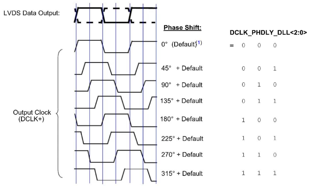
other
| Output Clock (DCLK+) | Phase Shift | | --------------------- | ----------- | | 0° (Default)¹ | 0 | | 45° + Default | 0 | | 90° + Default | 0 | | 135° + Default | 0 | | 180° + Default | 1 | | 225° + Default | 1 | | 270° + Default | 1 | | 315° + Default | 1 |Note 1: Default value may not be 0^ in all operations.
FIGURE 4-25: Example of Phase Shifting of Digital Output Clock (DCLK+) when DLL is Used.
4.12.10 DIGITAL OUTPUT RANDOMIZER
Depending on PCB layout considerations and power supply coupling, SFDR may be improved by decorrelating the ADC input from the ADC digital output data. The device includes an output data randomizer option. When this option is enabled, the digital output is randomized by applying an exclusive-OR logic operation between the LSb (D0) and all other data output bits.
To decode the randomized data, the reverse operation is applied: an exclusive-OR operation is applied between the LSb (D0) and all other bits. The DCLK, OVR, WCK and LSb (D0) outputs are not affected. Figure 4-26 shows the block diagram of the data randomizer and decoder logic. The output randomizer is enabled by setting the EN_OUT_RANDOM bit in Address 0x07 (Register 5-5).
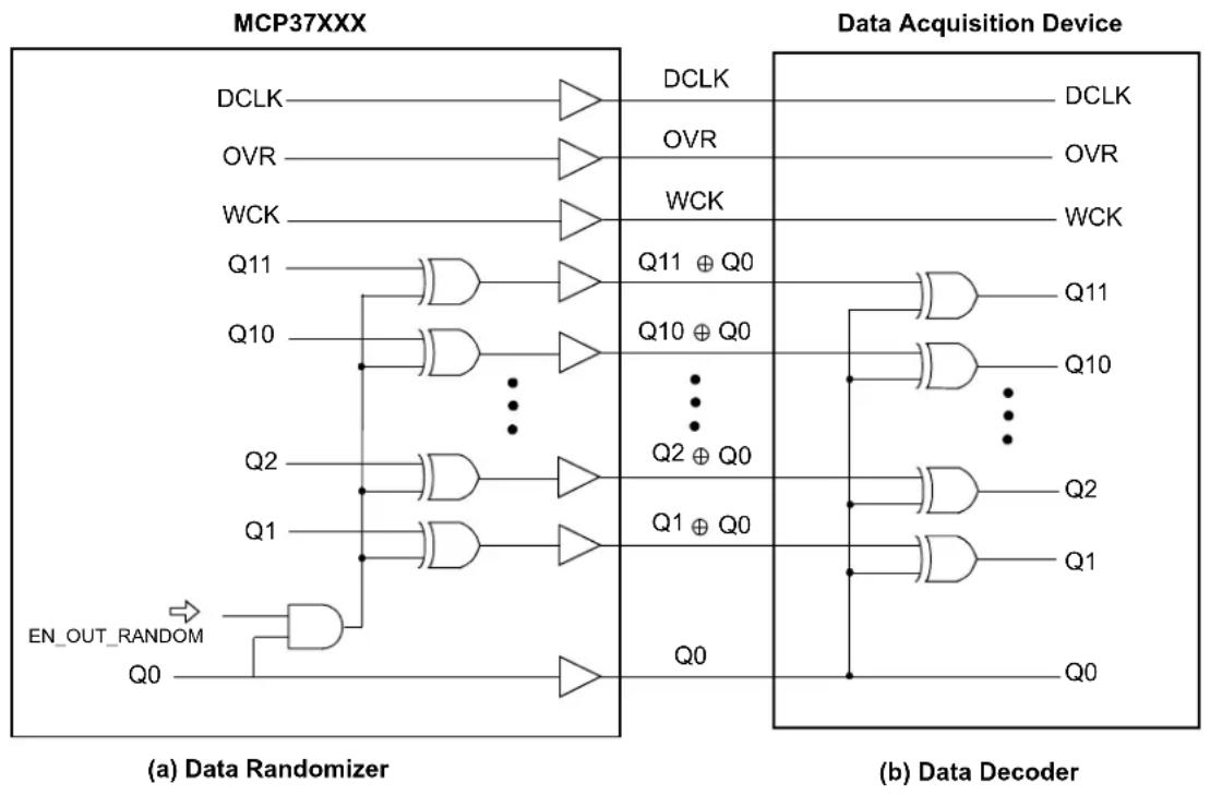
FIGURE 4-26: Logic Diagram for Digital Output Randomizer and Decoder.
4.12.11 OUTPUT DISABLE
The digital output can be disabled by setting OUTPUT_MODE<1:0> = 00 in Address 0x62 (Register 5-20). All digital outputs are disabled, including OVR, WCK, DCLK, etc.
4.12.12 OUTPUT TEST PATTERNS
To facilitate testing of the I/O interface, the device can produce various predefined or user-defined patterns on the digital outputs. See TEST_PATTERN<2:0> in Address 0x62 (Register 5-20) for the predefined test patterns. For the user-defined patterns, Addresses 0x74 - 0x77 (Registers 5-29 - 5-32) can be programmed using the SPI interface. When an output test mode is enabled, the ADC's analog section can still be operational, but does not drive the digital outputs. The outputs are driven only with the selected test pattern.
4.12.12.1 Pseudo-Random Number (PN) Sequence Output
When TEST_PATTERNNS<2:0> = 111, the device outputs a pseudo-random number (PN) sequence which is defined by the polynomial of degree 16, as shown in Equation 4-11. Figure 4-27 shows the block diagram of a 16-bit Linear Feedback Shift Register (LFSR) for the PN sequence.
EQUATION 4-11: POLYNOMIAL FOR PN
$$ P x (\equiv) + I ^ {4} \neq x ^ {1 3} + x ^ {1 5} + x ^ {1 6} $$
The output PN[15:4] is directly applied to the output pins Qn[11:0]. In addition to the output at the Qn[11:0] pins, the two MSbs, PN[15] and PN[14], are copied to the OVR and WCK pins, respectively.

flowchart
graph TD
    A["XOR"] --> B["Z⁻⁴"]
    B --> C["Z⁻⁹"]
    C --> D["Z⁻²"]
    D --> E["Z⁻¹"]
    E --> F["PN[15"]]
    C --> G["PN[12"]]
    D --> H["PN[14"]]
    B --> I["PN[3"]]
    E --> J["PN[15"]]
FIGURE 4-27: Block Diagram of 16-Bit LFSR for Pseudo-Random Number (PN) Sequence for Output Test Pattern.
4.13 System Calibration
The built-in system calibration algorithm includes:
• Harmonic Distortion Correction (HDC)
• DAC Noise Cancellation (DNC)
• Dynamic Element Matching (DEM)
HDC and DNC correct the nonlinearity in the residue amplifier and DAC, respectively. The system calibration is performed by:
- Power-up calibration, which takes place during the Power-on Reset sequence (requires 2^27 clock cycles)
- Background calibration, which takes place during normal operation (per 2^30 clock cycles).
Background calibration time is invisible to the user, and primarily affects the ADC's ability to track variations in ambient temperature.
The calibration status is monitored by the CAL pin or the ADC_CAL_STAT bit in Address 0xC0 (Register 5-80). See Address 0x07 (Register 5-5) and 0x1E (Register 5-6) for time delay control of the auto-calibration. Table4-25 shows the calibration time for various ADC core sample rates.
TABLE 4-25: CALIBRATION TIME VS. ADC CORE SAMPLE RATE
| f_S (Msps) | 200 | 150 | 100 | 70 | 50 |
| Power-Up Calibration Time (s) | 0.67 | 0.9 | 1.34 | 1.92 | 2.68 |
| Background Calibration Time (s) | 5.37 | 7.16 | 10.73 | 15.34 | 21.48 |
4.13.1 RESET COMMAND
Although the background calibration will track changes in temperature or supply voltage, changes in clock frequency or register configuration should be followed by a recalibration of the ADC. This can be accomplished via either the Hard or Soft Reset command. The recalibration time is the same as the power-up calibration time ( 2^7 clock cycles). Resetting the device is highly recommended when exiting from Shutdown or Standby mode after an extended amount of time. During the reset, the device has the following state:
- No ADC output
- No change in power-on condition of internal reference
- Most of the internal clocks are not distributed
- Contents of internal user registers:
- Not affected by Soft Reset
- Reset to default values by Hardware Reset
- Current consumption of the digital section is negligible, but no change in the analog section.
4.13.1.1 Hardware Reset
A hard reset is triggered by toggling the RESET pin. On the rising edge, all internal calibration registers and user registers are initialized to their default states and recalibration of the ADC begins. The recalibration time is the same as the power-up calibration time. See Figure 2-6 for the timing details of the hardware RESET pin.
4.13.1.2 Soft Reset
The user can issue a Soft Reset command for a fast recalibration of the ADC by setting the SOFT_RESET bit to '0' in Address 0x00 (Register 5-1). During Soft Reset, all internal calibration registers are initialized to their initial default states. User registers are unaffected. When exiting the Soft Reset (changing from '0' to '1'), an automatic device calibration takes place.
4.14 Power Dissipation and Power Savings
The power dissipation of the ADC core is proportional to the sample rate ( f_S ). The digital power dissipation of the CMOS outputs are determined primarily by the strength of the digital drivers and the load condition on each output pin. The maximum digital load current ( I_LOAD ) can be calculated as:
EQUATION 4-12: CMOS OUTPUT LOAD CURRENT
$$ I _ {L O A D} = D V _ {D D I. 8} \times f _ {D C L K} \times N \times C _ {L O A D} $$
Where:
N = Number of bits
$$ C _ {L O A D} = \text { Capacitive load of output pin } $$
The capacitive load presented at the output pins needs to be minimized to minimize digital power consumption. The output load current of the LVDS output is constant, since it is set by LVDS_IMODE<2:0> in Address 0x63 (Register 5-21).
4.14.1 POWER-SAVING MODES
This device has two power-saving modes:
- Shutdown
- Standby
They are set by the SHUTDOWN and STANDBY bits in Address 0x00 (Register 5-1).
In Shutdown mode, most of the internal circuitry, including the reference and clock, are turned off with the exception of the SPI interface. During Shutdown, the device consumes 23 mA (typical), primarily due to digital leakage. When exiting from Shutdown, issuing a Soft Reset at the same time is highly recommended.
This will perform a fast recalibration of the ADC. The contents of the internal registers are not affected by the Soft Reset.
In Standby mode, most of the internal circuitry is disabled except for the reference, clock and SPI interface. If the device has been in standby for an extended period of time, the current calibration value may not be accurate. Therefore, when exiting from Standby mode, executing the device Soft Reset at the same time is highly recommended.
4.15 AutoSync Mode: Synchronizing Multiple ADCs at the Same Clock using Master and Slave Configuration
AutoSync allows multiple devices to sample input synchronously at the same clock, and output the conversion data at the same times if they are using the same digital signal post-processing. Figure 4-28 shows the system configuration using the AutoSync feature. Three examples with timing diagram are shown in Figure 2-7 – Figure 2-9.
Once the devices are synchronized, each device performs internal calibration ( T_PCAL ) before sending out valid data output. Any ADC data output before the calibration is complete should be ignored.
Note that the calibration time varies slightly from device to device, and the internal calibration status can be monitored using the CAL pin or ADC_CAL_STAT bit in the Register Address 0xC0.
The valid synchronized output is available when all devices complete their own internal calibration. For this reason, the user has two options for the synchronized output: (a) monitor the calibration status of individual devices and wait until all devices complete calibrations or (b) use an external AND gate as shown in Figure 4-27. Master and all Slave devices are synchronized when the AND gate output toggles to "High".
The AutoSync feature can be used with the following steps:
- Master device is selected by setting SLAVE pin to "GND": SYNC pin becomes output pin.
- Slave device is selected by setting SLAVE pin to "High" (or tie to DVDD18): SYNC pin becomes input pin.
- Feed the Master's SYNC pin output to Slave's SYNC pin.
- Use AutoSync mode using (a) Power-On Reset (Figure 2-7), (b) RESET Pin (Figure 2-8), or (c) SOFT RESET bit (Figure 2-9).
Note: The maximum sample rate may be affected by the PCB layout due to the parasitic capacitances between the Master and Slave devices.
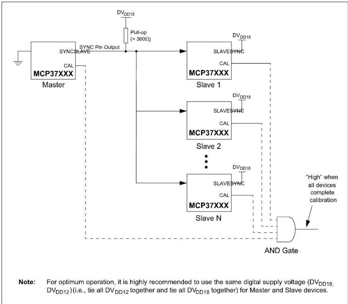
flowchart
graph TD
    A["MCP37XXX Master"] -->|SYNC| B["AND Gate"]
    B --> C[""High" when all devices complete calibration"]
    D["VL_DD18"] --> E["Pull-up (>360Ω)"]
    E --> F["SLAVE SYNC"]
    F --> G["SLAVE"]
    G --> H["SLAVE"]
    H --> I["SLAVE"]
    I --> J["AND Gate"]
    K["VL_DD18"] --> L["SLAVE SYNC"]
    L --> M["SLAVE"]
    M --> N["SLAVE"]
    N --> O["AND Gate"]
    P["VL_DD18"] --> Q["SLAVE SYNC"]
    Q --> R["SLAVE"]
    R --> S["SLAVE"]
    S --> T["AND Gate"]
    U["VL_DD18"] --> V["SLAVE SYNC"]
    V --> W["SLAVE"]
    W --> X["SLAVE"]
    X --> Y["AND Gate"]
    Z["VL_DD12"] --> AA["SLAVE SYNC"]
    AA --> AB["SLAVE"]
    AB --> AC["SLAVE"]
    AC --> AD["AND Gate"]
    AE["VL_DD12"] --> AF["SLAVE SYNC"]
    AF --> AG["SLAVE"]
    AG --> AH["SLAVE"]
    AH --> AI["AND Gate"]
FIGURE 4-28: Synchronizing Multiple ADCs Using AutoSync Feature.
NOTES:
5.0 SERIAL PERIPHERAL INTERFACE (SPI)
The user can configure the ADC for specific functions or optimized performance by setting the device's internal registers through the serial peripheral interface (SPI). The SPI communication uses three pins: SCLK and SDIO. Table 5-1 summarizes the SPI pin functions. The SCLK is used as a serial timing clock and can be used up to 50MHz . SDIO (Serial Data Input/Output) is a dual-purpose pin that allows data to be sent or read from the internal registers. The Chip Select pin ( ) enables SPI communication when active-low. The falling edge of followed by a rising edge of SCLK determines the start of the SPI communication. When is tied to high, SPI communication is disabled and the SPI pins are placed in high-impedance mode. The internal registers are accessible by their address.
Figures 5-1 and 5-2 show the SPI data communication protocols for this device with MSb-first and LSb-first options, respectively. It consists of:
- 16-bit wide instruction header + Data byte 1 + Data byte 2 + ... + Data Byte N
Table 5-2 summarizes the bit functions. The R/Wbit of the instruction header indicates whether the command is a read ('1') or a write ('0'):
- If t h ebitRs /1 The SDIO pin changes direction from an input (SDI) to an output (SDO) after the 16-bit wide instruction header.
By selecting the R/W bit, the user can write the register or read back the register contents. The W1 and W2 bits in the instruction header indicate the number of data bytes to transmit or receive in the following data frame.
Bits A2 – A0 are the SPI device address bits. These bits are used when multiple devices are used in the same SPI bus. A2 is internally hardcoded to '0'. Bits A1 and A0 correspond to the logic level of the ADR1 and ADR0 pins, respectively.
Note: In the VTLA-124 package, ADR1 is internally bonded to ground (logic '0').
The R9 – R0 bits represent the starting address of the Configuration register to write or read. The data bytes following the instruction header are the register data. All register data is eight bits wide. Data can be sent in MSb-first mode (default) or in LSb-first mode, which is determined by the
TABLE 5-1: SPI PIN FUNCTIONS
| Pin Name | Descriptions |
| Chip Select pin. SPI mode is initiated at the falling edge. It needs to maintain active-low for the entire period of the SPI communication. The device exits the SPI communication at the rising edge. | |
| SCLK | Serial clock input pin.Writing to the device: Data is latched at the rising edge of SCLKReading from the device: Data is latched at the falling edge of SCLK |
| SDIO | Serial data input/output pin. This pin is initially an input pin (SDI) during the first 16-bit instruction header. After the instruction header, its I/O status can be changed depending on the R/ bit:if R/ = 0 : Data input pin (SDI) for writingif = 1 Data output pin (SDO) for reading |
TABLE 5-2: SPI DATA PROTOCOL BIT FUNCTIONS
| Bit Name | Descriptions |
| R/W | 1 = Read Mode0 = Write Mode |
| W1, W0(Data Length) | 00 = Data for one register (1 byte)01 = Data for two registers (2 bytes)10 = Data for three registers (3 bytes)11 = Continuous reading or writing by clocking SCLK(1) |
| A2 - A0 | Device SPI Address for multiple devices in SPI busA2: Internally hardcoded to '0'A1: Logic level of ADR1 pinA0: Logic level of ADR0 pin |
| R9 - R0 | Address of starting register |
| D7 - D0 | Register data. MSb or LSb first, depending on the LSb_FIRST bit setting in 0x00 |
Note 1: The register address counter is incremented by one per step. The counter does not automatically reset to 0x00 after reaching the last address (0x15D). Be aware that the user registers are not sequentially allocated.
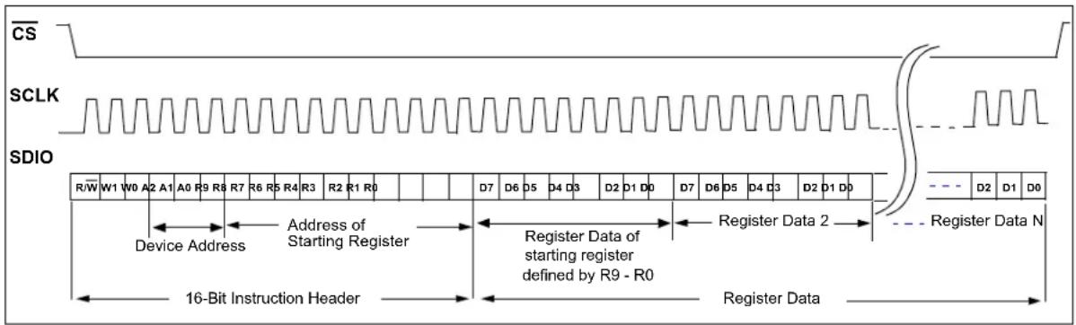
text_image
CS SCLK SDIO R/W W1 W0 A2 A1 A0 R9 R8 R7 R6 R5 R4 R3 R2 R1 R0 D7 D6 D5 D4 D3 D2 D1 D0 D7 D6 D5 D4 D3 D2 D1 D0 Device Address Address of Starting Register Register Data of starting register defined by R9 - R0 Register Data N 16-Bit Instruction Header Register DataFIGURE 5-1: SPI Serial Data Communication Protocol with MSb-first. See Figures 2-3 and 2-4 for Timing Specifications.
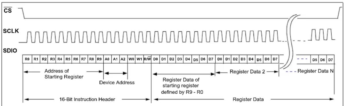
text_image
CS SCLK SDIO R0 R1 R2 R3 R4 R5 R6 R7 R8 R9 A0 A1 A2 W0 W1 R/W D0 D1 D2 D3 D4 D5 D6 D7 D0 D1 D2 D3 D4 D5 D6 D7 Address of Starting Register Device Address Register Data of starting register defined by R9 - R0 16-Bit Instruction Header Register Data Register Data NFIGURE 5-2: SPI Serial Data Communication Protocol - with LSb-First. See Figures 2-3 and 2-4 for Timing Specifications.
5.1 Register Initialization
The internal Configuration registers are initialized to their default values under two different conditions:
- After 2^20 clock cycles of delay from the Power-on Reset (POR).
- Resetting the hardware reset pin (RESET).
Figures 2-3 and 2-4 show the timing details.
Note 1: All address and bit locations that are not included in the following register map table should not be written or modified by the user.
2: Some registers include factory-controlled bits (FCB). Do not overwrite these bits.
5.2 Configuration Registers
The internal registers are mapped from Addresses 0x00 - 0x15D. These user registers are not sequentially located. Some user Configuration registers include factory-controlled bits. The factory-controlled bits should not be overwritten by the user.
All user Configuration registers are read/write, except for the last four registers, which are read-only. Each register is made of an 8-bit-wide volatile memory, and their default values are loaded during the power-up sequence or by using the hardware RESET pin. All registers are accessible by the SPI command using the register address. Table5-3 shows the user-register memory map, and Registers 5-1 - 5-83 show the details of the register bit functions.
TABLE 5-3: REGISTER MAP TABLE
| Addr. | Register Name | Bits | Default Value | |||||||
| b7 b6 b5 b4 b3 b2 b1 b0 | ||||||||||
| 0x00 S | PI Bit Ordering and ADC Mode Selection | SHUTDOWN↓ = Shutdown | LSb-FIRST↓ = LSB first0 = MSb first | SOFT_RESET0 = Soft Reset | STANDBY↓ = Standby | STANDBY↓ = Standby | SOFT_RESET0=Soft Reset | LSb-FIRST↓ = LSB first0 = MSb first | SHUTDOWN↓ = Shutdown | 0x24 |
| 0x01 No. of Channel Selection and Independence Control of Output Data and Clock Divider | EN_DATCLK_IND | FCB<3> = 0 | SEL_NCH<2:0> | FCB<2:0> = 111 | 0x0F | |||||
| 0x02 Output Data and Clock Rate Control | OUT_DATARATE<3:0> | OUT_CLKRATE<3:0> | 0x00 | |||||||
| 0x04 S | PI SDO Timing Control | SDO_TIME | FCB<8:0> = 001111 | 0x9F | ||||||
| 0x07 | Output Randomizer and WCK Polarity Control | POL_WCK | EN_AUTOCAL_TIMEDLY | FCB<4:0> = 1000 | EN_OUT RANDOM | 0x62 | ||||
| 0x1E | Auto-Calibration Time Delay Control | AUTOCAL_TIMEDLY<7:0> | 0x80 | |||||||
| 0x52 | DLL Control | EN_DUTY | DCLK_PHDLY_DLL<2:0> | EN_DLL_DCLK | EN_DLL | EN_CLK | RESET_DLL | 0x0A | ||
| 0x53 C | Clock Source Selection | FCB<6:4>= 0:0 | CLK_SOURCE | FCB<3:0>= 0101 | 0x45 | |||||
| 0x54 | PLL Reference Divider | PLL_REFDIV<7:0> | 0x00 | |||||||
| 0x55 P | PLL Output and Reference Divider | PLL_OUTDIV<3:0> | FCB<1:0>= 0 | PLL_REFDIV<9:8> | 0x48 | |||||
| 0x56 | PLL Prescaler (LSb) | PLL_PRE (LSB)<7:0> | 0x78 | |||||||
| 0x57 | PLL Prescaler (MSb) | FCB<3:0> = 0:00 | PLL_PRE (MSB)<11:8> | 0x40 | ||||||
| 0x58 | PLL Charge Pump | FCB<2:0> = 000 | PLL_BIAS | PLL_CHAGPUMP<3:0> | 0x12 | |||||
| 0x59 P | PLL Enable Control 1 | U | FCB<4:3> = 10 | EN_PLL_REFDIV | FCB<2:1>= 00 | EN_PLL | FCB<0>= 1 | 0x41 | ||
| 0x5A | PLL Loop Filter Resistor | U | FCB<1:0> = 01 | PLL_RES<4:0> | 0x2F | |||||
| 0x5B | PLL Loop Filter Cap3 | U | FCB<1:0> = 01 | PLL_CAP3<4:0> | 0x27 | |||||
| 0x5C | PLL Loop Filter Cap1 | U | FCB<1:0> = 01 | PLL_CAP1<4:0> | 0x27 | |||||
| 0x5D | PLL Loop Filter Cap2 | U | FCB<1:0> = 01 | PLL_CAP2<4:0> | 0x27 | |||||
| 0x5F P | PLL Enable Control 2 | FCB<5:2> = 1111 | EN_PLL_OUT | EN_PLL_BIAS | FCB<1:0>= 01 | 0xF1 | ||||
| 0x62 | Output Data Format and Output Test Pattern | U | FCB<0>= 0 | DATA_FORMAT | OUTPUT_MODE<1:0> | TEST_PATTERNNS<2:0> | 0x10 | |||
| 0x63 LVDS Output Load and Drive Current Control | FCB<3:0> = 0000 | LVDS_LOAD | LVDS_IMODE<2:0> | 0x01 | ||||||
| 0x64 Output Clock Phase Control when Decimation Filter is used | EN_PHDLY | DCLK_PHDLY_DEC<2:0> | FCB<3:0>= 0011 | 0x03 | ||||||
| 0x65 | LVDS Output Polarity Control | POL_LVDS<5:0> | NO EFFECT<1:0> | 0x00 | ||||||
| 0x66 Digital Offset Correction - Lower Byte | DIG_OFFSET_GLOBAL<7:0> | 0x00 | ||||||||
| 0x67 Digital Offset Correction - Upper Byte | DIG_OFFSET_GLOBAL<15:8> 0x00 | |||||||||
| 0x68 WCK and OVR | FCB<5:2> = 00_0 | POL_WCK_OVR | EN_WCK_OVR FCB<1:0> = 00 0x24 | |||||||
| 0x6B PLL Calibration | FCB<6:2> = 00001 | PLL_CAL_TRIG | FCB<1:0> = 00 | 0x08 | ||||||
| 0x6D PLL Output and Output Clock Phase | U<1:0> | EN_PLL_CLK | FCB<1> = 0 | DCLK_DLY_PLL<2:0> | FCB<0> = 0 | 0x00 | ||||
| 0x74 User-Defined Output Pattern A - Lower Nibble | PATTERN A<3:0> | Do not use (Leave these bits as '0000') | 0x00 | |||||||
| 0x75 User-Defined Output Pattern A - Upper Byte | PATTERN A<11:4> | 0x00 | ||||||||
| 0x76 User-Defined Output Pattern B - Lower Nibble | PATTERN B<3:0> | Do not use (Leave these bits as '0000') | 0x00 | |||||||
| 0x77 User-Defined Output Pattern B - Upper Byte | PATTERN B<11:4> | 0x00 | ||||||||
| 0x7B Noise-Shaping Requantizer Channel A Filter | NSR_RESET | NSRA<6:0> | 0x00 | |||||||
| 0x79 Dual-Channel DSPP Control | EN_DSPP_2 | NSRB<6:0> | 0x00 | |||||||
| 0x7A FIR A Filter | FIR_A=0 | FIR_A<0> | EN_FDR | FCB<0> = 0 | EN_NSRB_11 | EN_NSRB_12 | EN_NSRA_11 | EN_NSRA_12 | 0x00 | |
| 0x7B FIR A Filter | FIR_A<8:1> | 0x00 | ||||||||
| 0x7C FIR B Filter | FIR_B<7:0> | 0x00 | ||||||||
| 0x7D Auto-Scan Channel Order - Lower Byte | CH_ORDER<7:0> | 0x78 | ||||||||
| 0x7E Auto-Scan Channel Order - Middle Byte | CH_ORDER<15:8> | 0xAC | ||||||||
| 0x7F Auto-Scan Channel Order - Upper Byte | CH_ORDER<23:16> | 0x8E | ||||||||
| 0x80 Digital Down-Converter Control 1 | HBFILTER_B | HBFILTER_A | EN_NCO | EN_AMPDITH | EN_PHSDITH | EN_LFSR | EN_DDC_FS/8 | EN_DDC1 | 0x00 | |
| 0x81 Digital Down-Converter Control 2 | FDR_BAND | EN_DDC2 | GAIN_HBF_DDC | SEL_FDR | EN_DSPP_8 | 8CH_CW | GAIN_8CH<1:0> | 0x00 | ||
| 0x82 Numerically Controlled Oscillator (NCO) Tuning - Lower Byte | NCO_TUNE<7:0> | 0x00 | ||||||||
| 0x83 Numerically Controlled Oscillator (NCO) Tuning - Middle Lower Byte | NCO_TUNE<15:8> | 0x00 | ||||||||
| 0x84 Numerically Controlled Oscillator (NCO) Tuning - Middle Upper Byte | NCO_TUNE<23:16> | 0x00 | ||||||||
| 0x85 | Numerically Controlled Oscillator (NCO) Tuning - Upper Byte | NCO_TUNE<31:24> 0x00 | ||||||||
| 0x86 | CH0 NCO Phase Offset in CW or DDC Mode - Lower Byte | CH0_NCO_PHASE<7:0> 0x00 | ||||||||
| 0x87 | CH0 NCO Phase Offset in CW or DDC Mode - Upper Byte | CH0_NCO_PHASE<15:8> 0x00 | ||||||||
| 0x88 | CH1 NCO Phase Offset in CW or DDC Mode - Lower Byte | CH1_NCO_PHASE<7:0> 0x00 | ||||||||
| 0x89 | CH1 NCO Phase Offset in CW or DDC Mode - Upper Byte | CH1_NCO_PHASE<15:8> 0x00 | ||||||||
| 0x8A | CH2 NCO Phase Offset in CW or DDC Mode - Lower Byte | CH2_NCO_PHASE<7:0> 0x00 | ||||||||
| 0x8B | CH2 NCO Phase Offset in CW or DDC Mode - Upper Byte | CH2_NCO_PHASE<15:8> 0x00 | ||||||||
| 0x8C | CH3 NCO Phase Offset in CW or DDC Mode - Lower Byte | CH3_NCO_PHASE<7:0> 0x00 | ||||||||
| 0x8D | CH3 NCO Phase Offset in CW or DDC Mode - Upper Byte | CH3_NCO_PHASE<15:8> 0x00 | ||||||||
| 0x8E | CH4 NCO Phase Offset in CW or DDC Mode - Lower Byte | CH4_NCO_PHASE<7:0> 0x00 | ||||||||
| 0x8F | CH4 NCO Phase Offset in CW or DDC Mode - Upper Byte | CH4_NCO_PHASE<15:8> 0x00 | ||||||||
| 0x90 | CH5 NCO Phase Offset in CW or DDC Mode - Lower Byte | CH5_NCO_PHASE<7:0> 0x00 | ||||||||
| 0x91 | CH5 NCO Phase Offset in CW or DDC Mode - Upper Byte | CH5_NCO_PHASE<15:8> 0x00 | ||||||||
| 0x92 | CH6 NCO Phase Offset in CW or DDC Mode - Lower Byte | CH6_NCO_PHASE<7:0> 0x00 | ||||||||
| 0x93 | CH6 NCO Phase Offset in CW or DDC Mode - Upper Byte | CH6_NCO_PHASE<15:8> 0x00 | ||||||||
| 0x94 | CH7 NCO Phase Offset in CW or DDC Mode - Lower Byte | CH7_NCO_PHASE<7:0> 0x00 | ||||||||
| 0x95 | CH7 NCO Phase Offset in CW or DDC Mode - Upper Byte | CH7_NCO_PHASE<15:8> 0x00 | ||||||||
| 0x96 | CH0 Digital Gain CH0_DIG_GAIN<7:0> 0x3C | |||||||||
| 0x97 | CH1 Digital Gain CH1_DIG_GAIN<7:0> 0x3C | |||||||||
| 0x98 | CH2 Digital Gain CH2_DIG_GAIN<7:0> 0x3C | |||||||||
| 0x99 | CH3 Digital Gain CH3_DIG_GAIN<7:0> 0x3C | |||||||||
| 0x9A CH4 Digital Gain CH4_DIG_GAIN<7:0> 0x3C | ||||||||||
| 0x9B CH5 Digital Gain CH5_DIG_GAIN<7:0> 0x3C | ||||||||||
| 0x9C CH6 Digital Gain CH6_DIG_GAIN<7:0> 0x3C | ||||||||||
| 0x9D CH7 Digital Gain CH7_DIG_GAIN<7:0> 0x3C | ||||||||||
| 0x9E CH0 Digital Offset CH0_DIG_OFFSET<7:0> 0x00 | ||||||||||
| 0x9F CH1 Digital Offset CH1_DIG_OFFSET<7:0> 0x00 | ||||||||||
| 0xA0 CH2 Digital Offset CH2_DIG_OFFSET<7:0> 0x00 | ||||||||||
| 0xA1 CH3 Digital Offset CH3_DIG_OFFSET<7:0> 0x00 | ||||||||||
| 0xA2 CH4 Digital Offset CH4_DIG_OFFSET<7:0> 0x00 | ||||||||||
| 0xA3 CH5 Digital Offset CH5_DIG_OFFSET<7:0> 0x00 | ||||||||||
| 0xA4 CH6 Digital Offset CH6_DIG_OFFSET<7:0> 0x00 | ||||||||||
| 0xA5 CH7 Digital Offset CH7_DIG_OFFSET<7:0> 0x00 | ||||||||||
| 0xA7 Digital Offset Weight Control | FCB<5:3> = 0:0 | DIG_OFFSET_WEIGHT<1:0> | FCB<2:0>= '11 | 0x47 | ||||||
| 0xC0 Calibration Status Indication (Read only) | ADC_CAL_STAT | FCB<6:0>= 000-0000 | — | |||||||
| 0xD1 PLL Calibration Status and PLL Drift Status Indication (Read only) | FCB<4:3>= xx | PLL_CAL_STAT | FCB<2:1>= xx | PLL_VCOL_STAT | PLL_VCOH_STAT | FCB<0>= x | — | |||
| 0x15C CHIP ID - Lower Byte(2)(Read only) | CHIP_ID<7:0> | — | ||||||||
| 0x15D CHIP ID - Upper Byte(2)(Read only) | CHIP_ID<15:8> | — | ||||||||
Legend: U = Unimplemented bit, read as '0' FCB = Factory-Controlled Bits. Do not program 1 = bit is set 0 = bit is cleared x = bit is unknown 2: Read-only register. Preprogrammed at the factory for internal use.
REGISTER 5-1: ADDRESS 0X00 - SPI BIT ORDERING AND ADC MODE SELECTION (1)
| R/W-0 R/W-0 R/W-1 R/W-0 | R/W-0 R/W-1 R/W-0 R/W-0 | ||||||
| SHUTDOWN | LSb_FIRST SOFT_RESET | STANDBY | STANDBY | SOFT_RESET | LSb_FIRST | SHUTDOWN | |
| bit 7 bit 0 | |||||||
| Legend: | |||
| R = Readable bit | W = Writable bit | U = Unimplemented bit, read as '0' | |
| -n = Value at POR | '1' = Bit is set | '0' = Bit is cleared | x = Bit is unknown |
bit 7 SHUTDOWN: Shutdown mode setting for power-saving ^2
1 = ADC in Shutdown mode
0 = Not in Shutdown mode (Default)
bit 6 LSb_FIRST: Select SPI communication bit order
1 = Start SPI communication with LSb first
0 = Start SPI communication with MSb first (Default)
bit 5 SOFT_RESET: Soft Reset control bit ^(3)
1 = Not in Soft Reset mode (Default)
0 = ADC in Soft Reset
bit 4 STANDBY: Send the device into a power-saving Standby mode ^(4)
1 = ADC in Standby mode
0 = Not in Standby mode (Default)
bit 3 STANDBY: Send the device into a power-saving Standby mode ^(4)
1 = ADC in Standby mode
0 = Not in Standby mode (Default)
bit 2 SOFT_RESET: Soft Reset control bit ^(3)
1 = Not in Soft Reset mode (Default)
0 = ADC in Soft Reset
bit 1 LSb_FIRST: Select SPI communication bit order
1 = Start SPI communication with LSb first
0 = Start SPI communication with MSb first (Default)
bit 0 SHUTDOWN: Shutdown mode setting for power-saving ^(2)
1 = ADC in Shutdown mode
0 = Not in Shutdown mode (Default)
Note 1: Upper and lower nibble are mirrored, which makes the MSb- or LSb-first mode interchangeable. The lower nibble (bit <3:0>) has a higher priority when the mirrored bits have different values.
2: During Shutdown mode, most of the internal circuits including the reference and clock are turned-off except for the SPI interface. When exiting from Shutdown (changing from '1' to '0'), executing the device Soft Reset simultaneously is highly recommended for a fast recalibration of the ADC. The internal user registers are not affected.
3: This bit forces the device into Soft Reset mode, which initializes the internal calibration registers to their initial default states. The user-registers are not affected. When exiting Soft Reset mode (changing from '0' to '1'), the device performs an automatic device calibration including PLL calibration if PLL is enabled. DLL is reset if enabled. During Soft Reset, the device has the following states:
no ADC output
- no change in power-on condition of internal reference
- most of the internal clocks are not distributed
- power consumption: (a) digital section - negligible, (b) analog section - no change
4: During Standby mode, most of the internal circuits are turned off except for the reference, clock and SPI interface. When exiting from Standby mode (changing from '1' to '0') after an extended amount of time, executing Soft Reset simultaneously is highly recommended. The internal user registers are not affected.
REGISTER 5-2: ADDRESS 0X01 – NUMBER OF CHANNELS, INDEPENDENCY CONTROL OF OUTPUT DATA AND CLOCK DIVIDER
| R/W-0 R/W-0 R/W-0 R/W-0 R/W-1 R/W-1 R/W-1 R/W-1 | ||
| EN_DATCLK_IND | FCB<3> SEL_NCH<2:0> FCB<2:0> | |
| bit 7 bit 0 | ||
Legend:
| R = Readable bit | W = Writable bit | U = Unimplemented bit, read as '0' |
| -n = Value at POR | '1' = Bit is set | '0' = Bit is cleared x = Bit is unknown |
bit 7 EN_DATCLK_IND: Enable data and clock divider independently ^(1)
1 = Enabled
0 = Disabled (Default)
bit 6 FCB<3>: Factory-Controlled Bit. This is not for the user. Do not change default setting.
bit 5-3 SEL_NCH<2:0>: Select the total number of input channels to be used ^(2)
111 = 7 inputs
110 = 6 inputs
101 = 5 inputs
100 = 4 inputs
011 = 3 inputs
010 = 2 inputs
001 = 1 input (Default)
000 = 8 inputs
bit 2-0 FCB<2:0>: Factory-Controlled Bits. This is not for the user. Do not change default settings.
Note 1: EN_DATCLK_IND = 1 enables OUT_CLKRATE<3:0> settings in Address 0x02 (Register 5-3).
2: See Addresses 0x7D - 0x7F (Registers 5-38 - 5-40) for selecting the input channel order.
REGISTER 5-3: ADDRESS 0X02 – OUTPUT DATA AND CLOCK RATE CONTROL (1)
| R/W-0 R/W-0 R/W-0 R/W-0 R/W-0 R/W-0 R/W-0 | R/W-0 | |
| OUT_DATARATE<3:0> OUT_CLKRATE<3:0> | ||
| bit 7 bit 0 | ||
Legend:
| R = Readable bit W = Writable bit U = Unimplemented bit, read as '0' | ||
| -n = Value at POR | '1' = Bit is set | '0' = Bit is cleared |
bit 7-4
OUT_DATARATE<3:0>: Output data rate control bits
| 1111 = Output data is all 0's |
| 1110 = Output data is all 0's |
| 1101 = Output data is all 0's |
| 1100 = Internal test only(2) |
| 1011 = Internal test only(2) |
| 1010 = Internal test only(2) |
| 1001 = Full speed divided by 512 |
| 1000 = Full speed divided by 256 |
| 0111 = Full speed divided by 128 |
| 0110 = Full speed divided by 64 |
| 0101 = Full speed divided by 32 |
| 0100 = Full speed divided by 16 |
| 0011 = Full speed divided by 8 |
| 0010 = Full speed divided by 4 |
| 0001 = Full speed divided by 2 |
| 0000 = Full-speed rate (Default) |
bit 3-0
OUT_CLKRATE<3:0>: Output clock rate control bits ^(3,4)
| 1111 = Full-speed rate |
| 1110 = No clock output |
| 1101 = No clock output |
| 1100 = No clock output |
| 1011 = No clock output |
| 1010 = No clock output |
| 1001 = Full speed divided by 512 |
| 1000 = Full speed divided by 256 |
| 0111 = Full speed divided by 128 |
| 0110 = Full speed divided by 64 |
| 0101 = Full speed divided by 32 |
| 0100 = Full speed divided by 16 |
| 0011 = Full speed divided by 8 |
| 0010 = Full speed divided by 4 |
| 0001 = Full speed divided by 2 |
| 0000 = No clock output (Default) |
Note 1: This register should be used to realign the output data and clock when the decimation or digital down-conversion (DDC) option is used.
2: 1100 - 1010: Do not reprogram. These settings are used for the internal test only. If these bits are reprogrammed with different settings, the outputs will be in an undefined state.
3: Bits <3:0> become active if EN_DATCLK_IND = 1 in Address 0x01 (Register 5-2).
4: When no clock output is selected (Bits 1110 - 1010): clock output is not available at the DCLK+/DCLK-pins.
REGISTER 5-4: ADDRESS 0X04 - SPI SDO OUTPUT TIMING CONTROL
| R/W-1 R/W-0 R/W-0 R/W-1 R/W-1 R/W-1 R/W-1 R/W-1 | |
| SDO_TIME | FCB<6:0> |
| bit 7 bit 0 | |
Legend:
| R = Readable bit W = Writable bit U = Unimplemented bit, read as '0' | |||
| -n = Value at POR | '1' = Bit is set | '0' = Bit is cleared | x = Bit is unknown |
bit 7 SDO_TIME: SPI SDO output timing control bit
1 = SDO output at the falling edge of clock (Default)
0 = SDO output at the rising edge of clock
bit 6-0 FCB<6:0>: Factory-Controlled Bits. This is not for the user. Do not change default settings.
REGISTER 5-5: ADDRESS 0X07 - OUTPUT RANDOMIZER AND WCK POLARITY CONTROL
| R/W-0 | R/W-1 | R/W-1 | R/W-0 | R/W-0 | R/W-0 | R/W-1 | R/W-0 |
| POL_WCK | EN_AUTOCAL_TIMEDLY | FCB<4:0> | EN_OUT RANDOM | ||||
| bit 7 bit 0 | |||||||
Legend:
| R = Readable bit | W = Writable bit | U = Unimplemented bit, read as '0' |
| -n = Value at POR | '1' = Bit is set | '0' = Bit is cleared x = Bit is unknown |
bit 7 POL_WCK: WCK polarity control bit ^(1)
1 = Inverted
0 = Not inverted (Default)
bit 6 EN_AUTOCAL_TIMEDLY: Auto-calibration starter time delay counter control bit ^(2)
1 = Enabled (Default)
0 = Disabled
bit 5-1 FCB<4:0>: Factory-Controlled Bits. This is not for the user. Do not change default settings.
bit 0 EN_OUT_RANDOM: Output randomizer control bit
1 = Enabled: ADC data output is randomized
0 = Disabled (Default)
Note 1: See Address 0x68 (Register 5-26) for WCK/OVR pair control.
2: This bit enables the AUTOCAL_TIMEDLY<7:0> settings. See Address 0x1E (Register 5-6).
REGISTER 5-6: ADDRESS 0X1E - AUTOCAL TIME DELAY CONTROL (1)
| R/W-1 R/W-0 R/W-0 R/W-0 R/W-0 R/W-0 R/W-0 | R/W-0 |
| AUTOCAL_TIMEDLY<7:0> | |
| bit 7 | bit 0 |
Legend:
R = Readable bit    W = Writable bit    U = Unimplemented bit, read as '0'
-n = Value at POR    '1' = Bit is set    '0' = Bit is cleared    x = Bit is unknown
bit 7-0 AUTOCAL_TIMEDLY<7:0>: Auto-calibration start time delay control bits
1111-1111 = Maximum value
...
1000-0000 = (Default)
...
0000-0000 = Minimum value
Note 1: EN_AUTOCAL_TIMEDLY in Address 0x07 (Register 5-5) enables this register setting. This register controls the time delay before the auto-calibration starts. The value increases linearly with the bit settings, from minimum to maximum values.
REGISTER 5-7: ADDRESS 0X52 - DLL CONTROL
| R/W-0 | R/W-0 | R/W-0 | R/W-0 | R/W-1 | R/W-0 | R/W-1 | R/W-0 |
| EN_DUTY | DCLK_PHDLY_DLL<2:0> | EN_DLL_DCLK | EN_DLL | EN_CLK | RESET_DLL | ||
| bit 7 bit 0 | |||||||
Legend:
R = Readable bit W = Writable bit U = Unimplemented bit, read as '0'
-n = Value at POR '1' = Bit is set '0' = Bit is cleared x = Bit is unknown
bit 7 EN_DUTY: Enable DLL circuit for duty cycle correction (DCC) of input clock
1 = Correction is ON
0 = Correction is OFF (Default)
bit 6-4 DCLK_PHDLY_DLL<2:0>: Select the phase delay of the digital clock output when using DLL ^(1)
111 = +315° phase-shifted from default
110 = +270° phase-shifted from default
101 = +225° phase-shifted from default
100 = +180° phase-shifted from default
011 = +135 phase-shifted from default
010 = +90° phase-shifted from default
001 = +45° phase-shifted from default
000 = (Default)
bit 3 EN_DLL_DCLK: Enable DLL digital clock output
1 = Enabled (Default)
0 = Disabled: DLL digital clock is turned off. ADC output is not available when DLL is used.
bit 2 EN_DLL: Enable DLL circuitry to provide a selectable phase clock to digital output clock.
1 = Enabled
0 = Disabled. DLL block is disabled (Default)
bit 1 EN_CLK: Enable clock input buffer
1 = Enabled (Default).
0 = Disabled. No clock is available to the internal circuits, ADC output is not available.
bit 0 RESET_DLL : DLL circuit reset control ^(2)
1 = DLL is active
0 = DLL circuit is held in reset (Default)
Note 1: These bits have an effect only if EN_PHDLY = 1 and decimation is not used.
2: DLL reset control procedure: Set this bit to '0' (reset) and then to '1'.
REGISTER 5-8: ADDRESS 0X53 - CLOCK SOURCE SELECTION
| R/W-0 R/W-1 R/W-0 R/W-0 R/W-0 R/W-1 R/W-0 R/W-1 | |
| FCB<6:4> CLK_SOURCE FCB<3:0> | |
| bit 7 bit 0 | |
Legend:
| R = Readable bit W = Writable bit U = Unimplemented bit, read as '0' | |||
| -n = Value at POR | '1' = Bit is set | '0' = Bit is cleared | x = Bit is unknown |
bit 7-5 FCB<6:4>: Factory-Controlled Bits. This is not for the user. Do not change default settings.
bit 4 CLK_SOURCE: Select internal timing source
1 = PLL output is selected as timing source
0 = External clock input is selected as timing source (Default)
bit 3-0 FCB<3:0>: Factory-Controlled Bits. This is not for the user. Do not change default settings.
REGISTER 5-9: ADDRESS 0X54 – PLL REFERENCE DIVIDER
| R/W-0 | R/W-0 | R/W-0 | R/W-0 | R/W-0 | R/W-0 | R/W-0 | R/W-0 |
| PLL_REFDIV<7:0> | |||||||
| bit 7 bit 0 | |||||||
Legend:
| R = Readable bit | W = Writable bit | U = Unimplemented bit, read as '0' |
| -n = Value at POR | '1' = Bit is set | '0' = Bit is cleared x = Bit is unknown |
bit 7-0 PLL_REFDIV<7:0>: PLL Reference clock divider control bits ^(1)
1111-1111 = PLL reference divided by 255 (if PLL_REFDIV<9:8>=00)
1111-1110 = PLL reference divided by 254 (if PLL_REFDIV<9:8> = 00)
...
0000-0011 = PLL reference divided by 3 (if PLL_REFDIV<9:8>=00)
0000-0010 = Do not use (No effect)
0000-0001 = PLL reference divided by 1 (if PLL_REFDIV<9:8>=00)
0000-0000 = PLL reference not divided (if PLL_REFDIV<9:8>=00) (Default)
Note 1: PLL_REFDIV is a 10-bit wide setting. See Address 0x55 (Register 5-10) for the upper two bits and Table 5-4 for PLL_REF-DIV<9:0> bit settings. This setting controls the clock division ratio of the PLL reference clock (external clock input at the CLK pin) before the PLL phase-frequency detector circuitry. Note that the divider value of 2 is not supported. EN_PLL_REFDIV in Address 0x59 (Register 5-14) must be set.
REGISTER 5-10: ADDRESS 0X55 – PLL OUTPUT AND REFERENCE DIVIDER
| R/W-0 R/W-1 R/W-0 R/W-0 R/W-1 R/W-0 R/W-0 R/W-0 | ||
| PLL_OUTDIV<3:0> | FCB<1:0> PLL_REFDIV<9:8> | |
| bit 7 bit 0 | ||
| Legend: | |||
| R = Readable bit W = Writable bit | U = Unimplemented bit, read as ‘0’ | ||
| -n = Value at POR | ‘1’ = Bit is set | ‘0’ = Bit is cleared | x = Bit is unknown |
bit 7-4 PLL_OUTDIV<3:0>: PLL output divider control bits ^(1)
1111 = PLL output divided by 15
1110 = PLL output divided by 14
...
0100 = PLL output divided by 4 (Default)
0011 = PLL output divided by 3
0010 = PLL output divided by 2
0001 = PLL output divided by 1
0000 = PLL output not divided
bit 3-2 FCB<1:0>: Factory-Controlled Bits. This is not for the user. Do not change default settings.
bit 1-0 PLL_REFDIV<9:8>: Upper two MSb bits of PLL_REFDIV<9:0>(2)
00 = see Table 5-4. (Default)
Note 1: PLL_OUTDIV<3:0> controls the PLL output clock divider: VCO output is divided by the PLL_OUTDIV<3:0> setting.
2: See Address 0x54 (Register 5-9) and Table 5-4 for PLL_REFDIV<9:0> settings. EN_PLL_REFDIV in Address 0x59 (Register 5-14) must be set.
TABLE 5-4: EXAMPLE – PLL REFERENCE DIVIDER BIT SETTINGS VS. PLL REFERENCE INPUT FREQUENCY
| PLL_REFDIV<9:0> | PLL Reference Frequency |
| 11-1111-1111 | Reference frequency divided by 1023 |
| 11-1111-1110 | Reference frequency divided by 1022 |
| — | — |
| 00-0000-0011 | Reference frequency divided by 3 |
| 00-0000-0010 | Do not use (not supported) |
| 00-0000-0001 | Reference frequency divided by 1 |
| 00-0000-0000 | Reference frequency divided by 1 |
REGISTER 5-11: ADDRESS 0X56 – PLL PRESCALER (LSB)
R/W-0 R/W-1 R/W-1 R/W-1 R/W-1 R/W-0 R/W-0
R/W-0
PLL_PRE<7:0>
bit 7
bit 0
Legend:
R = Readable bit W = Writable bit U = Unimplemented bit, read as '0'
-n = Value at POR '1' = Bit is set '0' = Bit is cleared x = Bit is unknown
bit 7-0 PLL_PRE<7:0>: PLL prescaler selection
(1)
1111-1111 = VCO clock divided by 255 (if PLL_PRE<11:8> = 0000)
...
0111-1000 = VCO clock divided by 120 (if PLL_PRE<11:8> = 0000) (Default)
...
0000-0010 = VCO clock divided by 2 (if PLL_PRE<11:8> = 0000)
0000-0001 = VCO clock divided by 1 (if PLL_PRE<11:8> = 0000)
0000-0000 = VCO clock not divided (if PLL_PRE<11:8> = 0000)
Note 1: PLL_PRE is a 12-bit-wide setting. The upper four bits (PLL_PRE<11:8>) are defined in Address 0x57. See Table 5-5 for the PLL_PRE<11:0> settings. The PLL Prescaler is used to divide down the VCO output clock in the PLL phase-frequency detector loop circuit.
REGISTER 5-12: ADDRESS 0X57 – PLL PRESCALER (MSB)
R/W-0 R/W-1 R/W-0 R/W-0 R/W-0 R/W-0 R/W-0 R/W-0
FCB<3:0> PLL_PRE<11:8>
bit 7 bit 0
Legend:
R = Readable bit W = Writable bit U = Unimplemented bit, read as '0'
-n = Value at POR '1' = Bit is set '0' = Bit is cleared x = Bit is unknown
bit 7-4 FCB<3:0>: Factory-Controlled Bits. This is not for the user. Do not change default settings.
bit 3-0 PLL_PRE<11:8>: PLL prescaler selection (1)
1111 = 2 ^12 - 1 (max), if PLL_PRE<7:0> = 0xFF
...
0000 = Default)
Note 1: PLL_PRE is a 12-bit-wide setting. See the lower eight bit settings (PLL_PRE<7:0>) in Address 0x56 (Register 5-11). See Table 5-5 for the PLL_PRE<11:0> settings for PLL feedback frequency.
TABLE 5-5: Example: PLL Prescaler Bit Settings and PLL Feedback Frequency
| PLL_PRE<11:0> | PLL Feedback Frequency |
| 1111-1111-1111 | VCO clock divided by 4095 ( 2^12 - 1) |
| 1111-1111-1110 | VCO clock divided by 4094 ( 2^12 - 2) |
| — | — |
| 0000-0000-0011 | VCO clock divided by 3 |
| 0000-0000-0010 | VCO clock divided by 2 |
| 0000-0000-0001 | VCO clock divided by 1 |
| 0000-0000-0000 | VCO clock divided by 1 |
REGISTER 5-13: ADDRESS 0X58 – PLL CHARGE-PUMP
R/W-0 R/W-0 R/W-0 R/W-1 R/W-0 R/W-0 R/W-1 R/W-0
FCB<2:0>: PLL_BIAS PLL_CH|AGPUMP<3:0>
bit 7 bit 0
Legend:
R = Readable bit W = Writable bit U = Unimplemented bit, read as '0'
-n = Value at POR    '1' = Bit is set    '0' = Bit is cleared    x = Bit is unknown
bit 7-5 FCB<2:0>: Factory-Controlled Bits. This is not for the user. Do not change default settings.
bit 4 PLL_BIAS: PLL charge-pump bias source selection bit
1 = Self-biasing coming from AV_DD (Default)
0 = Bandgap voltage from the reference generator (1.2V)
bit 3-0 PLL_CHAGPUMP<3:0>: PLL charge pump bias current control bits ^(1)
1111 = Maximum current
...
0010 = (Default)
...
0000 = Minimum current
Note 1: PLL_CHAGPUMP<3:0> should be set based on the phase detector comparison frequency. The bias current amplitude increases linearly with increasing the bit setting values. The increase is from approximately 25 μA to 375 μA, 25 μA per step. See Section 4.7.2.1, "PLL Output Frequency and Output Control Parameters" for more details of the PLL block.
REGISTER 5-14: ADDRESS 0X59 - PLL ENABLE CONTROL 1
U-0 R/W-1 R/W-0 R/W-0 R/W-0 R/W-0 R/W-1
— FCB<4:3> EN_PLL_REFDIV FCB<2:1> EN_PLL FCB<0>
bit 7 bit 0
Legend:
R = Readable bit    W = Writable bit    U = Unimplemented bit, read as '0'
-n = Value at POR    '1' = Bit is set    '0' = Bit is cleared    x = Bit is unknown
bit 7 Unimplemented: Not used.
bit 6-5 FCB<4:3>: Factory-Controlled Bits. This is not for the user. Do not change default settings.
bit 4 EN_PLL_REFDIV: Enable PLL Reference Divider (PLL_REFDIV<9:0>).
1 = Enabled
0 = Reference divider is bypassed (Default)
bit 3-2 FCB<2:1>: Factory-Controlled Bits. This is not for the user. Do not change default settings.
bit 1 EN_PLL: Enable PLL circuit.
1 = Enabled
0 = Disabled (Default)
bit 0 FCB<0>: Factory-Controlled Bit. This is not for the user. Do not change default setting.
REGISTER 5-15: ADDRESS 0X5A – PLL LOOP FILTER RESISTOR
U-0 R/W-0 R/W-1 R/W-0 R/W-1 R/W-1 R/W-1 R/W-1
— FCB<1:0> PLL_RES<4:0>
bit 7 bit 0
Legend:
R = Readable bit W = Writable bit U = Unimplemented bit, read as '0'
-n = Value at POR '1' = Bit is set '0' = Bit is cleared x = Bit is unknown
bit 7 Unimplemented: Not used.
bit 6-5 FCB<1:0>: Factory-Controlled Bits. This is not for the user. Do not change default settings.
bit 4-0 PLL_RES<4:0>: Resistor value selection bits for PLL loop filter ^(1)
11111 = Maximum value
...
01111 = (Default)
...
00000 = Minimum value
Note 1: PLL_RES<4:0> should be set based on the phase detector comparison frequency. The resistor value increases linearly with the bit settings, from minimum to maximum values. See the PLL loop filter section in Section 4.7, "ADC Clock Selection".
REGISTER 5-16: ADDRESS 0X5B - PLL LOOP FILTER CAP3
U-0 R/W-0 R/W-1 R/W-0 R/W-0 R/W-1 R/W-1 R/W-1
— FCB<1:0> PLL_CAP3<4:0>
bit 7 bit 0
Legend:
R = Readable bit W = Writable bit U = Unimplemented bit, read as '0'
-n = Value at POR '1' = Bit is set '0' = Bit is cleared x = Bit is unknown
bit 7 Unimplemented: Not used.
bit 6-5 FCB<1:0>: Factory-Controlled Bits. This is not for the user. Do not change default settings.
bit 4-0 PLL_CAP3<4:0>: Capacitor 3 value selection bits for PLL loop filter ^(1)
11111 = Maximum value
...
00111 = (Default)
...
00000 = Minimum value
Note 1: This capacitor is in series with the shunt resistor, which is set by PLL_RES<4:0>. The capacitor value increases linearly with the bit settings, from minimum to maximum values. This setting should be set based on the phase detector comparison frequency.
REGISTER 5-17: ADDRESS 0X5C - PLL LOOP FILTER CAP1
| U-0 R/W-0 | R/W-1 R/W-0 | R/W-0 R/W-1 R/W-1 | R/W-1 | ||||
| — FCB<1:0> PLL_CAP1<4:0> | |||||||
| bit 7 bit 0 | |||||||
Legend:
| R = Readable bit W = Writable bit U = Unimplemented bit, read as ‘0’ | |||
| -n = Value at POR | ‘1’ = Bit is set | ‘0’ = Bit is cleared | x = Bit is unknown |
bit 7 Unimplemented: Not used.
bit 6-5 FCB<1:0>: Factory-Controlled Bits. This is not for the user. Do not change default settings.
bit 4-0 PLL_CAP1<4:0>: Capacitor 1 value selection bits for PLL loop filter ^(1)
11111 = Maximum value
...
00111 = (Default)
...
00000 = Minimum value
Note 1: This capacitor is located between the charge pump output and ground, and in parallel with the shunt resistor which is defined by the PLL_RES<4:0>. The capacitor value increases linearly with the bit settings, from minimum to maximum values. This setting should be set based on the phase detector comparison frequency.
REGISTER 5-18: ADDRESS 0X5D - PLL LOOP FILTER CAP2
| U-0 R/W-0 R/W-1 R/W-0 R/W-0 R/W-1 R/W-1 R/W-1 | ||
| — FCB<1:0> PLL_CAP2<4:0> | ||
| bit 7 bit 0 | ||
Legend:
| R = Readable bit W = Writable bit U = Unimplemented bit, read as ‘0’ | |||
| -n = Value at POR | ‘1’ = Bit is set | ‘0’ = Bit is cleared | x = Bit is unknown |
bit 7 Unimplemented: Not used.
bit 6-5 FCB<1:0>: Factory-Controlled Bits. This is not for the user. Do not change default settings.
bit 4-0 PLL_CAP2<4:0>: Capacitor 2 value selection bits for PLL loop filter ^(1)
11111 = Maximum value
...
00111 = (Default)
...
00000 = Minimum value
Note 1: This capacitor is located between the charge pump output and ground, and in parallel with CAP1 which is defined by the PLL_CAP1<4:0>. The capacitor value increases linearly with the bit settings, from minimum to maximum values. This setting should be set based on the phase detector comparison frequency.
REGISTER 5-19: ADDRESS 0X5F – PLL ENABLE CONTROL 2 (1)
| R/W-1 R/W-1 R/W-1 R/W-1 R/W-0 R/W-0 R/W-0 R/W-1 | |||
| FCB<5:2> | EN_PLL_OUT | EN_PLL_BIAS | FCB<1:0> |
| bit 7 bit 0 | |||
Legend:
R = Readable bit W = Writable bit U = Unimplemented bit, read as '0'
-n = Value at POR '1' = Bit is set '0' = Bit is cleared x = Bit is unknown
bit 7-4 FCB<5:2>: Factory-Controlled Bits. This is not for the user. Do not change the default settings.
bit 3 EN_PLL_OUT: Enable PLL output.
1 = Enabled
0 = Disabled (Default)
bit 2 EN_PLL_BIAS: Enable PLL bias
1 = Enabled
0 = Disabled (Default)
bit 1-0 FCB<1:0>: Factory-Controlled Bits. This is not for the user. Do not change default settings.
Note 1: To enable PLL output, EN_PLL_OUT, EN_PLL_BIAS and EN_PLL in Address 0x59 (Register 5-14) must be set.
REGISTER 5-20: ADDRESS 0X62 - OUTPUT DATA FORMAT AND OUTPUT TEST PATTERN
| U-0 R/W-0 R/W-0 R/W-1 R/W-0 | R/W-0 R/W-0 | R/W-0 | |||
| — FCB | DATA_FORMAT | OUTPUT_MODE | <1:0> | TEST_PATTERNNS<2:0> | |
| bit 7 bit 0 | |||||
Legend:
| R = Readable bit | W = Writable bit | U = Unimplemented bit, read as '0' |
| -n = Value at POR | ‘1’ = Bit is set | ‘0’ = Bit is cleared x = Bit is unknown |
bit 7 Unimplemented: Not used.
bit 6 FCB: Factory-controlled bit. This is not for the user. Do not change default setting.
bit 5 DATA_FORMAT: Output data format selection
1 = Offset binary (unsigned)
0 = Two's complement (Default)
bit 4-3 OUTPUT_MODE<1:0>: Output mode selection ^(1)
11 = Do not use. Output is undefined
10 = Select DDR LVDS output mode with even bit first ^2 (Default)
01 = Select CMOS output mode
00 = Output disabled
bit 2-0 TEST_PATTERN<2:0>: Test output data pattern selection ^(3)
111 = Output data is pseudo-random number (PN) sequence ^(4)
110 = Sync Pattern for LVDS output
Output: '11111111 0000'
101 = Alternating Sequence for LVDS mode
Output: '01010101 1010'
100 = Alternating Sequence for CMOS mode
Output: '1111111 1111' alternating with '0000000 0000'
011 = Alternating Sequence for CMOS
Output: '01010101 0101' alternating with '10101010 1010'
010 = Ramp Pattern: Output (Q0) is incremented by 1 LSB per 64 clock cycles ^(5)
001 = Double Custom Patterns
Output: Alternating custom pattern A (see Addresses 0X74 - 0X75 - Registers 5-29 -5-30)
and custom pattern B (see Address 0X76 - 0X77 - Registers 5-31 - 5-32) ^(6)
000 = Normal Operation. Output: ADC data (Default)
Note 1: See Figures 2-1-2-2 for the timing diagrams.
2: Rising edge: Q10, Q8, Q6, Q4, Q2, Q0.
Falling edge: Q11, Q9, Q7, Q5, Q3, Q1.
3: See Section 4.12.12 "Output Test Patterns" for more details.
(a) In LVDS mode: only the active pins (per register settings) are active. Inactive output pins are High Z state.
(b) In CMOS mode: all data output pins (Q11-Q0), output test pins (TP), OVR and WCK pins are active, even if they are disabled by register settings.
Since the output test pins (TP) can toggle during this test, the output test pins can draw extra current if they are connected to the supply pin or ground. To avoid the extra current draws, always leave the TP pins floating (not connected).
4: Pseudo-random number (PN) code is generated by the linear feedback shift register (LFSR). See Section 4.12.12.1, "Pseudo-Random Number (PN) Sequence Output" for more details.
5: OVR and WCK bits are incremented by 1 per 219 and 218 clock cycles, respectively.
6: Pattern A<11:0> and B<11:0> are applied to Q<11:0>. Q11 = OVR, Q10 = WCK.
REGISTER 5-21: ADDRESS 0X63 – LVDS OUTPUT LOAD AND DRIVER CURRENT CONTROL
R/W-0 R/W-0 R/W-0 R/W-0 R/W-0 R/W-0 R/W-0 R/W-1
FCB<3:0> LVDS_LOAD LVDS_IMODE<2:0>
bit 7 bit 0
Legend:
R = Readable bit W = Writable bit U = Unimplemented bit, read as '0'
-n = Value at POR '1' = Bit is set '0' = Bit is cleared x = Bit is unknown
bit 7-4 FCB<3:0>: Factory-controlled bits. This is not for the user. Do not change default setting.
bit 3 LVDS_LOAD: Internal LVDS load termination
1 = Enable internal load termination
0 = Disable internal load termination (Default)
bit 2-0 LVDS_IMODE<2:0>: LVDS driver current control bits
111 = 7.2 mA
011 = 5.4 mA
001 = 3.5 mA (Default)
000 = 1.8 mA
Do not use the following settings ^(1) :
110, 101, 100, 010
Note 1: Do not use these settings. These settings can result in unknown output currents.
REGISTER 5-22: ADDRESS 0X64 – OUTPUT CLOCK PHASE CONTROL WHEN DECIMATION FILTER IS USED
| R/W-0 R/W-0 R/W-0 R/W-0 R/W-0 R/W-0 R/W-1 R/W-1 | |
| EN_PHDLY DCLK_PHDLY_DEC<2:0> | FCB<3:0> |
| bit 7 bit 0 | |
Legend:
| R = Readable bit W = Writable bit | U = Unimplemented bit, read as '0' | ||
| -n = Value at POR | '1' = Bit is set | '0' = Bit is cleared | x = Bit is unknown |
bit 7 EN_PHDLY: Enable digital output clock phase delay control when DLL or decimation filter is used.
1 = Enabled
0 = Disabled (Default)
bit 6-4 DCLK_PHDLY_DEC<2:0>: Digital output clock phase delay control when decimation filter is used ^(2)
111 = +315° phase-shifted from default ^(2) 110 = +270° phase-shifted from default 101 = +225° phase-shifted from default ^(2) 100 = +180° phase-shifted from default 011 = +135° phase-shifted from default ^(2) 010 = +90° phase-shifted from default 001 = +45° phase-shifted from default ^(2) 000 = Default ^(3)
bit 3-0 FCB<3:0>: Factory-Controlled Bits. This is not for the user. Do not change default settings.
Note 1: These bits have an effect only if EN_PHDLY = 1. See Address 0x52 (Register 5-7) for the same feature when DLL is used.
2: Only available when the decimation filter setting is greater than 2. When FIR_A/B <8:1> = 0's (default) and FIR_A<6> = 0, only 4-phase shifts are available (+45°, +135°, +225°, +315°) from default. See Addresses 0x7A, 0x7B and 0x7C (Registers 5-35 - 5-37). See Addresses 0x6D and 0x52 (Registers 5-28 and 5-7) for DCLK phase shift for other modes.
3: The phase delay for all other settings is referenced to this default phase.
REGISTER 5-23: ADDRESS 0X65 – LVDS OUTPUT POLARITY CONTROL
| R/W-0 | R/W-0 | R/W-0 | R/W-0 | R/W-0 | R/W-0 | R/W-0 | R/W-0 |
| POL_LVDS<5:0> | NO EFFECT<1:0> | ||||||
| bit 7 bit 0 | |||||||
Legend:
| R = Readable bit | W = Writable bit | U = Unimplemented bit, read as '0' |
| -n = Value at POR | '1' = Bit is set | '0' = Bit is cleared x = Bit is unknown |
bit 7-2 POL_LVDS<5:0>: Control polarity of LVDS data pairs (Q5+/Q5- - Q0+/Q0-)
111111 = Invert all LVDS pairs
111110 = Invert all LVDS pairs except the LSb pair
...
100000 = Invert MSb LVDS pair
...
000001 = Invert LSb LVDS pair
000000 = No inversion of LVDS bit pairs (Default)
bit 1-0 NO EFFECT<1:0>: No effect bits.
REGISTER 5-24: ADDRESS 0X66 - DIGITAL OFFSET CORRECTION (LOWER BYTE)
R/W-0 R/W-0 R/W-0 R/W-0 R/W-0 R/W-0 R/W-0 R/W-0
DIG_OFFSET_GLOBAL<7:0>
bit 7 bit 0
Legend:
R = Readable bit W = Writable bit U = Unimplemented bit, read as '0'
-n = Value at POR    '1' = Bit is set    '0' = Bit is cleared    x = Bit is unknown
bit 7-0 DIG_OFFSET_GLOBAL<7:0>: Lower byte of DIG_OFFSET_GLOBAL<15:0> for all channels ^(-) 0000-0000 = Default
-Offset is added to the ADC output. Setting is two's complement using two combined registers (16-bits wide). Setting range: (-2^15 to 2^15 - 1)× 0.125 LSb(s)
REGISTER 5-25: ADDRESS 0X67 - DIGITAL OFFSET CORRECTION (UPPER BYTE)
R/W-0 R/W-0 R/W-0 R/W-0 R/W-0 R/W-0 R/W-0 R/W-0
DIG_OFFSET_GLOBAL<15:8>
bit 7 bit 0
Legend:
R = Readable bit W = Writable bit U = Unimplemented bit, read as '0'
-n = Value at POR    '1' = Bit is set    '0' = Bit is cleared    x = Bit is unknown
bit 7-0 DIG_OFFSET_GLOBAL<15:8>: Upper byte of DIG_OFFSET_GLOBAL<15:0> for all channels ^(1) 0000-0000 = Default
Note 1: See Note - in Address 0x66 (Register 5-24)
REGISTER 5-26: ADDRESS 0X68 - WCK AND OVR BIT CONTROL
R/W-0 R/W-0 R/W-1 R/W-0 R/W-0 R/W-1 R/W-0 R/W-0
FCB<5:2> POL_WCK_OVR EN_WCK_OVR FCB<1:0>
bit 7 bit 0
Legend:
R = Readable bit    W = Writable bit    U = Unimplemented bit, read as '0'
-n = Value at POR    '1' = Bit is set    '0' = Bit is cleared    x = Bit is unknown
bit 7-4 FCB<5:2>: Factory-controlled bits. This is not for the user. Do not change default settings.
bit 3 POL_WCK_OVR: Polarity control for WCK and OVR bit pair in LVDS mode
1 = Inverted
0 = Not inverted (Default)
bit 2 EN_WCK_OVR: Enable WCK and OVR output bit pair
1 = Enabled (Default)
0 = Disabled
bit 1-0 FCB<1:0>: Factory-controlled bits. This is not for the user. Do not change default settings.
REGISTER 5-27: ADDRESS 0X6B - PLL CALIBRATION
| R/W-0 R/W-0 R/W-0 R/W-0 R/W-1 R/W-0 R/W-0 R/W-0 | ||
| FCB<6:2> PLL_CAL_TRIG FCB<1:0> | ||
| bit 7 bit 0 | ||
Legend:
| R = Readable bit W = Writable bit U = Unimplemented bit, read as '0' | ||
| -n = Value at POR | '1' = Bit is set | '0' = Bit is cleared |
bit 7-3 FCB<6:2>: Factory-Controlled Bits. This is not for the user. Do not change default settings.
bit 2 PLL_CAL_TRIG: Manually force recalibration of the PLL at the state of bit transition ^(1) Toggle from “1” to “0”, or “0” to “1” = Start PLL calibration
bit 1-0 FCB<1:0>: Factory-Controlled Bits. This is not for the user. Do not program.
Note 1: See PLL_CAL_STAT in Address 0xD1 (Register 5-81) for calibration status indication.
REGISTER 5-28: ADDRESS 0X6D – PLL OUTPUT AND OUTPUT CLOCK PHASE (1)
| U-0 | U-0 | R/W-0 | R/W-0 | R/W-0 | R/W-0 | R/W-0 | R/W-0 |
| — | EN_PLL_CLK | FCB<1> | DCLK_DLY_PLL<2:0> | FCB<0> | |||
| bit 7 | bit 0 | ||||||
Legend:
| R = Readable bit W = Writable bit | U = Unimplemented bit, read as '0' | ||
| -n = Value at POR | '1' = Bit is set | '0' = Bit is cleared | x = Bit is unknown |
bit 7-6 Unimplemented: Not used
bit 5 EN_PLL_CLK: Enable PLL output clock
1 = PLL output clock is enabled to the ADC core
0 = PLL clock output is disabled (Default)
bit 4 FCB<1>: Factory-Controlled Bit. This is not for the user. Do not change default settings.
bit 3-1 DCLK_DLY_PLL<2:0>: Output clock is delayed by the number of VCO clock cycles from the nominal PLL output ^(2)
111 = Delay of 15 cycles
110 = Delay of 14 cycles
...
001 = Delay of one cycle
000 = No delay (Default)
bit 0 FCB<0>: Factory-Controlled Bit. This is not for the user. Do not change default setting.
Note 1: This register has effect only when the PLL clock is selected by the CLK_SOURCE bit in Address 0x53 (Register 5-8) and PLL circuit is enabled by EN_PLL bit in Address 0x59 (Register 5-14).
2: This bit setting enables the output clock phase delay. This phase delay control option is applicable when PLL is used as the clock source and the decimation is not used.
REGISTER 5-29: ADDRESS 0X74 – USER-DEFINED OUTPUT PATTERN A (LOWER NIBBLE)
| R/W-0 R/W-0 R/W-0 R/W-0 R/W-0 R/W-0 R/W-0 R/W-0 | |
| PATTERN_A<3:0> | Do not use (Leave these bits as ‘0000’) |
| bit 7 bit 0 | |
Legend:
| R = Readable bit W = Writable bit U = Unimplemented bit, read as '0' | |||
| -n = Value at POR | '1' = Bit is set | '0' = Bit is cleared | x = Bit is unknown |
bit 7-4 PATTERN_A<3:0>: Lower nibble of PATTERN_A<11:0>(1)
bit 3-0 Do not use: Leave these bits to default settings ('0000') ^(2)
Note 1: See PATTERN_A<11:4> in Address 0x75 (Register 5-30) and TEST_PATTERNS<2:0> in Address 0x62 (Register 5-20).
2: The output from these bit settings is on "Unused Output Pattern Test Pins", which are recommended to be not connected to the host device. Therefore, the effect of these bit settings is not monitored. Leave these bits as default settings ('0000') all the time.
REGISTER 5-30: ADDRESS 0X75 - USER-DEFINED OUTPUT PATTERN A (UPPER BYTE)
| R/W-0 R/W-0 R/W-0 R/W-0 R/W-0 R/W-0 R/W-0 R/W-0 |
| PATTERN_A<11:4> |
| bit 7 bit 0 |
Legend:
| R = Readable bit W = Writable bit U = Unimplemented bit, read as '0' | |||
| -n = Value at POR | '1' = Bit is set | '0' = Bit is cleared | x = Bit is unknown |
bit 7-0 PATTERN_A<11:4>: Upper byte of PATTERN_A<11:0>(1)
Note 1: See PATTERN_A<3:0> in Address 0x74 (Register 5-29) and TEST_PATTERNS<2:0> in Address 0x62 (Register 5-20).
REGISTER 5-31: ADDRESS 0X76 - USER-DEFINED OUTPUT PATTERN B (LOWER NIBBLE)
| R/W-0 R/W-0 R/W-0 R/W-0 R/W-0 R/W-0 R/W-0 R/W-0 | |
| PATTERN_B<3:0> | Do not use (Leave these bits as ‘0000’) |
| bit 7 bit 0 | |
Legend:
| R = Readable bit W = Writable bit U = Unimplemented bit, read as '0' | |||
| -n = Value at POR | '1' = Bit is set | '0' = Bit is cleared | x = Bit is unknown |
bit 7-4 PATTERN_B<3:0>: Lower nibble of PATTERN_B<11:0>(1)
bit 3-0 Do not use: Leave these bits to default settings ('0000') ^(2)
Note 1: See PATTERN_B<11:4> in Address 0x77 (Register 5-32) and TEST_PATTERNS<2:0> in Address 0x62 (Register 5-20).
2: The output from these bit settings is on "Unused Output Pattern Test Pins", which are recommended to be not connected to the host device. Therefore, the effect of these bit settings is not monitored. Leave these bits as default settings ('0000') all the time.
REGISTER 5-32: ADDRESS 0X77 - USER-DEFINED OUTPUT PATTERN B (UPPER BYTE)
| R/W-0 R/W-0 R/W-0 R/W-0 R/W-0 R/W-0 R/W-0 R/W-0 |
| PATTERN_B<11:4> |
| bit 7 bit 0 |
Legend:
| R = Readable bit W = Writable bit U = Unimplemented bit, read as '0' | |||
| -n = Value at POR | '1' = Bit is set | '0' = Bit is cleared | x = Bit is unknown |
bit 7-0 PATTERN_B<11:4>: Upper byte of PATTERN_B<11:0>(1)
Note 1: See PATTERN_B<3:0> in Address 0x76 (Register 5-31) and TEST_PATTERNS<2:0> in Address 0x62 (Register 5-20).
REGISTER 5-33: ADDRESS 0X78 – NOISE-SHAPING REQUANTIZER RESET CONTROL AND CHANNEL A FILTER (NSRA) ^(1)
| R/W-0 | R/W-0 | R/W-0 | R/W-0 | R/W-0 | R/W-0 | R/W-0 | R/W-0 |
| NSR_RESET | NSRA<6:0> | ||||||
| bit 7 | bit 0 | ||||||
Legend:
| R = Readable bit | W = Writable bit | U = Unimplemented bit, read as '0' |
| -n = Value at POR | '1' = Bit is set | '0' = Bit is cleared x = Bit is unknown |
bit 7 NSR_RESET: Toggle of this bit causes a reset of the NSRA and NSRB state.
- Toggle from '1' to '0' or from '0' to '1' = Reset of NSRA and NSRB ^(2)
- Otherwise = No effect (Default)
bit 6-0 NSRA<6:0>: NSRA filter settings. See Tables 4-13 to 4-14 for the NSR filter settings ^(3) 000-0000 = (Default)
Note 1: This register is used for single- and dual-channel modes only.
2: The NSR filter will be also automatically reset if the filter setting is changed.
3: In dual-channel mode, NSRA<6:0> is used for channel A.
REGISTER 5-34: ADDRESS 0X79 – DUAL-CHANNEL DIGITAL SIGNAL POST-PROCESSING CONTROL AND NOISE-SHAPING REQUANTIZER CHANNEL B FILTER (NSRB) ^(1)
| R/W-0 | R/W-0 | R/W-0 | R/W-0 | R/W-0 | R/W-0 | R/W-0 | R/W-0 |
| EN_DSPP_2 | NSRB<6:0> | ||||||
| bit 7 | bit 0 | ||||||
Legend:
| R = Readable bit | W = Writable bit | U = Unimplemented bit, read as '0' |
| -n = Value at POR | '1' = Bit is set | '0' = Bit is cleared x = Bit is unknown |
bit 7 EN_DSPP_2: Enable digital post-processing functions for dual-channel operations
1 = Enabled
0 = Disabled (Default)
bit 6-0 NSRB<6:0>: NSRB filter settings. See Tables 4-13 to 4-14 for the NSR filter settings ^(2)
000-0000 = (Default)
Note 1: This register is used for single- and dual-channel modes only.
2: In dual-channel mode, NSRB<6:0> is used for channel B.
REGISTER 5-35: ADDRESS 0X7A - FIR_A0 FILTER, FDR AND NSR CONTROL (1)
| R/W-0 R/W-0 R/W-0 R/W-0 R/W-0 R/W-0 R/W-0 R/W-0 | |||||||
| FCB<1> | FIR_A<0> | EN_FDR | FCB<0> | EN_NSRB_11 | EN_NSRB_12 | EN_NSRA_11 | EN_NSRA_12 |
| bit 7 bit 0 | |||||||
Legend:
| R = Readable bit | W = Writable bit | U = Unimplemented bit, read as '0' | |
| -n = Value at POR | '1' = Bit is set | '0' = Bit is cleared | x = Bit is unknown |
bit 7 FCB<1>: Factory-Controlled Bit. This is not for the user. Do not change default setting.
bit 6 FIR_A<0>: Enable the first 2x decimation (Stage 1A in FIR A) in single-channel mode ^(2)
1 = Enabled
0 = Disabled (Default)
bit 5 EN_FDR: Enable fractional delay recovery (FDR) option
1 = Enabled (with delay of 59 clock cycles).
0 = Disabled (Default)
bit 4 FCB<0>: Factory-Controlled Bit. This is not for the user. Do not change default setting.
bit 3 EN NSRB_11: Enable 11-bit noise-shaping requantizer for Channel B
1 = Enabled
0 = Disabled (Default)
bit 2 EN_NSRB_12: Enable 12-bit noise-shaping requantizer for Channel B
1 = Enabled
0 = Disabled (Default)
bit 1 EN_NSRA_11: Enable 11-bit noise-shaping requantizer for Channel A
1 = Enabled
0 = Disabled (Default)
bit 0 EN_NSRA_12: Enable 12-bit noise-shaping requantizer for Channel A
1 = Enabled
0 = Disabled (Default)
Note 1: This register is used only for single- and dual-channel modes.
2: This is the LSb of the FIR A filter settings. For the first 2x decimation, set FIR_A<0> = 1 for single-channel operation, and FIR_A<0> = 0 for dual-channel operation. See Address 0x7B (Register 5-36) for FIR_A<8:1> settings.
REGISTER 5-36: ADDRESS 0X7B - FIR A FILTER (1,5)
R/W-0 R/W-0 R/W-0 R/W-0 R/W-0 R/W-0 R/W-0
FIR_A<8:1>
bit 7 bit 0
Legend:
R = Readable bit W = Writable bit U = Unimplemented bit, read as '0'
-n = Value at POR
'1' = Bit is set
'0' = Bit is cleared
x = Bit is unknown
bit 7-0 FIR_A<8:1>: Decimation Filter FIR A settings for Channel A (or I) ^(2)
Single-Channel Mode: ^(3)
FIR\_A<8:0>=
1-1111-1111 = Stage 1 - 9 filters (decimation rate: 512)
0-1111-1111 = Stage 1 - 8 filters
0-0111-1111 = Stage 1 - 7 filters
0-0011-1111 = Stage 1 - 6 filters
0-0001-1111 = Stage 1 - 5 filters
0-0000-1111 = Stage 1 - 4 filters
0-0000-0111 = Stage 1 - 3 filters (decimation rate = 8)
0-0000-0011 = Stage 1 - 2 filters (decimation rate = 4)
0-0000-0001 = Stage 1 filter (decimation rate = 2)
0-0000-0000 = Disabled all FIR A filters. (Default)
Dual-Channel Mode: ^(4)
FIR\_A<8:0>=
1-1111-1110 = Stage 2 - 9 filters (decimation rate: 256)
0-1111-1110 = Stage 2 - 8 filters
0-0111-1110 = Stage 2 - 7 filters
0-0011-1110 = Stage 2 - 6 filters
0-0001-1110 = Stage 2 - 5 filters
0-0000-1110 = Stage 2 - 4 filters
0-0000-0110 = Stage 2 - 3 filters
0-0000-0010 = Stage 2 filter (decimation rate = 2)
0-0000-0000 = Disabled all FIR A filters. (Default)
Note 1: This register is used only for single and dual-channel modes. The register values are thermometer encoded.
2: FIR_A<0> is placed in Address 0x7A (Register 5-35).
3: In single-channel mode, the 1st stage filter is selected by FIR_A<0>=1 in Address 0x7A (Register 5-35).
4: In dual-channel mode, the 1st stage filter is disabled by setting FIR_A<0>=0 in Address 0x7A
5: SNR is improved by approximately 2.5 dB per each filter stage, and output data rate is reduced by a factor of two per stage. The data and clock rates in Address 0X02 (Register 5-3) need to be updated accordingly. Address 0x64 (Register 5-22) setting is also affected. The maximum decimation rate for the single-channel mode is 512, and 256 for the dual-channel mode.
| R = Readable bit W = Writable bit U = Unimplemented bit, read as '0' | ||
| -n = Value at POR | '1' = Bit is set | '0' = Bit is cleared |
bit 7-0 FIR_B<7:0>:Decimation Filter FIR B settings for Channel B (or Q) ^(3)
1111-1111 = Stage 2 - 9 filters (decimation rate = 256)
0111-1111 = Stage 2 - 8 filters
0011-1111 = Stage 2 - 7 filters
0001-1111 = Stage 2 - 6 filters
0000-1111 = Stage 2 - 5 filters
0000-0111 = Stage 2 - 4 filters
0000-0011 = Stage 2 - 3 filters
0000-0001 = Stage 2 filter (decimation rate = 2)
0000-0000 = Disabled all FIR B Filters. (Default)
Note 1: This register is used for the dual-channel mode only. The register values are thermometer encoded.
2: EN_DSPP_2 bit in Address 0x79 (Register 5-34) must be set when using decimation in dual-channel mode.
3: SNR is improved by approximately 2.5 dB per each filter stage, and output data rate is reduced by a factor of two per stage. The data and clock rates in Address 0X02 (Register 5-3) need to be updated accordingly. Address 0x64 (Register 5-22) setting is also affected. The maximum decimation factor for the dual-channel mode is 256.
REGISTER 5-38: ADDRESS 0X7D - AUTO-SCAN CHANNEL ORDER (LOWER BYTE)
| R/W-0 R/W-1 R/W-1 R/W-1 R/W-1 R/W-0 R/W-0 R/W-0 |
| CH_ORDER<7:0> |
| bit 7 bit 0 |
Legend:
R = Readable bit W = Writable bit U = Unimplemented bit, read as '0'
-n = Value at POR '1' = Bit is set '0' = Bit is cleared x = Bit is unknown
bit 7-0 CH_ORDER<7:0>: Lower byte of CH_ORDER<31:0>(1)
0111-1000 = Default
Note 1: See Table 5-3 for the channel order selection. See SEL_NCH<2:0> in Address 0x01 (Register 5-2) for the number of channels to be selected.
REGISTER 5-39: ADDRESS 0X7E - AUTO-SCAN CHANNEL ORDER (MIDDLE BYTE)
| R/W-1 R/W-0 R/W-1 R/W-0 R/W-1 R/W-1 R/W-0 R/W-0 |
| CH_ORDER<15:8> |
| bit 7 bit 0 |
Legend:
R = Readable bit W = Writable bit U = Unimplemented bit, read as '0'
-n = Value at POR '1' = Bit is set '0' = Bit is cleared x = Bit is unknown
bit 7-0 CH_ORDER<15:8>: Middle byte of CH_ORDER<31:0>(1)
1010-1100 = Default
Note 1: See Table 5-3 for the channel order selection. See SEL_NCH<2:0> in Address 0x01 (Register 5-2) for the number of channels to be selected.
REGISTER 5-40: ADDRESS 0X7F - AUTO-SCAN CHANNEL ORDER (UPPER BYTE)
| R/W-1 R/W-0 R/W-0 R/W-0 R/W-1 R/W-1 R/W-1 R/W-0 |
| CH_ORDER<23:16> |
| bit 7 bit 0 |
Legend:
| R = Readable bit W = Writable bit U = Unimplemented bit, read as '0' | |||
| -n = Value at POR | '1' = Bit is set | '0' = Bit is cleared | x = Bit is unknown |
bit 7-0 CH_ORDER<23:16>: Upper byte of CH_ORDER<31:0>(1)
1000-1110 = Default
Note 1: See Table 5-3 for the channel order selection. See SEL_NCH<2:0> in Address 0x01 (Register 5-2) for the number of channels to be selected.
REGISTER 5-41: ADDRESS 0X80 - DIGITAL DOWN-CONVETER CONTROL 1 (1)
| R/W-0 | R/W-0 | R/W-0 | R/W-0 | R/W-0 | R/W-0 | R/W-0 | R/W-0 |
| HBFILTER_B | HBFILTER_A | EN_NCO | EN_AMPDITH | EN_PHSDITH | EN_LFSR | EN_DDC_FS/8 | EN_DDC1 |
| bit 7 bit 0 | |||||||
Legend:
| R = Readable bit | W = Writable bit | U = Unimplemented bit, read as '0' |
| -n = Value at POR | '1' = Bit is set | '0' = Bit is cleared x = Bit is unknown |
bit 7 HBFILTER_B: Select half-bandwidth filter at DDC output of channel B in dual-channel mode ^(2)
1 = Select High-Pass filter at DDC output
0 = Select Low-Pass filter at DDC output (Default)
bit 6 HBFILTER_A: Select half-bandwidth filter at DDC output of channel A ^(2)
1 = Select High-Pass filter at DDC output
0 = Select Low-Pass filter at DDC output (Default)
bit 5 EN_NCO: Enable NCO of DDC1
1 = Enabled
0 = Disabled (Default)
bit 4 EN_AMPDITH: Enable amplitude dithering for NCO ^(3, 4)
1 = Enabled
0 = Disabled (Default)
bit 3 EN_PHSDITH: Enable phase dithering for NCO ^(3,4)
1 = Enabled
0 = Disabled (Default)
bit 2 EN_LFSR: Enable linear feedback shift register (LFSR) for amplitude and phase dithering for NCO
1 = Enabled
0 = Disabled (Default)
bit 1 EN_DDC_FS/8: Enable NCO for the DDC2 to center the DDC output signal to be around f_S / 8 / DER^(5)
1 = Enabled
0 = Disabled (Default)
bit 0 EN_DDC1: Enable digital down converter 1 (DDC1)
1 = Enabled ^(6) 0 = Disabled (Default)
Note 1: This register is used for single-, dual- and octal-channel modes when CW feature is enabled (8CH_CW = 1).
2: This filter includes a decimation of 2.
-Single-channel mode: HBFILTER_A is used.
-Dual-channel mode: Both HBFILTER_A and HBFILTER_B are used.
3: This requires the LFSR to be enabled: EN_LFSR=1
4: EN_AMPDITH = 1 and EN_PHSDITH = 1 are recommended for the best performance.
5: DER is the decimation rate defined by FIR A or FIR B filter. If up-converter is not enabled (disabled), output is I/Q data.
6: DDC and NCO are enabled. For DDC function, bits 0, 2 and 5 need to be enabled all together.
REGISTER 5-42: ADDRESS 0X81 - DIGITAL DOWN-CONVERTER CONTROL 2
R/W-0 R/W-0 R/W-0 R/W-0 R/W-0 R/W-0 R/W-0 R/W-0
FDR_BAND_EN_DDC2_GAIN_HBF_DDC_SEL_FDR_EN_DSPP_8 8CH_CW_GAIN_8CH<1:0>
bit 7 bit 0
Legend:
R = Readable bit    W = Writable bit    U = Unimplemented bit, read as '0'
-n = Value at POR    '1' = Bit is set    '0' = Bit is cleared    x = Bit is unknown
bit 7 FDR_BAND: Select 1st or 2nd Nyquist band
1 = 2nd Nyquist band
0 = 1st Nyquist band (Default)
bit 6 EN_DDC2: Enable DDC2 after the digital half-band filter (HBF) in DDC.
1 = Enabled
0 = Disabled (Default)
bit 5 GAIN_HBF_DDC: Gain selection for the output of the digital half-band filter (HBF) in DDC ^(1)
1 = x2
0 = x1 (Default)
bit 4 SEL_FDR: Select fractional delay recovery (FDR)
1 = FDR for 8-channel
0 = FDR for dual-channel (Default)
bit 3 EN_DSPP_8: Enable digital signal post-processing (DSPP) features for 8-channel operation ^(2)
1 = Enabled
0 = Disabled (Default)
bit 2 8CH_CW: Enable CW mode in octal-channel mode ^(2,3)
1 = Enabled
0 = Disabled (Default)
bit 1-0 GAIN_8CH<1:0>: Select gain factor for CW signal in octal-channel modes.
11 = x8, 10 = x4, 01 = x2, 00 = x1 (Default)
Note 1: See Section 4.8.3, "Decimation Filters".
2: By enabling this bit, the phase offset corrections in Addresses 0x086 - 0x095 (Registers 5-47 - 5-62) are also enabled.
EN_DSPP_8 is a global setting bit to enable SEL_FDR and LVDS_8CH bits (Address 0x62 - Register 5-20).
3: When CW mode is enabled, the ADC output is the result of the summation (addition) of all eight channels' data after each channel's digital phase offset, digital gain, and digital offset are controlled using the Addresses 0x86 - 0xA7 (Registers 5-47 to 5-79). The result is similar to the beamforming in the phased-array sensors.
REGISTER 5-43: ADDRESS 0X82 - NUMERICALLY CONTROLLED OSCILLATOR TUNING (LOWER BYTE)
| R/W-0 R/W-0 R/W-0 R/W-0 R/W-0 R/W-0 R/W-0 R/W-0 |
| NCO_TUNE<7:0> |
| bit 7 bit 0 |
Legend:
| R = Readable bit W = Writable bit U = Unimplemented bit, read as '0' | ||
| -n = Value at POR | '1' = Bit is set | '0' = Bit is cleared |
bit 7-0 NCO_TUNE <7:0>: Lower byte of NCO_TUNE<31:0>(1) 0000-0000 = DC (0 Hz) when NCO_TUNE<31:0> = 0x00000000 (Default)
Note 1: See Note 1 and Note 2 in Address 0x85 (Register 5-46).
REGISTER 5-44: ADDRESS 0X83 – NUMERICALLY CONTROLLED OSCILLATOR TUNING (MIDDLE-LOWER BYTE)
| R/W-0 | R/W-0 | R/W-0 | R/W-0 | R/W-0 | R/W-0 | R/W-0 | R/W-0 |
| NCO_TUNE<15:8> | |||||||
| bit 7 | bit 0 | ||||||
Legend:
| R = Readable bit | W = Writable bit | U = Unimplemented bit, read as '0' |
| -n = Value at POR | '1' = Bit is set | '0' = Bit is cleared x = Bit is unknown |
bit 7-0 NCO_TUNE<15:8>: Middle lower byte of NCO_TUNE<31:0>(1) 0000-0000 = Default
Note 1: See Note 1 and Note 2 in Address 0x85 (Register 5-46).
REGISTER 5-45: ADDRESS 0X84 - NUMERICALLY CONTROLLED OSCILLATOR TUNING (MIDDLE-UPPER BYTE)
| R/W-0 R/W-0 R/W-0 R/W-0 R/W-0 R/W-0 R/W-0 R/W-0 |
| NCO_TUNE<23:16> |
| bit 7 bit 0 |
Legend:
| R = Readable bit W = Writable bit U = Unimplemented bit, read as '0' | ||
| -n = Value at POR | '1' = Bit is set | '0' = Bit is cleared |
bit 7-0 NCO_TUNE<23:16>: Middle upper byte of NCO_TUNE<31:0>(1) 0000-0000 = Default
Note 1: See Note 1 and Note 2 in Address 0x85 (Register 5-46).
REGISTER 5-46: ADDRESS 0X85 – NUMERICALLY CONTROLLED OSCILLATOR TUNING (UPPER BYTE)
| R/W-0 R/W-0 R/W-0 R/W-0 R/W-0 R/W-0 R/W-0 R/W-0 |
| NCO_TUNE<31:24> |
| bit 7 bit 0 |
Legend:
| R = Readable bit W = Writable bit U = Unimplemented bit, read as '0' | |||
| -n = Value at POR | ‘1’ = Bit is set | ‘0’ = Bit is cleared | x = Bit is unknown |
bit 7-0 NCO_TUNE<31:24>: Upper byte of NCO_TUNE<31:0>(1,2)
1111-1111 = fS if NCO_TUNE<31:0> = 0xFFFF FFFF
...
0000-0000 = Default
Note 1: This Register is used only when DDC is enabled: EN_DDC1 = 1 in Address 0x80 (Register 5-41). See Section 4.8.4.3, "Numerically Controlled Oscillator (NCO)" for the details of NCO.
2: NCO frequency = (NCO_TUNE<31:0>/2 ^32 ) x f S , where f S is the sampling clock frequency.
REGISTER 5-47: ADDRESS 0X86 - CH0 NCO PHASE OFFSET IN CW OR DDC MODE (LOWER BYTE)
| R/W-0 R/W-0 R/W-0 R/W-0 R/W-0 R/W-0 R/W-0 R/W-0 |
| CH0_NCO_PHASE<7:0> |
| bit 7 bit 0 |
Legend:
| R = Readable bit W = Writable bit U = Unimplemented bit, read as '0' | |||
| -n = Value at POR | '1' = Bit is set | '0' = Bit is cleared | x = Bit is unknown |
bit 7-0 CH0_NCO_PHASE<7:0>: Lower byte of CH0_NCO_PHASE<15:0>(1,2,3)
1111-1111 = 1.4° when CH0_NCO_PHASE<15:0> = 0x00FF
...
0000-0000 = 0° when CH0_NCO_PHASE<15:0> = 0x0000 (Default)
Note 1: This register is not used in the MCP37211. In the MCP37D11, this register has an effect when the following modes are used:
- CW with DDC mode in octal-channel mode
- Single and dual-channel mode with DDC.
2: CH0 is the 1 ^st channel selected by CH_ORDER<23:0>.
3: CH(n)_NCO_PHASE<15:0> = 2 ^16 x Phase Offset Value/360.
REGISTER 5-48: ADDRESS 0X87: CH0 NCO PHASE OFFSET IN CW OR DDC MODE (UPPER BYTE)
R/W-0 R/W-0 R/W-0 R/W-0 R/W-0 R/W-0 R/W-0 R/W-0
CH0_NCO_PHASE<15:8>
bit 7 bit 0
Legend:
R = Readable bit W = Writable bit U = Unimplemented bit, read as '0'
-n = Value at POR '1' = Bit is set '0' = Bit is cleared x = Bit is unknown
bit 7-0
CH0_NCO_PHASE<15:8>: Upper byte of CH0_NCO_PHASE<15:0>(1)
1111-1111 = 359.995° when CH0_NCO_PHASE<15:0> = 0xFFFF
...
0000-0000 = 0° when CH0_NCO_PHASE<15:0> = 0x0000 (Default)
Note 1: See Note 1 - Note 3 in Register 5-47.
REGISTER 5-49: ADDRESS 0X88 - CH1 NCO PHASE OFFSET IN CW OR DDC MODE (LOWER BYTE)
R/W-0 R/W-0 R/W-0 R/W-0 R/W-0 R/W-0 R/W-0 R/W-0
CH1_NCO_PHASE<7:0>
bit 7 bit 0
Legend:
R = Readable bit W = Writable bit U = Unimplemented bit, read as '0'
-n = Value at POR    '1' = Bit is set    '0' = Bit is cleared    x = Bit is unknown
bit 7-0 CH1_NCO_PHASE<7:0>: Lower byte of CH1_NCO_PHASE<15:0>(1)
1111-1111 = 1.4° when CH1_NCO_PHASE<15:0> = 0x00FF
...
0000-0000 = 0° when CH1_NCO_PHASE<15:0> = 0x0000 (Default)
Note 1: See Note 1 - Note 3 in Register 5-47. CH1 is the 2nd channel selected by CH_ORDER<23:0> bits.
REGISTER 5-50: ADDRESS 0X89 - CH1 NCO PHASE OFFSET IN CW OR DDC MODE (UPPER BYTE)
R/W-0 R/W-0 R/W-0 R/W-0 R/W-0 R/W-0 R/W-0 R/W-0
CH1_NCO_PHASE<15:8>
bit 7 bit 0
Legend:
R = Readable bit W = Writable bit U = Unimplemented bit, read as '0'
-n = Value at POR '1' = Bit is set '0' = Bit is cleared x = Bit is unknown
bit 7-0 CH1_NCO_PHASE <15:8>: Upper byte of CH1_NCO_PHASE<15:0>(1)
1111-1111 = 359.995° when CH1_NCO_PHASE<15:0> = 0xFFFF
...
0000-0000 = 0° when CH1_NCO_PHASE<15:0> = 0x0000 (Default)
Note 1: See Note 1 - Note 3 in Register 5-47. CH1 is the 2nd channel selected by CH_ORDER<23:0> bits.
REGISTER 5-51: ADDRESS 0X8A - CH2 NCO PHASE OFFSET IN CW OR DDC MODE (LOWER BYTE)
R/W-0 R/W-0 R/W-0 R/W-0 R/W-0 R/W-0 R/W-0 R/W-0
CH2_NCO_PHASE<7:0>
bit 7 bit 0
Legend:
R = Readable bit W = Writable bit U = Unimplemented bit, read as '0'
-n = Value at POR '1' = Bit is set '0' = Bit is cleared x = Bit is unknown
bit 7-0 CH2_NCO_PHASE<7:0>: Lower byte of CH2_NCO_PHASE<15:0>(1)
1111-1111 = 1.4° when CH2_NCO_PHASE<15:0> = 0x00FF
...
0000-0000 = 0° when CH2_NCO_PHASE<15:0> = 0x0000 (Default)
Note 1: See Note 1 - Note 3 in Register 5-47. CH2 is the 3rd channel selected by CH_ORDER<23:0> bits.
REGISTER 5-52: ADDRESS 0X8B - CH2 NCO PHASE OFFSET IN CW OR DDC MODE (UPPER BYTE)
R/W-0 R/W-0 R/W-0 R/W-0 R/W-0 R/W-0 R/W-0 R/W-0
CH2_NCO_PHASE<15:8>
bit 7 bit 0
Legend:
R = Readable bit W = Writable bit U = Unimplemented bit, read as '0'
-n = Value at POR '1' = Bit is set '0' = Bit is cleared x = Bit is unknown
bit 7-0 CH2_NCO_PHASE <15:8>: Upper byte of CH2_NCO_PHASE<15:0>(1)
1111-1111 = 359.995° when CH2_NCO_PHASE<15:0> = 0xFFFF
...
0000-0000 = 0° when CH2_NCO_PHASE<15:0> = 0x0000 (Default)
Note 1: See Note 1 - Note 3 in Register 5-47. CH2 is the 3rd channel selected by CH_ORDER<23:0> bits.
REGISTER 5-53: ADDRESS 0X8C - CH3 NCO PHASE OFFSET IN CW OR DDC MODE (LOWER BYTE)
R/W-0 R/W-0 R/W-0 R/W-0 R/W-0 R/W-0 R/W-0 R/W-0
CH3_NCO_PHASE<7:0>
bit 7 bit 0
Legend:
R = Readable bit W = Writable bit U = Unimplemented bit, read as '0'
-n = Value at POR '1' = Bit is set '0' = Bit is cleared x = Bit is unknown
bit 7-0 CH3_NCO_PHASE<7:0>: Lower byte of CH3_NCO_PHASE<15:0>(1)
1111-1111 = 1.4° when CH3_NCO_PHASE<15:0> = 0x00FF
...
0000-0000 = 0° when CH3_NCO_PHASE<15:0> = 0x0000 (Default)
Note 1: See Note 1 - Note 3 in Register 5-47. CH3 is the 4th channel selected by CH_ORDER<23:0> bits.
REGISTER 5-54: ADDRESS 0X8D - CH3 NCO PHASE OFFSET IN CW OR DDC MODE (UPPER BYTE)
| R/W-0 R/W-0 R/W-0 R/W-0 R/W-0 R/W-0 R/W-0 R/W-0 |
| CH3_NCO_PHASE<15:8> |
| bit 7 bit 0 |
Legend:
| R = Readable bit W = Writable bit U = Unimplemented bit, read as '0' | ||
| -n = Value at POR | '1' = Bit is set | '0' = Bit is cleared |
| bit 7-0 | CH3_NCO_PHASE <15:8>: Upper byte of CH3_NCO_PHASE<15:0>(1)1111-1111 = 359.995° when CH3_NCO_PHASE<15:0> = 0xFFFF...0000-0000 = 0° when CH3_NCO_PHASE<15:0> = 0x0000 (Default) |
Note 1: See Note 1 - Note 3 in Register 5-47. CH3 is the 4th channel selected by CH_ORDER<23:0> bits.
REGISTER 5-55: ADDRESS 0X8E - CH4 NCO PHASE OFFSET IN CW OR DDC MODE (LOWER BYTE)
| R/W-0 R/W-0 R/W-0 R/W-0 R/W-0 R/W-0 R/W-0 R/W-0 |
| CH4_NCO_PHASE<7:0> |
| bit 7 bit 0 |
Legend:
| R = Readable bit W = Writable bit U = Unimplemented bit, read as '0' | ||
| -n = Value at POR | '1' = Bit is set | '0' = Bit is cleared |
| bit 7-0 | CH4_NCO_PHASE<7:0>: Lower byte of CH4_NCO_PHASE<15:0>(1)1111-1111 = 1.4° when CH4_NCO_PHASE<15:0> = 0x00FF...0000-0000 = 0° when CH4_NCO_PHASE<15:0> = 0x0000 (Default) |
Note 1: See Note 1 - Note 3 in Register 5-47. CH4 is the 5th channel selected by CH_ORDER<23:0> bits.
REGISTER 5-56: ADDRESS 0X8F - CH4 NCO PHASE OFFSET IN CW OR DDC MODE (UPPER BYTE)
| R/W-0 R/W-0 R/W-0 R/W-0 R/W-0 R/W-0 R/W-0 R/W-0 |
| CH4_NCO_PHASE<15:8> |
| bit 7 bit 0 |
Legend:
| R = Readable bit W = Writable bit U = Unimplemented bit, read as '0' | ||
| -n = Value at POR | '1' = Bit is set | '0' = Bit is cleared |
| bit 7-0 | CH4_NCO_PHASE <15:8>: Upper byte of CH4_NCO_PHASE<15:0>(1)1111-1111 = 359.995° when CH4_NCO_PHASE<15:0> = 0xFFFF···0000-0000 = 0° when CH4_NCO_PHASE<15:0> = 0x0000 (Default) |
Note 1: See Note 1 - Note 3 in Register 5-47. CH4 is the 5th channel selected by CH_ORDER<23:0> bits.
REGISTER 5-57: ADDRESS 0X90 - CH5 NCO PHASE OFFSET IN CW OR DDC MODE (LOWER BYTE)
R/W-0 R/W-0 R/W-0 R/W-0 R/W-0 R/W-0 R/W-0 R/W-0
CH5_NCO_PHASE<7:0>
bit 7 bit 0
Legend:
R = Readable bit W = Writable bit U = Unimplemented bit, read as '0'
-n = Value at POR '1' = Bit is set '0' = Bit is cleared x = Bit is unknown
bit 7-0 CH5_NCO_PHASE<7:0>: Lower byte of CH5_NCO_PHASE<15:0>(1)
1111-1111 = 1.4° when CH5_NCO_PHASE<15:0> = 0x00FF
...
0000-0000 = 0° when CH5_NCO_PHASE<15:0> = 0x0000 (Default)
Note 1: See Note 1 - Note 3 in Register 5-47. CH5 is the 6th channel selected by CH_ORDER<23:0> bits.
REGISTER 5-58: ADDRESS 0X91 – CH5 NCO PHASE OFFSET IN CW OR DDC MODE (UPPER BYTE)
R/W-0 R/W-0 R/W-0 R/W-0 R/W-0 R/W-0 R/W-0 R/W-0
CH5_NCO_PHASE<15:8>
bit 7 bit 0
Legend:
R = Readable bit W = Writable bit U = Unimplemented bit, read as '0'
-n = Value at POR '1' = Bit is set '0' = Bit is cleared x = Bit is unknown
bit 7-0 CH5_NCO_PHASE <15:8>: Upper byte of CH5_NCO_PHASE<15:0>(1)
1111-1111 = 359.995° when CH5_NCO_PHASE<15:0> = 0xFFFF
...
0000-0000 = 0° when CH5_NCO_PHASE<15:0> = 0x0000 (Default)
Note 1: See Note 1 - Note 3 in Register 5-47. CH5 is the 6th channel selected by CH_ORDER<23:0> bits.
REGISTER 5-59: ADDRESS 0X92 - CH6 NCO PHASE OFFSET IN CW OR DDC MODE (LOWER BYTE)
R/W-0 R/W-0 R/W-0 R/W-0 R/W-0 R/W-0 R/W-0 R/W-0
CH6_NCO_PHASE<7:0>
bit 7 bit 0
Legend:
R = Readable bit W = Writable bit U = Unimplemented bit, read as '0'
-n = Value at POR '1' = Bit is set '0' = Bit is cleared x = Bit is unknown
bit 7-0 CH6_NCO_PHASE<7:0>: Lower byte of CH6_NCO_PHASE<15:0>(1)
1111-1111 = 1.4° when CH6_NCO_PHASE<15:0> = 0x00FF
...
0000-0000 = 0° when CH6_NCO_PHASE<15:0> = 0x0000 (Default)
Note 1: See Note 1 - Note 3 in Register 5-47. CH6 is the 7th channel selected by CH_ORDER<23:0> bits.
REGISTER 5-60: ADDRESS 0X93 – CH6 NCO PHASE OFFSET IN CW OR DDC MODE (UPPER BYTE)
| R/W-0 R/W-0 R/W-0 R/W-0 R/W-0 R/W-0 R/W-0 R/W-0 |
| CH6_NCO_PHASE<15:8> |
| bit 7 bit 0 |
Legend:
| R = Readable bit W = Writable bit U = Unimplemented bit, read as '0' | ||
| -n = Value at POR | '1' = Bit is set | '0' = Bit is cleared |
| bit 7-0 | CH6_NCO_PHASE <15:8>: Upper byte of CH6_NCO_PHASE<15:0>(1)1111-1111 = 359.995° when CH6_NCO_PHASE<15:0> = 0xFFFF...0000-0000 = 0° when CH6_NCO_PHASE<15:0> = 0x0000 (Default) |
Note 1: See Note 1 - Note 3 in Register 5-47. CH6 is the 7th channel selected by CH_ORDER<23:0> bits.
REGISTER 5-61: ADDRESS 0X94 - CH7 NCO PHASE OFFSET IN CW OR DDC MODE (LOWER BYTE)
| R/W-0 R/W-0 R/W-0 R/W-0 R/W-0 R/W-0 R/W-0 R/W-0 |
| CH7_NCO_PHASE<7:0> |
| bit 7 bit 0 |
Legend:
| R = Readable bit W = Writable bit U = Unimplemented bit, read as '0' | ||
| -n = Value at POR | '1' = Bit is set | '0' = Bit is cleared |
| bit 7-0 | CH7_NCO_PHASE<7:0>: Lower byte of CH7_NCO_PHASE<15:0>(1)1111-1111 = 1.4° when CH7_NCO_PHASE<15:0> = 0x00FF···0000-0000 = 0° when CH7_NCO_PHASE<15:0> = 0x0000 (Default) |
Note 1: See Note 1 - Note 3 in Register 5-47. CH7 is the 8th channel selected by CH_ORDER<23:0> bits.
REGISTER 5-62: ADDRESS 0X95 - CH7 NCO PHASE OFFSET IN CW OR DDC MODE (UPPER BYTE)
| R/W-0 R/W-0 R/W-0 R/W-0 R/W-0 R/W-0 R/W-0 R/W-0 |
| CH7_NCO_PHASE<15:8> |
| bit 7 bit 0 |
Legend:
| R = Readable bit W = Writable bit U = Unimplemented bit, read as '0' | |||
| -n = Value at POR | '1' = Bit is set | '0' = Bit is cleared | x = Bit is unknown |
| bit 7-0 | CH7_NCO_PHASE <15:8>: Upper byte of CH7_NCO_PHASE<15:0>(1)1111-1111 = 359.995° when CH7_NCO_PHASE<15:0> = 0xFFFF···0000-0000 = 0° when CH7_NCO_PHASE<15:0> = 0x0000 (Default) |
Note 1: See Note 1 - Note 3 in Register 5-47. CH7 is the 8th channel selected by CH_ORDER<23:0> bits.
REGISTER 5-63: ADDRESS 0X96 - CH0 DIGITAL GAIN
R/W-0 R/W-0 R/W-1 R/W-1 R/W-1 R/W-1 R/W-0 R/W-0
CH0_DIG_GAIN<7:0>
bit 7 bit 0
Legend:
R = Readable bit W = Writable bit U = Unimplemented bit, read as '0'
-n = Value at POR '1' = Bit is set '0' = Bit is cleared x = Bit is unknown
bit 7-0
CH0_DIG_GAIN<7:0>: Digital gain setting for channel 0 ^(1,2)
1111-1111 = -0.03125
1111-1110 = -0.0625
1111-1101 = -0.09375
1111-1100 = -0.125
...
1000-0011 = -3.90625
1000-0010 = -3.9375
1000-0001 = -3.96875
1000-0000 = -4
0111-1111 = 3.96875 (MAX)
0111-1110 = 3.9375
0111-1101 = 3.90625
0111-1100 = 3.875
...
0011-1100 = 1.875 (Default)
...
0000-0011 = 0.09375
0000-0010 = 0.0625
0000-0001 = 0.03125
0000-0000 = 0.0
Note 1: CH0 is the 1^st channel selected by CH_ORDER<23:0>.
2: Max = 0x7F(3.96875), Min = 0x80 (-4), Step size = 0x01 (0.03125). Bits from 0x81-0xFF are two's complementary of 0x00-0x80. Negative gain setting inverts output. See Addresses 0x7D - 0x7F (Registers 5-38 - 5-40) for channel selection.
REGISTER 5-64: ADDRESS 0X97 - CH1 DIGITAL GAIN
R/W-0 R/W-0 R/W-1 R/W-1 R/W-1 R/W-1 R/W-0 R/W-0
CH1_DIG_GAIN<7:0>
bit 7 bit 0
Legend:
R = Readable bit W = Writable bit U = Unimplemented bit, read as '0'
-n = Value at POR '1' = Bit is set '0' = Bit is cleared x = Bit is unknown
bit 7-0 CH1_DIG_GAIN<7:0>: Digital gain setting for channel 1 ^(1,2)
1111-1111 = -0.03125
1111-1110 = -0.0625
1111-1101 = -0.09375
1111-1100 = -0.125
...
1000-0011 = -3.90625
1000-0010 = -3.9375
1000-0001 = -3.96875
1000-0000 = -4
0111-1111 = 3.96875 (MAX)
0111-1110 = 3.9375
0111-1101 = 3.90625
0111-1100 = 3.875
...
0011-1100 = 1.875 (Default)
...
0000-0011 = 0.09375
0000-0010 = 0.0625
0000-0001 = 0.03125
0000-0000 = 0.0
Note 1: CH1 is the 2^nd channel selected by CH_ORDER<23:0>.
2: See Note 2 in Register 5-63.
REGISTER 5-65: ADDRESS 0X98 - CH2 DIGITAL GAIN
R/W-0 R/W-0 R/W-1 R/W-1 R/W-1 R/W-1 R/W-0 R/W-0
CH2_DIG_GAIN<7:0>
bit 7 bit 0
Legend:
R = Readable bit W = Writable bit U = Unimplemented bit, read as '0'
-n = Value at POR '1' = Bit is set '0' = Bit is cleared x = Bit is unknown
bit 7-0 CH2_DIG_GAIN<7:0>: Digital gain setting for channel 2^(1,2)
1111-1111 = -0.03125
1111-1110 = -0.0625
1111-1101 = -0.09375
1111-1100 = -0.125
...
1000-0011 = -3.90625
1000-0010 = -3.9375
1000-0001 = -3.96875
1000-0000 = -4
0111-1111 = 3.96875 (MAX)
0111-1110 = 3.9375
0111-1101 = 3.90625
0111-1100 = 3.875
...
0011-1100 = 1.875 (Default)
...
0000-0011 = 0.09375
0000-0010 = 0.0625
0000-0001 = 0.03125
0000-0000 = 0.0
REGISTER 5-66: ADDRESS 0X99 - CH3 DIGITAL GAIN
R/W-0 R/W-0 R/W-1 R/W-1 R/W-1 R/W-1 R/W-0 R/W-0
CH3_DIG_GAIN<7:0>
bit 7 bit 0
Legend:
R = Readable bit W = Writable bit U = Unimplemented bit, read as '0'
-n = Value at POR '1' = Bit is set '0' = Bit is cleared x = Bit is unknown
bit 7-0 CH3_DIG_GAIN<7:0>: Digital gain setting for channel 3 ^(1,2)
1111-1111 = -0.03125
1111-1110 = -0.0625
1111-1101 = -0.09375
1111-1100 = -0.125
...
1000-0011 = -3.90625
1000-0010 = -3.9375
1000-0001 = -3.96875
1000-0000 = -4
0111-1111 = 3.96875 (MAX)
0111-1110 = 3.9375
0111-1101 = 3.90625
0111-1100 = 3.875
...
0011-1100 = 1.875 (Default)
...
0000-0011 = 0.09375
0000-0010 = 0.0625
0000-0001 = 0.03125
0000-0000 = 0.0
Note 1: CH3 is the 4^th channel selected by CH_ORDER<23:0> bits.
2: See Note 2 in Register 5-63.
REGISTER 5-67: ADDRESS 0X9A - CH4 DIGITAL GAIN
R/W-0 R/W-0 R/W-1 R/W-1 R/W-1 R/W-1 R/W-0 R/W-0
CH4_DIG_GAIN<7:0>
bit 7 bit 0
Legend:
R = Readable bit W = Writable bit U = Unimplemented bit, read as '0'
-n = Value at POR '1' = Bit is set '0' = Bit is cleared x = Bit is unknown
bit 7-0
CH4_DIG_GAIN<7:0>: Digital gain setting for channel 4 ^(1,2)
1111-1111 = -0.03125
1111-1110 = -0.0625
1111-1101 = -0.09375
1111-1100 = -0.125
...
1000-0011 = -3.90625
1000-0010 = -3.9375
1000-0001 = -3.96875
1000-0000 = -4
0111-1111 = 3.96875 (MAX)
0111-1110 = 3.9375
0111-1101 = 3.90625
0111-1100 = 3.875
...
0011-1100 = 1.875 (Default)
...
0000-0011 = 0.09375
0000-0010 = 0.0625
0000-0001 = 0.03125
0000-0000 = 0.0
REGISTER 5-68: ADDRESS 0X9B - CH5 DIGITAL GAIN
R/W-0 R/W-0 R/W-1 R/W-1 R/W-1 R/W-1 R/W-0 R/W-0
CH5_DIG_GAIN<7:0>
bit 7 bit 0
Legend:
R = Readable bit W = Writable bit U = Unimplemented bit, read as '0'
-n = Value at POR '1' = Bit is set '0' = Bit is cleared x = Bit is unknown
bit 7-0 CH5_DIG_GAIN<7:0>: Digital gain setting for channel 5 ^(1,2)
1111-1111 = -0.03125
1111-1110 = -0.0625
1111-1101 = -0.09375
1111-1100 = -0.125
...
1000-0011 = -3.90625
1000-0010 = -3.9375
1000-0001 = -3.96875
1000-0000 = -4
0111-1111 = 3.96875 (MAX)
0111-1110 = 3.9375
0111-1101 = 3.90625
0111-1100 = 3.875
...
0011-1100 = 1.875 (Default)
...
0000-0011 = 0.09375
0000-0010 = 0.0625
0000-0001 = 0.03125
0000-0000 = 0.0
Note 1: CH5 is the 6^th channel selected by CH_ORDER<23:0>.
2: See Note 2 in Register 5-63.
REGISTER 5-69: ADDRESS 0X9C - CH6 DIGITAL GAIN
R/W-0 R/W-0 R/W-1 R/W-1 R/W-1 R/W-1 R/W-0 R/W-0
CH6_DIG_GAIN<7:0>
bit 7 bit 0
Legend:
R = Readable bit W = Writable bit U = Unimplemented bit, read as '0'
-n = Value at POR '1' = Bit is set '0' = Bit is cleared x = Bit is unknown
bit 7-0
CH6_DIG_GAIN<7:0>: Digital gain setting for channel 6 ^(1,2)
1111-1111 = -0.03125
1111-1110 = -0.0625
1111-1101 = -0.09375
1111-1100 = -0.125
...
1000-0011 = -3.90625
1000-0010 = -3.9375
1000-0001 = -3.96875
1000-0000 = -4
0111-1111 = 3.96875 (MAX)
0111-1110 = 3.9375
0111-1101 = 3.90625
0111-1100 = 3.875
...
0011-1100 = 1.875 (Default)
...
0000-0011 = 0.09375
0000-0010 = 0.0625
0000-0001 = 0.03125
0000-0000 = 0.0
REGISTER 5-70: ADDRESS 0X9D - CH7 DIGITAL GAIN
R/W-0 R/W-0 R/W-1 R/W-1 R/W-1 R/W-1 R/W-0 R/W-0
CH7_DIG_GAIN<7:0>
bit 7 bit 0
Legend:
R = Readable bit W = Writable bit U = Unimplemented bit, read as '0'
-n = Value at POR '1' = Bit is set '0' = Bit is cleared x = Bit is unknown
bit 7-0 CH7_DIG_GAIN<7:0>: Digital gain setting for channel 7 ^(1,2)
1111-1111 = -0.03125
1111-1110 = -0.0625
1111-1101 = -0.09375
1111-1100 = -0.125
...
1000-0011 = -3.90625
1000-0010 = -3.9375
1000-0001 = -3.96875
1000-0000 = -4
0111-1111 = 3.96875 (MAX)
0111-1110 = 3.9375
0111-1101 = 3.90625
0111-1100 = 3.875
...
0011-1100 = 1.875 (Default)
...
0000-0011 = 0.09375
0000-0010 = 0.0625
0000-0001 = 0.03125
0000-0000 = 0.0
Note 1: CH7 is the 8^th channel selected by CH_ORDER<23:0>.
2: See Note 2 in Register 5-63.
REGISTER 5-71: ADDRESS 0X9E - CH0 DIGITAL OFFSET
R/W-0 R/W-0 R/W-0 R/W-0 R/W-0 R/W-0 R/W-0 R/W-0
CH0_DIG_OFFSET<7:0>
bit 7 bit 0
Legend:
R = Readable bit W = Writable bit U = Unimplemented bit, read as '0'
-n = Value at POR '1' = Bit is set '0' = Bit is cleared x = Bit is unknown
bit 7-0 CH0_DIG_OFFSET <7:0>: Digital offset setting bits for channel 0 ^(1)
1111-1111 = 0xFF x DIG_OFFSET_WEIGHT<1:0>
...
0000-0001 = 0x01 x DIG_OFFSET_WEIGHT<1:0>
0000-0000 = 0 (Default)
Note 1: See Table 4-21 for the corresponding channel. Offset value is two's complement. This value is multiplied by DIG_OFFSET_WEIGHT<1:0> in Address 0xA7 (Register 5-79).
REGISTER 5-72: ADDRESS 0X9F - CH1 DIGITAL OFFSET
R/W-0 R/W-0 R/W-0 R/W-0 R/W-0 R/W-0 R/W-0 R/W-0
CH1_DIG_OFFSET<7:0>
bit 7 bit 0
Legend:
R = Readable bit W = Writable bit U = Unimplemented bit, read as '0'
-n = Value at POR    '1' = Bit is set    '0' = Bit is cleared    x = Bit is unknown
bit 7-0
CH1_DIG_OFFSET <7:0>: Digital offset setting bits for channel 1 ^(1) 1111-1111 = 0xFF x DIG_OFFSET_WEIGHT<1:0>
...
0000-0001 = 0x01 x DIG_OFFSET_WEIGHT<1:0>
0000-0000 = 0 (Default)
Note 1: See Note 1 in Register 5-71.
REGISTER 5-73: ADDRESS 0XA0 - CH2 DIGITAL OFFSET
R/W-0 R/W-0 R/W-0 R/W-0 R/W-0 R/W-0 R/W-0 R/W-0
CH2_DIG_OFFSET<7:0>
bit 7 bit 0
Legend:
R = Readable bit W = Writable bit U = Unimplemented bit, read as '0'
-n = Value at POR '1' = Bit is set '0' = Bit is cleared x = Bit is unknown
bit 7-0 CH2_DIG_OFFSET <7:0>: Digital offset setting bits for channel 2 ^(1)
1111-1111 = 0xFF x DIG_OFFSET_WEIGHT<1:0>
...
0000-0001 = 0x01 x DIG_OFFSET_WEIGHT<1:0>
0000-0000 = 0 (Default)
Note 1: See Note 1 in Register 5-71.
REGISTER 5-74: ADDRESS 0XA1 - CH3 DIGITAL OFFSET
R/W-0 R/W-0 R/W-0 R/W-0 R/W-0 R/W-0 R/W-0 R/W-0
CH3_DIG_OFFSET<7:0>
bit 7 bit 0
Legend:
R = Readable bit W = Writable bit U = Unimplemented bit, read as '0'
-n = Value at POR '1' = Bit is set '0' = Bit is cleared x = Bit is unknown
bit 7-0 CH3_DIG_OFFSET <7:0>: Digital offset setting bits for channel 3 ^(1) 1111-1111 = 0xFF x DIG_OFFSET_WEIGHT<1:0>
...
0000-0001 = 0x01 x DIG_OFFSET_WEIGHT<1:0>
0000-0000 = 0 (Default)
Note 1: See Note 1 in Register 5-71.
REGISTER 5-75: ADDRESS 0XA2 - CH4 DIGITAL OFFSET
R/W-0 R/W-0 R/W-0 R/W-0 R/W-0 R/W-0 R/W-0 R/W-0
CH4_DIG_OFFSET<7:0>
bit 7 bit 0
Legend:
R = Readable bit W = Writable bit U = Unimplemented bit, read as '0'
-n = Value at POR '1' = Bit is set '0' = Bit is cleared x = Bit is unknown
bit 7-0 CH4_DIG_OFFSET <7:0>: Digital offset setting bits for channel 4 ^(1) 1111-1111 = 0xFF x DIG_OFFSET_WEIGHT<1:0>
...
0000-0001 = 0x01 x DIG_OFFSET_WEIGHT<1:0>
0000-0000 = 0 (Default)
Note 1: See Note 1 in Register 5-71.
REGISTER 5-76: ADDRESS 0XA3 - CH5 DIGITAL OFFSET
R/W-0 R/W-0 R/W-0 R/W-0 R/W-0 R/W-0 R/W-0 R/W-0
CH5_DIG_OFFSET<7:0>
bit 7 bit 0
Legend:
R = Readable bit W = Writable bit U = Unimplemented bit, read as '0'
-n = Value at POR '1' = Bit is set '0' = Bit is cleared x = Bit is unknown
bit 7-0 CH5_DIG_OFFSET <7:0>: Digital offset setting bits for channel 5 ^(1) 1111-1111 = 0x01 x DIG_OFFSET_WEIGHT<1:0>
...
0000-0001 = 0xFF x DIG_OFFSET_WEIGHT<1:0>
0000-0000 = 0 (Default)
Note 1: See Note 1 in Register 5-71.
REGISTER 5-77: ADDRESS 0XA4 - CH6 DIGITAL OFFSET
R/W-0 R/W-0 R/W-0 R/W-0 R/W-0 R/W-0 R/W-0 R/W-0
CH6_DIG_OFFSET<7:0>
bit 7 bit 0
Legend:
R = Readable bit W = Writable bit U = Unimplemented bit, read as '0'
-n = Value at POR '1' = Bit is set '0' = Bit is cleared x = Bit is unknown
bit 7-0 CH6_DIG_OFFSET <7:0>: Digital offset setting bits for channel 6 ^(1)
1111-1111 = 0xFF x DIG_OFFSET_WEIGHT<1:0>
...
0000-0001 = 0x01 x DIG_OFFSET_WEIGHT<1:0>
0000-0000 = 0 (Default)
Note 1: See Note 1 in Register 5-71.
REGISTER 5-78: ADDRESS 0XA5 - CH7 DIGITAL OFFSET
R/W-0 R/W-0 R/W-0 R/W-0 R/W-0 R/W-0 R/W-0 R/W-0
CH7_DIG_OFFSET<7:0>
bit 7 bit 0
Legend:
R = Readable bit W = Writable bit U = Unimplemented bit, read as '0'
-n = Value at POR '1' = Bit is set '0' = Bit is cleared x = Bit is unknown
bit 7-0
CH7_DIG_OFFSET <7:0>: Digital offset setting bits for channel 7 ^(1) 1111-1111 = 0xFF x DIG_OFFSET_WEIGHT<1:0>
...
0000-0001 = 0x01 x DIG_OFFSET_WEIGHT<1:0>
0000-0000 = 0 (Default)
Note 1: See Note 1 in Register 5-71.
REGISTER 5-79: ADDRESS 0XA7 - DIGITAL OFFSET WEIGHT CONTROL
R/W-0 R/W-1 R/W-0 R/W-0 R/W-0 R/W-1 R/W-1 R/W-1
FCB<5:3> DIG_OFFSET_WEIGHT<1:0> FCB<2:0>
bit 7 bit 0
Legend:
R = Readable bit    W = Writable bit    U = Unimplemented bit, read as '0'
-n = Value at POR    '1' = Bit is set    '0' = Bit is cleared    x = Bit is unknown
bit 7-5 FCB<5:3>: Factory-Controlled Bits. This is not for the user. Do not change default settings.
bit 4-3 DIG_OFFSET_WEIGHT<1:0>: Control the weight of the digital offset settings ^(1)
11 = 2 LSb x Digital Gain
10 = LSb x Digital Gain
01 = LSb/2 x Digital Gain
00 = LSb/4 x Digital Gain, (Default)
bit 2-0 FCB<2:0>: Factory-Controlled Bits. This is not for the user. Do not change default settings.
Note 1: This bit setting is used for the digital offset setting registers in Addresses 0x9E - 0xA7 (Registers 5-71 - 5-79).
REGISTER 5-80: ADDRESS 0XC0 - CALIBRATION STATUS INDICATION
| R-0 R-0 R-0 R-0 R-0 R-0 R-0 R-0 | |
| ADC_CAL_STAT | FCB<6:0> |
| bit 7 bit 0 | |
Legend:
| R = Readable bit | W = Writable bit | U = Unimplemented bit, read as '0' |
| -n = Value at POR | '1' = Bit is set | '0' = Bit is cleared x = Bit is unknown |
bit 7 ADC_CAL_STAT: Power-up auto-calibration status indication flag bit
1 = Device power-up calibration is completed
0 = Device power-up calibration is not completed
bit 6-0 FCB<6:0>: Factory-Controlled Bits. These bits are read only, and have no meaning for the user.
REGISTER 5-81: ADDRESS 0XD1 – PLL CALIBRATION STATUS AND PLL DRIFT STATUS INDICATION
| R = Readable bit | W = Writable bit | U = Unimplemented bit, read as '0' |
| -n = Value at POR | '1' = Bit is set | '0' = Bit is cleared x = Bit is unknown |
bit 7-6 FCB<4:3>: Factory-Controlled Bits. These bits are read only, and have no meaning for the user.
bit 5 PLL_CAL_STAT: PLL auto-calibration status indication flag bit ^(1)
1 = Complete: PLL auto-calibration is completed
0 = Incomplete: PLL auto-calibration is not completed
bit 4-3 FCB<2:1>: Factory-Controlled Bits. These bits are read only, and have no meaning for the user.
bit 2 PLL_VCOL_STAT: PLL drift status indication bit
1 = PLL drifts out of lock with low VCO frequency
0 = PLL operates as normal
1 = PLL drifts out of lock with high VCO frequency
0 = PLL operates as normal
bit 0 FCB<0>: Factory-Controlled Bit. This bit is readable, but has no meaning for the user.
Note 1: See PLL_CAL_TRIG bit setting in Address 0x6B (Register 5-27).
REGISTER 5-82: ADDRESS 0X15C - CHIP ID (LOWER BYTE)
R-x R-x R-x R-x R-x R-x R-x R-x
CHIP_ID<7:0>
bit 7 bit 0
Legend:
R = Readable bit W = Writable bit U = Unimplemented bit, read as '0'
-n = Value at POR '1' = Bit is set '0' = Bit is cleared x = Bit is unknown
bit 7-0 CHIP_ID<7:0>: Device identification number. Lower byte of the CHIP ID<15:0>(1)
Note 1: Read-only register. Preprogrammed at the factory for internal use.
Example: MCP37211-200: '0000 1000 0011 0000'
MCP37D11-200: '0000 1010 0011 0000'
REGISTER 5-83: ADDRESS 0X15D - CHIP ID (UPPER BYTE)
R-x R-x R-x R-x R-x R-x R-x R-x
CHIP_ID<15:8>
bit 7 bit 0
Legend:
R = Readable bit W = Writable bit U = Unimplemented bit, read as '0'
-n = Value at POR '1' = Bit is set '0' = Bit is cleared x = Bit is unknown
bit 7-0 CHIP_ID<15:8>: Device identification number. Lower byte of the CHIP ID<15:0>(1)
Note 1: See Note 1 in Register 5-82.
6.0 DEVELOPMENT SUPPORT
Microchip offers a high-speed ADC evaluation platform which can be used to evaluate Microchip's high-speed ADC products. The platform consists of an MCP37XXX evaluation board, an FPGA-based data capture card board, and PC-based Graphical User Interface (GUI)
software for ADC configuration and evaluation. Figure 6-1 and Figure 6-2 show this evaluation tool. This evaluation platform allows users to quickly evaluate the ADC's performance for their specific application requirements. More information is available at http://www.microchip.com.

text_image
(a) MCP37XXX-200 Evaluation Board (b) Data Capture BoardFIGURE 6-1: MCP37XXX Evaluation Kit.
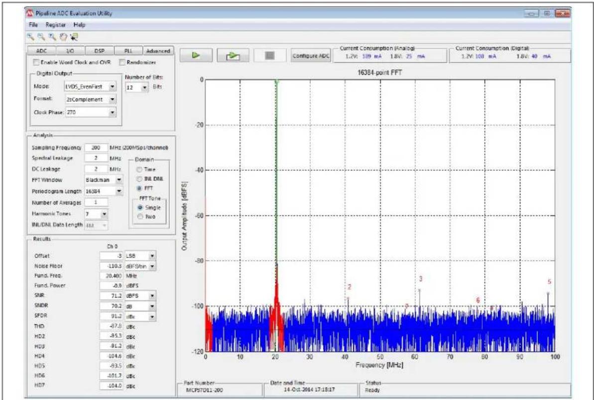
line
16384-point FFT | Frequency (MHz) | Output Amplitude (dBFS) | | :--- | :--- | | 20 | -100 | | 40 | -95 | | 60 | -90 | | 80 | -85 | | 100 | -80 | The chart displays a multi-axis waveform with labeled peaks corresponding to specific frequencies (e.g., 71.2, 70.2, 91.2, etc.), each annotated with its frequency value and symbol (e.g., 'Single', 'Two'). The left panel shows ADC configuration settings including Enable Word Clock and OVR, Randomizer, and Number of Bits: LVDS_EvenFirst, Format: 2sComplement, Clock Phase: 270.FIGURE 6-2: PC-Based Graphical User Interface Software.
NOTES:
7.0 TERMINOLOGY
Analog Input Bandwidth (Full-Power Bandwidth)
The analog input frequency at which the spectral power of the fundamental frequency (as determined by FFT analysis) is reduced by 3 dB.
Aperture Delay or Sampling Delay
This is the time delay between the rising edge of the input sampling clock and the actual time at which the sampling occurs.
Aperture Uncertainty
The sample-to-sample variation in aperture delay.
Aperture Delay Jitter
The variation in the aperture delay time from conversion to conversion. This random variation will result in noise when sampling an AC input. The signal-to-noise ratio due to the jitter alone will be:
EQUATION 7-1:
$$ S N R _ {J I T T E R} \quad 2 0 (2 \pi \times f _ {I N} \times t _ {J I T T E R}) $$
Calibration Algorithms
This device utilizes two patented analog and digital calibration algorithms, Harmonic Distortion Correction (HDC) and DAC Noise Cancellation (DNC), to improve the ADC performance. The algorithms compensate various sources of linear impairments such as capacitance mismatch, charge injection error and finite gain of operational amplifiers. These algorithms execute in both power-up sequence (foreground) and background mode:
- Power-Up Calibration: The calibration is conducted within the first 2^27 clock cycles after power-up. The user needs to wait this Power-Up Calibration period after the device is powered-up for an accurate ADC performance.
- Background Calibration: This calibration is conducted in the background while the ADC performs conversions. The update rate is about every 2^30 clock cycles.
Channel Crosstalk
This is a measure of the internal coupling of a signal from an adjacent channel into the channel of interest in the multi-channel mode. It is measured by applying a full-scale input signal in the adjacent channel. Crosstalk is the ratio of the power of the coupling signal (as measured at the output of the channel of interest) to the power of the signal applied at the adjacent channel input. It is typically expressed in dBc.
Pipeline Delay (LATENCY)
LATENCY is the number of clock cycles between the initiation of conversion and when that data is presented to the output driver stage. Data for any given sample is available after the pipeline delay plus the output delay after that sample is taken. New data is available at every clock cycle, but the data lags the conversion by the pipeline delay plus the output delay. Latency is increased if digital signal post-processing is used.
Clock Pulse Width and Duty Cycle
The clock duty cycle is the ratio of the time the clock signal remains at a logic high (clock pulse width) to one clock period. Duty cycle is typically expressed as a percentage. A perfect differential sine-wave clock results in a 50% duty cycle.
Differential Nonlinearity (DNL, No Missing Codes)
An ideal ADC exhibits code transitions that are exactly 1 LSb apart. DNL is the deviation from this ideal value. No missing codes to 12-bit resolution indicates that all 4096 codes must be present over all the operating conditions.
Integral Nonlinearity (INL)
INL is the maximum deviation of each individual code from an ideal straight line drawn from negative full scale through positive full scale.
Signal-to-Noise Ratio (SNR)
SNR is the ratio of the power of the fundamental ( P_S ) to the noise floor power ( P_N ), below the Nyquist frequency and excluding the power at DC and the first nine harmonics.
EQUATION 7-2:
$$ \text { SNR 10 } \quad \log \left(\frac {P _ {S}}{P _ {N}}\right) $$
SNR is either given in units of dBc (dB to carrier) when the absolute power of the fundamental is used as the reference, or dBFS (dB to full-scale) when the power of the fundamental is extrapolated to the converter full-scale range.
Signal-to-Noise and Distortion (SINAD)
SINAD is the ratio of the power of the fundamental (P_S) to the power of all the other spectral components including noise (P_N) and distortion (P_D) below the Nyquist frequency, but excluding DC:
EQUATION 7-3:
$$ \text { SINAD 10 } \quad \log \left(\frac {P _ {S}}{P _ {D} + P _ {N}}\right) $$
$$ 1 0 - = \left[ \begin{array}{c} \frac {S N R}{1 0} \ \text {log} \end{array} \right] ^ {\frac {T H D}{1 0}} 0 $$
SINAD is either given in units of dBc (dB to carrier) when the absolute power of the fundamental is used as the reference, or dBFS (dB to full-scale) when the power of the fundamental is extrapolated to the converter full-scale range.
Effective Number of Bits (ENOB)
The effective number of bits for a sine wave input at a given input frequency can be calculated directly from its measured SINAD using the following formula:
EQUATION 7-4:
$$ E N O B = \frac {S I N A D 1 . 7 6 -}{6 . 0 2} $$
Gain Error
Gain error is the deviation of the ADC's actual input full-scale range from its ideal value. The gain error is given as a percentage of the ideal input full-scale range.
Gain error is usually expressed in LSb or as a percentage of full-scale range (%FSR).
Gain-Error Drift
Gain-error drift is the variation in gain-error due to a change in ambient temperature, typically expressed in ppm/°C.
Offset Error
The major carry transition should occur for an analog value of 50% LSb below A_IN^+=A_IN^- . Offset error is defined as the deviation of the actual transition from that point.
Temperature Drift
The temperature drift for offset error and gain error specifies the maximum change from the initial (+25°C) value to the value across the T_MIN to T_MAX range.
Maximum Conversion Rate
The maximum clock rate at which parametric testing is performed.
Minimum Conversion Rate
The minimum clock rate at which parametric testing is performed.
Spurious-Free Dynamic Range (SFDR)
SFDR is the ratio of the power of the fundamental to the highest other spectral component (either spur or harmonic). SFDR is typically given in units of dBc (dB to carrier) or dBFS.
Total Harmonic Distortion (THD)
THD is the ratio of the power of the fundamental ( P_S ) to the summed power of the first 13 harmonics ( P_D ).
EQUATION 7-5:
$$ T H D 1 0 \log \left(\frac {P _ {S}}{P _ {D}}\right) $$
THD is typically given in units of dBc (dB to carrier). THD is also shown by:
EQUATION 7-6:
$$ T H D = - 2 0 \log \frac {\sqrt {V _ {2} ^ {2} + V _ {3} ^ {2} + V _ {4} ^ {2} + \dots + V _ {n} ^ {2}}}{V _ {1} ^ {2}} $$
Where:
$$ \begin{array}{c} V _ {1} = \text { RMS amplitude of the } \ \text { fundamental frequency } \end{array} $$
$$ \begin{array}{l} V _ {1} \text { through } V _ {n} = \text { Amplitudes of the second } \ \text { through } n ^ {\text { th }} \text { harmonics } \end{array} $$
Two-Tone Intermodulation Distortion (Two-Tone IMD, IMD3)
Two-tone IMD is the ratio of the power of the fundamental (at frequencies f_IN1 and f_IN2 ) to the power of the worst spectral component at either frequency 2f_IN1 - f_IN2 or 2f_IN2 - f_IN1 . Two-tone IMD is a function of the input amplitudes and frequencies ( f_IN1 and f_IN2 ). It is either given in units of dBc (dB to carrier) when the absolute power of the fundamental is used as the reference, or dBFS (dB to full-scale) when the power of the fundamental is extrapolated to the ADC full-scale range.
Common-Mode Rejection Ratio (CMRR)
Common-mode rejection is the ability of a device to reject a signal that is common to both sides of a differential input pair. The common-mode signal can be an AC or DC signal or a combination of the two. CMRR is measured using the ratio of the differential signal gain to the common-mode signal gain and expressed in dB with the following equation:
EQUATION 7-7:
$$ C M R R 2 0 \quad \log \left(\frac {A _ {D I F F}}{A _ {C M}}\right) $$
Where:
A_DIFF = Output Code/ Differential Voltage
A_DIFF = Output Code/ Common Mode Voltage
NOTES:
8.0 PACKAGING INFORMATION
8.1 Package Marking Information
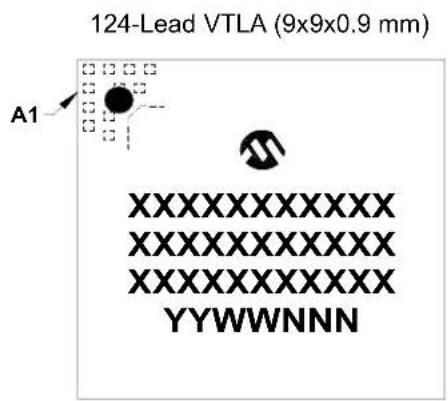
text_image
124-Lead VTLA (9x9x0.9 mm) A1 XXXXXXXXXXXX XXXXXXXXXXXX XXXXXXXXXXXX YYWWNNN
text_image
Example A1 MCP37211 200-I/TL e3 1417256Legend: XX...X Customer-specific information
Y Year code (last digit of calendar year)
YY Year code (last 2 digits of calendar year)
WW Week code (week of January 1 is week '01')
NNN Alphanumeric traceability code
eBb-free JEDEC ^® designator for Matte Tin (Sn)
* This package is Pb-free. The Pb-free JEDEC designator (e3) can be found on the outer packaging for this package.
Note: In the event the full Microchip part number cannot be marked on one line, it will be carried over to the next line, thus limiting the number of available characters for customer-specific information.
124-Terminal Very Thin Leadless Array Package (TL) - 9x9x0.9 mm Body [VTLA]
Note: For the most current package drawings, please see the Microchip Packaging Specification located at http://www.microchip.com/packaging
![Microchip MCP37211-200 - 124-Terminal Very Thin Leadless Array Package (TL) - 9x9x0.9 mm Body [VTLA] - 1](/content/2026/06/1219398/images/ce5f3a184ab8f90dd745b846619bf66f130f6f2a47e2b0935c363602aec6fe69.jpg)
Microchip Technology Drawing C04-193A Sheet 1 of 2
124-Terminal Very Thin Leadless Array Package (TL) - 9x9x0.9 mm Body [VTLA]
Note: For the most current package drawings, please see the Microchip Packaging Specification located at http://www.microchip.com/packaging
![Microchip MCP37211-200 - 124-Terminal Very Thin Leadless Array Package (TL) - 9x9x0.9 mm Body [VTLA] - 1](/content/2026/06/1219398/images/4518358e744631740295111d37af013b6013e289ac73e61ee30308b66d4a5f9e.jpg)
text_image
NX L eR TERMINAL TIP (DATUM A OR B) eT eT/2 DETAIL A EXPOSED Cu (0.025) EXPOSED Cu (0.125) SECTION B-B| Units | MILLIMETERS | |||
| Dimension Limits | MIN | NOM | MAX | |
| Number of Pins | N | 124 | ||
| Pitch | eT | 0.50 BSC | ||
| Pitch (Inner to outer terminal ring) | eR | 0.50 BSC | ||
| Overall Height | A | 0.80 | 0.85 | 0.90 |
| Standoff | A1 | 0.00 | - | 0.05 |
| Overall Width | E | 9.00 BSC | ||
| Exposed Pad Width | E2 | 6.40 | 6.55 | 6.70 |
| Overall Length | D | 9.00 BSC | ||
| Exposed Pad Length | D2 | 6.40 | 6.55 | 6.70 |
| Contact Width | b | 0.20 | 0.25 | 0.30 |
| Contact Length | L | 0.20 | 0.25 | 0.30 |
| Contact-to-Exposed Pad | K | 0.20 | - | - |
Notes:
- Pin 1 visual index feature may vary, but must be located within the hatched area.
- Package is saw singulated.
- Dimensioning and tolerancing per ASME Y14.5M.
BSC: Basic Dimension. Theoretically exact value shown without tolerances.
REF: Reference Dimension, usually without tolerance, for information purposes only.
Microchip Technology Drawing C04-193A Sheet 2 of 2
124-Very Thin Leadless Array Package (TL) - 9x9x0.9 mm Body [VTLA]
Note: For the most current package drawings, please see the Microchip Packaging Specification located at http://www.microchip.com/packaging
![Microchip MCP37211-200 - 124-Very Thin Leadless Array Package (TL) - 9x9x0.9 mm Body [VTLA] - 1](/content/2026/06/1219398/images/9f204fe870befbfb6dd800b39d1f9fba2b1646a5eec9400eecbddbd2afb09b8e.jpg)
text_image
E X1 E/2 G4 G3 X2 G1 G5 X4 G2 W3 W2 C1 T2 C2 SILK SCREENRECOMMENDED LAND PATTERN
| Units | MILLIMETERS | |||
| Dimension Limits | MIN | NOM | MAX | |
| Contact Pitch 0.50 BSCE | ||||
| Pad Clearance G1 | 0.20 | |||
| Pad Clearance G2 | 0.20 | |||
| Pad Clearance G3 | 0.20 | |||
| Pad Clearance G4 | 0.20 | |||
| Contact to Center Pad Clearance (X4) G5 | 0.30 | |||
| Optional Center Pad Width T2 | 6.60 | |||
| Optional Center Pad Length | W2 | 6.60 | ||
| Optional Center Pad Chamfer (X4) | W3 | 0.10 | ||
| Contact Pad Spacing | C1 | 8.50 | ||
| Contact Pad Spacing | C2 | 8.50 | ||
| Contact Pad Width (X124) | X1 | 0.30 | ||
| Contact Pad Length (X124) | X2 | 0.30 | ||
Notes:
1. Dimensioning and tolerancing per ASME Y14.5M
BSC: Basic Dimension. Theoretically exact value shown without tolerances.
Microchip Technology Drawing No. C04-2193A
121-Ball Thin Fine Pitch Ball Grid Array (TE) - 8x8 mm Body [TFBGA] System In Package
Note: For the most current package drawings, please see the Microchip Packaging Specification located at http://www.microchip.com/packaging
![Microchip MCP37211-200 - 121-Ball Thin Fine Pitch Ball Grid Array (TE) - 8x8 mm Body [TFBGA] System In Package - 1](/content/2026/06/1219398/images/d2df18659a4024f37eab8a6be7a4375e8c268bdf301edc96fc36c93cbf1d5c51.jpg)
Microchip Technology Drawing C04-212-TE Rev C Sheet 1 of 2
121-Ball Thin Fine Pitch Ball Grid Array (TE) - 8x8 mm Body [TFBGA] System In Package
Note: For the most current package drawings, please see the Microchip Packaging Specification located at http://www.microchip.com/packaging
![Microchip MCP37211-200 - 121-Ball Thin Fine Pitch Ball Grid Array (TE) - 8x8 mm Body [TFBGA] System In Package - 1](/content/2026/06/1219398/images/21c82737bfc476d16ff4df29f8baf0acdc57964dcafc58619d6674a9d32f5ae2.jpg)
text_image
121X Øb Ø0.15M C A B Ø0.08M CDETAIL A
| Units | MILLIMETERS | |||
| Dimension Limits | MIN | NOM | MAX | |
| Number of Terminals | N | 121 | ||
| Pitch | eE | 0.65 BSC | ||
| Pitch | eD | 0.65 BSC | ||
| Overall Height | A | - | - | 1.08 |
| Standoff | A1 | 0.21 | 0.32 | - |
| Cap Thickness | A2 | 0.40 0.50 | 0.45 | |
| Overall Width | E | 8.00 BSC | ||
| Overall Pitch | E1 | 6.50 BSC | ||
| Overall Length | D | 8.00 BSC | ||
| Overall Pitch | D1 | 6.50 BSC | ||
| Terminal Diameter | b | 0.35 | 0.40 | 0.45 |
Notes:
- Terminal A1 visual index feature may vary, but must be located within the hatched area.
- Dimensioning and tolerancing per ASME Y14.5M
BSC: Basic Dimension. Theoretically exact value shown without tolerances.
REF: Reference Dimension, usually without tolerance, for information purposes only.
Microchip Technology Drawing C04-212-TE Rev C Sheet 2 of 2
121-Ball Thin Fine Pitch Ball Grid Array (TE) - 8x8 mm Body [TFBGA] System In Package
Note: For the most current package drawings, please see the Microchip Packaging Specification located at http://www.microchip.com/packaging
![Microchip MCP37211-200 - 121-Ball Thin Fine Pitch Ball Grid Array (TE) - 8x8 mm Body [TFBGA] System In Package - 1](/content/2026/06/1219398/images/bdf382345e7e394200d470e7727d2ddb5387bc0d078eb32806e3b1c987250395.jpg)
text_image
1 2 3 4 5 6 7 8 9 10 11 A B C D E F G H J K L C1 E C2 121X ØB SILK SCREEN RECOMMENDED LAND PATTERN| Units | MILLIMETERS | |||
| Dimension Limits | MIN | NOM | MAX | |
| Contact Pitch | E | 0.65 BSC | ||
| C1Contact Pad Spacing | 6.50 | |||
| Contact Pad Spacing | C2 | 6.50 | ||
| Contact Pad Diameter (X121) B 0.35 | ||||
Notes:
1. Dimensioning and tolerancing per ASME Y14.5M
BSC: Basic Dimension. Theoretically exact value shown without tolerances.
Microchip Technology Drawing No. C04-2212-TE Rev C
NOTES:
APPENDIX A: REVISION HISTORY
Revision D (December 2019)
The following is the list of modifications:
- Added the AEC-Q100 automotive qualification.
- Updated Section "Typical Applications" and Section "Description".
- Updated Section 2.0, Electrical Specifications.
- Updated Figure 2-5
- Updated Figure 3-36, Figure 3-39, and Figure 3-40.
- Updated Section 4.15, AutoSync Mode: Synchronizing Multiple ADCs at the Same Clock using Master and Slave Configuration.
- Updated Section "Product Identification System".
Revision C (August 2016)
The following is the list of modifications:
- Updated availability of TFBGA package.
- Added Figure 2-7, Figure 2-8 and Figure 2-9.
- Added Section 4.15, AutoSync Mode: Synchronizing Multiple ADCs at the Same Clock using Master and Slave Configuration.
Revision B (July 2015)
- Updated the Features list.
- Updated the Functional Block Diagram.
- Updated the Description section.
- Updated and added notes in Tables 1-2 and 1-1.
- Updated values and notes in Tables 2-1 and 2-2.
- Updated value in Figure 2-1.
- Updated note in Section 3.0 "Typical Performance Curves".
- Updated text title in Figures 3-26 and 3-29.
- Updated text in Section 4.0 "Theory of Operation".
- Updated text in Section 4.5.1 "Analog Input Driving Circuit".
- Added new column to Table 4-2.
- Added Section 4.5.2.1 "SENSE Selection Vs. SNR/SFDR Performance" and Section 4.5.3.1 "Decoupling Circuits for REF1 and REF0 Pins".
- Replaced text in Section 4.5.3.1 "Decoupling Circuits for REF1 and REF0 Pins".
- Updated values in Figure 4-7.
- Added note after Figure 4-7.
- Replaced the entire Section 4.7 "ADC Clock Selection".
- Updated text in Section 4.8.1 "Fractional Delay
Recovery for Dual- and Octal-Channel Modes".
- Updated Figure 4-11.
- Changed parameters and updated/added notes in Tables 4-5, 4-6, 4-9, 4-10, 4-12, 4-13 and 4-14.
- Changed value in Equation 4-6.
- Deleted Note in Section 4.8.3 "Decimation Filters".
- Added Section 4.8.3.1 "Output Data Rate and Clock Phase Control When Decimation is Used".
- Changed parameter in Table 4-15 and bit names in Tables 4-17, 4-19, 4-20.
- Replaced and added text and reorganized structure in Section 4.8.4 "Digital Down-Conversion (MCP37D11-200 only)".
- Replaced text in Section 4.8.4.3 "Numerically Controlled Oscillator (NCO)".
- Updated values in Section 4.8.4.5 "NCO for fS/8 and fS/(8xDER)".
- Updated parameters and notes in Tables 4-16, 4-17, 4-18 and 4-19.
- Reorganized and added text to Section 4.11 "Output Data format" and Section 4.12 "Digital Output".
- Updated Figure 4-25.
- Updated Section 5.2 "Configuration Registers".
- Updated Table 5-3.
- Updated Registers 5-1 to 5-3, 5-7, 5-8, 5-10, 5-11, 5-13, 5-22, 5-24, 5-25, 5-27, 5-28, 5-34, 5-35, 5-36, 5-37, 5-42, 5-43 to 5-46, 5-47, 5-63, 5-79 and 5-80.
- Deleted "Power Supply Rejection Ration" section from Section 7.0 "Terminology".
- Updated Section "Product Identification System".
- Minor typographical corrections.
Revision A (October 2014)
• Original release of this document.
NOTES:
PRODUCT IDENTIFICATION SYSTEM
To order or obtain information, e.g., on pricing or delivery, refer to the factory or the listed sales office.

text_image
PART NO. Device [Tx](1) Tape and Reel Option Sample Rate Package Temperature Range X /XX-XXXDevice: MCP37211-200: 12-Bit Low-Power ADC with 8-Channel MUX
MCP37D11-200: 12-Bit Low-Power ADC with 8-Channel MUX, Digital Down-Converter and CW Beamforming
Tape and Blank = Standard packaging (tube or tray)
Reel Option: T = Tape and Reel ^(1)
Sample Rate: 200 = 200 Msps
Temperature E = -40°C to +125°C (Extended)
Range: I = -40^ to +85^ (Industrial)
Package: TE = Ball Plastic Thin Profile Fine Pitch Ball Grid Array -
8x8x1.08 mm Body (TFBGA), 121-Lead
TL = Terminal Very Thin Leadless Array Package -
9x9x0.9 mm Body (VTLA), 124-Lead
Note 1: Tape and Reel identifier appears only in the catalog part number description. This identifier is used for ordering purposes and is not printed on the device package. Check with your Microchip Sales Office for package availability with the Tape and Reel option.
Examples:
| a) | MCP37211-200E/TE: | 200 Msps,Extended temperature,121LD TFBGA package |
| b) | MCP37211T-200E/TE: | 200 Msps,Tape and Reel,Extended temperature,121LD TFBGA package |
| c) | MCP37211-200I/TE: | 200 Msps,Industrial temperature,121LD TFBGA package |
| d) | MCP37211T-200I/TE: | 200 Msps,Tape and Reel,Industrial temperature,121LD TFBGA package |
| e) | MCP37D11-200E/TE: | 200 Msps,Extended temperature,121LD TFBGA package |
| f) | MCP37D11T-200E/TE: | 200 Msps,Tape and Reel,Extended temperature,121LD TFBGA package |
| g) | MCP37D11-200I/TE: | 200 Msps,Industrial temperature,121LD TFBGA package |
| h) | MCP37D11T-200I/TE: | 200 Msps,Tape and Reel,Industrial temperature,121LD TFBGA package |
| i) | MCP37211-200I/TL: | 200 Msps,Industrial temperature,124LD VTLA package |
| j) | MCP37211T-200I/TL: | 200 Msps,Tape and Reel,Industrial temperature,124LD VTLA package |
| k) | MCP37D11-200I/TL: | 200 Msps,Industrial temperature,124LD VTLA package |
| l) | MCP37D11T-200I/TL: | 200 Msps,Tape and Reel,Industrial temperature,124LD VTLA package |
NOTES:
Note the following details of the code protection feature on Microchip devices:
• Microchip products meet the specification contained in their particular Microchip Data Sheet.
- Microchip believes that its family of products is one of the most secure families of its kind on the market today, when used in the intended manner and under normal conditions.
- There are dishonest and possibly illegal methods used to breach the code protection feature. All of these methods, to our knowledge, require using the Microchip products in a manner outside the operating specifications contained in Microchip's Data Sheets. Most likely, the person doing so is engaged in theft of intellectual property.
- Microchip is willing to work with the customer who is concerned about the integrity of their code.
- Neither Microchip nor any other semiconductor manufacturer can guarantee the security of their code. Code protection does not mean that we are guaranteeing the product as "unbreakable."
Code protection is constantly evolving. We at Microchip are committed to continuously improving the code protection features of our products. Attempts to break Microchip's code protection feature may be a violation of the Digital Millennium Copyright Act. If such acts allow unauthorized access to your software or other copyrighted work, you may have a right to sue for relief under that Act.
Information contained in this publication regarding device applications and the like is provided only for your convenience and may be superseded by updates. It is your responsibility to ensure that your application meets with your specifications. MICROCHIP MAKES NO REPRESENTATIONS OR WARRANTIES OF ANY KIND WHETHER EXPRESS OR IMPLIED, WRITTEN OR ORAL, STATUTORY OR OTHERWISE, RELATED TO THE INFORMATION, INCLUDING BUT NOT LIMITED TO ITS CONDITION, QUALITY, PERFORMANCE, MERCHANTABILITY OR FITNESS FOR PURPOSE. Microchip disclaims all liability arising from this information and its use. Use of Microchip devices in life support and/or safety applications is entirely at the buyer's risk, and the buyer agrees to defend, indemnify and hold harmless Microchip from any and all damages, claims, suits, or expenses resulting from such use. No licenses are conveyed, implicitly or otherwise, under any Microchip intellectual property rights unless otherwise stated.
Trademarks
The Microchip name and logo, the Microchip logo, Adaptec, AnyRate, AVR, AVR logo, AVR Freaks, BesTime, BitCloud, chipKIT, chipKIT logo, CryptoMemory, CryptoRF, dsPIC, FlashFlex, flexPWR, HELDO, IGLOO, JukeBlox, KeeLoq, Kleer, LANCheck, LinkMD, maXStylus, maXTouch, MediaLB, megaAVR, Microsemi, Microsemi logo, MOST, MOST logo, MPLAB, OptoLyzer, PackeTime, PIC, picoPower, PICSTART, PIC32 logo, PolarFire, Prochip Designer, QTouch, SAM-BA, SenGenuity, SpyNIC, SST, SST Logo, SuperFlash, Symmetricom, SyncServer, Tachyon, TempTrackr, TimeSource, tinyAVR, UNI/O, Vectron, and XMEGA are registered trademarks of Microchip Technology Incorporated in the U.S.A. and other countries.
APT, ClockWorks, The Embedded Control Solutions Company, EtherSynch, FlashTec, Hyper Speed Control, HyperLight Load, IntelliMOS, Libero, motorBench, mTouch, Powermite 3, Precision Edge, ProASIC, ProASIC Plus, ProASIC Plus logo, Quiet-Wire, SmartFusion, SyncWorld, Temux, TimeCesium, TimeHub, TimePictra, TimeProvider, Vite, WinPath, and ZL are registered trademarks of Microchip Technology Incorporated in the U.S.A.
Adjacent Key Suppression, AKS, Analog-for-the-Digital Age, Any Capacitor, AnyIn, AnyOut, BlueSky, BodyCom, CodeGuard, CryptoAuthentication, CryptoAutomotive, CryptoCompanion, CryptoController, dsPICDEM, dsPICDEM.net, Dynamic Average Matching, DAM, ECAN, EtherGREEN, In-Circuit Serial Programming, ICSP, INICnet, Inter-Chip Connectivity, JitterBlocker, KleerNet, KleerNet logo, memBrain, Mindi, MiWi, MPASM, MPF, MPLAB Certified logo, MPLIB, MPLINK, MultiTRAK, NetDetach, Omniscient Code Generation, PICDEM, PICDEM.net, PICKit, PICtail, PowerSmart, PureSilicon, QMatrix, REAL ICE, Ripple Blocker, SAM-ICE, Serial Quad I/O, SMART-I.S., SQI, SuperSwitcher, SuperSwitcher II, Total Endurance, TSHARC, USBCheck, VariSense, ViewSpan, WiperLock, Wireless DNA, and ZENA are trademarks of Microchip Technology Incorporated in the U.S.A. and other countries.
SQTP is a service mark of Microchip Technology Incorporated in the U.S.A.
The Adaptec logo, Frequency on Demand, Silicon Storage Technology, and Symmcom are registered trademarks of Microchip Technology Inc. in other countries.
GestIC is a registered trademark of Microchip Technology Germany II GmbH & Co. KG, a subsidiary of Microchip Technology Inc., in other countries.
All other trademarks mentioned herein are property of their respective companies.
© 2019, Microchip Technology Incorporated, All Rights Reserved.
ISBN: 978-1-5224-5380-2
For information regarding Microchip's Quality Management Systems, please visit www.microchip.com/quality.
Worldwide Sales and Service
AMERICAS
Corporate Office
2355 West Chandler Blvd.
Chandler, AZ 85224-6199
Tel: 480-792-7200
Fax: 480-792-7277
Technical Support:
http://www.microchip.com/
support
Web Address:
www.microchip.com
Atlanta
Duluth, GA
Tel: 678-957-9614
Fax: 678-957-1455
Austin, TX
Tel: 512-257-3370
Boston
Westborough, MA
Tel: 774-760-0087
Fax: 774-760-0088
Chicago
Itasca, IL
Tel: 630-285-0071
Fax: 630-285-0075
Dallas
Addison, TX
Tel: 972-818-7423
Fax: 972-818-2924
Detroit
Novi, MI
Tel: 248-848-4000
Houston, TX
Tel: 281-894-5983
Indianapolis
Noblesville, IN
Tel: 317-773-8323
Fax: 317-773-5453
Tel: 317-536-2380
Los Angeles
Mission Viejo, CA
Tel: 949-462-9523
Fax: 949-462-9608
Tel: 951-273-7800
Raleigh, NC
Tel: 919-844-7510
New York, NY
Tel: 631-435-6000
San Jose, CA
Tel: 408-735-9110
Tel: 408-436-4270
Canada - Toronto
Tel: 905-695-1980
Fax: 905-695-2078
ASIA/PACIFIC
Australia - Sydney
Tel: 61-2-9868-6733
China - Beijing
Tel: 86-10-8569-7000
China - Chengdu
Tel: 86-28-8665-5511
China - Chongqing
Tel: 86-23-8980-9588
China - Dongguan
Tel: 86-769-8702-9880
China - Guangzhou
Tel: 86-20-8755-8029
China - Hangzhou
Tel: 86-571-8792-8115
China - Hong Kong SAR
Tel: 852-2943-5100
China - Nanjing
Tel: 86-25-8473-2460
China - Qingdao
Tel: 86-532-8502-7355
China - Shanghai
Tel: 86-21-3326-8000
China - Shenyang
Tel: 86-24-2334-2829
China - Shenzhen
Tel: 86-755-8864-2200
China - Suzhou
Tel: 86-186-6233-1526
China - Wuhan
Tel: 86-27-5980-5300
China - Xian
Tel: 86-29-8833-7252
China - Xiamen
Tel: 86-592-2388138
China - Zhuhai
Tel: 86-756-3210040
ASIA/PACIFIC
India - Bangalore
Tel: 91-80-3090-4444
India - New Delhi
Tel: 91-11-4160-8631
India - Pune
Tel: 91-20-4121-0141
Japan - Osaka
Tel: 81-6-6152-7160
Japan - Tokyo
Tel: 81-3-6880-3770
Korea - Daegu
Tel: 82-53-744-4301
Korea - Seoul
Tel: 82-2-554-7200
Malaysia - Kuala Lumpur
Tel: 60-3-7651-7906
Malaysia - Penang
Tel: 60-4-227-8870
Philippines - Manila
Tel: 63-2-634-9065
Singapore
Tel: 65-6334-8870
Taiwan - Hsin Chu
Tel: 886-3-577-8366
Taiwan - Kaohsiung
Tel: 886-7-213-7830
Taiwan - Taipei
Tel: 886-2-2508-8600
Thailand - Bangkok
Tel: 66-2-694-1351
Tel: 43-7242-2244-39
Fax: 43-7242-2244-393
Denmark - Copenhagen
Tel: 45-4450-2828
Fax: 45-4485-2829
Finland - Espoo
Tel: 358-9-4520-820
France - Paris
Tel: 33-1-69-53-63-20
Fax: 33-1-69-30-90-79
Germany - Garching
Tel: 49-8931-9700
Germany - Haan
Tel: 49-2129-3766400
Germany - Heilbronn
Tel: 49-7131-72400
Germany - Karlsruhe
Tel: 49-721-625370
Germany - Munich
Tel: 49-89-627-144-0
Fax: 49-89-627-144-44
Germany - Rosenheim
Tel: 49-8031-354-560
Israel - Ra'anana
Tel: 972-9-744-7705
Italy - Milan
Tel: 39-0331-742611
Fax: 39-0331-466781
Italy - Padova
Tel: 39-049-7625286
Netherlands - Drunen
Tel: 31-416-690399
Fax: 31-416-690340
Norway - Trondheim
Tel: 47-7288-4388
Poland - Warsaw
Tel: 48-22-3325737
Romania - Bucharest
Tel: 40-21-407-87-50
Spain - Madrid
Tel: 34-91-708-08-90
Fax: 34-91-708-08-91
Sweden - Gothenberg
Tel: 46-31-704-60-40
Sweden - Stockholm
Tel: 46-8-5090-4654
UK - Wokingham
Tel: 44-118-921-5800
Fax: 44-118-921-5820