MIC26603 - Régulateur DC-DC Microchip - Free user manual and instructions
Find the device manual for free MIC26603 Microchip in PDF.

User questions about MIC26603 Microchip
0 question about this device. Answer the ones you know or ask your own.
Ask a new question about this device
Download the instructions for your Régulateur DC-DC in PDF format for free! Find your manual MIC26603 - Microchip and take your electronic device back in hand. On this page are published all the documents necessary for the use of your device. MIC26603 by Microchip.
USER MANUAL MIC26603 Microchip
The Micrel MIC26603-ZA is a constant-frequency, synchronous buck regulator featuring a unique adaptive ON-time control architecture. The MIC26603-ZA operates over an input supply range of 4.5V to 28V and provides a regulated output of up to 6A of output current. The output voltage is adjustable down to 0.6V with a guaranteed accuracy of ±1%, and the device operates at a switching frequency of 600kHz.
Micrel's Hyper Speed Control™ architecture allows for ultra-fast transient response while reducing the output capacitance and also makes (High V_IN /(Low V_OUT ) operation possible. This adaptive t_ON ripple control architecture combines the advantages of fixed-frequency operation and fast transient response in a single device.
The MIC26603-ZA offers a full suite of features to ensure protection of the IC during fault conditions. These include undervoltage lockout to ensure proper operation under power-sag conditions, internal soft-start to reduce inrush current, foldback current limit, "hiccup mode" short-circuit protection, and thermal shutdown. An open-drain Power Good (PG) pin is provided.
Datasheets and support documentation are available on Micrel's web site at: www.micrel.com.
SuperSwitcher™ II
Features
• Hyper Speed Control architecture enables
- High Delta V operation ( V_IN = 28V and V_OUT = 0.6V )
- Small output capacitance
• 4.5V to 28V voltage input
- 6A output current capability, up to 95% efficiency
- Adjustable output from 0.6V to 5.5V
- ± 1% feedback accuracy
- Any Capacitor™ stable – zero-to-high ESR
- 600kHz switching frequency
• No external compensation
• Power Good (PG) output
- Foldback current limit and short-circuit protection
• Supports safe startup into a pre-biased load
- -40°C to +125°C junction temperature range
• 28-pin 5mm × 6mm QFN package
Applications
• Distributed power systems
• Communications/networking infrastructure
- Set-top box, gateways, and routers
- Printers, scanners, graphic cards, and video cards
Typical Application
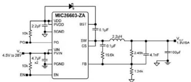
text_image
MIC26603-ZA VDD PVDD SGND PGND EN 10k PC 4.5V to 28V VIN PVIN 10k EN 2.2µF BST 0.1µF SW CS FB 2.2µH 0.1µF 19.6k 2.49k 4.7nF 1.24k VOUT 1.8V/8A 100µF
line
| OUTPUT CURRENT (A) | 3.8V | 4.0V | 4.2V | 4.4V | 4.6V | 4.8V | 5.0V | | ----------------- | ----- | ----- | ----- | ----- | ----- | ----- | ----- | | 0 | 70 | 70 | 70 | 70 | 70 | 70 | 70 | | 12 | 75 | 75 | 75 | 75 | 75 | 75 | 75 | | 24 | 80 | 80 | 80 | 80 | 80 | 80 | 80 | | 36 | 85 | 85 | 85 | 85 | 85 | 85 | 85 | | 48 | 90 | 90 | 90 | 90 | 90 | 90 | 90 | | 60 | 95 | 95 | 95 | 95 | 95 | 95 | 95 | | 72 | 98 | 98 | 98 | 98 | 98 | 98 | 98 | | 84 | 99 | 99 | 99 | 99 | 99 | 99 | 99 | | 96 | 100 | 100 | 100 | 100 | 100 | 100 | 100 | | 108 | 100 | 100 | 100 | 100 | 100 | 100 | 100 | | 120 | 100 | 100 | 100 | 100 | 100 | 100 | 100 | | Note: The '3.8V' label in the chart is not explicitly provided in the code snippet, so it is not included in the data series. The '4.2V' label in the chart is not included in the data series. The '4.4V' label in the chart is not included in the data series. The '4.6V' label in the chart is not included in the data series. The '4.8V' label in the chart is not included in the data series. The '5.0V' label in the chart is not included in the data series. The '5.2V' label in the chart is not included in the data series. The '5.4V' label in the chart is not included in the data series. The '5.6V' label in the chart is not included in the data series. The '5.8V' label in the chart is not included in the data series. The '6.0V' label in the chart is not included in the data series. The '6.2V' label in the chart is not included in the data series. The '6.4V' label in the chart is not included in the data series. The '6.6V' label in the chart is not included in the data series. The '6.8V' label in the chart is not included in the data series. The '7.0V' label in the chart is not included in the data series. The '7.2V' label in the chart is not included in the data series. The '7.4V' label in the chart is not included in the data series. The '7.6V' label in the chart is not included in the data series. The '7.8V' label in the chart is not included in the data series. The '8.0V' label in the chart is not included in the data series. The '8.2V' label in the chart is not included in the data series. The '8.4V' label in the chart is not included in the data series. The '8.6V' label in the chart is not included in the data series. The '8.8V' label in the chart is not included in the data series. The '9.0V' label in the chart is not included in the data series. The '9.2V' label in the chart is not included in the data series. The '9.4V' label in the chart is not included in the data series. The '9.6V' label in the chart is not included in the data series. The '9.8V' label in the chart is not included in the data series. The '10.0V' label in the chart is not included in the data series. The '10.2V' label in the chart is not included in the data series. The '10.4V' label in the chart is not included in the data series. The '10.6V' label in the chart is not included in the data series. The '10.8V' label in the chart is not included in the data series. The '11.0V' label in the chart is not included in the data series. The '11.2V' label in the chart is not included in the data series. The '11.4V' label in the chart is not included in the data series. The '11.6V' label in the chart is not included in the data series. The '11.8V' label in the chart is not included in the data series. The '12.0V' label in the chart is not included in the data series. The '12.2V' label in the chart is not included in the data series. The '12.4V' label in the chart is not included in the data series. The '12.6V' label in the chart is not included in the data series. The '12.8V' label in the chart is not included in the data series. The '13.0V' label in the chart is not included in the data series. The '13.2V' label in the chart is not included in the data series. The '13.4V' label in the chart is not included in the data series. The '13.6V' label in the chart is not included in the data series. The '13.8V' label in the chart is not included in the data series. The '14.0V' label in the chart is not included in the data series. The '14.2V' label in the chart is not included in the data series. The '14.4V' label in the chart is not included in the data series. The '14.6V' label in the chart is not included in the data series. The '14.8V' label in the chart is not included in the data series. The '15.0V' label in the chart is not included in the data series. The '15.2V' label in the chart is not included in the data series. The '15.4V' label in the chart is not included in the data series. The '15.6V' label in the chart is not included in the data series. The '15.8V' label in the chart is not included in the data series. The '16.0V' label in the chart is not included in the data series. The '16.2V' label in the chart is not included in the data series. The '16.4V' label in the chart is not included in the data series; but this appears to be a duplicate of all other values from this image, as each curve corresponds to a single voltage level from -38 V to +38 V.Hyper Speed Control, SuperSwitcher, and Any Capacitor are trademarks of Micrel, Inc.
Micrel Inc. • 2180 Fortune Drive • San Jose, CA 95131 • USA • tel +1 (408) 944-0800 • fax +1 (408) 474-1000 • http://www.micrel.com
Ordering Information
| Part Number Voltage | Switching Frequency | Package | Junction Temperature Range | Lead Finish | |
| MIC26603-ZAYJL | Adjustable | 600kHz | 28-Pin 5mm × 6mm QFN | -40°C to +125°C | Pb-Free |
Pin Configuration

text_image
VDD VIN EN PG FB SGND 28 27 26 25 24 23 PVDD 1 PGND CS PGND 2 NC 3 21 PGND BST SW 4 SW 19 PVIN PGND 5 18 PVIN PGND 6 PVIN PGND 7 PVIN PGND 8 PVIN 9 10 11 12 13 14 SW SW SW SW PVIN PVIN28-Pin 5mm × 6mm QFN (JL) (Top View)
Pin Description
| Pin Number | Pin Name | Pin Function |
| 1 PVDD | 5V Internal Linear Regulator output: PVDD supply is the power MOSFET gate drive supply voltage created by internal LDO from VIN. When VIN < +5.5V, PVDD should be tied to the PVIN pins. A 2.2μF ceramic capacitor from the PVDD pin to PGND (pin 2) must be placed next to the IC. | |
| 2, 5, 6, 7, 8, 21 | PGND | Power Ground: PGND is the ground path for the buck converter power stage. The PGND pins connect to the low-side N-Channel internal MOSFET gate drive supply ground, the sources of the MOSFETs, the negative terminals of input capacitors, and the negative terminals of output capacitors. The loop for the power ground should be as small as possible and separate from the signal ground (SGND) loop. |
| 3 NC No Connect. | ||
| 4, 9, 10, 11, 12 | SW | Switch Node output: Internal connection for the high-side MOSFET source and low-side MOSFET drain. Because of the high-speed switching on this pin, the SW pin should be routed away from sensitive nodes. |
| 13,14,15,16, 17,18,19 | PVIN | High-Side N-internal MOSFET Drain Connection input: The PVIN operating voltage range is from 4.5V to 28V. Input capacitors between the PVIN pins and the power ground (PGND) are required and keep the connection short. |
| 20 BST22 CS | Boost output: Bootstrapped voltage to the high-side N-channel MOSFET driver. A Schottky diode is connected between the PVDD pin and the BST pin. A boost capacitor of 0.1μF is connected between the BST pin and the SW pin. Adding a small resistor at the BST pin can reduce the turn-on time of high-side N-Channel MOSFETs.Current Sense input: The CS pin senses current by monitoring the voltage across the low-side MOSFET during the OFF-time. The current sensing is necessary for short circuit protection. To sense the current accurately, connect the low-side MOSFET drain to SW using a Kelvin connection. The CS pin is also the high-side MOSFET's output driver return. | |
| 23 SGND | Signal Ground: SGND must be connected directly to the ground planes. Do not route the SGND pin to the PGND pad on the top layer (see “PCB Layout Guidelines” for details). | |
| 24 FB | Feedback input: Input to the transconductance amplifier of the control loop. The FB pin is regulated to 0.6V. A resistor divider connecting the feedback to the output is used to adjust the desired output voltage. | |
| 25 PG | Power Good output: Open drain output. The PG pin is externally tied with a resistor to VDD. A high output is asserted when V_OUT > 92% of nominal. | |
| 26 EN | Enable input: A logic level control of the output. The EN pin is CMOS-compatible. Logic high = enable, logic low = shutdown. In the off state, the supply current of the device is greatly reduced (typically 5μA). Do not leave the EN pin floating. | |
| 27 | VIN | Power Supply Voltage input: Requires a bypass capacitor to SGND. |
| 28 VDD | 5V Internal Linear Regulator output: VDD supply is the power MOSFET gate drive supply voltage and the supply bus for the IC. VDD is created by internal LDO from VIN. When VIN < +5.5V, VDD should be tied to PVIN pins. A 1μF ceramic capacitor from the VDD pin to SGND pins must be placed next to the IC. | |
Absolute Maximum Ratings ^(1)
PVIN to PGND....-0.3V to +29V
VIN to PGND -0.3V to PVIN
PVDD, VDD to PGND -0.3V to +6V
V_SW , V_CS to PGND....-0.3V to (PVIN +0.3V)
V_BST to V_SW -0.3V to 6V
V_BST to PGND....-0.3V to 35V
V_FB, V_PG to PGND....-0.3V to (VDD + 0.3V)
V_EN to PGND -0.3V to (VIN +0.3V)
PGND to SGND....-0.3V to +0.3V
Junction Temperature ....+150°C
Storage Temperature ( T_s )....-65°C to +150°C
Lead Temperature (soldering, 10s)....260°C
ESD Rating ^(3) ESD Sensitive
Operating Ratings ^(2)
Supply Voltage (PVIN, VIN) 4.5V to 28V
PVDD, VDD Supply Voltage 4.5V to 5.5V
Enable Input ( V_EN ) 0V to V_IN
Junction Temperature (T _J ) ...... -40°C to +125°C
Maximum Power Dissipation......Note 4
Package Thermal Resistance ^(4)
5mm × 6mm QFN (θ JA) 28°C/W
Electrical Characteristics ^(5)
PVIN = VIN = V_EN = 12V, V_BST - V_SW = 5V; T_A = 25°C, unless noted. Bold values indicate -40°C ≤ T_J ≤ +125°C.
| Parameter | Condition | Min. | Typ. | Max. | Units |
| Power Supply Input | |||||
| Input Voltage Range (VIN, PVIN) | 4.5 | 28 | V | ||
| Quiescent Supply Current | V_FB = 1.5V (non-switching) | 730 | 1500 | μA | |
| Shutdown Supply Current | V_EN = 0V | 5 | 10 | μA | |
| VDD Supply Voltage | |||||
| VDD Output Voltage | VIN = 7V to 28V, I_DD = 40mA | 4.8 | 5 | 5.4 | V |
| VDD UVLO Threshold | VDD Rising | 3.7 | 4.2 | 4.5 | V |
| VDD UVLO Hysteresis | 400 | mV | |||
| Dropout Voltage (VIN - VDD) | I_DD = 25mA | 380 | 600 | mV | |
| DC-to-DC Controller | |||||
| Output Voltage Adjust Range ( V_OUT ) | -40°C ≤ T_J ≤ 85°C | 0.6 | 5.5 | V | |
| Reference | |||||
| Feedback Voltage | 0°C ≤ T_J ≤ 85°C, ±1.0% | 0.594 | 0.6 | 0.606 | V |
| -40°C ≤ T_J ≤ 125°C, ±1.5% | 0.591 | 0.6 | 0.609 | ||
| Load Regulation | I_OUT = 0A to 6A (continuous mode) | 0.25 | % | ||
| Line Regulation | VIN = 4.5V to 28V | 0.25 | % | ||
| FB Bias Current | V_FB = 0.6V | 50 | nA | ||
Notes:
- Exceeding the absolute maximum ratings may damage the device.
- The device is not guaranteed to function outside its operating ratings.
- Devices are ESD sensitive. Handling precautions are recommended. Human body model, 1.5k in series with 100pF.
- PD_(MAX) = (T_J(MAX) - T_A)/_JA , where _JA depends upon the printed circuit layout. A 5-in ^2 4 layer, 0.62", FR-4 PCB with 2oz finish copper weight per layer is used for the _JA .
- Specification is for packaged product only.
Electrical Characteristics ^(5) (Continued)
PVIN = VIN = V_EN = 12V , V_BST - V_SW = 5V ; T_A = 25^ C , unless noted. Bold values indicate -40^ C ≤ T_J ≤ +125^ C .
| Parameter | Condition | Min. | Typ. | Max. | Units |
| Enable Control | |||||
| EN Logic Level High | 1.8 | V | |||
| EN Logic Level Low | 0.6 | V | |||
| EN Bias Current V | _EN = 12V 6 | 30 | μA | ||
| Oscillator | |||||
| Switching Frequency(6) | 450 | 600 | 750 | kHz | |
| Maximum Duty Cycle(7) | V_FB = 0V | 82 | % | ||
| Minimum Duty Cycle | V_FB = 1.0V | 0 | % | ||
| Minimum Off-Time | 300 | ns | |||
| Soft-Start | |||||
| Soft-Start Time | 5 | ms | |||
| Short-Circuit Protection | |||||
| Current-Limit Threshold | V_FB = 0.6V, T_J = 25°C | 7.5 | 13 | 17 | A |
| Current-Limit Threshold | V_FB = 0.6V, T_J = 125°C | 6.6 | 13 | 17 | A |
| Short-Circuit Current | V_FB = 0V | 2.7 | A | ||
| Internal FETs | |||||
| Top-MOSFET R_DS(ON) | I_SW = 1A | 42 | mΩ | ||
| Bottom-MOSFET R_DS(ON) | I_SW = 1A | 12.5 | mΩ | ||
| SW Leakage Current | V_EN = 0V | 60 | μA | ||
| V_IN Leakage Current V | _EN = 0V | 25 | μA | ||
| Power Good (PG) | |||||
| PG Threshold Voltage | Sweep V_FB from low to high | 85 | 92 | 95 | % V_OUT |
| PG Hysteresis | Sweep V_FB from high to low | 5.5 | % V_OUT | ||
| PG Delay Time | Sweep V_FB from low to high | 100 | μs | ||
| PG Low Voltage | Sweep V_FB < 0.9 × V_NOM, I_PG = 1mA | 70 | 200 | mV | |
| Thermal Protection | |||||
| Overtemperature Shutdown | T_J Rising | 160 | °C | ||
| Overtemperature Shutdown Hysteresis | 15 | °C | |||
Notes:
6. Measured in test mode.
7. The maximum duty-cycle is limited by the fixed mandatory off-time t_OFF , typically 300ns.
Typical Characteristics
line
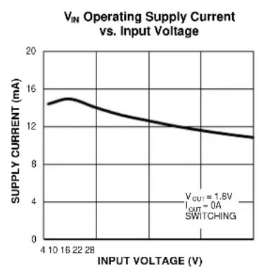
| INPUT VOLTAGE (V) | SUPPLY CURRENT (mA) | | ----------------- | ------------------- | | 4 | 15 | | 10 | 14 | | 16 | 13 | | 22 | 12 | | 28 | 11 |
line
| INPUT VOLTAGE (V) | SHUTDOWN CURRENT (μA) | | ----------------- | ---------------------- | | 4 | 0 | | 10 | 5 | | 16 | 10 | | 22 | 15 | | 28 | 20 | | 36 | 30 | | 48 | 50 |
line
| INPUT VOLTAGE (V) | VDD VOLTAGE (V) | | ----------------- | --------------- | | 4 | 4.5 | | 10 | 5.0 | | 15 | 5.0 | | 20 | 5.0 | | 25 | 5.0 | | 28 | 5.0 |
line
| INPUT VOLTAGE (V) | FEEDBACK VOLTAGE (V) | | ----------------- | -------------------- | | 4 | 0.600 | | 10 | 0.600 | | 16 | 0.600 | | 22 | 0.600 | | 28 | 0.600 |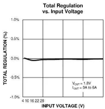
line
| INPUT VOLTAGE (V) | TOTAL REGULATION (%) | | ----------------- | -------------------- | | 4 | 0.0 | | 10 | -0.1 | | 16 | -0.2 | | 22 | -0.1 | | 28 | 0.0 |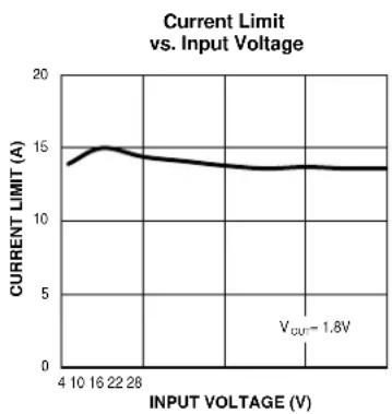
line
| INPUT VOLTAGE (V) | CURRENT LIMIT (A) | | ---------------- | ----------------- | | 4 | 14.0 | | 10 | 15.0 | | 16 | 14.5 | | 22 | 14.0 | | 28 | 13.5 | | V_CU | 1.8 |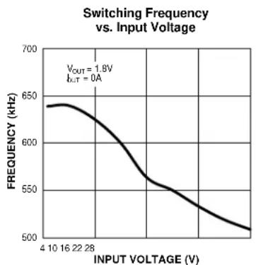
line
| INPUT VOLTAGE (V) | FREQUENCY (kHz) | | ---------------- | --------------- | | 4 | 650 | | 10 | 640 | | 16 | 630 | | 22 | 610 | | 28 | 590 | | 36 | 570 | | 48 | 550 | | 60 | 530 | | 72 | 510 | | 84 | 500 |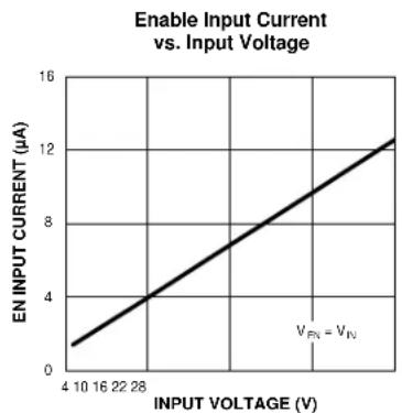
line
| INPUT VOLTAGE (V) | EN INPUT CURRENT (μA) | | ----------------- | --------------------- | | 4 | 0 | | 10 | 2 | | 16 | 4 | | 22 | 6 | | 28 | 8 | | 36 | 10 | | 42 | 12 | | 48 | 14 | | 56 | 16 |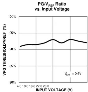
line
| INPUT VOLTAGE (V) | VPG THRESHOLD/VREF (%) | | ----------------- | ---------------------- | | 4.0 | 91.0 | | 10.0 | 91.5 | | 16.0 | 91.8 | | 22.0 | 92.0 | | 28.0 | 93.0 | | 36.0 | 92.5 | | 44.0 | 92.0 | | 52.0 | 91.5 | | 60.0 | 91.0 | | 68.0 | 90.5 | | 76.0 | 90.0 | | 84.0 | 89.5 | | 92.0 | 89.0 | | 100.0 | 88.5 |Typical Characteristics (Continued)
V_IN Operating Supply Current vs. Temperature
line
| TEMPERATURE (°C) | SUPPLY CURRENT (mA) | | ---------------- | ------------------- | | -50 | 12.0 | | -25 | 12.0 | | 0 | 12.0 | | 25 | 12.0 | | 50 | 12.0 | | 75 | 12.0 | | 100 | 12.0 | | 125 | 12.0 | | >125 | ~13.0 |V_IN Shutdown Current vs. Temperature
line
| TEMPERATURE (°C) | SUPPLY CURRENT (μA) | | ---------------- | ------------------- | | -50 | 4.0 | | 0 | 4.0 | | 25 | 4.0 | | 50 | 4.0 | | 75 | 4.0 | | 100 | 4.0 | | 125 | 5.0 | | 150 | 6.0 | | 175 | 8.0 | | 200 | 10.0 | | 225 | 12.0 | | 250 | 15.0 |V_DD UVLO Threshold vs. Temperature
line
| TEMPERATURE (°C) | Rising | Falling | Hyst | | ---------------- | ------ | ------- | ---- | | -50 | 4.5 | 4.0 | 0.5 | | 0 | 4.3 | 3.9 | 0.4 | | 25 | 4.2 | 3.8 | 0.3 | | 50 | 4.1 | 3.7 | 0.2 | | 75 | 4.0 | 3.6 | 0.1 | | 100 | 4.0 | 3.6 | 0.1 | | 125 | 4.0 | 3.6 | 0.1 |Feedback Voltage vs. Temperature

line
| TEMPERATURE (°C) | FEEBACK VOLTAGE (V) | | ---------------- | ------------------- | | -50 | 0.600 | | 0 | 0.600 | | 25 | 0.600 | | 50 | 0.600 | | 75 | 0.600 | | 100 | 0.600 | | 125 | 0.600 |Load Regulation vs. Temperature

line
| TEMPERATURE (°C) | LOAD REGULATION (%) | | ---------------- | ------------------- | | -50 | -0.2 | | 0 | -0.1 | | 25 | 0.0 | | 50 | 0.1 | | 75 | 0.2 | | 100 | 0.3 | | 125 | 0.4 | | 150 | 0.5 | | 175 | 0.6 | | 200 | 0.7 | | 225 | 0.8 | | 250 | 0.9 | | 275 | 1.0 |Line Regulation vs. Temperature

line
| TEMPERATURE (°C) | LINE REGULATION (%) | | ---------------- | ------------------- | | -50 | 0.08 | | -25 | 0.06 | | 0 | 0.07 | | 25 | 0.06 | | 50 | 0.07 | | 75 | 0.06 | | 100 | 0.07 | | 125 | 0.06 | | 150 | 0.07 | | 175 | 0.06 | | 200 | 0.07 | | 225 | 0.06 | | 250 | 0.07 | | 275 | 0.06 | | 300 | 0.07 | | 325 | 0.06 | | 350 | 0.07 | | 375 | 0.06 | | 400 | 0.07 | | 425 | 0.06 | | 450 | 0.07 | | 475 | 0.06 | | 500 | 0.07 |Switching Frequency vs. Temperature

line
| TEMPERATURE (°C) | FREQUENCY (kHz) | | ---------------- | --------------- | | -50 | 600 | | -25 | 605 | | 0 | 605 | | 25 | 605 | | 50 | 605 | | 75 | 605 | | 100 | 600 | | 125 | 590 | | 150 | 580 | | 175 | 570 | | 200 | 560 | | 225 | 550 | | 250 | 540 |V_DD
vs. Temperature

line
| TEMPERATURE (°C) | VDD (V) | | ---------------- | ------- | | -50 | 5.2 | | 0 | 5.2 | | 25 | 5.2 | | 50 | 5.2 | | 75 | 5.2 | | 100 | 5.2 | | 125 | 5.2 |Current Limit
vs. Temperature
line
| TEMPERATURE (°C) | CURRENT LIMIT (A) | | ---------------- | ----------------- | | -50 | 14.0 | | -25 | 14.5 | | 0 | 14.8 | | 25 | 14.7 | | 50 | 14.6 | | 75 | 14.5 | | 100 | 14.3 | | 125 | 13.8 | | 150 | 12.5 | | 175 | 10.5 | | 200 | 8.5 | | 225 | 7.0 |Typical Characteristics (Continued)

line
| OUTPUT CURRENT (A) | EFFICIENCY (%) | | ------------------ | -------------- | | 0 | 50 | | 1 | 65 | | 2 | 75 | | 3 | 80 | | 4 | 85 | | 5 | 88 | | 6 | 90 | | V_OUT | 1.8 |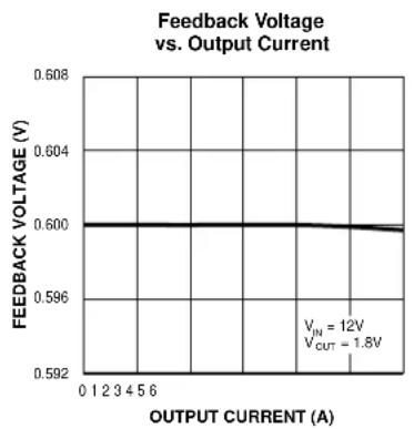
line
| OUTPUT CURRENT (A) | FEEDBACK VOLTAGE (V) | | ------------------ | -------------------- | | 0 | 0.600 | | 1 | 0.600 | | 2 | 0.600 | | 3 | 0.600 | | 4 | 0.600 | | 5 | 0.600 | | 6 | 0.600 |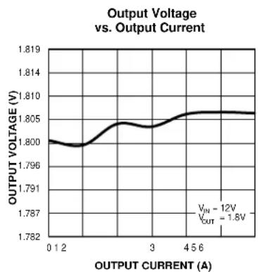
line
| OUTPUT CURRENT (A) | OUTPUT VOLTAGE (V) | | ------------------ | ------------------ | | 0 | 1.800 | | 1.2 | 1.799 | | 3 | 1.805 | | 4.5 | 1.806 | | 6 | 1.806 |
line
| OUTPUT CURRENT (A) | LINE REGULATION (%) | | ------------------ | ------------------- | | 0 | 0.2 | | 12 | 0.2 | | 34 | 0.25 | | 45 | 0.2 | | 56 | 0.15 | | 67 | 0.1 |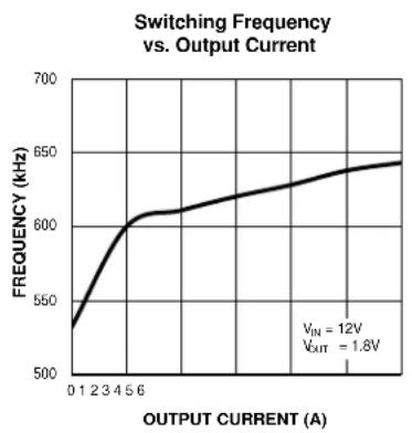
line
| OUTPUT CURRENT (A) | FREQUENCY (kHz) | | ------------------ | --------------- | | 0 | 530 | | 1 | 550 | | 2 | 570 | | 3 | 590 | | 4 | 600 | | 5 | 610 | | 6 | 620 | | >6 | >630 |
line
| OUTPUT CURRENT (A) | OUTPUT VOLTAGE (V) - 25°C | OUTPUT VOLTAGE (V) - 85°C | OUTPUT VOLTAGE (V) - 125°C | | ------------------ | -------------------------- | -------------------------- | --------------------------- | | 0 | 4.2 | 4.2 | 4.2 | | 1 | 4.1 | 4.1 | 4.1 | | 2 | 4.0 | 4.0 | 4.0 | | 3 | 3.9 | 3.9 | 3.9 | | 4 | 3.8 | 3.8 | 3.8 | | 5 | 3.7 | 3.7 | 3.7 | | 6 | 3.6 | 3.6 | 3.6 | | 7 | 3.5 | 3.5 | 3.5 | | 8 | 3.4 | 3.4 | 3.4 |
line
| OUTPUT CURRENT (A) | EFFICIENCY (%) | | ------------------ | -------------- | | 0 | 50 | | 1 | 65 | | 2 | 75 | | 3 | 85 | | 4 | 90 | | 5 | 92 | | 6 | 93 | | 7 | 94 | | 8 | 95 | | 9 | 94 | | 10 | 93 | | 11 | 92 | | 12 | 91 | | 13 | 90 | | 14 | 89 | | 15 | 88 | | 16 | 87 | | 17 | 86 | | 18 | 85 | | 19 | 84 | | 20 | 83 | | 21 | 82 | | 22 | 81 | | 23 | 80 | | 24 | 79 | | 25 | 78 | | 26 | 77 | | 27 | 76 | | 28 | 75 | | 29 | 74 | | 30 | 73 | | 31 | 72 | | 32 | 71 | | 33 | 70 | | 34 | 69 | | 35 | 68 | | 36 | 67 | | 37 | 66 | | 38 | 65 | | 39 | 64 | | 40 | 63 | | 41 | 62 | | 42 | 61 | | 43 | 60 | | 44 | 59 | | 45 | 58 | | 46 | 57 | | 47 | 56 | | 48 | 55 | | 49 | 54 | | 50 | 53 |
line
| V_IN | IC POWER DISSIPATION (W) | |------|--------------------------| | 5V | 0.0 | | 0.8V | 0.5 | | 1.0V | 0.7 | | 1.2V | 0.9 | | 1.5V | 1.1 | | 1.8V | 1.4 | | 2.5V | 1.7 | | 3.3V | 2.0 | | 0.8V | 2.5 |
line
| OUTPUT CURRENT (A) | DIE TEMPERATURE (°C) | | ------------------ | -------------------- | | 0 | 20 | | 1 | 25 | | 2 | 30 | | 3 | 35 | | 4 | 40 | | 5 | 45 | | 6 | 50 | | 7 | 55 | | 8 | 60 |Die Temperature* : The temperature measurement was taken at the hottest point on the MIC26603-ZA while it was case mounted on a 5in ^2 4-layer, 0.62", FR-4 PCB, with 2oz finish copper weight per layer. See the "Thermal Measurements" section for more details. Actual results will depend on the size of the PCB, ambient temperature, and proximity to other heat emitting components.
Typical Characteristics (Continued)
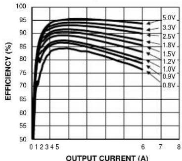
Efficiency ( V_IN = 12V ) vs. Output Current
line
| OUTPUT CURRENT (A) | 5.0V | 3.3V | 2.5V | 1.8V | 1.5V | 1.2V | 1.0V | 0.9V | 0.8V | | ----------------- | ----- | ----- | ----- | ----- | ----- | ----- | ----- | ----- | ----- | | 0 | 50 | 50 | 50 | 50 | 50 | 50 | 50 | 50 | 50 | | 1 | 70 | 70 | 70 | 70 | 70 | 70 | 70 | 70 | 70 | | 2 | 80 | 80 | 80 | 80 | 80 | 80 | 80 | 80 | 80 | | 3 | 85 | 85 | 85 | 85 | 85 | 85 | 85 | 85 | 85 | | 4 | 90 | 90 | 90 | 90 | 90 | 90 | 90 | 90 | 90 | | 5 | 95 | 95 | 95 | 95 | 95 | 95 | 95 | 95 | 95 | | 6 | 95 | 95 | 95 | 95 | 95 | 95 | 95 | 95 | 95 | | 7 | 95 | 95 | 95 | 95 | 95 | 95 | 95 | 95 | 95 | | 8 | 95 | 95 | 95 | 95 | 95 | 95 | 95 | 95 | 95 |IC Power Dissipation ( V_IN = 12V )
vs. Output Current

line
| OUTPUT CURRENT (A) | IC POWER DISSIPATION (W) | | ------------------ | ------------------------ | | 0.1 | 0.2 | | 0.2 | 0.3 | | 0.3 | 0.4 | | 0.4 | 0.5 | | 0.5 | 0.6 | | 0.6 | 0.7 | | 0.7 | 0.8 | | 0.8 | 0.9 | | 0.9 | 1.0 | | 1.0 | 1.1 | | 1.1 | 1.2 | | 1.2 | 1.3 | | 1.3 | 1.4 | | 1.4 | 1.5 | | 1.5 | 1.6 | | 1.6 | 1.7 | | 1.7 | 1.8 | | 1.8 | 1.9 | | 1.9 | 2.0 | | 2.0 | 2.1 |Die Temperature* (V_IN = 12V) vs. Output Current

line
| OUTPUT CURRENT (A) | DIE TEMPERATURE (°C) | | ------------------ | -------------------- | | 0 | 22 | | 1 | 24 | | 2 | 26 | | 3 | 29 | | 4 | 33 | | 5 | 40 | | 6 | 55 |Efficiency ( V_IN = 24V ) vs. Output Current

line
| OUTPUT CURRENT (A) | 5.0V | 3.3V | 2.5V | 1.8V | 1.5V | 1.2V | 1.0V | 0.9V | 0.8V | | ------------------ | ----- | ----- | ----- | ----- | ----- | ----- | ----- | ----- | ----- | | 0 | 50 | 50 | 50 | 50 | 50 | 50 | 50 | 50 | 50 | | 1 | 70 | 70 | 70 | 70 | 70 | 70 | 70 | 70 | 70 | | 2 | 80 | 80 | 80 | 80 | 80 | 80 | 80 | 80 | 80 | | 3 | 85 | 85 | 85 | 85 | 85 | 85 | 85 | 85 | 85 | | 4 | 90 | 90 | 90 | 90 | 90 | 90 | 90 | 90 | 90 | | 5 | 92 | 92 | 92 | 92 | 92 | 92 | 92 | 92 | 92 | | 6 | 93 | 93 | 93 | 93 | 93 | 93 | 93 | 93 | 93 | | 7 | 94 | 94 | 94 | 94 | 94 | 94 | 94 | 94 | 94 | | 8 | 95 | 95 | 95 | 95 | 95 | 95 | 95 | 95 | 95 | | >1 | ~96 | ~96 | ~96 | ~96 | ~96 | ~96 | ~96 | ~96 | ~96 | The chart displays efficiency (%) as a function of output current (A). The legend indicates voltage levels ranging from -5.0V to +0.8V. The data is presented in a table format with each row representing a single data point. Error bars are not visible in the chart.IC Power Dissipation ( V_IN = 24V )
vs. Output Current
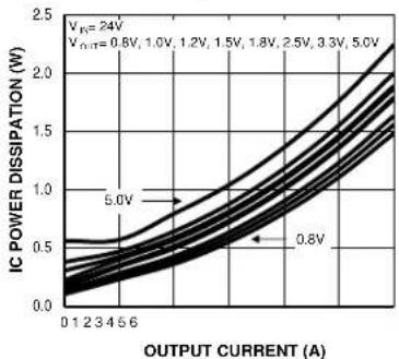
line
| OUTPUT CURRENT (A) | IC POWER DISSIPATION (W) | | ------------------ | ------------------------ | | 0.8 | 0.8 | | 1.2 | 1.0 | | 1.5 | 1.2 | | 1.8 | 1.5 | | 2.5 | 2.0 | | 3.3 | 2.5 | | 5.0 | 3.0 |Die Temperature* (V _IN = 24V) vs. Output Current
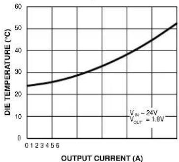
line
| OUTPUT CURRENT (A) | DIE TEMPERATURE (°C) | | ------------------ | -------------------- | | 0 | 23 | | 1 | 25 | | 2 | 27 | | 3 | 29 | | 4 | 31 | | 5 | 33 | | 6 | 35 | | 7 | 37 | | 8 | 39 | | 9 | 41 | | 10 | 43 | | 11 | 45 | | 12 | 47 | | 13 | 49 | | 14 | 51 | | 15 | 53 | | 16 | 55 | | 17 | 57 | | 18 | 59 | | 19 | 61 | | 20 | 63 | | 21 | 65 | | 22 | 67 | | 23 | 69 | | 24 | 71 | | 25 | 73 | | 26 | 75 | | 27 | 77 | | 28 | 79 | | 29 | 81 | | 30 | 83 | | 31 | 85 | | 32 | 87 | | 33 | 89 | | 34 | 91 | | 35 | 93 | | 36 | 95 | | 37 | 97 | | 38 | 99 | | 39 | 101 | | 40 | 103 | | 41 | 105 | | 42 | 107 | | 43 | 109 | | 44 | 111 | | 45 | 113 | | 46 | 115 | | 47 | 117 | | 48 | 119 | | 49 | 121 | | 50 | 123 | | 51 | 125 | | 52 | 127 | | 53 | 129 | | 54 | 131 | | 55 | 133 | | 56 | 135 | | 57 | 137 | | 58 | 139 | | 59 | 141 | | 60 | 143 | | 61 | 145 | | 62 | 147 | | 63 | 149 | | 64 | 151 | | 65 | 153 | | 66 | 155 | | 67 | 157 | | 68 | 159 | | 69 | 161 | | 70 | 163 | | 71 | 165 | | 72 | 167 | | 73 | 169 | | 74 | 171 | | 75 | 173 | | 76 | 175 | | 77 | 177 | | 78 | 179 | | 79 | 181 | | 80 | 183 | | 81 | 185 | | 82 | 187 | | 83 | 189 | | 84 | 191 | | 85 | 193 | | 86 | 195 | | 87 | 197 | | 88 | 199 | | 89 | 201 | | 90 | 203 | | 91 | 205 | | 92 | 207 | | 93 | 209 | | 94 | 211 | | 95 | 213 | | 96 | 215 | | 97 | 217 | | 98 | 219 | | 99 | 221 | | >20 | >23 |Thermal Derating* Ambient Temperature
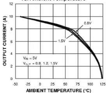
line
| AMBIENT TEMPERATURE (°C) | OUTPUT CURRENT (A) | | ------------------------ | ------------------ | | -50 | 10.0 | | 0 | 9.5 | | 25 | 8.5 | | 50 | 7.5 | | 75 | 6.0 | | 100 | 4.0 | | 125 | 0.0 |Thermal Derating* Ambient Temperature

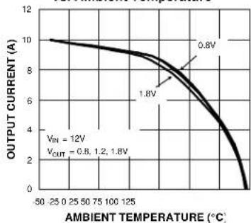
line
| AMBIENT TEMPERATURE (°C) | OUTPUT CURRENT (A) | | ------------------------ | ------------------ | | -50 | 10.0 | | 0 | 9.5 | | 25 | 8.5 | | 50 | 7.0 | | 75 | 5.0 | | 100 | 3.0 | | 125 | 0.0 |Thermal Derating* Ambient Temperature
line
| AMBIENT TEMPERATURE (°C) | OUTPUT CURRENT (A) | | ------------------------ | ------------------ | | -50 | 10.0 | | 0 | 9.5 | | 25 | 9.0 | | 50 | 8.5 | | 75 | 7.5 | | 100 | 6.5 | | 125 | 5.0 |Die Temperature*: The temperature measurement was taken at the hottest point on the MIC26603-ZA while it was case mounted on a 5in ^2 4-layer, 0.62", FR-4 PCB, with 2oz finish copper weight per layer. See the "Thermal Measurements" section for more details. Actual results will depend on the size of the PCB, ambient temperature, and proximity to other heat emitting components.
Typical Characteristics (Continued)

line
| Ambient Temperature (°C) | Output Current (A) | | ------------------------ | ------------------ | | -50 | 10 | | 0 | 9 | | 25 | 8 | | 50 | 7 | | 75 | 6 | | 100 | 5 | | 125 | 4 | | 150 | 3 | | 175 | 2 | | 200 | 1 | | 225 | 0.5 | | 250 | 0 |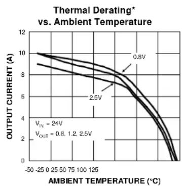
line
| Ambient Temperature (°C) | Output Current (A) | | ------------------------ | ------------------ | | -50 | 10.0 | | 0 | 9.5 | | 25 | 9.0 | | 50 | 8.5 | | 75 | 8.0 | | 100 | 7.5 | | 125 | 7.0 | | -50 | 10.0 | | 0 | 9.5 | | 25 | 9.0 | | 50 | 8.5 | | 75 | 8.0 | | 100 | 7.5 | | -50 | 10.0 | | 0 | 9.5 | | 25 | 9.0 | | 50 | 8.5 | | 75 | 8.0 | | 100 | 7.5 | | -50 | 10.0 | | 0 | 9.5 | | | 25 | 9.0 | | 50 | 8.5 | | 75 | 8.0 | | 100 | 7.5 | | -50 | 10.0 | | 0 | 9.5 | | | 25 | 9.0 | | 50 | 8.5 | | -50 | 10.0 | | -25 | 9.5 | | -25 | 9.0 | | -25 | 8.5 | | -25 | 8.0 | | -25 | 7.5 | | -25 | 7.0 | | -25 | 6.5 | | -25 | 6.0 | | -25 | 5.5 | | -25 | 5.0 | | -25 | 4.5 | | -25 | 4.0 | | -25 | 3.5 | | -25 | 3.0 | | -25 | 2.5 | | -25 | 2.0 | | -25 | 1.5 | | -25 | 1.0 | | -25 | 0.5 | | -25 | 0.0 | | -25 | -0.5 | | -25 | -1.0 | | -25 | -1.5 | | -25 | -2.0 | | -25 | -2.5 | | -25 | -3.0 | | -25 | -3.5 | | -25 | -4.0 | | -25 | -4.5 | | -25 | -5.0 | | -25 | -5.5 | | -25 | -6.0 | | -25 | -6.5 | | -25 | -7.0 | | -25 | -7.5 | | -25 | -8.0 | | -25 | -8.5 | | -25 | -9.0 | | -25 | -9.5 | | -25 | -10.0 | | -25 | -10.5 | | -25 | -11.0 | | -25 | -11.5 | | -25 | -12.0 | | -25 | -12.5 | | -25 | -13.0 | | -25 | -13.5 | | -25 | -14.0 | | -25 | -14.5 | | -25 | -15.0 | | -25 | -15.5 | | -25 | -16.0 | | -25 | -16.5 | | -25 | -17.0 | | -25 | -17.5 | | -25 | -18.0 | | -25 | -18.5 | | -25 | -19.0 | | -25 | -19.5 | | -25 | -20.0 | | -25 | -20.5 | | -25 | -21.0 | | -25 | -21.5 | | -25 | -22.0 | | -25 | -22.5 | | -25 | -23.0 | | -25 | -23.5 | | -25 | -24.0 | | -25 | -24.5 | | -25 | -25.0 | | -25 | -25.5 | | -25 | -26.0 | | -25 | -26.5 | | -25 | -27.0 | | -25 | -27.5 | | -25 | -28.0 | | -25 | -28.5 | | -25 | -29.0 | | -25 | -29.5 | | -25 | -30.0 | | -25 | -30.5 | | -25 | -31.0 | | -25 | -31.5 | | -25 | -32.0 | | -25 | -32.5 | | -25 | -33.0 | | -25 | -33.5 | | -25 | -34.0 | | -25 | -34.5 | | -25 | -35.0 | | -25 | -35.5 | | -25 | -36.0 | | -25 | -36.5 | | -25 | -37.0 | | -25 | -37.5 | | -25 | -38.0 | | -25 | -38.5 | | -25 | -39.0 | | -25 | -39.5 | | -25 | -40.0 | | 0 | 10.0 | | 1 | 9.8 | | 1 | 9.6 | | 1 | 9.4 | | 1 | 9.2 | | 1 | 9.0 | | 1 | 8.8 | | 1 | 8.6 | | 1 | 8.4 | | 1 | 8.2 | | 1 | 8.0 | | 1 | 7.8 | | 1 | 7.6 | | 1 | 7.4 | | 1 | 7.2 | | 1 | 7.0 | | 1 | 6.8 | | 1 | 6.6 | | 1 | 6.4 | | 1 | 6.2 | | 1 | 6.0 | | 1 | 6.8 | | 1 | 7.4 | | 1 | 8.0 | | 1 | 8.6 | | 1 | 9.2 | | 1 | 9.8 | | 1 | 10.4 | | 1 | 11.0 | | 1 | 11.6 | | 1 | 12.2 | | 1 | 12.8 | | 1 | 13.4 | | 1 | 14.0 | | 1 | 14.6 | | 1 | 16.0 | | 1 | 17.6 | | 1 | 19.2 | | 1 | 20.8 | | 1 | 22.4 | | 1 | 24.0 | | 1 | 24.6 | | 1 | 26.0 | | 1 | 27.6 | | 1 | 38.0 | | 1 | 48.6 | | 1 | 68.4 | | 1 | 88.4 | | 1 | 108.4 | | 1 | 138.4 | | 1 | 168.4 | | 1 | 198.4 | | 1 | 338.4 | | 1 | 488.4 | | 1 | 688.4 | | 1 | 938.4 | | 1 | 1338.4 | | 1 | nan | V_IN : V_OUT A V_OUT : V_OUT A V_OUT : V_OUT A V_OUT : V_OUT A V_OUT : V_OUT A V_OUT : V_OUT A V_OUT : V_OUT A V_OUT : V_OUT A V_OUT : V_OUT A V_OUT : V_OUT A V_OUT : V_OUT A V_OUT : V_OUT A V_OUT : V_OUT B V_OUT : V_OUT B V_OUT : V_OUT B V_OUT : V_OUT B V_OUT : V_OUT B V_OUT : V_OUT B V_OUT : V_OUT B V_OUT : V_OUT B V_OUT : V_OUT B V_OUT : V_OUT B V_OUT : V_OUT B V_OUT : V_OUT BDie Temperature*: The temperature measurement was taken at the hottest point on the MIC26603-ZA while it was case mounted on a 5in^2 4-layer, 0.62", FR-4 PCB, with 2oz finish copper weight per layer. See the "Thermal Measurements" section for more details. Actual results will depend on the size of the PCB, ambient temperature, and proximity to other heat emitting components.
Functional Characteristics

line
| Time (2.0ms/div) | V_IN (10V/div) | V_SW (10V/div) | V_OUT (1V/div) | I_L (5A/div) | | ---------------- | -------------- | -------------- | -------------- | ------------ | | 0 | 1.5 | 1.5 | 1.5 | 0 | | 2.0 | 1.5 | 1.5 | 1.5 | 0 | | 4.0 | 1.5 | 1.5 | 1.5 | 0 | | 6.0 | 1.5 | 1.5 | 1.5 | 0 | | 8.0 | 1.5 | 1.5 | 1.5 | 0 | | 10.0 | 1.5 | 1.5 | 1.5 | 0 | | 12.0 | 1.5 | 1.5 | 1.5 | 0 | | 14.0 | 1.5 | 1.5 | 1.5 | 0 | | 16.0 | 1.5 | 1.5 | 1.5 | 0 | | 18.0 | 1.5 | 1.5 | 1.5 | 0 | | 20.0 | 1.5 | 1.5 | 1.5 | 0 | | 22.0 | 1.5 | 1.5 | 1.5 | 0 | | 24.0 | 1.5 | 1.5 | 1.5 | 0 | | 26.0 | 1.5 | 1.5 | 1.5 | 0 | | 28.0 | 1.5 | 1.5 | 1.5 | 0 | | 30.0 | 1.5 | 1.5 | 1.5 | 0 | | 32.0 | 1.5 | 1.5 | 1.5 | 0 | | 34.0 | 1.5 | 1.5 | 1.5 | 0 | | 36.0 | 1.5 | 1.5 | 1.5 | 0 | | 38.0 | 1.5 | 1.5 | 1.5 | 0 | | 40.0 | 1.5 | 1.5 | 1.5 | 0 | | 42.0 | 1.5 | 1.5 | 1.5 | 0 | | 44.0 | 1.5 | 1.5 | 1.5 | 0 | | 46.0 | 1.5 | 1.5 | 1.5 | 0 | | 48.0 | 1.5 | 1.5 | 1.5 | 0 | | 50.0 | 1.5 | 1.5 | 1.5 | 0 | | 52.0 | 1.5 | 1.5 | 1.5 | 0 | | 54.0 | 1.5 | 1.5 | 1.5 | 0 | | 56.0 | 1.5 | 1.5 | 1.5 | 0 | | 58.0 | 1.5 | 1.5 | 1.5 | 0 | | 60.0 | 1.5 | 1.5 | 1.5 | 0 | | 62.0 | 1.5 | 1.5 | 1.5 | 0 | | 64.0 | 1.5 | 1.5 | 1.5 | 0 | | 66.0 | 1.5 | 1.5 | 1.5 | 0 | | 68.0 | 1.5 | 1.5 | 1.5 | 0 | | 70.0 | 1.5 | 1.5 | 1.5 | 0 | | 72.0 | 1.5 | 1.5 | 1.5 | 0 | | 74.0 | 1.5 | 1.5 | 1.5 | 0 | | 76.0 | 1.5 | 1.5 | 1.5 | 0 | | 78.0 | 1.5 | 1.5 | 1.5 | 0 | | 80.0 | 1.5 | 1.5 | 1.5 | 0 | | Note: The values for V_IN, V_SW, V_OUT, and I_L are not provided in the code snippet in the original image, so they are calculated based on the given code.
line
| Waveform | Value | | -------------- | --------- | | V_IN (10V/div) | 12V | | V_SW (10V/div) | 1.8V | | V_OUT (1V/div) | 6A | | I_L (5A/div) | - |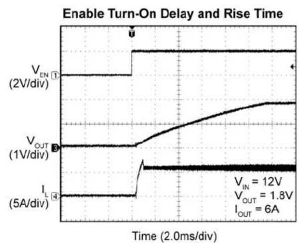
line
| Time (2.0ms/div) | V_IN (2V/div) | V_OUT (1V/div) | I_L (5A/div) | | ---------------- | ------------- | -------------- | ------------ | | 0 | 12V | 1.8V | 6A |
line
| Time (200μs/div) | V_IN (2V/div) | V_OUT (1V/div) | I_OUT (6A) | I_L (5A/div) | | ---------------- | ------------- | -------------- | ---------- | ------------ | | 0 | 12V | 1.8V | 6A | - | | 100 | - | - | - | - | | 200 | - | - | - | - |
line
| Time (2.0ms/div) | V_IN (10V/div) | V_OUT (1V/div) | V_SW (10V/div) | | ---------------- | -------------- | -------------- | -------------- | | V_IN | 12V | 1.8V | - | | I_OUT | 1A | - | - | | V_PRE_BIAS | 1V | - | - |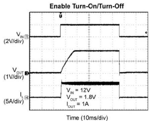
line
| Time (10ms/div) | V_IN (2V/div) | V_OUT (1V/div) | I_L (5A/div) | | --------------- | ------------- | -------------- | ------------ | | 0 | 0 | 0 | 0 | | 1 | 12V | 1.8V | 1A | | 2 | 12V | 1.8V | 1A | | 3 | 12V | 1.8V | 1A | | 4 | 12V | 1.8V | 1A | | 5 | 12V | 1.8V | 1A | | 6 | 12V | 1.8V | 1A | | 7 | 12V | 1.8V | 1A | | 8 | 12V | 1.8V | 1A | | 9 | 12V | 1.8V | 1A | | 10 | 12V | 1.8V | 1A | | 11 | 12V | 1.8V | 1A | | 12 | 12V | 1.8V | 1A | | 13 | 12V | 1.8V | 1A | | 14 | 12V | 1.8V | 1A | | 15 | 12V | 1.8V | 1A | | 16 | 12V | 1.8V | 1A | | 17 | 12V | 1.8V | 1A | | 18 | 12V | 1.8V | 1A | | 19 | 12V | 1.8V | 1A | | 20 | 12V | 1.8V | 1A | | 21 | 12V | 1.8V | 1A | | 22 | 12V | 1.8V | 1A | | 23 | 12V | 1.8V | 1A | | 24 | 12V | 1.8V | 1A | | 25 | 12V | 1.8V | 1A | | 26 | 12V | 1.8V | 1A | | 27 | 12V | 1.8V | 1A | | 28 | 12V | 1.8V | 1A | | 29 | 12V | 1.8V | 1A | | 30 | 12V | 1.8V | 1A | | 31 | 12V | 1.8V | 1A | | 32 | 12V | 1.8V | 1A | | 33 | 12V | 1.8V | 1A | | 34 | 12V | 1.8V | 1A | | 35 | 12V | 1.8V | 1A | | 36 | 12V | 1.8V | 1A | | 37 | 12V | 1.8V | 1A | | 38 | 12V | 1.8V | 1A | | 39 | 12V | 1.8V | 1A | | 40 | 12V | 1.8V | 1A | | Note: The actual values for V_IN and V_OUT are not provided in the code snippet, so they are calculated based on the given code snippet 'I_L' in the provided code snippet 'I_OUT'.Functional Characteristics (Continued)

Functional Characteristics (Continued)
Functional Diagram
flowchart
graph TD
    A["EN"] --> B["THERMAL SHUTDOWN"]
    B --> C["CONTROL LOGIC TIMER SOFT-START"]
    C --> D["SOFT START"]
    D --> E["INTERNAL RIPPLE INJECTION"]
    E --> F["COMP"]
    F --> G["COMPENSATION"]
    G --> H["g_m EA"]
    H --> I["V_REF 0.6V"]
    I --> J["92%"]
    J --> K["PG"]
    K --> L["V_DD 10kΩ"]
    L --> M["V_DD PVDD"]
    M --> N["LDO"]
    N --> O["FIXED T_ON ESTIMATE"]
    O --> P["VIN"]
    P --> Q["PVIN BST"]
    Q --> R["C_BST 0.1μF 2.2μH"]
    R --> S["SW CS"]
    S --> T["PGND"]
    T --> U["FB"]
    U --> V["R2 1.24kΩ"]
    V --> W["R1 2.49kΩ"]
    W --> X["100μF"]
    X --> Y["V_OUT 1.8V/6A"]
    Z["V_IN 10kΩ"] --> AA["EN"]
    AB["V_IN 2.2μF"] --> AC["EN"]
    AD["VOUT 4.5V TO 28V"] --> AE["V_IN 4.5V TO 28V"]
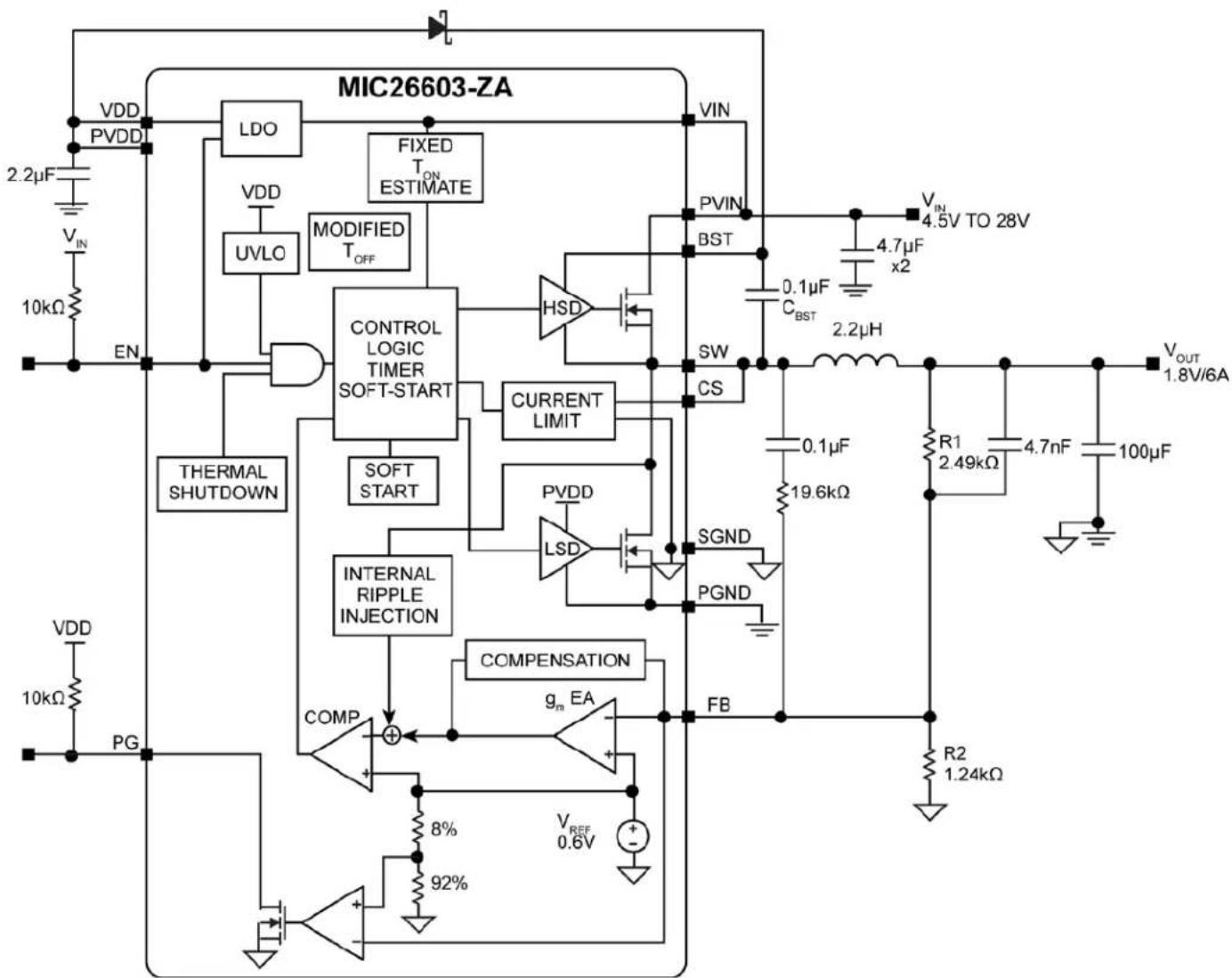
Figure 1. MIC26603-ZA Block Diagram
Functional Description
The MIC26603-ZA is an adaptive ON-time synchronous step-down DC-DC regulator with an internal 5V linear regulator and a Power Good (PG) output. It is designed to operate over a wide input voltage range from 4.5V to 28V and provides a regulated output voltage at up to 7A of output current. An adaptive ON-time control scheme is used to get a constant switching frequency and to simplify the control compensation. Overcurrent protection is implemented without using an external sense resistor. The device includes an internal soft-start function that reduces the power supply input surge current at start-up by controlling the output voltage rise time.
Theory of Operation
The MIC26603-ZA operates in a continuous mode, as shown in Figure 1.
Continuous Mode
In continuous mode, the output voltage is sensed by the MIC26603-ZA feedback pin FB through the voltage divider R1 and R2. It is then compared to a 0.6V reference voltage V_REF at the error comparator through a low-gain transconductance ( g_m ) amplifier. If the feedback voltage decreases and the output of the g_m amplifier is below 0.6V, then the error comparator will trigger the control logic and generate an ON-time period. The ON-time period length is predetermined by the “FIXED t_ON ESTIMATION” circuitry:
$$ t \quad \underset { \begin{array}{c} \text {ESTIMATED(ON)} \ \text {IN} \end{array} } {\overline {{\text {V}}} _ {\text {OUT}}} $$
where V_OUT is the output voltage and V_IN is the power stage input voltage.
At the end of the ON-time period, the internal high-side driver turns off the high-side MOSFET and the low-side driver turns on the low-side MOSFET. The OFF-time period length depends on the feedback voltage in most cases. When the feedback voltage decreases and the output of the g_m amplifier is below 0.6V, the ON-time period is triggered and the OFF-time period ends. If the OFF-time period determined by the feedback voltage is less than the minimum OFF-time t_OFF(min) , which is about 300ns, the MIC26603-ZA control logic will apply the t_OFF(min) instead. t_OFF(min) is required to maintain enough energy in the boost capacitor ( C_BST ) to drive the high-side MOSFET.
The maximum duty cycle is derived from the 300ns t_OFF(min) :
$$ D _ {\text { MAX }} = \frac {t _ {\mathrm{S}} - t _ {\mathrm{OFF(MIN)}}}{t _ {\mathrm{S}}} = 1 - \frac {3 0 0 \mathrm{ns}}{t _ {\mathrm{S}}} \tag {Eq.2} $$
where t_S = 1/600kHz = 1.66 s .
Using MIC26603-ZA with an OFF-time close to t_OFF(min) during steady-state operation is not recommended. Also, as V_OUT increases, the internal ripple injection increases and reduces the line regulation performance. Therefore, the maximum output voltage of the MIC26603-ZA should be limited to 5.5V and the maximum external ripple injection should be limited to 200mV. Please refer to the "Setting Output Voltage" subsection in Application Information for more details.
The actual ON-time and resulting switching frequency will vary with the part-to-part variation in the rise and fall times of the internal MOSFETs, the output load current, and variations in the V_DD voltage. Also, the minimum t_ON results in a lower switching frequency in high V_IN to V_OUT applications, such as 24V to 1.0V. The minimum t_ON measured on the MIC26603-ZA evaluation board is about 100ns. During load transients, the switching frequency is changed because of the varying OFF-time.
To illustrate the control loop operation, the datasheet will discuss both the steady-state and load transient scenarios. Figure 2 shows the MIC26603-ZA control loop timing during steady-state operation. During steady-state operation, the g_m amplifier senses the feedback voltage ripple, which is proportional to the output voltage ripple and the inductor current ripple, to trigger the ON-time period. The ON-time is predetermined by the t_ON estimator. The termination of the OFF-time is controlled by the feedback voltage. At the valley of the feedback voltage ripple, which occurs when V_FB falls below V_REF , the OFF-time period ends and the next ON-time period is triggered through the control logic circuitry.

line
| Signal | Value | |-----------------|------------------------| | I_L | ΔI_L(pp) | | V_OUT | ΔV_OUT(pp) | | V_FB | ΔV_FB(pp) | | HSD | Trigger ON-time if V_FB is below V_REF | | Estimated ON-Time | (no explicit label) |Figure 2. MIC26603-ZA Control Loop Timing
Figure 3 shows the operation of the MIC26603-ZA during a load transient. The output voltage drops because of the sudden load increase, which makes the V_FB less than V_REF . This causes the error comparator to trigger an ON-time period. At the end of the ON-time period, a minimum OFF-time t_OFF(min) is generated to charge C_BST because the feedback voltage is still below V_REF . Then, the next ON-time period is triggered by the low feedback voltage. Therefore, the switching frequency changes during the load transient, but returns to the nominal fixed frequency after the output has stabilized at the new load current level. With the varying duty cycle and switching frequency, the output recovery time is fast and the output voltage deviation is small in a MIC26603-ZA converter.

line
| Condition | I_OUT | V_OUT | V_FB | HSD | | --------------- | ----- | ----- | ---- | --- | | No load | High | Low | Low | Low | | Full load | High | Low | Low | Low |Figure 3. MIC26603-ZA Load Transient Response
Unlike true current-mode control, the MIC26603-ZA uses the output voltage ripple to trigger an ON-time period. The output voltage ripple is proportional to the inductor current ripple if the ESR of the output capacitor is large enough. The MIC26603-ZA control loop has the advantage of eliminating the need for slope compensation.
To meet the stability requirements, the MIC26603-ZA feedback voltage ripple should be in phase with the inductor current ripple and large enough to be sensed by the g_m amplifier and the error comparator. The recommended feedback voltage ripple is 20mV\~100mV. If a low-ESR output capacitor is selected, then the feedback voltage ripple may be too small to be sensed by the g_m amplifier and the error comparator. Also, the output voltage ripple and the feedback voltage ripple are not necessarily in phase with the inductor current ripple if the ESR of the output capacitor is very low. In these cases, ripple injection is required to ensure proper operation. Please refer to the “Ripple Injection” subsection in Application Information for more details about the ripple injection technique.
VDD Regulator
The MIC26603-ZA provides a 5V regulated output for input voltage VIN ranging from 5.5V to 28V. When V_IN < 5.5V , VDD should be tied to PVIN pins to bypass the internal linear regulator.
Soft-Start
Soft-start reduces the power supply input surge current at startup by controlling the output voltage rise time. The input surge appears while the output capacitor is charged up. A slower output rise time draws a lower input surge current.
The MIC26603-ZA implements an internal digital soft-start by making the 0.6V reference voltage V_REF ramp from 0 to 100% in about 6ms in 9.7mV steps. Therefore, the output voltage is controlled to increase slowly by a stair-case V_FB ramp. After the soft-start cycle ends, the related circuitry is disabled to reduce current consumption. V_DD must be powered up at the same time or after VIN to make the soft-start function correctly.
Current Limit
The MIC26603-ZA uses the R_DS(ON) of the internal low-side power MOSFET to sense overcurrent conditions. This method avoids adding cost, board space, and power losses taken by a discrete current sense resistor. The low-side MOSFET is used because it displays much lower parasitic oscillations during switching than the high-side MOSFET.
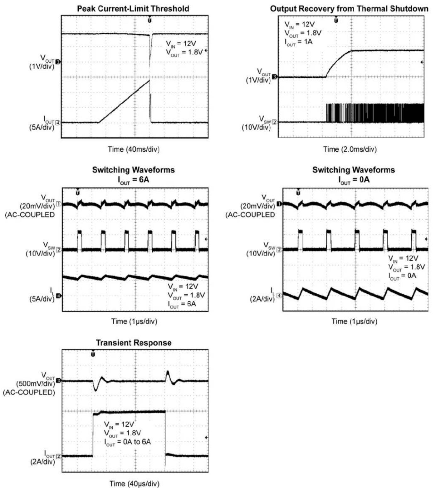
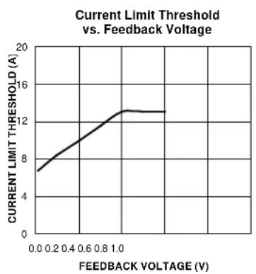
In each switching cycle of the MIC26603-ZA converter, the inductor current is sensed by monitoring the low-side MOSFET in the OFF-time period. If the peak inductor current is greater than 13A, then the MIC26603-ZA turns off the high-side MOSFET and a soft-start sequence is triggered. This mode of operation is called "hiccup mode" and its purpose is to protect the downstream load in case of a hard short. The load current-limit threshold has a foldback characteristic related to the feedback voltage, as shown in Figure 4.
line
| Feedback Voltage (V) | CURRENT LIMIT THRESHOLD (A) | | -------------------- | --------------------------- | | 0.0 | 7 | | 0.2 | 8 | | 0.4 | 9 | | 0.6 | 10 | | 0.8 | 12 | | 1.0 | 13 |Figure 4. MIC26603-ZA Current-Limit Foldback Characteristic
Power Good (PG)
The Power Good (PG) pin is an open-drain output that indicates logic high when the output is nominally 92% of its steady state voltage. A pull-up resistor of more than 10kΩ should be connected from PG to VDD.
MOSFET Gate Drive
The block diagram (Figure 1) shows a bootstrap circuit, consisting of D1 (a Schottky diode is recommended) and C_BST . This circuit supplies energy to the high-side drive circuit. Capacitor C_BST is charged, while the low-side MOSFET is on, and the voltage on the SW pin is approximately 0V. When the high-side MOSFET driver is turned on, energy from C_BST is used to turn the MOSFET on. As the high-side MOSFET turns on, the voltage on the SW pin increases to approximately V_IN . Diode D1 is reverse biased and C_BST floats high while continuing to keep the high-side MOSFET on. The bias current of the high-side driver is less than 10mA so a 0.1μF to 1μF capacitor is enough to hold the gate voltage with minimal droop for the power stroke (high-side switching) cycle, that is, BST = 10mA × 1.67 s / 0.1 F = 167mV . When the low-side MOSFET is turned back on, C_BST is recharged through D1. A small resistor R_G , in series with C_BST , can be used to slow down the turn-on time of the high-side N-channel MOSFET.
The drive voltage is derived from the V_DD supply voltage. The nominal low-side gate drive voltage is V_DD and the nominal high-side gate drive voltage is approximately V_DD-V_DIODE , where V_DIODE is the voltage drop across D1. An approximate 30ns delay between the high-side and low-side driver transitions is used to prevent current from simultaneously flowing unimpeded through both MOSFETs.
Application Information
Inductor Selection
Values for inductance, peak, and RMS currents are required to select the output inductor. The input and output voltages and the inductance value determine the peak-to-peak inductor ripple current. Generally, higher inductance values are used with higher input voltages. Larger peak-to-peak ripple currents increase the power dissipation in the inductor and MOSFETs. Larger output ripple currents also require more output capacitance to smooth out the larger ripple current. Smaller peak-to-peak ripple currents require a larger inductance value and therefore a larger and more expensive inductor. A good compromise between size, loss, and cost is to set the inductor ripple current equal to 20% of the maximum output current. The inductance value is calculated in Equation 3.
$$ L = \frac {O U T \times I N (M A X) - O U T) V V ^ {\prime}}{V _ {I N (M A X)} \quad S W \times \times 1 / 2 0 f _ {O U T (M A X)}} \tag {Eq.3} $$
where:
f_SW = switching frequency, 600kHz
20% = ratio of AC ripple current to DC output current
V_IN(MAX) = maximum power stage input voltage
The peak-to-peak inductor current ripple is:
$$ \Delta I _ {L (P P)} = \frac {V \times \left(V _ {\text {INOUT}}\right) _ {\text {MAX}} V _ {\text {OUT}}}{V _ {\text {IN MAX}} \times f _ {\text {SW}} \times L} \tag {Eq.4} $$
The peak inductor current is equal to the average output current plus one half of the peak-to-peak inductor current ripple.
$$ I _ {L (P K)} = I _ {\text { OUT(MAX) }} + 0. 5 \times \Delta I _ {L (P P)} \tag {Eq.5} $$
The RMS inductor current is used to calculate the I^2R losses in the inductor.
$$ I _ {L (R M S)} = \sqrt {I _ {O U T (M A X)} ^ {2} + \frac {\Delta I _ {L (P P)} ^ {2}}{1 2}} \tag {Eq.6} $$
Maximizing efficiency requires the selecting the proper core material and minimizing the winding resistance. The high-frequency operation of the MIC26603-ZA requires the use of ferrite materials for all but the most cost-sensitive applications. Lower-cost iron powder cores may be used but the increase in core loss reduces the efficiency of the power supply. This is especially noticeable at low output power. The winding resistance decreases efficiency at the higher output current levels.
The winding resistance must be minimized, although this usually comes at the expense of a larger inductor. The power dissipated in the inductor is equal to the sum of the core and copper losses. At higher output loads, the core losses are usually insignificant and can be ignored. At lower output currents, the core losses can be a significant contributor. Core loss information is usually available from the magnetics vendor. Copper loss in the inductor is calculated by Equation 7.
$$ P _ {\text { INDUCTOR(CU) }} = I _ {L (\mathrm{RMS})} ^ {2} \times R _ {\text { WINDING }} \tag {Eq.7} $$
The resistance of the copper wire, R_WINDING , increases with the temperature. The value of the winding resistance used should be at the operating temperature.
$$ P _ {\text { WINDING(Ht) }} = R _ {\text { WINDING(20°C) }} \times + 0. 0 0 4 2 \times \left(T _ {H} - T _ {2 0 ^ {\circ} C}\right)) $$
Eq. 8
where:
T_H= temperature of wire under full load
T_20^= ambient temperature
R_WINDING(20^) = room temperature winding resistance (usually specified by the manufacturer)
Output Capacitor Selection
The type of output capacitor is usually determined by its equivalent series resistance (ESR). Voltage and RMS current capability are two other important factors. Recommended capacitor types are ceramic, low-ESR aluminum electrolytic, OS-CON and POSCAP. The output capacitor's ESR is usually the main cause of the output ripple. The output capacitor ESR also affects the stability of the control loop.
The maximum value of ESR is calculated using Equation 9.
$$ \mathrm{ESR} _ {\mathrm{C} _ {\text {OUT}}} \leq \frac {\Delta \mathrm{V}}{\Delta \mathrm{I} _ {\mathrm{L} (\quad) \mathrm{PP}}} ^ {\mathrm{P}} \tag {Eq.9} $$
where:
V_OUT(pp) = peak-to-peak output voltage ripple
I_L(PP) = peak-to-peak inductor current ripple
The total output ripple is a combination of the ESR and output capacitance. The total ripple is calculated in Equation 10.
$$ \Delta V \times \Delta + _ {) P P (Q U T} \left(\frac {\Delta I}{C} \times f _ {S W O U P}\right) ^ {2} \quad \left(E S R I _ {C B P (U)}\right) ^ {2} \tag {Eq.10} $$
where:
D = duty cycle
C_OUT= output capacitance value
f_SW= switching frequency
As described in the "Theory of Operation" subsection in Functional Description, the MIC26603-ZA requires at least 20mV peak-to-peak ripple at the FB pin to make the g_m amplifier and the error comparator behave properly. Also, the output voltage ripple should be in phase with the inductor current. Therefore, the output voltage ripple caused by the output capacitors value should be much smaller than the ripple caused by the output capacitor ESR. If low-ESR capacitors, such as ceramic capacitors, are selected as the output capacitors, a ripple injection method should be applied to provide enough feedback voltage ripple. Please refer to the "Ripple Injection" subsection for more details.
The voltage rating of the capacitor should be twice the output voltage for tantalum and 20% greater for aluminum electrolytic or OS-CON. The output capacitor RMS current is calculated in Equation 11.
$$ I _ {C O U T (R M S)} = \frac {\Delta I}{\sqrt {1 2}}) P \tag {Eq.11} $$
The power dissipated in the output capacitor is:
$$ \mathrm{P} _ {\text {DISS} \left(\mathrm{C} _ {\text {OUT}}\right)} = \mathrm{I} _ {\mathrm{C} _ {\text {OUT}} (\text {RMS})} ^ {2} \times \mathrm{ESR} _ {\mathrm{C} _ {\text {OUT}}} \tag {Eq.12} $$
Input Capacitor Selection
The input capacitor for the power stage input V_IN should be selected for ripple current rating and voltage rating. Tantalum input capacitors may fail when subjected to high inrush currents caused by turning the input supply on. A tantalum input capacitor's voltage rating should be at least two times the maximum input voltage to maximize reliability. Aluminum electrolytic, OS-CON, and multilayer polymer film capacitors can handle the higher inrush currents without voltage derating. The input voltage ripple primarily depends on the input capacitor's ESR. The peak input current is equal to the peak inductor current, so:
$$ \Delta V _ {I N} = I _ {L (P K)} \times E S R _ {C _ {I N}} \tag {Eq.13} $$
The input capacitor must be rated for the input current ripple. The RMS value of input capacitor current is determined at the maximum output current. Assuming the peak-to-peak inductor current ripple is low:
$$ I _ {C _ {\text { IN }}} (\text { RMS }) \approx I _ {\text { OUT(MAX) }} \times \sqrt {D \times (1 - D)} \tag {Eq.14} $$
The power dissipated in the input capacitor is:
$$ P _ {D I S S (C _ {I N})} = I _ {C _ {I N} (R M S)} \times E S R _ {C _ {I N}} \tag {Eq.15} $$
Ripple Injection
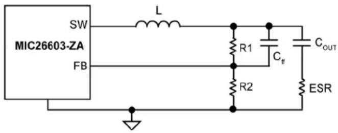
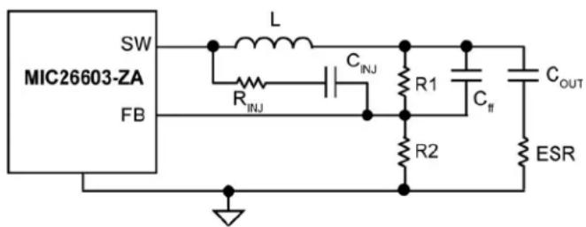
The V_FB ripple required for proper operation of the MIC26603-ZA g_m amplifier and error comparator is 20mV to 100mV. However, the output voltage ripple is generally designed as 1% to 2% of the output voltage. For a low output voltage, such as a 1V, the output voltage ripple is only 10mV to 20mV, and the feedback voltage ripple is less than 20mV. If the feedback voltage ripple is so small that the g_m amplifier and error comparator can't sense it, then the MIC26603-ZA will lose control and the output voltage is not regulated.
In order to have some amount of V_FB ripple, a ripple injection method is applied for low output voltage ripple applications.
The applications are divided into three situations according to the amount of the feedback voltage ripple:
- Enough ripple at the feedback voltage caused by the large ESR of the output capacitors.
As shown in Figure 5, the converter is stable without any ripple injection. The feedback voltage ripple is:
$$ \Delta V = \frac {R 2}{R 1 + R 2} \times E S R _ {C) P P (P B} \Delta I _ {L P P)} \quad \text { Eq. } 1 6 $$
where I_L(pp) is the peak-to-peak value of the inductor current ripple.
- Inadequate ripple at the feedback voltage caused by the small ESR of the output capacitors.
The output voltage ripple is fed into the FB pin through a feedforward capacitor C_ff in this situation, as shown in Figure 6. The typical C_ff value is between 1nF and 100nF. With the feedforward capacitor, the feedback voltage ripple is very close to the output voltage ripple:
$$ \Delta \quad \approx \quad \Delta I E S R _ {L P P (I)} \tag {Eq.17} $$
- Virtually no ripple at the FB pin voltage due to the very-low ESR of the output capacitors.

text_image
SW MIC26603-ZA FB L R1 R2 COUT ESRFigure 5. Enough Ripple at FB
text_image
SW MIC26603-ZA FB L R1 Cff COUT R2 ESRFigure 6. Inadequate Ripple at FB
text_image
SW MIC26603-ZA FB L R_INJ C_INJ R1 C_II R2 C_OUT ESRFigure 7. Invisible Ripple at FB
In this situation, the output voltage ripple is less than 20mV. Therefore, additional ripple is injected into the FB pin from the switching node SW via a resistor R_INJ and a capacitor C_INJ , as shown in Figure 7. The injected ripple is:
$$ V _ {(F B) P P} \Delta V _ {I N} \times K _ {D I V} \times D \times (1 - D) \times \frac {1}{f _ {S W} \times \tau} \quad E q. 1 8 $$
$$ K _ {\text { DIV }} = \frac {2 R R}{\text { INJ } + R / 2 1} \tag {Eq.19} $$
where:
V_IN = power stage input voltage
D = duty cycle
f_sw = switching frequency
$$ \tau = \left(R 1 / / R 2 / / R _ {I N J}\right) \times C _ {f f} $$
In Equations 18 and 19, it is assumed that the time constant associated with C_ff must be much greater than the switching period:
$$ \frac {1}{f s w \times \tau} = \frac {T}{\tau} < < 1 \quad E q. 2 0 $$
If the voltage divider resistors R1 and R2 are in the kΩ range, a C_ff of 1nF to 100nF can easily satisfy the large time constant requirements. Also, a 100nF injection capacitor C_INJ is used, which could be considered as short for a wide range of the frequencies.
The process of sizing the ripple injection resistor and capacitors is:
Step 1. Select C_ff to feed all output ripples into the feedback pin and make sure the large time constant assumption is satisfied. Typical choice of C_ff is 1nF to 100nF if R1 and R2 are in kΩ range.
Step 2. Select R_INJ according to the expected feedback voltage ripple using Equation 19.
$$ K _ {\text { DIV }} = \frac {\Delta V}{V _ {\text { IN }}} \times \frac {(F B _ {\text { SW }} ^ {f} \times \tau)}{\times -) [} \tag {Eq.21} $$
Then the value of R_INJ is obtained as:
$$ R _ {I N J} = (R 1 / / R 2) \times \left(\frac {1}{K _ {D I V}} - 1\right) \tag {Eq.22} $$
Step 3. Select C_INJ as 100nF, which could be considered as short for a wide range of the frequencies.
Setting Output Voltage
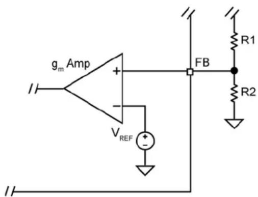
The MIC26603-ZA requires two resistors to set the output voltage, as shown in Figure 8.
The output voltage is determined by Equation 23:
$$ V _ {O U T} = V _ {F B} \times \left(1 + \frac {R 1}{R 2}\right) \tag {Eq.23} $$
where V_FB = 0.6V .
A typical value of R1 can be between 3kΩ and 10kΩ. If R1 is too large, it may allow noise to be introduced into the voltage feedback loop. If R1 is too small, it will decrease the efficiency of the power supply, especially at light loads. Once R1 is selected, R2 can be calculated using Equation 24.
$$ R 2 = \frac {V _ {\mathrm{FB}} \times 1 R}{V _ {\mathrm{OUT}} - V _ {\mathrm{FB}}} \tag {Eq.24} $$
text_image
gₘ Amp Vᵣₑᶠ FB R₁ R₂Figure 8. Voltage-Divider Configuration
In addition to the external ripple injection added at the FB pin, internal ripple injection is added at the inverting input of the comparator inside the MIC26603-ZA, as shown in Figure 9. The inverting input voltage V_INJ is clamped to 1.2V. As V_OUT increases, the swing of V_INJ is clamped. The clamped V_INJ reduces the line regulation because it is reflected as a DC error on the FB terminal. Therefore, the maximum output voltage of the MIC26603-ZA should be limited to 5.5V to avoid this problem.
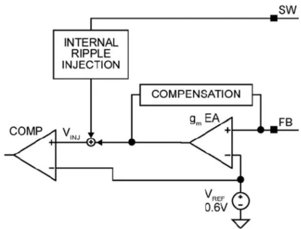
flowchart
graph TD
    A["COMP"] --> B["V_INJ"]
    B --> C["+"]
    D["INTERNAL RIPPLE INJECTION"] --> C
    E["COMPensation"] --> F["g_m EA"]
    F --> G["FB"]
    G --> H["V_REF 0.6V"]
    H --> I["Ground"]
    J["SW"] --> K["Switch"]
Figure 9. Internal Ripple Injection
Thermal Measurements
Measuring the IC's case temperature is recommended to ensure that it is within its operating limits. Although this might seem like an elementary task, it is easy to get false results. The most common mistake is to use the standard thermal couple that comes with a thermal meter. This thermal couple wire gauge is large, typically 22 gauge, and behaves like a heatsink, resulting in a lower case measurement.
Two methods of temperature measurement are using a smaller thermal couple wire or an infrared thermometer. If a thermal couple wire is used, it must be constructed of 36 gauge wire or higher (smaller wire size) to minimize the wire heat-sinking effect. In addition, the thermal couple tip must be covered in either thermal grease or thermal glue to make sure that the thermal couple junction is making good contact with the case of the IC. Omega brand thermal couple (5SC-TT-K-36-36) is adequate for most applications.
Wherever possible, an infrared thermometer is recommended. The measurement spot size of most infrared thermometers is too large for an accurate reading on a small form factor IC. However, an IR thermometer from Optris has a 1mm spot size, which makes it a good choice for measuring the hottest point on the case. An optional stand makes it easy to hold the beam on the IC for long periods of time.
PCB Layout Guidelines
Note: To minimize EMI and output noise, follow these layout recommendations.
PCB layout is critical to achieve reliable, stable, and efficient performance. A ground plane is required to control EMI and minimize the inductance in power, signal, and return paths.
Follow these guidelines to ensure proper MIC26603-ZA regulator operation:
IC
- A 2.2μF ceramic capacitor, which is connected to the PVDD pin, must be located right at the IC. The PVDD pin is very noise sensitive, so placement of the capacitor is critical. Use wide traces to connect to the PVDD and PGND pins.
- A 1μF ceramic capacitor must be placed right between VDD and the signal ground (SGND). SGND must be connected directly to the ground planes. Do not route the SGND pin to the PGND pad on the top layer.
- Place the IC close to the point-of-load (POL).
- Use fat traces to route the input and output power lines.
- Keep signal and power grounds separate and connected at only one location.
Input Capacitor
- Place the input capacitor next.
- Place the input capacitor on the same side of the board and as close to the IC as possible.
- Keep both the PVIN pin and PGND connections short.
- Place several vias to the ground plane close to the input capacitor ground terminal.
- Use either X7R or X5R dielectric input capacitors. Do not use Y5V or Z5U type capacitors.
- Do not replace the ceramic input capacitor with any other type of capacitor. Any type of capacitor can be placed in parallel with the input capacitor.
- If a Tantalum input capacitor is placed in parallel with the input capacitor, it must be recommended for switching regulator applications and the operating voltage must be derated by 50%.
- In "Hot-Plug" applications, a Tantalum or Electrolytic bypass capacitor must be used to limit the overvoltage spike seen on the input supply when power is suddenly applied.
Inductor
- Keep the inductor connection to the switch node (SW) short.
- Do not route any digital lines underneath or close to the inductor.
- Keep the switch node (SW) away from the feedback (FB) pin.
- Connect the CS pin directly to the SW pin to accurately sense the voltage across the low-side MOSFET.
- To minimize noise, place a ground plane underneath the inductor.
- The inductor can be placed on the opposite side of the PCB with respect to the IC. It does not matter whether the IC or inductor is on the top or bottom as long as there is enough air flow to keep the power components within their temperature limits. The input and output capacitors must be placed on the same side of the board as the IC.
Output Capacitor
- Use a wide trace to connect the output capacitor ground terminal to the input capacitor ground terminal.
- Phase margin changes as the output capacitor value and ESR changes. Contact the factory if the output capacitor is different from what is shown in the BOM.
- The feedback trace should be separate from the power trace and connected as near as possible to the output capacitor. Sensing a long high current load trace can degrade the DC load regulation.
Optional RC Snubber
- Place the RC snubber on either side of the board and as close to the SW pin as possible.
Evaluation Board Schematic
text_image
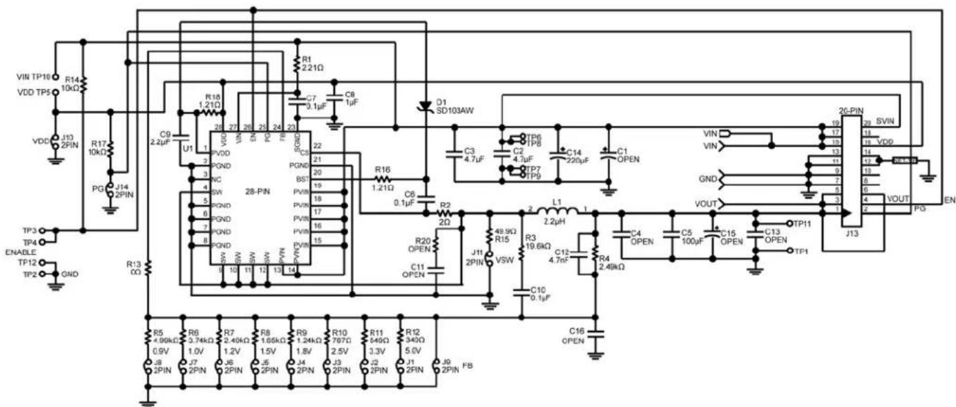
VIN TP10 R14 VDD TP5 10kΩ VDD J13 2PIN R17 10kΩ PG J14 2PIN TP3 TP4 ENABLE TF12 TP2 GND R13 CC R18 1.21Ω U1 20 27 26 25 24 23 C9 2.2μF PVDD PGND NC SW PGND PGND PGND 6 7 8 8 6 5 4 3 2 1 28-PIN 28-PIN 28-PIN 28-PIN 28-PIN 28-PIN 28-PIN 28-PIN 28-PIN 28-PIN 28-PIN 28-PIN 28-PIN 28-PIN 28-PIN 28-PIN 28-PIN 28-PIN 28-PIN 28-PIN 28-Pin C7 0.1μF C8 1μF D1 SD103AW C3 4.7μF TP6 P8 C2 4.7μF TP7 TP9 C14 220μF C1 OPEN VIN VIN GND VOUT VOUT J13 J11 2PIN R20 OPEN C11 OPEN R30 19.6kΩ VSW L1 2.2μH 1.1 μF R40 4.7nF 1.1 μF C40 OPEN 100μF 1.1 μF 1.1 μF 1.1 μF 1.1 μF 1.1 μF 1.1 μF 1.1 μF 1.1 μF 1.1 μF 1.1 μF 1.1 μF 1.1 μF 1.1 μF 1.1 μF 1.1 μF 1.1 μF 1.1 μF 1. R5 4.99kΩ R6 3.74kΩ R7 2.40kΩ R8 1.65kΩ R9 1.24kΩ R10 787Ω R11 349Ω R12 340Ω J5 0.9V J7 2PIN J6 2PIN J5 2PIN J4 2PIN J3 2PIN J2 2PIN J1 2PIN J0 2PIN FB C16 OPEN C5 100μF C5 100μF C5 100μF C5 100μF C5 100μF C5 100μF C5 100μF C5 100μF C5 100μF C5 100μF C5 100μF C5 100μF C5 100μF C5 3.74kΩ R7 2.40kΩ R8 1.65kΩ R9 1.24kΩ R10 787Ω R11 349Ω R12 340Ω J6 2PIN J5 2PIN J4 2PIN J3 2PIN J2 2PIN J1 2PIN J0 2PIN FB C6 0.1μF R6 3.74kΩ R7 2.40kΩ R8 1.65kΩ R9 1.24kΩ R10 787Ω R11 349Ω R12 340Ω J5 2PIN J4 2PIN J3 2PIN J2 2PIN J1 2PIN J0 2PIN FB C7 0.1μF C8 1μF D1 SD103AWFigure 10. Schematic of MIC26603-ZA Evaluation Board (J11, R13, R15 are for testing purposes)
Bill of Materials
| Item | Part Number | Manufacturer | Description | Qty. |
| C1 Open | ||||
| C2, C3 | 12105C475KAZ2A AVX | ^(8) | 4.7μF Ceramic Capacitor, X7R, Size 1210, 50V | 2 |
| GRM32ER71H475KA88L | Murata^(9) | |||
| C3225X7R1H475K TDK | ^(10) | |||
| C4, C13, C15 | Open | |||
| C5 | 12106D107MAT2A | AVX | 100μF Ceramic Capacitor, X5R, Size 1210, 6.3V | 1 |
| GRM32ER60J107ME20L | Murata | |||
| C3225X5R0J107M | TDK | |||
| C6, C7, C10 | 06035C104KAT2A | AVX | 0.1μF Ceramic Capacitor, X7R, Size 0603, 50V | 3 |
| GRM188R71H104KA93D | Murata | |||
| C1608X7R1H104K | TDK | |||
| C8 | 0603ZC105KAT2A | AVX | 1.0μF Ceramic Capacitor, X7R, Size 0603, 10V | 1 |
| GRM188R71A105KA61D | Murata | |||
| C1608X7R1A105K | TDK | |||
| C9 | 0603ZD225KAT2A | AVX | 2.2μF Ceramic Capacitor, X5R, Size 0603, 10V | 1 |
| GRM188R61A225KE34D | Murata | |||
| C1608X5R1A225K | TDK | |||
| C12 | 06035C472KAZ2A | AVX | 4.7nF Ceramic Capacitor, X7R, Size 0603, 50V | 1 |
| GRM188R71H472K | Murata | |||
| C1608X7R1H472K | TDK | |||
| C14 | B41851F7227M | EPCOS^(11) | 220μF Aluminum Capacitor, 35V | 1 |
| C11, C16 | Open | |||
| D1 | SD103AWS | MCC^(12) | 40V, 350mA, Schottky Diode, SOD323 | 1 |
| SD103AWS-7 | Diodes Inc. ^(13) | |||
| SD103AWS | Vishay^(14) | |||
| L1 | HCF1305-2R2-R | Cooper Bussmann ^(15) | 2.2μH Inductor, 15A Saturation Current | 1 |
| R1 | CRCW06032R21FKEA | Vishay Dale | 2.21Ω Resistor, Size 0603, 1% | 1 |
| R2 | CRCW06032R00FKEA | Vishay Dale | 2.00Ω Resistor, Size 0603, 1% | 1 |
| R3 | CRCW060319K6FKEA | Vishay Dale | 19.6kΩ Resistor, Size 0603, 1% | 1 |
| R4 | CRCW06032K49FKEA | Vishay Dale | 2.49kΩ Resistor, Size 0603, 1% | 1 |
| R5 | CRCW06034K99FKEA | Vishay Dale | 4.99kΩ Resistor, Size 0603, 1% | 1 |
Notes:
- AVX: www.avx.com.
- Murata: www.murata.com.
- TDK: www.tdk.com.
- EPCOS: www.epcos.com.
- MCC: www.mccsemi.com.
- Diodes Inc.: www.diodes.com.
- Vishay: www.vishay.com.
- Cooper Bussmann: www.cooperbussmann.com.
Bill of Materials (Continued)
| Item | Part Number | Manufacturer | Description | Qty. |
| R6 | CRCW06033K74FKEA | Vishay Dale | 3.74kΩ Resistor, Size 0603, 1% | 1 |
| R7 | CRCW06032K49FKEA | Vishay Dale | 2.49kΩ Resistor, Size 0603, 1% | 1 |
| R8 | CRCW06031K65FKEA | Vishay Dale | 1.65kΩ Resistor, Size 0603, 1% | 1 |
| R9 | CRCW06031K24FKEA | Vishay Dale | 1.24kΩ Resistor, Size 0603, 1% | 1 |
| R10 | CRCW0603787RFKEA | Vishay Dale | 787Ω Resistor, Size 0603, 1% | 1 |
| R11 | CRCW0603549RFKEA | Vishay Dale | 549Ω Resistor, Size 0603, 1% | 1 |
| R12 | CRCW0603340RFKEA | Vishay Dale | 340Ω Resistor, Size 0603, 1% | 1 |
| R13 | CRCW06030000FKEA | Vishay Dale | 0Ω Resistor, Size 0603, 5% | 1 |
| R14, R17 | CRCW060310K0FKEA | Vishay Dale | 10.0kΩ Resistor, Size 0603, 1% | 2 |
| R15 | CRCW060349R9FKEA | Vishay Dale | 49.9Ω Resistor, Size 0603, 1% | 1 |
| R16, R18 | CRCW06031R21FKEA | Vishay Dale | 1.21Ω Resistor, Size 0603, 1% | 2 |
| R20 | Open | |||
| U1 | MIC26603-ZAYJL | Micrel. Inc. ^(16) | 28V, 6A Hyper Speed Control Synchronous DC-to-DC Buck Regulator | 1 |
Note:
16. Micrel, Inc.: www.micrel.com.
PCB Layout Recommendations
text_image
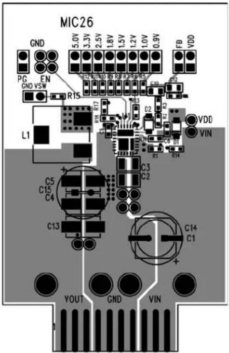
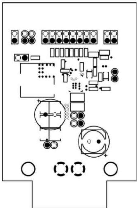
MIC26 GND 5.0V 3.3V 2.5V 1.8V 1.5V 1.2V 1.0V 0.9V FB VDD PG EN GND VSW R15 R12 R10 R9 R8 R7 R6 R5 C10 R12 L1 R18 R17 R13 R12 R10 R9 R8 R7 R6 R5 C2 C14 C13 C3 C2 C5 C15 C4 + - YOUT GND VINMIC26603-ZA Evaluation Board Top Layer
natural_image
Pure electrical circuit lines without any symbolsMIC26603-ZA Evaluation Board Mid-Layer 1 (Ground Plane)
PCB Layout Recommendations (Continued)

natural_image
Pure electrical circuit lines without any symbolsMIC26603-ZA Evaluation Board Mid-Layer 2

text_image
EM26903-9A-PWBFMIC26603-ZA Evaluation Board Bottom Layer
Package Information and Recommended Land Pattern ^(17)
text_image
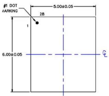
#1 DOT MARKING 5.00±0.05 28 1 6.00±0.05 ETOP VIEW NOTE 1, 2, 3

text_image
0.400±0.050 3.700±0.050 Exp.DAP P/N #1 IDENTIFICATION R0.100 1.600±0.025 Exp.DAP 0.350 0.400 2.950±0.050 Exp.DAP 0.650 Bsc 0.300±0.050 0.575 0.150 1.400±0.050 Exp.DAP 0.600 0.350 2.200±0.050 Exp.DAPBOTTOM VIEW NOTE 1, 2, 3
text_image
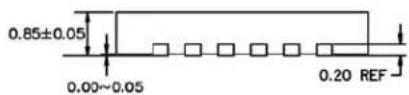
0.85±0.05 0.00~0.05 0.20 REFSIDE VIEW NOTE 1, 2, 3
text_image
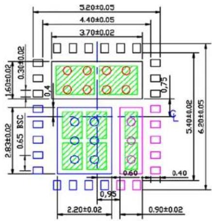
5.20±0.05 4.40±0.05 3.70±0.02 1.60±0.02 0.30±0.02 0.4 0.75 2.83±0.02 0.65 BSC 5.40±0.02 6.20±0.05 0.60 0.40 0.95 2.20±0.02 0.90±0.02RECOMMENDED LAND PATTERN
NOTE: 4.5
NOTE:
1. MAX PACKAGE WARPAGE IS 0.05 MM
2. MAX ALLOWABLE BURR IS 0.076MM IN ALL DIRECTIONS
3. PIN #1 IS ON TOP WILL BE LASER MARKED
4. RED CIRCLES IN LAND PATTERN REPRESENT THERMAL VIA & SHOULD BE CONNECTED TO GND FOR MAXIMUM PERFORMANCE.
5. GREEN RECTANGLES (SHADED AREA) REPRESENT SOLDER STENCIL OPENING ON EXPOSED PAD AREA
6. BLUE COLORED PADS & PURPLE COLORED PADS REPRESENT DIFFERENT POTENTIALS. DO NOT CONNECT TO GND.
7. RECOMMENDED SOLDER STENCIL OPENING AND VIA SIZES
28-Pin 5mm × 6mm QFN (JL)
Note:
- Package information is correct as of the publication date. For updates and most current information, go to www.micrel.com.
MICREL, INC. 2180 FORTUNE DRIVE SAN JOSE, CA 95131 USA
TEL +1 (408) 944-0800 FAX +1 (408) 474-1000 WEB http://www.micrel.com
Micrel makes no representations or warranties with respect to the accuracy or completeness of the information furnished in this data sheet. This information is not intended as a warranty and Micrel does not assume responsibility for its use. Micrel reserves the right to change circuitry, specifications and descriptions at any time without notice. No license, whether express, implied, arising by estoppel or otherwise, to any intellectual property rights is granted by this document. Except as provided in Micrel's terms and conditions of sale for such products, Micrel assumes no liability whatsoever, and Micrel disclaims any express or implied warranty relating to the sale and/or use of Micrel products including liability or warranties relating to fitness for a particular purpose, merchantability, or infringement of any patent, copyright or other intellectual property right.
Micrel Products are not designed or authorized for use as components in life support appliances, devices or systems where malfunction of a product can reasonably be expected to result in personal injury. Life support devices or systems are devices or systems that (a) are intended for surgical implant into the body or (b) support or sustain life, and whose failure to perform can be reasonably expected to result in a significant injury to the user. A Purchaser's use or sale of Micrel Products for use in life support appliances, devices or systems is a Purchaser's own risk and Purchaser agrees to fully indemnify Micrel for any damages resulting from such use or sale.
© 2013 Micrel, Incorporated.