MCP16362 - Electronic component Microchip - Free user manual and instructions
Find the device manual for free MCP16362 Microchip in PDF.

User questions about MCP16362 Microchip
0 question about this device. Answer the ones you know or ask your own.
Ask a new question about this device
Download the instructions for your Electronic component in PDF format for free! Find your manual MCP16362 - Microchip and take your electronic device back in hand. On this page are published all the documents necessary for the use of your device. MCP16362 by Microchip.
USER MANUAL MCP16362 Microchip
48V Input, 3A Output, 2.2 MHz Switching Frequency, Integrated Switch Step-Down Regulator
Features
- Input Voltage Range: 4.0V to 48V
- Adjustable Output Voltage Range: 2.0V to 24V
- Integrated N-Channel Buck Switch: 100 mΩ
- 3A Output Current
• 2.2 MHz Fixed Frequency - Shutdown Current: 5 A typical
- Quiescent Current: 18~ A typical (not switching)
• Device Selectable Switching Mode
- Automatic Pulse Frequency Modulation/Pulse Width Modulation (PFM/PWM) Operation - MCP16361
- PWM only Mode of Operation - MCP16362
- PWM only Mode of Operation with Switching Frequency Dithering for EMI constrained applications - MCP16363
- Power Good Output
• Undervoltage Lockout (UVLO)
• Peak Current Mode Control - Internal Compensation
- Internal Soft-Start
- Internal Bootstrap Diode
• Cycle-by-Cycle Peak Current Limit
• Overtemperature Protection
• Available Package: 8-lead 3x3 mm wettable flanks VDFN (see Package Type)
• Passes Automotive AEC-Q100 Reliability Testing
Applications
• Automotive DC/DC and 48V Systems
- Microcontroller Bias Supply
• 24V Industrial Input DC-DC Conversion
- Set-Top Boxes, DSL Cable Modems
• Wall Cube Regulation
• SLA Battery-Powered Devices
• AC-DC Digital Control Power Sources
- Power Meters
• Medical and Health Care
• Distributed Power Supplies
General Description
The MCP16361/2/3 family of devices are highly integrated, high-efficiency, fixed-frequency, step-down DC-DC converters in a compact 8-lead 3x3 mm VDFN package that operates from input voltage sources up to 48V. Integrated features include a high-side switch, fixed-frequency Peak Current Mode Control, Internal Compensation, Power Good, Peak Current Limit and Overtemperature Protection. The MCP16361/2/3 provides all the active functions for local DC-DC conversion, with fast transient response and accurate regulation.
High efficiency conversion is achieved by integrating the current-limited, low-resistance, high-speed N-Channel MOSFET and associated drive circuitry. High switching frequency minimizes the size of external filtering components resulting in a small size solution.
The MCP16361/2/3 can supply 3A of continuous current while regulating the output voltage from 2.0V to 24V. An integrated, high-performance peak current mode architecture keeps the output voltage tightly regulated, even during input voltage steps and output current transient conditions that are common in power systems.
The MCP16361 is capable of running in PFM/PWM mode. It switches in PFM mode for light load conditions and for large buck conversion ratios. This results in a higher efficiency over all load ranges.
By comparison, the MCP16362 runs in PWM-only mode, and is recommended for applications in which the low-frequency component associated with PFM mode of operation is not desirable.
Besides the two aforementioned options, the MCP16363 is designed for EMI constrained applications where reduced peak emissions are required. This is achieved by sweeping the switching frequency over a 10% range above the 2.2 MHz nominal value.
Output voltage is set with an external resistor divider. The Power Good output pin will go from logic low to logic high (through an external pull-up resistor) once the output voltage is within 93% of the nominal set point. The EN input is used to turn the device on and off. While off, only a few micro-amps of current are consumed from the input.
The MCP16361/2/3 is offered in a space-saving 8-lead 3x3 mm VDFN wettable flanks surface mount package. The MCP16361/2/3 also passes automotive AEC-Q100 reliability testing.
Package Type
MCP16361/2/3
8-Lead 3x3 VDFN
(Top View)
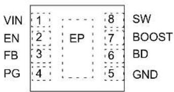
text_image
VIN 1 EN 2 EP 8 SW FB 3 7 BOOST PG 4 6 BD GND* Includes Exposed Thermal Pad (EP); see Table 4-1.
Functional Block Diagram

text_image
VIN CIN VOUT RTOP RBOT FB VREF EN GND BG REF VREG SS VREF OTEMP + Amp - RCOMP CCOMP PFM CTR SHDN all blocks 0.93 x VREF FB 2.2 MHz OSC S PWM Latch R Boost Pre Charge HS Drive CS RSENSE Slope Comp BD BOOST SW CBOOST L Schottky Diode COUT PG VOUTTypical Application Circuit

line
| IOUT (A) | Efficiency (%) - MCP16361 | Efficiency (%) - MCP16362 | |----------|---------------------------|---------------------------| | 0.0001 | ~30 | ~0 | | 0.001 | ~70 | ~10 | | 0.01 | ~80 | ~40 | | 0.1 | ~85 | ~60 | | 1 | ~90 | ~75 | | 10 | ~85 | ~80 | | 100 | ~85 | ~85 | | 2 | ~85 | ~85 | | 22 | ~85 | ~85 | | 3 | ~85 | ~85 | | 33 | ~85 | ~85 | | 31.6 | ~85 | ~85 | | 330 | ~85 | ~85 | | 330 nF | ~85 | ~85 | | L1 | ~85 | ~85 | | 1.5 μH | ~85 | ~85 | | 1.5 μH | ~85 | ~85 | | 1.5 μH | ~85 | ~85 | | 1.5 μH | ~85 | ~85 | | 1.5 μH | ~85 | ~85 | | 1.5 μH | ~85 (CBOOST) | ~85 (CBOOST) | | 1.5 μH | ~85 (SCHOTTKY Diode) | ~85 (SCHOTTKY Diode) | | 1.5 μH | ~85 (FB) | ~85 (FB) | | 1.5 μH | ~85 (PG) | ~85 (PG) | | 1.5 μH | ~85 (PG) | ~85 (PG) | | 1.5 μH | ~85 (PG) | ~85 (PG) | | 1.5 μH | ~85 (PG) | ~85 (PG) | | 1.5 μH | ~85 (PG) | ~85 (GND) | | 1.5 μH | ~85 (PG) | ~85 (PG) | | 1.5 μH | ~85 (PG) | ~85 (PG) | | 1.5 μH | ~85 (PG) | ~85 (PG) | | 1.5 μH | ~85 (PG) | ~85 (PG) | | 1.5 μH | ~85 (PG) | ~85 (PG) | | 1.5 μH | ~85 (PG) | ~85 (PG) | | 1.5 μH | ~85 (PG) | ~85 (PG) | | 1.5 μH | ~85 (PG) | ~85 (PG) / PG | | 1.5 μH | ~85 (PG) | ~85 (PG) / PG | | 1.5 μH | ~85 (PG) | ~85 (PG) / PG | | 1.5 μH | ~85 (PG) | ~85 (PG) / PG | | 1.5 μH | ~85 (PG) | VOUT @ 3A | | 1.5 μH | ~85 (PG) | VOUT @ 3A | | 1.5 μH | ~85 (PG) | VOUT @ 3A | | 1.5 μH | ~85 (PG) | VOUT @ 3A | | 1.5 μH | ~85 (PG) | VOUT @ 3A / PG | | 1.5 μH | ~85 (PG) | VOUT @ 3A / PG | | 1.5 μH | ~85 (PG) | VOUT @ 3A / PG | | 1.5 μH | ~85 (PG) | VOUT @ 3A / PG | | 1.5 μH | ~85 (PG) | SOUT @ 22 μF | | 1.5 μH | ~85 (PG) | SOUT @ 22 μF | | 1.5 μH | ~85 (PG) | SOUT @ 22 μF | | 1.5 μH | ~85 (PG) | SOUT @ 22 μF | | 1.5 μH | ~85 (PG) | VOUT @ 3A | | 1.5 μH | ~85 (PG) | VOUT @ 3A | | 1.5 μH | ~85 (PG) | VOUT @ 3A | | 1.5 μH | ~85 (PG) | VOUT @ 3 A | | 1.5 μH | ~85 (PG) | VOUT @ 3 A | | 1.5 μH | ~85 (PG) | VOUT @ 3 A | | 1.5 μH | ~85 (PG) | VOUT @ 3 A | | 1.5 μH | ~85 (PG) | VOUT @ 3 A / PG | | 1.000 | ~80 | - | | - | - | - | | - | - | - | | - | - | - | | - | - | - | | - | - | - | | - | - | - | | - | - | - | | - | - | - | | - | - | - | | - | - | - | | - | - | - | | - | - | - | | - | - | - | | - | - | - | | - | - | - | | - | - | - | | - | - | - | | - | - | - | | - | - | - | | - | - | - | | - | -20 | - | | - | -20 | - | | - | -20 | - | | - | -20 | - | | - | -20 | - | | - | -20 | - | | - | -20 | - | | - | -20 | - | | - | -20 | - | The diagram contains two sections: Top section: 'VIN' and 'SW' components; Bottom section: 'VD' and 'IN'. The top section includes 'VD' and 'IN' labels, each associated with an input voltage and output voltage.1.0 ELECTRICAL CHARACTERISTICS
Absolute Maximum Ratings †
| VIN, SW | -0.5V to 53V |
| BOOST – GND | -0.5V to 60V |
| BOOST – SW Voltage | -0.5V to 5.5V |
| FB, DB | -0.5V to 5.5V |
| PG, EN | -0.5V to ( V_IN + 0.3V) |
| Storage Temperature | -65°C to +150°C |
| Operating Junction Temperature | -40°C to +125°C |
ESD Protection on All Pins †
| HBM | 1 kV |
| CDM | 2 kV |
† Notice: Stresses above those listed under "Maximum Ratings" may cause permanent damage to the device. This is a stress rating only and functional operation of the device at those or any other conditions above those indicated in the operational sections of this specification is not intended. Exposure to maximum rating conditions for extended periods may affect device reliability.
DC CHARACTERISTICS
| Electrical Characteristics: Unless otherwise indicated, T_A = T_J = +25°C , V_IN = V_EN = 12V , V_BOOST - V_SW = 3.3V , V_OUT = 3.3V , I_OUT = 100 mA , L = 1.5 μH , C_IN = 2 x 10 μF X7R Ceramic Capacitors , C_OUT = 2 x 22 μF X7R Ceramic Capacitors . Boldface specifications apply over the T_J range of -40°C to +125°C . | ||||||
| Parameters Symbol | Min. Typ. Max. Units | Conditions | ||||
| Input Voltage V | IN | 4 | — | 48 | V | Note 1 |
| Feedback Voltage | V_FB | 0.784 | 0.800 | 0.816 | V | V_IN = 8V |
| Output Voltage Adjust Range | V_OUT | 2 | — | 24 | V | Note 2, Note 4 |
| Feedback Voltage Line Regulation | ( V_FB/V_FB)/ V_IN | — 0.01 | — | %/V | MCP16362, V_IN = 5V to 16V (Note 4) | |
| Feedback Voltage Load Regulation | ( V_FB/V_FB) | — | 0.3 | — | %/V | MCP16362, I_OUT = 10 mA to 3A (Note 4) |
| Feedback Input Bias Current | I_FB | — | +/- 10 | — | nA | — |
| Undervoltage Lockout Start | UVLO _STRT | 3.75 | 4 | 4.2 | V | V_IN Rising |
| Undervoltage Lockout Stop | UVLO _STOP | 3.3 | 3.4 | 3.6 | V | V_IN Falling |
| Undervoltage Lockout Hysteresis | UVLO _HYS | — | 0.5 | — | V | — |
| Switching Frequency | f_SW | 1.9 | 2.2 | 2.6 | MHz | MCP16361/2, I_OUT = 250 mA |
| Switching Frequency Dithering | f_SW,dither | — | +10 | — | % | MCP16363 |
| Maximum Duty Cycle | DC_MAX | — | 87 | — | % | Note 4 |
| Minimum On Time | Ton_MIN | — | 100 | — | ns | Note 4 |
| NMOS Switch On Resistance | R_DS(ON) | — | 0.1 | — | Ω | V_BOOST - V_SW = 3.3V (Note 4) |
| NMOS Switch Current Limit | I_N(MAX) | — | 4.5 | — | A | V_BOOST - V_SW = 3.3V , (Note 4) |
Note 1: The input voltage should be > output voltage + headroom voltage; higher load currents increase the input voltage necessary for regulation. See characterization graphs for typical input to output operating voltage range.
2: For the conditions explained in Section 6.7 "Input Voltage Limitations".
3: V_BOOST supply is derived from V_OUT .
4: Determined by characterization, not production tested.
DC CHARACTERISTICS
| Electrical Characteristics: Unless otherwise indicated, T_A = T_J =+25°C, V_IN = V_EN =12V, V_BOOST - V_SW =3.3V, V_OUT =3.3V, I_OUT =100 mA, L=1.5 μH, C_IN =2 x 10 μF X7R Ceramic Capacitors, C_OUT =2 x 22 μF X7R Ceramic Capacitors. Boldface specifications apply over the T_J range of -40°C to +125°C. | ||||||
| Parameters | Symbol | Min. | Typ. | Max. | Units | Conditions |
| Quiescent Current - PWM I | Q,PWM | —2 | 3.8 mA | V_BOOST =3.3V; MCP16362 Switching | ||
| Quiescent Current - PFM I | Q,PFM | —65 | 135 μA | V_BOOST =3.3V; MCP16361 Switching | ||
| Quiescent Current - PFM - Non-Switching | IQ | —18 | 24 μA | V_BOOST =3.3V; MCP16361 Non-Switching | ||
| Quiescent Current - Shutdown I | Q,SHD | —3 | 5 μA V | OUT =EN=0V | ||
| EN Input Logic High V | IH | 1.8 | — | — | V | — |
| EN Input Logic Low | V_IL | — | — | 0.4 | V | — |
| EN Input Leakage Current | I_ENLK | —0.1 | 0.15 | μA V | EN =12V | |
| Soft-Start Time | t_SS | — | 750 | — μs | EN Low to High, 90% of V_OUT (Note 4) | |
| Power Good Threshold | V_PG | 89 | 93 | 97 | % | — |
| Power Good Hysteresis | V_PG,hyst | —3 | — | % | — | |
| Power Good Blanking | PG_Blanking | —55 | 57 μs | — | ||
| Thermal Shutdown Die Temperature | T_SD | — | 155 | — | °C | Note 4 |
| Die Temperature Hysteresis | T_SDHYS | —25 | — | °C — | ||
Note 1: The input voltage should be > output voltage + headroom voltage; higher load currents increase the input voltage necessary for regulation. See characterization graphs for typical input to output operating voltage range.
2: For the conditions explained in Section 6.7 "Input Voltage Limitations".
3: V_BOOST supply is derived from V_OUT .
4: Determined by characterization, not production tested.
TEMPERATURE SPECIFICATIONS
| Parameters | Symbol | Min. | Typ. | Max. | Units | Conditions |
| Temperature Ranges | ||||||
| Operating Junction Temperature Range | T_J | -40 | — | +125 | °C | Steady State |
| Storage Temperature Range | T_A | -65 | — | +150 | °C | — |
| Maximum Junction Temperature | T_J | — | — | +150 | °C | Transient |
| Package Thermal Resistances | ||||||
| Thermal Resistance, 8-lead 3x3 VDFN | _JA | — | 52.5 | — | °C/W | — |
2.0 TYPICAL PERFORMANCE CURVES
Note: The graphs and tables provided following this note are a statistical summary based on a limited number of samples and are provided for informational purposes only. The performance characteristics listed herein are not tested or guaranteed. In some graphs or tables, the data presented may be outside the specified operating range (e.g., outside specified power supply range) and therefore outside the warranted range.
Note: Unless otherwise indicated: T_A=+25^ , V_IN=V_EN=12V , V_BOOST-V_SW=5V , V_OUT=5V , I_OUT=100mA , L=2.2 H , C_IN=2×10 F X7R Ceramic Capacitors, C_OUT=2×22 F X7R Ceramic Capacitors.

line
| IOUT (A) | MCP16361 Efficiency (%) | MCP16362 Efficiency (%) | | -------- | ------------------------ | ------------------------ | | 0.0001 | ~30 | ~0 | | 0.001 | ~70 | ~5 | | 0.1 | ~80 | ~20 | | 0.01 | ~85 | ~50 | | >0.01 | ~90 | ~80 |FIGURE 2-1: 3.3V V OUT Efficiency vs. IOUT.
line
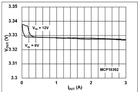
| I_OUT (A) | V_OUT (V) | | --------- | --------- | | 0 | 3.34 | | 0.5 | 3.33 | | 1 | 3.33 | | 2 | 3.33 | | 3 | 3.33 |FIGURE 2-4: 3.3V V OUT vs. I_OUT .

line
| Iout (A) | Efficiency (%) - MCP16361 | Efficiency (%) - MCP16362 | | -------- | -------------------------- | -------------------------- | | 0.0001 | ~35 | ~0 | | 0.001 | ~70 | ~10 | | 0.01 | ~80 | ~40 | | 0.1 | ~85 | ~70 | | 1 | ~90 | ~85 |FIGURE 2-2: 5V V OUT Efficiency vs. I_OUT .
line
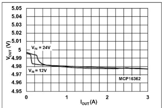
| IOUT (A) | VOUT (V) | | -------- | -------- | | 0 | 5.00 | | 0.5 | 4.99 | | 1.0 | 4.98 | | 1.5 | 4.98 | | 2.0 | 4.98 | | 2.5 | 4.98 | | 3.0 | 4.98 |FIGURE 2-5: 5V V OUT vs. IOUT.

line
| I_OUT (A) | MCP16361 Efficiency (%) | MCP16362 Efficiency (%) | | --------- | ------------------------ | ------------------------ | | 0.0001 | ~35 | ~5 | | 0.001 | ~70 | ~15 | | 0.01 | ~80 | ~40 | | 0.1 | ~90 | ~70 | | 1 | ~95 | ~85 |FIGURE 2-3: 12V V OUT Efficiency vs. IOUT.

line
| I_OUT (A) | V_OUT (V) | | --------- | --------- | | 0 | 12.04 | | 1 | 12.02 | | 2 | 12.02 | | 3 | 12.02 |FIGURE 2-6: 12V V OUT vs. IOUT.
Note: Unless otherwise indicated, T_A = +25^ , V_IN = V_EN = 12V , V_BOOST - V_SW = 5V , V_OUT = 5V , I_OUT = 100 mA , L = 2.2 , C_IN = 2× 10 X7R Ceramic Capacitors, C_OUT = 2× 22 X7R Ceramic Capacitors.
line
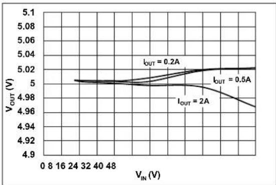
| VIN (V) | VOUT (V) for IOUT = 0.2A | VOUT (V) for IOUT = 0.5A | VOUT (V) for IOUT = 2A | | ------- | ------------------------ | ------------------------ | ---------------------- | | 0 | 5.0 | 5.0 | 5.0 | | 16 | 5.0 | 5.0 | 5.0 | | 24 | 5.0 | 5.0 | 5.0 | | 32 | 5.0 | 5.0 | 5.0 | | 40 | 5.0 | 5.0 | 5.0 | | 48 | 5.0 | 5.0 | 5.0 | | >48 | ~5.0 | ~5.0 | ~4.98 |FIGURE 2-7: V
OUT vs. V_IN

line
| Temperature (°C) | Switch R_DSON (Ω) | | ---------------- | ----------------- | | -40 | 0.08 | | -25 | 0.09 | | -10 | 0.10 | | 5 | 0.11 | | 20 | 0.12 | | 35 | 0.13 | | 50 | 0.14 | | 65 | 0.15 | | 80 | 0.16 | | 95 | 0.17 | | 110 | 0.18 | | 125 | 0.19 |FIGURE 2-10: Switch R
DSON VS.
Temperature.
line
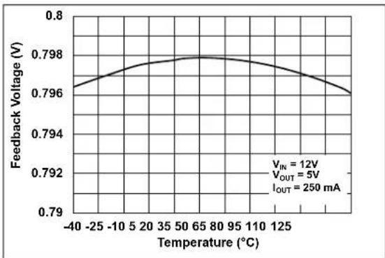
| Temperature (°C) | Feedback Voltage (V) | | ---------------- | -------------------- | | -40 | 0.796 | | -25 | 0.797 | | -10 | 0.7975 | | 5 | 0.798 | | 20 | 0.798 | | 35 | 0.798 | | 65 | 0.798 | | 80 | 0.798 | | 95 | 0.798 | | 110 | 0.7975 | | 125 | 0.7965 |FIGURE 2-8: V
F B vs. Temperature.

line
| VIN (V) | Switch RDSON (Ω) | | ------- | ---------------- | | 2.5 | 0.12 | | 3.5 | 0.10 | | 4.5 | 0.09 | | 5.5 | 0.08 |FIGURE 2-11: Switch R
DSON vs. V_BOOST
line
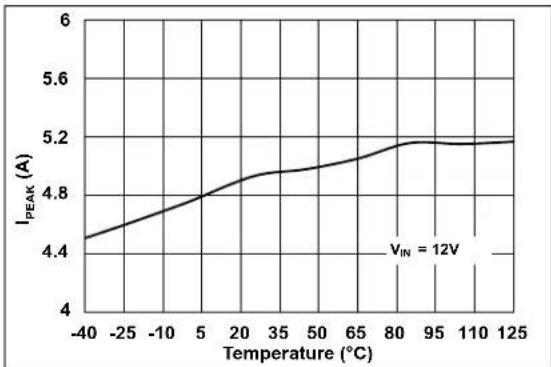
| Temperature (°C) | I_PEAK (A) | | ---------------- | ---------- | | -40 | 4.4 | | -25 | 4.6 | | -10 | 4.7 | | 5 | 4.8 | | 20 | 4.9 | | 35 | 5.0 | | 50 | 5.1 | | 65 | 5.2 | | 80 | 5.2 | | 95 | 5.2 | | 110 | 5.2 | | 125 | 5.2 |FIGURE 2-9: Peak Current Limit vs. Temperature.

line
| Temperature (°C) | START | STOP | | ---------------- | ----- | ---- | | -40 | 4.0 | 3.5 | | -25 | 4.0 | 3.5 | | -10 | 4.0 | 3.5 | | 5 | 4.0 | 3.5 | | 20 | 4.0 | 3.5 | | 35 | 4.0 | 3.5 | | 50 | 4.0 | 3.5 | | 65 | 4.0 | 3.5 | | 80 | 4.0 | 3.5 | | 95 | 4.0 | 3.5 | | 110 | 4.0 | 3.5 | | 125 | 4.0 | 3.5 |FIGURE 2-12: Undervoltage Lockout vs. Temperature.
Note: Unless otherwise indicated, T_A = +25^ , V_IN = V_EN = 12V , V_BOOST - V_SW = 5V , V_OUT = 5V , I_OUT = 100 mA , L = 2.2 H , C_IN = 2 × 10 F X7R Ceramic Capacitors, C_OUT = 2 × 22 F X7R Ceramic Capacitors.
line
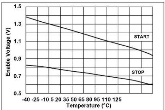
| Temperature (°C) | ENABLE VOLTAGE (V) | | ---------------- | ------------------ | | -40 | 1.35 | | -25 | 1.30 | | -10 | 1.25 | | 5 | 1.20 | | 20 | 1.15 | | 35 | 1.10 | | 50 | 1.05 | | 65 | 1.00 | | 80 | 0.95 | | 95 | 0.90 | | 110 | 0.85 | | 125 | 0.80 |FIGURE 2-13: EN Threshold Voltage vs. Temperature.

line
| Input Voltage (V) | No Load Input Current (µA) | | ----------------- | -------------------------- | | 5 | 110 | | 10 | 70 | | 15 | 55 | | 20 | 45 | | 25 | 40 | | 30 | 38 |FIGURE 2-16: No Load Input Current vs. V_IN , MCP16361.
line
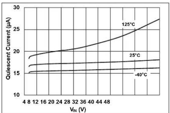
| VIN (V) | 125°C | 25°C | -40°C | | ------- | ----- | ---- | ----- | | 4 | 18.5 | 16.5 | 15.0 | | 8 | 19.0 | 16.8 | 15.2 | | 12 | 19.5 | 17.0 | 15.3 | | 16 | 20.0 | 17.2 | 15.4 | | 20 | 20.5 | 17.3 | 15.5 | | 24 | 21.0 | 17.4 | 15.6 | | 28 | 21.5 | 17.5 | 15.7 | | 32 | 22.0 | 17.6 | 15.8 | | 36 | 22.5 | 17.7 | 15.9 | | 40 | 23.0 | 17.8 | 16.0 | | 44 | 23.5 | 17.9 | 16.1 | | 48 | 24.0 | 18.0 | 16.2 | | | | | | | | | | | | | | | | | | | | | | | | | | | | | | | | | | | | | | | | | | | | | | | | | | | | | | | | | | | | |FIGURE 2-14: Input Quiescent Current vs. V_IN .
line
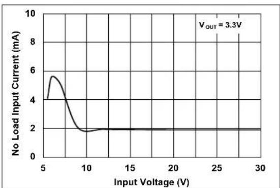
| Input Voltage (V) | No Load Input Current (mA) | | ----------------- | -------------------------- | | 5 | 4.0 | | 6 | 5.5 | | 7 | 4.5 | | 8 | 3.0 | | 9 | 2.0 | | 10 | 1.8 | | 15 | 2.0 | | 20 | 2.0 | | 25 | 2.0 | | 30 | 2.0 |FIGURE 2-17: No Load Input Current vs. V_IN , MCP16362.

FIGURE 2-15: Shutdown Current vs. V IN.
line
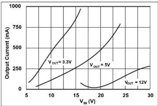
| V_IN (V) | Output Current (mA) | | -------- | ------------------- | | 3.3 | ~100 | | 5 | ~250 | | 12 | ~500 | | 25 | ~750 | | 30 | ~1000 |FIGURE 2-18: PFM/PWM Threshold.
Note: Unless otherwise indicated, T_A = +25^ , V_IN = V_EN = 12V , V_BOOST - V_SW = 5V , V_OUT = 5V , I_OUT = 100 mA , L = 2.2 H , C_IN = 2× 10 F X7R Ceramic Capacitors, C_OUT = 2× 22 F X7R Ceramic Capacitors.
line
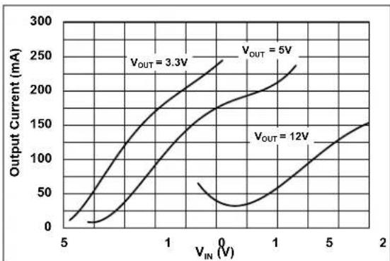
| V_IN (V) | Output Current (mA) at V_OUT = 3.3V | Output Current (mA) at V_OUT = 5V | Output Current (mA) at V_OUT = 12V | | -------- | ----------------------------------- | --------------------------------- | ---------------------------------- | | 5 | ~10 | ~10 | ~10 | | 1 | ~150 | ~175 | ~60 | | 2 | ~250 | ~240 | ~150 |FIGURE 2-19: PWM/Skipping Threshold.
line
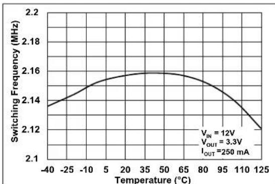
| Temperature (°C) | Switching Frequency (MHz) | | ---------------- | ------------------------- | | -40 | 2.14 | | -25 | 2.15 | | 0 | 2.16 | | 25 | 2.16 | | 50 | 2.16 | | 75 | 2.16 | | 100 | 2.15 | | 125 | 2.12 |FIGURE 2-22: Switching Frequency vs. Temperature.
line
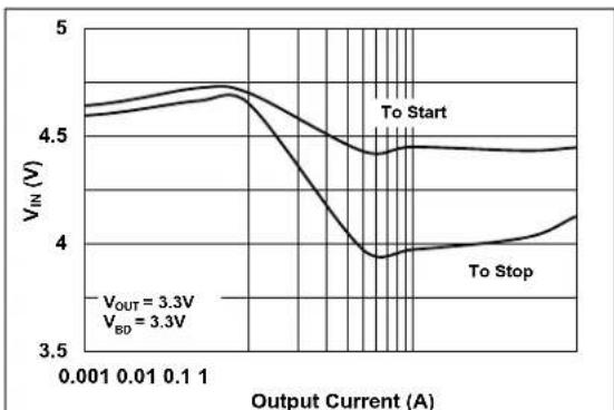
| Output Current (A) | V_IN (V) | | ------------------ | -------- | | 0.001 | 4.6 | | 0.01 | 4.7 | | 0.1 | 4.8 | | 0.11 | 4.7 | | 0.12 | 4.6 | | 0.13 | 4.5 | | 0.14 | 4.4 | | 0.15 | 4.3 | | 0.16 | 4.2 | | 0.17 | 4.1 | | 0.18 | 4.0 | | 0.19 | 3.9 | | 0.20 | 3.8 | | 0.21 | 3.9 | | 0.22 | 4.0 | | 0.23 | 4.1 | | 0.24 | 4.2 | | 0.25 | 4.3 | | 0.26 | 4.4 | | 0.27 | 4.5 | | 0.28 | 4.6 | | 0.29 | 4.7 | | 0.30 | 4.8 | | 0.31 | 4.9 | | 0.32 | 5.0 |FIGURE 2-20: Minimum Input Voltage vs. Output Current.

line
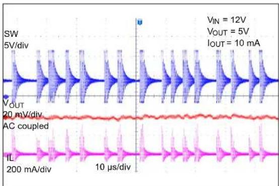
| Parameter | Value | | --------- | --------- | | V_IN | 12V | | V_OUT | 5V | | I_OUT | 3A |FIGURE 2-23: Heavy Load Switching Waveforms.
line
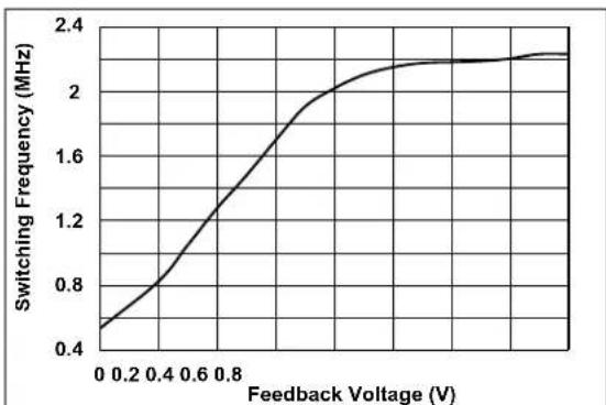
| Feedback Voltage (V) | Switching Frequency (MHz) | | -------------------- | ------------------------- | | 0.0 | 0.5 | | 0.2 | 0.7 | | 0.4 | 1.0 | | 0.6 | 1.4 | | 0.8 | 1.8 | | 1.0 | 2.0 | | 1.2 | 2.2 | | 1.4 | 2.3 | | 1.6 | 2.3 | | 1.8 | 2.3 | | 2.0 | 2.3 | | 2.2 | 2.3 | | 2.4 | 2.3 |FIGURE 2-21: Switching Frequency vs. Feedback Voltage.

line
| Parameter | Value | | --------------- | --------- | | SW | 5V/div | | VOUT | 200 mV/div| | AC coupled | - | | V_IN | 12V | | V_OUT | 5V | | I_OUT | 25 mA | | IL | 500 mA/div| | 80 µs/div | - |FIGURE 2-24: Light Load Switching Waveforms – MCP16361.
Note: Unless otherwise indicated, T_A = +25^ , V_IN = V_EN = 12V , V_BOOST - V_SW = 5V , V_OUT = 5V , I_OUT = 100mA , L = 2.2 H , C_IN = 2× 10 F X7R Ceramic Capacitors, C_OUT = 2× 22 F X7R Ceramic Capacitors.
line
| Signal | Value | |--------|-----------| | SW | 5V/div | | AC coupled | 20 mV/div | | IL | 200 mA/div |FIGURE 2-25: Light Load Switching Waveforms – MCP16362.

line
| Voltage | Description | | ------- | ----------- | | PG | 5V/div | | VOUT | 2V/div | | EN | 5V/div | | SW | 10V/div |FIGURE 2-28: Start-Up from EN.
line
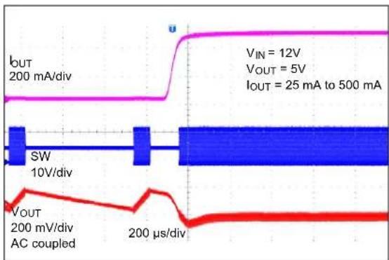
| Parameter | Value | | --------------- | ------------ | | VIN | 12V | | VOUT | 5V | | IOUT | 25 mA to 500 mA |FIGURE 2-26: PFM to PWM Transition.
line
| Time (μs) | V_IN (V) | V_OUT (V) | IC (I_OUT) | |-----------|----------|-----------|------------| | 0 | 12 | 5 | 0.5 |FIGURE 2-29: Line Transient Response.
line
| Parameter | Value | | --------- | --------- | | V_IN | 12V | | V_OUT | 5V | | I_OUT | 1A | | VOUT | 2V | | VOUT | 10V | | SW | 10V | | SW | 100 µs/div |FIGURE 2-27: Start-Up from V IN.

line
| Signal | Value | |--------|--------------| | IOUT | 1A/div | | VOUT | 200 mV/div | | SW | 10V/div | | V_IN | 12V | | V_OUT | 5V | | I_OUT | 5 mA to 1A | | SW | 400 µs/div |FIGURE 2-30: MCP16362 Load Transient Response (0.005A to 1A).
Note: Unless otherwise indicated, T_A = +25^ , V_IN = V_EN = 12V , V_BOOST - V_SW = 5V , V_OUT = 5V , I_OUT = 100 mA , L = 2.2 H , C_IN = 2× 10 F X7R Ceramic Capacitors, C_OUT = 2× 22 F X7R Ceramic Capacitors.
line
| Signal | Value | |--------|-------| | V_IN | 12V | | V_OUT | 5V | | I_OUT | 0.8A to 2.5A |FIGURE 2-31: MCP16362 Load Transient Response (0.8A to 2.5A).
3.0 PIN DESCRIPTIONS
The descriptions of the pins are listed in Table 3-1.
TABLE 3-1: PIN FUNCTION TABLE
| Pin Number | Symbol | Description |
| 1 | VIN | Input supply voltage pin for power and internal biasing. |
| 2 | EN | Enable pin. Logic high enables the operation. Do not allow this pin to float. |
| 3 | FB | Output voltage feedback pin. Connect FB to an external resistor divider to set the output voltage. |
| 4 | PG | Open Drain Power Good Output. |
| 5 | GND | Signal and Power Ground Reference. |
| 6 | BD | The anode of the internal bootstrap diode. Connect it to VOUT or to a power source < 5.5V. |
| 7 | BOOST | Boost voltage that drives the internal NMOS control switch. A bootstrap capacitor is connected between the BOOST and SW pins. |
| 8 | SW | Output switch node, connects to the inductor, freewheeling diode and the bootstrap capacitor. |
| 9 | EP | Exposed Pad. Internally connected to GND. Should be connected to the GND plane in order to help dissipate power. |
3.1 Power Supply Input Voltage Pin (VIN)
The VIN pin is the input voltage for the buck converter power stage and internal circuitry. This pin is connected to the drain terminal of the internal high-side N-Channel MOSFET. A 10 F minimum ceramic capacitor should be connected from VIN to the GND pin as close as possible to the device. A combination of multiple ceramic capacitors of different sizes is recommended.
3.2 Enable Pin (EN)
The EN pin is a logic-level input used to enable or disable the device switching, and lower the quiescent current while disabled. To turn off the device, the EN pin must be pulled low. Do not leave this pin floating.
3.3 Feedback Voltage Pin (FB)
The FB pin is used to provide output voltage regulation by using a resistor divider. The V_FB voltage will be 0.800V typical with the output voltage in regulation.
3.4 Power Good Output Pin (PG)
The PG pin is the drain connection of an internal N-channel FET. When the output voltage is within 93% of the nominal set point, this pin will go from logic low to logic high (through an external pull-up resistor).
3.5 Ground Pin (GND)
The ground or return pin is used for circuit ground connection. The length of the trace from the input capacitor return, output capacitor return and GND pin should be made as short as possible to minimize the noise on the GND pin.
3.6 Boost Diode Pin (BD)
The BD pin is the anode of a diode which is connected to the BOOST pin. The BD pin should be connected to a voltage output between 3V and 5.5V. If the output voltage is set between these values, the BD pin should be connected to the output.
3.7 Boost Pin (BOOST)
The BOOST pin is used to supply voltage for the driver of the high-side N-Channel power MOSFET. Connect the bootstrap capacitor to this pin.
3.8 Switch Node Pin (SW)
The switch node pin is connected internally to the source of the high-side N-channel MOSFET, and externally to the SW node consisting of the inductor, Schottky diode and bootstrap capacitor. The external components should be placed as close as possible to the SW pin such that the switching node is minimized as much as possible.
3.9 Exposed Pad (EP)
The Exposed Pad is electrically connected to the GND pin. Connect with thermal vias to the ground plane to ensure adequate heat-sinking.
4.0 PART NUMBER SELECTION
TABLE 4-1: DEVICE OPTIONS
| Part Number Switching Mode Option Switching Frequency | ||
| MCP16361 PFM/PWM Fixed 2.2 MHz | ||
| MCP16362 PWM Only Fixed 2.2 MHz | ||
| MCP16363 | PWM Only | 2.2 MHz with +10% Frequency Dithering |
5.0 FUNCTIONAL DESCRIPTION
The MCP16361/2/3 is a high input voltage step-down regulator, capable of supplying 3A to a regulated output voltage from 2.0V to 24V. Internally, the trimmed 2.2 MHz oscillator provides a fixed frequency, while the Peak Current Mode Control architecture varies the duty cycle for output voltage regulation. An internal floating driver is used to turn the high-side integrated N-Channel MOSFET on and off. The power for this driver is derived from an external boost capacitor whose energy is supplied from a fixed voltage ranging between 3.0V and 5.5V, typically the input or output voltage of the converter. For applications with an output voltage outside of this range, 12V for example, the boost capacitor bias can be derived from the output using a simple Zener diode regulator.
5.1 Theory of Operation
The integrated high-side switch is used to chop or modulate the input voltage using a controlled duty cycle for output voltage regulation. High efficiency is achieved by using a low-resistance switch, low forward voltage drop diode, low equivalent series resistance inductor (DCR) and capacitor (ESR). When the switch is turned on, a DC voltage is applied to the inductor V_IN-V_OUT , resulting in a positive linear ramp of inductor current. When the switch is turned off, the applied inductor voltage is equal to -V_OUT , resulting in a negative linear ramp of inductor current (ignoring the forward voltage drop of the Schottky diode).
For steady-state, continuous inductor current operation, the positive inductor current ramp must equal the negative current ramp in magnitude. While operating in steady state, the switch duty cycle must be equal to the relationship of V_OUT/V_IN , for constant output voltage regulation, under the condition that the inductor current is continuous, or never reaches zero. For discontinuous inductor current operation, the steady-state duty cycle will be less than V_OUT/V_IN to maintain voltage regulation. The average of the chopped input voltage or SW node voltage is equal to the output voltage, while the average of the inductor current is equal to the output current.
For a graphical representation of the switching waveform and inductor current for continuous and discontinuous inductor current modes, see Figure 5-1.
text_image
I_L V_IN + - Schottky Diode L V_OUT C_OUT I_L I_OUT SW on off on off on Continuous Inductor Current Mode V_IN V_OUT L I_OUT SW on off on off on Discontinuous Inductor Current ModeFIGURE 5-1: Step-Down Converter.
The MCP16361/2/3 integrates a Peak Current Mode, Control architecture, resulting in superior AC regulation while minimizing the number and size of the voltage loop compensation components integrated in the device. Peak Current Mode Control takes a small portion of the inductor current, replicates it and compares this replicated current sense signal with the output voltage of the integrated error amplifier. In practice, the inductor current and the internal switch current are equal during the switch-on time. By adding this peak current sense to the system control, the step-down power train system is reduced from a 2^nd order to a 1^st order. This reduces the system complexity and increases its dynamic performance.
5.2 Pulse-Width Modulation
For Pulse-Width Modulation (PWM) duty cycles that exceed 50%, the control system can become bimodal, where a wide pulse followed by a short pulse repeats instead of the desired fixed pulse width. To prevent this mode of operation, an internal compensating ramp is summed into the current shown in Figure 5-1.
The internal oscillator starts the switching period, which for MCP16361/2/3 occurs at a 2.2 MHz frequency. With the integrated switch turned on, the inductor current ramps up until the sum of the current sense and slope compensation ramp exceeds the integrated error amplifier output. The error amplifier output slews up or down to increase or decrease the inductor peak current feeding into the output LC filter. If the regulated output
voltage is lower than its target, the inverting error amplifier output rises. This results in an increase in the inductor current, to correct for error in the output voltage. The fixed frequency duty cycle is terminated when the sensed inductor peak current summed with the internal slope compensation exceeds the output voltage of the error amplifier. The PWM latch is set by turning off the internal switch and preventing it from turning on until the beginning of the next cycle. An overtemperature signal or boost capacitor undervoltage can also reset the PWM latch to asynchronously terminate the cycle.
5.3 Pulse Frequency Mode of Operation (PFM)
The MCP16361 selects the best operating switching mode (PFM or PWM) for high efficiency across a wide range of load currents, while in PFM, the duty cycle is determined by a fixed peak current. This allows for the output voltage to increase slightly above the typical regulation point. Once the output voltage increases above 810 mV typical, the MCP16361 stops switching and enters Sleep mode. The part resumes normal operation once the output voltage decreases. Switching to PFM mode at light load currents, combined with the very low I_Q current when not switching, results in obtaining very high efficiency at very low loads. During the sleep period (between two switching packets), the MCP16361 draws 18 A (typical) from the supply line. The switching pulse packets represent a small percentage of the total running cycle, and the overall average current drawn from power line is small.
The disadvantages of PWM/PFM mode are higher output voltage ripple and variable PFM mode frequency. The PFM mode threshold is a function of the input voltage, output voltage and load. The threshold between the PFM and PWM mode of operation can be observed in Figure 2-18.
5.4 Internal Reference Voltage V REF
An integrated precise 0.8V reference combined with an external resistor divider sets the desired converter output voltage. The resistor divider range can vary without affecting the control system gain. High-value resistors consume less current, but are more susceptible to noise.
5.5 Internal Compensation
All control system components necessary for stable operation over the entire device operating range are integrated, including the error amplifier and inductor current slope compensation. To add the proper amount of slope compensation, the inductor value changes along with the output voltage (see Table 6-1).
5.6 Enable Input
Enable input (EN) is used to disable the device. If disabled, the MCP16361/2/3 device consumes a minimal current from the input. Once enabled, the internal soft start controls the output voltage rate of rise, preventing high-inrush current and output voltage overshoot. To achieve automatic turn-on as soon as enough voltage is present, connect EN to the input.
5.7 Soft Start
The internal reference voltage rate of rise is controlled during start-up, minimizing the output voltage overshoot and the inrush current. The soft-start time is typically 750 s.
5.8 Undervoltage Lockout
An integrated Undervoltage Lockout (UVLO) prevents the converter from starting until the input voltage is high enough for normal operation. The converter will typically start at 4V and operate down to 3.4V. Hysteresis is added to prevent starting and stopping during start-up, as a result of loading the input voltage source.
5.9 Overtemperature Protection
Overtemperature protection limits the silicon die temperature to 155°C by turning the converter off. The normal switching resumes at 125°C.
5.10 High-Side Drive and Bootstrap
The MCP16361 features an integrated high-side N-Channel MOSFET for high efficiency step-down power conversion. An N-Channel MOSFET is used for its low resistance and size (instead of a P-Channel MOSFET). The N-Channel MOSFET gate must be driven above its source to fully turn on the transistor. A gate drive voltage above the input is necessary to turn on the high-side N-Channel. The high-side drive voltage should be between 3.0V and 5.5V.
The N-Channel source is connected to the inductor and Schottky diode, or switch node. When the switch is off, the inductor current flows through the Schottky diode, providing a path to recharge the boost capacitor from the boost voltage source, typically the output voltage for 3.0V to 5.5V output applications.
Prior to start-up, the boost capacitor has no stored charge to drive the switch. An internal regulator is used to "precharge" the boost capacitor. Once precharged, the switch is turned on and the inductor current starts to flow. When the switch turns off, the inductor current free-wheels through the Schottky diode providing a path to recharge the boost capacitor. Worst case conditions for recharge occur when the switch turns on for a very short duty cycle, at light load, limiting the inductor current ramp. In this case, there is a small
amount of time for the boost capacitor to recharge. For high-input voltages, there is enough precharge current to replace the boost capacitor charge. For input voltages above 5.5V typical, the MCP16361/2/3 device will regulate the output voltage with no load. After starting, the MCP16361/2/3 will regulate the output voltage until the input voltage decreases below 4V. See Figure 2-20 for device range of operation over input voltage and load.
5.11 Integrated Bootstrap Diode
In order to minimize the number of external components used in the application, the bootstrap diode has been integrated into the device, such that the anode is connected to the BD pin and cathode to the BOOST pin.
The permissible voltage that should be used on this pin is between 3V and 5.5V.
5.12 Frequency Dithering
When designing a DC-DC switching power supply, one of the challenges that must be overcome is controlling the electromagnetic interference (EMI) emissions produced during normal operation. The EMI is most relevant at the switch mode power supply fundamental switching frequency and is reduced for each higher order harmonic. In order to decrease this peak emission, modulating or dithering the switching frequency is used, such that the EMI is spread over a band of frequencies.
For the MCP16363, the switching frequency will vary above the 2.2 MHz by +10%, in order to reduce the EMI peak.
5.13 Power Good
Power Good (PG) is an open-drain output. For asserting a logic high level, PG requires an external resistor connected to a pull-up voltage, which should not exceed the input voltage.
PG is asserted when the output voltage reaches 93% of its target regulation voltage. PG is deasserted with a typical delay of 50 s when the output voltage falls below 90% of its target regulation voltage. The PG falling delay acts as a deglitch timer against very short spikes. The PG output is always immediately deasserted when the EN pin is below the power delivery enable threshold. The value of the pull-up resistor should be high enough to limit the PG pin current to below 5 mA.
The PG is also immediately deasserted (with no delay) whenever an undervoltage condition is detected, or in case of a thermal shutdown.
5.14 Overcurrent Protection
The MCP16361/2/3 features instantaneous cycle-by-cycle current limit by sensing the current through the high-side switch.
A leading edge blanking is provided on the high-side switch to prevent falsely triggering the overcurrent limit.
The device also offers frequency fold-back and overcurrent protection that inhibits future pulses for prolonged overloads or short-circuit condition.
In case of prolonged overloads at high input voltages, if the overcurrent protection is tripped, the next three future pulses will be inhibited, such that the inductor current is allowed to decrease to lower values.
At the same time, if the feedback voltage decreases, the switching frequency will also decrease down to 200 kHz. For more information regarding the frequency fold-back, see Figure 2-21.
5.15 Overvoltage Protection
The MCP16361/2/3 incorporates an output voltage protection (OVP) to minimize the output voltage overshoot when recovering from strong unload transients, in designs with low-output capacitance. For example, in applications, where the output voltage is overloaded when the load is removed, the regulator output can increase faster than the response of the error amplifier, resulting in an output overshoot.
The OVP circuitry compares the FB voltage to the OVP threshold, which is typically set at 860 mV, and immediately turns off the high-side MOSFET.
6.0 APPLICATION INFORMATION
6.1 Adjustable Output Voltage Calculations
To calculate the resistor divider values for the MCP16361/2/3, Equation 6-1 can be used. R_TOP is connected to V_OUT , R_BOT is connected to GND and both are connected to the FB input pin.
EQUATION 6-1: RESISTOR DIVIDER VALUES
$$ R _ {T O P} = R _ {B O T} \times \left(\frac {V _ {O U T}}{V _ {F B}} - I\right) $$
EXAMPLE 6-1: 3.3V OUTPUT EXAMPLE
$$ V _ {\text { OUT_target }} = 3. 3 \mathrm{V} $$
$$ V _ {F B} = 0. 8 V $$
$$ R _ {B O T} = 1 0 \mathrm{k} \Omega $$
$$ R _ {T O P} = 3 1. 2 5 \mathrm{k} \Omega $$
$$ (\text { Standard Value } = 3 1. 6 \mathrm{k} \Omega) $$
The transconductance error amplifier gain is controlled by its internal impedance. The external divider resistors have no effect on system gain, so a wide range of values can be used. It is recommended to use feedback resistors with 1% tolerances or better. To improve the efficiency at light load, a large value resistor should be used. However, if the values are too high, the regulator will be more susceptible to noise.
6.2 Inductor Selection and Slope Compensation
In order to select the best inductor for the application, the following factors should be considered: inductance value, RMS rated current, saturation current and DC resistance (DCR).
In case of the MCP16361/2/3, the inductance value is critical to the correct operation. For stable current loop operation, where duty cycle is above 50%, slope compensation is internally added according to the output voltage and the input-output voltage ratio.
For the proper amount of slope compensation, it is recommended to keep the inductor down-slope current constant by varying the inductance with V_OUT .
TABLE 6-1: RECOMMENDED INDUCTOR VALUES
| VOUT | LSTANDARD |
| 2.0V | 1 μH |
| 3.3V | 1.5 μH |
| 5.0V | 2.2 μH |
| 12V | 5.2 μH |
| 15V | 6.8 μH |
The inductor RMS current represents the current at which the inductor's temperature rises by +20°C to +40°C, depending on manufacturer. In the case of inductor saturation current, it represents the peak current at which the inductor exhibits a loss of inductance value between 10% and 30%, depending on manufacturer. For proper operation, ensure that the nominal and peak currents of the application are well within the permissible current ratings of the inductor.
The peak inductor current can be calculated with Equation 6-2:
EQUATION 6-2: PEAK INDUCTOR CURRENT
$$ I _ {L P E A K} = \left(I _ {O U T} + V _ {O U T} \times \frac {1 - V _ {O U T} / V _ {I N}}{2 \times f _ {s w} \times L}\right) $$
Where:
$$ I _ {O U T} = \text { Nominal output current } $$
$$ V _ {\text { OUT }} = \text { Output voltage } $$
$$ V _ {I N} = \text { Input voltage } $$
$$ f _ {s w} = \text { Switching frequency } $$
$$ L = \text { Inductance value } $$
When choosing the inductor, sufficient design margin should be taken into account such that the inductor does not enter deep saturation. Overcurrent situations should also be taken into account, especially at very high input voltages, where the inductor current can increase very rapidly.
6.3 Freewheeling Diode
The MCP16361/2/3 requires a freewheeling diode to create a path for inductor current flow after the internal switch is turned off. The diode must have a reverse voltage rating greater than the maximum input voltage possible in the application. The peak current rating of the diode must be higher than the maximum inductor current. The lower the forward voltage of the diode, the higher the efficiency of the regulator, and that is why Schottky diodes are typically a good choice for this purpose.
On the other hand, the diode should also be selected with an appropriate power rating. The diode conducts the output current during the off-time of the internal power switch, and therefore in high V_IN to V_OUT ratios, the conduction losses of the diode may become significant. The conduction losses can be estimated using Equation 6-3.
EQUATION 6-3: DIODE CONDUCTION LOSSES
$$ P _ {D} = \frac {(V _ {I N} - V _ {O U T}) \times I _ {O U T} \times V _ {F W}}{V _ {I N}} $$
Where:
$$ I _ {O U T} = \text { Nominal output current } $$
$$ V _ {\text { OUT }} = \text { Output voltage } $$
$$ V _ {I N} = \text { Input voltage } $$
$$ \begin{array}{r c l} V _ {F W} & = & \text { Forward voltage drop of } \ & & \text { the diode } \end{array} $$
Because of the high switching frequency, the AC losses of the diode should also be taken into account. These losses are caused by the charging and discharging of the junction capacitance and the reverse recovery charge.
6.4 Input Capacitor Selection
The step-down converter input capacitor must filter the high input current ripple, as a result of pulsing or chopping the input voltage. The MCP16361/2/3 input voltage pin is used to supply voltage for the power train and as a source for internal bias. A low equivalent series resistance (ESR), preferably a ceramic capacitor of at least 10 F capacitance is recommended. Depending on the loading profile and conditions, the application will benefit from additional bulk capacitance.
The minimum capacitance needed for a given input peak to peak voltage ripple can be calculated using Equation 6-4:
EQUATION 6-4: INPUT CAPACITOR RIPPLE
$$ C _ {I N (M I N)} = \frac {I _ {O U T} \times D \times (I - D)}{\varDelta V _ {r i p p l e , i n} \times f _ {S W}} $$
Where:
$$ I _ {O U T} = \text { Nominal output current } $$
$$ D = \text { Duty - cycle } $$
$$ \Delta V _ {\text { ripple,in }} = \text { Required input voltage ripple } $$
$$ f _ {S W} = \text { Switching frequency } $$
Because the value of ceramic capacitors varies significantly with temperature and DC bias, design margins should be taken into account to ensure enough capacitance at the input of the regulator. To mitigate temperature variations, X5R and X7R capacitors are recommended. The DC bias should also be considered, as the capacitance decreases with the voltage applied.
6.5 Output Capacitor Selection
The output capacitor helps in providing a stable output voltage during sudden load transients, and reduces the output voltage ripple. As with the input capacitor, X5R and X7R ceramic capacitors are well suited for this application.
The output voltage capacitor voltage rating should be a minimum of V_OUT , plus margin.
To determine the steady-state voltage ripple, the ESR component and the capacitive ripple need to be taken into account (Equation 6-5):
EQUATION 6-5: OUTPUT CAPACITOR RIPPLE
$$ \varDelta V _ {r i p p l e, o u t} = E S R \times \varDelta I _ {L} + \frac {\varDelta I _ {L}}{8 \times f _ {S W} \times C _ {O U T}} $$
Where:
$$ \begin{array}{r l} \text { ESR } & = \text { Output capacitor series } \ & \text { resistance } \end{array} $$
$$ f _ {S W} = \text { Switching frequency } $$
$$ C _ {O U T} = \text { Output capacitance } $$
$$ \Delta I _ {L} = \text { Inductor current ripple } $$
The worst case load transient for output capacitor calculations is an instantaneous load release from full load to no load. In this situation, the energy stored in the inductor, which is at its peak value, must be absorbed by the output capacitor.
The output voltage overshoot in such situations can be calculated using Equation 6-6:
EQUATION 6-6: OUTPUT VOLTAGE OVERSHOOT
$$ \Delta V _ {O U T} = \sqrt {V _ {O U T} ^ {2} + \frac {L}{C _ {O U T}} \times I _ {L P E A K} ^ {2}} - V _ {O U T} $$
Where:
$$ V _ {O U T} = \text { Output voltage } $$
$$ L = \text { Inductance value } $$
$$ I _ {L P E A K} = \text { Inductor peak current } $$
$$ C _ {O U T} = \text { Output capacitance } $$
As in the case of the input capacitors, enough design margin needs to be taken into account to mitigate temperature and DC bias variations.
6.6 Bootstrap Charging and Maximum Duty Cycle Limitations
The boost capacitor is used to supply current for the internal high-side drive circuitry that is above the input voltage. The boost capacitor must store enough energy to completely drive the high-side switch on and off. A 0.33 μF X5R or X7R capacitor is recommended for all applications. The boost capacitor maximum voltage is 5.5V, so a 6.3V or 10V rated capacitor is recommended.
The charging of the boost capacitor is done during the off-time of the switching cycle, when the SW node is pulled to GND, through the BD pin. When operating at a low voltage difference between input and output, the duty cycle will reach the maximum limitation at around 87%. This in turn, coupled with the high switching frequency of 2.2 MHz, allows for only 50 ns of charging time for the boost capacitor.
In most cases, this 50 ns time is sufficient to replenish the energy lost for the switching activity during each cycle. However, when the voltage applied on the BD pin is below 3V and the maximum duty cycle is reached, the voltage on the boost capacitor can decrease, reaching 2V and forcing an internal charge of the boost capacitor and therefore a stop in switching activity.
To improve the behavior at low input voltages, where the boost charge time reaches 50 ns, the MCP16361/2/3 further limits the maximum duty cycle to 75% typical for input voltage below 5.1V. Due to this, the parts can continue switching and operating correctly, although with a larger headroom between V_IN and V_OUT . Once the V_IN recovers and is above 6V, the maximum duty cycle is once again set to 87% for normal operation.
When the maximum duty cycle operation is expected to improve the operation at low V_IN , an ultra-fast external bootstrap diode can be connected to the boost pin, to improve the charging of the bootstrap capacitor.
6.7 Input Voltage Limitations
Although the high switching frequency has advantages when it comes to the requirement of external passive components and possible transient response, when operating in these conditions, there are certain limitations that need to be considered when designing the application:
- Dropout operation
- Minimum on-time
In order to determine the two ends of the operating range, Equation 6-7 can be used.
EQUATION 6-7: INPUT VOLTAGE RANGE
| V_IN = _OUT + I_OUT(R_DCR + R_DSON) + V_FW × (1 - D)D | |
| Where: | |
| V_OUT = Output voltage | |
| I_OUT = Output current | |
| L = Inductance value | |
| R_DCR = DCR of the selected inductor | |
| R_DSON = On-resistance of the internal high-side switch | |
| D = Duty cycle | |
| V_FW = Forward voltage drop of the diode |
In order to determine the minimum input voltage for proper regulation, the duty cycle should be replaced by the maximum duty cycle; whereas to determine the maximum voltage, the duty cycle should be calculated, to avoid going below the minimum on-time.
EXAMPLE 6-2: INPUT VOLTAGE RANGE VS. OUTPUT VOLTAGE
line
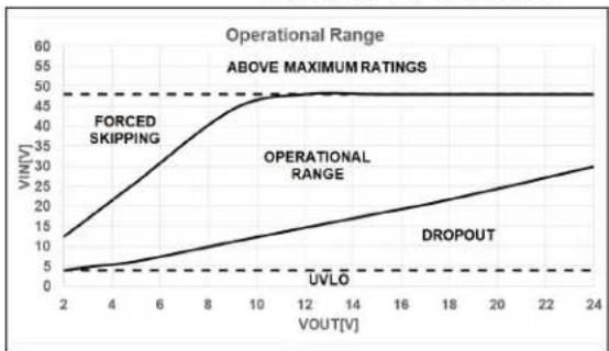
| VOUT[V] | FORCED SKIPPING | OPERATIONAL RANGE | DROPOUT | | ------- | ---------------- | ---------------- | ------- | | 2 | 10 | 10 | 5 | | 4 | 20 | 15 | 7 | | 6 | 30 | 20 | 10 | | 8 | 40 | 25 | 12 | | 10 | 45 | 30 | 15 | | 12 | 48 | 35 | 18 | | 14 | 49 | 40 | 20 | | 16 | 49 | 45 | 22 | | 18 | 49 | 48 | 24 | | 20 | 49 | 49 | 26 | | 22 | 49 | 49 | 28 | | 24 | 49 | 49 | 30 |6.8 Light Load Efficiency Guidelines
To increase efficiency at light load conditions, the MCP16361 operates in PFM, to keep the output voltage regulated while minimizing the input current. In this mode of operation, the MCP16361 delivers a packet of current pulses that is followed by sleep periods in which the output is maintained by the output capacitor. When in Sleep mode, the MCP16361 consumes around 18 μA from the input. As the output load decreases, the frequency and length of the packet of pulses decrease, such that the sleep period extends over most of the time. By maximizing the sleep time, the converter operating no load input current gets closer to the 18 μA. To optimize the performance at light loads, the current flowing through the feedback resistors and the reverse current through the freewheeling diode must be minimized, as they are seen as load currents. The feedback resistors should be in the order of tens of kΩ in range and the freewheeling diode reverse current should be less than 1 μA, at room temperature.
6.9 PCB Layout Information
Good printed circuit board layout techniques are important to any switching circuitry, and switch mode power supplies are no different. When wiring the switching high-current paths, short and wide traces should be used. Therefore, it is important that the input and output capacitors be placed as close as possible to the MCP16361/2/3, to minimize the loop area.
The feedback resistors and feedback signal should be routed away from the switching node and the switching current loop. When possible, ground planes and traces should be used to help shield the feedback signal and minimize noise and magnetic interference.
A good MCP16361/2/3 layout starts with C_IN placement. C_IN supplies current to the input of the circuit when the switch is turned on. In addition to supplying high-frequency switch current, C_IN also provides a stable voltage source for the internal MCP16361/2/3 circuitry. Unstable PWM operation can result if there are excessive transients or ringing on the VIN pin of the MCP16361/2/3 device. A ground plane on the bottom of the board provides a low resistive and inductive path for the return current. The next priority in placement is the freewheeling current loop formed by D1, C_OUT and L, while strategically placing C_OUT return close to C_IN return. Next, the boost capacitor should be placed between the boost pin and the switch node pin, SW. R_TOP and R_BOT are routed away from the switch node, so noise is not coupled into the high-impedance FB input.
7.0 TYPICAL APPLICATION CIRCUITS
text_image
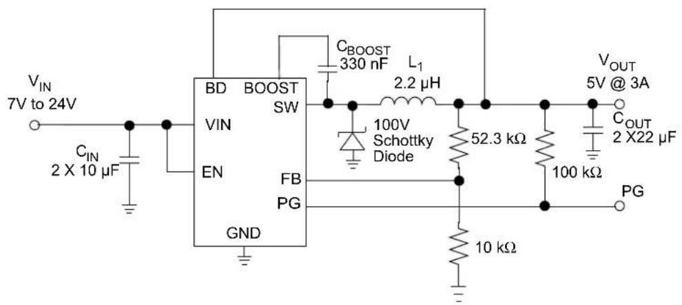
VIN 7V to 24V CIN 2 X 10 μF BD BOOST SW VIN EN FB PG GND CBOOST 330 nF L1 2.2 μH 100V Schottky Diode 52.3 kΩ 100 kΩ VOUT 5V @ 3A COUT 2 X22 μF PG| Component | Value Manufacturer Part Number Comment | |||
| C_IN | 2 x 10 μF | TDK C5750X7S2A106 | M Capacitor, 10 μF, 100V, | X7S, 2220 |
| C_OUT | 2 x 22 μF | KEMET C1206C226M8 | RACTU Capacitor, 22 μF, 10V, 1206 | |
| L | 2.2 μH | Coilcraft® | MSS1048-222 | MSS1048, 2.2 μH Shielded Power Inductor |
| FW Diode | B360 | Diodes® Inc. | B360-13-F | Schottky, 60V, 3A, SMC |
| C_BOOST | 330 nF | Murata GRM188R71C3 | 334KA01D | Capacitor, Ceramic, 0.33 μF, 16V, 10%, X7R, SMD, 0603 |
FIGURE 7-1: Typical Application 7V-24V V
IN (Transient up to 48V) to 5V VOUT.

text_image
C_BD 0.1 μF V_IN 17V to 48V C_IN 2 X 10 μF BD BOOST SW VIN EN FB PG GND C_BOOST 330 nF L_1 5.2 μH 100V Schottky Diode 140 kΩ 100 kΩ 10 kΩ DGZ 7.5V V_OUT 12V @ 3 A C_OUT 2 X22 μF PG| Component | Value Manufacturer Part Number Comment | |||
| C_IN | 2 x 10 μF TDK C5750X7S2A106M Capacitor, 10 μF, 100V, X7S, 2220 | |||
| C_OUT | 2 x 22 μF TDK | CGA8P1X7R1E226M250KC | Capacitor, 22 μF, 25V, 1812 | |
| L 5.2 μH Coilcraft | ® | MSS1038-522 MSS1038, 5.2 μH Shielded Power Inductor | ||
| FW Diode | B360 | Diodes® Inc. | B360-13-F | Schottky, 60V, 3A, SMC |
| C_{BOOST} | 330 nF | Murata | GRM188R71C334-KA01D | Capacitor Ceramic, 0.33 μF, 16V, 10%, X7R, SMD, 0603 |
| D_Z | 7.5V Zener | Diodes Inc. | MMSZ5236BS-7-F | Diode Zener, 7.5V, 200 mW, SOD-323 |
| C_{BD}$ | 0.1 μF | TDK | C1608X7R1H104K080AA | Capacitor, 0.1 μF, 50V, X7R, 0603 |
FIGURE 7-2: Typical Application 17V-48V V
IN to 12V V_OUT with Boost Drive Derived from Output.
8.0 PACKAGING INFORMATION
8.1 Package Marking Information
8-Lead VDFN (3x3x0.9 mm)
Example
text_image
XXXX YYWW NNN PIN 1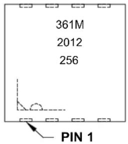
text_image
361M 2012 256 PIN 1Legend: XX...X Customer-specific information
Y Year code (last digit of calendar year)
YY Year code (last 2 digits of calendar year)
WW Week code (week of January 1 is week '01')
NNN Alphanumeric traceability code
_e3 Rb-free JEDEC designator for Matte Tin (Sn)
This package is Pb-free. The Pb-free JEDEC designator (e3)
can be found on the outer packaging for this package.
Note: In the event the full Microchip part number cannot be marked on one line, it will be carried over to the next line, thus limiting the number of available characters for customer-specific information.
8-Lead Very Thin Plastic Dual Flat, No Lead Package (NMX) - 3x3x0.9 mm Body [VDFN] With Multiple Exposed Pads, 2 Fused
Note: For the most current package drawings, please see the Microchip Packaging Specification located at http://www.microchip.com/packaging
![Microchip MCP16362 - 8-Lead Very Thin Plastic Dual Flat, No Lead Package (NMX) - 3x3x0.9 mm Body [VDFN] With Multiple Exposed Pads, 2 Fused - 1](/content/2026/06/1219382/images/e3ef31321954fbe1b87e91d3e8dc3ce2b3def1aaeaa76cb00694c9955e0cc911.jpg)
text_image
(DATUM A) (DATUM B) NOTE1 2X 0.10 C 2X 0.10 C TOP VIEW SEATING PLANE C A (A3) A1 SIDE VIEW 8X 0.08 C // 0.10 C (K2) D2 N L1 NOTE 1 L 2X (b2) 1 2 8X b e E K1) E2 0.10 A B 0.05 B BOTTOM VIEWMicrochip Technology Drawing C04-524 Rev A Sheet 1 of 2
8-Lead Very Thin Plastic Dual Flat, No Lead Package (NMX) - 3x3x0.9 mm Body [VDFN] With Multiple Exposed Pads, 2 Fused
Note: For the most current package drawings, please see the Microchip Packaging Specification located at http://www.microchip.com/packaging
![Microchip MCP16362 - 8-Lead Very Thin Plastic Dual Flat, No Lead Package (NMX) - 3x3x0.9 mm Body [VDFN] With Multiple Exposed Pads, 2 Fused - 1](/content/2026/06/1219382/images/57c912e885bddfe451b54f85074d1f67a6471d6c41481d1a8b53b438dc83a537.jpg)
text_image
A4 0.10 D3 0.06 SECTION A-A| Units | MILLIMETERS | |||
| Dimension Limits | MIN | NOM | MAX | |
| Number of Terminals | N | 8 | ||
| Pitch | e | 0.65 BSC | ||
| Overall Height | A | - | - | 0.90 |
| Standoff | A1 | 0.00 | 0.02 | 0.05 |
| Terminal Thickness | A3 | 0.203 REF | ||
| Overall Length | D | 3.00 BSC | ||
| Exposed Pad Length | D2 | 1.10 | 1.20 1.30 | |
| Overall Width | E | 3.00 BSC | ||
| Exposed Pad Width | E2 | 0.40 0.50 | 0.60 | |
| Terminal Width | b | 0.18 | 0.25 | 0.30 |
| Terminal Width | b | 0.40 REF | ||
| Terminal Length | L | 0.30 | 0.40 | 0.50 |
| Terminal Length L1 1.10 1.20 1.30 | ||||
| K1 0 | 85 REFTerminal-to-Exposed-Pad | |||
| K2 0 | 60 REFTerminal-to-Exposed-Pad | |||
| Wettable Flank Step Cut Length | D3 | 0.01 - 0.06 | ||
| A4 -- | 0 | |||
Notes:
1. Pin 1 visual index feature may vary, but must be located within the hatched area.
2. Package is saw singulated
3. Dimensioning and tolerancing per ASME Y14.5M
BSC: Basic Dimension. Theoretically exact value shown without tolerances.
REF: Reference Dimension, usually without tolerance, for information purposes only.
Sheet 2 of 2Microcl
8-Lead Very Thin Plastic Dual Flat, No Lead Package (NMX) - 3x3x0.9 mm Body [VDFN] With Multiple Exposed Pads, 2 Fused
Note: For the most current package drawings, please see the Microchip Packaging Specification located at http://www.microchip.com/packaging
![Microchip MCP16362 - 8-Lead Very Thin Plastic Dual Flat, No Lead Package (NMX) - 3x3x0.9 mm Body [VDFN] With Multiple Exposed Pads, 2 Fused - 1](/content/2026/06/1219382/images/0ba3c78c625457bf833c3ec5599c63b15c4b720af1c764322c111a00f0abb9e8.jpg)
text_image
X2 8 C3 X3 ØV C1 C2 Y3 Y2 1 2 Y1 SILK SCREEN G E X1RECOMMENDED LAND PATTERN
| Units | MILLIMETERS | |||
| Dimension Limits | MIN | NOM | MAX | |
| Contact Pitch | E | 0.65 BSC | ||
| Center Pad Width | X3 | 1.20 | ||
| Center Pad Length | Y3 | 0.50 | ||
| Center Pad Offset C3 0.50 | ||||
| C1Contact Pad Spacing 2.90 | ||||
| Contact Pad Spacing | C2 | 2.18 | ||
| Contact Pad Width (X6) | X1 | 0.30 | ||
| Contact Pad Length (X6) | Y1 | 0.90 | ||
| Contact Pad Width (X2) | X2 | 0.45 | ||
| Contact Pad Length (X2) | Y2 | 1.63 | ||
| Contact Pad to Contact Pad (X2) G | 0.20 | |||
| Thermal Via Diameter V 0.30 | ||||
Notes:
1. Dimensioning and tolerancing per ASME Y14.5M
BSC: Basic Dimension. Theoretically exact value shown without tolerances.
2. For best soldering results, thermal vias, if used, should be filled or tented to avoid solder loss during reflow process
Microchip Technology Drawing C04-2524 Rev A
APPENDIX A: REVISION HISTORY
Revision B (August 2021)
- Added AEC-Q100 Automotive Qualification.
- Very minor editorial text changes throughout.
Revision A (December 2020)
- Initial release of this document.
PRODUCT IDENTIFICATION SYSTEM
To order or obtain information, e.g., on pricing or delivery, contact your local Microchip representative or sales office.
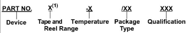
text_image
PART NO. Device X(1) Tape and Reel Range -Temperature /XX Package Type XXX QualificationDevice:
MCP16361/2/3: 48V Input, 3A Output, 2.2 MHz Switching Frequency, Integrated Switch Step-Down Regulator
Device Options: MCP16361: PFM/PWM, Fixed 2.2 MHz Switching Frequency
MCP16362: PWM Only, Fixed 2.2 MHz Switching Frequency
MCP16363: PWM Only, 2.2 MHz +10% Frequency Dithering
Temperature: E = -40°C to +125°C (Extended)
Package Type:
NMX= 8-Lead Very Thin Plastic Dual Flat, No Lead Package
Qualification:
Blank = Standard Qualification
VAO = AEC-Q100 Automotive Qualification
VXX = AEC-Q100 Automotive Qualification, custom device, additional terms or conditions may apply
Examples:
a) MCP16361T-E/NMX:
Tape and Reel,
Extended Temperature, 8-LD VDFN package
b) MCP16362T-E/NMX:
Tape and Reel,
Extended Temperature, 8-LD VDFN package
c) MCP16363T-E/NMX:
Tape and Reel,
Extended Temperature, 8-LD VDFN package
d) MCP16361T-E/NMXVAO:
Tape and Reel,
Extended Temperature, 8-LD VDFN package Automotive Qualified
e) MCP16362T-E/NMXVAO:
Tape and Reel,
Extended Temperature, 8-LD VDFN package Automotive Qualified
f) MCP16363T-E/NMXVAO:
Tape and Reel,
Extended Temperature, 8-LD VDFN package Automotive Qualified
Note 1: Tape and Reel identifier only appears in the catalog part number description. This identifier is used for ordering purposes and is not printed on the device package. Check with your Microchip sales office for package availability for the Tape and Reel option.
Note the following details of the code protection feature on Microchip devices:
• Microchip products meet the specifications contained in their particular Microchip Data Sheet.
• Microchip believes that its family of products is secure when used in the intended manner and under normal conditions.
- There are dishonest and possibly illegal methods being used in attempts to breach the code protection features of the Microchip devices. We believe that these methods require using the Microchip products in a manner outside the operating specifications contained in Microchip's Data Sheets. Attempts to breach these code protection features, most likely, cannot be accomplished without violating Microchip's intellectual property rights.
• Microchip is willing to work with any customer who is concerned about the integrity of its code.
- Neither Microchip nor any other semiconductor manufacturer can guarantee the security of its code. Code protection does not mean that we are guaranteeing the product is "unbreakable." Code protection is constantly evolving. We at Microchip are committed to continuously improving the code protection features of our products. Attempts to break Microchip's code protection feature may be a violation of the Digital Millennium Copyright Act. If such acts allow unauthorized access to your software or other copyrighted work, you may have a right to sue for relief under that Act.
Information contained in this publication is provided for the sole purpose of designing with and using Microchip products. Information regarding device applications and the like is provided only for your convenience and may be superseded by updates. It is your responsibility to ensure that your application meets with your specifications.
THIS INFORMATION IS PROVIDED BY MICROCHIP "AS IS". MICROCHIP MAKES NO REPRESENTATIONS OR WARRANTIES OF ANY KIND WHETHER EXPRESS OR IMPLIED, WRITTEN OR ORAL, STATUTORY OR OTHERWISE, RELATED TO THE INFORMATION INCLUDING BUT NOT LIMITED TO ANY IMPLIED WARRANTIES OF NON-INFRINGEMENT, MERCHANTABILITY, AND FITNESS FOR A PARTICULAR PURPOSE OR WARRANTIES RELATED TO ITS CONDITION, QUALITY, OR PERFORMANCE.
IN NO EVENT WILL MICROCHIP BE LIABLE FOR ANY INDIRECT, SPECIAL, PUNITIVE, INCIDENTAL OR CONSEQUENTIAL LOSS, DAMAGE, COST OR EXPENSE OF ANY KIND WHATSOEVER RELATED TO THE INFORMATION OR ITS USE, HOWEVER CAUSED, EVEN IF MICROCHIP HAS BEEN ADVISED OF THE POSSIBILITY OR THE DAMAGES ARE FORESEEABLE. TO THE FULLEST EXTENT ALLOWED BY LAW, MICROCHIP'S TOTAL LIABILITY ON ALL CLAIMS IN ANY WAY RELATED TO THE INFORMATION OR ITS USE WILL NOT EXCEED THE AMOUNT OF FEES, IF ANY, THAT YOU HAVE PAID DIRECTLY TO MICROCHIP FOR THE INFORMATION. Use of Microchip devices in life support and/or safety applications is entirely at the buyer's risk, and the buyer agrees to defend, indemnify and hold harmless Microchip from any and all damages, claims, suits, or expenses resulting from such use. No licenses are conveyed, implicitly or otherwise, under any Microchip intellectual property rights unless otherwise stated.
Trademarks
The Microchip name and logo, the Microchip logo, Adaptec, AnyRate, AVR, AVR logo, AVR Freaks, BesTime, BitCloud, chipKIT, chipKIT logo, CryptoMemory, CryptoRF, dsPIC, FlashFlex, flexPWR, HELDO, IGLOO, JukeBlox, KeeLoq, Kleer, LANCheck, LinkMD, maXStylus, maXTouch, MediaLB, megaAVR, Microsemi, Microsemi logo, MOST, MOST logo, MPLAB, OptoLyzer, PackeTime, PIC, picoPower, PICSTART, PIC32 logo, PolarFire, Prochip Designer, QTouch, SAM-BA, SenGenuity, SpyNIC, SST, SST Logo, SuperFlash, Symmetricom, SyncServer, Tachyon, TimeSource, tinyAVR, UNI/O, Vectron, and XMEGA are registered trademarks of Microchip Technology Incorporated in the U.S.A. and other countries.
AgileSwitch, APT, ClockWorks, The Embedded Control Solutions Company, EtherSynch, FlashTec, Hyper Speed Control, HyperLight Load, IntellMOS, Libero, motorBench, mTouch, Powermite 3, Precision Edge, ProASIC, ProASIC Plus, ProASIC Plus logo, Quiet-Wire, SmartFusion, SyncWorld, Temux, TimeCesium, TimeHub, TimePictra, TimeProvider, WinPath, and ZL are registered trademarks of Microchip Technology Incorporated in the U.S.A.
Adjacent Key Suppression, AKS, Analog-for-the-Digital Age, Any Capacitor, AnyIn, AnyOut, Augmented Switching, BlueSky, BodyCom, CodeGuard, CryptoAuthentication, CryptoAutomotive, CryptoCompanion, CryptoController, dsPICDEM, dsPICDEM.net, Dynamic Average Matching, DAM, ECAN, Espresso T1S, EtherGREEN, IdealBridge, In-Circuit Serial Programming, ICSP, INICnet, Intelligent Paralleling, Inter-Chip Connectivity, JitterBlocker, maxCrypto, maxView, memBrain, Mindi, MiWi, MPASM, MPF, MPLAB Certified logo, MPLIB, MPLINK, MultiTRAK, NetDetach, Omniscient Code Generation, PICDEM, PICDEM.net, PICkit, PICtail, PowerSmart, PureSilicon, QMatrix, REAL ICE, Ripple Blocker, RTAX, RTG4, SAM-ICE, Serial Quad I/O, simpleMAP, SimpliPHY, SmartBuffer, SMART-I.S., storClad, SQI, SuperSwitcher, SuperSwitcher II, Switchtec, SynchroPHY, Total Endurance, TSHARC, USBCheck, VariSense, VectorBlox, VeriPHY, ViewSpan, WiperLock, XpressConnect, and ZENA are trademarks of Microchip Technology Incorporated in the U.S.A. and other countries.
SQTP is a service mark of Microchip Technology Incorporated in the U.S.A. The Adaptec logo, Frequency on Demand, Silicon Storage Technology, and Symmcom are registered trademarks of Microchip Technology Inc. in other countries. GestIC is a registered trademark of Microchip Technology Germany II GmbH & Co. KG, a subsidiary of Microchip Technology Inc., in other countries. All other trademarks mentioned herein are property of their respective companies.
© 2020-2021, Microchip Technology Incorporated, All Rights Reserved.
ISBN: 978-1-5224-8817-0
For information regarding Microchip's Quality Management Systems, please visit www.microchip.com/quality.
Worldwide Sales and Service
AMERICAS
Corporate Office
2355 West Chandler Blvd.
Chandler, AZ 85224-6199
Tel: 480-792-7200
Fax: 480-792-7277
Technical Support:
http://www.microchip.com/
support
Web Address:
www.microchip.com
Atlanta
Duluth, GA
Tel: 678-957-9614
Fax: 678-957-1455
Austin, TX
Tel: 512-257-3370
Boston
Westborough, MA
Tel: 774-760-0087
Fax: 774-760-0088
Chicago
Itasca, IL
Tel: 630-285-0071
Fax: 630-285-0075
Dallas
Addison, TX
Tel: 972-818-7423
Fax: 972-818-2924
Detroit
Novi, MI
Tel: 248-848-4000
Houston, TX
Tel: 281-894-5983
Indianapolis
Noblesville, IN
Tel: 317-773-8323
Fax: 317-773-5453
Tel: 317-536-2380
Los Angeles
Mission Viejo, CA
Tel: 949-462-9523
Fax: 949-462-9608
Tel: 951-273-7800
Raleigh, NC
Tel: 919-844-7510
New York, NY
Tel: 631-435-6000
San Jose, CA
Tel: 408-735-9110
Tel: 408-436-4270
Canada - Toron
Tel: 905-695-1980
Fax: 905-695-2078
ASIA/PACIFIC
Australia - Sydney
Tel: 61-2-9868-6733
China - Beijing
Tel: 86-10-8569-7000
China - Chengdu
Tel: 86-28-8665-5511
China - Chongqing
Tel: 86-23-8980-9588
China - Dongguan
Tel: 86-769-8702-9880
China - Guangzhou
Tel: 86-20-8755-8029
China - Hangzhou
Tel: 86-571-8792-8115
China - Hong Kong SAR
Tel: 852-2943-5100
China - Nanjing
Tel: 86-25-8473-2460
China - Qingdao
Tel: 86-532-8502-7355
China - Shanghai
Tel: 86-21-3326-8000
China - Shenyang
Tel: 86-24-2334-2829
China - Shenzhen
Tel: 86-755-8864-2200
China - Suzhou
Tel: 86-186-6233-1526
China - Wuhan
Tel: 86-27-5980-5300
China - Xian
Tel: 86-29-8833-7252
China - Xiamen
Tel: 86-592-2388138
China - Zhuhai
Tel: 86-756-3210040
ASIA/PACIFIC
India - Bangalore
Tel: 91-80-3090-4444
India - New Delhi
Tel: 91-11-4160-8631
India - Pune
Tel: 91-20-4121-0141
Japan - Osaka
Tel: 81-6-6152-7160
Japan - Tokyo
Tel: 81-3-6880-3770
Korea - Daegu
Tel: 82-53-744-4301
Korea - Seoul
Tel: 82-2-554-7200
Malaysia - Kuala Lumpur
Tel: 60-3-7651-7906
Malaysia - Penang
Tel: 60-4-227-8870
Philippines - Manila
Tel: 63-2-634-9065
Singapore
Tel: 65-6334-8870
Taiwan - Hsin Chu
Tel: 886-3-577-8366
Taiwan - Kaohsiung
Tel: 886-7-213-7830
Taiwan - Taipei
Tel: 886-2-2508-8600
Thailand - Bangkok
Tel: 66-2-694-1351
Tel: 43-7242-2244-39
Fax: 43-7242-2244-393
Denmark - Copenhagen
Tel: 45-4485-5910
Fax: 45-4485-2829
Finland - Espoo
Tel: 358-9-4520-820
France - Paris
Tel: 33-1-69-53-63-20
Fax: 33-1-69-30-90-79
Germany - Garching
Tel: 49-8931-9700
Germany - Haan
Tel: 49-2129-3766400
Germany - Heilbronn
Tel: 49-7131-72400
Germany - Karlsruhe
Tel: 49-721-625370
Germany - Munich
Tel: 49-89-627-144-0
Fax: 49-89-627-144-44
Germany - Rosenheim
Tel: 49-8031-354-560
Israel - Ra'anana
Tel: 972-9-744-7705
Italy - Milan
Tel: 39-0331-742611
Fax: 39-0331-466781
Italy - Padova
Tel: 39-049-7625286
Netherlands - Drunen
Tel: 31-416-690399
Fax: 31-416-690340
Norway - Trondheim
Tel: 47-7288-4388
Poland - Warsaw
Tel: 48-22-3325737
Romania - Bucharest
Tel: 40-21-407-87-50
Spain - Madrid
Tel: 34-91-708-08-90
Fax: 34-91-708-08-91
Sweden - Gothenberg
Tel: 46-31-704-60-40
Sweden - Stockholm
Tel: 46-8-5090-4654
UK - Wokingham
Tel: 44-118-921-5800
Fax: 44-118-921-5820