AT91SAM9R64 - Electronic component Microchip - Free user manual and instructions
Find the device manual for free AT91SAM9R64 Microchip in PDF.

User questions about AT91SAM9R64 Microchip
0 question about this device. Answer the ones you know or ask your own.
Ask a new question about this device
Download the instructions for your Electronic component in PDF format for free! Find your manual AT91SAM9R64 - Microchip and take your electronic device back in hand. On this page are published all the documents necessary for the use of your device. AT91SAM9R64 by Microchip.
USER MANUAL AT91SAM9R64 Microchip
Board Description....3-1
3.1 AT91SAM9RL64 Microcontroller 3-1
3.2 AT91SAM9RL Block Diagram.... 3-4
3.3 Microcontroller 3-4
3.4 Memory 3-4
3.5 Clock Circuitry 3-4
3.6 Reset Circuitry 3-5
3.7 Shutdown Controller 3-5
3.8 Power Supply Circuitry.... 3-5
3.9 Remote Communication 3-5
3.10 Audio Stereo Interface 3-5
3.11 User Interface 3-5
3.12 Debug Interface 3-5
3.13 Expansion Slot 3-6
3.14 PIO Usage 3-7
Section 4
Jumpers....4-1
4.1 Jumpers 4-1
4.2 JTAG/ICE 4-1
Table of Contents (Continued)
4.3 Microcontroller Clock 4-2
4.4 Memory 4-2
4.5 Miscellaneous 4-2
Section 5
Schematics....5-1
5.1 Board Schematics.... 5-1
Section 6
Revision History 6-1
6.1 Revision History 6-1
1.1 Scope
The AT91SAM9RL-EK evaluation kit enables the evaluation of and code development for applications running on an AT91SAM9RL device. It significantly reduces design cycle time, increasing confidence in a right-first-time system solution.
This guide focuses on the AT91SAM9RL-EK board as an evaluation platform.
The board supports the AT91SAM9RL in an LFBGA217 package.
1.2 Deliverables
The AT91SAM9RL-EK package contains the following items:
■ an AT91SAM9RL-EK board
■ universal input AC/DC power supply with US, UK and Europe plug adapter
■ one 3V battery backup (CR1225 or equivalent)
■ one A/B-type USB cable
■ one serial RS232 cable
■ one CD-ROM that allows the user to begin evaluating the AT91 ARM Thumb® 32-bit microcontroller quickly.
1.3 AT91SAM9RL-EK Evaluation Board
■ The board is equipped with an AT91SAM9RL64 (217-ball LFBGA package) together with the following:
■ 64 Mbytes of SDRAM memory
■ 256 Mbytes of NAND Flash memory
■ one Atmel serial DataFlash®
■ one Atmel TWI serial EEPROM (footprint only)
■ one USB High Speed device port interface
■ one DBGU serial communication port
■ one additional serial communication port with RTS/CTS handshake control
■ JTAG/ICE debug interface
■ one AC97 Audio Codec
■ one 3.5" 1/4 VGA TFT LCD Module with TouchScreen and backlight
■ one Power LED and two general-purpose LED
Overview
■ two user input push buttons
■ one Wakeup input push button
■ one reset push button
■ one MCI SD/MMC card slot
■ four expansion connectors (PIOA, PIOB, PIOC, PIOD)
■ one BGA-like EBI expansion footprint connector
■ one Lithium Coin Cell Battery Retainer for 12 mm cell size
Setting Up the AT91SAM9RL-EK Board
2.1 Electrostatic Warning
Upon delivery, the AT91SAM9RL-EK evaluation board is wrapped in a protective anti-static bag. The board must not be exposed to electrostatic discharges. A grounding strap or similar protective device should be worn when handling the board. Avoid touching the component pins or any other on-board metallic element.
2.2 Requirements
In order to set up the AT91SAM9RL-EK evaluation board, the following items are needed:
■ The AT91SAM9RL-EK evaluation board itself
■ AC/DC power adapter (5V at 2A), 2.1 mm by 5.5 mm
2.3 Layout
Figure 2-1. AT91SAM9RL-EK Layout - Top View

text_image
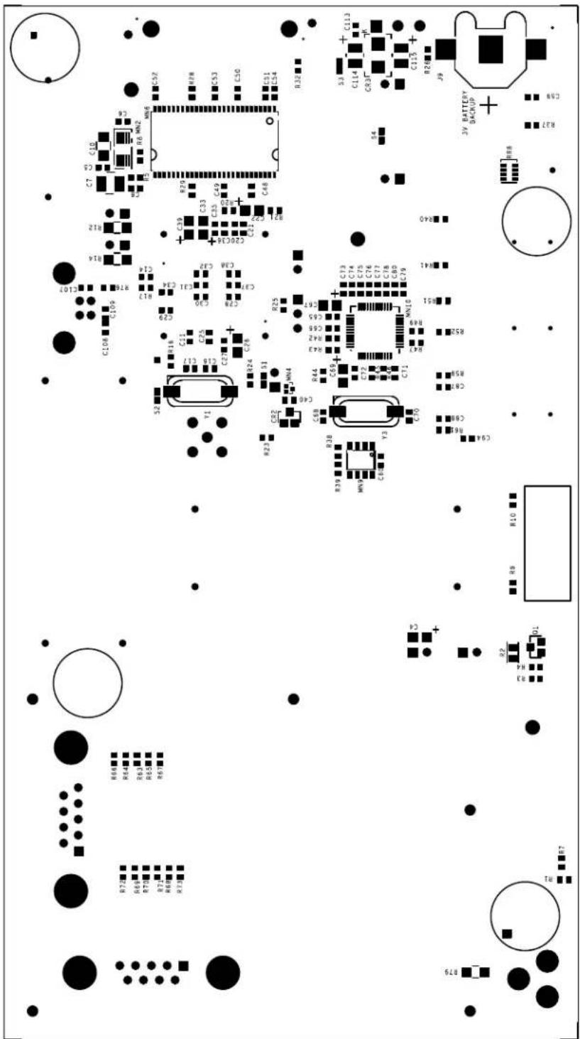
Circuit board layout diagram with labeled components including resistors, capacitors, ICs, and connectorsFigure 2-2. AT91SAM9RL-EK Layout - Bottom View
text_image
Circuit board layout diagram with labeled components and pin connections, including capacitors, resistors, and integrated circuits.2.4 Powering Up the Board
The AT91SAM9RL-EK requires 5V DC ( ±5% ). DC power is supplied to the board via the 2.1 mm by 5.5 mm socket J1. Coaxial plug center positive standard.
2.5 Backup Power Supply
The user has the possibility to plug a battery (3V Lithium Battery CR1225 or equivalent) in order to permanently power the backup part of the device.
Refer to Section 4.
2.6 Getting Started
The AT91SAM9RL-EK evaluation board is delivered with a CD-ROM containing all necessary information and step-by-step procedures for working with the most common development toolchains. Please refer to this CD-ROM, or to the AT91 web site, http://www.atmel.com/products/AT91/, for the most up-to-date information on getting started with the AT91SAM9RL-EK.
2.7 AT91SAM9RL-EK Block Diagram
Figure 2-3. AT91SAM9RL-EK Block Diagram

flowchart
graph TD
    A["1/2VDC POWER SUPPLY"] --> B["POWERLED"]
    B --> C["USERLED"]
    C --> D["USERLED2"]
    D --> E["RIGHTCLOCK LEFTCLK"]
    F["3A-AUDIO"] --> G["AUDIO"]
    G --> H["MIC OUTIN"]
    H --> I["USB DEVICE USBONX"]
    I --> J["DBGU DBUX"]
    J --> K["COM0 CT8"]
    L["3.5" QVGA"] --> M["LCD INTERFACE 3.5" QVGA"]
    M --> N["X RO-T TOUCH SCREEN X_LEFT Y_LOW"]

    O["1D - MICROCONTROLLER"] --> P["SHDN"]
    P --> Q["ACL 171"]
    P --> R["DD 18"]
    P --> S["RAS"]
    P --> T["SOD4"]
    P --> U["SOCS_NCE1"]
    P --> V["SOCK"]
    P --> W["SOCKE"]
    P --> X["CFOR NEWS NR31"]
    P --> Y["CFOR NEWS NR32"]
    P --> Z["CFWE_NVE NR33"]
    P --> AA["CFOE_SRC"]
    P --> AB["NCE9"]

    AC["1D -I/O MEMORY"] --> AD["SDRAMM/FLASH"]
    AD --> AE["DCR_21"]
    AD --> AF["AD_14"]
    AD --> AG["AD_14'"]
    AD --> AH["AD_14'"]
    AD --> AI["AD_14'"]
    AD --> AJ["AD_14'"]
    AD --> AK["AD_14'"]

    AL["3D -COMMUNICATION"] --> AM["USB Device USBONX"]
    AM --> AN["DBGU DBUX"]
    AN --> AO["COM0 CT8"]

    AP["3D - Expansion CONNECTORS"] --> AQ["DCP 31"]
    AQ --> AR["ACL 17"]
    AQ --> AS["RAS"]
    AQ --> AT["SOD4"]
    AQ --> AU["SOCS_NCE1"]
    AQ --> AV["SOCK"]
    AQ --> AW["SOCKE"]
    AQ --> AX["CFOR NEWS NR30"]
    AQ --> AY["CFOR NEWS NR31"]
    AQ --> AZ["CFOW NEWS NR32"]
    AQ --> BA["NCE9"]

    BB["PIO USAGE"] --> BC["PAD 31"]
    BC --> BD["PAS MC_DAB"]
    BC --> BE["PAS NC_DAB"]
    BC --> BF["PAS NC_DAB"]
    BC --> BG["PAS NC_DAB"]
    BC --> BH["PAS NC_DAB"]
    BC --> BI["PAS NC_DAB"]

    BJ["SIGNAL NAMING CONVENTIONS"] --> BK["SINAV SOFTWARE ASSIGNED NO SIGNAL/PX\nPxx PER= PERIPHERAL ASSIGNED NO SIGNAL\nPxx FREE IO SIGNAL\nPAXO/COS COMMNIT"]

    BL["SIGNAL NAMEING CONVENTIONS"] --> BM["SINAV SOFTWARE ASSIGNED NO SIGNAL/PX\nPxx PER= PERIPHERAL ASSIGNED NO SIGNAL\nPxx FREE IO SIGNAL\nPAXO/COS COMMNIT"]
3.1 AT91SAM9RL64 Microcontroller
■ Incorporates the ARM926EJ-S™ ARM® Thumb® Processor
- DSP Instruction Extensions
- ARM Jazelle ^® Technology for Java ^® Acceleration
- 4 Kbyte Data Cache, 4 Kbyte Instruction Cache, Write Buffer
- 210 MIPS at 190 MHz
– Memory Management Unit
- EmbeddedICE ^TM In-circuit Emulation, Debug Communication Channel Support
- Mid-level implementation Embedded Trace Macrocell™
■ Multi-layer AHB Bus Matrix for Large Bandwidth Transfers
– Six 32-bit-layer Matrix
- Boot Mode Select Option, Remap Command
■ One 32-KByte internal ROM, Single-cycle Access at Maximum Speed
■ One 64-KByte internal SRAM, Single-cycle Access at Maximum Speed
- 4 Blocks of 16 Kbytes Configurable in TCM or General-purpose SRAM on the AHB Bus Matrix
■ Single-cycle Accessible on AHB Bus at Bus Speed
■ Single-cycle Accessible on TCM Interface at Processor Speed
■ 2-channel DMA
– Memory to Memory Transfer
- 16 Bytes FIFO
- Linked List
■ External Bus Interface (EBI)
- EBI Supports SDRAM, Static Memory, ECC-enabled NAND Flash and CompactFlash ^®
■ LCD Controller
– Supports Passive or Active Displays
- Up to 24 Bits per Pixel in TFT Mode, Up to 16 bits per Pixel in STN Color Mode
- Up to 16M Colors in TFT Mode, Resolution Up to 2048x2048, Virtual Screen Support
■ High Speed (480 Mbit/s) USB 2.0 Device Controller
- On-Chip High Speed Transceiver, UTMI+ Physical Interface
- Integrated FIFOs and Dedicated DMA
- 4 Kbyte Configurable Integrated DPRAM
■ Fully-featured System Controller, including
- Reset Controller, Shutdown Controller
Board Description
– Four 32-bit Battery Backup Registers for a Total of 16 Bytes
– Clock Generator and Power Management Controller
- Advanced Interrupt Controller and Debug Unit
– Periodic Interval Timer, Watchdog Timer and Real-time Timer and Real-time Clock
■ Reset Controller (RSTC)
– Based on Two Power-on Reset Cells
– Reset Source Identification and Reset Output Control
■ Shutdown Controller (SHDC)
- Programmable Shutdown Pin Control and Wake-up Circuitry
■ Clock Generator (CKGR)
- Selectable 32768 Hz Low-power oscillator or Internal Low-power RC Oscillator on Battery Backup Power Supply, Providing a Permanent Slow Clock
- 12 MHz On-chip Oscillator for Main System Clock and USB Clock
- One PLL up to 240 MHz
- One PLL 480 MHz Optimized for USB HS
■ Power Management Controller (PMC)
– Very Slow Clock Operating Mode, Software Programmable Power Optimization Capabilities
- Two Programmable External Clock Signals
■ Advanced Interrupt Controller (AIC)
– Individually Maskable, Eight-level Priority, Vectored Interrupt Sources
– One External Interrupt Sources and One Fast Interrupt Source, Spurious Interrupt Protected
■ Debug Unit (DBGU)
- 2-wire UART and support for Debug Communication Channel
■ Periodic Interval Timer (PIT)
- 20-bit interval timer plus 12-bit interval counter
■ Watchdog Timer (WDT)
– Key-protected, Programmable Only Once, Windowed 16-bit Counter Running at Slow Clock
■ Real-time Timer (RTT)
- 32-bit Free-running Backup Counter Running at Slow Clock with 16-bit Prescaler
■ Real-time Clock (RTC)
– Time, Date and Alarm 32-bit Parallel Load
– Low Power Consumption
– Programmable Periodic Interrupt
■ One 6-channel 10-Bit Analog-to-Digital Converter
- Touch Screen Interface Compatible with Industry Standard 4-wire Sensitive Touch Panels
■ Four 32-bit Parallel Input/Output Controllers (PIOA, PIOB, PIOC and PIOD)
- 118 Programmable I/O Lines Multiplexed with up to Two Peripheral I/Os for 217-ball BGA package
– Input Change Interrupt Capability on Each I/O Line - Individually Programmable Open-drain, Pull-up resistor and Synchronous Output
■ 24-channel Peripheral DMA Controller (PDC)
■ One Multimedia Card Interface (MCI)
– SDCard/SDIO 1.0 and MultiMedia Card 3.1 Compliant
– Automatic Protocol Control and Fast Automatic Data Transfers with PDC
■ Two Synchronous Serial Controllers (SSC)
– Independent Clock and Frame Sync Signals for Each Receiver and Transmitter
– I²S Analog Interface Support, Time Division Multiplex Support
– High-speed Continuous Data Stream Capabilities with 32-bit Data Transfer
■ One AC97 Controller (AC97C)
- 6-channel Single AC97 Analog Front End Interface, Slot Assigner
■ Four Universal Synchronous/Asynchronous Receiver Transmitters (USART)
– Individual Baud Rate Generator, IrDA Infrared Modulation/Demodulation, Manchester Encoding/Decoding
– Support for ISO7816 T0/T1 Smart Card, Hardware Handshaking, RS485 Support
■ One Master/Slave Serial Peripheral Interface (SPI)
- 8- to 16-bit Programmable Data Length, Four External Peripheral Chip Selects
– High-speed Synchronous Communications
■ One Three-channel 16-bit Timer/Counter (TC)
– Three External Clock Inputs, Two Multi-purpose I/O Pins per Channel
– Double PWM Generation, Capture/Waveform Mode, Up/Down Capability
■ One Four-channel 16-bit PWM Controller (PWMC)
■ Two Two-wire Interfaces (TWI)
- Compatible with Standard Two-wire Serial Memories
– One, Two or Three Bytes for Slave Address
– Sequential Read/Write Operations
– Master, Multi-master and Slave Mode Operation - Bit Rate: Up to 400 Kbits
– General Call Supported in Slave mode - Connection to Peripheral DMA Controller (PDC) Channel Capabilities Optimizes Data Transfers in Master Mode Only (TWI0 only)
■ SAM-BA Boot Assistant
- Default Boot Program
– Interface with SAM-BA Graphic User Interface
■ IEEE 1149.1 JTAG Boundary Scan on All Digital Pins
■ Required Power Supplies:
- 1.08 to 1.32V for VDDCORE, VDDPLLB and VDDBU
- 3.0V to 3.6V for VDDPLLA, VDDANA, VDDUTMI and VDDIOP
- Programmable 1.65V to 1.95V or 3.0V to 3.6V for VDDIOM
■ Available in a 144-ball BGA (AT91SAM9R64) and a 217-ball LFBGA (AT91SAM9RL64) Package
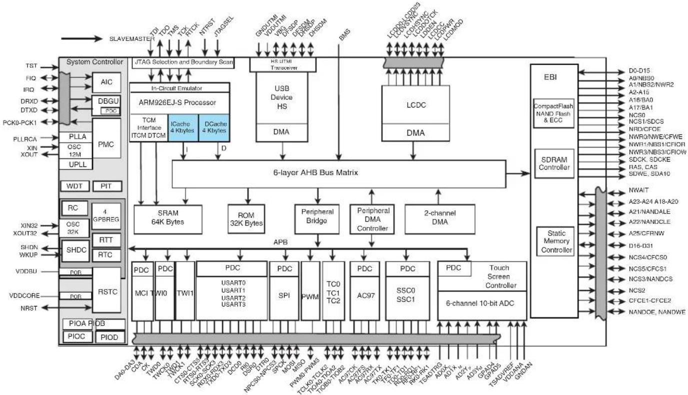
3.2 AT91SAM9RL Block Diagram
Figure 3-1. AT91SAM9RL Block Diagram
flowchart
graph TD
    subgraph System_Controller
        TST --> AIC
        HQ --> IRQ
        DRXD --> DTXD
        PCK0-PCK1 --> PLLRCA
        XIN --> XOUT
        UPLL --> UPLL
        WDT --> PIT
        RC --> OSC
        XIN32 --> XOUT32
        XOUT32 --> SHDC
        SHDN --> WKUP
        VDDBU --> POB
        VDDCORE --> POB
        NRST --> POA
        PIOA --> PIOC
        PPOB --> PIOC
        PIOC --> PIOD
    end

    subgraph JTAG_Selection_and_Boundary_Scan
        ARM926EJ-S_Processor --> TCM
        ARM926EJ-S_Processor --> ITCM
        ARM926EJ-S_Processor --> ITCM_DTCM
        ARM926EJ-S_Processor --> ICache_4Kbytes
        ARM926EJ-S_Processor --> DCache_4Kbytes
    end

    subgraph 6_Layer_AHB_Bus_Matrix
        SRAM["64K Bytes"] --> APB
        ROM["32K Bytes"] --> APB
        Peripheral_Bridge --> APB
        Peripheral_DMA_Controller --> APB
        2-channel_DMA --> APB
    end

    subgraph EBI
        CompactFlash["NAND Flash & ECC"] --> D0-D15
        CompactFlash --> AD/NBS0
        CompactFlash --> A1/NBS2/NWR2
        CompactFlash --> A2-A15
        CompactFlash --> A18/BA0
        CompactFlash --> A17/BA1
        CompactFlash --> NCS0
        CompactFlash --> NCS1/SDCS
        CompactFlash --> NRD/CFOE
        CompactFlash --> NWR0/NWE/CFWE
        CompactFlash --> NWR1/NBS1/CFIOR
        CompactFlash --> NWR3/NBS3/CFLOW
        CompactFlash --> SDCK_SDCKE
        CompactFlash --> BAS_CAS
        CompactFlash --> SDWE_SDA10

    subgraph SDRAM_Controller
        Static_Memory_Controller --> NWAIT
        Static_Memory_Controller --> A23-A24_A18-A20
        Static_Memory_Controller --> A21/NANDALE
        Static_Memory_Controller --> A22/NANDCLE
        Static_Memory_Controller --> A25/CFRNW
        Static_Memory_Controller --> D16-D31
        Static_Memory_Controller --> NCS4/CFCS0
        Static_Memory_Controller --> NCS5/CFCS1
        Static_Memory_Controller --> NCS3/NANDCS
        Static_Memory_Controller --> NCS2
        Static_Memory_Controller --> CFCE1-CFCE2
        Static_Memory_Controller --> NANDOE_NANDWE

    subgraph 6-channel_10-bit_ADC
        PDC_PDC_PDC_PDC_PDC_PDC_PDC_PDC_PDC_PDC_PDC_PDC_PDC_PDC_PDC_PDC_PDC_PDC_PDC_PDC_PDC_PDC_PDC_PDC_PDC_PDC_PDC_PDC_PDC_PDC_PDC_PDC_PDC_PDC_PDC_PDC_PDC_PDC_PDC_PDC_PDC_PDC_PDC_PDC_PDC_PDC_PDC_PDC_PDC_PDC_PDC(PWM-PCWS)
        PWD-PCWS["PWD-PCWS"]
        TCO-PCWS["PCO-PCWS"]
        THO-PCWS["PCO-PCWS"]
        ADC-PCWS["PAC-PCWS"]
        AC-PCWS["PAC-PCWS"]
        TKP-PCWS["PJK-PCWS"]
        TRP-PCWS["PJK-PCWS"]
        RXO-PCWS["PJK-PCWS"]
        TSAD-PCWS["PAD-PCWS"]
        ADDX["PAD-X"]
        ADYX["PAD-Y"]
        ADYX["PAD-X"]
        GRADS["PGRADS"]
        VDDANA["VDDANA"]
    end

    AIC --> DBGU
    DBGU --> PCC
    PCC --> PLLA
    PLLA --> OSC
    OSC --> UPLL

    PCMC --> PMC

    RSTC --> RSTC

    POB --> POB

    POA --> POA

    PINDB["PIOA"] --> PINDB

    PINDB --> PINDB

    APB --> PDC["PDC"]
    APB --> MCI1["MCI1"]
    APB --> TWI1["TWI1"]
    APB --> USART0["USART0"]
    APB --> USART1["USART1"]
    APB --> USART2["USART2"]
    APB --> USART3["USART3"]
    APB --> TXOXTXO["XOX"]
    APB --> DCD0["DCD0"]
    APB --> DSB0["DSB0"]
    APB --> DTRD["DTRD"]
    APB --> DSPX["DSPX"]
    APB --> MSI["MSI"]
    APB --> MSD["MSD"]
    APB --> PWM["PWM-PMWS"]
    APB --> TC0-TC0-TC0["TC0-TC0-TC0"]
    APB --> THO-THO-TH0["THO-THO-TH0"]
    APB --> ADCYCK["ADCYCK"]
    APB --> ACETRS["ACETRS"]
    APB --> ACPTTX["ACPTTX"]
    APB --> TKPL-TK1["TKPL-TK1"]
    APB --> TPRT-TPRT["TRPRT-TPRT"]
    APB --> RXO-RX1["RXO-RX1"]
    APB --> TSAOTRG["TSATOTRG"]
    APB --> ADDX["PAD-X"]
    APB --> ADYX["PAD-Y"]
    APB --> ADYX["PAD-X"]
    APB --> GRADS["PGRADS"]
    APB --> VDDANA["VDDANA"]

    HGTNTM["HDGDTTM"] --> USB_Device_HS
    HGTNTM_REFD["GNDUTTM"] --> LCDDR-LCDPE3["LCDDDR-LCDPE3"]
    HGTNTM_VEGU["GVG-DVG-UVG"] --> LDDDR-LCDPE3["LCDDDR-LCDPE3"]
    HGTNTM_VEG_SDP["GVG_SDP"] --> LDDDR_SDP["LCDDDR_SDP"]
    HGTNTM_VEG_DSP["GVG_DSP"] --> LDDDR_DSP["LCDDDR_DSP"]

    HCDSLID["HCDSLID"] --> LCDDR-LCDPE3["LCDDDR-LCDPE3"]
    HCDSLID_REFD --> LCDDR_SDP["LCDDDR_SDP"]

    BMS --> LCDC["LCDC"]
    LCDC --> DMA["DMA"]

    EBI["EBI"] --> CompactFlash["NAND Flash & ECC"]
    SDRAM_Controller["SDRAM Controller"] --> Static_Memory_Controller["Static Memory Controller"]

    style System_Controller fill:#f9f,stroke:#333,stroke-width:2px
    style EBI fill:#ccf,stroke:#333,stroke-width:2px
3.3 Microcontroller
■ One AT91SAM9RL64 217-ball LFBGA fitted on board
3.4 Memory
■ 32 Kbytes of Internal ROM
■ 64 Kbyte of Internal SRAM
■ Atmel serial DataFlash
■ 64 Mbytes of SDRAM memory (32-bit bus width)
■ 256 Mbytes of NAND Flash memory (8-bit bus width)
■ TWI serial EEPROM (footprint only)
3.5 Clock Circuitry
■ 12 MHz standard crystal for the embedded oscillator
3-4 AT91SAM9RL-EK Evaluation Board User Guide

■ Software selectable, 32768Hz Low-power external standard crystal Oscillator or Internal Low Power RC Oscillator
3.6 Reset Circuitry
■ Internal reset controller with bi-directional reset pin
■ External reset pushbutton
3.7 Shutdown Controller
■ Programmable shutdown and Wake-Up
■ Wake-up push button
3.8 Power Supply Circuitry
■ On-board 1.2V High Efficiency step-down charge pump regulator with shutdown control
■ On-board 3.3V linear regulator with shutdown control
3.9 Remote Communication
■ One serial interface (DBGU COM Port) via RS-232 DB9 male socket
■ One additional serial interface (COM Port 1) with RTS/CTS handshake control via RS-232 DB9 male socket
■ One High Speed USB 2.0 port 480 Mbits per second (UDP)
3.10 Audio Stereo Interface
■ One AC97 audio CODEC with:
■ One 32 Ohm Stereo Headset output (J16) with master volume and mute controls
■ One line-in
■ One Mono/Stereo Microphone input.
3.11 User Interface
■ Two user input pushbuttons
■ Two user green LED
■ One yellow power LED (can be also software controlled)
3.12 Debug Interface
■ 20-pin JTAG/ICE interface connector
■ DBGU COM port
3.13 Expansion Slot
■ One DataFlash, SD/MMC card slot
■ All I/Os of the AT91SAM9RL are routed to peripheral extension connectors (J23, J24, J25, J26).
■ All EBI Signals of the AT91SAM9RL are routed to extension footprint connectors (J27). Refer to the Atmel application note Connecting EBI Memory Daughter Boards to AT91SAM Evaluation Boards, lit. no. 6309.
This allows the developer to check the integrity of the components and to extend the features of the board by adding external hardware components or boards.
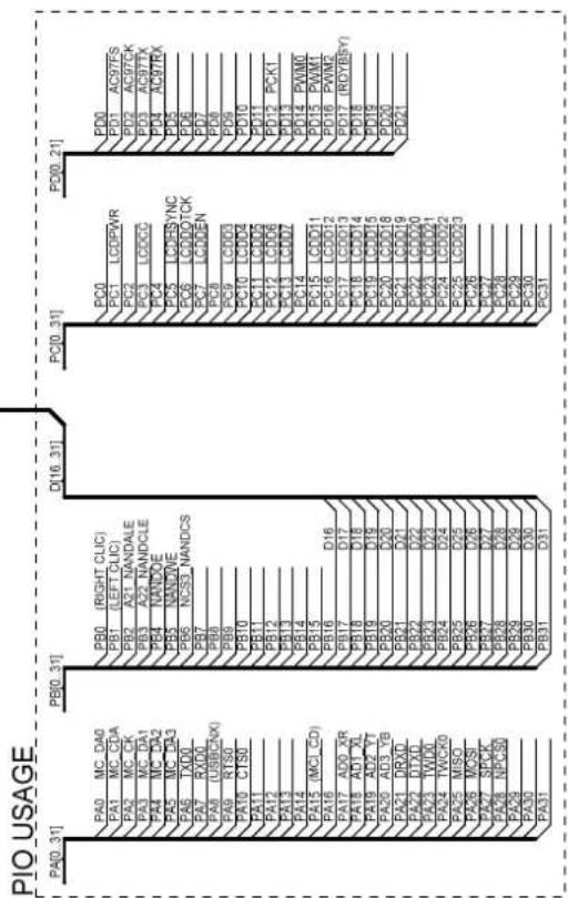
3.14 PIO Usage
Table 3-1. PIO Controller A
| I/O Line | Peripheral A Peripheral B Application | Usage Powered by | |||
| PA0 MC | _DA0 SD/MMC CARD READER MC_DA0 VDDIOP | ||||
| PA1 MC | _CDA SD/MMC CARD READER | MC_CDA | VDDIOP | ||
| PA2 | MC_CK | SD/MMC CARD READER | MC_CK | VDDIOP | |
| PA3 | MC_DA1 | TCLK0 | SD/MMC CARD READER | MC_DA1 | VDDIOP |
| PA4 | MC_DA2 | TIOA0 | SD/MMC CARD READER | MC_DA2 | VDDIOP |
| PA5 | MC_DA3 | TIOB0 | SD/MMC CARD READER | MC_DA3 | VDDIOP |
| PA6 | TXD0 | RS232 COM PORT | TXD0 | VDDIOP | |
| PA7 | RXD0 | RS232 COM PORT | RXD0 | VDDIOP | |
| PA8 | SCK0 | RF1 | USB DEVICE | PA8 as USB_CNX | VDDIOP |
| PA9 | RTS0 | RK1 | RS232 COM PORT | RTS0 | VDDIOP |
| PA10 | CTS0 | RK0 | RS232 COM PORT | CTS0 | VDDIOP |
| PA11 | TXD1 | VDDIOP | |||
| PA12 | RXD1 | VDDIOP | |||
| PA13 | TXD2 | TD1 | VDDIOP | ||
| PA14 | RXD2 | RD1 | VDDIOP | ||
| PA15 | TD0 | SD/MMC CARD READER | PA15 as MCI_CD | VDDIOP | |
| PA16 | RD0 | VDDIOP | |||
| PA17 | AD0 | TOUCH SCREEN PANEL | AD0_XR | VDDIOP | |
| PA18 | AD1 | RTS1 | TOUCH SCREEN PANEL | AD1_XL | VDDIOP |
| PA19 | AD2 | CTS1 | TOUCH SCREEN PANEL | AD2_YT | VDDIOP |
| PA20 | AD3 | SCK3 | TOUCH SCREEN PANEL | AD3_YB | VDDIOP |
| PA21 | DRXD | SERIAL DEBUG PORT | DRXD | VDDIOP | |
| PA22 | DTXD | RF0 | SERIAL DEBUG PORT | DTXD | VDDIOP |
| PA23 | TWD0 | I2C MEMORY | TWD0 | VDDIOP | |
| PA24 TWCK0 | I2C MEMORY | TWCK0 VDDIOP | |||
| PA25 | MISO | DATAFLASH DEVICE | MISO | VDDIOP | |
| PA26 | MOSI | DATAFLASH DEVICE | MOSI | VDDIOP | |
| PA27 | SPCK | DATAFLASH DEVICE | SPCK | VDDIOP | |
| PA28 | NPCS0 | DATAFLASH DEVICE | NPCS0 | VDDIOP | |
| PA29 | RTS2 | TF1 | VDDIOP | ||
| PA30 | CTS2 | TK1 | VDDIOP | ||
| PA31 | NWAIT | IRQ | VDDIOP | ||
Table 3-2. PIO Controller B
| I/O Line Peripheral A Peripheral B Application Usage Powered by | |||||
| PB0 TX | D3 USER'S PUSH | BUTTON 1 PB0 as LEFT CLICK VDDIOP | |||
| PB1 RX | D3 USER'S PUSH | BUTTON 2 PB1 as RIGHT CLICK VDDIOP | |||
| PB2 | A21/NANDALE | NAND FLASH MEMORY | NANDALE | VDDIOM | |
| PB3 | A22/NANDCLE | NAND FLASH MEMORY | NANDCLE | VDDIOM | |
| PB4 | NANDOE | NAND FLASH MEMORY | NANDOE | VDDIOM | |
| PB5 | NANDWE | NAND FLASH MEMORY | NANDWE | VDDIOM | |
| PB6 | NCS3/NANDCS | NAND FLASH MEMORY | NCS3/NANDCS | VDDIOM | |
| PB7 NCS4/CFCS0 | NPCS1 | VDDIOM | |||
| PB8 | CFCE1 | PWM0 | VDDIOM | ||
| PB9 | CFCE2 | PWM1 | VDDIOM | ||
| PB10 | A25/CFRNW | FIQ | VDDIOM | ||
| PB11 | A18 | VDDIOM | |||
| PB12 | A19 | VDDIOM | |||
| PB13 | A20 | VDDIOM | |||
| PB14 | A23 | PCK0 | VDDIOM | ||
| PB15 | A24 | ADTRG | VDDIOM | ||
| PB16 | D16 | SDRAM MEMORY | D16 | VDDIOM | |
| PB17 | D17 | SDRAM MEMORY | D17 | VDDIOM | |
| PB18 | D18 | SDRAM MEMORY | D18 | VDDIOM | |
| PB19 | D19 | SDRAM MEMORY | D19 | VDDIOM | |
| PB20 | D20 | SDRAM MEMORY | D20 | VDDIOM | |
| PB21 | D21 | SDRAM MEMORY | D21 | VDDIOM | |
| PB22 | D22 | SDRAM MEMORY | D22 | VDDIOM | |
| PB23 | D23 | SDRAM MEMORY | D23 | VDDIOM | |
| PB24 | D24 | SDRAM MEMORY | D24 | VDDIOM | |
| PB25 | D25 | SDRAM MEMORY | D25 | VDDIOM | |
| PB26 | D26 | SDRAM MEMORY | D26 | VDDIOM | |
| PB27 | D27 | SDRAM MEMORY | D27 | VDDIOM | |
| PB28 | D28 | SDRAM MEMORY | D28 | VDDIOM | |
| PB29 | D29 | SDRAM MEMORY | D29 | VDDIOM | |
| PB30 | D30 | SDRAM MEMORY | D30 | VDDIOM | |
| PB31 | D31 | SDRAM MEMORY | D31 | VDDIOM | |
Table 3-3. PIO Controller C
| I/O Line Peripheral A Peripheral B Application Usage Powered by | |||||
| PC0 TF0 VDDIOP | |||||
| PC1 TK0 LCDPWR LCD PANEL LCDPWR VDDIOP | |||||
| PC2 LCDMOD PWM0 VDDIOP | |||||
| PC3 | LCDCC | PWM1 | LCD PANEL | LCDCC | VDDIOP |
| PC4 | LCDVSYNC | VDDIOP | |||
| PC5 | LCDHSYNC | LCD PANEL | LCDHSYNC | VDDIOP | |
| PC6 | LCDDOTCK | LCD PANEL | LCDDOTCK | VDDIOP | |
| PC7 | LCDDEN | LCD PANEL | LCDDEN VDDIOP | ||
| PC8 | LCDD0 | LCDD2 | LCD PANEL | LCDD2 | VDDIOP |
| PC9 | LCDD1 | LCDD3 | LCD PANEL | LCDD3 | VDDIOP |
| PC10 | LCDD2 | LCDD4 | LCD PANEL | LCDD4 | VDDIOP |
| PC11 | LCDD3 | LCDD5 | LCD PANEL | LCDD5 | VDDIOP |
| PC12 | LCDD4 | LCDD6 | LCD PANEL | LCDD6 | VDDIOP |
| PC13 | LCDD5 | LCDD7 | LCD PANEL | LCDD7 | VDDIOP |
| PC14 | LCDD6 | LCDD10 | LCD PANEL | LCDD10 | VDDIOP |
| PC15 | LCDD7 | LCDD11 | LCD PANEL | LCDD11 | VDDIOP |
| PC16 | LCDD8 | LCDD12 | LCD PANEL | LCDD12 | VDDIOP |
| PC17 | LCDD9 | LCDD13 | LCD PANEL | LCDD13 | VDDIOP |
| PC18 | LCDD10 | LCDD14 | LCD PANEL | LCDD14 | VDDIOP |
| PC19 | LCDD11 | LCDD15 | LCD PANEL | LCDD15 | VDDIOP |
| PC20 | LCDD12 | LCDD18 | LCD PANEL | LCDD18 | VDDIOP |
| PC21 | LCDD13 | LCDD19 | LCD PANEL | LCDD19 | VDDIOP |
| PC22 | LCDD14 | LCDD20 | LCD PANEL | LCDD20 | VDDIOP |
| PC23 | LCDD15 | LCDD21 | LCD PANEL | LCDD21 | VDDIOP |
| PC24 | LCDD16 | LCDD22 | LCD PANEL | LCDD22 | VDDIOP |
| PC25 | LCDD17 | LCDD23 | LCD PANEL | LCDD23 | VDDIOP |
| PC26 LCDD18 | VDDIOP | ||||
| PC27 LCDD19 | VDDIOP | ||||
| PC28 LCDD20 | VDDIOP | ||||
| PC29 | LCDD21 | TIOA1 | VDDIOP | ||
| PC30 | LCDD22 | TIOB1 | VDDIOP | ||
| PC31 | LCDD23 | TCLK1 | VDDIOP | ||
Table 3-4. PIO Controller D
| I/O Line | Peripheral A Peripheral B Application | Usage Powered by | |||
| PD0 NC | S2 VDDIOP | ||||
| PD1 AC | 97_FS AC97 CODE | C AC97_FS VDDIOP | |||
| PD2 AC | 97_CK SCK1 AC97 | CODEC | AC97_CK | VDDIOP | |
| PD3 AC | 97_TX | CTS3 | AC97 CODEC AC97_TX VDDIOP | ||
| PD4 | AC97_RX | RTS3 | AC97 CODEC | AC97_RX | VDDIOP |
| PD5 | DTXD | PWM2 | VDDIOP | ||
| PD6 | AD4 | VDDIOP | |||
| PD7 | AD5 | VDDIOP | |||
| PD8 | NPCS2 | PWM3 | VDDIOP | ||
| PD9 SCK2 | NPCS3 | VDDIOP | |||
| PD10 | TWD1 | TIOA2 | VDDIOP | ||
| PD11 | TWCK1 | TIOB2 | VDDIOP | ||
| PD12 | PWM2 | PCK1 | VDDIOP | ||
| PD13 | NCS5/CFCS1 | NPCS3 | VDDIOP | ||
| PD14 | DSR0 | PWM0 | POWER LED | PD14 or PWM0 | VDDIOP |
| PD15 | DTR0 | PWM1 | USER LED 1 | PD15 or PWM1 | VDDIOP |
| PD16 | DCD0 | PWM2 | USER LED 2 | PD16 or PWM2 | VDDIOP |
| PD17 | RI0 | NAND FLASH MEMORY | PD17 as RDYBSY | VDDIOP | |
| PD18 | PWM3 | VDDIOP | |||
| PD19 | PCK0 | VDDIOP | |||
| PD20 | PCK1 | VDDIOP | |||
| PD21 | TCLK2 | VDDIOP | |||
4.1 Jumpers
Table 4-1. Jumpers Configuration
| Designation Default Setting Feature | ||
| J2 Closed 3 | 3V Jumper | (1) |
| J3 Closed | Forces power on.To use the software shutdown control, J3 must be opened. 3V battery backup must be present. | |
| J5 Closed VDDPLLB Jumper | (1) | |
| J6 Closed VDDPLLA Jumper | (1) | |
| J8 Closed VDDBU Jumper | (1) | |
| J10 Closed VDDCORE Jumper | (1) | |
| J11 1-2 | BMS (Boot Mode Select)1-2: Internal ROM2-3: NCS0 | |
| J12 Closed Enables the use of the embedded NAND FLASH device (MN7) | ||
| J13 Closed Enables the use of the embedded SERIAL DATAFLASH device (MN8) | ||
Note: 1. These jumpers are provided for power consumption measurement use. By default, they are closed. To use this feature, the user has to open the strap and insert an ammeter.
4.2 JTAG/ICE
Table 4-2. JTAG/ICE Configuration
| Designation Default Setting | Feature | |
| S1 | Opened | Selects ICE mode or JTAG mode |
| R11 | Soldered | Enables the ICE NTRST input |
| R13 | Soldered | Enables the ICE NRST input |
4.3 Microcontroller Clock
Table 4-3. Microcontroller Clock Configuration
| Designation | Default Setting Feature | |
| S2 Opened | To use an external source clock, the user has to close S2 and populate J7. In this case, C16, C17 and J7 have to be unsoldered. |
4.4 Memory
Table 4-4. Memory Configuration
| Designation | Default Setting Feature | |
| SDRAM (MN5 & MN6) | ||
| R29 | Soldered | Enables MN5 Chip select access |
| R30 | Soldered | Enables MN6 Chip select access |
| NANDFLASH (MN7) | ||
| J12 | Closed | Enables the use of the NANDFLASH device |
| R32 | Soldered | Enables the use of the Ready/Busy signal |
| S3 | Opened | Disables the write protect |
| SERIAL DATAFLASH (MN8) | ||
| J13 | Closed | Enables the use of the DATAFLASH device |
| S4 | Opened | Disables the write protect. |
| TWI SERIAL EEPROM NOT POPULATED (MN9) | ||
4.5 Miscellaneous
Refer to the TOP level schematic for the PIO usage.
Table 4-5. Miscellaneous
| Designation | Default Setting Feature | |
| USB HIGH SPEED DEVICE INTERFACE | ||
| R75 Soldered | USB DEVICE: | Enables the use of the USBCNX signal |
| DBGU COM PORT | ||
| R64 | Soldered | Enables the use of DTXD output signal |
| R66 | Soldered | Enables the use of DRXD input |
| RS232 COM PORT: Enable the use of Input/output signals | ||
Table 4-5. Miscellaneous
| Designation | Default Setting Feature | |
| R70 | Soldered | TXD |
| R71 | Soldered | RTS |
| R72 | Soldered | RXD |
| R73 | Soldered | CTS |
| TP1 N.A GND Test point | ||
| TP2 N.A GND Test point | ||
| TP3 N.A GND Test point | ||
5.1 Board Schematics
This section contains the following schematics:
■ Board Diagram - Schematic Top Level
■ Power supply
■ AT91SAM9RL Microcontroller
■ EBI Memory
Serial Memory
■ Audio AC97
Serial Interface
■ TFT LCD display
■ Expansion connectors

text_image
02 - POWER SUPPLY 12VDC POWERLED USERLED USERLED RIGHTCLOCK LEFTCLOCK 03 - MICROCONTROLLER SHDN A0. 17 D0. 15 RAS CAS SDA10 SDWE SDCS_NCS1 SDCK SDCKE CFOR_NBS1_NWR1 CFOR_NBS3_NWR3 CFWE_NWE_NWR0 CFOE_NRD NC50 NRST DM OP PA0. 31] PB0. 31] PC0. 31] PD0. 21) P40. 31] P80. 31] PC0. 31] P20. 21) NANDE NANDE NANDWE NANDWE NRST 09 - EXPANSION CONNECTORS DA0. 31) A0. 17) RAS CAS SDA10 SDWE SDCS_NCS1 SDCK SDCKE CFWE_NWE_NWR0 CFOR_NBS1_NWR1 CFOR_NBS3_NWR3 CFOE_NRD NC50 D0. 15 D0. 31) PIO USAGE PA0. 31) P80. 31) D0. 31) P30. 31) P30. 21) P40. 21) P40. 15) P40. 15) P40. 15) P40. 15) P40. 15) P40. 15) P40. 15) P40. 15) P40. 15) P40. 15) P40. 15) P40. 15) P40. 15) P42. MC_DA0 PA1 MC_DA4 PA2 MC_CK PA3 MC_DA1 PA4 MC_DA2 PA5 MC_DA3 PA6 TX00 PA7 RX00 PA8 USB(DX)X PA9 ADJ_XL PA10 ADJ_YB PA11 ADJ_YB PA12 ADJ_YB PA13 ADJ_YB PA14 ADJ_YB PA15 ADJ_YB PA16 ADJ_YB PA17 ADJ_YB PA18 ADJ_YB PA19 ADJ_YB PA20 ADJ_YB PA21 ADJ_YB PA22 ADJ_YB PA23 ADJ_YB PA24 ADJ_YB PA25 ADJ_YB PA26 ADJ_YB PA27 ADJ_YB PA28 ADJ_YB PA29 ADJ_YB PA30 ADJ_YB PA31 ADJ_YB P32 ADJ_YB P33 ADJ_YB P34 ADJ_YB P35 ADJ_YB P36 ADJ_YB P37 ADJ_YB P38 ADJ_YB P39 ADJ_YB P40 ADJ_YB P41 ADJ_YB P42 ADJ_YB P43 ADJ_YB P44 ADJ_YB P45 ADJ_YB P46 ADJ_YB P47 ADJ_YB P48 ADJ_YB P49 ADJ_YB P50 ADJ_YB P51 ADJ_YB P52 ADJ_YB P53 ADJ_YB P54 ADJ_YB P55 ADJ_YB P56 ADJ_YB P57 ADJ_YB P58 ADJ_YB P59 ADJ_YB P60 ADJ_YB P61 ADJ_YB P62 ADJ_YB P63 ADJ_YB P64 ADJ_YB P65 ADJ_YB P66 ADJ_YB P67 ADJ_YB P68 ADJ_YB P69 ADJ_YB P70 ADJ_YB P71 ADJ_YB P72 ADJ_YB P73 ADJ_YB P74 ADJ_YB P75 ADJ_YB P76 ADJ_YB P77 ADJ_YB P78 ADJ_YB P79 ADJ_YB P80 ADJ_YB P81 ADJ_YB P82 ADJ_YB P83 ADJ_YB P84 ADJ_YB P85 ADJ_YB P86 ADJ_YB P87 ADJ_YB P88 ADJ_YB P89 ADJ_YB P90 ADJ_YB P91 ADJ_YB P92 ADJ_YB P93 ADJ_YB P94 ADJ_YB P95 ADJ_YB P96 ADJ_YB P97 ADJ_YB P98 ADJ_YB P99 ADJ_YB| B | JPG | 18-APR-07 | ||||
| A | INIT EDIT | JPG | 01-MAR-07 | |||
| REV | MODIF. | DES. | DATE | VER. | DATE | |
| AT91SAM9RL-EK | SCALE 1/1 | REV. | SHEET | |||
| DIAGRAM | B | 19 | ||||
text_image
PIO USAGE PA0 [0..31] PB[0..31] D[16..31] PC[0..31] PD[0..21] PA0 MC_DA0 PB0 (RIGHT CLIC) PC0 PD0 PA1 MC_CDA PB1 (LEFT CLIC) PC1 LCDPWR PD1 AC97FS PA2 MC_CK PB2 A31 NANDALE PC2 PD2 AC97CK PA3 MC_DA1 PB3 A22 NANDCLE PC3 LCDCC PD3 AC97TX PA4 MC_DA2 PB4 NANDDE PC4 PD4 AC97RX PA5 MC_DA3 PB5 NANDWE PC5 LCDSYNC PD5 PA6 TXD0 PB6 NCS3_NANDCS PC6 LCDDOTCK PD6 PA7 RXD0 PB7 PC7 LCDDEN PD7 PA8 (USBCNX) PB8 PC8 PD8 PA9 RTSO PB9 PC9 LCDO3 PD9 PA10 CTSO PB10 PC10 LCDO4 PD10 PA11 PB11 PC11 LCDO5 PD11 PA12 PB12 PC12 LCDO6 PD12 PCK1 PA13 PB13 PC13 LCDO7 PD13 PA14 PB14 PC14 PD14 PWM0 PA15 (MCL_CD) PB15 PC15 LCDO11 PD15 PWM1 PA16 PB16 D16 PC16 LCDO12 PD16 PWM2 PA17 AD0_XR PB17 D17 PC17 LCDO13 PD17 (RDYBSY) PA18 AD1_XL PB18 D18 PC18 LCDO14 PD18 PA19 AD2_YT PB19 D19 PC19 LCDO15 PD19 PA20 AD3_YB PB20 D20 PC20 LCDO16 PD20 PA21 DRXD PB21 D21 PC21 LCDO18 PD20 PA22 DTXD PB22 D22 PC22 LCDO19 PD21 PA23 TWD0 PB23 D23 PC23 LCDO20 PD22 PA24 TWCK0 PB24 D24 PC24 LCDO21 PD23 PA25 MISO PB25 D25 PC25 LCDO22 PD24 PA26 MOSI PB26 D26 PC26 LCDO23 PD25 PA27 SPCK PB27 D27 PC27 PA28 NPCS0 PB28 D28 PC28 LCDO24 PD26 PA29 PB29 D29 PC29 LCDO25 PD27 PA30 PB30 D30 PC30 LCDO26 PD28 PA31 PB31 D31 PC30 LCDO27 PD29 PC30 D30 PC30 LCDO28 PD30 PC31 D31 PC31 LCDO29 PD31| Pxx (NAME) | SOFTWARE ASSIGNED I/O SIGNAL |
| Pxx PERIPH | PERIPHERAL ASSIGNED I/O SIGNAL |
| Pxx | FREE I/O SIGNAL |
| ITALIC FONTS | COMMENT |

text_image
10 SQUARE CM COPPER AREA FOR HEAT SINKING WITH NO SOLDER MASK REGULATED 5V ONLY J1 1 2 3 5V R1 100K C1 330μF CR1 5V R79 0R Q2 Si1563EDH J3 FORCE POWER ON SHDN C9 15PF R6 10K 6 5 4 3 2 1 2 3 R7 10K MN1 LT1963AEQ-3.3 GND VIN VOUT SD GND FB 3V3 CURRENT MEASURE J2 3V3 C3' 10μF C4' 10μF C5 1μF C6 1μF 8 6 3 4 TPS60500 C1M C1P C2M C2P VIN VOUT FB EN GND PG MN2 9 3V3 3V2 C7 22μF R5 100K C8 10PF R8 200K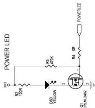
text_image
POWER LED 3V3 R2 120R DS3 YELLOW 3 Q1 IRLML2402 R3 470K 1 R4 0R POWERLED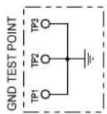

6.1 Pull-up Resistor on the Wrong Pin
The RTCK pin (connector J4, pin 11), which is an input, has a pull-up resistor whereas the TCK pin (connector J4, pin 9), which is an output, has not.
Problem Fix/Workaround
The user may observe a possible increase in the power consumption on VDDIO (a few micro-amps) but it does not prevent the JTAG-ICE interface to work correctly on this board.
Correct schematics would have a pull-up on the TCK pin to tie the CMOS input to a known level, in order to avoid a possible pad oscillation and a possible increase in power consumption.
6.2 VDDCORE Power Consumption Measurement Impossible
If the AT91SAM9RL64 device is an engineering sample (ES), VDDCORE power consumption measurement is impossible on J10 Jumper.
Problem Fix/Workaround
None.
7.1 Revision History
Table 7-1. Revision History
| Document Ref. Comments Change Request Ref. | ||
| 6325C | Section 6.2 "VDDCORE Power Consumption Measurement Impossible" errata added | 7188 |
| 6325B | CFE1 and CFE2 changed into CFCE1 and CFCE2 in Table 3-2 on page 3-8 | 5864 |
| Section 6.1 "Pull-up Resistor on the Wrong Pin" errata added 5983 | ||
| 6325A First issue. | ||
Revision History
Headquarters International
Atmel Corporation
2325 Orchard Parkway
San Jose, CA 95131
USA
Tel: 1(408) 441-0311
Fax: 1(408) 487-2600
Atmel Asia
Unit 1-5 & 16, 19/F
BEA Tower, Millennium City 5
418 Kwun Tong Road
Kwun Tong, Kowloon
Hong Kong
Tel: (852) 2245-6100
Fax: (852) 2722-1369
Atmel Europe
Le Krebs
Disclaimer: The information in this document is provided in connection with Atmel products. No license, express or implied, by estoppel or otherwise, to any intellectual property right is granted by this document or in connection with the sale of Atmel products. EXCEPT AS SET FORTH IN ATMEL'S TERMS AND CONDITIONS OF SALE LOCATED ON ATMEL'S WEB SITE, ATMEL ASSUMES NO LIABILITY WHATSOEVER AND DISCLAIMS ANY EXPRESS, IMPLIED OR STATUTORY WARRANTY RELATING TO ITS PRODUCTS INCLUDING, BUT NOT LIMITED TO, THE IMPLIED WARRANTY OF MERCHANTABILITY, FITNESS FOR A PARTICULAR PURPOSE, OR NON-INFRINGEMENT. IN NO EVENT SHALL ATMEL BE LIABLE FOR ANY DIRECT, INDIRECT, CONSEQUENTIAL, PUNITIVE, SPECIAL OR INCIDENTAL DAMAGES (INCLUDING, WITHOUT LIMITATION, DAMAGES FOR LOSS OF PROFITS, BUSINESS INTERRUPTION, OR LOSS OF INFORMATION) ARISING OUT OF THE USE OR INABILITY TO USE THIS DOCUMENT, EVEN IF ATMEL HAS BEEN ADVISED OF THE POSSIBILITY OF SUCH DAMAGES. Atmel makes no representations or warranties with respect to the accuracy or completeness of the contents of this document and reserves the right to make changes to specifications and product descriptions at any time without notice. Atmel does not make any commitment to update the information contained herein. Unless specifically provided otherwise, Atmel products are not suitable for, and shall not be used in, automotive applications. Atmel's products are not intended, authorized, or warranted for use as components in applications intended to support or sustain life.

© 2010 Atmel Corporation. All rights reserved. Atmel ^® , logo and combinations thereof, DataFlash ^® and others are registered trademarks or trademarks of Atmel Corporation or its subsidiaries. ARM ^® , the ARMPowered ^® logo, Thumb ^® and others are the registered trademarks or trademarks of ARM Ltd. Other terms and product names may be trademarks of others.