MCP652 - Amplificateur opérationnel Microchip - Free user manual and instructions
Find the device manual for free MCP652 Microchip in PDF.

User questions about MCP652 Microchip
0 question about this device. Answer the ones you know or ask your own.
Ask a new question about this device
Download the instructions for your Amplificateur opérationnel in PDF format for free! Find your manual MCP652 - Microchip and take your electronic device back in hand. On this page are published all the documents necessary for the use of your device. MCP652 by Microchip.
USER MANUAL MCP652 Microchip
50 MHz, 200 μV Op Amps with mCal
Features:
• Gain-Bandwidth Product: 50 MHz
- Slew Rate: 30 V/μs
- Low Input Offset: ±200 μV (maximum)
- Low Input Bias Current: 6 pA (typical)
• Noise: 7.5 nV/√Hz, at 1 MHz
- Ease-of-Use:
- Unity-Gain Stable
- Rail-to-Rail Output
- Input Range incl. Negative Rail
- No Phase Reversal
• Supply Voltage Range: +2.5V to +5.5V
• High Output Current: ±100 mA
• Supply Current: 6.0 mA/Ch (typical)
• Low-Power Mode: 5 μA/Ch
- Small Packages: SOT23-5, DFN
- Extended Temperature Range: -40°C to +125°C
Typical Applications:
- Driving A/D Converters
- Fast Low-side Current Sensing
• Power Amplifier Control Loops
• Optical Detector Amplifier - Barcode Scanners
- Multi-Pole Active Filter
• Consumer Audio
Design Aids:
• SPICE Macro Models
- Filte Softwareb
- Microchip Advanced Part Selector (MAPS)
• Analog Demonstration and Evaluation Boards
- MCP651EV-VOS
- Application Notes
Description:
The Microchip Technology Inc. MCP651/1S/2/3/4/5/9 family of high bandwidth and high slew rate operational amplifiers features low offset. At power-up, these op amps are self-calibrated using mCal. Some package options also provide a Calibration/Chip Select pin (CAL/CS) that supports a Low-Power mode of operation, with offset calibration at the time normal operation is re-started. These amplifiers are optimized for high speed, low noise and distortion, single-supply operation with rail-to-rail output and an input that includes the negative rail.
This family is offered in single (MCP651 and MCP651S), single with CAL/CS pin (MCP653), dual (MCP652), dual with CAL/CS pins (MCP655), quad (MCP654) and quad with CAL/CS pins (MCP659). All devices are fully specified from -40°C to +125°C.
Typical Application Circuit
text_image
MCP65X VIN + - VDD/2 1 kΩ 100 kΩ RL VOUTHigh Gain Amplifier (G = 101V/V)

histogram
| Input Offset Voltage (μV) | Percentage of Occurrences (%) | | :--- | :--- | | -100 | 0 | | -80 | 0 | | -60 | 0 | | -40 | 5 | | -20 | 15 | | 0 | 20 | | 20 | 30 | | 40 | 15 | | 60 | 6 | | 80 | 3 | | 100 | 4 | 80 Samples T_A = +25°C V_DD = 2.5V and 5.5V -Calibrated at +25°CHigh Gain-Bandwidth Op Amp Portfolio
| Model Family Channels | Package Gain-Bandwidth | V | os (max.) I | q/Ch (typ.) |
| MCP621/1S/2/3/4/5/9 | 1, 2, 4 | 20 MHz | 0.2 mV | 2.5 mA |
| MCP631/2/3/4/5/9 | 1, 2, 4 | 24 MHz | 8.0 mV | 2.5 mA |
| MCP651/1S/2/3/4/5/9 | 1, 2, 4 | 50 MHz | 0.2 mV | 6.0 mA |
| MCP660/1/2/3/4/5/9 | 1, 2, 3, 4 | 60 MHz | 8.0 mV | 6.0 mA |
Package Types
* Includes Exposed Thermal Pad (EP); see Table 3-1.
1.0 ELECTRICAL CHARACTERISTICS
1.1 Absolute Maximum Ratings †
V_DD-V_SS 6.5V
Current at Input Pins ....±2 mA
Analog Inputs ( V_IN+ and V_IN- ) . V_SS-1.0V to V_DD+1.0V
All other Inputs and Outputs .... VSS - 0.3V to VDD + 0.3V
Difference Input voltage |V_DD - V_SS|
Output Short Circuit Current ...... Continuous
Current at Output and Supply Pins ....±150 mA
Storage Temperature ....-65°C to +150°C
Max. Junction Temperature ....+150°C
ESD protection on all pins (HBM, MM) ....≥ 1 kV, 200V
† Notice: Stresses above those listed under "Absolute Maximum Ratings" may cause permanent damage to the device. This is a stress rating only and functional operation of the device at those or any other conditions above those indicated in the operational listings of this specification is not implied. Exposure to maximum rating conditions for extended periods may affect device reliability.
†† See Section 4.2.2 "Input Voltage and Current Limits".
1.2 Specifications
TABLE 1-1: DC ELECTRICAL SPECIFICATIONS
| Electrical Characteristics: Unless otherwise indicated, T_A =+25°C, V_DD =+2.5V to +5.5V, V_SS =GND, V_CM = V_DD/3 , V_OUT≈ V_D/2 , V_L = V_DD/2 , R_L =1 kΩ to V_L and CAL/ = V_SS (refer to Figure 1-2). | ||||||
| Parameters Sym. Min. | Typ. Max. | Units | Conditions | |||
| Input Offset | ||||||
| Input Offset Voltage | V_OS | -200 | — | +200 | μV | After calibration (Note 1) |
| Input Offset Voltage Trim Step | V_OSTRM | — | 37 | 200 | μV | |
| Input Offset Voltage Drift | V_OS/ T_A | — | ±2.5 | — | μV/°C | T_A =-40°C to +125°C |
| Power Supply Rejection Ratio | PSRR | 61 | 76 | — | dB | |
| Input Current and Impedance | ||||||
| Input Bias Current | I_B | — | 6 | — | pA | |
| Across Temperature | I_B | — | 130 | — | pA | T_A =+85°C |
| Across Temperature | I_B | — | 1700 | 5,000 pA | T | A =+125°C |
| Input Offset Current | I_OS | — | ±1 | — | pA | |
| Common Mode Input Impedance | Z_CM | — | 10^13||9 | — | Ω||pF | |
| Differential Input Impedance | Z_DIFF | — | 10^13||2 | — | Ω||pF | |
| Common Mode | ||||||
| Common Mode Input Voltage Range | V_CMR | V_SS-0.3 | —V | _DD-1.3 | V | (Note 2) |
| Common Mode Rejection Ratio | CMRR | 65 | 81 | — | dB | V_DD =2.5V, V_CM =-0.3 to 1.2V |
| CMRR | 68 | 84 | — | dB | V_DD =5.5V, V_CM =-0.3 to 4.2V | |
| Open-Loop Gain | ||||||
| DC Open-Loop Gain (large signal) | A_OL | 88 | 114 | — | dB | V_DD =2.5V, V_OUT =0.3V to 2.2V |
| A_OL | 94 | 123 | — | dB | V_DD =5.5V, V_OUT =0.3V to 5.2V | |
| Output | ||||||
| Maximum Output Voltage Swing | V_OL, V_OH | V_SS+25 | —V | _DD-25 | mV | V_DD =2.5V, G=+2, 0.5V Input Overdrive |
| V_OL, V_OH | V_SS+50 | —V | _DD-50 | mV | V_DD =5.5V, G=+2, 0.5V Input Overdrive | |
| Output Short-Circuit Current | I_SC | ±50 | ±95 | ±145 | mA | V_DD =2.5V (Note 3) |
| I_SC | ±50 | ±100 | ±150 mA | V | _DD =5.5V (Note 3) | |
Note 1: Describes the offset (under the specified conditions) right after power-up, or just after the CAL/CS pin is toggled. Thus, 1/f noise effects (an apparent wander in V_OS ; see Figure 2-35) are not included.
2: See Figure 2-6 and Figure 2-7 for temperature effects.
3: The I_SC specifications are for design guidance only; they are not tested.
TABLE 1-1: DC ELECTRICAL SPECIFICATIONS (CONTINUED)
| Electrical Characteristics: Unless otherwise indicated, T_A = +25°C , V_DD = +2.5V to +5.5V , V_SS = GND , V_CM = V_DD/3 , V_OUT ≈ V_DD/2 , V_L = V_DD/2 , R_L = 1 k to V_L and CAL/CS = V_SS (refer to Figure 1-2). | ||||||
| Parameters | Sym. | Min. | Typ. | Max. | Units | Conditions |
| Calibration Input | ||||||
| Calibration Input Voltage Range V | CALRNG | V_SS + 0.1 | — V | _DD - 1.4 | m V V | CAL pin externally driven |
| Internal Calibration Voltage V | CAL | 0.31V_DD | 0.33V_DD | 0.35V_DD | V_CAL pin open | |
| Input Impedance Z | CAL | — | 1 0 | 0 | | | | 5 — k Ω||pF |
| Power Supply | ||||||
| Supply Voltage | V_DD | 2.5 | — | 5.5 | V | |
| Quiescent Current per Amplifier | I_Q | 3 | 6 | 9 | mA | I_O = 0 |
| POR Input Threshold, Low | V_PRL | 1.15 | 1.40 | — | V | |
| POR Input Threshold, High | V_PRH | — | 1.40 | 1.65 | V | |
Note 1: Describes the offset (under the specified conditions) right after power-up, or just after the CAL/CS pin is toggled. Thus, 1/f noise effects (an apparent wander in V_OS ; see Figure 2-35) are not included.
2: See Figure 2-6 and Figure 2-7 for temperature effects.
3: The I_SC specifications are for design guidance only; they are not tested.
TABLE 1-2: AC ELECTRICAL SPECIFICATIONS
| Electrical Characteristics: Unless otherwise indicated, T_A=25°C , V_DD=+2.5V to +5.5V, V_SS=GND , V_CM=V_DD/2 , V_OUT≈ V_DD/2 , V_L=V_DD/2 , R_L=1kΩ to V_L , C_L=20pF and CAL/CS=V_SS (refer to Figure 1-2). | ||||||
| Parameters | Sym. | Min. | Typ. | Max. | Units | Conditions |
| AC Response | ||||||
| Gain-Bandwidth Product | GBWP | — | 50 | — | MHz | |
| Phase Margin | PM | — | 65 | — | ° | G = +1 |
| Open-Loop Output Impedance | R_OUT | — | 20 | — | Ω | |
| AC Distortion | ||||||
| Total Harmonic Distortion plus Noise | THD+N | — | 0.0012 | — | % | G = +1, V_OUT=4V_P-P , f = 1 kHz, V_DD=5.5V , BW = 80 kHz |
| Step Response | ||||||
| Rise Time, 10% to 90% | t_r | — | 6 | — | ns | G = +1, V_OUT=100mV_P-P |
| Slew Rate | SR | — | 30 | — | V/μs | G = +1 |
| Noise | ||||||
| Input Noise Voltage | E_ni | — | 17 | — | μ V_P-P | f = 0.1 Hz to 10 Hz |
| Input Noise Voltage Density | e_ni | — | 7.5 | — | nV/√Hz | f = 1 MHz |
| Input Noise Current Density | i_ni | 4 | — | fA/√Hz | f = 1 kHz | |
TABLE 1-3: DIGITAL ELECTRICAL SPECIFICATIONS
| Electrical Characteristics: Unless otherwise indicated, T_A=25°C , V_DD=+2.5V to +5.5V, V_SS=GND , V_CM=V_DD/2 , V_OUT≈ V_D/2 , V_L=V_DD/2 , R_L=1kΩ to V_L , C_L=20pF and CAL/=V_SS (refer to Figure 1-1 and Figure 1-2). | ||||||
| Parameters Sym. Min. | Typ. | Max. Units | Conditions | |||
| CAL/ Low Specifications | ||||||
| CAL/ Logic Threshold, Low V | IL | V_SS | — | 0 DD | 2 V V | |
| CAL/ Input Current, Low I | CSL | — | 0 | — | nA | CAL/ =0V |
| CAL/ High Specifications | ||||||
| CAL/ Logic Threshold, High | V_IH | 0.8V_DD | V_DD | V | ||
| CAL/ Input Current, High | I_CSH | — | 0.7 | — | μA | CAL/ = V_DD |
| GND Current | I_SS | -3.5 | -1.8 | — | μA | Single, CAL/ = V_DD =2.5V |
| I_SS | -8 | -4 | — | μA | Single, CAL/ = V_DD =5.5V | |
| I_SS | -5 | -2.5 | — | μA | Dual, CAL/ = V_DD =2.5V | |
| I_SS | -10 | -5 | — | μA | Dual, CAL/ = V_DD =5.5V | |
| CAL/ Internal Pull-Down Resistor R | PD | — | 5 | — | MΩ | |
| Amplifier Output Leakage I | O(LEAK) | — | 50 | — | nA | CAL/ = V_DD |
| POR Dynamic Specifications | ||||||
| V_DD Low to Amplifier Off Time(output goes High Z) | t_POFF | — | 200 | — | ns | G = +1 V/V, V_L=V_SS , V_DD =2.5V to 0V step to V_OUT =0.1 (2.5V) |
| V_DD High to Amplifier On Time(including calibration) | t_PON | 100 | 200 | 300 | ms | G = +1 V/V, V_L=V_SS , V_DD =0V to 2.5V step to V_OUT =0.9 (2.5V) |
| CAL/ Dynamic Specifications | ||||||
| CAL/ Input Hysteresis | V_HYST | — | 0.25 | — | V | |
| CAL/ Setup Time(between CAL/ edges) | t_CSU | 1 | — | — | μs | G = +1 V/V, V_L=V_SS (Notes 2, 3, 4) CAL/ =0.8 V_DD to V_OUT =0.1 ( V_DD/2 ) |
| CAL/ High to Amplifier Off Time(output goes High Z) | t_COFF | — | 200 | — | ns | G = +1 V/V, V_L=V_SS , CAL/ =0.8 V_DD to V_OUT =0.1 ( V_DD/2 ) |
| CAL/ Low to Amplifier On Time(including calibration) | t_CON | — | 3 | 4 | ms | G = +1 V/V, V_L=V_SS , MCP651 and MCP655, CAL/ =0.2 V_DD to V_OUT =0.9 ( V_DD/2 ) |
| t_CON | — | 6 | 8 | ms | G = +1 V/V, V_L=V_SS , MCP659, CAL/ =0.2 V_DD to V_OUT =0.9 ( V_DD/2 ) | |
Note 1: The MCP652 single, MCP653 single, MCP655 dual and MCP659 quad have their CAL/CS inputs internally pulled down to V_SS (0V).
2: This time ensures that the internal logic recognizes the edge. However, for the rising edge case, if CAL/CS is raised before the calibration is complete, the calibration will be aborted and the part will return to Low-Power mode.
3: For the MCP655 dual, there is an additional constraint. CALA/CSA and CALB/CSB can be toggled simultaneously (within a time much smaller than t_CSU ) to make both op amps perform the same function simultaneously. If they are toggled independently, then CALA/CSA (CALB/CSB) cannot be allowed to toggle while op amp B (op amp A) is in Calibration mode; allow more than the maximum t_CON time (4 ms) before the other side is toggled.
4: For the MCP659 quad, there is an additional constraint. CALAD/CSAD and CALBC/CSBC can be toggled simultaneously (within a time much smaller than t_CSU ) to make all four op amps perform the same function simultaneously, and the maximum t_CON time is approximately doubled (8 ms). If they are toggled independently, then CALAD/CSAD (CAL BC/CSBC) cannot be allowed to toggle while op amps B and C (op amps A and D) are in Calibration mode; allow more than the maximum t_CON time (8 ms) before the other side is toggled.
TABLE 1-4: TEMPERATURE SPECIFICATIONS
| Electrical Characteristics: Unless otherwise indicated, all limits are specified for: VDD=+2.5V to +5.5V, VSS=GND. | ||||||
| Parameters Sym. Min. | Typ. Max. Units Conditions | |||||
| Temperature Ranges | ||||||
| Specified Temperature Range T | A | -40 — | +125 | °C | ||
| Operating Temperature Range | TA | -40 | — | +125 | °C | (Note 1) |
| Storage Temperature Range | TA | -65 — | +150 | °C | ||
| Thermal Package Resistances | ||||||
| Thermal Resistance, 5L-2×3 SOT θ | JA | — 220.7 — °C/W | ||||
| Thermal Resistance, 6L-2×3 SOT θ | JA | — 190.5 — °C/W | ||||
| Thermal Resistance, 8L-2×3 TDFN | θJA | — | 52.5 | — | °C/W | |
| Thermal Resistance, 8L-3×3 DFN θ | JA | — | 63 | — | °C/W | (Note 2) |
| Thermal Resistance, 8L-SOIC | θJA | — | 163 | — | °C/W | |
| Thermal Resistance, 10L-3×3 DFN θ | JA | — | 71 | — | °C/W | (Note 2) |
| Thermal Resistance, 10L-MSOP | θJA | — | 202 | — | °C/W | |
| Thermal Resistance, 14L-SOIC θ | JA | — | 95.3 | — | °C/W | |
| Thermal Resistance, 14L-TSSOP | θJA | — | 100 | — | °C/W | |
| Thermal Resistance, 16L-4×4-QFN | θJA | — | 46 | — | °C/W | (Note 2) |
Note 1: Operation must not cause T_J to exceed Maximum Junction Temperature specification (150°C).
2: Measured on a standard JC51-7, four-layer printed circuit board with ground plane and vias.
1.3 Timing Diagram
text_image
CAL/CS VDD VPRH tPON VOUT High Z On High Z On High Z tCOFF tCSU tCON VIL VPRL tPOFF ISS -3 μA (typical) -6 mA (typical) -3 μA (typical) -6 mA (typical) -3 μA (typical) Iss 0 nA (typical) 0.7 μA (typical) 0 nA (typical)Note: For the MCP655 dual and the MCP659 quad, there is an additional constraint on toggling the two CAL/CS pins close together; see the T_CON specification in Table 1-3.
FIGURE 1-1: Timing Diagram.
1.4 Test Circuits
The circuit used for most DC and AC tests is shown in Figure 1-2. This circuit can independently set V_CM and V_OUT ; see Equation 1-1. Note that V_CM is not the circuit's Common mode voltage ((V_P + V_M)/2) , and that V_OST includes V_OS plus the effects (on the input offset error, V_OST ) of temperature, CMRR, PSRR and A_OL .
EQUATION 1-1:
$$ G _ {D M} \quad R _ {F} / = R _ {G} $$
$$ V _ {C M} = (V _ {P} + V _ {D D} / 2) / 2 $$
$$ V _ {O S T} = V _ {I N -} - V _ {I N +} $$
$$ V _ {O U T} = V _ {D D} 2 / (+ (P -) V _ {M}) + W _ {O S T} (1 + G _ {D M}) $$
Where:
$$ G _ {D M} = \text { Differential Mode Gain (V / V) } $$
$$ V _ {C M} = \begin{array}{l} \text { Op Amp's Common Mode } \ \text { Input Voltage } \end{array} \tag {V} $$
$$ V _ {O S T} = \begin{array}{l} \text { Op Amp's Total Input Offset } \ \text { Voltage } \end{array} \quad (\mathrm{mV}) $$
text_image
CF 6.8 pF RG 10 kΩ VF VIN+ RF 10 kΩ VDD/2 MCP65X CB1 100 nF CB2 2.2 μF VIN- + - VMO RG 10 kΩ RF 10 kΩ RL 1 kΩ CL 20 pF VOUT CF 6.8 pF VLFIGURE 1-2: AC and DC Test Circuit for Most Specifications.
2.0 TYPICAL PERFORMANCE CURVES
Note: The graphs and tables provided following this note are a statistical summary based on a limited number of samples and are provided for informational purposes only. The performance characteristics listed herein are not tested or guaranteed. In some graphs or tables, the data presented may be outside the specified operating range (e.g., outside specified power supply range) and therefore outside the warranted range.
Note: Unless otherwise indicated, T_A = +2.5^ C_DD +2.5V to 5.5V , V_SS = GND , V_CM = V_DD/3 , V_OUT = V_DD/2 , V_L = V_DD/2 , R_L = 1k to V_L , C_L = 20pF , and CAL/ = V_SS .
2.1 DC Signal Inputs
histogram
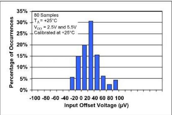
| Input Offset Voltage (μV) | Percentage of Occurrences (%) | | :--- | :--- | | -100 to -80 | 0 | | -80 to -60 | 0 | | -60 to -40 | 0 | | -40 to -20 | 5 | | -20 to 0 | 15 | | 0 to 20 | 20 | | 20 to 40 | 31 | | 40 to 60 | 15 | | 60 to 80 | 6 | | 80 to 100 | 3 | | 100 to 120 | 5 | The chart displays a distribution of sample percentages across different input offset voltages. The legend indicates that 80 samples are labeled as 'T_A = +25°C', V_DD is calculated as 2.5V and is 5.5V, and the calibration is at +25°C.FIGURE 2-1: Input Offset Voltage.
line
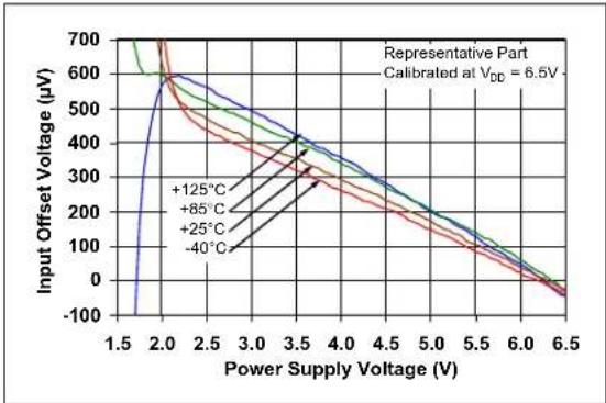
| Power Supply Voltage (V) | Input Offset Voltage (μV) | | ------------------------ | ------------------------- | | 1.5 | 700 | | 2.0 | 600 | | 2.5 | 500 | | 3.0 | 400 | | 3.5 | 300 | | 4.0 | 200 | | 4.5 | 100 | | 5.0 | 0 | | 5.5 | -100 | | 6.0 | -200 | | 6.5 | -300 |FIGURE 2-4: Input Offset Voltage vs. Power Supply Voltage.
histogram
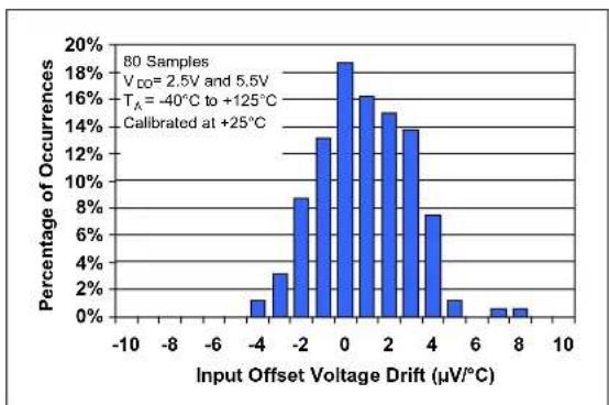
| Input Offset Voltage Drift (μV/°C) | Percentage of Occurrences (%) | |---|---| | -10 to -8 | 0 | | -8 to -6 | 0 | | -6 to -4 | 1 | | -4 to -2 | 3 | | -2 to 0 | 9 | | 0 to 2 | 18 | | 2 to 4 | 16 | | 4 to 6 | 7 | | 6 to 8 | 1 | | 8 to 10 | 0.5 | 80 Samples Vco=2.5V and 5.5V, TA=-40°C to +125°C, Calibrated at +25°CFIGURE 2-2: Input Offset Voltage Drift.
line
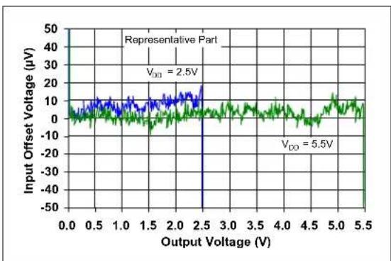
| Output Voltage (V) | Input Offset Voltage (µV) | | ------------------ | -------------------------- | | 0.0 | ~0 | | 0.5 | ~0 | | 1.0 | ~0 | | 1.5 | ~0 | | 2.0 | ~0 | | 2.5 | ~0 | | 3.0 | ~0 | | 3.5 | ~0 | | 4.0 | ~0 | | 4.5 | ~0 | | 5.0 | ~0 | | 5.5 | ~0 |FIGURE 2-5: Input Offset Voltage vs. Output Voltage.
bar
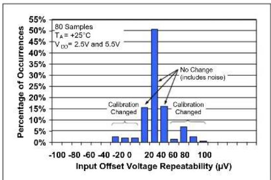
| Input Offset Voltage Repeatability (μV) | Percentage of Occurrences | | --------------------------------------- | ------------------------- | | -100 to -80 | 0% | | -80 to -60 | 0% | | -60 to -40 | 0% | | -40 to -20 | 0% | | -20 to 0 | 2% | | 0 to 20 | 3% | | 20 to 40 | 50% | | 40 to 60 | 15% | | 60 to 80 | 7% | | 80 to 100 | 2% |FIGURE 2-3: Input Offset Voltage Repeatability (repeated calibration).
line
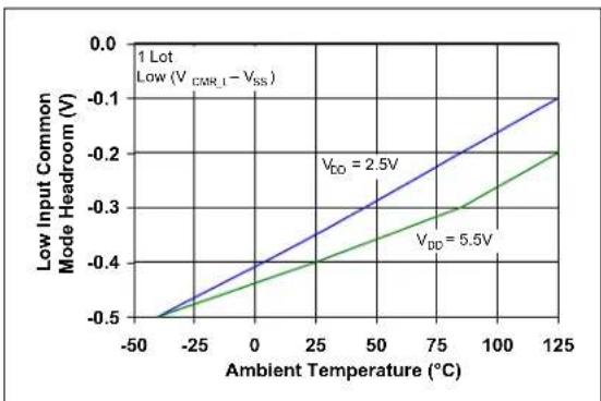
| Ambient Temperature (°C) | Low Input Common Mode Headroom (V) | | ------------------------ | ---------------------------------- | | -50 | -0.5 | | 0 | -0.4 | | 25 | -0.3 | | 50 | -0.2 | | 75 | -0.1 | | 100 | -0.05 | | 125 | -0.0 |FIGURE 2-6: Low-Input Common Mode Voltage Headroom vs. Ambient Temperature.
Note: Unless otherwise indicated, T_A = +2.5^ C_DDV = +2.5V to 5.5V , V_SS = GND , V_CM = V_DD/3 , V_OUT = V_DD/2 , V_L = V_DD/2 , R_L = 1k to V_L , C_L = 20pF , and CAL/CS = V_SS .
line
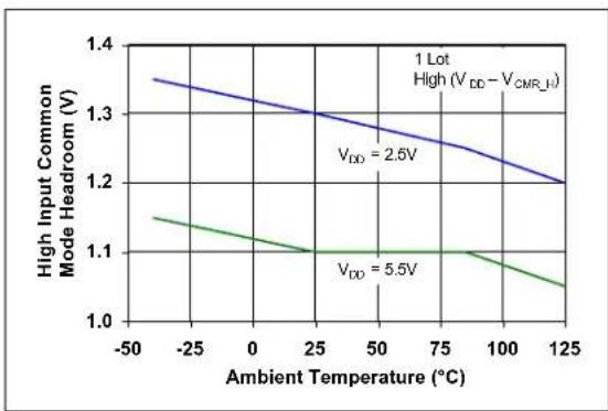
| Ambient Temperature (°C) | High Input Common Mode Headroom (V) | | ------------------------ | ----------------------------------- | | -50 | 1.35 | | 0 | 1.32 | | 25 | 1.30 | | 50 | 1.28 | | 75 | 1.26 | | 100 | 1.24 | | 125 | 1.20 |FIGURE 2-7: High-Input Common Mode Voltage Headroom vs. Ambient Temperature.

line
| Ambient Temperature (°C) | CMRR, PSRR (dB) | | ------------------------ | --------------- | | -50 | 94 | | -25 | 98 | | 0 | 100 | | 25 | 103 | | 50 | 101 | | 75 | 98 | | 100 | 94 | | 125 | 90 |FIGURE 2-10: CMRR and PSRR vs. Ambient Temperature.
line
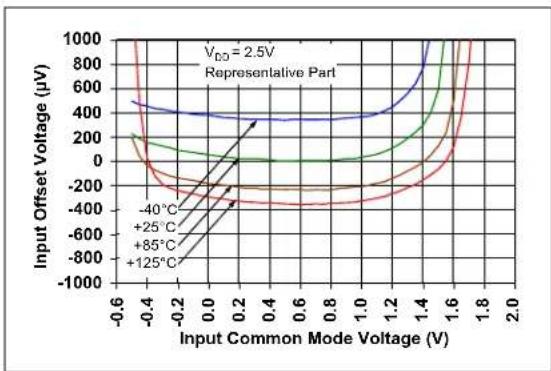
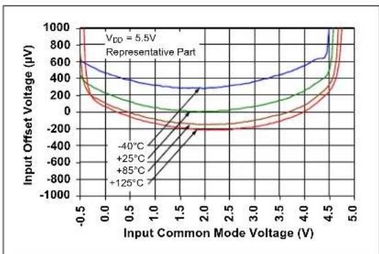
| Input Common Mode Voltage (V) | Input Offset Voltage (µV) at -40°C | Input Offset Voltage (µV) at +25°C | Input Offset Voltage (µV) at +85°C | Input Offset Voltage (µV) at +125°C | | ----------------------------- | ----------------------------------- | ----------------------------------- | ----------------------------------- | ------------------------------------ | | -0.6 | ~900 | ~500 | ~300 | ~100 | | -0.4 | ~700 | ~400 | ~200 | ~50 | | -0.2 | ~500 | ~300 | ~100 | ~-50 | | 0.0 | ~300 | ~200 | ~50 | ~-75 | | 0.2 | ~100 | ~100 | ~50 | ~-75 | | 0.4 | ~50 | ~50 | ~50 | ~-75 | | 0.6 | ~50 | ~50 | ~50 | ~-75 | | 0.8 | ~50 | ~50 | ~50 | ~-75 | | 1.0 | ~50 | ~50 | ~50 | ~-75 | | 1.2 | ~50 | ~50 | ~50 | ~-75 | | 1.4 | ~50 | ~50 | ~50 | ~-75 | | 1.6 | ~50 | ~50 | ~50 | ~-75 | | 1.8 | ~50 | ~50 | ~50 | ~-75 | | 2.0 | ~900 | ~900 | ~900 | ~900 |FIGURE 2-8: Input Offset Voltage vs. Common Mode Voltage with V_DD = 2.5 V .
line
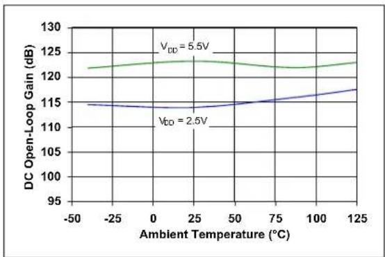
| Ambient Temperature (°C) | DC Open-Loop Gain (dB) for V_DD = 5.5V | DC Open-Loop Gain (dB) for V_CO = 2.5V | | ------------------------ | -------------------------------------- | -------------------------------------- | | -50 | 122 | 114 | | 0 | 123 | 113 | | 25 | 124 | 113 | | 50 | 123 | 114 | | 75 | 122 | 115 | | 100 | 122 | 116 | | 125 | 123 | 118 |FIGURE 2-11: DC Open-Loop Gain vs. Ambient Temperature.
line
| Input Common Mode Voltage (V) | Input Offset Voltage (µV) at -40°C | Input Offset Voltage (µV) at +25°C | Input Offset Voltage (µV) at +85°C | Input Offset Voltage (µV) at +125°C | | ----------------------------- | ---------------------------------- | ---------------------------------- | ---------------------------------- | ------------------------------------ | | -0.5 | ~600 | ~600 | ~600 | ~600 | | 0.0 | ~400 | ~400 | ~400 | ~400 | | 0.5 | ~200 | ~200 | ~200 | ~200 | | 1.0 | ~0 | ~0 | ~0 | ~0 | | 1.5 | ~-200 | ~-200 | ~-200 | ~-200 | | 2.0 | ~-400 | ~-400 | ~-400 | ~-400 | | 2.5 | ~-600 | ~-600 | ~-600 | ~-600 | | 3.0 | ~-800 | ~-800 | ~-800 | ~-800 | | 3.5 | ~-600 | ~-600 | ~-600 | ~-600 | | 4.0 | ~-400 | ~-400 | ~-400 | ~-400 | | 4.5 | ~-200 | ~-200 | ~-200 | ~-200 | | 5.0 | ~+125 | ~+125 | ~+125 | ~+125 |FIGURE 2-9: Input Offset Voltage vs. Common Mode Voltage with V_DD = 5.5 V .

line
| Ambient Temperature (°C) | Input Bias, Offset Currents (pA) | | ------------------------ | -------------------------------- | | 25 | 10 | | 45 | 100 | | 65 | 1000 | | 85 | 10000 | | 105 | 100000 | | 125 | 1000000 |FIGURE 2-12: Input Bias and Offset Currents vs. Ambient Temperature with V_DD = +5.5 V .
Note: Unless otherwise indicated, T_A = +2.5^ C_DDV = +2.5V to 5.5V , V_SS = GND , V_CM = V_DD/3 , V_OUT = V_DD/2 , V_L = V_DD/2 , R_L = 1k to V_L , C_L = 20pF , and CAL/CS = V_SS .
line
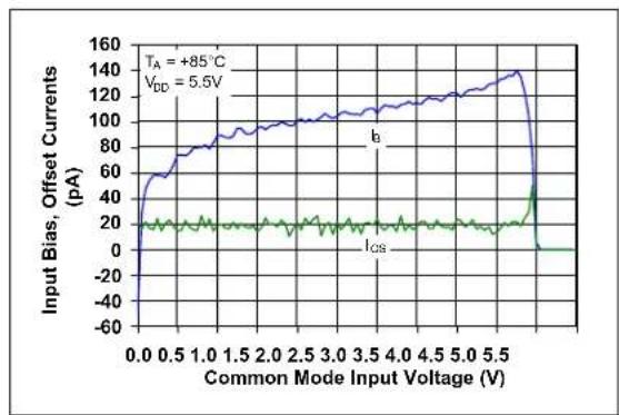
| Common Mode Input Voltage (V) | Input Bias, Offset Currents (pA) | | ----------------------------- | -------------------------------- | | 0.0 | -60 | | 0.5 | 60 | | 1.0 | 80 | | 1.5 | 90 | | 2.0 | 100 | | 2.5 | 105 | | 3.0 | 110 | | 3.5 | 115 | | 4.0 | 120 | | 4.5 | 125 | | 5.0 | 130 | | 5.5 | 140 | | 6.0 | 0 |FIGURE 2-13: Input Bias and Offset Currents vs. Common Mode Input Voltage with T_A = +85^ .
line
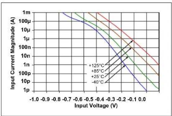
| Input Voltage (V) | +125°C | +85°C | +25°C | -40°C | | ----------------- | ------ | ----- | ----- | ----- | | -1.0 | 1m | 1m | 1m | 1m | | -0.9 | 1m | 1m | 1m | 1m | | -0.8 | 1m | 1m | 1m | 1m | | -0.7 | 1m | 1m | 1m | 1m | | -0.6 | 1m | 1m | 1m | 1m | | -0.5 | 1m | 1m | 1m | 1m | | -0.4 | 1m | 1m | 1m | 1m | | -0.3 | 1m | 1m | 1m | 1m | | -0.2 | 1n | 1n | 1n | 1n | | -0.1 | 1n | 1n | 1n | 1n | | 0.0 | 1p | 1p | 1p | 1p |FIGURE 2-15: Input Bias Current vs. Input Voltage (below V_SS ).
FIGURE 2-14: Input Bias and Offset
Currents vs. Common Mode Input Voltage with T_A = +125^ .
Note: Unless otherwise indicated, T_A = +2.5^ C_DDV = +2.5V to 5.5V, V_SS = GND , V_CM = V_DD/3 , V_OUT = V_DD/2 , V_L = V_DD/2 , R_L = 1k to V_L , C_L = 20pF , and CAL/CS = V_SS .
2.2 Other DC Voltages and Currents
line
| Output Current Magnitude (mA) | Ratio of Output Headroom to Output Current (mV/mA) | | ----------------------------- | -------------------------------------------------- | | 100 | 9.0 | | 100 | 8.5 | | 100 | 8.0 | | 100 | 7.5 | | 100 | 7.0 | | 100 | 6.5 | | 100 | 6.0 | | 100 | 5.5 | | 100 | 5.0 | | 100 | 4.5 | | 100 | 4.0 | | 100 | 3.5 | | 100 | 3.0 | | 100 | 2.5 | | 100 | 2.0 | | 100 | 1.5 | | 100 | 1.0 | | 100 | 0.5 | | 100 | 0.0 |FIGURE 2-16: Ratio of Output Voltage Headroom to Output Current.
line
| Power Supply Voltage (V) | +125°C | +85°C | +25°C | -40°C | | ------------------------- | ------ | ----- | ----- | ----- | | 0.0 | 0.0 | 0.0 | 0.0 | 0.0 | | 0.5 | 0.0 | 0.0 | 0.0 | 0.0 | | 1.0 | 0.0 | 0.0 | 0.0 | 0.0 | | 1.5 | 3.0 | 4.0 | 4.5 | 3.5 | | 2.0 | 6.0 | 5.5 | 5.0 | 4.0 | | 2.5 | 6.5 | 6.0 | 5.5 | 4.5 | | 3.0 | 7.0 | 6.5 | 6.0 | 5.0 | | 3.5 | 7.2 | 6.8 | 6.2 | 5.2 | | 4.0 | 7.3 | 7.0 | 6.5 | 5.5 | | 4.5 | 7.4 | 7.2 | 6.8 | 5.8 | | 5.0 | 7.5 | 7.3 | 7.0 | 6.0 | | 5.5 | 7.6 | 7.4 | 7.2 | 6.2 | | 6.0 | 7.7 | 7.5 | 7.3 | 6.3 | | 6.5 | 7.8 | 7.6 | 7.4 | 6.4 |FIGURE 2-19: Supply Current vs. Power Supply Voltage.
line
| Ambient Temperature (°C) | Output Headroom (mV) | | ------------------------ | -------------------- | | -50 | 8.0 | | 0 | 8.5 | | 25 | 9.0 | | 50 | 9.5 | | 75 | 10.0 | | 100 | 10.5 | | 125 | 11.0 | | 150 | 11.5 | | 175 | 12.0 | | 200 | 12.5 |FIGURE 2-17: Output Voltage Headroom vs. Ambient Temperature.

line
| Common Mode Input Voltage (V) | Supply Current (mA/amplifier) | | ----------------------------- | ----------------------------- | | 0.0 | 5.0 | | 1.0 | 5.0 | | 1.5 | 5.0 | | 2.0 | 5.0 | | 2.5 | 3.8 | | 3.0 | 3.8 | | 4.0 | 6.0 | | 5.5 | 6.0 |FIGURE 2-20: Supply Current vs. Common Mode Input Voltage.

line
| Power Supply Voltage (V) | +125°C (mA) | +85°C (mA) | +25°C (mA) | -40°C (mA) | | ------------------------ | ----------- | ---------- | ---------- | ---------- | | 0.0 | 0 | 0 | 0 | 0 | | 1.0 | 0 | 0 | 0 | 0 | | 1.5 | 0 | 0 | 0 | 0 | | 2.0 | 0 | 0 | 0 | 0 | | 2.5 | 0 | 0 | 0 | 0 | | 3.0 | 100 | 100 | 100 | 100 | | 3.5 | 100 | 100 | 100 | 100 | | 4.0 | 100 | 100 | 100 | 100 | | 4.5 | 100 | 100 | 100 | 100 | | 5.0 | 100 | 100 | 100 | 100 | | 5.5 | 100 | 100 | 100 | 100 | | 6.0 | 100 | 100 | 100 | 100 | | 6.5 | 100 | 100 | 100 | 100 |FIGURE 2-18: Output Short-Circuit Current vs. Power Supply Voltage.
line
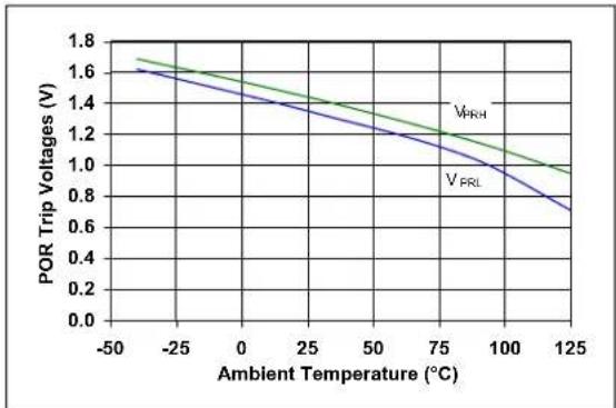
| Ambient Temperature (°C) | V_HK (V) | V_RL (V) | | ------------------------ | -------- | -------- | | -50 | 1.7 | 1.6 | | 0 | 1.5 | 1.4 | | 25 | 1.3 | 1.2 | | 50 | 1.1 | 1.0 | | 75 | 0.9 | 0.8 | | 100 | 0.7 | 0.6 | | 125 | 0.5 | 0.4 |FIGURE 2-21: Power-On Reset Voltages vs. Ambient Temperature.
Note: Unless otherwise indicated, T_A = +2.5^ C_DD V = +2.5V to 5.5V , V_SS = GND , V_CM = V_DD/3 , V_OUT = V_DD/2 , V_L = V_DD/2 , R_L = 1k to V_L , C_L = 20pF , and CAL/CS = V_SS .
bar
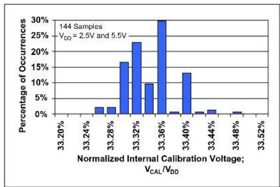
| Normalized Internal Calibration Voltage; V_CAL/V_DD | Percentage of Occurrences | | :--- | :--- | | 33.20% | 0 | | 33.24% | 0 | | 33.28% | 2 | | 33.32% | 17 | | 33.36% | 23 | | 33.40% | 10 | | 33.44% | 30 | | 33.48% | 1 | | 33.52% | 0 | 144 Samples V_DD = 2.5V and 5.5VFIGURE 2-22: Normalized Internal Calibration Voltage.
line
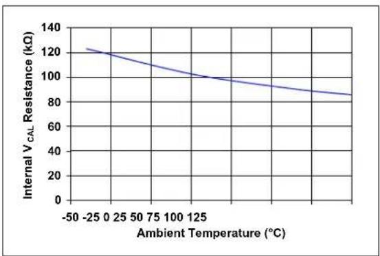
| Ambient Temperature (°C) | Internal V_CAL Resistance (kΩ) | | ------------------------ | ------------------------------ | | -50 | 120 | | 0 | 115 | | 25 | 110 | | 50 | 105 | | 75 | 100 | | 100 | 95 | | 125 | 90 | | >125 | ~85 |FIGURE 2-23: V CAL Input Resistance vs. Temperature.
Note: Unless otherwise indicated, T_A = +2.5^ C_DD V = +2.5V to 5.5V, V_SS = GND , V_CM = V_DD/3 , V_OUT = V_DD/2 , V_L = V_DD/2 , R_L = 1 k to V_L , C_L = 20 pF , and CAL/CS = V_SS .
2.3 Frequency Response
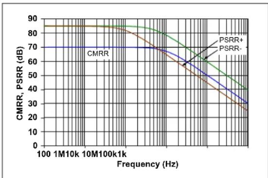
FIGURE 2-24: CMRR and PSRR vs. Frequency.
line
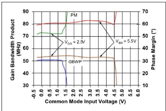
| Common Mode Input Voltage (V) | Gain Bandwidth Product (MHz) | Phase Margin (°) | | ----------------------------- | ---------------------------- | ---------------- | | -0.5 | 70 | 60 | | 0.0 | 70 | 60 | | 0.5 | 70 | 60 | | 1.0 | 70 | 60 | | 1.5 | 90 | 60 | | 2.0 | 80 | 60 | | 2.5 | 80 | 60 | | 3.0 | 80 | 60 | | 3.5 | 80 | 60 | | 4.0 | 80 | 60 | | 4.5 | 80 | 60 | | 5.0 | 80 | 60 | | 5.5 | 80 | 60 | | 6.0 | 80 | 60 |FIGURE 2-27: Gain-Bandwidth Product and Phase Margin vs. Common Mode Input Voltage.
line
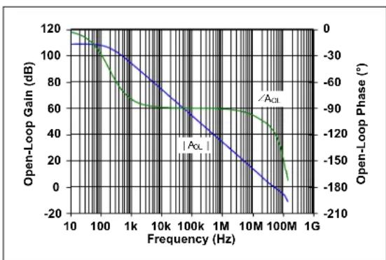
| Frequency (Hz) | Open-Loop Gain (dB) | Open-Loop Phase (°) | | -------------- | ------------------- | ------------------- | | 10 | 120 | 0 | | 100 | 100 | -30 | | 1k | 80 | -60 | | 10k | 60 | -90 | | 100k | 40 | -120 | | 1M | 20 | -150 | | 10M | 0 | -180 | | 100M | -20 | -210 | | 1G | -20 | -210 |FIGURE 2-25: Open-Loop Gain vs. Frequency.
line
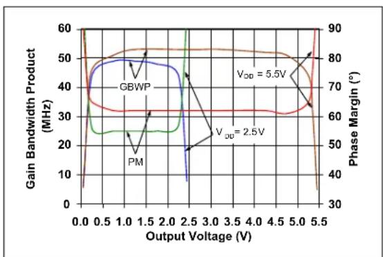
| Output Voltage (V) | Gain Bandwidth Product (MHz) | Phase Margin (°) | | ------------------ | ---------------------------- | ---------------- | | 0.0 | 60 | 90 | | 0.5 | 50 | 80 | | 1.0 | 45 | 70 | | 1.5 | 30 | 60 | | 2.0 | 20 | 50 | | 2.5 | 10 | 40 | | 3.0 | 20 | 50 | | 3.5 | 30 | 60 | | 4.0 | 40 | 70 | | 4.5 | 50 | 80 | | 5.0 | 60 | 90 | | 5.5 | 60 | 90 |FIGURE 2-28: Gain-Bandwidth Product and Phase Margin vs. Output Voltage.
line
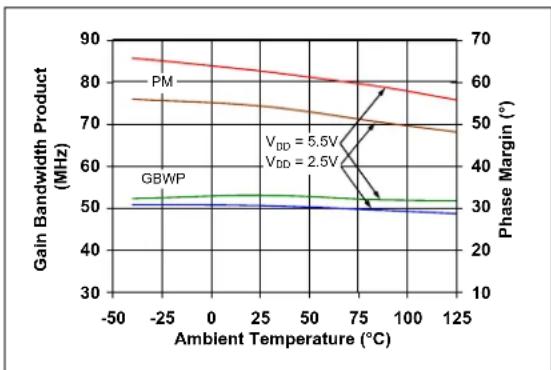
| Ambient Temperature (°C) | Gain Bandwidth Product (MHz) | Phase Margin (°) | | ------------------------ | ---------------------------- | ---------------- | | -50 | 85 | 60 | | 0 | 80 | 55 | | 25 | 75 | 50 | | 50 | 70 | 45 | | 75 | 65 | 40 | | 100 | 60 | 35 | | 125 | 55 | 30 |FIGURE 2-26: Gain-Bandwidth Product and Phase Margin vs. Ambient Temperature.
line
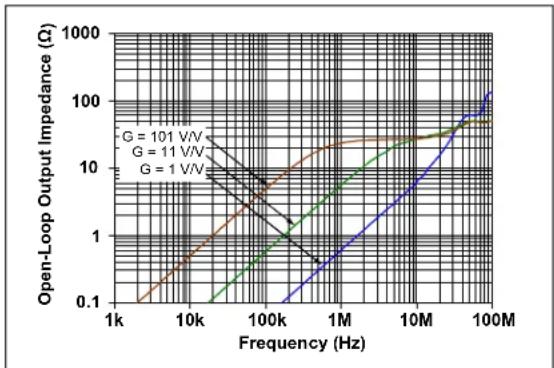
| Frequency (Hz) | G = 101 V/V | G = 11 V/V | G = 1 V/V | | -------------- | ----------- | ---------- | --------- | | 1k | ~0.1 | ~0.1 | ~0.1 | | 10k | ~0.5 | ~0.5 | ~0.5 | | 100k | ~2 | ~2 | ~2 | | 1M | ~5 | ~5 | ~5 | | 10M | ~20 | ~20 | ~20 | | 100M | ~100 | ~100 | ~100 |FIGURE 2-29: Closed-Loop Output Impedance vs. Frequency.
Note: Unless otherwise indicated, T_A = +2.5^ C_DD V = +2.5V to 5.5V , V_SS = GND , V_CM = V_DD/3 , V_OUT = V_DD/2 , V_L = V_DD/2 , R_L = 1k to V_L , C_L = 20pF , and CAL/CS = V_SS .
line
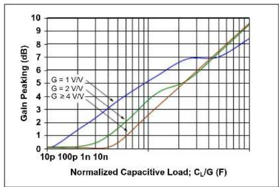
| Normalized Capacitive Load; C_L/G (F) | G = 1 V/V | G = 2 V/V | G ≥ 4 V/V | | ------------------------------------ | --------- | --------- | --------- | | 10p | 0 | 0 | 0 | | 100p | 3 | 2 | 1 | | 1n | 5 | 4 | 3 | | 10n | 7 | 6 | 5 | | Peak (dB) | 9 | 8 | 7 |FIGURE 2-30: Gain Peaking vs. Normalized Capacitive Load.
line
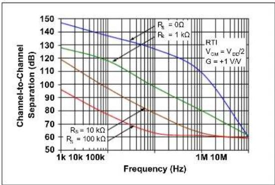
| Frequency (Hz) | Channel-to-Channel Separation (dB) for Rs = 0Ω | Channel-to-Channel Separation (dB) for Rs = 1 kΩ | Channel-to-Channel Separation (dB) for Rs = 10 kΩ | Channel-to-Channel Separation (dB) for Rs = 100 kΩ | | -------------- | --------------------------------------------- | ---------------------------------------------- | ----------------------------------------------- | ----------------------------------------------- | | 1k | 150 | 130 | 120 | 95 | | 10k | 140 | 120 | 110 | 85 | | 100k | 130 | 110 | 100 | 75 | | 1M | 120 | 100 | 90 | 65 | | 10M | 100 | 90 | 80 | 60 |FIGURE 2-31: Channel-to-Channel Separation vs. Frequency.
Note: Unless otherwise indicated, T_A = +25^_DD +2.5V to 5.5V, V_SS = GND , V_CM = V_DD/3 , V_OUT = V_DD/2 , V_L = V_DD/2 , R_L = 1k to V_L , C_L = 20pF , and CAL/CS = V_SS .
2.4 Input Noise and Distortion
line
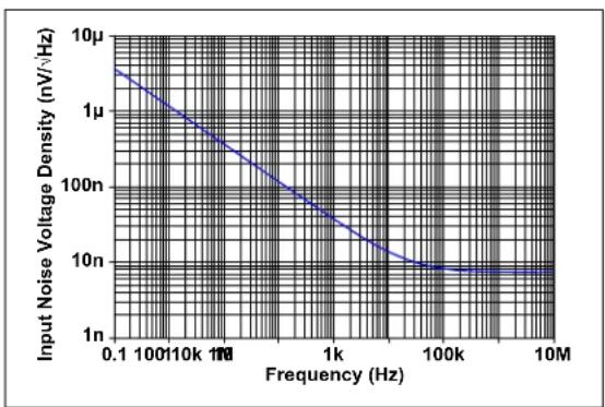
| Frequency (Hz) | Input Noise Voltage Density (nV/Hz) | | -------------- | ----------------------------------- | | 0.1 | 10μ | | 10 | 1μ | | 100 | 100n | | 1k | 10n | | 100k | 10n | | 10M | 1n |FIGURE 2-32: Input Noise Voltage Density vs. Frequency.
line
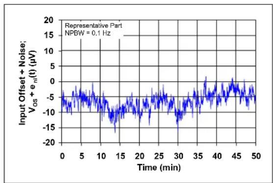
| Time (min) | Input Offset + Noise; V_OE + e_n(t) (µV) | | ---------- | ---------------------------------------- | | 0 | -5.0 | | 5 | -3.0 | | 10 | -4.0 | | 15 | -6.0 | | 20 | -7.0 | | 25 | -8.0 | | 30 | -9.0 | | 35 | -10.0 | | 40 | -11.0 | | 45 | -12.0 | | 50 | -13.0 |FIGURE 2-35: Input Noise plus Offset vs. Time with 0.1 Hz Filter.
line
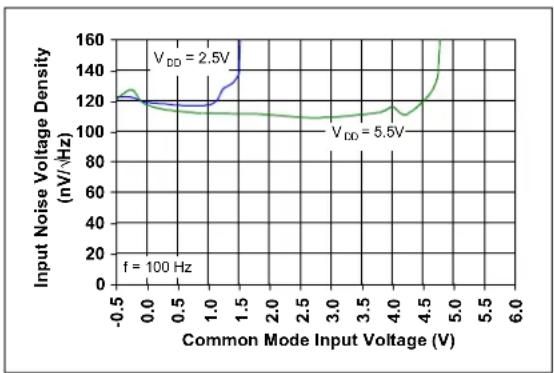
| Common Mode Input Voltage (V) | Input Noise Voltage Density (nV/Hz) | | ----------------------------- | ----------------------------------- | | -0.5 | 120 | | 0.0 | 120 | | 0.5 | 120 | | 1.0 | 120 | | 1.5 | 160 | | 2.0 | 120 | | 2.5 | 120 | | 3.0 | 120 | | 3.5 | 120 | | 4.0 | 120 | | 4.5 | 160 | | 5.0 | 160 | | 5.5 | 160 | | 6.0 | 160 |FIGURE 2-33: Input Noise Voltage Density vs. Input Common Mode Voltage with f = 100 Hz.
line
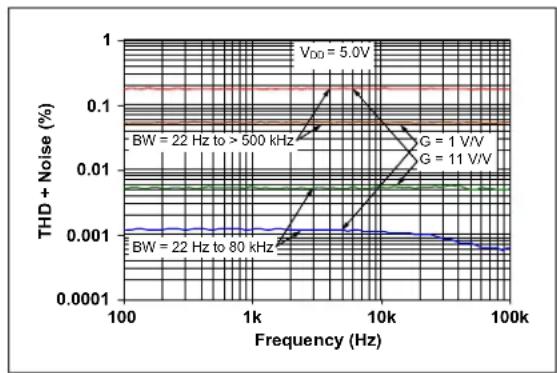
| Frequency (Hz) | THD + Noise (%) | | -------------- | --------------- | | 100 | 0.001 | | 1k | 0.001 | | 10k | 0.1 | | 100k | 0.1 |FIGURE 2-36: THD+N vs. Frequency.

line
| Common Mode Input Voltage (V) | Input Noise Voltage Density (nV/Hz) | | ----------------------------- | ----------------------------------- | | -0.5 | 7.0 | | 0.0 | 6.5 | | 0.5 | 7.0 | | 1.0 | 8.0 | | 1.5 | 11.0 | | 2.0 | 12.0 | | 2.5 | 12.0 | | 3.0 | 12.0 | | 3.5 | 12.0 | | 4.0 | 12.0 | | 4.5 | 12.0 | | 5.0 | 12.0 | | 5.5 | 12.0 |FIGURE 2-34: Input Noise Voltage Density vs. Input Common Mode Voltage with f = 1 MHz.
Note: Unless otherwise indicated, T_A = +2.5^ C_DD V = +2.5V to 5.5V , V_SS = GND , V_CM = V_DD/3 , V_OUT = V_DD/2 , V_L = V_DD/2 , R_L = 1k to V_L , C_L = 20pF , and CAL/CS = V_SS .
2.5 Time Response
line
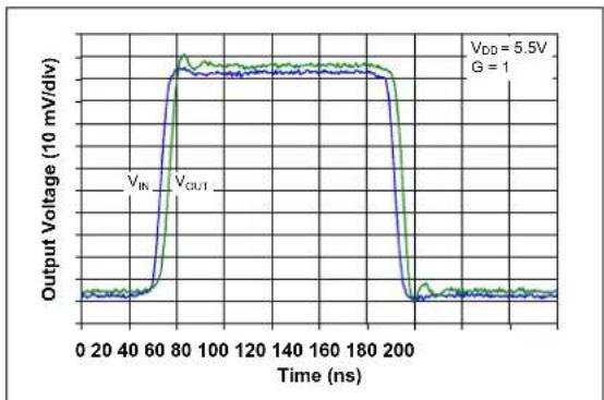
| Time (ns) | Output Voltage (10 mV/div) | | --------- | -------------------------- | | 0 | ~0 | | 20 | ~0 | | 40 | ~0 | | 60 | ~0 | | 80 | ~1.0 | | 100 | ~1.0 | | 120 | ~1.0 | | 140 | ~1.0 | | 160 | ~1.0 | | 180 | ~1.0 | | 200 | ~0 | | >200 | ~0 |FIGURE 2-37: Non-inverting Small Signal Step Response.
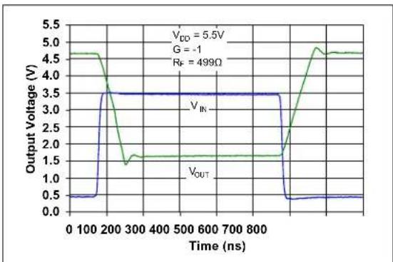
FIGURE 2-40: Inverting Large Signal Step Response.

line
| Time (ns) | Output Voltage (V) | | --------- | ------------------ | | 0 | 0.5 | | 200 | 3.5 | | 400 | 3.5 | | 600 | 3.5 | | 800 | 3.5 | | 900 | 0.5 | | 1000 | 0.5 |FIGURE 2-38: Non-inverting Large Signal Step Response.
line
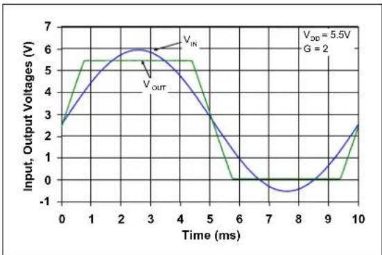
| Time (ms) | Input Voltage (V) | Output Voltage (V) | | --------- | ----------------- | ------------------ | | 0 | 3.0 | 3.0 | | 1 | 5.5 | 5.5 | | 2 | 6.0 | 6.0 | | 3 | 6.0 | 6.0 | | 4 | 5.5 | 5.5 | | 5 | 4.0 | 4.0 | | 6 | 0.0 | 0.0 | | 7 | -0.5 | -0.5 | | 8 | 0.0 | 0.0 | | 9 | 0.5 | 0.5 | | 10 | 2.5 | 2.5 |FIGURE 2-41: The MCP651/1S/2/3/4/5/9 family shows no input phase reversal with overdrive.

line
| Time (ns) | V_IN (10 mV/div) | V_OUT (10 mV/div) | | --------- | ---------------- | ----------------- | | 0 | ~0 | ~0 | | 50 | ~0.8 | ~0.8 | | 100 | ~0.8 | ~0.2 | | 150 | ~0.8 | ~0.2 | | 200 | ~0.8 | ~0.2 | | 250 | ~0.8 | ~0.2 | | 300 | ~0.8 | ~0.2 | | 350 | ~0.8 | ~0.2 | | 400 | ~0.8 | ~0.2 |FIGURE 2-39: Inverting Small Signal Step Response.
line
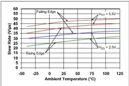
| Ambient Temperature (°C) | Slew Rate (V/μs) | | ------------------------ | ---------------- | | -50 | 15 | | 0 | 25 | | 25 | 35 | | 75 | 45 | | 100 | 50 | | 125 | 55 |FIGURE 2-42: Slew Rate vs. Ambient Temperature.
Note: Unless otherwise indicated, T_A = +2.5^ C_DD V = +2.5V to 5.5V, V_SS = GND , V_CM = V_DD/3 , V_OUT = V_DD/2 , V_L = V_DD/2 , R_L = 1 k to V_L , C_L = 20 pF , and CAL/CS = V_SS .
line
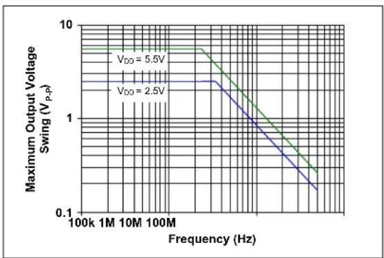
| Frequency (Hz) | Maximum Output Voltage Swing (V_P-p) for V_DD = 5.5V | Maximum Output Voltage Swing (V_P-p) for V_DD = 2.5V | | -------------- | --------------------------------------------------- | --------------------------------------------------- | | 100k | ~8.0 | ~3.0 | | 1M | ~8.0 | ~3.0 | | 10M | ~8.0 | ~3.0 | | 100M | ~8.0 | ~3.0 | | >100M | ~1.0 | ~0.3 |FIGURE 2-43: Maximum Output Voltage Swing vs. Frequency.
Note: Unless otherwise indicated, T_A = +25^ C_DD +2.5V to 5.5V, V_SS = GND , V_CM = V_DD/3 , V_OUT = V_DD/2 , V_L = V_DD/2 , R_L = 1k to V_L , C_L = 20pF , and CAL/CS = V_SS .
2.6 Calibration and Chip Select Response
line
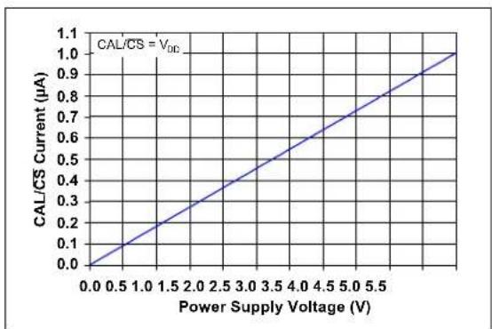
| Power Supply Voltage (V) | CAL/CS Current (μA) | | ------------------------ | ------------------- | | 0.0 | 0.0 | | 1.0 | 0.2 | | 2.0 | 0.4 | | 3.0 | 0.6 | | 4.0 | 0.8 | | 5.0 | 1.0 | | 5.5 | 1.0 |FIGURE 2-44: CAL/CS Current vs. Power Supply Voltage.
line
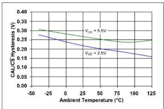
| Ambient Temperature (°C) | CAL/CS Hysteresis (V) for V_DD = 2.5V | CAL/CS Hysteresis (V) for V_DD = 5.5V | | ------------------------ | ------------------------------------- | ------------------------------------- | | -50 | 0.28 | 0.31 | | 0 | 0.24 | 0.29 | | 50 | 0.20 | 0.26 | | 100 | 0.17 | 0.24 | | 125 | 0.15 | 0.25 |FIGURE 2-47: CAL/CS — Hysteresis vs. Ambient Temperature.
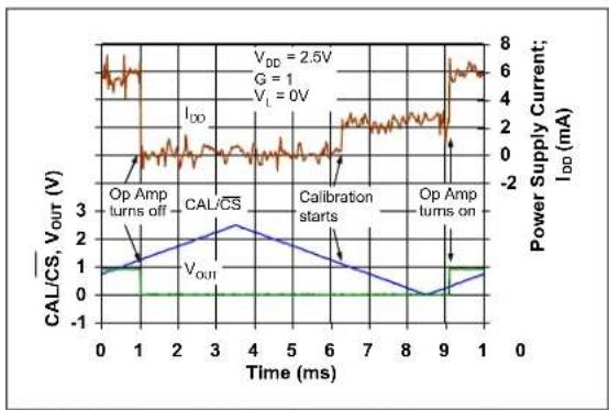
FIGURE 2-45: CAL/CS Voltage, Output Voltage and Supply Current (for Side A) vs. Time with V_DD = 2.5 ~V .
line
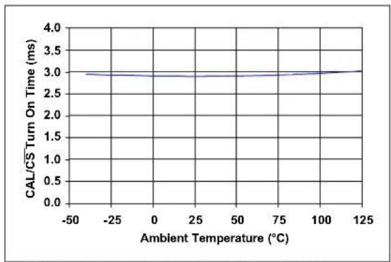
| Ambient Temperature (°C) | CAL/CS Turn On Time (ms) | | ------------------------ | ------------------------ | | -50 | 3.0 | | -25 | 3.0 | | 0 | 3.0 | | 25 | 3.0 | | 50 | 3.0 | | 75 | 3.0 | | 100 | 3.0 | | 125 | 3.0 |FIGURE 2-48: CAL/CS — Turn-On Time vs. Ambient Temperature.

line
| Time (ms) | CAL/CS, Vout (V) | Power Supply Current; Idd (mA) | | --------- | ---------------- | ----------------------------- | | 0 | 6 | 0 | | 1 | 6 | -1 | | 2 | 6 | -2 | | 3 | 6 | -3 | | 4 | 6 | -4 | | 5 | 6 | -5 | | 6 | 6 | -6 | | 7 | 6 | -7 | | 8 | 6 | -8 | | 9 | 6 | -9 | | 10 | 6 | -10 |FIGURE 2-46: CAL/CS Voltage, Output Voltage and Supply Current (for Side A) vs. Time with V_DD = 5.5 ~V .
line
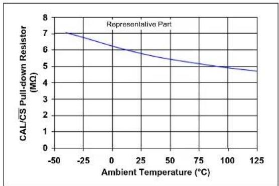
| Ambient Temperature (°C) | CAL/CS Pull-down Resistor (MΩ) | | ------------------------ | ------------------------------ | | -50 | 7.0 | | 0 | 6.0 | | 25 | 5.5 | | 50 | 5.0 | | 75 | 4.8 | | 100 | 4.7 | | 125 | 4.6 |FIGURE 2-49: CAL/CS's Pull-Down Resistor (R_PD) vs. Ambient Temperature.
Note: Unless otherwise indicated, T_A = +2.5^ C_DD V = +2.5V to 5.5V, V_SS = GND , V_CM = V_DD/3 , V_OUT = V_DD/2 , V_L = V_DD/2 , R_L = 1 k to V_L , C_L = 20 pF , and CAL/CS = V_SS .

line
| Power Supply Voltage (V) | Negative Power Supply Current, Iss (μA) at +125°C | Negative Power Supply Current, Iss (μA) at +85°C | Negative Power Supply Current, Iss (μA) at +25°C | Negative Power Supply Current, Iss (μA) at -40°C | | ------------------------- | -------------------------------------------------- | -------------------------------------------------- | -------------------------------------------------- | -------------------------------------------------- | | 0.0 | 0.0 | 0.0 | 0.0 | 0.0 | | 0.5 | ~-0.5 | ~-0.7 | ~-0.9 | ~-1.1 | | 1.0 | ~-1.0 | ~-1.3 | ~-1.6 | ~-1.9 | | 1.5 | ~-1.5 | ~-1.8 | ~-2.1 | ~-2.4 | | 2.0 | ~-2.0 | ~-2.3 | ~-2.6 | ~-2.9 | | 2.5 | ~-2.5 | ~-2.7 | ~-3.0 | ~-3.3 | | 3.0 | ~-3.0 | ~-3.1 | ~-3.4 | ~-3.7 | | 3.5 | ~-3.5 | ~-3.4 | ~-3.7 | ~-4.0 | | 4.0 | ~-4.0 | ~-3.7 | ~-4.0 | ~-4.3 | | 4.5 | ~-4.5 | ~-4.0 | ~-4.3 | ~-4.6 | | 5.0 | ~-5.0 | ~-4.3 | ~-4.6 | ~-4.9 | | 5.5 | ~-5.5 | ~-4.6 | ~-4.9 | ~-5.2 | | 6.0 | ~-6.0 | ~-4.9 | ~-5.2 | ~-5.5 | | 6.5 | ~-6.5 | ~-5.2 | ~-5.5 | ~-5.8 |FIGURE 2-50: Quiescent Current in Shutdown vs. Power Supply Voltage.
line
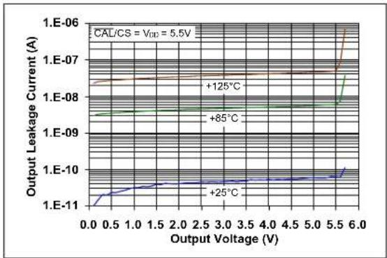
| Output Voltage (V) | +25°C Output Leakage Current (A) | +85°C Output Leakage Current (A) | +125°C Output Leakage Current (A) | | ------------------ | -------------------------------- | ------------------------------- | -------------------------------- | | 0.0 | ~1E-11 | ~1E-09 | ~1E-08 | | 0.5 | ~1E-10 | ~1E-09 | ~1E-08 | | 1.0 | ~1E-10 | ~1E-09 | ~1E-08 | | 1.5 | ~1E-10 | ~1E-09 | ~1E-08 | | 2.0 | ~1E-10 | ~1E-09 | ~1E-08 | | 2.5 | ~1E-10 | ~1E-09 | ~1E-08 | | 3.0 | ~1E-10 | ~1E-09 | ~1E-08 | | 3.5 | ~1E-10 | ~1E-09 | ~1E-08 | | 4.0 | ~1E-10 | ~1E-09 | ~1E-08 | | 4.5 | ~1E-10 | ~1E-09 | ~1E-08 | | 5.0 | ~1E-10 | ~1E-09 | ~1E-08 | | 5.5 | ~1E-09 | ~1E-08 | ~1E-07 | | 6.0 | ~1E-08 | ~1E-07 | ~1E-06 |FIGURE 2-51: Output Leakage Current vs. Output Voltage.
3.0 PIN DESCRIPTIONS
Descriptions of the pins are listed in Table 3-1.
TABLE 3-1: PIN FUNCTION TABLE
| MCP651 M | CPC651S MCP | 652 MCP653 | MCP654 MCP655 MCP659 | Symbol Description | ||||||||
| SOIC | TDFN S | OT SOIC DF | N SOT | SOIC | TSSOP M | SOP D | FN QFN | |||||
| 6 | 6 | 1 | 1 | 1 | 1 | 1 | 1 | 1 | 1 | 16 | V_OUT , V_OUTA | Output (op amp A) |
| 2 | 2 | 4 | 2 | 2 | 4 | 2 | 2 | 2 | 2 | 1 | V_IN-, V_INA- | Inverting Input (op amp A) |
| 3 | 3 | 3 | 3 | 3 | 3 | 3 | 3 | 3 | 3 | 2 | V_IN+, V_INA+ | Non-inverting Input (op amp A) |
| 4 | 4 | 2 | 4 | 4 | 2 | 11 | 11 | 4 | 4 | 11 | V_SS | Negative Power Supply |
| 8 | 8 | — | — | — | 5 | — | — | 5 | 5 | — | CAL/CS, CALA/CSA | Calibrate/Chip Select Digital Input (op amp A) |
| — | — | — | — | — | — | — | — | 6 | 6 | — | CALB/CSB | Calibrate/Chip Select Digital Input (op amp B) |
| — | — | — | — | — | — | — | — | — | — | 15 | CALAD/ CSAD | Calibrate/Chip Select Digital Input (op amps A and D) |
| — | — | — | — | — | — | — | — | — | — | 7 | CALBC/ CSBC | Calibrate/Chip Select Digital Input (op amps B and C) |
| — | — | — | 5 | 5 | — | 5 | 5 | 7 | 7 | 4 | V_INB+ | Non-inverting Input (op amp B) |
| — | — | — | 6 | 6 | — | 6 | 6 | 8 | 8 | 5 | V_INB- | Inverting Input (op amp B) |
| — | — | — | 7 | 7 | — | 7 | 7 | 9 | 9 | 6 | V_OUTB | Output (op amp B) |
| — | — | — | — | — | — | 10 | 10 | — | — | 10 | V_INC+ | Non-inverting input (op amp C) |
| — | — | — | — | — | — | 9 | 9 | — | — | 9 | V_INC- | Inverting Input (op amp C) |
| — | — | — | — | — | — | 8 | 8 | — | — | 8 | V_OUTC | Output (op amp C) |
| — | — | — | — | — | — | 12 | 12 | — | — | 12 | V_IND+ | Non-inverting Input (op amp D) |
| — | — | — | — | — | — | 13 | 13 | — | — | 13 | V_IND- | Inverting Input (op amp D) |
| — | — | — | — | — | — | 14 | 14 | — | — | 14 | V_OUTD | Output (op amp D) |
| 7 | 7 | 5 | 8 | 8 | 6 | 4 | 4 | 10 | 10 | 3 | V_DD | Positive Power Supply |
| 5 | 5 | — | — | — | — | — | — | — | — | — | V_CAL | Calibration Common Mode Voltage Input |
| 1 | 1 | — | — | — | — | — | — | — | — | — | NC | No Internal Connection |
| — | 9 | — | — | 9 | — | — | — | — | 11 | 17 | EP | Exposed Thermal Pad (EP); must be connected to V_SS |
3.1 Analog Outputs
The analog output pins ( V_OUT ) are low-impedance voltage sources.
3.2 Analog Inputs
The non-inverting and inverting inputs ( V_IN^+ , V_IN^- , ...) are high-impedance CMOS inputs with low bias currents.
3.3 Power Supply Pins
The positive power supply ( V_DD ) is 2.5V to 5.5V higher than the negative power supply ( V_SS ). For normal operation, the other pins are between V_SS and V_DD
Typically, these parts are used in a single (positive) supply configuration. In this case, V_SS is connected to ground and V_DD is connected to the supply. V_DD will need bypass capacitors.
3.4 Calibration Common Mode Voltage Input
A low-impedance voltage placed at this input ( V_CAL ) will set the op amps' Common mode input voltage during calibration. If this pin is left open, the Common mode input voltage during calibration is approximately V_DD/3 . The internal resistor divider is disconnected from the supplies whenever the part is not in calibration.
3.5 Calibrate/Chip Select Digital Input
This input (CAL/CS, ...) is a CMOS, Schmitt-Triggered input that affects the Calibration and Low-Power modes of operation. When this pin goes high, the part is placed into a Low-Power mode and the output is High Z. When this pin goes low, a calibration sequence is started (which corrects V_OS ). At the end of the calibration sequence, the output becomes low-impedance and the part resumes normal operation.
An internal POR triggers a calibration event when the part is powered on, or when the supply voltage drops too low. Thus, the MCP652 parts are calibrated, even though they do not have a CAL/CS pin.
3.6 Exposed Thermal Pad (EP)
There is an internal connection between the Exposed Thermal Pad (EP) and the V_SS pin; they must be connected to the same potential on the Printed Circuit Board (PCB).
This pad can be connected to a PCB ground plane to provide a larger heat sink. This improves the package thermal resistance ( _JA ).
4.0 APPLICATIONS
The MCP651/1S/2/3/4/5/9 family of self-zeroed op amps is manufactured using Microchip's state-of-the-art CMOS process. It is designed for low-cost, low-power and high-precision applications. Its low supply voltage, low quiescent current and wide bandwidth makes the MCP651/1S/2/3/4/5/9 ideal for battery-powered applications.
4.1 Calibration and Chip Select
These op amps include circuitry for dynamic calibration of the offset voltage ( V_OS ).
4.1.1 mCal CALIBRATION CIRCUITRY
The internal mCal circuitry, when activated, starts a delay timer (to wait for the op amp to settle to its new bias point), then calibrates the input offset voltage ( V_OS ). The mCal circuitry is triggered at power-up (and after some power brown-out events) by the internal POR, and by the memory's Parity Detector. The power-up time, when the mCal circuitry triggers the calibration sequence, is 200 ms (typical).
4.1.2 CAL/CS PIN
The CAL/CS pin gives the user a means to externally demand a Low-Power mode of operation, then to calibrate V_OS . Using the CAL/CS pin makes it possible to correct V_OS as it drifts over time (1/f noise and aging; see Figure 2-35) and across temperature.
The CAL/CS pin performs two functions: it places the op amp(s) in a Low-Power mode when it is held high, and starts a calibration event (correction of V_OS ) after a rising edge.
While in the Low-Power mode, the quiescent current is quite small ( I_SS = -3 A , typical). The output is also in a High Z state.
During the calibration event, the quiescent current is near, but smaller than, the specified quiescent current (6 mA, typical). The output continues in the High Z state, and the inputs are disconnected from the external circuit, to prevent internal signals from affecting circuit operation. The op amp inputs are internally connected to a Common mode voltage buffer and feedback resistors. The offset is corrected (using a digital state machine, logic and memory), and the calibration constants are stored in memory.
Once the calibration event is completed, the amplifier is reconnected to the external circuitry. The turn-on time, when calibration is started with the CAL/CSpin, is 3 ms (typical).
There is an internal 5 MΩ pull-down resistor tied to the CAL/CS pin. If the CAL/CS pin is left floating, the amplifier operates normally.
For the MCP655 dual and the MCP659 quad, there is an additional constraint on toggling the two CAL/CS pins close together; see the t_CON specification in Table 1-3. If the two pins are toggled simultaneously, or if they are toggled separately with an adequate delay between them (greater than t_CON ), then the CAL/CS inputs are accepted as valid. If one of the two pins toggles while the other pin's calibration routine is in progress, then an invalid input occurs and the result is unpredictable.
4.1.3 INTERNAL POR
This part includes an internal Power-On Reset (POR) to protect the internal calibration memory cells. The POR monitors the power supply voltage ( V_DD ). When the POR detects a low V_DD event, it places the part into the Low-Power mode of operation. When the POR detects a normal V_DD event, it starts a delay counter, then triggers an calibration event. The additional delay gives a total POR turn-on time of 200 ms (typical); this is also the power-up time (since the POR is triggered at power-up).
4.1.4 PARITY DETECTOR
A parity error detector monitors the memory contents for any corruption. In the rare event that a parity error is detected (e.g., corruption from an alpha particle), a POR event is automatically triggered. This will cause the input offset voltage to be re-corrected, and the op amp will not return to normal operation for a period of time (the POR turn-on time, t_PON ).
4.1.5 CALIBRATION INPUT PIN
A V_CAL pin is available in some options (e.g., the single MCP651) for those applications that need the calibration to occur at an internally driven Common mode voltage other than V_DD/3 .
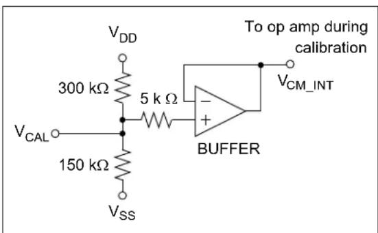
Figure 4-1 shows the reference circuit that internally sets the op amp's Common mode reference voltage ( V_CM_INT ) during calibration (the resistors are disconnected from the supplies at other times). The 5 kΩ resistor provides over-current protection for the buffer.
text_image
V_DD 300 kΩ 5 kΩ V_CAL 150 kΩ V_SS To op amp during calibration V_CM_INT BUFFERFIGURE 4-1: Common-Mode Reference's Input Circuitry.
When the V_CAL pin is left open, the internal resistor divider generates a V_CM_INT of approximately V_DD/3 , which is near the center of the input Common mode voltage range. It is recommended that an external capacitor from V_CAL to ground be added to improve noise immunity.
When the V_CAL pin is driven by an external voltage source, which is within its specified range, the op amp will have its input offset voltage calibrated at that Common mode input voltage. Make sure that V_CAL is within its specified range.
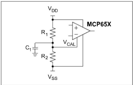
It is possible to use an external resistor voltage divider to modify V_CM_INT ; see Figure 4-2. The internal circuitry at the V_CAL pin looks like 100 kΩ tied to V_DD/3 . The parallel equivalent of R_1 and R_2 should be much smaller than 100 kΩ to minimize differences in matching and temperature drift between the internal and external resistors. Again, make sure that V_CAL is within its specified range.
text_image
VDD R1 C1 R2 VSS VCAL MCP65XFIGURE 4-2: Setting V CM with External Resistors.
For instance, a design goal to set V_CM_INT = 0.1 V when V_DD = 2.5 V could be met with: R = 24.3 k, R_2 = 1.00 k and 1G = 100 nF . This will keep V_CAL within its range for any V_DD , and should be close enough to 0V for ground-based applications.
4.2 Input
4.2.1 PHASE REVERSAL
The input devices are designed to not exhibit phase inversion when the input pins exceed the supply voltages. Figure 2-41 shows an input voltage exceeding both supplies with no phase inversion.
4.2.2 INPUT VOLTAGE AND CURRENT LIMITS
The ESD protection on the inputs can be depicted as shown in Figure 4-3. This structure was chosen to protect the input transistors, and to minimize input bias current ( I_B ). The input ESD diodes clamp the inputs when they try to go more than one diode drop below V_SS . They also clamp any voltages that go too far above V_DD ; their breakdown voltage is high enough to allow normal operation, and low enough to bypass quick ESD events within the specified limits.
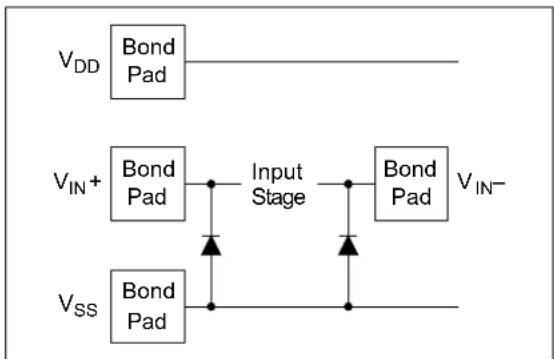
flowchart
graph TD
    A["V_DD"] --> B["Bond Pad"]
    C["V_IN+"] --> D["Bond Pad"]
    E["V_SS"] --> F["Bond Pad"]
    D --> G["Input Stage"]
    F --> H["Input Stage"]
    G --> I["Bond Pad"]
    H --> J["Bond Pad"]
    I --> K["V_IN-"]
FIGURE 4-3: Simplified Analog Input ESD Structures.
In order to prevent damage and/or improper operation of these amplifiers, the circuit must limit the currents (and voltages) at the input pins (see Section 1.1 "Absolute Maximum Ratings †"). Figure 4-4 shows the recommended approach to protecting these inputs. The internal ESD diodes prevent the input pins ( V_IN+ and V_IN- ) from going too far below ground, and the resistors R_1 and R_2 limit the possible current drawn out of the input pins. Diodes D_1 and D_2 prevent the input pins ( V_IN+ and V_IN- ) from going too far above V_DD , and dump any currents onto V_DD . When implemented as shown, resistors R_1 and R_2 also limit the current through D_1 and D_2 .

text_image
VDD D1 D2 V1 R1 MCP65X VOUT V2 R2 R1 > VSS - (minimum expected V1) / 2 mA R2 > VSS - (minimum expected V2) / 2 mAFIGURE 4-4: Protecting the Analog Inputs.
It is also possible to connect the diodes to the left of the resistor R_1 and R_2 . In this case, the currents through the diodes D_1 and D_2 need to be limited by some other mechanism. The resistors then serve as in-rush current limiters; the DC current into the input pins ( V_IN+ and V_IN- ) should be very small.
A significant amount of current can flow out of the inputs (through the ESD diodes) when the Common mode voltage ( V_CM ) is below ground ( V_SS ); see Figure 2-15. Applications that are high-impedance may need to limit the usable voltage range.
The input stage of the MCP651/1S/2/3/4/5/9 op amps uses a differential PMOS input stage. It operates at low Common mode input voltage ( V_CM ), with V_CM up to V_DD - 1.3V and down to V_SS - 0.3V . The input offset voltage ( V_OS ) is measured at V_CM = V_SS - 0.3V and V_DD - 1.3V to ensure proper operation. See Figure 2-6 and Figure 2-7 for temperature effects.
When operating at very low non-inverting gains, the output voltage is limited at the top by the V_CM range ( <V_DD-1.3V ); see Figure 4-5.
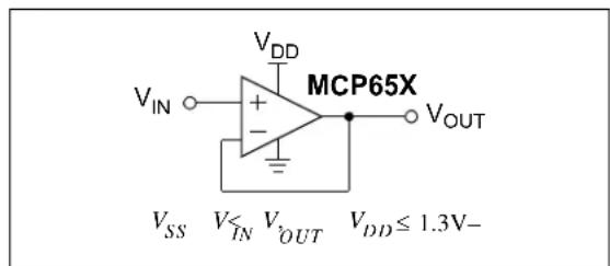
text_image
VDD MCP65X VIN + - VSS V≤IN VOUT VDD≤1.3V-
FIGURE 4-5: Unity-Gain Voltage Limitations for Linear Operation.
4.3 Rail-to-Rail Output
4.3.0.1 Maximum Output Voltage
The Maximum Output Voltage (see Figure 2-16 and Figure 2-17) describes the output range for a given load. For instance, the output voltage swings to within 15 mV of the negative rail with a 1 kΩ load tied to V_DD/2 .
4.3.0.2 Output Current
Figure 4-6 shows the possible combinations of output voltage ( V_OUT ) and output current ( I_OUT ). I_OUT is positive when it flows out of the op amp into the external circuit.

line
| IOUT (mA) | VOUT (V) | | --------- | -------- | | -100 | 0.5 | | -80 | 0.3 | | -60 | 0.1 | | -40 | 0.0 | | -20 | 0.0 | | 0 | 0.0 | | 20 | 5.5 | | 40 | 5.0 | | 60 | 4.5 | | 80 | 4.0 | | 100 | 3.5 | | 120 | 3.0 |FIGURE 4-6: Output Current.
4.3.0.3 Power Dissipation
Since the output short circuit current ( I_SC ) is specified at ±100 mA (typical), these op amps are capable of both delivering and dissipating significant power. Two common loads, and their impact on the op amp's power dissipation, will be discussed.
Figure 4-7 shows a resistive load ( R_L ) with a DC output voltage ( V_OUT ). V_L is R_L 's ground point, V_SS is usually ground (0V) and I_OUT is the output current. The input currents are assumed to be negligible.
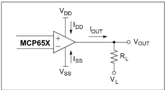
text_image
MCP65X V_DD I_DD I_OUT V_SS I_SS V_L R_L V_OUTFIGURE 4-7: Diagram for Resistive Load Power Calculations.
The DC currents are:
EQUATION 4-1:
$$ \begin{array}{l} I _ {O U T} \quad \frac {V _ {O U T} - V _ {L}}{R _ {L}} = \ I _ {D D} \approx I _ {Q} \quad \max 0, \mathbf {I} _ {O U T}) + \ I _ {S S} \approx I _ {\overline {{O}}} \quad \min 0, (O U T) \ \begin{array}{r l} {I _ {Q}} & {= \mathrm{Quiescent~supply~current~for~one}} \ & {\mathrm{op~amp~(mA/amplifier)}} \end{array} \ V _ {O U T} = A D C \text { value (V) } \ \end{array} $$
Where:
The DC op amp power is:
EQUATION 4-2:
$$ P _ {O A} = I _ {D D} (V _ {D D} - V _ {O U T}) + I _ {S S} (V _ {S S} - V _ {O U T}) $$
The maximum op amp power, for resistive loads at DC, occurs when V_OUT is halfway between V_DD and V_L or halfway between V_SS and V_L :
EQUATION 4-3:
$$ \begin{array}{l} \max (P _ {O A}) = I _ {D D} \left(V _ {D D} - V _ {S S}\right) \ + \frac {m a x ^ {2} (V _ {D D} - V _ {L} , V _ {L} - V _ {S S})}{4 R _ {L}} \ \end{array} $$
Figure 4-7 shows a capacitive load ( C_L ), which is driven by a sine wave with DC offset. The capacitive load causes the op amp to output higher currents at higher frequencies. Because the output rectifies I_OUT , the op amp's dissipated power increases (even though the capacitor does not dissipate power).

text_image
VDD IDD IOUT MCP65X + - ISS VSS CL VOUTFIGURE 4-8: Diagram for Capacitive Load Power Calculations.
The output voltage is assumed to be:
EQUATION 4-4:
$$ V _ {O U T} = V _ {D C} + V _ {A C} \sin (\omega t) $$
Where:
$$ V _ {D C} = D C \text { offset } (V) $$
$$ V _ {A C} = \text { Peak output swing } (V _ {P K}) $$
$$ \omega = \text { Radian frequency } (2 \pi f) (\text { rad / s }) $$
The op amp's currents are:
EQUATION 4-5:
$$ I _ {O U T} = C _ {L} \cdot \frac {d V _ {O U T}}{d t} = V _ {A C} \omega C _ {L} \cos (\omega t) $$
$$ I _ {D D} \approx I _ {\underline {{Q}}} \quad \max 0 I _ {(O U T)} \quad) \quad + $$
$$ I _ {S S} \approx I _ {\overline {{{Q}}}} \quad m i n 0 I (O U T) $$
Where:
$$ \begin{array}{r l} {I _ {Q}} & {= \text { Quiescent supply current for one }} \ & {\text { op amp (mA / amplifier) }} \end{array} $$
The op amp's instantaneous power, average power and peak power are:
EQUATION 4-6:
$$ P _ {O A} = I _ {D D} \left(V _ {D D} - V _ {O U T}\right) + I _ {S S} \left(V _ {S S} - V _ {O U T}\right) $$
$$ a v e (\mathcal {P} _ {O A}) = (V _ {D D} - V _ {S S}) \bigg (I _ {Q} + \frac {4 V _ {A C} f C _ {L}}{\pi} \bigg) $$
$$ \max (P _ {O A}) = (V _ {D D} - V _ {S S}) (I _ {Q} + 2 V _ {A C} f C _ {L}) $$
The power dissipated in a package depends on the powers dissipated by each op amp in that package:
EQUATION 4-7:
$$ P _ {P K G} = \sum_ {k 1 =} ^ {n} P _ {O A} $$
Where:
$$ n = \text { Number of op amps in package(1 or 2) } $$
The maximum ambient to junction temperature rise ( T_JA ) and junction temperature ( T_J ) can be calculated using the maximum expected package power ( P_PKG ), ambient temperature ( T_A ) and the package thermal resistance ( _JA ) found in Table 1-4:
EQUATION 4-8:
$$ \Delta T _ {J A} = P _ {P K G} \theta_ {J A} $$
$$ T _ {J} = T _ {A} + \Delta T _ {J A} $$
The worst-case power de-rating for the op amps in a particular package can be easily calculated:
EQUATION 4-9:
$$ P _ {P K G} \leq \frac {T _ {J m a x} - T _ {A}}{\theta_ {J A}} $$
Where:
$$ T _ {J m a x} = \begin{array}{l} \text { Absolute maximum junction } \ \text { temperature(°C) } \end{array} $$
$$ T _ {A} = \text { Ambient temperature } (^ {\circ} \mathrm{C}) $$
Several techniques are available to reduce T_JA for a given package:
- Reduce _JA
- Use another package
- Improve the PCB layout (ground plane, etc.)
- Add heat sinks and air flow
- Reduce max(P_PKG)
- Increase R_L
- Decrease C _L
- Limit I OUT using RISO (see Figure 4-9)
- Decrease V DD
4.4 Improving Stability
4.4.1 CAPACITIVE LOADS
Driving large capacitive loads can cause stability problems for voltage feedback op amps. As the load capacitance increases, the feedback loop's phase margin decreases and the closed-loop bandwidth is reduced. This produces gain peaking in the frequency response, with overshoot and ringing in the step response. See Figure 2-30. A unity-gain buffer (G = +1) is the most sensitive to capacitive loads, though all gains show the same general behavior.
When driving large capacitive loads with these op amps (e.g., > 20 pF when G = +1), a small series resistor at the output ( R_ISO in Figure 4-9) improves the feedback loop's phase margin (stability) by making the output load resistive at higher frequencies. The bandwidth will be generally lower than the bandwidth with no capacitive load.

chemical
Circuit diagram of MCP65X voltage regulator with input resistors and output capacitorFIGURE 4-9: Output Resistor, R ISO Stabilizes Large Capacitive Loads.
Figure 4-10 gives recommended R_ISO values for different capacitive loads and gains. The x-axis is the normalized load capacitance ( C_L / G_N ), where G_N is the circuit's noise gain. For non-inverting gains, G_N and the Signal Gain are equal. For inverting gains, G_N is 1 + |Signal Gain| (e.g., -1 V/V gives G_N = +2V / V ).
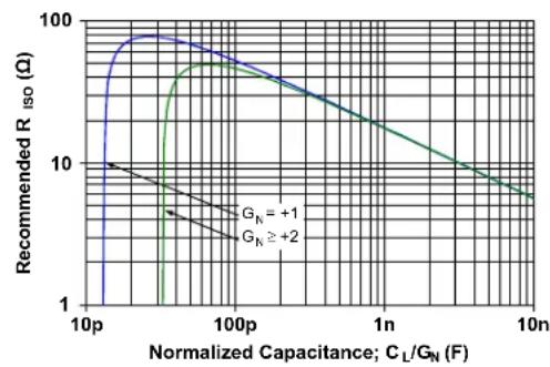
line
| Normalized Capacitance; C_L/G_N (F) | Recommended R_iso (Ω) for G_N = +1 | Recommended R_iso (Ω) for G_N ≥ +2 | | ----------------------------------- | ---------------------------------- | ---------------------------------- | | 10p | ~10 | ~1 | | 100p | ~50 | ~30 | | 1n | ~20 | ~10 | | 10n | ~5 | ~5 |FIGURE 4-10: Recommended R ISO Values for Capacitive Loads.
After selecting R_ISO for your circuit, double check the resulting frequency response peaking and step response overshoot. Modify R_ISO 's value until the response is reasonable. Bench evaluation and simulations with the MCP651/1S/2/3/4/5/9 SPICE macro model are helpful.
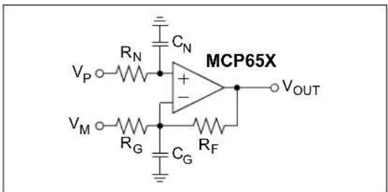
4.4.2 GAIN PEAKING
Figure 4-11 shows an op amp circuit that represents non-inverting amplifiers ( V_M is a DC voltage and V_P is the input) or inverting amplifiers ( V_P is a DC voltage and V_M is the input). The capacitances C_N and C_G represent the total capacitance at the input pins; they include the op amp's Common mode input capacitance ( C_CM ), board parasitic capacitance and any capacitor placed in parallel.
text_image
MCP65X V_P ○─R_N─●─[+]─●─○ V_OUT │ └─[ ]─●─●─●─●─●─○ │ │ ○ │ R_G ●─●─●─●─●─●─○ │ │ C_G ●─●─●─●─●─●─○ │ │ ○ │ R_F ●─●─●─●─●─●─○ │ │ ○ │ C_N ●─●─●─●─●─●─○ │ │ ○ │ C_G ●─●─●─●─●─●─○FIGURE 4-11: Amplifier with Parasitic Capacitance.
C_G acts in parallel with R_G (except for a gain of +1 V/V), which causes an increase in gain at high frequencies. C_G also reduces the phase margin of the feedback loop, which becomes less stable. This effect can be reduced by either reducing C_G or R_F .
C_N and R_N form a low-pass filter that affects the signal at V_P . This filter has a single real pole at 1/(2 R_NC_N) .
The largest value of R_F that should be used depends on noise gain (see G_N in Section 4.4.1 “Capacitive Loads”) and C_G . Figure 4-12 shows the maximum recommended R_F for several C_G values.

line
| Noise Gain; G_N (V/V) | Maximum Recommended R_F (Ω) for C_G = 10 pF | Maximum Recommended R_F (Ω) for C_G = 32 pF | Maximum Recommended R_F (Ω) for C_G = 100 pF | Maximum Recommended R_F (Ω) for C_G = 320 pF | Maximum Recommended R_F (Ω) for C_G = 1 nF | | --------------------- | ------------------------------------------ | ------------------------------------------- | -------------------------------------------- | -------------------------------------------- | ------------------------------------------ | | 1 | 100 | 100 | 100 | 100 | 100 | | 10 | 1000 | 1000 | 1000 | 1000 | 1000 | | 100 | 10000 | 10000 | 10000 | 10000 | 10000 |FIGURE 4-12: Maximum Recommended R_F vs. Gain.
Figure 2-37 and Figure 2-38 show the small signal and large signal step responses at G = +1 V/V. The unity-gain buffer usually has R_F = 0 and R_G open.
Figure 2-39 and Figure 2-40 show the small signal and large signal step responses at G = -1 V/V. Since the noise gain is 2 V/V and C_G ≈ 10 pF, the resistors were chosen to be R_F = R_G = 499 and R_N = 249 .
It is also possible to add a capacitor ( C_F ) in parallel with R_F to compensate for the de-stabilizing effect of C_G . This makes it possible to use larger values of R_F . The conditions for stability are summarized in Equation 4-10.
EQUATION 4-10:
Given:
$$ G _ {N I} = 1 + R _ {F} / R _ {G} $$
$$ G _ {N 2} = I + C _ {G} / C _ {F} $$
$$ f _ {F} = 1 / (2 \pi R _ {F} C _ {F}) $$
$$ f _ {Z} \quad f _ {F} \mathbf {G} _ {N 1} / \mathbf {G} _ {N 2}) $$
We need:
$$ f _ {F} \leq f _ {G B W P} / (2 G _ {N 2}), \quad G _ {N 1} < G _ {N 2} $$
$$ f _ {F} \leq f _ {G B W P} / (4 G _ {N 1}), \quad G _ {N 1} > G _ {N 2} $$
4.5 Power Supply
With this family of operational amplifiers, the Power Supply pin ( V_DD for single supply) should have a local bypass capacitor (i.e., 0.01 F to 0.1 F) within 2 mm for good high-frequency performance. Surface mount, multilayer ceramic capacitors, or their equivalent, should be used.
These op amps require a bulk capacitor (i.e., 2.2 F or larger) within 50 mm to provide large, slow currents. Tantalum capacitors, or their equivalent, may be a good choice. This bulk capacitor can be shared with other nearby analog parts as long as crosstalk through the supplies does not prove to be a problem.
4.6 High-Speed PCB Layout
These op amps are fast enough that a little extra care in the PCB (Printed Circuit Board) layout can make a significant difference in performance. Good PCB layout techniques will help achieve the performance shown in the specifications and Typical Performance Curves; it will also help minimize EMC (Electro-Magnetic Compatibility) issues.
Use a solid ground plane. Connect the bypass local capacitor(s) to this plane with minimal length traces to cut down inductive and capacitive crosstalk.
Separate digital from analog, low-speed from high-speed, and low-power from high-power. This will reduce interference.
Keep sensitive traces short and straight. Separate them from interfering components and traces. This is especially important for high-frequency (low rise time) signals.
Sometimes, it helps to place guard traces next to victim traces. They should be on both sides of the victim trace, and as close as possible. Connect guard traces to ground plane at both ends, and in the middle for long traces.
Use coax cables, or low inductance wiring, to route signal and power to and from the PCB. Mutual and self inductance of power wires is often a cause of crosstalk and unusual behavior.
4.7 Typical Applications
4.7.1 POWER DRIVER WITH HIGH GAIN
Figure 4-13 shows a power driver with high gain (1 + R_2/R_1) . The MCP651/1S/2/3/4/5/9 op amp's short-circuit current makes it possible to drive significant loads. The calibrated input offset voltage supports accurate response at high gains. R_3 should be small, and equal to R_1||R_2 , in order to minimize the bias current induced offset.

text_image
VDD/2 ○─R1─●─R2─●─○VOUT │ │ ○─R3─●─●─●─●─●─●─●─●─●─●─●─●─●─●─●─●─●─●─●─●─●─●─●─●─●─●─●─●─●─●─●─●─●─●─●─●─●─●─●─●─●─●─●─●─●─●─●─●─●─●─○ VIN ○─R3─●─+ ────●───────●───────●───────●───────●───────●───────●───────●───────●───────●───────●───────●───────●───────●───────●───────●───────●───────●───────●───────●───────●───────●───────●───────●───────●───────● MCP65XFIGURE 4-13: Power Driver.
4.7.2 OPTICAL DETECTOR AMPLIFIER
Figure 4-14 shows a transimpedance amplifier, using the MCP651 op amp, in a photo detector circuit. The photo detector is a capacitive current source. The op amp's input Common mode capacitance (5 pF, typical) acts in parallel with C_D . R_F provides enough gain to produce 10 mV at V_OUT . C_F stabilizes the gain and limits the transimpedance bandwidth to about 1.1 MHz. R_F 's parasitic capacitance (e.g., 0.2 pF for a 0805 SMD) acts in parallel with C_F .

text_image
Photo Detector ID 100 nA CD 30 pF CF 1.5 pF RF 100 kΩ VOUT MCP651 - + VDD/2FIGURE 4-14: Transimpedance Amplifier for an Optical Detector.
4.7.3 H-BRIDGE DRIVER
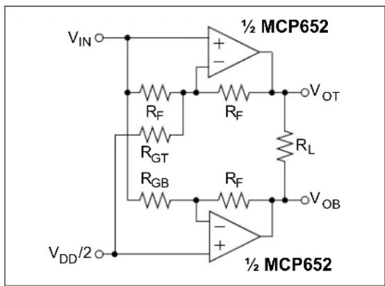
Figure 4-15 shows the MCP652 dual op amp used as a H-bridge driver. The load could be a speaker or a DC motor.
text_image
½ MCP652 VIN + - RF RF VOT RGT RGB RF RL VOB VDD/2 ½ MCP652FIGURE 4-15: H-Bridge Driver.
This circuit automatically makes the noise gains (G_N) equal, when the gains are set properly, so that the frequency responses match well (in magnitude and in phase). Equation 4-11 shows how to calculate R_GT and R_GB so that both op amps have the same DC gains; G_DM needs to be selected first.
EQUATION 4-11:
$$ G _ {D M} = \frac {V _ {O T} - V _ {O B}}{V _ {I N} - V _ {D D} / 2} 2 \geqslant V / V $$
$$ R _ {G T} = \frac {R _ {F}}{(G _ {D M} / 2)} \quad I - $$
$$ R _ {G B} = \frac {R _ {F}}{G _ {D M} / 2} $$
Equation 4-12 gives the resulting Common mode and Differential mode output voltages.
EQUATION 4-12:
$$ \frac {V _ {O T} + V _ {O B}}{2} = \frac {V _ {D D}}{2} $$
$$ V _ {O T} - V _ {O B} = G _ {D M} \bigg (V _ {I N} - \frac {V _ {D D}}{2} \bigg) $$
5.0 DESIGN AIDS
Microchip provides the basic design aids needed for the MCP651/1S/2/3/4/5/9 family of op amps.
5.1 SPICE Macro Model
The latest SPICE macro model for the MCP651/1S/2/3/4/5/9 op amps is available on the Microchip web site at www.microchip.com. This model is intended to be an initial design tool that works well in the op amp's linear region of operation over the temperature range. See the model file for information on its capabilities.
Bench testing is a very important part of any design and cannot be replaced with simulations. Also, simulation results using this macro model need to be validated by comparing them to the data sheet specifications and characteristic curves.
5.2 FilterLab ^® Software
Microchip's FilterLab® software is an innovative software tool that simplifies analog active filter (using op amps) design. Available at no cost from the Microchip web site at www.microchip.com/filterlab, the FilterLab design tool provides full schematic diagrams of the filter circuit with component values. It also outputs the filter circuit in SPICE format, which can be used with the macro model to simulate actual filter performance.
5.3 Microchip Advanced Part Selector (MAPS)
MAPS is a software tool that helps efficiently identify Microchip devices that fit a particular design requirement. Available at no cost from the Microchip web site at www.microchip.com/maps, the MAPS is an overall selection tool for Microchip's product portfolio that includes Analog, Memory, MCUs and DSCs. Using this tool, a customer can define a filter to sort features for a parametric search of devices and export side-by-side technical comparison reports. Helpful links are also provided for data sheets, purchase and sampling of Microchip parts.
5.4 Analog Demonstration and Evaluation Boards
Microchip offers a broad spectrum of Analog Demonstration and Evaluation Boards that are designed to help customers achieve faster time to market. For a complete listing of these boards and their corresponding user's guides and technical information, visit the Microchip web site at www.microchip.com/analog tools.
Some boards that are especially useful are:
• MCP6XXX Amplifier Evaluation Board 1
• MCP6XXX Amplifier Evaluation Board 2
• MCP6XXX Amplifier Evaluation Board 3
• MCP6XXX Amplifier Evaluation Board 4
• Active Filter Demo Board Kit
• 8-Pin SOIC/MSOP/TSSOP/DIP Evaluation Board, P/N SOIC8EV
5.5 Application Notes
The following Microchip Application Notes are available on the Microchip web site at www.microchip.com/appnotes and are recommended as supplemental reference resources.
- ADN003: "Select the Right Operational Amplifier for your Filtering Circuits" (DS21821)
- AN722: "Operational Amplifier Topologies and DC Specifications" (DS00722)
- AN723: "Operational Amplifier AC Specifications and Applications" (DS00723)
- AN884: "Driving Capacitive Loads With Op Amps" (DS00884)
- AN990: "Analog Sensor Conditioning Circuits – An Overview" (DS00990)
• AN1177: "Op Amp Precision Design: DC Errors" (DS01177) - AN1228: "Op Amp Precision Design: Random Noise" (DS01228)
• AN1332: "Current Sensing Circuit Concepts and Fundamentals" (DS01332)
Some of these application notes, and others, are listed in the design guide:
• "Signal Chain Design Guide" (DS21825)
6.0 PACKAGING INFORMATION
6.1 Package Marking Information
5-Lead SOT-23 (2x3) (MCP651S)

text_image
XXNN6-Lead SOT-23 (2x3) (MCP653)

text_image
XXNN8-Lead TDFN(2x3) (MCP651)
text_image
XXX YWW NN PIN 1Example:
text_image
YW25Example:

text_image
JD25Example:
text_image
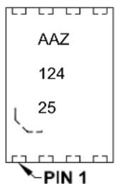
AAZ 124 25 PIN 1
Note: Applies to 8-Lead 3x3 DFN
Example:

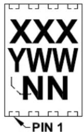
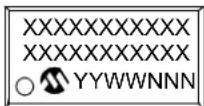
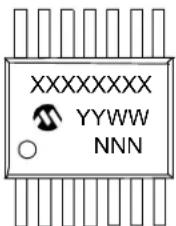
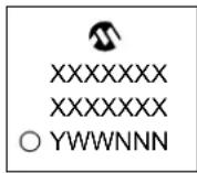
Legend: XX...X Customer-specific information
Y Year code (last digit of calendar year)
YY Year code (last 2 digits of calendar year)
WW Week code (week of January 1 is week '01')
NNN Alphanumeric traceability code
eBb-free JEDEC ^® designator for Matte Tin (Sn)
* This package is Pb-free. The Pb-free JEDEC designator (e3)
can be found on the outer packaging for this package.
Note: In the event the full Microchip part number cannot be marked on one line, it will be carried over to the next line, thus limiting the number of available characters for customer-specific information.
6.2 Package Marking Information
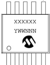
8-Lead SOIC (150 mil) (MCP651, MCP652)

Example:

10-Lead DFN (3x3) (MCP655)
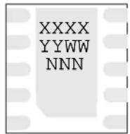
Example:
10-Lead MSOP (MCP655)
text_image
XXXXXX YWWNNNExample:

text_image
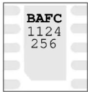
655EUN 12425614-Lead SOIC (MCP654) Example:

14-Lead TSSOP (MCP654)
text_image
XXXXXXXXX YYWW NNNExample:

text_image
654E/ST 1124 25616-Lead QFN (4x4) (MCP659) Example:
5-Lead Plastic Small Outline Transistor (OT) [SOT-23]
Note: For the most current package drawings, please see the Microchip Packaging Specification located at http://www.microchip.com/packaging
![Microchip MCP652 - 5-Lead Plastic Small Outline Transistor (OT) [SOT-23] - 1](/content/2026/06/1219345/images/8f0cf27b0476db16d1b327bc084bd8721d48068b2d6c1e550dcfa46f316d8d0a.jpg)
| Units | MILLIMETERS | |||
| Dimension Limitss | MINsNOMsMAX | |||
| Number of Pins | Ns | 5 | ||
| Lead Pitchses0.95 BSC | ||||
| Outside Lead Pitchse1s1.90 BSC | ||||
| Overall HeightsA 0.90 - | 1.45 | |||
| Molded Package Thickness | A2 | 0.89 | - | 1.30 |
| Standoff | A1 | 0.00 | - | 0.15 |
| Overall Width | E | 2.20 | - | 3.20 |
| Molded Package Width | E1 | 1.30 | - | 1.80 |
| Overall Length | D | 2.70 | - | 3.10 |
| Foot Length | L | 0.10 | - | 0.60 |
| Footprint | L1 | 0.35 | - | 0.80 |
| Foot Angle | 0° | - | 30° | |
| Lead Thickness | c | 0.08 | - | 0.26 |
| Lead Width | b | 0.20 | - | 0.51 |
Notes:
- Dimensions D and E1 do not include mold flash or protrusions. Mold flash or protrusions shall not exceed 0.127 mm per side.
2.sDimensioning and tolerancing per ASME Y14.5M.
BSC:sBasic Dimension. Theoretically exact value shown without tolerances.
Microchip Technology Drawing C04-091B
5-Lead Plastic Small Outline Transistor (OT) [SOT-23]
Note: For the most current package drawings, please see the Microchip Packaging Specification located at http://www.microchip.com/packaging
![Microchip MCP652 - 5-Lead Plastic Small Outline Transistor (OT) [SOT-23] - 1](/content/2026/06/1219345/images/7b8f6a32a347d7ba9bc01afd1e7b08d56e516a5264c3e730a7ab0ca11e451b82.jpg)
text_image
X Y Z C G SILK SCREEN E GXRECOMMENDED LAND PATTERN
| Units | MILLIMETERS | |||
| Dimension Limits | MIN | NOM | MAX | |
| Contact Pitch | E | 0.95 BSC | ||
| Contact Pad Spacing | C | 2.80 | ||
| Contact Pad Width (X5) | X | 0.60 | ||
| Contact Pad Length (X5) | Y | 1.10 | ||
| Distance Between Pads | G | 1.70 | ||
| Distance Between Pads | GX | 0.35 | ||
| Overall Width | Z | 3.90 | ||
Notes:
- Dimensioning and tolerancing per ASME Y14.5M
BSC: Basic Dimension. Theoretically exact value shown without tolerances.
Microchip Technology Drawing No. C04-2091A
6-Lead Plastic Small Outline Transistor (CHY) [SOT-23]
Note: For the most current package drawings, please see the Microchip Packaging Specification located at http://www.microchip.com/packaging
![Microchip MCP652 - 6-Lead Plastic Small Outline Transistor (CHY) [SOT-23] - 1](/content/2026/06/1219345/images/24b5df8be8bbf3afd65561c7beb9941322bfcc7f3e6dd5c89ab74e4b98ea1228.jpg)
| Units MILLIMETERS | ||||
| Dimension Limits MIN NOM MAX | ||||
| Number of Pins N 6 | ||||
| Pitch e 0.95 BSC | ||||
| Outside Lead Pitch e1 1 | 90 BSC | |||
| Overall Height | A | 0.90 | - | 1.45 |
| Molded Package Thickness | A2 | 0.89 | - | 1.30 |
| Standoff | A1 | 0.00 | - | 0.15 |
| Overall Width | E | 2.20 | - | 3.20 |
| Molded Package Width | E1 | 1.30 | - | 1.80 |
| Overall Length | D | 2.70 | - | 3.10 |
| Foot Length | L | 0.10 | - | 0.60 |
| Footprint | L1 | 0.35 | - | 0.80 |
| Foot Angle | 0° | - | 30° | |
| Lead Thickness c 0.08 | - | 0.26 | ||
| Lead Width | b | 0.20 | - | 0.51 |
Notes:
- Dimensions D and E1 do not include mold flash or protrusions. Mold flash or protrusions shall not exceed 0.127 mm per side.
- Dimensioning and tolerancing per ASME Y14.5M.
BSC: Basic Dimension. Theoretically exact value shown without tolerances.
Microchip Technology Drawing C04-028B
6-Lead Plastic Small Outline Transistor (CHY) [SOT-23]
Note: For the most current package drawings, please see the Microchip Packaging Specification located at http://www.microchip.com/packaging
![Microchip MCP652 - 6-Lead Plastic Small Outline Transistor (CHY) [SOT-23] - 1](/content/2026/06/1219345/images/8ae5151c8493d276bae83e802cf88a918442ebf495413dc6e2a64058398aca3f.jpg)
text_image
X Y Z C G SILK SCREEN E GXRECOMMENDED LAND PATTERN
| Units | MILLIMETERS | |||
| Dimension Limits | MIN | NOM | MAX | |
| Contact Pitch | E | 0.95 BSC | ||
| Contact Pad Spacing | C | 2.80 | ||
| Contact Pad Width (X6) | X | 0.60 | ||
| Contact Pad Length (X6) | Y | 1.10 | ||
| Distance Between Pads | G | 1.70 | ||
| Distance Between Pads | GX | 0.35 | ||
| Overall Width | Z | 3.90 | ||
Notes:
- Dimensioning and tolerancing per ASME Y14.5M
BSC: Basic Dimension. Theoretically exact value shown without tolerances.
Microchip Technology Drawing No. C04-2028A
8-Lead Plastic Dual Flat, No Lead Package (MF) - 3x3x0.9mm Body [DFN]
Note: For the most current package drawings, please see the Microchip Packaging Specification located at http://www.microchip.com/packaging
![Microchip MCP652 - 8-Lead Plastic Dual Flat, No Lead Package (MF) - 3x3x0.9mm Body [DFN] - 1](/content/2026/06/1219345/images/d3ce9056c16e914f245ee3cc6e71ee4d418e46c25bd64f1329b28e5f93e35804.jpg)
Microchip Technology Drawing No. C04-062C Sheet 1 of 2
8-Lead Plastic Dual Flat, No Lead Package (MF) - 3x3x0.9mm Body [DFN]
Note: For the most current package drawings, please see the Microchip Packaging Specification located at http://www.microchip.com/packaging
![Microchip MCP652 - 8-Lead Plastic Dual Flat, No Lead Package (MF) - 3x3x0.9mm Body [DFN] - 1](/content/2026/06/1219345/images/9b2e639e2158d2c43c6891c3d8cc8bd5ca89d7c3c5753acacc8d3d49e87e7cff.jpg)
text_image
NOTE 2| Units | MILLIMETERS | |||
| Dimension Limits | MIN | NOM | MAX | |
| Number of Pins | N | 8 | ||
| Pitch | e | 0.65 BSC | ||
| Overall Height | A | 0.80 | 0.90 | 1.00 |
| Standoff | A1 | 0.00 | 0.02 | 0.05 |
| Contact Thickness | A3 | 0.20 REF | ||
| Overall Length | D | 3.00 BSC | ||
| Exposed Pad Width | E2 | 1.34 | - | 1.60 |
| Overall Width | E | 3.00 BSC | ||
| Exposed Pad Length | D2 | 1.60 | - | 2.40 |
| Contact Width | b | 0.25 | 0.30 | 0.35 |
| Contact Length | L | 0.20 | 0.30 | 0.55 |
| Contact-to-Exposed Pad | K | 0.20 | - | - |
Notes:
1. Pin 1 visual index feature may vary, but must be located within the hatched area.
2. Package may have one or more exposed tie bars at ends.
3. Package is saw singulated
4. Dimensioning and tolerancing per ASME Y14.5M
BSC: Basic Dimension. Theoretically exact value shown without tolerances.
REF: Reference Dimension, usually without tolerance, for information purposes only.
Microchip Technology Drawing No. C04-062C Sheet 2 of 2
8-Lead Plastic Dual Flat, No Lead Package (MF) - 3x3x0.9mm Body [DFN]
Note: For the most current package drawings, please see the Microchip Packaging Specification located at http://www.microchip.com/packaging
![Microchip MCP652 - 8-Lead Plastic Dual Flat, No Lead Package (MF) - 3x3x0.9mm Body [DFN] - 1](/content/2026/06/1219345/images/bdaf6f08ac086f543c26424935194a121d683ffa5d5c7f2338642ccedbbdc55e.jpg)
text_image
W2 G C1 T2 E X1 Y1 SILK SCREENRECOMMENDED LAND PATTERN
| Units | MILLIMETERS | |||
| Dimension Limits | MIN | NOM | MAX | |
| Contact Pitch | E | 0.65 BSC | ||
| Optional Center Pad Width | W2 | 2.40 | ||
| Optional Center Pad Length | T2 | 1.55 | ||
| Contact Pad Spacing | C1 | 3.10 | ||
| Contact Pad Width (X8) | X1 | 0.35 | ||
| Contact Pad Length (X8) | Y1 | 0.65 | ||
| Distance Between Pads | G | 0.30 | ||
Notes:
1. Dimensioning and tolerancing per ASME Y14.5M
BSC: Basic Dimension. Theoretically exact value shown without tolerances.
Microchip Technology Drawing No. C04-2062B
8-Lead Plastic Small Outline (SN) - Narrow, 3.90 mm Body [SOIC]
Note: For the most current package drawings, please see the Microchip Packaging Specification located at http://www.microchip.com/packaging
![Microchip MCP652 - 8-Lead Plastic Small Outline (SN) - Narrow, 3.90 mm Body [SOIC] - 1](/content/2026/06/1219345/images/7f9a58a07849b9cc4d94186db88aba3aa3b52626c74742439a70a5450587d95f.jpg)
Microchip Technology Drawing No. C04-057C Sheet 1 of 2
8-Lead Plastic Small Outline (SN) - Narrow, 3.90 mm Body [SOIC]
Note: For the most current package drawings, please see the Microchip Packaging Specification located at http://www.microchip.com/packaging
![Microchip MCP652 - 8-Lead Plastic Small Outline (SN) - Narrow, 3.90 mm Body [SOIC] - 1](/content/2026/06/1219345/images/b7b4cf59e03acef70451861725d7cb40feeb2df051c6e33a6d1bee402ecf9677.jpg)
natural_image
Isometric line drawing of an integrated circuit chip with multiple pins (no text or symbols)| Units | MILLIMETERS | |||
| Dimension Limits | MIN | NOM | MAX | |
| Number of Pins | N | 8 | ||
| Pitch | e | 1.27 BSC | ||
| Overall Height | A | - | - | 1.75 |
| Molded Package Thickness | A2 | 1.25 | - | - |
| Standoff § | A1 | 0.10 | - | 0.25 |
| Overall Width | E | 6.00 BSC | ||
| Molded Package Width | E1 | 3.90 BSC | ||
| Overall Length | D | 4.90 BSC | ||
| Chamfer (Optional) | h | 0.25 | - | 0.50 |
| Foot Length | L | 0.40 | - | 1.27 |
| Footprint | L1 | 1.04 REF | ||
| Foot Angle | 0° | - | 8° | |
| Lead Thickness | c | 0.17 | - | 0.25 |
| Lead Width | b | 0.31 | - | 0.51 |
| Mold Draft Angle Top | 5° | - | 15° | |
| Mold Draft Angle Bottom | 5° | - | 15° | |
Notes:
- Pin 1 visual index feature may vary, but must be located within the hatched area.
- § Significant Characteristic
- Dimensions D and E1 do not include mold flash or protrusions. Mold flash or protrusions shall not exceed 0.15mm per side.
- Dimensioning and tolerancing per ASME Y14.5M
BSC: Basic Dimension. Theoretically exact value shown without tolerances.
REF: Reference Dimension, usually without tolerance, for information purposes only.
Microchip Technology Drawing No. C04-057C Sheet 2 of 2
8-Lead Plastic Small Outline (SN) – Narrow, 3.90 mm Body [SOIC]
Note: For the most current package drawings, please see the Microchip Packaging Specification located at http://www.microchip.com/packaging
![Microchip MCP652 - 8-Lead Plastic Small Outline (SN) – Narrow, 3.90 mm Body [SOIC] - 1](/content/2026/06/1219345/images/17121c27cb53f0c54ac353afe4c736483904feea91bb9bec402036cfd4b15212.jpg)
text_image
E C SILK SCREEN Y1 X1RECOMMENDED LAND PATTERN
| Units | MILLIMETERS | |||
| Dimension Limits | MIN | NOM | MAX | |
| Contact Pitch | E | 1.27 BSC | ||
| Contact Pad Spacing | C | 5.40 | ||
| Contact Pad Width (X8) | X1 | 0.60 | ||
| Contact Pad Length (X8) | Y1 | 1.55 | ||
Notes:
1. Dimensioning and tolerancing per ASME Y14.5M
BSC: Basic Dimension. Theoretically exact value shown without tolerances.
Microchip Technology Drawing No. C04-2057A
8-Lead Plastic Dual Flat, No Lead Package (MN) - 2x3x0.75mm Body [TDFN]
Note: For the most current package drawings, please see the Microchip Packaging Specification located at http://www.microchip.com/packaging
![Microchip MCP652 - 8-Lead Plastic Dual Flat, No Lead Package (MN) - 2x3x0.75mm Body [TDFN] - 1](/content/2026/06/1219345/images/d14bcde1b08d321c856f9014ae022087cf4fd13b4bc97b36d830a455a79a0757.jpg)
Microchip Technology Drawing No. C04-129C Sheet 1 of 2
8-Lead Plastic Dual Flat, No Lead Package (MN) - 2x3x0.75mm Body [TDFN]
Note: For the most current package drawings, please see the Microchip Packaging Specification located at http://www.microchip.com/packaging
![Microchip MCP652 - 8-Lead Plastic Dual Flat, No Lead Package (MN) - 2x3x0.75mm Body [TDFN] - 1](/content/2026/06/1219345/images/f82432e17a1988762f9c5af319036eb9bcc0fb31fc457bbb589620f5e8e26e3e.jpg)
text_image
NOTE 2| Units | MILLIMETERS | |||
| Dimension Limits | MIN | NOM | MAX | |
| Number of Pins | N | 8 | ||
| Pitch | e | 0.50 BSC | ||
| Overall Height | A | 0.70 | 0.75 | 0.80 |
| Standoff | A1 | 0.00 | 0.02 | 0.05 |
| Contact Thickness | A3 | 0.20 REF | ||
| Overall Length | D | 2.00 BSC | ||
| Overall Width | E | 3.00 BSC | ||
| Exposed Pad Length | D2 | 1.20 | - | 1.60 |
| Exposed Pad Width | E2 | 1.20 | - | 1.60 |
| Contact Width | b | 0.20 | 0.25 | 0.30 |
| Contact Length | L | 0.25 | 0.30 | 0.45 |
| Contact-to-Exposed Pad | K | 0.20 | - | - |
Notes:
- Pin 1 visual index feature may vary, but must be located within the hatched area.
- Package may have one or more exposed tie bars at ends.
- Package is saw singulated
- Dimensioning and tolerancing per ASME Y14.5M
BSC: Basic Dimension. Theoretically exact value shown without tolerances.
REF: Reference Dimension, usually without tolerance, for information purposes only.
Microchip Technology Drawing No. C04-129C Sheet 2 of 2
8-Lead Plastic Dual Flat, No Lead Package (MN) - 2x3x0.75 mm Body [TDFN]
Note: For the most current package drawings, please see the Microchip Packaging Specification located at http://www.microchip.com/packaging
![Microchip MCP652 - 8-Lead Plastic Dual Flat, No Lead Package (MN) - 2x3x0.75 mm Body [TDFN] - 1](/content/2026/06/1219345/images/6b376ffc860af0c55e525ffc7ac06cf5a3c90529ab646f079e741fa453df5c9c.jpg)
text_image
W2 G SILK SCREEN C1 T2 Y1 E X1RECOMMENDED LAND PATTERN
| Units | MILLIMETERS | |||
| Dimension Limits | MIN | NOM | MAX | |
| Contact Pitch | E | 0.50 BSC | ||
| Optional Center Pad Width | W2 | 1.46 | ||
| Optional Center Pad Length | T2 | 1.36 | ||
| Contact Pad Spacing | C1 | 3.00 | ||
| Contact Pad Width (X8) | X1 | 0.30 | ||
| Contact Pad Length (X8) | Y1 | 0.75 | ||
| Distance Between Pads | G | 0.20 | ||
Notes:
1. Dimensioning and tolerancing per ASME Y14.5M
BSC: Basic Dimension. Theoretically exact value shown without tolerances.
Microchip Technology Drawing No. C04-2129A
10-Lead Plastic Dual Flat, No Lead Package (MF) - 3x3x0.9mm Body [DFN]
Note: For the most current package drawings, please see the Microchip Packaging Specification located at http://www.microchip.com/packaging
![Microchip MCP652 - 10-Lead Plastic Dual Flat, No Lead Package (MF) - 3x3x0.9mm Body [DFN] - 1](/content/2026/06/1219345/images/4bc94a956a7881d64f459e3bfe534734db01004267e463ad5be1d5ec90538765.jpg)
Microchip Technology Drawing No. C04-063C Sheet 1 of 2
10-Lead Plastic Dual Flat, No Lead Package (MF) - 3x3x0.9mm Body [DFN]
Note: For the most current package drawings, please see the Microchip Packaging Specification located at http://www.microchip.com/packaging
![Microchip MCP652 - 10-Lead Plastic Dual Flat, No Lead Package (MF) - 3x3x0.9mm Body [DFN] - 1](/content/2026/06/1219345/images/16a52021b7964c2ea53c262e55f25c4af6af8a8be3ba6fcc67226cfe98a5c084.jpg)
text_image
NOTE 2| Units | MILLIMETERS | |||
| Dimension Limits | MIN | NOM | MAX | |
| Number of Pins | N | 10 | ||
| Pitch | e | 0.50 BSC | ||
| Overall Height | A | 0.80 | 0.90 | 1.00 |
| Standoff | A1 | 0.00 | 0.02 | 0.05 |
| Contact Thickness | A3 | 0.20 REF | ||
| Overall Length | D | 3.00 BSC | ||
| Exposed Pad Length | D2 | 2.15 | 2.35 | 2.45 |
| Overall Width | E | 3.00 BSC | ||
| Exposed Pad Width | E2 | 1.40 | 1.50 | 1.75 |
| Contact Width | b | 0.18 | 0.25 | 0.30 |
| Contact Length | L | 0.30 | 0.40 | 0.50 |
| Contact-to-Exposed Pad | K | 0.20 | - | - |
Notes:
- Pin 1 visual index feature may vary, but must be located within the hatched area.
- Package may have one or more exposed tie bars at ends.
- Package is saw singulated.
- Dimensioning and tolerancing per ASME Y14.5M. BSC: Basic Dimension. Theoretically exact value shown without tolerances. REF: Reference Dimension, usually without tolerance, for information purposes only.
Microchip Technology Drawing No. C04-063C Sheet 2 of 2
10-Lead Plastic Dual Flat, No Lead Package (MF) - 3x3x0.9mm Body [DFN]
Note: For the most current package drawings, please see the Microchip Packaging Specification located at http://www.microchip.com/packaging
![Microchip MCP652 - 10-Lead Plastic Dual Flat, No Lead Package (MF) - 3x3x0.9mm Body [DFN] - 1](/content/2026/06/1219345/images/5dda0371637d2ef39b79bd47e384ed2d035654ef3fc5e8249e0136e0177292b4.jpg)
text_image
W2 G Y1 C1 T2 E X1 SILK SCREENRECOMMENDED LAND PATTERN
| Units | MILLIMETERS | |||
| Dimension Limits | MIN | NOM | MAX | |
| Contact Pitch | E | 0.50 BSC | ||
| Optional Center Pad Width | W2 | 2.48 | ||
| Optional Center Pad Length | T2 | 1.55 | ||
| Contact Pad Spacing | C1 | 3.10 | ||
| Contact Pad Width (X10) | X1 | 0.30 | ||
| Contact Pad Length (X10) | Y1 | 0.65 | ||
| Distance Between Pads | G | 0.20 | ||
Notes:
1. Dimensioning and tolerancing per ASME Y14.5M
BSC: Basic Dimension. Theoretically exact value shown without tolerances.
Microchip Technology Drawing No. C04-2063B
10-Lead Plastic Micro Small Outline Package (UN) [MSOP]
Note: For the most current package drawings, please see the Microchip Packaging Specification located at http://www.microchip.com/packaging
![Microchip MCP652 - 10-Lead Plastic Micro Small Outline Package (UN) [MSOP] - 1](/content/2026/06/1219345/images/936d83838d70d17db49aa39bd5660193328297e2e60ac176d0f9d0a118c7e842.jpg)
text_image
2X 0.20 H D/2 A E/2 D E1/2 E1 N NOTE 1 1 2 N/2 e B NX b 0.25 C TOP VIEW A A2 A1 SIDE VIEW 0.13 M C A-B D 0.10 C SEATING PLANE C H SEE DETAIL C END VIEWMicrochip Technology Drawing C04-021C Sheet 1 of 2
10-Lead Plastic Micro Small Outline Package (UN) [MSOP]
Note: For the most current package drawings, please see the Microchip Packaging Specification located at http://www.microchip.com/packaging
![Microchip MCP652 - 10-Lead Plastic Micro Small Outline Package (UN) [MSOP] - 1](/content/2026/06/1219345/images/d41099e6e5541801911e7c15b322764a6887ea20a23e11ee4d7816502c9cdf6e.jpg)
text_image
SEATING PLANE C L (L1) GAUGE PLANE c φDETAIL C
| Units | MILLIMETERS | |||
| Dimension Limits | MIN | NOM | MAX | |
| Number of Pins | N | 10 | ||
| Pitch | e | 0.50 BSC | ||
| Overall Height | A | - | - | 1.10 |
| Molded Package Thickness | A2 | 0.75 | 0.85 | 0.95 |
| Standoff | A1 | 0.00 | - | 0.15 |
| Overall Width | E | 4.90 BSC | ||
| Molded Package Width | E1 | 3.00 BSC | ||
| Overall Length | D | 3.00 BSC | ||
| Foot Length | L | 0.40 | 0.60 | 0.80 |
| Footprint | L1 | 0.95 REF | ||
| Foot Angle | φ | 0° | - | 8° |
| Lead Thickness | c | 0.08 | - | 0.23 |
| Lead Width | b | 0.15 | - | 0.33 |
Notes:
- Pin 1 visual index feature may vary, but must be located within the hatched area.
- Dimensions D and E1 do not include mold flash or protrusions. Mold flash or protrusions shall not exceed 0.15mm per side.
- Dimensioning and tolerancing per ASME Y14.5M. BSC: Basic Dimension. Theoretically exact value shown without tolerances. REF: Reference Dimension, usually without tolerance, for information purposes only.
Microchip Technology Drawing C04-021C Sheet 2 of 2
10-Lead Plastic Micro Small Outline Package (UN) [MSOP]
Note: For the most current package drawings, please see the Microchip Packaging Specification located at http://www.microchip.com/packaging
![Microchip MCP652 - 10-Lead Plastic Micro Small Outline Package (UN) [MSOP] - 1](/content/2026/06/1219345/images/ee1500cdb8900d3cc9b8d91f6289f53e39ddab64bc4c1b7a829f5190fb74a2d0.jpg)
text_image
X Y Z C G1 SILK SCREEN GX ERECOMMENDED LAND PATTERN
| Units | MILLIMETERS | |||
| Dimension Limits | MIN | NOM | MAX | |
| Contact Pitch | E | 0.50 BSC | ||
| Contact Pad Spacing | C | 4.40 | ||
| Overall Width | Z | 5.80 | ||
| Contact Pad Width (X10) | X1 | 0.30 | ||
| Contact Pad Length (X10) | Y1 | 1.40 | ||
| Distance Between Pads | G1 | 3.00 | ||
| Distance Between Pads | GX | 0.20 | ||
Notes:
1. Dimensioning and tolerancing per ASME Y14.5M
BSC: Basic Dimension. Theoretically exact value shown without tolerances.
Microchip Technology Drawing No. C04-2021A
14-Lead Plastic Small Outline (SL) - Narrow, 3.90 mm Body [SOIC]
Note: For the most current package drawings, please see the Microchip Packaging Specification located at http://www.microchip.com/packaging
![Microchip MCP652 - 14-Lead Plastic Small Outline (SL) - Narrow, 3.90 mm Body [SOIC] - 1](/content/2026/06/1219345/images/9d1ce7d345a38cf67dc2c5c9ba480e6c122c57e3ee54f903d417ed53cede2757.jpg)
text_image
NOTE 1 2X 0.10 C D NOTE 5 N A D E1 E 0.10 C A-B 2X 2X N/2 TIPS e B NOTE 5 NX b 0.25 M C A-B DTOP VIEW
![Microchip MCP652 - 14-Lead Plastic Small Outline (SL) - Narrow, 3.90 mm Body [SOIC] - 2](/content/2026/06/1219345/images/a5542f01e3417be106703197662d0858fc5e0ae3d5e12e993a06647309c01b84.jpg)
text_image
A A2 A1 // 0.10 C SIDE VIEW NX 0.10 C SEATING PLANE C A![Microchip MCP652 - 14-Lead Plastic Small Outline (SL) - Narrow, 3.90 mm Body [SOIC] - 3](/content/2026/06/1219345/images/2ddbf13a3bc8b096179cf39593de0ce856e0a1c29505cba58628abf7659193b1.jpg)
text_image
h h c H SEE VIEW CVIEW A-A
Microchip Technology Drawing No. C04-065C Sheet 1 of 2
14-Lead Plastic Small Outline (SL) - Narrow, 3.90 mm Body [SOIC]
Note: For the most current package drawings, please see the Microchip Packaging Specification located at http://www.microchip.com/packaging
![Microchip MCP652 - 14-Lead Plastic Small Outline (SL) - Narrow, 3.90 mm Body [SOIC] - 1](/content/2026/06/1219345/images/6f9efa47f5f342b3a76ffd84cacbf03921ba64960836836f132a04397c589cc3.jpg)
text_image
α 4X Θ φ L (L1) 4X β![Microchip MCP652 - 14-Lead Plastic Small Outline (SL) - Narrow, 3.90 mm Body [SOIC] - 2](/content/2026/06/1219345/images/cf723bc79f4ffcb2c27f4cb337bbf0d94b26b71f0888e69e784243e2392cf87c.jpg)
natural_image
Isometric line drawing of an integrated circuit chip with multiple pins (no text or symbols)VIEW C
| Units | MILLIMETERS | |||
| Dimension Limits | MIN | NOM | MAX | |
| Number of Pins | N | 14 | ||
| Pitch | e | 1.27 BSC | ||
| Overall Height | A | - | - | 1.75 |
| Molded Package Thickness | A2 | 1.25 | - | - |
| Standoff § | A1 | 0.10 | - | 0.25 |
| Overall Width | E | 6.00 BSC | ||
| Molded Package Width | E1 | 3.90 BSC | ||
| Overall Length | D | 8.65 BSC | ||
| Chamfer (Optional) | h | 0.25 | - | 0.50 |
| Foot Length | L | 0.40 | - | 1.27 |
| Footprint | L1 | 1.04 REF | ||
| Lead Angle | 0^ | - | - | |
| Foot Angle | 0^ | - | 8^ | |
| Lead Thickness | c | 0.10 | - | 0.25 |
| Lead Width | b | 0.31 | - | 0.51 |
| Mold Draft Angle Top | 5^ | - | 15^ | |
| Mold Draft Angle Bottom | 5^ | - | 15^ | |
Notes:
- Pin 1 visual index feature may vary, but must be located within the hatched area.
- § Significant Characteristic
- Dimension D does not include mold flash, protrusions or gate burrs, which shall not exceed 0.15 mm per end. Dimension E1 does not include interlead flash or protrusion, which shall not exceed 0.25 mm per side.
- Dimensioning and tolerancing per ASME Y14.5M BSC: Basic Dimension. Theoretically exact value shown without tolerances. REF: Reference Dimension, usually without tolerance, for information purposes only.
- Datums A & B to be determined at Datum H.
Microchip Technology Drawing No. C04-065C Sheet 2 of 2
14-Lead Plastic Small Outline (SL) - Narrow, 3.90 mm Body [SOIC]
Note: For the most current package drawings, please see the Microchip Packaging Specification located at http://www.microchip.com/packaging

text_image
Gx C G SILK SCREEN Y E XRECOMMENDED LAND PATTERN
| Units | MILLIMETERS | |||
| Dimension Limits | MIN | NOM | MAX | |
| Contact Pitch | E | 1.27 BSC | ||
| Contact Pad Spacing | C | 5.40 | ||
| Contact Pad Width | X | 0.60 | ||
| Contact Pad Length | Y | 1.50 | ||
| Distance Between Pads | Gx | 0.67 | ||
| Distance Between Pads | G | 3.90 | ||
Notes:
1. Dimensioning and tolerancing per ASME Y14.5M
BSC: Basic Dimension. Theoretically exact value shown without tolerances.
Microchip Technology Drawing No. C04-2065A
14-Lead Plastic Thin Shrink Small Outline (ST) - 4.4 mm Body [TSSOP]
Note: For the most current package drawings, please see the Microchip Packaging Specification located at http://www.microchip.com/packaging
![Microchip MCP652 - 14-Lead Plastic Thin Shrink Small Outline (ST) - 4.4 mm Body [TSSOP] - 1](/content/2026/06/1219345/images/422f207f2a80caaadaa56bdee9f75209cad547aeaf8592dfcd4bc2bbc3f2d6e8.jpg)
![Microchip MCP652 - 14-Lead Plastic Thin Shrink Small Outline (ST) - 4.4 mm Body [TSSOP] - 2](/content/2026/06/1219345/images/bd410319f3a5ff413726c121a7340155f3a4dea8f0a4ae0151e746b8c9ea74ee.jpg)
text_image
0.10 C B A SEATING PLANE A D A2 A C A1 14X b Ø 0.10 M C B ASIDE VIEW
Microchip Technology Drawing C04-087C Sheet 1 of 2
14-Lead Plastic Thin Shrink Small Outline (ST) - 4.4 mm Body [TSSOP]
Note: For the most current package drawings, please see the Microchip Packaging Specification located at http://www.microchip.com/packaging
![Microchip MCP652 - 14-Lead Plastic Thin Shrink Small Outline (ST) - 4.4 mm Body [TSSOP] - 1](/content/2026/06/1219345/images/9722707da5f969bdb4e72888152ebd28b656cebc4bcef72ca56745fb0078a10d.jpg)
natural_image
Isometric line drawing of an integrated circuit chip with multiple pins (no text or symbols)| Units | MILLIMETERS | |||
| Dimension Limits | MIN | NOM | MAX | |
| Number of Pins | N | 14 | ||
| Pitch | e | 0.65 BSC | ||
| Overall Height | A | - | - | 1.20 |
| Molded Package Thickness | A2 | 0.80 | 1.00 | 1.05 |
| Standoff | A1 | 0.05 | - | 0.15 |
| Overall Width | E | 6.40 BSC | ||
| Molded Package Width | E1 | 4.30 | 4.40 | 4.50 |
| Molded Package Length | D | 4.90 | 5.00 | 5.10 |
| Foot Length | L | 0.45 | 0.60 | 0.75 |
| Footprint | (L1) | 1.00 REF | ||
| Foot Angle | φ | 0° | - | 8° |
| Lead Thickness | c | 0.09 | - | 0.20 |
| Lead Width | b | 0.19 | - | 0.30 |
Notes:
- Pin 1 visual index feature may vary, but must be located within the hatched area.
- Dimensions D and E1 do not include mold flash or protrusions. Mold flash or protrusions shall not exceed 0.15mm per side.
- Dimensioning and tolerancing per ASME Y14.5M
BSC: Basic Dimension. Theoretically exact value shown without tolerances.
REF: Reference Dimension, usually without tolerance, for information purposes only.
Microchip Technology Drawing No. C04-087C Sheet 2 of 2
14-Lead Plastic Thin Shrink Small Outline (ST) - 4.4 mm Body [TSSOP]
Note: For the most current package drawings, please see the Microchip Packaging Specification located at http://www.microchip.com/packaging
![Microchip MCP652 - 14-Lead Plastic Thin Shrink Small Outline (ST) - 4.4 mm Body [TSSOP] - 1](/content/2026/06/1219345/images/f84bf2f31838f29cb20f8f95f477887b4dcdd10587f54397fd03e78f74ec61a6.jpg)
text_image
C1 E G X1 Y1 SILK SCREENRECOMMENDED LAND PATTERN
| Units | MILLIMETERS | |||
| Dimension Limits | MIN | NOM | MAX | |
| Contact Pitch | E | 0.65 BSC | ||
| Contact Pad Spacing | C1 | 5.90 | ||
| Contact Pad Width (X14) | X1 | 0.45 | ||
| Contact Pad Length (X14) | Y1 | 1.45 | ||
| Distance Between Pads | G | 0.20 | ||
Notes:
1. Dimensioning and tolerancing per ASME Y14.5M
BSC: Basic Dimension. Theoretically exact value shown without tolerances.
Microchip Technology Drawing No. C04-2087A
16-Lead Plastic Quad Flat, No Lead Package (ML) - 4x4x0.9 mm Body [QFN]
Note: For the most current package drawings, please see the Microchip Packaging Specification located at http://www.microchip.com/packaging
![Microchip MCP652 - 16-Lead Plastic Quad Flat, No Lead Package (ML) - 4x4x0.9 mm Body [QFN] - 1](/content/2026/06/1219345/images/003f0eeaed531c4c47998ba36e2fa861b21414187c247d69964a5bc3fee5aa5d.jpg)
| Units | MILLIMETERS | ||||
| Dimension Limitss | MINsNOMsMAX | ||||
| Number of Pins | Ns | 16 | |||
| Pitchses0.65 BSC | |||||
| Overall HeightsA | 0.80 | 0.90 | 1.00 | ||
| Standoff | A1 | 0.00 | 0.02 | 0.05 | |
| Contact Thickness | A3 | 0.20 REF | |||
| Overall Width | E | 4.00 BSC | |||
| Exposed Pad Width | E2 | 2.50 | 2.65 | 2.80 | |
| Overall Length | D | 4.00 BSC | |||
| Exposed Pad Length | D2 | 2.50 | 2.65 | 2.80 | |
| Contact Width | b | 0.25 | 0.30 | 0.35 | |
| Contact Length | L | 0.30 | 0.40 | 0.50 | |
| Contact-to-Exposed Pad | K | 0.20 | - | - | |
Notes:
1.sPin 1 visual index feature may vary, but must be located within the hatched area.
2.sPackage is saw singulated.
3.sDimensioning and tolerancing per ASME Y14.5M.
BSC:sBasic Dimension. Theoretically exact value shown without tolerances.
REF:sReference Dimension, usually without tolerance, for information purposes only.
Microchip Technology Drawing C04-127B
16-Lead Plastic Quad Flat, No Lead Package (ML) - 4x4x0.9mm Body [QFN]
Note: For the most current package drawings, please see the Microchip Packaging Specification located at http://www.microchip.com/packaging
![Microchip MCP652 - 16-Lead Plastic Quad Flat, No Lead Package (ML) - 4x4x0.9mm Body [QFN] - 1](/content/2026/06/1219345/images/23e0a270fe85972a8137edf09f1647a8c2cf63d801c9b3f455f9cbb825d1d260.jpg)
text_image
C1 W2 C2 T2 E G Y1 X1 SILK SCREENRECOMMENDED LAND PATTERN
| Units | MILLIMETERS | |||
| Dimension Limits | MIN | NOM | MAX | |
| Contact Pitch | E | 0.65 BSC | ||
| Optional Center Pad Width | W2 | 2.50 | ||
| Optional Center Pad Length | T2 | 2.50 | ||
| Contact Pad Spacing | C1 | 4.00 | ||
| Contact Pad Spacing | C2 | 4.00 | ||
| Contact Pad Width (X16) | X1 | 0.35 | ||
| Contact Pad Length (X16) | Y1 | 0.80 | ||
| Distance Between Pads | G | 0.30 | ||
Notes:
- Dimensioning and tolerancing per ASME Y14.5M
BSC: Basic Dimension. Theoretically exact value shown without tolerances.
Microchip Technology Drawing No. C04-2127A
APPENDIX A: REVISION HISTORY
Revision D (July 2014)
The following is a list of modifications:
- Updated the title of the document.
- Added the High Gain-Bandwidth Op Amp Portfolio table and updated all sections on page 1.
Revision C (June 2011)
The following is a list of modifications:
- Added the 2x3 TDFN (8L) package option for MCP651, SOT-23 (5L) package for MCP651S and SOT-23 (6L) package option for MCP653 and the related information throughout the document.
Revision B (March 2011)
The following is a list of modifications:
- Added the MCP654 and MCP659 amplifiers to the product family and the related information throughout the document.
- Added the corresponding SOIC (14L), TSSOP (14L) and QFN (16L) package options and related information.
Revision A (April 2009)
• Original Release of this Document.
PRODUCT IDENTIFICATION SYSTEM
To order or obtain information, e.g., on pricing or delivery, refer to the factory or the listed sales office.
PART NO.
Device

Temperature Range
IXX
Package
Device: MCP651: Single Op Amp
MCP651T: Single Op Amp (Tape and Reel) (SOIC)
MCP651S: Single Op Amp (SOT)
MCP652: Dual Op Amp
MCP652T: Dual Op Amp (Tape and Reel) (DFN and SOIC)
MCP653T: Single Op Amp (Tape and Reel) (SOT)
MCP654: Quad Op Amp
MCP654T: Quad Op Amp (Tape and Reel) (TSSOP and SOIC)
MCP655: Dual Op Amp
MCP655T: Dual Op Amp (Tape and Reel) (DFN and MSOP)
MCP659: Quad Op Amp
MCP659T: Quad Op Amp (Tape and Reel) (QFN)
Temperature Range: E = -40°C to +125°C
Package: OT = Plastic Small Outline, (2x3 SOT), 5-lead
CHY = Plastic Small Outline, (2x3 SOT), 6-lead
SN = Plastic Small Outline, (3.90 mm), 8-lead
MNY = Plastic Dual Flat, (2x3 TDFN), 8-lead
MF = Plastic Dual Flat, No Lead (3x3 DFN), 8-lead, 10-lead
UN = Plastic Micro Small Outline, (MSOP), 10-lead
ST = Plastic Thin Shrink Small Outline, (4.4 mm),
14-lead
SL = Plastic Small Outline, Narrow, (3.90 mm), 14-lead
ML = Plastic Quad Flat, No Lead Package,
(4x4x0.9 mm), 16-lead
* Y = Nickel palladium gold manufacturing designator. Only available on the TDFN package.
Examples:
a) MCP651ST-E/OT: Tape and Reel,
Extended Temperature, 5LD SOT package.
b) MCP651T-E/SN: Tape and Reel,
Extended Temperature, 8LD SOIC package.
c) MCP651T-E/MNY: Tape and Reel,
Extended Temperature, 8LD TDFN package.
d) MCP652T-E/MF: Tape and Reel,
Extended Temperature, 8LD DFN package.
e) MCP652T-E/SN: Tape and Reel,
Extended Temperature, 8LD SOIC package.
f) MCP653T-E/CHY: Tape and Reel,
Extended Temperature, 6LD SOT package.
g) MCP654T-E/SL: Tape and Reel,
Extended Temperature, 14LD SOIC package.
h) MCP654T-E/ST: Tape and Reel,
Extended Temperature, 14LD TSSOP package.
i) MCP655T-E/MF: Tape and Reel,
Extended Temperature, 10LD DFN package.
j) MCP655T-E/UN: Tape and Reel,
Extended Temperature, 10LD MSOP package.
k) MCP659T-E/ML: Tape and Reel,
Extended Temperature, 16LD QFN package.
Note the following details of the code protection feature on Microchip devices:
• Microchip products meet the specification contained in their particular Microchip Data Sheet.
- Microchip believes that its family of products is one of the most secure families of its kind on the market today, when used in the intended manner and under normal conditions.
- There are dishonest and possibly illegal methods used to breach the code protection feature. All of these methods, to our knowledge, require using the Microchip products in a manner outside the operating specifications contained in Microchip's Data Sheets. Most likely, the person doing so is engaged in theft of intellectual property.
- Microchip is willing to work with the customer who is concerned about the integrity of their code.
- Neither Microchip nor any other semiconductor manufacturer can guarantee the security of their code. Code protection does not mean that we are guaranteeing the product as "unbreakable."
Code protection is constantly evolving. We at Microchip are committed to continuously improving the code protection features of our products. Attempts to break Microchip's code protection feature may be a violation of the Digital Millennium Copyright Act. If such acts allow unauthorized access to your software or other copyrighted work, you may have a right to sue for relief under that Act.
Information contained in this publication regarding device applications and the like is provided only for your convenience and may be superseded by updates. It is your responsibility to ensure that your application meets with your specifications. MICROCHIP MAKES NO REPRESENTATIONS OR WARRANTIES OF ANY KIND WHETHER EXPRESS OR IMPLIED, WRITTEN OR ORAL, STATUTORY OR OTHERWISE, RELATED TO THE INFORMATION, INCLUDING BUT NOT LIMITED TO ITS CONDITION, QUALITY, PERFORMANCE, MERCHANTABILITY OR FITNESS FOR PURPOSE. Microchip disclaims all liability arising from this information and its use. Use of Microchip devices in life support and/or safety applications is entirely at the buyer's risk, and the buyer agrees to defend, indemnify and hold harmless Microchip from any and all damages, claims, suits, or expenses resulting from such use. No licenses are conveyed, implicitly or otherwise, under any Microchip intellectual property rights.
QUALITY MANAGEMENT SYSTEM CERTIFIED BY DNV = ISO/TS 16949=
Trademarks
The Microchip name and logo, the Microchip logo, dsPIC, FlashFlex, flexPWR, JukeBlox, KEELOQ, KEELOQ logo, Kleer, LANCheck, MediaLB, MOST, MOST logo, MPLAB, OptoLyzer, PIC, PICSTART, PIC ^32 logo, RightTouch, SpyNIC, SST, SST Logo, SuperFlash and UNI/O are registered trademarks of Microchip Technology Incorporated in the U.S.A. and other countries.
The Embedded Control Solutions Company and mTouch are registered trademarks of Microchip Technology Incorporated in the U.S.A.
Analog-for-the-Digital Age, BodyCom, chipKIT, chipKIT logo, CodeGuard, dsPICDEM, dsPICDEM.net, ECAN, In-Circuit Serial Programming, ICSP, Inter-Chip Connectivity, KleerNet, KleerNet logo, MiWi, MPASM, MPF, MPLAB Certified logo, MPLIB, MPLINK, MultiTRAK, NetDetach, Omniscient Code Generation, PICDEM, PICDEM.net, PICkit, PICtail, RightTouch logo, REAL ICE, SQL, Serial Quad I/O, Total Endurance, TSHARC, USBCheck, VariSense, ViewSpan, WiperLock, Wireless DNA, and ZENA are trademarks of Microchip Technology Incorporated in the U.S.A. and other countries.
SQTP is a service mark of Microchip Technology Incorporated in the U.S.A.
Silicon Storage Technology is a registered trademark of Microchip Technology Inc. in other countries.
GestIC is a registered trademarks of Microchip Technology Germany II GmbH & Co. KG, a subsidiary of Microchip Technology Inc., in other countries.
All other trademarks mentioned herein are property of their respective companies.
© 2009-2014, Microchip Technology Incorporated, Printed in the U.S.A., All Rights Reserved.
ISBN: 978-1-63276-393-8
Microchip received ISO/TS-16949:2009 certification for its worldwide headquarters, design and wafer fabrication facilities in Chandler and Tempe, Arizona; Gresham, Oregon and design centers in California and India. The Company's quality system processes and procedures are for its PIC® MCUs and dsPIC® DSCs, KEELoo® code hopping devices, Serial EEPROMs, microperipherals, nonvolatile memory and analog products. In addition, Microchip's quality system for the design and manufacture of development systems is ISO 9001:2000 certified.
Worldwide Sales and Service
AMERICAS
Corporate Office
2355 West Chandler Blvd.
Chandler, AZ 85224-6199
Tel: 480-792-7200
Fax: 480-792-7277
Technical Support
http://www.microchip.com/support
Web Address:
www.microchip.com
Atlanta
Duluth, GA
Tel: 678-957-9614
Fax: 678-957-1455
Austin, TX
Tel: 512-257-3370
Boston
Westborough, MA
Tel: 774-760-0087
Fax: 774-760-0088
Chicago
Itasca, IL
Tel: 630-285-0071
Fax: 630-285-0075
Cleveland
Independence, OH
Tel: 216-447-0464
Fax: 216-447-0643
Dallas
Addison, TX
Tel: 972-818-7423
Fax: 972-818-2924
Detroit
Novi, MI
Tel: 248-848-4000
Houston, TX
Tel: 281-894-5983
Indianapolis
Noblesville, IN
Tel: 317-773-8323
Fax: 317-773-5453
Los Angeles
Mission Viejo, CA
Tel: 949-462-9523
Fax: 949-462-9608
New York, NY
Tel: 631-435-6000
San Jose, CA
Tel: 408-735-9110
Canada - Toronto
Tel: 905-673-0699
Fax: 905-673-6509
ASIA/PACIFIC
Asia Pacific Office
Suites 3707-14, 37th Floor
Tower 6, The Gateway
Harbour City, Kowloon
Hong Kong
Tel: 852-2943-5100
Fax: 852-2401-3431
Australia - Sydney
Tel: 61-2-9868-6733
Fax: 61-2-9868-6755
China - Beijing
Tel: 86-10-8569-7000
Fax: 86-10-8528-2104
China - Chengdu
Tel: 86-28-8665-5511
Fax: 86-28-8665-7889
China - Chongqing
Tel: 86-23-8980-9588
Fax: 86-23-8980-9500
China - Hangzhou
Tel: 86-571-8792-8115
Fax: 86-571-8792-8116
China - Hong Kong SAR
Tel: 852-2943-5100
Fax: 852-2401-3431
China - Nanjing
Tel: 86-25-8473-2460
Fax: 86-25-8473-2470
China - Qingdao
Tel: 86-532-8502-7355
Fax: 86-532-8502-7205
China - Shanghai
Tel: 86-21-5407-5533
Fax: 86-21-5407-5066
China - Shenyang
Tel: 86-24-2334-2829
Fax: 86-24-2334-2393
China - Shenzhen
Tel: 86-755-8864-2200
Fax: 86-755-8203-1760
China - Wuhan
Tel: 86-27-5980-5300
Fax: 86-27-5980-5118
China - Xian
Tel: 86-29-8833-7252
Fax: 86-29-8833-7256
China - Xiamen
Tel: 86-592-2388138
Fax: 86-592-2388130
China - Zhuhai
Tel: 86-756-3210040
Fax: 86-756-3210049
ASIA/PACIFIC
India - Bangalore
Tel: 91-80-3090-4444
Fax: 91-80-3090-4123
India - New Delhi
Tel: 91-11-4160-8631
Fax: 91-11-4160-8632
India - Pune
Tel: 91-20-3019-1500
Japan - Osaka
Tel: 81-6-6152-7160
Fax: 81-6-6152-9310
Japan - Tokyo
Tel: 81-3-6880-3770
Fax: 81-3-6880-3771
Korea - Daegu
Tel: 82-53-744-4301
Fax: 82-53-744-4302
Korea - Seoul
Tel: 82-2-554-7200
Fax: 82-2-558-5932 or
82-2-558-5934
Malaysia - Kuala Lumpur
Tel: 60-3-6201-9857
Fax: 60-3-6201-9859
Malaysia - Penang
Tel: 60-4-227-8870
Fax: 60-4-227-4068
Philippines - Manila
Tel: 63-2-634-9065
Fax: 63-2-634-9069
Singapore
Tel: 65-6334-8870
Fax: 65-6334-8850
Taiwan - Hsin Chu
Tel: 886-3-5778-366
Fax: 886-3-5770-955
Taiwan - Kaohsiung
Tel: 886-7-213-7830
Taiwan - Taipei
Tel: 886-2-2508-8600
Fax: 886-2-2508-0102
Thailand - Bangkok
Tel: 66-2-694-1351
Fax: 66-2-694-1350
EUROPE
Austria - Wels
Tel: 43-7242-2244-39
Fax: 43-7242-2244-393
Denmark - Copenhagen
Tel: 45-4450-2828
Fax: 45-4485-2829
France - Paris
Tel: 33-1-69-53-63-20
Fax: 33-1-69-30-90-79
Germany - Dusseldorf
Tel: 49-2129-3766400
Germany - Munich
Tel: 49-89-627-144-0
Fax: 49-89-627-144-44
Germany - Pforzheim
Tel: 49-7231-424750
Italy - Milan
Tel: 39-0331-742611
Fax: 39-0331-466781
Italy - Venice
Tel: 39-049-7625286
Netherlands - Drunen
Tel: 31-416-690399
Fax: 31-416-690340
Poland - Warsaw
Tel: 48-22-3325737
Spain - Madrid
Tel: 34-91-708-08-90
Fax: 34-91-708-08-91
Sweden - Stockholm
Tel: 46-8-5090-4654
UK - Wokingham
Tel: 44-118-921-5800
Fax: 44-118-921-5820
03/25/14