mcp4652 - Electronic component Microchip - Free user manual and instructions
Find the device manual for free mcp4652 Microchip in PDF.

User questions about mcp4652 Microchip
0 question about this device. Answer the ones you know or ask your own.
Ask a new question about this device
Download the instructions for your Electronic component in PDF format for free! Find your manual mcp4652 - Microchip and take your electronic device back in hand. On this page are published all the documents necessary for the use of your device. mcp4652 by Microchip.
USER MANUAL mcp4652 Microchip
7/8-Bit Single/Dual I²C Digital POT with Volatile Memory
Features:
- Single or Dual Resistor Network Options
- Potentiometer or Rheostat Configuration Options
• Resistor Network Resolution - 7-bit: 128 Resistors (129 Steps)
- 8-bit: 256 Resistors (257 Steps)
• R_AB Resistances Options of:
- 5 k Ω
- 1 0 k Ω
- 50 k Ω
- 1 0 0 k Ω
• Zero-Scale to Full-Scale Wiper Operation
- Low Wiper Resistance: 75 (typical)
- Low Tempco:
- Absolute (Rheostat): 50 ppm typical (0°C to 70°C)
- Ratiometric (Potentiometer): 15 ppm typical
- I²C Serial Interface
- 100 kHz, 400 kHz and 3.4 MHz Support
- Serial Protocol Allows:
- High-Speed Read/Write to Wiper - Increment/Decrement of Wiper
- Resistor Network Terminal Disconnect Feature via the Terminal Control (TCON) Register
- Brown-Out Reset Protection (1.5V typical)
- Serial Interface Inactive Current (2.5 uA typical)
• High-Voltage Tolerant Digital Inputs: up to 12.5V
- Wide Operating Voltage:
- 2.7V to 5.5V - Device Characteristics Specified - 1.8V to 5.5V - Device Operation
- Wide Bandwidth (-3dB) Operation: - 2 MHz (typical) for 5.0 kΩ Devio
- Extended Temperature Range (-40°C to +125°C)
Description:
The MCP45XX and MCP46XX devices offer a wide range of product offerings using an C interface. This family of devices support 7-bit and 8-bit resistor networks, volatile memory configurations, and Potentiometer and Rheostat pinouts.
Package Types (top view)
MCP46X1 Dual Potentiometers

MCP46X2 Dual Rheostat
text_image
HVC/A0 1 10 VDD SCL 2 9 A1 SDA 3 8 P0B VSS 4 7 P0W P1B 5 6 P1W MSOP
text_image
HVC / A0 1: ○ 10 VDD SCL 2: 9 A1 SDA 3: EP 8 P0B Vss 4: 11 7 P0W P1B 5: 6 P1W DFN 3x3 (MF) ** Includes Exposed Thermal Pad (EP); see Table 3-1.
Device Block Diagram
flowchart
graph TD
    A["V_DD"] --> B["Power-Up/ Brown-Out Control"]
    C["V_SS"] --> B
    D["A2"] --> E["I²C Serial Interface Module & Control Logic (WiperLock™ Technology)"]
    F["A1"] --> E
    G["HVC/A0"] --> E
    H["SCL"] --> E
    I["SDA"] --> E
    J["Memory (16x9)"] --> E
    K["Wiper0 (V) Wiper1 (V) TCON Reserved"] --> E
    L["Resistor Network 0 (Pot 0)"] --> M["Resistor Network 1 (Pot 1)"]
    N["Wiper 0 & TCON Register"] --> M
    O["P0A"] --> P["For Dual Resistor Network Devices Only"]
    Q["P0W"] --> P
    R["P0B"] --> P
    S["P1A"] --> P
    T["P1W"] --> P
    U["P1B"] --> P
    V["For Dual Resistor Network Devices Only"] --> M
    W["For Dual Resistor Network Devices Only"] --> M
Device Features
| Device | # of POTs | WiperConfiguration | Control | Memory Type | WiperLock | POR Wiper Setting | Resistance (typical) | # of Steps | V_DD Operating Range(2) | |
| R_AB Options ( k ) | Wiper - R_W() | |||||||||
| MCP4531 1 | Potentiometer | (1) | I^2C | RAM No | Mid- | Scale 5.0, 10 | 0.0, 50.0, 100.0 75 129 | 1.8V to | 5.5V | |
| MCP4532 1 | Rheostat I | ^2C | RAM No | Mid- | Scale 5.0, 10 | 0.0, 50.0, 100.0 75 129 | 1.8V to | 5.5V | ||
| MCP4541 1 | Potentiometer | (1) | I^2C | EE | Yes | NV Wiper | 5.0, 10.0, 50.0, 100.0 | 75 | 129 | 2.7V to 5.5V |
| MCP4542 1 | Rheostat I | ^2C | EE | Yes | NV Wiper | 5.0, 10.0, 50.0, 100.0 | 75 | 129 | 2.7V to 5.5V | |
| MCP4551 | 1 | Potentiometer(1) | I^2C | RAM No | Mid- | Scale 5.0, 10 | 0.0, 50.0, 100.0 75 257 | 1.8V to | 5.5V | |
| MCP4552 1 | Rheostat I | ^2C | RAM No | Mid- | Scale 5.0, 10 | 0.0, 50.0, 100.0 75 257 | 1.8V to | 5.5V | ||
| MCP4561 1 | Potentiometer | (1) | I^2C | EE | Yes | NV Wiper | 5.0, 10.0, 50.0, 100.0 | 75 | 257 | 2.7V to 5.5V |
| MCP4562 1 | Rheostat I | ^2C | EE | Yes | NV Wiper | 5.0, 10.0, 50.0, 100.0 | 75 | 257 | 2.7V to 5.5V | |
| MCP4631 2 | Potentiometer | (1) | I^2C | RAM No | Mid- | Scale 5.0, 10 | 0.0, 50.0, 100.0 75 129 | 1.8V to | 5.5V | |
| MCP4632 | 2 | Rheostat I | ^2C | RAM No | Mid- | Scale 5.0, 10 | 0.0, 50.0, 100.0 75 129 | 1.8V to | 5.5V | |
| MCP4641 2 | Potentiometer | (1) | I^2C | EE | Yes | NV Wiper | 5.0, 10.0, 50.0, 100.0 | 75 | 129 | 2.7V to 5.5V |
| MCP4642 2 | Rheostat I | ^2C | EE | Yes | NV Wiper | 5.0, 10.0, 50.0, 100.0 | 75 | 129 | 2.7V to 5.5V | |
| MCP4651 2 | Potentiometer | (1) | I^2C | RAM No | Mid- | Scale 5.0, 10 | 0.0, 50.0, 100.0 75 257 | 1.8V to | 5.5V | |
| MCP4652 2 | Rheostat I | ^2C | RAM No | Mid- | Scale 5.0, 10 | 0.0, 50.0, 100.0 75 257 | 1.8V to | 5.5V | ||
| MCP4661 2 | Potentiometer | (1) | I^2C | EE | Yes | NV Wiper | 5.0, 10.0, 50.0, 100.0 | 75 | 257 | 2.7V to 5.5V |
| MCP4662 2 | Rheostat I | ^2C | EE | Yes | NV Wiper | 5.0, 10.0, 50.0, 100.0 | 75 | 257 | 2.7V to 5.5V | |
Note 1: Floating either terminal (A or B) allows the device to be used as a Rheostat (variable resistor).
2: Analog characteristics only tested from 2.7V to 5.5V unless otherwise noted.
1.0 ELECTRICAL CHARACTERISTICS
Absolute Maximum Ratings †
Voltage on V_DD with respect to V_SS -0.6V to +7.0V
Voltage on HVC/A0, A1, A2, SCL, and SDA with respect to V_SS -0.6V to 12.5V
Voltage on all other pins (PxA, PxW, and PxB) with respect to V_SS -0.3V to V_DD + 0.3V
Input clamp current, I_IK ( V_I < 0 , V_I > V_DD , V_I > V_PP ON HV pins)....±20 mA
Output clamp current, I_OK ( V_O < 0 or V_O > V_DD )......±20 mA
Maximum output current sunk by any Output pin....25 mA
Maximum output current sourced by any Output pin 25 mA
Maximum current out of V_SS pin 100 mA
Maximum current into V_DD pin 100 mA
Maximum current into PxA, PxW & PxB pins ....±2.5 mA
Storage temperature ....-65°C to +150°C
Ambient temperature with power applied....-40°C to +125°C
Package power dissipation ( T_A = +50^ , T_J = +150^ )
MSSOP-8....473 mW
MSSOP-8 473 mW
MSSOP-10....495 mW
DFN-8 (3x3) 1.76W
DFN-10 (3x3) 1.87W
TSSOP-14....1.00W
QFN-16 (4x4) 2.18W
Soldering temperature of leads (10 seconds) ....+300°C
ESD protection on all pins ≥ 4 kV (HBM)
≥300V (MM)
Maximum Junction Temperature ( T_J ) .....+150°C
† Notice: Stresses above those listed under “Maximum Ratings” may cause permanent damage to the device. This is a stress rating only and functional operation of the device at those or any other conditions above those indicated in the operational listings of this specification is not implied. Exposure to maximum rating conditions for extended periods may affect device reliability.
AC/DC CHARACTERISTICS
| DC Characteristics | Standard Operating Conditions (unless otherwise specified)Operating Temperature -40°C ≤ TA ≤ +125°C (extended)All parameters apply across the specified operating ranges unless noted.VDD=+2.7V to 5.5V, 5 kΩ, 10 kΩ, 50 kΩ, 100 kΩ devices.Typical specifications represent values for VDD=5.5V, TA=+25°C. | ||||||
| Parameters Sym | Min Typ Max | Units Conditions | |||||
| Supply Voltage V | DD | 2.7 — | 5.5 V | ||||
| 1.8 — | 2.7 V | Serial | interface | only. | |||
| HVC pin Voltage Range | V HV | VSS | — | 12.5V | V | VDD≥4.5V | The HVC pin will be at one of three input levels(VIL, VIH or VIHH). (Note 6) |
| VSS | — | VDD+8.0V | V | VDD<4.5V | |||
| VDD Start Voltage to ensure Wiper Reset | VBOR | — | — | 1.65 | V | RAM retention voltage (VRAM)<VBOR | |
| VDD Rise Rate to ensure Power-on Reset | VDDRR | (Note 9) | V/ms | ||||
| Delay after device exits the reset state (VDD>VBOR) | TBORD | — | 10 | 20 | μs | ||
| Supply Current (Note 10) | IDD | — | — | 600 | μA | Serial Interface Active,HVC/A0 = VIH (or VIL) (Note 11)Write all 0's to Volatile Wiper 0VDD=5.5V, FSCL=3.4 MHz | |
| — | — | 250 | μA | Serial Interface Active,HVC/A0 = VIH (or VIL) (Note 11)Write all 0's to Volatile Wiper 0VDD=5.5V, FSCL=100 kHz | |||
| —2.5 | 5 | μA | Serial Interface Inactive,(Stop condition, SCL = SDA = VIH),Wiper = 0VDD=5.5V, HVC/A0 = VIH | ||||
Note 1: Resistance is defined as the resistance between terminal A to terminal B.
2: INL and DNL are measured at V_W with V_A = V_DD and V_B = V_SS .
3: MCP4XX1 only.
4: MCP4XX2 only, includes V_WZSE and V_WFSE .
5: Resistor terminals A, W and B's polarity with respect to each other is not restricted.
6: This specification by design.
7: Non-linearity is affected by wiper resistance ( R_W ), which changes significantly overvoltage and temperature.
8: The MCP4XX1 is externally connected to match the configurations of the MCP45X2 and MCP46X2, and then tested.
9: POR/BOR is not rate dependent.
10: Supply current is independent of current through the resistor network.
11: When HVC/A0 = V_IHH , the I_DD current is less due to current into the HVC/A0 pin. See I_PU specification.
AC/DC CHARACTERISTICS (CONTINUED)
| DC Characteristics | Standard Operating Conditions (unless otherwise specified)Operating Temperature -40^ ≤ T_A ≤ +125^ (extended)All parameters apply across the specified operating ranges unless noted. V_DD = +2.7V to 5.5V, 5 kΩ, 10 kΩ, 50 kΩ, 100 kΩ devices.Typical specifications represent values for V_DD = 5.5V , T_A = +25^ . | ||||||
| Parameters | Sym | Min | Typ | Max | Units | Conditions | |
| Resistance(±20%) | R_AB | 4.0 | 5 | 6.0 | kΩ | -502 devices (Note 1) | |
| 8.0 | 10 | 12.0 | kΩ | -103 devices (Note 1) | |||
| 40.0 | 50 | 60.0 | kΩ | -503 devices (Note 1) | |||
| 80.0 | 100 | 120.0 | kΩ | -104 devices (Note 1) | |||
| Resolution | N | 257 | Taps | 8-bit | No Missing Codes | ||
| 129 | Taps | 7-bit No | Missing Codes | ||||
| Step Resistance | R_S | — | R_AB/(256) | — | Ω | 8-bit | Note 6 |
| — | R_AB/(128) | — | Ω | 7-bit | Note 6 | ||
| NominalResistance Match | |R_AB0-R_AB1|/R_AB | — | 0.2 | 1.25 | % | MCP46X1 devices only | |
| |R_BW0-R_BW1|/R_BW | — | 0.25 | 1.5 | % | MCP46X2 devices only,Code = Full-Scale | ||
| Wiper Resistance(Note 3, Note 4) | R_W | — | 75 160 Ω | V | _DD = 5.5 V, I_W = 2.0 mA, code = 00h | ||
| — | 75 300 Ω | V | _DD = 2.7 V, I_W = 2.0 mA, code = 00h | ||||
| NominalResistanceTempco | R_AB/ T | — | 50 | — | ppm/°C | T_A = -20^ to +70^ | |
| — | 100 | — | ppm/°C | T_A = -40^ to +85^ | |||
| — | 150 | — | ppm/°C | T_A = -40^ to +125^ | |||
| RatiometericTempco | V_WB/ T | — | 15 | — | ppm/°C | Code = Midscale (80h or 40h) | |
| Resistor Terminal InputVoltage Range(Terminals A, B and W) | V_A, V_W, V_B | Vss | — V | _DD | V | Note 5, Note 6 | |
Note 1: Resistance is defined as the resistance between terminal A to terminal B.
2: INL and DNL are measured at V_W with V_A = V_DD and V_B = V_SS .
3: MCP4XX1 only.
4: MCP4XX2 only, includes V_WZSE and V_WFSE .
5: Resistor terminals A, W and B's polarity with respect to each other is not restricted.
6: This specification by design.
7: Non-linearity is affected by wiper resistance ( R_W ), which changes significantly overvoltage and temperature.
8: The MCP4XX1 is externally connected to match the configurations of the MCP45X2 and MCP46X2, and then tested.
9: POR/BOR is not rate dependent.
10: Supply current is independent of current through the resistor network.
11: When HVC/A0 = V_IHH , the I_DD current is less due to current into the HVC/A0 pin. See p_U specification.
AC/DC CHARACTERISTICS (CONTINUED)
| DC Characteristics | Standard Operating Conditions (unless otherwise specified)Operating Temperature -40^ ≤ T_A ≤ +125^ (extended)All parameters apply across the specified operating ranges unless noted. V_DD = +2.7V to 5.5V, 5 kΩ, 10 kΩ, 50 kΩ, 100 kΩ devices.Typical specifications represent values for V_DD = 5.5V , T_A = +25^ . | ||||||
| Parameters | Sym | Min | Typ | Max | Units | Conditions | |
| Maximum current through Terminal (A, W or B)Note 6 | I_T | — — | 2.5 mA | Terminal | A I | AW,W = Full-Scale (FS) | |
| — — | 2.5 mA | Terminal | B I | BW,W = Zero Scale (ZS) | |||
| — — | 2.5 mA | Terminal | W I | AW or I_BW ,W = FS or ZS | |||
| — | — | 1 | . | 3 8 | mI_AB, V_B A 0V , V_A = 5.5V , R_AB(MIN) = 4000 | ||
| — — | 0.688 | mA | ITerminal A and Terminal B | AB, V_B = 0V , V_A = 5.5V , R_AB(MIN) = 8000 | |||
| — — | 0.138 | mA | AB, V_B = 0V , V_A = 5.5V , R_AB(MIN) = 40000 | ||||
| — — | 0.069 | mA | I | AB, V_B = 0V , V_A = 5.5V , R_AB(MIN) = 80000 | |||
| Leakage current into A, W or B | I_WL | — | 100 | — | nA | MCP4XX1 PxA = PxW = PxB = V_SS | |
| — | 100 | — | nA | MCP4XX2 PxB = PxW = V_SS | |||
| — | 100 | — | nA Terminals Disconnected(R1HW = R0HW = 0) | ||||
Note 1: Resistance is defined as the resistance between terminal A to terminal B.
2: INL and DNL are measured at V_W with V_A = V_DD and V_B = V_SS .
3: MCP4XX1 only.
4: MCP4XX2 only, includes V_WZSE and V_WFSE .
5: Resistor terminals A, W and B's polarity with respect to each other is not restricted.
6: This specification by design.
7: Non-linearity is affected by wiper resistance ( R_W ), which changes significantly overvoltage and temperature.
8: The MCP4XX1 is externally connected to match the configurations of the MCP45X2 and MCP46X2, and then tested.
9: POR/BOR is not rate dependent.
10: Supply current is independent of current through the resistor network.
11: When HVC/A0 = V IHH , the I DD current is less due to current into the HVC/A0 pin. See I _PU specification.
AC/DC CHARACTERISTICS (CONTINUED)
| DC Characteristics | Standard Operating Conditions (unless otherwise specified)Operating Temperature -40^ ≤ T_A ≤ +125^ (extended)All parameters apply across the specified operating ranges unless noted. V_DD = +2.7V to 5.5V, 5 kΩ, 10 kΩ, 50 kΩ, 100 kΩ devices.Typical specifications represent values for V_DD = 5.5V , T_A = +25^ . | |||||||
| Parameters | Sym | Min | Typ | Max | Units | Conditions | ||
| Full-Scale Error(MCP4XX1 only)(8-bit code = 100h,7-bit code = 80h) | V_WFSE | -6.0 | -0.1 | — | LSb | 5 kΩ | 8-bit | 3.0V ≤ V_DD ≤ 5.5V |
| -4.0 | -0.1 | — | LSb | Sb | 7-bit | 3.0V _DD ≤ V_DD | ||
| -3.5 | -0.1 | — | LSb | 10 kΩ | 8-bit | 3.0V ≤ V_DD ≤ 5.5V | ||
| -2.0 | -0.1 | — | LSb | 7-bit | 3.0V ≤ V_DD ≤ 5.5V | |||
| -0.8 | -0.1 | — | LSb | 50 kΩ | 8-bit | 3.0V ≤ V_DD ≤ 5.5V | ||
| -0.5 | -0.1 | — | LSb | Sb | 7-bit | 3.0V _DD ≤ V_DD | ||
| -0.5 | -0.1 | — | LSb | 100 kΩ | 8-bit | 3.0V ≤ V_DD ≤ 5.5V | ||
| -0.5 | -0.1 | — | LSb | 7-bit | 3.0V ≤ V_DD ≤ 5.5V | |||
| Zero-Scale Error(MCP4XX1 only)(8-bit code = 00h,7-bit code = 00h) | V_WZSE | — | +0.1 | +6.0 | LSb | 5 kΩ | 8-bit | 3.0V ≤ V_DD ≤ 5.5V |
| — | +0.1 | +3.0 | LSb | 7-bit | 3.0V ≤ V_DD ≤ 5.5V | |||
| — | +0.1 | +3.5 | LSb | 10 kΩ | 8-bit | 3.0V ≤ V_DD ≤ 5.5V | ||
| — | +0.1 | +2.0 | LSb | 7-bit | 3.0V ≤ V_DD ≤ 5.5V | |||
| — | +0.1 | +0.8 | LSb | 50 kΩ | 8-bit | 3.0V ≤ V_DD ≤ 5.5V | ||
| — | +0.1 | +0.5 | LSb | 7-bit | 3.0V ≤ V_DD ≤ 5.5V | |||
| — | +0.1 | +0.5 | LSb | 100 kΩ | 8-bit | 3.0V ≤ V_DD ≤ 5.5V | ||
| — | +0.1 | +0.5 | LSb | 7-bit | 3.0V ≤ V_DD ≤ 5.5V | |||
| Potentiometer IntegralNon-linearity | INL | -1 | ±0.5 | +1 | LSb | 8-bit | 3.0V ≤ V_DD ≤ 5.5VMCP4XX1 devices only (Note 2) | |
| -0.5 | ±0.25 | +0.5 | LSb 7 | -bit | ||||
| PotentiometerDifferential Non-linearity | DNL | -0.5 | ±0.25 | +0.5 | LSb | 8-bit | 3.0V ≤ V_DD ≤ 5.5VMCP4XX1 devices only (Note 2) | |
| -0.25 | ±0.125 | +0.25 | LSb 7 | -bit | ||||
Note 1: Resistance is defined as the resistance between terminal A to terminal B.
2: INL and DNL are measured at V_W with V_A = V_DD and V_B = V_SS .
3: MCP4XX1 only.
4: MCP4XX2 only, includes V_WZSE and V_WFSE .
5: Resistor terminals A, W and B's polarity with respect to each other is not restricted.
6: This specification by design.
7: Non-linearity is affected by wiper resistance ( R_W ), which changes significantly overvoltage and temperature.
8: The MCP4XX1 is externally connected to match the configurations of the MCP45X2 and MCP46X2, and then tested.
9: POR/BOR is not rate dependent.
10: Supply current is independent of current through the resistor network.
11: When HVC/A0 = V_IHH , the I_DD current is less due to current into the HVC/A0 pin. See I_PU specification.
AC/DC CHARACTERISTICS (CONTINUED)
| DC Characteristics | Standard Operating Conditions (unless otherwise specified)Operating Temperature -40^ ≤ T_A ≤ +125^ (extended)All parameters apply across the specified operating ranges unless noted. V_DD = +2.7V to 5.5V, 5 kΩ, 10 kΩ, 50 kΩ, 100 kΩ devices.Typical specifications represent values for V_DD = 5.5V , T_A = +25^ . | ||||||||
| Parameters | Sym | Min | Typ | Max | Units | Conditions | |||
| Bandwidth -3 dB(See Figure 2-65, load = 30 pF) | BW — 2 | — MHz 5 | kΩ 8-bit Code | = 80h | |||||
| — 2 — MHz 7-bit Code = 40h | |||||||||
| — | 1 — | M | H | z | 1 | 0 | k | ||
| — 1 — MHz 7-bit Code = 40h | |||||||||
| — | 200 — | kHz | 50 kΩ | 8-bit | Code = 80h | ||||
| — | 200 — | kHz | 7-bit | Code = 40h | |||||
| — | 100 — | kHz | 100 kΩ | 8-bit | Code = 80h | ||||
| — | 100 — | kHz | 7-bit | Code = 40h | |||||
Note 1: Resistance is defined as the resistance between terminal A to terminal B.
2: INL and DNL are measured at V_W with V_A = V_DD and V_B = V_SS .
3: MCP4XX1 only.
4: MCP4XX2 only, includes V_WZSE and V_WFSE .
5: Resistor terminals A, W and B's polarity with respect to each other is not restricted.
6: This specification by design.
7: Non-linearity is affected by wiper resistance ( R_W ), which changes significantly overvoltage and temperature.
8: The MCP4XX1 is externally connected to match the configurations of the MCP45X2 and MCP46X2, and then tested.
9: POR/BOR is not rate dependent.
10: Supply current is independent of current through the resistor network.
11: When HVC/A0 = V_IHH , the I_DD current is less due to current into the HVC/A0 pin. See I_PU specification.
AC/DC CHARACTERISTICS (CONTINUED)
| DC Characteristics | Standard Operating Conditions (unless otherwise specified)Operating Temperature -40^ ≤ T_A ≤ +125^ (extended)All parameters apply across the specified operating ranges unless noted. V_DD = +2.7V to 5.5V, 5 kΩ, 10 kΩ, 50 kΩ, 100 kΩ devices.Typical specifications represent values for V_DD = 5.5V , T_A = +25^ . | |||||||
| Parameters | Sym | Min | Typ | Max | Units | Conditions | ||
| Rheostat IntegralNon-linearityMCP45X1(Note 4, Note 8)MCP4XX2 devices only(Note 4) | R-INL -1.5 | ± 0.5 +1.5 | LSb 5 | kΩ 8-bit | 5.5V, l | W = 900 A | ||
| -8.25 | +4.5 | +8.25 | LSb | 3.0V, I_W = 480 A (Note 7) | ||||
| -1.125 | ± 0.5 | +1.125 | LSb | 7-bit | 5.5V, I_W = 900 A | |||
| -6.0 | +4.5 | +6.0 | LSb | 3.0V, I_W = 480 A (Note 7) | ||||
| -1.5 | ± 0.5 | +1.5 | LSb | 10 kΩ | 8-bit | 5.5V, I_W = 450 A | ||
| -5.5 | +2.5 | +5.5 | LSb | 3.0V, I_W = 240 A (Note 7) | ||||
| -1.125 | ± 0.5 | +1.125 | LSb | 7-bit | 5.5V, I_W = 450 A | |||
| -4.0 | +2.5 | +4.0 | LSb | 3.0V, I_W = 240 A (Note 7) | ||||
| -1.5 | ± 0.5 | +1.5 | LSb | 50 kΩ | 8-bit | 5.5V, I_W = 90 A | ||
| -2.0 | +1 | +2.0 | LSb | 3.0V, I_W = 48 A (Note 7) | ||||
| -1.125 | ± 0.5 | +1.125 | LSb | 7-bit | 5.5V, I_W = 90 A | |||
| -1.5 | +1 | +1.5 | LSb | 3.0V, I_W = 48 A (Note 7) | ||||
| -1.0 | ± 0.5 | +1.0 | LSb | 100 kΩ | 8-bit | 5.5V, I_W = 45 A | ||
| -1.5 | +0.25 | +1.5 | LSb | 3.0V, I_W = 24 A (Note 7) | ||||
| -0.8 | ± 0.5 | +0.8 | LSb | 7-bit | 5.5V, I_W = 45 A | |||
| -1.125 | +0.25 | +1.125 | LSb | 3.0V, I_W = 24 A (Note 7) | ||||
Note 1: Resistance is defined as the resistance between terminal A to terminal B.
2: INL and DNL are measured at V_W with V_A = V_DD and V_B = V_SS .
3: MCP4XX1 only.
4: MCP4XX2 only, includes V_WZSE and V_WFSE.
5: Resistor terminals A, W and B's polarity with respect to each other is not restricted.
6: This specification by design.
7: Non-linearity is affected by wiper resistance ( R_W ), which changes significantly overvoltage and temperature.
8: The MCP4XX1 is externally connected to match the configurations of the MCP45X2 and MCP46X2, and then tested.
9: POR/BOR is not rate dependent.
10: Supply current is independent of current through the resistor network.
11: When HVC/A0 = V_IHH , the I_DD current is less due to current into the HVC/A0 pin. See I_PU specification.
AC/DC CHARACTERISTICS (CONTINUED)
| DC Characteristics | Standard Operating Conditions (unless otherwise specified)Operating Temperature -40^ ≤ T_A ≤ +125^ (extended)All parameters apply across the specified operating ranges unless noted. V_DD = +2.7V to 5.5V, 5 kΩ, 10 kΩ, 50 kΩ, 100 kΩ devices.Typical specifications represent values for V_DD = 5.5V , T_A = +25^ . | |||||||
| Parameters | Sym | Min | Typ | Max | Units | Conditions | ||
| RheostatDifferential Non-linearityMCP45X1(Note 4, Note 8)MCP4XX2 devices only(Note 4) | R-DNL | -0.5 | ±0.25 | +0.5 | LSb | 5 kΩ7-bit | 8-bit | 5.5V, I_W = 900 μA |
| -1.0 | +0.5 | +1.0 | LSb | 3.0V, I_W = 480 μA(Note 7) | ||||
| -0.375 ±0.25 +0.375 LSb | 5.5V, I_W = 900 μA | |||||||
| -0.75 | +0.5 | +0.75 | LSb | 3.0V, I_W = 480 μA(Note 7) | ||||
| -0.5 | ±0.25 | +0.5 | LSb | 10 kΩ7-bit | 8-bit | 5.5V, I_W = 450 μA | ||
| -1.0 | +0.25 | +1.0 | LSb | 3.0V, I_W = 240 μA(Note 7) | ||||
| -0.375 ±0.25 +0.375 LSb | 5.5V, I_W = 450 μA | |||||||
| -0.75 | +0.5 | +0.75 | LSb | 3.0V, I_W = 240 μA(Note 7) | ||||
| -0.5 | ±0.25 | +0.5 | LSb | 50 kΩ7-bit | 8-bit | 5.5V, I_W = 90 μA | ||
| -0.5 | ±0.25 | +0.5 | LSb | 3.0V, I_W = 48 μA(Note 7) | ||||
| -0.375 ±0.25 +0.375 LSb | 5.5V, I_W = 90 μA | |||||||
| -0.375 | ±0.25 | +0.375 | LSb | 3.0V, I_W = 48 μA(Note 7) | ||||
| -0.5 | ±0.25 | +0.5 | LSb | 100 kΩ7-bit | 8-bit | 5.5V, I_W = 45 μA | ||
| -0.5 | ±0.25 | +0.5 | LSb | 3.0V, I_W = 24 μA(Note 7) | ||||
| -0.375 ±0.25 +0.375 LSb | 5.5V, I_W = 45 μA | |||||||
| -0.375 | ±0.25 | +0.375 | LSb | 3.0V, I_W = 24 μA(Note 7) | ||||
| Capacitance ( P_A ) | C_AW | — | 75 | — | pF | f =1 MHz, Code = Full-Scale | ||
| Capacitance ( P_W ) | C_W | — | 120 | — | pF | f =1 MHz, Code = Full-Scale | ||
| Capacitance ( P_B ) | C_BW | — | 75 | — | pF | f =1 MHz, Code = Full-Scale | ||
Note 1: Resistance is defined as the resistance between terminal A to terminal B.
2: INL and DNL are measured at V_W with V_A = V_DD and V_B = V_SS .
3: MCP4XX1 only.
4: MCP4XX2 only, includes V_WZSE and V_WFSE .
5: Resistor terminals A, W and B's polarity with respect to each other is not restricted.
6: This specification by design.
7: Non-linearity is affected by wiper resistance ( R_W ), which changes significantly overvoltage and temperature.
8: The MCP4XX1 is externally connected to match the configurations of the MCP45X2 and MCP46X2, and then tested.
9: POR/BOR is not rate dependent.
10: Supply current is independent of current through the resistor network.
11: When HVC/A0 = V_IHH , the I_DD current is less due to current into the HVC/A0 pin. See I_PU specification.
AC/DC CHARACTERISTICS (CONTINUED)
| DC Characteristics | Standard Operating Conditions (unless otherwise specified)Operating Temperature -40^ ≤ T_A ≤ +125^ (extended)All parameters apply across the specified operating ranges unless noted. V_DD = +2.7V to 5.5V, 5 kΩ, 10 kΩ, 50 kΩ, 100 kΩ devices.Typical specifications represent values for V_DD = 5.5V , T_A = +25^ . | |||||||
| Parameters | Sym | Min | Typ | Max | Units | Conditions | ||
| Digital Inputs/Outputs (SDA, SCK, HVC/A0, A1, A2, WP) | ||||||||
| Schmitt Trigger High Input Threshold | V_IH | 0.45 V_DD | — | — | VInputs exceptVSDA and SCL | 2.7V ± AV _DD ≤ 5.5V I(Allows 2.7V Digital V_DD with 5V Analog V_DD ) | ||
| 0.5 V_DD | — | — | 1 _DD ≤ 2.7V 8 V | |||||
| 0.7 V_DD | — | V_MAX | V | SDA and SCL | 100 kHz | |||
| 0.7 V_DD | — | V_MAX | V | 4 | 0 0 | |||
| 0.7 V_DD | — | V_MAX | V | 1 | . 7 | |||
| 0.7 V_DD | — | V_MAX | V | 3 | . 4 | |||
| Schmitt Trigger Low Input Threshold | V_IL | — — | 0.2V | _DD | V All | inputs except SDA and SCL | ||
| -0.5 — | 0.3V | _DD | V | SDA and SCL | 100 kHz | |||
| -0.5 — | 0.3V | _DD | V | 4 | 0 0 | |||
| -0.5 — | 0.3V | _DD | V | 1 | . 7 | |||
| -0.5 — | 0.3V | _DD | V | 3 | . 4 | |||
| Hysteresis of Schmitt Trigger Inputs (Note 6) | V_HYS | — | 0 _D | —1 | W All | inputs except SDA and SCL | ||
| N.A. | — | — | V | SDA and VSCL V | 100 kHz | V_DD < 2.0V | ||
| N.A. | — | — | V | V_DD ≥ 2.0V | ||||
| 0.1 V_DD | — | — | V | 400 kHz | V_DD < 2.0V | |||
| 0.05 V_DD | — | — | _DD ≥ 2.0V | |||||
| 0.1 V_DD | — | — | 1 | . 7 M H | ||||
| 0.1 V_DD | — | — | 3 | . 4 M h | ||||
| High Voltage Limit | V_MAX | — | — | 12.5(6) | V Pin | can tolerate V MAX or less. | ||
Note 1: Resistance is defined as the resistance between terminal A to terminal B.
2: INL and DNL are measured at V_W with V_A = V_DD and V_B = V_SS .
3: MCP4XX1 only.
4: MCP4XX2 only, includes V_WZSE and V_WFSE .
5: Resistor terminals A, W and B's polarity with respect to each other is not restricted.
6: This specification by design.
7: Non-linearity is affected by wiper resistance ( R_W ), which changes significantly overvoltage and temperature.
8: The MCP4XX1 is externally connected to match the configurations of the MCP45X2 and MCP46X2, and then tested.
9: POR/BOR is not rate dependent.
10: Supply current is independent of current through the resistor network.
11: When HVC/A0 = V IHH , the I DD current is less due to current into the HVC/A0 pin. See b _U specification.
AC/DC CHARACTERISTICS (CONTINUED)
| DC Characteristics | Standard Operating Conditions (unless otherwise specified)Operating Temperature -40^ ≤ T_A ≤ +125^ (extended)All parameters apply across the specified operating ranges unless noted. V_DD = +2.7V to 5.5V, 5 kΩ, 10 kΩ, 50 kΩ, 100 kΩ devices.Typical specifications represent values for V_DD = 5.5V , T_A = +25^ . | ||||||
| Parameters | Sym | Min | Typ | Max | Units | Conditions | |
| Output Low Voltage (SDA) | V_OL | V_SS | — | 0 DD | 2 V V | V_DD < 2.0V , I_OL = 1mA | |
| V_SS | — | 0 | . 4 | _DD ≥ 2.0V / I_OL = 3VmA | |||
| Weak Pull-up / Pull-down Current | I_PU | — — | 1.75 mA | Internal | V | _DD pull-up, V_IHH pull-down V_DD = 5.5V , V_IHH = 12.5V | |
| — 170 | — μA | HVC pin, | V | _DD = 5.5V , V_HVC = 3V | |||
| HVC Pull-up / Pull-down Resistance | R_HVC | — | 16 | — | kΩ | V_DD = 5.5V , V_HVC = 3V | |
| Input Leakage Current I | IL | -1 | — | 1 | μA | V_IN = V_DD and V_IN = V_SS | |
| Pin Capacitance | C_IN, C_OUT | — | 10 | — | pF | _C =f3.4 MHz | |
| RAM (Wiper) Value | |||||||
| Value Range | N | 0h | — | 1FFh | hex | 8-bit device | |
| 0h | — | 1FFh | hex | 7-bit device | |||
| TCON POR/BOR Value N TCON | 1FFh | hex | All Terminals connected | ||||
| Power Requirements | |||||||
| Power Supply Sensitivity (MCP45X2 and MCP46X2 only) | PSS | — | 0.0015 | 0.0035 | %/% | 8-bit | V_DD = 2.7V to 5.5V, V_A = 2.7V , Code = 80h |
| — | 0.0015 | 0.0035 | %/% | 7-bit | V_DD = 2.7V to 5.5V, V_A = 2.7V , Code = 40h | ||
Note 1: Resistance is defined as the resistance between terminal A to terminal B.
2: INL and DNL are measured at V_W with V_A = V_DD and V_B = V_SS .
3: MCP4XX1 only.
4: MCP4XX2 only, includes V_WZSE and V_WFSE .
5: Resistor terminals A, W and B's polarity with respect to each other is not restricted.
6: This specification by design.
7: Non-linearity is affected by wiper resistance ( R_W ), which changes significantly overvoltage and temperature.
8: The MCP4XX1 is externally connected to match the configurations of the MCP45X2 and MCP46X2, and then tested.
9: POR/BOR is not rate dependent.
10: Supply current is independent of current through the resistor network.
11: When HVC/A0 = V_IHH , the I_DD current is less due to current into the HVC/A0 pin. See I_PU specification.
text_image
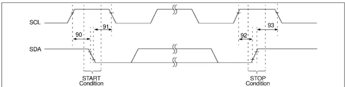
SCL 90 91 93 SDA START Condition STOP ConditionFIGURE 1-1: I ^2 C Bus Start/Stop Bits Timing Waveforms.
TABLE 1-1: I ^2 C BUS START/STOP BITS REQUIREMENTS
| I^2C AC Characteristics | Standard Operating Conditions (unless otherwise specified)Operating Temperature -40°C ≤ TA ≤ +125°C (Extended)Operating Voltage VDD range is described in AC/DC Characteristics | ||||||
| Param.No. | Symbol | Characteristic Min Max Units Conditions | |||||
| F_SCL | Standard | Mode | b=400 pF, 1.8V - 5.5V | ||||
| Fast Mode | 0 400 | kHz | C | b=400 pF, 2.7V - 5.5V | |||
| High-Speed 1.7 | 0 | 1.7 | MHz | C_D =400 pF, 4.5V - 5.5V | |||
| High-Speed 3.4 | 0 | 3.4 | MHz | C_D =100 pF, 4.5V - 5.5V | |||
| D102 | C_b | Bus capacitive loading | 100 kHz mode | — | 400 | pF | |
| 400 kHz mode | — | 400 | pF | ||||
| 1.7 MHz mode | — | 400 | pF | ||||
| 3.4 MHz mode | — | 100 | pF | ||||
| 90 | T_SU:STA | START condition Setup time | 100 kHz mode | 4700 | — | ns | Only relevant for repeated START condition |
| 400 kHz mode | 600 | — | ns | ||||
| 1.7 MHz mode | 160 | — | ns | ||||
| 3.4 MHz mode | 160 | — | ns | ||||
| 91 | T_HD:STA | START condition Hold time | 100 kHz mode | 4000 | — | ns | After this period the first clock pulse is generated |
| 400 kHz mode | 600 | — | ns | ||||
| 1.7 MHz mode | 160 | — | ns | ||||
| 3.4 MHz mode | 160 | — | ns | ||||
| 92 | T_SU:STO | STOP condition Setup time | 100 kHz mode | 4000 | — | ns | |
| 400 kHz mode | 600 | — | ns | ||||
| 1.7 MHz mode | 160 | — | ns | ||||
| 3.4 MHz mode | 160 | — | ns | ||||
| 93 | T_HD:STO | STOP condition Hold time | 100 kHz mode | 4000 | — | ns | |
| 400 kHz mode | 600 | — | ns | ||||
| 1.7 MHz mode | 160 | — | ns | ||||
| 3.4 MHz mode | 160 | — | ns | ||||

text_image
SCL 90 91 103 100 101 102 SDA In 106 107 92 110 109 109 SDA OutFIGURE 1-2: I ^2 C Bus Data Timing.
TABLE 1-2: I ^2 C BUS DATA REQUIREMENTS (SLAVE MODE)
| I^2C AC Characteristics | Standard Operating Conditions (unless otherwise specified)Operating Temperature -40^ ≤ T_A ≤ +125^ (Extended)Operating Voltage V_DD range is described inAC/DC Characteristics | ||||||
| Param.No. | Symbol | Characteristic Min Max Units Conditions | |||||
| 100 T | HIGH | Clock high time | 100 kHz mode | 4000 | — | ns | 1.8V-5.5V |
| 400 kHz mode | 600 | — | ns | 2.7V-5.5V | |||
| 1.7 MHz mode | 120 | ns | 4.5V-5.5V | ||||
| 3.4 MHz mode | 60 | — | ns | 4.5V-5.5V | |||
| 101 | T_LOW | Clock low time | 100 kHz mode | 4700 | — | ns | 1.8V-5.5V |
| 400 kHz mode | 1300 | — | ns | 2.7V-5.5V | |||
| 1.7 MHz mode | 320 | ns | 4.5V-5.5V | ||||
| 3.4 MHz mode | 160 | — | ns | 4.5V-5.5V | |||
| 102A(Note 5) | T_RSCL | SCL rise time | 100 kHz mode | — | 1000 | ns | Cb is specified to be from 10 to 400 pF (100 pF maximum for 3.4 MHz mode) |
| 400 kHz mode | 20 + 0.1Cb | 300 | ns | ||||
| 1.7 MHz mode | 20 | 80 ns | |||||
| 1.7 MHz mode | 20 | 160 | ns | After a Repeated Start condition or an Acknowledge bit | |||
| 3.4 MHz mode | 10 | 40 ns | |||||
| 3.4 MHz mode | 10 | 80 | ns | After a Repeated Start condition or an Acknowledge bit | |||
| 102B(Note 5) | T_RSDA | SDA rise time | 100 kHz mode | — | 1000 | ns | Cb is specified to be from 10 to 400 pF (100 pF max for 3.4 MHz mode) |
| 400 kHz mode | 20 + 0.1Cb | 300 | ns | ||||
| 1.7 MHz mode | 20 | 160 | ns | ||||
| 3.4 MHz mode | 10 | 80 ns | |||||
| 103A(Note 5) | T_FSCL | SCL fall time | 100 kHz mode | — | 300 | ns | Cb is specified to be from 10 to 400 pF (100 pF max for 3.4 MHz mode) |
| 400 kHz mode | 20 + 0.1Cb | 300 | ns | ||||
| 1.7 MHz mode | 20 | 80 ns | |||||
| 3.4 MHz mode | 10 | 40 ns | |||||
Note 1: As a transmitter, the device must provide this internal minimum delay time to bridge the undefined region (minimum 300 ns) of the falling edge of SCL to avoid unintended generation of START or STOP conditions.
2: A fast-mode (400 kHz) I²C-bus device can be used in a standard-mode (100 kHz) ℃C-bus system, but the requirement tSU:DAT≥250 ns must then be met. This will automatically be the case if the device does not stretch the LOW period of the SCL signal. If such a device does stretch the LOW period of the SCL signal, it must output the next data bit to the SDA line.
T_R max.+ t_SU;DAT=1000+250=1250 ns (according to the standard-mode I²C bus specification) before the SCL line is released.
3: Use C_b in pF for the calculations.
4: Not tested.
5: A Master Transmitter must provide a delay to ensure that difference between SDA and SCL fall times do not unintentionally create a Start or Stop condition.
6: Ensured by the T_AA 3.4 MHz specification test.
TABLE 1-2: I²C BUS DATA REQUIREMENTS (SLAVE MODE) (CONTINUED)
| I^2C AC Characteristics | Standard Operating Conditions (unless otherwise specified)Operating Temperature -40^ ≤ T_A ≤ +125^ (Extended)Operating Voltage V_DD range is described inAC/DC Characteristics | ||||||
| Param.No. | Symbol | Characteristic | Min | Max | Units | Conditions | |
| 103B(Note 5) | T_FSDA | DA fall time 100 | kHz mode — 300 | ns Cb is specified to be from | 10 to 400 pF (100 pF max for 3.4 MHz mode) | ||
| 400 kHz mode 20 + 0.1Cb (Note 3) | 300 ns | ||||||
| 1.7 MHz mode 20 160 ns | |||||||
| 3.4 MHz mode 10 80 ns | |||||||
| 106 T | HD:DAT | Data input hold time | 100 kHz mode | 0 | — | ns | 1.8V-5.5V, Note 5 |
| 400 kHz mode | 0 | — | ns | 2.7V-5.5V, Note 5 | |||
| 1.7 MHz mode | 0 | — | ns | 4.5V-5.5V, Note 5 | |||
| 3.4 MHz mode | 0 | — | ns | 4.5V-5.5V, Note 5 | |||
| 107 T | SU:DAT | Data input setup time | 100 kHz mode | 250 | — | ns | Note 2 |
| 400 kHz mode 100 — | ns | ||||||
| 1.7 MHz mode | 10 | — | ns | ||||
| 3.4 MHz mode | 10 | — | ns | ||||
| 109 | T_{AA} | Output valid from clock | 100 kHz mode | — | 3450 | ns | Note 1 |
| 400 kHz mode — 900 ns | |||||||
| 1.7 MHz mode | — | 150 | ns | Cb = 100 pF, Note 1, Note 6 | |||
| — 310 ns | Cb = 400 pF, | Note 1, Note 4 | |||||
| 3.4 MHz mode | — | 150 | ns | Cb = 100 pF, Note 1 | |||
| 110 | T_{BUF} | Bus free time | 100 kHz mode | 4700 | — | ns | Time the bus must be free before a new transmission can start |
| 400 kHz mode | 1300 | — ns | |||||
| 1.7 MHz mode | N.A. | — | ns | ||||
| 3.4 MHz mode | N.A. | — | ns | ||||
| T_{SP}$ | Input filter spike suppression (SDA and SCL) | 100 kHz mode | — | 50 | ns | Philips Spec states N.A. | |
| 400 kHz mode — 50 ns | |||||||
| 1.7 MHz mode | — | 10 | ns | Spike suppression | |||
| 3.4 MHz mode | — | 10 ns | Spike suppression | ||||
Note 1: As a transmitter, the device must provide this internal minimum delay time to bridge the undefined region (minimum 300 ns) of the falling edge of SCL to avoid unintended generation of START or STOP conditions.
2: A fast-mode (400 kHz) I²C-bus device can be used in a standard-mode (100 kHz) C-bus system, but the requirement t_SU;DAT ≥ 250 ns must then be met. This will automatically be the case if the device does not stretch the LOW period of the SCL signal. If such a device does stretch the LOW period of the SCL signal, it must output the next data bit to the SDA line. T_R max.+ t_SU;DAT = 1000 + 250 = 1250 ns (according to the standard-mode I²C bus specification) before the SCL line is released.
3: Use C_b in pF for the calculations.
4: Not tested.
5: A Master Transmitter must provide a delay to ensure that difference between SDA and SCL fall times do not unintentionally create a Start or Stop condition.
6: Ensured by the T_AA 3.4 MHz specification test.
TEMPERATURE CHARACTERISTICS
| Electrical Specifications: Unless otherwise indicated, V_DD = +2.7V to +5.5V, V_SS = GND . | ||||||
| Parameters Sym Min Typ Max Units Conditions | ||||||
| Temperature Ranges | ||||||
| Specified Temperature Range T | A | -40 — | +125 °C | |||
| Operating Temperature Range T | A | -40 — | +125 °C | |||
| Storage Temperature Range T | A | -65 — | +150 °C | |||
| Thermal Package Resistances | ||||||
| Thermal Resistance, 8L-DFN (3x3) | _JA | — | 56.7 | — | °C/W | |
| Thermal Resistance, 8L-MSOP | _JA | — | 211 | — | °C/W | |
| Thermal Resistance, 8L-SOIC θ | JA | — | 149.5 | — | °C/W | |
| Thermal Resistance, 10L-DFN (3x3) | _JA | — | 57 | — | °C/W | |
| Thermal Resistance, 10L-MSOP | _JA | — | 202 | — | °C/W | |
| Thermal Resistance, 14L-MSOP | _JA | — | N/A | — | °C/W | |
| Thermal Resistance, 14L-SOIC | _JA | — | 95.3 | — | °C/W | |
| Thermal Resistance, 16L-QFN | _JA | — | 45.7 | — | °C/W | |
2.0 TYPICAL PERFORMANCE CURVES
Note: The graphs and tables provided following this note are a statistical summary based on a limited number of samples and are provided for informational purposes only. The performance characteristics listed herein are not tested or guaranteed. In some graphs or tables, the data presented may be outside the specified operating range (e.g., outside specified power supply range) and therefore outside the warranted range.
Note: Unless otherwise indicated, T_A = +25^ , V_DD = 5V , V_SS = 0V .
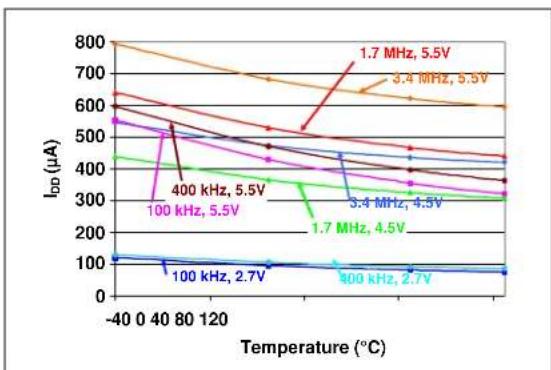
FIGURE 2-1: Device Current (I DD ) vs. I^2C Frequency ( fSCL ) and Ambient Temperature ( V_DD = 2.7V and 5.5V).
line
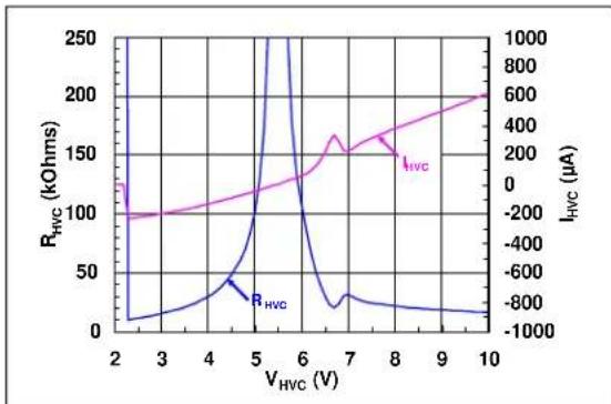
| V_HVC (V) | R_HVC (kOhms) | I_HVC (μA) | | --------- | ------------- | ---------- | | 2 | 0 | 100 | | 3 | 0 | 100 | | 4 | 0 | 100 | | 5 | 50 | 100 | | 6 | 250 | 200 | | 7 | 0 | 300 | | 8 | 0 | 400 | | 9 | 0 | 500 | | 10 | 0 | 600 |FIGURE 2-4: HVC Pull-up/Pull-down Resistance ( R_HVC ) and Current ( I_HVC ) vs. HVC Input Voltage ( V_HVC ) ( V_DD = 5.5V ).

line
| Temperature (°C) | Islandby (μA) | | ---------------- | ------------- | | -40 | 2.3 | | 120 | 2.3 | | 60 | 2.2 | | 120 | 2.5 | | 60 | 1.0 | | 120 | 1.2 |FIGURE 2-2: Device Current (I SHDN) and V_DD (HVC = V_DD ) vs. Ambient Temperature.
line
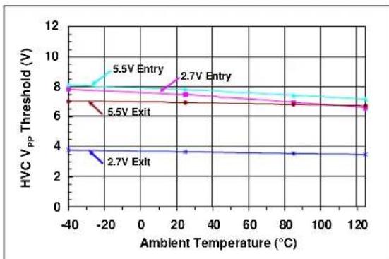
| Ambient Temperature (°C) | 5.5V Entry | 2.7V Entry | 5.5V Exit | 2.7V Exit | | ------------------------ | ---------- | ---------- | --------- | --------- | | -40 | 8.0 | 8.0 | 7.0 | 3.5 | | 20 | 7.5 | 7.5 | 6.5 | 3.5 | | 120 | 7.0 | 7.0 | 6.0 | 3.5 |FIGURE 2-5: HVC High Input Entry/Exit Threshold vs. Ambient Temperature and V_DD .

line
| Temperature (°C) | I_WRITE (μA) | | ---------------- | ------------ | | -40 | 320 | | 0 | 340 | | 80 | 360 | | 120 | 400 |FIGURE 2-3: Write Current (I WRITE) vs. Ambient Temperature.
Note: Unless otherwise indicated, T_A = +25^ , V_DD = 5V , V_SS = 0V .
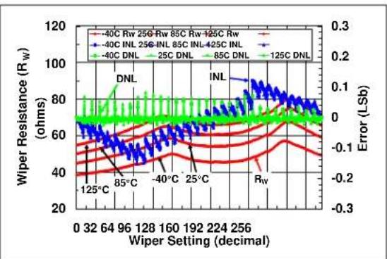
FIGURE 2-6: 5 k Pot Mode - R_W() , INL (LSb), DNL (LSb) vs. Wiper Setting and Ambient Temperature ( V_DD = 5.5V ).

line
| Wiper Setting (decimal) | -40C Rw | 25C Rw | 85C Rw | 125C Rw | -40C INL | 25C INL | 85C INL | 125C INL | -40C DNL | 25C DNL | 85C DNL | 125C DNL | | ----------------------- | ------- | ------ | ------ | ------- | -------- | ------- | ------- | -------- | -------- | ------- | ------- | -------- | | 0 | ~40 | ~60 | ~70 | ~80 | ~70 | ~80 | ~90 | ~100 | ~70 | ~80 | ~90 | ~100 | | 32 | ~45 | ~65 | ~75 | ~85 | ~75 | ~85 | ~95 | ~105 | ~75 | ~85 | ~95 | ~105 | | 64 | ~50 | ~70 | ~80 | ~90 | ~80 | ~90 | ~100 | ~110 | ~80 | ~90 | ~100 | ~110 | | 96 | ~55 | ~75 | ~85 | ~95 | ~85 | ~95 | ~105 | ~115 | ~85 | ~95 | ~105 | ~115 | | 128 | ~60 | ~80 | ~90 | ~100 | ~90 | ~100 | ~110 | ~120 | ~90 | ~100 | ~110 | ~120 | | 160 | ~65 | ~85 | ~95 | ~105 | ~95 | ~105 | ~115 | ~125 | ~95 | ~105 | ~115 | ~125 | | 192 | ~70 | ~90 | ~100 | ~110 | ~100 | ~110 | ~120 | ~130 | ~100 | ~110 | ~120 | ~130 | | 224 | ~75 | ~95 | ~105 | ~115 | ~105 | ~115 | ~125 | ~135 | ~105 | ~115 | ~125 | ~135 | | 256 | ~80 | ~100 | ~110 | ~120 | ~110 | ~120 | ~130 | ~140 | ~110 | ~120 | ~130 | ~140 | Error (LSb) | | 288 | - | - | - | - | - | - | - | - | - | - | - | - | | 332 | - | - | - | - | - | - | - | - | - | - | - | - | | 376 | - | - | - | - | - | - | - | - | - | - | - | - | | 420 | - | - | - | - | - | - | - | - | - | - | - | - | | 464 | - | - | - | - | - | - | - | - | - | - | - | - | | 518 | - | - | - | - | - | - | - | - | - | - | - | - | | 572 | - | - | - | - | - | - | - | - | - | - | - | - | | 627 | - | - | - | - | - | - | - | - | - | - | - | - | | 681 | - | - | - | - | - | - | - | - | - | - | - | - | | 736 | - | - | - | - | - | - | - | - | - | - | - | - | | 790 | - | - | - | - | - | - | - | - | - | - | - | - | | 844 | - | - | - | - | - | - | - | - | - | - | - | - | | 908 | - | - | - | - | - | - | - | - | - | - | - | - | | 972 | - | - | - | - | - | - | - | - | - | - | - | - | | 1036 | - | - | - | - | - | - | - | - | | 1100 | - | - | - | - | - | - | - | - | | 1164 | - | - | - | - | - | - | - | - | | 1228 | - | - | - | - | - | - | - | - | | 1292 | - | - | - | - | - | - | - | - | | 1356 | - | - | - | - | - | - | - | | 1420 | - | - | - | - | - | - | | 1484 | - | - | - | - | | 1548 | - | - | - | - | | 1622 | - | - | - | - | | 1686 | - | - | - | - | | 1749 | - | - | - | | 1823 | - | - | - | | 1897 | -FIGURE 2-9: 5 k Ω Rheo Mode - R_W(Ω), INL (LSb), DNL (LSb) vs. Wiper Setting and Ambient Temperature (V_DD = 5.5V).

line
| Wiper Setting (decimal) | -40°C Rw | 25°C Rw | 85°C Rw | 125°C Rw | 40°C INL | 25°C INL | 85°C INL | 125°C INL | 40°C DNL | 25°C DNL | 85°C DNL | 125°C DNL | | ----------------------- | ------- | ------ | ------ | ------- | -------- | -------- | -------- | --------- | -------- | -------- | -------- | --------- | | 0 | ~60 | ~60 | ~60 | ~60 | ~60 | ~60 | ~60 | ~60 | ~60 | ~60 | ~60 | ~60 | | 32 | ~70 | ~70 | ~70 | ~70 | ~70 | ~70 | ~70 | ~70 | ~70 | ~70 | ~70 | ~70 | | 64 | ~80 | ~80 | ~80 | ~80 | ~80 | ~80 | ~80 | ~80 | ~80 | ~80 | ~80 | ~80 | | 96 | ~90 | ~90 | ~90 | ~90 | ~90 | ~90 | ~90 | ~90 | ~90 | ~90 | ~90 | ~90 | | 128 | ~100 | ~100 | ~100 | ~100 | ~100 | ~100 | ~100 | ~100 | ~100 | ~100 | ~100 | ~100 | | 160 | ~110 | ~110 | ~110 | ~110 | ~110 | ~110 | ~110 | ~110 | ~110 | ~110 | ~110 | ~110 | | 192 | ~120 | ~120 | ~120 | ~120 | ~120 | ~120 | ~120 | ~120 | ~120 | ~120 | ~120 | ~120 | | 224 | ~130 | ~130 | ~130 | ~130 | ~130 | ~130 | ~130 | ~130 | ~130 | ~130 | ~130 | ~130 | | 256 | ~140 | ~140 | ~140 | ~140 | ~140 | ~140 | ~140 | ~140 | ~140 | ~140 | ~140 | ~140 |FIGURE 2-7: 5 k Ω Pot Mode - R_W(Ω), INL (LSb), DNL (LSb) vs. Wiper Setting and Ambient Temperature (V_DD = 3.0V).
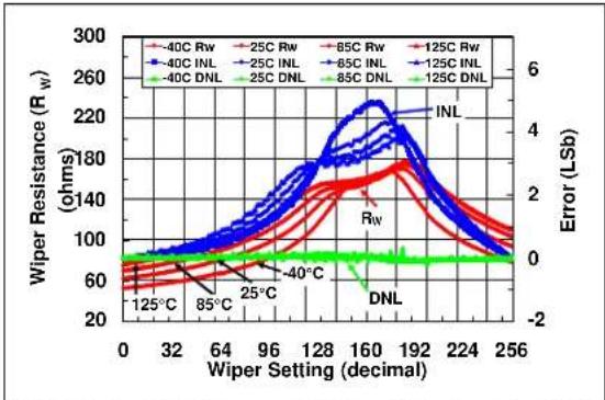
FIGURE 2-10: 5 k Ω Rheo Mode - R_W(Ω), INL (LSb), DNL (LSb) vs. Wiper Setting and Ambient Temperature (V_DD = 3.0V).
line
| Wiper Setting (decimal) | Wiper Resistance (Rw) (ohms) | Error (LSb) | | ----------------------- | ----------------------------- | ----------- | | 0 | 0 | -0.3 | | 64 | ~1000 | ~0.1 | | 128 | ~2000 | ~0.3 | | 192 | ~1000 | ~0.1 | | 256 | ~500 | ~-0.1 |Note: Refer to Appendix B: "Characterization Data Analysis" for additional information on the characteristics of the wiper resistance (R_W) with respect to device voltage and wiper setting value.
FIGURE 2-8: 5 k Ω Pot Mode - R_W() , INL (LSb), DNL (LSb) vs. Wiper Setting and Ambient Temperature ( V_DD = 1.8V ).
line
| Wiper Setting (decimal) | Wiper Resistance (Rw) | Error (LSb) | | ----------------------- | ---------------------- | ----------- | | 0 | 0 | -2 | | 64 | ~100 | ~-1 | | 128 | ~2000 | ~98 | | 192 | ~1500 | ~78 | | 256 | ~500 | ~38 |Note: Refer to Appendix B: "Characterization Data Analysis" for additional information on the characteristics of the wiper resistance (R_W) with respect to device voltage and wiper setting value.
FIGURE 2-11: 5 k Ω Rheo Mode - R_W() , INL (LSb), DNL (LSb) vs. Wiper Setting and Ambient Temperature ( V_DD = 1.8V ).
Note: Unless otherwise indicated, T_A = +25^ , V_DD = 5V , V_SS = 0V .
line
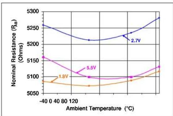
| Ambient Temperature (°C) | 1.8V | 5.5V | 2.7V | | ------------------------ | ------ | ------ | ------ | | -40 | 5090 | 5160 | 5260 | | 0 | 5090 | 5160 | 5260 | | 40 | 5090 | 5160 | 5260 | | 80 | 5090 | 5120 | 5240 | | 120 | 5090 | 5100 | 5220 | | 160 | 5090 | 5100 | 5230 | | 200 | 5100 | 5110 | 5270 | | 240 | 5110 | 5130 | 5290 |FIGURE 2-12: 5 k -Nominal Resistance ( ) vs. Ambient Temperature and V_DD .

line
| Wiper Setting (decimal) | -40°C | 25°C | 85°C | 125°C | | ----------------------- | ----- | ---- | ---- | ----- | | 0 | 0 | 0 | 0 | 0 | | 32 | 32 | 32 | 32 | 32 | | 64 | 64 | 64 | 64 | 64 | | 96 | 96 | 96 | 96 | 96 | | 128 | 128 | 128 | 128 | 128 | | 160 | 160 | 160 | 160 | 160 | | 192 | 192 | 192 | 192 | 192 | | 224 | 224 | 224 | 224 | 224 | | 256 | 256 | 256 | 256 | 256 | | 288 | 288 | 288 | 288 | 288 | | 320 | 320 | 320 | 320 | 320 | | 352 | 352 | 352 | 352 | 352 | | 384 | 384 | 384 | 384 | 384 | | 416 | 416 | 416 | 416 | 416 | | 448 | 448 | 448 | 448 | 448 | | 480 | 480 | 480 | 480 | 480 | | 512 | 512 | 512 | 512 | 512 | | 544 | 544 | 544 | 544 | 544 | | 576 | 576 | 576 | 576 | 576 | | 608 | 608 | 608 | 608 | 608 | | 640 | 640 | 640 | 640 | 640 | | Note: The data for -40°C and -125°C is not provided in the code snippet. The actual values for -40°C and -125°C are not explicitly provided in the code snippet. The numbers in the table represent the corresponding R_VB values for each temperature setting. There is no additional data series in this case. The values for all temperatures are estimated based on the current value. There is only one data series in the chart.FIGURE 2-13: 5 k - R_WB() vs. Wiper Setting and Ambient Temperature.
Note: Unless otherwise indicated, TA = + 25^ C,VDD = 5 V,V_SS = 0 V .
text_image
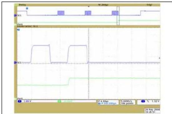
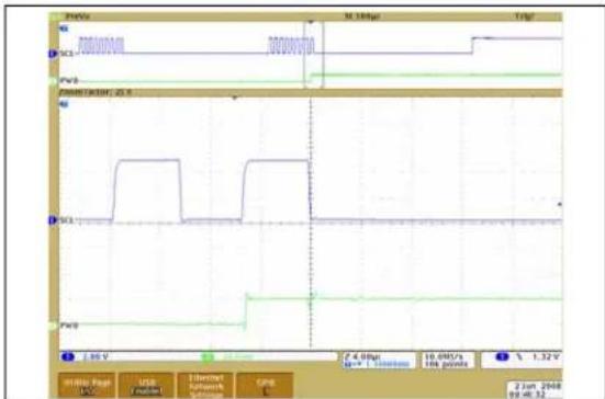
PVR VCC PVR VCC PVR 1.09 V 4.00 V 1.32 V 6.00 V 18A points 1.32 V Display Impedance Intuit Bandwidth Lator DC DC 10000000000000000000000000000000000000000000000000000000000000000000 2 sec 2018 09:58:51FIGURE 2-14: 5 k -Low-Voltage Decrement Wiper Settling Time ( V_DD = 5.5V ) (1 s/Div).
text_image
PWR SCL PWR Depolarization: 25.6 SCL PWR Display Impedance Next Switch Bandwidth Cut Lator DC DC TA TMC SC On Call Power 2.10V 2008 ps-78.65 1.32 VFIGURE 2-17: 5 k -Low-Voltage Increment Wiper Settling Time ( V_DD = 5.5V ) (1 s/Div).
text_image
SCL PVB Emulator: 20.3 SCL PVB 1.29 V Circuit: Impedance DC: 0.0 100 500 0.0 100 500 10.04V/s 18K points 1.32 V 2.0m 2008 06:34:45FIGURE 2-15: 5 k -Low-Voltage Decrement Wiper Settling Time ( V_DD = 2.7V ) (1 s/Div).

text_image
PDB SCL PWR Cancelactur: 25 s SCL PWR 1.00 V 1.32 V Timing: 1000 MHz DC: 1000 MHz T1: 1200 MHz T2: 1200 MHz T3: 1200 MHz T4: 1200 MHz T5: 1200 MHz T6: 1200 MHz T7: 1200 MHz T8: 1200 MHz T9: 1200 MHz T10: 1200 MHz T11: 1200 MHz T12: 1200 MHz T13: 1200 MHz T14: 1200 MHz T15: 1200 MHz T16: 1200 MHz T17: 1200 MHz T18: 1200 MHz T19: 1200 MHz T20: 1200 MHz T21: 1200 MHz T22: 1200 MHz T23: 1200 MHz T24: 1200 MHz T25: 1200 MHz T26: 1200 MHz T27: 1200 MHz T28: 1200 MHz T29: 1200 MHz T30: 1200 MHz T31: 1200 MHz T32: 1200 MHz T33: 1200 MHz T34: 1200 MHz T35: 1200 MHz T36: 1200 MHz T37: 1200 MHz T38: 1200 MHz T39: 1200 MHz T40: 1200 MHz T41: 1200 MHz T42: 1200 MHz T43: 1200 MHz T44: 1200 MHz T45: 1200 MHz T46: 1200 MHz T47: 1200 MHz T48: 1200 MHz T49: 1200 MHz T50: 1200 MHz T51: 1200 MHz T52: 1200 MHz T53: 1200 MHz T54: 1200 MHz T55: 1200 MHz T56: 1200 MHz T57: 1200 MHz T58: 1200 MHz T59: 1200 MHz T60: 1200 MHzFIGURE 2-18: 5 k -Low-Voltage Increment Wiper Settling Time ( V_DD = 2.7V) (1 s/Div).
line
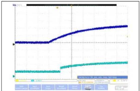
| Time Point | Blue Line Value | Teal Line Value | | ---------- | --------------- | --------------- | | Start | 0 | 0 | | Peak | ~0.8 | ~0.2 | | End | ~1.0 | ~0.3 |FIGURE 2-16: 5 k Ω - Power-Up Wiper Response Time (20 ms/Div).
Note: Unless otherwise indicated, T_A = +25^ , V_DD = 5V , V_SS = 0V .
line
| Wiper Setting (decimal) | Wiper Resistance (R_W) (ohms) | Error (Lsb) | | ----------------------- | ------------------------------ | ----------- | | 0 | 60 | 0.0 | | 25 | 50 | -0.1 | | 50 | 40 | -0.2 | | 75 | 30 | -0.1 | | 100 | 20 | 0.0 | | 125 | 10 | 0.1 | | 150 | 5 | 0.0 | | 175 | 0 | -0.1 | | 200 | -5 | -0.2 | | 225 | -10 | -0.1 | | 250 | -15 | 0.0 |FIGURE 2-19: 10 k Ω Pot Mode - R_W() , INL (LSb), DNL (LSb) vs. Wiper Setting and Ambient Temperature ( V_DD = 5.5V ).

line
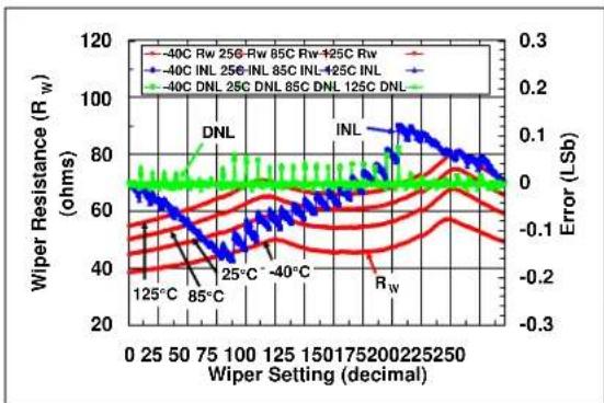
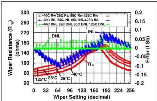
| Wiper Setting (decimal) | 40C Rw 25G-Rw 85C Rw | 125C Rw | 40C INL 25G-INL 85C INL-125C INL | 40C DNL | 25C DNL 85G DNL 125C DNL | | ----------------------- | --------------------- | ------- | ---------------------------------- | ------- | -------------------------- | | 0 | ~60 | ~60 | ~60 | ~60 | ~60 | | 32 | ~65 | ~65 | ~65 | ~65 | ~65 | | 64 | ~70 | ~70 | ~70 | ~70 | ~70 | | 96 | ~75 | ~75 | ~75 | ~75 | ~75 | | 128 | ~80 | ~80 | ~80 | ~80 | ~80 | | 160 | ~85 | ~85 | ~85 | ~85 | ~85 | | 192 | ~90 | ~90 | ~90 | ~90 | ~90 | | 224 | ~85 | ~85 | ~85 | ~85 | ~85 | | 256 | ~80 | ~80 | ~80 | ~80 | ~80 |FIGURE 2-22: 10 k Ω Rheo Mode - R_W() , INL (LSb), DNL (LSb) vs. Wiper Setting and Ambient Temperature ( V_DD = 5.5V ).
line
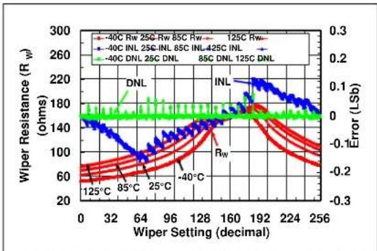
| Wiper Setting (decimal) | -40C Rw 25C Rw 85C Rw | -40C INL 25C INL 85C INL 425C INL | -40C DNL 25C DNL 85C DNL 125C DNL | -40C RW 25C RW 85C RW | -40C INL 25C INL 85C INL 425C INL | -40C DNL 25C DNL 85C DNL 125C DNL | | ----------------------- | ---------------------- | ---------------------------------- | ---------------------------------- | ---------------------- | ---------------------------------- | ---------------------------------- | | 0 | ~140 | ~140 | ~140 | ~140 | ~140 | ~140 | | 32 | ~130 | ~130 | ~130 | ~130 | ~130 | ~130 | | 64 | ~120 | ~120 | ~120 | ~120 | ~120 | ~120 | | 96 | ~110 | ~110 | ~110 | ~110 | ~110 | ~110 | | 128 | ~100 | ~100 | ~100 | ~100 | ~100 | ~100 | | 160 | ~90 | ~90 | ~90 | ~90 | ~90 | ~90 | | 192 | ~80 | ~80 | ~80 | ~80 | ~80 | ~80 | | 224 | ~70 | ~70 | ~70 | ~70 | ~70 | ~70 | | 256 | ~60 | ~60 | ~60 | ~60 | ~60 | ~60 |FIGURE 2-20: 10 k Ω Pot Mode - R_W() , INL (LSb), DNL (LSb) vs. Wiper Setting and Ambient Temperature ( V_DD = 3.0V ).

line
| Wiper Setting (decimal) | Wiper Resistance (Rw) (ohms) | Error (LSb) | | ----------------------- | ----------------------------- | ----------- | | 0 | 60 | -1.5 | | 25 | 90 | -1.0 | | 50 | 110 | -0.5 | | 75 | 130 | 0.0 | | 100 | 150 | 0.5 | | 125 | 170 | 1.0 | | 150 | 190 | 1.5 | | 175 | 210 | 2.0 | | 200 | 230 | 2.5 | | 225 | 210 | 2.0 | | 250 | 190 | 1.5 |FIGURE 2-23: 10 k Ω Rheo Mode - R_W() , INL (LSb), DNL (LSb) vs. Wiper Setting and Ambient Temperature ( V_DD = 3.0V ).
line
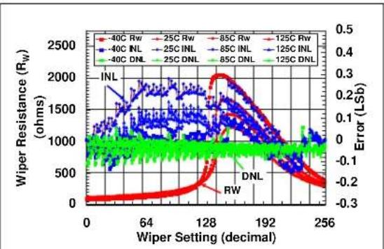
| Wiper Setting (decimal) | Wiper Resistance (R_W) (ohms) | Error (Lsb) | | ----------------------- | ------------------------------ | ----------- | | 0 | 0 | 0 | | 64 | ~1000 | ~0.1 | | 128 | ~1500 | ~0.1 | | 192 | ~3500 | ~0.4 | | 256 | ~1000 | ~0 |FIGURE 2-21: 10 k Ω Pot Mode - R_W (Ω), INL (LSb), DNL (LSb) vs. Wiper Setting and Ambient Temperature (V_DD = 1.8V).

line
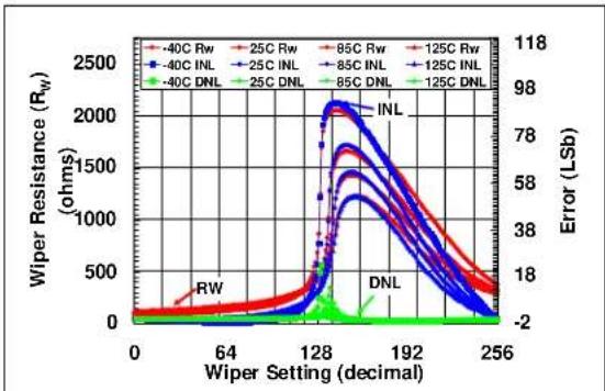
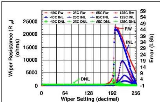
| Wiper Setting (decimal) | Wiper Resistance (Rw) (ohms) | Error (LSb) | | ----------------------- | ----------------------------- | ----------- | | 64 | ~0 | ~0 | | 128 | ~500 | ~2 | | 192 | ~3500 | ~78 | | 256 | ~0 | ~0 |FIGURE 2-24: 10 k Ω Rheo Mode - R_W() , INL (LSb), DNL (LSb) vs. Wiper Setting and Ambient Temperature ( V_DD = 1.8V ).
Note: Unless otherwise indicated, T_A = +25^ , V_DD = 5V , V_SS = 0V .
line
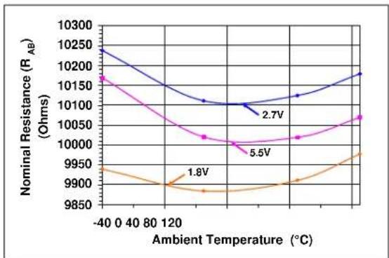
| Ambient Temperature (°C) | Nominal Resistance (R_AB) (Ohms) | | ------------------------ | -------------------------------- | | -40 | 10250 | | 0 | 10200 | | 40 | 10150 | | 80 | 10100 | | 120 | 10050 | | 160 | 10000 | | 200 | 9950 | | 240 | 9900 | | 280 | 9850 |FIGURE 2-25: 10 k -Nominal Resistance ( ) vs. Ambient Temperature and V_DD .
line
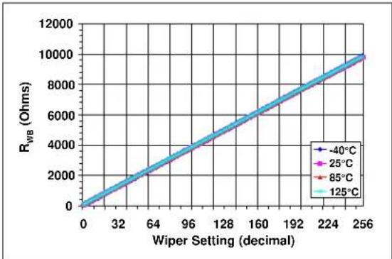
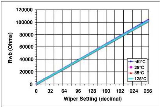
| Wiper Setting (decimal) | -40°C | 25°C | 85°C | 125°C | | ----------------------- | ----- | ---- | ---- | ----- | | 0 | 0 | 0 | 0 | 0 | | 32 | ~1500 | ~1500| ~1500| ~1500 | | 64 | ~3000 | ~3000| ~3000| ~3000 | | 96 | ~4500 | ~4500| ~4500| ~4500 | | 128 | ~6000 | ~6000| ~6000| ~6000 | | 160 | ~7500 | ~7500| ~7500| ~7500 | | 192 | ~9000 | ~9000| ~9000| ~9000 | | 224 | ~10500| ~10500| ~10500| ~10500| | 256 | ~12000| ~12000| ~12000| ~12000|FIGURE 2-26: 10 k - R_WB() vs. Wiper Setting and Ambient Temperature.
Note: Unless otherwise indicated, T_A = +25^ , V_DD = 5V , V_SS = 0V .
text_image
Run M 200µm 1µm SCL Pcc Interactor, 36.6 SCL Vcc 1.69 V F 4.5µm N= 200 mV 5.60kHz 10A points 1.32 V 29 Mar 2008 16.28:46FIGURE 2-27: 10 k Ω - Low-Voltage Decrement Wiper Settling Time ( V_DD = 5.5V ) (1 μs/Div).
text_image
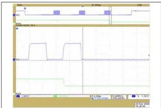
Punch M_200µA 1µA SCL PM2.5 Punch Punchactor: 16.8 M SCL PM2.5 1.32 V 2.69 V 4.0 µA N= 160 µA 5.00V/s 106 points 29 May 2008 18.28.12FIGURE 2-30: 10 k Ω - Low-Voltage Increment Wiper Settling Time ( V_DD = 5.5V ) (1 μs/Div).

text_image
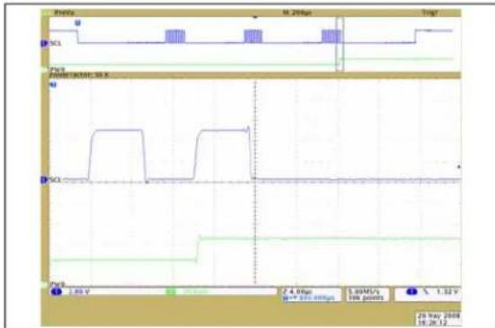
I/O V 2000p mp I/O PMI Amperifier: 16.5 I/O PMI - 2.00 V 4.00µs dB = 315 mV 5.000V/s 104 points 1.32 V 29 May 2008 16:28:15FIGURE 2-28: 10 k -Low-Voltage Decrement Wiper Settling Time ( V_DD = 2.7V ) (1 s/Div).
text_image
Prints 16.20V Targ D SCL Port Amplifier: 38.5 D SCL Port 1.20 V 4.40V 5.00V/s 100 points 1.32 V 29 May 2008 18:28:51FIGURE 2-31: 10 k Ω - Low-Voltage Increment Wiper Settling Time ( V_DD = 2.7V ) (1 μs/Div).
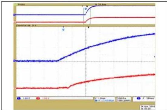
FIGURE 2-29: 10 k Ω - Power-Up Wiper Response Time (1 μs/Div).
Note: Unless otherwise indicated, T_A = +25^ , V_DD = 5V , V_SS = 0V .
line
| Wiper Setting (decimal) | Wiper Resistance (Rw) (ohms) | Error (Lsb) | | ----------------------- | ----------------------------- | ----------- | | 0 | ~70 | ~0.0 | | 32 | ~60 | ~-0.1 | | 64 | ~50 | ~-0.1 | | 96 | ~40 | ~-0.1 | | 128 | ~30 | ~-0.1 | | 160 | ~40 | ~-0.1 | | 192 | ~50 | ~-0.1 | | 224 | ~60 | ~-0.1 | | 256 | ~70 | ~-0.1 |FIGURE 2-32: 50 k Ω Pot Mode - R_W() , INL (LSb), DNL (LSb) vs. Wiper Setting and Ambient Temperature ( V_DD = 5.5V ).
line
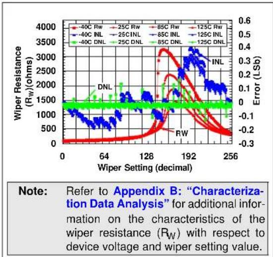
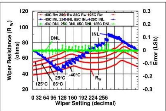
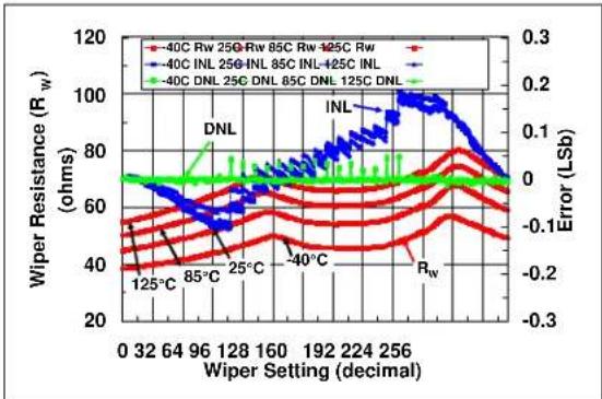
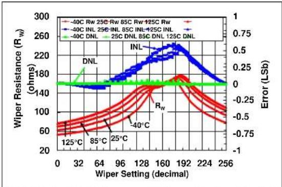
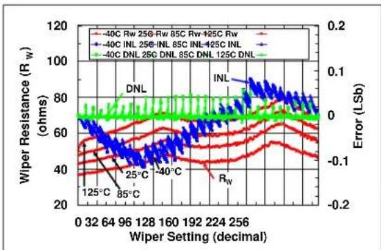
| Wiper Setting (decimal) | 125°C Rw | 85°C Rw | 25°C Rw | 40°C Rw | 85°C INL Rw | 125°C INL Rw | 40°C DNL Rw | 85°C DNL INL Rw | 125°C DNL INL Rw | 40°C DNL DNL INL Rw | 85°C DNL DNL DNL INL Rw | 125°C DNL DNL DNL INL Rw | | ----------------------- | -------- | ------- | ------- | ------- | ----------- | ------------- | ----------- | --------------- | ---------------- | ------------------- | ------------------------ | ------------------------- | | 0 | 40 | 40 | 40 | 40 | 40 | 40 | 40 | 40 | 40 | 40 | 40 | 40 | | 32 | 50 | 50 | 50 | 50 | 50 | 50 | 50 | 50 | 50 | 50 | 50 | 50 | | 64 | 60 | 60 | 60 | 60 | 60 | 60 | 60 | 60 | 60 | 60 | 60 | 60 | | 96 | 70 | 70 | 70 | 70 | 70 | 70 | 70 | 70 | 70 | 70 | 70 | 70 | | 128 | 80 | 80 | 80 | 80 | 80 | 80 | 80 | 80 | 80 | 80 | 80 | 80 | | 160 | 90 | 90 | 90 | 90 | 90 | 90 | 90 | 90 | 90 | 90 | 90 | 90 | | 192 | 100 | 100 | 100 | 100 | 100 | 100 | 100 | 100 | 100 | 100 | 100 | 100 | | 224 | 110 | 110 | 110 | 110 | 110 | 110 | 110 | 110 | 110 | 110 | 110 | 110 | | 256 | 120 | 120 | 120 | 120 | 120 | 120 | 120 | 120 | 120 | 120 | 120 | 120 | | R_W | - | - | - | - | - | - | - | - | - | - | - | - | Error (LSb) | | Error (LSb) | - | - | - | - | - | - | - | - | - | - | - | - | | Error (LSb) | - | - | - | - | - | - | - | - | - | - | - | - | | Error (LSb) | - | - | - | - | - | - | - | - | - | - | - | - | | Error (LSb) | - = - | - | - | - | - | - | - | - | - | - | - | - | | Error (LSb) | - = + | - | - | - | - | - | - | - | - | - | - | - | | Error (LSb) | - = + + (DNL) R_W + DNL DNL DNL DNL DNL DNL DNL DNL DNL DNL DNL DNL DNL DNL DNL DNL DNL DNL DNL DNL DNL DNL DNL DNL DNL DNL DNL DNL DNL DNL DNL DNL DNL DNL BDN BDN BDN BDN BDN BDN BDN BDN BDN BDN BDN BDN BDN BDN BDN BDN BDN BDN BDN BDN BDN BDN BDN BDN BDN BDN BDN BDN BDN BDN BDN BDN BDN BDN AINL AINL AINL AINL AINL AINL AINL AINL AINL AINL AINL AINL AINL AINL AINL AINL AINL AINL AINL AINL AINL AINL AINL AINL AINL AINL AINL AINL AINL AINL AINL AINL AINL AINL AINL AINL AINL AINL AINL AINL AINL AINL AINL AINL AINL AINL AINL AINL AINL AINL AINL BDN BDN BDN BDN BDN BDN BDN BDN BDN BDN BDN BDN BDN BDN BDN BDN BDN BDN BDN BDN BDN BDN BDN BDN Error (LSb) | | Error (LSb) | | Error (LSb) | | Error (LSb) | | Error (LSb) | | Error (LSb) | | Error (LSb) | | Error (LSb) | | Error (LSb) | | Error (LSb) | | Error (LSb) | | Error (LSb) | | Error (LSb) | | Error (LSb)FIGURE 2-35: 50 k Ω Rheo Mode - R_W() , INL (LSb), DNL (LSb) vs. Wiper Setting and Ambient Temperature ( V_DD=5.5V ).

line
| Wiper Setting (decimal) | -40C Rw 25C Rw 85C Rw 125C Rw | -40C INL 25C INL 85C INL 425C INL | -40C DNL 25C DNL 85C DNL 125C DNL | -40C RW 25C RW 85C RW 125C RW | -40C INL 25C INL 85C INL 425C INL | -40C DNL 25C DNL 85C DNL 125C DNL | | ----------------------- | ----------------------------- | ---------------------------------- | ---------------------------------- | ----------------------------- | ---------------------------------- | ---------------------------------- | | 0 | ~60 | ~60 | ~60 | ~60 | ~60 | ~60 | | 32 | ~70 | ~70 | ~70 | ~70 | ~70 | ~70 | | 64 | ~80 | ~80 | ~80 | ~80 | ~80 | ~80 | | 96 | ~90 | ~90 | ~90 | ~90 | ~90 | ~90 | | 128 | ~100 | ~100 | ~100 | ~100 | ~100 | ~100 | | 160 | ~110 | ~110 | ~110 | ~110 | ~110 | ~110 | | 192 | ~120 | ~120 | ~120 | ~120 | ~120 | ~120 | | 224 | ~130 | ~130 | ~130 | ~130 | ~130 | ~130 | | 256 | ~140 | ~140 | ~140 | ~140 | ~140 | ~140 |FIGURE 2-33: 50 k Ω Pot Mode - R_W() , INL (LSb), DNL (LSb) vs. Wiper Setting and Ambient Temperature ( V_DD = 3.0V ).
line
| Wiper Setting (decimal) | Wiper Resistance (Rw) | Error (LSb) | | ----------------------- | ---------------------- | ----------- | | 0 | 60 | -0.75 | | 32 | 140 | 0.0 | | 64 | 180 | 0.25 | | 96 | 220 | 0.5 | | 128 | 260 | 0.75 | | 160 | 240 | 0.5 | | 192 | 200 | 0.25 | | 224 | 160 | 0.0 | | 256 | 140 | -0.75 |FIGURE 2-36: 50 k Ω Rheo Mode - R_W() , INL (LSb), DNL (LSb) vs. Wiper Setting and Ambient Temperature ( V_DD = 3.0V ).

line
| Wiper Setting (decimal) | 40C Rw (R_w) | 25C Rw (R_w) | 85C Rw (R_w) | 125C Rw (R_w) | 40C INL (R_w) | 25C INL (R_w) | 85C INL (R_w) | 125C INL (R_w) | 40C DNL (R_w) | 25C DNL (R_w) | 85C DNL (R_w) | 125C DNL (R_w) | 40C RW (Error L_Sb) | 25C RW (Error L_Sb) | 85C RW (Error L_Sb) | 125C RW (Error L_Sb) | 40C DNL (Error L_Sb) | 25C DNL (Error L_Sb) | | ----------------------- | ------------ | ------------ | ------------ | ------------- | ------------- | ------------- | ------------- | -------------- | ------------- | ------------- | ------------- | -------------- | ------------------- | ------------------- | ------------------- | ------------------- | ------------------- | ------------------- | | 0 | ~0 | ~0 | ~0 | ~0 | ~0 | ~0 | ~0 | ~0 | ~0 | ~0 | ~0 | ~0 | ~0 | ~0 | ~0 | ~0 | ~0 | ~0 | | 64 | ~1000 | ~3000 | ~7000 | ~1000 | ~3000 | ~6000 | ~13000 | ~17000 | ~7000 | ~13000 | ~17000 | ~21000 | ~-0.1 | ~-0.1 | ~-0.1 | ~-0.1 | ~-0.1 | ~-0.1 | | 128 | ~2000 | ~4000 | ~8000 | ~1200 | ~4000 | ~7000 | ~14000 | ~18000 | ~8000 | ~14000 | ~18000 | ~22000 | ~-0.2 | ~-0.2 | ~-0.2 | ~-0.2 | ~-0.2 | ~-0.2 | | 192 | ~3000 | ~5000 | ~9000 | ~1400 | ~5000 | ~8000 | ~15000 | ~19000 | ~9000 | ~15000 | ~19000 | ~23000 | ~-0.3 | ~-0.3 | ~-0.3 | ~-0.3 | ~-0.3 | ~-0.3 | | 256 | ~4000 | ~6000 | ~10000 | ~1600 | ~6000 | ~9000 | ~16000 | ~21000 | ~10000 | ~16000 | ~21000 | ~25000 | ~-0.4 | ~-0.4 | ~-0.4 | ~-0.4 | ~-0.4 | ~-0.4 |Note: Refer to Appendix B: "Characterization Data Analysis" for additional information on the characteristics of the wiper resistance (R_W) with respect to device voltage and wiper setting value.

line
| Wiper Setting (decimal) | Wiper Resistance (Rw) (ohms) | Error (LSp) | | ----------------------- | ----------------------------- | ----------- | | 0 | 0 | -1.5 | | 25 | 0 | -1.5 | | 50 | 0 | -1.5 | | 75 | 0 | -1.5 | | 100 | 0 | -1.5 | | 125 | 0 | -1.5 | | 150 | 11000 | 63.5 | | 175 | 9000 | 58.5 | | 200 | 6000 | 33.5 | | 225 | 3000 | 18.5 | | 250 | 0 | -1.5 |Note: Refer to Appendix B: "Characterization Data Analysis" for additional information on the characteristics of the wiper resistance (R_W) with respect to device voltage and wiper setting value.
FIGURE 2-34: 50 k Pot Mode - R_W() , INL (LSb), DNL (LSb) vs. Wiper Setting and Ambient Temperature ( V_DD = 1.8V ).
FIGURE 2-37: 50 k Rheo Mode - R_W() , INL (LSb), DNL (LSb) vs. Wiper Setting and Ambient Temperature ( V_DD = 1.8V).
Note: Unless otherwise indicated, T_A=+25^ , V_DD=5V , V_SS=0V .
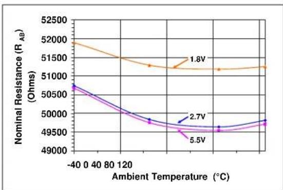
FIGURE 2-38: 50 k -Nominal Resistance ( ) vs. Ambient Temperature and V_DD .
line
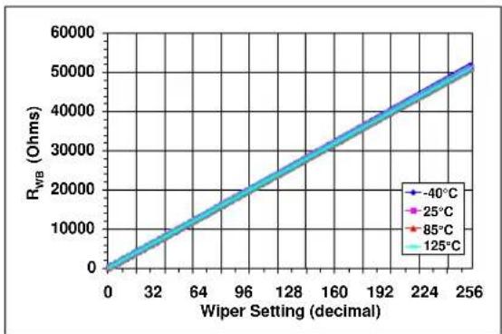
| Wiper Setting (decimal) | -40°C | 25°C | 85°C | 125°C | | ----------------------- | ----- | ---- | ---- | ----- | | 0 | 0 | 0 | 0 | 0 | | 32 | ~10000| ~9000| ~8000| ~7000 | | 64 | ~20000| ~18000| ~16000| ~14000| | 96 | ~30000| ~27000| ~24000| ~21000| | 128 | ~40000| ~36000| ~32000| ~28000| | 160 | ~50000| ~45000| ~40000| ~35000| | 192 | ~60000| ~54000| ~47000| ~42000| | 224 | ~70000| ~63000| ~54000| ~48000| | 256 | ~80000| ~72000| ~61000| ~53000|FIGURE 2-39: 50 k - R_WB() vs. Wiper Setting and Ambient Temperature.
Note: Unless otherwise indicated, T_A = +25^ , V_DD = 5V , V_SS = 0V .

text_image
SCL PWR Signal/Timing: 30.6 SCL FWP 1.69 V 4.00V 5.00Hz/s 18k points % 1.32 V USB Field USB Field Filterset Signal/Time GPs 29.94: 2008 18:11:24FIGURE 2-40: 50 k -Low-Voltage Decrement Wiper Settling Time ( V_DD = 5.5V ) (1 s/Div).

text_image
SCL PV0 Power Factor, 37.6 SCL PV1 4.8V d= 510 ms/Hz 5.0MHz/s link points % 1.32 V sforce Range: 1.0V USB Efficient Switches GND C 29 May 2008 16:06:12FIGURE 2-43: 50 k -Low-Voltage Increment Wiper Settling Time ( V_DD = 5.5V ) (1 s/Div).

text_image
Fms U 10.20µs Trig* SCL PWR PowerFactor: 35% M SCL PWR 1.69 V 2.4.0µs 5.00Hz/s 100 points % 1.32 V White Page SCL (Redacted) Unknown (Unknown) GB C 29 May 2008 16:16:17FIGURE 2-41: 50 k -Low-Voltage Decrement Wiper Settling Time ( V_DD = 2.7V ) (1 s/Div).

text_image
Wave 14.20µm Trig* Vcc Purs PowerInput: 5V X Vcc Purs J 69 V Z 4 Bits G=5V 0.0000 5.00ms/s 1Hz points % 1.32 V PHI/Hz Page OSK Energent Solutions GND 29 May 2008 16:15:26FIGURE 2-44: 50 k -Low-Voltage Increment Wiper Settling Time ( V_DD = 2.7V ) (1 s/Div).

line
| Time (ms) | Voltage (V) | | --------- | ----------- | | 0 | 1.0 | | 2 | 1.0 | | 4 | 1.0 | | 6 | 1.0 | | 8 | 1.0 | | 10 | 1.0 | | 12 | 1.0 | | 14 | 1.0 | | 16 | 1.0 | | 18 | 1.0 | | 20 | 1.0 | | 22 | 1.0 | | 24 | 1.0 | | 26 | 1.0 | | 28 | 1.0 | | 30 | 1.0 | | 32 | 1.0 | | 34 | 1.0 | | 36 | 1.0 | | 38 | 1.0 | | 40 | 1.0 | | 42 | 1.0 | | 44 | 1.0 | | 46 | 1.0 | | 48 | 1.0 | | 50 | 1.0 | | 52 | 1.0 | | 54 | 1.0 | | 56 | 1.0 | | 58 | 1.0 | | 60 | 1.0 | | 62 | 1.0 | | 64 | 1.0 | | 66 | 1.0 | | 68 | 1.0 | | 70 | 1.0 | | 72 | 1.0 | | 74 | 1.0 | | 76 | 1.0 | | 78 | 1.0 | | 80 | 1.0 | | 82 | 1.0 | | 84 | 1.0 | | 86 | 1.0 | | 88 | 1.0 | | 90 | 1.0 | | 92 | 1.0 | | 94 | 1.0 | | 96 | 1.0 | | 98 | 1.0 | | 100 | 1.0 |FIGURE 2-42: 50 k Ω - Power-Up Wiper Response Time (1 μs/Div).
Note: Unless otherwise indicated, T_A = +25^ , V_DD = 5V , V_SS = 0V .
line
| Wiper Setting (decimal) | Wiper Resistance (R_W) (ohms) | Error (Lsb) | | ----------------------- | ------------------------------ | ----------- | | 0 | ~60 | ~0.0 | | 32 | ~55 | ~-0.05 | | 64 | ~50 | ~-0.1 | | 96 | ~45 | ~-0.15 | | 128 | ~40 | ~-0.2 | | 160 | ~45 | ~-0.15 | | 192 | ~50 | ~-0.1 | | 224 | ~55 | ~-0.05 | | 256 | ~60 | ~0.0 |FIGURE 2-45: 100 k Ω Pot Mode - R_W (Ω), INL (LSb), DNL (LSb) vs. Wiper Setting and Ambient Temperature (V_DD = 5.5V).

line
| Wiper Setting (decimal) | Wiper Resistance (R_W) (ohms) | Error (LSb) | | ----------------------- | ------------------------------ | ----------- | | 0 | ~70 | ~0.0 | | 32 | ~65 | ~-0.05 | | 64 | ~60 | ~-0.1 | | 96 | ~55 | ~-0.15 | | 128 | ~50 | ~-0.2 | | 160 | ~45 | ~-0.25 | | 192 | ~40 | ~-0.3 | | 224 | ~35 | ~-0.25 | | 256 | ~30 | ~-0.2 | | 288 | ~25 | ~-0.15 | | 32 | ~20 | ~-0.1 |FIGURE 2-48: 100 k Ω Rheo Mode - R_W (Ω), INL (LSb), DNL (LSb) vs. Wiper Setting and Ambient Temperature ( V_DD = 5.5V ).
line
| Wiper Setting (decimal) | -40C Rw 25C-Rw 85C Rw-125C Rw | -40C INL 25C-INL 85C INL-425C INL | -40C DNL 25C DNL 85C DNL 125C DNL | DNL | | ----------------------- | ----------------------------- | ---------------------------------- | ---------------------------------- | --- | | 0 | ~60 | ~140 | ~140 | ~0.05 | | 32 | ~70 | ~130 | ~130 | ~0.05 | | 64 | ~80 | ~120 | ~120 | ~0.05 | | 96 | ~90 | ~110 | ~110 | ~0.05 | | 128 | ~100 | ~100 | ~100 | ~0.05 | | 160 | ~110 | ~90 | ~90 | ~0.05 | | 192 | ~120 | ~80 | ~80 | ~0.05 | | 224 | ~130 | ~70 | ~70 | ~0.05 | | 256 | ~140 | ~60 | ~60 | ~0.05 |FIGURE 2-46: 100 k Ω Pot Mode - R W (Ω), INL (LSb), DNL (LSb) vs. Wiper Setting and Ambient Temperature (V DD = 3.0V).

line
| Wiper Setting (decimal) | -40C Rw 256°Rw 85C Rw-125C Rw (Rw) | -40C INL 256°INL 85C INL-125C INL (Rw) | -40C DNL (Rw) | 25C DNL 85C DNL 125C DNL (Rw) | DNL (Rw) | Error (LSb) | | ----------------------- | ----------------------------------- | ---------------------------------------- | ------------ | ----------------------------- | -------- | ----------- | | 0 | 60 | 60 | 60 | 60 | 60 | 0.0 | | 32 | 140 | 140 | 140 | 140 | 140 | 0.0 | | 64 | 180 | 180 | 180 | 180 | 180 | 0.0 | | 96 | 220 | 220 | 220 | 220 | 220 | 0.0 | | 128 | 260 | 260 | 260 | 260 | 260 | 0.0 | | 160 | 240 | 240 | 240 | 240 | 240 | 0.0 | | 192 | 200 | 200 | 200 | 200 | 200 | 0.0 | | 224 | 160 | 160 | 160 | 160 | 160 | 0.0 | | 256 | 120 | 120 | 120 | 120 | 120 | 0.0 | | Peak | ~180 | ~180 | ~180 | ~180 | ~180 | ~-0.2 | | End | ~140 | ~140 | ~140 | ~140 | ~140 | ~-0.4 | Error bars labeled: R_W, Error (LSb). Values range from -6.6 to +6.0.FIGURE 2-49: 100 k Ω Rheo Mode - R_W (Ω), INL (LSb), DNL (LSb) vs. Wiper Setting and Ambient Temperature ( V_DD = 3.0V ).

line
| Wiper Setting (decimal) | 40C Rw | 25C Rw | 85C Rw | 125C Rw | 40C INL | 25C INL | 85C INL | 125C INL | 40C DNL | 25C DNL | 85C DNL | 125C DNL | | ----------------------- | ------ | ------ | ------ | ------- | ------- | ------- | ------- | -------- | ------- | ------- | ------- | -------- | | 0 | ~0 | ~0 | ~0 | ~0 | ~0 | ~0 | ~0 | ~0 | ~0 | ~0 | ~0 | ~0 | | 64 | ~0 | ~0 | ~0 | ~0 | ~15000 | ~15000 | ~15000 | ~15000 | ~15000 | ~15000 | ~15000 | ~15000 | | 128 | ~0 | ~0 | ~0 | ~0 | ~10000 | ~10000 | ~10000 | ~10000 | ~10000 | ~10000 | ~10000 | ~10000 | | 192 | ~-0.35 | ~-0.25 | ~-0.25 | ~-0.25 | ~25000 | ~25000 | ~25000 | ~25000 | ~25000 | ~25000 | ~25000 | ~25000 | | 256 | ~-0.35 | ~-0.35 | ~-0.35 | ~-0.35 | ~15000 | ~15000 | ~15000 | ~15000 | ~15000 | ~15000 | ~15000 | ~15000 |Note: Refer to Appendix B: "Characterization Data Analysis" for additional information on the characteristics of the wiper resistance (R_W) with respect to device voltage and wiper setting value.
line
| Wiper Setting (decimal) | Wiper Resistance (R_w) (ohms) | Error (LSb) | | ----------------------- | ------------------------------ | ----------- | | 0 | 0 | 0 | | 64 | 0 | 0 | | 128 | 0 | 0 | | 192 | 25000 | 59 | | 256 | 0 | 0 |Note: Refer to Appendix B: "Characterization Data Analysis" for additional information on the characteristics of the wiper resistance (R_W) with respect to device voltage and wiper setting value.
FIGURE 2-47: 100 k Ω Pot Mode - R_W (Ω), INL (LSb), DNL (LSb) vs. Wiper Setting and Ambient Temperature (V_DD = 1.8V).
FIGURE 2-50: 100 k Ω Rheo Mode - R_W (Ω), INL (LSb), DNL (LSb) vs. Wiper Setting and Ambient Temperature ( V_DD = 1.8V ).
Note: Unless otherwise indicated, T_A = +25^ , V_DD = 5V , V_SS = 0V .

line
| Ambient Temperature (°C) | 1.8V | 2.7V | 5.5V | | ------------------------ | -------- | -------- | -------- | | -40 | 103000 | 101500 | 101500 | | 0 | 102500 | 101000 | 101000 | | 40 | 102000 | 100500 | 100500 | | 80 | 101500 | 100000 | 100000 | | 120 | 101500 | 99500 | 99500 | | 160 | 101500 | 99500 | 99500 | | 200 | 101500 | 99500 | 99500 | | 240 | 101500 | 99500 | 99500 |FIGURE 2-51: 100 k Ω - Nominal
Resistance ( ) vs. Ambient Temperature and V_DD .
line
| Wiper Setting (decimal) | -40°C | 25°C | 85°C | 125°C | | ----------------------- | ------- | ------- | ------- | ------- | | 0 | 0 | 0 | 0 | 0 | | 32 | ~20000 | ~20000 | ~20000 | ~20000 | | 64 | ~40000 | ~40000 | ~40000 | ~40000 | | 96 | ~60000 | ~60000 | ~60000 | ~60000 | | 128 | ~80000 | ~80000 | ~80000 | ~80000 | | 160 | ~100000 | ~100000 | ~100000 | ~100000 | | 192 | ~120000 | ~120000 | ~120000 | ~120000 | | 224 | ~140000 | ~140000 | ~140000 | ~140000 | | 256 | ~160000 | ~160000 | ~160000 | ~160000 |FIGURE 2-52: 100 k - R_WB() vs. Wiper Setting and Ambient Temperature.
Note: Unless otherwise indicated, T_A = +25^ , V_DD = 5V , V_SS = 0V .

line
| Time (μs) | Voltage (V) | |-----------|-------------| | 0 | 1.00 | | 1 | 1.00 | | 2 | 1.00 | | 3 | 1.00 | | 4 | 1.00 | | 5 | 1.00 | | 6 | 1.00 | | 7 | 1.00 | | 8 | 1.00 | | 9 | 1.00 | | 10 | 1.00 | | 11 | 1.00 | | 12 | 1.00 |FIGURE 2-53: 100 k Ω - Low-Voltage Decrement Wiper Settling Time ( V_DD = 5.5V ) (1 μs/Div).

FIGURE 2-56: 100 k Ω - Low-Voltage Increment Wiper Settling Time ( V_DD = 2.7V ) (1 μs/Div).

line
| Signal | Time (s) | |--------|----------| | D | 0 | | Pvr | 0 |FIGURE 2-54: 100 k Ω - Low-Voltage Decrement Wiper Settling Time ( V_DD = 2.7V ) (1 μs/Div).
text_image
I/O 10.18µps T/R I/O 21.5 2.1µV 10.09µs 100 points 1.32 V USB Efficient Control CPS 2.1µV 2008 09:46:32FIGURE 2-55: 100 k Ω - Low-Voltage Increment Wiper Settling Time ( V_DD = 5.5V ) (1 μs/Div).
Note: Unless otherwise indicated, T_A = +25^ , V_DD = 5V , V_SS = 0V .
line
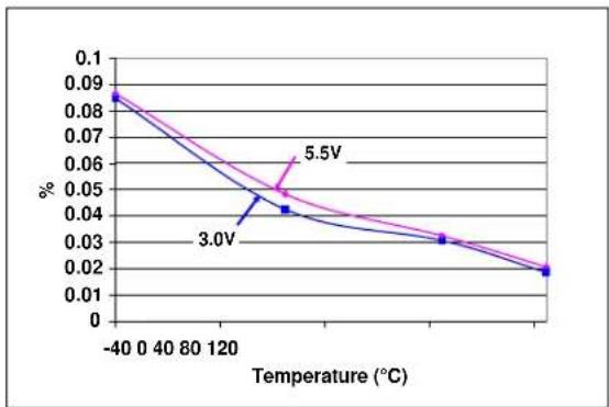
| Temperature (°C) | 5.5V (%) | 3.0V (%) | |---|---|---| | -40 | 0.087 | 0.086 | | 120 | 0.05 | 0.042 | | 120+ | 0.032 | 0.031 | | 120+ | 0.02 | 0.02 |FIGURE 2-57: Resistor Network 0 to Resistor Network 1 R_AB(5k) Mismatch vs. V_DD and Temperature.
line
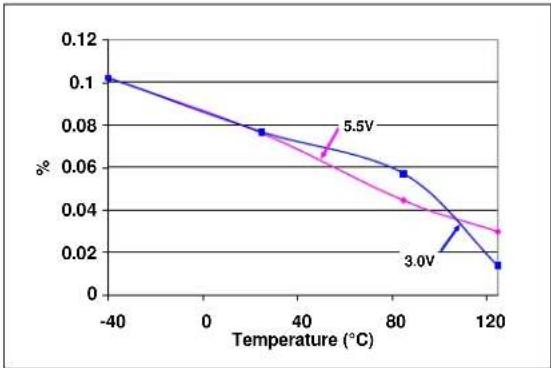
| Temperature (°C) | 5.5V | 3.0V | | ---------------- | ------ | ------ | | -40 | 0.1000 | 0.1000 | | 30 | 0.0780 | 0.0780 | | 80 | 0.0600 | 0.0580 | | 120 | 0.0300 | 0.0150 |FIGURE 2-59: Resistor Network 0 to Resistor Network 1 R_AB (50 kΩ) Mismatch vs. V_DD and Temperature.

line
| Temperature (°C) | 3.0V | 5.5V | | ---------------- | ------ | ------ | | -40 | 0.018 | 0.040 | | 120 | -0.005 | 0.005 | | 160 | -0.030 | -0.025 |FIGURE 2-58: Resistor Network 0 to Resistor Network 1 R_AB (10 kΩ) Mismatch vs. V_DD and Temperature.
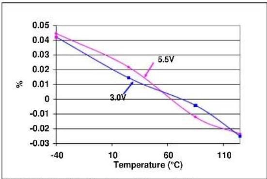
line
| Temperature (°C) | 5.5V | 3.0V | | ---------------- | ------ | ------ | | -40 | 0.045 | 0.045 | | 10 | 0.025 | 0.015 | | 60 | 0.01 | -0.01 | | 110 | -0.025 | -0.025 |FIGURE 2-60: Resistor Network 0 to Resistor Network 1 R_AB (100 kΩ) Mismatch vs. V_DD and Temperature.
Note: Unless otherwise indicated, T_A = +25^ , V_DD = 5V , V_SS = 0V .

line
| Temperature (°C) | V_H (V) | | ---------------- | ------- | | -40 | 3.5 | | 120 | 3.5 | | 120 | 2.7 |FIGURE 2-61: V IH (SDA, SCL) vs. VDD and Temperature.
line
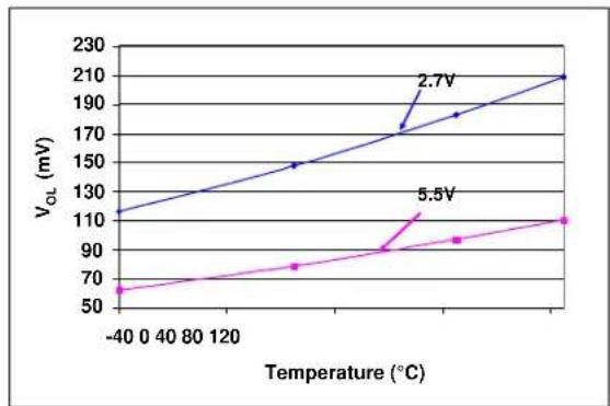
| Temperature (°C) | V_OL (mV) at 2.7V | V_OL (mV) at 5.5V | |---|---|---| | -40 | 110 | 60 | | 80 | 130 | 70 | | 120 | 150 | 80 | | 160 | 170 | 90 | | 200 | 180 | 100 | | 240 | 210 | 110 |FIGURE 2-63: V OL (SDA) vs. VDD and Temperature ( I_OL = 3 mA).

line
| Temperature (°C) | V_IL (V) | | ---------------- | -------- | | -40 | 1.0 | | 0 | 1.0 | | 40 | 1.0 | | 80 | 1.0 | | 120 | 1.0 | | 160 | 1.0 | | 200 | 1.0 | | 240 | 1.0 | | 280 | 1.0 | | 320 | 1.0 | | 360 | 1.0 | | 400 | 1.0 | | 440 | 1.0 | | 480 | 1.0 | | 520 | 1.0 | | 560 | 1.0 | | 600 | 1.0 | | 640 | 1.0 | | 680 | 1.0 | | 720 | 1.0 | | 760 | 1.0 | | 800 | 1.0 | | 840 | 1.0 | | 880 | 1.0 | | 920 | 1.0 | | 960 | 1.0 | | 1000 | 1.0 | | 1040 | 1.0 | | 1080 | 1.0 | | 1120 | 1.0 | | 1160 | 1.0 | | 1200 | 1.0 | | 1240 | 1.0 | | 1280 | 1.0 | | 1320 | 1.0 | | 1360 | 1.0 | | 1400 | 1.0 | | 1440 | 1.0 | | 1480 | 1.0 | | 1520 | 1.0 | | 1560 | 1.0 | | 1600 | 1.0 | | 1640 | 1.0 | | 1680 | 1.0 | | 1720 | 1.0 | | 1760 | 1.0 | | 1800 | 1.0 | | 1840 | 1.0 | | 1880 | 1.0 | | 1920 | 1.0 | | 1960 | 1.0 | | 2000 | 1.0 | | 2040 | 1.0 | | 2080 | 1.0 | | 2120 | 1.0 | | 2160 | 1.0 | | 2200 | 1.0 | | 2240 | 1.0 | | 2280 | 1.0 | | 2320 | 1.0 | | 2360 | 1.0 | | 2400 | 1.0 | | 2440 | 1.0 | | 2480 | 1.0 | | 2520 | 1.0 | | 2560 | 1.0 | | 2600 | 1.0 | | 2640 | 1.0 | | 2680 | 1.0 | | 2720 | 1.0 | | 2760 | 1.0 | | 2800 | 1.0 | | 2840 | 1.0 | | 2880 | 1.0 | | 2920 | 1.0 | | 2960 | 1.0 | | 3000 | 1.0 | | -44 | ~2.5 | | -48 | ~2.5 | | -52 | ~2.5 | | -56 | ~2.5 | | -64 | ~2.5 | | -72 | ~2.5 | | -82 | ~2.5 | | -92 | ~2.5 | | -96 | ~2.5 | | -98 | ~2.5 | | -99 | ~2.5 | | -99 | ~2.5 | | -99 | ~2.5 | | -99 | ~2.5 | | -99 | ~2.5 | | -99 | ~2.5 | | -99 | ~2.5 | | -99 | ~2.5 | | -99 | ~3.5 | | -99 | ~3.5 | | -99 | ~3.5 | | -99 | ~3.5 | | -99 | ~3.5 | | -99 | ~3.5 | | -99 | ~3.5 | | -99 | ~3.5 | | -99 | ~3.5 |FIGURE 2-62: V IL (SDA, SCL) vs. V_DD and Temperature.
Note: Unless otherwise indicated, T_A = +25^ , V_DD = 5V , V_SS = 0V .
line
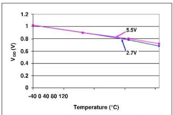
| Temperature (°C) | V_DD (V) | | ---------------- | -------- | | -40 | 1.0 | | 120 | 0.9 | | 80 | 0.8 | | 60 | 0.8 | | 40 | 0.7 | | 20 | 0.7 |FIGURE 2-64: POR/BOR Trip point vs. V and Temperature.
2.1 Test Circuits

text_image
VIN Offset GND A W B 2.5V DC +5V VOUTFIGURE 2-65: -3 db Gain vs. Frequency Test.

text_image
floating A V_A W V_W I_W B V_B R_BW = V_W/I_W R_W = (V_W - V_A)/I_WFIGURE 2-66: R BW and RW Measurement.
3.0 PIN DESCRIPTIONS
The descriptions of the pins are listed in Table 3-1.
Additional descriptions of the device pins follows.
TABLE 3-1: PINOUT DESCRIPTION FOR THE MCP453X/455X/463X/465X
| Pin | Weak Pull-up/ down (1) | Standard Function | |||||||
| Single Dual | Symbol I/O | Buffer Type | |||||||
| Rheo | Pot (1) | Rheo | Pot | ||||||
| 8L 8L | 10L 14L 16L | ||||||||
| 1 | 1 | 1 | 1 | 16 | HVC/A0 | I | HV w/ST | “smart” | High Voltage Command / Address 0 |
| 2 | 2 | 2 | 2 | 1 | SCL | I | HV w/ST | No | I^2C clock input |
| 3 | 3 | 3 | 3 | 2 | SDA | I/O | HV w/ST | No | I^2C serial data I/O. Open Drain output |
| 4 | 4 | 4 | 4 | 3, 4 | V_SS | — | P | — | Ground |
| — | — | 5 | 5 | 5 | P1B | A | Analog | No | Potentiometer 1 Terminal B |
| — | — | 6 | 6 | 6 | P1W | A | Analog | No | Potentiometer 1 Wiper Terminal |
| — | — | — | 7 | 7 | P1A | A | Analog | No | Potentiometer 1 Terminal A |
| — | 5 | — | 8 | 8 | P0A | A | Analog | No | Potentiometer 0 Terminal A |
| 5 | 6 | 7 | 9 | 9 | P0W | A | Analog | No | Potentiometer 0 Wiper Terminal |
| 6 | 7 | 8 | 10 | 10 | P0B | A | Analog | No | Potentiometer 0 Terminal B |
| — | — | — | 11 | 11, 12 | NC | — | — | — | No Connection |
| — | — | — | 12 | 13 | A2 | I | HV w/ST | “smart” | Address 2 |
| 7 | — | 9 | 13 | 14 | A1 | I | HV w/ST | “smart” | Address 1 |
| 8 | 8 | 10 | 14 | 15 | V_DD | — | P | — | Positive Power Supply Input |
| 9 | 9 | 11 | — | 17 | EP | — | — | — | Exposed Pad (Note 2) |
Legend: HV w/ST = High Voltage tolerant input (with Schmidt trigger input)
A = Analog pins (Potentiometer terminals) I = digital input (high Z)
O = digital output I/O = Input / Output
P = Power
Note 1: The pin's "smart" pull-up shuts off while the pin is forced low. This is done to reduce the standby and shutdown current.
2: The DFN and QFN packages have a contact on the bottom of the package. This contact is conductively connected to the die substrate, and therefore should be unconnected or connected to the same ground as the device's V_SS pin.
3.1 High Voltage Command / Address 0 (HVC/A0)
The HVC/A0 pin is the Address 0 input for the I²C interface as well as the High Voltage command pin. At the device's POR/BOR the value of the A0 address bit is latched. This input, along with the A2 and A1 pins, completes the device address. This allows up to eight MCP45XX/46XX devices on a single PC bus.
During normal operation the voltage on this pin determines if the I^2C command is a normal command or a High Voltage command (when HVC/A0 = V_IHH ).
3.2 Serial Clock (SCL)
The SCL pin is the serial interfaces Serial Clock pin. This pin is connected to the Host Controllers SCL pin. The MCP45XX/46XX is a slave device, so its SCL pin accepts only external clock signals.
3.3 Serial Data (SDA)
The SDA pin is the serial interfaces Serial Data pin. This pin is connected to the Host Controllers SDA pin. The SDA pin is an open-drain N-channel driver.
3.4 Ground (V ss)
The V_SS pin is the device ground reference.
3.5 Potentiometer Terminal B
The terminal B pin is connected to the internal potentiometer's terminal B.
The potentiometer's terminal B is the fixed connection to the Zero Scale wiper value of the digital potentiometer. This corresponds to a wiper value of 0x00 for both 7-bit and 8-bit devices.
The terminal B pin does not have a polarity relative to the terminal W or A pins. The terminal B pin can support both positive and negative current. The voltage on terminal B must be between V_SS and V_DD .
MCP46XX devices have two terminal B pins, one for each resistor network.
3.6 Potentiometer Wiper (W) Terminal
The terminal W pin is connected to the internal potentiometer's terminal W (the wiper). The wiper terminal is the adjustable terminal of the digital potentiometer. The terminal W pin does not have a polarity relative to terminals A or B pins. The terminal W pin can support both positive and negative current. The voltage on terminal W must be between V_SS and V_DD .
MCP46XX devices have two terminal W pins, one for each resistor network.
3.7 Potentiometer Terminal A
The terminal A pin is available on the MCP4XX1 devices, and is connected to the internal potentiometer's terminal A.
The potentiometer's terminal A is the fixed connection to the Full-Scale wiper value of the digital potentiometer. This corresponds to a wiper value of 0x100 for 8-bit devices or 0x80 for 7-bit devices.
The terminal A pin does not have a polarity relative to the terminal W or B pins. The terminal A pin can support both positive and negative current. The voltage on terminal A must be between V_SS and V_DD .
The terminal A pin is not available on the MCP4XX2 devices, and the internally terminal A signal is floating.
MCP46X1 devices have two terminal A pins, one for each resistor network.
3.8 Address 2 (A2)
The A2 pin is the I²C interface's Address 2 pin. Along with the A1 and A0 pins, up to eight MCP45XX/46XX devices can be used on a single ℃C bus.
3.9 Address 1 (A1)
The A2 pin is the I²C interface's Address 1 pin. Along with the A2 and A0 pins, up to eight MCP45XX/46XX devices can be used on a single ℃ bus.
3.10 Positive Power Supply Input (V DD)
The V_DD pin is the device's positive power supply input. The input power supply is relative to V_SS .
While the device V_DD < V_min (2.7V), the electrical performance of the device may not meet the data sheet specifications.
3.11 No Connect (NC)
These pins should be either connected to V_DD or V_SS .
3.12 Exposed Pad (EP)
This pad is conductively connected to the device's substrate. This pad should be tied to the same potential as the V_SS pin (or left unconnected). This pad could be used to assist as a heat sink for the device when connected to a PCB heat sink.
4.0 FUNCTIONAL OVERVIEW
This data sheet covers a family of thirty-two digital Potentiometer and Rheostat devices that will be referred to as MCP4XXX. The MCP4XX1 devices are the Potentiometer configuration, while the MCP4XX2 devices are the Rheostat configuration.
As the Device Block Diagram shows, there are four main functional blocks. These are:
- POR/BOR Operation
- Memory Map
- Resistor Network
- Serial Interface (I ^2 C)
The POR/BOR operation and the memory map are discussed in this section and the Resistor Network and I²C operation are described in their own sections. The Device Commands commands are discussed in Section 7.0 "Device Commands".
4.1 POR/BOR Operation
The Power-on Reset is the case where the device has power applied to it, starting from the V_SS level. The Brown-out Reset occurs when power is applied to the device, and that power (voltage) drops below the specified range.
The device's RAM retention voltage ( V_RAM ) is lower than the POR/BOR voltage trip point ( V_POR/V_BOR ). The maximum V_POR/V_BOR voltage is less than 1.8V.
When V_POR/V_BOR < V_DD < 2.7V , the electrical performance may not meet the data sheet specifications. In this region, the device is capable of incrementing, decrementing, reading and writing to its volatile memory if the proper serial command is executed.
4.1.1 POWER-ON RESET
When the device powers up, the device V_DD will cross the V_POR/V_BOR voltage. Once the V_DD voltage crosses the V_POR/V_BOR voltage the following happens:
- Volatile wiper register is loaded with value (mid-scale)
- The TCON register is loaded with the default value
- The device is capable of digital operation
4.1.2 BROWN-OUT RESET
When the device powers down, the device V_DD will cross the V_POR/V_BOR voltage.
Once the V_DD voltage decreases below the V_POR/V_BOR voltage, the Serial Interface is disabled.
If the V_DD voltage decreases below the V_RAM voltage, the following may happen:
• Volatile wiper registers become corrupt
• TCON register becomes corrupt
As the voltage recovers above the V_POR/V_BOR voltage see Section 4.1.1 “Power-on Reset”.
Serial commands not completed due to a brown-out condition may cause the volatile memory location to become corrupted.
4.2 Memory Map
The device memory map supports 16 locations, of which three locations are used. Each location is 9-bits wide (16x9 bits). This memory space is shown in Table 4-1.
TABLE 4-1: MEMORY MAP
| Address Function Memory Type | ||
| 00h Volatile Wiper 0 RAM | ||
| 01h Volatile Wiper 1 RAM | ||
| 02h Reserved — | ||
| 03h Reserved — | ||
| 04h Volatile TCON register | RAM | |
| 05h Reserved | RAM | |
| 06h - 0Fh | Reserved | — |
4.2.1 VOLATILE MEMORY (RAM)
There are four volatile memory locations. These are:
- Volatile Wiper 0
- Volatile Wiper 1
(Dual Resistor Network devices only)
• Terminal Control (TCON) register - Reserved
The volatile memory starts functioning at the RAM retention voltage ( V_RAM ).
4.2.1.1 Address 05h (Reserved)
This memory location is Reserved and is mapped to the Status Register of the nonvolatile MCP45XX/46XX devices. Since the nonvolatile device's bits are not used by the volatile device, this location is reserved. Reading this address will result in a value of 1F7h.
4.2.1.2 Terminal Control (TCON) Register
This register contains 8 control bits. Four bits are for Wiper 0, and four bits are for Wiper 1. Register 4-1 describes each bit of the TCON register.
The state of each resistor network terminal connection is individually controlled. That is, each terminal connection (A, B and W) can be individually connected/disconnected from the resistor network. This allows the system to minimize the currents through the digital potentiometer.
The value that is written to this register will appear on the resistor network terminals when the serial command has completed.
When the WL1 bit is enabled, writes to the TCON register bits R1HW, R1A, R1W, and R1B are inhibited.
When the WL0 bit is enabled, writes to the TCON register bits R0HW, R0A, R0W, and R0B are inhibited.
On a POR/BOR this register is loaded with 1FFh (9-bits), for all terminals connected. The Host Controller needs to detect the POR/BOR event and then update the volatile TCON register value.
Additionally, there is a bit which enables the operation of General Call commands.
REGISTER 4-1: TCON BITS (ADDRESS = 0x04) ^(1)
| R/W-1 R/W-1 R/W-1 R/W-1 R/W-1 R/W-1 R/W-1 R/W-1 | ||||||||
| GCEN R1 | HW | R1A | R1W | R1B | R0HW | R0A | R0W | R0B |
| bit 8 bit 0 | ||||||||
Legend:
| R = Readable bit | W = Writable bit | U = Unimplemented bit, read as '0' |
| -n = Value at POR | '1' = Bit is set | '0' = Bit is cleared x = Bit is unknown |
bit 8 GCEN: General Call Enable bit
This bit specifies if General Call commands are accepted
1 = Enable Device to "Accept" the General Call Address (0000h)
0 = The General Call Address is disabled
bit 7 R1HW: Resistor 1 Hardware Configuration Control bit
This bit forces Resistor 1 into the "shutdown" configuration of the Hardware pin
1 = Resistor 1 is NOT forced to the hardware pin "shutdown" configuration
0 = Resistor 1 is forced to the hardware pin "shutdown" configuration
bit 6 R1A: Resistor 1 Terminal A (P1A pin) Connect Control bit
This bit connects/disconnects the Resistor 1 Terminal A to the Resistor 1 Network
1 = P1A pin is connected to the Resistor 1 Network
0 = P1A pin is disconnected from the Resistor 1 Network
bit 5 R1W: Resistor 1 Wiper (P1W pin) Connect Control bit
This bit connects/disconnects the Resistor 1 Wiper to the Resistor 1 Network
1 = P1W pin is connected to the Resistor 1 Network
0 = P1W pin is disconnected from the Resistor 1 Network
bit 4 R1B: Resistor 1 Terminal B (P1B pin) Connect Control bit
This bit connects/disconnects the Resistor 1 Terminal B to the Resistor 1 Network
1 = P1B pin is connected to the Resistor 1 Network
0 = P1B pin is disconnected from the Resistor 1 Network
bit 3 ROHW: Resistor 0 Hardware Configuration Control bit
This bit forces Resistor 0 into the "shutdown" configuration of the Hardware pin
1 = Resistor 0 is NOT forced to the hardware pin "shutdown" configuration
0 = Resistor 0 is forced to the hardware pin "shutdown" configuration
bit 2 R0A: Resistor 0 Terminal A (P0A pin) Connect Control bit
This bit connects/disconnects the Resistor 0 Terminal A to the Resistor 0 Network
1 = P0A pin is connected to the Resistor 0 Network
0 = P0A pin is disconnected from the Resistor 0 Network
bit 1 R0W: Resistor 0 Wiper (P0W pin) Connect Control bit
This bit connects/disconnects the Resistor 0 Wiper to the Resistor 0 Network
1 = POW pin is connected to the Resistor 0 Network
0 = POW pin is disconnected from the Resistor 0 Network
bit 0 R0B: Resistor 0 Terminal B (P0B pin) Connect Control bit
This bit connects/disconnects the Resistor 0 Terminal B to the Resistor 0 Network
1 = P0B pin is connected to the Resistor 0 Network
0 = P0B pin is disconnected from the Resistor 0 Network
Note 1: These bits do not affect the wiper register values.
NOTES:
5.0 RESISTOR NETWORK
The Resistor Network has either 7-bit or 8-bit resolution. Each Resistor Network allows zero scale to full-scale connections. Figure 5-1 shows a block diagram for the resistive network of a device.
The Resistor Network is made up of several parts. These include:
- Resistor Ladder
- Wiper
- Shutdown (Terminal Connections)
Devices have either one or two resistor networks, These are referred to as Pot 0 and Pot 1.

text_image
A 8-Bit 7-Bit N = 256 N = 128 (100h) (80h) Rs Rw (1) 255 127 (RW (1) (FFh) (7Fh) Rs Rw (1) 254 126 (FEh) (7Eh) Rs Rw (1) 1 1 (01h) (01h) Rs Rw (1) 0 0 (00h) (00h) Analog Mux B WNote 1: The wiper resistance is dependent on several factors including, wiper code, device V_DD , Terminal voltages (on A, B, and W), and temperature. Also for the same conditions, each tap selection resistance has a small variation. This R_W variation has greater effects on some specifications (such as INL) for the smaller resistance devices (5.0 kΩ compared to larger resistance devices (100.0 kΩ)).
FIGURE 5-1: Resistor Block Diagram.
5.1 Resistor Ladder Module
The resistor ladder is a series of equal value resistors ( R_S ) with a connection point (tap) between the two resistors. The total number of resistors in the series (ladder) determines the R_AB resistance (see Figure 5-1). The end points of the resistor ladder are connected to analog switches, which are connected to the device Terminal A and Terminal B pins. The R_AB (and R_S ) resistance has small variations over voltage and temperature.
For an 8-bit device, there are 256 resistors in a string between terminal A and terminal B. The wiper can be set to tap onto any of these 256 resistors, thus providing 257 possible settings (including terminal A and terminal B).
For a 7-bit device, there are 128 resistors in a string between terminal A and terminal B. The wiper can be set to tap onto any of these 128 resistors, thus providing 129 possible settings (including terminal A and terminal B).
Equation 5-1 shows the calculation for the step resistance.
EQUATION 5-1: R S CALCULATION
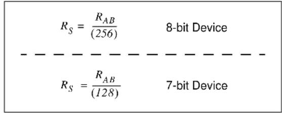
text_image
R_S = \frac{R_{AB}}{(256)} \quad 8\text{-bit Device} R_S = \frac{R_{AB}}{(128)} \quad 7\text{-bit Device}5.2 Wiper
Each tap point (between the R_S resistors) is a connection point for an analog switch. The opposite side of the analog switch is connected to a common signal, which is connected to the Terminal W (Wiper) pin.
A value in the Volatile Wiper register selects which analog switch to close, connecting the W terminal to the selected node of the resistor ladder.
The wiper can connect directly to Terminal B or to Terminal A. A zero-scale connection, connects the Terminal W (wiper) to Terminal B (wiper setting of 000h). A full-scale connection, connects the Terminal W (wiper) to Terminal A (wiper setting of 100h or 80h). In these configurations, the only resistance between Terminal W and the other Terminal (A or B) is that of the analog switches.
A wiper setting value greater than full-scale (wiper setting of 100h for 8-bit device or 80h for 7-bit devices) will also be a Full-Scale setting (Terminal W (wiper) connected to Terminal A). Table 5-1 illustrates the full wiper setting map.
Equation 5-2 illustrates the calculation used to determine the resistance between the wiper and terminal B.
EQUATION 5-2: R WB CALCULATION
| R_WB = _ABN256( + R)W | 8-bit Device |
| N = 0 to 256 (decimal) | |
| R_WB = _ABN128( + R)W | 7-bit Device |
| N = 0 to 128 (decimal) |
TABLE 5-1: VOLATILE WIPER VALUE VS. WIPER POSITION MAP
| Wiper Setting | Properties | |
| 7-bit Pot | 8-bit Pot | |
| 3FFh081h | 3FFh101h | Reserved (Full-Scale (W = A)),Increment and Decrement commands ignored |
| 080h 100h Full-Scale (W = A),Increment commands ignored | ||
| 07Fh041h | 0FFh081 | W = N |
| 040h 080h W = N (Mid-Scale) | ||
| 03Fh001h | 07Fh001 | W = N |
| 000h 000h Zero Scale (W = B)Decrement command ignored | ||
A POR/BOR event will load the Volatile Wiper register value with the default value. Table 5-2 shows the default values offered. Custom POR/BOR options are available. Contact the local Microchip Sales Office.
TABLE 5-2: DEFAULT FACTORY SETTINGS SELECTION
| Resistance Code | Typical RAB Value | Default POR Wiper Setting | Wiper Code | |
| 8-bit | 7-bit | |||
| -502 | 5.0 kΩ | Mid-scale | 80h | 40h |
| -103 | 10.0 kΩ | Mid-scale | 80h | 40h |
| -503 | 50.0 kΩ | Mid-scale | 80h | 40h |
| -104 | 100.0 kΩ | Mid-scale | 80h | 40h |
5.3 Shutdown
Shutdown is used to minimize the device's current consumption. The MCP4XXX achieves this through the Terminal Control Register (TCON).
5.3.1 TERMINAL CONTROL REGISTER (TCON)
The Terminal Control (TCON) register is a volatile register used to configure the connection of each resistor network terminal pin (A, B, and W) to the Resistor Network. This bits are described in Register 4-1.
When the RxHW bit is a "0", the selected resistor network is forced into the following state:
• The PxA terminal is disconnected
- The PxW terminal is simultaneously connected to the PxB terminal (see Figure 5-2)
- The Serial Interface is NOT disabled, and all Serial Interface activity is executed
Alternate low power configurations may be achieved with the RxA, RxW, and RxB bits.
Note 1: The RxHW bits are identical to the RxHW bits of the MCP41XX/42XX devices. The MCP42XX devices also have a SHDN pin which forces the resistor network into the same state as that resistor networks RxHW bit.
2: When RxHW = "0", the state of the TCON register RxA, RxW, and RxB bits is overridden (ignored). When the state of the RxHW bit returns to "1", the TCON register RxA, RxW, and RxB bits return to controlling the terminal connection state. In other words, the RxHW bit does not corrupt the state of the RxA, RxW, and RxB bits.

text_image
A Resistor Network B WFIGURE 5-2: Resistor Network Shutdown Configuration.
5.3.2 INTERACTION OF RxHW BIT AND RxA, RxW, AND RxB BITS (TCON REGISTER)
Using the TCON bits allows each resistor network (Pot 0 and Pot 1) to be individually "shutdown".
The state of the RxHW bit does NOT corrupt the other bit values in the TCON register, nor the value of the Volatile Wiper registers. When the Shutdown mode is exited (RxHW changes state from "0" to "1"):
- The device returns to the Wiper setting specified by the Volatile Wiper value
- The RxA, RxB, and RxW bits return to controlling the terminal connection state of that resistor network
NOTES:
6.0 SERIAL INTERFACE (I ^2 C)
The MCP45XX/46XX devices support the I²C serial protocol. The MCP45XX/46XX I²C's module operates in Slave mode (does not generate the serial clock).
Figure 6-1 shows a typical I ^2 C Interface connection. All I ^2 C interface signals are high-voltage tolerant.
The MCP45XX/46XX devices use the two-wire I²C serial interface. This interface can operate in standard, fast or High-Speed mode. A device that sends data onto the bus is defined as transmitter, and a device receiving data, as receiver. The bus has to be controlled by a master device which generates the serial clock (SCL), controls the bus access and generates the START and STOP conditions. The MCP45XX/46XX device works as slave. Both master and slave can operate as transmitter or receiver, but the master device determines which mode is activated. Communication is initiated by the master (microcontroller) which sends the START bit, followed by the slave address byte. The first byte transmitted is always the slave address byte, which contains the device code, the address bits, and the R/W bit.
Refer to the Phillips I ^2 C document for more details of the I ^2 C specifications.
Typical I ^2 C Interface Connections
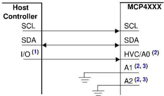
flowchart
graph TD
    A["Host Controller"] -->|SCL| B["MCP4XXX"]
    A -->|SDA| B
    A -->|I/O (1)| B
    B -->|SCL| C["Output"]
    B -->|SDA| D["Output"]
    B -->|HVC/A0 (2)| E["Output"]
    B -->|A1 (2, 3)| F["Output"]
    B -->|A2 (2, 3)| G["Output"]
Note 1: If High voltage commands are desired, some type of external circuitry needs to be implemented.
2: These pins have internal pull-ups. If faster rise times are required, then external pull-ups should be added.
3: This pin could be tied high, low, or connected to an I/O pin of the Host Controller.
FIGURE 6-1: Typical I ^2 C Interface Block Diagram.
6.1 Signal Descriptions
The I²C interface uses up to five pins (signals). These are:
- SDA (Serial Data)
- SCL (Serial Clock)
- A0 (Address 0 bit)
- A1 (Address 1 bit)
• A2 (Address 2 bit)
6.1.1 SERIAL DATA (SDA)
The Serial Data (SDA) signal is the data signal of the device. The value on this pin is latched on the rising edge of the SCL signal when the signal is an input.
With the exception of the START and STOP conditions, the High or Low state of the SDA pin can only change when the clock signal on the SCL pin is LOW. During the high period of the clock the SDA pin's value (high or low) must be stable. Changes in the SDA pin's value while the SCL pin is HIGH will be interpreted as a START or a STOP condition.
6.1.2 SERIAL CLOCK (SCL)
The Serial Clock (SCL) signal is the clock signal of the device. The rising edge of the SCL signal latches the value on the SDA pin. The MCP45XX/46XX supports three I²C interface clock modes:
- Standard mode: clock rates up to 100 kHz
- Fast mode: clock rates up to 400 kHz
• High-Speed mode (HS mode): clock rates up to 3.4 MHz
The MCP4XXX will not stretch the clock signal (SCL) since memory read accesses occur fast enough.
Depending on the clock rate mode, the interface will display different characteristics.
6.1.3 THE ADDRESS BITS (A2:A1:A0)
There are up to three hardware pins used to specify the device address. The number of address pins is determined by the part number.
Address 0 is multiplexed with the High Voltage Command (HVC) function. So the state of A0 is latched on the MCP4XXX's POR/BOR event.
The state of the A2 and A1 pins should be static, that is they should be tied high or tied low.
6.1.3.1 The High Voltage Command (HVC) Signal
The High Voltage Command (HVC) signal is multiplexed with Address 0 (A0) and is used to indicate that the command, or sequence of commands, are in the High Voltage mode. High Voltage commands are supported for compatibility with the nonvolatile devices.
The HVC pin has an internal resistor connection to the MCP45XX/46XXs internal V_DD signal.
6.2 I ^2 C Operation
The MCP45XX/46XX's I²C module is compatible with the Philips I²C specification. The following lists some of the module's features:
-
7-bit slave addressing
• Supports three clock rate modes: -
Standard mode, clock rates up to 100 kHz
- Fast mode, clock rates up to 400 kHz
- High-speed mode (HS mode), clock rates up to 3.4 MHz
• Support Multi-Master Applications
- General call addressing
- Internal weak pull-ups on interface signals
The I ^2 C 10-bit addressing mode is not supported.
The Philips I^2C specification only defines the field types, field lengths, timings, etc. of a frame. The frame content defines the behavior of the device. The frame content for the MCP4XXX is defined in Section 7.0.
6.2.1 I ^2 C BIT STATES AND SEQUENCE
Figure 6-8 shows the I²C transfer sequence. The serial clock is generated by the master. The following definitions are used for the bit states:
- Start bit (S)
- Data bit
- Acknowledge (A) bit (driven low) / No Acknowledge (A) bit (not driven low)
• Repeated Start bit (Sr) - Stop bit (P)
6.2.1.1 Start Bit
The Start bit (see Figure 6-2) indicates the beginning of a data transfer sequence. The Start bit is defined as the SDA signal falling when the SCL signal is HIGH.
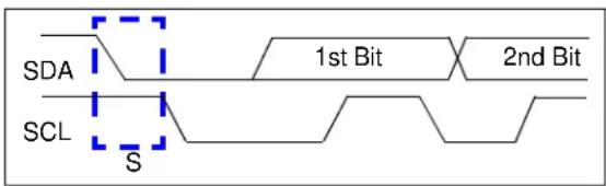
text_image
SDA SCL S 1st Bit 2nd BitFIGURE 6-2: Start Bit.
6.2.1.2 Data Bit
The SDA signal may change state while the SCL signal is LOW. While the SCL signal is HIGH, the SDA signal MUST be stable (see Figure 6-5).
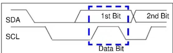
text_image
SDA SCL 1st Bit 2nd Bit Data BitFIGURE 6-3: Data Bit.
6.2.1.3 Acknowledge (A) Bit
The A bit (see Figure 6-4) is typically a response from the receiving device to the transmitting device. Depending on the context of the transfer sequence, the A bit may indicate different things. Typically, the Slave device will supply an A response after the Start bit and 8 "data" bits have been received. The A bit has the SDA signal low.

text_image
SDA D0 A SCL 8 9FIGURE 6-4: Acknowledge Waveform.
Not A (A) Response
The bit has the SDA signal HIGH. Table 6-1 shows some of the conditions where the Slave Device will issue a Not A ( ).
If an error condition occurs (such as an instead of A), then an START bit must be issued to reset the command state machine.
TABLE 6-1: MCP45XX/46XX A / A RESPONSES
| Event | Acknowledge Bit Response | Comment |
| General Call A | Only if GCEN bit is | set |
| Slave Address valid | A | |
| Slave Address not valid | ||
| Device memory address and specified command (AD3:AD0 and C1:C0) are an invalid combination | After device has received address and command | |
| Bus Collision N. | A. I | ^2C Module Resets, or a “Don't Care” if the collision occurs on the Masters “Start bit”. |
6.2.1.4 Repeated Start Bit
The Repeated Start bit (see Figure 6-5) indicates the current Master Device wishes to continue communicating with the current Slave Device without releasing the I²C bus. The Repeated Start condition is the same as the Start condition, except that the Repeated Start bit follows a Start bit (with the Data bits + A bit) and not a Stop bit.
The Start bit is the beginning of a data transfer sequence and is defined as the SDA signal falling when the SCL signal is HIGH.
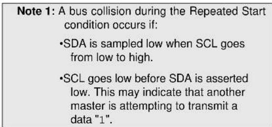
text_image
Note 1: A bus collision during the Repeated Start condition occurs if: •SDA is sampled low when SCL goes from low to high. •SCL goes low before SDA is asserted low. This may indicate that another master is attempting to transmit a data "1".
text_image
SDA 1st Bit SCL Sr = Repeated StartFIGURE 6-5: Repeat Start Condition Waveform.
6.2.1.5 Stop Bit
The Stop bit (see Figure 6-6) Indicates the end of the I²C Data Transfer Sequence. The Stop bit is defined as the SDA signal rising when the SCL signal is HIGH.
A Stop bit resets the interface of all MCP4XXX devices.
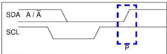
text_image
SDA A/Ā SCL PFIGURE 6-6: Stop Condition Receive or Transmit Mode.
6.2.2 CLOCK STRETCHING
"Clock Stretching" is something that the receiving device can do, to allow additional time to "respond" to the "data" that has been received.
The MCP4XXX will not stretch the clock signal (SCL) since memory read accesses occur fast enough.
6.2.3 ABORTING A TRANSMISSION
If any part of the I²C transmission does not meet the command format, it is aborted. This can be intentionally accomplished with a START or STOP condition. This is done so that noisy transmissions (usually an extra START or STOP condition) are aborted before they corrupt the device.

text_image
SDA SCL S 1st Bit 2nd Bit 3rd Bit 4th Bit 5th Bit 6th Bit 7th Bit 8th Bit PA / AFIGURE 6-7: Typical 8-Bit I ^2 C Waveform Format.

text_image
SDA SCL START Condition Data allowed to change Data or A valid STOP ConditionFIGURE 6-8: I ^2 C Data States and Bit Sequence.
6.2.4 ADDRESSING
The address byte is the first byte received following the START condition from the master device. The address contains four (or more) fixed bits and (up to) three user defined hardware address bits (pins A2, A1, and A0). These 7-bits address the desired I²C device. The A7:A4 address bits are fixed to "0101" and the device appends the value of following three address pins (A2, A1, A0). Address pins that are not present on the device are pulled up (a bit value of '1').
Since there are up to three address bits controlled by hardware pins, there may be up to eight MCP4XXX devices on the same PC bus.
Figure 6-9 shows the slave address byte format, which contains the seven address bits. There is also a read/write bit. Table6-2 shows the fixed address for each device.
Hardware Address Pins
The hardware address bits (A2, A1, and A0) correspond to the logic level on the associated address pins. This allows up to eight devices on the bus.
These pins have a weak pull-up enabled when the V_DD < V_BOR . The weak pull-up utilizes the “smart” pull-up technology and exhibits the same characteristics as the High-voltage tolerant I/O structure.
The state of the A0 address pin is latch on POR/BOR. This is required since High-Voltage commands force this pin (HVC/A0) to the V_IHH level.

text_image
Slave Address S A6 A5 A4 A3 A2 A1 A0 R/W A/A "0" "1" "0" "1" Start bit See Table 6-2 R/W bit R/W = 0 = write R/W = 1 = read A bit (controlled by slave device) A = 0 = Slave Device Acknowledges byte A = 1 = Slave Device does not Acknowledge byteFIGURE 6-9: Slave Address Bits in the I²C Control Byte.
TABLE 6-2: DEVICE SLAVE ADDRESSES
| Device Address Comment | ||
| MCP45X1 | ‘0101 11'b + A0 | Supports up to 2 devices. (Note 1) |
| MCP45X2 | ‘0101 1'b + A1:A0 | Supports up to 4 devices. (Note 1) |
| MCP46X1 | ‘0101'b + A2:A1:A0 | Supports up to 8 devices. (Note 1) |
| MCP46X2 | ‘0101 1'b + A1:A0 | Supports up to 4 devices. (Note 1) |
Note 1: A0 is used for High-Voltage commands, and the value is latched at POR.
6.2.5 SLOPE CONTROL
The MCP45XX/46XX implements slope control on the SDA output.
As the device transitions from HS mode to FS mode, the slope control parameter will change from the HS specification to the FS specification.
For Fast (FS) and High-Speed (HS) modes, the device has a spike suppression and a Schmidt trigger at SDA and SCL inputs.
6.2.6 HS MODE
The I²C specification requires that a high-speed mode device must be 'activated' to operate in High-Speed (3.4 Mbit/s) mode. This is done by the Master sending a special address byte following the START bit. This byte is referred to as the high-speed Master Mode Code (HSMMC).
The MCP45XX/46XX device does not acknowledge this byte. However, upon receiving this command, the device switches to HS mode. The device can now communicate at up to 3.4 Mbit/s on SDA and SCL lines. The device will switch out of the HS mode on the next STOP condition.
The master code is sent as follows:
- START condition (S)
- High-Speed Master Mode Code (0000 1XXX), The xxx bits are unique to the high-speed (HS) mode Master.
- No Acknowledge (A ^- )
After switching to the High-Speed mode, the next transferred byte is the I²C control byte, which specifies the device to communicate with, and any number of data bytes plus acknowledgements. The Master Device can then either issue a Repeated Start bit to address a different device (at High-Speed), or a Stop bit to return to Fast/Standard bus speed. After the Stop bit, any other Master Device (in a Multi-Master system) can arbitrate for the I²C bus.
See Figure 6-10 for illustration of HS mode command sequence.
For more information on the HS mode, or other I ^2 C modes, please refer to the Phillips ^2 C specification.
6.2.6.1 Slope Control
The slope control on the SDA output is different between the Fast/Standard Speed and the High-Speed clock modes of the interface.
6.2.6.2 Pulse Gobbler
The pulse gobbler on the SCL pin is automatically adjusted to suppress spikes < 10 ns during HS mode.

flowchart
graph TD
    A["F/S-mode"] --> B["HS-mode"]
    B --> C["P"]
    C --> D["F/S-mode"]
    D --> E["HS-mode continues"]
    E --> F["Control Byte"]
    subgraph HS Select Byte Control Byte Command/Data Byte(s)
        G["S = Start bit"]
        H["Sr = Repeated Start bit"]
        I["A = Acknowledge bit"]
        J["A̅ = Not Acknowledge bit"]
        K["R/W̅ = Read/Write bit"]
        L["P = Stop bit (Stop condition terminates HS Mode)"]
    end
    style A fill:#f9f,stroke:#333
    style B fill:#ccf,stroke:#333
    style C fill:#cfc,stroke:#333
    style D fill:#fcc,stroke:#333
    style E fill:#ffc,stroke:#333
    style F fill:#fcc,stroke:#333
    style G fill:#fff,stroke:#333
    style H fill:#fff,stroke:#333
    style I fill:#fff,stroke:#333
    style J fill:#fff,stroke:#333
    style K fill:#fff,stroke:#333
    style L fill:#fff,stroke:#333
FIGURE 6-10: HS Mode Sequence.
6.2.7 GENERAL CALL
The General Call is a method that the "Master" device can communicate with all other "Slave" devices. In a Multi-Master application, the other Master devices are operating in Slave mode. The General Call address has two documented formats. These are shown in Figure 6-11. We have added a MCP45XX/46XX format in this figure as well.
This will allow customers to have multiple Digital Potentiometers on the bus and have them operate in a synchronous fashion (analogous to the DAC Sync pin functionality). If these MCP45XX/46XX 7-bit commands conflict with other ^2 devices on the bus, then the customer will need two busses and ensure that the devices are on the correct bus for their desired application functionality.
Dual Pot devices cannot update both Pot0 and Pot1 from a single command. To address this, there are General Call commands for the Wiper 0, Wiper 1, and the TCON registers.
Table 6-3 shows the General Call commands. Three commands are specified by the PC specification and are not applicable to the MCP45XX/46XX (so command is Not Acknowledged) The MCP45XX/46XX General Call commands are Acknowledge. Any other command is Not Acknowledged.
Note: There is only one General Call command per General Call control byte (address). Any additional General Call commands are ignored and Not Acknowledged.
TABLE 6-3: GENERAL CALL COMMANDS
| 7-bit Command (1, 2, 3) | Comment |
| ‘1000 00d’b Write Next Byte (Third Byte) to Volatile Wiper 0 Register | |
| ‘1001 00d’b Write Next Byte (Third Byte) to Volatile Wiper 1 Register | |
| ‘1100 00d’b Write Next Byte (Third Byte) to TCON Register | |
| ‘1000 010’bor ‘1000 011’b | Increment Wiper 0 Register |
| ‘1001 010’bor ‘1001 011’b | Increment Wiper 1 Register |
| ‘1000 100’bor ‘1000 101’b | Decrement Wiper 0 Register |
| ‘1001 100’bor ‘1001 101’b | Decrement Wiper 1 Register |
Note 1: Any other code is Not Acknowledged. These codes may be used by other devices on the I²C bus.
2: The 7-bit command always appends a "0" to form 8-bits.
3: "d" is the D8 bit for the 9-bit write value.

text_image
Second Byte S 0 0 0 0 0 0 0 0 A X X X X X X X X X 0 A P General Call Address "7-bit Command"Reserved 7-bit Commands (By I ^2 C Specification - Philips # 9398 393 40011, Ver. 2.1 January 2000)
'0000 011'b - Reset and write programmable part of slave address by hardware.
'0000 010'b - Write programmable part of slave address by hardware.
'0000 000'b - NOT Allowed
MCP45XX/MCP46XX 7-bit Commands
'1000 01x'b - Increment Wiper 0 Register.
'1001 01x'b - Increment Wiper 1 Register.
'1000 10x'b - Decrement Wiper 0 Register.
'1001 10x'b - Decrement Wiper 1 Register.
The Following is a Microchip Extension to this General Call Format
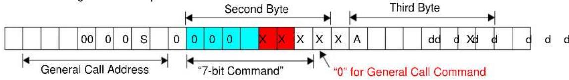
text_image
Second Byte Third Byte General Call Address "7-bit Command" "0" for General Call CommandMCP45XX/MCP46XX 7-bit Commands
'1000 00d'b - Write Next Byte (Third Byte) to Volatile Wiper 0 Register.
'1001 00d'b - Write Next Byte (Third Byte) to Volatile Wiper 1 Register.
'1100 00d'b - Write Next Byte (Third Byte) to TCON Register.
The Following is a "Hardware General Call" Format
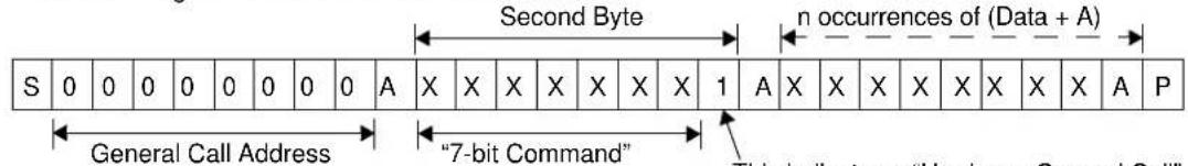
text_image
Second Byte n occurrences of (Data + A) S 0 0 0 0 0 0 0 0 A X X X X X X X X 1 A X X X X X X X X X A P General Call Address "7-bit Command" This indicates a "Hardware General Call"This indicates a "Hardware General Call" MCP45XX/MCP46XX will ignore this byte and all following bytes (and A), until a Stop bit (P) is encountered.
FIGURE 6-11: General Call Formats.
NOTES:
7.0 DEVICE COMMANDS
The MCP4XXX's I²C command formats are specified in this section. The I²C protocol does not specify how commands are formatted.
The MCP4XXX supports four basic commands. Depending on the location accessed determines the commands that are supported.
For the Volatile Wiper registers, these commands are:
- Write Data
- Read Data
- Increment Data
- Decrement Data
For the TCON Register, these commands are:
- Write Data
- Read Data
These commands have formats for both a single command or continuous commands. These commands are shown in Table 7-1.
Each command has two operational states. These operational states are referred to as:
• Normal Serial Commands
• High-Voltage Serial Commands
Note: High Voltage commands are supported for compatibility with nonvolatile devices in the family.
TABLE 7-1: I ^2 C COMMANDS
| Command | # of Bit Clocks (1) | Operates on Volatile/ Nonvolatile Memory | |
| Operation Mode | |||
| Write Data Single | 29 Both | ||
| Continuous | 18n + 11 Volatile Only | ||
| Read Data | Single | 29 | Both |
| Random | 48 | Both | |
| Continuous | 18n + 11 | Both | |
| Increment | Single | 20 | Volatile Only |
| Continuous | 9n + 11 | Volatile Only | |
| Decrement | Single | 20 | Volatile Only |
| Continuous | 9n + 11 | Volatile Only | |
Note 1: "n" indicates the number of times the command operation is to be repeated.
Normal serial commands are those where the HVC pin is driven to V_IH or V_IL . With High-Voltage Serial Commands, the HVC pin is driven to V_IHH . In each mode, there are four possible commands.
Table 7-2 shows the supported commands for each memory location.
Table 7-3 shows an overview of all the device commands and their interaction with other device features.
7.1 Command Byte
The MCP4XXX's Command Byte has three fields: the Address, the Command Operation, and two data bits, (see Figure 7-1). Currently only one of the data bits is defined (D8).
The device memory is accessed when the Master sends a proper Command Byte to select the desired operation. The memory location getting accessed is contained in the Command Byte's AD3:AD0 bits. The action desired is contained in the Command Byte's C1:C0 bits (see Table 7-1). C1:C0 determines if the desired memory location will be read, written, Incremented (wiper setting +1) or Decremented (wiper setting -1). The Increment and Decrement commands are only valid on the volatile wiper registers.
If the Address bits and Command bits are not a valid combination, then the MCP4XXX will generate a Not Acknowledge pulse to indicate the invalid combination. The I²C Master device must then force a Start Condition to reset the MCP4XXX's ²C module.
D9 and D8 are the most significant bits for the digital potentiometer's wiper setting. The 8-bit devices utilize D8 as their MSb while the 7-bit devices utilize D7 (from the data byte) as it's MSb.

text_image
COMMAND BYTE A A A A A C C D D A D D D D 1 0 1 0 9 8 MCP4XXX Memory Address MSbits (Data) Command Operation bits 0.0 = Write Data 0.1 = Increment 1.0 = Decrement 1.1 = Read DataFIGURE 7-1: Command Byte Format.
TABLE 7-2: MEMORY MAP AND THE SUPPORTED COMMANDS
| Address | Command Operation | Data (10-bits) ^(1) | Comment | |
| Value Function | ||||
| 00h Volatile Wiper 0 Write Data nn | nnnn nnnn | |||
| Read Data ^(3) | nn nnnn nnnn | |||
| Increment Wiper — | ||||
| Decrement Wiper — | ||||
| 01h Volatile Wiper 1 Write Data nn | nnnn nnnn | |||
| Read Data ^(3) | nn nnnn nnnn | |||
| Increment Wiper — | ||||
| Decrement Wiper — | ||||
| 02h | Reserved | — | — | |
| 03h | Reserved | — | — | |
| 04h ^(2) | Volatile TCON Register | Write Data nn nnnn nnnn | ||
| Read Data ^(3) | nn nnnn nnnn | |||
| 05h ^(2) | Reserved | Read ^(3) nn nnDatannn Maps to nonvolatile | MCP45XX/46XX device's STATUS Register | |
| 06h - 0Fh ^(2) | Reserved | — — | ||
Note 1: The Data memory is only 9-bits wide, so the MSb is ignored by the device.
2: Increment or Decrement commands are invalid for these addresses.
3: I^2C read operation will read 2 bytes, of which the 10-bits of data are contained within.
7.2 Data Byte
Only the Read Command and the Write Command have Data Byte(s).
The Write command concatenates the 8-bits of the Data Byte with the one data bit (D8) contained in the Command Byte to form 9-bits of data (D8:D0). The Command Byte format supports up to 9-bits of data so that the 8-bit resistor network can be set to Full-Scale (100h or greater). This allows wiper connections to Terminal A and to Terminal B. The D9 bit is currently unused.
7.3 Error Condition
If the four address bits received (AD3:AD0) and the two command bits received (C1:C0) are a valid combination, the MCP4XXX will Acknowledge the bus.
If the address bits and command bits are an invalid combination, then the MCP4XXX will Not Acknowledge the I²C bus.
Once an error condition has occurred, any following commands are ignored until the PC bus is reset with a Start Condition.
7.3.1 ABORTING A TRANSMISSION
A Restart or Stop condition in the expected data bit position will abort the current command sequence and data will not be written to the MCP4XXX.
TABLE 7-3: COMMANDS
| Command Name # of Bits | High Voltage ( V_IHH ) on HVC pin? | |
| Write Data 29 — | ||
| Read Data 29 — | ||
| Increment Wiper 20 — | ||
| Decrement Wiper 20 — | ||
| High Voltage Write Data | 29 | Yes |
| High Voltage Read Data | 29 | Yes |
| High Voltage Increment Wiper | 20 | Yes |
| High Voltage Decrement Wiper | 20 | Yes |
7.4 Write Data
Normal and High Voltage
The Write command can be issued to both the volatile and nonvolatile memory locations. The format of the command (see Figure 7-2), includes the I²C Control Byte, an A bit, the MCP4XXX Command Byte, an A bit, the MCP4XXX Data Byte, an A bit, and a Stop (or Restart) condition. The MCP4XXX generates the A/A bits.
A Write command to a volatile memory location changes that location after a properly formatted Write Command and the A/A clock have been received.
7.4.1 SINGLE WRITE TO VOLATILE MEMORY
For volatile memory locations, data is written to the MCP4XXX after every byte transfer (during the Acknowledge). If a Stop or Restart condition is generated during a data transfer (before the A), the data will not be written to the MCP4XXX. After the A bit, the master can initiate the next sequence with a Stop or Restart condition.
Refer to Figure 7-2 for the byte write sequence.
7.4.2 CONTINUOUS WRITES TO VOLATILE MEMORY
A continuous write mode of operation is possible when writing to the volatile memory registers (address 00h, 01h, and 04h). This continuous write mode allows writes without a Stop or Restart condition or repeated transmissions of the I²C Control Byte. Figure 7-3 shows the sequence for three continuous writes. The writes do not need to be to the same volatile memory address. The sequence ends with the master sending a STOP or RESTART condition.
7.4.3 THE HIGH VOLTAGE COMMAND (HVC) SIGNAL
The High Voltage Command (HVC) signal is multiplexed with Address 0 (A0) and is used to indicate that the command, or sequence of commands, are in the High Voltage operational state. High Voltage commands allow the device's WiperLock Technology and write protect features to be enabled and disabled.
The HVC pin has an internal resistor connection to the MCP45XX/46XXs internal V_DD signal.
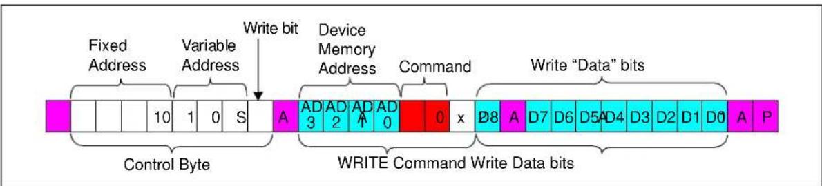
text_image
Fixed Address Variable Address Write bit Device Memory Address Command Write "Data" bits Control Byte WRITE Command Write Data bitsFIGURE 7-2: I ^2 C Write Sequence.

flowchart
graph TD
    A["Fixed Address"] --> B["Control Byte"]
    C["Variable Address"] --> B
    D["Write bit"] --> E["Device Memory Address"]
    E --> F["WRITE Command"]
    F --> G["Write Data bits"]
    H["Write “Data” bits"] --> I["WRITE Command Write Data bits"]
    I --> J["STOP bit"]
    K["Write Command Write Data bits"] --> L["WRITE Command Write Data bits"]
    L --> M["STOP bit"]
    N["AD3:AD0 = 00h, 01h, and 04h"] --> O["TCON register"]
FIGURE 7-3: I ^2 C Continuous Volatile Wiper Write.
7.5 Read Data
Normal and High Voltage
The Read command can be issued to both the volatile and nonvolatile memory locations. The format of the command (see Figure 7-4) includes the Start condition, I²C Control Byte (with R/W bit set to "0"), A bit, MCP4XXX Command Byte, A bit, followed by a Repeated Start bit, I²C Control Byte (with R/W bit set to "1"), and the MCP4XXX transmitting the requested Data High Byte, A bit, the Data Low Byte, the Master generating the , and Stop condition.
The I²C Control Byte requires the R/W bit equal to a logic one (R/W = 1) to generate a read sequence. The memory location read will be the last address contained in a valid write MCP4XXX Command Byte or address 00h, if no write operations have occurred since the device was reset (Power-on Reset or Brown-out Reset).
Read operations initially include the same address byte sequence as the write sequence (shown in Figure 6-9). This sequence is followed by another control byte (including the Start condition and Acknowledge) with the R/W bit equal to a logic one (R/ = 1) to indicate a read. The MCP4XXX will then transmit the data contained in the addressed register. This is followed by the master generating an A bit in preparation for more data, or an bit followed by a Stop. The sequence is ended with the master generating a Stop or Restart condition.
The internal address pointer is maintained.
7.5.1 SINGLE READ
Figure 7-4 shows the waveforms for a single read.
For single reads, the master sends a STOP or RESTART condition after the data byte is sent from the slave.
7.5.1.1 Random Read
Figure 7-5 shows the sequence for a Random Reads.
Refer to Figure 7-5 for the random byte read sequence.
7.5.2 CONTINUOUS READS
Continuous reads allow the device's memory to be read quickly. Continuous reads are possible to all memory locations. If a nonvolatile memory write cycle is occurring, then Read commands may only access the volatile memory locations.
Figure 7-6 shows the sequence for three continuous reads.
For continuous reads, instead of transmitting a STOP or RESTART condition after the data transfer, the master reads the next data byte. The sequence ends with the master Not Acknowledging and then sending a STOP or RESTART.
7.5.3 THE HIGH VOLTAGE COMMAND (HVC) SIGNAL
The High Voltage Command (HVC) signal is multiplexed with Address 0 (A0) and is used to indicate that the command, or sequence of commands, are in the High Voltage mode. High Voltage commands allow the device's WiperLock Technology, and write protect features to be enabled and disabled.
The HVC pin has an internal resistor connection to the MCP4XXXs internal V_DD signal.
7.5.4 IGNORING AN I ^2 C TRANSMISSION AND "FALLING OFF" THE BUS
The MCP4XXX expects to receive entire, valid I²C commands, and will assume any command not defined as a valid command is due to a bus corruption, and will enter a passive high condition on the SDA signal. All signals will be ignored until the next valid Start condition and Control Byte are received.
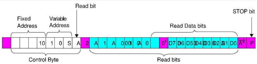
text_image
Fixed Address Variable Address Read bit Control Byte Read Data bits STOP bit Read bitsNote 1: Master Device is responsible for A/A signal. If an signal occurs, the MCP45XX/46XX will abort this transfer and release the bus.
2: The Master Device will Not Acknowledge, and the MCP45XX/46XX will release the bus so the Master Device can generate a Stop or Repeated Start condition.
3: The MCP45XX/46XX retains the last "Device Memory Address" that it has received. This is the MCP45XX/46XX does not "corrupt" the "Device Memory Address" after Repeated Start or Stop conditions.
4: The Device Memory Address pointer defaults to 00h on POR and BOR conditions.
FIGURE 7-4: I ^2 C Read (Last Memory Address Accessed).
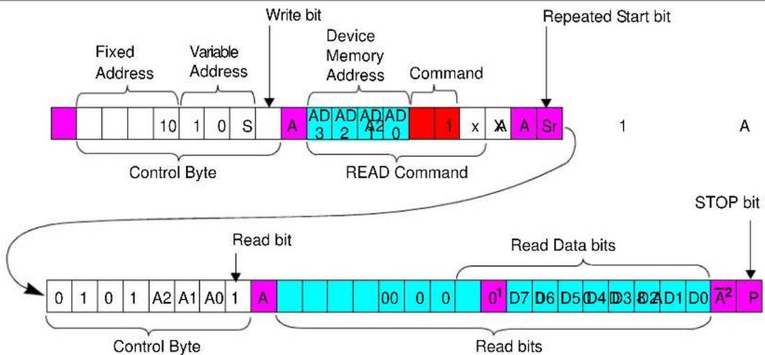
flowchart
graph TD
    A["Fixed Address"] --> B["10 1 0 S"]
    C["Variable Address"] --> B
    D["Device Memory Address"] --> E["A 3 AD 2 AD 1 AD 0"]
    F["Command"] --> G["1 x X A Sr"]
    H["Repeated Start Bit"] --> I["1 A"]
    J["STOP bit"] --> K["Read Data bits"]
    L["Read bit"] --> M["0 1 0 1 A2 A1 A0 1 A"]
    N["Control Byte"] --> O["Read bits"]
    P["Read bits"] --> Q["0 1 D7 D6 D5 D4 D3 D2 D1 D0 A̅² P"]
Note 1: Master Device is responsible for A / signal. If a signal occurs, the MCP45XX/46XX will abort this transfer and release the bus.
2: The Master Device will Not Acknowledge, and the MCP45XX/46XX will release the bus so the Master Device can generate a Stop or Repeated Start condition.
3: The MCP45XX/46XX retains the last "Device Memory Address" that it has received. This is the MCP45XX/46XX does not "corrupt" the "Device Memory Address" after Repeated Start or Stop conditions.
FIGURE 7-5: I ^2 C Random Read.

flowchart
graph TD
    A["Fixed Address"] --> B["10 1 0 S A"]
    C["Variable Address"] --> B
    B --> D["2 A 1 A 0 00 A 0 0 0 1 D7 D6 D5 D4 D3 D2 D1 D0 A1"]
    D --> E["Read Data bits"]
    E --> F["00 0 0 0 1 D7 D6 D5 D4 D3 D2 D1 D0 A1"]
    F --> G["Stop bit"]
    G --> H["0 0 0 0 0 0 0 D8 A1 D7 D6 D5 D4 D3 D2 D1 D0 A2 P"]
    style A fill:#f9f,stroke:#333
    style C fill:#f9f,stroke:#333
    style B fill:#ccf,stroke:#333
    style D fill:#cfc,stroke:#333
    style E fill:#fcc,stroke:#333
    style F fill:#cff,stroke:#333
    style G fill:#ffc,stroke:#333
    style H fill:#fcc,stroke:#333
FIGURE 7-6: I ^2 C Continuous Reads.
7.6 Increment Wiper Normal and High Voltage
The Increment Command provides a quick and easy method to modify the potentiometer's wiper by +1 with minimal overhead. The Increment Command will only function on the volatile wiper setting memory locations 00h and 01h.
Note: Table 7-2 shows the valid addresses for the Increment Wiper command. Other addresses are invalid.
When executing an Increment Command, the volatile wiper setting will be altered from n to n+1 for each Increment Command received. The value will increment up to 100h maximum on 8-bit devices, and 80h on 7-bit devices. If multiple Increment Commands are received after the value has reached 100h (or 80h), the value will not be incremented further. Table 7-4 shows the Increment Command versus the current volatile wiper value.
Refer to Figure 7-7 for the Increment Command sequence. The sequence is terminated by the Stop condition. So when executing a continuous command string, the Increment command can be followed by any other valid command. This means that writes do not need to be to the same volatile memory address.
Note: The command sequence can go from an increment to any other valid command for the specified address.
The advantage of using an Increment Command instead of a read-modify-write series of commands is speed and simplicity. The wiper will transition after each Command Acknowledge when accessing the volatile wiper registers.
TABLE 7-4: INCREMENT OPERATION VS. VOLATILE WIPER VALUE
| Current Wiper Setting | Wiper (W) Properties | Increment Command Operates? | |
| 7-bit Pot | 8-bit Pot | ||
| 3FFh081h | 3FFh101h | Reserved(Full-Scale (W = A)) | No |
| 080h 1 | 00h Full- | Scale (W = A) No | |
| 07Fh041h | 0FFh081 | W = N | |
| 040h 0 | 80h W = | N (Mid-Scale) Yes | |
| 03Fh001h | 07Fh001 | W = N | |
| 000h 0 | 00h Zero | Scale (W = B) Yes | |
7.6.1 THE HIGH VOLTAGE COMMAND (HVC) SIGNAL
The High Voltage Command (HVC) signal is multiplexed with Address 0 (A0) and is used to indicate that the command, or sequence of commands, are in the High Voltage mode. An HVC/A0 pin voltage > V_HH (\~8.5V) puts the MCP45XX/46XX device into the High Voltage mode.
Note: There is a required delay after the HVC pin is driven to the V_IHH level to the 1st edge of the SCL pin.
The HVC pin has an internal resistor connection to the MCP45XX/46XXs internal V_DD signal.
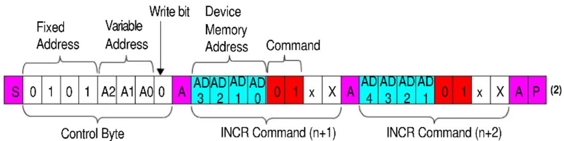
text_image
Fixed Address Variable Address Write bit Device Memory Address Command S 0 1 0 1 A2 A1 A0 0 A AD AD AD AD 0 1 x X A AD AD AD AD 0 1 x X A P (2) Control Byte INCR Command (n+1) INCR Command (n+2)Note1: Increment Command (INCR) only functions when accessing the volatile wiper registers (AD3:AD0 = 0h and 1h).
2: This command sequence does not need to terminate (using the Stop bit) and can change to any other desired command sequence (Increment, Read or Write).
FIGURE 7-7: I ^2 C Increment Command Sequence.
7.7 Decrement Wiper Normal and High Voltage
The Decrement Command provides a quick and easy method to modify the potentiometer's wiper by -1, with minimal overhead. The Decrement Command will only function on the volatile wiper setting memory locations 00h and 01h.
Note: Table 7-2 shows the valid addresses for the Decrement Wiper command. Other addresses are invalid.
When executing a Decrement Command, the volatile wiper setting will be altered from n to n-1 for each Decrement Command received. The value will decrement down to a minimum of 000h. If multiple Decrement Commands are received after the value has reached 000h, the value will not be decremented further. Table 7-5 shows the Increment Command versus the current volatile wiper value.
Refer to Figure 7-8 for the Decrement Command sequence. The sequence is terminated by the Stop condition. So when executing a continuous command string, The Increment command can be followed by any other valid command. This means that writes do not need to be to the same volatile memory address.
Note: The command sequence can go from an increment to any other valid command for the specified address.
The advantage of using a Decrement Command instead of a read-modify-write series of commands is speed and simplicity. The wiper will transition after each Command Acknowledge when accessing the volatile wiper registers.
TABLE 7-5: DECREMENT OPERATION VS. VOLATILE WIPER VALUE
| Current Wiper Setting | Wiper (W) Properties | Decrement Command Operates? | |
| 7-bit Pot | 8-bit Pot | ||
| 3FFh081h | 3FFh101h | Reserved(Full-Scale (W = A)) | No |
| 080h 1 | 00h Full-Scale (W = A) Yes | ||
| 07Fh041h | 0FFh081 | W = N | |
| 040h 0 | 80h W = N (Mid-Scale) Yes | ||
| 03Fh001h | 07Fh001 | W = N | |
| 000h 0 | 00h Zero | Scale (W = B) No | |
7.7.1 THE HIGH VOLTAGE COMMAND (HVC) SIGNAL
The High Voltage Command (HVC) signal is multiplexed with Address 0 (A0) and is used to indicate that the command, or sequence of commands, are in the High Voltage mode. An HVC/A0 pin voltage > V_HH (\~8.5V) puts the MCP45XX/46XX device into the High Voltage mode.
Note: There is a required delay after the HVC pin is driven to the V_IHH level to the 1st edge of the SCL pin.
The HVC pin has an internal resistor connection to the MCP45XX/46XXs internal V_DD signal.
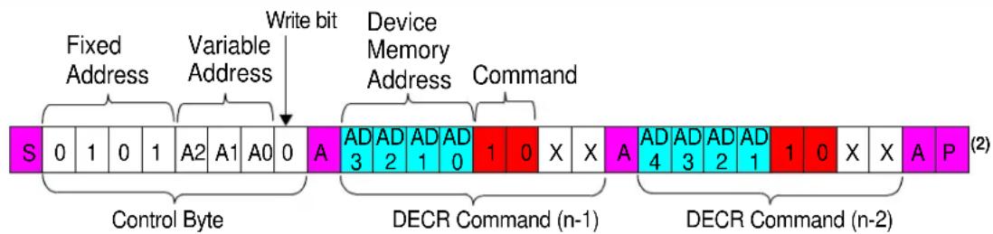
text_image
Fixed Address Variable Address Write bit S 0 1 0 1 A2 A1 A0 0 A AD 3 AD 2 AD 1 AD 0 1 0 X X A AD 4 AD 3 AD 2 AD 1 1 0 X X A P (2) Control Byte Device Memory Address Command DECR Command (n-1) DECR Command (n-2)Note1: Decrement Command (DECR) only functions when accessing the volatile wiper registers (AD3:AD0 = 0h and 1h).
2: This command sequence does not need to terminate (using the Stop bit) and can change to any other desired command sequence (INCR, Read, or Write).
FIGURE 7-8: I ^2 C Decrement Command Sequence.
8.0 APPLICATIONS EXAMPLES
Nonvolatile digital potentiometers have a multitude of practical uses in modern electronic circuits. The most popular uses include precision calibration of set point thresholds, sensor trimming, LCD bias trimming, audio attenuation, adjustable power supplies, motor control overcurrent trip setting, adjustable gain amplifiers and offset trimming. The MCP453X/455X/463X/465X devices can be used to replace the common mechanical trim pot in applications where the operating and terminal voltages are within CMOS process limitations ( V_DD = 2.7V to 5.5V).
8.1 Techniques to force the HVC pin to V_IHH
The circuit in Figure 8-1 shows a method using the TC1240A doubling charge pump. When the SHDN pin is HIGH, the TC1240A is off, and the level on the HVC pin is controlled by the PIC® microcontrollers (MCUs) IO2 pin.
When the SHDN pin is low, the TC1240A is on and the V_OUT voltage is 2 × V_DD . The resistor R_1 allows the HVC pin to go higher than the voltage such that the PIC MCU's IO2 pin "clamps" at approximately V_DD .
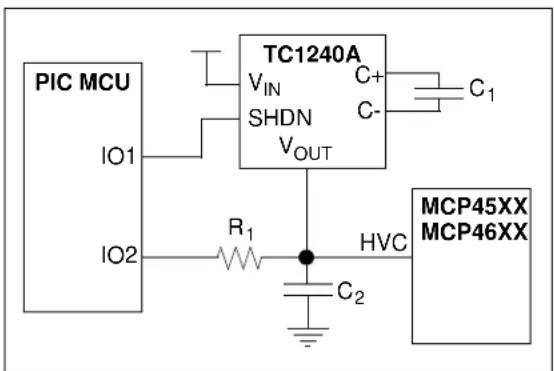
text_image
PIC MCU IO1 IO2 TC1240A VIN SHDN VOUT C+ C- C1 R1 HVC C2 MCP45XX MCP46XXFIGURE 8-1: Using the TC1240A to Generate the V_IHH Voltage.
The circuit in Figure 8-2 shows the method used on the MCP402X nonvolatile Digital Potentiometer Evaluation Board (Part Number: MCP402XEV). This method requires that the system voltage be approximately 5V. This ensures that when the PIC10F206 enters a brown-out condition, there is an insufficient voltage level on the HVC pin to change the stored value of the wiper. The MCP402X nonvolatile Digital Potentiometer Evaluation Board User's Guide (DS51546) contains a complete schematic.
GP0 is a general purpose I/O pin, while GP2 can either be a general purpose I/O pin or it can output the internal clock.
For the serial commands, configure the GP2 pin as an input (high impedance). The output state of the GP0 pin will determine the voltage on the HVC pin ( V_IL or V_IH ).
For high-voltage serial commands, force the GP0 output pin to output a high level ( V_OH ), and configure the GP2 pin to output the internal clock. This will form a charge pump and increase the voltage on the HVC pin (when the system voltage is approximately 5V).
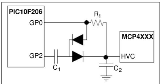
text_image
PIC10F206 GP0 R1 MCP4XXX GP2 C1 HVC C2FIGURE 8-2: MCP4XXX Nonvolatile Digital Potentiometer Evaluation Board (MCP402XEV) Implementation to Generate the V_IHH Voltage.
8.2 Using Shutdown
Figure 8-3 shows a possible application circuit where the independent terminals could be used. Disconnecting the wiper allows the transistor input to be taken to the Bias voltage level (disconnecting A and or B may be desired to reduce system current). Disconnecting Terminal A modifies the transistor input by the R_BW rheostat value to the Common B. Disconnecting Terminal B modifies the transistor input by the R_AW rheostat value to the Common A. The Common A and Common B connections could be connected to V_DD and V_SS .

text_image
Common A Input A W To base of Transistor (or Amplifier) Input B Common B Balance BiasFIGURE 8-3: Example Application Circuit using Terminal Disconnects.
8.3 Software Reset Sequence
Note: This technique is documented in AN1028.
At times it may become necessary to perform a Software Reset Sequence to ensure the MCP45XX/46XX device is in a correct and known Interface state. This technique only resets the state machine.
This is useful if the MCP45XX/46XX device powers up in an incorrect state (due to excessive bus noise, ...), or if the Master Device is reset during communication. Figure 8-4 shows the communication sequence to software reset the device.
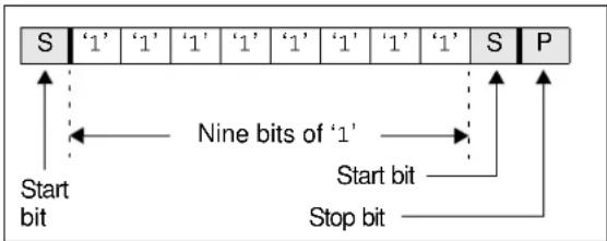
text_image
S '1' '1' '1' '1' '1' '1' '1' '1' S P Start bit Nine bits of '1' Start bit Stop bitFIGURE 8-4: Software Reset Sequence Format.
The 1st Start bit will cause the device to reset from a state in which it is expecting to receive data from the Master Device. This occurs since the device is monitoring the data bus in Receive mode and can detect the Start bit which forces an internal Reset.
The nine bits of '1' are used to force a Reset of those devices that could not be reset by the previous Start bit. This occurs only if the MCP45XX/46XX is driving an A bit on the I²C bus, or is in output mode (from a Read command) and is driving a data bit of '0' onto the PC bus. In both of these cases, the previous Start bit could not be generated due to the MCP45XX/46XX holding the bus low. By sending out nine '1' bits, it is ensured that the device will see an bit (the Master Device does not drive the I²C bus low to acknowledge the data sent by the MCP45XX/46XX), which also forces the MCP45XX/46XX to reset.
The 2nd Start bit is sent to address the rare possibility of an erroneous write. This could occur if the Master Device was reset while sending a Write command to the MCP45XX/46XX, AND then as the Master Device returns to normal operation and issues a Start condition, while the MCP45XX/46XX is issuing an Acknowledge. In this case, if the 2nd Start bit is not sent (and the Stop bit was sent) the MCP45XX/46XX could initiate a write cycle.
Note: The potential for this erroneous write ONLY occurs if the Master Device is reset while sending a Write command to the MCP45XX/46XX.
The Stop bit terminates the current PC bus activity. The MCP45XX/46XX wait to detect the next Start condition.
This sequence does not effect any other I^2C devices which may be on the bus, as they should disregard this as an invalid command.
8.4 Using the General Call Command
The use of the General Call Address Increment, Decrement, or Write commands is analogous to the "Load" feature (LDAC pin) on some DACs (such as the MCP4921). This allows all the devices to "Update" the output level "at the same time".
For some applications, the ability to update the wiper values at the same time may be a requirement, since they delay from writing to one wiper value and then the next may cause application issues. A possible example would be a "tuned" circuit that uses several MCP45XX/46XX in rheostat configuration. As the system condition changes (temperature, load, ...) these devices need to be changed (incremented/decremented) to adjust for the system change. These changes will either be in the same direction or in opposite directions. With the Potentiometer device, the customer can either select the PxB terminals (same direction) or the PxA terminal(s) (opposite direction).
Figure 8-6 shows that the update of six devices takes 6^T_I2CDLY time in “normal” operation, but only 1^T_I2CDLY time in “General Call” operation.
Note: The application system may need to partition the I²C bus into multiple busses to ensure that the MCP45XX/46XX General Call commands do not conflict with the General Call commands that the other I²C devices may have defined. Also if only a portion of the MCP45XX/46XX devices are to require this synchronous operation, then the devices that should not receive these commands should be on the second I²C bus.
Figure 8-5 shows two I²C bus configurations. In many cases, the single I²C bus configuration will be adequate. For applications that do not want all the MCP45XX/46XX devices to do General Call support or have a conflict with General Call commands, the multiple I²C bus configuration would be used.
Single I²C Bus Configuration

flowchart
graph TD
    A["Host Controller"] --> B["Device 1"]
    A --> C["Device 2"]
    A --> D["Device 3"]
    A --> E["Device 4"]
    A --> F["Device n"]
Multiple I²C Bus Configuration
flowchart
graph TD
    A["Host Controller"] --> B["Bus a"]
    A --> C["Bus b"]
    A --> D["Bus n"]
    B --> E["Device 1a"]
    B --> F["Device 2a"]
    B --> G["Device 3a"]
    B --> H["Device 4a"]
    C --> I["Device 1b"]
    C --> J["Device 2b"]
    C --> K["Device 3b"]
    C --> L["Device 4b"]
    D --> M["Device 1n"]
    D --> N["Device 2n"]
    D --> O["Device 3n"]
    D --> P["Device 4n"]
    E --> Q[●●●●●●●●●●●●●●●●●●●●●●●●●●●●●●●●●●●●●●●●●●●●●●●●●●●●●●●●●●●●●●●●●●●●●●●●●●●●●●●●●●●●●●●●●●●●●●●●●●●●○○○○○○○○○○○○○○○○○○○○○○○○○○○○○○○○○○○○○○○○○○○○○○○○○○○○○○○○○○○○○○○○○○○○○○○○○○○○○○○○○○○○○○○○○○○○○○○○○○○○ ○
FIGURE 8-5: Typical Application I ^2 C Bus Configurations.
Normal Operation

text_image
INC POT01 INC POT02 INC POT03 INC POT04 INC POT05 INC POT06 T12CDLY T12CDLY T12CDLY T12CDLY T12CDLY T12CDLYGeneral Call Operation

flowchart
graph LR
    A["INC POTs 01-06"] --> B["T12CDLY"]
    B --> C["INC POTs 01-06"]
    C --> D["T12CDLY"]
    D --> E["INC POTs 01-06"]
    E --> F["T12CDLY"]
    F --> G["INC POTs 01-06"]
    G --> H["T12CDLY"]
    H --> I["INC POTs 01-06"]
    I --> J["T12CDLY"]
T_I2CDLY= Time from one I^2C command completed to completing the next f^2C command.
FIGURE 8-6: Example Comparison of "Normal Operation" vs. "General Call Operation" Wiper Updates.
8.5 Implementing Log Steps with a Linear Digital Potentiometer
In audio volume control applications, the use of logarithmic steps is desirable since the human ear hears in a logarithmic manner. The use of a linear potentiometer can approximate a log potentiometer, but with fewer steps. An 8-bit potentiometer can achieve fourteen 3 dB log steps plus a 100% (0 dB) and a mute setting.
Figure 8-7 shows a block diagram of one of the MCP45X1 resistor networks being used to attenuate an input signal. In this case, the attenuation will be ground referenced. Terminal B can be connected to a common mode voltage, but the voltages on the A, B and Wiper terminals must not exceed the MCP45X1's V_DD/V_SS voltage limits.
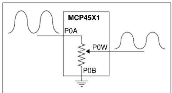
text_image
MCP45X1 P0A P0W P0BFIGURE 8-7: Signal Attenuation Block Diagram - Ground Referenced.
Equation 8-1 shows the equation to calculate voltage dB gain ratios for the digital potentiometer, while Equation 8-2 shows the equation to calculate resistance dB gain ratios. These two equations assume that the B terminal is connected to ground.
If terminal B is not directly resistively connected to ground, then this terminal B to ground resistance ( R_B2GND ) must be included into the calculation. Equation 8-3 shows this equation.
EQUATION 8-1: dB CALCULATIONS (VOLTAGE)
$$ L = 2 0 \times l o g _ {1 0} \left(\frac {V _ {O U T}}{V _ {I N}}\right) $$
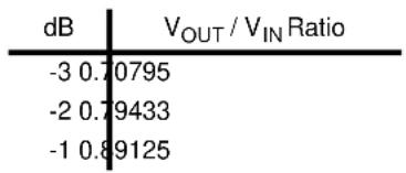
other
| dB | VOUT / VIN Ratio | |---|---| | -3 | 0.70795 | | -2 | 0.79433 | | -1 | 0.89125 |EQUATION 8-2: dB CALCULATIONS (RESISTANCE) - CASE 1
Terminal B connected to Ground (see Figure 8-7)
$$ L = 2 \times 0 _ {1 0} \left(\frac {R _ {B W}}{R _ {A B}}\right) g $$
EQUATION 8-3: dB CALCULATIONS (RESISTANCE) - CASE 2
Terminal B through R_B2GND to Ground
$$ L = 2 \times 0 _ {1 0} \left(\frac {R _ {B W} + R _ {B 2 G N D}}{R _ {A B}}\right) $$
Table 8-1 shows the codes that can be used for 8-bit digital potentiometers to implement the log attenuation. The table shows the wiper codes for -3 dB, -2 dB and -1 dB attenuation steps. This table also shows the calculated attenuation based on the wiper code's linear step. Calculated attenuation values less than the desired attenuation are shown with red text. At lower wiper code values, the attenuation may skip a step; if this occurs the next attenuation value is colored magenta to highlight that a skip occurred. For example, in the -3 dB column the -48 dB value is highlighted since the -45 dB step could not be implemented (there are no wiper codes between 2 and 1).
TABLE 8-1: LINEAR TO LOG ATTENUATION FOR 8-BIT DIGITAL POTENTIOMETERS
| # of Steps | -3 dB Steps -2 dB Steps | -1 dB Steps | |||||||
| Desired Attenuation | Wiper Code | Calculated Attenuation (1) | Desired Attenuation | Wiper Code | Calculated Attenuation (1) | Desired Attenuation | Wiper Code | Calculated Attenuation (1) | |
| 0 | 0 dB | 256 | 0 dB | 0 dB | 256 | 0 dB | 0 dB | 256 | 0 dB |
| 1 | -3 dB | 181 | -3.011 dB | -2 dB | 203 | -2.015 dB | -1 dB | 228 | -1.006 dB |
| 2 | -6 dB | 128 | -6.021 dB | -4 dB | 162 | -3.975 dB | -2 dB | 203 | -2.015 dB |
| 3 | -9dB | 91 | -8.984 dB | -6 dB | 128 | -6.021 dB | -3 dB | 181 | -3.011 dB |
| 4 | -12 dB | 64 | -12.041 dB | -8 dB | 102 | -7.993 dB | -4 dB | 162 | -3.975 dB |
| 5 | -15 dB | 46 | -14.910 dB | -10 dB | 81 | -9.995 dB | -5 dB | 144 | -4.998 dB |
| 6 | -18 dB | 32 | -18.062 dB | -12 dB | 64 | -12.041 dB | -6 dB | 128 | -6.021 dB |
| 7 | -21 dB | 23 | -20.930 dB | -14 dB | 51 | -14.013 dB | -7 dB | 114 | -7.027 dB |
| 8 | -24 dB | 16 | -24.082 dB | -16 dB | 41 | -15.909 dB | -8 dB | 102 | -7.993 dB |
| 9 | -27 dB | 11 | -27.337 dB | -18 dB | 32 | -18.062 dB | -9 dB | 91 | -8.984 dB |
| 10 | -30 dB | 8 | -30.103 dB | -20 dB | 26 | -19.865 dB | -10 dB | 81 | -9.995 dB |
| 11 | -33 dB | 6 | -32.602 dB | -22 dB | 20 | -22.144 dB | -11 dB | 72 | -11.018 dB |
| 12 | -36 dB | 4 | -36.124 dB | -24 dB | 16 | -24.082 dB | -12 dB | 64 | -12.041 dB |
| 13 | -39 dB | 3 | -38.622 dB | -26 dB | 13 | -25.886 dB | -13 dB | 57 | -13.047 dB |
| 14 | -42 dB | 2 | -42.144 dB | -28 dB | 10 | -28.165 dB | -14 dB | 51 | -14.013 dB |
| 15 | -48 dB | 1 | -48.165 dB | -30 dB | 8 | -30.103 dB | -15 dB | 46 | -14.910 dB |
| 16 | Mute | 0 | Mute | -32 dB | 6 | -32.602 dB | -16 dB | 41 | -15.909 dB |
| 17 | -34 dB | 5 | -34.185 dB | -17 dB | 36 | -17.039 dB | |||
| 18 | -36 dB | 4 | -36.124 dB | -18 dB | 32 | -18.062 dB | |||
| 19 | -38 dB | 3 | -38.622 dB | -19 dB | 29 | -18.917 dB | |||
| 20 | -42 dB | 2 | -42.144 dB | -20 dB | 26 | -19.865 dB | |||
| 21 | -48 dB | 1 | -48.165 dB | -21 dB | 23 | -20.930 dB | |||
| 22 | Mute | 0 | Mute | -22 dB | 20 | -22.144 dB | |||
| 23 | -23 dB | 18 | -23.059 dB | ||||||
| 24 | -24 dB | 16 | -24.082 dB | ||||||
| 25 | -25 dB | 14 | -25.242 dB | ||||||
| 26 | -26 dB | 13 | -25.886 dB | ||||||
| 27 | -27dB | 11 | -27.337 dB | ||||||
| 28 | -28 dB | 10 | -28.165 dB | ||||||
| 29 | -29 dB | 9 | -29.080 dB | ||||||
| 30 | -30 dB | 8 | -30.103 dB | ||||||
| 31 | -31 dB | 7 | -31.263 dB | ||||||
| 32 | -33 dB | 6 | -32.602 dB | ||||||
| 33 | -34 dB | 5 | -34.185 dB | ||||||
| 34 | -36 dB | 4 | -36.124 dB | ||||||
| 35 | -39 dB | 3 | -38.622 dB | ||||||
| 36 | -42 dB | 2 | -42.144 dB | ||||||
| 37 | -48 dB | 1 | -48.165 dB | ||||||
| 38 | Mute | 0 | Mute | ||||||
Note 1: Attenuation values do not include errors from Digital Potentiometer errors, such as Full Scale Error or Zero Scale Error.
8.6 Design Considerations
In the design of a system with the MCP4XXX devices, the following considerations should be taken into account:
• Power Supply Considerations
- Layout Considerations
8.6.1 POWER SUPPLY
CONSIDERATIONS
The typical application will require a bypass capacitor in order to filter high-frequency noise, which can be induced onto the power supply's traces. The bypass capacitor helps to minimize the effect of these noise sources on signal integrity. Figure 8-8 illustrates an appropriate bypass strategy.
In this example, the recommended bypass capacitor value is 0.1 F. This capacitor should be placed as close (within 4 mm) to the device power pin ( V_DD ) as possible.
The power source supplying these devices should be as clean as possible. If the application circuit has separate digital and analog power supplies, V_DD and V_SS should reside on the analog plane.

text_image
VDD 0.1 μF A W B MCP453X/455X/ 463X/465X SCL SDA PIC® Microcontroller VSS VSS 0.1 μF VDDFIGURE 8-8: Typical Microcontroller Connections.
8.6.2 LAYOUT CONSIDERATIONS
Inductively-coupled AC transients and digital switching noise can degrade the input and output signal integrity, potentially masking the MCP4XXX's performance. Careful board layout minimizes these effects and increases the Signal-to-Noise Ratio (SNR). Multi-layer boards utilizing a low-inductance ground plane, isolated inputs, isolated outputs and proper decoupling are critical to achieving the performance that the silicon is capable of providing. Particularly harsh environments may require shielding of critical signals.
If low noise is desired, breadboards and wire-wrapped boards are not recommended.
8.6.3 RESISTOR TEMPCO
Characterization curves of the resistor temperature coefficient (Tempco) are shown in Figure 2-12, Figure 2-25, Figure 2-38, and Figure 2-51.
These curves show that the resistor network is designed to correct for the change in resistance as temperature increases. This technique reduces the end-to-end change in R_AB resistance.
8.6.4 HIGH VOLTAGE TOLERANT PINS
High Voltage support ( V_IHH ) on the Serial Interface pins is for compatibility with the nonvolatile devices.
9.0 DEVICE OPTIONS
Additional, custom devices are available. These devices have weak pull-up resistors on the SDA and SCL pins. This is useful for applications where the wiper value is programmed during manufacture and not modified by the system during normal operation.
Please contact your local sales office for current information and minimum volume requirements.
9.1 Custom Options
The custom device will have a "P" (for Pull-up) after the resistance version in the Product Identification System. These devices will not be available through Microchip's online Microchip Direct, nor Microchip's Sample systems.
Example part number:
MCP4631-103PE/ST
NOTES:
10.0 DEVELOPMENT SUPPORT
10.1 Development Tools
Several development tools are available to assist in your design and evaluation of the MCP45XX/46XX devices. The currently available tools are shown in Table 10-1.
These boards may be purchased directly from the Microchip web site at www.microchip.com.
10.2 Technical Documentation
Several additional technical documents are available to assist you in your design and development. These technical documents include Application Notes, Technical Briefs, and Design Guides. Table 10-2 shows some of these documents.
TABLE 10-1: DEVELOPMENT TOOLS
| Board Name Part # Supported Devices | ||
| MCP46XX PICTail Plus Daughter Board ^(2) | MCP46XXDM-PTPLS | MCP46XX |
| MCP4XXX Digital Potentiometer Daughter Board ^(1) | MCP4XXXDM-DB MCP | 42XXX, MCP42XX, MCP46XX,MCP4021, and MCP4011 |
| MCP46XXEV Evaluation Board MCP46XXEV | MCP4631, MCP4641 | MCP4651,MCP4661 |
| TSSOP-20 and SSOP-20 Evaluation Board | TSSOP20EV | MCP4631, MCP4641, MCP4651,MCP4661 |
| 8-pin SOIC/MSOP/TSSOP/DIP Evaluation Board | SOIC8EV | Any 8-pin device in DIP, SOIC,MSOP, or TSSOP package |
| 14-pin SOIC/MSOP/DIP Evaluation Board | SOIC14EV | Any 14-pin device in DIP, SOIC, orMSOP package |
Note 1: Requires the use of a PICDEM Demo Board (see User's Guide for details) and the SOIC14EV board to convert an MCP46XX device in TSSOP package to the DIP footprint.
2: Requires the use of the PIC24 Explorer 16 Demo Board (see User's Guide for details)
TABLE 10-2: TECHNICAL DOCUMENTATION
| Application Note Number | Title | Literature # |
| AN1316 | Using Digital Potentiometers for Programmable Amplifier Gain | DS01316 |
| AN1080 | Understanding Digital Potentiometers Resistor Variations | DS01080 |
| AN737 | Using Digital Potentiometers to Design Low Pass Adjustable Filters | DS00737 |
| AN692 | Using a Digital Potentiometer to Optimize a Precision Single Supply Photo Detect | DS00692 |
| AN691 | Optimizing the Digital Potentiometer in Precision Circuits | DS00691 |
| AN219 | Comparing Digital Potentiometers to Mechanical Potentiometers | DS00219 |
| — | Digital Potentiometer Design Guide | DS22017 |
| — | Signal Chain Design Guide | DS21825 |
NOTES:
11.0 PACKAGING INFORMATION
11.1 Package Marking Information
8-Lead DFN (3x3)
| XXXX |
| XYWW |
| NNN |
| Part Number Code | Part Number Code | |
| MCP4531-502E/MF | DACA | MCP4532-502E/MF |
| MCP4531-103E/MF | DACB | MCP4532-103E/MF DACF |
| MCP4531-104E/MF | DACD | MCP4532-104E/MF |
| MCP4531-503E/MF | DACC | MCP4532-503E/MF |
| MCP4551-502E/MF | DACT | MCP4552-502E/MF |
| MCP4551-103E/MF | DACU | MCP4552-103E/MF |
| MCP4551-104E/MF | DACW MC | P4552-104E/MF DADA |
| MCP4551-503E/MF | DACV | MCP4552-503E/MF |
Example:
| DACA1028256 |
8-Lead MSOP
| XXXXXX |
| YWWNNN |
| Part Number Code | Part Number Code | ||
| MCP4531-103E/MS | 453113 | MCP4532-103E/MS | 453213 |
| MCP4531-104E/MS | 453114 | MCP4532-104E/MS | 453214 |
| MCP4531-502E/MS | 453152 | MCP4532-502E/MS | 453252 |
| MCP4531-503E/MS | 453153 | MCP4532-503E/MS | 453253 |
| MCP4551-103E/MS | 455113 | MCP4552-103E/MS | 455213 |
| MCP4551-104E/MS | 455114 | MCP4552-104E/MS | 455214 |
| MCP4551-502E/MS | 455152 | MCP4552-502E/MS | 455252 |
| MCP4551-503E/MS | 455153 | MCP4552-503E/MS | 455253 |
Example
| 453113028256 |
Legend: XX...X Customer-specific information
Y Year code (last digit of calendar year)
YY Year code (last 2 digits of calendar year)
WW Week code (week of January 1 is week '01')
NNN Alphanumeric traceability code
ePb-free JEDEC designator for Matte Tin (Sn)
* This package is Pb-free. The Pb-free JEDEC designator (e3) can be found on the outer packaging for this package.
Note: In the event the full Microchip part number cannot be marked on one line, it will be carried over to the next line, thus limiting the number of available characters for customer-specific information.
Package Marking Information (Continued)
10-Lead DFN (3x3)
| Part Number Code | Part Number Code | |
| MCP4632-502E/MF | AABA MCP4652-502E/MF AAKA | |
| MCP4632-103E/MF | AACA MCP4652-103E/MF AALA | |
| MCP4632-104E/MF | AAEA MCP4652-104E/MF AAPA | |
| MCP4632-503E/MF | AADA MCP4652-503E/MF AAMA |
Example:
10-Lead MSOP
| Part Number Code | Part Number Code | |
| MCP4632-502E/UN | 463252 MCP4652-502E/UN 4652 | 52 |
| MCP4632-103E/UN | 463213 MCP4652-103E/UN 4652 | 13 |
| MCP4632-104E/UN | 463214 MCP4652-104E/UN 4652 | 14 |
| MCP4632-503E/UN | 463253 MCP4652-503E/UN 4652 | 53 |
Example
14-Lead TSSOP (MCP4631, MCP4651)
text_image
XXXXXXXX YYWW NNNExample
text_image
4631502E 1028 25616-Lead QFN (MCP4631, MCP4651)
text_image
XXXXX XXXXXX XXXXXX YYWWNNNExample
text_image
4631 502 E/ML^e3 0282568-Lead Plastic Dual Flat, No Lead Package (MF) - 3x3x0.9mm Body [DFN]
Note: For the most current package drawings, please see the Microchip Packaging Specification located at http://www.microchip.com/packaging
![Microchip mcp4652 - 8-Lead Plastic Dual Flat, No Lead Package (MF) - 3x3x0.9mm Body [DFN] - 1](/content/2026/06/1219334/images/26a26cd1927f278309d88db24271a426f4a934c493ee21bc1bf3f41824f13f4d.jpg)
Microchip Technology Drawing No. C04-062C Sheet 1 of 2
8-Lead Plastic Dual Flat, No Lead Package (MF) - 3x3x0.9mm Body [DFN]
Note: For the most current package drawings, please see the Microchip Packaging Specification located at http://www.microchip.com/packaging
![Microchip mcp4652 - 8-Lead Plastic Dual Flat, No Lead Package (MF) - 3x3x0.9mm Body [DFN] - 1](/content/2026/06/1219334/images/148a015be22334ba29d248d320fe371bbc775c0071b6b0a9da32061a8b16e85e.jpg)
text_image
NOTE 2| Units | MILLIMETERS | |||
| Dimension Limits | MIN | NOM | MAX | |
| Number of Pins | N | 8 | ||
| Pitch | e | 0.65 BSC | ||
| Overall Height | A | 0.80 | 0.90 | 1.00 |
| Standoff | A1 | 0.00 | 0.02 | 0.05 |
| Contact Thickness | A3 | 0.20 REF | ||
| Overall Length | D | 3.00 BSC | ||
| Exposed Pad Width | E2 | 1.34 | - | 1.60 |
| Overall Width | E | 3.00 BSC | ||
| Exposed Pad Length | D2 | 1.60 | - | 2.40 |
| Contact Width | b | 0.25 | 0.30 | 0.35 |
| Contact Length | L | 0.20 | 0.30 | 0.55 |
| Contact-to-Exposed Pad | K | 0.20 | - | - |
Notes:
- Pin 1 visual index feature may vary, but must be located within the hatched area.
- Package may have one or more exposed tie bars at ends.
- Package is saw singulated
- Dimensioning and tolerancing per ASME Y14.5M
BSC: Basic Dimension. Theoretically exact value shown without tolerances.
REF: Reference Dimension, usually without tolerance, for information purposes only.
Microchip Technology Drawing No. C04-062C Sheet 2 of 2
8-Lead Plastic Dual Flat, No Lead Package (MF) - 3x3x0.9mm Body [DFN]
Note: For the most current package drawings, please see the Microchip Packaging Specification located at http://www.microchip.com/packaging
![Microchip mcp4652 - 8-Lead Plastic Dual Flat, No Lead Package (MF) - 3x3x0.9mm Body [DFN] - 1](/content/2026/06/1219334/images/13da82df90dd24ab5597d1674517af1e78794e5d9120b6e668d71f527936808c.jpg)
text_image
W2 G C1 T2 E X1 Y1 SILK SCREENRECOMMENDED LAND PATTERN
| Units | MILLIMETERS | |||
| Dimension Limits | MIN | NOM | MAX | |
| Contact Pitch | E | 0.65 BSC | ||
| Optional Center Pad Width | W2 | 2.40 | ||
| Optional Center Pad Length | T2 | 1.55 | ||
| Contact Pad Spacing | C1 | 3.10 | ||
| Contact Pad Width (X8) | X1 | 0.35 | ||
| Contact Pad Length (X8) | Y1 | 0.65 | ||
| Distance Between Pads | G | 0.30 | ||
Notes:
1. Dimensioning and tolerancing per ASME Y14.5M
BSC: Basic Dimension. Theoretically exact value shown without tolerances.
Microchip Technology Drawing No. C04-2062B
8-Lead Plastic Micro Small Outline Package (MS) [MSOP]
Note: For the most current package drawings, please see the Microchip Packaging Specification located at http://www.microchip.com/packaging
![Microchip mcp4652 - 8-Lead Plastic Micro Small Outline Package (MS) [MSOP] - 1](/content/2026/06/1219334/images/28e5dd37b3d895f0e48bf9fe0b39c7c8990faf2aab421944b845ec30c7e52823.jpg)
text_image
2X 0.20 H D/2 A E/2 D E1/2 E1 N E E/2 NOTE 1 1 2 N/2 0.25 C e B NX b 0.13 M C A-B D TOP VIEW SIDE VIEW A A2 A1 0.10 C SEATING PLANE C H SEE DETAIL C END VIEWMicrochip Technology Drawing C04-111C Sheet 1 of 2
8-Lead Plastic Micro Small Outline Package (MS) [MSOP]
Note: For the most current package drawings, please see the Microchip Packaging Specification located at http://www.microchip.com/packaging
![Microchip mcp4652 - 8-Lead Plastic Micro Small Outline Package (MS) [MSOP] - 1](/content/2026/06/1219334/images/40b642e829ea0e6b61e5d215c7bba30748144a7a3ad2af473946a25103c3ee1f.jpg)
text_image
SEATING PLANE L (L1) GAUGE PLANE c φDETAIL C
| Units | MILLIMETERS | |||
| Dimension Limits | MIN | NOM | MAX | |
| Number of Pins | N | 8 | ||
| Pitch | e | 0.65 BSC | ||
| Overall Height | A | - | - | 1.10 |
| Molded Package Thickness | A2 | 0.75 | 0.85 | 0.95 |
| Standoff | A1 | 0.00 | - | 0.15 |
| Overall Width | E | 4.90 BSC | ||
| Molded Package Width | E1 | 3.00 BSC | ||
| Overall Length | D | 3.00 BSC | ||
| Foot Length | L | 0.40 | 0.60 | 0.80 |
| Footprint | L1 | 0.95 REF | ||
| Foot Angle | 0° | - | 8° | |
| Lead Thickness | c | 0.08 | - | 0.23 |
| Lead Width | b | 0.22 | - | 0.40 |
Notes:
- Pin 1 visual index feature may vary, but must be located within the hatched area.
- Dimensions D and E1 do not include mold flash or protrusions. Mold flash or protrusions shall not exceed 0.15mm per side.
- Dimensioning and tolerancing per ASME Y14.5M. BSC: Basic Dimension. Theoretically exact value shown without tolerances. REF: Reference Dimension, usually without tolerance, for information purposes only.
Microchip Technology Drawing C04-111C Sheet 2 of 2
8-Lead Plastic Micro Small Outline Package (MS) [MSOP]
Note: For the most current package drawings, please see the Microchip Packaging Specification located at http://www.microchip.com/packaging
![Microchip mcp4652 - 8-Lead Plastic Micro Small Outline Package (MS) [MSOP] - 1](/content/2026/06/1219334/images/e5c9314dd1a84f461d26101546a71688bb8bd8102df405061325498094744f82.jpg)
text_image
X Y Z C G1 SILK SCREEN GX ERECOMMENDED LAND PATTERN
| Units | MILLIMETERS | |||
| Dimension Limits | MIN | NOM | MAX | |
| Contact Pitch | E | 0.65 BSC | ||
| Contact Pad Spacing | C | 4.40 | ||
| Overall Width | Z | 5.85 | ||
| Contact Pad Width (X8) | X1 | 0.45 | ||
| Contact Pad Length (X8) | Y1 | 1.45 | ||
| Distance Between Pads | G1 | 2.95 | ||
| Distance Between Pads | GX | 0.20 | ||
Notes:
1. Dimensioning and tolerancing per ASME Y14.5M
BSC: Basic Dimension. Theoretically exact value shown without tolerances.
Microchip Technology Drawing No. C04-2111A
10-Lead Plastic Dual Flat, No Lead Package (MF) - 3x3x0.9mm Body [DFN]
Note: For the most current package drawings, please see the Microchip Packaging Specification located at http://www.microchip.com/packaging
![Microchip mcp4652 - 10-Lead Plastic Dual Flat, No Lead Package (MF) - 3x3x0.9mm Body [DFN] - 1](/content/2026/06/1219334/images/b2b66402f6554791419a6b12a9d918ccc5559d41a2cd0b063624ae3a6d5637da.jpg)
Microchip Technology Drawing No. C04-063C Sheet 1 of 2
10-Lead Plastic Dual Flat, No Lead Package (MF) - 3x3x0.9mm Body [DFN]
Note: For the most current package drawings, please see the Microchip Packaging Specification located at http://www.microchip.com/packaging
![Microchip mcp4652 - 10-Lead Plastic Dual Flat, No Lead Package (MF) - 3x3x0.9mm Body [DFN] - 1](/content/2026/06/1219334/images/7d4874d1c32d7cacfdaac9f9d194f4ba6c6b3b7d21db8ed8c5f74264f0ca9df4.jpg)
text_image
NOTE 2| Units | MILLIMETERS | |||
| Dimension Limits | MIN | NOM | MAX | |
| Number of Pins | N | 10 | ||
| Pitch | e | 0.50 BSC | ||
| Overall Height | A | 0.80 | 0.90 | 1.00 |
| Standoff | A1 | 0.00 | 0.02 | 0.05 |
| Contact Thickness | A3 | 0.20 REF | ||
| Overall Length | D | 3.00 BSC | ||
| Exposed Pad Length | D2 | 2.15 | 2.35 | 2.45 |
| Overall Width | E | 3.00 BSC | ||
| Exposed Pad Width | E2 | 1.40 | 1.50 | 1.75 |
| Contact Width | b | 0.18 | 0.25 | 0.30 |
| Contact Length | L | 0.30 | 0.40 | 0.50 |
| Contact-to-Exposed Pad | K | 0.20 | - | - |
Notes:
- Pin 1 visual index feature may vary, but must be located within the hatched area.
- Package may have one or more exposed tie bars at ends.
- Package is saw singulated.
- Dimensioning and tolerancing per ASME Y14.5M.
BSC: Basic Dimension. Theoretically exact value shown without tolerances.
REF: Reference Dimension, usually without tolerance, for information purposes only.
Microchip Technology Drawing No. C04-063C Sheet 2 of 2
10-Lead Plastic Dual Flat, No Lead Package (MF) - 3x3x0.9mm Body [DFN]
Note: For the most current package drawings, please see the Microchip Packaging Specification located at http://www.microchip.com/packaging
![Microchip mcp4652 - 10-Lead Plastic Dual Flat, No Lead Package (MF) - 3x3x0.9mm Body [DFN] - 1](/content/2026/06/1219334/images/353029898bf8652ba3a826a52b0ba15e5c634dcc053e9ca2c583a9ac581bfdbc.jpg)
text_image
W2 G Y1 C1 T2 E X1 SILK SCREENRECOMMENDED LAND PATTERN
| Units | MILLIMETERS | |||
| Dimension Limits | MIN | NOM | MAX | |
| Contact Pitch | E | 0.50 BSC | ||
| Optional Center Pad Width | W2 | 2.48 | ||
| Optional Center Pad Length | T2 | 1.55 | ||
| Contact Pad Spacing | C1 | 3.10 | ||
| Contact Pad Width (X10) | X1 | 0.30 | ||
| Contact Pad Length (X10) | Y1 | 0.65 | ||
| Distance Between Pads | G | 0.20 | ||
Notes:
1. Dimensioning and tolerancing per ASME Y14.5M
BSC: Basic Dimension. Theoretically exact value shown without tolerances.
Microchip Technology Drawing No. C04-2063B
10-Lead Plastic Micro Small Outline Package (UN) [MSOP]
Note: For the most current package drawings, please see the Microchip Packaging Specification located at http://www.microchip.com/packaging
![Microchip mcp4652 - 10-Lead Plastic Micro Small Outline Package (UN) [MSOP] - 1](/content/2026/06/1219334/images/814c3a62a33d474da6b60b13d431852e1361d88e285d550bfff895252ac32991.jpg)
text_image
2X 0.20 H D/2 A E/2 D E1/2 E1 N E NOTE 1 1 2 N/2 B e NX b 0.25 C TOP VIEW A A2 A1 SIDE VIEW 0.13 M C A-B D C SEATING PLANE H SEE DETAIL C END VIEWMicrochip Technology Drawing C04-021C Sheet 1 of 2
10-Lead Plastic Micro Small Outline Package (UN) [MSOP]
Note: For the most current package drawings, please see the Microchip Packaging Specification located at http://www.microchip.com/packaging
![Microchip mcp4652 - 10-Lead Plastic Micro Small Outline Package (UN) [MSOP] - 1](/content/2026/06/1219334/images/fc36c45a6e326b782073c407f198d31c6d93a47817b76054991a9b7a546c5ab3.jpg)
text_image
SEATING PLANE L (L1) GAUGE PLANE c φ DETAIL C| Units | MILLIMETERS | |||
| Dimension Limits | MIN | NOM | MAX | |
| Number of Pins | N | 10 | ||
| Pitch | e | 0.50 BSC | ||
| Overall Height | A | - | - | 1.10 |
| Molded Package Thickness | A2 | 0.75 | 0.85 | 0.95 |
| Standoff | A1 | 0.00 | - | 0.15 |
| Overall Width | E | 4.90 BSC | ||
| Molded Package Width | E1 | 3.00 BSC | ||
| Overall Length | D | 3.00 BSC | ||
| Foot Length | L | 0.40 | 0.60 | 0.80 |
| Footprint | L1 | 0.95 REF | ||
| Foot Angle | φ | 0° | - | 8° |
| Lead Thickness | c | 0.08 | - | 0.23 |
| Lead Width | b | 0.15 | - | 0.33 |
Notes:
- Pin 1 visual index feature may vary, but must be located within the hatched area.
- Dimensions D and E1 do not include mold flash or protrusions. Mold flash or protrusions shall not exceed 0.15mm per side.
- Dimensioning and tolerancing per ASME Y14.5M. BSC: Basic Dimension. Theoretically exact value shown without tolerances. REF: Reference Dimension, usually without tolerance, for information purposes only.
Microchip Technology Drawing C04-021C Sheet 2 of 2
10-Lead Plastic Micro Small Outline Package (UN) [MSOP]
Note: For the most current package drawings, please see the Microchip Packaging Specification located at http://www.microchip.com/packaging
![Microchip mcp4652 - 10-Lead Plastic Micro Small Outline Package (UN) [MSOP] - 1](/content/2026/06/1219334/images/cf423c1cf70f82685242b088288cd0e0c05b42047eb14e6065c4b7a54cf8e8a3.jpg)
text_image
X Y Z C G1 SILK SCREEN GX ERECOMMENDED LAND PATTERN
| Units | MILLIMETERS | |||
| Dimension Limits | MIN | NOM | MAX | |
| Contact Pitch | E | 0.50 BSC | ||
| Contact Pad Spacing | C | 4.40 | ||
| Overall Width | Z | 5.80 | ||
| Contact Pad Width (X10) | X1 | 0.30 | ||
| Contact Pad Length (X10) | Y1 | 1.40 | ||
| Distance Between Pads | G1 | 3.00 | ||
| Distance Between Pads | GX | 0.20 | ||
Notes:
1. Dimensioning and tolerancing per ASME Y14.5M
BSC: Basic Dimension. Theoretically exact value shown without tolerances.
Microchip Technology Drawing No. C04-2021A
14-Lead Plastic Thin Shrink Small Outline (ST) - 4.4 mm Body [TSSOP]
Note: For the most current package drawings, please see the Microchip Packaging Specification located at http://www.microchip.com/packaging
![Microchip mcp4652 - 14-Lead Plastic Thin Shrink Small Outline (ST) - 4.4 mm Body [TSSOP] - 1](/content/2026/06/1219334/images/594ed4e7e1ab14241e088b9171a70d178bddb46147deffb102d22bbf716d5e45.jpg)
![Microchip mcp4652 - 14-Lead Plastic Thin Shrink Small Outline (ST) - 4.4 mm Body [TSSOP] - 2](/content/2026/06/1219334/images/857bec92ceb497d48232cbc0df6a3f47fb0f96279c308773957c1c90befbc739.jpg)
text_image
0.10 C B A SEATING PLANE C A D A2 A A1 14X b Ø 0.10 M C B A SIDE VIEWMicrochip Technology Drawing C04-087C Sheet 1 of 2
14-Lead Plastic Thin Shrink Small Outline (ST) - 4.4 mm Body [TSSOP]
Note: For the most current package drawings, please see the Microchip Packaging Specification located at http://www.microchip.com/packaging
![Microchip mcp4652 - 14-Lead Plastic Thin Shrink Small Outline (ST) - 4.4 mm Body [TSSOP] - 1](/content/2026/06/1219334/images/e710e99f38c603a6176fb5f8c24a39496642be251c53bf9afbd328a436b8f3df.jpg)
natural_image
Isometric line drawing of an integrated circuit chip with multiple pins (no text or symbols)| Units | MILLIMETERS | |||
| Dimension Limits | MIN | NOM | MAX | |
| Number of Pins | N | 14 | ||
| Pitch | e | 0.65 BSC | ||
| Overall Height | A | - | - | 1.20 |
| Molded Package Thickness | A2 | 0.80 | 1.00 | 1.05 |
| Standoff | A1 | 0.05 | - | 0.15 |
| Overall Width | E | 6.40 BSC | ||
| Molded Package Width | E1 | 4.30 | 4.40 | 4.50 |
| Molded Package Length | D | 4.90 | 5.00 | 5.10 |
| Foot Length | L | 0.45 | 0.60 | 0.75 |
| Footprint | (L1) | 1.00 REF | ||
| Foot Angle | φ | 0° | - | 8° |
| Lead Thickness | c | 0.09 | - | 0.20 |
| Lead Width | b | 0.19 | - | 0.30 |
Notes:
- Pin 1 visual index feature may vary, but must be located within the hatched area.
- Dimensions D and E1 do not include mold flash or protrusions. Mold flash or protrusions shall not exceed 0.15mm per side.
- Dimensioning and tolerancing per ASME Y14.5M BSC: Basic Dimension. Theoretically exact value shown without tolerances. REF: Reference Dimension, usually without tolerance, for information purposes only.
Microchip Technology Drawing No. C04-087C Sheet 2 of 2
14-Lead Plastic Thin Shrink Small Outline (ST) - 4.4 mm Body [TSSOP]
Note: For the most current package drawings, please see the Microchip Packaging Specification located at http://www.microchip.com/packaging
![Microchip mcp4652 - 14-Lead Plastic Thin Shrink Small Outline (ST) - 4.4 mm Body [TSSOP] - 1](/content/2026/06/1219334/images/5514cf6f23ceafc98d38dbc0a0a579101b6ac7d8d733bfb1ceaa42a4e7956608.jpg)
text_image
C1 E G X1 Y1 SILK SCREENRECOMMENDED LAND PATTERN
| Units | MILLIMETERS | |||
| Dimension Limits | MIN | NOM | MAX | |
| Contact Pitch | E | 0.65 BSC | ||
| Contact Pad Spacing | C1 | 5.90 | ||
| Contact Pad Width (X14) | X1 | 0.45 | ||
| Contact Pad Length (X14) | Y1 | 1.45 | ||
| Distance Between Pads | G | 0.20 | ||
Notes:
1. Dimensioning and tolerancing per ASME Y14.5M
BSC: Basic Dimension. Theoretically exact value shown without tolerances.
Microchip Technology Drawing No. C04-2087A
16-Lead Plastic Quad Flat, No Lead Package (ML) - 4x4x0.9 mm Body [QFN]
Note: For the most current package drawings, please see the Microchip Packaging Specification located at http://www.microchip.com/packaging
![Microchip mcp4652 - 16-Lead Plastic Quad Flat, No Lead Package (ML) - 4x4x0.9 mm Body [QFN] - 1](/content/2026/06/1219334/images/d00d253c5ec7f5ad93337ec3e89edf2fb4bc653e6ef7cb048bbfb0c1620e576a.jpg)
| Units | MILLIMETERS | |||
| Dimension Limits | MIN NOM MAX | |||
| Number of Pins N 16 | ||||
| Pitch e 0.65 BSC | ||||
| Overall Height | A | 0.80 | 0.90 | 1.00 |
| Standoff | A1 | 0.00 | 0.02 | 0.05 |
| Contact Thickness | A3 | 0.20 REF | ||
| Overall Width | E | 4.00 BSC | ||
| Exposed Pad Width | E2 | 2.50 | 2.65 | 2.80 |
| Overall Length | D | 4.00 BSC | ||
| Exposed Pad Length | D2 | 2.50 | 2.65 | 2.80 |
| Contact Width | b | 0.25 | 0.30 | 0.35 |
| Contact Length | L | 0.30 | 0.40 | 0.50 |
| Contact-to-Exposed Pad | K | 0.20 | - | - |
Notes:
- Pin 1 visual index feature may vary, but must be located within the hatched area.
- Package is saw singulated.
- Dimensioning and tolerancing per ASME Y14.5M.
BSC: Basic Dimension. Theoretically exact value shown without tolerances.
REF: Reference Dimension, usually without tolerance, for information purposes only.
Microchip Technology Drawing C04-127B
16-Lead Plastic Quad Flat, No Lead Package (ML) - 4x4x0.9mm Body [QFN]
Note: For the most current package drawings, please see the Microchip Packaging Specification located at http://www.microchip.com/packaging
![Microchip mcp4652 - 16-Lead Plastic Quad Flat, No Lead Package (ML) - 4x4x0.9mm Body [QFN] - 1](/content/2026/06/1219334/images/55ad22f12fdf886517408bfe9b7ae421a81d23b6a882e7e9cc847921c8cc8c9f.jpg)
text_image
C1 W2 C2 T2 E G Y1 X1 SILK SCREENRECOMMENDED LAND PATTERN
| Units | MILLIMETERS | |||
| Dimension Limits | MIN | NOM | MAX | |
| Contact Pitch | E | 0.65 BSC | ||
| Optional Center Pad Width | W2 | 2.50 | ||
| Optional Center Pad Length | T2 | 2.50 | ||
| Contact Pad Spacing | C1 | 4.00 | ||
| Contact Pad Spacing | C2 | 4.00 | ||
| Contact Pad Width (X16) | X1 | 0.35 | ||
| Contact Pad Length (X16) | Y1 | 0.80 | ||
| Distance Between Pads | G | 0.30 | ||
Notes:
1. Dimensioning and tolerancing per ASME Y14.5M
BSC: Basic Dimension. Theoretically exact value shown without tolerances.
Microchip Technology Drawing No. C04-2127A
NOTES:
APPENDIX A: REVISION HISTORY
Revision B (February 2013)
The following is the list of modifications:
-
Corrected MCP45x1 DFN package pinout.
-
Corrected Device Block Diagram.
-
Updated the Absolute Maximum Ratings with Total Power Dissipation values for each package type.
-
Updated typical thermal values in Temperature Characteristics table.
-
Corrected labeling in Figure 2-1, from Section 2.0 "Typical Performance Curves". Also corrected Figure 2-4.
-
Appropriate 1.8V Graphs in Section 2.0 "Typical Performance Curves" now reference Appendix B: "Characterization Data Analysis".
-
Added new Figure 2-66.
-
Corrected values in Figure 5-1.
-
Added description of wiper value on POR/BOR (Section 5.2 "Wiper").
-
Added new section Section 8.5 "Implementing Log Steps with a Linear Digital Potentiometer".
-
Added information in the Development Tools Section (Section 10.0 "Development support").
-
Updated packaging section with package available landing pattern diagrams.
-
Added Appendix B: "Characterization Data Analysis".
-
Updated the format of the Absolute Maximum Ratings page in Section 1.0 “Electrical Characteristics”.
-
Clarified actions of the POR in Section 4.1.1 "Power-on Reset".
-
Removed Note 3 from Table 10-1.
Revision A (November 2008)
• Original Release of this Document.
NOTES:
APPENDIX B: CHARACTERIZATION DATA ANALYSIS
Some designers may desire to understand the device operational characteristics outside of the specified operating conditions of the device.
Applications where the knowledge of the resistor network characteristics could be useful include battery powered devices and applications that experience brown-out conditions.
In battery applications, the application voltage decays over time until new batteries are installed. As the voltage decays, the system will continue to operate. At some voltage level, the application will be below its specified operating voltage range. This is dependent on the individual components used in the design. It is still useful to understand the device characteristics to expect when this low-voltage range is encountered. Unlike a microcontroller, which can use an external supervisor device to force the controller into the Reset state, a digital potentiometer's resistance characteristic is not specified. But understanding the operational characteristics can be important in the design of the application's circuit for this low-voltage condition.
Other application system scenarios, where understanding the low-voltage characteristics of the resistor network could be important, is for system brown-out conditions.
For the MCP453X/455X/463X/465X devices, the analog operation is specified at a minimum of 2.7V. Device testing has Terminal A connected to the device V_DD (for potentiometer configuration only) and Terminal B connected to V_SS .
B.1 Low-Voltage Operation
This appendix gives an overview of CMOS semiconductor characteristics at lower voltages. This is important so that the 1.8V resistor network characterization graphs of the MCP453X/455X/463X/465X devices can be better understood.
For this discussion, we will use the 5 kΩ device data. This data was chosen since the variations of wiper resistance has much greater implications for devices with smaller R_AB resistances.
Figure B-1 shows the worst case R_BW error from the average R_BW as a percentage, while Figure B-2 shows the R_BW resistance versus wiper code graph. Nonlinear behavior occurs at approximately wiper code 160. This is better shown in Figure B-2, where the R_BW resistance changes from a linear slope. This change is due to the change in the wiper resistance.

line
| Wiper Code | -40C | +25C | +85C | +125C | | ---------- | ------ | ------ | ------ | ------ | | 0 | -7.00% | 0.00% | 0.00% | 0.00% | | 32 | -5.00% | 0.00% | 0.00% | 0.00% | | 64 | -3.00% | 0.00% | 0.00% | 0.00% | | 96 | -1.00% | 0.00% | 0.00% | 0.00% | | 128 | -0.50% | 0.00% | 0.00% | 0.00% | | 160 | -0.25% | 0.00% | 0.00% | 0.00% | | 192 | -0.10% | 0.00% | 0.00% | 0.00% | | 224 | -0.05% | 0.00% | 0.00% | 0.00% | | 256 | -0.025%| 0.00% | 0.00% | 0.00% | | Final | -7.00% | -7.00% | -7.00% | -7.00% |FIGURE B-1: 1.8V Worst Case R BW Error from Average RBW ( R_BW0-R_BW3 ) vs. Wiper Code and Temperature ( V_DD=1.8V , I_W=190 A ).
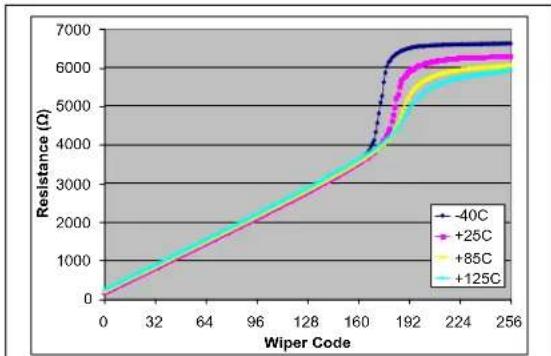
line
| Wiper Code | -40C | +25C | +85C | +125C | | ---------- | ----- | ----- | ----- | ----- | | 0 | 0 | 0 | 0 | 0 | | 32 | ~1000 | ~1000 | ~1000 | ~1000 | | 64 | ~2000 | ~2000 | ~2000 | ~2000 | | 96 | ~3000 | ~3000 | ~3000 | ~3000 | | 128 | ~4000 | ~4000 | ~4000 | ~4000 | | 160 | ~5000 | ~5000 | ~5000 | ~5000 | | 192 | ~6500 | ~6500 | ~6500 | ~6500 | | 224 | ~6800 | ~6800 | ~6800 | ~6800 | | 256 | ~7000 | ~7000 | ~7000 | ~7000 |FIGURE B-2: R BW vs. Wiper Code And Temperature (V DD = 1.8V, I _W = 190 μA).
Figure B-3 and Figure B-4 show the wiper resistance for V_DD voltages of 5.5, 3.0, 1.8 volts. These graphs show that as the resistor ladder wiper node voltage ( V_WCn ) approaches the V_DD/2 voltage, the wiper resistance increases. These graphs also show the different resistance characteristics of the NMOS and PMOS transistors that make up the wiper switch. This is demonstrated by the wiper code resistance curve, which does not mirror itself around the mid-scale code (wiper code = 128).
So why are the R_W graphs showing the maximum resistance at about mid-scale (wiper code = 128) and the R_BW graphs showing the issue at code 160?
This requires understanding low-voltage transistor characteristics as well as how the data was measured.

line
| Wiper Code | -40C @ 3.0V +25C @ 3.0V +85C @ 3.0V +125C @ 3.0V | -40C @ 5.5V +25C @ 5.5V +85C @ 5.5V +125C @ 5.5V | | ---------- | -------------------------------------------------- | -------------------------------------------------- | | 0 | 60 | 40 | | 64 | 80 | 50 | | 128 | 100 | 60 | | 192 | 120 | 70 | | 256 | 140 | 80 | | 308 | 160 | 90 | | 360 | 180 | 100 | | 412 | 160 | 90 | | 464 | 140 | 80 | | 516 | 120 | 70 | | 568 | 100 | 60 | | 620 | 80 | 50 | | 672 | 60 | 40 | | 724 | 40 | 30 | | 776 | 20 | 20 | | 838 | 20 | 20 | | 890 | 20 | 20 | | 942 | 20 | 20 | | 994 | 20 | 20 | | 1046 | 20 | 20 | | 1108 | 20 | 20 | | 1160 | 20 | 20 | | 1212 | 20 | 20 | | 1264 | 20 | 20 | | 1316 | 20 | 20 | | 1378 | 20 | 20 | | 1430 | 20 | 20 | | 1482 | 20 | 20 | | 1534 | 20 | 20 | | 1586 | 20 | 20 | | 1638 | 20 | 20 | | 1690 | 20 | 20 | | 1742 | 20 | 20 | | 1794 | 20 | 20 | | 1846 | 20 | 20 | | 1898 | 20 | 20 | | 1950 | 20 | 20 | | 2002 | 20 | 20 | | 2054 | 20 | 20 | | 2106 | 20 | 20 | | 2158 | 20 | 20 | | 2210 | 20 | 20 | | 2262 | 20 | 20 | | 2314 | 20 | 20 | | 2366 | 20 | 20 | | 2418 | 20 | 20 | | 2470 | 20 | 20 | | 2522 | 20 | 20 | | 2574 | 20 | 20 | | 2626 | 20 | 20 | | 2678 | 20 | 20 | | 2730 | 20 | 20 | | 2782 | 20 | 20 | | 2834 | 20 | 20 | | 2886 | 20 | 20 | | 2938 | 20 | 20 | | 3080 | 20 | 20 | | Note: The data is presented as a table with three columns: 'Wiper Code' and 'Resistance (Ω)' for each combination of voltage and power conditions. The values are estimated based on the given code format. There is only one data series in this case. The values are calculated based on the formula provided in the code format.FIGURE B-3: Wiper Resistance (R W ) vs. Wiper Code and Temperature ( VDD = 5.5V , I_W = 900 UA; V_DD = 3.0V , I_W = 480 μA).

FIGURE B-4: Wiper Resistance (R W ) vs. Wiper Code and Temperature ( VDD = 1.8V , I_W = 260 A ).
The method in which the data was collected is important to understand. Figure B-5 shows the technique that was used to measure the R_BW and R_W resistance. In this technique, Terminal A is floating and Terminal B is connected to ground. A fixed current is then forced into the wiper ( I_W ), and the corresponding wiper voltage ( V_W ) is measured. Forcing a known current through R_BW ( I_W ) and then measuring the voltage difference between the wiper ( V_W ) and Terminal A ( V_A ), the wiper resistance ( R_W ) can be calculated, as shown in Figure B-5. Changes in I_W current will change the wiper voltage ( V_W ). This may effect the device's wiper resistance ( R_W ).

text_image
floating A V_A W V_W I_W B V_B R_BW = V_W/I_W R_W = (V_W - V_A)/I_WFIGURE B-5: R BW and RW Measurement.
Figure B-6 shows a block diagram of the resistor network where the R_AB resistor is a series of 256 R_S resistors. These resistors are polysilicon devices. Each wiper switch is an analog switch made up of an NMOS and PMOS transistor. A more detailed figure of the wiper switch is shown in Figure B-7. The wiper resistance is influenced by the voltage on the wiper switches' nodes ( V_G V_W and V_WCn ). Temperature also influences the characteristics of the wiper switch, as shown in Figure B-4.
The NMOS transistor and PMOS transistor have different characteristics. These characteristics, as well as the wiper switch node voltages, determine the R_W resistance at each wiper code. The variation of each wiper switch's characteristics in the resistor network is greater than the variation of the R_S resistors.
The voltage on the resistor network node ( V_WCn ) is dependent upon the wiper code selected and the voltages applied to V_A , V_B and V_W . The wiper switch V_G voltage to V_W or V_WCn voltage determines how strongly the transistor is turned on. When the transistor is weakly turned on the wiper resistance, R_W will be high. When the transistor is strongly turned on, the wiper resistance ( R_W ) will be in the typical range.
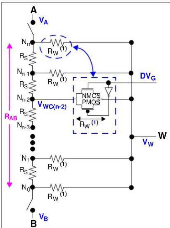
text_image
A V_A N_n R_S R_W (1) R_W (1) N_{n-1} R_S N_{n-2} R_S N_{n-3} V_{WC(n-2)} R_W (1) R_W (1) D_V_G N_MOS PMOS R_W (1) W V_W N_1 R_S N_0 R_W (1) R_W (1) B V_BNote 1: The wiper resistance is dependent on several factors including, wiper code, device V_DD , Terminal voltages (on A, B and W), and temperature.
FIGURE B-6: Resistor Network Block Diagram.
The characteristics of the wiper are determined by the characteristics of the wiper switch at each of the resistor networks tap points. Figure B-7 shows an example of a wiper switch. As the device operational voltage becomes lower, the characteristics of the wiper switch change due to a lower voltage on the V_G signal.
Figure B-7 shows an implementation of a wiper switch. When the transistor is turned off, the switch resistance is in the Giga s. When the transistor is turned on, the switch resistance is dependent on the V_G , V_W and V_WCn voltages. This resistance is referred to as R_W .
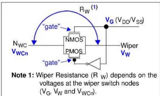
text_image
R_W^(1) "gate" N_WC V_WCN NMOS PMOS "Wiper V_W V_G(V_DD/V_SS) "gate" Note 1: Wiper Resistance (R_W) depends on the voltages at the wiper switch nodes (V_G, V_W and V_WCN).FIGURE B-7: Wiper Switch.
So, looking at the wiper voltage ( V_W ) for the 3.0V and 1.8V data gives the graphs in Figure B-8 and Figure B-9. In the 1.8V graph, as the V_W approaches 0.8V, the voltage increases nonlinearly. Since V = I^*R , and the current ( I_W ) is constant, it means that the device resistance increased nonlinearly at around wiper code 160.

line
| Wiper Code | -40C | +25C | +85C | +125C | | ---------- | ---- | ---- | ---- | ----- | | 0 | 0.0 | 0.0 | 0.0 | 0.0 | | 32 | 0.1 | 0.1 | 0.1 | 0.1 | | 64 | 0.2 | 0.2 | 0.2 | 0.2 | | 96 | 0.3 | 0.3 | 0.3 | 0.3 | | 128 | 0.4 | 0.4 | 0.4 | 0.4 | | 160 | 0.5 | 0.5 | 0.5 | 0.5 | | 192 | 0.6 | 0.6 | 0.6 | 0.6 | | 224 | 0.7 | 0.7 | 0.7 | 0.7 | | 256 | 0.8 | 0.8 | 0.8 | 0.8 | | Final | 1.0 | 1.0 | 1.0 | 1.0 |FIGURE B-8: Wiper Voltage (V W ) vs. Wiper Code ( VDD = 3.0V , I_W = 190 A ).
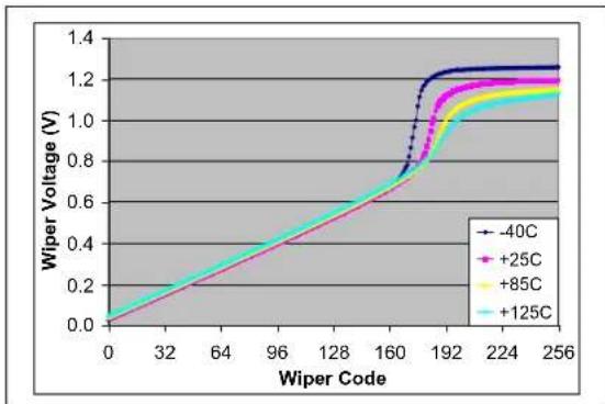
line
| Wiper Code | -40C | +25C | +85C | +125C | | ---------- | ----- | ----- | ----- | ----- | | 0 | 0.0 | 0.0 | 0.0 | 0.0 | | 32 | 0.2 | 0.2 | 0.2 | 0.2 | | 64 | 0.4 | 0.4 | 0.4 | 0.4 | | 96 | 0.6 | 0.6 | 0.6 | 0.6 | | 128 | 0.8 | 0.8 | 0.8 | 0.8 | | 160 | 1.0 | 1.0 | 1.0 | 1.0 | | 192 | 1.2 | 1.2 | 1.2 | 1.2 | | 224 | 1.3 | 1.3 | 1.3 | 1.3 | | 256 | 1.3 | 1.3 | 1.3 | 1.3 |FIGURE B-9: Wiper Voltage (V W vs. Wiper Code ( VDD = 1.8V , I_W = 190 A ).
Using the simulation models of the NMOS and PMOS devices for the MCP4XXX analog switch (Figure B-10), we plot the device resistance when the devices are turned on. Figure B-11 and Figure B-12 show the resistances of the NMOS and PMOS devices as the V_IN voltage is increased. The wiper resistance ( R_W ) is simply the parallel resistance on the NMOS and PMOS devices ( R_W = R_NMOS R_PMOS ). Below the threshold voltage for the NMOS and PMOS devices, the resistance becomes very large (Giga s ). In the transistor's active region, the resistance is much lower. For these graphs, the resistances are on different scales. Figure B-13 and Figure B-14 only plot the NMOS and PMOS device resistance for their active region and the resulting wiper resistance. For these graphs, all resistances are on the same scale.

text_image
V_IN "gate" R_W NMOS PMOS "gate" V_G (V_DD/V_SS) V_OUTFIGURE B-10: Analog Switch.

FIGURE B-11: NMOS and PMOS
Transistor Resistance ( R_NMOS , R_PMOS ) and Wiper Resistance ( R_W ) VS. V_IN ( V_DD = 3.0V ).
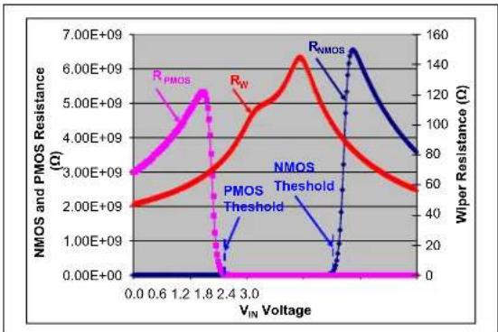
FIGURE B-12: NMOS and PMOS
Transistor Resistance ( R_NMOS , R_PMOS ) and Wiper Resistance ( R_W ) VS. V_IN ( V_DD = 1.8V ).
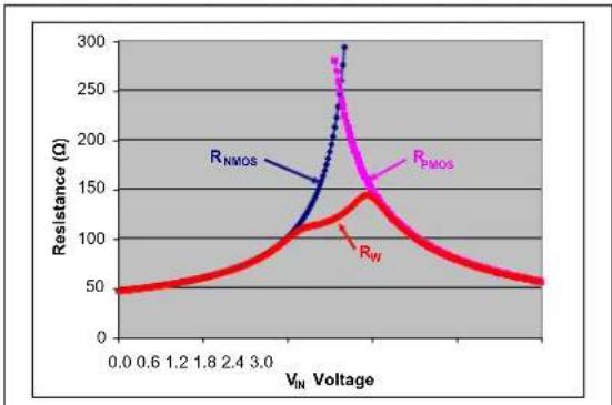
line
| VIN Voltage | Resistance (Ω) | | ----------- | -------------- | | 0.0 | 50 | | 0.6 | 50 | | 1.2 | 50 | | 1.8 | 50 | | 2.4 | 50 | | 3.0 | 50 | | 3.0 | 290 | | 3.0 | 250 | | 3.0 | 200 | | 3.0 | 150 | | 3.0 | 100 | | 3.0 | 50 |FIGURE B-13: NMOS and PMOS Transistor Resistance ( R_NMOS , R_PMOS ) and Wiper Resistance ( R_W ) VS. V_IN ( V_DD = 3.0V ).

line
| V_IN Voltage | Resistance (Ω) | | ------------ | -------------- | | 1.8 | 4700 | | 1.5 | 2500 | | 1.2 | 2000 | | 0.9 | 1500 | | 0.6 | 1000 | | 0.3 | 500 | | 0.0 | 0 |FIGURE B-14: NMOS and PMOS Transistor Resistance ( R_NMOS , R_PMOS ) and Wiper Resistance ( R_W ) VS. V_IN ( V_DD = 1.8V ).
B.2 Optimizing Circuit Design for Low-Voltage Characteristics
The low-voltage nonlinear characteristics can be minimized by application design. The section will show two application circuits that can be used to control a programmable reference voltage ( V_OUT ).
Minimizing the low-voltage nonlinear characteristics is done by keeping the voltages on the wiper switch nodes at a voltage where either the NMOS or PMOS transistor is turned on.
An example of this is if we are using a digital potentiometer for a voltage reference ( V_OUT ). Let's say that we want V_OUT to range from 0.5 × V_DD to 0.6 × V_DD .
In example implementation #1 (Figure B-15), we window the digital potentiometer using resistors R1 and R2. When the wiper code is at full scale, the V_OUT voltage will be ≥ 0.6 * V_DD , and when the wiper code is at zero scale, the V_OUT voltage will be ≤ 0.5 * V_DD . Remember that the digital potentiometers R_AB variation must be included. Table B-1 shows that the V_OUT voltage can be selected to be between 0.455 * V_DD and 0.727 * V_DD , which includes the desired range. With respect to the voltages on the resistor network node, at 1.8V the V_A voltage would range from 1.29V to 1.31V, while the V_B voltage would range from 0.82V to 0.86V. These voltages cause the wiper resistance to be in the nonlinear region (see Figure B-12). In Potentiometer mode, the variation of the wiper resistance is typically not an issue, as shown by the INL/DNL graph (Figure 2-7).
In example implementation #2 (Figure B-16), we use the digital potentiometer in Rheostat mode. The resistor ladder uses resistors R1 and R2 with R_BW at the bottom of the ladder. When the wiper code is at full scale, the V_OUT voltage will be ≥ 0.6 * V_DD , and when the wiper code is at full scale, the V_OUT voltage will be ≤ 0.5 * V_DD . Remember that the digital potentiometers R_AB variation must be included. Table B-2 shows that the V_OUT voltage can be selected to be between 0.50 * V_DD and 0.687 * V_DD , which includes the desired range. With respect to the voltages on the resistor network node, at 1.8V the V_W voltage would range from 0.29V to 0.38V. These voltages cause the wiper resistance to be in the linear region (see Figure B-12).

text_image
R1 V_A A W V_W V_OUT B V_B R2FIGURE B-15: Example Implementation #1.
TABLE B-1: EXAMPLE #1 VOLTAGE CALCULATIONS
| Variation | |||
| Min Typ | Max | ||
| R1 12,000 12 | 000 12,000 | ||
| R2 20,000 20 | 000 20,000 | ||
| R_AB | 8,000 | 10,000 12,000 | |
| V_OUT (@ FS) | 0.714 V_DD | 0.70 V_DD | 0.727 V_DD |
| V_OUT (@ ZS) | 0.476 V_DD | 0.50 V_DD | 0.455 V_DD |
| V_A | 0.714 V_DD | 0.70 V_DD | 0.727 V_DD |
| V_B | 0.476 V_DD | 0.50 V_DD | 0.455 V_DD |
Legend: FS – Full Scale, ZS – Zero Scale
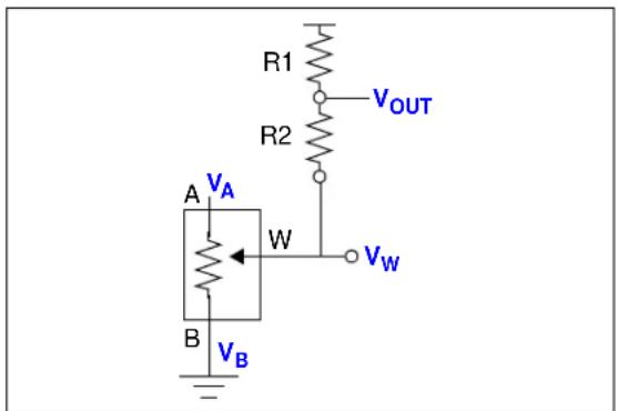
text_image
R1 VOUT R2 A VA W VW B VBFIGURE B-16: Example Implementation #2.
TABLE B-2: EXAMPLE #2 VOLTAGE CALCULATIONS
| Variation | |||
| Min Typ | Max | ||
| R1 10,000 10 | 000 10,000 | ||
| R2 10,000 10 | 000 10,000 | ||
| R_BW (max) 8,000 10,000 12,000 | |||
| V_OUT (@ FS) | 0.667 V_DD | 0.643 V_DD | 0.687 V_DD |
| V_OUT (@ ZS) | 0.50 V_DD | 0.50 V_DD | 0.50 V_DD |
| V_W (@ FS) | 0.333 V_DD | 0.286 V_DD | 0.375 V_DD |
| V_W (@ ZS) | V_SS | V_SS | V_SS |
Legend: FS – Full Scale, ZS – Zero Scale
PRODUCT IDENTIFICATION SYSTEM
To order or obtain information, e.g., on pricing or delivery, refer to the factory or the listed sales office.
| PART NO. | XXX | X | XX |
| Device | Resistance Version | Temperature Range | Package |
Device: MCP4531: Single Nonvolatile 7-bit Potentiometer
MCP4531T: Single Nonvolatile 7-bit Potentiometer
(Tape and Reel)
MCP4532: Single Nonvolatile 7-bit Rheostat
MCP4532T: Single Nonvolatile 7-bit Rheostat
(Tape and Reel)
MCP4551: Single Nonvolatile 8-bit Potentiometer
MCP4551T: Single Nonvolatile 8-bit Potentiometer
(Tape and Reel)
MCP4552: Single Nonvolatile 8-bit Rheostat
MCP4552T: Single Nonvolatile 8-bit Rheostat
(Tape and Reel)
MCP4631: Dual Nonvolatile 7-bit Potentiometer
MCP4631T: Dual Nonvolatile 7-bit Potentiometer
(Tape and Reel)
MCP4632: Dual Nonvolatile 7-bit Rheostat
MCP4632T: Dual Nonvolatile 7-bit Rheostat
(Tape and Reel)
MCP4651: Dual Nonvolatile 8-bit Potentiometer
MCP4651T: Dual Nonvolatile 8-bit Potentiometer
(Tape and Reel)
MCP4652: Dual Nonvolatile8-bit Rheostat
MCP4652T: Dual Nonvolatile 8-bit Rheostat
(Tape and Reel)
Resistance Version: 502 = 5 kΩ
103 = 10 kΩ
503 = 50 kΩ
104 = 100 kΩ
Temperature Range: E = -40°C to +125°C
Package: MF = Plastic Dual Flat No-lead (3x3 DFN), 8/10-lead
ML = Plastic Quad Flat No-lead (QFN), 16-lead
MS = Plastic Micro Small Outline (MSOP), 8-lead
ST = Plastic Thin Shrink Small Outline (TSSOP), 14-lead
UN = Plastic Micro Small Outline (MSOP), 10-lead
Examples:
a) MCP4531-502E/XX: 5 kΩ, 8LD Device
b) MCP4531-103E/XX: 10 kΩ, 8-LD Device
c) MCP4531-503E/XX: 50 kΩ, 8LD Device
d) MCP4531-104E/XX: 100 kΩ, 8LD Device
e) MCP4531T-104E/XX: T/R, 100 kΩ, 8LD Device
a) MCP4532-502E/XX: 5 kΩ, 8LD Device
b) MCP4532-103E/XX: 10 kΩ, 8-LD Device
c) MCP4532-503E/XX: 50 kΩ, 8LD Device
d) MCP4532-104E/XX: 100 kΩ, 8LD Device
e) MCP4532T-104E/XX: T/R, 100 kΩ, 8LD Device
a) MCP4551-502E/XX: 5 kΩ, 8LD Device
b) MCP4551-103E/XX: 10 kΩ, 8-LD Device
c) MCP4551-503E/XX: 50 kΩ, 8LD Device
d) MCP4551-104E/XX: 100 kΩ, 8LD Device
e) MCP4551T-104E/XX: T/R, 100 kΩ, 8LD Device
a) MCP4552-502E/XX: 5 kΩ, 8LD Device
b) MCP4552-103E/XX: 10 kΩ, 8-LD Device
c) MCP4552-503E/XX: 50 kΩ, 8LD Device
d) MCP4552-104E/XX: 100 kΩ, 8LD Device
e) MCP4552T-104E/XX: T/R, 100 kΩ, 8LD Device
a) MCP4631-502E/XX: 5 kΩ, 8LD Device
b) MCP4631-103E/XX: 10 kΩ, 8-LD Device
c) MCP4631-503E/XX: 50 kΩ, 8LD Device
d) MCP4631-104E/XX: 100 kΩ, 8LD Device
e) MCP4631T-104E/XX: T/R, 100 kΩ, 8LD Device
a) MCP4632-502E/XX: 5 kΩ, 8LD Device
b) MCP4632-103E/XX: 10 kΩ, 8-LD Device
c) MCP4632-503E/XX: 50 kΩ, 8LD Device
d) MCP4632-104E/XX: 100 kΩ, 8LD Device
e) MCP4632T-104E/XX: T/R, 100 kΩ, 8LD Device
a) MCP4651-502E/XX: 5 kΩ, 8LD Device
b) MCP4651-103E/XX: 10 kΩ, 8-LD Device
c) MCP4651-503E/XX: 50 kΩ, 8LD Device
d) MCP4651-104E/XX: 100 kΩ, 8LD Device
e) MCP4651T-104E/XX: T/R, 100 kΩ, 8LD Device
a) MCP4652-502E/XX: 5 kΩ, 8LD Device
b) MCP4652-103E/XX: 10 kΩ, 8-LD Device
c) MCP4652-503E/XX: 50 kΩ, 8LD Device
d) MCP4652-104E/XX: 100 kΩ, 8LD Device
e) MCP4652T-104E/XX: T/R, 100 kΩ, 8LD Device
XX = MF for 8/10-lead 3x3 DFN
= ML for 16-lead QFN
= MS for 8-lead MSOP
= ST for 14-lead TSSOP
= UN for 10-lead MSOP
NOTES:
Note the following details of the code protection feature on Microchip devices:
• Microchip products meet the specification contained in their particular Microchip Data Sheet.
- Microchip believes that its family of products is one of the most secure families of its kind on the market today, when used in the intended manner and under normal conditions.
- There are dishonest and possibly illegal methods used to breach the code protection feature. All of these methods, to our knowledge, require using the Microchip products in a manner outside the operating specifications contained in Microchip's Data Sheets. Most likely, the person doing so is engaged in theft of intellectual property.
- Microchip is willing to work with the customer who is concerned about the integrity of their code.
- Neither Microchip nor any other semiconductor manufacturer can guarantee the security of their code. Code protection does not mean that we are guaranteeing the product as "unbreakable."
Code protection is constantly evolving. We at Microchip are committed to continuously improving the code protection features of our products. Attempts to break Microchip's code protection feature may be a violation of the Digital Millennium Copyright Act. If such acts allow unauthorized access to your software or other copyrighted work, you may have a right to sue for relief under that Act.
Information contained in this publication regarding device applications and the like is provided only for your convenience and may be superseded by updates. It is your responsibility to ensure that your application meets with your specifications. MICROCHIP MAKES NO REPRESENTATIONS OR WARRANTIES OF ANY KIND WHETHER EXPRESS OR IMPLIED, WRITTEN OR ORAL, STATUTORY OR OTHERWISE, RELATED TO THE INFORMATION, INCLUDING BUT NOT LIMITED TO ITS CONDITION, QUALITY, PERFORMANCE, MERCHANTABILITY OR FITNESS FOR PURPOSE. Microchip disclaims all liability arising from this information and its use. Use of Microchip devices in life support and/or safety applications is entirely at the buyer's risk, and the buyer agrees to defend, indemnify and hold harmless Microchip from any and all damages, claims, suits, or expenses resulting from such use. No licenses are conveyed, implicitly or otherwise, under any Microchip intellectual property rights.
QUALITY MANAGEMENT SYSTEM CERTIFIED BY DNV = ISO/TS 16949=
Trademarks
The Microchip name and logo, the Microchip logo, dsPIC, FlashFlex, KEELOQ, KEELOQ logo, MPLAB, PIC, PICmicro, PICSTART, PIC ^32 logo, rfPIC, SST, SST Logo, SuperFlash and UNI/O are registered trademarks of Microchip Technology Incorporated in the U.S.A. and other countries.
FilterLab, Hampshire, HI-TECH C, Linear Active Thermistor, MTP, SEEVAL and The Embedded Control Solutions Company are registered trademarks of Microchip Technology Incorporated in the U.S.A.
Silicon Storage Technology is a registered trademark of Microchip Technology Inc. in other countries.
Analog-for-the-Digital Age, Application Maestro, BodyCom, chipKIT, chipKIT logo, CodeGuard, dsPICDEM, dsPICDEM.net, dsPICworks, dsSPEAK, ECAN, ECONOMONITOR, FanSense, HI-TIDE, In-Circuit Serial Programming, ICSP, Mindi, MiWi, MPASM, MPF, MPLAB Certified logo, MPLIB, MPLINK, mTouch, Omniscient Code Generation, PICC, PICC-18, PICDEM, PICDEM.net, PICkit, PICtail, REAL ICE, rfLAB, Select Mode, SQL, Serial Quad I/O, Total Endurance, TSHARC, UniWinDriver, WiperLock, ZENA and Z-Scale are trademarks of Microchip Technology Incorporated in the U.S.A. and other countries.
SQTP is a service mark of Microchip Technology Incorporated in the U.S.A.
GestIC and ULPP are registered trademarks of Microchip Technology Germany II GmbH & Co. & KG, a subsidiary of Microchip Technology Inc., in other countries.
All other trademarks mentioned herein are property of their respective companies.
© 2008-2013, Microchip Technology Incorporated, Printed in the U.S.A., All Rights Reserved.
Printed on recycled paper. ISBN: 978-1-62077-023-8
Microchip received ISO/TS-16949:2009 certification for its worldwide headquarters, design and wafer fabrication facilities in Chandler and Tempe, Arizona; Gresham, Oregon and design centers in California and India. The Company's quality system processes and procedures are for its PIC® MCUs and dsPIC® DSCs, KEELoQ® code hopping devices, Serial EEPROMs, microperipherals, nonvolatile memory and analog products. In addition, Microchip's quality system for the design and manufacture of development systems is ISO 9001:2000 certified.
Worldwide Sales and Service
AMERICAS
Corporate Office
2355 West Chandler Blvd.
Chandler, AZ 85224-6199
Tel: 480-792-7200
Fax: 480-792-7277
Technical Support:
http://www.microchip.com/
support
Web Address:
www.microchip.com
Atlanta
Duluth, GA
Tel: 678-957-9614
Fax: 678-957-1455
Boston
Westborough, MA
Tel: 774-760-0087
Fax: 774-760-0088
Chicago
Itasca,
Tel: 630-285-0071
Fax: 630-285-0075
Cleveland
Independence, OH
Tel: 216-447-0464
Fax: 216-447-0643
Dallas
Addison, TX
Tel: 972-818-7423
Fax: 972-818-2924
Detroit
Farmington Hills, MI
Tel: 248-538-2250
Fax: 248-538-2260
Indianapolis
Noblesville, IN
Tel: 317-773-8323
Fax: 317-773-5453
Los Angeles
Mission Viejo, CA
Tel: 949-462-9523
Fax: 949-462-9608
Santa Clara
Santa Clara, CA
Tel: 408-961-6444
Fax: 408-961-6445
Toronto
Mississauga, Ontario,
Canada
Tel: 905-673-0699
Fax: 905-673-6509
ASIA/PACIFIC
Asia Pacific Office
Suites 3707-14, 37th Floor
Tower 6, The Gateway
Harbour City, Kowloon
Hong Kong
Tel: 852-2401-1200
Fax: 852-2401-3431
Australia - Sydney
Tel: 61-2-9868-6733
Fax: 61-2-9868-6755
China - Beijing
Tel: 86-10-8569-7000
Fax: 86-10-8528-2104
China - Chengdu
Tel: 86-28-8665-5511
Fax: 86-28-8665-7889
China - Chongqing
Tel: 86-23-8980-9588
Fax: 86-23-8980-9500
China - Hangzhou
Tel: 86-571-2819-3187
Fax: 86-571-2819-3189
China - Hong Kong SAR
Tel: 852-2943-5100
Fax: 852-2401-3431
China - Nanjing
Tel: 86-25-8473-2460
Fax: 86-25-8473-2470
China - Qingdao
Tel: 86-532-8502-7355
Fax: 86-532-8502-7205
China - Shanghai
Tel: 86-21-5407-5533
Fax: 86-21-5407-5066
China - Shenyang
Tel: 86-24-2334-2829
Fax: 86-24-2334-2393
China - Shenzhen
Tel: 86-755-8864-2200
Fax: 86-755-8203-1760
China - Wuhan
Tel: 86-27-5980-5300
Fax: 86-27-5980-5118
China - Xian
Tel: 86-29-8833-7252
Fax: 86-29-8833-7256
China - Xiamen
Tel: 86-592-2388138
Fax: 86-592-2388130
China - Zhuhai
Tel: 86-756-3210040
Fax: 86-756-3210049
ASIA/PACIFIC
India - Bangalore
Tel: 91-80-3090-4444
Fax: 91-80-3090-4123
India - New Delhi
Tel: 91-11-4160-8631
Fax: 91-11-4160-8632
India - Pune
Tel: 91-20-2566-1512
Fax: 91-20-2566-1513
Japan - Osaka
Tel: 81-6-6152-7160
Fax: 81-6-6152-9310
Japan - Tokyo
Tel: 81-3-6880-3770
Fax: 81-3-6880-3771
Korea - Daegu
Tel: 82-53-744-4301
Fax: 82-53-744-4302
Korea - Seoul
Tel: 82-2-554-7200
Fax: 82-2-558-5932 or
82-2-558-5934
Malaysia - Kuala Lumpur
Tel: 60-3-6201-9857
Fax: 60-3-6201-9859
Malaysia - Penang
Tel: 60-4-227-8870
Fax: 60-4-227-4068
Philippines - Manila
Tel: 63-2-634-9065
Fax: 63-2-634-9069
Singapore
Tel: 65-6334-8870
Fax: 65-6334-8850
Taiwan - Hsin Chu
Tel: 886-3-5778-366
Fax: 886-3-5770-955
Taiwan - Kaohsiung
Tel: 886-7-213-7828
Fax: 886-7-330-9305
Taiwan - Taipei
Tel: 886-2-2508-8600
Fax: 886-2-2508-0102
Thailand - Bangkok
Tel: 66-2-694-1351
Fax: 66-2-694-1350
EUROPE
Austria - Wels
Tel: 43-7242-2244-39
Fax: 43-7242-2244-393
Denmark - Copenhagen
Tel: 45-4450-2828
Fax: 45-4485-2829
France - Paris
Tel: 33-1-69-53-63-20
Fax: 33-1-69-30-90-79
Germany - Munich
Tel: 49-89-627-144-0
Fax: 49-89-627-144-44
Italy - Milan
Tel: 39-0331-742611
Fax: 39-0331-466781
Netherlands - Drunen
Tel: 31-416-690399
Fax: 31-416-690340
Spain - Madrid
Tel: 34-91-708-08-90
Fax: 34-91-708-08-91
UK - Wokingham
Tel: 44-118-921-5869
Fax: 44-118-921-5820
11/29/12