MIC5385 - Electronic component Microchip - Free user manual and instructions
Find the device manual for free MIC5385 Microchip in PDF.

User questions about MIC5385 Microchip
0 question about this device. Answer the ones you know or ask your own.
Ask a new question about this device
Download the instructions for your Electronic component in PDF format for free! Find your manual MIC5385 - Microchip and take your electronic device back in hand. On this page are published all the documents necessary for the use of your device. MIC5385 by Microchip.
USER MANUAL MIC5385 Microchip
The MIC5385 is an advanced general purpose triple linear regulator offering high power supply rejection (PSRR) in an ultra-small 2mm x 2mm 8 pin Thin MLF® package. The MIC5385 is capable of sourcing 150mA for each output and offers high PSRR making it an ideal solution for any portable electronic application.
Ideal for battery powered applications, the MIC5385 offers 2% initial accuracy, low dropout voltage (180mV @ 150mA), and low ground current (typically 32μA per output). The MIC5385 can also be put into a zero-off-mode current state, drawing virtually no current when disabled.
The MIC5385 is available in a lead-free (RoHS compliant) 2mm x 2mm 8 pin Thin MLF ^® occupying only 4mm ^2 of PCB area, a 33% reduction in board area compared to a 3mm x 2mm Thin MLF ^® package.
The MIC5385 has an operating junction temperature range of -40^ to 125^ .
Datasheets and support documentation can be found on Micrel's web site at: www.micrel.com.
Features
• Input voltage range: 2.5V to 5.5V
• 150mA guaranteed output current for each output
• Stable with ceramic output capacitors
- Low dropout voltage – 180mV @ 150mA
• Excellent Load/Line Transient Response
- Low quiescent current – 32μA per LDO
- High PSRR - 70dB
• High output accuracy
- ±2% initial accuracy
• Thermal shutdown and current limit protection
• Available in tiny 2mm x 2mm Thin MLF®
Applications
- Mobile phones
- Digital cameras
• GPS, PDAs, PMP, handhelds - Portable electronics
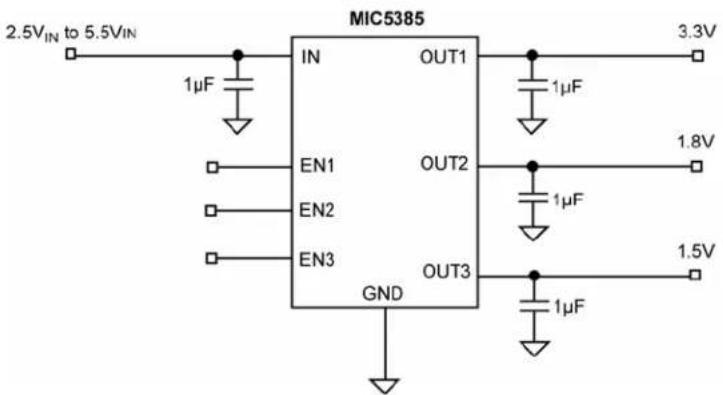
Typical Application
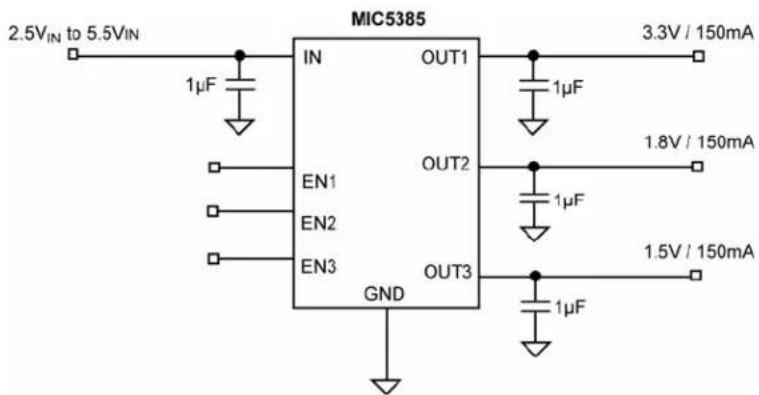
text_image
MIC5385 2.5VIN to 5.5VIN IN OUT1 3.3V / 150mA 1μF EN1 OUT2 1.8V / 150mA EN2 OUT3 1.5V / 150mA EN3 GNDMLF and MicroLeadFrame are registered trademarks of Amkor Technology, Inc.
Micrel Inc. • 2180 Fortune Drive • San Jose, CA 95131 • USA • tel +1 (408) 944-0800 • fax +1 (408) 474-1000 • http://www.micrel.com
Ordering Information
| Part Number Marking Code V | OUT1 | VOUT2 | VOUT3 | Temperature Range | Package | |
| MIC5385-SGFYMT | ZN1 | 3.3V | 1.8V | 1.5V40°C to +125°C 8-P | in 2mm x 2mm Thin MLF® | |
Notes:
1. Other voltages available. Contact Micrel for details.
2. MLF ^® ▲ = Pin 1 identifier.
3. MLF ^® is a GREEN RoHS-compliant package. Lead finish is NiPdAu. Mold compound is Halogen Free.
Pin Configuration
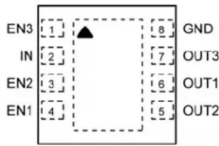
text_image
EN3 1 ▲ 8 GND IN 2 7 OUT3 EN2 3 6 OUT1 EN1 4 5 OUT28-Pin 2mm x 2mm Thin MLF ^® (MT)
Pin Description
| Pin Number | Pin Names | Pin Function |
| 1 | EN3 | Enable Input 3: Enables LDO3, Active High. High = ON; Low = OFF. Do not leave floating. |
| 2 IN | Input supply for LDO1, 2 and 3. | |
| 3 | EN2 | Enable Input 2: Enables LDO2, Active High. High = ON; Low = OFF. Do not leave floating. |
| 4 | EN1 | Enable Input 1: Enables LDO1, Active High. High = ON; Low = OFF. Do not leave floating. |
| 5 OUT2 | Output Voltage for LDO2. | |
| 6 OUT1 | Output Voltage for LDO1. | |
| 7 OUT3 | Output Voltage for LDO3. | |
| 8 | GND | Ground for LDO1, 2 and 3. |
| EP | HS Pad | Exposed Heastsink Pad. (connect to Ground plane for best thermal). |
Absolute Maximum Ratings ^(1)
Supply Voltage ( V_IN )....-0.3V to 6V
Enable Voltage ( V_EN )....-0.3V to V_IN
Power Dissipation ( P_D ) ..... Internally Limited ^(B)
Lead Temperature (soldering, 3μsec)....260°C
Junction Temperature ( T_J ) -40^ to +150^
Storage Temperature ( T_s ) -65^ to +150^
ESD Rating ^(4) 2kV
Operating Ratings ^(2)
Supply Voltage ( V_IN ).... 2.5V to 5.5V
Enable Voltage ( V_EN ).... 0V to V_IN
Junction Temperature ( T_J ) -40^ to +125^
Junction Thermal Resistance
2mm x 2mm Thin MLF ^ ( _JA ). 90°C/W
Electrical Characteristics ^(5)
V_IN = V_EN1 = V_EN2 = V_EN3 = V_OUT + 1V ; highest of the three outputs; C_IN = C_OUT1 = C_OUT2 = C_OUT3 = 1 F ; I_OUT1 = I_OUT2 = I_OUT3 = 100 A ; T_J = 25^ , bold values indicate -40^ to +125^ , unless noted.
| Parameter | Condition | Min | Typ | ||
| Variation from nominal V_OUT Output Voltage Accuracy | |||||
| Variation from nominal V_OUT ; -40°C to +125°C | -3.0 | +3.0 | % | ||
| Line Regulation | V_IN = V_OUT + 1V to 5.5V; I_OUT = 100μA | 0.02 | 0.3 | % | |
| Load Regulation(6) | I_OUT = 100μA to 150mA | 0.65 | % | ||
| Dropout Voltage(7) | I_OUT = 50mA ; V_OUT ≥ 2.8V | 55 | 110 | mV | |
| I_OUT = 150mA ; V_OUT ≥ 2.8V | 155 | 310 | mV | ||
| I_OUT = 50mA ; V_OUT < 2.8V | 60 | 135 | mV | ||
| I_OUT = 150mA ; V_OUT < 2.8V | 180 | 380 | mV | ||
| Ground Pin Current(8) | I_OUT = 0mA ; V_OUT > 1.3V , Single output enabled | 32 | μA | ||
| I_OUT = 0mA ; V_OUT > 1.3V , V_EN1 = V_EN2 = V_EN3 ≥ 1.2V | 96 | 120 | μA | ||
| Ground Pin Current in Shutdown | V_EN 1 = V_EN 2 = V_EN 3 ≤ 0.2V | 0.05 | 1 | μA | |
| Ripple Rejection | f = up to 1kHz; C_OUT = 1μF ; V_OUT < 2.5V | 70 | dB | ||
| f = 1kHz – 10kHz; C_OUT = 1μF ; V_OUT < 2.5V | 50 | dB | |||
| Current Limit | V_OUT = 0V | 200 | 325 | 550 | mA |
| Output Voltage Noise | C_OUT = 1μF , 10Hz to 100kHz | 200 | μVRMS | ||
| Enable Input | |||||
| Enable Input Voltage | Logic Low | 0.2 | V | ||
| EN1, EN2, EN3 | Logic High | 1.2 | V | ||
| Enable Input Current | V_IL ≤ 0.2V | 0.01 | 1 | μA | |
| EN1, EN2, EN3 | V_IH ≥ 1.2V | 0.01 | 1 | μA | |
| Turn-on Time | C_OUT = 1μF ; I_OUT = 150mA | 50 | 125 | μs | |
Notes:
- Exceeding the absolute maximum rating may damage the device.
- The device is not guaranteed to function outside its operating rating.
- The maximum allowable power dissipation of any T_A (ambient temperature) is P_D() = (T_J() - T_A) / _JA . Exceeding the maximum allowable power dissipation will result in excessive die temperature, and the regulator will go into thermal shutdown.
- Devices are ESD sensitive. Handling precautions recommended. Human body model, 1.5kΩ in series with 100pF.
- Specification for packaged product only.
- Regulation is measured at constant junction temperature using low duty cycle pulse testing, changes in output voltage due to heating effects are covered by the thermal regulation specification.
- Dropout voltage is defined as the input-to-output differential at which the output voltage drops 2% below its nominal value measured at 1V differential.
For outputs below 2.5V, dropout voltage is the input-to-output differential with the minimum input voltage 2.5V.
- Ground pin current is the regulator quiescent current. The total current drawn from the supply is the sum of the load current plus the ground pin current.
Typical Characteristics
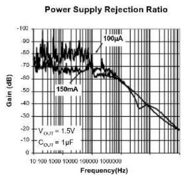
line
| Frequency(Hz) | Gain(dB) | | ------------- | -------- | | 10 | -90 | | 100 | -70 | | 1000 | -60 | | 10000 | -50 | | 100000 | -30 | | 1000000 | -20 |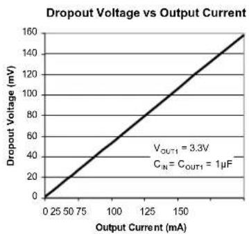
line
| Output Current (mA) | Dropout Voltage (mV) | | ------------------- | -------------------- | | 0 | 0 | | 25 | 25 | | 50 | 50 | | 75 | 75 | | 100 | 100 | | 125 | 125 | | 150 | 150 | | 175 | 175 | | 200 | 200 | | 225 | 225 | | 250 | 250 | | 275 | 275 | | 300 | 300 | | 325 | 325 | | 350 | 350 | | 375 | 375 | | 400 | 400 | | 425 | 425 | | 450 | 450 | | 475 | 475 | | 500 | 500 | | 525 | 525 | | 550 | 550 | | 575 | 575 | | 600 | 600 | | 625 | 625 | | 650 | 650 | | 675 | 675 | | 700 | 700 | | 725 | 725 | | 750 | 750 | | 775 | 775 | | 800 | 800 | | 825 | 825 | | 850 | 850 | | 875 | 875 | | 900 | 900 | | 925 | 925 | | 950 | 950 | | 975 | 975 | | 1000 | 1000 | | 1025 | 1025 | | 1050 | 1050 | | 1075 | 1075 | | 1100 | 1100 | | 1125 | 1125 | | 1150 | 1150 | | 1175 | 1175 | | 1200 | 1200 | | 1225 | 1225 | | 1250 | 1250 | | 1275 | 1275 | | 1300 | 1300 | | 1325 | 1325 | | 1350 | 1350 | | 1375 | 1375 | | 1400 | 1400 | | 1425 | 1425 | | 1450 | 1450 | | 1475 | 1475 | | 1500 | 1500 | | 1525 | 1525 | | 1550 | 1550 | | 1575 | 1575 | | 1600 | 1600 |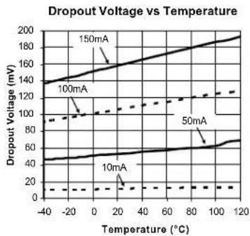
line
| Temperature (°C) | Dropout Voltage (mV) | | ---------------- | -------------------- | | -40 | 130 | | -20 | 140 | | 0 | 150 | | 20 | 160 | | 40 | 170 | | 60 | 180 | | 80 | 190 | | 100 | 200 | | 120 | 210 |
line
| Supply Voltage (V) | Ground Current (µA) | | ------------------ | ------------------- | | 2.5 | 36.0 | | 3.0 | 36.5 | | 3.5 | 37.0 | | 4.0 | 37.5 | | 4.5 | 38.0 | | 5.0 | 38.5 | | 5.5 | 39.0 |
line
Ground Current vs Supply Voltage (single output) | Supply Voltage (V) | Ground Current (μA) | | :--- | :--- | | 2.5 | 36.0 | | 3.0 | 36.1 | | 3.5 | 36.2 | | 4.0 | 36.3 | | 4.5 | 36.4 | | 5.0 | 36.5 | | 5.5 | 36.6 | | 6.0 | 36.7 | | 6.5 | 36.8 | | 7.0 | 36.9 | | 7.5 | 37.0 | | 8.0 | 37.1 | | 8.5 | 37.2 | | 9.0 | 37.3 | | 9.5 | 37.4 | | 10.0 | 37.5 | | 10.5 | 37.6 | | 11.0 | 37.7 | | 11.5 | 37.8 | | 12.0 | 37.9 | | 12.5 | 38.0 | | 13.0 | 38.1 | | 13.5 | 38.2 | | 14.0 | 38.3 | | 14.5 | 38.4 | | 15.0 | 38.5 | | 15.5 | 38.6 | | 16.0 | 38.7 | | 16.5 | 38.8 | | 17.0 | 38.9 | | 17.5 | 39.0 | | 18.0 | 39.1 | | 18.5 | 39.2 | | 19.0 | 39.3 | | 19.5 | 39.4 | | 20.0 | 39.5 | | 20.5 | 39.6 | | 21.0 | 39.7 | | 21.5 | 39.8 | | 22.0 | 39.9 | | 22.5 | 40.0 | | 23.0 | 40.1 | | 23.5 | 40.2 | | 24.0 | 40.3 | | 24.5 | 40.4 | | 25.0 | 40.5 | | 25.5 | 40.6 | | 26.0 | 40.7 | | 26.5 | 40.8 | | 27.0 | 40.9 | | 27.5 | 41.0 | | 28.0 | 41.1 | | 28.5 | 41.2 | | 29.0 | 41.3 | | 29.5 | 41.4 | | 30.0 | 41.5 | | 30.5 | 41.6 | | 31.0 | 41.7 | | 31.5 | 41.8 | | 32.0 | 41.9 | | 32.5 | 42.0 | | 33.0 | 42.1 | | 33.5 | 42.2 | | 34.0 | 42.3 | | 34.5 | 42.4 | | 35.0 | 42.5 | | 35.5 | 42.6 | | 36.0 | 42.7 | | 36.5 | 42.8 | | 37.0 | 42.9 | | 37.5 | 43.0 | | 38.0 | 43.1 | | 38.5 | 43.2 | | 39.0 | 43.3 | | 39.5 | 43.4 | | 40.0 | 43.5 | | 40.5 | 43.6 | | 41.0 | 43.7 | | 41.5 | 43.8 | | 42.0 | 43.9 | | 42.5 | 44.0 | | 43.0 | 44.1 | | 43.5 | 44.2 | | 44.0 | 44.3 | | 44.5 | 44.4 | | 45.0 | 44.5 | | 45.5 | 44.6 | | 46.0 | 44.7 | | 46.5 | 44.8 | | 47.0 | 44.9 | | 47.5 | 45.0 | | 48.0 | 45.1 | | 48.5 | 45.2 | | 49.0 | 45.3 | | 49.5 | 45.4 | | 50.0 | 45.5 | | 50.5 | -| | V_IN = V_EN3 V_LN1 = V_LN2 = O V_OUT3 = I.L.V C_IN = C_OUT3 = I.U.F.
line
| Supply Voltage(V) | Ground Current (µA) for 50mA | Ground Current (µA) for 150mA | Ground Current (µA) for 100μA | | ----------------- | ---------------------------- | ----------------------------- | ---------------------------- | | 2.5 | ~105 | ~105 | ~90 | | 3 | ~106 | ~106 | ~91 | | 3.5 | ~107 | ~107 | ~92 | | 4 | ~108 | ~108 | ~93 | | 4.5 | ~109 | ~109 | ~94 | | 5 | ~110 | ~110 | ~95 | | 5.5 | ~111 | ~111 | ~96 | | 6 | ~112 | ~112 | ~97 | | 6.5 | ~113 | ~113 | ~98 | | 7 | ~114 | ~114 | ~99 | | 7.5 | ~115 | ~115 | ~100 | | 8 | ~116 | ~116 | ~101 | | 8.5 | ~117 | ~117 | ~102 | | 9 | ~118 | ~118 | ~103 | | 9.5 | ~119 | ~119 | ~104 | | 10 | ~120 | ~120 | ~105 |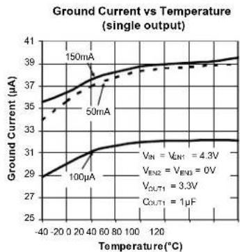
line
| Temperature(°C) | Ground Current(μA) | | --------------- | ------------------ | | -40 | 29 | | 0 | 31 | | 20 | 33 | | 40 | 35 | | 60 | 37 | | 80 | 38 | | 100 | 39 | | 120 | 40 |
line
| Supply Voltage (V) | Output Voltage (V) | | ------------------ | ------------------ | | 2.5 | 2.5 | | 3.0 | 3.0 | | 3.5 | 3.3 | | 4.0 | 3.3 | | 4.5 | 3.3 | | 5.0 | 3.3 | | 5.5 | 3.3 |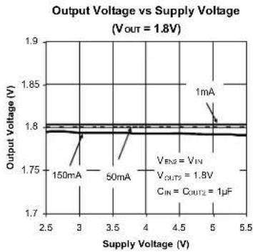
line
| Supply Voltage (V) | Output Voltage (V) | | ------------------ | ------------------ | | 3.0 | 1.78 | | 3.5 | 1.79 | | 5.0 | 1.80 |
line
| Supply Voltage (V) | Output Voltage (V) | | ------------------ | ------------------ | | 2.5 | 1.45 | | 3.0 | 1.45 | | 3.5 | 1.45 | | 4.0 | 1.45 | | 4.5 | 1.45 | | 5.0 | 1.45 | | 5.5 | 1.45 | | 6.0 | 1.45 | | 6.5 | 1.45 | | 7.0 | 1.45 | | 7.5 | 1.45 | | 8.0 | 1.45 | | 8.5 | 1.45 | | 9.0 | 1.45 | | 9.5 | 1.45 | | 10.0 | 1.45 |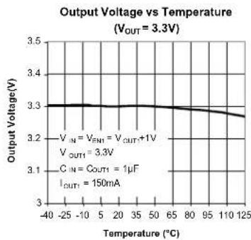
line
| Temperature (°C) | Output Voltage (V) | | ---------------- | ------------------ | | -40 | 3.3 | | -25 | 3.3 | | -10 | 3.3 | | 0 | 3.3 | | 25 | 3.3 | | 50 | 3.3 | | 65 | 3.3 | | 80 | 3.3 | | 95 | 3.3 | | 110 | 3.3 | | 125 | 3.3 |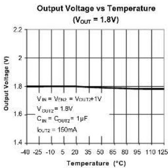
line
| Temperature (°C) | Output Voltage (V) | | ---------------- | ------------------ | | -40 | 1.8 | | -25 | 1.8 | | -10 | 1.8 | | 0 | 1.8 | | 25 | 1.8 | | 50 | 1.8 | | 65 | 1.8 | | 80 | 1.8 | | 95 | 1.8 | | 110 | 1.8 | | 125 | 1.8 |Typical Characteristics (Continued)
line
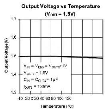
| Temperature (°C) | Output Voltage (V) | | ---------------- | ------------------ | | -40 | 1.5 | | 0 | 1.5 | | 20 | 1.5 | | 40 | 1.5 | | 60 | 1.5 | | 80 | 1.5 | | 100 | 1.5 | | 120 | 1.5 |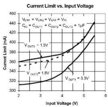
line
| Input Voltage (V) | Current Limit (mA) | | ----------------- | ------------------ | | 2 | 310 | | 3 | 320 | | 4 | 340 | | 5 | 380 | | 6 | 440 |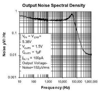
line
| Frequency (Hz) | Noise μV/Hz | | -------------- | ----------- | | 10 | ~0.9 | | 100 | ~0.85 | | 1,000 | ~0.8 | | 10,000 | ~0.75 | | 100,000 | ~0.6 | | 1,000,000 | ~0.1 |
line
| Parameter | Value | | --------- | ----- | | V_N | 5.36V | | V_OUT3 | 1.5V | | C_OUT3 | 1μF | | OUT3 | 150mA |Functional Characteristics


line
| Time (100μs/div) | V_IN (2V/div) | V_OUT1 (50mV/div) | V_OUT2 (50mV/div) | | ---------------- | ------------- | ----------------- | ----------------- | | 0 | 4.3 | 3.3 | 1.8 | | 5.5 | 5.5 | - | - | | 100 | - | - | - | | 150 | - | - | - | | 200 | - | - | - | | 250 | - | - | - | | 300 | - | - | - | | 350 | - | - | - | | 400 | - | - | - | | 450 | - | - | - | | 500 | - | - | - | | 550 | - | - | - | | 600 | - | - | - | | 650 | - | - | - | | 700 | - | - | - | | 750 | - | - | - | | 800 | - | - | - | | 850 | - | - | - | | 900 | - | - | - | | 950 | - | - | - | | 1000 | - | - | - |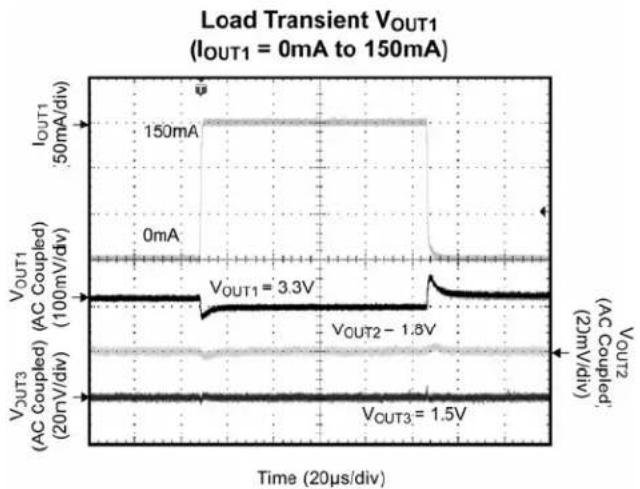
line
| Time (20μs/div) | IOUT1 (mA) | VOUT1 (V) | VOUT2 (mA) | VOUT2 (V) | | --------------- | ---------- | --------- | ---------- | --------- | | 0 | 150 | 3.3 | - | 1.8 | | 2 | - | - | - | - | | 4 | - | - | - | - | | 6 | - | - | - | - | | 8 | - | - | - | - | | 10 | - | - | - | - | | 12 | - | - | - | - | | 14 | - | - | - | - | | 16 | - | - | - | - | | 18 | - | - | - | - | | 20 | - | - | - | - | | 22 | - | - | - | - | | 24 | - | - | - | - | | 26 | - | - | - | - | | 28 | - | - | - | - | | 30 | - | - | - | - | | 32 | - | - | - | - | | 34 | - | - | - | - | | 36 | - | - | - | - | | 38 | - | - | - | - | | 40 | - | - | - | - | | 42 | - | - | - | - | | 44 | - | - | - | - | | 46 | - | - | - | - | | 48 | - | - | - | - | | 50 | 50 | 3.3 | - | 1.8 | | 52 | 50 | 3.3 | - | 1.8 | | 54 | 50 | 3.3 | - | 1.8 | | 56 | 50 | 3.3 | - | 1.8 | | 58 | 50 | 3.3 | - | 1.8 | | 60 | 50 | 3.3 | - | 1.8 | | 62 | 50 | 3.3 | - | 1.8 | | 64 | 50 | 3.3 | - | 1.8 | | 66 | 50 | 3.3 | - | 1.8 | | 68 | 50 | 3.3 | - | 1.8 | | 70 | 50 | 3.3 | - | 1.8 | | 72 | 50 | 3.3 | - | 1.8 | | 74 | 50 | 3.3 | - | 1.8 | | 76 | 50 | 3.3 | - | 1.8 | | 78 | 50 | 3.3 | - | 1.8 | | 80 | 50 | 3.3 | - | 1.8 | | 82 | 50 | 3.3 | - | 1.8 | | 84 | 50 | 3.3 | - | 1.8 | | 86 | 50 | 3.3 | - | 1.8 | | 88 | 50 | 3.3 | - | 1.8 | | 90 | 50 | 3.3 | - | 1.8 | | 92 | 50 | 3.3 | - | 1.8 | | 94 | 50 | 3.3 | - | 1.8 | | 96 | 50 | 3.3 | - | 1.8 | | 98 | 50 | 3.3 | - | 1.8 | | 100 | 50 | 3.3 | - | 1.8 | | 102 | 50 | 3.3 | - | 1.8 | | 104 | 50 | 3.3 | - | 1.8 | | 106 | 50 | 3.3 | - | 1.8 | | 108 | 50 | 3.3 | - | 1.8 | | 110 | 50 | 3.3 | - | 1.8 | | 112 | 50 | 3.3 | - | 1.8 | | 114 | 50 | 3.3 | - | 1.8 | | 116 | 50 | 3.3 | - | 1.8 | | 118 | 50 | 3.3 | - | 1.8 | | 120 | 50 | 3.3 | - | 1.8 | | 122 | 50 | 3.3 | - | 1.8 | | 124 | 50 | 3.3 | - | 1.8 | | 126 | 50 | 3.3 | - | 1.8 | | 128 | 50 | 3.3 | - | 1.8 | | 130 | 50 | 3.3 | - | 1.8 | | 132 | 50 | 3.3 | - | 1.8 | | 134 | 50 | 3.3 | - | 1.8 | | 136 | 50 | 3.3 | - | 1.8 | | 138 | 50 | 3.3 | - | 1.8 | | 140 | 50 | 3.3 | - | 1.8 | | 142 | 50 | 3.3 | - | 1.8 | | 144 | 50 | 3.3 | - | 1.8 | | 146 | 50 | 3.3 | - | 1.8 | | 148 | 50 | 3.3 | - | 1.8 | | Note: The actual values for IOUT1 and VOUT2 are not provided in the code snippet, so they are calculated based on the current value of VOUT2 and VOUT2 divided by the corresponding voltage values (VOUT1 and VOUT2). The current values are labeled as 'AC Coupled' and 'AC Coupled'.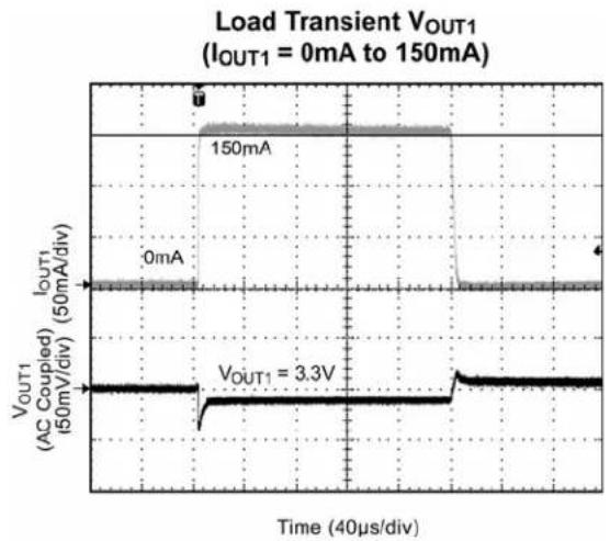
line
| Time (40μs/div) | IOUT1 (mA) | VOUT1 (V) | | --------------- | ---------- | --------- | | 0 | 150 | 3.3 |
line
| Time (40μs/div) | IOUT2 (0mA) | VOUT2 (AC Coupled) | | --------------- | ----------- | ------------------ | | 0 | 150 | 1.8 |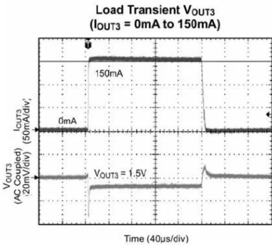
line
| Time (40μs/div) | IOUT3 (mA) | VOUT3 (V) | | --------------- | ---------- | --------- | | 0 | 0 | 1.5 | | 50 | 150 | 1.5 | | 100 | 150 | 1.5 | | 150 | 150 | 1.5 | | 200 | 0 | 1.5 |Block Diagram
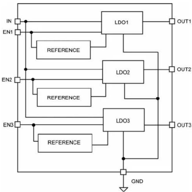
flowchart
graph TD
    IN --> LDO1
    EN1 --> LDO1
    LDO1 --> OUT1
    REFERENCE --> LDO2
    REFERENCE --> LDO2
    LDO2 --> OUT2
    REFERENCE --> LDO3
    REFERENCE --> LDO3
    LDO3 --> OUT3
    GND --> LDO1
    GND --> LDO2
    GND --> LDO3
    EN2 --> LDO2
    EN2 --> LDO3
    EN3 --> LDO3
    EN3 --> REFERENCE
    REFERENCE --> LDO3
    REFERENCE --> LDO2
Application Information
MIC5385 is a triple output Low noise 150mA LDO. The MIC5385 regulator is fully protected from damage due to fault conditions, offering linear current limiting and thermal shutdown.
Input Capacitor
The MIC5385 is a high-performance, high bandwidth device. An input capacitor of 1 F is required from the input-to-ground to provide stability. Low-ESR ceramic capacitors provide optimal performance at a minimum of space. Additional high-frequency capacitors, such as small-valued NPO dielectric-type capacitors, help filter out high-frequency noise and are good practice in any RF-based circuit. X5R or X7R dielectrics are recommended for the input capacitor. Y5V dielectrics lose most of their capacitance over temperature and are therefore, not recommended.
Output Capacitor
The MIC5385 requires an output capacitor of 1μF or greater for each output to maintain stability. The design is optimized for use with low-ESR ceramic chip capacitors. High ESR capacitors are not recommended because they may cause high frequency oscillation. The output capacitor can be increased, but performance has been optimized for a 1μF ceramic output capacitor and does not improve significantly with larger capacitance.
X7R/X5R dielectric-type ceramic capacitors are recommended because of their temperature performance. X7R-type capacitors change capacitance by 15% over their operating temperature range and are the most stable type of ceramic capacitors. Z5U and Y5V dielectric capacitors change value by as much as 50% and 60%, respectively, over their operating temperature ranges. To use a ceramic chip capacitor with Y5V dielectric, the value must be much higher than an X7R ceramic capacitor to ensure the same minimum capacitance over the equivalent operating temperature range.
No-Load Stability
Unlike many other voltage regulators, the MIC5385 will remain stable and in regulation with no load. This is especially important in CMOS RAM keep-alive applications.
Enable/Shutdown
The MIC5385 comes with an active-high enable pin that allows the regulator to be disabled. Forcing the enable pin low disables the regulator and sends it into a "zero" off-mode-current state. In this state, current consumed by the regulator goes nearly to zero. Forcing the enable pin high enables the output voltage. The active-high enable pin uses CMOS technology and the enable pin cannot be left floating; a floating enable pin may cause an indeterminate state on the output.
Thermal Considerations
The MIC5385 is designed to provide three outputs up to 150mA each of continuous current in a very small package. Maximum ambient operating temperature can be calculated based on the output current and the voltage drop across the part. For example if the input voltage is 3.6V and the output voltages are 3.3V, 1.8V, and 1.5V each with an output current = 150mA. The actual power dissipation of the regulator circuit can be determined using the equation:
$$ P _ {D} = \left(V _ {I N} - V _ {O U T 1}\right) I _ {O U T 1} + $$
$$ \left(V _ {I N} - V _ {O U T 2}\right) I _ {O U T 2} + $$
$$ \left(V _ {I N} - V _ {O U T 3}\right) I _ {O U T} + V _ {I N} I _ {G N D} $$
As the MIC5385 is a CMOS device, the ground current is typically <100 A over the load range, the power dissipation contributed by the ground current is <1% and may be ignored for this calculation.
$$ P _ {D} = (3. 6 \mathrm{V} - 3. 3 \mathrm{V}) 1 5 0 \mathrm{mA} + (3. 6 \mathrm{V} - 1. 8 \mathrm{V}) 1 5 0 \mathrm{mA} + $$
$$ (3. 6 \mathrm{V} - 1. 5 \mathrm{V}) 1 5 0 \mathrm{mA} $$
$$ P _ {D} = 0. 6 3 W $$
To determine the maximum ambient operating temperature of the package, use the junction-to-ambient thermal resistance of the device and the following basic equation:
$$ P _ {D (\max)} = \left(\frac {T - T _ {A J (\max)}}{\theta_ {J A}}\right) $$
T_J(max) = 125^ , the maximum junction temperature of the die, and _JA thermal resistance = 90°C/W for the Thin MLF® package.
Substituting P_D for P_D(max) and solving for the ambient operating temperature will give the maximum operating conditions for the regulator circuit.
The maximum power dissipation must not be exceeded for proper operation.
For example, when operating the MIC5385-SGFYMT at an input voltage of 3.6V and 450mA load with a minimum footprint layout, the maximum ambient operating temperature T_A can be determined as follows:
$$ 0. 6 3 \mathrm{W} = (1 2 5 ^ {\circ} \mathrm{C} - \mathrm{T} _ {\mathrm{A}}) / (9 0 ^ {\circ} \mathrm{C} / \mathrm{W}) $$
$$ T _ {A} = 6 8. 3 ^ {\circ} \mathrm{C} / \mathrm{W} $$
Therefore, the maximum ambient operating temperature of 68.3°C is allowed in a 2mm x 2mm thin MLF® package. For a full discussion of heat sinking and thermal effects on voltage regulators, refer to the "Regulator Thermals" section of Micrel's Designing with Low-Dropout Voltage Regulators handbook. This information can be found on Micrel's website at:
http://www.micrel.com/_PDF/other/LDOBk_ds.pdf
Typical Application
text_image
MIC5385 2.5VIN to 5.5VIN IN OUT1 1μF EN1 OUT2 1μF 1.8V EN2 OUT3 1μF 1.5V EN3 GNDBill of Materials
| Item | Part Number | Manufacturer Description | Qty. | ||
| C1,C2,C3,C4 | C1005X5R1A105K TDK | (1) Capacitor, 1μF Ceramic, 10V, X5R, Size 0402 4 | |||
| U1 | MIC5385-SGFYMT | Micrel, (2) High Performance Triple 150mA LDO 1 | |||
Notes:
1. TDK: www.tdk.com
2. Micrel, Inc.: www.micrel.com
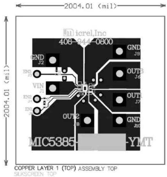
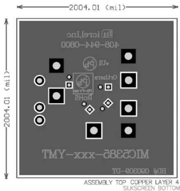
PCB Layout Recommendations (2mm x 2mm Thin MLF®)
text_image
2004.01 (mil) 2004.01 (mil) micrel,Inc 408-944-0800 GND J2 GND J9 OUT3 J6 VIN J1 OUT1 J7 EN2 J4 EN1 J6 OUT2 J8 GND J10 MIC5385-YMT COPPER LAYER 1 (TOP) ASSEMBLY TOP SILKSCREEN TOPTop Layer
text_image
2004.01 (mil) 2004.01 (mil) MICC389-xxx-MYL ASSEMBLY TOP COPPER LAYER 4 SILKSCREEN BOTTOMBottom Layer
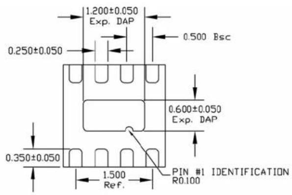
Package Information

text_image
2.000±0.050 8 2.000±0.050 1 2 PIN 1 ID BY MARKINGTOP VIEW
text_image
1.200±0.050 Exp. DAP 0.500 Bsc 0.250±0.050 0.600±0.050 Exp. DAP 0.350±0.050 1.500 Ref. PIN #1 IDENTIFICATION R0.100BOTTOM VIEW
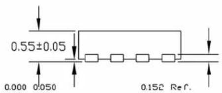
text_image
0.55±0.05 0.000 0.050 0.152 Ref.SIDE VIEW
NOTE:
1. ALL DIMENSIONS ARE IN MILLIMETERS.
2. MAX. PACKAGE WARPAGE IS 0.08 nm.
3. MAXIMUM ALLOWABE BURRS IS 0.076 mm IN ALL DIRECTIONS.
4. PIN #1 ID WILL BE LASER MARKED.
8-Pin 2mm x 2mm Thin MLF® (MT)
MICREL, INC. 2180 FORTUNE DRIVE SAN JOSE, CA 95131 USA
TEL +1 (408) 944-0800 FAX +1 (408) 474-1000 WEB http://www.micrel.com
The information furnished by Micrel in this data sheet is believed to be accurate and reliable. However, no responsibility is assumed by Micrel for its use. Micrel reserves the right to change circuitry and specifications at any time without notification to the customer.
Micrel Products are not designed or authorized for use as components in life support appliances, devices or systems where malfunction of a product can reasonably be expected to result in personal injury. Life support devices or systems are devices or systems that (a) are intended for surgical implant into the body or (b) support or sustain life, and whose failure to perform can be reasonably expected to result in a significant injury to the user. A Purchaser's use or sale of Micrel Products for use in life support appliances, devices or systems is a Purchaser's own risk and Purchaser agrees to fully indemnify Micrel for any damages resulting from such use or sale.
© 2009 Micrel, Incorporated.