MIC5322 - Electronic component Microchip - Free user manual and instructions
Find the device manual for free MIC5322 Microchip in PDF.

User questions about MIC5322 Microchip
0 question about this device. Answer the ones you know or ask your own.
Ask a new question about this device
Download the instructions for your Electronic component in PDF format for free! Find your manual MIC5322 - Microchip and take your electronic device back in hand. On this page are published all the documents necessary for the use of your device. MIC5322 by Microchip.
USER MANUAL MIC5322 Microchip
The MIC5322 is a tiny Dual Ultra Low-Dropout (ULDO™) linear regulator ideally suited for those applications that require high Power Supply Rejection Ratio (PSRR). It provides a bypass pin to increase PSRR for noise sensitive portable electronics. The MIC5322 integrates two high-performance; 150mA ULDOs into a very compact 1.6mm x 1.6mm leadless Thin MLF® package with exceptional thermal package characteristics.
The MIC5322 is a Cap design which enables operation with very small ceramic output capacitors for stability, thereby reducing required board space and component cost. The combination of extremely low-drop-out voltage, very high power supply rejection, very low output noise and exceptional thermal package characteristics makes it ideal for powering RF applications, cellular phones, GPS, imaging sensors for digital still cameras, PDAs, MP3 players and other portable applications.
The MIC5322 ULDO™ is available in fixed-output voltages in a tiny 6-pin 1.6mm x 1.6mm leadless Thin MLF® package which is only 2.56mm² in area, - 30% less area than the SOT-23, TSOP and MLF® 3x3 packages. Additional voltage options are available. For more information, contact Micrel marketing department.
Data sheets and support documentation can be found on Micrel's web site at: www.micrel.com.
Features
• 2.3V to 5.5V input voltage range
- Ultra-low dropout voltage ULDO™ 35mV @ 150mA
- Tiny 6-pin 1.6mm x 1.6mm Thin MLF® leadless package
- Bypass pin for improved noise performance
• High PSRR ->75dB on each LDO
• Ultra low noise output - > 30μVrms
- Dual 150mA outputs
- Cap stable with 1 F ceramic capacitor
- Low quiescent current – 150μA
- Fast turn-on time – 45μs
• Thermal shutdown protection
• Current Limit protection
Applications
- Mobile phones
- GPS receivers
- Portable media players
• Digital still and video cameras - PDAs
- Portable electronics
Typical Application

text_image
MIC5322-x.xYMT VIN VOUT 1 VOUT 2 EN BYP GND 1μF 0.01μF RF Core 1μF 1μF GPS ModuleRF Power Supply Circuit
ULDO is a trademark of Micrel, Inc.
MLF and MicroLeadFrame are registered trademarks of Amkor Technology, Inc.
Micrel Inc. • 2180 Fortune Drive • San Jose, CA 95131 • USA • tel +1 (408) 944-0800 • fax +1 (408) 474-1000 • http://www.micrel.com
Ordering Information
| Part number | Manufacturing Part Number | Marking^(1) | Voltage^(2) | Junction Temp. Range | Package |
| MIC5322-2.8/1.5YMT | MIC5322-MFYMT | VMF | 2.8V/1.5V | -40°C to +125°C 6-Pin 1.6x1.6 Thin MLF® | |
| MIC5322-2.8/1.8YMT | MIC5322-MGYMT | VMG | 2.8V/1.8V | -40°C to +125°C 6-Pin 1.6x1.6 Thin MLF® | |
| MIC5322-2.85/2.85YMT | MIC5322-NNYMT | VNN | 2.85V/2.85V | -40°C to +125°C | 6-Pin 1.6x1.6 Thin MLF® |
| MIC5322-3.0/2.8YMT | MIC5322-PMYMT | VPM | 3.0V/2.8V | -40°C to +125°C 6-Pin 1.6x1.6 Thin MLF® | |
| MIC5322-3.0/2.85YMT | MIC5322-PNYMT | VPN | 3.0V/2.85V | -40°C to +125°C 6-Pin 1.6x1.6 Thin MLF® | |
| MIC5322-3.0/3.0YMT | MIC5322-PPYMT | VPP | 3.0V/3.0V | -40°C to +125°C 6-Pin 1.6x1.6 Thin MLF® |
Notes:
1. Pin 1 identifier = ▲
2. For other voltage options. Contact Micrel Marketing for details.
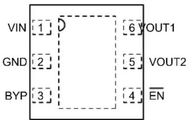
Pin Configuration
text_image
VIN [1] D [6] VOUT1 GND [2] [5] VOUT2 BYP [3] [4] EN6-Pin 1.6mm x 1.6mm Thin MLF ^® (MT) Top View
Pin Description
| Pin NumberThin MLF-6 | Pin Name | Pin Function |
| 1 | VIN | Supply Input. |
| 2 | GND | Ground |
| 3 | BYP | Reference Bypass: Connect external 0.01μF to GND to reduce output noise.May be left open. |
| 4 | /EN | Enable Input (both regulators): Active Low Input. Logic High = OFF; Logic Low = ON; Do not leave floating. |
| 5 | VOUT2 | Regulator Output – LDO2 |
| 6 | VOUT1 | Regulator Output – LDO1 |
| HS Pad | EPAD | Exposed heatsink pad connected to ground internally. |
Absolute Maximum Ratings ^(1)
Supply Voltage ( V_IN ) 0V to +6V
Enable Input Voltage (V/EN) 0V to +6V
Power Dissipation....Internally Limited ^(3)
Lead Temperature (soldering, 3sec).....260°C
Storage Temperature ( T_s )....-65°C to +150°C
ESD Rating ^(4) .....2kV
Operating Ratings ^(2)
Supply Voltage ( V_IN )....+2.3V to +5.5V
Enable Input Voltage (V/EN) 0V to VIN
Junction Temperature (T _J ) ...... -40°C to +125°C
Junction Thermal Resistance
6-pin 1.6mmx1.6mm Thin MLF ^ ( _JA ) .... 100°C/W
Electrical Characteristics ^(5)
V_IN = V_OUT + 1.0V ; higher of the two regulator outputs, I_OUTLDO1 = I_OUTLDO2 = 100 A ; V_JEN = 0V ; C_OUT1 = C_OUT2 = 1 F ; C_BYP = 0.01 F ; T_J = 25^ , bold values indicate -40^ ≤ T_J ≤ +125^ , unless noted.
| Parameter | Conditions | Min | Typ | |||
| Variation from nominal V_OUT | -2.0 | +2.0 | % Out | |||
| Variation from nominal V_OUT ; -40°C to +125°C | -3.0 | +3.0 | % | |||
| Line Regulation V | _IN = V_OUT + 1V to 5.5V; I_OUT = 100 A 0.02 | 0.30.6 | %/V%/V | |||
| Load Regulation | I_OUT = 100 A to 150mA | 0.5 | 2.0 | % | ||
| Dropout Voltage (6) | I_OUT = 100 A | 0.1 | mV | |||
| I_OUT = 50mA | 12 | 50 | mV | |||
| I_OUT = 100mA | 25 | 75 | mV | |||
| I_OUT = 150mA | 35 | 100 | mV | |||
| Ground Current V | _EN = Low; I_OUT1 = 150mA; I_OUT2 = 150mA | 150 | 190 | μA | ||
| Ground Current in Shutdown | V_EN = High | 0.01 | 2 | μA | ||
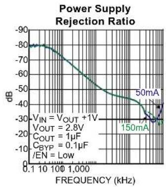
| Ripple Rejection | f = 1kHz; C_OUT = 1.0 F; C_BYP = 0.1 F | 75 | dB | |||
| f = 20kHz; C_OUT = 1.0 F; C_BYP = 0.1 F | 45 | dB | ||||
| Current Limit | V_OUT = 0V | 300 | 550 | 950 | mA | |
| Output Voltage Noise | C_OUT = 1.0 F; C_BYP = 0.01 F; 10Hz to 100kHz | 30 | μVRMS | |||
| Enable Inputs (/EN) | ||||||
| Enable Input Voltage | Logic Low | 0.2 | V | |||
| Logic High | 1.2 | V | ||||
| Enable Input Current | V_IL ≤ 0.2V | 0.01 | 1 | μA | ||
| V_IH ≥ 1.2V | 0.01 | 1 | μA | |||
| Turn-on Time (See Timing Diagram) | ||||||
| Turn-on Time (LDO1 and 2) | C_OUT = 1.0 F; No C_BYP C_OUT = 1.0 F; C_BYP = 0.01 F | 4045 | 100100 | μsμs | ||
Ma
tput Voltag
Notes:
- Exceeding the absolute maximum rating may damage the device.
- The device is not guaranteed to function outside its operating rating.
- The maximum allowable power dissipation of any T_A (ambient temperature) is P_D() = (T_J() - T_A) / _JA . Exceeding the maximum allowable power dissipation will result in excessive die temperature, and the regulator will go into thermal shutdown.
- Devices are ESD sensitive. Handling precautions recommended. Human body model, 1.5k in series with 100pF.
- Specification for packaged product only.
- Dropout voltage is defined as the input-to-output differential at which the output voltage drops 2% below its nominal V_OUT . For outputs below 2.3V, the dropout voltage is the input-to-output differential with the minimum input voltage 2.3V
Functional Diagram

flowchart
graph TD
    VIN --> LDO1
    EN --> Enable
    BYP --> Reference
    LDO1 --> VOUT1
    LDO2 --> VOUT2
    Enable --> LDO1
    Enable --> LDO2
    Reference --> GND
    VOUT1 --> LDO1
    VOUT2 --> LDO2
MIC5322 Block Diagram
Typical Characteristics
line
| FREQUENCY (kHz) | REJECTION RATIO (dB) | | --------------- | --------------------- | | 0.1 | -80 | | 1 | -80 | | 10 | -75 | | 100 | -65 | | 1,000 | -40 | | 150 | -30 | | 500 | -25 |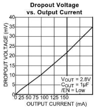
line
| OUTPUT CURRENT (mA) | DROPOUT VOLTAGE (mV) | | ------------------- | -------------------- | | 0 | 0 | | 25 | 5 | | 50 | 10 | | 75 | 15 | | 100 | 20 | | 125 | 25 | | 150 | 30 | | 175 | 35 |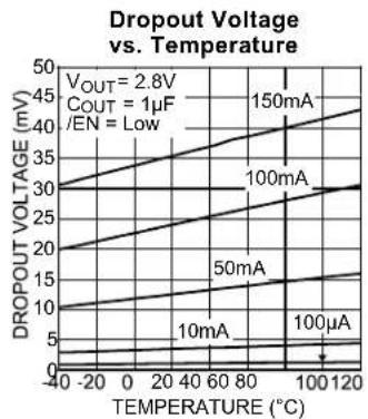
line
| TEMPERATURE (°C) | 10mA | 50mA | 100mA | 150mA | | ---------------- | ---- | ---- | ----- | ----- | | -40 | 10 | 15 | 20 | 30 | | 0 | 15 | 20 | 25 | 35 | | 40 | 20 | 25 | 30 | 40 | | 80 | 25 | 30 | 35 | 45 | | 120 | 30 | 35 | 40 | 50 |
line
| TEMPERATURE (°C) | GROUND CURRENT (μA) | | ---------------- | ------------------- | | -40 | 135 | | 0 | 145 | | 20 | 150 | | 40 | 152 | | 60 | 153 | | 80 | 154 | | 100 | 154 | | 120 | 154 |
line
| TEMPERATURE (°C) | GROUND CURRENT (pA) | | ---------------- | ------------------- | | -40 | 140 | | 0 | 145 | | 20 | 150 | | 40 | 152 | | 60 | 153 | | 80 | 154 | | 100 | 154 | | 120 | 154 |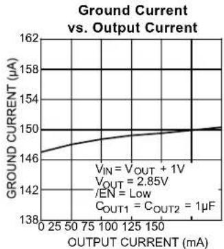
line
| OUTPUT CURRENT (mA) | GROUND CURRENT (μA) | | ------------------- | ------------------- | | 0 | 146 | | 25 | 147 | | 50 | 148 | | 75 | 149 | | 100 | 150 | | 125 | 151 | | 150 | 152 |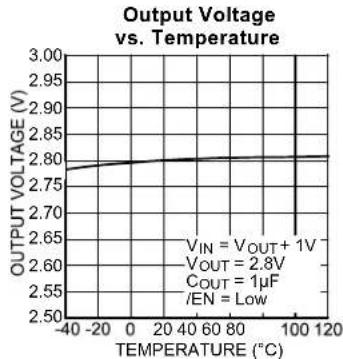
line
| TEMPERATURE (°C) | OUTPUT VOLTAGE (V) | | ---------------- | ------------------ | | -40 | 2.78 | | 0 | 2.79 | | 20 | 2.79 | | 40 | 2.79 | | 60 | 2.79 | | 80 | 2.79 | | 100 | 2.79 | | 120 | 2.79 |
line
| INPUT VOLTAGE (V) | OUTPUT VOLTAGE (V) | | ---------------- | ------------------ | | 0 | 0.0 | | 1 | 1.0 | | 2 | 2.0 | | 3 | 2.8 | | 4 | 2.8 | | 5 | 2.8 | | 6 | 2.8 |
line
| OUTPUT CURRENT (mA) | OUTPUT VOLTAGE (V) | | ------------------- | ------------------ | | 0 | 2.75 | | 25 | 2.75 | | 50 | 2.75 | | 75 | 2.75 | | 100 | 2.75 | | 125 | 2.75 | | 150 | 2.75 | | 175 | 2.75 | | 200 | 2.75 | | 225 | 2.75 | | 250 | 2.75 | | 275 | 2.75 | | 300 | 2.75 | | 325 | 2.75 | | 350 | 2.75 | | 375 | 2.75 | | 400 | 2.75 | | 425 | 2.75 | | 450 | 2.75 | | 475 | 2.75 | | 500 | 2.75 | | 525 | 2.75 | | 550 | 2.75 | | 575 | 2.75 | | 600 | 2.75 | | 625 | 2.75 | | 650 | 2.75 | | 675 | 2.75 | | 700 | 2.75 | | 725 | 2.75 | | 750 | 2.75 | | 775 | 2.75 | | 800 | 2.75 | | 825 | 2.75 | | 850 | 2.75 | | 875 | 2.75 | | 900 | 2.75 | | 925 | 2.75 | | 950 | 2.75 | | 975 | 2.75 | | 1000 | 2.75 | | 1025 | 2.75 | | 1050 | 2.75 | | 1075 | 2.75 | | 1100 | 2.75 | | 1125 | 2.75 | | 1150 | 2.75 | | 1175 | 2.75 | | 1200 | 2.75 | | 1225 | 2.75 | | 1250 | 2.75 | | 1275 | 2.75 | | 1300 | 2.75 | | 1325 | 2.75 | | 1350 | 2.75 | | 1375 | 2.75 | | 1400 | 2.75 | | 1425 | 2.75 | | 1450 | 2.75 | | 1475 | 2.75 | | 1500 | 2.75 | | 1525 | 2.75 | | 1550 | 2.75 | | 1575 | 2.75 | | 1600 | 2.75 | | 1625 | 2.75 | | 1650 | 2.75 | | 1675 | 2.75 | | 1700 | 2.75 | | 1725 | 2.75 | | 1750 | 2.75 | | 1775 | 2.75 | | 1800 | 2.75 | | 1825 | 2.75 | | 1850 | 2.75 | | 1875 | 2.75 | | 1900 | 2.75 | | 1925 | 2.75 | | 1950 | 2.75 | | 1975 | 2.75 | | 2000 | 2.75 | | Note: The output current values are not provided in the code, so they are calculated based on the given output voltage and output current values for each output current level (e.g., V_IN = V_OUT + V_OUT). The output current values are labeled as 'VOUT' and 'COUT1'.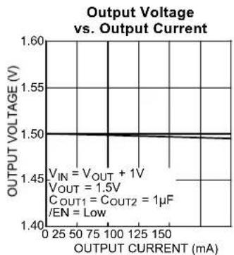
line
| OUTPUT CURRENT (mA) | OUTPUT VOLTAGE (V) | | ------------------- | ------------------ | | 0 | 1.50 | | 25 | 1.50 | | 50 | 1.50 | | 75 | 1.50 | | 100 | 1.50 | | 125 | 1.50 | | 150 | 1.50 | | 175 | 1.45 |
line
| INPUT VOLTAGE (V) | CURRENT LIMIT (mA) | | ---------------- | ------------------ | | 3.0 | 560 | | 3.5 | 562 | | 4.0 | 565 | | 4.5 | 568 | | 5.0 | 570 | | 5.5 | 575 | | 6.0 | 580 | | 6.5 | 590 | | 7.0 | 600 |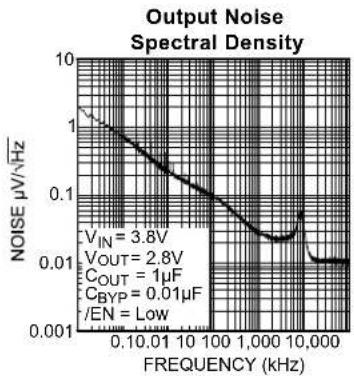
line
| FREQUENCY (kHz) | NOISE μV/Hz | | --------------- | ----------- | | 0.1 | 1 | | 1 | 0.1 | | 10 | 0.01 | | 100 | 0.001 | | 1000 | 0.0001 | | 10000 | 0.00001 |Functional Characteristics
line
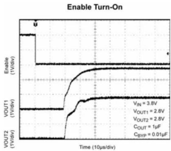
| Time (10μs/div) | VOUT1 (1V/div) | VOUT2 (1V/div) | | --------------- | -------------- | -------------- | | Start | 3.8 | 3.8 | | Peak | 2.8 | 2.8 | | Final | 2.8 | 2.8 |
line
| Time (40μs/div) | Output Voltage (20mV/div) | Output Current (50mA/div) | | --------------- | ------------------------- | ------------------------- | | 0 | 20 | 10 | | 150 | 20 | 10 | | 200 | 20 | 10 | | 300 | 20 | 10 | | 400 | 20 | 10 |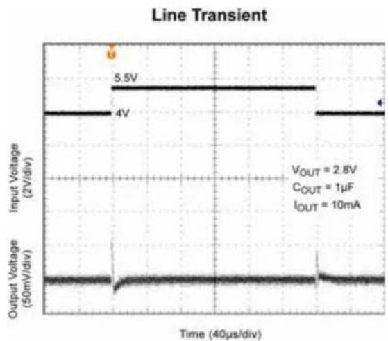
line
| Input Voltage (2V/div) | Output Voltage (50mV/div) | | ---------------------- | ------------------------- | | 5.5V | 5.5V | | 4V | 4V | | 4V | 4V |Applications Information
/Enable/Shutdown
The MIC5322 comes with a single active-low enable pin that allows both regulators to be disabled simultaneously. Forcing the enable pin high disables the regulators and sends it into a “zero” off-mode-current state. In this state, current consumed by the regulator goes nearly to zero. Forcing the enable pin low enables the output voltages. The active-low enable pin cannot be left floating since a floating enable pin may cause an indeterminate state on the output.
Input Capacitor
The MIC5322 is a high-performance, high bandwidth device. Therefore optimal performance can be achieved by providing a well-bypassed input supply. A 1 F capacitor is required from the input-to-ground to provide stability. Low-ESR ceramic capacitors provide optimal performance at a minimum of space. Additional high-frequency capacitors, such as small-valued NPO dielectric-type capacitors, help filter out high-frequency noise and are good practice in any RF-based circuit.
Output Capacitor
The MIC5322 requires an output capacitor of 1 F or greater to maintain stability. The design is optimized, for use, with low-ESR ceramic chip capacitors. High ESR capacitors may cause high frequency oscillation. The output capacitor can be increased, but performance has been optimized for a 1 F ceramic output capacitor and does not improve significantly with larger capacitance.
X7R/X5R dielectric-type ceramic capacitors are recommended because of their temperature stable performance. X7R-type capacitors change capacitance by 15% over their operating temperature range and are the most stable type of ceramic capacitors. Z5U and Y5V dielectric capacitors change value by as much as 50% and 60%, respectively, over their operating temperature ranges. To use a ceramic chip capacitor with Y5V dielectric, the value must be much higher than an X7R ceramic capacitor to ensure the same minimum capacitance over the equivalent operating temperature range.
Bypass Capacitor
A capacitor can be placed from the noise bypass pin-to-ground to reduce output voltage noise. The capacitor bypasses the internal reference. A 0.1μF capacitor is recommended for applications that require low-noise outputs. The bypass capacitor can be increased, further reducing noise and improving PSRR. Turn-on time increases slightly with respect to bypass capacitance. A unique, quick-start circuit allows the MIC5322 to drive a large capacitor on the bypass pin without significantly slowing turn-on time. Refer to the Typical Characteristics section of this datasheet for performance with different bypass capacitors.
No-Load Stability
Unlike many other voltage regulators, the MIC5322 will remain stable and in regulation with no load. This is especially important in CMOS RAM keep-alive applications.
Thermal Considerations
The MIC5322 is designed to provide 150mA of continuous current for both outputs in a very small package. Maximum ambient operating temperature can be calculated based on the output current and the voltage drop across the part. As an example: Given that the input voltage is 3.3V, the output voltage is 2.8V for V_OUT1 , 1.5V for V_OUT2 and the output current at 150mA. The actual power dissipation of the regulator circuit can be determined using the equation:
$$ P _ {D} = \left(V _ {I N} - V _ {O U T 1}\right) I _ {O U T 1} + \left(V _ {I N} - V _ {O U T 2}\right) I _ {O U T 2} + V _ {I N} I _ {G N D} $$
Because this device is CMOS and the ground current is typically < 150 A over the load range, the power dissipation contributed by the ground current is < 1% and can be ignored for this calculation.
$$ P _ {D} = (3. 3 \mathrm{V} - 2. 8 \mathrm{V}) \times 1 5 0 \mathrm{mA} + (3. 3 \mathrm{V} - 1. 5) \times 1 5 0 \mathrm{mA} $$
$$ \mathrm{PD} = 0. 3 4 5 \mathrm{W} $$
To determine the maximum ambient operating temperature of the package, use the junction-to-ambient thermal resistance of the device and the following basic equation:
$$ P _ {D (M A X)} = \left(\frac {T _ {J (M A X)} - T _ {A}}{\theta_ {J A}}\right) $$
T_J() = 125^ , the maximum junction temperature of the die _JA thermal resistance = 100^ / W .
The table below shows junction-to-ambient thermal resistance for the MIC5322 in the Thin MLF ^® package.
| Package | _JA Recommended Minimum Footprint | _JC |
| 6-Pin 1.6x1.6 Thin MLF® | 100°C/W |
Thermal Resistance
Substituting P_D for P_D(max) and solving for the ambient operating temperature will give the maximum operating conditions for the regulator circuit. The junction-to-ambient thermal resistance for the minimum footprint is 100^/W .
The maximum power dissipation must not be exceeded for proper operation.
For example, when operating the MIC5322-MFYMT at an input voltage of 3.3V and 150mA loads at each output with a minimum footprint layout, the maximum 2°C/Amambient operating temperature T_A can be determined as follows:
$$ 0. 3 4 5 \mathrm{W} = (1 2 5 ^ {\circ} \mathrm{C} - \mathrm{T} _ {\mathrm{A}}) / (1 0 0 ^ {\circ} \mathrm{C} / \mathrm{W}) $$
$$ T _ {A} = 9 0. 5 ^ {\circ} C $$
Therefore, a 2.8V/1.5V application with 150mA at each output current can accept an ambient operating temperature of 90.5°C in a 1.6mm x 1.6mm Thin MLF® package. For a full discussion of heat sinking and thermal effects on voltage regulators, refer to the "Regulator Thermals" section of Micrel's Designing with Low-Dropout Voltage Regulators handbook. This information can be found on Micrel's website at:
http://www.micrel.com/_PDF/other/LDOBk_ds.pdf
Package Information
text_image
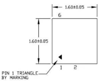
1.60±0.05 6 1.60±0.05 1 2 PIN 1 TRIANGLE BY MARKINGTOP VIEW
text_image
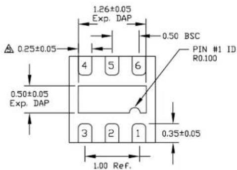
1.26±0.05 Exp. DAP 0.50 BSC PIN #1 ID R0.100 0.25±0.05 4 5 6 0.50±0.05 Exp. DAP 3 2 1 0.35±0.05 1.00 Ref.BOTTOM VIEW

text_image
0.55±0.05 0.00~0.05 0.152 Ref.SIDE VIEW
NOTE:
1. ALL DIMENSIONS ARE IN MILLIMETERS.
2. MAX. PACKAGE WARPAGE IS 0.05 mm.
3. MAXIMUM ALLOWABLE BURRS IS 0.076 mm IN ALL DIRECTIONS.
4. PIN #1 ID ON TOP WILL BE LASER/INK MARKED.
DIMENSION APPLIES TO METALIZED TERMINAL AND IS MEASURED
A BETWEEN 0.20 AND 0.25 MM FROM TERMINAL TIP.
APPLIED ONLY FOR TERMINALS
APPLIED ONLY FOR TERMINALS.
APPLIED FOR EXPOSED PAD AND TERMINALS.
6-Pin 1.6mm x 1.6mm Thin MLF (MT)
MICREL, INC. 2180 FORTUNE DRIVE SAN JOSE, CA 95131 USA
TEL +1 (408) 944-0800 FAX +1 (408) 474-1000 WEB http://www.micrel.com
The information furnished by Micrel in this data sheet is believed to be accurate and reliable. However, no responsibility is assumed by Micrel for its use. Micrel reserves the right to change circuitry and specifications at any time without notification to the customer.
Micrel Products are not designed or authorized for use as components in life support appliances, devices or systems where malfunction of a product can reasonably be expected to result in personal injury. Life support devices or systems are devices or systems that (a) are intended for surgical implant into the body or (b) support or sustain life, and whose failure to perform can be reasonably expected to result in a significant injury to the user. A Purchaser's use or sale of Micrel Products for use in life support appliances, devices or systems is a Purchaser's own risk and Purchaser agrees to fully indemnify Micrel for any damages resulting from such use or sale.
© 2007 Micrel, Inc.