MIC9130 - Electronic component Microchip - Free user manual and instructions
Find the device manual for free MIC9130 Microchip in PDF.

User questions about MIC9130 Microchip
0 question about this device. Answer the ones you know or ask your own.
Ask a new question about this device
Download the instructions for your Electronic component in PDF format for free! Find your manual MIC9130 - Microchip and take your electronic device back in hand. On this page are published all the documents necessary for the use of your device. MIC9130 by Microchip.
USER MANUAL MIC9130 Microchip
Note the following details of the code protection feature on Microchip devices:
• Microchip products meet the specification contained in their particular Microchip Data Sheet.
- Microchip believes that its family of products is one of the most secure families of its kind on the market today, when used in the intended manner and under normal conditions.
- There are dishonest and possibly illegal methods used to breach the code protection feature. All of these methods, to our knowledge, require using the Microchip products in a manner outside the operating specifications contained in Microchip's Data Sheets. Most likely, the person doing so is engaged in theft of intellectual property.
• Microchip is willing to work with the customer who is concerned about the integrity of their code.
- Neither Microchip nor any other semiconductor manufacturer can guarantee the security of their code. Code protection does not mean that we are guaranteeing the product as "unbreakable."
Code protection is constantly evolving. We at Microchip are committed to continuously improving the code protection features of our products. Attempts to break Microchip's code protection feature may be a violation of the Digital Millennium Copyright Act. If such acts allow unauthorized access to your software or other copyrighted work, you may have a right to sue for relief under that Act.
Information contained in this publication regarding device applications and the like is provided only for your convenience and may be superseded by updates. It is your responsibility to ensure that your application meets with your specifications. MICROCHIP MAKES NO REPRESENTATIONS OR WARRANTIES OF ANY KIND WHETHER EXPRESS OR IMPLIED, WRITTEN OR ORAL, STATUTORY OR OTHERWISE, RELATED TO THE INFORMATION, INCLUDING BUT NOT LIMITED TO ITS CONDITION, QUALITY, PERFORMANCE, MERCHANTABILITY OR FITNESS FOR PURPOSE. Microchip disclaims all liability arising from this information and its use. Use of Microchip devices in life support and/or safety applications is entirely at the buyer's risk, and the buyer agrees to defend, indemnify and hold harmless Microchip from any and all damages, claims, suits, or expenses resulting from such use. No licenses are conveyed, implicitly or otherwise, under any Microchip intellectual property rights unless otherwise stated.
Microchip received ISO/TS-16949:2009 certification for its worldwide headquarters, design and wafer fabrication facilities in Chandler and Tempe, Arizona; Gresham, Oregon and design centers in California and India. The Company's quality system processes and procedures are for its PIC® MCUs and dsPIC® DSCs, KEELQQ® code hopping devices, Serial EEPROMs, microperipherals, nonvolatile memory and analog products. In addition, Microchip's quality system for the design and manufacture of development systems is ISO 9001:2000 certified.
QUALITY MANAGEMENT SYSTEM CERTIFIED BY DNV = ISO/TS 16949=
Trademarks
The Microchip name and logo, the Microchip logo, AnyRate, AVR, AVR logo, AVR Freaks, BeaconThings, BitCloud, chipKIT, chipKIT logo, CryptoMemory, CryptoRF, dsPIC, FlashFlex, flexPWR, Heldo, JukeBlox, KEELOQ, KEELOQ logo, Kleer, LANCheck, LINK MD, maXStylus, maXTouch, MediaLB, megaAVR, MOST, MOST logo, MPLAB, OptoLyzer, PIC, picoPower, PICSTART, PIC32 logo, Prochip Designer, QTouch, RightTouch, SAM-BA, SpyNIC, SST, SST Logo, SuperFlash, tinyAVR, UNI/O, and XMEGA are registered trademarks of Microchip Technology Incorporated in the U.S.A. and other countries.
ClockWorks, The Embedded Control Solutions Company, EtherSynch, Hyper Speed Control, HyperLight Load, IntelliMOS, mTouch, Precision Edge, and Quiet-Wire are registered trademarks of Microchip Technology Incorporated in the U.S.A.
Adjacent Key Suppression, AKS, Analog-for-the-Digital Age, Any Capacitor, AnyIn, AnyOut, BodyCom, CodeGuard, CryptoAuthentication, CryptoCompanion, CryptoController, dsPICDEM, dsPICDEM.net, Dynamic Average Matching, DAM, ECAN, EtherGREEN, In-Circuit Serial Programming, ICSP, Inter Chip Connectivity, JitterBlocker, KleerNet, KleerNet logo, Mindi, MiWi, motorBench, MPASM, MPF, MPLAB Certified logo, MPLIB, MPLINK, MultiTRAK, NetDetach, Omniscient Code Generation, PICDEM, PICDEM.net, PICkit, PICtail, PureSilicon, QMatrix, RightTouch logo, REAL ICE, Ripple Blocker, SAM-ICE, Serial Quad I/O, SMART-I.S., SQI, SuperSwitcher, SuperSwitcher II, Total Endurance, TSHARC, USBCheck, VariSense, ViewSpan, WiperLock, Wireless DNA, and ZENA are trademarks of Microchip Technology Incorporated in the U.S.A. and other countries.
SQTP is a service mark of Microchip Technology Incorporated in the U.S.A.
Silicon Storage Technology is a registered trademark of Microchip Technology Inc. in other countries.
GestIC is a registered trademark of Microchip Technology Germany II GmbH & Co. KG, a subsidiary of Microchip Technology Inc., in other countries.
All other trademarks mentioned herein are property of their respective companies.
© 2018, Microchip Technology Incorporated, All Rights Reserved. ISBN: 978-1-5224-2804-6
Table of Contents
Preface 5
Introduction....5
Document Layout 5
Conventions Used in this Guide 6
Recommended Reading....7
The Microchip Web Site 7
Customer Support 7
Document Revision History 7
Chapter 1. Product Overview
1.1 Introduction ...... 9
1.2 MIC9130 Short Overview 9
1.3 MIC9130 Key Features 9
1.4 What Is the MIC9130 Power Over Ethernet Reference Design? 10
1.5 What Does the MIC9130 Power Over Ethernet Reference Design Kit Include? 12
Chapter 2. Installation and Operation
2.1 Introduction ...... 13
2.2 Board Features 13
2.3 How Does the MIC9130 Power Over Ethernet Work? 13
2.4 Setup and Testing the Board Procedure 14
2.4.1 Board Setup with PSE 14
2.4.2 Board Discrete Setup 14
2.5 Powered Device (PD) Controller Circuit 15
2.5.1 Detection Signature 15
2.5.2 Classification 15
2.5.3 Front End Analog Handshaking Limits 15
2.5.4 Power Mode 16
Appendix A. Schematic and Layouts
A.1 Introduction 17
A.2 Board – Schematic 18
A.3 Board – Top Silk Layer 19
A.4 Board – Top Copper and Silk Layer 20
A.5 Board – Top Copper Layer 21
A.6 Board – Bottom Copper Layer 22
A.7 Board – Bottom Copper and Silk Layer 23
A.8 Board – Bottom Silk Layer 24
Appendix B. Bill of Materials (BOM) 25
Appendix C. Plots and Waveforms
C.1 Flyback Converter Performance 29
C.2 Board Set Typical Waveforms 29
C.2.1 Bode Plot 32
C.3 Board Set Typical Measurements 33
Worldwide Sales and Service 35
Preface
NOTICE TO CUSTOMERS
All documentation becomes dated, and this manual is no exception. Microchip tools and documentation are constantly evolving to meet customer needs, so some actual dialogs and/or tool descriptions may differ from those in this document. Please refer to our website (www.microchip.com) to obtain the latest documentation available.
Documents are identified with a "DS" number. This number is located on the bottom of each page, in front of the page number. The numbering convention for the DS number is "DSXXXXXXXXA", where "XXXXXXXXX" is the document number and "A" is the revision level of the document.
For the most up-to-date information on development tools, see the MPLAB ^® IDE online help. Select the Help menu, and then Topics, to open a list of available online help files.
INTRODUCTION
This chapter contains general information that will be useful to know before using the MIC9130 Power Over Ethernet Reference Design. Items discussed in this chapter include:
- Document Layout
• Conventions Used in This Guide - Recommended Reading
• The Microchip Web Site - Customer Support
• Document Revision History
DOCUMENT LAYOUT
This document describes how to use the MIC9130 Power Over Ethernet Reference Design as a compliant power solution. The manual layout is as follows:
- Chapter 1. “Product Overview” – Important information about the MIC9130 Power Over Ethernet Reference Design.
- Chapter 2. “Installation and Operation” – Includes instructions on installing and starting the MIC9130 Power Over Ethernet Reference Design.
- Appendix A. “Schematic and Layouts” – Shows the schematic and layout diagrams for the MIC9130 Power Over Ethernet Reference Design.
- Appendix B. "Bill of Materials (BOM)" – Lists the parts used to build the MIC9130 Power Over Ethernet Reference Design.
- Appendix C. "Plots and Waveforms" – Shows the MIC9130 Power Over Ethernet Reference Design waveforms and typical measurements.
CONVENTIONS USED IN THIS GUIDE
This manual uses the following documentation conventions:
DOCUMENTATION CONVENTIONS
| Description Represents Examples | ||
| Arial font: | ||
| Italic characters Referenced books | oks MPLAB | ^ IDE User's Guide |
| Emphasized text ...is the only compiler... | ||
| Initial caps A window the Output | window | |
| A dialog the Settings dialog | ||
| A menu selection select Enable Programmer | ||
| Quotes A field name in a window or dialog | "Save project before build" | |
| Underlined, italic text with right angle bracket | A menu path File>Save | —— |
| Bold characters A dialog button | Click OK | |
| A tab | Click the Power tab | |
| N'Rnnnn | A number in verilog format, where N is the total number of digits, R is the radix and n is a digit. | 4'b0010, 2'hF1 |
| Text in angle brackets <> | A key on the keyboard | Press,, |
| Courier New font: | ||
| Plain Courier New | Sample source code | #define START |
| Filenames | autoexec.bat | |
| File paths | c:\mccl8\h | |
| Keywords | _asm, _endasm, static | |
| Command-line options | -0pa+, -0pa- | |
| Bit values | 0, 1 | |
| Constants | 0xFF, 'A' | |
| Italic Courier New | A variable argument | file.o, where file can be any valid filename |
| Square brackets [] | Optional arguments | mccl8 [options] file [options] |
| Curly brackets and pipe character: { | } | Choice of mutually exclusive arguments; an OR selection | errorlevel {0|1} |
| Ellipses... Replaces repeated text | var_name [, | var_name...] |
| Represents code supplied by user | void main (void){ ...} | |
RECOMMENDED READING
This user's guide describes how to use the MIC9130 Power Over Ethernet Reference Design. Another useful document is listed below. The following Microchip document is available and recommended as a supplemental reference resource:
- MIC9130 Data Sheet – “High-Voltage, High-Speed Telecom DC/DC Controller” (DS20000000)
Microchip provides online support via our web site at www.microchip.com. This web site is used as a means to make files and information easily available to customers. Accessible by using your favorite Internet browser, the web site contains the following information:
- Product Support – Data sheets and errata, application notes and sample programs, design resources, user's guides and hardware support documents, latest software releases and archived software
- General Technical Support – Frequently Asked Questions (FAQs), technical support requests, online discussion groups, Microchip consultant program member listing
- Business of Microchip – Product selector and ordering guides, latest Microchip press releases, listing of seminars and events, listings of Microchip sales offices, distributors and factory representatives
CUSTOMER SUPPORT
Users of Microchip products can receive assistance through several channels:
• Distributor or Representative
- Local Sales Office
• Field Application Engineer (FAE)
- Technical Support
Customers should contact their distributor, representative or field application engineer (FAE) for support. Local sales offices are also available to help customers. A listing of sales offices and locations is included in the back of this document.
Technical support is available through the web site at:
http://www.microchip.com/support.
DOCUMENT REVISION HISTORY
Revision A (March 2018)
- Initial Release of this Document.
NOTES:
Chapter 1. Product Overview
1.1 INTRODUCTION
This chapter provides an overview of the MIC9130 Power Over Ethernet Reference Design and covers the following topics:
• MIC9130 Short Overview
• MIC9130 Key Features
• What Is the MIC9130 Power Over Ethernet Reference Design?
• What Does the MIC9130 Power Over Ethernet Reference Design Kit Include?
1.2 MIC9130 SHORT OVERVIEW
The MIC9130 is a current-mode PWM controller that efficiently converts -48V telecom voltages to logic levels. The MIC9130 features a high-voltage start-up circuit that allows the device to be connected to input voltages as high as 180V. The high input voltage capability protects the MIC9130 from line transients that are common in telecom systems. The start-up circuitry also saves valuable board space and simplifies designs by integrating several external components.
The MIC9130 is capable of high-speed operation. Typically the MIC9130 can control a sub-25ns pulse width on the gate out pin. Its internal oscillator can operate over 2.5 MHz, with even higher frequencies available through synchronization. The high-speed operation of the MIC9130 is made safe by the very fast, 34 ns response from current sense to output, minimizing power dissipation in a fault condition.
The MIC9130 allows for the designs of high-efficiency power supplies. It can achieve efficiencies of more than 90% at high-output currents. Its low 1.3 mA quiescent current allows high efficiency even at light loads.
The MIC9130 has a maximum duty cycle of 50%. For designs requiring a high duty cycle, refer to the MIC9131 data sheet. The MIC9130 is available in 16-pin SOP and QSOP package options. The rated junction temperature range is from -40^ to +125^ .
1.3 MIC9130 KEY FEATURES
- Input voltage up to 180V
- Internal oscillator capable of >2.5 MHz operation
• Synchronization capability to 4 MHz - Current sense delay of 34 ns
• Minimum pulse width < 25 ns - 90% efficiency
• 1.3 mA quiescent current
• 1.0 μA shutdown current - Soft - start
- Resistor programmable current sense threshold
-
Selectable soft-start retry
• 4Ω sink, 12Ω source output driver -
Programmable undervoltage lockout
- Constant-frequency PWM current-mode control
• 16-pin SOIC and 16-pin QSOP packages
FIGURE 1-1: MIC9130 Typical Application Circuit.
1.4 WHAT IS THE MIC9130 POWER OVER ETHERNET REFERENCE DESIGN?
The MIC9130 Power over Ethernet, PoE, Powered Device (PD) Reference Design is designed to offer a complete IEEE802.3at PoE Plus compliant power solution.
The board includes an integrated solution (NCP1093), PoE signature and classification circuit, an EMI filter, and an isolated FLYBACK DC/DC converter using the MIC9130 controller. The MIC9130 is a high-speed current-mode PWM controller that features a high-voltage start-up circuit that enables the device to operate directly from 36V to 57V Power Sourcing Equipment (PSE) source voltage.
When a powered Ethernet cable is plugged into the board, the front-end handshaking circuit will apply the correct signature and classification impedances to accept power from the PSE. At the application of the power from the PSE, with input voltages between 36V and 57V, the DC/DC FLYBACK converter will engage and generate a 18.3V output with up to 1.7A of output current.
This board is for use with IEEE802.3at PoE Plus enabled Switch/Routers which provide power to the Ethernet cable as defined in IEEE802.3at PoE Plus PSE requirements.

text_image
MIC9130 POE+ 25W EVALUATION BOARD Rev D ADM00844 T1 CHINA POE+ ETH MAGNETICS CCI 1002 VIN L1 C11 SP2 BR1 GND_2 T2 C1 R1 O1 C3 m² J2 C9 GND_1 R2 Z15 C2 D3 + - R3 R24 D4 + - C7 R5 R26 R25 R10 AT R6 C9 C10 R19 C17 R12 R13 R9 C16 R17 C22 GND_1 C13 R18 RS R16 POE300F-XXX Coilcraft XXXX Y TP11 VOUT* MICROCHIP CEFIGURE 1-2: ADM00844 3D View.
text_image
C9130 POE+ 28M EVALUATION BOARD ADP ETHI-230L Coilcraft 1601D POE300F-19L Coilcraft 1541 J C9 R2 C2 D3 D1 C3 C4 C7 R24 D4 G10 R26 R25 R10 AT R6 R12 R13 R9 C18 C20 C6 C22 C17 C21 U3 R15 R23 C14 R11 C22 C16 C6 R17 C20 C6 R18 R9 R16 MICROCHIP e CEFIGURE 1-3: ADM00844 Board.

text_image
82mm 93.5mm RJ-45 ETH1- 230 RJ-45 PD CONTROLLER FLYBACK CONVERTER MICROCHIPFIGURE 1-4: Top View: ADM00844 Layout and Dimensions.
1.5 WHAT DOES THE MIC9130 POWER OVER ETHERNET REFERENCE DESIGN KIT INCLUDE?
The MIC9130 Power Over Ethernet Reference Design kit includes the following items:
- MIC9130 Power Over Ethernet Reference Design (ADM00844)
• Important Information Sheet
Chapter 2. Installation and Operation
2.1 INTRODUCTION
Explanations are provided for board setup with PSE and discrete setup. The MIC9130 Power Over Ethernet Reference Design kit set is fully tested to evaluate and demonstrate a complete IEEE802.3at PoE Plus compliant power solution and the MIC9130 controller.
2.2 BOARD FEATURES
The MIC9130 Power Over Ethernet Reference Design (ADM00844), has the following features:
- Input voltage: 36V to 57V input voltage
• 18.3V output voltage
• Output capability: up to 1.7A
• RJ45 input and output connectors - NCP1093 a PoE-PD IC that fully supports IEEE 802.3af/at specifications and includes a hot swap switch control and current limit block
- EMI filter
- Low cost single winding transformer
• MIC9130 DC/DC flyback converter
• > 3750VAC isolation
• 400 kHz fixed frequency PWM control
• Efficiency: over 90%
• Maximum output power: 30W
2.3 HOW DOES THE MIC9130 POWER OVER ETHERNET WORK?
When the RJ45 connector is plugged into a PSE, the front-end handshaking circuit applies the correct signature and classification impedances to gain power from the power source.
At the application of the power, the FLYBACK primary circuit is applied with 36V to 57V. This then converts power to the secondary circuit at 18.3V up to 1.7A.
For detailed explanation on DC/DC converter operation, refer to the MIC9130 data sheet.
2.4 SETUP AND TESTING THE BOARD PROCEDURE
2.4.1 Board Setup with PSE
Follow these steps to set up the board with available 802.3af compliant PSE:
- Plug-in a IEEE 802.3af compliant powered Ethernet cable into RJ45_1 I input connector.
- After the automatic handshake sequence, 18.3V are applied to post PL1.
- Data from the input is available at output connector RJ45_2.
2.4.2 Board Discrete Setup
Follow these steps to set up the board discretely to emulate 802.3af power sourcing equipment:
- Plug-in one end of CAT5 Ethernet cable into RJ45_1 connector, with the wires of the other end exposed.
-
Connect banana plug termination to brown, blue, orange, and green pairs.
-
Prepare test gear:
a) One Power Supply Unit PSU capable of supplying 60V with a 1A current limit.
b) Two Digital Volt Meters (DVMs) with 60V measuring capability
c) Two Ampere meters: 300 μA to 400 mA range (input side), and 2.5A rated for output side.
d) One Electronic Load, 18.3V capable set to 2A.
-
Apply test setup.
-
Turn ON all measurement devices.
-
Check Signature:
a) Set PSU to 9V.
b) Ammeter 1 should read between 280 μA to 368 mA (Class4).
- Check Classification:
a) Set PSU to: 14.5V to 20.5V range.
b) Ammeter 1 should read between 36 mA to 44 mA (Class4).
- DC/DC Power Supply Turn On and Start-up:
a) Set PSU to: 36V to 57V range.
b) DMV2 at the PL1 post should read 18.3V ± 1%.
c) Ammeter 2 should read between 1.7A ± 1% .

text_image
PSU Ammeter1 DVM1 Microchip DVM2 Ammeter2 Electronic LoadFIGURE 2-1: Connection Diagram.
2.5 POWERED DEVICE (PD) CONTROLLER CIRCUIT
The integrated PD interface supports the IEE 802.3af defined operating modes:
• Detection signature
- Current source classification
- Inrush current limits
- Operating current limits
2.5.1 Detection Signature
During the detection phase, the incremental equivalent resistance seen by PSE through the cable must be in the IEEE 802.3at standard specification range (23.70 kΩ to 26.30 kΩ) for a PSE voltage from 2.7V to 10.1V. In order to compensate for the nonlinear effect of the diode bridge and satisfy the specification at low PSE voltage, the NCP1093 presents a suitable impedance in parallel with 24.9 kΩ R _DET (R8) external resistor. During the detection phase, the DET pin is pulled to ground and goes in High Impedance mode (open-drain) once the device exits this mode, thus reducing the current consumption on the cable.
2.5.2 Classification
Once the PSE device has detected the PD device, the classification process begins. In classification, the PD regulates a constant current source that is set by the external resistor R_CLASS (R13) value on the CLASS pin.
The current source is defined as:
EQUATION 2-1:
| I_CLASS = 9.8VR/CLASS |
Table 2-1 shows how to configure the MIC9130 Power Over Ethernet classification circuit to set a Classification Level.
TABLE 2-1: CLASSIFICATION CIRCUIT CONFIGURATION
| Class | Input CurrentVIN = 15.4V to 20.5 V | PD Power Class Component Modification |
| Class 0 0 mA - 4 mA | 0.5W to 12.95W R13 = 4k9 | |
| Class 1 | 9 mA - 12 mA | 0.5W to 3.8W |
| Class 2 | 7 mA - 20 mA | 3.8W to 6.5W |
| Class 3 26 mA - 30 mA | 6.5W to 12 mA | 95W R13 = 350 |
| Class 4 | 36 mA - 44 mA | Not defined |
2.5.3 Front End Analog Handshaking Limits
Table 2-2 shows the designed limits of the board.
TABLE 2-2: ADM00844 LIMITS
| Description | Test Condition | Min. | Max. |
| Signature Test (Resistance) | V_IN = 2.7V to 10.1V | 23.7 kΩ | 26.3 kΩ |
| Classification Test, Class 4 (Line Current) | V_IN = 14.5V to 20.5V | 36 mA | 44 mA |
| DC/DC Full Power (Line Current) | V_IN = 36V to 57V; I_OUT = 1.7A V_OUT = 18.3V | 627 mA | 994 mA |
2.5.4 Power Mode
When the classification handshake is completed, the PSE and PD device move into Operating mode.
Appendix A. Schematic and Layouts
A.1 INTRODUCTION
This appendix contains the following schematics and layouts for the MIC9130 Power Over Ethernet Reference Design:
- Board – Schematic
- Board – Top Silk Layer
- Board – Top Copper and Silk Layer
- Board – Top Copper Layer
- Board – Bottom Copper Layer
- Board – Bottom Copper and Silk Layer
- Board – Bottom Silk Layer
DS50002731A-page 18 © 2018 Microchip Technology Inc.
A.2 BOARD - SCHEMATIC
text_image
CON1 X RS RAX SHELLI MOD 4/8/2-5 Vcc 1 J2 GND 2 GND 122F2 Vcc 1 D25 Vcc 100% U1 NCP1093 C19 1.5V 100% 100% 100% 100% 100% 100% 100% 100% 100% 100% 100% 100% 100% 100% 100% 100% 100% 100% 100% 100% 100% 100% 100% 100% 100% 100% AC C16 3.5V 30V 3.5V 3.5V 3.5V 3.5V 3.5V 3.5V 3.5V 3.5V 3.5V 3.5V 3.5V 3.5V 3.5V 3.5V 3.5V 3.5V 3.5V 3.5V 3.5V 3.5V 3.7V 3.7V 3.7V 3.7V 3.7V 3.7V 3.7V 3.7V 3.7V 3.7V 3.7V 3.7V 3.7V 3.7V 3.7V 3.7V 3.7V 3.7V 3.7V 3.7V 3.8V 3.8V 3.8V 3.8V 3.8V 3.8V 3.8V 3.8V 3.8V 3.8V 3.8V 3.8V 3.8V 3.8V 3.8V 3.8V 3.8V 3.8V 3.8V 3.8V 3.9V 3.9V 3.9V 3.9V 3.9V 3.9V 3.9V 3.9V 3.9V 3.9V 3.9V 3.9V 3.9V 3.9V 4.0V 4.0V 4.0V 4.0V 4.0V 4.0V 4.0V 4.0V 4.0V 4.0V 4.0V 4.0V 4.0V 4.0V 4.0V 4.0V 4.0V 4.0V 4.0V 4.1V 4.1V 4.1V 4.1V 4.1V 4.1V 4.1V 4.1V 4.1V 4.1V 4.1V 4.1V 4.1V 4.1V 4.2V 4.2V 4.2V 4.2V 4.2V 4.2V 4.2V 4.2V 4.2V 4.2V 4.2V 4.2V 4.2V 4.2V 4.2V 4.2VMIC9130 Power Over Ethernet IEE802.3at Poe Plus PD Reference Design
A.3 BOARD - TOP SILK LAYER

text_image
MIC9130 POE+ 25W EVALUATION BOARD Rev 0 CON1 ADM00844 T1 CON2 BR2 BR1 VIN L1 C11 GND_2 T2 C1 R1 D1 J2 C3 + C9 GND_1 R2 C2 D3 R3 D4 Gate C7 R5 R10JR10CR10 AT R6 R14 C8 C18 R15 C12 R7 C15 R19 Gnd_2 U2 C19 R12 R13 R8 C20 C22 R17 GND_1 C13 R18 R9 R16 TP12 GND C4 C5 J1 TP11 UOUT+ MICROCHIP CEA.4 BOARD – TOP COPPER AND SILK LAYER
text_image
MIC9130 POE+ 25W EVALUATION BOARD Rev 0 ADMO0844 T1 CON1 BR2 BR1 VIN L1 C11 GND_2 J2 C9 R2 C2 GND_1 D3 R3 R3 D4 Gate D5 R101R100R10 AT R14 C8 C18 R7 C15 C12 C19 Gnd_2 U2 C20 R12 R13 R8 C16 R17 C22 GND_1 C13 R18 R9 R16 C1 R1 D1 C3 GND TP12 C4 C5 J1 TP11 VOUT+ MICROCHIP CEA.5 BOARD - TOP COPPER LAYER

natural_image
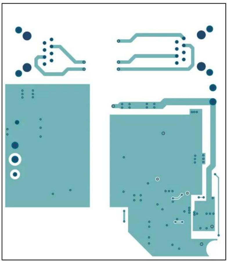
Pure electrical circuit lines without any symbolsA.6 BOARD - BOTTOM COPPER LAYER
natural_image
Pure electrical circuit lines without any symbolsA.7 BOARD - BOTTOM COPPER AND SILK LAYER
text_image
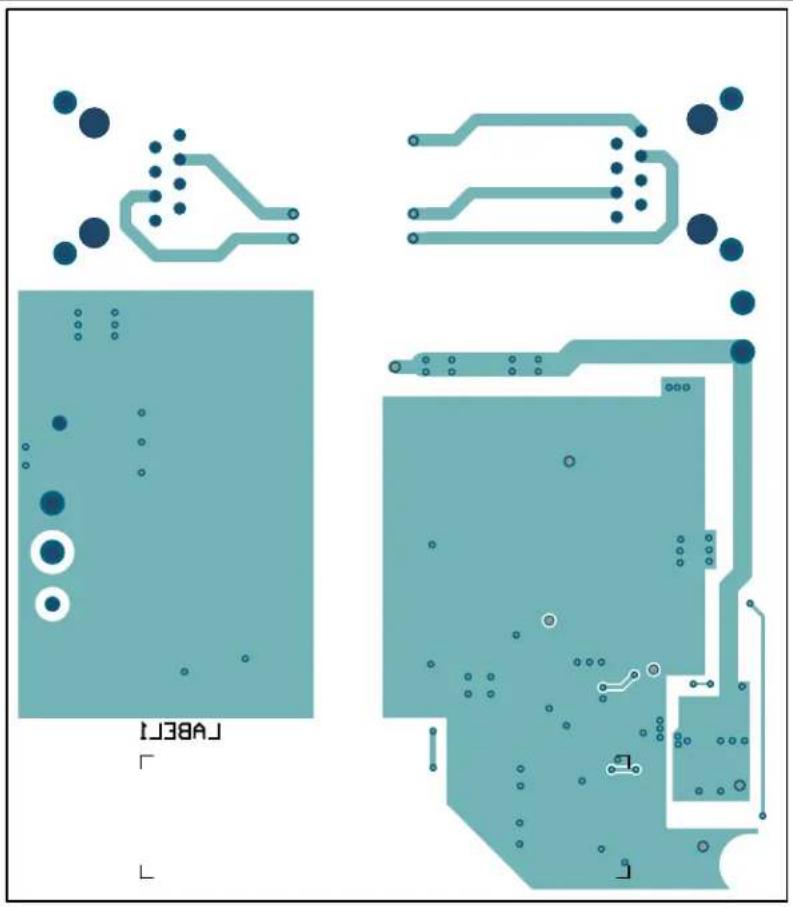
JABE1 JA.8 BOARD - BOTTOM SILK LAYER
text_image
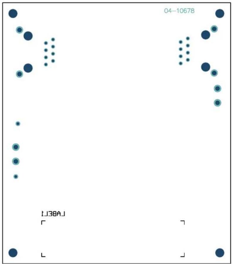
04-10678 JJ38AJAppendix B. Bill of Materials (BOM)
TABLE B-1: BILL OF MATERIALS (BOM) FOR MIC9130 POWER OVER ETHERNET REFERENCE DESIGN (ADM00844) ^(1)
| Qty. | Reference Description Manufacturer Part Number | |||
| 2 BR | 1, BR2 Bridge | rectifier, single phase standard 100V, surface mount DF-S | Diodes Incorporated® | DF1501S-T |
| 1 C1 | Capacitor ceramic 10 μF, ±10%, 6.3V, X5R, 1206, (3216 Metric) | Yageo Corporation CC | 1206KKX5R5BB106 | |
| 1 C2 | Capacitor ceramic 0.1 μF, 100V, 10%, X7R, SMD, 1206 | Yageo Corporation CC | 1206KKX7R0BB104 | |
| 1 C3 | Aluminum polymer capacitor radial, 82 μF, 35V, Can-SMD, 20 mΩ, 5000 Hours at 105°C | Panasonic® - ECG 35 | SVPF82M | |
| 2 C4 | C5 Capacitor ceramic 22 μF, 35V, 20%, JB, SMD, 0805 | TDK Corporation C201 | 2JB1V226M125AC | |
| 1 C6 | Aluminum electrolytic capacitors 47 μF, 35V, Radial, Can - SMD, 1000 Hours at 105°C | Nichicon Corporation | UWT1V470MCL1GS | |
| 5 C7 | C8, C15, C18, C19 | Capacitor ceramic 0.1 μF, 50V, 10%, X7R, SMD, 0805 | Yageo Corporation CC | 0805KRX7R9BB104 |
| 1 C9 | Capacitor aluminum 100 μF, 100V, 20%, SMD, J21 | Nichicon Corporation | UCD2A101MNQ1MS | |
| 1 C11 | Capacitor ceramic 1 μF, 100V, 20%, X7R, SMD, 1210 | TDK Corporation C322 | 25X7R2A105M200AA | |
| 1 C12 | Capacitor ceramic 0.1 μF, 100V, 10%, X7R, SMD, 1210 | KEMET | C1210C104K1RACTU | |
| 1 | C13 | Capacitor ceramic 10 μF, ±10%, 16V, X7R, 1206, (3216 Metric) | Yageo Corporation CC | 1206KKX7R7BB106 |
| 1 C14 | Capacitor ceramic 0.027 μF, 50V, 10%, X7R, SMD, 0805 | Yageo Corporation CC | 0805KRX7R9BB273 | |
| 1 C16 | Capacitor ceramic 330 pF, 50V, 10%, X7R, SMD, 0805 | Yageo Corporation CC | 0805KRX7R9BB331 | |
| 1 C17 | Capacitor ceramic 0.056 μF, 50V, 10%, X7R, SMD, 0805 | KEMET | C0805C563K5RACTU | |
| 1 C20 | Capacitor ceramic 220 pF, 50V, C0G/NPO, 0805 | Yageo Corporation CC | 0805JRNPO9BN221 | |
| 1 C21 | Capacitor ceramic 39 pF, 50V, 10%, C0G, SMD, 0805 | KEMET | C1210C104K1RACTU | |
| 1 C22 | Capacitor ceramic 2.2 μF, 100V, 10%, X7S, SMD, 1206 | TDK Corporation C321 | 6X7S2A225K160AB | |
| 2 | CON1, CON2 | Jack modular connector, 8p8c (RJ45, Ethernet), 90°Angle (Right) Shielded, Cat3 | Molex® | 956223981 |
| 1 D1 | Diode schottky, B560C, 5A, 60V, SMD, DO-214AB_SMC | Diodes Incorporated® | B560C-13-F | |
| Qty. | Reference | Description | Manufacturer | Part Number |
| 1 D3 | Diode standard, 100V, 1A, surface mount, SMA | Diodes Incorporated® | RS1B-13-F | |
| 1 D4 | Diode standard, 250V, 200 mA (DC), surface mount, SOD-232 | ON Semiconductor® | BAS21AHT1G | |
| 1 D5 | Diode zener, 12V, 200MW, SOD323 ON Semiconductor | ® | MM3Z12VST1G | |
| 1 D6 | Diode schottky, BAT54H, 30V, 0.2A, SMD, SOD-323 | ON Semiconductor® | NSVBAT54HT1G | |
| 2 J1, | J2 2 position wire-to-board terminal block, horizontal with board, 5.08 mm, through hole | On-Shore Technology, Inc. | OSTVI022152 | |
| 1 L1 | Inductor Hi SRF, Shlded, 10 uH, 1.7A, 10%, SMD 1812 | Coilcraft 1812PS-103KLB | ||
| 1 PCB | MIC9130 Power Over Ethernet Reference Design Printed Circuit Board | Microchip Technology Inc. | 04-10678 | |
| 1 Q1 | Bipolar transistors, BJT SS SOT23, GP, XSTR, NPN, 30V | ON Semiconductor® | MMBT2222ALT3G | |
| 1 Q2 | N-Channel, 150V, 33A (Tc), 74W (Tc), surface mount, PG-TDSON-8 | Infineon Technologies AG | BSC360N15NS3GATMA1 | |
| 1 R1 | Resistor, TKF, 100k, 1%, 1/4W, SMD, 1206 Panasonic | ® - ECG ER | J-8ENF1003V | |
| 1 R2 | Resistor, TKF, 5.1k, 1%, 1W, SMD, 2512 Panasonic | ® - ECG ER | J1TNF5101U | |
| 1 R3 | Resistor, TKF, 1.2R, 1%, 1/8W, SMD, 0805 Panasonic | ® - ECG ER | J-6RQF1R2V | |
| 1 R4 | Resistor, TKF, 4.75K, 1%, 1/8W, SMD, 0805 Panasonic | ® - ECG ER | J-6ENF4751V | |
| 1 | R5 | Resistor, TKF, 2.67k, 1%, 1/8W, SMD, 0805 | Yageo Corporation | RC0805FR-072K67L |
| 1 R6 | Resistor, TKF, 0.33R, 1%, 1W, SMD, 2512 Vishay/Dale WSL | 2512R3300FEA | ||
| 1 R7 | Resistor, TKF, 243k, 1%, 1/8W, SMD, 0805 Yageo Corporation on RC0805FR-07243KL | |||
| 1 R8 | Resistor, TF, 24.9k, 1%, 1/4W, SMD, 0805 Stackpole | Electronics, Inc, | RNCP0805FTD24K9 | |
| 2 | R9, R20 | Resistor, TKF, 30.1k, 1%, 1/8W, SMD, 0805 | Yageo Corporation | RC0805FR-0730K1L |
| 3 | R10, R14, R24 | Resistor, TKF, 10k, 1%, 1/8W, SMD, 0805 | Panasonic® - ECG ER | J-6ENF1002V |
| 1 | R11 | Resistor, TKF, 1.15K, 1%, 0.25W, SMD, 1206 | Yageo Corporation | RC1206FR-071K15L |
| 2 R12, R16 | Resistor, TKF, 169k, 1%, 1/8W, SMD, 0805 Panasonic | ® - ECG ER | J-6ENF1693V | |
| 1 | R13 | Resistor, TKF, 255R, 1%, 1/8W, SMD, 0805 | Yageo Corporation | RC0805FR-07255RL |
| 1 R15 | Resistor, TKF, 100k, 1/8W, 1%, SMD, 0805 Panasonic | ® - ECG ER | J-6ENF1003V | |
| 2 R17, R26 | Resistor, TKF, 0R, 1/8W, SMD, 0805 Panasonic | ® - ECG ER | J-6GEY0R00V | |
| 1 R18 | Resistor, TKF, 422k, 1%, 1/8W, SMD, 0805 Panasonic | ® - ECG ER | J-6ENF4223V | |
| 1 | R19 | Resistor, SMD, 5.1 kΩ, 1%, 1/8W, 0805 | TE Connectivity, Ltd. | CRG0805F5K1 |
| 1 | R21 | Resistor, TKF, 21.5k, 1%, 1/8W, SMD, 0805 | Yageo Corporation | RC0805FR-0721K5L |
| 1 | R22 | Resistor, TKF, 806R, 1%, 1/8W, SMD, 0805 | Yageo Corporation | RC0805FR-07806RL |
| 1 | R23 | Resistor, TKF, 15.8k, 1%, 1/8W, SMD, 0805 | Yageo Corporation | RC0805FR-0715K8L |
| 1 | R25 | Resistor, TKF, 64.9k, 1%, 1/8W, SMD, 0805 | Vishay/Dale | CRCW080564K9FKEA |
| 1 T1 | Signal transformer ETH1, 30W, 2 pairs PoE plus magnetic module, SMD | Coilcraft ETH1-230L | ||
| 1 T2Qty. | Flyback transformer, 1:0.56, 1:0.33, 36V-72V, SMDReference Description Manufacturer Part Number | Coilcraft POE300F-19L | ||
| 1 U1 | Power over Ethernet controller, 1-Channel, 802.3at (PoE+), 802.3af (PoE) 10-DFN (3 x 3) | ON Semiconductor® | NCP1093MNRG | |
| 1 U2 | MCHP ANALOG PWM CONTROLLER, 2.5 MHz, MIC9130YQS, QSOP-16 | Microchip Technology Inc. | MIC9130YQS | |
| 1 U3 | IC POWER, ATL432AQDBZR, Shunt Voltage Reference, SOT-23-3 | Texas Instruments ATL432AQDBZR | ||
| 1 U4 | IC PHOTO HCPL-181 4-SMD Avago Technologies HCPL-18 | 1-00CE | ||
Note 1: The components listed in this Bill of Materials are representative of the PCB assembly. The released BOM used in manufacturing uses all RoHS-compliant components.
NOTES:
Appendix C. Plots and Waveforms
C.1 FLYBACK CONVERTER PERFORMANCE
V_IN = 36V to 57V .
Efficiency 85% at full load.
V_(OUT RIPPLE) < 150 mV.
Load Regulation = 0.1% at V_IN = 48V.
C.2 BOARD SET TYPICAL WAVEFORMS

line
| Time (ns) | Voltage (mV) | | --------- | ------------ | | 0 | ~0 | | 500 | ~0 | | Peak | 100 |FIGURE C-1: V OUT Ripple.
line
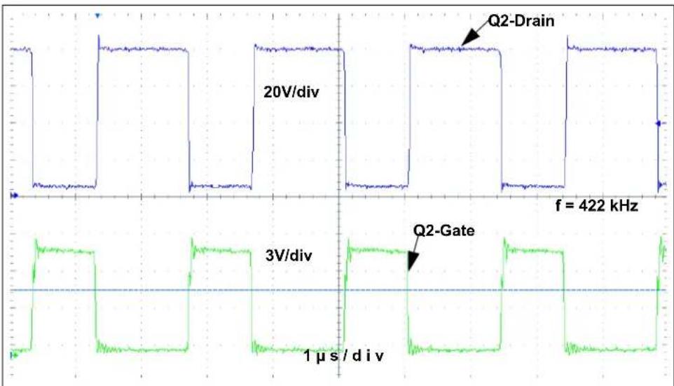
| Frequency (kHz) | Q2-Drain (20V/div) | Q2-Gate (3V/div) | | --------------- | ------------------ | ---------------- | | 422 | High | Low |FIGURE C-2: Switching Edges, Q2 Gate and Drain Voltage.

FIGURE C-3: Switching Edges, Q2 Gate and Drain Voltage.
line
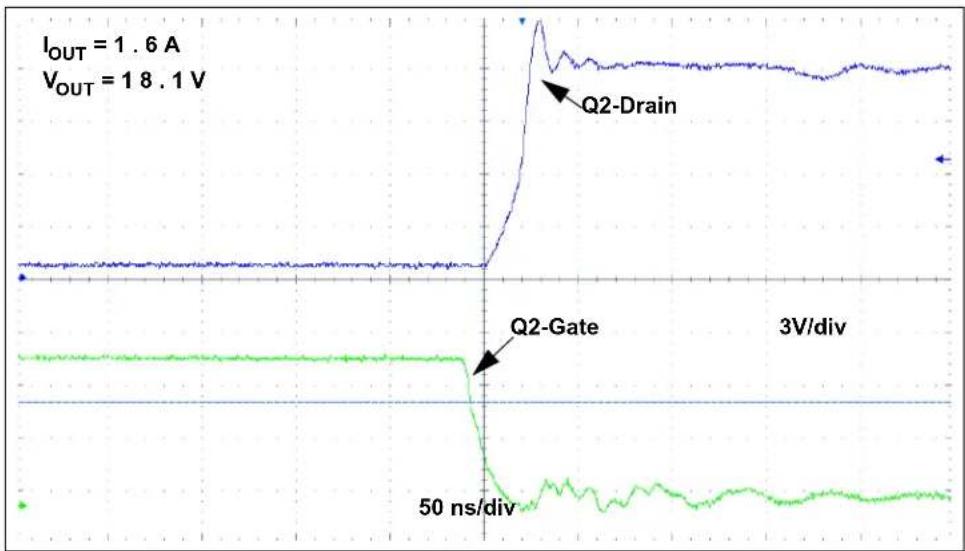
| Time (s) | Q2-Drain (A) | Q2-Gate (ns/div) | |----------|--------------|------------------| | 0 | 1.6 | 50 | | 3 | ~1.6 | ~50 |FIGURE C-4: Switching Edges, Q2 Gate and Drain Voltage.
line
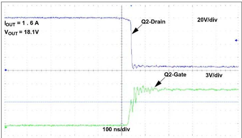
| Signal | Time (ns) | |------------|-----------| | Q2-Drain | ~0 | | Q2-Gate | ~100 |FIGURE C-5: Switching Edges, Q2 Gate and Drain Voltage.
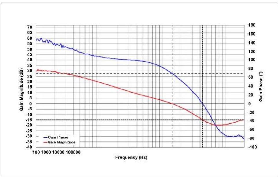
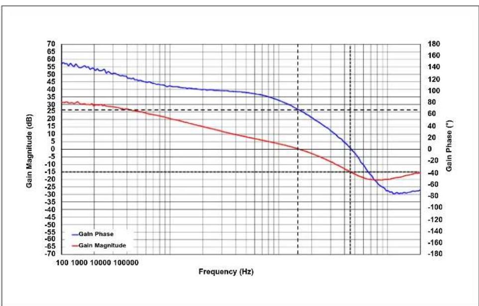
C.2.1 Bode Plot
Resistive Load 12.8Ω, 1.4A, P_OUT = 25 W
line
| Frequency (Hz) | Gain Magnitude (dB) | Gain Phase (°) | | -------------- | ------------------- | -------------- | | 100 | 30 | 140 | | 1000 | 28 | 130 | | 10000 | 25 | 120 | | 100000 | 20 | 110 | | 1000000 | 15 | 100 | | 10000000 | 10 | 90 | | 100000000 | 5 | 80 | | 1000000000 | 0 | 70 | | 10000000000 | -5 | 60 | | 100000000000 | -10 | 50 | | 1000000000000 | -15 | 40 | | 10000000000000 | -20 | 30 | | 100000000000000| -25 | 20 | | 1000000000000000| -35 | 15 | | 1000000000000000| -45 | 18 | | 100 | -85 | -85 | | 1 | -85 | -85 | | -1 | -85 | -85 | | -2 | -85 | -85 | | -3 | -85 | -85 | | -4 | -85 | -85 | | -5 | -85 | -85 | | -6 | -85 | -85 | | -7 | -85 | -85 | | -8 | -85 | -85 | | -9 | -85 | -85 | | -10 | -85 | -85 | | -11 | -85 | -85 | | -12 | -85 | -85 | | -13 | -85 | -85 | | -14 | -85 | -85 | | -15 | -85 | -85 | | -16 | -85 | -85 | | -17 | -85 | -85 | | -18 | -85 | -85 | | -19 | -85 | -85 | | -20 | -85 | -85 | | -21 | -85 | -85 | | -22 | -85 | -85 | | -23 | -85 | -85 | | -24 | -85 | -85 | | -25 | -85 | -85 | | -26 | -85 | -85 | | -27 | -85 | -85 | | -28 | -85 | -85 | | -29 | -85 | -85 | | -30 | -85 | -85 | | -31 | -85 | -85 | | -32 | -85 | -85 | | -33 | -85 | -85 | | -34 | -85 | -85 | | -35 | -85 | -85 | | -36 | -85 | -85 | | -37 | -85 | -85 | | -38 | -85 | -85 | | -39 | -85 | -85 | | -40 | -85 | -85 | | 1 | 6 | 6 | | 2 | 4 | 4 | | 3 | 2 | 2 | | 4 | 1 | 1 | | 5 | 0 | 0 | | 6 | -2 | -2 | | 7 | -4 | -4 | | 8 | -6 | -6 | | 9 | -8 | -8 | | 10 | -10 | -10 | | 11 | -12 | -12 | | 12 | -14 | -14 | | 13 | -16 | -16 | | 14 | -18 | -18 | | 15 | -2 | -2 | | 16 | -2.2 | -2.2 | | 17 | -2.4 | -2.4 | | 18 | -2.6 | -2.6 | | 19 | -2.8 | -2.8 | | 20 | -3 | -3 | | 21 | -3.2 | -3.2 | | 22 | -3.4 | -3.4 | | 23 | -3.6 | -3.6 | | 24 | -3.8 | -3.8 | | 25 | -4 | -4 | | 26 | -4.2 | -4.2 | | 27 | -4.4 | -4.4 | | 28 | -4.6 | -4.6 | | 29 | -4.8 | -4.8 | | 30 | -5 | -5 | | 31 | -5.2 | -5.2 | | 32 | -5.4 | -5.4 | | 33 | -5.6 | -5.6 | | 34 | -5.8 | -5.8 | | 35 | -6 | -6 | | 36 | -6.2 | -6.2 | | 37 | -6.4 | -6.4 | | 38 | -6.6 | -6.6 | | 39 | -6.8 | -6.8 | | 40 | -7 | -7 | | 41 | -7.2 | -7.2 | | 42 | -7.4 | -7.4 | | 43 | -7.6 | -7.6 | | 44 | -7.8 | -7.8 | | 45 | -8 | -8 | | 46 | -8.2 | -8.2 | | 47 | -8.4 | -8.4 | | 48 | -8.6 | -8.6 | | 49 | -8.8 | -8.8 | | 50 | -9 | -9 | | | 51 | nan | nan | |FIGURE C-6: Gain Magnitude and Gain Phase vs. Frequency for 48V Input. Gain Margin, GM = 14.9 dB, Phase Margin, PM = 69.6°.
line
| Frequency (Hz) | Gain Magnitude (dB) | Gain Phase (°) | | -------------- | ------------------- | -------------- | | 100 | 30 | 140 | | 1000 | 28 | 130 | | 10000 | 25 | 120 | | 100000 | 22 | 110 | | 1000000 | 20 | 100 | | 10000000 | 15 | 90 | | 100000000 | 10 | 80 | | 1000000000 | 5 | 70 | | 10000000000 | 2 | 60 | | 100000000000 | -5 | 50 | | 1000000000000 | -15 | 40 | | 10000000000000 | -25 | 30 | | 100000000000000| -35 | 25 | | 100000000000000| -45 | 22 | | 100000000000000| -55 | 25 | | 100000000000000| -65 | 35 | | 100000000000000| -75 | 45 | | 100 | 65 | 18 | | 1 | 65 | 18 | | 1e-1 | 65 | 18 | | 1e-2 | 65 | 18 | | 1e-3 | 65 | 18 | | 1e-4 | 65 | 18 | | 1e-5 | 65 | 18 | | 1e-6 | 65 | 18 | | 1e-7 | 65 | 18 | | 1e-8 | 65 | 18 | | 1e-9 | 65 | 18 | | 1e-10 | 65 | 18 | | 1e-11 | 65 | 18 | | 1e-12 | 65 | 18 | | 1e-13 | 65 | 18 | | 1e-14 | 65 | 18 | | 1e-15 | 65 | 18 | | 1e-16 | 65 | 18 | | 1e-17 | 65 | 18 | | 1e-18 | 65 | 18 | | 1e-19 | 65 | 18 | | 1e-20 | 65 | 18 | | 1e-21 | 65 | 18 | | 1e-22 | 65 | 18 | | 1e-23 | 65 | 18 | | 1e-24 | 65 | 18 | | 1e-25 | 65 | 18 | | 1e-26 | 65 | 18 | | 1e-27 | 65 | 18 | | 1e-28 | 65 | 18 | | 1e-29 | 65 | 18 | | 1e-30 | 65 | 18 | | 1e-31 | 65 | 18 | | 1e-32 | 65 | 18 | | 1e-33 | 65 | 18 | | 1e-34 | 65 | 18 | | 1e-35 | 65 | 18 | | 1e-36 | 65 | 18 | | 1e-37 | 65 | 18 | | 1e-38 | 65 | 18 | | 1e-39 | 65 | 18 | | 1e-40 | 65 | 18 | | 1e-41 | 65 | 18 | | 1e-42 | 65 | 18 | | 1e-43 | 65 | 18 | | 1e-44 | 65 | 18 | | 1e-45 | 65 | 18 | | 1e-46 | 65 | 18 | | 1e-47 | 65 | 18 | | 1e-48 | 65 | 18 | | 1e-49 | 65 | 18 | | 1e-50 | 65 | 18 | | 1e-51 | 65 | nan | | >*(-) | <-35 | ~-$9 | The data is presented in a table format with three columns: Frequency (Hz) and Gain Magnitude. The Gain Magnitude column contains values in dB, and the Gain Phase column contains values in degrees. There are two data series: Gain Phase and Gain Magnitude. The data is plotted as a line between two horizontal lines. The labels above the lines are 'Gain Magnitude' and 'Gain Phase'.FIGURE C-7: Gain Magnitude and Gain Phase vs. Frequency for 60V Input. Gain Margin, GM = 15.5 dB, Phase Margin, PM = 67.5°.
C.3 BOARD SET TYPICAL MEASUREMENTS

line
| Input Voltage (V) | 0.4A Load | 1.0A Load | 1.6A Load | | ----------------- | --------- | --------- | --------- | | 36 | 18.06 | 18.06 | 17.98 | | 38 | 18.06 | 18.06 | 18.00 | | 40 | 18.06 | 18.06 | 18.05 | | 42 | 18.06 | 18.06 | 18.05 | | 44 | 18.06 | 18.06 | 18.04 | | 46 | 18.06 | 18.06 | 18.05 | | 48 | 18.06 | 18.06 | 18.05 | | 50 | 18.06 | 18.06 | 18.05 | | 52 | 18.06 | 18.06 | 18.05 | | 54 | 18.06 | 18.06 | 18.05 | | 56 | 18.06 | 18.06 | 18.05 | | 58 | 18.06 | 18.06 | 18.05 | | 60 | 18.06 | 18.06 | 18.05 |FIGURE C-8: Line Regulation - Output Voltage vs. Input Voltage.
line
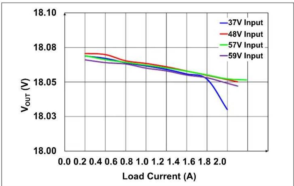
| Load Current (A) | 37V Input | 48V Input | 57V Input | 59V Input | | ---------------- | --------- | --------- | --------- | --------- | | 0.0 | 18.08 | 18.08 | 18.08 | 18.08 | | 0.2 | 18.075 | 18.08 | 18.078 | 18.076 | | 0.4 | 18.07 | 18.078 | 18.075 | 18.073 | | 0.6 | 18.065 | 18.075 | 18.072 | 18.07 | | 0.8 | 18.06 | 18.07 | 18.068 | 18.065 | | 1.0 | 18.055 | 18.065 | 18.063 | 18.06 | | 1.2 | 18.05 | 18.06 | 18.058 | 18.055 | | 1.4 | 18.045 | 18.055 | 18.053 | 18.05 | | 1.6 | 18.04 | 18.05 | 18.048 | 18.045 | | 1.8 | 18.035 | 18.045 | 18.043 | 18.04 | | 2.0 | 18.03 | 18.04 | 18.04 | 18.035 |FIGURE C-9: Load Regulation - Output Voltage vs. Output Current.
line
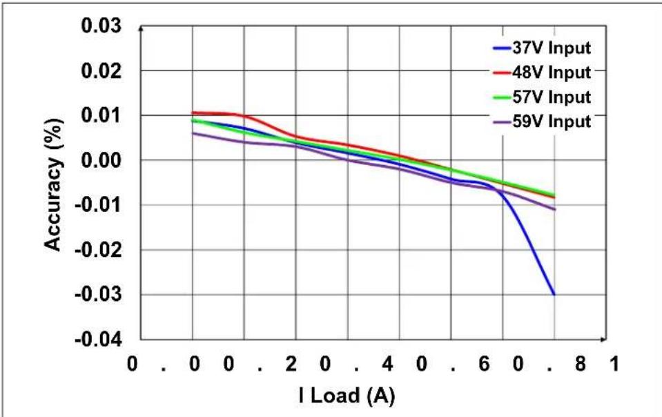
| I Load (A) | 37V Input | 48V Input | 57V Input | 59V Input | | ---------- | --------- | --------- | --------- | --------- | | 0 | 0.01 | 0.01 | 0.01 | 0.007 | | 2 | 0.005 | 0.008 | 0.006 | 0.004 | | 4 | 0.00 | 0.002 | 0.001 | 0.00 | | 6 | -0.005 | -0.001 | -0.002 | -0.003 | | 8 | -0.03 | -0.01 | -0.01 | -0.012 |FIGURE C-10: Output Voltage Accuracy - V OUT Accuracy vs. Output Current.

line
| Load Current (A) | 37V Input | 48V Input | 57V Input | 59V Input | | ---------------- | --------- | --------- | --------- | --------- | | 0.0 | 85.0 | 86.0 | 86.0 | 80.0 | | 0.2 | 86.0 | 87.0 | 87.0 | 81.0 | | 0.4 | 87.0 | 88.0 | 88.0 | 82.0 | | 0.6 | 88.0 | 89.0 | 89.0 | 83.0 | | 0.8 | 89.0 | 90.0 | 90.0 | 84.0 | | 1.0 | 90.0 | 91.0 | 91.0 | 85.0 | | 1.2 | 91.0 | 92.0 | 92.0 | 86.0 | | 1.4 | 92.0 | 92.0 | 92.0 | 87.0 | | 1.6 | 92.0 | 92.0 | 92.0 | 88.0 | | 1.8 | 92.0 | 92.0 | 92.0 | 89.0 | | >1.8 | ~92.0 | ~92.0 | ~92.0 | ~91.0 |FIGURE C-11: Efficiency vs. Load Current at Different Input Voltages.
Worldwide Sales and Service
AMERICAS
Corporate Office
2355 West Chandler Blvd.
Chandler, AZ 85224-6199
Tel: 480-792-7200
Fax: 480-792-7277
Technical Support:
http://www.microchip.com/
support
Web Address:
www.microchip.com
Atlanta
Duluth, GA
Tel: 678-957-9614
Fax: 678-957-1455
Austin, TX
Tel: 512-257-3370
Boston
Westborough, MA
Tel: 774-760-0087
Fax: 774-760-0088
Chicago
Itasca, IL
Tel: 630-285-0071
Fax: 630-285-0075
Dallas
Addison, TX
Tel: 972-818-7423
Fax: 972-818-2924
Detroit
Novi, MI
Tel: 248-848-4000
Houston, TX
Tel: 281-894-5983
Indianapolis
Noblesville, IN
Tel: 317-773-8323
Fax: 317-773-5453
Tel: 317-536-2380
Los Angeles
Mission Viejo, CA
Tel: 949-462-9523
Fax: 949-462-9608
Tel: 951-273-7800
Raleigh, NC
Tel: 919-844-7510
New York, NY
Tel: 631-435-6000
San Jose, CA
Tel: 408-735-9110
Tel: 408-436-4270
Canada - Tor
Tel: 905-695-1980
Fax: 905-695-2078
ASIA/PACIFIC
Asia Pacific Office
Suites 3707-14, 37th Floor
Tower 6, The Gateway
Harbour City, Kowloon
Hong Kong
Tel: 852-2943-5100
Fax: 852-2401-3431
Australia - Sydney
Tel: 61-2-9868-6733
Fax: 61-2-9868-6755
China - Beijing
Tel: 86-10-8569-7000
Fax: 86-10-8528-2104
China - Chengdu
Tel: 86-28-8665-551
Fax: 86-28-8665-7889
China - Chongqing
Tel: 86-23-8980-9588
Fax: 86-23-8980-9500
China - Dongguan
Tel: 86-769-8702-9880
China - Guangzhou
Tel: 86-20-8755-8029
China - Hangzhou
Tel: 86-571-8792-8115
Fax: 86-571-8792-8116
China - Hong Kong SAR
Tel: 852-2943-5100
Fax: 852-2401-3431
China - Nanjing
Tel: 86-25-8473-2460
Fax: 86-25-8473-2470
China - Qingdao
Tel: 86-532-8502-7355
Fax: 86-532-8502-7205
China - Shanghai
Tel: 86-21-3326-8000
Fax: 86-21-3326-8021
China - Shenyang
Tel: 86-24-2334-2829
Fax: 86-24-2334-2393
China - Shenzhen
Tel: 86-755-8864-2200
Fax: 86-755-8203-1760
China - Wuhan
Tel: 86-27-5980-5300
Fax: 86-27-5980-5118
China - Xian
Tel: 86-29-8833-7252
Fax: 86-29-8833-7256
ASIA/PACIFIC
China - Xiamen
Tel: 86-592-2388138
Fax: 86-592-2388130
China - Zhuhai
Tel: 86-756-3210040
Fax: 86-756-3210049
India - Bangalore
Tel: 91-80-3090-4444
Fax: 91-80-3090-4123
India - New Delhi
Tel: 91-11-4160-8631
Fax: 91-11-4160-8632
India - Pune
Tel: 91-20-3019-1500
Japan - Osaka
Tel: 81-6-6152-7160
Fax: 81-6-6152-9310
Japan - Tokyo
Tel: 81-3-6880-3770
Fax: 81-3-6880-3771
Korea - Daegu
Tel: 82-53-744-4301
Fax: 82-53-744-4302
Korea - Seoul
Tel: 82-2-554-7200
Fax: 82-2-558-5932 or
82-2-558-5934
Malaysia - Kuala Lumpur
Tel: 60-3-6201-9857
Fax: 60-3-6201-9859
Malaysia - Penang
Tel: 60-4-227-8870
Fax: 60-4-227-4068
Philippines - Manila
Tel: 63-2-634-9065
Fax: 63-2-634-9069
Singapore
Tel: 65-6334-8870
Fax: 65-6334-8850
Taiwan - Hsin Chu
Tel: 886-3-5778-366
Fax: 886-3-5770-955
Taiwan - Kaohsiung
Tel: 886-7-213-7830
Taiwan - Taipei
Tel: 886-2-2508-8600
Fax: 886-2-2508-0102
Thailand - Bangkok
Tel: 66-2-694-1351
Fax: 66-2-694-1350
EUROPE
Austria - Wels
Tel: 43-7242-2244-39
Fax: 43-7242-2244-393
Denmark - Copenhagen
Tel: 45-4450-2828
Fax: 45-4485-2829
Finland - Espoo
Tel: 358-9-4520-820
France - Paris
Tel: 33-1-69-53-63-20
Fax: 33-1-69-30-90-79
Germany - Garching
Tel: 49-8931-9700
Germany - Haan
Tel: 49-2129-3766400
Germany - Heilbronn
Tel: 49-7131-67-3636
Germany - Karlsruhe
Tel: 49-721-625370
Germany - Munich
Tel: 49-89-627-144-0
Fax: 49-89-627-144-44
Germany - Rosenheim
Tel: 49-8031-354-560
Israel - Ra'anana
Tel: 972-9-744-7705
Italy - Milan
Tel: 39-0331-742611
Fax: 39-0331-466781
Italy - Padova
Tel: 39-049-7625286
Netherlands - Drunen
Tel: 31-416-690399
Fax: 31-416-690340
Norway - Trondheim
Tel: 47-7289-7561
Poland - Warsaw
Tel: 48-22-3325737
Romania - Bucharest
Tel: 40-21-407-87-50
Spain - Madrid
Tel: 34-91-708-08-90
Fax: 34-91-708-08-91
Sweden - Gothenberg
Tel: 46-31-704-60-40
Sweden - Stockholm
Tel: 46-8-5090-4654
UK - Wokingham
Tel: 44-118-921-5800
Fax: 44-118-921-5820