MCP6H04 - Carte d'évaluation Microchip - Free user manual and instructions
Find the device manual for free MCP6H04 Microchip in PDF.

User questions about MCP6H04 Microchip
0 question about this device. Answer the ones you know or ask your own.
Ask a new question about this device
Download the instructions for your Carte d'évaluation in PDF format for free! Find your manual MCP6H04 - Microchip and take your electronic device back in hand. On this page are published all the documents necessary for the use of your device. MCP6H04 by Microchip.
USER MANUAL MCP6H04 Microchip
Note the following details of the code protection feature on Microchip devices:
• Microchip products meet the specification contained in their particular Microchip Data Sheet.
- Microchip believes that its family of products is one of the most secure families of its kind on the market today, when used in the intended manner and under normal conditions.
- There are dishonest and possibly illegal methods used to breach the code protection feature. All of these methods, to our knowledge, require using the Microchip products in a manner outside the operating specifications contained in Microchip's Data Sheets. Most likely, the person doing so is engaged in theft of intellectual property.
• Microchip is willing to work with the customer who is concerned about the integrity of their code.
- Neither Microchip nor any other semiconductor manufacturer can guarantee the security of their code. Code protection does not mean that we are guaranteeing the product as "unbreakable."
Code protection is constantly evolving. We at Microchip are committed to continuously improving the code protection features of our products. Attempts to break Microchip's code protection feature may be a violation of the Digital Millennium Copyright Act. If such acts allow unauthorized access to your software or other copyrighted work, you may have a right to sue for relief under that Act.
Information contained in this publication regarding device applications and the like is provided only for your convenience and may be superseded by updates. It is your responsibility to ensure that your application meets with your specifications. MICROCHIP MAKES NO REPRESENTATIONS OR WARRANTIES OF ANY KIND WHETHER EXPRESS OR IMPLIED, WRITTEN OR ORAL, STATUTORY OR OTHERWISE, RELATED TO THE INFORMATION, INCLUDING BUT NOT LIMITED TO ITS CONDITION, QUALITY, PERFORMANCE, MERCHANTABILITY OR FITNESS FOR PURPOSE. Microchip disclaims all liability arising from this information and its use. Use of Microchip devices in life support and/or safety applications is entirely at the buyer's risk, and the buyer agrees to defend, indemnify and hold harmless Microchip from any and all damages, claims, suits, or expenses resulting from such use. No licenses are conveyed, implicitly or otherwise, under any Microchip intellectual property rights.
QUALITY MANAGEMENT SYSTEM CERTIFIED BY DNV
=ISO/TS 16949:2009=
Trademarks
The Microchip name and logo, the Microchip logo, dsPIC, KEELOQ, KEELOQ logo, MPLAB, PIC, PICmicro, PICSTART, PIC ^32 logo, rfPIC and UNI/O are registered trademarks of Microchip Technology Incorporated in the U.S.A. and other countries.
FilterLab, Hampshire, HI-TECH C, Linear Active Thermistor, MXDEV, MXLAB, SEEVAL and The Embedded Control Solutions Company are registered trademarks of Microchip Technology Incorporated in the U.S.A.
Analog-for-the-Digital Age, Application Maestro, chipKIT, chipKIT logo, CodeGuard, dsPICDEM, dsPICDEM.net, dsPICWorks, dsSPEAK, ECAN, ECONOMONITOR, FanSense, HI-TIDE, In-Circuit Serial Programming, ICSP, Mindi, MiWi, MPASM, MPLAB Certified logo, MPLIB, MPLINK, mTouch, Omniscient Code Generation, PICC, PICC-18, PICDEM, PICDEM.net, PICkit, PICtail, REAL ICE, rfLAB, Select Mode, Total Endurance, TSHARC, UniWinDriver, WiperLock and ZENA are trademarks of Microchip Technology Incorporated in the U.S.A. and other countries.
SQTP is a service mark of Microchip Technology Incorporated in the U.S.A.
All other trademarks mentioned herein are property of their respective companies.
© 2011, Microchip Technology Incorporated, Printed in the U.S.A., All Rights Reserved.

Printed on recycled paper.
ISBN: 978-1-61341-737-9
Microchip received ISO/TS-16949:2009 certification for its worldwide headquarters, design and wafer fabrication facilities in Chandler and Tempe, Arizona; Gresham, Oregon and design centers in California and India. The Company's quality system processes and procedures are for its PIC® MCUs and dsPIO® DSCs, KEELoo® code hopping devices, Serial EEPROMs, microperipherals, nonvolatile memory and analog products. In addition, Microchip's quality system for the design and manufacture of development systems is ISO 9001:2000 certified.
Table of Contents
Preface 5
Introduction......5
Document Layout 5
Conventions Used in this Guide 6
Recommended Reading....7
The Microchip Web Site 7
Customer Support 7
Document Revision History....7
Chapter 1. Product Overview
1.1 Introduction ...... 9
1.2 Board Description 9
1.3 What the MCP6H04 Evaluation Board Kit Includes 10
Chapter 2. Installation and Operation
2.1 Introduction ...... 11
2.2 Required Tools 11
2.3 MCP6H04 Evaluation Board Set-Up 11
2.3.1 Top Level Amplifier Circuit Diagram 13
2.4 MCP6H04 Evaluation Board Operation 15
2.4.1 Building the Amplifier 15
2.4.2 Testing the Amplifier ....18
Appendix A. Schematic and Layouts
A.1 Introduction 25
A.2 Board – Schematic 26
A.3 Board – Silk and Solder Mask 27
A.4 Board – Top Metal Layer 27
A.5 Board – Bottom Metal Layer (Bottom View) 28
Appendix B. Bill of Materials
Worldwide Sales and Service ....30
NOTES:
Preface
NOTICE TO CUSTOMERS
All documentation becomes dated, and this manual is no exception. Microchip tools and documentation are constantly evolving to meet customer needs, so some actual dialogs and/or tool descriptions may differ from those in this document. Please refer to our web site (www.microchip.com) to obtain the latest documentation available.
Documents are identified with a "DS" number. This number is located on the bottom of each page, in front of the page number. The numbering convention for the DS number is "DSXXXXXA", where "XXXXX" is the document number and "A" is the revision level of the document.
For the most up-to-date information on development tools, see the MPLAB ^® IDE online help. Select the Help menu, and then Topics to open a list of available online help files.
INTRODUCTION
This chapter contains general information that will be useful to know before using the MCP6H04 Evaluation Board. Items discussed in this chapter include:
- Document Layout
- Conventions Used in this Guide
- Recommended Reading
• The Microchip Web Site - Customer Support
• Document Revision History
DOCUMENT LAYOUT
This document describes how to use the MCP6H04 Evaluation Board. The manual layout is as follows:
- Chapter 1. “Product Overview” – Important information about the MCP6H04 Evaluation Board.
- Chapter 2. “Installation and Operation” – Includes instructions on how to set up and operate the MCP6H04 Evaluation Board.
- Appendix A. “Schematic and Layouts” – Shows the schematic and layout diagrams for the MCP6H04 Evaluation Board.
- Appendix B. "Bill of Materials" – Lists the parts used to build the MCP6H04 Evaluation Board.
CONVENTIONS USED IN THIS GUIDE
This manual uses the following documentation conventions:
DOCUMENTATION CONVENTIONS
| Description Represents Examples | ||
| Arial font: | ||
| Italic characters Referenced books | MPLAB | ^ IDE User's Guide |
| Emphasized text ...is the only compiler... | ||
| Initial caps A window the Output | ut window | |
| A dialog the Settings dialog | ||
| A menu selection select Enable Programmer | ||
| Quotes A field name in a window or dialog | "Save project before build" | |
| Underlined, italic text with right angle bracket | A menu path File>Save | —— |
| Bold characters A dialog button | Click OK | |
| A tab | Click the Power tab | |
| N'Rnnnn | A number in verilog format, where N is the total number of digits, R is the radix and n is a digit. | 4'b0010, 2'hF1 |
| Text in angle brackets <> | A key on the keyboard | Press,, |
| Courier New font: | ||
| Plain Courier New | Sample source code | #define START |
| Filenames | autoexec.bat | |
| File paths c:\mcc18\h | ||
| Keywords | _asm, _endasm, static | |
| Command-line options | -Opa+, -Opa- | |
| Bit values | 0, 1 | |
| Constants | 0xFF, 'A' | |
| Italic Courier New | A variable argument | file.o, where file can be any valid filename |
| Square brackets [] | Optional arguments | mcc18 [options] file [options] |
| Curly brackets and pipe character: { | } | Choice of mutually exclusive arguments; an OR selection | errorlevel {0|1} |
| Ellipses... | Replaces repeated text | var_name [, var_name...] |
| Represents code supplied by user | void main (void) { ... } | |
RECOMMENDED READING
This user's guide describes how to use the MCP6H04 Evaluation Board. Other useful documents are listed below. The following Microchip document is available and recommended as a supplemental reference resource.
- MCP6H01/2/4 - "1.2 MHz, 16V Op Amps" (DS22243)
Microchip provides online support via our web site at www.microchip.com. This web site is used as a means to make files and information easily available to customers. Accessible by using your favorite Internet browser, the web site contains the following information:
- Product Support – Data sheets and errata, application notes and sample programs, design resources, user's guides and hardware support documents, latest software releases and archived software
- General Technical Support – Frequently Asked Questions (FAQs), technical support requests, online discussion groups, Microchip consultant program member listing
- Business of Microchip – Product selector and ordering guides, latest Microchip press releases, listing of seminars and events, listings of Microchip sales offices, distributors and factory representatives
CUSTOMER SUPPORT
Users of Microchip products can receive assistance through several channels:
• Distributor or Representative
- Local Sales Office
• Field Application Engineer (FAE)
- Technical Support
Customers should contact their distributor, representative or field application engineer (FAE) for support. Local sales offices are also available to help customers. A listing of sales offices and locations is included in the back of this document.
Technical support is available through the web site at: http://www.microchip.com/support.
DOCUMENT REVISION HISTORY
Revision A (October 2011)
- Initial Release of this Document.
NOTES:
Chapter 1. Product Overview
1.1 INTRODUCTION
The MCP6H04 Evaluation Board is described as follows:
- Assembly #:114-00375-R2
- Order#: MCP6H04EV
• Name: MCP6H04 Evaluation Board
1.2 BOARD DESCRIPTION
The MCP6H04 Evaluation Board is intended to support an instrumentation amplifier and show the capability of the MCP6H04 operational amplifier. The board has the following features:
- All amplifier resistors and capacitors are socketed
• Supports MCP6H04 Microchip quad op amp - SOIC-14 package
- Test points for connection to lab equipment
- Single supply configuration
Figure 1-1 shows the block diagram of the MCP6H04 Evaluation Board. Lab equipment can be attached (via test points) to measure the amplifier response.

flowchart
graph TD
    A["Signal Inputs and Test Points"] --> B["Amplifier Circuit (Op-amp, resistors, Capacitors)"]
    C["Power supply and Test Points"] --> B
    D["Mid-Supply ref and Test points"] --> B
    B --> E["Output signals and Test points"]
FIGURE 1-1: MCP6H04 Evaluation Board - Block Diagram.
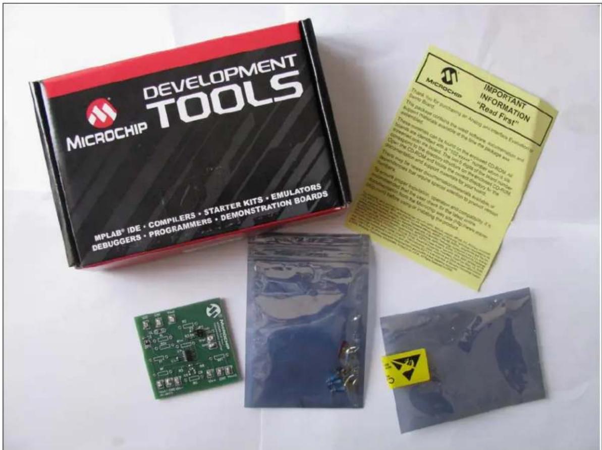
1.3 WHAT THE MCP6H04 EVALUATION BOARD KIT INCLUDES
• MCP6H04 Evaluation Board, 102-00375
- Important Information Sheet
- Accessories Bag – contains loose parts for populating sockets on board, such as resistors and capacitors
text_image
DEVELOPMENT TOOLS MICROCHIP MPLAB® IDE • COMPILERS • STARTER KITS • EMULATORS DEBUGGERS • PROGRAMMERS • DEMONSTRATION BOARDS IMPORTANT INFORMATION "Read First!" Thank you for purchasing an Intel and programming Enterprise The product contains the most software configuration and support the hardware and/or the other software users. Please note that you can be found on the proposed CD-ROM. All userware and tools are used to create a CD-ROM in the system. The 100% of the system has been used with the CD-ROM and/or the other software in the system. The CD-ROM is used to ensure that the system is not used with the other software in the system. The system is not used with the other software in the system. The system is not used with the other software in the system. The system is not used with the other software in the system. The system is not used with the other software in the system. The system is not used with the other software in the system. The system is not used with the other software in the system. The system is not used with the other software in the system. The system's use is not to be used or used to provide any information. Please use the other software to ensure that this is not used with the other software in the system. The system is not used with the other software in the system. The system is not used with the other software in the system. The system is not used with the other software in the system. The system is not used with the other software in the system. The system is not used with the other software in the system. The system is not used with the other software in the system. The system is also not used or used to provide any information. Please use the other software to ensure that this is not used with the other software in the system. The system is not used with the other software in the system. The system is not used with the other software in the system. The system is not used with the other software in the system. The system is not used with the other software in the system. The system is not used with the other software in the system.FIGURE 1-2: MCP6H04 Evaluation Board View.
Chapter 2. Installation and Operation
2.1 INTRODUCTION
This chapter describes how to set up the MCP6H04 Evaluation Board. Topics discussed in this chapter include:
- Required Tools
• MCP6H04 Evaluation Board Set-Up
• MCP6H04 Evaluation Board Operation
2.2 REQUIRED TOOLS
The following tools are required for testing the functionality of the board:
- Lab power supply
- Lab dual signal source (e.g., dual function generator)
- Lab measurement equipment (e.g., oscilloscope)
2.3 MCP6H04 EVALUATION BOARD SET-UP
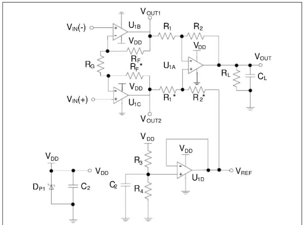
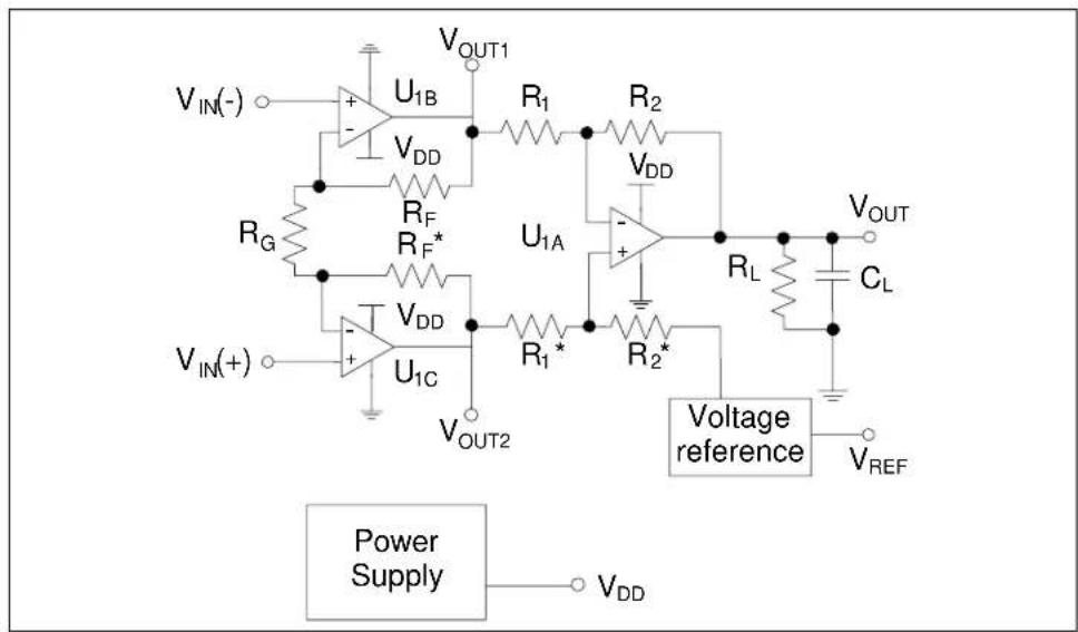
The MCP6H04 Evaluation Board uses a quad op amp in difference amplifier configuration with input buffers and voltage reference. Figure 2-1 shows the circuit diagram of the board.
text_image
VOUT1 VIN(-) + U1B R1 R2 - VDD RF RL VOUT RG RF* U1A RL CL VIN(+) - VDD R1* R2* U1C VOUT2 VDD VDD VDD VDD R3 U1D VREF DP1 C2 C2 R4FIGURE 2-1: MCP6H04 Evaluation Board Circuit Diagram.
The power supply voltage needs to be in the allowed range for the op amp. The MCP6H04 device supports a maximum of 16V power supply. The power supply is protected by a Zener diode with a nominal voltage of 16V and bypassed by a 1 F capacitor (see Figure 2-3).
The mid-supply reference voltage consists of a voltage divider and a buffer amplifier (see Figure 2-4).
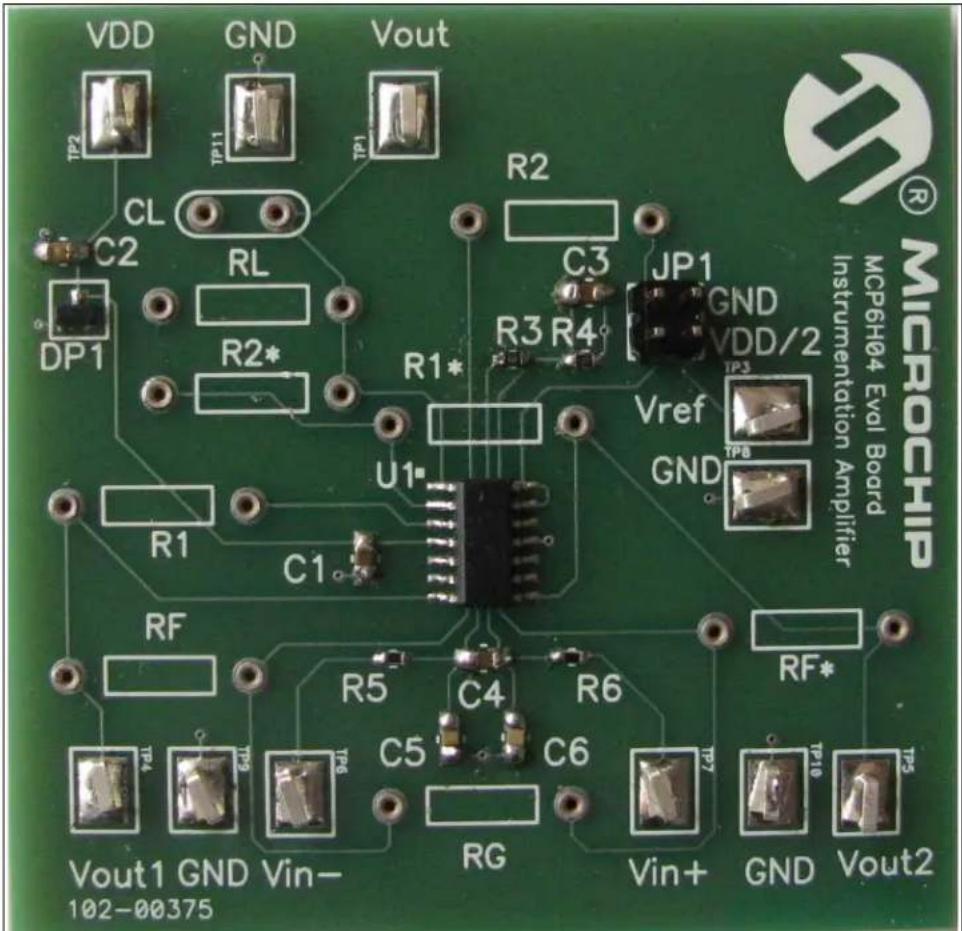
The resistors that are part of the amplifier are placed in pin sockets, which are labeled. All component labels on board are consistent with those on the schematic. The op amp on board is a 14-lead SOIC package, and is bypassed by a 0.1 F capacitor.
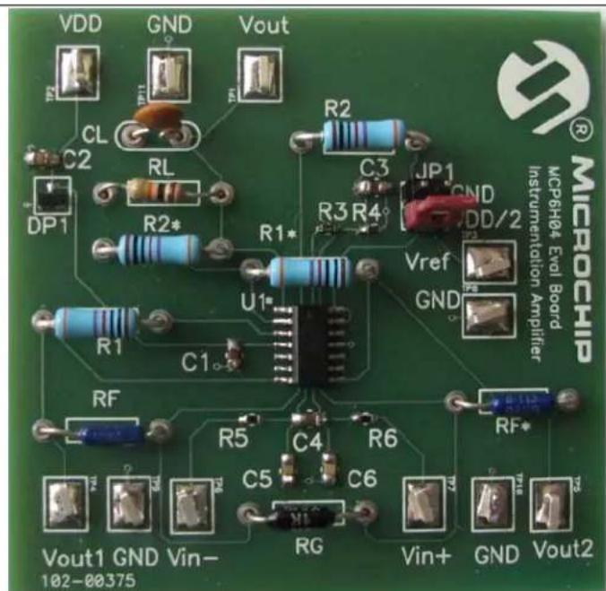
The test points for the power supply, ground, input signals, output signals, and voltage reference allow lab equipment to be connected to the board. The MCP6H04 Evaluation Board top view is shown in Figure 2-2.
text_image
VDD GND Vout TP2 CL RL R2 C3 JP1 GND VDD/2 MP6H04 Eval Board Instrumentation Amplifier MICROCHIP R C2 R2* R1* U1* R1 C1 RF R5 C4 R6 RF* Vout1 GND Vin- 102-00375 RG C5 C6 Vin+ GND Vout2FIGURE 2-2: MCP6H04 Evaluation Board Top View.
2.3.1 Top Level Amplifier Circuit Diagram
2.3.1.1 POWER SUPPLY BLOCK
The power supply is protected by a Zener diode and bypassed by a capacitor.
Figure 2-3 shows the circuit diagram for the power supply ( C_2=1 F ). P is a Zener diode with a nominal voltage of 16V.

chemical
Circuit diagram of a photodiode with diode voltage and capacitor capacitanceFIGURE 2-3: Circuit Diagram for Power Supply.
2.3.1.2 MID-SUPPLY REFERENCE BLOCK
The mid-supply reference consists of a voltage divider and a buffer amplifier. Figure 2-4 shows the circuit diagram for the mid-supply reference ( R_3 = R_4 = 100K , C_3 = 0.1 F ).

text_image
VDD R3 C2 R4 VDD U1D VREFFIGURE 2-4: Mid-Supply Reference Block.
2.3.1.3 OUTPUT LOAD BLOCK
The output load consists of a capacitor and a resistor. Figure 2-5 shows the circuit diagram of the output load ( R_L = 10K , C_L = 56 pF ).

chemical
Simple RC circuit diagram with input voltage, load resistor, and output voltage labelsFIGURE 2-5: Output Load Block.
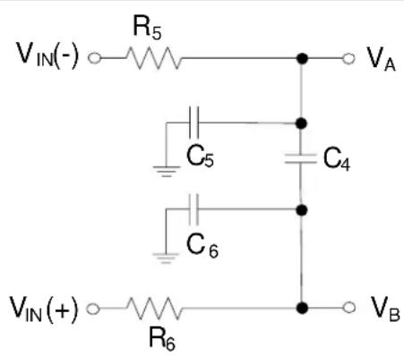
2.3.1.4 INPUT STAGE
The input stage consists of two resistors and three capacitors. All three capacitors are forming a noise filter. Figure 2-6 shows the circuit diagram of the input stage ( C_5=C_6=10nF,4100nF and R_5=R_6=1K ).
chemical
Electrical circuit diagram with resistors and capacitors labeled R5, C5, C4, C6, V_IN(-)/V_IN(+), V_A, V_BFIGURE 2-6: Input Stage Block.
2.3.1.5 INPUT BUFFER BLOCK
The input buffer block consists of two op amps in buffer configuration with outputs tied together through one resistor. Figure 2-7 shows the circuit diagram of the input buffer block ( R_F = R_F^* = 50 K , G = 1 K ).

text_image
V_A + - V_DD R_F R_G R_F* V_DD - V_B V_OUT1 V_OUT2FIGURE 2-7: Input Buffer Block.
2.3.1.6 DIFFERENCE AMPLIFIER
This circuit amplifies the difference between two voltages, while rejecting the Common mode input voltage. Output voltage can be shifted by a reference voltage for single supply operation.
Fill the sockets with the recommended resistors and capacitors (see the circuit diagram shown in Figure 2-8).

text_image
VOUT1 R1 R2 VDD - + RL VC VOUT2 R1* R2* JP1 VREFFIGURE 2-8: Difference Amplifier Block.
The jumper positions have the following effect:
- JP1 connected to ground: the output voltage will be centered on 0V.
- JP1 connected to V_REF: the output voltage will be centered on 8V.
This section covers the following topics:
• Building the Amplifier
- Testing the Amplifier
2.4.1 Building the Amplifier
The accessory bag that comes with this kit facilitates the evaluation of the amplifier described below.
The amplifier characteristics are:
- Instrumentation amplifier (Single supply operation)
• Power supply voltage = 16V
• Desired Gain = 101 V/V - Load Capacitance = 56 pF

text_image
V_{IN-} 1K R_{10} C_3 10n C_2 100n MCP6H04 + - X_1 V_{OUT1} R_1 50k R_4 10k R_2 1k MCP6H04 + - X_3 C_5 100n R_8 10k R_{12} 10k C_9 56p V_{OUT} 16V R_6 100k C_1 100n V_{IN+} R_{11} 10n C_4 10n MCP6H04 + - X_2 V_{OUT2} R_7 10k C_6 100n V_{IN+} V_{IN+} (+)FIGURE 2-9: Schematic of the Instrumentation Amplifier Designed for Simulation.
Figure 2-10 shows the same circuit redrawn to emphasize the instrumentation amplifier.
text_image
VOUT1 VIN(-) + U1B R1 R2 VDD RF RG RF* U1A VDD RL VOUT CL VOUT VIN(+) + U1C R1* R2* VOUT2 Voltage reference VREF Power Supply VDDFIGURE 2-10: Instrumentation Amplifier Diagram Block.
Each of the components in Figure 2-10 that need to be inserted in a socket on the MCP6H04 Evaluation Board is listed in Table 2-1 and Table 2-2. The op amp is soldered on the PCB.
TABLE 2-1: AMPLIFIER COMPONENTS LIST
| PCB Labels Component Value | |
| R_F | 50K |
| R_F^* 50K | |
| R_G | 1K |
| R_1 | 10K |
| R_1^* 10K | |
| R_2 | 10K |
| R_2^* 10K | |
| R_L | 10K |
| C_L | 56 pF |
TABLE 2-2: JUMPER POSITIONS
| Jumper Position | |
| JP1 V | DD/2 |
| GND |
The fully assembled MCP6H04 Evaluation Board top view is shown in Figure 2-11.
text_image
VDD GND Vout CL RL R2* C3 JP1 GND DD/2 Vref GND MICROCHIP Electrical Board Instrumentation Amplifier Vout1 GND Vin- 102-00375 RF C1 R1* R2* R3 R4* U1* R5 C4 R6 RG C5 C6 RF* Vin+ GND Vout2FIGURE 2-11: MCP6H04 Evaluation Board Top View.
2.4.2 Testing the Amplifier
2.4.2.1 CHECKING THE TEST POINTS
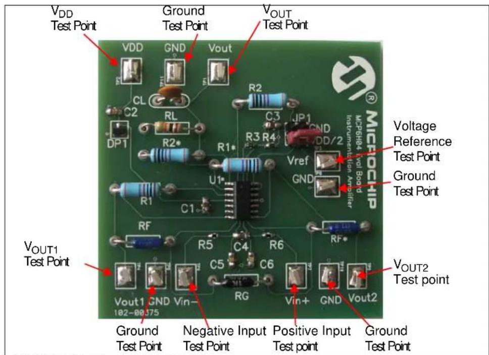
The test points for the power supply, ground, input signals and output signals allow lab equipment to be connected to the board. Figure 2-12 shows the test points to check.
text_image
VDD Test Point Ground Test Point VOUT Test Point VDD GND Vout CL RL R2 C3 JP1 CND DD/2 Vref GND VOUT1 Test Point RF C1 U1* C4 R6 RG Vin+ GND VOUT2 VOUT1 Test Point Ground Test Point Negative Input Test Point Positive Input Test point Ground Test Point Voltage Reference Test Point Ground Test Point MICROCHIP MCP684 vol Board instrumentation Amplifier VOUT2 Test pointFIGURE 2-12: Check-in Test Points.
2.4.2.2 BOARD VALIDATION
All resistors in sockets have 0.1% tolerance and all soldered resistors have 1% tolerance. The capacitors have 20% tolerance.
2.4.2.2.1 Sine Wave Response
Settings in bench measurement:
- Se _N for Source(-) at 10mV , 10Hz , 0^ phase and a Common mode voltage of 4V
- Se _IN for Source(+) at 10 mV, 10 Hz, 180° phase and a Common mode voltage of 4V
- V_REF = V_DD/2
- V_DD = 16V
• The output signal is centered on 8V
• The amplifier's Gain is 101 V/V
Figure 2-13 shows the result of this measurement.

line
| Time (s) | VOUT1 (V) | VOUT2 (V) | VOUT (V) | |----------|-----------|-----------|----------| | 0 | 0 | 0 | 0 | | 20.0 | 3.97 | 3.97 | 3.97 | | 40.0 | 0 | 0 | 0 | | 60.0 | -3.97 | -3.97 | -3.97 | | 80.0 | 3.97 | 3.97 | 3.97 | | 100.0 | 0 | 0 | 0 | | 120.0 | -3.97 | -3.97 | -3.97 | | 140.0 | 3.97 | 3.97 | 3.97 | | 160.0 | 0 | 0 | 0 | | 180.0 | -3.97 | -3.97 | -3.97 | | 200.0 | 3.97 | 3.97 | 3.97 | | 220.0 | 0 | 0 | 0 | | 240.0 | -3.97 | -3.97 | -3.97 | | 260.0 | 3.97 | 3.97 | 3.97 | | 280.0 | 0 | 0 | 0 | | 300.0 | -3.97 | -3.97 | -3.97 | | 320.0 | 3.97 | 3.97 | 3.97 | | 340.0 | 0 | 0 | 0 | | 360.0 | -3.97 | -3.97 | -3.97 | | 380.0 | 3.97 | 3.97 | 3.97 | | 400.0 | 0 | 0 | 0 | | 420.0 | -3.97 | -3.97 | -3.97 | | 440.0 | 3.97 | 3.97 | 3.97 | | 460.0 | 0 | 0 | 0 | | 480.0 | -3.97 | -3.97 | -3.97 | | 500.0 | 3.97 | 3.97 | 3.97 | | 520.0 | 0 | 0 | 0 | | 540.0 | -3.97 | -3.97 | -3.97 | | 560.0 | 3.97 | 3.97 | 3.97 | | 580.0 | 0 | 0 | 0 | | 600.0 | -3.97 | -3.97 | -3.97 | | 620.0 | 3.97 | 3.97 | 3.97 | | 640.0 | 0 | 0 | 0 | | 660.0 | -3.97 | -3.97 | -3.97 | | 680.0 | 3.97 | 3.97 | 3.97 | | 700.0 | 0 | 0 | 0 | | 720.0 | -3.97 | -3.97 | -3.97 | | 740.0 | 3.97 | 3.97 | 3.97 | | 760.0 | 0 | 0 | 0 | | 780.0 | -3.97 | -3.97 | -3.97 | | 800.0 | 3.97 | 3.97 | 3.97 | | 820.0 | 0 | 0 | 0 | | 840.0 | -3.97 | -3.97 | -3.97 | | 860.0 | 3.97 | 3.97 | 3.97 | | 880.0 | 0 | 0 | 0 | | 900.0 | -3.97 | -3.97 | -3.97 | | 920.0 | 3.97 | 3.97 | 3.97 | | 940.0 | 0 | 0 | 0 | | 960.0 | -3.97 | -3.97 | -3.97 | | 980.0 | 3.97 | 3.97 | 3.97 | | 1000 | 0 | 0 | 0 | | | | | | | | | | | | | | | | | | | | | | | | | | | | | | | | | | | | | | | | | | | | | | | | | | | | | | | | | | | | | | Time (s) | VOUT1 | | -------------- | --------- | | | | | | | | | | | | | | | | | | | | | | | | | | | | | | | | | | | | | | | | | | | | | | | | | | | | | | | | | | | | | | | (Note: The data is extracted from the code and labels as 'VOUT1' and 'VOUT2' for the time intervals). The values for 'VOUT1' and 'VOUT2' are estimated based on the provided code format.FIGURE 2-13: Sine Wave Response.
Simulation settings:
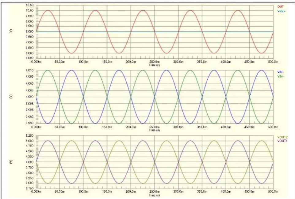
- S e _N for Source(-) at 10 mV, 10 Hz, 0^ phase and Common mode voltage 4V
- S e t_IN for Source(+) at 10 mV, 10 Hz, 180° phase and Common mode voltage 4V
- V_REF = V_DD/2
- V_DD = 16V
• The output signal is centered on 8V
• The amplifier's Gain is 101 V/V
Figure 2-14 shows the results.
line
| Time (s) | OUT | VIN | VOUT2 | VOUT1 | |----------|--------|--------|--------|--------| | 0.000m | 8.000 | 3.960 | 4.750 | 3.250 | | 50.00m | 10.000 | 4.010 | 4.750 | 3.250 | | 100.0m | 8.000 | 3.960 | 4.750 | 3.250 | | 150.0m | 10.000 | 4.010 | 4.750 | 3.250 | | 200.0m | 8.000 | 3.960 | 4.750 | 3.250 | | 250.0m | 10.000 | 4.010 | 4.750 | 3.250 | | 300.0m | 8.000 | 3.960 | 4.750 | 3.250 | | 350.0m | 10.000 | 4.010 | 4.750 | 3.250 | | 400.0m | 8.000 | 3.960 | 4.750 | 3.250 | | 450.0m | 10.000 | 4.010 | 4.750 | 3.250 | | 500.0m | 8.000 | 3.960 | 4.750 | 3.250 |FIGURE 2-14: Simulation of the Sine Wave Response.
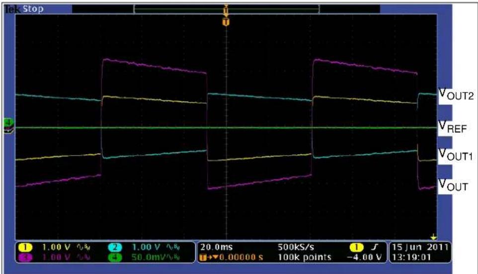
2.4.2.2.2 Square Wave Response
Settings in bench measurement:
- Set for Source(-) at 50 mV, 10 Hz, 0° phase and Common mode voltage 4V
- Set for Source(+) at 50 mV, 10 Hz, 180° phase and Common mode voltage 4V
- V_REF = V_DD/2
- V_DD = 16V
• The output signal is centered on 8V
• The amplifier's Gain is 101V/V
Figure 2-15 shows the result of this measurement.
line
| Time (ms) | VOUT2 (V) | VREF (V) | VOUT1 (V) | VOUT (V) | |-----------|-----------|----------|-----------|----------| | 0 | 1.00 | 1.00 | 1.00 | 1.00 | | 20.0 | 1.00 | 1.00 | 1.00 | 1.00 | | 40.0 | 1.00 | 1.00 | 1.00 | 1.00 | | 60.0 | 1.00 | 1.00 | 1.00 | 1.00 | | 80.0 | 1.00 | 1.00 | 1.00 | 1.00 | | 100.0 | 1.00 | 1.00 | 1.00 | 1.00 | | 120.0 | 1.00 | 1.00 | 1.00 | 1.00 | | 140.0 | 1.00 | 1.00 | 1.00 | 1.00 | | 160.0 | 1.00 | 1.00 | 1.00 | 1.00 | | 180.0 | 1.00 | 1.00 | 1.00 | 1.00 | | 200.0 | 1.00 | 1.00 | 1.00 | 1.00 | | 220.0 | 1.00 | 1.00 | 1.00 | 1.00 | | 240.0 | 1.00 | 1.00 | 1.00 | 1.00 | | 260.0 | 1.00 | 1.00 | 1.00 | 1.00 | | 280.0 | 1.00 | 1.00 | 1.00 | 1.00 | | 300.0 | 1.00 | 1.00 | 1.00 | 1.00 | | 320.0 | 1.00 | 1.00 | 1.00 | 1.00 | | 340.0 | 1.00 | 1.00 | 1.00 | 1.00 | | 360.0 | 1.00 | 1.00 | 1.00 | 1.00 | | 380.0 | 1.00 | 1.00 | 1.00 | 1.00 | | 400.0 | 1.00 | 1.00 | 1.00 | 1.00 | | 420.0 | 1.00 | 1.00 | 1.00 | 1.00 | | 440.0 | 1.00 | 1.00 | 1.00 | 1.00 | | 460.0 | 1.00 | 1.00 | 1.00 | 1.00 | | 480.0 | 1.00 | 1.00 | 1.00 | 1.00 | | 567 | - | - | - | - | | | | | | | | | | | | | | | | | | | | | | | | | | | | | | | | | | | | | | | | | | | | | | | | | | | | | | | | | | | | |FIGURE 2-15: Square Wave Response.
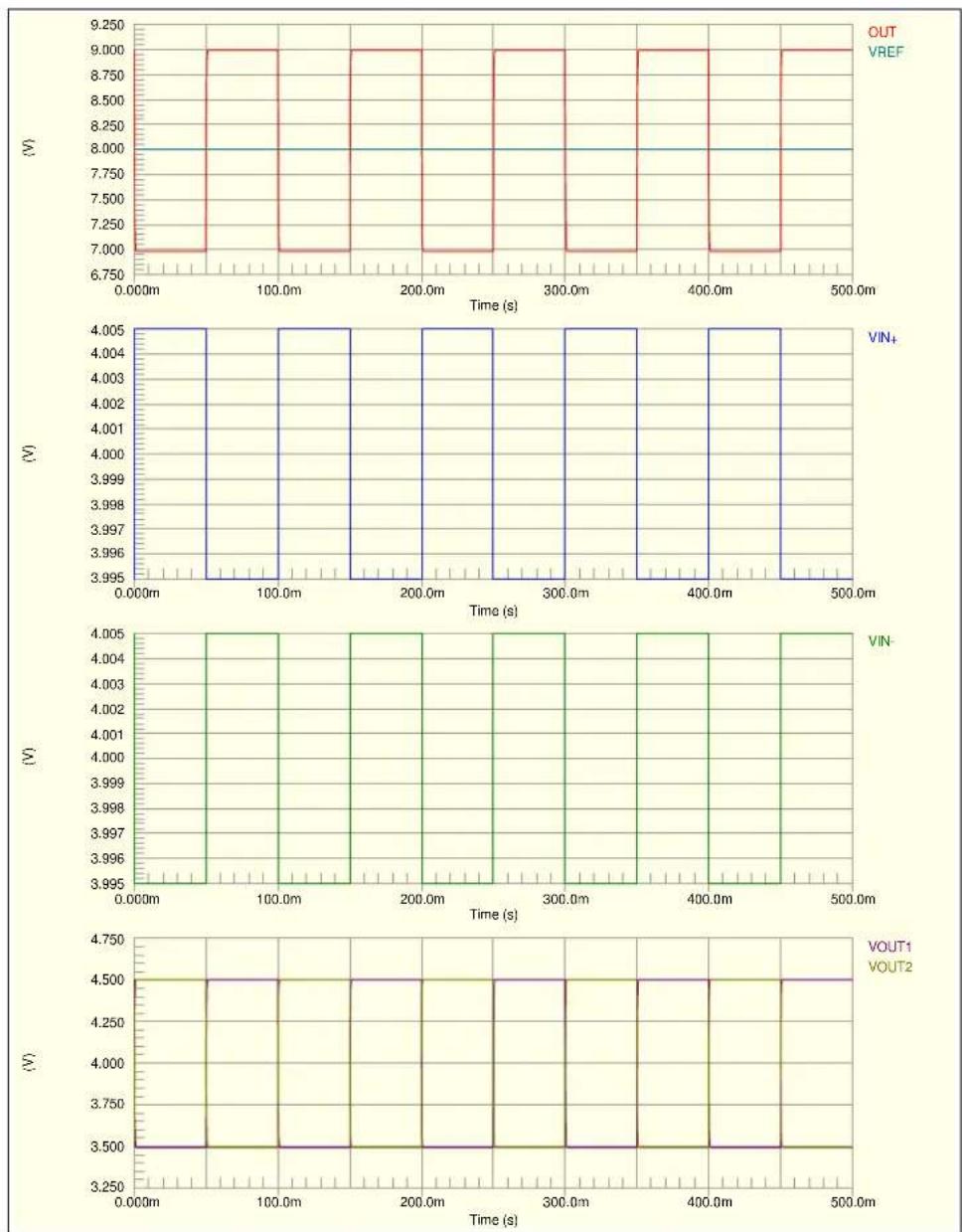
Simulation settings:
- S e t_IN for Source(-) at 50 mV, 10 Hz, 0° phase and common mode voltage 4V
- Set for Source(+) at 50 mV, 10 Hz, 180° phase and common mode voltage 4V
- V_REF = V_DD/2
- V_DD = 16V
• The output signal is centered on 8V
• The amplifier's Gain is 101V/V
Figure 2-16 shows the result of this simulation.
line
| Time (s) | OUT | VREF | VIN₁ | VIN | VOUT1 | VOUT2 | |----------|-------|-------|-------|-------|-------|-------| | 0.000m | 7.000 | 7.000 | 4.005 | 4.005 | 4.500 | 3.500 | | 100.0m | 9.000 | 9.000 | 4.005 | 4.005 | 4.500 | 3.500 | | 200.0m | 9.000 | 9.000 | 4.005 | 4.005 | 4.500 | 3.500 | | 300.0m | 9.000 | 9.000 | 4.005 | 4.005 | 4.500 | 3.500 | | 400.0m | 9.000 | 9.000 | 4.005 | 4.005 | 4.500 | 3.500 | | 500.0m | 9.000 | 9.000 | 4.005 | 4.005 | 4.500 | 3.500 |FIGURE 2-16: Simulation of the Square Wave Response.
2.4.2.2.3 DC Response
Settings in bench measurement:
• S e t_N for Source(-) at 80 mV DC signal
- Set for Source(+) at 30 mV DC signal
- V_REF = V_DD/2
- V_DD = 16V
Figure 2-17 shows the result of this measurement.

line
| Waveform | Voltage (mV) | |----------|--------------| | VOUT1 | 10.0 | | VOUT2 | 20.0 | | VOUT | 10.0 | | VREF | 10.0 |FIGURE 2-17: DC Response.
Simulation settings:
- Set for Source(-) at 80 mV DC signal
- Set for Source(+) at 30 mV DC signal
- V_REF = V_DD/2
- V_DD = 16V
Figure 2-18 shows the result of this measurement.

line
| Time (s) | OUT VREF (VREF) | VIN (m) | VOLT (m) | |----------|-----------------|---------|----------| | 0.000u | 8.125 | 150.3 | 75.0 | | 0.500u | 8.125 | 150.3 | 75.0 | | 1.000u | 8.125 | 150.3 | 75.0 | | 1.500u | 8.125 | 150.3 | 75.0 | | 2.000u | 8.125 | 150.3 | 75.0 | | 2.500u | 8.125 | 150.3 | 75.0 | | 3.000u | 8.125 | 150.3 | 75.0 | | 3.500u | 8.125 | 150.3 | 75.0 | | 4.000u | 8.125 | 150.3 | 75.0 | | 4.500u | 8.125 | 150.3 | 75.0 | | 5.000u | 8.125 | 150.3 | 75.0 |FIGURE 2-18: Simulation of the DC Response.
NOTES:
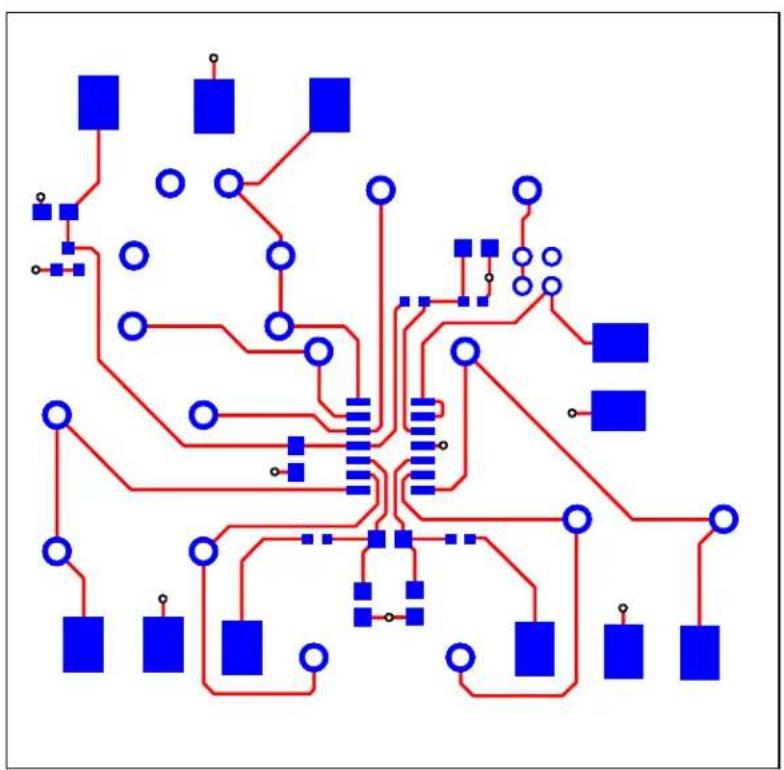
Appendix A. Schematic and Layouts
A.1 INTRODUCTION
This appendix contains the following schematics and layouts of the MCP6H04 Evaluation Board:
- Board – Schematic
- Board – Silk and Solder Mask
- Board – Top Metal Layer
- Board – Bottom Metal Layer (bottom View)
A.2 BOARD - SCHEMATIC

text_image
TP3 Vref R3 100K C3 0.1uF GND VCC VDD OUTD VSS 12 14 MCP6H04 U1D GND 24GND GND Vref R2 10K R1 10K TP4 Vout1 GND VSS OUTD VDD VCC 3+A VSS OUTD VDD VCC C1 60pF GND RL 10K GND TP1 Vout1 GND TP8 GND GND TP10 GND TP9 GND TP11 GND TP5 Vout2 TP6 Source(-) R5 1K GND C5 10nF GND C4 100nF C6 10nF GND C2 1uF GND D1 16V VCC TP7 Source(+) R6 1KA.3 BOARD – SILK AND SOLDER MASK

text_image
VDD GND Vout 2dL 11dL 1dL CL RL C2 RP1 R2* R1* C3 JP1 GND VDD/2 TP3 Vref TPB GND TPB U1* RF* RF* TP4 TP9 TP8 C5 C4 C6 RG TP7 TP8 Vin+ GND Vout2 MCP6H04 Eval Board Instrumentation Amplifier MICROCHIP Vout1 GND Vin- 102-00375A.4 BOARD - TOP METAL LAYER
natural_image
Pure electrical circuit lines without any symbolsA.5 BOARD – BOTTOM METAL LAYER (BOTTOM VIEW)

scatter
| Point ID | X Coordinate | Y Coordinate | |----------|--------------|--------------| | 1 | 0.1 | 0.8 | | 2 | 0.2 | 0.6 | | 3 | 0.3 | 0.9 | | 4 | 0.4 | 0.7 | | 5 | 0.5 | 0.5 | | 6 | 0.6 | 0.8 | | 7 | 0.7 | 0.4 | | 8 | 0.8 | 0.6 | | 9 | 0.9 | 0.3 | | 10 | 1.0 | 0.7 | | 11 | 1.1 | 0.5 | | 12 | 1.2 | 0.8 | | 13 | 1.3 | 0.4 | | 14 | 1.4 | 0.6 | | 15 | 1.5 | 0.9 | | 16 | 1.6 | 0.3 | | 17 | 1.7 | 0.7 | | 18 | 1.8 | 0.5 | | 19 | 1.9 | 0.8 | | 20 | 2.0 | 0.4 | | 21 | 2.1 | 0.6 | | 22 | 2.2 | 0.9 | | 23 | 2.3 | 0.3 | | 24 | 2.4 | 0.7 | | 25 | 2.5 | 0.5 | | 26 | 2.6 | 0.8 | | 27 | 2.7 | 0.4 | | 28 | 2.8 | 0.6 | | 29 | 2.9 | 0.9 | | 30 | 3.0 | 0.3 | | 31 | 3.1 | 0.7 | | 32 | 3.2 | 0.5 | | 33 | 3.3 | 0.8 | | 34 | 3.4 | 0.4 | | 35 | 3.5 | 0.6 | | 36 | 3.6 | 0.9 | | 37 | 3.7 | 0.3 | | 38 | 3.8 | 0.7 | | 39 | 3.9 | 0.5 | | 40 | 4.0 | 0.8 | | 41 | 4.1 | 0.4 | | 42 | 4.2 | 0.6 | | 43 | 4.3 | 0.9 | | 44 | 4.4 | 0.3 | | 45 | 4.5 | 0.7 | | 46 | 4.6 | 0.5 | | 47 | 4.7 | 0.8 | | 48 | 4.8 | 0.4 | | 49 | 4.9 | 0.6 | | 50 | 5.0 | 0.9 | | 51 | - | - | | 52 | - | - | | 53 | - | - | | 54 | - | - | | 55 | - | - | | 56 | - | - | | 57 | - | - | | 58 | - | - | | 59 | - | - | | 60 | - | - | | 61 | - | - | | 62 | - | - | | 63 | - | - | | 64 | - | - | | 65 | - | - | | 66 | - | - | | 67 | - | - | | 68 | - | - | | 69 | - | - | | 70 | - | - | | 71 | - | - | | 72 | - | - | | 73 | - | - | | 74 | - | - | | 75 | - | - | | 76 | - | - | | 77 | - | - | | 78 | - | - | | 79 | - | - | | 80 | - | - | | 81 | - | - | | 82 | - | - | | 83 | - | - | | 84 | - | - | | 85 | - | - | | 86 | - | - | | 87 | - | - | | 88 | - | - | | 89 | - | - | | 90 | - | - | | 91 | - | - | | 92 | - | - | | 93 | - | - | | 94 | - | - | | 95 | - | - | | 96 | - | - | | 97 | - | - | | 98 | - | - | | 99 | - | - | | Note: The actual values in the 'C' table are not provided in the code image, so they are represented as placeholders (e.g., '104-00375-R2').Appendix B. Bill of Materials
TABLE B-1: BILL OF MATERIALS (BOM)
| Qty | Reference Description Manufacturer Part Number | |||
| 3 C | 1,C3,C4 CAPACITOR, 0805, X7R, 100V, 100NF | AVX Corporation 08051C104 | K4T2A | |
| 1 C2 | CAPACITOR, 0805, X7R, 25V, 1UF AVX Corporation | 08053C105K4Z2A | ||
| 2 C5 | CAPACITOR, 0805, X7R, 100V, 10NF AVX Corporation | 08051C103K4Z2A | ||
| 1 DP1 | ZENER, 16V, 350MW, SOT-23 | Micro Commercial Components Corporation | BZX84C16-TP | |
| 1 JP1 | CONN HEADR BRKWAY .100 02POS STR | TE Connectivity Ltd. | 9-146258-0-02 | |
| 1 PCB | RoHS Compliant Bare PCB, MCP6H04 Evaluation Board | Microchip Technology Inc. | 104-00375 | |
| 18 | Pin Socket | PIN RECPT .015/.025 DIA 0667 SER | Mill-Max Mfg. Corporation | 0667-0-15-01-30-27-10-0 |
| 2 | R3,R4 | RESISTOR, 100K, 0603 1% 0.1W | Vishay Intertechnology, Inc. | MCT06030C1003FP500 |
| 2 | R5,R6 | RESISTOR, 0603, 1K ,0.1% | TE Connectivity Ltd. | CPF0603B1K0E1 |
| 11 | Test Points | PC TEST POINT COMPACT SMT | Keystone Electronics Corporation | 5016 |
| 1 U1 | MCP6H04 | Microchip Technology Inc. MCP6H04 | ||
Note 1: The components listed in this Bill of Materials are representative of the PCB assembly. The released BOM used in manufacturing uses all RoHS-compliant components.
TABLE B-2: BILL OF MATERIALS – ACCESSORIES BAG PARTS
| Qty | Reference | Description | Manufacturer | Part Number |
| 1 | CL | CAPACITOR, DISC, 100V, 56PF | AVX Corporation | 5KK560KOAAM |
| 4 | R1,R2,R1*, R2* | 10K, 0.125W, 0.1%, 15PPM | Vishay Intertechnology, Inc. | PTF5610K000BXEB |
| 1 | RG | RESISTOR, 0.25W, 0.1%, 1K0 | TE Connectivity Ltd. | H81K0BYA |
| 2 | RF, RF* | RES 50.0K OHM 1/4W 0.1% AXIAL | TE Connectivity Ltd. | H850KBCA |
| 1 | RL | 0.5W 5% 10K | Vishay Intertechnology, Inc. | NFR25H0001002JR500 |
Note 1: The components listed in this Bill of Materials are representative of the loose components found in the accessories bag. The released BOM used in manufacturing uses all RoHS-compliant components.
Worldwide Sales and Service
AMERICAS
Corporate Office
2355 West Chandler Blvd.
Chandler, AZ 85224-6199
Tel: 480-792-7200
Fax: 480-792-7277
Technical Support:
http://www.microchip.com/support
Web Address:
www.microchip.com
Atlanta
Duluth, GA
Tel: 678-957-9614
Fax: 678-957-1455
Boston
Westborough, MA
Tel: 774-760-0087
Fax: 774-760-0088
Chicago
Itasca, IL
Tel: 630-285-0071
Fax: 630-285-0075
Cleveland
Independence, OH
Tel: 216-447-0464
Fax: 216-447-0643
Dallas
Addison, TX
Tel: 972-818-7423
Fax: 972-818-2924
Detroit
Farmington Hills, MI
Tel: 248-538-2250
Fax: 248-538-2260
Indianapolis
Noblesville, IN
Tel: 317-773-8323
Fax: 317-773-5453
Los Angeles
Mission Viejo, CA
Tel: 949-462-9523
Fax: 949-462-9608
Santa Clara
Santa Clara, CA
Tel: 408-961-6444
Fax: 408-961-6445
Toronto
Mississauga, Ontario,
Canada
Tel: 905-673-0699
Fax: 905-673-6509
ASIA/PACIFIC
Asia Pacific Office
Suites 3707-14, 37th Floor
Tower 6. The Gateway
Harbour City, Kowloon
Hong Kong
Tel: 852-2401-1200
Fax: 852-2401-3431
Australia - Sydney
Tel: 61-2-9868-6733
Fax: 61-2-9868-6755
China - Beijing
Tel: 86-10-8569-7000
Fax: 86-10-8528-2104
China - Chengdu
Tel: 86-28-8665-5511
Fax: 86-28-8665-7889
China - Chongqing
Tel: 86-23-8980-9588
Fax: 86-23-8980-9500
China - Hangzhou
Tel: 86-571-2819-3187
Fax: 86-571-2819-3189
China - Hong Kong SAR
Tel: 852-2401-1200
Fax: 852-2401-3431
China - Nanjing
Tel: 86-25-8473-2460
Fax: 86-25-8473-2470
China - Qingdao
Tel: 86-532-8502-7355
Fax: 86-532-8502-7205
China - Shanghai
Tel: 86-21-5407-5533
Fax: 86-21-5407-5066
China - Shenyang
Tel: 86-24-2334-2829
Fax: 86-24-2334-2393
China - Shenzhen
Tel: 86-755-8203-2660
Fax: 86-755-8203-1760
China - Wuhan
Tel: 86-27-5980-5300
Fax: 86-27-5980-5118
China - Xian
Tel: 86-29-8833-7252
Fax: 86-29-8833-7256
China - Xiamen
Tel: 86-592-2388138
Fax: 86-592-2388130
China - Zhuhai
Tel: 86-756-3210040
Fax: 86-756-3210049
ASIA/PACIFIC
India - Bangalore
Tel: 91-80-3090-4444
Fax: 91-80-3090-4123
India - New Delhi
Tel: 91-11-4160-8631
Fax: 91-11-4160-8632
India - Pune
Tel: 91-20-2566-1512
Fax: 91-20-2566-1513
Japan - Yokohama
Tel: 81-45-471-6166
Fax: 81-45-471-6122
Korea - Daegu
Tel: 82-53-744-4301
Fax: 82-53-744-4302
Korea - Seoul
Tel: 82-2-554-7200
Fax: 82-2-558-5932 or
82-2-558-5934
Malaysia - Kuala Lumpur
Tel: 60-3-6201-9857
Fax: 60-3-6201-9859
Malaysia - Penang
Tel: 60-4-227-8870
Fax: 60-4-227-4068
Philippines - Manila
Tel: 63-2-634-9065
Fax: 63-2-634-9069
Singapore
Tel: 65-6334-8870
Fax: 65-6334-8850
Taiwan - Hsin Chu
Tel: 886-3-5778-366
Fax: 886-3-5770-955
Taiwan - Kaohsiung
Tel: 886-7-536-4818
Fax: 886-7-330-9305
Taiwan - Taipei
Tel: 886-2-2500-6610
Fax: 886-2-2508-0102
Thailand - Bangkok
Tel: 66-2-694-1351
Fax: 66-2-694-1350
08/02/11