MCP73861 - Electronic component Microchip - Free user manual and instructions
Find the device manual for free MCP73861 Microchip in PDF.

| Product Type | Battery Charge Management IC |
| Battery Chemistry | Single-cell Li-Ion, Li-Polymer |
| Maximum Charge Current | 1 A (programmable) |
| Supply Voltage Range | 4.5 V to 6.0 V |
| Package Type | MSOP-10 (3 mm x 3 mm) |
| Weight | 0.03 g (typical) |
| Operating Temperature Range | -40 °C to +85 °C |
| Charge Termination Method | Constant current / constant voltage (CC/CV) |
| Safety Features | Overvoltage protection, thermal regulation, charge status output |
| Typical Application | Portable devices, battery-powered systems |
| Power Dissipation | 0.5 W (maximum) |
| Charging Status Indication | Open-drain status output (active low) |
| Standby Current | 1 µA (typical) |
| Regulation Accuracy | ±0.5% (voltage), ±5% (current) |
| Maintenance and Cleaning | No maintenance required; keep free of moisture and static discharge |
| Spare Parts Availability | Contact Microchip distributors |
| Repairability | Not repairable; replace if faulty |
Frequently Asked Questions - MCP73861 Microchip
User questions about MCP73861 Microchip
0 question about this device. Answer the ones you know or ask your own.
Ask a new question about this device
Download the instructions for your Electronic component in PDF format for free! Find your manual MCP73861 - Microchip and take your electronic device back in hand. On this page are published all the documents necessary for the use of your device. MCP73861 by Microchip.
USER MANUAL MCP73861 Microchip
Advanced Single or Dual Cell, Fully Integrated Li-Ion/Li-Polymer Charge Management Controllers
Features:
• Linear Charge Management Controllers:
- Integrated Pass Transistor
- Integrated Current Sense
- Reverse-Blocking Protection
• High-Accuracy Preset Voltage Regulation: + 0.5%
- Four Selectable Voltage Regulation Options:
- 4.1V, 4.2V - MCP73861/3
- 8.2V, 8.4V - MCP73862/4
- Programmable Charge Current: 1.2A Maximum
• Programmable Safety Charge Timers
• Preconditioning of Deeply Depleted Cells
• Automatic End-of-Charge Control
- Optional Continuous Cell Temperature Monitoring
- Charge Status Output for Direct LED Drive
- Fault Output for Direct LED Drive
• Automatic Power-Down
• Thermal Regulation
• Temperature Range: -40°C to +85°C
• Packaging: 16-Pin, 4 x 4 QFN
16-Pin SOIC
Applications:
• Lithium-Ion/Lithium-Polymer Battery Chargers
• Personal Data Assistants (PDAs)
- Cellular Telephones
• Hand-Held Instruments
- Cradle Chargers
• Digital Cameras
- MP3 Players
Description:
The MCP7386X family of devices features highly advanced linear charge management controllers for use in space-limited, cost-sensitive applications. The devices combine high-accuracy, constant voltage and current regulation, cell preconditioning, cell temperature monitoring, advanced safety timers, automatic charge termination, internal current sensing, reverse-blocking protection, charge status and fault indication in either a space-saving 16-pin 4 x 4 QFN package, or a 16-pin SOIC package. The MCP7386X provides a complete, fully functional, stand-alone charge management solution with a minimum number of external components.
The MCP73861/3 is intended for applications utilizing single-cell Lithium-Ion or Lithium-Polymer battery packs, while the MCP73862/4 is intended for dual series cell Lithium-Ion or Lithium-Polymer battery packs. The MCP73861/3 has two selectable voltage-regulation options available (4.1V and 4.2V), for use with either coke or graphite anodes and operate with an input voltage range of 4.5V to 12V. The MCP73862/4 has two selectable voltage-regulation options available (8.2V and 8.4V), for use with coke or graphite anodes, and operate with an input voltage range of 8.7V to 12V.
The MCP73861/2 and MCP73863/4 differ only in the function of the charge status output (STAT1) when a charge cycle has been completed. The MCP73861/2 flashes the output, while the MCP73863/4 turns the output off. Refer to Section 5.2.1 "Charge Status Outputs (STAT1, STAT2)".
The MCP7386X family of devices are fully specified over the ambient temperature range of -40^ to +85^ .
Package Types
text_image
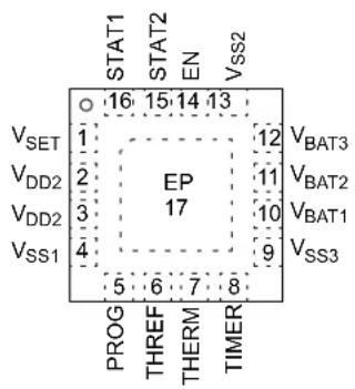
STAT1 STAT2 EN VSS2 VSET 16 15 14 13 VDD2 2 EP 12 VBAT3 VDD2 3 17 11 VBAT2 VSS1 4 9 VBAT1 PROG THREF THERM TIMER 5 6 7 8 VSS316-Pin SOIC16-Pin QFN

text_image
in QFN STAT2 1 ● 16 EN STAT1 2 15 VSS2 VSET 3 14 VBAT3 VDD1 4 13 VBAT2 VDD2 5 12 VBAT1 VSS1 6 11 VSS3 PROG 7 10 TIMER THREF 8 9 THERMTypical Application
text_image
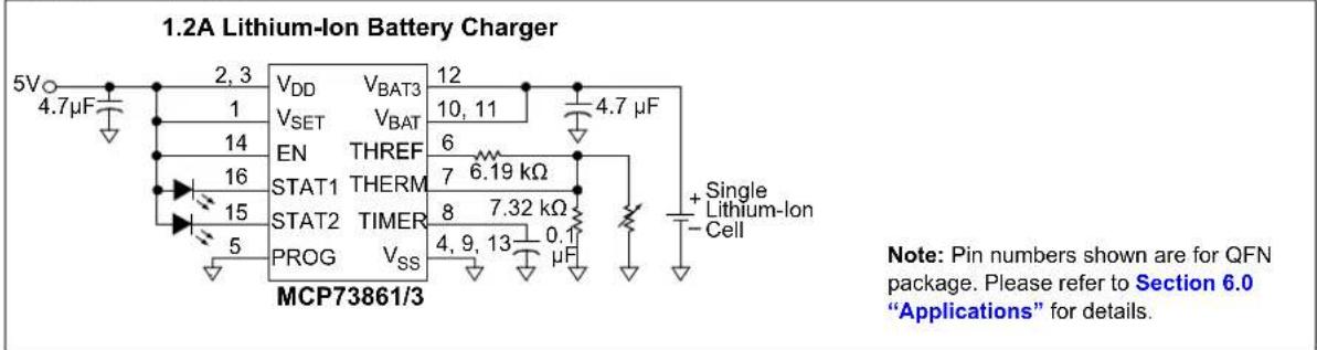
1.2A Lithium-Ion Battery Charger 5V○ 4.7μF 2,3 VDD VBAT3 12 1 VSET VBAT 10,11 4.7 μF EN THREF 6 STAT1 THERM 7 6.19 kΩ STAT2 TIMER 8 7.32 kΩ PROG VSS 4,9,13 0.1 μF + Single Lithium-Ion Cell MCP73861/3 Note: Pin numbers shown are for QFN package. Please refer to Section 6.0 "Applications" for details.Functional Block Diagram
text_image
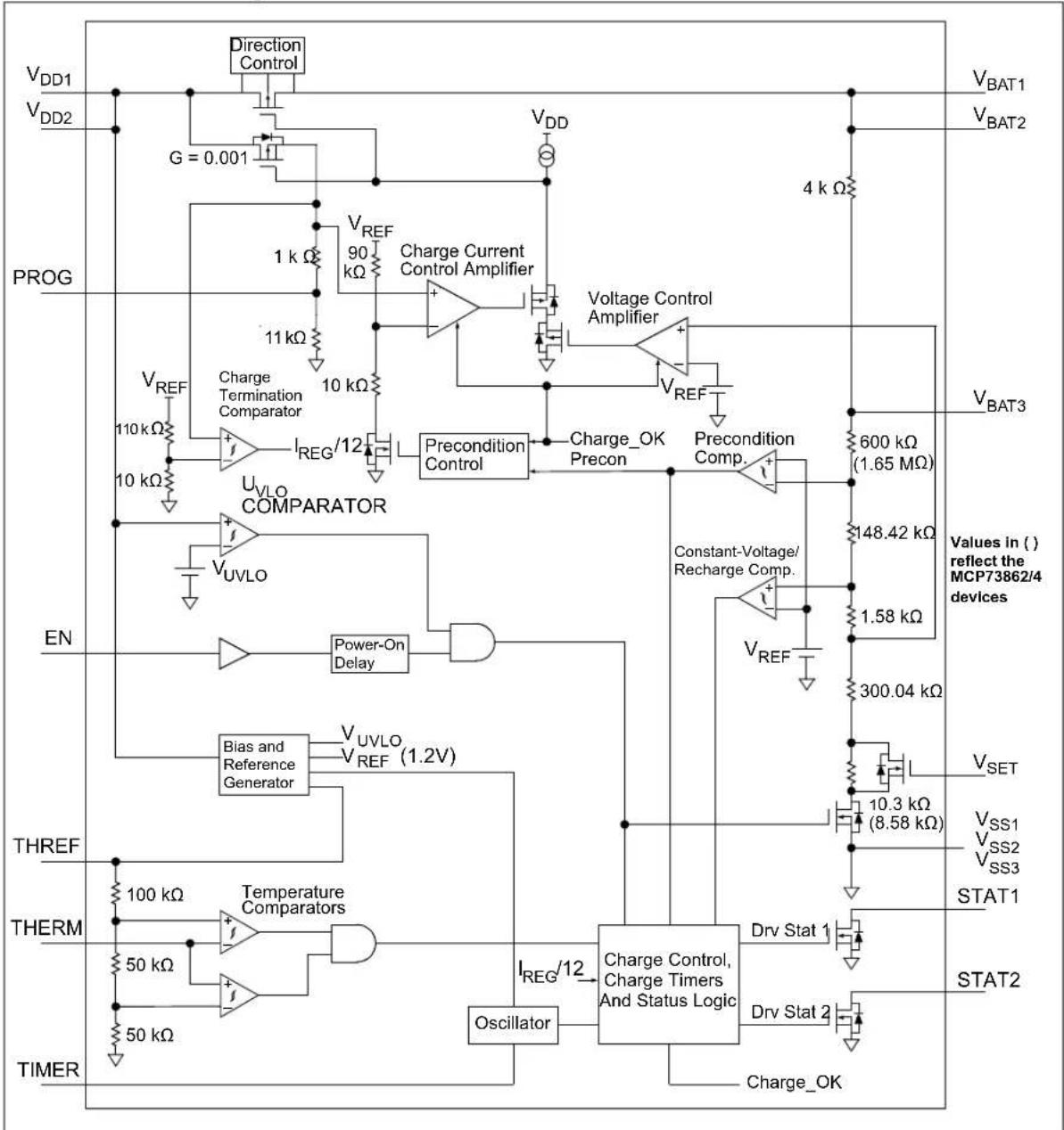
Direction Control G = 0.001 VREF 90 kΩ Charge Current Control Amplifier 11 kΩ 10 kΩ Voltage Control Amplifier 4 kΩ VDD1 VDD2 PROG VREF Charge Termination Comparator UREG/12 Precondition Control Charge_OK Precon Precondition Comp. 600 kΩ (1.65 MΩ) VBAT3 Values in () reflect the MCP73862/4 devices EN VUVLO COMPARATOR VUVLO Power-On Delay VUVLO VREF (1.2V) Bias and Reference Generator THREF THERM 100 kΩ Temperature Comparators 50 kΩ 50 kΩ IREG/12 Oscillator Charge Control, Charge Timers And Status Logic Drv Stat 1 Drv Stat 2 STAT1 STAT2 TIMER Charge_OK1.0 ELECTRICAL CHARACTERISTICS
Absolute Maximum Ratings†
V_DDN 13.5V
V_BATN, V_SET, EN, STAT1, STAT2 w.r.t. V_SS ·s·s-0.3 to (V_DD + 0.3)V
PROG, THREF, THERM, TIMER w.r.t. V_SS -0.3 to 6V
Maximum Junction Temperature, T_J .....Internally Limited
Storage temperature ....-65°C to +150°C
ESD protection on all pins:
Human Body Model (1.5 kΩ in series with 100 pF)....≥ 4 kV
Machine Model (200 pF, No series resistance) .....300V
† Notice: Stresses above those listed under “Maximum Ratings” may cause permanent damage to the device. This is a stress rating only and functional operation of the device at those or any other conditions above those indicated in the operational listings of this specification is not implied. Exposure to maximum rating conditions for extended periods may affect device reliability.
DC CHARACTERISTICS
| Electrical Specifications: Unless otherwise indicated, all limits apply for V_DD = [V_REG(typ.) + 0.3V] to 12V, T_A = -40°C to +85°C. Typical values are at +25°C, V_DD = [V_REG(typ.) + 1.0V] | ||||||
| Parameters Sym. Min. Typ. Max. Units Conditions | ||||||
| Supply Input | ||||||
| Supply Voltage | V_DD | 4.5 | — | 12 | V | MCP73861/3 |
| 8.7 | — | 12 | V | MCP73862/4 | ||
| Supply Current | I_SS | — | 0.17 | 4 | μA | Disabled |
| — | 0.53 | 4 | mA | Operating | ||
| UVLO Start Threshold | V_START | 4.25 | 4.5 | 4.65 | V | MCP73861/3 |
| 8.45 | 8.8 | 9.05 | V | MCP73862/4 V_DD Low-to-High | ||
| UVLO Stop Threshold | V_STOP | 4.20 | 4.4 | 4.55 | V | MCP73861/3 |
| 8.40 | 8.7 | 8.95 | V | MCP73862/4 V_DD High-to-Low | ||
| Voltage Regulation (Constant-Voltage Mode) | ||||||
| Regulated Output Voltage | V_REG | 4.079 | 4.1 | 4.121 | V | MCP73861/3, V_SET = V_SS |
| 4.179 | 4.2 | 4.221 | V | MCP73861/3, V_SET = V_DD | ||
| 8.159 | 8.2 | 8.241 | V | MCP73862/4, V_SET = V_SS | ||
| 8.358 | 8.4 | 8.442 | V | MCP73862/4, V_SET = V_DD V_DD = [V_REG(typ.) + 1V], I_OUT = 10 mA T_A = -5°C to +55°C | ||
| Line Regulation | |( V_BAT/V_BAT)| / V_DD | — | 0.025 0.25 | %/V V | _DD = [V_REG(typ.)+1V] to 12V I_OUT = 10 mA | |
| Load Regulation | | V_BAT/V_BAT| | — | 0.01 | 0.25 | % | I_OUT = 10 mA to 150 mA V_DD = [V_REG(typ.)+1V] |
| Supply Ripple Attenuation | PSRR | — | 60 | — | dB | I_OUT = 10 mA, 10 Hz to 1 kHz |
| — | 42 | — | dB | I_OUT = 10 mA, 10 Hz to 10 kHz | ||
| — | 28 | — | dB | I_OUT = 10 mA, 10 Hz to 1 MHz | ||
| Output Reverse Leakage Current | I_DISCHARGE | — | 0.23 | 1 | μA | V_DD < V_BAT = V_REG(typ.), V_DD = 1.5 k to Ground |
| Output Reverse Leakage Switchover Time | I_DISCHARGE\_SW | — | 0 | 1000 | ms | V_DD < V_BAT, V_DD <= 1.5 k to Ground |
| Parameters | Sym. | Min. | Typ. | Max. | Units | Conditions |
| Current Regulation (Fast Charge Constant-Current Mode) | ||||||
| Fast Charge Current Regulation | I_REG | 85 100 111020 1200425 500 57 | 5 mA PROG = OPEN1380 mA PROG = V75 mA PROG = 1.6 kΩ | sS T_A = -5°C to +55°C | ||
| Preconditioning Current Regulation (Trickle Charge Constant-Current Mode) | ||||||
| Precondition Current Regulation | I_PREG | 5 10 15 | mA PROG = OPEN | sS PROG = 1.6 kΩ T_A = -5°C to +55°C | ||
| 60 120 180 | mA PROG = V | |||||
| 25 | 50 | 75 | mA | |||
| Precondition Threshold Voltage | V_PTH | 2.70 | 2.80 | 2.90 | V | MCP73861/3, V_SET = V_SS |
| 2.75 | 2.85 | 2.95 | V | MCP73861/3, V_SET = V_DD | ||
| 5.40 | 5.60 | 5.80 | V | MCP73862/4, V_SET = V_SS | ||
| 5.50 | 5.70 | 5.90 | V | MCP73862/4, V_SET = V_DD V_BAT Low-to-High | ||
| Charge Termination | ||||||
| Charge Termination Current | I_TERM | 6 | 8.5 | 11 | mA | PROG = OPEN sS PROG = 1.6 kΩ T_A = -5°C to +55°C |
| 70 | 90 120 mA | PROG = V | ||||
| 32 | 41 | 50 | mA | |||
| Automatic Recharge | ||||||
| Recharge Threshold Voltage | V_RTH | V_REG -300 mV V_REG -600 mV | V_REG -200 mV V_REG -400 mV | V_REG -100 mV V_REG -200 mV | V | MCP73861/3 MCP73862/4 V_BAT High-to-Low |
| Thermistor Reference | ||||||
| Thermistor Reference Output Voltage | V_THREF | 2.475 2.55 | 2.625 V | T | A = 25°C,V_DD = V_REG(typ.) + 1V,I_THREF = 0 mA | |
| Thermistor Reference Source Current | I_THREF | 200 — | — | μA | ||
| Thermistor Reference Line Regulation | | V_THREF/V_THREF| V_DD | — | 0.1 0.25 %/V V | DD = [V_REG(typ.) + 1V] to 12V | ||
| Thermistor Reference Load Regulation | | V_THREF/V_THREF| V_DD | 0.01 | 0.10 | % | I_THREF = 0 mA to 0.20 mA | |
| Thermistor Comparator | ||||||
| Upper Trip Threshold | V_T1 | 1.18 | 1.25 | 1.32 | V | |
| Upper Trip Point Hysteresis | V_T1HYS | — | -50 | — | mV | |
| Lower Trip Threshold | V_T2 | 0.59 | 0.62 | 0.66 | V | |
| Lower Trip Point Hysteresis | V_T2HYS | — | 80 | — | mV | |
| Input Bias Current | I_BIAS | — | — | 2 | μA | |
| Status Indicator – STAT1, STAT2 | ||||||
| Sink Current | I_SINK | 4 | 8 | 12 | mA | |
| Low Output Voltage | V_OL | — 200 400 mV I | SINK = 1 mA | |||
| Input Leakage Current | I_LK | — | 0.01 | 1 | μA | I_SINK = 0 mA, V_STAT1,2 = 12V |
| Enable Input | ||||||
| Input High Voltage Level V | IH | 1.4 — — √ | ||||
| Input Low Voltage Level V | IL | — | — | 0 | 8 V | |
| Input Leakage Current I | LK | — | 0 | . | 0 | ENABLE ^1 = 12V 1 |
| Thermal Shutdown | ||||||
| Die Temperature | T_SD | — | 155 | — °C | ||
| Die Temperature Hysteresis | T_SDHYS | — | 10 | — | °C | |
AC CHARACTERISTICS
| Electrical Specifications: Unless otherwise indicated, all limits apply for V_DD = [V_REG (typ.) + 0.3V] to 12V, T_A = -40°C to +85°C . Typical values are at +25°C , V_DD = [V_REG (typ.) + 1.0V] | ||||||
| Parameters | Sym. | Min. | Typ. | Max. | Units | Conditions |
| UVLO Start Delay | t_START | — | — | 5 | ms | V_DD Low-to-High |
| Current Regulation | ||||||
| Transition Time Out of Preconditioning | t_DELAY | — | — | 1 | ms | V_BAT < V_PTH to V_BAT > V_PTH |
| Current Rise Time Out of Preconditioning | t_RISE | — | — | 1 | ms | I_OUT Rising to 90% of I_REG |
| Fast Charge Safety Timer Period | t_FAST | 1.1 | 1.5 | 1.9 | Hours | C_TIMER = 0.1 μF |
| Preconditioning Current Regulation | ||||||
| Preconditioning Charge Safety Timer Period | t_PRECON | 45 | 60 | 75 | Minutes | C_TIMER = 0.1 μF |
| Charge Termination | ||||||
| Elapsed Time Termination Period | t_TERM | 2.2 | 3 | 3.8 | Hours | C_TIMER = 0.1 μF |
| Status Indicators | ||||||
| Status Output turn-off | t_OFF | — | — | 200 | μs | I_SINK = 1 mA to 0 mA |
| Status Output turn-on | t_ON | — | — | 200 | μs | I_SINK = 0 mA to 1 mA |
TEMPERATURE SPECIFICATIONS
| Electrical Specifications: Unless otherwise indicated, all limits apply for V_DD = [V_REG (typ.) + 0.3V] to 12V.Typical values are at +25°C, V_DD = [V_REG (typ.) + 1.0V] | ||||||
| Parameters | Sym. | Min. | Typ. | Max. | Units | Conditions |
| Temperature Ranges | ||||||
| Specified Temperature Range | T_A | -40 | — | +85 | °C | |
| Operating Temperature Range | T_J | -40 | — | +125 | °C | |
| Storage Temperature Range | T_A | -65 | — | +150 | °C | |
| Thermal Package Resistances | ||||||
| Thermal Resistance, 16-lead,4 mm x 4 mm QFN | θ_JA | — | 47 | — | °C/W | 4-Layer JC51-7 Standard Board,Natural Convection |
| Thermal Resistance, 16-lead SOIC | θ_JA | — | 86.1 | — | °C/W | 4-Layer JC51-7 Standard Board,Natural Convection |
2.0 TYPICAL PERFORMANCE CURVES
Note: The graphs and tables provided following this note are a statistical summary based on a limited number of samples and are provided for informational purposes only. The performance characteristics listed herein are not tested or guaranteed. In some graphs or tables, the data presented may be outside the specified operating range (e.g., outside specified power supply range) and therefore outside the warranted range.
NOTE: Unless otherwise indicated, V_DD = [V_REG(typ.) + 1V] , I_OUT = 10 mA and T_A = +25^ , Constant-voltage mode.

line
| Charge Current (mA) | Battery Regulation Voltage (V) | | ------------------- | ------------------------------ | | 10 | 4.199 | | 100 | 4.199 | | 1000 | 4.199 | | 10000 | 4.199 | | 100000 | 4.199 | | 1000000 | 4.199 | | 10000000 | 4.199 | | 100000000 | 4.199 | | 1000000000 | 4.199 | | 10000000000 | 4.199 | | 100000000000 | 4.199 | | 1000000000000 | 4.199 | | 10000000000000 | 4.199 | | 100000000000000 | 4.199 | | 1000000000000000 | 4.199 | | 10000000000000000 | 4.199 | | 100000000000000000 | 4.199 | | 1000000000000000000 | 4.199 | | 1000000000000000000 | 4.199 | | 100000000000000000 | 4.199 | | 100000 | 4.27 |FIGURE 2-1: Battery Regulation Voltage ( V_BAT ) vs. Charge Current ( I_OUT ).

line
| Charge Current (mA) | Supply Current (mA) | | ------------------- | ------------------- | | 10 | 0.50 | | 100 | 0.55 | | 1000 | 0.75 |FIGURE 2-4: Supply Current (I SS ) vs. Charge Current (I OUT ).

line
| Supply Voltage (V) | Battery Regulation Voltage (V) | | ------------------ | ------------------------------ | | 4.5 | 3.90 | | 6.0 | 4.20 | | 7.5 | 4.20 | | 9.0 | 4.20 | | 10.5 | 4.20 | | 12.0 | 4.20 |FIGURE 2-2: Battery Regulation Voltage ( V_BAT ) vs. Supply Voltage ( V_DD ).
line
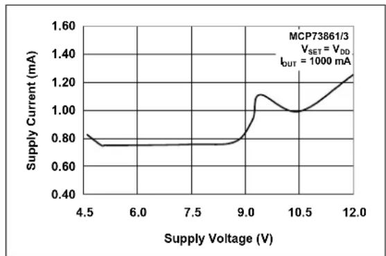
| Supply Voltage (V) | Supply Current (mA) | | ------------------ | ------------------- | | 4.5 | 0.80 | | 6.0 | 0.78 | | 7.5 | 0.78 | | 9.0 | 0.80 | | 10.5 | 1.00 | | 12.0 | 1.30 |FIGURE 2-5: Supply Current (I SS) vs. Supply Voltage (VDD).
line
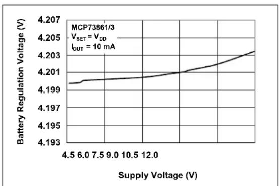
| Supply Voltage (V) | Battery Regulation Voltage (V) | | ------------------ | ------------------------------ | | 4.5 | 4.199 | | 6.0 | 4.200 | | 7.5 | 4.201 | | 9.0 | 4.201 | | 10.5 | 4.202 | | 12.0 | 4.203 |FIGURE 2-3: Battery Regulation Voltage ( V_BAT ) vs. Supply Voltage ( V_DD ).
line
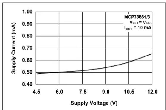
| Supply Voltage (V) | Supply Current (mA) | | ------------------ | ------------------- | | 4.5 | 0.50 | | 6.0 | 0.52 | | 7.5 | 0.54 | | 9.0 | 0.56 | | 10.5 | 0.60 | | 12.0 | 0.65 |FIGURE 2-6: Supply Current (I SS) vs. Supply Voltage ( V_DD ).
NOTE: Unless otherwise indicated, V_DD = [V_REG(typ.) + 1V] , I_OUT = 10 mA and T_A = +25^ , Constant-voltage mode.

line
| Battery Regulation Voltage (V) | +85°C | +25°C | -40°C | | ------------------------------ | ----- | ----- | ----- | | 2.0 | 0.25 | 0.20 | 0.15 | | 2.4 | 0.26 | 0.21 | 0.16 | | 2.8 | 0.27 | 0.22 | 0.17 | | 3.2 | 0.28 | 0.23 | 0.18 | | 3.6 | 0.29 | 0.24 | 0.19 | | 4.0 | 0.30 | 0.25 | 0.20 | | 4.4 | 0.31 | 0.26 | 0.21 |FIGURE 2-7: Output Leakage Current ( I_DISCHARGE ) vs. Battery Regulation Voltage ( V_BAT ).

line
| Ambient Temperature (°C) | Supply Current (mA) | | ------------------------ | ------------------ | | -40 | 0.40 | | -30 | 0.40 | | -20 | 0.40 | | -10 | 0.40 | | 0 | 0.40 | | 10 | 0.40 | | 20 | 0.40 | | 30 | 0.40 | | 40 | 0.40 | | 50 | 0.40 | | 60 | 0.60 | | 70 | 0.80 | | 80 | 1.00 |FIGURE 2-10: Supply Current (I SS) vs. Ambient Temperature ( T_A ).

line
| Supply Voltage (V) | Therm. Reference Voltage (V) | | ------------------ | ---------------------------- | | 4 | 2.510 | | 5 | 2.512 | | 6 | 2.515 | | 7 | 2.525 |FIGURE 2-8: Thermistor Reference Voltage ( V_THREF ) vs. Supply Voltage ( V_DD ).

line
| Ambient Temperature (°C) | Battery Regulation Voltage (V) | | ------------------------ | ------------------------------ | | -40 | 4.197 | | -30 | 4.198 | | -20 | 4.199 | | -10 | 4.200 | | 0 | 4.201 | | 10 | 4.199 | | 20 | 4.198 | | 30 | 4.199 | | 40 | 4.200 | | 50 | 4.201 | | 60 | 4.200 | | 70 | 4.199 | | 80 | 4.197 |FIGURE 2-11: Battery Regulation Voltage ( V_BAT ) vs. Ambient Temperature ( T_A ).
line
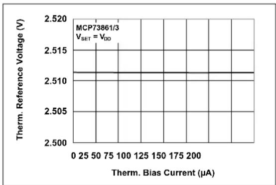
| Therm. Bias Current (μA) | Therm. Reference Voltage (V) | | ----------------------- | ---------------------------- | | 0 | 2.510 | | 25 | 2.510 | | 50 | 2.510 | | 75 | 2.510 | | 100 | 2.510 | | 125 | 2.510 | | 150 | 2.510 | | 175 | 2.510 | | 200 | 2.510 |FIGURE 2-9: Thermistor Reference Voltage ( V_THREF ) vs. Thermistor Bias Current ( I_THREF ).
line
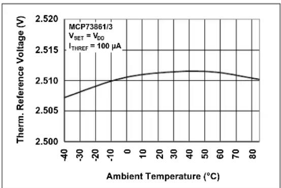
| Ambient Temperature (°C) | Therm. Reference Voltage (V) | | ------------------------ | ---------------------------- | | -40 | 2500 | | -30 | 2505 | | -20 | 2510 | | -10 | 2512 | | 0 | 2513 | | 10 | 2513 | | 20 | 2513 | | 30 | 2513 | | 40 | 2513 | | 50 | 2513 | | 60 | 2512 | | 70 | 2510 | | 80 | 2508 |FIGURE 2-12: Thermistor Reference Voltage ( V_THREF ) vs. Ambient Temperature ( T_A ).
NOTE: Unless otherwise indicated, V_DD = [V_REG(typ.) + 1V] , I_OUT = 10 mA and T_A = +25^ , Constant-voltage mode.

line
| Charge Current (mA) | Battery Regulation Voltage (V) | | ------------------- | ------------------------------ | | 10 | 8.401 | | 100 | 8.4015 | | 1000 | 8.402 | | 10000 | 8.403 |FIGURE 2-13: Battery Regulation Voltage ( V_BAT ) vs. Charge Current ( I_OUT ).
line
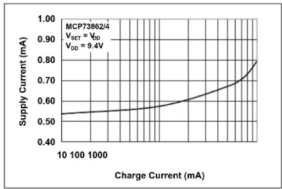
| Charge Current (mA) | Supply Current (mA) | | ------------------- | ------------------- | | 10 | 0.55 | | 100 | 0.56 | | 1000 | 0.57 | | 10000 | 0.58 | | 100000 | 0.60 | | 1000000 | 0.70 | | 10000000 | 0.80 |FIGURE 2-16: Supply Current (I SS ) vs. Charge Current (I OUT ).
line
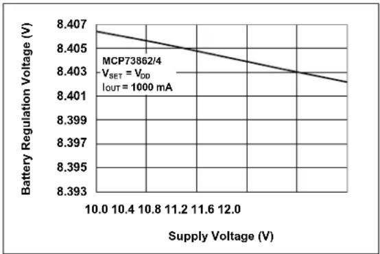
| Supply Voltage (V) | Battery Regulation Voltage (V) | | ------------------ | ------------------------------ | | 10.0 | 8.407 | | 10.4 | 8.405 | | 10.8 | 8.404 | | 11.2 | 8.403 | | 11.6 | 8.402 | | 12.0 | 8.401 |FIGURE 2-14: Battery Regulation Voltage ( V_BAT ) vs. Supply Voltage ( V_DD ).

line
| Supply Voltage (V) | Supply Current (mA) | | ------------------ | ------------------- | | 9.0 | 1.0 | | 9.5 | 0.8 | | 10.0 | 0.8 | | 10.5 | 0.8 | | 11.0 | 0.8 | | 11.5 | 0.8 | | 12.0 | 0.8 |FIGURE 2-17: Supply Current (I SS) vs. Supply Voltage (VDD).
line
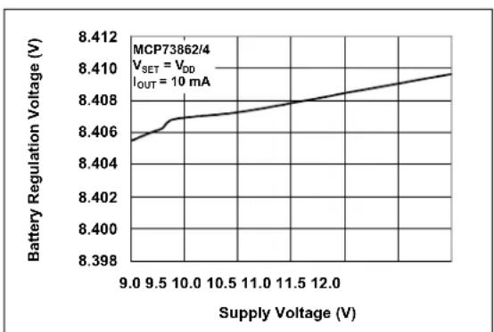
| Supply Voltage (V) | Battery Regulation Voltage (V) | | ------------------ | ------------------------------ | | 9.0 | 8.406 | | 9.5 | 8.407 | | 10.0 | 8.408 | | 10.5 | 8.408 | | 11.0 | 8.409 | | 11.5 | 8.410 | | 12.0 | 8.411 |FIGURE 2-15: Battery Regulation Voltage ( V_BAT ) vs. Supply Voltage ( V_DD ).
line
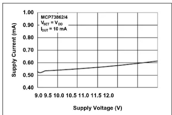
| Supply Voltage (V) | Supply Current (mA) | | ------------------ | ------------------- | | 9.0 | 0.52 | | 9.5 | 0.53 | | 10.0 | 0.54 | | 10.5 | 0.55 | | 11.0 | 0.56 | | 11.5 | 0.57 | | 12.0 | 0.58 |FIGURE 2-18: Supply Current (I SS) vs. Supply Voltage (VDD).
NOTE: Unless otherwise indicated, V_DD = [V_REG(typ.) + 1V] , I_OUT = 10 mA and T_A = +25^ , Constant-voltage mode.

line
| Battery Regulation Voltage (V) | +85°C | +25°C | +40°C | | ------------------------------ | ----- | ----- | ----- | | 4.0 | 0.05 | 0.10 | 0.15 | | 4.8 | 0.10 | 0.15 | 0.20 | | 5.6 | 0.15 | 0.20 | 0.25 | | 6.4 | 0.20 | 0.25 | 0.30 | | 7.2 | 0.25 | 0.30 | 0.35 | | 8.0 | 0.30 | 0.35 | 0.40 | | 8.8 | 0.35 | 0.40 | 0.45 |FIGURE 2-19: Output Leakage Current ( I_DISCHARGE ) vs. Battery Regulation Voltage ( V_BAT ).
line
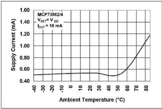
| Ambient Temperature (°C) | Supply Current (mA) | | ------------------------ | ------------------- | | -40 | 0.5 | | -30 | 0.5 | | -20 | 0.5 | | -10 | 0.5 | | 0 | 0.5 | | 10 | 0.5 | | 20 | 0.5 | | 30 | 0.5 | | 40 | 0.5 | | 50 | 0.5 | | 60 | 0.6 | | 70 | 0.9 | | 80 | 1.2 |FIGURE 2-22: Supply Current (I SS) vs. Ambient Temperature ( T_A ).

line
| Supply Voltage (V) | Therm. Reference Voltage (V) | | ------------------ | ---------------------------- | | 9.0 | 2.540 | | 9.5 | 2.542 | | 10.0 | 2.544 | | 10.5 | 2.546 | | 11.0 | 2.548 | | 11.5 | 2.550 | | 12.0 | 2.552 |FIGURE 2-20: Thermistor Reference Voltage ( V_THREF ) vs. Supply Voltage ( V_DD ).
line
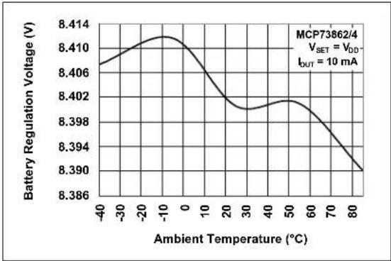
| Ambient Temperature (°C) | Battery Regulation Voltage (V) | | ------------------------ | ------------------------------ | | -40 | 8.406 | | -30 | 8.410 | | -20 | 8.412 | | -10 | 8.413 | | 0 | 8.412 | | 10 | 8.408 | | 20 | 8.402 | | 30 | 8.399 | | 40 | 8.401 | | 50 | 8.402 | | 60 | 8.399 | | 70 | 8.396 | | 80 | 8.390 |FIGURE 2-23: Battery Regulation Voltage ( V_BAT ) vs. Ambient Temperature ( T_A ).

line
| Thermistor Bias Current (µA) | Therm. Reference Voltage (V) | | --------------------------- | ---------------------------- | | 0 | 2.544 | | 25 | 2.544 | | 50 | 2.544 | | 75 | 2.544 | | 100 | 2.544 | | 125 | 2.544 | | 150 | 2.544 | | 175 | 2.544 | | 200 | 2.544 |FIGURE 2-21: Thermistor Reference Voltage ( V_THREF ) vs. Thermistor Bias Current ( I_THREF ).
line
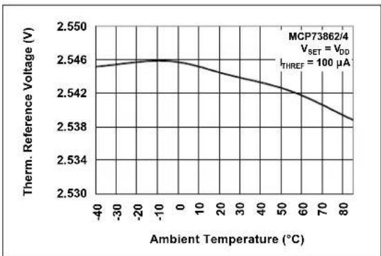
| Ambient Temperature (°C) | Therm. Reference Voltage (V) | | ------------------------ | ---------------------------- | | -40 | 2.546 | | -30 | 2.546 | | -20 | 2.546 | | -10 | 2.546 | | 0 | 2.546 | | 10 | 2.545 | | 20 | 2.544 | | 30 | 2.543 | | 40 | 2.542 | | 50 | 2.541 | | 60 | 2.540 | | 70 | 2.539 | | 80 | 2.538 |FIGURE 2-24: Thermistor Reference Voltage ( V_THREF ) vs. Ambient Temperature ( T_A ).
NOTE: Unless otherwise indicated, V_DD = [V_REG(typ.) + 1V] , I_OUT = 10 mA and T_A = +25^ , Constant-voltage mode.

line
| Voltage Level | Current (mA) | | ------------- | ------------ | | V_DD | 5.2 | | V_BAT | 10 |FIGURE 2-25: Line Transient Response.

line
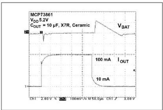
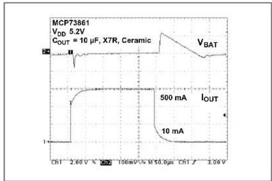
| Measurement | Value | |-------------|-----------| | V_DD | Stepped from 5.2V to 6.2V | | I_OUT | 500 mA | | C_OUT | 10 µF | | X7R | Ceramic |FIGURE 2-28: Line Transient Response.
line
| Parameter | Value | | --------- | --------- | | V_DD | 5.2V | | C_OUT | 10 μF | | X7R | Ceramic | | I_OUT | 10 mA | | Current | 10 mA |FIGURE 2-26: Load Transient Response.
line
| Time (μs) | V_BAT (mA) | I_OUT (mA) | |-----------|------------|------------| | 0 | 0 | 0 | | 2.00 | ~1.5 | ~1.5 | | 50.0 | ~2.0 | ~500 | | 3.00 | ~1.5 | 10 |FIGURE 2-29: Load Transient Response.
line
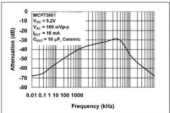
| Frequency (kHz) | Attenuation (dB) | | --------------- | ---------------- | | 0.01 | -70 | | 0.1 | -65 | | 1 | -60 | | 10 | -55 | | 100 | -50 | | 1000 | -45 | | >1000 | -30 |FIGURE 2-27: Power Supply Ripple Rejection.
line
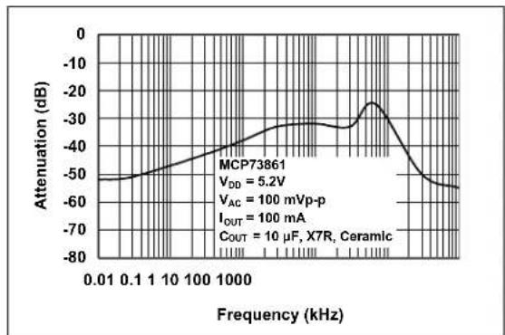
| Frequency (kHz) | Attenuation (dB) | | --------------- | ---------------- | | 0.01 | -50 | | 0.1 | -45 | | 1 | -40 | | 10 | -35 | | 100 | -30 | | 1000 | -25 | | >1000 | < -60 |FIGURE 2-30: Power Supply Ripple Rejection.
NOTE: Unless otherwise indicated, V_DD = [V_REG(typ.) + 1V] , I_OUT = 10 mA and T_A = +25^ , Constant-voltage mode.

line
| Operating Resistor (Ω) | Charge Current (mA) | | ---------------------- | ------------------- | | 4.8k | 100 | | 1.6k | 300 | | 536 | 500 | | >536 | >1000 |FIGURE 2-31: Charge Current (I OUT) vs. Programming Resistor ( R_PROG ).

line
| Ambient Temperature (°C) | Charge Current (mA) | | ------------------------ | ------------------- | | -40 | 493 | | -30 | 495 | | -20 | 497 | | -10 | 498 | | 0 | 499 | | 10 | 499 | | 20 | 499 | | 30 | 499 | | 40 | 500 | | 50 | 501 | | 60 | 501 | | 70 | 500 | | 80 | 499 |FIGURE 2-32: Charge Current (I OUT) vs. Ambient Temperature ( T_A ).
3.0 PIN DESCRIPTION
The descriptions of the pins are listed in Table3.1.
TABLE 3-1: PIN FUNCTION TABLE
| MCP73861/2/3/4 | Symbol Function | Symbol Function | |
| QFN SOIC | |||
| 1 | 3 | V_SET | Voltage Regulation Selection |
| 2 | 4 | V_DD1 | Battery Management Input Supply |
| 3 | 5 | V_DD2 | Battery Management Input Supply |
| 4 | 6 | V_SS1 | Battery Management 0V Reference |
| 5 | 7 | PROG | Current Regulation Set |
| 6 | 8 | THREF | Cell Temperature Sensor Bias |
| 7 | 9 | THERM | Cell Temperature Sensor Input |
| 8 | 10 | TIMER | Timer Set |
| 9 | 11 | V_SS3 | Battery Management 0V Reference |
| 10 | 12 | V_BAT1 | Battery Charge Control Output |
| 11 | 13 | V_BAT2 | Battery Charge Control Output |
| 12 | 14 | V_BAT3 | Battery Voltage Sense |
| 13 | 15 | V_SS2 | Battery Management 0V Reference |
| 14 | 16 | EN | Logic Enable |
| 15 | 1 | STAT2 | Fault Status Output |
| 16 | 2 | STAT1 | Charge Status Output |
| 17 | - | EP | Exposed Pad; Battery Management 0V Reference |
3.1 Voltage Regulation Selection ( V_SET )
MCP73861/3: Connect V_SET to V_SS for 4.1V regulation voltage, connect to V_DD for 4.2V regulation voltage. MCP73862/4: Connect V_SET to V_SS for 8.2V regulation voltage, connect to V_DD for 8.4V regulation voltage.
3.2 Battery Management Input Supply ( V_DD2 , V_DD1 )
A supply voltage of [V_REG (typ.) + 0.3V] to 12V is recommended. Bypass to V_SS with a minimum of 4.7 F. A 1.5 k resistor should be connected from V_DD to ground when using disconnectable supplies to force V_DD < V_BAT when the supply is disconnected and assure low leakage current.
3.3 Battery Management 0V Reference ( V_SS1 , V_SS2 , V_SS3 )
Connect to negative terminal of battery and input supply.
3.4 Current Regulation Set (PROG)
Preconditioning, fast and termination currents are scaled by placing a resistor from PROG to V_SS .
3.5 Cell Temperature Sensor Bias (THREF)
THREF is a voltage reference to bias external thermistor for continuous cell temperature monitoring and prequalification.
3.6 Cell Temperature Sensor Input (THERM)
THERM is an input for an external thermistor for continuous cell-temperature monitoring and prequalification. Connect to THREF/3 to disable temperature sensing.
3.7 Timer Set
All safety timers are scaled by C_TIMER/0.1 F .
3.8 Battery Charge Control Output ( V_BAT1 , V_BAT2 )
Connect to positive terminal of battery. Drain terminal of internal P-channel MOSFET pass transistor. Bypass to V_SS with a minimum of 4.7 F to ensure loop stability when the battery is disconnected.
3.9 Battery Voltage Sense (V BAT3)
V_BAT3 is a voltage sense input. Connect to positive terminal of battery. A precision internal resistor divider regulates the final voltage on this pin to V_REG
3.10 Logic Enable (EN)
EN is an input to force charge termination, initiate charge, clear faults or disable automatic recharge.
3.11 Fault Status Output (STAT2)
STAT2 is a current-limited, open-drain drive for direct connection to a LED for charge status indication. Alternatively, a pull-up resistor can be applied for interfacing to a host microcontroller.
3.12 Charge Status Output (STAT1)
STAT1 is a current-limited, open-drain drive for direct connection to a LED for charge status indication. Alternatively, a pull-up resistor can be applied for interfacing to a host microcontroller.
3.13 Exposed Pad (EP)
There is an internal electrical connection between the exposed thermal pad and V_SS . The EP must be connected to the same potential as the V_SS pin on the Printed Circuit Board (PCB).
4.0 DEVICE OVERVIEW
The MCP7386X family of devices are highly advanced linear charge management controllers. Refer to the functional block diagram. Figure 4-2 depicts the operational flow algorithm from charge initiation to completion and automatic recharge.
4.1 Charge Qualification and Preconditioning
Upon insertion of a battery, or application of an external supply, the MCP7386X family of devices automatically performs a series of safety checks to qualify the charge. The input source voltage must be above the Undervoltage Lockout (UVLO) threshold, the enable pin must be above the logic-high level and the cell temperature must be within the upper and lower thresholds. The qualification parameters are continuously monitored. Deviation beyond the limits automatically suspends or terminates the charge cycle. The input voltage must deviate below the UVLO stop threshold for at least one clock period to be considered valid.
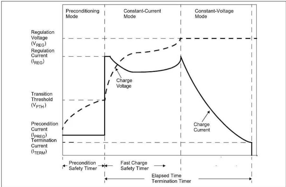
Once the qualification parameters have been met, the MCP7386X initiates a charge cycle. The charge status output is pulled low throughout the charge cycle (see Table 5-1 for charge status outputs). If the battery voltage is below the preconditioning threshold ( V_PTH ), the MCP7386X preconditions the battery with a trickle-charge. The preconditioning current is set to approximately 10% of the fast charge regulation current. The preconditioning trickle-charge safely replenishes deeply depleted cells and minimizes heat dissipation during the initial charge cycle. If the battery voltage has not exceeded the preconditioning threshold before the preconditioning timer has expired, a fault is indicated and the charge cycle is terminated.
4.2 Constant Current Regulation – Fast Charge
Preconditioning ends, and fast charging begins, when the battery voltage exceeds the preconditioning threshold. Fast charge regulates to a constant current ( I_REG ), which is set via an external resistor connected to the PROG pin. Fast charge continues until the battery voltage reaches the regulation voltage ( V_REG ), or the fast charge timer expires; in which case, a fault is indicated and the charge cycle is terminated.
4.3 Constant Voltage Regulation
When the battery voltage reaches the regulation voltage ( V_REG ), constant voltage regulation begins. The MCP7386X monitors the battery voltage at the V_BAT pin. This input is tied directly to the positive terminal of the battery.
The MCP7386X selects the voltage regulation value based on the state of V_SET . With V_SET tied to V_SS , the MCP73861/3 and MCP73862/4 regulate to 4.1V and 8.2V, respectively. With V_SET tied to V_DD , the MCP73861/3 and MCP73862/4 regulate to 4.2V and 8.4V, respectively.
4.4 Charge Cycle Completion and Automatic Re-Charge
The MCP7386X monitors the charging current during the Constant-voltage regulation mode. The charge cycle is considered complete when the charge current has diminished below approximately 8% of the regulation current ( I_REG ), or the elapsed timer has expired.
The MCP7386X automatically begins a new charge cycle when the battery voltage falls below the recharge threshold ( V_RTH ), assuming all the qualification parameters are met.
4.5 Thermal Regulation
The MCP7386X family limits the charge current based on the die temperature. Thermal regulation optimizes the charge cycle time while maintaining device reliability. If thermal regulation is entered, the timer is automatically slowed down to ensure that a charge cycle will not terminate prematurely. Figure 4-1 depicts the thermal regulation profile.

line
| Die Temperature (°C) | Maximum Charge Current (mA) | |---|---| | 0 | 1200 | | 40 | 1200 | | 80 | 1200 | | 120 | 1200 | | 140 | 1200 | | 160 | 1000 | | 180 | 800 | | 200 | 600 | | 220 | 400 | | 240 | 200 | | 260 | 0 | The chart displays a single line representing the maximum charge current across the die temperature range from 0 to approximately 130°C. The minimum and maximum curves are labeled in English. There is no additional data series present in the chart.FIGURE 4-1: Typical Maximum Charge Current vs. Die Temperature.
4.6 Thermal Shutdown
The MCP7386X family suspends charge if the die temperature exceeds 155°C. Charging will resume when the die temperature has cooled by approximately 10°C. The thermal shutdown is a secondary safety feature in the event that there is a failure within the thermal regulation circuitry.

flowchart
graph TD
    A["Initialize"] --> B{V_DD > V_UVLO EN High}
    B -->|No STAT1 = Off STAT2 = Off| C{Temperature OK}
    B -->|Yes| D{V_BAT > V_PTH}
    C -->|No| E["Preconditioning Mode Charge Current = I_PREG Reset Safety Timer"]
    C -->|Yes| F["Constant-Current Mode Charge Current = I_REG Reset Safety Timer"]
    D -->|No| F
    D -->|Yes| G["Constant-Voltage Mode Output Voltage = V_REG"]
    F --> H{V_BAT > V_PTH}
    H -->|No| I["Safety Timer Expired"]
    H -->|Yes| J["Fault Charge Current = 0 Reset Safety Timer"]
    I --> K{Temperature OK}
    K -->|No STAT1 = Off STAT2 = OnSTAT2 = Flashing| L{V_DD < V_UVLO or EN Low}
    K -->|Yes| M{V_DD < V_UVLO or EN Low}
    L --> N{Safety Timer Suspended Charge Current = 0}
    M --> O{Safety Timer Suspended Charge Current = 0}
    N --> P{I_OUT < I_TERM Elapsed Timer Expired}
    O --> Q{I_OUT < I_TERM Elapsed Timer Expired}
    P --> R{I_OUT < I_TERM Elapsed Timer Expired}
    Q --> S{I_OUT < I_TERM Elapsed Timer Expired}
    R --> T{I_OUT < I_TERM Elapsed Timer Expired}
    S --> U{I_OUT < I_TERM Elapsed Timer Expired}
    T --> V{I_OUT < I_TERM Elapsed Timer Expired}
    U --> W{I_OUT < I_TERM Elapsed Timer Expired}
    V --> X{I_OUT < I_TERM Elapsed Timer Expired}
    W --> Y{I_OUT < I_TERM Elapsed Timer Expired}
    X --> Z{I_OUT < I_TERM Elapsed Timer Expired}
    Y --> AA{I_OUT < I_TERM Elapsed Timer Expired}
    Z --> AB{I_OUT < I_TERM Elapsed Timer Expired}
    AA --> AC{I_OUT < I_TERM Elapsed Timer Expired}
    AB --> AD{I_OUT < I_TERM Elapsed Timer Expired}
    AC --> AE{I_OUT < I_TERM Elapsed Timer Expired}
    AD --> AF{I_OUT < I_TERM Elapsed Timer Expired}
    AE --> AG{I_OUT < I_TERM Elapsed Timer Expired}
    AF --> AH{I_OUT < I_TERM Elapsed Timer Expired}
    AG --> AI{I_OUT < I_TERM Elapsed Timer Expired}
    AH --> AJ{I_OUT < I_TERM Elapsed Timer Expired}
    AI --> AK{I_OUT < I_TERM Elapsed Timer Expired}
    AJ --> AL{I_OUT < I_TERM Elapsed Timer Expired}
    AK --> AM{I_OUT < I_TERM Elapsed Timer Expired}
    AL --> AN{I_OUT < I_TERM Elapsed Timer Expired}
    AM --> AO{I_OUT < I_TERM Elapsed Timer Expired}
    AN --> AP{I_OUT < I_TERM Elapsed Timer Expired}
    AO --> AQ{I_OUT < I_TERM Elapsed Timer Expired}
    AP --> AR{I_OUT < I_TERM Elapsed Timer Expired}
    AQ --> AS{I_OUT < I_TERM Elapsed Timer Expired}
    AR --> AT{I_OUT < I_TERM Elapsed Timer Expired}
    AS --> AU{I_OUT < I_TERM Elapsed Timer Expired}
    AT --> AV{I_OUT < I_TERM Elapsed Timer Expired}
    AU --> AW{I_OUT < I_TERM Elapsed Timer Expired}
    AV --> AX{I_OUT < I_TERM Elapsed Timer Expired}
    AW --> AY{I_OUT < I_TERM Elapsed Timer Expired}
    AX --> AZ{I_OUT < I_TERM Elapsed Timer Expired}
    AY --> BA{I_OUT < I_TERM Elapsed Timer Expired}
    AZ --> BB{I_OUT < I_TERM Elapsed Timer Expired}
    BA --> BC{I_OUT < I_TERM Elapsed Timer Expired}
    BB --> BD{I_OUT < I_TERM Elapsed Timer Expired}
    BC --> BE{I_OUT < I_TERM Elapsed Timer Expired}
    BD --> BF{I_OUT < I_TERM Elapsed Timer Expired}
    BE --> BG{I_OUT < I_TERM Elapsed Timer Expired}
    BF --> BH{I_OUT < I_TERM Elapsed Timer Expired}
    BG --> BI{I_OUT < I_TERM Elapsed Timer Expired}
    BH --> BJ{I_OUT < I_TERM Elapsed Timer Expired}
    BI --> BK{I_OUT < I_TERM Elapsed Timer Expired}
    BJ --> BL{I_OUT < I_TERM Elapsed Timer Expired}
    BK --> BM{I_OUT < I_TERM Elapsed Timer Expired}
    BL --> BN{I_OUT < I_TERM Elapsed Timer Expired}
    BM --> BO{I_OUT < I_TERM Elapsed Timer Expired}
    BN --> BP{I_OUT < I_TERM Elapsed Timer Expired}
    BO --> BQ{I_OUT < I_TERM Elapsed Timer Expired}
    BP --> BR{I_OUT < I_TERM Elapsed Timer Expired}
FIGURE 4-2: Operational Flow Algorithm.
5.0 DETAILED DESCRIPTION
5.1 Analog Circuitry
5.1.1 BATTERY MANAGEMENT INPUT SUPPLY ( V_DD1 , V_DD2 )
The V_DD input is the input supply to the MCP7386X. The MCP7386X automatically enters a Power-down mode if the voltage on the V_DD input falls below the UVLO voltage ( V_STOP ). This feature prevents draining the battery pack when the V_DD supply is not present. The V_DD inputs should be tied to ground with a resistor <= 1.5 kΩ to prevent V_DD from floating and staying at V_BAT level if the input supply is disconnected. The resistor will assure that V_DD < V_BAT when the input supply is removed.
5.1.2 PROG INPUT
Fast charge current regulation can be scaled by placing a programming resistor ( R_PROG ) from the PROG input to V_SS . Connecting the PROG input to V_SS allows for a maximum fast charge current of 1.2A, typically. The minimum fast charge current is 100 mA, set by letting the PROG input float. The following formula calculates the value for R_PROG :
$$ R _ {P R O G} \quad \frac {1 3 . 2 H I \times_ {R E G}}{1 2 \times I _ {R E G} 1 . 2 -} $$
Where:
I_REG = the desired fast charge current in amps.
R_PROG = measured in kΩ.
The preconditioning trickle-charge current and the charge termination current are scaled to approximately 10% and 8% of I_REG respectively.
5.1.3 CELL TEMPERATURE SENSOR BIAS (THREF)
A 2.5V voltage reference is provided to bias an external thermistor for continuous cell temperature monitoring and prequalification. A ratio metric window comparison is performed at threshold levels of V_THREF/2 and V_THREF/4 .
5.1.4 CELL TEMPERATURE SENSOR INPUT (THERM)
The MCP73861/2/3/4 continuously monitors temperature by comparing the voltage between the THERM input and V_SS with the upper and lower temperature thresholds. A negative or positive temperature coefficient, NTC or PTC thermistor and an external voltage-divider typically develop this voltage. The temperature sensing circuit has its own reference to which it performs a ratio metric comparison. Therefore, it is immune to fluctuations in the supply input ( V_DD ). The
temperature-sensing circuit is removed from the system when V_DD is not applied, eliminating additional discharge of the battery pack.
Figure 6-1 depicts a typical application circuit with connection of the THERM input. The resistor values of R_T1 and R_T2 are calculated with the following equations.
For NTC thermistors:
$$ R _ {T I} = \frac {2 \times R _ {C O L D} \times R _ {H O T}}{R _ {C O L D} - R _ {H O T}} $$
$$ R _ {T 2} = \frac {2 \times R _ {C O L D} \times R _ {H O T}}{R _ {C O L D} - 3 \times R _ {H O T}} $$
For PTC thermistors:
$$ R _ {T I} = \frac {2 \times R _ {C O L D} \times R _ {H O T}}{R _ {H O T} - R _ {C O L D}} $$
$$ R _ {T 2} = \frac {2 \times R _ {C O L D} \times R _ {H O T}}{R _ {H O T} - 3 \times R _ {C O L D}} $$
Where:
R_COLD and R_HOT are the thermistor resistance values at the temperature window of interest.
Applying a voltage equal to V_THREF/3 to the THERM input disables temperature monitoring.
5.1.5 TIMER SET INPUT (TIMER)
The TIMER input programs the period of the safety timers by placing a timing capacitor ( C_TIMER ) between the TIMER input pin and V_SS . Three safety timers are programmed via the timing capacitor.
The preconditioning safety timer period:
$$ t _ {P R E C O N} = \frac {C _ {T I M E R}}{0 . 1 \mu F} \times 1. 0 H o u r s $$
The fast charge safety timer period:
$$ t _ {F A S T} = \frac {C _ {T I M E R}}{0 . 1 \mu F} k. 5 H o u r s $$
The elapsed time termination period:
$$ t _ {T E R M} = \frac {C _ {T I M E R}}{0 . 1 \mu F} \times 3. 0 H o u r s $$
The preconditioning timer starts after qualification and resets when the charge cycle transitions to the fast charge, Constant-current mode. The fast charge timer and the elapsed timer start once the MCP7386X transitions from preconditioning. The fast charge timer resets when the charge cycle transitions to the Constant-voltage mode. The elapsed timer will expire and terminate the charge if the sensed current does not diminish below the termination threshold.
During thermal regulation, the timer is slowed down proportional to the charge current.
5.1.6 BATTERY VOLTAGE SENSE (V BAT3)
The MCP7386X monitors the battery voltage at the V_BAT3 pin. This input is tied directly to the positive terminal of the battery pack.
5.1.7 BATTERY CHARGE CONTROL
OUTPUT ( V_BAT1 , V_BAT2 )
The battery charge control output is the drain terminal of an internal P-channel MOSFET. The MCP7386X provides constant current and voltage regulation to the battery pack by controlling this MOSFET in the linear region. The battery charge control output should be connected to the positive terminal of the battery pack.
5.2 Digital Circuitry
5.2.1 CHARGE STATUS OUTPUTS (STAT1, STAT2)
Two status outputs provide information on the state of charge. The current-limited, open-drain outputs can be used to illuminate external LEDs. Optionally, a pull-up resistor can be used on the output for communication with a host microcontroller. Table 5-1 summarizes the state of the status outputs during a charge cycle.
TABLE 5-1: STATUS OUTPUTS
| CHARGE CYCLE STAT1 | STAT1 STAT2 | |
| Qualification Off Off | ||
| Preconditioning | On | Off |
| Constant-Current Fast Charge | On | Off |
| Constant-Voltage | On Off | |
| Charge Complete | Flashing (1 Hz, 50% duty cycle) (MCP73861/2) | Off(All Devices) |
| Off(MCP73863/4) | ||
| Fault | Off On | |
| THERM Invalid | Off | Flashing (1 Hz 50% duty cycle) |
| Disabled – Sleep mode | Off Off | |
| Input Voltage Dis-connected (1.5KΩ Pulldown) | Off Off | |
Legend: Off state: Open-drain is high-impedance On state: Open-drain can sink current typically 7 mA Flashing: Toggles between off state and on state
The flashing rate (1 Hz) is based off a timer capacitor ( C_TIMER ) of 0.1 F. The rate will vary based on the value of the timer capacitor.
During a Fault condition, the STAT1 status output will be off and the STAT2 status output will be on. To recover from a Fault condition, the input voltage must be removed and then reapplied, or the enable input (EN) must be de-asserted to a logic-low, then asserted to a logic-high.
When the voltage on the THERM input is outside the preset window, the charge cycle will not start, or will be suspended. The charge cycle is not terminated and recovery is automatic. The charge cycle will resume (or start) once the THERM input is valid and all other qualification parameters are met. During an invalid THERM condition, the STAT1 status output will be off and the STAT2 status output will flash.
5.2.2 V SET INPUT
The V_SET input selects the regulated output voltage of the MCP7386X. With V_SET tied to V_SS , the MCP73861/3 and MCP73862/4 regulate to 4.1V and 8.2V, respectively. With V_SET tied to V_DD , the MCP73861/3 and MCP73862/4 regulate to 4.2V and 8.4V, respectively.
5.2.3 LOGIC ENABLE (EN)
The logic enable input pin (EN) can be used to terminate a charge at any time during the charge cycle, as well as to initiate a charge cycle or initiate a recharge cycle.
Applying a logic-high input signal to the EN pin, or tying it to the input source, enables the device. Applying a logic-low input signal disables the device and terminates a charge cycle. When disabled, the device's supply current is reduced to 0.17 A, typically.
6.0 APPLICATIONS
The MCP7386X is designed to operate in conjunction with a host microcontroller or in stand-alone applications. The MCP7386X provides the preferred charge algorithm for Lithium-Ion and Lithium-Polymer cells Constant-current followed by Constant-voltage.
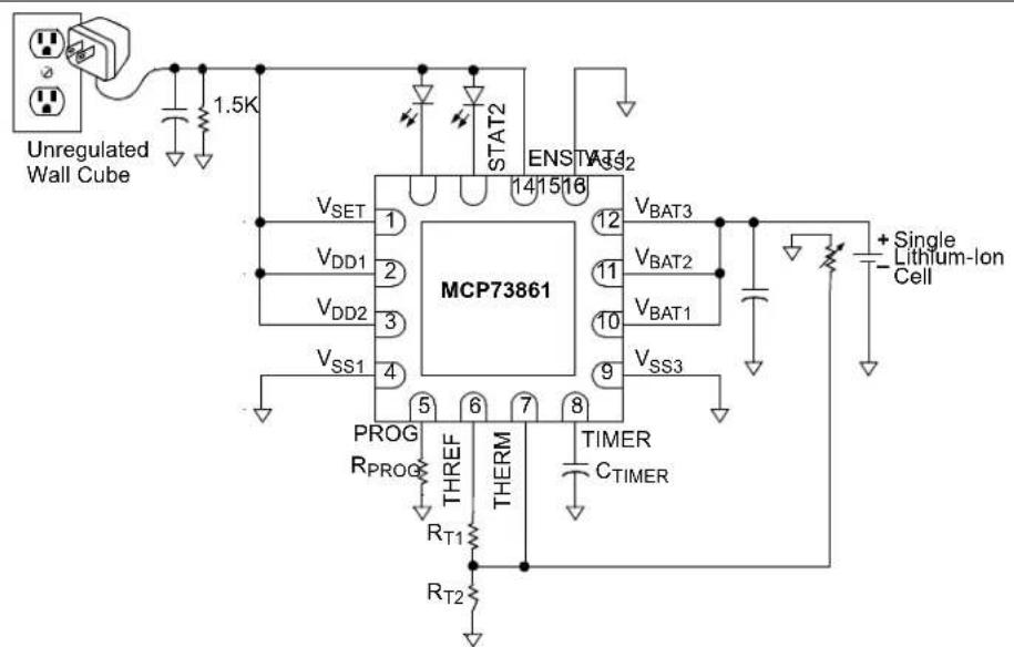
Figure 6-1 illustrates a typical stand-alone application circuit, while Figures 6-2 and 6-3 illustrate the accompanying charge profile
text_image
Unregulated Wall Cube 1.5K VSET VDD1 VDD2 VSS1 PROG RPROG THREF RT1 RT2 STAT2 ENSTAT1 14 15 16 VBAT3 VBAT2 VBAT1 VSS3 TIMER CTIMER + Single Lithium-Ion CellFIGURE 6-1: Typical Application Circuit.

line
| Mode Type | Voltage Level | |-----------------------|---------------------| | Preconditioning Mode | V_REG | | Constant-Current Mode | I_REG | | Constant-Voltage Mode | - | | Transition Threshold (V_PTH) | - | | Precondition Current (I_PREG) | - | | Termination Current (I_TERM) | - |FIGURE 6-2: Typical Charge Profile.
line
| Time Interval | Preconditioning Mode (V_REG) | Regulation Current (I_REG) | Transition Threshold (V_PTH) | Charge Voltage | Charge Current | | ------------- | ---------------------------- | -------------------------- | ----------------------------- | -------------- | -------------- | | Preconditioning | High | Low | Low | Low | Low | | Constant-Current | Medium | Medium | Medium | Medium | Medium | | Constant-Voltage | Low | Low | Low | Low | Low |FIGURE 6-3: Typical Charge Profile in Thermal Regulation.
6.1 Application Circuit Design
Due to the low efficiency of linear charging, the most important factors are thermal design and cost, which are a direct function of the input voltage, output current and thermal impedance between the battery charger and the ambient cooling air. The worst-case situation is when the device has transitioned from the Preconditioning mode to the Constant-current mode. In this situation, the battery charger has to dissipate the maximum power. A trade-off must be made between the charge current, cost and thermal requirements of the charger.
6.1.1 COMPONENT SELECTION
Selection of the external components in Figure 6-1 is crucial to the integrity and reliability of the charging system. The following discussion is intended as a guide for the component selection process.
6.1.1.1 Current Programming Resistor (RPROG)
The preferred fast charge current for Lithium-Ion cells is at the 1C rate, with an absolute maximum current at the 2C rate. For example, a 500 mAh battery pack has a preferred fast charge current of 500 mA. Charging at this rate provides the shortest charge cycle times without degradation to the battery pack performance or life.
1200 mA is the maximum charge current obtainable from the MCP7386X. For this situation, the PROG input should be connected directly to V_SS .
6.1.1.2 Thermal Considerations
The worst-case power dissipation in the battery charger occurs when the input voltage is at the maximum and the device has transitioned from the Pre-conditioning mode to the Constant-current mode. In this case, the power dissipation is:
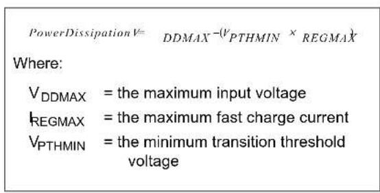
text_image
PowerDissipation V= DDMAX-(VPTHMIN × REGMAX) Where: VDDMAX = the maximum input voltage REGMAX = the maximum fast charge current VPTHMIN = the minimum transition threshold voltagePower dissipation with a 5V, ±10% input voltage source is:
$$ \text { PowerDissipation } \quad (5. 5 V - 2. 7 V) \times 5 7 5 m A \quad 1. 6 1 W = $$
With the battery charger mounted on a 1 in ^2 pad of 1 oz. copper, the junction temperature rise is 60°C, approximately. This would allow for a maximum operating ambient temperature of 50°C before thermal regulation is entered.
6.1.1.3 External Capacitors
The MCP7386X is stable with or without a battery load. In order to maintain good AC stability in the Constant-voltage mode, a minimum capacitance of 4.7 F is recommended to bypass the V_BAT pin to V_SS . This capacitance provides compensation when there is no battery load. In addition, the battery and interconnections appear inductive at high frequencies. These elements are in the control feedback loop during Constant-voltage mode. Therefore, the bypass capacitance may be necessary to compensate for the inductive nature of the battery pack.
Virtually any good quality output filter capacitor can be used, independent of the capacitor's minimum Effective Series Resistance (ESR) value. The actual value of the capacitor (and its associated ESR) depends on the output load current. A 4.7 F ceramic, tantalum or aluminum electrolytic capacitor at the output is usually sufficient to ensure stability for up to a 1A output current.
6.1.1.4 Reverse-Blocking Protection
The MCP7386X provides protection from a faulted or shorted input, or from a reversed-polarity input source. Without the protection, a faulted or shorted input would discharge the battery pack through the body diode of the internal pass transistor.
6.1.1.5 Enable Interface
In the stand-alone configuration, the enable pin is generally tied to the input voltage. The MCP7386X automatically enters a Low-power mode when voltage on the V_DD input falls below the UVLO voltage ( V_STOP ), reducing the battery drain current to 0.23 A, typically.
6.1.1.6 Charge Status Interface
Two status outputs provide information on the state of charge. The current-limited, open-drain outputs can be used to illuminate external LEDs. Refer to Table 5-1 for a summary of the state of the status outputs during a charge cycle.
6.2 PCB Layout Issues
For optimum voltage regulation, place the battery pack as close as possible to the device's V_BAT and V_SS pins, recommended to minimize voltage drops along the high current-carrying PCB traces.
If the PCB layout is used as a heatsink, adding many vias in the heatsink pad can help conduct more heat to the backplane of the PCB, thus reducing the maximum junction temperature.
NOTES:
7.0 PACKAGING INFORMATION
7.1 Package Marking Information
16-Lead QFN

text_image
XXXXX XXXXXX XXXXXX YWWNNNExample:

text_image
73861 I/ML 1108 25616-Lead SOIC (150 mil) Example:

text_image
XXXXXXXXXXXXXX XXXXXXXXXXXXXX YYWWNNN
text_image
MCP73861 I/SL e3 1108256Legend: XX...X Customer-specific information
Y Year code (last digit of calendar year)
YY Year code (last 2 digits of calendar year)
WW Week code (week of January 1 is week '01')
NNN Alphanumeric traceability code
ePb-free JEDEC designator for Matte Tin (Sn)
* This package is Pb-free. The Pb-free JEDEC designator (e3) can be found on the outer packaging for this package.
Note: In the event the full Microchip part number cannot be marked on one line, it will be carried over to the next line, thus limiting the number of available characters for customer-specific information.
16-Lead Plastic Quad Flat, No Lead Package (ML) - 4x4x0.9 mm Body [QFN]
Note: For the most current package drawings, please see the Microchip Packaging Specification located at http://www.microchip.com/packaging
![Microchip MCP73861 - 16-Lead Plastic Quad Flat, No Lead Package (ML) - 4x4x0.9 mm Body [QFN] - 1](/content/2026/06/1219295/images/6089f4f1802d036ecb10c931493d28cf60453166bd519ab40128c33d54d719a0.jpg)
| Units | MILLIMETERS | |||
| Dimension Limits | MIN NOM MAX | |||
| Number of Pins N 16 | ||||
| Pitch e 0.65 BSC | ||||
| Overall Height | A | 0.80 | 0.90 | 1.00 |
| Standoff | A1 | 0.00 | 0.02 | 0.05 |
| Contact Thickness | A3 | 0.20 REF | ||
| Overall Width | E | 4.00 BSC | ||
| Exposed Pad Width | E2 | 2.50 | 2.65 | 2.80 |
| Overall Length | D | 4.00 BSC | ||
| Exposed Pad Length | D2 | 2.50 | 2.65 | 2.80 |
| Contact Width | b | 0.25 | 0.30 | 0.35 |
| Contact Length | L | 0.30 | 0.40 | 0.50 |
| Contact-to-Exposed Pad | K | 0.20 | - | - |
Notes:
- Pin 1 visual index feature may vary, but must be located within the hatched area.
- Package is saw singulated.
- Dimensioning and tolerancing per ASME Y14.5M.
BSC: Basic Dimension. Theoretically exact value shown without tolerances.
REF: Reference Dimension, usually without tolerance, for information purposes only.
Microchip Technology Drawing C04-127B
16-Lead Plastic Quad Flat, No Lead Package (ML) - 4x4x0.9mm Body [QFN]
Note: For the most current package drawings, please see the Microchip Packaging Specification located at http://www.microchip.com/packaging
![Microchip MCP73861 - 16-Lead Plastic Quad Flat, No Lead Package (ML) - 4x4x0.9mm Body [QFN] - 1](/content/2026/06/1219295/images/66a75f548430a7f9b3c88c3c769dcaddce0da503ad80cc831753860285266a04.jpg)
text_image
C1 W2 C2 T2 E G Y1 X1 SILK SCREENRECOMMENDED LAND PATTERN
| Units | MILLIMETERS | |||
| Dimension Limits | MIN | NOM | MAX | |
| Contact Pitch | E | 0.65 BSC | ||
| Optional Center Pad Width | W2 | 2.50 | ||
| Optional Center Pad Length | T2 | 2.50 | ||
| Contact Pad Spacing | C1 | 4.00 | ||
| Contact Pad Spacing | C2 | 4.00 | ||
| Contact Pad Width (X16) | X1 | 0.35 | ||
| Contact Pad Length (X16) | Y1 | 0.80 | ||
| Distance Between Pads | G | 0.30 | ||
Notes:
1. Dimensioning and tolerancing per ASME Y14.5M
BSC: Basic Dimension. Theoretically exact value shown without tolerances.
Microchip Technology Drawing No. C04-2127A
16-Lead Plastic Small Outline (SL) - Narrow, 3.90 mm Body [SOIC]
Note: For the most current package drawings, please see the Microchip Packaging Specification located at http://www.microchip.com/packaging
![Microchip MCP73861 - 16-Lead Plastic Small Outline (SL) - Narrow, 3.90 mm Body [SOIC] - 1](/content/2026/06/1219295/images/1b6049f7f2a63d364804ae1255363c25e4968a4f932be62d4b35d8a826ef9fc1.jpg)
text_image
2X 0.10 C A-B 2X NOTE 5 A D E1 E 2X 0.10 C D NOTE 1 1 2 3 e B NOTE 5 0.20 C 2X N/2 TIPS NX b Φ 0.25M C A-B D TOP VIEW // 0.10 C A2 A1 SIDE VIEW NX SEATING PLANE C A h h c H SEE VIEW C I VIEW A-AMicrochip Technology Drawing No. C04-108C Sheet 1 of 2
16-Lead Plastic Small Outline (SL) - Narrow, 3.90 mm Body [SOIC]
Note: For the most current package drawings, please see the Microchip Packaging Specification located at http://www.microchip.com/packaging
![Microchip MCP73861 - 16-Lead Plastic Small Outline (SL) - Narrow, 3.90 mm Body [SOIC] - 1](/content/2026/06/1219295/images/5d59238f09b32a8d9f7f1e11235c6942b0d0226cd5885570adb1e45bedb42e76.jpg)
text_image
α 4X Θ φ L (L1) 4X βVIEW C
![Microchip MCP73861 - 16-Lead Plastic Small Outline (SL) - Narrow, 3.90 mm Body [SOIC] - 2](/content/2026/06/1219295/images/976633ae8b2b4b3efbc2ba77a556294c58d256a781d6fc8805edf0a789b998f1.jpg)
natural_image
Isometric line drawing of an integrated circuit chip with multiple pins (no text or symbols)| Units | MILLIMETERS | |||
| Dimension Limits | MIN | NOM | MAX | |
| Number of Pins | N | 16 | ||
| Pitch | e | 1.27 BSC | ||
| Overall Height | A | - | - | 1.75 |
| Molded Package Thickness | A2 | 1.25 | - | - |
| Standoff § | A1 | 0.10 | - | 0.25 |
| Overall Width | E | 6.00 BSC | ||
| Molded Package Width | E1 | 3.90 BSC | ||
| Overall Length | D | 9.90 BSC | ||
| Chamfer (Optional) | h | 0.25 | - | 0.50 |
| Foot Length | L | 0.40 | - | 1.27 |
| Footprint | L1 | 1.04 REF | ||
| Lead Angle | 0^ | - | - | |
| Foot Angle | 0^ | - | 8^ | |
| Lead Thickness | c | 0.10 | - | 0.25 |
| Lead Width | b | 0.31 | - | 0.51 |
| Mold Draft Angle Top | 5^ | - | 15^ | |
| Mold Draft Angle Bottom | 5^ | - | 15^ | |
Notes:
- Pin 1 visual index feature may vary, but must be located within the hatched area.
- § Significant Characteristic
- Dimension D does not include mold flash, protrusions or gate burrs, which shall not exceed 0.15 mm per end. Dimension E1 does not include interlead flash or protrusion, which shall not exceed 0.25 mm per side.
- Dimensioning and tolerancing per ASME Y14.5M BSC: Basic Dimension. Theoretically exact value shown without tolerances. REF: Reference Dimension, usually without tolerance, for information purposes only.
- Datums A & B to be determined at Datum H.
Microchip Technology Drawing No. C04-108C Sheet 2 of 2
16-Lead Plastic Small Outline (SL) - Narrow, 3.90 mm Body [SOIC]
Note: For the most current package drawings, please see the Microchip Packaging Specification located at http://www.microchip.com/packaging

text_image
Gx C G SILK SCREEN Y E XRECOMMENDED LAND PATTERN
| Units | MILLIMETERS | |||
| Dimension Limits | MIN | NOM | MAX | |
| Contact Pitch | E | 1.27 BSC | ||
| Contact Pad Spacing | C | 5.40 | ||
| Contact Pad Width | X | 0.60 | ||
| Contact Pad Length | Y | 1.50 | ||
| Distance Between Pads | Gx | 0.67 | ||
| Distance Between Pads | G | 3.90 | ||
Notes:
1. Dimensioning and tolerancing per ASME Y14.5M
BSC: Basic Dimension. Theoretically exact value shown without tolerances.
Microchip Technology Drawing No. C04-2108A
APPENDIX A: REVISION HISTORY
Revision F (March 2013)
The following is the list of modifications:
- Added the Output Reverse Leakage Switchover Time parameter to the DC Characteristics table.
- Updated Section 3.2.
- Updated Section 5.1.1.
- Updated Figure 6-1.
Revision E (April 2011)
The following is the list of modifications:
- Updated Figure 2-4.
Revision D (December 2008)
The following is the list of modifications:
- Updated package outline diagrams.
Revision C (August 2005)
The following is the list of modifications:
- Added MCP73863 and MCP73864 devices throughout data sheet.
- Added Appendix A: Revision History.
- Updated QFN and SOIC package diagrams.
Revision B (December 2004)
The following is the list of modifications:
Added SOIC package throughout data sheet.
Revision A (June 2004)
Original Release of this Document.
NOTES:
PRODUCT IDENTIFICATION SYSTEM
To order or obtain information, e.g., on pricing or delivery, contact the Microchip sales office.
PART NO. X /XX
Device

Range

PackageTemperature
Device: MCP73861: Single-Cell Charge Controller with
Temperature Monitor
MCP73861T: Single-Cell Charge Controller with
Temperature Monitor, Tape and Reel
MCP73862: Dual Series Cells Charge Controller with
Temperature Monitor
MCP73862T: Dual Series Cells Charge Controller with
Temperature Monitor, Tape and Reel
MCP73863: Single-cell Charge Controller with
Temperature Monitor
MCP73863T: Single-Cell Charge Controller with
Temperature Monitor, Tape and Reel
MCP73864: Dual Series Cells Charge Controller with
Temperature Monitor
MCP73864T: Dual Series Cells Charge Controller with
Temperature Monitor, Tape and Reel
Temperature Range:
= -40°C to +85°C (Industrial)
Package:
ML = Plastic Quad Flat No Lead. 4x4 mm Body (QFN).
16-lead
SL = Plastic Small Outline, 150 mm Body (SOIC),
16-lead
Examples:
a) MCP73861-I/ML: Single-Cell Controller
16LD-QFN package.
b) MCP73861T-I/ML: Tape and Reel,
Single-Cell Controller
16LD-QFN package.
c) MCP73861-I/SL: Single-Cell Controller
16LD-SOIC package.
d) MCP73861T-I/SL: Tape and Reel,
Single-Cell Controller
16LD-SOIC package.
a) MCP73862-I/ML: Dual-Cell Controller
16LD-QFN package.
b) MCP73862T-I/ML: Tape and Reel,
Dual-Cell Controller
16LD-QFN package
c) MCP73862-I/SL: Dual-Cell Controller
16LD-SOIC package.
d) MCP73862T-I/SL: Tape and Reel,
Dual-Cell Controller
16LD-SOIC package.
a) MCP73863-I/ML: Single-Cell Controller
16LD-QFN package.
b) MCP73863T-I/ML: Tape and Reel,
Single-Cell Controller
16LD-QFN package.
c) MCP73863-I/SL: Single-Cell Controller
16LD-SOIC package.
d) MCP73863T-I/SL: Tape and Reel,
Single-Cell Controller
16LD-SOIC package.
a) MCP73864-I/ML: Dual-Cell Controller
16LD-QFN package.
b) MCP73864T-I/ML: Tape and Reel,
Dual-Cell Controller
16LD-QFN package.
c) MCP73864-I/SL: Dual-Cell Controller
16LD-SOIC package.
d) MCP73864T-I/SL: Tape and Reel,
Dual-Cell Controller
16LD-SOIC package.
NOTES:
Note the following details of the code protection feature on Microchip devices:
• Microchip products meet the specification contained in their particular Microchip Data Sheet.
- Microchip believes that its family of products is one of the most secure families of its kind on the market today, when used in the intended manner and under normal conditions.
- There are dishonest and possibly illegal methods used to breach the code protection feature. All of these methods, to our knowledge, require using the Microchip products in a manner outside the operating specifications contained in Microchip's Data Sheets. Most likely, the person doing so is engaged in theft of intellectual property.
- Microchip is willing to work with the customer who is concerned about the integrity of their code.
- Neither Microchip nor any other semiconductor manufacturer can guarantee the security of their code. Code protection does not mean that we are guaranteeing the product as "unbreakable."
Code protection is constantly evolving. We at Microchip are committed to continuously improving the code protection features of our products. Attempts to break Microchip's code protection feature may be a violation of the Digital Millennium Copyright Act. If such acts allow unauthorized access to your software or other copyrighted work, you may have a right to sue for relief under that Act.
Information contained in this publication regarding device applications and the like is provided only for your convenience and may be superseded by updates. It is your responsibility to ensure that your application meets with your specifications. MICROCHIP MAKES NO REPRESENTATIONS OR WARRANTIES OF ANY KIND WHETHER EXPRESS OR IMPLIED, WRITTEN OR ORAL, STATUTORY OR OTHERWISE, RELATED TO THE INFORMATION, INCLUDING BUT NOT LIMITED TO ITS CONDITION, QUALITY, PERFORMANCE, MERCHANTABILITY OR FITNESS FOR PURPOSE. Microchip disclaims all liability arising from this information and its use. Use of Microchip devices in life support and/or safety applications is entirely at the buyer's risk, and the buyer agrees to defend, indemnify and hold harmless Microchip from any and all damages, claims, suits, or expenses resulting from such use. No licenses are conveyed, implicitly or otherwise, under any Microchip intellectual property rights.
QUALITY MANAGEMENT SYSTEM CERTIFIED BY DNV = ISO/TS 16949=
Trademarks
The Microchip name and logo, the Microchip logo, dsPIC, FlashFlex, KEELOQ, KEELOQ logo, MPLAB, PIC, PICmicro, PICSTART, PIC ^32 logo, rfPIC, SST, SST Logo, SuperFlash and UNI/O are registered trademarks of Microchip Technology Incorporated in the U.S.A. and other countries.
FilterLab, Hampshire, HI-TECH C, Linear Active Thermistor, MTP, SEEVAL and The Embedded Control Solutions Company are registered trademarks of Microchip Technology Incorporated in the U.S.A.
Silicon Storage Technology is a registered trademark of Microchip Technology Inc. in other countries.
Analog-for-the-Digital Age, Application Maestro, BodyCom, chipKIT, chipKIT logo, CodeGuard, dsPICDEM, dsPICDEM.net, dsPICworks, dsSPEAK, ECAN, ECONOMONITOR, FanSense, HI-TIDE, In-Circuit Serial Programming, ICSP, Mindi, MiWi, MPASM, MPF, MPLAB Certified logo, MPLIB, MPLINK, mTouch, Omniscient Code Generation, PICC, PICC-18, PICDEM, PICDEM.net, PICkit, PICtail, REAL ICE, rfLAB, Select Mode, SQI, Serial Quad I/O, Total Endurance, TSHARC, UniWinDriver, WiperLock, ZENA and Z-Scale are trademarks of Microchip Technology Incorporated in the U.S.A. and other countries.
SQTP is a service mark of Microchip Technology Incorporated in the U.S.A.
GestIC and ULPP are registered trademarks of Microchip Technology Germany II GmbH & Co. KG, a subsidiary of Microchip Technology Inc., in other countries.
All other trademarks mentioned herein are property of their respective companies.
© 2004-2013, Microchip Technology Incorporated, Printed in the U.S.A., All Rights Reserved.
Printed on recycled paper. ISBN: 9781620770405
Microchip received ISO/TS-16949:2009 certification for its worldwide headquarters, design and wafer fabrication facilities in Chandler and Tempe, Arizona; Gresham, Oregon and design centers in California and India. The Company's quality system processes and procedures are for its PIC® MCUs and dsPIC® DSCs, KEELOQ® code hopping devices, Serial EEPROMs, microperipherals, nonvolatile memory and analog products. In addition, Microchip's quality system for the design and manufacture of development systems is ISO 9001:2000 certified.
Worldwide Sales and Service
AMERICAS
Corporate Office
2355 West Chandler Blvd.
Chandler, AZ 85224-6199
Tel: 480-792-7200
Fax: 480-792-7277
Technical Support:
http://www.microchip.com/support
Web Address:
www.microchip.com
Atlanta
Duluth, GA
Tel: 678-957-9614
Fax: 678-957-1455
Boston
Westborough, MA
Tel: 774-760-0087
Fax: 774-760-0088
Chicago
Itasca,
Tel: 630-285-0071
Fax: 630-285-0075
Cleveland
Independence, OH
Tel: 216-447-0464
Fax: 216-447-0643
Dallas
Addison, TX
Tel: 972-818-7423
Fax: 972-818-2924
Detroit
Farmington Hills, MI
Tel: 248-538-2250
Fax: 248-538-2260
Indianapolis
Noblesville, IN
Tel: 317-773-8323
Fax: 317-773-5453
Los Angeles
Mission Viejo, CA
Tel: 949-462-9523
Fax: 949-462-9608
Santa Clara
Santa Clara, CA
Tel: 408-961-6444
Fax: 408-961-6445
Toronto
Mississauga, Ontario,
Canada
Tel: 905-673-0699
Fax: 905-673-6509
ASIA/PACIFIC
Asia Pacific Office
Suites 3707-14, 37th Floor
Tower 6, The Gateway
Harbour City, Kowloon
Hong Kong
Tel: 852-2401-1200
Fax: 852-2401-3431
Australia - Sydney
Tel: 61-2-9868-6733
Fax: 61-2-9868-6755
China - Beijing
Tel: 86-10-8569-7000
Fax: 86-10-8528-2104
China - Chengdu
Tel: 86-28-8665-5511
Fax: 86-28-8665-7889
China - Chongqing
Tel: 86-23-8980-9588
Fax: 86-23-8980-9500
China - Hangzhou
Tel: 86-571-2819-3187
Fax: 86-571-2819-3189
China - Hong Kong SAR
Tel: 852-2943-5100
Fax: 852-2401-3431
China - Nanjing
Tel: 86-25-8473-2460
Fax: 86-25-8473-2470
China - Qingdao
Tel: 86-532-8502-7355
Fax: 86-532-8502-7205
China - Shanghai
Tel: 86-21-5407-5533
Fax: 86-21-5407-5066
China - Shenyang
Tel: 86-24-2334-2829
Fax: 86-24-2334-2393
China - Shenzhen
Tel: 86-755-8864-2200
Fax: 86-755-8203-1760
China - Wuhan
Tel: 86-27-5980-5300
Fax: 86-27-5980-5118
China - Xian
Tel: 86-29-8833-7252
Fax: 86-29-8833-7256
China - Xiamen
Tel: 86-592-2388138
Fax: 86-592-2388130
China - Zhuhai
Tel: 86-756-3210040
Fax: 86-756-3210049
ASIA/PACIFIC
India - Bangalore
Tel: 91-80-3090-4444
Fax: 91-80-3090-4123
India - New Delhi
Tel: 91-11-4160-8631
Fax: 91-11-4160-8632
India - Pune
Tel: 91-20-2566-1512
Fax: 91-20-2566-1513
Japan - Osaka
Tel: 81-6-6152-7160
Fax: 81-6-6152-9310
Japan - Tokyo
Tel: 81-3-6880-3770
Fax: 81-3-6880-3771
Korea - Daegu
Tel: 82-53-744-4301
Fax: 82-53-744-4302
Korea - Seoul
Tel: 82-2-554-7200
Fax: 82-2-558-5932 or
82-2-558-5934
Malaysia - Kuala Lumpur
Tel: 60-3-6201-9857
Fax: 60-3-6201-9859
Malaysia - Penang
Tel: 60-4-227-8870
Fax: 60-4-227-4068
Philippines - Manila
Tel: 63-2-634-9065
Fax: 63-2-634-9069
Singapore
Tel: 65-6334-8870
Fax: 65-6334-8850
Taiwan - Hsin Chu
Tel: 886-3-5778-366
Fax: 886-3-5770-955
Taiwan - Kaohsiung
Tel: 886-7-213-7828
Fax: 886-7-330-9305
Taiwan - Taipei
Tel: 886-2-2508-8600
Fax: 886-2-2508-0102
Thailand - Bangkok
Tel: 66-2-694-1351
Fax: 66-2-694-1350
EUROPE
Austria - Wels
Tel: 43-7242-2244-39
Fax: 43-7242-2244-393
Denmark - Copenhagen
Tel: 45-4450-2828
Fax: 45-4485-2829
France - Paris
Tel: 33-1-69-53-63-20
Fax: 33-1-69-30-90-79
Germany - Munich
Tel: 49-89-627-144-0
Fax: 49-89-627-144-44
Italy - Milan
Tel: 39-0331-742611
Fax: 39-0331-466781
Netherlands - Drunen
Tel: 31-416-690399
Fax: 31-416-690340
Spain - Madrid
Tel: 34-91-708-08-90
Fax: 34-91-708-08-91
UK - Wokingham
Tel: 44-118-921-5869
Fax: 44-118-921-5820
11/29/12