SY89537L - Synthétiseur d'horloge Microchip - Free user manual and instructions
Find the device manual for free SY89537L Microchip in PDF.

User questions about SY89537L Microchip
0 question about this device. Answer the ones you know or ask your own.
Ask a new question about this device
Download the instructions for your Synthétiseur d'horloge in PDF format for free! Find your manual SY89537L - Microchip and take your electronic device back in hand. On this page are published all the documents necessary for the use of your device. SY89537L by Microchip.
USER MANUAL SY89537L Microchip
Programmable Multiple Output Bank Clock
Synthesizer and Fanout Buffer
General Description
The SY89537L integrated programmable clock synthesizer and fanout is part of a precision PLL-based clock generation family optimized for enterprise switch, router, and multiprocessor server applications. This family is ideal for generating internal system timing requirements up to 700MHz for multiple ASICs, FPGAs, and NPUs. These devices integrate the following blocks into a single monolithic IC:
- PLL (Phase-Lock-Loop) based synthesizer
- Fanout buffers
- Clock generator (dividers)
• Logic translation (LVPECL, LVDS) - Five independently programmable output banks
This level of integration minimizes additive jitter and part-to-part skew associated with discrete alternatives, resulting in superior system-level timing with reduced board space and power. For applications that require a zero-delay function, see the SY89538L.
All support documentation can be found on Micrel's web site at: www.micrel.com.
Applications
- Enterprise routers, switches, servers and workstations
• Parallel processor-based systems - Internal system clock generation for ASICs, NPUs, FPGAs
Markets
• LAN/WAN
- Enterprise servers
• Test and measurement
Precision Edge is a registered trademark of Micrel, Inc.

Precision Edge®
Features
- Integrated programmable synthesizer with multiple output dividers, fanout buffers, and clock drivers
- Direct interface to crystal: 14MHz to 18MHz
- Input MUX accepts a reference and a crystal (XTAL) source
- Ideal for reference backup clock source or system test frequency source
- Patent-pending unique input MUX isolates XTAL and reference inputs minimizes crosstalk
• Guaranteed AC performance:
- 87.15MHz to 700MHz output frequency range (with RFCK at 16.6MHz)
- < 100ps_PP total jitter
- <7ps_RMS cycle-to-cycle jitter
- < 8ps_PP deterministic jitter
- < 0.7ps_RMS crosstalk induced jitter
- <50ps bank-to-bank skew
• Output bank synchronization control pin
• LVPECL and LVDS outputs
• TTL/CMOS compatible control logic
- Five independently programmable output frequency banks:
– Four differential LVPECL output banks
– One differential LVDS output bank with 3 output pairs
- Separate output enable for each bank
- 3.3V ±10% power supply (2.5V output capable)
• Guaranteed over the commercial and industrial temperature range (-40C to +85C)
• Available in 44-pin (7mm x 7mm) QFN package
Functional Block Diagram

flowchart
graph TD
    A["LFSEL"] --> B["LOUT0"]
    C["LEN"] --> B
    D["RFCK"] --> E["Ref Divider /1/2,14/8"]
    F["/RFCK"] --> E
    G["XTAL 1"] --> H["Osc"]
    I["XTAL 2"] --> H
    J["Fosc: 14MHz to 18MHz"] --> K["PLL"]
    L["INSEL"] --> K
    K --> M["Pre-Divider /2"]
    N["Fvco: 2352MHz to 3024MHz"] --> O["Output Divider /2"]
    P["Feedback Divider /84"] --> O
    O --> Q["Post Divider /1,12,18"]
    R["PEN0"] --> S["POUT0"]
    T["PSEL0"] --> S
    U["PEN1"] --> V["PSEL1"]
    W["POUT1"] --> V
    X["PEN2"] --> Y["PSEL2"]
    Z["POUT2"] --> Y
    AA["PEN3"] --> AB["PSEL3"]
    AC["POUT3"] --> AB
    AD["fOUT: 73.5MHz to 756MHz"] --> AE["Post Divider /1,12,18"]
    AF["LVDS Output Banks"] --> AG["LOUT1"]
    AG --> AH["LOUT2"]
    AI["LVPECL Output Banks"] --> AJ["LOUT0"]
    AK["LVPECL Output Banks"] --> AL["LOUT1"]
    AM["LVPECL Output Banks"] --> AN["LOUT2"]
Ordering Information ^(1)
| Part Number | Package Type | Operating Range | Package Marking | Lead Finish |
| SY89537LMY | QFN-44 | Industrial | SY89537LMY with Pb-Free bar-line indicator | Matte-Sn Pb-Free |
| SY89537LMYTR(2) | QFN-44 | Industrial | SY89537LMY with Pb-Free bar-line indicator | Matte-Sn Pb-Free |
Notes:
1. Contact factory for die availability. Dice are guaranteed at T_A = 25^ , DC Electricals only.
2. Tape and Reel.
Pin Configuration

text_image
VCCA RSEL1 VCCD RSEL0 RFCK /RFCK INSEL XTAL2 XTAL1 GNDA GND LF LR PEN3 PSEL3 PEN2 PSEL2 IPOUT3 VCC0 IPOUT2 VCC0 IPOUT2 POUT2 44 43 42 41 40 39 38 37 36 35 34 1 ○ 2 3 4 5 6 7 8 9 10 11 SYNC /LOUT2 LOUT2 VCC0 /LOUT1 LOUT1 VCC0 /LOUT0 LOUT0 LEN LSEL POUT0 /POUT0 VCC0 POUT1 /POUT1 PSEL0 PEN0 PSEL1 PEN1 GND GND44-Pin QFN
Pin Description
Power
| Pin Number | Pin Name | Pin Function |
| 1 | VCCA | Analog PLL Power Pin: Connects to “quiet” 3.3V supply. 3.3V power pins are not internally connected on the die, and must be connected together on the PCB. Bypass with 0.1 F//0.01 F low ESR capacitors and place as close to the VCCA pin as possible. |
| 3 | VCCD | Digital Logic Core Power Pin: VCCD connects to a 3.3V supply. Power pins are not internally connected on the die, and must be connected together on the PCB. Bypass with 0.1 F//0.01 F low ESR capacitors and place bypass capacitors as close to the VCCD pin as possible. |
| 14, 27, 30, 36 | VCCO | LVDS and LVPECL Output Driver Power Pins: The outputs can be powered from a 2.5V supply or 3.3V supply. Connect all VCCO pins to the same power supply: 3.3V ± 10% or 2.5V ± 5% . Power pins are not internally connected on the die, and must be connected together on the PCB. Bypass with 0.1 F//0.01 F low ESR capacitor and place as close to the VCCO pin as possible. |
| 10 | GNDA | PLL Ground: Connect to “quiet” ground. GNDA and GND are not internally connected on the die, and must be connected on the PCB. |
| 11, 21, 22 | GND, Exposed Pad | Ground: GND pins and exposed pad must both be connected to the most negative potential of the chip ground. |
Control and Configuration
| Pin Number | Pin Name | Pin Function |
| 43 | LR | Analog Input/Output: Provides the reference voltage for the PLL loop filter and is used with the LF pin. See "External Loop Filter Considerations" for recommended loop filter values. |
| 44 | LF | Analog Input/Output: Provides the loop filter node for the PLL. See "External Loop Filter Considerations" for loop filter values. |
| 2, 4 | RSEL1, RSEL0 | TTL/CMOS Reference Input Pre-scaler. The two-bit input pre-scaler divides the input reference frequency by /1, /2, /4, or /8. RSEL0 is the LSB bit. See "Reference Input Divider Select Table," for proper decoding. The threshold voltage V_TH = V_CC/2 . Internal 25kΩ pull-up. |
| 7 | INSEL | TTL/CMOS Input Select Control. Selects either XTAL or Reference (RFCK) input. Internal 25kΩ pull-up. The default is logic HIGH, and selects the XTAL input. The threshold voltage V_TH = V_CC/2 .Logic HIGH: XTAL SelectLogic LOW: Reference Input Select |
| 23 | LSEL | TTL/CMOS input select control signal for the LVDS LOUT0-LOUT2 outputs. LSEL and LEN are used to decode the selection and the post divider of the LVDS output bank. LSEL includes an internal 25kΩ pull-up. See "LVDS Output and Frequency Select Table" for proper decoding. The threshold voltage V_TH = V_CC/2 . |
| 24 | LEN | TTL/CMOS Input Enable Pin. Used to control the LOUT0-LOUT2 outputs and acts as a frequency select pin. LEN and LSEL are used to decode the selection and the post divider of the LVDS output bank. See the "LVDS Output and Frequency Select Table" for proper decoding. LEN includes an internal 25kΩ pull-up. When disabled, LOUT0-LOUT2 outputs are LOW, and the complimentary outputs are HIGH. The threshold voltage V_TH = V_CC/2 . |
| 17 | PSEL0 | TTL/CMOS input select control signals for the PECL POUT0-POUT3 outputs. PSELx and PENx are used together to decode the selection and post divider of the PECL outputs. PSELx pins include an internal 25kΩ pull-up. The threshold voltage V_TH = V_CC/2 . See "PECL Output Frequency and Select Table" for proper decoding. |
| 19 | PSEL1 | |
| 39 | PSEL2 | |
| 41 | PSEL3 | |
| 18 | PEN0 | TTL/CMOS input enable pin. Used to control the POUT0-PECL2 outputs and acts as a frequency select pins. PENx and PSELx are used together; see the "PECL Output and Frequency Select Table" for proper decoding. PENx includes an internal 25kΩ pull-up. When disabled, PECL0-PECL2 outputs are LOW. The threshold voltage V_TH = V_CC/2 . |
| 20 | PEN1 | |
| 40 | PEN2 | |
| 42 | PEN3 | |
| 33 | SYNC | TTL/CMOS output bank synchronization control. Internal 25kΩ pull-up. The default state is HIGH. After any bank has been programmed, all PECL and LVDS outputs are synchronized when the SYNC control pin is toggled with a HIGH-LOW-HIGH transition. See "Synchronization" section for details. The threshold voltage V_TH = V_CC/2 . |
Pin Description (continued)
Input/Output
| Pin Number Pin Name Pin Function | ||
| 5, 6 RFCK, | /RFCK | Reference Clock Differential Input. Input accepts any input, single-ended or differential: TTL/CMOS, LVPECL, LVDS, HSTL, and SSTL. RFCK requires external termination. See "Input Interface" section for details. |
| 8, 9 | XTAL2, XTAL1 | Crystal Input. Directly connect a series resonant crystal across inputs. See “Quartz Crystal Oscillator Specification” table. Place crystal as close to the input as possible, keep XTAL and traces away from adjacent noisy traces to minimize noise coupling, and place the XTAL on the same side as the SY89537L (component side). |
| 12, 13 | POUT0, /POUT0 | 100K LVPECL Output Drivers. Terminate all PECL outputs with 50 to V_CCO-2V . Each output pair has respective output frequency control (PSELx, PENx) pins. See "PECL Output and Frequency Select Table" for proper coding. For low jitter applications, unused PECL output pairs should be terminated with pull-down resistors. See "Output Termination Recommendations" section for termination detail. |
| 15, 16 | POUT1, /POUT1 | |
| 34, 35 | POUT2, /POUT2 | |
| 37, 38 | POUT3, /POUT3 | |
| 25, 26 | LOUT0, /LOUT0 | Differential LVDS Compatible Output Drivers. Output termination is 100 across the pair. For low-jitter applications, unused LVDS output pairs should be terminated with 100 across the pair. See "Output Termination Recommendations" section for details. |
| 28, 29 | LOUT1, /LOUT1 | |
| 31, 32 | LOUT2, /LOUT2 | |
Reference Input Driver Select Table
| RSEL1 | RSEL0 | Internal Reference Clock |
| 0 0 RFCK/8 | ||
| 0 1 RFCK/4 | ||
| 1 0 RFCK/2 | ||
| 1 1 RFCK/1 |
Table 1. Reference Input Divider Select Table
Output and Frequency Select Tables
| PSELx | PENx | POUTx | Output | |
| 0 | 0 | Disable | ||
| 0 | 1 | (VCO/4) | / | 2 |
| 1 | 0 | (VCO/4) | / | 8 |
| 1 | 1 | (VCO/4) | / | 1 |
Table 2. PECL Output and Frequency Select Table
| LSEL | LEN | LOUTx |
| 0 | 0 | Disable Output |
| 0 | 1 | (VCO/4) / 2 |
| 1 | 0 | (VCO/4) / 8 |
| 1 | 1 | (VCO/4) / 1 |
Table 3. LVDS Output and Frequency Select Table
Absolute Maximum Ratings ^(1)
Supply Voltage (Vcc) -0.5V to +4.0V
Input Voltage ( V_IN ) ...... -0.5V to V_CC
XTAL Input Voltage (V XTAL1,2 ) ...... V CC -1.9V to V _CC
Output Current (IOUT)
LVPECL Outputs ±50mA
LVDS Outputs....±10mA
Lead Temperature (soldering, 20 sec.)..... +260°C
Storage Temperature ( T_s ) -65^ to 150^
Operating Ratings ^(2)
Supply Voltage (VCCD, VCCA) ....+3.0V to +3.6V
Supply Voltage ( V_ccO )....+2.375V to +3.6V
Ambient Temperature ( T_A )....-40°C to +85°C
Package Thermal Resistance ^(3)
QFN JA(θ)
Still-Air....24°C/W
QFN JB(ψ)
Junction-to-Board....8°C/W
DC Electrical Characteristics ^(4)
Power Supply
T_A = -40^ to +85^ , unless otherwise stated.
| Symbol | Parameter | Condition | Min | Typ | Max | Units |
| V_CCA | PLL Power Supply | Note 5 | 3.0 | 3.3 | 3.6 | V |
| V_CCD | Control Logic Supply Voltage | Note 5 | 3.0 | 3.3 | 3.6 | V |
| V_CCO | Output Supply Voltage | 2.375 | 2.5 | 2.625 | V | |
| 3.0 | 3.3 | 3.6 | V | |||
| I_CC | Total Power Supply Current | No load, max. V_CC , Note 6 | 240 | 300 | mA | |
| I_CCA | Analog Supply Current | Max. V_CC | 10 | mA | ||
| I_CCO | Output Supply Current | No load, max. V_CC | 55 | mA | ||
| I_CCD | Digital Supply Current | Max. V_CC | 175 | mA |
LVCMOS/LVTTL Input Control Logic
V_CCA = V_CCD + 3.3V ± 10% , V_CCO = +2.5V ± 5% or +3.3V ± 10% ; T_A = -40^ C to +85^ C , unless otherwise stated.
| Symbol | Parameter | Condition | Min | Typ | Max | Units |
| V_IH | Input High Voltage | 2.0 | V | |||
| V_IL | Input Low Voltage | 0.8 | V | |||
| I_IH | Input High Current | V_IN = V_CC | -125 | 150 | μA | |
| I_IL | Input Low Current | V_IN = 0.5V | -300 | μA |
Notes:
- Permanent device damage may occur if absolute maximum ratings are exceeded. This is a stress rating only and functional operation is not implied at conditions other than those detailed in the operational sections of this data sheet. Exposure to absolute maximum ratings conditions for extended periods may affect device reliability.
- The data sheet limits are not guaranteed if the device is operated beyond the operating ratings.
- Package thermal resistance assumes exposed pad is soldered (or equivalent) to the devices most negative potential on the PCB. _JA and _JB values are determined for a 4-layer board in still-air, unless otherwise stated.
- The circuit is designed to meet the DC specifications shown in the above table after thermal equilibrium has been established.
- V_CCA and V_CCD are not internally connected. They must be connected together on the PCB.
- I_CC = I_CCA + I_CCO + I_CCD.
Reference Clock Input
V_CCA = V_CCD + 3.3V ± 10% , V_CCO = +2.5V ± 5% or +3.3V ± 10% ; T_A = -40^ C to +85^ C , unless otherwise stated.
| Symbol | Parameter Condition | Min Typ | Max Units | |||
| V_IH Input HIGH Voltage RFCK, /RFCK V | _CCD + 0.3 | V | ||||
| V_IL | Input LOW Voltage | RFCK, /RFCK | -0.3 | V | ||
| V_IN | Input Voltage Swing | RFCK, /RFCK,See Figure 1a. | 100 | mV | ||
| V_DIFF-IN | Differential Input Voltage Swing | RFCK, /RFCK,See Figure 1b. | 200 | mV | ||
LVPECL Output DC Electrical Characteristics
V_CCA = V_CCD + 3.3V ± 10% , V_CCO = +2.5V ± 5% or +3.3V ± 10% , R_L = 50 into V_CCO - 2V ; T_A = -40^ to +85^ , unless otherwise stated.
| Symbol | Parameter Condition | Min | Typ | Max | Units | ||
| V_OH | Output HIGH Voltage | V_CCO-1.075 | V_CCO-0.830 | V | |||
| V_OL | Output LOW Voltage | V_CCO-1.860 | V_CCO-1.570 | V | |||
| V_OUT | Output Voltage Swing | See Figure 1a. | 550 | 800 | mV | ||
| V_DIFF-OUT | Differential Output Voltage Swing | See Figure 1b. | 1100 | 1600 | mV | ||
LVDS Output DC Electrical Characteristics
V_CCA = V_CCD + 3.3V ± 10% , V_CCO = +2.5V ± 5% or +3.3V ± 10% , R_L = 100 across the pair; T_A = -40^ to +85^ , unless otherwise stated.
| Symbol | Parameter Condition | Min Typ | Max Units | |||
| V_OUT | Output Voltage Swing | See Figure 1a. | 250 | 325 | mV | |
| V_DIFF-OUT | Differential Output Voltage Swing | See Figure 1b. | 500 | 650 | mV | |
| V_OCM | Output Common Mode Voltage | 1.125 | 1.275 | V | ||
| V_OCM | Change in Common Mode Voltage | 25 | mV | |||
AC Electrical Characteristics
V_CCA = V_CCD = +3.3V ± 10% ; V_CCO = +2.5V ± 5% or +3.3V ± 10% , R_L (LVDS) = 100Ω across the output, R_L (LVPECL) = 50Ω into V_CCO-2V ; T_A = -40^ to +85^ , unless otherwise stated.
| Symbol | Parameter Condition | Min Typ Max | Units | |||
| f_IN | XTAL Input Frequency Range Note 7 14 18 | MHz | ||||
| Reference Input Frequency Range | 14 | 144 | MHz | |||
| f_PHASE Phase | Detector Operating Frequency Range | 14 | 18 MHz | |||
| f_OUT | Output Frequency Range | 73.5 | 756 | MHz | ||
| f_VCO | Internal VCO Frequency Range | 2352 | 3024 | MHz | ||
| t_SKEW | LVPECL Output Banks (0–3), Bank-to-Bank LVDS Output Banks (0–2), Bank-to-Bank Part-to-Part Skew | Note 8 | 15 | 50 | ps | |
| 15 | 50 | ps | ||||
| Note 9 | 200 | ps | ||||
| t_LOCK | PLL Lock Time | 10 | ms | |||
| t_JITTER | Loop Filter Optimized for Cycle-to-Cycle Jitter• R = 130Ω• C1 = 0.47μF• C2 = 100pF1-Sigma Cycle-to-Cycle Jitter (XTAL Reference)1-Sigma Cycle-to-Cycle Jitter (RFCK Reference)Deterministic JitterTotal JitterSpur | |||||
| Note 10 4 6 ps | RMS | |||||
| Note 10 5 7 ps | RMS | |||||
| Note 11 5.5 8 ps | PP | |||||
| Note 12 80 100 ps | PP | |||||
| -35 | dBc@fphase | |||||
| XTAL/RFCK Crosstalk-Induced Jitter | Note 13 | 0.7 | ps_RMS | |||
| BW | PLL Bandwidth | See “PLL Stability” Table | 28.8 | 99.8 | kHz | |
| t_DC | F_OUT Duty Cycle | 43 | 50 | 57 | % | |
| t_r, ‡ | Output Rise/Fall Time (20% to 80%) LVPECL | 100 | 250 | 400 | ps | |
| Output Rise/Fall Time (20% to 80%) LVDS | 80 | 150 | 300 | ps | ||
| t_PW\_SYNC\_MIN | See “Synchronization” | 8 | Internal clockcycle | |||
| t_PD\_SYNC | See “Synchronization” | 8 | Internal clockcycle |
Notes:
- Fundamental mode, series resonant crystal.
- The bank-to-bank skew is defined as the worst-case difference between any two similar delay paths within a single device operating at the same voltage and temperature.
- Part-to-part skew is defined for two parts with identical power supply voltages at the same temperature and with no skew of the edges at the respective inputs.
- Cycle-to-cycle jitter definition: the variation of periods between adjacent cycles, T_n - T_n-1 where T is the time between rising edges of the output signal.
- Deterministic jitter is measured at 2.5Gbps with both K28.5 and 2^23-1 PRBS pattern.
- Total jitter definition: with an ideal clock input of frequency <f_MAX , no more than one output edge in 10^12 output edges will deviate by more than the specified peak-to-peak jitter value.
- Crosstalk is measured at the output while applying two similar differential clock frequencies that are asynchronous with respect to each other at the inputs.
Single-Ended and Differential Swings

text_image
V_IN, V_OUTFigure 1a. Single-Ended Voltage Swing

text_image
VDIFF_IN, VDIFF_OUTFigure 1b. Differential Voltage Swing
Functional Description
Overall Function
The SY89537L integrated programmable clock synthesizer and fanout buffer is part of a precision PLL-based clock generation family optimized for internal system clock generation for (FPGAs, ASICs, NPU) applications.
Input MUX
The device's input patent-pending MUX accepts both a single-ended or differential reference clock; and a 14MHz to 18MHz series resonant crystal (XTAL). The input MUX has built-in isolation, which minimizes crosstalk between the two inputs. The input MUX drives the PLLs phase detector, which expects a frequency between 14MHz and 18MHz, therefore, the reference clock can be a maximum frequency of 144MHz when the reference divider is set to: divide-by-8. The minimum frequency that the reference accepts is 14MHz when the reference divider is set at: divide-by-1.
PLL VCO
The VCOs range of operation is from 2.352GHz to 3.024GHz, and the output frequency range is from 73.5MHz to 756MHz. The minimum output frequency is calculated according to the following equation:
Oscillator Tips
- Mount the crystal as close to the SY89537L as possible to minimize parasitic effects.
- Mount on the same plane as the SY89537 to minimize on via hole inductance.
- To minimize noise pick up on the loop filter pins, cut the ground plane directly underneath the loop filter component pads and traces.
- Keep the crystal and its traces away from adjacent noisy traces to minimize on noise coupling.
Table 4 illustrates the crystal specifications. Figure 2 below illustrates how to interface the crystal with the SY89537L.
Figure 2. Crystal Interface
Quartz Crystal Selection:
Note: Raltron Series Resonant: AS-16.666-S-SMD-T-MI (2) Raltron
External Loop Filter Considerations
The SY89537L features an external PLL loop filter that allows the users to tailor the PLLs behavior. It is recommended that ceramic capacitors with NPO or Divider-Phase, which are used, since they have very low effective voltage resistance. For applications that require ultra-low, cycle-to-cycle jitter, use the components shown in Figure 3a. For best total jitter and best spur reduction, use the components shown in Figure 3b. Larger values of the pole capacitor (C2) results in less total jitter; however, the loop stability decreases. Loop stability decreases since the pole capacitor begins to dominate over the zero capacitor (C1). The external loop filter allows the user to change the loop filter values for specific jitter requirements. Using a smaller resistor in the loop filter decreases the PLLs loop bandwidth. This results in less noise from the PLL input, but potentially more noise from the VCO.

chemical
Simple RC circuit diagram with resistor, capacitors, and voltage labelsFigure 3a. Loop Filter for Lowest Cycle-to-Cycle Jitter
The maximum output frequency is calculated according to the following equation:
$$ f _ {\text { OUT }} (\max) = \frac {1 8 \mathrm{MHz} \times 2 \times 8 4}{2 \times 2 \times 1} $$
$$ f _ {\text { OUT }} (\max) = 7 5 6 \mathrm{MHz} $$
Crystal Input and Oscillator Interface
The SY89537L features a fully integrated on-board oscillator, which minimizes system implementation cost. The oscillator is a series resonant, multi-vibrator type crystal driver.
chemical
Simple RC circuit diagram with resistor, capacitor, and voltage labelsFigure 3b. Loop Filter for Lowest Total Jitter and Best Reference Spur Reduction
The reference spur is located at the phase detector frequency away from the carrier frequency. The attenuation of the reference spur is a function of the loop filter. Figure 4a shows the attenuation of the reference spur with the loop filter shown in Figure 3a. Figure 4b shows the attenuation of the reference spur with the loop filter shown in Figure 3b.
Crystal Frequency: 14MHz to 18MHz Mode of Oscillation: Fundamental
| Min. | Typ. | Max. | Unit | |
| Frequency Tolerance @25°C | ±30 ±50 | ppm | ||
| Frequency Stability over 0°C to 70°C | ±50 | ±100 | ppm | |
| Operating Temperature Range | -20 | +70 | °C | |
| Storage Temperature Range | -55 | +125 | °C | |
| Aging (per yr/1st3yrs) | ±5 | ppm | ||
| Equivalent Series Resistance (ESR) | 50 | Ω | ||
| Drive Level | 100 | μW | ||
Table 4. Quartz Crystal Oscillator Specifications
line
| Frequency (MHz) | Amplitude (dB) | | --------------- | -------------- | | 16.13 | -39.89 |Figure 4a. Reference Spur at -39dB at 16MHz (R = 130Ω, C1 = 0.47μF, C2 = 100pF)

line
| Parameter | Value | | --------------- | --------- | | PEAK LOG | - | | LOG | - | | MPK | 687.50 MHz| | -52.21 dBm | - | | CENTER | 671.50 MHz| | #RES BW | 800 kHz | | #VBW 100 Hz | 100 Hz | | SPAN | 50.00 MHz | | SWP | 15.0 sec | | MARKER NORMAL | - | | MARKER Δ | - | | MARKER AMPTD | - | | SELECT | 1 2 3 4 | | MARKER 1 ON OFF | - | | MORE | 1 of 2 |Figure 4b. Reference Spur at -52dB at 16MHz (R = 130Ω, C1 = 0.47μF, C2 = 1000pF)
Power Supply Filtering Techniques
As with any high-speed integrated circuit, power supply filtering is very important. At a minimum, VCCA, VCCD, and all VCCO pins should be individually connected using a via to the power supply plane, and separate bypass capacitors should be used for each pin. To achieve optimal jitter performance, each power supply pin should use separate instances of the circuit shown in Figure 5.
text_image
From Supply Ferrite Bead Vcc 22μF 1μF 0.01μFFigure 5. SY89537L Recommended Power Supply De-Coupling
Note: For V_CCA and V_CCD use ferrite bead, Murata P/N BLM21A1025. For V_CCO use ferrite bead, Murata, P/N BLM31P005.
Synchronization
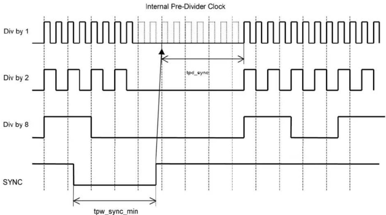
other
| Time Interval | Signal State | | ------------- | ------------ | | Div by 1 | High | | Div by 2 | Low | | Div by 8 | Low | | SYNC | Low |Output Synchronization Controlled by SYNC Timing Diagram
The SYNC control input is used to synchronize all divider outputs of the post divider. When a HIGH-LOW transition is applied to the SYNC control input the outputs are disabled when all post-divider outputs are LOW, see "Output Synchronization Controlled by SYNC Timing Diagram" for details. Once SYNC is
asserted with a rising edge, the outputs are enabled when all internal divider stages are reaching their LOW state. This ensures a simultaneous switching of all outputs with the next LOW-HIGH transition of the pre-divider clock.
PLL Stability
For the loop filter configurations shown in Figure 3a and 3b, Table 5a and 5b below summarizes the PLLs
loop stability in terms of damping factor, natural frequency, and bandwidth, and illustrates the pole and zero cutoff frequencies determined by the loop filter
| Parameter | ||||||||||
| V_CC | 3 | 3 | 3 | 3.3 | 3.3 | 3.3 | 3.6 | 3.6 | 3.6 | |
| Temperature | -40 | -40 | -40 | 25 | 25 | 25 | 85 | 85 | 85 | C |
| VCO Frequency | 2352 | 2800 | 3024 | 2352 | 2800 | 3024 | 2352 | 2800 | 3024 | MHz |
| Charge Pump Current | 1.80E-04 | 1.80E-04 | 1.80E-04 | 1.80E-04 | 1.80E-04 | 1.80E-04 | 1.80E-04 | 1.80E-04 | 1.80E-04 | A |
| Loop Filter Resistor | 130 | 130 | 130 | 130 | 130 | 130 | 130 | 130 | 130 | Ω |
| Zero Capacitor | 4.70E-07 | 4.70E-07 | 4.70E-07 | 4.70E-07 | 4.70E-07 | 4.70E-07 | 4.70E-07 | 4.70E-07 | 4.70E-07 | F |
| Pole Capacitor | 1.00E-09 | 1.00E-09 | 1.00E-09 | 1.00E-09 | 1.00E-09 | 1.00E-09 | 1.00E-09 | 1.00E-09 | 1.00E-09 | F |
| VCO Gain (KVCO) | 3.20E+09 | 4.50E+09 | 4.50E+09 | 2.80E+09 | 3.30E+09 | 3.10E+09 | 2.30E+09 | 1.70E+09 | 1.30E+09 | Hz/V |
| Feedback Divider | 168 | 168 | 168 | 168 | 168 | 168 | 168 | 168 | 168 | Integer |
| Phase Detector Frequency | 14 | 16 | 18 | 14 | 16 | 18 | 14 | |||
| Damping Factor | 2.6 | 3.1 | 3.1 | 2.4 | 2.6 | 2.6 | 2.2 | 1.7 | 1.9 | |
| Natural Frequency | 13600.29 | 16127.95 | 16127.95 | 12721.90 | 13811.16 | 13386.09 | 11530.20 | 9912.83 | 8668.52 | Hz |
| Ratio=Phase Detector Freq/BW | 197 | 160 | 180 | 225 | 219 | 262 | 274 | |||
| Zero Frequency | 2.61E+03 | 2.61E+03 | 2.61E+03 | 2.61E+03 | 2.61E+03 | 2.61E+03 | 2.61E+03 | 2.61E+03 | 2.61E+03 | Hz |
| Loop Bandwidth (BN) | 7.1E+04 | 9.98E+04 | 9.98+04 | 6.21E+04 | 7.32E+04 | 6.88E+04 | 5.1E+04 | 3.77E+04 | 2.88E+04 | Hz |
| Pole Frequency | 1.22E+07 | 1.22E+07 | 1.22E+07 | 1.22E+07 | 1.22E+07 | 1.22E+07 | 1.22E+07 | 1.22E+07 | 1.22E+07 | Hz |
[Non-Text]
16
424
Table 5a. Optimized for Lowest Cycle-to-Cycle Jitter (R = 130Ω, C1 = 0.47μF, C2 = 100pF)
| Parameter | ||||||||||
| V_cc | 3 | 3 | 3 | 3.3 | 3.3 | 3.3 | 3.6 | 3.6 | 3.6 | |
| Temperature | -40 | -40 | -40 | 25 | 25 | 25 | 85 | 85 | 85 | C |
| VCO Frequency | 2352 | 2800 | 3024 | 2352 | 2800 | 3024 | 2352 | 2800 | 3024 | MHz |
| Charge Pump Current | 1.80E-04 | 1.80E-04 | 1.80E-04 | 1.80E-04 | 1.80E-04 | 1.80E-04 | 1.80E-04 | 1.80E-04 | 1.80E-04 | A |
| Loop Filter Resistor | 130 | 130 | 130 | 130 | 130 | 130 | 130 | 130 | 130 | Ω |
| Zero Capacitor | 4.70E-07 | 4.70E-07 | 4.70E-07 | 4.70E-07 | 4.70E-07 | 4.70E-07 | 4.70E-07 | 4.70E-07 | 4.70E-07 | F |
| Pole Capacitor | 1.00E-09 | 1.00E-09 | 1.00E-09 | 1.00E-09 | 1.00E-09 | 1.00E-09 | 1.00E-09 | 1.00E-09 | 1.00E-09 | F |
| VCO Gain (KVCO) | 3.20E+09 | 4.50E+09 | 4.50E+09 | 2.80E+09 | 3.30E+09 | 3.10E+09 | 2.30E+09 | 1.70E+09 | 1.30E+09 | Hz/V |
| Feedback Divider | 168 | 168 | 168 | 168 | 168 | 168 | 168 | 168 | 168 | Integer |
| Phase Detector Frequency | 14 | 16 | 18 | 14 | 16 | 18 | 14 | |||
| Damping Factor | 2.6 | 3.1 | 3.1 | 2.4 | 2.6 | 2.6 | 2.2 | 1.7 | 1.9 | |
| Natural Frequency | 13600.29 | 16127.95 | 16127.95 | 12721.90 | 13811.16 | 13386.09 | 11530.20 | 9912.83 | 8668.52 | Hz |
| Ratio=Phase Detector Freq/BW | 197 | 160 | 180 | 225 | 219 | 262 | 274 | |||
| Zero Frequency | 2.61E+03 | 2.61E+03 | 2.61E+03 | 2.61E+03 | 2.61E+03 | 2.61E+03 | 2.61E+03 | 2.61E+03 | 2.61E+03 | Hz |
| Loop Bandwidth (BN) | 7.1E+04 | 9.98E+04 | 9.98+04 | 6.21E+04 | 7.32E+04 | 6.88E+04 | 5.1E+04 | 3.77E+04 | 2.88E+04 | Hz |
| Pole Frequency | 1.22E+06 | 1.22E+06 | 1.22E+06 | 1.22E+06 | 1.22E+06 | 1.22E+06 | 1.22E+06 | 1.22E+06 | 1.22E+06 | Hz |
[Non-Text]
16
424
Table 5b. Optimized for Total Jitter (R = 130Ω, C1 = 0.47μF, C2 = 1000pF)
Figure 6 shows the open and closed loop gain of the SY89537L. The closed loop-gain plot shows that the SY89537L when configured with the recommended loop filter values has essentially no jitter peaking near the -3dB point. In addition, the open loop curve shows the frequency at which unity gain occurs for a typical case of the SY89537L with V_CC = 3.3V at T_A = 25^ . At unity gain, Figure 7 can be used to determine the phase margin or stability of the SY89537L.

line
| Frequency (Hz) | dB (solid line) | dB (dashed line) | | -------------- | --------------- | ---------------- | | 10 | 1e-6 | 100 | | 100 | 1e-7 | 100 | | 1e-3 | 1e-8 | 100 | | 1e-4 | 1e-9 | 100 | | 1e-5 | 1e-10 | 100 | | 1e-6 | 1e-11 | 100 | | 1e-7 | 1e-12 | 100 | | 1e-8 | 1e-13 | 100 |Figure 6. Open and Closed Loop Gain at V_cc = 3.3V , T_A = 25^

line
| Frequency (Hz) | Phase Margin (°) | | -------------- | ---------------- | | 1e-8 | -180 |Figure 7. Phase Margin Plot at V_CC = 3.3V , T_A = 25^
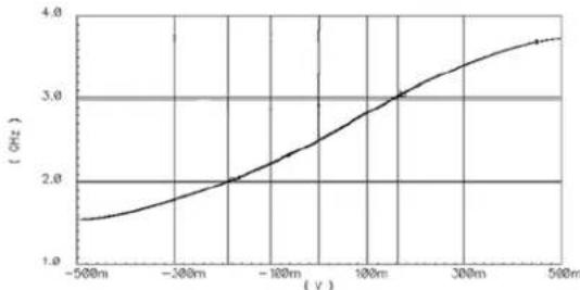
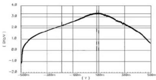
Figure 8 illustrates the VCO frequency versus the loop filter control voltage at 3.3V, T_A = 25^ . The normal loop filter control voltage is -300mV to +300mV. Figure 9 illustrates the VCO gain curve at V_CC = 3.3V , T_A = 25^ . With this set of information, determining the loop stability with other sets of loop filter configurations are possible.
line
| Voltage (V) | Frequency (GHz) | | :--- | :--- | | -500m | 1.5 | | -300m | 1.8 | | -100m | 2.2 | | 100m | 3.0 | | 300m | 3.4 | | 500m | 3.7 |Figure 8. VCO Frequency vs. Loop Filter Control Voltage at 3.3V, T_A = 25^
line
| Voltage (V) | Current Density (kW) | |-------------|----------------------| | -500 | -1.0 | | -400 | 0.0 | | -300 | 1.5 | | -200 | 2.5 | | -100 | 3.0 | | 0 | 3.2 | | 100 | 3.0 | | 200 | 2.5 | | 300 | 1.5 | | 400 | 0.5 | | 500 | -1.0 |Figure 9. VCO Gain vs. Loop Filter Control Voltage at 3.3V, T_A = 25^
Input Interface
RFCK is designed to accept any differential or single-ended input signal 300mV above V_cc or 300mV below GND. RFCK should not be left floating. Tie either the true or complement input to GND, but not both. A logic zero is achieved by connecting the complement input to GND with the true input floating. For TTL input, tie a 2.5kΩ resistor between the complement input and GND. LVDS, CML and HSTL differential signals may be connected directly to the reference inputs.

text_image
Vcc R2 R2 RFCK □─R1 /RFCK □─R1 R1 = 800Ω, R2 = 1kΩ GNDFigure 10. Simplified Input Structure
Input Termination
text_image
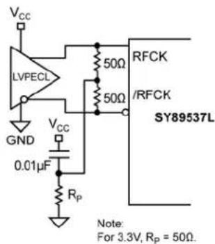
VCC LVPECL GND 0.01μF VCC Rp 50Ω 50Ω RFCK /RFCK SY89537L Note: For 3.3V, Rp = 50Ω.Figure 11a. LVPECL Interface (DC-Coupled)
text_image
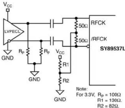
VCC LVPECL GND Rp Rp VCC R1 R2 GND 50Ω 50Ω RFCK /RFCK SY89537L Note: For 3.3V, Rp = 100Ω R1 = 130Ω. R2 = 82Ω.Figure 11b. LVPECL Interface (AC-Coupled)

text_image
Vcc CML 100Ω GND RFCK /RFCK SY89537LFigure 11c. CML Interface (DC-Coupled)

text_image
VCC CML GND VCC R1 R2 50Ω 50Ω RFCK /RFCK SY89537L Note: For 3.3V, R1 = 130Ω. R2 = 82Ω.Figure 11d. CML Interface (AC-Coupled)

text_image
Vcc LVDS 100Ω GND RFCK /RFCK SY89537LFigure 11e. LVDS (DC-Coupled)
text_image
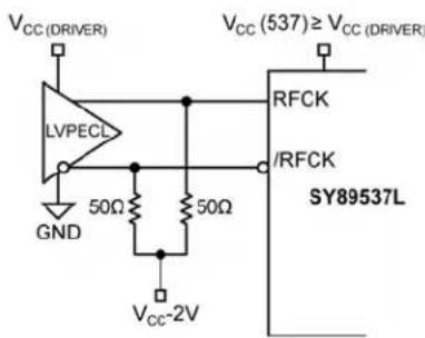
VCC (DRIVER) LVPECL GND 50Ω 50Ω VCC-2V VCC (537) ≥ VCC (DRIVER) RFCK /RFCK SY89537LFigure 11f. 2.5V LVPECL (DC-Coupled)
text_image
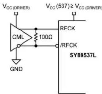
VCC (DRIVER) VCC (537) ≥ VCC (DRIVER) CML 100Ω GND RFCK /RFCK SY89537LFigure 11g. 2.5V CML (DC-Coupled)
Output Bank and Frequency Control
There are five independently programmable output frequency banks, four differential LVPECL output banks and one differential LVDS output bank with three output pairs. Each bank has frequency control SELx and Enx to generate different divider ratios (see "PECL and LVDS Output and Frequency Select" Tables). It can be programmed for pass-through, internal divided VCO clock divide-by- /2, /8 or disable state. When disabled, the non-inverted output goes to static LOW and the inverted output goes to static HIGH.
Output Logic Characteristics
See "Output Termination Recommendations" for proper termination. When LVPECL single-ended output is desired, the unused complimentary output should be terminated. Unused LVPECL output pairs can be left floating. LVDS output pairs should be terminated with 100 across the pair. In order to minimize jitter and skew, unused LVDS output banks and unused LVDS output pairs should be terminated with 100 across each pair.
LVPECL Outputs:
• Typical voltage swing is 800mV into 50Ω.
• Common mode voltage is V _cc0 -1.3V.
LVDS Outputs:
• Typical voltage swing is 325mV into 100Ω.
• Common mode voltage is 1.2V.
Output Termination Recommendations
LVPECL
LVPECL has high input impedance, very low output (open emitter) impedance, and small signal swing which results in low EMI. LVPECL is ideal for driving 50Ω-and-100Ω-controlled impedance transmission lines. There are several techniques for terminating the LVPECL output: Parallel Termination Thevenin-Equivalent, Parallel Termination (3-resistor), and AC-coupled termination. Unused output pairs may be left floating. However, single-ended outputs must be terminated, or balanced.
text_image
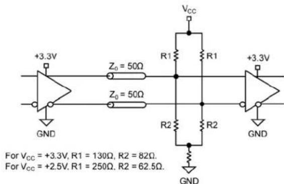
+3.3V Z₀ = 50Ω Z₀ = 50Ω GND VCC R1 R1 +3.3V R2 R2 GND For VCC = +3.3V, R1 = 130Ω, R2 = 82Ω. For VCC = +2.5V, R1 = 250Ω, R2 = 62.5Ω.Figure 12a. Parallel Thevenin-Equivalent

text_image
+3.3V Zo = 50Ω Zs = 50Ω +3.3V C1 (optional) 0.1μF 50Ω 50Ω Rb GND +3.3V GND For Vcc = +3.3V, Rb = 50Ω. For Vcc = +2.5V, Rb = 19Ω.Figure 12b. Parallel Termination
LVDS
LVDS specifies a small swing of 325mV typical, on a nominal 1.2V common mode above ground. The common mode voltage has tight limits to permit large variations in ground between an LVDS driver and receiver. Also, change in common mode voltage, as a function of data input, is kept to a minimum, to keep EMI low.
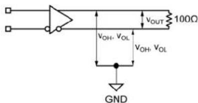
text_image
vOUT 100Ω VOH, VOL VOH, VOL GNDFigure 13a. LVDS Differential Measurement

text_image
50Ω 50Ω VOCM- ΔVOCM GNDFigure 13b. LVDS Common Mode Measurement
Related Product and Support Documentation
| Part Number Function Data Sheet Link | ||
| SY89538L | 3.3V, Precision LVPECL and LVDS Programmable, Multiple Output Bank Clock Synthesizer and Fanout Buffer with Zero Delay | http://www.micrel.com/product-info/products/sy89538l.shtml |
| HBW Solutions | New Products and Applications | www.micrel.com/product-info/products/solutions.shtml |
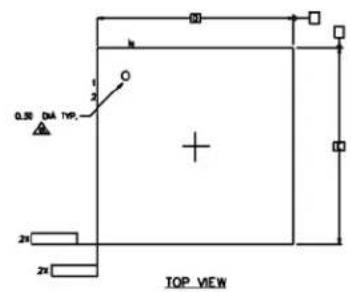
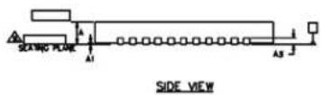
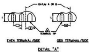
Package Information
text_image
0.30 DA TYP. 2x 2x TOP VIEWNOTES
-
DIMENSIONING AND TOLERANCING CONFORM TO ASME Y14.5M. - 1994.
-
ALL DIMENSIONS ARE IN MILLIMETERS, 0 IS IN DEGREES.
N IS THE TOTAL NUMBER OF TERMINALS. DIMENSION 5 APPLIES TO METALLIZED TERMINAL AND IS MEASURED BETWEEN 0.15 AND 0.30mm FROM TERMINAL TIP. IF THE TERMINAL HAS THE OPTIONAL RADIUS ON THE OTHER END OF THE TERMINAL, THE DIMENSION 5 SHOULD NOT BE MEASURED IN THAT RADIUS AREA.
△ ND AND NE REFER TO THE NUMBER OF TERMINALS ON EACH D AND E SIDE RESPECTIVELY. 6. MAX. PACKAGE WARPAGE IS 0.05 mm.
- MAXIMUM ALLOWABLE BURRS IS 0.076 mm IN ALL DIRECTIONS.
△PIN #1 ID ON TOP WILL BE LASER MARKED.
△BILATERAL COPLANARITY ZONE APPLIES TO THE EXPOSED HEAT SINK SLUG AS WELL AS THE TERMINALS.
- THIS DRAWING CONFORMES TO JEDEC REGISTERED OUTLINE MO-220
text_image
EVEN TERMINAL/SIDE ODD TERMINAL/SIDE DETAIL "A"| S.No. | DIMENSIONS | |||
| MIN. | NOM. | MAX. | N_0,1 | |
| 圆 | 0.50 BSC | |||
| N | 44 | 3 | ||
| ND | 11 | △ | ||
| NE | 11 | |||
| L | 0.55 | 0.60 | 0.65 | |
| b | 0.18 | 0.25 | 0.30 | △ |
| D2 | 3.20 | 3.30 | 3.40 | |
| E2 | 3.20 | 3.30 | 3.40 | |
| D | 7.00 BSC | |||
| E | 7.00 BSC | |||
| A | 0.80 | 0.85 | 1.00 | |
| A1 | 0.00 | 0.02 | 0.05 | |
| K | 0.20 MIN. | |||
| θ | 0 | — | 12 | 2 |
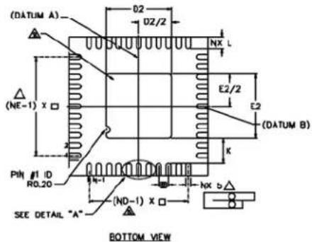
text_image
(DATUM A) D2 D2/2 NX L E2/2 E2 (NE-1) x □ (DATUM B) K PIN #1 ID RO.20 ND-1) x □ NX b △ SEE DETAIL "A" BOTTOM VIEW44-Pin QFN
MICREL, INC. 2180 FORTUNE DRIVE SAN JOSE, CA 95131 USA
TEL +1 (408) 944-0800 FAX +1 (408) 474-1000 WEB http://www.micrel.com
The information furnished by Micrel in this data sheet is believed to be accurate and reliable. However, no responsibility is assumed by Micrel for its use. Micrel reserves the right to change circuitry and specifications at any time without notification to the customer.
Micrel Products are not designed or authorized for use as components in life support appliances, devices or systems where malfunction of a product can reasonably be expected to result in personal injury. Life support devices or systems are devices or systems that (a) are intended for surgical implant into the body or (b) support or sustain life, and whose failure to perform can be reasonably expected to result in a significant injury to the user. A Purchaser's use or sale of Micrel Products for use in life support appliances, devices or systems is a Purchaser's own risk and Purchaser agrees to fully indemnify Micrel for any damages resulting from such use or sale.
© 2005 Micrel, Incorporated.