SY89834U - Electronic component Microchip - Free user manual and instructions
Find the device manual for free SY89834U Microchip in PDF.

User questions about SY89834U Microchip
0 question about this device. Answer the ones you know or ask your own.
Ask a new question about this device
Download the instructions for your Electronic component in PDF format for free! Find your manual SY89834U - Microchip and take your electronic device back in hand. On this page are published all the documents necessary for the use of your device. SY89834U by Microchip.
USER MANUAL SY89834U Microchip
■ Selects between two LVTTL/CMOS inputs and provides 4 LVPECL output copies
■ Guaranteed AC performance over temperature and voltage:
- DC-to >1.0GHz throughput
• <500ps propagation delay (IN-to-Q)
• < 20ps within-device skew - < 225ps rise/fall time
■ Ultra-low jitter design:
• < 1ps RMS cycle-to-cycle jitter
• < 1ps RMS random jitter
• < 10ps PP deterministic jitter
• < 10ps PP total jitter (clock)
■ Low voltage 2.5V and 3.3V supply operation
■ 100K LVPECL outputs
■ Industrial temperature range: -40^ to +85^
■ Includes a 2:1 MUX select input
■ Accepts single-ended TTL/CMOS inputs and provides four LVPECL outputs
■ Available in 16-pin (3mm · 3mm) MLF™ package

Precision Edge®
DESCRIPTION
The SY89834U is a high-speed, 1GHz LVTTL/CMOS-to-LVPECL fanout buffer/translator optimized for high-speed ultra-low skew applications. The input stage is designed to accept two single-ended LVTTL/CMOS compatible signals that feed into a 2:1 MUX. The selected input is translated and distributed as four differential 100K LVPECL outputs. Within device skew is guaranteed to be less than 20ps over supply voltage and temperature.
The single-ended input buffers accept TTL/CMOS logic levels. The internal threshold of the buffers is defined as V_CC/2 .
The SY89834U is a part of Micrel's high-speed Precision Edge® family. For applications that require a different I/O combination, consult Micrel's website at: www.micrel.com, and choose from a comprehensive product line of high-speed, low-skew fanout buffers, translators and clock generators.
APPLICATIONS
■ Processor clock distribution/translation
■ SONET clock distribution/translation
■ Fibre Channel clock distribution/translation
■ Gigabit Ethernet clock distribution/translation
■ Single-ended ASIC-to-differential communication IC signal translation
FUNCTIONAL BLOCK DIAGRAM

flowchart
graph TD
    A["IN1 (LVTTL/CMOS)"] --> B["MUX 0"]
    C["IN2 (LVTTL/CMOS)"] --> B
    D["EN LVTTL/CMOS"] --> E["D Q"]
    B --> F["1:4"]
    E --> F
    F --> G["Q0 /Q0"]
    F --> H["Q1 /Q1"]
    F --> I["Q2 /Q2"]
    F --> J["Q3 /Q3"]
    style A fill:#f9f,stroke:#333
    style C fill:#f9f,stroke:#333
    style D fill:#f9f,stroke:#333
    style B fill:#ccf,stroke:#333
    style E fill:#ccf,stroke:#333
    style F fill:#ccf,stroke:#333
    style G fill:#cfc,stroke:#333
    style H fill:#cfc,stroke:#333
    style I fill:#cfc,stroke:#333
    style J fill:#cfc,stroke:#333
Precision Edge is a registered trademark of Micrel, Inc.
MicroLeadFrame and MLF are trademarks of Amkor Technology, Inc.
PACKAGE/ORDERING INFORMATION
text_image
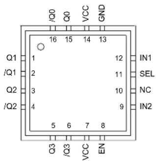
/Q0 /Q0 VCC GND 16 15 14 13 Q1 1 /Q1 2 Q2 3 /Q2 4 5 6 7 8 Q3 /Q3 VCC EN IN1 SEL NC IN216-Pin MLF™ (MLF-16)
Ordering Information ^(1)
| Part Number Type Range | Package Operating Package Lead | |||
| Marking | Finish | |||
| SY89834UMI | MLF-16 | Industrial | 834U | Sn-Pb |
| SY89834UMITR(2) | MLF-16 | Industrial | 834U | Sn-Pb |
| SY89834UMG(3) | MLF-16 | Industrial | 834U with Pb-Free bar line indicator | NiPdAu Pb-Free |
| SY89834UMGTR(2, 3) | MLF-16 | Industrial | 834U with Pb-Free bar line indicator | NiPdAu Pb-Free |
Notes:
- Contact factory for die availability. Dice are guaranteed at T_A = 25^ , DC Electricals only.
- Tape and Reel.
- Pb-Free package is recommended for new designs.
PIN DESCRIPTION
| Pin Number | Pin Name Pin Function | |
| 15, 161, 2,3, 4,5, 6 | Q0, /Q0Q1, /Q1Q2, /Q2Q3, /Q3 | Differential 100K LVPECL Outputs: These LVPECL outputs are the precision, low skew copies of the inputs. Please refer to the “Truth Table” section for details. Unused output pairs may be left open. Terminate with 50 to V_CC - 2V . See “Output Termination Recommendations” section for more details. |
| 8 | EN | This single-ended TTL/CMOS-compatible input functions as a synchronous output enable. The synchronous enable ensures that enable/disable will only occur when the outputs are in a logic LOW state. Note that this input is internally connected to a 25k pull-up resistor and will default to logic HIGH state (enabled) if left open. |
| 12,9 | IN1IN2 | Single-ended TTL/CMOS-compatible inputs to the device. These inputs are internally connected to a 25k pull-up resistor and will default to logic HIGH state if left open. The input threshold is V_CC/2 . |
| 10 | NC | No connect. Not internally connected. |
| 11 | SEL | TTL/CMOS Compatible Select Input for signals IN1 and IN2. The input threshold is V_CC/2 . HIGH at the SEL input selects signal IN1. LOW at the SEL input selects signal IN2. SEL includes a 25k pull-up resistor. The default state is HIGH when left floating. |
| 13 | GND | Ground. GND pins and exposed pad must be connected to the most negative potential of the device ground. |
| 7, 14 | VCC | Positive Power Supply: Bypass with 0.1 F//0.01 F low ESR capacitors and place as close to each VCC pin as possible. |
TRUTH TABLE
| IN1 IN2 EN SEL | Q0-Q3 /Q0-Q3 | ||||
| 0 | X | 1 | 1 | 0 | |
| 1 | X | 1 | 1 | 1 | |
| X | 0 | 1 | 0 | 0 | |
| X | 1 | 1 | 0 | 1 | |
| X | X | 0 | X | 0^(1) | 0^(1) |
Note:
- On next negative transition of the input signal (IN).
Absolute Maximum Ratings ^(1)
Supply Voltage (V _CC ) ...... -0.5V to +4.0V
Input Voltage ( V_IN ) -0.5V to V_CC + 0.3V
LVPECL Output Current ( I_OUT ) Continuous ....50mA Surge....100mA
Input Current (IN1, IN2) ....±50mA
Lead Temperature (Soldering, 20sec.), 260°C
Storage Temperature ( T_S ) -65^ to +150^
Operating Ratings ^(2)
Supply Voltage Range ....+2.375V to +2.625V ....+3.0V to +3.6V
Ambient Temperature ( T_A ) -40^ to +85^
Package Thermal Resistance ^(3) MLF ^TM ( _JA )
Still-Air 60°C/W
MLF ^TM ( _JB ) Junction-to-Board ....32°C/W
DC ELECTRICAL CHARACTERISTICS ^(4)
T_A = -40^ to +85^ , unless otherwise stated.
| Symbol Parameter Condition Min Typ Max Units | ||||||
| V_CC | Power Supply 2.375 2.625 V | 3.0 | 3.6 | V | ||
| I_CC | Power Supply Current | No load, max. V_CC . | 50 | 75 | mA | |
LVTTL/CMOS INPUTS DC ELECTRICAL CHARACTERISTICS ^(4)
V_CC = 2.5V ± 5% or V_CC = 3.3V ± 10% ; T_A = -40^ C to +85^ C , unless otherwise stated.
| Symbol Parameter Condition Min Typ Max | Units | |||||
| V_IH | Input HIGH Voltage | 2.0 | V | |||
| V_IL | Input LOW Voltage | 0.8 V | ||||
| I_IH | Input HIGH Current | I_IH @ V_IN = 2.7V | -125 | 30 | A | |
| I_IL | Input LOW Current | -125 | A | |||
(100KEP) LVPECL OUTPUTS DC ELECTRICAL CHARACTERISTICS ^(4)
V_CC = 2.5V ± 5% or V_CC = 3.3V ± 10% , R_L = 50 to V_CC - 2V ; T_A = -40^ C to +85^ C , unless otherwise stated.
| Symbol Parameter Condition | Min | Typ Max Units | |||||
| V_OH | Output HIGH Voltage | V_CC-1.145 | V_CC-1.020 | V_CC-0.895 | V | ||
| V_OL | Output LOW Voltage | V_CC-1.945 | V_CC-1.820 | V_CC-1.695 | V | ||
| V_OUT | Output Voltage Swing | See Figures 2a. | 550 | 800 | 1050 | mV | |
| V_DIFF\_OUT | Differential Output Voltage Swing | See Figures 2b. | 1100 | 1600 | 2100 | mV | |
Notes:
- Permanent device damage may occur if absolute maximum ratings are exceeded. This is a stress rating only and functional operation is not implied at conditions other than those detailed in the operational sections of this data sheet. Exposure to absolute maximum rating conditions for extended periods may affect device reliability.
- The data sheet limits are not guaranteed if the device is operated beyond the operating ratings.
- Junction-to-board resistance assumes exposed pad is soldered (or equivalent) to the device's most negative potential on the PCB. _JA and _JB values are determined for a 4-layer board in still-air, unless otherwise stated.
- The circuit is designed to meet the DC specifications shown in the above table after thermal equilibrium has been established.
AC ELECTRICAL CHARACTERISTICS ^(5)
V_CC = 2.5V ± 5% or V_CC = 3.3V ± 10% , R_L = 50 to V_CC - 2V ; T_A = -40^ to +85^ , unless otherwise stated.
| Symbol Parameter Condition Min Typ Max Units | ||||||
| f_MAX | Maximum Frequency Input t | r/t_f ≥ 350 ps 1.0 GHz | ||||
| t_pd | Propagation Delay IN-to-Q Note 6 200 | 320 500 ps | ||||
| t_SW | Switchover Time SEL-to-Q 200 320 500 ps | |||||
| t_SKEW | Within-Device Skew | Note 7 | 5 20 | ps | ||
| Part-to-Part Skew | Note 8 | 300 ps | ||||
| t_JITTER | DataRandom Jitter (RJ)Deterministic Jitter (DJ) | Note 9Note 10 | 110 | ps_RMS ps_PP | ||
| ClockCycle-to-Cycle JitterTotal Jitter (TJ) | Note 11Note 12 | 110 | ps_RMS ps_PP | |||
| DC | Duty Cycle | Input t_f/t_f ≥ 350 ps , Note 13 | 45 | 50 | 55 | % |
| t_S | Set-Up Time EN to IN1, IN Note 14 and Note 15 | 300 | ps | |||
| t_H | Hold Time EN to IN1, IN | Note 14 and Note 15 | 500 | ps | ||
| t_r, t_f | Output Rise/Fall Times(20% to 80%) | 70 | 140 22 | 5 ps | ||
Notes:
- High-frequency AC parameters are guaranteed by design and characterization.
- V_IH = 2.0V , V_IL = 0.8V , 50% duty cycle. Delay measured at 100MHz from the crossing of the input signal with V_CC/2 as the crossing of the differential output signal. See Figure 1.
- Within device skew is measured between two different outputs under identical input transitions.
- Part-to-part skew is defined for two parts with identical power supply voltages at the same temperature and no skew at the edges at the respective inputs.
- Random jitter is measured with a K28.7 pattern, measured at ≤ f_MAX .
- Deterministic jitter is measured at 2.5Gbps with both K28.5 and 2^23-1 PRBS pattern.
- Cycle-to-cycle jitter definition: The variation period between adjacent cycles over a random sample of adjacent cycle pairs. T_JITTER CC = T_n - T_n+1 , where T is the time between rising edges of the output signal.
- Total jitter definition: with an ideal clock input frequency of ≤ f_MAX (device), no more than one output edge in 10^12 output edges will deviate by more than the specified peak-to-peak jitter value.
- If t_r / 14 is less than 350ps, the duty cycle distortion will increase beyond the duty cycle limits.
- Set-up and hold times apply to synchronous applications that intend to enable/disable before the next clock cycle. For asynchronous applications set-up and hold times do not apply.
- See "Timing Diagrams," Figure 1a.
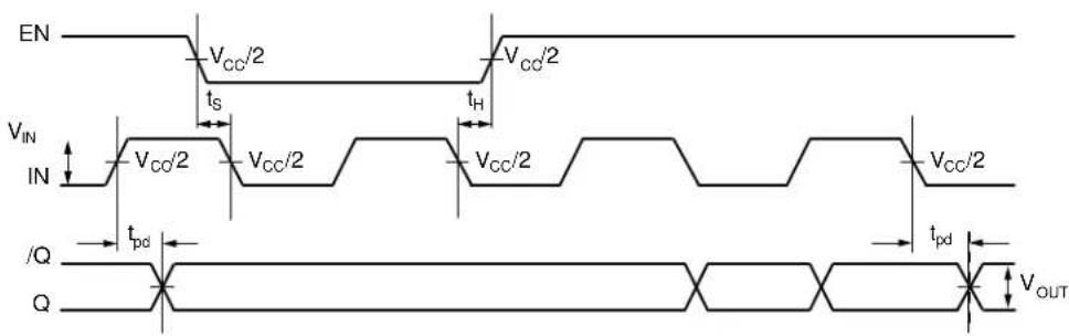
TIMING DIAGRAMS
text_image
EN VCC/2 VCC/2 VIN IN VCC/2 VCC/2 VCC/2 VCC/2 tS tH tpd tpd /Q Q VOUTFigure 1a. Timing Diagram (EN, IN1, IN2)
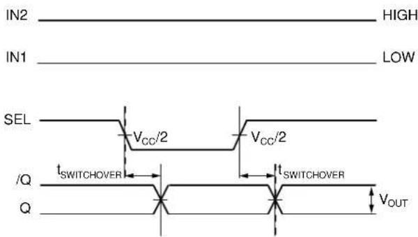
text_image
IN2 HIGH IN1 LOW SEL Vcc/2 Vcc/2 /Q tSWITCHOVER tSWITCHOVER Q VOUTFigure 1b. Timing Diagram (SEL)
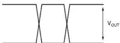
SINGLE-ENDED AND DIFFERENTIAL SWINGS
text_image
VOUTFigure 2a. Single-Ended Swing

text_image
V DIFF_OUTFigure 2b. Differential Swing
TYPICAL OPERATING CHARACTERISTICS
V_CC = 3.3V, GND = 0V, R_L = 50 to V_CC - 2V; T_A = 25^, unless otherwise stated.

line
| FREQUENCY (GHz) | OUTPUT SWING (mV) | | --------------- | ----------------- | | 0.5 | 780 | | 1.0 | 720 | | 1.5 | 660 | | 2.0 | 600 | | 2.5 | 540 | | 3.0 | 480 |
line
| TEMPERATURE (°C) | PROPAGATION DELAY (ps) | | ---------------- | ---------------------- | | -50 | 290 | | 90 | 360 |FUNCTIONAL CHARACTERISTICS
V_CC = 3.3V, GND = 0V, R_L = 50 to V_CC - 2V, T_A = 25^, unless otherwise stated.
155MHz Output
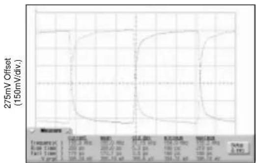
line
| Parameter | Value | | --------- | ----- | | Frequency X | 170.3 Hz | | Power Time | 200 ns | | Current Time | 179 ns | | Voltage | 100.34 ns | | Current Amplitude (Hz) | 200.34 ns | | Current Amplitude (Hz) | 170.3 ns | | Current Amplitude (Hz) | 179 ns | | Current Amplitude (Hz) | 100.34 ns | | Current Amplitude (Hz) | 179 ns | | Current Amplitude (Hz) | 100.4 ns | | Current Amplitude (Hz) | 179 ns | | Current Amplitude (Hz) | 100.4 ns | | Current Amplitude (Hz) | 100.4 ns | | Current Amplitude (Hz) | 179 ns | | Current Amplitude (Hz) | 100.4 ns | | Current Amplitude (Hz) | 100.4 ns | | Current Amplitude (Hz) | 179 ns | | Current Amplitude (Hz) | 100.4 ns | | Current Amplitude (kHz) | 200.34 ns | | Current Amplitude (kHz) | 179.3 ns | | Current Amplitude (kHz) | 179 ns | | Current Amplitude (kHz) | 100.34 ns | | Current Amplitude (kHz) | 179 ns | | Current Amplitude (kHz) | 100.4 ns | | Current Amplitude (kHz) | 179 ns | | Current Amplitude (kHz) | 100.4 ns | | Current Amplitude (kHz) | 179 ns | | Current Amplitude (kHz) | 100.4 ns | | Current Amplitude (kHz) | 179 ns | | Current Amplitude (kHz) | 100.4 ns | | Current Amplitude (kHz, V-gp) | 200.34 ns | | Current Amplitude (kHz, V-gp) | 179.3 ns | | Current Amplitude (kHz, V-gp) | 179 ns | | Current Amplitude (kHz, V-gp) | 100.34 ns | | Current Amplitude (kHz, V-gp) | 179 ns | | Current Amplitude (kHz, V-gp) | 100.4 ns | | Current Amplitude (kHz, V-gp) | 179 ns | | Current Amplitude (kHz, V-gp) | 100.4 ns | | Current Amplitude (kHz, V-gp) | 179 ns | | Current Amplitude (kHz, V-gp) | 100.4 ns | | Current Amplitude (kHz, V-gp) | 179 ns | | Current AMplitude (kHz, V-gp) | 100.4 ns | | Current Amplitude (kHz, V-gp) | 179 ns | | Current Amplitude (kHz, V-gp) | 100.4 ns | | Current Amplitude (kHz, V-gp) | 179 ns | | Current Amplitude (kHz, V-gp) | 100.4 ns | | Current Amplitude (kHz/π) | 200.34 ns | | Current Amplitude (kHz/π) | 179.3 ns | | Current Amplitude (kHz/π) | 179 ns | | Current Amplitude (kHz/π) | 100.34 ns | | Current Amplitude (kHz/π) | 179 ns | | Current Amplitude (kHz/π) | 100.4 ns | | Current Amplitude (kHz/π) | 179 ns | | Current Amplitude (kHz/π) | 100.4 ns | | Current Amplitude (kHz/π) | 179 ns | | Current Amplitude (kHz/π) | 100.4 ns | | Current Amplitude (kHz/π) | 179 ns | | Current Amplitude (kHz/π) | 180.34 ns | | Current Amplitude (kHz/π) | 179.3 ns | | Current Amplitude (kHz/π) | 179 ns | | Current Amplitude (kHz/π) | 100.34 ns | | Current Amplitude (kHz/π) | 179 ns | | Current Amplitude (kHz/π) | 180.34 ns | | Current Amplitude (kHz/π) | 179 ns | | Current Amplitude (kHz/π) | 180.34 ns | | Current Amplitude (kHz/π) | 179 ns | | Current Amplitude (kHz/π) | 180.34 ns | | Current Amplitude (kHz/π) | 179 nanosine wave wave wave wave wave wave wave wave wave wave wave wave wave wave wave wave wave wave wave wave wave wave wave wave wave wave wave wave wave wave wave wave wave wave wave wave wave wave wave wave wave wave wave wave wave wave wave wave wave wave wave wave wave wave wave wave wave wave wave wave wave wave wave wave wave wave wave wave wave wave wave wave wave wave wave wave wave wave wave wave wave wave wave wave wave wave wave wave wave wave wave wave wave wave wave wave wave wave wave wave wavesTIME (1ns/div.)
622MHz Output
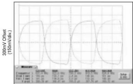
line
| Time (s) | Value | |----------|-------| | Start | 140.2 | | End | 138.2 |TIME (321.9ps/div.)
1GHz Output
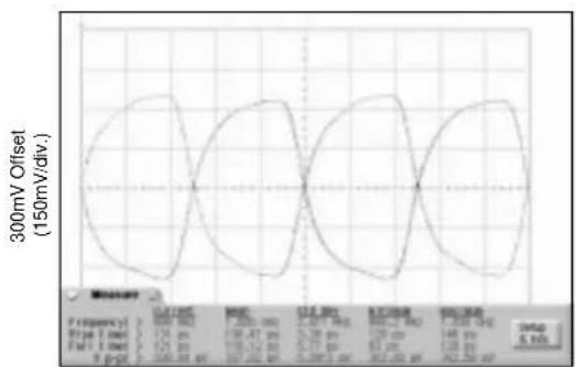
line
| Time (s) | Current (mV) | | -------- | ------------ | | 0 | 0 | | 1 | 150 | | 2 | 300 | | 3 | 450 | | 4 | 600 | | 5 | 750 | | 6 | 900 | | 7 | 1050 | | 8 | 1200 | | 9 | 1350 | | 10 | 1500 | | 11 | 1650 | | 12 | 1800 | | 13 | 1950 | | 14 | 2100 | | 15 | 2250 | | 16 | 2400 | | 17 | 2550 | | 18 | 2700 | | 19 | 2850 | | 20 | 3000 | | 21 | 3150 | | 22 | 3300 | | 23 | 3450 | | 24 | 3600 | | 25 | 3750 | | 26 | 3900 | | 27 | 4050 | | 28 | 4200 | | 29 | 4350 | | 30 | 4500 | | 31 | 4650 | | 32 | 4800 | | 33 | 4950 | | 34 | 5100 | | 35 | 5250 | | 36 | 5400 | | 37 | 5550 | | 38 | 5700 | | 39 | 5850 | | 40 | 6000 | | 41 | 6150 | | 42 | 6300 | | 43 | 6450 | | 44 | 6600 | | 45 | 6750 | | 46 | 6900 | | 47 | 7050 | | 48 | 7200 | | 49 | 7350 | | 50 | 7500 | | 51 | 7650 | | 52 | 7800 | | 53 | 7950 | | 54 | 8100 | | 55 | 8250 | | 56 | 8400 | | 57 | 8550 | | 58 | 8700 | | 59 | 8850 | | 60 | 9000 | | 61 | 9150 | | 62 | 9300 | | 63 | 9450 | | 64 | 9600 | | 65 | 9750 | | 66 | 9900 | | 67 | 10050 | | 68 | 10200 | | 69 | 10350 | | 70 | 10500 | | 71 | 10650 | | 72 | 10800 | | 73 | 11450 | | 74 | 12150 | | 75 | 12950 | | 76 | 13750 | | 77 | 14650 | | 78 | 15650 | | 79 | 16750 | | 80 | 17850 | | 81 | 18950 | | 82 | 20150 | | 83 | 21250 | | 84 | 22350 | | 85 | 23450 | | 86 | 24650 | | 87 | 26150 | | 88 | 27750 | | 89 | 29350 | | 90 | 31150 | | 91 | 32950 | | 92 | 34850 | | 93 | 36750 | | 94 | 38750 | | 95 | 41150 | | 96 | 43150 | | 97 | 44950 | | 98 | 47150 | | 99 | 49350 | | Note: The data is already in CSV format as it is extracted from the image. The code does not provide the original data for this visualization. The output is estimated based on the visual scale of the plot. The output values are calculated based on the formula input. The output values are calculated using the formula input by adding the square root of the sum of the squares of the sum of the squares of the sum of the squares of the sum of the squares of the sum of the squares of the sum of the squares of the sum of the squares of the sum of the squares of the sum of the squares of the sum of the squares of the sum of the squares of the sum of the squares of the sum of the squares of the sum of the squares of the sum of the squares of the sum of the squares of the sum of the squares of the sum. The output values are estimated based on the formula input. The output values are calculated using the formula input by adding the square root of the sum of the squares of the sum of the squares of the sum of the squares of the sum of the squares of the sum of the squares of the sum of the squares of the sum of the squares of the sum of the squares of the sum. The output value is estimated based on the formula input. The output value is calculated using the formula input by adding the square root of the sum of the squares of the sum of the squares of the sum of the squares of the sum of the squares of the sum of the squares of the sum. The output value is estimated based on the formula input. The output value is calculated using the formula input by adding the square root of the sum of the squares of the sum of the squares of the sum of the squares of the sum of the squares of the sum of the squares of the sum. The output value is estimated based upon an estimate that is not explicitly labeled in the chart.TIME (200ps/div.)
DIFFERENTIAL INPUT
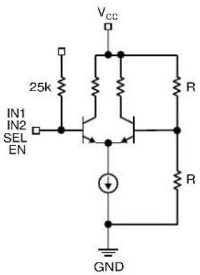
text_image
Vcc 25k IN1 IN2 SEL EN R R GNDFigure 3. Simplified TTL/CMOS Input Buffer
RELATED PRODUCTS AND SUPPORT DOCUMENTATION
| Part Number Function Data Sheet Link | ||
| SY89830U 2.5V | /3.3V/5V 2.5GHz 1:4 PECL/ECL http://www.micrel.com/product-info/products/sy89830u.shtmlClock Driver with 2:1 Differential Input Mux | |
| SY89831U Ultra | -Precision 1:4 LVPECL Fanout Buffer/ http://www.micrel.com/product-info/products/sy89831u.shtmlTranslator with Internal Termination | |
| SY89832U 2.5V | Ultra-Precision 1:4 LVDS Fanout Buffer/ http://www.micrel.com/product-info/products/sy89832u.shtmlTranslator with Internal Termination | |
| SY89833U 3.3V | Ultra-Precision 1:4 LVDS Fanout Buffer/ http://www.micrel.com/product-info/products/sy89833u.shtmlTranslator with Internal Termination | |
| 16-MLFTM Manufacturing GuidelinesExposed Pad Application Note MLF-appnote-0301.pdf | http://www.amkor.com/products/notes-papers/ | |
| HBW Solutions | New Products + Termination App Note | http://www.micrel.com/product-info/as/solutions.shtml |
TERMINATION RECOMMENDATIONS

text_image
+3.3V Z₀ = 50Ω Z₀ = 50Ω R1 130Ω +3.3V R1 130Ω +3.3V R2 82Ω R2 82Ω Vₜ = Vₓₓ -2VFigure 4a. Parallel Termination—Thevenin Equivalent
Note:
- For +2.5V systems: R1 = 250Ω, R2 = 62.5Ω
For +3.3V systems: R1 = 130Ω, R2 = 82Ω
text_image
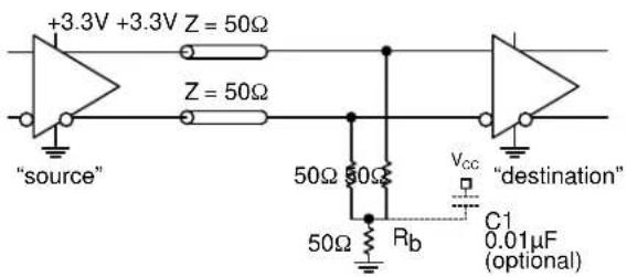
+3.3V +3.3V Z = 50Ω Z = 50Ω "source" 50Ω 50Ω 50Ω Rb Vcc "C1 0.01μF (optional) "destination"Figure 4b. Three-Resistor "Y-Termination"
Notes:
- Power-saving alternative to Thevenin termination.
- Place termination resistors as close to destination inputs as possible.
- R_b resistor sets the DC bias voltage, equal to V_t . For +3.3V systems R_b=50 . For +2.5V systems R_b=19 .
text_image
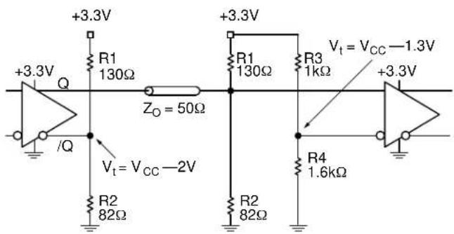
+3.3V +3.3V R1 130Ω Zo = 50Ω +3.3V R1 130Ω R3 1kΩ Vt = VCC -1.3V +3.3V R2 82Ω R4 1.6kΩ Vt = VCC -2V +Q -VCCFigure 4c. Terminating Unused LVPECL I/O
Notes:
- Unused output (/Q) must be terminated to balance the output.
- For +2.5V systems: R1 = 250Ω, R2 = 62.5Ω, R3 = 1.25kΩ, R4 = 1.2kΩ.
- Unused output pairs (Q and /Q) may be left floating.
16 LEAD EPAD MicroLeadFrame™ (MLF-16)
text_image
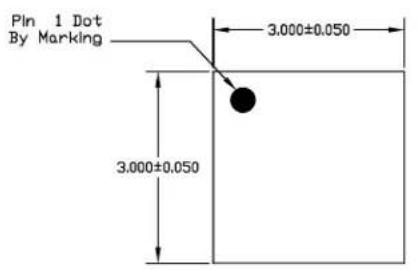
Pin 1 Dot By Marking 3.000±0.050 3.000±0.050TOP VIEW

text_image
PIN #1 IDENTIFICATION CHAMFER 0.300 X 45° 1.550±0.050 Exp. DAP 0.400±0.050 1.550±0.050 Exp. DAP 0.500 Bsc 0.230±0.050 0.400±0.050 1.500 Ref.BOTTOM VIEW

text_image
0.850±0.050 0.000-0.050 0.203±0.025SIDE VIEW
NOTE:
1. ALL DIMENSIONS ARE IN MILLIMETERS.
2. MAX. PACKAGE WARPAGE IS 0.05 mm.
3. MAXIMUM ALLOWABE BURRS IS 0.076 mm IN ALL DIRECTIONS.
4. PIN #1 ID ON TOP WILL BE LASER/INK MARKED.
text_image
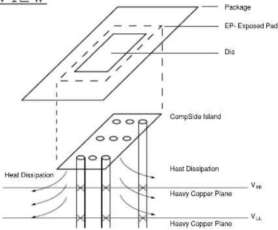
Package EP- Exposed Pad Dia CompSide Island Heat Dissipation Heat Dissipation Heavy Copper Plane V_EF V_LLPCB Thermal Consideration for 16-Pin MLF™ Package (Always solder, or equivalent, the exposed pad to the PCB.)
Package Notes:
Note 1. Package meets Level 2 moisture sensitivity classification, and are shipped in dry-pack form.
Note 2. Exposed pads must be soldered to a ground for proper thermal management.
MICREL, INC. 2180 FORTUNE DRIVE SAN JOSE, CA 95131 USA
TEL + 1 (408) 944-0800 FAX + 1 (408) 474-1000 WEB http://www.micrel.com
The information furnished by Micrel in this datasheet is believed to be accurate and reliable. However, no responsibility is assumed by Micrel for its use. Micrel reserves the right to change circuitry and specifications at any time without notification to the customer.
Micrel Products are not designed or authorized for use as components in life support appliances, devices or systems where malfunction of a product can reasonably be expected to result in personal injury. Life support devices or systems are devices or systems that (a) are intended for surgical implant into the body or (b) support or sustain life, and whose failure to perform can be reasonably expected to result in a significant injury to the user. A Purchaser's use or sale of Micrel Products for use in life support appliances, devices or systems is at Purchaser's own risk and Purchaser agrees to fully indemnify
Micrel for any damages resulting from such use or sale.
© 2005 Micrel, Incorporated.