SY89832U - Electronic component Microchip - Free user manual and instructions
Find the device manual for free SY89832U Microchip in PDF.

User questions about SY89832U Microchip
0 question about this device. Answer the ones you know or ask your own.
Ask a new question about this device
Download the instructions for your Electronic component in PDF format for free! Find your manual SY89832U - Microchip and take your electronic device back in hand. On this page are published all the documents necessary for the use of your device. SY89832U by Microchip.
USER MANUAL SY89832U Microchip
2.5V Ultra-Precision 1:4 LVDS Fanout Buffer/Translator with Internal Termination
Features
- Guaranteed AC Performance over Temperature and Voltage:
- DC-to >2.0 GHz Throughput
- <570 ps Propagation Delay (IN-to-Q)
- <20 ps Within-Device Skew
- <200 ps Rise/Fall Time
- Ultra-Low Jitter Design:
• 81 fs RMS Phase Jitter - Unique, Patented Input Termination and V_T Pin Accepts DC- and AC-Coupled Inputs
• High-Speed LVDS Outputs
• 2.5V Voltage Supply Operation - Industrial Temperature Range: -40^ to +85^
• Available in a 16-Lead 3 mm x 3 mm QFN Package
Applications
- Processor Clock Distribution
• SONET Clock Distribution
• Fibre Channel Clock Distribution
• Gigabit Ethernet Clock Distribution
General Description
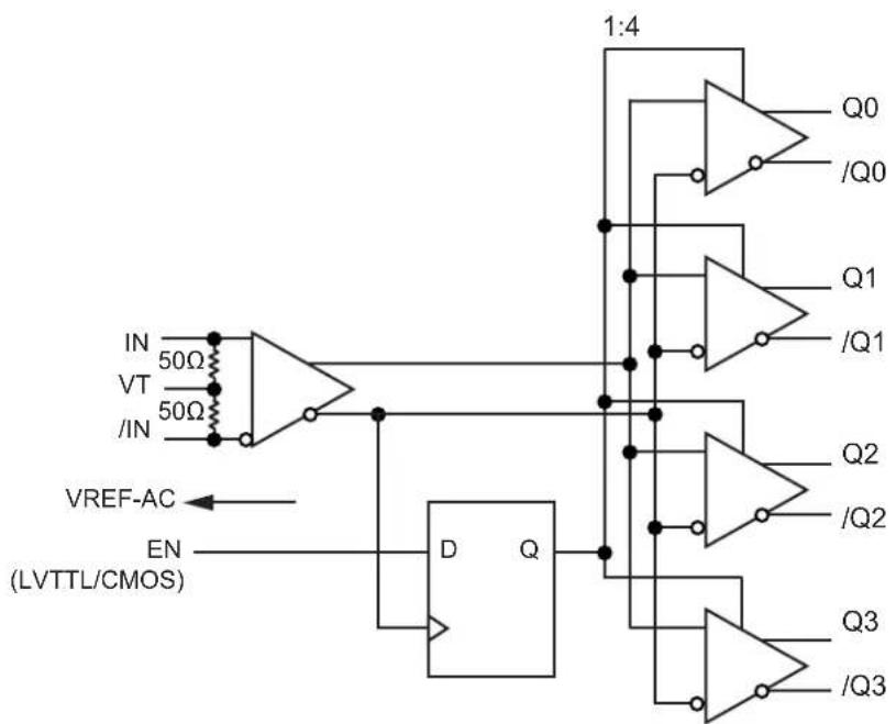
The SY89832U is a 2.5V, high-speed, 2 GHz differential, low voltage differential swing (LVDS) 1:4 fanout buffer optimized for ultra-low skew applications. Within device skew is guaranteed to be less than 20 ps over supply voltage and temperature.
The differential input buffer has a unique internal termination design that allows access to the termination network through a V_T pin. This feature allows the device to easily interface to different logic standards. A VREF–AC reference output is included for AC-coupled applications.
The SY89832U is a part of the high-speed clock synchronization family. For 3.3V applications, see SY89833L or SY89833AL.
Package Type

text_image
SY89832U 16-Pin 3x3 QFN (Top View) /Q0 Q0 VCC GND 16 15 14 13 Q1 1 IN /Q1 2 VT Q2 3 10 VREF-AC /Q2 4 /IN 5 6 7 8 Q3 /Q3 VCC ENUnited States Patent No. RE44,134
Functional Block Diagram
text_image
IN 50Ω VT 50Ω /IN VREF-AC EN (LVTTL/CMOS) D Q 1:4 Q0 /Q0 Q1 /Q1 Q2 /Q2 Q3 /Q31.0 ELECTRICAL CHARACTERISTICS
Absolute Maximum Ratings †
| Supply Voltage (VCC) | -0.5V to +4.0V |
| Input Voltage (VIN) | -0.5V to VCC+ 0.3V |
| LVDS Output Current (IOUT) | ±10 mA |
| Input Current (Source or Sink Current on IN, /IN) (IIN) | ±50 mA |
| Termination Current (Source or Sink Current on VT) (VT) | ±100 mA |
| VREF-AC Current (Source or Sink Current on VREF-AC) (IVREF-AC) (Note 1) | ±1.5 mA |
Operating Ratings ††
Supply Voltage Range ( V_CC )....+2.375V to +2.675V
† Notice: Permanent device damage may occur if absolute maximum ratings are exceeded. This is a stress rating only and functional operation is not implied at conditions other than those detailed in the operational sections of this data sheet. Exposure to absolute maximum rating conditions for extended periods may affect device reliability.
†† Notice: The data sheet limits are not guaranteed if the device is operated beyond the operating ratings.
Note 1: Due to the limited drive capability, the VREF-AC reference should only be used for the input of the same package device (i.e., do not use for other devices).
DC ELECTRICAL CHARACTERISTICS
| Electrical Characteristics: V_CC = 2.5V ± 5% ; T_A = -40°C to +85°C , unless otherwise stated, (Note 1) | ||||||
| Parameters Symbol | Min. Typ. | Max. Units | Conditions | |||
| Power Supply Current | I_CC | — | 75 | 100 | mA | No load |
| Input Resistance (IN-to-VT) | R_IN | 45 | 50 | 55 | Ω | — |
| Differential Input Resistance (IN-to-/IN) | R_DIFF\_IN | 90 | 100 | 110 Ω | — | |
| Input High Voltage (IN, /IN) | V_IH | 0.1 | — | V_CC + 0.3 V | — | |
| Input Low Voltage (IN, /IN) | V_IL | -0.3 | — | V_IH - 0.1 | V — | |
| Input Voltage Swing | V_IN | 0.1 | — | V_CC | V Note 2 | |
| Differential Input Voltage Swing | V_DIFF\_IN | 0.2 | — | — | V | Note 2 |
| Input Current (IN, /IN) | |I_IN| | — | — | 45 | mA | Note 3 |
| Output Reference Voltage | V_REF-AC | V_CC - 1.525 | V_CC - 1.425 | V_CC - 1.325 | V — | |
Note 1: Devices are designed to meet the DC specifications shown in the above table after thermal equilibration has been established.
2: See Figure 5-1 and Figure 5-2 for V_IN and V_DIFF_IN definitions.
3: Due to the internal termination the input current depends on the applied voltages at IN, /IN, and VT inputs. Do not apply a combination of voltages that causes the input current to exceed the maximum limit!
LVDS OUTPUTS DC ELECTRICAL CHARACTERISTICS
| Electrical Characteristics: V_CC = 2.5V ± 5% ; T_A = -40°C to +85°C , R_L = 100Ω across Q and /Q, unless otherwise stated. (Note 1) | ||||||
| Parameter Symbol | Min. Typ. Max. | Units | Conditions | |||
| Output Voltage Swing V | OUT | 250 | 325 | — | mV Note 2 | |
| Differential Voltage Output Swing | V_DIFF\_OUT | 500 | 650 | — | mV Note 2 | |
| Output Common Mode Voltage | V_OCM | 1.125 | — | 1.275 V Note 3 | ||
| Change in Output Common Mode Voltage | V_OCM | -50 | — | 50 | mV | Note 3 |
Note 1: Devices are designed to meet the DC specifications shown in the above table after thermal equilibration has been established.
2: See Figure 5-1 and Figure 5-2 for V_OUT and V_DIFF_OUT definitions.
3: See Figure 8-2.
LVTTL/CMOS DC ELECTRICAL CHARACTERISTICS
| Electrical Characteristics: V_CC = 2.5V ± 5% ; T_A = -40°C to +85°C , unless otherwise stated. (Note 1) | ||||||
| Parameter | Symbol | Min. | Typ. | Max. | Units | Conditions |
| Input High Voltage | V_IH | 2.0 — | V | CC | V | — |
| Input Low Voltage | V_IL | 0 | — 0.8 | V | — | |
| Input High Current | I_IH | -125 — | 30 μA | — | ||
| Input Low Current | I_IL | -300 — | — | μA | — | |
Note 1: Devices are designed to meet the DC specifications shown in the above table after thermal equilibration has been established.
AC ELECTRICAL CHARACTERISTICS
| Electrical Characteristics: V_CC = 2.5V ± 5% ; T_A = -40°C to +85°C, R_L = 100Ω across Q and /Q, unless otherwise stated. (Note 1) | ||||||
| Parameter Symbol | Min. Typ. | Max. Units | Conditions | |||
| Maximum Frequency f | MAX | 2.0 2.5 | — GHz | V | OUT ≥ 200 mV | |
| Propagation Delay In-to-Q t | PD | 370 | 470 | 570 | ps | V_IN < 400 mV |
| 300 | 410 | 500 | V_IN ≥ 400 mV | |||
| Within-Device Skew | t_SKEW | — | 5 | 20 | ps | Note 2 |
| Part-to-Part Skew | — | — | 200 | Note 3 | ||
| Set-Up Time EN to IN, /IN | t_S | 0 | — | — | ps | Note 4 |
| Hold Time IN, /IN to EN | t_H | 320 | — | — | ps | Note 4 |
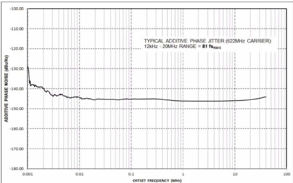
| Additive Phase Jitter | t_JITTER | — | 81 | — | fs_RMS | 622 MHz @ 2.5V, Integration range: 12 kHz to 20 MHz |
| — | 195 | — | 250 MHz @ 2.5V, Integration range: 12 kHz to 20 MHz | |||
| Output Rise/Fall Time Q (20% to 80%) | t_r/t_f | 70 150 | 200 | ps | At full output swing | |
Note 1: High-frequency AC parameters are guaranteed by design and characterization.
2: Within-device skew is measured between two different outputs under identical input transitions.
3: Part-to-part skew is defined for two parts with identical power supply voltages at the same temperature and no skew at the edges at the respective inputs.
4: Set-up and Hold times apply to synchronous applications that intend to enable/disable before the next clock cycle. For asynchronous applications, Set-up and Hold times do not apply.
TEMPERATURE SPECIFICATIONS
| Parameters | Symbol | Min. | Typ. | Max. | Units | Conditions |
| Temperature Ranges | ||||||
| Operating Temperature Range | T_A | -40 | — | +85 | °C | — |
| Lead Temperature | T_J | — | +260 | — | °C | Soldering, 20 sec. |
| Storage Temperature Range | T_A | -65 | — | +150 °C | ||
| Package Thermal Resistance (Note 1) | ||||||
| Thermal Resistance, QFN-16Ld | _JA | — | 60 | — °C/W | Junction-to-Ambient, Still-Air | |
| _JB | — | 32 | — | °C/W | Junction-to-Board | |
Note 1: Package thermal resistance assumes exposed pad is soldered (or equivalent) to the device's most negative potential; on the PCB. _JA and _JB values are determined for a 4-layer board in still-air number, unless otherwise stated.
2.0 TYPICAL OPERATING CHARACTERISTICS
Note: V_CC = 2.5V , GND = 0V, V_IN = 400mV , R_L = 100 across the outputs; T_A = 25^ C , unless otherwise stated.

line
| FREQUENCY (GHz) | OUTPUT SWING (mV) | | --------------- | ----------------- | | 0.5 | 350 | | 1.0 | 320 | | 1.5 | 300 | | 2.0 | 280 | | 2.5 | 260 | | 3.0 | 240 | | 3.5 | 200 |FIGURE 2-1: Output Swing vs. Frequency.

line
| Time (200ps/div) | Output Swing (75mV/div) | | ---------------- | ------------------------ | | 0 | 0 | | 10 | ±1.5 | | 20 | 0 | | 30 | ±0.5 | | 40 | 1.5 | | 50 | 0 | | 60 | ±0.5 | | 70 | 1.5 | | 80 | 0 | | 90 | ±0.5 | | 100 | 1.5 | | 110 | 0 | | 120 | ±0.5 | | 130 | 1.5 | | 140 | 0 | | 150 | ±0.5 | | 160 | 1.5 | | 170 | 0 | | 180 | ±0.5 | | 190 | 1.5 | | 200 | 0 |FIGURE 2-4: 622 MHz Output.
line
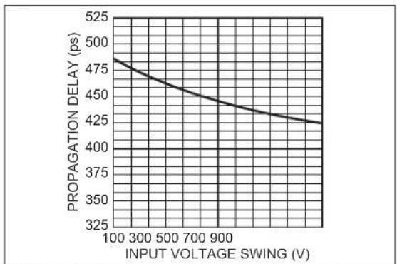
| INPUT VOLTAGE SWING (V) | PROPAGATION DELAY (ps) | | ----------------------- | ---------------------- | | 100 | 485 | | 300 | 475 | | 500 | 465 | | 700 | 455 | | 900 | 445 | | 1100 | 435 |FIGURE 2-2: Propagation Delay vs. Input Voltage Swing.

line
| Time (200ps/div) | OUTPUT SWING (75mV/div) | | ---------------- | ------------------------ | | 0 | 0 | | 10 | 1.000 V (MAX) | | 20 | 1.000 V (MAX) | | 30 | 1.004 V (MAX) | | 40 | 1.004 V (MAX) | | 50 | 1.004 V (MAX) | | 60 | 1.004 V (MAX) | | 70 | 1.004 V (MAX) | | 80 | 1.004 V (MAX) | | 90 | 1.004 V (MAX) | | 100 | 1.004 V (MAX) | | 110 | 1.004 V (MAX) | | 120 | 1.004 V (MAX) | | 130 | 1.004 V (MAX) | | 140 | 1.004 V (MAX) | | 150 | 1.004 V (MAX) | | 160 | 1.004 V (MAX) | | 170 | 1.004 V (MAX) | | 180 | 1.004 V (MAX) | | 190 | 1.004 V (MAX) | | 200 | 1.004 V (MAX) |FIGURE 2-5: 1 GHz Output.

line
| Time (1.3ns/div) | OUTPUT SWING (75mV/div) | | ---------------- | ------------------------ | | 0 | 150.0 | | 1.3 | 148.0 | | 2.6 | 150.0 | | 3.9 | 148.0 | | 5.2 | 150.0 | | 6.5 | 148.0 | | 7.8 | 150.0 | | 9.1 | 148.0 | | 10.4 | 150.0 | | 11.7 | 148.0 | | 13.0 | 150.0 | | 14.3 | 148.0 | | 15.6 | 150.0 | | 16.9 | 148.0 | | 18.2 | 150.0 | | 19.5 | 148.0 | | 20.8 | 150.0 | | 22.1 | 148.0 | | 23.4 | 150.0 | | 24.7 | 148.0 | | 26.0 | 150.0 | | 27.3 | 148.0 | | 28.6 | 150.0 | | 29.9 | 148.0 | | 31.2 | 150.0 | | 32.5 | 148.0 | | 33.8 | 150.0 | | 35.1 | 148.0 | | 36.4 | 150.0 | | 37.7 | 148.0 | | 39.0 | 150.0 | | 40.3 | 148.0 | | 41.6 | 150.0 | | 42.9 | 148.0 | | 44.2 | 150.0 | | 45.5 | 148.0 | | 46.8 | 150.0 | | 48.1 | 148.0 | | 49.4 | 150.0 | | 50.7 | 148.0 | | 52.0 | 150.0 | | 53.3 | 148.0 | | 54.6 | 150.0 | | 55.9 | 148.0 | | 57.2 | 150.0 | | 58.5 | 148.0 | | 59.8 | 150.0 | | 61.1 | 148.0 | | 62.4 | 150.0 | | 63.7 | 148.0 | | 65 | 150.0 | | | |FIGURE 2-3: 155 MHz Output.
$$ V _ {C C} = 2. 5 V, G N D = 0, T _ {A} = + 2 5 ^ {\circ} C. $$
line
| OFFSET FREQUENCY (MHz) | ADDITIVE PHASE NOISE (dBc/Hz) | | ---------------------- | ----------------------------- | | 0.001 | -130.0 | | 0.01 | -145.0 | | 0.1 | -147.0 | | 1 | -148.0 | | 10 | -147.5 | | 100 | -146.0 |FIGURE 2-6: Typical Additive Phase Jitter (622 MHz Carrier).

line
| OFFSET FREQUENCY (MHz) | ADDITIVE PHASE NOISE (dBc/Hz) | | ----------------------- | ------------------------------ | | 0.001 | -135.0 | | 0.01 | -145.0 | | 0.1 | -147.0 | | 1 | -148.0 | | 10 | -149.0 | | 100 | -150.0 |FIGURE 2-7: Typical Additive Phase Jitter (250 MHz Carrier).
3.0 PIN DESCRIPTIONS
The descriptions of the pins are listed in Table 3-1.
TABLE 3-1: PIN FUNCTION TABLE
| Pin Number | Pin Name Pin | Function |
| 15, 161, 23, 45, 6 | Q0, /Q0Q1, /Q1Q2, /Q2Q3, /Q3 | LVDS Differential (Outputs): Normally terminated with 100 across the pair (Q, /Q). See LVDS Outputs section for more details. Unused outputs should be terminated with a 100 resistor across each pair. |
| 8 | EN | The single-ended, TTL/CMOS-compatible input functions as a synchronous output enable. The synchronous enable ensures that enable/disable will only occur when the Q outputs are in a logic LOW state. Note that this input is internally connected to a 25k pull-up resistor and will default to logic HIGH state (enabled) if left open. |
| 9, 12 /IN, IN | Differential Input: This input is the differential signal input to the device. Input accepts AC- or DC-Coupled differential signs as small as 100mV . Each pin internally terminates to the V_T pin through 50 . Note that this input will default to an intermediate state if left open. See Input Interface Applications section for more details. | |
| 10 VREF-AC | Reference Voltage: This output biases to approximately V_CC - 1.4V . It is used when AC coupling the input (IN, /IN). For AC-Coupled applications, connect VREF-AC to VT pin and bypass with a 0.01 F low-ESR capacitor to VCC. See Input Interface Applications section for more details.Maximum sink/source current is ± 1.5mA . Due to the limited drive capability, the VREF-AC pin is only intended to drive the VT pin. | |
| 11 VT | Input Termination Center-Tap: Each side of the differential input pair terminates to the VT pin. The VT pin provides a center-tap to a termination network for maximum interface flexibility. See Input Interface Applications section for more details. | |
| 13 GND | Ground. GND pin and exposed pad must be connected to the most negative potential of the device ground. | |
| 7, 14 | VCC | Positive Power Supply: Bypass with 0.1 F//0.01 F low ESR capacitors and place as close to each VCC pin as possible. |
TABLE 3-2: TRUTH TABLE
| IN | /IN | EN | Q | /Q |
| 0 | 1 | 1 | 0 | 1 |
| 1 | 0 | 1 | 1 | 0 |
| X | X | 0 | 0 | 1 |
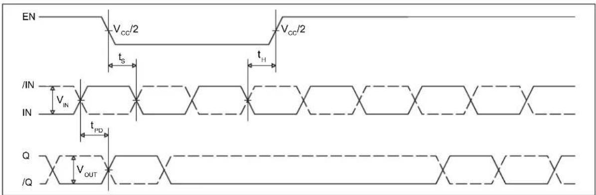
4.0 TIMING DIAGRAMS
text_image
EN Vcc/2 Vcc/2 IN VIN IN tS tH tPD Q VOUT /QFIGURE 4-1: Timing Diagram Disable.

text_image
EN Vcc/2 Vcc/2 IN tS tH IN VIN tPD /Q VOUT QFIGURE 4-2: Timing Diagram Enable.
5.0 SINGLE-ENDED AND DIFFERENTIAL SWINGS
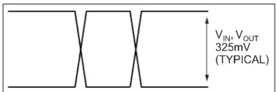
text_image
V_IN, V_OUT 325mV (TYPICAL)
text_image
650mV (TYPICAL) VDIFF_IN, VDIFF_OUTFIGURE 5-1: Single-Ended Swing. FIGURE 5-2: Differential Swing.
6.0 INPUT STAGE
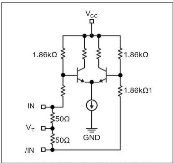
text_image
VCC 1.86kΩ 1.86kΩ IN 50Ω VT 50Ω /IN 1.86kΩ1 GNDFIGURE 6-1: Simplified Differential Input Buffer.
7.0 INPUT INTERFACE APPLICATIONS
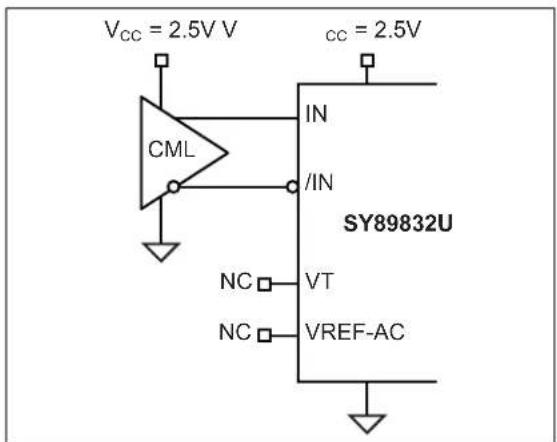
text_image
Vcc = 2.5V V CC = 2.5V CML IN /IN SY89832U NC □ VT NC □ VREF-ACFIGURE 7-1: DC-Coupled CML Input Interface.

text_image
VCC = 2.5V V LVPECL Rpd 50Ω Rpd 50Ω 0.01μF VCC = 2.5V IN /IN SY89832U VT VREF-AC CC = 2.5VFIGURE 7-4: AC-Coupled LVPECL Input Interface.

text_image
Vcc = 2.5V V CC = 2.5V CML IN /IN SY89832U VT VREF-AC Vcc 0.01μFFIGURE 7-2: AC-Coupled CML Input Interface.
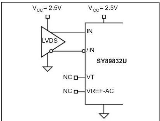
text_image
VCC = 2.5V LVDS IN /IN SY89832U NC □ VT NC □ VREF-AC VCC = 2.5VFIGURE 7-5: LVDS Input Interface.
text_image
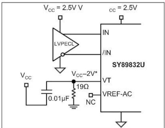
Vcc = 2.5V V CC = 2.5V LVPECL IN /IN SY89832U Vcc -2V* 19Ω VT VREF-AC NC 0.01μFFIGURE 7-3: DC-Coupled LVPECL Input Interface (*Bypass with 0.01 μF to GND).

text_image
VCC = 1.8V to 2.5V V HSTL IN /IN SY89832U VT NC VREF-AC CC = 2.5VFIGURE 7-6: HSTL Input Interface.
8.0 LVDS OUTPUTS
LVDS specifies a small swing of 325 mV typical, on a nominal 1.2V common-mode above ground.
The common-mode voltage has tight limits to permit large variations in ground noise between an LVDS driver and receiver.

text_image
100Ω VOUT VOH, VOL VOH, VOL GNDFIGURE 8-1: LVDS Differential Measurement.

text_image
50Ω 50Ω VOCM, ΔVOCM GNDFIGURE 8-2: LVDS Common Mode Measurement.
9.0 PACKAGING INFORMATION
9.1 Package Marking Information
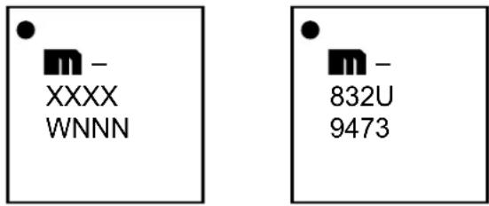
16-Lead QFN* Example
text_image
m - XXXX WNNN m - 832U 9473Legend: XX...X Product code or customer-specific information
Y Year code (last digit of calendar year)
YY Year code (last 2 digits of calendar year)
WW Week code (week of January 1 is week '01')
NNN Alphanumeric traceability code
eBb-free JEDEC ^® designator for Matte Tin (Sn)
* This package is Pb-free. The Pb-free JEDEC designator ( ) e3
can be found on the outer packaging for this package.
•, ▲, ▼ Pin one index is identified by a dot, delta up, or delta down (triangle mark).
Note: In the event the full Microchip part number cannot be marked on one line, it will be carried over to the next line, thus limiting the number of available characters for customer-specific information. Package may or may not include the corporate logo.
Underbar (_) and/or Overbar (−) symbol may not be to scale.
TITLE
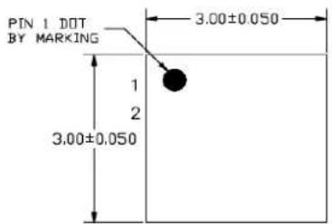
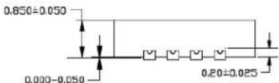
16 LEAD QFN 3x3mm PACKAGE OUTLINE & RECOMMENDED LAND PATTERN
| DRAWING # | QFN33-16LD-PL-3 | UNIT | MM |
| Lead Frame | NiPdAu | Lead Finish | NiPdAu |
text_image
PIN 1 DOT BY MARKING 3.00±0.050 1 2 3.00±0.050TOP VIEW NOTE 1, 2, 3

text_image
0.25±0.050 1.70±0.050 Exp. DAP PIN #1 IDENTIFICATION CHAMFER 0.300X45° 0.50 Bsc 1.70±0.050 Exp. DAP 0.30±0.050BOTTOM VIEW NOTE: 1, 2, 3
text_image
0.850±0.050 0.000-0.050 0.20±0.025SIDE VIEW NOTE: 1.2.3
text_image
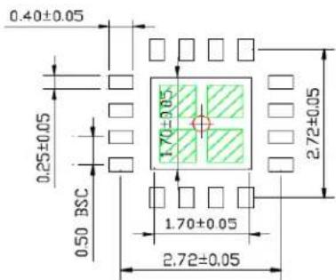
0.40±0.05 0.25±0.05 BSC 0.50 1.70±0.05 1.70±0.05 2.72±0.05 2.72±0.05RECOMMENDED LAND PATTERN NOTE: 4, 5
NOTE:
- MAX PACKAGE WARPAGE IS 0.05mm.
- MAX ALLOWABLE BURR IS 0.076mm IN ALL DIRECTIONS
- PIN #1 IS ON TOP WILL BE LASER MARKED.
- RED CIRCLE IN LAND PATTERN INDICATES THERMAL VIA. SIZE SHOULD BE 0.30-0.35mm IN DIAMETER AND SHOULD BE CONNECTED TO GND FOR MAX THERMAL PERFORMANCE.
- GREEN RECTANGLES (SHADED AREA) Indicate SOLDER STENCIL OPENING ON EXPOSED PAD AREA. SIZE SHOULD BE 0.60x0.60mm IN SIZE, 0.20mm SPACING.
Note: For the most current package drawings, please see the Microchip Packaging Specification located at http://www.microchip.com/packaging.
NOTES:
APPENDIX A: REVISION HISTORY
Revision A (March 2022)
- Converted Micrel document SY89832U to Microchip data sheet template DS20006659A.
- Minor text changes throughout.
NOTES:
PRODUCT IDENTIFICATION SYSTEM
To order or obtain information, e.g., on pricing or delivery, contact your local Microchip representative or sales office.

Device

Voltage Option

Package

Range

SpecialTemperatu
Processing
Device:
SY89832:
2.5V Ultra-Precision 1:4 LVDS Fanout Buffer/Translator with Internal Termination
Voltage Option:
U
= 2.5V
Package:
M
=
16-Lead Industrial QFN
Temperature Range:
G
=
-40°C to 85°C (NiPdAu Lead Free)
Special
100/Tube
Processing:
TR
= 1,000/Reel
Examples:
a) SY89832UMG: 2.5V Ultra-Precision 1:4
LVDS Fanout Buffer/
Translator with Internal
Termination, 2.5V, 16-
Lead Industrial QFN,
-40°C to 85°C (NiPdAu
Lead Free), 100/Tube
b) SY89832UMG-TR: 2.5V Ultra-Precision 1:4
LVDS Fanout Buffer/
Translator with Internal
Termination, 2.5V, 16-
Lead Industrial QFN,
-40°C to 85°C (NiPdAu
Lead Free), 1,000/Reel
NOTES:
Note the following details of the code protection feature on Microchip products:
• Microchip products meet the specifications contained in their particular Microchip Data Sheet.
- Microchip believes that its family of products is secure when used in the intended manner, within operating specifications, and under normal conditions.
- Microchip values and aggressively protects its intellectual property rights. Attempts to breach the code protection features of Microchip product is strictly prohibited and may violate the Digital Millennium Copyright Act.
- Neither Microchip nor any other semiconductor manufacturer can guarantee the security of its code. Code protection does not mean that we are guaranteeing the product is "unbreakable". Code protection is constantly evolving. Microchip is committed to continuously improving the code protection features of our products.
This publication and the information herein may be used only with Microchip products, including to design, test, and integrate Microchip products with your application. Use of this information in any other manner violates these terms. Information regarding device applications is provided only for your convenience and may be superseded by updates. It is your responsibility to ensure that your application meets with your specifications. Contact your local Microchip sales office for additional support or, obtain additional support at https://www.microchip.com/en-us/support/design-help/client-support-services.
THIS INFORMATION IS PROVIDED BY MICROCHIP "AS IS". MICROCHIP MAKES NO REPRESENTATIONS OR WARRANTIES OF ANY KIND WHETHER EXPRESS OR IMPLIED, WRITTEN OR ORAL, STATUTORY OR OTHERWISE, RELATED TO THE INFORMATION INCLUDING BUT NOT LIMITED TO ANY IMPLIED WARRANTIES OF NON-INFRINGEMENT, MERCHANTABILITY, AND FITNESS FOR A PARTICULAR PURPOSE, OR WARRANTIES RELATED TO ITS CONDITION, QUALITY, OR PERFORMANCE.
IN NO EVENT WILL MICROCHIP BE LIABLE FOR ANY INDIRECT, SPECIAL, PUNITIVE, INCIDENTAL, OR CONSEQUENTIAL LOSS, DAMAGE, COST, OR EXPENSE OF ANY KIND WHATSOEVER RELATED TO THE INFORMATION OR ITS USE, HOWEVER CAUSED, EVEN IF MICROCHIP HAS BEEN ADVISED OF THE POSSIBILITY OR THE DAMAGES ARE FORESEEABLE. TO THE FULLEST EXTENT ALLOWED BY LAW, MICROCHIP'S TOTAL LIABILITY ON ALL CLAIMS IN ANY WAY RELATED TO THE INFORMATION OR ITS USE WILL NOT EXCEED THE AMOUNT OF FEES, IF ANY, THAT YOU HAVE PAID DIRECTLY TO MICROCHIP FOR THE INFORMATION.
Use of Microchip devices in life support and/or safety applications is entirely at the buyer's risk, and the buyer agrees to defend, indemnify and hold harmless Microchip from any and all damages, claims, suits, or expenses resulting from such use. No licenses are conveyed, implicitly or otherwise, under any Microchip intellectual property rights unless otherwise stated.
Trademarks
The Microchip name and logo, the Microchip logo, Adaptec, AnyRate, AVR, AVR logo, AVR Freaks, BestTime, BitCloud, CryptoMemory, CryptoRF, dsPIC, flexPWR, HELDO, IGLOO, JukeBlox, KeeLoq, Kleer, LANCheck, LinkMD, maXStylus, maXTouch, MediaLB, megaAVR, Microsemi, Microsemi logo, MOST, MOST logo, MPLAB, OptoLyzer, PIC, picoPower, PICSTART, PIC32 logo, PolarFire, Prochip Designer, QTouch, SAM-BA, SenGenuity, SpyNIC, SST, SST Logo, SuperFlash, Symmetricom, SyncServer, Tachyon, TimeSource, tinyAVR, UNI/O, Vectron, and XMEGA are registered trademarks of Microchip Technology Incorporated in the U.S.A. and other countries.
AgileSwitch, APT, ClockWorks, The Embedded Control Solutions Company, EtherSynch, Flashtec, Hyper Speed Control, HyperLight Load, IntelliMOS, Libero, motorBench, mTouch, Powermite 3, Precision Edge, ProASIC, ProASIC Plus, ProASIC Plus logo, Quiet-Wire, SmartFusion, SyncWorld, Temux, TimeCesium, TimeHub, TimePictra, TimeProvider, TrueTime, WinPath, and ZL are registered trademarks of Microchip Technology Incorporated in the U.S.A.
Adjacent Key Suppression, AKS, Analog-for-the-Digital Age, Any Capacitor, AnyIn, AnyOut, Augmented Switching, BlueSky, BodyCom, CodeGuard, CryptoAuthentication, CryptoAutomotive, CryptoCompanion, CryptoController, dsPICDEM, dsPICDEM.net, Dynamic Average Matching, DAM, ECAN, Espresso T1S, EtherGREEN, GridTime, IdealBridge, In-Circuit Serial Programming, ICSP, INICnet, Intelligent Paralleling, Inter-Chip Connectivity, JitterBlocker, Knob-on-Display, maxCrypto, maxView, memBrain, Mindi, MiWi, MPASM, MPF, MPLAB Certified logo, MPLIB, MPLINK, MultiTRAK, NetDetach, NVM Express, NVMe, Omniscient Code Generation, PICDEM, PICDEM.net, PICkit, PICtail, PowerSmart, PureSilicon, QMatrix, REAL ICE, Ripple Blocker, RTAX, RTG4, SAM-ICE, Serial Quad I/O, simpleMAP, SimpliPHY, SmartBuffer, SmartHLS, SMART-I.S., storClad, SQI, SuperSwitcher, SuperSwitcher II, Switchtec, SynchroPHY, Total Endurance, TSHARC, USBCheck, VariSense, VectorBlox, VeriPHY, ViewSpan, WiperLock, XpressConnect, and ZENA are trademarks of Microchip Technology Incorporated in the U.S.A. and other countries.
SQTP is a service mark of Microchip Technology Incorporated in the U.S.A.
The Adaptec logo, Frequency on Demand, Silicon Storage Technology, Symmcom, and Trusted Time are registered trademarks of Microchip Technology Inc. in other countries.
GestIC is a registered trademark of Microchip Technology Germany II GmbH & Co. KG, a subsidiary of Microchip Technology Inc., in other countries.
All other trademarks mentioned herein are property of their respective companies.
© 2022, Microchip Technology Incorporated and its subsidiaries.
All Rights Reserved.
ISBN: 978-1-6683-0159-3
For information regarding Microchip's Quality Management Systems, please visit www.microchip.com/quality.
Worldwide Sales and Service
AMERICAS
Corporate Office
2355 West Chandler Blvd.
Chandler, AZ 85224-6199
Tel: 480-792-7200
Fax: 480-792-7277
Technical Support:
http://www.microchip.com/
support
Web Address:
www.microchip.com
Atlanta
Duluth, GA
Tel: 678-957-9614
Fax: 678-957-1455
Austin, TX
Tel: 512-257-3370
Boston
Westborough, MA
Tel: 774-760-0087
Fax: 774-760-0088
Chicago
Itasca, IL
Tel: 630-285-0071
Fax: 630-285-0075
Dallas
Addison, TX
Tel: 972-818-7423
Fax: 972-818-2924
Detroit
Novi, MI
Tel: 248-848-4000
Houston, TX
Tel: 281-894-5983
Indianapolis
Noblesville, IN
Tel: 317-773-8323
Fax: 317-773-5453
Tel: 317-536-2380
Los Angeles
Mission Viejo, CA
Tel: 949-462-9523
Fax: 949-462-9608
Tel: 951-273-7800
Raleigh, NC
Tel: 919-844-7510
New York, NY
Tel: 631-435-6000
San Jose, CA
Tel: 408-735-9110
Tel: 408-436-4270
Canada - Toronto
Tel: 905-695-1980
Fax: 905-695-2078
ASIA/PACIFIC
Australia - Sydney
Tel: 61-2-9868-6733
China - Beijing
Tel: 86-10-8569-7000
China - Chengdu
Tel: 86-28-8665-5511
China - Chongqing
Tel: 86-23-8980-9588
China - Dongguan
Tel: 86-769-8702-9880
China - Guangzhou
Tel: 86-20-8755-8029
China - Hangzhou
Tel: 86-571-8792-8115
China - Hong Kong SAR
Tel: 852-2943-5100
China - Nanjing
Tel: 86-25-8473-2460
China - Qingdao
Tel: 86-532-8502-7355
China - Shanghai
Tel: 86-21-3326-8000
China - Shenyang
Tel: 86-24-2334-2829
China - Shenzhen
Tel: 86-755-8864-2200
China - Suzhou
Tel: 86-186-6233-1526
China - Wuhan
Tel: 86-27-5980-5300
China - Xian
Tel: 86-29-8833-7252
China - Xiamen
Tel: 86-592-2388138
China - Zhuhai
Tel: 86-756-3210040
ASIA/PACIFIC
India - Bangalore
Tel: 91-80-3090-4444
India - New Delhi
Tel: 91-11-4160-8631
India - Pune
Tel: 91-20-4121-0141
Japan - Osaka
Tel: 81-6-6152-7160
Japan - Tokyo
Tel: 81-3-6880-3770
Korea - Daegu
Tel: 82-53-744-4301
Korea - Seoul
Tel: 82-2-554-7200
Malaysia - Kuala Lumpur
Tel: 60-3-7651-7906
Malaysia - Penang
Tel: 60-4-227-8870
Philippines - Manila
Tel: 63-2-634-9065
Singapore
Tel: 65-6334-8870
Taiwan - Hsin Chu
Tel: 886-3-577-8366
Taiwan - Kaohsiung
Tel: 886-7-213-7830
Taiwan - Taipei
Tel: 886-2-2508-8600
Thailand - Bangkok
Tel: 66-2-694-1351
Tel: 43-7242-2244-39
Fax: 43-7242-2244-393
Denmark - Copenhagen
Tel: 45-4485-5910
Fax: 45-4485-2829
Finland - Espoo
Tel: 358-9-4520-820
France - Paris
Tel: 33-1-69-53-63-20
Fax: 33-1-69-30-90-79
Germany - Garching
Tel: 49-8931-9700
Germany - Haan
Tel: 49-2129-3766400
Germany - Heilbronn
Tel: 49-7131-72400
Germany - Karlsruhe
Tel: 49-721-625370
Germany - Munich
Tel: 49-89-627-144-0
Fax: 49-89-627-144-44
Germany - Rosenheim
Tel: 49-8031-354-560
Israel - Ra'anana
Tel: 972-9-744-7705
Italy - Milan
Tel: 39-0331-742611
Fax: 39-0331-466781
Italy - Padova
Tel: 39-049-7625286
Netherlands - Drunen
Tel: 31-416-690399
Fax: 31-416-690340
Norway - Trondheim
Tel: 47-7288-4388
Poland - Warsaw
Tel: 48-22-3325737
Romania - Bucharest
Tel: 40-21-407-87-50
Spain - Madrid
Tel: 34-91-708-08-90
Fax: 34-91-708-08-91
Sweden - Gothenberg
Tel: 46-31-704-60-40
Sweden - Stockholm
Tel: 46-8-5090-4654
UK - Wokingham
Tel: 44-118-921-5800
Fax: 44-118-921-5820