SY89825U - Electronic component Microchip - Free user manual and instructions
Find the device manual for free SY89825U Microchip in PDF.

User questions about SY89825U Microchip
0 question about this device. Answer the ones you know or ask your own.
Ask a new question about this device
Download the instructions for your Electronic component in PDF format for free! Find your manual SY89825U - Microchip and take your electronic device back in hand. On this page are published all the documents necessary for the use of your device. SY89825U by Microchip.
USER MANUAL SY89825U Microchip
■ High-performance PCs
■ Workstations
■ Parallel processor-based systems
■ Other high-performance computing
■ Communications

Precision Edge®
DESCRIPTION
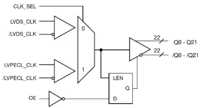
The SY89825U is a High Performance Bus Clock Driver with 22 differential LVPECL output pairs. This part is designed for use in low voltage (2.5V, 3.3V) applications which require a large number of outputs to drive precisely aligned, ultra low skew signals to their destination. The input is multiplexed from either LVDS or LVPECL by the CLK_SEL pin. The LVDS input includes a 100Ω internal termination, thus eliminating the need for external termination. The Output Enable (OE) is synchronous so that the outputs will only be enabled/disabled when they are already in the LOW state. This eliminates any chance of generating a runt clock pulse when the device is enabled/disabled as can happen with an asynchronous control.
The SY89825U features low pin-to-pin skew (35ps max.)—performance previously unachievable in a standard product having such a high number of outputs. The SY89825U is available in a single space saving package which provides a lower overall cost solution. In addition, a single chip solution improves timing budgets by eliminating the multiple device solution with their corresponding large part-to-part skew.
Precision Edge is a registered trademark of Micrel, Inc.
PACKAGE/ORDERING INFORMATION
text_image
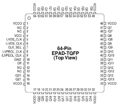
64 Pin EPAD-TQFP (Top View) VCCO 1 NC 2 NC 3 VCCI 4 LVDS_CLK 5 /LVDS_CLK 6 CLK_SEL 7 LVPECL_CLK 8 /LVPECL_CLK 9 GND 10 OE 11 NC 12 NC 13 /Q21 14 Q21 15 VCCO 16 VCCO 17 18 19 20 21 22 23 24 25 26 27 28 29 30 31 32 VCCO 18 VCCO 19 VCCO 20 VCCO 21 VCCO 22 VCCO 23 VCCO 24 VCCO 25 VCCO 26 VCCO 27 VCCO 28 VCCO 29 VCCO 30 VCCO 31 VCCO 32 VCCO 64 63 62 61 60 59 58 57 56 55 54 53 52 51 50 49 48 VCCO 47 Q7 45 Q7 45 Q8 44 Q8 43 Q9 42 Q9 41 Q10 40 Q10 39 Q11 38 Q11 37 Q12 36 Q12 35 Q13 34 Q13 33 VCCO64-Pin EPAD-TQFP (H64-1)
Ordering Information ^(1)
| Part Number Type R | Package Range Mark | Operating Png Finish | Package Lead | |
| SY89825UHI H64-1 | Industrial SY | 89825UHI Sn | Pb | |
| SY89825UHITR(2) | H64-1 | industrial SY8 | 9825UHI SN-PB | |
| SY89825UHY(3) | H64-1 | industrial SY8 | 9825UHY with Pb-Free Pb-Free bar-line indicator | Matte-Sn |
| SY89825UHYTR(2,3) | H64-1 | industrial SY8 | 9825UHY with Pb-Free Pb-Free bar-line indicator | Matte-Sn |
Notes:
- Contact factory for die availability. Dice are guaranteed at T_A = 25^ , DC electricals only.
- Tape and Reel.
- Pb-Free package recommended for new designs.
PIN NAMES
| Pin | Function |
| LVDS_CLK, /LVDS_CLK | Differential LVDS Inputs (Internal 100Ω termination included) |
| LVPECL_CLK, /LVPECL_CLK | Differential LVPECL Inputs. |
| CLK_SEL | Input CLK Select (LVTTL) |
| OE | Output Enable (LVTTL) |
| Q_0 - Q_21 , /Q_0 - /Q_21 | Differential LVPECL Outputs. Terminate with 50Ω to V_CC-2V |
| GND | Ground |
| V_CCI | Power Supply. Connect to V_CC on PCB. V_CCI and V_CCO are not internally connected |
| V_CCO | Power Supply for Output Buffer. Connect to V_CCI on PCB. V_CCI and V_CCO are not internally connected |
LOGIC SYMBOL
flowchart
graph TD
    A["CLK_SEL"] --> B["0"]
    C["LVDS_CLK"] --> B
    D["/LVDS_CLK"] --> B
    E["LVPECL_CLK"] --> F["1"]
    G["/LVPECL_CLK"] --> F
    H["OE"] --> I["LEN Q D"]
    B --> I
    F --> I
    I --> J["22 Q0 - Q21 /Q0 - /Q21"]
TRUTH TABLE
| OE^(1) | CLK_SEL Q | 0-Q_21 | / Q_0 -/ Q_21 |
| 0 0 LOW HIGH | |||
| 0 1 LOW HIGH | |||
| 1 0 LVDS_CLK /LVDS_CLK | |||
| 1 1 LVPECL_CLK /LVPECL_CLK |
SIGNAL GROUPS
| Signal I/O Level | ||
| LVDS_CLK, /LVDS_CLK Input | LVDS | |
| Q_0-Q_21 , /Q_0-/Q_21 | Output LVPECL | |
| LVPECL_CLK, /LVPECL_CLK | Input LVPECL | |
| CLK_SEL, OE | Input LVCMOS/LVTTL | |
NOTE:
- The OE (output enable) signal is synchronized with the low level of the LVDS_CLK and LVPECL_CLK signal.
ABSOLUTE MAXIMUM RATINGS ^(1)
| Symbol | Rating | Value | Unit |
| V_CCI/V_CCO | V_CC Pin Potential to Ground Pin | -0.5 to +4.0 | V |
| V_IN | Input Voltage | -0.5 to V_CCI | V |
| I_OUT | DC Output Current | -50 | mA |
| Tstore | Storage Temperature | -65 to +150 | °C |
| _JA | Package Thermal Resistance (Junction-to-Ambient)With exposed pad soldered to GND - Still-Air (multi-layer PCB)- 200lfpm (multi-layer PCB)- 500lfpm (multi-layer PCB) | 231815 | °C/W°C/W°C/W |
| Exposed padnotsoldered to GND - Still-Air (multi-layer PCB)- 200lfpm (multi-layer PCB)- 500lfpm (multi-layer PCB) | 443630 | °C/W°C/W°C/W | |
| _JC | Package Thermal Resistance(Junction-to-Case) | 4.3 | °C/W |
NOTE:
- Permanent device damage may occur if ABSOLUTE MAXIMUM RATINGS are exceeded. This is a stress rating only and functional operation is not implied at conditions other than those detailed in the operational sections of this data book. Exposure to ABSOLUTE MAXIMUM RATING conditions for extended periods may affect device reliability.
DC ELECTRICAL CHARACTERISTICS
Power Supply
| Symbol | Parameter Min. Typ. Max. Min. Typ. | T_A = -40°C | T_A = +25°C | T_A = +85°C | |||||||
| Max. Min. Typ. | Max. Unit | ||||||||||
| V_CCI, V_CCO | Power Supply(1) | 2.37 | — | 3.6 | 2.37 | — | 3.8 | 2.37 | — | 3.6 | V |
| I_CC | Total Supply Current(2) | — | 100 | 150 | — | 100 | 150 | — | 100 | 150 | mA |
Notes:
1. V_CCI and V_CCO must be connected together on the PCB such that they remain at the same potential. V_CCI and V_CCO are not internally connected on the die.
2. No load. Outputs floating.
LVDS Input ( V_CC = 2.37V to 3.6V, GND = 0V)
| Symbol | Parameter Min. Typ. Max. Min. Typ. | T_A = -40°C | T_A = +25°C | T_A = +85°C | |||||||
| Max. | Min. Typ. | Max. Unit | |||||||||
| V_IN | Input Voltage Range | 0 | — | 2.4 | 0 | — | 2.4 | 0 | — | 2.4 | V |
| V_ID | Differential Input Swing | 100 | — | — | 100 | — | — | 100 | — | — | mV |
| I_IL | Input Low Current(1) | -1.25 | — | — | -1.25 | — | — | -1.25 | — | — | mA |
| R_IN | LVDS Differential Input Resistance (LVDS_CLK to /LVDS_CLK) | 80 | 100 | 120 | 80 | 100 | 120 | 80 | 100 | 120 | Ω |
Note:
1. For I_IL , both LVDS inputs are grounded.
LVPECL Input/Output ( V_CC = 2.37V to 3.6V, GND = 0V)
| Symbol | Parameter | T_A = -40°C | T_A = +25°C | T_A = +85°C | Unit | |||
| Min. | Max. | Min. | Max. | Min. | Max. | |||
| V_IH | Input HIGH Voltage (Single ended) | V_CC - 1.165 | V_CC - 0.88 | V_CC - 1.165 | V_CC - 0.88 | V_CC - 1.165 | V_CC - 0.88 V | |
| V_IL | Input LOW Voltage | V_CC - 1.945 | V_CC - 1.625 | V_CC - 1.945 | V_CC - 1.625 | V_CC - 1.945 | V_CC - 1.625 | V |
| V_PP | Minimum Input Swing(1)LVPECL_CLK | 600 | — | 600 | — | 600 | — | mV |
| V_CMR | Common Mode Range(2)LVPECL_CLK | -1.5 | -0.4 | -1.5 | -0.4 | -1.5 | -0.4 | V |
| V_OH | Output HIGH Voltage(3) | V_CCO - 1.085 | V_CCO - 0.880 | V_CCO - 1.025 | V_CCO - 0.880 | V_CCO - 1.025 | V_CCO - 0.880 | V |
| V_OL | Output LOW Voltage(3) | V_CCO - 1.830 | V_CCO - 1.555 | V_CCO - 1.810 | V_CCO - 1.620 | V_CCO - 1.810 | V_CCO - 1.620 | V |
| I_IH | Input HIGH Current | — | 150 | — | 150 | — | 150 | ∞A |
| I_IL | Input LOW Current | 0.5 | — | 0.5 | — | 0.5 | — | ∞A |
Notes:
-
The V_PP (min.) is defined as the minimum input differential voltage which will cause no increase in the propagation delay.
-
V_CMR is defined as the range within which the V_IH level may vary, with the device still meeting the propagation delay specification. The numbers in the table are referenced to V_CCI . The V_IL level must be such that the peak-to-peak voltage is less than 1.0V and greater than or equal to V_PP (min.). The lower end of the CMR range varies 1:1 with V_CCI . The V_CMR (min) will be fixed at 3.3V - |V_CMR(min)| .
-
Outputs loaded with 50Ω to Vcc -2V.
LVCMOS/LVTTL Control Inputs (OE, CLK_SEL) ( V_CC = 2.37V to 3.6V, GND = 0V)
| Symbol | Parameter Min. Typ. Max. Min. Typ. | T_A=-40°C | T_A=+25°C | T_A=+85°C | |||||||
| Max. | Min. Typ. | Max. | Unit | ||||||||
| V_IH | Input HIGH Voltage | 2.0 | — | — | 2.0 | — | — | 2.0 | — | — | V |
| V_IL | Input LOW Voltage | — | — | 0.8 | — | — | 0.8 | — | — | 0.8 | V |
| I_IH | Input HIGH Current | +20 | — | -250 | +20 | — | -250 | +20 | — | -250 | A |
| I_IL | Input LOW Current | — | — | -600 | — | — | -600 | — | — | -600 | A |
AC ELECTRICAL CHARACTERISTICS ^(1)
V_CC = 2.37V to 3.6V, GND = 0V
| Symbol P | Parameter Min. Typ. Max. Min. Typ. | T_A=-40°C | T_A=+25°C | T_A=+85°C | |||||||
| Max. Min. Typ. | Max. Unit | ||||||||||
| f_MAX | Max Toggle Frequency(2) | 2 | — | — | 2 | — | — | 2 | — | — | GHz |
| t_PHL t_PLH | Propagation Delay ns(Differential)(3)LVPECL INLVDS IN | 0.6000.800 | —— | 1.21.4 | 0.6000.800 | 0.9001.1 | 1.21.4 | 0.6000.800 | —— | 1.21.4 | |
| t_SKEW | Within-Device Skew(4) | — | — | 35 | — | 20 | 35 | — | — | 35 | ps |
| Part-to-Part Skew(5) | — | 100 | 200 | — | 100 | 200 | — | 100 | 200 | ps | |
| t_S(OE) | OE Set-Up Time(6) | 1.0 | — | — | 1.0 | — | — | 1.0 | — | — | ns |
| t_H(OE) | OE Hold Time(6) | 0.5 | — | — | 0.5 | — | — | 0.5 | — | — | ns |
| t_JITTER | Random Jitter(7) | — | — | 1 | — | — | 1 | — | — | 1 | ps(RMS) |
| Cycle-to-Cylce Jitter(8) | — | — | 1 | — | — | 1 | — | — | 1 | ps(RMS) | |
| Total Jitter(9) | — | — | 10 | — | — | 10 | — | — | 10 | ps(PP) | |
| t_r t_f | Output Rise/Fall Time(20% - 80%) | 300 | — | 600 | 300 | 450 | 600 | 300 | — | 600 | ps |
| t_(switchover) | Input SwitchoverCLK_SEL-to-valid output | — | — | 1.2 | — | — | 1.2 | — | — | 1.2 | ns |
Notes:
-
Outputs loaded with 50Ω to V _CC - 2V. Airflow ≥ 300lfpm.
-
f_MAX is defined as the maximum toggle frequency measured. Measured with a 750mV input signal, all loading with 50Ω to V_CC-2V .
-
Differential propagation delay is defined as the delay from the crossing point of the differential input signals to the crossing point of the differential output signals.
-
The within-device skew is defined as the worst case difference between any two similar delay paths within a single device operating at the same voltage and temperature.
-
The part-to-part skew is defined as the absolute worst case difference between any two delay paths on any two devices operating at the same voltage and temperature. Part-to-part skew is the total skew difference; pin-to-pin skew + part-to-part skew.
-
Set-up and hold time applies to synchronous applications that intend to enable/disable before the next clock cycle. For asynchronous applications, set-up and hold time does not apply. OE set-up time is defined with respect to the rising edge of the clock. OE HIGH to LOW transition ensures outputs remain disabled during the next clock cycle. OE LOW to HIGH transition enables normal operation of the next input clock.
-
Random jitter is measured using K28.7 pattern, measured at ≤ f_MAX .
-
Cycle-to-cycle definition: the variation of periods between adjacent cycles, Tn–Tn-1 where T is the time between rising edges of the output signal.
-
Total jitter definition: with an ideal clock input of frequency ≤ f_MAX , no more than one output edge in 10^20 output edges will deviate by more than the specified peak-to-peak jitter value.
LVDS/LVPECL INPUTS

text_image
Vcc 75k LVPECL_CLK□ 75k 75k /LVPECL_CLK□ GNDLVPECL Input Stage

text_image
VCC 1.9k 1.9k 1.9k 9k VIN 100Ω VIN GNDLVDS Input Stage
Figure 1. Simplified LVPECL & LVDS Input Stage
TYPICAL CHARACTERISTICS
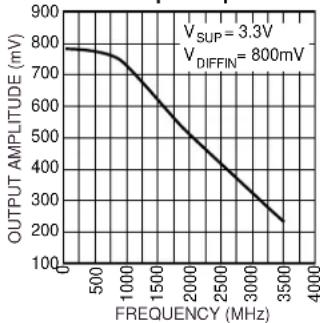
Frequency Response vs. Output Amplitude

line
| FREQUENCY (MHz) | OUTPUT AMPLITUDE (mV) | | --------------- | --------------------- | | 500 | 800 | | 1000 | 750 | | 1500 | 650 | | 2000 | 550 | | 2500 | 450 | | 3000 | 350 | | 3500 | 300 |Frequency Response vs. Output Amplitude @2.5V
Frequency Response vs. Output Amplitude
line
| FREQUENCY (MHz) | OUTPUT AMPLITUDE (mV) | | --------------- | --------------------- | | 500 | 800 | | 1000 | 750 | | 1500 | 650 | | 2000 | 550 | | 2500 | 450 | | 3000 | 350 | | 3500 | 250 | | 4000 | 200 |Frequency Response vs. Output Amplitude @3.3V
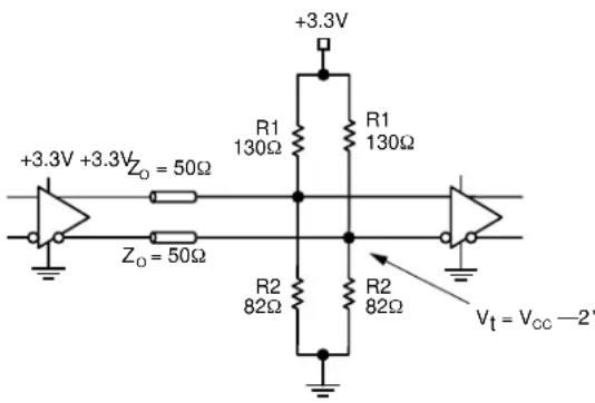
LVPECL TERMINATION RECOMMENDATIONS
Output Considerations
Be sure to properly terminate all outputs as shown below, or equivalent. For AC coupled applications, be sure to include a pull down resistor at the output of each driver. The emmiter follower outputs requires a DC current path to GND. Unused outputs can be left floating with minimal impact on skew and jitter.
text_image
+3.3V +3.3V +3.3VZ₀ = 50Ω R1 130Ω R1 130Ω Z₀ = 50Ω R2 82Ω R2 82Ω Vₜ = Vₒₐ - 2'Figure 1. Parallel Termination–Thevenin Equivalent
Notes:
- For +2.5V systems:
$$ R 1 = 2 5 0 \Omega $$
$$ R 2 = 6 2. 5 \Omega $$

text_image
"source" +3.3V +3.3V = 50Ω Z = 50Ω "destination" 50Ω 50Ω 46Ω to 49Ω RbFigure 2. Three-Resistor "Y-Termination"
Notes:
- Power-saving alternative to Thevenin termination.
- Place termination resistors as close to destination inputs as possible.
- R_b resistor sets the DC bias voltage equal to V_t . For +3.3V systems R_b = 46 to 49 .
- Precision, low-cost 3-Resistor networks are available from resistor manufacturers such as Thin Film Technology (www.thinfilm.com).
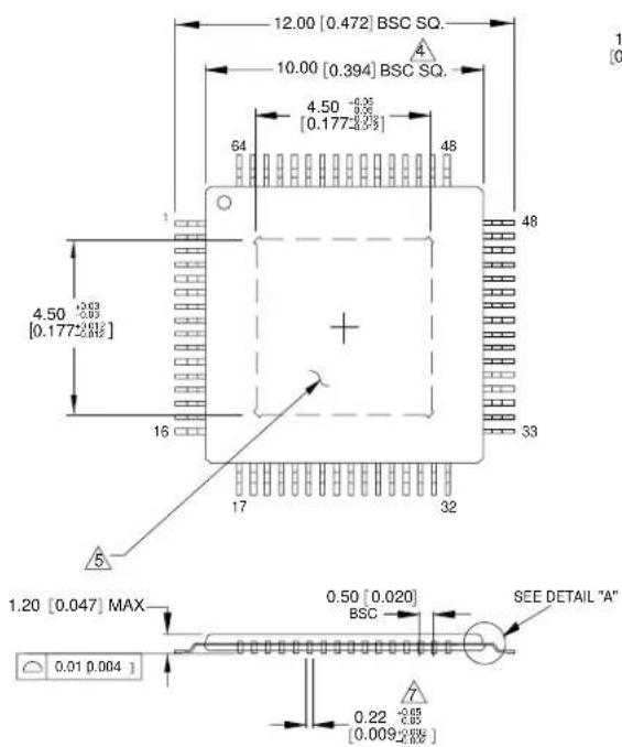
64-PIN EPAD-TQFP (DIE UP) (H64-1)
text_image
12.00 [0.472] BSC SQ. 10.00 [0.394] BSC SQ. 4.50 -0.65 [0.177-0.93] 64 48 48 4.50 -0.65 [0.177-0.93] 16 17 32 33 1.20 [0.047] MAX 0.50 [0.020] BSC SEE DETAIL "A" 0.22 -0.65 [0.009-0.93] 0.01 [0.004]
text_image
1.00 2.82 [0.039 2.82] DETAIL "A" 0° MIN. 6 7 0.20 [0.008] 0.09 [0.004] 6 0.15 [0.006] 0.05 [0.002] 0°-7° 0.60 9.18 [0.024 5.688] 1.00 [0.039] REF.NOTES.
1. DIMENSIONS ARE IN MM[INCHES].
2 CONTROLLING DIMENSION MM
3 EXPOSED PAD: Cu WITH Sn/Pb PLATING.
4 DIMENSION DOES NOT INCLUDE MOLD FLASH OF D.254[0.010] MAX.
5 DIE UP ORIENTATION SHOWN. EXPOSED PAD IS VISIBLE FROM BOTTOM OF PACKAGE.
6. MAXIMUM AND MINIMUM SPECIFICATIONS ARE INDICATED AS FOLLOWS MAX
MIN
7. THIS DIMENSION INCLUDES LEAD FINISH
Rev. 03
MICREL, INC. 2180 FORTUNE DRIVE SAN JOSE, CA 95131 USA
TEL + 1 (408) 944-0800 FAX + 1 (408) 474-1000 WEB http://www.micrel.com
The information furnished by Micrel in this data sheet is believed to be accurate and reliable. However, no responsibility is assumed by Micrel for its use.
Micrel reserves the right to change circuitry and specifications at any time without notification to the customer.
Micrel Products are not designed or authorized for use as components in life support appliances, devices or systems where malfunction of a product can reasonably be expected to result in personal injury. Life support devices or systems are devices or systems that (a) are intended for surgical implant into the body or (b) support or sustain life, and whose failure to perform can be reasonably expected to result in a significant injury to the user. A Purchaser's use or sale of Micrel Products for use in life support appliances, devices or systems is at Purchaser's own risk and Purchaser agrees to fully indemnify
Micrel for any damages resulting from such use or sale.
© 2005 Micrel, Incorporated.