SY89831U - Electronic component Microchip - Free user manual and instructions
Find the device manual for free SY89831U Microchip in PDF.

User questions about SY89831U Microchip
0 question about this device. Answer the ones you know or ask your own.
Ask a new question about this device
Download the instructions for your Electronic component in PDF format for free! Find your manual SY89831U - Microchip and take your electronic device back in hand. On this page are published all the documents necessary for the use of your device. SY89831U by Microchip.
USER MANUAL SY89831U Microchip
The SY89831U is a high-speed, 2GHz differential LVPECL 1:4 fanout buffer optimized for ultra-low skew applications. Within-device skew is guaranteed to be less than 20ps (5ps typ.) over supply voltage and temperature. The differential input buffer has a unique internal termination design that allows access to the termination network through a VT pin. This feature allows the device to easily interface to different logic standards. A VREF-AC reference output is included for AC-coupled applications.
The SY89831U is a part of Micrel's high-speed clock synchronization family. For applications that require a different I/O combination, consult Micrel's website at: www.micrel.com, and choose from a comprehensive product line of high-speed, low-skew fanout buffers, translators, and clock generators.
Datasheets and support documentation are available on Micrel's web site at: www.micrel.com.

Precision Edge®
Features
• Guaranteed AC performance over temperature and voltage
- DC-to 2.5GHz throughput (typical)
- 350ps propagation delay (IN-to-Q) (typical)
- 5ps within-device skew (typical)
- 150ps rise/fall time (typical)
• Ultra-low jitter design
- 62fs RMS phase jitter (typical)
- Unique patent-pending input termination and VT pin accepts DC- and AC-coupled differential inputs
• 800mV, 100K LVPECL typical output swing
• Power supply 2.5V ±5% or 3.3V ±10%
- Industrial temperature range: -40^ to +85^
• Available in 16-pin (3mm x 3mm) MLF® package
Applications
- Processor clock distribution
• SONET clock distribution
• Fibre Channel clock distribution
• Gigabit Ethernet clock distribution
Precision Edge is a registered trademark of Micrel, Inc.
MicroLeadFrame and MLF are registered trademarks of Amkor Technology, Inc.
Micrel Inc. • 2180 Fortune Drive • San Jose, CA 95131 • USA • tel +1 (408) 944-0800 • fax +1 (408) 474-1000 • http://www.micrel.com
Ordering Information ^(1)
| Part Number | Package Type | Operating Range | Package Marking | Lead Finish |
| SY89831UMG ^(2) | MLF-16 | Industrial | 831U with Pb-Free bar-line indicator | NiPdAu Pb-Free |
| SY89831UMGTR ^(2, 3) | MLF-16 | Industrial | 831U with Pb-Free bar-line indicator | NiPdAu Pb-Free |
Notes:
1. Contact factory for die availability. Dice are guaranteed at T A = 25^ , DC electricals only.
2. Pb-Free package is recommended for new designs.
3. Tape and Reel.
Pin Configuration
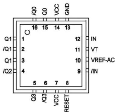
text_image
/Q0 Q0 VCC GND 16 15 14 13 Q1 1 12 /Q1 2 11 VT Q1 3 10 VREF-AC /Q2 4 9 /IN 5 6 7 8 Q3 /Q3 VCC RESET16-MLF (MLF-16)
Pin Description
| Pin # | Pin Name | Functional Description |
| 15, 16 | Q0, /Q0 | Differential 100K LVPECL Outputs: These LVPECL outputs are the precision, low-skew copies of the inputs. Please refer to the “Truth Table” section for details. Unused output pairs may be left open. |
| 1, 2 | Q1, /Q1 | |
| 3, 4 | Q2, /Q2 | Terminate with 50Ω to V_CC - 2V . See the “Output Termination Recommendations” section for more details. |
| 5, 6 | Q3, /Q3 | |
| 8 EN | This single-ended TTL/CMOS-compatible input functions as a synchronous output enable. The synchronous enable ensures that enable/disable only occurs when the outputs are in a logic low state. Note that this input is internally connected to a 25kΩ pull-up resistor and will default to logic high state (enabled) if left open. | |
| 9, 12 | /IN, IN | Differential Inputs: These input pairs are the differential signal inputs to the device. Inputs accept AC- or DC-coupled differential signs as small as 100mV. Each pin of a pair internally terminates to a VT pin through 50Ω. Note that these inputs default to an intermediate state if left open. Please refer to the “Input Interface Applications” section for more details. |
| 10 | VREF-AC | Reference Voltage: These outputs bias to VCC – 1.4V. They are used when AC coupling the inputs (IN, /IN). For AC-coupled applications, connect VREF-AC to the VT pin and bypass with a 0.01μF low-ESR capacitor to V_CC . See the “Input Interface Applications” section for more details. Maximum sink/source current is ±1.5mA. Due to the limited drive capability, each VREF-AC pin should only drive its respective VT pin. If VREF-AC is used with a 2.5V supply, make sure the input swing is large enough to comply with the V_IH min. spec. |
| 11 VT | Input Termination Center-Tap: Each side of the differential input pair terminates to a VT pin. The VT pins provide a center-tap to a termination network for maximum interface flexibility. See the “Input Interface Applications” section for more details. | |
| 13 GND | Ground. GND pins and exposed pad must be connected to the most negative potential of the device ground. | |
| 7, 14 VCC | Positive Power Supply: Bypass with 0.1 F/0.01 F low-ESR capacitors placed as close as possible to each VCC pin. |
Truth Table
| IN /IN | EN Q /Q | |||
| 0 1 1 | 0 1 | |||
| 1 0 1 | 1 0 | |||
| X | X 0 0 | (4) | 1 (4) |
Note:
- On the next negative transition of the input signal (IN).
Absolute Maximum Ratings ^(5)
Supply Voltage ( V_cc )....-0.5V to +4.0V
Input Voltage ( V_IN )....-0.5V to V_CC + 0.5V
LVPECL Output Current ( I_OUT )
Continuous....50mA
Surge 100mA
Input Current
Source or Sink Current on (IN, /IN) ....±50mA
VREF-AC Current
Source or Sink Current on (I _VT )....±2mA
Lead Temperature (soldering, 20s) 260°C
Storage Temperature (Ts)....-65°C to +150°C
Operating Ratings ^(6)
Supply Voltage Range ....+2.375V to +2.625V
+3.0V to +3.6V
Ambient Temperature ( T_A ) -40^ to +85^
Package Thermal Resistance ^(7)
(0 JA) Still Air....60°C/W
(θ JA) Junction to Board....32°C/W
DC Electrical Characteristics ^(8)
T_A = -40^ to +85^ , unless otherwise noted.
| Symbol | Parameter | Condition | Min. | Typ. | Max. | Units |
| V_CC | Power Supply | 2.3753.0 | 2.6253.6 | V | ||
| I_CC | Power Supply Current | No load, max. V_CC | 47 | 70 | mA | |
| R_IN | Input Resistance (IN-to-VT) | 45 | 50 | 55 | Ω | |
| R_DIFF-IN | Differential Input Resistance (IN-to-/IN) | 90 | 100 | 110 | Ω | |
| V_IH | Input HIGH Voltage (IN, /IN) | 1.2 | V_CC | V | ||
| V_IL | Input LOW Voltage (IN, /IN) | 0 | V_IH-0.1 | V | ||
| V_IN | Input Voltage Swing (IN, /IN) | See Figure 1. | 0.1 | 1.7 | V | |
| V_DIFF\_IN | Differential Input Voltage Swing |IN - /IN| | See Figure 2. | 0.2 | V | ||
| V_REF-AC | Output Reference Voltage | V_CC-1.525 | V_CC-1.425 | V_CC-1.325 | V |
LVTTL/LVCMOS Input DC Electrical Characteristics
V_CC = 2.375V to 3.60V; V_EE = 0V; T_A = -40^ to +85^
| Symbol | Parameter | Condition | Min. | Typ. | Max. | Units |
| V_IH | Input HIGH Voltage | 2.0 | V_cc | V | ||
| V_IL | Input LOW Voltage | 0 | 0.8 | V | ||
| I_IH | Input HIGH Current | -125 | 20 | μA | ||
| I_IL | Input LOW Current | -300 | μA |
Notes:
- Permanent device damage may occur if absolute maximum ratings are exceeded. This is a stress rating only and functional operation is not implied at conditions other than those detailed in the operational sections of this datasheet. Exposure to absolute maximum rating conditions for extended periods may affect device reliability.
- The datasheet limits are not guaranteed if the device is operated beyond the operating ratings.
- Package thermal resistance assumes the exposed pad is soldered (or equivalent) to the device's most negative potential on the PCB. _JB and _JA values are determined for a 4-layer board at the still-air package thermal resistance, unless otherwise stated.
- The circuit is designed to meet the DC specifications shown in the above table after thermal equilibrium has been established.
LVPECL Output DC Electrical Characteristics ^(8)
V_CC = 2.5V ± 5% or 3.3V ± 10% ; R_L = 50 to V_CC - 2V ; T_A = -40^ to +85^ , unless otherwise noted.
| Symbol | Parameter | Condition | Min. | Typ. | Max. | Units |
| V_OH Output | HIGH Voltage (Q, /Q) V | _cc - 1.145 | V | _cc - 0.895 V | ||
| V_OL | Output LOW Voltage (Q, /Q) | V_CC - 1.945 | V | _cc - 1.695 | V | |
| V_OUT | Output Voltage Swing (Q, /Q) | See Figure 1. | 550 | 800 | mV | |
| V_DIFF\_OUT | Differential Output Voltage Swing (Q, /Q) | See Figure 2. | 1100 | 1600 | mV |
LVTTL/LVCMOS DC Electrical Characteristics ^(8)
V_CC = 2.5V ± 5% or 3.3V ± 10% ; T_A = -40^ C to +85^ C , unless otherwise noted.
| Symbol | Parameter | Condition | Min. | Typ. | Max. | Units |
| V_IH | Input HIGH Voltage | 2.0 | V_CC | V | ||
| V_IL | Input LOW Voltage | 0 | 0.8 | V | ||
| I_IH | Input HIGH Current | -125 | 30 | μA | ||
| I_IL | Input LOW Current | -300 | μA |
AC Electrical Characteristics ^(9)
V_CC = 2.5V ± 5% or 3.3V ± 10% ; R_L = 50 to V_CC - 2V ; T_A = -40^ to +85^ , unless otherwise noted.
| Symbol | Parameter | Condition | Min. | Typ. | Max. | Units | |
| f_MAX | Maximum Frequency | V_OUT ≥ 450mV | 2.0 | 2.5 | GHz | ||
| t_pd | Propagation Delay | IN-to-Q | V_IN ≥ 100mV | 390 | ps | ||
| IN-to-Q | V_IN ≥ 800mV | 250 | 350 | 450 | ps | ||
| t_SKEW | Within-Device Skew | Note 10 | 5 | 20 | ps | ||
| Part-to-Part Skew | Note 11 | 150 | ps | ||||
| t_S | Set-Up Time | EN to IN, /IN | Note 12 | 300 | ps | ||
| t_H | Hold Time | EN to IN, /IN | Note 12 | 300 | ps | ||
| t_JITTER | RMS Phase Jitter | Output = 622MHzIntegration Range 12kHz–20MHz | 62 | fs | |||
| t_r,t_f | Output Rise/Fall Times(20% to 80%) | At full output swing | 70 | 150 | 225 | ps | |
| Duty Cycle | Freq. < 630MHz | 48 | 50 | 52 | % | ||
Notes:
- High-frequency AC parameters are guaranteed by design and characterization.
- Within-device skew is measured between two different outputs under identical input transitions.
- Part-to-part skew is defined for two parts with identical power supply voltages at the same temperature and no skew at the edges at the respective inputs.
- Set-up and hold times apply to synchronous applications that will enable/disable before the next clock cycle. For asynchronous applications, set-up and hold times do not apply.
Typical Phase Noise

line
| Offset Frequency (MHz) | Phase Noise (dBc/Hz) | | ---------------------- | -------------------- | | 0.01 | -165.0 | | 0.1 | -145.0 | | 1 | -145.0 | | 10 | -145.0 | | 100 | -145.0 |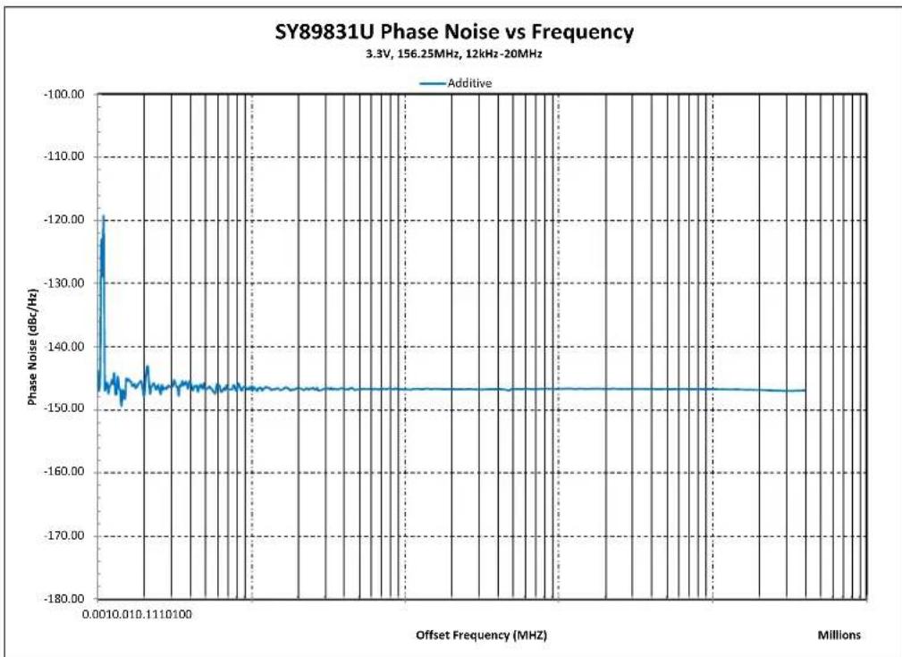
line
| Offset Frequency (MHz) | Phase Noise (dBc/Hz) | | ---------------------- | -------------------- | | 0.0010 | -120.00 | | 0.01 | -145.00 | | 0.1 | -148.00 | | 1 | -147.50 | | 10 | -147.80 | | 100 | -148.00 | | 1000 | -148.20 | | 10000 | -148.30 | | 100000 | -148.40 | | 1000000 | -148.50 | | 10000000 | -148.60 | | 100000000 | -148.70 | | 1000000000 | -148.80 | | 10000000000 | -148.90 | | 100000000000 | -149.00 |Typical Characteristics
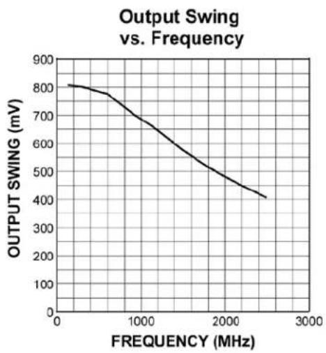
V_CC = 3.3V; GND = 0V; R_L = 50 to V_CC - 2V; T_A = 25^, unless otherwise noted.
line
| FREQUENCY (MHz) | OUTPUT SWING (mV) | | --------------- | ----------------- | | 0 | 800 | | 1000 | 700 | | 2000 | 500 | | 2500 | 400 |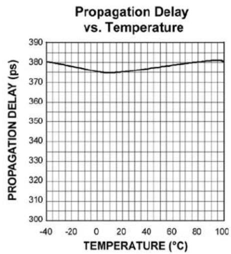
line
| TEMPERATURE (°C) | PROPAGATION DELAY (ps) | | ---------------- | ---------------------- | | -40 | 380 | | -20 | 378 | | 0 | 376 | | 20 | 375 | | 40 | 376 | | 60 | 378 | | 80 | 380 | | 100 | 380 |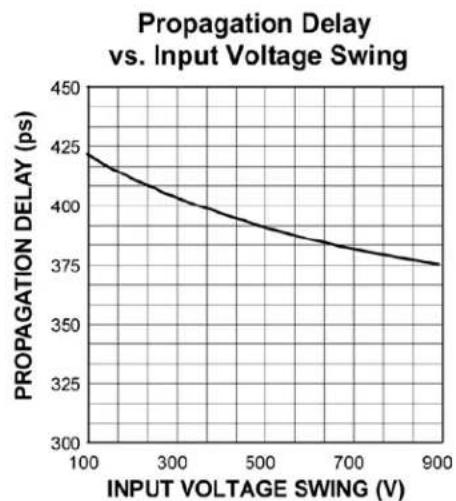
line
| INPUT VOLTAGE SWING (V) | PROPAGATION DELAY (ps) | | ---------------------- | --------------------- | | 100 | 425 | | 300 | 410 | | 500 | 395 | | 700 | 385 | | 900 | 375 |Typical Output Waveforms
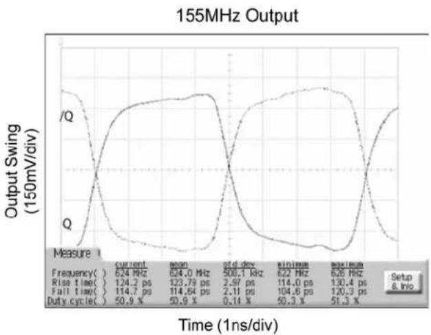
V_CC = 3.3V; GND = 0V; V_IN = 800mV; R_L = 50 to V_CC - 2V; T_A = 25^, unless otherwise noted.
line
| Time (1ns/div) | Output Swing (150mV/div) | | -------------- | ------------------------ | | current | 624.0 Hz | | soon | 624.0 Hz | | std dev | 508.1 Hz | | single | 622.0 Hz | | maximum | 626.0 Hz | | Setup | 624.0 Hz | | S. Info | 624.0 Hz | | Rise time | 124.2 ps | | Fall time | 114.7 ps | | Duty cycle | 50.9 % |
line
| Time (200ps/div) | Output Swing (150mV/div) | | ---------------- | ------------------------ | | current | 6.24 Hz | | rise time | 124.2 ps | | fall time | 114.7 ps | | duty cycle | 50.9 X |
line
| Measure | Frequency (Hz) | Rise time (ps) | Fall time (ps) | Duty cycle (%) | | -------- | -------------- | -------------- | -------------- | -------------- | | current | 1.001 | 113.3 | 104.3 | 49.9 | | mean | 1.001 | 113.21 | 102.85 | 50.0 | | std dev | 1.253 | 1.533 | 1.532 | 0.15 | | step | 997 | 106.8 | 97.2 | 49.5 | | max | 1.006 | 118.0 | 108.1 | 50.5 |
line
| Time (100ps/div) | Current (Hz) | Mean (Hz) | Std Dev (ps) | | ---------------- | ------------ | --------- | ------------ | | 0 | 2.002 | 2.001 | 142.4 | | 1 | 142.4 | 141.82 | 122.8 | | 2 | 122.8 | 122.24 | 50.2 | | 3 | 50.1 | 50.2 | 0.32 | | 4 | 0 | 0 | 49.1 | | 5 | 0 | 0 | 51.6 | | 6 | 0 | 0 | 51.6 | | 7 | 0 | 0 | 51.6 | | 8 | 0 | 0 | 51.6 | | 9 | 0 | 0 | 51.6 | | 10 | 0 | 0 | 51.6 | | 11 | 0 | 0 | 51.6 | | 12 | 0 | 0 | 51.6 | | 13 | 0 | 0 | 51.6 | | 14 | 0 | 0 | 51.6 | | 15 | 0 | 0 | 51.6 | | 16 | 0 | 0 | 51.6 | | 17 | 0 | 0 | 51.6 | | 18 | 0 | 0 | 51.6 | | 19 | 0 | 0 | 51.6 | | 20 | 0 | 0 | 51.6 | | 21 | 0 | 0 | 51.6 | | 22 | 0 | 0 | 51.6 | | 23 | 0 | 0 | 51.6 | | 24 | 0 | 0 | 51.6 | | 25 | 0 | 0 | 51.6 | | 26 | 0 | 0 | 51.6 | | 27 | 0 | 0 | 51.6 | | 28 | 0 | 0 | 51.6 | | 29 | 0 | 0 | 51.6 | | 30 | 0 | 0 | 51.6 | | Note: The actual output values are not provided in the code image. The code does not provide the original output data for this example. The output values are estimated based on the given code format and may vary slightly due to the random nature of the data generation. The output values are estimated based on the specified code format and may differ from the original data generated by the code generator. The output values are estimated based on the specified code format and may differ from the original data generated by the code generator. The output values are estimated based on the specified code format and may differ from the original data generated by the code generator. The output values are estimated based on the specified code format and may differ from the original data generated by the code generator. The output values are estimated based on the specified code format and may differ from the original data generated by the code generator.Functional Block Diagram
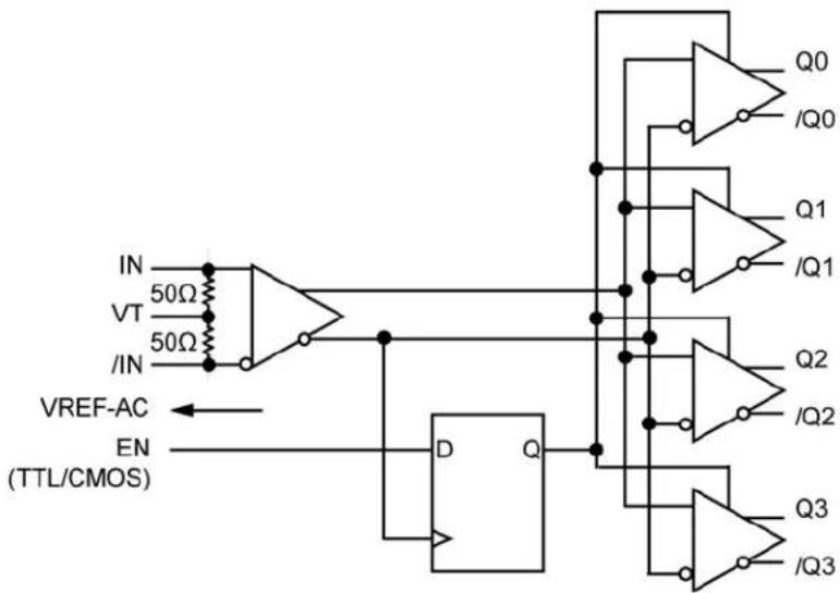
text_image
IN 50Ω VT 50Ω /IN VREF-AC EN (TTL/CMOS) D Q Q0 /Q0 Q1 /Q1 Q2 /Q2 Q3 /Q3Single-Ended and Differential Swings

text_image
V_{IN}, V_{OUT} 800mV_p (TYPICAL)Figure 1. Single-Ended Swing

text_image
VDIFF_IN' VDIFF_OUT 1.6V PP (TYPICAL)Figure 2. Differential Swing
Input and Output Stages

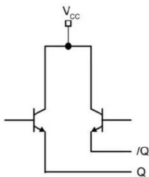
text_image
Vcc IN 50Ω VT 50Ω /IN SY89831UFigure 3. Simplified Differential
text_image
Vcc /Q QFigure 4. Simplified LVPECL Output Stage
Input Interface Applications
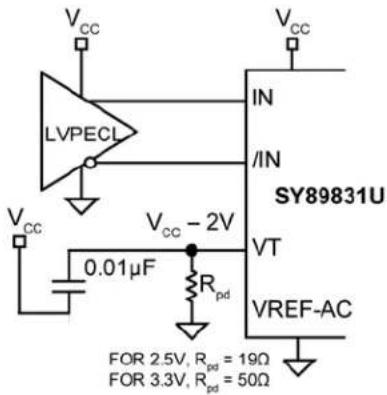
text_image
VCC LVPECL IN /IN SY89831U VCC - 2V VT VREF-AC 0.01μF Rpd FOR 2.5V, Rpd = 19Ω FOR 3.3V, Rpd = 50ΩFigure 5. DC-Coupled LVPECL Input Interface
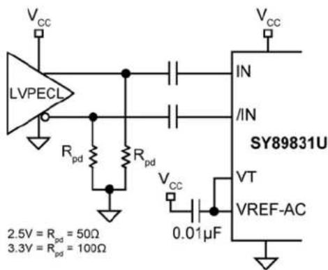
text_image
Vcc LVPECL Rpd Rpd IN /IN SY89831U VT VREF-AC 0.01μF 2.5V = Rpd = 50Ω 3.3V = Rp = 100ΩFigure 6. AC-Coupled LVPECL Input Interface
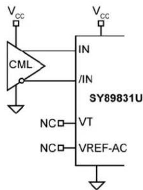
text_image
Vcc CML IN /IN SY89831U NC□ VT NC□ VREF-AC VccFigure 7. DC-Coupled CML Input Interface
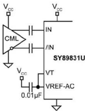
text_image
Vcc CML IN /IN SY89831U Vcc VT 0.01μF VREF-ACFigure 8. AC-Coupled CML Input Interface
text_image
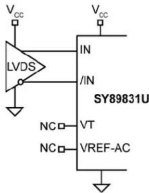
Vcc LVDS IN /IN SY89831U NC□—VT NC□—VREF-AC VccFigure 9. DC-Coupled LVDS Input Interface
text_image
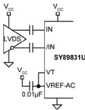
Vcc LVDS IN /IN SY89831U Vcc VT VREF-AC 0.01μFFigure 10. AC-Coupled LVDS Input Interface
Output Termination Recommendations
text_image
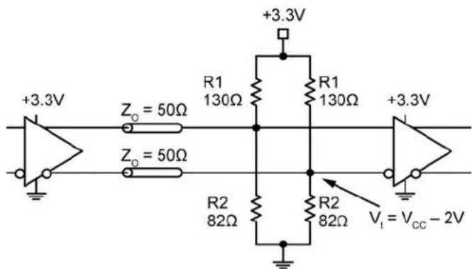
+3.3V Z₀ = 50Ω Z₀ = 50Ω R1 130Ω +3.3V R1 130Ω +3.3V R2 82Ω R2 82Ω V₁ = Vₐₐ - 2VFigure 11. Parallel Termination – Thevenin Equivalent
Note:
- For +2.5V Systems: R1 = 250Ω, R2 = 62.5Ω.

text_image
+3.3V Z = 50Ω Z = 50Ω "SOURCE" 50Ω 50Ω 50Ω Rb C1 0.01μF (OPTIONAL) +3.3V "DESTINATION" VccFigure 12. Three-Resistor "Y-Termination"
Notes:
- Power-saving alternative to Thevenin termination.
- Place termination resistors as close to destination inputs as possible.
- The R_b resistor sets the DC bias voltage equal to V_1 . For +2.5V systems, R_0 = 19 .
- C1 is an optional bypass capacitor that compensates for any t_t / t_1 mismatches.
Related Product and Support Documentation
| Part Number | Function | Data Sheet Link |
| SY89830U | 1:4 LVPECL Fanout Buffer w/2:1 MUX Input | http://www.micrel.com/index.php/en/products/clock-timing/clock-data-distribution/fanout-buffers/article/51-sy89830u.html |
| SY89832U | 2.5V Ultra-Precision 1:4 LVDS Fanout Buffer/ Translator with Internal Termination | http://www.micrel.com/index.php/en/products/clock-timing/clock-data-distribution/fanout-buffers/article/38-sy89832u.html |
| SY89833AL | 3.3V Ultra-Precision 1:4 LVDS Fanout Buffer/Translator with Internal Termination | http://www.micrel.com/index.php/en/products/clock-timing/clock-data-distribution/fanout-buffers/article/39-sy89833al.html |
| SY89834U | 2.5/3.3V Two Input, 1GHz LVTTL/CMOS-to-LVPECL 1:4 Fanout Buffer/Translator | http://www.micrel.com/index.php/en/products/clock-timing/clock-data-distribution/fanout-buffers/article/50-sy89834u.html |
| 16-MLF® Manufacturing Guidelines Exposed Pad Application Note | www.amkor.com/products/notes_papers/MLF_AppNote_0301.pdf |
Package Information ^(18)
text_image
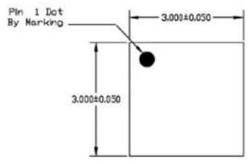
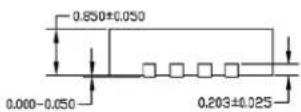
Pin 1 Dot By Marking 3.000±0.050 3.000±0.050TOP VIEW

text_image
PIN #1 IDENTIFICATION CHAMFER 0.300 X 45° 1.550±0.050 Exp. DAP 0.400±0.050 1.550±0.050 Exp. DAP 0.500 Bsc 0.230±0.050 0.400±0.050 1.500 Ref.BOTTOM VIEW
SIDE VIEW
NOTE
1. ALL DIMENSIONS ARE IN MILLIMETERS.
2. MAX. PACKAGE WARPAGE IS 0.05 mm.
3. MAXIMUM ALLOWABLE BURRS IS 0.076 mm IN ALL DIRECTIONS
4. PIN #1 ID ON TOP WILL BE LASER/INK MARKED.
text_image
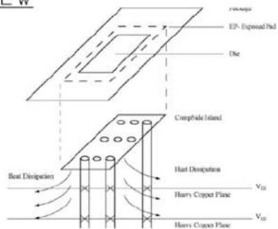
FRAME EP- Exposed Pad Die Compside Island Heat Dissipation Beat Dissipation Heavy Copper Plane Heavy Copper Plane VDD VDDPCB Thermal Consideration for 16-Pin MLF Package (Always solder, or equivalent, the exposed pad to the PCB)
16-Pin EPAD MicroLeadFrame ^® (MLF-16)
Notes:
- Package information is correct as of the publication date. For updates and most current information, go to www.micrel.com.
- Package meets Level 2 moisture sensitivity classification, and is shipped in dry-pack.
- Exposed pads must be soldered to a ground for proper thermal management.
MICREL, INC. 2180 FORTUNE DRIVE SAN JOSE, CA 95131 USA
TEL +1 (408) 944-0800 FAX +1 (408) 474-1000 WEB http://www.micrel.com
Micrel makes no representations or warranties with respect to the accuracy or completeness of the information furnished in this data sheet. This information is not intended as a warranty and Micrel does not assume responsibility for its use. Micrel reserves the right to change circuitry, specifications and descriptions at any time without notice. No license, whether express, implied, arising by estoppel or otherwise, to any intellectual property rights is granted by this document. Except as provided in Micrel's terms and conditions of sale for such products, Micrel assumes no liability whatsoever, and Micrel disclaims any express or implied warranty relating to the sale and/or use of Micrel products including liability or warranties relating to fitness for a particular purpose, merchantability, or infringement of any patent, copyright or other intellectual property right.
Micrel Products are not designed or authorized for use as components in life support appliances, devices or systems where malfunction of a product can reasonably be expected to result in personal injury. Life support devices or systems are devices or systems that (a) are intended for surgical implant into the body or (b) support or sustain life, and whose failure to perform can be reasonably expected to result in a significant injury to the user. A Purchaser's use or sale of Micrel Products for use in life support appliances, devices or systems is a Purchaser's own risk and Purchaser agrees to fully indemnify Micrel for any damages resulting from such use or sale.
© 2014 Micrel, Incorporated.