SY89826L - Electronic component Microchip - Free user manual and instructions
Find the device manual for free SY89826L Microchip in PDF.

User questions about SY89826L Microchip
0 question about this device. Answer the ones you know or ask your own.
Ask a new question about this device
Download the instructions for your Electronic component in PDF format for free! Find your manual SY89826L - Microchip and take your electronic device back in hand. On this page are published all the documents necessary for the use of your device. SY89826L by Microchip.
USER MANUAL SY89826L Microchip
• < 1ps (rms) cycle-to-cycle jitter
• < 1ps (pk-pk) total jitter
■ 2:1 mux input accepts LVDS and LVPECL
■3.3V supply voltage
■ LVDS input includes internal 100Ω termination
■ Output enable function
■ Available in a 64-Pin EPAD-TQFP
APPLICATIONS
■ Enterprise networking
■ High-end servers
■ Communications

Precision Edge®
DESCRIPTION
The SY89826L is a precision fanout buffer with 22 differential LVDS (Low Voltage Differential Swing) output pairs. The part is designed for use in low voltage 3.3V applications that require a large number of outputs to drive precisely aligned, ultra low-skew signals to their destination. The input is multiplexed from either LVDS or LVPECL (Low Voltage Positive Emitter Coupled Logic) by the CLK_SEL pin. The OE (Output Enable) is synchronous so that the outputs will only be enabled/disabled when they are already in the LOW state. This avoids any chance of generating a runt clock pulse when the device is enabled/disabled as can happen with an asynchronous control.
The SY89826L features a low pin-to-pin skew of less than 50ps—performance previously unachievable in a standard product having such a high number of outputs. The SY89826L is available in a single space saving package, enabling a lower overall cost solution.
FUNCTIONAL BLOCK DIAGRAM

flowchart
graph TD
    A["100Ω internal input termination"] --> B["LVDS_CLK"]
    A --> C["/LVDS_CLK"]
    D["LVPECL_CLK"] --> E["AND Gate"]
    F["/LVPECL_CLK"] --> G["AND Gate"]
    H["CLK_SEL"] --> I["0"]
    I --> J["1"]
    J --> K["22 LVDS compatible outputs"]
    L["LEN Q"] --> M["D"]
    N["OE"] --> O["D"]
    P["Q0 - Q21"] --> Q["22"]
    R["/Q0 - /Q21"] --> S["22"]
TRUTH TABLE
| OE(1) | CLK_SEL Q0 - Q21 /Q0 - /Q2 | |
| 0 0 LOW HIGH | ||
| 0 1 LOW HIGH | ||
| 1 0 LVDS_CLK /LVDS_CLK | ||
| 1 1 | LVPECL_CLK /LVPECL_CLK |
NOTE:
- The OE (output enable) signal is synchronized with the low level of the LVDS_CLK and LVPECL_CLK signal.
Precision Edge is a registered trademark of Micrel, Inc.
PACKAGE/ORDERING INFORMATION
text_image
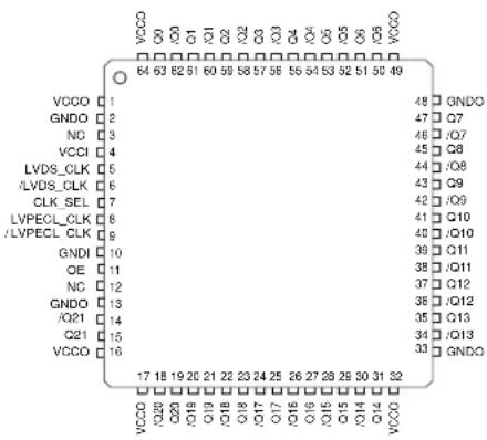
VCCO Q0 Q1 Q2 Q3 Q4 Q5 Q6 Q7 VCCO 1 GND0 2 NC 3 VCCI 4 LVDS_CLK 5 /LVDS_CLK 6 CLK_SEL 7 LVPECL_CLK 8 /LVPECL_CLK 9 GNDI 10 OE 11 NC 12 GND0 13 /Q21 14 Q21 15 VCCO 16 64 63 62 61 60 59 58 57 56 55 54 53 52 51 50 49 48 GNDO 47 Q7 46 /Q7 45 Q8 44 /Q8 43 Q9 42 /Q9 41 Q10 40 /Q10 39 Q11 38 /Q11 37 Q12 36 /Q12 35 Q13 34 /Q13 33 GNDO 17 18 19 20 21 22 23 24 25 26 27 28 29 30 31 S264-Pin TQFP (H64-1)
Ordering Information ^(1)
| Part Number | Package Type | Operating Range Marking | Package Finish | Lead |
| SY89826LHI | H64-1 | Industrial | SY89826LHI | Sn-Pb |
| SY89826LHITR(2) | H64-1 | Industrial | SY89826LHI | Sn-Pb |
| SY89826LHY(3) | H64-1 | Industrial | SY89826LHY with Pb-Free bar-line indicator | Pb-Free Matte-Sn |
| SY89826LHYTR(2, 3) | H64-1 | Industrial | SY89826LHY with Pb-Free bar-line indicator | Pb-Free Matte-Sn |
Notes:
- Contact factory for die availability. Dice are guaranteed at T_A=25^ , DC electricals only.
- Tape and Reel.
- Pb-Free package recommended for new designs.
PIN DESCRIPTIONS
| Pin Number Pin N | Name I/O Type | Internal Pull-up/Pull-down | Pin Function | ||
| 5, 6 | LVDS_CLK/LVDS_CLK | Input | LVDS w/100Ω internal (Figure 2) in terminator | 3.3kΩ pull-up directly to LVDS. | Differential LVDS clock input. Selected when CLKSEL = LOW (Can be left floating if CLKSEL = HIGH). This input pair includes internal termination, and is intended to interface LVDS. Leave floating if not used. |
| 8, 9 | LVPECL_CLK/LVPECL_CLK | Input | LVPECL | 75kΩ pull-down (Figure 1) | Differential LVPECL clock input. Selected when CLKSEL = HIGH (Can be left floating if CLKSEL = LOW). Requires external termination. Leave floating if not used. |
| 7 | CLK_SEL | Input | LVTTL/CMOS | 11kΩ to VCCI | Selects LVDS_CLK when LOW and LVPECL_CLK when HIGH. Default condition is HIGH if left floating. |
| 11 | OE | Input | LVTTL/ | Output enable/disable function. When LOW, Q outputs go LOW, /Q outputs go HIGH. Asynchronous input that is synchronized internally to prevent output glitches or runt pulses. | |
| 63, 61, 59, 57, 55, 53, 51, 47, 45, 43, 41, 39, 37, 35, 31, 29, 27, 25, 23, 21, 19, 15 | Q0 - Q21 | Output | LVDS | Differential LVDS clock outputs when OE = HIGH and static LOW when OE = LOW. Unused output pairs must be terminated with 100Ω across the differential pair to maintain low skew and jitter. | |
| 62, 60, 58, 56, 54, 52, 50, 46, 44, 42, 40, 38, 36, 34, 30, 28, 26, 24, 22, 20, 18, 14 | /Q0 - /Q21 | Output | LVDS | Differential clock outputs (complement) when OE = HIGH and static HIGH when OE = LOW. Unused output pairs must be terminated with 100Ω across the differential pair to maintain low skew and jitter. | |
| 4 | VCCI | Power | Core VCC connect to 3.3V supply. Not connected to VCCO internally. Connect to VCCO on PCB. Bypass with 0.1×F in parallel with 0.01×F low ESR capacitors as close to VCC pins as possible. | ||
| 1, 16, 17, 32, 49, 64 | VCCO | Power | Output buffer VCC connects to 3.3V supply. Not connected to VCCI internally. Connect to VCCI on PCB. Bypass with 0.1×F in parallel with 0.01×F low ESR capacitors as close to VCC pins as possible. | ||
| 10 | GNDI | Power | Core ground not connected to GNDO internally. Connect to GNDO on PCB. | ||
| 2, 13, 33, 48 | GNDO | Power | Output buffer ground not connected to GNDI internally. Connect to GNDI on PCB. | ||
| 3, 12 | NC | No connect pins to be left open. |
Absolute Maximum Ratings ^(Note 1)
Power Supply Voltage ( V_CCI , V_CCO ) .....-0.5 to +4.0V
Input Voltage ( V_IN ) ....-0.5 to V_CCI
Output Current (IOUT) ....±10mA
Lead Temperature ( T_LEAD , Soldering, 20sec.)..... 260°C
Storage Temperature (T_S) ...... -65 to +150^
ESD Rating, Note 3 ....>1kV
Operating Ratings ^(Note 2)
Supply Voltage (V _CC to GND) ....+3.0V to +3.6V
Ambient Temperature ( T_A ) -40^ to +85^
Package Thermal Resistance
TQFP ( _JA )
Exposed pad soldered to GND
Still-Air(multi-layer PCB)....23°C/W
-200lfpm (multi-layer PCB) 18°C/W
-500lfpm (multi-layer PCB) 15°C/W
Exposed pad NOT soldered to GND (not recommended)
Still-Air(multi-layer PCB)....44°C/W
-200lfpm (multi-layer PCB) 36°C/W
-500lfpm (multi-layer PCB) 30°C/W
TQFP ( _JC ) 4.4°C/W
Note 1. Permanent device damage may occur if ABSOLUTE MAXIMUM RATINGS are exceeded. This is a stress rating only and functional operation is not implied at conditions other than those detailed in the operational sections of this data sheet. Exposure to ABSOLUTE MAXIMUM RATING conditions for extended periods may affect device reliability.
Note 2. The data sheet limits are not guaranteed if the device is operated beyond the operating ratings.
Note 3. Devices are ESD sensitive. Handling precautions recommended.
DC ELECTRICAL CHARACTERISTICS
Power Supply: T_A = -40^ to +85^
| Symbol Parameter Condition Min Typ Max Units | ||||||
| V_CCl , V_CCO | V_CC Core, V_CC Output Note 4 3.0 3.3 | 3.6 V | ||||
| I_CCI | I_CC Core | Max. V_CC | 46 | 70 | mA | |
| I_CCO | I_CC Output | No Load, Max. V_CC | 175 | 260 | mA | |
Note 4. V_CCI and V_CCO must be connected together on the PCB such that they remain at the same potential. V_CCI and V_CCO are not internally connected on the die.
LVDS Input: V_CC = 3.3V ± 10% , T_A = -40^ to +85^
| Symbol Parameter Condition Min Typ Max Units | ||||||
| V_IN | Input Voltage Range | 0 | 2.4 V | |||
| V_ID | Differential Input Swing | 100 | mV | |||
| I_IL | Input LOW Current | -1.25 | mA | |||
| R_IN | LVDS Differential Input Resistance(LVDS_CLK to /LVDS_CLK) | 80 | 100 | 120 | Ω | |
DC ELECTRICAL CHARACTERISTICS
LVPECL Input: V_CC = 3.3V ± 10% , T_A = -40^ C to +85^ C
| Symbol Parameter Condition Min Typ Max Units | ||||||
| V_IH | Input HIGH Voltage (Single-Ended) V | CC-1.165 V | CC-0.880 V | |||
| V_IL | Input LOW Voltage V | CC-1.945 V | CC-1.625 V | |||
| V_PP | Minimum Input Swing (LVPECL_CLK) Note 6 300 mV | |||||
| V_CMR | Common Mode Range (LVPECL_CLK) | Note 7 | GNDI +1.8 | V_CCI-0.4 | V | |
| I_IH | Input HIGH Current | 150 | A | |||
| I_IL | Input LOW Current | 0.5 | A | |||
Note 6. The V_PP (min.) is defined as the minimum input differential voltage which will cause no increase in the propagation delay.
Note 7. V_CMR is defined as the range within which the V_IH level may vary, with the device still meeting the propagation delay specification. The numbers in the table are referenced to V_CCI . The V_IL level must be such that the peak-to-peak voltage is less than 1.0V and greater than or equal to V_PP (min.). V_CMR range varies 1:1 with V_CCI . V_CMR (min) is fixed at GNDI +1.8V.
CMOS/LVTTL Inputs: V_CC = 3.3V ± 10% , T_A = -40^ to +85^
| Symbol Parameter Condition Min Typ Max Units | ||||||
| V_IH | Input HIGH Voltage | 2.0 | V | |||
| V_IL | Input LOW Voltage | 0.8 | V | |||
| I_IH | Input HIGH Current | V_IN = V_CC | 150 | A | ||
| I_IL | Input LOW Current | V_IN = 0.5V | -600 | A | ||
LVDS Output: V_CC = 3.3V ± 10% , T_A = -40^ to +85^
| Symbol Parameter Condition Min Typ Max Units | ||||||
| V_OD | Differential Output Voltage | Note 8, 9 | 250 | 350 | 400 | mV |
| V_OH | Output HIGH Voltage | Note 8 | 1.474 | V | ||
| V_OL | Output LOW Voltage | Note 8 | 0.925 | V | ||
| V_OCM | Output Common Mode Voltage | Note 9 | 1.125 | 1.375 | V | |
| V_OCM | Change in Common Mode Voltage | -50 | 50 | mV | ||
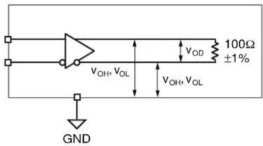
Note 8. Measured as per Figure 3, 100Ω across Q and /Q outputs.
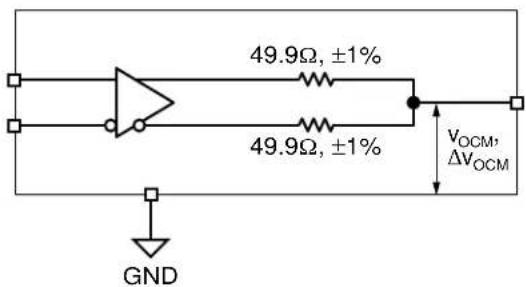
Note 9. Measured as per Figure 4.
AC ELECTRICAL CHARACTERISTICS ^(1)
V_CC = 3.3V ± 10% , T_A = -40^ C to +85^ C , unless noted.
| Symbol Parameter Condition Min Typ Max Units | ||||||
| f_MAX | Maximum Toggle Frequency Note 2 | 1.0 GHz | ||||
| t_PHL | Differential Propagation Delay, LVPECL Input: 150mV 0.750 1.0 1.250 ns | |||||
| t_PLH | Note 3 LVPECL Input: 800mV 0.6 0.850 1.10 ns | |||||
| LVDS Input: 100mVLVDS Input: 400mV | 0.950 1.2 1.450 ns0.800 1.0 1.30 ns | |||||
| t_SWITCHOVER | Clock Input Switchover | CLK_SEL-to-Valid Output | 1.4 | 1.7 | ns | |
| t_S(OE) | Output Enable Set-Up Time | Note 4 | 1.0 | ns | ||
| t_H(OE) | Output Enable Hold Time | Note 4 | 0.5 | ns | ||
| t_skew | Within Device Skew | Note 5 | 0°C to +85°C-40°C | 25 | ps75 | |
| Part-to-Part Skew | Note 6 | 400 | ps | |||
| t_JITTER | Cycle-to-CycleTotal Jitter | Note 7Note 8 | <1 | 12 | ps_RMSps_PP | |
| t_r,t_f | Output Rise/Fall Times(20% to 80%) | 200 | 290 | 400 | ps | |
Note 1. 100Ω termination between Q and /Q outputs. Airflow ≥300lfpm, or exposed pad soldered to ground plane. Typical are at nominal supply, T_A = 25^ C .
Note 2. f_MAX is defined as the maximum toggle frequency, measured with a 750mV LVPECL input or 350mV LVDS input. Output swing is ≥ 200mV.
Note 3. Differential propagation delay is defined as the delay from the crossing point of the differential input signals to the crossing point of the differential output signals.
Note 4. Set-up and hold time applies to synchronous applications that intend to enable/disable before the next clock cycle. For asynchronous applications, set-up and hold time does not apply. OE set-up time is defined with respect to the rising edge of the clock. OE HIGH to LOW transition ensures outputs remain disabled during the next clock cycle. OE LOW to HIGH transition enables normal operation of the next input clock.
Note 5. The within-device skew is defined as the worst case difference between any two similar delay paths within a single device with identical input transition, operating at the same voltage and temperature.
Note 6. The part-to-part skew is defined as the absolute worst case difference between any two delay paths on any two devices operating at the same voltage and temperature. Part-to-part skew is the total skew difference; pin-to-pin skew + part-to-part skew.
Note 7. Cycle-to-cycle jitter definition: The variation in period between adjacent cycles over a random sample of adjacent cycle pairs. T_JITTER_CC = T_n - T_n+1 where T is the time between rising edges of the output signal.
Note 8. Total jitter definition: with an ideal clock input, no more than one output edge in 10^12 output edges will deviate by more than the specified peak-to-peak jitter value.
TYPICAL OPERATING CHARACTERISTICS
V_CC = 3.3V, V_EE = GND, T_A = 25^ , unless otherwise stated

line
| FREQUENCY (MHz) | OUTPUT VOLTAGE (mV) | | --------------- | ------------------- | | 0 | 350 | | 400 | 340 | | 800 | 330 | | 1200 | 270 |
line
| TEMPERATURE (°C) | LVDS Input (ps) | LVPECL Input (ps) | | ---------------- | --------------- | ----------------- | | -50 | ~800 | ~800 | | 0 | ~850 | ~850 | | 25 | ~900 | ~900 | | 50 | ~950 | ~950 | | 75 | ~1000 | ~1000 | | 100 | ~1050 | ~1050 |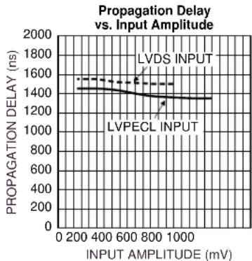
line
| INPUT AMPLITUDE (mV) | PROPOGATION DELAY (ns) | | ------------------- | ---------------------- | | 0 | 1500 | | 200 | 1450 | | 400 | 1400 | | 600 | 1350 | | 800 | 1300 | | 1000 | 1250 |
line
| TEMPERATURE (°C) | SWITCHOVER TIME (ns) | | ---------------- | --------------------- | | -50 | 1300 | | 0 | 1320 | | 25 | 1340 | | 50 | 1360 | | 75 | 1380 | | 100 | 1400 |FUNCTIONAL CHARACTERISTICS

line
| TIME (500ps/div.) | Output Swing (50mV/div.) | | ----------------- | ------------------------ | | 0 | Q | | Peak | /Q | | 500 | /Q | | 1000 | /Q | | 1500 | /Q | | 2000 | /Q | | 2500 | /Q | | 3000 | /Q | | 3500 | /Q | | 4000 | /Q | | 4500 | /Q | | 5000 | /Q |
line
| TIME (200ps/div.) | Output Swing (50mV/div.) | | ----------------- | ------------------------ | | 0 | 0 | | 200 | +1.5 | | 400 | -1.5 | | 600 | 0 | | 800 | +1.5 | | 1000 | -1.5 | | 1200 | 0 | | 1400 | +1.5 | | 1600 | -1.5 | | 1800 | 0 | | 2000 | +1.5 |
line
| TIME (100ps/div.) | Output Swing (50mV/div.) | | ----------------- | ------------------------ | | 0 | Q | | 1 | /Q | | 2 | Q | | 3 | /Q | | 4 | Q | | 5 | /Q | | 6 | Q | | 7 | /Q | | 8 | Q | | 9 | /Q | | 10 | Q | | 11 | /Q | | 12 | Q | | 13 | /Q | | 14 | Q | | 15 | /Q | | 16 | Q | | 17 | /Q | | 18 | Q | | 19 | /Q | | 20 | Q | | 21 | /Q | | 22 | Q | | 23 | Q | | 24 | /Q | | 25 | Q | | 26 | /Q | | 27 | Q | | 28 | Q | | 29 | Q | | 30 | Q | | 31 | Q | | 32 | Q | | 33 | Q | | 34 | Q | | 35 | Q | | 36 | Q | | 37 | Q | | 38 | Q | | 39 | Q | | 40 | Q | | 41 | Q | | 42 | Q | | 43 | Q | | 44 | Q | | 45 | Q | | 46 | Q | | 47 | Q | | 48 | Q | | 49 | Q | | 50 | Q | | 51 | Q | | 52 | Q | | 53 | Q | | 54 | Q | | 55 | Q | | 56 | Q | | 57 | Q | | 58 | Q | | 59 | Q | | 60 | Q | | 61 | Q | | 62 | Q | | 63 | Q | | 64 | Q | | 65 | Q | | 66 | Q | | 67 | Q | | 68 | Q | | 69 | Q | | 70 | Q | | 71 | Q | | 72 | Q | | 73 | Q | | 74 | Q | | 75 | Q | | 76 | Q | | 77 | Q | | 78 | Q | | 79 | Q | | 80 | Q | | 81 | Q | | 82 | Q | | 83 | Q | | 84 | Q | | 85 | Q | | 86 | Q | | 87 | Q | | 88 | Q | | 89 | Q | | 90 | Q | | 91 | Q | | 92 | Q | | 93 | Q | | 94 | Q | | 95 | Q | | 96 | Q | | 97 | Q | | 98 | Q | | 99 | Q | | 100 | Q |LVPECL/LVDS INPUTS
text_image
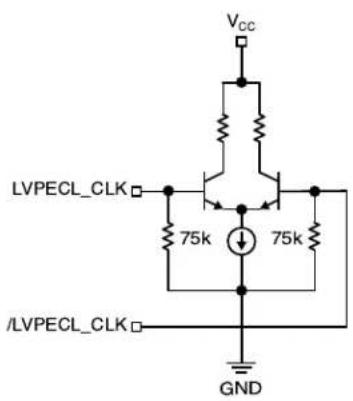
Vcc LVPECL_CLK 75k 75k /LVPECL_CLK GNDFigure 1. Simplified LLVMPECLInputStage
text_image
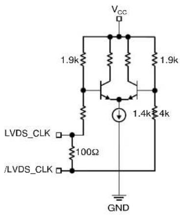
Vcc 1.9k 1.9k LVDS_CLK 100Ω /LVDS_CLK 1.4k 4k GNDFigure 2. Simplified LVDS Input Stage
LVDS OUTPUTS
LVDS specifies a small swing of 350mV typical, on a nominal 1.25V common mode above ground. The common mode voltage has tight limits to permit large variations in ground between an LVDS driver and receiver. Also, change in common mode voltage, as a function of data input, is also kept tight, to keep EMI low.
text_image
100Ω ±1% V_OH, V_OL V_OD V_OH, V_OL GNDFigure 3. LVDS Differential Measurement
text_image
49.9Ω, ±1% 49.9Ω, ±1% VOCM, ΔVOCM GNDFigure 4. LVDS Common Mode Measurement

text_image
QOUT /QOUT 350mV (typical)Figure 5. Output Driver Signal Levels (Single-Ended)
line
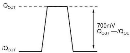
| Voltage Level | Current (V) | | ------------- | ----------- | | Peak | 700 |Figure 6. Output Driver Signal Levels (Differential)
DETAILED DESCRIPTION
The SY89826L is a precision 1:22 fanout buffer. It accepts either an LVPECL or LVDS input, selectable by an input mux, and outputs 22 LVDS output pairs. The device features a synchronous output enable. The SY89826L provides extremely low skew across its outputs.
LVPECL\_CLK
The SY89826L allows one input with standard LVPECL voltage swing. This input may be adjusted per the data sheet characteristics regarding the CMR and minimum input swing. As the SY89826L contains no appropriate internal termination, upstream devices need to be properly terminated to provide the proper LVPECL input swing. If not being used (CLK_SEL is LOW), this input pair may be left floating, as it is internally terminated to ground via a 75kΩ pull-down resistor.
LVDS\_CLK
The SY89826L allows one input with standard LVDS voltage swing. The SY89826L provides an appropriate internal 100Ω termination resistor. Hence, upstream LVDS devices do not require external termination to drive the SY89826L. If not being used (CLK_SEL is HIGH), this input pair may be left floating.
CLK\_SEL Input
The CLK_SEL TTL Input is used to select either LVDS_CLK (CLK_SEL is LOW) or LVPECL_CLK (CLK_SEL is LOW).
OE
The SY89826L's output enable function is designed to disable the outputs only when the outputs are LOW. This avoids the possibility of generating runt pulses. The OE input is an asynchronous input, but operates as a synchronous enable. For synchronous operation, please adhere to the specific setup and hold times. When disabled, the Q outputs are LOW and the /Q outputs are HIGH.
LVDS Outputs
The SY89826L's LVDS outputs swing typically 350mV around a 1.25V common mode voltage above ground. The common mode voltage has tight limits to permit large variations in ground between an LVDS driver and receiver. Also, change in common mode voltage, as a function of data input is kept tight to keep EMI low.
Each of the SY89826L's LVDS outputs should be terminated with a 100Ω termination resistor including any unused output pairs. This ensures the best jitter and skew performance of the device.
RELATED PRODUCT AND SUPPORT DOCUMENTATION
| Part Number Function Data Sheet Link | ||
| SY55855V Dual | CML/PECL/LVPECL-to-LVDS www.micrel.com/product-info/products/sy55855v.shtmlTranslator | |
| SY89825U 2.5/3 | .3V 1:22 High-performance, www.micrel.com/product-info/products/sy89825u.shtmlLow-voltage PECL Bus Clock Driver& Translator w/ Internal Termination | |
| SY89828L 3.3V | 1GHz Dual 1:10 Precision www.micrel.com/product-info/products/sy89828l.shtmlLVDS Fanout Buffer with 2:1 Input Mux | |
| SY89829U 2.5/3 | .3V High-performance, Dual 1:10 www.micrel.com/product-info/products/sy89829u.shtmlLVPECL Clock Driver w/ Internal Termination &Redundant Switchover | |
| M-0317 HBW Solutions www.micrel.com/product-info/as/solutions.shtml | ||
| Exposed Pad Amkor Exposed Pad Application Note www.amkor.com/products/notes_papers/epad.pdf | ||
64-PIN EPAD-TQFP (DIE UP) (H64-1)

text_image
12.00 [0.472] BSC SQ. 10.00 [0.394] BSC SQ. 5.00 1/8 [0.197 1/8] 64 49 1 48 5.00 2/8 [0.197 2/8] 16 17 32 33 1.20 [0.047] MAX 0.50 [0.020] BSC SEE DETAIL "A" 0.01 [0.004] 0.22 2/8 [0.009 2/8]
text_image
1.00 2.08 [0.039-2.08] 0.15 [0.006] 0.05 [0.002] DETAIL "A" 0° MIN. 0.20 [0.008] 0.09 [0.004] 0-7° 0.60 3.16 [0.024-3.88] 1.00 [0.039] REF.NOTES.
1. DIMENSIONS ARE IN MM[INCHES].
2 CONTROLLING DIMENSION MM
3 EXPOSED PAD: Cu WITH Sn/Pb PLATING
4 DIMENSION DOES NOT INCLUDE MOLD FLASH OF 0.254[0.010] MAX.
5 DIE UP ORIENTATION SHOWN. EXPOSED PAD IS VISIBLE FROM BOTTOM OF PACKAGE.
6. MAXIMUM AND MINIMUM SPECIFICATIONS ARE
INDICATED AS FOLLOWS' MAX
7. THIS DIMENSION INCLUDES LEAD FINISH
Rev. 02
text_image
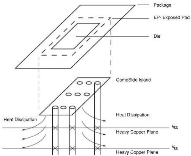
Package EP- Exposed Pad Die CompSlide Island Heat Dissipation Heat Dissipation Heavy Copper Plane Heavy Copper Plane VEE VEEPCB Thermal Consideration for 64-Pin EPAD-TQFP Package
MICREL, INC. 2180 FORTUNE DRIVE SAN JOSE, CA 95131 USA
TEL + 1 (408) 944-0800 FAX + 1 (408) 944-0970 WEB http://www.micrel.com
The information furnished by Micrel in this data sheet is believed to be accurate and reliable. However, no responsibility is assumed by Micrel for its use. Micrel reserves the right to change circuitry and specifications at any time without notification to the customer.
Micrel Products are not designed or authorized for use as components in life support appliances, devices or systems where malfunction of a product can reasonably be expected to result in personal injury. Life support devices or systems are devices or systems that (a) are intended for surgical implant into the body or (b) support or sustain life, and whose failure to perform can be reasonably expected to result in a significant injury to the user. A Purchaser's use or sale of Micrel Products for use in life support appliances, devices or systems is at Purchaser's own risk and Purchaser agrees to fully indemnify Micrel for any damages resulting from such use or sale.
© 2005 Micrel, Incorporated.