PIC32MZ2025DAB288 - Electronic component Microchip - Free user manual and instructions
Find the device manual for free PIC32MZ2025DAB288 Microchip in PDF.

User questions about PIC32MZ2025DAB288 Microchip
0 question about this device. Answer the ones you know or ask your own.
Ask a new question about this device
Download the instructions for your Electronic component in PDF format for free! Find your manual PIC32MZ2025DAB288 - Microchip and take your electronic device back in hand. On this page are published all the documents necessary for the use of your device. PIC32MZ2025DAB288 by Microchip.
USER MANUAL PIC32MZ2025DAB288 Microchip
Section 22. 12-bit High-Speed Successive Approximation Register (SAR) Analog-to-Digital Converter (ADC)
This section of the manual contains the following major topics:
22.1 Introduction 22-2
22.2 Control Registers 22-6
22.3 ADC Operation....22-61
22.4 ADC Module Configuration 22-65
22.5 Additional ADC Functions 22-85
22.6 Interrupts....22-108
22.7 Operation During Power-Saving Modes 22-114
22.8 Effects of Reset.... 22-116
22.9 Transfer Function 22-116
22.10 ADC Sampling Requirements 22-117
22.11 Connection Considerations.... 22-117
22.12 Related Application Notes.... 22-118
22.13 Revision History 22-119
Note: This family reference manual section is meant to serve as a complement to device data sheets. Depending on the device, this manual section may not apply to all PIC32 devices.
Please refer to the note at the beginning of the "ADC" chapter in the current device data sheet to check whether this document supports the device you are using.
Device data sheets and family reference manual sections are available for download from the Microchip Worldwide Web site at: http://www.microchip.com
22.1 INTRODUCTION
The PIC32 12-bit High-Speed Successive Approximation Register (SAR) Analog-to-Digital Converter (ADC) includes the following features:
- 12-bit resolution
- Up to eight ADC modules with dedicated Sample and Hold (S&H) circuits (see Note 1)
- Two dedicated ADC modules can be combined in Turbo mode to provide double conversion rate
- Single-ended and/or differential inputs
- Can operate during Sleep mode
• Supports touch sense applications - Up to six digital comparators
- Up to six digital filters supporting two modes:
- Oversampling mode
- Averaging mode
- FIFO and DMA engine for dedicated ADC modules (see Note 2)
- Early interrupt generation resulting in faster processing of converted data
- Designed for motor control, power conversion, and general purpose applications
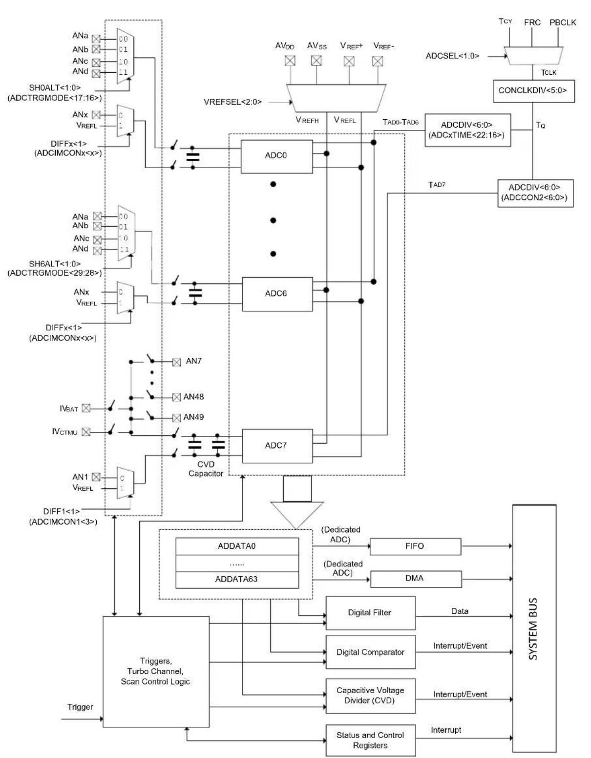
Note 1: Depending on the device, the 12-bit High-Speed SAR ADC has up to seven dedicated ADC modules and one shared ADC module. Throughout this chapter, the diagrams and code examples refer to a device with seven dedicated ADC modules (ADC0-ADC6) and one shared ADC (ADC7). Please consult the “ADC” chapter in the specific device data sheet to determine which ADC modules are available for your device.
2: This feature is not available on all devices. Refer to the "ADC" chapter in the specific device data sheet to determine availability.
3: Prior to enabling the ADC module, the user application must copy the ADC calibration data (DEVADCx) from the Configuration memory into the ADC Configuration registers (ADC0CFG-ADC7CFG). Refer to the “ADC” chapter in the specific device data sheet for more information.
The dedicated ADC modules use a single input (or its alternate) and is intended for high-speed and precise sampling of time-sensitive or transient inputs, whereas the shared ADC module incorporates a multiplexer on the input to facilitate a larger group of inputs, with slower sampling, and provides flexible automated scanning option through the input scan logic.
For each ADC module, the analog inputs are connected to the S&H capacitor. The clock, sampling time, and output data resolution for each ADC module can be set independently. The ADC module performs the conversion of the input analog signal based on the configurations set in the registers. When conversion is complete, the final result is stored in the result buffer for the specific analog input and is passed to the digital filter and digital comparator if configured to use data from this particular sample.
A simplified block diagram of the ADC module is illustrated in Figure 22-1.
Figure 22-1: ADC Block Diagram
flowchart
graph TD
    subgraph_System_BUS["System BUS"]
        A["ADCSEL<1:0>"] --> B["TCLK"]
        B --> C["CONCLKDIV<5:0>"]
        C --> D["Tq"]
        D --> E["ADCDIV<6:0> (ADCxTIME<22:16>)"]
        E --> F["TAD7"]
        F --> G["ADCDIV<6:0> (ADCCON2<6:0>)"]
        G --> H["TAD0-TAD6"]
        H --> I["VREFH"]
        I --> J["ADC0"]
        J --> K["ADC6"]
        K --> L["CVD Capacitor"]
        L --> M["ADC7"]
        M --> N["ADDATA0"]
        M --> O["ADDATA63"]
        N --> P["FIFO"]
        O --> Q["DMA"]
        P --> R["Dedicated ADC"]
        Q --> S["Digital Filter"]
        S --> T["Digital Comparator"]
        T --> U["Capacitive Voltage Divider (CVD)"]
        U --> V["Status and Control Registers"]
        V --> W["Interrupt"]
    end

    subgraph_System_BUS["System Bus<br>            X-axis: Trigger, Trigger1<1> (ADCIMCON1<3>)"]
        X-axis --> Y["ADDATA0"]
        X-axis --> Z["ADDATA63"]
        Y --> AA["(Dedicated ADC)"]
        Z --> AB["(Dedicated ADC)"]
        AA --> AC["FIFO"]
        AB --> AD["DMA"]
        AC --> AE["Data"]
        AD --> AF["Interrupt/Event"]
        AE --> AG["Interrupt/Event"]
    end

    subgraph_System_BUS["System Bus<br>            X-axis: TH0ALT<1:0> (ADCTRGMODE<17:16>)"]
        X-axis --> Y
        Y --> Z
        Z --> AA
        AA --> AB
        AB --> AC
        AC --> AD
        AD --> AE
        AE --> AF
        AF --> AG
        AG --> AH["Interrupt"]
    end

    subgraph_System_BUS["System Bus<br>            X-axis: TH0ALT<1:0> (ADCTRGMODE<17:16>)"]
        X-axis --> Y
        Y --> Z
        Z --> AA
        AA --> AB
        AB --> AC
        AC --> AD
        AD --> AE
        AE --> AF
        AF --> AG
    end

    subgraph_System_BUS["System Bus<br>            X-axis: TH0ALT<1:0> (ADCTRGMODE<17:16>)"]
        X-axis --> Y
        Y --> Z
        Z --> AA
        AA --> AB
        AB --> AC
        AC --> AD
        AD --> AE
        AE --> AF
    end

    subgraph_System_BUS["System Bus<br>            X-axis: TH0ALT<1:0> (ADCTRGMODE<17:16>)"]
        X-axis --> Y
        Y --> Z
        Z --> AA
        AA --> AB
        AB --> AC
        AC --> AD
        AD --> AE
    end

    subgraph_System_BUS["System Bus<br>            X-axis: TH0ALT<1:0> (ADCTRGMODE<17:16>)"]
        X-axis --> Y
        Y --> Z
        Z --> AA
        AA --> AB
        AB --> AC
        AC --> AD
        AD --> AE
    end

    subgraph_System_BUS["System Bus<br>            X-axis: TH0ALT<1:0> (ADCTRGRMODE<17:16>)"]
        X-axis --> Y
        Y --> Z
        Z --> AA
        AA --> AB
        AB --> AC
        AC --> AD
        AD --> AE
    end

    subgraph_System_BUS["System Bus<br>            X-axis: TH0ALT<1:0> (ADCTRGRMODE<17:16>)"]
        X-axis --> Y
        Y --> Z
        Z --> AA
        AA --> IB["CAPACitive Voltage Divider (CVD)"]
        IB --> AF["Status and Control Registers"]
    end

    subgraph_System_BUS["System Bus<br>            X-axis: TH0ALT<1:0> (ADCTRGRMODE<17:16>)"]
        X-axis --> Y
        Y --> Z
        Z --> AA
        AA --> IB
    end

    subgraph_System_BUS["System Bus<br>            X-axis: TH0ALT<1:0> (ADCTRGRMODE<17:16>)"]
        X-axis --> Y
        Y --> Z
        Z --> AA
    end

    subgraph_System_BUS["System Bus<br>            X-axis: TH0ALT<1:0> (ADCTRGRMODE<17:16>)"]
        X-axis --> Y
        Y --> Z
    end

    subgraph_System_BUS["System Bus<br>            X-axis: TH0ALT<1:0> (ADCTRGRMODE<17:16>)"]
        X-axis --> Y
        Y --> Z
    end

    subgraph_System_BUS["System Bus<br>            X-axis: TH0ALT<1:0> (ADCTRGRMODE<17:16>)"]
        X-axis --> Y
        Y --> Z
    end

    style System_BUS[System Bus fill:#f9f9f9,stroke:#333,stroke-width:2px,color:#fff
    style System_BUS[System Bus fill:#f9f9f9,stroke:#333,stroke-width:2px,color:#fff
Note: The number of ADC modules, analog inputs, ANa, ANb, ANc, and ANd, and the FIFO and DMA features are shown as an example. Refer to the "ADC" chapter in the specific device data sheet to determine the actual ANx selections, ADC module availability, and the specific FIFO and DMA features.
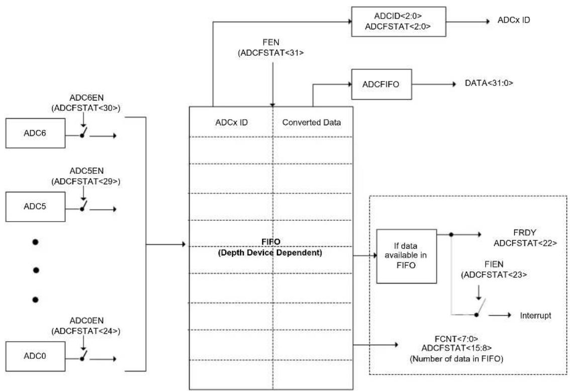
Figure 22-2: FIFO Block Diagram
flowchart
graph TD
    A["ADC0"] --> B["ADC0EN (ADCFSTAT<24>)"]
    C["ADC5"] --> D["ADC5EN (ADCFSTAT<29>)"]
    E["ADC6"] --> F["ADC6EN (ADCFSTAT<30>)"]
    G["FEN (ADCFSTAT<31>"] --> H["Converted Data"]
    I["ADCX ID"] --> H
    J["ADCFIFO"] --> K["Data<31:0>"]
    L["IFD (Depth Device Dependent)"] --> M["If data available in FIFO"]
    N["FCNT<7:0> ADCFSTAT<15:8> (Number of data in FIFO)"] --> M
    M --> O["FRDY ADCFSTAT<22>"]
    P["IFEN (ADCFSTAT<23>"] --> Q["Interrupt"]
    R["ADCID<2:0> ADCFSTAT<2:0>"] --> S["ADCx ID"]
Note: The number of ADC modules, analog inputs, ANa, ANb, ANc, and ANd, and the FIFO and DMA features are shown as an example. Refer to the "ADC" chapter in the specific device data sheet to determine the actual ANx selections, ADC module availability, and the specific FIFO and DMA features.
Figure 22-3: DMA Block Diagram

flowchart
graph TD
    A["DMAGEN (ADCDMASTAT<31>"] --> B["Buffer Full?"]
    B --> C["RBF6 (ADCDMASTAT<22>)"]
    B --> D["RBFIEN6 (ADCDMASTAT<30>)"]
    D --> E["Interrupt"]
    F["DMABADDR<31:0>"] --> G["Buffer A (ADC0)"]
    G --> H["Buffer B (ADC0)"]
    H --> I["Buffer A (ADC1)"]
    I --> J["Buffer B (ADC1)"]
    J --> K["Buffer A (ADC2)"]
    K --> L["Buffer B (ADC2)"]
    L --> M["Buffer A (ADC3)"]
    M --> N["Buffer B (ADC3)"]
    N --> O["Buffer A (ADC4)"]
    O --> P["Buffer B (ADC4)"]
    P --> Q["Buffer A (ADC5)"]
    Q --> R["Buffer B (ADC5)"]
    R --> S["Buffer A (ADC6)"]
    S --> T["Buffer B (ADC6)"]
    T --> U["Buffer A (ADC7)"]
    U --> V["Buffer B (ADC7)"]
    V --> W["Buffer A (ADC8)"]
    W --> X["Buffer B (ADC8)"]
    X --> Y["Buffer A (ADC9)"]
    Y --> Z["Buffer B (ADC9)"]
    Z --> AA["Buffer A (ADC10)"]
    AA --> AB["Buffer B (ADC10)"]
    AB --> AC["Buffer A (ADC11)"]
    AC --> AD["Buffer B (ADC11)"]
    AD --> AE["Buffer A (ADC12)"]
    AE --> AF["Buffer B (ADC12)"]
    AF --> AG["Buffer A (ADC13)"]
    AG --> AH["Buffer B (ADC13)"]
    AH --> AI["Buffer A (ADC14)"]
    AI --> AJ["Buffer B (ADC14)"]
    AJ --> AK["Buffer A (ADC15)"]
    AK --> AL["Buffer B (ADC15)"]
    AL --> AM["Buffer A (ADC16)"]
    AM --> AN["Buffer B (ADC16)"]
    AN --> AO["Buffer A (ADC17)"]
    AO --> AP["Buffer B (ADC17)"]
    AP --> AQ["Buffer A (ADC18)"]
    AQ --> AR["Buffer B (ADC18)"]
    AR --> AS["Buffer A (ADC19)"]
    AS --> AT["Buffer B (ADC19)"]
    AT --> AU["Buffer A (ADC20)"]
    AU --> AV["Buffer B (ADC20)"]
    AV --> AW["Buffer A (ADC21)"]
    AW --> AX["Buffer B (ADC21)"]
    AX --> AY["Buffer A (ADC22)"]
    AY --> AZ["Buffer B (ADC22)"]
    AZ --> BA["Buffer A (ADC23)"]
    BA --> BB["Buffer B (ADC23)"]
    BB --> BC["Buffer A (ADC24)"]
    BC --> BD["Buffer B (ADC24)"]
    BD --> BE["Buffer A (ADC25)"]
    BE --> BF["Buffer B (ADC25)"]
    BF --> BG["Buffer A (ADC26)"]
    BG --> BH["Buffer B (ADC26)"]
    BH --> BI["Buffer A (ADC27)"]
    BI --> BJ["Buffer B (ADC27)"]
    BJ --> BK["Buffer A (ADC28)"]
    BK --> BL["Buffer B (ADC28)"]
    BL --> BM["Buffer A (ADC29)"]
    BM --> BN["Buffer B (ADC29)"]
    BN --> BO["Buffer A (ADC30)"]
    BO --> BP["Buffer B (ADC30)"]
    BP --> BQ["Buffer A (ADC31)"]
    BQ --> BR["Buffer B (ADC31)"]
    BR --> BS["Buffer A (ADC32)"]
    BS --> BT["Buffer B (ADC32)"]
    BT --> BU["Buffer A (ADC33)"]
    BU --> BV["Buffer B (ADC33)"]
    BV --> BW["Buffer A (ADC34)"]
    BW --> BX["Buffer B (ADC34)"]
    BX --> BY["Buffer A (ADC35)"]
    BY --> BZ["Buffer B (ADC35)"]
    BC --> CA["Data Count for Buffer-A (ADC6)"]
    CA --> CB["Data Count for Buffer-B (ADC1)"]
    CA --> CC["Data Count for Buffer-A (ADC1)"]
    CA --> DD["Data Count for Buffer-B (ADC0)"]
    CC --> DE["Data Count for Buffer-A (ADC0)"]
Note: The number of ADC modules, analog inputs, ANa, ANb, ANc, and ANd, and the FIFO and DMA features are shown as an example. Refer to the "ADC" chapter in the specific device data sheet to determine the actual ANx selections, ADC module availability, and the specific FIFO and DMA features.
22.2 CONTROL REGISTERS
The PIC32 12-bit High-Speed SAR ADC module has the following Special Function Registers (SFRs):
• ADCCON1: ADC Control Register 1
This register controls the basic operation of all ADC modules, including behavior in Sleep and Idle modes, and data formatting. This register also specifies the vector shift amounts for the Interrupt Controller. Additional ADCCON1 functions include controlling the Turbo feature of the ADC, the RAM buffer length in DMA mode, and Capacitive Voltage Division (CVD).
• ADCCON2: ADC Control Register 2
This register controls the reference selection for all ADC modules, the sample time for the shared ADC module, interrupt enable for reference, early interrupt selection, and clock division selection for the shared ADC.
• ADCCON3: ADC Control Register 3
This register enables ADC clock selection, enables/disables the digital feature for the dedicated and shared ADC modules and controls the manual (software) sampling and conversion.
- ADCTRGMODE: ADC Triggering Mode for Dedicated ADC Register
This register has selections for alternate analog inputs and includes trigger settings for the dedicated ADC modules.
- ADCIMCON1: ADC Input Mode Control Register 1 through ADCIMCON4: ADC Input Mode Control Register 4
These registers enable the user to select between single-ended and differential operation as well as select between signed and unsigned data format.
- ADCGIRQEN1: ADC Global Interrupt Enable Register 1 and ADCGIRQEN2: ADC Global Interrupt Enable Register 2
These registers specify which of the individual input conversion interrupts can generate the global ADC interrupt.
- ADCCSS1: ADC Common Scan Select Register 1 and ADCCSS2: ADC Common Scan Select Register 2
These registers specify the analog inputs to be scanned by the common scan trigger.
- ADCDSTAT1: ADC Data Ready Status Register 1 and ADCDSTAT2: ADC Data Ready Status Register 2
These registers contain the interrupt status of the individual analog input conversions. Each bit represents the data-ready status for its associated conversion result.
- ADCCMPENx: ADC Digital Comparator 'x' Enable Register ('x' = 1 through 6)
These registers select which analog input conversion results will be processed by the digital comparator.
- ADCCMPx: ADC Digital Comparator 'x' Limit Value Register ('x' = 1 through 6)
These registers contain the high and low digital comparison values for use by the digital comparator.
- ADCFLTRx: ADC Digital Filter 'x' Register ('x' = 1 through 6)
These registers provide control and status bits for the oversampling filter accumulator, and also includes the 16-bit filter output data.
- ADCTRG1: ADC Trigger Source 1Register
This register controls the trigger source selection for AN0 through AN3 analog inputs.
- ADCTRG2: ADC Trigger Source 2 Register
This register controls the trigger source selection for AN4 through AN7 analog inputs.
- ADCTRG3: ADC Trigger Source 3 Register
This register controls the trigger source selection for AN8 through AN11 analog inputs.
- ADCTRG4: ADC Trigger Source 4 Register
This register controls the trigger source selection for AN12 through AN15 analog inputs.
• ADCTRG5: ADC Trigger Source 5 Register
This register controls the trigger source selection for AN16 through AN19 analog inputs.
• ADCTRG6: ADC Trigger Source 6 Register
This register controls the trigger source selection for AN20 through AN23 analog inputs.
• ADCTRG7: ADC Trigger Source 7 Register
This register controls the trigger source selection for AN24 through AN27 analog inputs.
• ADCTRG8: ADC Trigger Source 8 Register
This register controls the trigger source selection for AN28 through AN31 analog inputs.
• ADCCMPCON1: ADC Digital Comparator 1 Control Register
This register controls the operation of Digital Comparator 1, including the generation of interrupts, comparison criteria to be used, and provides status when a comparator event occurs. Additionally, this register provides the output data of CVD.
- ADCCMPCONx: ADC Digital Comparator 'x' Control Register ('x' = 2 through 6)
These registers control the operation of Digital Comparators 2 through 6, including the generation of interrupts and the comparison criteria to be used. This register also provides status when a comparator event occurs.
• ADCFSTAT: ADC FIFO Status Register
This register specifies the status of the dedicated ADC module FIFO.
• ADCFIFO: ADC FIFO Data Register
This register specifies the output value of the dedicated ADC module FIFO.
• ADCBASE: ADC Base Register
These registers specify the base address of the user ADC Interrupt Service Routine (ISR) jump table.
• ADCDMASTAT: ADC DMA Status Register
This register contains the DMA status bits.
- ADCCNTB: ADC Sample Count Base Address Register
This register contains the base address of the sample count in RAM. In addition to storying the converted data of each dedicated ADC module in RAM, DMA also stores the converted sample count.
- ADCDMAB: ADC DMA Base Address Register
This register contains the base address of RAM for the DMA engine.
- ADCTRGSNS: ADC Trigger Level/Edge Sensitivity Register
This register contains the setting for trigger level for each ADC analog input.
- ADCxTIME: Dedicated ADCx Timing Register 'x' ('x' = 0 through 6)
These registers contains the time and clock setting for dedicated analog input.
• ADCEIEN1: ADC Early Interrupt Enable Register 1 and
ADCEIEN2: ADC Early Interrupt Enable Register 2
These registers contains bits to enable or disable early interrupt for individual analog inputs.
- ADCEISTAT1: ADC Early Interrupt Status Register 1 and
ADCEISTAT2: ADC Early Interrupt Status Register 2
These registers contain status bits for early interrupt for individual analog inputs.
• ADCANCON: ADC Analog Warm-up Control Register
This register contains the warm-up control settings for the analog and bias circuit of the ADC module.
- ADCDATAx: ADC Output Data Register ('x' = 0 through 63)
These registers are the analog-to-digital conversion output data registers. The ADCDATAx register is associated with each analog input, 0-63.
- ADCxCFG: ADCx Configuration Register 'x' ('x' = 0 through 7)
These registers specify the ADC module configuration data.
- ADCSYSCFG0: ADC System Configuration Register 0 and
ADCSYSCFG1: ADC System Configuration Register 1
These registers contain read-only bits corresponding to the analog input.
Table 22-1 provides a summary of all ADC Special Function Registers (SFRs). Corresponding registers appear after the summaries, which include a detailed description of each bit. Depending on the device, functionality will vary. Refer to the “ADC” chapter in the specific device data sheet to determine which registers are available for your device.
Table 22-1: ADC SFR Summary
| Register Name | Bit Range | Bit 31/15 | Bit 30/14 | Bit 29/13 | Bit 28/12 | Bit 27/11 | Bit 26/10 | Bit 25/9 | Bit 24/8 | Bit 23/7 | Bit 22/6 | Bit 21/5 | Bit 20/4 | Bit 19/3 | Bit 18/2 | Bit 17/1 | Bit 16/0 |
| ADCCON1 | 31:16 | TRBEN | TRBERR | TRBMST<2:D> | TRBSLV<2:D> | FRACT | SELRES<1:D> | STRGSR<4:D> | |||||||||
| 15:0 | ON | — | SIDL | AICPMPEN | CVDEN | FSSCLKEN | FSPBCIKEN | — | — | IRQVS<2:D> | STRGLVL | DMABL<2:D> | |||||
| ADCCON2 | 31:16 | BGVRRDY | REFFLT | EOSRDY | CVDCPL<2:D> | SAMC<9:D> | |||||||||||
| 15:0 | BGVRIEN | REFFLTEN | EOSIEN | ADCEIOVR | ECRIEN | ADCEIS<2:D> | — | ADCDIV<6:D> | |||||||||
| ADCCON3 | 31:16 | ADCSEL<1:D> | CONCLKDIV<5:D> | DIGEN7 | DIGEN6 | DIGEN5 | DIGEN4 | DIGEN3 | DIGEN2 | DIGEN1 | DIGENO | ||||||
| 15:0 | VREFSEL<2:D> | TRGSUSP | UPDIEN | UPDRDY | SAMP | RQCNVRT | GLSWTRG | GSWTRG | ADINSEL<5:D> | ||||||||
| ADCTRGMODE | 31:16 | — | — | SH6ALT<1:D> | SH5ALT<1:D> | SH4ALT<1:D> | SH3ALT<1:D> | SH2ALT<1:D> | SH1ALT<1:D> | SH0ALT<1:D> | |||||||
| 15:0 | — | STRGEN6 | STRGEN5 | STRGEN4 | STRGEN3 | STRGEN2 | STRGEN1 | STRGEN0 | — | SSAMPEN6 | SSAMPEN5 | SSAMPEN4 | SSAMPEN3 | SSAMPEN2 | SSAMPEN1 | SSAMPENO | |
| ADCIMCON1 | 31:16 | DIFF15 | SIGN15 | DIFF14 | SIGN14 | DIFF13 | SIGN13 | DIFF12 | SIGN12 | DIFF11 | SIGN11 | DIFF10 | SIGN10 | DIFF9 | SIGN9 | DIFF8 | SIGN8 |
| 15:0 | DIFF7 | SIGN7 | DIFF5 | SIGN5 | DIFF5 | SIGN5 | DIFF4 | SIGN4 | DIFF3 | SIGN3 | DIFF2 | SIGN2 | DIFF1 | SIGN1 | DIFF0 | SIGN0 | |
| ADCIMCON2 | 31:16 | DIFF31 | SIGN31 | DIFF30 | SIGN30 | DIFF29 | SIGN29 | DIFF28 | SIGN28 | DIFF27 | SIGN27 | DIFF25 | SIGN25 | DIFF25 | SIGN25 | DIFF24 | SIGN24 |
| 15:0 | DIFF23 | SIGN23 | DIFF22 | SIGN22 | DIFF21 | SIGN21 | DIFF20 | SIGN20 | DIFF19 | SIGN19 | DIFF18 | SIGN18 | DIFF17 | SIGN17 | DIFF16 | SIGN16 | |
| ADCIMCON3 | 31:16 | DIFF47 | SIGN47 | DIFF46 | SIGN45 | DIFF45 | SIGN45 | DIFF44 | SIGN44 | DIFF43 | SIGN43 | DIFF42 | SIGN42 | DIFF41 | SIGN41 | DIFF40 | SIGN40 |
| 15:0 | DIFF39 | SIGN39 | DIFF38 | SIGN38 | DIFF37 | SIGN37 | DIFF35 | SIGN36 | DIFF35 | SIGN35 | DIFF34 | SIGN34 | DIFF33 | SIGN33 | DIFF32 | SIGN32 | |
| ADCIMCON4 | 31:16 | DIFF63 | SIGN63 | DIFF62 | SIGN62 | DIFF61 | SIGN61 | DIFF60 | SIGN60 | DIFF59 | SIGN59 | DIFF58 | SIGN58 | DIFF57 | SIGN57 | DIFF55 | SIGN55 |
| 15:0 | DIFF55 | SIGN55 | DIFF54 | SIGN54 | DIFF53 | SIGN53 | DIFF52 | SIGN52 | DIFF51 | SIGN51 | DIFF50 | SIGN50 | DIFF49 | SIGN49 | DIFF48 | SIGN48 | |
| ADCGIRGEN1 | 31:16 | AGIEN31 | AGIEN30 | AGIEN29 | AGIEN28 | AGIEN27 | AGIEN26 | AGIEN25 | AGIEN24 | AGIEN23 | AGIEN22 | AGIEN21 | AGIEN20 | AGIEN19 | AGIEN18 | AGIEN17 | AGIEN16 |
| 15:0 | AGIEN15 | AGIEN14 | AGIEN13 | AGIEN12 | AGIEN11 | AGIEN10 | AGIEN9 | AGIEN8 | AGIEN7 | AGIEN6 | AGIEN5 | AGIEN4 | AGIEN3 | AGIEN2 | AGIEN1 | AGIEN0 | |
| ADCGIRGEN2 | 31:16 | AGIEN63 | AGIEN62 | AGIEN61 | AGIEN60 | AGIEN59 | AGIEN58 | AGIEN57 | AGIEN56 | AGIEN55 | AGIEN54 | AGIEN53 | AGIEN52 | AGIEN51 | AGIEN50 | AGIEN49 | AGIEN48 |
| 15:0 | AGIEN47 | AGIEN46 | AGIEN45 | AGIEN44 | AGIEN43 | AGIEN42 | AGIEN41 | AGIEN40 | AGIEN39 | AGIEN38 | AGIEN37 | AGIEN36 | AGIEN35 | AGIEN34 | AGIEN33 | AGIEN32 | |
| ADCCSS1 | 31:16 | CSS31 | CSS30 | CSS29 | CSS28 | CSS27 | CSS26 | CSS25 | CSS24 | CSS23 | CSS22 | CSS21 | CSS20 | CSS19 | CSS18 | CSS17 | CSS16 |
| 15:0 | CSS15 | CSS14 | CSS13 | CSS12 | CSS11 | CSS10 | CSS9 | CSS6 | CSS7 | CSS6 | CSS5 | CSS4 | CSS3 | CSS2 | CSS1 | CSS0 | |
| ADCCSS2 | 31:16 | CSS63 | CSS62 | CSS61 | CSS60 | CSS59 | CSS58 | CSS57 | CSS56 | CSS55 | CSS54 | CSS53 | CSS52 | CSS51 | CSS50 | CSS49 | CSS48 |
| 15:0 | CSS47 | CSS46 | CSS45 | CSS44 | CSS43 | CSS42 | CSS41 | CSS40 | CSS39 | CSS38 | CSS37 | CSS36 | CSS35 | CSS34 | CSS33 | CSS32 | |
| ADCDSTAT1 | 31:16 | ARDY31 | ARDY30 | ARDY29 | ARDY28 | ARDY27 | ARDY25 | ARDY25 | ARDY24 | ARDY23 | ARDY22 | ARDY21 | ARDY20 | ARDY19 | ARDY18 | ARDY17 | ARDY16 |
| 15:0 | ARDY15 | ARDY14 | ARDY13 | ARDY12 | ARDY11 | ARDY10 | ARDY9 | ARDY8 | ARDY7 | ARDY6 | ARDY5 | ARDY4 | ARDY3 | ARDY2 | ARDY1 | ARDY0 | |
| ADCDSTAT2 | 31:16 | ARDY63 | ARDY62 | ARDY61 | ARDY60 | ARDY59 | ARDY58 | ARDY57 | ARDY56 | ARDY55 | ARDY54 | ARDY53 | ARDY52 | ARDY51 | ARDY50 | ARDY49 | ARDY48 |
| 15:0 | ARDY47 | ARDY46 | ARDY45 | ARDY44 | ARDY43 | ARDY42 | ARDY41 | ARDY40 | ARDY39 | ARDY35 | ARDY37 | ARDY36 | ARDY35 | ARDY34 | ARDY33 | ARDY32 | |
| ADCCMPENx' = 1-6 | 31:16 | CMPE31 | CMPE30 | CMPE29 | CMPE28 | CMPE27 | CMPE26 | CMPE25 | CMPE24 | CMPE23 | CMPE22 | CMPE21 | CMPE20 | CMPE19 | CMPE18 | CMPE17 | CMPE15 |
| 15:0 | CMPE15 | CMPE14 | CMPE13 | CMPE12 | CMPE11 | CMPE10 | CMPE9 | CMPE8 | CMPE7 | CMPE6 | CMPE5 | CMPE4 | CMPE3 | CMPE2 | CMPE1 | CMPE0 | |
| ADCCMPx' = 1-6 | 31:16 | ||||||||||||||||
| 15:0 | |||||||||||||||||
| ADCFLTRx' = 1-6 | 31:16 | AFEN | DATA15EN | DFMODE | OVRSAM<2:D> | AFGIEN | AFRDY | — | — | — | CHNLID<4:D> | ||||||
| 15:0 | |||||||||||||||||
| ADCTRIG1 | 31:16 | — | — | — | TRGSRC3<4:D> | — | — | — | |||||||||
| 15:0 | — | — | — | TRGSRC1<4:D> | — | — | — | ||||||||||
| ADCTRIG2 | 31:16 | — | — | — | TRGSRC7<4:D> | — | — | — | |||||||||
| 15:0 | — | — | — | TRGSRC5<4:D> | — | — | — | ||||||||||
| ADCTRIG3 | 31:16 | — | — | — | TRGSRC11<4:D> | — | — | — | |||||||||
| 15:0 | — | — | — | TRGSRC9<4:D> | — | — | — | ||||||||||
| ADCTRIG4 | 31:16 | — | — | — | TRGSRC15<4:D> | — | — | — | |||||||||
| 15:0 | — | — | — | TRGSRC13<4:D> | — | — | — | ||||||||||
| ADCTRIG5 | 31:16 | — | — | — | TRGSRC19<4:D> | — | — | — | |||||||||
| 15:0 | — | — | — | TRGSRC17<4:D> | — | — | — | ||||||||||
Note 1: Before enabling the ADC, the user application must initialize the ADC calibration values by copying them from the factory-programmed DEVADCx Flash registers into the corresponding ADCxCFG registers.
Table 22-1: ADC SFR Summary
| Register Name | Bit Range | BIT 31/15 | BIT 30/14 | BIT 29/13 | BIT 28/12 | BIT 27/11 | BIT 26/10 | BIT 25/9 | BIT 24/8 | BIT 23/7 | BIT 22/6 | BIT 21/5 | BIT 20/4 | BIT 19/3 | BIT 18/2 | BIT 17/1 | BIT 16/0 |
| ADCTRG6 | 31:16 | — | — | — | TRG SRC23<4:0> | — | — | — | TRG SRC22<4:0> | ||||||||
| 15:0 | — | — | — | TRG SRC21<4:0> | — | — | — | TRG SRC20<4:0> | |||||||||
| ADCTRG7 | 31:16 | — | — | — | TRG SRC27<4:0> | — | — | — | TRG SRC26<4:0> | ||||||||
| 15:0 | — | — | — | TRG SRC25<4:0> | — | — | — | TRG SRC24<4:0> | |||||||||
| ADCTRG8 | 31:16 | — | — | — | TRG SRC31<4:0> | — | — | — | TRG SRC30<4:0> | ||||||||
| 15:0 | — | — | — | TRG SRC29<4:0> | — | — | — | TRG SRC28<4:0> | |||||||||
| ADCCMPCON1 | 31:16 CVDDATA<15:0> | ||||||||||||||||
| 15:0 | — | — | AINID<5:0> | ENDCMP | DCMPGIEN | DCMPED | IEBTWN | IEHIHI | IEHILO | IELOHI | IELOLO | ||||||
| ADCCMPCONx X = 2-6 | 31:16 | — | — | — | — | — | — | — | — | — | — | — | — | — | — | — | — |
| 15:0 | — | — | — | AINID<4:0> | ENDCMP | DCMPGIEN | DCMPED | IEBTWN | IEHIHI | IEHILO | IELOHI | IELOLO | |||||
| ADCFSTAT | 31:16 | FEN | ADC6EN | ADC5EN | ADC4EN | ADC3EN | ADC2EN | ADC1EN | ADC0EN | FIEN | FRDY | FWROVERR | — | — | — | — | — |
| 15:0 | FCNT<7:0> | FSIGN | — | — | — | — | — | ADCID<2:0> | |||||||||
| ADCFIFO | 31:16 | DATA<31:16> | |||||||||||||||
| 15:0 | DATA<15:0> | ||||||||||||||||
| ADCBASE | 31:16 | — | — | — | — | — | — | — | — | — | — | — | — | — | — | — | — |
| 15:0 | ADCBASE<15:0> | ||||||||||||||||
| ADCDMASTAT | 31:16 | DMAGEN | RBFEN6 | RBFEN5 | RBFEN4 | RBFEN3 | RBFEN2 | RBFEN1 | RBFIEN0 | DMAWROVERR | RBF6 | RBF5 | RBF4 | RBF3 | RBF2 | RBF1 | RBF0 |
| 15:0 | DMACNTEN | RAFIEN6 | RAFIEN5 | RAFIEN4 | RAFIEN3 | RAFIEN2 | RAFIEN1 | RAFIEN0 | — | RAF6 | RAF5 | RAF4 | RAF3 | RAF2 | RAF1 | RAF0 | |
| ADCCNTB | 31:16 | CNTBADDR<31:16> | |||||||||||||||
| 15:0 | CNTBADDR<15:0> | ||||||||||||||||
| ADCDMAB | 31:16 | DMABADDR<31:16> | |||||||||||||||
| 15:0 | DMABADDR<15:0> | ||||||||||||||||
| ADCTRGSNS | 31:16 | LVL31 | LVL30 | LVL29 | LVL26 | LVL27 | LVL26 | LVL25 | LVL24 | LVL23 | LVL22 | LVL21 | LVL20 | LVL19 | LVL18 | LVL17 | LVL16 |
| 15:0 | LVL15 | LVL14 | LVL13 | LVL12 | LVL11 | LVL10 | LVL9 | LVL8 | LVL7 | LVL6 | LVL5 | LVL4 | LVL3 | LVL2 | LVL1 | LVL0 | |
| ADCXTIME X = 0-6 | 31:16 | — | — | — | ADCEIS<2:0> | SELRES<1:0> | DMAEN | ADCDIV<6:0> | |||||||||
| 15:0 | — | — | — | — | — | — | — | ||||||||||
| ADCEIEN1 | 31:16 | EIEN31 | EIEN30 | EIEN29 | EIEN28 | EIEN27 | EIEN26 | EIEN25 | EIEN24 | EIEN23 | EIEN22 | EIEN21 | EIEN20 | EIEN19 | EIEN18 | EIEN17 | EIEN16 |
| 15:0 | EIEN15 | EIEN14 | EIEN13 | EIEN12 | EIEN11 | EIEN10 | EIEN9 | EIEN8 | EIEN7 | EIEN6 | EIEN5 | EIEN4 | EIEN3 | EIEN2 | EIEN1 | EIEN0 | |
| ADCEIEN2 | 31:16 | EIEN83 | EIEN62 | EIEN61 | EIEN60 | EIEN59 | EIEN58 | EIEN57 | EIEN55 | EIEN55 | EIEN54 | EIEN53 | EIEN52 | EIEN51 | EIEN50 | EIEN49 | EIEN48 |
| 15:0 | EIEN47 | EIEN46 | EIEN45 | EIEN44 | EIEN43 | EIEN42 | EIEN41 | EIEN40 | EIEN39 | EIEN38 | EIEN37 | EIEN36 | EIEN35 | EIEN34 | EIEN33 | EIEN32 | |
| ADCEISTAT1 | 31:16 | EIRDY31 | EIRDY30 | EIRDY29 | EIRDY26 | EIRDY27 | EIRDY26 | EIRDY25 | EIRDY24 | EIRDY23 | EIRDY22 | EIRDY21 | EIRDY20 | EIRDY19 | EIRDY18 | EIRDY17 | EIRDY16 |
| 15:0 | EIRDY15 | EIRDY14 | EIRDY13 | EIRDY12 | EIRDY11 | EIRDY10 | EIRDY9 | EIRDY8 | EIRDY7 | EIRDY6 | EIRDY5 | EIRDY4 | EIRDY3 | EIRDY2 | EIRDY1 | EIRDY0 | |
| ADCEISTAT2 | 31:16 | EIRDY63 | EIRDY62 | EIRDY61 | EIRDY60 | EIRDY59 | EIRDY58 | EIRDY57 | EIRDY56 | EIRDY55 | EIRDY54 | EIRDY53 | EIRDY52 | EIRDY51 | EIRDY50 | EIRDY49 | EIRDY48 |
| 15:0 | EIRDY47 | EIRDY45 | EIRDY45 | EIRDY44 | EIRDY43 | EIRDY42 | EIRDY41 | EIRDY40 | EIRDY39 | EIRDY38 | EIRDY37 | EIRDY36 | EIRDY35 | EIRDY34 | EIRDY33 | EIRDY32 | |
| ADCANCON | 31:16 | WKUPCLKNT<3:0> | WKIEN7 | WKIEN6 | WKIEN5 | WKIEN4 | WKIEN3 | WKIEN2 | WKIEN1 | WKIEN0 | |||||||
| 15:0 | WKRDY7 | WKRDY6 | WKRDY5 | WKRDY4 | WKRDY3 | WKRDY2 | WKRDY1 | WKRDY0 | ANEN7 | ANEN6 | ANEN5 | ANEN4 | ANEN3 | ANEN2 | ANEN1 | ANEN0 | |
| ADCDATAx (X' = 0.163) | 31:16 | DATA<31:16> | |||||||||||||||
| 15:0 | DATA<15:0> | ||||||||||||||||
| ADCxCFG X = 0.7(1) | 31:16 | ADCCFG<31:16> | |||||||||||||||
| 15:0 | ADCCFG<15:0> | ||||||||||||||||
| ADCSYSCFG0 | 31:16 | AN<31:16> | |||||||||||||||
| 15:0 | AN<15:0> | ||||||||||||||||
| ADCSYSCFG1 | 31:16 | AN<53:48> | |||||||||||||||
| 15:0 | AN<47:32> | ||||||||||||||||
Note 1: Before enabling the ADC, the user application must initialize the ADC calibration values by copying them from the factory-programmed DEVADCx Flash registers into the corresponding ADCxCFG registers.
Register 22-1: ADCCON1: ADC Control Register 1
| Bit Range | Bit 31/23/15/7 | Bit 30/22/14/6 | Bit 29/21/13/5 | Bit 28/20/12/4 | Bit 27/19/11/3 | Bit 26/18/10/2 | Bit 25/17/9/1 | Bit 24/16/8/0 |
| 31:24 | R/W-0 R-0, TRBEN TRBERR TRBMST<2:0> | |||||||
| R/W-0 R/W-1 | R/W-1 | R/W-0 R/W-0 | R/W-0 R/W-0 R/W-0 | |||||
| 23:16 | FRACT SELRES<1:0> | STRGSRC<4:0> | ||||||
| 15:8 | R/W-0 | U-0 | R/W-0 | R/W-1 | R/W-0 | R/W-0 | R/W-0 | U-0 |
| ON | — | SIDL | AICPMPEN | CVDEN | FSSCLKEN | FSPBCLKEN | — | |
| 7:0 | U-0 | R/W-0 | R/W-0 R/W-0 | R/W-0 R/W-0 | R/W-0 R/W-0 | |||
| — | IRQVS<2:0> | STRGLVL | DMABL<2:0> | |||||
| Legend: | HC = Hardware Set | HS = Hardware Cleared |
| R = Readable bit | W = Writable bit | U = Unimplemented bit, read as ‘0’ |
| -n = Value at POR | ‘1’ = Bit is set | ‘0’ = Bit is cleared x = Bit is unknown |
bit 31 TRBEN: Turbo Channel Enable bit
1 = Enable the Turbo channel
0 = Disable the Turbo channel
bit 30 TRBERR: Turbo Channel Error Status bit
1 = An error occurred while setting the Turbo channel and Turbo channel function to be disabled regardless of the TRBEN bit being set to '1'.
0 = Turbo channel error did not occur
Note: The status of this bit is valid only after the TRBEN bit is set.
bit 29-27 TRBMST<2:0>: Turbo Master ADCx bits
111 = Reserved
110 = ADC6 is selected as the Turbo Master
•
- 000 = ADC0 is selected as the Turbo Master
bit 26-24 TRBSLV<2:0>: Turbo Slave ADCx bits
111 = Reserved
110 = ADC6 is selected as the Turbo Slave
•
-
■
000 = ADC0 is selected as the Turbo Slave
bit 23 FRACT: Fractional Data Output Format bit
1 = Fractional
0 = Integer
bit 22-21 SELRES<1:0>: Shared ADC Resolution bits
11 = 12 bits (default)
10 = 10 bits
01 = 8 bits
00 = 6 bits
bit 20-16 STRGSRC<4:0>: Scan Trigger Source Select bits
11111 - 00100 = Refer to the "ADC" chapter in the specific device data sheet for trigger source selections
00011 = Reserved
00010 = Global level software trigger (GLSWTRG) is not self-cleared
00001 = Global software trigger (GSWTRG) is self-cleared on the next clock cycle
00000 = No trigger
bit 15 ON: ADC Module Enable bit
1 = ADC module is enabled
0 = ADC module is disabled
Note: The ON bit should be set only after the ADC module has been configured.
bit 14 Unimplemented: Read as '0'
Register 22-1: ADCCON1: ADC Control Register 1 (Continued)
bit 13 SIDL: Stop in Idle Mode bit
1 = Discontinue module operation when the device enters Idle mode
0 = Continue module operation in Idle mode
bit 12 AICPMPEN: Analog Input Charge Pump Enable bit 1 = Analog input charge pump is enabled (default) 0 = Analog input charge pump is disabled
bit 11 CVDEN: Capacitive Voltage Division Enable bit 1 = CVD operation is enabled 0 = CVD operation is disabled
bit 10 FSSCLKEN: Fast Synchronous System Clock to ADC Control Clock bit 1 = Fast synchronous system clock to ADC control clock is enabled 0 = Fast synchronous system clock to ADC control clock is disabled
bit 9 FSPBCLKEN: Fast Synchronous Peripheral Clock to ADC Control Clock bit 1 = Fast synchronous peripheral clock to ADC control clock is enabled 0 = Fast synchronous peripheral clock to ADC control clock is disabled
bit 8-7 Unimplemented: Read as '0' bit 6-4 IRQVS<2:0>: Interrupt Vector Shift bits
To determine interrupt vector address, this bit specifies the amount of left shift done to the ARDYx status bits in the ADCDSTAT1 and ADCDSTAT2 registers, prior to adding with the ADCBASE register (see 22.6.2 "ADC Base Register (ADCBASE) Usage" for more information). Interrupt Vector Address = Read Value of ADCBASE = Value written to ADCBASE + x << IRQVS<2:0>, where 'x' is the smallest active input ID from the ADCDSTAT1 or ADCDSTAT2 registers (which has highest priority). 111 = Shift x left 7 bit position 110 = Shift x left 6 bit position 101 = Shift x left 5 bit position 100 = Shift x left 4 bit position 011 = Shift x left 3 bit position 010 = Shift x left 2 bit position 001 = Shift x left 1 bit position 000 = Shift x left 0 bit position
bit 3 STRGLVL: Scan Trigger High Level/Positive Edge Sensitivity bit 1 = Scan trigger is high level sensitive. Once STRIG mode is selected (TRGSRCx<4:0> in the ADCTRGx register), the scan trigger will continue for all selected analog inputs, until the STRIG option is removed. 0 = Scan trigger is positive edge sensitive. Once STRIG mode is selected (TRGSRCx<4:0> in the ADCTRGx register), only a single scan trigger will be generated, which will complete the scan of all selected analog inputs.
bit 2-0 DMABL<2:0>: DMA Buffer Length Size bits
111 = Allocates 128 locations in RAM to each analog input 110 = Allocates 64 locations in RAM to each analog input 101 = Allocates 32 locations in RAM to each analog input 100 = Allocates 16 locations in RAM to each analog input 011 = Allocates 8 locations in RAM to each analog input 010 = Allocates 4 locations in RAM to each analog input 001 = Allocates 2 locations in RAM to each analog input 000 = Allocates 1 location in RAM to each analog input
Note: Since each output data is 16-bit wide, one location consists of 2 bytes.
Register 22-2: ADCCON2: ADC Control Register 2
| Bit Range | Bit31/23/15/7 | Bit30/22/14/6 | Bit29/21/13/5 | Bit28/20/12/4 | Bit27/19/11/3 | Bit26/18/10/2 | Bit25/17/9/1 | Bit24/16/8/0 |
| 31:24 | R-0, HS, HC R-0, HS, HC R-0, HS | HC R/W-0 R/W-0 | R/W-0 R/W-0 R/W-0 | |||||
| BGVRRDY | REFFLT EOSRDY | CYDCPL | <2:0> SAMC<9:9> | |||||
| 23:16 | R/W-0 R/W-0 | R/W-0 | R/W-0 | R/W-0 R/W-0 R/W-0 | W-0 R/W-0 | |||
| SAMC<7:0> | ||||||||
| 15:8 | R/W-0 R/W-0 | R/W-0 | R/W-0 | R/W-0 R/W-0 R/W-0 | W-0 R/W-0 | |||
| BGVRIEN | REFFLTIEN | EOSIEN | ADCEIOVR | ECRIEN | ADCEIS<2:0> | |||
| 7:0 | U-0 | R/W-0 | R/W-0 | R/W-0 | R/W-0 | R/W-0 | R/W-0 | R/W-0 |
| — | ADCDIV<6:0> | |||||||
| Legend: | HC = Hardware Set | HS = Hardware Cleared | r = Reserved |
| R = Readable bit | W = Writable bit | U = Unimplemented bit, read as ‘0’ | |
| -n = Value at POR | ‘1’ = Bit is set | ‘0’ = Bit is cleared | x = Bit is unknown |
bit 31 BGVRRDY: Band Gap Voltage/ADC Reference Voltage Status bit
1 = Both band gap voltage and ADC reference voltages (VREF) are ready
0 = Either or both band gap voltage and ADC reference voltages (VREF) are not ready
Data processing is valid only after the BGVRRDY bit is set by hardware, hence the application code must check that the BGVRRDY bit is set to ensure data validity. This bit is set to '0' when the ON bit (ADCCON1<15>) = 0.
bit 30 REFFLT: Band Gap/VREF/AVDD BOR Fault Status bit
1 = Fault in band gap or the VREF voltage while the ON bit (ADCCON1<15>) was set. Most likely a band gap or VREF fault will be caused by a BOR of the analog VDD supply.
0 = Band gap and VREF voltage are working properly
This bit is cleared when the ON bit (ADCCON1<15>) = 0 and the BGVRRDY bit = 1.
bit 29 EOSRDY: End of Scan Interrupt Status bit
1 = All analog inputs are considered for scanning through the scan trigger (all analog inputs specified in the ADCCSS1 and ADCCSS2 registers) have completed scanning
0 = Scanning has not completed
This bit is cleared when ADCCON2<31:24> are read in software.
bit 28-26 CVDCPL<2:0>: Capacitor Voltage Divider (CVD) Setting bit
111 = 7 * 2.5 pF = 17.5 pF
110 = 6 * 2.5 pF = 15 pF
101 = 5 * 2.5 pF = 12.5 pF
100 = 4 * 2.5 pF = 10 pF
011 = 3 * 2.5 pF = 7.5 pF
010 = 2 * 2.5 pF = 5 pF
001 = 1 * 2.5 pF = 2.5 pF
000 = 0 * 2.5 pF = 0 pF
bit 25-16 SAMC<9:0>: Sample Time for the Shared ADC bits
1111111111 = 1025 TAD
.
•
0000000001 = 3 TAD
0000000000 = 2 TAD
Where TAD = period of the ADC conversion clock for the Shared ADC controlled by the ADCDIV<6:0> bits.
bit 15 BGVRIEN: Band Gap/VREF Voltage Ready Interrupt Enable bit
1 = Interrupt will be generated when the BGVRRDY bit is set
0 = No interrupt is generated when the BGVRRDY bit is set
Register 22-2: ADCCON2: ADC Control Register 2 (Continued)
bit 14 REFFLTEN: Band Gap/V REF Voltage Fault Interrupt Enable bit
1 = Interrupt will be generated when the REFFLT bit is set
0 = No interrupt is generated when the REFFLT bit is set
bit 13 EOSIEN: End of Scan Interrupt Enable bit
1 = Interrupt will be generated when EOSRDY bit is set
0 = No interrupt is generated when the EOSRDY bit is set
bit 12 ADCEIOVR: Early Interrupt Request Override bit
1 = Early interrupt generation is overridden and interrupt generation is controlled by the ADCGIRQEN1 and ADCGIRQEN2 registers
0 = Early interrupt generation is not overridden and interrupt generation is controlled by the ADCEIEN1 and ADCEIEN2 registers
bit 11 ECRIEN: External Conversion Request Interface Enable bit
1 = Enables ADC conversion start from external module (such as PTG)
0 = External modules cannot start ADC conversion
bit 10-8 ADCEIS<2:0>: Shared ADC Early Interrupt Select bits
These bits select the number of clocks (TAD) prior to the arrival of valid data that the associated interrupt is generated.
111 = The data ready interrupt is generated 8 ADC clocks prior to end of conversion
110 = The data ready interrupt is generated 7 ADC clocks prior to end of conversion
001 = The data ready interrupt is generated 2 ADC module clocks prior to end of conversion
000 = The data ready interrupt is generated 1 ADC module clock prior to end of conversion
Note: All options are available when the selected resolution, set by the SELRES<1:0> bits (ADCCON1<22:21>), is 12-bit or 10-bit. For a selected resolution of 8-bit, options from '000' to '101' are valid. For a selected resolution of 6-bit, options from '000' to '011' are valid.
bit 7 Unimplemented: Read as '0'
bit 6-0 ADCDIV<6:0>: Shared ADC Clock Divider bits
1111111 = 254 * TQ = TAD
.
.
.
0000011 = 6 * TQ = TAD
0000010 = 4 * TQ = TAD
0000001 = 2 * TQ = TAD
0000000 = Reserved
The ADCDIV<6:0> bits divide the ADC control clock (Tq) to generate the clock for the Shared ADC (TAD).
Register 22-3: ADCCON3: ADC Control Register 3
| Bit Range | Bit 31/23/15/7 | Bit 30/22/14/6 | Bit 29/21/13/5 | Bit 28/20/12/4 | Bit 27/19/11/3 | Bit 26/18/10/2 | Bit 25/17/9/1 | Bit 24/16/8/0 |
| 31:24 | R/W-0 R/W-0 R/W-0 R/W-0 | R/W-0 R/W-0 R/W-0 R/W-0 | ||||||
| ADCSEL<1:0> CON CLKDIV<5:0> | ||||||||
| 23:16 | R/W-0 R/W-0 R/W-0 R/W-0 | R/W-0 R/W-0 R/W-0 | ||||||
| DIGEN7(5) | DIGEN6(5) | DIGEN5(5) | DIGEN4(5) | DIGEN3(5) | DIGEN2(5) | DIGEN1(5) | DIGENO(5) | |
| 15:8 | R/W-0 R/W-0 R/W-0 R/W-0 R/W-0 HS, HC | |||||||
| VREFSEL<2:0> TRGSUSP | UPDIEN UPDRDY SAMP | (1,2,3,4) | RQCNVRT | |||||
| 7:0 | R/W-0 | R-0, HS, HC | R/W-0 R/W-0 | R/W-0 R/W-0 R/W-0 | R/W-0 R/W-0 | |||
| GLSWTRG | GSWTRG | ADINSEL<5:0>(5) | ||||||
| Legend: | HC = Hardware Set | HS = Hardware Cleared |
| R = Readable bit | W = Writable bit | U = Unimplemented bit, read as ‘0’ |
| -n = Value at POR | ‘1’ = Bit is set | ‘0’ = Bit is cleared x = Bit is unknown |
bit 31-30 ADCSEL<1:0>: Analog-to-Digital Clock Source ( T_CLK ) bits
Refer to the “12-bit High-Speed Successive Approximation Register (SAR)” chapter in the specific device data sheet for the ADC Clock source selections.
bit 29-24 CONCLKDIV<5:0>: Analog-to-Digital Control Clock (Tq) Divider bits
111111 = 126 * TCLK = TQ
.
.
.
000011 = 6 * TCLK = TQ
000010 = 4 * TCLK = TQ
000001 = 2 * TCLK = TQ
000000 = TCLK = TQ
bit 23 DIGEN7: ADC7 Digital Enable bit ^(5)
1 = ADC7 is digital enabled
0 = ADC7 is digital disabled
bit 22 DIGEN6: ADC6 Digital Enable bit ^(5)
1 = ADC6 is digital enabled
0 = ADC6 is digital disabled
bit 21 DIGEN5: ADC5 Digital Enable bit ^(5)
1 = ADC5 is digital enabled
0 = ADC5 is digital disabled
bit 20 DIGEN4: ADC4 Digital Enable bit ^(5)
1 = ADC4 is digital enabled
0 = ADC4 is digital disabled
Note 1: The SAMP bit has the highest priority and setting this bit will keep the S&H circuit in Sample mode until the bit is cleared. Also, usage of the SAMP bit will cause settings of the SAMC<9:0> bits (ADCCON2<25:16>) to be ignored.
2: The SAMP bit only connects Class 2 and Class 3 analog inputs to the shared ADC. All Class 1 analog inputs are not affected by the SAMP bit.
3: The SAMP bit is not a self-clearing bit and it is the responsibility of application software to first clear this bit and only after setting the RQCNVRT bit to start the analog-to-digital conversion.
4: Normally, when the SAMP and RQCNVRT bits are used by software routines, all TRGSRCx<4:0> bits and STRGSRC<4:0> bits should be set to '00000' to disable all external hardware triggers and prevent them from interfering with the software-controlled sampling command signal SAMP and with the software-controlled trigger RQCNVRT.
5: Depending on the device, the function will vary. Refer to the "ADC" chapter in the specific device data sheet to determine the function that is available for your device.
Register 22-3: ADCCON3: ADC Control Register 3 (Continued)
bit 19 DIGEN3: ADC3 Digital Enable bit (5)
1 = ADC3 is digital enabled
0 = ADC3 is digital disabled
bit 18 DIGEN2: ADC2 Digital Enable bit (5)
1 = ADC2 is digital enabled
0 = ADC2 is digital disabled
bit 17 DIGEN1: ADC1 Digital Enable bit (5)
1 = ADC1 is digital enabled
0 = ADC1 is digital disabled
bit 16 DIGEN0: ADC0 Digital Enable bit (5)
1 = ADC0 is digital enabled
0 = ADC0 is digital disabled
bit 15-13 VREFSEL<2:0>: Voltage Reference ( V_REF ) Input Selection bits
| VREFSEL<2:0> | AD REF+ | ADREF- |
| 111 AV | DD | Internal VREFL |
| 110 | Internal VREFH | AVss |
| 101 | Internal VREFH | External VREFL |
| 100 | Internal VREFH | Internal VREFL |
| 011 | External VREFH | External VREFL |
| 010 AV | DD | External VREFL |
| 001 | External VREFH | AVss |
| 000 AV | DD | AVss |
bit 12 TRGSUSP: Trigger Suspend bit
1 = Triggers are blocked from starting a new analog-to-digital conversion, but the ADC module is not disabled
0 = Triggers are not blocked
bit 11 UPDIEN: Update Ready Interrupt Enable bit
1 = Interrupt will be generated when the UPDRDY bit is set by hardware
0 = No interrupt is generated
bit 10 UPDRDY: ADC Update Ready Status bit
1 = ADC SFRs can be updated
0 = ADC SFRs cannot be updated
Note: This bit is only active while the TRGSUSP bit is set and there are no more running conversions of any ADC modules.
bit 9 SAMP: Class 2 and Class 3 Analog Input Sampling Enable bit (1,2,3,4)
1 = The ADC S&H amplifier is sampling
0 = The ADC S&H amplifier is holding
Note 1: The SAMP bit has the highest priority and setting this bit will keep the S&H circuit in Sample mode until the bit is cleared. Also, usage of the SAMP bit will cause settings of the SAMC<9:0> bits (ADCCON2<25:16>) to be ignored.
2: The SAMP bit only connects Class 2 and Class 3 analog inputs to the shared ADC. All Class 1 analog inputs are not affected by the SAMP bit.
3: The SAMP bit is not a self-clearing bit and it is the responsibility of application software to first clear this bit and only after setting the RQCNVRT bit to start the analog-to-digital conversion.
4: Normally, when the SAMP and RQCNVRT bits are used by software routines, all TRGSRCx<4:0> bits and STRGSRC<4:0> bits should be set to '00000' to disable all external hardware triggers and prevent them from interfering with the software-controlled sampling command signal SAMP and with the software-controlled trigger RQCNVRT.
5: Depending on the device, the function will vary. Refer to the "ADC" chapter in the specific device data sheet to determine the function that is available for your device.
Register 22-3: ADCCON3: ADC Control Register 3 (Continued)
bit 8 RQCNVRT: Individual ADC Input Conversion Request bit
This bit and its associated ADINSEL<5:0> bits enable the user to individually request an analog-to-digital conversion of an analog input through software.
1 = Trigger the conversion of the selected ADC input as specified by the ADINSEL<5:0> bits
0 = Do not trigger the conversion
Note: This bit is automatically cleared in the next ADC clock cycle.
bit 7 GLSWTRG: Global Level Software Trigger bit 1 = Trigger conversion for ADC inputs that have selected the GLSWTRG bit as the trigger signal, either through the associated TRGSRC<4:0> bits in the ADCTRGx registers or through the STRGSRC<4:0> bits in the ADCCON1 register 0 = Do not trigger an analog-to-digital conversion
bit 6 GSWTRG: Global Software Trigger bit 1 = Trigger conversion for ADC inputs that have selected the GSWTRG bit as the trigger signal, either through the associated TRGSRC<4:0> bits in the ADCTRGx registers or through the STRGSRC<4:0> bits in the ADCCON1 register 0 = Do not trigger an analog-to-digital conversion Note: This bit is automatically cleared in the next ADC clock cycle.
bit 5-0 ADINSEL<5:0>: Analog Input Select bits (5) These bits select the analog input to be converted when the RQCNVRT bit is set, where, MAX_AN_INPUT is the maximum analog inputs available on the device. MAX_AN_INPUT + 4 = Device dependent (see Note 5) MAX_AN_INPUT + 3 = Device dependent (see Note 5) MAX_AN_INPUT + 2 = Device dependent (see Note 5) MAX_AN_INPUT + 1 = Device dependent (see Note 5) MAX_AN_INPUT = AN[MAX_AN_INPUT] : : 000001 = AN1 000000 = AN0
Note 1: The SAMP bit has the highest priority and setting this bit will keep the S&H circuit in Sample mode until the bit is cleared. Also, usage of the SAMP bit will cause settings of the SAMC<9:0> bits (ADCCON2<25:16>) to be ignored. 2: The SAMP bit only connects Class 2 and Class 3 analog inputs to the shared ADC. All Class 1 analog inputs are not affected by the SAMP bit. 3: The SAMP bit is not a self-clearing bit and it is the responsibility of application software to first clear this bit and only after setting the RQCNVRT bit to start the analog-to-digital conversion. 4: Normally, when the SAMP and RQCNVRT bits are used by software routines, all TRGSRCx<4:0> bits and STRGSRC<4:0> bits should be set to '00000' to disable all external hardware triggers and prevent them from interfering with the software-controlled sampling command signal SAMP and with the software-controlled trigger RQCNVRT. 5: Depending on the device, the function will vary. Refer to the "ADC" chapter in the specific device data sheet to determine the function that is available for your device.
Register 22-4: ADCTRGMODE: ADC Triggering Mode for Dedicated ADC Register
| Bit Range | Bit 31/23/15/7 | Bit 30/22/14/6 | Bit 29/21/13/5 | Bit 28/20/12/4 | Bit 27/19/11/3 | Bit 26/18/10/2 | Bit 25/17/9/1 | Bit 24/16/8/0 |
| 31:24 | U-0 U-0 | R/W-0 R/W-0 R/W-0 | R/W-0 R/W-0 R/W-0 | R/W-0 | ||||
| — — | SH6ALT<1:0> | SH5ALT<1:0> | SH4ALT<1:0> | |||||
| 23:16 | R/W-0 R/W-0 | R/W-0 R/W-0 R/W-0 | R/W-0 R/W-0 R/W-0 | R/W-0 | ||||
| SH3ALT<1:0> | SH2ALT<1:0> | SH1ALT<1:0> | SH0ALT<1:0> | |||||
| 15:8 | U-0 R/W-0 | R/W-0 R/W-0 R/W-0 | R/W-0 R/W-0 R/W-0 | R/W-0 | ||||
| — | STRGEN6 | STRGEN5 | STRGEN4 | STRGEN3 | STRGEN2 | STRGEN1 | STRGEN0 | |
| 7:0 | U-0 R/W-0 | R/W-0 R/W-0 R/W-0 | R/W-0 R/W-0 R/W-0 | R/W-0 | ||||
| — | SSAMPEN6 | SSAMPEN5 | SSAMPEN4 | SSAMPEN3 | SSAMPEN2 | SSAMPEN1 | SSAMPEN0 | |
Legend:
| R = Readable bit | W = Writable bit | U = Unimplemented bit, read as '0' |
| -n = Value at POR | '1' = Bit is set | '0' = Bit is cleared x = Bit is unknown |
bit 31-30 Unimplemented: Read as ' '
bit 29-28 SH6ALT<1:0>: ADC6 Analog Input Select bit
11 - 01 = Refer to the "ADC" chapter in the specific device data sheet for the available selections 00 = AN6
bit 27-26 SH5ALT<1:0>: ADC5 Analog Input Select bit
11 - 01 = Refer to the "ADC" chapter in the specific device data sheet for the available selections 00 = AN5
bit 25-24 SH4ALT<1:0>: ADC4 Analog Input Select bit
11 - 01 = Refer to the "ADC" chapter in the specific device data sheet for the available selections 00 = AN4
bit 23-22 SH3ALT<1:0>: ADC3 Analog Input Select bit
11 - 01 = Refer to the "ADC" chapter in the specific device data sheet for the available selections 00 = AN3
bit 21-20 SH2ALT<1:0>: ADC2 Analog Input Select bit
11 - 01 = Refer to the "ADC" chapter in the specific device data sheet for the available selections 00 = AN2
bit 19-18 SH1ALT<1:0>: ADC1 Analog Input Select bit
11 - 01 = Refer to the "ADC" chapter in the specific device data sheet for the available selections 00 = AN1
bit 17-16 SH0ALT<1:0>: ADC0 Analog Input Select bit
11 - 01 = Refer to the "ADC" chapter in the specific device data sheet for the available selections 00 = AN0
bit 15 Unimplemented: Read as ' '
bit 14 STRGEN6: ADC6 Presynchronized Triggers bit
1 = ADC6 uses presynchronized triggers
0 = ADC6 does not use presynchronized triggers
bit 13 STRGEN5: ADC5 Presynchronized Triggers bit
1 = ADC5 uses presynchronized triggers
0 = ADC5 does not use presynchronized triggers
bit 12 STRGEN4: ADC4 Presynchronized Triggers bit
1 = ADC4 uses presynchronized triggers
0 = ADC4 does not use presynchronized triggers
bit 11 STRGEN3: ADC3 Presynchronized Triggers bit
1 = ADC3 uses presynchronized triggers
0 = ADC3 does not use presynchronized triggers
Register 22-4: ADCTRGMODE: ADC Triggering Mode for Dedicated ADC Register (Continued)
bit 10 STRGEN2: ADC2 Presynchronized Triggers bit
1 = ADC2 uses presynchronized triggers
0 = ADC2 does not use presynchronized triggers
bit 9 STRGEN1: ADC1 Presynchronized Triggers bit
1 = ADC1 uses presynchronized triggers
0 = ADC1 does not use presynchronized triggers
bit 8 STRGEN0: ADC0 Presynchronized Triggers bit
1 = ADC0 uses presynchronized triggers
0 = ADC0 does not use presynchronized triggers
bit 7 Unimplemented: Read as '
bit 6 SSAMPEN6: ADC6 Synchronous Sampling bit
1 = ADC6 uses synchronous sampling for the first sample after being idle or disabled
0 = ADC6 does not use synchronous sampling
bit 5 SSAMPEN5: ADC5 Synchronous Sampling bit
1 = ADC5 uses synchronous sampling for the first sample after being idle or disabled
0 = ADC5 does not use synchronous sampling
bit 4 SSAMPEN4: ADC4 Synchronous Sampling bit
1 = ADC4 uses synchronous sampling for the first sample after being idle or disabled
0 = ADC4 does not use synchronous sampling
bit 3 SSAMPEN3: ADC3 Synchronous Sampling bit
1 = ADC3 uses synchronous sampling for the first sample after being idle or disabled
0 = ADC3 does not use synchronous sampling
bit 2 SSAMPEN2: ADC2Synchronous Sampling bit
1 = ADC2 uses synchronous sampling for the first sample after being idle or disabled
0 = ADC2 does not use synchronous sampling
bit 1 SSAMPEN1: ADC1 Synchronous Sampling bit
1 = ADC1 uses synchronous sampling for the first sample after being idle or disabled
0 = ADC1 does not use synchronous sampling
bit 0 SSAMPENO: ADC0 Synchronous Sampling bit
1 = ADC0 uses synchronous sampling for the first sample after being idle or disabled
0 = ADC0 does not use synchronous sampling
Register 22-5: ADCIMCON1: ADC Input Mode Control Register 1
| Bit Range | Bit31/23/15/7 | Bit30/22/14/6 | Bit29/21/13/5 | Bit28/20/12/4 | Bit27/19/11/3 | Bit26/18/10/2 | Bit25/17/9/1 | Bit24/16/8/0 |
| 31:24 | R/W-0 R/W | -0 R/W-0 R/W-0 R/W-0 | R/W-0 R/W-0 R/W-0 | -0 R/W-0 | ||||
| DIFF15 S | IGN15 DIFF14 | SIGN14 DIFF13 | SIGN13 | DIFF12 SIGN12 | ||||
| 23:16 | R/W-0 R/W | -0 R/W-0 R/W-0 R/W-0 | R/W-0 R/W-0 R/W-0 | -0 R/W-0 | ||||
| DIFF11 S | SIGN11 DIFF10 | SIGN10 DIFF9 | SIGN9 | DIFF8 | SIGN8 | |||
| 15:8 | R/W-0 R/W | -0 R/W-0 R/W-0 R/W-0 | R/W-0 R/W-0 R/W-0 | -0 R/W-0 | ||||
| DIFF7 | SIGN7 | DIFF6 | SIGN6 | DIFF5 | SIGN5 | DIFF4 | SIGN4 | |
| 7:0 | R/W-0 R/W | -0 R/W-0 R/W-0 R/W-0 | R/W-0 R/W-0 R/W-0 | -0 R/W-0 | ||||
| DIFF3 | SIGN3 | DIFF2 | SIGN2 | DIFF1 | SIGN1 | DIFF0 | SIGN0 |
Legend:
| R = Readable bit | W = Writable bit | U = Unimplemented bit, read as '0' |
| -n = Value at POR | '1' = Bit is set | '0' = Bit is cleared x = Bit is unknown |
bit 31 DIFF15: AN15 Mode bit
1 = AN15 is using Differential mode
0 = AN15 is using Single-ended mode
bit 30 SIGN:15 AN15 Signed Data Mode bit
1 = AN15 is using Signed Data mode
0 = AN15 is using Unsigned Data mode
bit 29 DIFF14: AN14 Mode bit
1 = AN14 is using Differential mode
0 = AN14 is using Single-ended mode
bit 28 SIGN14: AN14 Signed Data Mode bit
1 = AN14 is using Signed Data mode
0 = AN14 is using Unsigned Data mode
bit 27 DIFF13: AN13 Mode bit
1 = AN13 is using Differential mode
0 = AN13 is using Single-ended mode
bit 26 SIGN13: AN13 Signed Data Mode bit
1 = AN13 is using Signed Data mode
0 = AN13 is using Unsigned Data mode
bit 25 DIFF12: AN12 Mode bit
1 = AN12 is using Differential mode
0 = AN12 is using Single-ended mode
bit 24 SIGN12: AN12 Signed Data Mode bit
1 = AN12 is using Signed Data mode
0 = AN12 is using Unsigned Data mode
bit 23 DIFF11: AN11 Mode bit
1 = AN11 is using Differential mode
0 = AN11 is using Single-ended mode
bit 22 SIGN11: AN11 Signed Data Mode bit
1 = AN11 is using Signed Data mode
0 = AN11 is using Unsigned Data mode
bit 21 DIFF10: AN10 Mode bit
1 = AN10 is using Differential mode
0 = AN10 is using Single-ended mode
Register 22-5: ADCIMCON1: ADC Input Mode Control Register 1 (Continued)
bit 20 SIGN10: AN10 Signed Data Mode bit
1 = AN10 is using Signed Data mode
0 = AN10 is using Unsigned Data mode
bit 19 DIFF9: AN9 Mode bit
1 = AN9 is using Differential mode
0 = AN9 is using Single-ended mode
bit 18 SIGN9: AN9 Signed Data Mode bit
1 = AN9 is using Signed Data mode
0 = AN9 is using Unsigned Data mode
bit 17 DIFF8: AN 8 Mode bit
1 = AN8 is using Differential mode
0 = AN8 is using Single-ended mode
bit 16 SIGN8: AN8 Signed Data Mode bit
1 = AN8 is using Signed Data mode
0 = AN8 is using Unsigned Data mode
bit 15 DIFF7: AN7 Mode bit
1 = AN7 is using Differential mode
0 = AN7 is using Single-ended mode
bit 14 SIGN7: AN7 Signed Data Mode bit
1 = AN7 is using Signed Data mode
0 = AN7 is using Unsigned Data mode
bit 13 DIFF6: AN6 Mode bit
1 = AN6 is using Differential mode
0 = AN6 is using Single-ended mode
bit 12 SIGN6: AN6 Signed Data Mode bit
1 = AN6 is using Signed Data mode
0 = AN6 is using Unsigned Data mode
bit 11 DIFF5: AN5 Mode bit
1 = AN5 is using Differential mode
0 = AN5 is using Single-ended mode
bit 10 SIGN5: AN5 Signed Data Mode bit
1 = AN5 is using Signed Data mode
0 = AN5 is using Unsigned Data mode
bit 9 DIFF4: AN4 Mode bit
1 = AN4 is using Differential mode
0 = AN4 is using Single-ended mode
bit 8 SIGN4: AN4 Signed Data Mode bit
1 = AN4 is using Signed Data mode
0 = AN4 is using Unsigned Data mode
bit 7 DIFF3: AN3 Mode bit
1 = AN3 is using Differential mode
0 = AN3 is using Single-ended mode
bit 6 SIGN3: AN3 Signed Data Mode bit
1 = AN3 is using Signed Data mode
0 = AN3 is using Unsigned Data mode
bit 5 DIFF2: AN2 Mode bit
1 = AN2 is using Differential mode
0 = AN2 is using Single-ended mode
Register 22-5: ADCIMCON1: ADC Input Mode Control Register 1 (Continued)
bit 4 SIGN2: AN2 Signed Data Mode bit
1 = AN2 is using Signed Data mode
0 = AN2 is using Unsigned Data mode
bit 3 DIFF1: AN1 Mode bit
1 = AN1 is using Differential mode
0 = AN1 is using Single-ended mode
bit 2 SIGN1: AN1 Signed Data Mode bit
1 = AN1 is using Signed Data mode
0 = AN1 is using Unsigned Data mode
bit 1 DIFF0: AN0 Mode bit
1 = AN0 is using Differential mode
0 = AN0 is using Single-ended mode
bit 0 SIGN0: AN0 Signed Data Mode bit
1 = AN0 is using Signed Data mode
0 = AN0 is using Unsigned Data mode
Register 22-6: ADCIMCON2: ADC Input Mode Control Register 2
| Bit Range | Bit31/23/15/7 | Bit30/22/14/6 | Bit29/21/13/5 | Bit28/20/12/4 | Bit27/19/11/3 | Bit26/18/10/2 | Bit25/17/9/1 | Bit24/16/8/0 |
| 31:24 | R/W-0 R/W | -0 R/W-0 R/W-0 | R/W-0 R/W-0 R/W-0 | R/W-0 | ||||
| DIFF31 S | GN31 DIFF30 | SIGN30 DIFF29 | SIGN29 | DIFF28 | SIGN28 | |||
| 23:16 | R/W-0 R/W | -0 R/W-0 R/W-0 | R/W-0 R/W-0 R/W-0 | R/W-0 | ||||
| DIFF27 S | GN27 DIFF26 | SIGN26 DIFF25 | SIGN25 | DIFF24 | SIGN24 | |||
| 15:8 | R/W-0 R/W | -0 R/W-0 R/W-0 | R/W-0 R/W-0 R/W-0 | R/W-0 | ||||
| DIFF23 S | GN23 DIFF22 | SIGN22 DIFF21 | SIGN21 | DIFF20 | SIGN20 | |||
| 7:0 | R/W-0 R/W | -0 R/W-0 R/W-0 | R/W-0 R/W-0 R/W-0 | R/W-0 | ||||
| DIFF19 S | GN19 DIFF18 | SIGN18 DIFF17 | SIGN17 | DIFF16 | SIGN16 |
Legend:
| R = Readable bit W = Writable bit U = Unimplemented bit, read as '0' | |||
| -n = Value at POR | '1' = Bit is set | '0' = Bit is cleared | x = Bit is unknown |
bit 31 DIFF31: AN31 Mode bit
1 = AN31 is using Differential mode
0 = AN31 is using Single-ended mode
bit 30 SIGN31: AN31 Signed Data Mode bit
1 = AN31 is using Signed Data mode
0 = AN31 is using Unsigned Data mode
bit 29 DIFF30: AN30 Mode bit
1 = AN30 is using Differential mode
0 = AN30 is using Single-ended mode
bit 28 SIGN30: AN30 Signed Data Mode bit
1 = AN30 is using Signed Data mode
0 = AN30 is using Unsigned Data mode
bit 27 DIFF29: AN29 Mode bit
1 = AN29 is using Differential mode
0 = AN29 is using Single-ended mode
bit 26 SIGN29: AN29 Signed Data Mode bit
1 = AN29 is using Signed Data mode
0 = AN29 is using Unsigned Data mode
bit 25 DIFF28: AN28 Mode bit
1 = AN28 is using Differential mode
0 = AN28 is using Single-ended mode
bit 24 SIGN28: AN28 Signed Data Mode bit
1 = AN28 is using Signed Data mode
0 = AN28 is using Unsigned Data mode
bit 23 DIFF27: AN27 Mode bit
1 = AN27 is using Differential mode
0 = AN27 is using Single-ended mode
bit 22 SIGN27: AN27 Signed Data Mode bit
1 = AN27 is using Signed Data mode
0 = AN27 is using Unsigned Data mode
bit 21 DIFF26: AN26 Mode bit
1 = AN26 is using Differential mode
0 = AN26 is using Single-ended mode
Register 22-6: ADCIMCON2: ADC Input Mode Control Register 2 (Continued)
bit 20 SIGN26: AN26 Signed Data Mode bit
1 = AN26 is using Signed Data mode
0 = AN26 is using Unsigned Data mode
bit 19 DIFF25: AN25 Mode bit
1 = AN25 is using Differential mode
0 = AN25 is using Single-ended mode
bit 18 SIGN25: AN25 Signed Data Mode bit
1 = AN25 is using Signed Data mode
0 = AN25 is using Unsigned Data mode
bit 17 DIFF24: AN24 Mode bit
1 = AN24 is using Differential mode
0 = AN24 is using Single-ended mode
bit 16 SIGN24: AN24 Signed Data Mode bit
1 = AN24 is using Signed Data mode
0 = AN24 is using Unsigned Data mode
bit 15 DIFF23: AN23 Mode bit
1 = AN23 is using Differential mode
0 = AN23 is using Single-ended mode
bit 14 SIGN23: AN23 Signed Data Mode bit
1 = AN23 is using Signed Data mode
0 = AN23 is using Unsigned Data mode
bit 13 DIFF22: AN22 Mode bit
1 = AN22 is using Differential mode
0 = AN22 is using Single-ended mode
bit 12 SIGN22: AN22 Signed Data Mode bit
1 = AN22 is using Signed Data mode
0 = AN22 is using Unsigned Data mode
bit 11 DIFF21: AN21 Mode bit
1 = AN21 is using Differential mode
0 = AN21 is using Single-ended mode
bit 10 SIGN21: AN21 Signed Data Mode bit
1 = AN21 is using Signed Data mode
0 = AN21 is using Unsigned Data mode
bit 9 DIFF20: AN20 Mode bit
1 = AN20 is using Differential mode
0 = AN20 is using Single-ended mode
bit 8 SIGN20: AN20 Signed Data Mode bit
1 = AN20 is using Signed Data mode
0 = AN20 is using Unsigned Data mode
bit 7 DIFF19: AN19 Mode bit
1 = AN19 is using Differential mode
0 = AN19 is using Single-ended mode
bit 6 SIGN19: AN19 Signed Data Mode bit
1 = AN19 is using Signed Data mode
0 = AN19 is using Unsigned Data mode
bit 5 DIFF18: AN18 Mode bit
1 = AN18 is using Differential mode
0 = AN18 is using Single-ended mode
Register 22-6: ADCIMCON2: ADC Input Mode Control Register 2 (Continued)
bit 4 SIGN18: AN18 Signed Data Mode bit
1 = AN18 is using Signed Data mode
0 = AN18 is using Unsigned Data mode
bit 3 DIFF17: AN17 Mode bit
1 = AN17 is using Differential mode
0 = AN17 is using Single-ended mode
bit 2 SIGN17: AN17 Signed Data Mode bit
1 = AN17 is using Signed Data mode
0 = AN17 is using Unsigned Data mode
bit 1 DIFF16: AN16 Mode bit
1 = AN16 is using Differential mode
0 = AN16 is using Single-ended mode
bit 0 SIGN16: AN16 Signed Data Mode bit
1 = AN16 is using Signed Data mode
0 = AN16 is using Unsigned Data mode
Register 22-7: ADCIMCON3: ADC Input Mode Control Register 3
| Bit Range | Bit31/23/15/7 | Bit30/22/14/6 | Bit29/21/13/5 | Bit28/20/12/4 | Bit27/19/11/3 | Bit26/18/10/2 | Bit25/17/9/1 | Bit24/16/8/0 |
| 31:24 | R/W-0 R/W | -0 R/W-0 R/W-0 R/W-0 | R/W-0 R/W-0 R/W-0 | -0 R/W-0 | ||||
| DIFF47 S | IGN47 DIFF46 | SIGN46 DIFF45 | SIGN45 DIFF44 | SIGN44 | ||||
| 23:16 | R/W-0 R/W | -0 R/W-0 R/W-0 R/W-0 | R/W-0 R/W-0 R/W-0 | -0 R/W-0 | ||||
| DIFF43 S | IGN43 DIFF42 | SIGN42 DIFF41 | SIGN41 DIFF40 | SIGN40 | ||||
| 15:8 | R/W-0 R/W | -0 R/W-0 R/W-0 R/W-0 | R/W-0 R/W-0 R/W-0 | -0 R/W-0 | ||||
| DIFF39 S | IGN39 DIFF38 | SIGN38 DIFF37 | SIGN37 DIFF36 | SIGN36 | ||||
| 7:0 | R/W-0 R/W | -0 R/W-0 R/W-0 R/W-0 | R/W-0 R/W-0 R/W-0 | -0 R/W-0 | ||||
| DIFF35 S | IGN35 DIFF34 | SIGN34 DIFF33 | SIGN33 DIFF32 | SIGN32 |
Legend:
| R = Readable bit W = Writable bit U = Unimplemented bit, read as '0' | |||
| -n = Value at POR | '1' = Bit is set | '0' = Bit is cleared | x = Bit is unknown |
bit 31 DIFF47: AN47 Mode bit
1 = AN47 is using Differential mode
0 = AN47 is using Single-ended mode
bit 30 SIGN47: AN47 Signed Data Mode bit
1 = AN47 is using Signed Data mode
0 = AN47 is using Unsigned Data mode
bit 29 DIFF46: AN46 Mode bit
1 = AN46 is using Differential mode
0 = AN46 is using Single-ended mode
bit 28 SIGN46: AN46 Signed Data Mode bit
1 = AN46 is using Signed Data mode
0 = AN46 is using Unsigned Data mode
bit 27 DIFF45: AN45 Mode bit
1 = AN45 is using Differential mode
0 = AN45 is using Single-ended mode
bit 26 SIGN45: AN45 Signed Data Mode bit
1 = AN45 is using Signed Data mode
0 = AN45 is using Unsigned Data mode
bit 25 DIFF44: AN44 Mode bit
1 = AN44 is using Differential mode
0 = AN44 is using Single-ended mode
bit 24 SIGN44: AN44 Signed Data Mode bit
1 = AN44 is using Signed Data mode
0 = AN44 is using Unsigned Data mode
bit 23 DIFF43: AN43 Mode bit
1 = AN43 is using Differential mode
0 = AN43 is using Single-ended mode
bit 22 SIGN43: AN43 Signed Data Mode bit
1 = AN43 is using Signed Data mode
0 = AN43 is using Unsigned Data mode
bit 21 DIFF42: AN42 Mode bit
1 = AN42 is using Differential mode
0 = AN42 is using Single-ended mode
Register 22-7: ADCIMCON3: ADC Input Mode Control Register 3 (Continued)
bit 20 SIGN42: AN42 Signed Data Mode bit
1 = AN42 is using Signed Data mode
0 = AN42 is using Unsigned Data mode
bit 19 DIFF41: AN41 Mode bit
1 = AN41 is using Differential mode
0 = AN41 is using Single-ended mode
bit 18 SIGN41: AN41 Signed Data Mode bit
1 = AN41 is using Signed Data mode
0 = AN41 is using Unsigned Data mode
bit 17 DIFF40: AN40 Mode bit
1 = AN40 is using Differential mode
0 = AN40 is using Single-ended mode
bit 16 SIGN40: AN40 Signed Data Mode bit
1 = AN40 is using Signed Data mode
0 = AN40 is using Unsigned Data mode
bit 15 DIFF39: AN39 Mode bit
1 = AN39 is using Differential mode
0 = AN39 is using Single-ended mode
bit 14 SIGN39: AN39 Signed Data Mode bit
1 = AN39 is using Signed Data mode
0 = AN39 is using Unsigned Data mode
bit 13 DIFF38: AN38 Mode bit
1 = AN38 is using Differential mode
0 = AN38 is using Single-ended mode
bit 12 SIGN38: AN38 Signed Data Mode bit
1 = AN38 is using Signed Data mode
0 = AN38 is using Unsigned Data mode
bit 11 DIFF37: AN37 Mode bit
1 = AN37 is using Differential mode
0 = AN37 is using Single-ended mode
bit 10 SIGN37: AN37 Signed Data Mode bit
1 = AN37 is using Signed Data mode
0 = AN37 is using Unsigned Data mode
bit 9 DIFF36: AN36 Mode bit
1 = AN36 is using Differential mode
0 = AN36 is using Single-ended mode
bit 8 SIGN36: AN36 Signed Data Mode bit
1 = AN36 is using Signed Data mode
0 = AN36 is using Unsigned Data mode
bit 7 DIFF35: AN35 Mode bit
1 = AN35 is using Differential mode
0 = AN35 is using Single-ended mode
bit 6 SIGN35: AN35 Signed Data Mode bit
1 = AN35 is using Signed Data mode
0 = AN35 is using Unsigned Data mode
bit 5 DIFF34: AN34 Mode bit
1 = AN34 is using Differential mode
0 = AN34 is using Single-ended mode
Register 22-7: ADCIMCON3: ADC Input Mode Control Register 3 (Continued)
bit 4 SIGN34: AN34 Signed Data Mode bit
1 = AN34 is using Signed Data mode
0 = AN34 is using Unsigned Data mode
bit 3 DIFF33: AN33 Mode bit
1 = AN33 is using Differential mode
0 = AN33 is using Single-ended mode
bit 2 SIGN33: AN33 Signed Data Mode bit
1 = AN33 is using Signed Data mode
0 = AN33 is using Unsigned Data mode
bit 1 DIFF32: AN32 Mode bit
1 = AN32 is using Differential mode
0 = AN32 is using Single-ended mode
bit 0 SIGN32: AN32 Signed Data Mode bit
1 = AN32 is using Signed Data mode
0 = AN32 is using Unsigned Data mode
Register 22-8: ADCIMCON4: ADC Input Mode Control Register 4
| Bit Range | Bit31/23/15/7 | Bit30/22/14/6 | Bit29/21/13/5 | Bit28/20/12/4 | Bit27/19/11/3 | Bit26/18/10/2 | Bit25/17/9/1 | Bit24/16/8/0 |
| 31:24 | R/W-0 R/W | -0 R/W-0 R/W-0 | R/W-0 R/W-0 R/W-0 | R/W-0 | ||||
| DIFF63 S | GN63 DIFF62 | SIGN62 DIFF61 | SIGN61 | DIFF60 | SIGN60 | |||
| 23:16 | R/W-0 R/W | -0 R/W-0 R/W-0 | R/W-0 R/W-0 R/W-0 | R/W-0 | ||||
| DIFF59 S | GN59 DIFF58 | SIGN58 DIFF57 | SIGN57 | DIFF56 | SIGN56 | |||
| 15:8 | R/W-0 R/W | -0 R/W-0 R/W-0 | R/W-0 R/W-0 R/W-0 | R/W-0 | ||||
| DIFF55 S | GN55 DIFF54 | SIGN54 DIFF53 | SIGN53 | DIFF52 | SIGN52 | |||
| 7:0 | R/W-0 R/W | -0 R/W-0 R/W-0 | R/W-0 R/W-0 R/W-0 | R/W-0 | ||||
| DIFF51 S | GN51 DIFF50 | SIGN50 DIFF49 | SIGN49 | DIFF48 | SIGN48 |
Legend:
| R = Readable bit W = Writable bit U = Unimplemented bit, read as '0' | ||
| -n = Value at POR | '1' = Bit is set | '0' = Bit is cleared x = Bit is unknown |
bit 31 DIFF63: AN63 Mode bit
1 = AN63 is using Differential mode
0 = AN63 is using Single-ended mode
bit 30 SIGN63: AN63 Signed Data Mode bit
1 = AN63 is using Signed Data mode
0 = AN63 is using Unsigned Data mode
bit 29 DIFF62: AN62 Mode bit
1 = AN62 is using Differential mode
0 = AN62 is using Single-ended mode
bit 28 SIGN62: AN62 Signed Data Mode bit
1 = AN62 is using Signed Data mode
0 = AN62 is using Unsigned Data mode
bit 27 DIFF61: AN61 Mode bit
1 = AN61 is using Differential mode
0 = AN61 is using Single-ended mode
bit 26 SIGN61: AN61 Signed Data Mode bit
1 = AN61 is using Signed Data mode
0 = AN61 is using Unsigned Data mode
bit 25 DIFF60: AN60 Mode bit
1 = AN60 is using Differential mode
0 = AN60 is using Single-ended mode
bit 24 SIGN60: AN60 Signed Data Mode bit
1 = AN60 is using Signed Data mode
0 = AN60 is using Unsigned Data mode
bit 23 DIFF59: AN59 Mode bit
1 = AN59 is using Differential mode
0 = AN59 is using Single-ended mode
bit 22 SIGN59: AN59 Signed Data Mode bit
1 = AN59 is using Signed Data mode
0 = AN59 is using Unsigned Data mode
bit 21 DIFF58: AN58 Mode bit
1 = AN58 is using Differential mode
0 = AN58 is using Single-ended mode
Register 22-8: ADCIMCON4: ADC Input Mode Control Register 4 (Continued)
bit 20 SIGN58: AN58 Signed Data Mode bit
1 = AN58 is using Signed Data mode
0 = AN58 is using Unsigned Data mode
bit 19 DIFF57: AN57 Mode bit
1 = AN57 is using Differential mode
0 = AN57 is using Single-ended mode
bit 18 SIGN57: AN57 Signed Data Mode bit
1 = AN57 is using Signed Data mode
0 = AN57 is using Unsigned Data mode
bit 17 DIFF56: AN56 Mode bit
1 = AN56 is using Differential mode
0 = AN56 is using Single-ended mode
bit 16 SIGN56: AN56 Signed Data Mode bit
1 = AN56 is using Signed Data mode
0 = AN56 is using Unsigned Data mode
bit 15 DIFF55: AN55 Mode bit
1 = AN55 is using Differential mode
0 = AN55 is using Single-ended mode
bit 14 SIGN55: AN55 Signed Data Mode bit
1 = AN55 is using Signed Data mode
0 = AN55 is using Unsigned Data mode
bit 13 DIFF54: AN54 Mode bit
1 = AN54 is using Differential mode
0 = AN54 is using Single-ended mode
bit 12 SIGN54: AN54 Signed Data Mode bit
1 = AN54 is using Signed Data mode
0 = AN54 is using Unsigned Data mode
bit 11 DIFF53: AN53 Mode bit
1 = AN53 is using Differential mode
0 = AN53 is using Single-ended mode
bit 10 SIGN53: AN53 Signed Data Mode bit
1 = AN53 is using Signed Data mode
0 = AN53 is using Unsigned Data mode
bit 9 DIFF52: AN52 Mode bit
1 = AN52 is using Differential mode
0 = AN52 is using Single-ended mode
bit 8 SIGN52: AN52 Signed Data Mode bit
1 = AN52 is using Signed Data mode
0 = AN52 is using Unsigned Data mode
bit 7 DIFF51: AN51 Mode bit
1 = AN51 is using Differential mode
0 = AN51 is using Single-ended mode
bit 6 SIGN51: AN51 Signed Data Mode bit
1 = AN51 is using Signed Data mode
0 = AN51 is using Unsigned Data mode
bit 5 DIFF50: AN50 Mode bit
1 = AN50 is using Differential mode
0 = AN50 is using Single-ended mode
Register 22-8: ADCIMCON4: ADC Input Mode Control Register 4 (Continued)
bit 4 SIGN50: AN50 Signed Data Mode bit
1 = AN50 is using Signed Data mode
0 = AN50 is using Unsigned Data mode
bit 3 DIFF49: AN49 Mode bit
1 = AN49 is using Differential mode
0 = AN49 is using Single-ended mode
bit 2 SIGN49: AN49 Signed Data Mode bit
1 = AN49 is using Signed Data mode
0 = AN49 is using Unsigned Data mode
bit 1 DIFF48: AN48 Mode bit
1 = AN48 is using Differential mode
0 = AN48 is using Single-ended mode
bit 0 SIGN48: AN48 Signed Data Mode bit
1 = AN48 is using Signed Data mode
0 = AN48 is using Unsigned Data mode
Register 22-9: ADCGIRQEN1: ADC Global Interrupt Enable Register 1
| Bit Range | Bit31/23/15/7 | Bit30/22/14/6 | Bit29/21/13/5 | Bit28/20/12/4 | Bit27/19/11/3 | Bit26/18/10/2 | Bit25/17/9/1 | Bit24/16/8/0 |
| 31:24 | R/W-0 R/W | -0 R/W-0 R/W-0 R | W-0 R/W-0 R/W | -0 R/W-0 | ||||
| AGIEN31 | AGIEN30 AGIEN29 AGIEN28 AGIEN27 | AGIEN26 AGIEN25 AGIEN24 | ||||||
| 23:16 | R/W-0 R/W | -0 R/W-0 R/W-0 R | W-0 R/W-0 R/W | -0 R/W-0 | ||||
| AGIEN23 | AGIEN22 AGIEN21 AGIEN20 AGIEN19 | AGIEN18 AGIEN17 AGIEN16 | ||||||
| 15:8 | R/W-0 R/W | -0 R/W-0 R/W-0 R | W-0 R/W-0 R/W | -0 R/W-0 | ||||
| AGIEN15 | AGIEN14 AGIEN13 AGIEN12 AGIEN11 | AGIEN10 AGIEN9 AGIEN8 | ||||||
| 7:0 | R/W-0 R/W | -0 R/W-0 R/W-0 R | W-0 R/W-0 R/W | -0 R/W-0 | ||||
| AGIEN7 | AGIEN6 | AGIEN5 | AGIEN4 | AGIEN3 | AGIEN2 | AGIEN1 | AGIEN0 |
Legend:
| R = Readable bit | W = Writable bit | U = Unimplemented bit, read as '0' |
| -n = Value at POR | '1' = Bit is set | '0' = Bit is cleared x = Bit is unknown |
bit 31-0 AGIEN31:AGIEN0: ADC Interrupt Enable bits
1 = Interrupts are enabled for the selected analog input. The interrupt is generated after the converted data is ready (indicated by the ARDYx bit ('x' = 31-0) of the ADCDSTAT1 register)
0 = Interrupts are disabled
Register 22-10: ADCGIRQEN2: ADC Global Interrupt Enable Register 2
| Bit Range | Bit31/23/15/7 | Bit30/22/14/6 | Bit29/21/13/5 | Bit28/20/12/4 | Bit27/19/11/3 | Bit26/18/10/2 | Bit25/17/9/1 | Bit24/16/8/0 |
| 31:24 | R/W-0 R/W | -0 R/W-0 R/W-0 | R/W-0 R/W-0 | R/W-0 R/W-0 | ||||
| AGIEN63 | AGIEN62 | AGIEN61 | AGIEN60 | AGIEN59 | AGIEN58 | AGIEN57 | AGIEN56 | |
| 23:16 | R/W-0 R/W | -0 R/W-0 R/W-0 | R/W-0 R/W-0 | R/W-0 R/W-0 | ||||
| AGIEN55 | AGIEN54 | AGIEN53 | AGIEN52 | AGIEN51 | AGIEN50 | AGIEN49 | AGIEN48 | |
| 15:8 | R/W-0 R/W | -0 R/W-0 R/W-0 | R/W-0 R/W-0 | R/W-0 R/W-0 | ||||
| AGIEN47 | AGIEN46 | AGIEN45 | AGIEN44 | AGIEN43 | AGIEN42 | AGIEN41 | AGIEN40 | |
| 7:0 | R/W-0 R/W | -0 R/W-0 R/W-0 | R/W-0 R/W-0 | R/W-0 R/W-0 | ||||
| AGIEN39 | AGIEN38 | AGIEN37 | AGIEN36 | AGIEN35 | AGIEN34 | AGIEN33 | AGIEN32 |
Legend:
| R = Readable bit | W = Writable bit | U = Unimplemented bit, read as '0' |
| -n = Value at POR | ‘1’ = Bit is set | ‘0’ = Bit is cleared x = Bit is unknown |
bit 31-0 AGIEN63:AGIEN32 ADC Interrupt Enable bits
1 = Interrupts are enabled for the selected analog input. The interrupt is generated after the converted data is ready (indicated by the ARDYx bit ('x' = 63-32) of the ADCDSTAT2 register)
0 = Interrupts are disabled
Register 22-11: ADCCSS1: ADC Common Scan Select Register 1
| Bit Range | Bit31/23/15/7 | Bit30/22/14/6 | Bit29/21/13/5 | Bit28/20/12/4 | Bit27/19/11/3 | Bit26/18/10/2 | Bit25/17/9/1 | Bit24/16/8/0 |
| 31:24 | R/W-0 R/W | -0 R/W-0 R/W-0 | R/W-0 R/W-0 R/W-0 | R/W-0 | ||||
| CSS31 CSS30 CSS29 | CSS28 CSS27 CSS26 CSS25 CSS24 | |||||||
| 23:16 | R/W-0 R/W | -0 R/W-0 R/W-0 | R/W-0 R/W-0 R/W-0 | R/W-0 | ||||
| CSS23 CSS22 CSS21 | CSS20 CSS19 CSS18 CSS17 CSS16 | |||||||
| 15:8 | R/W-0 R/W | -0 R/W-0 R/W-0 | R/W-0 R/W-0 R/W-0 | R/W-0 | ||||
| CSS15 CSS14 CSS13 | CSS12 CSS11 CSS10 CSS9 CSS8 | |||||||
| 7:0 | R/W-0 R/W | -0 R/W-0 R/W-0 | R/W-0 R/W-0 R/W-0 | R/W-0 | ||||
| CSS7 | CSS6 | CSS5 | CSS4 | CSS3 | CSS2 | CSS1 | CSS0 | |
Legend:
| R = Readable bit | W = Writable bit | U = Unimplemented bit, read as '0' |
| -n = Value at POR | '1' = Bit is set | '0' = Bit is cleared x = Bit is unknown |
bit 31-0 CSS31:CSS0: Analog Common Scan Select bits
1 = Select ANx for input scan
0 = Skip ANx for input scan
Note 1: In addition to setting the appropriate bits in this register, Class 1 and Class 2 analog inputs must select the STRIG input as the trigger source if they are to be scanned through the CSSx bits. Refer to the bit descriptions in the ADCTRGx register (Register 22-18) for selecting the STRIG option.
2: If a Class 1 or Class 2 input is included in the scan by setting the CSSx bit to '1' and by setting the TRGSRCx<4:0> bits to STRIG mode ('0b11), the user application must ensure that no other triggers are generated for that input using the RQCNVRT bit in the ADCCON3 register or the hardware input or any digital filter. Otherwise, the scan behavior is unpredictable.
Register 22-12: ADCCSS2: ADC Common Scan Select Register 2
| Bit Range | Bit31/23/15/7 | Bit30/22/14/6 | Bit29/21/13/5 | Bit28/20/12/4 | Bit27/19/11/3 | Bit26/18/10/2 | Bit25/17/9/1 | Bit24/16/8/0 |
| 31:24 | R/W-0 R/W | -0 R/W-0 R/W-0 R | W-0 R/W-0 R/W-0 R/W-0 | |||||
| CSS63 CSS62 CSS61 | CSS60 CSS59 CSS58 CSS57 CSS56 | |||||||
| 23:16 | R/W-0 R/W | -0 R/W-0 R/W-0 R | W-0 R/W-0 R/W-0 R/W-0 | |||||
| CSS55 CSS54 CSS53 | CSS52 CSS51 CSS50 CSS49 CSS48 | |||||||
| 15:8 | R/W-0 R/W | -0 R/W-0 R/W-0 R | W-0 R/W-0 R/W-0 R/W-0 | |||||
| CSS47 CSS46 CSS45 | CSS44 CSS43 CSS42 CSS41 CSS40 | |||||||
| 7:0 | R/W-0 R/W | -0 R/W-0 R/W-0 R | W-0 R/W-0 R/W-0 R/W-0 | |||||
| CSS39 CSS38 CSS37 | CSS36 CSS35 CSS34 CSS33 CSS32 | |||||||
Legend:
| R = Readable bit | W = Writable bit | U = Unimplemented bit, read as '0' |
| -n = Value at POR | '1' = Bit is set | '0' = Bit is cleared x = Bit is unknown |
bit 31-0 CSS63:CSS32: Analog Common Scan Select bits
1 = Select ANx for input scan
0 = Skip ANx for input scan
Note: Analog inputs 63 to 32 are always Class 3, as there are only 32 triggers available.
Register 22-13: ADCDSTAT1: ADC Data Ready Status Register 1
| Bit Range | Bit31/23/15/7 | Bit30/22/14/6 | Bit29/21/13/5 | Bit28/20/12/4 | Bit27/19/11/3 | Bit26/18/10/2 | Bit25/17/9/1 | Bit24/16/8/0 |
| 31:24 | R-0, HS, HC R-0, HS, HC R-0, HS, ARDY31 ARDY30 ARDY29 ARDY28 | HC R-0, HS, HC ARDY27 ARDY26 ARDY25 ARDY24 | ||||||
| ARDY23 ARDY22 ARDY21 ARDY20 | HC R-0, HS, HC ARDY19 ARDY18 ARDY17 ARDY16 | |||||||
| 23:16 | R-0, HS, HC R-0, HS, HC R-0, HS, ARDY15 ARDY14 ARDY13 ARDY12 | HC R-0, HS, HC ARDY11 ARDY10 ARDY9 ARDY8 | ||||||
| ARDY15 ARDY14 ARDY13 ARDY12 | HC R-0, HS, HC ARDY11 ARDY10 ARDY9 ARDY8 | |||||||
| 15:8 | R-0, HS, HC R-0, HS, HC R-0, HS, ARDY7 ARDY6 ARDY5 ARDY4 | HC R-0, HS, HC ARDY3 ARDY2 ARDY1 ARDY0 | ||||||
| 7:0 | R-0, HS, HC R-0, HS, HC R-0, HS, ARDY7 ARDY6 ARDY5 ARDY4 | HC R-0, HS, HC ARDY3 ARDY2 ARDY1 ARDY0 | ||||||
| Legend: | HS = Hardware Set | HC = Hardware Cleared |
| R = Readable bit | W = Writable bit | U = Unimplemented bit, read as ‘0’ |
| -n = Value at POR | ‘1’ = Bit is set | ‘0’ = Bit is cleared x = Bit is unknown |
bit 31-0 ARDY31:ARDY0: Conversion Data Ready for Corresponding Analog Input Ready bits
1 = This bit is set when converted data is ready in the data register
0 = This bit is cleared when the associated data register is read
Register 22-14: ADCDSTAT2: ADC Data Ready Status Register 2
| Bit Range | Bit31/23/15/7 | Bit30/22/14/6 | Bit29/21/13/5 | Bit28/20/12/4 | Bit27/19/11/3 | Bit26/18/10/2 | Bit25/17/9/1 | Bit24/16/8/0 |
| 31:24 | R-0, HS, HC R-0, HS, HC R-0, HS, ARDY63 ARDY62 ARDY61 ARDY60 | HC R-0, HS, HCR-0, HS, ARDY59 ARDY58 ARDY57 ARDY56 | HS, HC R-0, HS, ARDY56 | |||||
| 23:16 | R-0, HS, HC R-0, HS, HC R-0, HS, ARDY55 ARDY54 ARDY53 ARDY52 | HC R-0, HS, HCR-0, HS, ARDY51 ARDY50 ARDY49 ARDY48 | HS, HC R-0, HS, ARDY48 | |||||
| 15:8 | R-0, HS, HC R-0, HS, HC R-0, HS, ARDY47 ARDY46 ARDY45 ARDY44 | HC R-0, HS, HCR-0, HS, ARDY43 ARDY42 ARDY41 ARDY40 | HS, HC R-0, HS, ARDY40 | |||||
| 7:0 | R-0, HS, HC R-0, HS, HC R-0, HS, ARDY39 ARDY38 ARDY37 ARDY36 | HC R-0, HS, HCR-0, HS, ARDY35 ARDY34 ARDY33 ARDY32 | HS, HC R-0, HS, ARDY32 | |||||
| Legend: | HS = Hardware Set | HC = Hardware Cleared |
| R = Readable bit | W = Writable bit | U = Unimplemented bit, read as ‘0’ |
| -n = Value at POR | ‘1’ = Bit is set | ‘0’ = Bit is cleared x = Bit is unknown |
bit 31-0 ARDY63:ARDY32: Conversion Data Ready for Corresponding Analog Input Ready bits
1 = This bit is set when converted data is ready in the data register
0 = This bit is cleared when the associated data register is read
Register 22-15: ADCCMPENx: ADC Digital Comparator 'x' Enable Register ('x' = 1 through 6)
| Bit Range | Bit31/23/15/7 | Bit30/22/14/6 | Bit29/21/13/5 | Bit28/20/12/4 | Bit27/19/11/3 | Bit26/18/10/2 | Bit25/17/9/1 | Bit24/16/8/0 |
| 31:24 | R/W-0 R/W | R/W-0 R/W-0 R/W-0 | R/W-0 R/W-0 R/W-0 | R/W-0 | ||||
| CMPE31 | CMPE30 | CMPE29 | CMPE28 | CMPE27 | CMPE26 | CMPE25 | CMPE24 | |
| 23:16 | R/W-0 R/W | R/W-0 R/W-0 | R/W-0 R/W-0 R/W-0 | R/W-0 | ||||
| CMPE23 | CMPE22 | CMPE21 | CMPE20 | CMPE19 | CMPE18 | CMPE17 | CMPE16 | |
| 15:8 | R/W-0 R/W | R/W-0 R/W-0 | R/W-0 R/W-0 R/W-0 | R/W-0 | ||||
| CMPE15 | CMPE14 | CMPE13 | CMPE12 | CMPE11 | CMPE10 | CMPE9 | CMPE8 | |
| 7:0 | R/W-0 | R/W-0 | R/W-0 | R/W-0 | R/W-0 | R/W-0 | R/W-0 | R/W-0 |
| CMPE7 | CMPE6 | CMPE5 | CMPE4 | CMPE3 | CMPE2 | CMPE1 | CMPE0 |
| Legend: | |||
| R = Readable bit | W = Writable bit | U = Unimplemented bit, read as ‘0’ | |
| -n = Value at POR | ‘1’ = Bit is set | ‘0’ = Bit is cleared | x = Bit is unknown |
bit 31-0 CMPE31:CMPE0: ADC Digital Comparator 'x' Enable bits
These bits enable conversion results corresponding to the Analog Input to be processed by the Digital Comparator. CMPE0 enables AN0, CMPE1 enables AN1, and so on.
Note 1: CMPEx = ANx, where 'x' = 0-31 (Digital Comparator inputs are limited to AN0 through AN31).
2: Changing the bits in this register while the Digital Comparator is enabled (ENDCMP = 1) can result in unpredictable behavior.
Register 22-16: ADCCMPx: ADC Digital Comparator 'x' Limit Value Register ('x' = 1 through 6)
| Bit Range | Bit31/23/15/7 | Bit30/22/14/6 | Bit29/21/13/5 | Bit28/20/12/4 | Bit27/19/11/3 | Bit26/18/10/2 | Bit25/17/9/1 | Bit24/16/8/0 |
| 31:24 | R/W-0 R/W | 0 R/W-0 R/W-0 | R/W-0 | R/W-0 R/W-0 R/W-0 | ||||
| DCMPHI<15:8>(1,2,3) | ||||||||
| 23:16 | R/W-0 R/W | 0 R/W-0 R/W-0 | R/W-0 | R/W-0 R/W-0 R/W-0 | ||||
| DCMPHI<7:0>(1,2,3) | ||||||||
| 15:8 | R/W-0 R/W | 0 R/W-0 R/W-0 | R/W-0 | R/W-0 R/W-0 R/W-0 | ||||
| DCMPLO<15:8>(1,2,3) | ||||||||
| 7:0 | R/W-0 R/W | 0 R/W-0 R/W-0 | R/W-0 | R/W-0 R/W-0 R/W-0 | ||||
| DCMPLO<7:0>(1,2,3) | ||||||||
| Legend: | |||
| R = Readable bit | W = Writable bit | U = Unimplemented bit, read as ‘0’ | |
| -n = Value at POR | ‘1’ = Bit is set | ‘0’ = Bit is cleared | x = Bit is unknown |
bit 31-16 DCMPHI<15:0>: Digital Comparator 'x' High Limit Value bits ^(1,2,3)
These bits store the high limit value, which is used by digital comparator for comparisons with ADC converted data.
bit 15-0 DCMPO<15:0>: Digital Comparator 'x' Low Limit Value bits ^(1,2,3)
These bits store the low limit value, which is used by digital comparator for comparisons with ADC converted data.
Note 1: Changing theses bits while the Digital Comparator is enabled (ENDCMP = 1) can result in unpredictable behavior.
2: The format of the limit values should match the format of the ADC converted value in terms of sign and fractional settings.
3: For Digital Comparator 1 used in CVD mode, the DCMPHI<15:0> and DCMPO<15:0> bits must always be specified in signed format, as the CVD output data is differential and is always signed.
Register 22-17: ADCFLTRx: ADC Digital Filter 'x' Register ('x' = 1 through 6)
| Bit Range | Bit 31/23/15/7 | Bit 30/22/14/6 | Bit 29/21/13/5 | Bit 28/20/12/4 | Bit 27/19/11/3 | Bit 26/18/10/2 | Bit 25/17/9/1 | Bit 24/16/8/0 |
| 31:24 | R/W-0 R/W | 0 R/W-0 R/W-0 | W-0 R/W-0 R/W-0 | R-0, HS, HC | ||||
| AFEN DATA16EN DFM | ODE OVRSAM<2:0> AFGIEN AFRDY | |||||||
| 23:16 | U-0 | U-0 | U-0 | R/W-0 | R/W-0 | R/W-0 | R/W-0 | R/W-0 |
| — | — | — | CHNLID<4:0> | |||||
| 15:8 | R-0, HS, HC | R-0, HS, HC | R-0, HS, HC | R-0, HS, HC | R-0, HS, HC | R-0, HS, HC | R-0, HS, HC | R-0, HS, HC |
| FLTRDATA<15:8> | ||||||||
| 7:0 | R-0, HS, HC | R-0, HS, HC | R-0, HS, HC | R-0, HS, HC | R-0, HS, HC | R-0, HS, HC | R-0, HS, HC | R-0, HS, HC |
| FLTRDATA<7:0> | ||||||||
| Legend: | HS = Hardware Set | HC = Hardware Cleared |
| R = Readable bit | W = Writable bit | U = Unimplemented bit, read as ‘0’ |
| -n = Value at POR | ‘1’ = Bit is set | ‘0’ = Bit is cleared x = Bit is unknown |
bit 31 AFEN: Digital Filter 'x' Enable bit
1 = Digital filter is enabled
0 = Digital filter is disabled and the AFRDY status bit is cleared
bit 30 DATA16EN: Filter Significant Data Length bit
1 = All 16 bits of the filter output data are significant
0 = Only the first 12 bits are significant, followed by four zeros
Note: This bit is significant only if DFMODE = 1 (Averaging Mode) and FRACT (ADCCON1<23>) = 1 (Fractional Output Mode).
bit 29 DFMODE: ADC Filter Mode bit
1 = Filter 'x' works in Averaging mode
0 = Filter 'x' works in Oversampling Filter mode (default)
When the ADC filter is enabled and DFMODE =0:
Once an ADC edge conversion trigger event occurs, it is held active until the filter OVRSAM sample count has expired.
The Minimum Trigger Period = (OVRSAM<2:0> bits in ADCFLTRx) (SAMC<7:0> bits in ADCxTIME TAD + ((SELRES<1:0> bits in ADCxTIME + 1) TAD).
Example:
• OVRSAM<2:0> bits in ADCFLTRx = 8x Samples
• SAMC<7:0> bits in ADCxTIME = 3 TAD
- SELRES<1:0> bits in ADCxTIME = 12 bits
User Min Trig period ≥ (8^*(3T_AD + 13T_AD)) = 128T_AD
When the ADC filter is enabled and DFMODE = 1:
All ADC conversions are initiated solely by trigger events. After OVRSAM normal edge trigger events and subsequent conversions, the ADC filter result will contain the average value of OVRSAM number of conversions.
Refer to Figure 22-18: "ADC Filter Comparisons Example" for more information.
Register 22-17: ADCFLTRx: ADC Digital Filter 'x' Register ('x' = 1 through 6) (Continued)
bit 28-26 OVRSAM<2:0>: Oversampling Filter Ratio bits
If DFMODE is '0':
111 = 128 samples (shift sum 3 bits to right, output data is in 15.1 format)
110 = 32 samples (shift sum 2 bits to right, output data is in 14.1 format)
101 = 8 samples (shift sum 1 bit to right, output data is in 13.1 format)
100 = 2 samples (shift sum 0 bits to right, output data is in 12.1 format)
011 = 256 samples (shift sum 4 bits to right, output data is 16 bits)
010 = 64 samples (shift sum 3 bits to right, output data is 15 bits)
001 = 16 samples (shift sum 2 bits to right, output data is 14 bits)
000 = 4 samples (shift sum 1 bit to right, output data is 13 bits)
If DFMODE is '1': 111 = 256 samples (256 samples to be averaged) 110 = 128 samples (128 samples to be averaged) 101 = 64 samples (64 samples to be averaged) 100 = 32 samples (32 samples to be averaged) 011 = 16 samples (16 samples to be averaged) 010 = 8 samples (8 samples to be averaged) 001 = 4 samples (4 samples to be averaged) 000 = 2 samples (2 samples to be averaged)
bit 25 AFGIEN: Digital Filter 'x' Interrupt Enable bit 1 = Digital filter interrupt is enabled and is generated by the AFRDY status bit 0 = Digital filter is disabled
bit 24 AFRDY: Digital Filter 'x' Data Ready Status bit 1 = Data is ready in the FLTRDATA<15:0> bits 0 = Data is not ready
Note: This bit is cleared by reading the FLTRDATA<15:0> bits or by disabling the Digital Filter module (by setting AFEN to '0').
bit 23-21 Unimplemented: Read as '0' bit 20-16 CHNLID<4:0>: Digital Filter Analog Input Selection bits These bits specify the analog input to be used as the oversampling filter data source. 11111 = AN31 : : 00010 = AN2 00001 = AN1 00000 = AN0
Note: Only the first 32 analog inputs (Class 1 and Class 2) can use a digital filter.
bit 15-0 FLTRDATA<15:0>: Digital Filter 'x' Data Output Value bits The filter output data is as per the fractional format set in the FRACT bit (ADCCON1<23>). The FRACT bit should not be changed while the filter is enabled. Changing the state of the FRACT bit after the operation of the filter has ended will not update the value of the FLTRDATA<15:0> bits to reflect the new format.
Register 22-18: ADCTRG1: ADC Trigger Source 1Register
| Bit Range | Bit 31/23/15/7 | Bit 30/22/14/6 | Bit 29/21/13/5 | Bit 28/20/12/4 | Bit 27/19/11/3 | Bit 26/18/10/2 | Bit 25/17/9/1 | Bit 24/16/8/0 |
| 31:24 | U-0 U-0 U | -0 R/W-0 R/W-0 | R/W-0 R/W-0 R/W-0 | -0 | ||||
| — — — | TRGSRC3<4:0> | |||||||
| 23:16 | U-0 U-0 U | -0 R/W-0 R/W-0 | R/W-0 R/W-0 R/W-0 | -0 | ||||
| — — — | TRGSRC2<4:0> | |||||||
| 15:8 | U-0 U-0 U | -0 R/W-0 R/W-0 | R/W-0 R/W-0 R/W-0 | -0 | ||||
| — — — | TRGSRC1<4:0> | |||||||
| 7:0 | U-0 U-0 U | -0 R/W-0 R/W-0 | R/W-0 R/W-0 R/W-0 | -0 | ||||
| — — — | TRGSRC0<4:0> | |||||||
Legend:
| R = Readable bit W = Writable bit U = Unimplemented bit, read as '0' | |||
| -n = Value at POR | '1' = Bit is set | '0' = Bit is cleared | x = Bit is unknown |
bit 31-29 Unimplemented: Read as '0'
bit 28-24 TRGSRC3<4:0>: Trigger Source for Conversion of Analog Input AN3 Select bits
11111 - 00100 = Refer to the "ADC" chapter in the specific device data sheet for trigger source selections 00011 = Scan Trigger (STRIG)
00010 = Global level software trigger (GLSWTRG)
00001 = Global software edge Trigger (GSWTRG)
00000 = No Trigger
For STRIG, in addition to setting the trigger, it also requires programming of the STRGSRC<4:0> bits (ADCCON1<20:16>) to select the trigger source, and requires the appropriate CSSx bits to be set in the ADCCSSx registers.
bit 23-21 Unimplemented: Read as '0'
bit 20-16 TRGSRC2<4:0>: Trigger Source for Conversion of Analog Input AN2 Select bits See bits 28-24 for bit value definitions.
bit 15-13 Unimplemented: Read as '0'
bit 12-8 TRGSRC1<4:0>: Trigger Source for Conversion of Analog Input AN1 Select bits See bits 28-24 for bit value definitions.
bit 7-5 Unimplemented: Read as '0'
bit 4-0 TRGSRC0<4:0>: Trigger Source for Conversion of Analog Input AN0 Select bits See bits 28-24 for bit value definitions.
Register 22-19: ADCTRG2: ADC Trigger Source 2 Register
| Bit Range | Bit 31/23/15/7 | Bit 30/22/14/6 | Bit 29/21/13/5 | Bit 28/20/12/4 | Bit 27/19/11/3 | Bit 26/18/10/2 | Bit 25/17/9/1 | Bit 24/16/8/0 |
| 31:24 | U-0 U-0 U-0 | R/W-0 R/W-0 | R/W-0 R/W-0 R/W-0 | |||||
| — — — | TRGSRC7<4:0> | |||||||
| 23:16 | U-0 U-0 U-0 | R/W-0 R/W-0 | R/W-0 R/W-0 R/W-0 | |||||
| — — — | TRGSRC6<4:0> | |||||||
| 15:8 | U-0 U-0 U-0 | R/W-0 R/W-0 | R/W-0 R/W-0 R/W-0 | |||||
| — — — | TRGSRC5<4:0> | |||||||
| 7:0 | U-0 U-0 U-0 | R/W-0 R/W-0 | R/W-0 R/W-0 R/W-0 | |||||
| — — — | TRGSRC4<4:0> | |||||||
Legend:
| R = Readable bit W = Writable bit U = Unimplemented bit, read as '0' | |||
| -n = Value at POR | '1' = Bit is set | '0' = Bit is cleared | x = Bit is unknown |
bit 31-29 Unimplemented: Read as '0'
bit 28-24 TRGSRC7<4:0>: Trigger Source for Conversion of Analog Input AN7 Select bits
11111 - 00100 = Refer to the "ADC" chapter in the specific device data sheet for trigger source selections 00011 = Scan Trigger (STRIG)
00010 = Global level software trigger (GLSWTRG)
00001 = Global software edge Trigger (GSWTRG)
00000 = No Trigger
For STRIG, in addition to setting the trigger, it also requires programming of the STRGSRC<4:0> bits (ADCCON1<20:16>) to select the trigger source, and requires the appropriate CSSx bits to be set in the ADCCSSx registers.
bit 23-21 Unimplemented: Read as '0'
bit 20-16 TRGSRC6<4:0>: Trigger Source for Conversion of Analog Input AN6 Select bits See bits 28-24 for bit value definitions.
bit 15-13 Unimplemented: Read as '0'
bit 12-8 TRGSRC5<4:0>: Trigger Source for Conversion of Analog Input AN5 Select bits See bits 28-24 for bit value definitions.
bit 7-5 Unimplemented: Read as '0'
bit 4-0 TRGSRC4<4:0>: Trigger Source for Conversion of Analog Input AN4 Select bits See bits 28-24 for bit value definitions.
Register 22-20: ADCTRG3: ADC Trigger Source 3 Register
| Bit Range | Bit 31/23/15/7 | Bit 30/22/14/6 | Bit 29/21/13/5 | Bit 28/20/12/4 | Bit 27/19/11/3 | Bit 26/18/10/2 | Bit 25/17/9/1 | Bit 24/16/8/0 |
| 31:24 | U-0 U-0 U | R/W-0 R/W-0 | R/W-0 R/W-0 R/W-0 | 0 | ||||
| — — — | TRGSRC11 | <4:0> | ||||||
| 23:16 | U-0 U-0 U | R/W-0 R/W-0 | R/W-0 R/W-0 R/W-0 | 0 | ||||
| — — — | TRGSRC10 | <4:0> | ||||||
| 15:8 | U-0 U-0 U | R/W-0 R/W-0 | R/W-0 R/W-0 R/W-0 | 0 | ||||
| — — — | TRGSRC9 | <4:0> | ||||||
| 7:0 | U-0 U-0 U | R/W-0 R/W-0 | R/W-0 R/W-0 R/W-0 | 0 | ||||
| — — — | TRGSRC8 | <4:0> | ||||||
Legend:
| R = Readable bit | W = Writable bit | U = Unimplemented bit, read as '0' |
| -n = Value at POR | '1' = Bit is set | '0' = Bit is cleared x = Bit is unknown |
bit 31-29 Unimplemented: Read as '0'
bit 28-24 TRGSRC11<4:0>: Trigger Source for Conversion of Analog Input AN11 Select bits
11111 - 00100 = Refer to the "ADC" chapter in the specific device data sheet for trigger source selections
00011 = Scan Trigger (STRIG)
00010 = Global level software trigger (GLSWTRG)
00001 = Global software edge Trigger (GSWTRG)
00000 = No Trigger
For STRIG, in addition to setting the trigger, it also requires programming of the STRGSRC<4:0> bits (ADCCON1<20:16>) to select the trigger source, and requires the appropriate CSSx bits to be set in the ADCCSSx registers.
bit 23-21 Unimplemented: Read as '0'
bit 20-16 TRGSRC10<4:0>: Trigger Source for Conversion of Analog Input AN10 Select bits
See bits 28-24 for bit value definitions.
bit 15-13 Unimplemented: Read as '0'
bit 12-8 TRGSRC9<4:0>: Trigger Source for Conversion of Analog Input AN9 Select bits
See bits 28-24 for bit value definitions.
bit 7-5 Unimplemented: Read as '0'
bit 4-0 TRGSRC8<4:0>: Trigger Source for Conversion of Analog Input AN8 Select bits
See bits 28-24 for bit value definitions.
Register 22-21: ADCTRG4: ADC Trigger Source 4 Register
| Bit Range | Bit 31/23/15/7 | Bit 30/22/14/6 | Bit 29/21/13/5 | Bit 28/20/12/4 | Bit 27/19/11/3 | Bit 26/18/10/2 | Bit 25/17/9/1 | Bit 24/16/8/0 |
| 31:24 | U-0 U-0 U- | 0 R/W-0 R/W-0 R | W-0 R/W-0 R/W-0 | -0 | ||||
| — — — | TRGSRC15<4:0> | |||||||
| 23:16 | U-0 U-0 U- | 0 R/W-0 R/W-0 R | W-0 R/W-0 R/W-0 | -0 | ||||
| — — — | TRGSRC14<4:0> | |||||||
| 15:8 | U-0 U-0 U- | 0 R/W-0 R/W-0 R | W-0 R/W-0 R/W-0 | -0 | ||||
| — — — | TRGSRC13<4:0> | |||||||
| 7:0 | U-0 U-0 U- | 0 R/W-0 R/W-0 R | W-0 R/W-0 R/W-0 | -0 | ||||
| — — — | TRGSRC12<4:0> | |||||||
Legend:
| R = Readable bit W = Writable bit U = Unimplemented bit, read as '0' | |||
| -n = Value at POR | '1' = Bit is set | '0' = Bit is cleared | x = Bit is unknown |
bit 31-29 Unimplemented: Read as '0'
bit 28-24 TRGSRC15<4:0>: Trigger Source for Conversion of Analog Input AN15 Select bits
11111 - 00100 = Refer to the "ADC" chapter in the specific device data sheet for trigger source selections 00011 = Scan Trigger (STRIG)
00010 = Global level software trigger (GLSWTRG)
00001 = Global software edge Trigger (GSWTRG)
00000 = No Trigger
For STRIG, in addition to setting the trigger, it also requires programming of the STRGSRC<4:0> bits (ADCCON1<20:16>) to select the trigger source, and requires the appropriate CSSx bits to be set in the ADCCSSx registers.
bit 23-21 Unimplemented: Read as '0'
bit 20-16 TRGSRC14<4:0>: Trigger Source for Conversion of Analog Input AN14 Select bits See bits 28-24 for bit value definitions.
bit 15-13 Unimplemented: Read as '0'
bit 12-8 TRGSRC13<4:0>: Trigger Source for Conversion of Analog Input AN13 Select bits See bits 28-24 for bit value definitions.
bit 7-5 Unimplemented: Read as '0'
bit 4-0 TRGSRC12<4:0>: Trigger Source for Conversion of Analog Input AN12 Select bits See bits 28-24 for bit value definitions.
Register 22-22: ADCTRG5: ADC Trigger Source 5 Register
| Bit Range | Bit 31/23/15/7 | Bit 30/22/14/6 | Bit 29/21/13/5 | Bit 28/20/12/4 | Bit 27/19/11/3 | Bit 26/18/10/2 | Bit 25/17/9/1 | Bit 24/16/8/0 |
| 31:24 | U-0 U-0 U | -0 R/W-0 R/W-0 | R/W-0 R/W-0 R/W-0 | -0 | ||||
| — — — | TRGSRC19 | <4:0> | ||||||
| 23:16 | U-0 U-0 U | -0 R/W-0 R/W-0 | R/W-0 R/W-0 R/W-0 | -0 | ||||
| — — — | TRGSRC18 | <4:0> | ||||||
| 15:8 | U-0 U-0 U | -0 R/W-0 R/W-0 | R/W-0 R/W-0 R/W-0 | -0 | ||||
| — — — | TRGSRC17 | <4:0> | ||||||
| 7:0 | U-0 U-0 U | -0 R/W-0 R/W-0 | R/W-0 R/W-0 R/W-0 | -0 | ||||
| — — — | TRGSRC16 | <4:0> | ||||||
Legend:
| R = Readable bit W = Writable bit U = Unimplemented bit, read as '0' | |||
| -n = Value at POR | '1' = Bit is set | '0' = Bit is cleared | x = Bit is unknown |
bit 31-29 Unimplemented: Read as '0'
bit 28-24 TRGSRC19<4:0>: Trigger Source for Conversion of Analog Input AN19 Select bits
11111 - 00100 = Refer to the "ADC" chapter in the specific device data sheet for trigger source selections
00011 = Scan Trigger (STRIG)
00010 = Global level software trigger (GLSWTRG)
00001 = Global software edge Trigger (GSWTRG)
00000 = No Trigger
For STRIG, in addition to setting the trigger, it also requires programming of the STRGSRC<4:0> bits (ADCCON1<20:16>) to select the trigger source, and requires the appropriate CSSx bits to be set in the ADCCSSx registers.
bit 23-21 Unimplemented: Read as '0'
bit 20-16 TRGSRC18<4:0>: Trigger Source for Conversion of Analog Input AN18 Select bits
See bits 28-24 for bit value definitions.
bit 15-13 Unimplemented: Read as '0'
bit 12-8 TRGSRC17<4:0>: Trigger Source for Conversion of Analog Input AN17 Select bits
See bits 28-24 for bit value definitions.
bit 7-5 Unimplemented: Read as '0'
bit 4-0 TRGSRC16<4:0>: Trigger Source for Conversion of Analog Input AN16 Select bits
See bits 28-24 for bit value definitions.
Register 22-23: ADCTRG6: ADC Trigger Source 6 Register
| Bit Range | Bit 31/23/15/7 | Bit 30/22/14/6 | Bit 29/21/13/5 | Bit 28/20/12/4 | Bit 27/19/11/3 | Bit 26/18/10/2 | Bit 25/17/9/1 | Bit 24/16/8/0 |
| 31:24 | U-0 U-0 U- | 0 R/W-0 R/W-0 R | W-0 R/W-0 R/W-0 | -0 | ||||
| — — — | TRGSRC23<4:0> | |||||||
| 23:16 | U-0 U-0 U- | 0 R/W-0 R/W-0 R | W-0 R/W-0 R/W-0 | -0 | ||||
| — — — | TRGSRC22<4:0> | |||||||
| 15:8 | U-0 U-0 U- | 0 R/W-0 R/W-0 R | W-0 R/W-0 R/W-0 | -0 | ||||
| — — — | TRGSRC21<4:0> | |||||||
| 7:0 | U-0 U-0 U- | 0 R/W-0 R/W-0 R | W-0 R/W-0 R/W-0 | -0 | ||||
| — — — | TRGSRC20<4:0> | |||||||
Legend:
| R = Readable bit W = Writable bit U = Unimplemented bit, read as '0' | |||
| -n = Value at POR | '1' = Bit is set | '0' = Bit is cleared | x = Bit is unknown |
bit 31-29 Unimplemented: Read as '0'
bit 28-24 TRGSRC23<4:0>: Trigger Source for Conversion of Analog Input AN23 Select bits
11111-00100 = Refer to the "ADC" chapter in the specific device data sheet for information
00011 = Scan Trigger (STRIG)
00010 = Global level software trigger (GLSWTRG)
00001 = Global software edge Trigger (GSWTRG)
00000 = No Trigger
For STRIG, in addition to setting the trigger, it also requires programming of the STRGSRC<4:0> bits (ADCCON1<20:16>) to select the trigger source, and requires the appropriate CSSx bits to be set in the ADCCSSx registers.
bit 23-21 Unimplemented: Read as '0'
bit 20-16 TRGSRC22<4:0>: Trigger Source for Conversion of Analog Input AN22 Select bits
See bits 28-24 for bit value definitions.
bit 15-13 Unimplemented: Read as '0'
bit 12-8 TRGSRC21<4:0>: Trigger Source for Conversion of Analog Input AN21 Select bits
See bits 28-24 for bit value definitions.
bit 7-5 Unimplemented: Read as '0'
bit 4-0 TRGSRC20<4:0>: Trigger Source for Conversion of Analog Input AN20 Select bits
See bits 28-24 for bit value definitions.
Register 22-24: ADCTRG7: ADC Trigger Source 7 Register
| Bit Range | Bit 31/23/15/7 | Bit 30/22/14/6 | Bit 29/21/13/5 | Bit 28/20/12/4 | Bit 27/19/11/3 | Bit 26/18/10/2 | Bit 25/17/9/1 | Bit 24/16/8/0 |
| 31:24 | U-0 U-0 U | -0 R/W-0 R/W-0 R | /R/W-0 R/W-0 R/W-0 | -0 | ||||
| — — — | TRGSRC27 | <4:0> | ||||||
| 23:16 | U-0 U-0 U | -0 R/W-0 R/W-0 R | /R/W-0 R/W-0 R/W-0 | -0 | ||||
| — — — | TRGSRC26 | <4:0> | ||||||
| 15:8 | U-0 U-0 U | -0 R/W-0 R/W-0 R | /R/W-0 R/W-0 R/W-0 | -0 | ||||
| — — — | TRGSRC25 | <4:0> | ||||||
| 7:0 | U-0 U-0 U | -0 R/W-0 R/W-0 R | /R/W-0 R/W-0 R/W-0 | -0 | ||||
| — — — | TRGSRC24 | <4:0> | ||||||
Legend:
| R = Readable bit W = Writable bit U = Unimplemented bit, read as '0' | |||
| -n = Value at POR | '1' = Bit is set | '0' = Bit is cleared | x = Bit is unknown |
bit 31-29 Unimplemented: Read as '0'
bit 28-24 TRGSRC27<4:0>: Trigger Source for Conversion of Analog Input AN27 Select bits
11111-00100 = Refer to the "ADC" chapter in the specific device data sheet for information
00011 = Scan Trigger (STRIG)
00010 = Global level software trigger (GLSWTRG)
00001 = Global software edge Trigger (GSWTRG)
00000 = No Trigger
For STRIG, in addition to setting the trigger, it also requires programming of the STRGSRC<4:0> bits (ADCCON1<20:16>) to select the trigger source, and requires the appropriate CSSx bits to be set in the ADCCSSx registers.
bit 23-21 Unimplemented: Read as '0'
bit 20-16 TRGSRC26<4:0>: Trigger Source for Conversion of Analog Input AN26 Select bits See bits 28-24 for bit value definitions.
bit 15-13 Unimplemented: Read as '0'
bit 12-8 TRGSRC25<4:0>: Trigger Source for Conversion of Analog Input AN25 Select bits See bits 28-24 for bit value definitions.
bit 7-5 Unimplemented: Read as '0'
bit 4-0 TRGSRC24<4:0>: Trigger Source for Conversion of Analog Input AN24 Select bits See bits 28-24 for bit value definitions.
Register 22-25: ADCTRG8: ADC Trigger Source 8 Register
| Bit Range | Bit 31/23/15/7 | Bit 30/22/14/6 | Bit 29/21/13/5 | Bit 28/20/12/4 | Bit 27/19/11/3 | Bit 26/18/10/2 | Bit 25/17/9/1 | Bit 24/16/8/0 |
| 31:24 | U-0 U-0 U- | 0 R/W-0 R/W-0 R | W-0 R/W-0 R/W-0 | -0 | ||||
| — — — | TRGSRC31<4:0> | |||||||
| 23:16 | U-0 U-0 U- | 0 R/W-0 R/W-0 R | W-0 R/W-0 R/W-0 | -0 | ||||
| — — — | TRGSRC30<4:0> | |||||||
| 15:8 | U-0 U-0 U- | 0 R/W-0 R/W-0 R | W-0 R/W-0 R/W-0 | -0 | ||||
| — — — | TRGSRC29<4:0> | |||||||
| 7:0 | U-0 U-0 U- | 0 R/W-0 R/W-0 R | W-0 R/W-0 R/W-0 | -0 | ||||
| — — — | TRGSRC28<4:0> | |||||||
Legend:
| R = Readable bit W = Writable bit U = Unimplemented bit, read as '0' | |||
| -n = Value at POR | '1' = Bit is set | '0' = Bit is cleared | x = Bit is unknown |
bit 31-29 Unimplemented: Read as '0'
bit 28-24 TRGSRC31<4:0>: Trigger Source for Conversion of Analog Input AN31 Select bits
11111-00100 = Refer to the "ADC" chapter in the specific device data sheet for information
00011 = Scan Trigger (STRIG)
00010 = Global level software trigger (GLSWTRG)
00001 = Global software edge Trigger (GSWTRG)
00000 = No Trigger
For STRIG, in addition to setting the trigger, it also requires programming of the STRGSRC<4:0> bits (ADCCON1<20:16>) to select the trigger source, and requires the appropriate CSSx bits to be set in the ADCCSSx registers.
bit 23-21 Unimplemented: Read as '0'
bit 20-16 TRGSRC30<4:0>: Trigger Source for Conversion of Analog Input AN30 Select bits
See bits 28-24 for bit value definitions.
bit 15-13 Unimplemented: Read as '0'
bit 12-8 TRGSRC29<4:0>: Trigger Source for Conversion of Analog Input AN29 Select bits
See bits 28-24 for bit value definitions.
bit 7-5 Unimplemented: Read as '0'
bit 4-0 TRGSRC28<4:0>: Trigger Source for Conversion of Analog Input AN28 Select bits
See bits 28-24 for bit value definitions.
Register 22-26: ADCCMPCON1: ADC Digital Comparator 1 Control Register
| Bit Range | Bit31/23/15/7 | Bit30/22/14/6 | Bit29/21/13/5 | Bit28/20/12/4 | Bit27/19/11/3 | Bit26/18/10/2 | Bit25/17/9/1 | Bit24/16/8/0 |
| 31:24 | R-0, HS, HC | R-0, HS, HC | R-0, HS, HC | R-0, HS, HC | R-0, HS, HC | R-0, HS, HC | R-0, HS, HC | R-0, HS, HC |
| CVDDATA<15:8> | ||||||||
| 23:16 | R-0, HS, HC | R-0, HS, HC | R-0, HS, HC | R-0, HS, HC | R-0, HS, HC | R-0, HS, HC | R-0, HS, HC | R-0, HS, HC |
| CVDDATA<7:0> | ||||||||
| 15:8 | U-0 | U-0 | R-0, HS, HC | R-0, HS, HC | R-0, HS, HC | R-0, HS, HC | R-0, HS, HC | R-0, HS, HC |
| — — A|NID<5:0> | ||||||||
| 7:0 | R/W-0 R/W-0 R/W-0 R/W-0 R/W-0 R/W-0 | R/W-0 R/W-0 | ||||||
| ENDCMP | DCMPGIEN | DCMPED | IEBTWN | IEHIHI | IEHILO | IELOHI | IELOLO | |
| Legend: | HS = Hardware Set | HC = Hardware Cleared |
| R = Readable bit | W = Writable bit | U = Unimplemented bit, read as ‘0’ |
| -n = Value at POR | ‘1’ = Bit is set | ‘0’ = Bit is cleared x = Bit is unknown |
bit 31-16 CVDDATA<15:0>: CVD Data Status bits
In CVD mode, these bits obtain the CVD differential output data (subtraction of CVD positive and negative measurement), whenever a Digital Comparator event is generated. The value in these bits is compliant with the FRACT bit (ADCCON1<23>) and is always signed.
bit 15-14 Unimplemented: Read as '0'
bit 13-8 AINID<5:0>: Digital Comparator 1 Analog Input Identification (ID) bits
When a digital comparator event occurs (DCMPED = 1), these bits identify the analog input being monitored by Digital Comparator 1.
Note: In normal ADC mode, only analog inputs <31:0> can be processed by the Digital Comparator 1. The Digital Comparator 1 also supports the CVD mode, in which Class 2 and Class 3 analog inputs may be stored in the AINID<5:0> bits.
111111 = AN63 is being monitored
111110 = AN62 is being monitored
•
:
000001 = AN1 is being monitored
000000 = AN0 is being monitored
bit 7 ENDCMP: Digital Comparator 1 Enable bit
1 = Digital Comparator 1 is enabled
0 = Digital Comparator 1 is not enabled, and the DCMPED status bit (ADCCMPCON1<5>) is cleared
bit 6 DCMPGIEN: Digital Comparator 1 Interrupt Enable bit
1 = A Digital Comparator 1 interrupt is generated when the DCMPED status bit (ADCCMPCON1<5>) is set
0 = A Digital Comparator 1 interrupt is disabled
bit 5 DCMPED: Digital Comparator 1 "Output True" Event Status bit
The logical conditions under which the digital comparator gets “True” are defined by the IEBTWN, IEHIHI, IEHILO, IELOHI, and IELOLO bits.
Note: This bit is cleared by reading the AINID<5:0> bits or by disabling the Digital Comparator module (by setting ENDCMP to '0').
1 = Digital Comparator 1 output true event has occurred (output of Comparator is '1')
0 = Digital Comparator 1 output is false (output of comparator is '0')
bit 4 IEBTWN: Between Low/High Digital Comparator 1 Event bit
1 = Generate a digital comparator event when DCMPO<15:0> ≤ DATA<31:0> < DCMPHI<15:0>
0 = Do not generate a digital comparator event
bit 3 IEHIHI: High/High Digital Comparator 1 Event bit
1 = Generate a Digital Comparator 1 Event when DCMPHI<15:0> ≤ DATA<31:0>
0 = Do not generate an event
bit 2 IEHILO: High/Low Digital Comparator 1 Event bit
1 = Generate a Digital Comparator 1 Event when DATA<31:0><DCMPHI<15:0>
0 = Do not generate an event
Register 22-26: ADCCMPCON1: ADC Digital Comparator 1 Control Register
bit 1 IELOHI: Low/High Digital Comparator 1 Event bit
1 = Generate a Digital Comparator 1 Event when DCMPO<15:0> ≤ DATA<31:0>
0 = Do not generate an event
bit 0 IELOLO: Low/Low Digital Comparator 1 Event bit
1 = Generate a Digital Comparator 1 Event when DATA<31:0> DCMPO<15:0>
0 = Do not generate an event
Register 22-27: ADCCMPCONx: ADC Digital Comparator 'x' Control Register ('x' = 2 through 6)
| Bit Range | Bit31/23/15/7 | Bit30/22/14/6 | Bit29/21/13/5 | Bit28/20/12/4 | Bit27/19/11/3 | Bit26/18/10/2 | Bit25/17/9/1 | Bit24/16/8/0 |
| 31:24 | U-0 U-0 U-0 | U-0 U-0 U-0 U-0 | U-0 | |||||
| —— — | —— — — — — | |||||||
| 23:16 | U-0 U-0 U-0 | U-0 U-0 U-0 U-0 | U-0 | |||||
| —— — | —— — — — — | |||||||
| 15:8 | U-0 U-0 U-0 | R-0, HS, HC R-0, | HS, HC R-0, HS, | HC R-0, HS, HC | ||||
| —— — | AINID<4:0> | |||||||
| 7:0 | R/W-0 | R/W-0 | R-0, HS, HC | R/W-0 | R/W-0 | R/W-0 | R/W-0 | R/W-0 |
| ENDCMP | DCMPGIEN | DCMPED | IEBTWN | IEHIHI | IEHILO | IELOHI | IELOLO | |
| Legend: | HS = Hardware Set | HC = Hardware Cleared |
| R = Readable bit | W = Writable bit | U = Unimplemented bit, read as ‘0’ |
| -n = Value at POR | ‘1’ = Bit is set | ‘0’ = Bit is cleared x = Bit is unknown |
bit 31-13 Unimplemented: Read as '0'
bit 12-8 AINID<4:0>: Digital Comparator 'x' Analog Input Identification (ID) bits
When a digital comparator event occurs (DCMPED = 1), these bits identify the analog input being monitored by the Digital Comparator.
Note: Only analog inputs <31:0> can be processed by the Digital Comparator module 'x' ('x' = 2-6).
11111 = AN31 is being monitored
11110 = AN30 is being monitored
•
•
00001 = AN1 is being monitored
00000 = AN0 is being monitored
bit 7 ENDCMP: Digital Comparator 'x' Enable bit
1 = Digital Comparator 'x' is enabled
0 = Digital Comparator 'x' is not enabled, and the DCMPED status bit (ADCCMPCONx<5>) is cleared
bit 6 DCMPGIEN: Digital Comparator 'x' Interrupt Enable bit
1 = A Digital Comparator 'x' interrupt is generated when the DCMPED status bit (ADCCMPCONx<5>) is set
0 = A Digital Comparator 'x' interrupt is disabled
bit 5 DCMPED: Digital Comparator 'x' "Output True" Event Status bit
The logical conditions under which the digital comparator gets “True” are defined by the IEBTWN, IEHIHI, IEHILO, IELOHI and IELOLO bits.
Note: This bit is cleared by reading the AINID<5:0> bits (ADCCMPCON1<13:8>) or by disabling the Digital Comparator module (by setting ENDCMP to '0').
1 = Digital Comparator 'x' output true event has occurred (output of Comparator is '1')
0 = Digital Comparator 'x' output is false (output of Comparator is '0')
bit 4 IEBTWN: Between Low/High Digital Comparator 'x' Event bit
1 = Generate a digital comparator event when the DCMPLO<15:0> bits ≤ DATA<31:0> bits <DCMPHI<15:0> bits
0 = Do not generate a digital comparator event
bit 3 IEHIHI: High/High Digital Comparator 'x' Event bit
1 = Generate a Digital Comparator 'x' Event when the DCMPHI<15:0> bits ≤ DATA<31:0> bits
0 = Do not generate an event
bit 2 IEHILO: High/Low Digital Comparator 'x' Event bit
1 = Generate a Digital Comparator 'x' Event when the DATA<31:0> bits <DCMPHI<15:0> bits
0 = Do not generate an event
Register 22-27: ADCCMPCONx: ADC Digital Comparator 'x' Control Register ('x' = 2 through 6) (Continued)
bit 1 IELOHI: Low/High Digital Comparator 'x' Event bit
1 = Generate a Digital Comparator 'x' Event when the DCMPLO<15:0> bits ≤ DATA<31:0> bits
0 = Do not generate an event
bit 0 IELOLO: Low/Low Digital Comparator 'x' Event bit
1 = Generate a Digital Comparator 'x' Event when the DATA<31:0> bits<DCMPLO<15:0> bits
0 = Do not generate an event
Register 22-28: ADCFSTAT: ADC FIFO Status Register
| Bit Range | Bit31/23/15/7 | Bit30/22/14/6 | Bit29/21/13/5 | Bit28/20/12/4 | Bit27/19/11/3 | Bit26/18/10/2 | Bit25/17/9/1 | Bit24/16/8/0 |
| 31:24 | R/W-0 R/W | -0 R/W-0 R/W-0 | R/W-0 R/W-0 R/W-0 | R/W-0 | ||||
| FEN | ADC6EN | ADC5EN | ADC4EN | ADC3EN | ADC2EN | ADC1EN | ADC0EN | |
| 23:16 | R/W-0 | R-0, HS, HC | R-0, HS, HC | U-0 | U-0 | U-0 | U-0 | U-0 |
| FIEN | FRDY | FWROVERR | — | — | — | — | — | |
| 15:8 | R-0 | R-0 | R-0 | R-0 | R-0 | R-0 | R-0 | R-0 |
| FCNT<7:0> | ||||||||
| 7:0 | R-0 | U-0 | U-0 | U-0 | U-0 | R-0 | R-0 | R-0 |
| FSIGN | — | — | — | — | ADCID<2:0> | |||
Legend:
| R = Readable bit | W = Writable bit | U = Unimplemented bit, read as '0' |
| -n = Value at POR | '1' = Bit is set | '0' = Bit is cleared x = Bit is unknown |
bit 31 FEN: FIFO Enable bit
1 = FIFO is enabled
0 = FIFO is disabled; no data is being saved into the FIFO
bit 30-24 ADC6EN:ADC0EN: ADC6-ADC0 Enable bits
1 = Converted output data of ADC6-ADC0 is stored in the FIFO
0 = Converted output data of ADC6-ADC0 is not stored in the FIFO
Note: While using FIFO, the output data is additionally stored in the respective output data register (ADCDATAx).
bit 23 FIEN: FIFO Interrupt Enable bit
1 = FIFO interrupts are enabled; an interrupt is generated once the FRDY bit is set
0 = FIFO interrupts are disabled
bit 22 FRDY: FIFO Data Ready Interrupt Status bit
1 = FIFO has data to be read
0 = No data is available in the FIFO
Note: This bit is cleared when the FIFO output data in ADCFIFO has been read and there is no additional data ready in the FIFO (that is, the FIFO is empty).
bit 21 FWROVERR: FIFO Write Overflow Error Status bit
1 = A write overflow error in the FIFO has occurred (circular FIFO)
0 = A write overflow error in the FIFO has not occurred
Note: This bit is cleared after ADCFSTAT<23:16> are read by software.
bit 15-8 FCNT<7:0>: FIFO Data Entry Count Status bit
The value in these bits indicates the number of data entries in the FIFO.
bit 7 FSIGN: FIFO Sign Setting bit
This bit reflects the sign of data stored in the ADCFIFO register.
bit 6-3 Unimplemented: Read as '0'
bit 2-0 ADCID<2:0>: ADC6-ADC0 Identifier bits
These bits specify the ADC module whose data is stored in the FIFO.
111 = Reserved
110 = Converted data of ADC6 is stored in FIFO
• • •
000 = Converted data of ADC0 is stored in FIFO
Register 22-29: ADCFIFO: ADC FIFO Data Register
| Bit Range | Bit31/23/15/7 | Bit30/22/14/6 | Bit29/21/13/5 | Bit28/20/12/4 | Bit27/19/11/3 | Bit26/18/10/2 | Bit25/17/9/1 | Bit24/16/8/0 |
| 31:24 | R-0 R-0 R-0 R-0 R-0 R-0 | |||||||
| DATA<31:24> | ||||||||
| 23:16 | R-0 R-0 R-0 R-0 R-0 R-0 | |||||||
| DATA<23:16> | ||||||||
| 15:8 | R-0 R-0 R-0 R-0 R-0 R-0 | |||||||
| DATA<15:8> | ||||||||
| 7:0 | R-0 R-0 R-0 R-0 R-0 R-0 | |||||||
| DATA<7:0> | ||||||||
Legend:
R = Readable bit W = Writable bit U = Unimplemented bit, read as '0' -n = Value at POR '1' = Bit is set '0' = Bit is cleared x = Bit is unknown
bit 31-0 DATA<31:0>: FIFO Data Output Value bits
Note: When an alternate input is used as the input source for a dedicated ADC module, the data output is still read from the Primary input Data Output Register.
Register 22-30: ADCBASE: ADC Base Register
| Bit Range | Bit31/23/15/7 | Bit30/22/14/6 | Bit29/21/13/5 | Bit28/20/12/4 | Bit27/19/11/3 | Bit26/18/10/2 | Bit25/17/9/1 | Bit24/16/8/0 |
| 31:24 | U-0 U-0 U-0 U-0 U-0 U-0 | |||||||
| — | — | — | — | — | — | — | — | |
| 23:16 | U-0 U-0 U-0 U-0 U-0 U-0 | |||||||
| — | — | — | — | — | — | — | — | |
| 15:8 | R/W-0 | R/W-0 | R/W-0 | R/W-0 | R/W-0 | R/W-0 | R/W-0 | R/W-0 |
| ADCBASE<15:8> | ||||||||
| 7:0 | R/W-0 | R/W-0 | R/W-0 | R/W-0 | R/W-0 | R/W-0 | R/W-0 | R/W-0 |
| ADCBASE<7:0> | ||||||||
Legend:
R = Readable bit W = Writable bit U = Unimplemented bit, read as '0' -n = Value at POR '1' = Bit is set '0' = Bit is cleared x = Bit is unknown
bit 31-0 Unimplemented: Read as '0'
bit 15-0 ADCBASE<15:0>: ADC ISR Base Address bits
This register, when read, contains the base address of the user's ADC ISR jump table. The interrupt vector address is determined by the IRQVS<2:0> bits of the ADCCON1 register specifying the amount of left shift done to the ARDYx status bits in the ADCDSTAT1 and ADCDSTAT2 registers, prior to adding with ADCBASE register.
Interrupt Vector Address = Read Value of ADCBASE = Value written to ADCBASE + x << IRQVS<2:0>, where 'x' is the smallest active analog input ID from the ADCDSTAT1 or ADCDSTAT2 registers (which has highest priority).
Register 22-31: ADCDATAx: ADC Output Data Register ('x' = 0 through 63)
| Bit Range | Bit31/23/15/7 | Bit30/22/14/6 | Bit29/21/13/5 | Bit28/20/12/4 | Bit27/19/11/3 | Bit26/18/10/2 | Bit25/17/9/1 | Bit24/16/8/0 |
| 31:24 | R-0 R-0 R-0 R-0 R-0 R-0 | |||||||
| DATA<31:24> | ||||||||
| 23:16 | R-0 R-0 R-0 R-0 R-0 R-0 | |||||||
| DATA<23:16> | ||||||||
| 15:8 | R-0 R-0 R-0 R-0 R-0 R-0 | |||||||
| DATA<15:8> | ||||||||
| 7:0 | R-0 R-0 R-0 R-0 R-0 R-0 | |||||||
| DATA<7:0> | ||||||||
Legend:
R = Readable bit W = Writable bit U = Unimplemented bit, read as '0' -n = Value at POR '1' = Bit is set '0' = Bit is cleared x = Bit is unknown
bit 31-0 DATA<31:0>: ADC Converted Data Output bits.
Note 1: When an alternate input is used as the input source for a dedicated ADC module, the data output is still read from the Primary input Data Output Register.
2: Reading the ADCDATAx register value after changing the FRACT bit converts the data into the format specified by FRACT bit.
Register 22-32: ADCDMASTAT: ADC DMA Status Register
| Bit Range | Bit 31/23/15/7 | Bit 30/22/14/6 | Bit 29/21/13/5 | Bit 28/20/12/4 | Bit 27/19/11/3 | Bit 26/18/10/2 | Bit 25/17/9/1 | Bit 24/16/8/0 |
| 31:24 | R/W-0 R/W-0 R | R/W-0 R/W-0 R/W | R/W-0 R/W-0 R/W-0 | R/W-0 | ||||
| DMAGEN RBF | IEN6 RBF | EN5 RBF | EN4 RBF | EN3 RBF | EN2 RBF | EN1 RBF | EN0 | |
| 23:16 | R-0, HS, HC | R-0, HS, HC | R-0, HS, HC | R-0, HS, HC | R-0, HS, HC | R-0, HS, HC | R-0, HS, HC | R-0, HS, HC |
| DMAWROVERR | RBF6 | RBF5 | RBF4 | RBF3 | RBF2 | RBF1 | RBF0 | |
| 15:8 | R/W-0 R/W-0 R | R/W-0 R/W-0 R/W | R/W-0 R/W-0 R/W-0 | R/W-0 | ||||
| DMACNTEN RAF | IEN6 RAF | IEN5 RAF | IEN4 RAF | IEN3 RAF | IEN2 RAF | IEN1 RAF | IEN0 | |
| 7:0 | U-0 | R-0, HS, HC | R-0, HS, HC | R-0, HS, HC | R-0, HS, HC | R-0, HS, HC | R-0, HS, HC | R-0, HS, HC |
| — | RAF6 | RAF5 | RAF4 | RAF3 | RAF2 | RAF1 | RAF0 |
Legend:
| R = Readable bit | W = Writable bit | U = Unimplemented bit, read as '0' |
| -n = Value at POR | '1' = Bit is set | '0' = Bit is cleared x = Bit is unknown |
bit 31 DMAGEN: DMA Global Enable bit
1 = DMA engine is enabled globally for all ADC modules. To use DMA, individual dedicated ADC modules should enable their DMAEN bits (ADCxTIME<23>).
0 = DMA engine is globally disabled for all ADC modules
bit 30-24 RBFEN6:RBFIENO: RAM Buffer B Full Interrupt Enable bit
1 = Interrupts are enabled and generated when the RBFx Status bit is set
0 = Interrupts are disabled
bit 23 DMAWROVERR: DMA Write Overflow Error bit
1 = DMA write overflow error has occurred (circular buffer)
0 = DMA write overflow error has not occurred
Note: This bit is cleared by hardware after a software read of the ADCDMASTAT register.
bit 22-16 RBF6:RBF0: RAM Buffer B Full Status bit
1 = RAM Buffer B is full
0 = RAM Buffer B is not full
Note: These bits are self-clearing upon being a read by software.
bit 15 DMACNTEN: DMA Buffer Sample Count Enable bit
The DMA engine will save the current sample count for each buffer in the table starting at the ADCCNTB address after each sample write into the corresponding buffer in the SRAM.
bit 14-8 RAFIEN6:RAFIENO: RAM Buffer A Full Interrupt Enable bit
1 = Interrupts are enabled and generated when the RAFx status bit is set
0 = Interrupts are disabled
bit 7 Unimplemented: Read as '0'
bit 6-0 RAF6:RAF0: RAM Buffer A Full Status bit
1 = RAM Buffer A is full
0 = RAM Buffer A is not full
Note: These bits are self-clearing upon being a read by software.
Register 22-33: ADCCNTB: ADC Sample Count Base Address Register
| Bit Range | Bit31/23/15/7 | Bit30/22/14/6 | Bit29/21/13/5 | Bit28/20/12/4 | Bit27/19/11/3 | Bit26/18/10/2 | Bit25/17/9/1 | Bit24/16/8/0 |
| 31:24 | R/W-0 R/W | 0 R/W-0 R/W-0 | R/W-0 R/W-0 R/W | 0 R/W-0 | ||||
| CNTBADDR<31:24> | ||||||||
| 23:16 | R/W-0 R/W | 0 R/W-0 R/W-0 | R/W-0 R/W-0 R/W | 0 R/W-0 | ||||
| CNTBADDR<23:16> | ||||||||
| 15:8 | R/W-0 R/W | 0 R/W-0 R/W-0 | R/W-0 R/W-0 R/W | 0 R/W-0 | ||||
| CNTBADDR<15:8> | ||||||||
| 7:0 | R/W-0 R/W | 0 R/W-0 R/W-0 | R/W-0 R/W-0 R/W | 0 R/W-0 | ||||
| CNTBADDR<7:0> | ||||||||
Legend:
R = Readable bit W = Writable bit U = Unimplemented bit, read as '0' -n = Value at POR '1' = Bit is set '0' = Bit is cleared x = Bit is unknown
bit 31 CNTBADDR<31:0>: Analog-to-Digital Count Base Address bits
The ADCCNTB register contains the user-defined RAM address at which the DMA engine will start saving the current count of output samples (if the DMACNTEN bit (ADCDMASTAT<15>) is set), which is already written to each of the buffers in the System RAM for each ADC module. The ADCx module will have its Buffer A current sample count saved at the address ((ADCCNTB) + 2 * x) and its Buffer B current sample count saved at the address ((ADCCNTB) + (2 * x + 1)). Where 'x' is the dedicated ADC module ID.
Register 22-34: ADCDMAB: ADC DMA Base Address Register
| Bit Range | Bit31/23/15/7 | Bit30/22/14/6 | Bit29/21/13/5 | Bit28/20/12/4 | Bit27/19/11/3 | Bit26/18/10/2 | Bit25/17/9/1 | Bit24/16/8/0 |
| 31:24 | R/W-0 R/W | 0 R/W-0 R/W-0 | R/W-0 R/W-0 R/W | 0 R/W-0 | ||||
| DMABADDR<31:24> | ||||||||
| 23:16 | R/W-0 R/W | 0 R/W-0 R/W-0 | R/W-0 R/W-0 R/W | 0 R/W-0 | ||||
| DMABADDR<23:16> | ||||||||
| 15:8 | R/W-0 R/W | 0 R/W-0 R/W-0 | R/W-0 R/W-0 R/W | 0 R/W-0 | ||||
| DMABADDR<15:8> | ||||||||
| 7:0 | R/W-0 R/W | 0 R/W-0 R/W-0 | R/W-0 R/W-0 R/W | 0 R/W-0 | ||||
| DMABADDR<7:0> | ||||||||
Legend:
R = Readable bit W = Writable bit U = Unimplemented bit, read as '0' -n = Value at POR '1' = Bit is set '0' = Bit is cleared x = Bit is unknown
bit 31 DMABADDR<31:0>: DMA Base Address bits
The ADCDMAB register contains the user-specified RAM address at which DMA engine will start saving the converted data. The address of saving each data is specified by the following relations:
Buffer A starting address at: ADCDMAB + (2 * x) * 2(ADCON1bits.DMABL + 1)
Buffer B starting at: ADCDMAB + (2 * (x + 1)) * 2(ADCON1bits.DMABL + 1)
Where, 'x' is the dedicated ADC module ID.
Register 22-35: ADCTRGSNS: ADC Trigger Level/Edge Sensitivity Register
| Bit Range | Bit31/23/15/7 | Bit30/22/14/6 | Bit29/21/13/5 | Bit28/20/12/4 | Bit27/19/11/3 | Bit26/18/10/2 | Bit25/17/9/1 | Bit24/16/8/0 |
| 31:24 | R/W-0 R/W-0 R/W-0 R/W-0 R/W-0 R/W-0 R/W-0 | |||||||
| LVL31 LVL30 LVL29 LVL28 LVL27 LVL26 LVL25 LVL24 | ||||||||
| 23:16 | R/W-0 R/W-0 R/W-0 R/W-0 R/W-0 R/W-0 R/W-0 | |||||||
| LVL23 LVL22 LVL21 LVL20 LVL19 LVL18 LVL17 LVL16 | ||||||||
| 15:8 | R/W-0 R/W-0 R/W-0 R/W-0 R/W-0 R/W-0 R/W-0 | |||||||
| LVL15 LVL14 LVL13 LVL12 LVL11 LVL10 LVL9 LVL8 | ||||||||
| 7:0 | R/W-0 R/W-0 R/W-0 R/W-0 R/W-0 R/W-0 R/W-0 | |||||||
| LVL7 LVL6 LVL5 LVL4 LVL3 LVL2 LVL1 LVL0 | ||||||||
Legend:
| R = Readable bit | W = Writable bit | U = Unimplemented bit, read as '0' |
| -n = Value at POR | '1' = Bit is set | '0' = Bit is cleared x = Bit is unknown |
bit 31 LVL31:LVL0: Trigger Level and Edge Sensitivity bits
1 = Analog input is sensitive to the high level of its trigger (level sensitivity implies retriggering as long as the trigger signal remains high)
0 = Analog input is sensitive to the positive edge of its trigger (this is the value after a reset)
Note 1: This register specifies the trigger level for analog inputs 0 to 31.
2: The higher analog input ID belongs to Class 3, and therefore, is only scan triggered. All Class 3 analog inputs use the Scan Trigger, for which the level/edge is defined by the STRGLVL bit (ADCCON1<3>).
Register 22-36: ADCxTIME: Dedicated ADCx Timing Register 'x' ('x' = 0 through 6)
| Bit Range | Bit31/23/15/7 | Bit30/22/14/6 | Bit29/21/13/5 | Bit28/20/12/4 | Bit27/19/11/3 | Bit26/18/10/2 | Bit25/17/9/1 | Bit24/16/8/0 |
| 31:24 | U-0 U-0 U-0 R/W-0 R/W-0 R/W-0 R/W-1 R/W-1 | |||||||
| — — — ADCEIS<2:0> SELRES<1:0> | ||||||||
| 23:16 | R/W-0 | R/W-0 R/W-0 | R/W-0 | R/W-0 R/W-0 R/W-0 | R/W-0 R/W-0 | |||
| DMAEN | ADCDIV<6:0> | |||||||
| 15:8 | U-0 U-0 U-0 U-0 | U-0 | U-0 | R/W-0 R/W-0 | ||||
| — — — — — | — | SAMC<9:8> | ||||||
| 7:0 | R/W-0 | R/W-0 R/W-0 | R/W-0 | R/W-0 R/W-0 R/W-0 | R/W-0 R/W-0 | |||
| SAMC<7:0> | ||||||||
Legend:
| R = Readable bit | W = Writable bit | U = Unimplemented bit, read as '0' |
| -n = Value at POR | '1' = Bit is set | '0' = Bit is cleared x = Bit is unknown |
bit 31-29 Unimplemented: Read as '0'
bit 28-26 ADCEIS<2:0>: ADCx Early Interrupt Select bits
111 = The data ready interrupt is generated 8 ADC clocks prior to the end of conversion
110 = The data ready interrupt is generated 7 ADC clocks prior to the end of conversion
•
-
。
001 = The data ready interrupt is generated 2 ADC clocks prior to the end of conversion
000 = The data ready interrupt is generated 1 ADC clock prior to the end of conversion
Note: All options are available when the selected resolution, specified by the SELRES<1:0> bits (ADCxTIME<25:24>), is 12-bit or 10-bit. For a selected resolution of 8-bit, options from '000' to '101' are valid. For a selected resolution of 6-bit, options from '000' to '011' are valid.
bit 25-24 SELRES<1:0>: ADC Resolution Select bits
11 = 12 bits
10 = 10 bits
01 = 8 bits
00 = 6 bits
bit 23 DMAEN: DMA Enable bit
1 = DMA engine is enabled for the ADC module. The ADC can save data on system RAM.
0 = DMA engine is disabled for the ADC module. The converted data can only be retrieved from the respective data register.
bit 22-16 ADCDIV<6:0>: ADC Clock Divisor bits
These bits divide the ADC control clock with period T to generate the clock for ADC (TAD).
1111111 = 254 * TQ = TAD
•
•
0000011 = 6 * TQ = TAD
0000010 = 4 * TQ = TAD
0000001 = 2 * TQ = TAD
0000000 = Reserved
bit 15-10 Unimplemented: Read as '0'
bit 9-0 SAMC<9:0>: ADC Sample Time bits
Where TAD = period of the ADC conversion clock for the dedicated ADC controlled by the ADCDIV<6:0> bits.
1111111111 = 1025 TAD
•
•
0000000001 = 3 TAD
0000000000 = 2 TAD
Register 22-37: ADCEIEN1: ADC Early Interrupt Enable Register 1
| Bit Range | Bit 31/23/15/7 | Bit 30/22/14/6 | Bit 29/21/13/5 | Bit 28/20/12/4 | Bit 27/19/11/3 | Bit 26/18/10/2 | Bit 25/17/9/1 | Bit 24/16/8/0 |
| 31:24 | R/W-0 R/W-0 | R/W-0 R/W-0 R/W | R/W-0 R/W-0 R/W-0 | R/W-0 | ||||
| EIEN31 EIEN30 EIEN29 | EIEN28 EIEN27 | EIEN26 EIEN25 EIEN24 | ||||||
| 23:16 | R/W-0 R/W-0 | R/W-0 R/W-0 R/W | R/W-0 R/W-0 R/W-0 | R/W-0 | ||||
| EIEN23 EIEN22 EIEN21 | EIEN20 EIEN19 | EIEN18 EIEN17 EIEN16 | ||||||
| 15:8 | R/W-0 R/W-0 | R/W-0 R/W-0 R/W | R/W-0 R/W-0 R/W-0 | R/W-0 | ||||
| EIEN15 EIEN14 EIEN13 | EIEN12 EIEN11 | EIEN10 EIEN9 EIEN8 | ||||||
| 7:0 | R/W-0 R/W-0 | R/W-0 R/W-0 R/W | R/W-0 R/W-0 R/W-0 | R/W-0 | ||||
| EIEN7 EIEN6 EIEN5 EIEN4 EIEN3 EIEN2 EIEN1 EIEN0 |
Legend:
| R = Readable bit W = Writable bit U = Unimplemented bit, read as '0' | ||
| -n = Value at POR | '1' = Bit is set | '0' = Bit is cleared x = Bit is unknown |
bit 31-0 EIEN31:EIENO: Early Interrupt Enable for Analog Input bits
1 = Early Interrupts are enabled for the selected analog input. The interrupt is generated after the early interrupt event occurs (indicated by the EIRDYx bit ('x' = 31-0) of the ADCEISTAT1 register)
0 = Interrupts are disabled
Register 22-38: ADCEIEN2: ADC Early Interrupt Enable Register 2
| Bit Range | Bit 31/23/15/7 | Bit 30/22/14/6 | Bit 29/21/13/5 | Bit 28/20/12/4 | Bit 27/19/11/3 | Bit 26/18/10/2 | Bit 25/17/9/1 | Bit 24/16/8/0 |
| 31:24 | R/W-0 R/W-0 | R/W-0 R/W-0 R/W | R/W-0 R/W-0 R/W-0 | R/W-0 | ||||
| EIEN63 EIE | N62 EIEN61 | EIEN60 EIEN | N59 EIEN58 | EIEN57 EIEN | 56 | |||
| 23:16 | R/W-0 R/W-0 | R/W-0 R/W-0 R/W | R/W-0 R/W-0 R/W-0 | R/W-0 | ||||
| EIEN55 EIE | N54 EIEN53 | EIEN52 EIEN | N51 EIEN50 | EIEN49 EIEN | 48 | |||
| 15:8 | R/W-0 R/W-0 | R/W-0 R/W-0 R/W | R/W-0 R/W-0 R/W-0 | R/W-0 | ||||
| EIEN47 EIE | N46 EIEN45 | EIEN44 EIEN | N43 EIEN42 | EIEN41 EIEN | 40 | |||
| 7:0 | R/W-0 R/W-0 | R/W-0 R/W-0 R/W | R/W-0 R/W-0 R/W-0 | R/W-0 | ||||
| EIEN39 EIE | N38 EIEN37 | EIEN36 EIEN | N35 EIEN34 | EIEN33 EIEN | 32 |
Legend:
| R = Readable bit W = Writable bit U = Unimplemented bit, read as '0' | |||
| -n = Value at POR | '1' = Bit is set | '0' = Bit is cleared | x = Bit is unknown |
bit 31-0 EIEN63:EIEN32: Early Interrupt Enable for Analog Input bits
1 = Early Interrupts are enabled for the selected analog input. The interrupt is generated after the early interrupt event occurs (indicated by the EIRDYx bit ('x' = 63-32) of the ADCEISTAT2 register)
0 = Interrupts are disabled
Register 22-39: ADCEISTAT1: ADC Early Interrupt Status Register 1
| Bit Range | Bit 31/23/15/7 | Bit 30/22/14/6 | Bit 29/21/13/5 | Bit 28/20/12/4 | Bit 27/19/11/3 | Bit 26/18/10/2 | Bit 25/17/9/1 | Bit 24/16/8/0 |
| 31:24 | R-0, HS, HC R-0, EIRDY31 EIRDY30 EIRDY29 EIRDY28 EIRDY27 EIRDY26 EIRDY25 EIRDY24 | |||||||
| 23:16 | R-0, HS, HC R-0, EIRDY23 EIRDY22 EIRDY21 EIRDY20 EIRDY19 EIRDY18 EIRDY17 EIRDY16 | |||||||
| 15:8 | R-0, HS, HC R-0, EIRDY15 EIRDY14 EIRDY13 EIRDY12 EIRDY11 EIRDY10 EIRDY9 EIRDY8 | |||||||
| 7:0 | R-0, HS, HC R-0, EIRDY7 EIRDY6 EIRDY5 EIRDY4 EIRDY3 EIRDY2 EIRDY1 EIRDY0 | |||||||
| Legend: HS = Hardware Set HC = Hardware Cleared | |||
| R = Readable bit | W = Writable bit | U = Unimplemented bit, read as '0' | |
| -n = Value at POR | ‘1’ = Bit is set | ‘0’ = Bit is cleared | x = Bit is unknown |
bit 31-0 EIRDY31:EIRDY0: Early Interrupt for Corresponding Analog Input Ready bits
1 = This bit is set when the early interrupt event occurs for the specified analog input. An interrupt will be generated if early interrupts are enabled in the ADCEIEN1 register. For the Class 1 analog inputs, this bit will set as per the configuration of the ADCEIS<2:0> bits in the ADCxTIME register. For the shared ADC module, this bit will be set as per the configuration of the ADCEIS<2:0> bits in the ADCCON2 register.
0 = Interrupts are disabled
Register 22-40: ADCEISTAT2: ADC Early Interrupt Status Register 2
| Bit Range | Bit 31/23/15/7 | Bit 30/22/14/6 | Bit 29/21/13/5 | Bit 28/20/12/4 | Bit 27/19/11/3 | Bit 26/18/10/2 | Bit 25/17/9/1 | Bit 24/16/8/0 |
| 31:24 | R-0, HS, HC R-0, EIRDY63 | HS, HC R-0, H | HC R-0, HS, HC R-0, HS, HC R-0, HS, HC R-0, HS, HC R-0, HS, HC R-0, HS, HC R-0, HS, HC R-0, HS, HC R-0, HS, HC R-0, HS, HC R-0, HS, HC R-0, HS, HC R-0, HS, HC R-0, HS, HC R-0, HS, HC R -0, HS, HC R-0, HS, HC R-0, HS, HC R-0, HS, HC R-0, HS, HC R-0, HS, HC R-0, HS, HC R-0, HS, HC R-0, HS, HC R-0, HS, HC R-0, HS, HC R-0, HS, HC R-0, HS, HC R-0, HS, HC R-0 | EIRDY62 EIRDY61 EIRDY60 EIRDY59 EIRDY58 EIRDY57 EIRDY56 | EIRDY59 EIRDY58 EIRDY57 EIRDY56 | EIRDY59 EIRDY58 EIRDY57 EIRDY56 | EIRDY59 EIRDY57 EIRDY56 | EIRDY59 EIRDY57 EIRDY56 |
| 23:16 | R-0, HS, HC R-0, EIRDY55 EIRDY54 EIRDY53 EIRDY52 EIRDY51 EIRDY50 EIRDY49 EIRDY48 | HS, HC R-0, H | HC R-0, HS, HC R-0, HS, HC R-0, HS, HC R-0, HS, HC R-0, HS, HC R-0, HS, HC R-0, HS, HC R-0, HS, HC R-0, HS, HC R-0, HS, HC R-0, HS, HC R-0, HS, HC R-0 | EIRDY51 EIRDY50 EIRDY49 EIRDY48 | EIRDY51 EIRDY50 EIRDY49 EIRDY48 | EIRDY51 EIRDY50 EIRDY49 EIRDY48 | EIRDY51 EIRDY50 EIRDY49 EIRDY48 | EIRDY51 EIRDY50 EIRDY49 EIRDY48 |
| 15:8 | R-0, HS, HC R-0, EIRDY47 EIRDY46 EIRDY45 EIRDY44 EIRDY43 EIRDY42 EIRDY41 EIRDY40 | HS, HC R-0, H$ | HC R-0, HS, HC R-0, HS, HC R-0, HS, HC R-0, HS, HC R-0, HS, HC R-0, HS, HC R-0, HS, HC R-0, HS, HC R-0, HS, HC R-0, HS, HC R-0, HS, HC R-0, HS, HC R-0 | |||||
| 7:0 | R-0, HS, HC R-0, EIRDY39 EIRDY38 EIRDY37 EIRDY36 EIRDY35 EIRDY34 EIRDY33 EIRDY32 | |||||||
| Legend: HS = Hardware Set HC = Hardware Cleared | |||
| R = Readable bit | W = Writable bit | U = Unimplemented bit, read as '0' | |
| -n = Value at POR | ‘1’ = Bit is set | ‘0’ = Bit is cleared | x = Bit is unknown |
bit 31-0 EIRDY63:EIRDY32: Early Interrupt for Corresponding Analog Input Ready bits
1 = This bit is set when the early interrupt event occurs for the specified analog input. An interrupt will be generated if early interrupts are enabled in the ADCEIEN2 register. For the Class 1 analog inputs, this bit will set as per the configuration of the ADCEIS<2:0> bits in the ADCxTIME register. For the shared ADC module, this bit will be set as per the configuration of the ADCEIS<2:0> bits in the ADCCON2 register.
0 = Interrupts are disabled
Register 22-41: ADCANCON: ADC Analog Warm-up Control Register
| Bit Range | Bit 31/23/15/7 | Bit 30/22/14/6 | Bit 29/21/13/5 | Bit 28/20/12/4 | Bit 27/19/11/3 | Bit 26/18/10/2 | Bit 25/17/9/1 | Bit 24/16/8/0 |
| 31:24 | U-0 U-0 U-0 | U-0 R/W-0 R/W-0 | R/W-0 R/W-0 R/W-0 | |||||
| — — — | — WKUPCLKCNT<3:0> | |||||||
| 23:16 | R/W-0 R/W-0 | R/W-0 R/W-0 | R/W-0 R/W-0 R/W-0 | R/W-0 | ||||
| WKIEN7(1) | WKIEN6(1) | WKIEN5(1) | WKIEN4(1) | WKIEN3(1) | WKIEN2(1) | WKIEN1(1) | WKIENO(1) | |
| 15:8 | R-0, HS, HC | R-0, HS, HC | R-0, HS, HC | R-0, HS, HC | R-0, HS, HC | R-0, HS, HC | R-0, HS, HC | R-0, HS, HC |
| WKRDY7(1) | WKRDY6(1) | WKRDY5(1) | WKRDY4(1) | WKRDY3(1) | WKRDY2(1) | WKRDY1(1) | WKRDY0(1) | |
| 7:0 | R/W-0 R/W-0 | R/W-0 R/W-0 | R/W-0 R/W-0 R/W-0 | R/W-0 | ||||
| ANEN7(1) | ANEN6(1) | ANEN5(1) | ANEN4(1) | ANEN3(1) | ANEN2(1) | ANEN1(1) | ANENO(1) | |
| Legend: | HS = Hardware Set | HC = Hardware Cleared |
| R = Readable bit | W = Writable bit | U = Unimplemented bit, read as ‘0’ |
| -n = Value at POR | ‘1’ = Bit is set | ‘0’ = Bit is cleared x = Bit is unknown |
bit 31-28 Unimplemented: Read as '0'
bit 27-24 WKUPCLKCNT<3:0>: Wake-up Clock Count bits
These bits represent the number of ADC clocks required to warm-up the ADC module before it can perform conversion. Although the clocks are specific to each ADC, the WKUPCLKCNT bit is common to all ADC modules.
1111 = 2^15 = 32,768 clocks 0110 = 2^6 = 64 clocks 0101 = 2^5 = 32 clocks 0100 = 2^4 = 16 clocks 0011 = 2^4 = 16 clocks 0010 = 2^4 = 16 clocks 0001 = 2^4 = 16 clocks 0000 = 2^4 = 16 clocks
bit 23-16 WKIEN7:WKIEN0: ADC Wake-up Interrupt Enable bit ^(1)
1 = Enable interrupt and generate interrupt when the WKRDYx status bit is set
0 = Disable interrupt
bit 15-8 WKRDY7:WKRDY0: ADC Wake-up Status bit ^(1)
1 = ADC Analog and Bias circuitry ready after the wake-up count number 2^WKUPEXP clocks after setting ANENx to '1'
0 = ADC Analog and Bias circuitry is not ready
Note: These bits are cleared by hardware when the ANENx bit is cleared
bit 7-0 ANEN7:ANENO: ADC Analog and Bias Circuitry Enable bits ^(1)
1 = Analog and bias circuitry enabled. Once the analog and bias circuit is enabled, the ADC module needs a warm-up time, as defined by the WKUPCLKCNT<3:0> bits. 0 = Analog and bias circuitry disabled
Note 1: Refer to the "ADC" chapter in the specific device data sheet to determine the available bits for your device.
Register 22-42: ADCxCFG: ADCx Configuration Register 'x' ('x' = 0 through 7)
| Bit Range | Bit31/23/15/7 | Bit30/22/14/6 | Bit29/21/13/5 | Bit28/20/12/4 | Bit27/19/11/3 | Bit26/18/10/2 | Bit25/17/9/1 | Bit24/16/8/0 |
| 31:24 | R/W-0 R/W | 0 R/W-0 R/W-0 | R/W-0 R/W-0 R/W | 0 R/W-0 | ||||
| ADCCFG<31:24> | ||||||||
| 23:16 | R/W-0 R/W | 0 R/W-0 R/W-0 | R/W-0 R/W-0 R/W | 0 R/W-0 | ||||
| ADCCFG<23:16> | ||||||||
| 15:8 | R/W-0 R/W | 0 R/W-0 R/W-0 | R/W-0 R/W-0 R/W | 0 R/W-0 | ||||
| ADCCFG<15:8> | ||||||||
| 7:0 | R/W-0 R/W | 0 R/W-0 R/W-0 | R/W-0 R/W-0 R/W | 0 R/W-0 | ||||
| ADCCFG<7:0> | ||||||||
Legend:
R = Readable bit W = Writable bit U = Unimplemented bit, read as '0' -n = Value at POR '1' = Bit is set '0' = Bit is cleared x = Bit is unknown
bit 31-0 ADCCFG<31:0>: ADC Module Configuration Data bits
Note: These bits can only change when the applicable ANENx bit in the ADCANCON register is cleared.
Register 22-43: ADCSYSCFG0: ADC System Configuration Register 0
| Bit Range | Bit31/23/15/7 | Bit30/22/14/6 | Bit29/21/13/5 | Bit28/20/12/4 | Bit27/19/11/3 | Bit26/18/10/2 | Bit25/17/9/1 | Bit24/16/8/0 |
| 31:24 | R-0, HS, HC | R-0, HS, HC | R-0, HS, HC | R-0, HS, HC | R-0, HS, HC | R-0, HS, HC | R-0, HS, HC | R-0, HS, HC |
| AN<31:23> | ||||||||
| 23:16 | R-0, HS, HC | R-0, HS, HC | R-0, HS, HC | R-0, HS, HC | R-0, HS, HC | R-0, HS, HC | R-0, HS, HC | R-0, HS, HC |
| AN<23:16> | ||||||||
| 15:8 | R-0, HS, HC | R-0, HS, HC | R-0, HS, HC | R-0, HS, HC | R-0, HS, HC | R-0, HS, HC | R-0, HS, HC | R-0, HS, HC |
| AN<15:8> | ||||||||
| 7:0 | R-0, HS, HC | R-0, HS, HC | R-0, HS, HC | R-0, HS, HC | R-0, HS, HC | R-0, HS, HC | R-0, HS, HC | R-0, HS, HC |
| AN<7:0> | ||||||||
| Legend: HS = Hardware Set HC = Hardware Cleared | |||
| R = Readable bit W = Writable bit U = Unimplemented bit, read as '0' | |||
| -n = Value at POR | ‘1’ = Bit is set | ‘0’ = Bit is cleared | x = Bit is unknown |
bit 31-0 AN<31:0>: ADC Analog Input bits
These bits reflect the system configuration and are updated during boot-up time. By reading these read-only bits, the user application can determine whether or not an analog input in the device is available. AN<31:0>: Reflects the presence or absence of the respective analog input (AN31-AN0).
Register 22-44: ADCSYSCFG1: ADC System Configuration Register 1
| Bit Range | Bit31/23/15/7 | Bit30/22/14/6 | Bit29/21/13/5 | Bit28/20/12/4 | Bit27/19/11/3 | Bit26/18/10/2 | Bit25/17/9/1 | Bit24/16/8/0 |
| 31:24 | R-0, HS, HC | R-0, HS, HC | R-0, HS, HC | R-0, HS, HC | R-0, HS, HC | R-0, HS, HC | R-0, HS, HC | R-0, HS, HC |
| AN<63:56> | ||||||||
| 23:16 | R-0, HS, HC | R-0, HS, HC | R-0, HS, HC | R-0, HS, HC | R-0, HS, HC | R-0, HS, HC | R-0, HS, HC | R-0, HS, HC |
| AN<55:48> | ||||||||
| 15:8 | R-0, HS, HC | R-0, HS, HC | R-0, HS, HC | R-0, HS, HC | R-0, HS, HC | R-0, HS, HC | R-0, HS, HC | R-0, HS, HC |
| AN<47:40> | ||||||||
| 7:0 | R-0, HS, HC | R-0, HS, HC | R-0, HS, HC | R-0, HS, HC | R-0, HS, HC | R-0, HS, HC | R-0, HS, HC | R-0, HS, HC |
| AN<39:32> | ||||||||
| Legend: HS = Hardware Set HC = Hardware Cleared | |||
| R = Readable bit W = Writable bit U = Unimplemented bit, read as '0' | |||
| -n = Value at POR | ‘1’ = Bit is set | ‘0’ = Bit is cleared | x = Bit is unknown |
bit 31-0 AN<63:32>: ADC Analog Input bits
These bits reflect the system configuration and are updated during boot-up time. By reading these read-only bits, the user application can determine whether or not an analog input in the device is available. AN<63:32>: Reflects the presence or absence of the respective analog input (AN63-AN32).
22.3 ADC OPERATION
The High-Speed Successive Approximation Register (SAR) ADC is designed to support power conversion and motor control applications and consists of up to eight individual ADC modules. The dedicated ADC modules have single analog inputs (after alternate selection) connected to their S&H circuit. Since these ADC modules sample a dedicated analog input, they are termed "dedicated" ADC modules. Dedicated ADC modules are used to measure/capture time sensitive or transitory analog signals. The shared ADC module has multiple analog input connected to its S&H circuit through a multiplexer. Since multiple analog input share this ADC, it is termed the "shared" ADC module. The shared ADC module is used to measure analog signals of lower frequencies and signals, which are static in nature (i.e., do not change significantly with time).
The analog inputs that are connected to the dedicated ADC modules are considered Class 1 inputs. The analog inputs connected to the shared ADC module are Class 2 and Class 3 inputs. The number of inputs designated for each "class" depends on the specific device. For example, a device with eight ADC modules and 54 analog inputs will have the following arrangement:
• Class 1 = AN0 to AN6
• Class 2 = AN7 to AN31
• Class 3 = AN32 to AN53
| Note: Refer to the “ADC” chapter in the specific device data sheet for the actual number of analog inputs for each class. |
The property of each class of analog input is described in Table 22-2:
Table 22-2: Analog Input Class
| ADC Module | Analog Input Class | Trigger Trigger Action | |
| Dedicated ADC modules | Class 1 Individual trigger source or scan trigger | Ends sampling and starts conversion | |
| Shared ADC module Class | 2 Individual trigger source or scan trigger | Starts sampling sequence or begins scan sequence | |
| Shared ADC module with input scan | Class 3 Scan trigger Starts scan sequence | ||
Class 1 analog input properties:
- Class 1 inputs are associated with a dedicated ADC module. Each dedicated ADC has a single Class 1 input associated with it at a given time. The (alternate) input selection is made through the SHxALT<1:0> bits in the ADCTRGMODE register. Regardless of the alternate input selection, the trigger source and the result register remains the same.
- Each Class 1 input has a unique trigger (selected by the ADCTRGx register) and upon arrival of the trigger, ends sampling and starts conversion. Upon completion of conversion, the ADC module reverts back to sampling mode. When a Class 1 input is enabled and is not being converted, it is always sampled.
- All Class 1 inputs have same priority, work independently and it is possible to start conversion on all Class 1 inputs at the same time
- Class 1 inputs can be part of a scan list, triggered by the common scan trigger source.
Figure 22-4: Sample and Conversion Sequence for Dedicated ADC Modules
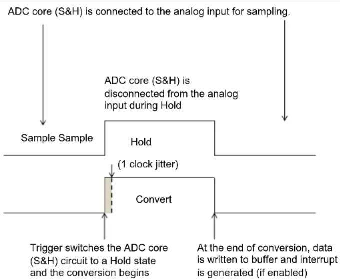
flowchart
graph TD
    A["ADC core (S&H) is connected to the analog input for sampling."] --> B["Sample Sample"]
    B --> C["Hold"]
    C --> D["(1 clock jitter)"]
    D --> E["Convert"]
    E --> F["Trigger switches the ADC core (S&H) circuit to a Hold state and the conversion begins"]
    E --> G["At the end of conversion, data is written to buffer and interrupt is generated (if enabled)."]
Class 2 and Class 3 analog input properties:
- Class 2 inputs are used on the shared ADC module, either individually triggered or as part of a scan list. When used individually they are triggered by their unique trigger selected by the ADCTRGx register.
- The analog inputs on the shared ADC have a natural order of priority (for example, AN7 has a higher priority than AN12)
- Class 3 inputs are used exclusively for scanning and share a common trigger source (scan trigger)
- Since Class 3 analog inputs share both the ADC module and the trigger source, the only method possible to convert them is to scan them sequentially for each incoming scan trigger event, where scanning occurs in the natural order of priority
- Unlike Class 1 analog inputs, the arrival of a trigger in the shared ADC module only starts the sampling. When the trigger arrives, the ADC module goes into sampling mode for the sampling time decided by the SAMC<9:0> bits (ADCCON2<25:16>). At the end of sampling, the ADC starts conversion. Upon completion of conversion, the ADC module is used to convert the next in line Class 2 or Class 3 inputs, according to the natural order of priority. When a shared analog input (Class 2 or Class 3) has completed all conversion and no trigger is pending, the ADC module is disconnected from all analog inputs.
Figure 22-5: Sample and Conversion Sequence for Shared ADC Modules
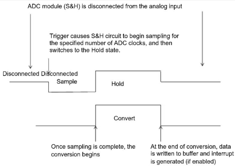
flowchart
graph TD
    A["ADC module (S&H) is disconnected from the analog input"] --> B["Trigger causes S&H circuit to begin sampling for the specified number of ADC clocks, and then switches to the Hold state."]
    B --> C["Disconnected Disconnected Sample"]
    C --> D["Hold"]
    D --> E["Convert"]
    E --> F["Once sampling is complete, the conversion begins"]
    E --> G["At the end of conversion, data is written to buffer and interrupt is generated (if enabled)."]
22.3.1 Class 2 Triggering
When a single Class 2 input is triggered, it is sampled and converted by the shared S&H using the sequence illustrated in Figure 22-5. When multiple Class 2 inputs are triggered, it is important to understand the consequences of trigger timing. If a conversion is underway and another Class 2 trigger occurs then the sample-hold-conversion for the new trigger will be stalled until the in-process sample-hold cycle is complete, as shown in the Figure 22-6.
Figure 22-6: Multiple Independent Class 2 Trigger Conversion Sequence
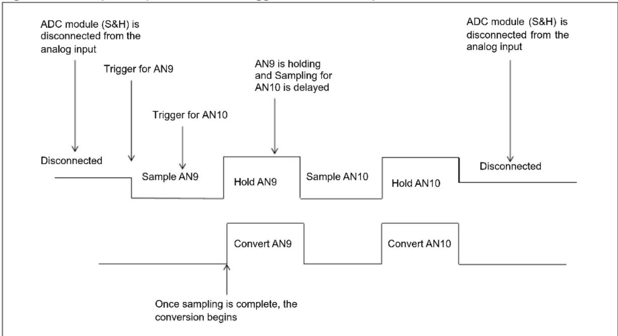
flowchart
graph TD
    A["ADC module (S&H) is disconnected from the analog input"] --> B["Trigger for AN9"]
    B --> C["Sample AN9"]
    C --> D["Hold AN9"]
    D --> E["Sample AN10"]
    E --> F["Hold AN10"]
    F --> G["Transmitted to ADIC module"]
    H["ADC module (S&H) is disconnected from the analog input"] --> I["Transmitted to ADIC module"]
    J["Convert AN9"] --> K["Once sampling is complete, the conversion begins"]
    L["Convert AN10"] --> M["Once sampling is complete, the conversion begins"]
When multiple inputs to the shared S&H are triggered simultaneously, the processing order is determined by their natural priority (the lowest numbered input has the highest priority). As an example, if AN9, AN10, and AN11 are triggered simultaneously, AN9 will be sampled and converted first, followed by AN10 and finally, AN11. When using the independent Class 2 triggering on the shared S&H, the SAMC<9:0> bits (ADCCON2<25:16>) determine the sample time for all inputs while the appropriate TRGSRC<4:0> bits in the ADCTRGx Register (see Register 22-18) determine the trigger source for each input.
22.3.2 Input Scan
Input scanning is a feature that allows an automated scanning sequence of multiple Class 1, Class 2 or Class 3 inputs. All Class 2 and Class 3 inputs are scanned using the single shared S&H. Class 1 inputs are scanned using their dedicated S&H on the dedicated ADC module. The selection of analog inputs for scanning is done with the CSSx bits of the ADCCSS1 and ADCCSS2 registers. Class 1 and Class 2 inputs are triggered using STRIG selection in ADCTRGx register and Class 3 inputs are triggered using the STRGSRC<4:0> of ADCCON1<20:16> register. When a trigger occurs, all Class 1 inputs are captured simultaneously and conversions are started simultaneously. For Class 2 or Class 3 inputs, the sampling and conversion occur in the natural input order is used; lower number inputs are sampled before higher number inputs.
Figure 22-7: Input Scan Conversion Sequence for Three Class 2 Inputs

flowchart
graph TD
    A["ADC module (S&H) is disconnected from the analog input"] --> B["Trigger causes S&H circuit to begin sampling first input in the scan list for the specified number of ADC clocks, and then switches to Hold state."]
    B --> C["Once the first conversion is complete, sampling begins for next input in scan list"]
    C --> D["Sample AN9"]
    D --> E["Hold AN9"]
    E --> F["Sample AN10"]
    F --> G["Hold AN10"]
    G --> H["Sample AN11"]
    H --> I["Hold AN11"]
    I --> J["Disconnected"]
    J --> K["Once sampling is complete, the conversion begins"]
    K --> L["Convert AN9"]
    L --> M["Convert AN10"]
    M --> N["Convert AN11"]
    N --> O["When each conversion is complete, the result is written to the ADC result buffer and an interrupt is generated"]
    O --> P["Disconnected"]
When using the shared analog inputs in scan mode, the SAMC<9:0> bits in the ADC Control Register 2 (ADCCON2<25:16>) determine the sample time for all inputs while the Scan Trigger Source Selection bits (STRGSRC<4:0>) in the ADC Control Register 1 (ADCCON1<20:16>), determine the trigger source.
To ensure predicable results, a scan should not be retriggered until sampling of all inputs has completed. Care should be taken in the system design to preclude retriggering a scan while a scan is in progress.
Individual Class 2 triggers that occur during a scan will pre-empt the scan sequence if they are a higher priority than the sample currently being processed. In Figure 22-8, a scan of AN11, AN12, and AN13 is underway when an independent trigger of Class 2 input AN8 takes place.
The scan is interrupted for the sampling and conversion of AN8.
Figure 22-8: Scan Conversion Pre-empted by Class 2 Input Trigger

flowchart
graph TD
    A["Scan trigger starts scan process of inputs AN11, AN12 and AN13"] --> B["Sample AN11"]
    B --> C["Hold AN11"]
    C --> D["Sample AN12"]
    D --> E["Hold AN12"]
    E --> F["Sample AN6"]
    F --> G["Hold AN8"]
    G --> H["Sample AN13"]
    H --> I["Hold AN13"]
    I --> J["Convert AN13"]
    J --> K["Convert AN8"]
    K --> L["Convert AN12"]
    L --> M["Convert AN11"]
    M --> N["Sample AN11"]
    style A fill:#f9f,stroke:#333
    style J fill:#f9f,stroke:#333
    style K fill:#f9f,stroke:#333
    style L fill:#f9f,stroke:#333
    style M fill:#f9f,stroke:#333
    style N fill:#f9f,stroke:#333
22.4 ADC MODULE CONFIGURATION
Operation of the ADC module is directed through bit settings in the specific registers. The following instructions summarize the actions and the settings. The options and details for each configuration step are provided in the subsequent sections.
To configure the ADC module, perform the following steps:
- Configure the analog port pins, as described in 22.4.1 "Configuring the Analog Port Pins".
- Initialize the ADC calibration values by copying them from the factory-programmed DEVADCx Flash registers into the corresponding ADCxCFG registers.
- Select the analog inputs to the ADC multiplexers, as described in 22.4.2 "Selecting the ADC Multiplexer Analog Inputs".
- Select the format of the ADC result, as described in 22.4.3 "Selecting the Format of the ADC Result".
- Select the conversion trigger source, as described in 22.4.4 "Selecting the Conversion Trigger Source".
- Select the voltage reference source, as described in 22.4.5 "Selecting the Voltage Reference Source".
- Select the scanned inputs, as described in 22.4.6 "Selecting the Scanned Inputs".
- Select the analog-to-digital conversion clock source and prescaler, as described in 22.4.7 "Selecting the Analog-to-Digital Conversion Clock Source and Prescaler".
- Specify any additional acquisition time, if required, as described in 22.10 "ADC Sampling Requirements".
- Turn on the ADC module, as described in Equation 22-2: "Sample Time for the Shared ADC Module".
- Poll (or wait for the interrupt) for the voltage reference to be ready, as described in 22.4.5 "Selecting the Voltage Reference Source".
- Enable the analog and bias circuit for required ADC modules and after the ADC module wakes-up, enable the digital circuit, as described in 22.7.3 "ADC Low-power Mode"
- Configure the ADC interrupts (if required), as described in 22.6 "Interrupts".
22.4.1 Configuring the Analog Port Pins
The ANSELx registers for the I/O ports associated with the analog inputs are used to configure the corresponding pin as an analog or a digital pin. A pin is configured as analog input when the corresponding ANSELx bit = 1. When the ANSELx bit = 0, the pin is set to digital control. The ANSELx registers are set when the device comes out of Reset, causing the ADC input pins to be configured as analog inputs by default.
The TRISx registers control the digital function of the port pins. The port pins that are required as analog inputs must have their corresponding bit set in the specific TRISx register, configuring the pin as an input. If the I/O pin associated with an ADC input is configured as an output by clearing the TRISx bit, the port's digital output level ( _H or V_OL ) will be converted. After a device Reset, all of the TRISx bits are set. For more information on port pin configuration, refer to the "I/O Ports" chapter of the specific device data sheet.
Note: When reading a PORT register that shares pins with the ADC, any pin configured as an analog input reads as a '0' when the PORT latch is read. Analog levels on any pin that is defined as a digital input but not configured as an analog input, may cause the input buffer to consume current that exceeds the device specification.
Example 22-1: Initializing and Using ADC Class 1 Input
int main(int argc, char** argv) {
    int result[3];

    /* Initialize ADC calibration setting */
    ADC0CFG = DEVADC0;
    ADC1CFG = DEVADC1;
    ADC2CFG = DEVADC2;
    ADC3CFG = DEVADC3;
    ADC4CFG = DEVADC4;
    ADC5CFG = DEVADC5;
    ADC7CFG = DEVADC7;

    /* Configure ADCCON1 */
    ADCCON1 = 0; // No ADCCON1 features are enabled including: Stop-in-Idle, turbo, // CVD mode, Fractional mode and scan trigger source.

    /* Configure ADCCON2 */
    ADCCON2 = 0; // Since, we are using only the Class 1 inputs, no setting is // required for ADCDIV

    /* Initialize warm up time register */
    ADCANCON = 0;
    ADCANCONbits.WKUPCLKCNT = 5; // Wakeup exponent = 32 * TADx

    /* Clock setting */
    ADCCON3 = 0;
    ADCCON3bits.ADCSEL = 0; // Select input clock source
    ADCCON3bits.CONCLKDIV = 1; // Control clock frequency is half of input clock
    ADCCON3bits.VREFSEL = 0; // Select AVDD and AVSS as reference source

    /* Select ADC sample time and conversion clock */
    ADC0TIMEbits.ADCDIV = 1; // ADC0 clock frequency is half of control clock = TAD0
    ADC0TIMEbits.SAMC = 5; // ADC0 sampling time = 5 * TAD0
    ADC0TIMEbits.SELRES = 3; // ADC0 resolution is 12 bits
    ADC1TIMEbits.ADCDIV = 1; // ADC1 clock frequency is half of control clock = TAD1
    ADC1TIMEbits.SAMC = 5; // ADC1 sampling time = 5 * TAD1
    ADC1TIMEbits.SELRES = 3; // ADC1 resolution is 12 bits
    ADC2TIMEbits.ADCDIV = 1; // ADC2 clock frequency is half of control clock = TAD2
    ADC2TIMEbits.SAMC = 5; // ADC2 sampling time = 5 * TAD2
    ADC2TIMEbits.SELRES = 3; // ADC2 resolution is 12 bits

    /* Select analog input for ADC modules, no presync trigger, not sync sampling */
    ADCTRGMODEbits.SH0ALT = 0; // ADC0 = AN0
    ADCTRGMODEbits.SH1ALT = 0; // ADC1 = AN1
    ADCTRGMODEbits.SH2ALT = 0; // ADC2 = AN2

    /* Select ADC input mode */
    ADCIMCON1bits.SIGN0 = 0; // unsigned data format
    ADCIMCON1bits.DIFF0 = 0; // Single ended mode
    ADCIMCON1bits.SIGN1 = 0; // unsigned data format
    ADCIMCON1bits.DIFF1 = 0; // Single ended mode
    ADCIMCON1bits.SIGN2 = 0; // unsigned data format
    ADCIMCON1bits.DIFF2 = 0; // Single ended mode

    /* Configure ADCGIRQENx */
    ADCGIRQEN1 = 0; // No interrupts are used
    ADCGIRQEN2 = 0;

    /* Configure ADCCSSx */
    ADCCSS1 = 0; // No scanning is used
    ADCCSS2 = 0;

    /* Configure ADCCMPCONx */
    ADCCMPCON1 = 0; // No digital comparators are used. Setting the ADCCMPCONx
    ADCCMPCON2 = 0; // register to '0' ensures that the comparator is disabled.
    ADCCMPCON3 = 0; // Other registers are "don't care".
    ADCCMPCON4 = 0;
    ADCCMPCON5 = 0;
    ADCCMPCON6 = 0;
Example 22-1: Initializing and Using ADC Class 1 Input (Continued)
/* Configure ADCFLTRx */
ADCFLTR1 = 0;    // No oversampling filters are used.
ADCFLTR2 = 0;
ADCFLTR3 = 0;
ADCFLTR4 = 0;
ADCFLTR5 = 0;
ADCFLTR6 = 0;

/* Set up the trigger sources */
ADCTRGSNSbits.LVL0 = 0;    // Edge trigger
ADCTRGSNSbits.LVL1 = 0;    // Edge trigger
ADCTRGSNSbits.LVL2 = 0;    // Edge trigger
ADCTRGLbits.TRGSRC0 = 1;    // Set AN0 to trigger from software.
ADCTRGLbits.TRGSRC1 = 1;    // Set AN1 to trigger from software.
ADCTRGLbits.TRGSRC2 = 1;    // Set AN2 to trigger from software.

/* Early interrupt */
ADCEIEN1 = 0;    // No early interrupt
ADCEIEN2 = 0;

/* Turn the ADC on */
ADCCON1bits.ON = 1;

/* Wait for voltage reference to be stable */
while(!ADCCON2bits.BGVRRDY);    // Wait until the reference voltage is ready
while(ADCCON2bits.REFFLT);    // Wait if there is a fault with the reference voltage

/* Enable clock to analog circuit */
ADCANCONbits.ANEN0 = 1;    // Enable the clock to analog bias
ADCANCONbits.ANEN1 = 1;    // Enable the clock to analog bias
ADCANCONbits.ANEN2 = 1;    // Enable the clock to analog bias

/* Wait for ADC to be ready */
while(!ADCANCONbits.WKRDY0);    // Wait until ADC0 is ready
while(!ADCANCONbits.WKRDY1);    // Wait until ADC1 is ready
while(!ADCANCONbits.WKRDY2);    // Wait until ADC2 is ready

/* Enable the ADC module */
ADCCON3bits.DIGEN0 = 1;    // Enable ADC0
ADCCON3bits.DIGEN1 = 1;    // Enable ADC1
ADCCON3bits.DIGEN2 = 1;    // Enable ADC2

while (1) {
    /* Trigger a conversion */
    ADCCON3bits.GSWTRG = 1;

    /* Wait the conversions to complete */
    while (ADCDSTAT1bits.ARDY0 == 0);
    /* fetch the result */
    result[0] = ADCDATA0;

    while (ADCDSTAT1bits.ARDY1 == 0);
    /* fetch the result */
    result[1] = ADCDATA1;

    while (ADCDSTAT1bits.ARDY2 == 0);
    /* fetch the result */
    result[2] = ADCDATA2;

    /*
    * Process results here
    *
    * Note: Loop time determines the sampling time since all inputs are Class 1.
    * If the loop time is small and the next trigger happens before the completion
    * of set sample time, the conversion will happen only after the sample time
    * has elapsed.
    *
    */
}
return (1);
}
22.4.2 Selecting the ADC Multiplexer Analog Inputs
Each ADC module has two inputs referred to as the positive and negative inputs. Input selection options vary for the dedicated and shared ADC module are described in the following sections.
22.4.2.1 SELECTION OF POSITIVE INPUTS
For dedicated ADC modules, four alternate selection is provided for each positive input. This alternate input can be chosen using the SHxALT<1:0> bits in the ADC Triggering Mode Register (ADCTRGMODE) as follows:
• SH0ALT<1:0> (ADCTRGMODE<17:16>)
• SH1ALT<1:0> (ADCTRGMODE<19:18>)
• SH2ALT<1:0> (ADCTRGMODE<21:20>)
• SH3ALT<1:0> (ADCTRGMODE<23:22>)
• SH4ALT<1:0> (ADCTRGMODE<25:24>)
• SH5ALT<1:0> (ADCTRGMODE<27:26>)
• SH6ALT<1:0> (ADCTRGMODE<29:28>)
Refer to the device data sheet for possible alternate selection of ADC inputs.
For the shared ADC module, the positive input is shared among all Class 2 and Class 3 inputs. Input connection of the analog input ANx to the shared ADC is automatic for either Class 2 input trigger or during a scan of Class 2 and or Class 3 inputs. Selecting inputs for scanning is discussed separately in 22.4.6 "Selecting the Scanned Inputs".
22.4.2.2 SELECTION OF NEGATIVE INPUTS
Negative input selection is determined by the setting of the DIFFx bit of the ADCIMCONx register. The DIFFx bit allows the inputs to be rail-to-rail, and either single-ended or differential. The SIGNx and DIFFx bits in the ADCIMCONx registers scale the internal ADC analog inputs and reference voltages and configure the digital result to align with the expected full-scale output range.
For the shared ADC module, the analog inputs have individual settings for the DIFFx bit. Therefore, the user has the ability to select certain inputs as single-ended and others as differential, while being connected to the same shared ADC module. While sampling, the signal will change on-the-fly as single-ended or differential, according to its corresponding DIFFx bit setting.
Table 22-3: Negative Input Selection
| ADCIMCON1 | InputConfiguration | Input Voltage | Output | |||
| DIFFx | SIGNx | |||||
| 1 | 1 | Differential 2's complement | Minimum input | VINP - VINN = -VREF | -2048 | |
| Maximum input | VINP - VINN = VREF | +2047 | ||||
| 1 | 0 | Differential unipolar | Minimum input | VINP - VINN = -VREF | 0 | |
| Maximum input | VINP - VINN = VREF | +4095 | ||||
| 0 | 1 | Single-ended 2's complement | Minimum input | VINP = VREF | -2048 | |
| Maximum input | VINP - VINN = VREF | +2047 | ||||
| 0 | 0 | Single-ended unipolar | Minimum input | VINP = VREF | 0 | |
| Maximum input | VINP - VINN = VREF | +4095 | ||||
Legend: V_INP = Positive S\&H input; V_INN = Negative S\&H input; V_REF = V_REFH - V_REFL
Note: For proper operation and to prevent device damage, input voltage levels should not exceed the limits listed in the “Electrical Characteristics” chapter of the specific device data sheet.
22.4.3 Selecting the Format of the ADC Result
The data in the ADC Result register can be read in any of the four supported data formats. The user can select from unsigned integer, signed integer, unsigned fractional, or signed fractional. Integer data is right-justified and fractional data is left-justified.
- The integer or fractional data format selection is specified globally for all analog inputs using the Fractional Data Output Format bit, FRACT (ADCCON1<23>)
- The signed or unsigned data format selection can be independently specified for each individual analog input using the SIGNx bits in the ADCIMCONx registers.
Table 22-4 provides how ADC result is formatted.
Table 22-4: ADC Result Format Results
| FRACT | SIGNx | Description 32-bit Output Data Format | ||||||
| 0 | 0 | Unsigned integer | 0000 | 0000 | 0000 | 0000 | 0000 | |
| 0000 | dddd | dddd | dddd | dddd | ||||
| 0 | 1 | Signed integer | ssss | ssss | ssss | ssss | ssss | |
| ssss | sddd | dddd | dddd | dddd | ||||
| 1 | 0 | Fractional | dddd | dddd | dddd | 0000 | ||
| 0000 | 0000 | 0000 | 0000 | 0000 | ||||
| 1 | 1 | Signed fractional | sddd | dddd | dddd | dddd | dd | |
| 0000 | 0000 | 0000 | 0000 | 0000 | ||||
Example 22-2: ADC Class 2 Configuration and Fractional Format
int main(int argc, char** argv) {
    int result[3];

    /* Configure ADCCON1 */
    ADCCON1bits.FRACT = 1; // use Fractional output format
    ADCCON1bits.SELRES = 3; // ADC7 resolution is 12 bits
    ADCCON1bits.STRGSRC = 0; // No scan trigger.

    /* Configure ADCCON2 */
    ADCCON2bits.SAMC = 5; // ADC7 sampling time = 5 * TAD7
    ADCCON2bits.ADCDIV = 1; // ADC7 clock freq is half of control clock = TAD7

    /* Initialize warm up time register */
    ADCANCON = 0;
    ADCANCONbits.WKUPCLKCNT = 5; // Wakeup exponent = 32 * TADx

    /* Clock setting */
    ADCCON3 = 0;
    ADCCON3bits.ADCSEL = 0; // Select input clock source
    ADCCON3bits.CONCLKDIV = 1; // Control clock frequency is half of input clock
    ADCCON3bits.VREFSEL = 0; // Select AVDD and AVSS as reference source

    /* No selection for dedicated ADC modules, no presync trigger, not sync sampling */
    ADCTRGMODEbits = 0;

    /* Select ADC input mode */
    ADCIMCON1bits.SIGN7 = 0; // unsigned data format
    ADCIMCON1bits.DIFF7 = 0; // Single ended mode
    ADCIMCON1bits.SIGN8 = 0; // unsigned data format
    ADCIMCON1bits.DIFF8 = 0; // Single ended mode
    ADCIMCON1bits.SIGN9 = 0; // unsigned data format
    ADCIMCON1bits.DIFF9 = 0; // Single ended mode

    /* Configure ADCGIRQENx */
    ADCGIRQEN1 = 0; // No interrupts are used
    ADCGIRQEN2 = 0;

    /* Configure ADCCSSx */
    ADCCSS1 = 0; // No scanning is used
    ADCCSS2 = 0;

    /* Configure ADCCMPCONx */
    ADCCMPCON1 = 0; // No digital comparators are used. Setting the ADCCMPCONx
    ADCCMPCON2 = 0; // register to '0' ensures that the comparator is disabled.
    ADCCMPCON3 = 0; // Other registers are "don't care".
    ADCCMPCON4 = 0;
    ADCCMPCON5 = 0;
    ADCCMPCON6 = 0;

    /* Configure ADCFLTRx */
    ADCFLTR1 = 0; // No oversampling filters are used.
    ADCFLTR2 = 0;
    ADCFLTR3 = 0;
    ADCFLTR4 = 0;
    ADCFLTR5 = 0;
    ADCFLTR6 = 0;
    /* Set up the trigger sources */
    ADCTRGSNSbits.LVL7 = 0; // Edge trigger
    ADCTRGSNSbits.LVL8 = 0; // Edge trigger
    ADCTRGSNSbits.LVL9 = 0; // Edge trigger
    ADC1TRG2bits.TRGSRC7 = 1; // Set AN7 to trigger from software
    ADC2TRG3bits.TRGSRC8 = 1; // Set AN8 to trigger from software
    ADC2TRG3bits.TRGSRC9 = 1; // Set AN9 to trigger from software
Example 22-2: ADC Class 2 Configuration and Fractional Format (Continued)
/* Early interrupt */
ADCEIEN1 = 0; // No early interrupt
ADCEIEN2 = 0;

/* Turn the ADC on */
ADCCON1bits.ON = 1;

/* Wait for voltage reference to be stable */
while(!ADCCON2bits.BGVRRDY); // Wait until the reference voltage is ready
while(ADCCON2bits.REFFLT); // Wait if there is a fault with the reference voltage

/* Enable clock to analog circuit */
ADCANCONbits.ANEN7 = 1; // Enable the clock to analog bias

/* Wait for ADC to be ready */
while(!ADCANCONbits.WKRDY7); // Wait until ADC7 is ready

/* Enable the ADC module */
ADCCON3bits.DIGEN7 = 1; // Enable ADC7

while (1) {
    /* Trigger a conversion */
    ADCCON3bits.GSWTRG = 1;

    /* Wait the conversions to complete */
    while (ADCDSTAT1bits.ARDY7 == 0);
    /* fetch the result */
    result[0] = ADCDATA7;

    while (ADCDSTAT1bits.ARDY8 == 0);
    /* fetch the result */
    result[1] = ADCDATA8;

    while (ADCDSTAT1bits.ARDY9 == 0);
    /* fetch the result */
    result[2] = ADCDATA9;

    /*
    * Process results here
    *
    * Note 1: Loop time determines the sampling time since all inputs are Class 2.
    * If the loop time happens is small and the next trigger happens before the
    * completion of set sample time, the conversion will happen only after the
    * sample time has elapsed.
    *
    * Note 2: Results are in fractional format
    *
    */
}
return (1);
22.4.4 Selecting the Conversion Trigger Source
Class 1 and Class 2 inputs to the ADC module can be triggered for conversion either individually, or as part of a scan sequence. Class 3 inputs can only be triggered as part of a scan sequence. Individual or scan triggers can originate from an on-board timer or output compare peripheral event, from external digital circuits connected to INT0, from external analog circuits connected to an analog comparator, or through software by setting a trigger bit in a SFR.
Note: When conversion triggers for multiple Class 2 analog inputs occur simultaneously, they are prioritized according to a natural order priority scheme based on the analog input used. AN7 has the highest priority, AN8 has the next highest priority, etc.
22.4.4.1 TRIGGER SELECTION FOR CLASS 1 AND CLASS 2 INPUTS
For each one of the Class 1 and Class 2 inputs, the user application can independently specify a conversion trigger source. The individual trigger source for an analog input 'x' is specified by the TRGSRC<4:0> bits located in registers ADCTRG1 through ADCTRG8. Refer to the "ADC" chapter of the specific device data sheet for more information on the available conversion trigger options. For example, these trigger sources may include:
- General Purpose (GP) Timers: When a period match occurs for the 32-bit timer, Timer3/2 or Timer5/4, or the 16-bit Timer1, Timer3 or Timer5, a special ADC trigger event signal is generated by the timer. This feature does not exist for other timers. For more information, refer to Section 14. "Timers" (DS60001105) and the "Timer" chapters in the specific device data sheet.
- Output Compare: The Output Compare peripherals, OC1, OC3, and OC5, can be used to generate an ADC trigger then the output transitions from a low to high state. For more information, refer to Section 16. "Output Compare" (DS60001111), and the "Output Compare" chapter in the specific device data sheet.
- Comparators: The analog Comparators can be used to generate an ADC trigger when the output transitions from a low state to a high state. For more information, refer to Section 19. "Comparator" (DS60001110), and the "Comparator" chapter in the specific device data sheet.
- External INT0 Pin Trigger: In this mode, the ADC module starts a conversion on an active transition on the INT0 pin. The INT0 pin may be programmed for either a rising edge input or a falling edge input to trigger the conversion process.
- Global Software Trigger: The ADC module can be configured for manually triggering a conversion for all inputs that have selected this trigger option. The user can manually trigger a conversion by setting the Global Software Trigger bit, GSWTRG (ADCCON3<6>).
22.4.4.2 PRESYNCHRONIZED TRIGGER AND ASYNCHRONOUS SAMPLING FOR CLASS 1 ANALOG INPUTS
The ADCTRGx register is used for ADC triggers.
- Converted data can be stored in dedicated output registers (ADCDATAx)
- Converted data can be stored in the FIFO
- Converted data can be stored in system RAM using the DMA engine
The ADCTRGMODE register contains the trigger mode for the ADC module determined by the STRGEN bit (presynchronized trigger enable) and the SSAMPEN bit (synchronous sampling also for the first sample after being idle or disabled).
Note 1: The trigger and synchronization works on "control clock (T Q)". But the sampling time (tSAMCx) is based on clock (which is derived from the signal after passing through a divisor).
2: When Synchronous sampling is used (SSAMPEN = 1), the presynchronized trigger value is ignored (STRGEN = "don't care").
22.4.4.2.1 Synchronous Sampling (SSAMPEN = 1) →
After a trigger event, sampling ends and conversion starts exactly (2 Q T+ \AMCX) after presynchronized trigger or \AMC after the previous conversion, where \$AMCX is the sample time set by the SAMC<9:0> (ADCxTIME<9:0>) bits.
22.4.4.2.2 Asynchronous Sampling (SSAMPEN = 0) →
After a trigger event, sampling ends and conversion starts immediately (with or without presynchronized), provided that (2 × T_Q + t_SAMCX) after pre-synchronized trigger or tSAMCX after previous conversion, is met and already completed (elapsed). If the time is not met, then the sampling will go on for tSAMCX time and only then conversion starts. Effectively, this becomes a synchronous sampling, but only when the tSAMCX requirement is not met before the last asynchronous trigger. If the tSAMCX requirement is met before the last asynchronous trigger, in fact the last trigger will issue an asynchronous end-of-sampling. It is only the start-of-conversion which is always synchronous. The variable delay between the asynchronous end-of-sampling and the next clock-positive edge-aligned start-of-conversion is bridged by the sampling capacitor which holds the analog voltage value unchanged until it can be converted by the synchronous ADC.
Table 22-5: Class 1 ADC Triggering
| STRGEN | SSAMPEN | Description |
| 0 | 0 | No presynchronized trigger and asynchronous sampling. |
| 1 | 0 | Presynchronized trigger and asynchronous sampling. |
| x | 1 | Synchronous sampling. |
Figure 22-9 graphically explains the various cases for the STRGEN and SSAMPEN bits. Any trigger is asynchronous by nature and similarly, the trigger for ADC module being asynchronous can arrive any time, with reference to a single T α clock. This is depicted by “(1 period jitter)”. Once the trigger is received, the “presynchronized trigger” occurs 1 T α clock after the actual trigger. Please note that the presynchronized trigger is an internal signal.
Considering the case when both STRGENx and SSAMPENx are '0' (no presynchronized trigger and asynchronous sampling), the asynchronous trigger causes the ADC to switch from Sample mode to Conversion mode. In other words, in such a situation, the presynchronized trigger is ignored (i.e., not used). This is true only if the sample time ( AMCX ) is met.
Considering the next case, when STRGENx = 1 and SSAMPENx = 0 (presynchronized trigger and asynchronous sampling), the presynchronized trigger is the signal that causes the ADC to switch from Sample mode to Conversion mode. This condition is true only if the sample time ( t_SAMCX ) is met.
For both conditions previously mentioned STRGENx, SSAMPENx = 00 and STRGENx, SSAMPENx = 10), the explained behaviors are true if sample time (tSAMCx) is met. In a case of a repeated trigger and when sample time (tSAMCx) is met, the explained behavior is graphically depicted in Figure 22-10. The figure shows that the second trigger occurs after the tSAMCx time is elapsed. Therefore, the second trigger causes the ADC to switch from Sample mode to Convert mode. Please note that, the trigger (first or second trigger) is an asynchronous trigger or a presynchronized trigger, based on the setting of STRGENx, SSAMPENx as '00' or '10'.
In case where the \$AMCx time is not met, the trigger (whether asynchronous or presynchronized) would not cause the switch from sample to convert. Instead, the ADC will wait for tSAMCx time before switching from sample to convert mode. This is depicted in Figure 22-11. In the figure, the second trigger occurs well before the tSAMCx time is elapsed. Therefore, this trigger does not cause a start of conversion. Instead, the sample-to-conversion happens only after the tSAMCx time is complete. In other words, even while setting the ADC to Asynchronous Sampling mode (SSAMPEN = 0), the behavior of the ADC will be synchronous if the sample time (tSAMCx) is not met between each trigger.
Returning to Figure 22-9 and considering the case when STRGENx = x and SSAMPENx = 1 (synchronous sampling), the ADC switches from sample to conversion (2^*T Q + t_SAMCX) after the presynchronized trigger.
Figure 22-9: Presynchronized Trigger (STRGEN bit) and Synchronized Sampling (SSAMPEN bit)

flowchart
graph TD
    A["Control Clock (TQ)"] --> B["Trigger"]
    B --> C["(1 period jitter)"]
    C --> D["Presynchronized Trigger"]
    D --> E["Sample ends"]
    E --> F["Conversion starts"]
    F --> G["fSAMCx already completed in past"]
    G --> H["Total Sample Time"]
    H --> I["Sample ends, Conversion starts"]
    I --> J["fSAMCx (ADCxTIME<9:0>)"]
    J --> K["'x1': STRGENx = 0 or 1, SSAMPENx = 1"]
    K --> L["'10': STRGENx = 1, SSAMPENx = 0"]
    style A fill:#f9f,stroke:#333
    style B fill:#ccf,stroke:#333
    style C fill:#cfc,stroke:#333
    style D fill:#fcc,stroke:#333
    style E fill:#cff,stroke:#333
    style F fill:#ffc,stroke:#333
    style G fill:#fcf,stroke:#333
    style H fill:#cff,stroke:#333
    style I fill:#ffc,stroke:#333
    style J fill:#cfc,stroke:#333
    style K fill:#fcc,stroke:#333
    style L fill:#ffc,stroke:#333
Figure 22-10: Asynchronous Sampling (SSAMPEN = 0) (When trigger is at rate such that tSAMcx is met, the ADC allows asynchronous trigger to start conversion)
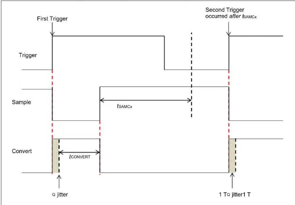
flowchart
graph TD
    A["First Trigger"] --> B["Trigger"]
    B --> C["Sample"]
    C --> D["Convert"]
    D --> E["α jitter"]
    D --> F["tCONVERT"]
    F --> G["1 To jitter1 T"]
    H["Second Trigger occurred after tsAMCx"] --> I["→"]
    J["tsAMCx"] --> K["→"]
    L["σ jitter"] --> M["→"]
Figure 22-11: Asynchronous Sampling (SSAMPEN = 0) (When trigger is too fast (before tSAMCx is complete), the ADC enforces minimum sampling time (SAMCx) and defaults to synchronous sampling)
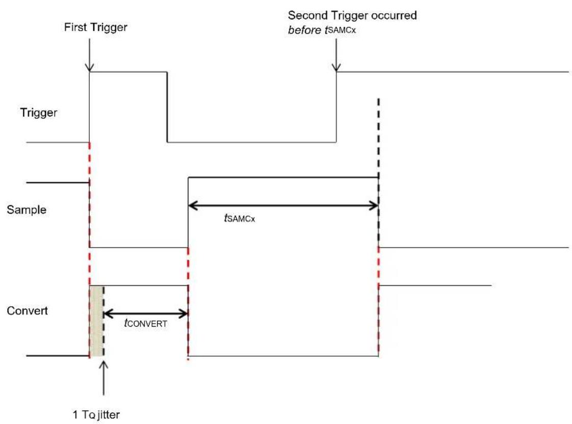
flowchart
graph TD
    A["First Trigger"] --> B["Trigger"]
    B --> C["Sample"]
    C --> D["Convert"]
    D --> E["1 To jitter"]
    F["Second Trigger occurred before tSAMCx"] --> G["tsAMCx"]
    D --> H["tCONVERT"]
    style D fill:#f9f,stroke:#333
    style G fill:#ccf,stroke:#333
    style H fill:#cfc,stroke:#333
Class 1 inputs are usually meant to convert analog signals that are fast and transitory in nature. In addition, multiple Class 1 inputs would be required to convert different analog signals that are in phase relation to each other. Examples of such a signal would be 3-phase current signals of a motor.
Considering a case when ADC0, ADC1, and ADC2 are used to sample 3-phase current and all of the ADC modules use STRGENx, SSAMPENx = 00 (no presynchronized trigger and asynchronous sampling), the individual trigger for ADC occurs at slightly different times (due to propagation delay of trigger signal). This is depicted in Figure 22-12. This difference in trigger causes a phase error in the sampled analog signal. To avoid such errors, the presynchronized trigger and asynchronous sampling should be used (i.e., STRGENx, SSAMPENx = 10). The usage of a presynchronized trigger will ensure that all of the ADC modules receive the trigger at exactly the same time.
Figure 22-12: Presynchronized Trigger Waveform (When multiple Class 1 inputs are used to convert phase currents of a 3-phase motor)
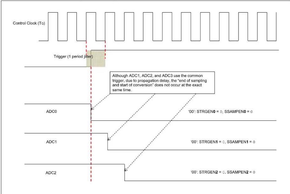
flowchart
graph TD
    A["Control Clock (Tα)"] --> B["Trigger (1 period jitter)"]
    B --> C["ADC0"]
    C --> D["'00': STRGEN0 = 0, SSAMPEN0 = 0"]
    C --> E["'00': STRGEN1 = 0, SSAMPEN1 = 0"]
    C --> F["'00': STRGEN2 = 0, SSAMPEN2 = 0"]
    G["ADC1"] --> H["..."]
    I["ADC2"] --> J["..."]
    style A fill:#f9f,stroke:#333
    style B fill:#ccf,stroke:#333
    style C fill:#cfc,stroke:#333
    style D fill:#fcc,stroke:#333
    style E fill:#fcc,stroke:#333
    style F fill:#fcc,stroke:#333
    note right of B: Although ADC1, ADC2, and ADC3 use the common trigger due to propagation delay, the "end of sampling and start of conversion" does not occur at the exact same time.
Since the trigger and synchronization works with the control clock (T α) and the ADC modules work on their own clock (TADx), proper synchronization should be maintained between the two clock domains. For proper synchronization, two bits are provided, FSSCLKEN (ADCCON1<10> and FSPBCLKEN (ADCCON1<9>). The usage of these bits are as follows:
- Set the FSSCLKEN bit if one of the following conditions is true:
- ADCSEL<1:0> = (SYSCLK)
- ADCSEL<1:0> = (REFCLK3) and the REFCLK3 is also a divided clock derived from the system clock (SYSCLK)
- ADCSEL<1:0> = (FRC) and the system clock is also set to be driven by FRC
- ADCSEL<1:0> = PBCLK (for PIC32MZ family)/SYSCLK (for PIC32MK family) and the PBCLK (for PIC32MZ family) clock is a divided clock derived from the system clock
- Set the FSPBCLKEN bit if one of the following conditions is true:
- ADCSEL<1:0> = SYSCLK and the peripheral clock is a divided clock from the system clock and the ADC is not faster than the peripheral clock. This means that both the peripheral clock and the ADC clock are divided from the same system clock, but the division ratio of the ADC clock is higher than or equal to the division ratio of the peripheral clock, which makes the peripheral clock synchronous to, but not slower than the ADC clock.
- ADCSEL<1:0> = REFCLK3 and REFCLK3 is synchronous to, and slower than the peripheral clock, which is true if the peripheral clock is also derived from the REFCLK3, but is not slower than the ADC clock
- ADCSEL<1:0> = FRC and the peripheral clock is also divided from the FRC and is not slower than the ADC clock
- ADCSEL<1:0> = PBCLK (for PIC32MZ family/SYSCLK (for PIC32MK family))
22.4.4.3 CONVERSION TRIGGER SOURCES AND CONTROL
The following are the possible sources for each trigger signal:
- External trigger selection through the TRGSRCx<4:0> bits in the ADCTRGx registers. This capability is supported only for class 1 and class 2 analog inputs. Typically, the user specifies a particular trigger source to initiate a conversion for specific input.
All of the analog inputs may select the same trigger source if desired. In such an event, the result will resemble a "scanned conversion", which will have its order of completion enforced by the priority of the inputs associated with the same trigger source. The first trigger selection is '00000' (no trigger), which amounts to temporarily disabling that particular trigger and consequently, temporarily disabling that analog input from being converted. The next two selections for trigger source (GSWTRG and GLSWTRG) are software generated trigger sources. The second software generated trigger selection is the Global Software Trigger (GSWTRG). This trigger links to the GSWTRG bit in the ADCCON3 register, which may be used to enable the user application to initiate a single conversion. Since GSWTRG is a self-clearing bit, it clears itself on the next ADC clock cycle after being set by the user application. The third software generated trigger selection is the Global Level Software Trigger (GLSWTRG), which is linked to the GLSWTRG bit in the ADCCON3 register. This trigger may be used by the user application to initiate a burst of consecutive samples, as the GLSWTRG bit is not self-clearing. The fourth trigger selection is a special selection, the Scan Trigger selection, which allows the Class 1 and Class 2 analog inputs to be included as members of a global scan of all inputs. The remaining trigger selections 5 to 31 are device dependent. Refer to the specific device data sheet for more information.
- Scanned trigger selection via the STRGSRC<4:0> bits in the ADCCON1 register and select bits in the ADCCSSx registers. This mode is typically used to initiate the conversion of a group of analog inputs. This capability works for Class 1, 2, and 3 analog inputs, but is typically used for Class 3 inputs because they do not have individual associated TRGSRC bits. One of the trigger selections is the GSWTRG bit in the ADCCON3 register, which may be used to enable the user software to initiate a conversion.
- User initiated trigger via the ADINSEL<5:0> bits and the RQCNVRT bit in the ADCCON3 register. This mode enables the user application to create an individual conversion trigger request for a specified analog input. Using this mode enables the user application to trigger the conversion of an input without changing the trigger source configuration of the ADC. This is useful in handling error situations where another software module wants ADC information without disrupting the normal operation of the ADC. This is also the preferred method to generate the initial trigger to start an digital filter sequence.
- User controlled sampling of Class 2 and Class 3 inputs through the ADINSEL<5:0> bits and the SAMP bit in the ADCCON3 register. Setting the SAMP bit causes the Class 2 and Class 3 inputs to be in Sampling mode, while ignoring the selection of the SAMC<9:0> bits. This mode is also useful in software conversion of ADC with software selectable sample time.
- External module (such as PTG) may specify an analog input for conversion through the setting of ECRIEN bit in the ADCCON2 register. This method operates independently of the normal TRGSRC and STRGSRC methods. External modules may still use individual trigger signals and initiate conversions through the normal TRGSRC and STRGSRC methods.
22.4.4.4 USER-REQUESTED INDIVIDUAL CONVERSION TRIGGER (SOFTWARE ADC CONVERSION) (ONLY FOR CLASS 2 AND CLASS 3 INPUTS)
The user can explicitly request a single conversion (by software) of any selected analog input at any time during program execution, without changing the trigger source configuration of the ADC. The steps to be followed for conversion are as follows:
- The analog input ID to be converted is specified by the ADC Input Select bits, ADINSEL<5:0> (ADCCON3<5:0>).
• The sampling of analog input is started by setting the SAMP bit (ADCCON3<9>)
• After the required sampling time (time delay), the SAMP bit is cleared - The conversion of sampled signal is started by setting the RQCNVRT bit (ADCCON3<8>)
- Once the conversion is complete, the ARDYx bit of the ADCDSTATx register will be set. The data can be read from the ADCDATAx register.
Figure 22-13 illustrates the conversion process in graphical form:
Figure 22-13: Individual Conversion Trigger Process

flowchart
graph TD
    A["(AD1CON3<5:0>)"] --> B["Select AN8ADINSEL<5:0>"] --> C["Select AN10"]
    D["SAMP (AD1CON3<9>)"] --> E["SAMP bit is first cleared before the RQCNVRT bit is set"]
    F["Disconnected"] --> G["Sample AN8"] --> H["Hold AN8"] --> I["Hold AN10Sample AN10"] --> J["Disconnected"]
    K["RQCNVRT (AD1CON3<8>)"] --> L["Automatically cleared in next clock Tq"]
    M["Convert AN8"] --> N["Converted data stored in buffer"] --> O["Converted data stored in buffer"]
22.4.5 Selecting the Voltage Reference Source
The user application can select the voltage reference for the ADC module, which can be internal or external. The Voltage Reference Input Selection bits, VREFSEL<2:0> (ADCCON3<15:13>), select the voltage reference for analog-to-digital conversions. The upper voltage reference (VREFH) and the lower voltage reference (VREFL) may be the internal AVD and AVSS voltage rails or the band gap reference generator or the external REF+ and REF- input pins. When the voltage reference and band gap reference are ready, the BGVRRDY (ADCCON2<31>) bit is set. If a Fault occurs in the voltage reference (such as a brown-out), the REFFLT bit (ADCCON2<30>) is set. The BGVRRDY and REFFLT bits can also generate interrupts if the BGVRIEN bit (ADCCON2<15>) and REFFTLIEN bit (ADCCON2<14>) are set, respectively.
The voltages applied to the external reference pins must comply with certain specifications. Refer to the “Electrical Characteristics” chapter in the specific device data sheet for the electrical specifications.
The Analog Input Charge Pump Enable bit, AICPMPEN (ADCCON1<12>), should be set when the difference between the selected reference voltages ( k_EFH-V_REFL ) is less than 0.65 * (AV DD - AVss). Setting this bit does not increase the magnitude of reference voltage; however, setting this bit reduces the series source resistance to the sampling capacitors. This maximizes the SNR for analog-to-digital conversions using small reference voltage rails.
Note 1: The external VREF+ and VREF- pins can be shared with other analog peripherals. Refer to the "Pin Tables" section of the specific device data sheet for more information. In addition, the ANSELx bits for the VREF+ and VREF- pins must be set to Analog mode.
2: The Band Gap reference source is not available on all devices. Please refer to the specific device data sheet to determine availability of this feature.
22.4.6 Selecting the Scanned Inputs
All available analog inputs can be configured for scanning. Class 1 inputs are sampled using their dedicated ADC module. Class 2 and Class 3 inputs are sampled using the shared ADC module. A single conversion trigger source is selected for all of the inputs selected for scanning using the STRGSRC<4:0> bits (ADCCON1<20:16>). On each conversion trigger, the ADC module starts converting in the natural priority all inputs specified in the user-specified scan list (ADCCSS1 or ADCCSS2). For Class 1 inputs, sampling ends at the time of the trigger and conversion for all of them begin in parallel. For Class 2 and Class 3 inputs, the trigger initiates a sequential sample/conversion process in the natural priority order.
An analog input belongs to the scan if it is:
- A Class 3 input. For Class 3 inputs, scan is the only mechanism for conversion.
- A Class 1 or a Class 2 input, which has the scan trigger selected as the trigger source, by selecting the STRIG option in the TRGSRCx<4:0> bits located in the ADCTRG1 through ADCTRG8 registers.
The trigger options available for scan are identical to those available for independent triggering of Class 1 and Class 2 inputs. Any Class 1 or Class 2 inputs that are part of the scan must have the STRIG option selected as their trigger source in the TRGSRCx<4:0> bits.
Note 1: Since the clock divisor, resolution and sampling time for each dedicated ADC module (SELRES, ADCDIV, and SAMC<9:0> bits in the ADCxTIME register), and the shared ADC module (SELRES in the ADCCON1 register, ADCDIV and SAMC<9:0> bits in the ADCCON2 register) are handled through separate registers, if a scan sequence is to be set involving both dedicated and shared inputs, each of these registers must be initialized individually, even in scan mode.
2: The end-of-scan (EOS) is generated only if all Class 1 inputs have completed the scan, and the last shared input conversion has completed. Until both of these conditions are met, the scan sequence is still in effect. Therefore, the EOS Interrupt can be used for any scan sequence, with any combination of input types.
Example 22-3: ADC Scanning Multiple Inputs
int main(int argc, char** argv) {
    int result[3];

    /* Configure ADCCON1 */
    ADCCON1 = 0; // No ADCCON1 features are enabled including: Stop-in-Idle, turbo, // CVD mode, Fractional mode and scan trigger source.
    ADCCON1bits.SELRES = 3; // ADC7 resolution is 12 bits
    ADCCON1bits.STRGSRC = 1; // Select scan trigger.

    /* Configure ADCCON2 */
    ADCCON2bits.SAMC = 5; // ADC7 sampling time = 5 * TAD7
    ADCCON2bits.ADCDIV = 1; // ADC7 clock freq is half of control clock = TAD7

    /* Initialize warm up time register */
    ADCANCON = 0;
    ADCANCONbits.WKUPCLKCNT = 5; // Wakeup exponent = 32 * TADx

    /* Clock setting */
    ADCCON3bits.ADCSEL = 0; // Select input clock source
    ADCCON3bits.CONCLKDIV = 1; // Control clock frequency is half of input clock
    ADCCON3bits.VREFSEL = 0; // Select AVDD and AVSS as reference source

    ADCOTIMEbits.ADCDIV = 1; // ADC0 clock frequency is half of control clock = TAD0
    ADCOTIMEbits.SAMC = 5; // ADC0 sampling time = 5 * TAD0
    ADCOTIMEbits.SELRES = 3; // ADC0 resolution is 12 bits

    /* Select analog input for ADC modules, no presync trigger, not sync sampling */
    ADCTRGMODEbits.SHOALT = 0; // ADC0 = AN0

    /* Select ADC input mode */
    ADCIMCON1bits.SIGN0 = 0; // unsigned data format
    ADCIMCON1bits.DIFF0 = 0; // Single ended mode
    ADCIMCON1bits.SIGN8 = 0; // unsigned data format
    ADCIMCON1bits.DIFF8 = 0; // Single ended mode
    ADCIMCON1bits.SIGN40 = 0; // unsigned data format
    ADCIMCON1bits.DIFF40 = 0; // Single ended mode

    /* Configure ADCGIRQENx */
    ADCGIRQEN1 = 0; // No interrupts are used.
    ADCGIRQEN2 = 0;

    /* Configure ADCCSSx */
    ADCCSS1 = 0; // Clear all bits
    ADCCSS2 = 0;
    ADCCSS1bits.CSS0 = 1; // AN0 (Class 1) set for scan
    ADCCSS1bits.CSS8 = 1; // AN8 (Class 2) set for scan
    ADCCSS2bits.CSS40 = 1; // AN40 (Class 3) set for scan

    /* Configure ADCCMPCONx */
    ADCCMPCON1 = 0; // No digital comparators are used. Setting the ADCCMPCONx
    ADCCMPCON2 = 0; // register to '0' ensures that the comparator is disabled.
    ADCCMPCON3 = 0; // Other registers are 'don't care'.
    ADCCMPCON4 = 0;
    ADCCMPCON5 = 0;
    ADCCMPCON6 = 0;

    /* Configure ADCFLTRx */
    ADCFLTR1 = 0; // No oversampling filters are used.
    ADCFLTR2 = 0;
    ADCFLTR3 = 0;
    ADCFLTR4 = 0;
    ADCFLTR5 = 0;
    ADCFLTR6 = 0;
Example 22-3: ADC Scanning Multiple Inputs (Continued)
/* Set up the trigger sources */
ADCTRGLbits.TRGSRC0 = 3; // Set AN0 (Class 1) to trigger from scan source
ADCTRGR3bits.TRGSRC8 = 3; // Set AN8 (Class 2) to trigger from scan source
// AN40 (Class 3) always uses scan trigger source

/* Early interrupt */
ADCEIEN1 = 0; // No early interrupt
ADCEIEN2 = 0;

/* Turn the ADC on */
ADCCON1bits.ON = 1;

/* Wait for voltage reference to be stable */
while(!ADCCON2bits.BGVRRDY); // Wait until the reference voltage is ready
while(ADCCON2bits.REFFLT); // Wait if there is a fault with the reference voltage

/* Enable clock to analog circuit */
ADCANCONbits.ANENO = 1; // Enable the clock to analog bias ADC0
ADCANCONbits.ANEN7 = 1; // Enable, ADC7

/* Wait for ADC to be ready */
while(!ADCANCONbits.WKRDY0); // Wait until ADC0 is ready
while(!ADCANCONbits.WKRDY7); // Wait until ADC7 is ready

/* Enable the ADC module */
ADCCON3bits.DIGENO = 1; // Enable ADC0
ADCCON3bits.DIGEN7 = 1; // Enable ADC7

while (1) {
    /* Trigger a conversion */
    ADCCON3bits.GSWTRG = 1;

    /* Wait the conversions to complete */
    while (ADCDSTAT1bits.ARDY0 == 0);
    /* fetch the result */
    result[0] = ADCDATA0;

    while (ADCDSTAT1bits.ARDY8 == 0);
    /* fetch the result */
    result[1] = ADCDATA8;

    while (ADCDSTAT2bits.ARDY40 == 0);
    /* fetch the result */
    result[2] = ADCDATA40;

    /*
    * Process results here
    *
    *
    */
}
return (1);
}
22.4.7 Selecting the Analog-to-Digital Conversion Clock Source and Prescaler
The ADC module can use the internal Fast RC (FRC) oscillator output, system clock (SYSCLK), reference clock (REFCLK3) or peripheral bus clock (PBCLK) as the conversion clock source (Tq). Refer to the "ADC" chapter in the specific device data sheet to determine which reference clock output source may be available.
When the ADCSEL<1:0> bits (ADCCON2<31:30>) = 0.1, the internal FRC oscillator is used as the ADC clock source. When using the internal FRC oscillator, the ADC module can continue to function in Sleep and Idle modes.
Note: It is recommended that applications that require precise timing of ADC acquisitions use SYSCLK as the clock source for the ADC.
For correct analog-to-digital conversions, the conversion clock limits must not be exceeded. Clock frequencies from 1 MHz to 28 MHz are supported by the ADC module.
The maximum rate at which analog-to-digital conversions may be completed by the ADC module (effective conversion throughput) is >3 Msps. However, the maximum rate at which a single input can be converted is dependent on the sampling time requirements. In addition, the sampling time depends on the output impedance of the analog signal source. More information on sampling time is provided in the section 22.10 "ADC Sampling Requirements".
The ADC clock structure is designed to provide separate and independent clocks to dedicated ADC modules and to the shared ADC module. The input clock source for the ADC is selected using the ADCSEL<1:0> bits (ADCCON3<31:30>). The input clock is further divided by the control clock divider CONCLKDIV<5:0> bits (ADCCON3<29:24>). The output clock is called the "ADC control clock" with a time period of To.
The ADC control clock is divided by the ADCDIV<6:0> bits (ADCxTIME<22:16>). This acts as the clock source for the respective dedicated ADC modules with a time period of .
The ADC control clock is divided before it is used for the shared ADC by the ADCDIV<6:0> bits (ADCCON2<6:0>). The time period for this clock is denoted as TAD7.
Figure 22-14: Clock Derivation for Dedicated (Class 1) and Shared ADC Modules
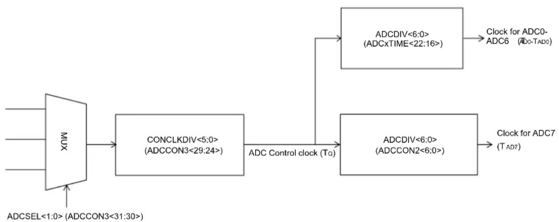
flowchart
graph LR
    A["MUX"] --> B["CONCLKDIV<5:0>(ADCCON3<29:24>)"]
    B --> C["ADC Control clock (To)"]
    C --> D["ADCDIV<6:0>(ADCxTIME<22:16>)"]
    D --> E["Clock for ADC0-ADC6 (ADC-TAD0)"]
    C --> F["ADCDIV<6:0>(ADCCON2<6:0>)"]
    F --> G["Clock for ADC7 (TAD7)"]
    H["ADCSEL<1:0>(ADCCON3<31:30>)"] --> A
Note: Refer to the "ADC" chapter in the specific device data sheet to determine the actual number of dedicated and shared ADC modules.
22.4.8 Sample and Conversion Time
Equation 22-1: Sample Time for Dedicated ADC Modules
$$ t _ {S A M C} = ((A D C x T I M E < 9: 0 > + 2) ^ {*} T _ {A D}) $$
$$ t _ {\text { conversion }} = ((\text { Number of Bits Resolution } + 1) * T _ {A D}) $$
Equation 22-2: Sample Time for the Shared ADC Module
$$ t _ {S A M C} = ((A D C C O N 2 < 2 5: 1 6 > + 2) ^ {*} T _ {A D}) $$
$$ t _ {\text { conversion }} = ((\text { Number of Bits Resolution } + 1) ^ {*} T _ {A D}) $$
ADC Scan Throughput rate = (1/((tSAMC + Tconversion)*#ADC ANx Scan inputs used))
22.4.9 Turning ON the ADC
Turning ON the ADC module involves these steps:
When the ADC module enable bit, ON (ADCCON1<15>), is set to '1', the module is in Active mode and is fully powered and functional. When the ON bit is '0', the ADC module is disabled. Once disabled, the digital and analog portions of the ADC are turned off for maximum current savings. In addition to setting the ON bit, the analog and digital circuits of ADC should be turned ON. More details are provided in the Section 22.7.3 "ADC Low-power Mode".
Note: Writing to the ADC control bits that control the ADC clock, input assignments, scanning, voltage reference selection, S&H circuit operating modes, and interrupt configuration is not recommended while the ADC module is enabled.
22.4.10 ADC Status Bits
The ADC module includes the WKRDYx/WKRDY7 status bit in the ADCANCON register, which indicates the current state of ADC Analog and bias circuit. The user application should not perform any ADC operations until this bit is set.
22.5 ADDITIONAL ADC FUNCTIONS
This section describes some additional features of the ADC module, which includes:
- Digital comparator
- Oversampling filter
- Turbo mode
• C V D mode
22.5.1 Digital Comparator
The ADC module features digital comparators that can be used to monitor selected analog input conversion results and generate interrupts when a conversion result is within the user-specified limits. Conversion triggers are still required to initiate conversions. The comparison occurs automatically once the conversion is complete. This feature is enabled by setting the Digital Comparator Module Enable bit, ENDCMP (ADCCMPCONx<7>).
The user application makes use of an interrupt that is generated when the analog-to-digital conversion result is higher or lower than the specified high and low limit values in the ADCCMPx register. The high and low limit values are specified in the DCMPHI<15:0> bits (ADCCMPx<31:16>) and the DCMPO<15:0> bits (ADCCMPx<15:0>).
The CMPEx bits ('x' = 0 through 31) in the ADCCMPENx registers are used to specify which analog inputs are monitored by the digital comparator (for the first 32 analog inputs, ANx, where 'x' = 0 through 31). The ADCCMPCONx register specifies the comparison conditions that will generate an interrupt, as follows:
- When IEBTWN = 1, interrupt is generated when DCMPO ≤ ADCDATA < DCMPHI
- When IEHIHI = 1, interrupt is generated when DCMPHI ≤ ADCDATA
- When IEHILO = 1, interrupt is generated when ADCDATA < DCMPHI
- When IELOHI = 1, interrupt is generated when DCMPO ≤ ADCDATA
- When IELOLO = 1, interrupt is generated when ADCDATA < DCMPO
The comparator event generation is illustrated in Figure 22-15. When the ADC module generates a conversion result, the conversion result is provided to the comparator. The comparator uses the DIFFx and SIGNx bits of the ADCIMCONx register (depending on the analog input used) to determine the data format used and appropriately select whether the comparison should be signed or unsigned. The global ADC setting, which is specified by the FRACT bit (ADCCON1<23>), is also used to set the fractional or integer format. The digital comparator compares the ADC result with the high and low limit values (depending on the selected comparison criteria) in the ADCCMPx register.
Depending on the comparator results, a digital comparator interrupt event may be generated. If a comparator event occurs, the Digital Comparator Interrupt Event Detected status bit, DCMPED (ADCCMPCONx<5>), is set, and the Analog Input Identification (ID) bits, AINID<4:0>(ADCCMPCONx<12:8>), are automatically updated so that the user application knows which analog input generated the interrupt event.
Note 1: The Digital Comparator module supports only the first 32 analog inputs (AN0 through AN31).
2: The user software must format the values contained in the ADCCMPx registers to match converted data format as either signed or unsigned, and fractional or integer
Figure 22-15: Digital Comparator

flowchart
graph TD
    A["ADCDATAx"] --> B["ADCDATAx < DCMPLO"]
    A --> C["ADCDATAx = DCMPLO"]
    A --> D["ADCDATAx > DCMPLO"]
    A --> E["ADCDATAx < DCMPHI"]
    A --> F["ADCDATAx = DCMPHI"]
    A --> G["ADCDATAx > DCMPHI"]
    B --> H["IELOLO"]
    C --> I["IELOHI"]
    D --> J["IEBTWN"]
    E --> K["IEHILO"]
    F --> L["IEHIHI"]
    G --> M["ENDCMI"]
    H --> N["Interrupt Generation Logic For Digital Comparator"]
    I --> N
    J --> N
    K --> N
    L --> N
    M --> N
Example 22-4: ADC Digital Comparator
int main(int argc, char** argv) {
    int result = 0, eventFlag = 0;

    /* Configure ADCCON1 */
    ADCCON1 = 0; // No ADCCON1 features are enabled including: Stop-in-Idle,
    // turbo, CVD mode, Fractional mode and scan trigger source.
    ADCCON1bits.SELRES = 3; // ADC resolution is 12 bits
    ADCCON1bits.STRGSRC = 0; // No scan trigger.

    /* Configure ADCCON2 */
    ADCCON2bits.SAMC = 5; // ADC7 sampling time = 5 * TAD7
    ADCCON2bits.ADCDIV = 1; // ADC7 clock freq = TAD7

    /* Initialize warm up time register */
    ADCANCON = 0;
    ADCANCONbits.WKUPCLKCNT = 5; // Wakeup exponent = 32 * TADx

    /* Clock setting */
    ADCCON3 = 0;
    ADCCON3bits.ADCSEL = 0; // Select input clock source
    ADCCON3bits.CONCLKDIV = 1; // Control clock frequency is half of input clock
    ADCCON3bits.VREFSEL = 0; // Select AVDD and AVSS as reference source

    /* No selection for dedicated ADC modules, no presync trigger, not sync sampling */
    ADCTRGMODEbits = 0;

    /* Select ADC input mode */
    ADCIMCON1bits.SIGN8 = 0; // unsigned data format
    ADCIMCON1bits.DIFF8 = 0; // Single ended mode

    /* Configure ADCGIRQENx */
    ADCGIRQEN1 = 0; // No interrupts are used
    ADCGIRQEN2 = 0;

    /* Configure ADCCSSx */
    ADCCSS1 = 0; // No scanning is used
    ADCCSS2 = 0;

    /* Configure ADCCMPCONx */
    ADCCMP1 = 0; // Clear the register
    ADCCMP1bits.DCMPHI = 0xC00; // High limit is a 3072 result.
    ADCCMP1bits.DCMPLO = 0x500; // Low limit is a 1280 result.
    ADCCMPCON1bits.IEBTWN = 1; // Create an event when the measured result is
    // >= low limits and < high limit.
    ADCCMPEN1 = 0; // Clear all enable bits
    ADCCMPEN1bits.CMPE8 = 1; // set the bit corresponding to AN8
    ADCCMPCON1bits.ENDCMP = 1; // enable comparator
    ADCCMPCON2 = 0;
    ADCCMPCON3 = 0;
    ADCCMPCON4 = 0;
    ADCCMPCON5 = 0;
    ADCCMPCON6 = 0;

    /* Configure ADCFLTRx */
    ADCFLTR1 = 0; // No oversampling filters are used.
    ADCFLTR2 = 0;
    ADCFLTR3 = 0;
    ADCFLTR4 = 0;
    ADCFLTR5 = 0;
    ADCFLTR6 = 0;
Example 22-4: ADC Digital Comparator (Continued)
/* Set up the trigger sources */
ADCTRG3bits.TRGSRC8 = 3;    // Set AN8 (Class 2) to trigger from scan source

/* Early interrupt */
ADCEIEN1 = 0;    // No early interrupt
ADCEIEN2 = 0;

/* Turn the ADC on */
ADCCON1bits.ON = 1;

/* Wait for voltage reference to be stable */
while(!ADCCON2bits.BGVRRDY);    // Wait until the reference voltage is ready
while(ADCCON2bits.REFFLT);    // Wait if there is a fault with the reference voltage

/* Enable clock to analog circuit */
ADCANCONbits.ANEN7 = 1;    // Enable the clock to analog bias

/* Wait for ADC to be ready */
while(!ADCANCONbits.WKRDY7);    // Wait until ADC7 is ready

/* Enable the ADC module */
ADCCON3bits.DIGEN7 = 1;    // Enable ADC7

while (1) {
    /* Trigger a conversion */
    ADCCON3bits.GSWTRG = 1;

    while (ADCDSTAT1bits.ARDY8 == 0);
    /* fetch the result */
    result = ADCDATA8;

    /* Note: It is not necessary to fetch the result for the digital
    * comparator to work. In this example we are triggering from
    * software so we are using the ARDY8 to gate our loop. Reading the
    * data clears the ARDY bit.
    */
    /* See if we have a comparator event*/
    if (ADCCMPCON1bits.DCMPED == 1) {
    eventFlag = 1;
    /*
    * Process results here
    */
    }
}
return (1);
}
22.5.2 Oversampling Digital Filter
The ADC module supports up to six oversampling digital filters. The oversampling digital filter consists of an accumulator and a decimator (down-sampler), which function together as a low-pass filter. By sampling an analog input at a higher-than-required sample rate, and then processing the data through the oversampling digital filter, the effective resolution of the ADC module can be increased at the expense of decreased conversion throughput.
To obtain 'x' bits of extra resolution, number of samples required (over and above the Nyquist rate) = (2^x)^2 :
- 4x oversampling yields one extra bit of resolution (total 13 bits resolution)
- 16x oversampling yields two extra bits of resolution (total 14 bits resolution)
- 64x oversampling provides three extra bits of resolution (total 15 bits resolution)
- 256x oversampling provides four extra bits of resolution (total 16 bits resolution)
The digital filter also has an averaging mode, where it accumulates the samples and divides it by the number of samples.
Note 1: Only Class 1 and Class 2 analog inputs can engage the digital filter. Therefore, the CHNLID<4:0> bits are 5 bits wide (0 to 31).
2: During the burst conversion process (repeated trigger until all required data for oversampling is obtained) in the case of filtering Class 2 input using the shared ADC module, higher priority ADC inputs may still process conversions; lower priority ADC conversion requests are held waiting until the filter burst sequence has been completed.
3: If higher priority requests occur during the digital filter sequence, they delay the completion of the filtering process. This delay may affect the accuracy of the result because the multiple samples will not be contiguous. The user should arrange the initiation trigger for the over sampling filters to occur while there are no expected interruptions from higher priority ADC conversion requests.
The user application should configure the following bits to perform an oversampling conversion:
- Select the amount of oversampling through the Oversampling Filter Oversampling Ratio (OVRSAM<2:0>) bits in the ADC Filter register (ADCFLTRx<28:26>)
- Set the filter mode to either Oversampling mode or Averaging mode using the DFMODE bit (ADCFLTRx<29>)
- If the filter is set to Averaging mode and the data format is set to fractional (FRACT bit), set or clear the DATA16EN bit (ADCFLTRx<30>) to set the output resolution
-
Set the sample time for subsequent samples:
-
If using Class 1 inputs, select the sample time of the recurring conversions using the SAMC<9:0> bits ADCxTIME<9:0>)
- If using Class 2 inputs, select the sample time using the SAMC<9:0> bits (ADCCON2<25:16>)
- Select the specific analog input to be oversampled by configuring the Analog Input ID Selection bits, CHNLID<4:0> (ADCFLTRx<20:16>)
- If needed, include the oversampling filter interrupt event in the global ADC interrupt, by setting the Accumulator Filter Global Interrupt Enable bit, AFGIEN (ADCFLTRx<25>)
- Enable the oversampling filter by setting the Oversampling Filter Accumulator Enable bit, AFEN (ADCFLTRx<31>)
Once the digital filter module is configured, the filter's control logic waits for an external trigger to initiate the process. The trigger signal for the analog input to be oversampled causes the accumulator to be cleared and initiates the first conversion. The trigger also force the trigger sensitivity into level mode and forces the trigger itself to 1 as long as the filter needs to acquire the user specified number of samples via the OVRSAM<2:0> bits (ADCFLTRx<28:26>). The time delay between each acquired sample is decided by the set sample time (SAMC<9:0> bits in the ADCxTIME register for Class 1 or the SAMC<9:0> bits in the ADCCON2 register for Class 2) and the time for conversion. When the required number set by OVRSAM<2:0> have been received and processed, the data stored in the FLTRDATA<15:0> bit (ADCFLTRx<15:0>) and the AFRDY bit (ADCFLTRx<24>) is set, and the interrupt is generated (if enabled).
Figure 22-16 illustrates 4x oversampling on a Class 1 input. Prior to the trigger, the Class 1 input is sampling the input signal. The trigger starts the first conversion. Once the conversion is complete, the ADC goes into sampling mode. When the sampling time expires, a new conversion sequence occurs. After each sample is converted it is added to the accumulator. The sequence repeats until the number of samples specified by the OVRSAM<2:0> bits have been accumulated. When the last sample has been converted, its value is added to the accumulator. The result is right shifted and then stored in the FLTRDATA<15:0> bits.
Figure 22-16: 4x Oversampling of a Class 1 Input
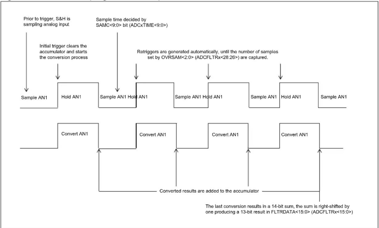
flowchart
graph TD
    A["Sample AN1"] --> B["Hold AN1"]
    B --> C["Sample AN1 Hold AN1"]
    C --> D["Sample AN1 Hold AN1"]
    D --> E["Sample AN1 Hold AN1"]
    E --> F["Sample AN1"]
    F --> G["Convert AN1"]
    G --> H["Convert AN1"]
    H --> I["Convert AN1"]
    I --> J["Convert AN1"]
    J --> K["The last conversion results in a 14-bit sum, the sum is right-shifted by one producing a 13-bit result in FLTRDATA<15:0> (ADCFLTRx<15:0>)"]

    L["Prior to trigger, S&H is sampling analog input"] --> M["Initial trigger clears the accumulator and starts the conversion process"]
    M --> N["Sample time decided by SAMC<9:0> bit (ADCxTIME<9:0>)"]
    N --> O["Retriggers are generated automatically, until the number of samples set by OVRSAM<2:0> (ADCFLTRx<28:26>) are captured."]
    O --> P["Sample AN1 Hold AN1"]
    P --> Q["Sample AN1 Hold AN1"]
    Q --> R["Sample AN1 Hold AN1"]
    R --> S["Sample AN1"]
    S --> T["Sample AN1"]

    U["The last conversion results in a 14-bit sum, the sum is right-shifted by one producing a 13-bit result in FLTRDATA<15:0> (ADCFLTRx<15:0>)"]
If multiple Class 1 inputs use filtering, they all operate in parallel and independent from each other.
Figure 22-17 illustrates 4x Oversampling using a Class 2 input. Triggering a Class 2 input initiates sampling for the length of time defined by the SAMC<9:0> bits. Retriggers generated by the oversampling logic use the SAMC<9:0> bits, to set the sample time.
Since Class 2 inputs use the shared S&H, oversampling blocks lower priority Class 2 and Class 3 triggers. Higher priority Class 2 triggers will completely disrupt the oversampling process, and therefore, should be avoided completely. The same priority rule applies to two Class 2 inputs that use two digital filters. In such a case, the higher priority input will also use the shared ADC module in Burst mode and will prevent the lower priority input to use the shared ADC. Only after all required samples are obtained by the higher priority input, the lower priority input can use the shared ADC to acquire samples for its own digital filtering.
Figure 22-17: 4x Oversampling of a Class 2 Input
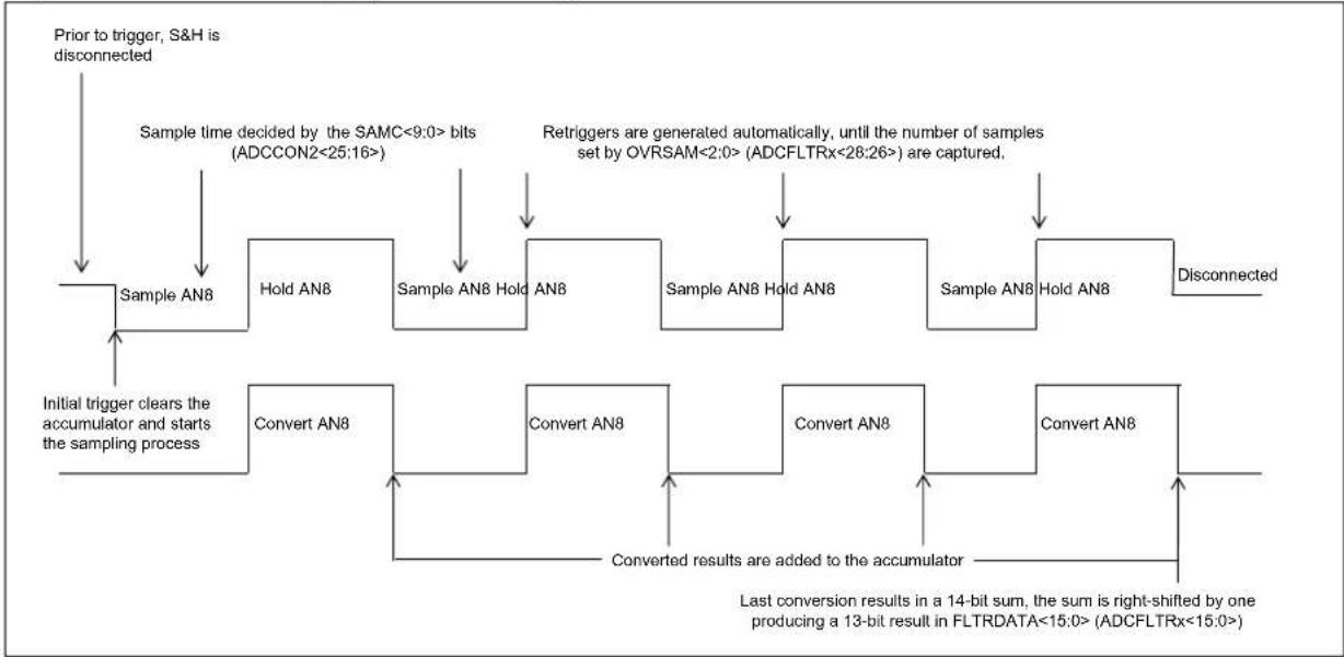
flowchart
graph TD
    A["Prior to trigger, S&H is disconnected"] --> B["Sample AN8"]
    B --> C["Sample time decided by the SAMC<9:0> bits (ADCCON2<25:16>)"]
    C --> D["Sample AN8 Hold AN8"]
    D --> E["Sample AN8 Hold AN8"]
    E --> F["Sample AN8 Hold AN8"]
    F --> G["Sample AN8 Hold AN8"]
    G --> H["Sample AN8 Hold AN8"]
    H --> I["Disconnected"]
    B --> J["Initial trigger clears the accumulator and starts the sampling process"]
    J --> K["Convert AN8"]
    K --> L["Convert results are added to the accumulator"]
    L --> M["Last conversion results in a 14-bit sum, the sum is right-shifted by one producing a 13-bit result in FLTRDATA<15:0> (ADCFLTRx<15:0>)"]
    M --> N["Retriggers are generated automatically, until the number of samples set by OVRSAM<2:0> (ADCFLTRx<28:26>) are captured."]
Example 22-5: ADC Digital Oversampling Filter
int main(int argc, char** argv) {
    int result;

    /* Configure ADCCON1 */
    ADCCON1 = 0; // No ADCCON1 features are enabled including: Stop-in-Idle, turbo, // CVD mode, Fractional mode and scan trigger source.

    /* Configure ADCCON2 */
    ADCCON2 = 0; // Since, we are using only the Class 1 inputs, no setting is // required for ADCDIV

    /* Initialize warm up time register */
    ADCANCON = 0;
    ADCANCONbits.WKUPCLKCNT = 5; // Wake-up exponent = 32 * TADx

    /* Clock setting */
    ADCCON3 = 0;
    ADCCON3bits.ADCSEL = 0; // Select input clock source
    ADCCON3bits.CONCLKDIV = 1; // Control clock frequency is half of input clock
    ADCCON3bits.VREFSEL = 0; // Select AVDD and AVSS as reference source

    ADC0TIMEbits.ADCDIV = 1; // ADC0 clock frequency is half of control clock = TAD0
    ADC0TIMEbits.SAMC = 5; // ADC0 sampling time = 5 * TAD0
    ADC0TIMEbits.SELRES = 3; // ADC0 resolution is 12 bits

    /* Select analog input for ADC modules, no presync trigger, not sync sampling */
    ADCTRGMODEbits.SH0ALT = 0; // ADC0 = AN0

    /* Select ADC input mode */
    ADCIMCON1bits.SIGN0 = 0; // unsigned data format
    ADCIMCON1bits.DIFF0 = 0; // Single ended mode

    /* Configure ADCGIRQENx */
    ADCGIRQEN1 = 0; // No interrupts are used
    ADCGIRQEN2 = 0;

    /* Configure ADCCSSx */
    ADCCSS1 = 0; // No scanning is used
    ADCCSS2 = 0;
Example 22-5: ADC Digital Oversampling Filter (Continued)
/* Configure ADCCMPCONx */
ADCCMPCON1 = 0; // No digital comparators are used. Setting the ADCCMPCONx
ADCCMPCON2 = 0; // register to '0' ensures that the comparator is disabled.
ADCCMPCON3 = 0; // Other registers are 'don't care'.
ADCCMPCON4 = 0;
ADCCMPCON5 = 0;
ADCCMPCON6 = 0;

/* Configure ADCFLTRx */
ADCFLTR1 = 0; // Clear all bits
ADCFLTR1bits.CHNLID = 0; // Use ANO as the source
ADCFLTR1bits.OVRSAM = 3; // 16x oversampling
ADCFLTR1bits.DFMODE = 0; // Oversampling mode
ADCFLTR1bits.AFEN = 1; // Enable filter 1
ADCFLTR2 = 0; // Clear all bits
ADCFLTR3 = 0;
ADCFLTR4 = 0;
ADCFLTR5 = 0;
ADCFLTR6 = 0;

/* Set up the trigger sources */
ADCTGSNSbits.LVL0 = 0; // Edge trigger
ADCTRGLbits.TRGSRC0 = 1; // Set ANO to trigger from software.

/* Turn the ADC on */
ADCCON1bits.ON = 1;

/* Wait for voltage reference to be stable */
while(!ADCCON2bits.BGVRRDY); // Wait until the reference voltage is ready
while(ADCCON2bits.REFFLT); // Wait if there is a fault with the reference voltage

/* Enable clock to analog circuit */
ADCANCONbits.ANENO = 1; // Enable the clock to analog bias and digital control

/* Wait for ADC to be ready */
while(!ADCANCONbits.WKRDY0); // Wait until ADC0 is ready

/* Enable the ADC module */
ADCCON3bits.DIGEN0 = 1; // Enable ADC0

while (1) {
    /* Trigger a conversion */
    ADCCON3bits.GSWTRG = 1;

    /* Wait for the oversampling process to complete */
    while (ADCFLTR1bits.AFRDY == 0);
    /* fetch the result */
    result = ADCFLTR1bits.FLTRDATA;

    /*
    * Process result Here
    *
    * Note 1: Loop time determines the sampling time for the first sample.
    * remaining samples sample time is determined by set sampling + conversion time.
    *
    * Note 2: The first 5 samples may have reduced accuracy.
    *
    */
}
return (1);
© 2016-2019 Microcship Technology Inc. DS60001344E-page 22-93
Figure 22-18: ADC Filter Comparisons Example
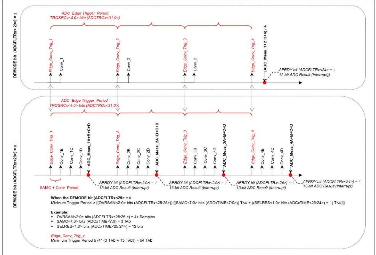
22.5.3 FIFO Data Output
The dedicated ADC module has a provision to store the output data into a FIFO. This could be useful while the ADC is used to convert signals at a very high throughput. The ADCFIFO register is the read port for the FIFO. The FIFO is 128 level deep and is circular in nature.
The ADC module that needs to use the FIFO is selected by the ADCxEN bits (ADCFSTAT<30:24>). If more than one ADC module needs to use FIFO, all those respective bits can be set among ADCxEN. While reading the data from FIFO, the ADCID<2:0> bits (ADCFSTAT<2:0>) should be read first and then the data from the ADCFIFO register. This way, the user application knows from which ADC module the data originated from the FIFO. The FEN bit (ADCFSTAT<31>) bit is set to enable the FIFO operation. Once data is available in FIFO, the FRDY bit (ADCFSTAT<22>) is set and remains set until the FIFO is entirely read and is devoid of any data. If required, the FIEN bit (ADCFSTAT<23) can be set to generate interrupt.
Note 1: FIFO depth depends on the device. Please refer to the specific device data sheet for details.
2: While retrieving data from the FIFO, user code should read both the ADCID<2:0> bits and the ADCFIFO register during each successive reads.
Example 22-6: ADC FIFO Usage for Class 1 Input
int main(int argc, char** argv) {
    int result[128], index = 0;

    /* Configure ADCCON1 */
    ADCCON1 = 0;    // No ADCCON1 features are enabled including: Stop-in-Idle, turbo,
    // CVD mode, Fractional mode and scan trigger source.

    /* Configure ADCCON2 */
    ADCCON2 = 0;    // Since, we are using only the Class 1 inputs, no setting is
    // required for ADCDIV

    /* Initialize warm up time register */
    ADCANCON = 0;
    ADCANCONbits.WKUPCLKCNT = 5;    // Wakeup exponent = 32 * TADx

    /* Clock setting */
    ADCCON3 = 0;
    ADCCON3bits.ADCSEL = 0;    // Select input clock source
    ADCCON3bits.CONCLKDIV = 1;    // Control clock frequency is half of input clock
    ADCCON3bits.VREFSEL = 0;    // Select AVDD and AVSS as reference source

    ADCOTIMEbits.ADCDIV = 1;    // ADC0 clock frequency is half of control clock = TAD0
    ADCOTIMEbits.SAMC = 5;    // ADC0 sampling time = 5 * TAD0
    ADCOTIMEbits.SELRES = 3;    // ADC0 resolution is 12 bits

    /* Select analog input for ADC modules, no presync trigger, not sync sampling */
    ADCTRGMODEbits.SH0ALT = 0;    // ADC0 = AN0

    /* Select ADC input mode */
    ADCIMCON1bits.SIGN0 = 0;    // unsigned data format
    ADCIMCON1bits.DIFF0 = 0;    // Single ended mode

    /* Configure ADCGIRQENx */
    ADCGIRQEN1 = 0;    // No interrupts are used
    ADCGIRQEN2 = 0;

    /* Configure ADCCSSx */
    ADCCSS1 = 0;    // No scanning is used
    ADCCSS2 = 0;

    /* Configure ADCCMPCONx */
    ADCCMPCON1 = 0;    // No digital comparators are used. Setting the ADCCMPCONx
    ADCCMPCON2 = 0;    // register to '0' ensures that the comparator is disabled.
    ADCCMPCON3 = 0;    // Other registers are 'don't care'.
    ADCCMPCON4 = 0;
    ADCCMPCON5 = 0;
    ADCCMPCON6 = 0;
Example 22-6: ADC FIFO Usage for Class 1 Input (Continued)
/* Configure ADCFLTRx */
ADCFLTR1 = 0;    // Clear all bits
ADCFLTR2 = 0;
ADCFLTR3 = 0;
ADCFLTR4 = 0;
ADCFLTR5 = 0;
ADCFLTR6 = 0;

/* Set up the trigger sources */
ADCTGSNSbits.LVLO = 0;    // Edge trigger
ADCTRGObits.TRGSRC0 = 1;    // Set ANO to trigger from software.

/* Early interrupt */
ADCEIEN1 = 0;    // No early interrupt
ADCEIEN2 = 0;

/* Set FIFO */
ADCFSTAT = 0;    // Clear all bits
ADCFSATbits.ADC0EN = 1;    // Select ADC0
ADCFSATbits.FEN = 1;    // Enable FIFO

/* Turn the ADC on */
ADCCON1bits.ON = 1;

/* Wait for voltage reference to be stable */
while(!ADCCON2bits.BGVRRDY);    // Wait until the reference voltage is ready
while(ADCCON2bits.REFFLT);    // Wait if there is a fault with the reference voltage

/* Enable clock to analog circuit */
ADCANCONbits.ANENO = 1;    // Enable the clock to analog bias and digital control

/* Wait for ADC to be ready */
while(!ADCANCONbits.WKRDY0);    // Wait until ADC0 is ready

/* Enable the ADC module */
ADCCON3bits.DIGENO = 1;    // Enable ADC0

while (1) {
    /* Trigger a conversion */
    ADCCON3bits.GSWTRG = 1;

    /* Wait the conversions to complete and data available in FIFO */
    while (ADCFSTATbits.FRDY == 0);

    /* Once FIFO bit is set, read all possible data, until bit is clear */
    while(ADCFSTATbits.FRDY)
    {
    /* If data overflow occurred in FIFO, break read process */
    if(ADCFSTATbits.FWROVERR)
    {
    break;
    }
    /* if ADC ID is really '0', read data.
    This is more appropriate when multiple ADC modules are
    using the FIFO, therefore, reading the ADC ID will
    identify the ADC and data relation */
    if(ADCFSTATbits.ADCID == 0)
    {
    /* Read data from FIFO */
    result[index] = ADCFIFO;
    /* For each FIFO read, ADCFSTATbits.FCNT will keep reducing */
    index++;
    if(index >= 128)
    index = 0;
    }
    }
    /*
    * Process results here
    *
    */
}
return (1);
}
22.5.4 Dedicated DMA-based Data Output
Depending on the device, each dedicated ADC module has a DMA engine that can be used to store converted data directly into system memory (RAM). Refer to the "ADC" chapter in the specific device data sheet to determine whether this feature is available for your device.
If the DMACNTEN bit in the ADCDMASTAT register is set, the ADC module current sample count is also written by the DMA engine into system RAM starting at the address specified in the ADCCNTB register.
The size of the buffer used for storage is specified by the DMABL<2:0> bits (ADCCON1<2:0>). Also, the RAM address where the output data should be stored is specified by the DMABADDR<31:0> bits in the ADCDMAB register. Each dedicated ADC module has two buffers: Buffer A and Buffer B.
Since DMABL<2:0> counts the number of data and each data is 16 bits, the actual size of the buffer (in bytes) for each ADC module is given by the formula:
$$ = 2 ^ {(\text { ADCCON1bits.DMABL } + 1)} $$
The channel storage buffers spaces are contiguous in the System RAM, starting at the base address (given by the ADCDMAB register) with the ADC0 Buffer A, followed by the ADC0 Buffer B, followed by the ADC1 Buffer A, followed by the ADC1 Buffer B, and so on in the natural order of the channel number assignments.
Table 22-6: DMA Buffer Format When Used by Multiple ADC Modules
| ADC Module ID | Buffer | RAM Address Space |
| 0 | A | (DMABADDR<31:0>) + 0 to (DMABADDR<31:0>) + 255 |
| 0 | B | (DMABADDR<31:0>) + 256 to (DMABADDR<31:0>) + 511 |
| 1 | A | (DMABADDR<31:0>) + 512 to (DMABADDR<31:0>) + 767 |
| 1 | B | (DMABADDR<31:0>) + 768 to (DMABADDR<31:0>) + 1023 |
| 2 | A | (DMABADDR<31:0>) + 1024 to (DMABADDR<31:0>) + 1279 |
| 2 | B | (DMABADDR<31:0>) + 1280 to (DMABADDR<31:0>) + 1535 |
| · · · | · · · | · · · |
| 6 | A | (DMABADDR<31:0>) + 3072 to (DMABADDR<31:0>) + 3327 |
| 6 | B | (DMABADDR<31:0>) + 3328 to (DMABADDR<31:0>) + 3583 |
As shown in Table 22-6, the user can get up to 128 samples (two bytes per sample) for each ADC module until data loss occurs by new data overwriting old data. The DMA engine will wrap around the address for each channel inside its own allocated RAM space.
ADCx, 'x' = 0 through 6, will have Buffer A starting at:
$$ = \text { ADCDMAB } + (2 * x) * 2 ^ {\text {(ADCCON1bits.DMABL+1)}} $$
ADCx, 'x' = 0 through 6, will have Buffer B starting at:
$$ = \text { ADCDMAB } + (2 * (x + 1)) * 2 ^ {\text {(ADCCON1bits.DMABL+1)}} $$
The ADCCNTB register contains the user-given address at which (if the DMACNTEN bit (ADCDMASTAT<15>) is set) the DMA engine will start saving the current count of output samples already written to each of the buffers in the System RAM for each ADC module. The ADCx will have its Buffer A current sample count saved at the address ((ADCCNTB) + 2 * x) and its Buffer B current sample count saved at the address ((ADCCNTB) + (2 * x + 1)). Each ADC buffer count takes only 1 byte of RAM storage, because the maximum value is 128. At any time, by reading the memory location specified by ADCCNTB register, the user can know the number of available data for each ADC (0 through 6) and each buffer (A, B); even before the RAFx or RBFx bit is set.
Table 22-7: DMA Buffer Count Table
| ADC Module ID | Buffer Sample Count | |
| 0 A Read memory (s) | specified by ADCCNTB register) to determine the number of samples stored. | |
| 0 B Read memory (s) | specified by ADCCNTB register) + 1 to determine the number of samples stored. | |
| 1 A Read memory (s) | specified by ADCCNTB register) + 2 to determine the number of samples stored. | |
| 1 B Read memory (s) | specified by ADCCNTB register) + 3 to determine the number of samples stored. | |
| 2 A Read memory (s) | specified by ADCCNTB register) + 4 to determine the number of samples stored. | |
| 2 B Read memory (s) | specified by ADCCNTB register) + 5 to determine the number of samples stored. | |
| : | : | : |
| : | : | : |
| 6 | A | Read memory (specified by ADCCNTB register) + 12 to determine the number of samples stored. |
| 6 | B | Read memory (specified by ADCCNTB register) + 13 to determine the number of samples stored. |
Immediately after ADC module (0 through 6) has been enabled by the user by setting the DIGENx bit (ADCCON3 register), the DMA engine will reset to zero in both the ADCx Buffer A sample count at address ((ADCCNTB) + 2 * x) and the Buffer B sample count at address ((ADCCNTB)+(2 * x + 1)).
22.5.4.1 DMA PING-PONG MODE
The DMA engine Ping-Pong mode of operation when used with a single ADC module, is described in the following steps:
- DMA engine saves converted data into a buffer in system RAM for Buffer A.
- Once Buffer A is full, the RAFx bit (ADCDMASTAT<6:0>) for the used ADC is set. Also, the DMA engine will start using and saving data into Buffer B.
- An interrupt will be generated if the RAFIENx bit (ADCDMASTAT<14:8>) is set for the selected ADC.
- Inside the ISR, the user application must know the buffer ID (either A or B) by reading the RAFx or RBFx bits.
- Whichever bit is set, the user application must read the converted data from the buffer ID and perform suitable processing on the converted data.
- While the user application is processing the converted data, the DMA engine is saving data into Buffer B.
- Once the user application completes the processing of data from Buffer A, it waits for completion of Buffer B.
If an application needs to use the data being stored in a buffer before the buffer is full, the following steps are necessary:
- To locate the data being saved in buffer, the user code should have enabled DMACNTEN bit (ADCDMASTAT<15> register).
- The current sample count can be retrieved from (ADCCNTB + (2 * x + 1)) (considering Buffer B being used), and then read the suitable memory offset specified in the ADCDMAB register.
- Once Buffer B is full, the RBFx bit for the used channel is set. Also, the DMA engine will start saving data into Buffer A.
Note 1: The initialization of the buffer sample count table to all zeros before enabling the DMA engine is left completely as a task for the software. It should be done in order to avoid garbage data in the buffer sample count table before the first sample is being saved in each of the buffers.
2: A read of the ADCDMASTAT register will clear all status bits in this register. Because the dedicated ADC modules work completely independent one of another, more than one status bit can be set at the same time. The user must read the ADCDMASTAT register and save its contents into a separate variable for logic bit-level operations to identify which dedicated ADC module buffers are full at that time.
Figure 22-19 illustrates Ping-Pong mode with continuous operation.
Figure 22-19: Repetitive Data Transfer in Ping-Pong Mode
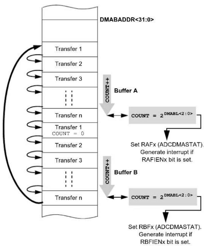
flowchart
graph TD
    A["Transfer 1"] --> B["Buffer A"]
    C["Transfer 2"] --> B
    D["Transfer 3"] --> B
    E["..."] --> F["Buffer B"]
    G["Transfer n"] --> H["Buffer A"]
    I["Transfer 1 COUNT = 0"] --> J["Set RAFx (ADCDMASTAT). Generate interrupt if RAFIENx bit is set."]
    K["Transfer 2"] --> L["Buffer B"]
    M["Transfer 3"] --> L
    N["..."] --> O["Set RBFx (ADCDMASTAT). Generate interrupt if RBFIENx bit is set."]
22.5.5 Capacitive Voltage Divider (CVD) mode
The ADC has CVD mode, which can be used to detect an event of touch in a touch sensor application. The principle of CVD measurement is based on charge balancing between two capacitors and then measuring the voltage.
In touch sensing applications, the presence of finger near a pad alters the capacitance of the pad. This variation in capacitance can be sensed by the CVD module to detect the presence (and subsequent absence) of a finger.
Note: Only shared analog inputs (Class 2 and Class 3) can be used for CVD measurement.
- When a finger is touching the sensor pad, external capacitance = CEXT = CPAD + CFINGER
- External capacitance of pad (when finger is not touching) = C EXT = CPAD
- Internal capacitance = C INT = CPLINE + CSAMP
Figure 22-20: CVD Mode Diagram

text_image
I/O Pad CFINGER CPAD CPLINE = 2.5...17.5 pF CSAMP = 5 pF ADC7 CEXT CINT When finger is touching the pad: CEXT = CPAD + CFINGER When finger is removed: CEXT = CPADCVD measurement consists of two phases, Positive and Negative.
Positive Phase: The CEXT is connected to V_DD and CINT is connected to ground (GND) (as shown in Figure 22-21). Then, both capacitors are connected in parallel for half of sampling time, set by the SAMC<9:0> bits (ADCCON2<25:16>). After the half sampling time is complete, the voltage is converted by the ADC module and is named VNP.
Figure 22-21: CVD Mode Positive Phases Diagram
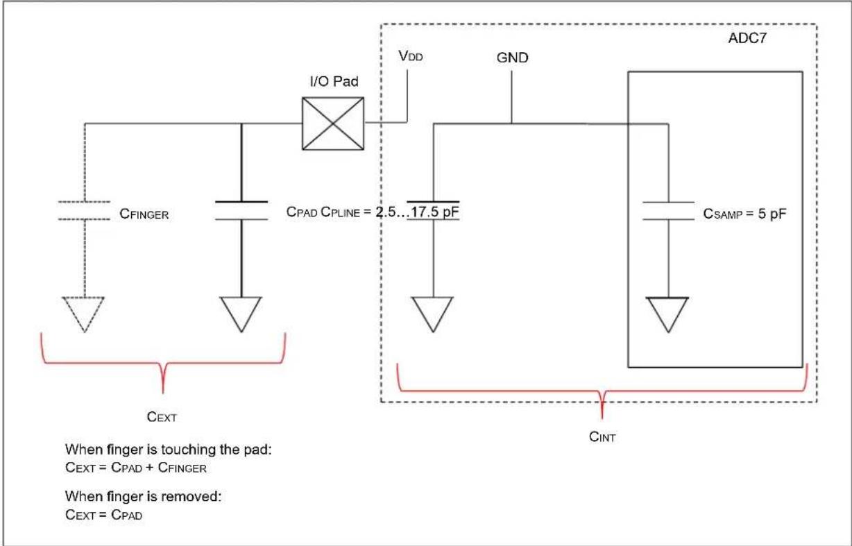
text_image
I/O Pad CFINGER CPAD CPLINE = 2.5...17.5 pF VDD GND ADC7 CSAMP = 5 pF CINT When finger is touching the pad: CEXT = CPAD + CFINGER When finger is removed: CEXT = CPADNegative Phase: The CEXT is connected to GND and CINT is connected to VDD, as shown in Figure 22-22. Similar to the positive phase, the voltage is measured for the negative phase and is named as VINN.
Figure 22-22: CVD Mode - Negative Phase Diagram
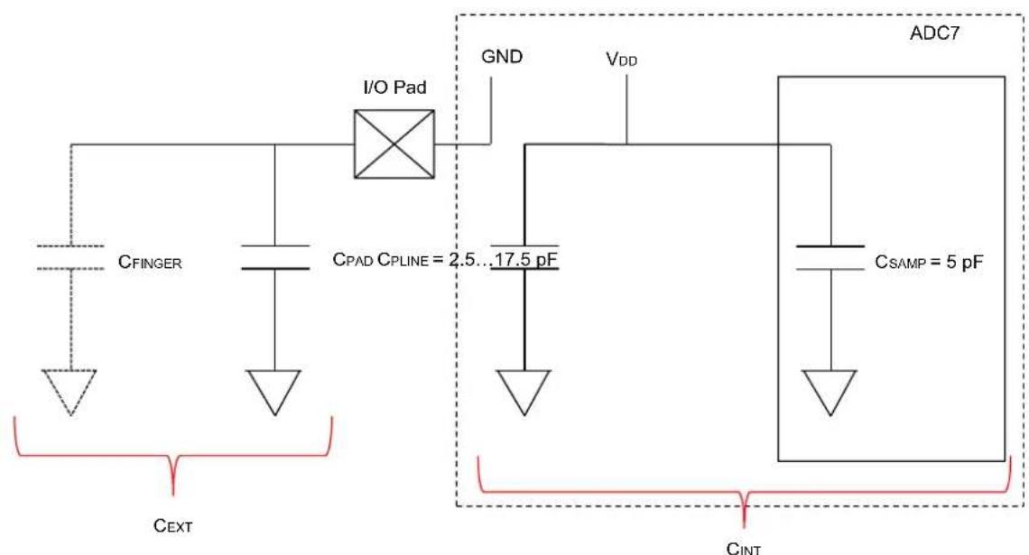
text_image
I/O Pad CFINGER CPAD CPLINE = 2.5...17.5 pF GND VDD ADC7 CSAMP = 5 pF CINT CEXTWhen finger is touching the pad:
C_EXT = C_PAD + C_FINGER
When finger is removed:
C_EXT = C_PAD
The CVD module internally calculates the difference between MP and VINN and stores the data in the CVDDATA<15:0> bits (ADCCMPCON1<31:16>) in signed format. The plot in Figure 22-23 shows how during a touch event, the increase in external capacitance causes the (VNP - VINN) to be higher than the non-touch condition (decreased external capacitance).
Figure 22-23: CVD Signal - Difference Between Pressed and Released Differential Values
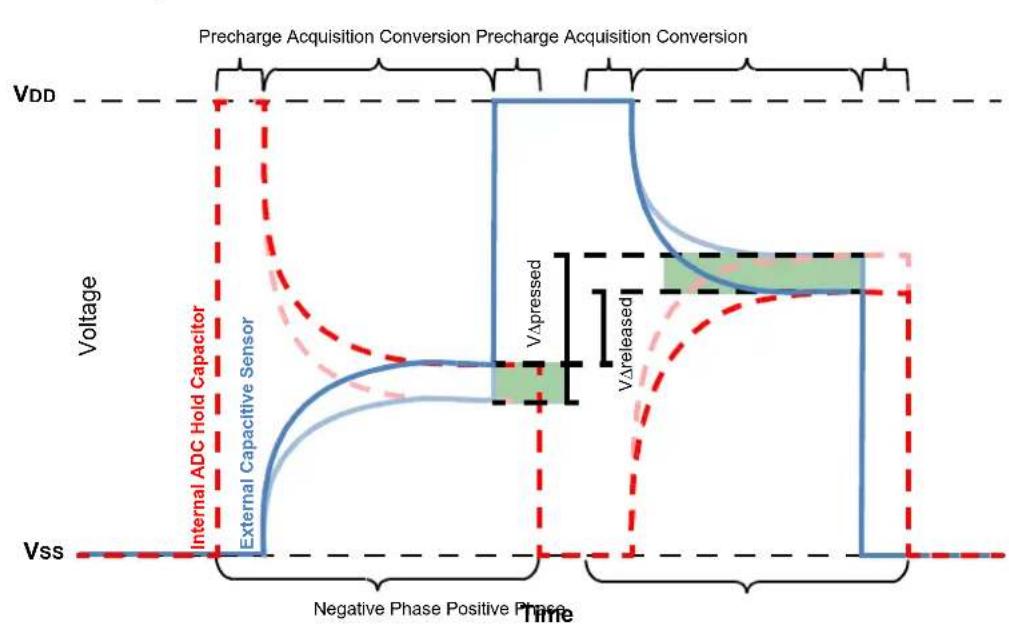
line
| Time Segment | Voltage Level | | ------------------------- | ------------- | | VDD | VDD | | Negative Phase Positive Phase | Vss | | External Capacitive Sensor | Internal ADC Hold Capacitor | | VΔpressed | VΔpressed | | VΔreleased | VΔreleased |Equation 22-3 shows the relation ( V_INP - V_INN ).
Equation 22-3: V INP and VINN Relation
$$ (V _ {I N} P - V _ {I N} N) = V _ {D D} \cdot \left(\frac {(C _ {E X T} - C _ {I N T})}{(C _ {E X T} + C _ {I N T})}\right) $$
During a touch condition, C_EXT increases and (V_INP - V_INN) increases.
During no touch condition, C_EXT decreases and (V_INP - V_INN) reduces.
Digital Comparator 1 is linked to CVD and it can be used to generate a comparator event and interrupt when a touch is detected, by setting the IEHIHI bit (ADCCMPCON1<3>). The digital comparator can generate an event when measured (VINP - VINN) is above the value set in the DCMPHI<15:0> bit (ADCCMP1<31:16>). When the comparator event is detected by reading the DCMPED bit (ADCCMPCON1<5>), or inside the ISR, the analog input that caused the touch event can be read from the AINID<5:0> bits (ADCCMPCON1<13:8>).
To ensure maximum sensitivity, QNT should have similar value as CPAD, which can be done by suitably selecting the value of C PLINE capacitance through the CVDCPL<2:0> bits (ADCCON2<28:26>).
Note: Before CVD is enabled by setting the CVDEN bit, external triggers for all Class 2 and Class 3 inputs are disabled by clearing the TRGSRC<4:0> and STRGSRC<4:0> bits.
Example 22-7: ADC CVD Mode
unsigned char touchDetected = 0;

void __ISR(_ADC_DC1_VECTOR, IPL3AUTO) _IntHandlerDrvAdc(void)
{
    IFS1bits.ADCDC1IF = 0;
    /* Check and clear event flag for comparator 1 */
    if (ADCCMPCON1bits.DCMPED == 1)
    {
    /* Verify if comparator event really due to AN21 */
    if (ADCCMPCON1bits.AINID == 21)
    {
    touchDetected = 1;
    }
    }
}

int main(void)
{
    /* Configure ADCCON1 */
    ADCCON1bits.SELRES = 3; // ADC resolution is 12 bits
    ADCCON1bits.STRGSRC = 0; // No scan trigger.
    ADCCON1bits.AICPMPEN = 0;
    ADCCON1bits.FRACT = 0; // Integer format

    /* Configure ADCCON2 */
    ADCCON2bits.SAMC = 32; // ADC7 sampling time
    ADCCON2bits.ADCDIV = 4; // ADC7 clock freq is half of control clock = TAD7
    ADCCON2bits.CVDCPL = 2; // 5 pF is the CVD capacitor value selected

    /* Initialize warm up time register */
    ADCANCON = 0;
    ADCANCONbits.WKUPCLKCNT = 5; // Wakeup exponent = 32 * TADx

    /* Clock setting */
    ADCCON3 = 0;
    ADCCON3bits.ADCSEL = 0; // Select input clock source
    ADCCON3bits.CONCLKDIV = 1; // Control clock frequency is half of input clock
    ADCCON3bits.VREFSEL = 0; // Select AVDD and AVSS as reference source

    /* No selection for dedicated ADC modules, no presync trigger, not sync sampling */
    ADCTRGMODE = 0;
    /* Select ADC input mode */
    ADCIMCON2bits.SIGN21 = 1; // signed data format
    ADCIMCON2bits.DIFF21 = 0; // Single ended mode

    /* Configure ADCGIRQENx */
    ADCGIRQEN1 = 0; // No interrupts are used.
    ADCGIRQEN2 = 0;

    /* Configure ADCCSSx */
    ADCCSS1 = 0; // No scanning is used
    ADCCSS2 = 0;
    ADCCSS1bits.CSS21 = 1; // AN21 (Class 3) set for CVD

    /* Configure ADCCMPCONx */
    ADCCMP1 = 0; // Clear the register
    ADCCMP1bits.DCMPHI = 1600; // High limit, depends on touch pad layout and selected
    // cap, sample time etc.
    ADCCMP1bits.DCMPLO = 0; // Low limit, not very important for sensing touch event
    ADCCMPCON1bits.IEHIHI = 1; // When touched, the CVDDATA > HI_LIMIT(DCMPHI)
Example 22-7: ADC CVD Mode (Continued)
ADCCMPCON1bits.IEBTWN = 0;
ADCCMPCON1bits.IEHILO = 0;
ADCCMPCON1bits.IELOHI = 0;
ADCCMPCON1bits.IELOLO = 0;
ADCCMPCON1bits.DCMPGIEN = 1; // enable interrupt
ADCCMPCON1bits.ENDCMP = 1; // enable comparator
ADCCMPEN1 = 0; // Clear all enable bits, as it is irrelevant in CVD mode
ADCCMPCON2 = 0;
ADCCMPCON3 = 0;
ADCCMPCON4 = 0;
ADCCMPCON5 = 0;
ADCCMPCON6 = 0;

/* Configure ADCFLTRx */
ADCFLTR1 = 0; // No oversampling filters are used.
ADCFLTR2 = 0;
ADCFLTR3 = 0;
ADCFLTR4 = 0;
ADCFLTR5 = 0;
ADCFLTR6 = 0;

/* Set up the trigger sources */
ADCTRGSNS = 0;
ADCTRG1 = 0;
ADCTRG2 = 0;
ADCTRG3 = 0;

/* Early interrupt */
ADCEIEN1 = 0; // No early interrupt
ADCEIEN2 = 0;

/* Turn the ADC on */
ADCCON1bits.ON = 1;
/* Wait for voltage reference to be stable */
while(!ADCCON2bits.BGVRRDY); // Wait until the reference voltage is ready
while(ADCCON2bits.REFFLT); // Wait if there is a fault with the reference voltage
/* Enable clock to analog circuit */
ADCANCONbits.ANEN7 = 1; // Enable the clock to analog bias
/* Wait for ADC to be ready */
while(!ADCANCONbits.WKRDY7); // Wait until the ADC7 is ready

/* Enable interrupt setting for digital comparator 1 */
IFS1bits.ADCDC1IF = 0;
IEC1bits.ADCDC1IE = 1;
IPC11bits.ADCDC1IP = 3;
IPC11bits.ADCDC1IS = 3;

INTCONbits.MVEC = 1;

__builtin_enable_interrupts();

/* Enable the ADC module */
ADCCON3bits.DIGEN7 = 1; // Enable ADC7

/* Turn the CVD mode on */
ADCCON1bits.CVDEN = 1;
while (1);

return (1);
}
22.5.6 Double Fast Turbo Channel
In certain applications, the user may require to achieve a data throughput from the ADC that is higher than what can be possible from a single dedicated ADC module. In such a case, the Turbo mode can be used, which interleaves two dedicated ADC modules. By interleaving two dedicated modules, one ADC module would be sampling, while the other ADC module would be converting. Therefore, the throughput could be increased to a double rate.
22.5.6.1 CONFIGURING TURBO CHANNEL
The Turbo mode consists of two dedicated ADC modules, called master and slave, which are selected by the TRBMST<2:0> bits (ADCCON1<29:27>) and the TRBSLV<2:0> bits (ADCCON1<26:24>), respectively. When the master ADC module is triggered by selection of the TRGSRCx<4:0> bits (ADCTRGx), the master ADC completes the sampling time and undergoes conversion. At the same time, the master ADC triggers the slave in the middle of (tSAMC + tCONV), which begins its sampling. The discrete steps, which follow, explain Turbo mode operation:
- Master ADC receives trigger from external source (selected by TRGSRCx<4:0>).
- Master ADC goes to Sampling mode.
- After sampling, conversion begins. Also, master ADC triggers the slave ADC in the middle of (t_SAMC + t_CONV) . Therefore, the slave ADC enters Sampling mode.
- While master ADC is converting data, the slave ADC completes sampling and starts conversion.
- Master ADC ends conversion and the slave ADC also ends conversion after some time.
Overall, at the end of conversion, the data is available at a much higher rate, as compared to data rate from a single channel.
At the end of conversion, the output data goes to two separate data buffers (ADCDATAx) associated with the analog inputs of each dedicated ADC module or to a FIFO or system RAM.
Note: Even if two dedicated ADC modules are configured as master and slave, they still maintain their separate analog input pins and it is the user responsibility to short these two inputs (or two and two if in differential mode) at the application board level to present the same input signal to both master and slave for sampling and conversion.
22.5.6.2 TURBO CHANNEL ERROR
There are several configuration conditions that must be met before the turbo channel can function. If turbo channel is not configured appropriately, the turbo channel error bit, TRBERR (ADCCON1<30>), is set by hardware. When the TRBERR bit (ADCCON1<30>) is set, the hardware will disable the functioning of the turbo channel despite the fact the user code had set the TRBEN bit (ADCCON1<31>) to '1'. The turbo channel error makes sure that the user chooses the right setup for the turbo channel. The following conditions must be matched for proper turbo channel operation; otherwise, the TRBERR bit will be set by hardware:
- ADC module clock divisor: The ADCDIV<6:0> bits (ADCxTIME<22:16>) of master and slave ADC modules should be the same
- ADC resolution: The SELRES<1:0> bits (ADCxTIME<25:24>) of master and slave ADC modules should be same. Also, 6-bit resolution (SELRES<1:0> = 00) is not supported in Turbo mode. Therefore, the value of the SELRES<1:0> bits should be other than '00'.
- Sampling time: The SAMC<9:0> bits (ADCxTIME<9:0>) of master and slave ADC modules should be same
- The STRGEN bit (ADCTRGMODE) for both master and slave ADC modules should be set
- The SSAMPEN bit (ADCTRGMODE) for both master and slave ADC modules should be set
22.5.6.3 EFFECTIVENESS OF TURBO CHANNEL
Turbo channel will only be effective if, the sample time (SAMC) is less than the conversion time (CONV). This means that one ADC module will finish sampling before the other ADC module finishes conversion. Otherwise, both ADC modules will end up sampling at the same time, which defeats the purpose of turbo channel. For a single SAR ADC, the ADC conversion time is the time in which no output data is produced. Using the turbo channel, the conversion time is interleaved with sampling of other channel.
The sample time of ADC depends on the input resistance of analog source. To reduce the sample time, the input resistance of analog source should be reduced.
If the user is presented with an application where (t SAMC) is greater than the conversion time (tCONV) (as then the source impedance cannot be reduced any further due to design constraints or productized hardware etc.), the clock frequency can be reduced by increasing the ADCDIV<6:0> bits (ADCxTIME<22:16>) in such a way that the conversion time (counts * TAD) is the same as the sampling time (not counts). Please note that the counts for the sampling time SAMC<9:0> bits (ADCxTIME<9:0>) should be made smaller due to the reduced clock frequency.
If the sampling time is very large compared to the fastest conversion time (14 * TAD) supported, the turbo channel will not achieve a significant increase in conversion bandwidth. When this occurs, it is better to run in single channel mode at the fastest conversion rate supported by the hardware.
Figure 22-24 illustrates the operation of turbo channel mode with the master trigger in edge and level sensitivity mode.
Figure 22-24: Turbo Mode Operation

flowchart
graph TD
    subgraph_Edge_Triggered_Mode["Edge Triggered mode"]
        A1["Master Trigger"] --> B1["Master Sample"]
        B1 --> C1["Slave Trigger"]
        C1 --> D1["Slave Sample"]
    end
    subgraph_Level_Triggered_Mode["Level Triggered mode"]
        E1["Master Trigger"] --> F1["Master Sample"]
        F1 --> G1["Master Conversion"]
        G1 --> H1["Slave Trigger"]
    end
    A1 --> I1["Master triggers slave at mid-point of sample and conversion"]
    B1 --> J1["Master triggers slave at mid-point of sample and conversion"]
    C1 --> K1["Master triggers slave at mid-point of sample and conversion"]
    D1 --> L1["Master triggers slave at mid-point of sample and conversion"]
    I1 --> M1["End of Master conversion retriggers master sample"]
    J1 --> N1["End of Master conversion retriggers master sample"]
    K1 --> O1["End of Master conversion retriggers master sample"]
    L1 --> P1["End of Master conversion retriggers master sample"]
    M1 --> Q1["End of Master conversion retriggers master sample"]
    N1 --> R1["End of Master conversion retriggers master sample"]
    O1 --> S1["End of Master conversion retriggers master sample"]
    P1 --> T1["End of Master conversion retriggers master sample"]
    Q1 --> U1["End of Master conversion retriggers master sample"]
    R1 --> V1["End of Master conversion retriggers master sample"]
    S1 --> W1["End of Master conversion retriggers master sample"]
    T1 --> X1["End of Master conversion retriggers master sample"]
    U1 --> Y1["End of Master conversion retriggers master sample"]
    V1 --> Z1["End of Master conversion retriggers master sample"]
    W1 --> AA1["End of Master conversion retriggers master sample"]
    X1 --> AB1["End of Master conversion retriggers master sample"]
    Y1 --> AC1["End of Master conversion retriggers master sample"]
    Z1 --> AD1["End of Master conversion retriggers master sample"]
While in Interrupt mode, the user application should enable the AGIENx bit of the analog inputs associated with both the master and slave ADC modules.
22.6 INTERRUPTS
Each ADC module supports interrupts triggered from a variety of sources, which can be processed individually or globally. An early interrupt feature is also available to compensate for interrupt servicing latency.
After an enabled interrupt is generated, the CPU will jump to the vector assigned to that interrupt. The CPU will then begin executing code at the vector address. The user software at this vector address should perform the required operations, such as processing the data results, clearing the interrupt flag, and then exit. For more information on interrupts and the vector address table details, refer to the Section 8. "Interrupts" (DS60001108) in the "PIC32 Family Reference Manual" and the "Interrupt Controller" chapter in the specific device data sheet.
22.6.1 Interrupt Sources
Each ADC is capable of generating interrupts from the events listed in Table 22-8.
Table 22-8: ADC Interrupt Sources
| Interrupt Event Description Interrupt Enable bit Interrupt Status | bit | ||
| ANx Data Ready Event | Interrupt is generated upon a completion of a conversion from an analog input source (ANx). Each of the ARDYx bits is capable of generating a unique interrupt when set, using the ADCBASE register. | AGIENx of ADCGIRQEN1 or ADCGIRQEN2 register | ARDYx of ADCDSTATx register |
| Digital Comparator Event | When a conversion's comparison criteria are met by a configured and enabled digital comparator. Each of the digital comparators is capable of generating a unique interrupt when its DCMPED bit is set | DCMPGIEN of ADCCMPCONx register | DCMPED of ADCCMPCONx register |
| Oversampling Filter Data Ready Event | When an oversampling filter has completed the accumulation/decimation process and has stored the result. | AFGIEN of ADCFLTRx register | AFRDY of ADCFLTRx register |
| Both Band Gap Voltage and ADC Reference Voltage Ready Event | Interrupt is generated when both band gap voltage and ADC reference voltage are ready. | BGVRIEN of ADCCON2 register | BGVRRDY of ADCCON2 register |
| Band Gap Fault/Reference Voltage Fault/AVDD Brown-out Fault Event | Interrupt is generated when Band Gap Fault/Reference Voltage Fault/AVDD Brown-out occurs. | REFFLTEN of ADCCON2 register | REFFLT of ADCCON2 register |
| End of Scan Event Interrupt | Interrupt is generated when all the selected inputs have completed scan | EOSIEN of ADCCON2 register | EOSRDY of ADCCON2 register |
| FIFO Data Ready Event | Interrupt is generated when data is ready to be read from FIFO. | FIEN of ADCFSTAT register | FRDY of ADCFSTAT register |
| DMA Buffer B Full Event | Interrupt is generated when DMA Buffer B is full. | RBFIEN6:RBFIEN0 of ADCDMASTAT register | RBF6:RBF0 of ADCDMASTAT register |
| DMA Buffer A Full Event | Interrupt is generated when DMA Buffer A is full. | RAFIEN6:RAFIEN0 of ADCDMASTAT register | RAF6:RAF0 of ADCDMASTAT register |
| ADC Module Wake-up Event | Interrupt is generated when ADC wakes up after being enabled. | WKIEN6:WKIEN0, WKIEN7 of ADCANCON register | WKRDY6:WKRDY0, WKRDY7 of ADCANCON register |
| Update Ready Event | Interrupt is generated when ADC SFRs are ready to be (and can be safely) updated with new values. | UPDIEN of ADCCON3 register | UPDRDY of ADCCON3 register |
| Early Interrupt Event | Interrupt is generated earlier than certain ADC clocks (prior to end-of-conversion) as set by ADCEIS<2:0> bits (ADCxTIME<28:26>) and ADCEIS<2:0> bits (ADCCON2<10:8>). | EIEN6:EIEN0 of ADCEIENx register | EIRDY6:EIRDY0 of ADCEISTATx register |
22.6.2 ADC Base Register (ADCBASE) Usage
After conversion of ADC is complete, if the interrupt is vectored to a function which is common to all analog inputs, it takes some significant time to find the ADC input by evaluating the ARDYx bits in the ADCDSTATx. To avoid this time spent, ADCBASE register is provided, which contains the base address of the user's ADC ISR jump table. When read, the ADCBASE register will provide a sum of the contents of the ADCBASE register plus an encoding of the ARDYx bits set in the ADCDSTATx registers. This use of the ADCBASE register supports the creation of an interrupt vector address that can be used to improve the performance of an ISR.
The ARDYx bits are binary priority encoded with ARDY0 being the highest priority, and A63RDY being the lowest priority. The encoded priority result is then shifted left the amount specified by the number of bit positions specified by the IRQVS<2:0> bits in the ADCCON1 register, and then added to the contents of the ADCBASE register. If there are no ARDYx bits set, then reading the ADCBASE register will equal the value written into the ADCBASE register.
The ADCBASE register will typically be loaded with the base address of a jump table that will contain the address of appropriate ISR. The k^th interrupt request is enabled via the AGIENx bit ( 0 ≤ x ≤ 63 ) in one of ADCGIRQENx SFRs ('x' = 1 or 2).
Example 22-8 shows the usage of ADCBASE register. In addition, the code in Example 22-9 shows how to use the ADCBASE register for vectoring interrupts for different ADC inputs.
Example 22-8: ADCBASE Register Usage
Case 1:
ADCBASE = 0x1234; // Set the address
ADCCON1bits.IRQVS = 2; // left shift by 2
ADCGIRQEN1bits.AGIENO = 1; // enable interrupt when ANO completion is done.
Once the ADC conversion for AN0 is complete, bit 0 of ADCDSTAT1 = ARDY0 is set.
Read value of ADCBASE = 0x1234 + (0 << 2) = 0x1234.
Therefore, the ISR should be placed at address 0x1234 for AN0.
Case 2:
ADCBASE = 0x1234; // Set the address
ADCCON1bits.IRQVS = 2; // left shift by 2
ADCGIRQEN1bits.AGIEN0 = 2; // enable interrupt when AN2 completion is done.
Once the ADC conversion for AN2 is complete, bit 2 of ADCDSTAT1 = ARDY2 is set.
Read value of ADCBASE = 0x1234 + (2 << 2) = 0x123C.
Therefore, the ISR should be placed at address 0x123C for AN2.
Note: The contents of the ADCBASE register are not altered. Summation is performed when ADCBASE register is read and the summation result is the returned read value from the ADCBASE SFR.
Example 22-9: Vectoring Interrupts for Different ADC Inputs
/* Number of ADC modules doing conversion */
#defineADC_MODULES3

/* Declare functions for each ADC handler */
void ADC0Handler(void);
void ADC1Handler(void);
void ADC2Handler(void);

void(*jumpTable[ADC_MODULES * 2])(void);

int ADC0Result;
int ADC1Result;
int ADC2Result;

int main(int argc, char** argv) {

    jumpTable[0] = &ADC0Handler; // Set up jump table
    jumpTable[2] = &ADC1Handler;
    jumpTable[4] = &ADC2Handler;

    /* Configure ADCCON1 */
    ADCCON1 = 0; // No ADCCON1 features are enabled including: Stop-in-Idle, turbo,
    // CVD mode, Fractional mode and scan trigger source.

    /* Configure ADCCON2 */
    ADCCON2 = 0; // Since, we are using only the Class 1 inputs, no setting is
    // required for ADCDIV

    /* Initialize warm up time register */
    ADCANCON = 0;
    ADCANCONbits.WKUPCLKCNT = 5; // Wakeup exponent = 32 * TADx

    /* Clock setting */
    ADCCON3 = 0;
    ADCCON3bits.ADCSEL = 0; // Select input clock source
    ADCCON3bits.CONCLKDIV = 1; // Control clock frequency is half of input clock
    ADCCON3bits.VREFSEL = 0; // Select AVDD and AVSS as reference source

    /* Select ADC sample time and conversion clock */
    ADC0TIMEbits.ADCDIV = 1; // ADC0 clock frequency is half of control clock = TAD0
    ADC0TIMEbits.SAMC = 5; // ADC0 sampling time = 5 * TAD0
    ADC0TIMEbits.SELRES = 3; // ADC0 resolution is 12 bits
    ADC1TIMEbits.ADCDIV = 1; // ADC1 clock frequency is half of control clock = TAD1
    ADC1TIMEbits.SAMC = 5; // ADC1 sampling time = 5 * TAD1
    ADC1TIMEbits.SELRES = 3; // ADC1 resolution is 12 bits
    ADC2TIMEbits.ADCDIV = 1; // ADC2 clock frequency is half of control clock = TAD2
    ADC2TIMEbits.SAMC = 5; // ADC2 sampling time = 5 * TAD2
    ADC2TIMEbits.SELRES = 3; // ADC2 resolution is 12 bits

    /* Select analog input for ADC modules, no presync trigger, not sync sampling */
    ADCTRGMODEbits.SH0ALT = 0; // ADC0 = AN0
    ADCTRGMODEbits.SH1ALT = 0; // ADC1 = AN1
    ADCTRGMODEbits.SH2ALT = 0; // ADC2 = AN2

    /* Select ADC input mode */
    ADCIMCON1bits.SIGN0 = 0; // unsigned data format
    ADCIMCON1bits.DIFF0 = 0; // Single ended mode
    ADCIMCON1bits.SIGN1 = 0; // unsigned data format
    ADCIMCON1bits.DIFF1 = 0; // Single ended mode
    ADCIMCON1bits.SIGN2 = 0; // unsigned data format
    ADCIMCON1bits.DIFF2 = 0; // Single ended mode

    /* Configure ADCGIRQENx */
    ADCGIRQEN1 = 0;
    ADCGIRQEN2 = 0;
    ADCGIRQEN1bits.AGIEN0 = 1; // Enable data ready interrupt for AN0
    ADCGIRQEN1bits.AGIEN1 = 1; // Enable data ready interrupt for AN1
    ADCGIRQEN1bits.AGIEN2 = 1; // Enable data ready interrupt for AN2

    /* Configure ADBASE */
    ADCBASE = (int)(&jumpTable[0]); // Initialize ADCBASE with starting address of jump table
    ADCCON1bits.IRQVS = 0; // No left shift of address

    /* Configure ADCCSSx */
    ADCCSS1 = 0; // No scanning is used
    ADCCSS2 = 0;
Example 22-9: Vectoring Interrupts for Different ADC Inputs (Continued)
/* Configure ADCCMPCONx */
ADCCMPCON1 = 0; // No digital comparators are used. Setting the ADCCMPCONx
ADCCMPCON2 = 0; // register to '0' ensures that the comparator is disabled.
ADCCMPCON3 = 0; // Other registers are "don't care".
ADCCMPCON4 = 0;
ADCCMPCON5 = 0;
ADCCMPCON6 = 0;

/* Configure ADCFLTRx */
ADCFLTR1 = 0; // No oversampling filters are used.
ADCFLTR2 = 0;
ADCFLTR3 = 0;
ADCFLTR4 = 0;
ADCFLTR5 = 0;
ADCFLTR6 = 0;

/* Set up the trigger sources */
ADCTRGSNSbits.LVL0 = 0; // Edge trigger
ADCTRGSNSbits.LVL1 = 0; // Edge trigger
ADCTRGSNSbits.LVL2 = 0; // Edge trigger
ADCTRGLbits.TRGSRC0 = 1; // Set AN0 to trigger from software.
ADCTRGLbits.TRGSRC1 = 1; // Set AN1 to trigger from software.
ADCTRGLbits.TRGSRC2 = 1; // Set AN2 to trigger from software.

/* Early interrupt */
ADCEIEN1 = 0; // No early interrupt
ADCEIEN2 = 0;
ADCCON2bits.ADCEIOVR = 1; // Override early interrupt

/* Turn the ADC on */
ADCCON1bits.ON = 1;

/* Wait for voltage reference to be stable */
while(!ADCCON2bits.BGVRRDY); // Wait until the reference voltage is ready
while(ADCCON2bits.REFFLT); // Wait if there is a fault with the reference voltage

/* Enable clock to analog circuit */
ADCANCONbits.ANEN0 = 1; // Enable the clock to analog bias and digital control
ADCANCONbits.ANEN1 = 1; // Enable the clock to analog bias and digital control
ADCANCONbits.ANEN2 = 1; // Enable the clock to analog bias and digital control

/* Wait for ADC to be ready */
while(!ADCANCONbits.WKRDY0); // Wait until ADC0 is ready
while(!ADCANCONbits.WKRDY1); // Wait until ADC1 is ready
while(!ADCANCONbits.WKRDY2); // Wait until ADC2 is ready

/* Enable the ADC module */
ADCCON3bits.DIGEN0 = 1; // Enable ADC0
ADCCON3bits.DIGEN1 = 1; // Enable ADC1
ADCCON3bits.DIGEN2 = 1; // Enable ADC2

/* Trigger a conversion */
ADCCON3bits.GSWTRG = 1;

while (1);

return (1);
}

/* Handler for the ADC interrupt */
void __ISR(_ADC_VECTOR, ip13) ADCHandler1(void)
{
    /* call the corresponding ADC module handler */
    ((void(*)())*(int *)ADCBASE))();

}

void ADCOHandler(void)
{
    /* Verify if data for AN0 is ready. This bit is self cleared upon data read */
    if(ADCDSTAT1bits.ARDY0)
    {
    ADCOResult = ADCDATA0;
    }
}
Example 22-9: Vectoring Interrupts for Different ADC Inputs (Continued)
void ADC1Handler(void)
{
    /* Verify if data for AN1 is ready. This bit is self cleared upon data read */
    if (ADCDSTAT1bits.ARDY1)
    {
    ADC1Result = ADCDATA1;
    }
}

void ADC2Handler(void)
{
    /* Verify if data for AN2 is ready. This bit is self cleared upon data read */
    if (ADCDSTAT2bits.ARDY2)
    {
    ADC2Result = ADCDATA2;
    }
}
22.6.3 Interrupt Enabling, Priority and Vectoring
Each of the ADC events previously mentioned will generate an interrupt when its associate Interrupt Enable bit, IE, is set. An Interrupt Flag bit, IF, priority bits, IP<2:0>, and sub-priority bits IS<1:0> are also associated with each of the events. For more information on how to enable and prioritize interrupts, refer to Section 8. "Interrupts" (DS60001108). Each of the ADC events previously listed also has an associated interrupt vector. Refer to the "Interrupt Controller" chapter in the specific device data sheet for more information on the vector location and control/status bits associated with each individual interrupt.
22.6.4 Individual and Global Interrupts
The use of the individual interrupts previously listed can significantly optimize the servicing of multiple ADC events, by keeping each ISR focused on efficiently handling a specific event. In addition, different ISRs can be easily segregated according to the tasks performed, thereby making user software easier to implement and maintain. There may be cases where it is desirable to have a single ISR service multiple interrupt events. To facilitate this, each ADC event can be logically “ORed” to create a single global ADC interrupt. When an ADC event is enabled for a global interrupt, it will vector to a single interrupt routine. It will be the responsibility of this single global ISR to determine the source of the interrupt through polling and process it accordingly.
Use of the Global Interrupt requires configuration of its own unique IE, IF, IP and IS bits as well as configuration of its interrupt vector as described in 22.6.3 "Interrupt Enabling, Priority and Vectoring".
Interrupts for the ADC can be configured as individual or global, or utilize both where some are processed individually and others in the global ISR.
22.6.5 Early Interrupts
The early interrupt feature lets ADC module generate interrupt before the conversion is complete. Even though the input is still in the conversion process, the processor application software can use the "head-start" to begin execution of the entry into the ISR. The early interrupt can improve the throughput of a system by overlapping the completion of the ADC conversion with the processor overhead associated with an interrupt. The ADCEIS<2:0> bits (ADCxTIME<28:26>) and ADCEIS<2:0> bits (ADCCON2<10:8>) sets the number of ADC clock prior to which, the interrupt should occur (for dedicated and shared inputs respectively). Suitably configuring these bits can reduce the latency from the moment the analog signal was sampled until the point in time when the user application software can use the data.
Once the set number of ADC clocks reached prior to end-of-conversion (i.e., prior to data actually being available in the ADCDATAx register), the corresponding early interrupt ready bit, EIRDYx, in the ADCEISTAT1 or ADCEISTAT2 register is set. If the respective interrupt enable bit, EIENx, in the ADCEIEN1 or ADCEIEN2 register is set, the interrupt will be generated.
The early interrupt feature can be overridden by setting the Early Interrupt Override bit, ADCEIOVR (ADCCON2<12>). Once this bit is set, setting the bits in the ADCEIEN1 or ADCEIEN2 register has no effect on interrupt generation. The interrupt generation is then controlled by the setting of ADCGIRQEN1 and ADCGIRQEN2 registers.
Note: The ADCEIS<2:0> bits setting does not apply to the Oversampling Filter Data Ready signal, AFRDY.
22.7 OPERATION DURING POWER-SAVING MODES
The power-saving modes, Sleep and Idle, are useful for reducing the conversion noise by minimizing the digital activity of the CPU, buses and other peripherals.
22.7.1 Sleep Mode
When device enters Sleep mode, the system clock (SYCCLK) is halted. If an ADC module selects SYSCLK as its clock source or selects REFCLK3 as its clock source (REFCLK3 is generated from SYSCLK), the ADC will enter the Sleep mode.
When the SYSCLK is the source, (directly or indirectly) and Sleep mode occurs during a conversion, the conversion is aborted. The converter will not resume a partially completed conversion on exiting from Sleep mode. The ADC register contents are not affected by the device entering or leaving Sleep mode. The ADC module can operate during Sleep mode if the ADC clock source is derived from a source other than SYSCLK that is active during Sleep mode. The FRC clock source is a logical choice for operation during Sleep; however, the REFCLK3 clock source can also be used, provided it has an input clock that is operational during Sleep mode.
ADC operation during Sleep mode reduces the digital switching noise from the conversion. When the conversion is completed, the ARDYx status bit for that analog input will be set and the result will be loaded into the corresponding ADC Result register (ADCDATAx).
If any of the ADC interrupts is enabled, the device will wake-up from Sleep mode when the ADC interrupt occurs. The program execution will resume at the ADC ISR, if the ADC interrupt is greater than the current CPU priority. Otherwise, execution will continue from the instruction after the WAIT instruction that placed the device in Sleep mode.
To minimize the effects of digital noise on the ADC module operation, the user must select a conversion trigger source that ensures that the analog-to-digital conversion will take place in Sleep mode. For example, the external interrupt pin (INT0) conversion trigger option (TRGSRC<4:0> = 00100) can be used for performing sampling and conversion while the device is in Sleep mode.
Note: For the ADC module to operate in Sleep mode, the ADC clock source must be set to Internal FRC (ADCSEL<1:0> bits (ADCCON2<31:30>) = 01). Alternately, the REFCLK3 source can be used; however, the clock source used for REFCLK3 mus operate during Sleep. Any changes to the ADC clock configuration require that the ADC be disabled.
22.7.2 ADC Operation During Idle Mode
For the ADC, the Stop in Idle Mode bit, SIDL (ADCCON1<13>), specifies whether the ADC module will stop on Idle or continue on Idle. If SIDL = 0, the ADC module will continue normal operation when the device enters Idle mode. If any of the ADC interrupts are enabled, the device will wake-up from Idle mode when the ADC interrupt occurs. The program execution will resume at the ADC ISR if the ADC interrupt is greater than the current CPU priority. Otherwise, execution will continue from the instruction after the WAIT instruction that placed the device in Idle mode.
If SIDL = 1, the ADC module will stop in Idle mode. If the device enters Idle mode during a conversion, the conversion is aborted. The converter will not resume a partially completed conversion on exiting from Idle mode.
22.7.3 ADC Low-power Mode
The ADC module can be placed in a low-power state by disabling the digital circuit for individual ADC modules, which are not running. This is possible by clearing the DIGENx bits and the DIGEN7 bit in the ADCCON3 register (see Register 22-3).
An even lower power state is possible by disabling the analog and bias circuit for individual ADC modules, which are not running. This is possible by clearing the ANENx bits and the ANEN7 bit in the ADCANCON register (see Register 22-41). Disabling the digital circuit to achieve Low-power mode provides a significantly faster module restart compared to disabling and re-enabling the analog and bias circuit of the ADC module. This is because disabling and re-enabling the analog and bias circuit using the ANENx bits and the ANEN7 bit requires a wake-up time (typical minimum wake-up time of 20 s) for the ADC module, before it can be used. Refer to the “Electrical Characteristics” chapter in the specific device data sheet for more information on the stabilization time.
Once the analog and bias circuit for an ADC module is enabled, the wake-up should be polled (or through an interrupt) using the wake-up ready bits, WKRDY6:WKRDY0 and WKRDY7, which should be equal to '1'.
22.8 EFFECTS OF RESET
Following any Reset event, all the ADC control and status registers are reset to their default values with control bits in a non-active state. This disables the ADC module and sets the analog input pins to Analog Input mode. Any conversion that was in progress will terminate and the result will not be written to the result buffer. The values in the ADCDATAx registers are initialized to 0x00000000 during a device Reset. The bias circuits are also turned off, so the ADC resuming operations will have to wait for the bias circuits to stabilize by polling (or requesting to be interrupted by) the BGVRRDY bit (ADCCON2 register).
22.9 TRANSFER FUNCTION
A typical transfer function of the 12-bit ADC is illustrated in Figure 22-25. The difference of the input voltages (VINH - VINL) is compared with the reference (V REFH - VREFL).
- The first code transition (A) occurs when the input voltage is (VREFH - VREFL/8192) or 0.5 LSb
• The 00 0000 0001 code is centered at (V VREFL/4096) or 1.0 LSb (B)
• The 10 0000 0000 code is centered at (204REF(HV-VREFL)/4096) (C) - An input voltage less than (1 * (V_REFH - VREFL)/8192) converts as 00 0000 0000 (D)
- An input greater than (8192 * (V REFH - VREFL)/8192) converts as 11 1111 1111 (E)
Figure 22-25: Analog-to-Digital Transfer Function
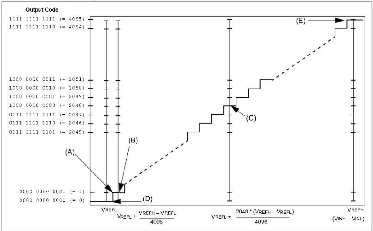
line
| Output Code | Value | |-------------|-----------| | 1111 | 4095 | | 1111 | 4094 | | 1000 | 2051 | | 1000 | 2050 | | 1000 | 2049 | | 1000 | 2048 | | 0111 | 2047 | | 0111 | 2046 | | 0111 | 2045 | | VREFL | 4096 | | VREFL + VREFH - VREFL | 4096 | | VREFL + 2048 * (VREFH - VREFL) | 4096 | | VREFH | VINH - VINL |22.10 ADC SAMPLING REQUIREMENTS
The analog input model of the 12-bit ADC is illustrated in Figure 22-26. The total acquisition time for the analog-to-digital conversion is a function of the internal circuit settling time and the holding capacitor charge time.
For the ADC module to meet its specified accuracy, the charge holding capacitor (CHOLD) must be allowed to fully charge to the voltage level on the analog input pin. The analog output source impedance (Rs), the interconnect impedance (Rc), and the internal sampling switch (Rs) impedance combine to directly affect the time required to charge the CHOLD. The combined impedance of the analog sources must therefore be small enough to fully charge (to within one-fourth LSB of the desired voltage) the holding capacitor within the selected sample time. The internal holding capacitor will be in the discharged state prior to each sample operation.
At least 1 TAD time period should be allowed between conversions for the acquisition time. Refer to the “Electrical Characteristics” chapter in the specific device data sheet for more information.
Figure 22-26: 12-bit ADC Analog Input Model

text_image
RS ANx VDD VT = 0.6V Ric = 200Ω Sampling Switch RSS = 44 Ω VA CPIN VT = 0.6V ILEAKAGE ± 500 nA CHOLD = DAC capacitance = 5 pF VSSNote: The C PIN value depends on the device package and is not tested. The effect of the CPIN is negligible if Rs ≤ 5 kΩ.
Legend:
$$ \begin{array}{l} C _ {P I N} = \text { Input capacitance } V \quad T = \text { Threshold voltage } \ \mathrm{Rss} = \text { Sampling switch resistance } \mathrm{R} \quad \mathrm{IC} = \text { Interconnect resistance } \ R _ {S} = \text { Source resistance } \quad C _ {\text { HOLD }} = \text { Sample / hold capacitance } \ I _ {\text { LEAKAGE }} = \text { Leakage current at the pin due to various junctions } \ \end{array} $$
22.11 CONNECTION CONSIDERATIONS
Because the analog inputs employ Electrostatic Discharge (ESD) protection, they have diodes to V_DD and V_SS ; therefore, the analog input must be between V_DD and V_SS . The presence of diodes is the reason why the analog pins cannot be 5V tolerant. If the input voltage exceeds this range by greater than 0.3V (either direction), one of the diodes becomes forward biased and it may damage the device if the input current specification exceeds.
An external RC filter is sometimes added for anti-aliasing of the input signal. The R (resistive) component should be selected to ensure that the acquisition time is met. Any external components connected (through high-impedance) to an analog input pin (capacitor, Zener diode, and so on) should have very little leakage current at the pin.
22.12 RELATED APPLICATION NOTES
This section lists application notes that are related to this section of the manual. These application notes may not be written specifically for the PIC32 device family, but the concepts are pertinent and could be used with modification and possible limitations. The current application notes related to the 12-bit High-Speed Successive Approximation Register (SAR) Analog-to-Digital Converter (ADC) module are:
Title Application Note #
No related application notes at this time. N/A
Note: Please visit the Microchip web site (www.microchip.com) for additional application notes and code examples for the PIC32 family of devices.
22.13 REVISION HISTORY
Revision A (June 2015)
This is the initial released version of the document.
Revision B (April 2016)
This revision includes the following updates:
- The ADINSEL<5:0> bits in the ADCCON3 register were updated (see Register 22-7)
- The DFMODE bit in the ADCFLTRx register was updated (see Register 22-17)
• Figure 22-18: "ADC Filter Comparisons Example" was added - The ADC CVD Mode code example was updated (see Example 22-7)
- Minor updates to text and formatting were incorporated throughout the document
Revision C (September 2017)
This revision includes the following updates:
- Section 22.4.11 "Only-the-fly Update of SFRs" was removed.
- Minor updates to text and formatting were incorporated throughout the document
Revision D (November 2017)
This revision includes the following updates:
- The bit values for the ADC Clock Source (TCLK) bits, ADCSEL<1:0> (ADCCON3<31:30>), were removed and a referral to the specific device data sheet for the ADC clock source selections was added (see Register 22-3)
- The Sample and Conversion Time equations were updated (see Equation 22-1 and Equation 22-2)
Revision E (September 2019)
This revision includes the following updates:
- Added missing mathematical symbols in Equation 22-1 and Equation 22-2
- Removed ADC6CFG configuration in Example 22-1
NOTES:
Note the following details of the code protection feature on Microchip devices:
• Microchip products meet the specification contained in their particular Microchip Data Sheet.
- Microchip believes that its family of products is one of the most secure families of its kind on the market today, when used in the intended manner and under normal conditions.
- There are dishonest and possibly illegal methods used to breach the code protection feature. All of these methods, to our knowledge, require using the Microchip products in a manner outside the operating specifications contained in Microchip's Data Sheets. Most likely, the person doing so is engaged in theft of intellectual property.
• Microchip is willing to work with the customer who is concerned about the integrity of their code.
- Neither Microchip nor any other semiconductor manufacturer can guarantee the security of their code. Code protection does not mean that we are guaranteeing the product as "unbreakable."
Code protection is constantly evolving. We at Microchip are committed to continuously improving the code protection features of our products. Attempts to break Microchip's code protection feature may be a violation of the Digital Millennium Copyright Act. If such acts allow unauthorized access to your software or other copyrighted work, you may have a right to sue for relief under that Act.
Information contained in this publication regarding device applications and the like is provided only for your convenience and may be superseded by updates. It is your responsibility to ensure that your application meets with your specifications. MICROCHIP MAKES NO REPRESENTATIONS OR WARRANTIES OF ANY KIND WHETHER EXPRESS OR IMPLIED, WRITTEN OR OTHERWISE, RELATED TO THE INFORMATION, INCLUDING BUT NOT LIMITED TO ITS CONDITION, QUALITY, PERFORMANCE, MERCHANTABILITY OR FITNESS FOR PURPOSE. Microchip disclaims all liability arising from this information and its use. Use of Microchip devices in life support and/or safety applications is entirely at the buyer's risk, and the buyer agrees to defend, indemnify and hold harmless Microchip from any and all damages, claims, suits, or expenses resulting from such use. No licenses are conveyed, implicitly or otherwise, under any Microchip intellectual property rights unless otherwise stated.
For information regarding Microchip's Quality Management Systems, please visit www.microchip.com/quality.
Trademarks
The Microchip name and logo, the Microchip logo, Adaptec, AnyRate, AVR, AVR logo, AVR Freaks, BesTime, BitCloud, chipKIT, chipKIT logo, CryptoMemory, CryptoRF, dsPIC, FlashFlex, flexPWR, HELDO, IGLOO, JukeBlox, KeeLoq, Kleer, LANCheck, LinkMD, maXStylus, maXTouch, MediaLB, megaAVR, Microsemi, Microsemi logo, MOST, MOST logo, MPLAB, OptoLyzer, PocketTimeA PLC, picoPower, PICSTART, PIC32 logo, RolarFire, O R Prochip Designer, QTouch, SAM-BA, SenGenuity, SpyNIC, SST, SST Logo, SuperFlash, Symmetricom, SyncServer, Tachyon, TempTrackr, TimeSource, tinyAVR, UNI/O, Vectron, and XMEGA are registered trademarks of Microchip Technology Incorporated in the U.S.A. and other countries.
APT, ClockWorks, The Embedded Control Solutions Company, EtherSynch, FlashTec, Hyper Speed Control, HyperLight Load, IntelliMOS, Libero, motorBench, mTouch, Powermite 3, Precision Edge, ProASIC, ProASIC Plus, ProASIC Plus logo, Quiet-Wire, SmartFusion, SyncWorld, Temux, TimeCesium, TimeHub, TimePictra, TimeProvider, Vite, WinPath, and ZL are registered trademarks of Microchip Technology Incorporated in the U.S.A.
Adjacent Key Suppression, AKS, Analog-for-the-Digital Age, Any Capacitor, AnyIn, AnyOut, BlueSky, BodyCom, CodeGuard, CryptoAuthentication, CryptoAutomotive, CryptoCompanion, CryptoController, dsPICDEM, dsPICDEM.net, Dynamic Average Matching, DAM, ECAN, EtherGREEN, In-Circuit Serial Programming, ICSP, INICnet, Inter-Chip Connectivity, JitterBlocker, KleerNet, KleerNet logo, memBrain, Mindi, MiWi, MPASM, MPF, MPLAB Certified logo, MPLIB, MPLINK, MultiTRAK, NetDetach, Omniscient Code Generation, PICDEM, PICDEM.net, PICkit, PICtail, PowerSmart, PureSilicon, QMatrix, REAL ICE, Ripple Blocker, SAM-ICE, Serial Quad I/O, SMART-I.S., SQI, SuperSwitcher, SuperSwitcher II, Total Endurance, TSHARC, USBCheck, VariSense, ViewSpan, WiperLock, Wireless DNA, and ZENA are trademarks of Microchip Technology Incorporated in the U.S.A. and other countries.
SQTP is a service mark of Microchip Technology Incorporated in the U.S.A. The Adaptec logo, Frequency on Demand, Silicon Storage Technology, and Symmcom are registered trademarks of Microchip Technology Inc. in other countries. GestIC is a registered trademark of Microchip Technology Germany II GmbH & Co. KG, a subsidiary of Microchip Technology Inc., in other countries. All other trademarks mentioned herein are property of their respective companies.
© 2015-2019, Microchip Technology Incorporated, All Rights Reserved.
ISBN: 978-1-5224-5083-2
Worldwide Sales and Service
AMERICAS
Corporate Office
2355 West Chandler Blvd.
Chandler, AZ 85224-6199
Tel: 480-792-7200
Fax: 480-792-7277
Technical Support:
http://www.microchip.com/
support
Web Address:
www.microchip.com
Atlanta
Duluth, GA
Tel: 678-957-9614
Fax: 678-957-1455
Austin, TX
Tel: 512-257-3370
Boston
Westborough, MA
Tel: 774-760-0087
Fax: 774-760-0088
Chicago
Itasca, IL
Tel: 630-285-0071
Fax: 630-285-0075
Dallas
Addison, TX
Tel: 972-818-7423
Fax: 972-818-2924
Detroit
Novi, MI
Tel: 248-848-4000
Houston, TX
Tel: 281-894-5983
Indianapolis
Noblesville, IN
Tel: 317-773-8323
Fax: 317-773-5453
Tel: 317-536-2380
Los Angeles
Mission Viejo, CA
Tel: 949-462-9523
Fax: 949-462-9608
Tel: 951-273-7800
Raleigh, NC
Tel: 919-844-7510
New York, NY
Tel: 631-435-6000
San Jose, CA
Tel: 408-735-9110
Tel: 408-436-4270
Canada - Toronto
Tel: 905-695-1980
Fax: 905-695-2078
ASIA/PACIFIC
Australia - Sydney
Tel: 61-2-9868-6733
China - Beijing
Tel: 86-10-8569-7000
China - Chengdu
Tel: 86-28-8665-5511
China - Chongqing
Tel: 86-23-8980-9588
China - Dongguan
Tel: 86-769-8702-9880
China - Guangzhou
Tel: 86-20-8755-8029
China - Hangzhou
Tel: 86-571-8792-8115
China - Hong Kong SAR
Tel: 852-2943-5100
China - Nanjing
Tel: 86-25-8473-2460
China - Qingdao
Tel: 86-532-8502-7355
China - Shanghai
Tel: 86-21-3326-8000
China - Shenyang
Tel: 86-24-2334-2829
China - Shenzhen
Tel: 86-755-8864-2200
China - Suzhou
Tel: 86-186-6233-1526
China - Wuhan
Tel: 86-27-5980-5300
China - Xian
Tel: 86-29-8833-7252
China - Xiamen
Tel: 86-592-2388138
China - Zhuhai
Tel: 86-756-3210040
ASIA/PACIFIC
India - Bangalore
Tel: 91-80-3090-4444
India - New Delhi
Tel: 91-11-4160-8631
India - Pune
Tel: 91-20-4121-0141
Japan - Osaka
Tel: 81-6-6152-7160
Japan - Tokyo
Tel: 81-3-6880-3770
Korea - Daegu
Tel: 82-53-744-4301
Korea - Seoul
Tel: 82-2-554-7200
Malaysia - Kuala Lumpur
Tel: 60-3-7651-7906
Malaysia - Penang
Tel: 60-4-227-8870
Philippines - Manila
Tel: 63-2-634-9065
Singapore
Tel: 65-6334-8870
Taiwan - Hsin Chu
Tel: 886-3-577-8366
Taiwan - Kaohsiung
Tel: 886-7-213-7830
Taiwan - Taipei
Tel: 886-2-2508-8600
Thailand - Bangkok
Tel: 66-2-694-1351
Tel: 43-7242-2244-39
Fax: 43-7242-2244-393
Denmark - Copenhagen
Tel: 45-4450-2828
Fax: 45-4485-2829
Finland - Espoo
Tel: 358-9-4520-820
France - Paris
Tel: 33-1-69-53-63-20
Fax: 33-1-69-30-90-79
Germany - Garching
Tel: 49-8931-9700
Germany - Haan
Tel: 49-2129-3766400
Germany - Heilbronn
Tel: 49-7131-72400
Germany - Karlsruhe
Tel: 49-721-625370
Germany - Munich
Tel: 49-89-627-144-0
Fax: 49-89-627-144-44
Germany - Rosenheim
Tel: 49-8031-354-560
Israel - Ra'anana
Tel: 972-9-744-7705
Italy - Milan
Tel: 39-0331-742611
Fax: 39-0331-466781
Italy - Padova
Tel: 39-049-7625286
Netherlands - Drunen
Tel: 31-416-690399
Fax: 31-416-690340
Norway - Trondheim
Tel: 47-7288-4388
Poland - Warsaw
Tel: 48-22-3325737
Romania - Bucharest
Tel: 40-21-407-87-50
Spain - Madrid
Tel: 34-91-708-08-90
Fax: 34-91-708-08-91
Sweden - Gothenberg
Tel: 46-31-704-60-40
Sweden - Stockholm
Tel: 46-8-5090-4654
UK - Wokingham
Tel: 44-118-921-5800
Fax: 44-118-921-5820