SY89473U - Electronic component Microchip - Free user manual and instructions
Find the device manual for free SY89473U Microchip in PDF.

User questions about SY89473U Microchip
0 question about this device. Answer the ones you know or ask your own.
Ask a new question about this device
Download the instructions for your Electronic component in PDF format for free! Find your manual SY89473U - Microchip and take your electronic device back in hand. On this page are published all the documents necessary for the use of your device. SY89473U by Microchip.
USER MANUAL SY89473U Microchip
The SY89473U is a 2.5V/3.3V precision, high-speed 2:1 differential MUX capable of processing clocks up to 2.5GHz and data up to 2.5Gbps.
The differential input includes Micrel's unique, 3-pin input termination architecture that directly interfaces to any differential signal (AC- or DC-coupled) as small as 100mV (200mV _PP ) without any level shifting or termination resistor networks in the signal path. The output is 800mV, 100K-compatible, LVPECL with fast rise/fall times guaranteed to be less than 190ps.
The SY89473U operates from a 2.5V ±5% or 3.3V ±10% supply and is guaranteed over the full industrial temperature range of -40°C to +85°C. The SY89473U is part of Micrel's high-speed, Precision Edge® product line. For multiple-clock switchover solutions, please refer to the SY89840-SY89843U family.
All support documentation can be found on Micrel's web site at: www.micrel.com.
Functional Block Diagram
flowchart
graph TD
    IN0["IN0"] -->|50Ω| A["NOT"]
    VT0["VT0"] -->|50Ω| B["NOT"]
    /IN0["/IN0"] -->|50Ω| C["NOT"]
    VREF-AC0["VREF-AC0"] --> A
    VREF-AC0 --> B
    VREF-AC1["VREF-AC1"] --> C
    A --> D["2:1 MUX"]
    B --> D
    C --> D
    D --> E["1:2 Fanout"]
    E --> Q0["Q0"]
    E --> Q1["Q1"]
    E --> Q0
    E --> Q1
    D --> S["MUX"]
    S --> T["S"]
    T --> U["SEL (LVTTL/CMOS)"]
    U --> V["OUT"]
    style D fill:#f9f,stroke:#333
    style E fill:#ccf,stroke:#333

Features
-
Selects between two input channels and provides two copies of the selected output
• Guaranteed AC performance over temperature and supply voltage: -
DC to 2.5Gbps data throughput
- DC to 2.5GHz f_MAX (clock)
- <500ps In-to-Out t_pd
- <190ps t_r/t_f
-
<20ps Output-to-output skew
-
Unique patented input isolation design minimizes crosstalk
• Ultra-low Jitter Design: -
<1ps _RMS random jitter
- <1ps _RMS cycle-to-cycle jitter
- <10psPP total jitter (clock)
- <0.7ps _RMS crosstalk induced jitter
- Unique patent-pending input termination and VT pin accepts DC- and AC-coupled inputs (CML, PECL, LVDS)
• 800mV (100K) LVPECL output swing
• 2.5V ±5% or 3.3V ±10% supply voltage
- -40°C to +85°C industrial temperature range
• Available in 24-pin (4mm x 4mm) QFN package
Applications
- Clock switchover
• Data distribution
Markets
• LAN/WAN
- Enterprise servers
- ATE
• Test and measurement
Precision Edge is a registered trademark of Micrel, Inc.
Micrel Inc. • 2180 Fortune Drive • San Jose, CA 95131 • USA • tel +1 (408) 944-0800 • fax +1 (408) 474-1000 • http://www.micrel.com
Ordering Information ^(1)
| Part Number Package Type | Operating Range | Package Marking | Lead Finish |
| SY89473UMG QFN-24 Industrial 473U with Pb-Free bar-line indicator | NiPdAu Pb-Free | ||
| SY89473UMGTR(2)QFN-24 Industrial | 473U with Pb-Free bar-line indicator | NiPdAu Pb-Free | |
Notes:
-
Contact factory for die availability. Dice are guaranteed at T_A=25^ , DC Electricals Only.
-
Tape and Reel.
Pin Configuration
text_image
VCC IN1 VT1 VREF-AC1 /IN0 24 23 22 21 20 19 GND VREF-AC0 1 2 17 NC VT0 3 4 5 16 SEL IN0 5 6 7 8 9 10 11 12 GND VCC 6 7 8 9 10 11 12 VCC Q0 /Q0 VCC VCC Q1 /Q124-Pin QFN
Pin Description
| Pin Number Pin Name Pin Function | ||
| 5, 2,23, 20 | IN0, /IN0IN1, /IN1 | Differential Inputs: These input pairs are the differential signal inputs to the device. They accept AC or DC-coupled signals as small as 100mV (200mV PP). Note that these inputs will default to an indeterminate state if left open. Each pin of a pair internally terminates to a VT pin through 50Ω. Please refer to the “Input Interface Applications” section for more details. |
| 3, 21 | VREF-AC0,VREF-AC1 | Reference Voltage: These outputs bias to VCC -1.2V. They are used for AC-coupling inputs IN and /IN. Connect VREF-AC directly to the corresponding VT pin. Bypass with 0.01μF low ESR capacitor to VCC. Maximum sink/source current is ±1.5mA. Due to the limited drive capability, the VREF-AC pin is only intended to drive its respective VT pin. Please refer to the “Input Interface Applications” section for more details. |
| 4, 22 VT0 | VT1 | Input Termination Center-Tap: Each side of the differential input pair terminates to a VT pin. The VT0 and VT1 pins provide a center-tap to a termination network for maximum interface flexibility. Please refer to the “Input Interface Applications” section for more details. |
| 1, 6, 9, 10, 13,19, 24 | VCC | Positive Power Supply: Connect to +2.5V or +3.3V power supply. Bypass with 0.1μF//0.01μF low ESR capacitors as close to VCC pins as possible. |
| 7, 811, 12 | Q0, /Q0Q1, /Q1 | Differential Outputs: These differential LVPECL output pairs are a logic function of the IN0, IN1, and SEL inputs. Please refer to the truth table below for details. Unused output pairs can be left floating with no impact on jitter. |
| 15 | SEL | This single-ended TTL/CMOS-compatible input selects the inputs to the multiplexer. Note that this input is internally connected to a 25kΩ pull-up resistor and will default to a logic HIGH state if left open. VTH = VCC/2. Please refer to the “Timing Diagram” section for more details. |
| 14, 17, 18 | GND, Exposed Pad | Ground: Ground pins and exposed pad must be connected to the same ground plane. |
Truth Table
| INPUTS | OUTPUTS | |||||
| IN0 | /IN0 | IN1 | /IN1 | SEL | Q | |
| 0 | 1 | X | X | 0 | 0 | 1 |
| 1 | 0 | X | X | 0 | 1 | 0 |
| X | X | 0 | 1 | 1 | 0 | 1 |
| X | X | 1 | 0 | 1 | 1 | 0 |
/Q
Absolute Maximum Ratings ^(1)
Supply Voltage ( V_CC )....-0.5V to +4.0V
Input Voltage ( V_IN )....-0.5V to V_CC
LVPECL Output Current ( I_OUT )
Continuous ....±50mA
Surge ±100mA
Input Current
Source/sink Current on IN, /IN....±50mA
Source/sink Current on V _T ......±100mA
V_REF-AC Current
Source/sink Current on V REF-AC....±2mA
Lead Temperature (soldering, 20 sec.) .....+260°C
Storage Temperature ( T_s )....-65°C to 150°C
Operating Ratings ^(2)
Supply Voltage ( V_cc ) ....+2.375V to +2.625V .....+3.0V to +3.6V
Ambient Temperature (T _A )......-40°C to +85°C
Package Thermal Resistance ^(3)
QFN (A)
Still-Air.... 50°C/W
QFN (ΨJB)
Junction-to-Board 30°C/W
DC Electrical Characteristics ^(4)
T_A = -40^ to +85^ ; unless otherwise stated.
| Symbol | Parameter Condition Min Typ Max Units | ||||||
| _CC | Power Supply | 2.375 | 2.5 | 2.625 | |||
| 3.0 | 3.3 | 3.6 | |||||
| I_CC | Power Supply Current | No load, max V_CC . | 45 | 65 | mA | ||
| R_IN | Input Resistance (IN-to- V_T ) | 45 | 50 | 55 | Ω | ||
| R_DIFF\_IN | Differential Input Resistance (IN-to-/IN) | 90 | 100 | 110 | Ω | ||
| V_IH | Input High Voltage (IN, /IN) | 1.2 | V_CC | V | |||
| V_IL | Input Low Voltage (IN, /IN) | 0 | V_IH-0.1 | V | |||
| V_IN | Input Voltage Swing (IN, /IN) | See Figure 1a. Note 5 | 0.1 | V_CC | V | ||
| V_DIFF\_IN | Differential Input Voltage Swing |IN-/IN| | See Figure 1b. | 0.2 | V | |||
| V_T\_IN | IN-to- V_T (IN, /IN) | 1.28 | V | ||||
| V_REF-AC | Output Reference Voltage | V_CC-1.3 | V_CC-1.2 | V_CC-1.1 | V | ||
Notes:
- Permanent device damage may occur if absolute maximum ratings are exceeded. This is a stress rating only and functional operation is not implied at conditions other than those detailed in the operational sections of this data sheet. Exposure to absolute maximum ratings conditions for extended periods may affect device reliability.
- The data sheet limits are not guaranteed if the device is operated beyond the operating ratings.
- Package thermal resistance assumes exposed pad is soldered (or equivalent) to the devices most negative potential on the PCB. _JA and _JB values are determined for a 4-layer board in still air unless otherwise stated.
- The circuit is designed to meet the DC specifications shown in the above table after thermal equilibrium has been established.
- V_IN (max) is specified when V_T is floating.
LVPECL Outputs DC Electrical Characteristics ^(6)
V_CC = 2.5V ± 5% or 3.3V ± 10% ; T_A = -40^ C to +85^ C ; R_L = 50 to V_CC-2V , unless otherwise stated.
| Symbol | Parameter Condition | Min Typ | Max | Units | ||
| V_OH | Output HIGH VoltageQ, /Q | V_CC-1.145 | V_CC-0.895 | V | ||
| V_OL | Output LOW VoltageQ, /Q | V_CC-1.945 | V_CC-1.695 | V | ||
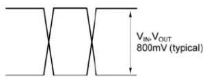
| V_OUT | Output Voltage SwingQ, /Q | See Figure 1a. 550 800 | mV | |||
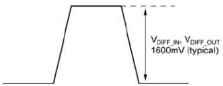
| V_DIFF-OUT | Differential Output Voltage SwingQ, /Q | See Figure 1b. 1100 1600 | mV |
LVTTL/CMOS DC Electrical Characteristics ^(6)
V_CC = 2.5V ± 5% or 3.3V ± 10% ; T_A = -40^ C to +85^ C , unless otherwise stated.
| Symbol | Parameter | Condition | Min | Typ | Max | Units |
| V_IH | Input HIGH Voltage | 2.0 | V | |||
| V_IL | Input LOW Voltage | 0.8 | V | |||
| I_IH | Input HIGH Current | -125 | 30 | μA | ||
| I_IL | Input LOW Current | -300 | μA |
Note:
- The circuit is designed to meet the DC specifications shown in the above table after thermal equilibrium has been established.
AC Electrical Characteristics ^(7)
V_CC = 2.5V ± 5% or 3.3V ± 10% ; T_A = -40^ C to +85^ C , R_L = 50 to V_CC-2V , unless otherwise stated.
| Symbol | Parameter Condition Min | Typ Max Units | ||||
| MAX Maximum Operating Frequency | NRZ Data | 2.5 3.2 | Gbps f | |||
| V_OUT ≥ 400mV Clock | 2.5 3.0 | GHz | ||||
| t_pd | Differential Propagation Delay In-to-Q | 250 | 320 | 500 | ps | |
| SEL-to-Q | V_TH=V_CC/2 | 250 | 360 | 600 | ps | |
| T_pd Tempco | Differential Propagation Delay Temperature Coefficient | 158 | fs/°C | |||
| t_SKEW | Output-to-Output Skew | Note 8 | 5 | 20 | ps | |
| Part-to-Part Skew | Note 9 | 200 | ps | |||
| t_Jitter | Clock Random Jitter | Note 10 | 1 | ps_RMS | ||
| Cycle-to-Cycle Jitter | Note 11 | 1 | ps_RMS | |||
| Total Jitter (TJ) | Note 12 | 10 | ps_PP | |||
| Crosstalk-Induced Jitter | Note 13 | 0.7 | ps_RMS | |||
| t_r, t_f | Output Rise/Fall Time (20% to 80%) | At full output swing. | 70 | 130 | 190 | ps |
Notes:
- High-frequency AC-parameters are guaranteed by design and characterization.
- Output-to-output skew is measured between two different outputs under identical transitions.
- Part-to-part skew is defined for two parts with identical power supply voltages at the same temperature and with no skew of the edges at the respective inputs.
- Random Jitter is measured with a K28.7 pattern, measured at <f_MAX .
- Cycle-to-cycle jitter definition: The variation of periods between adjacent cycles, T_n-T_n-1 where T is the time between rising edges of the output signal.
- Total Jitter definition: With an ideal clock input of frequency <f_MAX , no more than one output edge in 10^12 output edges will deviate by more than the specified peak-to-peak jitter value.
- Crosstalk is measured at the output while applying two similar differential clock frequencies that are asynchronous with respect to each other at the inputs.
Typical Operating Characteristics
V_CC = 3.3V; V_IN > 400mV; T_A = 25^, R_L = 50 to V_CC-2V, unless otherwise stated.
line
| FREQUENCY (MHz) | OUTPUT SWING (mV) | | --------------- | ----------------- | | 0 | 800 | | 1000 | 750 | | 2000 | 650 | | 3000 | 500 | | 4000 | 350 |Functional Characteristics
V_CC = 3.3V; V_IN > 400mV; T_A = 25^, R_L = 50 to V_CC-2V, unless otherwise stated.

line
| Time (700ps/div.) | Output Swing (200mV/div.) | | ----------------- | -------------------------- | | 0 | 0 | | 1 | 1 | | 2 | 0 | | 3 | 1 | | 4 | 0 | | 5 | 1 | | 6 | 0 | | 7 | 1 | | 8 | 0 | | 9 | 1 | | 10 | 0 | | 11 | 1 | | 12 | 0 | | 13 | 1 | | 14 | 0 | | 15 | 1 | | 16 | 0 | | 17 | 1 | | 18 | 0 | | 19 | 1 | | 20 | 0 | | 21 | 1 | | 22 | 0 | | 23 | 1 | | 24 | 0 | | 25 | 1 | | 26 | 0 | | 27 | 1 | | 28 | 0 | | 29 | 1 | | 30 | 0 | | 31 | 1 | | 32 | 0 | | 33 | 1 | | 34 | 0 | | 35 | 1 | | 36 | 0 | | 37 | 1 | | 38 | 0 | | 39 | 1 | | 40 | 0 | | 41 | 1 | | 42 | 0 | | 43 | 1 | | 44 | 0 | | 45 | 1 | | 46 | 0 | | 47 | 1 | | 48 | 0 | | 49 | 1 | | 50 | 0 | | 51 | 1 | | 52 | 0 | | 53 | 1 | | 54 | 0 | | 55 | 1 | | 56 | 0 | | 57 | 1 | | 58 | 0 | | 59 | 1 | | 60 | 0 | | 61 | 1 | | 62 | 0 | | 63 | 1 | | 64 | 0 | | 65 | 1 | | 66 | 0 | | 67 | 1 | | 68 | 0 | | 69 | 1 | | 70 | 0 | | 71 | 1 | | 72 | 0 | | 73 | 1 | | 74 | 0 | | 75 | 1 | | 76 | 0 | | 77 | 1 | | 78 | 0 | | 79 | 1 | | 80 | 0 | | 81 | 1 | | 82 | 0 | | 83 | 1 | | 84 | 0 | | 85 | 1 | | 86 | 0 | | 87 | 1 | | 88 | 0 | | 89 | 1 | | 90 | 0 | | 91 | 1 | | 92 | 0 | | 93 | 1 | | 94 | 0 | | 95 | 1 | | 96 | 0 | | 97 | 1 | | 98 | 0 | | 99 | 1 | | Note: The data is in a grid format with 'Time (700ps/div.)' as the index of the time axis. There are no labels for the output swing values. The output swing values are estimated based on the given code. There is only one data series in this case.
line
| TIME (120ps/div.) | Output Swing (200mV/div) | | ----------------- | ------------------------- | | 0 | 0 | | 125 | 125 | | 37 | 0 | | 59 | -125 | | 81 | 0 | | 103 | 125 | | 125 | 0 | | 147 | -125 | | 169 | 0 | | 191 | 125 | | 213 | 0 | | 235 | -125 | | 257 | 0 | | 279 | 125 | | 301 | 0 | | 323 | -125 | | 345 | 0 | | 367 | 125 | | 389 | 0 | | 411 | -125 | | 433 | 0 | | 455 | 125 | | 477 | 0 | | 499 | -125 | | 521 | 0 | | 543 | 125 | | 565 | 0 | | 587 | -125 | | 609 | 0 | | 631 | 125 | | 653 | 0 | | 675 | -125 | | 697 | 0 | | 719 | 125 | | 741 | 0 | | 763 | -125 | | 785 | 0 | | 807 | 125 | | 829 | 0 | | 851 | -125 | | 873 | 0 | | 895 | 125 | | 917 | 0 | | 939 | -125 | | 961 | 0 | | 983 | 125 | | 1005 | 0 | | 1027 | -125 | | | |
line
| TIME (80ps/div.) | Output Swing (200mV/div.) | | ---------------- | ------------------------- | | 0 | 0 | | 1 | 0.5 | | 2 | 1 | | 3 | 0.5 | | 4 | 0 | | 5 | -0.5 | | 6 | 0.5 | | 7 | 1 | | 8 | 0 | | 9 | -0.5 | | 10 | 0.5 | | 11 | 1 | | 12 | 0 | | 13 | -0.5 | | 14 | 0.5 | | 15 | 1 | | 16 | 0 | | 17 | -0.5 | | 18 | 0.5 | | 19 | 1 | | 20 | 0 | | 21 | -0.5 | | 22 | 0.5 | | 23 | 1 | | 24 | 0 | | 25 | -0.5 | | 26 | 0.5 | | 27 | 1 | | 28 | 0 | | 29 | -0.5 | | 30 | 0.5 | | 31 | 1 | | 32 | 0 | | 33 | -0.5 | | 34 | 0.5 | | 35 | 1 | | 36 | 0 | | 37 | -0.5 | | 38 | 0.5 | | 39 | 1 | | 40 | 0 | | 41 | -0.5 | | 42 | 0.5 | | 43 | 1 | | 44 | 0 | | 45 | -0.5 | | 46 | 0.5 | | 47 | 1 | | 48 | 0 | | 49 | -0.5 | | 50 | 0.5 | | 51 | 1 | | 52 | 0 | | 53 | -0.5 | | 54 | 0.5 | | 55 | 1 | | 56 | 0 | | 57 | -0.5 | | 58 | 0.5 | | 59 | 1 | | 60 | 0 | | 61 | -0.5 | | 62 | 0.5 | | 63 | 1 | | 64 | 0 | | 65 | -0.5 | | 66 | 0.5 | | 67 | 1 | | 68 | 0 | | 69 | -0.5 | | 70 | 0.5 | | 71 | 1 | | 72 | 0 | | 73 | -0.5 | | 74 | 0.5 | | 75 | 1 | | 76 | 0 | | 77 | -0.5 | | 78 | 0.5 | | 79 | 1 | | 80 | 0 |
line
| TIME (70ps/div.) | Output Swing (200mV/div) | | ---------------- | ------------------------ | | 0 | 0 | | 1 | 0.5 | | 2 | 1 | | 3 | 0.5 | | 4 | 0 | | 5 | -0.5 | | 6 | -1 | | 7 | -0.5 | | 8 | 0 | | 9 | 0.5 | | 10 | 1 | | 11 | 0 | | 12 | -0.5 | | 13 | -1 | | 14 | -0.5 | | 15 | 0 | | 16 | 0.5 | | 17 | 1 | | 18 | 0 | | 19 | -0.5 | | 20 | -1 | | 21 | -0.5 | | 22 | 0 | | 23 | 0.5 | | 24 | 1 | | 25 | 0 | | 26 | -0.5 | | 27 | -1 | | 28 | -0.5 | | 29 | 0 | | 30 | 0.5 | | 31 | 1 | | 32 | 0 | | 33 | -0.5 | | 34 | -1 | | 35 | -0.5 | | 36 | 0 | | 37 | 0.5 | | 38 | 1 | | 39 | 0 | | 40 | -0.5 | | 41 | -1 | | 42 | -0.5 | | 43 | 0 | | 44 | 0.5 | | 45 | 1 | | 46 | 0 | | 47 | -0.5 | | 48 | -1 | | 49 | -0.5 | | 50 | 0 | | 51 | 0.5 | | 52 | 1 | | 53 | 0 | | 54 | -0.5 | | 55 | -1 | | 56 | -0.5 | | 57 | 0 | | 58 | 0.5 | | 59 | 1 | | 60 | 0 | | 61 | -0.5 | | 62 | -1 | | 63 | -0.5 | | 64 | 0 | | 65 | 0.5 | | 66 | 1 | | 67 | 0 | | 68 | -0.5 | | 69 | -1 | | 70 | -0.5 |Single-Ended and Differential Swings
text_image
V_IN-V_OUT 800mV (typical)Figure 1a. Single-Ended Voltage Swing
text_image
VDIFF_IN, VDIFF_OUT 1600mV (typical)Figure 1b. Differential Voltage Swing
Timing Diagrams

text_image
IN0 /IN0 Q /Q tpd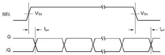
text_image
SEL VTH VTH tpd tpd Q /QInput and Output Stages
text_image
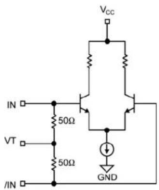
VCC IN 50Ω VT 50Ω /IN GNDFigure 2a. Simplified Differential Input Stage

text_image
VCC /Q QFigure 2b. Simplified LVPECL Output Stage
Input Interface Applications
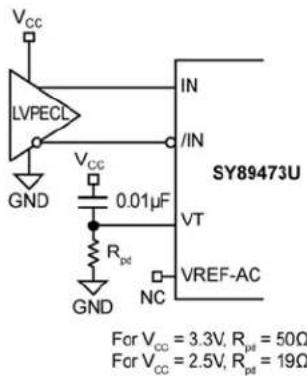
text_image
Vcc LVPECL GND Vcc 0.01μF Rpd GND IN /IN SY89473U VT VREF-AC NC For Vcc = 3.3V, Rpd = 50Ω For Vcc = 2.5V, Rpd = 19ΩFigure 3a. LVPECL Interface (DC-Coupled)
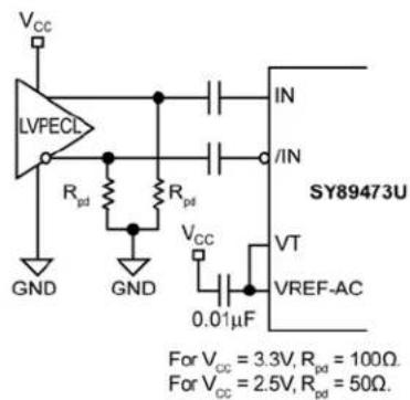
text_image
VCC LVPECL IN Rpd Rpd GND GND VT VREF-AC 0.01μF SY89473U For VCC = 3.3V, Rpd = 100Ω. For VCC = 2.5V, Rpd = 50Ω.Figure 3b. LVPECL Interface (AC-Coupled)
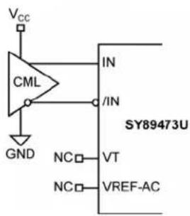
text_image
Vcc CML IN /IN GND SY89473U NC□ VT NC□ VREF-ACOption: may connect V_T to V_CC
Figure 3c. CML Interface (DC-Coupled)
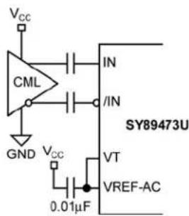
text_image
VCC CML IN /IN GND VCC 0.01μF VT VREF-AC SY89473UFigure 3d. CML Interface (AC-Coupled)
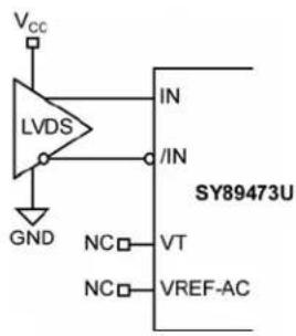
text_image
Vcc LVDS IN IN GND SY89473U NC □ VT NC □ VREF-ACFigure 3e. LVDS Interface (DC-Coupled)
LVPECL Output Interface Applications
LVPECL has a high input impedance, a very low output impedance (open emitter), and a small signal swing which results in low EMI. LVPECL is ideal for driving 50Ω- and-100Ω-controlled impedance transmission lines. There are several techniques for terminating the LVPECL output including: Parallel Termination-Thevenin Equivalent, Parallel Termination (3-resistor), and AC-coupled Termination. Unused output pairs may be left floating. However, single-ended outputs must be terminated, or balanced.
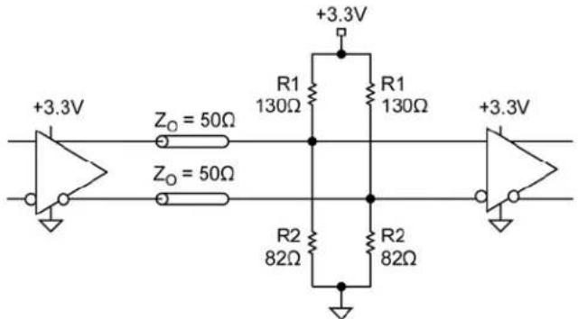
text_image
+3.3V Z₀ = 50Ω Z₀ = 50Ω +3.3V R1 130Ω R1 130Ω +3.3V R2 82Ω R2 82Ω +3.3VNote:
1. For +2.5V systems, R1 = 250Ω, R2 = 62.5Ω.
Figure 4a. Parallel Termination-Thevenin Equivalent

text_image
+3.3V Z = 50Ω Z = 50Ω "source" 50Ω 50Ω 50Ω Rb +3.3V "destination" Vcc C1 (optional) 0.01μFNote:
-
Power-saving alternative to Thevenin termination.
-
Place termination resistors as close to destination inputs as possible.
-
Rb resistor sets the DC bias voltage, equal to V _T .
-
For 2.5V systems, Rb = 19Ω.
Figure 4b. Parallel Termination (3-Resistor)
Related Product and Support Information
| Part Number | Function Data Sheet Link | |
| SY89474U | Precision LVDS 2:1 Multiplexer with 1:2 Fanout and Internal Termination | www.micrel.com/product-info/products/sy89474u.shtml |
| SY89475U | Precision CML 2:1 Multiplexer with 1:2 Fanout and Internal Termination | www.micrel.com/product-info/products/sy89475u.shtml |
| HBW Solutions | New Products and Applications | www.micrel.com/product-info/products/solutions.shtml |
Package Information
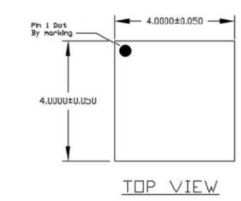
text_image
Pin 1 Dot By marking 4.0000±0.050 4.0000±0.050 TOP VIEW
text_image
2.7000±0.050 Exp. DAP PIN #: IDENTIFICATION CHAMFER 0.300 x 45° 0.4000±0.050 0.2500±0.025 2.700±0.050 Exp. DAP 0.5000 BSC 2.5000 Ref. BOTTOM VIEW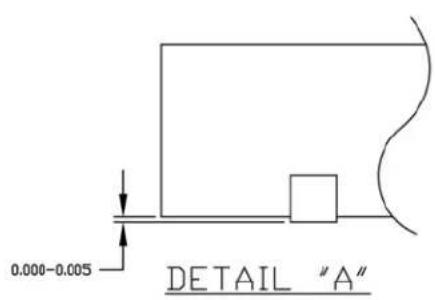
text_image
0.000-0.005 DETAIL "A"
text_image
0.8500±0.050 SEE DETAIL A 0.203±0.025 SIDE VIEWNOTE:
1. ALL DIMENSIONS ARE IN MILLIMETERS (mm).
2. THE PIN#1 IDENTIFIER MUST EXIST ON THE TOP SURFACE OF PACKAGE BY USING IDENTIFICATION MARK OR OTHER FEATURE OF PACKAGE BODY.

CHAMFER STYLE PIN 1 IDENTIFIER ON BOTTOM SIDE
24-Pin QFN
MICREL, INC. 2180 FORTUNE DRIVE SAN JOSE, CA 95131 USA
TEL +1 (408) 944-0800 FAX +1 (408) 474-1000 WEB http://www.micrel.com
The information furnished by Micrel in this data sheet is believed to be accurate and reliable. However, no responsibility is assumed by Micrel for its use. Micrel reserves the right to change circuitry and specifications at any time without notification to the customer.
Micrel Products are not designed or authorized for use as components in life support appliances, devices or systems where malfunction of a product can reasonably be expected to result in personal injury. Life support devices or systems are devices or systems that (a) are intended for surgical implant into the body or (b) support or sustain life, and whose failure to perform can be reasonably expected to result in a significant injury to the user. A Purchaser's use or sale of Micrel Products for use in life support appliances, devices or systems is a Purchaser's own risk and Purchaser agrees to fully indemnify Micrel for any damages resulting from such use or sale.
© 2005 Micrel, Incorporated.