MCP33151D-10 - Unspecified Microchip - Free user manual and instructions
Find the device manual for free MCP33151D-10 Microchip in PDF.

User questions about MCP33151D-10 Microchip
0 question about this device. Answer the ones you know or ask your own.
Ask a new question about this device
Download the instructions for your Unspecified in PDF format for free! Find your manual MCP33151D-10 - Microchip and take your electronic device back in hand. On this page are published all the documents necessary for the use of your device. MCP33151D-10 by Microchip.
USER MANUAL MCP33151D-10 Microchip
Note the following details of the code protection feature on Microchip devices:
• Microchip products meet the specification contained in their particular Microchip Data Sheet.
- Microchip believes that its family of products is one of the most secure families of its kind on the market today, when used in the intended manner and under normal conditions.
- There are dishonest and possibly illegal methods used to breach the code protection feature. All of these methods, to our knowledge, require using the Microchip products in a manner outside the operating specifications contained in Microchip's Data Sheets. Most likely, the person doing so is engaged in theft of intellectual property.
• Microchip is willing to work with the customer who is concerned about the integrity of their code.
- Neither Microchip nor any other semiconductor manufacturer can guarantee the security of their code. Code protection does not mean that we are guaranteeing the product as "unbreakable."
Code protection is constantly evolving. We at Microchip are committed to continuously improving the code protection features of our products. Attempts to break Microchip's code protection feature may be a violation of the Digital Millennium Copyright Act. If such acts allow unauthorized access to your software or other copyrighted work, you may have a right to sue for relief under that Act.
Information contained in this publication regarding device applications and the like is provided only for your convenience and may be superseded by updates. It is your responsibility to ensure that your application meets with your specifications. MICROCHIP MAKES NO REPRESENTATIONS OR WARRANTIES OF ANY KIND WHETHER EXPRESS OR IMPLIED, WRITTEN OR ORAL, STATUTORY OR OTHERWISE, RELATED TO THE INFORMATION, INCLUDING BUT NOT LIMITED TO ITS CONDITION, QUALITY, PERFORMANCE, MERCHANTABILITY OR FITNESS FOR PURPOSE. Microchip disclaims all liability arising from this information and its use. Use of Microchip devices in life support and/or safety applications is entirely at the buyer's risk, and the buyer agrees to defend, indemnify and hold harmless Microchip from any and all damages, claims, suits, or expenses resulting from such use. No licenses are conveyed, implicitly or otherwise, under any Microchip intellectual property rights unless otherwise stated.
Trademarks
The Microchip name and logo, the Microchip logo, Adaptec, AnyRate, AVR, AVR logo, AVR Freaks, BesTime, BitCloud, chipKIT, chipKIT logo, CryptoMemory, CryptoRF, dsPIC, FlashFlex, flexPWR, HELDO, IGLOO, JukeBlox, KeeLoq, Kleer, LANCheck, LinkMD, maXStylus, maXTouch, MediaLB, megaAVR, Microsemi, Microsemi logo, MOST, MOST logo, MPLAB, OptoLyzer, PackeTime, PIC, picoPower, PICSTART, PIC32 logo, PolarFire, Prochip Designer, QTouch, SAM-BA, SenGenuity, SpyNIC, SST, SST Logo, SuperFlash, Symmetricom, SyncServer, Tachyon, TempTrackr, TimeSource, tinyAVR, UNI/O, Vectron, and XMEGA are registered trademarks of Microchip Technology Incorporated in the U.S.A. and other countries.
APT, ClockWorks, The Embedded Control Solutions Company, EtherSynch, FlashTec, Hyper Speed Control, HyperLight Load, IntelliMOS, Libero, motorBench, mTouch, Powermite 3, Precision Edge, ProASIC, ProASIC Plus, ProASIC Plus logo, Quiet-Wire, SmartFusion, SyncWorld, Temux, TimeCesium, TimeHub, TimePictra, TimeProvider, Vite, WinPath, and ZL are registered trademarks of Microchip Technology Incorporated in the U.S.A.
Adjacent Key Suppression, AKS, Analog-for-the-Digital Age, Any Capacitor, AnyIn, AnyOut, BlueSky, BodyCom, CodeGuard, CryptoAuthentication, CryptoAutomotive, CryptoCompanion, CryptoController, dsPICDEM, dsPICDEM.net, Dynamic Average Matching, DAM, ECAN, EtherGREEN, In-Circuit Serial Programming, ICSP, INICnet, Inter-Chip Connectivity, JitterBlocker, KleerNet, KleerNet logo, memBrain, Mindi, MiWi, MPASM, MPF, MPLAB Certified logo, MPLIB, MPLINK, MultiTRAK, NetDetach, Omniscient Code Generation, PICDEM, PICDEM.net, PICkit, PICtail, PowerSmart, PureSilicon, QMatrix, REAL ICE, Ripple Blocker, SAM-ICE, Serial Quad I/O, SMART-I.S., SQI, SuperSwitcher, SuperSwitcher II, Total Endurance, TSHARC, USBCheck, VariSense, ViewSpan, WiperLock, Wireless DNA, and ZENA are trademarks of Microchip Technology Incorporated in the U.S.A. and other countries.
SQTP is a service mark of Microchip Technology Incorporated in the U.S.A. The Adaptec logo, Frequency on Demand, Silicon Storage Technology, and Symmcom are registered trademarks of Microchip Technology Inc. in other countries. GestIC is a registered trademark of Microchip Technology Germany II GmbH & Co. KG, a subsidiary of Microchip Technology Inc., in other countries. All other trademarks mentioned herein are property of their respective companies.
© 2019, Microchip Technology Incorporated, All Rights Reserved.
ISBN: 978-1-5224-4713-9
For information regarding Microchip's Quality Management Systems, please visit www.microchip.com/quality.
Table of Contents
Preface 5
Introduction....5
Document Layout 5
Conventions Used in this Guide 6
Recommended Reading....7
The Microchip Website....7
Customer Support 7
Document Revision History 8
Chapter 1. Quick Start Guide for Hardware Setup
Chapter 2. Product Overview
2.1 Introduction ...... 11
2.2 MCP331X1D 16/14/12-Bit, 1 Msps SAR ADC Evaluation Board Features .. 11
2.3 MCP331X1D 16/14/12-Bit, 1 Msps SAR ADC Evaluation Kit Contents ..... 11
2.4 MCP331X1D 16/14/12-Bit, 1 Msps SAR ADC Evaluation Kit Requirements 12
2.5 MCP331X1D 16/14/12-Bit, 1 Msps SAR ADC Evaluation Board Overview . 12
2.6 SAR ADC Device Configuration 14
2.7 PIC32MZ EF Curiosity Development Board (DM320104) Overview ..... 15
2.8 SAR ADC Utility Software Overview 16
Chapter 3. Installation and Operation
3.1 Configuration Requirements 25
3.2 Evaluation Kit Setup 25
Chapter 4. Firmware
4.1 PIC32MZ2048EFM100 Initialization 27
4.2 Data Acquisition 27
4.3 USB Transfer 29
4.4 ADC Functions 30
Appendix A. Schematics and Layout
A.1 Introduction 33
A.2 Board – Schematic (Page 1 of 2) ...... 34
A.3 Board - Schematic (Page 2 of 2) 35
A.4 Board – Top Silk Layer 36
A.5 Board – Top Copper and Silk Layer 37
A.6 Board - Top Copper Layer 38
A.7 Board – Bottom Copper Layer 39
A.8 Board – Bottom Copper and Silk Layer 40
A.9 Board – Bottom Silk Layer 41
Appendix B. Bill of Materials (BOM)
B.1 MCP331X1D Evaluation Board – Bill of Materials (BOM) 43
Worldwide Sales and Service ....49
Preface
NOTICE TO CUSTOMERS
All documentation becomes dated, and this manual is no exception. Microchip tools and documentation are constantly evolving to meet customer needs, so some actual dialogs and/or tool descriptions may differ from those in this document. Please refer to our website (www.microchip.com) to obtain the latest documentation available.
Documents are identified with a "DS" number. This number is located on the bottom of each page, in front of the page number. The numbering convention for the DS number is "DSXXXXXXXXA", where "XXXXXXXXX" is the document number and "A" is the revision level of the document.
For the most up-to-date information on development tools, see the MPLAB ^® IDE online help. Select the Help menu, and then Topics to open a list of available online help files.
INTRODUCTION
This chapter contains general information that will be useful to know before using the MCP331X1D 16/14/12-Bit, 1 Msps SAR ADC Evaluation Kit. Items discussed in this chapter include:
- Document Layout
• Conventions Used in this Guide
• Recommended Reading
• The Microchip Website - Customer Support
• Document Revision History
DOCUMENT LAYOUT
This document describes how to use the MCP331X1D 16/14/12-Bit, 1 Msps SAR ADC Evaluation Kit to demonstrate the performance of the MCP331X1 device family. The manual layout is as follows:
- Chapter 1. "Quick Start Guide for Hardware Setup" – Provides quick, step-by-step information on setting up the MCP331X1D 16/14/12-Bit, 1 Msps SAR ADC Evaluation Kit.
- Chapter 2. "Product Overview" – Important information about the MCP331X1D 16/14/12-Bit, 1 Msps SAR ADC Evaluation Kit.
- Chapter 3. "Installation and Operation" – Includes instructions on how to get started with the MCP331X1D 16/14/12-Bit, 1 Msps SAR ADC Evaluation Kit.
- Chapter 4. "Firmware" - Includes information about the firmware that is included with the MCP331X1D 16/14/12-Bit, 1 Msps SAR ADC Evaluation Kit.
- Appendix A. "Schematics and Layout" – Refer to the board's web page for the complete Schematics and Layouts.
- Appendix B. "Bill of Materials (BOM)" – Refer to the board's web page for the complete Bill of Materials.
CONVENTIONS USED IN THIS GUIDE
This manual uses the following documentation conventions:
DOCUMENTATION CONVENTIONS
| Description Represents Examples | ||
| Arial font: | ||
| Italic characters Referenced books | mPLAB | ^ IDE User's Guide |
| Emphasized text ...is the only compiler... | ||
| Initial caps A window the Output | ut window | |
| A dialog the Settings dialog | ||
| A menu selection select Enable Programmer | ||
| Quotes A field name in a window or dialog | "Save project before build" | |
| Underlined, Italic text with right angle bracket | A menu path File>Save | —— |
| Bold characters A dialog button | Click OK | |
| A tab | Click the Power tab | |
| N'Rnnnn | A number in verilog format, where N is the total number of digits, R is the radix and n is a digit. | 4'b0010, 2'hF1 |
| Text in angle brackets <> | A key on the keyboard | Press,, |
| Courier New font: | ||
| Plain Courier New | Sample source code | #define START |
| Filenames | autoexec.bat | |
| File paths | c:\mccl8\h | |
| Keywords | _asm, _endasm, static | |
| Command-line options | -Opa+, -Opa- | |
| Bit values | 0, 1 | |
| Constants | 0xFF, 'A' | |
| Italic Courier New | A variable argument | file.o, where file can be any valid filename |
| Square brackets [] | Optional arguments | mccl8 [options] file [options] |
| Curly brackets and pipe character: { | } | Choice of mutually exclusive arguments; an OR selection | errorlevel {0|1} |
| Ellipses... Replaces repeated text | var_name [, | var_name...] |
| Represents code supplied by user | void main (void){ ...} | |
RECOMMENDED READING
This user's guide describes how to use the MCP331X1D 16/14/12-Bit, 1 Msps SAR ADC Evaluation Kit. Another useful document is listed below. The following Microchip document is available and recommended as a supplemental reference resource.
- MCP33131D/21D/11D-XX Data Sheet – “1 Msps /500 ksps 16/14/12-Bit Differential Input SAR ADC” (DS20005947)
THE MICROCHIP WEBSITE
Microchip provides online support via our website at www.microchip.com. This website is used as a means to make files and information easily available to customers. Accessible by using your favorite Internet browser, the website contains the following information:
- Product Support – Data sheets and errata, application notes and sample programs, design resources, user's guides and hardware support documents, latest software releases and archived software
- General Technical Support – Frequently Asked Questions (FAQs), technical support requests, online discussion groups, Microchip consultant program member listing
- Business of Microchip – Product selector and ordering guides, latest Microchip press releases, listing of seminars and events, listings of Microchip sales offices, distributors and factory representatives
CUSTOMER SUPPORT
Users of Microchip products can receive assistance through several channels:
• Distributor or Representative
- Local Sales Office
- Embedded System Engineer (ESE)
- Technical Support
Customers should contact their distributor, representative or field application engineer (FAE) for support. Local sales offices are also available to help customers. A listing of sales offices and locations is included in the back of this document.
Technical support is available through the website at: http://www.microchip.com/support.
DOCUMENT REVISION HISTORY
Revision C (April 2020)
Updated Table 2-1 in Section 2.5 "MCP331X1D 16/14/12-Bit, 1 Msps SAR ADC Evaluation Board Overview".
Updated Table 2-2 in Section 2.6 "SAR ADC Device Configuration".
Updated Figure 4-2 description in Section 4.2 "Data Acquisition".
Revision B (June 2019)
- Updated figure in Chapter 1. "Quick Start Guide for Hardware Setup"
- Updated figures in Section 2.6 "SAR ADC Device Configuration"
- Updated Appendix A. "Schematics and Layout"
- Updated Appendix B. "Bill of Materials (BOM)"
- Grammar and styling updates
Revision A (April 2018)
- Initial release of this document.
Chapter 1. Quick Start Guide for Hardware Setup
The following nine steps provide a quick start guide for setting up the MCP331X1D 16/14/12-Bit, 1 Msps SAR ADC Evaluation Board and the PIC32MZ EF Curiosity Development Board.
text_image
MCP331X1D Evaluation Board PIC32MZ EF Curiosity Development Board MCROCHIP RHO00873 MICROCHIP RHO00873 MICROCHIP RHO00873 MICROCHIP RHO00873 MICROCHIP RHO00873 MICROCHIP RHO00873 MICROCHIP RHO00873 MICROCHIP RHO00873 MICROCHIP RHO00873 MICROCHIP SAR_Adc_Uti lity.exe SAR ADC Evaluation Utility File Help Device Selection: MCP33131D-10 Interface Mode: 3-wire CS without BUSV Input Structure Differential Operating Mode: Continuous Analysis: Sampling Frequency 1000 kHz Electrical Leakage 2 kHz DC Leakage 2 kHz FFT Window Electrans Radiogram Length 26204 FFT Domain: Volts/Time Codes/Time INIL DNL FFT Single Conv. Continuous StopFIGURE 1-1: MCP331X1D 16/14/12-Bit, 1 Msps SAR ADC Evaluation Kit (default).
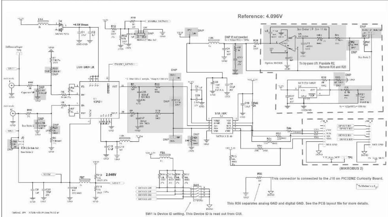
- On the PIC32MZ EF Curiosity Development Board, move the PWR IN jumper to connect pins, V_IN and V_BUS .
- Connect the Micro-USB cable from the PC to J12 on the PIC32MZ EF Curiosity Development Board. This USB is used for both power and data transfer for the PIC32MZ EF board.
- If using a preprogrammed PIC32MZ EF Curiosity Development Board, skip to Step 5. If using a non-programmed version of the PIC32MZ EF Curiosity Development Board, then program the PIC32MZ with the latest MCP331X1D Evaluation Board (ADM00873) Hex file (available on www.microchip.com) using an external programmer (MPLAB® ICD, PICkit™ ICD, etc.) connected to the ICSP™ HDR (J16).
- Once the firmware is loaded, remove the programmer and wait for LED4 to illuminate with a solid red light. A solid red lit LED indicates that the firmware is loaded and the board is working as intended.
- Connect the MCP331X1D Evaluation Board (ADM00873) to the top right mikroBUS™ header (J10), as displayed in Figure 1-1.
-
Connect a 9V power supply to the barrel jack connection point using either the supplied 9V wall power supply or, alternatively, connect 9V from an external power source to the H1 headers. D1, directly below the barrel jack, will illuminate to confirm that 9V is being supplied to the evaluation board.
-
Connect either a fully differential or single-ended signal source.
a) When using a Fully Differential signal source:
- Connect positive input to J1 SMA connector
- Connect negative input to J2 SMA connector
b) When using Single-Ended input signal:
- Connect positive input to J1 SMA connector
- Populate jumper at J6 headers to connect the negative input to V REF/2
Note: When the jumper J6 is connected, V_REF/2 is automatically provided to input pin IN- of U1 (ADC driver). The U1 output swings with V_IN+/2 centered at the V_COM voltage. Where V_REF = 4.048V is used in this board.
- PC GUI: Install and launch SAR_ADC_Utility.exe (available on www.microchip.com). The software will automatically recognize the plugged in device and launch the GUI.
- Once the GUI is open, use the blue Play button to run single or continuous acquisitions. The GUI will display all performance analysis data related to the acquired signal.
Chapter 2. Product Overview
2.1 INTRODUCTION
This chapter provides an overview of the MCP331X1D 16/14/12-Bit, 1 Msps SAR ADC Evaluation Kit and covers the following topics:
• MCP331X1D 16/14/12-Bit, 1 Msps SAR ADC Evaluation Board Features
- MCP331X1D 16/14/12-Bit, 1 Msps SAR ADC Evaluation Kit Contents
• MCP331X1D 16/14/12-Bit, 1 Msps SAR ADC Evaluation Kit Requirements
• MCP331X1D 16/14/12-Bit, 1 Msps SAR ADC Evaluation Board Overview
• SAR ADC Device Configuration
• PIC32MZ EF Curiosity Development Board (DM320104) Overview
• SAR ADC Utility Software Overview
2.2 MCP331X1D 16/14/12-BIT, 1 MSPS SAR ADC EVALUATION BOARD FEATURES
This MCP331X1D 16/14/12-Bit, 1 Msps SAR ADC Evaluation Kit is a fully assembled, programmed and tested solution to evaluate and demonstrate the MCP33131D operating performance.
The MCP331X1D 16/14/12-Bit, 1 Msps SAR ADC Evaluation Kit features:
• Full-Scale Analog Input Range: -V REF to +V REF
- ADM00873 with Differential Input Configuration: -4 V PP to +4 VPP
- ADM00873 with Single-Ended Input Configuration: 0V to +4 V PP
• Dynamic Performance Monitoring
- Evaluation of Performance Parameters, such as: SNR, SFDR, THD, INL, DNL, Voltage Measurement and so on
- Evaluate Input Signal in Time Domain
- Ability to Save and Load Software Configurations
- Ability to Save and Load Raw Data for User Post-Processing
For information about the device features, refer to the "MCP331X1 Data Sheet".
2.3 MCP331X1D 16/14/12-BIT, 1 MSPS SAR ADC EVALUATION KIT CONTENTS
The MCP331X1D 16/14/12-Bit, 1 Msps SAR ADC Evaluation Board includes the following items:
- MCP331X1D 16/14/12-Bit, 1 Msps SAR ADC Evaluation Board with On-Board Reference ( V_REF = 4V ) (ADM00873)
- PIC32MZ EF Curiosity Development Board, Preprogrammed with SAR ADC Firmware (ADM320104)
• 9V Wall Plug-in Power Supply
- USB Cable from Curiosity PIC32 Development Board to PC
- Important Information Sheet
2.4 MCP331X1D 16/14/12-BIT, 1 MSPS SAR ADC EVALUATION KIT REQUIREMENTS
The MCP331X1D 16/14/12-Bit, 1 Msps SAR ADC Evaluation Board requires:
• Curiosity PIC32MZEF Development Board (DM320104)
• Type A Male to Micro-B USB Cable
- External Signal Input:
- Supplied by the user
• SAR ADC Utility Software (GUI):
- Available on the Microchip website
2.5 MCP331X1D 16/14/12-BIT, 1 MSPS SAR ADC EVALUATION BOARD OVERVIEW
The MCP331X1D 16/14/12-Bit, 1 Msps SAR ADC Evaluation Board is intended to demonstrate the performance of the MCP331X1 device family. This evaluation board is used together with:
- Curiosity PIC32MZEF Development Board (DM320104)
• SAR ADC Utility Software
Figure 2-1 displays the system setup.
flowchart
graph LR
    A["Signal Input"] --> B["MCP331X1D Evaluation Board (Note 1)"]
    B <-->|SPI| C["Curiosity PIC32MZEF Development Board (DM320104) (Note 2)"]
    C <-->|USB| D["PC GUI (SAR ADC Utility Software) (Note 3)"]
    E["9V Power Supply 5V Power Supplied via USB"] --> B
    F["Note 1: The ADC part is available on this board."] --> B
    G["Note 2: This board collects ADC data from the evaluation board and passes them to the PC GUI."] --> C
    H["Note 3: This GUI provides various user interfaces to test the performance of the MCP331X1 device."] --> C
FIGURE 2-1: MCP331X1D 16/14/12-Bit, 1 Msps SAR ADC Evaluation Kit System Setup.
This evaluation board supports the MCP331X1D-10 device family, which is Microchip Technology's fully differential single channel 12/14/16-bit, 1 Msps SAR Analog-to-Digital Converter (ADC).
The MCP331X1D Evaluation Board comes with the MCP331X1 device on board. All conditions and features can be evaluated using this evaluation board. Refer to Figure 2-2 and Figure 2-3 for photos of the evaluation boards, and refer to Table 2-1 for our currently available fully differential device offerings compatible with this evaluation board.
TABLE 2-1: DEVICES SUPPORTED BY MCP331X1D EVALUATION KIT ^(1)
| Part Number | Resolution | Sample Rate | SNR^(1) | SFDR^(1) | Input Configuration |
| MCP33131D-10 | 16-bit | 1 Msps | 91.3 dBFS | 103.5 dB | Differential |
| MCP33151D-10/MCP33121D-10 | 14-bit | 1 Msps | 85.1 dBFS | 103.5 dB | Differential |
| MCP33141D-10/MCP33111D-10 | 12-bit | 1 Msps | 73.9 dBFS | 99.3 dB | Differential |
| MCP33131D-05 | 16-bit | 500 ksps | 91.3 dBFS | 103.5 dB | Differential |
| MCP33141D-05/MCP33121D-05 | 14-bit | 500 ksps | 85.1 dBFS | 103.5 dB | Differential |
| MCP33111D-05/MCP33111D-05 | 12-bit | 500 ksps | 73.9 dBFS | 99.3 dB | Differential |
Note 1: SNR and SFDR are measured with f_IN = 10 kHz, V_IN = -1 dBFS, V_REF = 5V .
text_image
MUCROCHIP ADM00873 MCP331 x1 Eval Bd. Driver En. SND1 DHUST GND2 GND3 GND1 R0 R29 R0 R29 R0 R29 R0 R29 R0 R29 R0 R29 R0 R29 R0 R29 R0 R29 R0 R29 R0 R29 R0 R29 R0 R29 R0 R29 R0 R29 U6 U6 U6 U6 U6 U6 U6 U6 U6 U6 U6 U6 U6 U6 U6 U6 U6 U6 U6 U6 U6 U6 U6 U6 U6 U6 U6 U6 U6 U6 U6 U6 U6 U6FIGURE 2-2: MCP331X1D 16/14/12-Bit, 1 Msps SAR ADC Evaluation Board, 4V Reference.
Note: The 4V on-board reference can be replaced with an external voltage reference source by removing R60 and supplying a reference voltage at TP7.
2.6 SAR ADC DEVICE CONFIGURATION
Each evaluation board features a 4-way SPST DIP switch (schematic designator: SW1) that allows the user to manually configure the board for a variety of available Microchip SAR ADC devices. Table 2-2 lists each available switch setting. Refer to Figure 3-1 from Chapter 3. "Installation and Operation" to view the location of SW1.
TABLE 2-2: SW1 DEVICE CONFIGURATION SETTINGS
| Part Number Resolution | Speed | Input Configuration | SW1 Setting: (ID3:ID2:ID1:ID0) | Notes | |
| MCP33111-05/MCP33141-05 12 | 500 ksps Single-Ended 0-0-0-0 | ||||
| MCP33111D-05/MCP33141D-05 | 12 500 ksps | Differential | 0-0-0-1 | ||
| MCP33121-05/MCP33151-05 | 14 500 ksps Single-Ended 0-0-1-0 | ||||
| MCP33121D-05/MCP33151D-05 | 14 | 500 ksps | Differential | 0-0-1-1 | |
| MCP33131-05 | 16 500 ksps Single-Ended 0-1-0-0 | ||||
| MCP33131D-05 | 16 | 500 ksps | Differential | 0-1-0-1 | |
| MCP33111-10/MCP33141-10 12 | 1 Msps Single-Ended 1-0-1-0 | ||||
| MCP33111D-10/MCP33141D-10 | 12 | 1 Msps | Differential | 1-0-1-1 | |
| MCP33121-10/MCP33151-10 | 14 | 1 Msps | Single-Ended | 1-1-0-0 | |
| MCP33121D-10/MCP33151D-10 | 14 | 1 Msps | Differential | 1-1-0-1 | |
| MCP33131-10 | 16 | 1 Msps | Single-Ended | 1-1-1-0 | |
| MCP33131D-10 | 16 | 1 Msps | Differential | 1-1-1-1 | Default |
2.7 PIC32MZ EF CURIOSITY DEVELOPMENT BOARD (DM320104) OVERVIEW
Note 1: The PIC32MZ EF Curiosity Development Board is used for data capture from the MCP331X1D Evaluation Board. This board can be purchased with preprogrammed SAR ADC firmware compatible with the MCP331X1D Evaluation Board (ADM00873).
2: The PIC32MZ EF Curiosity Development Board included in the MCP331X1D Evaluation Kit is already preprogrammed with SAR ADC firmware.
The PIC32MZ EF Curiosity Development Board (DM320104) is a fully-integrated, 32-bit development platform featuring the high-performance PIC32MZ EF Series PIC ^® Microcontroller (PIC32MZ2048EFM100), which is utilized for capturing the digital data received from the MCP331X1D Analog-to-Digital Converter (ADC) Evaluation Board.
Figure 2-1 shows the connection of the PIC32MZ EF Curiosity Development Board directly between the MCP331X1D 16/14/12-Bit, 1 Msps SAR ADC Evaluation Board and the SAR ADC Utility Software.
The Curiosity Development Board (DM320104) connects to the PC through a USB cable, providing the user with two functionalities:
- The ability to send user commands directly to the device from the SAR ADC Utility Software.
- The ability to collect data from the evaluation board and send them to the SAR ADC Utility Software.
Figure 2-3 displays a close-up of the PIC32MZ EF Curiosity Development Board. More information, including user's guides and other resources for the Curiosity Development Board, can be found by visiting www.microchip.com.

text_image
PWR IN AN/RP04 RST/RAS CS/RPO4 SCK/RPO1 HISU/RPO14 HOSI/RPO3 +3.3V RSP2 2-RBP SND RSP65 2-RBP0 SND MICROCHIP GND LED1 LED2 LED3 S1 J16 ICSP HDR Microchip Curiosity PIC32 MZ EF MICROCHIP BUST PWR SEL PWR SEL MICROCHIP BUST PWR SEL MICROCHIP BUST PWR SEL MICROCHIP BUST PWR SEL MICROCHIP BUST PWR SEL MICROCHIP BUST PWR SEL MICROCHIP BUST PWR SEL MICROCHIP BUST PWR SEL MICROCHIP BUST PWR SEL MICROCHIP BUST PWR SEL MICROCHIP BUSTFIGURE 2-3: PIC32MZ EF Curiosity Development Board (DM320104).
2.7.1 Using the PIC32MZ EF Curiosity Development Board for Firmware Development Tool
The PIC32MZ EF Curiosity Development Board includes the PICkit™ On-Board (PKOB) debugger based on the PIC24FJ256GB106 USB microcontroller. In addition, it provides the option to use external debuggers, such as MPLAB® REAL ICE™ or MPLAB ICD 3, by connecting to the In-Circuit Serial Programming™ (ICSP™) header, J16.
By default, the on-board debugger is connected to the programming pins (PGEC and PGED) of the PIC32 device. To use an external debugger, remove jumper J2 to disconnect the on-board debugger from driving the programming pins.
Note: More details about this can be found in the “PIC32MZ EF Curiosity Development Board User’s Guide” (DS70005282), available for download at www.microchip.com.
TABLE 2-3: DEBUGGER SELECTION
| J2 Jumper Positions | |
| On-Board Debugger External Debugger | |
| Pins 1-2 Shorted Pins 1-2 Open | |
| Pins 3-4 Shorted Pins 3-4 Open | |
2.8 SAR ADC UTILITY SOFTWARE OVERVIEW
The SAR ADC Utility Software is the Graphical User Interface (GUI) used to communicate with the device and to configure its operating parameters. The software communicates with the ADC through the PIC32MZ EF Curiosity Development Board and a USB cable. When the user interacts with the software, the user's commands are passed to the MCP331X1 device through the PIC32MZ EF Curiosity Development Board. Once the commands are executed by the MCP331X1D Evaluation Board, the software receives the requested data from the PIC32MZ EF Curiosity Development Board. The software then analyzes the data, performs an FFT or other analysis and displays the results. Refer to Figure 2-1 for a diagram of the system setup.
Figure 2-4 through Figure 2-10 show screen captures of the various performance displays available within the SAR ADC Utility.
The SAR ADC Utility Software is available for download at www.microchip.com. For instructions on using the GUI, refer to the software's supporting documentation included with the installation file, as well as within the application Help menu.
line
| Frequency [kHz] | Output Amplitude [dBFS] | | --------------- | ---------------------- | | 0 | 0 | | 50 | -120 | | 100 | -120 | | 150 | -120 | | 200 | -120 | | 250 | -120 | | 300 | -120 | | 350 | -120 | | 400 | -120 | | 450 | -120 | | 500 | -120 |FIGURE 2-4: SAR ADC Utility Software Displaying a Typical FFT Waveform.
- Click the Single Conv. button for a single shot of the conversion results. Click Continuous for continuous repeated conversion results.
- Click Calibrate to manually send an ADC calibration command. ADC automatically self-calibrates on initial hardware start-up.
- Device selected automatically based on DIP setting at SW1. See Section 2.6 "SAR ADC Device Configuration" for details.

line
| Bit Position | Digital Output | | ------------ | -------------- | | b15 | 0 | | b14 | 0 | | b13 | 0 | | b12 | 1 | | b11 | 0 | | b10 | 1 | | b9 | 1 | | b8 | 1 | | b7 | 0 | | b6 | 1 | | b5 | 0 | | b4 | 1 | | b3 | 1 | | b2 | 0 | | b1 | 0 | | b0 | 0 |FIGURE 2-5: SAR ADC Utility Software Displaying a Single Acquisition Bit Position Digital Output.
- This feature is only available in Single Conversion One-Shot mode.
- Select Single-Shot from Operating Mode drop-down menu to enable the single acquisition bit position digital output display.
- V_REF value must be manually entered based on the ADC's supplied V_REF . ADM00873 defaults on board to V_REF = 4V .
This feature is very useful for the MCU firmware developer for using a known input signal, and seeing the output code and voltage to validate the firmware.

line
| CODE | DNL [LSB] | INL [LSB] | |------------|-----------|-----------| | 32768 | ~0.0 | ~-1.5 | | 65536 | ~0.0 | ~-1.5 |FIGURE 2-6: INL DNL Performance Display.
- Select INL DNL from the Domain menu in order to enable INL DNL Measurement mode.

line
| Time [msec] | Codes | | ----------- | ----------- | | 1 | -3.0 | | 2 | -2.5 | | 3 | -2.0 | | 4 | -1.5 | | 5 | -1.0 | | 6 | -0.5 | | 7 | 0.0 | | 8 | 0.5 |FIGURE 2-7: Codes vs. Time Display.
- Select Codes/Time from the Domain menu in order to enable the ADC Output Codes vs. Time display.
The display represents the digitized code value that corresponds to the input signal amplitude in time domain.

line
| Time [msec] | Codes (×10⁴) | | ----------- | ------------ | | 1.4 | 3 | | 1.5 | 3 | | 1.6 | 3 | | 1.7 | 3 | | 1.8 | 3 |FIGURE 2-8: Codes vs. Time Display (Zoomed).
- Select the +/- magnifying glass, then click and drag on the screen to zoom in and out. The data cursor can be selected to hover over the wave form and see the exact code value at any point in the display.
line
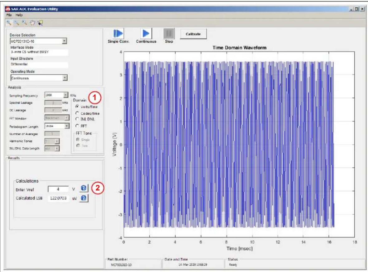
| Parameter | Value | |-------------------------|-----------| | Sampling Frequency | 1000 | | Spectral Leakage | 2 kHz | | DC Leakage | 2 kHz | | FFT Window | Blackman | | Periodogram Length | 16184 | | Number of Averages | 1 | | Harmonic Tone | 1 | | INL/DNL Data Length | 457 | | Time [msec] | 0 to 18 | | Voltage [V] | -4 to 4 | | Time [msec] | 0 to 18 | | Part Number | 0 | | MCP3313D-10 | 0 | | Date and Time | 0 | | 14-Mar-2019 10:55:29 | 0 | | Status | 0 | | Ready | 0 |FIGURE 2-9: Input Signal Voltage Amplitude vs. Time Display.
- Select Volts/Time from the Domain menu in order to enable the ADC Input Signal Voltage vs. Time display.
- V_REF value must be manually entered based on the ADC's supplied V_REF . ADM00873 defaults on board to V_REF = 4V .
This display shows the digitized input signal with the voltage amplitude reconstructed based on the supplied voltage reference value.
line
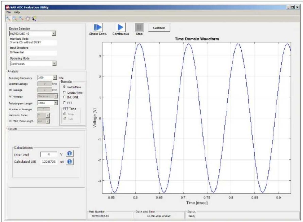
| Time [msec] | Voltage (V) | | ----------- | ----------- | | 0.55 | -3.0 | | 0.60 | 3.0 | | 0.65 | -3.0 | | 0.70 | 3.0 | | 0.75 | -3.0 | | 0.80 | 3.0 | | 0.85 | -3.0 | | 0.90 | 3.0 |FIGURE 2-10: Volts vs. Time Display (Zoomed).
NOTES:
Chapter 3. Installation and Operation
3.1 CONFIGURATION REQUIREMENTS
To power up and run the evaluation kit, the following are required:
• SAR ADC Utility Software
• MCP331X1D 16/14/12-Bit, 1 Msps SAR ADC Evaluation Board
• PIC32MZ EF Curiosity Development Board (DM320104)
- Type A Male to Micro-B USB Cable
- External Signal Source, Differential or Single-Ended Output (see Section 3.2.1 "Input Signal")
3.1.1 Power Input Connection
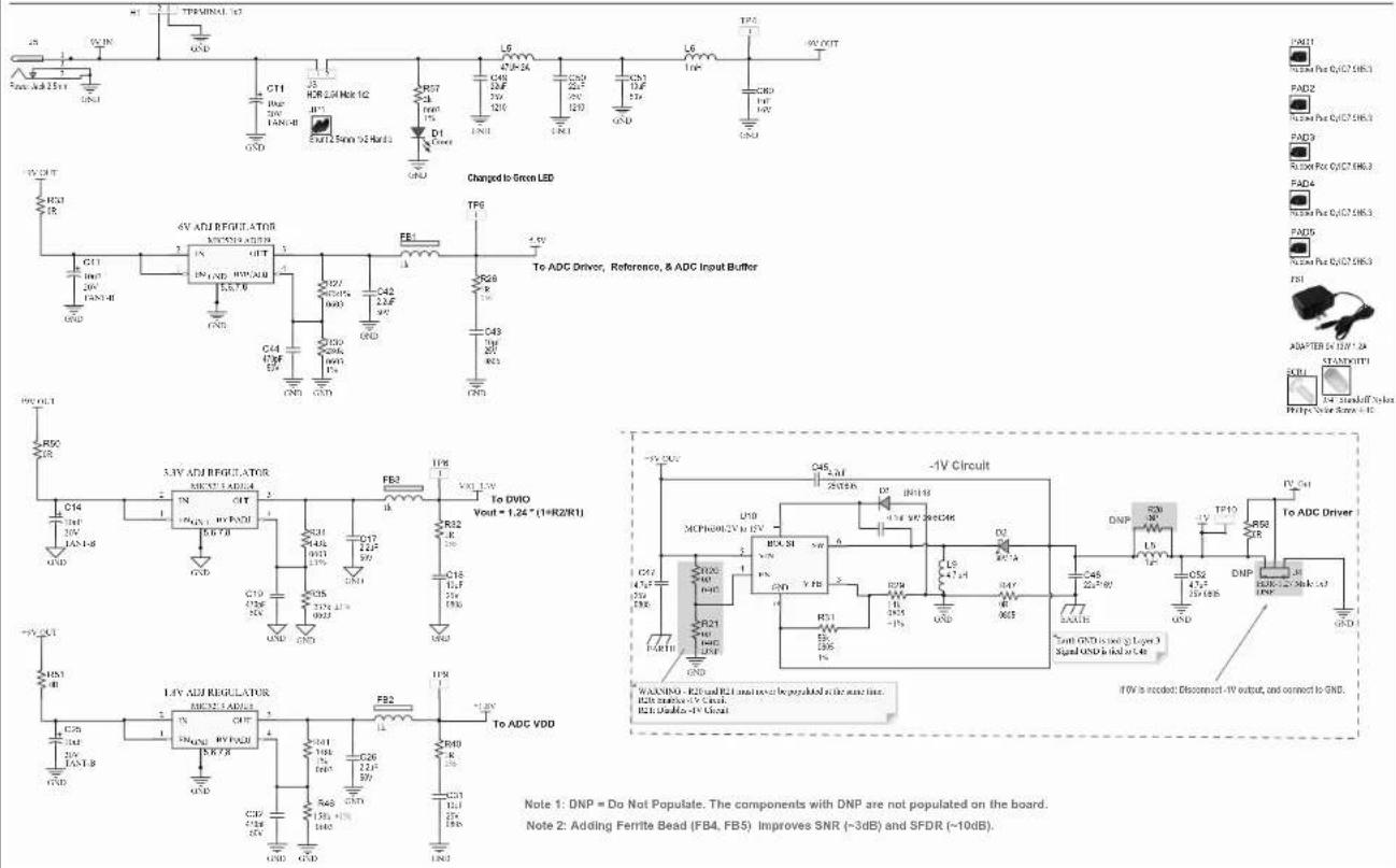
This MCP331X1D Evaluation Board comes with a 9V wall plug-in switching power supply (CUI INC P/N: SWI12-9-N-P6). This power supply is able to provide a 9V, 1.2A maximum output. It can be connected to an AC wall outlet rated between 100V AC and 240V AC, at a frequency of 50 Hz to 60 Hz. The other end of the power supply is a 2.1 mm barrel plug that connects to the MCP331X1D Evaluation Board (see
Figure 3-1). If the user chooses to connect a different external power supply, a minimum output of 500 mA is required, with a voltage output between 6V-12V. There is no on-board 9V regulator, so the 9V OUT pin (TP4) will read a voltage equal to the voltage input value selected by the user.
WARNING
Avoid connecting a power supply with a voltage greater than what is recommended in this user guide. Doing so can damage the voltage regulators, requiring them to be replaced.
3.2 EVALUATION KIT SETUP
- Connect the MCP331X1D Evaluation Board and the PIC32MZ EF Curiosity Development Board, as shown in Figure 3-1.
- Connect the PIC32MZ EF Curiosity Development Board to a computer using a Type A male to Micro-B USB cable. In order to power the Curiosity Board through USB, the USB cable must be plugged into the USB connection located at J12. In addition to this, the headers located at J8 need to have the jumper connecting the V_BUS pin to V_IN . Figure 3-1 shows the component locations.
- Power up the MCP331X1D Evaluation Board using the provided 9V power supply.
- Connect a differential or single-ended analog input signal to the MCP331X1D Evaluation Board SMA terminals. For single-ended operation, populate jumper J6 (see Figure 3-1 for jumper location). By populating this jumper, the negative signal input will be tied to V_REF/2 ( V_COM ). Another option is to terminate the negative signal input (J2) with 0Ω. This can be done by shorting C34.
- Run the SAR ADC Utility Software. See Section 2.8 "SAR ADC Utility Software Overview".

text_image
Analog Inputs ADC Power Circuit MCP331X1D 16/14/12-Bit, 1 Msps SAR ADC Evaluation Board (ADM00873) VCOM(VREF/2 for S.E. Source) Jumper (J6)) -1V/GND Driver Input Select (J4) Driver Enable (J8) Differential Driver (U1) VREF Regulator (U2) MCP6286 Op Amp (U5) ADC Device (U3) Curiosity Power Source Selection Header (J8) USB Power Supply (J12) MICROCHIP ADH00873 HCP331x1 Eval Bd. MICROCHIP Configuration Switch (SW1) MICROCHIP Curiosity PIC32 MZ EF Curiosity Development Board (DM320104)FIGURE 3-1: The MCP331X1D 16/14/12-Bit, 1 Msps SAR ADC Evaluation Board (ADM00873) connected to the PIC32MZ EF Curiosity Development Board (DM320104).
3.2.1 Input Signal
The best way to evaluate the MCP331X1D device is to use a clean analog input signal with as little noise as possible and no harmonic contents. The AP2722 Audio Analyzer from Audio Precision can be used to generate a clean analog signal for evaluation purposes. If using a less pure signal source, a filter can be added between the signal source and EVB to remove any noise outside of the desired frequency.
Chapter 4. Firmware
4.1 PIC32MZ2048EFM100 INITIALIZATION
MPLAB® X IDE and MPLAB Harmony were used to develop the firmware for the PIC32MZ2048EFM100 on the PIC32MZ EF Curiosity Development Board (DM320104).
The MCU runs at 130 MHz and the SPI prescaler is set to perform a division by 2 in order to obtain an SPI clock frequency of 65 MHz. This is the minimum SPI speed required to successfully read 16 bits of data out of the ADC at 1 Msps.
In the firmware for this demo, a USB stack was used to achieve communication with the GUI. Direct Memory Access (DMA) was used together with SPI and Output Compare in order to acquire data, and to gate the clock during acquisition.
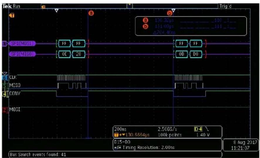
In this demonstration, the ADC acquisition is triggered by the CONV pulse (RPD5), which is generated by the OC2. The OC2 is generated by Timer3 (OCTSEL = 1). Timer3 is also used to generate OC1 which triggers the DMA SPI transfer. Because both the SPI transfer and CONV pulse are generated by the same timer, they are synchronous. Figure 4-1 displays the timing diagram between the CONV pulse and SPI transfer.
text_image
Tek Run Trig d a 130.32ps 110 b 131.03ps 111 Δ704.40ns SPI(MOSI) FF FF SPI(MISO) OE 28 FF FF FF FF OB D8 CLK MISO CONV MOSI 200ns 2.500S/s D4 →130.6664ps 100k points 1.40 V D15-00 Timing Resolution: 2.00ns 8 Aug 2017 11:21:07 Bus Search events found: 41FIGURE 4-1: SPI Transfer and CONV Pulse.
The reason for using OC2 and not SS is related to Electromagnetic Interference (EMI). By using OC2, the user can control the timing between the falling edge of the CONV pulse and SPI transfer, and also the timing between the data transfer and CONV rising edge/ADC conversion start. For best EMI performance, it is recommended to keep a few nanoseconds between the SPI data transfer and ADC conversion start.
The ADC's data conversion time is fixed (700 ns for the MCP33131D-10), but the input acquisition time (300 ns for 1 Msps sampling rate) can be increased by the user for a lower sampling rate. The ADC output data are transferred during the input acquisition time (300 ns for 1 Msps sampling rate).
It is important to reduce external noises during the data conversion time for accurate performance (i.e., higher SNR and SFDR). The high-speed SPI operation can disturb the ADC's data conversion during the data conversion time. Therefore, it is highly recommended to allow at least 10 ns of quiet time between the last edge on the SPI clock/data and the rising edge on the ADC conversion start pulse.
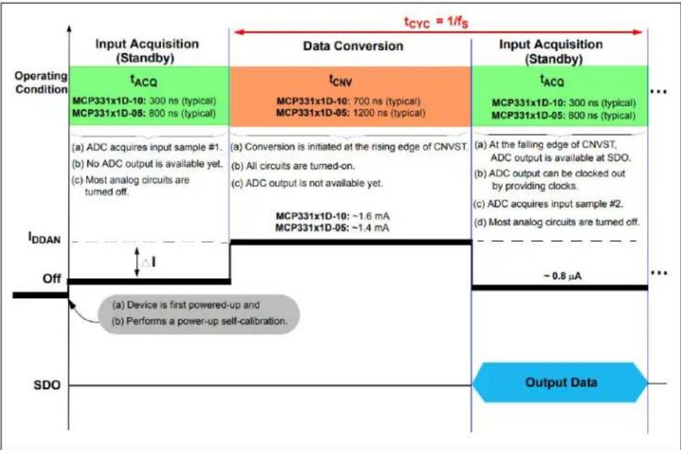
FIGURE 4-2: Input Acquisition (Input Sampling) and Data Conversion of the ADC Operation Sequence. See the product data sheet for details.
Once the data are transferred from the ADC to SPI, the DMA will place it in a 8192 word buffer (ADC_BUFFER[ ]). Since the sampling speed is 1 Msps, this buffer will be updated every 8.1 ms, making timing less critical for other tasks.
The GUI requires a larger amount of data to be processed in order to indicate accurate performance characteristics: FFT, THD, SINAD, etc. Because of this, a larger data buffer is created in RAM (storage[]) with a length of 262144 bytes. 32 DMA transfers are required to fill this buffer. The flowchart in Figure 4-3 provides a simple overview of the sample acquisition process and an overview of the entire firmware process.
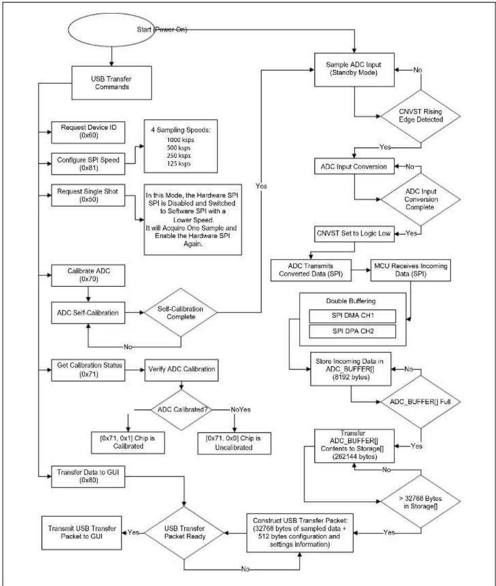
flowchart
graph TD
    A["Start (Power On)"] --> B["USB Transfer Commands"]
    B --> C["Request Device ID (0x60)"]
    C --> D["Configure SPI Speed (0x81)"]
    D --> E["Request Single Shot (0x50)"]
    E --> F["In this Mode, the Hardware SPI SPI is Disabled and Switched to Software SPI with a Lower Speed. It will Acquire One Sample and Enable the Hardware SPI Again."]
    F --> G["Calibrate ADC (0x70)"]
    G --> H["ADC Self-Calibration"]
    H --> I{Self-Calibration Complete}
    I -->|No| J["Get Calibration Status (0x71)"]
    I -->|Yes| K["Verify ADC Calibration"]
    K --> L{ADC Calibrated?}
    L -->|NoYes| M["[0x71, 0x1"] Chip is Calibrated]
    L -->|Yes| N["[0x71, 0x0"] Chip is Uncalibrated]
    N --> O["Transfer Data to GUI (0x80)"]
    O --> P{USB Transfer Packet Ready}
    P -->|No| Q["Construct USB Transfer Packet: (32768 bytes of sampled data + 512 bytes configuration and settings information)"]
    P -->|Yes| R["Transmit USB Transfer Packet to GUI"]
    R --> S["Transmit USB Transfer Packet to GUI"]
    S --> T{USB Transfer Packet Ready}
    T -->|No| U["Construct USB Transfer Packet: (32768 bytes of sampled data + 512 bytes configuration and settings information)"]
    T -->|Yes| V["Transfer ADC_BUFFER["] Contents_to_Storage[] (262144 bytes)]
    V --> W["Transfer ADC_BUFFER["] Full]
    W --> X["Store Incoming Data in ADC_BUFFER["] (8192 bytes)]
    X --> Y["Double Buffering SPI DMA CH1 SPI DPA CH2"]
    Y --> Z["MCU Receives Incoming Data (SPI)"]
    Z --> AA["ADC Transmits Converted Data (SPI)"]
    AA --> AB["CNVST Set to Logic Low"]
    AB --> AC["ADC Input Conversion"]
    AC --> AD{ADC Input Conversion Complete}
    AD -->|No| AE["CNVST Rising Edge Detected"]
    AE --> AF["Sample ADC Input (Standby Mode)"]
    AF --> AG["Start (Power On)"]
FIGURE 4-3: Firmware Flowchart.
4.3 USB TRANSFER
The MCU firmware implements a WinUSB device to handle the data transfer between the USB host (a PC for example) and the USB device (evaluation board).
Each USB transfer has a length of 33280 bytes out of which the first 512 bytes are configuration and setting bytes. The remaining 32768 bytes will contain samples. This will require eight logical transfers to be executed (Figure 4-4). The physical USB layer will split the 33280 byte packets into 512 byte chunks before transmitting on the USB bus.
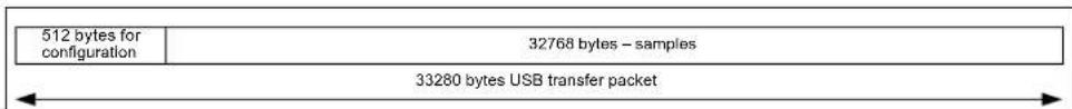
text_image
512 bytes for configuration 32768 bytes – samples 33280 bytes USB transfer packetFIGURE 4-4: USB Transfer Frame.
4.4 ADC FUNCTIONS
In addition to the actual sample transfer from MCU to PC, there are other ADC functions available: Calibration, Read Device ID and Sampling Speed Change.
The PC not only receives data from the EVB, but it also sends 512 bits of data back to the MCU. The 512-bit length size is required because of the USB high-speed endpoint size. Out of these, only the first five are meaningful. The first element, receivedDataBuffer[0], indicates to the MCU the desired function. For 0x80, the MCU will send samples. For 0x81, the transfer is stopped and the MCU RAM is filled with samples from the ADC. The code will not perform transfers in the same time as the acquisition of ADC samples.
The calibration function is executed when value 0x70 is received. Calibration status function has code 0x71. Table 4-1 provides the command structure byte values sent to, and the responses from, the PIC32MZ2048EFM100 on the PIC32MZ EF Curiosity Development Board (DM320104). Figure 4-5 displays the timing diagram of the calibration process.
TABLE 4-1: COMMAND STRUCTURE BYTE VALUES
| Command | receivedDataBuffer[x] | transmitDataBuffer[x] | Description | |||||
| Byte[0] | Byte[1] Byte[2] | Byte[3] | Byte[0] | Byte[1] | Byte[2] | Byte[3] Byte[4] Byte[5] | ||
| Send Samples | 0x80 — | [0 to 7] | Package Index | 0x80 | 0x00 — | — | 332 | 80-byte reply,[0-511] – Irrelevant,[512-33279] – Data samples,Combine the read data into a 16b signed value as follows:dataH: dataL = read[odd index]:read—even index] |
| Change Sampling Speed | 0x81 — | 1 | -4Sampling Speed | 0x81 | 0x01 — | — | Select sampling speed from Byte[3] and change transmitDataBuffer[1] = 0x80 to start sending data | |
| 0x80 | 0x01 | — | — | |||||
| Calibrate ADC | 0x70 | — | — | 0x70 | 0x01 | — | — | [0x70, 0x01] – Command received successfully,[0x70, 0x00] – Error |
| Calibration Status | 0x71 | — | — | 0x71 | 0x01 | — | — | [0x71, 0x01] – Calibration successful,[0x71, 0x00] – Calibration failed |
| Acquire Single Sample | 0x50 | — | — | 0x50 | MSb | LSb | — | [0x50, ADCHighByte, ADCLowByte] |
| Read Device ID | 0x60 | — | — | 0x60 | — | — | — | [0x60, chip ID] |

text_image
Tek Stop 3.56ms 010 6.85ms 000 Δ3.072ms SPI(MOSI) SPI(MISO) CLK MISO CONV MOSI 2.00ms 500MS/s D4\ 1.678906ms 10M points 1.40 V D15-D0 Timing Resolution: 2.00ms Bus Search events found: 2 8 Aug 2017 12:00:05 Mode Record FastAcq Delay Horizontal Waveform XY Display Sample Length 10M Off On Off Position Display OffFIGURE 4-5: ADC Calibration.
The Read Device ID code is 0x60. In order to retrieve the Chip ID, more Read registers are required. Figure 4-6 describes the Read register command format.
To retrieve the samples, the GUI will send to the MCU information on the packet required to be received as an index, which is a number from 0 to 7. This index is sent to the MCU in receivedDataBuffer[4].
Another function controlled by the GUI is the sampling speed change. There are four available sampling speeds. These are selected in accordance with the value received in receivedDataBuffer[3]. The sampling speed is controlled by changing the prescaler of the reference system clock.

text_image
Tek PreVu SPI(MISI) MISI: 95 MISO: SC 00 SPI(MISO) MISO: 3F MISO: FF 80 CLK MISO CONV MOSI 4.00μs 2.50GS/s D-4\ 142.9064 μs 1M points 1.40 V D15-00 Timing Resolution: 2.00rs Bus Search events found: 12 8 Aug 2017 11:39:42FIGURE 4-6: Read Register from ADC.
NOTES:
Appendix A. Schematics and Layout
A.1 INTRODUCTION
This appendix contains the following schematics and layouts for the MCP331X1D 16/14/12-Bit, 1 Msps SAR ADC Evaluation Board with 4V_REF (ADM00873):
- Board – Schematic (Page 1 of 2)
- Board – Schematic (Page 2 of 2)
- Board – Top Silk Layer
• Board – Top Copper and Silk Layer - Board – Top Copper Layer
- Board – Bottom Copper Layer
• Board – Bottom Copper and Silk Layer - Board – Bottom Silk Layer
A.2 BOARD - SCHEMATIC (PAGE 1 OF 2)
text_image
Reference: 4.096V SW1 is Device ID setting. This Device ID is read out from GUI. Differential Input GND GND DIN-DRIVER Circuit Capacitor N GND GND DIN-DRIVER Circuit Capacitor N GND GND DIN-DRIVER Circuit Capacitor N GND GND DIN-DRIVER Circuit Capacitor N GND GND DIN-DRIVER Circuit Capacitor N GND GND DIN-DRIVER Circuit CapacitorN GND GND DIN-DRIVER Circuit CapacitorN GND GND DIN-DRIVER Circuit CapacitorN GND GND DIN-DRIVER Circuit CapacitorN GND GND DIN-DRIVER Circuit CapacitorN GND GND DIN-DRIVER Circuit CapacitorO GND GND DIN-DRIVER Circuit CapacitorO GND GND DIN-DRIVER Circuit CapacitorO GND GND DIN-DRIVER Circuit CapacitorO GND GND DIN-DRIVER Circuit CapacitorO GND GND DIN-DRIVER Circuit CapacitorN GND GND DIN-DRIVER Circuit CapacitorN GND GND DIN-DRIVER Circuit CapacitorO GND GND DIN-DRIVER Circuit CapacitorO GND GND
Note 1: DNP = Do Not Populate. The components with DNP are not populated on the board.
Note 2: This board can be configured for a Single-Ended input using one of the following two options:
Option A: Short J6's two pins. This will set VCOM (VREF/2 = 2V) voltage at J2 (VIN1-). Apply analog input to J1 only.
Option B: Short C34, and apply analog input at J1 only.
Note 3: If other than 4V Reference is needed, disconnect J7 from U2 output and apply the Reference Voltage at J7.
A.3 BOARD - SCHEMATIC (PAGE 2 OF 2)
Note 1: DNP = Do Not Populate. The components with DNP are not populated on the board.
Note 2: Adding Ferrite Bead (FB4, FB5) Improves SNR (\~3dB) and SFDR (\~10dB).
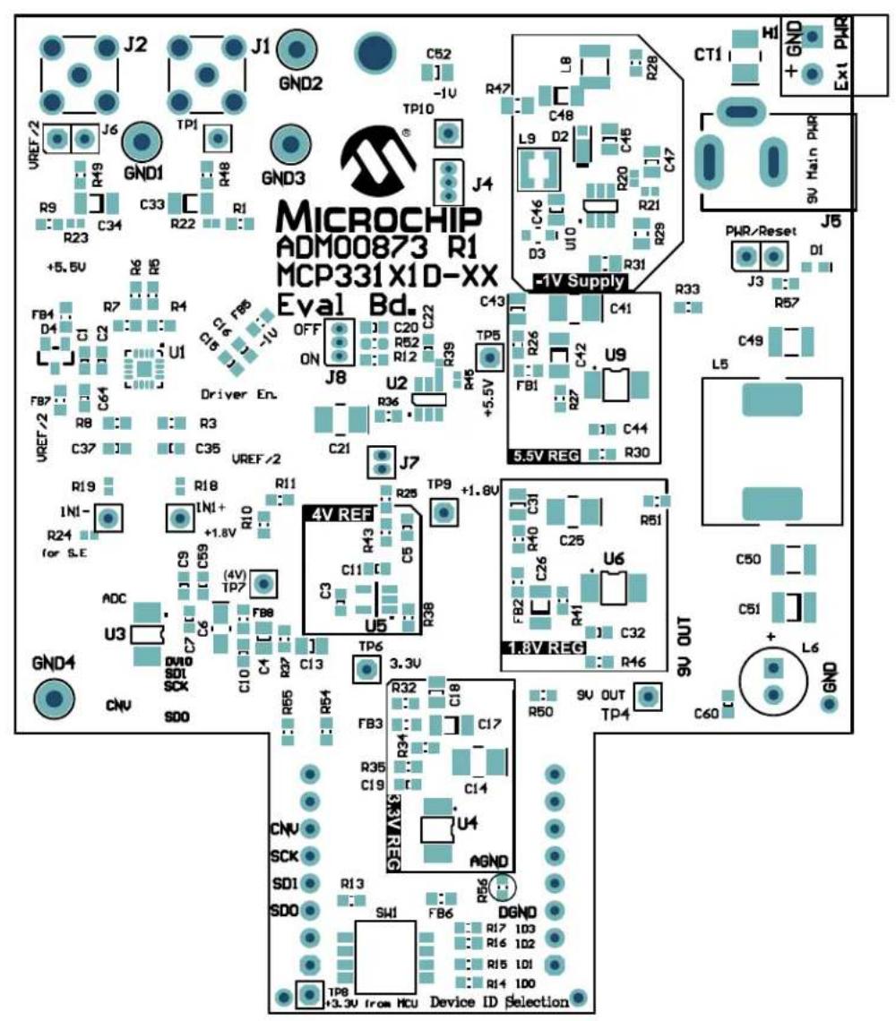
A.4 BOARD - TOP SILK LAYER
text_image
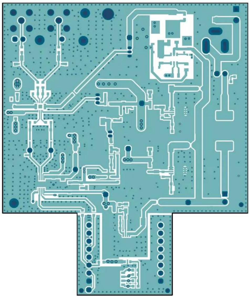
MICROCHIP ADM00873 R1 MCP331X1D-XX Eval Bd. VREF/2 J6 GND1 TP1 GND3 CT1 Hi + GND Ext PWR +5.5V R9 R49 R19 R6 R5 R7 R4 R3 C33 C22 R1 R23 C34 R22 R1 FB4 D4 C1 C1 U1 Driver En. OFF ON J8 U2 R3 R6 R7 C21 J7 J7 R19 INI- R24 for S.E R18 INI+ +1.8V R11 R10 R11 +5V REF 4V REF TP9 +1.8V C31 C25 R51 +5V REF 4V REF U6 C59 (4V) TP7 C11 C5 C3 C26 U6 ADC U3 SDI SCK C4 C3 U5 TP6 C32 GND4 CNV SDO RD5 RF4 RB3 FB3 RB4 RB5 RB6 RB7 RB8 RB9 RB10 RB11 RB12 RB13 RB14 RB15 RB16 RB17 RB18 RB19 RB20 RB21 RB22 RB23 RB24 RB25 RB26 RB27 RB28 RB29 RB30 TPB +3.3V from HCU Device ID SelectionA.5 BOARD - TOP COPPER AND SILK LAYER

text_image
MICROCHIP ADM00873 R1 MCP331X1D-XX Eval Bd. EVI Supply 5.5V REG 4V REF C20 R52 R12 R39 R43 C11 U5 TP6 +1.8V R25 R38 TP8 +1.8V C26 R40 C31 R51 FB2 C50 C51 L6 8V REG SUV OUT GND GND4 GND4 GND4 GND4 GND4 GND4 GND4 GND4 GND4 GND4 GND4 GND4 GND4 GND4 GND4 GND4 GND4 GND4 GND4 GND4 GND4 GND4 GND4 GND4 GND4 GND3 GND3 GND3 GND3 GND3 GND3 GND3 GND3 GND3 GND3 GND3 GND3 GND3 GND3 GND3 GND3 GND3 GND3 GND3 GND3 GND3 GND3 GND3 GND3 GND3 GND4 GND4 GND4 GND4 GND4 GND4 GND4 GND4 GND4 GND4 GND4 GND4 GND4 GND4 GND4 GND4 GND4 GND4 GND4 GND4 GND4 GND4 GND4 GND4 GND5 GND5 GND5 GND5 GND5 GND5 GND5 GND5 GND5 GND5 GND5 GND5 GND5 GND5 GND5 GND5 GND5 GND5 GND5 GND5 GND5 GND5 GND5 GND5 GND5 GND6 GND6 GND6 GND6 GND6 GND6 GND6 GND6 GND6 GND6 GND6 GND6 GND6 GND6 GND6 GND6A.6 BOARD - TOP COPPER LAYER
natural_image
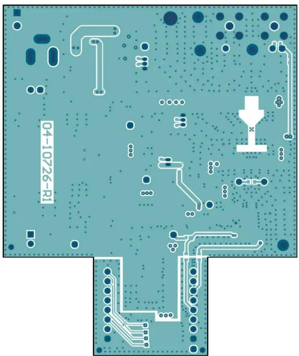
Top-down view of a printed circuit board layout with traces, pads, and components (no readable text or symbols)A.7 BOARD - BOTTOM COPPER LAYER
text_image
04-10726-R1A.8 BOARD - BOTTOM COPPER AND SILK LAYER

text_image
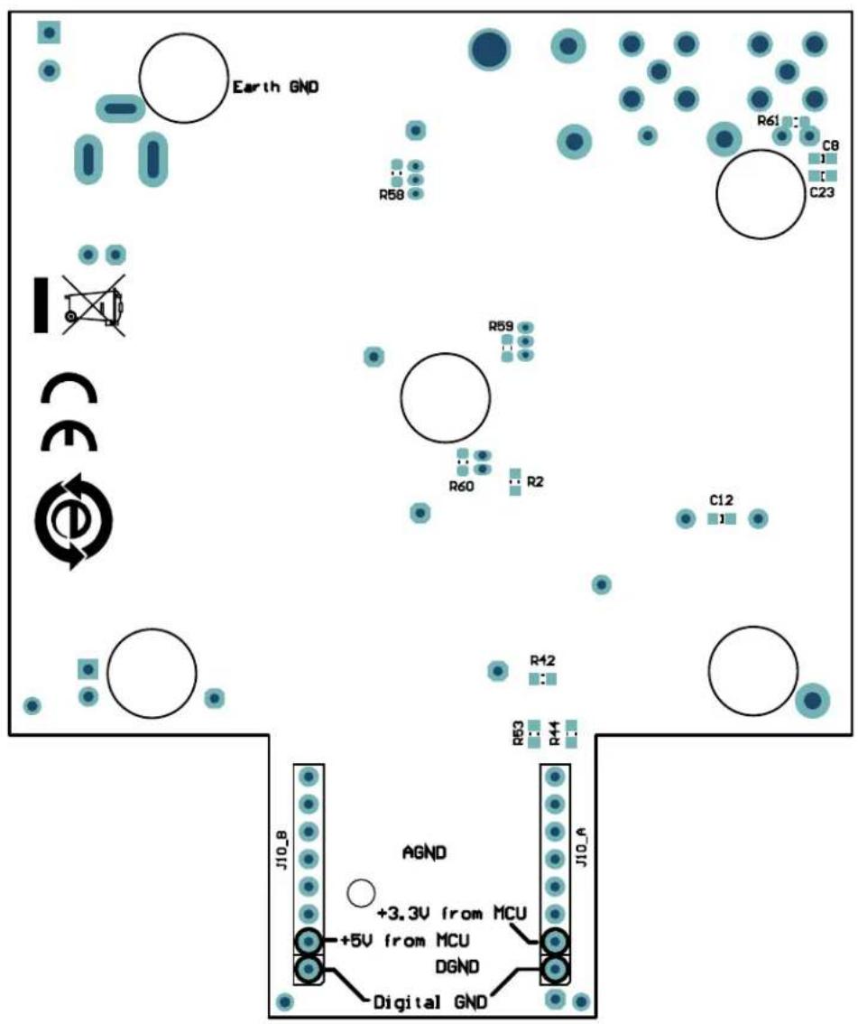
Earth GND R61 C8 1 C23 04-10726-R1 CE R58 R59 R60 R2 C12 1 R42 R53 +3.3V from MCU J10_B AGND +5V from MCU DGND Digital GND J10_AA.9 BOARD - BOTTOM SILK LAYER
text_image
Earth GND R61 C8 C23 R58 R59 R60 R2 C12 R42 R53 R44 J10_A AGND +3.3V from MCU +5V from MCU DGND Digital GNDNOTES:
Appendix B. Bill of Materials (BOM)
B.1 MCP331X1D EVALUATION BOARD – BILL OF MATERIALS (BOM)
TABLE B-1: MCP331X1D EVALUATION BOARD – BILL OF MATERIALS (BOM) ^(1)
| Qty. | Reference Description | Manufacturer Part Number | ||
| 4 C1 | C10, C15, C59 | Capacitor, Ceramic, 0.1 μF, 16V, 10%, X7R, SMD, 0603 | AVX Corporation 0603 | YC104KAT2A |
| 1 C1 | 1 Capacitor, Ceramic | Capacitor, Ceramic, 0.1 μF, 16V, 10%, X7R, SMD, 0603 | TDK Corporation | CGA3E1X7R1E105K080AC |
| 0 C12 | Capacitor, Ceramic, 0.1 μF, 16V, 10%, X7R, SMD, 0603 | AVX Corporation 0603 | YC104KAT2A | |
| 4 C13 | C18, C31, C43 | Capacitor, Ceramic, 10 μF, ±10%, 25V, X5R, MLCC, 0805 | Murata Electronics North America, Inc. | GRM21BR61E106KA73L |
| 4 C14 | C25, C41, CT1 | Capacitor, Tantalum, 10 μF, 20V, 10%, 2.1Ω, SMD, B | AVX Corporation TAJB | 106K020RNJ |
| 3 C17 | C26, C42 | Capacitor, Ceramic, 2.2 μF, 50V, 10%, X7R, SMD, 1206 | TDK Corporation | CGA5L3X7R1H225K160AB |
| 3 C19 | C32, C44 | Capacitor, Ceramic, 470 pF, 50V, 10%, X7R, SMD, 0603 | Johanson Technology Inc. | 500R14W471KV4T |
| 3 C2 | C16, C20 | Capacitor, Ceramic, 1 μF, 16V, 10%, X7R, SMD, 0603 | TDK Corporation | C1608X7R1C105K |
| 1 C21 | Capacitor, Tantalum, 22 μF, 16V, 10%, 2.3Ω, SMD, B | AVX Corporation TAJB | 22226K016R | |
| 4 C3 | C8, C9, C22 | Capacitor, Ceramic, 1 μF, 16V, 10%, X5R, SMD, 0603 | AVX Corporation 0603 | YD105KAT2A |
| 0 C33 | 0.062 μF, 1206, Ceramic, 50V, 5%, COG | Murata Electronics® | GRM31C5C1H623JA01L | |
| 0 C34 | 0.062 μF, 1206, Ceramic, 50V, 5%, COG | Murata Electronics | GRM31C5C1H623JA01L | |
| 2 C35, C37 | Multilayer Ceramic Capacitors MLCC - SMD/SMT, 0603, 1800 pF, 50V, COG, 2% | Murata Electronics North America, Inc. | GCM1885C1H182GA16J | |
| 1 C4 | Capacitor, Ceramic, 1 μF, 16V, 20%, Y5V, SMD, 0805 | AVX Corporation 0805 | YG105ZAT2A | |
| 3 C45, C47, C52 | Capacitor, Ceramic, 4.7 μF, 25V, 10%, X7R, SMD, 0805 | TDK Corporation | C2012X7R1E475K125AB | |
| 1 C46 | Capacitor, Ceramic, 0.1 μF, 50V, 10%, X7R, SMD, 0805 | Yageo Corporation | CC0805KRX7R9BB104 | |
| 1 C48 | Capacitor, Ceramic, 22 μF, 16V, 20%, X5R, SMD, 1206 | Panasonic® - ECG | ECJ-3YB1C226M | |
| 2 C49, C50 | Capacitor, Ceramic, 22 μF, 25V, 10%, X7R, SMD, 1210 | Samsung Electro-Mechanics America, Inc. | CL32B226KAJNFNE | |
| Qty. | Reference | Description | Manufacturer | Part Number |
| 1 C5 | Capacitor, Ceramic | 2.2 μF, 16V, 10%, X5R, SMD, 0603 | TDK Corporation C160 | 8X5R1C225K |
| 1 C51 | Capacitor, Ceramic | 10 μF, 50V, 20%, X7S, SMD, 1210 | TDK Corporation C322 | 5X7S1H106M |
| 1 C6 | Capacitor, Tantalum | 10 μF, 16V, 20%, 8Ω, SMD, A | KEMET T491A106M01 | 6AS |
| 1 C60 | Capacitor, Ceramic | 1 μF, 16V, 10%, X7R, SMD, 0603 | Yageo Corporation CC | 0603KRX7R7BB105 |
| 1 C64 | Capacitor, Ceramic | 1 μF, 25V, 20%, X5R, SMD, 0603 | Panasonic® - ECG ECJ | -1V41E105M |
| 2 C7 | C23 Capacitor, Ceramic | 100 pF, 25V, 10%, NP0, SMD, 0603 | AVX Corporation 0603 | 3A101KAT2A |
| 1 D1 | Diode, LED, Red, 2V, 30 mA, 2 mcd, Clear, SMD, 0603 | Lite-On®, Inc. LTST-C1 | 90EKT | |
| 1 D2 | Diode, Schottky, 30V, 1A, POWERDI323 | Diodes Incorporated® | PD3S130L-7 | |
| 1 D3 | Diode, Rectifier, 1N4148, 855 mV, 300 mA, 75V, SOD-323 | Diodes Incorporated | 1N4148WS-7-F | |
| 1 D4 | Diode, Rectifier, MMBD1503A, 1.1V, 200 mA, 200V, SMD, SOT-23-3 | Fairchild Semiconductor® | MMBD1503A | |
| 8 FB1 | FB2, FB3, FB4, FB5, FB6, FB7, FB8 | Ferrite Bead, 1 kΩ, 0603, 1LN | Wurth Elektronik | 742792662 |
| 4 GND1 | GND2, GND3, GND4 | Connector, Test Point, Loop, Black, TH | Keystone Electronics Corp. | 5011 |
| 1 H1 | Connector, Terminal | 3.5 mm, 6A, Female, 1x2, TH, R/A | Keystone Electronics Corp. | 8722 |
| 0 IN1+, IN1-, TP7 | Connector, HDR-2.54, Male, 1x1, Gold, 5.97MH, TH, Vertical | Samtec, Inc. | TSW-101-07-L-S | |
| 2 J1, J2 | Connector, RF Coaxial, SMA, Female, TH, R/A | TE Connectivity Alcoswitch | 5-1814400-1 | |
| 2 J10_A, J10_B | Connector, HDR-2.54, Male, 1x8, Gold, 5.84MH, TH | FCI | 68001-108HLF | |
| 2 J3, J6 | Connector, HDR-2.54, Male, 1x2, Gold, 5.84MH, TH, Vertical | FCI | 77311-118-02LF | |
| 0 J4, J8 | Connector, HDR, 1.27 mm, TH, Gold, 3POS | Harwin Plc. | 952-3599-ND | |
| 1 J5 | Connector, Power Jack, Male, 2.5 mm, CLSD | CUI Inc. | PJ-002B | |
| 0 J7 | Connector, HDR-1.27, Male, 1x2, Gold, TH, Vertical | Harwin Plc. | 952-3598-ND | |
| 1 JP1 | Mechanical, HW, Jumper, 2.54 mm, 1x2, w/Handle | TE Connectivity Alcoswitch | 880584-4 | |
| 1 L5 | Fixed Inductor, 47 μH, 2A, 135 MΩ, SMD | Bourns®, Inc. | SRR1240-470M | |
| 1 L6 | Fixed Inductor, 1 MH, 250 MA, 6Ω, TH | Wurth Elektronik | 7447462102 | |
| 1 | L8 | Fixed Inductor, 1 μH, 1A, 60 MΩ, SMD | Murata Electronics North America, Inc. | LQH32CN1R0M33L |
| 1 L9 | Fixed Shielded Power Inductor, 4.7 μH | Coilcraft LPS3015-472 | MLB | |
| 5 PAD1, PAD2, PAD3, PAD4, PAD5 | Mechanical HW Rubber Pad, Cylindrical, D7.9, H5.3, Black | 3M SJ61A11 | ||
| 1 PCB1 Printed Circuit Board | Board - MCP331X1D 16/14/12-Bit, 1 Msps SAR ADC Evaluation Board | Microchip Technology Inc. | 04-10726-R1 | |
| 1 PS1 AC/DC, Wall Mount Adapter, 9V, 12W, 1.2A, 2.5 mm, I.D | CUI Inc. SWI12-9-N-P6 | |||
| 2 R1, R9 Resistor, Thin Film, 20R, 1%, 1/16W, SMD, 0603 | Stackpole Electronics, Inc. | RNCP0603FTD20R0 | ||
| 2 | R10, R11 | Resistor, Thin Film, 10 kΩ, 0.1%, 1/10W, SMD, 0603 | Panasonic® - ECG | ERA-3AEB103V |
| 1 | R12 | Resistor, Thin Film, 10 kΩ, 1%, 1/16W, SMD, 0603 | TE Connectivity Alcoswitch | 5-1879337-9 |
| 1 | R13 | Resistor, Thick Film, 30 kΩ, 5%, 1/10W, SMD, 0603 | Panasonic - ECG | ERJ-3GEYJ303V |
| 4 R14, R15, R16, R17 | Resistor, Thick Film, 10 kΩ, 5% 1/10W, SMD, 0603 | Panasonic - ECG | ERJ-3GEYJ103V | |
| 2 R18, R19 | Resistor, Thick Film, 0R, SMD, 0402 | Panasonic - ECG | ERJ-2GE0R00X | |
| 0 R2, R61 | Resistor, Thick Film, 0R, 1/10W, SMD, 0603 | Panasonic - ECG | ERJ-3GSY0R00V | |
| 2 R20, R39 | Resistor, Thick Film, 0R, 1/16W, SMD, 0402 | Yageo Corporation | RC0402JR-070RL | |
| 0 R21, R45 | Resistor, Thick Film, 0R, 1/16W, SMD, 0402 | Yageo Corporation | RC0402JR-070RL | |
| 0 R22, R23, R24 | Resistor, Thick Film, 0R, SMD, 0402 | Panasonic - ECG | ERJ-2GE0R00X | |
| 1 | R25 | Resistor, Thick Film, 7.15 kΩ, 1%, 1/10W, SMD, 0603 | Panasonic - ECG | ERJ-3EKF7151V |
| 3 R26, R32, R40 | Resistor, Thick Film, 1R, 1%, 1/10W, SMD, 0603 | ROHM Semiconductor | KTR03EZPF1R00 | |
| 1 | R27 | Resistor, Thick Film, 82 kΩ, 1%, 1/10W, SMD, 0603 | Panasonic - ECG | ERJ-3EKF8202V |
| 0 | R28 | Resistor, Thick Film, 35.7 kΩ, 1%, 1/10W, SMD, 0603 | Vishay/Dale | CRCW060335K7FKEA |
| 1 | R29 | Resistor, Thick Film, 14 kΩ, 1%, 1/8W, SMD, 0805 | Panasonic - ECG | ERJ-6ENF1402V |
| 2 R3, R8 Resistor, Thick Film, 24R, 1%, 1/10W, SMD, 0603 | Yageo Corporation | RC0603FR-0724RL | ||
| 1 | R30 | Resistor, Thick Film, 280 kΩ, 1%, 1/10W, SMD, 0603 | Panasonic - ECG | ERJ-3EKF2803V |
| 1 | R31 | Resistor, Thick Film, 56 kΩ, 1%, 1/8W, SMD, 0805 | Vishay/Dale | CRCW080556K0FKEA |
| 11 R33, R38, R42,R48, R49, R50,R51, R56, R58,R59, R60 | Resistor, Thick Film, 0R, 1/10W,SMD, 0603 | Panasonic®- ECG ERJ-3GSY0R00V | ||
| 1 R34 Resistor, SMD, 143 kΩ, 1%,1/10W, 0603 | Bourns, Inc. CR0603-FX-1433ELF | |||
| 1 R35 Resistor, SMD, 237 kΩ, 1%,1/10W, 0603 | StackpoleElectronics, Inc. | RMCF0603FT237K | ||
| 1 R36 Resistor, Thick Film, 10.5R, 1%,1/10W, SMD, 0603 | Vishay/Dale CRCW060310R5FKEA | |||
| 5 R4, R5, R6, R7,R37 | Resistor, Thin Film, 1 kΩ, 0.1%,1/10W, SMD, 0603 | Panasonic - ECG ERA-3AEB102V | ||
| 1 | R41 | Resistor, Thick Film, 348 kΩ,1/10W, 1%, SMD, 0603 | StackpoleElectronics, Inc. | RMCF0603FT348K |
| 1 | R43 | Resistor, Thick Film, 13.3 kΩ,1%, 1/10W, SMD, 0603 | StackpoleElectronics, Inc. | RMCF0603FT13K3 |
| 4 R44, R53, R54,R55 | Resistor, Thick Film, 33R, 1%,1/10W, SMD, 0603 | ROHMSemiconductor | MCR03EZPFX33R0 | |
| 1 R46 Resistor, Thick Film, 158 kΩ, 1%,1/10W, SMD, 0603 | Yageo Corporation RC0603FR-07158KL | |||
| 1 R47 Resistor, Thick Film, 0R, 1/8W,SMD, 0805 | Panasonic - ECG ERJ-6GEY0R00V | |||
| 1 | R52 | Resistor, Thick Film, 47 kΩ, 1%,1/10W, SMD, 0603 | Panasonic - ECG ERJ-3EKF4702V | |
| 1 | R57 | Resistor, Thick Film, 2 kΩ, 1%,1/10W, SMD, 0603 | Panasonic - ECG ERJ-3EKF2001V | |
| 1 SCR1 Mechanical HW Machine Screw,Pan Phillips, 4-40, NYLON | B&FTM Fasteners Supply | H544-ND | ||
| 1 STANDOFF1 Mechanical HW Standoff,#4-40 x 3/4", F/F, Hex, Nylon | KeystoneElectronics Corp. | 1902D | ||
| 1 SW1 Switch Dip, 4-POS, Slide, SMD,6V | Nidec CopalElectronics, Inc. | CHS-04TB | ||
| 7 TP1, TP4, TP5,TP6, TP8, TP9,TP10 | Connector, HDR-2.54, Male,1x1, Gold, 5.97MH, TH, Vertical | Samtec, Inc. | TSW-101-07-L-S | |
| 1 U1 MCHP Analog Op Amp,MCP6D11-MG16, QFN-16 | MicrochipTechnology Inc. | MCP6D11-MG16 | ||
| 1 U10 MCHP Analog Switcher Buck,2V to 15V, MCP16301T-I/CHY,SOT-23-6 | MicrochipTechnology Inc. | MCP16301T-I/CHY | ||
| 1 U2 MCHP Analog VREF, 4.096V,MCP1501T-40E/CHY, SOT-23-6 | MicrochipTechnology Inc. | MCP1501T-40E/CHY | ||
| 1 U3 MCP33131D-10-I/MS MicrochipTechnology Inc. | MCP33131D-10-I/MS | |||
| 3 U4, U6, U9 | MCHP Analog LDO, 2.5V-5V,MIC5219YMM, MSOP-8 | MicrochipTechnology Inc. | MIC5219YMM | |
| 1 U5 IC Op Amp GP, 3.5 MHz, RRO,SOT23-5 | MicrochipTechnology Inc. | MCP6286T-E/OT | ||
Note 1: The components listed in this Bill of Materials are representative of the PCB assembly. The released BOM used in manufacturing uses all RoHS-compliant components.
NOTES:
NOTES:
Worldwide Sales and Service
AMERICAS
Corporate Office
2355 West Chandler Blvd.
Chandler, AZ 85224-6199
Tel: 480-792-7200
Fax: 480-792-7277
Technical Support:
http://www.microchip.com/
support
Web Address:
www.microchip.com
Atlanta
Duluth, GA
Tel: 678-957-9614
Fax: 678-957-1455
Austin, TX
Tel: 512-257-3370
Boston
Westborough, MA
Tel: 774-760-0087
Fax: 774-760-0088
Chicago
Itasca, IL
Tel: 630-285-0071
Fax: 630-285-0075
Dallas
Addison, TX
Tel: 972-818-7423
Fax: 972-818-2924
Detroit
Novi, MI
Tel: 248-848-4000
Houston, TX
Tel: 281-894-5983
Indianapolis
Noblesville, IN
Tel: 317-773-8323
Fax: 317-773-5453
Tel: 317-536-2380
Los Angeles
Mission Viejo, CA
Tel: 949-462-9523
Fax: 949-462-9608
Tel: 951-273-7800
Raleigh, NC
Tel: 919-844-7510
New York, NY
Tel: 631-435-6000
San Jose, CA
Tel: 408-735-9110
Tel: 408-436-4270
Canada - Toronto
Tel: 905-695-1980
Fax: 905-695-2078
ASIA/PACIFIC
Australia - Sydney
Tel: 61-2-9868-6733
China - Beijing
Tel: 86-10-8569-7000
China - Chengdu
Tel: 86-28-8665-5511
China - Chongqing
Tel: 86-23-8980-9588
China - Dongguan
Tel: 86-769-8702-9880
China - Guangzhou
Tel: 86-20-8755-8029
China - Hangzhou
Tel: 86-571-8792-8115
China - Hong Kong SAR
Tel: 852-2943-5100
China - Nanjing
Tel: 86-25-8473-2460
China - Qingdao
Tel: 86-532-8502-7355
China - Shanghai
Tel: 86-21-3326-8000
China - Shenyang
Tel: 86-24-2334-2829
China - Shenzhen
Tel: 86-755-8864-2200
China - Suzhou
Tel: 86-186-6233-1526
China - Wuhan
Tel: 86-27-5980-5300
China - Xian
Tel: 86-29-8833-7252
China - Xiamen
Tel: 86-592-2388138
China - Zhuhai
Tel: 86-756-3210040
ASIA/PACIFIC
India - Bangalore
Tel: 91-80-3090-4444
India - New Delhi
Tel: 91-11-4160-8631
India - Pune
Tel: 91-20-4121-0141
Japan - Osaka
Tel: 81-6-6152-7160
Japan - Tokyo
Tel: 81-3-6880-3770
Korea - Daegu
Tel: 82-53-744-4301
Korea - Seoul
Tel: 82-2-554-7200
Malaysia - Kuala Lumpur
Tel: 60-3-7651-7906
Malaysia - Penang
Tel: 60-4-227-8870
Philippines - Manila
Tel: 63-2-634-9065
Singapore
Tel: 65-6334-8870
Taiwan - Hsin Chu
Tel: 886-3-577-8366
Taiwan - Kaohsiung
Tel: 886-7-213-7830
Taiwan - Taipei
Tel: 886-2-2508-8600
Thailand - Bangkok
Tel: 66-2-694-1351
Tel: 43-7242-2244-39
Fax: 43-7242-2244-393
Denmark - Copenhagen
Tel: 45-4485-5910
Fax: 45-4485-2829
Finland - Espoo
Tel: 358-9-4520-820
France - Paris
Tel: 33-1-69-53-63-20
Fax: 33-1-69-30-90-79
Germany - Garching
Tel: 49-8931-9700
Germany - Haan
Tel: 49-2129-3766400
Germany - Heilbronn
Tel: 49-7131-72400
Germany - Karlsruhe
Tel: 49-721-625370
Germany - Munich
Tel: 49-89-627-144-0
Fax: 49-89-627-144-44
Germany - Rosenheim
Tel: 49-8031-354-560
Israel - Ra'anana
Tel: 972-9-744-7705
Italy - Milan
Tel: 39-0331-742611
Fax: 39-0331-466781
Italy - Padova
Tel: 39-049-7625286
Netherlands - Drunen
Tel: 31-416-690399
Fax: 31-416-690340
Norway - Trondheim
Tel: 47-7288-4388
Poland - Warsaw
Tel: 48-22-3325737
Romania - Bucharest
Tel: 40-21-407-87-50
Spain - Madrid
Tel: 34-91-708-08-90
Fax: 34-91-708-08-91
Sweden - Gothenberg
Tel: 46-31-704-60-40
Sweden - Stockholm
Tel: 46-8-5090-4654
UK - Wokingham
Tel: 44-118-921-5800
Fax: 44-118-921-5820