MCP6V26 - Electronic component Microchip - Free user manual and instructions
Find the device manual for free MCP6V26 Microchip in PDF.

User questions about MCP6V26 Microchip
0 question about this device. Answer the ones you know or ask your own.
Ask a new question about this device
Download the instructions for your Electronic component in PDF format for free! Find your manual MCP6V26 - Microchip and take your electronic device back in hand. On this page are published all the documents necessary for the use of your device. MCP6V26 by Microchip.
USER MANUAL MCP6V26 Microchip
Note the following details of the code protection feature on Microchip devices:
• Microchip products meet the specification contained in their particular Microchip Data Sheet.
- Microchip believes that its family of products is one of the most secure families of its kind on the market today, when used in the intended manner and under normal conditions.
- There are dishonest and possibly illegal methods used to breach the code protection feature. All of these methods, to our knowledge, require using the Microchip products in a manner outside the operating specifications contained in Microchip's Data Sheets. Most likely, the person doing so is engaged in theft of intellectual property.
• Microchip is willing to work with the customer who is concerned about the integrity of their code.
- Neither Microchip nor any other semiconductor manufacturer can guarantee the security of their code. Code protection does not mean that we are guaranteeing the product as "unbreakable."
Code protection is constantly evolving. We at Microchip are committed to continuously improving the code protection features of our products. Attempts to break Microchip's code protection feature may be a violation of the Digital Millennium Copyright Act. If such acts allow unauthorized access to your software or other copyrighted work, you may have a right to sue for relief under that Act.
Information contained in this publication regarding device applications and the like is provided only for your convenience and may be superseded by updates. It is your responsibility to ensure that your application meets with your specifications. MICROCHIP MAKES NO REPRESENTATIONS OR WARRANTIES OF ANY KIND WHETHER EXPRESS OR IMPLIED, WRITTEN OR ORAL, STATUTORY OR OTHERWISE, RELATED TO THE INFORMATION, INCLUDING BUT NOT LIMITED TO ITS CONDITION, QUALITY, PERFORMANCE, MERCHANTABILITY OR FITNESS FOR PURPOSE. Microchip disclaims all liability arising from this information and its use. Use of Microchip devices in life support and/or safety applications is entirely at the buyer's risk, and the buyer agrees to defend, indemnify and hold harmless Microchip from any and all damages, claims, suits, or expenses resulting from such use. No licenses are conveyed, implicitly or otherwise, under any Microchip intellectual property rights.
QUALITY MANAGEMENT SYSTEM CERTIFIED BY DNV
=ISO/TS 16949:2009=
Trademarks
The Microchip name and logo, the Microchip logo, dsPIC, KEELOQ, KEELOQ logo, MPLAB, PIC, PICmicro, PICSTART, PIC ^32 logo, rfPIC and UNI/O are registered trademarks of Microchip Technology Incorporated in the U.S.A. and other countries.
FilterLab, Hampshire, HI-TECH C, Linear Active Thermistor, MXDEV, MXLAB, SEEVAL and The Embedded Control Solutions Company are registered trademarks of Microchip Technology Incorporated in the U.S.A.
Analog-for-the-Digital Age, Application Maestro, chipKIT, chipKIT logo, CodeGuard, dsPICDEM, dsPICDEM.net, dsPICWorks, dsSPEAK, ECAN, ECONOMONITOR, FanSense, HI-TIDE, In-Circuit Serial Programming, ICSP, Mindi, MiWi, MPASM, MPLAB Certified logo, MPLIB, MPLINK, mTouch, Omniscient Code Generation, PICC, PICC-18, PICDEM, PICDEM.net, PICkit, PICtail, REAL ICE, rfLAB, Select Mode, Total Endurance, TSHARC, UniWinDriver, WiperLock and ZENA are trademarks of Microchip Technology Incorporated in the U.S.A. and other countries.
SQTP is a service mark of Microchip Technology Incorporated in the U.S.A.
All other trademarks mentioned herein are property of their respective companies.
© 2012, Microchip Technology Incorporated, Printed in the U.S.A., All Rights Reserved.

Printed on recycled paper.
ISBN: ISBN: 978-1-61341-925-0
Microchip received ISO/TS-16949:2009 certification for its worldwide headquarters, design and wafer fabrication facilities in Chandler and Tempe, Arizona; Gresham, Oregon and design centers in California and India. The Company's quality system processes and procedures are for its PIC® MCUs and dsPIC® DSCs, KEELoo® code hopping devices, Serial EEPROMs, microperipherals, nonvolatile memory and analog products. In addition, Microchip's quality system for the design and manufacture of development systems is ISO 9001:2000 certified.
Table of Contents
Preface 5
Introduction....5
Document Layout 6
Conventions Used in this Guide 7
Recommended Reading....8
The Microchip Web Site 8
Customer Support 9
Document Revision History 9
Chapter 1. Product Overview
1.1 Introduction ...... 11
1.2 Purpose 11
1.3 Description 12
1.4 What Does this Kit Contain? 15
Chapter 2. Installation and Operation
2.1 Introduction ...... 17
2.2 Required Tools 17
2.3 Basic Configurations 18
2.4 Configurations with Modifications ...... 19
2.5 Configuring the PCB 20
Chapter 3. Analog Circuit
3.1 Introduction 23
3.2 Bridge With PWM Interference 23
3.3 Signal Processing Circuitry 24
3.4 Test Points 28
3.5 PIC Microcontroller 28
Chapter 4. Firmware
4.1 Introduction ...... 31
4.2 Analog Signals at the ADC Inputs 31
4.3 Data Conditioning 32
4.4 Temperature Calculations ...... 33
4.5 Resistance Calculations ...... 34
4.6 Calibrating the MCP6N11 34
4.7 Temperature Calibration ...... 35
4.8 PWM Output 35
4.9 USB Communications 35
Chapter 5. Software GUI
5.1 Introduction ...... 37
5.2 Platform Requirements ...... 37
5.3 USB Communications 37
5.4 Display Data 38
5.5 Calibrate Temperature 38
5.6 Calibrate the MCP6N11 38
5.7 Configuration Options ...... 38
5.8 Export Data to a File 39
5.9 Screen Captures 39
Appendix A. Schematics and Layouts
A.1 Introduction 51
A.2 Board – Schematic 52
A.3 Board – Top Silk Screen and Pads ...... 53
A.4 Board – Top Metal Layer 54
A.5 Board – Ground Plane (Second layer) 55
A.6 Board - Power Plane (Third layer) 56
A.7 Board – Bottom Metal Layer (top view) 57
A.8 Board – Bottom Silk and Pads (top view) 58
Appendix B. Bill Of Materials (BOM)
Appendix C. Conversion Polynomials
C.1 Circuit Response 63
C.2 RTD Temperature and Resistance 65
C.3 INA Voltage to Temperature 66
Appendix D. Board Validation Summary
D.1 Thermal Steady State Response 67
D.2 Thermal Impulse Response 67
Worldwide Sales and Service ....70
Preface
NOTICE TO CUSTOMERS
All documentation becomes dated, and this manual is no exception. Microchip tools and documentation are constantly evolving to meet customer needs, so some actual dialogs and/or tool descriptions may differ from those in this document. Please refer to our web site (www.microchip.com) to obtain the latest documentation available.
Documents are identified with a "DS" number. This number is located on the bottom of each page, in front of the page number. The numbering convention for the DS number is "DSXXXXXA", where "XXXXX" is the document number and "A" is the revision level of the document.
For the most up-to-date information on development tools, see the MPLAB ^® IDE online help. Select the Help menu, and then Topics to open a list of available online help files.
INTRODUCTION
This chapter contains general information that will be useful to know before using the MCP6N11 and MCP6V2x Wheatstone Bridge Reference Design User's Guide. Items discussed in this chapter include:
- Document Layout
- Conventions Used in this Guide
- Recommended Reading
• The Microchip Web Site - Customer Support
• Document Revision History
DOCUMENT LAYOUT
This document describes how to use the MCP6N11 and MCP6V2x Wheatstone Bridge Reference Design. The manual layout is as follows:
- Chapter 1. "Product Overview" – Important information about the MCP6N11 and MCP6V2x Wheatstone Bridge Reference Design.
- Chapter 2. “Installation and Operation” – Covers the initial set-up of this board, required tools, board setup and lab equipment connections.
- Chapter 3. “Analog Circuit” – Discusses the analog functionality of the circuit on this board.
- Chapter 4. "Firmware" – Discusses the firmware on the PIC® device.
- Chapter 5. "Software GUI" – Discusses the GUI on the PC.
- Appendix A. “Schematics and Layouts” – Shows the schematic and board layouts for the MCP6N11 and MCP6V2x Wheatstone Bridge Reference Design.
- Appendix B. "Bill Of Materials (BOM)" – Lists the parts used to populate the MCP6N11 and MCP6V2x Wheatstone Bridge Reference Design. Also lists alternate components.
- Appendix C. “Conversion Polynomials” – Gives background information on the polynomials used in firmware.
- Appendix D. “Board Validation Summary” – Summarizes analog performance of two boards.
CONVENTIONS USED IN THIS GUIDE
This manual uses the following documentation conventions:
DOCUMENTATION CONVENTIONS
| Description Represents Examples | ||
| Arial font: | ||
| Italic characters Referenced books | oks MPLAB | ^ IDE User's Guide |
| Emphasized text ...is the only compiler... | ||
| Initial caps A window the Output | ut window | |
| A dialog the Settings dialog | ||
| A menu selection select Enable Programmer | ||
| Quotes A field name in a window or dialog | "Save project before build" | |
| Underlined, italic text with right angle bracket | A menu path File>Save | —— |
| Bold characters A dialog button | Click OK | |
| A tab | Click the Power tab | |
| N'Rnnnn | A number in verilog format, where N is the total number of digits, R is the radix and n is a digit. | 4'b0010, 2'hF1 |
| Text in angle brackets <> | A key on the keyboard | Press,, |
| Courier New font: | ||
| Plain Courier New | Sample source code | #define START |
| Filenames | autoexec.bat | |
| File paths c:\mcc18\h | ||
| Keywords | _asm, _endasm, static | |
| Command-line options | -Opa+, -Opa- | |
| Bit values | 0, 1 | |
| Constants | 0xFF, 'A' | |
| Italic Courier New | A variable argument | file.o, where file can be any valid filename |
| Square brackets [] | Optional arguments | mccl8 [options] file [options] |
| Curly brackets and pipe character: { | } | Choice of mutually exclusive arguments; an OR selection | errorlevel {0|1} |
| Ellipses... | Replaces repeated text | var_name [, var_name...] |
| Represents code supplied by user | void main (void) { ... } | |
RECOMMENDED READING
This user's guide describes how to use MCP6N1X. Other useful documents are listed below. The following Microchip documents are available and recommended as supplemental reference resources.
Provides detailed information on the op amp that is used for VREF.
- MCP6N11 Data Sheet – “500 kHz, 800 μA Instrumentation Amplifiers” (DS25073)
Provides detailed information on the INA that is used for INA #1.
- MCP6V26/7/8 Data Sheet – “620 μA, 2 MHz Auto-Zeroed Op Amps” (DS25007)
Provides detailed information on the auto-zeroed op amps used for INA #2.
- PIC18F2455/2550/4455/4550 Data Sheet – “28/40/44-Pin, High-Performance, Enhanced Flash, USB Microcontrollers with nanoWatt Technology” (DS39632)
Provides information on the USB PIC MCU family.
- PIC18F2458/2553/4458/4553 Data Sheet – “28/40/44-Pin High-Performance, Enhanced Flash, USB Microcontrollers with 12-Bit A/D and nanoWatt Technology” (DS39887)
Provides additional information on the USB PIC MCU devices with 12-bit ADCs.
- AN1258 Application Note – “Op Amp Precision Design: PCB Layout Techniques” (DS01258)
Discusses methods to minimize thermo-junction voltage effects in a PCB design.
Microchip provides online support via our web site at www.microchip.com. This web site is used as a means to make files and information easily available to customers. Accessible by using your favorite Internet browser, the web site contains the following information:
- Product Support – Data sheets and errata, application notes and sample programs, design resources, user's guides and hardware support documents, latest software releases and archived software
- General Technical Support – Frequently Asked Questions (FAQs), technical support requests, online discussion groups, Microchip consultant program member listing
- Business of Microchip – Product selector and ordering guides, latest Microchip press releases, listing of seminars and events, listings of Microchip sales offices, distributors and factory representatives
CUSTOMER SUPPORT
Users of Microchip products can receive assistance through several channels:
• Distributor or Representative
- Local Sales Office
• Field Application Engineer (FAE)
- Technical Support
- Development Systems Information Line
Customers can contact their distributor, representative or field application engineer for support. Local sales offices are also available to help customers. A listing of sales offices and locations is included in the back of this document.
Technical support is available on the web site at: http://www.microchip.com/support.
DOCUMENT REVISION HISTORY
Revision A (January 2012)
The initial release of this document.
NOTES:
Chapter 1. Product Overview
1.1 INTRODUCTION
The MCP6N11 and MCP6V2x Wheatstone Bridge Reference Design is described by the following:
• Assembly #: 114-00354-R2
- Order #: ADM00354
- Name: MCP6N11 and MCP6V2x Wheatstone Bridge Reference Design
This board uses the following Microchip ICs:
- MCP6001 (op amp)
• MCP6N11-100 (INA) - MCP6V27 (dual auto-zeroed op amp)
- MCP6V26 (single auto-zeroed op amp)
- PIC18F2553 (USB PIC ^ microcontroller)
Items discussed in this chapter include:
- Purpose
- Description
• What Does this Kit Contain?
1.2 PURPOSE
This board demonstrates the performance of Microchip's MCP6N11 instrumentation amplifier (INA) and a traditional three op amp INA using the MCP6V26 and MCP6V27 auto-zeroed op amps from Microchip. The input signal comes from an RTD temperature sensor in a Wheatstone bridge. Real world interference is added to the bridge's output, to provide realistic performance comparisons.
Data is gathered and displayed on a PC, for ease of use. The USB PIC microcontroller and included Graphical User Interface (GUI) show how to implement these functions.
1.3 DESCRIPTION
1.3.1 Block Diagram
Figure 1-1 shows the overall functionality of this demo board. Detailed information is available in Appendix A. “Schematics and Layouts” and Appendix B. “Bill Of Materials (BOM)”.

flowchart
graph TD
    A["Sensor<br>• RTD<br>• Bridge"] --> B["Interference<br>PWM at 25 kHz"]
    B --> C["Miscellaneous<br>• Test Points<br>• Power Supply"]
    D["INA #1<br>• I/O Filters<br>• INA with mCal<br>MCP6N11-100"] --> E["Mixed Signal<br>• USB PIC MCU<br>- PIC18F2553<br>- PWM output<br>- 12-bit ADC<br>- USB<br>- ISSP<br>• Firmware<br>- Averaging<br>- Calculations<br>- Communications"]
    F["INA #2<br>• I/O Filters<br>• Traditional INA<br>- MCP6V27<br>- MCP6V26"] --> E
    G["VREF"] --> E
    E --> H["Digital<br>• PC<br>- USB<br>- Display<br>- Memory<br>• GUI<br>- Strip Chart<br>- User Inputs<br>- Save Results<br>- Communications"]
    B --> E
    C --> E
    D --> E
    E --> H
    E --> G
FIGURE 1-1: Overall Block Diagram.
This board uses an RTD temperature sensor, in a Wheatstone bridge, to measure the board's temperature. The bridge's output is a small Differential mode (DM) signal with a large Common mode (CM) interference signal superimposed. The CM signal is a PWM waveform generated by the microcontroller, which simulates real world interference.
VREF (not a fixed reference) outputs a voltage level proportional to the analog supply voltage, keeping the INAs' outputs in range.
The two INAs process the bridge's output, rejecting the CM interference and providing large gains for the DM signal. There are R-C low-pass filters at the input and output of each INA.
A pulse-width modulation (PWM) signal at 25 kHz is an optional output of the microcontroller. It shows how the two INAs perform with one type of real world interference. This signal can represent, for instance, interference from an H-bridge motor controller.
Test points simplify bench setups.
The power supply can be provided by the USB or by a lab power supply.
A 12-bit ADC inside the microcontroller converts analog signals to digital data.
The microcontroller's firmware averages the data to achieve noise and data rate reduction. It then subtracts the VREF voltage from the INA outputs (correcting any slow VREF errors), calculates the voltages and temperatures, calibrates the temperature and sends data to the PC via the USB.
The ICSP header allows the user, if desired, to re-program the microcontroller. In many cases, the installed firmware will provide the necessary functionality for an evaluation of this design.
The GUI (Thermal Management Utility) runs on the PC. It handles communications through the USB, displays results on a strip chart, stores single point calibration coefficients on the PIC MCU, tells the PIC MCU how to configure the averaging filter, initiates offset calibration events for the MCP6N11 and exports data to CSV files.
1.3.2 Sensor
The RTD converts board temperature to resistance with a nearly linear response. It is placed in a Wheatstone bridge to convert its resistance to a (small) DM voltage. The bridge's characteristics are:
- Ratiometric current (reducing hardware and firmware complexity)
- Sets the CM voltage at mid-supply (2.5V) for the greatest headroom
1.3.3 Interference
The PIC device outputs a PWM waveform at 25 kHz (when it is enabled by the GUI and by JP2), which can be coupled onto the top of the bridge using a jumper (JP1); this is a CM interference signal (about 0.2 V_P-P at the bridge). The coupling mechanism can be either a capacitor or a resistor with a DC blocking capacitor; the bridge's DC bias point is not affected. This interference demonstrates how bridges are susceptible to CM noise.
The following are options selected with a jumper or in the GUI:
- GUI option:
- Enable or Disable the PIC MCU's PWM output
- JP1 options:
- Couple=C uses a capacitor to put the PWM waveform on the bridge
- Couple=RC uses resistive coupling (with a DC blocking capacitor) to put the PWM waveform on the bridge
- Couple=Open disconnects the PWM signal from the bridge
- JP2 options:
- PWM=PIC connects the PIC MCU's PWM signal onto the bridge
- PWM=EXT connects an external (PWM) signal onto the bridge
1.3.4 VREF
VREF (not a fixed voltage reference) provides a buffered ratiometric level (proportional to V_DD ) that keeps the amplifiers in their normal operating range. When at the design point of V_DD = 5.0V , its output is 1.8V.
It has a low-pass filter at the output, whose pole is the same as the DM pole for the INA's input and output filters. This minimizes mismatches in the outputs, due to unequal settling after a V_DD disturbance.
1.3.5 INA #1
The input filter provides a low-pass function for both CM and DM signals. They are fast enough to follow supply variations and to let the INA reject CM mains noise (e.g., harmonics of 50 or 60 Hz).
This INA is the MCP6N11-100. It is set at a high DM gain (200 V/V) and has good CMRR at 25 kHz (92 dB, at the PWM frequency). Its V_OS is calibrated using the internal mCal function, which has the following (selectable) control options:
• The DUT is calibrated at power up
- The GUI sends a signal to the MCP6N11 via the USB PIC device
• The user presses SW _1 (mCalSw)
The output filter provides a low-pass function for both CM and DM signals out of the INA. It is slow to minimize noise and interference.
1.3.6 INA #2
The input and output filters are the same as for the INA #1. This input filter is isolated from INA #1's input filter by the input resistors.
The INA is a traditional three op amp instrumentation amplifier. It uses Microchip's auto-zeroed MCP6V27(dual) and MCP6V26 (single). Its performance can be compared to INA #1; it is also set at a high DM gain (200 V/V). It has good CMRR at DC (>100 dB). Its CMRR at 25 kHz (e.g., 96 dB) is also good.
1.3.7 Mixed Signal
The USB PIC microcontroller performs the following functions:
- Interfaces with the analog circuitry:
- 12-bit ADC
- PWM output for interference
- Does calculations in firmware:
- Averages data from the ADC
- Converts voltages to temperature
- Corrects the RTD temperature using stored calibration coefficients
- Calculates the RTD resistance from temperature
- Communicates with the PC:
- Uses the USB port to upload data (averaged voltages, temperatures and resistances)
- Uses the USB port to download configuration options (calibrate INA #1, number of averages, temperature calibration coefficient)
- Provides easy programming for user designs, if desired:
- I C S P i n t e r f a c e
1.3.8 Digital
The PC is a convenient interface for the user. The GUI provides:
- Communications with the demo board (via the USB PIC device)
• Data display (strip chart)
• Data storage (graphics and text files)
- Configuration inputs
- Temperature calibration (an input sent to the USB PIC MCU)
- Send an mCal calibration signal (to the USB PIC MCU) now
- Number of averages
1.3.9 Miscellaneous
The Test Points are for evaluating analog performance and for connecting a lab power supply:
- The +5.0V power supply is for all components on the PCB, when not connected to the USB
- A remote RTD can be connected via wires (for measuring elevated temperatures)
- The INA outputs (filtered and unfiltered) are available
- An external PWM signal provides for alternate interfering signals
The power supply provides a 5V rail from either lab equipment or from the USB.
1.4 WHAT DOES THIS KIT CONTAIN?
This MCP6N11 and MCP6V2x Wheatstone Bridge Reference Design kit includes:
• MCP6N11 and MCP6V2x Wheatstone Bridge Reference Design, 102-00354
- USB cable
- Important Information Sheet

text_image
DEVELOPMENT TOOLS MICROCHIP MPLAB® IDE • COMPILERS • STARTER KITS • EMULATORS DEBUGGERS • PROGRAMMERS • DEMONSTRATION BOARDS MICROCHIP MICROCHIP MICROCHIP IMPORTANT INFORMATION "Read First" Thank you for purchasing an Analog and Interface Evaluation, Demonstration, or Reference Design Board. The latest software, documentation and support materials can be downloaded from: http://www.microchip.com/analogtools The order number can be searched using the search box in the upper right corner. The part number can be found on the label on the outside of the box (see the example below). Example: MCP4725 SOT-23-6 Eval Board * MCP4725EVR The Order Number can be found on the label on the outside of the box as shown in this example. The Marketing can be used by the Microchip Tool, Deviation, MFC, ECU, etc., Microsoft, MPLAB, PLC, HCMOS, PNETDAI and the 100% of the 100% of the 100% of the 100% of the 100% of the 100% of the 100% of the 100% of the 100% of the 100% of the 100% of the 100% of the 100% of the 100% of the 100% of the Microchip Tool * DUBO-139* The Order Number can be found on the label on the outside of the box as shown in this example. The Microchip Tool is designed to use a microchip tool with a device that is designed to use a microchip tool with a device that is designed to use a microchip tool with a device that is designed to use a microchip tool with a device that is designed to use a microchip tool with a device that is designed to use a microchip tool with a device that is designed to use a microchip tool with a device that is designed to use a microchip tool with a device that is designed to use a microchip tool with a device that is designed to Use A1.2.2.2.2.2.2.2.2.2.2.2.2.2.2.2.2.2.2.2.2.2.2.2.2.2.2.2.2.2.2.2.2.2.2.2.2.2.2.2.2.2.2.2.2.2.2.2.2.2.2.3 RoHS compliantFIGURE 1-2: MCP6N11 and MCP6V2x Wheatstone Bridge Reference Design Kit Contents.
NOTES:
Chapter 2. Installation and Operation
2.1 INTRODUCTION
This chapter shows how to set up and operate the MCP6N11 and MCP6V2x Wheatstone Bridge Reference Design. Items discussed in this chapter include:
- Required Tools
- Basic Configurations
- Configurations with Modifications
- Configuring the PCB
2.2 REQUIRED TOOLS
2.2.1 Setup With the PC
The default setup uses the USB bus to connect to the PC. The following is required:
- MCP6N11 and MCP6V2x Wheatstone Bridge Reference Design
• USB 2.0 Cable, A to Mini B
• PC
- Microsoft Windows XP SP3, Vista, and 7 (64 and 32 bit)
-.NET2 Framework
• Thermal Management Utility
- Microchip's GUI for thermal demo boards
- Version 1.4.0.0, or later
CAUTION
When using the PC and USB, do not connect lab supplies to test points TP1 (+5.0V) and TP2 (GND). This avoids contention with the USB.
2.2.2 Bench Setup
Measurements on the bench focus on analog performance; they only use the PIC microcontroller to generate the 25 kHz interference signal. The USB is not connected.
- MCP6N11 and MCP6V2x Wheatstone Bridge Reference Design
• Lab Power Supply with single output
- Generates +5.0V (TP1) and ground (TP2)
- Voltmeter
- Signal Analyzer (oscilloscope, network analyzer, spectrum analyzer, ...)
- High input impedance (e.g., 1 MΩ || 10 pF)
CAUTION
When using the bench setup (5V supply at TP1 (+5.0V) and TP2 (GND)), do not connect a USB cable to the demo board. This avoids contention with the lab supply.
2.3 BASIC CONFIGURATIONS
The following sections discuss various configurations supported by this board.
2.3.1 Out of the Box Setup
The setup for these boards when they are shipped is as follows:
• R2 (RTD) is mounted on the PCB
- JP1 is at position #1 (Couple=C); the PWM signal capacitively couples to the bridge
- JP2 is at position #1 (PWM=PIC); the PIC MCU generates the PWM interference signal
- The user must enable the PWM output (see #26 in Section 5.9.2 "Additional Configuration and RTD Temp Tabs")
- USB cable connects the PCB and PC and provides power to the PCB
- No external power supply is connected to TP1 and TP2
• Thermal Management Utility (GUI) needs to be running before use
• ICSP connector not used
This is the most convenient setup for the user. Most of the work is handled by the GUI.
2.3.2 Other PWM Setups
2.3.2.1 RESISTIVE COUPLING
Changing JP1 to position #2 (Couple=RC) gives a basically resistive coupling into the bridge. For convenience, C2 blocks any change in DC bias point.
2.3.2.2 NO COUPLING
Changing JP1 to position #3 (Couple=Open) produces no coupling (no PWM signal at the bridge); it serves as a baseline that other options are compared to.
2.3.2.3 EXTERNAL PWM
Changing JP2 to position #2 (PWM=EXT) allows the user to input an arbitrary PWM (interference) signal onto the board (using TP16).
Note: Changing JP2 to a vertical connection between pins 1 and 3 allows the PIC MCU's PWM signal to be sent off board, via TP16 (Vpwmx). This is useful for connecting to other PCBs.
2.3.3 Initiating VOS Calibration Events
At power up, the MCP6N11 internally self-calibrates. The GUI allows the user to send an mCal event signal to the PIC microcontroller, which uses an open drain connection to toggle the MCP6N11's (U2) EN/CAL pin. The mCalSw switch (SW1) also toggles this pin.
2.3.4 Other Power Supply Setup
The USB can be left open (don't use the PC) and a lab power supply connected to TP1 and TP2. This makes analog measurements easier and cleaner, but does not have the convenience of the GUI.
The effects of crosstalk, INA CMRR and analog filters can be examined in detail, using bench equipment.
2.4 CONFIGURATIONS WITH MODIFICATIONS
2.4.1 External RTD Setup
R2 can be external to the PCB, if desired, for sensing temperatures over a wider range. De-solder R2 from the PCB. Connect wires from TP3 and TP4 to the RTD (preferably the RTD that was de-soldered from the board).
This modification has the advantage of allowing a wider temperature range (you may need to change the INAs' gains). The main disadvantages come from the wiring resistance and connectors:
- The wiring resistance adds directly to the RTD resistance
- The apparent RTD temperature increases
- The increase has a significant random component to it
- Accommodating different wire lengths and gauges in firmware is cumbersome and error prone
- Wires can change resistance with aging
- Connectors can be less than ideal, due to:
- Junctions between different metals (creating thermocouple voltages)
- Vibration (wires become brittle and connections loosen over time)
- Corrosion (resistance increases plus a DC potential appears over time)
Other circuits take advantage of 3-wire and 4-wire RTDs to solve some of these problems. The MCP6V26 data sheet's Typical Applications section shows one example.
2.4.2 Modified Firmware
The PIC microcontroller's firmware can be re-programmed via the ICSP connector. Modifications, that a user might decide to code, include:
- Different averaging scheme (for speed or noise performance)
- Con v RA to R RTD , then R RTD to T RTD (if R RTD is a required output)
2.4.3 Component Substitutions
The following component substitutions may be of interest to the user:
- Replace the MCP6V26 with either the MCP6V06 or the MCP6V01 (lower power)
- Replace the MCP6V27 with either the MCP6V07 or the MCP6V02 (lower power)
- Replace the MCP6N11-100 with another MCP6N11 G MIN option (need lower gain)
- Replace the RTD (requires a change in firmware) to evaluate another RTD
2.5 CONFIGURING THE PCB
2.5.1 Test Points
Table 2-1 lists the test points and describes their functionality.
TABLE 2-1: TEST POINTS
| Test Point Comments | |||||
| Ref. Des. | Label Connector I/O A/D | ||||
| TP1 +5.0V 5.0V I | A Power supply (also labeled V _DD )(Note 1) | ||||
| TP2 GND | — I A | (for TP1) | |||
| TP3 | Rtd1 | Vrtd | I | A | Connected to external RTD (R2) |
| TP4 | Rtd2 | VL | I A | ||
| TP5 | Vo1 | Vo1 | O | A | Un-filtered output of U2 (INA #1) |
| TP6 | Vad1 | Vad1 | O | A | Filtered signal output of INA #1 |
| TP7 | Vad2 | Vad2 | O | A | Filtered reference output of INA #1 |
| TP8 | GND | — | I | A | (for TP5, TP6, TP7) |
| TP9 | Vo2 | Vo2 | O | A | Un-filtered output of U3, Side A |
| TP10 | Vo3 | Vo3 | O | A | Un-filtered output of U3, Side B |
| TP11 | Vo4 | Vo4 | O | A | Un-filtered output of U4 |
| TP12 | GND | — | I | A | (for TP9, TP10, TP11) |
| TP13 | Vad3 | Vad3 | O | A | Filtered signal output of INA #2 |
| TP14 | Vad4 | Vad4 | O | A | Filtered reference output of INA #2 |
| TP15 | GND | — | I | A | (for TP13, TP14, TP16) |
| TP16 | Vpwms | Vpwmx | I | D | External PWM signal (couples onto bridge) |
Note 1: Use this test point for only one of two purposes: to measure power supplied by the USB or to provide 5V power when the USB is not connected. Do not provide power to the USB and this test point at the same time.
2.5.2 Jumper and Switch Settings
Table 2-2 gives the jumper settings.
TABLE 2-2: JUMPER SETTINGS
| Jumper | Comments | |||
| Identity | Position | |||
| Ref. Des. | Label No. Label | |||
| JP1 | Couple= | 1 | C | Uses capacitive coupling between PWM source and bridge |
| 2 | RC | Uses resistive coupling between PWM source and bridge; a DC-blocking capacitor avoids DC bias shifts and has low step response droop | ||
| 3 | Open | No coupling of PWM source to bridge | ||
| JP2 | PWM= | 1 | PIC | Use PIC MCU as source for PWM signal |
| 2 | EXT | Use external source (via TP16) for PWM signal | ||
Note 1: Changing JP2 to a vertical connection between pins 1 and 3 allows the PIC microcontroller's PWM signal to be sent off board, via TP16 (Vpwmx). This is useful for connecting to other PCBs.
2.5.3 Schematic Connectors
Table 2-3 shows the connector labels used in the schematic.
TABLE 2-3: CONNECTOR LABELS
| External Signals Internal Signals | ||||
| Label | Test Point | Description Label | Description | tion |
| 5.0V TP1 | Power Sup-ply Vdd1 Filtered lab power supply | analog supply (PCB's power plane) | ||
| Vrtd TP3 | Connection to RTD Vdd2 Filtered USB power; digital power | |||
| VL | TP4 Conn-ection to RTD and negative output of bridge | Vdd3 USB power | ||
| Vad1 TP6 | INA #1's signal output VR Positive output of bridge | |||
| Vad2 | TP7 | INA #1's ref. output | Vpwm | PWM output from PIC MCU |
| Vad3 TP13 | INA #2's signal output Vref | Buffered | 1.8V reference | |
| Vad4 | TP14 | INA #2's ref. output | E/C | mCal signal (EN/CAL) sent by PIC MCU |
| Vo1 | TP5 U2's output | |||
| Vo2 | TP9 U3, Side A's output | |||
| Vo3 | TP10 | U3, Side B's output | ||
| Vo4 | TP11 | U4's output | ||
| Vpwmx | TP16 | External PWM input | ||
2.5.4 Connection and Configuration Points on the PCB
Figure 2-1 shows the points on the PCB where equipment is connected, and where the configuration is altered.

text_image
ICSP J1 RTD R2 R3 R1 R6 C7 R12 C6 R11 C5 U2 R17 R18 INA#1 C4 R19 R20 C13 C10 TP5 Uo1 TP8 TP5 GND mCal Su TP6 Uad1 TP7 Uad2 TP1 5.0+ TP2 GND TP16 Upumx MICROCHIP MCP6N11and MCP6V2x Wheatstone Bridge Reference Design ARD00351 TP10 Uo3 TP9 Vo2 TP11 Vo4 TP12 GND TP13 Uad3 TP14 Uad4 TP15 Uo0 TP3 Rtd2 Rtd1 C1 RC Open R37 R16 C11 C8 R15 C12 SUI INAN#2 R33 R31 R32 R34 C26 C25 C24 R36 R35 R39 R38 R40 PWM= PIC EXTLegend:
1 = ICSP connector for re-programming the PIC MCU's firmware.
2 = USB connector (bottom layer) for the USB cable from the PC (when TP1 and TP2 are not connected; see item #5).
3 = Test Points for evaluating INA #2's performance on the bench.
a) Auto-zeroed op amp output voltages (Vo2, Vo3 and Vo4)
b) Filtered output voltages sent to the ADC (Vad3 and Vad4)
4 = PWM signal configuration:
a) Test Points for inputting an external PWM signal
b) Jumper for selecting between PWM sources (PIC microcontroller and external)
5 = Test Points for inputting power (5V) from a lab supply (when the USB is not connected; see item #2)
6 = Test Points for evaluating INA #1's performance on the bench
a) INA output voltage (Vo1)
b) Filtered output voltages sent to the ADC (Vad1 and Vad2)
7 = Manually input a V OS calibration for INA #1's (mCal event)
8 = Jumper for configuring the PWM signal's coupling (capacitive only, series R-C or no coupling (open))
FIGURE 2-1: Equipment Connection Scheme.
Chapter 3. Analog Circuit
3.1 INTRODUCTION
This chapter discusses the performance of the analog circuitry. Items discussed in this chapter include:
• Bridge With PWM Interference
• Signal Processing Circuitry
- PIC Microcontroller
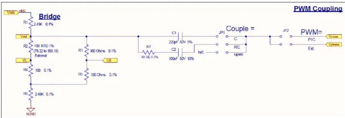
3.2 BRIDGE WITH PWM INTERFERENCE
Figure 3-1 shows the Wheatstone bridge with one RTD element (R2) and three other resistors (R3, R4 and R5). R1 and R6 set the current, which is ratiometric with the 5.0V supply. R1 and R3-R6 are 0.1% resistors to minimize the gain error (they can be lower precision, if the user modifies the firmware to calibrate offset and gain errors).
Vpwm is a 5 V P-P PWM signal generated by the PIC MCU (U3), which is set at 25 kHz and 50% duty cycle. JP1 selects a capacitive feedthrough (C1), a resistive feedthrough (R7, with C2 for DC-blocking) or no feedthrough (open). The first two methods produce roughly 0.2 V P-P at the top of the bridge (Vrtd), while the last produces no PWM signal at Vrtd. Inputting an external PWM signal (JP2, position #2) will give different results.
text_image
PWM Coupling Vdd1 vdd1 Bridge R1 2.49K 0.1% Vind R2 100 RTD 1% (78.32 to 169.19) External VL R4 100 0.1% R5 2.49K 0.1% SGND R3 100 Ohms 0.1% VR R5 100 Ohms 0.1% C1 220pF 50V 5% C2 100nF 50V 10% N/C C RC open JP1 JF2 PWM= PIC Ext. JP2 PWM= Vppm VppmFIGURE 3-1: Bridge with PWM Interference.
The RTD's resistance is a quadratic polynomial in temperature (see
Appendix C. “Conversion Polynomials”). It can be approximated as a linear polynomial, with a temperature error less than ±1.3^ , but that is not accurate enough for applications requiring an RTD. The point is that the resistance to temperature conversion is a non-linear relationship.
The RTD's resistance (R2) appears in the denominator of the equation describing the bridge's differential output voltage (VR – VL) as a function of Vdd1 and the resistors R1 to R6. This means that the relationship between R2 and VR – VL is also non-linear.
Fortunately, as will be discussed later, the firmware does the necessary calculations to overcome these non-linear relationships.
3.3 SIGNAL PROCESSING CIRCUITRY
This circuitry includes two INAs, a VREF and corresponding filters. The MCP6N11's performance is contrasted with a three op amp INA based on the MCP6V27 and MCP6V26 auto-zeroed op amps.
3.3.1 Voltage Reference
Figure 3-2 shows the VREF block (not a fixed reference), which produces a buffered ratiometric (proportional to V_DD ) voltage (Vref). Vref keeps the INAs within their range, even when V_DD changes. Errors in Vref are subtracted out later in firmware.
The pole set at VREF's input matches Input Filter #1 and #2's Differential Mode (DM) poles so that power supply disturbances will be treated the same. Its output is 1.80V, which gives good output headroom for both INAs. The filter on the supply helps keep Vref quiet. R8 and R9 are 1% resistors to minimize circuit cost; the error in Vref is corrected in firmware (subtraction of Vref from INA output voltages).

text_image
VREF Vdd1 vdd1 R10 C4 100nF 50V 10% 200 5% SGND U1 VOUT VDD R8 121K 1% SGND 1 VSS 3 VIN- VIN- R9 68.1K 1% C3 MCP6001-SOT23-5 Vref SGND 100nF 50V 10% SGND 4 SGND 100nF 50V 10% VrefFIGURE 3-2: Voltage Reference.
3.3.2 First INA
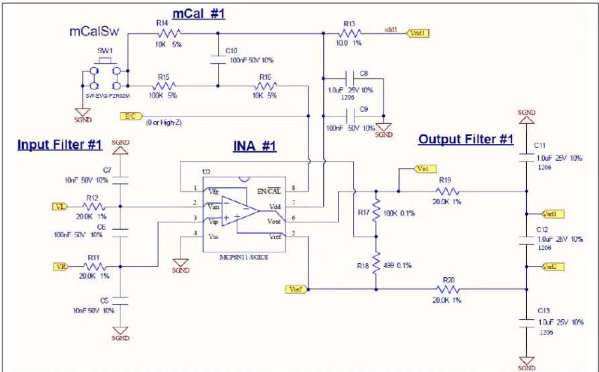
Figure 3-3 shows INA #1, which includes the Input Filter #1, mCal #1 and Output Filter #1 blocks.
Input Filter #1 is a Differential Mode (DM) and Common Mode (CM), low-pass filter. The CM pole is at 800 Hz, so that INA #1 will reject mains interference (at 50 Hz or 60 Hz); its CMRR is very good at low frequencies. The DM pole is at 38 Hz, for low CM-to-DM conversion error, at a reasonable price. R11 and R12 are small enough to have good EMI performance; C5-C7 are sized for the desired poles.
INA #1 (U2) is set to a DM gain of 201 V/V, and has its output shifted up by 1.80V (Vref), producing an output that uses most of the ADC's input range. INA #1's CMRR at 25 kHz is excellent (e.g., 92 dB). INA #1's PSRR rejects mains interference (e.g., harmonics of 50 Hz or 60 Hz). R17 and R18 are 0.1% resistors to minimize gain error (they can be lower precision, if the user modifies the firmware to calibrate offset and gain errors).
To minimize thermo-junction voltage effects, at INA #1's input, R11 and R12 are close together and in parallel. See AN1258 ("Op Amp Precision Design: PCB Layout Techniques") for more information on this topic.
Output Filter #1 is a DM and CM, low-pass filter. The CM pole is at 8 Hz, for further rejection of CM interference. The DM pole is at 2.7 Hz; it is faster than the RTD, but slow enough to limit the output noise. C12 is large enough to cause minimal gain error (it causes a voltage division as it interacts with the ADC's input sampling capacitor, C_HOLD = 25 pF). R19 and R20 are small enough to have good EMI performance; C11-C13 are sized for the desired poles.
mCal #1 triggers an internal calibration event in U1 (MCP6N11), which corrects its V OS; the pole is set for SW1's maximum bounce time (10 ms). R16 makes the EN/CAL pin of INA #1 act as a wired-OR logic input; an E/C signal can be sent from the PIC MCU independent of mCalSw's state.
text_image
mCal Sw SW1 SW-EVG-P2R02M SGND E/C (0 or High-Z) mCal #1 R14 10K 5% C10 100nF 50V 10% R15 100K 5% R16 10K 5% R13 10.0 1% udd1 Vdd1 C8 1.0uF 25V 10% 1206 C9 100nF 50V 10% SGND Input Filter #1 SGND C7 10nF 50V 10% VL R12 20.0K 1% C5 100nF 50V 10% VR R11 20.0K 1% C5 10nF 50V 10% SGND INA #1 U2 1 2 3 4 5 6 7 8 EN/CAL Vin Vap Vss Vref MCPSN1-SCICE8 Output Filter #1 Vol R17 100K 0.1% R19 20.0K 1% R18 499 0.1% R20 20.0K 1% C11 1.0uF 25V 10% 1206 Gnd1 C12 1.0uF 25V 10% 1206 Gnd2 C13 1.0uF 25V 10% 1206 SGNDFIGURE 3-3: First INA.
3.3.3 Power Supply
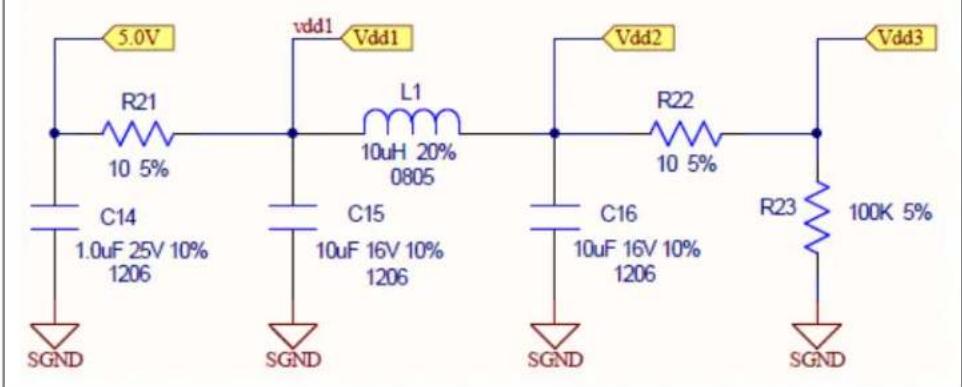
Figure 3-4 shows the power supply connections and filters. Power is provided at either the Lab Power Supply or by the USB connection. The R-C low-pass filters have a pole at 0.80 kHz, which reduces ripple and crosstalk from the PWM interference; they are symmetrically placed so that applying power at either end works well. L1 isolates the analog and digital supplies, to prevent digital signals from interfering with the analog signals; it produces an L-C pole at 23 kHz (a compromise between performance and cost). R23 is a bleed-off resistor that discharges the bypass capacitors when no power supply voltage is present; its power drain is not significant. The signal connectors shown are:
- 5.0V = An external connection to the analog power supply voltage
- When the USB powers the board (no lab supply connected), it provides a convenient point to measure the USB's 5V power
- When a lab supply powers the board (USB is not connected), it is connected here (at TP1)
• Vdd1 = Analog power supply voltage
• Vdd2 = Digital power supply voltage - Vdd3 = USB 5V power
Power Supply
text_image
5.0V R21 10 5% C14 1.0uF 25V 10% 1206 SGND vdd1 Vdd1 L1 10uH 20% 0805 C15 10uF 16V 10% 1206 SGND Vdd2 R22 10 5% C16 10uF 16V 10% 1206 SGND R23 100K 5% Vdd3FIGURE 3-4: Power Supply.
CAUTION
When using the PC and USB, do not connect lab supplies to test points TP1 (+5.0V) and TP2 (GND). This avoids contention with the USB.
When using the bench setup (5V supply at TP1 (+5.0V) and TP2 (GND)), do not connect USB to the demo board. This avoids contention with the lab supply.
3.3.4 Second INA (Traditional Three Op Amp Implementation)
Figure 3-5 shows INA #2, which provides a means of comparing the MCP6N11 to a traditional INA.
Input Filter #2 is the same as Input Filter #1, for ease of comparison. R24 and R25 provide a separate signal path, so that U3's input bias currents and U2's input bias currents don't interact.
INA #2 (U3, U4) is set to a DM gain of 201 V/V, and has its output shifted up by 1.80V (Vref), producing an output that uses most of the ADC's input range. INA #2's CMRR at 25 kHz is excellent (e.g., 96 dB). INA #2's PSRR rejects mains interference (e.g., harmonics of 50 Hz or 60 Hz). R27-R30 are 0.1% resistors to minimize gain error (they can be lower precision, if the user modifies the firmware to calibrate offset and gain errors). R31-R34 are 0.1% resistors to minimize gain error and maximize CMRR.
To minimize thermo-junction voltage effects, at INA #2's input, R24 and R25 are close together and in parallel. The gain resistors for U3 (R27-R30) are also close together and in parallel; R28 and R29 have not been combined into one resistor, to make this possible. The gain resistors for U4 (R31-R34) are also close together and in parallel. See AN1258 ("Op Amp Precision Design: PCB Layout Techniques") for more information on this topic.
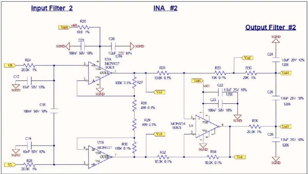
FIGURE 3-5: Second INA.
3.4 TEST POINTS
Figure 3-6 shows the test points available to the user. See Table 2-1 for a list of their functions.

other
Test Points | Test Point | Voltage Source | Voltage Regulator | Voltage (%) | | :--- | :--- | :--- | :--- | | TP1 | +5.0V | Vo1 | 5.0 | | TP5 | Vo1 | R37 | 1.0K | | TP9 | Vo2 | R38 | 1.0K | | TP13 | Vad3 | Vad3 | | | TP2 | GND | SGND | | | TP6 | Vad1 | Vad1 | | | TP10 | Vo3 | R39 | 1.0K | | TP14 | Vad4 | Vad4 | | | TP3 | Rtd1 | Vnd | | | TP7 | Vad2 | Vad2 | | | TP11 | Vo4 | R40 | 1.0K | | TP15 | GND | SGND | | | TP4 | Rtd2 | VL | | | TP8 | GND | SGND | | | TP12 | GND | SGND | | | TP16 | Vpwmx | Vpwux | |FIGURE 3-6: Test Points.
Figure 3-7 shows the PIC microcontroller (USB PIC MCU) with analog connectors to the blocks previously shown, local supply bypassing, a 20 MHz ceramic resonator, ICSP header and USB header.
The four ADC inputs (Vad1 to Vad4) are multiplexed into the USB PIC MCU's internal 12-bit ADC. As discussed later on, the firmware takes the differences Vad1 – Vad2 and Vad3 – Vad4, which corrects VREF's output error (present at Vad2 and Vad4). Since the analog signal processing circuitry does not totally eliminate interference from the 25 kHz PWM signal or the mains (50 Hz or 60 Hz), some will appear at the ADC inputs. The 12-bit ADC supports a typical temperature resolution better than 0.09°C.
The PWM output (Vpwm) is a 5 V _P-P digital signal at 25 kHz and 50% duty cycle. It emulates the CM interference from a motor control application.
The 20 MHz ceramic resonator runs the USB PIC MCU at a rate that supports the firmware tasks' overhead and the USB. An internal PLL Prescaler divides by 5, to produce a 4 MHz clock. The internal PLL then locks onto this clock and produces a 96 MHz output, which is divided down for the USB module's operation.
Use a low ESR capacitor for C27.
The ICSP header makes it possible to program the USB PIC MCU in circuit, for further user experiments.
The USB header provides the data link to the PC, where data is displayed on the included GUI.

text_image
USB PIC U5 1 MCLR Vad1 2 AN0 Vad2 3 AN1 Vad3 4 AN2 Vad4 5 AN3 N/C 6 RA4 N/C 7 RA5 SGND 8 VSS 9 OSC1 10 OSC2 N/C 11 RC0 E/C 12 RC1 Vpwm 13 CCP1 14 VUSB C27 1.0uF 25V 10% 1206 SGND ICSP J1 1 Vdd2 2 CON5 SGND 3 4 5 6 PGD 28 27 PGC 26 N/C RB3 25 N/C RB4 24 N/C RB3 23 N/C RB2 22 N/C RB1 21 N/C RB0 20 VDD 19 SGND VSS 18 N/C RC7 17 N/C RC6 16 VP VM 15 USB SGND 6 J2 C28 100nF 50V 10% SGND 5 N/C 4 D+ 2 D- Vdd3 1 VBUS CONN_USB_MINI_BFIGURE 3-7: PIC Microcontroller.
Section Chapter 4. "Firmware" and Section Chapter 5. "Software GUI" discuss in detail how the digitized data is processed, displayed and stored.
NOTES:
Chapter 4. Firmware
4.1 INTRODUCTION
This chapter discusses the PIC microcontroller's firmware. Items discussed in this chapter include:
• Analog Signals at the ADC Inputs
- Data Conditioning
• Temperature Calculations
• Resistance Calculations
• Calibrating the MCP6N11
• Temperature Calibration
- PWM Output
- USB Communications
4.2 ANALOG SIGNALS AT THE ADC INPUTS
As discussed in Section 3.2 “Bridge With PWM Interference”, the relationship between the RTD temperature and RTD resistance is non-linear, as is the relationship between the RTD resistance and the bridge’s differential output voltage. These non-linearities are corrected in firmware, because that minimizes the design cost.
Section 3.3 “Signal Processing Circuitry” mentions that interference from the 25 kHz PWM signal and the mains (50 Hz or 60 Hz) is reduced significantly, but not totally eliminated, at the ADC inputs. The firmware uses averaging to reduce the effect of these interfering signals.
The 12-bit ADC supports a temperature resolution that could be as good as 0.05^ C. Since the analog inputs do not go rail-to-rail, for a more robust solution, the resolution is reduced somewhat. The non-linear relationships mentioned above make the resolution change, depending on the RTD temperature. The firmware solution gives a resolution between 0.06^ C and 0.09^ C. Obviously, the ADC is not ideal, so the temperature error can be somewhat larger.
4.3 DATA CONDITIONING
4.3.1 Basic Digital Data
The firmware on the PIC microcontroller inputs data for key analog DC voltages (Vad1 to Vad4), then converts them to digital ( V_AD1 to V_AD4 ), with a 12-bit representation:
EQUATION
$$ V _ {A D 1} = I N A # 1 ^ {\prime} s s i g n a l (V a d 1) $$
$$ V _ {A D 2} = I N A # 1 ^ {\prime} s V R E F (V a d 2) $$
$$ V _ {A D 3} = I N A # 2 ^ {\prime} s \text { signal } (V a d 3) $$
$$ V _ {A D 4} = I N A # 2 ^ {\prime} s V R E F (V a d 4) $$
4.3.2 Data Sampling
The DC analog voltages are sampled in this order: V_AD1 , V_AD2 , V_AD3 , and V_AD4 . Each voltage is sampled every 50 ms (a 20 SPS rate). Since the ADC samples all four voltages, it takes a total of 80 samples per second.
4.3.3 Data Averaging and Output Data Rate
The GUI tells the microcontroller the number of averages (n) or whether averaging is turned off. The GUI collects the averaged data from the microcontroller at adjustable time intervals.
When averaging is off, the firmware makes the latest sample available to the GUI. The samples are updated every 50 ms.
When averaging is on, the firmware calculates an exponential moving average, which is updated every 50 ms. These samples are made available for collection by the GUI. A higher number of averages (n) reduces noise more, but has a slower response. The following equation shows how V_AD1 , V_AD2 , V_AD3 , and V_AD4 (shown as x_k ) are averaged (shown as y_k ):
EQUATION
$$ y _ {k} = \alpha_ {k} x + (1 - \alpha) y _ {k - 1} $$
Where:
$$ n = 2, 4, 8, 1 6, 3 2, 6 4 \text { or } 1 2 8 $$
$$ \alpha = 2 / (n + 1) $$
$$ x _ {k} = \text { current sample } $$
$$ y _ {k - 1} = \text { previous average } $$
$$ y _ {k} = \text { current average } $$
4.4 TEMPERATURE CALCULATIONS
It would be possible to convert the measured voltages into RTD resistance, then into RTD temperature. This approach adds overhead to the PIC MCU, so it was not done on this design; the firmware converts directly from INA voltage to temperature.
The firmware gives two estimates of the same RTD temperature, based on the outputs of INA #1 and INA #2:
EQUATION
$$ T _ {R T D 1} = R T D \text { temperature from INA #1 (based on } V _ {A D 1} - V _ {A D 2}) $$
$$ T _ {R T D 2} = R T D \text { temperature from INA #2 (based on } V _ {A D 3} - V _ {A D 4}) $$
4.4.1 Polynomial Estimate of Temperature
Section C.3 "INA Voltage to Temperature" discusses the conversion of V_INA to T_RTD . This section summarizes those results. To accommodate fixed point arithmetic, T_RTD and V_INA are scaled as follows:
EQUATION
$$ v = V _ {I N A} / (V _ {D D} / 2) $$
$$ w = T _ {R T D} / T _ {S 1} $$
Where:
$$ V _ {I N A} = V _ {A D 1} - V _ {A D 2}, \text { for INA #1 } $$
$$ = V _ {A D 3} - V _ {A D 4}, \text { for INA #2 } $$
$$ V _ {D D} / 2 = 2. 5 V $$
$$ T _ {S 1} = 2 5 6 ^ {\circ} \mathrm{C} $$
The firmware uses a cubic polynomial for the conversion. Its accuracy supports the 12-bit ADC we are using (1 LSB is between 0.055^ and 0.088^ , nominally).
EQUATION
$$ w = K _ {0} + v \left(K _ {1} + v \left(K _ {2} + v \left(K _ {3}\right)\right)\right) \pm \varepsilon_ {W} $$
$$ T _ {R T D} = w T _ {S I} \pm \varepsilon_ {T} $$
Where:
$$ K _ {0} = 0. 0 0 0 0 2 $$
$$ K _ {1} = 0. 5 0 4 1 7 $$
$$ \mathrm{K} _ {2} = 0. 0 7 4 6 3 $$
$$ K _ {3} = 0. 0 1 3 7 0 $$
$$ \varepsilon_ {W} = \text { Error in w } $$
$$ \varepsilon_ {T} = \varepsilon_ {\mathrm{W}} T _ {S 1} $$
$$ \left| \varepsilon_ {T} \right| \leq 0. 0 2 1 ^ {\circ} \mathrm{C} $$
$$ T _ {R T D} = T _ {R T D 1,} \quad I N A # 1 $$
$$ T _ {R T D 2}, \texttt {I N A # 2} $$
The GUI collects 10 temperature estimates per second for each INA.
4.5 RESISTANCE CALCULATIONS
For convenience of the user, the firmware gives two estimates of the RTD resistance. We do not need these estimates, since we convert directly from voltage to temperature. They are useful, however, to a user that wants to change the firmware or hardware.
The firmware gives two estimates of the same RTD resistance, based on the previously calculated of T_RTD1 and T_RTD2 ; see Appendix C. “Conversion Polynomials”.
EQUATION
$$ R _ {R T D 1} = R T D \text { resistance from INA #1 (based on } T _ {R T D 1}) $$
$$ R _ {R T D 2} = R T D \text { resistance from INA #2 (based on } T _ {R T D 2}) $$
To accommodate fixed point arithmetic, T_RTD and R_RTD are scaled as follows:
EQUATION
$$ p = T _ {R T D} / T _ {S I} $$
$$ q = \left(R _ {R T D} - R _ {S 0}\right) / R _ {S I} $$
Where:
$$ T _ {S 1} = + 2 5 6 ^ {\circ} \mathrm{C} $$
$$ R _ {S 0} = 1 2 0 \Omega $$
$$ R _ {S 1} = 6 4 \Omega $$
The RTD's resistance is estimated with this polynomial approximation (with scaling):
EQUATION
$$ q = A _ {0} + p \left(A _ {1} + p \left(A _ {2}\right)\right) \pm \varepsilon_ {Q} $$
$$ R _ {R T D} = R _ {S O} + q R _ {S I} \pm \varepsilon_ {R} $$
Where:
$$ A _ {0} = - 0. 3 1 2 5 1 $$
$$ A _ {1} = 1. 5 6 3 5 3 $$
$$ A _ {2} = - 0. 0 5 9 4 6 $$
$$ \varepsilon_ {Q} = \text { Error in } q $$
$$ \varepsilon_ {R} = \varepsilon_ {Q} R _ {S 1,} $$
$$ \left| \varepsilon_ {R} \right| \leq 0. 0 0 5 3 \Omega $$
$$ R _ {R T D} = R _ {R T D 1}, \quad I N A # 1 $$
$$ = R _ {R T D 2}, \quad I N A # 2 $$
$$ \varepsilon_ {T} = \varepsilon_ {R} / (d R _ {R T D} / d T _ {R T D}) $$
The GUI collects 10 resistance estimates per second for each INA.
4.6 CALIBRATING THE MCP6N11
When JP3 is set to position #1, the PIC MCU can send an mCal signal to the MCP6N11 device. This happens when the GUI sends a signal to the PIC MCU (via USB) to start an mCal event. The effect of this signal is to internally re-calibrate the MCP6N11 devices' input offset voltage; its output is high-impedance while this re-calibration is in progress.
4.7 TEMPERATURE CALIBRATION
4.7.1 Single Point Calibration
One of the user options available in our Thermal Management GUI (see
Chapter 5. "Software GUI") is a single-point (offset) calibration (usually at 50^ ); it helps to correct for both circuit and RTD errors.
The GUI calculates the errors and sends calibration coefficients to the USB PIC MCU, which correct all subsequent temperature values. These corrections are simple subtractions.
Note 1: The demo board initially has the calibration coefficient set to zero.
2: Only a single point calibration will be provided for our demo board.
4.7.2 Higher Order Calibrations
Higher order calibrations are potentially more accurate. With two temperature measurements (e.g., at 0^ C and +100^ C), it is possible to do a linear correction (offset and gain). With three temperature measurements (e.g., at 0^ C, +50^ C, and +100^ C), it is possible to do a quadratic correction (offset, gain, and bow). These corrections require firmware modifications by the user.
4.7.3 Circuit Calibration
Separating the circuit calibration from the temperature calibration gives more insight into error sources, but not more accuracy.
It is possible to do a separate circuit calibration by inserting a resistance in R2's place. For example, use the 0°C value of 100Ω (±0.01%).
4.8 PWM OUTPUT
The firmware sets the Vpwm output (pin 13) to produce a square wave with 5 V_P-P , 25 kHz and 50% duty cycle. It runs continuously.
The manually set options on JP1 allow different coupling methods to the Wheatstone bridge, including no connection.
4.9 USB COMMUNICATIONS
The USB PIC MCU device's clock runs on a 20 MHz ceramic resonator, which supports the microcontroller's firmware overhead and USB communications (see
Section 3.5 "PIC Microcontroller").
The GUI provides a means for sending the following configuration information to the board via the USB:
• Temperature calibration coefficient
• Number of averages
- Strobe signal to trigger a V_OS calibration event (mCal) in INA #1
The firmware will send the following data to the GUI (in this order): V_AD1 , V_AD2 , V_AD3 , V_AD4 , T_RTD1 , T_RTD2 , R_RTD1 , and R_RTD2 .
NOTES:
Chapter 5. Software GUI
5.1 INTRODUCTION
This chapter discusses the PC's GUI. Items discussed in this chapter include:
- Platform Requirements
- USB Communications
- Display Data
- Calibrate Temperature
• Calibrate the MCP6N11 - Configuration Options
- Export Data to a File
The GUI is Microchip's "Thermal Management Utility" software. It downloads data from the USB PIC MCU, calculates one point calibration coefficients for T_RTD1 and T_RTD2 , sends them to the PIC MCU, sends an mCal event trigger signal, sends the number of averages, displays the data on a strip chart and exports data in different file formats, including text.
5.2 PLATFORM REQUIREMENTS
The “Thermal Management Utility” software used for many of our thermal demo boards runs on Microsoft Windows (XP SP3, Vista, and 7 (64 and 32 bit)). It also needs the .NET2 framework package; the installer package will install it, if it is not on your machine.
5.3 USB COMMUNICATIONS
The GUI sends configuration information to the firmware, via the USB. This includes: temperature calibration coefficient, number of averages and a strobe signal to trigger a V_OS calibration event (mCal) in INA #1.
The GUI collects the following (averaged) data from the firmware: V_AD1 , V_AD2 , V_AD3 , V_AD4 , T_RTD1 , T_RTD2 , R_RTD1 and R_RTD2 . This data is collected at adjustable time intervals, with a default value of 200 ms (5 SPS per variable).
5.4 DISPLAY DATA
The GUI uses a standard interface to display the temperature calibration coefficient and number of averages.
Displays the four voltages ( V_AD1 through V_AD4 ) on a strip chart. Also displays the RTD temperature estimates ( T_RTD1 and T_RTD2 ) on a strip chart, with a different y-axis. The RTD resistance estimates ( R_RTD1 and R_RTD2 ) are not displayed on the strip chart.
The user will select the data to display on the strip chart. The vectors in bold blue font in Figure 5-1 can be displayed when their check boxes are checked (the ADC & F/W block represents the ADC internal to the PIC MCU and the firmware stored in its memory). The GUI requests the latest data from the microcontroller, after each sampling interval period has passed, and uses that data to perform the plotting and data calculations. Data between collection requests are not sent to the GUI.

flowchart
graph LR
    A["RTD & Bridge"] --> B["INA #1"]
    A --> C["INA #2"]
    B --> D["✓ V_AD1"] --> E["ADC & F/W"]
    C --> F["✓ V_AD3"] --> E
    C --> G["✓ V_AD4"] --> E
    E --> H["✓ T_RTD1"] --> I["R_RTD1"]
    E --> J["✓ T_RTD2"] --> K["R_RTD2"]
FIGURE 5-1: Selecting Vectors to Display on Strip Chart.
5.5 CALIBRATE TEMPERATURE
Supports a single-point calibration of T_RTD1 and T_RTD2 , at a temperature selected by the user. The GUI sends these calibration coefficients to the USB PIC microcontroller, which does the actual corrections.
5.6 CALIBRATE THE MCP6N11
The MCP6N11 MCU internally re-calibrates its input offset voltage when any one of these three events occurs:
- Power up
- The user clicks the mCal push button in the GUI (which sends an mCal event signal to the PIC microcontroller)
• The user presses the mCalSw switch (SW1)
5.7 CONFIGURATION OPTIONS
The GUI provides a means for sending the following configuration information to the firmware, via the USB bus:
• Temperature calibration coefficient
• Number of averages (n)
- Strobe signal to trigger a V_OS calibration event (mCal) in INA #1
5.8 EXPORT DATA TO A FILE
Export all of the data ( V_AD1 , V_AD2 , V_AD3 , V_AD4 , T_RTD1 , T_RTD2 , R_RTD1 and R_RTD2 ) to a user-selected text file. The GUI either sends the displayed data (limited to 500 time points) to the file, or sends “recorded” data over a selected time period (which has no time point limit).
Export the strip chart to a user-selected file, in one of several formats.
5.9 SCREEN CAPTURES
All of the figures in this section have circled numbers that point to important features. These numbers correspond to the associated numbered list. Cross references to these numbers are displayed in the text as follows: (#1).
Some useful features, that may be hard to find, include:
- Resize Right Edge of Information Box (#4)
- Export Strip Chart
- See Section 5.9.4.8 "Exporting Data Acquisition Box"
- Data File
- Graphic File
- Maximize Strip Chart
- See Section 5.9.4.9 "Maximized Strip Chart Display"
- Maximizes Strip Chart only
• Chart Menu (more chart options)
- See Section 5.9.4.10 "Right Mouse Click (inside the Strip Chart Area)"
5.9.1 Data View Tab
Figure 5-2 shows the default screen. On the left, the Data View tab (#9) is selected, and the Strip Chart is displayed.

text_image
Thermal Management Utility - [MCP6N11 and MCP6V2x Wheatstone Bridge Reference Design] View/Select 6GUs Data View Additional Configuration 9 1 2 3 8 4 5 6 7 Help Firmware Version: V1.0.0 Data Acquisition RTD1 Temperature RTD2 Temperature RTD Resistance RTD Temperature RTD Resistance RTD Resistance Voltage TA RTD Resistance Voltage TA RTD Resistance Voltage TA RTD Resistance Voltage TA RTD Resistance Voltage TA RTD Resistance Voltage TA RTD Resistance Voltage TA RTD Resistance Voltage TA RTD Resistance Voltage TA RTD Resistance Voltage TA RTD Resistance Voltage TA RTD Resistance Voltage TA RTD Resistance Voltage TA RTD Resistance Voltage TA RTD Resistance Voltage TA RTD Resistance Voltage TA RTD Resistance Voltage TA RTD Transmission Rate (V): Reference Pts (V): Reference Pts (V): Reference Pts (V): Reference Pts (V): Reference Pts (V): Reference Pts (V): Reference Pts (V): Reference Pts (V): Reference Pts (V): Reference Pts (V): Reference Pts (V): Reference Pts (V): Reference Pts (V): Reference Pts (V): Reference Pts (V): Reference Pts (V): Reference Pts (V): Average Current (A) = 100 ms (Fastest) 10 11 12 1413 15 16 17 18 RTD & Bridge ADC & F/W RTD & Bridge RTD & Bridge RTD & Bridge RTD & Bridge RTD & Bridge RTD & Bridge RTD & Bridge RTD & Bridge RTD & Bridge RTD & Bridge RTD & Bridge RTD & Bridge RTD & Bridge RTD & Bridge RTD & Bridge RTD & Bridge RTD & Bridge RTD & Bridge RTD & Bridge RTD & Bridge RTD & bridge RTD & bridge RTD & bridge RTD & bridge RTD & bridge RTD & bridge RTD & bridge RTD & bridge RTD & bridge RTD & bridge RTD & bridge RTD & bridge RTD & bridge RTD & bridge RTD & bridge RTD & bridge RTD & bridge RTD & bridge RTD & bridge RTD & bridge RTD & Bridge RTD & Bridge RTD & Bridge RTD & Bridge RTD & Bridge RTD & Bridge RTD & Bridge RTD & Bridge RTD & Bridge RTD & Bridge RTD & Bridge RTD & Bridge RTD & Bridge RTD & Bridge RTD & Bridge RTD & Bridge RTD & Bridge RTD & Bridge RTD & Bridge RTD & Cambridge TATR1 TATR2 TATR3 TATR4 TATR5 TATR6 TATR7 TATR8 TATR9 TATR10 TATR11 TATR12 TATR13 TATR14 TATR15 TATR16 TATR17 TATR18 TATR19 TATR20 TATR21 TATR22 TATR23 TATR24 TATR25 TATR26 TATR27 TATR28 TATR29 TATR30 TATR31 TATR32 TATR33 TATR34 TATR35 TATR36 TATR37 TATR38 TATR39 TATR40 TATR41 TATR42 TATR43 TATR44 TATR45 TATR46 TATR47 TATR48 TATR49 TATR50 TATR51 TATR52 TATR53 TATR54 TATR55 TATR56 TATR57 TATR58 TATR59 TATR60 TATR61 TATR62 TATR63 TATR64 TATR65 TATR66 TATR67 TATR68 TATR69 TATR70 TATR71 TATR72 TATR73 TATR74 TATR75 TATR76 TATR77 TATR78 TATR79 TATR80 TATR81 TATR82 TATR83 TATR84 TATR85 TATR86 TATR87 TATR88 TATR89 TATR90 TATR91 TATR92 TATR93 TATR94 TATR95 TATR96 TATR97 TATR98 TATR99 TATR100 TATR101 TATR102 TATR103 TATR104 TATR105 TATR106 TATR107 TATR108 TATR109 TATR110 TATR111 TATR112 TATR113 TATR114 TATR115 TATR116 TATR117 TATR118 TATR119 TATR120 TATR121 TATR122 TATR123 TATR124 TATR125 TATR126 TATR127 TATR128 TATR129 TATR130 TATR131 TATR132 TATR133 TATR134 TATR135 TATR136 TATR137 TATR138 TATR139 TATR140 TATR141 TATR142 TATR143 TATR144 TATR145 TATR146 TATR147 TATR148 TATR149 TATR150 TATR151 W 5.0 V 5.0 V 5.0 V 5.0 V 5.0 V 5.0 V 5.0 V 5.0 V 5.0 V 5.0 V 5.0 V 5.0 V 5.0 V 5.0 V 5.0 V 5.0 V 5.0 V 5.0 V 5.0 V 5.0 V 5.0V 5.0V 5.0V 5.0V 5.0V 5.0V 5.0V 5.0V 5.0V 5.0V 5.0V 5.0V 5.0V 5.0V 5.0V 5.0V 5.0V 5.0V 5.0V 5.0V 5.0W 5.0W 5.0W 5.0W 5.0W 5.0W 5.0W 5.0W 5.0W 5.0W 5.0W 5.0W 5.0W 5.0W 5.0W 5.0W 5.0W 5.0W 5.0W 5.0W 5.0V 5.0V 5.0V 5.0V 5.0V 5.0V 5.0V 5.0V 5.0V 5.0V 5.0V 5.0V 5.0V 5.0V 5.0V 5.0V 5.0V 5.0V 5.0V 5.0CFIGURE 5-2: Data View Tab, with Strip Chart.
The indicated features for Figure 5-2 are:
- Data Collection buttons:
a) Data Acquisition Buttons (standard data collection).
Start Acquisition
Stop Acquisition
Reset Chart Buffer
b) Record Acquisition Buttons (data sent to a file, with user selected length).
Record Acquisition
Stop Record Acquisition
c) Zoom Buttons (resize Strip Chart).
Zoom Information (click and drag inside Strip Chart)
Zoom Out
d) Chart Customization Button.
Open chart customization dialog
- Current measured values for INA #1:
a) RTD Resistance
b) RTD Temperature
c) V_AD1 Reference Point (voltage which changes with temperature)
d) V_AD2 Reference Point (voltage based on VREF)
- Current measured values for INA #2:
a) RTD Resistance
b) RTD Temperature
c) V_AD3 Reference Point (voltage which changes with temperature)
d) V_AD4 Reference Point (voltage based on VREF)
-
Right edge of Information Box. To resize this box, Left Click this edge with the mouse and Drag.
-
Strip Chart area.
a) Double-click in this area to open the Strip Chart Dialog Box.
b) Right-click in this area to open another chart menu.
- Strip Chart.
a) To zoom in on a smaller area, click on one corner and drag to the other corner (the magnifier icon appears).
b) To zoom out to the full Strip Chart area, click on the Zoom Out button (#1).
-
Right edge of GUI window. To resize this window, click this edge and drag.
-
Help button
-
Data View tab is selected
-
Sampling Interval drop-down menu (interval between stored and displayed points).
-
Data display boxes for ADC input voltages ( V_AD1 to V_AD4 ).
-
Data display boxes for calculated temperatures ( T_RTD1 and T_RTD2 ).
-
Y-axis for ADC input voltages ( V_AD1 to V_AD4 ).
-
Y-axis for calculated temperatures ( T_RTD1 and T_RTD2 ).
-
X-axis for collected data.
-
Strip Chart curves.
-
Bottom edge of GUI window. To resize this window, click this edge and drag.
-
Bottom Right corner of GUI window. To resize this window, click and drag.
5.9.2 Additional Configuration and RTD Temp Tabs
Figure 5-3 shows that the Additional Configuration tab (#22) and RTD Temp sub-tab (#23) are selected, and the Strip Chart is displayed (Figure 5-2 has more information).

text_image
Thermal Management Utility - IMCP6N11 and MCPSV2x Wheatstone Bridge Reference Design? View/Select GUIs Data View: Additional Configuration Calibration RTD Temp MCPSN11 Calibration Temperature (°C): Calibrate I INA1 Calibration Offset (°C) 0 INA2 Calibration Offset (°C) 0 Reset Temperature Units Celsius (°C) Fahrenheit Kelvin (K) Number of Averages: OFF PWM PWM Enable Duty: 50 % Sat Duty Freq Adjustment: 0 % Est. Frequency: 25 kHz Chart Update Speed Sampling Interval: 100 ms (Fastout) 19 20 21 Firmware Version: V1.0.0 Data Acquisition RTD1 Temperature RTD2 Temperature Voltage (V) VA01 VA02 VA03 VA04 150 100 50 25 0 -50 -5.0 2.0 1.5 1.0 0.5 0.0 0 50 100 150 200 250 300 350 400 450 Data BufferFIGURE 5-3: Additional Configuration and RTD Temp Tabs, with Strip Chart.
- Calibration input boxes:
a) Calibration Temperature (press the Calibrate! button (#20) when ready).
b) INA1 Calibration Offset (input temperature correction for INA1).
c) INA2 Calibration Offset (input temperature correction for INA2).
-
Calibrate! button (enter Calibration Temperature (#19), then press when ready).
-
Reset button (resets Calibration inputs (#19) to 0).
- Additional Configuration tab is selected.
- RTD Temp sub-tab is selected.
- Temperature Units selection radio buttons.
- Number of Averages drop-down menu.
- PWM inputs:
a) Enabled check box (turns on PWM output from PIC microcontroller and activates other features in the PWM box).
b) Duty input box (inputs duty cycle).
c) Set Duty button (sends updated value to the microcontroller).
d) Frequency Adjustment slider (changes the PWM frequency).
e) Approximate Frequency input box (adjusts PWM frequency; 25 kHz is preferred).
- Sampling Interval drop-down menu (shown at 100 ms per sample).
5.9.3 Additional Configuration and MCP6N11 Tabs
Figure 5-4 shows that the Additional Configuration tab (#29) and MCP6N11 sub-tab (#30) are selected, and the Strip Chart is displayed (Figure 5-2 has more information).
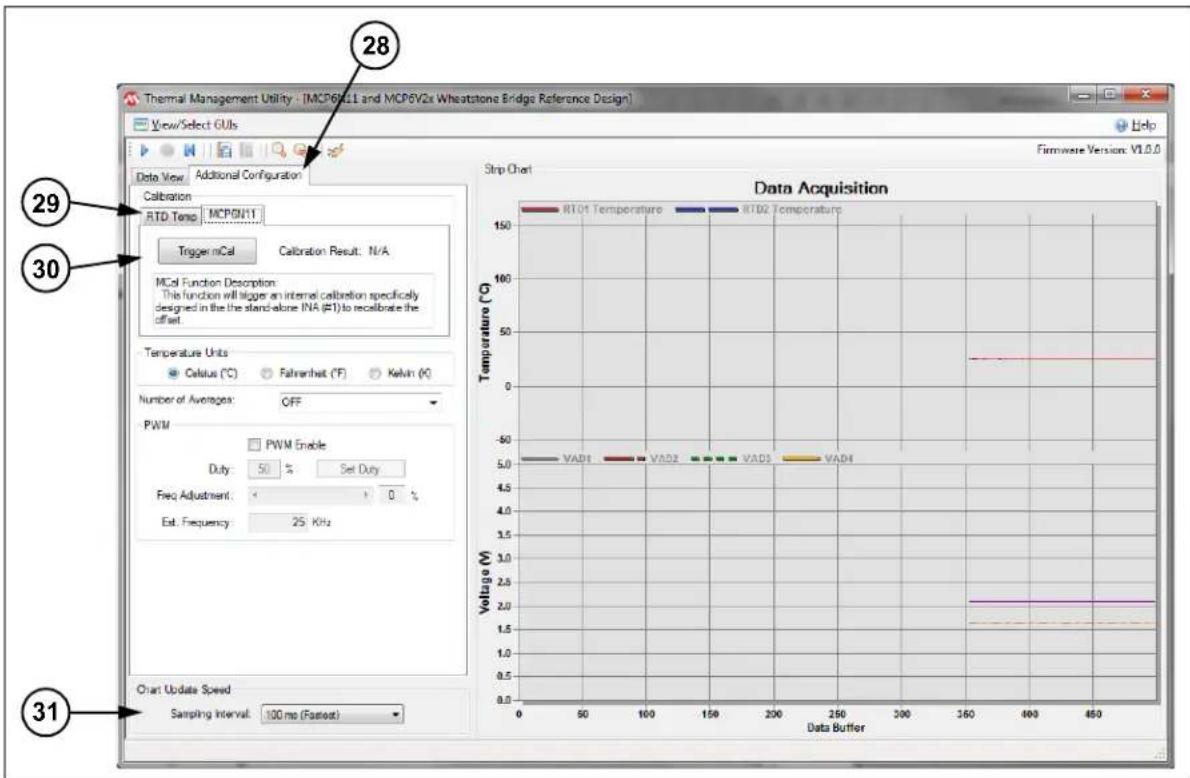
text_image
Thermal Management Utility - [MCP6V11 and MCP6V2x Wheatstone Bridge Reference Design] View/Select GUIs Data View Additional Configuration Calibration RTD Temp: MCP0N11 Trigger mCal Calibration Result: N/A MCal Function Description This function will trigger an internal calibration specifically designed in the stand-alone INA (#1) to recalibrate the offset. Temperature Units Celsius (°C) Fahrenheit (°F) Kelvin (°C) Number of Averages: OFF PWM PWM Enable Duty: 50 % Set Duty Freq Adjustment: 0 % Est. Frequency: 25 kHz Chart Update Speed Sampling Interval: 100 ms (Fastest) Strip Chart Data Acquisition Temperature (°C) 150 50 45 40 35 30 25 20 15 10 5 0 -50 -45 -40 -35 -30 -25 -20 -15 -10 -5 0 28 Help Firmware Version: V1.0.0 31FIGURE 5-4: Additional Configuration and MCP6N11 Tabs, with Strip Chart.
The indicated features for Figure 5-4 are:
- Additional Configuration tab is selected.
- MCP6N11 sub-tab is selected.
- Trigger mCal button; sends a trigger to INA #1 to recalibrate its offset.
- Sampling Interval pull-down menu (shown at 100 ms per sample)
5.9.4 Strip Chart Customization
5.9.4.1 DATA ACQUISITION CUSTOMIZATION – GENERAL TAB
Figure 5-5 shows the dialog box, with the General tab selected. To open this box, double-click inside the Strip Chart area (#5). The overall look and feel of the Strip Chart area can be changed here.

text_image
Data Acquisition Customization... General Plot Subsets Points Font Color Style Main Title: Data Acquisition Show Annotations Sub Title: Border Style No Border Line Shadow 3D Inset Numeric Precision 0 1 2 3 Viewing Style Color Monochrome Monochrome - Symbols Grid Lines Both Y X None Grid in front of data Display Graph Table Both Font Size Large Medium Small OK Cancel Apply Export... Maximize...FIGURE 5-5: Data Acquisition Customization – General Tab.
5.9.4.2 DATA ACQUISITION CUSTOMIZATION – PLOT TAB
Figure 5-6 shows the Data Acquisition dialog box, with the Plot tab selected. To open this box, double-click inside the Strip Chart area (#5). The Strip Chart curve's axes and display types can be changed here.
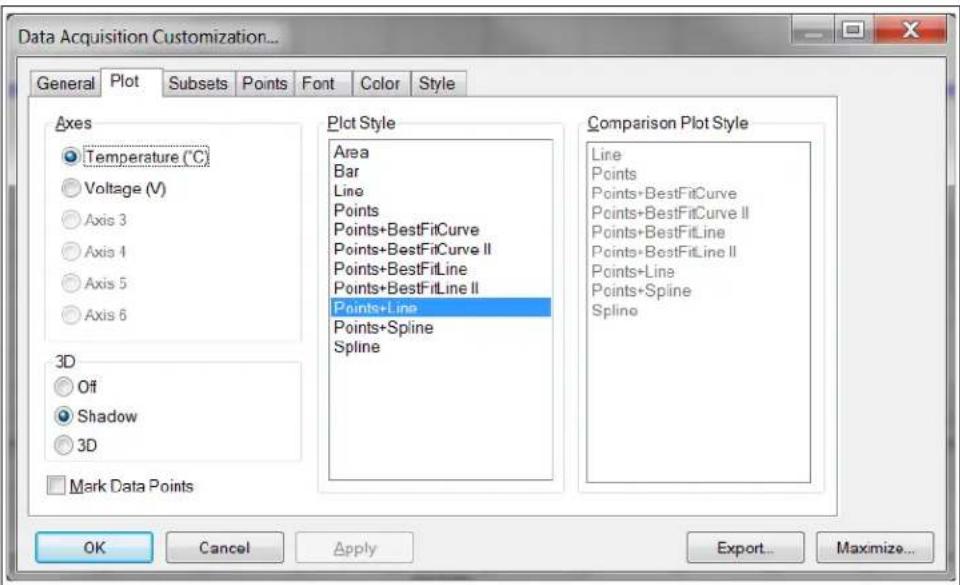
text_image
Data Acquisition Customization... General Plot Subsets Points Font Color Style Axes Temperature (°C) Voltage (V) Axis 3 Axis 4 Axis 5 Axis 6 3D Off Shadow 3D Mark Data Points Plot Style Area Bar Line Points Points+BestFitCurve Points+BestFitCurve II Points+BestFitLine Points+BestFitLine II Points+Line Points+Spline Spline Comparison Plot Style Line Points Points+BestFitCurve Points+BestFitCurve II Points+BestFitLine Points+BestFitLine II Points+Line Points+Spline Spline OK Cancel Apply Export... Maximize...FIGURE 5-6: Data Acquisition Customization – Plot Tab.
5.9.4.3 DATA ACQUISITION CUSTOMIZATION – SUBSETS TAB
Figure 5-7 shows that the Data Acquisition Dialog box, with the Subsets tab selected. To open this box, double-click inside the Strip Chart area (#5). The Strip Chart curves can be selected, or de-selected, here.
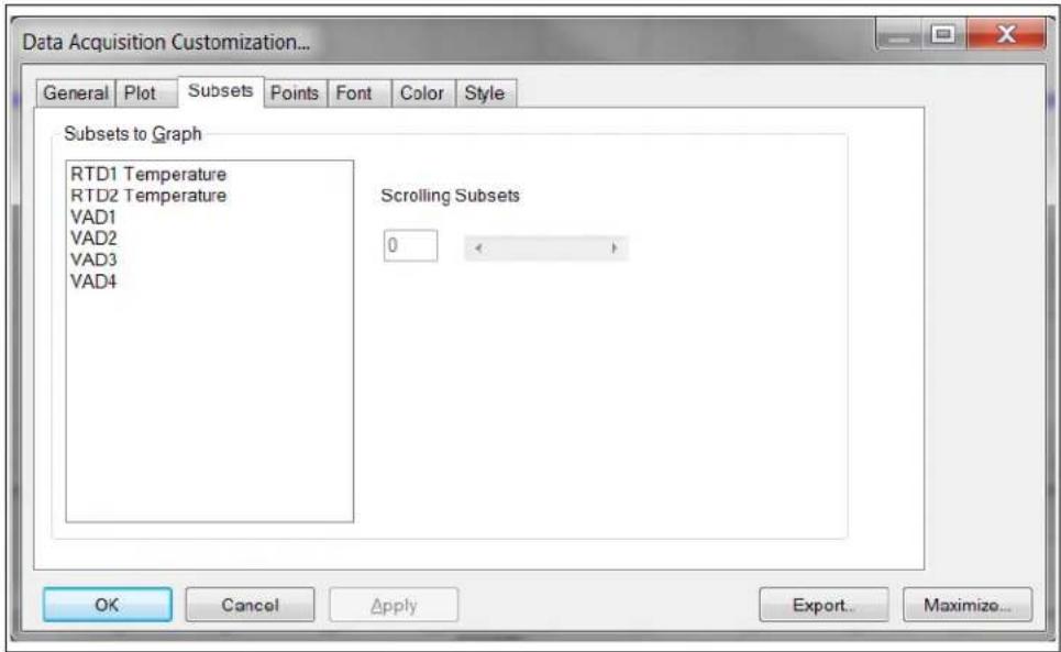
text_image
Data Acquisition Customization... General Plot Subsets Points Font Color Style Subsets to Graph RTD1 Temperature RTD2 Temperature VAD1 VAD2 VAD3 VAD4 Scrolling Subsets 0 OK Cancel Apply Export Maximize...FIGURE 5-7: Data Acquisition Customization – Subsets Tab.
5.9.4.4 DATA ACQUISITION CUSTOMIZATION – POINTS TAB
Figure 5-8 shows that the Data Acquisition dialog box, with the Points tab selected. To open this box, double-click inside the Strip Chart area (#5). The number of points displayed on the Strip Chart's x-axis is changed here.
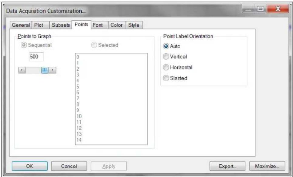
text_image
Data Acquisition Customization... General Plot Subsets Points Font Color Style Points to Graph Sequential Selected 500 0 1 2 3 4 5 6 7 8 9 10 11 12 13 14 Point Label Orientation Auto Vertical Horizontal Slanted OK Cancel Apply Export... Maximize...FIGURE 5-8: Data Acquisition Customization – Points Tab.
5.9.4.5 DATA ACQUISITION CUSTOMIZATION - FONT TAB
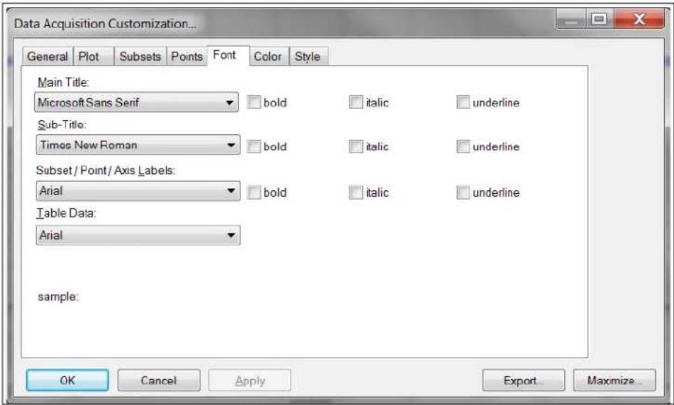
Figure 5-9 shows that the Data Acquisition dialog box, with the Font tab selected. To open this box, double-click inside the Strip Chart area (#5). The Strip Chart's font types and sizes are changed here.
text_image
Data Acquisition Customization... General Plot Subsets Points Font Color Style Main Title: Microsoft Sans Serif ▼ □ bold □ italic □ underline Sub-Title: Times New Roman ▼ □ bold □ italic □ underline Subset / Point / Axis Labels: Arial ▼ □ bold □ italic □ underline Table Data: Arial sample: OK Cancel Apply Export...Maximize...FIGURE 5-9: Data Acquisition Customization – Font Tab.
5.9.4.6 DATA ACQUISITION CUSTOMIZATION - COLOR TAB
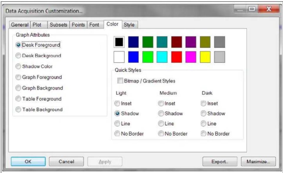
Figure 5-10 shows that the Data Acquisition dialog box, with the Color tab selected. To open this box, double-click inside the Strip Chart area (#5). The font and object colors are changed here.
text_image
Data Acquisition Customization... General Plot Subsets Points Font Color Style Graph Attributes Desk Foreground Desk Background Shadow Color Graph Foreground Graph Background Table Foreground Table Background Quick Styles Bitmap / Gradient Styles Light Medium Dark Inset Inset Inset Shadow Shadow Shadow Line Line Line No Border No Border No Border OK Cancel Apply Export... Maximize...FIGURE 5-10: Data Acquisition Customization – Color Tab.
5.9.4.7 DATA ACQUISITION CUSTOMIZATION – STYLE TAB
Figure 5-11 shows that the Data Acquisition dialog box, with the Style tab selected. To open this box, double-click inside the Strip Chart area (#5). The Strip Chart's curve colors are changed here.

text_image
Data Acquisition Customization... General Plot Subsets Points Font Color Style RTD1 Temperature RTD2 Temperature VAD1 VAD2 VAD3 VAD4 Point Type: Solid Circle Line Type: OK Cancel Apply Export... Maximize...FIGURE 5-11: Data Acquisition Customization – Style Tab.
Figure 5-12 shows the Exporting Data Acquisition box. To open this dialog, double-click inside the Strip Chart area (#5), then press the Export button on the bottom right (e.g., see Figure 5-11). When the data is exported as a picture, its destination and size can be selected. When the data is exported as text, only its destination can be selected.

text_image
Exporting Data Acquisition Export MetaFile BMP JPG PNG Text / Data Only Export Destination ClipBoard File Browse Printer Object Size No Specific Size Millimeters Inches Points Width: 1000 / 676 Units Export Cancel HelpFIGURE 5-12: Exporting Data Acquisition Box.
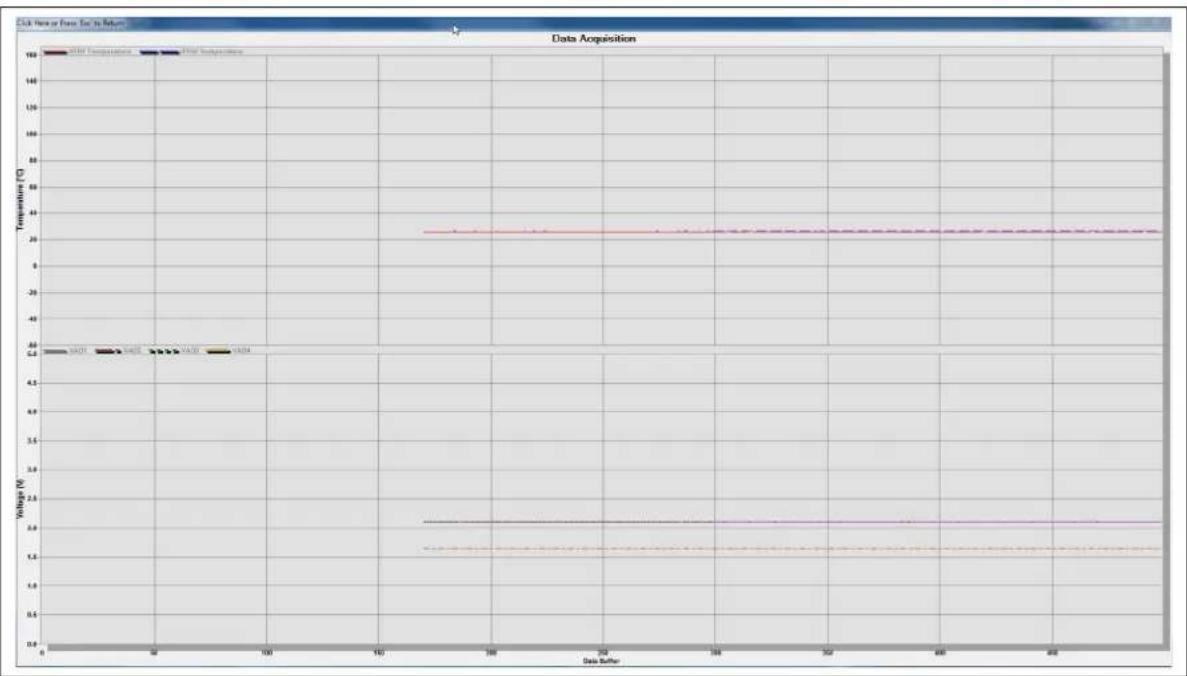
5.9.4.9 MAXIMIZED STRIP CHART DISPLAY
Figure 5-13 shows the maximized strip chart display. To open this window (on the PC's main display), double-click inside the Strip Chart area (#5), then press the Maximize ... button on the bottom right (e.g., see Figure 5-11). To exit this screen, click on the top banner or press the "Esc" key on your keyboard.
line
| Data Better | Temperature (°C) | | ----------- | ---------------- | | 14.21 | 6.0 | | 14.22 | 6.0 | | 14.23 | 6.0 | | 14.24 | 6.0 |FIGURE 5-13: Maximized Strip Chart Display (under the Strip Chart Dialog Box).
5.9.4.10 RIGHT MOUSE CLICK (INSIDE THE STRIP CHART AREA)
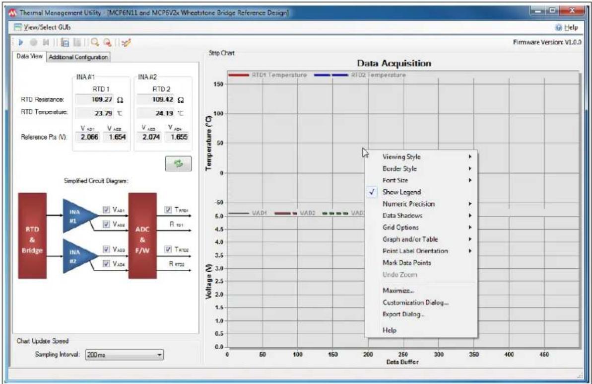
Figure 5-14 shows a chart menu with more chart options. This window is opened (on the PC's main display) by right-clicking inside the Strip Chart area (#5).
line
Thermal Management Utility - [MCP6N11 and MCP5V2x Wheatstone Bridge Reference Design] View/Select GUIs Data View: Additional Configuration RTD Resistance: RTD Temperature: Reference Pts (V): INA #1 RTD 1 Ω RTD Temperature: 23.79 °C INA #2 RTD 2 Ω 24.19 °C INA #1 V Add1 V Add2 INA #2 V Add3 V Add4 INA #1 V Add1 INA #2 V Add3 V Add4 INA #1 V Add1 INA #2 V Add3 V Add4 INA #1 V Add1 INA #2 V Add3 V Add4 INA #1 V Add1 INA #2 V Add3 V Add4 INA #1 V Add1 INA #2 V Add3 V Add4 INA #1 V Add1 INA #2 V Add3 INA #1 V Add1 INA #2 V Add3 INA #1 V Add1 INA #2 V Add3 INA #1 V Add1 INA #2 V Add3 INA #1 V Add1 INA #2 V Add3 INA #1 V Add1 INA #2 V Add3 INA #1 V Add1 INA #2 V Add3 INA #066 1.654 2.074 1.655 Simplified Circuit Diagram: RTD & Bridge VTAD1 VTAD2 ADC & F/W TAD01 R TAD01 R TAD01 TAD02 R TAD02 R TAD02 RTD# Temperature 150°C 150°C 150°C 150°C 150°C 150°C 150°C 150°C 150°C 150°C 150°C 150°C 150°C 150°C 150°C 150°C 150°C 150°C 150°C 150°C 150℃ RTD# Temperature 6.0 V 6.0 V 6.0 V 6.0 V 6.0 V 6.0 V 6.0 V 6.0 V 6.0 V 6.0 V 6.0 V 6.0 V 6.0 V 6.0 V 6.0 V 6.0 V 6.0 V 6.0 V 6.0 V 6.0 V 6.0 Smpfing Style: Border Style: Font Size: Show Legend: Numeric Precision: Data Shadows: Grid Options: Graph and/or Table: Point Label Orientation: Mark Data Points: Undo Zoom: Maximize... Customization Dialog... Export Dialog... Help: Chat Update Speed: Sampling Interval: 200 msFIGURE 5-14: Chart Menu With More Chart Options (Right Click inside the Strip Chart Area).
5.9.4.11 ZOOMING IN AND OUT
Figure 5-15 shows the result of clicking and dragging inside the Chart Area; this will cause the Strip Chart to display the selected area only. To zoom out to full view, click the Zoom out button (second from right button under arrows #1 in Figure 5-2).

FIGURE 5-15: Zoom In area in Strip Chart.
Appendix A. Schematics and Layouts
A.1 INTRODUCTION
This appendix contains the following schematics and layouts for the MCP6N11 and MCP6V2x Wheatstone Bridge Reference Design:
- Board – Schematic
- Board – Top Silk Screen and Pads
- Board – Top Metal Layer
- Board – Ground Plane (Second layer)
- Board – Power Plane (Third layer)
- Board – Bottom Metal Layer (top view)
- Board – Bottom Silk and Pads (top view)
The Gerber files for this board are available on the Microchip website, (www.microchip.com) and are contained in the zip file 00354R3_Gerbers.zip. This is a four-layer PCB.
A.2 BOARD - SCHEMATIC
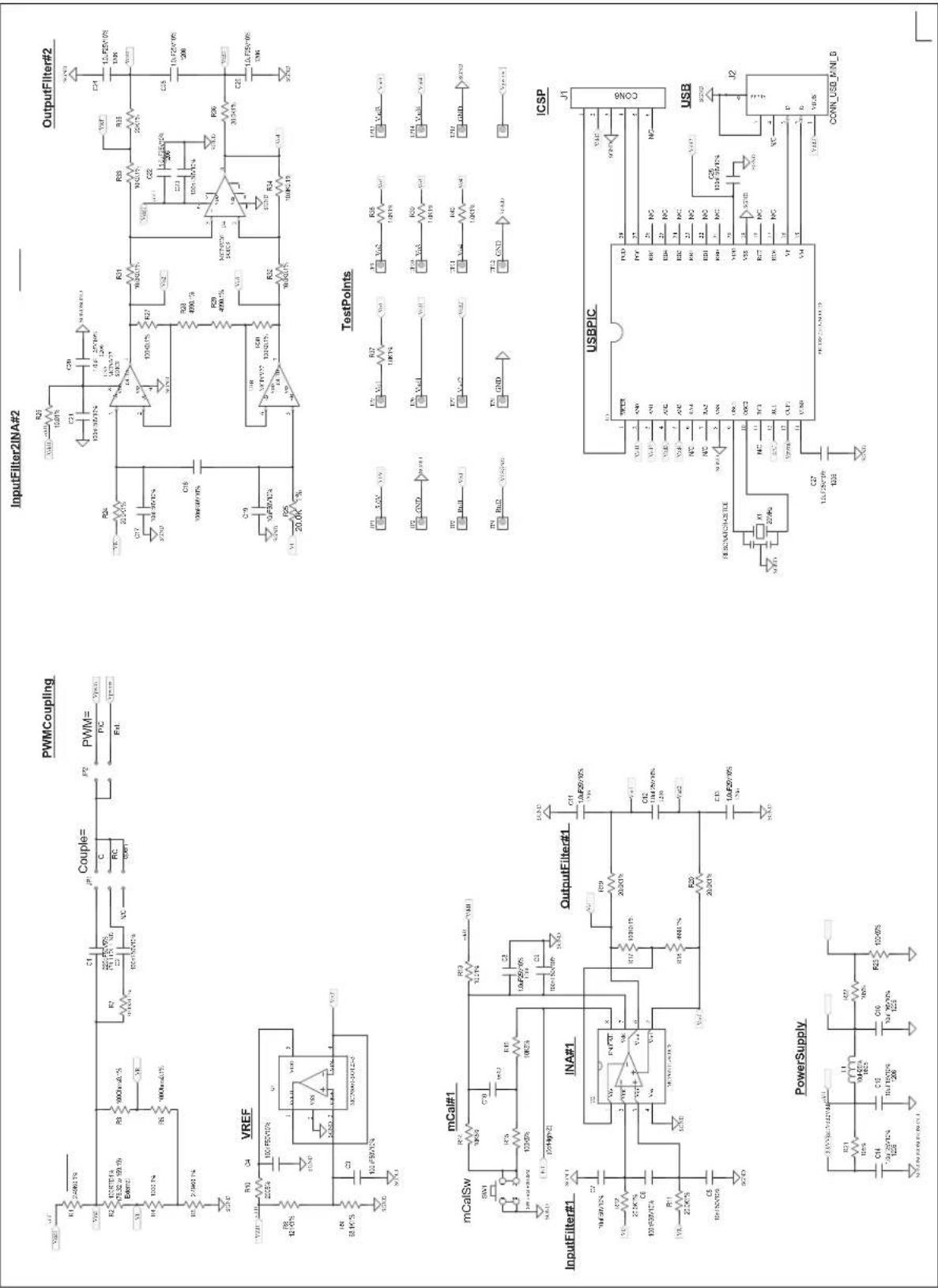
text_image
InputFilter2IN#A#2 OutputFilter#2 PWM Coupling C1 P2 C R3 R4 C5 C6 C7 C8 C9 C10 C11 C12 C13 C14 C15 C16 C17 C18 C19 C20 C21 C22 C23 C24 C25 C26 C27 C28 C29 C30 C31 C32 C33 C34 C35 C36 C37 C38 C39 C40 C41 C42 C43 C44 C45 C46 C47 C48 C49 C50 C51 C52 C53 C54 C55 C56 C57 C58 C59 C60 C61 C62 C63 C64 C65 C66 C67 C68 C69 C70 C71 C72 C73 C74 C75 C76 C77 C78 C79 C80 C81 C82 C83 C84 C85 C86 C87 C88 C89 C90 C91 C92 C93 C94 C95 C96 C97 C98 C99 C100 TestPoints mCal#1 mCalSw1 mCalSW2# VREF. VREF# VREF# VREF# VREF# VREF# VREF# VREF# VREF# VREF# VREF# VREF# VREF# VREF# VREF# VREF# VREF# VREF# VREF# VREF# VREF# VREF# VREF# VREF# VREF# VREF# VREF# VREF# VREF# VREF# VREF# VREF# VREF# VREF# VREF# GUSBIPIC USB# 1.1.1.1.1.1.1.1.1.1.1.1.1.1.1.1.1.1.1.1.1.1.1.1.1.1.1.1.1.1.1.1.1.1.1.1.1.1.1.1.1.1.1.1.1.1.1.1.1.1.1. ICA# 0.0000000000000000000000000000000000000000000000000000000000000000000000000000000000000000000000000000. PowerSupply: GUSB# 1.1.1.1.1.1.1.1.1.1.1.1.1.1.1.1.1.1.1.1.1.1.1.1.1.1.1.1.1.1.1.1.1.1.1.1.1. GUSB# 1.1.1.1.1.1.1.1.1.1.1.1.1.1.1.1.1.1.1.1.1.1.1.1.1.1.1.1.1.1.1.1. GUSB# 1.1.1.1.1.1.1.1.1.1.1.1.1.1.1.1-NC- NC- NC- NC- NC- NC- NC- NC- NC- NC- NC- NC- NC- NC- NC- NC- NC- NC- NC- NC- NC- NC- NC- NC- NC- NC- NC- NC- NC- NC- NC- NC- NC- NC- NC- NC- NC- NC- NC- NC- NC- NC- NC- NC- NC- NC- NC- NC- NC- NC- NC+ OutputFilter#2IN#A# 2. OutputFilter#2IN#A# 3. OutputFilter#2IN#A# 4. OutputFilter#2IN#A# 5. OutputFilter#2IN#A# 6. OutputFilter#2IN#A# 7. OutputFilter#2IN#A# 8. OutputFilter#2IN#A# 9. OutputFilter#2IN#A# 10. OutputFilter#2IN#A# 11. OutputFilter#2IN#A# 12. OutputFilter#2IN#A# 13. OutputFilter#2IN#A# 14. OutputFilter#2IN#A# 15. OutputFilter#2IN#A# 16. OutputFilter#2IN#A# 17. OutputFilter#2IN#A# 18. OutputFilter#2IN#A# 19. OutputFilter#2IN#A# 20. OutputFilter#2IN#A# 21. OutputFilter#2IN#A# 22. OutputFilter#2IN#A# 23. OutputFilter#2IN#A# 24. OutputFilter#2IN#A# 25. OutputFilter#2IN#A# 26. OutputFilter#2IN#A# 27. OutputFilter#2IN#A# 28. OutputFilter#2IN#A# 29. OutputFilter#2IN#A# 30. OutputFilter#2IN#A# 31. OutputFilter#2IN#A# 32. OutputFilter#2IN#A# 33. OutputFilter#2IN#A# 34. OutputFilter#2IN#A# 35. OutputFilter#2IN#A# 36. OutputFilter#2IN#A# 37. OutputFilter#2IN#A# 38. OutputFilter#2IN#A# 39. OutputFilter#2IN#A# 40. OutputFilter#2IN#A# 41. OutputFilter#2IN#A# 42. OutputFilter#2IN#A# 43. OutputFilter#2IN## A## B## B## C## D## E## F## G## H## I## J## K## L## M## N## O## P## Q## R## S## T## U## W## X## Y## Z## W## X## Y## Y## Y## Y## Y## Y## Y## Y## Y## Y## Y## Y## Y## Y## Y## Y## Y## Y## Y## Y## Y## Y## Y## Y## Y## Y## Y## Y## Y## Y## Y## Y## Y## Y## Y## Y## Y## Y## Y## Y## Y## Y## Y## Y## Y## Y## Y## Y## Y## Y## V##B##B##B##B##B##B##B##B##B##B##B##B##B##B##B##B##B##B##B##B##B##B##B##B##B##B##B##B##B##B##B##B##B##B##B##B##B##B##B##B##B##B##B##B##B##B##B##B##B##B## B## B### V#### B### V#### B### V#### B### V#### B### V#### B### V#### B### V#### B### V#### B### V#### B### V#### B### V#### B### V#### B### V#### B### V#### B### V#### B### V#### B### V#### B### V#### B### V#### B### V#### B### V#### B### V#### B### V#### B### V#### B### V#### B### V### B### V#### B### V#### B### V#### B### V#### B### V#### B### V#### B### V#### B### V#### B### V#### B### V#### B### V#### B### V#### B### V#### B### V#### B### V#### B### V#### B### V#### B### V#### B### V#### B### V#### B### V#### B### V#### B### V#### B### V#### B### V###### B### V###### B### V###### B### V###### B### V###### B### V###### B### V###### B### V###### B### V###### B### V###### B### V###### B### V###### B### V###### B### V###### B### V###### B### V###### B### V###### B### V###### B### V###### B### V###### B### V###### B### V###### B### V###### B### V###### B### V###### B### V##### ## #### #### #### #### #### #### #### #### #### #### #### #### #### #### #### #### #### #### #### #### #### #### #### #### #### #### #### #### #### #### #### #### #### #### #### #### #### #### #### #### #### #### #### #### #### #### #### #### #### #### #### #### #### #### #### #### #### #### #### #### #### #### #### #### #### #### #### #### #### #### #### #### #### #### #### #### #### #### #### #### #### #### #### #### #### #### #### #### #### triple number of samples in the output of the output of the output of the output of the output of the output of the output of the output of the output of the output of the output of the output of the output of the output of the output of the output of the output of the output of the output of the output of the output of the output of the output of the output of the output of the output of the output of the output of the output of the output of the output of the output of the output of the output of this source or source of the source or source of the source or source of the source or source of the source or source of the source or source of the source or source of the source or source of the source or source of the source or source of the source or source of the source or source of the source or source of the source or source of the source or source of the source or source of the source or source of the source or source of the source or source of the source or source of the source or source of that source or source of the source or source of the source or source of the source or source of the source or source of the source or source of the source or source of the source or source of the source or source of the source or source of the source or source of the source or source of the source or source of the source or source of the source or source of the source or source of the source or source of the source or source of the source or source of the source or source of this source or source of this source or source of this source or source of this source or source of this source or source of this source or source of this source or source of this source or source of this source or source of this source or source of this source or source of this source or source of this source or source of this source or source of this source or source of this source or source of this source or source of this source or source of this source or source of this source or source of these sources or sources for each other (e.g., V#, W#, Z#, R#, S#, T#, U#, V#, W#, X#, Y#, Z#, R#, S#, T#, U#, V#, W#, X#, Y#, Z#, R#, S#, T#, U#, V#, W#, X#, Y#, Z#, R#, S#, T#, U#, V#, W#, X#, Y#, Z#, R#, S#, T#, U#, V#, W#, X#, Y#, Z#, R#, S#, T#, U#, V#, W#, X#, Y#, Z#, R#, S#, T#,U#, V#, W#, X#, Y#, Z#, R#, S#, T#,U#, V#, W#, X#, Y#, Z#, R#, S#, T#,U#, V#, W#, X#, Y#, Z#, R#, S#, T#,U#, V#, W#, X#, Y#, Z#, R#, S#, T#,U#, V#, W#.A.3 BOARD - TOP SILK SCREEN AND PADS

text_image
ICSP J1 RTD R2 R3 R1 R4 R5 R6 R7 C1 R7 C2 JP1 Couple= C RC Open R37 R16 U2 R12 C6 R11 C5 R17 R18 INA#1 C19 C18 C17 C14 R9 R10 U1 C4 C3 R8 U4 C33 R33 R31 R32 R34 INA#2 MPC6N11 and MCP6V2x Wheatstone Bridge Reference Design R30 R29 R28 R27 C26 C25 C24 R36 R35 R30 R39 R38 R40 ARD00354 TP4 Rtd2 TP3 Rtd1 TP10 Uo3 TP9 Uo2 TP11 Uo4 TP12 GND TP13 Uad3 TP14 Uad4 TP15 GND TP5 Vo1 TP8 TP8 C8 R15 GND SW1 mCal Sw TP6 Uad1 TP7 Uad2 TP1 5.0+ TP2 GND PWM= JP2 PIC EXT TP16 UpwmxA.4 BOARD - TOP METAL LAYER

natural_image
Pure electrical circuit lines without any symbolsA.5 BOARD - GROUND PLANE (SECOND LAYER)

A.6 BOARD - POWER PLANE (THIRD LAYER)

A.7 BOARD - BOTTOM METAL LAYER (TOP VIEW)
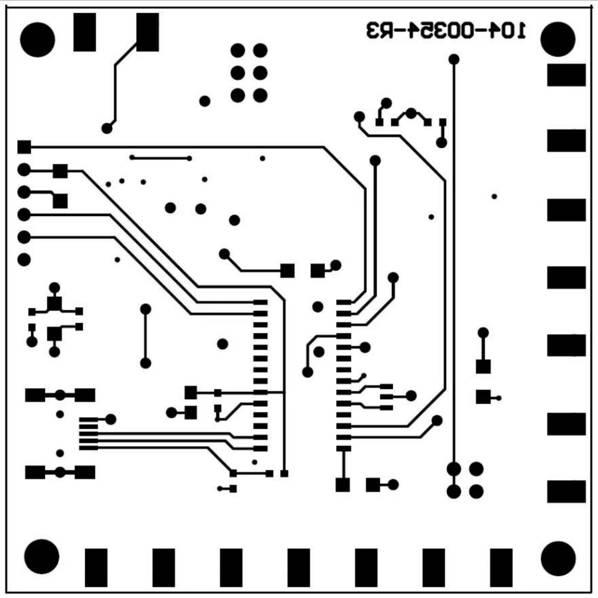
text_image
104-00324-B3A.8 BOARD – BOTTOM SILK AND PADS (TOP VIEW)

text_image
CIE B13 CA CS0 CS1 SS8 SS9 SS0 SS3 SS5 SS7 SS8 SS9 SS10 SS11 SS12 SS13 SS14 SS15 SS16 SS17 SS18 SS19 SS20 SS21 SS22 SS23 SS24 SS25 SS26 SS27 SS28 SS29 SS30 SS31 SS32 SS33 SS34 SS35 SS36 SS37 SS38 SS39 SS40 SS41 SS42 SS43 SS44 SS45 SS46 SS47 SS48 SS49 SS50 SS51 SS52 SS53 SS54 SS55 SS56 SS57 SS58 SS59 SS60 NSB 1SAppendix B. Bill Of Materials (BOM)
TABLE B-1: BILL OF MATERIALS - ASSEMBLED PCB
| Qty | Reference Designator | Description Manufacturer Part Number | ||
| 1 C1 | 220 pF, 0603 SMD, Ceramic, NP0, 50V, 5% AVX Corporation 06035A221JAT2A | |||
| 10 C2-C4, C6, C9, C10, C18, C21, C23, C28 | 100 nF, 0603 SMD, Ceramic, X7R, 50V, 10% | AVX Corporation 06035C104KAT2A | ||
| 4 | C5, C7, C17, C19 | 10 nF, 0603 SMD, Ceramic, X7R, 50V, 10% | AVX Corporation 06035C103KAT2A | |
| 11 C8, C11-C14, C20, C22, C24-C27 | 1.0 μF, 1206 SMD, Ceramic, X7R, 25V, 10% | AVX Corporation 12063C105KAT2A | ||
| 2 C15, C16 | 10 μF, 1206 SMD, Ceramic, X7R, 16V, 10% AVX Corporation 1206YC106KAT2A | |||
| 1 | J2 | Header, Mini USB | Tyco Electronics | 1734035-2 |
| 1 JP1 | Header, 3×2, 100 mil | Molex® | 10-89-7062 | |
| 1 JP2 | Header, 2×2, 100 mil | Molex® | 10-89-7042 | |
| 1 | L1 | 10 μH, 100 mA, 0805 SMD, 20% | Murata Electronics | LQM21FN100M70L |
| 1 PCB | MCP6N11 and MCP6V2x Wheatstone Bridge Reference Design, 4 layer PCB (2.60 in × 2.60 in) | — | — | |
| 2 | R1, R6 | 2.49 kΩ, 0603 SMD, 0.1%, 1/10W | SUSUMU | RG1608P-2491-B-T5 |
| 1 | R2 | 100Ω RTD, 0603 SMD, 1% | Vishay/Beyschlag | PTS060301B100RP100 |
| 3 | R3-R5 | 100Ω, 0603 SMD, 0.1%, 1/10W | SUSUMU | RG1608P-101-B-T5 |
| 1 | R7 | 30.1 kΩ, 0603 SMD, 0.1%, 1/10W | SUSUMU | RG1608P-3012-B-T5 |
| 1 | R8 | 121 kΩ, 0603 SMD, 1%, 1/10W | Yageo | RC0603FR-07121KL |
| 1 | R9 | 68.1 kΩ, 0603 SMD, 1%, 1/10W | Yageo | RC0603FR-0768K1L |
| 1 | R10 | 200Ω, 0603 SMD, 5%, 1/10W | Yageo | RC0603JR-07200RL |
| 8 | R11, R12, R19, R20, R24, R25, R35, R36 | 20.0 kΩ, 0603 SMD, 1%, 1/10W | Yageo | RC0603FR-0720KL |
| 2 | R13, R26 | 10.0Ω, 0603 SMD, 1%, 1/10W | Yageo | RC0603FR-0710RL |
| 2 | R14, R16 | 10 kΩ, 0603 SMD, 5%, 1/10W | Yageo | RC0603JR-0710KL |
| 2 | R15, R23 | 100 kΩ, 0603 SMD, 5%, 1/10W | Yageo | RC0603JR-07100KL |
| 3 | R17, R27, R30 | 100 kΩ, 0603 SMD, 0.1%, 1/10W | SUSUMU | RG1608P-104-B-T5 |
| 3 | R18, R28, R29 | 499Ω, 0603 SMD, 0.1%, 1/10W | SUSUMU | RG1608P-4990-B-T5 |
| 2 | R21, R22 | 10Ω, 0603 SMD, 5%, 1/10W | Yageo | RC0603JR-0710KL |
| Qty | Reference Designator | Description | Manufacturer | Part Number |
| 4 | R31-R34 | 10.0 kΩ, 0603 SMD, 0.1%, 1/10W | SUSUMU | RG1608P-103-B-T5 |
| 4 | R37-R40 | 1.00 kΩ, 0603 SMD, 1%, 1/10W | Yageo | RC0603FR-071KL |
| 2 | SH1, SH2 Shunt, 100 mil Thru-Hole, 2 Pos., 30 μm Au Tyco Electronics Corp. 881545-2 | |||
| 1 | SW1 SMD, Switch, Push Button, 1 Pos., SPST-NO | Panasonic-ECG EVQ-P2R02M | ||
| 1 | U1 | MCP6001, SOT-23-5, Single Op Amp | Microchip Technology Inc. | MCP6001T-E/OT |
| 1 | U2 | MCP6N11, SOIC-8, Single INA, GMIN = 100 | Microchip Technology Inc. | MCP6N11-100U/SN |
| 1 | U3 MCP6V27, SOIC-8, Dual Auto-Zeroed Op Amp | Microchip Technology Inc. | MCP6V27-E/SN | |
| 1 | U4 MCP6V26, SOIC-8, Single Auto-Zeroed Op Amp | Microchip Technology Inc. | MCP6V26-E/SN | |
| 1 | U5 PIC18F2553, SOIC-28 (300 mil), USB PIC MCU | Microchip Technology Inc. | PIC18F2553-I/SO | |
| 1 | Y1 | 20 MHz Ceramic Resonator, SMT, E-temp | Murata Electronics | CSTCE20M0V53Z-R0 |
Note 1: The components listed in this Bill of Materials are representative of the PCB assembly. The released BOM used in manufacturing uses all RoHS-compliant components.
TABLE B-2: BILL OF MATERIALS – OTHER PARTS IN KIT
| Qty | Reference Designator | Description | Manufacturer | Part Number |
| 1 | — | USB 2.0 Cable, A to Mini B, 1 m | Molex® | 88732-8600 |
Note 1: The components listed in this Bill of Materials are representative of the other parts in the kit. The released BOM used in manufacturing uses all RoHS-compliant components.
TABLE B-3: BILL OF MATERIALS – ALTERNATE COMPONENTS
| Qty | Reference Designator | Description | Manufacturer | Part Number |
| 1 | C27 | 470 nF, 1206 SMD, Ceramic, X7R, 25V, 10% | AVX Corporation | 12063C474KAT2A |
| 4 | R31-R34 | 10.0 kΩ, 0603 SMD, 0.01%, 1/16W | Stackpole Electronics Inc. | RNCF0603TKY10K0 |
| 1 | U3 | MCP6V07, SOIC-8, Dual Auto-Zeroed Op Amp | Microchip Technology Inc. | MCP6V07-E/SN |
| MCP6V02, SOIC-8, Dual Auto-Zeroed Op Amp | Microchip Technology Inc. | MCP6V02-E/SN | ||
| 1 | U4 | MCP6V06, SOIC-8, Single Auto-Zeroed Op Amp | Microchip Technology Inc. | MCP6V06-E/SN |
| MCP6V01, SOIC-8, Single Auto-Zeroed Op Amp | Microchip Technology Inc. | MCP6V01-E/SN |
Note 1: The components listed in this Bill of Materials are representative of the alternate components used for modifications. The released BOM used in manufacturing uses all RoHS-compliant components.
TABLE B-4: BILL OF MATERIALS – OPTIONAL PARTS
| Qty | Reference Designator | Description Manufacturer | Part Number | |
| 1 J | 1 Header, 1×6, 100 mil | Molex® | 22-28-4060 | |
| 16 TP1-TP16 SMD, Test | Point Keystone Electronics 5016 | |||
| 4 (for PCB mounting) Hemispherical BumponTM Standoff, 0.44 in × 0.20 in | 3MTM SJ-5003 (BLACK) | |||
| 4 (for PCB mounting) Stand-off, Hex, 0.500", 4 × 40 Thread, Nylon, 0.285" max. O.D. | Keystone Electronics | 1902C | ||
| 4 (for PCB mounting) Machine Screw, Phillips, 4 × 40 Thread, 1/4" long, Nylon | Building Fasteners | NY PMS 440 0025 PH | ||
| 2 | (for External RTD) | 24 AWG wires, twisted strands, 2 m | n/a | n/a |
Note 1: The components listed in this Bill of Materials are representative of the optional parts that the user may wish to acquire and install. The released BOM used in manufacturing uses all RoHS-compliant components.
NOTES:
Appendix C. Conversion Polynomials
C.1 CIRCUIT RESPONSE
Table C-1 shows the nominal performance of critical circuit parameters used in this appendix. V_BRIDGE is the differential output voltage of the Wheatstone bridge. V_INA_OUT is the output voltage of the INAs. V_REF shifts the INAs' output above ground (about 1.80V). V_INA is V_INA_OUT - V_REF , which corrects the measured voltages for V_REF errors (about ±0.03V).
TABLE C-1: NOMINAL VALUES
| T_RTD (°C) | R_RTD (Ω) | V_BRIDGE (V) | V_INA\_OUT (V) | V_INA (V) |
| -55 78.32 | -0.00565 0.665 | 1.136 | ||
| -50 80.31 | -0.00510 0.774 | 1.026 | ||
| -45 82.29 | -0.00456 0.883 | 0.918 | ||
| -40 84.27 | -0.00403 0.989 | 0.811 | ||
| -35 86.25 | -0.00351 1.095 | 0.706 | ||
| -30 88.22 | -0.00299 1.199 | 0.601 | ||
| -25 90.19 | -0.00248 1.303 | 0.498 | ||
| -20 92.16 | -0.00197 1.404 | 0.396 | ||
| -15 94.12 | -0.00147 1.505 | 0.295 | ||
| -10 96.04 | -0.00097 1.605 | 0.196 | ||
| -5 98.04 | -0.00048 1.703 | 0.097 | ||
| 0 100.00 | 0.00000 1.801 | 0.000 | ||
| 5 101.95 | 0.00048 1.897 | 0.096 | ||
| 10 | 103.90 0.00 | 095 1.992 | 0.191 | |
| 15 | 105.85 0.00 | 142 2.086 | 0.285 | |
| 20 | 107.79 0.00 | 188 2.179 | 0.378 | |
| 25 | 109.74 0.00 | 234 2.271 | 0.470 | |
| 30 | 111.67 0.00 | 279 2.362 | 0.561 | |
| 35 | 113.61 0.00 | 324 2.452 | 0.651 | |
| 40 | 115.54 0.00 | 368 2.541 | 0.740 | |
| 45 | 117.47 0.00 | 412 2.629 | 0.828 | |
| 50 | 119.40 0.00 | 455 2.716 | 0.915 | |
| 55 | 121.32 0.00 | 498 2.802 | 1.001 | |
| 60 | 123.24 0.00 | 540 2.887 | 1.086 | |
| 65 | 125.16 0.00 | 582 2.971 | 1.171 | |
| 70 | 127.08 0.00 | 623 3.055 | 1.254 | |
| 75 | 128.99 0.00 | 664 3.137 | 1.336 | |
| 80 | 130.90 0.00 | 705 3.219 | 1.418 | |
| 85 | 132.80 0.00 | 745 3.299 | 1.499 | |
| 90 | 134.71 0.00 | 785 3.379 | 1.579 | |
| 95 | 136.61 0.00 | 824 3.458 | 1.658 | |
| T_RTD (°C) | R_RTD (Ω) | V_BRIDGE (V) | V_INA\_OUT (V) | V_INA (V) |
| 100 138. | 51 0.00863 3.537 | 1.736 | ||
| 105 140. | 40 0.00901 3.614 | 1.813 | ||
| 110 142. | 29 0.00939 3.691 | 1.890 | ||
| 115 144. | 18 0.00977 3.767 | 1.966 | ||
| 120 146. | 07 0.01014 3.842 | 2.041 | ||
| 125 147. | 95 0.01051 3.916 | 2.115 | ||
| 130 149. | 83 0.01088 3.990 | 2.189 | ||
| 135 151. | 71 0.01124 4.063 | 2.262 | ||
| 140 153. | 58 0.01160 4.135 | 2.334 | ||
| 145 155. | 46 0.01196 4.206 | 2.405 | ||
| 150 157. | 33 0.01231 4.277 | 2.476 | ||
| 155 159. | 19 0.01266 4.347 | 2.546 |
C.2 RTD TEMPERATURE AND RESISTANCE
The RTD's temperature error is Class F0.3:
EQUATION
$$ T _ {T o l} = \pm (0. 3 0 ^ {\circ} C + 0. 0 0 5 | T _ {R T D} |), \text { Class } F 0. 3 $$
To accommodate fixed point arithmetic, R_RTD and T_RTD are scaled as follows:
EQUATION
$$ p = T _ {R T D} / T _ {S I} $$
$$ q = \left(R _ {R T D} - R _ {S 0}\right) / R _ {S I} $$
Where:
$$ T _ {S 1} = + 2 5 6 ^ {\circ} \mathrm{C} $$
$$ R _ {S 0} = 1 2 0 \Omega $$
$$ R _ {S 1} = 6 4 \Omega $$
The RTD's resistance is estimated with this polynomial approximation (with scaling):
EQUATION
$$ q = A _ {0} + p \left(A _ {1} + p \left(A _ {2}\right)\right) \pm \varepsilon_ {Q} $$
$$ R _ {R T D} = R _ {S 0} + q R _ {S I} \pm \varepsilon_ {R} $$
Where:
$$ A _ {0} = - 0. 3 1 2 5 1 $$
$$ A _ {1} = 1. 5 6 3 5 3 $$
$$ A _ {2} = - 0. 0 5 9 4 6 $$
$$ \varepsilon_ {R} = \varepsilon_ {Q} R _ {S 1}, \quad | \varepsilon_ {R} | \leq 0. 0 0 5 3 \Omega $$
$$ \varepsilon_ {T} = \varepsilon_ {R} / (d R _ {R T D} / d T _ {R T D}), | \varepsilon_ {T} | \leq 0. 0 1 3 ^ {\circ} C $$
The RTD's temperature is estimated with this polynomial approximation (with scaling):
EQUATION
$$ p = B _ {0} + q \left(B _ {1} + q \left(B _ {2} + q \left(B _ {3} + q \left(B _ {4}\right)\right)\right)\right) \pm \varepsilon_ {P} $$
$$ T _ {R T D} = p T _ {S I} \pm \varepsilon_ {T} $$
Where:
$$ B _ {0} = 0. 2 0 1 4 2 4 $$
$$ B _ {1} = 0. 6 4 9 5 4 7 $$
$$ \mathrm{B} _ {2} = 0. 0 1 6 2 3 2 $$
$$ \mathrm{B} _ {3} = 0. 0 0 0 7 6 8 $$
$$ \mathrm{B} _ {4} = 0. 0 0 0 1 6 3 $$
$$ \varepsilon_ {T} = \varepsilon_ {P} T _ {S 1}, \quad | \varepsilon_ {T} \leq 0. 0 1 3 ^ {\circ} C $$
$$ \varepsilon_ {R} = \varepsilon_ {T} (d R _ {R T D} / d T _ {R T D}) \quad | \varepsilon_ {R} \leq 0. 0 0 4 9 \Omega $$
Preliminary work was done in an Excel ^® spreadsheet to fit polynomials to the T_RTD using V_INA (see Table C-1). Different order approximations were produced for different purposes: hand estimates, firmware algorithm and spreadsheet calculations.
To accommodate fixed point arithmetic, T_RTD is scaled as before and V_INA is scaled based on its binary representation:
EQUATION
$$ v = V _ {I N A} / (V _ {D D} / 2) $$
$$ w = T _ {R T D} / T _ {S I} $$
Where:
$$ V _ {I N A} = V _ {A D 1} - V _ {A D 2} \quad \text { for INA #1 } $$
$$ = V _ {A D 3} - V _ {A D 4}, \text { for INA #2 } $$
$$ V _ {D D} / 2 = 2. 5 V $$
$$ T _ {S 1} = + 2 5 6 ^ {\circ} \mathrm{C} $$
The reason V_INA subtracts V_REF ( V_AD2 or V_AD4 ) is to correct the VREF's inaccuracy (about ±0.03V ).
Since the PIC MCU's ADC uses the supply as its reference voltage, v is easy to produce in firmware. Simply use the most significant bit (MSb) as the sign bit, and the other bits to produce the magnitude.
The fitted polynomials are based on the average of the two nominal INA gains ( G_INA = 201.2 V/V ); the resulting nominal error is only ± 0.1% , which is well within the circuit's error budget.
EQUATION
$$ w = K _ {0} + v \left(K _ {1} + v \left(K _ {2} + v \left(K _ {3} + v \left(K _ {4}\right)\right)\right)\right) \pm \varepsilon_ {W} $$
$$ T _ {R T D} = w T _ {S I} $$
$$ \varepsilon_ {T} = \varepsilon_ {W} T _ {S I} $$
Where several polynomials are of use:
| Parameters | Polynomials | |||
| n = 1 n = 2 n = 3 n = 4 | ||||
| K_0 | 0.01453 -0 | 0.00130 0.00002 | 0.00001 | |
| K_1 | 0.55695 0.50628 | 0.50417 0.50465 | ||
| K_2 | 0 | 0.08652 | 0.07463 0.07452 | |
| K_3 | 0 | 0.01370 0.01116 | ||
| K_4 | 0 | 0.00221 | ||
| _T (°C) | 6.1 | 0.35 | 0.021 | 0.0013 |
Note 1: n = 1 and 2 are useful for hand calculations, n = 3 for the firmware algorithm and n = 4 for spreadsheet design calculations.
2: Other RTDs will use different coefficients.
Appendix D. Board Validation Summary
This appendix summarizes the data collected during validation of two Rev. 1 boards.
D.1 THERMAL STEADY STATE RESPONSE
The boards' bias voltages were within expected ranges. The difference between the two INA outputs on each board was less than ± 0.2^ (caused by resistor tolerances). The difference between the two boards was less than ± 1.4^ (caused by RTD tolerances).
The first board's steady state temperature was 23.4^ (74.1°F).
D.2 THERMAL IMPULSE RESPONSE
A quick blast from a freeze spray can onto the RTD (on the first board) cooled it rapidly, giving the thermal impulse response of the RTD and PCB. The following plots are from the second INA on that board.
Figure D-1 shows V_AD3 , which is in range.

line
| Time (s) | INA #2 Output Voltage (V) | | -------- | ------------------------- | | 0 | 0.5 | | 0.5 | 1.2 | | 1 | 2.0 | | 1.5 | 2.1 | | 2 | 2.15 | | 2.5 | 2.18 | | 3 | 2.19 | | 3.5 | 2.20 | | 4 | 2.20 | | 4.5 | 2.20 | | 5 | 2.20 | | 5.5 | 2.20 | | 6 | 2.20 | | 6.5 | 2.20 | | 7 | 2.20 | | 7.5 | 2.20 | | 8 | 2.20 | | 8.5 | 2.20 | | 9 | 2.20 |FIGURE D-1: INA #2's Output Voltage.
Figure D-2 shows the RTD's temperature as it changes over a two minute period of time. It starts out of range for this RTD sensor (-55°C is the specified minimum).
line
| Time (s) | RTD Temperature (°C) | | -------- | -------------------- | | 0 | -60 | | 0.5 | -30 | | 1 | 0 | | 1.5 | 10 | | 2 | 18 | | 2.5 | 19 | | 3 | 19 | | 3.5 | 19 | | 4 | 19 | | 4.5 | 19 | | 5 | 19 | | 5.5 | 19 | | 6 | 19 | | 6.5 | 19 | | 7 | 19 | | 7.5 | 19 | | 8 | 19 | | 8.5 | 19 | | 9 | 19 |FIGURE D-2: RTD Temperature.
Figure D-3 shows the difference between the steady state temperature (23.4°C) and the temperature at each time point. Initially, the RTD's thermal settling dominates, with = 4.2~sP(f88MHz) . Later on, the PCB's thermal settling (with still air, laying flat on the bench) dominates, with = 9.4~sP(f1.7MHz) .

line
| Time (s) | Magnitude of Change in RTD Temperature (°C) | | -------- | ------------------------------------------ | | 0 | 100 | | 1 | 30 | | 2 | 15 | | 3 | 8 | | 4 | 6 | | 5 | 5 | | 6 | 4 | | 7 | 3.5 | | 8 | 3 | | 9 | 2.5 | | 10 | 2 | | 11 | 1.8 | | 12 | 1.6 | | 13 | 1.5 | | 14 | 1.4 | | 15 | 1.3 | | 16 | 1.2 | | 17 | 1.1 | | 18 | 1.0 | | 19 | 0.9 | | 20 | 0.8 | | 21 | 0.7 | | 22 | 0.6 | | 23 | 0.5 | | 24 | 0.4 | | 25 | 0.3 | | 26 | 0.2 | | 27 | 0.1 | | 28 | 0.05 | | 29 | 0.03 | | 30 | 0.02 |FIGURE D-3: Exponential Settling of Temperature vs. Time.
Worldwide Sales and Service
AMERICAS
Corporate Office
2355 West Chandler Blvd.
Chandler, AZ 85224-6199
Tel: 480-792-7200
Fax: 480-792-7277
Technical Support
http://www.microchip.com/support
Web Address:
www.microchip.com
Atlanta
Duluth, GA
Tel: 678-957-9614
Fax: 678-957-1455
Boston
Westborough, MA
Tel: 774-760-0087
Fax: 774-760-0088
Chicago
Itasca,
Tel: 630-285-0071
Fax: 630-285-0075
Cleveland
Independence, OH
Tel: 216-447-0464
Fax: 216-447-0643
Dallas
Addison, TX
Tel: 972-818-7423
Fax: 972-818-2924
Detroit
Farmington Hills, MI
Tel: 248-538-2250
Fax: 248-538-2260
Indianapolis
Noblesville, IN
Tel: 317-773-8323
Fax: 317-773-5453
Los Angeles
Mission Viejo, CA
Tel: 949-462-9523
Fax: 949-462-9608
Santa Clara
Santa Clara, CA
Tel: 408-961-6444
Fax: 408-961-6445
Toronto
Mississauga, Ontario,
Canada
Tel: 905-673-0699
Fax: 905-673-6509
ASIA/PACIFIC
Asia Pacific Office
Suites 3707-14, 37th Floor
Tower 6, The Gateway
Harbour City, Kowloon
Hong Kong
Tel: 852-2401-1200
Fax: 852-2401-3431
Australia - Sydney
Tel: 61-2-9868-6733
Fax: 61-2-9868-6755
China - Beijing
Tel: 86-10-8569-7000
Fax: 86-10-8528-2104
China - Chengdu
Tel: 86-28-8665-5511
Fax: 86-28-8665-7889
China - Chongqing
Tel: 86-23-8980-9588
Fax: 86-23-8980-9500
China - Hangzhou
Tel: 86-571-2819-3187
Fax: 86-571-2819-3189
China - Hong Kong SAR
Tel: 852-2401-1200
Fax: 852-2401-3431
China - Nanjing
Tel: 86-25-8473-2460
Fax: 86-25-8473-2470
China - Qingdao
Tel: 86-532-8502-7355
Fax: 86-532-8502-7205
China - Shanghai
Tel: 86-21-5407-5533
Fax: 86-21-5407-5066
China - Shenyang
Tel: 86-24-2334-2829
Fax: 86-24-2334-2393
China - Shenzhen
Tel: 86-755-8203-2660
Fax: 86-755-8203-1760
China - Wuhan
Tel: 86-27-5980-5300
Fax: 86-27-5980-5118
China - Xian
Tel: 86-29-8833-7252
Fax: 86-29-8833-7256
China - Xiamen
Tel: 86-592-2388138
Fax: 86-592-2388130
China - Zhuhai
Tel: 86-756-3210040
Fax: 86-756-3210049
ASIA/PACIFIC
India - Bangalore
Tel: 91-80-3090-4444
Fax: 91-80-3090-4123
India - New Delhi
Tel: 91-11-4160-8631
Fax: 91-11-4160-8632
India - Pune
Tel: 91-20-2566-1512
Fax: 91-20-2566-1513
Japan - Osaka
Tel: 81-66-152-7160
Fax: 81-66-152-9310
Japan - Yokohama
Tel: 81-45-471-6166
Fax: 81-45-471-6122
Korea - Daegu
Tel: 82-53-744-4301
Fax: 82-53-744-4302
Korea - Seoul
Tel: 82-2-554-7200
Fax: 82-2-558-5932 or
82-2-558-5934
Malaysia - Kuala Lumpur
Tel: 60-3-6201-9857
Fax: 60-3-6201-9859
Malaysia - Penang
Tel: 60-4-227-8870
Fax: 60-4-227-4068
Philippines - Manila
Tel: 63-2-634-9065
Fax: 63-2-634-9069
Singapore
Tel: 65-6334-8870
Fax: 65-6334-8850
Taiwan - Hsin Chu
Tel: 886-3-5778-366
Fax: 886-3-5770-955
Taiwan - Kaohsiung
Tel: 886-7-536-4818
Fax: 886-7-330-9305
Taiwan - Taipei
Tel: 886-2-2500-6610
Fax: 886-2-2508-0102
Thailand - Bangkok
Tel: 66-2-694-1351
Fax: 66-2-694-1350
EUROPE
Austria - Wels
Tel: 43-7242-2244-39
Fax: 43-7242-2244-393
Denmark - Copenhagen
Tel: 45-4450-2828
Fax: 45-4485-2829
France - Paris
Tel: 33-1-69-53-63-20
Fax: 33-1-69-30-90-79
Germany - Munich
Tel: 49-89-627-144-0
Fax: 49-89-627-144-44
Italy - Milan
Tel: 39-0331-742611
Fax: 39-0331-466781
Netherlands - Drunen
Tel: 31-416-690399
Fax: 31-416-690340
Spain - Madrid
Tel: 34-91-708-08-90
Fax: 34-91-708-08-91
UK - Wokingham
Tel: 44-118-921-5869
Fax: 44-118-921-5820
11/29/11