dsPIC33EP64GS805 - Microcontroller Microchip - Free user manual and instructions
Find the device manual for free dsPIC33EP64GS805 Microchip in PDF.

User questions about dsPIC33EP64GS805 Microchip
0 question about this device. Answer the ones you know or ask your own.
Ask a new question about this device
Download the instructions for your Microcontroller in PDF format for free! Find your manual dsPIC33EP64GS805 - Microchip and take your electronic device back in hand. On this page are published all the documents necessary for the use of your device. dsPIC33EP64GS805 by Microchip.
USER MANUAL dsPIC33EP64GS805 Microchip
16-Bit Digital Signal Controllers for Digital Power Applications with Interconnected High-Speed PWM, ADC, PGA and Comparators
Operating Conditions
• 3.0V to 3.6V, -40°C to +85°C, DC to 70 MIPS
• 3.0V to 3.6V, -40°C to +125°C, DC to 60 MIPS
Flash Architecture
- Dual Partition Flash Program Memory with LiveUpdate:
- Supports programming while operating
- Supports partition soft swap
Core: 16-Bit dsPIC33E CPU
• Code-Efficient (C and Assembly) Architecture
- Two 40-Bit Wide Accumulators
• Single-Cycle (MAC/MPY) with Dual Data Fetch
- Single-Cycle Mixed-Sign MUL plus Hardware Divide
• 32-Bit Multiply Support
- Four Additional Working Register Sets (reduces context switching)
Clock Management
• ±0.9% Internal Oscillator
- Programmable PLLs and Oscillator Clock Sources
• Fail-Safe Clock Monitor (FSCM)
• Independent Watchdog Timer (WDT)
- Fast Wake-up and Start-up
Power Management
- Low-Power Management modes (Sleep, Idle, Doze)
- Integrated Power-on Reset and Brown-out Reset
• 0.5 mA/MHz Dynamic Current (typical)
• 20 PA Current (typical)
High-Speed PWM
• Eight PWM Generators (two outputs per generator)
- Individual Time Base and Duty Cycle for each PWM
• 1.04 ns PWM Resolution (frequency, duty cycle, dead time and phase)
• Supports Center-Aligned, Redundant, Complementary and True Independent Output modes
- Independent Fault and Current-Limit Inputs
• Output Override Control
- PWM Support for AC/DC, DC/DC, Inverters, PFC and Lighting
Advanced Analog Features
• High-Speed ADC module:
- 12-bit with four dedicated SAR ADC cores and one shared SAR ADC core
- Configurable resolution (up to 12-bit) for each ADC core
- Up to 3.25 Msps conversion rate per channel at 12-bit resolution
- 11 to 22 single-ended inputs
- Dedicated result buffer for each analog channel
- Flexible and independent ADC trigger sources
- Two digital comparators
- Two oversampling filters for increased resolution
- Four Rail-to-Rail Comparators with Hysteresis:
- Dedicated 12-bit Digital-to-Analog Converter (DAC) for each analog comparator
- Up to two DAC reference outputs
- Up to two external reference inputs
- Two Programmable Gain Amplifiers:
- Single-ended or independent ground reference
- Five selectable gains (4x, 8x, 16x, 32x and 64x)
- 40 MHz gain bandwidth
Interconnected SMPS Peripherals
- Reduces CPU Interaction to Improve Performance
-
Flexible PWM Trigger Options for ADC Conversions
• High-Speed Comparator Truncates PWM (15 ns typical): -
Supports Cycle-by-Cycle Current-mode control
- Current Reset mode (variable frequency)
Timers/Output Compare/Input Capture
- Five 16-Bit and up to Two 32-Bit Timers/Counters
- Four Output Compare (OC) modules, Configurable as Timers/Counters
- Four Input Capture (IC) modules
Communication Interfaces
- Two UART modules (15 Mbps):
- Supports LIN/J2602 protocols and IrDA®
- Three Variable Width SPI modules with Operating modes:
- 3-wire SPI
- 8x16 or 8x8 FIFO mode
- I²S mode
- T w 2C modules (up to 1 Mbaud) with SMBus Support
- Up to Two CAN modules
- Four-Channel DMA
Input/Output
• Constant-Current Source (10 μA nominal)
- Sink/Source up to 12 mA/15 mA, respectively; Pin-Specific for Standard VoH/VoL
- 5V Tolerant Pins
- Selectable, Open-Drain Pull-ups and Pull-Downs
- External Interrupts on all I/O Pins
- Peripheral Pin Select (PPS) to allow Function Remap with Six Virtual I/Os
Qualification and Class B Support
• AEC-Q100 REVG (Grade 1, -40°C to +125°C)
• Class B Safety Library, IEC 60730
- The 6x6x0.55 mm UQFN Package is Designed and Optimized to ease IPC9592B 2nd Level Temperature Cycle Qualification
Debugger Development Support
• In-Circuit and In-Application Programming
- Five Program and Three Complex Data Breakpoints
• IEEE 1149.2 Compatible (JTAG) Boundary Scan
- Trace and Run-Time Watch
Digital Peripherals
- Four Configurable Logic Cells
• Peripheral Trigger Generator
| Device | Pins | Program Memory Bytes | RAM (Bytes) | General Purpose I/O (GPIO) | Remappable Peripherals | ^2C | CLC | PTG | 12-Bit ADC | PGA | DMA | Analog Comparator | DAC Output | Constant-Current Source | Packages | |||||||||
| Timers(1) | Input Capture | Output Compare | UART | SPI | PWM(2) | External Interrupts(3) | CAN | Reference Clock | Analog Inputs | S&H Circuits | ||||||||||||||
| dsPIC33EP128GS702 | 28 | 128K | 8K | 20 | 5 | 4 | 4 | 2 | 3 | 8x2 | 4 | 0 | 1 | 2 | 4 | 1 | 11 | 5 | 2 | 0 | 4 | 1 | 1 | SOIC, QFN-S, UQFN |
| dsPIC33EP64GS804 | 44 | 64K | 8K | 33 | 5 | 4 | 4 | 2 | 3 | 8x2 | 4 | 2 | 1 | 2 | 4 | 1 | 17 | 5 | 2 | 4 | 4 | 1 | 1 | QFN, TQFP |
| dsPIC33EP128GS704 | 44 | 128K | 8K | 33 | 5 | 4 | 4 | 2 | 3 | 8x2 | 4 | 0 | 1 | 2 | 4 | 1 | 17 | 5 | 2 | 0 | 4 | 1 | 1 | |
| dsPIC33EP128GS804 | 44 | 128K | 8K | 33 | 5 | 4 | 4 | 2 | 3 | 8x2 | 4 | 2 | 1 | 2 | 4 | 1 | 17 | 5 | 2 | 4 | 4 | 1 | 1 | |
| dsPIC33EP64GS805 | 48 | 64K | 8K | 33 | 5 | 4 | 4 | 2 | 3 | 8x2 | 4 | 2 | 1 | 2 | 4 | 1 | 17 | 5 | 2 | 4 | 4 | 1 | 1 | TQFP |
| dsPIC33EP128GS705 | 48 | 128K | 8K | 33 | 5 | 4 | 4 | 2 | 3 | 8x2 | 4 | 0 | 1 | 2 | 4 | 1 | 17 | 5 | 2 | 0 | 4 | 1 | 1 | |
| dsPIC33EP128GS805 | 48 | 128K | 8K | 33 | 5 | 4 | 4 | 2 | 3 | 8x2 | 4 | 2 | 1 | 2 | 4 | 1 | 17 | 5 | 2 | 4 | 4 | 1 | 1 | |
| dsPIC33EP64GS806 | 64 | 64K | 8K | 51 | 5 | 4 | 4 | 2 | 3 | 8x2 | 4 | 2 | 1 | 2 | 4 | 1 | 22 | 5 | 2 | 4 | 4 | 2 | 1 | TQFP |
| dsPIC33EP128GS706 | 64 | 128K | 8K | 51 | 5 | 4 | 4 | 2 | 3 | 8x2 | 4 | 0 | 1 | 2 | 4 | 1 | 22 | 5 | 2 | 0 | 4 | 2 | 1 | |
| dsPIC33EP128GS806 | 64 | 128K | 8K | 51 | 5 | 4 | 4 | 2 | 3 | 8x2 | 4 | 2 | 1 | 2 | 4 | 1 | 22 | 5 | 2 | 4 | 4 | 2 | 1 | |
| dsPIC33EP64GS708 | 80 | 64K | 8K | 67 | 5 | 4 | 4 | 2 | 3 | 8x2 | 4 | 0 | 1 | 2 | 4 | 1 | 22 | 5 | 2 | 0 | 4 | 2 | 1 | TQFP |
| dsPIC33EP64GS808 | 80 | 64K | 8K | 67 | 5 | 4 | 4 | 2 | 3 | 8x2 | 4 | 2 | 1 | 2 | 4 | 1 | 22 | 5 | 2 | 4 | 4 | 2 | 1 | |
| dsPIC33EP128GS708 | 80 | 128K | 8K | 67 | 5 | 4 | 4 | 2 | 3 | 8x2 | 4 | 0 | 1 | 2 | 4 | 1 | 22 | 5 | 2 | 0 | 4 | 2 | 1 | |
| dsPIC33EP128GS808 | 80 | 128K | 8K | 67 | 5 | 4 | 4 | 2 | 3 | 8x2 | 4 | 2 | 1 | 2 | 4 | 1 | 22 | 5 | 2 | 4 | 4 | 2 | 1 | |
Note 1: The external clock for Timer1, Timer2 and Timer3 is remappable.
2: PWM4 through PWM8 are remappable on 28/44/48-pin devices; on 64-pin devices, only PWM7/PWM8 are remappable.
3: External interrupts, INT0 and INT4, are not remappable.
Pin Diagrams
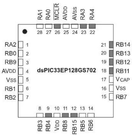
28-Pin SOIC

text_image
MCLR 1 28 AVDD RA0 2 27 AVss RA1 3 26 RA3 RA2 4 25 RA4 RB0 5 24 RB14 RB9 6 23 RB13 AVDD 7 22 RB12 Vss 8 21 RB11 RB1 9 20 VCAP RB2 10 19 Vss RB3 11 18 RB7 RB4 12 17 RB6 VDD 13 16 RB5 RB8 14 15 RB15 dsPIC33EP128GS702| Pin Pin Function Pin Pin Function | |||
| 1 | M C L R | 15 PGEC3/SCL2/RP47/RB15 | |
| 2 | AN0/CMP1A/PGA1P1/RP16/RA0 | 16 | TDO/AN19/PGA2N2/RP37/RB5 |
| 3 | AN1/CMP1B/PGA1P2/PGA2P1/RP17/RA1 | 17 | PGED1/TDI/AN20/SCL1/RP38/RB6 |
| 4 | AN2/CMP1C/CMP2A/PGA1P3/PGA2P2/RP18/RA2 | 18 | PGEC1/AN21/SDA1/RP39/RB7 |
| 5 AN3/CMP1D/CMP2B/PGA2P3/RP32/RB0 | 19 V | SS | |
| 6 | AN4/CMP2C/CMP3A/ISRC4/RP41/RB9 | 20 | VCAP |
| 7 | AVDD | 21 | TMS/PWM3H/RP43/RB11 |
| 8 | Vss | 22 | TCK/PWM3L/RP44/RB12 |
| 9 | OSCI/CLKI/AN6/CMP3C/CMP4A/ISRC2/RP33/RB1 | 23 | PWM2H/RP45/RB13 |
| 10 OSC2/CLKO/AN7/CMP3D/CMP4B/PGA1N2/RP34/RB2 (1) | 24 PWM2L/RP46/RB14 | ||
| 11 | PGED2/DACOUT1/AN18/INT0/RP35/RB3 | 25 | PWM1H/RP20/RA4 |
| 12 | PGEC2/ADTRG31/EXTREF1/RP36/RB4 | 26 | PWM1L/RP19/RA3 |
| 13 | VDD | 27 AVss | |
| 14 | PGED3/SDA2/FLT31/RP40/RB8 | 28 | AVDD |
Legend: Shaded pins are up to 5 VDC tolerant.
RPn represents remappable peripheral functions. See Table 11-12 and Table 11-13 for the complete list of remappable sources.
Note 1: At device power-up (POR), a pulse with an amplitude around 2V and a duration greater than 500 s, may be observed on this device pin independent of pull-down resistors. It is recommended not to use this pin as an output driver unless the circuit being driven can endure this active duration.
Pin Diagrams (Continued)
28-Pin QFN-S, UQFN
text_image
RA1 RA0 MCLR AVDD AVSS RA3 RA4 28 27 26 25 24 23 22 RA2 1 RB0 2 RB9 3 AVDD 4 Vss 5 RB1 6 RB2 7 dsPIC33EP128GS702 21 RB14 20 RB13 19 RB12 18 RB11 17 VCAP 16 VSS 15 RB7 8 9 10 11 12 13 14 RB3 RB4 VDD RB8 RB15 RB5 RB6| Pin Pin Function Pin Pin Function | |||
| 1 | AN2/CMP1C/CMP2A/PGA1P3/PGA2P2/RP18/RA2 | 15 | PGEC1/AN21/SDA1/RP39/RB7 |
| 2 AN | 3/CMP1D/CMP2B/PGA2P3/RP32/RB0 16 V | SS | |
| 3 | AN4/CMP2C/CMP3A/ISRC4/RP41/RB9 | 17 | VCAP |
| 4 | AVDD | 18 | TMS/PWM3H/RP46/RB11 |
| 5 | Vss 19 TCK/PWM3L/RP44/RB12 | ||
| 6 | OSCI/CLKI/AN6/CMP3C/CMP4A/ISRC2/RP33/RB1 | 20 | PWM2H/RP45/RB13 |
| 7 OSC | C2/CLKO/AN7/CMP3D/CMP4B/PGA1N2/RP34/RB2 (1) | 21 P | VM2L/RP46/RB14 |
| 8 | PGED2/DACOUT1/AN18/INT0/RP35/RB3 | 22 | PWM1H/RP20/RA4 |
| 9 | PGEC2/ADTRG31/EXTREF1/RP36/RB4 | 23 | PWM1L/RP19/RA3 |
| 10 | VDD | 24 AVss | |
| 11 | PGED3/SDA2/FLT31/RP40/RB8 | 25 | AVDD |
| 12 PGE C3/SCL2/RP47/RB15 | 26 MCLR | ||
| 13 | TDO/AN19/PGA2N2/RP37/RB5 | 27 | AN0/CMP1A/PGA1P1/RP16/RA0 |
| 14 | PGED1/TDI/AN20/SCL1/RP38/RB6 | 28 | AN1/CMP1B/PGA1P2/PGA2P1/RP17/RA1 |
Legend: Shaded pins are up to 5 VDC tolerant. RPn represents remappable peripheral functions. See Table 11-12 and Table 11-13 for the complete list of remappable sources. Note 1: At device power-up (POR), a pulse with an amplitude around 2V and a duration greater than 500 µs, may be observed on this device pin independent of pull-down resistors. It is recommended not to use this pin as an output driver unless the circuit being driven can endure this active duration.
Pin Diagrams (Continued)
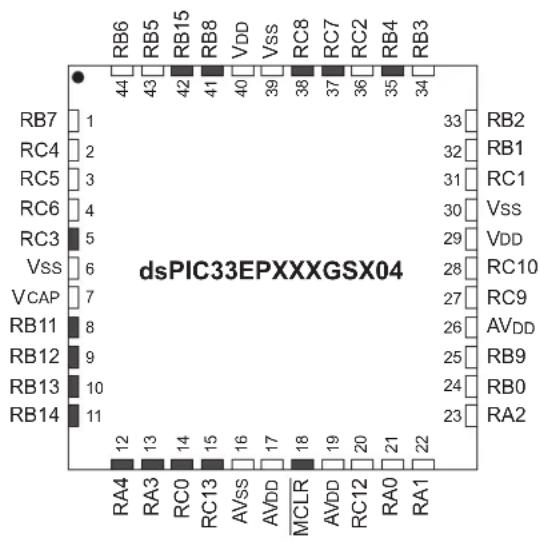
44-Pin QFN, TQFP
geo
| Category | Value | | -------- | ----- | | RB6 | 44 | | RB5 | 43 | | RB15 | 42 | | RB8 | 41 | | VDD | 40 | | VSS | 39 | | RC8 | 38 | | RC7 | 37 | | RC2 | 36 | | RB4 | 35 | | RB3 | 34 | | RB7 | 1 | | RC4 | 2 | | RC5 | 3 | | RC6 | 4 | | RC3 | 5 | | VSS | 6 | | VCAP | 7 | | RB11 | 8 | | RB12 | 9 | | RB13 | 10 | | RB14 | 11 | | RA4 | 12 | | RA3 | 13 | | RC0 | 14 | | RC13 | 15 | | AVSS | 16 | | AVDD | 17 | | MCLR | 18 | | AVDD | 19 | | RC12 | 20 | | RA0 | 21 | | RA1 | 22 | | RB2 | 33 | | RB1 | 32 | | RC1 | 31 | | VSS | 30 | | VDD | 29 | | RC10 | 28 | | RC9 | 27 | | AVDD | 26 | | RB9 | 25 | | RB0 | 24 | | RA2 | 23 || Pin P | n Function Pin Pin Function | ||
| 1 | PGEC1/AN21/SDA1/RP39/RB7 | 23 | AN2/CMP1C/CMP2A/PGA1P3/PGA2P2/RP18/RA2 |
| 2 | AN1ALT/RP52/RC4 | 24 | AN3/CMP1D/CMP2B/PGA2P3/RP32/RB0 |
| 3 | AN0ALT/RP53/RC5 | 25 | AN4/CMP2C/CMP3A/ISRC4/RP41/RB9 |
| 4 | A N 1 7 / RP54/RC6 26 AV | DD | |
| 5 | RP51/RC3 | 27 | AN11/PGA1N3/RP57/RC9 |
| 6 | Vss | 28 | EXTREF2/AN10/PGA1P4/RP58/RC10 |
| 7 | VCAP | 29 VDD | |
| 8 | TMS/PWM3H/RP43/RB11 | 30 | Vss |
| 9 | TCK/PWM3L/RP44/RB12 | 31 | AN8/CMP4C/PGA2P4/RP49/RC1 |
| 10 | PWM2H/RP45/RB13 | 32 | OSCI/CLKI/AN6/CMP3C/CMP4A/ISRC2/RP33/RB1 |
| 11 | PWM2L/RP46/RB14 | 33 | OSC2/CLKO/AN7/CMP3D/CMP4B/PGA1N2/RP34/RB2 ^(1) |
| 12 | PWM1H/RP20/RA4 | 34 | PGED2/DACOUT1/AN18/INT0/RP35/RB3 |
| 13 | PWM1L/RP19/RA3 | 35 | PGEC2/ADTRG31/RP36/RB4 |
| 14 | FLT12/RP48/RC0 | 36 | EXTREF1/AN9/CMP4D/RP50/RC2 |
| 15 | FLT11/RP61/RC13 | 37 | ASDA1/RP55/RC7 |
| 16 AV | SS | 38 | ASCL1/RP56/RC8 |
| 17 AV | DD | 39 Vss | |
| 18 MCLR | 40 VDD | ||
| 19 | AVDD | 41 | PGED3/SDA2/FLT31/RP40/RB8 |
| 20 | AN14/PGA2N3/RP60/RC12 | 42 | PGEC3/SCL2/RP47/RB15 |
| 21 | AN0/CMP1A/PGA1P1/RP16/RA0 | 43 | TDO/AN19/PGA2N2/RP37/RB5 |
| 22 | AN1/CMP1B/PGA1P2/PGA2P1/RP17/RA1 | 44 | PGED1/TDI/AN20/SCL1/RP38/RB6 |
Legend: Shaded pins are up to 5 VDC tolerant.
RPn represents remappable peripheral functions. See Table 11-12 and Table 11-13 for the complete list of remappable sources.
Note 1: At device power-up (POR), a pulse with an amplitude around 2V and a duration greater than 500~ s , may be observed on this device pin independent of pull-down resistors. It is recommended not to use this pin as an output driver unless the circuit being driven can endure this active duration.
Pin Diagrams (Continued)
48-Pin TQFP

text_image
dsPIC33EPXXXGSX05 RB6 RB5 RB15 RB8 RD14 VDD Vss RC8 RC7 RC2 RB4 RB3 RB7 1 36 RB2 RC4 2 35 RB1 RC5 3 34 RC1 RC6 4 33 N/C RC3 5 32 Vss VSS 6 31 VDD VCAP 7 30 RC10 RD4 8 29 RC9 RB11 9 28 AVDD RB12 10 27 RB9 RB13 11 26 RB0 RB14 12 25 RA2 RA4 13 24 RA3 14 RA0 15 RA1 16 AVDD 17 MCLR 18 ACLD 19 RC12 20 RA0 21 AVDD 22 MCLR 23 RA2 24| Pin P | In Function Pin Pin Function | ||
| 1 | PGEC1/AN21/SDA1/RP39/RB7 | 25 | AN2/CMP1C/CMP2A/PGA1P3/PGA2P2/RP18/RA2 |
| 2 | AN1ALT/RP52/RC4 | 26 | AN3/CMP1D/CMP2B/PGA2P3/RP32/RB0 |
| 3 | AN0ALT/RP53/RC5 | 27 | AN4/CMP2C/CMP3A/ISRC4/RP41/RB9 |
| 4 | A N 1 7 / RP54/RC6 28 AV | DD | |
| 5 | RP51/RC3 | 29 | AN11/PGA1N3/RP57/RC9 |
| 6 | Vss 30 EXTREF2/AN10/PGA1P4/RP58/RC10 | ||
| 7 | VCAP 31 VDD | ||
| 8 RP68/RD4 32 Vss | |||
| 9 | T M S / P W M 3 H | / | RP43/RB11 33 N/C |
| 10 | TCK/PWM3L/RP44/RB12 | 34 | AN8/CMP4C/PGA2P4/RP49/RC1 |
| 11 | PWM2H/RP45/RB13 | 35 | OSCI/CLKI/AN6/CMP3C/CMP4A/ISRC2/RP33/RB1 |
| 12 | PWM2L/RP46/RB14 | 36 | OSC2/CLKO/AN7/CMP3D/CMP4B/PGA1N2/RP34/RB2 ^(1) |
| 13 | PWM1H/RP20/RA4 | 37 | PGED2/DACOUT1/AN18/INT0/RP35/RB3 |
| 14 | PWM1L/RP19/RA3 | 38 | PGEC2/ADTRG31/RP36/RB4 |
| 15 | FLT12/RP48/RC0 | 39 | EXTREF1/AN9/CMP4D/RP50/RC2 |
| 16 | FLT11/RP61/RC13 | 40 | ASDA1/RP55/RC7 |
| 17 | CLC4OUT/FLT10/RP74/RD10 | 41 | ASCL1/RP56/RC8 |
| 18 AV | ss 42 Vss | ||
| 19 AVDD | 43 VDD | ||
| 20 MCLR | 44 CLC3OUT/RD14 | ||
| 21 AV DD | 45 | PGED3/SDA2/FLT31/RP40/RB8 | |
| 22 | AN14/PGA2N3/RP60/RC12 | 46 | PGEC3/SCL2/RP47/RB15 |
| 23 | AN0/CMP1A/PGA1P1/RP16/RA0 | 47 | TDO/AN19/PGA2N2/RP37/RB5 |
| 24 | AN1/CMP1B/PGA1P2/PGA2P1/RP17/RA1 | 48 | PGED1/TDI/AN20/SCL1/RP38/RB6 |
Legend: Shaded pins are up to 5 VDC tolerant. RPn represents remappable peripheral functions. See Table 11-12 and Table 11-13 for the complete list of remappable sources. Note 1: At device power-up (POR), a pulse with an amplitude around 2V and a duration greater than 500 s, may be observed on this device pin independent of pull-down resistors. It is recommended not to use this pin as an output driver unless the circuit being driven can endure this active duration.
Pin Diagrams (Continued)
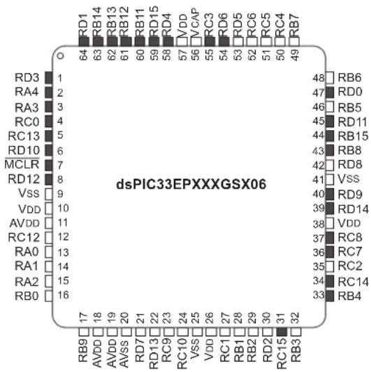
64-Pin TQFP
other
dsPIC33EPXXXGSX06 | Pin | Label | |---|---| | RD1 | 64 | | RB14 | 63 | | RB13 | 62 | | RB12 | 61 | | RB11 | 60 | | RD15 | 59 | | RD4 | 58 | | VDD | 57 | | VCAP | 56 | | RC3 | 55 | | RD6 | 54 | | RD5 | 53 | | RC6 | 52 | | RC5 | 51 | | RC4 | 50 | | RB7 | 49 | | RB6 | 48 | | RD0 | 47 | | RB5 | 46 | | RD11 | 45 | | RB15 | 44 | | RB8 | 43 | | RD8 | 42 | | VSS | 41 | | RD9 | 40 | | RD14 | 39 | | VDD | 38 | | RC8 | 37 | | RC7 | 36 | | RC2 | 35 | | RC15 | 31 | | RB4 | 33 | | RB3 | 32 | | VDD | 17 | | AVDD | 18 | | AVDD | 19 | | AVSS | 20 | | RD7 | 21 | | RD13 | 22 | | RC9 | 23 | | RC10 | 24 | | VSS | 25 | | VDD | 26 | | RB1 | 27 | | RB2 | 28 | | RB2 | 29 | | RD2 | 30 | | RC15 | 31 | RB0 | 16 | RA0 | 13 | RA1 | 14 | RA2 | 15 | VDD | 10 | VDD | 11 | VDD | 12 | VDD | 13 | VDD | 14 | VDD | 16 | VDD | 9 | RCLR | 7 | RD12 | 8 | RD10 | 6 | RC13 | 5 | RC0 | 4 | RA3 | 3 | RA4 | 2 | RD3 | 1 || Pin | Pin Function Pin Pin Function | ||
| 1 | PWM4L/RP67/RD3 | 33 | PGEC2/ADTRG31/RP36/RB4 |
| 2 | PWM1H/RP20/RA4 | 34 | RP62/RC14 |
| 3 | PWM1L/RP19/RA3 | 35 | EXTREF1/AN9/CMP4D/RP50/RC2 |
| 4 | FLT12/RP48/RC0 | 36 | ASDA1/RP55/RC7 |
| 5 | FLT11/RP61/RC13 | 37 | ASCL1/RP56/RC8 |
| 6 | CLC4OUT/FLT10/RP74/RD10 | 38 V | DD |
| 7 | M C L R | 39 CLC3OUT/RD14 | |
| 8 | T5CK/FLT9/RP76/RD12 | 40 | SCK3/RP73/RD9 |
| 9 | Vss | 41 Vss | |
| 10 | VDD | 42 | AN5/CMP2D/CMP3B/ISRC3/RP72RD8 |
| 11 | AVDD | 43 | PGED3/SDA2/FLT31/RP40/RB8 |
| 12 | AN14/PGA2N3/RP60/RC12 | 44 | PGEC3/SCL2/RP47/RB15 |
| 13 | AN0/CMP1A/PGA1P1/RP16/RA0 | 45 | INT4/RP75/RD11 |
| 14 | AN1/CMP1B/PGA1P2/PGA2P1/RP17/RA1 | 46 | TDO/AN19/PGA2N2/RP37/RB5 |
| 15 | AN2/CMP1C/CMP2A/PGA1P3/PGA2P2/RP18/RA2 | 47 | T4CK/RP64/RD0 |
| 16 | AN3/CMP1D/CMP2B/PGA2P3/RP32/RB0 | 48 | PGED1/TDI/AN20/SCL1/RP38/RB6 |
| 17 | AN4/CMP2C/CMP3A/ISRC4/RP41/RB9 | 49 | PGEC1/AN21/SDA1/RP39/RB7 |
| 18 | AVDD | 50 | AN1ALT/RP52/RC4 |
| 19 | AVDD | 51 | AN0ALT/RP53/RC5 |
| 20 | AVss | 52 | AN17/RP54/RC6 |
| 21 | AN15/RP71/RD7 | 53 | AN12/ISRC1/RP69/RD5 |
| 22 | DACOUT2/AN13/RD13 | 54 | PWM5H/RP70/RD6 |
| 23 | AN11/PGA1N3/RP57/RC9 | 55 | PWM5L/RP51/RC3 |
| 24 | EXTREF2/AN10/PGA1P4/RP58/RC10 | 56 | VCAP |
| 25 | Vss | 57 | VDD |
| 26 | VDD | 58 | PWM6H/RP68/RD4 |
| 27 | AN8/CMP4C/PGA2P4/RP49/RC1 | 59 | PWM6L/RD15 |
| 28 | OSCI/CLKI/AN6/CMP3C/CMP4A/ISRC2/RP33/RB1 | 60 | TMS/PWM3H/RP43/RB11 |
| 29 | OSC2/CLKO/AN7/CMP3D/CMP4B/PGA1N2/RP34/RB2 ^(1) | 61 TCK/PWM3L/RP44/RB12 | |
| 30 | AN16/RP66/RD2 | 62 | PWM2H/RP45/RB13 |
| 31 | ASDA2/RP63/RC15 | 63 | PWM2L/RP46/RB14 |
| 32 | PGED2/DACOUT1/AN18/ASCL2/INT0/RP35/RB3 | 64 | PWM4H/RP65/RD1 |
Legend: Shaded pins are up to 5 VDC tolerant.
RPn represents remappable peripheral functions. See Table 11-12 and Table 11-13 for the complete list of remappable sources.
Note 1: At device power-up (POR), a pulse with an amplitude around 2V and a duration greater than 500 s, may be observed on this device pin independent of pull-down resistors. It is recommended not to use this pin as an output driver unless the circuit being driven can endure this active duration.
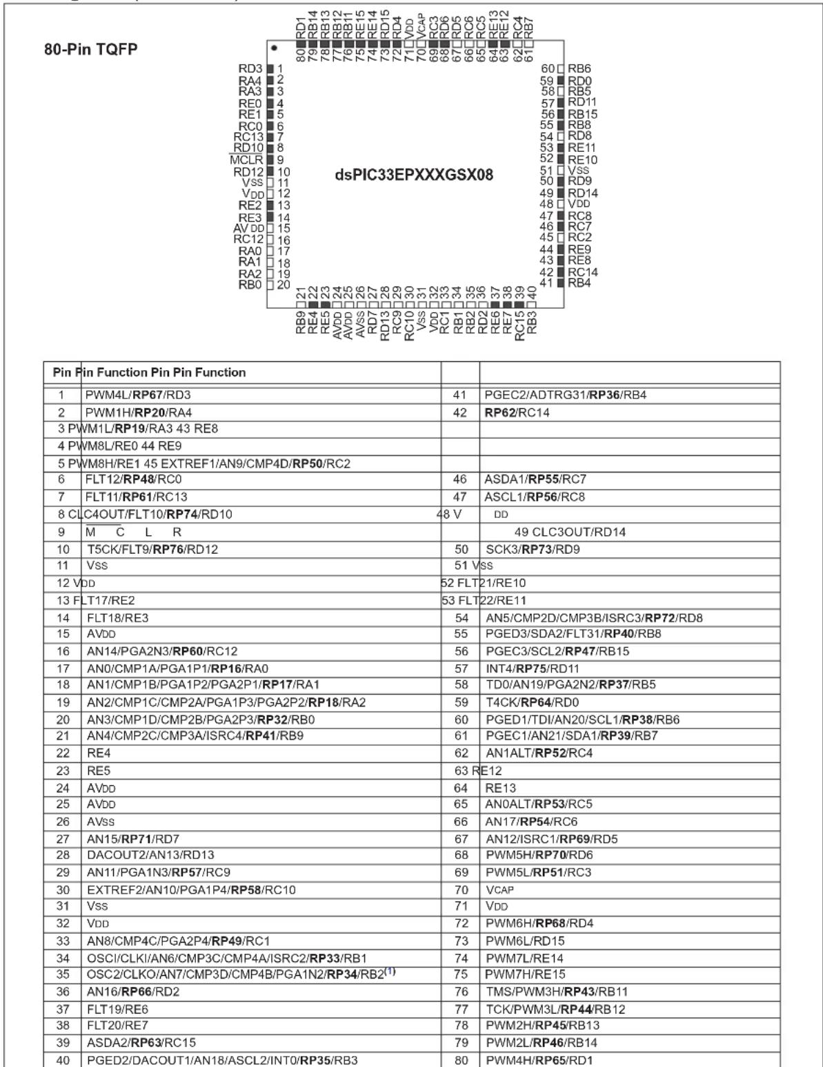
Pin Diagrams (Continued)
other
80-Pin TQFP dsPIC33EPXXXGSX08 Pin Function Pin Pin Function | Pin | Pin Function Pin Pin Function | |---|---| | 1 | PWM4L/RP67/RD3 | | 2 | PWM1H/RP20/RA4 | | 3 | PWM1L/RP19/RA3 43 RE8 | | 4 | PWM8L/RE0 44 RE9 | | 5 | PWM8H/RE1 45 EXTREF1/AN9/CMP4D/RP50/RC2 | | 6 | FLT12/RP48/RC0 | | 7 | FLT11/RP61/RC13 | | 8 | CLC4OUT/FLT10/RP74/RD10 | | 9 | M C L R | | 10 | T5CK/FLT9/RP76/RD12 | | 11 | Vss | | 12 | VDD | | 13 | FLT17/RE2 | | 14 | FLT18/RE3 | | 15 | AVDD | | 16 | AN14/PGA2N3/RP60/RC12 | | 17 | ANO/CMP1A/PGA1P1/RP16/RA0 | | 18 | AN1/CMP1B/PGA1P2/PGA2P1/RP17/RA1 | | 19 | AN2/CMP1C/CMP2A/PGA1P3/PGA2P2/RP18/RA2 | | 20 | AN3/CMP1D/CMP2B/PGA2P3/RP32/RB0 | | 21 | AN4/CMP2C/CMP3A/ISRC4/RP41/RB9 | | 22 | RE4 | | 23 | RE5 | | 24 | AVDD | | 25 | AVDD | | 26 | AVss | | 27 | AN15/RP71/RD7 | | 28 | DACOUT2/AN13/RD13 | | 29 | AN11/PGA1N3/RP57/RC9 | | 30 | EXTREF2/AN10/PGA1P4/RP58/RC10 | | 31 | Vss | | 32 | VDD | | 33 | AN8/CMP4C/PGA2P4/RP49/RC1 | | 34 | OSCI/CLKI/AN6/CMP3C/CMP4A/ISRC2/RP33/RB1 | | 35 | OSC2/CLKO/AN7/CMP3D/CMP4B/PGA1N2/RP34/RB2(1) | | 36 | AN16/RP66/RD2 | | 37 | FLT19/RE6 | | 38 | FLT20/RE7 | | 39 | ASDA2/RP63/RC15 | | 40 | PGED2/DACOUT1/AN18/ASCL2/INT0/RP35/RB3 | | Pin Function Pin Pin Function | Pin Function Pin Pin Function | | :--- | :--- | | 1 | PWM4L/RP67/RD3 | | 2 | PWM1H/RP20/RA4 | | 3 | PWM1L/RP19/RA3 43 RE8 | | 4 | PWM8L/RE0 44 RE9 | | 5 | PWM8H/RE1 45 EXTREF1/AN9/CMP4D/RP50/RC2 | | 7 | FLT12/RP48/RC0 | | 8 | FLT11/RP61/RC13 | | 9 | CLC4OUT/FLT10/RP74/RD10 | | 10 | T5CK/FLT9/RP76/RD12 | | 11 | Vss | | 12 | VDD | | 13 | FLT17/RE2 | | 14 | FLT18/RE3 | | 15 | AVDD | | 16 | AN14/PGA2N3/RP60/RC12 | | 17 | ANO/CNP1A/PGA1P1/RP16/RA0 | | 18 | AN1/CMP1B/PGA1P2/PGA2P1/RP17/RA1 | | 19 | AN2/CMP1C/CMP2A/PGA1P3/PGA2P2/RP18/RA2 | | 20 | AN3/CMP1D/CMP2B/PGA2P3/RP42/RB0 | | 21 | AN4/CMP2C/CMP3A/ISRC4/RP41/RB9 | | 22 | RE4 | | 23 | RE5 | | 24 | AVDD | | 25 | AVDD | | 26 | AVss | | 27 | AN15/RP71/RD7 | | 28 | DACOUT2/AN10/RD3 | | 29 | AN11/PGA1N3/RP57/RC9 | | 30 | EXTREF2/AN10/PGA1P4/RP58/RC10 | | 31 | Vss | | 32 | VDD | | 33 | AN8/CMP4C/PGA2P4/RP49/RC1 | | 34 | OSCI/CLKI/A6/CMP3C/CMP4A/ISRC2/RP33/RB1 | | 35 | OSC2/CLKO/A7/CMP3D/CMP4B/PGA1N2/RP34/BR2(1) | | 36 | AN16/RP66/RD2 | | 37 | FLT19/RE6 | | 38 | FLT20/RE7 | | 39 | ASDA2/RP63/RC15 | | 40 | PGED2/DACOUT1/AN18/ASCL2/INT0/RP35/RB3 | | Pin Function Pin Pin Function (Pin Number) | Pin Function Pin Pin Function (Pin Number) | |---|---| | Pin Function Pin Pin Function (Pin Number) | Pin Function Pin Pin Function (Pin Number) | |---|---| | Pin Function Pin Pin Function (Pin Number) | Pin Function Pin Pin Function (Pin Number) | | | 1 | PWM4L/RP67/RD3 | | 2 | PWM1H/RP20/RA4 | | 3 | PWM8H/RE1 45 EXTREF1/AN9/CMP4D/RP50/RC2 | | 6 | FLT12/RP48/RC0 | | 7 | FLT11/RP66/RC13 | | 8 | CLC4OUT/FLT10/RP74/RD10 | | ---:---:---:---:---:---:---:---:---:---:---:---:---:---:---:---:---:---:---:---:---:---:---:---:---:---:---:---:---:---:---:---:---:---:---:---:---:---:---:---:---:---:---:---:---:---:---:---:---:---:---; **Pin Function Pin Pin Function (Pin Number)Legend: Shaded pins are up to 5 VDC tolerant.
RPn represents remappable peripheral functions. See Table 11-12 and Table 11-13 for the complete list of remappable sources.
Note 1: At device power-up (POR), a pulse with an amplitude around 2V and a duration greater than 500 s, may be observed on this device pin independent of pull-down resistors. It is recommended not to use this pin as an output driver unless the circuit being driven can endure this active duration.
Table of Contents
1.0 Device Overview 13
2.0 Guidelines for Getting Started with 16-Bit Digital Signal Controllers.... 17
3.0 CPU 23
4.0 Memory Organization....33
5.0 Flash Program Memory....63
6.0 Resets 71
7.0 Interrupt Controller 75
8.0 Direct Memory Access (DMA) 91
9.0 Oscillator Configuration....105
10.0 Power-Saving Features.... 117
11.0 I/O Ports 127
12.0 Timer1 171
13.0 Timer2/3 and Timer4/5 175
14.0 Input Capture.... 179
15.0 Output Compare.... 183
16.0 High-Speed PWM 189
17.0 Peripheral Trigger Generator (PTG) Module 217
18.0 Serial Peripheral Interface (SPI) 233
19.0 Inter-Integrated Circuit (I ^2 C) 249
20.0 Universal Asynchronous Receiver Transmitter (UART) 257
21.0 Configurable Logic Cell (CLC) 263
22.0 High-Speed, 12-Bit Analog-to-Digital Converter (ADC).... 277
23.0 Controller Area Network (CAN) Module (dsPIC33EPXXXGS80X Devices Only) 311
24.0 High-Speed Analog Comparator 337
25.0 Programmable Gain Amplifier (PGA) 345
26.0 Constant-Current Source 349
27.0 Special Features 351
28.0 Instruction Set Summary 365
29.0 Development Support 375
30.0 Electrical Characteristics 379
31.0 DC and AC Device Characteristics Graphs 439
32.0 Packaging Information....443
Appendix A: Revision History 469
Index 471
The Microchip Website 479
Customer Change Notification Service 479
Customer Support 479
Product Identification System 481
TO OUR VALUED CUSTOMERS
It is our intention to provide our valued customers with the best documentation possible to ensure successful use of your Microchip products. To this end, we will continue to improve our publications to better suit your needs. Our publications will be refined and enhanced as new volumes and updates are introduced.
If you have any questions or comments regarding this publication, please contact the Marketing Communications Department via E-mail at docerrors@microchip.com. We welcome your feedback.
Most Current Data Sheet
To obtain the most up-to-date version of this data sheet, please register at our Worldwide Website at:
http://www.microchip.com
You can determine the version of a data sheet by examining its literature number found on the bottom outside corner of any page. The last character of the literature number is the version number, (e.g., DS30000000A is version A of document DS30000000).
Errata
An errata sheet, describing minor operational differences from the data sheet and recommended workarounds, may exist for current devices. As device/documentation issues become known to us, we will publish an errata sheet. The errata will specify the revision of silicon and revision of document to which it applies.
To determine if an errata sheet exists for a particular device, please check with one of the following:
- Microchip's Worldwide Website; http://www.microchip.com
- Your local Microchip sales office (see last page)
When contacting a sales office, please specify which device, revision of silicon and data sheet (include literature number) you are using.
Customer Notification System
Register on our website at www.microchip.com to receive the most current information on all of our products.
Referenced Sources
This device data sheet is based on the following individual chapters of the "dsPIC33/PIC24 Family Reference Manual". These documents should be considered as the general reference for the operation of a particular module or device feature.
Note 1: To access the documents listed below, browse to the documentation section of the dsPIC33EPXXXGS70X/80X product page of the Microchip website (www.microchip.com) or select a family reference manual section from the following list.
In addition to parameters, features and other documentation, the resulting page provides links to the related family reference manual sections.
- "dsPIC33E Enhanced CPU" (DS70005158)
- "dsPIC33E/PIC24E Program Memory" (DS70000613)
• "Data Memory" (DS70595) - "Dual Partition Flash Program Memory" (DS70005156)
• “Flash Programming” (DS70609) - "Reset" (DS70602)
- "Interrupts" (DS70000600)
- "Direct Memory Access (DMA)" (DS70348)
• "Oscillator Module" (DS70005131) - "Watchdog Timer and Power-Saving Modes" (DS70615)
• "I/O Ports" (DS70000598)
• “Timers” (DS70362) - "Input Capture with Dedicated Timer" (DS70000352)
- "Output Compare with Dedicated Timer" (DS70005159)
• "High-Speed PWM Module" (DS70000323) - "Peripheral Trigger Generator (PTG)" (DS70000669)
- "Serial Peripheral Interface (SPI) with Audio Codec Support" (DS70005136)
- "Inter-Integrated Circuit (I ^2 C)" (DS70000195)
- “Universal Asynchronous Receiver Transmitter (UART)” (DS70000582)
- "Configurable Logic Cell (CLC)" (DS70005298)
- “12-Bit High-Speed, Multiple SARs A/D Converter (ADC)” (DS70005213)
- “Enhanced Controller Area Network (ECAN™)” (DS70353)
- "High-Speed Analog Comparator Module" (DS70005128)
- "Programmable Gain Amplifier (PGA)" (DS70005146)
- "Device Configuration" (DS70000618)
- "Watchdog Timer and Power-Saving Modes" (DS70615)
- “CodeGuard™ Intermediate Security” (DS70005182)
- "Programming and Diagnostics" (DS70608)
NOTES:
1.0 DEVICE OVERVIEW
Note 1: This data sheet summarizes the features of the dsPIC33EPXXXGS70X/80X family of devices. It is not intended to be a comprehensive resource. To complement the information in this data sheet, refer to the related section of the "dsPIC33/PIC24 Family Reference Manual", which is available from the Microchip website (www.microchip.com).
2: Some registers and associated bits described in this section may not be available on all devices. Refer to Section 4.0 "Memory Organization" in this data sheet for device-specific register and bit information.
This document contains device-specific information for the dsPIC33EPXXXGS70X/80X Digital Signal Controller (DSC) devices.
dsPIC33EPXXXGS70X/80X devices contain extensive Digital Signal Processor (DSP) functionality with a high-performance, 16-bit MCU architecture.
Figure 1-1 shows a general block diagram of the core and peripheral modules. Table 1-1 lists the functions of the various pins shown in the pinout diagrams.
FIGURE 1-1: dsPIC33EPXXXGS70X/80X FAMILY BLOCK DIAGRAM

flowchart
graph TD
    A["Peripheral Modules"] --> B["Peripherals"]
    B --> C["OSC1/CLKI"]
    B --> D["CAN Modules 1-2"]
    B --> E["PTG"]
    B --> F["ADC"]
    B --> G["Input Captures"]
    B --> H["Output Compares 1-41-4"]
    B --> I["I2C1, I2C2"]
    B --> J["Constant Current Source"]
    B --> K["CLC 1-4"]
    B --> L["Analog Comparators 1-4"]
    B --> M["PWMs 8x2"]
    B --> N["Timers 1-5"]
    B --> O["SPI1-3"]
    B --> P["UART1, UART2"]
    B --> Q["PortA"]
    B --> R["PORTB"]
    B --> S["PORTC"]
    B --> T["PORTD"]
    B --> U["PORTE"]
    B --> V["Remappable Pins"]
    A --> W["Power-up Timer"]
    A --> X["Oscillator Start-up Timer"]
    A --> Y["POR/BOR"]
    A --> Z["Watchdog Timer"]
    W <--> AA["Timing Generation"]
    X <--> AB["MCLR"]
    Y <--> AC["VDD, Vss AVdd, AVss"]
    AA <--> AD["PortA"]
    AB <--> AE["PORTB"]
    AC <--> AF["PORTC"]
    AD <--> AG["PORTD"]
    AE <--> AH["PORTE"]
    AF <--> AI["Remappable Pins"]
    AG <--> AJ["PortA"]
    AH <--> AK["PORTB"]
    AI <--> AL["PORTC"]
    AJ <--> AM["PORTD"]
    AK <--> AN["PORTE"]
    AL <--> AO["Remappable Pins"]
    AM <--> AP["PortA"]
TABLE 1-1: PINOUT I/O DESCRIPTIONS
| Pin Name(1) | Pin Type | Buffer Type | PPS | Description |
| AN0-AN21 | I | Analog | No | Analog input channels. |
| AN0ALT-AN1ALT | I | Analog | No | Alternate analog input channels. |
| C1RXR | I | ST | Yes | CAN1 receive. |
| C2RXR | I | ST | Yes | CAN2 receive. |
| C1TX | O | ST | Yes | CAN1 transmit. |
| C2TX | O | ST | Yes | CAN2 transmit. |
| CLKI | I | ST/CMOS | No | External clock source input. Always associated with OSC1 pin function. |
| CLKO | O | — | No | Oscillator crystal output. Connects to crystal or resonator in Crystal Oscillator mode. Optionally functions as CLKO in RC and EC modes. Always associated with OSC2 pin function. |
| OSC1 | I | ST/CMOS | No | Oscillator crystal input. ST buffer when configured in RC mode; CMOS otherwise. |
| OSC2 | I/O | — | No | Oscillator crystal output. Connects to crystal or resonator in Crystal Oscillator mode. Optionally functions as CLKO in RC and EC modes. |
| CLC1OUT | O | DIG | Yes | CLC1 output. |
| CLC2OUT | O | DIG | Yes | CLC2 output. |
| CLC3OUT | O | DIG | No^(4) | CLC3 output. |
| CLC4OUT | O | DIG | No^(4) | CLC4 output. |
| REFCLKO O — Yes Reference clock output. | ||||
| IC1-IC4 I ST Yes Capture Inputs 1 through 4 | ||||
| OCFA | I | ST | Yes | Compare Fault A input (for compare channels). |
| OC1-OC4 | O | — | Yes | Compare Outputs 1 through 4. |
| INT0 | I | ST | No | External Interrupt 0. |
| INT1 | I | ST | Yes | External Interrupt 1. |
| INT2 | I | ST | Yes | External Interrupt 2. |
| INT4 | I | ST | Yes | External Interrupt 4. |
| RA0-RA4 I/O ST No | PORTA is a bidirectional I/O port. | |||
| RB0-RB15 | I/O T No | PORTB | is a bidirectional I/O port. | |
| RC0-RC15 | I/OT No | PORTC | is a bidirectional I/O port. | |
| RD0-RD15 | I/O T No | PORTD | is a bidirectional I/O port. | |
| RE0-RE15 | I/OT No | PORTE | is a bidirectional I/O port. | |
| T1CK | I | ST | Yes | Timer1 external clock input. |
| T2CK | I | ST | Yes | Timer2 external clock input. |
| T3CK | I | ST | Yes | Timer3 external clock input. |
| T4CK | I | ST | No | Timer4 external clock input. |
| T5CK | I | ST | No | Timer5 external clock input. |
| U1CTS | I | ST | Yes | UART1 Clear-to-Send. |
| U1RTS | O | — | Yes | UART1 Ready-to-Send. |
| U1RX | I | ST | Yes | UART1 receive. |
| U1TX | O | — | Yes | UART1 transmit. |
| BCLK1 | O | ST | Yes | UART1 IrDA® baud clock output. |
Legend: CMOS = CMOS compatible input or output ST = Schmitt Trigger input with CMOS levels PPS = Peripheral Pin Select
Analog = Analog input O = Output
P = Power
I = Input
1: Not all pins are available in all package variants. See the "Pin Diagrams" section for pin availability.
2: PWM4H/L through PWM8H/L are fixed on dsPIC33EPXXXGS708/808 devices. PWM4H/L through PWM6H/L are fixed on dsPIC33EPXXXGS706/806 devices.
3: The SCK3 pin is fixed on dsPIC33EPXXXGS706/806 and dsPIC33EPXXXGS708/808 devices.
4: PPS is available on dsPIC33EPXXXGS702 devices only.
TABLE 1-1: PINOUT I/O DESCRIPTIONS (CONTINUED)
| Pin Name(1) | Pin Type | Buffer Type | PPS | Description |
| U2CTS | I | ST | Yes | UART2 Clear-to-Send. |
| U2RTS | O | — | Yes | UART2 Ready-to-Send. |
| U2RX | I | ST | Yes | UART2 receive. |
| U2TX | O | — | Yes | UART2 transmit. |
| BCLK2 | O | ST | Yes | UART2 IrDA baud clock output. |
| SCK1 | I/O | ST | Yes | Synchronous serial clock input/output for SPI1. |
| SDI1 | I | ST | Yes | SPI1 data in. |
| SDO1 | O | — | Yes | SPI1 data out. |
| SS1 | I/O | ST | Yes | SPI1 slave synchronization or frame pulse I/O. |
| SCK2 | I/O | ST | Yes | Synchronous serial clock input/output for SPI2. |
| SDI2 | I | ST | Yes | SPI2 data in. |
| SDO2 | O | — | Yes | SPI2 data out. |
| SS2 | I/O | ST | Yes | SPI2 slave synchronization or frame pulse I/O. |
| SCK3 | I/O | ST | Yes(3) | Synchronous serial clock input/output for SPI3. |
| SDI3 | I | ST | Yes | SPI3 data in. |
| SDO3 | O | — | Yes | SPI3 data out. |
| SS3 | I/O | ST | Yes | SPI3 slave synchronization or frame pulse I/O. |
| SCL1 | I/O | ST | No | Synchronous serial clock input/output for I2C1. |
| SDA1 | I/O | ST | No | Synchronous serial data input/output for I2C1. |
| ASCL1 | I/O | ST | No | Alternate synchronous serial clock input/output for I2C1. |
| ASDA1 | I/O | ST | No | Alternate synchronous serial data input/output for I2C1. |
| SCL2 | I/O | ST | No | Synchronous serial clock input/output for I2C2. |
| SDA2 | I/O | ST | No | Synchronous serial data input/output for I2C2. |
| ASCL2 | I/O | ST | No | Alternate synchronous serial clock input/output for I2C2. |
| ASDA2 | I/O | ST | No | Alternate synchronous serial data input/output for I2C2. |
| TMS | I | ST | No | JTAG Test mode select pin. |
| TCK | I | ST | No | JTAG test clock input pin. |
| TDI | I | ST | No | JTAG test data input pin. |
| TDO | O | — | No | JTAG test data output pin. |
| FLT1-FLT8 | I | ST | Yes | PWM Fault Inputs 1 through 8. |
| FLT9-FLT12 | I | ST | No | PWM Fault Inputs 9 through 12. |
| FLT17-FLT22 | I | ST | No | PWM Fault Inputs 17 through 22. |
| FLT31 | I | ST | No | PWM Fault Input 31 (Class B Fault). |
| PWM1L-PWM3L | O | — | No | PWM Low Outputs 1 through 3. |
| PWM1H-PWM3H | O | — | No | PWM High Outputs 1 through 3. |
| PWM4L-PWM8L(2) | O | — | Yes | PWM Low Outputs 4 through 8. |
| PWM4H-PWM8H(2) | O | — | Yes | PWM High Outputs 4 through 8. |
| SYNC11, SYNCI2 | I | ST | Yes | PWM Synchronization Inputs 1 and 2. |
| SYNCO1, SYNCO2 | O | — | Yes | PWM Synchronization Outputs 1 and 2. |
Legend: CMOS = CMOS compatible input or output Analog = Analog input P = Power
ST = Schmitt Trigger input with CMOS levels O = Output I = Input
PPS = Peripheral Pin Select
1: Not all pins are available in all package variants. See the "Pin Diagrams" section for pin availability.
2: PWM4H/L through PWM8H/L are fixed on dsPIC33EPXXXGS708/808 devices. PWM4H/L through PWM6H/L are fixed on dsPIC33EPXXXGS706/806 devices.
3: The SCK3 pin is fixed on dsPIC33EPXXXGS706/806 and dsPIC33EPXXXGS708/808 devices.
4: PPS is available on dsPIC33EPXXXGS702 devices only.
TABLE 1-1: PINOUT I/O DESCRIPTIONS (CONTINUED)
| Pin Name(1) | Pin Type | Buffer Type | PPS | Description |
| CMP1A-CMP4A | I | Analog | No | Comparator Channels 1A through 4A inputs. |
| CMP1B-CMP4B | I | Analog | No | Comparator Channels 1B through 4B inputs. |
| CMP1C-CMP4C | I | Analog | No | Comparator Channels 1C through 4C inputs. |
| CMP1D-CMP4D | I | Analog | No | Comparator Channels 1D through 4D inputs. |
| ACMP1-ACMP4 O — Yes Analog Comparator Outputs 1-4. | ||||
| DACOUT1, DACOUT2 | O — No DAC Output Voltages 1 and 2. | |||
| EXTREF1, EXTREF2 I Analog No External Voltage Reference Inputs 1 and 2 for the Reference DACs. | ||||
| PGA1P1-PGA1P4 I Analog No PGA1 Positive Inputs 1 through 4. | ||||
| PGA1N1-PGA1N3 I Analog No PGA1 Negative Inputs 1 through 3. | ||||
| PGA2P1-PGA2P4 I Analog No PGA2 Positive Inputs 1 through 4. | ||||
| PGA2N1-PGA2N3 I Analog No PGA2 Negative Inputs 1 through 3. | ||||
| ADTRG31 I ST No External ADC trigger source. | ||||
| PGED1 | I/O | ST | No | Data I/O pin for Programming/Debugging Communication Channel 1. |
| PGEC1 | I | ST | No | Clock input pin for Programming/Debugging Communication Channel 1. |
| PGED2 | I/O | ST | No | Data I/O pin for Programming/Debugging Communication Channel 2. |
| PGEC2 | I | ST | No | Clock input pin for Programming/Debugging Communication Channel 2. |
| PGED3 | I/O | ST | No | Data I/O pin for Programming/Debugging Communication Channel 3. |
| PGEC3 | I | ST | No | Clock input pin for Programming/Debugging Communication Channel 3. |
| MCLR | I/P | ST | No | Master Clear (Reset) input. This pin is an active-low Reset to the device. |
| AVDD | P | P | No | Positive supply for analog modules. This pin must be connected at all times. |
| AVss | P | P | No | Ground reference for analog modules. This pin must be connected at all times. |
| VDD | P | — | No | Positive supply for peripheral logic and I/O pins. |
| VCAP | P | — | No | CPU logic filter capacitor connection. |
| Vss | P | — | No | Ground reference for logic and I/O pins. |
Legend: CMOS = CMOS compatible input or output Analog = Analog input P = Power
ST = Schmitt Trigger input with CMOS levels O = Output I = Input
PPS = Peripheral Pin Select
1: Not all pins are available in all package variants. See the "Pin Diagrams" section for pin availability.
2: PWM4H/L through PWM8H/L are fixed on dsPIC33EPXXXGS708/808 devices. PWM4H/L through PWM6H/L are fixed on dsPIC33EPXXXGS706/806 devices.
3: The SCK3 pin is fixed on dsPIC33EPXXXGS706/806 and dsPIC33EPXXXGS708/808 devices.
4: PPS is available on dsPIC33EPXXXGS702 devices only.
2.0 GUIDELINES FOR GETTING STARTED WITH 16-BIT DIGITAL SIGNAL CONTROLLERS
Note 1: This data sheet summarizes the features of the dsPIC33EPXXXGS70X/80X family of devices. It is not intended to be a comprehensive reference source. To complement the information in this data sheet, refer to the related section of the "dsPIC33/PIC24 Family Reference Manual", which is available from the Microchip website (www.microchip.com).
2: Some registers and associated bits described in this section may not be available on all devices. Refer to Section 4.0 "Memory Organization" in this data sheet for device-specific register and bit information.
2.1 Basic Connection Requirements
Getting started with the dsPIC33EPXXXGS70X/80X family requires attention to a minimal set of device pin connections before proceeding with development. The following is a list of pin names which must always be connected:
• A I D and Vss pins
(see Section 2.2 "Decoupling Capacitors")
• A I I da and AVss pins
regardless if ADC module is not used (see Section 2.2 "Decoupling Capacitors")
- VCAP
(see Section 2.3 "CPU Logic Filter Capacitor Connection (VCAP)")
- M C L R pin
(see Section 2.4 "Master Clear (MCLR) Pin")
- PGECx/PGEDx pins used for In-Circuit Serial Programming™ (ICSP™) and debugging purposes (see Section 2.5 "ICSP Pins")
- OSC1 and OSC2 pins when external oscillator source is used (see Section 2.6 "External Oscillator Pins")
2.2 Decoupling Capacitors
The use of decoupling capacitors on every pair of power supply pins, such as VDD, Vss, AVDD and AVss is required.
Consider the following criteria when using decoupling capacitors:
- Value and type of capacitor: Recommendation of 0.1 F (100 nF), 10-20V. This capacitor should be a low-ESR and have resonance frequency in the range of 20 MHz and higher. It is recommended to use ceramic capacitors.
- Placement on the printed circuit board: The decoupling capacitors should be placed as close to the pins as possible. It is recommended to place the capacitors on the same side of the board as the device. If space is constricted, the capacitor can be placed on another layer on the PCB using a via; however, ensure that the trace length from the pin to the capacitor is within one-quarter inch (6 mm) in length.
- Handling high-frequency noise: If the board is experiencing high-frequency noise, above tens of MHz, add a second ceramic-type capacitor in parallel to the above described decoupling capacitor. The value of the second capacitor can be in the range of 0.01 F to 0.001 F . Place this second capacitor next to the primary decoupling capacitor. In high-speed circuit designs, consider implementing a decade pair of capacitances as close to the power and ground pins as possible. For example, 0.1 F in parallel with 0.001 F .
- Maximizing performance: On the board layout from the power supply circuit, run the power and return traces to the decoupling capacitors first, and then to the device pins. This ensures that the decoupling capacitors are first in the power chain. Equally important is to keep the trace length between the capacitor and the power pins to a minimum, thereby reducing PCB track inductance.
FIGURE 2-1: RECOMMENDED MINIMUM CONNECTION

text_image
VDD R R1 C 10 µF Tantalum VCAP MCLR dsPIC33EP 0.1 µF Ceramic VDD VSS VSS VSS VSS 0.1 µF Ceramic 0.1 µF Ceramic AVDD AVSS VDD VSS 0.1 µF Ceramic L1(1)Note 1: As an option, instead of a hard-wired connection, an inductor (L1) can be substituted between VDD and AVDD to improve ADC noise rejection. The inductor impedance should be less than 1 and the inductor capacity greater than 10 mA.
Where:
$$ f \quad \frac {F C N V}{2} = \quad (\text { i.e., ADC Conversion Rate } / 2) $$
$$ f = \frac {1}{(2 \pi \sqrt {L C})} $$
$$ L = \left(\frac {1}{(2 \pi f \sqrt {C})}\right) ^ {2} $$
2.2.1 TANK CAPACITORS
On boards with power traces running longer than six inches in length, it is suggested to use a tank capacitor for integrated circuits, including DSCs, to supply a local power source. The value of the tank capacitor should be determined based on the trace resistance that connects the power supply source to the device and the maximum current drawn by the device in the application. In other words, select the tank capacitor so that it meets the acceptable voltage sag at the device. Typical values range from 4.7 F to 47 F.
2.3 CPU Logic Filter Capacitor Connection (VCAP)
A low-ESR (< 0.5Ω) capacitor is required on the VCAP pin, which is used to stabilize the voltage regulator output voltage. The VCAP pin must not be connected to VDD and must have a capacitor greater than 4.7 μF (10 μF is recommended), 16V connected to ground. The type can be ceramic or tantalum. See Section 30.0 "Electrical Characteristics" for additional information.
The placement of this capacitor should be close to the VCAP pin. It is recommended that the trace length not exceed one-quarter inch (6 mm). See Section 27.4 "On-Chip Voltage Regulator" for details.
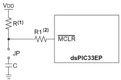
2.4 Master Clear (MCLR) Pin
The MCLR pin provides two specific device functions:
- Device Reset
• Device Programming and Debugging.
During device programming and debugging, the resistance and capacitance that can be added to the pin must be considered. Device programmers and debuggers drive the MCLR pin. Consequently, specific voltage levels (MH and VIL) and fast signal transitions must not be adversely affected. Therefore, specific values of R and C will need to be adjusted based on the application and PCB requirements.
For example, as shown in Figure 2-2, it is recommended that the capacitor, C, be isolated from the MCLR pin during programming and debugging operations.
Place the components as shown in Figure 2-2, within one-quarter inch (6 mm) from the MCLR pin.
FIGURE 2-2: EXAMPLE OF MCLR PIN CONNECTIONS
text_image
VDD R(1) R1(2) JP C MCLR dsPIC33EPNote 1: R ≤ 10 k is recommended. A suggested starting value is 10 k . Ensure that the MCLR pin VIH and VIL specifications are met.
2: R1 ≤ 470Ω will limit any current flowing into MCLR from the external capacitor, C, in the event of MCLR pin breakdown due to Electrostatic Discharge (ESD) or Electrical Overstress (EOS). Ensure that the MCLR pin VIH and VIL specifications are met.
2.5 ICSP Pins
The PGECx and PGEDx pins are used for ICSP and debugging purposes. It is recommended to keep the trace length between the ICSP connector and the ICSP pins on the device as short as possible. If the ICSP connector is expected to experience an ESD event, a series resistor is recommended, with the value in the range of a few tens of Ohms, not to exceed 100 Ohms.
Pull-up resistors, series diodes and capacitors on the PGECx and PGEDx pins are not recommended as they will interfere with the programmer/debugger communications to the device. If such discrete components are an application requirement, they should be removed from the circuit during programming and debugging. Alternatively, refer to the AC/DC characteristics and timing requirements information in the respective device Flash programming specification for information on capacitive loading limits and pin Voltage Input High (VIH) and Voltage Input Low (VIL) requirements.
Ensure that the "Communication Channel Select" (i.e., PGECx/PGEDx pins) programmed into the device matches the physical connections for the ICSP to MPLAB ^ PICkit ^TM 3, MPLAB ICD 3, or MPLAB REAL ICE ^TM .
For more information on MPLAB ICD 2, MPLAB ICD 3 and REAL ICE connection requirements, refer to the following documents that are available on the Microchip website.
- "Using MPLAB ^ ICD 3 In-Circuit Debugger" (poster) (DS51765)
- "Development Tools Design Advisory" (DS51764)
- "MPLAB ^ REAL ICE ^TM In-Circuit Emulator User's Guide for MPLAB X IDE" (DS50002085)
- "Using MPLAB ^ REAL ICE ^TM In-Circuit Emulator" (poster) (DS51749)
2.6 External Oscillator Pins
Many DSCs have options for at least two oscillators: a high-frequency primary oscillator and a low-frequency secondary oscillator. For details, see Section 9.0 "Oscillator Configuration" for details.
The oscillator circuit should be placed on the same side of the board as the device. Also, place the oscillator circuit close to the respective oscillator pins, not exceeding one-half inch (12 mm) distance between them. The load capacitors should be placed next to the oscillator itself, on the same side of the board. Use a grounded copper pour around the oscillator circuit to isolate them from surrounding circuits. The grounded copper pour should be routed directly to the MCU ground. Do not run any signal traces or power traces inside the ground pour. Also, if using a two-sided board, avoid any traces on the other side of the board where the crystal is placed. A suggested layout is shown in Figure 2-3.
FIGURE 2-3: SUGGESTED PLACEMENT OF THE OSCILLATOR CIRCUIT
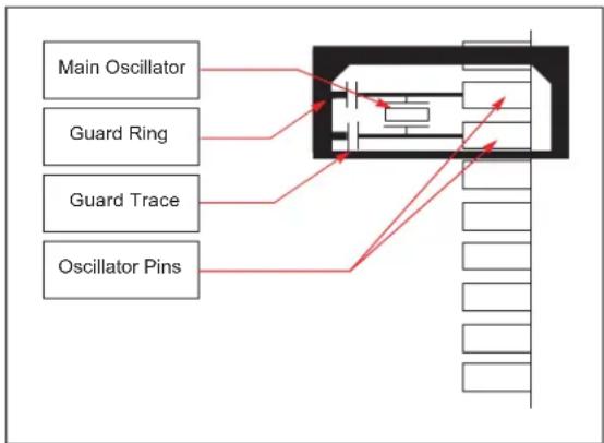
text_image
Main Oscillator Guard Ring Guard Trace Oscillator Pins2.7 Oscillator Value Conditions on Device Start-up
If the PLL of the target device is enabled and configured for the device start-up oscillator, the maximum oscillator source frequency must be limited to 3 MHz < FIN < 5.5 MHz to comply with device PLL start-up conditions. This means that if the external oscillator frequency is outside this range, the application must start up in the FRC mode first. The default PLL settings, after a POR with an oscillator frequency outside this range, will violate the device operating speed.
Once the device powers up, the application firmware can initialize the PLL SFRs, CLKDIV and PLLFBD, to a suitable value, and then perform a clock switch to the Oscillator + PLL clock source. Note that clock switching must be enabled in the device Configuration Word.
2.8 Unused I/Os
Unused I/O pins should be configured as outputs and driven to a logic low state.
Alternatively, connect a 1k to 10k resistor between Vs and unused pins, and drive the output to logic low.
2.9 Targeted Applications
• Power Factor Correction (PFC)
- Interleaved PFC
- Critical Conduction PFC
- Bridgeless PFC
- DC/DC Converters
- Buck, Boost, Forward, Flyback, Push-Pull
- Half/Full-Bridge
- Phase-Shift Full-Bridge
- Resonant Converters
- DC/AC
- Half/Full-Bridge Inverter
- Resonant Inverter
Examples of typical application connections are shown in Figure 2-4 through Figure 2-6.
FIGURE 2-4: INTERLEAVED PFC

flowchart
graph TD
    A["PGA/ADC Channel"] --> B["ADC Channel"]
    B --> C["dsPIC33EPXXXGS70X/80X"]
    D["VOUT+"] --> E["Diode"]
    E --> F["k1"]
    E --> G["k2"]
    E --> H["k3"]
    F --> I["FET Driver"]
    G --> J["FET Driver"]
    H --> K["VOUT-"]
    I --> L["PGA/ADC Channel"]
    J --> M["PGA/ADC Channel"]
    K --> N["VOUT-"]
    L --> O["+"]
    M --> P["-"]
    N --> Q["~"]
    O --> R["~"]
    P --> S["~"]
    Q --> T["~"]
    R --> U["~"]
    S --> V["~"]
    T --> W["~"]
    U --> X["~"]
    V --> Y["~"]
    W --> Z["~"]
    X --> AA["~"]
    Y --> AB["~"]
FIGURE 2-5: PHASE-SHIFTED FULL-BRIDGE CONVERTER
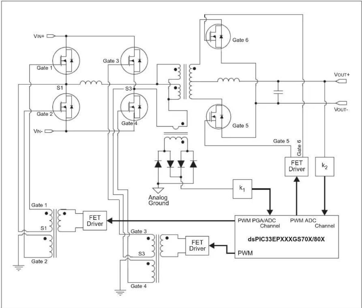
flowchart
graph TD
    A["Gate 1"] --> B["S1"]
    C["Gate 2"] --> D["S1"]
    E["Gate 3"] --> F["S3"]
    G["Gate 4"] --> H["S3"]
    I["Gate 5"] --> J["S3"]
    K["Gate 6"] --> L["S3"]
    M["VOUT+"] --> N["Gate 6"]
    O["VOUT-"] --> P["Gate 6"]
    Q["Analog Ground"] --> R["FET Driver"]
    S["FET Driver"] --> T["dsPIC33EPXXXGS70X/80X"]
    U["PWM"] --> V["FET Driver"]
    W["PWM"] --> X["FET Driver"]
    Y["PWM"] --> Z["FET Driver"]
    AA["PWM"] --> AB["FET Driver"]
    AC["PWM"] --> AD["FET Driver"]
    AE["PWM"] --> AF["FET Driver"]
    AG["k1"] --> AH["PWM PGA/ADC Channel"]
    AH --> AI["PWM ADC Channel"]
    AJ["Gate 5"] --> AK["FET Driver"]
    AL["Gate 6"] --> AM["FET Driver"]
    AN["Gate 1"] --> AO["FET Driver"]
    AP["Gate 2"] --> AQ["FET Driver"]
FIGURE 2-6: OFF-LINE UPS
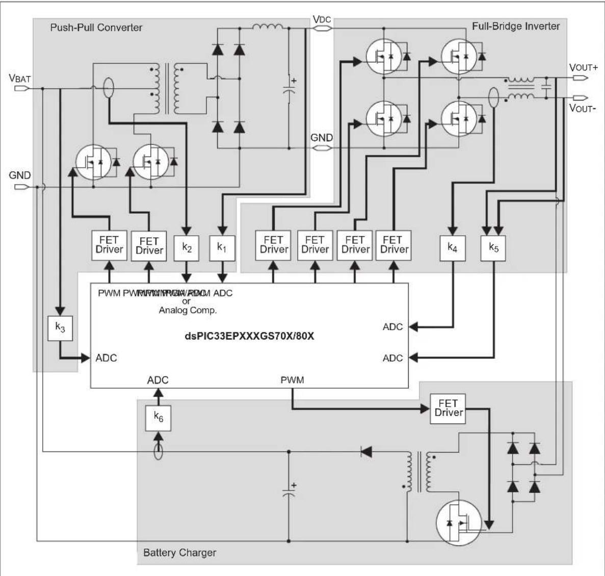
flowchart
graph TD
    subgraph Push-Pull Converter
        VBAT --> A["Transformer"]
        GND --> B["Switch"]
        A --> C["Resistor"]
        B --> D["Resistor"]
        C --> E["Full-Bridge Inverter"]
        D --> E
    end

    subgraph Full-Bridge Inverter
        VOUT+ --> E
        VOUT- --> E
    end

    subgraph PWM / PWMout/ROM ADC or Analog Comp.
            PWM --> K2
        PWM --> K1
        PWM --> K4
        PWM --> K5
    end

    subgraph dsPIC33EPXXXGS70X/80X
            ADC --> K3
        ADC --> K6
    end

    subgraph Battery Charger
            ADC --> K6
        ADC --> FETDriver
        FETDriver --> FETDriver
        FETDriver --> FETDriver
        FETDriver --> FETDriver
        FETDriver --> FETDriver
        FETDriver --> FETDriver
        FETDriver --> FETDriver
    end

    style Push-Pull Converter fill:#f9f,stroke:#333
    style Full-Bridge Inverter fill:#ccf,stroke:#333
    style dsPIC33EPXXXGS70X/80X fill:#cfc,stroke:#333
3.0 CPU
Note 1: This data sheet summarizes the features of the dsPIC33EPXXXGS70X/80X family of devices. It is not intended to be a comprehensive reference source. To complement the information in this data sheet, refer to “dsPIC33E Enhanced CPU” (DS70005158) in the “dsPIC33/PIC24 Family Reference Manual”, which is available from the Microchip website (www.microchip.com).
2: Some registers and associated bits described in this section may not be available on all devices. Refer to Section 4.0 "Memory Organization" in this data sheet for device-specific register and bit information.
The dsPIC33EPXXXGS70X/80X family CPU has a 16-bit (data) modified Harvard architecture with an enhanced instruction set, including significant support for Digital Signal Processing (DSP). The CPU has a 24-bit instruction word with a variable length opcode field. The Program Counter (PC) is 23 bits wide and addresses up to 4M x 24 bits of user program memory space.
An instruction prefetch mechanism helps maintain throughput and provides predictable execution. Most instructions execute in a single-cycle effective execution rate, with the exception of instructions that change the program flow, the double-word move (MOV.D) instruction, PSV accesses and the table instructions. Overhead-free program loop constructs are supported using the DO and REPEAT instructions, both of which are interruptible at any point.
3.1 Registers
The dsPIC33EPXXXGS70X/80X devices have sixteen, 16-bit Working registers in the programmer's model. Each of the Working registers can act as a Data, Address or Address Offset register. The 16th Working register (W15) operates as a Software Stack Pointer for interrupts and calls.
In addition, the dsPIC33EPXXXGS70X/80X devices include four Alternate Working register sets which consist of W0 through W14. The Alternate Working registers can be made persistent to help reduce the saving and restoring of register content during Interrupt Service Routines (ISRs). The Alternate Working registers can be assigned to a specific Interrupt Priority Level (IPL1 through IPL7) by configuring the CTXTx<2:0> bits in the FALTREG Configuration register. The Alternate Working registers can also be accessed manually by using the CTXTSWP instruction. The CCTXI<2:0> and MCTXI<2:0> bits in the CTXTSTAT register can be used to identify the current, and most recent, manually selected Working register sets.
3.2 Instruction Set
The instruction set for dsPIC33EPXXXGS70X/80X devices has two classes of instructions: the MCU class of instructions and the DSP class of instructions. These two instruction classes are seamlessly integrated into the architecture and execute from a single execution unit. The instruction set includes many addressing modes and was designed for optimum C compiler efficiency.
3.3 Data Space Addressing
The base Data Space can be addressed as up to 4K words or 8 Kbytes, and is split into two blocks, referred to as X and Y data memory. Each memory block has its own independent Address Generation Unit (AGU). The MCU class of instructions operates solely through the X memory AGU, which accesses the entire memory map as one linear Data Space. Certain DSP instructions operate through the X and Y AGUs to support dual operand reads, which splits the data address space into two parts. The X and Y Data Space boundary is device-specific.
The upper 32 Kbytes of the Data Space memory map can optionally be mapped into Program Space (PS) at any 16K program word boundary. The program-to-Data Space mapping feature, known as Program Space Visibility (PSV), lets any instruction access Program Space as if it were Data Space. Refer to "Data Memory" (DS70595) in the "dsPIC33/PIC24 Family Reference Manual" for more details on PSV and table accesses.
On dsPIC33EPXXXGS70X/80X devices, overhead-free circular buffers (Modulo Addressing) are supported in both X and Y address spaces. The Modulo Addressing removes the software boundary checking overhead for DSP algorithms. The X AGU Circular Addressing can be used with any of the MCU class of instructions. The X AGU also supports Bit-Reversed Addressing to greatly simplify input or output data re-ordering for radix-2 FFT algorithms.
3.4 Addressing Modes
The CPU supports these addressing modes:
- Inherent (no operand)
- Relative
- Literal
- Memory Direct
- Register Direct
- Register Indirect
Each instruction is associated with a predefined addressing mode group, depending upon its functional requirements. As many as six addressing modes are supported for each instruction.
FIGURE 3-1: dsPIC33EPXXXGS70X/80X FAMILY CPU BLOCK DIAGRAM

flowchart
graph TD
    A["X Address Bus"] --> B["Interrupt Controller"]
    A --> C["PSV and Table Data Access Control Block"]
    A --> D["PCU PCH PCL Program Counter"]
    A --> E["Y Data Bus"]
    A --> F["X Data Bus"]
    B --> G["Address Latch"]
    C --> H["Program Memory"]
    C --> I["Data Latch"]
    D --> J["Stack Control Logic"]
    D --> K["Loop Control Logic"]
    E --> L["Y Data RAM"]
    E --> M["Address Latch"]
    F --> N["X Data RAM"]
    F --> O["Address Latch"]
    F --> P["X RAGU X WAGU"]
    F --> Q["Y Data Bus"]
    F --> R["Y AGU"]
    F --> S["EA MUX"]
    S --> T["16-Bit Working Register Arrays"]
    S --> U["DSP Engine"]
    S --> V["Divide Support"]
    S --> W["16-Bit ALU"]
    W --> X["16-Bit ALU"]
    X --> Y["Ports"]
    X --> Z["Peripheral Modules"]
    Y --> AA["Control Signals to Various Blocks"]
    AA --> AB["Instruction Decode and Control"]
    AB --> AC["Power, Reset and Oscillator Modules"]
    AC --> AD["24"]
    AD --> AE["24"]
    AE --> AF["24"]
    AF --> AG["8"]
    AG --> AH["16"]
    AH --> AI["16"]
    AI --> AJ["16"]
    AJ --> AK["16"]
    AK --> AL["16"]
    AL --> AM["16"]
    AM --> AN["16"]
    AN --> AO["Literal Data"]
    AO --> AP["16-Bit Working Register Arrays"]
    AP --> AQ["16-Bit ALU"]
3.5 Programmer's Model
The programmer's model for the dsPIC33EPXXXGS70X/80X family is shown in Figure 3-2. All registers in the programmer's model are memory-mapped and can be manipulated directly by instructions. Table 3-1 lists a description of each register.
In addition to the registers contained in the programmer's model, the dsPIC33EPXXXGS70X/80X devices contain control registers for Modulo Addressing, Bit-Reversed Addressing and interrupts. These registers are described in subsequent sections of this document.
All registers associated with the programmer's model are memory-mapped, as shown in Table 3-1.
TABLE 3-1: PROGRAMMER'S MODEL REGISTER DESCRIPTIONS
| Register(s) Name Description | |
| W0 through W15(1) | Working Register Array |
| W0 through W14(1) | Alternate 1 Working Register Array |
| W0 through W14(1) | Alternate 2 Working Register Array |
| W0 through W14(1) | Alternate 3 Working Register Array |
| W0 through W14(1) | Alternate 4 Working Register Array |
| ACCA, ACCB 40-Bit DSP Accumulators | |
| PC 23-Bit Program Counter | |
| SR ALU and DSP Engine STATUS Register | |
| SPLIM Stack Pointer Limit Value Register | |
| TBLPAG Table Memory Page Address | Register |
| DSRPAG Extended Data Space (EDS) | Read Page Register |
| RCOUNT REPEAT Loop Counter Register | |
| DCOUNT DO Loop Counter Register | |
| DOSTARTH(2), DOSTARTL(2) | DO Loop Start Address Register (High and Low) |
| DOENDH, DOENDL | DO Loop End Address Register (High and Low) |
| CORCON | Contains DSP Engine, DO Loop Control and Trap Status bits |
Note 1: Memory-mapped W0 through W14 represent the value of the register in the currently active CPU context.
2: The DOSTARTH and DOSTARTL registers are read-only.
FIGURE 3-2: PROGRAMMER'S MODEL

3.6 CPU Resources
Many useful resources are provided on the main product page of the Microchip website for the devices listed in this data sheet. This product page contains the latest updates and additional information.
3.6.1 KEY RESOURCES
- "dsPIC33E Enhanced CPU" (DS70005158) in the "dsPIC33/PIC24 Family Reference Manual"
- Code Samples
- Application Notes
- Software Libraries
- Webinars
- All related "dsPIC33/PIC24 Family Reference Manual" Sections
- Development Tools
3.7 CPU Control Registers
REGISTER 3-1: SR: CPU STATUS REGISTER
| R/W-0 R/W-0 R/W-0 R/W-0 R/C-0 R/C-0 R-0 R/W-0 | |||||||
| OA OB SA | (3) | SB(3) | OAB SAB DA DC | ||||
| bit 15 bit 8 | |||||||
| R/W-0^(2) | R/W-0^(2) | R/W-0^(2) | R-0 R/W-0 | R/W-0 | R/W-0 | R/W-0 | ||
| IPL2^(1) | IPL1^(1) | IPL0^(1) | RA | N | OV | Z | C | |
| bit 7 bit 0 | ||||||||
| Legend: | C = Clearable bit | ||
| R = Readable bit | W = Writable bit | U = Unimplemented bit, read as ‘0’ | |
| -n = Value at POR | ‘1’= Bit is set | ‘0’ = Bit is cleared | x = Bit is unknown |
bit 15 OA: Accumulator A Overflow Status bit
1 = Accumulator A has overflowed
0 = Accumulator A has not overflowed
bit 14 OB: Accumulator B Overflow Status bit
1 = Accumulator B has overflowed
0 = Accumulator B has not overflowed
bit 13 SA: Accumulator A Saturation 'Sticky' Status bit ^(3)
1 = Accumulator A is saturated or has been saturated at some time
0 = Accumulator A is not saturated
bit 12 SB: Accumulator B Saturation 'Sticky' Status bit ^(3)
SB: Accumulator B Saturation 'Sticky' Status bit ^(3)
1 = Accumulator B is saturated or has been saturated at some time
0 = Accumulator B is not saturated
bit 11 OAB: OA || OB Combined Accumulator Overflow Status bit
1 = Accumulator A or B has overflowed
0 = Neither Accumulator A or B has overflowed
bit 10 SAB: SA || SB Combined Accumulator 'Sticky' Status bit
1 = Accumulator A or B is saturated or has been saturated at some time
0 = Neither Accumulator A or B is saturated
bit 9 DA: DO Loop Active bit
1 = DO loop is in progress
0 = DO loop is not in progress
bit 8 DC: MCU ALU Half Carry/Borrow bit
1 = A carry-out from the 4th low-order bit (for byte-sized data) or 8th low-order bit (for word-sized data) of the result occurred
U = No carry-out from the 4th low-order bit (for byte-sized data) or 8th low-order bit (for word-sized data) of the result occurred
Note 1: The IPL<2:0> bits are concatenated with the IPL<3> bit (CORCON<3>) to form the CPU Interrupt Priority Level. The value in parentheses indicates the IPL, if IPL<3>=1. User interrupts are disabled when IPL<3>=1.
2: The IPL<2:0> Status bits are read-only when the NSTDIS bit (INTCON1<15>) = 1.
3: A data write to the SR register can modify the SA and SB bits by either a data write to SA and SB or by clearing the SAB bit. To avoid a possible SA or SB bit write race condition, the SA and SB bits should not be modified using bit operations.
REGISTER 3-1: SR: CPU STATUS REGISTER (CONTINUED)
bit 7-5 IPL<2:0>: CPU Interrupt Priority Level Status bits ^(1,2)
111 = CPU Interrupt Priority Level is 7 (15); user interrupts are disabled
110 = CPU Interrupt Priority Level is 6 (14)
101 = CPU Interrupt Priority Level is 5 (13)
100 = CPU Interrupt Priority Level is 4 (12)
011 = CPU Interrupt Priority Level is 3 (11)
010 = CPU Interrupt Priority Level is 2 (10)
001 = CPU Interrupt Priority Level is 1 (9)
000 = CPU Interrupt Priority Level is 0 (8)
bit 4 RA: REPEAT Loop Active bit
1 = REPEAT loop is in progress
0 = REPEAT loop is not in progress
bit 3 N: MCU ALU Negative bit
1 = Result was negative
0 = Result was non-negative (zero or positive)
bit 2 OV: MCU ALU Overflow bit
This bit is used for signed arithmetic (two's complement). It indicates an overflow of the magnitude that causes the sign bit to change state.
1 = Overflow occurred for signed arithmetic (in this arithmetic operation)
0 = No overflow occurred
bit 1 Z: MCU ALU Zero bit
1 = An operation that affects the Z bit has set it at some time in the past
0 = The most recent operation that affects the Z bit has cleared it (i.e., a non-zero result)
bit 0 C: MCU ALU Carry/Borrow bit
1 = A carry-out from the Most Significant bit of the result occurred
0 = No carry-out from the Most Significant bit of the result occurred
Note 1: The IPL<2:0> bits are concatenated with the IPL<3> bit (CORCON<3>) to form the CPU Interrupt Priority Level. The value in parentheses indicates the IPL, if IPL<3>=1. User interrupts are disabled when IPL<3>=1.
2: The IPL<2:0> Status bits are read-only when the NSTDIS bit (INTCON1<15>) = 1.
3: A data write to the SR register can modify the SA and SB bits by either a data write to SA and SB or by clearing the SAB bit. To avoid a possible SA or SB bit write race condition, the SA and SB bits should not be modified using bit operations.
REGISTER 3-2: CORCON: CORE CONTROL REGISTER
| R/W-0 U-0 R/W-0 R/W-0 R/W-0 R-0 R-0 R-0 | |||||||
| VAR | — US1 | US0 EDT | (1) | DL2 | DL1 | DL0 | |
| bit 15 bit 8 | |||||||
| R/W-0 | R/W-0 | R/W-1 | R/W-0 | R/C-0 | R-0 | R/W-0 | R/W-0 |
| SATA | SATB | SATDW | ACCSAT | IPL3^(2) | SFA | RND IF | |
| bit 7 bit 0 | |||||||
| Legend: | C = Clearable bit | ||
| R = Readable bit | W = Writable bit | U = Unimplemented bit, read as '0' | |
| -n = Value at POR | '1' = Bit is set | '0' = Bit is cleared | x = Bit is unknown |
| bit 15 | VAR: Variable Exception Processing Latency Control bit1 = Variable exception processing latency is enabled0 = Fixed exception processing latency is enabled |
| bit 14 | Unimplemented: Read as ‘0’ |
| bit 13-12 | US<1:0>: DSP Multiply Unsigned/Signed Control bits11 = Reserved10 = DSP engine multiplies are mixed-sign01 = DSP engine multiplies are unsigned00 = DSP engine multiplies are signed |
| bit 11 | EDT: Early DO Loop Termination Control bit(1)1 = Terminates executing DO loop at the end of current loop iteration0 = No effect |
| bit 10-8 | DL<2:0>: DO Loop Nesting Level Status bits111 = Seven DO loops are active···001 = One DO loop is active000 = Zero DO loops are active |
| bit 7 | SATA: ACCA Saturation Enable bit1 = Accumulator A saturation is enabled0 = Accumulator A saturation is disabled |
| bit 6 | SATB: ACCB Saturation Enable bit1 = Accumulator B saturation is enabled0 = Accumulator B saturation is disabled |
| bit 5 | SATDW: Data Space Write from DSP Engine Saturation Enable bit1 = Data Space write saturation is enabled0 = Data Space write saturation is disabled |
| bit 4 | ACCSAT: Accumulator Saturation Mode Select bit1 = 9.31 saturation (super saturation)0 = 1.31 saturation (normal saturation) |
| bit 3 | IPL3: CPU Interrupt Priority Level Status bit 3(2)1 = CPU Interrupt Priority Level is greater than 70 = CPU Interrupt Priority Level is 7 or less |
Note 1: This bit is always read as '0'.
2: The IPL3 bit is concatenated with the IPL<2:0> bits (SR<7:5>) to form the CPU Interrupt Priority Level.
REGISTER 3-2: CORCON: CORE CONTROL REGISTER (CONTINUED)
bit 2 SFA: Stack Frame Active Status bit
1 = Stack frame is active; W14 and W15 address 0x0000 to 0xFFFF, regardless of DSRPAG
0 = Stack frame is not active; W14 and W15 address the base Data Space
bit 1 RND: Rounding Mode Select bit
1 = Biased (conventional) rounding is enabled
0 = Unbiased (convergent) rounding is enabled
bit 0 IF: Integer or Fractional Multiplier Mode Select bit
1 = Integer mode is enabled for DSP multiply
0 = Fractional mode is enabled for DSP multiply
Note 1: This bit is always read as '0'.
2: The IPL3 bit is concatenated with the IPL<2:0> bits (SR<7:5>) to form the CPU Interrupt Priority Level.
REGISTER 3-3: CTXTSTAT: CPU W REGISTER CONTEXT STATUS REGISTER
| U-0 U-0 U-0 U-0 R-0 R-0 | |||||||
| — | — | — | — | — | CCTXI2 | CCTXI1 | CCTXI0 |
| bit 15 bit 8 | |||||||
| U-0 U-0 U-0 U-0 R-0 R-0 | |||||||
| — | — | — | — | — | MCTXI2 | MCTXI1 | MCTXI0 |
| bit 7 bit 0 | |||||||
Legend:
| R = Readable bit | W = Writable bit | U = Unimplemented bit, read as '0' |
| -n = Value at POR | '1' = Bit is set | '0' = Bit is cleared x = Bit is unknown |
bit 15-11 Unimplemented: Read as '0'
bit 10-8 CCTXI<2:0>: Current (W Register) Context Identifier bits
111 = Reserved
•
•
。
101 = Reserved
100 = Alternate Working Register Set 4 is currently in use
011 = Alternate Working Register Set 3 is currently in use
010 = Alternate Working Register Set 2 is currently in use
001 = Alternate Working Register Set 1 is currently in use
000 = Default register set is currently in use
bit 7-3 Unimplemented: Read as '0'
bit 2-0 MCTXI<2:0>: Manual (W Register) Context Identifier bits
111 = Reserved
•
•
.
101 = Reserved
100 = Alternate Working Register Set 4 was most recently manually selected
011 = Alternate Working Register Set 3 was most recently manually selected
010 = Alternate Working Register Set 2 was most recently manually selected
001 = Alternate Working Register Set 1 was most recently manually selected
000 = Default register set was most recently manually selected
3.8 Arithmetic Logic Unit (ALU)
The dsPIC33EPXXXGS70X/80X family ALU is 16 bits wide and is capable of addition, subtraction, bit shifts and logic operations. Unless otherwise mentioned, arithmetic operations are two's complement in nature. Depending on the operation, the ALU can affect the values of the Carry (C), Zero (Z), Negative (N), Overflow (OV) and Digit Carry (DC) Status bits in the SR register. The C and DC Status bits operate as Borrowand Digit Borrow bits, respectively, for subtraction operations.
The ALU can perform 8-bit or 16-bit operations, depending on the mode of the instruction that is used. Data for the ALU operation can come from the W register array or data memory, depending on the addressing mode of the instruction. Likewise, output data from the ALU can be written to the W register array or a data memory location.
Refer to the "16-Bit MCU and DSC Programmer's Reference Manual" (DS70000157) for information on the SR bits affected by each instruction.
The core CPU incorporates hardware support for both multiplication and division. This includes a dedicated hardware multiplier and support hardware for 16-bit divisor division.
3.8.1 MULTIPLIER
Using the high-speed, 17-bit x 17-bit multiplier, the ALU supports unsigned, signed or mixed-sign operation in several MCU Multiplication modes:
- 16-bit x 16-bit signed
- 16-bit x 16-bit unsigned
• 16-bit signed x 5-bit (literal) unsigned
• 16-bit signed x 16-bit unsigned
• 16-bit unsigned x 5-bit (literal) unsigned
• 16-bit unsigned x 16-bit signed - 8-bit unsigned x 8-bit unsigned
3.8.2 DIVIDER
The divide block supports 32-bit/16-bit and 16-bit/16-bit signed and unsigned integer divide operations with the following data sizes:
• 32-bit signed/16-bit signed divide
• 32-bit unsigned/16-bit unsigned divide
• 16-bit signed/16-bit signed divide
• 16-bit unsigned/16-bit unsigned divide
The quotient for all divide instructions ends up in W0 and the remainder in W1. 16-bit signed and unsigned DIV instructions can specify any W register for both the 16-bit divisor (Wn) and any W register (aligned) pair (W(m + 1):Wm) for the 32-bit dividend. The divide algorithm takes one cycle per bit of divisor, so both 32-bit/16-bit and 16-bit/16-bit instructions take the same number of cycles to execute.
3.9 DSP Engine
The DSP engine consists of a high-speed 17-bit x 17-bit multiplier, a 40-bit barrel shifter and a 40-bit adder/subtracter (with two target accumulators, round and saturation logic).
The DSP engine can also perform inherent accumulator-to-accumulator operations that require no additional data. These instructions are, ADD, SUB and NEG.
The DSP engine has options selected through bits in the CPU Core Control register (CORCON), as listed below:
• Fractional or Integer DSP Multiply (IF)
• Signed, Unsigned or Mixed-Sign DSP Multiply (USx)
- Conventional or Convergent Rounding (RND)
• Automatic Saturation On/Off for ACCA (SATA)
• Automatic Saturation On/Off for ACCB (SATB)
• Automatic Saturation On/Off for Writes to Data Memory (SATDW)
- Accumulator Saturation mode Selection (ACCSAT)
TABLE 3-2: DSP INSTRUCTIONS SUMMARY
| Instruction | Algebraic Operation | ACC Write-Back |
| CLR A = 0 Yes | ||
| ED A = (x - y) | ^2 | No |
| EDAC A = A + (x - y) | ^2 | No |
| MAC | A = A + (x · y) | Yes |
| MAC A = A + x | ^2 | No |
| MOVSAC No change in A Yes | ||
| MPY | A = x · y | No |
| MPY A = x | ^2 | No |
| MPY . N | A = -x · y | No |
| MSC | A = A - x · y | Yes |
4.0 MEMORY ORGANIZATION
Note: This data sheet summarizes the features of the dsPIC33EPXXXGS70X/80X family of devices. It is not intended to be a comprehensive reference source. To complement the information in this data sheet, refer to “dsPIC33E/PIC24E Program Memory” (DS70000613) in the “dsPIC33/PIC24 Family Reference Manual”, which is available from the Microchip website (www.microchip.com).
The dsPIC33EPXXXGS70X/80X family architecture features separate program and data memory spaces, and buses. This architecture also allows the direct access of program memory from the Data Space (DS) during code execution.
4.1 Program Address Space
The program address memory space of the dsPIC33EPXXXGS70X/80X family devices is 4M instructions. The space is addressable by a 24-bit value derived either from the 23-bit PC during program execution, or from table operation or Data Space remapping, as described in Section 4.9 "Interfacing Program and Data Memory Spaces".
User application access to the program memory space is restricted to the lower half of the address range (0x000000 to 0x7FFFFFF). The exception is the use of TBLRD operations, which use TBLPAG<7> to permit access to calibration data and Device ID sections of the configuration memory space.
The program memory maps for dsPIC33EPXXXGS70X/80X devices not operating in Dual Partition mode are shown in Figure 4-1 and Figure 4-2.
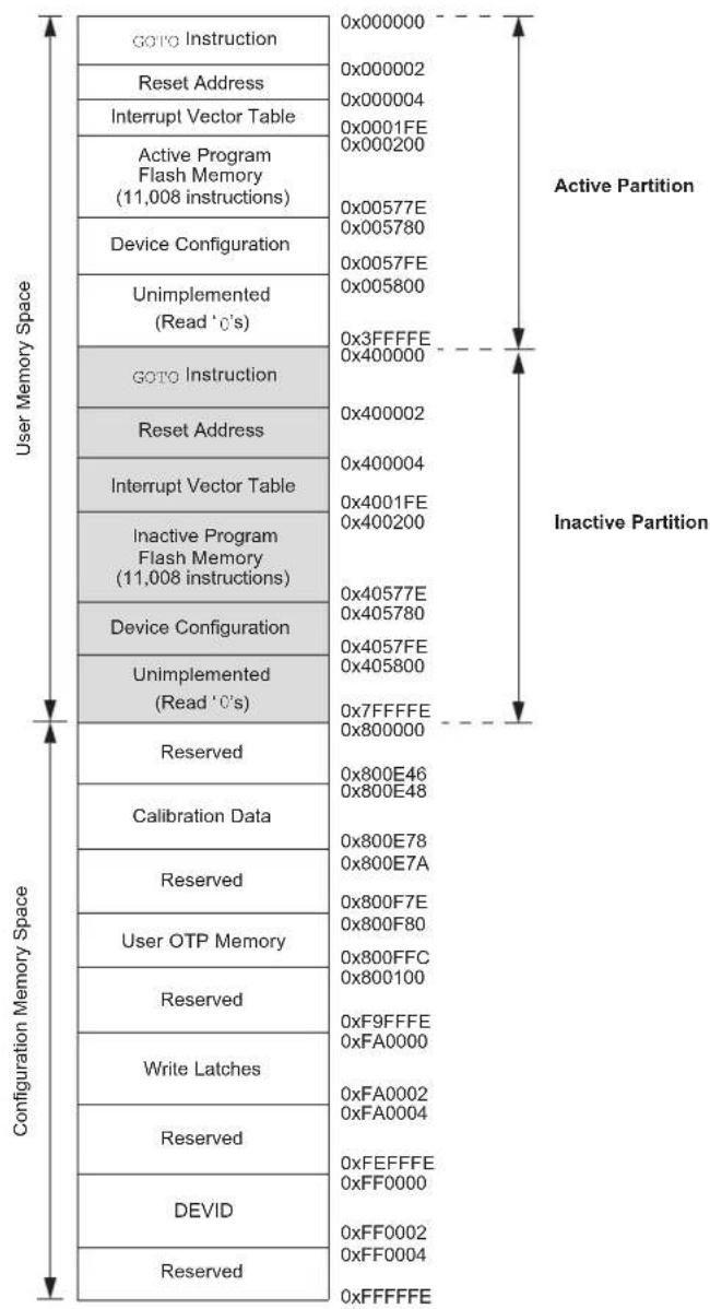
The dsPIC33EPXXXGS70X/80X devices can operate in a Dual Partition Flash Program Memory mode, where the user Program Flash Memory is arranged as two separate address spaces, one for each of the Flash partitions. The Active Partition always starts at address, 0x000000, and contains half of the available Flash memory (64k/128k, depends on device). The Inactive Partition always starts at address, 0x400000, and implements the remaining half of Flash memory. As shown in Figure 4-3 and Figure 4-4, the Active and Inactive Partitions are identical, and both contain unique copies of the Reset vector, Interrupt Vector Tables (IVT and AIVT if enabled) and the Flash Configuration Words.
4.2 Unique Device Identifier (UDID)
All dsPIC33EPXXXGS70X/80X family devices are individually encoded during final manufacturing with a Unique Device Identifier or UDID. This feature allows for manufacturing traceability of Microchip Technology devices in applications where this is a requirement. It may also be used by the application manufacturer for any number of things that may require unique identification, such as:
- Tracking the device
- Unique serial number
- Unique security key
The UDID comprises five 24-bit program words. When taken together, these fields form a unique 120-bit identifier.
The UDID is stored in five read-only locations, located between 800F00h and 800F08h in the device configuration space. Table4-1 lists the addresses of the identifier words and shows their contents.
TABLE 4-1: UDID ADDRESSES
| Name | Address Bits | 23:16 Bits | 15:8 Bits 7:0 |
| UDID1 | 800F00 | UDID Word 1 | |
| UDID2 | 800F02 | UDID Word 2 | |
| UDID3 | 800F04 | UDID Word 3 | |
| UDID4 | 800F06 | UDID Word 4 | |
| UDID5 | 800F08 | UDID Word 5 |
FIGURE 4-1: PROGRAM MEMORY MAP FOR dsPIC33EP64GS70X/80X DEVICES

text_image
GOTO Instruction Reset Address Interrupt Vector Table User Program Flash Memory (22,016 instructions) Device Configuration Unimplemented (Read '0's) Reserved Calibration Data Reserved UDID Reserved User OTP Memory Reserved Write Latches Reserved DEVID Reserved 0x000000 0x000002 0x000004 0x0001FE 0x000200 0x00AF7E 0x00AF80 0x00AFFE 0x00B000 0x7FFFFE 0x800000 0x800E46 0x800E48 0x800E78 0x800E7A 0x800EFE 0x800F00 0x800F08 0x800F0A 0x800F7E 0x800F80 0x800FFC 0x801000 0xF9FFFE 0xFA0000 0xFA0002 0xFA0004 0xFEFFE 0xFF0000 0xFF0002 0xFF0004 0xFFFFFENote: Memory areas are not shown to scale.
FIGURE 4-2: PROGRAM MEMORY MAP FOR dsPIC33EP128GS70X/80X DEVICES
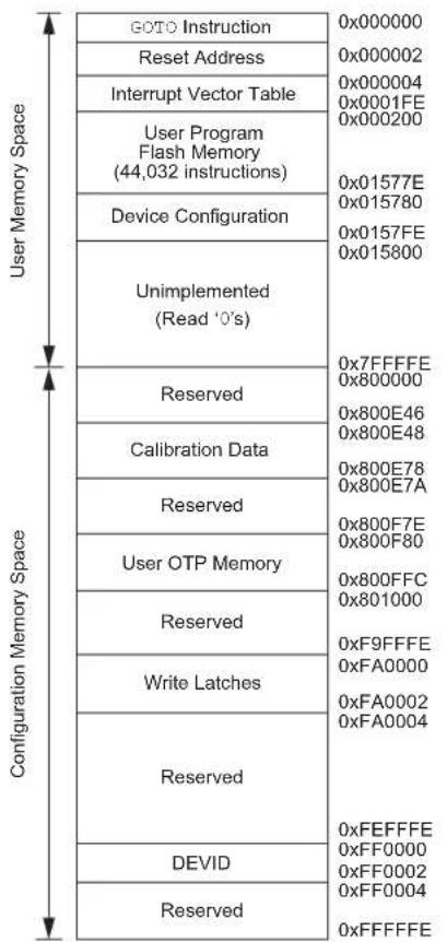
text_image
GOTO Instruction Reset Address Interrupt Vector Table User Program Flash Memory (44,032 instructions) Device Configuration Unimplemented (Read '0's) Reserved Calibration Data Reserved User OTP Memory Reserved Write Latches Reserved DEVID Reserved 0x000000 0x000002 0x000004 0x0001FE 0x000200 0x01577E 0x015780 0x0157FE 0x015800 0x7FFFFE 0x800000 0x800E46 0x800E48 0x800E78 0x800E7A 0x800F7E 0x800F80 0x800FFC 0x801000 0xF9FFFE 0xFA0000 0xFA0002 0xFA0004 0xFEFFFFE 0xFF0000 0xFF0002 0xFF0004 0xFFFFFENote: Memory areas are not shown to scale.
FIGURE 4-3: PROGRAM MEMORY MAP FOR dsPIC33EP64GS70X/80X DEVICES (DUAL PARTITION)
text_image
GO TO Instruction Reset Address Interrupt Vector Table Active Program Flash Memory (11,008 instructions) Device Configuration Unimplemented (Read 'c's) GO TO Instruction Reset Address Interrupt Vector Table Inactive Program Flash Memory (11,008 instructions) Device Configuration Unimplemented (Read 'c's) Reserved Calibration Data Reserved User OTP Memory Reserved Write Latches Reserved DEVID Reserved 0x000000 0x000002 0x000004 0x0001FE 0x000200 0x0057E 0x005780 0x0057FE 0x005800 0x3FFFFE 0x400000 0x400002 0x400004 0x4001FE 0x400200 0x4057E 0x405780 0x4057FE 0x405800 0x7FFFFE 0x800000 0x800E46 0x800E48 0x800E78 0x800E7A 0x800F7E 0x800F8O 0x800FFC 0x80010O 0xF9FFFFE 0xFA000O 0xFA0002 0xFA0004 0xFEFFFFE 0xFF00O 0xFF00O2 0xFF00O4 0xFFFFFENote: Memory areas are not shown to scale.
FIGURE 4-4: PROGRAM MEMORY MAP FOR dsPIC33EP128GS70X/80X DEVICES (DUAL PARTITION)

text_image
GOTO Instruction Reset Address Interrupt Vector Table Active Program Flash Memory (22,016 instructions) Device Configuration Unimplemented (Read '0's) GOTO Instruction Reset Address Interrupt Vector Table Inactive Program Flash Memory (22,016 instructions) Device Configuration Unimplemented (Read '0's) Reserved Calibration Data Reserved User OTP Memory Reserved Write Latches Reserved DEVID Reserved 0x000000 0x000002 0x000004 0x0001FE 0x000200 0x00AB7E 0x00AB80 0x00ABFE 0x00AC00 0x3FFFFE 0x400000 0x400002 0x400004 0x4001FE 0x400200 0x40AB7E 0x40AB80 0x40ABFE 0x40AC00 0x7FFFFE 0x800000 0x800E46 0x800E48 0x800E78 0x800E7A 0x800F7E 0x800F80 0x800FFC 0x800100 0xF9FFFE 0xFA0000 0xFA0002 0xFA0004 0xFEFFFFE 0xFF0000 0xFF0002 0xFF0004 0xFFFFFENote: Memory areas are not shown to scale.
4.2.1 PROGRAM MEMORY ORGANIZATION
The program memory space is organized in word-addressable blocks. Although it is treated as 24 bits wide, it is more appropriate to think of each address of the program memory as a lower and upper word, with the upper byte of the upper word being unimplemented. The lower word always has an even address, while the upper word has an odd address (Figure 4-5).
Program memory addresses are always word-aligned on the lower word, and addresses are incremented or decremented by two, during code execution. This arrangement provides compatibility with data memory space addressing and makes data in the program memory space accessible.
4.2.2 INTERRUPT AND TRAP VECTORS
All dsPIC33EPXXXGS70X/80X family devices reserve the addresses between 0x000000 and 0x000200 for hard-coded program execution vectors. A hardware Reset vector is provided to redirect code execution from the default value of the PC on device Reset to the actual start of code. A GOTO instruction is programmed by the user application at address, 0x000000, of Flash memory, with the actual address for the start of code at address, 0x000002, of Flash memory.
A more detailed discussion of the Interrupt Vector Tables (IVTs) is provided in Section 7.1 “Interrupt Vector Table”.
FIGURE 4-5: PROGRAM MEMORY ORGANIZATION
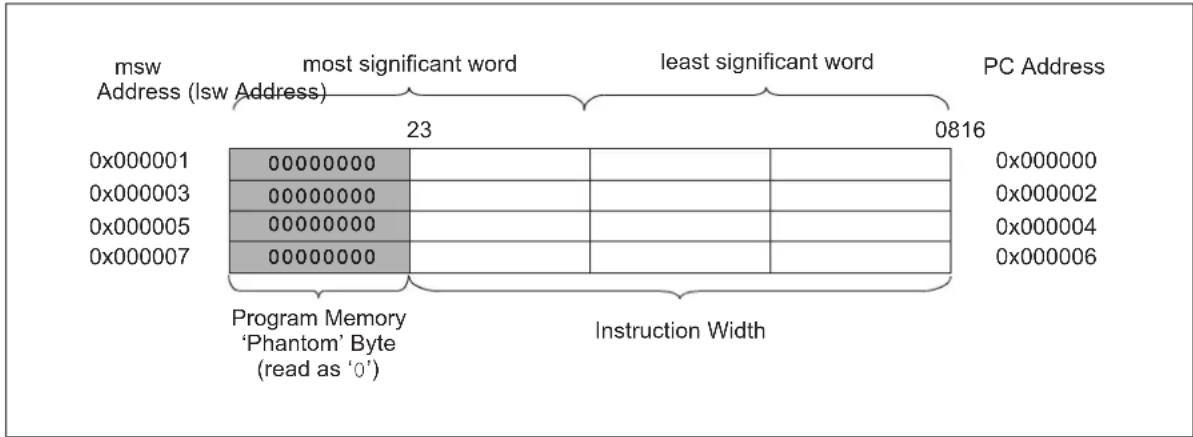
text_image
msw Address (lsw Address) most significant word least significant word PC Address 23 0816 0x000001 0x000003 0x000005 0x000007 Program Memory 'Phantom' Byte (read as '0') Instruction Width 0x000000 0x000002 0x000004 0x0000064.3 Data Address Space
The dsPIC33EPXXXGS70X/80X family CPU has a separate 16-bit wide data memory space. The Data Space is accessed using separate Address Generation Units (AGUs) for read and write operations. The data memory map is shown in Figure 4-6.
All Effective Addresses (EAs) in the data memory space are 16 bits wide and point to bytes within the Data Space. This arrangement gives a base Data Space address range of 64 Kbytes or 32K words.
The lower half of the data memory space (i.e., when EA<15> = 0) is used for implemented memory addresses, while the upper half (EA<15> = 1) is reserved for the Program Space Visibility (PSV).
dsPIC33EPXXXGS70X/80X family devices implement up to 12 Kbytes of data memory. If an EA points to a location outside of this area, an all-zero word or byte is returned.
4.3.1 DATA SPACE WIDTH
The data memory space is organized in byte-addressable, 16-bit wide blocks. Data is aligned in data memory and registers as 16-bit words, but all Data Space EAs resolve to bytes. The Least Significant Bytes (LSBs) of each word have even addresses, while the Most Significant Bytes (MSBs) have odd addresses.
4.3.2 DATA MEMORY ORGANIZATION AND ALIGNMENT
To maintain backward compatibility with PIC® MCU devices and improve Data Space memory usage efficiency, the dsPIC33EPXXXGS70X/80X family instruction set supports both word and byte operations. As a consequence of byte accessibility, all Effective Address calculations are internally scaled to step through word-aligned memory. For example, the core recognizes that Post-Modified Register Indirect Addressing mode [Ws++] results in a value of Ws + 1 for byte operations and Ws + 2 for word operations.
A data byte read, reads the complete word that contains the byte, using the LSb of any EA to determine which byte to select. The selected byte is placed onto the LSB of the data path. That is, data memory and registers are organized as two parallel, byte-wide entities with shared (word) address decode, but separate write lines. Data byte writes only write to the corresponding side of the array or register that matches the byte address.
All word accesses must be aligned to an even address. Misaligned word data fetches are not supported, so care must be taken when mixing byte and word operations, or translating from 8-bit MCU code. If a misaligned read or write is attempted, an address error trap is generated. If the error occurred on a read, the instruction underway is completed. If the error occurred on a write, the instruction is executed but the write does not occur. In either case, a trap is then executed, allowing the system and/or user application to examine the machine state prior to execution of the address Fault.
All byte loads into any W register are loaded into the LSB; the MSB is not modified.
A Sign-Extend (SE) instruction is provided to allow user applications to translate 8-bit signed data to 16-bit signed values. Alternatively, for 16-bit unsigned data, user applications can clear the MSB of any W register by executing a Zero-Extend (ZE) instruction on the appropriate address.
4.3.3 SFR SPACE
The first 4 Kbytes of the Near Data Space, from 0x0000 to 0x0FFF, is primarily occupied by Special Function Registers (SFRs). These are used by the dsPIC33EPXXXGS70X/80X family core and peripheral modules for controlling the operation of the device.
SFRs are distributed among the modules that they control and are generally grouped together by module. Much of the SFR space contains unused addresses; these are read as '0'.
Note: The actual set of peripheral features and interrupts varies by the device. Refer to the corresponding device tables and pinout diagrams for device-specific information.
4.3.4 NEAR DATA SPACE
The 8-Kbyte area, between 0x0000 and 0x1FFF, is referred to as the Near Data Space. Locations in this space are directly addressable through a 13-bit absolute address field within all memory direct instructions. Additionally, the whole Data Space is addressable using MOV instructions, which support Memory Direct Addressing mode with a 16-bit address field, or by using Indirect Addressing mode using a Working register as an Address Pointer.
FIGURE 4-6: DATA MEMORY MAP FOR dsPIC33EP64GS70X/80X DEVICES
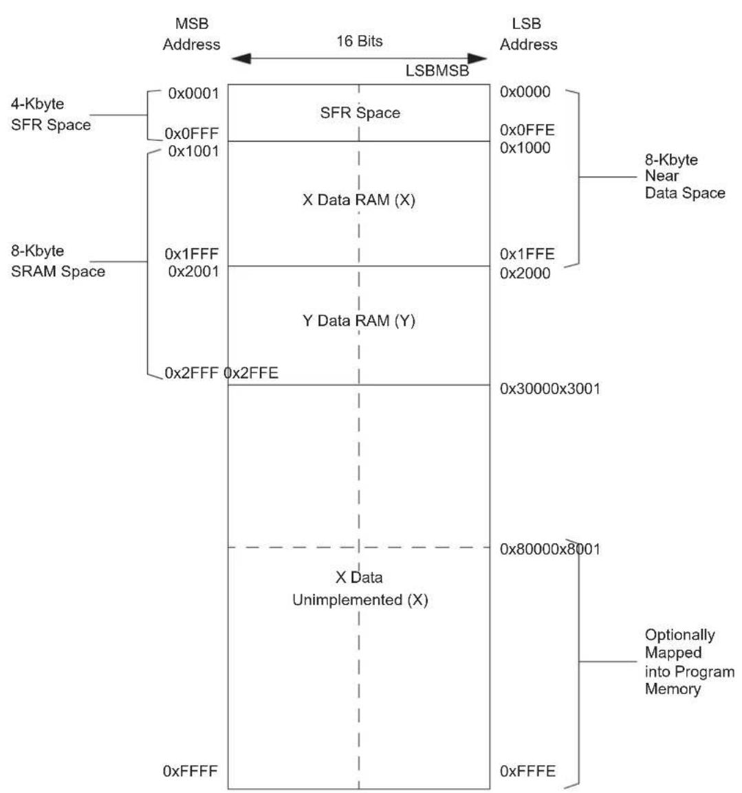
flowchart
graph TD
    A["4-Kbyte SFR Space"] --> B["0x0001"]
    A --> C["0x0FFF"]
    A --> D["0x1001"]
    E["8-Kbyte SRAM Space"] --> F["0x1FFF"]
    E --> G["0x2001"]
    E --> H["0x2FFF"]
    B --> I["SFR Space"]
    C --> J["X Data RAM (X)"]
    D --> K["Y Data RAM (Y)"]
    F --> L["X Data Unimplemented (X)"]
    G --> M["Optionally Mapped into Program Memory"]
    H --> N["LSB Address"]
    I --> O["0x0000"]
    I --> P["0x0FFE"]
    I --> Q["0x1000"]
    J --> R["0x1FFE"]
    J --> S["0x2000"]
    K --> T["0x30000x3001"]
    L --> U["0x80000x8001"]
    M --> V["0xFFFE"]
    N --> W["LSBMSB"]
    style A fill:#f9f,stroke:#333
    style E fill:#f9f,stroke:#333
    style B fill:#ccf,stroke:#333
    style C fill:#ccf,stroke:#333
    style D fill:#ccf,stroke:#333
    style F fill:#ccf,stroke:#333
    style G fill:#ccf,stroke:#333
    style H fill:#ccf,stroke:#333
    style I fill:#ccf,stroke:#333
    style J fill:#ccf,stroke:#333
    style K fill:#ccf,stroke:#333
    style L fill:#ccf,stroke:#333
    style M fill:#ccf,stroke:#333
    style N fill:#ccf,stroke:#333
    style O fill:#ccf,stroke:#333
    style P fill:#ccf,stroke:#333
    style Q fill:#ccf,stroke:#333
    style R fill:#ccf,stroke:#333
    style S fill:#ccf,stroke:#333
    style T fill:#ccf,stroke:#333
    style U fill:#ccf,stroke:#333
    style V fill:#ccf,stroke:#333
Note: Memory areas are not shown to scale.
4.3.5 X AND Y DATA SPACES
The dsPIC33EPXXXGS70X/80X core has two Data Spaces, X and Y. These Data Spaces can be considered either separate (for some DSP instructions) or as one unified linear address range (for MCU instructions). The Data Spaces are accessed using two Address Generation Units (AGUs) and separate data paths. This feature allows certain instructions to concurrently fetch two words from RAM, thereby enabling efficient execution of DSP algorithms, such as Finite Impulse Response (FIR) filtering and Fast Fourier Transform (FFT).
The X Data Space is used by all instructions and supports all addressing modes. X Data Space has separate read and write data buses. The X read data bus is the read data path for all instructions that view Data Space as combined X and Y address space. It is also the X data prefetch path for the dual operand DSP instructions (MAC class).
The Y Data Space is used in concert with the X Data Space by the MAC class of instructions (CLR, ED, EDAC, MAC, MOVSAC, MPY, MPY.N and MSC) to provide two concurrent data read paths.
Both the X and Y Data Spaces support Modulo Addressing mode for all instructions, subject to addressing mode restrictions. Bit-Reversed Addressing mode is only supported for writes to X Data Space.
All data memory writes, including in DSP instructions, view Data Space as combined X and Y address space. The boundary between the X and Y Data Spaces is device-dependent and is not user-programmable.
4.4 Memory Resources
Many useful resources are provided on the main product page of the Microchip website for the devices listed in this data sheet. This product page contains the latest updates and additional information.
4.4.1 KEY RESOURCES
- "dsPIC33E/PIC24E Program Memory"
(DS70000613) in the "dsPIC33/PIC24 Family Reference Manual" - Code Samples
- Application Notes
- Software Libraries
- Webinars
- All Related "dsPIC33/PIC24 Family Reference Manual" Sections
- Development Tools
4.5 Special Function Register Maps
TABLE 4-2: SFR BLOCK 000h
| Register Address All | Resets Register Address | All Resets | Register Address All Resets | ||||
| Core | WREG14 | 01C | 000000000000000 | DOSTARTL | 03A | ||
| WREG0 | 000 | 000000000000000 | WREG15 | 01E | 000010000000000 | DOSTARTH | 03C |
| WREG1 | 002 | 000000000000000 | SPLIM | 020 | xxxxxxxxxxxxxx0 | DOENDL | 03E |
| WREG2 | 004 | 000000000000000 | ACCAL | 022 | xxxxxxxxxxxxxx | DOENDH | 040 |
| WREG3 | 006 | 000000000000000 | ACCAH | 024 | xxxxxxxxxxxxxx | SR | 042 |
| WREG4 | 008 | 000000000000000 | ACCAU | 026 | 0000000xxxxxxxx | CORCON | 044 |
| WREG5 | 00A | 000000000000000 | ACCBL | 028 | xxxxxxxxxxxxxx | MODCON | 046 |
| WREG6 | 00C | 000000000000000 | ACCBH | 02A | xxxxxxxxxxxxxx | XMODSRT | 048 |
| WREG7 | 00E | 000000000000000 | ACCBU | 02C | 0000000xxxxxxxx | XMODEND | 04A |
| WREG8 | 010 | 000000000000000 | PCL | 02E | 00000000000000 | YMODSRT | 04C |
| WREG9 | 012 | 000000000000000 | PCH | 030 | 00000000000000 | YMODEND | 04E |
| WREG10 | 014 | 000000000000000 | DSRPAG | 032 | 000000000000001 | XBREV | 050 |
| WREG11 | 016 | 000000000000000 | DSWPAG | 034 | 000000000000001 | DISICNT | 052 |
| WREG12 | 018 | 000000000000000 | RCOUNT | 036 | xxxxxxxxxxxxxx | TBLPAG | 054 |
| WREG13 | 01A | 000000000000000 | DCOUNT | 038 | xxxxxxxxxxxxxx | CTXTSTAT | 05A |
Legend: x = unknown or indeterminate value. Address values are in hexadecimal. Reset values are in binary.
TABLE 4-3: SFR BLOCK 100h
| Register Address All Resets Register Address | All Resets Register Address All Resets | |||||||
| Timers | TMR5HLD | 116 | xxxxxxxxxxxxxxxxxx | IC2CON2 | 14A | 0000000000001101 | ||
| TMR1 | 100 xx | xxxxxxxxxxxxx | TMR5 | 118 | xxxxxxxxxxxxxxxxxx | IC2BUF | 14C | xxxxxxxxxxxxxxxxxx |
| PR1 | 102 | 1111111111111111 | PR4 | 11A | 1111111111111111 | IC2TMR | 14E | 0000000000000000 |
| T1CON | 104 | 0000000000000000 | PR5 | 11C | 1111111111111111 | IC3CON1 | 150 | 0000000000000000 |
| TMR2 | 106 | xxxxxxxxxxxxxxxxx | T4CON | 11E | 0000000000000000 | IC3CON2 | 152 | 0000000000001101 |
| TMR3HLD | 108 | xxxxxxxxxxxxxxxxx | T5CON | 120 | 0000000000000000 | IC3BUF | 154 | xxxxxxxxxxxxxxxxx |
| TMR3 | 10A | xxxxxxxxxxxxxxxxx | Input Capture | IC3TMR | 156 | 0000000000000000 | ||
| PR2 | 10C | 1111111111111111 | IC1CON1 | 140 | 0000000000000000 | IC4CON1 | 158 | 000000000000000 |
| PR3 | 10E | 1111111111111111 | IC1CON2 | 142 | 0000000000001101 | IC4CON2 | 15A | 0000000000001101 |
| T2CON | 110 | 000000000000000 | IC1BUF | 144 | xxxxxxxxxxxxxxxxxx | IC4BUF | 15C | xxxxxxxxxxxxxxxxx |
| T3CON | 112 | 000000000000000 | IC1TMR | 146 | 0000000000000000 | IC4TMR | 15E | 000000000000000 |
| TMR4 | 114 | xxxxxxxxxxxxxxxxx | IC2CON1 | 148 | 0000000000000000 | |||
Legend: x = unknown or indeterminate value. Address values are in hexadecimal. Reset values are in binary.
TABLE 4-4: SFR BLOCK 200h
| Register Address All | Resets Register Address | All Resets | Register Address All Resets | ||||
| I2C1 and I2C2 | U1STA | 222 | 0000000010010000 | SPI1BRGH | 252 | ||
| I2C1CONL | 200 | 0001000000000000 | U1TXREG | 224 | 0000000xxxxxxxxxx | SPI1IMSKL | 254 |
| I2C1CONH | 202 | 0000000000000000 | U1RXREG | 226 | 000000000000000 | SPI1IMSKH | 256 |
| I2C1STAT | 204 | 0000000000000000 | U1BRG | 228 | 000000000000000 | SPI1URDTL | 258 |
| I2C1ADD | 206 | 0000000000000000 | U2MODE | 230 | 000000000000000 | SPI1URDTH | 25A |
| I2C1MSK | 208 | 0000000000000000 | U2STA | 232 | 000000010010000 | SPI2CON1L | 260 |
| I2C1BRG | 20A | 0000000000000000 | U2TXREG | 234 | 000000xxxxxxxxxx | SPI2CON1H | 262 |
| I2C1TRN | 20C | 000000011111111 | U2RXREG | 236 | 000000000000000 | SPI2CON2L | 264 |
| I2C1RCV | 20E | 0000000000000000 | U2BRG | 238 | 000000000000000 | SPI2CON2H | 266 |
| I2C2CON1 | 210 | 0001000000000000 | SPI | SPI2STATL | 268 | ||
| I2C2CON2 | 212 | 0000000000000000 | SPI1CON1L | 240 | 000000000000000 | SPI2STATH | 26A |
| I2C2STAT | 214 | 0000000000000000 | SPI1CON1H | 242 | 000000000000000 | SPI2BUFL | 26C |
| I2C2ADD | 216 | 0000000000000000 | SPI1CON2L | 244 | 000000000000000 | SPI2BUFH | 26E |
| I2C2MSK | 218 | 0000000000000000 | SPI1CON2H | 246 | 000000000000000 | SPI3STAT | 270 |
| I2C2BRG | 21A | 0000000000000000 | SPI1STATL | 248 | 00000000101000 | SPI2BRGH | 272 |
| I2C2TRN | 21C | 000000011111111 | SPI1STATH | 24A | 000000000000000 | SPI2IMSKL | 274 |
| I2C2RCV | 21E | 0000000000000000 | SPI1BUFL | 24C | 000000000000000 | SPI2IMSKH | 276 |
| UART1 and UART2 | SPI1BUFH | 24E | 000000000000000 | SPI2URDTL | 278 | ||
| U1MODE | 220 | 0000000000000000 | SPI1BRGL | 250 | 000xxxxxxxxxxxx | SPI2URDTH | 27A |
Legend: x = unknown or indeterminate value. Address values are in hexadecimal. Reset values are in binary.
TABLE 4-5: SFR BLOCK 300h
| Register | Address | All Resets | Register | Address | All Resets | Register | Address | All Resets |
| ADC | ADCMP0ENH | 33A | 0000000000000000 | ADTRIG4L | 390 | 0000000000000000 | ||
| ADCON1L | 300 | 0000000000000000 | ADCMP0LO | 33C | 0000000000000000 | ADTRIG4H | 392 | 0000000000000000 |
| ADCON1H | 302 | 000000001100000 | ADCMP0HI | 33E | 0000000000000000 | ADCMP0CON | 3A0 | 0000000000000000 |
| ADCON2L | 304 | 0000000000000000 | ADCMP1ENL | 340 | 0000000000000000 | ADCMP1CON | 3A4 | 0000000000000000 |
| ADCON2H | 306 | 0000000000000000 | ADCMP1ENH | 342 | 0000000000000000 | ADBASE | 3C0 | 0000000000000000 |
| ADCON3L | 308 | 0000000000000000 | ADCMP1LO | 344 | 0000000000000000 | ADLVLTRGL | 3D0 | 0000000000000000 |
| ADCON3H | 30A | 0000000000000000 | ADCMP1HI | 346 | 0000000000000000 | ADLVLTRGH | 3D2 | 0000000000000000 |
| ADCON4L | 30C | 0000000000000000 | ADFL0DAT | 368 | 0000000000000000 | ADCORE0L | 3D4 | 0000000000000000 |
| ADCON4H | 30E | 0000000000000000 | ADFL0CON | 36A | 0000000000000000 | ADCORE0H | 3D6 | 000001100000000 |
| ADMOD0L | 310 | 000000000000000 | ADFL1DAT | 36C | 0000000000000000 | ADCORE1L | 3D8 | 000000000000000 |
| ADMOD0H | 312 | 000000000000000 | ADFL1CON | 36E | 0000000000000000 | ADCORE1H | 3DA | 00000110000000 |
| ADMOD1L | 314 | 000000000000000 | ADTRIG0L | 380 | 0000000000000000 | ADCORE2L | 3DC | 000000000000000 |
| ADIEL | 320 | 000000000000000 | ADTRIG0H | 382 | 000000000000000 | ADCORE2H | 3DE | 00000110000000 |
| ADIEH | 322 | 000000000000000 | ADTRIG1L | 384 | 000000000000000 | ADCORE3L | 3E0 | 00000000000000 |
| ADCSS1L | 328 | 00000000000000 | ADTRIG1H | 386 | 00000000000000 | ADCORE3H | 3E2 | 0000011000000 |
| ADCSS1H | 32A | 0000000000000 | ADTRIG2L | 388 | 0000000000000 | ADEIEL | 3F0 | 0000000000000 |
| ADSTATL | 330 | 000000000000 | ADTRIG2H | 38A | 000000000000 | ADEIEH | 3F2 | 000000000000 |
| ADSTATH | 332 | 00000000000 | ADTRIG3L | 38C | 00000000000 | ADEISTATL | 3F8 | 00000000000 |
| ADCMP0ENL | 338 | 00000000000 | ADTRIG3H | 38E | 0000000000 | ADEISTATH | 3FA | 0000000000 |
Legend: x = unknown or indeterminate value. Address values are in hexadecimal. Reset values are in binary.
TABLE 4-6: SFR BLOCK 400h
| Register Address All | Resets Register Address | All Resets | Register | Address | All Resets | |||
| ADC (Continued) | C1FCTRL | 486 | 0000000000000000 | C1RXM2EID | 4BA | xxxxxxxxxxxxxx | ||
| ADCON5L | 400 | 0000000000000000 | C1FIFO | 488 | 0000000000000000 | C1RXF1SID | 4C4 | xxxxxxxxxxxxxx |
| ADCON5H | 402 | 0000000000000000 | C1INTF | 48A | 0000000000000000 | C1RXF1EID | 4C6 | xxxxxxxxxxxxxx |
| ADCAL0L | 404 | 0000000000000000 | C1INTE | 48C | 0000000000000000 | C1RXF2SID | 4C8 | xxxxxxxxxxxxxx |
| ADCAL0H | 406 | 0000000000000000 | C1EC | 48E | 0000000000000000 | C1RXF2EID | 4CA | xxxxxxxxxxxxxx |
| ADCAL1H | 40A | 0000000000000000 | C1CFG1 | 490 | 0000000000000000 | C1RXF3SID | 4CC | xxxxxxxxxxxxxx |
| ADCBUF0 | 40C | 0000000000000000 | C1CFG2 | 492 | 0x000xxxxxxxxxx | C1RXF3EID | 4CE | xxxxxxxxxxxxxx |
| ADCBUF1 | 40E | 0000000000000000 | C1FEN1 | 494 | 111111111111111 | C1RXF4SID | 4D0 | xxxxxxxxxxxxxx |
| ADCBUF2 | 410 | 0000000000000000 | C1FMSKSEL1 | 498 | 0000000000000000 | C1RXF4EID | 4D2 | xxxxxxxxxxxxxx |
| ADCBUF3 | 412 | 0000000000000000 | C1FMSKSEL2 | 49A | 0000000000000000 | C1RXF5SID | 4D4 | xxxxxxxxxxxxxx |
| ADCBUF4 | 414 | 0000000000000000 | CAN (WIN (C1CTRL<0>) = 0) | C1RXF5EID | 4D6 | xxxxxxxxxxxxxx | ||
| ADCBUF5 | 416 | 0000000000000000 | C1RXFUL1 | 4A0 | 0000000000000000 | C1RXF6SID | 4D8 | xxxxxxxxxxxxxx |
| ADCBUF6 | 418 | 0000000000000000 | C1RXFUL2 | 4A2 | 0000000000000000 | C1RXF6EID | 4DA | xxxxxxxxxxxxxx |
| ADCBUF7 | 41A | 0000000000000000 | C1RXOVF1 | 4A8 | 0000000000000000 | C1RXF7SID | 4DC | xxxxxxxxxxxxxx |
| ADCBUF8 | 41C | 0000000000000000 | C1RXOVF2 | 4AA | 0000000000000000 | C1RXF7EID | 4DE | xxxxxxxxxxxxxx |
| ADCBUF9 | 41E | 0000000000000000 | C1TR01CON | 4B0 | 0000000000000000 | C1RXF8SID | 4E0 | xxxxxxxxxxxxxx |
| ADCBUF10 | 420 | 0000000000000000 | C1TR23CON | 4B2 | 0000000000000000 | C1RXF8EID | 4E2 | xxxxxxxxxxxxxx |
| ADCBUF11 | 422 | 0000000000000000 | C1TR45CON | 4B4 | 0000000000000000 | C1RXF9SID | 4E4 | xxxxxxxxxxxxxx |
| ADCBUF12 | 424 | 0000000000000000 | C1TR67CON | 4B6 | xxxxxxxxxxxxxx | C1RXF9EID | 4E6 | xxxxxxxxxxxxxx |
| ADCBUF13 | 426 | 0000000000000000 | C1RXD | 4C0 | xxxxxxxxxxxxxx | C1RXF10SID | 4E8 | xxxxxxxxxxxxxx |
| ADCBUF14 | 428 | 0000000000000000 | C1TXD | 4C2 | xxxxxxxxxxxxxx | C1RXF10EID | 4EA | xxxxxxxxxxxxxx |
| ADCBUF15 | 42A | 0000000000000000 | CAN (WIN (C1CTR1<0>) = 1) | C1RXF11SID | 4EC | xxxxxxxxxxxxxx | ||
| ADCBUF16 | 42C | 0000000000000000 | C1BUFNT1 | 4A0 | 0000000000000000 | C1RXF11EID | 4EE | xxxxxxxxxxxxxx |
| ADCBUF17 | 42E | 0000000000000000 | C1BUFNT2 | 4A2 | 0000000000000000 | C1RXF12SID | 4F0 | xxxxxxxxxxxxxx |
| ADCBUF18 | 430 | 0000000000000000 | C1BUFNT3 | 4A4 | 0000000000000000 | C1RXF12EID | 4F2 | xxxxxxxxxxxxxx |
| ADCBUF19 | 432 | 0000000000000000 | C1BUFNT4 | 4A6 | 0000000000000000 | C1RXF13SID | 4F4 | xxxxxxxxxxxxxx |
| ADCBUF20 | 434 | 0000000000000000 | C1RXMOSID | 4B0 | xxxxxxxxxxxxxx | C1RXF13EID | 4F6 | xxxxxxxxxxxxxx |
| ADCBUF21 | 436 | 0000000000000000 | C1RXMOSID | 4B2 | xxxxxxxxxxxxxx | C1RXF14SID | 4F8 | xxxxxxxxxxxxxx |
| CAN (WIN (C1CTRL<0>) = 0 OR 1) | C1RXM1SID | 4B4 | xxxxxxxxxxxxxx | C1RXF14EID | 4FA | xxxxxxxxxxxxxx | ||
| C1CTRL1 | 480 | 00001001000000 | C1RXM1EID | 4B6 | xxxxxxxxxxxxxx | C1RXF15SID | 4FC | xxxxxxxxxxxxxx |
| C1CTRL2 | 482 | 000000000000000 | CAN | C1RXF15EID | 4FE | xxxxxxxxxxxxxx | ||
| C1VEC | 484 | 0000000100000 | C1RXM2SID | 4B8 | xxxxxxxxxxxxxx | |||
Legend: x = unknown or indeterminate value. Address values are in hexadecimal. Reset values are in binary.
TABLE 4-7: SFR BLOCK 500h
| Register | Address | All Resets | Register | Address | All Resets | Register | Address | All Resets |
| PGA | PGA2CAL | 50A | 000000000000000 | CMP2DAC | 546 | 000000000000000 | ||
| ISRCCON | 500 | 000000000000000 | Comparators | CMP3CON | 548 | 000000000000000 | ||
| PGA1CON | 504 | 000000000000000 | CMP1CON | 540 | 000000000000000 | CMP3DAC | 54A | 000000000000000 |
| PGA1CAL | 506 | 000000000000000 | CMP1DAC | 542 | 000000000000000 | CMP4CON | 54C | 000000000000000 |
| PGA2CON | 508 | 000000000000000 | CMP2CON | 544 | 000000000000000 | CMP4DAC | 54E | 000000000000000 |
Legend: x = unknown or indeterminate value. Address values are in hexadecimal. Reset values are in binary.
TABLE 4-8: SFR BLOCK 600h
| Register Address All | Resets Register Address | All Resets | Register Address All Resets | ||||
| SPI | RPOR8 | 678 | 000000000000000 | RPINR7 | 6AE | ||
| SPI3CON1L | 600 | 000000000000000 | RPOR9 | 67A | 000000000000000 | RPINR8 | 6B0 |
| SPI3CON1H | 602 | 000000000000000 | RPOR10 | 67C | 000000000000000 | RPINR11 | 6B6 |
| SPI3CON2L | 604 | 000000000000000 | RPOR11 | 67E | 000000000000000 | RPINR12 | 6B8 |
| SPI3CON2H | 606 | 000000000000000 | RPOR12 | 680 | 000000000000000 | RPINR13 | 6BA |
| SPI3STATL | 608 | 000000000101000 | RPOR13 | 682 | 000000000000000 | RPINR18 | 6C4 |
| SPI3STATH | 60A | 000000000000000 | RPOR14 | 684 | 000000000000000 | RPINR19 | 6C6 |
| SPI3BUFL | 60C | 000000000000000 | RPOR15 | 686 | 000000000000000 | RPINR20 | 6C8 |
| SPI3BUFH | 60E | 000000000000000 | RPOR17 | 68A | 000000000000000 | RPINR21 | 6CA |
| SPI3BRGL | 610 | 000xxxxxxxxxxxx | RPOR18 | 68C | 000000000000000 | RPINR22 | 6CC |
| SPI3BRGH | 612 | 000000000000000 | RPOR19 | 68E | 000000000000000 | RPINR23 | 6CE |
| SPI3IMSKL | 614 | 000000000000000 | RPOR20 | 690 | 000000000000000 | RPINR26 | 6D4 |
| SPI3IMSKH | 616 | 000000000000000 | RPOR21 | 692 | 000000000000000 | RPINR29 | 6DA |
| SPI3URDTL | 618 | 000000000000000 | RPOR22 | 694 | 000000000000000 | RPINR30 | 6DC |
| SPI3URDTH | 61A | 000000000000000 | RPOR23 | 696 | 000000000000000 | RPINR37 | 6EA |
| RPOR0 | 668 | 000000000000000 | RPOR24 | 698 | 000000000000000 | RPINR38 | 6EC |
| RPOR1 | 66A | 000000000000000 | RPOR25 | 69A | 000000000000000 | RPINR42 | 6F4 |
| RPOR2 | 66C | 000000000000000 | RPOR26 | 69C | 000000000000000 | RPINR43 | 6F6 |
| RPOR3 | 66E | 000000000000000 | RPINR0 | 6A0 | 000000000000000 | RPINR45 | 6FA |
| RPOR4 | 670 | 000000000000000 | RPINR1 | 6A2 | 000000000000000 | RPINR46 | 6FC |
| RPOR5 | 672 | 000000000000000 | RPINR2 | 6A4 | 000000000000000 | ||
| RPOR6 | 674 | 000000000000000 | RPINR3 | 6A6 | 00000000000000 | ||
Legend: x = unknown or indeterminate value. Address values are in hexadecimal. Reset values are in binary.
TABLE 4-9: SFR BLOCK 700h
| Register Address All Resets Register Address | All Resets Register Address All Resets | |||||||
| NVM | C2INTF | 78A | 000000000000000 | C2RXF1SID | 7C4 | xxxxxxxxxxxxxx | ||
| NVMCON | 728 | 000000000000000 | C2INTE | 78C | 000000000000000 | C2RXF1EID | 7C6 | xxxxxxxxxxxxxx |
| NVMADR | 72A | 000000000000000 | C2EC | 78E | 000000000000000 | C2RXF2SID | 7C8 | xxxxxxxxxxxxxx |
| NVMADRU | 72C | 000000000000000 | C2CFG1 | 790 | 000000000000000 | C2RXF2EID | 7CA | xxxxxxxxxxxxxx |
| NVMKEY | 72E | 000000000000000 | C2CFG2 | 792 | 0x000xxxxxxxxxx | C2RXF3SID | 7CC | xxxxxxxxxxxxxx |
| NVMSRCADR | 730 | 000000000000000 | C2FEN1 | 794 | 111111111111111 | C2RXF3EID | 7CE | xxxxxxxxxxxxxx |
| NVMSRCADRH | 732 | 000000000000000 | C2FMSKSEL1 | 798 | 000000000000000 | C2RXF4SID | 7D0 | xxxxxxxxxxxxxx |
| System Control | C2FMSKSEL2 | 79A | 000000000000000 | C2RXF4EID | 7D2 | xxxxxxxxxxxxxx | ||
| RCON | 740 | 0x00x0x01x0xxxxx | CAN (WIN (C1CTR1<0>) = 0) | C2RXF5SID | 7D4 | xxxxxxxxxxxxxx | ||
| OSCCON | 742 | 000000000000000 | C2RXFUL1 | 7A0 | 000000000000000 | C2RXF5EID | 7D6 | xxxxxxxxxxxxxx |
| CLKDIV | 744 | 000000000000000 | C2RXFUL2 | 7A2 | 000000000000000 | C2RXF6SID | 7D8 | xxxxxxxxxxxxxx |
| PLLFBD | 746 | 000000000000000 | C2RXOVF1 | 7A8 | 000000000000000 | C2RXF6EID | 7DA | xxxxxxxxxxxxxx |
| OSCTUN | 748 | 000000000000000 | C2RXOVF2 | 7AA | 000000000000000 | C2RXF7SID | 7DC | xxxxxxxxxxxxxx |
| LFSR | 74C | 000000000000000 | C2TR01CON | 7B0 | 000000000000000 | C2RXF7EID | 7DE | xxxxxxxxxxxxxx |
| REFOCON | 74E | 000000000000000 | C2TR23CON | 7B2 | 000000000000000 | C2RXF8SID | 7E0 | xxxxxxxxxxxxxx |
| ACLKCON | 750 | 00000000100000 | C2TR45CON | 7B4 | 000000000000000 | C2RXF8EID | 7E2 | xxxxxxxxxxxxxx |
| PMD | C2TR67CON | 7B6 | xxxxxxxxxxxxxx | C2RXF9SID 7E4 | xxxxxxxxxxxxxx | |||
| PMD1 | 760 | 000000000000000 | C2RXD | 7C0 | xxxxxxxxxxxxxx | C2RXF9EID | 7E6 | xxxxxxxxxxxxxx |
| PMD2 | 762 | 000000000000000 | C2TXD | 7C2 | xxxxxxxxxxxxxx | C2RXF10SID | 7E8 | xxxxxxxxxxxxxx |
| PMD3 | 764 | 000000000000000 | CAN (WIN (C1CTR1<0>) = 1) | C2RXF10EID | 7EA | xxxxxxxxxxxxxx | ||
| PMD4 | 766 | 000000000000000 | C2BUFPT1 | 7A0 | 000000000000000 | C2RXF11SID | 7EC | xxxxxxxxxxxxxx |
| PMD6 | 76A | 000000000000000 | C2BUFPT2 | 7A2 | 000000000000000 | C2RXF11EID | 7EE | xxxxxxxxxxxxxx |
| PMD7 | 76C | 000000000000000 | C2BUFPT3 | 7A4 | 000000000000000 | C2RXF12SID | 7F0 | xxxxxxxxxxxxxx |
| PMD8 | 76E | 000000000000000 | C2BUFPT4 | 7A6 | 000000000000000 | C2RXF12EID | 7F2 | xxxxxxxxxxxxxx |
| CAN (WIN (C1CTR1<0>) = 0 or 1) | C2RXMOSID | 7B0 | xxxxxxxxxxxxxx | C2RXF13SID | 7F4 | xxxxxxxxxxxxxx | ||
| C2CTRL1 | 780 | 000001001000000 | C2RXMOEID | 7B2 | xxxxxxxxxxxxxx | C2RXF13EID | 7F6 | xxxxxxxxxxxxxx |
| C2CTRL2 | 782 | 000000000000000 | C2RXM1SID | 7B4 | xxxxxxxxxxxxxx | C2RXF14SID | 7F8 | xxxxxxxxxxxxxx |
| C2VEC | 784 | 00000000100000 | C2RXM1EID | 7B6 | xxxxxxxxxxxxxx | C2RXF14EID | 7FA | xxxxxxxxxxxxxx |
| C2FCTRL | 786 | 00000000000000 | C2RXM2SID | 7B8 | xxxxxxxxxxxxxx | C2RXF15SID | 7FC | xxxxxxxxxxxxxx |
| C2FIFO | 788 | 00000000000000 | C2RXM2EID | 7BA | xxxxxxxxxxxxxx | C2RXF15EID | 7FE | xxxxxxxxxxxxxx |
Legend: x = unknown or indeterminate value. Address values are in hexadecimal. Reset values are in binary.
TABLE 4-10: SFR BLOCK 800h
| Register Address All R | Resets Register Address | All Resets | Register Address All Resets | ||||
| Interrupt Controller | IEC9 | 832 | 000000000000000 | IPC26 | 874 | ||
| IFS0 | 800 | 000000000000000 | IEC10 | 834 | 000000000000000 | IPC27 | 876 |
| IFS1 | 802 | 000000000000000 | IEC11 | 836 | 000000000000000 | IPC28 | 878 |
| IFS2 | 804 | 000000000000000 | IPC0 | 840 | 0100010001000100 | IPC29 | 87A |
| IFS3 | 806 | 000000000000000 | IPC1 | 842 | 010001000100000 | IPC35 | 886 |
| IFS4 | 808 | 000000000000000 | IPC2 | 844 | 0100010001000100 | IPC36 | 888 |
| IFS5 | 80A | 000000000000000 | IPC3 | 846 | 010000001000100 | IPC37 | 88A |
| IFS6 | 80C | 000000000000000 | IPC4 | 848 | 0100010001000100 | IPC38 | 88C |
| IFS7 | 80E | 000000000000000 | IPC5 | 84A | 0000000000000100 | IPC39 | 88E |
| IFS8 | 810 | 000000000000000 | IPC6 | 84C | 010001000100000 | IPC40 | 890 |
| IFS9 | 812 | 000000000000000 | IPC7 | 84E | 0100010001000100 | IPC41 | 892 |
| IFS10 | 814 | 000000000000000 | IPC8 | 850 | 000000001000100 | IPC42 | 894 |
| IFS11 | 816 | 000000000000000 | IPC9 | 852 | 000001000100000 | IPC43 | 896 |
| IEC0 | 820 | 000000000000000 | IPC11 | 856 | 000000000000000 | IPC44 | 898 |
| IEC1 | 822 | 000000000000000 | IPC12 | 858 | 000001000100000 | IPC45 | 89A |
| IEC2 | 824 | 000000000000000 | IPC13 | 85A | 000001000000000 | IPC46 | 89C |
| IEC3 | 826 | 000000000000000 | IPC14 | 85C | 00000000100000 | IPC47 | 89E |
| IEC4 | 828 | 000000000000000 | IPC16 | 860 | 000001000100000 | INTCON1 | 8C0 |
| IEC5 | 82A | 000000000000000 | IPC18 | 864 | 00000000100000 | INTCON2 | 8C2 |
| IEC6 | 82C | 000000000000000 | IPC23 | 86E | 010001000000000 | INTCON3 | 8C4 |
| IEC7 | 82E | 000000000000000 | IPC24 | 870 | 0000010001000100 | INTCON4 | 8C6 |
| IEC8 | 830 | 000000000000000 | IPC25 | 872 | 010000000000000 | INTTREG | 8C8 |
Legend: x = unknown or indeterminate value. Address values are in hexadecimal. Reset values are in binary.
TABLE 4-11: SFR BLOCK 900h
| Register Address All R | Resets Register Address | All Resets | Register Address All Resets | ||||
| Output Compare | OC3R | 91A | xxxxxxxxxxxxxx | CLC2CONH | 9CE | ||
| OC1CON1 | 900 | 0000000000000000 | OC3TMR | 91C | 0000000000000000 | CLC2SEL | 9D0 |
| OC1CON2 | 902 | 0000000000001100 | OC4CON1 | 91E | 0000000000000000 | CLC2GLSL | 9D4 |
| OC1RS | 904 | xxxxxxxxxxxxxx | OC4CON2 | 920 | 000000000001100 | CLC2GLSH | 9D6 |
| OC1R | 906 | xxxxxxxxxxxxxx | OC4RS | 922 | xxxxxxxxxxxxxx | CLC3CONL | 9D8 |
| OC1TMR | 908 | 0000000000000000 | OC4R | 924 | xxxxxxxxxxxxxx | CLC3CONH | 9DA |
| OC2CON1 | 90A | 000000000000000 | OC4TMR | 926 | 000000000000000 | CLC3SEL | 9DC |
| OC2CON2 | 90C | 000000000001100 | CLC | CLC3GLSL | 9E0 | ||
| OC2RS | 90E | xxxxxxxxxxxxxx | CLC1CONL | 9C0 | 000000000000000 | CLC3GLSH | 9E2 |
| OC2R | 910 | xxxxxxxxxxxxxx | CLC1CONH | 9C2 | 000000000000000 | CLC4CONL | 9E4 |
| OC2TMR | 912 | 0000000000000000 | CLC1SEL | 9C4 | 000000000000000 | CLC4CONH | 9E6 |
| OC3CON1 914 | 000000000000000 | CLC1GLSL | 9C8 | 000000000000000 | CLC4SEL | 9E8 | 00000000000000 |
| OC3CON2 | 916 | 000000000001100 | CLC1GLSH | 9CA | 000000000000000 | CLC4GLSL | 9EC |
| OC3RS | 918 | xxxxxxxxxxxxxx | CLC2CONL | 9CC | 000000000000000 | CLC4GLSH | 9EE |
Legend: x = unknown or indeterminate value. Address values are in hexadecimal. Reset values are in binary.
TABLE 4-12: SFR BLOCK A00h
| Register Address All Resets Register Address | All Resets Register Address All Resets | |||||||
| PTG | PTGADJ | AD2 | 000000000000000 | PTGQUE7 | AE6 | xxxxxxxxxxxxxx | ||
| PTGCST | AC0 | 000000000000000 | PTGL0 | AD4 | 000000000000000 | PTGQUE8 | AE8 | xxxxxxxxxxxxxx |
| PTGCON | AC2 | 000000000000000 | PTGQPTR | AD6 | 000000000000000 | PTGQUE9 | AEA | xxxxxxxxxxxxxx |
| PTGBTE | AC4 | 000000000000000 | PTGQUE0 | AD8 | xxxxxxxxxxxxxx | PTGQUE10 | AEC | xxxxxxxxxxxxxx |
| PTGHOLD | AC6 | 000000000000000 | PTGQUE1 | ADA | xxxxxxxxxxxxxx | PTGQUE11 | AEE | xxxxxxxxxxxxxx |
| PTGT0LIM | AC8 | 000000000000000 | PTGQUE2 | ADC | xxxxxxxxxxxxxx | PTGQUE12 | AF0 | xxxxxxxxxxxxxx |
| PTGT1LIM | ACA | 000000000000000 | PTGQUE3 | ADE | xxxxxxxxxxxxxx | PTGQUE13 | AF2 | xxxxxxxxxxxxxx |
| PTGSDLIM | ACC | 000000000000000 | PTGQUE4 | AE0 | xxxxxxxxxxxxxx | PTGQUE14 | AF4 | xxxxxxxxxxxxxx |
| PTGC0LIM | ACE | 000000000000000 | PTGQUE5 | AE2 | xxxxxxxxxxxxxx | PTGQUE15 | AF6 | xxxxxxxxxxxxxx |
| PTGC1LIM | AD0 | 000000000000000 | PTGQUE6 | AE4 | xxxxxxxxxxxxxx | |||
Legend: x = unknown or indeterminate value. Address values are in hexadecimal. Reset values are in binary.
TABLE 4-13: SFR BLOCK B00h
| Register Address All Resets Register Address | All Resets Register Address All Resets | |||||||
| DMA | DMA1STBL | B18 | 0000000000000000 | DMA3REQ | B32 | 0000000000000000 | ||
| DMA0CON | B00 | 0000000000000000 | DMA1STBH | B1A | 0000000000000000 | DMA3STAL | B34 | 0000000000000000 |
| DMA0REQ | B02 | 0000000000000000 | DMA1PAD | B1C | 0000000000000000 | DMA3STAH | B36 | 0000000000000000 |
| DMA0STAL | B04 | 0000000000000000 | DMA1CNT | B1E | 0000000000000000 | DMA3STBL | B38 | 0000000000000000 |
| DMA0STAH | B06 | 0000000000000000 | DMA2CON | B20 | 0000000000000000 | DMA3STBH | B3A | 0000000000000000 |
| DMA0STBL | B08 | 0000000000000000 | DMA2REQ | B22 | 0000000000000000 | DMA3PAD | B3C | 0000000000000000 |
| DMA0STBH | B0A | 0000000000000000 | DMA2STAL | B24 | 0000000000000000 | DMA3CNT | B3E 00 | 000000000000000 |
| DMA0PAD | B0C | 0000000000000000 | DMA2STAH | B26 | 0000000000000000 | DMAPWC | BF0 | 000000000000000 |
| DMA0CNT | B0E | 0000000000000000 | DMA2STBL | B28 | 0000000000000000 | DMARQC | BF2 | 000000000000000 |
| DMA1CON | B10 | 0000000000000000 | DMA2STBH | B2A | 0000000000000000 | DMAPPS | BF4 | 000000000000000 |
| DMA1REQ | B12 | 0000000000000000 | DMA2PAD | B2C | 0000000000000000 | DMALCA | BF6 | 000000000001111 |
| DMA1STAL | B14 | 0000000000000000 | DMA2CNT | B2E | 0000000000000000 | DSADRL | BF8 | 000000000000000 |
| DMA1STAH | B16 | 0000000000000000 | DMA3CON | B30 | 0000000000000000 | DSADRH | BFA | 000000000000000 |
Legend: x = unknown or indeterminate value. Address values are in hexadecimal. Reset values are in binary.
TABLE 4-14: SFR BLOCK C00h-D00h
| Register Address All R | Resets Register Address | All Resets Register Address All Resets | |||||||
| PWM | FCLCON3 | C64 | 0000000000000000 | IOCON6 | CC2 | 1100000000000000 | |||
| PTCON | C00 | 0000000000000000 | PDC3 | C66 | 0000000000000000 | FCLCON6 | CC4 | 0000000000000000 | |
| PTCON2 | C02 | 0000000000000000 | PHASE3 | C68 | 0000000000000000 | PDC6 | CC6 | 0000000000000000 | |
| PTPER | C04 | 1111111111111000 | DTR3 | C6A | 0000000000000000 | PHASE6 | CC8 | 0000000000000000 | |
| SEVTCMP | C06 | 0000000000000000 | ALTDTR3 | C6C | 0000000000000000 | DTR6 | CCA | 0000000000000000 | |
| MDC | C0A | 0000000000000000 | SDC3 | C6E | 0000000000000000 | ALTDTR6 | CCC | 0000000000000000 | |
| STCON | C0E | 0000000000000000 | SPHASE3 | C70 | 0000000000000000 | SDC6 | CCE | 0000000000000000 | |
| STCON2 | C10 | 0000000000000000 | TRIG3 | C72 | 0000000000000000 | SPHASE6 | CD0 | 0000000000000000 | |
| STPER | C12 | 1111111111111000 | TRGCON3 | C74 | 0000000000000000 | TRIG6 | CD2 | 0000000000000000 | |
| SSEVTCMP | C14 | 0000000000000000 | STRIG3 | C76 | 0000000000000000 | TRGCON6 | CD4 | 0000000000000000 | |
| CHOP | C1A | 0000000000000000 | PWMCAP3 | C78 | 0000000000000000 | STRIG6 | CD6 | 0000000000000000 | |
| PWMKEY | C1E | xxxxxxxxxxxxxx | LEBCON3 | C7A | 0000000000000000 | PWMCAP6 | CD8 | 0000000000000000 | |
| PWM Generator | LEBDLY3 | C7C | 0000000000000000 | LEBCON6 | CDA | 0000000000000000 | |||
| PWMCON1 | C20 | 0000000000000000 | AUXCON3 | C7E | 0000000000000000 | LEBDLY6 | CDC | 0000000000000000 | |
| IOCON1 | C22 | 1100000000000000 | PWMCON4 | C80 | 0000000000000000 | AUXCON6 | CDE | 0000000000000000 | |
| FCLCON1 | C24 | 0000000000000000 | IOCON4 | C82 | 1100000000000000 | PWMCON7 | CEO | 0000000000000000 | |
| PDC1 | C26 | 0000000000000000 | FCLCON4 | C84 | 0000000000000000 | IOCON7 | CE2 | 1100000000000000 | |
| PHASE1 | C28 | 0000000000000000 | PDC4 | C86 | 0000000000000000 | FCLCON7 | CE4 | 0000000000000000 | |
| DTR1 | C2A | 0000000000000000 | PHASE4 | C88 | 0000000000000000 | PDC7 | CE6 | 0000000000000000 | |
| ALTDTR1 | C2C | 0000000000000000 | DTR4 | C8A | 0000000000000000 | PHASE7 | CE8 | 0000000000000000 | |
| SDC1 | C2E | 0000000000000000 | ALTDTR4 | C8C | 0000000000000000 | DTR7 | CEA | 0000000000000000 | |
| SPHASE1 | C30 | 0000000000000000 | SDC4 | C8E | 0000000000000000 | ALTDTR7 | CEC | 0000000000000000 | |
| TRIG1 | C32 | 0000000000000000 | SPHASE4 | C90 | 0000000000000000 | SDC7 | CEE | 0000000000000000 | |
| TRGCON1 | C34 | 0000000000000000 | TRIG4 | C92 | 0000000000000000 | SPHASE7 | CFO | 0000000000000000 | |
| STRIG1 | C36 | 0000000000000000 | TRGCON4 | C94 | 0000000000000000 | TRIG7 | CF2 | 0000000000000000 | |
| PWMCAP1 | C38 | 0000000000000000 | STRIG4 | C96 | 0000000000000000 | TRGCON7 | CF4 | 0000000000000000 | |
| LEBCON1 | C3A | 0000000000000000 | PWMCAP4 | C98 | 0000000000000000 | STRIG7 | CF6 | 0000000000000000 | |
| LEBDLY1 | C3C | 0000000000000000 | LEBCON4 | C9A | 0000000000000000 | PWMCAP7 | CF8 | 0000000000000000 | |
| AUXCON1 | C3E | 0000000000000000 | LEBDLY4 | C9C | 0000000000000000 | LEBCON7 | CFA | 0000000000000000 | |
| PWMCON2 | C4O | 0000000000000000 | AUXCON4 | C9E | 0000000000000000 | LEBDLY7 | CFC | 0000000000000000 | |
| IOCON2 | C42 | 1100000000000000 | PWMCON5 | CAO | 0000000000000000 | AUXCON7 | CFE | 0000000000000000 | |
| FCLCON2 | C44 | 0000000000000000 | IOCON5 | CA2 | 1100000000000000 | PWMCON8 | DOO | 0000000000000000 | |
| PDC2 | C46 | 0000000000000000 | FCLCON5 | CA4 | 0000000000000000 | IOCON8 | DQ2 | 1100000000000000 | |
| PHASE2 | C48 | 000000000000000 | PDC5 | CA6 | 000000000000000 | FCLCON8 | DQ4 | 9999999999999999999999999999999999999999999999999999999999999999999999999999999999999999999999999999 | |
| DTR2 | C4A | 99999999999999999999999999999999999999999999999999999999999999999999999999999999999999999999999999 999999999999999999999999999999999999999999999999999999999999999999999999999999999999999999999999999 1111111111111111111111111111111111111111111111111111111111111111111111111111111111111111111111111111 | |||||||
Legend: x = unknown or indeterminate value. Address values are in hexadecimal. Reset values are in binary.
TABLE 4-15: SFR BLOCK E00h-F00h
| Register Address All Resets Register Address | All Resets Register Address All Resets | |||||||
| PORTA | ANSELB | E1E | 0000001011101111 | CNPDD | E3C | 000000000000000 | ||
| TRISA | E00 | 0000000000011111 | PORTC | ANSELD | E3E | 0010000110100100 | ||
| PORTA | E02 | 0000000000000000 | TRISC | E20 | 1111011111111111 | PORTE | ||
| LATA | E04 | 0000000000000000 | PORTC | E22 | 0000000000000000 | TRISE | E40 | 1111111111111111 |
| ODCA | E06 | 0000000000000000 | LATC | E24 | 0000000000000000 | PORTE | E42 | 0000000000000000 |
| CNENA | E08 | 0000000000000000 | ODCC | E26 | 0000000000000000 | LATE | E44 | 0000000000000000 |
| CNPUA | E0A | 0000000000000000 | CNENC | E28 | 0000000000000000 | ODCE | E46 | 0000000000000000 |
| CNPDA | E0C | 0000000000000000 | CNPUC | E2A | 0000000000000000 | CNENE | E48 | 0000000000000000 |
| ANSELA | E0E | 0000000000000111 | CNPDC | E2C | 0000000000000000 | CNPUE | E4A | 0000000000000000 |
| PORTB | ANSELC | E2E | 0001011001110110 | CNPDE | E4C | 0000000000000000 | ||
| TRISB | E10 | 1111101111111111 | PORTD | ANSELE | E4E | 0000000000000000 | ||
| PORTB | E12 | 0000000000000000 | TRISD | E30 | 1111111111111111 | CPU | ||
| LATB | E14 | 0000000000000000 | PORTD | E32 | 0000000000000000 | VISI | F88 | 0000000000000000 |
| ODCB | E16 | 000000000000000 | LATD | E34 | 0000000000000000 | JTAG | ||
| CNENB | E18 | 0000000000000000 | ODCD | E36 | 0000000000000000 | JDATAH | FF0 | 0000000000000000 |
| CNPUB | E1A | 000000000000000 | CNEND | E38 | 0000000000000000 | JDATAL | FF2 | 0000000000000000 |
| CNPDB | E1C | 000000000000000 | CNPUD | E3A | 0000000000000000 | |||
Legend: x = unknown or indeterminate value. Address values are in hexadecimal. Reset values are in binary.
4.5.1 PAGED MEMORY SCHEME
The dsPIC33EPXXXGS70X/80X family architecture extends the available Data Space through a paging scheme, which allows the available Data Space to be accessed using MOV instructions in a linear fashion for pre- and post-modified Effective Addresses (EAs). The upper half of the base Data Space address is used in conjunction with the Data Space Read Page (DSRPAG) register to form the Program Space Visibility (PSV) address.
The Data Space Read Page (DSRPAG) register is located in the SFR space. Construction of the PSV address is shown in Figure 4-7. When DSRPAG<9> = 1 and the base address bit, EA<15> = 1, the DSRPAG<8:0> bits are concatenated onto EA<14:0> to form the 24-bit PSV read address.
The paged memory scheme provides access to multiple 32-Kbyte windows in the PSV memory. The Data Space Read Page (DSRPAG) register, in combination with the upper half of the Data Space address, can provide up to 8 Mbytes of PSV address space. The paged data memory space is shown in Figure 4-8.
The Program Space (PS) can be accessed with a DSRPAG of 0x200 or greater. Only reads from PS are supported using the DSRPAG register.
FIGURE 4-7: PROGRAM SPACE VISIBILITY (PSV) READ ADDRESS GENERATION

flowchart
graph TD
    A["No EDS Access"] --> B{DSRPAG<9>=1}
    B -->|EA<15>| C["Select DSRPAG"]
    B -->|EA| D["Select 16-Bit DS EA"]
    C --> E["Generate PSV Address"]
    D --> F["Byte24-Bit PSV EA Select"]
    style A fill:#f9f,stroke:#333
    style B fill:#ccf,stroke:#333
    style C fill:#cfc,stroke:#333
    style D fill:#fcc,stroke:#333
    style E fill:#ffc,stroke:#333
    style F fill:#fcc,stroke:#333
Note: DS read access when DSRPAG = 0x000 will force an address error trap.
FIGURE 4-8: PAGED DATA MEMORY SPACE
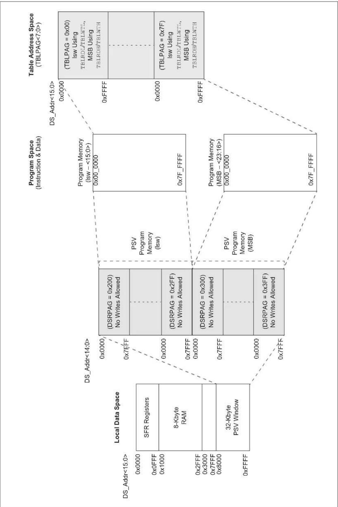
flowchart
graph TD
    A["Local Data Space"] -->|DS_Addr<15:0>| B["Local Data Space"]
    B -->|0x0000| C["SFR Registers"]
    B -->|0x1000| D["8-Kbyte RAM"]
    B -->|0x200| E["32-Kbyte PSV Window"]
    B -->|0x300| F["0x7FFF"]
    B -->|0x7FFF| G["0xFFFF"]
    C --> H["(DSRPAG = 0x200) No Writes Allowed"]
    D --> I["(DSRPAG = 0x2FF) No Writes Allowed"]
    E --> J["(DSRPAG = 0x300) No Writes Allowed"]
    F --> K["(DSRPAG = 0x3FF) No Writes Allowed"]
    G --> L["(DSRPAG = 0x7FFF)"]
    H --> M["(DSRPAG = 0x200) No Writes Allowed"]
    I --> N["(DSRPAG = 0x2FF) No Writes Allowed"]
    J --> O["(DSRPAG = 0x300) No Writes Allowed"]
    K --> P["(DSRPAG = 0x3FF) No Writes Allowed"]
    L --> Q["(DSRPAG = 0x7FFF)"]
    M --> R["(DSRPAG = 0x200) No Writes Allowed"]
    N --> S["(DSRPAG = 0x2FF) No Writes Allowed"]
    O --> T["(DSRPAG = 0x300) No Writes Allowed"]
    P --> U["(DSRPAG = 0x3FF) No Writes Allowed"]
    Q --> V["(DSRPAG = 0x7FFF)"]
    R --> W["(DSRPAG = 0x200) No Writes Allowed"]
    S --> X["(DSRPAG = 0x2FF) No Writes Allowed"]
    T --> Y["(DSRPAG = 0x300) No Writes Allowed"]
    U --> Z["(DSRPAG = 0x3FF) No Writes Allowed"]
    V --> AA["(DSRPAG = 0x7FFF)"]
    W --> AB["(DSRPAG = 0x200) No Writes Allowed"]
    X --> AC["(DSRPAG = 0x2FF) No Writes Allowed"]
    Y --> AD["(DSRPAG = 0x300) No Writes Allowed"]
    Z --> AE["(DSRPAG = 0x3FF) No Writes Allowed"]
    AA --> AF["(DSRPAG = 0x7FFF)"]
    AB --> AG["(DSRPAG = 0x200) No Writes Allowed"]
    AC --> AH["(DSRPAG = 0x2FF) No Writes Allowed"]
    AD --> AI["(DSRPAG = 0x300) No Writes Allowed"]
    AE --> AJ["(DSRPAG = 0x3FF) No Writes Allowed"]
    AF --> AK["(DSRPAG = 0x7FFF)"]
    AG --> AL["(DSRPAG = 0x200) No Writes Allowed"]
    AH --> AM["(DSRPAG = 0x2FF) No Writes Allowed"]
    AI --> AN["(DSRPAG = 0x300) No Writes Allowed"]
    AJ --> AO["(DSRPAG = 0x3FF) No Writes Allowed"]
    AK --> AP["(DSRPAG = 0x7FFF)"]
    AL --> AQ["(DSRPAG = 0x200) No Writes Allowed"]
    AM --> AR["(DSRPAG = 0x2FF) No Writes Allowed"]
    AN --> AS["(DSRPAG = 0x300) No Writes Allowed"]
    AO --> AT["(DSRPAG = 0x3FF) No Writes Allowed"]
    AP --> AU["(DSRPAG = 0x7FFF)"]
    AQ --> AV["(DSRPAG = 0x200) No Writes Allowed"]
    AR --> AW["(DSRPAG = 0x2FF) No Writes Allowed"]
    AS --> AX["(DSRPAG = 0x300) No Writes Allowed"]
    AT --> AY["(DSRPAG = 0x3FF) No Writes Allowed"]
    AU --> AZ["(DSRPAG = 0x7FFF)"]
    AV --> BA["(DSRPAG = 0x200) No Writes Allowed"]
    AW --> BB["(DSRPAG = 0x2FF) No Writes Allowed"]
    AX --> BC["(DSRPAG = 0x300) No Writes Allowed"]
    AY --> BD["(DSRPAG = 0x3FF) No Writes Allowed"]
    AZ --> BE["(DSRPAG = 0x7FFF)"]
    BA --> BF["(DSRPAG = 0x200) No Writes Allowed"]
    BB --> BG["(DSRPAG = 0x2FF) No Writes Allowed"]
    AC --> BH["(DSRPAG = 0x300) No Writes Allowed"]
    AD --> BI["(DSRPAG = 0x3FF) No Writes Allowed"]
    AE --> BJ["(DSRPAG = 0x7FFF)"]
    AF --> BK["(DSRPAG = 0x200) No Writes Allowed"]
    AG --> BL["(DSRPAG = 0x2FF) No Writes Allowed"]
    AH --> BM["(DSRPAG = 0x300) No Writes Allowed"]
    AI --> BN["(DSRPAG = 0x3FF) No Writes Allowed"]
    AJ --> BO["(DSRPAG = 0x7FFF)"]
    AK --> BP["(DSRPAG = 0x200) No Writes Allowed"]
    AL --> BQ["(DSRPAG = 0x2FF) No Writes Allowed"]
    AM --> BR["(DSRPAG = 0x300) No Writes Allowed"]
    AN --> BS["(DSRPAG = 0x3FF) No Writes Allowed"]
    AO --> BT["(DSRPAG = 0x7FFF)"]
    AP --> BU["(DSRPAG = 0x200) No Writes Allowed"]
    AQ --> BV["(DSRPAG = 0x2FF) No Writes Allowed"]
    AR --> BW["(DSRPAG = 0x300) No Writes Allowed"]
    AS --> BX["(DSRPAG = 0x3FF) No Writes Allowed"]
    AT --> BY["(DSRPAG = 0x7FFF)"]
    AU --> BZ["(DSRPAG = 0x200) No Writes Allowed"]
    AV --> CA["(DSRPAG = 0x2FF) No Writes Allowed"]
    AW --> CB["(DSRPAG = 0x300) No Writes Allowed"]
    AX --> CC["(DSRPAG = 0x3FF) No Writes Allowed"]
    AY --> OD["Table Address Space (TBLPAG<7:O>)"]
    AO --> EV["Table Address Space (TBLPAG= 0x7F)"]
    AP --> EG["Table Address Space (TBLPAG= 15:O>)"]
When a PSV page overflow or underflow occurs, EA<15> is cleared as a result of the register indirect EA calculation. An overflow or underflow of the EA in the PSV pages can occur at the page boundaries when:
- The initial address, prior to modification, addresses the PSV page
- The EA calculation uses Pre- or Post-Modified Register Indirect Addressing; however, this does not include Register Offset Addressing
In general, when an overflow is detected, the DSRPAG register is incremented and the EA<15> bit is set to keep the base address within the PSV window. When an underflow is detected, the DSRPAG register is decremented and the EA<15> bit is set to keep the base
address within the PSV window. This creates a linear PSV address space, but only when using Register Indirect Addressing modes.
Exceptions to the operation described above arise when entering and exiting the boundaries of Page 0 and PSV spaces. Table 4-16 lists the effects of overflow and underflow scenarios at different boundaries.
In the following cases, when overflow or underflow occurs, the EA<15> bit is set and the DSRPAG is not modified; therefore, the EA will wrap to the beginning of the current page:
- Register Indirect with Register Offset Addressing
- Modulo Addressing
- Bit-Reversed Addressing
TABLE 4-16: OVERFLOW AND UNDERFLOW SCENARIOS AT PAGE 0 AND PSV SPACE BOUNDARIES ^(2,3,4)
| O/U,R/W | Operation | Before After | |||||
| DSxPAG | DSEA<15> | PageDescription | DSxPAG | DSEA<15> | PageDescription | ||
| O,Read | [++Wn]or[Wn++] | DSRPAG = 0x2FF 1 | PSV: Last lswpage | DSRPAG = 0x300 1 | PSV: First MSBpage | ||
| O,Read | DSRPAG = 0x3FF 1 | PSV: Last MSBpage | DSRPAG = 0x3FF | 0 | See Note 1 | ||
| U,Read | [--Wn]or[Wn--] | DSRPAG = 0x001 | 1 | PSV page | DSRPAG = 0x001 | 0 | See Note 1 |
| U,Read | DSRPAG = 0x200 1 | PSV: First lswpage | DSRPAG = 0x200 | 0 | See Note 1 | ||
| U,Read | DSRPAG = 0x300 1 | PSV: First MSBpage | DSRPAG = 0x2FF 1 | PSV: Last lswpage | |||
Legend: O = Overflow, U = Underflow, R = Read, W = Write
Note 1: The Register Indirect Addressing now addresses a location in the base Data Space (0x0000-0x7FFF).
2: An EDS access, with DSRPAG = 0x000, will generate an address error trap.
3: Only reads from PS are supported using DSRPAG.
4: Pseudolinear Addressing is not supported for large offsets.
4.5.2 EXTENDED X DATA SPACE
The lower portion of the base address space range, between 0x0000 and 0x7FFF, is always accessible, regardless of the contents of the Data Space Read Page register. It is indirectly addressable through the register indirect instructions. It can be regarded as being located in the default EDS Page 0 (i.e., EDS address range of 0x000000 to 0x007FFF with the base address bit, EA<15>=0, for this address range). However, Page 0 cannot be accessed through the upper 32 Kbytes, 0x8000 to 0xFFFF, of base Data Space in combination with DSRPAG = 0x000. Consequently, DSRPAG is initialized to 0x001 at Reset.
Note 1: DSRPAG should not be used to access Page 0. An EDS access with DSRPAG set to 0x000 will generate an address error trap.
2: Clearing the DSRPAG in software has no effect.
The remaining PSV pages are only accessible using the DSRPAG register in combination with the upper 32 Kbytes, 0x8000 to 0xFFFF, of the base address, where base address bit, EA<15>=1.
4.5.3 SOFTWARE STACK
The W15 register serves as a dedicated Software Stack Pointer (SSP), and is automatically modified by exception processing, subroutine calls and returns; however, W15 can be referenced by any instruction in the same manner as all other W registers. This simplifies reading, writing and manipulating the Stack Pointer (for example, creating stack frames).
Note: To protect against misaligned stack accesses, W15<0> is fixed to '0' by the hardware.
W15 is initialized to 0x1000 during all Resets. This address ensures that the SSP points to valid RAM in all dsPIC33EPXXXGS70X/80X devices and permits stack availability for non-maskable trap exceptions. These can occur before the SSP is initialized by the user software. You can reprogram the SSP during initialization to any location within Data Space.
The Software Stack Pointer always points to the first available free word and fills the software stack, working from lower toward higher addresses. Figure 4-9 illustrates how it pre-decrements for a stack pop (read) and post-increments for a stack push (writes).
When the PC is pushed onto the stack, PC<15:0> are pushed onto the first available stack word, then PC<22:16> are pushed into the second available stack location. For a PC push during any CALL instruction, the MSB of the PC is zero-extended before the push, as shown in Figure 4-9. During exception processing, the MSB of the PC is concatenated with the lower eight bits of the CPU STATUS Register, SR. This allows the contents of SRL to be preserved automatically during interrupt processing.
Note 1: To maintain system Stack Pointer (W15) coherency, W15 is never subject to (EDS) paging, and is therefore, restricted to an address range of 0x0000 to 0xFFFF. The same applies to W14 when used as a Stack Frame Pointer (SFA = 1).
2: As the stack can be placed in, and can access X and Y spaces, care must be taken regarding its use, particularly with regard to local automatic variables in a C development environment
FIGURE 4-9: CALL STACK FRAME
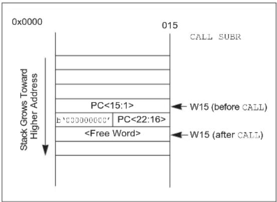
text_image
0x0000 Stack Grows Toward Higher Address 015 CALL SUBR PC<15:1> b'c30000000' PC<22:16>4.6 Instruction Addressing Modes
The addressing modes shown in Table 4-17 form the basis of the addressing modes optimized to support the specific features of individual instructions. The addressing modes provided in the MAC class of instructions differ from those in the other instruction types.
4.6.1 FILE REGISTER INSTRUCTIONS
Most file register instructions use a 13-bit address field (f) to directly address data present in the first 8192 bytes of data memory (Near Data Space). Most file register instructions employ a Working register, W0, which is denoted as WREG in these instructions. The destination is typically either the same file register or WREG (with the exception of the MUL instruction), which writes the result to a register or register pair. The MOV instruction allows additional flexibility and can access the entire Data Space.
4.6.2 MCU INSTRUCTIONS
The three-operand MCU instructions are of the form:
Operand 3 = Operand 1
where Operand 1 is always a Working register (that is, the addressing mode can only be Register Direct), which is referred to as Wb. Operand 2 can be a W register fetched from data memory or a 5-bit literal. The result location can either be a W register or a data memory location. The following addressing modes are supported by MCU instructions:
- Register Direct
- Register Indirect
- Register Indirect Post-Modified
- Register Indirect Pre-Modified
- 5-Bit or 10-Bit Literal
Note: Not all instructions support all the addressing modes given above. Individual instructions can support different subsets of these addressing modes.
TABLE 4-17: FUNDAMENTAL ADDRESSING MODES SUPPORTED
| Addressing Mode Description | |
| File Register Direct The address of the file register is specified explicitly. | |
| Register Direct The contents of a register are accessed directly. | |
| Register Indirect The contents of Wn form the Effective Address (EA). | |
| Register Indirect Post-Modified The contents of Wn form the EA. Wn is post-modified (incremented or decremented) by a constant value. | |
| Register Indirect Pre-Modified | Wn is pre-modified (incremented or decremented) by a signed constant value to form the EA. |
| Register Indirect with Register Offset (Register Indexed) | The sum of Wn and Wb forms the EA. |
| Register Indirect with Literal Offset | The sum of Wn and a literal forms the EA. |
4.6.3 MOVE AND ACCUMULATOR INSTRUCTIONS
Move instructions, and the DSP accumulator class of instructions, provide a greater degree of addressing flexibility than other instructions. In addition to the addressing modes supported by most MCU instructions, move and accumulator instructions also support Register Indirect with Register Offset Addressing mode, also referred to as Register Indexed mode.
| Note: | For the MOV instructions, the addressing mode specified in the instruction can differ for the source and destination EA. However, the 4-bit Wb (Register Offset) field is shared by both source and destination (but typically only used by one). |
In summary, the following addressing modes are supported by move and accumulator instructions:
- Register Direct
- Register Indirect
- Register Indirect Post-modified
- Register Indirect Pre-modified
- Register Indirect with Register Offset (Indexed)
- Register Indirect with Literal Offset
- 8-Bit Literal
- 16-Bit Literal
| Note: Not all instructions support all the addressing modes given above. Individual instructions may support different subsets of these addressing modes. |
4.6.4 MAC INSTRUCTIONS
The dual source operand DSP instructions (CLR, ED, EDAC, MAC, MPY, MPY.N, MOVSAC and MSC), also referred to as MAC instructions, use a simplified set of addressing modes to allow the user application to effectively manipulate the Data Pointers through register indirect tables.
The two-source operand prefetch registers must be members of the set {W8, W9, W10, W11}. For data reads, W8 and W9 are always directed to the X RAGU, and W10 and W11 are always directed to the Y AGU. The Effective Addresses generated (before and after modification) must therefore, be valid addresses within X Data Space for W8 and W9, and Y Data Space for W10 and W11.
| Note: Register Indirect with Register Offset Addressing mode is available only for W9 (in X space) and W11 (in Y space). |
In summary, the following addressing modes are supported by the MAC class of instructions:
- Register Indirect
- Register Indirect Post-Modified by 2
- Register Indirect Post-Modified by 4
- Register Indirect Post-Modified by 6
- Register Indirect with Register Offset (Indexed)
4.6.5 OTHER INSTRUCTIONS
Besides the addressing modes outlined previously, some instructions use literal constants of various sizes. For example, BRA (branch) instructions use 16-bit signed literals to specify the branch destination directly, whereas the DISI instruction uses a 14-bit unsigned literal field. In some instructions, such as ULNK, the source of an operand or result is implied by the opcode itself. Certain operations, such as a NOP, do not have any operands.
4.7 Modulo Addressing
Modulo Addressing mode is a method of providing an automated means to support circular data buffers using hardware. The objective is to remove the need for software to perform data address boundary checks when executing tightly looped code, as is typical in many DSP algorithms.
Modulo Addressing can operate in either Data or Program Space (since the Data Pointer mechanism is essentially the same for both). One circular buffer can be supported in each of the X (which also provides the pointers into Program Space) and Y Data Spaces. Modulo Addressing can operate on any W Register Pointer. However, it is not advisable to use W14 or W15 for Modulo Addressing since these two registers are used as the Stack Frame Pointer and Stack Pointer, respectively.
In general, any particular circular buffer can be configured to operate in only one direction, as there are certain restrictions on the buffer start address (for incrementing buffers) or end address (for decrementing buffers), based upon the direction of the buffer.
The only exception to the usage restrictions is for buffers that have a power-of-two length. As these buffers satisfy the start and end address criteria, they can operate in a Bidirectional mode (that is, address boundary checks are performed on both the lower and upper address boundaries).
4.7.1 START AND END ADDRESS
The Modulo Addressing scheme requires that a starting and ending address be specified and loaded into the 16-bit Modulo Buffer Address registers: XMODSRT, XMODEND, YMODSRT and YMODEND (see Table4-2).
Note: Y space Modulo Addressing EA calculations assume word-sized data (LSb of every EA is always clear).
The length of a circular buffer is not directly specified. It is determined by the difference between the corresponding start and end addresses. The maximum possible length of the circular buffer is 32K words (64 Kbytes).
4.7.2 W ADDRESS REGISTER SELECTION
The Modulo and Bit-Reversed Addressing Control register, MODCON<15:0>, contains enable flags, as well as a W register field to specify the W Address registers. The XWM and YWM fields select the registers that operate with Modulo Addressing:
- If XWM = 1111, X RAGU and X WAGU Modulo Addressing is disabled
- I f Y W M = 1111, Y AGU Modulo Addressing is disabled
The X Address Space Pointer W (XWM) register, to which Modulo Addressing is to be applied, is stored in MODCON<3:0> (see Table 4-2). Modulo Addressing is enabled for X Data Space when XWM is set to any value other than '1111' and the XMODEN bit is set (MODCON<15>).
The Y Address Space Pointer W (YWM) register, to which Modulo Addressing is to be applied, is stored in MODCON<7:4>. Modulo Addressing is enabled for Y Data Space when YWM is set to any value other than '1111' and the YMODEN bit (MODCON<14>) is set.
FIGURE 4-10: MODULO ADDRESSING OPERATION EXAMPLE

text_image
Byte Address 0x1100 0x1163 Start Addr = 0x1100 End Addr = 0x1163 Length = 0x0032 words MOV #0x1100, WO MOV WO, XMODSRT ;set modulo start address MOV #0x1163, WO MOV WO, MODEND ;set modulo end address MOV #0x8001, WO MOV WO, MODCON ;enable W1, X AGU for modulo MOV #0x0000, WO ;WO holds buffer fill value MOV #0x1110, W1 ;point W1 to buffer DO AGAIN, #0x31 ;fill the 50 buffer locations MOV WO, [W1++] ;fill the next location AGAIN: INC WO, WO ;increment the fill value4.7.3 MODULO ADDRESSING APPLICABILITY
Modulo Addressing can be applied to the Effective Address (EA) calculation associated with any W register. Address boundaries check for addresses equal to:
- The upper boundary addresses for incrementing buffers
- The lower boundary addresses for decrementing buffers
It is important to realize that the address boundaries check for addresses less than or greater than the upper (for incrementing buffers) and lower (for decrementing buffers) boundary addresses (not just equal to). Address changes can therefore, jump beyond boundaries and still be adjusted correctly.
Note: The modulo corrected Effective Address is written back to the register only when Pre-Modify or Post-Modify Addressing mode is used to compute the Effective Address. When an address offset (such as [W7 + W2]) is used, Modulo Addressing correction is performed, but the contents of the register remain unchanged.
4.8 Bit-Reversed Addressing
Bit-Reversed Addressing mode is intended to simplify data reordering for radix-2 FFT algorithms. It is supported by the X AGU for data writes only.
The modifier, which can be a constant value or register contents, is regarded as having its bit order reversed. The address source and destination are kept in normal order. Thus, the only operand requiring reversal is the modifier.
4.8.1 BIT-REVERSED ADDRESSING IMPLEMENTATION
Bit-Reversed Addressing mode is enabled when all of these situations are met:
- BWMx bits (W register selection) in the MODCON register are any value other than '1111' (the stack cannot be accessed using Bit-Reversed Addressing)
- The BREN bit is set in the XBREV register
- The addressing mode used is Register Indirect with Pre-Increment or Post-Increment
If the length of a bit-reversed buffer is M = 2^N bytes, the last 'N' bits of the data buffer start address must be zeros.
XB<14:0> is the Bit-Reversed Addressing modifier, or 'pivot point', which is typically a constant. In the case of an FFT computation, its value is equal to half of the FFT data buffer size.
Note: All bit-reversed EA calculations assume word-sized data (LSb of every EA is always clear). The XB value is scaled accordingly to generate compatible (byte) addresses.
When enabled, Bit-Reversed Addressing is executed only for Register Indirect with Pre-Increment or Post-Increment Addressing and word-sized data writes. It does not function for any other addressing mode or for byte-sized data and normal addresses are generated instead. When Bit-Reversed Addressing is active, the W Address Pointer is always added to the address modifier (XB) and the offset associated with the Register Indirect Addressing mode is ignored. In addition, as word-sized data is a requirement, the LSb of the EA is ignored (and always clear).
Note: Modulo Addressing and Bit-Reversed Addressing can be enabled simultaneously using the same W register, but Bit-Reversed Addressing operation will always take precedence for data writes when enabled.
If Bit-Reversed Addressing has already been enabled by setting the BREN (XBREV<15>) bit, a write to the XBREV register should not be immediately followed by an indirect read operation using the W register that has been designated as the Bit-Reversed Pointer.
FIGURE 4-11: BIT-REVERSED ADDRESSING EXAMPLE
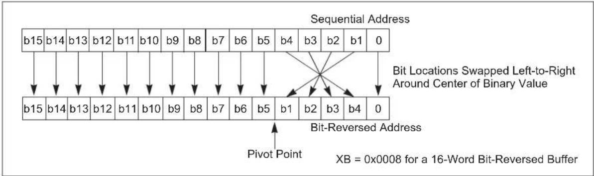
flowchart
graph TD
    A["Sequential Address"] --> B["b15 b14 b13 b12 b11 b10 b9 b8 b7 b6 b5 b4 b3 b2 b1 0"]
    B --> C["b15 b14 b13 b12 b11 b10 b9 b8 b7 b6 b5 b1 b2 b3 b4 0"]
    C --> D["Pivot Point"]
    D --> E["Bit-Reversed Address"]
    E --> F["XB = 0x0008 for a 16-Word Bit-Reversed Buffer"]
    style A fill:#f9f,stroke:#333
    style B fill:#ccf,stroke:#333
    style C fill:#cfc,stroke:#333
    style D fill:#fcc,stroke:#333
    style E fill:#ffc,stroke:#333
    style F fill:#fcc,stroke:#333
TABLE 4-18: BIT-REVERSED ADDRESSING SEQUENCE (16-ENTRY)
| Normal Address Bit-Reversed Address | |||||||||
| A3 A2 | A1 A0 | Decimal | A3 A2 | A1 A0 Decimal | |||||
| 0 | 0 | 0 | 0 | 0 0 | 0 | 0 | 0 | 0 | |
| 0 | 0 | 0 | 1 | 1 1 | 0 | 0 | 0 | 8 | |
| 0 | 0 | 1 | 0 | 2 0 | 1 | 0 | 0 | 4 | |
| 0 | 0 | 1 | 1 | 3 1 | 1 | 0 | 0 | 12 | |
| 0 | 1 | 0 | 0 | 4 0 | 0 | 1 | 0 | 2 | |
| 0 | 1 | 0 | 1 | 5 1 | 0 | 1 | 0 | 10 | |
| 0 | 1 | 1 | 0 | 6 0 | 1 | 1 | 0 | 6 | |
| 0 | 1 | 1 | 1 | 7 1 | 1 | 1 | 0 | 14 | |
| 1 | 0 | 0 | 0 | 8 0 | 0 | 0 | 1 | 1 | |
| 1 | 0 | 0 | 1 | 9 1 | 0 | 0 | 1 | 9 | |
| 1 | 0 | 1 | 0 | 10 0 | 1 | 0 | 1 | 5 | |
| 1 | 0 | 1 | 1 | 11 | 1 | 1 | 0 | 1 | 13 |
| 1 | 1 | 0 | 0 | 12 0 | 0 | 1 | 1 | 3 | |
| 1 | 1 | 0 | 1 | 13 | 1 | 0 | 1 | 1 | 11 |
| 1 | 1 | 1 | 0 | 14 0 | 1 | 1 | 1 | 7 | |
| 1 | 1 | 1 | 1 | 15 1 | 1 | 1 | 1 | 15 | |
4.9 Interfacing Program and Data Memory Spaces
The dsPIC33EPXXXGS70X/80X family architecture uses a 24-bit wide Program Space (PS) and a 16-bit wide Data Space (DS). The architecture is also a modified Harvard scheme, meaning that data can also be present in the Program Space. To use this data successfully, it must be accessed in a way that preserves the alignment of information in both spaces.
Aside from normal execution, the architecture of the dsPIC33EPXXXGS70X/80X family devices provides two methods by which Program Space can be accessed during operation:
- Using table instructions to access individual bytes or words anywhere in the Program Space
- Remapping a portion of the Program Space into the Data Space (Program Space Visibility)
Table instructions allow an application to read or write to small areas of the program memory. This capability makes the method ideal for accessing data tables that need to be updated periodically. It also allows access to all bytes of the program word. The remapping method allows an application to access a large block of data on a read-only basis, which is ideal for look-ups from a large table of static data. The application can only access the least significant word of the program word.
TABLE 4-19: PROGRAM SPACE ADDRESS CONSTRUCTION
| Access Type | Access Space | Program Space Address | ||||
| <23> | <22:16> | <15> | <14:1> | <0> | ||
| Instruction Access (Code Execution) | User 0 PC<22:1> 0 | |||||
| 0xxx xxxx xxxx xxxx xxxx xxxx | ||||||
| TBLRD/TBLWT (Byte/Word Read/Write) | User | TBLPAG<7:0> | Data EA<15:0> | |||
| 0xxx xxxx | xxxx xxxx xxxx | |||||
| Configuration | TBLPAG<7:0> | Data EA<15:0> | ||||
| 1xxx xxxx | xxxx xxxx xxxx | |||||
FIGURE 4-12: DATA ACCESS FROM PROGRAM SPACE ADDRESS GENERATION

flowchart
graph TD
    A["Program Counter(1)"] --> B["0"]
    B --> C["Program Counter"]
    C --> D["0"]
    D --> E["23 Bits"]
    E --> F["EA"]
    F --> G["1/0"]
    G --> H["Table Operations(2)"]
    H --> I["1/0"]
    I --> J["TBLPAG"]
    J --> K["8 Bits"]
    K --> L["16 Bits"]
    L --> M["24 Bits"]
    M --> N["User/Configuration Space Select"]
    M --> O["Byte Select"]
Note 1: The Least Significant bit (LSb) of Program Space addresses is always fixed as '0' to maintain word alignment of data in the Program and Data Spaces.
2: Table operations are not required to be word-aligned. Table Read operations are permitted in the configuration memory space.
4.9.1 DATA ACCESS FROM PROGRAM MEMORY USING TABLE INSTRUCTIONS
The TBLRDL and TBLWTL instructions offer a direct method of reading or writing the lower word of any address within the Program Space without going through Data Space. The TBLRDH and TBLWTH instructions are the only method to read or write the upper eight bits of a Program Space word as data.
The PC is incremented by two for each successive 24-bit program word. This allows program memory addresses to directly map to Data Space addresses. Program memory can thus be regarded as two 16-bit wide word address spaces, residing side by side, each with the same address range. TBLRDL and TBLWTL access the space that contains the least significant data word. TBLRDH and TBLWTH access the space that contains the upper data byte.
Two table instructions are provided to move byte or word-sized (16-bit) data to and from Program Space. Both function as either byte or word operations.
• TBLRDL (Table Read Low):
- In Word mode, this instruction maps the lower word of the Program Space location (P<15:0>) to a data address (D<15:0>)
- In Byte mode, either the upper or lower byte of the lower program word is mapped to the lower byte of a data address. The upper byte is selected when Byte Select is '1'; the lower byte is selected when it is '0'.
• TBLRDH (Table Read High):
- In Word mode, this instruction maps the entire upper word of a program address (P<23:16>) to a data address. The 'phantom' byte (D<15:8>) is always '0'.
- In Byte mode, this instruction maps the upper or lower byte of the program word to D<7:0> of the data address in the TBLRDL instruction. The data is always '0' when the upper 'phantom' byte is selected (Byte Select = 1).
In a similar fashion, two table instructions, TBLWTH and TBLWTL, are used to write individual bytes or words to a Program Space address. The details of their operation are explained in Section 5.0 "Flash Program Memory".
For all table operations, the area of program memory space to be accessed is determined by the Table Page register (TBLPAG). TBLPAG covers the entire program memory space of the device, including user application and configuration spaces. When TBLPAG<7> = 0, the table page is located in the user memory space. When TBLPAG<7> = 1, the page is located in configuration space.
FIGURE 4-13: ACCESSING PROGRAM MEMORY WITH TABLE INSTRUCTIONS
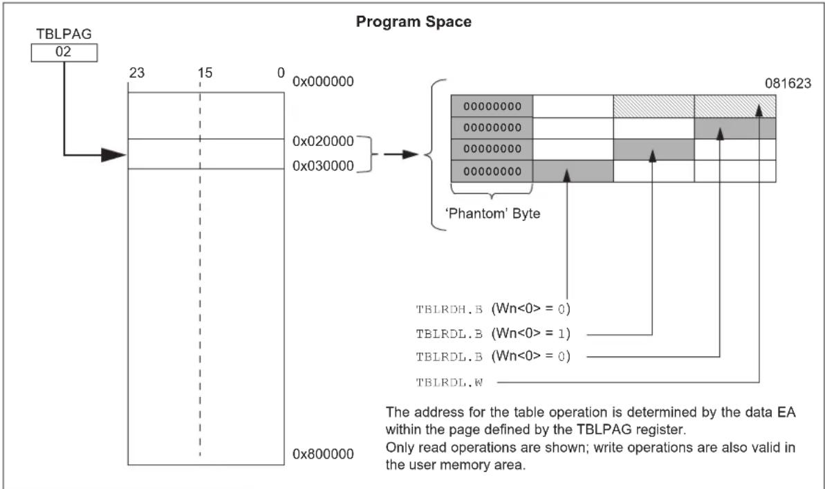
flowchart
graph TD
    A["TBLPAG 02"] --> B["Program Space"]
    B --> C["0x800000"]
    C --> D["0x030000"]
    D --> E["0x020000"]
    E --> F["0x000000"]
    F --> G["0x000000"]
    G --> H["0x000000"]
    H --> I["0x000000"]
    I --> J["0x000000"]
    J --> K["0x000000"]
    K --> L["0x000000"]
    L --> M["0x000000"]
    M --> N["0x000000"]
    N --> O["0x000000"]
    O --> P["0x000000"]
    P --> Q["0x000000"]
    Q --> R["0x000000"]
    R --> S["0x800000"]
    S --> T["TBLRDH.B (Wn<0> = 1)"]
    S --> U["TBLRDL.B (Wn<0> = 1)"]
    S --> V["TBLRDL.W (Wn<0> = 1)"]
    S --> W["TBLRDL.W (Wn<0> = 1)"]
    S --> X["TBLRDL.W (Wn<0> = 1)"]
    S --> Y["TBLRDL.W (Wn<0> = 1)"]
    S --> Z["TBLRDL.W (Wn<0> = 1)"]
    S --> AA["TBLRDL.W (Wn<0> = 1)"]
    S --> AB["TBLRDL.W (Wn<0> = 1)"]
    S --> AC["TBLRDL.W (Wn<0> = 1)"]
    S --> AD["TBLRDL.W (Wn<0> = 1)"]
    S --> AE["TBLRDL.W (Wn<0> = 1)"]
    S --> AF["TBLRDL.W (Wn<0> = 1)"]
    S --> AG["TBLRDL.W (Wn<0> = 1)"]
    S --> AH["TBLRDL.W (Wn<0> = 1)"]
    S --> AI["TBLRDL.W (Wn<0> = 1)"]
    S --> AJ["TBLRDL.W (Wn<0> = 1)"]
    S --> AK["TBLRDL.W (Wn<0> = 1)"]
    S --> AL["TBLRDL.W (Wn<0> = 1)"]
    S --> AM["TBLRDL.W (Wn<0> = 1)"]
    S --> AN["TBLRDL.W (Wn<0> = 1)"]
    S --> AO["TBLRDL.W (Wn<0> = 1)"]
    S --> AP["TBLRDL.W (Wn<0> = 1)"]
    S --> AQ["TBLRDL.W (Wn<0> = 1)"]
    S --> AR["TBLRDL.W (Wn<0> = 1)"]
    S --> AS["TBLRDL.W (Wn<0> = 1)"]
    S --> AT["TBLRDL.W (Wn<0> = 1)"]
    S --> AU["TBLRDL.W (Wn<0> = 1)"]
    S --> AV["TBLRDL.W (Wn<0> = 1)"]
    S --> AW["TBLRDL.W (Wn<0> = 1)"]
    S --> AX["TBLRDL.W (Wn<0> = 1)"]
    S --> AY["TBLRDL.W (Wn<0> = 1)"]
    S --> AZ["TBLRDL.W (Wn<0> = 1)"]
    S --> BA["TBLRDL.W (Wn<0> = 1)"]
    S --> BB["TBLRDL.W (Wn<0> = 1)"]
    S --> BC["TBLRDL.W (Wn<0> = 1)"]
    S --> BD["TBLRDL.W (Wn<0> = 1)"]
    S --> BE["TBLRDL.W (Wn<0> = 1)"]
    S --> BF["TBLRDL.W (Wn<0> = 1)"]
    S --> BG["TBLRDL.W (Wn<0> = 1)"]
    S --> BH["TBLRDL.W (Wn<0> = 1)"]
    S --> BI["TBLRDL.W (Wn<0> = 1)"]
    S --> BJ["TBLRDL.W (Wn<0> = 1)"]
    S --> BK["TBLRDL.W (Wn<0> = 1)"]
    S --> BL["TBLRDL.W (Wn<0> = 1)"]
    S --> BM["TBLRDL.W (Wn<0> = 1)"]
    S --> BN["TBLRDL.W (Wn<0> = 1)"]
    S --> BO["TBLRDL.W (Wn<0> = 1)"]
    S --> BP["TBLRDL.W (Wn<0> = 1)"]
    S --> BQ["TBLRDL.W (Wn<0> = 1)"]
    S --> BR["TBLRDL.W (Wn<0> = 1)"]
    S --> BS["TBLRDL.W (Wn<0> = 1)"]
    S --> BT["TBLRDL.W (Wn<0> = 1)"]
    S --> BU["TBLRDL.W (Wn<0> = 1)"]
    S --> BV["TBLRDL.W (Wn<0> = 1)"]
    S --> BW["TBLRDL.W (Wn<0> = 1)"]
NOTES:
5.0 FLASH PROGRAM MEMORY
Note 1: This data sheet summarizes the features of the dsPIC33EPXXXGS70X/80X family of devices. It is not intended to be a comprehensive reference source. To complement the information in this data sheet, refer to "Dual Partition Flash Program Memory" (DS70005156) in the "dsPIC33/PIC24 Family Reference Manual", which is available from the Microchip website (www.microchip.com)
2: Some registers and associated bits described in this section may not be available on all devices. Refer to Section 4.0 "Memory Organization" in this data sheet for device-specific register and bit information.
The dsPIC33EPXXXGS70X/80X family devices contain internal Program Flash Memory for storing and executing application code. The memory is readable, writable and erasable during normal operation over the entire VDD range.
Flash memory can be programmed in three ways:
- In-Circuit Serial Programming™ (ICSP™) programming capability
• Enhanced In-Circuit Serial Programming (Enhanced ICSP)
• Run-Time Self-Programming (RTSP)
ICSP allows for a dsPIC33EPXXXGS70X/80X family device to be serially programmed while in the end application circuit. This is done with a programming clock and programming data (PGECx/PGEDx) line, and three other lines for power (VDD), ground (Vss) and Master Clear (MCLR). This allows customers to
manufacture boards with unprogrammed devices and then program the device just before shipping the product. This also allows the most recent firmware or a custom firmware to be programmed.
Enhanced In-Circuit Serial Programming uses an on-board bootloader, known as the Program Executive, to manage the programming process. Using an SPI data frame format, the Program Executive can erase, program and verify program memory. For more information on Enhanced ICSP, see the device programming specification.
RTSP is accomplished using TBLRD (Table Read) and TBLWT (Table Write) instructions. With RTSP, the user application can write program memory data with a single program memory word and erase program memory in blocks or 'pages' of 512 instructions (1536 bytes) at a time.
5.1 Table Instructions and Flash Programming
Regardless of the method used, all programming of Flash memory is done with the Table Read and Table Write instructions. These instructions allow direct read and write access to the program memory space, from the data memory, while the device is in normal operating mode. The 24-bit target address in the program memory is formed using bits<7:0> of the TBLPAG register and the Effective Address (EA) from a W register, specified in the table instruction, as shown in Figure 5-1. The TBLRDL and the TBLWTL instructions are used to read or write to bits<15:0> of program memory. TBLRDL and TBLWTL can access program memory in both Word and Byte modes. The TBLRDH and TBLWTH instructions are used to read or write to bits<23:16> of program memory. TBLRDH and TBLWTH can also access program memory in Word or Byte mode.
FIGURE 5-1: ADDRESSING FOR TABLE REGISTERS
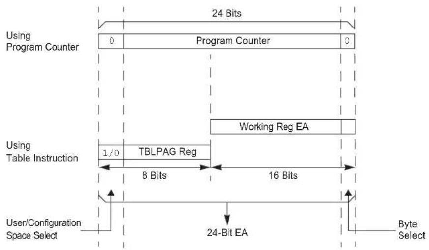
text_image
Using Program Counter 24 Bits 0 Program Counter 0 Working Reg EA Using Table Instruction 1/0 TBLPAG Reg 8 Bits 16 Bits User/Configuration Space Select 24-Bit EA Byte Select5.2 RTSP Operation
The dsPIC33EPXXXGS70X/80X family Flash program memory array is organized into rows of 64 instructions or 192 bytes. RTSP allows the user application to erase a single page (8 rows or 512 instructions) of memory at a time and to program one row at a time. It is possible to program two instructions at a time as well.
The page erase and single row write blocks are edge-aligned, from the beginning of program memory, on boundaries of 1536 bytes and 192 bytes, respectively. Figure 30-14 in Section 30.0 “Electrical Characteristics” lists the typical erase and programming times.
Row programming is performed by loading 192 bytes into data memory and then loading the address of the first byte in that row into the NVMSRCADR register. Once the write has been initiated, the device will automatically load the write latches and increment the NVMSRCADR and the NVMADR(U) registers until all bytes have been programmed. The RPDF bit (NVMCON<9>) selects the format of the stored data in RAM to be either compressed or uncompressed. See Figure 5-2 for data formatting. Compressed data helps to reduce the amount of required RAM by using the upper byte of the second word for the MSB of the second instruction.
The basic sequence for RTSP word programming is to use the TBLWTL and TBLWTH instructions to load two of the 24-bit instructions into the write latches found in configuration memory space. Refer to Figure 4-1 through Figure 4-4 for write latch addresses. Programming is performed by unlocking and setting the control bits in the NVMCON register.
All erase and program operations may optionally use the NVM interrupt to signal the successful completion of the operation. For example, when performing Flash write operations on the Inactive Partition in Dual Partition mode, where the CPU remains running, it is necessary to wait for the NVM interrupt before programming the next block of Flash program memory.
FIGURE 5-2: UNCOMPRESSED/
COMPRESSED FORMAT
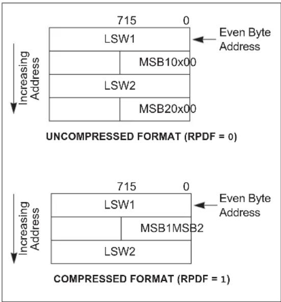
text_image
715 0 LSW1 Even Byte Address MSB10x00 LSW2 MSB20x00 INCOMPRESSED FORMAT (RPDF = 0) 715 0 LSW1 Even Byte Address MSB1MSB2 LSW2 INCOMPRESSED FORMAT (RPDF = 1)5.3 Programming Operations
A complete programming sequence is necessary for programming or erasing the internal Flash in RTSP mode. The processor stalls (waits) until the programming operation is finished. Setting the WR bit (NVMCON<15>) starts the operation and the WR bit is automatically cleared when the operation is finished.
5.3.1 PROGRAMMING ALGORITHM FOR FLASH PROGRAM MEMORY
Programmers can program two adjacent words (24 bits x 2) of Program Flash Memory at a time on every other word address boundary (0x000000, 0x000004, 0x000008, etc.). To do this, it is necessary to erase the page that contains the desired address of the location the user wants to change. For protection against accidental operations, the write initiate sequence for NVMKEY must be used to allow any erase or program operation to proceed. After the programming command has been executed, the user application must wait for the programming time until programming is complete. The two instructions following the start of the programming sequence should be NOPs.
5.4 Dual Partition Flash Configuration
For dsPIC33EPXXXGS70X/80X devices operating in Dual Partition Flash Program Memory modes, the Inactive Partition can be erased and programmed without stalling the processor. The same programming algorithms are used for programming and erasing the Flash in the Inactive Partition, as described in Section 5.2 "RTSP Operation". On top of the page erase option, the entire Flash memory of the Inactive Partition can be erased by configuring the NVMOP<3:0> bits in the NVMCON register.
Note 1: The application software to be loaded into the Inactive Partition will have the address of the Active Partition. The bootloader firmware will need to offset the address by 0x400000 in order to write to the Inactive Partition.
5.4.1 FLASH PARTITION SWAPPING
The Boot Sequence Number is used for determining the Active Partition at start-up and is encoded within the FBTSEQ Configuration register bits. Unlike most Configuration registers, which only utilize the lower 16 bits of the program memory, FBTSEQ is a 24-bit Configuration Word. The Boot Sequence Number (BSEQ) is a 12-bit value and is stored in FBTSEQ twice. The true value is stored in bits, FBTSEQ<11:0>, and its complement is stored in bits, FBTSEQ<23:12>. At device Reset, the sequence numbers are read and the partition with the lowest sequence number becomes the Active Partition. If one of the Boot Sequence Numbers is invalid, the device will select the partition with the valid Boot Sequence Number, or default to Partition 1 if both sequence numbers are invalid. See Section 27.0 "Special Features" for more information.
The BOOTSWP instruction provides an alternative means of swapping the Active and Inactive Partitions (soft swap) without the need for a device Reset. The BOOTSWP must always be followed by a GOTO instruction. The BOOTSWP instruction swaps the Active and Inactive Partitions, and the PC vectors to the location specified by the GOTO instruction in the newly Active Partition.
It is important to note that interrupts should temporarily be disabled while performing the soft swap sequence and that after the partition swap, all peripherals and interrupts which were enabled remain enabled. Additionally, the RAM and stack will maintain state after the switch. As a result, it is recommended that applications using soft swaps jump to a routine that will reinitialize the device in order to ensure the firmware runs as expected. The Configuration registers will have no effect during a soft swap.
For robustness of operation, in order to execute the BOOTSWP instruction, it is necessary to execute the NVM unlocking sequence as follows:
- Write 0x55 to NVMKEY.
- Write 0xAA to NVMKEY.
- Execute the BOOTSWP instruction.
If the unlocking sequence is not performed, the BOOTSWP instruction will be executed as a forced NOP and a GOTO instruction, following the BOOTSWP instruction, will be executed, causing the PC to jump to that location in the current operating partition.
The SFTSWP and P2ACTIV bits in the NVMCON register are used to determine a successful swap of the Active and Inactive Partitions, as well as which partition is active. After the BOOTSWP and GOTO instructions, the SFTSWP bit should be polled to verify the partition swap has occurred and then cleared for the next panel swap event.
5.4.2 DUAL PARTITION MODES
While operating in Dual Partition mode, the dsPIC33EPXXXGS70X/80X family devices have the option for both partitions to have their own defined security segments, as shown in Figure 27-4. Alternatively, the device can operate in Protected Dual Partition mode, where Partition 1 becomes permanently erase/write-protected. Protected Dual Partition mode allows for a "Factory Default" mode, which provides a fail-safe backup image to be stored in Partition 1.
dsPIC33EPXXXGS70X/80X family devices can also operate in Privileged Dual Partition mode, where additional security protections are implemented to allow for protection of intellectual property when multiple parties have software within the device. In Privileged Dual Partition mode, both partitions place additional restrictions on the FBSLIM register. These prevent changes to the size of the Boot Segment and General Segment, ensuring that neither segment will be altered.
5.5 Flash Memory Resources
Many useful resources are provided on the main product page of the Microchip website for the devices listed in this data sheet. This product page contains the latest updates and additional information.
5.5.1 KEY RESOURCES
- “Dual Partition Flash Program Memory” (DS70005156) in the “dsPIC33/PIC24 Family Reference Manual”
- Code Samples
- Application Notes
- Software Libraries
- Webinars
- All Related "dsPIC33/PIC24 Family Reference Manual" Sections
- Development Tools
5.6 Control Registers
Five SFRs are used to write and erase the Program Flash Memory: NVMCON, NVMKEY, NVMADR, NVMADRU and NVMSRCADR/H.
The NVMCON register (Register 5-1) selects the operation to be performed (page erase, word/row program, Inactive Partition erase), initiates the program or erase cycle and is used to determine the Active Partition in Dual Partition modes.
NVMKEY (Register 5-4) is a write-only register that is used for write protection. To start a programming or erase sequence, the user application must consecutively write 0x55 and 0xAA to the NVMKEY register.
There are two NVM Address registers: NVMADRU and NVMADR. These two registers, when concatenated, form the 24-bit Effective Address (EA) of the selected word/row for programming operations, or the selected page for erase operations. The NVMADRU register is used to hold the upper eight bits of the EA, while the NVMADR register is used to hold the lower 16 bits of the EA.
For row programming operation, data to be written to Program Flash Memory is written into data memory space (RAM) at an address defined by the NVMSRCADR register (location of first element in row programming data).
REGISTER 5-1: NVMCON: NONVOLATILE MEMORY (NVM) CONTROL REGISTER
| R/SO-0^(1) | R/W-0^(1) | R/W-0^(1) | R/W-0 | R/C-0 | R-0 | R/W-0 | R/C-0 |
| WR WRE | N WRERR NV | MSIDL | (2) | SFTSWP(6) | P2ACTIV(6) | RPDF URERR | |
| bit 15 bit 8 | |||||||
| U-0 U-0 U-0 U-0 R/W-0 | (1) | R/W-0(1) | R/W-0(1) | R/W-0(1) | |||
| — | — | — | — | NVMOP3(3,4) | NVMOP2(3,4) | NVMOP1(3,4) | NVMOP0(3,4) |
| bit 7 bit 0 | |||||||
| Legend: | C = Clearable bit | SO = Settable Only bit |
| R = Readable bit | W = Writable bit | U = Unimplemented bit, read as ‘0’ |
| -n = Value at POR | ‘1’ = Bit is set | ‘0’ = Bit is cleared x = Bit is unknown |
bit 15 WR: Write Control bit ^(1) 1 = Initiates a Flash Memory Program or erase operation; the operation is self-timed and the bit is cleared by hardware once the operation is complete
0 = Program or erase operation is complete and inactive
bit 14 WREN: Write Enable bit ^(1) 1 = Enables Flash program/erase operations 0 = Inhibits Flash program/erase operations
bit 13 WRERR: Write Sequence Error Flag bit ^(1) 1 = An improper program or erase sequence attempt, or termination has occurred (bit is set automatically on any set attempt of the WR bit)
0 = The program or erase operation completed normally
bit 12 NVMSIDL: NVM Stop in Idle Control bit ^(2) 1 = Flash voltage regulator goes into Standby mode during Idle mode
0 = Flash voltage regulator is active during Idle mode
bit 11 SFTSWP: Partition Soft Swap Status bit ^(6) 1 = Partitions have been successfully swapped using the BOOTSWP instruction (soft swap)
0 = Awaiting successful partition swap using the BOOTSWP instruction or a device Reset will determine the Active Partition based on the FBTSEQ register
bit 10 P2ACTIV: Partition 2 Active Status bit ^(6) 1 = Partition 2 Flash is mapped into the active region 0 = Partition 1 Flash is mapped into the active region
bit 9 RPDF: Row Programming Data Format bit 1 = Row data to be stored in RAM is in compressed format 0 = Row data to be stored in RAM is in uncompressed format
Note 1: These bits can only be reset on a POR. 2: If this bit is set, power consumption will be further reduced (IIDLE) and upon exiting Idle mode, there is a delay (TVREG) before Flash memory becomes operational.
3: All other combinations of NVMOP<3:0> are unimplemented. 4: Execution of the PWRSAV instruction is ignored while any of the NVM operations are in progress.
5: Two adjacent words on a 4-word boundary are programmed during execution of this operation.
6: Only applicable when operating in Dual Partition mode.
7: The specific Boot mode depends on bits<1:0> of the programmed data:
11 = Single Partition Flash mode
10 = Dual Partition Flash mode
01 = Protected Dual Partition Flash mode
00 = Reserved
REGISTER 5-1: NVMCON: NONVOLATILE MEMORY (NVM) CONTROL REGISTER (CONTINUED)
bit 8 URERR: Row Programming Data Underrun Error bit
1 = Indicates row programming operation has been terminated
0 = No data underrun error is detected
bit 7-4 Unimplemented: Read as '0'
bit 3-0 NVMOP<3:0>: NVM Operation Select bits (1,3,4)
1111 = Reserved
1110 = User memory bulk erase operation
1011 = Reserved
1010 = Reserved
1001 = Reserved
1000 = Boot memory double-word program operation in a Dual Partition Flash mode ^7
0101 = Reserved
0100 = Inactive Partition memory erase operation
0011 = Memory page erase operation
0010 = Memory row program operation
0001 = Memory double-word program operation ^(5)
0000 = Reserved
Note 1: These bits can only be reset on a POR.
2: If this bit is set, power consumption will be further reduced (I IDLE) and upon exiting Idle mode, there is a delay (TvREG) before Flash memory becomes operational.
3: All other combinations of NVMOP<3:0> are unimplemented.
4: Execution of the PWRSAV instruction is ignored while any of the NVM operations are in progress.
5: Two adjacent words on a 4-word boundary are programmed during execution of this operation.
6: Only applicable when operating in Dual Partition mode.
7: The specific Boot mode depends on bits<1:0> of the programmed data:
11 = Single Partition Flash mode
10 = Dual Partition Flash mode
01 = Protected Dual Partition Flash mode
00 = Reserved
REGISTER 5-2: NVMADR: NONVOLATILE MEMORY LOWER ADDRESS REGISTER
| R/W-x R/W-x R/W-x R/W-x R/W-x R/W-x R/W-x R/W-x |
| NVMADR<15:8> |
| bit 15 bit 8 |
| R/W-x R/W-x R/W-x R/W-x R/W-x R/W-x R/W-x R/W-x |
| NVMADR<7:0> |
| bit 7 bit 0 |
Legend:
R = Readable bit W = Writable bit U = Unimplemented bit, read as '0'
-n = Value at POR '1' = Bit is set '0' = Bit is cleared x = Bit is unknown
bit 15-0 NVMADR<15:0>: Nonvolatile Memory Lower Write Address bits
Selects the lower 16 bits of the location to program or erase in Program Flash Memory. This register may be read or written to by the user application.
REGISTER 5-3: NVMADRU: NONVOLATILE MEMORY UPPER ADDRESS REGISTER
| R/W-x R/W-x R/W-x R/W-x R/W-x R/W-x R/W-x R/W-x |
| NVMADRU<23:16> |
| bit 7 bit 0 |
Legend:
R = Readable bit W = Writable bit U = Unimplemented bit, read as '0'
-n = Value at POR '1' = Bit is set '0' = Bit is cleared x = Bit is unknown
bit 15-8 Unimplemented: Read as '0'
bit 7-0 NVMADRU<23:16>: Nonvolatile Memory Upper Write Address bits
Selects the upper eight bits of the location to program or erase in Program Flash Memory. This register may be read or written to by the user application.
REGISTER 5-4: NVMKEY: NONVOLATILE MEMORY KEY REGISTER
| U-0 U-0 U-0 U-0 U-0 U-0 U-0 U-0 | |||||||
| —— | ——— | ||||||
| bit 15 | bit 8 | ||||||
| W-0 | W-0 | W-0 | W-0 | W-0 | W-0 | W-0 | W-0 |
| NVMKEY<7:0> | |||||||
| bit 7 | bit 0 | ||||||
| Legend: | |||
| R = Readable bit | W = Writable bit | U = Unimplemented bit, read as ‘0’ | |
| -n = Value at POR | ‘1’ = Bit is set | ‘0’ = Bit is cleared | x = Bit is unknown |
bit 15-8 Unimplemented: Read as '0'
bit 7-0 NVMKEY<7:0>: NVM Key Register bits (write-only)
REGISTER 5-5: NVMSRCADR: NVM SOURCE DATA ADDRESS REGISTER
| R/W-0 | R/W-0 | R/W-0 | R/W-0 | R/W-0 | R/W-0 | R/W-0 | R/W-0 |
| NVMSRCADR<15:8> | |||||||
| bit 15 | bit 8 | ||||||
| R/W-0 | R/W-0 | R/W-0 | R/W-0 | R/W-0 | R/W-0 | R/W-0 | R/W-0 |
| NVMSRCADR<7:0> | |||||||
| bit 7 | bit 0 | ||||||
| Legend: | |||
| R = Readable bit | W = Writable bit | U = Unimplemented bit, read as ‘0’ | |
| -n = Value at POR | ‘1’ = Bit is set | ‘0’ = Bit is cleared | x = Bit is unknown |
bit 15-0 NVMSRCADR<15:0>: NVM Source Data Address bits
The RAM address of the data to be programmed into Flash when the NVMOP<3:0> bits are set to row programming.
6.0 RESETS
Note 1: This data sheet summarizes the features of the dsPIC33EPXXXGS70X/80X family of devices. It is not intended to be a comprehensive reference source. To complement the information in this data sheet, refer to "Reset" (DS70602) in the "dsPIC33/PIC24 Family Reference Manual", which is available from the Microchip website (www.microchip.com)
2: Some registers and associated bits described in this section may not be available on all devices. Refer to Section 4.0 "Memory Organization" in this data sheet for device-specific register and bit information.
The Reset module combines all Reset sources and controls the device Master Reset Signal, SYSRST. The following is a list of device Reset sources:
- POR: Power-on Reset
• BOR: Brown-out Reset
• M C LMBster Clear Pin Reset -
S W R : RESET Instruction
• WDTO: Watchdog Timer Time-out Reset
• CM: Configuration Mismatch Reset
• TRAPR: Trap Conflict Reset
• IOPUWR: Illegal Condition Device Reset -
Illegal Opcode Reset
- Uninitialized W Register Reset
- Security Reset
A simplified block diagram of the Reset module is shown in Figure 6-1.
Any active source of Reset will make the SYSRST signal active. On system Reset, some of the registers associated with the CPU and peripherals are forced to a known Reset state, and some are unaffected.
Note: Refer to the specific peripheral section or Section 4.0 "Memory Organization" of this data sheet for register Reset states.
All types of device Reset set a corresponding status bit in the RCON register to indicate the type of Reset (see Register 6-1).
A POR clears all the bits, except for the BOR and POR bits (RCON<1:0>) that are set. The user application can set or clear any bit, at any time, during code execution. The RCON bits only serve as status bits. Setting a particular Reset status bit in software does not cause a device Reset to occur.
The RCON register also has other bits associated with the Watchdog Timer and device power-saving states. The function of these bits is discussed in other sections of this manual.
Note: The status bits in the RCON register should be cleared after they are read so that the next RCON register value after a device Reset is meaningful.
For all Resets, the default clock source is determined by the FNOSC<2:0> bits in the FOSCSEL Configuration register. The value of the FNOSCx bits is loaded into the NOSC<2:0> (OSCCON<10:8>) bits on Reset, which in turn, initializes the system clock.
FIGURE 6-1: RESET SYSTEM BLOCK DIAGRAM

flowchart
graph TD
    A["MCLR"] --> B["Inverter"]
    B --> C["Glitch Filter"]
    C --> D["AND"]
    D --> E["Internal Regulator"]
    E --> F["VDD Rise Detect"]
    F --> G["POR"]
    G --> H["AND"]
    H --> I["SYSRST"]
    J["WDT Module\nSleep or Idle"] --> D
    K["Trap Conflict"] --> H
    L["Illegal Opcode"] --> H
    M["Uninitialized W Register"] --> H
    N["Security Reset"] --> H
    O["Configuration Mismatch"] --> H
    P["RESET Instruction"] --> C
6.1 Reset Resources
Many useful resources are provided on the main product page of the Microchip website for the devices listed in this data sheet. This product page contains the latest updates and additional information.
6.1.1 KEY RESOURCES
- "Reset" (DS70602) in the "dsPIC33/PIC24 Family Reference Manual"
- Code Samples
- Application Notes
- Software Libraries
- Webinars
- All Related "dsPIC33/PIC24 Family Reference Manual" Sections
- Development Tools
REGISTER 6-1: RCON: RESET CONTROL REGISTER (1)
| R/W-0 R/W-0 U-0 U-0 R/W-0 U-0 R/W-0 R/W-0 | |||||||
| TRAPR IOP | UWR | — | — | VREGSF | — | CM | VREGS |
| bit 15 bit 8 | |||||||
| R/W-0 | R/W-0 | R/W-0 | R/W-0 | R/W-0 | R/W-0 | R/W-1 | R/W-1 |
| EXTR SWR | SWDTE | N(2) | WDTO S | EEP | IDLE BOR POR | ||
| bit 7 bit 0 | |||||||
Legend:
| R = Readable bit | W = Writable bit | U = Unimplemented bit, read as '0' |
| -n = Value at POR | '1' = Bit is set | '0' = Bit is cleared x = Bit is unknown |
bit 15 TRAPR: Trap Reset Flag bit
1 = A Trap Conflict Reset has occurred
0 = A Trap Conflict Reset has not occurred
bit 14 IOPUWR: Illegal Opcode or Uninitialized W Register Access Reset Flag bit
1 = An illegal opcode detection, an illegal address mode or Uninitialized W register used as an Address Pointer caused a Reset
0 = An illegal opcode or Uninitialized W register Reset has not occurred
bit 13-12 Unimplemented: Read as '0'
bit 11 VREGSF: Flash Voltage Regulator Standby During Sleep bit
1 = Flash voltage regulator is active during Sleep
0 = Flash voltage regulator goes into Standby mode during Sleep
bit 10 Unimplemented: Read as '0'
bit 9 CM: Configuration Mismatch Flag bit
1 = A Configuration Mismatch Reset has occurred
0 = A Configuration Mismatch Reset has not occurred
bit 8 VREGS: Voltage Regulator Standby During Sleep bit
1 = Voltage regulator is active during Sleep
0 = Voltage regulator goes into Standby mode during Sleep
bit 7 EXTR: External Reset (MCLR) Pin bit
1 = A Master Clear (pin) Reset has occurred
0 = A Master Clear (pin) Reset has not occurred
bit 6 SWR: Software RESET (Instruction) Flag bit
1 = A RESET instruction has been executed
0 = A RESET instruction has not been executed
bit 5 SWDTEN: Software Enable/Disable of WDT bit ^(2)
1 = WDT is enabled
0 = WDT is disabled
bit 4 WDTO: Watchdog Timer Time-out Flag bit
1 = WDT time-out has occurred
0 = WDT time-out has not occurred
Note 1: All of the Reset status bits can be set or cleared in software. Setting one of these bits in software does not cause a device Reset.
2: If the WDTEN<1:0> Configuration bits are '11' (unprogrammed), the WDT is always enabled, regardless of the SWDTEN bit setting.
REGISTER 6-1: RCON: RESET CONTROL REGISTER (1) (CONTINUED)
bit 3 SLEEP: Wake-up from Sleep Flag bit
1 = Device has been in Sleep mode
0 = Device has not been in Sleep mode
bit 2 IDLE: Wake-up from Idle Flag bit
1 = Device has been in Idle mode
0 = Device has not been in Idle mode
bit 1 BOR: Brown-out Reset Flag bit
1 = A Brown-out Reset has occurred
0 = A Brown-out Reset has not occurred
bit 0 POR: Power-on Reset Flag bit
1 = A Power-on Reset has occurred
0 = A Power-on Reset has not occurred
Note 1: All of the Reset status bits can be set or cleared in software. Setting one of these bits in software does not cause a device Reset.
2: If the WDTEN<1:0> Configuration bits are '11' (unprogrammed), the WDT is always enabled, regardless of the SWDTEN bit setting.
7.0 INTERRUPT CONTROLLER
Note 1: This data sheet summarizes the features of the dsPIC33EPXXXGS70X/80X family of devices. It is not intended to be a comprehensive reference source. To complement the information in this data sheet, refer to "Interrupts" (DS70000600) in the "dsPIC33/PIC24 Family Reference Manual", which is available from the Microchip website (www.microchip.com).
2: Some registers and associated bits described in this section may not be available on all devices. Refer to Section 4.0 "Memory Organization" in this data sheet for device-specific register and bit information.
The dsPIC33EPXXXGS70X/80X family interrupt controller reduces the numerous peripheral interrupt request signals to a single interrupt request signal to the dsPIC33EPXXXGS70X/80X family CPU.
The interrupt controller has the following features:
- Six Processor Exceptions and Software Traps
- Seven User-Selectable Priority Levels
- Interrupt Vector Table (IVT) with a Unique Vector for each Interrupt or Exception Source
- Fixed Priority within a Specified User Priority Level
• Fixed Interrupt Entry and Return Latencies - Alternate Interrupt Vector Table (AIVT) for Debug Support
7.1 Interrupt Vector Table
The dsPIC33EPXXXGS70X/80X family Interrupt Vector Table (IVT), shown in Figure 7-1, resides in program memory, starting at location, 000004h. The IVT contains six non-maskable trap vectors and up to 246 sources of interrupts. In general, each interrupt source has its own vector. Each interrupt vector contains a 24-bit wide address. The value programmed into each interrupt vector location is the starting address of the associated Interrupt Service Routine (ISR).
Interrupt vectors are prioritized in terms of their natural priority. This priority is linked to their position in the vector table. Lower addresses generally have a higher natural priority. For example, the interrupt associated with Vector 0 takes priority over interrupts at any other vector address.
7.1.1 ALTERNATE INTERRUPT VECTOR TABLE
The Alternate Interrupt Vector Table (AIVT), shown in Figure 7-2, is available only when the Boot Segment is defined and the AIVT has been enabled. To enable the Alternate Interrupt Vector Table, the Configuration bit, AIVTDIS in the FSEC register, must be programmed and the AIVTEN bit must be set (INTCON2<8> = 1). When the AIVT is enabled, all interrupt and exception processes use the alternate vectors instead of the default vectors. The AIVT begins at the start of the last page of the Boot Segment, defined by BSLIM<12:0>. The second half of the page is no longer usable space. The Boot Segment must be at least two pages to enable the AIVT.
Note: Although the Boot Segment must be enabled in order to enable the AIVT, application code does not need to be present inside of the Boot Segment. The AIVT (and IVT) will inherit the Boot Segment code protection.
The AIVT supports debugging by providing a means to switch between an application and a support environment without requiring the interrupt vectors to be reprogrammed. This feature also enables switching between applications for evaluation of different software algorithms at run time.
7.2 Reset Sequence
A device Reset is not a true exception because the interrupt controller is not involved in the Reset process. The dsPIC33EPXXXGS70X/80X family devices clear their registers in response to a Reset, which forces the PC to zero. The device then begins program execution at location, 0x000000. A GOTO instruction at the Reset address can redirect program execution to the appropriate start-up routine.
Note: Any unimplemented or unused vector locations in the IVT should be programmed with the address of a default interrupt handler routine that contains a RESET instruction.
FIGURE 7-1: dsPIC33EPXXXGS70X/80X FAMILY INTERRUPT VECTOR TABLE

bar_stacked
| Interrupt Vector | Priority Level | | --------------- | -------------- | | Reset - GOTO Instruction | 0x000000 | | Reset - GOTO Address | 0x000002 | | Oscillator Fail Trap Vector | 0x000004 | | Address Error Trap Vector | 0x000006 | | Generic Hard Trap Vector | 0x000008 | | Stack Error Trap Vector | 0x00000A | | Math Error Trap Vector | 0x00000C | | Reserved 0x00000E | | | Generic Soft Trap Vector | 0x000010 | | Reserved 0x000012 | | | Interrupt Vector 0 | 0x000014 | | Interrupt Vector 1 | 0x000016 | | : | : | | : | : | | : | : | | : | : | | Interrupt Vector 52 | 0x00007C | | Interrupt Vector 53 | 0x00007E | | Interrupt Vector 54 | | | : | 0x000080 | | : | : | | : | : | | : | : | | Interrupt Vector 116 | | | Interrupt Vector 117 | | | Interrupt Vector 118 | | | Interrupt Vector 119 | | | Interrupt Vector 120 | | | : | : | | : | : | | : | : | | Interrupt Vector 244 | | | Interrupt Vector 245 | | | START OF CODE | | See Table 7-1 for Interrupt Vector DetailsNote: In Dual Partition Flash modes, each partition has a dedicated Interrupt Vector Table.
FIGURE 7-2: dsPIC33EPXXXGS70X/80X ALTERNATE INTERRUPT VECTOR TABLE
(2)

bar_stacked
| Interrupt Vector | BSLIM Range | Output Value | |---|---|---| | Reserved BSLIM<12:0> | (1) + 0x000000 | (1) + 0x000002 | | Reserved BSLIM<12:0> | (1) + 0x000004 | (1) + 0x000006 | | Oscillator Fail Trap Vector BSL | M<12:0> | (1) + 0x000008 | | Address Error Trap Vector BSL | M<12:0> | (1) + 0x0000A | | Generic Hard Trap Vector BSL | M<12:0> | (1) + 0x0000C | | Stack Error Trap Vector BSLIM | M<12:0> | (1) + 0x0000E | | Math Error Trap Vector BSLIM | M<12:0> | (1) + 0x00010 | | Reserved BSLIM<12:0> | (1) + 0x000012 | (1) + 0x00014 | | Generic Soft Trap Vector BSL | M<12:0> | (1) + 0x00016 | | Reserved BSLIM<12:0> | (1) + 0x0007C | (1) + 0x0007E | | Interrupt Vector 0 BSLIM<12:0> | (1) + 0x0008O | (1) + 0x00016 | | Interrupt Vector 1 BSLIM<12:0> | (1) + 0x000FC | (1) + 0x00014 | | Interrupt Vector 52 | BSLIM<12:0(1)+ 0x0007C | (1) + 0x0007E | | Interrupt Vector 53 | BSLIM<12:0(1)+ 0x0007E | (1) + 0x0007E | | Interrupt Vector 54 | BSLIM<12:0(1)+ 0x0008O | (1) + 0x0008O | | Interrupt Vector 116 | BSLIM<12:0(1)+ 0x000FC | (1) + 0x000FC | | Interrupt Vector 117 | BSLIM<12:0(1)+ 0x000FE | (1) + 0x0014 | | Interrupt Vector 118 | BSLIM<12:0(1)+ 0x001D | (1) + 0x014 | | Interrupt Vector 119 | BSLIM<12:0(1)+ 0x001D | (1) + 0x14 | | Interrupt Vector 12D | BSLIM<12:0(1)+ 0x001D | (1) + 0x14 | | Interrupt Vector 244 | BSLIM<12:0(1)+ 0x001FC | (1) + 0x14 | | Interrupt Vector 245 | BSLIM<12:0(1)+ 0x001FE | (1) + 0x14 | The chart displays a vertical scale from 'Decreasing Natural Order Priority' to 'AIVT', indicating the relative importance of each priority in the data. The top row contains the priority names and their corresponding output values.Note 1: The address depends on the size of the Boot Segment defined by BSLIM<12:0>. [(BSLIM<12:0> - 1) x 0x400] + Offset.
2: In Dual Partition Flash modes, each partition has a dedicated Alternate Interrupt Vector Table (if enabled).
TABLE 7-1: INTERRUPT VECTOR DETAILS
| Interrupt Source | Vector # | IRQ # | IVT Address | Interrupt Bit Location | ||
| Flag Enable Priority | ||||||
| Highest Natural Order Priority | ||||||
| INT0 – External Interrupt 0 8 0 0x000014 IFS0<0> | INT0IF | IEC0<0>INT0IE | IPC0<2:0>INT0IP<2:0> | |||
| IC1 – Input Capture 1 9 1 0x000016 IFS0<1> | IC1IF | IEC0<1>IC1IE | IPC0<6:4>IC1IP<2:0> | |||
| OC1 – Output Compare 1 10 2 0x000018 IFS0<2> | OC1IF | IEC0<2>OC1IE | IPC0<10:8>OC1IP<2:0> | |||
| T1 – Timer1 11 3 0x00001A IFS0<3> | T1IF | IEC0<3>T1IE | IPC0<14:12>T1IP<2:0> | |||
| DMA0 – DMA Channel 0 | 12 | 4 | 0x00001C | IFS0<4>DMA0IF | IEC0<4>DMA0IE | IPC1<2:0>DMA0IP<2:0> |
| IC2 – Input Capture 2 | 13 | 5 | 0x00001E | IFS0<5>IC2IF | IEC0<5>IC2IE | IPC1<6:4>IC2IP<2:0> |
| OC2 – Output Compare 2 14 6 0x000020 IFS0<6> | OC2IF | IEC0<6>OC2IE | IPC1<10:8>OC2IP<2:0> | |||
| T2 – Timer2 15 7 0x000022 IFS0<7> | T2IF | IEC0<7>T2IE | IPC1<14:12>T2IP<2:0> | |||
| T3 – Timer3 16 8 0x000024 IFS0<8> | T3IF | IEC0<8>T3IE | IPC2<2:0>T3IP<2:0> | |||
| SPI1TX – SPI1 Transfer Done | 17 9 0x000026 IFS0<9> | SPI1TXIF | IEC0<9>SPI1TXIE | IPC2<6:4>SPI1TXIP<2:0> | ||
| SPI1RX – SPI1 Receive Done | 18 | 10 | 0x000028 | IFS0<10>SPI1RXIF | IEC0<10>SPI1RXIE | IPC2<10:8>SPI1RXIP<2:0> |
| U1RX – UART1 Receiver | 19 | 11 | 0x00002A | IFS0<11>U1RXIF | IEC0<11>U1RXIE | IPC2<14:12>U1RXIP<2:0> |
| U1TX – UART1 Transmitter | 20 | 12 | 0x00002C | IFS0<12>U1TXIF | IEC0<12>U1TXIE | IPC3<2:0>U1TXIP<2:0> |
| ADC – ADC Global Convert Done | 21 | 13 | 0x00002E | IFS0<13>ADCIF | IEC0<13>ADCIE | IPC3<6:4>ADCIP<2:0> |
| DMA1 – DMA Channel 1 | 22 | 14 | 0x000030 | IFS0<14>DMA1IF | IEC0<14>DMA1IE | IPC3<10:8>DMA1IP<2:0> |
| NVM – NVM Write Complete | 23 | 15 | 0x000032 | IFS0<15>NVMIF | IEC0<15>NVMIE | IPC3<14:12>NVMIP<2:0> |
| SI2C1 – I2C1 Slave Event | 24 | 16 | 0x000034 | IFS1<0>SI2C1IF | IEC1<0>SI2C1IE | IPC4<2:0>SI2C1IP<2:0> |
| MI2C1 – I2C1 Master Event | 25 | 17 | 0x000036 | IFS1<1>M2C1IF | IEC1<1>M2C1IE | IPC4<6:4>M2C1IP<2:0> |
| AC1 – Analog Comparator 1 Interrupt | 26 | 18 | 0x000038 | IFS1<2>AC1IF | IEC1<2>AC1IE | IPC4<10:8>AC1IP<2:0> |
| CN – Input Change Interrupt | 27 | 19 | 0x00003A | IFS1<3>CNIF | IEC1<3>CNIE | IPC4<14:12>CNIP<2:0> |
| INT1 – External Interrupt 1 | 28 | 20 | 0x00003C | IFS1<4>INT1IF | IEC1<4>INT1IE | IPC5<2:0>INT1IP<2:0> |
| Reserved | 29-31 | 21-23 | 0x00003E-0x000043 | — | — | — |
| DMA2 – DMA Channel 2 | 32 | 24 | 0x00044 | IFS1<8>DMA2IF | IEC1<8>DMA2IE | IPC6<2:0>DMA2IP<2:0> |
| OC3 – Output Compare 3 33 25 | 0x000046 IFS1<9> | OC3IF | IEC1<9>OC3IE | IPC6<6:4>OC3IP<2:0> | ||
| OC4 – Output Compare 4T4 - Timer4 35 27 0x00004A IFS1<11> | 34 | 26 | 0x000048 | IFS1<10>OC4IFT4IF | IEC1<10>OC4IEIEC1<11>T4IE | IPC6<10:8>OC4IP<2:0>IPC6<14:12>T4IP<2:0> |
| T5 - Timer5 36 28 0x00004C IFS1<12> | T5IF | IEC1<12>T5IE | IPC7<2:0>T5IP<2:0> | |||
| INT2 - External Interrupt 2 37 29 0x00004E IFS1<13> | INT2IF | IEC1<13>INT2IE | IPC7<6:4>INT2IP<2:0> | |||
| U2RX - UART2 Receiver 38 30 0x000050 IFS1<14> | U2RXIF | IEC1<14>U2RXIE | IPC7<10:8>U2RXIP<2:0> | |||
| U2TX - UART2 Transmitter 39 31 0x000052 IFS1<15> | U2TXIF | IEC1<15>U2TXIE | IPC7<14:12>U2TXIP<2:0> | |||
| SPI2TX - SPI2 Transfer Done 40 32 0x000054 | IFS2<0> | SPI2TXIF | IEC2<0>SPI2TXIE | IPC8<2:0>SPI2TXIP<2:0> | ||
| SPI2RX - SPI2 Receive Done 41 33 0x000056 | IFS2<1> | SPI2RXIF | IEC2<1>SPI2RXIE | IPC8<6:4>SPI2RXIP<2:0> | ||
| C1RX - CAN1 RX Data Ready | 42 | 34 | 0x000058 | IFS2<2>C1RXIF | IEC2<2>C1RXIE | IPC8<10:8>C1RXIP<2:0> |
| C1 - CAN1 Combined Error | 43 | 35 | 0x000059 | IFS2<3>C1IF | IEC2<3>C1IE | IPC8<14:12>C1IP<2:0> |
| DMA3 - DMA Channel 3 | 44 | 36 | 0x00005A | IFS2<4>DMA3IF | IEC2<4>DMA3IE | IPC9<2:0>DMA3IP<2:0> |
| IC3 - Input Capture 3 | 45 37 | 0x00005E | IFS2<5> | IC3IF | IEC2<5>IC3IE | IPC9<6:4>IC3IP<2:0> |
| IC4 - Input Capture 4 | 46 38 | 0x000060 | IFS2<6> | IC4IF | IEC2<6>IC4IE | IPC9<10:8>IC4IP<2:0> |
| Reserved | 47-56 | 39-48 | 0x000062-0x000074 | — | — | — |
| SI2C2 - I2C2 Slave Event | 57 49 | 0x000076 | IFS3<1> | SI2C2IF | IEC3<1>SI2C2IE | IPC12<6:4>SI2C2IP<2:0> |
| MI2C2 - I2C2 Master Event | 58 50 | 0x000078 | IFS3<2> | MI2C2IF | IEC3<2>M12C2IE | IPC12<10:8>M12C2IP<2:0> |
| Reserved | 59-61 | 51-53 | 0x00007A-0x00007E | — | — | — |
| INT4 - External Interrupt 4 62 54 0x000080 | IFS3<6> | INT4IF | IEC3<6>INT4IE | IPC13<10:8>INT4IP<2:0> | ||
| C2RX - CAN2 RX Data Ready | 63 | 55 | 0x000082 | IFS3<7>C2RXIF | IEC3<7>C2RXIE | IPC13<14:12>C2RXIP<2:0> |
| C2 - CAN 2 Combined Error | 64 | 56 | 0x000083 | IFS3<8>C2IF | IEC3<8>C2IE | IPC14<2:0>C2IP<2:0> |
| PSEM - PWM Special Event Match | 65 57 | 0x000086 | IFS3<9> | PSEMIF | IEC3<9>PSEMIE | IPC14<6:4>PSEMIP<2:0> |
| Reserved | 66-72 | 58-64 | 0x000088-0x000094 | — | — | — |
| U1E - UART1 Error Interrupt | 73 65 | 0x000096 | IFS4<1> | U1EIF | IEC4<1>U1EIE | IPC16<6:4>U1EIP<2:0> |
| U2E - UART2 Error Interrupt | 74 66 | 0x000098 | IFS4<2> | U2EIF | IEC4<2>U2EIE | IPC16<10:8>U2EIP<2:0> |
| Reserved | 75-77 | 67-69 | 0x00009A-0x0000A2 | — | — | — |
| C1TX - CAN1 TX Data Request | 78 | 70 | 0x0000A0 | IFS4<6>C1TXIF | IEC4<6>C1TXIE | IPC17<10:8>C1TXIP<2:0> |
| C2TX - CAN2 TX Data Request | 79 | 71 | 0x0000A | IFS4<7>C2TXIF | IEC4<7>C2TXIE | IPC17<14:12>C2TXIP<2:0> |
| Reserved | 80 | 72 | 0x0000A4 | — | — | — |
| PSES-PWM Secondary Special Event Match | 81 73 | 0x0000A6 | IFS4<9> | PSESIF | IEC4<9>PSESIE | IPC18<6:4>PSESIP<2:0> |
| Reserved 82-97 74-89 0x0000A8-0x0000C6 — | — — | |||||
| SPI3TX-SPI3 Transfer Done | 98 | 90 | 0x0000C8 | IFS5<10>SPI3TXIF | IEC5<10>SPI3TXIE | IPC22<10:8>SPI3TXIP<2:0> |
| SPI3RX-SPI3 Receive Done | 99 | 91 | 0x0000CA | IFS5<10>SPI3RXIF | IEC5<11>SPI3RXIE | IPC22<14:12>SPI3RXIP<2:0> |
| Reserved | 100-101 | 92-93 | 0x0000CC-0x0000CE | — | — | — |
| PWM1-PWM1 Interrupt | 102 | 94 | 0x0000D0 | IFS5<14>PWM1IF | IEC5<14>PWM1IE | IPC23<10:8>PWM1IP<2:0> |
| PWM2-PWM2 Interrupt | 103 | 95 | 0x0000D2 | IFS5<15>PWM2IF | IEC5<15>PWM2IE | IPC23<14:12>PWM2IP<2:0> |
| PWM3-PWM3 Interrupt | 104 | 96 | 0x0000D4 | IFS6<0>PWM3IF | IEC6<0>PWM3IE | IPC24<2:0>PWM3IP<2:0> |
| PWM4-PWM4 Interrupt | 105 | 97 | 0x0000D6 | IFS6<1>PWM4IF | IEC6<1>PWM4IE | IPC24<6:4>PWM4IP<2:0> |
| PWM5-PWM5 Interrupt | 106 | 98 | 0x0000D8 | IFS6<2>PWM5IF | IEC6<2>PWM5IE | IPC24<10:8>PWM5IP<2:0> |
| PWM6-PWM6 Interrupt | 107 | 99 | 0x0000DA | IFS6<3>PWM6IF | IEC6<3>PWM6IE | IPC24<14:12>PWM6IP<2:0> |
| PWM7-PWM7 Interrupt | 108 | 100 | 0x0000DC | IFS6<4>PWM7IF | IEC6<4>PWM7IE | IPC25<2:0>PWM7IP<2:0> |
| PWM8-PWM8 Interrupt | 109 | 101 | 0x0000DE | IFS6<5>PWM8IF | IEC6<5>PWM8IE | IPC25<6:4>PWM8IP<2:0> |
| Reserved | 110 | 102 | 0x0000E0 | — | — | — |
| AC2-Analog Comparator 2 Interrupt | 111 | 103 | 0x0000E2 | IFS6<7>AC2IF | IEC6<7>AC2IE | IPC25<14:12>AC2IP<2:0> |
| AC3-Analog Comparator 3 Interrupt | 112 | 104 | 0x0000E4 | IFS6<8>AC3IF | IEC6<8>AC3IE | IPC26<2:0>AC3IP<2:0> |
| AC4-Analog Comparator 4 Interrupt | 113 | 105 | 0x0000E6 | IFS6<9>AC4IF | IEC6<9>AC4IE | IPC26<6:4>AC4IP<2:0> |
| Reserved | 114-117 | 106-109 | 0x0000E8-0x0000EE | — | — | — |
| AN0 Conversion Done | 118 | 110 | 0x0000F0 | IFS6<14>AN0IF | IEC6<14>AN0IE | IPC27<10:8>AN0IP<2:0> |
| AN1 Conversion Done | 119 | 111 | 0x0000F2 | IFS6<15>AN1IF | IEC6<15>AN1IE | IPC27<14:12>AN1IP<2:0> |
| AN2 Conversion Done | 120 | 112 | 0x0000F4 | IFS7<0>AN2IF | IEC7<0>AN2IE | IPC28<2:0>AN2IP<2:0> |
| AN3 Conversion Done | 121 | 113 | 0x0000F6 | IFS7<1>AN3IF | IEC7<1>AN3IE | IPC28<6:4>AN3IP<2:0> |
| AN4 Conversion Done | 122 | 114 | 0x0000F8 | IFS7<2>AN4IF | IEC7<2>AN4IE | IPC28<10:8>AN4IP<2:0> |
| AN5 Conversion Done | 123 | 115 | 0x0000FA | IFS7<3>AN5IF | IEC7<3>AN5IE | IPC28<14:12>AN5IP<2:0> |
| AN6 Conversion Done | 124 | 116 | 0x0000FC | IFS7<4>AN6IF | IEC7<4>AN6IE | IPC29<2:0>AN6IP<2:0> |
| AN7 Conversion Done | 125 | 117 | 0x0000FE | IFS7<5>AN7IF | IEC7<5>AN7IE | IPC29<6:4>AN7IP<2:0> |
| ReservedSPI1 Error Interrupt | 126-131132 | 118-123124 | 0x000100-0x00010A0x00010C | —IFS7<12>SPI1IF | —IEC7<12>SPI1IE | —IPC31<2:0>SPI1IP<2:0> |
| SPI2 Error Interrupt | 133 | 125 | 0x00010E | IFS7<13>SPI2IF | IEC7<13>SPI2IE | IPC31<6:4>SPI2IP<2:0> |
| SPI3 Error Interrupt | 134 | 126 | 0x000110 | IFS7<13>SPI3IF | IEC7<13>SPI3IE | IPC31<10:8>SPI3IP<2:0> |
| Reserved | 135-145 | 127-137 | 0x000112-0x000126 | — | — | — |
| CLC1 Interrupt | 146 | 138 | 0x000128 | IFS8<10>CLC1IF | IEC8<10>CLC1IE | IPC34<10:8>CLC1IP<2:0> |
| CLC2 Interrupt | 147 | 139 | 0x00012A | IFS8<11>CLC2IF | IEC8<11>CLC2IE | IPC34<14:12>CLC2IP<2:0> |
| CLC3 Interrupt | 148 | 140 | 0x00012C | IFS8<12>CLC3IF | IEC8<12>CLC3IE | IPC35<2:0>CLC3IP<2:0> |
| CLC4 Interrupt | 149 | 141 | 0x00012E | IFS8<13>CLC4IF | IEC8<13>CLC4IE | IPC35<6:4>CLC4IP<2:0> |
| ICD - ICD Application | 150 142 | 0x000130 | IFS8<14> | ICDIF | IEC8<14>ICDIE | IPC35<10:8>ICDIP<2:0> |
| JTAG - JTAG Programming | 151 | 143 | 0x000132 | IFS8<15>JTAGIF | IEC8<15>JTAGIE | IPC35<14:12>JTAGIP<2:0> |
| Reserved | 152 | 144 | 0x000134 | — | — | — |
| PTGSTEP - PTG Step | 153 | 145 | 0x000136 | IFS9<1>PTGSTEPIF | IEC9<1>PTGSTEPIE | IPC36<6:4>PTGSTEP<2:0> |
| PTGWDT - PTG WDT Time-out | 154 | 146 | 0x000138 | IFS9<2>PTGWDTIF | IEC9<2>PTGWDTIE | IPC36<10:8>PTGWDT<2:0> |
| PTG0 - PTG Interrupt Trigger 0 | 155 | 147 | 0x00013A | IFS9<3>PTG0IF | IEC9<3>PTG0IE | IPC36<14:12>PTG0IP<2:0> |
| PTG1 - PTG Interrupt Trigger 1 | 156 | 148 | 0x00013C | IFS9<4>PTG1IF | IEC9<4>PTG1IE | IPC37<2:0>PTG1IP<2:0> |
| PTG2 - PTG Interrupt Trigger 2 | 157 | 149 | 0x00013E | IFS9<5>PTG2IF | IEC9<5>PTG2IE | IPC37<6:4>PTG2IP<2:0> |
| PTG3 - PTG Interrupt Trigger 3 | 158 | 150 | 0x000140 | IFS9<6>PTG3IF | IEC9<6>PTG3IE | IPC37<10:8>PTG3IP<2:0> |
| AN8 Conversion Done | 159 | 151 | 0x000142 | IFS9<7>AN8IF | IEC9<7>AN8IE | IPC37<14:12>AN8IP<2:0> |
| AN9 Conversion Done | 160 | 152 | 0x000144 | IFS9<8>AN9IF | IEC9<8>AN9IE | IPC38<2:0>AN9IP<2:0> |
| AN10 Conversion Done | 161 153 | 0x000146 | IFS9<9> | AN10IF | IEC9<9>AN10IE | IPC38<6:4>AN10IP<2:0> |
| AN11 Conversion Done | 162 | 154 | 0x000148 | IFS9<10>AN11IF | IEC9<10>AN11IE | IPC38<10:8>AN11IP<2:0> |
| AN12 Conversion Done | 163 | 155 | 0x00014A | IFS9<11>AN12IF | IEC9<11>AN12IE | IPC38<14:12>AN12IP<2:0> |
| AN13 Conversion Done | 164 156 | 0x00014C IFS9<12> | AN13IF | IEC9<12>AN13IE | IPC39<2:0>AN13IP<2:0> | |
| AN14 Conversion Done | 165 157 | 0x00014E IFS9<13> | AN14IF | IEC9<13>AN14IE | IPC39<6:4>AN14IP<2:0> | |
| AN15 Conversion Done | 166 158 | 0x000150 | IFS9<14> | AN15IF | IEC9<14>AN15IE | IPC39<10:8>AN15IP<2:0> |
| AN16 Conversion Done | 167 159 | 0x000152 | IFS9<15> | AN16IF | IEC9<15>AN16IE | IPC39<14:12>AN16IP<2:0> |
| AN17 Conversion Done 168 160 0x000 | 0154 IFS1 | 0<0> | AN17IF | IEC10<0>AN17IE | IPC40<2:0>AN17IP<2:0> | |
| AN18 Conversion Done 169 161 0x000 | 0156 IFS1 | 0<1> | AN18IF | IEC10<1>AN18IE | IPC40<6:4>AN18IP<2:0> | |
| AN19 Conversion Done 170 162 0x000 | 0158 IFS1 | 0<2> | AN19IF | IEC10<2>AN19IE | IPC40<10:8>AN19IP<2:0> | |
| AN20 Conversion Done 171 163 0x000 | 015A IFS1 | 0<3> | AN20IF | IEC10<3>AN20IE | IPC40<14:12>AN20IP<2:0> | |
| AN21 Conversion Done 172 164 0x000 | 015C IFS1 | 0<4> | AN21IF | IEC10<4>AN21IE | IPC41<2:0>AN21IP<2:0> | |
| Reserved | 173-180 | 165-172 | 0x00015C-0x00016C | — | — | — |
| I2C1 – I2C1 Bus Collision 181 173 0x00016E | IFS10<13> | I2C1IF | IEC10<13>I2C1IE | IPC43<6:4>I2C1IP<2:0> | ||
| I2C2 – I2C2 Bus Collision 182 174 0x000170 | IFS10<14> | I2C2IF | IEC10<14>I2C2IE | IPC43<10:8>I2C2IP<2:0> | ||
| Reserved | 183-184 | 175-176 | 0x000172-0x000174 | — | — | — |
| ADCMP0 – ADC Digital Comparator 0 | 185 177 | 0x000176 | IFS11<1> | ADCMP0IF | IEC11<1>ADCMP0IE | IPC44<6:4>ADCMP0IP<2:0> |
| ADCMP1 – ADC Digital Comparator 1 | 186 | 178 | 0x000178 | IFS11<2>ADCMP1IF | IEC11<2>ADCMP1IE | IPC44<10:8>ADCMP1IP<2:0> |
| ADFLTR0 – ADC Filter 0 | 187 179 | 0x00017A | IFS11<3> | ADFLTR0IF | IEC11<3>ADFLTR0IE | IPC44<14:12>ADFLTR0IP<2:0> |
| ADFLTR1 – ADC Filter 1 | 188 | 180 | 0x00017C | IFS11<4>ADFLTR1IF | IEC11<4>ADFLTR1IE | IPC45<2:0>ADFLTR1IP<2:0> |
| Reserved | 189-253 | 181-245 | 0x00017E-0x000192 | — | — | — |
7.3 Interrupt Resources
Many useful resources are provided on the main product page of the Microchip website for the devices listed in this data sheet. This product page contains the latest updates and additional information.
7.3.1 KEY RESOURCES
- “Interrupts” (DS70000600) in the “dsPIC33/PIC24 Family Reference Manual”
- Code Samples
- Application Notes
- Software Libraries
- Webinars
- All Related "dsPIC33/PIC24 Family Reference Manual" Sections
- Development Tools
7.4 Interrupt Control and Status Registers
dsPIC33EPXXXGS70X/80X family devices implement the following registers for the interrupt controller:
- INTCON1
- INTCON2
- INTCON3
- INTCON4
• INT TREG
7.4.1 INTCON1 THROUGH INTCON4
Global interrupt control functions are controlled from INTCON1, INTCON2, INTCON3 and INTCON4.
INTCON1 contains the Interrupt Nesting Disable bit (NSTDIS), as well as the control and status flags for the processor trap sources.
The INTCON2 register controls external interrupt request signal behavior, contains the Global Interrupt Enable bit (GIE) and the Alternate Interrupt Vector Table Enable bit (AIVTEN).
INTCON3 contains the status flags for the Auxiliary PLL and DO stack overflow status trap sources.
The INTCON4 register contains the Software Generated Hard Trap Status bit (SGHT).
7.4.2 IFSx
The IFSx registers maintain all of the interrupt request flags. Each source of interrupt has a status bit, which is set by the respective peripherals or external signal and is cleared via software.
7.4.3 IECx
The IECx registers maintain all of the interrupt enable bits. These control bits are used to individually enable interrupts from the peripherals or external signals.
7.4.4 IPCx
The IPCx registers are used to set the Interrupt Priority Level (IPL) for each source of interrupt. Each user interrupt source can be assigned to one of seven priority levels.
7.4.5 INTTREG
The INTTREG register contains the associated interrupt vector number and the new CPU Interrupt Priority Level, which are latched into the Vector Number of Pending Interrupt bits (VECNUM<7:0>) and New CPU Interrupt Priority Level bits (ILR<3:0>) fields in the INTTREG register. The new Interrupt Priority Level is the priority of the pending interrupt.
The interrupt sources are assigned to the IFSx, IECx and IPCx registers in the same sequence as they are listed in Table 7-1. For example, the INT0 (External Interrupt 0) is shown as having Vector Number 8 and a natural order priority of 0. Thus, the INT0IF bit is found in IFS0<0>, the INT0IE bit in IEC0<0> and the INT0IP<2:0> bits in the first position of IPC0 (IPC0<2:0>).
7.4.6 STATUS/CONTROL REGISTERS
Although these registers are not specifically part of the interrupt control hardware, two of the CPU Control registers contain bits that control interrupt functionality. For more information on these registers, refer to "dsPIC33E Enhanced CPU" (DS70005158) in the "dsPIC33/PIC24 Family Reference Manual".
- The CPU STATUS Register, SR, contains the IPL<2:0> bits (SR<7:5>). These bits indicate the current CPU Interrupt Priority Level. The user software can change the current CPU Interrupt Priority Level by writing to the IPLx bits.
- The CORCON register contains the IPL3 bit which, together with IPL<2:0>, also indicates the current CPU priority level. IPL3 is a read-only bit so that trap events cannot be masked by the user software.
All Interrupt registers are described in Register 7-3 through Register 7-7 in the following pages.
REGISTER 7-1: SR: CPU STATUS REGISTER (1)
| R/W-0 R/W-0 R/W-0 R/W-0 R/C-0 R/C-0 R-0 R/W-0 | |||||||
| OA OB S | A SB OAB SAB | DA DC | |||||
| bit 15 | bit 8 | ||||||
| R/W-0^(3) | R/W-0^(3) | R/W-0^(3) | R-0 R/W-0 | R/W-0 | R/W-0 | R/W-0 | |
| IPL2^(2) | IPL1^(2) | IPL0^(2) | RA | N | OV | Z | C |
| bit 7 bit 0 | |||||||
| Legend: | C = Clearable bit | ||
| R = Readable bit | W = Writable bit | U = Unimplemented bit, read as ‘0’ | |
| -n = Value at POR | ‘1’= Bit is set | ‘0’ = Bit is cleared | x = Bit is unknown |
bit 7-5 IPL<2:0>: CPU Interrupt Priority Level Status bits ^(2,3)
111 = CPU Interrupt Priority Level is 7 (15); user interrupts are disabled
110 = CPU Interrupt Priority Level is 6 (14)
101 = CPU Interrupt Priority Level is 5 (13)
100 = CPU Interrupt Priority Level is 4 (12)
011 = CPU Interrupt Priority Level is 3 (11)
010 = CPU Interrupt Priority Level is 2 (10)
001 = CPU Interrupt Priority Level is 1 (9)
000 = CPU Interrupt Priority Level is 0 (8)
Note 1: For complete register details, see Register 3-1.
2: The IPL<2:0> bits are concatenated with the IPL<3> bit (CORCON<3>) to form the CPU Interrupt Priority Level. The value in parentheses indicates the IPL, if IPL<3>=1. User interrupts are disabled when IPL<3>=1.
3: The IPL<2:0> Status bits are read-only when the NSTDIS bit (INTCON1<15>) = 1.
REGISTER 7-2: CORCON: CORE CONTROL REGISTER (1)
| R/W-0 U-0 R/W-0 R/W-0 R/W-0 R-0 R-0 R-0 | |||||||
| VAR | — US1 | US0 EDT DL2 | DL1 DL0 | ||||
| bit 15 bit 8 | |||||||
| R/W-0 | R/W-0 | R/W-1 | R/W-0 | R/C-0 | R-0 | R/W-0 | R/W-0 |
| SATA | SATB | SATDW | ACCSAT | IPL3^(2) | SFA RND | IF | |
| bit 7 bit 0 | |||||||
| Legend: | C = Clearable bit | ||
| R = Readable bit | W = Writable bit | U = Unimplemented bit, read as ‘0’ | |
| -n = Value at POR | ‘1’= Bit is set | ‘0’ = Bit is cleared | x = Bit is unknown |
bit 15 VAR: Variable Exception Processing Latency Control bit
1 = Variable exception processing is enabled
0 = Fixed exception processing is enabled
bit 3 IPL3: CPU Interrupt Priority Level Status bit 3 ^(2)
1 = CPU Interrupt Priority Level is greater than 7
0 = CPU Interrupt Priority Level is 7 or less
Note 1: For complete register details, see Register 3-2.
2: The IPL3 bit is concatenated with the IPL<2:0> bits (SR<7:5>) to form the CPU Interrupt Priority Level.
REGISTER 7-3: INTCON1: INTERRUPT CONTROL REGISTER 1
| R/W-0 R/W-0 R/W-0 R/W-0 R/W-0 R/W-0 R/W-0 R/W-0 | ||||||
| NSTDIS OVAERR OVBERR COVAERR COVBERR OVATE OVBTE COVTE | ||||||
| bit 15 bit 8 | ||||||
| R/W-0 | R/W-0 | U-0 | R/W-0 | R/W-0 | R/W-0 | R/W-0 | U-0 |
| SFTACERR | DIV0ERR | — | MATHERR | ADDRERR | STKERR | OSCFAIL | — |
| bit 7 bit 0 | |||||||
| Legend: | |||
| R = Readable bit | W = Writable bit | U = Unimplemented bit, read as ‘0’ | |
| -n = Value at POR | ‘1’ = Bit is set | ‘0’ = Bit is cleared | x = Bit is unknown |
| bit 15 | NSTDIS: Interrupt Nesting Disable bit1 = Interrupt nesting is disabled0 = Interrupt nesting is enabled |
| bit 14 | OVAERR:Accumulator A Overflow Trap Flag bit1 = Trap was caused by overflow of Accumulator A0 = Trap was not caused by overflow of Accumulator A |
| bit 13 | OVBERR:Accumulator B Overflow Trap Flag bit1 = Trap was caused by overflow of Accumulator B0 = Trap was not caused by overflow of Accumulator B |
| bit 12 | COVAERR:Accumulator A Catastrophic Overflow Trap Flag bit1 = Trap was caused by catastrophic overflow of Accumulator A0 = Trap was not caused by catastrophic overflow of Accumulator A |
| bit 11 | COVBERR:Accumulator B Catastrophic Overflow Trap Flag bit1 = Trap was caused by catastrophic overflow of Accumulator B0 = Trap was not caused by catastrophic overflow of Accumulator B |
| bit 10 | OVATE:Accumulator A Overflow Trap Enable bit1 = Trap overflow of Accumulator A0 = Trap is disabled |
| bit 9 | OVBTE:Accumulator B Overflow Trap Enable bit1 = Trap overflow of Accumulator B0 = Trap is disabled |
| bit 8 | COVTE:Catastrophic Overflow Trap Enable bit1 = Trap on catastrophic overflow of Accumulator A or B is enabled0 = Trap is disabled |
| bit 7 | SFTACERR:Shift Accumulator Error Status bit1 = Math error trap was caused by an invalid accumulator shift0 = Math error trap was not caused by an invalid accumulator shift |
| bit 6 | DIV0ERR:Divide-by-Zero Error Status bit1 = Math error trap was caused by a divide-by-zero0 = Math error trap was not caused by a divide-by-zero |
| bit 5 | Unimplemented:Read as ‘0’ |
| bit 4 | MATHERR:Math Error Status bit1 = Math error trap has occurred0 = Math error trap has not occurred |
| bit 3 | ADDRERR:Address Error Trap Status bit1 = Address error trap has occurred0 = Address error trap has not occurred |
REGISTER 7-3: INTCON1: INTERRUPT CONTROL REGISTER 1 (CONTINUED)
bit 2 STKERR: Stack Error Trap Status bit
1 = Stack error trap has occurred
0 = Stack error trap has not occurred
bit 1 OSCFAIL: Oscillator Failure Trap Status bit
1 = Oscillator failure trap has occurred
0 = Oscillator failure trap has not occurred
bit 0 Unimplemented: Read as '0'
REGISTER 7-4: INTCON2: INTERRUPT CONTROL REGISTER 2
| R/W-1 R/W-0 R/W-0 U-0 U-0 U-0 U-0 R/W-0 | |||||||
| GIE DISI SWTRAP | — — — | — | A | I | V T E | ||
| bit 15 bit 8 | |||||||
| U-0 | U-0 | U-0 | R/W-0 | U-0 | R/W-0 | R/W-0 | R/W-0 |
| — | — | — | INT4EP | — | INT2EP | INT1EP | INT0EP |
| bit 7 bit 0 | |||||||
| Legend: | |||
| R = Readable bit | W = Writable bit | U = Unimplemented bit, read as ‘0’ | |
| -n = Value at POR | ‘1’ = Bit is set | ‘0’ = Bit is cleared | x = Bit is unknown |
| bit 15 | GIE: Global Interrupt Enable bit1 = Interrupts and associated IE bits are enabled0 = Interrupts are disabled, but traps are still enabled |
| bit 14 | DISI: DISI Instruction Status bit1 = DISI instruction is active0 = DISI instruction is not active |
| bit 13 | SWTRAP: Software Trap Status bit1 = Software trap is enabled0 = Software trap is disabled |
| bit 12-9 | Unimplemented: Read as ‘0’ |
| bit 8 | AIVTEN: Alternate Interrupt Vector Table Enable1 = Uses Alternate Interrupt Vector Table0 = Uses standard Interrupt Vector Table |
| bit 7-5 | Unimplemented: Read as ‘0’ |
| bit 4 | INT4EP: External Interrupt 4 Edge Detect Polarity Se1 = Interrupt on negative edge0 = Interrupt on positive edge |
| bit 3 | Unimplemented: Read as ‘0’ |
| bit 2 | INT2EP: External Interrupt 2 Edge Detect Polarity Se1 = Interrupt on negative edge0 = Interrupt on positive edge |
| bit 1 | INT1EP: External Interrupt 1 Edge Detect Polarity Se1 = Interrupt on negative edge0 = Interrupt on positive edge |
| bit 0 | INT0EP: External Interrupt 0 Edge Detect Polarity Se1 = Interrupt on negative edge0 = Interrupt on positive edge |
REGISTER 7-5: INTCON3: INTERRUPT CONTROL REGISTER 3
| U-0 U-0 U-0 U-0 U-0 U-0 R/W-0 | |||||||
| — — — | — — — — | NAE | |||||
| bit 15 bit 8 | |||||||
| U-0 U-0 U-0 R/W-0 U-0 U-0 U-0 R/W-0 | |||||||
| — | — | — | DOOVR | — | — | — | APLL |
| bit 7 bit 0 | |||||||
Legend:
| R = Readable bit | W = Writable bit | U = Unimplemented bit, read as '0' |
| -n = Value at POR | '1' = Bit is set | '0' = Bit is cleared x = Bit is unknown |
bit 15-9 Unimplemented: Read as '0'
bit 8 NAE: NVM Address Error Soft Trap Status bit 1 = NVM address error soft trap has occurred 0 = NVM address error soft trap has not occurred
bit 7-5 Unimplemented: Read as '0'
bit 4 DOOVR: DO Stack Overflow Soft Trap Status bit 1 = DO stack overflow soft trap has occurred 0 = DO stack overflow soft trap has not occurred
bit 3-1 Unimplemented: Read as '0'
bit 0 APLL: Auxiliary PLL Loss of Lock Soft Trap Status bit 1 = APLL lock soft trap has occurred 0 = APLL lock soft trap has not occurred
REGISTER 7-6: INTCON4: INTERRUPT CONTROL REGISTER 4
| R = Readable bit | W = Writable bit | U = Unimplemented bit, read as '0' |
| -n = Value at POR | '1' = Bit is set | '0' = Bit is cleared x = Bit is unknown |
bit 15-1 Unimplemented: Read as '0'
bit 0 SGHT: Software Generated Hard Trap Status bit 1 = Software generated hard trap has occurred 0 = Software generated hard trap has not occurred
REGISTER 7-7: INTTREG: INTERRUPT CONTROL AND STATUS REGISTER
| U-0 U-0 U-0 U-0 R-0 R-0 R-0 R-0 | |||||
| ——— | — | I | L | R | |
| bit 15 bit 8 | |||||
| R-0 R-0 R-0 R-0 R-0 R-0 R-0 R-0 | |
| VECNUM<7:0> | |
| bit 7 | bit 0 |
| Legend: | |||
| R = Readable bit | W = Writable bit | U = Unimplemented bit, read as ‘0’ | |
| -n = Value at POR | ‘1’ = Bit is set | ‘0’ = Bit is cleared | x = Bit is unknown |
bit 15-12 Unimplemented: Read as '0'
bit 11-8 ILR<3:0>: New CPU Interrupt Priority Level bits
1111 = CPU Interrupt Priority Level is 15
.
.
.
0001 = CPU Interrupt Priority Level is 1
0000 = CPU Interrupt Priority Level is 0
bit 7-0 VECNUM<7:0>: Vector Number of Pending Interrupt bits
11111111 = 255, Reserved; do not use
.
.
.
00001001 = 9, IC1 – Input Capture 1
00001000 = 8, INT0 – External Interrupt 0
00000111 = 7, Reserved; do not use
00000110 = 6, Generic soft error trap
00000101 = 5, Reserved; do not use
00000100 = 4, Math error trap
00000011 = 3, Stack error trap
00000010 = 2, Generic hard trap
00000001 = 1, Address error trap
00000000 = 0, Oscillator fail trap
8.0 DIRECT MEMORY ACCESS (DMA)
Note 1: This data sheet summarizes the features of the dsPIC33EPXXXGS70X/80X family of devices. It is not intended to be a comprehensive reference source. To complement the information in this data sheet, refer to “Direct Memory Access (DMA)” (DS70348) in the “dsPIC33/PIC24 Family Reference Manual”, which is available from the Microchip website (www.microchip.com).
2: Some registers and associated bits described in this section may not be available on all devices. Refer to Section 4.0 "Memory Organization" in this data sheet for device-specific register and bit information.
The DMA Controller transfers data between Peripheral Data registers and Data Space SRAM.
In addition, DMA can access the entire data memory space. The data memory bus arbiter is utilized when either the CPU or DMA attempts to access SRAM, resulting in potential DMA or CPU Stalls.
The DMA Controller supports four independent channels. Each channel can be configured for transfers to or from selected peripherals. The peripherals supported by the DMA Controller include:
• CAN
• UART
- Input Capture
- Output Compare
- Timers
Refer to Table8-1 for a complete list of supported peripherals.
FIGURE 8-1: PERIPHERAL TO DMA CONTROLLER
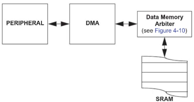
flowchart
graph TD
    A["PERIPHERAL"] <--> B["DMA"]
    B <--> C["Data Memory Arbiter (see Figure 4-10)"]
    C <--> D["SRAM"]
In addition, DMA transfers can be triggered by timers as well as external interrupts. Each DMA channel is unidirectional. Two DMA channels must be allocated to read and write to a peripheral. If more than one channel receives a request to transfer data, a simple fixed priority scheme, based on channel number, dictates which channel completes the transfer and which channel, or channels, are left pending. Each DMA channel moves a block of data, after which, it generates an interrupt to the CPU to indicate that the block is available for processing.
The DMA Controller provides these functional capabilities:
- Four DMA Channels
- Register Indirect with Post-Increment Addressing mode
-
Register Indirect without Post-Increment Addressing mode
-
Peripheral Indirect Addressing mode (peripheral generates destination address)
- CPU Interrupt after Half or Full Block Transfer Complete
- Byte or Word Transfers
• Fixed Priority Channel Arbitration - Manual (software) or Automatic (peripheral DMA requests) Transfer Initiation
- One-Shot or Auto-Repeat Block Transfer modes
- Ping-Pong mode (automatic switch between two SRAM Start addresses after each block transfer complete)
- DMA Request for each Channel can be Selected from any Supported Interrupt Source
- Debug Support Features
The peripherals that can utilize DMA are listed in Table 8-1.
TABLE 8-1: DMA CHANNEL TO PERIPHERAL ASSOCIATIONS
| Peripheral to DMA Association | DMAxREQ RegisterIRQSEL<7:0> Bits | DMAxPAD Register(Values to Read from Peripheral) | DMAxPAD Register(Values to Write to Peripheral) |
| INT0 – External Interrupt 0 00000000 — | — | ||
| IC1 – Input Capture 1 00000001 0x0144 (IC1BUF) — | |||
| IC2 – Input Capture 2 00000101 0x014C (IC2BUF) — | |||
| IC3 – Input Capture 3 00100101 0x0154 (IC3BUF) — | |||
| IC4 – Input Capture 4 00100110 0x015C (IC4BUF) — | |||
| OC1 – Output Compare 1 00000010 — 0x0906 (OC1R) | 0x0904 (OC1RS) | ||
| OC2 – Output Compare 2 00000110 — 0x0910 (OC2R) | 0x090E (OC2RS) | ||
| OC3 – Output Compare 3 | 00011001 | — | 0x091A (OC3R)0x0918 (OC3RS) |
| OC4 – Output Compare 4 00011010 — 0x0924 (OC4R) | 0x0922 (OC4RS) | ||
| TMR2 – Timer2 | 00000111 — | — | |
| TMR3 – Timer3 | 00001000 — | — | |
| TMR4 – Timer4 | 00011011 — | — | |
| TMR5 – Timer5 | 00011100 — | — | |
| UART1RX – UART1 Receiver | 00001011 | 0x0226 (U1RXREG) | — |
| UART1TX – UART1 Transmitter | 00001100 | — | 0x0224 (U1TXREG) |
| UART2RX – UART2 Receiver | 00011110 | 0x0236 (U2RXREG) | — |
| UART2TX – UART2 Transmitter | 00011111 | — | 0x0234 (U2TXREG) |
| CAN1 – RX Data Ready | 00100010 | 0x04C0 (C1RXD) | — |
| CAN1 – TX Data Request | 01000110 | — | 0x04C2 (C1TXD) |
| CAN2 – RX Data Ready | 00110111 | 0x07C0(C2RXD) | — |
| CAN2 – TX Data Request | 01000111 | — | 0x07C2 (C2TXD) |
FIGURE 8-2: DMA CONTROLLER BLOCK DIAGRAM
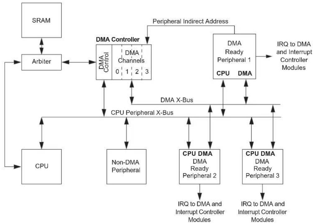
flowchart
graph TD
    A["SRAM"] --> B["Arbiter"]
    B --> C["DMA Controller"]
    C --> D["Peripheral Indirect Address"]
    D --> E["CPU"]
    E --> F["CPU Peripheral X-Bus"]
    F --> G["Non-DMA Peripheral"]
    G --> H["CPU DMA"]
    H --> I["CPU DMA Ready Peripheral 2"]
    I --> J["CPU DMA Ready Peripheral 3"]
    J --> K["IRQ to DMA and Interrupt Controller Modules"]
    C --> L["DMA Channels"]
    L --> M["CPU Peripheral X-Bus"]
    M --> N["Non-DMA Peripheral"]
    N --> O["CPU"]
    O --> P["CPU Peripheral X-Bus"]
    P --> Q["Non-DMA Peripheral"]
    Q --> R["CPU DMA"]
    R --> S["CPU DMA Ready Peripheral 2"]
    S --> T["CPU DMA Ready Peripheral 3"]
    T --> U["IRQ to DMA and Interrupt Controller Modules"]
    U --> V["CPU"]
    V --> W["CPU Peripheral X-Bus"]
    W --> X["Non-DMA Peripheral"]
    X --> Y["CPU DMA"]
    Y --> Z["CPU DMA Ready Peripheral 2"]
    Z --> AA["CPU DMA Ready Peripheral 3"]
    AA --> AB["IRQ to DMA and Interrupt Controller Modules"]
    AB --> AC["CPU"]
    AC --> AD["CPU Peripheral X-Bus"]
Note: CPU and DMA address buses are not shown for clarity.
8.1 DMA Controller Registers
Each DMA Controller Channel x (where x = 0 through 3) contains the following registers:
• 16-Bit DMA Channel x Control Register (DMAxCON)
- 16-Bit DMA Channel x IRQ Select Register (DMAxREQ)
• 32-Bit DMA Channel x Start Address Register A (DMAxSTAL/H)
• 32-Bit DMA Channel x Start Address Register B (DMAxSTBL/H)
• 16-Bit DMA Channel x Peripheral Address Register (DMAxPAD)
• 14-Bit DMA Channel x Transfer Count Register (DMAxCNT)
Additional status registers (DMAPWC, DMARQC, DMAPPS, DMALCA and DSADRL/H) are common to all DMA Controller channels. These status registers provide information on write and request collisions, as well as on last address and channel access information.
The interrupt flags (DMAxIF) are located in an IFSx register in the interrupt controller. The corresponding interrupt enable control bits (DMAxIE) are located in an IECx register in the interrupt controller and the corresponding interrupt priority control bits (DMAxIP) are located in an IPCx register in the interrupt controller.
REGISTER 8-1: DMAxCON: DMA CHANNEL x CONTROL REGISTER
| R/W-0 R/W-0 R/W-0 R/W-0 R/W-0 U-0 U-0 U-0 | |||||||
| CHEN | SIZE | DIR | HALF | NULLW | — | — | — |
| bit 15 bit 8 | |||||||
| U-0 | U-0 | R/W-0 | R/W-0 | U-0 | U-0 | R/W-0 | R/W-0 | |
| — | — | AMODE1 | AMODE0 | — | — | MODE1 | MODE0 | |
| bit 7 bit 0 | ||||||||
| Legend: | |||
| R = Readable bit | W = Writable bit | U = Unimplemented bit, read as ‘0’ | |
| -n = Value at POR | ‘1’ = Bit is set | ‘0’ = Bit is cleared | x = Bit is unknown |
| bit 15 | CHEN: DMA Channel Enable bit1 = Channel is enabled0 = Channel is disabled |
| bit 14 | SIZE: DMA Data Transfer Size bit1 = Byte0 = Word |
| bit 13 | DIR: Transfer Direction bit (source/destination bus select)1 = Reads from RAM address, writes to peripheral address0 = Reads from peripheral address, writes to RAM address |
| bit 12 | HALF: Block Transfer Interrupt Select bit1 = Initiates interrupt when half of the data has been moved0 = Initiates interrupt when all of the data has been moved |
| bit 11 | NULLW: Null Data Peripheral Write Mode Select bit1 = Null data write to peripheral in addition to RAM write (DIR bit must also be clear)0 = Normal operation |
| bit 10-6 | Unimplemented: Read as ‘0’ |
| bit 5-4 | AMODE<1:0>: DMA Channel Addressing Mode Select bits11 = Reserved10 = Peripheral Indirect mode01 = Register Indirect without Post-Increment mode00 = Register Indirect with Post-Increment mode |
| bit 3-2 | Unimplemented: Read as ‘0’ |
| bit 1-0 | MODE<1:0>: DMA Channel Operating Mode Select bits11 = One-Shot, Ping-Pong modes are enabled (one block transfer from/to each DMA buffer)10 = Continuous, Ping-Pong modes are enabled01 = One-Shot, Ping-Pong modes are disabled00 = Continuous, Ping-Pong modes are disabled |
REGISTER 8-2: DMAxREQ: DMA CHANNEL x IRQ SELECT REGISTER
| Legend: | S = Settable bit | ||
| R = Readable bit | W = Writable bit | U = Unimplemented bit, read as ‘0’ | |
| -n = Value at POR | ‘1’ = Bit is set | ‘0’ = Bit is cleared | x = Bit is unknown |
bit 15 FORCE: Force DMA Transfer bit ^(1)
1 = Forces a single DMA transfer (Manual mode)
0 = Automatic DMA transfer initiation by DMA request
bit 14-8 Unimplemented: Read as '0'
bit 7-0 IRQSEL<7:0>: DMA Peripheral IRQ Number Select bits
01000111 = CAN2 - TX data request
01000110 = CAN1 - TX data request
00110111 = CAN2 - RX data ready
00100110 = IC4 - Input Capture 4
00100101 = IC3 - Input Capture 3
00100010 = CAN1 - RX data ready
00011111 = UART2TX - UART2 transmitter
00011110 = UART2RX - UART2 receiver
00011100 = TMR5 - Timer5
00011011 = TMR4 - Timer4
00011010 = OC4 - Output Compare 4
00011001 = OC3 - Output Compare 3
00001100 = UART1TX - UART1 transmitter
00001011 = UART1RX - UART1 receiver
00001000 = TMR3 - Timer3
00000111 = TMR2 - Timer2
00000110 = OC2 - Output Compare 2
00000101 = IC2 - Input Capture 2
00000010 = OC1 - Output Compare 1
00000001 = IC1 - Input Capture 1
00000000 = INTO - External Interrupt 0
Note 1: The FORCE bit cannot be cleared by user software. The FORCE bit is cleared by hardware when the forced DMA transfer is complete or the channel is disabled (CHEN = 0).
REGISTER 8-3: DMAxSTAH: DMA CHANNEL x START ADDRESS REGISTER A (HIGH)
| U-0 U-0 U-0 U-0 U-0 U-0 U-0 U-0 | |||||||
| ——— | ———— | ||||||
| bit 15 | bit 8 | ||||||
| R/W-0 | R/W-0 | R/W-0 | R/W-0 | R/W-0 | R/W-0 | R/W-0 | R/W-0 |
| STA<23:16> | |||||||
| bit 7 | bit 0 | ||||||
| Legend: | |||
| R = Readable bit | W = Writable bit | U = Unimplemented bit, read as '0' | |
| -n = Value at POR | '1' = Bit is set | '0' = Bit is cleared | x = Bit is unknown |
bit 15-8 Unimplemented: Read as '0'
bit 7-0 STA<23:16>: DMA Primary Start Address bits (source or destination)
REGISTER 8-4: DMAxSTAL: DMA CHANNEL x START ADDRESS REGISTER A (LOW)
| R/W-0 | R/W-0 | R/W-0 | R/W-0 | R/W-0 | R/W-0 | R/W-0 | R/W-0 |
| STA<15:8> | |||||||
| bit 15 | bit 8 | ||||||
| R/W-0 | R/W-0 | R/W-0 | R/W-0 | R/W-0 | R/W-0 | R/W-0 | R/W-0 |
| STA<7:0> | |||||||
| bit 7 | bit 0 | ||||||
| Legend: | |||
| R = Readable bit | W = Writable bit | U = Unimplemented bit, read as ‘0’ | |
| -n = Value at POR | ‘1’ = Bit is set | ‘0’ = Bit is cleared | x = Bit is unknown |
bit 15-0 STA<15:0>: DMA Primary Start Address bits (source or destination)
REGISTER 8-5: DMAxSTBH: DMA CHANNEL x START ADDRESS REGISTER B (HIGH)
| U-0 U-0 U-0 U-0 R/W-0 U-0 U-0 U-0 | |||||||
| —— | ——— | ||||||
| bit 15 | bit 8 | ||||||
| R/W-0 | R/W-0 | R/W-0 | R/W-0 | R/W-0 | R/W-0 | R/W-0 | R/W-0 |
| STB<23:16> | |||||||
| bit 7 | bit 0 | ||||||
| Legend: | |||
| R = Readable bit | W = Writable bit | U = Unimplemented bit, read as '0' | |
| -n = Value at POR | '1' = Bit is set | '0' = Bit is cleared | x = Bit is unknown |
bit 15-8 Unimplemented: Read as '0'
bit 7-0 STB<23:16>: DMA Secondary Start Address bits (source or destination)
REGISTER 8-6: DMAxSTBL: DMA CHANNEL x START ADDRESS REGISTER B (LOW)
| R/W-0 | R/W-0 | R/W-0 | R/W-0 | R/W-0 | R/W-0 | R/W-0 | R/W-0 |
| STB<15:8> | |||||||
| bit 15 | bit 8 | ||||||
| R/W-0 | R/W-0 | R/W-0 | R/W-0 | R/W-0 | R/W-0 | R/W-0 | R/W-0 |
| STB<7:0> | |||||||
| bit 7 | bit 0 | ||||||
| Legend: | |||
| R = Readable bit | W = Writable bit | U = Unimplemented bit, read as '0' | |
| -n = Value at POR | '1' = Bit is set | '0' = Bit is cleared | x = Bit is unknown |
bit 15-0 STB<15:0>: DMA Secondary Start Address bits (source or destination)
REGISTER 8-7: DMAxPAD: DMA CHANNEL x PERIPHERAL ADDRESS REGISTER (1)
| R/W-0 R/W-0 R/W-0 R/W-0 R/W-0 R/W-0 R/W-0 R/W-0 |
| PAD<15:8> |
| bit 15 bit 8 |
| R/W-0 R/W-0 R/W-0 R/W-0 R/W-0 R/W-0 R/W-0 R/W-0 |
| PAD<7:0> |
| bit 7 bit 0 |
| Legend: | |||
| R = Readable bit W = Writable bit | U = Unimplemented bit, read as ‘0’ | ||
| -n = Value at POR | ‘1’ = Bit is set | ‘0’ = Bit is cleared | x = Bit is unknown |
bit 15-0 PAD<15:0>: DMA Peripheral Address Register bits
Note 1: If the channel is enabled (i.e., active), writes to this register may result in unpredictable behavior of the DMA channel and should be avoided.
REGISTER 8-8: DMAxCNT: DMA CHANNEL x TRANSFER COUNT REGISTER (1)
| U-0 | U-0 | R/W-0 R/W-0 R/W-0 R/W-0 R/W-0 R/W-0 |
| — | — | CNT<13:8>(2) |
| bit 15 bit 8 | ||
| R/W-0 R/W-0 R/W-0 R/W-0 R/W-0 R/W-0 R/W-0 R/W-0 |
| CNT<7:0>(2) |
| bit 7 bit 0 |
| Legend: | |||
| R = Readable bit W = Writable bit | U = Unimplemented bit, read as ‘0’ | ||
| -n = Value at POR | ‘1’ = Bit is set | ‘0’ = Bit is cleared | x = Bit is unknown |
bit 15-14 Unimplemented: Read as '0'
bit 13-0 CNT<13:0>: DMA Transfer Count Register bits ^(2)
Note 1: If the channel is enabled (i.e., active), writes to this register may result in unpredictable behavior of the DMA channel and should be avoided.
2: The number of DMA transfers = CNT<13:0> + 1.
REGISTER 8-9: DSADRH: DMA MOST RECENT RAM HIGH ADDRESS REGISTER
| U-0 U-0 U-0 U-0 U-0 U-0 U-0 U-0 | |||||||
| —— | ——— | ||||||
| bit 15 | bit 8 | ||||||
| R-0 R-0 R-0 R-0 R-0 R-0 R-0 R-0 | |
| DSADR<23:16> | |
| bit 7 | bit 0 |
| Legend: | |||
| R = Readable bit | W = Writable bit | U = Unimplemented bit, read as ‘0’ | |
| -n = Value at POR | ‘1’ = Bit is set | ‘0’ = Bit is cleared | x = Bit is unknown |
bit 15-8 Unimplemented: Read as '0'
bit 7-0 DSADR<23:16>: Most Recent DMA Address Accessed by DMA bits
REGISTER 8-10: DSADRL: DMA MOST RECENT RAM LOW ADDRESS REGISTER
| R-0 R-0 R-0 R-0 R-0 R-0 R-0 R-0 | |
| DSADR<15:8> | |
| bit 15 | bit 8 |
| R-0 R-0 R-0 R-0 R-0 R-0 R-0 R-0 | |
| DSADR<7:0> | |
| bit 7 | bit 0 |
| Legend: | |||
| R = Readable bit | W = Writable bit | U = Unimplemented bit, read as ‘0’ | |
| -n = Value at POR | ‘1’ = Bit is set | ‘0’ = Bit is cleared | x = Bit is unknown |
bit 15-0
DSADR<15:0>: Most Recent DMA Address Accessed by DMA bits
REGISTER 8-11: DMAPWC: DMA PERIPHERAL WRITE COLLISION STATUS REGISTER
| U-0 U-0 U-0 U-0 U-0 U-0 U-0 U-0 | |||||||
| —— | ——— | ||||||
| bit 15 | bit 8 | ||||||
| U-0 U-0 U-0 U-0 R-0 R-0 R-0 R-0 | |||||||
| — | — | — | — | PWCOL3 | PWCOL2 | PWCOL1 | PWCOL0 |
| bit 7 bit 0 | |||||||
| Legend: | |||
| R = Readable bit | W = Writable bit | U = Unimplemented bit, read as '0' | |
| -n = Value at POR | '1' = Bit is set | '0' = Bit is cleared | x = Bit is unknown |
bit 15-4 Unimplemented: Read as '0'
bit 3 PWCOL3: Channel 3 Peripheral Write Collision Flag bit
1 = Write collision is detected
0 = No write collision is detected
bit 2 PWCOL2: Channel 2 Peripheral Write Collision Flag bit
1 = Write collision is detected
0 = No write collision is detected
bit 1 PWCOL1: Channel 1 Peripheral Write Collision Flag bit
1 = Write collision is detected
0 = No write collision is detected
bit 0 PWCOL0: Channel 0 Peripheral Write Collision Flag bit
1 = Write collision is detected
0 = No write collision is detected
REGISTER 8-12: DMARQC: DMA REQUEST COLLISION STATUS REGISTER
| R = Readable bit | W = Writable bit | U = Unimplemented bit, read as '0' |
| -n = Value at POR | '1' = Bit is set | '0' = Bit is cleared x = Bit is unknown |
bit 15-4 Unimplemented: Read as '0'
bit 3 RQCOL3: Channel 3 Transfer Request Collision Flag bit
1 = User FORCE and interrupt-based request collision are detected 0 = No request collision is detected
bit 2 RQCOL2: Channel 2 Transfer Request Collision Flag bit
1 = User FORCE and interrupt-based request collision are detected 0 = No request collision is detected
bit 1 RQCOL1: Channel 1 Transfer Request Collision Flag bit
1 = User FORCE and interrupt-based request collision are detected 0 = No request collision is detected
bit 0 RQCOL0: Channel 0 Transfer Request Collision Flag bit
1 = User FORCE and interrupt-based request collision are detected 0 = No request collision is detected
REGISTER 8-13: DMALCA: DMA LAST CHANNEL ACTIVE STATUS REGISTER
| U-0 U-0 U-0 U-0 U-0 U-0 U-0 U-0 | |||||||
| —— | ——— | ||||||
| bit 15 | bit 8 | ||||||
| U-0 U-0 U-0 U-0 R-1 R-1 R-1 R-1 | |||
| ——— | LSTCH<3:0> | ||
| bit 7 bit 0 | |||
| Legend: | |||
| R = Readable bit | W = Writable bit | U = Unimplemented bit, read as '0' | |
| -n = Value at POR | '1' = Bit is set | '0' = Bit is cleared | x = Bit is unknown |
bit 15-4 Unimplemented: Read as '0'
bit 3-0 LSTCH<3:0>: Last DMA Controller Channel Active Status bits
1111 = No DMA transfer has occurred since system Reset
1110 = Reserved
•
.
.
0100 = Reserved
0011 = Last data transfer was handled by Channel 3
0010 = Last data transfer was handled by Channel 2
0001 = Last data transfer was handled by Channel 1
0000 = Last data transfer was handled by Channel 0
REGISTER 8-14: DMAPPS: DMA PING-PONG STATUS REGISTER
| R = Readable bit | W = Writable bit | U = Unimplemented bit, read as '0' |
| -n = Value at POR | '1' = Bit is set | '0' = Bit is cleared x = Bit is unknown |
bit 15-4 Unimplemented: Read as '0'
bit 3 PPST3: Channel 3 Ping-Pong Mode Status Flag bit
1 = DMA3STB register is selected
0 = DMA3STA register is selected
bit 2 PPST2: Channel 2 Ping-Pong Mode Status Flag bit
1 = DMA2STB register is selected
0 = DMA2STA register is selected
bit 1 PPST1: Channel 1 Ping-Pong Mode Status Flag bit
1 = DMA1STB register is selected
0 = DMA1STA register is selected
bit 0 PPST0: Channel 0 Ping-Pong Mode Status Flag bit
1 = DMA0STB register is selected
0 = DMA0STA register is selected
NOTES:
Note 1: This data sheet summarizes the features of the dsPIC33EPXXXGS70X/80X family of devices. It is not intended to be a comprehensive reference source. To complement the information in this data sheet, refer to “Oscillator Module” (DS70005131) in the “dsPIC33/PIC24 Family Reference Manual”, which is available from the Microchip website (www.microchip.com).
2: Some registers and associated bits described in this section may not be available on all devices. Refer to Section 4.0 "Memory Organization" in this data sheet for device-specific register and bit information.
The dsPIC33EPXXXGS70X/80X family oscillator system provides:
- On-Chip Phase-Locked Loop (PLL) to Boost Internal Operating Frequency on Select Internal and External Oscillator Sources
- On-the-Fly Clock Switching between Various Clock Sources
- Doze mode for System Power Savings
- Fail-Safe Clock Monitor (FSCM) that Detects Clock Failure and Permits Safe Application Recovery or Shutdown
- Configuration Bits for Clock Source Selection
• Auxiliary PLL for ADC and PWM
A simplified diagram of the oscillator system is shown in Figure 9-1.
FIGURE 9-1: OSCILLATOR SYSTEM DIAGRAM
flowchart
graph TD
    subgraph Primary Oscillator (POSC)
        OSC1["OSC1"] --> A["AND"]
        OSC2["OSC2"] --> A
        A --> B["POSCCLK"]
        B --> C["S3"]
        B --> D["S1"]
        C --> E["PLL"]
        D --> E
        E --> F["FPLLO"]
        F --> G["XT, HS, EC"]
        G --> H["XYPLL, HSPLL, ECP LL, FRCPLL"]
        H --> I["FVCO(1)"]
        I --> J["S2"]
        J --> K["S1/S3"]
    end

    subgraph Reference Clock Output
        DOZE["DOZE"] --> L["Fcy(2)"]
        L --> M["Fp(2)"]
        M --> N["Fosc"]
        N --> O["÷ 2"]
        O --> P["FRCDIVN"]
        P --> Q["S7"]
        Q --> R["FRCDIV<2:0>"]
        R --> S["÷ 16"]
        S --> T["FRCDIV16"]
        T --> U["S6"]
        U --> V["FRC"]
        V --> W["S0"]
        W --> X["LPRC"]
        X --> Y["S5"]
        Y --> Z["S4"]
    end

    subgraph Clock Fail
        LPRC["LRPC Oscillator"] --> Y
        Y --> Z
    end

    subgraph Clock Switch
        Z --> AA["S0"]
        AA --> AB["NOSC<2:0> FNOSC<2:0>"]
        AB --> AC["Reset"]
    end

    subgraph Reset
        Z --> AD["REFCLKO"]
        AD --> AE["ROPn"]
        AE --> AF["ROSEL"]
        AF --> AG["÷ N"]
        AG --> AH["RODIV<3:0>"]
    end

    subgraph Reference Clock Output
        ID["DOZE<2:0>"] --> AE
    end

    style Primary Oscillator fill:#f9f,stroke:#333
    style Reference Clock Output fill:#ccf,stroke:#333
AUXILIARY CLOCK GENERATOR CIRCUIT BLOCK DIAGRAM

flowchart
graph LR
    A["POS CCLK"] --> B["1"]
    C["GND"] --> D["0"]
    B --> E["FRCCLK"]
    D --> F["ASRCSEL"]
    E --> G["1"]
    F --> H["0"]
    G --> I["FRCSEL"]
    H --> J["APLL x 16"]
    I --> K["ENAPLL"]
    J --> L["FVCO(1)"]
    K --> M["1"]
    L --> N["SELACLK"]
    M --> O["÷N"]
    N --> P["APSTSCLR<2:0>(4)"]
    O --> Q["ACLK"]
    P --> R["PWM/ADC to LFSR"]
Note 1: See Figure 9-2 for the source of the Fvco signal.
2: F P refers to the clock source for all the peripherals, while FCY (or MIPS) refers to the clock source for the CPU. Throughout this document, FCY and FP are used interchangeably, except in the case of Doze mode. FP and FCY will be different when Doze mode is used in any ratio other than 1:1.
3: The auxiliary clock postscaler must be configured to divide-by-1 (APSTSCLR<2:0>=111) for proper operation of the PWM and ADC modules.
9.1 CPU Clocking System
The dsPIC33EPXXXGS70X/80X family of devices provides six system clock options:
- Fast RC (FRC) Oscillator
- FRC Oscillator with Phase-Locked Loop (FRCPLL)
• FRC Oscillator with Postscaler
• Primary (XT, HS or EC) Oscillator
• Primary Oscillator with PLL (XTPLL, HSPLL, ECPLL) - Low-Power RC (LPRC) Oscillator
Instruction execution speed or device operating frequency, Fcy, is given by Equation 9-1.
EQUATION 9-1: DEVICE OPERATING FREQUENCY
$$ F C Y = F O S C / 2 $$
Figure 9-2 is a block diagram of the PLL module. Equation 9-2 provides the relationship between Input Frequency (FIN) and Output Frequency (FPLLO). Equation 9-3 provides the relationship between Input Frequency (FIN) and VCO Frequency (Fvco).
FIGURE 9-2: PLL BLOCK DIAGRAM
flowchart
graph TD
    A["FIN"] --> B["÷ N1"]
    B --> C["FPLLI"]
    C --> D["PFD VCO"]
    D --> E["Fvco Fosc"]
    E --> F["÷ N2"]
    F --> G["FPLLO(1) ≤ 120 MHz @ +125°C\nFPLLO(1) ≤ 140 MHz @ +85°C"]
    B --> H["÷ M"]
    H --> I["PLLDIV<8:0>"]
    B --> J["PLLPRE<4:0>"]
    F --> K["PLLPOST<1:0>"]
    style A fill:#f9f,stroke:#333
    style G fill:#f9f,stroke:#333
    note right of B "0.8 MHz < FPLL(1) < 8.0 MHz"
    note right of C "120 MHz < Fvco(1) < 340 MHz"
    note right of F "FPLLO(1) ≤ 120 MHz @ +125°C\nFPLLO(1) ≤ 140 MHz @ +85°C"
EQUATION 9-2: F PLLO CALCULATION
$$ F _ {P L L O} = F _ {I N} \times \left(\frac {M}{N 1 \times N 2}\right) = F _ {I N} \times \left(\frac {P L L D I V < 8 : 0 > + 2}{(P L L P R E < 4 : 0 > + 2) \times 2 (P L L P O S T < 1 : 0 > + 1)}\right) $$
Where:
$$ \begin{array}{l} N 1 = P L L P R E < 4: 0 > + 2 \ N 2 = 2 \mathrm{x} (P L L P O S T < 1: 0 > + 1) \ M = P L L D I V < 8: 0 > + 2 \ \end{array} $$
EQUATION 9-3: F vco CALCULATION
$$ F _ {V C O} = F _ {I N} \times \left(\frac {M}{N 1}\right) = F _ {I N} \times \left(\frac {P L L D I V < 8 : 0 > + 2}{(P L L P R E < 4 : 0 > + 2)}\right) $$
TABLE 9-1: CONFIGURATION BIT VALUES FOR CLOCK SELECTION
| Oscillator Mode Oscillator Source | POSCMD<1:0> | FNOSC<2:0> | See Notes | |
| Fast RC Oscillator with Divide-by-n (FRCDIVN) | Internal | xx | 111 | 1, 2 |
| Fast RC Oscillator with Divide-by-16 | Internal | xx | 110 | 1 |
| Low-Power RC Oscillator (LPRC) | Internal | xx | 101 | 1 |
| Primary Oscillator (HS) with PLL (HSPLL) | Primary | 10 | 011 | |
| Primary Oscillator (XT) with PLL (XTPLL) | Primary | 01 | 011 | |
| Primary Oscillator (EC) with PLL (ECPLL) | Primary | 00 | 011 | 1 |
| Primary Oscillator (HS) | Primary | 10 | 010 | |
| Primary Oscillator (XT) | Primary | 01 | 010 | |
| Primary Oscillator (EC) | Primary | 00 | 010 | 1 |
| Fast RC Oscillator (FRC) with Divide-by-N and PLL (FRCPLL) | Internal xx 001 | 1 | ||
| Fast RC Oscillator (FRC) | Internal | xx | 000 | 1 |
Note 1: OSC2 pin function is determined by the OSCIOFNC Configuration bit.
2: This is the default Oscillator mode for an unprogrammed (erased) device.
9.2 Auxiliary Clock Generation
The auxiliary clock generation is used for peripherals that need to operate at a frequency unrelated to the system clock, such as PWM or ADC.
The primary oscillator and internal FRC oscillator sources can be used with an Auxiliary PLL (APLL) to obtain the auxiliary clock. The Auxiliary PLL has a fixed 16x multiplication factor.
The auxiliary clock has the following configuration restrictions:
- For proper PWM operation, auxiliary clock generation must be configured for 120 MHz (see Parameter OS56 in Section 30.0 "Electrical Characteristics"). If a slower frequency is desired, the PWM Input Clock Prescaler (Divider) Select bits (PCLKDIV<2:0>) should be used.
- To achieve 1.04 ns PWM resolution, the auxiliary clock must use the 16x Auxiliary PLL (APLL). All other clock sources will have a minimum PWM resolution of 8 ns.
- If the primary PLL is used as a source for the auxiliary clock, the primary PLL should be configured up to a maximum operation of 30 MIPS or less.
9.3 Reference Clock Generation
The reference clock output logic provides the user with the ability to output a clock signal based on the system clock or the crystal oscillator on a device pin. The user application can specify a wide range of clock scaling prior to outputting the reference clock.
9.4 Oscillator Resources
Many useful resources are provided on the main product page of the Microchip website for the devices listed in this data sheet. This product page contains the latest updates and additional information.
9.4.1 KEY RESOURCES
- "Oscillator Module" (DS70005131) in the "dsPIC33/PIC24 Family Reference Manual"
- Code Samples
- Application Notes
- Software Libraries
- Webinars
- All Related "dsPIC33/PIC24 Family Reference Manual" Sections
• Development Tools
9.5 Oscillator Control Registers
REGISTER 9-1: OSCCON: OSCILLATOR CONTROL REGISTER (1)
| U-0 R-0 R-0 R-0 U-0 R/W-y R/W-y R/W-y | ||||||||
| — COS | C2 | COSC1 | CO | SC0 — | N | O | S | C (2)2 |
| bit 15 bit 8 | ||||||||
| R/W-0 R/W-0 R-0 U-0 R/W-0 U-0 U-0 R/W-0 | |||||||
| CLKLOCK I | OLOCK LOCK | — | CF(3) | — | — | OSWEN | |
| bit 7 bit 0 | |||||||
| Legend: | y = Value set from Configuration bits on POR | ||
| R = Readable bit | W = Writable bit | U = Unimplemented bit, read as ‘0’ | |
| -n = Value at POR | ‘1’ = Bit is set | ‘0’ = Bit is cleared | x = Bit is unknown |
bit 15 Unimplemented: Read as '0'
bit 14-12 COSC<2:0>: Current Oscillator Selection bits (read-only)
111 = Fast RC Oscillator (FRC) with Divide-by-n
110 = Fast RC Oscillator (FRC) with Divide-by-16
101 = Low-Power RC Oscillator (LPRC)
100 = Reserved
011 = Primary Oscillator (XT, HS, EC) with PLL
010 = Primary Oscillator (XT, HS, EC)
001 = Fast RC Oscillator (FRC) with Divide-by-N and PLL (FRCPLL)
000 = Fast RC Oscillator (FRC)
bit 11 Unimplemented: Read as '0'
bit 10-8 NOSC<2:0>: New Oscillator Selection bits ^(2)
111 = Fast RC Oscillator (FRC) with Divide-by-n
110 = Fast RC Oscillator (FRC) with Divide-by-16
101 = Low-Power RC Oscillator (LPRC)
100 = Reserved
011 = Primary Oscillator (XT, HS, EC) with PLL
010 = Primary Oscillator (XT, HS, EC)
001 = Fast RC Oscillator (FRC) with Divide-by-N and PLL (FRCPLL)
000 = Fast RC Oscillator (FRC)
bit 7 CLKLOCK: Clock Lock Enable bit
1 = If (FCKSM0 = 1), then clock and PLL configurations are locked; if (FCKSM0 = 0), then clock and PLL configurations may be modified
0 = Clock and PLL selections are not locked, configurations may be modified
bit 6 IOLOCK: I/O Lock Enable bit
1 = I/O lock is active
0 = I/O lock is not active
bit 5 LOCK: PLL Lock Status bit (read-only)
1 = Indicates that PLL is in lock or PLL start-up timer is satisfied
0 = Indicates that PLL is out of lock, start-up timer is in progress or PLL is disabled
Note 1: Writes to this register require an unlock sequence.
2: Direct clock switches between any Primary Oscillator mode with PLL and FRCPLL mode are not permitted. This applies to clock switches in either direction. In these instances, the application must switch to FRC mode as a transitional clock source between the two PLL modes.
3: This bit should only be cleared in software. Setting the bit in software (= 1) will have the same effect as an actual oscillator failure and will trigger an oscillator failure trap.
REGISTER 9-1: OSCCON: OSCILLATOR CONTROL REGISTER (1) (CONTINUED)
bit 4 Unimplemented: Read as '0'
bit 3 CF: Clock Fail Detect bit (3)
1 = FSCM has detected a clock failure
0 = FSCM has not detected a clock failure
bit 2-1 Unimplemented: Read as '0'
bit 0 OSWEN: Oscillator Switch Enable bit
1 = Requests oscillator switch to the selection specified by the NOSC<2:0> bits
0 = Oscillator switch is complete
Note 1: Writes to this register require an unlock sequence.
2: Direct clock switches between any Primary Oscillator mode with PLL and FRCPLL mode are not permitted. This applies to clock switches in either direction. In these instances, the application must switch to FRC mode as a transitional clock source between the two PLL modes.
3: This bit should only be cleared in software. Setting the bit in software (= 1) will have the same effect as an actual oscillator failure and will trigger an oscillator failure trap.
REGISTER 9-2: CLKDIV: CLOCK DIVISOR REGISTER
| R/W-0 R/W-0 R/W-1 R/W-1 R/W-0 R/W-0 R/W-0 R/W-0 | |||||||
| ROI DOZ | E2(1) | DOZE1(1) | DOZE0(1) | DOZEN(2,3) | FRCDIV2 FR | RCDIV1 FRCD | IV0 |
| bit 15 bit 8 | |||||||
| R/W-0 R/W-1 U-0 R/W-0 R/W-0 R/W-0 R/W-0 R/W-0 | |||||||
| PLLPOST1 | PLLPOST0 | — PLLP | RE4 PLLPRE3 | PLLPRE2 PLL | PRE1 PLLPRE | E0 | |
| bit 7 bit 0 | |||||||
| Legend: | |||
| R = Readable bit | W = Writable bit | U = Unimplemented bit, read as ‘0’ | |
| -n = Value at POR | ‘1’ = Bit is set | ‘0’ = Bit is cleared | x = Bit is unknown |
bit 15 ROI: Recover on Interrupt bit 1 = Interrupts will clear the DOZEN bit and the processor clock, and the peripheral clock ratio is set to 1:1 0 = Interrupts have no effect on the DOZEN bit
bit 14-12 DOZE<2:0>: Processor Clock Reduction Select bits ^(1)
111 = Fcγ divided by 128
110 = FcY divided by 64
101 = FcY divided by 32
100 = FcY divided by 16
011 = FcY divided by 8 (default)
010 = FcY divided by 4
001 = FcY divided by 2
000 = FcY divided by 1
bit 11 DOZEN: Doze Mode Enable bit ^(2,3) 1 = DOZE<2:0> field specifies the ratio between the peripheral clocks and the processor clocks
0 = Processor clock and peripheral clock ratio is forced to 1:1
bit 10-8 FRCDIV<2:0>: Internal Fast RC Oscillator Postscaler bits
111 = FRC divided by 256
110 = FRC divided by 64
101 = FRC divided by 32
100 = FRC divided by 16
011 = FRC divided by 8
010 = FRC divided by 4
001 = FRC divided by 2
000 = FRC divided by 1 (default)
bit 7-6 PLLPOST<1:0>: PLL VCO Output Divider Select bits (also denoted as 'N2', PLL postscaler)
11 = Output divided by 8
10 = Reserved
01 = Output divided by 4 (default)
00 = Output divided by 2
bit 5 Unimplemented: Read as '0'
Note 1: The DOZE<2:0> bits can only be written to when the DOZEN bit is clear. If DOZEN = 1, any writes to DOZE<2:0> are ignored.
2: This bit is cleared when the ROI bit is set and an interrupt occurs.
3: The DOZEN bit cannot be set if DOZE<2:0> = 000. If DOZE<2:0> = 000, any attempt by user software to set the DOZEN bit is ignored.
REGISTER 9-2: CLKDIV: CLOCK DIVISOR REGISTER (CONTINUED)
bit 4-0 PLLPRE<4:0>: PLL Phase Detector Input Divider Select bits (also denoted as 'N1', PLL prescaler)
11111 = Input divided by 33
•
•
•
00001 = Input divided by 3
00000 = Input divided by 2 (default)
Note 1: The DOZE<2:0> bits can only be written to when the DOZEN bit is clear. If DOZEN = 1, any writes to DOZE<2:0> are ignored.
2: This bit is cleared when the ROI bit is set and an interrupt occurs.
3: The DOZEN bit cannot be set if DOZE<2:0> = 000. If DOZE<2:0> = 000, any attempt by user software to set the DOZEN bit is ignored.
REGISTER 9-3: PLLFBD: PLL FEEDBACK DIVISOR REGISTER
| U-0 U-0 U-0 U-0 U-0 U-0 R/W-0 | ||||||
| — — — | — — — — PLLDIV8 | |||||
| bit 15 bit 8 | ||||||
| R/W-0 R/W-0 R/W-1 R/W-1 R/W-0 R/W-0 R/W-0 R/W-0 | |
| PLLDIV<7:0> | |
| bit 7 | bit 0 |
Legend:
| R = Readable bit | W = Writable bit | U = Unimplemented bit, read as '0' |
| -n = Value at POR | '1' = Bit is set | '0' = Bit is cleared x = Bit is unknown |
bit 15-9 Unimplemented: Read as '0'
bit 8-0 PLLDIV<8:0>: PLL Feedback Divisor bits (also denoted as 'M', PLL multiplier)
111111111 = 513
•
•
•
000110000 = 50 (default)
•
•
•
000000010 = 4
000000001 = 3
000000000 = 2
REGISTER 9-4: OSCTUN: FRC OSCILLATOR TUNING REGISTER (1)
| U-0 U-0 U-0 U-0 U-0 U-0 U-0 U-0 | |||||||
| —— | —— | —— | |||||
| bit 15 bit 8 | |||||||
| U-0 U-0 R/W-0 R/W-0 R/W-0 R/W-0 R/W-0 R/W-0 | ||
| — — | T U | |
| bit 7 bit 0 | ||
| Legend: | |||
| R = Readable bit | W = Writable bit | U = Unimplemented bit, read as ‘0’ | |
| -n = Value at POR | ‘1’ = Bit is set | ‘0’ = Bit is cleared | x = Bit is unknown |
bit 15-6 Unimplemented: Read as '0'
bit 5-0 TUN<5:0>: FRC Oscillator Tuning bits
011111 = Maximum frequency deviation of 1.457% (7.477 MHz)
011110 = Center frequency + 1.41% (7.474 MHz)
•
.
[Non-Text]
000001 = Center frequency + 0.047% (7.373 MHz)
000000 = Center frequency (7.37 MHz nominal)
111111 = Center frequency - 0.047% (7.367 MHz)
•
•
。
100001 = Center frequency - 1.457% (7.263 MHz)
100000 = Minimum frequency deviation of -1.5% (7.259 MHz)
Note 1: OSCTUN functionality has been provided to help customers compensate for temperature effects on the FRC frequency over a wide range of temperatures. The tuning step-size is an approximation and is neither characterized nor tested.
REGISTER 9-5: ACLKCON: AUXILIARY CLOCK DIVISOR CONTROL REGISTER
| R/W-0 R-0 R/W-1 U-0 U-0 R/W-1 R/W-1 R/W-1 | ||||||
| ENAPLL APLLCK SELACLK | — — AP | STSCLR2 AP | $TSCLR1 AP | TSCLR0 | ||
| bit 15 bit 8 | ||||||
| R/W-0 R/W-1 U-0 U-0 U-0 U-0 U-0 U-0 | |||||||
| ASRCSEL FRCSEL | ——— | ——— | |||||
| bit 7 bit 0 | |||||||
| Legend: | |||
| R = Readable bit W = Writable bit | U = Unimplemented bit, read as '0' | ||
| -n = Value at POR | '1' = Bit is set | '0' = Bit is cleared | x = Bit is unknown |
bit 15 ENAPLL: Auxiliary PLL Enable bit
1 = APLL is enabled
0 = APLL is disabled
bit 14 APLLCK: APLL Locked Status bit (read-only)
1 = Indicates that Auxiliary PLL is in lock
0 = Indicates that Auxiliary PLL is not in lock
bit 13 SELACLK: Select Auxiliary Clock Source for Auxiliary Clock Divider bit
1 = Auxiliary oscillators provide the source clock for the auxiliary clock divider
0 = Primary PLL (Fvco) provides the source clock for the auxiliary clock divider
bit 12-11 Unimplemented: Read as '0'
bit 10-8 APSTSCLR<2:0>: Auxiliary Clock Output Divider bits
111 = Divided by 1
110 = Divided by 2
101 = Divided by 4
100 = Divided by 8
011 = Divided by 16
010 = Divided by 32
001 = Divided by 64
000 = Divided by 256
bit 7 ASRCSEL: Select Reference Clock Source for Auxiliary Clock bit
1 = Primary oscillator is the clock source
0 = No clock input is selected
bit 6 FRCSEL: Select Reference Clock Source for Auxiliary PLL bit
1 = Selects the FRC clock for Auxiliary PLL
0 = Input clock source is determined by the ASRCSEL bit setting
bit 5-0 Unimplemented: Read as '0'
REGISTER 9-6: REFOCON: REFERENCE OSCILLATOR CONTROL REGISTER
| R/W-0 U-0 R/W-0 R/W-0 R/W-0 R/W-0 R/W-0 R/W-0 | ||||||
| ROON | — ROSLP ROSEL RODIV3 | (1) | \text{RODIV2}^{(1)} | \text{RODIV1}^{(1)} | \text{RODIV0}^{(1)}$ | |
| bit 15 bit 8 | ||||||
| U-0 U-0 U-0 U-0 U-0 U-0 U-0 U-0 | |||||||
| —— | —— | —— | |||||
| bit 7 bit 0 | |||||||
Legend:
| R = Readable bit W = Writable bit | U = Unimplemented bit, read as '0' | ||
| -n = Value at POR | '1' = Bit is set | '0' = Bit is cleared | x = Bit is unknown |
bit 15 ROON: Reference Oscillator Output Enable bit
1 = Reference oscillator output is enabled on the RPnpin ^(2)
0 = Reference oscillator output is disabled
bit 14 Unimplemented: Read as '0'
bit 13 ROSSLP: Reference Oscillator Run in Sleep bit
1 = Reference oscillator output continues to run in Sleep
0 = Reference oscillator output is disabled in Sleep
bit 12 ROSEL: Reference Oscillator Source Select bit
1 = Oscillator crystal is used as the reference clock
0 = System clock is used as the reference clock
bit 11-8 RODIV<3:0>: Reference Oscillator Divider bits ^(1)
1111 = Reference clock divided by 32,768
1110 = Reference clock divided by 16,384
1101 = Reference clock divided by 8,192
1100 = Reference clock divided by 4,096
1011 = Reference clock divided by 2,048
1010 = Reference clock divided by 1,024
1001 = Reference clock divided by 512
1000 = Reference clock divided by 256
0111 = Reference clock divided by 128
0110 = Reference clock divided by 64
0101 = Reference clock divided by 32
0100 = Reference clock divided by 16
0011 = Reference clock divided by 8
0010 = Reference clock divided by 4
0001 = Reference clock divided by 2
0000 = Reference clock
bit 7-0 Unimplemented: Read as '0'
Note 1: The reference oscillator output must be disabled (ROON = 0) before writing to these bits.
2: This pin is remappable. See Section 11.6 "Peripheral Pin Select (PPS)" for more information.
REGISTER 9-7: LFSR: LINEAR FEEDBACK SHIFT REGISTER
| U-0 R/W-0 R/W-0 R/W-0 R/W-0 R/W-0 R/W-0 R/W-0 | ||
| — | L | F |
| bit 15 bit 8 | ||
| R/W-0 R/W-0 R/W-0 R/W-0 R/W-0 R/W-0 R/W-0 R/W-0 |
| LFSR<7:0> |
| bit 7 bit 0 |
| Legend: | |||
| R = Readable bit | W = Writable bit | U = Unimplemented bit, read as ‘0’ | |
| -n = Value at POR | ‘1’ = Bit is set | ‘0’ = Bit is cleared | x = Bit is unknown |
bit 15
Unimplemented: Read as '0'
bit 14-0 LFSR<14:0>: Pseudorandom Data bits
10.0 POWER-SAVING FEATURES
Note 1: This data sheet summarizes the features of the dsPIC33EPXXXGS70X/80X family of devices. It is not intended to be a comprehensive reference source. To complement the information in this data sheet, refer to “Watchdog Timer and Power-Saving Modes” (DS70615) in the “dsPIC33/PIC24 Family Reference Manual”, which is available from the Microchip website (www.microchip.com).
2: Some registers and associated bits described in this section may not be available on all devices. Refer to Section 4.0 "Memory Organization" in this data sheet for device-specific register and bit information.
The dsPIC33EPXXXGS70X/80X family devices provide the ability to manage power consumption by selectively managing clocking to the CPU and the peripherals. In general, a lower clock frequency and a reduction in the number of peripherals being clocked constitutes lower consumed power.
dsPIC33EPXXXGS70X/80X family devices can manage power consumption in four ways:
- Clock Frequency
- Instruction-Based Sleep and Idle modes
- Software-Controlled Doze mode
- Selective Peripheral Control in Software
Combinations of these methods can be used to selectively tailor an application's power consumption while still maintaining critical application features, such as timing-sensitive communications.
10.1 Clock Frequency and Clock Switching
The dsPIC33EPXXXGS70X/80X family devices allow a wide range of clock frequencies to be selected under application control. If the system clock configuration is not locked, users can choose low-power or high-precision oscillators by simply changing the NOSCx bits (OSCCON<10:8>). The process of changing a system clock during operation, as well as limitations to the process, are discussed in more detail in Section 9.0 "Oscillator Configuration".
10.2 Instruction-Based Power-Saving Modes
The dsPIC33EPXXXGS70X/80X family devices have two special power-saving modes that are entered through the execution of a special PWRSAV instruction. Sleep mode stops clock operation and halts all code execution. Idle mode halts the CPU and code execution, but allows peripheral modules to continue operation. The assembler syntax of the PWRSAV instruction is shown in Example 10-1.
Note: SLEEP_MODE and IDLE_MODE are constants defined in the assembler include file for the selected device.
Sleep and Idle modes can be exited as a result of an enabled interrupt, WDT time-out or a device Reset. When the device exits these modes, it is said to "wake-up".
EXAMPLE 10-1: PWRSAV INSTRUCTION SYNTAX
PWRSAV #SLEEP_MODE ; Put the device into Sleep mode PWRSAV #IDLE_MODE ; Put the device into Idle mode
10.2.1 SLEEP MODE
The following occurs in Sleep mode:
- The system clock source is shut down. If an on-chip oscillator is used, it is turned off.
- The device current consumption is reduced to a minimum, provided that no I/O pin is sourcing current.
- The Fail-Safe Clock Monitor does not operate, since the system clock source is disabled.
- The LPRC clock continues to run in Sleep mode if the WDT is enabled.
- The WDT, if enabled, is automatically cleared prior to entering Sleep mode.
- Some device features or peripherals can continue to operate. This includes items such as the Input Change Notification on the I/O ports or peripherals that use an external clock input.
- Any peripheral that requires the system clock source for its operation is disabled.
The device wakes up from Sleep mode on any of the these events:
- Any interrupt source that is individually enabled
- Any form of device Reset
• A WDT time-out
On wake-up from Sleep mode, the processor restarts with the same clock source that was active when Sleep mode was entered.
For optimal power savings, the internal regulator and the Flash regulator can be configured to go into standby when Sleep mode is entered by clearing the VREGS (RCON<8>) and VREGSF (RCON<11>) bits (default configuration).
If the application requires a faster wake-up time, and can accept higher current requirements, the VREGS (RCON<8>) and VREGSF (RCON<11>) bits can be set to keep the internal regulator and the Flash regulator active during Sleep mode.
10.2.2 IDLE MODE
The following occurs in Idle mode:
- The CPU stops executing instructions.
• The WDT is automatically cleared. - The system clock source remains active. By default, all peripheral modules continue to operate normally from the system clock source, but can also be selectively disabled (see Section 10.4 "Peripheral Module Disable").
- If the WDT or FSCM is enabled, the LPRC also remains active.
The device wakes from Idle mode on any of these events:
- Any interrupt that is individually enabled
- Any device Reset
- A WDT time-out
On wake-up from Idle mode, the clock is reapplied to the CPU and instruction execution will begin (two to four clock cycles later), starting with the instruction following the PWRSAV instruction or the first instruction in the ISR.
All peripherals also have the option to discontinue operation when Idle mode is entered to allow for increased power savings. This option is selectable in the control register of each peripheral (for example, the TSIDL bit in the Timer1 Control register (T1CON<13>).
10.2.3 INTERRUPTS COINCIDENT WITH POWER SAVE INSTRUCTIONS
Any interrupt that coincides with the execution of a PWRSAV instruction is held off until entry into Sleep or Idle mode has completed. The device then wakes up from Sleep or Idle mode.
10.3 Doze Mode
The preferred strategies for reducing power consumption are changing clock speed and invoking one of the power-saving modes. In some circumstances, this cannot be practical. For example, it may be necessary for an application to maintain uninterrupted synchronous communication, even while it is doing nothing else. Reducing system clock speed can introduce communication errors, while using a power-saving mode can stop communications completely.
Doze mode is a simple and effective alternative method to reduce power consumption while the device is still executing code. In this mode, the system clock continues to operate from the same source and at the same speed. Peripheral modules continue to be clocked at the same speed, while the CPU clock speed is reduced. Synchronization between the two clock domains is maintained, allowing the peripherals to access the SFRs while the CPU executes code at a slower rate.
Doze mode is enabled by setting the DOZEN bit (CLKDIV<11>). The ratio between peripheral and core clock speed is determined by the DOZE<2:0> bits (CLKDIV<14:12>). There are eight possible configurations, from 1:1 to 1:128, with 1:1 being the default setting.
Programs can use Doze mode to selectively reduce power consumption in event-driven applications. This allows clock-sensitive functions, such as synchronous communications, to continue without interruption while the CPU Idles, waiting for something to invoke an interrupt routine. An automatic return to full-speed CPU operation on interrupts can be enabled by setting the ROI bit (CLKDIV<15>). By default, interrupt events have no effect on Doze mode operation.
10.4 Peripheral Module Disable
The Peripheral Module Disable (PMD) registers provide a method to disable a peripheral module by stopping all clock sources supplied to that module. When a peripheral is disabled using the appropriate PMD control bit, the peripheral is in a minimum power consumption state. The control and status registers associated with the peripheral are also disabled, so writes to those registers do not have any effect and read values are invalid.
A peripheral module is enabled only if both the associated bit in the PMD register is cleared and the peripheral is supported by the specific dsPIC® DSC variant. If the peripheral is present in the device, it is enabled in the PMD register by default.
Note: If a PMD bit is set, the corresponding module is disabled after a delay of one instruction cycle. Similarly, if a PMD bit is cleared, the corresponding module is enabled after a delay of one instruction cycle (assuming the module control registers are already configured to enable module operation).
10.5 Power-Saving Resources
Many useful resources are provided on the main product page of the Microchip website for the devices listed in this data sheet. This product page contains the latest updates and additional information.
10.5.1 KEY RESOURCES
- “Watchdog Timer and Power-Saving Modes” (DS70615) in the “dsPIC33/PIC24 Family Reference Manual”
- Code Samples
- Application Notes
- Software Libraries
- Webinars
- All related "dsPIC33/PIC24 Family Reference Manual" Sections
- Development Tools
REGISTER 10-1: PMD1: PERIPHERAL MODULE DISABLE CONTROL REGISTER 1
| R/W-0 R/W-0 R/W-0 R/W-0 R/W-0 U-0 R/W-0 U-0 | |||||
| T5MD T4MD T3MD T2MD T1MD | — PWMMD — | ||||
| bit 15 bit 8 | |||||
| R/W-0 R/W-0 R/W-0 R/W-0 R/W-0 R/W-0 R/W-0 R/W-0 | |||||
| I2C1MD U2MD U1MD SP | I2MD SPI1MD | C2MD C1MD ADCMD | |||
| bit 7 bit 0 | |||||
Legend:
| R = Readable bit W = Writable bit U = Unimplemented bit, read as '0' | ||
| -n = Value at POR | '1' = Bit is set | '0' = Bit is cleared |
bit 15 T5MD: Timer5 Module Disable bit
1 = Timer5 module is disabled
0 = Timer5 module is enabled
bit 14 T4MD: Timer4 Module Disable bit
1 = Timer4 module is disabled
0 = Timer4 module is enabled
bit 13 T3MD: Timer3 Module Disable bit
1 = Timer3 module is disabled
0 = Timer3 module is enabled
bit 12 T2MD: Timer2 Module Disable bit
1 = Timer2 module is disabled
0 = Timer2 module is enabled
bit 11 T1MD: Timer1 Module Disable bit
1 = Timer1 module is disabled
0 = Timer1 module is enabled
bit 10 Unimplemented: Read as '0'
bit 9 PWMMD: PWM Module Disable bit
1 = PWM module is disabled
0 = PWM module is enabled
bit 8 Unimplemented: Read as '0'
bit 7 I2C1MD: I2C1 Module Disable bit
1 = I2C1 module is disabled
0 = I2C1 module is enabled
bit 6 U2MD: UART2 Module Disable bit
1 = UART2 module is disabled
0 = UART2 module is enabled
bit 5 U1MD: UART1 Module Disable bit
1 = UART1 module is disabled
0 = UART1 module is enabled
bit 4 SPI2MD: SPI2 Module Disable bit
1 = SPI2 module is disabled
0 = SPI2 module is enabled
bit 3 SPI1MD: SPI1 Module Disable bit
1 = SPI1 module is disabled
0 = SPI1 module is enabled
bit 2 C2MD: CAN2 Module Disable bit
1 = CAN2 module is disabled
0 = CAN2 module is enabled
REGISTER 10-1: PMD1: PERIPHERAL MODULE DISABLE CONTROL REGISTER 1 (CONTINUED)
bit 1 C1MD: CAN1 Module Disable bit
1 = CAN1 module is disabled
0 = CAN1 module is enabled
bit 0 ADCMD: ADC Module Disable bit
1 = ADC module is disabled
0 = ADC module is enabled
REGISTER 10-2: PMD2: PERIPHERAL MODULE DISABLE CONTROL REGISTER 2
| U-0 U-0 U-0 U-0 R/W-0 R/W-0 R/W-0 R/W-0 | |||||||
| — — — | — IC4MD IC3 | MD IC2MD IC1 | MD | ||||
| bit 15 bit 8 | |||||||
| U-0 U-0 U-0 U-0 R/W-0 R/W-0 R/W-0 R/W-0 | |||||||
| — — — | — OC4MD OC | 3MD OC2MD | OC1MD | ||||
| bit 7 bit 0 | |||||||
Legend:
| R = Readable bit W = Writable bit U = Unimplemented bit, read as '0' | |||
| -n = Value at POR | '1' = Bit is set | '0' = Bit is cleared | x = Bit is unknown |
bit 15-12 Unimplemented: Read as '0'
bit 11 IC4MD: Input Capture 4 Module Disable bit 1 = Input Capture 4 module is disabled 0 = Input Capture 4 module is enabled
bit 10 IC3MD: Input Capture 3 Module Disable bit 1 = Input Capture 3 module is disabled 0 = Input Capture 3 module is enabled
bit 9 IC2MD: Input Capture 2 Module Disable bit 1 = Input Capture 2 module is disabled 0 = Input Capture 2 module is enabled
bit 8 IC1MD: Input Capture 1 Module Disable bit 1 = Input Capture 1 module is disabled 0 = Input Capture 1 module is enabled
bit 7-4 Unimplemented: Read as '0'
bit 3 OC4MD: Output Compare 4 Module Disable bit 1 = Output Compare 4 module is disabled 0 = Output Compare 4 module is enabled
bit 2 OC3MD: Output Compare 3 Module Disable bit 1 = Output Compare 3 module is disabled 0 = Output Compare 3 module is enabled
bit 1 OC2MD: Output Compare 2 Module Disable bit 1 = Output Compare 2 module is disabled 0 = Output Compare 2 module is enabled
bit 0 OC1MD: Output Compare 1 Module Disable bit 1 = Output Compare 1 module is disabled 0 = Output Compare 1 module is enabled
REGISTER 10-3: PMD3: PERIPHERAL MODULE DISABLE CONTROL REGISTER 3
| U-0 U-0 U-0 U-0 U-0 R/W-0 U-0 U-0 | ||||||||
| — — — | — — | C | M | P | M | D | — — | |
| bit 15 bit 8 | ||||||||
| U-0 U-0 U-0 U-0 U-0 U-0 R/W-0 U-0 | ||||||
| ——— | ——— I2C2MD — | |||||
| bit 7 bit 0 | ||||||
Legend:
| R = Readable bit W = Writable bit U = Unimplemented bit, read as '0' | ||
| -n = Value at POR | '1' = Bit is set | '0' = Bit is cleared |
bit 15-11 Unimplemented: Read as '0'
bit 10 CMPMD: Comparator Module Disable bit 1 = Comparator module is disabled 0 = Comparator module is enabled
bit 9-2 Unimplemented: Read as '0'
bit 1 I2C2MD: I2C2 Module Disable bit 1 = I2C2 module is disabled 0 = I2C2 module is enabled
bit 0 Unimplemented: Read as '0'
REGISTER 10-4: PMD4: PERIPHERAL MODULE DISABLE CONTROL REGISTER 4
| U-0 U-0 U-0 U-0 U-0 U-0 U-0 U-0 | |||||||
| —— | —— | —— | |||||
| bit 15 bit 8 | |||||||
| R = Readable bit W = Writable bit U = Unimplemented bit, read as '0' | ||
| -n = Value at POR | '1' = Bit is set | '0' = Bit is cleared x = Bit is unknown |
bit 15-4 Unimplemented: Read as '0'
bit 3 REFOMD: Reference Clock Module Disable bit 1 = Reference clock module is disabled 0 = Reference clock module is enabled
bit 2-0 Unimplemented: Read as '0'
REGISTER 10-5: PMD6: PERIPHERAL MODULE DISABLE CONTROL REGISTER 6
| R/W-0 R/W-0 R/W-0 R/W-0 R/W-0 R/W-0 R/W-0 R/W-0 | |||||||
| PWM8MD P | WM7MD PWM | 6MD PWM5MD | PWM4MD PW | WM3MD PWM2 | MD PWM1MD | ||
| bit 15 bit 8 | |||||||
| U-0 U-0 U-0 U-0 U-0 U-0 R/W-0 | |||||||
| — — — | — — — — SP | |3MD | |||||
| bit 7 bit 0 | |||||||
Legend:
| R = Readable bit W = Writable bit | U = Unimplemented bit, read as '0' | ||
| -n = Value at POR | '1' = Bit is set | '0' = Bit is cleared | x = Bit is unknown |
bit 15 PWM8MD: PWM8 Module Disable bit
1 = PWM8 module is disabled
0 = PWM8 module is enabled
bit 14 PWM7MD: PWM7 Module Disable bit
1 = PWM7 module is disabled
0 = PWM7 module is enabled
bit 13 PWM6MD: PWM6 Module Disable bit
1 = PWM6 module is disabled
0 = PWM6 module is enabled
bit 12 PWM5MD: PWM5 Module Disable bit
1 = PWM5 module is disabled
0 = PWM5 module is enabled
bit 11 PWM4MD: PWM4 Module Disable bit
1 = PWM4 module is disabled
0 = PWM4 module is enabled
bit 10 PWM3MD: PWM3 Module Disable bit
1 = PWM3 module is disabled
0 = PWM3 module is enabled
bit 9 PWM2MD: PWM2 Module Disable bit
1 = PWM2 module is disabled
0 = PWM2 module is enabled
bit 8 PWM1MD: PWM1 Module Disable bit
1 = PWM1 module is disabled
0 = PWM1 module is enabled
bit 7-1 Unimplemented: Read as '0'
bit 0 SPI3MD: SPI3 Module Disable bit
1 = SPI3 module is disabled
0 = SPI3 module is enabled
REGISTER 10-6: PMD7: PERIPHERAL MODULE DISABLE CONTROL REGISTER 7
| U-0 U-0 U-0 U-0 R/W-0 R/W-0 R/W-0 R/W-0 | ||||||
| — — — | — CMP4MD | CMP3MD CMP | 2MD CMP1MD | |||
| bit 15 bit 8 | ||||||
| U-0 U-0 U-0 R/W-0 R/W-0 U-0 R/W-0 U-0 | |||||||
| — | — | — | DMAMD | PTGMD | — | PGA1MD | — |
| bit 7 bit 0 | |||||||
Legend:
| R = Readable bit W = Writable bit | U = Unimplemented bit, read as '0' | ||
| -n = Value at POR | '1' = Bit is set | '0' = Bit is cleared | x = Bit is unknown |
bit 15-12 Unimplemented: Read as '0'
bit 11 CMP4MD: CMP4 Module Disable bit
1 = CMP4 module is disabled
0 = CMP4 module is enabled
bit 10 CMP3MD: CMP3 Module Disable bit
1 = CMP3 module is disabled
0 = CMP3 module is enabled
bit 9 CMP2MD: CMP2 Module Disable bit
1 = CMP2 module is disabled
0 = CMP2 module is enabled
bit 8 CMP1MD: CMP1 Module Disable bit
1 = CMP1 module is disabled
0 = CMP1 module is enabled
bit 7-5 Unimplemented: Read as '0'
bit 4 DMAMD: DMA Module Disable bit
1 = DMA module is disabled
0 = DMA module is enabled
bit 3 PTGMD: PTG Module Disable bit
1 = PTG module is disabled
0 = PTG module is enabled
bit 2 Unimplemented: Read as '0'
1 = PGA1 module is disabled
0 = PGA1 module is enabled
bit 0 Unimplemented: Read as '0'
REGISTER 10-7: PMD8: PERIPHERAL MODULE DISABLE CONTROL REGISTER 8
| U-0 U-0 U-0 U-0 U-0 R/W-0 U-0 U-0 | ||||||||
| — — — | — — | P | G | A | 2 | M | D | — — |
| bit 15 bit 8 | ||||||||
| U-0 U-0 R/W-0 R/W-0 R/W-0 R/W-0 R/W-0 U-0 | |||||||
| — | — | CLC4MD | CLC3MD | CLC2MD | CLC1MD | CCSMD | — |
| bit 7 bit 0 | |||||||
| Legend: | |||
| R = Readable bit W = Writable bit | U = Unimplemented bit, read as '0' | ||
| -n = Value at POR | ‘1’ = Bit is set | ‘0’ = Bit is cleared | x = Bit is unknown |
bit 15-11 Unimplemented: Read as '0'
bit 10 PGA2MD: PGA2 Module Disable bit
1 = PGA2 module is disabled
0 = PGA2 module is enabled
bit 9-6 Unimplemented: Read as '0'
bit 5 CLC4MD: CLC4 Module Disable bit
1 = CLC4 module is disabled
0 = CLC4 module is enabled
bit 4 CLC3MD: CLC3 Module Disable bit
1 = CLC3 module is disabled
0 = CLC3 module is enabled
bit 3 CLC2MD: CLC2 Module Disable bit
1 = CLC2 module is disabled
0 = CLC2 module is enabled
bit 2 CLC1MD: CLC1 Module Disable bit
1 = CLC1 module is disabled
0 = CLC1 module is enabled
bit 1 CCSMD: Constant-Current Source Module Disable bit
1 = Constant-current source module is disabled
0 = Constant-current source module is enabled
bit 0 Unimplemented: Read as '0'
11.0 I/O PORTS
Note 1: This data sheet summarizes the features of the dsPIC33EPXXXGS70X/80X family of devices. It is not intended to be a comprehensive reference source. To complement the information in this data sheet, refer to "I/O Ports" (DS70000598) in the "dsPIC33/PIC24 Family Reference Manual", which is available from the Microchip website (www.microchip.com).
2: Some registers and associated bits described in this section may not be available on all devices. Refer to Section 4.0 "Memory Organization" in this data sheet for device-specific register and bit information.
Many of the device pins are shared among the peripherals and the Parallel I/O ports. All I/O input ports feature Schmitt Trigger inputs for improved noise immunity.
11.1 Parallel I/O (PIO) Ports
Generally, a Parallel I/O port that shares a pin with a peripheral is subservient to the peripheral. The peripheral's output buffer data and control signals are provided to a pair of multiplexers. The multiplexers select whether the peripheral or the associated port has ownership of the output data and control signals of the I/O pin. The logic also prevents "loop through", in
which a port's digital output can drive the input of a peripheral that shares the same pin. Figure 11-1 illustrates how ports are shared with other peripherals and the associated I/O pin to which they are connected.
When a peripheral is enabled and the peripheral is actively driving an associated pin, the use of the pin as a general purpose output pin is disabled. The I/O pin can be read, but the output driver for the parallel port bit is disabled. If a peripheral is enabled, but the peripheral is not actively driving a pin, that pin can be driven by a port.
All port pins have eight registers directly associated with their operation as digital I/Os. The Data Direction register (TRISx) determines whether the pin is an input or an output. If the data direction bit is a '1', then the pin is an input. All port pins are defined as inputs after a Reset. Reads from the latch (LATx), read the latch. Writes to the latch, write the latch. Reads from the port (PORTx), read the port pins, while writes to the port pins, write the latch.
Any bit and its associated data and control registers that are not valid for a particular device are disabled. This means the corresponding LATx and TRISx registers, and the port pin are read as zeros. Table 11-1 through Table 11-5 show ANSELx bits' availability for device variants.
When a pin is shared with another peripheral or function that is defined as an input only, it is nevertheless regarded as a dedicated port because there is no other competing source of outputs.
FIGURE 11-1: BLOCK DIAGRAM OF A TYPICAL SHARED PORT STRUCTURE
flowchart
graph TD
    subgraph Peripheral Module
        A["Peripheral Input Data"] --> B["Output Multiplexer"]
        C["Peripheral Module Enable"] --> B
        D["Peripheral Output Enable"] --> B
        E["Peripheral Output Data"] --> B
    end

    subgraph Output Multiplexers
        F["Data Bus"] --> G["TRISx Latch"]
        H["WR TRISx"] --> G
        I["Data Latch"] --> G
        J["Read TRISx"] --> G
        K["Read LATx"] --> G
        L["Read PORTx"] --> G
    end

    G --> M["I/O Pin"]
    M --> N["Output Enable"]
    N --> O["I/O"]
    O --> P["Input Data"]
    style Peripheral Module fill:#f9f,stroke:#333
    style Output Multiplexer fill:#ccf,stroke:#333
TABLE 11-1: PORTA PIN AND ANSELA AVAILABILITY
| Device | PORTA I/O Pins | ||||||||||||||||||||
| RA15 | RA14 | RA13 | RA12 | RA11 | RA10 | RA9 | RA8 | RA7 | RA6 | RA5 | RA4 | RA3 | RA2 | RA1 | RA0 | ||||||
| dsPIC33EPXXXGSX08 | — — | — — | — — | — — | — — | — | X | X | X | X | X | ||||||||||
| dsPIC33EPXXXGSX06 | — — | — — | — — | — — | — — | — | X | X | X | X | X | ||||||||||
| dsPIC33EPXXXGSX05 | — — | — — | — — | — — | — — | — | X | X | X | X | X | ||||||||||
| dsPIC33EPXXXGSX04 | — — | — — | — — | — — | — — | — | X | X | X | X | X | ||||||||||
| dsPIC33EPXXXGS702 | — — | — — | — — | — — | — — | — | X | X | X | X | X | ||||||||||
| ANSELA Bit Present | — — | — — | — — | — — | — — | — — | — | X | X | X | |||||||||||
TABLE 11-2: PORTB PIN AND ANSELB AVAILABILITY
| Device | PORTB I/O Pins | |||||||||||||||||
| RB15 | RB14 | RB13 | RB12 | RB11 | RB10 | RB9 | RB8 | RB7 | RB6 | RB5 | RB4 | RB3 | RB2 | RB1 | RB0 | |||
| dsPIC33EPXXXGSX08 | X | X | X | — | X | X | X | X | X | X | X | X | X | X | ||||
| dsPIC33EPXXXGSX06 | X | X | X | — | X | X | X | X | X | X | X | X | X | X | ||||
| dsPIC33EPXXXGSX05 | X | X | X | — | X | X | X | X | X | X | X | X | X | X | ||||
| dsPIC33EPXXXGSX04 | X | X | X | — | X | X | X | X | X | X | X | X | X | X | ||||
| dsPIC33EPXXXGS702 | X | X | X | — | X | X | X | X | X | X | X | X | X | X | ||||
| ANSELB Bit Present | — | — | — | — | — | — | — | X | — | X | X | X | — | X | X | X | X | X |
TABLE 11-3: PORTC PIN AND ANSELC AVAILABILITY
| Device | PORTC I/O Pins | |||||||||||||||||
| RC15 | RC14 | RC13 | RC12 | RC11 | RC10 | RC9 | RC8 | RC7 | RC6 | RC5 | RC4 | RC3 | RC2 | RC1 | RC0 | |||
| dsPIC33EPXXXGSX08 | X | X | X | — | X | X | X | X | X | X | X | X | X | X | X | X | ||
| dsPIC33EPXXXGSX06 | X | X | X | — | X | X | X | X | X | X | X | X | X | X | X | X | ||
| dsPIC33EPXXXGSX05 | — | — | X | X | — | — | X | X | X | X | X | X | X | X | X | X | X | X |
| dsPIC33EPXXXGSX04 | — | — | X | X | — | — | X | X | X | X | X | X | X | X | X | X | X | X |
| dsPIC33EPXXXGS702 | — — | — — | — — | — — | — — | — — | — — | — | ||||||||||
| ANSELC Bit Present | — | — | — | X | — | X | X | — | — | X | X | X | — | X | X | — | ||
TABLE 11-4: PORTD PIN AND ANSELD AVAILABILITY
| Device | PORTD I/O Pins | |||||||||||||||||
| RD15 | RD14 | RD13 | RD12 | RD11 | RD10 | RD9 | RD8 | RD7 | RD6 | RD5 | RD4 | RD3 | RD2 | RD1 | RD0 | |||
| dsPIC33EPXXXGSX08 | X | X | X | X | X | X | X | X | X | X | X | X | X | X | X | X | X | X |
| dsPIC33EPXXXGSX06 | X | X | X | X | X | X | X | X | X | X | X | X | X | X | X | X | X | X |
| dsPIC33EPXXXGSX05 | — | X | — | — | — | X | — | — | — | — | — | — | X | — | — | — | — | — |
| dsPIC33EPXXXGSX04 | — | X | — | — | — | X | — | — | — | — | — | — | X | — | — | — | — | — |
| dsPIC33EPXXXGS702 | — — | — — | — — | — — | — — | — — | — — | — | ||||||||||
| ANSELD Bit Present | — | — | X | — | — | — | — | — | X | X | — | X | — | — | X | — | — | — |
TABLE 11-5: PORTE PIN AND ANSELE AVAILABILITY
11.2 I/O Port Control Register Maps
TABLE 11-6: PORTA REGISTER MAP (1)
Legend: — = unimplemented, read as '0'.
Note 1: Refer to Table 11-1 for bit availability on each pin count variant.
TABLE 11-7: PORTB REGISTER MAP (1)
| File Name | Bit 15 | Bit 14 | Bit 13 | Bit 12 | Bit 11 | Bit 10 | Bit 9 | Bit 8 | Bit 7 | Bit 6 | Bit 5 | Bit 4 | Bit 3 | Bit 2 | Bit 1 | Bit 0 |
| TRISB | TRISB<15:11> | — | TRISB<9:0> | |||||||||||||
| PORTB | RB<15:11> | — | RB<9:0> | |||||||||||||
| LATB | LATB<15:11> | — | LATB<9:0> | |||||||||||||
| ODCB | ODCB<15:11> | — | ODCB<9:0> | |||||||||||||
| CNENB | CNIEB<15:11> | — | CNIEB<9:0> | |||||||||||||
| CNPUB | CNPUB<15:11> | — | CNPUB<9:0> | |||||||||||||
| CNPDB | CNPDB<15:11> | — | CNPDB<9:0> | |||||||||||||
| ANSELB | — | — | — | — | — | — | ANSB9 | — | ANSB<7:5> | — | ANSB<3:0> | |||||
Legend: — = unimplemented, read as '0'.
Note 1: Refer to Table 11-2 for bit availability on each pin count variant.
TABLE 11-8: PORTC REGISTER MAP (1)
| File Name | Bit 15 Bit | Bit 14 Bit 13 | Bit 12 Bit | 11 Bit 10 Bit | 9 Bit 8 Bit | 7 Bit 6 Bit | 5 Bit 4 Bit | 3 Bit 2 Bit | 1 Bit 0 | |||||||
| TRISC TR | SC<15:12> | — | TRISC<10:0> | |||||||||||||
| PORTC | RC<15:12> | — | RC<10:0> | |||||||||||||
| LATC | LATC<15:12> | — | LATC<10:0> | |||||||||||||
| ODCC | ODCC<15:12> | — | ODCC<10:0> | |||||||||||||
| CNENC | CNIEC<15:12> | — | CNIEC<10:0> | |||||||||||||
| CNPUC | CNPUC<15:12> | — | CNPUC<10:0> | |||||||||||||
| CNPDC | CNPDC<15:12> | — | CNPDC<10:0> | |||||||||||||
| ANSELC | — | — | — | ANSC12 | — | ANSC<10:9> | — | — | ANSC<6:4> | — | ANSC<2:1> | — | ||||
Legend: — = unimplemented, read as '0'.
Note 1: Refer to Table 11-3 for bit availability on each pin count variant.
TABLE 11-9: PORTD REGISTER MAP (1)
| File Name | Bit 15 | Bit 14 | Bit 13 | Bit 12 | Bit 11 | Bit 10 | Bit 9 | Bit 8 | Bit 7 | Bit 6 | Bit 5 | Bit 4 | Bit 3 | Bit 2 | Bit 1 | Bit 0 |
| TRISD | TRISD<15:0> | |||||||||||||||
| PORTD | RD<15:0> | |||||||||||||||
| LATD | LATD<15:0> | |||||||||||||||
| ODCD | ODCD<15:0> | |||||||||||||||
| CNEND | CNIED<15:0> | |||||||||||||||
| CNPUD | CNPUD<15:0> | |||||||||||||||
| CNPDD | CNPDD<15:0> | |||||||||||||||
| ANSELD | — | — | ANSD13 | — | — | — | — | ANSD<8:7> | — | ANSD5 | — | — | ANSD2 | — | — | |
Legend: — = unimplemented, read as '0'.
Note 1: Refer to Table 11-4 for bit availability on each pin count variant.
TABLE 11-10: PORTE REGISTER MAP (1)
| File Name | Bit 15 Bit 14 Bit 13 | Bit 12 Bit 11 Bit 10 Bit 9 Bit 8 Bit 7 Bit 6 Bit 5 Bit 4 Bit 3 Bit 2 Bit 1 Bit 0 | |||||||||||||||
| TRISE TRISE<15:0> | |||||||||||||||||
| PORTE RE<15:0> | |||||||||||||||||
| LATE LATE<15:0> | |||||||||||||||||
| ODCE | ODCE<15:0> | ||||||||||||||||
| CNENE | CNIEE<15:0> | ||||||||||||||||
| CNPUE | CNPUE<15:0> | ||||||||||||||||
| CNPDE | CNPDE<15:0> | ||||||||||||||||
| ANSELE | — | — | — | — | — | — | — | — | — | — | — | — | — | — | — | — | — |
Legend: — = unimplemented, read as '0'.
Note 1: Refer to Table 11-5 for bit availability on each pin count variant.
11.2.1 OPEN-DRAIN CONFIGURATION
In addition to the PORTx, LATx and TRISx registers for data control, port pins can also be individually configured for either digital or open-drain output. This is controlled by the Open-Drain Control x register, ODCx, associated with each port. Setting any of the bits configures the corresponding pin to act as an open-drain output.
The open-drain feature allows the generation of outputs other than VDD by using external pull-up resistors. The maximum open-drain voltage allowed on any pin is the same as the maximum VIH specification for that particular pin. See the "Pin Diagrams" section for the available 5V tolerant pins and Table 30-11 for the maximum VIH specification for each pin.
11.3 Configuring Analog and Digital Port Pins
The ANSELx register controls the operation of the analog port pins. The port pins that are to function as analog inputs or outputs must have their corresponding ANSELx and TRISx bits set. In order to use port pins for I/O functionality with digital modules, such as timers, UARTs, etc., the corresponding ANSELx bit must be cleared.
The ANSELx register has a default value of 0xFFFF; therefore, all pins that share analog functions are analog (not digital) by default.
Pins with analog functions affected by the ANSELx registers are listed with a buffer type of analog in the Pinout I/O Descriptions (see Table 1-1). Table 11-1 through Table 11-5 show ANSELx bits' availability for device variants.
If the TRISx bit is cleared (output) while the ANSELx bit is set, the digital output level (VOH or VOL) is converted by an analog peripheral, such as the ADC module or comparator module.
When the PORTx register is read, all pins configured as analog input channels are read as cleared (a low level).
Pins configured as digital inputs do not convert an analog input. Analog levels on any pin, defined as a digital input (including the ANx pins), can cause the input buffer to consume current that exceeds the device specifications.
11.3.1 I/O PORT WRITE/READ TIMING
One instruction cycle is required between a port direction change or port write operation and a read operation of the same port. Typically, this instruction would be a NOP, as shown in Example 11-1.
11.4 Input Change Notification (ICN)
The Input Change Notification function of the I/O ports allows devices to generate interrupt requests to the processor in response to a Change-of-State (COS) on selected input pins. This feature can detect input Change-of-States, even in Sleep mode, when the clocks are disabled. Every I/O port pin can be selected (enabled) for generating an interrupt request on a Change-of-State.
Three control registers are associated with the ICN functionality of each I/O port. The CNENx registers contain the ICN interrupt enable control bits for each of the input pins. Setting any of these bits enables an ICN interrupt for the corresponding pins.
Each I/O pin also has a weak pull-up and a weak pull-down connected to it. The pull-ups and pull-downs act as a current source, or sink source, connected to the pin, and eliminate the need for external resistors when push button or keypad devices are connected. The pull-ups and pull-downs are enabled separately, using the CNPUx and the CNPDx registers, which contain the control bits for each of the pins. Setting any of the control bits enables the weak pull-ups and/or pull-downs for the corresponding pins.
Note: Pull-ups and pull-downs on Input Change Notification pins should always be disabled when the port pin is configured as a digital output.
EXAMPLE 11-1: PORT WRITE/READ EXAMPLE
MOV 0xFF00, W0 ; Configure PORTB<15:8>
    ; as inputs
MOV W0, TRISB ; and PORTB<7:0>
    ; as outputs
NOP ; Delay 1 cycle
BTSS PORTB, #13 ; Next Instruction
11.5 I/O Port Control Registers
REGISTER 11-1: TRISx: PORTx DATA DIRECTION CONTROL REGISTER (1)
| R/W-1 R/W-1 R/W-1 R/W-1 R/W-1 R/W-1 R/W-1 R/W-1 |
| TRISx<15:8> |
| bit 15 bit 8 |
| R/W-1 R/W-1 R/W-1 R/W-1 R/W-1 R/W-1 R/W-1 R/W-1 |
| TRISx<7:0> |
| bit 7 bit 0 |
Legend:
| R = Readable bit | W = Writable bit | U = Unimplemented bit, read as '0' |
| -n = Value at POR | '1' = Bit is set | '0' = Bit is cleared x = Bit is unknown |
bit 15-8 TRISx<15:0>: PORTx Data Direction Control bits
1 = The pin is an input
0 = The pin is an output
Note 1: See Table 11-1, Table 11-2, Table 11-3, Table 11-4 and Table 11-5 for individual bit availability in this register.
REGISTER 11-2: PORTx: I/O PORTx REGISTER ^(1)
| R/W-0 R/W-0 R/W-0 R/W-0 R/W-0 R/W-0 R/W-0 R/W-0 |
| PORTx<15:8> |
| bit 15 bit 8 |
| R/W-0 R/W-0 R/W-0 R/W-0 R/W-0 R/W-0 R/W-0 R/W-0 |
| PORTx<7:0> |
| bit 7 bit 0 |
Legend:
| R = Readable bit | W = Writable bit | U = Unimplemented bit, read as '0' |
| -n = Value at POR | '1' = Bit is set | '0' = Bit is cleared x = Bit is unknown |
bit 15-8 PORTx<15:0>: I/O PORTx bits
1 = The pin data is '1'
0 = The pin data is '0'
Note 1: See Table 11-1, Table 11-2, Table 11-3, Table 11-4 and Table 11-5 for individual bit availability in this register.
REGISTER 11-3: LATx: PORTx DATA LATCH REGISTER (1)
| R/W-0 R/W-0 R/W-0 R/W-0 R/W-0 R/W-0 R/W-0 R/W-0 |
| LATx<15:8> |
| bit 15 bit 8 |
| R/W-0 R/W-0 R/W-0 R/W-0 R/W-0 R/W-0 R/W-0 R/W-0 |
| LATx<7:0> |
| bit 7 bit 0 |
| Legend: | |||
| R = Readable bit W = Writable bit U = Unimplemented bit, read as ‘0’ | |||
| -n = Value at POR | ‘1’ = Bit is set | ‘0’ = Bit is cleared | x = Bit is unknown |
bit 15-8 LATx<15:0>: PORTx Data Latch bits
1 = The latch content is '1'
0 = The latch content is '0'
Note 1: See Table 11-1, Table 11-2, Table 11-3, Table 11-4 and Table 11-5 for individual bit availability in this register.
REGISTER 11-4: ODCx: PORTx OPEN-DRAIN CONTROL REGISTER (1)
| R/W-0 R/W-0 R/W-0 R/W-0 R/W-0 R/W-0 R/W-0 R/W-0 |
| ODCx<15:8> |
| bit 15 bit 8 |
| R/W-0 R/W-0 R/W-0 R/W-0 R/W-0 R/W-0 R/W-0 R/W-0 |
| ODCx<7:0> |
| bit 7 bit 0 |
| Legend: | |||
| R = Readable bit W = Writable bit U = Unimplemented bit, read as ‘0’ | |||
| -n = Value at POR | ‘1’ = Bit is set | ‘0’ = Bit is cleared | x = Bit is unknown |
bit 15-8 PORTx<15:0>: PORTx Open-Drain Control bits
1 = The pin acts as an open-drain output pin if TRISx is '0'
0 = The pin acts as a normal pin
Note 1: See Table 11-1, Table 11-2, Table 11-3, Table 11-4 and Table 11-5 for individual bit availability in this register.
REGISTER 11-5: CNENx: INPUT CHANGE NOTIFICATION INTERRUPT ENABLE x REGISTER (1)
| R/W-0 R/W-0 R/W-0 R/W-0 R/W-0 R/W-0 R/W-0 R/W-0 |
| CNIEx<15:8> |
| bit 15 bit 8 |
| R/W-0 R/W-0 R/W-0 R/W-0 R/W-0 R/W-0 R/W-0 R/W-0 |
| CNIEx<7:0> |
| bit 7 bit 0 |
Legend:
| R = Readable bit W = Writable bit U = Unimplemented bit, read as '0' | ||
| -n = Value at POR | '1' = Bit is set | '0' = Bit is cleared x = Bit is unknown |
bit 15-8 CNIEx<15:0>: Input Change Notification Interrupt Enable x bits
1 = Enables interrupt on input change
0 = Disables interrupt on input change
Note 1: See Table 11-1, Table 11-2, Table 11-3, Table 11-4 and Table 11-5 for individual bit availability in this register.
REGISTER 11-6: CNPUx: INPUT CHANGE NOTIFICATION PULL-UP ENABLE x REGISTER (1)
| R/W-0 R/W-0 R/W-0 R/W-0 R/W-0 R/W-0 R/W-0 R/W-0 |
| CNPUx<15:8> |
| bit 15 bit 8 |
| R/W-0 R/W-0 R/W-0 R/W-0 R/W-0 R/W-0 R/W-0 R/W-0 |
| CNPUx<7:0> |
| bit 7 bit 0 |
Legend:
| R = Readable bit W = Writable bit U = Unimplemented bit, read as '0' | ||
| -n = Value at POR | '1' = Bit is set | '0' = Bit is cleared x = Bit is unknown |
bit 15-8 CNPUx<15:0>: Input Change Notification Pull-up Enable bits
1 = Enables pull-up on PORTx pin
0 = Disables pull-up on PORTx pin
Note 1: See Table 11-1, Table 11-2, Table 11-3, Table 11-4 and Table 11-5 for individual bit availability in this register.
REGISTER 11-7: CNPDx: INPUT CHANGE NOTIFICATION PULL-DOWN ENABLE x REGISTER (1)
| R/W-0 R/W-0 R/W-0 R/W-0 R/W-0 R/W-0 R/W-0 R/W-0 |
| CNPDx<15:8> |
| bit 15 bit 8 |
| R/W-0 R/W-0 R/W-0 R/W-0 R/W-0 R/W-0 R/W-0 R/W-0 |
| CNPDx<7:0> |
| bit 7 bit 0 |
Legend:
| R = Readable bit W = Writable bit U = Unimplemented bit, read as '0' | |||
| -n = Value at POR | '1' = Bit is set | '0' = Bit is cleared | x = Bit is unknown |
bit 15-8 CNPDx<15:0>: Input Change Notification Pull-Down Enable x bits
1 = Enables pull-down on PORTx pin
0 = Disables pull-down on PORTx pin
Note 1: See Table 11-1, Table 11-2, Table 11-3, Table 11-4 and Table 11-5 for individual bit availability in this register.
REGISTER 11-8: ANSELx: ANALOG SELECT CONTROL x REGISTER (1)
| R/W-1 R/W-1 R/W-1 R/W-1 R/W-1 R/W-1 R/W-1 R/W-1 |
| ANSx<15:8> |
| bit 15 bit 8 |
| R/W-1 R/W-1 R/W-1 R/W-1 R/W-1 R/W-1 R/W-1 R/W-1 |
| ANSx<7:0> |
| bit 7 bit 0 |
Legend:
| R = Readable bit W = Writable bit U = Unimplemented bit, read as '0' | ||
| -n = Value at POR | '1' = Bit is set | '0' = Bit is cleared x = Bit is unknown |
bit 15-8 ANSx<15:0>: Analog PORTx Enable bits
1 = Enables analog PORTx pin
0 = Enables digital PORTx pin
Note 1: See Table 11-1, Table 11-2, Table 11-3, Table 11-4 and Table 11-5 for individual bit availability in this register.
11.6 Peripheral Pin Select (PPS)
A major challenge in general purpose devices is providing the largest possible set of peripheral features, while minimizing the conflict of features on I/O pins. The challenge is even greater on low pin count devices. In an application where more than one peripheral needs to be assigned to a single pin, inconvenient work arounds in application code, or a complete redesign, may be the only option.
Peripheral Pin Select configuration provides an alternative to these choices by enabling peripheral set selection and placement on a wide range of I/O pins. By increasing the pinout options available on a particular device, users can better tailor the device to their entire application, rather than trimming the application to fit the device.
The Peripheral Pin Select configuration feature operates over a fixed subset of digital I/O pins. Users may independently map the input and/or output of most digital peripherals to any one of these I/O pins. Hardware safeguards are included that prevent accidental or spurious changes to the peripheral mapping once it has been established.
11.6.1 AVAILABLE PINS
The number of available pins is dependent on the particular device and its pin count. Pins that support the Peripheral Pin Select feature include the label, "RPn", in their full pin designation, where "n" is the remappable pin number. "RP" is used to designate pins that support both remappable input and output functions.
11.6.2 AVAILABLE PERIPHERALS
The peripherals managed by the Peripheral Pin Select are all digital only peripherals. These include general serial communications (UART and SPI), general purpose timer clock inputs, timer-related peripherals (input capture and output compare) and interrupt-on-change inputs.
In comparison, some digital only peripheral modules are never included in the Peripheral Pin Select feature. This is because the peripheral's function requires special I/O circuitry on a specific port and cannot be easily connected to multiple pins. One example includes I^2C modules. A similar requirement excludes all modules with analog inputs, such as the ADC Converter.
A key difference between remappable and non-remappable peripherals is that remappable peripherals are not associated with a default I/O pin. The peripheral must always be assigned to a specific I/O pin before it can be used. In contrast, non-remappable peripherals are always available on a default pin, assuming that the peripheral is active and not conflicting with another peripheral.
When a remappable peripheral is active on a given I/O pin, it takes priority over all other digital I/Os and digital communication peripherals associated with the pin. Priority is given regardless of the type of peripheral that is mapped. Remappable peripherals never take priority over any analog functions associated with the pin.
11.6.3 CONTROLLING PERIPHERAL PIN SELECT
Peripheral Pin Select features are controlled through two sets of SFRs: one to map peripheral inputs and one to map outputs. Because they are separately controlled, a particular peripheral's input and output (if the peripheral has both) can be placed on any selectable function pin without constraint.
The association of a peripheral to a peripheral-selectable pin is handled in two different ways, depending on whether an input or output is being mapped.
11.6.4 INPUT MAPPING
The inputs of the Peripheral Pin Select options are mapped on the basis of the peripheral. That is, a control register associated with a peripheral dictates the pin it will be mapped to. The RPINRx registers are used to configure peripheral input mapping (see Register 11-9 through Register 11-32). Each register contains sets of 8-bit fields, with each set associated with one of the remappable peripherals. Programming a given peripheral's bit field with an appropriate 8-bit index value maps the RPn pin with the corresponding value, or internal signal, to that peripheral. See Table 11-11 for a list of available inputs.
For example, Figure 11-2 illustrates remappable pin selection for the U1RX input.
FIGURE 11-2: REMAPPABLE INPUT FOR U1RX
text_image
U1RXR<7:0> Vss PWM4L RP16 RP181 15 16 181 U1RX Input to Peripheral Note: For input only, Peripheral Pin Select functionality does not have priority over TRISx settings. Therefore, when configuring an RPn pin for input, the corresponding bit in the TRISx register must also be configured for input (set to '1').11.6.4.1 Virtual Connections
The dsPIC33EPXXXGS70X/80X devices support six virtual RPn pins (RP176-RP181), which are identical in functionality to all other RPn pins, with the exception of pinouts. These six pins are internal to the devices and are not connected to a physical device pin.
These pins provide a simple way for inter-peripheral connection without utilizing a physical pin. For example, the output of the analog comparator can be connected to RP176 and the PWM Fault input can be configured for RP176 as well. This configuration allows the analog comparator to trigger PWM Faults without the use of an actual physical pin on the device.
TABLE 11-11: REMAPPABLE SOURCES
| Remap Index | Output Function |
| 0 | V_SS |
| 1 | C |
| 2 | C |
| 3 | C |
| 4 | C |
| 5 | P |
| 6 | P |
| 7 | P |
| 8-11 | Reserved |
| 12 | REFO |
| 13 | SYNCO1 |
| 14 | SYNCO2 |
| 15 | PWM4L |
| 16-20 | RP16-RP20 |
| 21-31 | Reserved |
| 32-41 | RP32-RP41 |
| 42 | Reserved |
| 43-58 | RP43-RP58 |
| 59 | Reserved |
| 60-76 | RP60-RP76 |
| 77-175 | Reserved |
| 176-181 | RP176-RP181 |
TABLE 11-12: SELECTABLE INPUT SOURCES (MAPS INPUT TO FUNCTION)
| Input Name(1) | Function Name Register Configuration Bits | ||
| External Interrupt 1 INT1 RPINR0 INT1 | 1R<7:0> | ||
| External Interrupt 2 INT2 RPINR1 INT2 | 2R<7:0> | ||
| Timer1 External Clock T1CK RPINR2 | T1CKR<7:0> | ||
| Timer2 External Clock T2CK RPINR3 | T2CKR<7:0> | ||
| Timer3 External Clock T3CK RPINR3 | T3CKR<7:0> | ||
| Input Capture 1 IC1 | RPINR7 | IC1R<7:0> | |
| Input Capture 2 IC2 | RPINR7 | IC2R<7:0> | |
| Input Capture 3 IC3 | RPINR8 | IC3R<7:0> | |
| Input Capture 4 IC4 | RPINR8 | IC4R<7:0> | |
| Output Compare Fault A | OCFA | RPINR11 | OCFAR<7:0> |
| PWM Fault 1 | FLT1 | RPINR12 | FLT1R<7:0> |
| PWM Fault 2 | FLT2 | RPINR12 | FLT2R<7:0> |
| PWM Fault 3 | FLT3 RPINR13 | FLT3R<7:0> | |
| PWM Fault 4 | FLT4 RPINR13 | FLT4R<7:0> | |
| UART1 Receive | U1RX | RPINR18 | U1RXR<7:0> |
| UART1 Clear-to-Send | 1CTS | RPINR18 | U1CTSR<7:0> |
| UART2 Receive | U2RX | RPINR19 | U2RXR<7:0> |
| UART2 Clear-to-Send | 2CTS | RPINR19 | U2CTSR<7:0> |
| SPI1 Data Input | SDI1 | RPINR20 | SDI1R<7:0> |
| SPI1 Clock Input | SCK1 RPINR20 | SCK1R<7:0> | |
| SPI1 Slave Select | 1 | RPINR21 | SS1R<7:0> |
| CAN1 Receive | C1RX | PRINR26 | C1RXR<7:0> |
| CAN2 Receive | C2RX | PRINR26 | C2RXR<7:0> |
| SPI3 Data Input | SDI3 | RPINR29 | SDI3R<7:0> |
| SPI3 Clock Input | SCK3 RPINR29 | SCK3R<7:0> | |
| SPI3 Slave Select | 3 | RPINR30 | SS3R<7:0> |
| SPI2 Data Input | SDI2 | RPINR22 | SDI2R<7:0> |
| SPI2 Clock Input | SCK2 RPINR22 | SCK2R<7:0> | |
| SPI2 Slave Select | 2 | RPINR23 | SS2R<7:0> |
| PWM Synchronous Input 1 | SYNC11 | RPINR37 | SYNC11R<7:0> |
| PWM Synchronous Input 2 | SYNC12 | RPINR38 | SYNC12R<7:0> |
| PWM Fault 5 | FLT5 | RPINR42 | FLT5R<7:0> |
| PWM Fault 6 | FLT6 | RPINR42 | FLT6R<7:0> |
| PWM Fault 7 | FLT7 | RPINR43 | FLT7R<7:0> |
| PWM Fault 8 | FLT8 | RPINR43 | FLT8R<7:0> |
| CLC Input A | CLCINA | RPINR45 | CLCINA<7:0> |
| CLC Input B | CLCINB | RPINR46 | CLCINB<7:0> |
Note 1: Unless otherwise noted, all inputs use the Schmitt Trigger input buffers.
11.6.5 OUTPUT MAPPING
In contrast to inputs, the outputs of the Peripheral Pin Select options are mapped on the basis of the pin. In this case, a control register associated with a particular pin dictates the peripheral output to be mapped. The RPORx registers are used to control output mapping. Each register contains sets of 6-bit fields, with each set associated with one RPn pin (see Register 11-33 through Register 11-56). The value of the bit field corresponds to one of the peripherals and that peripheral's output is mapped to the pin (see Table 11-13 and Figure 11-3).
A null output is associated with the output register Reset value of '0'. This is done to ensure that remappable outputs remain disconnected from all output pins by default.
FIGURE 11-3: MULTIPLEXING REMAPPABLE OUTPUTS FOR RPn

flowchart
graph LR
    A["Default"] --> B["6:6"]
    C["U1TX Output"] --> B
    D["SDO2 Output"] --> B
    E["CLC3OUT Output"] --> B
    F["CLC4OUT Output"] --> B
    B --> G["Output Data"]
    G --> H["RPN"]
11.6.5.1 Mapping Limitations
The control schema of the peripheral select pins is not limited to a small range of fixed peripheral configurations. There are no mutual or hardware-enforced lockouts between any of the peripheral mapping SFRs. Literally any combination of peripheral mappings, across any or all of the RPn pins, is possible. This includes both many-to-one and one-to-many mappings of peripheral inputs, and outputs to pins. While such mappings may be technically possible from a configuration point of view, they may not be supportable from an electrical point of view.
TABLE 11-13: OUTPUT SELECTION FOR REMAPPABLE PINS (RPn)
| Function RPnR<6:0> Output Name | ||
| Default PORT 0000000 | RPn tied to Default Pin | |
| U1TX 0000001 RPn tied to UART1 Transmit | ||
| 1RTS | 0000010 RPn tied to UART1 Request-to-Send | |
| U2TX 0000011 RPn tied to UART2 Transmit | ||
| 2RTS | 0000100 RPn tied to UART2 Request-to-Send | |
| SDO1 0000101 RPn tied to SPI1 Data Output | ||
| SCK1 0000110 RPn tied to SPI1 Clock Output | ||
| 1 | 0000111 RPn tied to SPI1 Slave Select | |
| SDO2 0001000 RPn tied to SPI2 Data Output | ||
| SCK2 0001001 RPn tied to SPI2 Clock Output | ||
| 2 | 0001010 RPn tied to SPI2 Slave Select | |
| C1TX 0001110 RPn tied to CAN1 Transmit | ||
| C2TX 0001111 RPn tied to CAN2 Transmit | ||
| OC1 0010000 RPn tied to Output Compare 1 Output | ||
| OC2 0010001 RPn tied to Output Compare 2 Output | ||
| OC3 0010010 RPn tied to Output Compare 3 Output | ||
| OC4 0010011 RPn tied to Output Compare 4 Output | ||
| ACMP1 0011000 RPn tied to Analog Comparator 1 Output | ||
| ACMP2 0011001 RPn tied to Analog Comparator 2 Output | ||
| ACMP3 0011010 RPn tied to Analog Comparator 3 Output | ||
| SDO3 0011111 RPn tied to SPI3 Data Output | ||
| SCK3 0100000 RPn tied to SPI3 Clock Output | ||
| 3 | 0100001 RPn tied to SPI3 Slave Select | |
| SYNCO1 | 0101101 | RPn tied to PWM Primary Master Time Base Sync Output |
| SYNCO2 | 0101110 | RPn tied to PWM Secondary Master Time Base Sync Output |
| REFCLKO | 0110001 | RPn tied to Reference Clock Output |
| ACMP4 0110010 RPn tied to Analog Comparator 4 Output | ||
| PWM4H | 0110011 | RPn tied to PWM Output Pins Associated with PWM Generator 4 |
| PWM4L | 0110100 | RPn tied to PWM Output Pins Associated with PWM Generator 4 |
| PWM5H | 0110101 | RPn tied to PWM Output Pins Associated with PWM Generator 5 |
| PWM5L | 0110110 | RPn tied to PWM Output Pins Associated with PWM Generator 5 |
| PWM6H | 0111001 | RPn tied to PWM Output Pins Associated with PWM Generator 6 |
| PWM6L | 0111010 | RPn tied to PWM Output Pins Associated with PWM Generator 6 |
| PWM7H | 0111011 | RPn tied to PWM Output Pins Associated with PWM Generator 7 |
| PWM7L | 0111100 | RPn tied to PWM Output Pins Associated with PWM Generator 7 |
| PWM8H | 0111101 | RPn tied to PWM Output Pins Associated with PWM Generator 8 |
| PWM8L | 0111110 | RPn tied to PWM Output Pins Associated with PWM Generator 8 |
| CLC1OUT | 0111111 RPn tied to CLC1 Output | |
| CLC2OUT | 1000000 RPn tied to CLC2 Output | |
| CLC3OUT^(1) | 1000001 RPn tied to CLC3 Output | |
| CLC4OUT^(1) | 1000010 RPn tied to CLC4 Output | |
Note 1: PPS outputs are only available on dsPIC33EPXXXGS702 (28-pin) devices.
11.7 I/O Helpful Tips
- In some cases, certain pins, as defined in Table 30-11 under "Injection Current", have internal protection diodes to VDD and Vss. The term, "Injection Current", is also referred to as "Clamp Current". On designated pins, with sufficient external current-limiting precautions by the user, I/O pin input voltages are allowed to be greater or less than the data sheet absolute maximum ratings, with respect to the Vss and VDD supplies. Note that when the user application forward biases either of the high or low-side internal input clamp diodes, that the resulting current being injected into the device, that is clamped internally by the VDD and Vss power rails, may affect the ADC accuracy by four to six counts.
- I/O pins that are shared with any analog input pin (i.e., ANx) are always analog pins, by default, after any Reset. Consequently, configuring a pin as an analog input pin automatically disables the digital input pin buffer and any attempt to read the digital input level by reading PORTx or LATx will always return a '0', regardless of the digital logic level on the pin. To use a pin as a digital I/O pin on a shared ANx pin, the user application needs to configure the Analog Pin Configuration registers (i.e., ANSELx) in the I/O ports module by setting the appropriate bit that corresponds to that I/O port pin to a '0'.
Note: Although it is not possible to use a digital input pin when its analog function is enabled, it is possible to use the digital I/O output function, TRISx = 0x0, while the analog function is also enabled. However, this is not recommended, particularly if the analog input is connected to an external analog voltage source, which would create signal contention between the analog signal and the output pin driver.
- Most I/O pins have multiple functions. Referring to the device pin diagrams in this data sheet, the priorities of the functions allocated to any pins are indicated by reading the pin name from left-to-right. The left most function name takes precedence over any function to its right in the naming convention. For example: AN16/T2CK/T7CK/RC1; this indicates that AN16 is the highest priority in this example and will supersede all other functions to its right in the list. Those other functions to its right, even if enabled, would not work as long as any other function to its left was enabled. This rule applies to all of the functions listed for a given pin.
- Each pin has an internal weak pull-up resistor and pull-down resistor that can be configured using the CNPUx and CNPDx registers, respectively. These resistors eliminate the need for external resistors in certain applications. The internal pull-up is up to (V_DD-0.8) , not VDD. This value is still above the minimum VIH of CMOS and TTL devices.
- When driving LEDs directly, the I/O pin can source or sink more current than what is specified in the VOH/LOH and VOL/LOL DC characteristics specification. The respective IOH and IOL current rating only applies to maintaining the corresponding output at or above the VOH, and at or below the VOL levels. However, for LEDs, unlike digital inputs of an externally connected device, they are not governed by the same minimum VIH/VIIL levels. An I/O pin output can safely sink or source any current less than that listed in the Absolute Maximum Ratings in Section 30.0 "Electrical Characteristics" of this data sheet. For example:
$$ \mathrm{VOH} = 2. 4 \mathrm{V} @ \mathrm{IOH} = - 8 \mathrm{mA} \text { and } \mathrm{VDD} = 3. 3 \mathrm{V} $$
The maximum output current sourced by any 8 mA I/O pin = 12 mA.
LED source current < 12 mA is technically permitted. Refer to the VOH/IoH graphs in Section 31.0 “DC and AC Device Characteristics Graphs” for additional information.
- The Peripheral Pin Select (PPS) pin mapping rules are as follows:
a) Only one "output" function can be active on a given pin at any time, regardless if it is a dedicated or remappable function (one pin, one output).
b) It is possible to assign a "remappable output" function to multiple pins and externally short or tie them together for increased current drive.
c) If any "dedicated output" function is enabled on a pin, it will take precedence over any remappable "output" function.
d) If any "dedicated digital" (input or output) function is enabled on a pin, any number of "input" remappable functions can be mapped to the same pin.
e) If any "dedicated analog" function(s) are enabled on a given pin, "digital input(s)" of any kind will all be disabled, although a single "digital output", at the user's cautionary discretion, can be enabled and active as long as there is no signal contention with an external analog input signal. For example, it is possible for the ADC to convert the digital output logic level, or to toggle a digital output on a comparator or ADC input, provided there is no external analog input, such as for a built-in self-test.
f) Any number of "input" remappable functions can be mapped to the same pin(s) at the same time, including to any pin with a single output from either a dedicated or remappable "output".
g) The TRISx registers control only the digital I/O output buffer. Any other dedicated or remappable active "output" will automatically override the TRISx setting. The TRISx register does not control the digital logic "input" buffer. Remappable digital "inputs" do not automatically override TRISx settings, which means that the TRISx bit must be set to input for pins with only remappable input function(s) assigned.
h) All analog pins are enabled by default after any Reset and the corresponding digital input buffer on the pin has been disabled. Only the Analog Pin Select (ANSELx) registers control the digital input buffer, not the TRISx register. The user must disable the analog function on a pin using the Analog Pin Select registers in order to use any "digital input(s)" on a corresponding pin, no exceptions.
11.8 I/O Ports Resources
Many useful resources are provided on the main product page of the Microchip website for the devices listed in this data sheet. This product page contains the latest updates and additional information.
11.8.1 KEY RESOURCES
- "I/O Ports" (DS70000598) in the "dsPIC33/PIC24 Family Reference Manual"
- Code Samples
- Application Notes
- Software Libraries
- Webinars
- All Related "dsPIC33/PIC24 Family Reference Manual" Sections
- Development Tools
11.9 Peripheral Pin Select Registers
REGISTER 11-9: RPINR0: PERIPHERAL PIN SELECT INPUT REGISTER 0
| R/W-0 R/W-0 R/W-0 R/W-0 R/W-0 R/W-0 R/W-0 | |||||||
| INT1R7 | INT1R6 | INT1R5 | INT1R4 | INT1R3 | INT1R2 | INT1R1 | INT1R0 |
| bit 15 bit 8 | |||||||
| Legend: | |||
| R = Readable bit | W = Writable bit | U = Unimplemented bit, read as '0' | |
| -n = Value at POR | '1' = Bit is set | '0' = Bit is cleared | x = Bit is unknown |
| bit 15-8 | INT1R<7:0>: Assign External Interrupt 1 (INT1) to the Corresponding RPn Pin bits See Table 11-11 which contains a list of remappable inputs for the index value. |
| bit 7-0 | Unimplemented: Read as '0' |
REGISTER 11-10: RPINR1: PERIPHERAL PIN SELECT INPUT REGISTER 1
| Legend: | |||
| R = Readable bit | W = Writable bit | U = Unimplemented bit, read as '0' | |
| -n = Value at POR | '1' = Bit is set | '0' = Bit is cleared | x = Bit is unknown |
bit 15-8 Unimplemented: Read as '0'
bit 7-0 INT2R<7:0>: Assign External Interrupt 2 (INT2) to the Corresponding RPn Pin bits See Table 11-11 which contains a list of remappable inputs for the index value.
REGISTER 11-11: RPINR2: PERIPHERAL PIN SELECT INPUT REGISTER 2
| R/W-0 R/W-0 R/W-0 R/W-0 R/W-0 R/W-0 R/W-0 | |||||||
| T1CKR7 | T1CKR6 | T1CKR5 | T1CKR4 | T1CKR3 | T1CKR2 | T1CKR1 | T1CKR0 |
| bit 15 bit 8 | |||||||
| R = Readable bit | W = Writable bit | U = Unimplemented bit, read as '0' |
| -n = Value at POR | '1' = Bit is set | '0' = Bit is cleared x = Bit is unknown |
bit 15-8 T1CKR<7:0>: Assign Timer1 External Clock (T1CK) to the Corresponding RPn Pin bits See Table 11-11 which contains a list of remappable inputs for the index value.
bit 7-0 Unimplemented: Read as '0'
REGISTER 11-12: RPINR3: PERIPHERAL PIN SELECT INPUT REGISTER 3
| R/W-0 R/W-0 R/W-0 R/W-0 R/W-0 R/W-0 R/W-0 R/W-0 | |||||||
| T3CKR7 T3 | CKR6 T3CKR5 | T3CKR4 T3 | CKR3 | T3CKR2 T3CKR1 | T3CKR0 | ||
| bit 15 bit 8 | |||||||
| R/W-0 R/W-0 R/W-0 R/W-0 R/W-0 R/W-0 R/W-0 R/W-0 | |||||||
| T2CKR7 T2 | CKR6 T2CKR5 | T2CKR4 T2CKR3 | T2CKR2 T2CKR1 | T2CKR0 | |||
| bit 7 bit 0 | |||||||
Legend:
| R = Readable bit | W = Writable bit | U = Unimplemented bit, read as '0' |
| -n = Value at POR | '1' = Bit is set | '0' = Bit is cleared x = Bit is unknown |
bit 15-8 T3CKR<7:0>: Assign Timer3 External Clock (T3CK) to the Corresponding RPn Pin bits See Table 11-11 which contains a list of remappable inputs for the index value.
bit 7-0 T2CKR<7:0>: Assign Timer2 External Clock (T2CK) to the Corresponding RPn Pin bits See Table 11-11 which contains a list of remappable inputs for the index value.
REGISTER 11-13: RPINR7: PERIPHERAL PIN SELECT INPUT REGISTER 7
| R/W-0 R/W-0 R/W-0 R/W-0 R/W-0 R/W-0 R/W-0 R/W-0 | |||||||
| IC2R7 IC2 | R6 | IC2R5 | IC2R4 | IC2R3 | IC2R2 | IC2R1 | IC2R0 |
| bit 15 bit 8 | |||||||
| R/W-0 R/W-0 R/W-0 R/W-0 R/W-0 R/W-0 R/W-0 R/W-0 | |||
| IC1R7 IC1R6 IC1R5 IC1R4 IC1R3 IC1R2 IC1R1 IC1R0 | |||
| bit 7 bit 0 | |||
Legend:
R = Readable bit W = Writable bit U = Unimplemented bit, read as '0'
-n = Value at POR '1' = Bit is set '0' = Bit is cleared x = Bit is unknown
bit 15-8 IC2R<7:0>: Assign Input Capture 2 (IC2) to the Corresponding RPn Pin bits
See Table 11-11 which contains a list of remappable inputs for the index value.
bit 7-0 IC1R<7:0>: Assign Input Capture 1 (IC1) to the Corresponding RPn Pin bits
See Table 11-11 which contains a list of remappable inputs for the index value.
REGISTER 11-14: RPINR8: PERIPHERAL PIN SELECT INPUT REGISTER 8
| R/W-0 R/W-0 R/W-0 R/W-0 R/W-0 R/W-0 R/W-0 R/W-0 | |||||||
| IC4R7 IC4R6 IC4R5 IC4R4 IC4R3 IC4R2 IC4R1 IC4R0 | |||||||
| bit 15 bit 8 | |||||||
| R/W-0 R/W-0 R/W-0 R/W-0 R/W-0 R/W-0 R/W-0 R/W-0 | ||||||||
| IC3R7 IC3 | R6 | IC3R5 | IC3R4 | IC3R3 | IC3R2 | IC3R1 | IC3R0 | |
| bit 7 bit 0 | ||||||||
Legend:
R = Readable bit W = Writable bit U = Unimplemented bit, read as '0'
-n = Value at POR '1' = Bit is set '0' = Bit is cleared x = Bit is unknown
bit 15-8 IC4R<7:0>: Assign Input Capture 4 (IC4) to the Corresponding RPN Pin bits
See Table 11-11 which contains a list of remappable inputs for the index value.
bit 7-0 IC3R<7:0>: Assign Input Capture 3 (IC3) to the Corresponding RPN Pin bits
See Table 11-11 which contains a list of remappable inputs for the index value.
REGISTER 11-15: RPINR11: PERIPHERAL PIN SELECT INPUT REGISTER 11
| Legend: | |||
| R = Readable bit | W = Writable bit | U = Unimplemented bit, read as '0' | |
| -n = Value at POR | '1' = Bit is set | '0' = Bit is cleared | x = Bit is unknown |
bit 15-8 Unimplemented: Read as '0'
bit 7-0 OCFAR<7:0>: Assign Output Compare Fault A (OCFA) to the Corresponding RPn Pin bits See Table 11-11 which contains a list of remappable inputs for the index value.
REGISTER 11-16: RPINR12: PERIPHERAL PIN SELECT INPUT REGISTER 12
| R/W-0 | R/W-0 | R/W-0 | R/W-0 | R/W-0 | R/W-0 | R/W-0 | R/W-0 |
| FLT2R7 | FLT2R6 | FLT2R5 | FLT2R4 | FLT2R3 | FLT2R2 | FLT2R1 | FLT2R0 |
| bit 15 bit 8 | |||||||
| R/W-0 | R/W-0 | R/W-0 | R/W-0 | R/W-0 | R/W-0 | R/W-0 | R/W-0 |
| FLT1R7 | FLT1R6 | FLT1R5 | FLT1R4 | FLT1R3 | FLT1R2 | FLT1R1 | FLT1R0 |
| bit 7 bit 0 | |||||||
| Legend: | |||
| R = Readable bit | W = Writable bit | U = Unimplemented bit, read as '0' | |
| -n = Value at POR | '1' = Bit is set | '0' = Bit is cleared | x = Bit is unknown |
bit 15-8 FLT2R<7:0>: Assign PWM Fault 2 (FLT2) to the Corresponding RPn Pin bits See Table 11-11 which contains a list of remappable inputs for the index value.
bit 7-0 FLT1R<7:0>: Assign PWM Fault 1 (FLT1) to the Corresponding RPn Pin bits See Table 11-11 which contains a list of remappable inputs for the index value.
REGISTER 11-17: RPINR13: PERIPHERAL PIN SELECT INPUT REGISTER 13
| R/W-0 R/W-0 R/W-0 R/W-0 R/W-0 R/W-0 R/W-0 | |||||||
| FLT4R7 FLT | T4R6 FLT4R5 | FLT4R4 FLT4R3 | FLT4R2 FLT | T4R1 | FLT4R0 | ||
| bit 15 | bit 8 | ||||||
| R/W-0 R/W-0 R/W-0 R/W-0 R/W-0 R/W-0 R/W-0 | |||||||
| FLT3R7 FLT | T3R6 FLT3R5 | FLT3R4 FLT3R3 | FLT3R2 FLT | T3R1 | FLT3R0 | ||
| bit 7 | bit 0 | ||||||
| Legend: | |||
| R = Readable bit | W = Writable bit | U = Unimplemented bit, read as ‘0’ | |
| -n = Value at POR | ‘1’ = Bit is set | ‘0’ = Bit is cleared | x = Bit is unknown |
bit 15-8 FLT4R<7:0>: Assign PWM Fault 4 (FLT4) to the Corresponding RPn Pin bits See Table 11-11 which contains a list of remappable inputs for the index value.
bit 7-0 FLT3R<7:0>: Assign PWM Fault 3 (FLT3) to the Corresponding RPn Pin bits See Table 11-11 which contains a list of remappable inputs for the index value.
REGISTER 11-18: RPINR18: PERIPHERAL PIN SELECT INPUT REGISTER 18
| R/W-0 R/W-0 R/W-0 R/W-0 R/W-0 R/W-0 R/W-0 | |||||||
| U1CTSR7 | U1CTSR6 | U1CTSR5 | U1CTSR4 | U1CTSR3 | U1CTSR2 | U1CTSR1 | U1CTSR0 |
| bit 15 bit 8 | |||||||
| R/W-0 R/W-0 R/W-0 R/W-0 R/W-0 R/W-0 R/W-0 R/W-0 | |||||||
| U1RXR7 | U1RXR6 | U1RXR5 | U1RXR4 | U1RXR3 | U1RXR2 | U1RXR1 | U1RXR0 |
| bit 7 bit 0 | |||||||
| Legend: | |||
| R = Readable bit | W = Writable bit | U = Unimplemented bit, read as ‘0’ | |
| -n = Value at POR | ‘1’ = Bit is set | ‘0’ = Bit is cleared | x = Bit is unknown |
bit 15-8 U1CTSR<7:0>: Assign UART1 Clear-to-Send (U1CTS) to the Corresponding RPn Pin bits See Table 11-11 which contains a list of remappable inputs for the index value.
bit 7-0 U1RXR<7:0>: Assign UART1 Receive (U1RX) to the Corresponding RPn Pin bits See Table 11-11 which contains a list of remappable inputs for the index value.
REGISTER 11-19: RPINR19: PERIPHERAL PIN SELECT INPUT REGISTER 19
| R/W-0 R/W-0 R/W-0 R/W-0 R/W-0 R/W-0 R/W-0 | |||||||
| U2CTSR7 | U2CTSR6 | U2CTSR5 | U2CTSR4 | U2CTSR3 | U2CTSR2 | U2CTSR1 | U2CTSR0 |
| bit 15 bit 8 | |||||||
| R/W-0 R/W-0 R/W-0 R/W-0 R/W-0 R/W-0 R/W-0 R/W-0 | |||||||
| U2RXR7 | U2RXR6 | U2RXR5 | U2RXR4 | U2RXR3 | U2RXR2 | U2RXR1 | U2RXR0 |
| bit 7 bit 0 | |||||||
Legend:
| R = Readable bit | W = Writable bit | U = Unimplemented bit, read as '0' |
| -n = Value at POR | '1' = Bit is set | '0' = Bit is cleared x = Bit is unknown |
bit 15-8 U2CTSR<7:0>: Assign UART2 Clear-to-Send (U2CTS) to the Corresponding RPn Pin bits See Table 11-11 which contains a list of remappable inputs for the index value.
bit 7-0 U2RXR<7:0>: Assign UART2 Receive (U2RX) to the Corresponding RPn Pin bits See Table 11-11 which contains a list of remappable inputs for the index value.
REGISTER 11-20: RPINR20: PERIPHERAL PIN SELECT INPUT REGISTER 20
| R/W-0 R/W-0 R/W-0 R/W-0 R/W-0 R/W-0 R/W-0 | |||||||
| SCK1INR7 | SCK1INR6 | SCK1INR5 | SCK1INR4 | SCK1INR3 | SCK1INR2 | SCK1INR1 | SCK1INR0 |
| bit 15 bit 8 | |||||||
| R/W-0 R/W-0 R/W-0 R/W-0 R/W-0 R/W-0 R/W-0 R/W-0 | |||||||
| SDI1R7 | SDI1R6 | SDI1R5 | SDI1R4 | SDI1R3 | SDI1R2 | SDI1R1 | SDI1R0 |
| bit 7 bit 0 | |||||||
Legend:
| R = Readable bit | W = Writable bit | U = Unimplemented bit, read as '0' |
| -n = Value at POR | '1' = Bit is set | '0' = Bit is cleared x = Bit is unknown |
bit 15-8 SCK1INR<7:0>: Assign SPI1 Clock Input (SCK1) to the Corresponding RPn Pin bits See Table 11-11 which contains a list of remappable inputs for the index value.
bit 7-0 SDI1R<7:0>: Assign SPI1 Data Input (SDI1) to the Corresponding RPn Pin bits See Table 11-11 which contains a list of remappable inputs for the index value.
REGISTER 11-21: RPINR21: PERIPHERAL PIN SELECT INPUT REGISTER 21
| U-0 U-0 U-0 U-0 U-0 U-0 U-0 U-0 | |||||||
| ——— | ———— | ||||||
| bit 15 | bit 8 | ||||||
| R/W-0 | R/W-0 | R/W-0 | R/W-0 | R/W-0 | R/W-0 | R/W-0 | R/W-0 |
| SS1R7 | SS1R6 | SS1R5 | SS1R4 | SS1R3 | SS1R2 | SS1R1 | SS1R0 |
| bit 7 bit 0 | |||||||
| Legend: | |||
| R = Readable bit | W = Writable bit | U = Unimplemented bit, read as ‘0’ | |
| -n = Value at POR | ‘1’ = Bit is set | ‘0’ = Bit is cleared | x = Bit is unknown |
bit 15-8 Unimplemented: Read as '0'
bit 7-0 SS1R<7:0>: Assign SPI1 Slave Select (SS1) to the Corresponding RPn Pin bits
See Table 11-11 which contains a list of remappable inputs for the index value.
REGISTER 11-22: RPINR22: PERIPHERAL PIN SELECT INPUT REGISTER 22
| R/W-0 | R/W-0 | R/W-0 | R/W-0 | R/W-0 | R/W-0 | R/W-0 | R/W-0 |
| SCK2INR7 | SCK2INR6 | SCK2INR5 | SCK2INR4 | SCK2INR3 | SCK2INR2 | SCK2INR1 | SCK2INR0 |
| bit 15 bit 8 | |||||||
| R/W-0 | R/W-0 | R/W-0 | R/W-0 | R/W-0 | R/W-0 | R/W-0 | R/W-0 |
| SDI2R7 | SDI2R6 | SDI2R5 | SDI2R4 | SDI2R3 | SDI2R2 | SDI2R1 | SDI2R0 |
| bit 7 bit 0 | |||||||
| Legend: | |||
| R = Readable bit | W = Writable bit | U = Unimplemented bit, read as ‘0’ | |
| -n = Value at POR | ‘1’ = Bit is set | ‘0’ = Bit is cleared | x = Bit is unknown |
bit 15-8 SCK2INR<7:0>: Assign SPI2 Clock Input (SCK2) to the Corresponding RPn Pin bits See Table 11-11 which contains a list of remappable inputs for the index value.
bit 7-0 SDI2R<7:0>: Assign SPI2 Data Input (SDI2) to the Corresponding RPn Pin bits See Table 11-11 which contains a list of remappable inputs for the index value.
REGISTER 11-23: RPINR23: PERIPHERAL PIN SELECT INPUT REGISTER 23
| R/W-0 | R/W-0 | R/W-0 | R/W-0 | R/W-0 | R/W-0 | R/W-0 | R/W-0 |
| SS2R7 | SS2R6 | SS2R5 | SS2R4 | SS2R3 | SS2R2 | SS2R1 | SS2R0 |
| bit 7 bit 0 | |||||||
| Legend: | |||
| R = Readable bit | W = Writable bit | U = Unimplemented bit, read as '0' | |
| -n = Value at POR | '1' = Bit is set | '0' = Bit is cleared | x = Bit is unknown |
bit 15-8 Unimplemented: Read as '0'
bit 7-0 SS2R<7:0>: Assign SPI2 Slave Select (SS2) to the Corresponding RPn Pin bits
See Table 11-11 which contains a list of remappable inputs for the index value.
REGISTER 11-24: RPINR26: PERIPHERAL PIN SELECT INPUT REGISTER 26
| R/W-0 | R/W-0 | R/W-0 | R/W-0 | R/W-0 | R/W-0 | R/W-0 | R/W-0 |
| C2RXR7 | C2RXR6 | C2RXR5 | C2RXR4 | C2RXR3 | C2RXR2 | C2RXR1 | C2RXR0 |
| bit 15 bit 8 | |||||||
| R/W-0 | R/W-0 | R/W-0 | R/W-0 | R/W-0 | R/W-0 | R/W-0 | R/W-0 |
| C1RXR7 | C1RXR6 | C1RXR5 | C1RXR4 | C1RXR3 | C1RXR2 | C1RXR1 | C1RXR0 |
| bit 7 bit 0 | |||||||
| Legend: | |||
| R = Readable bit | W = Writable bit | U = Unimplemented bit, read as ‘0’ | |
| -n = Value at POR | ‘1’ = Bit is set | ‘0’ = Bit is cleared | x = Bit is unknown |
bit 15-8 C2RXR<7:0>: Assign CAN2 Receive (C2RX) to the Corresponding RPn Pin bits See Table 11-11 which contains a list of remappable inputs for the index value.
bit 7-0 C1RXR<7:0>: Assign CAN1 Receive (C1RX) to the Corresponding RPn Pin bits See Table 11-11 which contains a list of remappable inputs for the index value.
REGISTER 11-25: RPINR29: PERIPHERAL PIN SELECT INPUT REGISTER 29
| R/W-0 R/W-0 R/W-0 R/W-0 R/W-0 R/W-0 R/W-0 R/W-0 | |||||||
| SCK3R7 SCK3R6 SCK3R5 SCK3R4 SCK3R3 SCK3R2 SCK3R1 | SCK3R0 | ||||||
| bit 15 bit 8 | |||||||
| R/W-0 R/W-0 R/W-0 R/W-0 R/W-0 R/W-0 R/W-0 | |||||||
| SDI3R7 | SDI3R6 | SDI3R5 | SDI3R4 | SDI3R3 | SDI3R2 | SDI3R1 | SDI3R0 |
| bit 7 bit 0 | |||||||
| Legend: | |||
| R = Readable bit | W = Writable bit | U = Unimplemented bit, read as ‘0’ | |
| -n = Value at POR | ‘1’ = Bit is set | ‘0’ = Bit is cleared | x = Bit is unknown |
bit 15-8 SCK3R<7:0>: Assign SPI3 Clock Input (SCK3) to the Corresponding RPn Pin bits
See Table 11-11 which contains a list of remappable inputs for the index value.
bit 7-0 SDI3R<7:0>: Assign SPI3 Data Input (SDI3) to the Corresponding RPn Pin bits
See Table 11-11 which contains a list of remappable inputs for the index value.
REGISTER 11-26: RPINR30: PERIPHERAL PIN SELECT INPUT REGISTER 30
| Legend: | |||
| R = Readable bit | W = Writable bit | U = Unimplemented bit, read as ‘0’ | |
| -n = Value at POR | ‘1’ = Bit is set | ‘0’ = Bit is cleared | x = Bit is unknown |
bit 15-8 Unimplemented: Read as '0'
bit 7-0 SS3R<7:0>: Assign SPI3 Slave Select (SS3) to the Corresponding RPn Pin bits
See Table 11-11 which contains a list of remappable inputs for the index value.
REGISTER 11-27: RPINR37: PERIPHERAL PIN SELECT INPUT REGISTER 37
| R/W-0 R/W-0 R/W-0 R/W-0 R/W-0 R/W-0 R/W-0 R/W-0 | |||||||
| SYNC1R7 | SYNC1R6 | SYNC1R5 | SYNC1R4 | SYNC1R3 | SYNC1R2 | SYNC1R1 | SYNC1R0 |
| bit 15 bit 8 | |||||||
| R = Readable bit | W = Writable bit | U = Unimplemented bit, read as '0' |
| -n = Value at POR | '1' = Bit is set | '0' = Bit is cleared x = Bit is unknown |
bit 15-8 SYNCI1R<7:0>: Assign PWM Synchronization Input 1 (SYNCI1) to the Corresponding RPn Pin bits See Table 11-11 which contains a list of remappable inputs for the index value.
bit 7-0 Unimplemented: Read as '0'
REGISTER 11-28: RPINR38: PERIPHERAL PIN SELECT INPUT REGISTER 38
| R = Readable bit | W = Writable bit | U = Unimplemented bit, read as '0' |
| -n = Value at POR | '1' = Bit is set | '0' = Bit is cleared x = Bit is unknown |
bit 15-8 Unimplemented: Read as '0'
bit 7-0 SYNCI2R<7:0>: Assign PWM Synchronization Input 2 (SYNCI2) to the Corresponding RPn Pin bits See Table 11-11 which contains a list of remappable inputs for the index value.
REGISTER 11-29: RPINR42: PERIPHERAL PIN SELECT INPUT REGISTER 42
| R/W-0 R/W-0 R/W-0 R/W-0 R/W-0 R/W-0 R/W-0 | |||||||
| FLT6R7 | FLT6R6 | FLT6R5 | FLT6R4 | FLT6R3 | FLT6R2 | FLT6R1 | FLT6R0 |
| bit 15 bit 8 | |||||||
| R/W-0 R/W-0 R/W-0 R/W-0 R/W-0 R/W-0 R/W-0 | |||||||
| FLT5R7 | FLT5R6 | FLT5R5 | FLT5R4 | FLT5R3 | FLT5R2 | FLT5R1 | FLT5R0 |
| bit 7 bit 0 | |||||||
| Legend: | |||
| R = Readable bit | W = Writable bit | U = Unimplemented bit, read as ‘0’ | |
| -n = Value at POR | ‘1’ = Bit is set | ‘0’ = Bit is cleared | x = Bit is unknown |
bit 15-8 FLT6R<7:0>: Assign PWM Fault 6 (FLT6) to the Corresponding RPn Pin bits See Table 11-11 which contains a list of remappable inputs for the index value.
bit 7-0 FLT5R<7:0>: Assign PWM Fault 5 (FLT5) to the Corresponding RPn Pin bits See Table 11-11 which contains a list of remappable inputs for the index value.
REGISTER 11-30: RPINR43: PERIPHERAL PIN SELECT INPUT REGISTER 43
| R/W-0 R/W-0 R/W-0 R/W-0 R/W-0 R/W-0 R/W-0 | |||||||
| FLT8R7 | FLT8R6 | FLT8R5 | FLT8R4 | FLT8R3 | FLT8R2 | FLT8R1 | FLT8R0 |
| bit 15 bit 8 | |||||||
| R/W-0 R/W-0 R/W-0 R/W-0 R/W-0 R/W-0 R/W-0 | |||||||
| FLT7R7 | FLT7R6 | FLT7R5 | FLT7R4 | FLT7R3 | FLT7R2 | FLT7R1 | FLT7R0 |
| bit 7 bit 0 | |||||||
| Legend: | |||
| R = Readable bit | W = Writable bit | U = Unimplemented bit, read as ‘0’ | |
| -n = Value at POR | ‘1’ = Bit is set | ‘0’ = Bit is cleared | x = Bit is unknown |
bit 15-8 FLT8R<7:0>: Assign PWM Fault 8 (FLT8) to the Corresponding RPn Pin bits See Table 11-11 which contains a list of remappable inputs for the index value.
bit 7-0 FLT7R<7:0>: Assign PWM Fault 7 (FLT7) to the Corresponding RPn Pin bits See Table 11-11 which contains a list of remappable inputs for the index value.
REGISTER 11-31: RPINR45: PERIPHERAL PIN SELECT INPUT REGISTER 45
| R/W-0 R/W-0 R/W-0 R/W-0 R/W-0 R/W-0 R/W-0 | |||||||
| CLCINAR7 | CLCINAR6 | CLCINAR5 | CLCINAR4 | CLCINAR3 | CLCINAR2 | CLCINAR1 | CLCINAR0 |
| bit 15 bit 8 | |||||||
| U-0 | U-0 | U-0 | U-0 | U-0 | U-0 | U-0 | U-0 |
| — | — | — | — | — | — | — | — |
| bit 7 bit 0 | |||||||
| Legend: | |||
| R = Readable bit | W = Writable bit | U = Unimplemented bit, read as ‘0’ | |
| -n = Value at POR | ‘1’ = Bit is set | ‘0’ = Bit is cleared | x = Bit is unknown |
bit 15-8 CLCINAR<7:0>: Assign CLC Input A (CLCINA) to the Corresponding RPn Pin bits
See Table 11-11 which contains a list of remappable inputs for the index value.
bit 7-0 Unimplemented: Read as '0'
REGISTER 11-32: RPINR46: PERIPHERAL PIN SELECT INPUT REGISTER 46
| Legend: | |||
| R = Readable bit | W = Writable bit | U = Unimplemented bit, read as ‘0’ | |
| -n = Value at POR | ‘1’ = Bit is set | ‘0’ = Bit is cleared | x = Bit is unknown |
bit 15-8 Unimplemented: Read as '0'
bit 7-0 CLCINBR<7:0>: Assign CLC Input B (CLCINB) to the Corresponding RPn Pin bits
See Table 11-11 which contains a list of remappable inputs for the index value.
REGISTER 11-33: RPOR0: PERIPHERAL PIN SELECT OUTPUT REGISTER 0
| U-0 R/W-0 R/W-0 R/W-0 R/W-0 R/W-0 R/W-0 R/W-0 | |||||||
| — RP17 | R6 | RP17R5 | RP17R4 | RP17R3 | RP17R2 | RP17R1 | RP17R0 |
| bit 15 bit 8 | |||||||
| U-0 R/W-0 R/W-0 R/W-0 R/W-0 R/W-0 R/W-0 R/W-0 | |||||||
| — RP16 | R6 | RP16R5 | RP16R4 | RP16R3 | RP16R2 | RP16R1 | RP16R0 |
| bit 7 bit 0 | |||||||
| Legend: | |||
| R = Readable bit | W = Writable bit | U = Unimplemented bit, read as ‘0’ | |
| -n = Value at POR | ‘1’ = Bit is set | ‘0’ = Bit is cleared | x = Bit is unknown |
bit 15 Unimplemented: Read as '0'
bit 14-8 RP17R<6:0>: Peripheral Output Function is Assigned to RP17 Output Pin bits (see Table 11-13 for peripheral function numbers)
bit 7 Unimplemented: Read as '0'
bit 6-0 RP16R<6:0>: Peripheral Output Function is Assigned to RP16 Output Pin bits (see Table 11-13 for peripheral function numbers)
REGISTER 11-34: RPOR1: PERIPHERAL PIN SELECT OUTPUT REGISTER 1
| U-0 R/W-0 R/W-0 R/W-0 R/W-0 R/W-0 R/W-0 R/W-0 | |||||||
| — RP19 | R6 | RP19R5 | RP19R4 | RP19R3 | RP19R2 | RP19R1 | RP19R0 |
| bit 15 bit 8 | |||||||
| U-0 R/W-0 R/W-0 R/W-0 R/W-0 R/W-0 R/W-0 R/W-0 | |||||||
| — RP18 | R6 | RP18R5 | RP18R4 | RP18R3 | RP18R2 | RP18R1 | RP18R0 |
| bit 7 bit 0 | |||||||
| Legend: | |||
| R = Readable bit | W = Writable bit | U = Unimplemented bit, read as ‘0’ | |
| -n = Value at POR | ‘1’ = Bit is set | ‘0’ = Bit is cleared | x = Bit is unknown |
bit 15 Unimplemented: Read as '0'
bit 14-8 RP19R<6:0>: Peripheral Output Function is Assigned to RP19 Output Pin bits (see Table 11-13 for peripheral function numbers)
bit 7 Unimplemented: Read as '0'
bit 6-0 RP18R<6:0>: Peripheral Output Function is Assigned to RP18 Output Pin bits (see Table 11-13 for peripheral function numbers)
REGISTER 11-35: RPOR2: PERIPHERAL PIN SELECT OUTPUT REGISTER 2
| U-0 R/W-0 R/W-0 R/W-0 R/W-0 R/W-0 R/W-0 R/W-0 | |||||||
| — | RP32R6 | RP32R5 | RP32R4 | RP32R3 | RP32R2 | RP32R1 | RP32R0 |
| bit 15 bit 8 | |||||||
| U-0 R/W-0 R/W-0 R/W-0 R/W-0 R/W-0 R/W-0 R/W-0 | |||||||
| — | RP20R6 | RP20R5 | RP20R4 | RP20R3 | RP20R2 | RP20R1 | RP20R0 |
| bit 7 bit 0 | |||||||
Legend:
| R = Readable bit | W = Writable bit | U = Unimplemented bit, read as '0' |
| -n = Value at POR | '1' = Bit is set | '0' = Bit is cleared x = Bit is unknown |
bit 15 Unimplemented: Read as '0'
bit 14-8 RP32R<6:0>: Peripheral Output Function is Assigned to RP32 Output Pin bits (see Table 11-13 for peripheral function numbers)
bit 7 Unimplemented: Read as '0'
bit 6-0 RP20R<6:0>: Peripheral Output Function is Assigned to RP20 Output Pin bits (see Table 11-13 for peripheral function numbers)
REGISTER 11-36: RPOR3: PERIPHERAL PIN SELECT OUTPUT REGISTER 3
| U-0 R/W-0 R/W-0 R/W-0 R/W-0 R/W-0 R/W-0 R/W-0 | |||||||
| — | RP34R6 | RP34R5 | RP34R4 | RP34R3 | RP34R2 | RP34R1 | RP34R0 |
| bit 15 bit 8 | |||||||
| U-0 R/W-0 R/W-0 R/W-0 R/W-0 R/W-0 R/W-0 R/W-0 | |||||||
| — | RP33R6 | RP33R5 | RP33R4 | RP33R3 | RP33R2 | RP33R1 | RP33R0 |
| bit 7 bit 0 | |||||||
Legend:
| R = Readable bit | W = Writable bit | U = Unimplemented bit, read as '0' |
| -n = Value at POR | '1' = Bit is set | '0' = Bit is cleared x = Bit is unknown |
bit 15 Unimplemented: Read as '0'
bit 14-8 RP34R<6:0>: Peripheral Output Function is Assigned to RP34 Output Pin bits (see Table 11-13 for peripheral function numbers)
bit 7 Unimplemented: Read as '0'
bit 6-0 RP33R<6:0>: Peripheral Output Function is Assigned to RP33 Output Pin bits (see Table 11-13 for peripheral function numbers)
REGISTER 11-37: RPOR4: PERIPHERAL PIN SELECT OUTPUT REGISTER 4
| U-0 R/W-0 R/W-0 R/W-0 R/W-0 R/W-0 R/W-0 R/W-0 | |||||||
| — RP36 | R6 | RP36R5 | RP36R4 | RP36R3 | RP36R2 | RP36R1 | RP36R0 |
| bit 15 bit 8 | |||||||
| U-0 R/W-0 R/W-0 R/W-0 R/W-0 R/W-0 R/W-0 R/W-0 | |||||||
| — RP35R6 RP35R5 RP35R4 RP35R3 RP35R2 | RP35R1 | RP35R0 | |||||
| bit 7 bit 0 | |||||||
| Legend: | |||
| R = Readable bit | W = Writable bit | U = Unimplemented bit, read as ‘0’ | |
| -n = Value at POR | ‘1’ = Bit is set | ‘0’ = Bit is cleared | x = Bit is unknown |
bit 15 Unimplemented: Read as '0'
bit 14-8 RP36R<6:0>: Peripheral Output Function is Assigned to RP36 Output Pin bits (see Table 11-13 for peripheral function numbers)
bit 7 Unimplemented: Read as '0'
bit 6-0 RP35R<6:0>: Peripheral Output Function is Assigned to RP35 Output Pin bits (see Table 11-13 for peripheral function numbers)
REGISTER 11-38: RPOR5: PERIPHERAL PIN SELECT OUTPUT REGISTER 5
| U-0 R/W-0 R/W-0 R/W-0 R/W-0 R/W-0 R/W-0 R/W-0 | |||||||
| — RP38 | R6 | RP38R5 | RP38R4 | RP38R3 | RP38R2 | RP38R1 | RP38R0 |
| bit 15 bit 8 | |||||||
| U-0 R/W-0 R/W-0 R/W-0 R/W-0 R/W-0 R/W-0 R/W-0 | |||||||
| — RP37 | R6 | RP37R5 | RP37R4 | RP37R3 | RP37R2 | RP37R1 | RP37R0 |
| bit 7 bit 0 | |||||||
| Legend: | |||
| R = Readable bit | W = Writable bit | U = Unimplemented bit, read as ‘0’ | |
| -n = Value at POR | ‘1’ = Bit is set | ‘0’ = Bit is cleared | x = Bit is unknown |
bit 15 Unimplemented: Read as '0'
bit 14-8 RP38R<6:0>: Peripheral Output Function is Assigned to RP38 Output Pin bits (see Table 11-13 for peripheral function numbers)
bit 7 Unimplemented: Read as '0'
bit 6-0 RP37R<6:0>: Peripheral Output Function is Assigned to RP37 Output Pin bits (see Table 11-13 for peripheral function numbers)
REGISTER 11-39: RPOR6: PERIPHERAL PIN SELECT OUTPUT REGISTER 6
| U-0 R/W-0 R/W-0 R/W-0 R/W-0 R/W-0 R/W-0 R/W-0 | |||||||
| — | RP40R6 | RP40R5 | RP40R4 | RP40R3 | RP40R2 | RP40R1 | RP40R0 |
| bit 15 bit 8 | |||||||
| U-0 R/W-0 R/W-0 R/W-0 R/W-0 R/W-0 R/W-0 R/W-0 | |||||||
| — | RP39R6 | RP39R5 | RP39R4 | RP39R3 | RP39R2 | RP39R1 | RP39R0 |
| bit 7 bit 0 | |||||||
Legend:
| R = Readable bit | W = Writable bit | U = Unimplemented bit, read as ‘0’ |
| -n = Value at POR | ‘1’ = Bit is set | ‘0’ = Bit is cleared x = Bit is unknown |
bit 15 Unimplemented: Read as '0'
bit 14-8 RP40R<6:0>: Peripheral Output Function is Assigned to RP40 Output Pin bits (see Table 11-13 for peripheral function numbers)
bit 7 Unimplemented: Read as '0'
bit 6-0 RP39R<6:0>: Peripheral Output Function is Assigned to RP39 Output Pin bits (see Table 11-13 for peripheral function numbers)
REGISTER 11-40: RPOR7: PERIPHERAL PIN SELECT OUTPUT REGISTER 7
| U-0 R/W-0 R/W-0 R/W-0 R/W-0 R/W-0 R/W-0 R/W-0 | |||||||
| — | RP43R6 | RP43R5 | RP43R4 | RP43R3 | RP43R2 | RP43R1 | RP43R0 |
| bit 15 bit 8 | |||||||
| U-0 R/W-0 R/W-0 R/W-0 R/W-0 R/W-0 R/W-0 R/W-0 | |||||||
| — | RP41R6 | RP41R5 | RP41R4 | RP41R3 | RP41R2 | RP41R1 | RP41R0 |
| bit 7 bit 0 | |||||||
Legend:
| R = Readable bit | W = Writable bit | U = Unimplemented bit, read as '0' |
| -n = Value at POR | '1' = Bit is set | '0' = Bit is cleared x = Bit is unknown |
bit 15 Unimplemented: Read as '0'
bit 14-8 RP43R<6:0>: Peripheral Output Function is Assigned to RP43 Output Pin bits (see Table 11-13 for peripheral function numbers)
bit 7 Unimplemented: Read as '0'
bit 6-0 RP41R<6:0>: Peripheral Output Function is Assigned to RP41 Output Pin bits (see Table 11-13 for peripheral function numbers)
REGISTER 11-41: RPOR8: PERIPHERAL PIN SELECT OUTPUT REGISTER 8
| U-0 R/W-0 R/W-0 R/W-0 R/W-0 R/W-0 R/W-0 R/W-0 | |||||||
| — RP45 | R6 | RP45R5 | RP45R4 | RP45R3 | RP45R2 | RP45R1 | RP45R0 |
| bit 15 bit 8 | |||||||
| U-0 R/W-0 R/W-0 R/W-0 R/W-0 R/W-0 R/W-0 R/W-0 | ||||||
| — RP44R6 RP44R5 RP44R4 RP44R3 RP44R2 | RP44R1 | RP44R0 | ||||
| bit 7 bit 0 | ||||||
| Legend: | |||
| R = Readable bit | W = Writable bit | U = Unimplemented bit, read as ‘0’ | |
| -n = Value at POR | ‘1’ = Bit is set | ‘0’ = Bit is cleared | x = Bit is unknown |
bit 15 Unimplemented: Read as '0'
bit 14-8 RP45R<6:0>: Peripheral Output Function is Assigned to RP45 Output Pin bits (see Table 11-13 for peripheral function numbers)
bit 7 Unimplemented: Read as '0'
bit 6-0 RP44R<6:0>: Peripheral Output Function is Assigned to RP44 Output Pin bits (see Table 11-13 for peripheral function numbers)
REGISTER 11-42: RPOR9: PERIPHERAL PIN SELECT OUTPUT REGISTER 9
| U-0 R/W-0 R/W-0 R/W-0 R/W-0 R/W-0 R/W-0 R/W-0 | ||||||
| — RP47R6 RP47R5 RP47R4 RP47R3 RP47R2 | RP47R1 | RP47R0 | ||||
| bit 15 | bit 8 | |||||
| U-0 R/W-0 R/W-0 R/W-0 R/W-0 R/W-0 R/W-0 R/W-0 | |||||||
| — RP46 | R6 | RP46R5 | RP46R4 | RP46R3 | RP46R2 | RP46R1 | RP46R0 |
| bit 7 bit 0 | |||||||
| Legend: | |||
| R = Readable bit | W = Writable bit | U = Unimplemented bit, read as ‘0’ | |
| -n = Value at POR | ‘1’ = Bit is set | ‘0’ = Bit is cleared | x = Bit is unknown |
bit 15 Unimplemented: Read as '0'
bit 14-8 RP47R<6:0>: Peripheral Output Function is Assigned to RP47 Output Pin bits (see Table 11-13 for peripheral function numbers)
bit 7 Unimplemented: Read as '0'
bit 6-0 RP46R<6:0>: Peripheral Output Function is Assigned to RP46 Output Pin bits (see Table 11-13 for peripheral function numbers)
REGISTER 11-43: RPOR10: PERIPHERAL PIN SELECT OUTPUT REGISTER 10
| U-0 R/W-0 R/W-0 R/W-0 R/W-0 R/W-0 R/W-0 R/W-0 | |||||||
| — | RP49R6 | RP49R5 | RP49R4 | RP49R3 | RP49R2 | RP49R1 | RP49R0 |
| bit 15 bit 8 | |||||||
| U-0 R/W-0 R/W-0 R/W-0 R/W-0 R/W-0 R/W-0 R/W-0 | |||||||
| — | RP48R6 | RP48R5 | RP48R4 | RP48R3 | RP48R2 | RP48R1 | RP48R0 |
| bit 7 bit 0 | |||||||
Legend:
| R = Readable bit | W = Writable bit | U = Unimplemented bit, read as '0' |
| -n = Value at POR | '1' = Bit is set | '0' = Bit is cleared x = Bit is unknown |
bit 15 Unimplemented: Read as '0'
bit 14-8 RP49R<6:0>: Peripheral Output Function is Assigned to RP49 Output Pin bits (see Table 11-13 for peripheral function numbers)
bit 7 Unimplemented: Read as '0'
bit 6-0 RP48R<6:0>: Peripheral Output Function is Assigned to RP48 Output Pin bits (see Table 11-13 for peripheral function numbers)
REGISTER 11-44: RPOR11: PERIPHERAL PIN SELECT OUTPUT REGISTER 11
| U-0 R/W-0 R/W-0 R/W-0 R/W-0 R/W-0 R/W-0 R/W-0 | |||||||
| — | RP51R6 | RP51R5 | RP51R4 | RP51R3 | RP51R2 | RP51R1 | RP51R0 |
| bit 15 bit 8 | |||||||
| U-0 R/W-0 R/W-0 R/W-0 R/W-0 R/W-0 R/W-0 R/W-0 | |||||||
| — | RP50R6 | RP50R5 | RP50R4 | RP50R3 | RP50R2 | RP50R1 | RP50R0 |
| bit 7 bit 0 | |||||||
Legend:
| R = Readable bit | W = Writable bit | U = Unimplemented bit, read as '0' |
| -n = Value at POR | '1' = Bit is set | '0' = Bit is cleared x = Bit is unknown |
bit 15 Unimplemented: Read as '0'
bit 14-8 RP51R<6:0>: Peripheral Output Function is Assigned to RP51 Output Pin bits (see Table 11-13 for peripheral function numbers)
bit 7 Unimplemented: Read as '0'
bit 6-0 RP50R<6:0>: Peripheral Output Function is Assigned to RP50 Output Pin bits (see Table 11-13 for peripheral function numbers)
REGISTER 11-45: RPOR12: PERIPHERAL PIN SELECT OUTPUT REGISTER 12
| U-0 R/W-0 R/W-0 R/W-0 R/W-0 R/W-0 R/W-0 R/W-0 | |||||||
| — RP53 | R6 | RP53R5 | RP53R4 | RP53R3 | RP53R2 | RP53R1 | RP53R0 |
| bit 15 bit 8 | |||||||
| U-0 R/W-0 R/W-0 R/W-0 R/W-0 R/W-0 R/W-0 R/W-0 | |||||||
| — RP52 | R6 | RP52R5 | RP52R4 | RP52R3 | RP52R2 | RP52R1 | RP52R0 |
| bit 7 bit 0 | |||||||
| Legend: | |||
| R = Readable bit | W = Writable bit | U = Unimplemented bit, read as ‘0’ | |
| -n = Value at POR | ‘1’ = Bit is set | ‘0’ = Bit is cleared | x = Bit is unknown |
bit 15 Unimplemented: Read as '0'
bit 14-8 RP53R<6:0>: Peripheral Output Function is Assigned to RP53 Output Pin bits (see Table 11-13 for peripheral function numbers)
bit 7 Unimplemented: Read as '0'
bit 6-0 RP52R<6:0>: Peripheral Output Function is Assigned to RP52 Output Pin bits (see Table 11-13 for peripheral function numbers)
REGISTER 11-46: RPOR13: PERIPHERAL PIN SELECT OUTPUT REGISTER 13
| U-0 R/W-0 R/W-0 R/W-0 R/W-0 R/W-0 R/W-0 R/W-0 | |||||||
| — RP55 | R6 | RP55R5 | RP55R4 | RP55R3 | RP55R2 | RP55R1 | RP55R0 |
| bit 15 bit 8 | |||||||
| U-0 R/W-0 R/W-0 R/W-0 R/W-0 R/W-0 R/W-0 R/W-0 | |||||||
| — RP54R6 RP54R5 RP54R4 RP54R3 RP54R2 | RP54R1 | RP54R0 | |||||
| bit 7 bit 0 | |||||||
| Legend: | |||
| R = Readable bit | W = Writable bit | U = Unimplemented bit, read as ‘0’ | |
| -n = Value at POR | ‘1’ = Bit is set | ‘0’ = Bit is cleared | x = Bit is unknown |
bit 15 Unimplemented: Read as '0'
bit 14-8 RP55R<6:0>: Peripheral Output Function is Assigned to RP55 Output Pin bits (see Table 11-13 for peripheral function numbers)
bit 7 Unimplemented: Read as '0'
bit 6-0 RP54R<6:0>: Peripheral Output Function is Assigned to RP54 Output Pin bits (see Table 11-13 for peripheral function numbers)
REGISTER 11-47: RPOR14: PERIPHERAL PIN SELECT OUTPUT REGISTER 14
| U-0 R/W-0 R/W-0 R/W-0 R/W-0 R/W-0 R/W-0 R/W-0 | |||||||
| — | RP57R6 | RP57R5 | RP57R4 | RP57R3 | RP57R2 | RP57R1 | RP57R0 |
| bit 15 bit 8 | |||||||
| U-0 R/W-0 R/W-0 R/W-0 R/W-0 R/W-0 R/W-0 R/W-0 | |||||||
| — | RP56R6 | RP56R5 | RP56R4 | RP56R3 | RP56R2 | RP56R1 | RP56R0 |
| bit 7 bit 0 | |||||||
Legend:
| R = Readable bit | W = Writable bit | U = Unimplemented bit, read as '0' |
| -n = Value at POR | '1' = Bit is set | '0' = Bit is cleared x = Bit is unknown |
bit 15 Unimplemented: Read as '0'
bit 14-8 RP57R<6:0>: Peripheral Output Function is Assigned to RP57 Output Pin bits (see Table 11-13 for peripheral function numbers)
bit 7 Unimplemented: Read as '0'
bit 6-0 RP56R<6:0>: Peripheral Output Function is Assigned to RP56 Output Pin bits (see Table 11-13 for peripheral function numbers)
REGISTER 11-48: RPOR15: PERIPHERAL PIN SELECT OUTPUT REGISTER 15
| U-0 R/W-0 R/W-0 R/W-0 R/W-0 R/W-0 R/W-0 R/W-0 | |||||||
| — | RP60R6 | RP60R5 | RP60R4 | RP60R3 | RP60R2 | RP60R1 | RP60R0 |
| bit 15 bit 8 | |||||||
| U-0 R/W-0 R/W-0 R/W-0 R/W-0 R/W-0 R/W-0 R/W-0 | |||||||
| — | RP58R6 | RP58R5 | RP58R4 | RP58R3 | RP58R2 | RP58R1 | RP58R0 |
| bit 7 bit 0 | |||||||
Legend:
| R = Readable bit | W = Writable bit | U = Unimplemented bit, read as '0' |
| -n = Value at POR | '1' = Bit is set | '0' = Bit is cleared x = Bit is unknown |
bit 15 Unimplemented: Read as '0'
bit 14-8 RP60R<6:0>: Peripheral Output Function is Assigned to RP60 Output Pin bits (see Table 11-13 for peripheral function numbers)
bit 7 Unimplemented: Read as '0'
bit 6-0 RP58R<6:0>: Peripheral Output Function is Assigned to RP58 Output Pin bits (see Table 11-13 for peripheral function numbers)
REGISTER 11-49: RPOR16: PERIPHERAL PIN SELECT OUTPUT REGISTER 16
| U-0 R/W-0 R/W-0 R/W-0 R/W-0 R/W-0 R/W-0 R/W-0 | |||||||
| — RP62 | R6 | RP62R5 | RP62R4 | RP62R3 | RP62R2 | RP62R1 | RP62R0 |
| bit 15 bit 8 | |||||||
| U-0 R/W-0 R/W-0 R/W-0 R/W-0 R/W-0 R/W-0 R/W-0 | |||||||
| — RP61 | R6 | RP61R5 | RP61R4 | RP61R3 | RP61R2 | RP61R1 | RP61R0 |
| bit 7 bit 0 | |||||||
| Legend: | |||
| R = Readable bit | W = Writable bit | U = Unimplemented bit, read as ‘0’ | |
| -n = Value at POR | ‘1’ = Bit is set | ‘0’ = Bit is cleared | x = Bit is unknown |
bit 15 Unimplemented: Read as '0'
bit 14-8 RP62R<6:0>: Peripheral Output Function is Assigned to RP62 Output Pin bits (see Table 11-13 for peripheral function numbers)
bit 7 Unimplemented: Read as '0'
bit 6-0 RP61R<6:0>: Peripheral Output Function is Assigned to RP61 Output Pin bits (see Table 11-13 for peripheral function numbers)
REGISTER 11-50: RPOR17: PERIPHERAL PIN SELECT OUTPUT REGISTER 17
| U-0 R/W-0 R/W-0 R/W-0 R/W-0 R/W-0 R/W-0 R/W-0 | |||||||
| — RP64R6 RP64R5 RP64R4 RP64R3 RP64R2 | RP64R1 | RP64R0 | |||||
| bit 15 bit 8 | |||||||
| U-0 R/W-0 R/W-0 R/W-0 R/W-0 R/W-0 R/W-0 R/W-0 | |||||||
| — RP63 | R6 | RP63R5 | RP63R4 | RP63R3 | RP63R2 | RP63R1 | RP63R0 |
| bit 7 bit 0 | |||||||
| Legend: | |||
| R = Readable bit | W = Writable bit | U = Unimplemented bit, read as ‘0’ | |
| -n = Value at POR | ‘1’ = Bit is set | ‘0’ = Bit is cleared | x = Bit is unknown |
bit 15 Unimplemented: Read as '0'
bit 14-8 RP64R<6:0>: Peripheral Output Function is Assigned to RP64 Output Pin bits (see Table 11-13 for peripheral function numbers)
bit 7 Unimplemented: Read as '0'
bit 6-0 RP63R<6:0>: Peripheral Output Function is Assigned to RP63 Output Pin bits (see Table 11-13 for peripheral function numbers)
REGISTER 11-51: RPOR18: PERIPHERAL PIN SELECT OUTPUT REGISTER 18
| U-0 R/W-0 R/W-0 R/W-0 R/W-0 R/W-0 R/W-0 R/W-0 | |||||||
| — | RP66R6 | RP66R5 | RP66R4 | RP66R3 | RP66R2 | RP66R1 | RP66R0 |
| bit 15 bit 8 | |||||||
| U-0 R/W-0 R/W-0 R/W-0 R/W-0 R/W-0 R/W-0 R/W-0 | |||||||
| — | RP65R6 | RP65R5 | RP65R4 | RP65R3 | RP65R2 | RP65R1 | RP65R0 |
| bit 7 bit 0 | |||||||
| Legend: | |||
| R = Readable bit | W = Writable bit | U = Unimplemented bit, read as ‘0’ | |
| -n = Value at POR | ‘1’ = Bit is set | ‘0’ = Bit is cleared | x = Bit is unknown |
bit 15 Unimplemented: Read as '0'
bit 14-8 RP66R<6:0>: Peripheral Output Function is Assigned to RP66 Output Pin bits (see Table 11-13 for peripheral function numbers)
bit 7 Unimplemented: Read as '0'
bit 6-0 RP65R<6:0>: Peripheral Output Function is Assigned to RP65 Output Pin bits (see Table 11-13 for peripheral function numbers)
REGISTER 11-52: RPOR19: PERIPHERAL PIN SELECT OUTPUT REGISTER 19
| U-0 R/W-0 R/W-0 R/W-0 R/W-0 R/W-0 R/W-0 R/W-0 | |||||||
| — | RP68R6 | RP68R5 | RP68R4 | RP68R3 | RP68R2 | RP68R1 | RP68R0 |
| bit 15 bit 8 | |||||||
| U-0 R/W-0 R/W-0 R/W-0 R/W-0 R/W-0 R/W-0 R/W-0 | |||||||
| — | RP67R6 | RP67R5 | RP67R4 | RP67R3 | RP67R2 | RP67R1 | RP67R0 |
| bit 7 bit 0 | |||||||
| Legend: | |||
| R = Readable bit | W = Writable bit | U = Unimplemented bit, read as ‘0’ | |
| -n = Value at POR | ‘1’ = Bit is set | ‘0’ = Bit is cleared | x = Bit is unknown |
bit 15 Unimplemented: Read as '0'
bit 14-8 RP68R<6:0>: Peripheral Output Function is Assigned to RP68 Output Pin bits (see Table 11-13 for peripheral function numbers)
bit 7 Unimplemented: Read as '0'
bit 6-0 RP67R<6:0>: Peripheral Output Function is Assigned to RP67 Output Pin bits (see Table 11-13 for peripheral function numbers)
REGISTER 11-53: RPOR20: PERIPHERAL PIN SELECT OUTPUT REGISTER 20
| U-0 R/W-0 R/W-0 R/W-0 R/W-0 R/W-0 R/W-0 R/W-0 | |||||||
| — RP70 | R6 | RP70R5 | RP70R4 | RP70R3 | RP70R2 | RP70R1 | RP70R0 |
| bit 15 bit 8 | |||||||
| U-0 R/W-0 R/W-0 R/W-0 R/W-0 R/W-0 R/W-0 R/W-0 | |||||||
| — RP69R6 RP69R5 RP69R4 RP69R3 RP69R2 | RP69R1 | RP69R0 | |||||
| bit 7 bit 0 | |||||||
| Legend: | |||
| R = Readable bit | W = Writable bit | U = Unimplemented bit, read as ‘0’ | |
| -n = Value at POR | ‘1’ = Bit is set | ‘0’ = Bit is cleared | x = Bit is unknown |
bit 15 Unimplemented: Read as '0'
bit 14-8 RP70R<6:0>: Peripheral Output Function is Assigned to RP70 Output Pin bits (see Table 11-13 for peripheral function numbers)
bit 7 Unimplemented: Read as '0'
bit 6-0 RP69R<6:0>: Peripheral Output Function is Assigned to RP69 Output Pin bits (see Table 11-13 for peripheral function numbers)
REGISTER 11-54: RPOR21: PERIPHERAL PIN SELECT OUTPUT REGISTER 21
| U-0 R/W-0 R/W-0 R/W-0 R/W-0 R/W-0 R/W-0 R/W-0 | |||||||
| — RP72 | R6 | RP72R5 | RP72R4 | RP72R3 | RP72R2 | RP72R1 | RP72R0 |
| bit 15 bit 8 | |||||||
| U-0 R/W-0 R/W-0 R/W-0 R/W-0 R/W-0 R/W-0 R/W-0 | |||||||
| — RP71 | R6 | RP71R5 | RP71R4 | RP71R3 | RP71R2 | RP71R1 | RP71R0 |
| bit 7 bit 0 | |||||||
| Legend: | |||
| R = Readable bit | W = Writable bit | U = Unimplemented bit, read as ‘0’ | |
| -n = Value at POR | ‘1’ = Bit is set | ‘0’ = Bit is cleared | x = Bit is unknown |
bit 15 Unimplemented: Read as '0'
bit 14-8 RP72R<6:0>: Peripheral Output Function is Assigned to RP72 Output Pin bits (see Table 11-13 for peripheral function numbers)
bit 7 Unimplemented: Read as '0'
bit 6-0 RP71R<6:0>: Peripheral Output Function is Assigned to RP71 Output Pin bits (see Table 11-13 for peripheral function numbers)
REGISTER 11-55: RPOR22: PERIPHERAL PIN SELECT OUTPUT REGISTER 22
| U-0 R/W-0 R/W-0 R/W-0 R/W-0 R/W-0 R/W-0 R/W-0 | |||||||
| — | RP74R6 | RP74R5 | RP74R4 | RP74R3 | RP74R2 | RP74R1 | RP74R0 |
| bit 15 bit 8 | |||||||
| R = Readable bit | W = Writable bit | U = Unimplemented bit, read as '0' |
| -n = Value at POR | '1' = Bit is set | '0' = Bit is cleared x = Bit is unknown |
bit 15 Unimplemented: Read as '0'
bit 14-8 RP74R<6:0>: Peripheral Output Function is Assigned to RP74 Output Pin bits (see Table 11-13 for peripheral function numbers)
bit 7 Unimplemented: Read as '0'
bit 6-0 RP73R<6:0>: Peripheral Output Function is Assigned to RP73 Output Pin bits (see Table 11-13 for peripheral function numbers)
REGISTER 11-56: RPOR23: PERIPHERAL PIN SELECT OUTPUT REGISTER 23
| U-0 R/W-0 R/W-0 R/W-0 R/W-0 R/W-0 R/W-0 R/W-0 | |||||||
| — | RP76R6 | RP76R5 | RP76R4 | RP76R3 | RP76R2 | RP76R1 | RP76R0 |
| bit 15 bit 8 | |||||||
| U-0 R/W-0 R/W-0 R/W-0 R/W-0 R/W-0 R/W-0 R/W-0 | |||||||
| — | RP75R6 | RP75R5 | RP75R4 | RP75R3 | RP75R2 | RP75R1 | RP75R0 |
| bit 7 bit 0 | |||||||
Legend:
| R = Readable bit | W = Writable bit | U = Unimplemented bit, read as '0' |
| -n = Value at POR | '1' = Bit is set | '0' = Bit is cleared x = Bit is unknown |
bit 15 Unimplemented: Read as '0'
bit 14-8 RP76R<6:0>: Peripheral Output Function is Assigned to RP76 Output Pin bits (see Table 11-13 for peripheral function numbers)
bit 7 Unimplemented: Read as '0'
bit 6-0 RP75R<6:0>: Peripheral Output Function is Assigned to RP75 Output Pin bits (see Table 11-13 for peripheral function numbers)
REGISTER 11-57: RPOR24: PERIPHERAL PIN SELECT OUTPUT REGISTER 24
| U-0 R/W-0 R/W-0 R/W-0 R/W-0 R/W-0 R/W-0 R/W-0 | ||||||||
| — RP17 | 7R6 | RP177R5 | RP177R4 | RP177R2 | RP177R1 | RP177R0 | ||
| bit 15 bit 8 | ||||||||
| U-0 R/W-0 R/W-0 R/W-0 R/W-0 R/W-0 R/W-0 R/W-0 | ||||||||
| — RP176R6 RP176R5 | RP176R4 RP176R2 | RP176R1 | RP176R0 | |||||
| bit 7 | bit 0 | |||||||
| Legend: | |||
| R = Readable bit | W = Writable bit | U = Unimplemented bit, read as ‘0’ | |
| -n = Value at POR | ‘1’ = Bit is set | ‘0’ = Bit is cleared | x = Bit is unknown |
bit 15 Unimplemented: Read as '0'
bit 14-8 RP177R<6:0>: Peripheral Output Function is Assigned to RP177 Output Pin bits (see Table 11-13 for peripheral function numbers)
bit 7 Unimplemented: Read as '0'
bit 6-0 RP176R<6:0>: Peripheral Output Function is Assigned to RP176 Output Pin bits (see Table 11-13 for peripheral function numbers)
REGISTER 11-58: RPOR25: PERIPHERAL PIN SELECT OUTPUT REGISTER 25
| U-0 R/W-0 R/W-0 R/W-0 R/W-0 R/W-0 R/W-0 R/W-0 | ||||||||
| — RP179R6 RP179R5 | RP179R4 RP | 79R3 RP179R2 | RP179R1 | RP179R0 | ||||
| bit 15 | bit 8 | |||||||
| U-0 R/W-0 R/W-0 R/W-0 R/W-0 R/W-0 R/W-0 R/W-0 | ||||||||
| — RP178R6 RP178R5 | RP178R4 RP1 | 78R3 RP178R2 | RP178R1 | RP178R0 | ||||
| bit 7 | bit 0 | |||||||
| Legend: | |||
| R = Readable bit | W = Writable bit | U = Unimplemented bit, read as ‘0’ | |
| -n = Value at POR | ‘1’ = Bit is set | ‘0’ = Bit is cleared | x = Bit is unknown |
bit 15 Unimplemented: Read as '0'
bit 14-8 RP179R<6:0>: Peripheral Output Function is Assigned to RP179 Output Pin bits (see Table 11-13 for peripheral function numbers)
bit 7 Unimplemented: Read as '0'
bit 6-0 RP178R<6:0>: Peripheral Output Function is Assigned to RP178 Output Pin bits (see Table 11-13 for peripheral function numbers)
REGISTER 11-59: RPOR26: PERIPHERAL PIN SELECT OUTPUT REGISTER 26
| U-0 R/W-0 R/W-0 R/W-0 R/W-0 R/W-0 R/W-0 R/W-0 | |||||||
| — | RP181R6 | RP181R5 | RP181R4 | RP181R3 | RP181R2 | RP181R1 | RP181R0 |
| bit 15 bit 8 | |||||||
| U-0 R/W-0 R/W-0 R/W-0 R/W-0 R/W-0 R/W-0 R/W-0 | |||||||
| — | RP180R6 | RP180R5 | RP180R4 | RP180R3 | RP180R2 | RP180R1 | RP180R0 |
| bit 7 bit 0 | |||||||
| Legend: | |||
| R = Readable bit | W = Writable bit | U = Unimplemented bit, read as ‘0’ | |
| -n = Value at POR | ‘1’ = Bit is set | ‘0’ = Bit is cleared | x = Bit is unknown |
bit 15 Unimplemented: Read as '0'
bit 14-8 RP181R<6:0>: Peripheral Output Function is Assigned to RP181 Output Pin bits (see Table 11-13 for peripheral function numbers)
bit 7 Unimplemented: Read as '0'
bit 6-0 RP180R<6:0>: Peripheral Output Function is Assigned to RP180 Output Pin bits (see Table 11-13 for peripheral function numbers)
NOTES:
12.0 TIMER1
Note 1: This data sheet summarizes the features of the dsPIC33EPXXXGS70X/80X family of devices. It is not intended to be a comprehensive reference source. To complement the information in this data sheet, refer to "Timers" (DS70362) in the "dsPIC33/PIC24 Family Reference Manual", which is available from the Microchip website (www.microchip.com).
2: Some registers and associated bits described in this section may not be available on all devices. Refer to Section 4.0 "Memory Organization" in this data sheet for device-specific register and bit information.
The Timer1 module is a 16-bit timer that can operate as a free-running interval timer/counter.
The Timer1 module has the following unique features over other timers:
- Can be Operated in Asynchronous Counter mode from an External Clock Source
- The External Clock Input (T1CK) can Optionally be Synchronized to the Internal Device Clock and the Clock Synchronization is Performed after the prescaler
A block diagram of Timer1 is shown in Figure 12-1.
The Timer1 module can operate in one of the following modes:
- Timer mode
- Gated Timer mode
• Synchronous Counter mode
• Asynchronous Counter mode
In Timer and Gated Timer modes, the input clock is derived from the internal instruction cycle clock (F cy). In Synchronous and Asynchronous Counter modes, the input clock is derived from the external clock input at the T1CK pin.
The Timer modes are determined by the following bits:
- Timer1 Clock Source Select bit (TCS): T1CON<1>
- Timer1 External Clock Input Synchronization Select bit (TSYNC): T1CON<2>
- Timer1 Gated Time Accumulation Enable bit (TGATE): T1CON<6>
Timer control bit settings for different operating modes are provided in Table 12-1.
TABLE 12-1: TIMER1 MODE SETTINGS
| Mode TCS | TGATE | TSYNC | |
| Timer | 0 | 0 | x |
| Gated Timer | 0 | 1 | x |
| Synchronous Counter | 1 | x | 1 |
| Asynchronous Counter | 1 | x | 0 |
FIGURE 12-1: 16-BIT TIMER1 MODULE BLOCK DIAGRAM
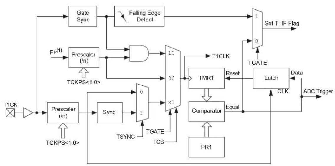
flowchart
graph TD
    A["T1CK"] --> B["Prescaler (/n)"]
    B --> C["Sync"]
    C --> D["0/1"]
    D --> E["x1"]
    E --> F["T1CLK"]
    F --> G["TMR1"]
    G --> H["Comparator"]
    H --> I["PR1"]
    I --> J["Data"]
    J --> K["Latch"]
    K --> L["Set T1IF Flag"]
    M["Falling Edge Detect"] --> N["Gate Sync"]
    O["TCKPS<1:0>"] --> P["Prescaler (/n)"]
    P --> Q["AND Gate"]
    Q --> R["10"]
    R --> S["x1"]
    S --> T["T1CLK"]
    U["Reset"] --> V["TGATE"]
    W["Equal"] --> X["Comparator"]
    Y["ADC Trigger"] --> Z["Data"]
    style A fill:#f9f,stroke:#333
    style B fill:#ccf,stroke:#333
    style C fill:#cfc,stroke:#333
    style D fill:#fcc,stroke:#333
    style E fill:#cff,stroke:#333
    style F fill:#ffc,stroke:#333
    style G fill:#fcc,stroke:#333
    style H fill:#ffc,stroke:#333
    style I fill:#fcc,stroke:#333
    style J fill:#ffc,stroke:#333
    style K fill:#fcc,stroke:#333
    style L fill:#fcc,stroke:#333
    style M fill:#fcc,stroke:#333
    style N fill:#ccf,stroke:#333
    style O fill:#ccf,stroke:#333
    style P fill:#ccf,stroke:#333
    style Q fill:#ccf,stroke:#333
    style R fill:#ccf,stroke:#333
    style S fill:#ccf,stroke:#333
    style T fill:#ccf,stroke:#333
    style U fill:#ccf,stroke:#333
    style V fill:#ccf,stroke:#333
    style W fill:#ccf,stroke:#333
    style X fill:#ccf,stroke:#333
Note 1: FP is the peripheral clock.
12.1 Timer1 Resources
Many useful resources are provided on the main product page of the Microchip website for the devices listed in this data sheet. This product page contains the latest updates and additional information.
12.1.1 KEY RESOURCES
- “Timers” (DS70362) in the “dsPIC33/PIC24 Family Reference Manual”
- Code Samples
- Application Notes
- Software Libraries
- Webinars
- All Related "dsPIC33/PIC24 Family Reference Manual" Sections
- Development Tools
12.2 Timer1 Control Register
REGISTER 12-1: T1CON: TIMER1 CONTROL REGISTER
| R/W-0 U-0 R/W-0 U-0 U-0 U-0 U-0 | |||||||
| TON^(1) | — | TSIDL | — | — | — | — | — |
| bit 15 bit 8 | |||||||
| U-0 | R/W-0 | R/W-0 | R/W-0 | U-0 | R/W-0 | R/W-0 | U-0 |
| — | TGATE | TCKPS1 | TCKPS0 | — | TSYNC^(1) | TCS^(1) | — |
| bit 7 bit 0 | |||||||
Legend:
| R = Readable bit | W = Writable bit | U = Unimplemented bit, read as '0' |
| -n = Value at POR | '1' = Bit is set | '0' = Bit is cleared x = Bit is unknown |
bit 15 TON: Timer1 On bit ^(1)
1 = Starts 16-bit Timer1
0 = Stops 16-bit Timer1
bit 14 Unimplemented: Read as '0'
bit 13 TSIDL: Timer1 Stop in Idle Mode bit
1 = Discontinues module operation when device enters Idle mode
0 = Continues module operation in Idle mode
bit 12-7 Unimplemented: Read as '0'
bit 6 TGATE: Timer1 Gated Time Accumulation Enable bit
When TCS = 1:
This bit is ignored.
When TCS = 0:
1 = Gated time accumulation is enabled
0 = Gated time accumulation is disabled
bit 5-4 TCKPS<1:0>: Timer1 Input Clock Prescale Select bits
11 = 1:256
10 = 1:64
01 = 1:8
00 = 1:1
bit 3 Unimplemented: Read as '0'
bit 2 TSYNC: Timer1 External Clock Input Synchronization Select bit ^(1)
When TCS = 1:
1 = Synchronizes external clock input
0 = Does not synchronize external clock input
When TCS = 0:
This bit is ignored.
bit 1 TCS: Timer1 Clock Source Select bit ^(1)
1 = External clock is from pin, T1CK (on the rising edge)
0 = Internal clock (FP)
bit 0 Unimplemented: Read as '0'
Note 1: When Timer1 is enabled in External Synchronous Counter mode (TCS = 1, TSYNC = 1, TON = 1), any attempts by user software to write to the TMR1 register are ignored.
NOTES:
13.0 TIMER2/3 AND TIMER4/5
Note 1: This data sheet summarizes the features of the dsPIC33EPXXXGS70X/80X family of devices. It is not intended to be a comprehensive reference source. To complement the information in this data sheet, refer to “Timers” (DS70362) in the “dsPIC33/PIC24 Family Reference Manual”, which is available from the Microchip website (www.microchip.com).
2: Some registers and associated bits described in this section may not be available on all devices. Refer to Section 4.0 "Memory Organization" in this data sheet for device-specific register and bit information.
The Timer2/3 and Timer4/5 modules are 32-bit timers, which can also be configured as four independent 16-bit timers with selectable operating modes.
As 32-bit timers, Timer2/3 and Timer4/5 operate in three modes:
- Two Independent 16-Bit Timers (e.g., Timer2 and Timer3) with all 16-Bit Operating modes (except Asynchronous Counter mode)
- Single 32-Bit Timer
• Single 32-Bit Synchronous Counter
They also support these features:
- Timer Gate Operation
- Selectable Prescaler Settings
- Timer Operation during Idle and Sleep modes
- Interrupt on a 32-Bit Period Register Match
- Time Base for Input Capture and Output Compare modules (Timer2 and Timer3 only)
Individually, all four of the 16-bit timers can function as synchronous timers or counters. They also offer the features listed previously, except for the event trigger; this is implemented only with Timer2/3. The operating modes and enabled features are determined by setting the appropriate bit(s) in the T2CON, T3CON, T4CON and T5CON registers. T2CON and T4CON are shown in generic form in Register 13-1. T3CON and T5CON are shown in Register 13-2.
For 32-bit timer/counter operation, Timer2 and Timer4 are the least significant word (lsw); Timer3 and Timer5 are the most significant word (msw) of the 32-bit timers.
Note: For 32-bit operation, T3CON and T5CON control bits are ignored. Only T2CON and T4CON control bits are used for setup and control. Timer2 and Timer4 clock and gate inputs are utilized for the 32-bit timer modules, but an interrupt is generated with the Timer3 and Timer5 interrupt flags.
A block diagram for an example 32-bit timer pair (Timer2/3 and Timer4/5) is shown in Figure 13-2.
13.1 Timer Resources
Many useful resources are provided on the main product page of the Microchip website for the devices listed in this data sheet. This product page contains the latest updates and additional information.
13.1.1 KEY RESOURCES
- "Timers" (DS70362) in the "dsPIC33/PIC24 Family Reference Manual"
- Code Samples
- Application Notes
- Software Libraries
- Webinars
- All Related "dsPIC33/PIC24 Family Reference Manual" Sections
- Development Tools
FIGURE 13-1: TIMERx BLOCK DIAGRAM (x = 2 THROUGH 5)

flowchart
graph TD
    TxCK --> A["Amplifier"]
    A --> B["Prescaler (/n)"]
    B --> C["Sync"]
    C --> D["x1"]
    D --> E["TMRx"]
    E --> F["Comparator"]
    F --> G["PRx"]
    G --> H["Set TxIF Flag"]
    H --> I["Latch"]
    I --> J["ADC Trigger(2)"]
    J --> K["Data"]
    K --> L["Reset"]
    L --> M["TxCLK"]
    M --> N["TGATE"]
    N --> O["Set TxIF Flag"]
    O --> P["Falling Edge Detect"]
    P --> Q["Gate Sync"]
    Q --> R["FPS(1)"]
    R --> S["TCKPS<1:0>"]
    S --> T["Prescaler (/n)"]
    T --> U["TCKPS<1:0>"]
    U --> V["TXCLK"]
    V --> W["Reset"]
    W --> X["TGATE"]
    X --> Y["TxCLK"]
    Y --> Z["TGATE"]
    Z --> AA["TXCLK"]
    AA --> AB["Set TxIF Flag"]
Note 1: FP is the peripheral clock.
2: The ADC trigger is only available on TMR2.
FIGURE 13-2: TYPE B/TYPE C TIMER PAIR BLOCK DIAGRAM (32-BIT TIMER)

flowchart
graph TD
    TxCK["TxCK"] --> Prescaler1["Prescaler (/n)"]
    Prescaler1 --> Prescaler2["Prescaler (/n)"]
    Prescaler2 --> Sync["Sync"]
    Prescaler1 --> Negator["AND"]
    Negator --> Comparator["Comparator"]
    Comparator --> PRx["PRx"]
    Comparator --> PRy["PRy"]
    Comparator --> Latch["Latch"]
    PRx --> Comparator
    PRy --> Comparator
    Latch --> Data["Data"]
    Data --> Reset["Reset"]
    Reset --> TMRx["TMRx"]
    Reset --> TMRy["TMRy"]
    TMRx --> TMRyHLD["TMRyHLD"]
    TMRyHLD --> DataBus["Data Bus<15:0>"]
    TMRx --> TGATE["TGATE"]
    TGATE --> x1["x1"]
    x1 --> Negator
    Negator --> Counter["Counter"]
    Counter --> GateSync["Gate Sync"]
    GateSync --> FallingEdgeDetect["Falling Edge Detect"]
    FallingEdgeDetect --> SetTylFlag["Set TylF Flag"]
    TGATE --> Comparator
    PRx --> Comparator
    PRy --> Comparator
    Comparator --> Equal["Equal"]
    Equal --> TGATE
    TGATE --> Data
    DataBus --> TMRx
    DataBus --> TMRy
    DataBus --> TMRyHLD
    TMRx --> TMRy
    TMRy --> TMRyHLD
    TMRx --> TMRyHLD
    TMRyHLD --> TGATE
    TGATE --> x1
Note 1: Timerx is a Type B timer (x = 2 and 4).
2: Timery is a Type C timer (y = 3 and 5).
13.2 Timer2/3 and Timer4/5 Control Registers
REGISTER 13-1: TxCON: (TIMER2 AND TIMER4) CONTROL REGISTER
| R/W-0 U-0 R/W-0 U-0 U-0 U-0 U-0 | |||||||
| TON | — | TSIDL | — | — | — | — | — |
| bit 15 bit 8 | |||||||
| U-0 | R/W-0 | R/W-0 | R/W-0 | R/W-0 | U-0 | R/W-0 | U-0 |
| — | TGATE | TCKPS1 | TCKPS0 | T32 | — | TCS(1) | — |
| bit 7 bit 0 | |||||||
| Legend: | |||
| R = Readable bit | W = Writable bit | U = Unimplemented bit, read as '0' | |
| -n = Value at POR | '1' = Bit is set | '0' = Bit is cleared | x = Bit is unknown |
bit 15 TON: Timerx On bit
When T32 = 1:
1 = Starts 32-bit Timerx/y
0 = Stops 32-bit Timerx/y
When T32 = 0:
1 = Starts 16-bit Timerx
0 = Stops 16-bit Timerx
bit 14 Unimplemented: Read as '0'
bit 13 TSIDL: Timerx Stop in Idle Mode bit
1 = Discontinues module operation when device enters Idle mode
0 = Continues module operation in Idle mode
bit 12-7 Unimplemented: Read as '0'
bit 6 TGATE: Timerx Gated Time Accumulation Enable bit
When TCS = 1:
This bit is ignored.
When TCS = 0:
1 = Gated time accumulation is enabled
0 = Gated time accumulation is disabled
bit 5-4 TCKPS<1:0>: Timerx Input Clock Prescale Select bits
11 = 1:256
10 = 1:64
01 = 1:8
00 = 1:1
bit 3 T32: 32-Bit Timer Mode Select bit
1 = Timerx and Timery form a single 32-bit timer
0 = Timerx and Timery act as two 16-bit timers
bit 2 Unimplemented: Read as '0'
bit 1 TCS: Timerx Clock Source Select bit (1)
1 = External clock is from pin, TxCK (on the rising edge)
0 = Internal clock (FP)
bit 0 Unimplemented: Read as '0'
Note 1: The TxCK pin is not available on all devices. Refer to the "Pin Diagrams" section for the available pins.
REGISTER 13-2: TyCON: (TIMER3 AND TIMER5) CONTROL REGISTER
| R/W-0 U-0 R/W-0 U-0 U-0 U-0 U-0 | |||||||
| TON^(1) | — | T (2) S | —+— | —D | L | ||
| bit 15 | bit 8 | ||||||
| U-0 | R/W-0 | R/W-0 | R/W-0 | U-0 | U-0 | R/W-0 | U-0 |
| — | T(1) | GATEKPS1(1) | TCKPS0(1) | — — | TCS | (1,3) | — |
| bit 7 bit 0 | |||||||
| Legend: | |||
| R = Readable bit | W = Writable bit | U = Unimplemented bit, read as ‘0’ | |
| -n = Value at POR | ‘1’ = Bit is set | ‘0’ = Bit is cleared | x = Bit is unknown |
bit 15 TON: Timery On bit(1)
1 = Starts 16-bit Timery
0 = Stops 16-bit Timery

bit 14 Unimplemented: Read as '0'
bit 13 TSIDL: Timery Stop in Idle Mode bit(2)
1 = Discontinues module operation when device enters Idle mode
0 = Continues module operation in Idle mode

bit 12-7 Unimplemented: Read as '0'
bit 6 TGATE: Timery Gated Time Accumulation Enable bit(1)
When TCS = 1:
This bit is ignored.
When TCS = 0:
1 = Gated time accumulation is enabled
0 = Gated time accumulation is disabled

bit 5-4 TCKPS<1:0>: Timery Input Clock Prescale Select bits(1)
11 = 1:256
10 = 1:64
01 = 1:8
00 = 1:1

bit 3-2 Unimplemented: Read as '0'
bit 1 TCS: Timery Clock Source Select bit(1,3)
1 = External clock is from pin, TyCK (on the rising edge)
0 = Internal clock (FP)

bit 0 Unimplemented: Read as '0'
Note 1: When 32-bit operation is enabled (TxCON<3> = 1), these bits have no effect on Timery operation; all timer functions are set through TxCON.
2: When 32-bit timer operation is enabled (T32 = 1) in the Timerx Control register (TxCON<3>), the TSIDL bit must be cleared to operate the 32-bit timer in Idle mode.
3: The TyCK pin is not available on all devices. See the "Pin Diagrams" section for the available pins.
14.0 INPUT CAPTURE
Note 1: This data sheet summarizes the features of the dsPIC33EPXXXGS70X/80X family of devices. It is not intended to be a comprehensive reference source. To complement the information in this data sheet, refer to “Input Capture with Dedicated Timer” (DS70000352) in the “dsPIC33/PIC24 Family Reference Manual”, which is available from the Microchip website (www.microchip.com).
2: Some registers and associated bits described in this section may not be available on all devices. Refer to Section 4.0 "Memory Organization" in this data sheet for device-specific register and bit information.
The input capture module is useful in applications requiring frequency (period) and pulse measurements. The dsPIC33EPXXXGS70X/80X devices support four input capture channels.
Key features of the input capture module include:
- Hardware-Configurable for 32-Bit Operation in All modes by Cascading Two Adjacent modules
- Synchronous and Trigger modes of Output Compare Operation, with up to 21 User-Selectable Trigger/Sync Sources available
• A 4-Level FIFO Buffer for Capturing and Holding Timer Values for Several Events - Configurable Interrupt Generation
- Up to Six Clock Sources available for each module, Driving a Separate Internal 16-Bit Counter
14.1 Input Capture Resources
Many useful resources are provided on the main product page of the Microchip website for the devices listed in this data sheet. This product page contains the latest updates and additional information.
14.1.1 KEY RESOURCES
- "Input Capture with Dedicated Timer" (DS70000352) in the "dsPIC33/PIC24 Family Reference Manual"
- Code Samples
- Application Notes
- Software Libraries
- Webinars
- All Related "dsPIC33/PIC24 Family Reference Manual" Sections
• Development Tools
FIGURE 14-1: INPUT CAPTURE x MODULE BLOCK DIAGRAM
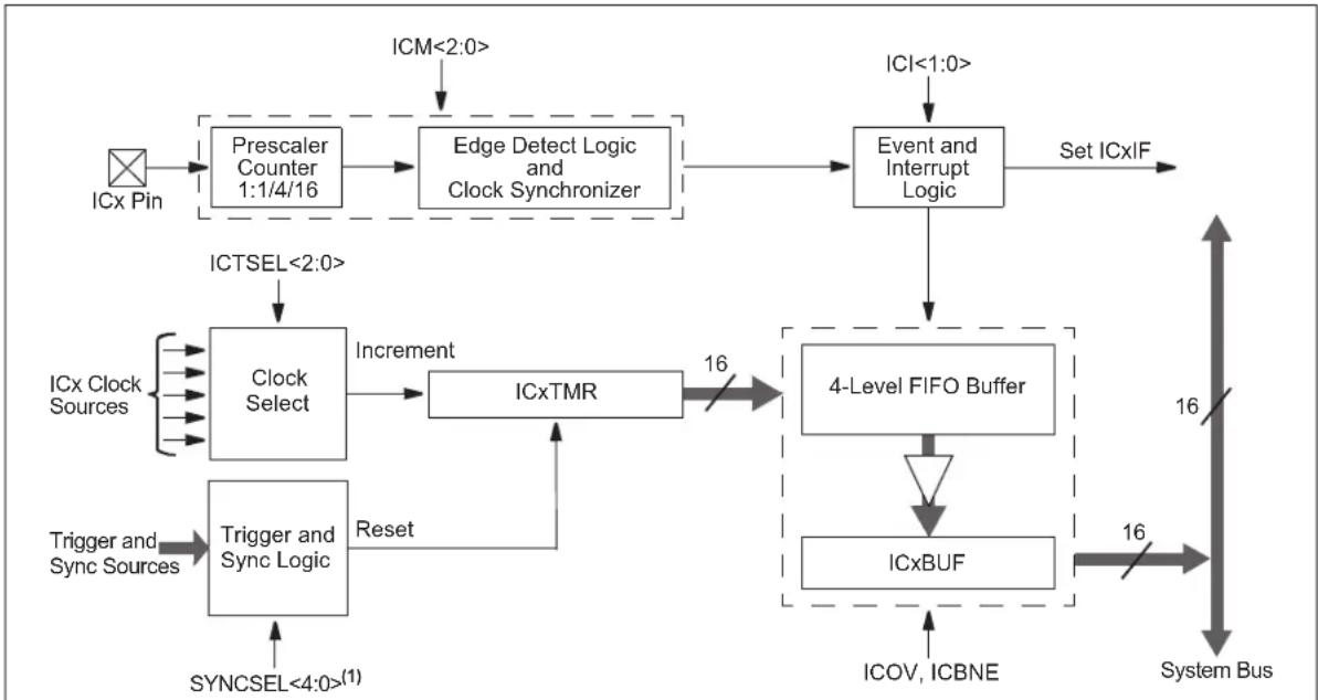
flowchart
graph TD
    A["ICx Pin"] --> B["Prescaler Counter 1:1/4/16"]
    B --> C["Edge Detect Logic and Clock Synchronizer"]
    C --> D["Event and Interrupt Logic"]
    D --> E["Set ICxIF"]
    F["ICx Clock Sources"] --> G["Clock Select"]
    G --> H["Increment"]
    H --> I["ICxTMR"]
    I --> J["4-Level FIFO Buffer"]
    J --> K["ICxBUF"]
    K --> L["ICOV, ICBNE"]
    L --> M["System Bus"]
    N["Trigger and Sync Sources"] --> O["Trigger and Sync Logic"]
    O --> P["Reset"]
    P --> G
    Q["SYNCSEL<4:0>(1)"] --> O
    R["ICTSEL<2:0>"] --> G
    S["ICM<2:0>"] --> C
    T["ICI<1:0>"] --> D
    U["16"] --> J
    V["16"] --> K
Note 1: The trigger/sync source is enabled by default and is set to Timer3 as a source. This timer must be enabled for proper ICx module operation or the trigger/sync source must be changed to another source option.
14.2 Input Capture Registers
REGISTER 14-1: ICxCON1: INPUT CAPTURE x CONTROL REGISTER 1
| U-0 U-0 R/W-0 R/W-0 R/W-0 R/W-0 U-0 U-0 | |||||||
| — — IC | SIDL | ICTSEL2 | ICTSEL1 | ICTSEL0 — | — | ||
| bit 15 bit 8 | |||||||
| U-0 | R/W-0 | R/W-0 | HC/HS/R-0 | HC/HS/R-0 | R/W-0 | R/W-0 | R/W-0 |
| — | ICI1 | ICI0 | ICOV | ICBNE | ICM2 | ICM1 | ICM0 |
| bit 7 bit 0 | |||||||
| Legend: | HC = Hardware Clearable bit | HS = Hardware Settable bit |
| R = Readable bit | W = Writable bit | U = Unimplemented bit, read as ‘0’ |
| -n = Value at POR | ‘1’ = Bit is set | ‘0’ = Bit is cleared x = Bit is unknown |
bit 15-14 Unimplemented: Read as '0'
bit 13 ICSIDL: Input Capture x Stop in Idle Control bit
1 = Input capture will halt in CPU Idle mode
0 = Input capture will continue to operate in CPU Idle mode
bit 12-10 ICTSEL<2:0>: Input Capture x Timer Select bits
111 = Peripheral clock (FP) is the clock source of the ICx
110 = Reserved
101 = Reserved
100 = T1CLK is the clock source of the ICx (only the synchronous clock is supported)
011 = T5CLK is the clock source of the ICx
010 = T4CLK is the clock source of the ICx
001 = T2CLK is the clock source of the ICx
000 = T3CLK is the clock source of the ICx
bit 9-7 Unimplemented: Read as '0'
bit 6-5 ICI<1:0>: Number of Captures per Interrupt Select bits (this field is not used if ICM<2:0> = 001 or 111)
11 = Interrupt on every fourth capture event
10 = Interrupt on every third capture event
01 = Interrupt on every second capture event
00 = Interrupt on every capture event
bit 4 ICOV: Input Capture x Overflow Status Flag bit (read-only)
1 = Input capture buffer overflow has occurred
0 = No input capture buffer overflow has occurred
bit 3 ICBNE: Input Capture x Buffer Not Empty Status bit (read-only)
1 = Input capture buffer is not empty, at least one more capture value can be read
0 = Input capture buffer is empty
bit 2-0 ICM<2:0>: Input Capture x Mode Select bits
111 = Input Capture x functions as an interrupt pin only in CPU Sleep and Idle modes (rising edge detect only, all other control bits are not applicable)
110 = Unused (module is disabled)
101 = Capture mode, every 16th rising edge (Prescaler Capture mode)
100 = Capture mode, every 4th rising edge (Prescaler Capture mode)
011 = Capture mode, every rising edge (Simple Capture mode)
010 = Capture mode, every falling edge (Simple Capture mode)
001 = Capture mode, every rising and falling edge (Edge Detect mode, ICI<1:0> is not used in this mode)
000 = Input Capture x is turned off
REGISTER 14-2: ICxCON2: INPUT CAPTURE x CONTROL REGISTER 2
| U-0 U-0 U-0 U-0 U-0 U-0 R/W-0 | |||||||
| —— | —— — — | I | C | 3 | 2 | ||
| bit 15 | bit 8 | ||||||
| R/W-0 | HS/R/W-0 | U-0 | R/W-0 | R/W-1 | R/W-1 | R/W-0 | R/W-1 |
| ICTRIG ^(2) | TRIGSTAT ^(3) | — | SYNCSEL4 ^(4) | SYNCSEL3 ^(4) | SYNCSEL2 ^(4) | SYNCSEL1 ^(4) | SYNCSEL0 ^(4) |
| bit 7 bit 0 | |||||||
| Legend: | HS = Hardware Settable bit | ||
| R = Readable bit | W = Writable bit | U = Unimplemented bit, read as '0' | |
| -n = Value at POR | '1' = Bit is set | '0' = Bit is cleared | x = Bit is unknown |
bit 15-9 Unimplemented: Read as '0'
bit 8 IC32: Input Capture x 32-Bit Timer Mode Select bit (Cascade mode)
1 = Odd ICx and even ICx form a single 32-bit input capture module ^(1)
0 = Cascade module operation is disabled
bit 7 ICTRIG: Input Capture x Trigger Operation Select bit ^(2)
1 = Input source is used to trigger the input capture timer (Trigger mode)
0 = Input source is used to synchronize the input capture timer to a timer of another module (Synchronization mode)
bit 6 TRIGSTAT: Timer Trigger Status bit ^(3)
1 = ICxTMR has been triggered and is running
0 = ICxTMR has not been triggered and is being held clear
bit 5 Unimplemented: Read as '0'
Note 1: The IC32 bit in both the odd and even ICx must be set to enable Cascade mode.
2: The input source is selected by the SYNCSEL<4:0> bits of the ICxCON2 register.
3: This bit is set by the selected input source (selected by SYNCSEL<4:0> bits); it can be read, set and cleared in software.
4: Do not use the ICx module as its own sync or trigger source.
5: This option should only be selected as a trigger source and not as a synchronization source.
REGISTER 14-2: ICxCON2: INPUT CAPTURE x CONTROL REGISTER 2 (CONTINUED)
bit 4-0 SYNCSEL<4:0>: Input Source Select for Synchronization and Trigger Operation bits ^(4) 11111 = No sync or trigger source for ICx
11110 = Reserved
11101 = Reserved
11100 = Reserved
11011 = CMP4 module synchronizes or triggers ICx ^(5) 11010 = CMP3 module synchronizes or triggers ICx ^(5) 11001 = CMP2 module synchronizes or triggers ICx ^(5) 11000 = CMP1 module synchronizes or triggers ICx ^(5) 10111 = Reserved
10110 = Reserved
10101 = Reserved
10100 = Reserved
10011 = IC4 module interrupt synchronizes or triggers ICx
10010 = IC3 module interrupt synchronizes or triggers ICx
10001 = IC2 module interrupt synchronizes or triggers ICx
10000 = IC1 module interrupt synchronizes or triggers ICx
01111 = Timer5 synchronizes or triggers ICx
01110 = Timer4 synchronizes or triggers ICx
01101 = Timer3 synchronizes or triggers ICx (default)
01100 = Timer2 synchronizes or triggers ICx
01011 = Timer1 synchronizes or triggers ICx
01010 = Reserved
01001 = Reserved
01000 = IC4 module synchronizes or triggers ICx
00111 = IC3 module synchronizes or triggers ICx
00110 = IC2 module synchronizes or triggers ICx
00101 = IC1 module synchronizes or triggers ICx
00100 = OC4 module synchronizes or triggers ICx
00011 = OC3 module synchronizes or triggers ICx
00010 = OC2 module synchronizes or triggers ICx
00001 = OC1 module synchronizes or triggers ICx
00000 = No sync or trigger source for ICx
Note 1: The IC32 bit in both the odd and even ICx must be set to enable Cascade mode.
2: The input source is selected by the SYNCSEL<4:0> bits of the ICxCON2 register.
3: This bit is set by the selected input source (selected by SYNCSEL<4:0> bits); it can be read, set and cleared in software.
4: Do not use the ICx module as its own sync or trigger source.
5: This option should only be selected as a trigger source and not as a synchronization source.
15.0 OUTPUT COMPARE
Note 1: This data sheet summarizes the features of the dsPIC33EPXXXGS70X/80X family of devices. It is not intended to be a comprehensive reference source. To complement the information in this data sheet, refer to "Output Compare with Dedicated Timer" (DS70005159) in the "dsPIC33/PIC24 Family Reference Manual", which is available from the Microchip website (www.microchip.com).
2: Some registers and associated bits described in this section may not be available on all devices. Refer to Section 4.0 "Memory Organization" in this data sheet for device-specific register and bit information.
The output compare module can select one of six available clock sources for its time base. The module compares the value of the timer with the value of one or two Compare registers, depending on the operating mode selected. The state of the output pin changes when the timer value matches the Compare register value. The output compare module generates either a
single output pulse, or a sequence of output pulses, by changing the state of the output pin on the compare match events. The output compare module can also generate interrupts on compare match events.
15.1 Output Compare Resources
Many useful resources are provided on the main product page of the Microchip website for the devices listed in this data sheet. This product page contains the latest updates and additional information.
15.1.1 KEY RESOURCES
- "Output Compare with Dedicated Timer" (DS70005159) in the "dsPIC33/PIC24 Family Reference Manual"
- Code Samples
- Application Notes
- Software Libraries
- Webinars
- All Related "dsPIC33/PIC24 Family Reference Manual" Sections
- Development Tools
FIGURE 15-1: OUTPUT COMPARE x MODULE BLOCK DIAGRAM
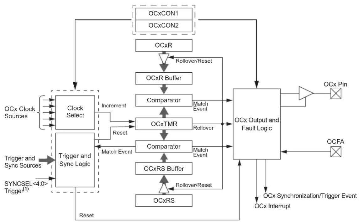
flowchart
graph TD
    A["Clock Select"] -->|Increment| B["Comparator"]
    C["Trigger and Sync Logic"] -->|Match Event| B
    D["OCxR"] -->|Rollover/Reset| E["OCxR Buffer"]
    E --> F["Comparator"]
    F -->|Match Event| G["OCxTMR"]
    G --> H["Comparator"]
    H -->|Match Event| I["OCxRS Buffer"]
    I --> J["OCxRS"]
    J --> K["OCxOutput and Fault Logic"]
    L["OCx Clock Sources"] --> A
    M["SYNCSEL<4:0> Trigger(1)"] --> C
    N["OCx Pin"] --> O["OCx Output and Fault Logic"]
    P["OCFA"] --> Q["OCx Synchronization/Trigger Event"]
    R["OCx Interrupt"] --> S["OCx Output and Fault Logic"]
    T["Reset"] --> A
    U["Reset"] --> C
Note 1: The trigger/sync source is enabled by default and is set to Timer2 as a source. This timer must be enabled for proper OCx module operation or the trigger/sync source must be changed to another source option.
15.2 Output Compare Control Registers
REGISTER 15-1: OCxCON1: OUTPUT COMPARE x CONTROL REGISTER 1
| U-0 U-0 R/W-0 R/W-0 R/W-0 R/W-0 U-0 U-0 | ||||||
| — — O | CSIDL OCTSEL2 OCTSEL1 | OCTSEL0 | — | — | ||
| bit 15 bit 8 | ||||||
| R/W-0 | U-0 | U-0 | HSC/R/W-0 | R/W-0 | R/W-0 | R/W-0 | R/W-0 |
| ENFLTA | — | — | OCFLTA | TRIGMODE | OCM2 | OCM1 | OCM0 |
| bit 7 bit 0 | |||||||
| Legend: | HSC = Hardware Settable/Clearable bit | ||
| R = Readable bit W = Writable bit | U = Unimplemented bit, read as ‘0’ | ||
| -n = Value at POR | ‘1’ = Bit is set | ‘0’ = Bit is cleared | x = Bit is unknown |
bit 15-14 Unimplemented: Read as '0'
bit 13 OCSIDL: Output Compare x Stop in Idle Mode Control bit
1 = Output Compare x halts in CPU Idle mode
0 = Output Compare x continues to operate in CPU Idle mode
bit 12-10 OCTSEL<2:0>: Output Compare x Clock Select bits
111 = Peripheral clock (FP)
110 = Reserved
101 = Reserved
100 = T1CLK is the clock source of the OCx (only the synchronous clock is supported)
011 = T5CLK is the clock source of the OCx
010 = T4CLK is the clock source of the OCx
001 = T3CLK is the clock source of the OCx
000 = T2CLK is the clock source of the OCx
bit 9-8 Unimplemented: Read as '0'
bit 7 ENFLTA: Fault A Input Enable bit
1 = Output Compare Fault A input (OCFA) is enabled
0 = Output Compare Fault A input (OCFA) is disabled
bit 6-5 Unimplemented: Read as '0'
bit 4 OCFLTA: PWM Fault A Condition Status bit
1 = PWM Fault A condition on the OCFA pin has occurred
0 = No PWM Fault A condition on the OCFA pin has occurred
bit 3 TRIGMODE: Trigger Status Mode Select bit
1 = TRIGSTAT (OCxCON2<6>) is cleared when OCxRS = OCxTMR or in software
0 = TRIGSTAT is cleared only by software
Note 1: OCxR and OCxRS are double-buffered in PWM mode only.
REGISTER 15-1: OCxCON1: OUTPUT COMPARE x CONTROL REGISTER 1 (CONTINUED)
bit 2-0 OCM<2:0>: Output Compare x Mode Select bits
111 = Center-Aligned PWM mode: Output is set high when OCxTMR = OCxR and set low when OCxTMR = OCxRS ^(1)
110 = Edge-Aligned PWM mode: Output is set high when OCxTMR = 0 and set low when OCxTMR = OCxR ^(1)
101 = Double Compare Continuous Pulse mode: Initializes OCx pin low, toggles OCx state continuously on alternate matches of OCxR and OCxRS
100 = Double Compare Single-Shot mode: Initializes OCx pin low, toggles OCx state on matches of OCxR and OCxRS for one cycle
011 = Single Compare mode: Compare event with OCxR, continuously toggles OCx pin
010 = Single Compare Single-Shot mode: Initializes OCx pin high, compare event with OCxR, forces OCx pin low
001 = Single Compare Single-Shot mode: Initializes OCx pin low, compare event with OCxR, forces OCx pin high
000 = Output compare channel is disabled
Note 1: OCxR and OCxRS are double-buffered in PWM mode only.
REGISTER 15-2: OCxCON2: OUTPUT COMPARE x CONTROL REGISTER 2
| R/W-0 R/W-0 R/W-0 R/W-0 U-0 U-0 U-0 R/W-0 | |||||||
| FLTMD FLTOUT FLTTRIEN OCINV | ——— | O | C | 3 | |||
| bit 15 bit 8 | |||||||
| R/W-0 | HS/R/W-0 | R/W-0 | R/W-0 | R/W-1 | R/W-1 | R/W-0 | R/W-0 | |
| OCTRIG | TRIGSTAT | OCTRIS | SYNCSEL4 | SYNCSEL3 | SYNCSEL2 | SYNCSEL1 | SYNCSEL0 | |
| bit 7 bit 0 | ||||||||
| Legend: | HS = Hardware Settable bit | ||
| R = Readable bit | W = Writable bit | U = Unimplemented bit, read as ‘0’ | |
| -n = Value at POR | ‘1’ = Bit is set | ‘0’ = Bit is cleared | x = Bit is unknown |
bit 15 FLTMD: Fault Mode Select bit
1 = Fault mode is maintained until the Fault source is removed; the corresponding OCFLTA bit is cleared in software and a new PWMx period starts 0 = Fault mode is maintained until the Fault source is removed and a new PWMx period starts
bit 14 FLTOUT: Fault Out bit
1 = PWMx output is driven high on a Fault 0 = PWMx output is driven low on a Fault
bit 13 FLTTRIEN: Fault Output State Select bit
1 = OCx pin is tri-stated on a Fault condition 0 = OCx pin I/O state is defined by the FLTOUT bit on a Fault condition
bit 12 OCINV: Output Compare x Invert bit
1 = OCx output is inverted 0 = OCx output is not inverted
bit 11-9 Unimplemented: Read as '0'
bit 8 OC32: Cascade Two OCx Modules Enable bit (32-bit operation)
1 = Cascade module operation is enabled 0 = Cascade module operation is disabled
bit 7 OCTRIG: Output Compare x Trigger/Sync Select bit
1 = Triggers OCx from the source designated by the SYNCSELx bits 0 = Synchronizes OCx with the source designated by the SYNCSELx bits
bit 6 TRIGSTAT: Timer Trigger Status bit
1 = Timer source has been triggered and is running 0 = Timer source has not been triggered and is being held clear
bit 5 OCTRIS: Output Compare x Output Pin Direction Select bit
1 = OCx is tri-stated 0 = OCx module drives the OCx pin
Note 1: Do not use the OCx module as its own synchronization or trigger source.
2: When the OCy module is turned off, it sends a trigger out signal. If the OCx module uses the OCy module as a trigger source, the OCy module must be unselected as a trigger source prior to disabling it.
3: For each OCMPx instance, a different PTG trigger out is used:
OCMP1 – PTG trigger out [0] OCMP2 – PTG trigger out [1] OCMP3 – PTG trigger out [2] OCMP4 – PTG trigger out [3]
REGISTER 15-2: OCxCON2: OUTPUT COMPARE x CONTROL REGISTER 2 (CONTINUED)
bit 4-0 SYNCSEL<4:0>: Trigger/Synchronization Source Selection bits
11111 = OCxRS compare event is used for synchronization
11110 = INT2 pin synchronizes or triggers OCx
11101 = INT1 pin synchronizes or triggers OCx
11100 = Reserved
11011 = CMP4 module synchronizes or triggers OCx
11010 = CMP3 module synchronizes or triggers OCx
11001 = CMP2 module synchronizes or triggers OCx
11000 = CMP1 module synchronizes or triggers OCx
10111 = Reserved
10110 = Reserved
10101 = Reserved
10100 = Reserved
10011 = IC4 input capture interrupt event synchronizes or triggers OCx
10010 = IC3 input capture interrupt event synchronizes or triggers OCx
10001 = IC2 input capture interrupt event synchronizes or triggers OCx
10000 = IC1 input capture interrupt event synchronizes or triggers OCx
01111 = Timer5 synchronizes or triggers OCx
01110 = Timer4 synchronizes or triggers OCx
01101 = Timer3 synchronizes or triggers OCx
01100 = Timer2 synchronizes or triggers OCx (default)
01011 = Timer1 synchronizes or triggers OCx
01010 = PTG Trigger Output x ^(3) 01001 = Reserved
01000 = IC4 input capture event synchronizes or triggers OCx
00111 = IC3 input capture event synchronizes or triggers OCx
00110 = IC2 input capture event synchronizes or triggers OCx
00101 = IC1 input capture event synchronizes or triggers OCx
00100 = OC4 module synchronizes or triggers OCx ^(1,2) 00011 = OC3 module synchronizes or triggers OCx ^(1,2) 00010 = OC2 module synchronizes or triggers OCx ^(1,2) 00001 = OC1 module synchronizes or triggers OCx ^(1,2) 00000 = No sync or trigger source for OCx
Note 1: Do not use the OCx module as its own synchronization or trigger source.
2: When the OCy module is turned off, it sends a trigger out signal. If the OCx module uses the OCy module as a trigger source, the OCy module must be unselected as a trigger source prior to disabling it.
3: For each OCMPx instance, a different PTG trigger out is used:
OCMP1 - PTG trigger out [0]
OCMP2 - PTG trigger out [1]
OCMP3 - PTG trigger out [2]
OCMP4 - PTG trigger out [3]
NOTES:
16.0 HIGH-SPEED PWM
Note: This data sheet summarizes the features of the dsPIC33EPXXXGS70X/80X family of devices. It is not intended to be a comprehensive reference source. To complement the information in this data sheet, refer to “High-Speed PWM Module” (DS70000323) in the “dsPIC33/PIC24 Family Reference Manual”, which is available from the Microchip website (www.microchip.com).
The high-speed PWM on dsPIC33EPXXXGS70X/80X devices supports a wide variety of PWM modes and output formats. This PWM module is ideal for power conversion applications, such as:
- AC/DC Converters
- DC/DC Converters
• Power Factor Correction
• Uninterruptible Power Supply (UPS) - Inverters
- Battery Chargers
- Digital Lighting
16.1 Features Overview
The high-speed PWM module incorporates the following features:
• Eight PWMx Generators with Two Outputs per Generator
- Two Master Time Base modules
- Individual Time Base and Duty Cycle for each PWM Output
- Duty Cycle, Dead Time, Phase Shift and a Frequency Resolution of 1.04 ns
- Independent Fault and Current-Limit Inputs
- Redundant Output
• True Independent Output
• Center-Aligned PWM mode
• Output Override Control
- Chop mode (also known as Gated mode)
- Special Event Trigger
- Dual Trigger from PWMx to Analog-to-Digital Converter (ADC)
- PWMxL and PWMxH Output Pin Swapping
- Independent PWMx Frequency, Duty Cycle and Phase-Shift Changes
• Enhanced Leading-Edge Blanking (LEB) Functionality
- PWM Capture Functionality
Note: Duty cycle, dead time, phase shift and frequency resolution is 8.32 ns in Center-Aligned PWM mode.
Figure 16-1 conceptualizes the PWM module in a simplified block diagram. Figure 16-2 illustrates how the module hardware is partitioned for each PWMx output pair for the Complementary PWM mode.
The PWM module contains eight PWM generators. The module has up to 16 PWMx output pins: PWM1H/PWM1L through PWM8H/PWM8L. For complementary outputs, these 16 I/O pins are grouped into high/low pairs. PWM1 through PWM6 can be used to trigger an ADC conversion.
16.2 Feature Description
The PWM module is designed for applications that require:
• High resolution at high PWM frequencies
- The ability to drive Standard Edge-Aligned, Center-Aligned, Complementary mode and Push-Pull mode outputs
- The ability to create multiphase PWM outputs
Two common, medium power converter topologies are push-pull and half-bridge. These designs require the PWM output signal to be switched between alternate pins, as provided by the Push-Pull PWM mode.
Phase-shifted PWM describes the situation where each PWM generator provides outputs, but the phase relationship between the generator outputs is specifiable and changeable.
Multiphase PWM is often used to improve DC/DC Converter load transient response, and reduce the size of output filter capacitors and inductors. Multiple DC/DC Converters are often operated in parallel, but phase shifted in time. A single PWM output, operating at 250 kHz, has a period of 4 s but an array of four PWM channels, staggered by 1 s each, yields an effective switching frequency of 1 MHz. Multiphase PWM applications typically use a fixed-phase relationship.
Variable phase PWM is useful in Zero Voltage Transition (ZVT) power converters. Here, the PWM duty cycle is always 50% and the power flow is controlled by varying the relative phase shift between the two PWM generators.
16.2.1 WRITE-PROTECTED REGISTERS
On dsPIC33EPXXXGS70X/80X family devices, write protection is implemented for the IOCONx and FCLCONx registers. The write protection feature prevents any inadvertent writes to these registers. This protection feature can be controlled by the PWMLOCK Configuration bit (FDEVOPT<0>). The default state of the write protection feature is enabled (PWMLOCK = 1). The write protection feature can be disabled by configuring PWMLOCK = 0.
To gain write access to these locked registers, the user application must write two consecutive values (0xABCD and 0x4321) to the PWMKEY register to perform the unlock operation. The write access to the IOCONx or FCLCONx registers must be the next SFR access following the unlock process. There can be no other SFR accesses during the unlock process and subsequent write access. To write to both the IOCONx and FCLCONx registers requires two unlock operations.
The correct unlocking sequence is described in Example 16-1.
EXAMPLE 16-1: PWM WRITE-PROTECTED REGISTER UNLOCK SEQUENCE
; Writing to FCLCON1 register requires unlock sequence
mov #0abcd, w10 ; Load first unlock key to w10 register
mov #0x4321, w11 ; Load second unlock key to w11 register
mov #0x0000, w0 ; Load desired value of FCLCON1 register in w0
mov w10, PWMKEY ; Write first unlock key to PWMKEY register
mov w11, PWMKEY ; Write second unlock key to PWMKEY register
mov w0, FCLCON1 ; Write desired value to FCLCON1 register
; Set PWM ownership and polarity using the IOCON1 register
; Writing to IOCON1 register requires unlock sequence
mov #0abcd, w10 ; Load first unlock key to w10 register
mov #0x4321, w11 ; Load second unlock key to w11 register
mov #0xF000, w0 ; Load desired value of IOCON1 register in w0
mov w10, PWMKEY ; Write first unlock key to PWMKEY register
mov w11, PWMKEY ; Write second unlock key to PWMKEY register
mov w0, IOCON1 ; Write desired value to IOCON1 register
16.3 PWM Resources
Many useful resources are provided on the main product page of the Microchip website for the devices listed in this data sheet. This product page contains the latest updates and additional information.
16.3.1 KEY RESOURCES
- "High-Speed PWM Module" (DS70000323) in the "dsPIC33/PIC24 Family Reference Manual"
- Code Samples
- Application Notes
- Software Libraries
- Webinars
- All Related "dsPIC33/PIC24 Family Reference Manual" Sections
- Development Tools
FIGURE 16-1: HIGH-SPEED PWM MODULE ARCHITECTURAL DIAGRAM
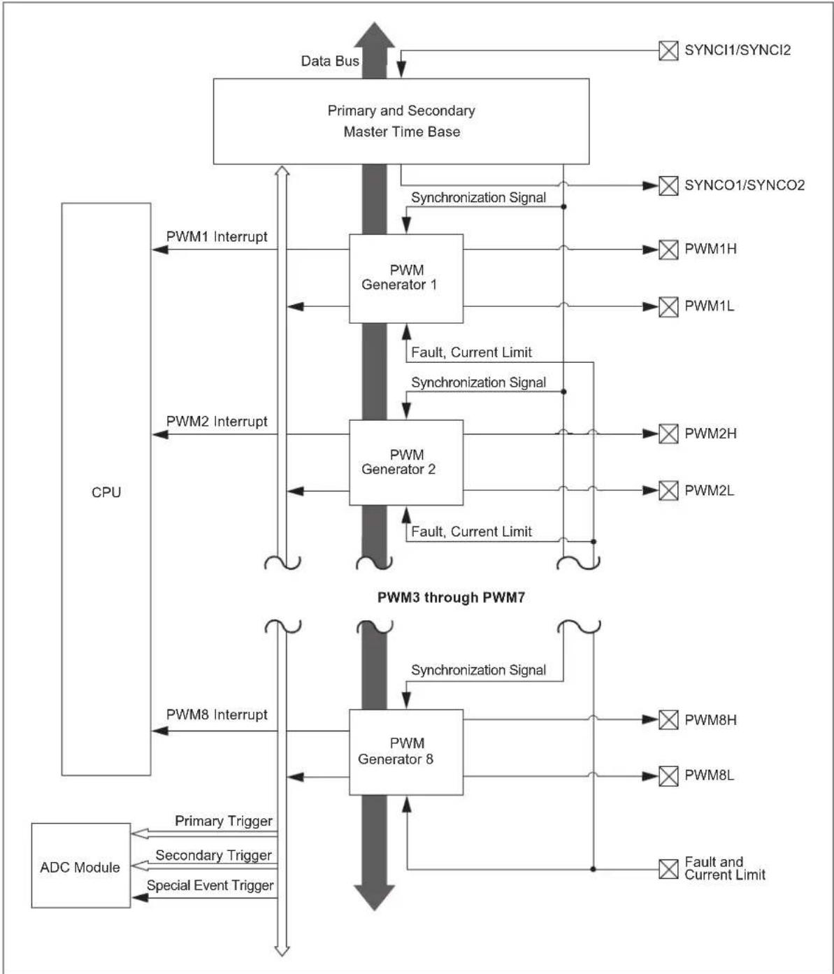
flowchart
graph TD
    A["Data Bus"] --> B["Primary and Secondary Master Time Base"]
    B --> C["PWM Generator 1"]
    C --> D["CPU"]
    D --> E["PWM1 Interrupt"]
    D --> F["PWM2 Interrupt"]
    D --> G["PWM3 through PWM7"]
    G --> H["PWM8 Interrupt"]
    G --> I["PWM8H"]
    G --> J["PWM8L"]
    G --> K["PWM8"]
    G --> L["PWM8"]
    G --> M["PWM8"]
    G --> N["PWM8"]
    G --> O["PWM8"]
    G --> P["PWM8"]
    G --> Q["PWM8"]
    G --> R["PWM8"]
    G --> S["PWM8"]
    G --> T["PWM8"]
    G --> U["PWM8"]
    G --> V["PWM8"]
    G --> W["PWM8"]
    G --> X["PWM8"]
    G --> Y["PWM8"]
    G --> Z["PWM8"]
    G --> AA["PWM8"]
    G --> AB["PWM8"]
    G --> AC["PWM8"]
    G --> AD["PWM8"]
    G --> AE["PWM8"]
    G --> AF["PWM8"]
    G --> AG["PWM8"]
    G --> AH["PWM8"]
    G --> AI["PWM8"]
    G --> AJ["PWM8"]
    G --> AK["PWM8"]
    G --> AL["PWM8"]
    G --> AM["PWM8"]
    G --> AN["PWM8"]
    G --> AO["PWM8"]
    G --> AP["PWM8"]
    G --> AQ["PWM8"]
    G --> AR["PWM8"]
    G --> AS["PWM8"]
    G --> AT["PWM8"]
    G --> AU["PWM8"]
    G --> AV["PWM8"]
    G --> AW["PWM8"]
    G --> AX["PWM8"]
    G --> AY["PWM8"]
    G --> AZ["PWM8"]
    G --> BA["PWM8"]
    G --> BB["PWM8"]
    G --> BC["PWM8"]
    G --> BD["PWM8"]
    G --> BE["PWM8"]
    G --> BF["PWM8"]
    G --> BG["PWM8"]
    G --> BH["PWM8"]
    G --> BI["PWM8"]
    G --> BJ["PWM8"]
    G --> BK["PWM8"]
    G --> BL["PWM8"]
    G --> BM["PWM8"]
    G --> BN["PWM8"]
    G --> BO["PWM8"]
    G --> BP["PWM8"]
    G --> BQ["PWM8"]
    G --> BR["PWM8"]
    G --> BS["PWM8"]
    G --> BT["PWM8"]
    G --> BU["PWM8"]
    G --> BV["PWM8"]
    G --> BW["PWM8"]
    G --> BX["PWM8"]
    G --> BY["PWM8"]
    G --> BZ["PWM8"]
    G --> CA["PWM8"]
    G --> CB["PWM8"]
    G --> CC["PWM8"]
    G --> CD["PWM8"]
    G --> CE["PWM8"]
    G --> CF["PWM8"]
    G --> CG["ADC Module"]
    CG --> CH["Primary Trigger"]
    CG --> CI["Secondary Trigger"]
    CG --> CJ["Special Event Trigger"]
FIGURE 16-2: SIMPLIFIED CONCEPTUAL BLOCK DIAGRAM OF THE HIGH-SPEED PWM

flowchart
graph TD
    subgraph "16-Bit Data Bus"
        A["PTCON, PTCON2 STCON, STCON2"] --> B["PWMKEY"]
        C["PTPER"] --> D["Comparator"]
        E["SEVTCMP"] --> F["Comparator"]
        G["Special Event Compare Trigger"] --> H["SYNCO1"]
        I["STPER"] --> J["Comparator"]
        K["SEVTCMP"] --> L["Comparator"]
        M["Special Event Postscaler"] --> N["Special Event Trigger"]
        O["SMTMR"] --> P["Master Time Base Counter"]
        Q["SMTMR"] --> R["Master Time Base Counter"]
        S["SMTMR"] --> T["Master Duty Cycle Register"]
        U["MDC"] --> V["Master Duty Cycle Register"]
        W["PDCx"] --> X["MUX"]
        X --> Y["Comparator"]
        Y --> Z["PWMCAPx"]
        Z --> AA["ADC Trigger"]
        AB["PTMRx"] --> AC["Comparator"]
        AD["PHASEx"] --> AE["TRIGx"]
        AF["SDCx"] --> AG["MUX"]
        AG --> AH["Comparator"]
        AH --> AI["Interrupt Logic"]
        AI --> AJ["ADC Trigger"]
        AK["STMRx"] --> AL["Comparator"]
        AM["SPHASEx"] --> AN["STRIGx"]
        AO["PWMCONx AUXCONx"] --> AP["TRGCONx"]
        AQ["PWMxH"] --> AR["PWMxL"]
        AS["PWMxL"] --> AT["FLTx"]
    end

    subgraph "Primary Master Time Base"
        AU["SYNCO2"] --> AV["Special Event Compare Trigger"]
        AW["STPER"] --> AX["Comparator"]
        AY["SEVTCMP"] --> AZ["Comparator"]
        BA["Special Event Postscaler"] --> BB["Special Event Trigger"]
        BC["STPMR"] --> BD["Comparator"]
        BE["SMTMR"] --> BF["Master Time Base Counter"]
        BG["SMTMR"] --> BH["Master Duty Cycle Register"]
    end

    subgraph "Secondary Master Time Base"
        BI["SYNCO2"] --> BJ["Special Event Compare Trigger"]
        BK["SMTMR"] --> BL["Master Duty Cycle Register"]
        BM["SMTMR"] --> BN["Master Duty Cycle Register"]
    end

    subgraph "PWM Generator 1"
        BO["PWMx Output Mode Control Logic\nUser Override Logic\nCurrent-Limit Override Logic\nFault Override Logic"] --> BP["PWM1H PWM1L"]
        BP --> BQ["PWM1H"]
        BP --> BR["PWM1L"]

    subgraph "PWM Generator 1 – PWM Generator 8"
        BS["PWMhX"] --> BT["PWMxL"]
        BT --> BU["FLTx"]

    A --> D
    C --> F
    D --> Z
    Z --> AA
    AA --> AB
    AB --> AC
    AC --> AD
    AD --> AE
    AE --> AF
    AF --> AG
    AG --> AH
    AH --> AI
    AI --> AJ
    AJ --> AK
    AK --> AK
    AK --> AL
    AL --> AM
    AM --> AN
    AN --> AO
    AO --> AP
    AP --> AQ
    AQ --> AR
    AR --> AS
    AS --> AT
    AT --> AU
    AU --> AV
    AV --> AW
    AW --> AX
    AX --> AY
    AY --> AZ
    AZ --> BA
    BA --> BB
    BB --> BC
    BC --> AD
    AD --> AD
    AD --> AF
REGISTER 16-1: PTCON: PWM TIME BASE CONTROL REGISTER
| R/W-0 U-0 R/W-0 HSC/R-0 R/W-0 R/W-0 R/W-0 R/W-0 | |||||||
| PTEN | — PTSIDL SESTAT SEIEN EIPU | (1) | SYNCPOL^(1) | SYNCOEN^(1) | |||
| bit 15 bit 8 | |||||||
| R/W-0 R/W-0 | R/W-0 | R/W-0 R/W-0 R/W-0 | R/W-0 R/W-0 | ||||
| SYNCEN(1) | SYNCSRC2(1) | SYNCSRC1(1) | SYNCSRC0(1) | SEVTPS3(1) | SEVTPS2(1) | SEVTPS1(1) | SEVTPS0(1) |
| bit 7 bit 0 | |||||||
| Legend: | HSC = Hardware Settable/Clearable bit | ||
| R = Readable bit | W = Writable bit | U = Unimplemented bit, read as '0' | |
| -n = Value at POR | '1' = Bit is set | '0' = Bit is cleared | x = Bit is unknown |
| bit 15 | PTEN: PWM Module Enable bit1 = PWM module is enabled0 = PWM module is disabled |
| bit 14 | Unimplemented: Read as '0' |
| bit 13 | PTSIDL: PWM Time Base Stop in Idle Mode bit1 = PWM time base halts in CPU Idle mode0 = PWM time base runs in CPU Idle mode |
| bit 12 | SESTAT: Special Event Interrupt Status bit1 = Special event interrupt is pending0 = Special event interrupt is not pending |
| bit 11 | SEIEN: Special Event Interrupt Enable bit1 = Special event interrupt is enabled0 = Special event interrupt is disabled |
| bit 10 | EIPU: Enable Immediate Period Updates bit(1)1 = Active Period register is updated immediately0 = Active Period register updates occur on PWM cycle boundaries |
| bit 9 | SYNCPOL: Synchronize Input and Output Polarity bit(1)1 = SYNCIx/SYNCO1 polarity is inverted (active-low)0 = SYNCIx/SYNCO1 is active-high |
| bit 8 | SYNCOEN: Primary Time Base Synchronization Enable bit(1)1 = SYNCO1 output is enabled0 = SYNCO1 output is disabled |
| bit 7 | SYNCEN: External Time Base Synchronization Enable bit(1)1 = External synchronization of primary time base is enabled0 = External synchronization of primary time base is disabled |
| bit 6-4 | SYNCSRC<2:0>: Synchronous Source Selection bits(1)111 = Reserved101 = Reserved100 = Reserved011 = PTG Trigger Output 17010 = PTG Trigger Output 16001 = SYNCI2000 = SYNCI1 |
Note 1: These bits should be changed only when PTEN = 0. In addition, when using the SYNClx feature, the user application must program the Period register with a value that is slightly larger than the expected period of the external synchronization input signal.
REGISTER 16-1: PTCON: PWM TIME BASE CONTROL REGISTER (CONTINUED)
bit 3-0 SEVTPS<3:0>: PWM Special Event Trigger Output Postscaler Select bits ^(1)
1111 = 1:16 postscaler generates a Special Event Trigger on every sixteenth compare match event
•
•
•
0001 = 1:2 postscaler generates a Special Event Trigger on every second compare match event
0000 = 1:1 postscaler generates a Special Event Trigger on every compare match event
Note 1: These bits should be changed only when PTEN = 0. In addition, when using the SYNCIx feature, the user application must program the Period register with a value that is slightly larger than the expected period of the external synchronization input signal.
REGISTER 16-2: PTCON2: PWM CLOCK DIVIDER SELECT REGISTER
| U-0 U-0 U-0 U-0 U-0 U-0 U-0 U-0 | |||||||
| —— | —— | —— | |||||
| bit 15 bit 8 | |||||||
| U-0 U-0 U-0 U-0 U-0 R/W-0 R/W-0 R/W-0 | ||||
| — — — | — — | PCL | KDIV<2:0> | |
| bit 7 bit 0 | ||||
Legend:
| R = Readable bit W = Writable bit | U = Unimplemented bit, read as '0' | |
| -n = Value at POR | '1' = Bit is set | '0' = Bit is cleared x = Bit is unknown |
bit 15-3 Unimplemented: Read as '0'
bit 2-0 PCLKDIV<2:0>: PWMx Input Clock Prescaler (Divider) Select bits ^(1)
111 = Reserved
110 = Divide-by-64, maximum PWM timing resolution
101 = Divide-by-32, maximum PWM timing resolution
100 = Divide-by-16, maximum PWM timing resolution
011 = Divide-by-8, maximum PWM timing resolution
010 = Divide-by-4, maximum PWM timing resolution
001 = Divide-by-2, maximum PWM timing resolution
000 = Divide-by-1, maximum PWM timing resolution (power-on default)
Note 1: These bits should be changed only when PTEN = 0. Changing the clock selection during operation will yield unpredictable results.
REGISTER 16-3: PTPER: PWM PRIMARY MASTER TIME BASE PERIOD REGISTER (1,2)
| R/W-1 R/W-1 R/W-1 R/W-1 R/W-1 R/W-1 R/W-1 R/W-1 |
| PTPER<15:8> |
| bit 15 bit 8 |
| R/W-1 R/W-1 R/W-1 R/W-1 R/W-1 R/W-1 R/W-1 R/W-1 |
| PTPER<7:0> |
| bit 7 bit 0 |
Legend:
| R = Readable bit W = Writable bit U = Unimplemented bit, read as '0' | |||
| -n = Value at POR | '1' = Bit is set | '0' = Bit is cleared | x = Bit is unknown |
bit 15-0 PTPER<15:0>: Primary Master Time Base (PMTMR) Period Value bits
Note 1: The PWMx time base has a minimum value of 0x0010 and a maximum value of 0xFFFF8.
2: Any period value that is less than 0x0028 must have the Least Significant three bits set to '0', thus yielding a period resolution at 8.32 ns (at fastest auxiliary clock rate).
REGISTER 16-4: SEVTCMP: PWM SPECIAL EVENT COMPARE REGISTER ^(1)
| R/W-0 | R/W-0 | R/W-0 | R/W-0 | R/W-0 | R/W-0 | R/W-0 | R/W-0 |
| SEVTCMP<12:5> | |||||||
| bit 15 bit 8 | |||||||
| R/W-0 | R/W-0 | R/W-0 | R/W-0 | R/W-0 | U-0 | U-0 | U-0 |
| SEVTCMP<4:0> | — | — | — | ||||
| bit 7 bit 0 | |||||||
Legend:
| R = Readable bit | W = Writable bit | U = Unimplemented bit, read as '0' |
| -n = Value at POR | '1' = Bit is set | '0' = Bit is cleared x = Bit is unknown |
bit 15-3 SEVTCMP<12:0>: Special Event Compare Count Value bits
bit 2-0 Unimplemented: Read as '0'
Note 1: One LSB = 1.04 ns (at fastest auxiliary clock rate); therefore, the minimum SEVTCMP resolution is 8.32 ns.
REGISTER 16-5: STCON: PWM SECONDARY MASTER TIME BASE CONTROL REGISTER
| U-0 U-0 U-0 HSC/R-0 R/W-0 R/W-0 R/W-0 R/W-0 | |||||||
| — — — | SESTAT SEIEN EIPU | (1) | SYNCPOLSYNCOEN | ||||
| bit 15 bit 8 | |||||||
| R/W-0 R/W-0 R/W-0 R/W-0 R/W-0 R/W-0 R/W-0 R/W-0 | |||||||
| SYNCEN | SYNCSRC2 | SYNCSRC1 | SYNCSRC0 | SEVTPS3 | SEVTPS2 | SEVTPS1 | SEVTPS0 |
| bit 7 bit 0 | |||||||
| Legend: | HSC = Hardware Settable/Clearable bit | ||
| R = Readable bit | W = Writable bit | U = Unimplemented bit, read as '0' | |
| -n = Value at POR | '1' = Bit is set | '0' = Bit is cleared | x = Bit is unknown |
bit 15-13 Unimplemented: Read as '0'
bit 12 SESTAT: Special Event Interrupt Status bit
1 = Secondary special event interrupt is pending
0 = Secondary special event interrupt is not pending
bit 11 SEIEN: Special Event Interrupt Enable bit
1 = Secondary special event interrupt is enabled
0 = Secondary special event interrupt is disabled
bit 10 EIPU: Enable Immediate Period Updates bit (1)
1 = Active Secondary Period register is updated immediately
0 = Active Secondary Period register updates occur on PWMx cycle boundaries
bit 9 SYNCPOL: Synchronize Input and Output Polarity bit
1 = SYNClx/SYNCO2 polarity is inverted (active-low)
0 = SYNCIx/SYNCO2 polarity is active-high
bit 8 SYNCOEN: Secondary Master Time Base Synchronization Enable bit
1 = SYNCO2 output is enabled
0 = SYNCO2 output is disabled
bit 7 SYNCEN: External Secondary Master Time Base Synchronization Enable bit
1 = External synchronization of secondary time base is enabled
0 = External synchronization of secondary time base is disabled
bit 6-4 SYNCSRC<2:0>: Secondary Time Base Sync Source Selection bits
111 = Reserved
101 = Reserved
100 = Reserved
011 = PTG Trigger Output 17
010 = PTG Trigger Output 16
001 = SYNCI2
000 = SYNCI1
bit 3-0 SEVTPS<3:0>: PWMx Secondary Special Event Trigger Output Postscaler Select bits
1111 = 1:16 postcaler
0001 = 1:2 postcaler
•
.
•
0000 = 1:1 postscaler
Note 1: This bit only applies to the secondary master time base period.
REGISTER 16-6: STCON2: PWM SECONDARY CLOCK DIVIDER SELECT REGISTER
| U-0 U-0 U-0 U-0 U-0 U-0 U-0 U-0 | |||||||
| —— | —— | —— | |||||
| bit 15 bit 8 | |||||||
| U-0 U-0 U-0 U-0 U-0 R/W-0 R/W-0 R/W-0 | ||||
| — — — | — — PCLKDIV<2:0> | (1) | ||
| bit 7 bit 0 | ||||
Legend:
| R = Readable bit W = Writable bit U = Unimplemented bit, read as '0' | ||
| -n = Value at POR | ‘1’ = Bit is set | ‘0’ = Bit is cleared x = Bit is unknown |
bit 15-3 Unimplemented: Read as '0'
bit 2-0 PCLKDIV<2:0>: PWM Input Clock Prescaler (Divider) Select bits ^(1)
111 = Reserved
110 = Divide-by-64, maximum PWM timing resolution
101 = Divide-by-32, maximum PWM timing resolution
100 = Divide-by-16, maximum PWM timing resolution
011 = Divide-by-8, maximum PWM timing resolution
010 = Divide-by-4, maximum PWM timing resolution
001 = Divide-by-2, maximum PWM timing resolution
000 = Divide-by-1, maximum PWM timing resolution (power-on default)
Note 1: These bits should be changed only when PTEN = 0. Changing the clock selection during operation will yield unpredictable results.
REGISTER 16-7: STPER: PWM SECONDARY MASTER TIME BASE PERIOD REGISTER (1,2)
| R/W-1 R/W-1 R/W-1 R/W-1 R/W-1 | R/W-1 R/W-1 | R/W-1 |
| STPER<15:8> | ||
| bit 15 | bit 8 | |
| R/W-1 R/W-1 R/W-1 R/W-1 R/W-1 | R/W-1 R/W-1 | R/W-1 |
| STPER<7:0> | ||
| bit 7 | bit 0 | |
Legend:
| R = Readable bit | W = Writable bit U = Unimplemented bit, read as '0' | ||
| -n = Value at POR | '1' = Bit is set | '0' = Bit is cleared | x = Bit is unknown |
bit 15-0 STPER<15:0>: Secondary Master Time Base (SMTMR) Period Value bits
Note 1: The PWMx time base has a minimum value of 0x0010 and a maximum value of 0xFFFF8.
2: Any period value that is less than 0x0028 must have the Least Significant 3 bits set to '0', thus yielding a period resolution at 8.32 ns (at fastest auxiliary clock rate).
REGISTER 16-8: SSEVTCMP: PWM SECONDARY SPECIAL EVENT COMPARE REGISTER (1)
| R/W-0 R/W-0 R/W-0 R/W-0 R/W-0 R/W-0 R/W-0 R/W-0 |
| SSEVTCMP<12:5> |
| bit 15 bit 8 |
| R/W-0 R/W-0 R/W-0 R/W-0 R/W-0 U-0 U-0 U-0 | |||
| SSEVTCMP<4:0> | — — — | ||
| bit 7 bit 0 | |||
Legend:
R = Readable bit W = Writable bit U = Unimplemented bit, read as '0'
-n = Value at POR '1' = Bit is set '0' = Bit is cleared x = Bit is unknown
bit 15-3 SSEVTCMP<12:0>: Special Event Compare Count Value bits
bit 2-0 Unimplemented: Read as '0'
Note 1: One LSB = 1.04 ns (at fastest auxiliary clock rate); therefore, the minimum SSEVTCMP resolution is 8.32 ns.
REGISTER 16-9: CHOP: PWM CHOP CLOCK GENERATOR REGISTER (1)
| R/W-0 U-0 U-0 U-0 U-0 R/W-0 R/W-0 | |||||||
| CHPCLKEN | — | — | — | — | — | CHOPCLK6 | CHOPCLK5 |
| bit 15 bit 8 | |||||||
| R/W-0 R/W-0 R/W-0 R/W-0 R/W-0 U-0 U-0 U-0 | |||||||
| CHOPCLK4 | CHOPCLK3 | CHOPCLK2 | CHOPCLK1 | CHOPCLK0 | ——— | ||
| bit 7 bit 0 | |||||||
Legend:
R = Readable bit W = Writable bit U = Unimplemented bit, read as '0'
-n = Value at POR '1' = Bit is set '0' = Bit is cleared x = Bit is unknown
bit 15 CHPCLKEN: Enable Chop Clock Generator bit
1 = Chop clock generator is enabled
0 = Chop clock generator is disabled
bit 14-10 Unimplemented: Read as '0'
bit 9-3 CHOPCLK<6:0>: Chop Clock Divider bits
Value is in 8.32 ns increments. The frequency of the chop clock signal is given by:
Chop Frequency = 1/(16.64 * (CHOP<7:3> + 1) * Primary Master PWM Input Clock Period).
bit 2-0 Unimplemented: Read as '0'
Note 1: The chop clock generator operates with the primary PWM clock prescaler (PCLKDIV<2:0>) in the PTCON2 register (Register 16-2).
REGISTER 16-10: MDC: PWM MASTER DUTY CYCLE REGISTER (1,2)
| R/W-0 R/W-0 R/W-0 R/W-0 R/W-0 R/W-0 R/W-0 R/W-0 |
| MDC<15:8> |
| bit 15 bit 8 |
| R/W-0 R/W-0 R/W-0 R/W-0 R/W-0 R/W-0 R/W-0 R/W-0 |
| MDC<7:0> |
| bit 7 bit 0 |
Legend:
R = Readable bit W = Writable bit U = Unimplemented bit, read as '0' -n = Value at POR '1' = Bit is set '0' = Bit is cleared x = Bit is unknown
bit 15-0 MDC<15:0>: PWM Master Duty Cycle Value bits
Note 1: The smallest pulse width that can be generated on the PWM output corresponds to a value of 0x0008, while the maximum pulse width generated corresponds to a value of Period - 0x0008.
2: As the duty cycle gets closer to 0% or 100% of the PWM period (0 to 40 ns, depending on the mode of operation), PWM duty cycle resolution will increase from one to three LSBs.
REGISTER 16-11: PWMKEY: PWM PROTECTION LOCK/UNLOCK KEY REGISTER
| R/W-0 R/W-0 R/W-0 R/W-0 R/W-0 R/W-0 R/W-0 R/W-0 | |
| PWMKEY<15:8> | |
| bit 15 | bit 8 |
| R/W-0 R/W-0 R/W-0 R/W-0 R/W-0 R/W-0 R/W-0 R/W-0 | |
| PWMKEY<7:0> | |
| bit 7 | bit 0 |
Legend:
R = Readable bit W = Writable bit U = Unimplemented bit, read as '0' -n = Value at POR '1' = Bit is set '0' = Bit is cleared x = Bit is unknown
bit 15-0 PWMKEY<15:0>: PWM Protection Lock/Unlock Key Value bits
REGISTER 16-12: PWMCONx: PWMx CONTROL REGISTER (x = 1 to 8)
| HSC/R-0 HSC/R-0 HSC/R-0 R/W-0 R/W-0 R/W-0 R/W-0 R/W-0 | ||||||
| FLTSTAT^(1) | CLSTAT^(1) | TRGSTAT FLTIEN CLIEN | T RGIEN ITB | (3) | MDCS^(3) | |
| bit 15 bit 8 | ||||||
| R/W-0 R/W-0 U-0 U-0 R/W-0 R/W-0 R/W-0 R/W-0 | |||||||
| DTC1 DTC0 | — | — | MTBS | CAM^(2,3,4) | XPRES^(5) | IUE | |
| bit 7 bit 0 | |||||||
| Legend: | HSC = Hardware Settable/Clearable bit | ||
| R = Readable bit | W = Writable bit | U = Unimplemented bit, read as ‘0’ | |
| -n = Value at POR | ‘1’ = Bit is set | ‘0’ = Bit is cleared | x = Bit is unknown |
bit 15 FLTSTAT: Fault Interrupt Status bit (1)
1 = Fault interrupt is pending
0 = No Fault interrupt is pending
This bit is cleared by setting FLTIEN = 0.
bit 14 CLSTAT: Current-Limit Interrupt Status bit (1)
1 = Current-limit interrupt is pending
0 = No current-limit interrupt is pending
This bit is cleared by setting CLIEN = 0.
bit 13 TRGSTAT: Trigger Interrupt Status bit
1 = Trigger interrupt is pending
0 = No trigger interrupt is pending
This bit is cleared by setting TRGIEN = 0.
bit 12 FLTIEN: Fault Interrupt Enable bit
1 = Fault interrupt is enabled
0 = Fault interrupt is disabled and the FLTSTAT bit is cleared
bit 11 CLIEN: Current-Limit Interrupt Enable bit
1 = Current-limit interrupt is enabled
0 = Current-limit interrupt is disabled and the CLSTAT bit is cleared
bit 10 TRGIEN: Trigger Interrupt Enable bit
1 = A trigger event generates an interrupt request
0 = Trigger event interrupts are disabled and the TRGSTAT bit is cleared
bit 9 ITB: Independent Time Base Mode bit ^(3)
1 = PHASEx/SPHASEx registers provide the time base period for this PWMx generator
0 = PTPER register provides timing for this PWMx generator
bit 8 MDCS: Master Duty Cycle Register Select bit ^(3)
1 = MDC register provides duty cycle information for this PWMx generator
0 = PDCx and SDCx registers provide duty cycle information for this PWMx generator
Note 1: Software must clear the interrupt status here and in the corresponding IFSx bit in the interrupt controller.
2: The Independent Time Base mode (ITB = 1) must be enabled to use Center-Aligned mode. If ITB = 0, the CAM bit is ignored.
3: These bits should not be changed after the PWMx is enabled by setting PTEN (PTCON<15>) = 1.
4: Center-Aligned mode ignores the Least Significant three bits of the Duty Cycle, Phase and Dead-Time registers. The highest Center-Aligned mode resolution available is 8.32 ns with the clock prescaler set to the fastest clock.
5: Configure CLMOD (FCLCONx<8>) = 0 and ITB (PWMCONx<9>) = 1 to operate in External Period Reset mode.
REGISTER 16-12: PWMCONx: PWMx CONTROL REGISTER (x = 1 to 8) (CONTINUED)
bit 7-6 DTC<1:0>: Dead-Time Control bits
11 = Reserved
10 = Dead-time function is disabled
01 = Negative dead time is actively applied for Complementary Output mode
00 = Positive dead time is actively applied for all Output modes
bit 5-4 Unimplemented: Read as '0'
bit 3 MTBS: Master Time Base Select bit
1 = PWMx generator uses the secondary master time base for synchronization and the clock source for the PWMx generation logic (if secondary time base is available)
0 = PWMx generator uses the primary master time base for synchronization and the clock source for the PWMx generation logic
bit 2 CAM: Center-Aligned Mode Enable bit (2,3,4)
1 = Center-Aligned mode is enabled
0 = Edge-Aligned mode is enabled
bit 1 XPRES: External PWMx Reset Control bit (5)
1 = Current-limit source resets the time base for this PWMx generator if it is in Independent Time Base mode
0 = External pins do not affect the PWMx time base
bit 0 IUE: Immediate Update Enable bit
1 = Updates to the active Duty Cycle, Phase Offset, Dead-Time and local Time Base Period registers are immediate
0 = Updates to the active Duty Cycle, Phase Offset, Dead-Time and local Time Base Period registers are synchronized to the local PWMx time base
Note 1: Software must clear the interrupt status here and in the corresponding IFSx bit in the interrupt controller.
2: The Independent Time Base mode (ITB = 1) must be enabled to use Center-Aligned mode. If ITB = 0, the CAM bit is ignored.
3: These bits should not be changed after the PWMx is enabled by setting PTEN (PTCON<15>) = 1.
4: Center-Aligned mode ignores the Least Significant three bits of the Duty Cycle, Phase and Dead-Time registers. The highest Center-Aligned mode resolution available is 8.32 ns with the clock prescaler set to the fastest clock.
5: Configure CLMOD (FCLCONx<8>) = 0 and ITB (PWMCONx<9>) = 1 to operate in External Period Reset mode.
REGISTER 16-13: PDCx: PWMx GENERATOR DUTY CYCLE REGISTER (x = 1 to 8) ^(1,2,3)
| R/W-0 R/W-0 R/W-0 R/W-0 R/W-0 R/W-0 R/W-0 R/W-0 |
| PDCx<15:8> |
| bit 15 bit 8 |
| R/W-0 R/W-0 R/W-0 R/W-0 R/W-0 R/W-0 R/W-0 R/W-0 |
| PDCx<7:0> |
| bit 7 bit 0 |
Legend:
R = Readable bit W = Writable bit U = Unimplemented bit, read as '0' -n = Value at POR '1' = Bit is set '0' = Bit is cleared x = Bit is unknown
bit 15-0 PDCx<15:0>: PWMx Generator Duty Cycle Value bits
Note 1: In Independent PWM mode, the PDCx register controls the PWMxH duty cycle only. In the Complementary, Redundant and Push-Pull PWM modes, the PDCx register controls the duty cycle of both the PWMxH and PWMxL.
2: The smallest pulse width that can be generated on the PWMx output corresponds to a value of 0x0008, while the maximum pulse width generated corresponds to a value of Period - 0x0008.
3: As the duty cycle gets closer to 0% or 100% of the PWM period (0 to 40 ns, depending on the mode of operation), PWMx duty cycle resolution will increase from one to three LSBs.
REGISTER 16-14: SDCx: PWMx SECONDARY DUTY CYCLE REGISTER (x = 1 to 8) ^(1,2,3)
| R/W-0 R/W-0 R/W-0 R/W-0 R/W-0 R/W-0 R/W-0 R/W-0 |
| SDCx<15:8> |
| bit 15 bit 8 |
| R/W-0 R/W-0 R/W-0 R/W-0 R/W-0 R/W-0 R/W-0 R/W-0 |
| SDCx<7:0> |
| bit 7 bit 0 |
Legend:
R = Readable bit W = Writable bit U = Unimplemented bit, read as '0' -n = Value at POR '1' = Bit is set '0' = Bit is cleared x = Bit is unknown
bit 15-0 SDCx<15:0>: PWMx Secondary Duty Cycle for PWMxL Output Pin bits
Note 1: The SDCx register is used in Independent PWM mode only. When used in Independent PWM mode, the SDCx register controls the PWMxL duty cycle.
2: The smallest pulse width that can be generated on the PWMx output corresponds to a value of 0x0008, while the maximum pulse width generated corresponds to a value of Period - 0x0008.
3: As the duty cycle gets closer to 0% or 100% of the PWM period (0 to 40 ns, depending on the mode of operation), PWMx duty cycle resolution will increase from one to three LSBs.
REGISTER 16-15: PHASEx: PWMx PRIMARY PHASE-SHIFT REGISTER (x = 1 to 8) ^(1,2)
| R/W-0 R/W-0 R/W-0 R/W-0 R/W-0 R/W-0 R/W-0 R/W-0 |
| PHASEx<15:8> |
| bit 15 bit 8 |
| R/W-0 R/W-0 R/W-0 R/W-0 R/W-0 R/W-0 R/W-0 R/W-0 |
| PHASEx<7:0> |
| bit 7 bit 0 |
Legend:
R = Readable bit W = Writable bit U = Unimplemented bit, read as '0'
-n = Value at POR '1' = Bit is set '0' = Bit is cleared x = Bit is unknown
bit 15-0 PHASEx<15:0>: PWMx Phase-Shift Value or Independent Time Base Period for the PWMx Generator bits
Note 1: If PWMCONx<9> = 0, the following applies based on the mode of operation:
- Complementary, Redundant and Push-Pull Output mode (IOCONx<11:10> = 00, 01 or 10); PHASEx<15:0> = Phase-shift value for PWMxH and PWMxL outputs
- True Independent Output mode (IOCONx<11:10> = 11); PHASEx<15:0> = Phase-shift value for PWMxH only
- When the PHASEx/SPHASEx registers provide the phase shift with respect to the master time base; therefore, the valid range is 0x0000 through period
2: If PWMCONx<9> = 1, the following applies based on the mode of operation:
- Complementary, Redundant and Push-Pull Output mode (IOCONx<11:10> = 00, 01 or 10); PHASEx<15:0> = Independent time base period value for PWMxH and PWMxL
- True Independent Output mode (IOCONx<11:10>=11); PHASEx<15:0>=Independent time base period value for PWMxH only
- When the PHASEx/SPHASEx registers provide the local period, the valid range is 0x0000-0xFFFF8
REGISTER 16-16: SPHASEx: PWMx SECONDARY PHASE-SHIFT REGISTER (x = 1 to 8) ^(1,2)
| R/W-0 R/W-0 R/W-0 R/W-0 R/W-0 R/W-0 R/W-0 R/W-0 |
| SPHASEx<15:8> |
| bit 15 bit 8 |
| R/W-0 R/W-0 R/W-0 R/W-0 R/W-0 R/W-0 R/W-0 R/W-0 |
| SPHASEx<7:0> |
| bit 7 bit 0 |
Legend:
R = Readable bit W = Writable bit U = Unimplemented bit, read as '0' -n = Value at POR '1' = Bit is set '0' = Bit is cleared x = Bit is unknown
bit 15-0 SPHAEx<15:0>: Secondary Phase Offset for PWMxL Output Pin bits (used in Independent PWM mode only)
Note 1: If PWMCONx<9>=0, the following applies based on the mode of operation:
- Complementary, Redundant and Push-Pull Output mode (IOCONx<11:10> = 00, 01 or 10); SPHASEx<15:0> = Not used
- True Independent Output mode (IOCONx<11:10> = 11), SPHASEx<15:0> = Phase-shift value for PWMxL only
2: If PWMCONx<9>=1, the following applies based on the mode of operation:
- Complementary, Redundant and Push-Pull Output mode (IOCONx<11:10> = 00, 01 or 10); SPHASEx<15:0> = Not used
- True Independent Output mode (IOCONx<11:10> = 11); SPHASEx<15:0> = Independent time base period value for PWMxL only
- When the PHASEx/SPHASEx registers provide the local period, the valid range of values is 0x0010-0xFFFF8
REGISTER 16-17: DTRx: PWMx DEAD-TIME REGISTER (x = 1 to 8)
| U-0 U-0 R/W-0 R/W-0 R/W-0 R/W-0 R/W-0 R/W-0 | ||
| — — | D T | |
| bit 15 bit 8 | ||
| R/W-0 R/W-0 R/W-0 R/W-0 R/W-0 R/W-0 R/W-0 R/W-0 |
| DTRx<7:0> |
| bit 7 bit 0 |
Legend:
R = Readable bit W = Writable bit U = Unimplemented bit, read as '0'
-n = Value at POR '1' = Bit is set '0' = Bit is cleared x = Bit is unknown
bit 15-14 Unimplemented: Read as '0'
bit 13-0 DTRx<13:0>: Unsigned 14-Bit Dead-Time Value for PWMx Dead-Time Unit bits
REGISTER 16-18: ALTDTRx: PWMx ALTERNATE DEAD-TIME REGISTER (x = 1 to 8)
| U-0 U-0 R/W-0 R/W-0 R/W-0 R/W-0 R/W-0 R/W-0 | ||
| — — | ALTDTRx<13:8> | |
| bit 15 bit 8 | ||
| R/W-0 R/W-0 R/W-0 R/W-0 R/W-0 R/W-0 R/W-0 R/W-0 |
| ALTDTRx<7:0> |
| bit 7 bit 0 |
Legend:
R = Readable bit W = Writable bit U = Unimplemented bit, read as '0'
-n = Value at POR '1' = Bit is set '0' = Bit is cleared x = Bit is unknown
bit 15-14 Unimplemented: Read as '0'
bit 13-0 ALTDTRx<13:0>: Unsigned 14-Bit Alternate Dead-Time Value for PWMx Dead-Time Unit bits
REGISTER 16-19: TRGCONx: PWMx TRIGGER CONTROL REGISTER (x = 1 to 8)
| R/W-0 R/W-0 R/W-0 R/W-0 U-0 U-0 U-0 U-0 | |||||||
| TRGDIV3 TRGDIV2 TRGDIV1 TRGDIV0 | — — — — | ||||||
| bit 15 bit 8 | |||||||
| R/W-0 U-0 R/W-0 R/W-0 R/W-0 R/W-0 R/W-0 R/W-0 | |||||||
| DTM(1) | — TRGSTRT5 TRGSTRT4 TRGSTRT3 TRGSTRT2 | TRGSTRT1 TRGSTRT0 | |||||
| bit 7 bit 0 | |||||||
Legend:
R = Readable bit W = Writable bit U = Unimplemented bit, read as '0'
-n = Value at POR '1' = Bit is set '0' = Bit is cleared x = Bit is unknown
bit 15-12 TRGDIV<3:0>: Trigger # Output Divider bits
1111 = Trigger output for every 16th trigger event
1110 = Trigger output for every 15th trigger event
1101 = Trigger output for every 14th trigger event
1100 = Trigger output for every 13th trigger event
1011 = Trigger output for every 12th trigger event
1010 = Trigger output for every 11th trigger event
1001 = Trigger output for every 10th trigger event
1000 = Trigger output for every 9th trigger event
0111 = Trigger output for every 8th trigger event
0110 = Trigger output for every 7th trigger event
0101 = Trigger output for every 6th trigger event
0100 = Trigger output for every 5th trigger event
0011 = Trigger output for every 4th trigger event
0010 = Trigger output for every 3rd trigger event
0001 = Trigger output for every 2nd trigger event
0000 = Trigger output for every trigger event
bit 11-8 Unimplemented: Read as '0'
bit 7 DTM: Dual Trigger Mode bit ^(1)
1 = Secondary trigger event is combined with the primary trigger event to create a PWM trigger
0 = Secondary trigger event is not combined with the primary trigger event to create a PWM trigger; two separate PWM triggers are generated
bit 6 Unimplemented: Read as '0'
bit 5-0 TRGSTRT<5:0>: Trigger Postscaler Start Enable Select bits
111111 = Wait 63 PWM cycles before generating the first trigger event after the module is enabled
000010 = Wait 2 PWM cycles before generating the first trigger event after the module is enabled
000001 = Wait 1 PWM cycle before generating the first trigger event after the module is enabled
000000 = Wait 0 PWM cycles before generating the first trigger event after the module is enabled
Note 1: The secondary PWMx generator cannot generate PWM trigger interrupts.
REGISTER 16-20: IOCONx: PWMx I/O CONTROL REGISTER (x = 1 to 8)
| R/W-1 R/W-1 R/W-0 R/W-0 R/W-0 R/W-0 R/W-0 R/W-0 | |||||||
| PENH PENL POLH POLL PMOD1 | (1) | PMOD0(1) | OVRENH O | VRENL | |||
| bit 15 bit 8 | |||||||
| R/W-0 R/W-0 R/W-0 R/W-0 R/W-0 R/W-0 R/W-0 R/W-0 | |||||||
| OVRDAT1 | OVRDAT0 | FLTDAT1 | (2) | FLTDAT0^(2) | CLDAT1(2) | CLDAT0(2) | SWAP OSYNC |
| bit 7 bit 0 | |||||||
Legend:
| R = Readable bit | W = Writable bit | U = Unimplemented bit, read as '0' |
| -n = Value at POR | '1' = Bit is set | '0' = Bit is cleared x = Bit is unknown |
bit 15 PENH: PWMxH Output Pin Ownership bit
1 = PWMx module controls the PWMxH pin
0 = GPIO module controls the PWMxH pin
bit 14 PENL: PWMxL Output Pin Ownership bit
1 = PWMx module controls the PWMxL pin
0 = GPIO module controls the PWMxL pin
bit 13 POLH: PWMxH Output Pin Polarity bit
1 = PWMxH pin is active-low
0 = PWMxH pin is active-high
bit 12 POLL: PWMxL Output Pin Polarity bit
1 = PWMxL pin is active-low
0 = PWMxL pin is active-high
bit 11-10 PMOD<1:0>: PWMx I/O Pin Mode bits ^(1)
11 = PWMx I/O pin pair is in the True Independent Output mode
10 = PWMx I/O pin pair is in the Push-Pull Output mode
01 = PWMx I/O pin pair is in the Redundant Output mode
00 = PWMx I/O pin pair is in the Complementary Output mode
bit 9 OVRENH: Override Enable for PWMxH Pin bit
1 = OVRDAT1 provides data for output on the PWMxH pin
0 = PWMx generator provides data for the PWMxH pin
bit 8 OVRENL: Override Enable for PWMxL Pin bit
1 = OVRDAT0 provides data for output on the PWMxL pin
0 = PWMx generator provides data for the PWMxL pin
bit 7-6 OVRDAT<1:0>: Data for PWMxH, PWMxL Pins if Override is Enabled bits
If OVRENH = 1, OVRDAT1 provides data for the PWMxH pin.
If OVRENL = 1, OVRDAT0 provides data for the PWMxL pin.
bit 5-4 FLTDAT<1:0>: State for PWMxH and PWMxL Pins if FLTMOD<1:0> are Enabled bits ^(2)
IFLTMOD (FCLCONx<15>) = 0: Normal Fault mode:
If Fault is active, then FLTDAT1 provides the state for the PWMxH pin.
If Fault is active, then FLTDAT0 provides the state for the PWMxL pin.
IFLTMOD (FCLCONx<15>) = 1: Independent Fault mode:
If current limit is active, then FLTDAT1 provides the state for the PWMxH pin.
If Fault is active, then FLTDAT0 provides the state for the PWMxL pin.
Note 1: These bits should not be changed after the PWMx module is enabled (PTEN = 1).
2: State represents the active/inactive state of the PWMx depending on the POLH and POLL bits settings.
REGISTER 16-20: IOCONx: PWMx I/O CONTROL REGISTER (x = 1 to 8) (CONTINUED)
bit 3-2 CLDAT<1:0>: State for PWMxH and PWMxL Pins if CLMOD is Enabled bits ^(2)
IFLTMOD (FCLCONx<15>) = 0: Normal Fault mode:
If current limit is active, then CLDAT1 provides the state for the PWMxH pin.
If current limit is active, then CLDAT0 provides the state for the PWMxL pin.
IFLTMOD (FCLCONx<15>) = 1: Independent Fault mode:
CLDAT<1:0> bits are ignored.
bit 1 SWAP: SWAP PWMxH and PWMxL Pins bit
1 = PWMxH output signal is connected to the PWMxL pins; PWMxL output signal is connected to the PWMxH pins
0 = PWMxH and PWMxL pins are mapped to their respective pins
bit 0 OSYNC: Output Override Synchronization bit
1 = Output overrides via the OVRDAT<1:0> bits are synchronized to the PWMx time base
0 = Output overrides via the OVRDAT<1:0> bits occur on the next CPU clock boundary
Note 1: These bits should not be changed after the PWMx module is enabled (PTEN = 1).
2: State represents the active/inactive state of the PWMx depending on the POLH and POLL bits settings.
REGISTER 16-21: TRIGx: PWMx PRIMARY TRIGGER COMPARE VALUE REGISTER (x = 1 to 8)
| R/W-0 R/W-0 R/W-0 R/W-0 R/W-0 R/W-0 R/W-0 R/W-0 |
| TRGCMP<12:5> |
| bit 15 bit 8 |
| R/W-0 R/W-0 R/W-0 R/W-0 R/W-0 U-0 U-0 U-0 | |||
| TRGCMP<4:0> | ——— | ||
| bit 7 bit 0 | |||
| Legend: | |||
| R = Readable bit | W = Writable bit | U = Unimplemented bit, read as ‘0’ | |
| -n = Value at POR | ‘1’ = Bit is set | ‘0’ = Bit is cleared | x = Bit is unknown |
bit 15-3 TRGCMP<12:0>: Trigger Compare Value bits
When the primary PWMx functions in the local time base, this register contains the compare values that can trigger the ADC module.
bit 2-0 Unimplemented: Read as '0'
REGISTER 16-22: FCLCONx: PWMx FAULT CURRENT-LIMIT CONTROL REGISTER
(x = 1 to 8)
| R/W-0 R/W-0 R/W-0 R/W-0 R/W-0 R/W-0 R/W-0 R/W-0 | |||||||
| IFLTMOD | CLSRC4 | CLSRC3 | CLSRC2 | CLSRC1 | CLSRC0 | CLPOL | |
| bit 15 bit 8 | |||||||
| R/W-1 R/W-1 R/W-1 R/W-1 R/W-1 R/W-0 R/W-0 R/W-0 | |||||||
| FLTSRC4 | FLTSRC3 | FLTS | RC2 | FLTSRC1 | FLTSRC0 | FL | TPOL |
| bit 7 bit 0 | |||||||
Legend:
| R = Readable bit W = Writable bit U = Unimplemented bit, read as '0' | ||
| -n = Value at POR | '1' = Bit is set | '0' = Bit is cleared x = Bit is unknown |
bit 15 IFLTMOD: Independent Fault Mode Enable bit
1 = Independent Fault mode: Current-limit input maps FLTDAT1 to the PWMxH output and the Fault input maps FLTDAT0 to the PWMxL output; the CLDAT<1:0> bits are not used for override functions 0 = Normal Fault mode: Current-Limit mode maps CLDAT<1:0> bits to the PWMxH and PWMxL outputs; the PWM Fault mode maps FLTDAT<1:0> to the PWMxH and PWMxL outputs
bit 14-10 CLSRC<4:0>: Current-Limit Control Signal Source Select for PWMx Generator bits
11111 = FLT31
10001 = Reserved
10000 = Analog Comparator 4
01111 = Analog Comparator 3
01110 = Analog Comparator 2
01101 = Analog Comparator 1
01100 = Fault 12
01011 = Fault 11
01010 = Fault 10
01001 = Fault 9
01000 = Fault 8
00111 = Fault 7
00110 = Fault 6
00101 = Fault 5
00100 = Fault 4
00011 = Fault 3
00010 = Fault 2
00001 = Fault 1
00000 = Reserved
bit 9 CLPOL: Current-Limit Polarity for PWMx Generator bit ^(1)
1 = The selected current-limit source is active-low
0 = The selected current-limit source is active-high
bit 8 CLMOD: Current-Limit Mode Enable for PWMx Generator bit
1 = Current-Limit mode is enabled
0 = Current-Limit mode is disabled
Note 1: These bits should be changed only when PTEN = 0 (PTCON<15>).
REGISTER 16-22: FCLCONx: PWMx FAULT CURRENT-LIMIT CONTROL REGISTER (x = 1 to 8) (CONTINUED)
bit 7-3 FLTSRC<4:0>: Fault Control Signal Source Select for PWMx Generator bits
11111 = Fault 31 (Default)
11110-10111 = Reserved
10110 = Fault 22
10101 = Fault 21
10100 = Fault 20
10011 = Fault 19
10010 = Fault 18
10001 = Fault 17
10000 = Analog Comparator 4
01111 = Analog Comparator 3
01110 = Analog Comparator 2
01101 = Analog Comparator 1
01100 = Fault 12
01011 = Fault 11
01010 = Fault 10
01001 = Fault 9
01000 = Fault 8
00111 = Fault 7
00110 = Fault 6
00101 = Fault 5
00100 = Fault 4
00011 = Fault 3
00010 = Fault 2
00001 = Fault 1
00000 = Reserved
bit 2 FLTPOL: Fault Polarity for PWMx Generator bit (1)
1 = The selected Fault source is active-low
0 = The selected Fault source is active-high
bit 1-0 FLTMOD<1:0>: Fault Mode for PWMx Generator bits
11 = Fault input is disabled
10 = Reserved
01 = The selected Fault source forces the PWMxH, PWMxL pins to FLTDATx values (cycle)
00 = The selected Fault source forces the PWMxH, PWMxL pins to FLTDATx values (latched condition)
Note 1: These bits should be changed only when PTEN = 0 (PTCON<15>).
REGISTER 16-23: STRIGx: PWMx SECONDARY TRIGGER COMPARE VALUE REGISTER (x = 1 to 8) ^(1)
| R/W-0 R/W-0 R/W-0 R/W-0 R/W-0 R/W-0 R/W-0 R/W-0 |
| STRGCMP<12:5> |
| bit 15 bit 8 |
| R/W-0 R/W-0 R/W-0 R/W-0 R/W-0 U-0 U-0 U-0 | |||
| STRGCMP<4:0> | ——— | ||
| bit 7 bit 0 | |||
Legend:
R = Readable bit W = Writable bit U = Unimplemented bit, read as '0'
-n = Value at POR '1' = Bit is set '0' = Bit is cleared x = Bit is unknown
bit 15-3 STRGCMP<12:0>: Secondary Trigger Compare Value bits
When the secondary PWMx functions in the local time base, this register contains the compare values that can trigger the ADC module.
bit 2-0 Unimplemented: Read as '0'
Note 1: STRIGx cannot generate the PWM trigger interrupts.
REGISTER 16-24: LECCONx: PWMx LEADING-EDGE BLANKING (LEB) CONTROL REGISTER (x = 1 to 8)
| R/W-0 R/W-0 R/W-0 R/W-0 R/W-0 R/W-0 U-0 U-0 | |||||||
| PHR PHF | PLR PLF FLT | LEBEN | CLLEBEN | — | — | ||
| bit 15 bit 8 | |||||||
| U-0 U-0 R/W-0 R/W-0 R/W-0 R/W-0 R/W-0 R/W-0 | |||||||
| — — | B | C (1) | H BCL(1) | BPHH BPHL | BPLH | BP LL | |
| bit 7 bit 0 | |||||||
Legend:
| R = Readable bit W = Writable bit | U = Unimplemented bit, read as '0' | ||
| -n = Value at POR | '1' = Bit is set | '0' = Bit is cleared | x = Bit is unknown |
bit 15 PHR: PWMxH Rising Edge Trigger Enable bit
1 = Rising edge of PWMxH will trigger the Leading-Edge Blanking counter 0 = Leading-Edge Blanking ignores the rising edge of PWMxH
bit 14 PHF: PWMxH Falling Edge Trigger Enable bit
1 = Falling edge of PWMxH will trigger the Leading-Edge Blanking counter 0 = Leading-Edge Blanking ignores the falling edge of PWMxH
bit 13 PLR: PWMxL Rising Edge Trigger Enable bit
1 = Rising edge of PWMxL will trigger the Leading-Edge Blanking counter 0 = Leading-Edge Blanking ignores the rising edge of PWMxL
bit 12 PLF: PWMxL Falling Edge Trigger Enable bit
1 = Falling edge of PWMxL will trigger the Leading-Edge Blanking counter 0 = Leading-Edge Blanking ignores the falling edge of PWMxL
bit 11 FLTLEBEN: Fault Input Leading-Edge Blanking Enable bit
1 = Leading-Edge Blanking is applied to the selected Fault input
0 = Leading-Edge Blanking is not applied to the selected Fault input
bit 10 CLLEBEN: Current-Limit Leading-Edge Blanking Enable bit
1 = Leading-Edge Blanking is applied to the selected current-limit input 0 = Leading-Edge Blanking is not applied to the selected current-limit input
bit 9-6 Unimplemented: Read as '0'
bit 5 BCH: Blanking in Selected Blanking Signal High Enable bit ^(1)
1 = State blanking (of current-limit and/or Fault input signals) when the selected blanking signal is high 0 = No blanking when the selected blanking signal is high
bit 4 BCL: Blanking in Selected Blanking Signal Low Enable bit ^(1)
1 = State blanking (of current-limit and/or Fault input signals) when the selected blanking signal is low 0 = No blanking when the selected blanking signal is low
bit 3 BPHH: Blanking in PWMxH High Enable bit
1 = State blanking (of current-limit and/or Fault input signals) when the PWMxH output is high 0 = No blanking when the PWMxH output is high
bit 2 BPHL: Blanking in PWMxH Low Enable bit
1 = State blanking (of current-limit and/or Fault input signals) when the PWMxH output is low
0 = No blanking when the PWMxH output is low
Note 1: The blanking signal is selected via the BLANKSEL<3:0> bits in the AUXCONx register.
REGISTER 16-24: LECCONx: PWMx LEADING-EDGE BLANKING (LEB) CONTROL REGISTER (x = 1 to 8) (CONTINUED)
bit 1 BPLH: Blanking in PWMxL High Enable bit
1 = State blanking (of current-limit and/or Fault input signals) when the PWMxL output is high 0 = No blanking when the PWMxL output is high
bit 0 BPLL: Blanking in PWMxL Low Enable bit
1 = State blanking (of current-limit and/or Fault input signals) when the PWMxL output is low 0 = No blanking when the PWMxL output is low
Note 1: The blanking signal is selected via the BLANKSEL<3:0> bits in the AUXCONx register.
REGISTER 16-25: LEBDLYx: PWMx LEADING-EDGE BLANKING DELAY REGISTER (x = 1 to 8)
| U-0 U-0 U-0 U-0 R/W-0 R/W-0 R/W-0 R/W-0 | ||||
| — — — | — LEB<8:5> | |||
| bit 15 | bit 8 | |||
| R/W-0 R/W-0 R/W-0 R/W-0 R/W-0 U-0 U-0 U-0 | |||
| LEB<4:0> | ——— | ||
| bit 7 bit 0 | |||
Legend:
| R = Readable bit W = Writable bit | U = Unimplemented bit, read as '0' | ||
| -n = Value at POR | '1' = Bit is set | '0' = Bit is cleared | x = Bit is unknown |
bit 15-12 Unimplemented: Read as '0'
bit 11-3 LEB<8:0>: Leading-Edge Blanking Delay for Current-Limit and Fault Inputs bits The value is in 8.32 ns increments.
bit 2-0 Unimplemented: Read as '0'
REGISTER 16-26: AUXCONx: PWMx AUXILIARY CONTROL REGISTER (x = 1 to 8)
| R/W-0 R/W-0 U-0 U-0 R/W-0 R/W-0 R/W-0 R/W-0 | ||||||
| HRPDIS HRDDIS | — — BL | ANKSEL3 BL | NKSEL2 BL | KSEL1 BLANK | SEL0 | |
| bit 15 bit 8 | ||||||
| U-0 U-0 R/W-0 R/W-0 R/W-0 R/W-0 R/W-0 R/W-0 | |||||||
| — | — | CHOPSEL3 | CHOPSEL2 | CHOPSEL1 | CHOPSEL0 | CHOPHEN | CHOPLEN |
| bit 7 bit 0 | |||||||
Legend:
| R = Readable bit W = Writable bit | U = Unimplemented bit, read as '0' | ||
| -n = Value at POR | '1' = Bit is set | '0' = Bit is cleared | x = Bit is unknown |
bit 15 HRPDIS: High-Resolution PWMx Period Disable bit
1 = High-resolution PWMx period is disabled to reduce power consumption
0 = High-resolution PWMx period is enabled
bit 14 HRDDIS: High-Resolution PWMx Duty Cycle Disable bit
1 = High-resolution PWMx duty cycle is disabled to reduce power consumption
0 = High-resolution PWMx duty cycle is enabled
bit 13-12 Unimplemented: Read as '0'
bit 11-8 BLANKSEL<3:0>: PWMx State Blank Source Select bits
The selected state blank signal will block the current-limit and/or Fault input signals (if enabled via the BCH and BCL bits in the LECCONx register).
1001 = Reserved
1000 = PWM8H is selected as the state blank source
0111 = PWM7H is selected as the state blank source
0110 = PWM6H is selected as the state blank source
0101 = PWM5H is selected as the state blank source
0100 = PWM4H is selected as the state blank source
0011 = PWM3H is selected as the state blank source
0010 = PWM2H is selected as the state blank source
0001 = PWM1H is selected as the state blank source
0000 = No state blanking
bit 7-6 Unimplemented: Read as '0'
bit 5-2 CHOPSEL<3:0>: PWMx Chop Clock Source Select bits
The selected signal will enable and disable (chop) the selected PWMx outputs.
1001 = Reserved
1000 = PWM8H is selected as the chop clock source
0111 = PWM7H is selected as the chop clock source
0110 = PWM6H is selected as the chop clock source
0101 = PWM5H is selected as the chop clock source
0100 = PWM4H is selected as the chop clock source
0011 = PWM3H is selected as the chop clock source
0010 = PWM2H is selected as the chop clock source
0001 = PWM1H is selected as the chop clock source
0000 = Chop clock generator is selected as the chop clock source
bit 1 CHOPHEN: PWMxH Output Chopping Enable bit
1 = PWMxH chopping function is enabled
0 = PWMxH chopping function is disabled
bit 0 CHOPLEN: PWMxL Output Chopping Enable bit
1 = PWMxL chopping function is enabled
0 = PWMxL chopping function is disabled
REGISTER 16-27: PWMCAPx: PWMx PRIMARY TIME BASE CAPTURE REGISTER (x = 1 to 8)
| R-0 R-0 R-0 R-0 R-0 R-0 R-0 R-0 |
| PWMCAP<12:5>(1,2,3,4) |
| bit 15 bit 8 |
| R-0 R-0 R-0 R-0 R-0 U-0 U-0 U-0 | |||
| PWMCAP<4:0>(1,2,3,4) | — — — | ||
| bit 7 bit 0 | |||
Legend:
R = Readable bit W = Writable bit U = Unimplemented bit, read as '0'
-n = Value at POR '1' = Bit is set '0' = Bit is cleared x = Bit is unknown
bit 15-3 PWMCAP<12:0>: PWMx Primary Time Base Capture Value bits ^(1,2,3,4)
The value in this register represents the captured PWMx time base value when a leading edge is detected on the current-limit input.
bit 2-0 Unimplemented: Read as '0'
Note 1: The capture feature is only available on a primary output (PWMxH).
2: This feature is active only after LEB processing on the current-limit input signal is complete.
3: The minimum capture resolution is 8.32 ns.
4: This feature can be used when the XPRES bit (PWMCONx<1>) is set to '0'.
NOTES:
17.0 PERIPHERAL TRIGGER GENERATOR (PTG) MODULE
Note 1: This data sheet summarizes the features of the dsPIC33EPXXXGS70X/80X family of devices. It is not intended to be a comprehensive reference source. To complement the information in this data sheet, refer to “Peripheral Trigger Generator (PTG)” (DS70000669) in the “dsPIC33/PIC24 Family Reference Manual”, which is available from the Microchip website (www.microchip.com).
2: Some registers and associated bits described in this section may not be available on all devices. Refer to Section 4.0 "Memory Organization" in this data sheet for device-specific register and bit information.
17.1 Module Introduction
The Peripheral Trigger Generator (PTG) provides a means to schedule complex, high-speed peripheral operations that would be difficult to achieve using software. The PTG module uses 8-bit commands, called "Steps", that the user writes to the PTG Queue register (PTGQUE0-PTQUE15) which performs operations, such as wait for input signal, generate output trigger and wait for timer.
The PTG module has the following major features:
• Multiple Clock Sources
- Two 16-Bit General Purpose Timers
- Two 16-Bit General Limit Counters
- Configurable for Rising or Falling Edge Triggering
- Generates Processor Interrupts to include:
- Four configurable processor interrupts
- Interrupt on a Step event in Single-Step mode
- Interrupt on a PTG Watchdog Timer time-out
- Able to Receive Trigger Signals from these Peripherals:
- ADC
- PWM
- Output Compare
- Input Capture
- Comparator
- I N T 2
- Able to Trigger or Synchronize to these Peripherals:
- Watchdog Timer
- Output Compare
- Input Capture
- ADC
- P W M
- Comparator
FIGURE 17-1: PTG BLOCK DIAGRAM

flowchart
graph TD
    A["PTGHOLD"] --> B["PTGADJ"]
    C["PTGOLD"] --> D["PTGADJ"]
    B --> E["PTGADJ"]
    D --> E
    E --> F["PTGADJ"]
    F --> G["PTGADJ"]
    G --> H["PTGADJ"]
    H --> I["PTGADJ"]
    I --> J["PTGADJ"]
    J --> K["PTGADJ"]
    K --> L["PTGADJ"]
    L --> M["PTGADJ"]
    M --> N["PTGADJ"]
    N --> O["PTGADJ"]
    O --> P["PTGADJ"]
    P --> Q["PTGADJ"]
    Q --> R["PTGADJ"]
    R --> S["PTGADJ"]
    S --> T["PTGADJ"]
    T --> U["PTGADJ"]
    U --> V["PTGADJ"]
    V --> W["PTGADJ"]
    W --> X["PTGADJ"]
    X --> Y["PTGADJ"]
    Y --> Z["PTGADJ"]
    Z --> AA["PTGADJ"]
    AA --> AB["PTGADJ"]
    AB --> AC["PTGADJ"]
    AC --> AD["PTGADJ"]
    AD --> AE["PTGADJ"]
    AE --> AF["PTGADJ"]
    AF --> AG["PTGADJ"]
    AG --> AH["PTGADJ"]
    AH --> AI["PTGADJ"]
    AI --> AJ["PTGADJ"]
    AJ --> AK["PTGADJ"]
    AK --> AL["PTGADJ"]
    AL --> AM["PTGADJ"]
    AM --> AN["PTGADJ"]
    AN --> AO["PTGADJ"]
    AO --> AP["PTGADJ"]
    AP --> AQ["PTGADJ"]
    AQ --> AR["PTGADJ"]
    AR --> AS["PTGADJ"]
    AS --> AT["PTGADJ"]
    AT --> AU["PTGADJ"]
    AU --> AV["PTGADJ"]
    AV --> AW["PTGADJ"]
    AW --> AX["PTGADJ"]
    AX --> AY["PTGADJ"]
    AY --> AZ["PTGADJ"]
    AZ --> BA["PTGADJ"]
    BA --> BB["PTGADJ"]
    BB --> BC["PTGADJ"]
    BC --> BD["PTGADJ"]
    BD --> BE["PTGADJ"]
    BE --> BF["PTGADJ"]
    BF --> BG["PTGADJ"]
    BG --> BH["PTGADJ"]
    BH --> BI["PTGADJ"]
    BI --> BJ["PTGADJ"]
    BJ --> BK["PTGADJ"]
    BK --> BL["PTGADJ"]
    BL --> BM["PTGADJ"]
    BM --> BN["PTGADJ"]
    BN --> BO["PTGADJ"]
    BO --> BP["PTGADJ"]
    BP --> BQ["PTGADJ"]
    BQ --> BR["PTGADJ"]
    BR --> BS["PTGADJ"]
    BS --> BT["PTGADJ"]
    BT --> BU["PTGADJ"]
    BU --> BV["PTGADJ"]
    BV --> BW["PTGADJ"]
    BW --> BX["PTGADJ"]
    BX --> BY["PTGADJ"]
    BY --> BZ["PTGADJ"]
    BZ --> CA["PTGADJ"]
    CA --> CB["PTGADJ"]
    CB --> CC["PTGADJ"]
    CC --> CD["PTGADJ"]
    CD --> CE["PTGADJ"]
    CE --> CF["PTGADJ"]
    CF --> CG["PTGADJ"]
    CG --> CH["PTGADJ"]
    CH --> CI["PTGADJ"]
    CI --> CJ["PTGADJ"]
    CJ --> CK["PTGADJ"]
    CK --> CL["PTGADJ"]
    CL --> CM["PTGADJ"]
    CM --> CN["PTGADJ"]
    CN --> CO["PTGADJ"]
    CO --> CP["PTGADJ"]
    CP --> CQ["PTGADJ"]
    CQ --> CR["PTGADJ"]
    CR --> CS["PTGADJ"]
    CS --> CT["PTGADJ"]
    CT --> CU["PTGADJ"]
    CU --> CV["PTGADJ"]
    CV --> CW["PTGADJ"]
    CW --> CX["PTGADJ"]
    CX --> CY["PTGADJ"]
    CY --> CZ["PTGADJ"]
    CZ --> DA["PTGADJ"]
    DA --> DB["PTGADJ"]
    DB --> DC["PTGADJ"]
    DC --> DD["PTGADJ"]
    DD --> DE["PTGADJ"]
    DE --> DF["PTGADJ"]
    DF --> DG["PTGADJ"]
    DG --> DH["PTGADJ"]
    DH --> DI["PTGADJ"]
    DI --> DJ["PTGADJ"]
    DJ --> DK["PTGADJ"]
    DK --> DL["PTGADJ"]
    DL --> DV["PTGADJ"]
    DV --> DW["PTGADJ"]
    DW --> DX["PTGADJ"]
    DX --> DY["PTGADJ"]
Note 1: This is a dedicated Watchdog Timer for the PTG module and is independent of the device Watchdog Timer.
17.2 PTG Control Registers
REGISTER 17-1: PTGCST: PTG CONTROL/STATUS REGISTER
| R/W-0 U-0 R/W-0 R/W-0 U-0 R/W-0 R/W-0 R/W-0 | |||||||
| PTGEN | — | PTGSIDL | PTGTOGL | — | PTGSWT(2) | PTGSSEN | PTGIVIS |
| bit 15 bit 8 | |||||||
| R/W-0 | HS-0 | U-0 | U-0 | U-0 | U-0 | R/W-0 | R/W-0 |
| PTGSTRT | PTGWDTO | — | — | — | — | PTGITM1^(1) | PTGITM0^(1) |
| bit 7 bit 0 | |||||||
| Legend: | HS = Hardware Settable bit | ||
| R = Readable bit | W = Writable bit | U = Unimplemented bit, read as '0' | |
| -n = Value at POR | '1' = Bit is set | '0' = Bit is cleared | x = Bit is unknown |
| bit 15 | PTGEN: PTG Module Enable bit1 = PTG module is enabled0 = PTG module is disabled |
| bit 14 | Unimplemented: Read as '0' |
| bit 13 | PTGSIDL: PTG Stop in Idle Mode bit1 = Discontinues module operation when device enters Idle mode0 = Continues module operation in Idle mode |
| bit 12 | PTGTOGL: PTG TRIG Output Toggle Mode bit1 = Toggles the state of the PTGOx for each execution of the PTGTRIG command0 = Each execution of the PTGTRIG command will generate a single PTGOx pulse determined by the value in the PTGPWDx bits |
| bit 11 | Unimplemented: Read as '0' |
| bit 10 | PTGSWT: PTG Software Trigger bit(2)1 = Triggers the PTG module0 = No action (clearing this bit will have no effect) |
| bit 9 | PTGSSEN: PTG Enable Single-Step bit1 = Enables Single-Step mode0 = Disables Single-Step mode |
| bit 8 | PTGIVIS: PTG Counter/Timer Visibility Control bit1 = Reads of the PTGSDLIM, PTGCxLIM or PTGTxLIM registers return the current values of their corresponding Counter/Timer registers (PTGSD, PTGCx, PTGTx)0 = Reads of the PTGSDLIM, PTGCxLIM or PTGTxLIM registers return the value previously written to those PTG Limit registers |
| bit 7 | PTGSTRT: Start PTG Sequencer bit1 = Starts to sequentially execute commands (Continuous mode)0 = Stops executing commands |
| bit 6 | PTGWDTO: PTG Watchdog Timer Time-out Status bit1 = PTG Watchdog Timer has timed out0 = PTG Watchdog Timer has not timed out. |
| bit 5-2 | Unimplemented: Read as '0' |
Note 1: These bits apply to the PTGWHI and PTGWLO commands only.
2: This bit is only used with the PTGCTRL Step command software trigger option.
REGISTER 17-1: PTGCST: PTG CONTROL/STATUS REGISTER (CONTINUED)
bit 1-0 PTGITM<1:0>: PTG Input Trigger Command Operating Mode bits ^(1)
11 = Single level detect with Step delay is not executed on exit of command (regardless of PTGCTRL command)
10 = Single level detect with Step delay is executed on exit of command
01 = Continuous edge detect with Step delay is not executed on exit of command (regardless of PTGCTRL command)
00 = Continuous edge detect with Step delay is executed on exit of command
Note 1: These bits apply to the PTGWHI and PTGWLO commands only.
2: This bit is only used with the PTGCTRL Step command software trigger option.
REGISTER 17-2: PTGCON: PTG CONTROL REGISTER
| R/W-0 R/W-0 R/W-0 R/W-0 R/W-0 R/W-0 R/W-0 | |||||||
| PTGCLK2 PT | TGCLK1 PTG | LK0 PTGDIV4 | PTGDIV3 PT | GDIV2 | PT | TGDIV1 PTGDIV0 | |
| bit 15 bit 8 | |||||||
| R/W-0 R/W-0 R/W-0 R/W-0 U-0 | R/W-0 R/W-0 R/W-0 | |||||||
| PTGPWD3 | PTGPWD2 | PTGPWD1 | PTGPWD0 | — PTGWDT2 | PTGWDT1 | PTGWDT0 | ||
| bit 7 | bit 0 | |||||||
| Legend: | |||
| R = Readable bit | W = Writable bit | U = Unimplemented bit, read as ‘0’ | |
| -n = Value at POR | ‘1’ = Bit is set | ‘0’ = Bit is cleared | x = Bit is unknown |
| bit 15-13 | PTGCLK<2:0>: Select PTG Module Clock Source bits |
| 111 = CLC2 | |
| 110 = CLC1 | |
| 101 = PTG module clock source will be T3CLK | |
| 100 = PTG module clock source will be T2CLK | |
| 011 = PTG module clock source will be T1CLK | |
| 010 = PTG module clock source will be TAD | |
| 001 = PTG module clock source will be Fosc | |
| 000 = PTG module clock source will be FP | |
| bit 12-8 | PTGDIV<4:0>: PTG Module Clock Prescaler (divider) bits |
| 11111 = Divide-by-32 | |
| 11110 = Divide-by-31 | |
| • | |
| • | |
| • | |
| 00001 = Divide-by-2 | |
| 00000 = Divide-by-1 |
| bit 7-4 | PTGPWD<3:0>: PTG Trigger Output Pulse-Width bits1111 = All trigger outputs are 16 PTG clock cycles wide1110 = All trigger outputs are 15 PTG clock cycles wide···.0001 = All trigger outputs are 2 PTG clock cycles wide0000 = All trigger outputs are 1 PTG clock cycle wide |
| bit 3 | Unimplemented: Read as ‘0’ |
| bit 2-0 | PTGWDT<2:0>: Select PTG Watchdog Timer Time-out Count Value bits111 = Watchdog Timer will time-out after 512 PTG clocks110 = Watchdog Timer will time-out after 256 PTG clocks101 = Watchdog Timer will time-out after 128 PTG clocks100 = Watchdog Timer will time-out after 64 PTG clocks011 = Watchdog Timer will time-out after 32 PTG clocks010 = Watchdog Timer will time-out after 16 PTG clocks001 = Watchdog Timer will time-out after 8 PTG clocks000 = Watchdog Timer is disabled |
REGISTER 17-3: PTGBTE: PTG BROADCAST TRIGGER ENABLE REGISTER (1,2)
| U-0 U-0 U-0 R/W-0 R/W-0 R/W-0 R/W-0 R/W-0 | |||||||
| ——— | ADCTS1 IC4TSS IC3TSS | IC2TSS | IC1TSS | ||||
| bit 15 bit 8 | |||||||
| R/W-0 | R/W-0 | R/W-0 | R/W-0 | R/W-0 | R/W-0 | R/W-0 | R/W-0 |
| OC4CS | OC3CS | OC2CS | OC1CS | OC4TSS | OC3TSS | OC2TSS | OC1TSS |
| bit 7 bit 0 | |||||||
| Legend: | |||
| R = Readable bit | W = Writable bit | U = Unimplemented bit, read as ‘0’ | |
| -n = Value at POR | ‘1’ = Bit is set | ‘0’ = Bit is cleared | x = Bit is unknown |
| bit 15-13 | Unimplemented: Read as ‘0’ |
| bit 12 | ADCTS1: Sample Trigger PTGO12 for ADCx bit1 = Generates trigger when the broadcast command is executed0 = Does not generate trigger when the broadcast command is executed |
| bit 11 | IC4TSS: Trigger/Synchronization Source for IC4 bit1 = Generates trigger/synchronization when the broadcast command is executed0 = Does not generate trigger/synchronization when the broadcast command is executed |
| bit 10 | IC3TSS: Trigger/Synchronization Source for IC3 bit1 = Generates trigger/synchronization when the broadcast command is executed0 = Does not generate trigger/synchronization when the broadcast command is executed |
| bit 9 | IC2TSS: Trigger/Synchronization Source for IC2 bit1 = Generates trigger/synchronization when the broadcast command is executed0 = Does not generate trigger/synchronization when the broadcast command is executed |
| bit 8 | IC1TSS: Trigger/Synchronization Source for IC1 bit1 = Generates trigger/synchronization when the broadcast command is executed0 = Does not generate trigger/synchronization when the broadcast command is executed |
| bit 7 | OC4CS: Clock Source for OC4 bit1 = Generates clock pulse when the broadcast command is executed0 = Does not generate clock pulse when the broadcast command is executed |
| bit 6 | OC3CS: Clock Source for OC3 bit1 = Generates clock pulse when the broadcast command is executed0 = Does not generate clock pulse when the broadcast command is executed |
| bit 5 | OC2CS: Clock Source for OC2 bit1 = Generates clock pulse when the broadcast command is executed0 = Does not generate clock pulse when the broadcast command is executed |
| bit 4 | OC1CS: Clock Source for OC1 bit1 = Generates clock pulse when the broadcast command is executed0 = Does not generate clock pulse when the broadcast command is executed |
| bit 3 | OC4TSS: Trigger/Synchronization Source for OC4 bit1 = Generates trigger/synchronization when the broadcast command is executed0 = Does not generate trigger/synchronization when the broadcast command is executed |
| bit 2 | OC3TSS: Trigger/Synchronization Source for OC3 bit1 = Generates trigger/synchronization when the broadcast command is executed0 = Does not generate trigger/synchronization when the broadcast command is executed |
Note 1: This register is read-only when the PTG module is executing Step commands (PTGEN = 1 and PTGSTRT = 1). 2: This register is only used with the PTGCTRL OPTION = 1111 Step command.
REGISTER 17-3: PTGBTE: PTG BROADCAST TRIGGER ENABLE REGISTER (1,2) (CONTINUED)
bit 1 OC2TSS: Trigger/Synchronization Source for OC2 bit
1 = Generates trigger/synchronization when the broadcast command is executed
0 = Does not generate trigger/synchronization when the broadcast command is executed
bit 0 OC1TSS: Trigger/Synchronization Source for OC1 bit
1 = Generates trigger/synchronization when the broadcast command is executed
0 = Does not generate trigger/synchronization when the broadcast command is executed
Note 1: This register is read-only when the PTG module is executing Step commands (PTGEN = 1 and PTGSTRT = 1).
2: This register is only used with the PTGCTRL OPTION = 1111 Step command.
REGISTER 17-4: PTGT0LIM: PTG TIMER0 LIMIT REGISTER (1)
| R/W-0 R/W-0 R/W-0 R/W-0 R/W-0 R/W-0 R/W-0 R/W-0 |
| PTGTOLIM<15:8> |
| bit 15 bit 8 |
| R/W-0 R/W-0 R/W-0 R/W-0 R/W-0 R/W-0 R/W-0 R/W-0 |
| PTGTOLIM<7:0> |
| bit 7 bit 0 |
Legend:
R = Readable bit W = Writable bit U = Unimplemented bit, read as '0'
-n = Value at POR '1' = Bit is set '0' = Bit is cleared x = Bit is unknown
bit 15-0 PTGT0LIM<15:0>: PTG Timer0 Limit Register bits
General purpose Timer0 Limit register (effective only with a PTGT0 Step command).
Note 1: This register is read-only when the PTG module is executing Step commands (PTGEN = 1 and PTGSTRT = 1).
REGISTER 17-5: PTGT1LIM: PTG TIMER1 LIMIT REGISTER (1)
| R/W-0 R/W-0 R/W-0 R/W-0 R/W-0 R/W-0 R/W-0 R/W-0 |
| PTGT1LIM<15:8> |
| bit 15 bit 8 |
| R/W-0 R/W-0 R/W-0 R/W-0 R/W-0 R/W-0 R/W-0 R/W-0 |
| PTGT1LIM<7:0> |
| bit 7 bit 0 |
Legend:
| R = Readable bit | W = Writable bit | U = Unimplemented bit, read as '0' |
| -n = Value at POR | '1' = Bit is set | '0' = Bit is cleared x = Bit is unknown |
bit 15-0 PTGT1LIM<15:0>: PTG Timer1 Limit Register bits
General purpose Timer1 Limit register (effective only with a PTGT1 Step command).
Note 1: This register is read-only when the PTG module is executing Step commands (PTGEN = 1 and PTGSTRT = 1).
REGISTER 17-6: PTGSDLIM: PTG STEP DELAY LIMIT REGISTER (1,2)
| R/W-0 R/W-0 R/W-0 R/W-0 R/W-0 R/W-0 R/W-0 R/W-0 |
| PTGSDLIM<15:8> |
| bit 15 bit 8 |
| R/W-0 R/W-0 R/W-0 R/W-0 R/W-0 R/W-0 R/W-0 R/W-0 |
| PTGSDLIM<7:0> |
| bit 7 bit 0 |
Legend:
R = Readable bit W = Writable bit U = Unimplemented bit, read as '0' -n = Value at POR '1' = Bit is set '0' = Bit is cleared x = Bit is unknown
bit 15-0 PTGSDLIM<15:0>: PTG Step Delay Limit Register bits
Holds a PTG Step delay value, representing the number of additional PTG clocks, between the start of a Step command and the completion of a Step command.
Note 1: A base Step delay of one PTG clock is added to any value written to the PTGSDLIM register (Step Delay = (PTGSDLIM) + 1).
2: This register is read-only when the PTG module is executing Step commands (PTGEN = 1 and PTGSTRT = 1).
REGISTER 17-7: PTGC0LIM: PTG COUNTER 0 LIMIT REGISTER (1)
| R/W-0 R/W-0 R/W-0 R/W-0 R/W-0 R/W-0 R/W-0 R/W-0 |
| PTGC0LIM<15:8> |
| bit 15 bit 8 |
| R/W-0 R/W-0 R/W-0 R/W-0 R/W-0 R/W-0 R/W-0 R/W-0 |
| PTGCOLIM<7:0> |
| bit 7 bit 0 |
Legend:
R = Readable bit W = Writable bit U = Unimplemented bit, read as '0' -n = Value at POR '1' = Bit is set '0' = Bit is cleared x = Bit is unknown
bit 15-0 PTGC0LIM<15:0>: PTG Counter 0 Limit Register bits
May be used to specify the loop count for the PTGJMPC0 Step command or as a limit register for the General Purpose Counter 0.
Note 1: This register is read-only when the PTG module is executing Step commands (PTGEN = 1 and PTGSTRT = 1).
REGISTER 17-8: PTGC1LIM: PTG COUNTER 1 LIMIT REGISTER (1)
| R/W-0 R/W-0 R/W-0 R/W-0 R/W-0 R/W-0 R/W-0 R/W-0 |
| PTGC1LIM<15:8> |
| bit 15 bit 8 |
| R/W-0 R/W-0 R/W-0 R/W-0 R/W-0 R/W-0 R/W-0 R/W-0 |
| PTGC1LIM<7:0> |
| bit 7 bit 0 |
Legend:
R = Readable bit W = Writable bit U = Unimplemented bit, read as '0'
-n = Value at POR '1' = Bit is set '0' = Bit is cleared x = Bit is unknown
bit 15-0 PTGC1LIM<15:0>: PTG Counter 1 Limit Register bits
May be used to specify the loop count for the PTGJMPC1 Step command or as a limit register for the General Purpose Counter 1.
Note 1: This register is read-only when the PTG module is executing Step commands (PTGEN = 1 and PTGSTRT = 1).
REGISTER 17-9: PTGHOLD: PTG HOLD REGISTER (1)
| R/W-0 R/W-0 R/W-0 R/W-0 R/W-0 R/W-0 R/W-0 R/W-0 |
| PTGHOLD<15:8> |
| bit 15 bit 8 |
| R/W-0 R/W-0 R/W-0 R/W-0 R/W-0 R/W-0 R/W-0 R/W-0 |
| PTGHOLD<7:0> |
| bit 7 bit 0 |
Legend:
R = Readable bit W = Writable bit U = Unimplemented bit, read as '0'
-n = Value at POR '1' = Bit is set '0' = Bit is cleared x = Bit is unknown
bit 15-0 PTGHOLD<15:0>: PTG General Purpose Hold Register bits
Holds user-supplied data to be copied to the PTGTxLIM, PTGCxLIM, PTGSDLIM or PTGL0 register with the PTGCOPY command.
Note 1: This register is read-only when the PTG module is executing Step commands (PTGEN = 1 and PTGSTRT = 1).
REGISTER 17-10: PTGADJ: PTG ADJUST REGISTER (1)
| R/W-0 R/W-0 R/W-0 R/W-0 R/W-0 R/W-0 R/W-0 R/W-0 |
| PTGADJ<15:8> |
| bit 15 bit 8 |
| R/W-0 R/W-0 R/W-0 R/W-0 R/W-0 R/W-0 R/W-0 R/W-0 |
| PTGADJ<7:0> |
| bit 7 bit 0 |
Legend:
| R = Readable bit W = Writable bit U = Unimplemented bit, read as '0' | ||
| -n = Value at POR | '1' = Bit is set | '0' = Bit is cleared x = Bit is unknown |
bit 15-0 PTGADJ<15:0>: PTG Adjust Register bits
This register holds user-supplied data to be added to the PTGTxLIM, PTGCxLIM, PTGSDLIM or PTGL0 register with the PTGADD command.
Note 1: This register is read-only when the PTG module is executing Step commands (PTGEN = 1 and PTGSTRT = 1).
REGISTER 17-11: PTGL0: PTG LITERAL 0 REGISTER ^(1)
| R/W-0 R/W-0 R/W-0 R/W-0 R/W-0 R/W-0 R/W-0 R/W-0 |
| PTGL0<15:8> |
| bit 15 bit 8 |
| R/W-0 R/W-0 R/W-0 R/W-0 R/W-0 R/W-0 R/W-0 R/W-0 |
| PTGL0<7:0> |
| bit 7 bit 0 |
Legend:
| R = Readable bit | W = Writable bit | U = Unimplemented bit, read as '0' |
| -n = Value at POR | '1' = Bit is set | '0' = Bit is cleared x = Bit is unknown |
bit 15-0 PTGL0<15:0>: PTG Literal 0 Register bits
This register holds the 6-bit value to be written to the CNVCHSEL<5:0> bits (ADCON3L<5:0>) with the PTGCTRL Step command.
Note 1: This register is read-only when the PTG module is executing Step commands (PTGEN = 1 and PTGSTRT = 1).
REGISTER 17-12: PTGQPTR: PTG STEP QUEUE POINTER REGISTER (1)
| U-0 U-0 U-0 U-0 U-0 U-0 U-0 U-0 | |||||||
| —— | ——— | ||||||
| bit 15 bit 8 | |||||||
| U-0 | U-0 | U-0 | R/W-0 | R/W-0 | R/W-0 | R/W-0 | R/W-0 |
| — | — | — | PTGQPTR<4:0> | ||||
| bit 7 bit 0 | |||||||
| Legend: | |||
| R = Readable bit | W = Writable bit | U = Unimplemented bit, read as ‘0’ | |
| -n = Value at POR | ‘1’ = Bit is set | ‘0’ = Bit is cleared | x = Bit is unknown |
bit 15-5 Unimplemented: Read as '0'
bit 4-0 PTGQPTR<4:0>: PTG Step Queue Pointer Register bits
This register points to the currently active Step command in the Step queue.
Note 1: This register is read-only when the PTG module is executing Step commands (PTGEN = 1 and PTGSTRT = 1).
REGISTER 17-13: PTGQUEx: PTG STEP QUEUE REGISTER x (x = 0-15) ^(1,3)
| R/W-0 | R/W-0 | R/W-0 | R/W-0 | R/W-0 | R/W-0 | R/W-0 | R/W-0 |
| STEP(2x + 1) < 7:0 >^(2) | |||||||
| bit 15 bit 8 | |||||||
| R/W-0 | R/W-0 | R/W-0 | R/W-0 | R/W-0 | R/W-0 | R/W-0 | R/W-0 |
| STEP(2x) < 7:0 >^(2) | |||||||
| bit 7 | bit 0 | ||||||
| Legend: | |||
| R = Readable bit | W = Writable bit | U = Unimplemented bit, read as '0' | |
| -n = Value at POR | '1' = Bit is set | '0' = Bit is cleared | x = Bit is unknown |
bit 15-8 STEP(2x + 1)<7:0>: PTG Step Queue Pointer Register bits ^(2)
A queue location for storage of the STEP(2x +1) command byte.
bit 7-0 STEP(2x)<7:0>: PTG Step Queue Pointer Register bits ^(2)
A queue location for storage of the STEP(2x) command byte.
Note 1: This register is read-only when the PTG module is executing Step commands (PTGEN = 1 and PTGSTRT = 1).
2: Refer to Table 17-1 for the Step command encoding.
3: The Step registers maintain their values on any type of Reset.
17.3 Step Commands and Format
TABLE 17-1: PTG STEP COMMAND FORMAT
| Step Command Byte: | |
| STEPx<7:0> | |
| CMD<3:0> OPTION<3:0> | |
| bit 7 bit 4 bit 3 bit 0 | |
| bit 7-4 | CMD<3:0> | Step Command | Command Description |
| 0000 PTGCTRL Execute | control command as described by OPTION<3:0> | ||
| 0001 PTGADD Add contents of PTGADJ register to target register as described by OPTION<3:0> | |||
| 001x | PTGSTRB | Copy the value contained in CMD0:OPTION<3:0> to the CNVCHSEL<5:0> bits (ADCON3L<5:0>) | |
| 0100 | PTGWHI | Wait for a low-to-high edge input from selected PTG trigger input as described by OPTION<3:0> | |
| 0101 | PTGWLO | Wait for a high-to-low edge input from selected PTG trigger input as described by OPTION<3:0> | |
| 0110 Reserved Reserved | |||
| 0111 PTGIRQ Generate individual interrupt request as described by OPTION<3:0> | |||
| 100x | PTGTRIG | Generate individual trigger output as described by <:OPTION<3:0>> | |
| 101x | PTGJMP | Copy the value indicated in <:OPTION<3:0>> to the PTG Queue Pointer (PTGQPTR) and jump to that Step queue | |
| 110x PTGJMPC0 PTGC0 = PTGC0LIM: Increment the PTG Queue Pointer (PTGQPTR) | |||
| 111x PTGJMPC1 PTGC1 = PTGC1LIM: Increment the PTG Queue Pointer (PTGQPTR) | |||
Note 1: All reserved commands or options will execute but have no effect (i.e., execute as a NOP instruction).
2: Refer to Table 17-2 for the trigger output descriptions.
TABLE 17-1: PTG STEP COMMAND FORMAT (CONTINUED)
| bit 3-0 | Step Command | OPTION<3:0> | Option Description |
| PTGCTRL^(1) | 0000 Reserved | ||
| 0001 Reserved | |||
| 0010 Disable PTG Step Delay Timer (PTGSD) | |||
| 0011 Reserved | |||
| 0100 Reserved | |||
| 0101 Reserved | |||
| 0110 Enable PTG Step Delay Timer (PTGSD) | |||
| 0111 Reserved | |||
| 1000 Start and wait for the PTG Timer0 to match the PTG Timer0 Limit register | |||
| 1001 Start and wait for the PTG Timer1 to match the PTG Timer1 Limit register | |||
| 1010 Reserved | |||
| 1011 Wait for software trigger bit transition from low-to-high before continuing (PTGSWT = 0 to 1) | |||
| 1100 Copy contents of the PTG Counter 0 register to the CNVCHSEL<5:0> bits (ADCON3L<5:0>) | |||
| 1101 Copy contents of the PTG Counter 1 register to the CNVCHSEL<5:0> bits (ADCON3L<5:0>) | |||
| 1110 Copy contents of the PTG Literal 0 register to the CNVCHSEL<5:0> bits (ADCON3L<5:0>) | |||
| 1111 Generate the triggers indicated in the PTG Broadcast Trigger Enable register (PTGBTE) | |||
| PTGADD^(1) | 0000 Add contents of PTGADJ register to the PTG Counter 0 Limit register (PTGC0LIM) | ||
| 0001 Add contents of PTGADJ register to the PTG Counter 1 Limit register (PTGC1LIM) | |||
| 0010 Add contents of PTGADJ register to the PTG Timer0 Limit register (PTGT0LIM) | |||
| 0011 Add contents of PTGADJ register to the PTG Timer1 Limit register (PTGT1LIM) | |||
| 0100 Add contents of PTGADJ register to the PTG Step Delay Limit register (PTGSDLIM) | |||
| 0101 Add contents of PTGADJ register to the PTG Literal 0 register (PTGL0) | |||
| 0110 Reserved | |||
| 0111 Reserved | |||
| PTGCOPY^(1) | 1000 Copy contents of PTGHOLD register to the PTG Counter 0 Limit register (PTGC0LIM) | ||
| 1001 Copy contents of PTGHOLD register to the PTG Counter 1 Limit register (PTGC1LIM) | |||
| 1010 Copy contents of PTGHOLD register to the PTG Timer0 Limit register (PTGT0LIM) | |||
| 1011 Copy contents of PTGHOLD register to the PTG Timer1 Limit register (PTGT1LIM) | |||
| 1100 Copy contents of PTGHOLD register to the PTG Step Delay Limit register (PTGSDLIM) | |||
| 1101 Copy contents of PTGHOLD register to the PTG Literal 0 register (PTGL0) | |||
| 1110 Reserved | |||
| 1111 Reserved |
Note 1: All reserved commands or options will execute but have no effect (i.e., execute as a NOP instruction).
2: Refer to Table 17-2 for the trigger output descriptions.
TABLE 17-1: PTG STEP COMMAND FORMAT (CONTINUED)
| bit 3-0 | Step Command | OPTION<3:0> | Option Description |
| PTGWHI^(1) or PTGWLO^(1) | 0000 PWM | Special Event Trigger | |
| 0001 PWM | master time base synchronization output | ||
| 0010 PWM | interrupt | ||
| 0011 PWM | 2 interrupt | ||
| 0100 PWM | 3 interrupt | ||
| 0101 PWM | 4 interrupt | ||
| 0110 PWM | 5 interrupt | ||
| 0111 OC | 1 trigger event | ||
| 1000 OC | 2 trigger event | ||
| 1001 IC | 1 trigger event | ||
| 1010 CMP | 1 trigger event | ||
| 1011 CMP | 2 trigger event | ||
| 1100 CMP | 3 trigger event | ||
| 1101 CMP | 4 trigger event | ||
| 1110 ADC | conversion done interrupt | ||
| 1111 INT | 2 external interrupt | ||
| PTGIRQ^(1) | 0000 Generate | PTG Interrupt 0 | |
| 0001 Generate | PTG Interrupt 1 | ||
| 0010 Generate | PTG Interrupt 2 | ||
| 0011 Generate | PTG Interrupt 3 | ||
| 0100 Reserved | |||
| • | • | ||
| • | • | ||
| 1111 Reserved | |||
| PTGTRIG^(2) | 00000 PT | GO0 | |
| 00001 PT | GO1 | ||
| • | • | ||
| • | • | ||
| 11110 PT | GO30 | ||
| 11111 PT | GO31 | ||
Note 1: All reserved commands or options will execute but have no effect (i.e., execute as a NOP instruction).
2: Refer to Table 17-2 for the trigger output descriptions.
TABLE 17-2: PTG OUTPUT DESCRIPTIONS
| PTG Output Number | PTG Output Description |
| PTGO0 Trigger/synchronization source for OC1 | |
| PTGO1 Trigger/synchronization source for OC2 | |
| PTGO2 Trigger/synchronization source for OC3 | |
| PTGO3 Trigger/synchronization source for OC4 | |
| PTGO4 Clock source for OC1 | |
| PTGO5 Clock source for OC2 | |
| PTGO6 Clock source for OC3 | |
| PTGO7 Clock source for OC4 | |
| PTGO8 Trigger/synchronization source for IC1 | |
| PTGO9 Trigger/synchronization source for IC2 | |
| PTGO10 Trigger/synchronization source for IC3 | |
| PTGO11 Trigger/synchronization source for IC4 | |
| PTGO12 Sample trigger for ADC | |
| PTGO13 Reserved | |
| PTGO14 Reserved | |
| PTGO15 Reserved | |
| PTGO16 PWM time base synchronous source for PWM3 | |
| PTGO17 PWM time base synchronous source for PWM4 | |
| PTGO18 Reserved | |
| PTGO19 Reserved | |
| PTGO20 Reserved | |
| PTGO21 Reserved | |
| PTGO22 Reserved | |
| PTGO23 Reserved | |
| PTGO24 Reserved | |
| PTGO25 Reserved | |
| PTGO26 CLC1 input | |
| PTGO27 CLC2 input | |
| PTGO28 CLC3 input | |
| PTGO29 CLC4 input | |
| PTGO30 PTG output to PPS input selection, RPI6 | |
| PTGO31 PTG output to PPS input selection, RPI7 |
18.0 SERIAL PERIPHERAL INTERFACE (SPI)
Note: This data sheet summarizes the features of the dsPIC33EPXXXGS70X/80X family of devices. It is not intended to be a comprehensive reference source. To complement the information in this data sheet, refer to "Serial Peripheral Interface (SPI) with Audio Codec Support" (DS70005136) in the "dsPIC33/PIC24 Family Reference Manual", which is available from the Microchip website (www.microchip.com).
The Serial Peripheral Interface (SPI) module is a synchronous serial interface useful for communicating with other peripheral or microcontroller devices. These peripheral devices may be serial EEPROMs, shift registers, display drivers, A/D Converters, etc. The SPI module is compatible with the Motorola® SPI and SIOP interfaces. All devices in the dsPIC33EPXXXGS70X/80X family include three SPI modules.
The module supports operation in two buffer modes. In Standard mode, data is shifted through a single serial buffer. In Enhanced Buffer mode, data is shifted through a FIFO buffer. The FIFO level depends on the configured mode.
Variable length data can be transmitted and received, from 2 to 32 bits.
Note: Do not perform Read-Modify-Write operations (such as bit-oriented instructions) on the SPIxBUF register in either Standard or Enhanced Buffer mode.
The module also supports a basic framed SPI protocol while operating in either Master or Slave mode. A total of four framed SPI configurations are supported.
SPI3 also supports Audio modes. Four different Audio modes are available.
• I²S
- Left Justified
- Right Justified
- PCM / DSP
In each of these modes, the serial clock is free-running and audio data is always transferred.
If an audio protocol data transfer takes place between two devices, then usually one device is the master and the other is the slave. However, audio data can be transferred between two slaves. Because the audio protocols require free-running clocks, the master can be a third party controller. In either case, the master generates two free-running clocks: SCKx and LRC (Left, Right Channel Clock/SSx/FSYNC).
The SPI serial interface consists of four pins:
- SDlx: Serial Data Input
• SDOx: Serial Data Output
• SCKx: Shift Clock Input or Output - SSx : Active-Low Slave Select or Frame Synchronization I/O Pulse
The SPI module can be configured to operate using two, three or four pins. In the 3-pin mode, SSx is not used. In the 2-pin mode, both SDOx and SSx are not used.
The SPI module has the ability to generate three interrupts, reflecting the events that occur during the data communication. The following types of interrupts can be generated:
- Receive interrupts are signalled by SPIxRXIF.
This event occurs when:
- RX watermark interrupt
- SPIROV = 1
- SPIRBF = 1
- SPIRBE = 1
provided the respective mask bits are enabled in SPIxIMSKL/H.
-
Transmit interrupts are signalled by SPIxTXIF. This event occurs when:
-
TX watermark interrupt
- SPITUR = 1
- SPITBF = 1
- SPITBE = 1
provided the respective mask bits are enabled in SPIxIMSKL/H.
-
General interrupts are signalled by SPIxIF. This event occurs when
-
FRMERR = 1
- SPIBUSY = 1
- S R M T = 1
provided the respective mask bits are enabled in SPIxIMSKL/H.
Block diagrams of the module in Standard and Enhanced modes are shown in Figure 18-1 and Figure 18-2.
Note: In this section, the SPI modules are referred to together as SPIx, or separately as SPI1, SPI2 or SPI3. Special Function Registers will follow a similar notation. For example, SPIxCON1 and SPIxCON2 refer to the control registers for any of the three SPI modules.
To set up the SPIx module for the Standard Master mode of operation:
- If using interrupts:
a) Clear the interrupt flag bits in the respective IFSx register.
b) Set the interrupt enable bits in the respective IECx register.
c) Write the SPIxIP bits in the respective IPCx register to set the interrupt priority.
-
Write the desired settings to the SPIxCON1L and SPIxCON1H registers with the MSTEN bit (SPIxCON1L<5>) = 1.
-
Clear the SPIROV bit (SPIxSTATL<6>).
- Enable SPIx operation by setting the SPIEN bit (SPIxCON1L<15>).
- Write the data to be transmitted to the SPIxBUFL and SPIxBUFH registers. Transmission (and reception) will start as soon as data is written to the SPIxBUFL and SPIxBUFH registers.
To set up the SPIx module for the Standard Slave mode of operation:
- Clear the SPIxBUF registers.
- If using interrupts:
a) Clear the SPIxBUFL and SPIxBUFH registers.
b) Set the interrupt enable bits in the respective IECx register.
c) Write the SPIxIP bits in the respective IPCx register to set the interrupt priority.
-
Write the desired settings to the SPIxCON1L, SPIxCON1H and SPIxCON2L registers with the MSTEN bit (SPIxCON1L<5>) = 0.
-
Clear the SMP bit.
- If the CKE bit (SPIxCON1L<8>) is set, then the SSEN bit (SPIxCON1L<7>) must be set to enable the SSx pin.
- Clear the SPIROV bit (SPIxSTATL<6>).
- Enable SPIx operation by setting the SPIEN bit (SPIxCON1L<15>).
FIGURE 18-1: SPIx MODULE BLOCK DIAGRAM (STANDARD MODE)
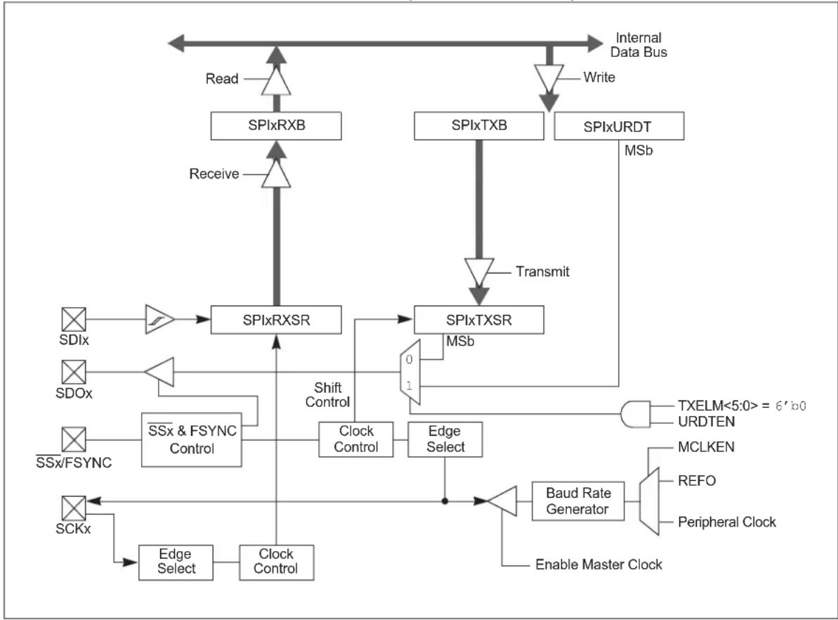
flowchart
graph TD
    A["Read"] --> B["SPIxRXB"]
    B --> C["SPIxTXB"]
    C --> D["SPIxURDT"]
    D --> E["MSb"]
    E --> F["SPIxTXSR"]
    F --> G["Shift Control"]
    G --> H["Clock Control"]
    H --> I["Edge Select"]
    I --> J["Baud Rate Generator"]
    J --> K["Enable Master Clock"]
    K --> L["Peripheral Clock"]
    M["SCKx"] --> N["Edge Select"]
    N --> O["Clock Control"]
    P["SSx/FSYNC"] --> Q["SSx & FSYNC Control"]
    R["SDIx"] --> S["Transfer"]
    T["SDOx"] --> U["Transfer"]
    V["SCLKEN"] --> W["Refo"]
    X["TXELM<5:0>=6'00 URDTEN"] --> Y["MCLKEN"]
    Z["Internal Data Bus"] --> A
To set up the SPIx module for the Enhanced Buffer Master mode of operation:
- If using interrupts:
a) Clear the interrupt flag bits in the respective IFSx register.
b) Set the interrupt enable bits in the respective IECx register.
c) Write the SPIxIP bits in the respective IPCx register.
- Write the desired settings to the SPIxCON1L, SPIxCON1H and SPIxCON2L registers with MSTEN (SPIxCON1L<5>) = 1.
- Clear the SPIROV bit (SPIxSTATL<6>).
- Select Enhanced Buffer mode by setting the ENHBUF bit (SPIxCON1L<0>).
- Enable SPIx operation by setting the SPIEN bit (SPIxCON1L<15>).
- Write the data to be transmitted to the SPIxBUFL and SPIxBUFH registers. Transmission (and reception) will start as soon as data is written to the SPIxBUFL and SPIxBUFH registers.
To set up the SPIx module for the Enhanced Buffer Slave mode of operation:
- Clear the SPIxBUFL and SPIxBUFH registers.
- If using interrupts:
a) Clear the interrupt flag bits in the respective IFSx register.
b) Set the interrupt enable bits in the respective IECx register.
c) Write the SPIxIP bits in the respective IPCx register to set the interrupt priority.
- Write the desired settings to the SPIxCON1L, SPIxCON1H and SPIxCON2L registers with the MSTEN bit (SPIxCON1L<5>) = 0.
- Clear the SMP bit.
- If the CKE bit is set, then the SSEN bit must be set, thus enabling the SSx pin.
- Clear the SPIROV bit (SPIxSTATL<6>).
- Select Enhanced Buffer mode by setting the ENHBUF bit (SPIxCON1L<0>).
- Enable SPIx operation by setting the SPIEN bit (SPIxCON1L<15>).
FIGURE 18-2: SPIx MODULE BLOCK DIAGRAM (ENHANCED MODE)
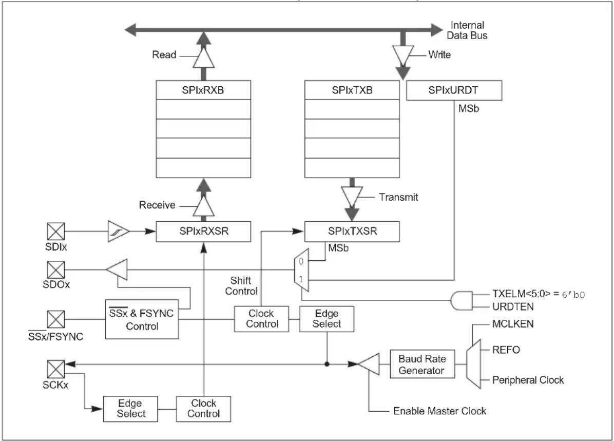
flowchart
graph TD
    A["Read"] --> B["SPIxRXB"]
    C["Write"] --> D["SPIxTXB"]
    B --> E["SPIxRXSR"]
    D --> F["SPIxTXSR"]
    E --> G["Shift Control"]
    F --> H["MSb"]
    G --> I["Clock Control"]
    H --> J["Edge Select"]
    I --> K["SSx & FSYNC Control"]
    J --> L["SSx/FSYNC"]
    K --> M["SCKx"]
    L --> N["SCLKX"]
    M --> O["Edge Select"]
    N --> P["Clock Control"]
    O --> Q["External Data Bus"]
    P --> R["External Data Bus"]
    S["TXELM<5:0>=6'b0"] --> T["URDTEN"]
    U["MCLKEN"] --> V["REFO"]
    W["Peripheral Clock"] --> X["Baud Rate Generator"]
    Y["Enable Master Clock"] --> Z["Edge Select"]
    style A fill:#f9f,stroke:#333
    style C fill:#f9f,stroke:#333
    style D fill:#f9f,stroke:#333
    style E fill:#ccf,stroke:#333
    style F fill:#ccf,stroke:#333
    style G fill:#cfc,stroke:#333
    style H fill:#cfc,stroke:#333
    style I fill:#fcc,stroke:#333
    style J fill:#fcc,stroke:#333
    style K fill:#fcc,stroke:#333
    style L fill:#fcc,stroke:#333
    style M fill:#fcc,stroke:#333
    style N fill:#fcc,stroke:#333
    style O fill:#fcc,stroke:#333
    style P fill:#fcc,stroke:#333
    style Q fill:#fcc,stroke:#333
    style R fill:#fcc,stroke:#333
    style S fill:#fcc,stroke:#333
To set up the SPIx module for Audio mode:
- Clear the SPIxBUFL and SPIxBUFH registers.
- If using interrupts:
a) Clear the interrupt flag bits in the respective IFSx register.
b) Set the interrupt enable bits in the respective IECx register.
a) Write the SPIxIP bits in the respective IPCx register to set the interrupt priority.
- Write the desired settings to the SPIxCON1L, SPIxCON1H and SPIxCON2L registers with AUDEN (SPIxCON1H<15>) = 1.
- Clear the SPIROV bit (SPIxSTATL<6>).
- Enable SPIx operation by setting the SPIEN bit (SPIxCON1L<15>).
- Write the data to be transmitted to the SPIxBUFL and SPIxBUFH registers. Transmission (and reception) will start as soon as data is written to the SPIxBUFL and SPIxBUFH registers.
REGISTER 18-1: SPIxCON1L: SPIx CONTROL REGISTER 1 LOW
| R/W-0 U-0 R/W-0 R/W-0 R/W-0 R/W-0 R/W-0 R/W-0 | |||||||
| SPIEN — | SPISIDL | DISSDO | MODE32 | ^(1,4) | MODE16 ^(1,4) | SMP CKE | ^(1) |
| bit 15 bit 8 | |||||||
| R/W-0 R/W-0 R/W-0 R/W-0 R/W-0 R/W-0 R/W-0 R/W-0 | |||||||||
| SSEN ^(2) | CKP MST | EN | DISDI | DISCK | MCLKEN | (3) | SPIFE | ENHBUF | |
| bit 7 bit 0 | |||||||||
| Legend: | |||
| R = Readable bit | W = Writable bit | U = Unimplemented bit, read as ‘0’ | |
| -n = Value at POR | ‘1’ = Bit is set | ‘0’ = Bit is cleared | x = Bit is unknown |
1 = Enables module
0 = Turns off and resets module, disables clocks, disables interrupt event generation, allows SFR modifications
bit 14 Unimplemented: Read as '0'
bit 13 SPISIDL: SPIx Stop in Idle Mode bit
1 = Halts in CPU Idle mode
0 = Continues to operate in CPU Idle mode
bit 12 DISSDO: Disable SDOx Output Port bit
1 = SDOx pin is not used by the module; pin is controlled by port function
0 = SDOx pin is controlled by the module
bit 11-10 MODE32 and MODE16: Serial Word Length Select bits ^(1,4)
| MODE32 | MODE16 | AUDEN | Communication |
| 1 | x | 0 | 32-Bit |
| 0 | 1 | 16-Bit | |
| 0 | 0 | 8-Bit | |
| 1 | 1 | 1 | 24-Bit Data, 32-Bit FIFO, 32-Bit Channel/64-Bit Frame |
| 1 | 0 | 32-Bit Data, 32-Bit FIFO, 32-Bit Channel/64-Bit Frame | |
| 0 | 1 | 16-Bit Data, 16-Bit FIFO, 32-Bit Channel/64-Bit Frame | |
| 0 | 0 | 16-Bit FIFO, 16-Bit Channel/32-Bit Frame |
Note 1: When AUDEN (SPIxCON1H<15>) = 1, this module functions as if CKE = 0, regardless of its actual value.
2: When FRMEN = 1, SSEN is not used.
3: MCLKEN can only be written when the SPIEN bit = 0.
4: This channel is not meaningful for DSP/PCM mode as LRC follows FRMSYPW.
REGISTER 18-1: SPIxCON1L: SPIx CONTROL REGISTER 1 LOW (CONTINUED)
bit 9 SMP: SPIx Data Input Sample Phase bit
Master Mode:
1 = Input data is sampled at the end of data output time
0 = Input data is sampled at the middle of data output time
Slave Mode:
Input data is always sampled at the middle of data output time, regardless of the SMP setting.
bit 8 CKE: SPIx Clock Edge Select bit (1)
1 = Transmit happens on transition from active clock state to Idle clock state
0 = Transmit happens on transition from Idle clock state to active clock state
bit 7 SSEN: Slave Select Enable bit (Slave mode) (2)
1 = SSx pin is used by the macro in Slave mode; SSx pin is used as the slave select input
0 = SSx pin is not used by the macro (SSx pin will be controlled by the port I/O)
bit 6 CKP: Clock Polarity Select bit
1 = Idle state for clock is a high level; active state is a low level
0 = Idle state for clock is a low level; active state is a high level
bit 5 MSTEN: Master Mode Enable bit
1 = Master mode
0 = Slave mode
bit 4 DISSDI: Disable SDIx Input Port bit
1 = SDIx pin is not used by the module; pin is controlled by port function
0 = SDIx pin is controlled by the module
bit 3 DISSCK: Disable SCKx Output Port bit
1 = SCKx pin is not used by the module; pin is controlled by port function
0 = SCKx pin is controlled by the module
bit 2 MCLKEN: Master Clock Enable bit (3)
1 = REFO is used by the Baud Rate Generator (BRG)
0 = Peripheral clock is used by the BRG
bit 1 SPIFE: Frame Sync Pulse Edge Select bit
1 = Frame Sync pulse (Idle-to-active edge) coincides with the first bit clock
0 = Frame Sync pulse (Idle-to-active edge) precedes the first bit clock
bit 0 ENHBUF: Enhanced Buffer Enable bit
1 = Enhanced Buffer mode is enabled
0 = Enhanced Buffer mode is disabled
Note 1: When AUDEN (SPIxCON1H<15>) = 1, this module functions as if CKE = 0, regardless of its actual value.
2: When FRMEN = 1, SSEN is not used.
3: MCLKEN can only be written when the SPIEN bit = 0.
4: This channel is not meaningful for DSP/PCM mode as LRC follows FRMSYPW.
REGISTER 18-2: SPIxCON1H: SPIx CONTROL REGISTER 1 HIGH
| R/W-0 R/W-0 R/W-0 R/W-0 R/W-0 R/W-0 R/W-0 | |||||||
| AUDEN(1) | SPISGNEXT | IGNROV | IGNTUR | AUDMONO (2) | URDTEN(3) | AUDMOD1(4) | AUDMOD0(4) |
| bit 15 bit 8 | |||||||
| R/W-0 R/W-0 R/W-0 R/W-0 R/W-0 R/W-0 R/W-0 R/W-0 | ||||||
| FRMEN FR | MSYNC FRMP | POL MSSEN | FRMSYPW FR | MCNT2 FRMCN | T1 FRMCNT0 | |
| bit 7 bit 0 | ||||||
Legend:
| R = Readable bit W = Writable bit | U = Unimplemented bit, read as '0' | ||
| -n = Value at POR | ‘1’ = Bit is set | ‘0’ = Bit is cleared | x = Bit is unknown |
bit 15 AUDEN: Audio Codec Support Enable bit (1)
| 1 = Audio protocol is enabled; MSTEN controls the direction of both SCKx and frame (a.k.a. LRC), and this module functions as if FRMEN = 1, FRMSYNC = MSTEN, FRMCNT<2:0> = 001 and SMP = 0, regardless of their actual values |
| 0 = Audio protocol is disabled |
bit 14 SPISGNEXT: SPIx Sign-Extend RX FIFO Read Data Enable bit
| 1 = Data from RX FIFO is sign-extended |
| 0 = Data from RX FIFO is not sign-extended |
bit 13 IGNROV: Ignore Receive Overflow bit
| 1 = A Receive Overflow (ROV) is NOT a critical error; during ROV, data in the FIFO is not overwritten by the receive data |
| 0 = A ROV is a critical error that stops SPI operation |
bit 12 IGNTUR: Ignore Transmit Underrun bit
| 1 = A Transmit Underrun (TUR) is NOT a critical error and data indicated by URDTEN is transmitted until the SPIxTXB is not empty |
| 0 = A TUR is a critical error that stops SPI operation |
bit 11 AUDMONO: Audio Data Format Transmit bit ^(2)
| 1 = Audio data is mono (i.e., each data word is transmitted on both left and right channels) |
| 0 = Audio data is stereo |
bit 10 URDTEN: Transmit Underrun Data Enable bit (3)
| 1 = Transmits data out of SPIxURDT register during Transmit Underrun conditions |
| 0 = Transmits the last received data during Transmit Underrun conditions |
bit 9-8 AUDMOD<1:0>: Audio Protocol Mode Selection bits ^(4)
| 11 = PCM/DSP mode |
| 10 = Right Justified mode: This module functions as if SPIFE = 1, regardless of its actual value |
| 01 = Left Justified mode: This module functions as if SPIFE = 1, regardless of its actual value |
| 00 = I2S mode: This module functions as if SPIFE = 0, regardless of its actual value |
bit 7 FRMEN: Framed SPIx Support bit
| 1 = Framed SPIx support is enabled ( pin is used as the FSYNC input/output) |
| 0 = Framed SPIx support is disabled |
Note 1: AUDEN can only be written when the SPIEN bit = 0.
| 2: AUDMONO can only be written when the SPIEN bit = 0 and is only valid for AUDEN = 1. |
3: URDTEN is only valid when IGNTUR = 1.
| 4: The AUDMOD<1:0> bits can only be written when the SPIEN bit = 0 and are only valid when AUDEN = 1. When NOT in PCM/DSP mode, this module functions as if FRMSYPW = 1, regardless of its actual value. |
REGISTER 18-2: SPIxCON1H: SPIx CONTROL REGISTER 1 HIGH (CONTINUED)
bit 6 FRMSYNC: Frame Sync Pulse Direction Control bit
1 = Frame Sync pulse input (slave)
0 = Frame Sync pulse output (master)
bit 5 FRMPOL: Frame Sync/Slave Select Polarity bit
1 = Frame Sync pulse/slave select is active-high
0 = Frame Sync pulse/slave select is active-low
bit 4 MSSEN: Master Mode Slave Select Enable bit
1 = SPIx slave select support is enabled with polarity determined by FRMPOL (SSx pin is automatically driven during transmission in Master mode)
0 = Slave select SPIx support is disabled (SS x pin will be controlled by port I/O)
bit 3 FRMSYPW: Frame Sync Pulse-Width bit
1 = Frame Sync pulse is one serial word length wide (as defined by MODE<32,16>/WLENGTH<4:0>)
0 = Frame Sync pulse is one clock (SCK) wide
bit 2-0 FRMCNT<2:0>: Frame Sync Pulse Counter bits
Controls the number of serial words transmitted per Sync pulse.
111 = Reserved
110 = Reserved
101 = Generates a Frame Sync pulse on every 32 serial words
100 = Generates a Frame Sync pulse on every 16 serial words
011 = Generates a Frame Sync pulse on every 8 serial words
010 = Generates a Frame Sync pulse on every 4 serial words
001 = Generates a Frame Sync pulse on every 2 serial words (value used by audio protocols)
000 = Generates a Frame Sync pulse on each serial word
Note 1: AUDEN can only be written when the SPIEN bit = 0.
2: AUDMONO can only be written when the SPIEN bit = 0 and is only valid for AUDEN = 1.
3: URDTEN is only valid when IGNTUR = 1.
4: The AUDMOD<1:0> bits can only be written when the SPIEN bit = 0 and are only valid when AUDEN = 1. When NOT in PCM/DSP mode, this module functions as if FRMSYPW = 1, regardless of its actual value.
REGISTER 18-3: SPIxCON2L: SPIx CONTROL REGISTER 2 LOW
| U-0 U-0 U-0 U-0 U-0 U-0 U-0 U-0 | |||||||
| —— | —— | —— | |||||
| bit 15 bit 8 | |||||||
| U-0 U-0 U-0 R/W-0 R/W-0 R/W-0 R/W-0 R/W-0 | |||
| ——— | W | L (1,2) E | |
| bit 7 bit 0 | |||
Legend:
| R = Readable bit W = Writable bit U = Unimplemented bit, read as '0' | |||
| -n = Value at POR | '1' = Bit is set | '0' = Bit is cleared | x = Bit is unknown |
bit 15-5 Unimplemented: Read as '0'
| bit 4-0 | WLENGTH<4:0>: Variable Word Length bits(1,2) |
| 11111 = 32-bit data | |
| 11110 = 31-bit data | |
| 11101 = 30-bit data | |
| 11100 = 29-bit data | |
| 11011 = 28-bit data | |
| 11010 = 27-bit data | |
| 11001 = 26-bit data | |
| 11000 = 25-bit data | |
| 10111 = 24-bit data | |
| 10110 = 23-bit data | |
| 10101 = 22-bit data | |
| 10100 = 21-bit data | |
| 10011 = 20-bit data | |
| 10010 = 19-bit data | |
| 10001 = 18-bit data | |
| 10000 = 17-bit data | |
| 01111 = 16-bit data | |
| 01110 = 15-bit data | |
| 01101 = 14-bit data | |
| 01100 = 13-bit data | |
| 01011 = 12-bit data | |
| 01010 = 11-bit data | |
| 01001 = 10-bit data | |
| 01000 = 9-bit data | |
| 00111 = 8-bit data | |
| 00110 = 7-bit data | |
| 00101 = 6-bit data | |
| 00100 = 5-bit data | |
| 00011 = 4-bit data | |
| 00010 = 3-bit data | |
| 00001 = 2-bit data | |
| 00000 = See MODE<32,16> bits in SPIxCON1L |
Note 1: These bits are effective when AUDEN = 0 only.
2: Varying the length by changing these bits does not affect the depth of the TX/RX FIFO.
| Legend: | C = Clearable bit | U = Unimplemented, read as ‘0’ |
| R = Readable bit | W = Writable bit | HSC = Hardware Settable/Clearable bit |
| -n = Value at POR | ‘1’ = Bit is set | ‘0’ = Bit is cleared HS = Hardware Settable bit |
bit 15-13 Unimplemented: Read as '0'
bit 12 FRMERR: SPIx Frame Error Status bit
1 = Frame error is detected
0 = No frame error is detected
bit 11 SPIBUSY: SPIx Activity Status bit
1 = Module is currently busy with some transactions
0 = No ongoing transactions (at time of read)
bit 10-9 Unimplemented: Read as '0'
bit 8 SPITUR: SPIx Transmit Underrun Status bit ^(1)
1 = Transmit buffer has encountered a Transmit Underrun condition
0 = Transmit buffer does not have a Transmit Underrun condition
bit 7 SRMT: Shift Register Empty Status bit
1 = No current or pending transactions (i.e., neither SPIxTXB or SPIxTXSR contains data to transmit)
0 = Current or pending transactions
bit 6 SPIROV: SPIx Receive Overflow Status bit
1 = A new byte/half-word/word has been completely received when the SPIxRXB was full
0 = No overflow
bit 5 SPIRBE: SPIx RX Buffer Empty Status bit
1 = RX buffer is empty
0 = RX buffer is not empty
Standard Buffer mode:
Automatically set in hardware when SPIxBUF is read from, reading SPIxRXB. Automatically cleared in hardware when SPIx transfers data from SPIxRXSR to SPIxRXB.
Enhanced Buffer mode:
Indicates RXELM<5:0>=000000.
bit 4 Unimplemented: Read as '0'
Note 1: SPITUR is cleared when SPIEN = 0. When IGNTUR = 1, SPITUR provides dynamic status of the Transmit Underrun condition, but does not stop RX/TX operation and does not need to be cleared by software.
REGISTER 18-4: SPIxSTATL: SPIx STATUS REGISTER LOW (CONTINUED)
bit 3 SPITBE: SPIx Transmit Buffer Empty Status bit
1 = SPIxTXB is empty
0 = SPIxTXB is not empty
Standard Buffer mode:
Automatically set in hardware when SPIx transfers data from SPIxTXB to SPIxTXSR. Automatically cleared in hardware when SPIxBUF is written, loading SPIxTXB.
Enhanced Buffer mode:
Indicates TXELM<5:0> = 000000.
bit 2 Unimplemented: Read as '0'
bit 1 SPITBF: SPIx Transmit Buffer Full Status bit
1 = SPIxTXB is full
0 = SPIxTXB not full
Standard Buffer mode:
Automatically set in hardware when SPIxBUF is written, loading SPIxTXB. Automatically cleared in hardware when SPIx transfers data from SPIxTXB to SPIxTXSR.
Enhanced Buffer mode:
Indicates TXELM<5:0> = 111111.
bit 0 SPIRBF: SPIx Receive Buffer Full Status bit
1 = SPIxRXB is full
0 = SPIxRXB is not full
Standard Buffer mode:
Automatically set in hardware when SPIx transfers data from SPIxRXSR to SPIxRXB. Automatically cleared in hardware when SPIxBUF is read from, reading SPIxRXB.
Enhanced Buffer mode:
Indicates RXELM<5:0> = 111111.
Note 1: SPITUR is cleared when SPIEN = 0. When IGNTUR = 1, SPITUR provides dynamic status of the Transmit Underrun condition, but does not stop RX/TX operation and does not need to be cleared by software.
| U-0 U-0 HSC/R-0 HSC/R-0 HSC/R-0 HSC/R-0 HSC/R-0 HSC/R-0 | |||||||
| — — RXELM5 | (3) | RXELM4(2) | RXELM3(1) | RXELM2 RX | ELM1 RXELM0 | ||
| bit 15 bit 8 | |||||||
| U-0 U-0 HSC/R-0 HSC/R-0 HSC/R-0 HSC/R-0 HSC/R-0 HSC/R-0 | ||||||
| — — | T | X | E^(3) | TXELM4 ^(2) | M TXELM3 ^(1) | TXELM2 TXELM1 TXELM0 |
| bit 7 bit 0 | ||||||
| Legend: | HSC = Hardware Settable/Clearable bit | ||
| R = Readable bit W = Writable bit | U = Unimplemented bit, read as ‘0’ | ||
| -n = Value at POR | ‘1’ = Bit is set | ‘0’ = Bit is cleared | x = Bit is unknown |
bit 15-14 Unimplemented: Read as '0'
bit 13-8 RXELM<5:0>: Receive Buffer Element Count bits (valid in Enhanced Buffer mode) ^(1,2,3)
bit 7-6 Unimplemented: Read as '0'
bit 5-0 TXELM<5:0>: Transmit Buffer Element Count bits (valid in Enhanced Buffer mode) ^(1,2,3)
Note 1: RXELM3 and TXELM3 bits are only present when FIFODEPTH = 8 or higher.
2: RXELM4 and TXELM4 bits are only present when FIFODEPTH = 16 or higher.
3: RXELM5 and TXELM5 bits are only present when FIFODEPTH = 32.
REGISTER 18-6: SPIxIMSKL: SPIx INTERRUPT MASK REGISTER LOW
| U-0 U-0 U-0 R/W-0 R/W-0 U-0 U-0 R/W-0 | |||||||
| — — — | FRMERREN | BUSYEN — — | SPITUREN | ||||
| bit 15 bit 8 | |||||||
| R/W-0 R/W-0 R/W-0 U-0 R/W-0 U-0 R/W-0 R/W-0 | |||||||
| SRMTEN SPIROVEN SPIRBEN | — | SPITBEN | — | SPITBFEN | SPIRBFEN | ||
| bit 7 bit 0 | |||||||
Legend:
| R = Readable bit | W = Writable bit | U = Unimplemented bit, read as '0' |
| -n = Value at POR | '1' = Bit is set | '0' = Bit is cleared x = Bit is unknown |
bit 15-13 Unimplemented: Read as '0'
bit 12 FRMERREN: Enable Interrupt Events via FRMERR bit
1 = Frame error generates an interrupt event
0 = Frame error does not generate an interrupt event
bit 11 BUSYEN: Enable Interrupt Events via SPIBUSY bit
1 = SPIBUSY generates an interrupt event
0 = SPIBUSY does not generate an interrupt event
bit 10-9 Unimplemented: Read as '0'
bit 8 SPITUREN: Enable Interrupt Events via SPITUR bit
1 = Transmit Underrun (TUR) generates an interrupt event
0 = Transmit Underrun does not generate an interrupt event
bit 7 SRMTEN: Enable Interrupt Events via SRMT bit
1 = Shift Register Empty (SRMT) generates interrupt events
0 = Shift Register Empty does not generate interrupt events
bit 6 SPIROVEN: Enable Interrupt Events via SPIROV bit
1 = SPIx Receive Overflow (ROV) generates an interrupt event
0 = SPIx Receive Overflow does not generate an interrupt event
bit 5 SPIRBEN: Enable Interrupt Events via SPIRBE bit
1 = SPIx RX buffer empty generates an interrupt event
0 = SPIx RX buffer empty does not generate an interrupt event
bit 4 Unimplemented: Read as '0'
bit 3 SPITBEN: Enable Interrupt Events via SPITBE bit
1 = SPIx transmit buffer empty generates an interrupt event
0 = SPIx transmit buffer empty does not generate an interrupt event
bit 2 Unimplemented: Read as '0'
bit 1 SPITBFEN: Enable Interrupt Events via SPITBF bit
1 = SPIx transmit buffer full generates an interrupt event
0 = SPIx transmit buffer full does not generate an interrupt event
bit 0 SPIRBFEN: Enable Interrupt Events via SPIRBF bit
1 = SPIx receive buffer full generates an interrupt event
0 = SPIx receive buffer full does not generate an interrupt event
REGISTER 18-7: SPIxIMSKH: SPIx INTERRUPT MASK REGISTER HIGH
| R/W-0 U-0 R/W-0 R/W-0 R/W-0 R/W-0 R/W-0 R/W-0 | |||||||
| RXWIEN | — RXMSK5 | (1) | RXMSK4(1,4) | RXMSK3(1,3) | RXMSK2(1,2) | RXMSK1(1) | RXMSK0(1) |
| bit 15 bit 8 | |||||||
| R/W-0 U-0 R/W-0 R/W-0 R/W-0 R/W-0 R/W-0 R/W-0 | |||||||
| TXWIEN | — TXMSK5 | ^(1) | TXMSK4 ^(1,4) | TXMSK3 ^(1,3) | TXMSK2 ^(1,2) | TXMSK1 ^(1) | TXMSK0 ^(1) |
| bit 7 bit 0 | |||||||
Legend:
R = Readable bit W = Writable bit U = Unimplemented bit, read as '0'
-n = Value at POR '1' = Bit is set '0' = Bit is cleared x = Bit is unknown
| bit 15 | RXWIEN:Receive Watermark Interrupt Enable bit 1 = Triggers receive buffer element watermark interrupt when RXMSK<5:0> ≤ RXELM<5:0>0= Disables receive buffer element watermark interrupt |
| bit 14 | Unimplemented:Read as ‘0’ |
| bit 13-8 | RXMSK<5:0>: RX Buffer Mask bits ^(1,2,3,4) RX mask bits; used in conjunction with the RXWIEN bit. |
| bit 7 | TXWIEN:Transmit Watermark Interrupt Enable bit 1 = Triggers transmit buffer element watermark interrupt when TXMSK<5:0>= TXELM<5:0>0= Disables transmit buffer element watermark interrupt |
| bit 6 | Unimplemented:Read as ‘0’ |
| bit 5-0 | TXMSK<5:0>: TX Buffer Mask bits ^(1,2,3,4) TX mask bits; used in conjunction with the TXWIEN bit. |
Note 1: Mask values higher than FIFODEPTH are not valid. The module will not trigger a match for any value in this case.
2: RXMSK2 and TXMSK2 bits are only present when FIFODEPTH = 8 or higher.
3: RXMSK3 and TXMSK3 bits are only present when FIFODEPTH = 16 or higher.
4: RXMSK4 and TXMSK4 bits are only present when FIFODEPTH = 32.
FIGURE 18-3: SPIx MASTER/SLAVE CONNECTION (STANDARD MODE)

flowchart
graph TD
    subgraph Processor 1 (SPIx Master)
        A["Serial Receive Buffer (SPIxRXB)^(2)"] --> B["Shift Register (SPIxRXSR)"]
        B --> C["MSb"]
        B --> D["LSb"]
        E["Shift Register (SPIxTXSR)"] --> F["MSb"]
        F --> G["LSb"]
        H["Serial Transmit Buffer (SPIxTXB)^(2)"] --> I["SPIx Buffer (SPIxBUF)^(2)"]
        I --> J["MSb"]
        J --> K["LSb"]
    end

    subgraph Processor 2 (SPIx Slave)
        L["Serial Transmit Buffer (SPIxTXB)^(2)"] --> M["Shift Register (SPIxTXSR)"]
        M --> N["MSb"]
        M --> O["LSb"]
        P["Shift Register (SPIxRXSR)"] --> Q["MSb"]
        Q --> R["LSb"]
        S["Serial Receive Buffer (SPIxRXB)^(2)"] --> T["SPIx Buffer (SPIxBUF)^(2)"]
        T --> U["SSx^(1)"]
    end

    A --> B
    B --> C
    C --> D
    D --> E
    E --> F
    F --> G
    G --> H
    H --> I
    I --> J
    J --> K
    K --> L
    L --> M
    M --> N
    N --> O
    O --> P
    P --> Q
    Q --> R
    R --> S
    S --> T
    T --> U
    U --> V
    V --> W
    W --> X
    X --> Y
    Y --> Z
    Z --> AA
    AA --> AB
    AB --> AC
    AC --> AD
    AD --> AE
    AE --> AF
    AF --> AG
    AG --> AH
    AH --> AI
    AI --> AJ
    AJ --> AK
    AK --> AL
    AL --> AM
    AM --> AN
    AN --> AO
    AO --> AP
    AP --> AQ
    AQ --> AR
    AR --> AS
    AS --> AT
    AT --> AU
    AU --> AV
    AV --> AW
    AW --> AX
    AX --> AY
Note 1: Using the SSx pin in Slave mode of operation is optional.
2: User must write transmit data to read the received data from SPIxBUF. The SPIxTXB and SPIxRXB registers are memory-mapped to SPIxBUF.
FIGURE 18-4: SPIx MASTER/SLAVE CONNECTION (ENHANCED BUFFER MODES)

flowchart
graph TD
    subgraph Processor 1 (SPIx Master)
        A["Serial Receive FIFO (SPIxRXB)^(2)"] --> B["Shift Register (SPIxRXSR)"]
        B --> C["MSb"]
        B --> D["LSb"]
        E["Shift Register (SPIxTXSR)"] --> F["MSb"]
        F --> G["LSb"]
        H["Serial Transmit FIFO (SPIxTXB)^(2)"] --> I["MSb"]
        I --> J["LSb"]
        K["SPIx Buffer (SPIxBUF)^(2)"] --> L["MSb"]
        L --> M["LSb"]
    end

    subgraph Processor 2 (SPIx Slave)
        N["Serial Transmit FIFO (SPIxTXB)^(2)"] --> O["Shift Register (SPIxTXSR)"]
        O --> P["MSb"]
        O --> Q["LSb"]
        R["Shift Register (SPIxRXSR)"] --> S["MSb"]
        S --> T["LSb"]
        U["Serial Receive FIFO (SPIxRXB)^(2)"] --> V["MSb"]
        V --> W["LSb"]
        X["SPIx Buffer (SPIxBUF)^(2)"] --> Y["SSx^(1)"]
    end

    M --> Z["SDOx SDIx"]
    T --> AA["SDOx SDIx"]
    Y --> AB["SCKx Serial Clock"]
    Z --> AC["SDOx SDIx"]
    AA --> AD["SCKx SSx"]
    AB --> AE["SDOx SDIx"]
    AC --> AF["SDOx SDIx"]
    AD --> AG["SDOx SDIx"]
    AE --> AH["SDOx SDIx"]
    AF --> AI["SDOx SDIx"]
    AG --> AJ["SDOx SDIx"]
    AH --> AK["SDOx SDIx"]
    AI --> AL["SDOx SDIx"]
    AJ --> AM["SDOx SDIx"]
    AK --> AN["SDOx SDIx"]
    AL --> AO["SDOx SDIx"]
    AM --> AP["SDOx SDIx"]
    AN --> AQ["SDOx SDIx"]
Note 1: Using the SSx pin in Slave mode of operation is optional.
2: User must write transmit data to read the received data from SPIxBUF. The SPIxTXB and SPIxRXB registers are memory-mapped to SPIxBUF.
FIGURE 18-5: SPIx MASTER, FRAME MASTER CONNECTION DIAGRAM

flowchart
graph LR
    subgraph PIC24F (SPIx Master, Frame Master)
        A["SDOx"] --> B["SDIx"]
        C["SDIx"] <--_D["Serial Clock"]
        E["SCKx"] --> F["SCKx"]
        G["SSx"] --> H["Frame Sync Pulse"]
    end
    subgraph Processor 2
        I["SSx"] --> J["SSIx"]
    end
FIGURE 18-6: SPIx MASTER, FRAME SLAVE CONNECTION DIAGRAM

flowchart
graph LR
    subgraph PIC24F
        A["SDOx"] --> B["SDIx"]
        C["SDIx"] --> D["Serial Clock"]
        E["SCKx"] --> F["SCKx"]
        G["SSx"] --> H["Frame Sync Pulse"]
    end
    subgraph Processor 2
        I["SDIx"] --> J["SDOx"]
        K["SCKx"] --> L["SSx"]
    end
FIGURE 18-7: SPIx SLAVE, FRAME MASTER CONNECTION DIAGRAM

flowchart
graph LR
    subgraph PIC24F (SPIx Slave, Frame Master)
        A["SDOx"] --> B["SDIx"]
        C["SDIx"] <--_D["Serial Clock"]
        E["SCKx"] <--_F["SCKx"]
        G["SSx"] <--_H["SSx"]
        I["Frame Sync Pulse"] --> J["Processor 2"]
    end
FIGURE 18-8: SPIx SLAVE, FRAME SLAVE CONNECTION DIAGRAM
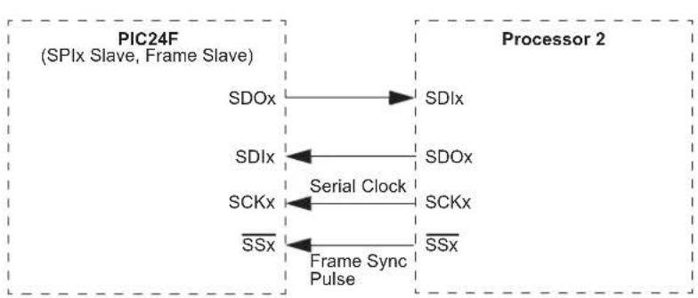
flowchart
graph LR
    subgraph PIC24F (SPIx Slave, Frame Slave)
        A["SDOx"] --> B["SDIx"]
        C["SDIx"] --> D["Serial Clock"]
        E["SCKx"] --> F["SCKx"]
        G["SSx"] --> H["Frame Sync Pulse"]
    end
    subgraph Processor 2
        I["SDIx"] --> J["SDOx"]
        K["SCKx"] --> L["SSx"]
    end
EQUATION 18-1: RELATIONSHIP BETWEEN DEVICE AND SPIx CLOCK SPEED
$$ \text { Baud Rate } = \frac {F _ {P B}}{(2 * (S P I x B R G + 1))} $$
Where:
FPB is the Peripheral Bus Clock Frequency.
19.0 INTER-INTEGRATED CIRCUIT (I²C)
Note 1: This data sheet summarizes the features of the dsPIC33EPXXXGS70X/80X family of devices. It is not intended to be a comprehensive reference source. To complement the information in this data sheet, refer to “Inter-Integrated Circuit (I²C)” (DS70000195) in the “dsPIC33/PIC24 Family Reference Manual”, which is available from the Microchip website (www.microchip.com).
2: Some registers and associated bits described in this section may not be available on all devices. Refer to Section 4.0 "Memory Organization" in this data sheet for device-specific register and bit information.
The dsPIC33EPXXXGS70X/80X family of devices contains two Inter-Integrated Circuit (I²C) modules: I2C1 and I2C2.
The I²C module provides complete hardware support for both Slave and Multi-Master modes of the P²C serial communication standard, with a 16-bit interface.
The I^2C module has a 2-pin interface:
• The SCLx/ASCLx pin is clock
• The SDAx/ASDAX pin is data
The I ^2 C module offers the following key features:
- I ^2 C Interface supporting both Master and Slave modes of Operation
- I ^2 C Slave mode Supports 7 and 10-Bit Addressing
- I ^2 C Master mode Supports 7 and 10-Bit Addressing
- I²C Port allows Bidirectional Transfers between Master and Slaves
- Serial Clock Synchronization for I ^2 C Port can be used as a Handshake Mechanism to Suspend and Resume Serial Transfer (SCLREL control)
- I²C Supports Multi-Master Operation, Detects Bus Collision and Arbitrates Accordingly
• System Management Bus (SMBus) Support
• Alternate I ^2 C Pin Mapping (ASCLx/ASDAx)
19.1 I ^2 C Resources
Many useful resources are provided on the main product page of the Microchip website for the devices listed in this data sheet. This product page contains the latest updates and additional information.
19.1.1 KEY RESOURCES
- “Inter-Integrated Circuit (I ^2 C)” (DS70000195) in the “dsPIC33/PIC24 Family Reference Manual”
- Code Samples
- Application Notes
- Software Libraries
- Webinars
- All Related "dsPIC33/PIC24 Family Reference Manual" Sections
- Development Tools
FIGURE 19-1: I2Cx BLOCK DIAGRAM (x = 1 OR 2)
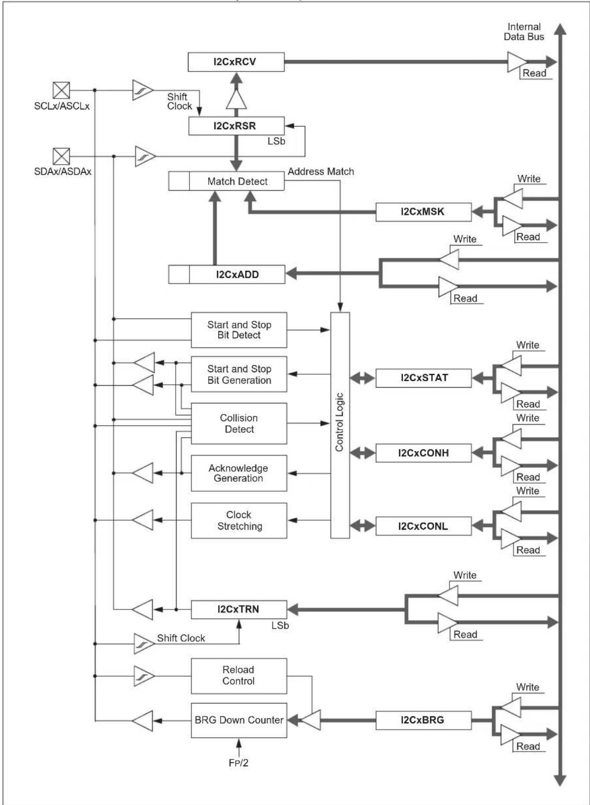
flowchart
graph TD
    A["SCLx/ASCLx"] --> B["Shift Clock"]
    C["SDAx/ASDAx"] --> D["Match Detect"]
    B --> E["I2CxRCV"]
    D --> F["I2CxRSR"]
    F --> G["Address Match"]
    G --> H["I2CxMSK"]
    H --> I["Write"]
    H --> J["Read"]
    K["Start and Stop Bit Detect"] --> L["Control Logic"]
    M["Start and Stop Bit Generation"] --> L
    N["Collision Detect"] --> L
    O["Acknowledge Generation"] --> L
    P["Clock Stretching"] --> L
    Q["I2CxTRN"] --> R["LSb"]
    S["Shift Clock"] --> T["LRG Down Counter"]
    U["Reload Control"] --> V["I2CxBRG"]
    W["FP/2"] --> X["BRG Down Counter"]
    Y["I2CxSTAT"] --> Z["Write"]
    Y --> AA["Read"]
    AB["I2CxCONH"] --> AC["Write"]
    AD["I2CxCONL"] --> AE["Read"]
    AF["Write"] --> AG["Internal Data Bus"]
    AH["Write"] --> AI["Internal Data Bus"]
19.2 I ^2 C Control Registers
REGISTER 19-1: I2CxCONL: I2Cx CONTROL REGISTER LOW
| R/W-0 U-0 R/W-0 HC/R/W-1 R/W-0 R/W-0 R/W-0 R/W-0 | |||||||
| I2CEN | — | I2CSIDL | SCLREL | STRICT | A10M | DISSLW | SMEN |
| bit 15 bit 8 | |||||||
| R/W-0 | R/W-0 | R/W-0 | HC/R/W-0 | HC/R/W-0 | HC/R/W-0 | HC/R/W-0 | HC/R/W-0 |
| GCEN | STREN | ACKDT | ACKEN | RCEN | PEN | RSEN | SEN |
| bit 7 bit 0 | |||||||
| Legend: | HC = Hardware Clearable bit | ||
| R = Readable bit | W = Writable bit | U = Unimplemented bit, read as ‘0’ | |
| -n = Value at POR | ‘1’ = Bit is set | ‘0’ = Bit is cleared | x = Bit is unknown |
bit 15 I2CEN: I2Cx Enable bit
1 = Enables the I2Cx module and configures the SDAx and SCLx pins as serial port pins 0 = Disables the I2Cx module; all I^2C pins are controlled by port functions
bit 14 Unimplemented: Read as '0'
bit 13 I2CSIDL: I2Cx Stop in Idle Mode bit
1 = Discontinues module operation when device enters Idle mode 0 = Continues module operation in Idle mode
bit 12 SCLREL: SCLx Release Control bit (when operating as I²C slave)
1 = Releases SCLx clock 0 = Holds SCLx clock low (clock stretch) If STREN = 1:
Bit is R/W (i.e., software can write '0' to initiate stretch and write '1' to release clock). It is cleared by hardware at the beginning of every slave data byte transmission. It is cleared by hardware at the end of every slave address byte reception. It is cleared by hardware at the end of every slave data byte reception.
If STREN = 0:
Bit is R/S (i.e., software can only write '1' to release clock). It is cleared by hardware at the beginning of every slave data byte transmission. It is cleared by hardware at the end of every slave address byte reception.
bit 11 STRICT: Strict I2Cx Reserved Address Enable bit
1 = Strict Reserved Addressing is Enabled: In Slave mode, the device will NACK any reserved address. In Master mode, the device is allowed to generate addresses within the reserved address space. 0 = Reserved Addressing is Acknowledged: In Slave mode, the device will ACK any reserved address. In Master mode, the device should not address a slave device with a reserved address.
bit 10 A10M: 10-Bit Slave Address bit
1 = I2CxADD is a 10-bit slave address 0 = I2CxADD is a 7-bit slave address
bit 9 DISSLW: Disable Slew Rate Control bit
1 = Slew rate control is disabled 0 = Slew rate control is enabled
bit 8 SMEN: SMBus Input Levels bit
1 = Enables I/O pin thresholds compliant with SMBus specification 0 = Disables SMBus input thresholds
REGISTER 19-1: I2CxCONL: I2Cx CONTROL REGISTER LOW (CONTINUED)
| bit 7 | GCEN: General Call Enable bit (when operating as I^2C slave)1 = Enables interrupt when a general call address is received in I2CxRSR (module is enabled for reception)0 = General call address is disabled |
| bit 6 | STREN: SCLx Clock Stretch Enable bit (when operating as I^2C slave)Used in conjunction with the SCLREL bit.1 = Enables software controlled clock stretching0 = Disables software controlled clock stretching |
| bit 5 ACKDT: Acknowledge Data bit (when operating as I^2C master, applicable during master receive) | |
| Value that is transmitted when the software initiates an Acknowledge sequence.1 = Sends NACK during Acknowledge0 = Sends ACK during Acknowledge | |
| bit 4 ACKEN: Acknowledge Sequence Enable bit(when operating as I^2C master, applicable during master receive) | |
| 1 = Initiates Acknowledge sequence on SDAx and SCLx pins and transmits ACKDT data bit; it is cleared by hardware at the end of the master Acknowledge sequence0 = Acknowledge sequence is not in progress | |
| bit 3 RCEN: Receive Enable bit (when operating as I^2C master) | |
| 1 = Enables Receive mode for I^2C ; it is cleared by hardware at the end of the eighth bit of the master receive data byte0 = Receive sequence is not in progress | |
| bit 2 PEN: Stop Condition Enable bit (when operating as I^2C master) | |
| 1 = Initiates Stop condition on SDAx and SCLx pins; it is cleared by hardware at the end of the master Stop sequence0 = Stop condition is not in progress | |
| bit 1 | RSEN: Repeated Start Condition Enable bit (when operating as I^2C master)1 = Initiates Repeated Start condition on SDAx and SCLx pins; it is cleared by hardware at the end of the master Repeated Start sequence0 = Repeated Start condition is not in progress |
| bit 0 | SEN: Start Condition Enable bit (when operating as I^2C master)1 = Initiates Start condition on SDAx and SCLx pins; it is cleared by hardware at the end of the master Start sequence0 = Start condition is not in progress |
REGISTER 19-2: I2CxCONH: I2Cx CONTROL REGISTER HIGH
| U-0 U-0 U-0 U-0 U-0 U-0 U-0 U-0 | |||||||
| —— | —— | —— | |||||
| bit 15 bit 8 | |||||||
| U-0 | R/W-0 | R/W-0 | R/W-0 | R/W-0 | R/W-0 | R/W-0 | R/W-0 |
| — | PCIE | SCIE | BOEN | SDAHT | SBCDE | AHEN | DHEN |
| bit 7 bit 0 | |||||||
| Legend: | |||
| R = Readable bit | W = Writable bit | U = Unimplemented bit, read as '0' | |
| -n = Value at POR | '1' = Bit is set | '0' = Bit is cleared | x = Bit is unknown |
bit 15-7 Unimplemented: Read as '0'
bit 6 PCIE: Stop Condition Interrupt Enable bit (I²C Slave mode only)
1 = Enables interrupt on detection of Stop condition
0 = Stop detection interrupts are disabled
bit 5 SCIE: Start Condition Interrupt Enable bit (I²C Slave mode only)
1 = Enables interrupt on detection of Start or Restart conditions
0 = Start detection interrupts are disabled
bit 4 BOEN: Buffer Overwrite Enable bit (I²C Slave mode only)
1 = I2CxRCV is updated and ACK is generated for a received address/data byte, ignoring the state of the I2COV only if the RBF bit = 0
0 = I2CxRCV is only updated when I2COV is clear
bit 3 SDAHT: SDAx Hold Time Selection bit
1 = Minimum of 300 ns hold time on SDAx after the falling edge of SCLx
0 = Minimum of 100 ns hold time on SDAx after the falling edge of SCLx
bit 2 SBCDE: Slave Mode Bus Collision Detect Enable bit ( I^2C Slave mode only)
1 = Enables slave bus collision interrupts
0 = Slave bus collision interrupts are disabled
If the rising edge of SCLx and SDAx is sampled low when the module is in a high state, the BCL bit is set and the bus goes Idle. This Detection mode is only valid during data and ACK transmit sequences.
bit 1 AHEN: Address Hold Enable bit (I²C Slave mode only)
1 = Following the 8th falling edge of SCLx for a matching received address byte, the SCLREL (I2CxCONL<12>) bit will be cleared and SCLx will be held low
0 = Address holding is disabled
bit 0 DHEN: Data Hold Enable bit (I²C Slave mode only)
1 = Following the 8th falling edge of SCLx for a received data byte, the slave hardware clears the SCLREL (I2CxCONL<12>) bit and SCLx is held low
0 = Data holding is disabled
REGISTER 19-3: I2CxSTAT: I2Cx STATUS REGISTER
| HSC/R-0 HSC/R-0 HSC/R-0 U-0 U-0 HS/R/C-0 HSC/R-0 HSC/R-0 | |||||
| ACKSTAT TRSTAT ACKTIM | — — BCL GCSTAT | ADD10 | |||
| bit 15 bit 8 | |||||
| HS/R/C-0 | HS/R/C-0 | HSC/R-0 | HSC/R/C-0 | HSC/R/C-0 | HSC/R-0 | HSC/R-0 | HSC/R-0 |
| IWCOL | I2COV | D_A | P | S | R_W | RBF | TBF |
| bit 7 bit 0 | |||||||
| Legend: | C = Clearable bit | ‘0’ = Bit is cleared | HS = Hardware Settable bit |
| R = Readable bit | W = Writable bit | HSC = Hardware Settable/Clearable bit | |
| -n = Value at POR | ‘1’ = Bit is set | U = Unimplemented bit, read as ‘0’ | |
bit 15 ACKSTAT: Acknowledge Status bit (when operating as I²C master, applicable to master transmit operation)
1 = NACK was received from slave
0 = ACK was received from slave
It is set or cleared by hardware at the end of a slave Acknowledge.
bit 14 TRSTAT: Transmit Status bit (when operating as I²C master, applicable to master transmit operation)
1 = Master transmit is in progress (8 bits + ACK)
0 = Master transmit is not in progress
It is set by hardware at the beginning of master transmission. It is cleared by hardware at the end of slave Acknowledge.
bit 13 ACKTIM: Acknowledge Time Status bit (I²C Slave mode only)
1 = I²C bus is an Acknowledge sequence, set on the 8th falling edge of SCLx
0 = Not an Acknowledge sequence, cleared on the 9th rising edge of SCLx
bit 12-11 Unimplemented: Read as '0'
bit 10 BCL: Master Bus Collision Detect bit
1 = A bus collision has been detected during a master operation
0 = No bus collision detected
It is set by hardware at detection of a bus collision.
bit 9 GCSTAT: General Call Status bit
1 = General call address was received
0 = General call address was not received
It is set by hardware when address matches the general call address. It is cleared by hardware at Stop detection.
bit 8 ADD10: 10-Bit Address Status bit
1 = 10-bit address was matched
0 = 10-bit address was not matched
It is set by hardware at the match of the 2nd byte of the matched 10-bit address. It is cleared by hardware at Stop detection.
bit 7 IWCOL: I2Cx Write Collision Detect bit
1 = An attempt to write to the I2CxTRN register failed because the I²C module is busy
0 = No collision
It is set by hardware at the occurrence of a write to I2CxTRN while busy (cleared by software).
bit 6 I2COV: I2Cx Receive Overflow Flag bit
1 = A byte was received while the I2CxRCV register was still holding the previous byte
0 = No overflow
It is set by hardware at an attempt to transfer I2CxRSR to I2CxRCV (cleared by software).
REGISTER 19-3: I2CxSTAT: I2Cx STATUS REGISTER (CONTINUED)
bit 5 D_A: Data/Address bit (I)
^2 C Slave mode only)
1 = Indicates that the last byte received was data
0 = Indicates that the last byte received was a device address
It is cleared by hardware at a device address match. It is set by hardware by reception of a slave byte.
bit 4 P: Stop bit
1 = Indicates that a Stop bit has been detected last
0 = Stop bit was not detected last
It is set or cleared by hardware when a Start, Repeated Start or Stop is detected.
bit 3 S: Start bit
1 = Indicates that a Start (or Repeated Start) bit has been detected last
0 = Start bit was not detected last
It is set or cleared by hardware when a Start, Repeated Start or Stop is detected.
bit 2 R_W: Read/Write Information bit (I)
^2 C Slave mode only)
1 = Read - Indicates data transfer is output from the slave
0 = Write - Indicates data transfer is input to the slave
It is set or cleared by hardware after reception of an I²C device address byte.
bit 1 RBF: Receive Buffer Full Status bit
1 = Receive is complete, I2CxRCV is full
0 = Receive is not complete, I2CxRCV is empty
It is set by hardware when I2CxRCV is written with a received byte. It is cleared by hardware when software reads I2CxRCV.
bit 0 TBF: Transmit Buffer Full Status bit
1 = Transmit is in progress, I2CxTRN is full
0 = Transmit is complete, I2CxTRN is empty
It is set by hardware when software writes to I2CxTRN. It is cleared by hardware at completion of a data transmission.
REGISTER 19-4: I2CxMSK: I2Cx SLAVE MODE ADDRESS MASK REGISTER
| U-0 U-0 U-0 U-0 U-0 U-0 R/W-0 R/W-0 | |||||
| — — — | — — — AMSK<9:8> | ||||
| bit 15 bit 8 | |||||
| R/W-0 R/W-0 R/W-0 R/W-0 R/W-0 R/W-0 R/W-0 R/W-0 |
| AMSK<7:0> |
| bit 7 bit 0 |
Legend:
R = Readable bit W = Writable bit U = Unimplemented bit, read as '0' -n = Value at POR '1' = Bit is set '0' = Bit is cleared x = Bit is unknown
bit 15-10 Unimplemented: Read as '0'
bit 9-0 AMSK<9:0>: Address Mask Select bits
For 10-Bit Address:
1 = Enables masking for bit Ax of incoming message address; bit match is not required in this position 0 = Disables masking for bit Ax; bit match is required in this position
For 7-Bit Address (I2CxMSK<6:0> only):
1 = Enables masking for bit Ax + 1 of incoming message address; bit match is not required in this position 0 = Disables masking for bit Ax + 1; bit match is required in this position
20.0 UNIVERSAL ASYNCHRONOUS RECEIVER TRANSMITTER (UART)
Note 1: This data sheet summarizes the features of the dsPIC33EPXXXGS70X/80X family of devices. It is not intended to be a comprehensive reference source. To complement the information in this data sheet, refer to “Universal Asynchronous Receiver Transmitter (UART)” (DS70000582) in the “dsPIC33/PIC24 Family Reference Manual”, which is available from the Microchip website (www.microchip.com).
2: Some registers and associated bits described in this section may not be available on all devices. Refer to Section 4.0 "Memory Organization" in this data sheet for device-specific register and bit information.
The dsPIC33EPXXXGS70X/80X family of devices contains two UART modules.
The Universal Asynchronous Receiver Transmitter (UART) module is one of the serial I/O modules available in the dsPIC33EPXXXGS70X/80X device family. The UART is a full-duplex, asynchronous system that can communicate with peripheral devices, such as personal computers, LIN/J2602, RS-232 and RS-485 interfaces. The module also supports a hardware flow control option with the UxCTS and UxRTS pins, and also includes an IrDA ^® encoder and decoder.
The primary features of the UARTx module are:
- Full-Duplex, 8 or 9-Bit Data Transmission through the UxTX and UxRX Pins
- Even, Odd or No Parity Options (for 8-bit data)
- One or Two Stop bits
- Hardware Flow Control Option with UxCTS and UxRTS Pins
- Fully Integrated Baud Rate Generator with 16-Bit Prescaler
- Baud Rates Ranging from 4.375 Mbps to 67 bps in 16x mode at 70 MIPS
- Baud Rates Ranging from 17.5 Mbps to 267 bps in 4x mode at 70 MIPS
- 4-Deep First-In First-Out (FIFO) Transmit Data Buffer
• 4-Deep FIFO Receive Data Buffer - Parity, Framing and Buffer Overrun Error Detection
- Support for 9-Bit mode with Address Detect (9th bit = 1)
• Transmit and Receive Interrupts
• A Separate Interrupt for all UARTx Error Conditions - Loopback mode for Diagnostic Support
• Support for Sync and Break Characters
• Support for Automatic Baud Rate Detection - I r D EAcoder and Decoder Logic
• 16x Baud Clock Output for IrDA Support
A simplified block diagram of the UARTx module is shown in Figure 20-1. The UARTx module consists of these key hardware elements:
- Baud Rate Generator
• Asynchronous Transmitter - Asynchronous Receiver
FIGURE 20-1: UARTx SIMPLIFIED BLOCK DIAGRAM
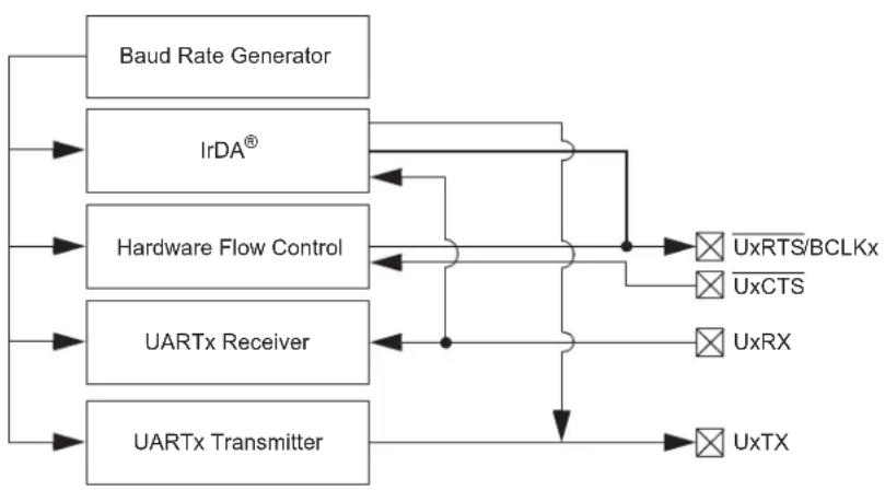
flowchart
graph TD
    A["Baud Rate Generator"] --> B["IrDA®"]
    B --> C["Hardware Flow Control"]
    C --> D["UARTx Receiver"]
    D --> E["UARTx Transmitter"]
    E --> F["UxRTS/BCLKx"]
    E --> G["UxCTS"]
    E --> H["UxRX"]
    E --> I["UxTX"]
    B --> J["Crossed Lines"]
    C --> K["Crossed Lines"]
    D --> L["Crossed Lines"]
    E --> M["Crossed Lines"]
20.1 UART Helpful Tips
- In multi-node, direct connect UART networks, UART receive inputs react to the complementary logic level defined by the URXINV bit (UxMODE<4>), which defines the Idle state, the default of which is logic high (i.e., URXINV = 0). Because remote devices do not initialize at the same time, it is likely that one of the devices, because the RX line is floating, will trigger a Start bit detection and will cause the first byte received, after the device has been initialized, to be invalid. To avoid this situation, the user should use a pull-up or pull-down resistor on the RX pin depending on the value of the URXINV bit.
a) If URXINV = 0, use a pull-up resistor on the UxRX pin.
b) If URXINV = 1, use a pull-down resistor on the UxRX pin.
- The first character received on a wake-up from Sleep mode, caused by activity on the UxRX pin of the UARTx module, will be invalid. In Sleep mode, peripheral clocks are disabled. By the time the oscillator system has restarted and stabilized from Sleep mode, the baud rate bit sampling clock, relative to the incoming UxRX bit timing, is no longer synchronized, resulting in the first character being invalid; this is to be expected.
20.2 UART Resources
Many useful resources are provided on the main product page of the Microchip website for the devices listed in this data sheet. This product page contains the latest updates and additional information.
20.2.1 KEY RESOURCES
- “Universal Asynchronous Receiver Transmitter (UART)” (DS70000582) in the “dsPIC33/PIC24 Family Reference Manual”
- Code Samples
- Application Notes
- Software Libraries
- Webinars
- All Related "dsPIC33/PIC24 Family Reference Manual" Sections
- Development Tools
20.3 UART Control Registers
REGISTER 20-1: UxMODE: UARTx MODE REGISTER
| R/W-0 U-0 R/W-0 R/W-0 R/W-0 U-0 R/W-0 R/W-0 | |||||||
| UARTEN(1) | — USIDL IREN | (2) | RTSMD — | U | E | N | |
| bit 15 bit 8 | |||||||
| HC/R/W-0 | R/W-0 | HC/R/W-0 | R/W-0 | R/W-0 | R/W-0 | R/W-0 | R/W-0 |
| WAKE | LPBACK | ABAUD | URXINV | BRGH | PDSEL1 | PDSEL0 | STSEL |
| bit 7 bit 0 | |||||||
| Legend: | HC = Hardware Clearable bit | ||
| R = Readable bit | W = Writable bit | U = Unimplemented bit, read as ‘0’ | |
| -n = Value at POR | ‘1’ = Bit is set | ‘0’ = Bit is cleared | x = Bit is unknown |
bit 15 UARTEN: UARTx Enable bit ^(1) 1 = UARTx is enabled; all UARTx pins are controlled by UARTx as defined by UEN<1:0>
0 = UARTx is disabled; all UARTx pins are controlled by PORT latches; UARTx power consumption is minimal
bit 14 Unimplemented: Read as '0'
bit 13 USIDL: UARTx Stop in Idle Mode bit
1 = Discontinues module operation when device enters Idle mode
0 = Continues module operation in Idle mode
bit 12 IREN: IrDA ^® Encoder and Decoder Enable bit ^(2)
1 = IrDA encoder and decoder are enabled
0 = IrDA encoder and decoder are disabled
bit 11 RTSMD: Mode Selection for UxRTS Pin bit
1 = UxRTS pin is in Simplex mode
0 = UxRTS pin is in Flow Control mode
bit 10 Unimplemented: Read as '0'
bit 9-8 UEN<1:0>: UARTx Pin Enable bits
11 = UxTX, UxRX and BCLKx pins are enabled and used; UxCTS pin is controlled by PORT latches
10 = UxTX, UxRX, UxCTS and UxRTS pins are enabled and used
01 = UxTX, UxRX and UxRTS pins are enabled and used; UxCTS pin is controlled by PORT latches
00 = UxTX and UxRX pins are enabled and used; UxCTS and UxRTS/BCLKx pins are controlled by PORT latches
bit 7 WAKE: Wake-up on Start Bit Detect During Sleep Mode Enable bit
1 = UARTx continues to sample the UxRX pin, interrupt is generated on the falling edge; bit is cleared in hardware on the following rising edge
0 = No wake-up is enabled
bit 6 LPBACK: UARTx Loopback Mode Select bit
1 = Enables Loopback mode
0 = Loopback mode is disabled
Note 1: Refer to “Universal Asynchronous Receiver Transmitter (UART)” (DS70000582) in the “dsPIC33/PIC24 Family Reference Manual” for information on enabling the UARTx module for receive or transmit operation.
2: This feature is only available for the 16x BRG mode (BRGH = 0).
REGISTER 20-1: UxMODE: UARTx MODE REGISTER (CONTINUED)
bit 5 ABAUD: Auto-Baud Enable bit
1 = Enables baud rate measurement on the next character – requires reception of a Sync field (55h) before other data; cleared in hardware upon completion
0 = Baud rate measurement is disabled or completed
bit 4 URXINV: UARTx Receive Polarity Inversion bit
1 = UxRX Idle state is '0'
0 = UxRX Idle state is '1'
bit 3 BRGH: High Baud Rate Enable bit
1 = BRG generates 4 clocks per bit period (4x baud clock, High-Speed mode) 0 = BRG generates 16 clocks per bit period (16x baud clock, Standard mode)
bit 2-1 PDSEL<1:0>: Parity and Data Selection bits
11 = 9-bit data, no parity
10 = 8-bit data, odd parity
01 = 8-bit data, even parity
00 = 8-bit data, no parity
bit 0 STSEL: Stop Bit Selection bit
1 = Two Stop bits
0 = One Stop bit
Note 1: Refer to “Universal Asynchronous Receiver Transmitter (UART)” (DS70000582) in the “dsPIC33/PIC24 Family Reference Manual” for information on enabling the UARTx module for receive or transmit operation.
2: This feature is only available for the 16x BRG mode (BRGH = 0).
REGISTER 20-2: UxSTA: UARTx STATUS AND CONTROL REGISTER
| R/W-0 R/W-0 R/W-0 U-0 HC/R/W-0 R/W-0 R-0 R-1 | ||||||
| UTXISEL1 UTXINV UTXISEL0 | — UTXBRK UTXEN | (1) | UTXBF TRMT | |||
| bit 15 bit 8 | ||||||
| R/W-0 R/W-0 R/W-0 R-1 | R-0 | R-0 | R/C-0 R-0 | ||||
| URXISEL1 | URXISEL0 | ADDEN | RIDLE | PERR | FERR | OERR | URXDA |
| bit 7 bit 0 | |||||||
| Legend: | C = Clearable bit | HC = Hardware Clearable bit |
| R = Readable bit | W = Writable bit | U = Unimplemented bit, read as '0' |
| -n = Value at POR | '1' = Bit is set | '0' = Bit is cleared x = Bit is unknown |
bit 15,13 UTXISEL<1:0>: UARTx Transmission Interrupt Mode Selection bits
11 = Reserved; do not use
10 = Interrupt when a character is transferred to the Transmit Shift Register (TSR), and as a result, the transmit buffer becomes empty
01 = Interrupt when the last character is shifted out of the Transmit Shift Register; all transmit operations are completed
00 = Interrupt when a character is transferred to the Transmit Shift Register (this implies there is at least one character open in the transmit buffer)
bit 14 UTXINV: UARTx Transmit Polarity Inversion bit
If IREN = 0:
1 = UxTX Idle state is '0'
0 = UxTX Idle state is '1'
If IREN = 1:
1 = IrDA ^® encoded, UxTX Idle state is '1'
0 = IrDA encoded, UxTX Idle state is '0'
bit 12 Unimplemented: Read as '0'
bit 11 UTXBRK: UARTx Transmit Break bit
1 = Sends Sync Break on next transmission – Start bit, followed by twelve '0' bits, followed by Stop bit; cleared by hardware upon completion
0 = Sync Break transmission is disabled or completed
bit 10 UTXEN: UARTx Transmit Enable bit ^(1)
1 = Transmit is enabled, UxTX pin is controlled by UARTx
0 = Transmit is disabled, any pending transmission is aborted and buffer is reset; UxTX pin is controlled by the PORT
bit 9 UTXBF: UARTx Transmit Buffer Full Status bit (read-only)
1 = Transmit buffer is full
0 = Transmit buffer is not full, at least one more character can be written
bit 8 TRMT: Transmit Shift Register Empty bit (read-only)
1 = Transmit Shift Register is empty and transmit buffer is empty (the last transmission has completed)
0 = Transmit Shift Register is not empty, a transmission is in progress or queued
bit 7-6 URXISEL<1:0>: UARTx Receive Interrupt Mode Selection bits
11 = Interrupt is set on UxRSR transfer, making the receive buffer full (i.e., has four data characters)
10 = Interrupt is set on UxRSR transfer, making the receive buffer 3/4 full (i.e., has three data characters)
0x = Interrupt is set when any character is received and transferred from the UxRSR to the receive buffer; receive buffer has one or more characters
Note 1: Refer to "Universal Asynchronous Receiver Transmitter (UART)" (DS70000582) in the "dsPIC33/PIC24 Family Reference Manual" for information on enabling the UARTx module for transmit operation.
REGISTER 20-2: UxSTA: UARTx STATUS AND CONTROL REGISTER (CONTINUED)
bit 5 ADDEN: Address Character Detect bit (bit 8 of received data = 1)
1 = Address Detect mode is enabled; if 9-bit mode is not selected, this does not take effect
0 = Address Detect mode is disabled
bit 4 RIDLE: Receiver Idle bit (read-only) 1 = Receiver is Idle 0 = Receiver is active
bit 3 PERR: Parity Error Status bit (read-only) 1 = Parity error has been detected for the current character (character at the top of the receive FIFO) 0 = Parity error has not been detected
bit 2 FERR: Framing Error Status bit (read-only) 1 = Framing error has been detected for the current character (character at the top of the receive FIFO) 0 = Framing error has not been detected
bit 1 OERR: Receive Buffer Overrun Error Status bit (clear/read-only) 1 = Receive buffer has overflowed 0 = Receive buffer has not overflowed; clearing a previously set OERR bit (1 → 0 transition) resets the receiver buffer and the UxRSR to the empty state
bit 0 URXDA: UARTx Receive Buffer Data Available bit (read-only)
1 = Receive buffer has data, at least one more character can be read
0 = Receive buffer is empty
Note 1: Refer to "Universal Asynchronous Receiver Transmitter (UART)" (DS70000582) in the "dsPIC33/PIC24 Family Reference Manual" for information on enabling the UARTx module for transmit operation.
21.0 CONFIGURABLE LOGIC CELL (CLC)
Note: This data sheet summarizes the features of the dsPIC33EPXXXGS70X/80X family devices. It is not intended to be a comprehensive reference source. To complement the information in this data sheet, refer to "Configurable Logic Cell (CLC)" (DS70005298) in the "dsPIC33/PIC24 Family Reference Manual", which is available from the Microchip website (www.microchip.com).
The Configurable Logic Cell (CLC) module allows the user to specify combinations of signals as inputs to a logic function and to use the logic output to control other peripherals or I/O pins. This provides greater flexibility and potential in embedded designs, since the CLC module can operate outside the limitations of software execution and supports a vast amount of output designs.
There are four input gates to the selected logic function. These four input gates select from a pool of up to 32 signals that are selected using four data source selection multiplexers. Figure 21-1 shows an overview of the module. Figure 21-3 shows the details of the data source multiplexers and logic input gate connections.
FIGURE 21-1: CLCx MODULE
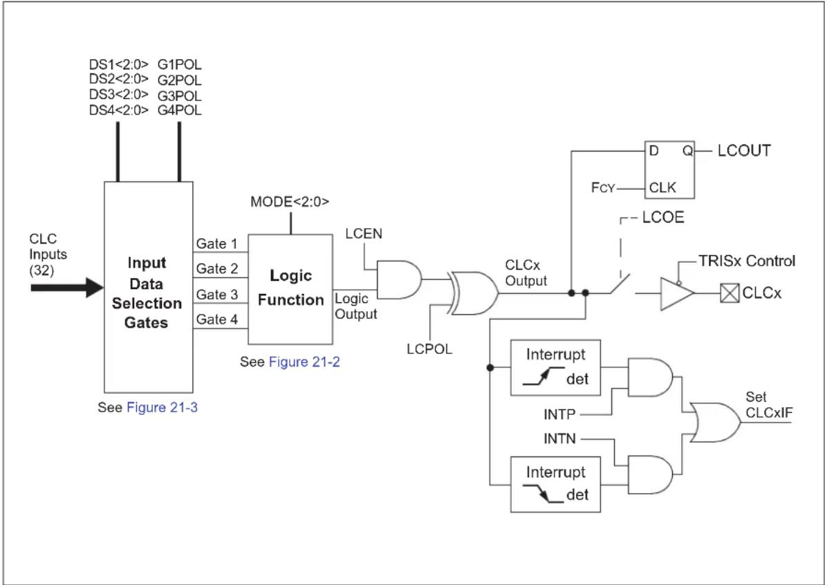
flowchart
graph LR
    A["CLC Inputs (32)"] --> B["Input Data Selection Gates"]
    B --> C["See Figure 21-3"]
    C --> D["Logic Function"]
    D --> E["LCEN"]
    E --> F["Logic Output"]
    F --> G["LCPOL"]
    G --> H["CLCx Output"]
    H --> I["Interrupt det"]
    H --> J["INTP"]
    H --> K["INTN"]
    H --> L["Interrupt det"]
    I --> M["Set CLCxIF"]
    J --> M
    K --> M
    L --> M
    N["DS1<2:0> G1POL"] --> B
    O["DS2<2:0> G2POL"] --> B
    P["DS3<2:0> G3POL"] --> B
    Q["DS4<2:0> G4POL"] --> B
    R["LCOUT"] --> H
    S["CLK"] --> H
    T["LCOE"] --> H
    U["FCY"] --> H
    V["TRISx Control"] --> W["CLCx"]
FIGURE 21-2: CLCx LOGIC FUNCTION COMBINATORIAL OPTIONS
AND - OR MODE<2:0> = 000 MODE<2:0> = 000 | OR - XOR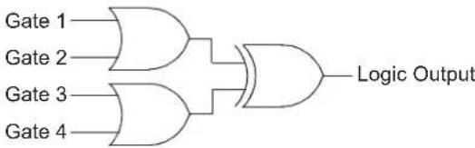 MODE<2:0> = 001 MODE<2:0> = 001 |
4-Input AND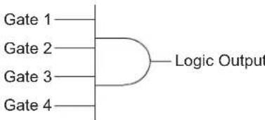 MODE<2:0> = 010 MODE<2:0> = 010 | S-R Latch MODE<2:0> = 011 MODE<2:0> = 011 |
1-Input D Flip-Flop with S and R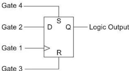 MODE<2:0> = 100 MODE<2:0> = 100 | 2-Input D Flip-Flop with R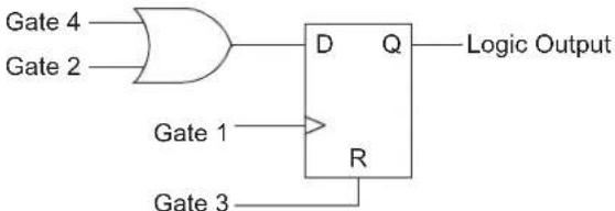 MODE<2:0> = 101 MODE<2:0> = 101 |
J-K Flip-Flop with R MODE<2:0> = 110 MODE<2:0> = 110 | 1-Input Transparent Latch with S and R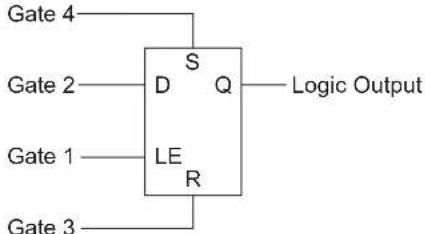 MODE<2:0> = 111 MODE<2:0> = 111 |
FIGURE 21-3: CLCx INPUT SOURCE SELECTION DIAGRAM
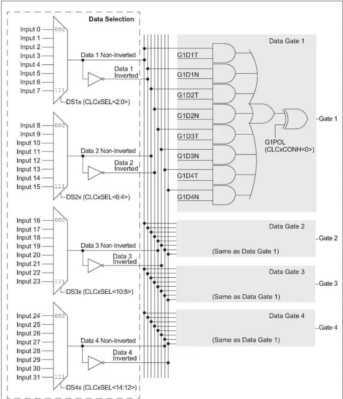
flowchart
graph TD
    subgraph_DS1x["DS1x (CLCxSEL<2:0>)"]
        A["Input 0"] --> B["Data 1 Non-Inverted"]
        C["Input 1"] --> B
        D["Input 2"] --> B
        E["Input 3"] --> F["Data 1 Inverted"]
        G["Input 4"] --> F
        H["Input 5"] --> F
        I["Input 6"] --> F
        J["Input 7"] --> F
    end

    subgraph_DS2x["DS2x (CLCxSEL<6:4>)"]
        K["Input 8"] --> L["Data 2 Non-Inverted"]
        M["Input 9"] --> L
        N["Input 10"] --> L
        O["Input 11"] --> L
        P["Input 12"] --> L
        Q["Input 13"] --> L
        R["Input 14"] --> L
        S["Input 15"] --> L
    end

    subgraph_DS3x["DS3x (CLCxSEL<10:8>)"]
        T["Input 16"] --> U["Data 3 Non-Inverted"]
        V["Input 17"] --> U
        W["Input 18"] --> U
        X["Input 19"] --> Y["Data 3 Inverted"]
        Z["Input 20"] --> Y
        AA["Input 21"] --> Y
        AB["Input 22"] --> Y
        AC["Input 23"] --> Y
    end

    subgraph_DS4x["DS4x (CLCxSEL<14:12>)"]
        AD["Input 24"] --> AE["Data 4 Non-Inverted"]
        AF["Input 25"] --> AE
        AG["Input 26"] --> AE
        AH["Input 27"] --> AE
        AI["Input 28"] --> AE
        AJ["Input 29"] --> AE
        AK["Input 30"] --> AE
        AL["Input 31"] --> AE
    end

    B --> M
    L --> N
    Y --> U
    AE --> U
    AE --> Y
    AE --> Y
    F --> U
    F --> Y
    F --> Y
    F --> Y
    F --> Y
    F --> Y
    F --> Y
    F --> Y

    G --> H
    G --> I
    G --> J
    G --> K
    G --> L

    G1D1T --> H
    G1D1N --> H
    G1D2T --> H
    G1D2N --> H
    G1D3T --> H
    G1D3N --> H
    G1D4T --> H
    G1D4N --> H

    H --> O["G1POL (CLCxCONH<0>)"]
    O --> P["-Gate 1"]

    H --> Q["G1D1T"]
    H --> R["G1D1N"]
    H --> S["G1D2T"]
    H --> T["G1D2N"]
    H --> U["G1D3T"]
    H --> V["G1D3N"]
    H --> W["G1D4T"]
    H --> X["G1D4N"]

    Q --> Y["G1D1T"]
    R --> Z["G1D1N"]
    S --> AA["G1D2T"]
    T --> AB["G1D2N"]
    U --> AC["G1D3T"]
    V --> AD["G1D3N"]
    W --> AE["G1D4T"]
    X --> AF["G1D4N"]

    Y --> AG["G1D1T"]
    Z --> AH["G1D1N"]
    AA --> AI["G1D2T"]
    AB --> AJ["G1D2N"]
    AC --> AK["G1D3T"]
    AD --> AL["G1D3N"]
    AE --> AM["G1D4T"]
    AF --> AN["G1D4N"]

    AG --> AO["G1D1T"]
    AH --> AP["G1D1N"]
    AI --> AQ["G1D2T"]
    AJ --> AR["G1D2N"]
    AK --> AS["G1D3T"]
    AL --> AT["G1D3N"]
    AM --> AU["G1D4T"]
    AN --> AV["G1D4N"]

    AO --> AW["G1D1T"]
    AP --> AX["G1D1N"]
    AQ --> AY["G1D2T"]
    AR --> AZ["G1D2N"]
    AS --> BA["G1D3T"]
    AT --> BB["G1D3N"]
    AU --> BC["G1D4T"]
    AV --> BD["G1D4N"]

    AW & AX & AY & AZ & BA & BB & AC & AD & AE & AF & AG & AH & AI & AJ & AK & AL & AM & AN & AO & AP & AH & AI & AJ & AK & AL & AO & AP & AH & AI & AJ & AK & AL & AO & AP & AH & AI & AJ & AO & AP & AH & AI & AJ & AO & AP & AH & AI & AJ & AO & AP & AH & AI & AJ & AO & AP & AH & AI & AJ & AO & AP & AH & AI & AJ & AO & AP & AH & AI & AJ & AO & AP & AH & AI & AJ & AO & AP & AH & AI & AJ & AO & AP & AH & AI & AJ & AO & AP & AH & AI & AH & AI & AJ & AO & AH & AI & AJ & AO & AP & AH & AI & AJ & AO & AH & AI & AJ & AO & AP & AH & AI & AJ & AO & AI & AH & AI & AJ & AO & AI & AH & AI & AJ & AO & AI & AH & AI & AJ & AO & AI & AH & AI & AJ & AO & AI & AH & AI & AJ & AO & AI & AH & AI & AJ & AO & AI & AH & AI & AJ & AO, Gate 2, Gate 3, Gate 4, Gate 4, Gate 2, Gate 3, Gate 4, Gate 2, Gate 3, Gate 4, Gate 2, Gate 3, Gate 4, Gate 2, Gate 3, Gate 4, Gate 2, Gate 3, Gate 4, Gate 2, Gate 3, Gate 4, Gate 2, Gate 3, Gate 4, Gate 2, Gate 3, Gate 4, Gate 2, Gate 3, Gate 2, Gate 3, Gate 4, Gate 2, Gate 3, Gate 4, Gate 2, Gate 3, Gate 4, Gate 2, Gate 3, Gate 4, Gate 2, Gate 3, Gate 4, Gate 2, Gate 3, Gate 4, Gate 2, Gate 3, Gate 4, Gate 2, Gate 3, Gate 4, Gate 3, Gate 4, Gate 2, Gate 3, Gate 4, Gate 2, Gate 3, Gate 4, Gate 2, Gate 3, Gate 4, Gate 2, Gate 3, Gate 4, Gate 2, Gate 3, Gate 4, Gate 2, Gate 3, Gate 4, Gate 2, Gate 3, Gate 4, Gate 2, Gate 5, Gate 5, Gate 5, Gate 5, Gate 5, Gate 5, Gate 5, Gate 5, Gate 5, Gate 5, Gate 5, Gate 5, Gate 5, Gate 5, Gate 5, Gate 5, Gate 5, Gate 5, Gate 5, Gate 5, Gate 5, Gate 5, Gate 5, Gate 5, Gate 5, Gate 6, Gate 6
    style DS1x fill:#f9f9f9,stroke:#ccc
    style DS2x fill:#f9f9f9,stroke:#ccc
    style DS3x fill:#f9f9f9,stroke:#ccc
    style DS4x fill:#f9f9f9,stroke:#ccc
Note: All controls are undefined at power-up.
21.1 Control Registers
The CLCx module is controlled by the following registers:
- CLC×CONL
• C L C x C O N H - CLCxSEL
• C L C x G L S L
• C L C x G L S H
The CLCx Control registers (CLCxCONL and CLCxCONH) are used to enable the module and interrupts, control the output enable bit, select output polarity and select the logic function. The CLCx Control registers also allow the user to control the logic polarity of not only the cell output, but also some intermediate variables.
The CLCx Input MUX Select register (CLCxSEL) allows the user to select up to four data input sources using the four data input selection multiplexers. Each multiplexer has a list of eight data sources available.
The CLCx Gate Logic Input Select registers (CLCxGLSL and CLCxGLSH) allow the user to select which outputs from each of the selection MUXes are used as inputs to the input gates of the logic cell. Each data source MUX outputs both a true and a negated version of its output. All of these eight signals are enabled, ORed together by the logic cell input gates.
REGISTER 21-1: CLCxCONL: CLCx CONTROL REGISTER (LOW)
| R/W-0 U-0 U-0 U-0 R/W-0 R/W-0 U-0 U-0 | ||||||
| LCEN — — INTP INTN — — | ||||||
| bit 15 bit 8 | ||||||
| R-0 R-0 R/W-0 U-0 U-0 R/W-0 | R/W-0 | R/W-0 | |||||
| LCOE | LCOUT | LCPOL | — — M∅DE2 | M∅DE1 | M∅DE0 | ||
| bit 7 bit 0 | |||||||
| Legend: | |||
| R = Readable bit | W = Writable bit | U = Unimplemented bit, read as ‘0’ | |
| -n = Value at POR | ‘1’ = Bit is set | ‘0’ = Bit is cleared | x = Bit is unknown |
| bit 15 | LCEN: CLCx Enable bit1 = CLCx is enabled and mixing input signals0 = CLCx is disabled and has logic zero outputs |
| bit 14-12 | Unimplemented: Read as '0' |
| bit 11 | INTP: CLCx Positive Edge Interrupt Enable bit1 = Interrupt will be generated when a rising edge occurs on LCOUT0 = Interrupt will not be generated |
| bit 10 | INTN: CLCx Negative Edge Interrupt Enable bit1 = Interrupt will be generated when a falling edge occurs on LCOUT0 = Interrupt will not be generated |
| bit 9-8 | Unimplemented: Read as '0' |
| bit 7 | LCOE: CLCx Port Enable bit1 = CLCx port pin output is enabled0 = CLCx port pin output is disabled |
| bit 6 | LCOUT: CLCx Data Output Status bit1 = CLCx output high0 = CLCx output low |
| bit 5 | LCPOL: CLCx Output Polarity Control bit1 = The output of the module is inverted0 = The output of the module is not inverted |
| bit 4-3 | Unimplemented: Read as '0' |
REGISTER 21-1: CLCxCONL: CLCx CONTROL REGISTER (LOW) (CONTINUED)
bit 2-0 MODE<2:0>: CLCx Mode bits
111 = Single Input Transparent Latch with S and R
110 = JK Flip-Flop with R
101 = Two-Input D Flip-Flop with R
100 = Single Input D Flip-Flop with S and R
011 = SR Latch
010 = Four-Input AND
001 = Four-Input OR-XOR
000 = Four-Input AND-OR
REGISTER 21-2: CLCxCONH: CLCx CONTROL REGISTER (HIGH)
| U-0 U-0 U-0 U-0 U-0 U-0 U-0 U-0 | |||||||
| —— | —— | —— | |||||
| bit 15 bit 8 | |||||||
| U-0 U-0 U-0 U-0 R/W-0 R/W-0 R/W-0 R/W-0 | |||||||
| — — — | — G4POL G3 | POL G2POL G | 1POL | ||||
| bit 7 bit 0 | |||||||
Legend:
| R = Readable bit W = Writable bit | U = Unimplemented bit, read as '0' | ||
| -n = Value at POR | '1' = Bit is set | '0' = Bit is cleared | x = Bit is unknown |
bit 15-4 Unimplemented: Read as '0'
bit 3 G4POL: Gate 4 Polarity Control bit
1 = Channel 4 logic output is inverted when applied to the logic cell
0 = Channel 4 logic output is not inverted
bit 2 G3POL: Gate 3 Polarity Control bit
1 = Channel 3 logic output is inverted when applied to the logic cell
0 = Channel 3 logic output is not inverted
bit 1 G2POL: Gate 2 Polarity Control bit
1 = Channel 2 logic output is inverted when applied to the logic cell
0 = Channel 2 logic output is not inverted
bit 0 G1POL: Gate 1 Polarity Control bit
1 = Channel 1 logic output is inverted when applied to the logic cell
0 = Channel 1 logic output is not inverted
REGISTER 21-3: CLCxSEL: CLCx INPUT MUX SELECT REGISTER
| U-0 R/W-0 R/W-0 R/W-0 U-0 R/W-0 R/W-0 R/W-0 | ||||
| — | D | S | 4 < | |
| bit 15 bit 8 | ||||
| U-0 R/W-0 R/W-0 R/W-0 U-0 R/W-0 R/W-0 R/W-0 | ||||
| — | D | S | 2 < | |
| bit 7 bit 0 | ||||
Legend:
R = Readable bit W = Writable bit U = Unimplemented bit, read as '0' -n = Value at POR '1' = Bit is set '0' = Bit is cleared x = Bit is unknown
bit 15 Unimplemented: Read as '0'
bit 14-12 DS4<2:0>: Data Selection MUX 4 Signal Selection bits See Table 21-1 for input selections.
bit 11 Unimplemented: Read as '0'
bit 10-8 DS3<2:0>: Data Selection MUX 3 Signal Selection bits See Table 21-1 for input selections.
bit 7 Unimplemented: Read as '0'
bit 6-4 DS2<2:0>: Data Selection MUX 2 Signal Selection bits See Table 21-1 for input selections.
bit 3 Unimplemented: Read as '0'
bit 2-0 DS1<2:0>: Data Selection MUX 1 Signal Selection bits See Table 21-1 for input selections.
TABLE 21-1: CLC1 MULTIPLEXER INPUT SOURCES
| DSx<2:0> Signal Source | ||
| DS1<2:0> | 000 CLCINA | |
| 001 System Clock | ||
| 010 Timer1 Match | ||
| 011 PWM1H | ||
| 100 PWM5L | ||
| 101 High-Speed PWM Clock | ||
| 110 Timer2 Match | ||
| 111 Timer3 Match | ||
| DS2<2:0> | 000 CLCINB | |
| 001 CLC2 Out | ||
| 010 CMP1 Out | ||
| 011 UART1 TX Out | ||
| 100 ADC End-of-Conversion | ||
| 101 DMA Channel 0 Interrupt | ||
| 110 PWM1L | ||
| 111 PWM5H | ||
| DS3<2:0> | 000 CLCINA | |
| 001 CLC1 Out | ||
| 010 CMP2 Out | ||
| 011 SPI1 SDO Out | ||
| 100 | UART1 RX | |
| 101 PWM2H | ||
| 110 PWM6L | ||
| 111 | OCMP2 Sync Output | |
| DS4<2:0> | 000 CLCINB | |
| 001 CLC2 Out | ||
| 010 CMP3 Out | ||
| 011 | SDI1 | |
| 100 | PTGO26 | |
| 101 | ECAN1 | |
| 110 PWM2L | ||
| 111 PWM6H | ||
TABLE 21-2: CLC2 MULTIPLEXER INPUT SOURCES
| DSx<2:0> Signal Source | ||
| DS1<2:0> | 000 CLCINA | |
| 001 System Clock | ||
| 010 Timer1 Match | ||
| 011 PWM3H | ||
| 100 PWM7L | ||
| 101 High-Speed PWM Clock | ||
| 110 Timer2 Match | ||
| 111 Timer3 Match | ||
| DS2<2:0> | 000 CLCINB | |
| 001 CLC1 Out | ||
| 010 CMP1 Out | ||
| 011 UART2 TX Out | ||
| 100 ADC End-of-Conversion | ||
| 101 DMA Channel 0 Interrupt | ||
| 110 PWM3L | ||
| 111 PWM7H | ||
| DS3<2:0> | 000 CLCINA | |
| 001 CLC2 Out | ||
| 010 CMP2 Out | ||
| 011 SPI2 SDO Out | ||
| 100 | UART2 RX | |
| 101 PWM4H | ||
| 110 PWM8L | ||
| 111 | OCMP2 Sync Output | |
| DS4<2:0> | 000 CLCINB | |
| 001 CLC1 Out | ||
| 010 CMP3 Out | ||
| 011 | SDI2 | |
| 100 | PTGO27 | |
| 101 | ECAN1 | |
| 110 PWM4L | ||
| 111 PWM8H | ||
TABLE 21-3: CLC3 MULTIPLEXER INPUT SOURCES
| DSx<2:0> Signal Source | ||
| DS1<2:0> | 000 CLCINA | |
| 001 System Clock | ||
| 010 Timer1 Match | ||
| 011 PWM5H | ||
| 100 REFO1 Clock Output | ||
| 101 High-Speed PWM Clock | ||
| 110 Timer2 Match | ||
| 111 PWM3L | ||
| DS2<2:0> | 000 CLCINB | |
| 001 CLC4 Out | ||
| 010 CMP1 Out | ||
| 011 PWM5L | ||
| 100 ADC End-of-Conversion | ||
| 101 PWM3H | ||
| 110 ICAP1 Sync Output | ||
| 111 ICAP2 Sync Output | ||
| DS3<2:0> | 000 CLCINA | |
| 001 CLC3 Out | ||
| 010 CMP2 Out | ||
| 011 PWM6H | ||
| 100 UART1 RX | ||
| 101 | DMA Channel 1 Interrupt | |
| 110 OCMP1 Sync Output | ||
| 111 PWM4L | ||
| DS4<2:0> | 000 CLCINB | |
| 001 CLC4 Out | ||
| 010 CMP3 Out | ||
| 011 PWM6L | ||
| 100 | PTGO28 | |
| 101 PWM4H | ||
| 110 PC_PWM | ||
| 111 OCMP3 Sync Output | ||
TABLE 21-4: CLC4 MULTIPLEXER INPUT SOURCES
| DSx<2:0> Signal Source | ||
| DS1<2:0> | 000 CLCINA | |
| 001 PWM7H | ||
| 010 Timer1 Match | ||
| 011 INTOSC/LPRC Clock | ||
| 100 REFO1 Clock Output | ||
| 101 High-Speed PWM Clock | ||
| 110 Timer2 Match | ||
| 111 PWM1L | ||
| DS2<2:0> | 000 CLCINB | |
| 001 CLC3 Out | ||
| 010 CMP1 Out | ||
| 011 PWM7L | ||
| 100 ADC End-of-Conversion | ||
| 101 PWM1H | ||
| 110 ICAP1 Sync Output | ||
| 111 ICAP2 Sync Output | ||
| DS3<2:0> | 000 CLCINA | |
| 001 CLC4 Out | ||
| 010 CMP2 Out | ||
| 011 PWM8H | ||
| 100 UART2 RX | ||
| 101 | DMA Channel 1 Interrupt | |
| 110 OCMP1 Sync Output | ||
| 111 PWM2L | ||
| DS4<2:0> | 000 CLCINB | |
| 001 CLC3 Out | ||
| 010 CMP3 Out | ||
| 011 PWM8L | ||
| 100 | PTGO29 | |
| 101 PWM2H | ||
| 110 | PWM Sync Output | |
| 111 OCMP3 Sync Output | ||
REGISTER 21-4: CLCxGLSL: CLCx GATE LOGIC INPUT SELECT LOW REGISTER
| R/W-0 R/W-0 R/W-0 R/W-0 R/W-0 R/W-0 R/W-0 R/W-0 | |||||||
| G2D4T G2 | D4N G2D3T G | 2D3N G2D2T | G2D2N G2D1T | G2D1N | |||
| bit 15 bit 8 | |||||||
| R/W-0 R/W-0 R/W-0 R/W-0 R/W-0 R/W-0 R/W-0 R/W-0 | |||||||
| G1D4T G1 | D4N G1D3T G | 1D3N G1D2T | G1D2N G1D1† | G1D1N | |||
| bit 7 bit 0 | |||||||
Legend:
R = Readable bit W = Writable bit U = Unimplemented bit, read as '0'
-n = Value at POR '1' = Bit is set '0' = Bit is cleared x = Bit is unknown
| bit 15 | G2D4T: Gate 2 Data Source 4 True Enable bit1 = Data Source 4 non-inverted signal is enabled for Gate 20 = Data Source 4 non-inverted signal is disabled for Gate 2 |
| bit 14 | G2D4N: Gate 2 Data Source 4 Negated Enable bit1 = Data Source 4 inverted signal is enabled for Gate 20 = Data Source 4 inverted signal is disabled for Gate 2 |
| bit 13 | G2D3T: Gate 2 Data Source 3 True Enable bit1 = Data Source 3 non-inverted signal is enabled for Gate 20 = Data Source 3 non-inverted signal is disabled for Gate 2 |
| bit 12 | G2D3N: Gate 2 Data Source 3 Negated Enable bit1 = Data Source 3 inverted signal is enabled for Gate 20 = Data Source 3 inverted signal is disabled for Gate 2 |
| bit 11 | G2D2T: Gate 2 Data Source 2 True Enable bit1 = Data Source 2 non-inverted signal is enabled for Gate 20 = Data Source 2 non-inverted signal is disabled for Gate 2 |
| bit 10 | G2D2N: Gate 2 Data Source 2 Negated Enable bit1 = Data Source 2 inverted signal is enabled for Gate 20 = Data Source 2 inverted signal is disabled for Gate 2 |
| bit 9 | G2D1T: Gate 2 Data Source 1 True Enable bit1 = Data Source 1 non-inverted signal is enabled for Gate 20 = Data Source 1 non-inverted signal is disabled for Gate 2 |
| bit 8 | G2D1N: Gate 2 Data Source 1 Negated Enable bit1 = Data Source 1 inverted signal is enabled for Gate 20 = Data Source 1 inverted signal is disabled for Gate 2 |
| bit 7 | G1D4T: Gate 1 Data Source 4 True Enable bit1 = Data Source 4 non-inverted signal is enabled for Gate 10 = Data Source 4 non-inverted signal is disabled for Gate 1 |
| bit 6 | G1D4N: Gate 1 Data Source 4 Negated Enable bit1 = Data Source 4 inverted signal is enabled for Gate 10 = Data Source 4 inverted signal is disabled for Gate 1 |
| bit 5 | G1D3T: Gate 1 Data Source 3 True Enable bit1 = Data Source 3 non-inverted signal is enabled for Gate 10 = Data Source 3 non-inverted signal is disabled for Gate 1 |
| bit 4 | G1D3N: Gate 1 Data Source 3 Negated Enable bit1 = Data Source 3 inverted signal is enabled for Gate 10 = Data Source 3 inverted signal is disabled for Gate 1 |
REGISTER 21-4: CLCxGLSL: CLCx GATE LOGIC INPUT SELECT LOW REGISTER (CONTINUED)
bit 3 G1D2T: Gate 1 Data Source 2 True Enable bit
1 = Data Source 2 non-inverted signal is enabled for Gate 1
0 = Data Source 2 non-inverted signal is disabled for Gate 1
bit 2 G1D2N: Gate 1 Data Source 2 Negated Enable bit
1 = Data Source 2 inverted signal is enabled for Gate 1
0 = Data Source 2 inverted signal is disabled for Gate 1
bit 1 G1D1T: Gate 1 Data Source 1 True Enable bit
1 = Data Source 1 non-inverted signal is enabled for Gate 1
0 = Data Source 1 non-inverted signal is disabled for Gate 1
bit 0 G1D1N: Gate 1 Data Source 1 Negated Enable bit
1 = Data Source 1 inverted signal is enabled for Gate 1
0 = Data Source 1 inverted signal is disabled for Gate 1
REGISTER 21-5: CLCxGLSH: CLCx GATE LOGIC INPUT SELECT HIGH REGISTER
| R/W-0 R/W-0 R/W-0 R/W-0 R/W-0 R/W-0 R/W-0 R/W-0 | |||||||
| G4D4T G4 | D4N G4D3T G | 4D3N G4D2T | G4D2N G4D1T | G4D1N | |||
| bit 15 bit 8 | |||||||
| R/W-0 R/W-0 R/W-0 R/W-0 R/W-0 R/W-0 R/W-0 R/W-0 | |||||||
| G3D4T G3 | D4N G3D3T G | 3D3N G3D2T | G3D2N G3D1T | G3D1N | |||
| bit 7 bit 0 | |||||||
Legend:
R = Readable bit W = Writable bit U = Unimplemented bit, read as '0'
-n = Value at POR '1' = Bit is set '0' = Bit is cleared x = Bit is unknown
| bit 15 | G4D4T: Gate 4 Data Source 4 True Enable bit1 = Data Source 4 non-inverted signal is enabled for Gate 40 = Data Source 4 non-inverted signal is disabled for Gate 4 |
| bit 14 | G4D4N: Gate 4 Data Source 4 Negated Enable bit1 = Data Source 4 inverted signal is enabled for Gate 40 = Data Source 4 inverted signal is disabled for Gate 4 |
| bit 13 | G4D3T: Gate 4 Data Source 3 True Enable bit1 = Data Source 3 non-inverted signal is enabled for Gate 40 = Data Source 3 non-inverted signal is disabled for Gate 4 |
| bit 12 | G4D3N: Gate 4 Data Source 3 Negated Enable bit1 = Data Source 3 inverted signal is enabled for Gate 40 = Data Source 3 inverted signal is disabled for Gate 4 |
| bit 11 | G4D2T: Gate 4 Data Source 2 True Enable bit1 = Data Source 2 non-inverted signal is enabled for Gate 40 = Data Source 2 non-inverted signal is disabled for Gate 4 |
| bit 10 | G4D2N: Gate 4 Data Source 2 Negated Enable bit1 = Data Source 2 inverted signal is enabled for Gate 40 = Data Source 2 inverted signal is disabled for Gate 4 |
| bit 9 | G4D1T: Gate 4 Data Source 1 True Enable bit1 = Data Source 1 non-inverted signal is enabled for Gate 40 = Data Source 1 non-inverted signal is disabled for Gate 4 |
| bit 8 | G4D1N: Gate 4 Data Source 1 Negated Enable bit1 = Data Source 1 inverted signal is enabled for Gate 40 = Data Source 1 inverted signal is disabled for Gate 4 |
| bit 7 | G3D4T: Gate 3 Data Source 4 True Enable bit1 = Data Source 4 non-inverted signal is enabled for Gate 30 = Data Source 4 non-inverted signal is disabled for Gate 3 |
| bit 6 | G3D4N: Gate 3 Data Source 4 Negated Enable bit1 = Data Source 4 inverted signal is enabled for Gate 30 = Data Source 4 inverted signal is disabled for Gate 3 |
| bit 5 | G3D3T: Gate 3 Data Source 3 True Enable bit1 = Data Source 3 non-inverted signal is enabled for Gate 30 = Data Source 3 non-inverted signal is disabled for Gate 3 |
| bit 4 | G3D3N: Gate 3 Data Source 3 Negated Enable bit1 = Data Source 3 inverted signal is enabled for Gate 30 = Data Source 3 inverted signal is disabled for Gate 3 |
REGISTER 21-5: CLCxGLSH: CLCx GATE LOGIC INPUT SELECT HIGH REGISTER (CONTINUED)
bit 3 G3D2T: Gate 3 Data Source 2 True Enable bit
1 = Data Source 2 non-inverted signal is enabled for Gate 3
0 = Data Source 2 non-inverted signal is disabled for Gate 3
bit 2 G3D2N: Gate 3 Data Source 2 Negated Enable bit
1 = Data Source 2 inverted signal is enabled for Gate 3
0 = Data Source 2 inverted signal is disabled for Gate 3
bit 1 G3D1T: Gate 3 Data Source 1 True Enable bit
1 = Data Source 1 non-inverted signal is enabled for Gate 3
0 = Data Source 1 non-inverted signal is disabled for Gate 3
bit 0 G3D1N: Gate 3 Data Source 1 Negated Enable bit
1 = Data Source 1 inverted signal is enabled for Gate 3
0 = Data Source 1 inverted signal is disabled for Gate 3
22.0 HIGH-SPEED, 12-BIT ANALOG-TO-DIGITAL CONVERTER (ADC)
Note 1: This data sheet summarizes the features of the dsPIC33EPXXXGS70X/80X family of devices. It is not intended to be a comprehensive reference source. To complement the information in this data sheet, refer to "12-Bit High-Speed, Multiple SARs A/D Converter (ADC)" (DS70005213) in the "dsPIC33/PIC24 Family Reference Manual", which is available from the Microchip website (www.microchip.com).
2: Some registers and associated bits described in this section may not be available on all devices. Refer to Section 4.0 "Memory Organization" in this data sheet for device-specific register and bit information.
dsPIC33EPXXXGS70X/80X devices have a high-speed, 12-bit Analog-to-Digital Converter (ADC) that features a low conversion latency, high resolution and oversampling capabilities to improve performance in AC/DC, DC/DC power converters.
22.1 Features Overview
The high-speed, 12-bit multiple SARs Analog-to-Digital Converter (ADC) includes the following features:
- Five ADC Cores: Four Dedicated Cores and One Shared (common) Core
- User-Configurable Resolution of up to 12 Bits for each Core
- Up to 3.25 Msps Conversion Rate per Channel at 12-Bit Resolution
- Low Latency Conversion
- Up to 22 Analog Input Channels, with a Separate 16-Bit Conversion Result Register for each Input
- Conversion Result can be Formatted as Unsigned or Signed Data, on a per Channel Basis, for All Channels
-
Single-Ended and Pseudodifferential Conversions are available on All ADC Cores
-
Simultaneous Sampling of up to Five Analog Inputs
• Channel Scan Capability - Multiple Conversion Trigger Options for each Core, including:
- PWM1 through PWM6 (primary and secondary triggers, and current-limit event trigger)
- PWM Special Event Trigger
- Timer1/Timer2 period match
- Output Compare 1 and event trigger
- External pin trigger event (ADTRG31)
- Software trigger
- Two Integrated Digital Comparators with Dedicated Interrupts:
- Multiple comparison options
- Assignable to specific analog inputs
- Two Oversampling Filters with Dedicated Interrupts:
- Provide increased resolution
- Assignable to a specific analog input
The module consists of five independent SAR ADC cores. Simplified block diagrams of the multiple SARs 12-bit ADC are shown in Figure 22-1, Figure 22-2 and Figure 22-3.
The analog inputs (channels) are connected through multiplexers and switches to the Sample-and-Hold (S&H) circuit of each ADC core. The core uses the channel information (the output format, the Measurement mode and the input number) to process the analog sample. When conversion is complete, the result is stored in the result buffer for the specific analog input, and passed to the digital filter and digital comparator if they were configured to use data from this particular channel.
The ADC module can sample up to five inputs at a time (four inputs from the dedicated SAR cores and one from the shared SAR core). If multiple ADC inputs request conversion on the shared core, the module will convert them in a sequential manner, starting with the lowest order input.
The ADC provides each analog input the ability to specify its own trigger source. This capability allows the ADC to sample and convert analog inputs that are associated with PWM generators operating on independent time bases.
FIGURE 22-1: ADC MODULE BLOCK DIAGRAM

flowchart
graph TD
    A["AVDD AVss"] --> B["Voltage Reference (REFSEL<2:0>)"]
    B --> C["Dedicated ADC Core 0(2)"]
    C --> D["AND"]
    C --> E["AND"]
    C --> F["AND"]
    C --> G["AND"]
    C --> H["AND"]
    C --> I["AND"]
    C --> J["AND"]
    C --> K["AND"]
    C --> L["AND"]
    C --> M["AND"]
    C --> N["AND"]
    C --> O["AND"]
    C --> P["AND"]
    C --> Q["AND"]
    C --> R["AND"]
    C --> S["AND"]
    C --> T["AND"]
    C --> U["AND"]
    C --> V["AND"]
    C --> W["AND"]
    C --> X["AND"]
    C --> Y["AND"]
    C --> Z["AND"]
    C --> AA["AND"]
    C --> AB["AND"]
    C --> AC["AND"]
    C --> AD["AND"]
    C --> AE["AND"]
    C --> AF["AND"]
    C --> AG["AND"]
    C --> AH["AND"]
    C --> AI["AND"]
    C --> AJ["AND"]
    C --> AK["AND"]
    C --> AL["AND"]
    C --> AM["AND"]
    C --> AN["AND"]
    C --> AO["AND"]
    C --> AP["AND"]
    C --> AQ["AND"]
    C --> AR["AND"]
    C --> AS["AND"]
    C --> AT["AND"]
    C --> AU["AND"]
    C --> AV["AND"]
    C --> AW["AND"]
    C --> AX["AND"]
    C --> AY["AND"]
    C --> AZ["AND"]
    C --> BA["AND"]
    C --> BB["AND"]
    C --> BC["AND"]
    C --> BD["AND"]
    C --> BE["AND"]
    C --> BF["AND"]
    C --> BG["AND"]
    C --> BH["AND"]
    C --> BI["AND"]
    C --> BJ["AND"]
    C --> BK["AND"]
    C --> BL["AND"]
    C --> BM["AND"]
    C --> BN["AND"]
    C --> BO["AND"]
    C --> BP["AND"]
    C --> BQ["AND"]
    C --> BR["AND"]
    C --> BS["AND"]
    C --> BT["AND"]
    C --> BU["AND"]
    C --> BV["AND"]
    C --> BW["AND"]
    C --> BX["AND"]
    C --> BY["AND"]
    C --> BZ["AND"]
    C --> CA["AND"]
    C --> CB["AND"]
    C --> CC["AND"]
    C --> CD["AND"]
    C --> CE["AND"]
    C --> CF["AND"]
    C --> CG["AND"]
    C --> CH["AND"]
    C --> CI["AND"]
    C --> CJ["AND"]
    C --> CK["AND"]
    C --> CR["AND"]
    C --> CS["AND"]
    C --> CT["AND"]
    C --> CU["AND"]
    C --> CV["AND"]
    C --> CW["AND"]
    C --> CX["AND"]
    C --> CY["AND"]
    C --> CZ["AND"]
    C --> DA["AND"]
    C --> DB["AND"]
    C --> DC["AND"]
    C --> DV["AND"]
    C --> DW["AND"]
    C --> DX["AND"]
    C --> DXB["AND"]
    C --> DXF["AND"]
    C --> DXG["AND"]
    C --> DXH["AND"]
    C --> DXI["AND"]
    C --> DXJ["AND"]
    C --> DXK["AND"]
    C --> DXL["AND"]
    C --> DXM["AND"]
    C --> DXN["AND"]
    C --> DXO["AND"]
    C --> DXP["AND"]
    C --> DXQ["AND"]
    C --> DXR["AND"]
    C --> DXS["AND"]
    C --> DXT["AND"]
    C --> DXU["AND"]
    C --> DXV["AND"]
    C --> DXW["AND"]
    C --> DXX["AND"]
    C --> DXY["AND"]
    C --> DXZ["AND"]
    C --> DXR
    D --> U["Dedicated ADC Core 0(2)"]
    U --> V1AN0
    U1AN7
    U1PGA1(1)
    U1AN0ALT
    U1AN1
    U1AN18
    U1PGA2(1)
    U1AN1ALT
    U1AN2
    U1VBG Reference(1)
    U1AN11
    U1AN3
    U1AN15
    U1AN4
    U1AN21

    B <--> D
Note 1: PGA1, PGA2 and the Band Gap Reference (VBG) are internal analog inputs and are not available on device pins. 2: If the dedicated core uses an alternate channel, then shared core function cannot be used.
FIGURE 22-2: DEDICATED ADC CORES 0 TO 3 BLOCK DIAGRAM

flowchart
graph TD
    A["Positive Input"] --> B["PGAx"]
    C["Alternate Positive Input"] --> D["Negative Input"]
    E["AVss"] --> F["Negative Input Selection (DIFFx)(1)"]
    B --> G["Sample-and-Hold"]
    D --> G
    F --> G
    G --> H["12-Bit SAR ADC"]
    H --> I["Reference"]
    H --> J["Output Data"]
    H --> K["Clock"]
    G --> L["Trigger Stops Sampling"]
    L --> F
    H --> M["ADC Core Clock Divider (ADCS<6:0> bits)"]
Note 1: The DIFFx bit for the corresponding positive input channel must be set in order to use the negative differential input.
FIGURE 22-3: SHARED ADC CORE BLOCK DIAGRAM
flowchart
graph TD
    A["AN4"] --> B["Analog Channel Number from Current Trigger"]
    C["AN21"] --> B
    D["AN9(1)"] --> E["Negative Input Selection (DIFFx)(1)"]
    E --> F["Shared Sample-and-Hold"]
    F --> G["12-Bit SAR ADC"]
    G --> H["ADC Core Clock Divider (SHRADC<6:0> bits)"]
    H --> I["Sampling Time"]
    I --> J["SHRSAMC<9:0>"]
    K["AVss"] --> E
    L["Reference"] --> G
    M["Output Data"] --> G
    N["Clock"] --> H
Note 1: Differential-mode conversion is not available for the shared ADC core in dsPIC33EPXXGS70X/80X devices. For all other devices, the DIFFx bit for the corresponding positive input channel must be set to use AN9 as the negative differential input.
22.2 Analog-to-Digital Converter Resources
Many useful resources are provided on the main product page of the Microchip website for the devices listed in this data sheet. This product page contains the latest updates and additional information.
22.2.1 KEY RESOURCES
- "12-Bit High-Speed, Multiple SARs A/D Converter (ADC)" (DS70005213) in the "dsPIC33/PIC24 Family Reference Manual"
- Code Samples
- Application Notes
- Software Libraries
- Webinars
- All Related "dsPIC33/PIC24 Family Reference Manual" Sections
- Development Tools
REGISTER 22-1: ADCON1L: ADC CONTROL REGISTER 1 LOW
| R/W-0 U-0 R/W-0 U-0 U-0 U-0 U-0 U-0 | ||||||||
| ADON^(1) | — | A | D | S | I | D | L | —— |
| bit 15 bit 8 | ||||||||
| Legend: | r = Reserved bit | ||
| R = Readable bit W = Writable bit | U = Unimplemented bit, read as ‘0’ | ||
| -n = Value at POR | ‘1’ = Bit is set | ‘0’ = Bit is cleared | x = Bit is unknown |
bit 15 ADON: ADC Enable bit ^(1)
1 = ADC module is enabled
0 = ADC module is off
bit 14 Unimplemented: Read as '0'
bit 13 ADSIDL: ADC Stop in Idle Mode bit
1 = Discontinues module operation when device enters Idle mode
0 = Continues module operation in Idle mode
bit 12-8 Unimplemented: Read as '0'
bit 7 NRE: Noise Reduction Enable bit ^(2)
1 = Holds conversion process for one TADCORE when another core completes conversion to reduce noise between cores
0 = Noise reduction feature is disabled
bit 6-3 Reserved: Maintain as '0'
bit 2-0 Unimplemented: Read as '0'
Note 1: Set the ADON bit only after the ADC module has been configured. Changing ADC Configuration bits when ADON = 1 will result in unpredictable behavior.
2: If the NRE bit in the ADCON1L register is set, the end of conversion time is adjusted to reduce the noise between ADC cores. Depending on the number of cores converting and the priority of the input, a few additional TADS may be inserted, making the conversion time slightly less deterministic.
REGISTER 22-2: ADCON1H: ADC CONTROL REGISTER 1 HIGH
| r-0 r-0 r-0 r-0 r-0 r-0 r-0 | |||||||
| —— | —— | —— | |||||
| bit 15 bit 8 | |||||||
| R/W-0 R/W-1 R/W-1 r-0 r-0 r-0 r-0 | |||||||
| FORM SH | RRES1 | SHRRES0 | —— | —— | |||
| bit 7 bit 0 | |||||||
| Legend: r = Reserved bit | |||
| R = Readable bit W = Writable bit | U = Unimplemented bit, read as ‘0’ | ||
| -n = Value at POR | ‘1’ = Bit is set | ‘0’ = Bit is cleared | x = Bit is unknown |
bit 15-8 Reserved: Maintain as '0'
bit 7 FORM: Fractional Data Output Format bit
1 = Fractional
0 = Integer
bit 6-5 SHRRES<1:0>: Shared ADC Core Resolution Selection bits
11 = 12-bit resolution
10 = 10-bit resolution
01 = 8-bit resolution
00 = 6-bit resolution
bit 4-0 Reserved: Maintain as '0'
REGISTER 22-3: ADCON2L: ADC CONTROL REGISTER 2 LOW
| R/W-0 R/W-0 r-0 R/W-0 r-0 R/W-0 R/W-0 R/W-0 | ||||||
| REFCIE REFERCIE | — | E | I | E | N(1) | SHREISESHREISEL0(1) |
| bit 15 bit 8 | ||||||
| U-0 R/W-0 R/W-0 R/W-0 R/W-0 R/W-0 R/W-0 R/W-0 | |
| — | SHRADCS<6:0> |
| bit 7 | bit 0 |
| Legend: | r = Reserved bit | ||
| R = Readable bit | W = Writable bit | U = Unimplemented bit, read as ‘0’ | |
| -n = Value at POR | ‘1’ = Bit is set | ‘0’ = Bit is cleared | x = Bit is unknown |
| bit 15 | REFCIE: Band Gap and Reference Voltage Ready Common Interrupt Enable bit1 = Common interrupt will be generated when the band gap will become ready0 = Common interrupt is disabled for the band gap ready event |
| bit 14 | REFERCIE: Band Gap or Reference Voltage Error Common Interrupt Enable bit1 = Common interrupt will be generated when a band gap or reference voltage error is detected0 = Common interrupt is disabled for the band gap and reference voltage error event |
| bit 13 | Reserved: Maintain as ‘0’ |
| bit 12 | EIEN: Early Interrupts Enable bit1 = The early interrupt feature is enabled for the input channel interrupts (when the EISTATx flag is set)0 = The individual interrupts are generated when conversion is done (when the ANxRDY flag is set) |
| bit 11 | Reserved: Maintain as ‘0’ |
| bit 10-8 | SHREISEL<2:0>: Shared Core Early Interrupt Time Selection bits(1)111 = Early interrupt is set and interrupt is generated eight TADCORE clocks prior to when the data is ready110 = Early interrupt is set and interrupt is generated seven TADCORE clocks prior to when the data is ready101 = Early interrupt is set and interrupt is generated six TADCORE clocks prior to when the data is ready100 = Early interrupt is set and interrupt is generated five TADCORE clocks prior to when the data is ready011 = Early interrupt is set and interrupt is generated four T ADCORE clocks prior to when the data is ready010 = Early interrupt is set and interrupt is generated three TADCORE clocks prior to when the data is ready001 = Early interrupt is set and interrupt is generated two TADCORE clocks prior to when the data is ready000 = Early interrupt is set and interrupt is generated one TADCORE clock prior to when the data is ready |
| bit 7 | Unimplemented: Read as ‘0’ |
| bit 6-0 | SHRADCS<6:0>: Shared ADC Core Input Clock Divider bitsThese bits determine the number of TCORESRC (Source Clock Periods) for one shared TADCORE (Core Clock Period).1111111 = 254 Source Clock Periods•••0000011 = 6 Source Clock Periods0000010 = 4 Source Clock Periods0000001 = 2 Source Clock Periods0000000 = 2 Source Clock Periods |
Note 1: For the 6-bit shared ADC core resolution (SHRRES<1:0> = 00), the SHREISEL<2:0> settings, from '100' to '111', are not valid and should not be used. For the 8-bit shared ADC core resolution (SHRRES<1:0> = 01), the SHREISEL<2:0> settings, '110' and '111', are not valid and should not be used.
REGISTER 22-4: ADCON2H: ADC CONTROL REGISTER 2 HIGH
| HSC/R-0 HSC/R-0 r-0 r-0 r-0 R/W-0 R/W-0 | ||||||
| REFRDY REFERR | — — — | — SHRSAMC | <9:8> | |||
| bit 15 bit 8 | ||||||
| R/W-0 R/W-0 R/W-0 R/W-0 R/W-0 R/W-0 R/W-0 R/W-0 |
| SHRSAMC<7:0> |
| bit 7 bit 0 |
| Legend: | r = Reserved bit | U = Unimplemented bit, read as ‘0’ | |
| R = Readable bit W = Writable bit | HSC = Hardware Settable/Clearable bit | ||
| -n = Value at POR | ‘1’ = Bit is set | ‘0’ = Bit is cleared | x = Bit is unknown |
bit 15 REFRDY: Band Gap and Reference Voltage Ready Flag bit
1 = Band gap is ready
0 = Band gap is not ready
bit 14 REFERR: Band Gap or Reference Voltage Error Flag bit
1 = Band gap was removed after the ADC module was enabled (ADON = 1)
0 = No band gap error was detected
bit 13-10 Reserved: Maintain as '0'
bit 9-0 SHRSAMC<9:0>: Shared ADC Core Sample Time Selection bits
These bits specify the number of shared ADC Core Clock Periods (T ADCORE) for the shared ADC core sample time.
1111111111 = 1025 TADCORE
•
.
.
0000000001 = 3 TADCORE
0000000000 = 2 TADCORE
REGISTER 22-5: ADCON3L: ADC CONTROL REGISTER 3 LOW
| R/W-0 R/W-0 R/W-0 R/W-0 R/W-0 | HSC/R-0 | R/W-0 | HSC/R-0 | ||||
| REFSEL2 | REFSEL1 | REFSEL0 | SUSPEND | SUSPCIE SU | USPRDY SHR$ | AMP CNVRTCH | |
| bit 15 bit 8 | |||||||
| R/W-0 | HSC/R/W-0 | R/W-0 | R/W-0 | R/W-0 | R/W-0 | R/W-0 | R/W-0 |
| SWLCTRG | $WCTRG CNV | CHSEL5 | CNVC | CHSEL4 | CNVC | HSEL3 | CNVC |
| bit 7 bit 0 | |||||||
| Legend: | U = Unimplemented bit, read as ‘0’ | ||
| R = Readable bit | W = Writable bit | HSC = Hardware Settable/Clearable bit | |
| -n = Value at POR | ‘1’ = Bit is set | ‘0’ = Bit is cleared | x = Bit is unknown |
bit 15-13 REFSEL<2:0>: ADC Reference Voltage Selection bits
| Value | VREFH | VREFL |
| 000 | AVDD | AVss |
001-111 = Unimplemented: Do not use
bit 12 SUSPEND: All ADC Cores Triggers Disable bit
1 = All new trigger events for all ADC cores are disabled
0 = All ADC cores can be triggered
bit 11 SUSPCIE: Suspend All ADC Cores Common Interrupt Enable bit
1 = Common interrupt will be generated when ADC core triggers are suspended (SUSPEND bit = 1) and all previous conversions are finished (SUSPRDY bit becomes set)
0 = Common interrupt is not generated for suspend ADC cores event
bit 10 SUSPRDY: All ADC Cores Suspended Flag bit
1 = All ADC cores are suspended (SUSPEND bit = 1) and have no conversions in progress
0 = ADC cores have previous conversions in progress
bit 9 SHRSAMP: Shared ADC Core Sampling Direct Control bit
This bit should be used with the individual channel conversion trigger controlled by the CNVRTCH bit. It connects an analog input, specified by the CNVCHSEL<5:0> bits, to the shared ADC core and allows extending the sampling time. This bit is not controlled by hardware and must be cleared before the conversion starts (setting CNVRTCH to '1').
1 = Shared ADC core samples an analog input specified by the CNVCHSEL<5:0> bits
0 = Sampling is controlled by the shared ADC core hardware
bit 8 CNVRTCH: Software Individual Channel Conversion Trigger bit
1 = Single trigger is generated for an analog input specified by the CNVCHSEL<5:0> bits; when the bit is set, it is automatically cleared by hardware on the next instruction cycle
0 = Next individual channel conversion trigger can be generated
bit 7 SWLCTRG: Software Level-Sensitive Common Trigger bit
1 = Triggers are continuously generated for all channels with the software, level-sensitive common trigger selected as a source in the ADTRIGxL and ADTRIGxH registers
0 = No software, level-sensitive common triggers are generated
bit 6 SWCTRG: Software Common Trigger bit
1 = Single trigger is generated for all channels with the software, common trigger selected as a source in the ADTRIGxL and ADTRIGxH registers; when the bit is set, it is automatically cleared by hardware on the next instruction cycle
0 = Ready to generate the next software common trigger
bit 5-0 CNVCHSEL <5:0>: Channel Number Selection for Software Individual Channel Conversion Trigger bits
These bits define a channel to be converted when the CNVRTCH bit is set.
REGISTER 22-6: ADCON3H: ADC CONTROL REGISTER 3 HIGH
| R/W-0 R/W-0 R/W-0 R/W-0 R/W-0 R/W-0 R/W-0 R/W-0 | |||||||
| CLKSEL1 | CLKSEL0 | CLKDIV5 | CLKDIV4 | CLKDIV3 | CLKDIV2 | CLKDIV1 | CLKDIV0 |
| bit 15 bit 8 | |||||||
| R/W-0 U-0 U-0 U-0 R/W-0 R/W-0 R/W-0 R/W-0 | |||||||
| SHREN | — | — | — | C3EN | C2EN | C1EN | C0EN |
| bit 7 bit 0 | |||||||
Legend:
| R = Readable bit W = Writable bit | U = Unimplemented bit, read as '0' | ||
| -n = Value at POR | '1' = Bit is set | '0' = Bit is cleared | x = Bit is unknown |
bit 15-14 CLKSEL<1:0>: ADC Module Clock Source Selection bits
11 = APLL
10 = FRC
01 = Fosc (System Clock x 2)
00 = Fsys (System Clock)
bit 13-8 CLKDIV<5:0>: ADC Module Clock Source Divider bits
The divider forms a TCORESRC clock used by all ADC cores (shared and dedicated) from the TSRC ADC module clock source selected by the CLKSEL<1:0> bits. Then, each ADC core individually divides the TCORESRC clock to get a core-specific TADCORE clock using the ADCS<6:0> bits in the ADCORExH register or the SHRADCS<6:0> bits in the ADCON2L register.
111111 = 64 Source Clock Periods
•
•
•
000011 = 4 Source Clock Periods
000010 = 3 Source Clock Periods
000001 = 2 Source Clock Periods
000000 = 1 Source Clock Period
bit 7 SHREN: Shared ADC Core Enable bit
1 = Shared ADC core is enabled
0 = Shared ADC core is disabled
bit 6-4 Unimplemented: Read as '0'
bit 3 C3EN: Dedicated ADC Core 3 Enable bits
1 = Dedicated ADC Core 3 is enabled
0 = Dedicated ADC Core 3 is disabled
bit 2 C2EN: Dedicated ADC Core 2 Enable bits
1 = Dedicated ADC Core 2 is enabled
0 = Dedicated ADC Core 2 is disabled
bit 1 C1EN: Dedicated ADC Core 1 Enable bits
1 = Dedicated ADC Core 1 is enabled
0 = Dedicated ADC Core 1 is disabled
bit 0 C0EN: Dedicated ADC Core 0 Enable bits
1 = Dedicated ADC Core 0 is enabled
0 = Dedicated ADC Core 0 is disabled
REGISTER 22-7: ADCON4L: ADC CONTROL REGISTER 4 LOW
| U-0 U-0 U-0 U-0 U-0 U-0 U-0 U-0 | |||||||
| —— | —— | —— | |||||
| bit 15 bit 8 | |||||||
| U-0 U-0 U-0 U-0 R/W-0 R/W-0 R/W-0 R/W-0 | ||||||
| — — — | — SAMC3EN | SAMC2EN SAMC1EN SAMC0EN | ||||
| bit 7 bit 0 | ||||||
Legend:
R = Readable bit W = Writable bit U = Unimplemented bit, read as '0'
-n = Value at POR '1' = Bit is set '0' = Bit is cleared x = Bit is unknown
bit 15-4 Unimplemented: Read as '0'
bit 3 SAMC3EN: Dedicated ADC Core 3 Conversion Delay Enable bit
1 = After trigger, the conversion will be delayed and the ADC core will continue sampling during the time specified by the SAMC<9:0> bits in the ADCORE3L register
0 = After trigger, the sampling will be stopped immediately and the conversion will be started on the next core clock cycle
bit 2 SAMC2EN: Dedicated ADC Core 2 Conversion Delay Enable bit
1 = After trigger, the conversion will be delayed and the ADC core will continue sampling during the time specified by the SAMC<9:0> bits in the ADCORE2L register
0 = After trigger, the sampling will be stopped immediately and the conversion will be started on the next core clock cycle
bit 1 SAMC1EN: Dedicated ADC Core 1 Conversion Delay Enable bit
1 = After trigger, the conversion will be delayed and the ADC core will continue sampling during the time specified by the SAMC<9:0> bits in the ADCORE1L register
0 = After trigger, the sampling will be stopped immediately and the conversion will be started on the next core clock cycle
bit 0 SAMC0EN: Dedicated ADC Core 0 Conversion Delay Enable bit
1 = After trigger, the conversion will be delayed and the ADC core will continue sampling during the time specified by the SAMC<9:0> bits in the ADCORE0L register
0 = After trigger, the sampling will be stopped immediately and the conversion will be started on the next core clock cycle
REGISTER 22-8: ADCON4H: ADC CONTROL REGISTER 4 HIGH
| U-0 U-0 U-0 U-0 U-0 U-0 U-0 U-0 | |||||||
| —— | —— | —— | |||||
| bit 15 bit 8 | |||||||
| R/W-0 R/W-0 R/W-0 R/W-0 R/W-0 R/W-0 R/W-0 R/W-0 | |||||||
| C3CHS1 C3CHS0 C2CHS1 C2CHS0 C1CHS1 C1CHS0 C0CHS1 C0CHS0 | |||||||
| bit 7 bit 0 | |||||||
Legend:
| R = Readable bit W = Writable bit U = Unimplemented bit, read as '0' | ||
| -n = Value at POR | '1' = Bit is set | '0' = Bit is cleared x = Bit is unknown |
bit 15-8 Unimplemented: Read as '0'
bit 7-6 C3CHS<1:0>: Dedicated ADC Core 3 Input Channel Selection bits 1x = Reserved 01 = AN15 (differential negative input when DIFF3 (ADMOD0L<7>) = 1) 00 = AN3
bit 5-4 C2CHS<1:0>: Dedicated ADC Core 2 Input Channel Selection bits 11 = Reserved 10 = VREF band gap 01 = AN11 (differential negative input when DIFF2 (ADMOD0L<5>) = 1) 00 = AN2
bit 3-2 C1CHS<1:0>: Dedicated ADC Core 1 Input Channel Selection bits 11 = AN1ALT 10 = PGA2 01 = AN18 (differential negative input when DIFF1 (ADMOD0L<3>) = 1) 00 = AN1
bit 1-0 C0CHS<1:0>: Dedicated ADC Core 0 Input Channel Selection bits 11 = AN0ALT 10 = PGA1 01 = AN7 (differential negative input when DIFF0 (ADMOD0L<1>) = 1) 00 = AN0
REGISTER 22-9: ADCON5L: ADC CONTROL REGISTER 5 LOW
| HSC/R-0 U-0 U-0 HSC/R-0 HSC/R-0 HSC/R-0 HSC/R-0 | ||||||
| SHRRDY | — — — | C3RDY C2RDY | C1RDY C0RDY | |||
| bit 15 bit 8 | ||||||
| R/W-0 U-0 U-0 U-0 R/W-0 R/W-0 R/W-0 R/W-0 | |||||||
| SHRPWR | — — — | C3PWR C2PWR C1PWR C0PWR | |||||
| bit 7 bit 0 | |||||||
| Legend: U = Unimplemented bit, read as ‘0’ | |||
| R = Readable bit | W = Writable bit | HSC = Hardware Settable/Clearable bit | |
| -n = Value at POR | ‘1’ = Bit is set | ‘0’ = Bit is cleared | x = Bit is unknown |
| bit 15 | SHRRDY: Shared ADC Core Ready Flag bit1 = ADC core is powered and ready for operation0 = ADC core is not ready for operation |
| bit 14-12 | Unimplemented: Read as ‘0’ |
| bit 11 | C3RDY: Dedicated ADC Core 3 Ready Flag bit1 = ADC core is powered and ready for operation0 = ADC core is not ready for operation |
| bit 10 | C2RDY: Dedicated ADC Core 2 Ready Flag bit1 = ADC core is powered and ready for operation0 = ADC core is not ready for operation |
| bit 9 | C1RDY: Dedicated ADC Core 1 Ready Flag bit1 = ADC core is powered and ready for operation0 = ADC core is not ready for operation |
| bit 8 | C0RDY: Dedicated ADC Core 0 Ready Flag bit1 = ADC core is powered and ready for operation0 = ADC core is not ready for operation |
| bit 7 | SHRPWR: Shared ADC Core x Power Enable bit1 = ADC Core x is powered0 = ADC Core x is off |
| bit 6-4 | Unimplemented: Read as ‘0’ |
| bit 3 | C3PWR: Dedicated ADC Core 3 Power Enable bit1 = ADC core is powered0 = ADC core is off |
| bit 2 | C2PWR: Dedicated ADC Core 2 Power Enable bit1 = ADC core is powered0 = ADC core is off |
| bit 1 | C1PWR: Dedicated ADC Core 1 Power Enable bit1 = ADC core is powered0 = ADC core is off |
| bit 0 | C0PWR: Dedicated ADC Core 0 Power Enable bit1 = ADC core is powered0 = ADC core is off |
REGISTER 22-10: ADCON5H: ADC CONTROL REGISTER 5 HIGH
| U-0 U-0 U-0 U-0 R/W-0 R/W-0 R/W-0 R/W-0 | ||||
| — — — | — WARMTIME<3:0> | |||
| bit 15 bit 8 | ||||
| R/W-0 U-0 U-0 U-0 R/W-0 R/W-0 R/W-0 R/W-0 | ||||||
| SHRCIE | — — — | C3CIE C2CIE | C1CIE C0CIE | |||
| bit 7 bit 0 | ||||||
| Legend: | |||
| R = Readable bit | W = Writable bit | U = Unimplemented bit, read as ‘0’ | |
| -n = Value at POR | ‘1’ = Bit is set | ‘0’ = Bit is cleared | x = Bit is unknown |
bit 15-12 Unimplemented: Read as '0'
bit 11-8 WARMTIME<3:0>: ADC Dedicated Core x Power-up Delay bits
These bits determine the power-up delay in the number of the Core Source Clock Periods (CORESRC) for all ADC cores.
1111 = 32768 Source Clock Periods
1110 = 16384 Source Clock Periods
1101 = 8192 Source Clock Periods
1100 = 4096 Source Clock Periods
1011 = 2048 Source Clock Periods
1010 = 1024 Source Clock Periods
1001 = 512 Source Clock Periods
1000 = 256 Source Clock Periods
0111 = 128 Source Clock Periods
0110 = 64 Source Clock Periods
0101 = 32 Source Clock Periods
0100 = 16 Source Clock Periods
00xx = 16 Source Clock Periods
bit 7 SHRCIE: Shared ADC Core Ready Common Interrupt Enable bit
1 = Common interrupt will be generated when ADC core is powered and ready for operation
0 = Common interrupt is disabled for an ADC core ready event
bit 6-4 Unimplemented: Read as '0'
bit 3 C3CIE: Dedicated ADC Core 3 Ready Common Interrupt Enable bit
1 = Common interrupt will be generated when ADC Core 3 is powered and ready for operation
0 = Common interrupt is disabled for an ADC Core 3 ready event
bit 2 C2CIE: Dedicated ADC Core 2 Ready Common Interrupt Enable bit
1 = Common interrupt will be generated when ADC Core 2 is powered and ready for operation
0 = Common interrupt is disabled for an ADC Core 2 ready event
bit 1 C1CIE: Dedicated ADC Core 1 Ready Common Interrupt Enable bit
1 = Common interrupt will be generated when ADC Core 1 is powered and ready for operation
0 = Common interrupt is disabled for an ADC Core 1 ready event
bit 0 C0CIE: Dedicated ADC Core 0 Ready Common Interrupt Enable bit
1 = Common interrupt will be generated when ADC Core 0 is powered and ready for operation
0 = Common interrupt is disabled for an ADC Core 0 ready event
REGISTER 22-11: ADCORExL: DEDICATED ADC CORE x CONTROL REGISTER LOW (x = 0 to 3)
| U-0 U-0 U-0 U-0 U-0 U-0 R/W-0 R/W-0 | |||||
| — — — | — — — SAM<9:8> | ||||
| bit 15 bit 8 | |||||
| R/W-0 R/W-0 R/W-0 R/W-0 R/W-0 R/W-0 R/W-0 R/W-0 |
| SAMC<7:0> |
| bit 7 bit 0 |
Legend:
R = Readable bit W = Writable bit U = Unimplemented bit, read as '0'
-n = Value at POR '1' = Bit is set '0' = Bit is cleared x = Bit is unknown
bit 15-10 Unimplemented: Read as '0'
bit 9-0 SAMC<9:0>: Dedicated ADC Core x Conversion Delay Selection bits
These bits determine the time between the trigger event and the start of conversion in the number of the Core Clock Periods (TADCORE). During this time, the ADC Core x still continues sampling. This feature is enabled by the SAMCxEN bits in the ADCON4L register.
1111111111 = 1025 TADCORE
•
•
.
0000000001 = 3 TADCORE
0000000000 = 2 TADCORE
REGISTER 22-12: ADCORExH: DEDICATED ADC CORE x CONTROL REGISTER HIGH (x = 0 to 3) ^(1)
| U-0 U-0 U-0 R/W-0 R/W-0 R/W-0 R/W-1 R/W-1 | |||||||
| — — — | EISEL2 EISEL | 1 EISEL0 RES | 1 RES0 | ||||
| bit 15 bit 8 | |||||||
| U-0 R/W-0 R/W-0 R/W-0 R/W-0 R/W-0 R/W-0 | R/W-0 | |
| — | ADCS<6:0> | |
| bit 7 | bit 0 | |
| Legend: | |||
| R = Readable bit W = Writable bit | U = Unimplemented bit, read as ‘0’ | ||
| -n = Value at POR | ‘1’ = Bit is set | ‘0’ = Bit is cleared | x = Bit is unknown |
bit 15-13 Unimplemented: Read as '0'
bit 12-10 EISEL<2:0>: ADC Core x Early Interrupt Time Selection bits
111 = Early interrupt is set and an interrupt is generated eight TADCORE clocks prior to when the data is ready 110 = Early interrupt is set and an interrupt is generated seven TADCORE clocks prior to when the data is ready 101 = Early interrupt is set and an interrupt is generated six TADCORE clocks prior to when the data is ready 100 = Early interrupt is set and an interrupt is generated five TADCORE clocks prior to when the data is ready 011 = Early interrupt is set and an interrupt is generated four TADCORE clocks prior to when the data is ready 010 = Early interrupt is set and an interrupt is generated three TADCORE clocks prior to when the data is ready 001 = Early interrupt is set and an interrupt is generated two TADCORE clocks prior to when the data is ready 000 = Early interrupt is set and an interrupt is generated one TADCORE clock prior to when the data is ready
bit 9-8 RES<1:0>: ADC Core x Resolution Selection bits
11 = 12-bit resolution 10 = 10-bit resolution 01 = 8-bit resolution 00 = 6-bit resolution
bit 7 Unimplemented: Read as '0'
bit 6-0 ADCS<6:0>: ADC Core x Input Clock Divider bits
These bits determine the number of Source Clock Periods (TCORESRC) for one Core Clock Period (TADCORE). 1111111 = 254 Source Clock Periods . . . 0000011 = 6 Source Clock Periods 0000010 = 4 Source Clock Periods 0000001 = 2 Source Clock Periods 0000000 = 2 Source Clock Periods
Note 1: For the 6-bit ADC core resolution (RES<1:0> = 00), the EISEL<2:0> bits settings, from '100' to '111', are not valid and should not be used. For the 8-bit ADC core resolution (RES<1:0> = 01), the EISEL<2:0> bits settings, '110' and '111', are not valid and should not be used.
REGISTER 22-13: ADLVLTRGL: ADC LEVEL-SENSITIVE TRIGGER CONTROL REGISTER LOW
| R/W-0 R/W-0 U-0 U-0 R/W-0 R/W-0 R/W-0 R/W-0 |
| LVLEN<15:8> |
| bit 15 bit 8 |
| R/W-0 R/W-0 R/W-0 R/W-0 R/W-0 R/W-0 R/W-0 R/W-0 |
| LVLEN<7:0> |
| bit 7 bit 0 |
Legend:
R = Readable bit W = Writable bit U = Unimplemented bit, read as '0' -n = Value at POR '1' = Bit is set '0' = Bit is cleared x = Bit is unknown
bit 15-0 LVLEN<15:0>: Level Trigger for Corresponding Analog Input Enable bits
1 = Input trigger is level-sensitive
0 = Input trigger is edge-sensitive
REGISTER 22-14: ADLVLTRGH: ADC LEVEL-SENSITIVE TRIGGER CONTROL REGISTER HIGH
R = Readable bit W = Writable bit U = Unimplemented bit, read as '0' -n = Value at POR '1' = Bit is set '0' = Bit is cleared x = Bit is unknown
bit 15-6 Unimplemented: Read as '0'
bit 5-0 LVLEN<21:16>: Level Trigger for Corresponding Analog Input Enable bits
1 = Input trigger is level-sensitive
0 = Input trigger is edge-sensitive
REGISTER 22-15: ADEIEL: ADC EARLY INTERRUPT ENABLE REGISTER LOW
| R/W-0 R/W-0 R/W-0 R/W-0 R/W-0 R/W-0 R/W-0 R/W-0 |
| EIEN<15:8> |
| bit 15 bit 8 |
| R/W-0 R/W-0 R/W-0 R/W-0 R/W-0 R/W-0 R/W-0 R/W-0 |
| EIEN<7:0> |
| bit 7 bit 0 |
Legend:
R = Readable bit W = Writable bit U = Unimplemented bit, read as '0'
-n = Value at POR '1' = Bit is set '0' = Bit is cleared x = Bit is unknown
bit 15-0 EIEN<15:0>: Early Interrupt Enable for Corresponding Analog Inputs bits
1 = Early interrupt is enabled for the channel
0 = Early interrupt is disabled for the channel
REGISTER 22-16: ADEIEH: ADC EARLY INTERRUPT ENABLE REGISTER HIGH
R = Readable bit W = Writable bit U = Unimplemented bit, read as '0'
-n = Value at POR '1' = Bit is set '0' = Bit is cleared x = Bit is unknown
bit 15-6 Unimplemented: Read as '0'
bit 5-0 EIEN<21:16>: Early Interrupt Enable for Corresponding Analog Inputs bits
1 = Early interrupt is enabled for the channel
0 = Early interrupt is disabled for the channel
REGISTER 22-17: ADEISTATL: ADC EARLY INTERRUPT STATUS REGISTER LOW
| R/W-0 R/W-0 R/W-0 R/W-0 R/W-0 R/W-0 R/W-0 R/W-0 |
| EISTAT<15:8> |
| bit 15 bit 8 |
| R/W-0 R/W-0 R/W-0 R/W-0 R/W-0 R/W-0 R/W-0 R/W-0 |
| EISTAT<7:0> |
| bit 7 bit 0 |
Legend:
R = Readable bit W = Writable bit U = Unimplemented bit, read as '0' -n = Value at POR '1' = Bit is set '0' = Bit is cleared x = Bit is unknown
bit 15-0 EISTAT<15:0>: Early Interrupt Status for Corresponding Analog Inputs bits
1 = Early interrupt was generated
0 = Early interrupt was not generated since the last ADCBUFx read
REGISTER 22-18: ADEISTATH: ADC EARLY INTERRUPT STATUS REGISTER HIGH
R = Readable bit W = Writable bit U = Unimplemented bit, read as '0' -n = Value at POR '1' = Bit is set '0' = Bit is cleared x = Bit is unknown
bit 15-6 Unimplemented: Read as '0'
bit 5-0 EISTAT<21:16>: Early Interrupt Status for Corresponding Analog Inputs bits
1 = Early interrupt was generated
0 = Early interrupt was not generated since the last ADCBUFx read
REGISTER 22-19: ADMOD0L: ADC INPUT MODE CONTROL REGISTER 0 LOW
| R/W-0 R/W-0 R/W-0 R/W-0 R/W-0 R/W-0 R/W-0 R/W-0 | |||||||
| DIFF7 SIGN | N7 | DIFF6 SIGN | N6 | DIFF5 SIGN | N5 | DIFF4 SIGN | 4 |
| bit 15 bit 8 | |||||||
| R/W-0 R/W-0 R/W-0 R/W-0 R/W-0 R/W-0 R/W-0 R/W-0 | |||||||
| DIFF3 SIGN | N3 | DIFF2 SIGN | N2 | DIFF1 SIGN | 1 | DIFF0 SIGN | 0 |
| bit 7 bit 0 | |||||||
Legend:
R = Readable bit W = Writable bit U = Unimplemented bit, read as '0'
-n = Value at POR '1' = Bit is set '0' = Bit is cleared x = Bit is unknown
bit 15-1(odd) DIFF<7:0>: Differential-Mode for Corresponding Analog Inputs bits
1 = Channel is differential
0 = Channel is single-ended
bit 14-0 (even) SIGN<7:0>: Output Data Sign for Corresponding Analog Inputs bits
1 = Channel output data is signed
0 = Channel output data is unsigned
REGISTER 22-20: ADMOD0H: ADC INPUT MODE CONTROL REGISTER 0 HIGH
| R/W-0 R/W-0 R/W-0 R/W-0 R/W-0 R/W-0 R/W-0 | |||||||
| DIFF15 | SIGN15 | DIFF14 | SIGN14 | DIFF13 | SIGN13 | DIFF12 | SIGN12 |
| bit 15 bit 8 | |||||||
| R/W-0 R/W-0 R/W-0 R/W-0 R/W-0 R/W-0 R/W-0 | |||||||
| DIFF11 | SIGN11 | DIFF10 | SIGN10 | DIFF9 | SIGN9 | DIFF8 | SIGN8 |
| bit 7 bit 0 | |||||||
Legend:
R = Readable bit W = Writable bit U = Unimplemented bit, read as '0'
-n = Value at POR '1' = Bit is set '0' = Bit is cleared x = Bit is unknown
bit 15-1(odd) DIFF<15:8>: Differential-Mode for Corresponding Analog Inputs bits
1 = Channel is differential
0 = Channel is single-ended
bit 14-0 (even) SIGN<15:8>: Output Data Sign for Corresponding Analog Inputs bits
1 = Channel output data is signed
0 = Channel output data is unsigned
REGISTER 22-21: ADMOD1L: ADC INPUT MODE CONTROL REGISTER 1 LOW
| U-0 U-0 U-0 U-0 R/W-0 R/W-0 R/W-0 R/W-0 | ||||||
| — — — | DIFF21 SIGN | N21 DIFF20 SIGN20 | ||||
| bit 15 bit 8 | ||||||
| R/W-0 R/W-0 R/W-0 R/W-0 R/W-0 R/W-0 R/W-0 | |||||||
| DIFF19 | SIGN19 DI | FF18 SIGN18 | DIFF17 SIGN17 | DIFF16 SIGN16 | |||
| bit 7 bit 0 | |||||||
Legend:
| R = Readable bit | W = Writable bit | U = Unimplemented bit, read as '0' |
| -n = Value at POR | '1' = Bit is set | '0' = Bit is cleared x = Bit is unknown |
bit 15-12 Unimplemented: Read as '0'
bit 11-1(odd) DIFF<21:16>: Differential-Mode for Corresponding Analog Inputs bits
1 = Channel is differential
0 = Channel is single-ended
bit 10-0 (even) SIGN<21:16>: Output Data Sign for Corresponding Analog Inputs bits
1 = Channel output data is signed
0 = Channel output data is unsigned
REGISTER 22-22: ADIEL: ADC INTERRUPT ENABLE REGISTER LOW
| R/W-0 R/W-0 R/W-0 R/W-0 R/W-0 R/W-0 R/W-0 R/W-0 |
| IE<15:8> |
| bit 15 bit 8 |
| R/W-0 R/W-0 R/W-0 R/W-0 R/W-0 R/W-0 R/W-0 R/W-0 |
| IE<7:0> |
| bit 7 bit 0 |
Legend:
R = Readable bit W = Writable bit U = Unimplemented bit, read as '0'
-n = Value at POR '1' = Bit is set '0' = Bit is cleared x = Bit is unknown
bit 15-0 IE<15:0>: Common Interrupt Enable bits
1 = Common and individual interrupts are enabled for the corresponding channel
0 = Common and individual interrupts are disabled for the corresponding channel
REGISTER 22-23: ADIEH: ADC INTERRUPT ENABLE REGISTER HIGH
R = Readable bit W = Writable bit U = Unimplemented bit, read as '0'
-n = Value at POR '1' = Bit is set '0' = Bit is cleared x = Bit is unknown
bit 15-6 Unimplemented: Read as '0'
bit 5-0 IE<21:16>: Common Interrupt Enable bits
1 = Common and individual interrupts are enabled for the corresponding channel
0 = Common and individual interrupts are disabled for the corresponding channel
REGISTER 22-24: ADSTATL: ADC DATA READY STATUS REGISTER LOW
| HSC/R-0 HSC/R-0 HSC/R-0 HSC/R-0 HSC/R-0 HSC/R-0 HSC/R-0 HSC/R-0 |
| AN<15:8>RDY |
| bit 15 bit 8 |
| HSC/R-0 HSC/R-0 HSC/R-0 HSC/R-0 HSC/R-0 HSC/R-0 HSC/R-0 HSC/R-0 |
| AN<7:0>RDY |
| bit 7 bit 0 |
| Legend: U = Unimplemented bit, read as '0' |
| R = Readable bit W = Writable bit HSC = Hardware Settable/Clearable bit -n = Value at POR '1' = Bit is set '0' = Bit is cleared x = Bit is unknown |
bit 15-0 AN<15:0>RDY: Common Interrupt Enable for Corresponding Analog Inputs bits
1 = Channel conversion result is ready in the corresponding ADCBUFx register
0 = Channel conversion result is not ready
REGISTER 22-25: ADSTATH: ADC DATA READY STATUS REGISTER HIGH
| U-0 U-0 | HSC/R-0 HSC/R-0 HSC/R-0 HSC/R-0 HSC/R-0 HSC/R-0 | |
| — — | AN<21:16>RDY | |
| bit 7 bit 0 | ||
| Legend: U = Unimplemented bit, read as '0' |
| R = Readable bit W = Writable bit HSC = Hardware Settable/Clearable bit |
| -n = Value at POR '1' = Bit is set '0' = Bit is cleared x = Bit is unknown |
bit 15-6 Unimplemented: Read as '0'
bit 5-0 AN<21:16>RDY: Common Interrupt Enable for Corresponding Analog Inputs bits
1 = Channel conversion result is ready in the corresponding ADCBUFx register
0 = Channel conversion result is not ready
REGISTER 22-26: ADTRIGxL: ADC CHANNEL TRIGGER x SELECTION REGISTER LOW (x = 0 to 5)
| U-0 U-0 U-0 R/W-0 R/W-0 R/W-0 R/W-0 R/W-0 | ||
| — — — | TRGSRC(4x+1)<4:0> | |
| bit 15 bit 8 | ||
| U-0 U-0 U-0 R/W-0 R/W-0 R/W-0 R/W-0 R/W-0 | ||
| — — — | TRGSRC(4x)<4:0> | |
| bit 7 bit 0 | ||
Legend:
R = Readable bit W = Writable bit U = Unimplemented bit, read as '0'
-n = Value at POR '1' = Bit is set '0' = Bit is cleared x = Bit is unknown
bit 15-13 Unimplemented: Read as '0'
bit 12-8 TRGSRC(4x+1)<4:0>: Trigger Source Selection for Corresponding Analog Inputs bits
11111 = ADTRG31
11110 = PTG Trigger Output 12
11101 = PWM Generator 6 current-limit trigger
11100 = PWM Generator 5 current-limit trigger
11011 = PWM Generator 4 current-limit trigger
11010 = PWM Generator 3 current-limit trigger
11001 = PWM Generator 2 current-limit trigger
11000 = PWM Generator 1 current-limit trigger
10111 = Output Compare 2 trigger
10110 = Output Compare 1 trigger
10101 = CLC2 output
10100 = PWM Generator 6 secondary trigger
10011 = PWM Generator 5 secondary trigger
10010 = PWM Generator 4 secondary trigger
10001 = PWM Generator 3 secondary trigger
10000 = PWM Generator 2 secondary trigger
01111 = PWM Generator 1 secondary trigger
01110 = PWM secondary Special Event Trigger
01101 = Timer2 period match
01100 = Timer1 period match
01011 = CLC1 output
01010 = PWM Generator 6 primary trigger
01001 = PWM Generator 5 primary trigger
01000 = PWM Generator 4 primary trigger
00111 = PWM Generator 3 primary trigger
00110 = PWM Generator 2 primary trigger
00101 = PWM Generator 1 primary trigger
00100 = PWM Special Event Trigger
00011 = Reserved
00010 = Level software trigger
00001 = Common software trigger
00000 = No trigger is enabled
bit 7-5 Unimplemented: Read as '0'
REGISTER 22-26: ADTRIGxL: ADC CHANNEL TRIGGER x SELECTION REGISTER LOW (x = 0 to 5) (CONTINUED)
bit 4-0 TRGSRC(4x)<4:0>: Trigger Source Selection for Corresponding Analog Inputs bits
11111 = ADTRG31
11110 = PTG Trigger Output 30
11101 = PWM Generator 6 current-limit trigger
11100 = PWM Generator 5 current-limit trigger
11011 = PWM Generator 4 current-limit trigger
11010 = PWM Generator 3 current-limit trigger
11001 = PWM Generator 2 current-limit trigger
11000 = PWM Generator 1 current-limit trigger
10111 = Output Compare 2 trigger
10110 = Output Compare 1 trigger
10101 = CLC2 output
10100 = PWM Generator 6 secondary trigger
10011 = PWM Generator 5 secondary trigger
10010 = PWM Generator 4 secondary trigger
10001 = PWM Generator 3 secondary trigger
10000 = PWM Generator 2 secondary trigger
01111 = PWM Generator 1 secondary trigger
01110 = PWM secondary Special Event Trigger
01101 = Timer2 period match
01100 = Timer1 period match
01011 = CLC1 output
01010 = PWM Generator 6 primary trigger
01001 = PWM Generator 5 primary trigger
01000 = PWM Generator 4 primary trigger
00111 = PWM Generator 3 primary trigger
00110 = PWM Generator 2 primary trigger
00101 = PWM Generator 1 primary trigger
00100 = PWM Special Event Trigger
00011 = Reserved
00010 = Level software trigger
00001 = Common software trigger
00000 = No trigger is enabled
REGISTER 22-27: ADTRIGxH: ADC CHANNEL TRIGGER x SELECTION REGISTER HIGH (x = 0 to 5)
| U-0 U-0 U-0 R/W-0 R/W-0 R/W-0 R/W-0 R/W-0 | ||
| — — — | TRGSRC(4x+3)<4:0> | |
| bit 15 bit 8 | ||
| U-0 U-0 U-0 R/W-0 R/W-0 R/W-0 R/W-0 R/W-0 | ||
| — — — | TRGSRC(4x+2)<4:0> | |
| bit 7 bit 0 | ||
Legend:
| R = Readable bit W = Writable bit | U = Unimplemented bit, read as '0' | ||
| -n = Value at POR | '1' = Bit is set | '0' = Bit is cleared | x = Bit is unknown |
bit 15-13 Unimplemented: Read as '0'
bit 12-8 TRGSRC(4x+3)<4:0>: Trigger Source Selection for Corresponding Analog Inputs bits
11111 = ADTRG31
11110 = PTG Trigger Output 30
11101 = PWM Generator 6 current-limit trigger
11100 = PWM Generator 5 current-limit trigger
11011 = PWM Generator 4 current-limit trigger
11010 = PWM Generator 3 current-limit trigger
11001 = PWM Generator 2 current-limit trigger
11000 = PWM Generator 1 current-limit trigger
10111 = Output Compare 2 trigger
10110 = Output Compare 1 trigger
10101 = CLC2 output
10100 = PWM Generator 6 secondary trigger
10011 = PWM Generator 5 secondary trigger
10010 = PWM Generator 4 secondary trigger
10001 = PWM Generator 3 secondary trigger
10000 = PWM Generator 2 secondary trigger
01111 = PWM Generator 1 secondary trigger
01110 = PWM secondary Special Event Trigger
01101 = Timer2 period match
01100 = Timer1 period match
01011 = CLC1 output
01010 = PWM Generator 6 primary trigger
01001 = PWM Generator 5 primary trigger
01000 = PWM Generator 4 primary trigger
00111 = PWM Generator 3 primary trigger
00110 = PWM Generator 2 primary trigger
00101 = PWM Generator 1 primary trigger
00100 = PWM Special Event Trigger
00011 = Reserved
00010 = Level software trigger
00001 = Common software trigger
00000 = No trigger is enabled
bit 7-5 Unimplemented: Read as '0'
REGISTER 22-27: ADTRIGxH: ADC CHANNEL TRIGGER x SELECTION REGISTER HIGH (x = 0 to 5) (CONTINUED)
bit 4-0 TRGSRC(4x+2)<4:0>: Trigger Source Selection for Corresponding Analog Inputs bits
11111 = ADTRG31
11110 = PTG Trigger Output 30
11101 = PWM Generator 6 current-limit trigger
11100 = PWM Generator 5 current-limit trigger
11011 = PWM Generator 4 current-limit trigger
11010 = PWM Generator 3 current-limit trigger
11001 = PWM Generator 2 current-limit trigger
11000 = PWM Generator 1 current-limit trigger
10111 = Output Compare 2 trigger
10110 = Output Compare 1 trigger
10101 = CLC2 output
10100 = PWM Generator 6 secondary trigger
10011 = PWM Generator 5 secondary trigger
10010 = PWM Generator 4 secondary trigger
10001 = PWM Generator 3 secondary trigger
10000 = PWM Generator 2 secondary trigger
01111 = PWM Generator 1 secondary trigger
01110 = PWM secondary Special Event Trigger
01101 = Timer2 period match
01100 = Timer1 period match
01011 = CLC1 output
01010 = PWM Generator 6 primary trigger
01001 = PWM Generator 5 primary trigger
01000 = PWM Generator 4 primary trigger
00111 = PWM Generator 3 primary trigger
00110 = PWM Generator 2 primary trigger
00101 = PWM Generator 1 primary trigger
00100 = PWM Special Event Trigger
00011 = Reserved
00010 = Level software trigger
00001 = Common software trigger
00000 = No trigger is enabled
REGISTER 22-28: ADCAL0L: ADC CALIBRATION REGISTER 0 LOW
| HSC/R-0 U-0 U-0 U-0 r-0 R/W-0 R/W-0 R/W-0 | |||||||
| CAL1RDY | — — — | — CAL1DIFF | CAL1EN CAL1 | RUN | |||
| bit 15 bit 8 | |||||||
| HSC/R-0 U-0 U-0 U-0 r-0 R/W-0 R/W-0 R/W-0 | |||||||
| CAL0RDY | — — — | — CAL0DIFF | CAL0EN CAL0 | RUN | |||
| bit 7 bit 0 | |||||||
| Legend: r = Reserved bit | U = Unimplemented bit, read as ‘0’ | ||
| R = Readable bit | W = Writable bit | HSC = Hardware Settable/Clearable bit | |
| -n = Value at POR | ‘1’ = Bit is set | ‘0’ = Bit is cleared | x = Bit is unknown |
| bit 15 | CAL1RDY: Dedicated ADC Core 1 Calibration Status Flag bit1 = Dedicated ADC Core 1 calibration is finished0 = Dedicated ADC Core 1 calibration is in progress |
| bit 14-12 | Unimplemented: Read as ‘0’ |
| bit 11 | Reserved: Maintain as ‘0’ |
| bit 10 | CAL1DIFF: Dedicated ADC Core 1 Differential-Mode Calibration bit1 = Dedicated ADC Core 1 will be calibrated in Differential Input mode0 = Dedicated ADC Core 1 will be calibrated in Single-Ended Input mode |
| bit 9 | CAL1EN: Dedicated ADC Core 1 Calibration Enable bit1 = Dedicated ADC Core 1 calibration bits (CALxRDY, CALxDIFF and CALxRUN) can be accessed by software0 = Dedicated ADC Core 1 calibration bits are disabled |
| bit 8 | CAL1RUN: Dedicated ADC Core 1 Calibration Start bit1 = If this bit is set by software, the dedicated ADC Core 1 calibration cycle is started; this bit is automatically cleared by hardware0 = Software can start the next calibration cycle |
| bit 7 | CAL0RDY: Dedicated ADC Core 0 Calibration Status Flag bit1 = Dedicated ADC Core 0 calibration is finished0 = Dedicated ADC Core 0 calibration is in progress |
| bit 6-4 | Unimplemented: Read as ‘0’ |
| bit 3 | Reserved: Maintain as ‘0’ |
| bit 2 | CAL0DIFF: Dedicated ADC Core 0 Differential-Mode Calibration bit1 = Dedicated ADC Core 0 will be calibrated in Differential Input mode0 = Dedicated ADC Core 0 will be calibrated in Single-Ended Input mode |
| bit 1 | CAL0EN: Dedicated ADC Core 0 Calibration Enable bit1 = Dedicated ADC Core 0 calibration bits (CALxRDY, CALxDIFF and CALxRUN) can be accessed by software0 = Dedicated ADC Core 0 calibration bits are disabled |
| bit 0 | CAL0RUN: Dedicated ADC Core 0 Calibration Start bit1 = If this bit is set by software, the dedicated ADC Core 0 calibration cycle is started; this bit is automatically cleared by hardware0 = Software can start the next calibration cycle |
REGISTER 22-29: ADCAL0H: ADC CALIBRATION REGISTER 0 HIGH
| HSC/R-0 U-0 U-0 U-0 r-0 R/W-0 R/W-0 R/W-0 | |||||||
| CAL3RDY | — — — | — CAL3DIFF | CAL3EN CAL3 | RUN | |||
| bit 15 bit 8 | |||||||
| HSC/R-0 U-0 U-0 U-0 r-0 R/W-0 R/W-0 R/W-0 | |||||||
| CAL2RDY | — — — | — CAL2DIFF | CAL2EN CAL2 | RUN | |||
| bit 7 bit 0 | |||||||
| Legend: r = Reserved bit U = Unimplemented bit, read as '0' | |||
| R = Readable bit W = Writable bit | HSC = Hardware Settable/Clearable bit | ||
| -n = Value at POR | '1' = Bit is set | '0' = Bit is cleared | x = Bit is unknown |
| bit 15 | CAL3RDY: Dedicated ADC Core 3 Calibration Status Flag bit1 = Dedicated ADC Core 3 calibration is finished0 = Dedicated ADC Core 3 calibration is in progress |
| bit 14-12 | Unimplemented: Read as '0' |
| bit 11 | Reserved: Maintain as '0' |
| bit 10 | CAL3DIFF: Dedicated ADC Core 3 Differential-Mode Calibration bit1 = Dedicated ADC Core 3 will be calibrated in Differential Input mode0 = Dedicated ADC Core 3 will be calibrated in Single-Ended Input mode |
| bit 9 | CAL3EN: Dedicated ADC Core 3 Calibration Enable bit1 = Dedicated ADC Core 3 calibration bits (CALxRDY, CALxDIFF and CALxRUN) can be accessed by software0 = Dedicated ADC Core 3 calibration bits are disabled |
| bit 8 | CAL3RUN: Dedicated ADC Core 3 Calibration Start bit1 = If this bit is set by software, the dedicated ADC Core 3 calibration cycle is started; this bit is automatically cleared by hardware0 = Software can start the next calibration cycle |
| bit 7 | CAL2RDY: Dedicated ADC Core 2 Calibration Status Flag bit1 = Dedicated ADC Core 2 calibration is finished0 = Dedicated ADC Core 2 calibration is in progress |
| bit 6-4 | Unimplemented: Read as '0' |
| bit 3 | Reserved: Maintain as '0' |
| bit 2 | CAL2DIFF: Dedicated ADC Core 2 Differential-Mode Calibration bit1 = Dedicated ADC Core 2 will be calibrated in Differential Input mode0 = Dedicated ADC Core 2 will be calibrated in Single-Ended Input mode |
| bit 1 | CAL2EN: Dedicated ADC Core 2 Calibration Enable bit1 = Dedicated ADC Core 2 calibration bits (CALxRDY, CALxDIFF and CALxRUN) can be accessed by software0 = Dedicated ADC Core 2 calibration bits are disabled |
| bit 0 | CAL2RUN: Dedicated ADC Core 2 Calibration Start bit1 = If this bit is set by software, the dedicated ADC Core 2 calibration cycle is started; this bit is automatically cleared by hardware0 = Software can start the next calibration cycle |
REGISTER 22-30: ADCAL1H: ADC CALIBRATION REGISTER 1 HIGH
| HS/R/W-0 U-0 U-0 U-0 r-0 R/W-0 R/W-0 R/W-0 | |||||||
| CSHRRDY | — — — | — CSHRDIFF | CSHREN CSHRRUN | ||||
| bit 15 bit 8 | |||||||
| U-0 U-0 U-0 U-0 U-0 U-0 U-0 U-0 | |||||||
| ——— | —————— | ||||||
| bit 7 bit 0 | |||||||
| Legend: | r = Reserved bit | U = Unimplemented bit, read as ‘0’ |
| R = Readable bit | W = Writable bit | HS = Hardware Settable bit |
| -n = Value at POR | ‘1’ = Bit is set | ‘0’ = Bit is cleared x = Bit is unknown |
bit 15 CSHRRDY: Shared ADC Core Calibration Status Flag bit
1 = Shared ADC core calibration is finished
0 = Shared ADC core calibration is in progress
bit 14-12 Unimplemented: Read as '0'
bit 11 Reserved: Maintain as '0'
bit 10 CSHRDIFF: Shared ADC Core Differential-Mode Calibration bit
1 = Shared ADC core will be calibrated in Differential Input mode
0 = Shared ADC core will be calibrated in Single-Ended Input mode
bit 9 CSHREN: Shared ADC Core Calibration Enable bit
1 = Shared ADC core calibration bits (CSHRRDY, CSHRDIFF and CSHRRUN) can be accessed by software
0 = Shared ADC core calibration bits are disabled
bit 8 CSHRRUN: Shared ADC Core Calibration Start bit
1 = If this bit is set by software, the shared ADC core calibration cycle is started; this bit is cleared automatically by hardware
0 = Software can start the next calibration cycle
bit 7-0 Unimplemented: Read as '0'
REGISTER 22-31: ADCMPxCON: ADC DIGITAL COMPARATOR x CONTROL REGISTER (x = 0 or 1)
| U-0 U-0 U-0 HSC/R-0 HSC/R-0 HSC/R-0 HSC/R-0 HSC/R-0 | |||
| — — — | CHNL<4:0> | ||
| bit 15 bit 8 | |||
| R/W-0 R/W-0 HC/HS/R-0 R/W-0 R/W-0 R/W-0 R/W-0 R/W-0 | |||||||
| CMPEN IE | STAT BTWN | HIHI | HILO | LOHI LOLO | |||
| bit 7 bit 0 | |||||||
| Legend: | HC = Hardware Clearable bit U = Unimplemented bit, read as ‘0’ | ||
| R = Readable bit W = Writable bit | HSC = Hardware Settable/Clearable bit | ||
| -n = Value at POR | ‘1’ = Bit is set | ‘0’ = Bit is cleared | HS = Hardware Settable bit |
bit 15-13 Unimplemented: Read as '0'
bit 12-8 CHNL<4:0>: Input Channel Number bits
If the comparator has detected an event for a channel, this channel number is written to these bits. 11111 = Reserved
-
-
10110 = Reserved
10101 = AN21
10100 = AN20
-
-
00001 = AN1
00000 = AN0
bit 7 CMPEN: Comparator Enable bit
1 = Comparator is enabled
0 = Comparator is disabled and the STAT status bit is cleared
bit 6 IE: Comparator Common ADC Interrupt Enable bit
1 = Common ADC interrupt will be generated if the comparator detects a comparison event
0 = Common ADC interrupt will not be generated for the comparator
bit 5 STAT: Comparator Event Status bit
This bit is cleared by hardware when the channel number is read from the CHNL<4:0> bits.
1 = A comparison event has been detected since the last read of the CHNL<4:0> bits
0 = A comparison event has not been detected since the last read of the CHNL<4:0> bits
bit 4 BTWN: Between Low/High Comparator Event bit
1 = Generates a comparator event when ADCMPxLO ≤ ADCBUFx < ADCMPxHI
0 = Does not generate a digital comparator event when ADCMPxLO ≤ ADCBUFx < ADCMPxHI
bit 3 HIHI: High/High Comparator Event bit
1 = Generates a digital comparator event when ADCBUFx ≥ ADCMPxHI
0 = Does not generate a digital comparator event when ADCBUFx ≥ ADCMPxHI
bit 2 HILO: High/Low Comparator Event bit
1 = Generates a digital comparator event when ADCBUFx < ADCMPxHI
0 = Does not generate a digital comparator event when ADCBUFx < ADCMPxHI
bit 1 LOHI: Low/High Comparator Event bit
1 = Generates a digital comparator event when ADCBUFx ≥ ADCMPxLO
0 = Does not generate a digital comparator event when ADCBUFx ≥ ADCMPxLO
bit 0 LOLO: Low/Low Comparator Event bit
1 = Generates a digital comparator event when ADCBUFx < ADCMPxLO
0 = Does not generate a digital comparator event when ADCBUFx < ADCMPxLO
REGISTER 22-32: ADCMPxENL: ADC DIGITAL COMPARATOR x CHANNEL ENABLE REGISTER LOW (x = 0 or 1)
| R/W-0 R/W-0 R/W-0 R/W-0 R/W-0 R/W-0 R/W-0 R/W-0 |
| CMPEN<15:8> |
| bit 15 bit 8 |
| R/W/0 R/W-0 R/W-0 R/W-0 R/W-0 R/W-0 R/W-0 R/W-0 |
| CMPEN<7:0> |
| bit 7 bit 0 |
Legend:
R = Readable bit W = Writable bit U = Unimplemented bit, read as '0' -n = Value at POR '1' = Bit is set '0' = Bit is cleared x = Bit is unknown
bit 15-0 CMPEN<15:0>: Comparator Enable for Corresponding Input Channels bits
1 = Conversion result for corresponding channel is used by the comparator
0 = Conversion result for corresponding channel is not used by the comparator
REGISTER 22-33: ADCMPxENH: ADC DIGITAL COMPARATOR x CHANNEL ENABLE REGISTER HIGH (x = 0 or 1)
| U-0 | U-0 | U-0 | U-0 | U-0 | U-0 | U-0 | R/W-0 |
| —— | ———— | ||||||
| bit 15 bit 8 | |||||||
| U-0 | U-0 | R/W-0 R/W-0 R/W-0 R/W-0 R/W-0 R/W-0 |
| — — | CMPEN<21:16> | |
| bit 7 bit 0 | ||
Legend:
R = Readable bit W = Writable bit U = Unimplemented bit, read as '0' -n = Value at POR '1' = Bit is set '0' = Bit is cleared x = Bit is unknown
bit 15-6 Unimplemented: Read as '0'
bit 5-0 CMPEN<21:16>: Comparator Enable for Corresponding Input Channels bits
1 = Conversion result for corresponding channel is used by the comparator
0 = Conversion result for corresponding channel is not used by the comparator
REGISTER 22-34: ADFLxCON: ADC DIGITAL FILTER x CONTROL REGISTER (x = 0 or 1)
| R/W-0 R/W-0 R/W-0 R/W-0 R/W-0 R/W-0 R/W-0 HSC/R-0 | ||||||
| FLEN MODE1 MODE0 OVRSAM2 OVR SAM1 OVR SAM0 IE RDY | ||||||
| bit 15 bit 8 | ||||||
| U-0 U-0 U-0 R/W-0 R/W-0 R/W-0 R/W-0 R/W-0 | |||
| — — — | FLCHSEL<4:0> | ||
| bit 7 bit 0 | |||
| Legend: | U = Unimplemented bit, read as '0' | ||
| R = Readable bit W = Writable bit | HSC = Hardware Settable/Clearable bit | ||
| -n = Value at POR | '1' = Bit is set | '0' = Bit is cleared | x = Bit is unknown |
bit 15 FLEN: Filter Enable bit
1 = Filter is enabled
0 = Filter is disabled and the RDY bit is cleared
bit 14-13 MODE<1:0>: Filter Mode bits
11 = Averaging mode
10 = Reserved
01 = Reserved
00 = Oversampling mode
bit 12-10 OVRSAM<2:0>: Filter Averaging/Oversampling Ratio bits
If MODE<1:0>=00:
111 = 128x (16-bit result in the ADFLxDAT register is in 12.4 format)
110 = 32x (15-bit result in the ADFLxDAT register is in 12.3 format)
101 = 8x (14-bit result in the ADFLxDAT register is in 12.2 format)
100 = 2x (13-bit result in the ADFLxDAT register is in 12.1 format)
011 = 256x (16-bit result in the ADFLxDAT register is in 12.4 format)
010 = 64x (15-bit result in the ADFLxDAT register is in 12.3 format)
001 = 16x (14-bit result in the ADFLxDAT register is in 12.2 format)
000 = 4x (13-bit result in the ADFLxDAT register is in 12.1 format)
If MODE<1:0>=11(12-bit result in the ADFLxDAT register in all instances):
111 = 256x
110 = 128x
101 = 64x
100 = 32x
011 = 16x
010 = 8x
001 = 4x
000 = 2x
bit 9 IE: Filter Common ADC Interrupt Enable bit
1 = Common ADC interrupt will be generated when the filter result will be ready
0 = Common ADC interrupt will not be generated for the filter
bit 8 RDY: Oversampling Filter Data Ready Flag bit
This bit is cleared by hardware when the result is read from the ADFLxDAT register.
1 = Data in the ADFLxDAT register is ready
0 = The ADFLxDAT register has been read and new data in the ADFLxDAT register is not ready
bit 7-5 Unimplemented: Read as '0'
REGISTER 22-34: ADFLxCON: ADC DIGITAL FILTER x CONTROL REGISTER (x = 0 or 1) (CONTINUED)
bit 4-0 FLCHSEL<4:0>: Oversampling Filter Input Channel Selection bits
11111 = Reserved
•
•
•
10110 = Reserved
10101 = AN21
10100 = AN20
•
•
•
00001 = AN1
00000 = AN0
NOTES:
23.0 CONTROLLER AREA NETWORK (CAN) MODULE (dsPIC33EPXXXGS80X DEVICES ONLY)
Note 1: This data sheet summarizes the features of the dsPIC33EPXXXGS70X/80X family of devices. It is not intended to be a comprehensive reference source. To complement the information in this data sheet, refer to “Enhanced Controller Area Network (ECAN™)” (DS70353) in the “dsPIC33/PIC24 Family Reference Manual”, which is available from the Microchip website (www.microchip.com).
2: Some registers and associated bits described in this section may not be available on all devices. Refer to Section 4.0 "Memory Organization" in this data sheet for device-specific register and bit information.
23.1 Overview
The Controller Area Network (CAN) module is a serial interface, useful for communicating with other CAN modules or microcontroller devices. This interface/protocol was designed to allow communications within noisy environments. The dsPIC33EPXXXGS80X devices contain two CAN modules.
The CAN module is a communication controller, implementing the CAN 2.0 A/B protocol, as defined in the BOSCH CAN specification. The module supports CAN 1.2, CAN 2.0A, CAN 2.0B Passive and CAN 2.0B Active versions of the protocol. The module implementation is a full CAN system. The CAN specification is not covered within this data sheet. The reader can refer to the BOSCH CAN specification for further details.
The CAN module features are as follows:
- Implementation of the CAN Protocol, CAN 1.2, CAN 2.0A and CAN 2.0B
- Standard and Extended Data Frames
• 0-8 Bytes of Data Length - Programmable Bit Rate, up to 1 Mbit/sec
• Automatic Response to Remote Transmission Requests - Up to Eight Transmit Buffers with Application Specified Prioritization and Abort Capability (each buffer can contain up to 8 bytes of data)
- Up to 32 Receive Buffers (each buffer can contain up to 8 bytes of data)
- Up to 16 Full (Standard/Extended Identifier) Acceptance Filters
• Three Full Acceptance Filter Masks
• DeviceNet™ Addressing Support - Programmable Wake-up Functionality with Integrated Low-Pass Filter
- Programmable Loopback mode supports Self-Test Operation
• Signaling via Interrupt Capabilities for All CAN Receiver and Transmitter Error States
• Programmable Clock Source - Programmable Link to Input Capture 2 (IC2) module for Timestamping and Network Synchronization
- Low-Power Sleep and Idle modes
The CAN bus module consists of a protocol engine and message buffering/control. The CAN protocol engine handles all functions for receiving and transmitting messages on the CAN bus. Messages are transmitted by first loading the appropriate data registers. Status and errors can be checked by reading the appropriate registers. Any message detected on the CAN bus is checked for errors and then matched against filters to see if it should be received and stored in one of the receive registers.
FIGURE 23-1: CANx MODULE BLOCK DIAGRAM
23.2 Modes of Operation
The CANx module can operate in one of several operation modes selected by the user. These modes include:
- Initialization mode
- Disable mode
- Normal Operation mode
- Listen Only mode
- Listen All Messages mode
- Loopback mode
Modes are requested by setting the REQOP<2:0> bits (CxCTRL1<10:8>). Entry into a mode is Acknowledged by monitoring the OPMODE<2:0> bits (CxCTRL1<7:5>). The module does not change the mode and the OPMODEx bits until a change in mode is acceptable, generally during bus Idle time, which is defined as at least eleven consecutive recessive bits.
23.3 CAN Control Registers
REGISTER 23-1: CxCTRL1: CANx CONTROL REGISTER 1
| U-0 U-0 R/W-0 R/W-0 R/W-0 R/W-1 R/W-0 R/W-0 | |||||||
| — | — | CSIDL | ABAT | CANCKS | REQOP2 | REQOP1 | REQOP0 |
| bit 15 bit 8 | |||||||
| R-1 | R-0 | R-0 | U-0 | R/W-0 | U-0 | U-0 | R/W-0 |
| OPMODE2 | OPMODE1 | OPMODE0 | — | CANCAP | — | — | WIN |
| bit 7 bit 0 | |||||||
Legend:
| R = Readable bit | W = Writable bit | U = Unimplemented bit, read as '0' |
| -n = Value at POR | '1' = Bit is set | '0' = Bit is cleared x = Bit is unknown |
bit 15-14 Unimplemented: Read as '0'
bit 13 CSIDL: CANx Stop in Idle Mode bit
1 = Discontinues module operation when device enters Idle mode
0 = Continues module operation in Idle mode
bit 12 ABAT: Abort All Pending Transmissions bit
1 = Signals all transmit buffers to abort transmission
0 = Module will clear this bit when all transmissions are aborted
bit 11 CANCKS: CANx Module Clock (FCAN) Source Select bit
1 = FCAN is equal to 2 * FP
0 = FCAN is equal to FP
bit 10-8 REQOP<2:0>: Request Operation Mode bits
111 = Set Listen All Messages mode
110 = Reserved
101 = Reserved
100 = Set Configuration mode
011 = Set Listen Only mode
010 = Set Loopback mode
001 = Set Disable mode
000 = Set Normal Operation mode
bit 7-5 OPMODE<2:0>: Operation Mode bits
111 = Module is in Listen All Messages mode
110 = Reserved
101 = Reserved
100 = Module is in Configuration mode
011 = Module is in Listen Only mode
010 = Module is in Loopback mode
001 = Module is in Disable mode
000 = Module is in Normal Operation mode
bit 4 Unimplemented: Read as '0'
bit 3 CANCAP: CANx Message Receive Timer Capture Event Enable bit
1 = Enables input capture based on CAN message receive
0 = Disables CAN capture
bit 2-1 Unimplemented: Read as '0'
bit 0 WIN: SFR Map Window Select bit
1 = Uses filter window
0 = Uses buffer window
REGISTER 23-2: CxCTRL2: CANx CONTROL REGISTER 2
| U-0 U-0 U-0 U-0 U-0 U-0 U-0 U-0 | |||||||
| —— | ——— | ||||||
| bit 15 bit 8 | |||||||
| U-0 U-0 U-0 R-0 R-0 R-0 R-0 R-0 | |||
| —— | DNCNT<4:0> | ||
| bit 7 bit 0 | |||
| Legend: | |||
| R = Readable bit | W = Writable bit | U = Unimplemented bit, read as ‘0’ | |
| -n = Value at POR | ‘1’ = Bit is set | ‘0’ = Bit is cleared | x = Bit is unknown |
bit 15-5 Unimplemented: Read as '0'
bit 4-0 DNCNT<4:0>: DeviceNet™ Filter Bit Number bits
10010-11111 = Invalid selection
10001 = Compare up to Data Byte 3, bit 6 with EID<17>
•
.
.
00001 = Compare up to Data Byte 1, bit 7 with EID<0>
00000 = Do not compare data bytes
REGISTER 23-3: CxVEC: CANx INTERRUPT CODE REGISTER
| U-0 U-0 U-0 R-0 R-0 R-0 R-0 R-0 | |||||||
| — | — | — | FILHIT4 | FILHIT3 | FILHIT2 | FILHIT1 | FILHIT0 |
| bit 15 bit 8 | |||||||
| U-0 R-1 R-0 R-0 R-0 R-0 R-0 R-0 | |||||||
| — | ICODE6 | ICODE5 | ICODE4 | ICODE3 | ICODE2 | ICODE1 | ICODE0 |
| bit 7 bit 0 | |||||||
| Legend: | |||
| R = Readable bit | W = Writable bit | U = Unimplemented bit, read as ‘0’ | |
| -n = Value at POR | ‘1’ = Bit is set | ‘0’ = Bit is cleared | x = Bit is unknown |
bit 15-13 Unimplemented: Read as '0'
bit 12-8 FILHIT<4:0>: Filter Hit Number bits
10000-11111 = Reserved
01111 = Filter 15
•
。
.
00001 = Filter 1
00000 = Filter 0
bit 7 Unimplemented: Read as '0'
bit 6-0 ICODE<6:0>: Interrupt Flag Code bits
1000101-1111111 = Reserved
1000100 = FIFO almost full interrupt
1000011 = Receiver overflow interrupt
1000010 = Wake-up interrupt
1000001 = Error interrupt
1000000 = No interrupt
•
•
•
0010000-0111111 = Reserved
0001111 = RB15 buffer interrupt
•
•
•
0001001 = RB9 buffer interrupt
0001000 = RB8 buffer interrupt
0000111 = TRB7 buffer interrupt
0000110 = TRB6 buffer interrupt
0000101 = TRB5 buffer interrupt
0000100 = TRB4 buffer interrupt
0000011 = TRB3 buffer interrupt
0000010 = TRB2 buffer interrupt
0000001 = TRB1 buffer interrupt
0000000 = TRB0 buffer interrupt
REGISTER 23-4: CxFCTRL: CANx FIFO CONTROL REGISTER
| R/W-0 R/W-0 R/W-0 U-0 U-0 U-0 U-0 U-0 | |||||||
| DMABS2 DMABS1 DMAB$0 — — — — | — | ||||||
| bit 15 bit 8 | |||||||
| U-0 | U-0 | U-0 | R/W-0 | R/W-0 | R/W-0 | R/W-0 | R/W-0 |
| — | — | — | FSA4 | FSA3 | FSA2 | FSA1 | FSA0 |
| bit 7 bit 0 | |||||||
Legend:
| R = Readable bit | W = Writable bit | U = Unimplemented bit, read as '0' |
| -n = Value at POR | '1' = Bit is set | '0' = Bit is cleared x = Bit is unknown |
bit 15-13 DMABS<2:0>: DMA Buffer Size bits
111 = Reserved
110 = 32 buffers in RAM
101 = 24 buffers in RAM
100 = 16 buffers in RAM
011 = 12 buffers in RAM
010 = 8 buffers in RAM
001 = 6 buffers in RAM
000 = 4 buffers in RAM
bit 12-5 Unimplemented: Read as '0'
bit 4-0 FSA<4:0>: FIFO Area Starts with Buffer bits
11111 = Receive Buffer RB31
11110 = Receive Buffer RB30
•
•
。
00001 = Transmit/Receive Buffer TRB1
00000 = Transmit/Receive Buffer TRB0
REGISTER 23-5: CxFIFO: CANx FIFO STATUS REGISTER
| U-0 U-0 R-0 R-0 R-0 R-0 R-0 R-0 | |||||||
| — — FBP5 FBP4 FBP3 FBP2 | FBP1 | FBP0 | |||||
| bit 15 bit 8 | |||||||
| U-0 U-0 R-0 R-0 R-0 R-0 R-0 R-0 | |||||||
| — | — | FNRB5 | FNRB4 | FNRB3 | FNRB2 | FNRB1 | FNRB0 |
| bit 7 bit 0 | |||||||
Legend:
| R = Readable bit | W = Writable bit | U = Unimplemented bit, read as '0' |
| -n = Value at POR | '1' = Bit is set | '0' = Bit is cleared x = Bit is unknown |
bit 15-14 Unimplemented: Read as '0'
bit 13-8 FBP<5:0>: FIFO Buffer Pointer bits
011111 = RB31 buffer
011110 = RB30 buffer
•
。
。
000001 = TRB1 buffer
000000 = TRB0 buffer
bit 7-6 Unimplemented: Read as '0'
bit 5-0 FNRB<5:0>: FIFO Next Read Buffer Pointer bits
011111 = RB31 buffer
011110 = RB30 buffer
•
•
•
000001 = TRB1 buffer
000000 = TRB0 buffer
REGISTER 23-6: CxINTF: CANx INTERRUPT FLAG REGISTER
| U-0 U-0 R-0 R-0 R-0 R-0 R-0 R-0 | |||||||
| — — TX | BO | TXBP | RXBP | TXWAR | RXWAR | EWARN | |
| bit 15 | |||||||
| R/C-0 | R/C-0 | R/C-0 | U-0 | R/C-0 | R/C-0 | R/C-0 | R/C-0 |
| IVRIF | WAKIF | ERRIF | — | FIFOIF | RBOVIF | RBIF | TBIF |
| bit 7 bit 0 | |||||||
| Legend: | C = Writable bit, but only ‘0’ can be Written to Clear bit | ||
| R = Readable bit | W = Writable bit | U = Unimplemented bit, read as ‘0’ | |
| -n = Value at POR | ‘1’ = Bit is set | ‘0’ = Bit is cleared | x = Bit is unknown |
bit 15-14 Unimplemented: Read as '0'
bit 13 TXBO: Transmitter in Error State Bus Off bit
1 = Transmitter is in Bus Off state
0 = Transmitter is not in Bus Off state
bit 12 TXBP: Transmitter in Error State Bus Passive bit
1 = Transmitter is in Bus Passive state
0 = Transmitter is not in Bus Passive state
bit 11 RXBP: Receiver in Error State Bus Passive bit
1 = Receiver is in Bus Passive state
0 = Receiver is not in Bus Passive state
bit 10 TXWAR: Transmitter in Error State Warning bit
1 = Transmitter is in Error Warning state
0 = Transmitter is not in Error Warning state
bit 9 RXWAR: Receiver in Error State Warning bit
1 = Receiver is in Error Warning state
0 = Receiver is not in Error Warning state
bit 8 EWARN: Transmitter or Receiver in Error State Warning bit
1 = Transmitter or receiver is in Error Warning state
0 = Transmitter or receiver is not in Error Warning state
bit 7 IVRIF: Invalid Message Interrupt Flag bit
1 = Interrupt request has occurred
0 = Interrupt request has not occurred
bit 6 WAKIF: Bus Wake-up Activity Interrupt Flag bit
1 = Interrupt request has occurred
0 = Interrupt request has not occurred
bit 5 ERRIF: Error Interrupt Flag bit (multiple sources in CxINTF<13:8> register)
1 = Interrupt request has occurred
0 = Interrupt request has not occurred
bit 4 Unimplemented: Read as '0'
bit 3 FIFOIF: FIFO Almost Full Interrupt Flag bit
1 = Interrupt request has occurred
0 = Interrupt request has not occurred
bit 2 RBOVIF: RX Buffer Overflow Interrupt Flag bit
1 = Interrupt request has occurred
0 = Interrupt request has not occurred
REGISTER 23-6: CxINTF: CANx INTERRUPT FLAG REGISTER (CONTINUED)
bit 1 RBIF: RX Buffer Interrupt Flag bit
1 = Interrupt request has occurred
0 = Interrupt request has not occurred
bit 0 TBIF: TX Buffer Interrupt Flag bit
1 = Interrupt request has occurred
0 = Interrupt request has not occurred
REGISTER 23-7: CxINTE: CANx INTERRUPT ENABLE REGISTER
| U-0 U-0 U-0 U-0 U-0 U-0 U-0 | |||||||
| —— | —— | — | |||||
| bit 15 | bit 8 | ||||||
| R/W-0 | R/W-0 | R/W-0 | U-0 | R/W-0 | R/W-0 | R/W-0 | R/W-0 |
| IVRIE | WAKIE | ERRIE | — | FIFOIE | RBOVIE | RBIE | TBIE |
| bit 7 bit 0 | |||||||
Legend:
| R = Readable bit | W = Writable bit | U = Unimplemented bit, read as '0' |
| -n = Value at POR | '1' = Bit is set | '0' = Bit is cleared x = Bit is unknown |
bit 15-8 Unimplemented: Read as '0'
bit 7 IVRIE: Invalid Message Interrupt Enable bit
1 = Interrupt request is enabled
0 = Interrupt request is not enabled
bit 6 WAKIE: Bus Wake-up Activity Interrupt Enable bit
1 = Interrupt request is enabled
0 = Interrupt request is not enabled
bit 5 ERRIE: Error Interrupt Enable bit
1 = Interrupt request is enabled
0 = Interrupt request is not enabled
bit 4 Unimplemented: Read as '0'
bit 3 FIFOIE: FIFO Almost Full Interrupt Enable bit
1 = Interrupt request is enabled
0 = Interrupt request is not enabled
bit 2 RBOVIE: RX Buffer Overflow Interrupt Enable bit
1 = Interrupt request is enabled
0 = Interrupt request is not enabled
bit 1 RBIE: RX Buffer Interrupt Enable bit
1 = Interrupt request is enabled
0 = Interrupt request is not enabled
bit 0 TBIE: TX Buffer Interrupt Enable bit
1 = Interrupt request is enabled
0 = Interrupt request is not enabled
REGISTER 23-8: CxEC: CANx TRANSMIT/RECEIVE ERROR COUNT REGISTER
| R-0 R-0 R-0 R-0 R-0 R-0 R-0 R-0 | |||||||
| TERRCNT7 | TERRCNT6 | TERRCNT5 | TERRCNT4 | TERRCNT3 | TERRCNT2 | TERRCNT1 | TERRCNT0 |
| bit 15 bit 8 | |||||||
| R-0 R-0 R-0 R-0 R-0 R-0 R-0 | |||||||
| RERRCNT7 | RERRCNT6 | RERRCNT5 | RERRCNT4 | RERRCNT3 | RERRCNT2 | RERRCNT1 | RERRCNT0 |
| bit 7 bit 0 | |||||||
| Legend: | |||
| R = Readable bit | W = Writable bit | U = Unimplemented bit, read as ‘0’ | |
| -n = Value at POR | ‘1’ = Bit is set | ‘0’ = Bit is cleared | x = Bit is unknown |
bit 15-8 TERRCNT<7:0>: Transmit Error Count bits
bit 7-0 RERRCNT<7:0>: Receive Error Count bits
REGISTER 23-9: CxCFG1: CANx BAUD RATE CONFIGURATION REGISTER 1
| Legend: | |||
| R = Readable bit | W = Writable bit | U = Unimplemented bit, read as '0' | |
| -n = Value at POR | '1' = Bit is set | '0' = Bit is cleared | x = Bit is unknown |
bit 15-8 Unimplemented: Read as '0'
bit 7-6 SJW<1:0>: Synchronization Jump Width bits
11 = Length is 4 x TQ
10 = Length is 3 x TQ
01 = Length is 2 x TQ
00 = Length is 1 x TQ
bit 5-0 BRP<5:0>: Baud Rate Prescaler bits
11 1111 = TQ = 2 × 64 × 1/FCAN
。
•
[Non-Text]
•
00 0010 = TQ = 2 × 3 × 1/FCAN
00 0001 = TQ = 2 × 2 × 1/FCAN
00 0000 = TQ = 2 x 1 x 1/FCAN
REGISTER 23-10: CxCFG2: CANx BAUD RATE CONFIGURATION REGISTER 2
| U-0 R/W-x U-0 U-0 U-0 R/W-x R/W-x R/W-x | |||||||
| — WAKFIL — — — SEG | G2PH2 | SEG2 | PH1 | SEG2PH0 | |||
| bit 15 bit 8 | |||||||
| R/W-x | R/W-x | R/W-x | R/W-x | R/W-x | R/W-x | R/W-x | R/W-x |
| SEG2PHTS | SAM | SEG1PH2 | SEG1PH1 | SEG1PH0 | PRSEG2 | PRSEG1 | PRSEG0 |
| bit 7 bit 0 | |||||||
| Legend: | |||
| R = Readable bit | W = Writable bit | U = Unimplemented bit, read as ‘0’ | |
| -n = Value at POR | ‘1’ = Bit is set | ‘0’ = Bit is cleared | x = Bit is unknown |
bit 15 Unimplemented: Read as '0' bit 14 WAKFIL: Select CAN Bus Line Filter for Wake-up bit 1 = Uses CAN bus line filter for wake-up 0 = CAN bus line filter is not used for wake-up
bit 13-11 Unimplemented: Read as '0'
bit 10-8 SEG2PH<2:0>: Phase Segment 2 bits
111 = Length is 8 x TQ
.
.
.
000 = Length is 1 x TQ
bit 7 SEG2PHTS: Phase Segment 2 Time Select bit 1 = Freely programmable 0 = Maximum of SEG1PHx bits or Information Processing Time (IPT), whichever is greater
bit 6 SAM: Sample of the CAN Bus Line bit 1 = Bus line is sampled three times at the sample point 0 = Bus line is sampled once at the sample point
bit 5-3 SEG1PH<2:0>: Phase Segment 1 bits 111 = Length is 8 x TQ • • • 000 = Length is 1 x TQ
bit 2-0 PRSEG<2:0>: Propagation Time Segment bits 111 = Length is 8 x TQ . . . 000 = Length is 1 x TQ
REGISTER 23-11: CxFEN1: CANx ACCEPTANCE FILTER ENABLE REGISTER 1
| R/W-1 R/W-1 R/W-1 R/W-1 R/W-1 R/W-1 R/W-1 R/W-1 |
| FLTEN<15:8> |
| bit 15 bit 8 |
| R/W-1 R/W-1 R/W-1 R/W-1 R/W-1 R/W-1 R/W-1 R/W-1 |
| FLTEN<7:0> |
| bit 7 bit 0 |
Legend:
| R = Readable bit W = Writable bit U = Unimplemented bit, read as '0' | |||
| -n = Value at POR | '1' = Bit is set | '0' = Bit is cleared | x = Bit is unknown |
bit 15-0 FLTEN<15:0>: Enable Filter n to Accept Messages bits
1 = Enables Filter n
0 = Disables Filter n
REGISTER 23-12: CxBUFPNT1: CANx FILTERS 0-3 BUFFER POINTER REGISTER 1
| R/W-0 R/W-0 R/W-0 R/W-0 R/W-0 R/W-0 R/W-0 | |||||||
| F3BP3 | F3BP2 | F3BP1 | F3BP0 | F2BP3 | F2BP2 | F2BP1 | F2BP0 |
| bit 15 bit 8 | |||||||
| R/W-0 R/W-0 R/W-0 R/W-0 R/W-0 R/W-0 R/W-0 R/W-0 | |||||||
| F1BP3 | F1BP2 | F1BP1 | F1BP0 | F0BP3 | F0BP2 | F0BP1 | F0BP0 |
| bit 7 bit 0 | |||||||
Legend:
| R = Readable bit W = Writable bit U = Unimplemented bit, read as '0' | |||
| -n = Value at POR | '1' = Bit is set | '0' = Bit is cleared | x = Bit is unknown |
bit 15-12 F3BP<3:0>: RX Buffer Mask for Filter 3 bits
1111 = Filter hits received in RX FIFO buffer
1110 = Filter hits received in RX Buffer 14
•
•
•
0001 = Filter hits received in RX Buffer 1
0000 = Filter hits received in RX Buffer 0
bit 11-8 F2BP<3:0>: RX Buffer Mask for Filter 2 bits (same values as bits 15-12)
bit 7-4 F1BP<3:0>: RX Buffer Mask for Filter 1 bits (same values as bits 15-12)
bit 3-0 F0BP<3:0>: RX Buffer Mask for Filter 0 bits (same values as bits 15-12)
REGISTER 23-13: CxBUFPNT2: CANx FILTERS 4-7 BUFFER POINTER REGISTER 2
| R/W-0 R/W-0 R/W-0 R/W-0 R/W-0 R/W-0 R/W-0 R/W-0 | ||||||
| F7BP3 F7B | F7BP2 F7BP1 F7B | F6BP0 F6BP3 F6 | F6BP2 F6BP1 F6 | F6BP0 | ||
| bit 15 bit 8 | ||||||
| R/W-0 R/W-0 R/W-0 R/W-0 R/W-0 R/W-0 R/W-0 R/W-0 | ||||||
| F5BP3 F5B | F5BP2 F5BP1 F5B | F4BP3 F4 | F4BP2 F4BP1 F4 | F4BP0 | ||
| bit 7 bit 0 | ||||||
| Legend: | |||
| R = Readable bit | W = Writable bit | U = Unimplemented bit, read as ‘0’ | |
| -n = Value at POR | ‘1’ = Bit is set | ‘0’ = Bit is cleared | x = Bit is unknown |
| bit 15-12 | F7BP<3:0>: RX Buffer Mask for Filter 7 bits1111 = Filter hits received in RX FIFO buffer1110 = Filter hits received in RX Buffer 14···.0001 = Filter hits received in RX Buffer 10000 = Filter hits received in RX Buffer 0 |
| bit 11-8 | F6BP<3:0>: RX Buffer Mask for Filter 6 bits (same values as bits 15-12) |
| bit 7-4 | F5BP<3:0>: RX Buffer Mask for Filter 5 bits (same values as bits 15-12) |
| bit 3-0 | F4BP<3:0>: RX Buffer Mask for Filter 4 bits (same values as bits 15-12) |
REGISTER 23-14: CxBUFPNT3: CANx FILTERS 8-11 BUFFER POINTER REGISTER 3
| R/W-0 R/W-0 R/W-0 R/W-0 R/W-0 R/W-0 R/W-0 R/W-0 | |||||||
| F11BP3 | F11BP2 | F11BP1 | F11BP0 | F10BP3 | F10BP2 | F10BP1 | F10BP0 |
| bit 15 bit 8 | |||||||
| R/W-0 R/W-0 R/W-0 R/W-0 R/W-0 R/W-0 R/W-0 R/W-0 | |||||||
| F9BP3 F9BP2 F9BP1 F9BP0 F8BP3 F8BP2 F8BP1 F8BP0 | |||||||
| bit 7 bit 0 | |||||||
| Legend: | |||
| R = Readable bit | W = Writable bit | U = Unimplemented bit, read as ‘0’ | |
| -n = Value at POR | ‘1’ = Bit is set | ‘0’ = Bit is cleared | x = Bit is unknown |
| bit 15-12 | F11BP<3:0>: RX Buffer Mask for Filter 11 bits1111 = Filter hits received in RX FIFO buffer1110 = Filter hits received in RX Buffer 14···0001 = Filter hits received in RX Buffer 10000 = Filter hits received in RX Buffer 0 |
| bit 11-8 | F10BP<3:0>: RX Buffer Mask for Filter 10 bits (same values as bits 15-12) |
| bit 7-4 | F9BP<3:0>: RX Buffer Mask for Filter 9 bits (same values as bits 15-12) |
| bit 3-0 | F8BP<3:0>: RX Buffer Mask for Filter 8 bits (same values as bits 15-12) |
REGISTER 23-15: CxBUFPNT4: CANx FILTERS 12-15 BUFFER POINTER REGISTER 4
| R/W-0 R/W-0 R/W-0 R/W-0 R/W-0 R/W-0 R/W-0 | |||||||
| F15BP3 F15BP2 F15BP1 | F15BP0 F14BP3 F14BP2 F14BP1 | F14BP0 | |||||
| bit 15 | bit 8 | ||||||
| R/W-0 R/W-0 R/W-0 R/W-0 R/W-0 R/W-0 R/W-0 | |||||||
| F13BP3 F13BP2 F13BP1 | F13BP0 F12BP3 F12BP2 F12BP1 | F12BP0 | |||||
| bit 7 | bit 0 | ||||||
| Legend: | |||
| R = Readable bit | W = Writable bit | U = Unimplemented bit, read as ‘0’ | |
| -n = Value at POR | ‘1’ = Bit is set | ‘0’ = Bit is cleared | x = Bit is unknown |
| bit 15-12 | F15BP<3:0>: RX Buffer Mask for Filter 15 bits1111 = Filter hits received in RX FIFO buffer1110 = Filter hits received in RX Buffer 14···.0001 = Filter hits received in RX Buffer 10000 = Filter hits received in RX Buffer 0 |
| bit 11-8 | F14BP<3:0>: RX Buffer Mask for Filter 14 bits (same values as bits 15-12) |
| bit 7-4 | F13BP<3:0>: RX Buffer Mask for Filter 13 bits (same values as bits 15-12) |
| bit 3-0 | F12BP<3:0>: RX Buffer Mask for Filter 12 bits (same values as bits 15-12) |
REGISTER 23-16: CxRXFnSID: CANx ACCEPTANCE FILTER n STANDARD IDENTIFIER REGISTER (n = 0-15)
| R/W-x R/W-x R/W-x R/W-x R/W-x R/W-x R/W-x R/W-x | |||||||
| SID10 SID9 | SID8 SID7 S | D6 SID5 SID4 | SID3 | ||||
| bit 15 bit 8 | |||||||
| R/W-x R/W-x R/W-x U-0 R/W-x U-0 | R/W-x R/W-x | ||||||
| SID2 SID1 | SID0 | — | EXIDE | — | EID17 | EID16 | |
| bit 7 bit 0 | |||||||
Legend:
| R = Readable bit | W = Writable bit | U = Unimplemented bit, read as '0' |
| -n = Value at POR | '1' = Bit is set | '0' = Bit is cleared x = Bit is unknown |
bit 15-5 SID<10:0>: Standard Identifier bits
1 = Message address bit, SIDx, must be '1' to match filter
0 = Message address bit, SIDx, must be '0' to match filter
bit 4 Unimplemented: Read as '0'
bit 3 EXIDE: Extended Identifier Enable bit
If MIDE = 1:
1 = Matches only messages with Extended Identifier addresses
0 = Matches only messages with Standard Identifier addresses
If MIDE = 0:
Ignores EXIDE bit.
bit 2 Unimplemented: Read as '0'
bit 1-0 EID<17:16>: Extended Identifier bits
1 = Message address bit, EIDx, must be '1' to match filter
0 = Message address bit, EIDx, must be '0' to match filter
REGISTER 23-17: CxRXFnEID: CANx ACCEPTANCE FILTER n EXTENDED IDENTIFIER REGISTER (n = 0-15)
| R/W-x R/W-x R/W-x R/W-x R/W-x R/W-x R/W-x R/W-x | |
| EID<15:8> | |
| bit 15 | bit 8 |
| R/W-x R/W-x R/W-x R/W-x R/W-x R/W-x R/W-x R/W-x | |
| EID<7:0> | |
| bit 7 | bit 0 |
Legend:
| R = Readable bit | W = Writable bit | U = Unimplemented bit, read as '0' |
| -n = Value at POR | '1' = Bit is set | '0' = Bit is cleared x = Bit is unknown |
bit 15-0 EID<15:0>: Extended Identifier bits
1 = Message address bit, EIDx, must be '1' to match filter
0 = Message address bit, EIDx, must be '0' to match filter
REGISTER 23-18: CxFMSKSEL1: CANx FILTERS 7-0 MASK SELECTION REGISTER 1
| R/W-0 R/W-0 R/W-0 R/W-0 R/W-0 R/W-0 R/W-0 R/W-0 | ||||||
| F7MSK1 F7 | MSK0 F6MSK1 | F6MSK0 F5 | MSK1 F5MSK0 | F4MSK1 | F4MSK0 | |
| bit 15 bit 8 | ||||||
| R/W-0 R/W-0 R/W-0 R/W-0 R/W-0 R/W-0 R/W-0 R/W-0 | |||||||
| F3MSK1 F3 | MSK0 F2MSK1 | F2MSK0 F1MSK1 | F1MSK0 | F0MSK1 | F0MSK0 | ||
| bit 7 bit 0 | |||||||
Legend:
| R = Readable bit | W = Writable bit | U = Unimplemented bit, read as ‘0’ |
| -n = Value at POR | ‘1’ = Bit is set | ‘0’ = Bit is cleared x = Bit is unknown |
bit 15-14 F7MSK<1:0>: Mask Source for Filter 7 bits
11 = Reserved
10 = Acceptance Mask 2 registers contain mask
01 = Acceptance Mask 1 registers contain mask
00 = Acceptance Mask 0 registers contain mask
bit 13-12 F6MSK<1:0>: Mask Source for Filter 6 bits (same values as bits 15-14)
bit 11-10 F5MSK<1:0>: Mask Source for Filter 5 bits (same values as bits 15-14)
bit 9-8 F4MSK<1:0>: Mask Source for Filter 4 bits (same values as bits 15-14)
bit 7-6 F3MSK<1:0>: Mask Source for Filter 3 bits (same values as bits 15-14)
bit 5-4 F2MSK<1:0>: Mask Source for Filter 2 bits (same values as bits 15-14)
bit 3-2 F1MSK<1:0>: Mask Source for Filter 1 bits (same values as bits 15-14)
bit 1-0 F0MSK<1:0>: Mask Source for Filter 0 bits (same values as bits 15-14)
REGISTER 23-19: CxFMSKSEL2: CANx FILTERS 15-8 MASK SELECTION REGISTER 2
| R/W-0 R/W-0 R/W-0 R/W-0 R/W-0 R/W-0 R/W-0 R/W-0 | ||||||||
| F15MSK1 F1 | 15MSK0 F14MSK1 F14MSK0 | F13MSK1 | F13MSK0 F1 | 12MSK1 | F12MSK0 | |||
| bit 15 | bit 8 | |||||||
| R/W-0 R/W-0 R/W-0 R/W-0 R/W-0 R/W-0 R/W-0 R/W-0 | |||||||
| F11MSK1 | F11MSK0 | F10MSK1 | F10MSK0 | F9MSK1 | F9MSK0 | F8MSK1 | F8MSK0 |
| bit 7 bit 0 | |||||||
Legend:
| R = Readable bit | W = Writable bit | U = Unimplemented bit, read as '0' |
| -n = Value at POR | '1' = Bit is set | '0' = Bit is cleared x = Bit is unknown |
bit 15-14 F15MSK<1:0>: Mask Source for Filter 15 bits
11 = Reserved
10 = Acceptance Mask 2 registers contain mask
01 = Acceptance Mask 1 registers contain mask
00 = Acceptance Mask 0 registers contain mask
bit 13-12 F14MSK<1:0>: Mask Source for Filter 14 bits (same values as bits 15-14)
bit 11-10 F13MSK<1:0>: Mask Source for Filter 13 bits (same values as bits 15-14)
bit 9-8 F12MSK<1:0>: Mask Source for Filter 12 bits (same values as bits 15-14)
bit 7-6 F11MSK<1:0>: Mask Source for Filter 11 bits (same values as bits 15-14)
bit 5-4 F10MSK<1:0>: Mask Source for Filter 10 bits (same values as bits 15-14)
bit 3-2 F9MSK<1:0>: Mask Source for Filter 9 bits (same values as bits 15-14)
bit 1-0 F8MSK<1:0>: Mask Source for Filter 8 bits (same values as bits 15-14)
REGISTER 23-20: CxRXMnSID: CANx ACCEPTANCE FILTER MASK n STANDARD IDENTIFIER REGISTER (n = 0-2)
| R/W-x R/W-x R/W-x R/W-x R/W-x R/W-x R/W-x R/W-x | |||||||
| SID10 SID9 | SID8 SID7 S | D6 SID5 SID4 | SID3 | ||||
| bit 15 bit 8 | |||||||
| R/W-x R/W-x R/W-x U-0 R/W-x U-0 | R/W-x R/W-x | ||||||
| SID2 SID1 | SID0 | — | MIDE | — | EID17 | EID16 | |
| bit 7 bit 0 | |||||||
Legend:
| R = Readable bit | W = Writable bit | U = Unimplemented bit, read as '0' |
| -n = Value at POR | '1' = Bit is set | '0' = Bit is cleared x = Bit is unknown |
bit 15-5 SID<10:0>: Standard Identifier bits
1 = Includes bit, SIDx, in filter comparison
0 = Bit, SIDx, is a don't care in filter comparison
bit 4 Unimplemented: Read as '0'
bit 3 MIDE: Identifier Receive Mode bit
1 = Matches only message types (standard or extended address) that correspond to the EXIDE bit in the filter
0 = Matches either standard or extended address message if filters match
(i.e., if (Filter SIDx) = (Message SIDx) or if (Filter SIDx/EIDx) = (Message SIDx/EIDx))
bit 2 Unimplemented: Read as '0'
bit 1-0 EID<17:16>: Extended Identifier bits
1 = Includes bit, EIDx, in filter comparison
0 = Bit, EIDx, is a don't care in filter comparison
REGISTER 23-21: CxRXMnEID: CANx ACCEPTANCE FILTER MASK n EXTENDED IDENTIFIER REGISTER (n = 0-2)
| R/W-x R/W-x R/W-x R/W-x R/W-x R/W-x R/W-x R/W-x |
| EID<15:8> |
| bit 15 bit 8 |
| R/W-x R/W-x R/W-x R/W-x R/W-x R/W-x R/W-x R/W-x | |
| EID<7:0> | |
| bit 7 | bit 0 |
Legend:
| R = Readable bit | W = Writable bit | U = Unimplemented bit, read as '0' |
| -n = Value at POR | '1' = Bit is set | '0' = Bit is cleared x = Bit is unknown |
bit 15-0 EID<15:0>: Extended Identifier bits
1 = Includes bit, EIDx, in filter comparison
0 = Bit, EIDx, is a don't care in filter comparison
REGISTER 23-22: CxRXFUL1: CANx RECEIVE BUFFER FULL REGISTER 1
| R/C-0 R/C-0 R/C-0 R/C-0 R/C-0 R/C-0 R/C-0 R/C-0 |
| RXFUL<15:8> |
| bit 15 bit 8 |
| R/C-0 R/C-0 R/C-0 R/C-0 R/C-0 R/C-0 R/C-0 R/C-0 |
| RXFUL<7:0> |
| bit 7 bit 0 |
| Legend: C = Writable bit, but only '0' can be Written to Clear bit | |||
| R = Readable bit W = Writable bit U = Unimplemented bit, read as '0' | |||
| -n = Value at POR | ‘1’ = Bit is set | ‘0’ = Bit is cleared | x = Bit is unknown |
bit 15-0 RXFUL<15:0>: Receive Buffer n Full bits
1 = Buffer is full (set by module)
0 = Buffer is empty (cleared by user software)
REGISTER 23-23: CxRXFUL2: CANx RECEIVE BUFFER FULL REGISTER 2
| R/C-0 R/C-0 R/C-0 R/C-0 R/C-0 R/C-0 R/C-0 R/C-0 |
| RXFUL<31:24> |
| bit 15 bit 8 |
| R/C-0 R/C-0 R/C-0 R/C-0 R/C-0 R/C-0 R/C-0 R/C-0 |
| RXFUL<23:16> |
| bit 7 bit 0 |
| Legend: C = Writable bit, but only ‘0’ can be Written to Clear bit | |||
| R = Readable bit W = Writable bit U = Unimplemented bit, read as ‘0’ | |||
| -n = Value at POR | ‘1’ = Bit is set | ‘0’ = Bit is cleared | x = Bit is unknown |
bit 15-0 RXFUL<31:16>: Receive Buffer n Full bits
1 = Buffer is full (set by module)
0 = Buffer is empty (cleared by user software)
REGISTER 23-24: CxRXOVF1: CANx RECEIVE BUFFER OVERFLOW REGISTER 1
| R/C-0 R/C-0 R/C-0 R/C-0 R/C-0 R/C-0 R/C-0 R/C-0 |
| RXOVF<15:8> |
| bit 15 bit 8 |
| R/C-0 R/C-0 R/C-0 R/C-0 R/C-0 R/C-0 R/C-0 R/C-0 |
| RXOVF<7:0> |
| bit 7 bit 0 |
| Legend: C = Writable bit, but only '0' can be Written to Clear bit | |||
| R = Readable bit W = Writable bit U = Unimplemented bit, read as '0' | |||
| -n = Value at POR | '1' = Bit is set | '0' = Bit is cleared | x = Bit is unknown |
bit 15-0 RXOVF<15:0>: Receive Buffer n Overflow bits
1 = Module attempted to write to a full buffer (set by module)
0 = No overflow condition (cleared by user software)
REGISTER 23-25: CxRXOVF2: CANx RECEIVE BUFFER OVERFLOW REGISTER 2
| R/C-0 R/C-0 R/C-0 R/C-0 R/C-0 R/C-0 R/C-0 R/C-0 |
| RXOVF<31:24> |
| bit 15 bit 8 |
| R/C-0 R/C-0 R/C-0 R/C-0 R/C-0 R/C-0 R/C-0 R/C-0 |
| RXOVF<23:16> |
| bit 7 bit 0 |
| Legend: C = Writable bit, but only '0' can be Written to Clear bit | |||
| R = Readable bit W = Writable bit U = Unimplemented bit, read as '0' | |||
| -n = Value at POR | '1' = Bit is set | '0' = Bit is cleared | x = Bit is unknown |
bit 15-0 RXOVF<31:16>: Receive Buffer n Overflow bits
1 = Module attempted to write to a full buffer (set by module)
0 = No overflow condition (cleared by user software)
REGISTER 23-26: CxTRmnCON: CANx TX/RX BUFFER mn CONTROL REGISTER
(m = 0,2,4,6; n = 1,3,5,7)
| R/W-0 R-0 R-0 R-0 R/W-0 R/W-0 R/W-0 R/W-0 | |||||||
| TXENn TXABTn TXLARBn TXERRn TXREQn | RTRENn | TXnPRI1 TXnPRI0 | |||||
| bit 15 bit 8 | |||||||
| R/W-0 R-0 R-0 R-0 R/W-0 R/W-0 R/W-0 R/W-0 | |||||||
| TXENm | TXABTm^(1) | TXLARBm^(1) | TXERRm^(1) | TXREQm | RTRENm | TXmPRI1 | TxmPRI0 |
| bit 7 bit 0 | |||||||
Legend:
| R = Readable bit | W = Writable bit | U = Unimplemented bit, read as '0' |
| -n = Value at POR | '1' = Bit is set | '0' = Bit is cleared x = Bit is unknown |
bit 15-8 See Definition for bits 7-0, controls Buffer n.
bit 7 TXENm: TX/RX Buffer m Selection bit
1 = Buffer, TRBm, is a transmit buffer
0 = Buffer, TRBm, is a receive buffer
bit 6 TXABTm: Message Aborted bit ^(1)
1 = Message was aborted
0 = Message completed transmission successfully
bit 5 TXLARBm: Message Lost Arbitration bit ^(1)
1 = Message lost arbitration while being sent
0 = Message did not lose arbitration while being sent
bit 4 TXERRm: Error Detected During Transmission bit ^(1)
1 = A bus error occurred while the message was being sent
0 = A bus error did not occur while the message was being sent
bit 3 TXREQm: Message Send Request bit
1 = Requests that a message be sent; the bit automatically clears when the message is successfully sent
0 = Clearing the bit to '0' while set requests a message abort
bit 2 RTRENm: Auto-Remote Transmit Enable bit
1 = When a remote transmit is received, TXREQx will be set
0 = When a remote transmit is received, TXREQx will be unaffected
bit 1-0 TXmPRI<1:0>: Message Transmission Priority bits
11 = Highest message priority
10 = High intermediate message priority
01 = Low intermediate message priority
00 = Lowest message priority
Note 1: This bit is cleared when TXREQmn is set.
Note: The buffers, SIDx, EIDx, DLCx, Data Field and Receive Status registers, are located in DMA RAM.
23.4 CAN Message Buffers
CAN Message Buffers are part of RAM memory. They are not CAN Special Function Registers. The user application must directly write into the RAM area that is configured for CAN Message Buffers. The location and size of the buffer area is defined by the user application.
BUFFER 21-1: CANx MESSAGE BUFFER WORD 0
| U-0 U-0 U-0 R/W-x R/W-x R/W-x R/W-x R/W-x | |||||||
| — | — | — | SID10 | SID9 | SID8 | SID7 | SID6 |
| bit 15 bit 8 | |||||||
| R/W-x | R/W-x | R/W-x | R/W-x | R/W-x | R/W-x | R/W-x | R/W-x |
| SID5 | SID4 | SID3 | SID2 | SID1 | SID0 | SRR | IDE |
| bit 7 bit 0 | |||||||
Legend:
| R = Readable bit | W = Writable bit | U = Unimplemented bit, read as '0' |
| -n = Value at POR | '1' = Bit is set | '0' = Bit is cleared x = Bit is unknown |
bit 15-13 Unimplemented: Read as '0'
bit 12-2 SID<10:0>: Standard Identifier bits
bit 1 SRR: Substitute Remote Request bit
When IDE = 0:
1 = Message will request remote transmission
0 = Normal message
When IDE = 1:
The SRR bit must be set to '1'.
bit 0 IDE: Extended Identifier bit
1 = Message will transmit an Extended Identifier
0 = Message will transmit a Standard Identifier
BUFFER 21-2: CANx MESSAGE BUFFER WORD 1
| U-0 U-0 U-0 | U-0 | R/W-x R/W-x R/W-x R/W-x | |||
| — | — | — | — | — | EID<17:14> |
| bit 15 | |||||
| R/W-x | R/W-x | R/W-x | R/W-x | R/W-x | R/W-x | R/W-x | R/W-x |
| EID<13:6> | |||||||
| bit 7 | bit 0 | ||||||
Legend:
| R = Readable bit | W = Writable bit | U = Unimplemented bit, read as ‘0’ |
| -n = Value at POR | ‘1’ = Bit is set | ‘0’ = Bit is cleared x = Bit is unknown |
bit 15-12 Unimplemented: Read as '0'
bit 11-0 EID<17:6>: Extended Identifier bits
BUFFER 21-3: CANx MESSAGE BUFFER WORD 2
| R/W-x R/W-x R/W-x R/W-x R/W-x R/W-x R/W-x | |||||||
| EID5 EID4 | EID3 EID2 EID1 | EID0 RTR | RB1 | ||||
| bit 15 bit 8 | |||||||
| U-x | U-x | U-x | R/W-x | R/W-x | R/W-x | R/W-x | R/W-x |
| — | — | — | RB0 | DLC3 | DLC2 | DLC1 | DLC0 |
| bit 7 bit 0 | |||||||
| Legend: | |||
| R = Readable bit | W = Writable bit | U = Unimplemented bit, read as ‘0’ | |
| -n = Value at POR | ‘1’ = Bit is set | ‘0’ = Bit is cleared | x = Bit is unknown |
bit 15-10 EID<5:0>: Extended Identifier bits
bit 9 RTR: Remote Transmission Request bit
When IDE = 1:
1 = Message will request remote transmission
0 = Normal message
When IDE = 0:
The RTR bit is ignored.
bit 8 RB1: Reserved Bit 1
User must set this bit to '0' per CAN protocol.
bit 7-5 Unimplemented: Read as '0'
bit 4 RB0: Reserved Bit 0
User must set this bit to '0' per CAN protocol.
bit 3-0 DLC<3:0>: Data Length Code bits
BUFFER 21-4: CANx MESSAGE BUFFER WORD 3
| R/W-x R/W-x R/W-x R/W-x R/W-x R/W-x R/W-x R/W-x | |
| Byte 1<15:8> | |
| bit 15 | bit 8 |
| R/W-x R/W-x R/W-x R/W-x R/W-x R/W-x R/W-x R/W-x | |
| Byte 0<7:0> | |
| bit 7 | bit 0 |
Legend:
| R = Readable bit | W = Writable bit | U = Unimplemented bit, read as '0' |
| -n = Value at POR | '1' = Bit is set | '0' = Bit is cleared x = Bit is unknown |
bit 15-8 Byte 1<15:8>: CANx Message Byte 1 bits
bit 7-0 Byte 0<7:0>: CANx Message Byte 0 bits
BUFFER 21-5: CAN x MESSAGE BUFFER WORD 4
| R/W-x R/W-x R/W-x R/W-x R/W-x R/W-x R/W-x R/W-x |
| Byte 3<15:8> |
| bit 15 bit 8 |
| R/W-x R/W-x R/W-x R/W-x R/W-x R/W-x R/W-x R/W-x |
| Byte 2<7:0> |
| bit 7 bit 0 |
| Legend: | |||
| R = Readable bit W = Writable bit U = Unimplemented bit, read as '0' | |||
| -n = Value at POR | '1' = Bit is set | '0' = Bit is cleared | x = Bit is unknown |
bit 15-8 Byte 3<15:8>: CANx Message Byte 3 bits
bit 7-0 Byte 2<7:0>: CANx Message Byte 2 bits
BUFFER 21-6: CAN x MESSAGE BUFFER WORD 5
| R/W-x R/W-x R/W-x R/W-x R/W-x R/W-x R/W-x R/W-x |
| Byte 5<15:8> |
| bit 15 bit 8 |
| R/W-x R/W-x R/W-x R/W-x R/W-x R/W-x R/W-x R/W-x |
| Byte 4<7:0> |
| bit 7 bit 0 |
| Legend: | |||
| R = Readable bit W = Writable bit U = Unimplemented bit, read as '0' | |||
| -n = Value at POR | ‘1’ = Bit is set | ‘0’ = Bit is cleared | x = Bit is unknown |
bit 15-8 Byte 5<15:8>: CANx Message Byte 5 bits
bit 7-0 Byte 4<7:0>: CANx Message Byte 4 bits
BUFFER 21-7: CAN x MESSAGE BUFFER WORD 6
| R/W-x R/W-x R/W-x R/W-x R/W-x R/W-x R/W-x R/W-x |
| Byte 7<15:8> |
| bit 15 bit 8 |
| R/W-x R/W-x R/W-x R/W-x R/W-x R/W-x R/W-x R/W-x |
| Byte 6<7:0> |
| bit 7 bit 0 |
Legend:
R = Readable bit W = Writable bit U = Unimplemented bit, read as '0'
-n = Value at POR '1' = Bit is set '0' = Bit is cleared x = Bit is unknown
bit 15-8 Byte 7<15:8>: CANx Message Byte 7 bits
bit 7-0 Byte 6<7:0>: CANx Message Byte 6 bits
BUFFER 21-8: CANx MESSAGE BUFFER WORD 7
| U-0 | U-0 | U-0 | R/W-x | R/W-x | R/W-x | R/W-x | R/W-x |
| — | — | — | FILHIT<4:0>(1) | ||||
| bit 15 bit 8 | |||||||
R = Readable bit W = Writable bit U = Unimplemented bit, read as '0'
-n = Value at POR '1' = Bit is set '0' = Bit is cleared x = Bit is unknown
bit 15-13 Unimplemented: Read as '0'
bit 12-8 FILHIT<4:0>: Filter Hit Code bits (1)
Encodes number of filter that resulted in writing this buffer.
bit 7-0 Unimplemented: Read as '0'
Note 1: Only written by module for receive buffers, unused for transmit buffers.
NOTES:
24.0 HIGH-SPEED ANALOG COMPARATOR
Note 1: This data sheet summarizes the features of the dsPIC33EPXXXGS70X/80X family of devices. It is not intended to be a comprehensive reference source. To complement the information in this data sheet, refer to “High-Speed Analog Comparator Module” (DS70005128) in the “dsPIC33/PIC24 Family Reference Manual”, which is available from the Microchip website (www.microchip.com).
2: Some registers and associated bits described in this section may not be available on all devices. Refer to Section 4.0 "Memory Organization" in this data sheet for device-specific register and bit information.
The high-speed analog comparator module monitors current and/or voltage transients that may be too fast for the CPU and ADC to capture.
24.1 Features Overview
The Switch Mode Power Supply (SMPS) comparator module offers the following major features:
• Four Rail-to-Rail Analog Comparators
• Dedicated 12-Bit DAC for each Analog Comparator
- Up to Six Selectable Input Sources per Comparator:
- Four external inputs
- Two internal inputs from the PGAx module
• Programmable Comparator Hysteresis
• Programmable Output Polarity
- Up to Two DAC Outputs to Device Pins
- Multiple Voltage References for the DAC:
- External References (EXTREF1 or EXTREF2)
- AVDD
-
Interrupt Generation Capability
• Functional Support for PWMx: -
PWM duty cycle control
- PWM period control
- PWM Fault detected
24.2 Module Description
Figure 24-1 shows a functional block diagram of one analog comparator from the high-speed analog comparator module. The analog comparator provides high-speed operation with a typical delay of 15 ns. The negative input of the comparator is always connected to the DACx circuit. The positive input of the comparator is connected to an analog multiplexer that selects the desired source pin.
The analog comparator input pins are typically shared with pins used by the Analog-to-Digital Converter (ADC) module. Both the comparator and the ADC can use the same pins at the same time. This capability enables a user to measure an input voltage with the ADC and detect voltage transients with the comparator.
FIGURE 24-1: HIGH-SPEED ANALOG COMPARATOR x MODULE BLOCK DIAGRAM

flowchart
graph TD
    A["PGA1OUT"] --> B["MUX"]
    C["PGA2OUT"] --> B
    D["CMPxA(1)"] --> B
    E["CMPxB(1)"] --> B
    F["CMPxC(1)"] --> B
    G["CMPxD(1)"] --> B
    H["EXTREF RANGE"] --> I["MUX"]
    J["AV_DD"] --> I
    K["EXTREF1(2)"] --> I
    L["EXTREF2(2,3)"] --> I
    M["INSELx ALTINP"] --> B
    N["DACx(1)"] --> O["CMREFx"]
    O --> I
    P["CMPPOL"] --> Q["+CMPx(1)"]
    Q --> R["0"]
    R --> S["Pulse Stretcher and Digital Filter"]
    T["PWM Trigger (remappable I/O)"] --> U["Status"]
    T --> V["Interrupt Request"]
    W["DACOE"] --> X["DAC1/DAC3"]
    X --> Y["Output Buffer"]
    Y --> Z["DACOUT1"]
    AA["PGAOEN"] --> AB["PGA1OUT"]
    AB --> AC["DBCC bit FDEVOPT<6>"]
    AD["DACOE"] --> AE["DAC2/DAC4"]
    AE --> AF["Output Buffer"]
    AF --> AG["DACOUT2(3)"]
    AH["PGAOEN"] --> AI["PGA2OUT"]
Note 1: x = 1-4
2: EXTREF1 is connected to DAC1/DAC3. EXTREF2 is connected to DAC2/DAC4.
3: Not available on all devices.
24.3 Module Applications
This module provides a means for the SMPS dsPIC ^® DSC devices to monitor voltage and currents in a power conversion application. The ability to detect transient conditions and stimulate the dsPIC DSC processor and/or peripherals, without requiring the processor and ADC to constantly monitor voltages or currents, frees the dsPIC DSC to perform other tasks.
The comparator module has a high-speed comparator and an associated 12-bit DAC that provides a programmable reference voltage to the inverting input of the comparator. The polarity of the comparator output is user-programmable. The output of the module can be used in the following modes:
- Generate an Interrupt
- Trigger an ADC Sample and Convert Process
- Truncate the PWM Signal (current limit)
- Truncate the PWM Period (current minimum)
- Disable the PWM Outputs (Fault latch)
The output of the comparator module may be used in multiple modes at the same time, such as: 1) generate an interrupt, 2) have the ADC take a sample and convert it, and 3) truncate the PWM output in response to a voltage being detected beyond its expected value.
The comparator module can also be used to wake-up the system from Sleep or Idle mode when the analog input voltage exceeds the programmed threshold voltage.
24.4 Digital-to-Analog Comparator (DAC)
Each analog comparator has a dedicated 12-bit DAC that is used to program the comparator threshold voltage via the CMPxDAC register. The DAC voltage reference source is selected using the EXTREF and RANGE bits in the CMPxCON register.
The EXTREF bit selects either the external voltage reference, EXTREFx, or an internal source as the voltage reference source. The EXTREFx input enables users to connect to a voltage reference that better suits their application. The RANGE bit enables AVDD as the voltage reference source for the DAC when an internal voltage reference is selected.
Note: EXTREF2 is not available on all devices.
Each DACx has an output enable bit, DACOE, in the CMPxCON register that enables the DACx reference voltage to be routed to an external output pin (DACOUTx). Refer to Figure 24-1 for connecting the DACx output voltage to the DACOUTx pins.
Note 1: Ensure that multiple DACOE bits are not set in software. The output on the DACOUTx pin will be indeterminate if multiple comparators enable the DACx output.
2: DACOUT2 is not available on all devices.
24.5 Pulse Stretcher and Digital Logic
The analog comparator can respond to very fast transient signals. After the comparator output is given the desired polarity, the signal is passed to a pulse stretching circuit. The pulse stretching circuit has an asynchronous set function and a delay circuit that ensures the minimum pulse width is three system clock cycles wide to allow the attached circuitry to properly respond to a narrow pulse event.
The pulse stretcher circuit is followed by a digital filter. The digital filter is enabled via the FLTREN bit in the CMPxCON register. The digital filter operates with the clock specified via the FCLKSEL bit in the CMPxCON register. The comparator signal must be stable in a high or low state, for at least three of the selected clock cycles, for it to pass through the digital filter.
24.6 Hysteresis
An additional feature of the module is hysteresis control. Hysteresis can be enabled or disabled and its amplitude can be controlled by the HYSSEL<1:0> bits in the CMPxCON register. Three different values are available: 15 mV, 30 mV and 45 mV. It is also possible to select the edge (rising or falling) to which hysteresis is to be applied.
Hysteresis control prevents the comparator output from continuously changing state because of small perturbations (noise) at the input (see Figure 24-2).
FIGURE 24-2: HYSTERESIS CONTROL
text_image
Output Hysteresis Range (15 mV/30 mV/45 mV) Input24.7 Analog Comparator Resources
Many useful resources are provided on the main product page of the Microchip website for the devices listed in this data sheet. This product page contains the latest updates and additional information.
24.7.1 KEY RESOURCES
- "High-Speed Analog Comparator Module" (DS70005128) in the "dsPIC33/PIC24 Family Reference Manual"
- Code Samples
- Application Notes
- Software Libraries
- Webinars
- All Related "dsPIC33/PIC24 Family Reference Manual" Sections
- Development Tools
REGISTER 24-1: CMPxCON: COMPARATOR x CONTROL REGISTER
| R/W-0 U-0 R/W-0 R/W-0 R/W-0 R/W-0 R/W-0 R/W-0 | |||||||
| CMPON | — | CMPSIDL | HYSSEL1 | HYSSEL0 | FLTREN | FCLKSEL | DACOE |
| bit 15 bit 8 | |||||||
| R/W-0 | R/W-0 | R/W-0 | R/W-0 | HS/HC-0 | R/W-0 | R/W-0 | R/W-0 |
| INSEL1 | INSEL0 | EXTREF | HYSPOL | CMPSTAT | ALTINP | CMPPOL | RANGE |
| bit 7 bit 0 | |||||||
| Legend: | HC = Hardware Clearable bit | HS = Hardware Settable bit |
| R = Readable bit | W = Writable bit | U = Unimplemented bit, read as ‘0’ |
| -n = Value at POR | ‘1’ = Bit is set | ‘0’ = Bit is cleared x = Bit is unknown |
| bit 15 | CMPON: Comparator Operating Mode bit1 = Comparator module is enabled0 = Comparator module is disabled (reduces power consumption) |
| bit 14 | Unimplemented: Read as ‘0’ |
| bit 13 | CMPSIDL: Comparator Stop in Idle Mode bit1 = Discontinues module operation when device enters Idle mode.0 = Continues module operation in Idle modeIf a device has multiple comparators, any CMPSIDL bit set to ‘1’ disables all comparators while in Idle mode. |
| bit 12-11 | HYSSEL<1:0>: Comparator Hysteresis Select bits |
| 11 = 45 mV hysteresis | |
| 10 = 30 mV hysteresis | |
| 01 = 15 mV hysteresis | |
| 00 = No hysteresis is selected |
| bit 10 | FLTREN: Digital Filter Enable bit1 = Digital filter is enabled0 = Digital filter is disabled |
| bit 9 | FCLKSEL: Digital Filter and Pulse Stretcher Clock Select bit1 = Digital filter and pulse stretcher operate with the PWM clock0 = Digital filter and pulse stretcher operate with the system clock |
| bit 8 | DACOE: DACx Output Enable bit 1 = DACx analog voltage is connected to the DACOUTx pin^(1) 0 = DACx analog voltage is not connected to the DACOUTx pin |
| bit 7-6 | INSEL<1:0>: Input Source Select for Comparator bits |
| If ALTINP = 0, Select from Comparator Inputs: | |
| 11 = Selects CMPxD input pin | |
| 10 = Selects CMPxC input pin | |
| 01 = Selects CMPxB input pin | |
| 00 = Selects CMPxA input pin | |
| If ALTINP = 1, Select from Alternate Inputs: | |
| 11 = Reserved | |
| 10 = Reserved | |
| 01 = Selects PGA2 output | |
| 00 = Selects PGA1 output |
Note 1: DACOUTx can be associated only with a single comparator at any given time. The software must ensure that multiple comparators do not enable the DACx output by setting their respective DACOE bit.
REGISTER 24-1: CMPxCON: COMPARATOR x CONTROL REGISTER (CONTINUED)
bit 5 EXTREF: Enable External Reference bit
1 = External source provides reference to DACx (maximum DAC voltage is determined by the external voltage source)
0 = AVDD provides reference to DACx (maximum DAC voltage is AVDD)
bit 4 HYSPOL: Comparator Hysteresis Polarity Select bit
1 = Hysteresis is applied to the falling edge of the comparator output
0 = Hysteresis is applied to the rising edge of the comparator output
bit 3 CMPSTAT: Comparator Current State bit
Reflects the current output state of Comparator x, including the setting of the CMPPOL bit.
bit 2 ALTINP: Alternate Input Select bit
1 = INSEL<1:0> bits select alternate inputs
0 = INSEL<1:0> bits select comparator inputs
bit 1 CMPPOL: Comparator Output Polarity Control bit
1 = Output is inverted
0 = Output is non-inverted
bit 0 RANGE: DACx Output Voltage Range Select bit
1 = AVDD is the maximum DACx output voltage
0 = Unimplemented, do not use
Note 1: DACOUTx can be associated only with a single comparator at any given time. The software must ensure that multiple comparators do not enable the DACx output by setting their respective DACOE bit.
dsPIC33EPXXXGS70X/80X FAMILY
REGISTER 24-2: CMPxDAC: COMPARATOR x DAC CONTROL REGISTER
U-0 U-0 U-0 U-0 R/W-0 R/W-0 R/W-0 R/W-0
| ——— | C | M | R | ||||
| bit 15 | bit 8 | ||||||
| R/W-0 | R/W-0 | R/W-0 | R/W-0 | R/W-0 | R/W-0 | R/W-0 | R/W-0 |
| CMREF<7:0> | |||||||
| bit 7 | bit 0 | ||||||
Legend:
| R = Readable bit | W = Writable bit | U = Unimplemented bit, read as ‘0’ |
| -n = Value at POR | ‘1’ = Bit is set | ‘0’ = Bit is cleared x = Bit is unknown |
bit 15-12 Unimplemented: Read as '0'
bit 11-0 CMREF<11:0>: Comparator Reference Voltage Select bits
11111111111
•
•
•
•
.
.
000000000000
NOTES:
25.0 PROGRAMMABLE GAIN AMPLIFIER (PGA)
Note 1: This data sheet summarizes the features of the dsPIC33EPXXXGS70X/80X family of devices. It is not intended to be a comprehensive reference source. To complement the information in this data sheet, refer to "Programmable Gain Amplifier (PGA)" (DS70005146) in the "dsPIC33/PIC24 Family Reference Manual", which is available from the Microchip website (www.microchip.com).
2: Some registers and associated bits described in this section may not be available on all devices. Refer to Section 4.0 "Memory Organization" in this data sheet for device-specific register and bit information.
The dsPIC33EPXXXGS70X/80X family devices have two Programmable Gain Amplifiers (PGA1, PGA2). The PGA is an op amp-based, non-inverting amplifier with user-programmable gains. The output of the PGA can be connected to a number of dedicated Sample-and-Hold inputs of the Analog-to-Digital Converter and/or to the high-speed analog comparator module. The PGA has five selectable gains and may be used as a ground referenced amplifier (single-ended) or used with an independent ground reference point.
Key features of the PGA module include:
• Single-Ended or Independent Ground Reference
- Selectable Gains: 4x, 8x, 16x, 32x and 64x
• High Gain Bandwidth
• Rail-to-Rail Output Voltage
- Wide Input Voltage Range
FIGURE 25-1: PGAx MODULE BLOCK DIAGRAM
flowchart
graph TD
    A["PGAx Negative Input"] --> B["AMPx"]
    C["PGAx Positive Input"] --> B
    D["GAIN<2:0>=6"] --> E["Gain of 64x"]
    F["GAIN<2:0>=5"] --> G["Gain of 32x"]
    H["GAIN<2:0>=4"] --> I["Gain of 16x"]
    J["GAIN<2:0>=3"] --> K["Gain of 8x"]
    L["GAIN<2:0>=2"] --> M["Gain of 4x"]
    N["PGACAL<5:0>"] --> O["+"]
    P["PGAxOUT"] --> Q["Output"]
    style A fill:#f9f,stroke:#333
    style C fill:#f9f,stroke:#333
    style D fill:#ccf,stroke:#333
    style F fill:#ccf,stroke:#333
    style H fill:#ccf,stroke:#333
    style J fill:#ccf,stroke:#333
    style L fill:#ccf,stroke:#333
    style N fill:#ccf,stroke:#333
    style P fill:#ccf,stroke:#333
    style Q fill:#ccf,stroke:#333
25.1 Module Description
The Programmable Gain Amplifiers are used to amplify small voltages (i.e., voltages across burden/shunt resistors) to improve the signal-to-noise ratio of the measured signal. The PGAx output voltage can be read by any of the four dedicated Sample-and-Hold circuits on the ADC module. The output voltage can also be fed to the comparator module for overcurrent/voltage protection. Figure 25-2 shows a functional block diagram of the PGAx module. Refer to Section 22.0 "High-Speed, 12-Bit Analog-to-Digital Converter (ADC)" and Section 24.0 "High-Speed Analog Comparator" for more interconnection details.
The gain of the PGAx module is selectable via the GAIN<2:0> bits in the PGAxCON register. There are five selectable gains, ranging from 4x to 64x. The SELPI<2:0> and SELNI<2:0> bits in the PGAxCON register select one of four positive/negative inputs to the PGAx module. For single-ended applications, the SELNI<2:0> bits will select the ground as the negative input source. To provide an independent ground reference, the PGAxN2 and PGAxN3 pins are available as the negative input source to the PGAx module.
Note 1: Not all PGA positive/negative inputs are available on all devices. Refer to the specific device pinout for available input source pins.
The output voltage of the PGAx module can be connected to the DACOUTx pin by setting the PGAOEN bit in the PGAxCON register. When the PGAOEN bit is enabled, the output voltage of PGA1 is connected to DACOUT1 and PGA2 is connected to DACOUT2. For devices with a single DACOUTx pin, the output voltage of PGA2 can be connected to DACOUT1 by configuring the DBCC Configuration bit in the FDEVOPT register (FDEVOPT<6>).
If both the DACx output voltage and PGAx output voltage are connected to the DACOUTx pin, the resulting output voltage would be a combination of signals. There is no assigned priority between the PGAx module and the DACx module.
FIGURE 25-2: PGAx FUNCTIONAL BLOCK DIAGRAM
flowchart
graph TD
    A["SELPI<2:0>"] --> B["PGAxP1(1)"]
    A --> C["PGAxP2(1)"]
    A --> D["PGAxP3(1)"]
    A --> E["PGAxP4(1)"]
    F["GND"] --> G["PGAxN2(1)"]
    F --> H["PGAxN3(1,3)"]
    F --> I["GND"]
    J["SELNI<2:0>"] --> K["PGAx(1)"]
    K --> L["PGAxCON(1)"]
    K --> M["PGAxCAL(1)"]
    K --> N["PGACAL<5:0>"]
    O["PGAOEN"] --> P["To DACOUTx Pin(2)"]
    Q["INSEL<1:0>(CMPCONx)"] --> R["DACx"]
    S["CxCHS<1:0>(ADCON4H)"] --> T["ADC"]
    U["PGAEN GAIN<2:0>"] --> V["PGACAL<5:0>"]
    W["PGAXCON(1)"] --> X["PGACAL<5:0>"]
    Y["PGACAL<5:0>"] --> Z["PGACAL<5:0>"]
    AA["PGACAL<5:0>"] --> AB["PGACAL<5:0>"]
    AC["PGACAL<5:0>"] --> AD["PGACAL<5:0>"]
    AE["PGACAL<5:0>"] --> AF["PGACAL<5:0>"]
    AG["PGACAL<5:0>"] --> AH["PGACAL<5:0>"]
    AI["PGACAL<5:0>"] --> AJ["PGACAL<5:0>"]
    AK["PGACAL<5:0>"] --> AL["PGACAL<5:0>"]
    AM["PGACAL<5:0>"] --> AN["PGACAL<5:0>"]
    AO["PGACAL<5:0>"] --> AP["PGACAL<5:0>"]
    AQ["PGACAL<5:0>"] --> AR["PGACAL<5:0>"]
    AS["PGACAL<5:0>"] --> AT["PGACAL<5:0>"]
    AU["PGACAL<5:0>"] --> AV["PGACAL<5:0>"]
    AW["PGACAL<5:0>"] --> AX["PGACAL<5:0>"]
    AY["INSEL<1:0>(CMPCONx)"] --> AZ["DACx"]
    BA["CxCHS<1:0>(ADCON4H)"] --> BB["ADC"]
    BC["PGACAL<5:0>"] --> BD["PGACAL<5:0>"]
    BE["PGACAL<5:0>"] --> BF["PGACAL<5:0>"]
    BG["PGACAL<5:0>"] --> BH["PGACAL<5:0>"]
    BI["PGACAL<5:0>"] --> BJ["PGACAL<5:0>"]
Note 1: x = 1 and 2.
2: The DACOUT2 device pin is only available on 64-pin devices.
3: The PGAxN3 input is not available on 28-pin devices.
25.2 PGA Resources
Many useful resources are provided on the main product page of the Microchip website for the devices listed in this data sheet. This product page contains the latest updates and additional information.
25.2.1 KEY RESOURCES
- "Programmable Gain Amplifier (PGA)"
(DS70005146) in the "dsPIC33/PIC24 Family Reference Manual" - Code Samples
- Application Notes
- Software Libraries
- Webinars
- All Related "dsPIC33/PIC24 Family Reference Manual" Sections
- Development Tools
REGISTER 25-1: PGAxCON: PGAx CONTROL REGISTER
| R/W-0 R/W-0 R/W-0 R/W-0 R/W-0 R/W-0 R/W-0 | |||||||
| PGAEN | PGAOEN | SELPI2 | SELPI1 | SELPI0 | SELNI2 | SELNI1 | SELNI0 |
| bit 15 bit 8 | |||||||
| U-0 | U-0 | U-0 | U-0 | U-0 | R/W-0 | R/W-0 | R/W-0 |
| — | — | — | — | — | GAIN2 | GAIN1 | GAIN0 |
| bit 7 bit 0 | |||||||
| Legend: | |||
| R = Readable bit | W = Writable bit | U = Unimplemented bit, read as ‘0’ | |
| -n = Value at POR | ‘1’ = Bit is set | ‘0’ = Bit is cleared | x = Bit is unknown |
bit 15 PGAEN: PGAx Enable bit
1 = PGAx module is enabled
0 = PGAx module is disabled (reduces power consumption)
bit 14 PGAOEN: PGAX Output Enable bit
1 = PGAx output is connected to the DACOUTx pin
0 = PGAx output is not connected to the DACOUTx pin
bit 13-11 SELPI<2:0>: PGAx Positive Input Selection bits
111 = Reserved
110 = Reserved
101 = Reserved
100 = Reserved
011 = PGAxP4
010 = PGAxP3
001 = PGAxP2
000 = PGAxP1
bit 10-8 SELNI<2:0>: PGAx Negative Input Selection bits
111 = Reserved
110 = Reserved
101 = Reserved
100 = Reserved
011 = Ground (Single-Ended mode)
010 = PGAxN3
001 = PGAxN2
000 = Ground (Single-Ended mode)
bit 7-3 Unimplemented: Read as '0'
REGISTER 25-1: PGAxCON: PGAx CONTROL REGISTER (CONTINUED)
bit 2-0 GAIN<2:0>: PGAx Gain Selection bits
111 = Reserved
110 = Gain of 64x
101 = Gain of 32x
100 = Gain of 16x
011 = Gain of 8x
010 = Gain of 4x
001 = Reserved
000 = Reserved
REGISTER 25-2: PGAXCAL: PGAX CALIBRATION REGISTER
| U-0 U-0 U-0 U-0 U-0 U-0 U-0 U-0 | |||||||
| —— | ——— | ||||||
| bit 15 bit 8 | |||||||
| U-0 | U-0 | R/W-0 | R/W-0 | R/W-0 | R/W-0 | R/W-0 | R/W-0 |
| — — | PGACAL<5:0> | ||||||
| bit 7 | bit 0 | ||||||
| Legend: | |||
| R = Readable bit | W = Writable bit | U = Unimplemented bit, read as ‘0’ | |
| -n = Value at POR | ‘1’ = Bit is set | ‘0’ = Bit is cleared | x = Bit is unknown |
bit 15-6 Unimplemented: Read as '0'
bit 5-0 PGACAL<5:0>: PGAx Offset Calibration bits
The calibration values for PGA1 and PGA2 must be copied from Flash addresses, 0x800E48 and 0x800E4C, respectively, into these bits before the module is enabled. Refer to the calibration data address table (Table 27-3) in Section 27.0 "Special Features" for more information.
26.0 CONSTANT-CURRENT SOURCE
Note 1: This data sheet summarizes the features of the dsPIC33EPXXXGS70X/80X family of devices. It is not intended to be a comprehensive reference source. To complement the information in this data sheet, refer to the related section of the "dsPIC33/PIC24 Family Reference Manual", which is available from the Microchip website (www.microchip.com).
2: Some registers and associated bits described in this section may not be available on all devices. Refer to Section 4.0 "Memory Organization" in this data sheet for device-specific register and bit information.
The constant-current source module is a precision current generator and is used in conjunction with the ADC module to measure the resistance of external resistors connected to device pins.
26.1 Features Overview
The constant-current source module offers the following major features:
• Constant-Current Generator (10 μA nominal)
- Internal Selectable Connection to One of Four Pins
- Enable/Disable bit
26.2 Module Description
Figure 26-1 shows a functional block diagram of the constant-current source module. It consists of a precision current generator with a nominal value of 10 μA. The module can be enabled and disabled using the ISRCEN bit in the ISRCCON register. The output of the current generator is internally connected to a device pin. The dsPIC33EPXXXGS70X/80X family can have up to four selectable current source pins. The OUTSEL<2:0> bits in the ISRCCON register allow selection of the target pin.
The current source is calibrated during testing.
FIGURE 26-1: CONSTANT-CURRENT SOURCE MODULE BLOCK DIAGRAM
flowchart
graph TD
    A["ISRCEN"] --> B["Current Source"]
    B --> C["Constant-Current Source"]
    C --> D["MUX"]
    D --> E["ISRC1"]
    D --> F["ISRC2"]
    D --> G["ISRC3"]
    D --> H["ISRC4"]
    D --> I["OUTSEL<2:0>"]
26.3 Current Source Control Register
REGISTER 26-1: ISRCCON: CONSTANT-CURRENT SOURCE CONTROL REGISTER
| R/W-0 U-0 U-0 U-0 R/W-0 R/W-0 R/W-0 | |||||||
| ISRCEN — | — — — OUTSEL2 | (1) | OUTSEL1(1) | OUTSEL0(1) | |||
| bit 15 bit 8 | |||||||
| U-0 | U-0 | R/W-0 | R/W-0 | R/W-0 | R/W-0 | R/W-0 | R/W-0 |
| — | — | ISRCCAL5 | ISRCCAL4 | ISRCCAL3 | ISRCCAL2 | ISRCCAL1 | ISRCCAL0 |
| bit 7 bit 0 | |||||||
Legend:
| R = Readable bit | W = Writable bit | U = Unimplemented bit, read as '0' |
| -n = Value at POR | '1' = Bit is set | '0' = Bit is cleared x = Bit is unknown |
bit 15 ISRCEN: Constant-Current Source Enable bit
1 = Current source is enabled
0 = Current source is disabled
bit 14-11 Unimplemented: Read as '0'
bit 10-8 OUTSEL<2:0>: Output Constant-Current Select bits ^(1)
111 = Reserved
110 = Reserved
101 = Reserved
100 = Reserved
011 = Input pin, ISRC4 (AN4)
010 = Input pin, ISRC3 (AN5)
001 = Input pin, ISRC2 (AN6)
000 = Input pin, ISRC1 (AN12)
bit 7-6 Unimplemented: Read as '0'
bit 5-0 ISRCCAL<5:0>: Constant-Current Source Calibration bits
The calibration value must be copied from Flash address, 0x800E78, into these bits before the module is enabled. Refer to the calibration data address table (Table 27-3) in Section 27.0 "Special Features" for more information.
Note 1: ISRC1 and ISCR3 are not available on 28, 44 and 48-pin packages. Refer to the “Pin Diagrams” section for availability.
27.0 SPECIAL FEATURES
Note: This data sheet summarizes the features of the dsPIC33EPXXXGS70X/80X family of devices. It is not intended to be a comprehensive reference source. To complement the information in this data sheet, refer to "Device Configuration" (DS70000618), "Watchdog Timer and Power-Saving Modes" (DS70615) and "CodeGuard™ Intermediate Security" (DS70005182) in the "dsPIC33/PIC24 Family Reference Manual", which is available from the Microchip website (www.microchip.com).
The dsPIC33EPXXXGS70X/80X family devices include several features intended to maximize application flexibility and reliability, and minimize cost through elimination of external components. These are:
- Flexible Configuration
- Watchdog Timer (WDT)
• Code Protection and CodeGuard™ Security
• JTAG Boundary Scan Interface - In-Circuit Serial Programming™ (ICSP™)
• In-Circuit Emulation - Brown-out Reset (BOR)
27.1 Configuration Bits
In dsPIC33EPXXXGS70X/80X family devices, the Configuration Words are implemented as volatile memory. This means that configuration data must be programmed each time the device is powered up. Configuration data is stored at the end of the on-chip program memory space, known as the Flash Configuration Words. Their specific locations are shown in Table 27-1 with detailed descriptions in Table 27-2. The configuration data is automatically loaded from the Flash Configuration Words to the proper Configuration Shadow registers during device Resets.
For devices operating in Dual Partition Flash modes, the BSEQx bits (FBTSEQ<11:0>) determine which panel is the Active Partition at start-up and the Configuration Words from that panel are loaded into the Configuration Shadow registers.
Note: Configuration data is reloaded on all types of device Resets.
When creating applications for these devices, users should always specifically allocate the location of the Flash Configuration Words for configuration data in their code for the compiler. This is to make certain that program code is not stored in this address when the code is compiled. Program code executing out of configuration space will cause a device Reset.
Note: Performing a page erase operation on the last page of program memory clears the Flash Configuration Words.
TABLE 27-1: CONFIGURATION REGISTER MAP (3)
Note 1: These bits are reserved and must be programmed as 'L'.
2: This bit is reserved and must be programmed as '0'.
3: When operating in Dual Partition Flash mode, each partition will have dedicated Configuration registers. On a device Reset, the configuration values of the Active Partition are read at start-up, but during a soft swap condition, the configuration settings of the newly Active Partition are ignored.
4: FBOOT resides in configuration memory space.
TABLE 27-2: CONFIGURATION BITS DESCRIPTION
| Bit Field Description | |
| BSS<1:0> Boot Segment | Code-Protect Level bits11 = Boot Segment is not code-protected other than BWRP10 = Standard security0x = High security |
| BSEN Boot Segment Control bit | 1 = No Boot Segment is enabled0 = Boot Segment size is determined by the BSLIM<12:0> bits |
| BWRP Boot Segment Write-Protect bit | 1 = Boot Segment can be written0 = Boot Segment is write-protected |
| BSLIM<12:0> Boot Segment Flash Page Address Limit bitsContains the last active Boot Segment page. The value to be programmed is the inverted page address, such that programming additional '0's can only increase the Boot Segment size (i.e., 0x1FFD = 2 Pages or 1024 IW). | |
| GSS<1:0> General Segment Code-Protect Level bits | 11 = User program memory is not code-protected10 = Standard security0x = High security |
| GWRP General Segment Write-Protect bit | 1 = User program memory is not write-protected0 = User program memory is write-protected |
| CWRP Configuration Segment Write-Protect bit | 1 = Configuration data is not write-protected0 = Configuration data is write-protected |
| CSS<2:0> Configuration Segment Code-Protect Level bits | 111 = Configuration data is not code-protected110 = Standard security10x = Enhanced security0xx = High security |
| BTSWP BOOTSWP Instruction Enable/Disable bit | 1 = BOOTSWP instruction is disabled0 = BOOTSWP instruction is enabled |
| BSEQ<11:0> | Boot Sequence Number bits (Dual Partition modes only)Relative value defining which partition will be active after device Reset; the partition containing a lower boot number will be active. |
| IBSEQ<11:0> Inverse Boot Sequence Number bits (Dual Partition modes only) | The one's complement of BSEQ<11:0>; must be calculated by the user and written for device programming. If BSEQx and IBSEQx are not complements of each other, the Boot Sequence Number is considered to be invalid. |
| AIVTDIS(1) | Alternate Interrupt Vector Table bit1 = Alternate Interrupt Vector Table is disabled0 = Alternate Interrupt Vector Table is enabled if INTCON2<8> = 1 |
| IESO | Two-Speed Oscillator Start-up Enable bit1 = Starts up device with FRC, then automatically switches to the user-selected oscillator source when ready0 = Starts up device with the user-selected oscillator source |
| PWMLOCK | PWMx Lock Enable bit1 = Certain PWMx registers may only be written after a key sequence0 = PWMx registers may be written without a key sequence |
| Bit Field | Description |
| FNOSC<2:0> Oscillator | Selection bits111 = Fast RC Oscillator with Divide-by-N (FRCDIVN)110 = Fast RC Oscillator with Divide-by-16101 = Low-Power RC Oscillator (LPRC)100 = Reserved; do not use011 = Primary Oscillator with PLL module (XT+PLL, HS+PLL, EC+PLL)010 = Primary Oscillator (XT, HS, EC)001 = Fast RC Oscillator with Divide-by-N with PLL module (FRCPLL)000 = Fast RC Oscillator (FRC) |
| FCKSM<1:0> Clock Switching Mode bits | 1x = Clock switching is disabled, Fail-Safe Clock Monitor is disabled01 = Clock switching is enabled, Fail-Safe Clock Monitor is disabled00 = Clock switching is enabled, Fail-Safe Clock Monitor is enabled |
| IOL1WAY Peripheral Pin | Select Configuration bit1 = Allows only one reconfiguration0 = Allows multiple reconfigurations |
| OSCIOFNC OSC2 Pin F | Function bit (except in XT and HS modes)1 = OSC2 is the clock output0 = OSC2 is a general purpose digital I/O pin |
| POSCMD<1:0> Primary | Oscillator Mode Select bits11 = Primary Oscillator is disabled10 = HS Crystal Oscillator mode01 = XT Crystal Oscillator mode00 = EC (External Clock) mode |
| WDTEN<1:0> Watchdog | Timer Enable bits11 = Watchdog Timer is always enabled (LPRC oscillator cannot be disabled; clearing the SWDTEN bit in the RCON register will have no effect)10 = Watchdog Timer is enabled/disabled by user software (LPRC can be disabled by clearing the SWDTEN bit in the RCON register)01 = Watchdog Timer is enabled only while device is active and is disabled while in Sleep mode; software control is disabled in this mode00 = Watchdog Timer and SWDTEN bit are disabled |
| WINDIS Watchdog Timer | Window Enable bit1 = Watchdog Timer is in Non-Window mode0 = Watchdog Timer is in Window mode |
| PLLKEN PLL Lock Enable | bit1 = PLL lock is enabled0 = PLL lock is disabled |
| WDTPRE Watchdog Timer | Prescaler bit1 = 1:1280 = 1:32 |
| WDTPOST<3:0> Watchdog | Timer Postscaler bits1111 = 1:32,7681110 = 1:16,3840001 = 1:20000 = 1:1 |
| Bit Field Description | |
| WDTWIN<1:0> Watchdog Timer Window Select bits11 = WDT window is 25% of the WDT period10 = WDT window is 37.5% of the WDT period01 = WDT window is 50% of the WDT period00 = WDT window is 75% of the WDT period | |
| ALTI2C1 Alternate I2C1 Pin bit1 = I2C1 is mapped to the SDA1/SCL1 pins0 = I2C1 is mapped to the ASDA1/ASCL1 pins | |
| ALTI2C2 Alternate I2C2 Pin bit1 = I2C2 is mapped to the SDA2/SCL2 pins0 = I2C2 is mapped to the ASDA2/ASCL2 pins | |
| JTAGEN JTAG Enable bit1 = JTAG is enabled0 = JTAG is disabled | |
| ICS<1:0> ICD Communication Channel Select bits11 = Communicates on PGEC1 and PGED110 = Communicates on PGEC2 and PGED201 = Communicates on PGEC3 and PGED300 = Reserved, do not use | |
| DBCC DACx Output Cross Connection Select bit1 = No cross connection between DAC outputs0 = Interconnects DACOUT1 and DACOUT2 | |
| CTXT1<2:0> Alternate Working Register Set 1 Interrupt Priority Level (IPL) Select bits111 = Reserved110 = Assigned to IPL of 7101 = Assigned to IPL of 6100 = Assigned to IPL of 5011 = Assigned to IPL of 4010 = Assigned to IPL of 3001 = Assigned to IPL of 2000 = Assigned to IPL of 1 | |
| CTXT2<2:0> Alternate Working Register Set 2 Interrupt Priority Level (IPL) Select bits111 = Reserved110 = Assigned to IPL of 7101 = Assigned to IPL of 6100 = Assigned to IPL of 5011 = Assigned to IPL of 4010 = Assigned to IPL of 3001 = Assigned to IPL of 2000 = Assigned to IPL of 1 | |
| CTXT3<2:0> Alternate Working Register Set 3 Interrupt Priority Level (IPL) Select bits111 = Reserved110 = Assigned to IPL of 7101 = Assigned to IPL of 6100 = Assigned to IPL of 5011 = Assigned to IPL of 4010 = Assigned to IPL of 3001 = Assigned to IPL of 2000 = Assigned to IPL of 1 | |
| CTXT4<2:0> Alternate Working Register Set 4 Interrupt Priority Level (IPL) Select bits | |
| 111 = Reserved110 = Assigned to IPL of 7101 = Assigned to IPL of 6100 = Assigned to IPL of 5011 = Assigned to IPL of 4010 = Assigned to IPL of 3001 = Assigned to IPL of 2000 = Assigned to IPL of 1 | |
| BTMODE<1:0> Boot Mode Configuration bits | |
| 11 = Single Partition mode10 = Dual Partition mode01 = Protected Dual Partition mode00 = Privileged Dual Partition mode | |
Note 1: The Boot Segment must be present to use the Alternate Interrupt Vector Table.
27.2 Device Calibration and Identification
The PGAx and current source modules on the dsPIC33EPXXXGS70X/80X family devices require Calibration Data registers to improve performance of the module over a wide operating range. These Calibration registers are read-only and are stored in configuration memory space. Prior to enabling the module, the calibration data must be read (TBLPAG and Table Read instruction) and loaded into its respective SFR registers. The device calibration addresses are shown in Table27-3.
The dsPIC33EPXXXGS70X/80X devices have two Identification registers near the end of configuration memory space that store the Device ID (DEVID) and Device Revision (DEVREV). These registers are used to determine the mask, variant and manufacturing information about the device. These registers are read-only and are shown in Register 27-1 and Register 27-2.
TABLE 27-3: DEVICE CALIBRATION ADDRESSES (1)
| Calibration Name | Address | Bits 23-16 | Bit 15 | Bit 14 | Bit 13 | Bit 12 | Bit 11 | Bit 10 | Bit 9 | Bit 8 | Bit 7 | Bit 6 | Bit 5 | Bit 4 | Bit 3 | Bit 2 | Bit 1 | Bit 0 |
| PGA1CAL | 800E48 | — | — | — | — | — | — | — | — | — | — | — | PGA1 Calibration Data | |||||
| PGA2CAL | 800E4C | — | — | — | — | — | — | — | — | — | — | — | PGA2 Calibration Data | |||||
| ISRCCAL | 800E78 | — | — | — | — | — | — | — | — | — | — | — | Current Source Calibration Data | |||||
Note 1: The calibration data must be copied into its respective SFR registers prior to enabling the module.
REGISTER 27-1: DEVID: DEVICE ID REGISTER
| R | R | R | R | R | R | R | R |
| DEVID<23:16> | |||||||
| bit 23 bit 16 | |||||||
| R | R | R | R | R | R | R | R |
| DEVID<15:8> | |||||||
| bit 15 bit 8 | |||||||
| R | R | R | R | R | R | R | R |
| DEVID<7:0> | |||||||
| bit 7 bit 0 | |||||||
Legend: R = Read-Only bit U = Unimplemented bit
bit 23-0 DEVID<23:0>: Device Identifier bits
REGISTER 27-2: DEVREV: DEVICE REVISION REGISTER
| R | R | R | R | R | R | R | R |
| DEVREV<23:16> | |||||||
| bit 23 bit 16 | |||||||
| R | R | R | R | R | R | R | R |
| DEVREV<15:8> | |||||||
| bit 15 bit 8 | |||||||
| R | R | R | R | R | R | R | R |
| DEVREV<7:0> | |||||||
| bit 7 bit 0 | |||||||
Legend: R = Read-only bit U = Unimplemented bit
bit 23-0
DEVREV<23:0>: Device Revision bits
27.3 User OTP Memory
The dsPIC33EPXXXGS70X/80X family devices contain 64 words of user One-Time-Programmable (OTP) memory, located at addresses, 0x800F80 through 0x800FFC. The user OTP Words can be used for storing checksum, code revisions, product information, such as serial numbers, system manufacturing dates, manufacturing lot numbers and other application-specific information. These words can only be written once at program time and not at run time; they can be read at run time.
27.4 On-Chip Voltage Regulator
All the dsPIC33EPXXXGS70X/80X family devices power their core digital logic at a nominal 1.8V. This can create a conflict for designs that are required to operate at a higher typical voltage, such as 3.3V. To simplify system design, all devices in the dsPIC33EPXXXGS70X/80X family incorporate an on-chip regulator that allows the device to run its core logic from VDD.
The regulator provides power to the core from the other VDD pins. A low-ESR (less than 1 Ohm) capacitor (such as tantalum or ceramic) must be connected to the VCAP pin (Figure 27-1). This helps to maintain the stability of the regulator. The recommended value for the filter capacitor is provided in Table 30-5, located in Section 30.0 "Electrical Characteristics".
Note: It is important for the low-ESR capacitor to be placed as close as possible to the VCAP pin.
FIGURE 27-1: CONNECTIONS FOR THE ON-CHIP VOLTAGE REGULATOR ^(1,2,3)

text_image
3.3V dsPIC33EP VDD CEFC VCAP VSSNote 1: These are typical operating voltages. Refer to Table 30-5 located in Section 30.0 "Electrical Characteristics" for the full operating ranges of VDD and VCAP.
2: It is important for the low-ESR capacitor to be placed as close as possible to the VCAP pin.
3: Typical V CAP pin voltage = 1.8V when V_DD ≥ V_DDMIN .
27.5 Brown-out Reset (BOR)
The Brown-out Reset (BOR) module is based on an internal voltage reference circuit that monitors the regulated supply voltage, VCAP. The main purpose of the BOR module is to generate a device Reset when a brown-out condition occurs. Brown-out conditions are generally caused by glitches on the AC mains (for example, missing portions of the AC cycle waveform due to bad power transmission lines or voltage sags due to excessive current draw when a large inductive load is turned on).
A BOR generates a Reset pulse which resets the device. The BOR selects the clock source based on the device Configuration bit values (FNOSC<2:0> and POSCMD<1:0>).
If an Oscillator mode is selected, the BOR activates the Oscillator Start-up Timer (OST). The system clock is held until OST expires. If the PLL is used, the clock is held until the LOCK bit (OSCCON<5>) is '1'.
Concurrently, the Power-up Timer (PWRT) Time-out (TPWRT) is applied before the internal Reset is released. If TPWRT = 0 and a crystal oscillator is being used, then a nominal delay of TFSCM is applied. The total delay in this case is TFSCM. Refer to Parameter SY35 in Table 30-23 of Section 30.0 "Electrical Characteristics" for specific TFSCM values.
The BOR status bit (RCON<1>) is set to indicate that a BOR has occurred. The BOR circuit continues to operate while in Sleep or Idle modes and resets the device should VDD fall below the BOR threshold voltage.
27.6 Watchdog Timer (WDT)
For dsPIC33EPXXXGS70X/80X family devices, the WDT is driven by the LPRC oscillator. When the WDT is enabled, the clock source is also enabled.
27.6.1 PRESCALER/POSTSCALER
The nominal WDT clock source from LPRC is 32 kHz. This feeds a prescaler that can be configured for either 5-bit (divide-by-32) or 7-bit (divide-by-128) operation. The prescaler is set by the WDTPRE Configuration bit. With a 32 kHz input, the prescaler yields a WDT Time-out Period (TWDT), as shown in Parameter SY12 in Table 30-23.
A variable postscaler divides down the WDT prescaler output and allows for a wide range of time-out periods. The postscaler is controlled by the WDTPOST<3:0>Configuration bits (FWDT<3:0>), which allow the selection of 16 settings, from 1:1 to 1:32,768. Using the prescaler and postscaler time-out periods, ranges from 1 ms to 131 seconds can be achieved.
The WDT, prescaler and postscaler are reset:
- On any device Reset
- On the completion of a clock switch, whether invoked by software (i.e., setting the OSWEN bit after changing the NOSCx bits) or by hardware (i.e., Fail-Safe Clock Monitor)
- When a PWRSAV instruction is executed (i.e., Sleep or Idle mode is entered)
- When the device exits Sleep or Idle mode to resume normal operation
- By a CLRWDT instruction during normal execution
Note: The CLRWDT and PWRSAV instructions clear the prescaler and postscaler counts when executed.
27.6.2 SLEEP AND IDLE MODES
If the WDT is enabled, it continues to run during Sleep or Idle modes. When the WDT time-out occurs, the device wakes and code execution continues from where the PWRSAV instruction was executed. The corresponding SLEEP or IDLE bit (RCON<3:2>) needs to be cleared in software after the device wakes up.
27.6.3 ENABLING WDT
The WDT is enabled or disabled by the WDTEN<1:0> Configuration bits in the FWDT Configuration register. When the WDTEN<1:0> Configuration bits have been programmed to '0b11', the WDT is always enabled.
The WDT can be optionally controlled in software when the WDTEN<1:0> Configuration bits have been programmed to '0b10'. The WDT is enabled in software by setting the SWDTEN control bit (RCON<5>). The SWDTEN control bit is cleared on any device Reset. The software WDT option allows the user application to enable the WDT for critical code segments and disables the WDT during non-critical segments for maximum power savings.
The WDT Time-out flag bit, WDTO (RCON<4>), is not automatically cleared following a WDT time-out. To detect subsequent WDT events, the flag must be cleared in software.
27.6.4 WDT WINDOW
The Watchdog Timer has an optional Windowed mode, enabled by programming the WINDIS bit in the WDT Configuration register (FWDT<7>). In the Windowed mode (WINDIS = 0), the WDT should be cleared based on the settings in the programmable Watchdog Timer Window select bits (WDTWIN<1:0>).
FIGURE 27-2: WDT BLOCK DIAGRAM
flowchart
graph TD
    A["All Device Resets"] --> B["AND"]
    C["Transition to New Clock Source"] --> B
    D["Exit Sleep or Idle Mode"] --> B
    E["EWRSAV Instruction"] --> B
    F["CLRWDT Instruction"] --> B
    G["SWDTEN"] --> H["AND"]
    I["WDTEN<1:0>"] --> H
    J["LPRC Clock"] --> H
    H --> K["AND"]
    K --> L["Prescaler (Divide-by-N1)"]
    L --> M["RS RS"]
    M --> N["Postscaler (Divide-by-N2)"]
    N --> O["AND"]
    P["WINDIS"] --> Q["WDT Window Select"]
    R["WDTWIN<1:0>"] --> Q
    Q --> Q
    Q --> S["AND"]
    T["CLRWDT Instruction"] --> U["AND"]
    V["Watchdog Timer"] --> W["WDTPOST<3:0>"]
    W --> N
    X["Sleep/Idle"] --> Y["1"]
    Y --> Z["0"]
    AA["WDT Wake-up"] --> AB["AND"]
    AC["WDT Reset"] --> AD["AND"]
    AE["AND"] --> AF["AND"]
    AG["AND"] --> AH["AND"]
27.7 JTAG Interface
The dsPIC33EPXXXGS70X/80X family devices implement a JTAG interface, which supports boundary scan device testing. Detailed information on this interface is provided in future revisions of the document.
Note: Refer to “Programming and Diagnostics” (DS70608) in the “dsPIC33/PIC24 Family Reference Manual” for further information on usage, configuration and operation of the JTAG interface.
27.8 In-Circuit Serial Programming ^TM (ICSP ^TM )
The dsPIC33EPXXXGS70X/80X family devices can be serially programmed while in the end application circuit. This is done with two lines for clock and data, and three other lines for power, ground and the programming sequence. Serial programming allows customers to manufacture boards with unprogrammed devices and then program the device just before shipping the product. Serial programming also allows the most recent firmware or a custom firmware to be programmed. Refer to the "dsPIC33E/PIC24E Flash Programming Specification for Devices with Volatile Configuration Bits" (DS70663) for details about In-Circuit Serial Programming™ (ICSP™).
Any of the three pairs of programming clock/data pins can be used:
- PGEC1 and PGED1
• PGEC2 and PGED2 - PGEC3 and PGED3
27.9 In-Circuit Debugger
When MPLAB ^® ICD 3 or REAL ICE ^™ emulator is selected as a debugger, the in-circuit debugging functionality is enabled. This function allows simple debugging functions when used with MPLAB IDE. Debugging functionality is controlled through the PGECx (Emulation/Debug Clock) and PGEDx (Emulation/Debug Data) pin functions.
Any of the three pairs of debugging clock/data pins can be used:
- PGEC1 and PGED1
- PGEC2 and PGED2
• PGEC3 and PGED3
To use the in-circuit debugger function of the device, the design must implement ICSP connections to MCLR, VDD, Vss and the PGECx/PGEDx pin pair. In addition, when the feature is enabled, some of the resources are not available for general use. These resources include the first 80 bytes of data RAM and two I/O pins (PGECx and PGEDx).
27.10 Code Protection and CodeGuard™ Security
dsPIC33EPXXXGS70X/80X devices offer multiple levels of security for protecting individual intellectual property. The program Flash protection can be broken up into three segments: Boot Segment (BS), General Segment (GS) and Configuration Segment (CS). Boot Segment has the highest security privilege and can be thought to have limited restrictions when accessing other segments. General Segment has the least security and is intended for the end user system code. Configuration Segment contains only the device user configuration data which is located at the end of the program memory space.
The code protection features are controlled by the Configuration registers, FSEC and FBSLIM. The FSEC register controls the code-protect level for each segment and if that segment is write-protected. The size of BS and GS will depend on the BSLIM<12:0> bits setting and if the Alternate Interrupt Vector Table (AIVT) is enabled. The BSLIM<12:0> bits define the number of pages for BS with each page containing 512 IW. The smallest BS size is one page, which will consist of the Interrupt Vector Table (IVT) and 256 IW of code protection.
If the AIVT is enabled, the last page of BS will contain the AIVT and will not contain any BS code. With AIVT enabled, the smallest BS size is now two pages (1024 IW), with one page for the IVT and BS code, and the other page for the AIVT. Write protection of the BS does not cover the AIVT. The last page of BS can always be programmed or erased by BS code. The General Segment will start at the next page and will consume the rest of program Flash except for the Flash Configuration Words. The IVT will assume GS security only if BS is not enabled. The IVT is protected from being programmed or page erased when either security segment has enabled write protection.
Note: Refer to "CodeGuard™ Intermediate Security" (DS70005182) in the "dsPIC33/PIC24 Family Reference Manual" for further information on usage, configuration and operation of CodeGuard Security.
The different device security segments are shown in Figure 27-3. Here, all three segments are shown but are not required. If only basic code protection is required, then GS can be enabled independently or combined with CS, if desired.
FIGURE 27-3: SECURITY SEGMENTS
EXAMPLE FOR
dsPIC33EPXXXGS70X/80X
DEVICES
text_image
IVT and AIVT Assume BS Protection IVT 0x000000 0x000200 BS AIVT + 256 IW(2) BSLIM<12:0> GS CS(1) 0x0XXX00Note 1: If CS is write-protected, the last page (GS + CS) of program memory will be protected from an erase condition.
2: The last half (256 IW) of the last page of BS is unusable program memory.
dsPIC33EPXXXGS70X/80X family devices can be operated in Dual Partition mode, where security is required for each partition. When operating in Dual Partition mode, the Active and Inactive Partitions both contain unique copies of the Reset vector, Interrupt Vector Tables (IVT and AIVT, if enabled) and the Flash Configuration Words. Both partitions have the three security segments described previously. Code may not be executed from the Inactive Partition, but it may be programmed by, and read from, the Active Partition, subject to defined code protection. Figure 27-4 and Figure 27-5 show the different security segments for devices operating in Dual Partition mode.
The device may also operate in a Protected Dual Partition mode or in Privileged Dual Partition mode. In Protected Dual Partition mode, Partition 1 is permanently erase/write-protected. This implementation allows for a "Factory Default" mode, which provides a fail-safe backup image to be stored in Partition 1. For example, a fail-safe bootloader can be placed in Partition 1, along with a fail-safe backup code image, which can be used or rewritten into Partition 2 in the event of a failed Flash update to Partition 2.
Privileged Dual Partition mode performs the same function as Protected Dual Partition mode, except additional constraints are applied in an effort to prevent code in the Boot Segment and General Segment from being used against each other.
FIGURE 27-4: SECURITY SEGMENTS
EXAMPLE FOR
dsPIC33EP64GS70X/80X
DEVICES (DUAL
PARTITION MODES)

text_image
IVT and AIVT Assume BS Protection IVT 0x000000 BS 0x000200 AIVT + 256IW(2) BSLIM<12:0> GS CS(1) Unimplemented (read '0's) 0x400000 IVT 0x400200 BS AIVT + 256 IW(2) BSLIM<12:0> GS CS(1) IVT and AIVT Assume BS ProtectionNote 1: If CS is write-protected, the last page (GS + CS) of program memory will be protected from an erase condition.
2: The last half (256 IW) of the last page of BS is unusable program memory.
FIGURE 27-5: SECURITY SEGMENTS
EXAMPLE FOR
dsPIC33EP128GS70X/80X
DEVICES (DUAL
PARTITION MODES)
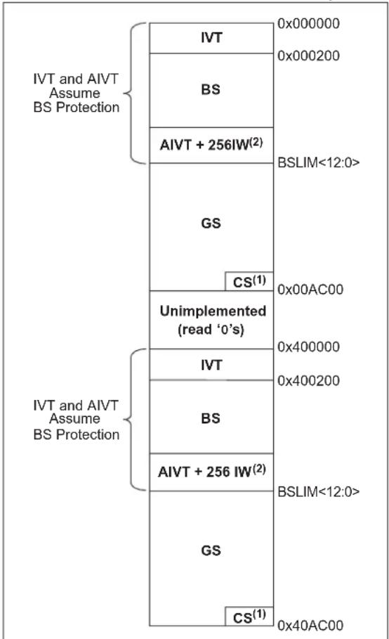
text_image
IVT and AIVT Assume BS Protection IVT 0x000000 BS 0x000200 AIVT + 256IW(2) BSLIM<12:0> GS CS(1) Unimplemented (read '0's) 0x00AC00 IVT 0x400000 BS 0x400200 AIVT + 256 IW(2) BSLIM<12:0> GS CS(1) 0x40AC00 IVT and AIVT Assume BS ProtectionNote 1: If CS is write-protected, the last page
(GS + CS) of program memory will be protected from an erase condition.
2: The last half (256 IW) of the last page of BS is unusable program memory.
NOTES:
28.0 INSTRUCTION SET SUMMARY
Note: This data sheet summarizes the features of the dsPIC33EPXXGS70X/80X family of devices. It is not intended to be a comprehensive reference source. To complement the information in this data sheet, refer to the related section of the "dsPIC33/PIC24 Family Reference Manual", which is available from the Microchip web site (www.microchip.com).
The dsPIC33EP instruction set is almost identical to that of the dsPIC30F and dsPIC33F.
Most instructions are a single program memory word (24 bits). Only three instructions require two program memory locations.
Each single-word instruction is a 24-bit word, divided into an 8-bit opcode, which specifies the instruction type and one or more operands, which further specify the operation of the instruction.
The instruction set is highly orthogonal and is grouped into five basic categories:
• Word or byte-oriented operations
- Bit-oriented operations
- Literal operations
- DSP operations
• Control operations
Table 28-1 lists the general symbols used in describing the instructions.
The dsPIC33E instruction set summary in Table 28-2 lists all the instructions, along with the status flags affected by each instruction.
Most word or byte-oriented W register instructions (including barrel shift instructions) have three operands:
- The first source operand, which is typically a register 'Wb' without any address modifier
- The second source operand, which is typically a register 'Ws' with or without an address modifier
- The destination of the result, which is typically a register 'Wd' with or without an address modifier
However, word or byte-oriented file register instructions have two operands:
- The file register specified by the value 'f'
- The destination, which could be either the file register 'f' or the W0 register, which is denoted as 'WREG'
Most bit-oriented instructions (including simple rotate/shift instructions) have two operands:
- The W register (with or without an address modifier) or file register (specified by the value of 'Ws' or 'f')
- The bit in the W register or file register (specified by a literal value or indirectly by the contents of register 'Wb')
The literal instructions that involve data movement can use some of the following operands:
- A literal value to be loaded into a W register or file register (specified by 'k')
- The W register or file register where the literal value is to be loaded (specified by 'Wb' or 'f')
However, literal instructions that involve arithmetic or logical operations use some of the following operands:
- The first source operand, which is a register 'Wb' without any address modifier
- The second source operand, which is a literal value
- The destination of the result (only if not the same as the first source operand), which is typically a register 'Wd' with or without an address modifier
The MAC class of DSP instructions can use some of the following operands:
- The accumulator (A or B) to be used (required operand)
- The W registers to be used as the two operands
• The X and Y address space prefetch operations
• The X and Y address space prefetch destinations
• The accumulator write back destination
The other DSP instructions do not involve any multiplication and can include:
• The accumulator to be used (required)
- The source or destination operand (designated as Wso or Wdo, respectively) with or without an address modifier
- The amount of shift specified by a W register 'Wn' or a literal value
The control instructions can use some of the following operands:
• A program memory address
- The mode of the Table Read and Table Write instructions
Most instructions are a single word. Certain double-word instructions are designed to provide all the required information in these 48 bits. In the second word, the eight MSbs are '0's. If this second word is executed as an instruction (by itself), it executes as a NOP.
The double-word instructions execute in two instruction cycles.
Most single-word instructions are executed in a single instruction cycle, unless a conditional test is true or the Program Counter is changed as a result of the instruction, or a PSV or Table Read is performed. In
these cases, the execution takes multiple instruction cycles, with the additional instruction cycle(s) executed as a NOR. Certain instructions that involve skipping over the subsequent instruction require either two or three cycles if the skip is performed, depending on whether the instruction being skipped is a single-word or two-word instruction. Moreover, double-word moves require two cycles.
Note: For more details on the instruction set, refer to the "16-Bit MCU and DSC Programmer's Reference Manual" (DS70000157).
TABLE 28-1: SYMBOLS USED IN OPCODE DESCRIPTIONS
| Field Description | |
| #text Means literal defined by "text" | |
| (text) Means "content of text" | |
| [text] Means "the location addressed by text" | |
| {} Optional field or operation | |
| a ∈ {b, c, d} a is selected from the set of values b, c, d | |
| .b | Byte mode selection |
| .d | Double-Word mode selection |
| .S Shadow register select | |
| .w | Word mode selection (default) |
| Acc | One of two accumulators {A, B} |
| AWB | Accumulator Write-Back Destination Address register ∈ {W13, [W13]+ = 2} |
| bit4 | 4-bit bit selection field (used in word addressed instructions) ∈ {0...15} |
| C, DC, N, OV, Z | MCU Status bits: Carry, Digit Carry, Negative, Overflow, Sticky Zero |
| Expr | Absolute address, label or expression (resolved by the linker) |
| f | File register address ∈ {0x0000...0x1FFF} |
| lit1 | 1-bit unsigned literal ∈ {0,1} |
| lit4 | 4-bit unsigned literal ∈ {0...15} |
| lit5 | 5-bit unsigned literal ∈ {0...31} |
| lit8 | 8-bit unsigned literal ∈ {0...255} |
| lit10 | 10-bit unsigned literal ∈ {0...255} for Byte mode, {0:1023} for Word mode |
| lit14 | 14-bit unsigned literal ∈ {0...16384} |
| lit16 | 16-bit unsigned literal ∈ {0...65535} |
| lit23 | 23-bit unsigned literal ∈ {0...8388608}; LSb must be '0' |
| None | Field does not require an entry, can be blank |
| OA, OB, SA, SB | DSP Status bits: ACCA Overflow, ACCB Overflow, ACCA Saturate, ACCB Saturate |
| PC | Program Counter |
| Slit10 | 10-bit signed literal ∈ {-512...511} |
| Slit16 | 16-bit signed literal ∈ {-32768...32767} |
| Slit6 | 6-bit signed literal ∈ {-16...16} |
| Wb | Base W register ∈ {W0...W15} |
| Wd | Destination W register ∈ { Wd, [Wd], [Wd++], [Wd--], [++Wd], [--Wd]} |
| Wdo | Destination W register ∈ { Wnd, [Wnd], [Wnd++], [Wnd--], [++Wnd], [--Wnd], [Wnd+Wb]} |
| Wm,Wn | Dividend, Divisor Working register pair (Direct Addressing) |
| Wm*Wm Multiplicand and Multiplier | Working register pair for Square instructions ∈{W4 * W4,W5 * W5,W6 * W6,W7 * W7} |
| Wm*Wn Multiplicand and Multiplier | Working register pair for DSP instructions ∈{W4 * W5,W4 * W6,W4 * W7,W5 * W6,W5 * W7,W6 * W7} |
| Wn One of 16 Working registers ∈ {W0...W15} | |
| Wnd One of 16 Destination Working registers ∈ {W0...W15} | |
| Wns One of 16 Source Working registers ∈ {W0...W15} | |
| WREG W0 (Working register used in file register instructions) | |
| Ws | Source W register ∈ {Ws, [Ws], [Ws++, [Ws--], [++Ws], [--Ws]} |
| Wso Source W register ∈ | { Wns, [Wns], [Wns++, [Wns--], [++Wns], [--Wns], [Wns+Wb]} |
| Wx X Data Space Prefetch Address | register for DSP instructions ∈ {[W8] += 6, [W8] += 4, [W8] += 2, [W8], [W8] -= 6, [W8] -= 4, [W8] -= 2,[W9] += 6, [W9] += 4, [W9] += 2, [W9], [W9] -= 6, [W9] -= 4, [W9] -= 2,[W9 + W12], none} |
| Wxd | X Data Space Prefetch Destination register for DSP instructions ∈ {W4...W7} |
| Wy Y Data Space Prefetch Address | register for DSP instructions ∈ {[W10] += 6, [W10] += 4, [W10] += 2, [W10], [W10] -= 6, [W10] -= 4, [W10] -= 2,[W11] += 6, [W11] += 4, [W11] += 2, [W11], [W11] -= 6, [W11] -= 4, [W11] -= 2,[W11 + W12], none} |
| Wyd | Y Data Space Prefetch Destination register for DSP instructions ∈ {W4...W7} |
TABLE 28-2: INSTRUCTION SET OVERVIEW
| Base Instr # | Assembly Mnemonic | Assembly Syntax Description | # of Words | # of Cycles(1) | Status Flags Affected | |
| 1 ADD | ADD Acc Add | Accumulators 1 1 OA,OB,SA,SB | ||||
| ADD f = f + WREG 1 1 C,DC,N,OV,Z | ||||||
| ADD f,WREG | WREG = f + WREG | 1 | 1 | C,DC,N,OV,Z | ||
| ADD #lit10,Wn | Wd = lit10 + Wd | 1 | 1 | C,DC,N,OV,Z | ||
| ADD Wb,Ws,Wd | Wd = Wb + Ws | 1 | 1 | C,DC,N,OV,Z | ||
| ADD Wc,#lit5,Wd | Wd = Wb + lit5 | 1 | 1 | C,DC,N,OV,Z | ||
| ADD Wso,#Slit4,Acc | 16-bit Signed Add to Accumulator | 1 | 1 | OA,OB,SA,SB | ||
| 2 | ADDC | ADDC f | f = f + WREG + (C) | 1 | 1 | C,DC,N,OV,Z |
| ADDC f,WREG | WREG = f + WREG + (C) | 1 | 1 | C,DC,N,OV,Z | ||
| ADDC #lit10,Wn | Wd = lit10 + Wd + (C) | 1 | 1 | C,DC,N,OV,Z | ||
| ADDC Wb,Ws,Wd | Wd = Wb + Ws + (C) | 1 | 1 | C,DC,N,OV,Z | ||
| ADDC Wc,#lit5,Wd | Wd = Wb + lit5 + (C) | 1 | 1 | C,DC,N,OV,Z | ||
| 3 | AND | AND f | f = f.AND.WREG | 1 | 1 | N,Z |
| AND f,WREG | WREG = f.AND.WREG | 1 | 1 | N,Z | ||
| AND #lit10,Wn | Wd = lit10.AND.Wd | 1 | 1 | N,Z | ||
| AND Wb,Ws,Wd | Wd = Wb.AND.Ws | 1 | 1 | N,Z | ||
| AND Wc,#lit5,Wd | Wd = Wb.AND.lit5 | 1 | 1 | N,Z | ||
| 4 | ASR | ASR f | f = Arithmetic Right Shift f | 1 | 1 | C,N,OV,Z |
| ASR f,WREG | WREG = Arithmetic Right Shift f | 1 | 1 | C,N,OV,Z | ||
| ASR Ws,Wd | Wd = Arithmetic Right Shift Ws | 1 | 1 | C,N,OV,Z | ||
| ASR Wc,Wns,Wnd | Wnd = Arithmetic Right Shift Wb by Wns | 1 | 1 | N,Z | ||
| ASR Wc,#lit5,Wnd | Wnd = Arithmetic Right Shift Wb by lit5 | 1 | 1 | N,Z | ||
| 5 | BCLR | BCLR f,#bit4 | Bit Clear f | 1 | 1 | None |
| BCLR Ws,#bit4 | Bit Clear Ws | 1 | 1 | None | ||
| 6 | BOOTSWP | BOOTSWP | Swap the Active and Inactive Program Flash Space | 1 | 2 | None |
| 7 | BRA | BRA C,Expr | Branch if Carry | 1 | 1 (4) | None |
| BRA GF,Expr | Branch if Greater Than or Equal | 1 | 1 (4) | None | ||
| BRA CEU,Expr | Branch if Unsigned Greater Than or Equal | 1 | 1 (4) | None | ||
| BRA GT,Expr | Branch if Greater Than | 1 | 1 (4) | None | ||
| BRA GTU,Expr | Branch if Unsigned Greater Than | 1 | 1 (4) | None | ||
| BRA LE,Expr | Branch if Less Than or Equal | 1 | 1 (4) | None | ||
| BRA LEU,Expr | Branch if Unsigned Less Than or Equal | 1 | 1 (4) | None | ||
| BRA LT,Expr | Branch if Less Than | 1 | 1 (4) | None | ||
| BRA LTU,Expr | Branch if Unsigned Less Than | 1 | 1 (4) | None | ||
| BRA N,Expr | Branch if Negative | 1 | 1 (4) | None | ||
| BRA NC,Expr | Branch if Not Carry | 1 | 1 (4) | None | ||
| BRA NN,Expr | Branch if Not Negative | 1 | 1 (4) | None | ||
| BRA NOV,Expr | Branch if Not Overflow | 1 | 1 (4) | None | ||
| BRA NZ,Expr | Branch if Not Zero | 1 | 1 (4) | None | ||
| BRA OA,Expr | Branch if Accumulator A Overflow | 1 | 1 (4) | None | ||
| BRA OB,Expr | Branch if Accumulator B Overflow | 1 | 1 (4) | None | ||
| BRA OV,Expr | Branch if Overflow | 1 | 1 (4) | None | ||
| BRA SA,Expr | Branch if Accumulator A Saturated | 1 | 1 (4) | None | ||
| BRA SB,Expr | Branch if Accumulator B Saturated | 1 | 1 (4) | None | ||
| BRA Expr | Branch Unconditionally | 1 | 4 | None | ||
| BRA Z,Expr | Branch if Zero | 1 | 1 (4) | None | ||
| BRA Wn | Computed Branch | 1 | 4 | None | ||
| 8 | BSET | BSET f,#bit4 | Bit Set f | 1 | 1 | None |
| BSET Ws,#bit4 | Bit Set Ws | 1 | 1 | None | ||
| Base Instr # | Assembly Mnemonic | Assembly Syntax | Description | # of Words | # of Cycles(1) | Status Flags Affected |
| 9 BSW | BSW.C Ws, Nb | Write C bit to Ws1 1 None | ||||
| BSW.Z Ws, Nb Write Z bit to Ws1 1 None | ||||||
| 10 BTG | BTG f,#bit4 | Bit Toggle f 1 1 None | ||||
| BTG Ws,#bit4 | Bit Toggle Ws | 1 | 1 | None | ||
| 11 | BTSC | BTSC f,#bit4 | Bit Test f, Skip if Clear | 1 | 1 (2 or 3) | None |
| BTSC Ws,#bit4 | Bit Test Ws, Skip if Clear | 1 | 1 (2 or 3) | None | ||
| 12 | BTSS | BTSS f,#bit4 | Bit Test f, Skip if Set | 1 | 1 (2 or 3) | None |
| BTSS Ws,#bit4 | Bit Test Ws, Skip if Set | 1 | 1 (2 or 3) | None | ||
| 13 | BTST | BTST f,#bit4 | Bit Test f | 1 | 1 | Z |
| BTST.C Ws,#bit4 | Bit Test Ws to C | 1 | 1 | C | ||
| BTST.Z Ws,#bit4 | Bit Test Ws to Z | 1 | 1 | Z | ||
| BTST.C Ws,Wb | Bit Test Wsto C | 1 | 1 | C | ||
| BTST.Z Ws,Wb | Bit Test Wsto Z | 1 | 1 | Z | ||
| 14 | BTSTS | BTSTS f,#bit4 | Bit Test then Set f | 1 | 1 | Z |
| BTSTS.C Ws,#bit4 | Bit Test Ws to C, then Set | 1 | 1 | C | ||
| BTSTS.Z Ws,#bit4 | Bit Test Ws to Z, then Set | 1 | 1 | Z | ||
| 15 | CALL | CALL lit23 | Call Subroutine | 2 | 4 | SFA |
| CALL Wn | Call Indirect Subroutine | 1 | 4 | SFA | ||
| CALL.L Wn | Call Indirect Subroutine (long address) | 1 | 4 | SFA | ||
| 16 | CLR | CLR f | f = 0x0000 | 1 | 1 | None |
| CLR WREG | WREG = 0x0000 | 1 | 1 | None | ||
| CLR Ws | Ws = 0x0000 | 1 | 1 | None | ||
| CLR Acc,Wx,Wxd,Wy,Wyd,NWB | Clear Accumulator | 1 | 1 | OA,OB,SA,SB | ||
| 17 | CLRWDT | CLRWDT | Clear Watchdog Timer | 1 | 1 | WDTO,Sleep |
| 18 | COM | COM f | f=f | 1 | 1 | N,Z |
| COM f,WREG WREG = f | WREG = f | 1 | 1 | N,Z | ||
| COM Ws,Wd Wd = Ws | — | 1 | 1 | N,Z | ||
| 19 | CP | CP f | Compare f with WREG | 1 | 1 | C,DC,N,OV,Z |
| CP Wb,#lit8 | Compare Wb with lit8 | 1 | 1 | C,DC,N,OV,Z | ||
| CP Wb,Ws | Compare Wb with Ws (Wb - Ws) | 1 | 1 | C,DC,N,OV,Z | ||
| 20 | CPO | CPO f | Compare f with 0x0000 | 1 | 1 | C,DC,N,OV,Z |
| CPO Ws | Compare Ws with 0x0000 | 1 | 1 | C,DC,N,OV,Z | ||
| 21 | CPB | CPB f | Compare f with WREG, with Borrow | 1 | 1 | C,DC,N,OV,Z |
| CPB Wb,#lit8 | Compare Wb with lit8, with Borrow | 1 | 1 | C,DC,N,OV,Z | ||
| CPB Wb,Ws Compare Wb with Ws, with Borrow | (Wb - Ws - C) | 1 1 | C,DC,N,OV,Z | |||
| 22 | CPSEQ | CPSEQ Wb,Wn | Compare Wb with Wn, Skip if = | 1 | 1 (2 or 3) | None |
| CPBEO | CPBEO Wb,Wn,Expr | Compare Wb with Wn, Branch if = | 1 | 1 (5) | None | |
| 23 | CPSGT | CPSGT Wb,Wn | Compare Wb with Wn, Skip if > | 1 | 1 (2 or 3) | None |
| CPBCT | CPBCT Wb,Wn,Expr | Compare Wb with Wn, Branch if > | 1 | 1 (5) | None | |
| 24 | CPSLT | CPSLT Wb,Wn | Compare Wb with Wn, Skip if < | 1 | 1 (2 or 3) | None |
| CPBLT | CPBLT Wb,Wn,Expr | Compare Wb with Wn, Branch if < | 1 | 1 (5) | None | |
| 25 | CPSNE | CPSNE Wb,Wn | Compare Wb with Wn, Skip if ≠ | 1 | 1 (2 or 3) | None |
| CPDNE | CPDNE Wb,Wn,Expr | Compare Wb with Wn, Branch if ≠ | 1 | 1 (5) | None | |
| 26 | CTXTSWP | CTXTSWP #lit3 | Switch CPU Register Context to Context Defined by lit3 | 1 | 2 | N |
| CTXTSWP Wn Switch CPU Register Context to Context Defined by Wn | 1 | 2 | N | |||
| 27 | DAW DAW Wn Wn = Decimal Adjust Wn 1 1 C | |||||
| 28 | DEC | DEC f | f=f-1 | 1 | 1 | C,DC,N,OV,Z |
| DEC f,WREG | WREG=f-1 | 1 | 1 | C,DC,N,OV,Z | ||
| DEC Ws,Wd | Wd=Ws-1 | 1 | 1 | C,DC,N,OV,Z | ||
| 29 | DEC2 | DEC2 f | f=f-2 | 1 | 1 | C,DC,N,OV,Z |
| DEC2 f,WREG | WREG=f-2 | 1 | 1 | C,DC,N,OV,Z | ||
| DEC2 Ws,Wd | Wd=Ws-2 | 1 | 1 | C,DC,N,OV,Z | ||
| 30 | DIS1 | DIS1 #lit14 | Disable Interrupts for k Instruction Cycles | 1 | 1 | None |
| 31 | DIV | DIV.S Wm,Wn | Signed 16/16-bit Integer Divide | 1 | 18 | N,Z,C,OV |
| DIV.SD Wm,Wn | Signed 32/16-bit Integer Divide | 1 | 18 | N,Z,C,OV | ||
| DIV.U Wm,Wn | Unsigned 16/16-bit Integer Divide | 1 | 18 | N,Z,C,OV | ||
| DIV.UD Wm,Wn | Unsigned 32/16-bit Integer Divide | 1 | 18 | N,Z,C,OV | ||
| 32 | DIVF | DIVF Wm,Wn | Signed 16/16-bit Fractional Divide | 1 | 18 | N,Z,C,OV |
| 33 | DO | DO #lit15,Expr | Do Code to PC + Expr, lit15+1 Times | 2 | 2 | None |
| DO Wn,Expr | Do Code to PC + Expr, (Wn)+1 Times | 2 | 2 | None | ||
| 34 | ED | ED Wm*Wm,Acc,Wx,Wy,Wxd | Euclidean Distance (no accumulate) | 1 | 1 | OA,OB,OAB, SA,SB,SAB |
| 35 | EDAC | EDAC Wm*Wm,Acc,Wx,Wy,Wxd | Euclidean Distance | 1 | 1 | OA,OB,OAB, SA,SB,SAB |
| 36 | EXCH | EXCH Wns,Wnd | Swap Wns with Wnd | 1 | 1 | None |
| 37 | FBCL | FBCL Ws,Wnd | Find Bit Change from Left (MSb) Side | 1 | 1 | C |
| 38 | FFIL | FFIL Ws,Wnd | Find First One from Left (MSb) Side | 1 | 1 | C |
| 39 | FFIR | FFIR Ws,Wnd | Find First One from Right (LSb) Side | 1 | 1 | C |
| 40 | GOTO | GOTO Expr | Go to Address | 2 | 4 | None |
| GOTO Wn | Go to Indirect | 1 | 4 | None | ||
| GOTO.L Wn | Go to Indirect (long address) | 1 | 4 | None | ||
| 41 | INC | INC f | f=f+1 | 1 | 1 | C,DC,N,OV,Z |
| INC f,WREG | WREG=f+1 | 1 | 1 | C,DC,N,OV,Z | ||
| INC Ws,Wd | Wd=Ws+1 | 1 | 1 | C,DC,N,OV,Z | ||
| 42 | INC2 | INC2 f | f=f+2 | 1 | 1 | C,DC,N,OV,Z |
| INC2 f,WREG | WREG=f+2 | 1 | 1 | C,DC,N,OV,Z | ||
| INC2 Ws,Wd | Wd=Ws+2 | 1 | 1 | C,DC,N,OV,Z | ||
| 43 | IOR | IOR f | f=f.IOR.WREG | 1 | 1 | N,Z |
| IOR f,WREG | WREG=f.IOR.WREG | 1 | 1 | N,Z | ||
| IOR #lit10,Wn | Wd=lit10.IOR.Wd | 1 | 1 | N,Z | ||
| IOR Wb,Ws,Wd | Wd=Wb.IOR.Ws | 1 | 1 | N,Z | ||
| IOR Wb,#lit5,Wd | Wd=Wb.IOR.lit5 | 1 | 1 | N,Z | ||
| 44 | LAC | LAC Wso,#Slit4,Acc | Load Accumulator | 1 | 1 | OA,OB,OAB, SA,SB,SAB |
| 45 | LNK | LNK #lit14 | Link Frame Pointer | 1 | 1 | SFA |
| 46 | LSR | LSR f | f=Logical Right Shift f | 1 | 1 | C,N,OV,Z |
| LSR f,WREG | WREG=Logical Right Shift f | 1 | 1 | C,N,OV,Z | ||
| LSR Ws,Wd | Wd=Logical Right Shift Ws | 1 | 1 | C,N,OV,Z | ||
| LSR Wb,Wns,Wnd | Wnd=Logical Right Shift Wb by Wns | 1 | 1 | N,Z | ||
| LSR Wb,#lit5,Wnd | Wnd=Logical Right Shift Wb by lit5 | 1 | 1 | N,Z | ||
| 47 | MAC | MAC Wm*Wn,Acc,Wx,Wxd,Wy,Wyd,AMB | Multiply and Accumulate | 1 | 1 | OA,OB,OAB, SA,SB,SAB |
| MAC Wm*Wn,Acc,Wx,Wxd,Wy,Wyd | Square and Accumulate | 1 | 1 | OA,OB,OAB, SA,SB,SAB | ||
| 48 MOV | MOV f,Wn | Move f to Wn 1 1 None | ||||
| MOV f Move f to f 1 1 None | ||||||
| MOV f,WREG Move f to WREG 1 1 None | ||||||
| MOV #lit16,Wn | Move 16-bit Literal to Wn | 1 | 1 | None | ||
| MOV.b #lit8,Wn | Move 8-bit Literal to Wn | 1 | 1 | None | ||
| MOV Wn,f Move Wn to f 1 1 None | ||||||
| MOV Wsc,Wdo | Move Ws to Wd | 1 | 1 | None | ||
| MOV WREG,f Move WREG to f 1 1 None | ||||||
| MOV.D Wns,Wd | Move Double from W(ns):W(ns + 1) to Wd | 1 | 2 | None | ||
| MOV.D Ws,Wnd | Move Double from Ws to W(nd + 1):W(nd) | 1 | 2 | None | ||
| 49 | MOVPAG | MOVPAG #lit10,DSRPAG | Move 10-bit Literal to DSRPAG | 1 | 1 | None |
| MOVPAG #lit8,TBLPAG | Move 8-bit Literal to TBLPAG | 1 | 1 | None | ||
| MOVPAGW Ws, DSRPAG | Move Ws<9:0> to DSRPAG | 1 | 1 | None | ||
| MOVPAGW Ws, TBLPAG | Move Ws<7:0> to TBLPAG | 1 | 1 | None | ||
| 50 | MOVSAC | MOVSAC Acc,Wx,Wxd,Wy,Wyd,AMB | Prefetch and Store Accumulator | 1 | 1 | None |
| 51 | MPY | MPY Wm*Wn,Acc,Wx,Wxd,Wy,Wyd | Multiply Wm by Wn to Accumulator | 1 | 1 | OA,OB,OAB,SA,SB,SAB |
| MPY Wm*Wm,Acc,Wx,Wxd,Wy,Wyd | Square Wm to Accumulator | 1 | 1 | OA,OB,OAB,SA,SB,SAB | ||
| 52 | MPY.N | MPY.N Wm*Wn,Acc,Wx,Wxd,Wy,Wyd | -(Multiply Wm by Wn) to Accumulator | 1 | 1 | None |
| 53 | MSC | MSC Wm*Wm,Acc,Wx,Wxd,Wy,Wyd,AMB | Multiply and Subtract from Accumulator | 1 | 1 | OA,OB,OAB,SA,SB,SAB |
| 54 | MUL | MUL.SS Wb,Ws,Wnd | {Wnd + 1,Wnd} = Signed(Wb) * Signed(Ws) | 1 | 1 | None |
| MUL.SS Wb,Ws,Acc | Accumulator = Signed(Wb) * Signed(Ws) | 1 | 1 | None | ||
| MUL.SU Wb,Ws,Wnd | {Wnd + 1,Wnd} = Signed(Wb) * Unsigned(Ws) | 1 | 1 | None | ||
| MUL.SU Wb,Ws,Acc | Accumulator = Signed(Wb) * Unsigned(Ws) | 1 | 1 | None | ||
| MUL.SU Wb,#lit5,Acc | Accumulator = Signed(Wb) * Unsigned(lit5) | 1 | 1 | None | ||
| MUL.US Wb,Ws,Wnd | {Wnd + 1,Wnd} = Unsigned(Wb) * Signed(Ws) | 1 | 1 | None | ||
| MUL.US Wb,Ws,Acc | Accumulator = Unsigned(Wb) * Signed(Ws) | 1 | 1 | None | ||
| MUL.UU Wb,Ws,Wnd | {Wnd + 1,Wnd} = Unsigned(Wb) * Unsigned(Ws) | 1 | 1 | None | ||
| MUL.UU Wb,#lit5,Acc | Accumulator = Unsigned(Wb) * Unsigned(lit5) | 1 | 1 | None | ||
| MUL.UU Wb,Ws,Acc | Accumulator = Unsigned(Wb) * Unsigned(Ws) | 1 | 1 | None | ||
| MULW.SS Wb,Ws,Wnd | Wnd = Signed(Wb) * Signed(Ws) | 1 | 1 | None | ||
| MULW.SU Wb,Ws,Wnd | Wnd = Signed(Wb) * Unsigned(Ws) | 1 | 1 | None | ||
| MULW.US Wb,Ws,Wnd | Wnd = Unsigned(Wb) * Signed(Ws) | 1 | 1 | None | ||
| MULW.UU Wb,Ws,Wnd | Wnd = Unsigned(Wb) * Unsigned(Ws) | 1 | 1 | None | ||
| MUL.SU Wb,#lit5,Wnd | {Wnd + 1,Wnd} = Signed(Wb) * Unsigned(lit5) | 1 | 1 | None | ||
| MUL.SU Wb,#lit5,Wnd | Wnd = Signed(Wb) * Unsigned(lit5) | 1 | 1 | None | ||
| MUL.UU Wb,#lit5,Wnd | {Wnd + 1,Wnd} = Unsigned(Wb) * Unsigned(lit5) | 1 | 1 | None | ||
| MUL.UU Wb,#lit5,Wnd | Wnd = Unsigned(Wb) * Unsigned(lit5) | 1 | 1 | None | ||
| MUL fNegate Accumulator 1 1 OA,OB,OAB, | W3:W2 = f * WREG | 1 | 1 | NoneSA,SB,SAB | ||
| 55 NEG | NEG Acc | |||||
| NEG f=f | +1 1 1 C,DC,N,OV,Z | |||||
| NEG f,WREG WREG=f | +1 1 1 C,DC,N,OV,Z | |||||
| NFG Ws,Wd | Wd=Ws +1 | 1 1 C | DC,N,OV,Z | |||
| 56 | NOP | NOP | No Operation | 1 | 1 | None |
| NOPR | No Operation | 1 | 1 | None | ||
| 57 | POP | POP f | Pop f from Top-of-Stack (TOS) | 1 | 1 | None |
| POP Wdo | Pop from Top-of-Stack (TOS) to Wdo | 1 | 1 | None | ||
| POP.D Wnd | Pop from Top-of-Stack (TOS) to W(nd):W(nd + 1) | 1 | 2 | None | ||
| POP.S | Pop Shadow Registers | 1 | 1 | All | ||
| 58 | PUSH | PUSH f | Push f to Top-of-Stack (TOS) | 1 | 1 | None |
| PUSH Wso | Push Wso to Top-of-Stack (TOS) | 1 | 1 | None | ||
| PUSH.D Wns | Push W(ns):W(ns + 1) to Top-of-Stack (TOS) | 1 | 2 | None | ||
| PUSH.S | Push Shadow Registers | 1 | 1 | None | ||
| 59 | PWRSAV | PWRSAV #lit1 | Go into Sleep or Idle mode | 1 | 1 | WDTO,Sleep |
| 60 | RCALL | RCALL Expr | Relative Call | 1 | 4 | SFA |
| RCALL Wn | Computed Call | 1 | 4 | SFA | ||
| 61 | REPEAT | REPEAT #lit15 | Repeat Next Instruction lit15 + 1 Times | 1 | 1 | None |
| REPEAT Wn | Repeat Next Instruction (Wn) + 1 Times | 1 | 1 | None | ||
| 62 | RESET | RESET | Software Device Reset | 1 | 1 | None |
| 63 | RETFIE | RETFIE | Return from Interrupt | 1 | 6 (5) | SFA |
| 64 | RETLW | RETLW #lit10,Wn | Return with Literal in Wn | 1 | 6 (5) | SFA |
| 65 | RETURN | RETURN | Return from Subroutine | 1 | 6 (5) | SFA |
| 66 | RLC | RLC f | f = Rotate Left through Carry f | 1 | 1 | C,N,Z |
| RLC f,WREG | WREG = Rotate Left through Carry f | 1 | 1 | C,N,Z | ||
| RLC Ws,Wd | Wd = Rotate Left through Carry Ws | 1 | 1 | C,N,Z | ||
| 67 | RLNC | RLNC f | f = Rotate Left (No Carry) f | 1 | 1 | N,Z |
| RLNC f,WREG | WREG = Rotate Left (No Carry) f | 1 | 1 | N,Z | ||
| RLNC Ws,Wd | Wd = Rotate Left (No Carry) Ws | 1 | 1 | N,Z | ||
| 68 | RRC | RRC f | f = Rotate Right through Carry f | 1 | 1 | C,N,Z |
| RRC f,WREG | WREG = Rotate Right through Carry f | 1 | 1 | C,N,Z | ||
| RRC Ws,Wd | Wd = Rotate Right through Carry Ws | 1 | 1 | C,N,Z | ||
| 69 | RRNC | RRNC f | f = Rotate Right (No Carry) f | 1 | 1 | N,Z |
| RRNC f,WREG | WREG = Rotate Right (No Carry) f | 1 | 1 | N,Z | ||
| RRNC Ws,Wd | Wd = Rotate Right (No Carry) Ws | 1 | 1 | N,Z | ||
| 70 | SAC | SAC Acc,#Slit4,Wdo | Store Accumulator | 1 | 1 | None |
| SAC.R Acc,#Slit4,Wdo | Store Rounded Accumulator | 1 | 1 | None | ||
| 71 | SE | SE Ws,Wnd | Wnd = Sign-Extended Ws | 1 | 1 | C,N,Z |
| 72 | SETM | SETM f | f = 0xFFFF | 1 | 1 | None |
| SETM WREG | WREG = 0xFFFF | 1 | 1 | None | ||
| SETM Ws | Ws = 0xFFFF | 1 | 1 | None | ||
| 73 | SFTAC | SFTAC Acc,Wn | Arithmetic Shift Accumulator by (Wn) | 1 | 1 | OA,OB,OAB, SA,SB,SAB |
| SFTAC Acc,#Slit6 | Arithmetic Shift Accumulator by Slit6 | 1 1 OA,OB,OAB, SA,SB,SAB | ||||
| 74 SL | SL f = Left | Shift f 1 1 C,N,OV,Z | ||||
| SL f,WREG WREG = Left Shift f 1 1 C,N,OV,Z | ||||||
| SL Ms,Wd Wd = Left Shift Ws 1 1 C,N,OV,Z | ||||||
| SL Wb,Wns,Wnd | Wnd = Left Shift Wb by Wns | 1 | 1 | N,Z | ||
| SL Wb,#lit5,Wnd | Wnd = Left Shift Wb by lit5 | 1 | 1 | N,Z | ||
| 75 | SUB | SUB Acc | Subtract Accumulators | 1 | 1 | OA,OB,OAB,SA,SB,SAB |
| SUB f | f = f - WREG | 1 | 1 | C,DC,N,OV,Z | ||
| SUB f,WREG | WREG = f - WREG | 1 | 1 | C,DC,N,OV,Z | ||
| SUB #lit10,Wn | Wn = Wn - lit10 | 1 | 1 | C,DC,N,OV,Z | ||
| SUB wb,ws,Wd | Wd = Wb - Ws | 1 | 1 | C,DC,N,OV,Z | ||
| SUB wb,#lit5,Wd | Wd = Wb - lit5 | 1 | 1 | C,DC,N,OV,Z | ||
| 76 | SUBB | SUBB f | f = f - WREG - (C) | 1 1 | C,DC,N,OV,Z | |
| SUBB f,WREG WREG = f - WREG - (C) | - ) | 1 1 | C,DC,N,OV,Z | |||
| SUBB #lit10,Wn | Wn = Wn - lit10 - (C) | 1 1 | C,DC,N,OV,Z | |||
| SUBB wb,ws,Wd | Wd = Wb - Ws - (C) 1 1 C,DC,N,OV,Z | |||||
| SUBB wb,#lit5,Wd | Wd = Wb - lit5 - (C) | 1 1 | C,DC,N,OV,Z | |||
| 77 | SUBR | SUBR f | f = WREG - f | 1 | 1 | C,DC,N,OV,Z |
| SUBR f,WREG | WREG = WREG - f | 1 | 1 | C,DC,N,OV,Z | ||
| SUBR wb,ws,Wd | Wd = Ws - Wb | 1 | 1 | C,DC,N,OV,Z | ||
| SUBR wb,#lit5,Wd | Wd = lit5 - Wb | 1 | 1 | C,DC,N,OV,Z | ||
| 78 | SUBBR | SUBBR f | f = WREG - f - (C) | 1 | 1 | C,DC,N,OV,Z |
| SUBBR f,WREG WREG = WREG - f - (C) | - ) | 1 | 1 | C,DC,N,OV,Z | ||
| SUBBR wb,ws,Wd | Wd = Ws - Wb - (C) 1 1 C,DC,N,OV,Z | |||||
| SUBBR wb,#lit5,Wd | Wd = lit5 - Wb - (C) | 1 | 1 | C,DC,N,OV,Z | ||
| 79 | SWAP | SWAP.b Wn | Wn = Nibble Swap Wn | 1 | 1 | None |
| SWAP Wn | Wn = Byte Swap Wn | 1 | 1 | None | ||
| 80 | TBLRDH | TBLRDH Ws,Wd | Read Prog<23:16> to Wd<7:0> | 1 | 5 | None |
| 81 | TBLRDL | TBLRDL Ws,Wd | Read Prog<15:0> to Wd | 1 | 5 | None |
| 82 | TBLMTH | TBLMTH Ws,Wd | Write Ws<7:0> to Prog<23:16> | 1 | 2 | None |
| 83 | TBLMTL | TBLMTL Ws,Wd | Write Ws to Prog<15:0> | 1 | 2 | None |
| 84 | ULNK | ULNK | Unlink Frame Pointer | 1 | 1 | SFA |
| 85 | XOR | XOR f | f = f .XOR. WREG | 1 | 1 | N,Z |
| XOR f,WREG | WREG = f .XOR. WREG | 1 | 1 | N,Z | ||
| XOR #lit10,Wn | Wd = lit10 .XOR. Wd | 1 | 1 | N,Z | ||
| XOR wb,ws,Wd | Wd = Wb .XOR. Ws | 1 | 1 | N,Z | ||
| XOR wb,#lit5,Wd | Wd = Wb .XOR. lit5 | 1 | 1 | N,Z | ||
| 86 | ZE | ZE Ws,Wnd | Wnd = Zero-Extend Ws | 1 | 1 | C,Z,N |
Note 1: Read and Read-Modify-Write (e.g., bit operations and logical operations) on non-CPU SFRs incur an additional instruction cycle.
NOTES:
29.0 DEVELOPMENT SUPPORT
The PIC ^® microcontrollers (MCU) and dsPIC ^® digital signal controllers (DSC) are supported with a full range of software and hardware development tools:
- Integrated Development Environment - MPLAB ^® X IDE Software
- Compilers/Assemblers/Linkers
- MPLAB XC Compiler
- MPASM ^TM Assembler
- M P L ^TM Object Linker/MPLIB ^TM Object Librarian
- MPLAB Assembler/Linker/Librarian for Various Device Families
- Simulators
- MPLAB X SIM Software Simulator
- Emulators
- MPLAB REAL ICE™ In-Circuit Emulator
- In-Circuit Debuggers/Programmers - MPLAB ICD 3 - PICkit™ 3
• Device Programmers
- MPLAB PM3 Device Programmer
- Low-Cost Demonstration/Development Boards, Evaluation Kits and Starter Kits
• Third-party development tools
29.1 MPLAB X Integrated Development Environment Software
The MPLAB X IDE is a single, unified graphical user interface for Microchip and third-party software, and hardware development tool that runs on Windows ^® , Linux and Mac OS ^® X. Based on the NetBeans IDE, MPLAB X IDE is an entirely new IDE with a host of free software components and plug-ins for high-performance application development and debugging. Moving between tools and upgrading from software simulators to hardware debugging and programming tools is simple with the seamless user interface.
With complete project management, visual call graphs, a configurable watch window and a feature-rich editor that includes code completion and context menus, MPLAB X IDE is flexible and friendly enough for new users. With the ability to support multiple tools on multiple projects with simultaneous debugging, MPLAB X IDE is also suitable for the needs of experienced users.
Feature-Rich Editor:
• Color syntax highlighting
- Smart code completion makes suggestions and provides hints as you type
• Automatic code formatting based on user-defined rules
- Live parsing
User-Friendly, Customizable Interface:
- Fully customizable interface: toolbars, toolbar buttons, windows, window placement, etc.
- Call graph window
Project-Based Workspaces:
- Multiple projects
- Multiple tools
- Multiple configurations
- Simultaneous debugging sessions
File History and Bug Tracking:
- Local file history feature
• Built-in support for Bugzilla issue tracker
29.2 MPLAB XC Compilers
The MPLAB XC Compilers are complete ANSI C compilers for all of Microchip's 8, 16 and 32-bit MCU and DSC devices. These compilers provide powerful integration capabilities, superior code optimization and ease of use. MPLAB XC Compilers run on Windows, Linux or MAC OS X.
For easy source level debugging, the compilers provide debug information that is optimized to the MPLAB X IDE.
The free MPLAB XC Compiler editions support all devices and commands, with no time or memory restrictions, and offer sufficient code optimization for most applications.
MPLAB XC Compilers include an assembler, linker and utilities. The assembler generates relocatable object files that can then be archived or linked with other relocatable object files and archives to create an executable file. MPLAB XC Compiler uses the assembler to produce its object file. Notable features of the assembler include:
- Support for the entire device instruction set
- Support for fixed-point and floating-point data
- Command-line interface
- Rich directive set
- Flexible macro language
- MPLAB X IDE compatibility
29.3 MPASM Assembler
The MPASM Assembler is a full-featured, universal macro assembler for PIC10/12/16/18 MCUs.
The MPASM Assembler generates relocatable object files for the MPLINK Object Linker, Intel ^® standard HEX files, MAP files to detail memory usage and symbol reference, absolute LST files that contain source lines and generated machine code, and COFF files for debugging.
The MPASM Assembler features include:
• Integration into MPLAB X IDE projects
- User-defined macros to streamline assembly code
- Conditional assembly for multipurpose source files
- Directives that allow complete control over the assembly process
29.4 MPLINK Object Linker/MPLIB Object Librarian
The MPLINK Object Linker combines relocatable objects created by the MPASM Assembler. It can link relocatable objects from precompiled libraries, using directives from a linker script.
The MPLIB Object Librarian manages the creation and modification of library files of precompiled code. When a routine from a library is called from a source file, only the modules that contain that routine will be linked in with the application. This allows large libraries to be used efficiently in many different applications.
The object linker/library features include:
- Efficient linking of single libraries instead of many smaller files
- Enhanced code maintainability by grouping related modules together
- Flexible creation of libraries with easy module listing, replacement, deletion and extraction
29.5 MPLAB Assembler, Linker and Librarian for Various Device Families
MPLAB Assembler produces relocatable machine code from symbolic assembly language for PIC24, PIC32 and dsPIC DSC devices. MPLAB XC Compiler uses the assembler to produce its object file. The assembler generates relocatable object files that can then be archived or linked with other relocatable object files and archives to create an executable file. Notable features of the assembler include:
- Support for the entire device instruction set
- Support for fixed-point and floating-point data
- Command-line interface
- Rich directive set
- Flexible macro language
- MPLAB X IDE compatibility
29.6 MPLAB X SIM Software Simulator
The MPLAB X SIM Software Simulator allows code development in a PC-hosted environment by simulating the PIC MCUs and dsPIC DSCs on an instruction level. On any given instruction, the data areas can be examined or modified and stimuli can be applied from a comprehensive stimulus controller. Registers can be logged to files for further run-time analysis. The trace buffer and logic analyzer display extend the power of the simulator to record and track program execution, actions on I/O, most peripherals and internal registers.
The MPLAB X SIM Software Simulator fully supports symbolic debugging using the MPLAB XC Compilers, and the MPASM and MPLAB Assemblers. The software simulator offers the flexibility to develop and debug code outside of the hardware laboratory environment, making it an excellent, economical software development tool.
29.7 MPLAB REAL ICE In-Circuit Emulator System
The MPLAB REAL ICE In-Circuit Emulator System is Microchip's next generation high-speed emulator for Microchip Flash DSC and MCU devices. It debugs and programs all 8, 16 and 32-bit MCU, and DSC devices with the easy-to-use, powerful graphical user interface of the MPLAB X IDE.
The emulator is connected to the design engineer's PC using a high-speed USB 2.0 interface and is connected to the target with either a connector compatible with in-circuit debugger systems (RJ-11) or with the new high-speed, noise tolerant, Low-Voltage Differential Signal (LVDS) interconnection (CAT5).
The emulator is field upgradable through future firmware downloads in MPLAB X IDE. MPLAB REAL ICE offers significant advantages over competitive emulators including full-speed emulation, run-time variable watches, trace analysis, complex breakpoints, logic probes, a ruggedized probe interface and long (up to three meters) interconnection cables.
29.8 MPLAB ICD 3 In-Circuit Debugger System
The MPLAB ICD 3 In-Circuit Debugger System is Microchip's most cost-effective, high-speed hardware debugger/programmer for Microchip Flash DSC and MCU devices. It debugs and programs PIC Flash microcontrollers and dsPIC DSCs with the powerful, yet easy-to-use graphical user interface of the MPLAB IDE.
The MPLAB ICD 3 In-Circuit Debugger probe is connected to the design engineer's PC using a high-speed USB 2.0 interface and is connected to the target with a connector compatible with the MPLAB ICD 2 or MPLAB REAL ICE systems (RJ-11). MPLAB ICD 3 supports all MPLAB ICD 2 headers.
29.9 PICkit 3 In-Circuit Debugger/Programmer
The MPLAB PICkit 3 allows debugging and programming of PIC and dsPIC Flash microcontrollers at a most affordable price point using the powerful graphical user interface of the MPLAB IDE. The MPLAB PICkit 3 is connected to the design engineer's PC using a full-speed USB interface and can be connected to the target via a Microchip debug (RJ-11) connector (compatible with MPLAB ICD 3 and MPLAB REAL ICE). The connector uses two device I/O pins and the Reset line to implement in-circuit debugging and In-Circuit Serial Programming™ (ICSP™).
29.10 MPLAB PM3 Device Programmer
The MPLAB PM3 Device Programmer is a universal, CE compliant device programmer with programmable voltage verification at VDDMIN and VDDMAX for maximum reliability. It features a large LCD display (128 x 64) for menus and error messages, and a modular, detachable socket assembly to support various package types. The ICSP cable assembly is included as a standard item. In Stand-Alone mode, the MPLAB PM3 Device Programmer can read, verify and program PIC devices without a PC connection. It can also set code protection in this mode. The MPLAB PM3 connects to the host PC via an RS-232 or USB cable. The MPLAB PM3 has high-speed communications and optimized algorithms for quick programming of large memory devices, and incorporates an MMC card for file storage and data applications.
29.11 Demonstration/Development Boards, Evaluation Kits and Starter Kits
A wide variety of demonstration, development and evaluation boards for various PIC MCUs and dsPIC DSCs allows quick application development on fully functional systems. Most boards include prototyping areas for adding custom circuitry and provide application firmware and source code for examination and modification.
The boards support a variety of features, including LEDs, temperature sensors, switches, speakers, RS-232 interfaces, LCD displays, potentiometers and additional EEPROM memory.
The demonstration and development boards can be used in teaching environments, for prototyping custom circuits and for learning about various microcontroller applications.
In addition to the PICDEM™ and dsPICDEM™ demonstration/development board series of circuits, Microchip has a line of evaluation kits and demonstration software for analog filter design, KEELoQ® security ICs, CAN, IrDA®, PowerSmart battery management, SEEVAL® evaluation system, Sigma-Delta ADC, flow rate sensing, plus many more.
Also available are starter kits that contain everything needed to experience the specified device. This usually includes a single application and debug capability, all on one board.
Check the Microchip web page (www.microchip.com) for the complete list of demonstration, development and evaluation kits.
29.12 Third-Party Development Tools
Microchip also offers a great collection of tools from third-party vendors. These tools are carefully selected to offer good value and unique functionality.
• Device Programmers and Gang Programmers from companies, such as SoftLog and CCS
- Software Tools from companies, such as Gimpel and Trace Systems
- Protocol Analyzers from companies, such as Saleae and Total Phase
- Demonstration Boards from companies, such as MikroElektronika, Digilent® and Olimex
- Embedded Ethernet Solutions from companies, such as EZ Web Lynx, WIZnet and IPLogika®
30.0 ELECTRICAL CHARACTERISTICS
This section provides an overview of the dsPIC33EPXXXGS70X/80X family electrical characteristics. Additional information will be provided in future revisions of this document as it becomes available.
Absolute maximum ratings for the dsPIC33EPXXXGS70X/80X family are listed below. Exposure to these maximum rating conditions for extended periods may affect device reliability. Functional operation of the device at these, or any other conditions above the parameters indicated in the operation listings of this specification, is not implied.
Absolute Maximum Ratings ^(1)
Ambient temperature under bias....-40°C to +125°C
Storage temperature -65°C to +150°C
Voltage on VDD with respect to Vss -0.3V to +4.0V
Voltage on any pin that is not 5V tolerant with respect to Vs^(3) -0.3V to (V_DD + 0.3V)
Voltage on any 5V tolerant pin with respect to Vss when V_DD ≥ 3.0V^(3) -0.3V to +5.5V
Voltage on any 5V tolerant pin with respect to Vss when V_DD < 3.0V^(3) -0.3V to +3.6V
Maximum current out of V ss pin ....300 mA
Maximum current into VDD pin ^(2) 300 mA
Maximum current sunk/sourced by any 4x I/O pin....15 mA
Maximum current sunk/sourced by any 8x I/O pin....25 mA
Maximum current sunk by all ports ^(2) 200 mA
Note 1: Stresses above those listed under “Absolute Maximum Ratings” may cause permanent damage to the device. This is a stress rating only and functional operation of the device at those, or any other conditions above those indicated in the operation listings of this specification, is not implied. Exposure to maximum rating conditions for extended periods may affect device reliability.
2: Maximum allowable current is a function of device maximum power dissipation (see Table 30-2).
3: See the "Pin Diagrams" section for the 5V tolerant pins.
30.1 DC Characteristics
TABLE 30-1: OPERATING MIPS vs. VOLTAGE
| Characteristic | VDD Range (in Volts) | Temperature Range (in °C) | Maximum MIPS |
| dsPIC33EPXXXGS70X/80X Family | |||
| — 3.0V to 3.6V (1) | -40°C to +85°C 70 | ||
| — 3.0V to 3.6V (1) | -40°C to +125°C 60 | ||
Note 1: Device is functional at VBORMIN < VDD < VDDMIN. Analog modules (ADC, PGAs and comparators) may have degraded performance. Device functionality is tested but not characterized. Refer to Parameter BO10 in Table 30-13 for the minimum and maximum BOR values.
TABLE 30-2: THERMAL OPERATING CONDITIONS
| Rating Symbol Min. Typ. Max. | Unit | ||||
| Industrial Temperature Devices | |||||
| Operating Junction Temperature Range | TJ | -40 | — | +125 | °C |
| Operating Ambient Temperature Range | TA | -40 | — | +85 | °C |
| Extended Temperature Devices | |||||
| Operating Junction Temperature Range | TJ | -40 | — | +140 | °C |
| Operating Ambient Temperature Range | TA | -40 | — | +125 | °C |
| Power Dissipation: | |||||
| Internal Chip Power Dissipation: P_INT = V_DD × (I_DD - I_OH) I/O Pin Power Dissipation: I/O = (_DD - V_OH × I_OH) + (V_OL × I_OL) | PD | P_INT + P_I/O | W | ||
| Maximum Allowed Power Dissipation | P_DMAX | (T_J - T_A)/0JA | W | ||
TABLE 30-3: THERMAL PACKAGING CHARACTERISTICS
| Characteristic | Symbol | Typ. | Max. | Unit | Notes |
| Package Thermal Resistance, 80-Pin TQFP 12x12x1 mm | _JA | 53.0 | — | °C/W | 1 |
| Package Thermal Resistance, 64-Pin TQFP 10x10x1 mm | _JA | 49.0 | — | °C/W | 1 |
| Package Thermal Resistance, 48-Pin TQFP 7x7x1 mm | _JA | 63.0 | — | °C/W | 1 |
| Package Thermal Resistance, 44-Pin QFN 8x8 mm | _JA | 29.0 | — | °C/W | 1 |
| Package Thermal Resistance, 44-Pin TQFP 10x10x1 mm | _JA | 50.0 | — | °C/W | 1 |
| Package Thermal Resistance, 28-Pin QFN-S 6x6x0.9 mm | _JA | 30.0 | — | °C/W | 1 |
| Package Thermal Resistance, 28-Pin UQFN 6x6x0.55 mm | _JA | 26.0 | — | °C/W | 1 |
| Package Thermal Resistance, 28-Pin SOIC 7.50 mm | _JA | 70.0 | — | °C/W | 1 |
Note 1: Junction to ambient thermal resistance, Theta- JA ( JA) numbers are achieved by package simulations.
TABLE 30-4: DC TEMPERATURE AND VOLTAGE SPECIFICATIONS
| DC CHARACTERISTICS | Standard Operating Conditions: 3.0V to 3.6V(unless otherwise stated)(1)Operating temperature -40°C ≤ TA ≤ +85°C for Industrial-40°C ≤ AT ≤ +125°C for Extended | ||||||
| Param No. | Symbol | Characteristic Min. Typ. Max. Units | Conditions | ||||
| Operating Voltage | |||||||
| DC10 V | DD | Supply Voltage | 3.0 | — | 3.6 | V | |
| DC12 VDR RAM R | Retention Voltage (2) | — | — | 1.95 | V | +25°C, +85°C, +125°C | |
| — | — | 2.0 | V | -40°C | |||
| DC16 V | POR | VDD Start Voltageto Ensure InternalPower-on Reset Signal | — | — | Vss | V | |
| DC17 S | VDD VDD Rise Rateto Ensure InternalPower-on Reset Signal | 1.0 | — | — | V/ms 0 | V-3V in 3 ms | |
Note 1: Device is functional at VBORMIN < VDD < VDDMIN. Analog modules (ADC, PGAs and comparators) may have degraded performance. Device functionality is tested but not characterized. Refer to Parameter BO10 in Table 30-13 for the minimum and maximum BOR values.
2: This is the limit to which V DD may be lowered and the RAM contents will always be retained.
TABLE 30-5: FILTER CAPACITOR (CEFC) SPECIFICATIONS
| Standard Operating Conditions (unless otherwise stated):Operating temperature -40°C ≤ TA ≤ +85°C for Industrial-40°C ≤ AT ≤ +125°C for Extended | |||||||
| Param No. | Symbol | Characteristics | Min. | Typ. | Max. | Units | Comments |
| CEFC | External Filter Capacitor Value(1) | 4.7 | — | 10 | μF | Capacitor must have a low series resistance (<1 Ohm) | |
Note 1: Typical V CAP Voltage = 1.8 volts when VDD ≥ VDDMIN.
TABLE 30-6: DC CHARACTERISTICS: OPERATING CURRENT (IDD)
| DC CHARACTERISTICS | Standard Operating Conditions: 3.0V to 3.6V(unless otherwise stated)Operating temperature -40°C ≤ TA ≤ +85°C for Industrial-40°C ≤ AT ≤ +125°C for Extended | |||||
| Parameter No. | Typ. Max. Units Conditions | |||||
| Operating Current (IDD)(1) | ||||||
| DC20d 8 13 mA | -40°C | 3.3V 10 MIPS | ||||
| DC20a 8 13 mA | +25°C | |||||
| DC20b 8 13 mA | +85°C | |||||
| DC20c | 8 13 mA | +125°C | ||||
| DC22d | 12 | 20 mA | -40°C | 3.3V 20 MIPS | ||
| DC22a | 12 | 20 | mA +25°C | |||
| DC22b | 12 | 20 | mA +85°C | |||
| DC22c | 12 | 20 | mA | +125°C | ||
| DC24d | 19 | 30 | mA -40°C | 3.3V 40 MIPS | ||
| DC24a | 19 | 30 | mA +25°C | |||
| DC24b | 19 | 30 | mA +85°C | |||
| DC24c | 19 | 30 | mA | +125°C | ||
| DC25d | 27 | 42 | mA -40°C | 3.3V 60 MIPS | ||
| DC25a | 27 | 42 | mA +25°C | |||
| DC25b | 27 | 42 | mA +85°C | |||
| DC25c | 27 | 42 | mA | +125°C | ||
| DC26d | 30 | 46 | mA -40°C | 3.3V | 70 MIPS | |
| DC26a | 30 | 46 | mA | +25°C | ||
| DC26b | 30 | 46 | mA +85°C | |||
| DC27d | 57 | 75 | mA -40°C | 3.3V | 70 MIPS(Note 2) | |
| DC27a | 57 | 75 | mA +25°C | |||
| DC27b | 57 | 75 | mA +85°C | |||
Note 1: IDD is primarily a function of the operating voltage and frequency. Other factors, such as I/O pin loading and switching rate, oscillator type, internal code execution pattern and temperature, also have an impact on the current consumption. The test conditions for all DD measurements are as follows:
- Oscillator is configured in EC mode with PLL, OSC1 is driven with external square wave from rail-to-rail (EC clock overshoot/undershoot < 250 mV required)
- CLKO is configured as an I/O input pin in the Configuration Word
- All I/O pins are configured as inputs and pulled to Vss
- = V_DD , WDT and FSCM are disabled
• CPU, SRAM, program memory and data memory are operational
- No peripheral modules are operating or being clocked (all defined PMDx bits are set)
• CPU is executing while(1) statement
- JTAG is disabled
2: For this specification, the following test conditions apply:
- APLL clock is enabled
- All 8 PWMs enabled and operating at maximum speed (PTCON2<2:0> = 0.00), PTPER = 1000h, 50% duty cycle
- All other peripherals are disabled (corresponding PMDx bits are set)
TABLE 30-7: DC CHARACTERISTICS: IDLE CURRENT (IIDLE)
| DC CHARACTERISTICS | Standard Operating Conditions: 3.0V to 3.6V(unless otherwise stated)Operating temperature -40°C ≤ TA ≤ +85°C for Industrial-40°C ≤ TA ≤ +125°C for Extended | |||||
| Parameter No. | Typ. Max. Units Conditions | |||||
| Idle Current (IDLE)(1) | ||||||
| DC40d 2 4 mA | -40°C | 3.3V 10 MIPS | ||||
| DC40a 2 4 mA | +25°C | |||||
| DC40b 2 4 mA | +85°C | |||||
| DC40c 2 4 mA | +125°C | |||||
| DC42d 3 6 mA | -40°C | 3.3V 20 MIPS | ||||
| DC42a 3 6 mA | +25°C | |||||
| DC42b 4 7 mA | +85°C | |||||
| DC42c 4 7 mA | +125°C | |||||
| DC44d 6 | 12 | mA -40°C | 3.3V 40 MIPS | |||
| DC44a 6 | 12 | mA +25°C | ||||
| DC44b 6 | mA +85°C | |||||
| DC44c | 6 | 12 | mA | +125°C | ||
| DC45d 9 | 17 | mA -40°C | 3.3V 60 MIPS | |||
| DC45a 9 | 17 | mA +25°C | ||||
| DC45b 9 | mA +85°C | |||||
| DC45c | 9 | 17 | mA | +125°C | ||
| DC46d | 10 | 20 | mA -40°C | 3.3V | 70 MIPS | |
| DC46a | 10 | 20 | mA | +25°C | ||
| DC46b | 10 | 20 | mA | +85°C | ||
Note 1: Base Idle current (I IDLE) is measured as follows:
- CPU core is off, oscillator is configured in EC mode and external clock is active; OSC1 is driven with external square wave from rail-to-rail (EC clock overshoot/undershoot < 250 mV required)
- CLKO is configured as an I/O input pin in the Configuration Word
- All I/O pins are configured as inputs and pulled to Vss
• MCLR = VDD, WDT and FSCM are disabled
- No peripheral modules are operating or being clocked (all defined PMDx bits are set)
- The NVMSIDL bit (NVMCON<12>) = 1 (i.e., Flash regulator is set to standby while the device is in Idle mode)
- The VREGSF bit (RCON<11>) = 0 (i.e., Flash regulator is set to standby while the device is in Sleep mode)
- JTAG is disabled
TABLE 30-8: DC CHARACTERISTICS: POWER-DOWN CURRENT (IPD)
| DC CHARACTERISTICS | Standard Operating Conditions: 3.0V to 3.6V(unless otherwise stated)Operating temperature -40°C ≤ TA ≤ +85°C for Industrial-40°C ≤ AT ≤ +125°C for Extended | ||||
| Parameter No. | Typ. Max. | Units Conditions | |||
| Power-Down Current (IPD)(1) | |||||
| DC60d 15 110 | μA -40°C | C3.3V | |||
| DC60a 20 150 | μA | + | 2 | 5° | |
| DC60b | 150 | 500 | μA | +85°C | |
| DC60c | 500 | 1200 | μA | +125°C | |
Note 1: IPD (Sleep) current is measured as follows:
- CPU core is off, oscillator is configured in EC mode and external clock is active; OSC1 is driven with external square wave from rail-to-rail (EC clock overshoot/undershoot < 250 mV required)
- CLKO is configured as an I/O input pin in the Configuration Word
- All I/O pins are configured as inputs and pulled to Vss
• MCLR = VDD, WDT and FSCM are disabled
- All peripheral modules are disabled (PMDx bits are all set)
- The VREGS bit (RCON<8>) = 0 (i.e., core regulator is set to standby while the device is in Sleep mode)
- The VREGSF bit (RCON<11>) = 0 (i.e., Flash regulator is set to standby while the device is in Sleep mode)
- JTAG is disabled
TABLE 30-9: DC CHARACTERISTICS: WATCHDOG TIMER DELTA CURRENT ( IwDT ) ^(1)
| DC CHARACTERISTICS | Standard Operating Conditions: 3.0V to 3.6V(unless otherwise stated)Operating temperature -40°C ≤ TA ≤ +85°C for Industrial-40°C ≤ AT ≤ +125°C for Extended | ||||
| Parameter No. | Typ. | Max. | Units | Conditions | |
| DC61d | 1 | 10 | μA | -40°C | 3.3V |
| DC61a | 1 | 10 | μA | +25°C | |
| DC61b | 2 | 17 | μA | +85°C | |
| DC61c | 2 | 20 | μA | +125°C | |
Note 1: The IWD T current is the additional current consumed when the module is enabled. This current should be added to the base IPD current. All parameters are characterized but not tested during manufacturing.
TABLE 30-10: DC CHARACTERISTICS: DOZE CURRENT (IDOZE)
| DC CHARACTERISTICS | Standard Operating Conditions: 3.0V to 3.6V(unless otherwise stated)Operating temperature -40°C ≤ TA ≤ +85°C for Industrial-40°C ≤ AT ≤ +125°C for Extended | ||||||
| Parameter No. | Typ. Max. | Doze Ratio | Units C | Conditions | |||
| Doze Current (IDOZE)(1) | |||||||
| DC73a(2) | 20 40 1:2 | mA | -40°C 3.3V F | osc = 140 MHz | |||
| DC73g 10 22 1:12 | 8 mA | ||||||
| DC70a(2) | 20 40 1:2 | mA | +25°C | 3.3V F | osc = 140 MHz | ||
| DC70g 10 22 1:12 | 8 mA | ||||||
| DC71a(2) | 20 40 1:2 | mA | +85°C | 3.3V F | osc = 140 MHz | ||
| DC71g 10 22 1:12 | 8 mA | ||||||
| DC72a(2) | 20 40 1:2 | mA | +125°C | 3.3V F | osc = 120 MHz | ||
| DC72g 10 22 1:12 | 8 mA | ||||||
Note 1: I DOZE is primarily a function of the operating voltage and frequency. Other factors, such as I/O pin loading and switching rate, oscillator type, internal code execution pattern and temperature, also have an impact on the current consumption. The test conditions for all IDOZE measurements are as follows:
- Oscillator is configured in EC mode and external clock is active, OSC1 is driven with external square wave from rail-to-rail (EC clock overshoot/undershoot < 250 mV required)
- CLKO is configured as an I/O input pin in the Configuration Word
- All I/O pins are configured as inputs and pulled to Vss
• MCLR = VDD, WDT and FSCM are disabled
• CPU, SRAM, program memory and data memory are operational
- No peripheral modules are operating or being clocked (all defined PMDx bits are set)
• CPU is executing while(1) statement
- JTAG is disabled
2: These parameter are characterized but not tested in manufacturing.
TABLE 30-11: DC CHARACTERISTICS: I/O PIN INPUT SPECIFICATIONS
| DC CHARACTERISTICS | Standard Operating Conditions: 3.0V to 3.6V(unless otherwise stated)Operating temperature -40°C ≤ TA ≤ +85°C for Industrial-40°C ≤ AT ≤ +125°C for Extended | ||||||
| Param No. | Symbol | Characteristic Min. Typ. | (1) | Max. Units Conditions | |||
| DI10 Any I/O Pin | VL Input | Low Voltageand MCLR | Vss | — | 0.2 VDD | V | SMBus disabled |
| Vss | — | 0.3 VDD | V | ||||
| Vss | — | 0.8 | V | SMBus enabled | |||
| DI18 | I/O Pins with SDAx, SCLx | Vss | |||||
| DI19 | I/O Pins with SDAx, SCLx | Vss | |||||
| DI20 | VIH | Input High VoltageI/O Pins Not 5V Tolerant(4) | 0.8 VDD | — | VDD | V | SMBus disabled |
| I/O Pins 5V Tolerant andMCLR(4) | 0.8 VDD | — | 5.5 | V | |||
| 5V Tolerant I/O Pins withSDAx, SCLx(4) | 0.8 VDD | — | 5.5 | V | |||
| 5V Tolerant I/O Pins withSDAx, SCLx(4) | 2.1 | — | 5.5 V | SMBus enabled | |||
| I/O Pins with SDAx, SCLx Not5V Tolerant(4) | 0.8 VDD | — | VDD | V | SMBus disabled | ||
| I/O Pins with SDAx, SCLx Not5V Tolerant(4) | 2.1 | — | VDD | V | SMBus enabled | ||
| DI30 | ICNPU | Input Change NotificationPull-up Current | 100 | 230 | 550 | μA | VDD = 3.3V, VPIN = VSS |
| DI31 | ICNPD | Input Change NotificationPull-Down Current(5) | 100 | 230 | 400 | μA | VDD = 3.3V, VPIN = VDD |
Note 1: Data in "Typ." column is at 3.3V, +25°C unless otherwise stated.
2: The leakage current on the MCLR pin is strongly dependent on the applied voltage level. The specified levels represent normal operating conditions. Higher leakage current can be measured at different input voltages.
3: Negative current is defined as current sourced by the pin.
4: See the "Pin Diagrams" section for the 5V tolerant I/O pins.
5: V IL Source < (Vss - 0.3). Characterized but not tested.
6: VIH Source > (VDD + 0.3) for pins that are not 5V tolerant only.
7: Digital 5V tolerant pins do not have internal high-side diodes to V DD and cannot tolerate any "positive" input injection current.
8: | Injection Currents | > 0 can affect the ADC results by approximately 4-6 counts.
9: Any number and/or combination of I/O pins not excluded under I ICL or IICH conditions are permitted provided the mathematical "absolute instantaneous" sum of the input injection currents from all pins do not exceed the specified limit. Characterized but not tested.
TABLE 30-11: DC CHARACTERISTICS: I/O PIN INPUT SPECIFICATIONS (CONTINUED)
| DC CHARACTERISTICS | Standard Operating Conditions: 3.0V to 3.6V(unless otherwise stated)Operating temperature -40°C ≤ TA ≤ +85°C for Industrial-40°C ≤ AT ≤ +125°C for Extended | ||||||
| Param No. | Symbol | Characteristic | Min. | Typ.^(1) | Max. | Units | Conditions |
| IIL Input | Leakage Current (2,3) | ||||||
| DI50 I/O | Pins 5V | Tolerant (4) | -1 | — | +1 | μA | Vss ≤ VPIN ≤ VDD,pin at high-impedance |
| DI51 I/O | Pins Not | 5V Tolerant (4) | -1 | — | +1 | μA | Vss ≤ VPIN ≤ VDD,pin at high-impedance,-40°C ≤ TA ≤ +85°C |
| DI51a I/O | Pins Not | 5V Tolerant (4) | -1 — | +1 μA Analog pins shared with | external reference pins,-40°C ≤ TA ≤ +85°C | ||
| DI51b I/O | Pins Not | 5V Tolerant (4) | -1 | — | +1 | μA | Vss ≤ VPIN ≤ VDD,pin at high-impedance,-40°C ≤ TA ≤ +125°C |
| DI51c | I/O Pins Not 5V Tolerant^(4) | -1 — | +1 μA Analog pins shared with | external reference pins,-40°C ≤ TA ≤ +125°C | |||
| DI55 MCLR | —— | -5 | — | +5 | μA | Vss ≤ VPIN ≤ VDD | |
| DI56 | OSC1 | -5 | — | +5 | μA | Vss ≤ VPIN ≤ VDD,XT and HS modes | |
Note 1: Data in "Typ." column is at 3.3V, +25°C unless otherwise stated.
2: The leakage current on the pin is strongly dependent on the applied voltage level. The specified levels represent normal operating conditions. Higher leakage current can be measured at different input voltages.
3: Negative current is defined as current sourced by the pin.
4: See the "Pin Diagrams" section for the 5V tolerant I/O pins.
5: VIL Source < (Vss - 0.3). Characterized but not tested.
6: VIH Source > (VDD + 0.3) for pins that are not 5V tolerant only.
7: Digital 5V tolerant pins do not have internal high-side diodes to VDD and cannot tolerate any "positive" input injection current.
8: | Injection Currents | > 0 can affect the ADC results by approximately 4-6 counts.
9: Any number and/or combination of I/O pins not excluded under IICL or IICH conditions are permitted provided the mathematical "absolute instantaneous" sum of the input injection currents from all pins do not exceed the specified limit. Characterized but not tested.
TABLE 30-11: DC CHARACTERISTICS: I/O PIN INPUT SPECIFICATIONS (CONTINUED)
| DC CHARACTERISTICS | Standard Operating Conditions: 3.0V to 3.6V(unless otherwise stated)Operating temperature -40°C ≤ TA ≤ +85°C for Industrial-40°C ≤ TA ≤ +125°C for Extended | ||||||
| Param No. | Symbol | Characteristic | Min. | Typ.^(1) | Max. | Units | Conditions |
| DI60a | IICL | Input Low Injection Current | 0 | — | -5(5,8) | mA | All pins except VDD, Vss, AVDD, AVss, MCLR, VCAP and RB7 |
| DI60b I | ICH Input | High Injection Current 0 | — | + | 5 (6,7,8) | mA | All pins except VDD, Vss, AVDD, AVss, MCLR, VCAP, RB7 and all 5V tolerant pins(7) |
| DI60c | ΣIiCT | Total Input Injection Current (sum of all I/O and control pins) | -20(9) | — | +20(9) | mA A | Absolute instantaneous sum of all ± input injection currents from all I/O pins ( | IICL | + | IICH | ) ≤ ΣIiCT |
Note 1: Data in "Typ." column is at 3.3V, +25°C unless otherwise stated.
2: The leakage current on the MCLR pin is strongly dependent on the applied voltage level. The specified levels represent normal operating conditions. Higher leakage current can be measured at different input voltages.
3: Negative current is defined as current sourced by the pin.
4: See the "Pin Diagrams" section for the 5V tolerant I/O pins.
5: V IL Source < (Vss - 0.3). Characterized but not tested.
6: VIH Source > (VDD + 0.3) for pins that are not 5V tolerant only.
7: Digital 5V tolerant pins do not have internal high-side diodes to VDD and cannot tolerate any "positive" input injection current.
8: | Injection Currents | > 0 can affect the ADC results by approximately 4-6 counts.
9: Any number and/or combination of I/O pins not excluded under IICL or IICH conditions are permitted provided the mathematical "absolute instantaneous" sum of the input injection currents from all pins do not exceed the specified limit. Characterized but not tested.
TABLE 30-12: DC CHARACTERISTICS: I/O PIN OUTPUT SPECIFICATIONS
| DC CHARACTERISTICS | Standard Operating Conditions: 3.0V to 3.6V(unless otherwise stated)Operating temperature -40°C ≤ TA ≤ +85°C for Industrial-40°C ≤ AT ≤ +125°C for Extended | ||||||
| Param. | Symbol C | Characteristic Min. Typ. Max. | Units | Conditions | |||
| DO10 V | OL | Output Low Voltage4x Sink Driver Pins(2) | — | — | 0.4 | V | VDD=3.3V, IOL≤6 mA, -40°C ≤ TA ≤ +85°C, IOL≤5 mA, +85°C < TA ≤ +125°C |
| Output Low Voltage8x Sink Driver Pins(3) | — | — | 0.4 | V | VDD=3.3V, IOL≤12 mA, -40°C ≤ TA ≤ +85°C, IOL≤8 mA, +85°C < TA ≤ +125°C | ||
| DO20 | VOH | Output High Voltage4x Source Driver Pins(2) | 2.4 | — | — | V | IOH≥-10 mA, VDD=3.3V |
| Output High Voltage8x Source Driver Pins(3) | 2.4 | — | — | V | IOH≥-15 mA, VDD=3.3V | ||
| DO20A | VOH1 | Output High Voltage4x Source Driver Pins(2) | 1.5(1) | — | — | V | IOH≥-14 mA, VDD=3.3V |
| 2.0(1) | — | — | IOH≥-12 mA, VDD=3.3V | ||||
| 3.0(1) | — | — | IOH≥-7 mA, VDD=3.3V | ||||
| Output High Voltage8x Source Driver Pins(3) | 1.5(1) | — | — | V | IOH≥-22 mA, VDD=3.3V | ||
| 2.0(1) | — | — | IOH≥-18 mA, VDD=3.3V | ||||
| 3.0(1) | — | — | IOH≥-10 mA, VDD=3.3V | ||||
Note 1: Parameters are characterized but not tested.
2: Includes RA0-RA2, RB0-RB1, RB9, RC1-RC2, RC9-RC10, RC12, RD7, RD8, RE4-RE5, RE8-RE9 and RE12-RE13 pins.
3: Includes all I/O pins that are not 4x driver pins (see Note 2).
TABLE 30-13: ELECTRICAL CHARACTERISTICS: BOR
| DC CHARACTERISTICS | Standard Operating Conditions: 3.0V to 3.6V(unless otherwise stated)(1)Operating temperature -40°C ≤ TA ≤ +85°C for Industrial-40°C ≤ AT ≤ +125°C for Extended | ||||||
| Param No. | Symbol | Characteristic | Min.(2) | Typ. | Max. | Units | Conditions |
| BO10 | VBOR | BOR Event on VDD Transition High-to-Low | 2.65 | — | 2.95 | V | VDD (Notes 2 and 3) |
Note 1: Device is functional at V BORMIN < VDD < VDDMIN, but will have degraded performance. Device functionality is tested, but not characterized. Analog modules (ADC, PGAs and comparators) may have degraded performance.
2: Parameters are for design guidance only and are not tested in manufacturing.
3: The V BOR specification is relative to VDD.
TABLE 30-14: DC CHARACTERISTICS: PROGRAM MEMORY
| DC CHARACTERISTICS | Standard Operating Conditions: 3.0V to 3.6V(unless otherwise stated)Operating temperature -40°C ≤ TA ≤ +85°C for Industrial-40°C ≤ AT ≤ +125°C for Extended | ||||||
| Param No. | Symbol | Characteristic Min. Typ. | (1) | Max. Units Conditions | |||
| Program Flash Memory | |||||||
| D130 E | P | Cell Endurance | 10,000 | — | — | E/W | -40°C to +125°C |
| D131 | VPR | VDD for Read | 3.0 | — | 3.6 | V | |
| D132b V | PEW | VDD for Self-Timed Write | 3.0 | — | 3.6 | V | |
| D134 | TRETD | Characteristic Retention | 20 | — | — | Year | Provided no other specifications are violated, -40°C to +125°C |
| D135 I | DDP | Supply Current during Programming(2) | — | 10 | — | mA | |
| D136 I | PEAK | Instantaneous Peak Current During Start-up | — | — | 150 | mA | |
| D137a T | PE | Page Erase Time | 19.7 | — | 20.1 | ms | TPE = 146893 FRC cycles,TA = +85°C (Note 3) |
| D137b T | PE | Page Erase Time | 19.5 | — | 20.3 | ms | TPE = 146893 FRC cycles,TA = +125°C (Note 3) |
| D138a | Tww | Word Write Cycle Time | 46.5 | — | 47.3 | μs | Tww = 346 FRC cycles,TA = +85°C (Note 3) |
| D138b | Tww | Word Write Cycle Time | 46.0 | — | 47.9 | μs | Tww = 346 FRC cycles,TA = +125°C (Note 3) |
| D139a T | RW | Row Write Time | 667 | — | 679 | μs | TRW = 4965 FRC cycles,TA = +85°C (Note 3) |
| D139b | TRW | Row Write Time | 660 | — | 687 | μs | TRW = 4965 FRC cycles,TA = +125°C (Note 3) |
Note 1: Data in "Typ." column is at 3.3V, +25°C unless otherwise stated.
2: Parameter characterized but not tested in manufacturing.
3: Other conditions: FRC = 7.37 MHz, TUN<5:0> = 011111 (for Minimum), TUN<5:0> = 100000 (for Maximum). This parameter depends on the FRC accuracy (see Table 30-20) and the value of the FRC Oscillator Tuning register (see Register 9-4). For complete details on calculating the Minimum and Maximum time, see Section 5.3 "Programming Operations".
30.2 AC Characteristics and Timing Parameters
This section defines the dsPIC33EPXXXGS70X/80X family AC characteristics and timing parameters.
TABLE 30-15: TEMPERATURE AND VOLTAGE SPECIFICATIONS – AC
| AC CHARACTERISTICS | Standard Operating Conditions: 3.0V to 3.6V(unless otherwise stated)Operating temperature -40^ ≤ TA ≤ +85^ for Industrial -40^ ≤ AT ≤ +125^ for ExtendedOperating voltage VDD range as described in Section 30.1 “DC Characteristics”. |
FIGURE 30-1: LOAD CONDITIONS FOR DEVICE TIMING SPECIFICATIONS
Load Condition 1 – for all pins except OSC2

text_image
Pin VDD/2 RL CL VssLoad Condition 2 – for OSC2

$$ R L = 4 6 4 \Omega $$
$$ \begin{array}{r l} \mathrm{CL} & = 5 0 \mathrm{pF} \text { for all pins except OSC2 } \ & 1 5 \mathrm{pF} \text { for OSC2 output } \end{array} $$
TABLE 30-16: CAPACITIVE LOADING REQUIREMENTS ON OUTPUT PINS
| Param No. | Symbol | Characteristic Min. Typ. Max. | Units | Conditions | |||
| DO50 | Cosco | OSC2 Pin | — | — | 15 | pF | In XT and HS modes, when external clock is used to drive OSC1 |
| DO56 | CIO | All I/O Pins and OSC2 | — | — | 50 | pF | EC mode |
| DO58 | CB | SCLx, SDAx | — | — | 400 | pF | In mode |
FIGURE 30-2: EXTERNAL CLOCK TIMING

text_image
OSC1 Q1 Q2 Q3 Q4 Q1 Q2 Q3 Q4 OS20 OS30 OS30 OS31 OS31 OS25 CLKO OS41 OS40TABLE 30-17: EXTERNAL CLOCK TIMING REQUIREMENTS
| AC CHARACTERISTICS | Standard Operating Conditions: 3.0V to 3.6V(unless otherwise stated)Operating temperature -40°C ≤ TA ≤ +85°C for Industrial-40°C ≤ AT ≤ +125°C for Extended | ||||||
| Param No. | Sym | Characteristic Min. Typ. | (1) | Max. | Units | Conditions | |
| OS10 F | IN | External CLKI Frequency(External clocks allowed onlyin EC and ECP LL modes) | DC | — | 60 | MHz | EC |
| Oscillator Crystal Frequency | 3.510 | —— | 1040 | MHzMHz | XTHS | ||
| OS20 T | OSC | Tosc = 1/Fosc | 8.33 | — | DC | ns | +125°C |
| Tosc = 1/Fosc | 7.14 | — | DC | ns | +85°C | ||
| OS25 | TCY | Instruction Cycle Time(2) | 16.67 | — | DC | ns | +125°C |
| Instruction Cycle Time(2) | 14.28 | — | DC | ns | +85°C | ||
| OS30 TosL,TosH | External Clock in (OSC1)High or Low Time | 0.45 x Tosc | — | 0.55 x Tosc | ns | EC | |
| OS31 TosR,TosF | External Clock in (OSC1)Rise or Fall Time | — | — | 20 | ns | EC | |
| OS40 TckR | CLK | KO Rise Time (3,4) | — | 5.2 | — | ns | |
| OS41 TckF | CLK | KO Fall Time (3,4) | — | 5.2 | — | ns | |
| OS42 G | M | External OscillatorTransconductance(4) | —— | 12 | — | mA/V | HS, VDD=3.3V,TA=+25°C |
| 6 | — | mA/V | XT, VDD=3.3V,TA=+25°C | ||||
Note 1: Data in "Typ." column is at 3.3V, +25°C unless otherwise stated.
2: Instruction cycle period (TCY) equals two times the input oscillator time base period. All specified values are based on characterization data for that particular oscillator type, under standard operating conditions, with the device executing code. Exceeding these specified limits may result in an unstable oscillator operation and/or higher than expected current consumption. All devices are tested to operate at "Minimum" values with an external clock applied to the OSC1 pin. When an external clock input is used, the "Maximum" cycle time limit is "DC" (no clock) for all devices.
3: Measurements are taken in EC mode. The CLKO signal is measured on the OSC2 pin.
4: This parameter is characterized but not tested in manufacturing.
TABLE 30-18: PLL CLOCK TIMING SPECIFICATIONS
| AC CHARACTERISTICS | Standard Operating Conditions: 3.0V to 3.6V(unless otherwise stated)Operating temperature -40°C ≤ TA ≤ +85°C for Industrial-40°C ≤ AT ≤ +125°C for Extended | ||||||
| Param No. | Symbol | Characteristic Min. Typ. | (1) | Max. Units Conditions | |||
| OS50 F | PLLI PLL | Voltage Controlled Oscillator (VCO) Input Frequency Range | 0.8 — | 8.0 MHz EC | PLL, XTPLL modes | ||
| OS51 F | VCO | On-Chip VCO System Frequency | 120 | — | 340 | MHz | |
| OS52 | TLOCK | PLL Start-up Time (Lock Time) | 0.9 | 1.5 | 3.1 | ms | |
| OS53 D | CLK CLKO | Stability (Jitter)(2) | -3 0.5 | 3 | % | ||
Note 1: Data in "Typ." column is at 3.3V, +25°C unless otherwise stated. Parameters are for design guidance only and are not tested.
2: This jitter specification is based on clock cycle-by-clock cycle measurements. To get the effective jitter for individual time bases, or communication clocks used by the application, use the following formula:
$$ E f f e c t i v e J i t t e r = \frac {D C L K}{\sqrt {\frac {F O S C}{T i m e B a s e o r C o m m u n i c a t i o n C l o c k}}} $$
For example, if F osc = 120 MHz and the SPIx bit rate = 10 MHz, the effective jitter is as follows:
$$ \text { Effective Jitter } = \frac {D C L K}{\sqrt {\frac {1 2 0}{1 0}}} = \frac {D C L K}{\sqrt {1 2}} = \frac {D C L K}{3 . 4 6 4} $$
TABLE 30-19: AUXILIARY PLL CLOCK TIMING SPECIFICATIONS
| AC CHARACTERISTICS | Standard Operating Conditions: 3.0V to 3.6V(unless otherwise stated)Operating temperature -40°C ≤ TA ≤ +85°C for Industrial-40°C ≤ TA ≤ +125°C for Extended | |||||||
| Param No. | Symbol | Characteristic | Min | Typ^(1) | Max | Units | Conditions | |
| OS56 F | HPOUT | On-Chip 16x PLL CCO Frequency | 112 | 118 | 120 | MHz | ||
| OS57 F | HPIN | On-Chip 16x PLL Phase Detector Input Frequency | 7.0 7.37 | 7.5 MHz | ||||
| OS58 T | SU | Frequency Generator Lock Time | — | — | 10 | μs | ||
Note 1: Data in "Typ" column is at 3.3V, +25°C unless otherwise stated. Parameters are for design guidance only and are not tested in manufacturing.
TABLE 30-20: INTERNAL FRC ACCURACY
| AC CHARACTERISTICS | Standard Operating Conditions: 3.0V to 3.6V (unless otherwise stated)Operating temperature -40°C ≤ TA ≤ +85°C for Industrial-40°C ≤ AT ≤ +125°C for Extended | ||||||
| Param No. | Characteristic Min. | Typ. Max. | Units Conditions | ||||
| Internal FRC Accuracy @ FRC Frequency = 7.37 MHz (1) | |||||||
| F20a | FRC | -2 | 0.5 | +2 | % | -40°C ≤ TA ≤ -10°C | VDD=3.0-3.6V |
| -0.9 | 0.5 | +0.9 | % | -10°C ≤ TA ≤ +85°C | VDD=3.0-3.6V | ||
| F20b | FRC | -2 | 1 | +2 | % | +85°C ≤ TA ≤ +125°C | VDD=3.0-3.6V |
Note 1: Frequency is calibrated at +25°C and 3.3V. TUNx bits can be used to compensate for temperature drift.
TABLE 30-21: INTERNAL LPRC ACCURACY
| AC CHARACTERISTICS | Standard Operating Conditions: 3.0V to 3.6V (unless otherwise stated)Operating temperature -40°C ≤ TA ≤ +85°C for Industrial-40°C ≤ AT≤ +125°C for Extended | ||||||
| Param No. | Characteristic | Min. | Typ. | Max. | Units | Conditions | |
| LPRC @ 32.768 kHz(1) | |||||||
| F21a | LPRC | -30 | — | +30 | % | -40°C ≤ TA ≤ -10°C | VDD = 3.0-3.6V |
| -20 | — | +20 | % | -10°C ≤ TA ≤ +85°C | VDD = 3.0-3.6V | ||
| F21b | LPRC | -30 | — | +30 | % | +85°C ≤ TA ≤ +125°C | VDD = 3.0-3.6V |
Note 1: This is the change of the LPRC frequency as V DD changes.
FIGURE 30-3: I/O TIMING CHARACTERISTICS
text_image
I/O Pin (Input) DI35 DI40 I/O Pin (Output) Old Value New Value DO31 DO32 Note: Refer to Figure 30-1 for load conditions.TABLE 30-22: I/O TIMING REQUIREMENTS
| AC CHARACTERISTICS | Standard Operating Conditions: 3.0V to 3.6V(unless otherwise stated)Operating temperature -40°C ≤ TA ≤ +85°C for Industrial-40°C ≤ AT ≤ +125°C for Extended | ||||||
| Param No. | Symbol | Characteristic Min. Typ. | (1) | Max. Units Conditions | |||
| DO31 | TIOR | Port Output Rise Time | — | 5 | 10 | ns | |
| DO32 | TIOF | Port Output Fall Time | — | 5 | 10 | ns | |
| DI35 | TINP | INTx Pin High or Low Time (input) | 20 | — | — | ns | |
| DI40 | TRBP | CNx High or Low Time (input) | 2 | — | — | TCY | |
Note 1: Data in "Typ." column is at 3.3V, +25°C unless otherwise stated.
FIGURE 30-4: BOR AND MASTER CLEAR RESET TIMING CHARACTERISTICS

flowchart
graph TD
    A["MCLR"] --> B["TMCLR (SY20)"]
    B --> C["Reset Sequence"]
    D["BOR"] --> E["TBOR (SY30)"]
    E --> F["Various Delays (depending on configuration)"]
    G["CPU Starts Fetching Code"] --> H["End"]
TABLE 30-23: RESET, WATCHDOG TIMER, OSCILLATOR START-UP TIMER, POWER-UP TIMER TIMING REQUIREMENTS
| AC CHARACTERISTICS | Standard Operating Conditions: 3.0V to 3.6V(unless otherwise stated)Operating temperature -40°C ≤ TA ≤ +85°C for Industrial-40°C ≤ AT ≤ +125°C for Extended | ||||||
| Param No. | Symbol | Characteristic (1) | Min. Typ. (2) | Max. | Units | Conditions | |
| SY00 T | PU Power-up Period — 400 600 μs | ||||||
| SY10 T | OST | Oscillator Start-up Time | — | 1024 Tosc | — | — | Tosc = OSC1 period |
| SY12 T | WDT | Watchdog Timer Time-out Period | 0.81 | — | 1.22 | ms | WDTPRE = 0,WDTPOST<3:0> = 0000,using LPRC tolerances indicated in F21 (see Table 30-21) at +85°C |
| 3.25 | — | 4.88 | ms | WDTPRE = 1,WDTPOST<3:0> = 0000,using LPRC tolerances indicated in F21 (see Table 30-21) at +85°C | |||
| SY13 T | IOZ I/O High-Impedance from MCLR Low or Watchdog Timer Reset | 0.68 | 0.72 1.2 | μs | |||
| SY20 T | MCLR | MCLR Pulse Width (low) | 2 | — | — | μs | |
| SY30 T | BOR | BOR Pulse Width (low) | 1 | — | — | μs | |
| SY35 | TFSCM | Fail-Safe Clock Monitor Delay | — 500 | 900 μs | -40°C to +85°C | ||
| SY36 T | VREG | Voltage Regulator Standby-to-Active mode Transition Time | — | — | 30 | μs | |
| SY37 T | OSCDFRC | FRC Oscillator Start-up Delay | — | 48 | — | μs | |
| SY38 T | OSCDLPRC | LPRC Oscillator Start-up Delay | — | — | 70 | μs | |
Note 1: These parameters are characterized but not tested in manufacturing.
2: Data in "Typ." column is at 3.3V, +25°C unless otherwise stated.
FIGURE 30-5: TIMER1-TIMER5 EXTERNAL CLOCK TIMING CHARACTERISTICS
Note: Refer to Figure 30-1 for load conditions.
TABLE 30-24: TIMER1 EXTERNAL CLOCK TIMING REQUIREMENTS (1)
| AC CHARACTERISTICS | Standard Operating Conditions: 3.0V to 3.6V(unless otherwise stated)Operating temperature -40°C ≤ TA ≤ +85°C for Industrial-40°C ≤ AT ≤ +125°C for Extended | |||||||
| Param No. | Symbol | Characteristic (2) | Min. Typ. | Max. Units Conditions | ||||
| TA10 | TTXH | T1CK High Time | Synchronous mode | Greater of:20 or(TCY + 20)/N | — | — | ns | Must also meet Parameter TA15, N = Prescale Value(1, 8, 64, 256) |
| Asynchronous mode | 35 | — | — | ns | ||||
| TA11 | TTXL | T1CK Low Time | Synchronous mode | Greater of:20 or(TCY + 20)/N | — | — | ns | Must also meet Parameter TA15, N = Prescale Value(1, 8, 64, 256) |
| Asynchronous mode | 10 | — | — | ns | ||||
| TA15 | TTXP | T1CK Input Period | Synchronous mode | Greater of:40 or(2 TCY + 40)/N | — | — | ns | N = Prescale Value(1, 8, 64, 256) |
| OS60 | Ft1 | T1CK Oscillator Input Frequency Range (oscillator enabled by setting bit, TCS (T1CON<1>)) | DC | — | 50 | kHz | ||
| TA20 | TCKEXTMRL | Delay from External T1CK Clock Edge to Timer Increment | 0.75 TCY + 40 | — | 1.75 TCY + 40 | ns | ||
Note 1: Timer1 is a Type A timer.
2: These parameters are characterized but not tested in manufacturing.
TABLE 30-25: TIMER2 AND TIMER4 (TYPE B TIMER) EXTERNAL CLOCK TIMING REQUIREMENTS
| AC CHARACTERISTICS | Standard Operating Conditions: 3.0V to 3.6V(unless otherwise stated)Operating temperature -40°C ≤ TA ≤ +85°C for Industrial-40°C ≤ AT ≤ +125°C for Extended | |||||||
| Param No. | Symbol | Characteristic (1) | Min. Typ. | Max. Units Conditions | ||||
| TB10 TtxH TxCK High Time | Synchronous mode | Greater of:20 or(TCY + 20)/N | — — | ns Must also meet | Parameter TB15,N = Prescale Value(1, 8, 64, 256) | |||
| TB11 | TtxL | TxCK Low Time | Synchronous mode | Greater of:20 or(TCY + 20)/N | — — | ns Must also meet | Parameter TB15,N = Prescale Value(1, 8, 64, 256) | |
| TB15 TtxP TxCK Input Period | Synchronous mode | Greater of:40 or(2 TCY + 40)/N | — — | ns N = Prescale Value | (1, 8, 64, 256) | |||
| TB20 | TCKEXTMRL | Delay from External TxCK Clock Edge to Timer Increment | 0.75 TCY + 40 | — | 1.75 TCY + 40 | ns | ||
Note 1: These parameters are characterized but not tested in manufacturing.
TABLE 30-26: TIMER3 AND TIMER5 (TYPE C TIMER) EXTERNAL CLOCK TIMING REQUIREMENTS
| AC CHARACTERISTICS | Standard Operating Conditions: 3.0V to 3.6V(unless otherwise stated)Operating temperature -40°C ≤ TA ≤ +85°C for Industrial-40°C ≤ AT≤ +125°C for Extended | |||||||
| Param No. | Symbol C | characteristic (1) | Min. | Typ. | Max. | Units | Conditions | |
| TC10 | TtxH | TxCK High Time | Synchronous | TCY + 20 | — — | ns Must also meet | Parameter TC15 | |
| TC11 | TtxL | TxCK Low Time | Synchronous | TCY + 20 | — — | ns Must also meet | Parameter TC15 | |
| TC15 | TtxP | TxCK Input Period | Synchronous with Prescaler | 2 TCY + 40 | — | — | ns | N = Prescale Value(1, 8, 64, 256) |
| TC20 | TCKEXTMRL | Delay from External TxCK Clock Edge to Timer Increment | 0.75 TCY + 40 | — | 1.75 TCY + 40 | ns | ||
Note 1: These parameters are characterized but not tested in manufacturing.
FIGURE 30-6: INPUT CAPTURE x (ICx) TIMING CHARACTERISTICS

text_image
ICx IC10 IC14 IC15Note: Refer to Figure 30-1 for load conditions.
TABLE 30-27: INPUT CAPTURE x MODULE TIMING REQUIREMENTS
| AC CHARACTERISTICS | Standard Operating Conditions: 3.0V to 3.6V(unless otherwise stated)Operating temperature -40°C ≤ TA ≤ +85°C for Industrial-40°C ≤ AT ≤ +125°C for Extended | ||||||
| Param.No. | Symbol | Characteristics (1) | Min. Max. | Units Conditions | |||
| IC10 T | ccL ICx | Input Low Time Greater of:12.5 + 25 or(0.5 TCy/N) + 25 | — | ns | Must also meetParameter IC15 | N = Prescale Value(1, 4, 16) | |
| IC11 | TccH | ICx Input High Time | Greater of:12.5 + 25 or(0.5 TCy/N) + 25 | — | ns | Must also meetParameter IC15 | |
| IC15 T | ccP | ICx Input Period | Greater of:25 + 50 or(1 TCy/N) + 50 | — | ns | ||
Note 1: These parameters are characterized but not tested in manufacturing.
FIGURE 30-7: OUTPUT COMPARE x MODULE (OCx) TIMING CHARACTERISTICS

text_image
OCx (Output Compare or PWM Mode) OC11 OC10Note: Refer to Figure 30-1 for load conditions.
TABLE 30-28: OUTPUT COMPARE x MODULE TIMING REQUIREMENTS
| AC CHARACTERISTICS | Standard Operating Conditions: 3.0V to 3.6V(unless otherwise stated)Operating temperature -40°C ≤ TA ≤ +85°C for Industrial-40°C ≤ AT ≤ +125°C for Extended | ||||||
| Param No. | Symbol | Characteristic (1) | Min. Typ. Max. | Units Conditions | |||
| OC10 | TccF | OCx Output Fall Time | — | — | — | ns | See Parameter DO32 |
| OC11 | TccR | OCx Output Rise Time | — | — | — | ns | See Parameter DO31 |
Note 1: These parameters are characterized but not tested in manufacturing.
FIGURE 30-8: OCx/PWMx MODULE TIMING CHARACTERISTICS

text_image
OC20 OCFA OC15 OCxTABLE 30-29: OCx/PWMx MODULE TIMING REQUIREMENTS
| AC CHARACTERISTICS | Standard Operating Conditions: 3.0V to 3.6V(unless otherwise stated)Operating temperature -40°C ≤ TA ≤ +85°C for Industrial-40°C ≤ AT ≤ +125°C for Extended | ||||||
| Param No. | Symbol | Characteristic^(1) | Min. | Typ. | Max. | Units | Conditions |
| OC15 | TFD | Fault Input to PWMx I/O Change | — | — | TCY + 20 | ns | |
| OC20 | TFLT | Fault Input Pulse Width | TCY + 20 | — | — | ns | |
Note 1: These parameters are characterized but not tested in manufacturing.
FIGURE 30-9: HIGH-SPEED PWMx MODULE FAULT TIMING CHARACTERISTICS
text_image
MP30 Fault Input (active-low) MP20 PWMxFIGURE 30-10: HIGH-SPEED PWMx MODULE TIMING CHARACTERISTICS
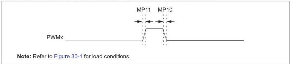
text_image
MP11 MP10 PWMx Note: Refer to Figure 30-1 for load conditions.TABLE 30-30: HIGH-SPEED PWMx MODULE TIMING REQUIREMENTS
| AC CHARACTERISTICS | Standard Operating Conditions: 3.0V to 3.6V(unless otherwise stated)Operating temperature -40°C ≤ TA ≤ +85°C for Industrial-40°C ≤ AT ≤ +125°C for Extended | ||||||
| Param No. | Symbol | Characteristic (1) | Min. Typ. Max. | Units C | Conditions | ||
| MP10 T | FPWM | PWMx Output Fall Time | — | — | — | ns | See Parameter DO32 |
| MP11 | TRPWM | PWMx Output Rise Time | — | — | — | ns | See Parameter DO31 |
| MP20 T | FD | Fault Input ↓ to PWMx I/O Change | — | — | 15 | ns | |
| MP30 T | FH | Fault Input Pulse Width | 15 | — | — | ns | |
Note 1: These parameters are characterized but not tested in manufacturing.
TABLE 30-31: SPI1, SPI2 AND SPI3 MAXIMUM DATA/CLOCK RATE SUMMARY (1)
| AC CHARACTERISTICS | Standard Operating Conditions: 3.0V to 3.6V(unless otherwise stated)Operating temperature -40°C ≤ TA ≤ +85°C for Industrial-40°C ≤ AT ≤ +125°C for Extended | |||||
| Maximum Data Rate | Master Transmit Only (Half-Duplex) | Master Transmit/Receive (Full-Duplex) | Slave Transmit/Receive (Full-Duplex) | CKE CKP | SMP | |
| 15 MHz | Table 30-32 | — | — | 0,1 | 0,1 | 0,1 |
| 9 MHz | — | Table 30-33 | — | 1 | 0,1 | 1 |
| 9 MHz | — | Table 30-34 | — | 0 | 0,1 | 1 |
| 15 MHz | — | — | Table 30-35 | 1 | 0 | 0 |
| 11 MHz | — | — | Table 30-36 | 1 | 1 | 0 |
| 15 MHz | — | — | Table 30-37 | 0 | 1 | 0 |
| 11 MHz | — | — | Table 30-38 | 0 | 0 | 0 |
Note 1: Pertaining to SPI3: dsPIC33EPXXXGS702, dsPIC33EPXXXGSX04 and dsPIC33EPXXXGSX05 devices with a remappable SCK3 pin.
FIGURE 30-11: SPI1, SPI2 AND SPI3 MASTER MODE (HALF-DUPLEX, TRANSMIT ONLY, CKE = 0) TIMING CHARACTERISTICS ^(1,2)
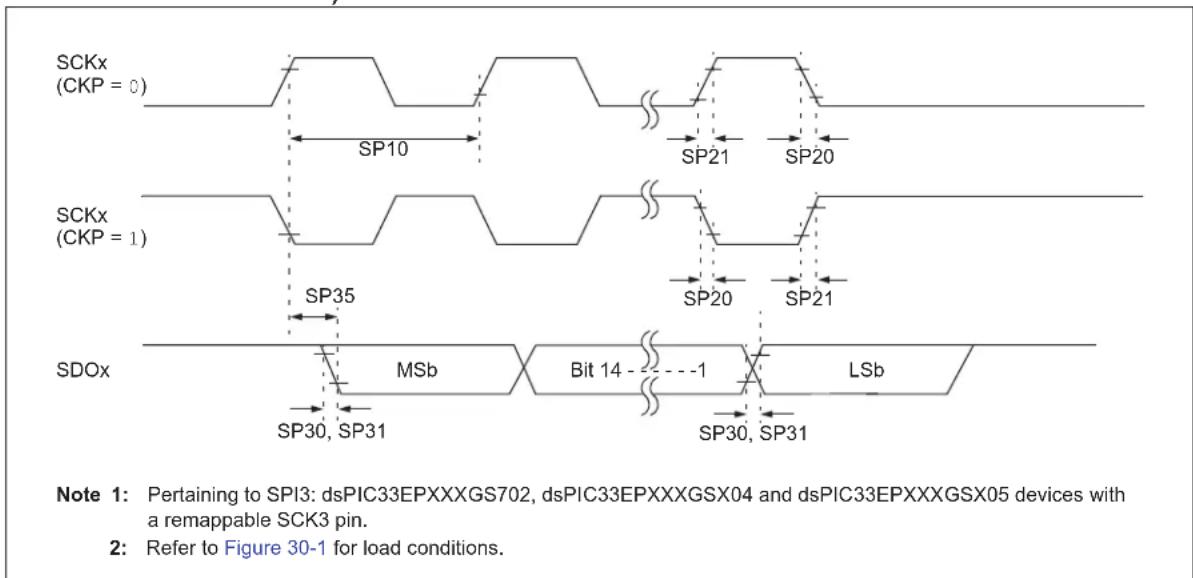
text_image
SCKx (CKP = 0) SP10 SP21 SP20 SCKx (CKP = 1) SP35 SP20 SP21 SDOx MSb Bit 14 LSb SP30, SP31 SP30, SP31 Note 1: Pertaining to SPI3: dsPIC33EPXXXGS702, dsPIC33EPXXXGSX04 and dsPIC33EPXXXGSX05 devices with a remappable SCK3 pin. 2: Refer to Figure 30-1 for load conditions.FIGURE 30-12: SPI1, SPI2 AND SPI3 MASTER MODE (HALF-DUPLEX, TRANSMIT ONLY, CKE = 1) TIMING CHARACTERISTICS ^(1,2)

text_image
SCKx (CKP = 0) SP36 SP10 SP21 SP20 SCKx (CKP = 1) SP35 SP20 SP21 SDOx MSb Bit 14 - - - - - - - - - - - - - - - - - - - - - - - - - - - - - - - - - - - - - - - - - - - - - - - - - - - - - - - - - - - - - - - - - - - - - - - - - - - - - - - - - - - - - - SP30, SP31 LSbNote 1: Pertaining to SPI3: dsPIC33EPXXXGS702, dsPIC33EPXXXGSX04 and dsPIC33EPXXXGSX05 devices with a remappable SCK3 pin.
2: Refer to Figure 30-1 for load conditions.
TABLE 30-32: SPI1, SPI2 AND SPI3 MASTER MODE (HALF-DUPLEX, TRANSMIT ONLY) TIMING REQUIREMENTS ^(5)
| AC CHARACTERISTICS | Standard Operating Conditions: 3.0V to 3.6V(unless otherwise stated)Operating temperature -40°C ≤ TA ≤ +85°C for Industrial-40°C ≤ AT ≤ +125°C for Extended | ||||||
| Param. | Symbol Char | acteristic (1) | Min. Typ. (2) | Max. Units Conditions | |||
| SP10 | FscP | Maximum SCKx Frequency | — | — | 15 | MHz | (Note 3) |
| SP20 | TscF | SCKx Output Fall Time | — | — | — | ns | See Parameter DO32(Note 4) |
| SP21 | TscR | SCKx Output Rise Time | — | — | — | ns | See Parameter DO31(Note 4) |
| SP30 | TdoF | SDOx Data Output Fall Time | — | — | — | ns | See Parameter DO32(Note 4) |
| SP31 | TdoR | SDOx Data Output Rise Time | — | — | — | ns | See Parameter DO31(Note 4) |
| SP35 | TscH2doV,TscL2doV | SDOx Data Output Valid after SCKx Edge | — | 6 | 20 | ns | |
| SP36 | TdiV2scH,TdiV2scL | SDOx Data Output Setup to First SCKx Edge | 30 | — | — | ns | |
Note 1: These parameters are characterized, but are not tested in manufacturing.
2: Data in "Typical" column is at 3.3V, +25°C unless otherwise stated.
3: The minimum clock period for SCKx is 66.7 ns. Therefore, the clock generated in Master mode must not violate this specification.
4: Assumes 50 pF load on all SPIx pins.
5: Pertaining to SPI3: dsPIC33EPXXXGS702, dsPIC33EPXXXGSX04 and dsPIC33EPXXXGSX05 devices with a remappable SCK3 pin.
FIGURE 30-13: SPI1, SPI2 AND SPI3 MASTER MODE (FULL-DUPLEX, CKE = 1, CKP = x, SMP = 1) TIMING CHARACTERISTICS ^(1,2)
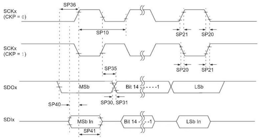
flowchart
graph TD
    A["SCKx (CKP = 0)"] --> B["SP36"]
    B --> C["SP10"]
    C --> D["SP21"]
    D --> E["SP20"]
    F["SCKx (CKP = 1)"] --> G["SP35"]
    G --> H["SP20"]
    H --> I["SP21"]
    J["SDOx"] --> K["MSb"]
    K --> L["Bit 14 -1"]
    L --> M["LSb"]
    N["SDIx"] --> O["MSb In"]
    O --> P["Bit 14 -1"]
    P --> Q["LSb In"]
    K --> R["SP30, SP31"]
    R --> S["SP40"]
    S --> T["SP41"]
Note 1: Pertaining to SPI3: dsPIC33EPXXXGS702, dsPIC33EPXXXGSX04 and dsPIC33EPXXXGSX05 devices with a remappable SCK3 pin.
2: Refer to Figure 30-1 for load conditions.
TABLE 30-33: SPI1, SPI2 AND SPI3 MASTER MODE (FULL-DUPLEX, CKE = 1, CKP = x, SMP = 1) TIMING REQUIREMENTS ^(5)
| AC CHARACTERISTICS | Standard Operating Conditions: 3.0V to 3.6V(unless otherwise stated)Operating temperature -40°C ≤ TA ≤ +85°C for Industrial-40°C ≤ AT ≤ +125°C for Extended | ||||||
| Param. | Symbol Char | characteristic (1) | Min. Typ. (2) | Max. Units Conditions | |||
| SP10 | FscP | Maximum SCKx Frequency | — | — | 9 | MHz | (Note 3) |
| SP20 | TscF | SCKx Output Fall Time | — | — | — | ns | See Parameter DO32 (Note 4) |
| SP21 | TscR | SCKx Output Rise Time | — | — | — | ns | See Parameter DO31 (Note 4) |
| SP30 | TdoF | SDOx Data Output Fall Time | — | — | — | ns | See Parameter DO32 (Note 4) |
| SP31 | TdoR | SDOx Data Output Rise Time | — | — | — | ns | See Parameter DO31 (Note 4) |
| SP35 Tsc | H2doV,TscL2doV | SDOx Data Output Valid after SCKx Edge | — | 6 | 20 | ns | |
| SP36 TdoV2sc,TdoV2scL | SDOx Data Output Setup to First SCKx Edge | 30 | — | — | ns | ||
| SP40 TdiV2scH,TdiV2scL | Setup Time of SDIx Data Input to SCKx Edge | 30 | — | — | ns | ||
| SP41 Tsc | H2diL,TscL2diL | Hold Time of SDIx Data Input to SCKx Edge | 30 | — | — | ns | |
Note 1: These parameters are characterized, but are not tested in manufacturing.
2: Data in "Typical" column is at 3.3V, +25°C unless otherwise stated.
3: The minimum clock period for SCKx is 111 ns. The clock generated in Master mode must not violate this specification.
4: Assumes 50 pF load on all SPIx pins.
5: Pertaining to SPI3: dsPIC33EPXXXGS702, dsPIC33EPXXXGSX04 and dsPIC33EPXXXGSX05 devices with a remappable SCK3 pin.
FIGURE 30-14: SPI1, SPI2 AND SPI3 MASTER MODE (FULL-DUPLEX, CKE = 0, CKP = x, SMP = 1) TIMING CHARACTERISTICS ^(1,2)

flowchart
graph LR
    A["SCKx (CKP = 0)"] --> B["SP10"]
    B --> C["SP21"]
    C --> D["SP20"]
    E["SCKx (CKP = 1)"] --> F["SP35, SP36"]
    F --> G["SP20"]
    G --> H["SP21"]
    I["SDOx"] --> J["MSb"]
    J --> K["Bit 14 - -1"]
    K --> L["LSb"]
    M["SDIx"] --> N["MSb In"]
    N --> O["Bit 14 - -1"]
    O --> P["LSb In"]
    Q["Note 1: Pertaining to SPI3: dsPIC33EPXXXGS702, dsPIC33EPXXXGSX04 and dsPIC33EPXXXGSX05 devices with a remappable SCK3 pin."]
    R["Note 2: Refer to Figure 30-1 for load conditions."]
TABLE 30-34: SPI1, SPI2 AND SPI3 MASTER MODE (FULL-DUPLEX, CKE = 0, CKP = x, SMP = 1) TIMING REQUIREMENTS ^(5)
| AC CHARACTERISTICS | Standard Operating Conditions: 3.0V to 3.6V(unless otherwise stated)Operating temperature -40°C ≤ TA ≤ +85°C for Industrial-40°C ≤ AT ≤ +125°C for Extended | ||||||
| Param. | Symbol Char | acteristic (1) | Min. Typ. (2) | Max. Units Conditions | |||
| SP10 | FscP | Maximum SCKx Frequency | — | — | 9 | MHz | -40°C to +125°C (Note 3) |
| SP20 | TscF | SCKx Output Fall Time | — | — | — | ns | See Parameter DO32 (Note 4) |
| SP21 | TscR | SCKx Output Rise Time | — | — | — | ns | See Parameter DO31 (Note 4) |
| SP30 | TdoF | SDOx Data Output Fall Time | — | — | — | ns | See Parameter DO32 (Note 4) |
| SP31 | TdoR | SDOx Data Output Rise Time | — | — | — | ns | See Parameter DO31 (Note 4) |
| SP35 Tsc | H2doV,TscL2doV | SDOx Data Output Valid after SCKx Edge | — | 6 | 20 | ns | |
| SP36 TdoV2scH,TdoV2scL | SDOx Data Output Setup to First SCKx Edge | 30 | — | — | ns | ||
| SP40 TdiV2scH,TdiV2scL | Setup Time of SDIx Data Input to SCKx Edge | 30 | — | — | ns | ||
| SP41 Tsc | H2diL,TscL2diL | Hold Time of SDIx Data Input to SCKx Edge | 30 | — | — | ns | |
Note 1: These parameters are characterized, but are not tested in manufacturing.
2: Data in "Typical" column is at 3.3V, +25°C unless otherwise stated.
3: The minimum clock period for SCKx is 111 ns. The clock generated in Master mode must not violate this specification.
4: Assumes 50 pF load on all SPIx pins.
5: Pertaining to SPI3: dsPIC33EPXXXGS702, dsPIC33EPXXXGSX04 and dsPIC33EPXXXGSX05 devices with a remappable SCK3 pin.
FIGURE 30-15: SPI1, SPI2 AND SPI3 SLAVE MODE (FULL-DUPLEX, CKE = 1, CKP = 0, SMP = 0) TIMING CHARACTERISTICS ^(1,2)
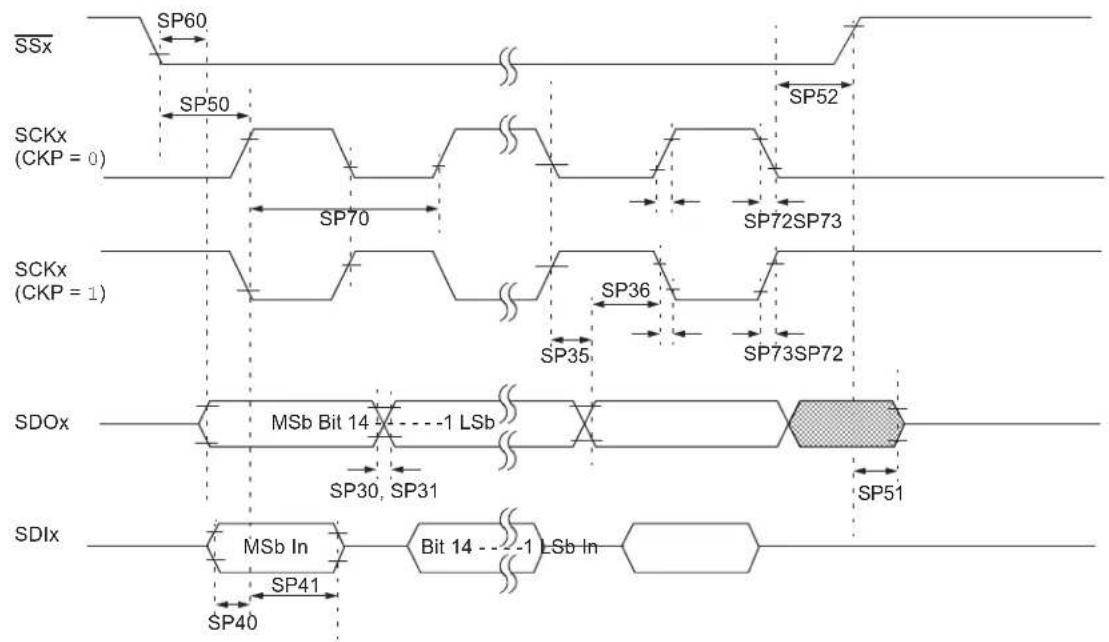
flowchart
graph TD
    subgraph SSx
        A["SP60"] --> B["SP50"]
        B --> C["SP70"]
        C --> D["SP35"]
        D --> E["SP73SP72"]
    end
    subgraph SCKx (CKP = 0)
        F["SP52"] --> G["SP72SP73"]
    end
    subgraph SCKx (CKP = 1)
        H["SP36"] --> I["SP73SP72"]
    end
    subgraph SDOx
        J["MSb Bit 14"] --> K["SP30, SP31"]
        K --> L["SP51"]
        M["MSb In"] --> N["SP40"]
        N --> O["Bit 14 - - - LSb In"]
    end
    subgraph SDIx
        P["SP41"] --> Q["SP30, SP31"]
        Q --> R["SP51"]
        S["MSb In"] --> T["Bit 14 - - - LSb In"]
    end
Note 1: Pertaining to SPI3: dsPIC33EPXXXGS702, dsPIC33EPXXXGSX04 and dsPIC33EPXXXGSX05 devices with a remappable SCK3 pin.
2: Refer to Figure 30-1 for load conditions.
TABLE 30-35: SPI1, SPI2 AND SPI3 SLAVE MODE (FULL-DUPLEX, CKE = 1, CKP = 0, SMP = 0) TIMING REQUIREMENTS ^(5)
| AC CHARACTERISTICS | Standard Operating Conditions: 3.0V to 3.6V(unless otherwise stated)Operating temperature -40°C ≤ TA ≤ +85°C for Industrial-40°C ≤ AT ≤ +125°C for Extended | ||||||
| Param. | Symbol Characteristic (1) | Min. Typ. (2) | Max. Units Conditions | ||||
| SP70 | FscP | Maximum SCKx Input Frequency | — | — | 15 | MHz | (Note 3) |
| SP72 | TscF | SCKx Input Fall Time | — | — | — | ns | See Parameter DO32(Note 4) |
| SP73 | TscR | SCKx Input Rise Time | — | — | — | ns | See Parameter DO31(Note 4) |
| SP30 | TdoF | SDOx Data Output Fall Time | — | — | — | ns | See Parameter DO32(Note 4) |
| SP31 | TdoR | SDOx Data Output Rise Time | — | — | — | ns | See Parameter DO31(Note 4) |
| SP35 | TscH2doV,TscL2doV | SDOx Data Output Valid after SCKx Edge | — | 6 | 20 | ns | |
| SP36 | TdoV2scH,TdoV2scL | SDOx Data Output Setup to First SCKx Edge | 30 | — | — | ns | |
| SP40 | TdiV2scH,TdiV2scL | Setup Time of SDIx Data Input to SCKx Edge | 30 | — | — | ns | |
| SP41 | TscH2diL,TscL2diL | Hold Time of SDIx Data Input to SCKx Edge | 30 | — | — | ns | |
| SP50 | TssL2scH,TssL2scL | to SCKx ↑ or SCKx ↓ Input | 120 | — | — | ns | |
| SP51 | TssH2doZ | to SDOx Output High-Impedance | 10 | — | 50 | ns | (Note 4) |
| SP52 | TscH2ssHTscL2ssH | after SCKx Edge | 1.5 TCY + 40 | — | — | ns | (Note 4) |
| SP60 | TssL2doV S | DOx Data Output Valid after Edge | — | — | 50 | ns | |
Note 1: These parameters are characterized, but are not tested in manufacturing.
2: Data in "Typical" column is at 3.3V, +25°C unless otherwise stated.
3: The minimum clock period for SCKx is 66.7 ns. Therefore, the SCKx clock generated by the master must not violate this specification.
4: Assumes 50 pF load on all SPIx pins.
5: Pertaining to SPI3: dsPIC33EPXXXGS702, dsPIC33EPXXXGSX04 and dsPIC33EPXXXGSX05 devices with a remappable SCK3 pin.
FIGURE 30-16: SPI1, SPI2 AND SPI3 SLAVE MODE (FULL-DUPLEX, CKE = 1, CKP = 1, SMP = 0) TIMING CHARACTERISTICS ^(1,2)

flowchart
graph TD
    subgraph SSx
        A["SP60"] --> B["SP50"]
        B --> C["SP70"]
        C --> D["SP52"]
        E["SCKx (CKP = 0)"] --> F["SP72SP73"]
        G["SCKx (CKP = 1)"] --> H["SP73SP72"]
    end
    subgraph SDOx
        I["MSb Bit 14"] --> J["SP30, SP31"]
        K["MSb In"] --> L["SP40"]
        M["Bit 14"] --> N["SP41"]
        O["LSb In"] --> P["SP51"]
    end
    subgraph SDIx
        Q["MSb In"] --> R["SP40"]
        S["Bit 14"] --> T["SP30, SP31"]
        U["LSb In"] --> V["SP51"]
    end
Note 1: Pertaining to SPI3: dsPIC33EPXXXGS702, dsPIC33EPXXXGSX04 and dsPIC33EPXXXGSX05 devices with a remappable SCK3 pin.
2: Refer to Figure 30-1 for load conditions.
TABLE 30-36: SPI1, SPI2 AND SPI3 SLAVE MODE (FULL-DUPLEX, CKE = 1, CKP = 1, SMP = 0) TIMING REQUIREMENTS ^(5)
| AC CHARACTERISTICS | Standard Operating Conditions: 3.0V to 3.6V(unless otherwise stated)Operating temperature -40°C ≤ TA ≤ +85°C for Industrial-40°C ≤ AT ≤ +125°C for Extended | ||||||
| Param. | Symbol Char | characteristic (1) | Min. Typ. | (2) | Max. | Units Co | nditions |
| SP70 | FscP | Maximum SCKx Input Frequency | — | — | 11 | MHz | (Note 3) |
| SP72 | TscF | SCKx Input Fall Time | — | — | — | ns | See Parameter DO32(Note 4) |
| SP73 | TscR | SCKx Input Rise Time | — | — | — | ns | See Parameter DO31(Note 4) |
| SP30 | TdoF | SDOx Data Output Fall Time | — | — | — | ns | See Parameter DO32(Note 4) |
| SP31 | TdoR | SDOx Data Output Rise Time | — | — | — | ns | See Parameter DO31(Note 4) |
| SP35 | TscH2doV,TscL2doV | SDOx Data Output Valid after SCKx Edge | — | 6 | 20 | ns | |
| SP36 | TdoV2scH,TdoV2scL | SDOx Data Output Setup to First SCKx Edge | 30 | — | — | ns | |
| SP40 | TdiV2scH,TdiV2scL | Setup Time of SDIx Data Input to SCKx Edge | 30 | — | — | ns | |
| SP41 | TscH2diL,TscL2diL | Hold Time of SDIx Data Input to SCKx Edge | 30 | — | — | ns | |
| SP50 | TssL2scH,TssL2scL | to SCKx ↑ or SCKx ↓ Input | 120 | — | — | ns | |
| SP51 | TssH2doZ | to SDOx Output High-Impedance | 10 | — | 50 | ns | (Note 4) |
| SP52 | TscH2ssHTscL2ssH | after SCKx Edge | 1.5 TCY + 40 | — | — | ns | (Note 4) |
| SP60 | TssL2doVS | DOx Data Output Valid after Edge | — | — | 50 | ns | |
Note 1: These parameters are characterized, but are not tested in manufacturing.
2: Data in "Typical" column is at 3.3V, +25°C unless otherwise stated.
3: The minimum clock period for SCKx is 91 ns. Therefore, the SCKx clock generated by the master must not violate this specification.
4: Assumes 50 pF load on all SPIx pins.
5: Pertaining to SPI3: dsPIC33EPXXXGS702, dsPIC33EPXXXGSX04 and dsPIC33EPXXXGSX05 devices with a remappable SCK3 pin.
FIGURE 30-17: SPI1, SPI2 AND SPI3 SLAVE MODE (FULL-DUPLEX, CKE = 0, CKP = 1, SMP = 0) TIMING CHARACTERISTICS ^(1,2)

flowchart
graph TD
    subgraph SSx
        A["SP50"] --> B["SCKx (CKP = 0)"]
        B --> C["SP70"]
        C --> D["SCKx (CKP = 1)"]
        D --> E["SP35 SP36"]
        E --> F["SDOx"]
        F --> G["MSb LSbBit14"]
        G --> H["SP30', SP31"]
        H --> I["SDIx"]
        I --> J["MSb In"]
        J --> K["Bit 14"]
        K --> L["SP40"]
        L --> M["SP41"]
        M --> N["SP52"]
        N --> O["SP72SP73"]
        O --> P["SP73SP72"]
        P --> Q["SP51"]
    end
Note 1: Pertaining to SPI3: dsPIC33EPXXXGS702, dsPIC33EPXXXGSX04 and dsPIC33EPXXXGSX05 devices with a remappable SCK3 pin.
2: Refer to Figure 30-1 for load conditions.
TABLE 30-37: SPI1, SPI2 AND SPI3 SLAVE MODE (FULL-DUPLEX, CKE = 0, CKP = 1, SMP = 0) TIMING REQUIREMENTS ^(5)
| AC CHARACTERISTICS | Standard Operating Conditions: 3.0V to 3.6V(unless otherwise stated)Operating temperature -40°C ≤ TA ≤ +85°C for Industrial-40°C ≤ AT ≤ +125°C for Extended | ||||||
| Param. | Symbol Char | (1) | Min. Typ. | (2) | Max. | Units Conditions | |
| SP70 | FscP | Maximum SCKx Input Frequency | — | — | 15 | MHz | (Note 3) |
| SP72 | TscF | SCKx Input Fall Time | — | — | — | ns | See Parameter DO32 (Note 4) |
| SP73 | TscR | SCKx Input Rise Time | — | — | — | ns | See Parameter DO31 (Note 4) |
| SP30 | TdoF | SDOx Data Output Fall Time | — | — | — | ns | See Parameter DO32 (Note 4) |
| SP31 | TdoR | SDOx Data Output Rise Time | — | — | — | ns | See Parameter DO31 (Note 4) |
| SP35 | TscH2doV, TscL2doV | SDOx Data Output Valid after SCKx Edge | — | 6 | 20 | ns | |
| SP36 | TdoV2scH, TdoV2scL | SDOx Data Output Setup to First SCKx Edge | 30 | — | — | ns | |
| SP40 | TdiV2scH, TdiV2scL | Setup Time of SDIx Data Input to SCKx Edge | 30 | — | — | ns | |
| SP41 | TscH2diL, TscL2diL | Hold Time of SDIx Data Input to SCKx Edge | 30 | — | — | ns | |
| SP50 | TssL2scH, TssL2scL | to SCKx ↑ or SCKx ↓ Input | 120 | — | — | ns | |
| SP51 | TssH2doZ | to SDOx Output High-Impedance | 10 | — | 50 | ns | (Note 4) |
| SP52 | TscH2ssH TscL2ssH | after SCKx Edge | 1.5 TCY + 40 | — | — | ns | (Note 4) |
Note 1: These parameters are characterized, but are not tested in manufacturing.
2: Data in "Typical" column is at 3.3V, +25°C unless otherwise stated.
3: The minimum clock period for SCKx is 66.7 ns. Therefore, the SCKx clock generated by the master must not violate this specification.
4: Assumes 50 pF load on all SPIx pins.
5: Pertaining to SPI3: dsPIC33EPXXXGS702, dsPIC33EPXXXGSX04 and dsPIC33EPXXXGSX05 devices with a remappable SCK3 pin.
FIGURE 30-18: SPI1, SPI2 AND SPI3 SLAVE MODE (FULL-DUPLEX, CKE = 0, CKP = 0, SMP = 0) TIMING CHARACTERISTICS ^(1,2)

flowchart
graph TD
    A["SSx"] --> B["SCKx (CKP = 0)"]
    B --> C["SCKx (CKP = 1)"]
    C --> D["SDOx"]
    D --> E["SDlx"]
    subgraph Time Points
        F["SP50"] --> G["SP70"] --> H["SP72"] --> I["SP73"] --> J["SP74"]
        K["SP52"] --> L["SP72"] --> M["SP73"] --> N["SP74"]
        O["SP35"] --> P["SP36"] --> Q["MSb LSbBit14"] --> R["SP30, SP31"] --> S["SP51"]
        T["SP40"] --> U["Bit 14"] --> V["LSb In"] --> W["SP41"]
    end
Note 1: Pertaining to SPI3: dsPIC33EPXXXGS702, dsPIC33EPXXXGSX04 and dsPIC33EPXXXGSX05 devices with a remappable SCK3 pin.
2: Refer to Figure 30-1 for load conditions.
TABLE 30-38: SPI1, SPI2 AND SPI3 SLAVE MODE (FULL-DUPLEX, CKE = 0, CKP = 0, SMP = 0) TIMING REQUIREMENTS ^(5)
| AC CHARACTERISTICS | Standard Operating Conditions: 3.0V to 3.6V(unless otherwise stated)Operating temperature -40°C ≤ TA ≤ +85°C for Industrial-40°C ≤ AT ≤ +125°C for Extended | ||||||
| Param. | Symbol Char | characteristic (1) | Min. Typ. | (2) | Max. | Units Conditions | |
| SP70 | FscP | Maximum SCKx Input Frequency | — | — | 11 | MHz | (Note 3) |
| SP72 | TscF | SCKx Input Fall Time | — | — | — | ns | See Parameter DO32(Note 4) |
| SP73 | TscR | SCKx Input Rise Time | — | — | — | ns | See Parameter DO31(Note 4) |
| SP30 | TdoF | SDOx Data Output Fall Time | — | — | — | ns | See Parameter DO32(Note 4) |
| SP31 | TdoR | SDOx Data Output Rise Time | — | — | — | ns | See Parameter DO31(Note 4) |
| SP35 | TscH2doV,TscL2doV | SDOx Data Output Valid after SCKx Edge | — | 6 | 20 | ns | |
| SP36 | TdoV2scH,TdoV2scL | SDOx Data Output Setup to First SCKx Edge | 30 | — | — | ns | |
| SP40 | TdiV2scH,TdiV2scL | Setup Time of SDIx Data Input to SCKx Edge | 30 | — | — | ns | |
| SP41 | TscH2diL,TscL2diL | Hold Time of SDIx Data Input to SCKx Edge | 30 | — | — | ns | |
| SP50 | TssL2scH,TssL2scL | to SCKx ↑ or SCKx ↓ Input | 120 | — | — | ns | |
| SP51 | TssH2doZ | to SDOx Output High-Impedance | 10 | — | 50 | ns | (Note 4) |
| SP52 | TscH2ssHTscL2ssH | after SCKx Edge | 1.5 TCY + 40 | — | — | ns | (Note 4) |
Note 1: These parameters are characterized, but are not tested in manufacturing.
2: Data in "Typical" column is at 3.3V, +25°C unless otherwise stated.
3: The minimum clock period for SCKx is 91 ns. Therefore, the SCKx clock generated by the master must not violate this specification.
4: Assumes 50 pF load on all SPIx pins.
5: Pertaining to SPI3: dsPIC33EPXXXGS702, dsPIC33EPXXXGSX04 and dsPIC33EPXXXGSX05 devices with a remappable SCK3 pin.
TABLE 30-39: SPI3 MAXIMUM DATA/CLOCK RATE SUMMARY (1)
| AC CHARACTERISTICS | Standard Operating Conditions: 3.0V to 3.6V(unless otherwise stated)Operating temperature -40°C ≤ TA ≤ +85°C for Industrial-40°C ≤ AT ≤ +125°C for Extended | |||||
| Maximum Data Rate | Master Transmit Only (Half-Duplex) | Master Transmit/Receive (Full-Duplex) | Slave Transmit/Receive (Full-Duplex) | CKE CKP | SMP | |
| 25 MHz | Table 30-40 | — | — | 0,1 | 0,1 | 0,1 |
| 25 MHz | — | Table 30-41 | — | 1 | 0,1 | 1 |
| 25 MHz | — | Table 30-42 | — | 0 | 0,1 | 1 |
| 25 MHz | — | — | Table 30-43 | 1 | 0 | 0 |
| 25 MHz | — | — | Table 30-44 | 1 | 1 | 0 |
| 25 MHz | — | — | Table 30-45 | 0 | 1 | 0 |
| 25 MHz | — | — | Table 30-46 | 0 | 0 | 0 |
Note 1: For dsPIC33EPXXXGSX06 and dsPIC33EPXXXGSX08 devices with a fixed SCK3 pin.
FIGURE 30-19: SPI3 MASTER MODE (HALF-DUPLEX, TRANSMIT ONLY, CKE = 0) TIMING CHARACTERISTICS ^(1,2)
text_image
SCK3 (CKP = 0) SP10 SP21 SP20 SCK3 (CKP = 1) SP35 SP20 SP21 SDO3 MSb Bit 14 LSb SP30, SP31 SP30, SP31 Note 1: For dsPIC33EPXXXGSX06 and dsPIC33EPXXXGSX08 devices with a fixed SCK3 pin. 2: Refer to Figure 30-1 for load conditions.FIGURE 30-20: SPI3 MASTER MODE (HALF-DUPLEX, TRANSMIT ONLY, CKE = 1) TIMING CHARACTERISTICS ^(1,2)
text_image
SCK3 (CKP = 0) SP36 SP10 SP21 SP20 SCK3 (CKP = 1) SP35 SP20 SP21 SDO3 MSb Bit 14 LSb SP30, SP31Note 1: For dsPIC33EPXXXGSX06 and dsPIC33EPXXXGSX08 devices with a fixed SCK3 pin. 2: Refer to Figure 30-1 for load conditions.
TABLE 30-40: SPI3 MASTER MODE (HALF-DUPLEX, TRANSMIT ONLY) TIMING REQUIREMENTS ^(5)
| AC CHARACTERISTICS | Standard Operating Conditions: 3.0V to 3.6V(unless otherwise stated)Operating temperature -40°C ≤ TA ≤ +85°C for Industrial-40°C ≤ AT ≤ +125°C for Extended | ||||||
| Param. | Symbol Characteristic (1) | Min. Typ. (2) | Max. Units Conditions | ||||
| SP10 | FscP | Maximum SCK3 Frequency | — | — | 25 | MHz | (Note 3) |
| SP20 | TscF | SCK3 Output Fall Time | — | — | — | ns | See Parameter DO32(Note 4) |
| SP21 | TscR | SCK3 Output Rise Time | — | — | — | ns | See Parameter DO31(Note 4) |
| SP30 | TdoF | SDO3 Data Output Fall Time | — | — | — | ns | See Parameter DO32(Note 4) |
| SP31 | TdoR | SDO3 Data Output Rise Time | — | — | — | ns | See Parameter DO31(Note 4) |
| SP35 TscH2doV,TscL2doV | SDO3 Data Output Valid after SCK3 Edge | — | 6 | 20 | ns | ||
| SP36 TcdiV2scH,TdiV2scL | SDO3 Data Output Setup to First SCK3 Edge | 20 | — | — | ns | ||
Note 1: These parameters are characterized, but are not tested in manufacturing.
2: Data in "Typical" column is at 3.3V, +25°C unless otherwise stated.
3: The minimum clock period for SCK3 is 66.7 ns. Therefore, the clock generated in Master mode must not violate this specification.
4: Assumes 50 pF load on all SPI3 pins.
5: For dsPIC33EPXXXGSX06 and dsPIC33EPXXXGSX08 devices with a fixed SCK3 pin.
FIGURE 30-21: SPI3 MASTER MODE (FULL-DUPLEX, CKE = 1, CKP = x, SMP = 1) TIMING CHARACTERISTICS ^(1,2)
flowchart
graph TD
    subgraph SCK3(CKP = 0)
        A["SP36"] --> B["SP10"]
        B --> C["SP21"]
        C --> D["SP20"]
    end
    subgraph SCK3(CKP = 1)
        E["SP35"] --> F["SP20"]
        F --> G["SP21"]
    end
    subgraph SDO3
        H["MSb"] --> I["Bit 14 -1"]
        I --> J["LSb"]
        K["SP40"] --> L["SP30, SP31"]
    end
    subgraph SDI3
        M["MSb In"] --> N["Bit 14 -1"]
        N --> O["LSb In"]
        P["SP41"] --> Q["SP40"]
    end
Note 1: For dsPIC33EPXXXGSX06 and dsPIC33EPXXXGSX08 devices with a fixed SCK3 pin.
2: Refer to Figure 30-1 for load conditions.
TABLE 30-41: SPI3 MASTER MODE (FULL-DUPLEX, CKE = 1, CKP = x, SMP = 1) TIMING REQUIREMENTS ^(5)
| AC CHARACTERISTICS | Standard Operating Conditions: 3.0V to 3.6V(unless otherwise stated)Operating temperature -40°C ≤ TA ≤ +85°C for Industrial-40°C ≤ AT ≤ +125°C for Extended | ||||||
| Param. | Symbol Characteristic (1) | Min. Typ. (2) | Max. Units Conditions | ||||
| SP10 | FscP | Maximum SCK3 Frequency | — | — | 25 | MHz | (Note 3) |
| SP20 | TscF | SCK3 Output Fall Time | — | — | — | ns | See Parameter DO32 (Note 4) |
| SP21 | TscR | SCK3 Output Rise Time | — | — | — | ns | See Parameter DO31 (Note 4) |
| SP30 | TdoF | SDO3 Data Output Fall Time | — | — | — | ns | See Parameter DO32 (Note 4) |
| SP31 | TdoR | SDO3 Data Output Rise Time | — | — | — | ns | See Parameter DO31 (Note 4) |
| SP35 TscH2doV,TscL2doV | SDO3 Data Output Valid after SCK3 Edge | — | 6 | 20 | ns | ||
| SP36 TdoV2sc,TdoV2scL | SDO3 Data Output Setup to First SCK3 Edge | 20 | — | — | ns | ||
| SP40 TdV2scH,TdiV2scL | Setup Time of SDI3 Data Input to SCK3 Edge | 20 | — | — | ns | ||
| SP41 TscH2diL,TscL2diL | Hold Time of SDI3 Data Input to SCK3 Edge | 15 | — | — | ns | ||
Note 1: These parameters are characterized, but are not tested in manufacturing.
2: Data in "Typical" column is at 3.3V, +25°C unless otherwise stated.
3: The minimum clock period for SCK3 is 100 ns. The clock generated in Master mode must not violate this specification.
4: Assumes 50 pF load on all SPI3 pins.
5: For dsPIC33EPXXXGSX06 and dsPIC33EPXXXGSX08 devices with a fixed SCK3 pin.
FIGURE 30-22: SPI3 MASTER MODE (FULL-DUPLEX, CKE = 0, CKP = x, SMP = 1) TIMING CHARACTERISTICS ^(1,2)

flowchart
graph TD
    A["SCK3 (CKP = 0)"] --> B["SP10"]
    B --> C["SP21"]
    C --> D["SP20"]
    E["SCK3 (CKP = 1)"] --> F["SP35"]
    F --> G["SP20"]
    G --> H["SP21"]
    I["SDO3"] --> J["MSb"]
    J --> K["Bit 14 - -1"]
    K --> L["LSb"]
    M["SD3"] --> N["MSb In"]
    N --> O["Bit 14 - -1"]
    O --> P["LSb In"]
    Q["Note 1: For dsPIC33EPXXXGSX06 and dsPIC33EPXXXGSX08 devices with a fixed SCK3 pin."]
    R["Note 2: Refer to Figure 30-1 for load conditions."]
TABLE 30-42: SPI3 MASTER MODE (FULL-DUPLEX, CKE = 0, CKP = x, SMP = 1) TIMING REQUIREMENTS ^(5)
| AC CHARACTERISTICS | Standard Operating Conditions: 3.0V to 3.6V(unless otherwise stated)Operating temperature -40°C ≤ TA ≤ +85°C for Industrial-40°C ≤ AT ≤ +125°C for Extended | ||||||
| Param. | Symbol Characteristic (1) | Min. Typ. (2) | Max. Units Conditions | ||||
| SP10 | FscP | Maximum SCK3 Frequency | — | — | 25 | MHz | -40°C to +125°C (Note 3) |
| SP20 | TscF | SCK3 Output Fall Time | — | — | — | ns | See Parameter DO32 (Note 4) |
| SP21 | TscR | SCK3 Output Rise Time | — | — | — | ns | See Parameter DO31 (Note 4) |
| SP30 | TdoF | SDO3 Data Output Fall Time | — | — | — | ns | See Parameter DO32 (Note 4) |
| SP31 | TdoR | SDO3 Data Output Rise Time | — | — | — | ns | See Parameter DO31 (Note 4) |
| SP35 Tsc | H2doV,TscL2doV | SDO3 Data Output Valid after SCK3 Edge | — | 6 | 20 | ns | |
| SP36 TdoV2scH,TdoV2scL | SDO3 Data Output Setup to First SCK3 Edge | 20 | — | — | ns | ||
| SP40 TdiV2scH,TdiV2scL | Setup Time of SDI3 Data Input to SCK3 Edge | 20 | — | — | ns | ||
| SP41 Tsc | H2diL,TscL2diL | Hold Time of SDI3 Data Input to SCK3Edge | 20 | — | — | ns | |
Note 1: These parameters are characterized, but are not tested in manufacturing.
2: Data in "Typical" column is at 3.3V, +25°C unless otherwise stated.
3: The minimum clock period for SCK3 is 100 ns. The clock generated in Master mode must not violate this specification.
4: Assumes 50 pF load on all SPI3 pins.
5: For dsPIC33EPXXXGSX06 and dsPIC33EPXXXGSX08 devices with a fixed SCK3 pin.
FIGURE 30-23: SPI3 SLAVE MODE (FULL-DUPLEX, CKE = 1, CKP = 0, SMP = 0) TIMING CHARACTERISTICS ^(1,2)
flowchart
graph TD
    subgraph SS3
        A["SP60"] --> B["SP50"]
        B --> C["SP70"]
        C --> D["SP52"]
    end
    subgraph SCK3 (CKP = 0)
        E["SP52"] --> F["SP72SP73"]
    end
    subgraph SCK3 (CKP = 1)
        G["SP52"] --> H["SP72SP73"]
    end
    subgraph SDO3
        I["MSb Bit 14"] --> J["SP30, SP31"]
        J --> K["SP51"]
        L["MSb In"] --> M["SP40"]
        N["Bit 14"] --> O["SP41"]
        P["LSb In"] --> Q["SP40"]
    end
Note 1: For dsPIC33EPXXXGSX06 and dsPIC33EPXXXGSX08 devices with a fixed SCK3 pin.
2: Refer to Figure 30-1 for load conditions.
TABLE 30-43: SPI3 SLAVE MODE (FULL-DUPLEX, CKE = 1, CKP = 0, SMP = 0) TIMING REQUIREMENTS ^(5)
| AC CHARACTERISTICS | Standard Operating Conditions: 3.0V to 3.6V(unless otherwise stated)Operating temperature -40°C ≤ TA ≤ +85°C for Industrial-40°C ≤ AT ≤ +125°C for Extended | ||||||
| Param. | Symbol Characteristic (1) | Min. Typ. (2) | Max. Units Conditions | ||||
| SP70 | FscP | Maximum SCK3 Input Frequency | — | — | 25 | MHz | (Note 3) |
| SP72 | TscF | SCK3 Input Fall Time | — | — | — | ns | See Parameter DO32(Note 4) |
| SP73 | TscR | SCK3 Input Rise Time | — | — | — | ns | See Parameter DO31(Note 4) |
| SP30 | TdoF | SDO3 Data Output Fall Time | — | — | — | ns | See Parameter DO32(Note 4) |
| SP31 | TdoR | SDO3 Data Output Rise Time | — | — | — | ns | See Parameter DO31(Note 4) |
| SP35 | TscH2doV,TscL2doV | SDO3 Data Output Valid after SCK3 Edge | — | 6 | 20 | ns | |
| SP36 | TdoV2scH,TdoV2scL | SDO3 Data Output Setup to First SCK3 Edge | 20 | — | — | ns | |
| SP40 | TdiV2scH,TdiV2scL | Setup Time of SDI3 Data Input to SCK3 Edge | 20 | — | — | ns | |
| SP41 | TscH2diL,TscL2diL | Hold Time of SDI3 Data Input to SCK3 Edge | 15 | — | — | ns | |
| SP50 | TssL2scH,TssL2scL | 3 to SCK3 ↑ or SCK3 ↓ Input | 120 | — | — | ns | |
| SP51 | TssH2doZ | 3 to SDO3 Output High-Impedance | 10 | — | 50 | ns | (Note 4) |
| SP52 | TscH2ssHTscL2ssH | 3 after SCK3 Edge | 1.5 TCY + 40 | — | — | ns | (Note 4) |
| SP60 | TssL2doV | SDO3 Data Output Valid after 3 Edge | — | — | 50 | ns | |
Note 1: These parameters are characterized, but are not tested in manufacturing.
2: Data in "Typical" column is at 3.3V, +25°C unless otherwise stated.
3: The minimum clock period for SCK3 is 66.7 ns. Therefore, the SCK3 clock generated by the master must not violate this specification.
4: Assumes 50 pF load on all SPI3 pins.
5: For dsPIC33EPXXXGSX06 and dsPIC33EPXXXGSX08 devices with a fixed SCK3 pin.
FIGURE 30-24: SPI3 SLAVE MODE (FULL-DUPLEX, CKE = 1, CKP = 1, SMP = 0) TIMING CHARACTERISTICS ^(1,2)

flowchart
graph TD
    subgraph SS3
        A["SP60"] --> B["SCK3 (CKP = 0)"]
        B --> C["SP50"]
        C --> D["SCK3 (CKP = 1)"]
        D --> E["SP36"]
        E --> F["SDO3"]
        F --> G["MSb Bit 14 -1 LSb"]
        G --> H["SP30, SP31"]
        H --> I["SDI3"]
        I --> J["MSb In"]
        J --> K["Bit 14 -1 LSb In"]
        K --> L["SP40"]
        L --> M["SP41"]
        M --> N["SP52"]
        N --> O["SP72SP73SP70"]
        O --> P["SP73SP72"]
        P --> Q["SP51"]
    end
Note 1: For dsPIC33EPXXXGSX06 and dsPIC33EPXXXGSX08 devices with a fixed SCK3 pin.
2: Refer to Figure 30-1 for load conditions.
TABLE 30-44: SPI3 SLAVE MODE (FULL-DUPLEX, CKE = 1, CKP = 1, SMP = 0) TIMING REQUIREMENTS ^(5)
| AC CHARACTERISTICS | Standard Operating Conditions: 3.0V to 3.6V(unless otherwise stated)Operating temperature -40°C ≤ TA ≤ +85°C for Industrial-40°C ≤ AT ≤ +125°C for Extended | ||||||
| Param. | Symbol Characteristic (1) | Min. Typ. (2) | Max. Units Conditions | ||||
| SP70 | FscP | Maximum SCK3 Input Frequency | — | — | 25 | MHz | (Note 3) |
| SP72 | TscF | SCK3 Input Fall Time | — | — | — | ns | See Parameter DO32(Note 4) |
| SP73 | TscR | SCK3 Input Rise Time | — | — | — | ns | See Parameter DO31(Note 4) |
| SP30 | TdoF | SDO3 Data Output Fall Time | — | — | — | ns | See Parameter DO32(Note 4) |
| SP31 | TdoR | SDO3 Data Output Rise Time | — | — | — | ns | See Parameter DO31(Note 4) |
| SP35 | TscH2doV,TscL2doV | SDO3 Data Output Valid after SCK3 Edge | — | 6 | 20 | ns | |
| SP36 | TdoV2scH,TdoV2scL | SDO3 Data Output Setup to First SCK3 Edge | 20 | — | — | ns | |
| SP40 | TdiV2scH,TdiV2scL | Setup Time of SDI3 Data Input to SCK3 Edge | 20 | — | — | ns | |
| SP41 | TscH2diL,TscL2diL | Hold Time of SDI3 Data Input to SCK3 Edge | 15 | — | — | ns | |
| SP50 | TssL2scH,TssL2scL | 3 to SCK3 ↑ or SCK3 ↓ Input | 120 | — | — | ns | |
| SP51 | TssH2doZ | 3 to SDO3 Output High-Impedance | 10 | — | 50 | ns | (Note 4) |
| SP52 | TscH2ssH,TscL2ssH | 3 after SCK3 Edge | 1.5 TCY + 40 | — | — | ns | (Note 4) |
| SP60 | TssL2doV | SDO3 Data Output Valid after 3 Edge | — | — | 50 | ns | |
Note 1: These parameters are characterized, but are not tested in manufacturing.
2: Data in "Typical" column is at 3.3V, +25°C unless otherwise stated.
3: The minimum clock period for SCK3 is 91 ns. Therefore, the SCK3 clock generated by the master must not violate this specification.
4: Assumes 50 pF load on all SPI3 pins.
5: For dsPIC33EPXXXGSX06 and dsPIC33EPXXXGSX08 devices with a fixed SCK3 pin.
FIGURE 30-25: SPI3 SLAVE MODE (FULL-DUPLEX, CKE = 0, CKP = 1, SMP = 0) TIMING CHARACTERISTICS ^(1,2)

flowchart
graph TD
    subgraph SS3
        A["SP50"] --> B["SCK3 (CKP = 0)"]
        B --> C["SP70"]
        C --> D["SCK3 (CKP = 1)"]
        D --> E["SP35 SP36"]
        E --> F["SDO3"]
        F --> G["MSb LSbBit14"]
        G --> H["SP30, SP31"]
        H --> I["SDI3"]
        I --> J["MSb In"]
        J --> K["Bit 14 - -1 Sb In"]
        K --> L["SP40"]
        L --> M["SP41"]
        M --> N["SP52"]
        N --> O["SP72SP73"]
        O --> P["SP73SP72"]
    end
Note 1: For dsPIC33EPXXXGSX06 and dsPIC33EPXXXGSX08 devices with a fixed SCK3 pin.
2: Refer to Figure 30-1 for load conditions.
TABLE 30-45: SPI3 SLAVE MODE (FULL-DUPLEX, CKE = 0, CKP = 1, SMP = 0) TIMING REQUIREMENTS ^(5)
| AC CHARACTERISTICS | Standard Operating Conditions: 3.0V to 3.6V(unless otherwise stated)Operating temperature -40°C ≤ TA ≤ +85°C for Industrial-40°C ≤ AT ≤ +125°C for Extended | ||||||
| Param. | Symbol Char | (1) | Min. Typ. | (2) | Max. | Units Conditions | |
| SP70 | FscP | Maximum SCK3 Input Frequency | — | — | 25 | MHz | (Note 3) |
| SP72 | TscF | SCK3 Input Fall Time | — | — | — | ns | See Parameter DO32 (Note 4) |
| SP73 | TscR | SCK3 Input Rise Time | — | — | — | ns | See Parameter DO31 (Note 4) |
| SP30 | TdoF | SDO3 Data Output Fall Time | — | — | — | ns | See Parameter DO32 (Note 4) |
| SP31 | TdoR | SDO3 Data Output Rise Time | — | — | — | ns | See Parameter DO31 (Note 4) |
| SP35 | TscH2doV, TscL2doV | SDO3 Data Output Valid after SCK3 Edge | — | 6 | 20 | ns | |
| SP36 | TdoV2scH, TdoV2scL | SDO3 Data Output Setup to First SCK3 Edge | 20 | — | — | ns | |
| SP40 | TdiV2scH, TdiV2scL | Setup Time of SDI3 Data Input to SCK3 Edge | 20 | — | — | ns | |
| SP41 | TscH2diL, TscL2diL | Hold Time of SDI3 Data Input to SCK3 Edge | 15 | — | — | ns | |
| SP50 | TssL2scH, TssL2scL | 3 to SCK3 ↑ or SCK3 ↓ Input | 120 | — | — | ns | |
| SP51 | TssH2doZ | 3 to SDO3 Output High-Impedance | 10 | — | 50 | ns | (Note 4) |
| SP52 | TscH2ssH, TscL2ssH | 3 after SCK3 Edge | 1.5 TCY + 40 | — | — | ns | (Note 4) |
Note 1: These parameters are characterized, but are not tested in manufacturing.
2: Data in "Typical" column is at 3.3V, +25°C unless otherwise stated.
3: The minimum clock period for SCK3 is 66.7 ns. Therefore, the SCK3 clock generated by the master must not violate this specification.
4: Assumes 50 pF load on all SPI3 pins.
5: For dsPIC33EPXXXGSX06 and dsPIC33EPXXXGSX08 devices with a fixed SCK3 pin.
FIGURE 30-26: SPI3 SLAVE MODE (FULL-DUPLEX, CKE = 0, CKP = 0, SMP = 0) TIMING CHARACTERISTICS ^(1,2)
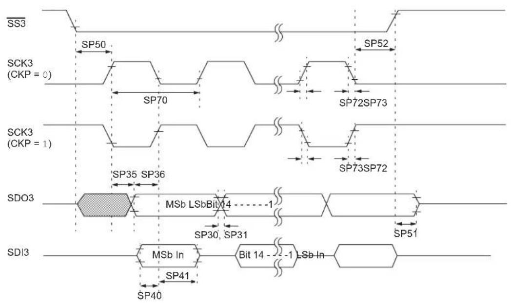
text_image
SS3 SP50 SP52 SCK3 (CKP = 0) SP70 SP72SP73 SCK3 (CKP = 1) SP35 SP36 SP73SP72 SDO3 MSb LSbBit14 -1 SP30, SP31 SP51 SDI3 MSb In Bit 14 -1 LSb In SP40 SP41Note 1: For dsPIC33EPXXXGSX06 and dsPIC33EPXXXGSX08 devices with a fixed SCK3 pin.
2: Refer to Figure 30-1 for load conditions.
TABLE 30-46: SPI3 SLAVE MODE (FULL-DUPLEX, CKE = 0, CKP = 0, SMP = 0) TIMING REQUIREMENTS ^(5)
| AC CHARACTERISTICS | Standard Operating Conditions: 3.0V to 3.6V(unless otherwise stated)Operating temperature -40°C ≤ TA ≤ +85°C for Industrial-40°C ≤ AT ≤ +125°C for Extended | ||||||
| Param. | Symbol Char | characteristic (1) | Min. Typ. | (2) | Max. | Units Conditions | |
| SP70 | FscP | Maximum SCK3 Input Frequency | — | — | 25 | MHz | (Note 3) |
| SP72 | TscF | SCK3 Input Fall Time | — | — | — | ns | See Parameter DO32(Note 4) |
| SP73 | TscR | SCK3 Input Rise Time | — | — | — | ns | See Parameter DO31(Note 4) |
| SP30 | TdoF | SDO3 Data Output Fall Time | — | — | — | ns | See Parameter DO32(Note 4) |
| SP31 | TdoR | SDO3 Data Output Rise Time | — | — | — | ns | See Parameter DO31(Note 4) |
| SP35 | TscH2doV,TscL2doV | SDO3 Data Output Valid after SCK3 Edge | — | 6 | 20 | ns | |
| SP36 | TdoV2scH,TdoV2scL | SDO3 Data Output Setup to First SCK3 Edge | 20 | — | — | ns | |
| SP40 | TdiV2scH,TdiV2scL | Setup Time of SDI3 Data Input to SCK3 Edge | 20 | — | — | ns | |
| SP41 | TscH2diL,TscL2diL | Hold Time of SDI3 Data Input to SCK3 Edge | 15 | — | — | ns | |
| SP50 | TssL2scH,TssL2scL | 3 to SCK3 ↑ or SCK3 ↓ Input | 120 | — | — | ns | |
| SP51 | TssH2doZ | 3 to SDO3 Output High-Impedance | 10 | — | 50 | ns | (Note 4) |
| SP52 | TscH2ssH,TscL2ssH | 3 after SCK1 Edge | 1.5 TCY + 40 | — | — | ns | (Note 4) |
Note 1: These parameters are characterized, but are not tested in manufacturing.
2: Data in "Typical" column is at 3.3V, +25°C unless otherwise stated.
3: The minimum clock period for SCK3 is 91 ns. Therefore, the SCK3 clock generated by the master must not violate this specification.
4: Assumes 50 pF load on all SPI3 pins.
5: For dsPIC33EPXXXGSX06 and dsPIC33EPXXXGSX08 devices with a fixed SCK3 pin.
FIGURE 30-27: I2Cx BUS START/STOP BITS TIMING CHARACTERISTICS (MASTER MODE)

text_image
SCLx IM30 IM31 SDAx Start Condition Stop Condition IM33 IM34 Note: Refer to Figure 30-1 for load conditions.FIGURE 30-28: I2Cx BUS DATA TIMING CHARACTERISTICS (MASTER MODE)
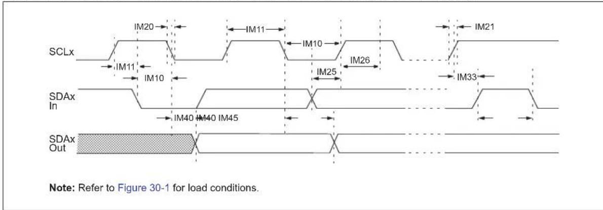
other
| Signal | Phase 1 | Phase 2 | Phase 3 | Phase 4 | |------------|---------|---------|---------|---------| | SCLx | IM20 | IM11 | IM10 | IM26 | | SDAx In | IM10 | IM25 | IM33 | IM40 | | SDAx Out | IM40 | IM40 | IM45 | (not labeled) |TABLE 30-47: I2Cx BUS DATA TIMING REQUIREMENTS (MASTER MODE)
| AC CHARACTERISTICS | Standard Operating Conditions: 3.0V to 3.6V(unless otherwise stated)Operating temperature -40°C ≤ TA ≤ +85°C for Industrial-40°C ≤ AT ≤ +125°C for Extended | ||||||
| Param No. | Symbol | Characteristic (4) | Min.(1) | Max. Units Conditions | |||
| IM10 T | LO:SCL | Clock Low Time | 100 kHz mode | Tcy/2 (BRG + 2) | — | μs | |
| 400 kHz mode | Tcy/2 (BRG + 2) | — | μs | ||||
| 1 MHz mode(2) | Tcy/2 (BRG + 2) | — | μs | ||||
| IM11 T | HI:SCL | Clock High Time | 100 kHz mode | Tcy/2 (BRG + 2) | — | μs | |
| 400 kHz mode | Tcy/2 (BRG + 2) | — | μs | ||||
| 1 MHz mode(2) | Tcy/2 (BRG + 2) | — | μs | ||||
| IM20 T | F:SCL | SDAx and SCLxFall Time | 100 kHz mode | — | 300 | ns | Cb is specified to be from 10 to 400 pF |
| 400 kHz mode | 20 + 0.1 CB | 300 | ns | ||||
| 1 MHz mode(2) | — | 100 | ns | ||||
| IM21 T | R:SCL SD | DAx and SCLx Rise Time | 100 kHz mode | — | 1000 | ns | Cb is specified to be from 10 to 400 pF |
| 400 kHz mode | 20 + 0.1 CB | 300 | ns | ||||
| 1 MHz mode(2) | — | 300 | ns | ||||
| IM25 T | SU:DAT | Data Input Setup Time | 100 kHz mode | 250 | — | ns | |
| 400 kHz mode | 100 | — | ns | ||||
| 1 MHz mode(2) | 40 | — | ns | ||||
| IM26 T | HD:DAT | Data Input Hold Time | 100 kHz mode | 0 | — | μs | |
| 400 kHz mode | 0 | 0.9 | μs | ||||
| 1 MHz mode(2) | 0.2 | — | μs | ||||
| IM30 T | SU:STA | Start Condition Setup Time | 100 kHz mode | Tcy/2 (BRG + 2) | — | μs | Only relevant for Repeated Start condition |
| 400 kHz mode | Tcy/2 (BRG + 2) | — | μs | ||||
| 1 MHz mode(2) | Tcy/2 (BRG + 2) | — | μs | ||||
| IM31 | THD:STA | Start Condition Hold Time | 100 kHz mode | Tcy/2 (BRG + 2) | — | μs | After this period, the first clock pulse is generated |
| 400 kHz mode | Tcy/2 (BRG + 2) | — | μs | ||||
| 1 MHz mode(2) | Tcy/2 (BRG + 2) | — | μs | ||||
| IM33 | TSU:STO | Stop Condition Setup Time | 100 kHz mode | Tcy/2 (BRG + 2) | — | μs | |
| 400 kHz mode | Tcy/2 (BRG + 2) | — | μs | ||||
| 1 MHz mode(2) | Tcy/2 (BRG + 2) | — | μs | ||||
| IM34 | THD:STO | Stop Condition Hold Time | 100 kHz mode | Tcy/2 (BRG + 2) | — | μs | |
| 400 kHz mode | Tcy/2 (BRG + 2) | — | μs | ||||
| 1 MHz mode(2) | Tcy/2 (BRG + 2) | — | μs | ||||
| IM40 | TAA:SCL | Output Valid from Clock | 100 kHz mode | — | 3500 | ns | |
| 400 kHz mode | — | 1000 | ns | ||||
| 1 MHz mode(2) | — | 400 | ns | ||||
| IM45 | TBF:SDA | Bus Free Time | 100 kHz mode | 4.7 | — | μs | Time the bus must be free before a new transmission can start |
| 400 kHz mode | 1.3 | — | μs | ||||
| 1 MHz mode(2) | 0.5 | — | μs | ||||
| IM50 | CB | Bus Capacitive Loading | — | 400 | pF | ||
| IM51 | TPGD | Pulse Gobbler Delay | 65 | 390 | ns | (Note 3) | |
Note 1: BRG is the value of the I ^2 C Baud Rate Generator.
2: Maximum Pin Capacitance = 10 pF for all I2Cx pins (for 1 MHz mode only).
3: Typical value for this parameter is 130 ns.
4: These parameters are characterized but not tested in manufacturing.
FIGURE 30-29: I2Cx BUS START/STOP BITS TIMING CHARACTERISTICS (SLAVE MODE)

text_image
SCLx IS30 IS31 IS34 SDAx Start Condition Stop ConditionFIGURE 30-30: I2Cx BUS DATA TIMING CHARACTERISTICS (SLAVE MODE)
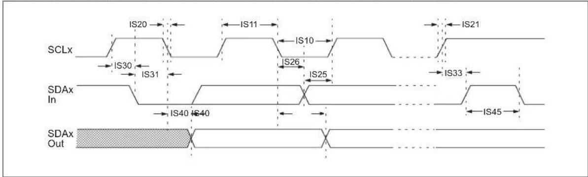
text_image
SCLx IS20 IS11 IS10 IS21 IS30 IS31 IS26 IS25 IS33 SDAx In IS40 IS40 IS45 SDAx OutTABLE 30-48: I2Cx BUS DATA TIMING REQUIREMENTS (SLAVE MODE)
| AC CHARACTERISTICS | Standard Operating Conditions: 3.0V to 3.6V(unless otherwise stated)Operating temperature -40°C ≤ TA ≤ +85°C for Industrial-40°C ≤ TA ≤ +125°C for Extended | ||||||
| Param No. | Symbol | Characteristic (3) | Min. Max. | Units | Conditions | ||
| IS10 T | LO:SCL | Clock Low Time | 100 kHz mode | 4.7 | — | μs | |
| 400 kHz mode | 1.3 | — | μs | ||||
| 1MHzmode^(1) | 0.5 | — | μs | ||||
| IS11 | THI:SCL | Clock High Time | 100 kHz mode | 4.0 | — | μs | Device must operate at a minimum of 1.5 MHz |
| 400 kHz mode | 0.6 | — | μs | Device must operate at a minimum of 10 MHz | |||
| 1MHzmode^(1) | 0.5 | — | μs | ||||
| IS20 | TF:SCL | SDAx and SCLx Fall Time | 100 kHz mode | — | 300 | ns | CB is specified to be from 10 to 400 pF |
| 400 kHz mode | 20 + 0.1 CB | 300 | ns | ||||
| 1MHzmode^(1) | — | 100 | ns | ||||
| IS21 | TR:SCL | SDAx and SCLx Rise Time | 100 kHz mode | — | 1000 | ns | CB is specified to be from 10 to 400 pF |
| 400 kHz mode | 20 + 0.1 CB | 300 | ns | ||||
| 1MHzmode^(1) | — | 300 | ns | ||||
| IS25 | TSU:DAT | Data Input Setup Time | 100 kHz mode | 250 | — | ns | |
| 400 kHz mode | 100 | — | ns | ||||
| 1MHzmode^(1) | 100 | — | ns | ||||
| IS26 | THD:DAT | Data Input Hold Time | 100 kHz mode | 0 | — | μs | |
| 400 kHz mode | 0 | 0.9 | μs | ||||
| 1MHzmode^(1) | 0 | 0.3 | μs | ||||
| IS30 | TSU:STA | Start Condition Setup Time | 100 kHz mode | 4.7 | — | μs | Only relevant for Repeated Start condition |
| 400 kHz mode | 0.6 | — | μs | ||||
| 1MHzmode^(1) | 0.25 | — | μs | ||||
| IS31 | THD:STA | Start Condition Hold Time | 100 kHz mode | 4.0 | — | μs | After this period, the first clock pulse is generated |
| 400 kHz mode | 0.6 | — | μs | ||||
| 1MHzmode^(1) | 0.25 | — | μs | ||||
| IS33 | TSU:STO | Stop Condition Setup Time | 100 kHz mode | 4.7 | — | μs | |
| 400 kHz mode | 0.6 | — | μs | ||||
| 1MHzmode^(1) | 0.6 | — | μs | ||||
| IS34 | THD:STO | Stop Condition Hold Time | 100 kHz mode | 4 | — | μs | |
| 400 kHz mode | 0.6 | — | μs | ||||
| 1MHzmode^(1) | 0.25 | μs | |||||
| IS40 | TAA:SCL | Output Valid from Clock | 100 kHz mode | 0 | 3500 | ns | |
| 400 kHz mode | 0 | 1000 | ns | ||||
| 1MHzmode^(1) | 0 | 350 | ns | ||||
| IS45 | TBF:SDA | Bus Free Time | 100 kHz mode | 4.7 | — | μs | Time the bus must be free before a new transmission can start |
| 400 kHz mode | 1.3 | — | μs | ||||
| 1MHzmode^(1) | 0.5 | — | μs | ||||
| IS50 | CB | Bus Capacitive Loading | — | 400 | pF | ||
| IS51 T | PGD | Pulse Gobbler Delay | 65 | 390 | ns | (Note 2) | |
Note 1: Maximum Pin Capacitance = 10 pF for all I2Cx pins (for 1 MHz mode only).
2: Typical value for this parameter is 130 ns.
3: These parameters are characterized but not tested in manufacturing.
FIGURE 30-31: CANx MODULE I/O TIMING CHARACTERISTICS

text_image
CxTX Pin (output) Old Value New Value CA10 CA11 CxRX Pin (input) CA20TABLE 30-49: CANx MODULE I/O TIMING REQUIREMENTS
| AC CHARACTERISTICS | Standard Operating Conditions: 3.0V to 3.6V(unless otherwise stated)Operating temperature -40°C ≤ TA ≤ +85°C for Industrial-40°C ≤ AT ≤ +125°C for Extended | ||||||
| Param No. | Symbol | Characteristic (1) | Min. Typ. (2) | Max. Units Conditions | |||
| CA10 T | IoF | Port Output Fall Time | — | — | — | ns | See Parameter DO32 |
| CA11 | TioR | Port Output Rise Time | — | — | — | ns | See Parameter DO31 |
| CA20 | TcWF | Pulse Width to TriggerCAN Wake-up Filter | 120 — | — | ns | ||
Note 1: These parameters are characterized but not tested in manufacturing.
2: Data in "Typical" column is at 3.3V, +25°C unless otherwise stated. Parameters are for design guidance only and are not tested.
FIGURE 30-32: UARTx MODULE I/O TIMING CHARACTERISTICS
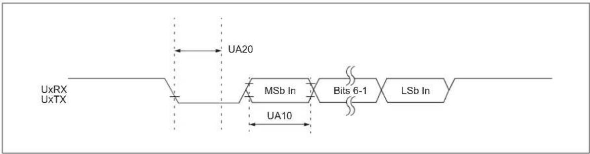
flowchart
graph LR
    A["UxRX"] --> B["Pin 1"]
    C["UxTX"] --> D["Pin 2"]
    B --> E["UA20"]
    D --> F["UA10"]
    E --> G["MSb In"]
    F --> H["Bits 6-1"]
    G --> I["LSb In"]
TABLE 30-50: UARTx MODULE I/O TIMING REQUIREMENTS
| AC CHARACTERISTICS | Standard Operating Conditions: 3.0V to 3.6V(unless otherwise stated)Operating temperature -40°C ≤ TA ≤ +125°C | ||||||
| Param No. | Symbol C | characteristic (1) | Min. Typ. (2) | Max. Units Conditions | |||
| UA10 T | UABAUD UA | ARTx Baud Time 66.67 — — | ns | ||||
| UA11 | FBAUD | UARTx Baud Frequency | — | — | 15 | Mbps | |
| UA20 | TCWF | Start Bit Pulse Width to Trigger UARTx Wake-up | 500 | — — | ns | ||
Note 1: These parameters are characterized but not tested in manufacturing.
2: Data in "Typ." column is at 3.3V, +25°C unless otherwise stated. Parameters are for design guidance only and are not tested.
TABLE 30-51: ANALOG CURRENT SPECIFICATIONS
| AC CHARACTERISTICS | Standard Operating Conditions: 3.0V to 3.6V(unless otherwise stated)Operating temperature -40°C ≤ TA ≤ +125°C | ||||||
| Param No. | Symbol | Characteristic^(1) | Min. | Typ.^(2) | Max. | Units | Conditions |
| AVD01 | IDD | Analog Modules Current Consumption | — | 9 | — | mA Ch | characterized data with the following modules enabled:APLL, 5 ADC Cores, 2 PGAs and 4 Analog Comparators |
Note 1: These parameters are characterized but not tested in manufacturing.
2: Data in "Typ." column is at 3.3V, +25°C unless otherwise stated. Parameters are for design guidance only and are not tested.
TABLE 30-52: ADC MODULE SPECIFICATIONS
| AC CHARACTERISTICS | Standard Operating Conditions: 3.0V to 3.6V(unless otherwise stated)(5)Operating temperature -40°C ≤ TA ≤ +85°C for Industrial-40°C ≤ TA ≤ +125°C for Extended | ||||||
| Param No. | Symbol | Characteristics Min. Typical Max. Units Conditions | |||||
| Device Supply | |||||||
| AD01 AV | DD | Module VDD Supply | Greater of: VDD - 0.3 or 3.0 | — Lesser of: VDD + 0.3 or 3.6 | V within 300 mV of V DD at all times, including device power-up | ||
| AD02 AV | SS | Module Vss Supply | Vss | — | Vss + 0.3 | V | |
| Reference Inputs | |||||||
| AD06 | VREFL | Reference Voltage Low | — | AVss | — | V | (Note 1) |
| AD07 V | REF | Absolute Reference Voltage (VREFH - VREFL) | 2.7 | — | AVDD | V | (Note 3) |
| AD08 I | REF | Reference Input Current | — | 5 | 10 | μA | ADC operating or in standby |
| Analog Input | |||||||
| AD12 V | INH-VINL | Full-Scale Input Span | AVss | — | AVDD | V | |
| AD14 | VIN | Absolute Input Voltage | AVss - 0.3 | — | AVDD + 0.3 | V | |
| AD17 R | IN | Recommended Impedance of Analog Voltage Source | — | 100 | — | Ω | For minimum sampling time (Note 1) |
| AD66 V | BG | Internal Voltage Reference Source | — | 1.2 | — | V | |
| ADC Accuracy: Pseudodifferential Input | |||||||
| AD20a | Nr Resolution | 12 bits | |||||
| AD21a | INL | Integral Nonlinearity | > -3 | — | < 3 | LSb | AVss = 0V, AVDD = 3.3V |
| AD22a | DNL | Differential Nonlinearity | > -1 | — | < 1 | LSb | AVss = 0V, AVDD = 3.3V (Note 2) |
| AD23a | GERR Gain | Error (Dedicated Core) | > 0 | 8 | < 15 | LSb | AVss = 0V, AVDD = 3.3V |
| Gain Error (Shared Core) | > 5 | 15 | < 22 | LSb | |||
| AD24a | EOFF | Offset Error (Dedicated Core) | > 0 | 5 | < 10 | LSb | AVss = 0V, AVDD = 3.3V |
| Offset Error (Shared Core) | > 2 | 8 | < 13 | LSb | |||
| AD25a | — | Monotonicity | — | — | — | — | Guaranteed |
Note 1: These parameters are not characterized or tested in manufacturing.
2: No missing codes, limits based on characterization results.
3: These parameters are characterized but not tested in manufacturing.
4: Characterized with a 15 kHz sine wave.
5: The ADC module is functional at VBORMIN < VDD < VDDMIN, but with degraded performance. Unless otherwise stated, module functionality is ensured, but not characterized.
TABLE 30-52: ADC MODULE SPECIFICATIONS (CONTINUED)
| AC CHARACTERISTICS | Standard Operating Conditions: 3.0V to 3.6V(unless otherwise stated)(5)Operating temperature -40°C ≤ TA ≤ +85°C for Industrial-40°C ≤ TA ≤ +125°C for Extended | ||||||
| Param No. | Symbol | Characteristics | Min. | Typical | Max. | Units | Conditions |
| ADC Accuracy: Single-Ended Input | |||||||
| AD20b | Nr Resolution | 12 bits | |||||
| AD21b | INL Integral | Nonlinearity >5 — < 5 L | Sb AV | ss = 0V, AVDD = 3.3V | |||
| AD22b | DNL | Differential Nonlinearity | >-1 | — | < 1 | LSb | AVss = 0V, AVDD = 3.3V(Note 2) |
| AD23b | G ERR | Gain Error(Dedicated Core) | >0 | 8 | < 15 | LSb | AVss = 0V, AVDD = 3.3V |
| Gain Error(Shared Core) | >5 | 15 | < 22 | LSb | |||
| AD24b | EOFF Offset | Error(Dedicated Core) | >2 | 9 | < 15 | LSb | AVss = 0V, AVDD = 3.3V |
| Offset Error(Shared Core) | >5 | 17 | < 22 | LSb | |||
| AD25b | — | Monotonicity | — | — | — | — | Guaranteed |
| Dynamic Performance | |||||||
| AD31b | $INAD | Signal-to-Noise and Distortion | 63 | — | >65 | dB | (Notes 3, 4) |
| AD34b | ENOB | Effective Number of Bits | 10.3 | — | — | bits | (Notes 3, 4) |
Note 1: These parameters are not characterized or tested in manufacturing.
2: No missing codes, limits based on characterization results.
3: These parameters are characterized but not tested in manufacturing.
4: Characterized with a 15 kHz sine wave.
5: The ADC module is functional at VBORMIN < VDD < VDDMIN, but with degraded performance. Unless otherwise stated, module functionality is ensured, but not characterized.
TABLE 30-53: ANALOG-TO-DIGITAL CONVERSION TIMING REQUIREMENTS
| AC CHARACTERISTICS | Standard Operating Conditions: 3.0V to 3.6V(unless otherwise stated)(2)Operating temperature -40°C ≤ TA ≤ +85°C for Industrial-40°C ≤ TA ≤ +125°C for Extended | ||||||
| Param No. | Symbol | Characteristics | Min. Typ. | (1) | Max. | Units | Conditions |
| Clock Parameters | |||||||
| AD50 T | AD ADC | Clock Period | 14.28 | — | — | ns | |
| Throughput Rate | |||||||
| AD51 | FTP | SH0-SH3 | — | — | 3.25 | Msps | 70 MHz ADC clock, 12 bits, no pendingconversion at time of trigger |
| SH4 | — — | 3.25 | Msps | ||||
Note 1: These parameters are characterized but not tested in manufacturing.
2: The ADC module is functional at VBORMIN < VDD < VDDMIN, but with degraded performance. Unless otherwise stated, module functionality is ensured, but not characterized.
TABLE 30-54: HIGH-SPEED ANALOG COMPARATOR MODULE SPECIFICATIONS
| AC/DC CHARACTERISTICS | Standard Operating Conditions: 3.0V to 3.6V(unless otherwise stated)(2)Operating temperature -40°C ≤ TA ≤ +85°C for Industrial-40°C ≤ TA ≤ +125°C for Extended | ||||||
| Param No. | Symbol | Characteristic | Min. | Typ. | Max. | Units | Comments |
| CM10 | VIOFF | Input Offset Voltage | -35 | ±5 | 35 | mV | |
| CM11 | VICM | Input Common-Mode Voltage Range(1) | 0 | — | AVDD | V | |
| CM13 | CMRR | Common-Mode Rejection Ratio | 60 | — | — | dB | |
| CM14 | TRESP | Large Signal Response | — | 15 | — | ns | V+ input step of 100 mV while V- input is held at AVDD/2. Delay measured from analog input pin to PWMx output pin. |
| CM15 | VHYST | Input Hysteresis | 5 | 10 | 20 | mV | Depends on HYSSEL<1:0> |
| CM16 | TON | Comparator Enabled to Valid Output | — | — | 1 | μs | |
Note 1: These parameters are for design guidance only and are not tested in manufacturing.
2: The comparator module is functional at VBORMIN < VDD < VDDMIN, but with degraded performance. Unless otherwise stated, module functionality is tested, but not characterized.
TABLE 30-55: DACx MODULE SPECIFICATIONS
| AC/DC CHARACTERISTICS | Standard Operating Conditions: 3.0V to 3.6V(unless otherwise stated) ^(2) Operating temperature -40°C ≤ TA ≤ +85°C for Industrial-40°C ≤ TA ≤ +125°C for Extended | ||||||
| Param No. | Symbol | Characteristic Min. Typ. Max. | Units | Comments | |||
| DA01 EXTREF External Voltage Reference ^(1) | 1 | — | AVDD | V | |||
| DA02 | CVRES | Resolution | 12 | bits | |||
| DA03 | INL | Integral Nonlinearity Error | -16 | -12 | 0 | LSB | |
| DA04 | DNL | Differential Nonlinearity Error | -1.8 | ±1 | 1.8 | LSB | |
| DA05 | EOFF | Offset Error | -8 | 3 | 15 | LSB | |
| DA06 | EG | Gain Error | -1.2 | -0.5 | 0 | % | |
| DA07 T | SET | Settling Time ^(1) | — | 700 | — | ns | Output with 2% of desired output voltage with a 10-90% or 90-10% step |
Note 1: Parameters are for design guidance only and are not tested in manufacturing.
2: The DACx module is functional at V BORMIN < VDD < VDDMIN, but with degraded performance. Unless otherwise stated, module functionality is tested, but not characterized.
TABLE 30-56: DACx OUTPUT (DACOUTx PIN) SPECIFICATIONS
| DC CHARACTERISTICS | Standard Operating Conditions: 3.0V to 3.6V(unless otherwise stated)(1)Operating temperature -40°C ≤ TA ≤ +85°C for Industrial-40°C ≤ TA ≤ +125°C for Extended | ||||||
| Param No. | Symbol | Characteristic | Min. | Typ. | Max. | Units | Comments |
| DA11 | RLOAD | Resistive Output Load Impedance | 10k | — | — | Ohm | |
| DA11a | CLOAD Output Load Capacitance | — | — | 35 pF | Including output pin capacitance | ||
| DA12 | IOUT | Output Current Drive Strength | — | 300 | — | μA | Sink and source |
| DA13 | VRANGE | Output Drive Voltage Range at Current Drive of 300 μA | AVss + 250 mV | — | AVDD – 900 mV | V | |
| DA14 | VLRANGE | Output Drive Voltage Range at Reduced Current Drive of 50 μA | AVss + 50 mV | — | AVDD – 500 mV | V | |
| DA15 | IDD | Current Consumed when Module is Enabled | — | — | 1.3 x IOUT | μA | Module will always consume this current, even if no load is connected to the output |
| DA30 | VOFFSET | Input Offset Voltage | — | ±5 | — | mV | |
Note 1: The DACx module is functional at VBORMIN < VDD < VDDMIN, but with degraded performance. Unless otherwise stated, module functionality is tested, but not characterized.
TABLE 30-57: PGAx MODULE SPECIFICATIONS
| AC/DC CHARACTERISTICS | Standard Operating Conditions: 3.0V to 3.6V(unless otherwise stated)(1)Operating temperature -40°C ≤ TA ≤ +85°C for Industrial-40°C ≤ TA ≤ +125°C for Extended | |||||||
| Param No. | Symbol | Characteristic Min. Typ. Max. Units Comments | ||||||
| PA01 V | IN | Input Voltage Range | AVss - 0.3 | — | AVDD + 0.3 | V | ||
| PA02 V | CM | Common-Mode Input Voltage Range | AVss | — | AVDD - 1.6 | V | ||
| PA03 | Vos | Input Offset Voltage | -10 | — | 10 | mV | ||
| PA04 V | OS | Input Offset Voltage Drift with Temperature | — | ±15 | — | μV/°C | ||
| PA05 R | IN+ | Input Impedance of Positive Input | — | >1M || 7 pF | — | Ω|| pF | ||
| PA06 RIN- | Input Impedance of Negative Input | — | 10k || 7 pF | — | Ω|| pF | |||
| PA07 | GERR | Gain Error | -2 | — | 2 | % | Gain = 4x, 8x | |
| -3 | — | 3 | % | Gain = 16x | ||||
| -4 | — | 4 | % | Gain = 32x, 64x | ||||
| PA08 L | ERR | Gain Nonlinearity Error | — | — | 0.5 | % | % of full scale, Gain = 16x | |
| PA09 I | DD | Current Consumption | — | 2.0 | — | mA | Module is enabled with a 2-volt P-P output voltage swing | |
| PA10a | BW | Small Signal Bandwidth (-3 dB) | G = 4x | — | 10 | — | MHz | |
| PA10b | G = 8x | — | 5 | — | MHz | |||
| PA10c | G = 16x | — | 2.5 | — | MHz | |||
| PA10d | G = 32x | — | 1.25 | — | MHz | |||
| PA10e | G = 64x | — | 0.625 | — | MHz | |||
| PA11 OST Output Settling Time to 1% of Final Value | — | 0.4 | — | μs | Gain = 16x, 100 mV input step change | |||
| PA12 | SR | Output Slew Rate | — | 40 | — | V/μs | Gain = 16x | |
| PA13 T | GSEL | Gain Selection Time | — | 1 | — | μs | ||
| PA14 T | ON | Module Turn On/Setting Time | — | — | 10 | μs | ||
Note 1: The PGAx module is functional at VBORMIN < VDD < VDDMIN, but with degraded performance. Unless otherwise stated, module functionality is tested, but not characterized.
TABLE 30-58: CONSTANT-CURRENT SOURCE SPECIFICATIONS
| DC CHARACTERISTICS | Standard Operating Conditions: 3.0V to 3.6V(unless otherwise stated)(1)Operating temperature -40°C ≤ TA ≤ +85°C for Industrial-40°C ≤ TA ≤ +125°C for Extended | ||||||
| Param No. | Symbol | Characteristic Min. Typ. Max. Units | Conditions | ||||
| CC01 I | DD | Current Consumption | — | 30 | — | μA | |
| CC02 I | REG | Regulation of Current with Voltage On | — | ±3 | — | % | |
| CC03 | IOUT | Current Output at Terminal | — | 10 | — | μA | |
Note 1: The constant-current source module is functional at VBORMIN < VDD < VDDMIN, but with degraded performance. Unless otherwise stated, module functionality is tested, but not characterized.
TABLE 30-59: DMA MODULE TIMING REQUIREMENTS
| AC CHARACTERISTICS | Standard Operating Conditions: 3.0V to 3.6V(unless otherwise stated)Operating temperature -40°C ≤ TA ≤ +85°C for Industrial-40°C ≤ TA ≤ +125°C for Extended | |||||
| Param No. | Characteristic | Min. | Typ.^(1) | Max. | Units | Conditions |
| DM1 DMA Byte/Word Transfer Latency | 1 T CY^(2) | — | — | ns | ||
Note 1: These parameters are characterized, but not tested in manufacturing.
2: Because DMA transfers use the CPU data bus, this time is dependent on other functions on the bus.
NOTES:
31.0 DC AND AC DEVICE CHARACTERISTICS GRAPHS
Note: The graphs provided following this note are a statistical summary based on a limited number of samples and are provided for design guidance purposes only. The performance characteristics listed herein are not tested or guaranteed. In some graphs, the data presented may be outside the specified operating range (e.g., outside specified power supply range) and therefore, outside the warranted range.
FIGURE 31-1: Voh - 4x DRIVER PINS

line
| Voltage | IOH (A) | | ------- | ------- | | 3.6V | -0.045 | | 3.3V | -0.038 | | 3V | -0.032 | | Absolute Maximum | -0.015 |FIGURE 31-3: V OL - 4x DRIVER PINS
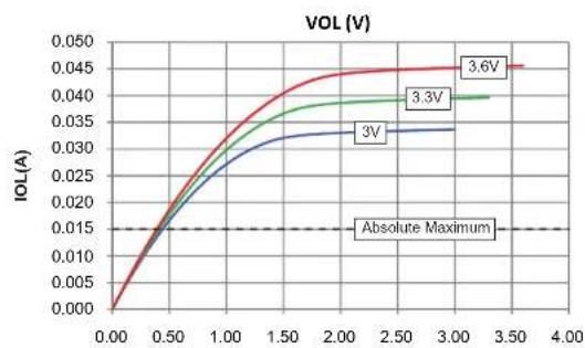
line
| VOLT (V) | IOL (A) at 3V | IOL (A) at 3.3V | IOL (A) at 3.6V | | -------- | ------------- | --------------- | --------------- | | Absolute Maximum | 0.015 | 0.015 | 0.015 | | Currents (approx.) | 0.025 | 0.030 | 0.040 | | Thresholds (approx.) | 0.030 | 0.035 | 0.045 |FIGURE 31-2: V OH - 8x DRIVER PINS
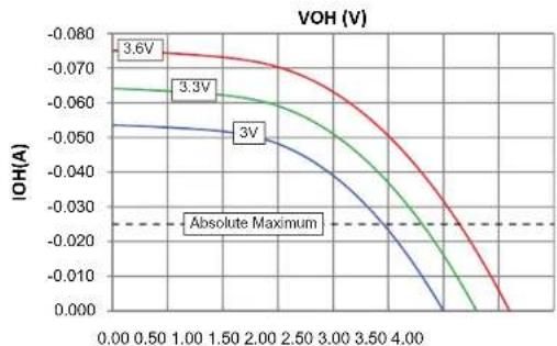
line
| VOH (V) | IOH (A) at 3.6V | IOH (A) at 3.3V | IOH (A) at 3V | | ------- | --------------- | --------------- | ------------- | | 0.00 | -0.070 | -0.055 | -0.050 | | 0.50 | -0.075 | -0.058 | -0.052 | | 1.00 | -0.078 | -0.060 | -0.054 | | 1.50 | -0.080 | -0.062 | -0.056 | | 2.00 | -0.082 | -0.064 | -0.058 | | 2.50 | -0.084 | -0.066 | -0.060 | | 3.00 | -0.086 | -0.068 | -0.062 | | 3.50 | -0.088 | -0.070 | -0.064 | | 4.00 | -0.090 | -0.072 | -0.066 |FIGURE 31-4: V OL - 8x DRIVER PINS
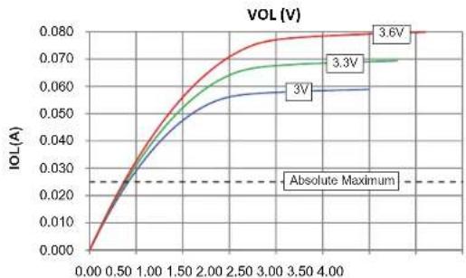
line
| VOLT (V) | IOL (A) at 3V | IOL (A) at 3.3V | IOL (A) at 3.6V | | -------- | ------------- | --------------- | --------------- | | 0.00 | 0.000 | 0.000 | 0.000 | | 0.50 | 0.025 | 0.025 | 0.025 | | 1.00 | 0.040 | 0.040 | 0.040 | | 1.50 | 0.055 | 0.055 | 0.055 | | 2.00 | 0.065 | 0.065 | 0.065 | | 2.50 | 0.070 | 0.070 | 0.070 | | 3.00 | 0.072 | 0.072 | 0.072 | | 3.50 | 0.073 | 0.073 | 0.073 | | 4.00 | 0.074 | 0.074 | 0.074 |FIGURE 31-5: TYPICAL IPD CURRENT @ VDD = 3.3V
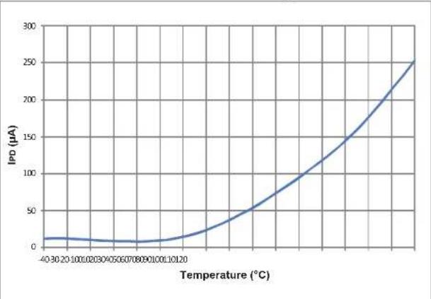
line
| Temperature (°C) | IPD (μA) | | ---------------- | -------- | | -40 | 10 | | -30 | 10 | | -20 | 10 | | -10 | 10 | | 0 | 10 | | 10 | 10 | | 20 | 10 | | 30 | 10 | | 40 | 10 | | 50 | 10 | | 60 | 10 | | 70 | 10 | | 80 | 10 | | 90 | 10 | | 100 | 10 | | 110 | 10 | | 120 | 10 | | 130 | 10 | | 140 | 10 | | 150 | 10 | | 160 | 10 | | 170 | 10 | | 180 | 10 | | 190 | 10 | | 200 | 10 | | 210 | 10 | | 220 | 10 | | 230 | 10 | | 240 | 10 | | 250 | 10 | | 260 | 10 | | 270 | 10 | | 280 | 10 | | 290 | 10 | | 300 | 10 |FIGURE 31-6: TYPICAL I DD CURRENT @ VDD = 3.3V, +25°C

line
| MIPS | Idd (mA) | | ---- | -------- | | 100 | 7 | | 300 | 10 | | 600 | 14 | | 900 | 18 | | 1200 | 22 | | 1500 | 25 | | 1800 | 28 | | 2100 | 30 |FIGURE 31-7: TYPICAL I DOZE CURRENT @ VDD = 3.3V, +25°C
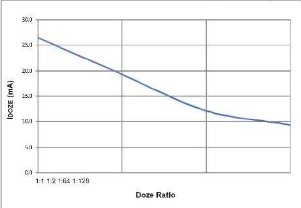
line
| Doze Ratio | I_DOZE (mA) | | ---------- | ----------- | | 1:1 | 26.0 | | 1:2 | 24.0 | | 1:64 | 20.0 | | 1:128 | 18.0 | | | 15.0 | | | 12.0 | | | 10.0 | | | 9.0 |FIGURE 31-8: TYPICAL I IDLE CURRENT @ VDD = 3.3V, +25°C
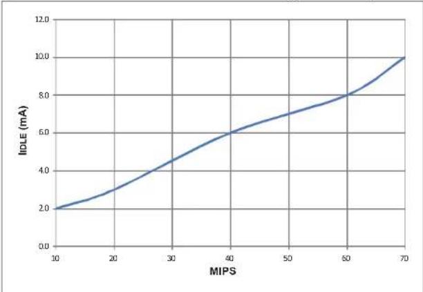
line
| MIPS | IodLE (mA) | | ---- | ---------- | | 10 | 2.0 | | 20 | 3.0 | | 30 | 4.5 | | 40 | 6.0 | | 50 | 7.0 | | 60 | 8.0 | | 70 | 10.0 |FIGURE 31-9: TYPICAL FRC FREQUENCY @ VDD = 3.3V

line
| Temperature (°C) | Frequency (kHz) | | :--- | :--- | | -3.5 | 7360 | | -3.0 | 7365 | | -2.5 | 7370 | | -2.0 | 7380 | | -1.5 | 7385 | | -1.0 | 7388 | | -0.5 | 7385 | | 0.0 | 7375 | | 0.5 | 7365 | | 1.0 | 7355 | | 1.5 | 7345 | | 2.0 | 7335 | | 2.5 | 7325 | | 3.0 | 7315 | | 3.5 | 7305 | | 4.0 | 7295 | | 4.5 | 7285 | | 5.0 | 7275 | | 5.5 | 7265 | | 6.0 | 7255 | | 6.5 | 7245 | | 7.0 | 7235 | | 7.5 | 7225 | | 8.0 | 7215 | | 8.5 | 7205 | | 9.0 | 7195 | | 9.5 | 7185 | | 10.0 | 7175 |FIGURE 31-10: TYPICAL LPRC FREQUENCY @ VDD = 3.3V
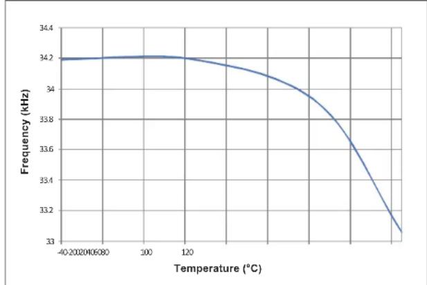
line
| Temperature (°C) | Frequency (kHz) | | :--- | :--- | | -40-20 | 34.2 | | -20-10 | 34.2 | | -10-0 | 34.2 | | -0-10 | 34.2 | | 10-20 | 34.15 | | 20-30 | 34.05 | | 30-40 | 33.95 | | 40-50 | 33.85 | | 50-60 | 33.75 | | 60-70 | 33.65 | | 70-80 | 33.55 | | 80-90 | 33.45 | | 90-100 | 33.35 | | 100-110 | 33.3 | | 110-120 | 33.25 | | 120-130 | 33.2 | | 130-140 | 33.15 | | 140-150 | 33.1 |NOTES:
32.0 PACKAGING INFORMATION
32.1 Package Marking Information
28-Lead SOIC (7.50 mm)
text_image
XXXXXXXXXXXXXXXXXX XXXXXXXXXXXXXXXXXX XXXXXXXXXXXXXXXXXX YYWWNNN28-Lead UQFN (6x6x0.55 mm)

text_image
XXXXXXXX XXXXXXXX YYWWNNN28-Lead QFN-S (6x6x0.9 mm)

text_image
XXXXXXXX XXXXXXXX YYWWNNN44-Lead TQFP (10x10x1 mm)

text_image
MICROCHIP XXXXXXXXXX XXXXXXXXXX XXXXXXXXXX YYWWNNNExample

text_image
dsPIC33EP128GS702 1810017Example

text_image
33EP128 GS702 1810017Example

text_image
33EP128 GS702 1810017Example
text_image
MICROCHIP dsPIC33EP 64GS804 1810017Legend: XX...X Customer-specific information
Y Year code (last digit of calendar year)
YY Year code (last 2 digits of calendar year)
WW Week code (week of January 1 is week '01')
NNN Alphanumeric traceability code
Note: In the event the full Microchip part number cannot be marked on one line, it will be carried over to the next line, thus limiting the number of available characters for customer-specific information.
32.1 Package Marking Information (Continued)
44-Lead QFN (8x8 mm)

text_image
XXXXXXXXXXXX XXXXXXXXXXXX XXXXXXXXXXXX YYWWNNNExample
text_image
dsPIC33EP 64GS804 181001748-Lead TQFP (7x7x1.0 mm) Example
text_image
XXXXXXXX XXXXXXXXXXXXYWW NNN
text_image
EP64GS 8051810 01764-Lead TQFP (10x10x1 mm)
text_image
MICROCHIP XXXXXXXXX XXXXXXXXX XXXXXXXXX ○ YYWWNNNExample

text_image
MICROCHIP dsPIC33EP 64GS806 181001780-Lead TQFP (12x12x1 mm)
text_image
MICROCHIP XXXXXXXXXXXXXX XXXXXXXXXXXXX YYWWNNNExample
text_image
MICROCHIP dsPIC33EP64 GS808 181001732.2 Package Details
28-Lead Plastic Small Outline (SO) - Wide, 7.50 mm Body [SOIC]
Note: For the most current package drawings, please see the Microchip Packaging Specification located at http://www.microchip.com/packaging
![Microchip dsPIC33EP64GS805 - 28-Lead Plastic Small Outline (SO) - Wide, 7.50 mm Body [SOIC] - 1](/content/2026/06/1217585/images/d293545ce11203cd9e3737035de1a6775126cea3f27cb234eb465e6fdd11ab4e.jpg)
text_image
NOTE 1 2X 0.10 C D NOTE 1 1 2 3 D A NOTE 5 E1 e B NOTE 5 TOP VIEW 0.20 C A-B 2X D E/2 E 0.33 C 2X N/2 TIPS NX b ⊕ 0.25 M C A-B D![Microchip dsPIC33EP64GS805 - 28-Lead Plastic Small Outline (SO) - Wide, 7.50 mm Body [SOIC] - 2](/content/2026/06/1217585/images/e78fe9ff3f7be6a88ebb9efc4ecdac83ad9a031f50421ed2aa90ffa3f2f52b06.jpg)
text_image
A A2 A1 // 0.10 C // 0.10 C NX SEATING PLANE C SIDE VIEW A A![Microchip dsPIC33EP64GS805 - 28-Lead Plastic Small Outline (SO) - Wide, 7.50 mm Body [SOIC] - 3](/content/2026/06/1217585/images/012377e027dd9ccca2bdf5cc6cf107ec7c8a17bb729a793fb8c45c75884863dd.jpg)
text_image
h H SEE VIEW C VIEW A-AMicrochip Technology Drawing C04-052C Sheet 1 of 2
28-Lead Plastic Small Outline (SO) - Wide, 7.50 mm Body [SOIC]
Note: For the most current package drawings, please see the Microchip Packaging Specification located at http://www.microchip.com/packaging
![Microchip dsPIC33EP64GS805 - 28-Lead Plastic Small Outline (SO) - Wide, 7.50 mm Body [SOIC] - 1](/content/2026/06/1217585/images/52a03a57205d74bd03b4218f923035f393070bd63cbfc073fef71026b3df33eb.jpg)
text_image
α 4X θ φ L (L1) 4X βVIEW C
![Microchip dsPIC33EP64GS805 - 28-Lead Plastic Small Outline (SO) - Wide, 7.50 mm Body [SOIC] - 2](/content/2026/06/1217585/images/aeb0716f1561e25d1cfdee34b9cd94452491a6bfafcb8cadd3d3a04607364b0e.jpg)
natural_image
Isometric line drawing of an integrated circuit chip with multiple 24-pin pins (no text or symbols)| Units | MILLIMETERS | |||
| Dimension Limits | MIN | NOM | MAX | |
| Number of Pins | N | 28 | ||
| Pitch | e | 1.27 BSC | ||
| Overall Height | A | - | - | 2.65 |
| Molded Package Thickness | A2 | 2.05 | - | - |
| Standoff § | A1 | 0.10 | - | 0.30 |
| Overall Width | E | 10.30 BSC | ||
| Molded Package Width | E1 | 7.50 BSC | ||
| Overall Length | D | 17.90 BSC | ||
| Chamfer (Optional) | h | 0.25 | - | 0.75 |
| Foot Length | L | 0.40 | - | 1.27 |
| Footprint | L1 | 1.40 REF | ||
| Lead Angle | 0^ | - | - | |
| Foot Angle | 0^ | - | 8^ | |
| Lead Thickness | c | 0.18 | - | 0.33 |
| Lead Width | b | 0.31 | - | 0.51 |
| Mold Draft Angle Top | 5^ | - | 15^ | |
| Mold Draft Angle Bottom | 5^ | - | 15^ | |
Notes:
- Pin 1 visual index feature may vary, but must be located within the hatched area.
- § Significant Characteristic
- Dimension D does not include mold flash, protrusions or gate burrs, which shall not exceed 0.15 mm per end. Dimension E1 does not include interlead flash or protrusion, which shall not exceed 0.25 mm per side.
- Dimensioning and tolerancing per ASME Y14.5M BSC: Basic Dimension. Theoretically exact value shown without tolerances. REF: Reference Dimension, usually without tolerance, for information purposes only.
- Datums A & B to be determined at Datum H.
Microchip Technology Drawing C04-052C Sheet 2 of 2
28-Lead Plastic Small Outline (SO) - Wide, 7.50 mm Body [SOIC]
Note: For the most current package drawings, please see the Microchip Packaging Specification located at http://www.microchip.com/packaging

text_image
Gx C G SILK SCREEN Y E XRECOMMENDED LAND PATTERN
| Units | MILLIMETERS | |||
| Dimension Limits | MIN | NOM | MAX | |
| Contact Pitch | E | 1.27 BSC | ||
| Contact Pad Spacing | C | 9.40 | ||
| Contact Pad Width (X28) | X | 0.60 | ||
| Contact Pad Length (X28) | Y | 2.00 | ||
| Distance Between Pads | Gx | 0.67 | ||
| Distance Between Pads | G | 7.40 | ||
Notes:
- Dimensioning and tolerancing per ASME Y14.5M
BSC: Basic Dimension. Theoretically exact value shown without tolerances.
Microchip Technology Drawing No. C04-2052A
28-Lead Ultra Thin Plastic Quad Flat, No Lead Package (2N) - 6x6x0.55 mm Body [UQFN] With 4.65x4.65 mm Exposed Pad and Corner Anchors
Note: For the most current package drawings, please see the Microchip Packaging Specification located at http://www.microchip.com/packaging
![Microchip dsPIC33EP64GS805 - 28-Lead Ultra Thin Plastic Quad Flat, No Lead Package (2N) - 6x6x0.55 mm Body [UQFN] With 4.65x4.65 mm Exposed Pad and Corner Anchors - 1](/content/2026/06/1217585/images/dc6fb4e642ac233794b46ff01a332f7d61d4cf15d8eedebc0cfd9c7428ca03b0.jpg)
text_image
NOTE 1 N 1 2 (DATUM B) (DATUM A) 2X 0.10 C 2X 0.10 C TOP VIEW SEATING PLANE A (A3) // 0.10 C A1 SIDE VIEW 28X 0.08 C 8X b1 D2 0.10 A B 8X b2 E2 2 1 2X P NOTE 1 N e 28X K BOTTOM VIEW 0.10 A B 0.05 MMicrochip Technology Drawing C04-385 Rev C Sheet 1 of 2
28-Lead Ultra Thin Plastic Quad Flat, No Lead Package (2N) - 6x6x0.55 mm Body [UQFN] With 4.65x4.65 mm Exposed Pad and Corner Anchors
Note: For the most current package drawings, please see the Microchip Packaging Specification located at http://www.microchip.com/packaging
![Microchip dsPIC33EP64GS805 - 28-Lead Ultra Thin Plastic Quad Flat, No Lead Package (2N) - 6x6x0.55 mm Body [UQFN] With 4.65x4.65 mm Exposed Pad and Corner Anchors - 1](/content/2026/06/1217585/images/a403d24feb16005dc20f9b2c82617de815e76f7521fc3f75a613d51d3fa39abb.jpg)
natural_image
Technical line drawing of two rectangular electronic components with pins, shown from top and bottom views (no text or symbols)| Units | MILLIMETERS | |||
| Dimension Limits | MIN | NOM | MAX | |
| Number of Terminals | N | 28 | ||
| Pitch | e | 0.65 BSC | ||
| Overall Height | A | 0.45 | 0.50 | 0.55 |
| Standoff | A1 | 0.00 | 0.02 | 0.05 |
| Terminal Thickness | A3 | 0.127 REF | ||
| Overall Width | E | 6.00 BSC | ||
| Exposed Pad Width | E2 | 4.55 | 4.65 | 4.75 |
| Overall Length | D | 6.00 BSC | ||
| Exposed Pad Length | D2 | 4.55 | 4.65 | 4.75 |
| Exposed Pad Corner Chamfer P - | 0.35 - | |||
| Terminal Width | b | 0.25 | 0.30 | 0.35 |
| b1 | 0.35 0.40 | 0.43Corner | Anchor Pad | |
| Corner Pad, Metal Free Zone b2 | 0.15 0.20 | 0.25 | ||
| Terminal Length | L | 0.30 | 0.40 | 0.50 |
| Terminal-to-Exposed-Pad | K | - | ||
0.20 -
Notes:
- Pin 1 visual index feature may vary, but must be located within the hatched area.
- Package is saw singulated
- Dimensioning and tolerancing per ASME Y14.5M
BSC: Basic Dimension. Theoretically exact value shown without tolerances.
REF: Reference Dimension, usually without tolerance, for information purposes only.
Microchip Technology Drawing C04-385 Rev C Sheet 2 of 2
28-Lead Ultra Thin Plastic Quad Flat, No Lead Package (2N) - 6x6x0.55 mm Body [UQFN] With 4.65x4.65 mm Exposed Pad and Corner Anchors
Note: For the most current package drawings, please see the Microchip Packaging Specification located at http://www.microchip.com/packaging
![Microchip dsPIC33EP64GS805 - 28-Lead Ultra Thin Plastic Quad Flat, No Lead Package (2N) - 6x6x0.55 mm Body [UQFN] With 4.65x4.65 mm Exposed Pad and Corner Anchors - 1](/content/2026/06/1217585/images/0121ab47803849fa55860e654c1e0cdb9d7cb652694f0cf70e575332bf03ed38.jpg)
text_image
C2 Y2 EV 28 X1 1 2 C1 EV ØV Y3 Y4 G1 G2 X4 E Y1 SILK SCREEN X3RECOMMENDED LAND PATTERN
| Units | MILLIMETERS | |||
| Dimension Limits | MIN | NOM | MAX | |
| Contact Pitch | E | 0.65 BSC | ||
| Optional Center Pad Width | X2 | 4.75 | ||
| Optional Center Pad Length | Y2 | 4.75 | ||
| C1Contact Pad Spacing 6.00 | ||||
| Contact Pad Spacing | C2 | 6.00 | ||
| Contact Pad Width (X28) | X1 | 0.35 | ||
| Contact Pad Length (X28) | Y1 | 0.80 | ||
| Corner Anchor (X4) | X3 | 1.00 | ||
| Corner Anchor (X4) | Y3 | 1.00 | ||
| Corner Anchor Chamfer (X4) | X4 | 0.35 | ||
| Corner Anchor Chamfer (X4) | Y4 | 0.35 | ||
| Contact Pad to Pad (X28) G1 0.20 | ||||
| Contact Pad to Center Pad (X28) G2 0.20 | ||||
| Thermal Via Diameter V | 0.33 | |||
| Thermal Via Pitch EV | 1.20 | |||
Notes:
1. Dimensioning and tolerancing per ASME Y14.5M
BSC: Basic Dimension. Theoretically exact value shown without tolerances.
2. For best soldering results, thermal vias, if used, should be filled or tented to avoid solder loss during reflow process
Microchip Technology Drawing C04-2385B
Note: Corner anchor pads are not connected internally and are designed as mechanical features when the package is soldered to the PCB.
28-Lead Plastic Quad Flat, No Lead Package (MM) - 6x6x0.9mm Body [QFN-S] With 0.40 mm Terminal Length
Note: For the most current package drawings, please see the Microchip Packaging Specification located at http://www.microchip.com/packaging
![Microchip dsPIC33EP64GS805 - 28-Lead Plastic Quad Flat, No Lead Package (MM) - 6x6x0.9mm Body [QFN-S] With 0.40 mm Terminal Length - 1](/content/2026/06/1217585/images/4f35ded6ee1fe37640541ef1a00904ab54b293cb8d02204ae1dc4e95dff4fa53.jpg)
text_image
NOTE 1 1 2 (DATUM B) (DATUM A) 2X 0.15 C 2X 0.15 C D A B E TOP VIEW![Microchip dsPIC33EP64GS805 - 28-Lead Plastic Quad Flat, No Lead Package (MM) - 6x6x0.9mm Body [QFN-S] With 0.40 mm Terminal Length - 2](/content/2026/06/1217585/images/bffb1ac92dd3cff33885c2aec60d1e88f5868ac38ce432f0d803248472f084a2.jpg)
text_image
SEATING PLANE A3 SIDE VIEW A A1 28 X // 0.10 C 0.08 C![Microchip dsPIC33EP64GS805 - 28-Lead Plastic Quad Flat, No Lead Package (MM) - 6x6x0.9mm Body [QFN-S] With 0.40 mm Terminal Length - 3](/content/2026/06/1217585/images/d9ecbb3bcfb93302d79a62485c5f0a69c46465c3db916bb8d45a061adf14cc5d.jpg)
text_image
0.10M C A B E2 2 1 28X L NOTE 1 N 28X b BOTTOM VIEW D2 e 28X K 0.10M C A B 0.05M CMicrochip Technology Drawing C04-124C Sheet 1 of 2
28-Lead Plastic Quad Flat, No Lead Package (MM) - 6x6x0.9mm Body [QFN-S] With 0.40 mm Terminal Length
Note: For the most current package drawings, please see the Microchip Packaging Specification located at http://www.microchip.com/packaging
![Microchip dsPIC33EP64GS805 - 28-Lead Plastic Quad Flat, No Lead Package (MM) - 6x6x0.9mm Body [QFN-S] With 0.40 mm Terminal Length - 1](/content/2026/06/1217585/images/07d3063bc9d72404a3d7b4315eedb1dcb19fbb1ae534eb631f39e1c078fbd52b.jpg)
natural_image
Isometric line drawing of a square integrated circuit chip with multiple pins (no text or symbols)| Units | MILLIMETERS | |||
| Dimension Limits | MIN | NOM | MAX | |
| Number of Pins | N | 28 | ||
| Pitch | e | 0.65 BSC | ||
| Overall Height | A | 0.80 | 0.90 | 1.00 |
| Standoff | A1 | 0.00 | 0.02 | 0.05 |
| Terminal Thickness | A3 | 0.20 REF | ||
| Overall Width | E | 6.00 BSC | ||
| Exposed Pad Width | E2 | 3.65 | 3.70 | 4.70 |
| Overall Length | D | 6.00 BSC | ||
| Exposed Pad Length | D2 | 3.65 | 3.70 | 4.70 |
| Terminal Width | b | 0.23 | 0.30 | 0.35 |
| Terminal Length | L | 0.30 | 0.40 | 0.50 |
| Terminal-to-Exposed Pad | K | 0.20 | - | - |
Notes:
- Pin 1 visual index feature may vary, but must be located within the hatched area.
- Package is saw singulated
- Dimensioning and tolerancing per ASME Y14.5M
BSC: Basic Dimension. Theoretically exact value shown without tolerances.
REF: Reference Dimension, usually without tolerance, for information purposes only.
Microchip Technology Drawing C04-124C Sheet 2 of 2
28-Lead Plastic Quad Flat, No Lead Package (MM) - 6x6x0.9 mm Body [QFN-S] with 0.40 mm Contact Length
Note: For the most current package drawings, please see the Microchip Packaging Specification located at http://www.microchip.com/packaging
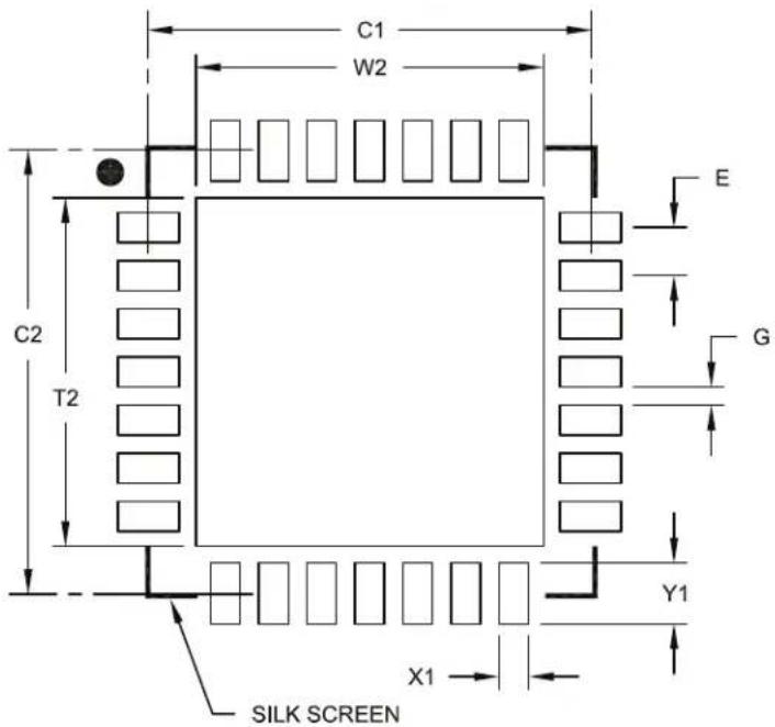
text_image
C1 W2 E G Y1 X1 SILK SCREEN C2 T2RECOMMENDED LAND PATTERN
| Units | MILLIMETERS | |||
| Dimension Limits | MIN | NOM | MAX | |
| Contact Pitch | E | 0.65 BSC | ||
| Optional Center Pad Width | W2 | 4.70 | ||
| Optional Center Pad Length | T2 | 4.70 | ||
| Contact Pad Spacing | C1 | 6.00 | ||
| Contact Pad Spacing | C2 | 6.00 | ||
| Contact Pad Width (X28) | X1 | 0.40 | ||
| Contact Pad Length (X28) | Y1 | 0.85 | ||
| Distance Between Pads | G | 0.25 | ||
Notes:
1. Dimensioning and tolerancing per ASME Y14.5M
BSC: Basic Dimension. Theoretically exact value shown without tolerances.
Microchip Technology Drawing No. C04-2124A
44-Lead Plastic Thin Quad Flatpack (PT) - 10x10x1.0 mm Body [TQFP]
Note: For the most current package drawings, please see the Microchip Packaging Specification located at http://www.microchip.com/packaging
![Microchip dsPIC33EP64GS805 - 44-Lead Plastic Thin Quad Flatpack (PT) - 10x10x1.0 mm Body [TQFP] - 1](/content/2026/06/1217585/images/979e532ef8dd62dd2ce6a2755b7d8e0e9dea24ed9e43bedd272d06bf260903ca.jpg)
text_image
NOTE 2 (DATUM A) (DATUM B) NOTE 1 2X 0.20 H A B N 2X 0.20 H A B TOP VIEW 4X 11 TIPS 0.20 C A B SEATING PLANE C A A2 SIDE VIEW 0.10 C A1 NOTE 1 N 44 X b e Φ 0.20® A B BOTTOM VIEWMicrochip Technology Drawing C04-076C Sheet 1 of 2
44-Lead Plastic Thin Quad Flatpack (PT) - 10x10x1.0 mm Body [TQFP]
Note: For the most current package drawings, please see the Microchip Packaging Specification located at http://www.microchip.com/packaging
![Microchip dsPIC33EP64GS805 - 44-Lead Plastic Thin Quad Flatpack (PT) - 10x10x1.0 mm Body [TQFP] - 1](/content/2026/06/1217585/images/effcd2f65b32a52298298bab27788b69ac7f3c30205bbfcb555a18fee72f166d.jpg)
text_image
H L (L1) c θ SECTION A-A| Units | MILLIMETERS | |||
| Dimension Limits | MIN | NOM | MAX | |
| Number of Leads | N | 44 | ||
| Lead Pitch | e | 0.80 BSC | ||
| Overall Height | A | - | - | 1.20 |
| Standoff | A1 | 0.05 | - | 0.15 |
| Molded Package Thickness | A2 | 0.95 1.00 | 1.05 | |
| Overall Width | E | 12.00 BSC | ||
| Molded Package Width | E1 | 10.00 BSC | ||
| Overall Length | D | 12.00 BSC | ||
| Molded Package Length | D1 | 10.00 BSC | ||
| Lead Width | b | 0.30 | 0.37 | 0.45 |
| Lead Thickness | c | 0.09 - 0.20 | ||
| Lead Length | L | 0.45 | 0.60 | 0.75 |
| Footprint L1 1.00 REF | ||||
| θ | 3.5°0' 7" | Foot Angle | ||
Notes:
1. Pin 1 visual index feature may vary, but must be located within the hatched area.
2. Exact shape of each corner is optional.
3. Dimensioning and tolerancing per ASME Y14.5M
BSC: Basic Dimension. Theoretically exact value shown without tolerances.
REF: Reference Dimension, usually without tolerance, for information purposes only.
Microchip Technology Drawing C04-076C Sheet 2 of 2
44-Lead Plastic Thin Quad Flatpack (PT) 10X10X1 mm Body, 2.00 mm Footprint [TQFP]
Note: For the most current package drawings, please see the Microchip Packaging Specification located at http://www.microchip.com/packaging
![Microchip dsPIC33EP64GS805 - 44-Lead Plastic Thin Quad Flatpack (PT) - 10x10x1.0 mm Body [TQFP] - 2](/content/2026/06/1217585/images/9eede922631236954d517e18b517f4b7d536e2ea527d0e7fdfaba9166e7a1d16.jpg)
text_image
C1 G SILK SCREEN Y1 X1 E C2RECOMMENDED LAND PATTERN
| Units | MILLIMETERS | |||
| Dimension Limits | MIN | NOM | MAX | |
| Contact Pitch | E | 0.80 BSC | ||
| Contact Pad Spacing | C1 | 11.40 | ||
| Contact Pad Spacing | C2 | 11.40 | ||
| Contact Pad Width (X44) | X1 | 0.55 | ||
| Contact Pad Length (X44) | Y1 | 1.50 | ||
| Distance Between Pads | G | 0.25 | ||
Notes:
1. Dimensioning and tolerancing per ASME Y14.5M
BSC: Basic Dimension. Theoretically exact value shown without tolerances.
Microchip Technology Drawing No. C04-2076B
44-Lead Plastic Quad Flat, No Lead Package (ML) - 8x8 mm Body [QFN or VQFN]
Note: For the most current package drawings, please see the Microchip Packaging Specification located at http://www.microchip.com/packaging
![Microchip dsPIC33EP64GS805 - 44-Lead Plastic Quad Flat, No Lead Package (ML) - 8x8 mm Body [QFN or VQFN] - 1](/content/2026/06/1217585/images/6266e01168d7395f60dfa3cc5fdac5f9036a4e26e590f3e171c27b18458a5bb7.jpg)
text_image
NOTE 1 1 2 (DATUM B) (DATUM A) 2X 0.20 C 2X 0.20 C TOP VIEW SEATING PLANE C A A3 // 0.10 C A1 44X 0.08 C SIDE VIEW L D2 0.10 A B E2 K 2 1 NOTE 1 N 44X b e 0.07 A B 0.05 B BOTTOM VIEWMicrochip Technology Drawing C04-103D Sheet 1 of 2
44-Lead Plastic Quad Flat, No Lead Package (ML) - 8x8 mm Body [QFN or VQFN]
Note: For the most current package drawings, please see the Microchip Packaging Specification located at http://www.microchip.com/packaging
![Microchip dsPIC33EP64GS805 - 44-Lead Plastic Quad Flat, No Lead Package (ML) - 8x8 mm Body [QFN or VQFN] - 1](/content/2026/06/1217585/images/0e46eec7721e3a1a5f45d138e8695b7c60a0e4602885cc06e92548ace8f766aa.jpg)
natural_image
Two isometric diagrams of an integrated circuit chip with square and rectangular components, showing top and bottom views (no text or symbols)| Units | MILLIMETERS | |||
| Dimension Limits | MIN | NOM | MAX | |
| Number of Pins | N | 44 | ||
| Pitch | e | 0.65 BSC | ||
| Overall Height | A | 0.80 | 0.90 | 1.00 |
| Standoff | A1 | 0.00 | 0.02 | 0.05 |
| Terminal Thickness | A3 | 0.20 REF | ||
| Overall Width | E | 8.00 BSC | ||
| Exposed Pad Width | E2 | 6.25 | 6.45 | 6.60 |
| Overall Length | D | 8.00 BSC | ||
| Exposed Pad Length | D2 | 6.25 | 6.45 | 6.60 |
| Terminal Width | b | 0.20 | 0.30 | 0.35 |
| Terminal Length | L | 0.30 | 0.40 | 0.50 |
| Terminal-to-Exposed-Pad | K | - | ||
0.20 -
Notes:
- Pin 1 visual index feature may vary, but must be located within the hatched area.
- Package is saw singulated
- Dimensioning and tolerancing per ASME Y14.5M
BSC: Basic Dimension. Theoretically exact value shown without tolerances.
REF: Reference Dimension, usually without tolerance, for information purposes only.
Microchip Technology Drawing C04-103D Sheet 2 of 2
44-Lead Plastic Quad Flat, No Lead Package (ML) - 8x8 mm Body [QFN or VQFN]
Note: For the most current package drawings, please see the Microchip Packaging Specification located at http://www.microchip.com/packaging
![Microchip dsPIC33EP64GS805 - 44-Lead Plastic Quad Flat, No Lead Package (ML) - 8x8 mm Body [QFN or VQFN] - 1](/content/2026/06/1217585/images/2f63785b5e55a4772b0855cd2f1388d9df8490c5fad68e2231570a60e4127120.jpg)
text_image
C1 X2 EV 44 G2 1 2 EV ØV G1 C2 Y2 Y1 E X1 SILK SCREENRECOMMENDED LAND PATTERN
| Units | MILLIMETERS | |||
| Dimension Limits | MIN | NOM | MAX | |
| Contact Pitch | E | 0.65 BSC | ||
| Optional Center Pad Width | X2 | 6.60 | ||
| Optional Center Pad Length | Y2 | 6.60 | ||
| C1Contact Pad Spacing 8.00 | ||||
| Contact Pad Spacing | C2 | 8.00 | ||
| Contact Pad Width (X44) | X1 | 0.35 | ||
| Contact Pad Length (X44) | Y1 | 0.85 | ||
| Contact Pad to Contact Pad (X40) G1 0.30 | ||||
| Contact Pad to Center Pad (X44) G2 0.28 | ||||
| Thermal Via Diameter V | 0.33 | |||
| Thermal Via Pitch EV | 1.20 | |||
Notes:
- Dimensioning and tolerancing per ASME Y14.5M
BSC: Basic Dimension. Theoretically exact value shown without tolerances.
- For best soldering results, thermal vias, if used, should be filled or tented to avoid solder loss during reflow process
Microchip Technology Drawing No. C04-2103C
48-Lead Thin Quad Flatpack (PT) - 7x7x1.0 mm Body [TQFP]
Note: For the most current package drawings, please see the Microchip Packaging Specification located at http://www.microchip.com/packaging
![Microchip dsPIC33EP64GS805 - 48-Lead Thin Quad Flatpack (PT) - 7x7x1.0 mm Body [TQFP] - 1](/content/2026/06/1217585/images/0bbeecb4d0941d7f169b7c33703dcc4d68a5600435e8b62f24dcc9b3406ebb2b.jpg)
text_image
48X TIPS 0.20 C A-B D D D1 D1/2 D A B E1 E E1/2 E1/4 N NOTE 1 1 2 D1/4 e 4X 0.20 H A-B D 48x b Φ 0.08 M A-B D TOP VIEW SEATING PLANE C A A2 A1 // 0.10 C H SIDE VIEWMicrochip Technology Drawing C04-300-PT Rev A Sheet 1 of 2
48-Lead Thin Quad Flatpack (PT) - 7x7x1.0 mm Body [TQFP]
Note: For the most current package drawings, please see the Microchip Packaging Specification located at http://www.microchip.com/packaging
![Microchip dsPIC33EP64GS805 - 48-Lead Thin Quad Flatpack (PT) - 7x7x1.0 mm Body [TQFP] - 1](/content/2026/06/1217585/images/8a2ad538322df7635dac4cf3cf4f5405aec8632140e2f8e59bc7cd261c4d3691.jpg)
text_image
α H β L (L1) c θ![Microchip dsPIC33EP64GS805 - 48-Lead Thin Quad Flatpack (PT) - 7x7x1.0 mm Body [TQFP] - 2](/content/2026/06/1217585/images/a566ecd4687fd3dc1d54e715d5f30c9d2563a1778bfa7fdc83f9e9f5b21a58c8.jpg)
natural_image
Isometric line drawing of an integrated circuit chip with multiple pins (no text or symbols)SECTION A-A
| Units | MILLIMETERS | |||
| Dimension Limits | MIN | NOM | MAX | |
| Number of Leads | N | 48 | ||
| Lead Pitch | e | 0.50 BSC | ||
| Overall Height | A | - | - | 1.20 |
| Standoff | A1 | 0.05 | - | 0.15 |
| Molded Package Thickness | A2 | 0.95 | 1.00 | 1.05 |
| Foot Length | 0.750.60 | |||
| Footprint | L1 | 1.00 REF | ||
| Foot Angle | 0^ | 3.5^ | 7^ | |
| Overall Width | E | 9.00 BSC | ||
| Overall Length | D | 9.00 BSC | ||
| Molded Package Width | E1 | 7.00 BSC | ||
| Molded Package Length | D1 | 7.00 BSC | ||
| Lead Thickness | c | 0.09 | 0.16- | |
| Lead Width | b | 0.17 | 0.22 | 0.27 |
| Mold Draft Angle Top | 11^ | 12^ | 13^ | |
| Mold Draft Angle Bottom | 11^ 13^ | 12^ | ||
Notes:
- Pin 1 visual index feature may vary, but must be located within the hatched area.
- Chamfers at corners are optional; size may vary.
- Dimensions D1 and E1 do not include mold flash or protrusions. Mold flash or protrusions shall not exceed 0.25mm per side.
- Dimensioning and tolerancing per ASME Y14.5M
BSC: Basic Dimension. Theoretically exact value shown without tolerances.
REF: Reference Dimension, usually without tolerance, for information purposes only. - Datums A-B and D to be determined at center line between leads where leads exit plastic body at datum plane H
Microchip Technology Drawing C04-300-PT Rev A Sheet 2 of 2
48-Lead Thin Quad Flatpack (PT) - 7x7x1.0 mm Body [TQFP]
Note: For the most current package drawings, please see the Microchip Packaging Specification located at http://www.microchip.com/packaging
![Microchip dsPIC33EP64GS805 - 48-Lead Thin Quad Flatpack (PT) - 7x7x1.0 mm Body [TQFP] - 1](/content/2026/06/1217585/images/a4a0c33288f32f008344e92232fa1f867f9c90359e24a287bb1a264447e19eb2.jpg)
text_image
C1 C2 48 SILK SCREEN G Y1 1 2 X1 ERECOMMENDED LAND PATTERN
| Units | MILLIMETERS | |||
| Dimension Limits | MIN | NOM | MAX | |
| Contact Pitch | E | 0.50 BSC | ||
| C1Contact Pad Spacing 8.40 | ||||
| C2Contact Pad Spacing40 | ||||
| Contact Pad Width (X48) | X1 | 0.30 | ||
| Contact Pad Length (X48) | Y1 | 1.50 | ||
| Distance Between Pads G 0.20 | ||||
Notes:
1. Dimensioning and tolerancing per ASME Y14.5M
BSC: Basic Dimension. Theoretically exact value shown without tolerances.
2. For best soldering results, thermal vias, if used, should be filled or tented to avoid solder loss during reflow process
Microchip Technology Drawing C04-2300-PT Rev A
64-Lead Plastic Thin Quad Flatpack (PT)-10x10x1 mm Body, 2.00 mm Footprint [TQFP]
Note: For the most current package drawings, please see the Microchip Packaging Specification located at http://www.microchip.com/packaging
![Microchip dsPIC33EP64GS805 - 64-Lead Plastic Thin Quad Flatpack (PT)-10x10x1 mm Body, 2.00 mm Footprint [TQFP] - 1](/content/2026/06/1217585/images/bad339fceb21c34832623af9b3fcbd9645ccaa940fe5429ec2c84ee2c4d36b91.jpg)
text_image
NOTE 2 A SEE DETAIL 1 N 4X N/4 TIPS NOTE 1 D1/2 D D1 A B E1/2 A A 1 2 3 4X 0.20 C A-B D 0.20 H A-B D EE1TOP VIEW
![Microchip dsPIC33EP64GS805 - 64-Lead Plastic Thin Quad Flatpack (PT)-10x10x1 mm Body, 2.00 mm Footprint [TQFP] - 2](/content/2026/06/1217585/images/8eceb72b5f68a794d338e13fa5765037bbf84bf93557f4a7bcd885ecb5ad6812.jpg)
text_image
SEATING PLANE A C 0.08 C e 64 X b A1 A2 — 0.05 ⊕ 0.08® A-E DSIDE VIEW
Microchip Technology Drawing C04-085C Sheet 1 of 2
64-Lead Plastic Thin Quad Flatpack (PT)-10x10x1 mm Body, 2.00 mm Footprint [TQFP]
Note: For the most current package drawings, please see the Microchip Packaging Specification located at http://www.microchip.com/packaging
![Microchip dsPIC33EP64GS805 - 64-Lead Plastic Thin Quad Flatpack (PT)-10x10x1 mm Body, 2.00 mm Footprint [TQFP] - 1](/content/2026/06/1217585/images/6d457a178d84387882c1690ae8cb2936fb095f931ac5941eebfb9be4de669259.jpg)
text_image
α H β L (L1) c θ SECTION A-A X=A-B OR D e/2 XDETAIL 1
| Units | MILLIMETERS | |||
| Dimension Limits | MIN | NOM | MAX | |
| NNumber of Leads 64 | ||||
| Lead Pitch | e | 0.50 BSC | ||
| 1.20--AOverall Height0.95A2Molded Package | ||||
| 1.051.00 | ||||
| 0.15-0.05A1Standoff | ||||
| 0.750.600.45LFoot Length | ||||
| Footprint | L1 | 1.00 REF | ||
| Foot Angle | 7°3.5°0° | |||
| 12.00 BSCEOverall Width | ||||
| 12.00 BSCDOverall Length | ||||
| 10.00 BSCE1Molded Package Width | ||||
| Molded Package Length | D1 | 10.00 BSC | ||
| Lead Thickness | c | 0.20-0.09 | ||
| Lead Width | b | 0.270.220.17 | ||
| Mold Draft Angle Top | 13°12°11° | |||
| Mold Draft Angle Bottom | 13°12°11° | |||
Notes:
- Pin 1 visual index feature may vary, but must be located within the hatched area.
- Chamfers at corners are optional; size may vary.
- Dimensions D1 and E1 do not include mold flash or protrusions. Mold flash or protrusions shall not exceed 0.25mm per side.
- Dimensioning and tolerancing per ASME Y14.5M BSC: Basic Dimension. Theoretically exact value shown without tolerances. REF: Reference Dimension, usually without tolerance, for information purposes only.
Microchip Technology Drawing C04-085C Sheet 2 of 2
64-Lead Plastic Thin Quad Flatpack (PT) 10x10x1 mm Body, 2.00 mm Footprint [TQFP]
Note: For the most current package drawings, please see the Microchip Packaging Specification located at http://www.microchip.com/packaging

text_image
C1 G SILK SCREEN Y1 X1 E C2RECOMMENDED LAND PATTERN
| Units | MILLIMETERS | |||
| Dimension Limits | MIN | NOM | MAX | |
| Contact Pitch | E | 0.50 BSC | ||
| Contact Pad Spacing | C1 | 11.40 | ||
| Contact Pad Spacing | C2 | 11.40 | ||
| Contact Pad Width (X64) | X1 | 0.30 | ||
| Contact Pad Length (X64) | Y1 | 1.50 | ||
| Distance Between Pads | G | 0.20 | ||
Notes:
1. Dimensioning and tolerancing per ASME Y14.5M
BSC: Basic Dimension. Theoretically exact value shown without tolerances.
Microchip Technology Drawing No. C04-2085B
80-Lead Plastic Thin Quad Flatpack (PT) - 12x12x1 mm Body, 2.00 mm [TQFP]
Note: For the most current package drawings, please see the Microchip Packaging Specification located at http://www.microchip.com/packaging
![Microchip dsPIC33EP64GS805 - 80-Lead Plastic Thin Quad Flatpack (PT) - 12x12x1 mm Body, 2.00 mm [TQFP] - 1](/content/2026/06/1217585/images/0592696360cdfc9413d6ab823811d65e291f5965c7b790cb309ff73fd43db1c8.jpg)
text_image
D D1 E E1 e b N NOTE 1 123 NOTE 2 C β φ L A A1 L1 A2 α| Units MILLIMETERS | ||||
| Dimension Limits MIN NOM MAX | ||||
| Number of Leads N 80 | ||||
| Lead Pitch e 0.50 BSC | ||||
| Overall Height | A | - | ||
| Molded Package Thickness | A2 | 0.95 | 1.00 | 1.05 |
| Standoff | A1 | 0.05 | - | 0.15 |
| Foot Length | L | 0.45 | 0.60 | 0.75 |
| Footprint | L1 | 1.00 REF | ||
| Foot Angle | 0° | 3.5° | 7° | |
| Overall Width | E | 14.00 BSC | ||
| Overall Length | D | 14.00 BSC | ||
| Molded Package Width | E1 | 12.00 BSC | ||
| Molded Package Length | D1 | 12.00 BSC | ||
| Lead Thickness | c | 0.09 | - | 0.20 |
| Lead Width | b | 0.17 | 0.22 | 0.27 |
| Mold Draft Angle Top | 11° | 12° | 13° | |
| Mold Draft Angle Bottom | 11° | 12° | 13° | |
1.20
Notes:
- Pin 1 visual index feature may vary, but must be located within the hatched area.
- Chamfers at corners are optional; size may vary.
- Dimensions D1 and E1 do not include mold flash or protrusions. Mold flash or protrusions shall not exceed 0.25 mm per side.
- Dimensioning and tolerancing per ASME Y14.5M.
BSC: Basic Dimension. Theoretically exact value shown without tolerances.
REF: Reference Dimension, usually without tolerance, for information purposes only.
Microchip Technology Drawing C04-092B
80-Lead Plastic Thin Quad Flatpack (PT)-12x12x1mm Body, 2.00 mm Footprint [TQFP]
Note: For the most current package drawings, please see the Microchip Packaging Specification located at http://www.microchip.com/packaging
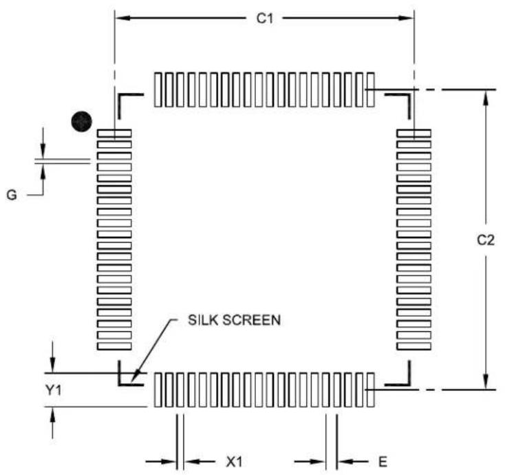
text_image
C1 G SILK SCREEN Y1 X1 E C2RECOMMENDED LAND PATTERN
| Units | MILLIMETERS | |||
| Dimension Limits | MIN | NOM | MAX | |
| Contact Pitch | E | 0.50 BSC | ||
| Contact Pad Spacing | C1 | 13.40 | ||
| Contact Pad Spacing | C2 | 13.40 | ||
| Contact Pad Width (X80) | X1 | 0.30 | ||
| Contact Pad Length (X80) | Y1 | 1.50 | ||
| Distance Between Pads | G | 0.20 | ||
Notes:
1. Dimensioning and tolerancing per ASME Y14.5M
BSC: Basic Dimension. Theoretically exact value shown without tolerances.
Microchip Technology Drawing No. C04-2092B
NOTES:
APPENDIX A: REVISION HISTORY
Revision A (May 2016)
This is the initial version of the document.
Revision B (January 2017)
- Sections:
- Updates Note 1 in Section 5.0 "Flash Program Memory".
- Tables:
- Updates the device description table on page 2.
- Updates Table 1-1, Table 4-2, Table 4-11, Table 7-1, Table 8-1, Table 11-11, Table 11-13, Table 17-1, Table 30-3, Table 30-4, Table 30-6, Table 30-7, Table 30-8, Table 30-9, Table 30-10, Table 30-11, Table 30-52, Table 30-54 and Table 30-55.
- Adds Table 11-6, Table 11-7, Table 11-8, Table 11-9 and Table 11-10.
- Figures:
- Updates the Pin Function tables in the Pin Diagram figures on pages 5 through 8.
- Updates Figure 4-1, Figure 17-1, Figure 18-1 and Figure 18-2.
- Registers:
- Updates Register 3-3, Register 16-5, Register 17-11, Register 18-1 and Register 19-2.
- Adds Register 11-1, Register 11-2, Register 11-3, Register 11-4, Register 11-5, Register 11-6, Register 11-7 and Register 11-8.
Revision C (October 2018)
- Sections:
- Adds Note 1 to all "Pin Diagrams".
- Updates Section 2.5 "ICSP Pins", Section 4.5.2 "Extended X Data Space", Section 8.0 "Direct Memory Access (DMA)", Section 11.7 "I/O Helpful Tips", Section 16.2 "Feature Description", Section 24.1 "Features Overview" and Section 24.3 "Module Applications".
- Tables:
- Updates Table 1-1, Table 4-9, Table 4-15, Table 8-1, Table 21-1, Table 21-2, Table 21-3, Table 21-4, Table 30-11, Table 30-56 and Table 30-57.
- Registers:
- Updates Register 3-2, Register 5-1, Register 9-4, Register 9-5, Register 10-1, Register 11-8, Register 14-1, Register 16-1, Register 16-2, Register 16-3, Register 16-4, Register 16-5, Register 16-6, Register 16-7, Register 16-8, Register 16-9, Register 16-10, Register 16-11, Register 16-13, Register 16-14, Register 16-16, Register 16-22, Register 19-1, Register 19-3, Register 21-3, Register 22-1, Register 22-28, Register 22-29, Register 22-30 and Register 26-1.
- Figures:
- Updates Figure 16-2, Figure 18-1, Figure 18-2 and Figure 30-30.
NOTES:
INDEX
A
Absolute Maximum Ratings 379
AC Characteristics 391
ADC Specifications 432
Analog Current Specifications.... 431
Analog-to-Digital Conversion Requirements...... 434
Auxiliary PLL Clock 393
CANx I/O Requirements 430
Capacitive Loading Requirements on Output Pins 391
DMA Module Requirements.... 437
External Clock Requirements 392
High-Speed PWMx Requirements 401
I/O Requirements.... 395
I2Cx Bus Data Requirements (Master Mode) 427
I2Cx Bus Data Requirements (Slave Mode) 429
Input Capture x Requirements 399
Internal FRC Accuracy.... 394
Internal LPRC Accuracy.... 394
Load Conditions 391
OCx/PWMx Module Requirements 400
Output Compare x Requirements 400
PLL Clock.... 393
Reset, WDT, OST, PWRT Requirements 396
SPI1, SPI2 and SPI3 Master Mode (Full-Duplex, CKE = 0, CKP = x, SMP = 1) Requirements ..... 405
SPI1, SPI2 and SPI3 Master Mode (Full-Duplex, CKE = 1, CKP = x, SMP = 1) Requirements ..... 404
SPI1, SPI2 and SPI3 Master Mode (Half-Duplex, Transmit Only) Requirements 403
SPI1, SPI2 and SPI3 Slave Mode (Full-Duplex, CKE = 0, CKP = 0, SMP = 0) Requirements ..... 413
SPI1, SPI2 and SPI3 Slave Mode (Full-Duplex, CKE = 0, CKP = 1, SMP = 0) Requirements ..... 411
SPI1, SPI2 and SPI3 Slave Mode (Full-Duplex, CKE = 1, CKP = 0, SMP = 0) Requirements ..... 407
SPI1, SPI2 and SPI3 Slave Mode (Full-Duplex, CKE = 1, CKP = 1, SMP = 0) Requirements ..... 409
SPI3 Master Mode (Full-Duplex, CKE = 0, CKP = x, SMP = 1) Requirements .... 417
SPI3 Master Mode (Full-Duplex, CKE = 1, CKP = x, SMP = 1) Requirements .... 416
SPI3 Master Mode (Half-Duplex, Transmit Only) Requirements 415
SPI3 Slave Mode (Full-Duplex, CKE = 0, CKP = 0, SMP = 0) Requirements.... 425
SPI3 Slave Mode (Full-Duplex, CKE = 0, CKP = 1, SMP = 0) Requirements.... 423
SPI3 Slave Mode (Full-Duplex, CKE = 1, CKP = 0, SMP = 0) Requirements.... 419
SPI3 Slave Mode (Full-Duplex, CKE = 1, CKP = 1, SMP = 0) Requirements.... 421
Temperature and Voltage Specifications 391
Timer1 External Clock Requirements 397
Timer2/Timer4 External Clock Requirements 398
Timer3/Timer5 External Clock Requirements .... 398
UARTx I/O Requirements 431
AC/DC Characteristics
DACx Specifications 435
High-Speed Analog Comparator Specifications..... 434
PGAx Specifications 436
Analog-to-Digital Converter. See ADC.
Arithmetic Logic Unit (ALU).... 32
Assembler
MPASM Assembler 376
MPLAB Assembler, Linker, Librarian.... 376
B
Bit-Reversed Addressing.... 58
Example.... 59
Implementation 58
Sequence Table (16-Entry) 59
Block Diagrams
16-Bit Timer1 Module 171
ADC Module 278
Addressing for Table Registers 63
CALL Stack Frame 54
CANx Module 312
CLCx Input Source Selection 265
CLCx Logic Function Combinatorial Options.... 264
CLCx Module 263
Connections for On-Chip Voltage Regulator 359
Constant-Current Source.... 349
CPU Core 24
Data Access from Program Space Address Generation....60
Dedicated ADC Cores 0-3 279
DMA Controller 93
dsPIC33EPXXGS70X/80X Family.... 13
High-Speed Analog Comparator x.... 338
High-Speed PWM Architecture.... 191
Hysteresis Control 340
I2Cx Module 250
Input Capture x 179
Interleaved PFC....20
MCLR Pin Connections 18
Multiplexing Remappable Outputs for RPn 140
Off-Line UPS 22
Oscillator System.... 106
Output Compare x Module 183
Peripheral to DMA Controller 91
PGAx Functions.... 346
PGAx Module 345
Phase-Shifted Full-Bridge Converter.... 21
PLL Module 107
Programmer's Model 26
PSV Read Address Generation.... 51
PTG Module 218
Recommended Minimum Connection 18
Remappable Input for U1RX 138
Reset System 71
Security Segments for dsPIC33EP128GS70X/80X (Dual Partition Modes).... 363
Security Segments for dsPIC33EP64GS70X/80X (Dual Partition Modes).... 362
Security Segments for dsPIC33EPXXXGS70X/80X.... 362
Shared ADC Core.... 279
Shared Port Structure.... 127
Simplified Conceptual of High-Speed PWM 192
SPIx Master, Frame Master Connection 247
SPIx Master, Frame Slave Connection 248
SPIx Master/Slave Connection (Enhanced Buffer Modes).... 247
SPIx Master/Slave Connection (Standard Mode)..... 246
SPIx Module (Enhanced Mode).... 235
SPIx Module (Standard Mode).... 234
SPIx Slave, Frame Master Connection 248
SPIx Slave, Frame Slave Connection.... 248
Suggested Oscillator Circuit Placement.... 19
Timerx (x = 2 through 5).... 176
Type B/Type C Timer Pair (32-Bit Timer).... 176
UARTx Module....257
Watchdog Timer (WDT) 360
Brown-out Reset (BOR) 351, 359
C
C Compilers
MPLAB XC 376
CAN Module
Control Registers 313
Message Buffers 332
Word 0 332
Word 1 332
Word 2 333
Word 3 333
Word 4 334
Word 5 334
Word 6 335
Word 7 335
Modes of Operation 312
Overview 311
CAN Module (CAN) 311
CLC
Control Registers 266
Code Examples
Port Write/Read 132
PWM Write-Protected Register
Unlock Sequence.... 190
PWRSAV Instruction Syntax.... 117
Code Protection 351, 361
CodeGuard Security 351, 361
Configurable Logic Cell (CLC) 263
Configurable Logic Cell. See CLC.
Configuration Bits....351
Description 353
Configuration Register Map 352
Constant-Current Source 349
Control Register 350
Description 349
Features Overview....349
Controller Area Network. See CAN.
CPU
Addressing Modes 23
Clocking System Options.... 107
Fast RC (FRC) Oscillator....107
FRC Oscillator with PLL (FRCPLL).... 107
FRC Oscillator with Postscaler 107
Low-Power RC (LPRC) Oscillator.... 107
Primary (XT, HS, EC) Oscillator....107
Primary Oscillator with PLL
(XTPLL, HSPLL, ECPLL)....107
Control Registers 28
Data Space Addressing 23
Instruction Set 23
Registers....23
Resources 27
Customer Change Notification Service 478
Customer Notification Service 478
Customer Support 478
D
Data Address Space.... 39
Memory Map for dsPIC33EP64GS70X/80X
Devices....40
Near Data Space 39
Organization, Alignment 39
SFR Space 39
Width 39
Data Space
Extended X 54
Paged Data Memory Space (figure) 52
Paged Memory Scheme 51
DC Characteristics
Brown-out Reset (BOR)...... 389
Constant-Current Source Specifications.... 437
DACx Output (DACOUTx Pin) Specifications...... 435
Doze Current (IDOZE) 385
I/O Pin Input Specifications.... 386
I/O Pin Output Specifications.... 389
Idle Current (IIDLE) 383
Operating Current (IDD) 382
Operating MIPS vs. Voltage 380
Power-Down Current (IPD) 384
Program Memory 390
Temperature and Voltage Specifications.... 381
Watchdog Timer Delta Current (ΔIWDT)...... 384
DC/AC Characteristics
Graphs and Tables 439
Demo/Development Boards, Evaluation and
Starter Kits 378
Development Support 375
Device Calibration.... 357
Addresses.... 357
and Identification 357
Device Programmer
MPLAB PM3 377
Direct Memory Access. See DMA.
DMA Controller
Channel to Peripheral Associations.... 92
Control Registers 94
DMAxCNT 94
DMAxCON....94
DMAxPAD 94
DMAxREQ....94
DMAxSTAL/H 94
DMAxSTBL/H 94
Supported Peripherals.... 91
Doze Mode 119
DSP Engine 32
E
Electrical Characteristics 379
AC 391
Equations
Device Operating Frequency 107
FPLLO Calculation 107
Fvco Calculation 107
Relationship Between Device and
SPIx Clock Speed 248
Errata 10
F
Filter Capacitor (CEFC) Specifications....381
Flash Program Memory 63
and Table Instructions....63
Control Registers 66
Dual Partition Flash Configuration 65
Operations 64
Resources.... 65
RTSP Operation....64
Flexible Configuration 351
G
Getting Started Guidelines.... 17
Connection Requirements 17
CPU Logic Filter Capacitor Connection (VCAP) ...... 18
Decoupling Capacitors.... 17
External Oscillator Pins.... 19
ICSP Pins.... 19
Master Clear (MCLR) Pin.... 18
Oscillator Value Conditions on Start-up 20
Targeted Applications 20
Unused I/Os.... 20
H
High-Speed Analog Comparator
Applications.... 339
Description.... 338
Digital-to-Analog Comparator (DAC) 339
Features Overview.... 337
Hysteresis 340
Pulse Stretcher and Digital Logic.... 339
Resources.... 340
High-Speed PWM
Features.... 189
Resources.... 190
Write-Protected Registers.... 190
High-Speed, 12-Bit Analog-to-Digital
Converter (ADC) 277
Control Registers 280
Features Overview.... 277
Resources.... 280
|
I/O Ports....127
Configuring Analog/Digital Port Pins.... 132
Control Registers 133
Helpful Tips.... 142
Open-Drain Configuration 132
Parallel I/O (PIO).... 127
Register Maps.... 129
PORTA 129
PORTB 129
PORTC 130
PORTD 130
PORTE 131
Resources.... 143
Write/Read Timing 132
In-Circuit Debugger.... 361
MPLAB ICD 3....377
PICkit 3 Programmer 377
In-Circuit Emulation.... 351
In-Circuit Serial Programming (ICSP) 351, 361
Input Capture 179
Control Registers 180
Resources.... 179
Input Change Notification (ICN).... 132
Instruction Addressing Modes 55
File Register Instructions 55
Fundamental Modes Supported 55
MAC Instructions 56
MCU Instructions 55
Move and Accumulator Instructions 56
Other Instructions 56
Instruction Set Summary 365
Overview.... 368
Symbols Used in Opcode Descriptions 366
Instruction-Based Power-Saving Modes.... 117
Idle....118
Sleep 118
Inter-Integrated Circuit (I²C) 249
Control Registers 251
Resources 249
Inter-Integrated Circuit. See I²C.
Internet Address 478
Interrupt Controller
Alternate Interrupt Vector Table (AIVT).... 75
Control and Status Registers.... 83
INTCON1....83
INTCON2....83
INTCON3....83
INTCON4....83
INTTREG....83
Interrupt Vector Details....78
Interrupt Vector Table (IVT)....75
Reset Sequence 75
Resources 83
Interrupts Coincident with Power Save Instructions ..... 118
J
JTAG Boundary Scan Interface 351
JTAG Interface 361
L
Leading-Edge Blanking (LEB) 189
LPRC Oscillator
Use with WDT 360
M
Memory Organization 33
Resources 41
Special Function Register Maps.... 42
Microchip Internet Web Site 478
Modulo Addressing 57
Applicability.... 58
Operation Example.... 57
Start and End Address 57
W Address Register Selection.... 57
MPLAB REAL ICE In-Circuit Emulator System 377
MPLAB X Integrated Development
Environment Software 375
MPLINK Object Linker/MPLIB Object Librarian 376
Multiplexer Input Sources
CLC1 269
CLC2 270
CLC3 271
CLC4 272
0
Oscillator
Control Registers 109
Resources.... 108
Oscillator Configuration.... 105
Output Compare....183
Control Registers 184
Resources.... 183
P
Packaging 443
Details 445
Marking 443
Peripheral Module Disable (PMD).... 119
Peripheral Pin Select (PPS) 137
Available Peripherals 137
Available Pins 137
Control 137
Control Registers 144
Input Mapping 138
Output Mapping 140
Output Selection for Remappable Pins.... 141
Selectable Input Sources 139
Peripheral Trigger Generator (PTG) Module 217
Peripheral Trigger Generator. See PTG.
Pinout I/O Descriptions (table) 14
Power-Saving Features....117
Clock Frequency and Switching.... 117
Resources.... 119
Program Address Space 33
Construction....60
Data Access from Program Memory Using Table Instructions....61
Memory Map (dsPIC33EP128GS70X/80X Devices, Dual Partition) 37
Memory Map (dsPIC33EP128GS70X/80X Devices) 35
Memory Map (dsPIC33EP64GS70X/80X Devices, Dual Partition) 36
Memory Map (dsPIC33EP64GS70X/80X Devices) 34
Table Read High Instructions (TBLRDH) 61
Table Read Low Instructions (TBLRDL)....61
Program Memory
Interfacing with Data Memory Spaces 60
Organization.... 38
Reset Vector 38
Programmable Gain Amplifier (PGA) 345
Description 346
Resources.... 347
Programmable Gain Amplifier. See PGA.
Programmer's Model.... 25
Register Descriptions.... 25
PTG
Control Registers 219
Introduction 217
Output Descriptions 232
Step Commands and Format.... 229
Pulse-Width Modulator. See PWM.
R
Referenced Sources 11
Registers
ACLKCON (Auxiliary Clock Divisor Control) 114
ADCAL0L (ADC Calibration 0 High) 304
ADCAL0L (ADC Calibration 0 Low) 303
ADCAL1H (ADC Calibration 1 High).... 305
ADCMPxCON (ADC Digital Comparator x Control).... 306
ADCMPxENH (ADC Digital Comparator x Channel Enable High) 307
ADCMPxENL (ADC Digital Comparator x Channel Enable Low) 307
ADCON1H (ADC Control 1 High) 281
ADCON1L (ADC Control 1 Low).... 280
ADCON2H (ADC Control 2 High) 283
ADCON2L (ADC Control 2 Low).... 282
ADCON3H (ADC Control 3 High) 285
ADCON3L (ADC Control 3 Low).... 284
ADCON4H (ADC Control 4 High) 287
ADCON4L (ADC Control 4 Low).... 286
ADCON5H (ADC Control 5 High) 289
ADCON5L (ADC Control 5 Low).... 288
ADCORExH (Dedicated ADC Core x Control High) 291
ADCORExL (Dedicated ADC Core x Control Low) 290
ADEIEH (ADC Early Interrupt Enable High) 293
ADEIEL (ADC Early Interrupt Enable Low).... 293
ADEISTATH (ADC Early Interrupt Status High) ..... 294
ADEISTATL (ADC Early Interrupt Status Low)...... 294
ADFLxCON (ADC Digital Filter x Control) 308
ADIEH (ADC Interrupt Enable High).... 297
ADIEL (ADC Interrupt Enable Low) 297
ADLVLTRGH (ADC Level-Sensitive Trigger Control High) 292
ADLVLTRGL (ADC Level-Sensitive Trigger Control Low) 292
ADMOD0H (ADC Input Mode Control 0 High)...... 295
ADMOD0L (ADC Input Mode Control 0 Low) ...... 295
ADMOD1L (ADC Input Mode Control 1 Low) ...... 296
ADSTATH (ADC Data Ready Status High) 298
ADSTATL (ADC Data Ready Status Low)...... 298
ADTRIGxH (ADC Channel Trigger x Selection High) 301
ADTRIGxL (ADC Channel Trigger x Selection Low) 299
ALTDTRx (PWMx Alternate Dead-Time).... 205
ANSELx (Analog Select Control x) 136
AUXCONx (PWMx Auxiliary Control) 214
CHOP (PWM Chop Clock Generator) 198
CLCxCONH (CLCx Control High) 267
CLCxCONL (CLCx Control Low) 266
CLCxGLSH (CLCx Gate Logic Input Select High) 275
CLCxGLSL (CLCx Gate Logic Input Select Low) ..... 273
CLCxSEL (CLCx Input MUX Select).... 268
CLKDIV (Clock Divisor) 111
CMPxCON (Comparator x Control) 341
CMPxDAC (Comparator x DAC Control) 343
CNENx (Input Change Notification Interrupt Enable x) 135
CNPDx (Input Change Notification Pull-Down Enable x) 136
CNPUx (Input Change Notification Pull-up Enable x) 135
CORCON (Core Control) 30, 85
CTXTSTAT (CPU W Register Context Status)...... 31
CxBUFPNT1 (CANx Filters 0-3 Buffer Pointer 1) ..... 322
CxBUFPNT2 (CANx Filters 4-7 Buffer Pointer 2) ..... 323
CxBUFPNT3 (CANx Filters 8-11
Buffer Pointer 3).... 323
CxBUFPNT4 (CANx Filters 12-15
Buffer Pointer 4).... 324
CxCFG1 (CANx Baud Rate Configuration 1)...... 320
CxCFG2 (CANx Baud Rate Configuration 2)...... 321
CxCTRL1 (CANx Control 1).... 313
CxCTRL2 (CANx Control 2).... 314
CxEC (CANx Transmit/Receive Error Count) ...... 320
CxFCTRL (CANx FIFO Control) 316
CxFEN1 (CANx Acceptance Filter Enable 1)...... 322
CxFIFO (CANx FIFO Status) 317
CxFMSKSEL1 (CANx Filters 7-0
Mask Selection 1) 326
CxFMSKSEL2 (CANx Filters 15-8
Mask Selection 2) 327
CxINTE (CANx Interrupt Enable) 319
CxINTF (CANx Interrupt Flag) 318
CxRXFnEID (CANx Acceptance Filter n
Extended Identifier).... 325
CxRXFnSID (CANx Acceptance Filter n
Standard Identifier) 325
CxRXFUL1 (CANx Receive Buffer Full 1).... 329
CxRXFUL2 (CANx Receive Buffer Full 2).... 329
CxRXMnEID (CANx Acceptance Filter Mask n
Extended Identifier).... 328
CxRXMnSID (CANx Acceptance Filter Mask n
Standard Identifier) 328
CxRXOVF1 (CANx Receive Buffer Overflow 1)...... 330
CxRXOVF2 (CANx Receive Buffer Overflow 2)...... 330
CxTRmnCON (CANx TX/RX Buffer mn Control) ..... 331
CxVEC (CANx Interrupt Code) 315
DEVID (Device ID) 358
DEVREV (Device Revision) 358
DMALCA (DMA Last Channel Active Status) ..... 102
DMAPPS (DMA Ping-Pong Status) 103
DMAPWC (DMA Peripheral Write
Collision Status).... 100
DMARQC (DMA Request Collision Status) 101
DMAxCNT (DMA Channel x Transfer Count) 98
DMAxCON (DMA Channel x Control) 94
DMAxPAD (DMA Channel x Peripheral Address)..... 98
DMAxREQ (DMA Channel x IRQ Select) 95
DMAxSTAH (DMA Channel x
Start Address A, High) 96
DMAxSTAL (DMA Channel x
Start Address A, Low)....96
DMAxSTBH (DMA Channel x
Start Address B, High) 97
DMAxSTBL (DMA Channel x
Start Address B, Low).... 97
DSADRH (DMA Most Recent RAM High Address)..... 99
DSADRL (DMA Most Recent RAM Low Address) ..... 99
DTRx (PWMx Dead-Time) 205
FCLCONx (PWMx Fault Current-Limit Control) ..... 209
I2CxCONH (I2Cx Control High) 253
I2CxCONL (I2Cx Control Low).... 251
I2CxMSK (I2Cx Slave Mode Address Mask) ...... 256
I2CxSTAT (I2Cx Status) 254
ICxCON1 (Input Capture x Control 1).... 180
ICxCON2 (Input Capture x Control 2).... 181
INTCON1 (Interrupt Control 1)....86
INTCON2 (Interrupt Control 2)...... 88
INTCON3 (Interrupt Control 3)....89
INTCON4 (Interrupt Control 4)....89
INTTREG (Interrupt Control and Status) 90
IOCONx (PWMx I/O Control) 207
ISRCCON (Constant-Current Source Control) ...... 350
LATx (PORTx Data Latch).... 134
LEBCONx (PWMx Leading-Edge Blanking Control) 212
LEBDLYx (PWMx Leading-Edge Blanking Delay) 213
LFSR (Linear Feedback Shift) 116
MDC (PWM Master Duty Cycle).... 199
NVMADR (Nonvolatile Memory Lower Address)...... 69
NVMADRU (Nonvolatile Memory Upper Address) ..... 69
NVMCON (Nonvolatile Memory (NVM) Control) ..... 67
NVMKEY (Nonvolatile Memory Key) 70
NVMSRCADR (NVM Source Data Address).... 70
OCxCON1 (Output Compare x Control 1) ...... 184
OCxCON2 (Output Compare x Control 2) ...... 186
ODCx (PORTx Open-Drain Control) 134
OSCCON (Oscillator Control) 109
OSCTUN (FRC Oscillator Tuning).... 113
PDCx (PWMx Generator Duty Cycle).... 202
PGAxCAL (PGAx Calibration) 348
PGAxCON (PGAx Control) 347
PHASEx (PWMx Primary Phase-Shift).... 203
PLLFBD (PLL Feedback Divisor) 112
PMD1 (Peripheral Module Disable Control 1) ...... 120
PMD2 (Peripheral Module Disable Control 2) ...... 122
PMD3 (Peripheral Module Disable Control 3) ...... 123
PMD4 (Peripheral Module Disable Control 4) ...... 123
PMD6 (Peripheral Module Disable Control 6) ...... 124
PMD7 (Peripheral Module Disable Control 7) ...... 125
PMD8 (Peripheral Module Disable Control 8) ...... 126
PORTx (I/O PORTx).... 133
PTCON (PWM Time Base Control) 193
PTCON2 (PWM Clock Divider Select).... 194
PTGADJ (PTG Adjust) 227
PTGBTE (PTG Broadcast Trigger Enable).... 222
PTGC0LIM (PTG Counter 0 Limit) 225
PTGC1LIM (PTG Counter 1 Limit) 226
PTGCON (PTG Control).... 221
PTGCST (PTG Control/Status) 219
PTGHOLD (PTG Hold) 226
PTGL0 (PTG Literal 0)....227
PTGQPTR (PTG Step Queue Pointer).... 228
PTGQUEx (PTG Step Queue x).... 228
PTGSDLIM (PTG Step Delay Limit) 225
PTGT0LIM (PTG Timer0 Limit) 224
PTGT1LIM (PTG Timer1 Limit) 224
PTPER (PWM Primary Master Time Base Period).... 195
PWMCAPx (PWMx Primary Time Base Capture) 215
PWMCONx (PWMx Control) 200
PWMKEY (PWM Protection Lock/Unlock Key) ..... 199
RCON (Reset Control).... 73
REFOCON (Reference Oscillator Control) 115
RPINR0 (Peripheral Pin Select Input 0) 144
RPINR1 (Peripheral Pin Select Input 1) ...... 144
RPINR11 (Peripheral Pin Select Input 11) ...... 147
RPINR12 (Peripheral Pin Select Input 12) ...... 147
RPINR13 (Peripheral Pin Select Input 13) ...... 148
RPINR18 (Peripheral Pin Select Input 18) ...... 148
RPINR19 (Peripheral Pin Select Input 19) ...... 149
RPINR2 (Peripheral Pin Select Input 2) 145
RPINR20 (Peripheral Pin Select Input 20) ...... 149
RPINR21 (Peripheral Pin Select Input 21).... 150
RPINR22 (Peripheral Pin Select Input 22).... 150
RPINR23 (Peripheral Pin Select Input 23).... 151
RPINR26 (Peripheral Pin Select Input 26)....151
RPINR29 (Peripheral Pin Select Input 29)...... 152
RPINR3 (Peripheral Pin Select Input 3).... 145
RPINR30 (Peripheral Pin Select Input 30)...... 152
RPINR37 (Peripheral Pin Select Input 37).... 153
RPINR38 (Peripheral Pin Select Input 38).... 153
RPINR42 (Peripheral Pin Select Input 42).... 154
RPINR43 (Peripheral Pin Select Input 43).... 154
RPINR45 (Peripheral Pin Select Input 45).... 155
RPINR46 (Peripheral Pin Select Input 46).... 155
RPINR7 (Peripheral Pin Select Input 7)....146
RPINR8 (Peripheral Pin Select Input 8).... 146
RPOR0 (Peripheral Pin Select Output 0) 156
RPOR1 (Peripheral Pin Select Output 1) 156
RPOR10 (Peripheral Pin Select Output 10) ...... 161
RPOR11 (Peripheral Pin Select Output 11) ...... 161
RPOR12 (Peripheral Pin Select Output 12) ...... 162
RPOR13 (Peripheral Pin Select Output 13) ...... 162
RPOR14 (Peripheral Pin Select Output 14) ...... 163
RPOR15 (Peripheral Pin Select Output 15) ...... 163
RPOR16 (Peripheral Pin Select Output 16) ...... 164
RPOR17 (Peripheral Pin Select Output 17) 164
RPOR18 (Peripheral Pin Select Output 18) ...... 165
RPOR19 (Peripheral Pin Select Output 19) ...... 165
RPOR2 (Peripheral Pin Select Output 2) 157
RPOR20 (Peripheral Pin Select Output 20) ...... 166
RPOR21 (Peripheral Pin Select Output 21) ...... 166
RPOR22 (Peripheral Pin Select Output 22) ...... 167
RPOR23 (Peripheral Pin Select Output 23) ...... 167
RPOR24 (Peripheral Pin Select Output 24) ...... 168
RPOR25 (Peripheral Pin Select Output 25) ...... 168
RPOR26 (Peripheral Pin Select Output 26) ...... 169
RPOR3 (Peripheral Pin Select Output 3) 157
RPOR4 (Peripheral Pin Select Output 4) 158
RPOR5 (Peripheral Pin Select Output 5) 158
RPOR6 (Peripheral Pin Select Output 6) 159
RPOR7 (Peripheral Pin Select Output 7) 159
RPOR8 (Peripheral Pin Select Output 8) 160
RPOR9 (Peripheral Pin Select Output 9) 160
SDCx (PWMx Secondary Duty Cycle) 202
SEVTCMP (PWM Special Event Compare)...... 195
SPHASEx (PWMx Secondary Phase-Shift) 204
SPIxCON1H (SPIx Control 1 High)....238
SPIxCON1L (SPIx Control 1 Low) 236
SPIxCON2L (SPIx Control 2 Low) 240
SPIxIMSKH (SPIx Interrupt Mask High)...... 245
SPIxIMSKL (SPIx Interrupt Mask Low) 244
SPIxSTATH (SPIx Status High) 243
SR (CPU STATUS)....28, 84
SSEVTCMP (PWM Secondary Special Event Compare)....198
STCON (PWM Secondary Master Time Base Control)....196
STCON2 (PWM Secondary Clock Divider Select)....197
STPER (PWM Secondary Master Time Base Period) 197
STRIGx (PWMx Secondary Trigger Compare Value) 211
T1CON (Timer1 Control) 173
TRGCONx (PWMx Trigger Control) 206
TRIGx (PWMx Primary Trigger Compare Value)..... 208
TRISx (PORTx Data Direction Control) 133
TxCON (Timer2/4 Control).... 177
TyCON (Timer3/5 Control).... 178
UxMODE (UARTx Mode).... 259
UxSTA (UARTx Status and Control).... 261
Resets....71
Brown-out Reset (BOR)....71
Configuration Mismatch Reset (CM)....71
Illegal Condition Reset (IOPUWR)....71
Illegal Opcode....71
Security....71
Uninitialized W Register 71
Master Clear (MCLR) Pin Reset 71
Power-on Reset (POR)....71
RESET Instruction (SWR)....71
Resources 72
Trap Conflict Reset (TRAPR) 71
Watchdog Timer Time-out Reset (WDTO) 71
Revision History 469
S
Serial Peripheral Interface (SPI) 233
Serial Peripheral Interface. See SPI.
SFR Blocks
000h....42
100h....42
200h....43
300h....43
400h.... 44
500h....44
600h....45
700h....46
800h 47
900h....47
A00h 48
B00h 48
C00h-D00h 49
E00h-F00h 50
Software Simulator MPLAB X SIM.... 377
Special Features of the CPU 351
T
Thermal Operating Conditions.... 380
Thermal Packaging Characteristics 380
Third-Party Development Tools.... 378
Timer1.... 171
Control Register.... 173
Mode Settings.... 171
Resources 172
Timer2/3 and Timer4/5 175
Control Registers 177
Resources 175
Timing Diagrams
BOR and Master Clear Reset Characteristics ..... 395
CANx I/O 430
External Clock.... 392
High-Speed PWMx Fault Characteristics.... 401
High-Speed PWMx Module Characteristics...... 401
I/O Characteristics 395
I2Cx Bus Data (Master Mode) 426
I2Cx Bus Data (Slave Mode) 428
I2Cx Bus Start/Stop Bits (Master Mode) 426
I2Cx Bus Start/Stop Bits (Slave Mode) 428
Input Capture x (ICx) Characteristics.... 399
OCx/PWMx Characteristics 400
Output Compare x (OCx) Characteristics .... 400
SPI1, SPI2 and SPI3 Master Mode (Full-Duplex, CKE = 0, CKP = x, SMP = 1) .... 405
SPI1, SPI2 and SPI3 Master Mode (Full-Duplex, CKE = 1, CKP = x, SMP = 1) 404
SPI1, SPI2 and SPI3 Master Mode (Half-Duplex, Transmit Only, CKE = 0)....402
SPI1, SPI2 and SPI3 Master Mode (Half-Duplex, Transmit Only, CKE = 1)....403
SPI1, SPI2 and SPI3 Slave Mode (Full-Duplex, CKE = 0, CKP = 0, SMP = 0)...... 412
SPI1, SPI2 and SPI3 Slave Mode (Full-Duplex, CKE = 0, CKP = 1, SMP = 0)...... 410
SPI1, SPI2 and SPI3 Slave Mode (Full-Duplex, CKE = 1, CKP = 0, SMP = 0)...... 406
SPI1, SPI2 and SPI3 Slave Mode (Full-Duplex, CKE = 1, CKP = 1, SMP = 0)...... 408
SPI3 Master Mode (Full-Duplex, CKE = 0, CKP = x, SMP = 1) 417
SPI3 Master Mode (Full-Duplex, CKE = 1, CKP = x, SMP = 1) .... 416
SPI3 Master Mode (Half-Duplex, Transmit Only, CKE = 0)...... 414
SPI3 Master Mode (Half-Duplex, Transmit Only, CKE = 1)....415
SPI3 Slave Mode (Full-Duplex, CKE = 0, CKP = 0, SMP = 0) .... 424
SPI3 Slave Mode (Full-Duplex, CKE = 0, CKP = 1, SMP = 0) .... 422
SPI3 Slave Mode (Full-Duplex, CKE = 1, CKP = 0, SMP = 0) .... 418
SPI3 Slave Mode (Full-Duplex, CKE = 1, CKP = 1, SMP = 0) 420
Timer1-Timer5 External Clock Characteristics ..... 397
UARTx I/O Characteristics.... 431
U
UART
Unique Device Identifier (UDID) 34
Universal Asynchronous Receiver Transmitter (UART) 257
Control Registers 259
Helpful Tips.... 258
Resources 258
Universal Asynchronous Receiver Transmitter. See UART
User OTP Memory 359
V
Voltage Regulator (On-Chip) 359
W
Watchdog Timer (WDT).... 351, 360
Programming Considerations 360
WWW Address 478
WWW, On-Line Support 10
NOTES:
THE MICROCHIP WEBSITE
Microchip provides online support via our WWW site at www.microchip.com. This website is used as a means to make files and information easily available to customers. Accessible by using your favorite Internet browser, the website contains the following information:
- Product Support – Data sheets and errata, application notes and sample programs, design resources, user's guides and hardware support documents, latest software releases and archived software
- General Technical Support – Frequently Asked Questions (FAQ), technical support requests, online discussion groups, Microchip consultant program member listing
- Business of Microchip – Product selector and ordering guides, latest Microchip press releases, listing of seminars and events, listings of Microchip sales offices, distributors and factory representatives
CUSTOMER CHANGE NOTIFICATION SERVICE
Microchip's customer notification service helps keep customers current on Microchip products. Subscribers will receive e-mail notification whenever there are changes, updates, revisions or errata related to a specified product family or development tool of interest.
To register, access the Microchip website at www.microchip.com. Under “Support”, click on “Customer Change Notification” and follow the registration instructions.
CUSTOMER SUPPORT
Users of Microchip products can receive assistance through several channels:
• Distributor or Representative
- Local Sales Office
• Field Application Engineer (FAE)
- Technical Support
Customers should contact their distributor, representative or Field Application Engineer (FAE) for support. Local sales offices are also available to help customers. A listing of sales offices and locations is included in the back of this document.
Technical support is available through the website at: http://microchip.com/support
NOTES:
PRODUCT IDENTIFICATION SYSTEM
To order or obtain information, e.g., on pricing or delivery, refer to the factory or the listed sales office.
| dsPIC 33 EP 64 GS8 04 T - I / PT XXXMicrochip Trademark Architecture Flash Memory Family Program Memory Size (Kbyte) Product Group Pin Count Tape and Reel Flag (if applicable) Temperature Range Package Pattern | Examples: dsPIC33EP64GS804-I/PT: dsPIC33, Enhanced Performance, 64-Kbyte Program Memory, SMPS, 44-Pin, Industrial Temperature, TQFP Package. |
| Architecture: 33 = 16-Bit Digital Signal ControllerFlash Memory Family: EP = Enhanced PerformanceProduct Group: GS = SMPS FamilyPin Count: 02 = 28-pin04 = 44-pin05 = 48-pin06 = 64-pin08 = 80-pinTemperature Range: I = -40°C to +85°C (Industrial)E = -40°C to +125°C (Extended)Package: ML = Plastic Quad, No Lead Package – (44-pin) 8x8 mm body (QFN)MM = Plastic Quad, No Lead Package – (28-pin) 6x6 mm body (QFN-S)2N = Plastic Quad Flat, No Lead Package – (28-pin) 6x6 mm body (UQFN)PT = Plastic Thin Quad Flatpack – (44-pin) 10x10 mm body (TQFP)PT = Plastic Thin Quad Flatpack – (48-pin) 7x7 mm body (TQFP)PT = Plastic Thin Quad Flatpack – (64-pin) 10x10 mm body (TQFP)PT = Plastic Thin Quad Flatpack – (80-pin) 12x12 mm body (TQFP)SO = Plastic Small Outline, Wide – (28-pin) 7.50 mm body (SOIC) | |
NOTES:
Note the following details of the code protection feature on Microchip devices:
• Microchip products meet the specification contained in their particular Microchip Data Sheet.
- Microchip believes that its family of products is one of the most secure families of its kind on the market today, when used in the intended manner and under normal conditions.
- There are dishonest and possibly illegal methods used to breach the code protection feature. All of these methods, to our knowledge, require using the Microchip products in a manner outside the operating specifications contained in Microchip's Data Sheets. Most likely, the person doing so is engaged in theft of intellectual property.
- Microchip is willing to work with the customer who is concerned about the integrity of their code.
- Neither Microchip nor any other semiconductor manufacturer can guarantee the security of their code. Code protection does not mean that we are guaranteeing the product as "unbreakable."
Code protection is constantly evolving. We at Microchip are committed to continuously improving the code protection features of our products. Attempts to break Microchip's code protection feature may be a violation of the Digital Millennium Copyright Act. If such acts allow unauthorized access to your software or other copyrighted work, you may have a right to sue for relief under that Act.
Information contained in this publication regarding device applications and the like is provided only for your convenience and may be superseded by updates. It is your responsibility to ensure that your application meets with your specifications. MICROCHIP MAKES NO REPRESENTATIONS OR WARRANTIES OF ANY KIND WHETHER EXPRESS OR IMPLIED, WRITTEN OR ORAL, STATUTORY OR OTHERWISE, RELATED TO THE INFORMATION, INCLUDING BUT NOT LIMITED TO ITS CONDITION, QUALITY, PERFORMANCE, MERCHANTABILITY OR FITNESS FOR PURPOSE. Microchip disclaims all liability arising from this information and its use. Use of Microchip devices in life support and/or safety applications is entirely at the buyer's risk, and the buyer agrees to defend, indemnify and hold harmless Microchip from any and all damages, claims, suits, or expenses resulting from such use. No licenses are conveyed, implicitly or otherwise, under any Microchip intellectual property rights unless otherwise stated.
Microchip received ISO/TS-16949:2009 certification for its worldwide headquarters, design and wafer fabrication facilities in Chandler and Tempe, Arizona; Gresham, Oregon and design centers in California and India. The Company's quality system processes and procedures are for its PIC® MCUs and dsPIC® DSCs, KEELQ® code hopping devices, Serial EEPROMs, microperipherals, nonvolatile memory and analog products. In addition, Microchip's quality system for the design and manufacture of development systems is ISO 9001:2000 certified.
QUALITY MANAGEMENT SYSTEM
CERTIFIED BY DNV
= ISO/TS 16949=
Trademarks
The Microchip name and logo, the Microchip logo, AnyRate, AVR, AVR logo, AVR Freaks, BitCloud, chipKIT, chipKIT logo, CryptoMemory, CryptoRF, dsPIC, FlashFlex, flexPWR, Heldo, JukeBlox, KeeLoq, Kleer, LANCheck, LINK MD, maXStylus, maXTouch, MediaLB, megaAVR, MOST, MOST logo, MPLAB, OptoLyzer, PIC, picoPower, PICSTART, PIC32 logo, Prochip Designer, QTouch, SAM-BA, SpyNIC, SST, SST Logo, SuperFlash, tinyAVR, UNI/O, and XMEGA are registered trademarks of Microchip Technology Incorporated in the U.S.A. and other countries.
ClockWorks, The Embedded Control Solutions Company, EtherSynch, Hyper Speed Control, HyperLight Load, IntelliMOS, mTouch, Precision Edge, and Quiet-Wire are registered trademarks of Microchip Technology Incorporated in the U.S.A. Adjacent Key Suppression, AKS, Analog-for-the-Digital Age, Any Capacitor, AnyIn, AnyOut, BodyCom, CodeGuard, CryptoAuthentication, CryptoAutomotive, CryptoCompanion, CryptoController, dsPICDEM, dsPICDEM.net, Dynamic Average Matching, DAM, ECAN, EtherGREEN, In-Circuit Serial Programming, ICSP, INICnet, Inter-Chip Connectivity, JitterBlocker, KleerNet, KleerNet logo, memBrain, Mindi, MiWi, motorBench, MPASM, MPF, MPLAB Certified logo, MPLIB, MPLINK, MultiTRAK, NetDetach, Omniscient Code Generation, PICDEM, PICDEM.net, PICkit, PICtail, PowerSmart, PureSilicon, QMatrix, REAL ICE, Ripple Blocker, SAM-ICE, Serial Quad I/O, SMART-I.S., SQI, SuperSwitcher, SuperSwitcher II, Total Endurance, TSHARC, USBCheck, VariSense, ViewSpan, WiperLock, Wireless DNA, and ZENA are trademarks of Microchip Technology Incorporated in the U.S.A. and other countries.
SQTP is a service mark of Microchip Technology Incorporated in the U.S.A.
Silicon Storage Technology is a registered trademark of Microchip Technology Inc. in other countries.
GestIC is a registered trademark of Microchip Technology Germany II GmbH & Co. KG, a subsidiary of Microchip Technology Inc., in other countries.
All other trademarks mentioned herein are property of their respective companies.
© 2018, Microchip Technology Incorporated, All Rights Reserved. ISBN: 978-1-5224-3795-6
Worldwide Sales and Service
AMERICAS
Corporate Office
2355 West Chandler Blvd.
Chandler, AZ 85224-6199
Tel: 480-792-7200
Fax: 480-792-7277
Technical Support:
http://www.microchip.com/
support
Web Address:
www.microchip.com
Atlanta
Duluth, GA
Tel: 678-957-9614
Fax: 678-957-1455
Austin, TX
Tel: 512-257-3370
Boston
Westborough, MA
Tel: 774-760-0087
Fax: 774-760-0088
Chicago
Itasca, II
Tel: 630-285-0071
Fax: 630-285-0075
Dallas
Addison, TX
Tel: 972-818-7423
Fax: 972-818-2924
Detroit
Novi, MI
Tel: 248-848-4000
Houston, TX
Tel: 281-894-5983
Indianapolis
Noblesville, IN
Tel: 317-773-8323
Fax: 317-773-5453
Tel: 317-536-2380
Los Angeles
Mission Viejo, CA
Tel: 949-462-9523
Fax: 949-462-9608
Tel: 951-273-7800
Raleigh, NC
Tel: 919-844-7510
New York, NY
Tel: 631-435-6000
San Jose, CA
Tel: 408-735-9110
Tel: 408-436-4270
Canada - Toronto
Tel: 905-695-1980
Fax: 905-695-2078
ASIA/PACIFIC
Australia - Sydney
Tel: 61-2-9868-6733
China - Beijing
Tel: 86-10-8569-7000
China - Chengdu
Tel: 86-28-8665-5511
China - Chongqing
Tel: 86-23-8980-9588
China - Dongguan
Tel: 86-769-8702-9880
China - Guangzhou
Tel: 86-20-8755-8029
China - Hangzhou
Tel: 86-571-8792-8115
China - Hong Kong SAR
Tel: 852-2943-5100
China - Nanjing
Tel: 86-25-8473-2460
China - Qingdao
Tel: 86-532-8502-7355
China - Shanghai
Tel: 86-21-3326-8000
China - Shenyang
Tel: 86-24-2334-2829
China - Shenzhen
Tel: 86-755-8864-2200
China - Suzhou
Tel: 86-186-6233-1526
China - Wuhan
Tel: 86-27-5980-5300
China - Xian
Tel: 86-29-8833-7252
China - Xiamen
Tel: 86-592-2388138
China - Zhuhai
Tel: 86-756-3210040
ASIA/PACIFIC
India - Bangalore
Tel: 91-80-3090-4444
India - New Delhi
Tel: 91-11-4160-8631
India - Pune
Tel: 91-20-4121-0141
Japan - Osaka
Tel: 81-6-6152-7160
Japan - Tokyo
Tel: 81-3-6880-3770
Korea - Daegu
Tel: 82-53-744-4301
Korea - Seoul
Tel: 82-2-554-7200
Malaysia - Kuala Lumpur
Tel: 60-3-7651-7906
Malaysia - Penang
Tel: 60-4-227-8870
Philippines - Manila
Tel: 63-2-634-9065
Singapore
Tel: 65-6334-8870
Taiwan - Hsin Chu
Tel: 886-3-577-8366
Taiwan - Kaohsiung
Tel: 886-7-213-7830
Taiwan - Taipei
Tel: 886-2-2508-8600
Thailand - Bangkok
Tel: 66-2-694-1351
Tel: 43-7242-2244-39
Fax: 43-7242-2244-393
Denmark - Copenhagen
Tel: 45-4450-2828
Fax: 45-4485-2829
Finland - Espoo
Tel: 358-9-4520-820
France - Paris
Tel: 33-1-69-53-63-20
Fax: 33-1-69-30-90-79
Germany - Garching
Tel: 49-8931-9700
Germany - Haan
Tel: 49-2129-3766400
Germany - Heilbronn
Tel: 49-7131-67-3636
Germany - Karlsruhe
Tel: 49-721-625370
Germany - Munich
Tel: 49-89-627-144-0
Fax: 49-89-627-144-44
Germany - Rosenheim
Tel: 49-8031-354-560
Israel - Ra'anana
Tel: 972-9-744-7705
Italy - Milan
Tel: 39-0331-742611
Fax: 39-0331-466781
Italy - Padova
Tel: 39-049-7625286
Netherlands - Drunen
Tel: 31-416-690399
Fax: 31-416-690340
Norway - Trondheim
Tel: 47-7288-4388
Poland - Warsaw
Tel: 48-22-3325737
Romania - Bucharest
Tel: 40-21-407-87-50
Spain - Madrid
Tel: 34-91-708-08-90
Fax: 34-91-708-08-91
Sweden - Gothenberg
Tel: 46-31-704-60-40
Sweden - Stockholm
Tel: 46-8-5090-4654
UK - Wokingham
Tel: 44-118-921-5800
Fax: 44-118-921-5820