dsPIC33CK1024MP708 - Electronic component Microchip - Free user manual and instructions
Find the device manual for free dsPIC33CK1024MP708 Microchip in PDF.

User questions about dsPIC33CK1024MP708 Microchip
0 question about this device. Answer the ones you know or ask your own.
Ask a new question about this device
Download the instructions for your Electronic component in PDF format for free! Find your manual dsPIC33CK1024MP708 - Microchip and take your electronic device back in hand. On this page are published all the documents necessary for the use of your device. dsPIC33CK1024MP708 by Microchip.
USER MANUAL dsPIC33CK1024MP708 Microchip
High-Performance Digital Signal Controllers with High-Resolution PWM and CAN Flexible Data-Rate (CAN FD)
dsPIC33CK1024MP710 Family
Operating Conditions
- 3V to 3.6V, -40°C to +125°C:
- DC to 100 MIPS
- 3V to 3.6V, -40°C to +150°C: - DC to 70 MIPS
Core: dsPIC33CK CPU
• 256-1024 Kbytes of Program Flash with ECC and 128 Kbytes of Data RAM
- Fast Six-Cycle Divide
- Flash with Dual Partition for LiveUpdate Capabilities
- LiveUpdate
• Code Efficient (C and Assembly) Architecture
• 40-Bit Wide Accumulators
- Single-Cycle (MAC/MPY) with Dual Data Fetch
- Single-Cycle, Mixed-Sign MUL Plus Hardware Divide
• 32-Bit Multiply Support
- Five Sets of Interrupt Context Selected Registers for Fast Interrupt Response
- Zero Overhead Looping
• RAM Memory Built-In Self-Test (MBIST)
Clock Management
- Fast RC (FRC)
- Internal Oscillator
- Programmable PLLs and Oscillator Clock Sources
• Reference Clock Output
• Fail-Safe Clock Monitor (FSCM) - Fast Wake-up and Start-up
- 8 MHz Backup FRC (BFRC) with a Divider (244 decimal) to provide a Nominal 32.768 kHz Output with a 50% Duty Cycle
Power Management
- Low-Power Management Modes (Sleep, Idle, Doze)
- Integrated Power-on Reset and Brown-out Reset
High-Resolution PWM with Fine Edge Placement
- Up to Twelve PWM Channels
• 250 ps PWM Resolution -
Applications include:
-
DC/DC converters
- AC/DC power supplies
– Uninterruptable Power Supply (UPS)
– Motor Control: BLDC, PMSM, SR, ACIM
Timers/Output Compare/Input Capture
• One General Purpose 16-Bit Timer
• Peripheral Trigger Generator (PTG) Module
• Eight SCCP Modules:
– Timer, Capture/Compare and PWM modes
- 16 or 32-bit time base
- 16 or 32-bit capture
– Four-deep capture buffer
– Fully asynchronous operation, available in Sleep modes
- Nine MCCP/SCCP modules which include Timer, Capture/Compare and PWM:
- One MCCP
- Eight SCCPs
- 16 or 32-bit time base
- 16 or 32-bit capture
– Four-deep capture buffer
Advanced Analog Features
- Five ADC Modules:
- 12-bit, 3.5 Msps ADC
- Up to 27 conversion channels
- 250 ns conversion latency
- Six DAC/Analog Comparator Modules:
- 12-bit DACs with hardware slope compensation
- 15 ns analog comparators
• Shared DAC/Analog Output:
– DAC/analog comparator outputs
- Three Op Amp Modules – 20 MHz GBW:
- 40 V/s Slew Rate
- ±1 mV offset
Communication Interfaces
- Three UART Modules:
- Support for DMX, LIN/J2602 protocols
• Three 4-Wire SPI/I ^2 S Modules - Two CAN Flexible Data-Rate (FD) Modules
- Three I ^2 C Modules:
- Support for SMBus
- PPS to Allow Function Remap
- Two SENT Modules
Direct Memory Access (DMA)
• Eight DMA Channels
Peripheral Features
- Three Quadrature Encoder Interfaces (QEIs):
– Four inputs: Phase A, Phase B, Home, Index
• Eight Configurable Logic Cells (CLCs) with Internal Connections to Select Peripherals and PPS - Two Current Bias Generators (CBGs)
Debugger Development Support
• In-Circuit and In-Application Programming
- Three Complex, Five Simple Breakpoints
- IEEE 1149.2 Compatible (JTAG) Boundary Scan
- Trace Buffer and Run-Time Watch
Safety Features
- DMT (Deadman Timer)
- ECC (Error Correcting Code) for Flash Memory
• WDT (Watchdog Timer)
• CodeGuard ^TM Security
• CRC (Cyclic Redundancy Check) - Flash OTP by ICSP ^TM Write Inhibit
• RAM Memory Built-In Self Test (MBIST) - Two-Speed Start-up
- Fail-Safe Clock Monitoring (FSCM)
- Backup FRC (BFRC)
- Capless Internal Voltage Regulator
• Virtual Pins for Redundancy and Monitoring
Functional Safety Support – ISO 26262/IEC 61508/IEC 60730
The devices in this family are ISO 26262 compliant and developed following the ISO 26262 process. To learn about various Functional Safety standards and target safety levels that this device family supports, visit www.microchip.com/dsPIC33-Functional-Safety.
Qualification Support
- AEC-Q100 REV-H (Grade 1: -40°C to +125°C) Compliant
- AEC-Q100 REV-H (Grade 0: -40°C to +150°C) Compliant
dsPIC33CK1024MP710 Product Families
The device names, pin counts, memory sizes and peripheral availability of each device are listed in Table 1 and Table 2. The following pages show their pinout diagrams.
Table 1. dsPIC33CK1024MP710 Motor Control/Power Supply Families with CAN FD
| Product | Pins | Flash | Data RAM | ADC Modules | ADC Channels | 16-BR Timers | 5CCP/MCCP | CAN FD | SENT | UART | SPJ/JS | IC | QEI | CLC | PTG | CRC | PWM Outputs | 12-BR DAC/Analog CMP | Current Bias Source | REFO | Op Amp |
| Devices with CAN FD | |||||||||||||||||||||
| dsPIC33CK1024MP710 | 100 1024K | 128K 5 28 1 8/1 | 2 2 3 3 3 3 8 | 1 1 12x2 | 6 1 1 3 | ||||||||||||||||
| dsPIC33CK1024MP708 | 80 1024K | 128K 5 24 1 8/1 | 2 2 3 3 3 3 8 | 1 1 8x2 | 6 1 1 3 | ||||||||||||||||
| dsPIC33CK1024MP706 | 64 1024K | 128K 5 20 1 8/1 | 2 2 3 3 3 3 8 | 1 1 8x2 | 6 1 1 3 | ||||||||||||||||
| dsPIC33CK1024MP705 | 48 1024K | 128K 5 19 1 8/1 | 2 2 3 3 3 3 8 | 1 1 8x2 | 6 1 1 3 | ||||||||||||||||
| dsPIC33CK512MP710 | 100 512K | 128K 5 28 1 8/1 | 2 2 3 3 3 3 8 | 1 1 12x2 | 6 1 1 3 | ||||||||||||||||
| dsPIC33CK512MP708 | 80 512K | 128K 5 24 1 8/1 | 2 2 3 3 3 3 8 | 1 1 8x2 | 6 1 1 3 | ||||||||||||||||
| dsPIC33CK512MP706 | 64 512K | 128K 5 20 1 8/1 | 2 2 3 3 3 3 8 | 1 1 8x2 | 6 1 1 3 | ||||||||||||||||
| dsPIC33CK512MP705 | 48 512K | 128K 5 19 1 8/1 | 2 2 3 3 3 3 8 | 1 1 8x2 | 6 1 1 3 | ||||||||||||||||
| dsPIC33CK256MP710 | 100 256K | 128K 5 28 1 8/1 | 2 2 3 3 3 3 8 | 1 1 12x2 | 6 1 1 3 | ||||||||||||||||
| dsPIC33CK256MP708 | 80 256K | 128K 5 24 1 8/1 | 2 2 3 3 3 3 8 | 1 1 8x2 | 6 1 1 3 | ||||||||||||||||
| dsPIC33CK256MP706 | 64 256K | 128K 5 20 1 8/1 | 2 2 3 3 3 3 8 | 1 1 8x2 | 6 1 1 3 | ||||||||||||||||
| dsPIC33CK256MP705 | 48 256K | 128K 5 19 1 8/1 | 2 2 3 3 3 3 8 | 1 1 8x2 | 6 1 1 3 | ||||||||||||||||
Table 2. dsPIC33CK1024MP710 Motor Control/Power Supply Families with No CAN FD
| Product | Pins | Flash | Data RAM | ADC Modules | ADC Channels | 16-BR Timers | 5CCP/MCCP | CAN FD | SENT | UART | SPJ/JS | IC | QEI | CLC | PTG | CRC | PWM Outputs | 12-BR DAC/Analog CMP | Current Bias Source | REFO | Op Amp |
| Devices with No CAN FD | |||||||||||||||||||||
| dsPIC33CK1024MP410 | 100 1024K | 128K 5 28 1 8/1 | 0 2 3 3 3 3 8 | 1 1 12x2 | 6 1 1 3 | ||||||||||||||||
| dsPIC33CK1024MP408 | 80 1024K | 128K 5 24 1 8/1 | 0 2 3 3 3 3 8 | 1 1 8x2 | 6 1 1 3 | ||||||||||||||||
| dsPIC33CK1024MP406 | 64 1024K | 128K 5 20 1 8/1 | 0 2 3 3 3 3 8 | 1 1 8x2 | 6 1 1 3 | ||||||||||||||||
| dsPIC33CK1024MP405 | 48 1024K | 128K 5 19 1 8/1 | 0 2 3 3 3 3 8 | 1 1 8x2 | 6 1 1 3 | ||||||||||||||||
| dsPIC33CK512MP410 | 100 512K | 128K 5 28 1 8/1 | 0 2 3 3 3 3 8 | 1 1 12x2 | 6 1 1 3 | ||||||||||||||||
| dsPIC33CK512MP408 | 80 512K | 128K 5 24 1 8/1 | 0 2 3 3 3 3 8 | 1 1 8x2 | 6 1 1 3 | ||||||||||||||||
| dsPIC33CK512MP406 | 64 512K | 128K 5 20 1 8/1 | 0 2 3 3 3 3 8 | 1 1 8x2 | 6 1 1 3 | ||||||||||||||||
| dsPIC33CK512MP405 | 48 512K | 128K 5 19 1 8/1 | 0 2 3 3 3 3 8 | 1 1 8x2 | 6 1 1 3 | ||||||||||||||||
| dsPIC33CK256MP410 | 100 256K | 128K 5 28 1 8/1 | 0 2 3 3 3 3 8 | 1 1 12x2 | 6 1 1 3 | ||||||||||||||||
| dsPIC33CK256MP408 | 80 256K | 128K 5 24 1 8/1 | 0 2 3 3 3 3 8 | 1 1 8x2 | 6 1 1 3 | ||||||||||||||||
| dsPIC33CK256MP406 | 64 256K | 128K 5 20 1 8/1 | 0 2 3 3 3 3 8 | 1 1 8x2 | 6 1 1 3 | ||||||||||||||||
| dsPIC33CK256MP405 | 48 256K | 128K 5 19 1 8/1 | 0 2 3 3 3 3 8 | 1 1 8x2 | 6 1 1 3 | ||||||||||||||||
Pin Diagrams
Figure 1. 48-Pin TQFP/VQFN ^(1,2)

geo
dsPIC33CKXXXXMP705 | Pin | Value | |---|---| | RB13 | 48 | | RB12 | 47 | | RB11 | 46 | | RB10 | 45 | | RD1 | 44 | | VDD | 43 | | VSS | 42 | | RC11 | 41 | | RC10 | 40 | | RC5 | 39 | | RC4 | 38 | | RB9 | 37 | | RB14 | 1 | | RB15 | 2 | | RC12 | 3 | | RC13 | 4 | | MCLR | 5 | | RD13 | 6 | | RC0 | 7 | | RA0 | 8 | | RA1 | 9 | | RA2 | 10 | | RA3 | 11 | | RA4 | 12 | AVDD | 13 | | AV/SS | 14 | | RC1 | 15 | | RC2 | 16 | | RC6 | 17 | | VDD | 18 | | VSS | 19 | | RC3 | 20 | | RB0 | 21 | | RB1 | 22 | | RD10 | 23 | | RC7 | 24 | 36 RB8 35 RB7 34 RB6 33 RB5 VDD 32 VSS 31 RD8 29 RC9 28 RC8 27 RB4 26 RB3 25 RB2Notes:
- Shaded pins are up to 5.5 V DC tolerant.
- The large center pad on the bottom of the package may be left floating or connected to V_ss . The four-corner anchor pads are internally connected to the large bottom pad, and therefore, must be connected to the same net as the large center pad.
Table 3. 48-Pin TQFP/VQFN
| Pin # FunctionPin # Function | ||
| 1 RP46/PWM1H/RB14 25 OA2OUT/AN1/AN7/ANA0/ANA2/ANA3/CMP1D/ | CMP2D/CMP3D/CMP4D/CMP5D/CMP6D/RP34/SCL3/INT0/RB2 | |
| 2 RP47/PWM1L/RB15 26 PGD2/OA2IN-/AN8/CMP4A/RP35/RB3 | ||
| 3 RP60/PWM8H/RC12 27 PGC2/OA2IN+/RP36/RB4 | ||
| 4 RP61/PWM8L/RC13 28 RP56/ASDA1/SCK2/RC8 | ||
| 5 MCLR 29 RP57/ASCL1/SDI2/RC9 | ||
| 6 ANN4/CMP5B/RP77/RD13 30 RP72/SDO2/PCI19/RD8 | ||
| 7 AN12/ANN0/RP48/RC0 31 V | SS | |
| 8 OA1OUT/AN0/CMP1A/IBIAS0/RA0 32 V | DD | |
| 9 OA1IN-/ANA1/RA1 33 PGD3/RP37/PWM6L/SDA2/RB5 | ||
| 10 OA1IN+/AN9/RA2 34 PGC3/RP38/PWM6H/SCL2/RB6 | ||
| 11 DACOUT1/AN3/AN31/CMP1C/RA3 35 TDO/AN2/AN30/CMP3A/RP39/SDA3/RB7 | ||
| Legend: RPN and RPin represent remappable peripheral functions. Notes: | ||
| 1. A pull-up resistor is connected to this pin when device is erased (JTAG enabled) and during programming. | ||
| 2. This pin is toggled during programming. | ||
| Pin # Function Pin # Function | |||
| 12 OA3OUT/AN4/ANB1/ANB2/CMP3B/IBIAS3/RA4 | 36 PGD1/AN10/CMP6A/RP40/SCL1/RB8 | ||
| 13 AV | DD | 37 PGC1/AN11/CMP5A/RP41/SDA1/RB9 | |
| 14 AV | ss | 38 RP52/PWM5H/ASDA2/RC4 | |
| 15 OA3IN-/AN13/CMP1B/ISRC0/RP49/RC1 39 RP53/PWM5L/ASCL2/RC5 | |||
| 16 OA3IN+/AN14/CMP2B/ISRC1/RP50/RC2 40 RP58/PWM7H/RC10 | |||
| 17 AN17/ANN1/CMP4B/IBIAS1/RP54/RC6 41 RP59/PWM7L/RC11 | |||
| 18 | V_DD | 42 | V_SS |
| 19 | V_SS | 43 | V_DD |
| 20 AN15/ANN2/CMP2A/IBIAS2/RP51/RC3 44 RP65/PWM4H/RD1 | |||
| 21 OSCI/CLKI/AN5/RP32/RB0 45 TMS/RP42/PWM3H/RB10 | (1) | ||
| 22 OSCO/CLKO/AN6/RP33/RB1 (2) | 46 TCK/RP43/PWM3L/RB11 | ||
| 23 AN18/ANC2/CMP3C/ISRC3/RP74/RD10 47 TDI/RP44/PWM2H/RB12 | |||
| 24 DACOUT2/AN16/CMP4C/ISRC2/RP55/RC7 48 RP45/PWM2L/RB13 | |||
| Legend: RPN and RPin represent remappable peripheral functions. Notes:1. A pull-up resistor is connected to this pin when device is erased (JTAG enabled) and during programming.2. This pin is toggled during programming. | |||
Pin Diagrams (Continued)
Figure 2. 64-Pin TQFP, QFN ^(1,2)

other
dsPIC33CKXXXX706 | Pin | Value | |---|---| | RB13 | 64 | | RB12 | 63 | | RB11 | 62 | | RB10 | 61 | | RD0 | 60 | | RD1 | 59 | | RD2 | 58 | | VDD | 57 | | VSS | 56 | | RD3 | 55 | | RD4 | 54 | | RC11 | 53 | | RC10 | 52 | | RC5 | 51 | | RC4 | 50 | | RB9 | 49 | | Pin Label | Value | | :--- | :--- | | RB14 | 1 | | RB15 | 2 | | RC12 | 3 | | RC13 | 4 | | RC14 | 5 | | RC15 | 6 | | MCLR | 7 | | RD15 | 8 | | Vss | 9 | | VDD | 10 | | RD14 | 11 | | RD13 | 12 | | RC0 | 13 | | RA0 | 14 | | RA1 | 15 | | RA2 | 16 | [dsPIC33CKXXXX706 dsPIC33CKXXXX406] | Pin Label | Value | | :--- | :--- | | RB8 | 48 | | RB7 | 47 | | RB6 | 46 | | RB5 | 45 | | RD5 | 44 | | RD6 | 43 | | RD7 | 42 | | VDD | 41 | | Vss | 40 | | RD8 | 39 | | RD9 | 38 | | RC9 | 37 | | RC8 | 36 | | RB4 | 35 | | RB3 | 34 | | RB2 | 33 | [DS PIC33CKXXXX706 dsPIC33CKXXXX406] | Pin Label | Value | | :--- | :--- | | RA3 | 17 | | RA4 | 18 | | AVDD | 19 | | AVSS | 20 | | RD12 | 21 | | RC1 | 22 | | RC2 | 23 | | RC6 | 24 | | VDD | 25 | | VSS | 26 | | RC3 | 27 | | RB0 | 28 | | RB1 | 29 | | RD11 | 30 | | RD10 | 31 | | RC7 | 32 | [DS PIC33CKXXXX706 dsPIC33CKXXXX406]Notes:
-
Shaded pins are up to 5.5 V DC tolerant.
-
The large center pad on the bottom of the package may be left floating or connected to V_SS . The four-corner anchor pads are internally connected to the large bottom pad, and, therefore, must be connected to the same net as the large center pad.
Table 4. 64-Pin TQFP/QFN
| Pin # FunctionPin # Function | |||
| 1 RP46/PWM1H/PMD5/RB14 33 OA2OUT/AN1/AN7/ANA0/ANA2/ANA3/CMP1D/ | CMP2D/CMP3D/CMP4D/CMP5D/CMP6D/RP34/SCL3/INT0/RB2 | ||
| 2 RP47/PWM1L/PMD6/RB15 34 PGD2/OA2IN-/AN8/CMP4A/RP35/RB3 | |||
| 3 RP60/PWM8H/PMD7/RC12 35 PGC2/OA2IN+/RP36/RB4 | |||
| 4 RP61/PWM8L/PMA5/RC13 36 RP56/ASDA1/SCK2/RC8 | |||
| 5 RP62/PWM6H/PMA4/RC14 37 RP57/ASCL1/SDI2/RC9 | |||
| 6 RP63/PWM6L/PMA3/RC15 38 RP73/PCI20/RD9 | |||
| 7 MCLR 39 RP72/SDO2/PCI19/RD8 | |||
| 8 RP79/PCI22/PMA2/RD15 40 V | ss | ||
| 9 | V_SS | 41 | V_DD |
| 10 | V_DD | 42 RP71/PMD15/RD7 | |
Legend: RPn and RPIn represent remappable peripheral functions.
Notes:
| 1. A pull-up resistor is connected to this pin when the device is erased (JTAG enabled) and during programming. |
| 2. This pin is toggled during programming. |
| Pin # FunctionPin # Function | |||
| 11 RP78/PCI21/RD14 43 RP70/PMD14/RD6 | |||
| 12 ANN4/CMP5B/RP77/RD13 44 RP69/PMA15/PMCS2/RD5 | |||
| 13 AN12/ANN0/RP48/RC0 45 PGD3/RP37/SDA2/PMA14/PMCS1/PSCS/RB5 | |||
| 14 OA1OUT/AN0/CMP1A/IBIAS0/RA0 46 PGC3/RP38/SCL2/RB6 | |||
| 15 OA1IN-/ANA1/RA1 47 TDO/AN2/AN30/CMP3A/RP39/SDA3/RB7 | |||
| 16 OA1IN+/AN9/PMA6/RA2 48 PGD1/AN10/CMP6A/RP40/SCL1/RB8 | |||
| 17 DACOUT1/AN3/AN31/CMP1C/RA3 49 PGC1/AN11/CMP5A/RP41/SDA1/RB9 | |||
| 18 OA3OUT/AN4/ANB1/ANB2/CMP3B/IBIAS3/RA4 50 RP52/PWM5H/ASDA2/RC4 | |||
| 19 AV | DD | 51 RP53/PWM5L/ASCL2/PMWR/PMENB/PSWR/RC5 | |
| 20 AV | SS | 52 RP58/PWM7H/PMRD/PMWR/PSRD/RC10 | |
| 21 RP76/RD12 53 RP59/PWM7L/RC11 | |||
| 22 OA3IN-/AN13/CMP1B/ISRC0/RP49/PMA7/RC1 54 RP68/ASDA3/RD4 | |||
| 23 OA3IN+/AN14/CMP2B/ISRC1/RP50/PMD13/PMA13/RC2 | 55 RP67/ASCL3/RD3 | ||
| 24 AN17/ANN1/CMP4B/IBIAS1/RP54/PMD12/PMA12/RC6 | 56 | Vss | |
| 25 | VDD | 57 | VDD |
| 26 | Vss | 58 RP66/RD2 | |
| 27 AN15/ANN2/CMP2A/IBIAS2/RP51/PMD11/PMA11/RC3 | 59 RP65/PWM4H/RD1 | ||
| 28 | OSCI/CLKI/AN5/RP32/PMD10/PMA10/RB0 | 60 | RP64/PWM4L/PMD0/RD0 |
| 29 OSCO/CLKO/AN6/RP33/PMA1/PMALH/PSA1/RB1 (2) | 61 TMS/RP42/PWM3H/PMD1/RB10 (1) | ||
| 30 AN19/ANB0/CMP2C/RP75/PMA0/PMALL/PSA0/RD11 | 62 TCK/RP43/PWM3L/PMD2/RB11 | ||
| 31 AN18/ANC2/CMP3C/ISRC3/RP74/PMD9/PMA9/RD10 | 63 TDI/RP44/PWM2H/PMD3/RB12 | ||
| 32 DACOUT2/AN16/CMP4C/ISRC2/RP55/PMD8/PMA8/RC7 | 64 RP45/PWM2L/PMD4/RB13 | ||
| Legend: RPN and RPin represent remappable peripheral functions. Notes: A pull-up resistor is connected to this pin when the device is erased (JTAG enabled) and during programming. This pin is toggled during programming. | |||
Pin Diagrams (Continued)
Figure 3. 80-Pin TQFP ^(1)

other
dsPIC33CKXXXXMP708 dsPIC33CKXXXXMP408 Pin Number (Pin) | Pin Label | Pin Color | Pin Value | | :--- | :--- | :--- | :--- | | 80 | RB13 | Dark Red | 80 | | 79 | RB15 | Dark Red | 79 | | 78 | RB12 | Dark Red | 78 | | 77 | RB14 | Dark Red | 77 | | 76 | RB11 | Dark Red | 76 | | 75 | RB10 | Dark Red | 75 | | 74 | RD0 | Dark Red | 74 | | 73 | RD1 | Dark Red | 73 | | 72 | RD2 | Dark Red | 72 | | 71 | VDD | Dark Red | 71 | | 70 | VSS | Dark Red | 70 | | 69 | RD3 | Dark Red | 69 | | 68 | RD4 | Dark Red | 68 | | 67 | RC11 | Dark Red | 67 | | 66 | RC10 | Dark Red | 66 | | 65 | RC5 | Dark Red | 65 | | 64 | RE13 | Dark Red | 64 | | 63 | RC4 | Dark Red | 63 | | 62 | RE12 | Dark Red | 62 | | 61 | RB9 | Dark Red | 61 | | 60 | RB8 | White | 60 | | 59 | RE11 | White | 59 | | 58 | RB7 | White | 58 | | 57 | RE10 | White | 57 | | 56 | RB6 | White | 56 | | 55 | RB5 | White | 55 | | 54 | RD5 | White | 54 | | 53 | RD6 | White | 53 | | 52 | RD7 | White | 52 | | 51 | VDD | White | 51 | | 50 | VSS | White | 50 | | 49 | RD8 | White | 49 | | 48 | RD9 | White | 48 | | 47 | RC9 | White | 47 | | 46 | RC8 | White | 46 | | 45 | RB4 | White | 45 | | 44 | RE9 | White | 44 | | 43 | RB3 | White | 43 | | 42 | RE8 | White | 42 | | 41 | RB2 | White | 41 | RA3: RA3, RA4: RA4, RA5: RA5, AVDD: AVDD, RD12: RD12, RC2: RC2, RC6: RC6, VDD: VDD, VSS: VSS, RC3: RC3, RB0: RB0, RB1: RB1, RD11: RD11, RE6: RE6, RD10: RD10, RD7: RD7, RC7: RC7 RA2: RA2, RA3: RA3, RA4: RA4, RA5: RA5, AVDD: AVDD, RD11: RD11, RE6: RE6, RD10: RD10, RD7: RD7, RC7: RC7Note:
- Shaded pins are up to 5.5 V _DC tolerant.
Table 5. 80-Pin TQFP
| Pin # Function Pin # Function | |||
| 1 RP46/PWM1H/PMD5/RB14 41 OA2OUT/AN1/AN7/ANA0/ANA2/ANA3/ | CMP1D/CMP2D/CMP3D/CMP4D/CMP5D/CMP6D/RP34/SCL3/INT0/RB2 | ||
| 2 AN20/ANCO/CMP5C/RE0 42 RE8 | |||
| 3 RP47/PWM1L/PMD6/RB15 43 PGD2/OA2IN-/AN8/CMP4A/RP35/RB3 | |||
| 4 AN21/ANC1/CMP6B/RE1 44 RE9 | |||
| 5 RP60/PWM8H/PMD7/RC12 45 PGC2/OA2IN+/RP36/RB4 | |||
| 6 RP61/PWM8L/PMA5/RC13 46 RP56/ASDA1/SCK2/RC8 | |||
| 7 | RP62/PWM6H/PMA4/RC14 | 47 | RP57/ASCL1/SDI2/RC9 |
| 8 RP63/PWM6L/PMA3/RC15 48 RP73/PCI20/RD9 | |||
| 9 | MCLR | 49 RP72/SDO2/PCI19/RD8 | |
| 10 | RP79/PCI22/PMA2/RD15 | 50 | Vss |
| 11 | Vss | 51 | VDD |
| 12 | VDD | 52 | RP71/PMD15/RD7 |
| 13 | RP78/PCI21/RD14 | 53 | RP70/PMD14/RD6 |
| 14 | ANN4/CMP5B/RP77/RD13 | 54 | RP69/PMA15/PMCS2/RD5 |
| 15 | AN12/ANN0/RP48/RC0 | 55 | PGD3/RP37/SDA2/PMA14/PMCS1/PSCS/RB5 |
| 16 | OA1OUT/AN0/CMP1A/IBIAS0/RA0 | 56 | PGC3/RP38/SCL2/RB6 |
| 17 AN22/ANB3/CMP6C/RE2 57 RE10 | |||
| Legend: RPN and RPin represent remappable pins for Peripheral Pin Select (PPS) functions. Notes:1. A pull-up resistor is connected to this pin when device is erased (JTAG enabled) and during programming.2. This pin is toggled during programming. | |||
| 18 OA1IN-/ANA1/RA1 58 TDO/AN2/AN30/CMP3A/RP39/SDA3/RB7 | |||
| 19 AN23/ANN3/RE3 59 RE11 | |||
| 20 OA1IN+/AN9/PMA6/RA2 60 PGD1/AN10/CMP6A/RP40/SCL1/RB8 | |||
| 21 DACOUT1/AN3/AN31/CMP1C/RA3 61 PGC1/AN11/CMP5A/RP41/SDA1/RB9 | |||
| 22 RE4 62 RE12 | |||
| 23 OA3OUT/AN4/ANB1/ANB2/CMP3B/IBIAS3/RA4 63 RP52/PWM5H/ASDA2/RC4 | |||
| 24 RE5 64 RE13 | |||
| 25 AV | DD | 65 | RP53/PWM5L/ASCL2/PMWR/PMENB/PSWR/RC5 |
| 26 | AVss | 66 | RP58/PWM7H/PMRD/PMWR/PSRD/RC10 |
| 27 RP76/RD12 67 | RP59/PWM7L/RC11 | ||
| 28 | OA3IN-/AN13/CMP1B/ISRC0/RP49/PMA7/RC1 | 68 | RP68/ASDA3/RD4 |
| 29 | OA3IN+/AN14/CMP2B/ISRC1/RP50/PMD13/PMA13/RC2 | 69 | RP67/ASCL3/RD3 |
| 30 | AN17/ANN1/CMP4B/IBIAS1/RP54/PMD12/PMA12/RC6 | 70 | Vss |
| 31 | VDD | 71 | VDD |
| 32 | Vss | 72 | RP66/RD2 |
| 33 | AN15/ANN2/CMP2A/IBIAS2/RP51/PMD11/PMA11/RC3 | 73 | RP65/PWM4H/RD1 |
| 34 | OSCI/CLKI/AN5/RP32/PMD10/PMA10/RBO | 74 | RP64/PWM4L/PMD0/RDO |
| 35 | OSCO/CLKO/AN6/RP33/PMA1/PMALH/PSA1/RB1(2) | 75 | TMS/RP42/PWM3H/PMD1/RB10(1) |
| 36 | AN19/ANB0/CMP2C/RP75/PMA0/PMALL/PSA0/RD11 | 76 | TCK/RP43/PWM3L/PMD2/RB11 |
| 37 RE6 77 RE14 | |||
| 38 | AN18/ANC2/CMP3C/ISRC3/RP74/PMD9/PMA9/RD10 | 78 | TDI/RP44/PWM2H/PMD3/RB12 |
| 39 RE7 79 RE15 | |||
| 40 | DACOUT2/AN16/CMP4C/ISRC2/RP55/PMD8/PMA8/RC7 | 80 | RP45/PWM2L/PMD4/RB13 |
| Legend: RPN and RPin represent remappable pins for Peripheral Pin Select (PPS) functions. Notes: A pull-up resistor is connected to this pin when device is erased (JTAG enabled) and during programming. This pin is toggled during programming. | |||
Pin Diagrams (Continued)
Figure 4. 100-Pin TQFP ^(1)

other
| Pin | Value | |-----|-------| | RB13 | 100 | | RA8 | 99 | | RE15 | 98 | | RB12 | 97 | | RA7 | 96 | | RA6 | 95 | | RE14 | 94 | | RB11 | 93 | | RB10 | 92 | | RD0 | 91 | | RD1 | 90 | | RD2 | 89 | | VDD | 88 | | VSS | 87 | | RD3 | 86 | | RD4 | 85 | | RC11 | 84 | | RC10 | 83 | | RC5 | 82 | | RE13 | 81 | | RC4 | 80 | | RA5 | 79 | | RE12 | 78 | | RB9 | 77 | | RF15 | 76 | | RB14 | 1 | | RE0 | 2 | | RB15 | 3 | | RE1 | 4 | | RF0 | 5 | | RC12 | 6 | | RC13 | 7 | | RC14 | 8 | | RC15 | 9 | | MCLR | 10 | | RD15 | 11 | | RF1 | 12 | | Vss | 13 | | VDD | 14 | | RD14 | 15 | | RD13 | 16 | | RC0 | 17 | | RA0 | 18 | | RE2 | 19 | | RF2 | 20 | | RA1 | 21 | | RE3 | 22 | | RF3 | 23 | | RA2 | 24 | | RF4 | 25 | | RF5 | 26 | | RA3 | 27 | | RE4 | 28 | | RF6 | 29 | | RA4 | 30 | | RE5 | 31 | | RF7 | 32 | | AVdd | 33 | | AVss | 34 | | RD12 | 35 | | RC1 | 36 | | RC2 | 37 | | RC6 | 38 | | VDD | 39 | | Vss | 40 | | RC3 | 41 | | RB0 | 42 | | RB1 | 43 | | RD11 | 44 | | RE6 | 45 | | RF8 | 46 | | RD10 | 47 | | RE7 | 48 | | RF9 | 49 | | RB2 | 50 | dsPIC33CKXXXXMP710 dsPIC33CKXXXXMP410Note:
- Shaded pins are up to 5.5 V DC tolerant.
Table 6. 100-Pin TQFP
| Pin # Function | Pin # Function | ||
| 1 RP46/PWM1H/PMD5/RB14 51 OA2OUT/AN1/AN7/ANA0/ANA2/ANA3/CMP1D/ | CMP2D/CMP3D/CMP4D/CMP5D/CMP6D/RP34/SCL3/INT0/RB2 | ||
| 2 AN20/ANCO/CMP5C/RE0 52 RE8 | |||
| 3 RP47/PWM1L/PMD6/RB15 53 RP90/RF10 | |||
| 4 AN21/ANC1/CMP6B/RE1 54 PGD2/OA2IN-/AN8/CMP4A/RP35/RB3 | |||
| 5 RP80/RF0 55 RE9 | |||
| 6 RP60/PWM8H/PMD7/RC12 56 RP91/RF11 | |||
| Legend: RPN and RPin represent remappable pins for Peripheral Pin Select (PPS) functions. Notes:1. A pull-up resistor is connected to this pin during programming.2. This pin is toggled during programming. | |||
| Pin # Function Pin # Function | |||
| 7 RP61/PWM8L/PMA5/RC13 57 PGC2/OA2IN+/RP36/RB4 | |||
| 8 RP62/PWM6H/PMA4/RC14 58 RP56/ASDA1/SCK2/RC8 | |||
| 9 RP63/PWM6L/PMA3/RC15 59 RP57/ASCL1/SDI2/RC9 | |||
| 10 MCLR 60 RP92/RF12 | |||
| 11 RP79/PCI22/PMA2/RD15 61 RP73/PCI20/RD9 | |||
| 12 RP81/RF1 62 RP72/SDO2/PCI19/RD8 | |||
| 13 | V_SS | 63 | V_SS |
| 14 | V_DD | 64 | V_DD |
| 15 RP78/PCI21/RD14 65 RP71/PMD15/RD7 | |||
| 16 ANN4/CMP5B/RP77/RD13 66 RP70/PMD14/RD6 | |||
| 17 AN12/ANN0/RP48/RC0 67 RP69/PMA15/PMCS2/RD5 | |||
| 18 | OA1OUT/AN0/CMP1A/IBIAS0/RA0 | 68 | PGD3/RP37/SDA2/PMA14/PMCS1/PSCS/RB5 |
| 19 AN22/ANB3/CMP6C/RE2 | 69 PGC3/RP38/SCL2/RB6 | ||
| 20 RP82/RF2 70 RE10 | |||
| 21 OA1IN-/ANA1/RA1 | 71 RP93/APWM4H/RF13 | ||
| 22 AN23/ANN3/RE3 | 72 TDO/AN2/AN30/CMP3A/RP39/SDA3/RB7 | ||
| 23 RP83/RF3 73 APWM4L/RE11 | |||
| 24 | OA1IN+/AN9/PMA6/RA2 | 74 | RP94/APWM3H/RF14 |
| 25 RP84/RF4 75 PGD1/AN10/CMP6A/RP40/SCL1/RB8 | |||
| 26 RP85/RF5 76 RP95/APWM3L/RF15 | |||
| 27 DACOUT1/AN3/AN31/CMP1C/RA3 | 77 PGC1/AN11/CMP5A/RP41/SDA1/RB9 | ||
| 28 RE4 | 78 APWM2H/RE12 | ||
| 29 AN24/RP86/RF6 | 79 RP96/APWM2L/RA5 | ||
| 30 | OA3OUT/AN4/ANB1/ANB2/CMP3B/IBIAS3/RA4 | 80 | RP52/PWM5H/ASDA2/RC4 |
| 31 RE5 | 81 RE13 | ||
| 32 | AN25/RP87/RF7 | 82 | RP53/PWM5L/ASCL2/PMWR/PMENB/PSWR/RC5 |
| 33 AV | DD | 83 RP58/PWM7H/PMRD/PMWR/PSRD/RC10 | |
| 34 AV | ss | 84 RP59/PWM7L/RC11 | |
| 35 RP76/RD12 | 85 RP68/ASDA3/RD4 | ||
| 36 | OA3IN-/AN13/CMP1B/ISRC0/RP49/PMA7/RC1 | 86 | RP67/ASCL3/RD3 |
| 37 OA3IN+/AN14/CMP2B/ISRC1/RP50/PMD13/PMA13/RC2 | 87 | V_SS | |
| 38 AN17/ANN1/CMP4B/IBIAS1/RP54/PMD12/PMA12/RC6 | 88 | V_DD | |
| 39 | V_DD | 89 RP66/RD2 | |
| 40 | V_SS | 90 RP65/PWM4H/RD1 | |
| 41 AN15/ANN2/CMP2A/IBIAS2/RP51/PMD11/PMA11/RC3 | 91 RP64/PWM4L/PMD0/RD0 | ||
| 42 | OSCI/CLKI/AN5/RP32/PMD10/PMA10/RB0 | 92 | TMS/RP42/PWM3H/PMD1/RB10 (1) |
| 43 OSCO/CLKO/AN6/RP33/PMA1/PMALH/PSA1/RB1(2) | 93 TCK/RP43/PWM3L/PMD2/RB11 | ||
Legend: RPn and RPIn represent remappable pins for Peripheral Pin Select (PPS) functions.
Notes:
- A pull-up resistor is connected to this pin during programming.
- This pin is toggled during programming.
| Pin # Function Pin # Function | ||
| 44 AN19/ANB0/CMP2C/RP75/PMA0/PMALL/PSA0/RD11 | 94 RE14 | |
| 45 RE6 95 RP97/APWM1H/RA6 | ||
| 46 AN26/RP88/RF8 96 RP98/APWM1L/RA7 | ||
| 47 AN18/ANC2/CMP3C/ISRC3/RP74/PMD9/PMA9/RD10 | 97 TDI/RP44/PWM2H/PMD3/RB12 | |
| 48 RE7 98 RE15 | ||
| 49 RP89/RF9 99 RP99/RA8 | ||
| 50 DACOUT2/AN16/CMP4C/ISRC2/RP55/PMD8/PMA8/RC7 | 100 RP45/PWM2L/PMD4/RB13 | |
| Legend: RPN and RPin represent remappable pins for Peripheral Pin Select (PPS) functions. Notes:1. A pull-up resistor is connected to this pin during programming.2. This pin is toggled during programming. | ||
To Our Valued Customers
It is our intention to provide our valued customers with the best documentation possible to ensure successful use of your Microchip products. To this end, we will continue to improve our publications to better suit your needs. Our publications will be refined and enhanced as new volumes and updates are introduced.
If you have any questions or comments regarding this publication, please contact the Marketing Communications Department via E-mail at docerrors@microchip.com. We welcome your feedback.
Most Current Data Sheet
To obtain the most up-to-date version of this data sheet, please register at our Worldwide Website at:
www.microchip.com/
You can determine the version of a data sheet by examining its literature number found on the bottom outside corner of any page. The last character of the literature number is the version number, (e.g., DS30000000A is version A of document DS30000000).
Errata
An errata sheet, describing minor operational differences from the data sheet and recommended workarounds, may exist for current devices. As device/documentation issues become known to us, we will publish an errata sheet. The errata will specify the revision of silicon and revision of document to which it applies.
To determine if an errata sheet exists for a particular device, please check with one of the following:
- Microchip's Worldwide Website: www.microchip.com/
- Your local Microchip sales office (see last page)
When contacting a sales office, please specify which device, revision of silicon and data sheet (include literature number) you are using.
Customer Notification System
Register on our website at www.microchip.com/ to receive the most current information on all of our products.
Referenced Sources
This device data sheet is based on the following individual chapters of the "dsPIC33/PIC24 Family Reference Manual". These documents should be considered as the general reference for the operation of a particular module or device feature.
Note: To access the documents listed below, browse to the documentation section of the dsPIC33CK1024MP710 product page of the Microchip website (www.microchip.com) or select a family reference manual section from the following list. In addition to parameters, features and other documentation, the resulting page provides links to the related family reference manual sections.
- "Introduction" (www.microchip.com/DS70573)
- "Enhanced CPU" (www.microchip.com/DS70005158)
- "dsPIC33/PIC24 Program Memory" (www.microchip.com/DS70000613)
- "Data Memory" (www.microchip.com/DS70595)
- "Dual Partition Flash Program Memory" (www.microchip.com/DS70005156)
- "Flash Programming" (www.microchip.com/DS70000609)
- "Reset" (www.microchip.com/DS70602)
- "Interrupts" (www.microchip.com/DS70000600)
- "I/O Ports with Edge Detect" (www.microchip.com/DS70005322)
- "Oscillator Module with High-Speed PLL" (www.microchip.com/DS70005255)
- "Direct Memory Access Controller (DMA)" (www.microchip.com/DS30009742)
- "CAN Flexible Data-Rate (FD) Protocol Module" (www.microchip.com/DS70005340)
- "High-Resolution PWM with Fine Edge Placement" (www.microchip.com/DS70005320)
- "12-Bit High-Speed, Multiple SARs A/D Converter (ADC)" (www.microchip.com/DS70005213)
- "Quadrature Encoder Interface (QEI)" (www.microchip.com/DS70000601)
- "Inter-Integrated Circuit (I ^2 C)" (www.microchip.com/DS70000195)
- "Single-Edge Nibble Transmission (SENT) Module" (www.microchip.com/DS70005145)
• "Timer1 Module" (www.microchip.com/DS70005279) - "Capture/Compare/PWM/Timer (MCCP and SCCP)" (www.microchip.com/DS30003035)
- "Configurable Logic Cell (CLC)" (www.microchip.com/DS70005298)
- "Peripheral Trigger Generator (PTG)" (www.microchip.com/DS70000669)
- "32-Bit Programmable Cyclic Redundancy Check (CRC)" (www.microchip.com/DS30009729)
- "Current Bias Generator (CBG)" (www.microchip.com/DS70005253)
- "Deadman Timer" (www.microchip.com/DS70005155)
- "Watchdog Timer and Power-Saving Modes" (www.microchip.com/DS70615)
- "CodeGuard™ Intermediate Security" (www.microchip.com/DS70005182)
- "Dual Watchdog Timer (DMT)" (www.microchip.com/DS70005250)
- "Programming and Diagnostics" (www.microchip.com/DS70608)
- "High-Speed Analog Comparator with Slope Compensation DAC" (www.microchip.com/DS70005280)
- "Multiprotocol Universal Asynchronous Receiver Transmitter (UART) Module" (www.microchip.com/DS70005288)
- "Serial Peripheral Interface (SPI) with Audio Codec Support" (www.microchip.com/DS70005136)
Table of Contents
Operating Conditions....1
Core: dsPIC33CK CPU....1
Clock Management....1
Power Management....1
High-Resolution PWM with Fine Edge Placement....2
Timers/Output Compare/Input Capture....2
Advanced Analog Features....2
Communication Interfaces....3
Direct Memory Access (DMA)....3
Peripheral Features....3
Debugger Development Support.... 3
Safety Features....3
Functional Safety Support – ISO 26262/IEC 61508/IEC 60730....4
Qualification Support....4
dsPIC33CK1024MP710 Product Families.... 4
Pin Diagrams....7
Pin Diagrams (Continued)....9
Pin Diagrams (Continued).... 10
Pin Diagrams (Continued).... 13
To Our Valued Customers....16
Referenced Sources....17
-
Device Overview.... 23
-
Guidelines for Getting Started with Digital Signal Controllers....29
2.1. Basic Connection Requirements....29
2.2. Decoupling Capacitors....29
2.3. Master Clear (MCLR) Pin.... 30
2.7. Oscillator Value Conditions on Device Start-up....32
2.8. Unused I/Os.... 33
2.9. Bulk Capacitors....33
2.10. Targeted Applications....33
3. CPU....37
3.1. Registers....37
3.2. Instruction Set.... 37
3.3. Data Space Addressing.... 37
3.4. Addressing Modes....37
3.5. CPU Control/Status Registers....43
3.6. Arithmetic Logic Unit (ALU)....77
3.7. DSP Engine.... 78
4. Memory Organization....80
4.1. Program Address Space....80
4.2. Data Address Space....83
4.3. BIST Overview 85
4.4. Memory Resources....87
5. Flash Program Memory....98
5.1. Table Instructions and Flash Programming....98
5.2. RTSP Operation....99
5.3. Error Correcting Code (ECC).... 101
5.4. ECC Fault Injection.... 101
5.5. Flash OTP by ICSP ^TM Write Inhibit....101
5.6. Dual Partition Flash Configuration.... 102
5.7. NVM/ECC Control Registers.... 105
6. Resets....119
6.1. Reset Resources.... 120
7. Interrupt Controller....123
7.1. Interrupt Vector Table.... 123
7.2. Alternate Interrupt Vector Table.... 124
7.3. Reset Sequence....126
7.4. Interrupt Resources....132
7.5. Interrupt Control and Status Registers....132
7.6. Status/Control Registers....133
7.7. Status/Control Registers....134
8. I/O Ports 285
8.1. Parallel I/O (PIO) Ports 285
8.2. Configuring Analog and Digital Port Pins....287
8.3. Input Change Notification (ICN).... 302
8.4. Peripheral Pin Select (PPS) 303
8.5. Considerations for Peripheral Pin Selection....304
8.6. Input Mapping....304
8.7. Virtual Connections....308
8.8. Output Mapping....310
8.9. Mapping Limitations.... 311
8.10. I/O Helpful Tips.... 314
8.11. I/O Ports Resources....316
8.12. Peripheral Pin Select Control Registers.... 318
9. Oscillator with High-Frequency PLL 402
9.1. Primary PLL....403
9.2. Auxiliary PLL.... 406
9.3. CPU Clocking.... 408
9.4. Primary Oscillator (POSC) 409
9.5. Internal Fast RC (FRC) Oscillator....410
9.6. Low-Power RC Oscillator 410
9.7. Backup Internal Fast RC (BFRC) Oscillator 410
9.8. Reference Clock Output 410
9.9. Oscillator Configuration.... 411
9.10. OSCCON Unlock Sequence....412
9.11. Oscillator Control Registers....413
10. Direct Memory Access (DMA) Controller 429
10.1. Summary of DMA Operations.... 430
10.2. Typical Setup....433
11. Controller Area Network Flexible Data-Rate (CAN FD) Modules....449
11.1. Features....449
11.2. CAN Control/Status Registers....452
12. High-Resolution PWM with Fine Edge Placement....541
12.1. Features....541
12.2. Architecture Overview.... 542
12.3. Lock and Write Restrictions....543
12.4. PWM4H/L Output on Peripheral Pin Select.... 543
12.5. PWM Control/Status Registers....543
12.6. Control Registers.... 544
13. High-Speed, 12-Bit Analog-to-Digital Converter....643
13.1. ADC Features Overview....643
13.2. Temperature Sensor....645
13.3. Analog-to-Digital Converter Resources....645
13.4. ADC Control Registers....647
14. High-Speed Analog Comparator with Slope Compensation DAC....729
14.1. Overview....729
14.2. Features Overview....730
14.3. DAC Control Registers.... 731
14.4. DAC Control Registers.... 732
15. Quadrature Encoder Interface (QEI)....746
15.1. QEI Control/Status Registers....749
16. Universal Asynchronous Receiver Transmitter (UART)....778
16.1. Architectural Overview....778
16.2. Character Frame....779
16.3. Data Buffers....779
16.4. Protocol Extensions....779
16.5. UART Control/Status Registers....780
- Serial Peripheral Interface (SPI)....805
17.1. SPI Control/Status Registers....811
- Inter-Integrated Circuit (I ^2 C)....833
18.1. Communicating as a Host in a Single Host Environment....833
18.2. Setting Baud Rate When Operating as a Bus Main....834
18.3. Client Address Masking....835
18.4. SMBus Support....836
18.5. I2C Control/Status Registers....837
- Parallel Main Port (PMP) 850
19.1. Parallel Main Port Control Registers....852
- Single-Edge Nibble Transmission (SENT)....868
20.1. Transmit Mode 869
20.2. Receive Mode....870
20.3. SENT Control/Status Registers....872
- Timer1....882
21.1. Timer1 Control Register 883
- Capture/Compare/PWM/Timer Modules (SCCP)......888
22.1. Time Base Generator....889
22.2. General Purpose Timer....889
22.3. Output Compare Mode....890
22.4. Input Capture Mode....891
22.5. Auxiliary Output....893
22.6. SCCP Control/Status Registers....894
- Configurable Logic Cell (CLC)....918
23.1. CLC Control Registers.... 921
- Peripheral Trigger Generator (PTG)....931
24.1. Features....931
24.2. PTG Registers....933
24.3. PTG Step Commands....949
- 32-Bit Programmable Cyclic Redundancy Check (CRC) Generator....952
25.1. CRC Control Registers....953
- Current Bias Generator (CBG) 959
26.1. Current Bias Generator Control Registers....961
- Operational Amplifier....967
27.1. Operational Amplifier Control Registers.... 968
- Deadman Timer (DMT)....971
28.1. Deadman Timer Control/Status Registers....972
- Power-Saving Features.... 984
29.1. Clock Frequency and Clock Switching.... 984
29.2. Instruction-Based Power-Saving Modes....984
29.3. Doze Mode....986
29.4. Peripheral Module Disable....986
29.5. Power-Saving Resources....986
29.6. Power-Saving Control Registers....988
- Special Features.... 1001
30.1. Configuration Bits....1001
30.2. Configuration Registers.... 1003
30.3. Device Calibration and Identification....1026
30.4. User OTP Memory....1029
30.5. On-Chip Voltage Regulators.... 1029
30.6. Brown-out Reset (BOR)....1030
30.7. Dual Watchdog Timer (WDT).... 1031
30.8. JTAG Interface.... 1035
30.9. In-Circuit Debugger.... 1035
30.10. Code Protection and CodeGuard™ Security.... 1035
- Instruction Set Summary....1037
- Development Support....1050
- Electrical Characteristics.... 1051
33.1. DC Characteristics.... 1051
33.2. AC Characteristics and Timing Parameters....1063
- High-Temperature Electrical Characteristics.... 1092
34.1. DC Characteristics.... 1092
- Packaging Information.... 1101
35.1. Package Marking Information.... 1101
35.2. Package Marking Information (Continued).... 1102
35.3. Package Details....1103
- Revision History....1121
Microchip Information.... 1123
The Microchip Website.... 1123
Product Change Notification Service....1123
Customer Support....1123
Product Identification System.... 1124
Microchip Devices Code Protection Feature....1125
Legal Notice....1125
Trademarks....1125
Quality Management System....1126
Worldwide Sales and Service.... 1127
1. Device Overview
Notes:
- This data sheet summarizes the features of the dsPIC33CK1024MP710 family of devices. It is not intended to be a comprehensive resource. To complement the information in this data sheet, refer to the related section of the "dsPIC33/PIC24 Family Reference Manual", which is available from the Microchip website (www.microchip.com)
- Some registers and associated bits described in this section may not be available on all devices. Refer to 4. Memory Organization in this data sheet for device-specific register and bit information.
This document contains device-specific information for the dsPIC33CK1024MP710 Digital Signal Controller (DSC) devices.
dsPIC33CK1024MP710 devices contain extensive Digital Signal Processor (DSP) functionality with a high-performance, DSC architecture.
Figure 1-1 shows a general block diagram of the core and peripheral modules of the dsPIC33CK1024MP710 family.
Figure 1-1. dsPIC33CK1024MP710 Family Block Diagram ^(1)

flowchart
graph TD
    CPU["CPU\nRefer to Figure 3-1 for CPU diagram details."] --> Timing_Generation["Timing Generation"]
    Timing_Generation --> OSC1_CKI["OSC1/CLKI"]
    Timing_Generation --> MCLR["MCLR"]
    Timing_Generation --> VDD_VSS["VDD, VSS\nAVDD, AVSS"]
    OSC1_CKI --> Timing_Generation
    MCLR --> Timing_Generation
    VDD_VSS --> Timing_Generation
    Timing_Generation <--> Oscillator_Start-up_Timer["Oscillator Start-up Timer"]
    Oscillator_Start-up_Timer --> POR_BOR["POR/BOR"]
    Oscillator_Start-up_Timer --> Watchdog_Timer["Watchdog Timer"]
    Por_BOR --> Oscillator_Start-up_Timer
    Watchdog_Timer --> Oscillator_Start-up_Timer
    Por_BOR --> PortA2["PORTA(2)"]
    Por_BOR --> PortB2["PORTB(2)"]
    Por_BOR --> PORTC2["PORTC(2)"]
    Por_BOR --> PORTD2["PORTD(2)"]
    Por_BOR --> PortE2["PORTE(2)"]
    Por_BOR --> Remppable_Pins3["Remppable Pins(3)"]

    subgraph Peripheral Modules
        PMP["PMP (1)"] --> OP_AMP_OP_AMP_(3)(4)
        CLC["CLC (4)"] --> OP_AMP_WDT_DMT
        QEI["QEI (3)"] --> OP_AMP_CRC_(1)
        SENT["SENT (2)"] --> OP_AMP_PTG_(1)
        CAN_FD_CAN_FD_(2) --> OP_AMP_HR_PWM_(12)
        ADC["ADC (5)"] --> OP_AMP_Timer1_
        DMA["DMA (8)"] --> OP_AMP_Timer1_
        MACP["MCCP (1)/SCCP (8)"] --> OP_AMP_Timer1_
        UART["I²C (3)"] --> OP_AMP_PPT1_
        OP_AMP_PPT1 --> OP_AMP_TRC1_
        WDT_DMT["WDT/DMT"] --> OP_AMP_TRC1_
        CRC_CRC1_CRC1
        PTG_PTG1_PTG1
        HR_PWM_HR_PWM1
        Timer1_Timer1
        DAC_CRC1_DAC_Comparator1
        SPI_I²S_SPI_I²S
        UART_UART1_UART1
        Remppable_Pins3["Remppable Pins(3)"]
    end

    %% Additional connections shown on the Peripheral Modules.
Notes:
- The numbers in the parentheses are the number of instantiations of the module indicated.
- Not all I/O pins or features are implemented on all device pinout configurations. See Table 1-1 for specific implementations by pin count.
- Some peripheral I/Os are only accessible through Peripheral Pin Select (PPS).
Table 1-1. Pinout I/O Descriptions
| Pin Name^(1) | Pin Type | Buffer Type | PPS Description | |
| ANO-AN26, AN30, AN31 | I | Analog | No | Analog input channels |
| ANA0-ANA3 | I | Analog | No | Analog alternate inputs |
| ANB0-ANB3 | I | Analog | No | Analog alternate “B” inputs |
| ANCO-ANC2 | I | Analog | No | Analog alternate “C” inputs |
| ANNO-ANN4 | I | Analog | No | Analog negative inputs |
| ADTRG31 | ST Yes ADC Trigger Input 31 | ||||
| CAN1RX | I | ST | Yes | CAN1 receive input |
| CAN1 | O | — | Yes | CAN1 transmit output |
| CAN2RX | I | ST | Yes | CAN2 receive input |
| CAN2 | O | — | Yes | CAN2 transmit output |
| CLKI | I | ST/CMOS | No | External Clock (EC) source input. Always associated with OSCI pin function. |
| CLKO | O | — | No | Oscillator crystal output. Connects to crystal or resonator in Crystal Oscillator mode. Optionally functions as CLKO in RC and EC modes. Always associated with OSCO pin function. |
| OSCI | I | ST/CMOS | No | Oscillator crystal input. ST buffer when configured in RC mode; CMOS otherwise. |
| OSCO | I/O | — | No | Oscillator crystal output. Connects to crystal or resonator in Crystal Oscillator mode. Optionally functions as CLKO in RC and EC modes. |
| REFOI | ST Yes Reference clock input | ||||
| REFCLKO O — Yes Reference clock output | ||||
| INT0 | I | ST | No | External Interrupt 0 |
| INT1 | I | ST | Yes | External Interrupt 1 |
| INT2 | I | ST | Yes | External Interrupt 2 |
| INT3 | I | ST | Yes | External Interrupt 3 |
| IOCA[4:0] | I | ST | No | Interrupt-on-Change input for PORTA |
| IOCB[15:0] | I | ST | No | Interrupt-on-Change input for PORTB |
| IOCC[15:0] | I | ST | No | Interrupt-on-Change input for PORTC |
| IOCD[15:0] | I | ST | No | Interrupt-on-Change input for PORTD |
| IOCE[15:0] | I | ST | No | Interrupt-on-Change input for PORTE |
| IOCF[15:0] | I | ST | No | Interrupt-on-Change input for PORTF |
| QEIA1 | I | ST | Yes | QEI Input A1 |
| QEIB1 | I | ST | Yes | QEI Input B1 |
| QEINDX1 | I | ST | Yes | QEI Index 1 input |
| QEIHOM1 | I | ST | Yes | QEI Home 1 input |
| QEICMP | O | — | Yes | QEI comparator output |
Legend: CMOS = CMOS compatible input or output; Analog = Analog input; P = Power; ST = Schmitt Trigger input with CMOS levels; O = Output; I = Input;
PPS = Peripheral Pin Select; TTL = TTL input buffer
Notes:
-
Not all pins are available in all package variants. See the Pin Diagrams section for pin availability.
-
These pins are remappable as well as dedicated.
......continued
| Pin Name^(1) | Pin Type | Buffer Type | PPS Description | |
| QEIA2 | I | ST | Yes | QEI Input A2 |
| QEIB2 | I | ST | Yes | QEI Input B2 |
| QEINDX2 | I | ST | Yes | QEI Index 2 input |
| QEHOM2 | I | ST | Yes | QEI Home 2 input |
| QEICMP | O | — | Yes | QEI comparator output |
| QEIA3 | I | ST | Yes | QEI Input A3 |
| QEIB3 | I | ST | Yes | QEI Input B3 |
| QEINDX3 | I | ST | Yes | QEI Index 3 input |
| QEHOM3 | I | ST | Yes | QEI Home 3 input |
| QEICMP | O | — | Yes | QEI comparator output |
| RA0-RA4 I/O ST No PORTA is a bidirectional I/O port | ||||
| RBO-RB15 I/O ST No PORTB is a bidirectional I/O port | ||||
| RC0-RC15 I/O ST No PORTC is a bidirectional I/O port | ||||
| RD0-RD15 I/O ST No PORTD is a bidirectional I/O port | ||||
| RE0-RE15 I/O ST No PORTE is a bidirectional I/O port | ||||
| RF0-RF15 I/O ST No PORTF is a bidirectional I/O port | ||||
| T1CK I ST Yes Timer1 external clock input | ||||
| U1CTS | I | ST | Yes | UART1 Clear-to-Send |
| U1RTS | O | — | Yes | UART1 Request-to-Send |
| U1RX | I | ST | Yes | UART1 receive |
| U1TX | O | — | Yes | UART1 transmit |
| U1DSR | I | ST | Yes | UART1 Data-Set-Ready |
| U1DTR | O | — | Yes | UART1 Data-Terminal-Ready |
| U2CTS | I | ST | Yes | UART2 Clear-to-Send |
| U2RTS | O | — | Yes | UART2 Request-to-Send |
| U2RX | I | ST | Yes | UART2 receive |
| U2TX | O | — | Yes | UART2 transmit |
| U2DSR | I | ST | Yes | UART2 Data-Set-Ready |
| U2DTR | O | — | Yes | UART2 Data-Terminal-Ready |
| U3CTS | I | ST | Yes | UART3 Clear-to-Send |
| U3RTS | O | — | Yes | UART3 Request-to-Send |
| U3RX | I | ST | Yes | UART3 receive |
| U3TX | O | — | Yes | UART3 transmit |
| U3DSR | I | ST | Yes | UART3 Data-Set-Ready |
| U3DTR | O | — | Yes | UART3 Data-Terminal-Ready |
| SENT1 | I | ST | Yes | SENT1 input |
| SENT2 | I | ST | Yes | SENT2 input |
| SENT1OUT | O | — | Yes | SENT1 output |
| SENT2OUT | O | — | Yes | SENT2 output |
Legend: CMOS = CMOS compatible input or output; Analog = Analog input; P = Power; ST = Schmitt Trigger input with CMOS levels; O = Output; I = Input;
PPS = Peripheral Pin Select; TTL = TTL input buffer
Notes:
- Not all pins are available in all package variants. See the Pin Diagrams section for pin availability.
- These pins are remappable as well as dedicated.
......continued
| Pin Name^(1) | Pin Type | Buffer Type | PPS Description | |
| PTGTRG24 | O | — | Yes | PTG Trigger Output 24 |
| PTGTRG25 | O | — | Yes | PTG Trigger Output 25 |
| TCKI1-TCKI9 | I | ST | Yes | SCCP/MCCP Timer Inputs 1 through 9 |
| ICM1-ICM9 | I | ST | Yes | SCCP/MCCP Capture Inputs 1 through 9 |
| OCFA-OCFD | I | — | Yes | SCCP/MCCP Fault Inputs A through D |
| OCM1-OCM9 | O | — | Yes | SCCP/MCCP Compare Outputs 1 through 9 |
| SCK1 | I/O | ST | Yes | Synchronous serial clock I/O for SPI1 |
| SDI1 | I | ST | Yes | SPI1 data in |
| SDO1 | O | — | Yes | SPI1 data out |
| SS1 | I/O | ST | Yes | SPI1 Client synchronization or frame pulse I/O |
| SCK2 | I/O | ST | Yes | Synchronous serial clock I/O for SPI2 |
| SDI2 | I | ST | Yes | SPI2 data in |
| SDO2 | O | — | Yes | SPI2 data out |
| SS2 | I/O | ST | Yes | SPI2 Client synchronization or frame pulse I/O |
| SCK3 | I/O | ST | Yes | Synchronous serial clock I/O for SPI3 |
| SDI3 | I | ST | Yes | SPI3 data in |
| SDO3 | O | — | Yes | SPI3 data out |
| SS3 | I/O | ST | Yes | SPI3 Client synchronization or frame pulse I/O |
| SCL1 | I/O | ST | No | Synchronous serial clock I/O for I2C1 |
| SDA1 | I/O | ST | No | Synchronous serial data I/O for I2C1 |
| ASCL1 | I/O | ST | No | Alternate synchronous serial clock I/O for I2C1 |
| ASDA1 | I/O | ST | No | Alternate synchronous serial data I/O for I2C1 |
| SCL2 | I/O | ST | No | Synchronous serial clock I/O for I2C2 |
| SDA2 | I/O | ST | No | Synchronous serial data I/O for I2C2 |
| ASCL2 | I/O | ST | No | Alternate synchronous serial clock I/O for I2C2 |
| ASDA2 | I/O | ST | No | Alternate synchronous serial data I/O for I2C2 |
| SCL3 | I/O | ST | No | Synchronous serial clock I/O for I2C3 |
| SDA3 | I/O | ST | No | Synchronous serial data I/O for I2C3 |
| ASCL3 | I/O | ST | No | Alternate synchronous serial clock I/O for I2C3 |
| ASDA3 | I/O | ST | No | Alternate synchronous serial data I/O for I2C3 |
| TMS | I | ST | No | JTAG Test mode select pin |
| TCK | I | ST | No | JTAG test clock input pin |
| TDI | I | ST | No | JTAG test data input pin |
| TDO | O | — | No | JTAG test data output pin |
Legend: CMOS = CMOS compatible input or output; Analog = Analog input; P = Power; ST = Schmitt Trigger input with CMOS levels; O = Output; I = Input; PPS = Peripheral Pin Select; TTL = TTL input buffer
Notes:
-
Not all pins are available in all package variants. See the Pin Diagrams section for pin availability.
-
These pins are remappable as well as dedicated.
......continued
| Pin Name^(1) | Pin Type | Buffer Type | PPS Description | |
| PCI8-PCI18 | I | ST | Yes | PWM Inputs 8 through 18 |
| PCI19-PCI22 | I | ST | Yes | PWM Inputs 19 through 22 |
| PWMEA-PWMEF | O | — | Yes | PWM Event Outputs A through F |
| PWM1L-PWM8L^(2) | O | — | No | PWM Low Outputs 1 through 8 |
| PWM1H-PWM8H^(2) | O | — | No | PWM High Outputs 1 through 8 |
| APWM1L-APWM4L | O | — | No | APWM Low Outputs 1 through 4 |
| APWM1H-APWM4H | O | — | No | APWM High Outputs 1 through 4 |
| CLCINA-CLCIND | I | ST | Yes | CLC Inputs A through D |
| CLC1OUT-CLC8OUT | O | — | Yes | CLC Outputs 1 through 8 |
| CMP1 | O | — | Yes | Comparator 1 output |
| CMP1A-CMP3A | I | Analog | No | Comparator Channels 1A through 3A inputs |
| CMP1B-CMP3B | I | Analog | No | Comparator Channels 1B through 3B inputs |
| CMP1C-CMP3C | I | Analog | No | Comparator Channels 1C through 3C inputs |
| CMP1D-CMP3D | I | Analog | No | Comparator Channels 1D through 3D inputs |
| DACOUT1 | O | — | No | DAC1 output voltage |
| DACOUT2 | O | — | No | DAC2 output voltage |
| IBIAS3, IBIAS2, IBIAS1,IBIAS0/ISRC3, ISRC2,ISRC1, ISRC0 | O Analog No Constant-Current Outputs 0 through 3 | |||
| OA1IN+ | I | — | No | Op Amp 1+ input |
| OA1IN- | I | — | No | Op Amp 1- input |
| OA1OUT | O | — | No | Op Amp 1 output |
| OA2IN+ | I | — | No | Op Amp 2+ input |
| OA2IN- | I | — | No | Op Amp 2- input |
| OA2OUT | O | — | No | Op Amp 2 output |
| OA3IN+ | I | — | No | Op Amp 3+ input |
| OA3IN- | I | — | No | Op Amp 3- input |
| OA3OUT | O | — | No | Op Amp 3 output |
Legend: CMOS = CMOS compatible input or output; Analog = Analog input; P = Power; ST = Schmitt Trigger input with CMOS levels; O = Output; I = Input;
PPS = Peripheral Pin Select; TTL = TTL input buffer
Notes:
- Not all pins are available in all package variants. See the Pin Diagrams section for pin availability.
- These pins are remappable as well as dedicated.
......continued
| Pin Name^(1) | Pin Type | Buffer Type | PPS Description |
| PGD1 | I/O | ST | No Data I/O pin for Programming/Debugging Communication Channel 1 |
| PGC1 | I | ST | No Clock input pin for Programming/Debugging Communication Channel 1 |
| PGD2 | I/O | ST | No Data I/O pin for Programming/Debugging Communication Channel 2 |
| PGC2 | I | ST | No Clock input pin for Programming/Debugging Communication Channel 2 |
| PGD3 | I/O | ST | No Data I/O pin for Programming/Debugging Communication Channel 3 |
| PGC3 | I | ST | No Clock input pin for Programming/Debugging Communication Channel 3 |
| MCLR I/P ST No Master Clear (Reset) input. This pin is an | active-low Reset to the device. | ||
| AV_DD | P P No Positive supply for analog modules. This pin must be connected at all times. | ||
| AV_SS | P P No Ground reference for analog modules. This pin must be connected at all times. | ||
| V_DD | P — No Positive supply for peripheral logic and I/O pins | ||
| V_SS | P — No Ground reference for logic and I/O pins | ||
| Legend: CMOS = CMOS compatible input or output; Analog = Analog input; P = Power; ST = Schmitt Trigger input with CMOS levels; O = Output; I = Input;PPS = Peripheral Pin Select; TTL = TTL input bufferNotes:Not all pins are available in all package variants. See the Pin Diagrams section for pin availability.These pins are remappable as well as dedicated. | |||
2. Guidelines for Getting Started with Digital Signal Controllers
2.1 Basic Connection Requirements
Getting started with the family devices of the dsPIC33CK1024MP710 requires attention to a minimal set of device pin connections before proceeding with development. The following is a list of pin names which must always be connected:
- All V DD and V SS pins (see 2.2. Decoupling Capacitors)
- All AV DD and AV SS pins regardless if ADC module is not used (see 2.2. Decoupling Capacitors)
- MCLR pin (see 2.3. Master Clear (MCLR) Pin)
- PGCx/PGDx pins used for In-Circuit Serial Programming™ (ICSP™) and debugging purposes (see 2.4. ICSP Pins)
- OSCI and OSCO pins when an external oscillator source is used (see 2.5. External Oscillator Pins)
2.2 Decoupling Capacitors
The use of decoupling capacitors on every pair of power supply pins, such as V_DD , V_SS , AV_DD and AV_SS is required.
Consider the following criteria when using decoupling capacitors:
- Value and type of capacitor: Recommendation of 0.1 F (100 nF), 10-20V. This capacitor should be a low-ESR and have resonance frequency in the range of 20 MHz and higher. It is recommended to use ceramic capacitors.
- Placement on the Printed Circuit Board: The decoupling capacitors should be placed as close to the pins as possible. It is recommended to place the capacitors on the same side of the board as the device. If space is constricted, the capacitor can be placed on another layer on the PCB using a via; however, ensure that the trace length from the pin to the capacitor is within one-quarter inch (6 mm) in length.
- Handling high-frequency noise: If the board is experiencing high-frequency noise above tens of MHz, add a second ceramic-type capacitor in parallel to the above described decoupling capacitor. The value of the second capacitor can be in the range of 0.01 μF to 0.001 μF. Place this second capacitor next to the primary decoupling capacitor. In high-speed circuit designs, consider implementing a decade pair of capacitances as close to the power and ground pins as possible. For example, 0.1 μF in parallel with 0.001 μF.
- Maximizing performance: On the board layout from the power supply circuit, run the power and return traces to the decoupling capacitors first, and then to the device pins. This ensures that the decoupling capacitors are first in the power chain. Equally important is to keep the trace length between the capacitor and the power pins to a minimum, thereby reducing PCB track inductance.
Figure 2-1. Recommended Minimum Connection

text_image
VDD R R1 MCLR C 0.1 μF Ceramic dsPIC33 VSS VDD AVDD AVSS VDD VSS 0.1 μF Ceramic 0.1 μF Ceramic 0.1 μF Ceramic L1(1)Note 1: As an option, instead of a hard-wired connection, an inductor (L1) can be substituted between VDD and AVDD to improve ADC noise rejection. The inductor impedance should be less than 1 and the inductor capacity greater than 10mA .
Where:
$$ f = \frac {F C N V}{2} \quad (\text { i.e., ADC Conversion Rate } / 2) $$
$$ f = \frac {1}{(2 \pi \sqrt {L C})} $$
$$ L = \left(\frac {1}{(2 \pi f \sqrt {C})}\right) ^ {2} $$
2.3 Master Clear (MCLR) Pin
The MCLR pin provides two specific device functions:
- Device Reset
• Device Programming and Debugging
During device programming and debugging, the resistance and capacitance that can be added to the pin must be considered. Device programmers and debuggers drive the pin. Consequently, specific voltage levels ( V_IH and V_IL ) and fast signal transitions must not be adversely affected. Therefore, specific values of R and C will need to be adjusted based on the application and PCB requirements.
For example, as shown in Figure 2-2, it is recommended that the capacitor, C, be isolated from the MCLR pin during programming and debugging operations.
Place the components, as shown in Figure 2-2, within one-quarter inch (6 mm) from the MCLR pin.
Figure 2-2. Example of MCLR Pin Connections

text_image
VDD R(1) R1(2) MCLR JP C dsPIC33Notes:
- R ≤ 10 k is recommended. A suggested starting value is 10 k . Ensure that the pin V_IH and V_IL specifications are met.
- R1 ≤ 470Ω will limit any current flowing into MCLR from the external capacitor, C, in the event of MCLR pin breakdown due to Electrostatic Discharge (ESD) or Electrical Overstress (EOS). Ensure that the MCLR pin V IH and V II specifications are met.
2.4 ICSP Pins
The PGCx and PGDx pins are used for ICSP and debugging purposes. It is recommended to keep the trace length between the ICSP connector and the ICSP pins on the device as short as possible. If the ICSP connector is expected to experience an ESD event, a series resistor is recommended, with the value in the range of a few tens of Ohms, not to exceed 100 Ohms.
Pull-up resistors, series diodes and capacitors on the PGCx and PGDx pins are not recommended as they will interfere with the programmer/debugger communications to the device. If such discrete components are an application requirement, they should be removed from the circuit during programming and debugging. Alternatively, refer to the AC/DC characteristics and timing requirements information in the respective device Flash programming specification for information on capacitive loading limits and pin Voltage Input High ( V_IH ) and Voltage Input Low ( V_IL ) requirements.
Ensure that the "Communication Channel Select" (i.e., PGCx/PGDx pins) programmed into the device matches the physical connections for the ICSP to PICkit™ 3, MPLAB ICD 3 or MPLAB REAL ICE™ emulator.
For more information on MPLAB ICD 2, MPLAB ICD 3 and REAL ICE emulator connection requirements, refer to the following documents that are available on the Microchip website.
- "Using MPLAB ^® ICD 3 In-Circuit Debugger" (poster) (DS51765)
• "Development Tools Design Advisory" (DS51764) - "MPLAB ^® REAL ICE ^TM In-Circuit Emulator User's Guide for MPLAB X IDE" (DS50002085)
- "Using MPLAB ^* REAL ICE ^TM In-Circuit Emulator" (poster) (DS51749)
2.5 External Oscillator Pins
When the Primary Oscillator (POSC) circuit is used to connect a crystal oscillator, special care and consideration is needed to ensure proper operation. The POSC circuit should be tested across the environmental conditions that the end product is intended to be used. The load capacitors specified in the crystal oscillator data sheet can be used as a starting point, however, the parasitic capacitance from the PCB traces can affect the circuit, and the values may need to be altered to ensure proper start-up and operation. Excessive trace length and other physical interaction can lead to poor signal quality. Poorly tuned oscillator circuits can have reduced amplitude, incorrect frequency (runt pulses), distorted waveforms and long start-up times that may result in unpredictable application behavior, such as instruction misexecution, illegal opcode fetch, etc. Ensure that the crystal oscillator circuit is at full amplitude and the correct frequency before the system begins to execute code. In planning the application's routing and I/O assignments, ensure that adjacent port pins, and other signals in close proximity to the oscillator,
do not have high frequencies, short rise and fall times, and other similar noise. For further information on the Primary Oscillator, see 9.4. Primary Oscillator (POSC).
2.6 External Oscillator Layout Guidance
Use best practices during PCB layout to ensure robust start-up and operation. The oscillator circuit should be placed on the same side of the board as the device. Also, place the oscillator circuit close to the respective oscillator pins, not exceeding one-half inch (12 mm) distance between them. The load capacitors should be placed next to the oscillator itself, on the same side of the board. Use a grounded copper pour around the oscillator circuit to isolate them from surrounding circuits. The grounded copper pour should be routed directly to the MCU ground. Do not run any signal traces or power traces inside the ground pour. If using a two-sided board, avoid any traces on the other side of the board where the crystal is placed. A suggested layouts are shown in Figure 2-3. With fine-pitch packages, it is not always possible to completely surround the pins and components. A suitable solution is to tie the broken guard sections to a mirrored ground layer. In all cases, the guard trace(s) must be returned to ground.
For additional information and design guidance on oscillator circuits, please refer to these Microchip Application Notes, available at the Microchip website (www.microchip.com):
• AN943, "Practical PICmicro ° Oscillator Analysis and Design"
• AN949, "Making Your Oscillator Work"
• AN1798, "Crystal Selection for Low-Power Secondary Oscillator
Figure 2-3. Suggested Placement of the Oscillator Circuit
Single-Sided and In-Line Layouts:

text_image
Copper Pour (tied to ground) Primary Oscillator Crystal DEVICE PINS Primary Oscillator C1 C2 OSCI OSCO GNDFine-Pitch (Dual-Sided) Layouts:

text_image
Top Layer Copper Pour (tied to ground) Bottom Layer Copper Pour (tied to ground) OSCO GND OSCI C2 Oscillator Crystal C1DEVICE PINS
2.7 Oscillator Value Conditions on Device Start-up
If the PLL of the target device is enabled and configured for the device start-up oscillator, the maximum oscillator source frequency must be limited to a certain frequency (see 9. Oscillator with High-Frequency PLL) to comply with device PLL Start-up conditions. This means that if the external oscillator frequency is outside this range, the application must start up in the FRC mode first. The default PLL settings after a POR with an oscillator frequency outside this range will violate the device operating speed.
Once the device powers up, the application firmware can initialize the PLL SFRs, CLKDIV and PLLFBD, to a suitable value, and then perform a clock switch to the Oscillator + PLL clock source. Note that clock switching must be enabled in the device Configuration Word.
2.8 Unused I/Os
Unused I/O pins should be configured as outputs and driven to a Logic Low state.
Alternatively, connect a 1k to 10k resistor between V_SS and unused pins, and drive the output to logic low.
2.9 Bulk Capacitors
On boards with power traces running longer than six inches in length, it is suggested to use a bulk capacitor for integrated circuits, including DSCs, to supply a local power source. The value of the bulk capacitor should be determined based on the trace resistance that connects the power supply source to the device and the maximum current drawn by the device in the application. In other words, select the bulk capacitor so that it meets the acceptable voltage sag at the device. Typical values range from 4.7 F to 47 F.
2.10 Targeted Applications
• Power Factor Correction (PFC):
- Interleaved PFC
– Critical Conduction PFC - Bridgeless PFC
- DC/DC Converters:
– Buck, Boost, Forward, Flyback, Push-Pull
- Half/Full-Bridge
- Phase-Shift Full-Bridge
- Resonant Converters
- DC/AC:
- Half/Full-Bridge Inverter
- Resonant Inverter
- Motor Control:
- BLDC
- PMSM
- SR
- ACIM
Examples of typical application connections are shown in Figure 2-4 through Figure 2-6.
Figure 2-4. Interleaved PFC

flowchart
graph TD
    A["|VAC|"] --> B["VAC"]
    B --> C["ΔC"]
    C --> D["k1"]
    C --> E["k2"]
    D --> F["FC"]
    E --> G["FC"]
    F --> H["FET Driver"]
    G --> I["FET Driver"]
    H --> J["PGA/ADC Channel"]
    I --> K["PGA/ADC Channel"]
    J --> L["dsPIC33CK1024MP710"]
    K --> L
    L --> M["ADC Channel"]
    N["VOUT+"] --> O["Output"]
    P["VOUT-"] --> Q["Feedback to FET Driver"]
    R["VAC"] --> S["~"]
    T["VOUT+"] --> U["Output"]
Figure 2-5. Phase-Shifted Full-Bridge Converter

flowchart
graph TD
    subgraph Inputs
        A["Gate 1"] --> B["S1"]
        C["Gate 2"] --> D["S1"]
        E["Gate 2"] --> F["S1"]
        G["Gate 2"] --> H["S1"]
    end

    subgraph Outputs
        I["Gate 3"] --> J["S3"]
        K["Gate 4"] --> L["S3"]
        M["Gate 4"] --> N["S3"]
        O["Gate 5"] --> P["S3"]
        Q["Gate 6"] --> R["S3"]
    end

    S["Analog Ground"] --> T["FET Driver"]
    U["PWM"] --> V["PGA/ADC Channel"]
    W["PWM"] --> X["ADC Channel"]
    Y["k1"] --> Z["FET Driver"]
    AA["k2"] --> AB["FET Driver"]
    AC["VOUT+"] --> AD["Gate 6"]
    AE["VOUT-"] --> AF["Gate 6"]
    AG["VIN+"] --> AH["Gate 6"]
    AI["VIN-"] --> AJ["Gate 6"]
    AK["dsPIC33CK1024MP710"] --> AL["PWM"]
    AL --> AM["FET Driver"]
    AN["FET Driver"] --> AO["Gate 3"]
    AP["FET Driver"] --> AQ["Gate 4"]
    AR["FET Driver"] --> AS["Gate 5"]
    AT["Gate 5"] --> AU["FET Driver"]
    AV["Gate 6"] --> AW["FET Driver"]
    AX["Gate 6"] --> AY["FET Driver"]
Figure 2-6. Off-Line UPS

flowchart
graph TD
    subgraph Push-Pull Converter
        VBAT --> A["Transformer"]
        GND --> B["Analog Comp."]
        A --> C["FET Driver"]
        A --> D["FET Driver"]
        A --> E["k2"]
        A --> F["k1"]
        B --> G["PWM"]
        B --> H["PWM"]
        B --> I["PGA/ADC or Analog Comp."]
        I --> J["ADC"]
        J --> K["dsPIC33CK1024MP710"]
    end

    subgraph Full-Bridge Inverter
        VDC --> L["Inverter"]
        GND --> M["Inverter"]
        L --> N["FET Driver"]
        L --> O["FET Driver"]
        L --> P["FET Driver"]
        L --> Q["FET Driver"]
        L --> R["k4"]
        L --> S["k5"]
    end

    subgraph Battery Charger
        K --> T["ADC"]
        T --> U["PWM"]
        U --> V["+"]
        V --> W["ACD"]
        W --> X["Ground"]
    end

    style Push-Pull Converter fill:#f9f,stroke:#333
    style Full-Bridge Inverter fill:#ccf,stroke:#333
    style Battery Charger fill:#dfd,stroke:#333
3. CPU
Note: This data sheet summarizes the features of the dsPIC33CK1024MP710 family of devices. It is not intended to be a comprehensive reference source. To complement the information in this data sheet, refer to "Enhanced CPU" (www.microchip.com/DS70005158).
The dsPIC33CK1024MP710 family CPU has a (data) modified Harvard architecture with an enhanced instruction set, including significant support for Digital Signal Processing (DSP). The CPU has a 24-bit instruction word with a variable length opcode field. The Program Counter (PC) is 23 bits wide and addresses up to 4M x 24 bits of user program memory space.
An instruction prefetch mechanism helps maintain throughput and provides predictable execution. Most instructions execute in a single-cycle effective execution rate, with the exception of instructions that change the program flow, the double-word move (MOV.D) instruction, PSV accesses and the table instructions. Overhead-free program loop constructs are supported using the DO and REPEAT instructions, both of which are interruptible at any point.
3.1 Registers
The dsPIC33CK1024MP710 devices have sixteen, 16-bit Working registers in the programmer's model. Each of the Working registers can act as a Data, Address or Address Offset register. The 16th Working register (W15) operates as a Software Stack Pointer (SSP) for interrupts and calls.
In addition, the dsPIC33CK1024MP710 devices include four Alternate Working register sets, which consist of W0 through W14. The Alternate Working registers can be made persistent to help reduce the saving and restoring of register content during Interrupt Service Routines (ISRs). The Alternate Working registers can be assigned to a specific Interrupt Priority Level (IPL1 through IPL6) by configuring the CTXTx[2:0] bits in the FALTREG Configuration register. The Alternate Working registers can also be accessed manually by using the CTXTSWP instruction. The CCTXI[2:0] and MCTXI[2:0] bits in the CTXTSTAT register can be used to identify the current, and most recent, manually selected Working register sets.
3.2 Instruction Set
The instruction set for dsPIC33CK1024MP710 devices has two classes of instructions: the MCU class of instructions and the DSP class of instructions. These two instruction classes are seamlessly integrated into the architecture and execute from a single execution unit. The instruction set includes many addressing modes and was designed for optimum C compiler efficiency.
Refer to the 31. Instruction Set Summary for more information.
3.3 Data Space Addressing
The base Data Space can be addressed up to 4K words or 8 Kbytes, and is split into two blocks, referred to as X and Y data memory. Each memory block has its own independent Address Generation Unit (AGU). The MCU class of instructions operates solely through the X memory AGU, which accesses the entire memory map as one linear Data Space. Certain DSP instructions operate through the X and Y AGUs to support dual operand reads, which splits the data address space into two parts. The X and Y Data Space boundary is device-specific.
The upper 32 Kbytes of the Data Space memory map can optionally be mapped into Program Space (PS) at any 16K program word boundary. The program-to-Data Space mapping feature, known as Program Space Visibility (PSV), lets any instruction access Program Space as if it were Data Space. Refer to "Data Memory" (www.microchip.com/DS70595) for more details on PSV and table accesses.
On dsPIC33CK1024MP710 family devices, overhead-free circular buffers (Modulo Addressing) are supported in both X and Y address spaces. The Modulo Addressing removes the software boundary checking overhead for DSP algorithms. The X AGU Circular Addressing can be used with any of the MCU class of instructions. The X AGU also supports Bit-Reversed Addressing to greatly simplify input or output data re-ordering for radix-2 FFT algorithms.
3.4 Addressing Modes
The CPU supports these addressing modes:
- Inherent (no operand)
- Relative
- Literal
- Memory Direct
- Register Direct
- Register Indirect
Each instruction is associated with a predefined addressing mode group, depending upon its functional requirements. As many as six addressing modes are supported for each instruction.
Figure 3-1. dsPIC33CK1024MP710 Family CPU Block Diagram

flowchart
graph TD
    A["X Address Bus"] --> B["Interrupt Controller"]
    A --> C["PSV and Table Data Access Control Block"]
    A --> D["Address Latch"]
    A --> E["Program Memory"]
    A --> F["Data Latch"]
    B --> G["24"]
    C --> H["8"]
    D --> I["16"]
    E --> J["16"]
    F --> K["16"]
    G --> L["PCU PCH PCL Program Counter"]
    H --> M["Stack Control Logic Loop Control Logic"]
    I --> N["Y AGU"]
    J --> O["Y Data RAM"]
    K --> P["Y Data Latch"]
    L --> Q["16"]
    M --> R["X RAGU X WAGU"]
    N --> S["16"]
    O --> T["16"]
    P --> U["16"]
    Q --> V["16"]
    R --> W["EA MUX"]
    S --> X["Literal Data"]
    T --> Y["16-Bit Working Register Arrays"]
    U --> Z["DSP Engine"]
    V --> AA["Divide Support"]
    W --> AB["16-Bit ALU"]
    X --> AC["Ports"]
    Y --> AD["Peripheral Modules"]
    Z --> AE["16"]
    AA --> AF["16"]
    AB --> AG["Control Signals to Various Blocks"]
    AC --> AH["Power, Reset and Oscillator Modules"]
    AD --> AI["16"]
    AE --> AJ["16"]
    AF --> AK["16"]
    AG --> AL["16"]
    AH --> AM["16"]
    AI --> AN["16"]
    AJ --> AO["16"]
    AK --> AP["16"]
    AL --> AQ["16"]
    AM --> AR["16"]
    AN --> AS["16"]
    AO --> AT["16"]
    AP --> AU["16"]
    AQ --> AV["16"]
    AR --> AW["16"]
    AS --> AX["16"]
    AT --> AY["16"]
    AU --> AZ["16"]
    AV --> BA["16"]
    AW --> BB["16"]
3.4.1 Programmer's Model
The programmer's model for the dsPIC33CK1024MP710 family is shown in Figure 3-2. All registers in the programmer's model are memory-mapped and can be manipulated directly by instructions. Table 3-1 lists a description of each register.
In addition to the registers contained in the programmer's model, the dsPIC33CK1024MP710 devices contain control registers for Modulo Addressing, Bit-Reversed Addressing and interrupts. These registers are described in subsequent sections of this document.
All registers associated with the programmer's model are memory-mapped, as shown in Figure 3-2.
Table 3-1. Programmer's Model Register Descriptions
| Register(s) Name Description | |
| W0 through W15(1) | Working Register Array |
| W0 through W14(1) | Alternate Working Register Array 1 |
| W0 through W14(1) | Alternate Working Register Array 2 |
| W0 through W14(1) | Alternate Working Register Array 3 |
| W0 through W14(1) | Alternate Working Register Array 4 |
| ACCA, ACCB 40-Bit DSP Accumulators (Additional 4 Alternate Accumulators) | |
| PC 23-Bit Program Counter | |
| SR ALU and DSP Engine STATUS Register | |
| SPLIM Stack Pointer Limit Value Register | |
| TBLPAG Table Memory Page Address Register | |
| DSRPAG Extended Data Space (EDS) Read Page Register | |
| RCOUNT REPEAT Loop Counter Register | |
| DCOUNT DO Loop Counter Register | |
| DOSTARTH, DOSTARTL(2) | DO Loop Start Address Register (High and Low) |
| DOENDH, DOENDL DO Loop End Address Register (High and Low) | |
| CORCON Contains DSP Engine, DO Loop Control and Trap Status bits | |
| Notes:1. Memory-mapped W0 through W14 represent the value of the register in the currently active CPU context.2. The DOSTARTH and DOSTARTL registers are read-only. | |
Figure 3-2. Programmer's Model

flowchart
graph TD
    A["Working/Address Registers"] --> B["DSP Operand Registers"]
    A --> C["DSP Address Registers"]
    B --> D["W0-W3"]
    B --> E["W0 (WREG)"]
    B --> F["W1"]
    B --> G["W2"]
    B --> H["W3"]
    B --> I["W4"]
    B --> J["W5"]
    B --> K["W6"]
    B --> L["W7"]
    B --> M["W8"]
    B --> N["W9"]
    B --> O["W10"]
    B --> P["W11"]
    B --> Q["W12"]
    B --> R["W13"]
    B --> S["Frame Pointer/W14"]
    B --> T["Stack Pointer/W15"]

    U["DSP Accumulators(1)"] --> V["ACCA"]
    U --> W["ACCB"]

    X["Alternate Working/Address Registers"] --> Y["WSLIM"]
    X --> Z["Stack Pointer Limit"]

    AA["Program Counter"] --> AB["Program Counter"]

    AC["Data Table Page Address"] --> AD["TBLPAG"]
    AD --> AE["X Data Space Read Page Address"]

    AF["Data Table Page Address"] --> AG["Data Table Page Address"]

    AH["Data Table Page Address"] --> AI["Data Table Page Address"]

    AJ["Data Table Page Address"] --> AK["X Data Space Read Page Address"]

    AL["Data Table Page Address"] --> AM["Data Table Page Address"]

    AN["Data Table Page Address"] --> AO["X Data Space Read Page Address"]

    AP["Data Table Page Address"] --> AQ["X Data Space Read Page Address"]

    AR["Data Table Page Address"] --> AS["X Data Space Read Page Address"]

    AT["Data Table Page Address"] --> AU["X Data Space Read Page Address"]

    AV["Data Table Page Address"] --> AW["X Data Space Read Page Address"]

    AX["Data Table Page Address"] --> AY["X Data Space Read Page Address"]

    AZ["Data Table Page Address"] --> BA["X Data Space Read Page Address"]

    BB["Data Table Page Address"] --> BC["X Data Space Read Page Address"]

    BD["Data Table Page Address"] --> BE["X Data Space Read Page Address"]

    BF["Data Table Page Address"] --> BG["X Data Space Read Page Address"]

    BH["Data Table Page Address"] --> BH1["X Data Space Read Page Address"]

    BI["Data Table Page Address"] --> BJ["X Data Space Read Page Address"]

    BK["Data Table Page Address"] --> BK1["X Data Space Read Page Address"]

    BL["Data Table Page Address"] --> BL1["X Data Space Read Page Address"]

    BM["Data Table Page Address"] --> BM1["X Data Space Read Page Address"]

    BN["Data Table Page Address"] --> BN1["X Data Space Read Page Address"]

    BO["Data Table Page Address"] --> BP["X Data Space Read Page Address"]

    BP --> BP1["X Data Space Read Page Address"]

    BQ["DO Loop Counter and Stack"] --> BR["DO Loop Counter and Stack"]

    BS["DO Loop Start Address and Stack"] --> BT["DO Loop Start Address and Stack"]

    BU["DO Loop End Address and Stack"] --> BV["DO Loop End Address and Stack"]

    BW["DO Loop End Address and Stack"] --> BX["DO Loop End Address and Stack"]

    BY["DO Loop End Address and Stack"] --> BY1["DO Loop End Address and Stack"]

    CA["DO Loop End Address and Stack"] --> CB["DO Loop End Address and Stack"]

    CC["CPU Core Control Register"] --> DD["CPU Core Control Register"]

    DE["SRL"] --> DF["SRL"]

    DG["STATUS Register"] --> DH["STATUS Register"]
3.4.2 CPU Resources
Many useful resources are provided on the main product page of the Microchip website for the devices listed in this data sheet. This product page contains the latest updates and additional information.
3.5 CPU Control/Status Registers
| OffsetName | Bit Pos. 765 | 43210 | |||||||
| 0x00 WREG0 | 15:8 WREG0[15:8] | ||||||||
| 7:0 WREG0[7:0] | |||||||||
| 0x02 WREG1 | 15:8 WREG1[15:8] | ||||||||
| 7:0 WREG1[7:0] | |||||||||
| 0x04 WREG2 | 15:8 WREG2[15:8] | ||||||||
| 7:0 WREG2[7:0] | |||||||||
| 0x06 WREG3 | 15:8 WREG3[15:8] | ||||||||
| 7:0 WREG3[7:0] | |||||||||
| 0x08 WREG4 | 15:8 WREG4[15:8] | ||||||||
| 7:0 WREG4[7:0] | |||||||||
| 0x0A WREG5 | 15:8 WREG5[15:8] | ||||||||
| 7:0 WREG5[7:0] | |||||||||
| 0x0C WREG6 | 15:8 WREG6[15:8] | ||||||||
| 7:0 WREG6[7:0] | |||||||||
| 0x0E WREG7 | 15:8 WREG7[15:8] | ||||||||
| 7:0 WREG7[7:0] | |||||||||
| 0x10 WREG8 | 15:8 WREG8[15:8] | ||||||||
| 7:0 WREG8[7:0] | |||||||||
| 0x12 WREG9 | 15:8 WREG9[15:8] | ||||||||
| 7:0 WREG9[7:0] | |||||||||
| 0x14 WREG10 | 15:8 WREG10[15:8] | ||||||||
| 7:0 WREG10[7:0] | |||||||||
| 0x16 WREG11 | 15:8 WREG11[15:8] | ||||||||
| 7:0 WREG11[7:0] | |||||||||
| 0x18 WREG12 | 15:8 WREG12[15:8] | ||||||||
| 7:0 WREG12[7:0] | |||||||||
| 0x1A WREG13 | 15:8 WREG13[15:8] | ||||||||
| 7:0 WREG13[7:0] | |||||||||
| 0x1C WREG14 | 15:8 WREG14[15:8] | ||||||||
| 7:0 WREG14[7:0] | |||||||||
| 0x1E WREG15 | 15:8 WREG15[15:8] | ||||||||
| 7:0 WREG15[7:0] | |||||||||
| 0x20 SPLIM | 15:8 SPLIM[15:8] | ||||||||
| 7:0 | SPLIM[7:0] | ||||||||
| 0x22 | ACCAL | 15:8 | ACCAL[15:8] | ||||||
| 7:0 | ACCAL[7:0] | ||||||||
| 0x24 | ACCAH | 15:8 | ACCAH[15:8] | ||||||
| 7:0 | ACCAH[7:0] | ||||||||
| 0x26 | ACCAU | 15:8 | ACCA39[7:0] | ||||||
| 7:0 | ACCAU[7:0] | ||||||||
| 0x28 | ACCBL | 15:8 | ACCBL[15:8] | ||||||
| 7:0 | ACCBL[7:0] | ||||||||
| 0x2A | ACCBH | 15:8 | ACCBH[15:8] | ||||||
| 7:0 | ACCBH[7:0] | ||||||||
| 0x2C | ACCBU | 15:8 | ACCB39[7:0] | ||||||
| 7:0 | ACCBU[7:0] | ||||||||
| 0x2E | PCL | 15:8 | PCL[15:8] | ||||||
| 7:0 | PCL[7:0] | ||||||||
| 0x30 | PCH | 15:8 | |||||||
| 7:0 | PCH[7:0] | ||||||||
| 0x32 | DSRPAG | 15:8 | DSRPAG[9:8] | ||||||
| 7:0 | DSRPAG[7:0] | ||||||||
| 0x33 DSWPAG | 15:8 | DSWPAG[8] | |||||||
| 7:0 | DSWPAG[7:0] | ||||||||
| 0x35 | Reserved | ||||||||
| 0x36 RCOUNT | 15:8 RCOUNT[15:8] | ||||||||
| 7:0 RCOUNT[7:0] | |||||||||
| 0x38 DCOUNT | 15:8 DCOUNT[15:8] | ||||||||
| 7:0 DCOUNT[7:0] | |||||||||
......continued
| OffsetName Bit Pos. 7 6 5 4 3 2 1 0 | ||||||||||
| 0x3A DOSTARTL | 15:8 DOSTARTL[15:8] | |||||||||
| 7:0 DOSTARTL[7:0] | ||||||||||
| 0x3C DOSTARTH | 15:8 | |||||||||
| 7:0 DOSTARTH[6:0] | ||||||||||
| 0x3E DOENDL | 15:8 DOENDL[15:8] | |||||||||
| 7:0 DOENDL[7:0] | ||||||||||
| 0x40 | DOENDH | 15:8 | ||||||||
| 7:0 | DOENDH[6:0] | |||||||||
| 0x42 | SR | 15:8 | OA | OB | SA | SB | OAB | SAB | DA | DC |
| 7:0 | IPL[2:0] | RA | N | OV | Z | C | ||||
| 0x44 | CORCON | 15:8 | VAR | US[1:0] | EDT | DL[2:0] | ||||
| 7:0 | SATA | SATB | SATDW | ACCSAT | IPL3 | SFA | RND | IF | ||
| 0x46 | MODCON | 15:8 | XMODEN | YMODEN | BWM[3:0] | |||||
| 7:0 | YWM[3:0] | XWM[3:0] | ||||||||
| 0x48 | XMODSRT | 15:8 | XS[15:8] | |||||||
| 7:0 | XS[7:0] | |||||||||
| 0x4A XMODEND | 15:8 | XE[15:8] | ||||||||
| 7:0 | XE[7:0] | |||||||||
| 0x4C | YMODSRT | 15:8 | YS[15:8] | |||||||
| 7:0 | YS[7:0] | |||||||||
| 0x4E YMODEND | 15:8 | YE[15:8] | ||||||||
| 7:0 | YE[7:0] | |||||||||
| 0x50 XBREV | 15:8 | BREN | XB[14:8] | |||||||
| 7:0 | XB[7:0] | |||||||||
| 0x52 | DISICNT | 15:8 | DISICNT[13:8] | |||||||
| 7:0 | DISICNT[7:0] | |||||||||
| 0x54 | TBLPAG | 15:8 | ||||||||
| 7:0 | TBLPAG[7:0] | |||||||||
| 0x56 YPAG | 15:8 | |||||||||
| 7:0 | YPAG[7:0] | |||||||||
| 0x58 MSTRPR | 15:8 | |||||||||
| 7:0 | DMAPR | CANPR | CAN2PR | NVMPR | ||||||
| 0x5A | CTXTSTAT | 15:8 | CCTXI[2:0] | |||||||
| 7:0 | MCTXI[2:0] | |||||||||
3.5.1 Working Register x
Name: WREGx
Offset: 0x00, 0x02, 0x04, 0x06, 0x08, 0x0A, 0x0C, 0x0E, 0x10, 0x12, 0x14, 0x16, 0x18, 0x1A, 0x1C, 0x1E
| Bit 15 14 13 12 11 10 9 8 | |
| WREGx[15:8] | |
| Access R/W R/W R/W R/W R/W R/W R/W R/W | |
| Reset 0 0 0 0 0 0 0 0 | |
| Bit 7 6 5 4 3 2 1 0 | |
| WREGx[7:0] | |
| Access R/W R/W R/W R/W R/W R/W R/W R/W | |
| Reset 0 0 0 0 0 0 0 0 | |
Bits 15:0 – WREGx[15:0] Data bits
3.5.2 Stack Pointer Limit Value Register
Name: SPLIM
Offset: 0x20
Bit 15 14 13 12 11 10 9 8
| SPLIM[15:8] | |
| Access | R/W R/W R/W R/W R/W R/W R/W R/W |
| Reset | 0 0 0 0 0 0 0 |
| Bit | 7 6 5 4 3 2 1 0 |
| SPLIM[7:0] | |
| Access | R/W R/W R/W R/W R/W R/W R/W R/W |
| Reset | 0 0 0 0 0 0 0 |
Bits 15:0 – SPLIM[15:0] Stack Limit Address bits
3.5.3 Accumulator A Low Register
Name: ACCAL Offset: 0x22
| Bit 15 14 13 12 11 10 9 8 | |
| ACCAL[15:8] | |
| Access R/W R/W R/W R/W R/W R/W R/W R/W | |
| Reset 0 0 0 0 0 0 0 0 | |
| Bit 7 6 5 4 3 2 1 0 | |
| ACCAL[7:0] | |
| Access R/W R/W R/W R/W R/W R/W R/W R/W | |
| Reset 0 0 0 0 0 0 0 0 | |
Bits 15:0 – ACCAL[15:0] Accumulator A Low Register bits
3.5.4 Accumulator A High Register
Name: ACCAH
Offset: 0x24
Bit 15 14 13 12 11 10 9 8
| ACCAH[15:8] | |
| Access | R/W R/W R/W R/W R/W R/W R/W R/W |
| Reset | 0 0 0 0 0 0 0 |
| Bit | 7 6 5 4 3 2 1 0 |
| ACCAH[7:0] | |
| Access | R/W R/W R/W R/W R/W R/W R/W R/W |
| Reset | 0 0 0 0 0 0 0 |
Bits 15:0 – ACCAH[15:0] Accumulator A High Register bits
3.5.5 Accumulator A Upper Register
Name: ACCAU Offset: 0x26
| Bit 15 14 13 12 11 10 9 8 | |
| ACCA39[7:0] | |
| Access R/W R/W R/W R/W R/W R/W R/W R/W | |
| Reset 0 0 0 0 0 0 0 0 | |
| Bit 7 6 5 4 3 2 1 0 | |
| ACCAU[7:0] | |
| Access R/W R/W R/W R/W R/W R/W R/W R/W | |
| Reset 0 0 0 0 0 0 0 0 | |
Bits 15:8 – ACCA39[7:0] Accumulator A bits
Bits 7:0 - ACCAU[7:0] Accumulator A bits
3.5.6 Accumulator B Low Register
Name: ACCBL
Offset: 0x28
Property: R/W
Bit 15 14 13 12 11 10 9 8
ACCBL[15:8]
Access R/W R/W R/W R/W R/W R/W R/W R/W
Reset 00000000
Bit 76543210
ACCBL[7:0]
Access R/W R/W R/W R/W R/W R/W R/W R/W
Reset 00000000
Bits 15:0 – ACCBL[15:0] Accumulator B Low Register bits
3.5.7 Accumulator B High Register
Name: ACCBH
Offset: 0x2A
Property: R/W
Bit 15 14 13 12 11 10 9 8
ACCBH[15:8]
Access R/W R/W R/W R/W R/W R/W R/W R/W
Reset 00000000
Bit 76543210
ACCBH[7:0]
Access R/W R/W R/W R/W R/W R/W R/W R/W
Reset 00000000
Bits 15:0 – ACCBH[15:0] Accumulator B High Register bits
3.5.8 Accumulator B Upper Address Register
Name: ACCBU Offset: 0x2C

text_image
Bit 15 14 13 12 11 10 9 8 ACCB39[7:0] Access R/W R/W R/W R/W R/W R/W R/W R/W Reset 0 0 0 0 0 0 0 0 Bit 7 6 5 4 3 2 1 0 ACCBU[7:0] Access R/W R/W R/W R/W R/W R/W R/W R/W Reset 0 0 0 0 0 0 0 0Bits 15:8 – ACCB39[7:0] Accumulator B bits
Bits 7:0 - ACCBU[7:0] Accumulator B bits
3.5.9 Program Counter Low Register
Name: PCL Offset: 0x2B

text_image
Bit 15 14 13 12 11 10 9 8 PCL[15:8] Access R/W R/W R/W R/W R/W R/W R/W R/W Reset 0 0 0 0 0 0 0 0 Bit 7 6 5 4 3 2 1 0 PCL[7:0] Access R/W R/W R/W R/W R/W R/W R/W R/W Reset 0 0 0 0 0 0 0 0Bits 15:0 – PCL[15:0] Program Counter Low Value bits
3.5.10 Program Counter High Register
Name: PCH Offset: 0x30

text_image
Bit 15 14 13 12 11 10 9 8 Access Reset Bit 7 6 5 4 3 2 1 0 PCH[7:0] Access R/W R/W R/W R/W R/W R/W R/W R/W Reset 0 0 0 0 0 0 0 0Bits 7:0 – PCH[7:0] Program Counter High Value bits
3.5.11 Data Space Read Page Register
Name: DSRPAG
Offset: 0x32
Bit 15 14 13 12 11 10 9 8
| DSRPAG[9:8] | ||||||
| Access Reset 0 0 | R/W R/W | |||||
Bit 76543210
| DSRPAG[7:0] |
Access R/W R/W R/W R/W R/W R/W R/W R/W
Reset 00000000
Bits 9:0 – DSRPAG[9:0] Data Space Read Page Value bits
3.5.12 Data Space Write Page Register
Name: DSWPAG
Offset: 0x33

text_image
Bit 15 14 13 12 11 10 9 8 DSWPAG[8] Access Reset 0 R/W Bit 7 6 5 4 3 2 1 0 DSWPAG[7:0] Access R/W R/W R/W R/W R/W R/W R/W Reset 0 0 0 0 0 0 0 0Bits 8:0 – DSWPAG[8:0] Data Space Write Page Value bits
3.5.13 REPEAT Loop Counter Register
Name: RCOUNT
Offset: 0x36
| Bit 15 14 13 12 11 10 9 8 | |
| RCOUNT[15:8] | |
| Access R/W R/W R/W R/W R/W R/W R/W R/W | |
| Reset 0 0 0 0 0 0 0 0 | |
| Bit 7 6 5 4 3 2 1 0 | |
| RCOUNT[7:0] | |
| Access R/W R/W R/W R/W R/W R/W R/W R/W | |
| Reset 0 0 0 0 0 0 0 0 | |
Bits 15:0 – RCOUNT[15:0] Current Loop Counter Value for REPEAT Instruction bits
3.5.14 DO Loop Iteration Count Register
Name: DCOUNT
Offset: 0x38
| Bit 15 14 13 12 11 10 9 8 | |
| DCOUNT[15:8] | |
| Access R/W R/W R/W R/W R/W R/W R/W R/W | |
| Reset 0 0 0 0 0 0 0 0 | |
| Bit 7 6 5 4 3 2 1 0 | |
| DCOUNT[7:0] | |
| Access R/W R/W R/W R/W R/W R/W R/W R/W | |
| Reset 0 0 0 0 0 0 0 0 | |
Bits 15:0 – DCOUNT[15:0] DO Loop Iteration Count Register bits
3.5.15 DO Loop Start Address Register Low
Name: DOSTARTL
Offset: 0x3A

text_image
Bit 15 14 13 12 11 10 9 8 DOSTARTL[15:8] Access R R R R R R R R Reset 0 0 0 0 0 0 0 0 Bit 7 6 5 4 3 2 1 0 DOSTARTL[7:0] Access R R R R R R R R R Reset 0 0 0 0 0 0 0 0Bits 15:0 - DOSTARTL[15:0] Current DO Loop Start Address bits
Note: DOSTARTL[0] always reads as '0'; DOSTARTL is a read-only register.
3.5.16 DO Loop Start Address Register High
Name: DOSTARTH
Offset: 0x3C

text_image
Bit 15 14 13 12 11 10 9 8 Access Reset Bit 7 6 5 4 3 2 1 0 DOSTARTH[6:0] Access R R R R R R R Reset 0 0 0 0 0 0 0Bits 6:0 – DOSTARTH[6:0] Current DO Loop Start Address bits
Note: DOSTARTH[0] always reads as '0'; DOSTARTH is a read-only register.
3.5.17 DO Loop End Address Register Low
Name: DOENDL
Offset: 0x3E

text_image
Bit 15 14 13 12 11 10 9 8 DOENDL[15:8] Access R R R R R R R R Reset 0 0 0 0 0 0 0 0 Bit 7 6 5 4 3 2 1 0 DOENDL[7:0] Access R R R R R R R R R Reset 0 0 0 0 0 0 0 0Bits 15:0 - DOENDL[15:0] Current DO Loop End Address bits
Note: DOENDL[0] always reads as '0'.
3.5.18 DO Loop End Address Register High
Name: DOENDH
Offset: 0x40

text_image
Bit 15 14 13 12 11 10 9 8 Access Reset Bit 7 6 5 4 3 2 1 0 DOENDH[6:0] Access R R R R R R R Reset 0 0 0 0 0 0 0Bits 6:0 - DOENDH[6:0] Current DO Loop End Address bits
Note: DOENDH[0] always reads as '0'.
3.5.19 CPU STATUS Register
Name: SR
Offset: 0x42
Notes:
- The IPL[2:0] bits are concatenated with the IPL[3] bit (CORCON[3]) to form the CPU Interrupt Priority Level. The value in parentheses indicates the IPL, if IPL[3] = 1. User interrupts are disabled when IPL[3] = 1.
- The IPL[2:0] Status bits are read-only when the NSTDIS bit (INTCON1[15]) = 1.
- A data write to the SR register can modify the SA and SB bits by either a data write to SA and SB or by clearing the SAB bit. To avoid a possible SA or SB Bit Write Race condition, the SA and SB bits should not be modified using bit operations.
Legend: C = Clearable bit
Bit 15 14 13 12 11 10 9 8
| OA OB SA | SB OAB SAB DA | DC | ||||||
| Access | R/W | R/W | R/W | R/W | R/C | R/C | R | R/W |
| Reset | 0 0 0 0 0 0 0 0 | |||||||
Bit 76543210
| IPL[2:0] | RA | N | OV | Z | C | |||
| Access | R/W | R/W | R/W | R | R/W | R/W | R/W | R/W |
| Reset | 0 0 0 0 0 0 0 0 | |||||||
Bit 15 - OA Accumulator A Overflow Status bit
| Value | Description |
| 1 | Accumulator A has overflowed |
| 0 | Accumulator A has not overflowed |
Bit 14 - OB Accumulator B Overflow Status bit
| Value | Description |
| 1 | Accumulator B has overflowed |
| 0 | Accumulator B has not overflowed |
Bit 13 – SA Accumulator A Saturation 'Sticky' Status bit ^(3)
| Value | Description |
| 1 | Accumulator A is saturated or has been saturated at some time |
| 0 | Accumulator A is not saturated |
Bit 12 – SB Accumulator B Saturation 'Sticky' Status bit ^(3)
| Value | Description |
| 1 | Accumulator B is saturated or has been saturated at some time |
| 0 | Accumulator B is not saturated |
Bit 11 – OAB OA || OB Combined Accumulator Overflow Status bit
| Value | Description |
| 1 | Accumulator A or B has overflowed |
| 0 | Neither Accumulator A or B has overflowed |
Bit 10 – SAB SA || SB Combined Accumulator 'Sticky' Status bit
| Value | Description |
| 1 | Accumulator A or B is saturated or has been saturated at some time |
| 0 | Neither Accumulator A or B is saturated |
Bit 9 – DA DO Loop Active bit
| Value Description | |
| 1 | DO loop is in progress |
| 0 | DO loop is not in progress |
Bit 8 - DC MCU ALU Half Carry/Borrow bit
| Value Description | |
| 1 | A carry-out from the 4th low-order bit (for byte-sized data) or 8th low-order bit (for word-sized data) of the result occurred |
| 0 | No carry-out from the 4th low-order bit (for byte-sized data) or 8th low-order bit (for word-sized data) of the result occurred |
Bits 7:5 – IPL[2:0] CPU Interrupt Priority Level Status bits ^(1,2)
| Value Description | |
| 111 | CPU Interrupt Priority Level is 7 (15); user interrupts are disabled |
| 110 | CPU Interrupt Priority Level is 6 (14) |
| 101 | CPU Interrupt Priority Level is 5 (13) |
| 100 | CPU Interrupt Priority Level is 4 (12) |
| 011 | CPU Interrupt Priority Level is 3 (11) |
| 010 | CPU Interrupt Priority Level is 2 (10) |
| 001 | CPU Interrupt Priority Level is 1 (9) |
| 000 | CPU Interrupt Priority Level is 0 (8) |
Bit 4 - RA REPEAT Loop Active bit
| Value Description | |
| 1 | REPEAT loop is in progress |
| 0 | REPEAT loop is not in progress |
Bit 3 - N MCU ALU Negative bit
| Value Description | |
| 1 | Result was negative |
| 0 | Result was non-negative (zero or positive) |
Bit 2-OV MCU ALU Overflow bit
This bit is used for signed arithmetic (two's complement). It indicates an overflow of the magnitude that causes the sign bit to change state.
| Value Description | |
| 1 | Overflow occurred for signed arithmetic (in this arithmetic operation) |
| 0 | No overflow occurred |
Bit 1-Z MCU ALU Zero bit
| Value Description | |
| 1 | An operation that affects the Z bit has set it at some time in the past |
| 0 | The most recent operation that affects the Z bit has cleared it (i.e., a non-zero result) |
Bit 0-C MCU ALU Carry/Borrow bit
| Value Description | |
| 1 | A carry-out from the Most Significant bit of the result occurred |
| 0 | No carry-out from the Most Significant bit of the result occurred |
3.5.20 Core Control Register
Name: CORCON
Offset: 0x44
Notes:
-
This bit is always read as '0'.
-
The IPL3 bit is concatenated with the IPL[2:0] bits (SR[7:5]) to form the CPU Interrupt Priority Level.
Legend: C = Clearable bit
Bit 15 14 13 12 11 10 9 8
| VAR US[1:0] EDT DL[2:0] | |||||||
| Access | R/W | R/W | R/W | R/W | R | R | R |
| Reset | 0 | 0 0 0 0 0 0 | |||||
Bit 76543210
| SATA | SATB | SATDW | ACCSAT | IPL3 | SFA | RND | IF | |
| Access | R/W | R/W | R/W | R/W | R/C | R | R/W | R/W |
| Reset | 0 0 1 0 0 0 0 0 | |||||||
Bit 15 – VAR Variable Exception Processing Latency Control bit
| Value | Description |
| 1 | Variable exception processing is enabled |
| 0 | Fixed exception processing is enabled |
Bits 13:12 - US[1:0] DSP Multiply Unsigned/Signed Control bits
| Value | Description |
| 11 | Reserved |
| 10 | DSP engine multiplies are mixed sign |
| 01 | DSP engine multiplies are unsigned |
| 00 | DSP engine multiplies are signed |
Bit 11 - EDT Early DO Loop Termination Control bit ^(1)
| Value | Description |
| 1 | Terminates executing DO loop at the end of the current loop iteration |
| 0 | No effect |
Bits 10:8 – DL[2:0] DO Loop Nesting Level Status bits
| Value | Description |
| 111 | 7 DO loops are active |
| ... | |
| 001 | 1 DO loop is active |
| 000 | 0 DO loops are active |
Bit 7 – SATA ACCA Saturation Enable bit
| Value | Description |
| 1 | Accumulator A saturation is enabled |
| 0 | Accumulator A saturation is disabled |
Bit 6 – SATB ACCB Saturation Enable bit
| Value | Description |
| 1 | Accumulator B saturation is enabled |
| 0 | Accumulator B saturation is disabled |
Bit 5 – SATDW Data Space Write from DSP Engine Saturation Enable bit
| Value Description | |
| 1 | Data Space write saturation is enabled |
| 0 | Data Space write saturation is disabled |
Bit 4 – ACCSAT Accumulator Saturation Mode Select bit
| Value Description | |
| 1 | 9.31 saturation (super saturation) |
| 0 | 1.31 saturation (normal saturation) |
Bit 3 – IPL3 CPU Interrupt Priority Level Status bit 3 ^(2)
| Value Description | |
| 1 | CPU Interrupt Priority Level is greater than 7 |
| 0 | CPU Interrupt Priority Level is 7 or less |
Bit 2 – SFA Stack Frame Active Status bit
| Value Description | |
| 1 | Stack frame is active; W14 and W15 address 0x0000 to 0xFFFF, regardless of DSRPAG |
| 0 | Stack frame is not active; W14 and W15 address the base Data Space |
Bit 1 – RND Rounding Mode Select bit
| Value Description | |
| 1 | Biased (conventional) rounding is enabled |
| 0 | Unbiased (convergent) rounding is enabled |
Bit 0 - IF Integer or Fractional Multiplier Mode Select bit
| Value Description | |
| 1 | Integer mode is enabled for DSP multiply |
| 0 | Fractional mode is enabled for DSP multiply |
3.5.21 Modulo and Bit-Reversed Addressing Control Register
Name: MODCON
Offset: 0x46
Bit 15 14 13 12 11 10 9 8
| XMODEN YMODEN BWM[3:0] | |||
| Access | R/W R/W R/W R/W R/W R/W | ||
| Reset 0 0 | 0 0 0 0 |
Bit 76543210
| YWM[3:0] | XWM[3:0] |
Access R/W R/W R/W R/W R/W R/W R/W R/W
Reset 00000000
Bit 15 - XMODEN X RAGU and X WAGU Modulus Addressing Enable bit
| Value | Description |
| 1 | X AGU Modulus Addressing enabled |
| 0 | X AGU Modulus Addressing disabled |
Bit 14 – YMODEN Y AGU Modulus Addressing Enable bit
| Value | Description |
| 1 | Y AGU Modulus Addressing enabled |
| 0 | Y AGU Modulus Addressing disabled |
Bits 11:8 – BWM[3:0] X WAGU Register Select for Bit-Reversed Addressing bits
| Value | Description |
| 0000 | W0 selected for Bit-Reversed Addressing |
| 1110 | W14 selected for Bit-Reversed Addressing |
| 1111 | W15 Bit-Reversed Addressing disabled |
Bits 7:4 – YWM[3:0] Y AGU W Register Select for Modulo Addressing bits
| Value | Description |
| 0000 | W0 selected for Modulo Addressing |
| 1110 | W14 selected for Modulo Addressing |
| 1111 | W15 Modulo Addressing disabled |
Bits 3:0 – XWM[3:0] X RAGU and X WAGU W Register Select for Modulo Addressing bits
| Value | Description |
| 0000 | W0 selected for Modulo Addressing |
| 1110 | W14 selected for Modulo Addressing |
| 1111 | W15 Modulo Addressing disabled |
3.5.22 X AGU Modulo Addressing Start Register
Name: XMODSRT
Offset: 0x48

text_image
Bit 15 14 13 12 11 10 9 8 XS[15:8] Access R/W R/W R/W R/W R/W R/W R/W R/W Reset 0 0 0 0 0 0 0 0 Bit 7 6 5 4 3 2 1 0 XS[7:0] Access R/W R/W R/W R/W R/W R/W R/W R/W Reset 0 0 0 0 0 0 0 0Bits 15:0 – XS[15:0] X RAGU and X WAGU Modulo Addressing Start Address bits
3.5.23 X AGU Modulo Addressing End Register
Name: XMODEND
Offset: 0x4A
| Bit 15 14 13 12 11 10 9 8 | |
| XE[15:8] | |
| Access R/W R/W R/W R/W R/W R/W R/W R/W | |
| Reset 0 0 0 0 0 0 0 0 | |
| Bit 7 6 5 4 3 2 1 0 | |
| XE[7:0] | |
| Access R/W R/W R/W R/W R/W R/W R/W R/W | |
| Reset 0 0 0 0 0 0 0 0 | |
Bits 15:0 – XE[15:0] X RAGU and X WAGU Modulo Addressing End Address bits
3.5.24 Y AGU Modulo Addressing Start Register
Name: YMODSRT
Offset: 0x4C

text_image
Bit 15 14 13 12 11 10 9 8 YS[15:8] Access R/W R/W R/W R/W R/W R/W R/W R/W Reset 0 0 0 0 0 0 0 0 Bit 7 6 5 4 3 2 1 0 YS[7:0] Access R/W R/W R/W R/W R/W R/W R/W R/W Reset 0 0 0 0 0 0 0 0Bits 15:0 - YS[15:0] Y AGU Modulo Addressing Start Address bits
3.5.25 Y AGU Modulo Addressing End Register
Name: YMODEND
Offset: 0x4E
| Bit 15 14 13 12 11 10 9 8 | |
| YE[15:8] | |
| Access R/W R/W R/W R/W R/W R/W R/W R/W | |
| Reset 0 0 0 0 0 0 0 0 | |
| Bit 7 6 5 4 3 2 1 0 | |
| YE[7:0] | |
| Access R/W R/W R/W R/W R/W R/W R/W R/W | |
| Reset 0 0 0 0 0 0 0 0 | |
Bits 15:0 – YE[15:0] X AGU Modulo Addressing End Address bits
3.5.26 X AGU Bit Reversal Addressing Control Register
Name: XBREV
Offset: 0x50
Bit 15 14 13 12 11 10 9 8
BREN XB[14:8]
Access R/W R/W R/W R/W R/W R/W R/W R/W
Reset 0xxxxxxx
Bit 76543210
XB[7:0]
Access R/W R/W R/W R/W R/W R/W R/W R/W
Reset xxxxxxxx
Bit 15 – BREN Bit-Reversed Addressing (X AGU) Enable bit
| Value | Description |
| 1 | Bit-Reversed Addressing enabled |
| 0 | Bit-Reversed Addressing disabled |
Bits 14:0 – XB[14:0] X AGU Bit-Reversed Modifier bits
3.5.27 Disable Interrupt Count Register
Name: DISICNT Offset: 0x52

text_image
Bit 15 14 13 12 11 10 9 8 DISICNT[13:8] Access R/W R/W R/W R/W R/W R/W Reset 0 0 0 0 0 0 Bit 7 6 5 4 3 2 1 0 DISICNT[7:0] Access R/W R/W R/W R/W R/W R/W R/W Reset 0 0 0 0 0 0 0 0Bits 13:0 – DISICNT[13:0] Current Counter Value for DISI Instruction bits
3.5.28 Table Memory Page Address Register
Name: TBLPAG
Offset: 0x54

text_image
Bit 15 14 13 12 11 10 9 8 Access Reset Bit 7 6 5 4 3 2 1 0 TBLPAG[7:0] Access R/W R/W R/W R/W R/W R/W R/W Reset 0 0 0 0 0 0 0Bits 7:0 – TBLPAG[7:0] Table Memory Page Value bits
3.5.29 Y Page Register
Name: YPAG
Offset: 0x56

text_image
Bit 15 14 13 12 11 10 9 8 Access Reset Bit 7 6 5 4 3 2 1 0 YPAG[7:0] Access R R R R R R R R Reset 0 0 0 0 0 1 1Bits 7:0 – YPAG[7:0] Y Page bits
Note: YPAG is a read-only SFR register which will always return the fixed Y RAM page value, 0x0003.
3.5.30 EDS Bus Initiator Priority Control Register
Name: MSTRPR
Offset: 0x58

text_image
Bit 15 14 13 12 11 10 9 8 Access Reset Bit 7 6 5 4 3 2 1 0 DMAPR CANPR CAN2PR Access R/W R/W R/W R/W R/W Reset 0 0 0 NVMPR 0Bit 5 – DMAPR Modify DMA Controller Bus Initiator Priority Relative to CPU bit
| Value | Description |
| 1 | Raises DMA Controller bus Initiator priority to above that of the CPU |
| 0 | No change to DMA Controller bus Initiator priority |
Bit 4 – CANPR Modify CAN1 Bus Initiator Priority Relative to CPU bit
| Value | Description |
| 1 | Raises CAN1 bus Initiator priority to above that of the CPU |
| 0 | No change to CAN1 bus Initiator priority |
Bit 3 – CAN2PR Modify CAN2 Bus Initiator Priority Relative to CPU bit
| Value | Description |
| 1 | Raises CAN2 bus Initiator priority to above that of the CPU |
| 0 | No change to CAN2 bus Initiator priority |
Bit 0 – NVMPR Modify NVM Controller Bus Initiator Priority Relative to CPU bit
| Value | Description |
| 1 | Raises NVM Controller bus Initiator priority to above that of the CPU |
| 0 | No change to NVM Controller bus Initiator priority |
3.5.31 CPU W Register Context Status Register
Name: CTXTSTAT
Offset: 0x5A
Bit 15 14 13 12 11 10 9 8
| CCTXI[2:0] | ||||
| Access | R R R | |||
| Reset 0 0 0 |
Bit 76543210
| MCTXI[2:0] | ||||
| Access | R R R | |||
| Reset 0 0 0 |
Bits 10:8 – CCTXI[2:0] Current (W Register) Context Identifier bits
| Value | Description |
| 111 | Reserved |
| . . . | |
| 100 | Alternate Working Register Set 4 is currently in use |
| 011 | Alternate Working Register Set 3 is currently in use |
| 010 | Alternate Working Register Set 2 is currently in use |
| 001 | Alternate Working Register Set 1 is currently in use |
| 000 | Default register set is currently in use |
Bits 2:0 - MCTXI[2:0] Manual (W Register) Context Identifier bits
| Value | Description |
| 111 | Reserved |
| . . . | |
| 100 | Alternate Working Register Set 4 was most recently manually selected |
| 011 | Alternate Working Register Set 3 was most recently manually selected |
| 010 | Alternate Working Register Set 2 was most recently manually selected |
| 001 | Alternate Working Register Set 1 was most recently manually selected |
| 000 | Default register set was most recently manually selected |
3.6 Arithmetic Logic Unit (ALU)
The dsPIC33CK1024MP710 family ALU is 16 bits wide and is capable of addition, subtraction, bit shifts and logic operations. Unless otherwise mentioned, arithmetic operations are two's complement in nature. Depending on the operation, the ALU can affect the values of the Carry (C), Zero (Z), Negative (N), Overflow (OV) and Digit Carry (DC) Status bits in the SR register. The C and DC Status bits operate as Borrow and Digit Borrow bits, respectively, for subtraction operations.
The ALU can perform 8-bit or 16-bit operations, depending on the mode of the instruction that is used. Data for the ALU operation can come from the W register array or data memory, depending on the addressing mode of the instruction. Likewise, output data from the ALU can be written to the W register array or a data memory location.
Refer to the "16-Bit MCU and DSC Programmer's Reference Manual" (www.microchip.com/DS70000157) for information on the SR bits affected by each instruction.
The core CPU incorporates hardware support for both multiplication and division. This includes a dedicated hardware multiplier and support hardware for 16-bit divisor division.
3.6.1 Multiplier
Using the high-speed, 17-bit x 17-bit multiplier, the ALU supports an unsigned, signed or mixed-sign operation in several MCU Multiplication modes:
- 16-bit x 16-bit signed
- 16-bit x 16-bit unsigned
• 16-bit signed x 5-bit (literal) unsigned
• 16-bit signed x 16-bit unsigned
• 16-bit unsigned x 5-bit (literal) unsigned
• 16-bit unsigned x 16-bit signed - 8-bit unsigned x 8-bit unsigned
3.6.2 Divider
The divide block supports 32-bit/16-bit and 16-bit/16-bit signed and unsigned integer divide operations with the following data sizes:
• 32-bit signed/16-bit signed divide
• 32-bit unsigned/16-bit unsigned divide
• 16-bit signed/16-bit signed divide
• 16-bit unsigned/16-bit unsigned divide
The 16-bit signed and unsigned DIV instructions can specify any W register for both the 16-bit divisor (Wn) and any W register (aligned) pair (W(m + 1):Wm) for the 32-bit dividend. The divide algorithm takes one cycle per bit of divisor, so both 32-bit/16-bit and 16-bit/16-bit instructions take the same number of cycles to execute. There are additional instructions: DIV2 and DIVF2. Divide instructions will complete in six cycles.
3.7 DSP Engine
The DSP engine consists of a high-speed 17-bit x 17-bit multiplier, a 40-bit barrel shifter and a 40-bit adder/subtracter (with two target accumulators, round and saturation logic).
The DSP engine can also perform inherent accumulator-to-accumulator operations that require no additional data. These instructions are: ADD, SUB, NEG, MIN and MAX.
The DSP engine has options selected through bits in the CPU Core Control register (CORCON), as listed below:
• Fractional or integer DSP multiply (IF)
• Signed, unsigned or mixed-sign DSP multiply (USx)
- Conventional or convergent rounding (RND)
• Automatic saturation on/off for ACCA (SATA)
• Automatic saturation on/off for ACCB (SATB)
• Automatic saturation on/off for writes to data memory (SATDW)
• Accumulator Saturation mode selection (ACCSAT)
Table 3-2. DSP Instructions Summary
| InstructionAlgebraic OperationACC Write-Back | ||
| CLR | A = 0 Yes | |
| ED | A = (x - y)^2 | No |
| EDAC | A = A + (x - y)^2 | No |
| MAC | A = A + (x · y) Yes | |
| MAC | A = A + x^2 | No |
| MOVSAC | No change in A Yes | |
| MPY | A = x · y No | |
| MPY | A = x^2 | No |
| MPY.N | A = -x · y No | |
| MSC | A = A - x · y Yes | |
4. Memory Organization
Note: This data sheet summarizes the features of the dsPIC33CK1024MP710 family of devices. It is not intended to be a comprehensive reference source. To complement the information in this data sheet, refer to "dsPIC33/PIC24 Program Memory" (www.microchip.com/DS70000613).
The dsPIC33CK1024MP710 family architecture features separate program and data memory spaces, and buses. This architecture also allows the direct access of program memory from the Data Space (DS) during code execution.
4.1 Program Address Space
The program address memory space of the dsPIC33CK1024MP710 family devices is 4M instructions. The space is addressable by a 24-bit value derived either from the 23-bit PC during program execution or from table operation or Data Space remapping, as described in 4.4.5. Interfacing Program and Data Memory Spaces.
User application access to the program memory space is restricted to the lower half of the address range (0x000000 to 0x7FFFFFF). The exception is the use of TBLRD operations, which use TBLPAG[7] to permit access to calibration data and Device ID sections of the configuration memory space.
The program memory maps for dsPIC33CK1024MP710 devices are shown in Figure 4-1.
Figure 4-1. Program Memory Map for dsPIC33CK1024MP710 Device ^(1)

text_image
IVT Code Memory Device Configuration Unimplemented (Read '0's) Executive Code Memory Calibration(2,3) Data OTP Memory Reserved Write Latches Reserved DEVID Reserved 0x000000 0x0001FE 0x000200 0x0XXXFE 0x0XXX00 0x0XXXFE 0x0XXX00 0x7FFFFE 0x800000 0x800FFE 0x801000 0x8016FE 0x801700 0x8017FE 0x801800 0xF9FFFE 0xFA0000 0xFA0002 0xFA0004 0xFEFFFE 0xFF0000 0xFF0002 0xFF0004 0xFFFFFE User Memory Space Configuration Memory Space (Note 4)Notes:
- Memory areas are not shown to scale.
- Calibration data area must be maintained during programming.
- Calibration data area includes UDID, ICSP ^TM Write Inhibit and FBOOT registers' locations.
- See Figure 4-2, Figure 4-3 and Figure 4-4 for details
Figure 4-2. Program Memory Map for dsPIC33CK1024MP7XX/4XX Devices ^(1)

text_image
Single Partition User Program Memory 0x000000 Device Configuration 0x0AFEFE 0x0AFF00 0x0AFFEFE 0x0B0000 Unimplemented (Read '0's) 0x7FFFFFE
bar_stacked
Dual Partition | Category | Memory Count (x) | | :--- | :--- | | User Program Memory | 0x000000 | | Device Configuration | 0x057EFE | | Unimplemented (Read '0's) | 0x057F00 | | User Program Memory | 0x057FFE | | Device Configuration | 0x058000 | | Unimplemented (Read '0's) | 0x400000 | | Device Configuration | 0x4AFEFE | | Unimplemented (Read '0's) | 0x4AFF00 | | Device Configuration | 0x4AFFE | | Unimplemented (Read '0's) | 0x4B0000 | | Inactive Partition Active Partition | 0x7FFFFE |Note:
- Memory areas are not shown to scale.
Figure 4-3. Program Memory Map for dsPIC33CK512MP7XX/4XX Devices ^(1)

text_image
Single Partition User Program Memory 0x000000 Device Configuration 0x057EFE 0x057F00 0x057FFE 0x058000 Unimplemented (Read '0's) 0x7FFFFFE
bar_stacked
Dual Partition | Category | Memory Count (x) | | :--- | :--- | | User Program Memory | 0x000000 | | Device Configuration | 0x02BEFE 0x02BF00 | | Unimplemented (Read '0's) | 0x02BFFE 0x02C000 | | User Program Memory | 0x400000 | | Device Configuration | 0x42BEFE 0x42BF00 | | Unimplemented (Read '0's) | 0x42BFFE 0x42C000 | | Inactive Partition Active Partition | 0x7FFFFE |Note:
- Memory areas are not shown to scale.
Figure 4-4. Program Memory Map for dsPIC33CK256MP7XX/4XX Devices ^(1)

text_image
Single Partition User Program Memory 0x000000 Device Configuration 0x02BEFE 0x02BF00 0x02BFFE 0x02C000 Unimplemented (Read '0's) 0x7FFFFE
bar_stacked
Dual Partition | Category | Memory Count (x) | |---|---| | User Program Memory | 0x000000 | | Device Configuration | 0x015EFE | | Unimplemented (Read '0's) | 0x015F00 | | User Program Memory | 0x015FFE | | Device Configuration | 0x016000 | | Unimplemented (Read '0's) | 0x400000 | | Device Configuration | 0x415EFE | | Unimplemented (Read '0's) | 0x415F00 | | Device Configuration | 0x415FFE | | Unimplemented (Read '0's) | 0x416000 | | Inactive Partition Active Partition | 0x7FFFFE |Note:
- Memory areas are not shown to scale.
4.1.1 Program Memory Organization
The program memory space is organized in word-addressable blocks. Although it is treated as 24 bits wide, it is more appropriate to think of each address of the program memory as a lower and upper word, with the upper byte of the upper word being unimplemented. The lower word always has an even address, while the upper word has an odd address (4.1.2. Interrupt and Trap Vectors).
Program memory addresses are always word-aligned on the lower word, and addresses are incremented or decremented, by two, during code execution. This arrangement provides compatibility with data memory space addressing and makes data in the program memory space accessible.
4.1.2 Interrupt and Trap Vectors
All dsPIC33CK1024MP710 family devices reserve addresses between 0x000000 and 0x000200 for hard-coded program execution vectors. A hardware Reset vector is provided to redirect code execution from the default value of the PC on device Reset to the actual start of code. A GOTO instruction is programmed by the user application at address 0x000000 of Flash memory, with the actual address for the start of code at address 0x000002 of Flash memory.
A more detailed discussion of the Interrupt Vector Tables (IVTs) is provided in 7. Interrupt Controller.
Figure 4-5. Program Memory Organization

bar_stacked
| msw Address | most significant word | least significant word | PC Address (Isw Address) | | ----------- | --------------------- | ---------------------- | ------------------------ | | 0x000001 | 00000000 | 0 | 0x000000 | | 0x000003 | 00000000 | 0 | 0x000002 | | 0x000005 | 00000000 | 0 | 0x000004 | | 0x000007 | 00000000 | 0 | 0x000006 |4.1.3 Unique Device Identifier (UDID)
All dsPIC33CK1024MP710 family devices are individually encoded during final manufacturing with a Unique Device Identifier (UDID). The UDID cannot be erased by a bulk erase command or any other user-accessible means.
This feature allows for manufacturing traceability of Microchip Technology devices in applications where this is a requirement. It may also be used by the application manufacturer for any number of things that may require unique identification, such as:
- Tracking the device
- Unique identifying number
- Unique security key
The UDID comprises five 24-bit program words. When taken together, these fields form a unique 120-bit identifier.
The UDID is stored in five read-only locations, located between 0x801200 and 0x801208 in the device configuration space. Table 4-1 lists the addresses of the identifier words and shows their contents.
Table 4-1. UDID Addresses
| UDID Address Description | |
| UDID1 0x801200 UDID Word 1 | |
| UDID2 0x801202 UDID Word 2 | |
| UDID3 0x801204 UDID Word 3 | |
| UDID4 0x801206 UDID Word 4 | |
| UDID5 0x801208 UDID Word 5 |
4.2 Data Address Space
The dsPIC33CK1024MP710 family CPU has a separate 16-bit wide data memory space. The Data Space is accessed using separate Address Generation Units (AGUs) for read and write operations. The data memory map is shown in Figure 4-6.
All Effective Addresses (EAs) in the data memory space are 16 bits wide and point to bytes within the Data Space. This arrangement gives a base Data Space address range of 64 Kbytes or 32K words.
The lower half of the data memory space (i.e., when EA[15] = 0) is used for implemented memory addresses, while the upper half (EA[15] = 1) is reserved for the Program Space Visibility (PSV).
The dsPIC33CK1024MP710 family devices implement up to 128 Kbytes of data memory. If an EA points to a location outside of this area, an all-zero word or byte is returned.
4.2.1 Data Memory Organization and Alignment
To maintain backward compatibility with PIC MCU devices and improve Data Space memory usage efficiency, the dsPIC33CK1024MP710 family instruction set supports both word and byte operations. As a consequence of byte accessibility, all Effective Address calculations are internally scaled to step through word-aligned memory. For example, the core recognizes that Post-Modified Register Indirect Addressing mode [Ws++] results in a value of Ws + 1 for byte operations and Ws + 2 for word operations.
A data byte read reads the complete word that contains the byte using the LSB of any EA to determine which byte to select. The selected byte is placed onto the LSB of the data path. That is, data memory and registers are organized as two parallel, byte-wide entities with shared (word) address decode but separate write lines. Data byte writes only write to the corresponding side of the array or register that matches the byte address.
All word accesses must be aligned to an even address. Misaligned word data fetches are not supported, so care must be taken when mixing byte and word operations, or translating from 8-bit MCU code. If a misaligned read or write is attempted, an address error trap is generated. If the error occurred on a read, the instruction underway is completed. If the error occurred on a write, the instruction is executed but the write does not occur. In either case, a trap is then executed, allowing the system and/or user application to examine the machine state prior to execution of the address Fault.
All byte loads into any W register are loaded into the LSB; the MSB is not modified.
A Sign-Extend (SE) instruction is provided to allow user applications to translate 8-bit signed data to 16-bit signed values. Alternatively, for 16-bit unsigned data, user applications can clear the MSB of any W register by executing a Zero-Extend (ZE) instruction on the appropriate address.
4.2.2 Near Data Space
The 8-Kbyte area, between 0x0000 and 0x1FFF, is referred to as the Near Data Space. Locations in this space are directly addressable through a 13-bit absolute address field within all memory direct instructions. Additionally, the whole Data Space is addressable using MOV instructions, which support Memory Direct Addressing mode with a 16-bit address field, or by using Indirect Addressing mode using a Working register as an Address Pointer.
Figure 4-6. Data Memory Map for dsPIC33CKXXXXMPXXX Devices

flowchart
graph TD
    A["4-Kbyte SFR Space"] --> B["0x0001"]
    A --> C["0x0FFF"]
    A --> D["0x1001"]
    E["127-Kbyte SRAM Space"] --> F["0x18001"]
    E --> G["0x187FF"]
    E --> H["0x18801"]
    I["Optionally Mapped into Program Memory"] --> J["Y Data RAM (Y) (30720)"]
    K["LSB Address"] --> L["SFR Space"]
    L --> M["X Data RAM (X) (96256)"]
    L --> N["Y Data RAM (Y) (30720)"]
    L --> O["LSBMSB"]
    P["8-Kbyte Near Data Space"] --> Q["0x0000"]
    P --> R["0x0FFE"]
    P --> S["0x2000"]
    T["LSB Address"] --> U["0x18000"]
    T --> V["0x187FE"]
    T --> W["0x18800"]
    X["LSB Address"] --> Y["0x1FFF E"]
    X --> Z["0x20000"]
Note: Memory areas are not shown to scale.
4.2.3 X and Y Data Spaces
The dsPIC33CK1024MP710 family core has two Data Spaces, X and Y. These Data Spaces can be considered either separate (for some DSP instructions) or as one unified linear address range (for MCU instructions). The Data Spaces are accessed using two Address Generation Units (AGUs) and separate data paths. This feature allows certain
instructions to concurrently fetch two words from RAM, thereby enabling efficient execution of DSP algorithms, such as Finite Impulse Response (FIR) filtering and Fast Fourier Transform (FFT).
The X Data Space is used by all instructions and supports all addressing modes. X Data Space has separate read and write data buses. The X read data bus is the read data path for all instructions that view Data Space as combined X and Y address space. It is also the X data prefetch path for the dual operand DSP instructions (MAC class).
The Y Data Space is used in concert with the X Data Space by the MAC class of instructions (CLR, ED, EDAC, MAC, MOVSAC, MPY, MPY.N and MSC) to provide two concurrent data read paths.
Both the X and Y Data Spaces support Modulo Addressing mode for all instructions, subject to addressing mode restrictions. Bit-Reversed Addressing mode is only supported for writes to X Data Space.
All data memory writes, including in DSP instructions, view Data Space as combined X and Y address space. The boundary between the X and Y Data Spaces is device-dependent and is not user-programmable.
4.3 BIST Overview
The dsPIC33CK1024MP710 family features a data memory Built-In Self-Test (BIST) that has the option to be run at start-up or run time. The memory test checks that all memory locations are functional and provides a pass/fail status of the RAM that can be used by software to take action if needed. If a failure is reported, the specific location(s) are not identified.
The MBISTCON register (4.3.4. MBISTCON) contains control and status bits for BIST operation. The MBISTDONE bit (MBISTCON[7]) indicates if a BIST was run since the last Reset and the MBISTSTAT bit (MBISTCON[4]) provides the pass/fail result.
BIST will always run on FRC+PLL with PLL settings resulting in a 125 MHz clock rate.
4.3.1 BIST at Start-up
The BIST can be configured to automatically run on a POR-type Reset, as shown in Figure 4-7. By default, when BISTDIS (FPOR[6]) = 1, the BIST is disabled and will not be part of device start-up. If the BISTDIS bit is cleared during device programming, the BIST will run after all Configuration registers have been loaded and before code execution begins.
Figure 4-7. BIST Flowchart

flowchart
graph TD
    A["POR"] --> B{BISTDIS (FPOR["6"])]
    B -->|0| C["BIST"]
    C --> D["Code Execution"]
    B -->|1| C
4.3.2 Fault Simulation
A mechanism is available to simulate a BIST failure to allow testing of Fault handling software. When the FLTINJ bit is set during a run-time BIST, the MBISTSTAT bit will be set regardless of the test result. The procedure for a BIST Fault simulation is as follows:
- Execute the unlock sequence by consecutively writing 0x55 and 0xAA to the NVMKEY register.
- Set the MBISTEN bit (MBISTCON[0]).
- Execute 2nd unlock sequence by consecutively writing 0x55 and 0xAA to the NVMKEY register.
- Set the FLTINJ bit (MBISTCON[8]).
- Execute a Software Reset command.
- Verify a Software Reset has occurred by reading SWR (RCON[6]) (optional).
- Verify the MBISTDONE, MBSITSTAT and FLTINJ bits are all set.
4.3.3 BIST at Run Time
The BIST can also be run at any time during code execution. Note that a BIST will corrupt all of the RAM contents, including the Stack Pointer, and requires a subsequent Reset. The system should be prepared for a Reset before a BIST is performed. The BIST is invoked by setting the MBISTEN bit (MBISTCON[0]). The MBISTCON register is protected against accidental writes and requires an unlock sequence prior to writing. Only one bit can be set per unlock sequence. The procedure for a run-time BIST is as follows:
- Execute the unlock sequence by consecutively writing 0x55 and 0xAA to the NVMKEY register.
- Write 0x0001 to the MBISTCON SFR.
- Execute a Software Reset command.
- Verify a Software Reset has occurred by reading SWR (RCON[6]) (optional).
- Verify that the MBISTDONE bit is set.
- Take action depending on test result indicated by MBISTSTAT.
4.3.4 MBIST Control Register
Name: MBISTCON
Offset: OEFC
Notes:
-
Resets only on a true POR Reset.
-
This bit will self-clear when the MBIST test is complete.
Legend: HS = Hardware Settable bit; HC = Hardware Clearable bit
Bit 15 14 13 12 11 10 9 8

text_image
FLTINJ Access Reset 0 R/WBit 76543210

text_image
MBISTDONE MBISTSTAT MBISTEN Access R/W/HS R/W/HC Reset 0 0 0Bit 8 – FLTINJ MBIST Fault Inject Control bit ^(1)
| Value | Description |
| 1 | The MBIST test will complete and sets MBISTSTAT = 1, simulating an SRAM test failure |
| 0 | The MBIST test will execute normally |
Bit 7 – MBISTDONE MBIST Done Status bit
| Value | Description |
| 1 | An MBIST operation has been executed |
| 0 | No MBIST operation has occurred on the last Reset sequence |
Bit 4 – MBISTSTAT MBIST Status bit
| Value | Description |
| 1 | The last MBIST failed |
| 0 | The last MBIST passed; all memory may not have been tested |
Bit 0 – MBISTEN MBIST Enable bit ^(2)
| Value | Description |
| 1 | MBIST test is armed; an MBIST test will execute at the next device Reset |
| 0 | MBIST test is disarmed |
4.4 Memory Resources
Many useful resources are provided on the main product page of the Microchip website for the devices listed in this data sheet. This product page contains the latest updates and additional information.
4.4.1 Paged Memory Scheme
The dsPIC33CK1024MP710 architecture extends the available Data Space through a paging scheme, which allows the available Data Space to be accessed using MOV instructions in a linear fashion for pre-modified and post-modified Effective Addresses (EAs). The upper half of the base Data Space address is used in conjunction with the Data Space Read Page (DSRPAG) register to form the Program Space Visibility (PSV) address.
The DSRPAG register is located in the SFR space. When DSRPAG[9] = 1 and the base address bit EA[15] = 1, the DSRPAG[8:0] bits are concatenated onto EA[14:0] to form the 24-bit PSV read address.
The paged memory scheme provides access to multiple 32-Kbyte windows in the PSV memory. The DSRPAG register, in combination with the upper half of the Data Space address, can provide up to 8 Mbytes of PSV address space. The paged data memory space is shown in Figure 4-9.
The Program Space (PS) can be accessed with a DSRPAG of 0x200 or greater. Only reads from PS are supported using the DSRPAG.
Figure 4-8. Program Space Visibility (PSV) Read Address Generation

flowchart
graph TD
    A["16-Bit DS EA"] --> B["0"]
    B --> C["EA"]
    D["24-Bit PSV EA"] --> E["15 Bits"]
    E --> F["Byte Select"]
    G["Select DSRPAG"] --> H["1"]
    H --> I["DSRPAG[8:0"]]
    I --> J["DAIR"]
    K["DAIR"] --> L["DAIR[9"] = 1]
    L --> M["No EDS Access"]
    N["DAIR[9"] = 1] --> O["DAIR[15"]]
    P["DAIR[15"] = 1] --> Q["DAIR"]
    R["DAIR[15"] = 1] --> S["DAIR"]
    T["DAIR[15"] = 1] --> U["DAIR"]
    V["DAIR[15"] = 1] --> W["DAIR"]
    X["DAIR[15"] = 1] --> Y["DAIR"]
    Z["DAIR[15"] = 1] --> AA["DAIR"]
    AB["DAIR[15"] = 1] --> AC["DAIR"]
    AD["DAIR[15"] = 1] --> AE["DAIR"]
    AF["DAIR[15"] = 1] --> AG["DAIR"]
    AH["DAIR[15"] = 1] --> AI["DAIR"]
    AJ["DAIR[15"] = 1] --> AK["DAIR"]
    AL["DAIR[15"] = 1] --> AM["DAIR"]
    AN["DAIR[15"] = 1] --> AO["DAIR"]
    AP["DAIR[15"] = 1] --> AQ["DAIR"]
    AR["DAIR[15"] = 1] --> AS["DAIR"]
    AT["DAIR[15"] = 0 (DSRPAG = don't care)] --> AU["0"]
    AU --> AV["EA"]
    AW["Generate PSV Address"] --> AX["Select DSRPAG"]
    AX --> AY["DSRPAG[8:0"]]
    AY --> AZ["9 Bits"]
    AZ --> BA["15 Bits"]
    BB["24-Bit PSV EA"] --> BC["24-Bit PSV EA"]
    BC --> BD["Byte Select"]
Note: DS read access when DSRPAG = 0x000 will force an address error trap.
Figure 4-9. Paged Data Memory Space

flowchart
graph TD
    A["Local Data Space"] --> B["DS_Addr[14:0"]]
    B --> C["0x0000"]
    C --> D["(DSRPAG = 0x200)<br>No Writes Allowed"]
    D --> E["0x7FFF"]
    E --> F["(DSRPAG = 0x2FF)<br>No Writes Allowed"]
    F --> G["0x0000"]
    G --> H["(DSRPAG = 0x300)<br>No Writes Allowed"]
    H --> I["0x7FFF"]
    I --> J["(DSRPAG = 0x3FF)<br>No Writes Allowed"]
    J --> K["0x0000"]
    K --> L["(DSRPAG = 0x3FF)<br>No Writes Allowed"]
    L --> M["0x7FFF"]
    M --> N["Program Space (Instruction & Data)"]
    N --> O["0x00_0000"]
    O --> P["Program Memory (Isw - [15:0"])]
    P --> Q["0x7F_FFFF"]
    Q --> R["Program Memory (MSB - [23:16"])]
    R --> S["0x00_0000"]
    S --> T["Table Address Space (TBLPAG[7:0"])]

    subgraph_DS_Addr["Local Data Space"]
        U["DS_Addr[15:0"]]
        V["SFR Registers"]
        W["Up to 61-Kbyte RAM(1)"]
        X["32-Kbyte PSV Window"]
    end

    subgraph TableAddressSpace
        Y["(TBLPAG = 0x00)<br>Isw Using TBLRD/TBLNTL, MSB Using TBLRD/TBLNTH"]
        Z["(TBLPAG = 0x7F)<br>Isw Using TBLRD/TBLNTL, MSB Using TBLRD/TBLNTH"]
    end
When a PSV page overflow or underflow occurs, EA[15] is cleared as a result of the register indirect EA calculation. An overflow or underflow of the EA in the PSV pages can occur at the page boundaries when:
• The initial address, prior to modification, addresses the PSV page
- The EA calculation uses Pre-Modified or Post-Modified Register Indirect Addressing; however, this does not include Register Offset Addressing
In general, when an overflow is detected, the DSRPAG register is incremented and the EA[15] bit is set to keep the base address within the PSV window. When an underflow is detected, the DSRPAG register is decremented and the EA[15] bit is set to keep the base address within the PSV window. This creates a linear PSV address space, but only when using Register Indirect Addressing modes.
Exceptions to the operation described above arise when entering and exiting the boundaries of Page 0 and PSV spaces. Table 4-2 lists the effects of overflow and underflow scenarios at different boundaries.
In the following cases, when overflow or underflow occurs, the EA[15] bit is set and the DSRPAG is not modified; therefore, the EA will wrap to the beginning of the current page:
- Register Indirect with Register Offset Addressing
- Modulo Addressing
- Bit-Reversed Addressing
Table 4-2. Overflow and Underflow Scenarios at Page 0 and PSV Space Boundaries ^(2,3,4)
| O/U, R/W Operation | Before After | ||||||
| DSRPAG | DSEA[15] | Page Description | DSRPAG | DSEA[15] | Page Description | ||
| O, Read | [++Wn] or [Wn++] | DSRPAG = 0x2FF | 1 | PSV: Last lsw page | DSRPAG = 0x300 | 1 | PSV: First MSB page |
| O, Read | DSRPAG = 0x3FF | 1 | PSV: Last MSB page | DSRPAG = 0x3FF | 0 | See Note 1 | |
| U, Read | [--Wn] or [Wn--] | DSRPAG = 0x001 | 1 | PSV page DSRPAG = | 0x001 | 0 | See Note 1 |
| U, Read | DSRPAG = 0x200 | 1 | PSV: First lsw page | DSRPAG = 0x200 | 0 | See Note 1 | |
| U, Read | DSRPAG = 0x300 | 1 | PSV: First MSB page | DSRPAG = 0x2FF | 1 | PSV: Last lsw page | |
Legend: O = Overflow, U = Underflow, R = Read, W = Write
Notes:
- The Register Indirect Addressing now addresses a location in the base Data Space (0x0000-0x8000).
- An EDS access, with DSRPAG = 0x000, will generate an address error trap.
- Only reads from PS are supported using DSRPAG.
- Pseudolinear Addressing is not supported for large offsets.
4.4.1.1 Extended X Data Space
The lower portion of the base address space range, between 0x0000 and 0x7FFF, is always accessible, regardless of the contents of the Data Space Read Page register. It is indirectly addressable through the register indirect instructions. It can be regarded as being located in the default EDS Page 0 (i.e., EDS address range of 0x000000 to 0x007FFF with the base address bit, EA[15] = 0, for this address range). However, Page 0 cannot be accessed through the upper 32 Kbytes, 0x8000 to 0xFFFF, of base Data Space in combination with DSRPAG = 0x00. Consequently, DSRPAG is initialized to 0x001 at Reset.
Notes:
- DSRPAG should not be used to access Page 0. An EDS access with DSRPAG set to 0x000 will generate an address error trap.
- Clearing the DSRPAG in software has no effect.
The remaining PSV pages are only accessible using the DSRPAG register in combination with the upper 32 Kbytes, 0x8000 to 0xFFFF, of the base address, where the base address bit EA[15] = 1.
4.4.1.2 Software Stack
The W15 register serves as a dedicated Software Stack Pointer (SSP), and is automatically modified by exception processing, subroutine calls and returns; however, W15 can be referenced by any instruction in the same manner as all other W registers. This simplifies reading, writing and manipulating the Stack Pointer (for example, creating stack frames).
Note: To protect against misaligned stack accesses, W15[0] is fixed to '0' by the hardware.
W15 is initialized to 0x1000 during all Resets. This address ensures that the SSP points to valid RAM in all dsPIC33CK1024MP710 devices and permits stack availability for non-maskable trap exceptions. These can occur before the SSP is initialized by the user software. You can reprogram the SSP during initialization to any location within Data Space.
The Software Stack Pointer always points to the first available free word and fills the software stack, working from lower toward higher addresses. Figure 4-10 illustrates how it pre-decrements for a stack pop (read) and post-increments for a stack push (write).
When the PC is pushed onto the stack, PC[15:0] are pushed onto the first available stack word, then PC[22:16] are pushed into the second available stack location. For a PC push during any CALL instruction, the MSB of the PC is zero-extended before the push, as shown in Figure 4-10. During exception processing, the MSB of the PC is concatenated with the lower eight bits of the CPU STATUS Register, SR. This allows the contents of SRL to be preserved automatically during interrupt processing.
Notes:
- To maintain system Stack Pointer (W15) coherency, W15 is never subject to (EDS) paging, and is, therefore, restricted to an address range of 0x0000 to 0xFFFF. The same applies to the W14 when used as a Stack Frame Pointer (SFA = 1).
- As the stack can be placed in, and can access X and Y spaces, care must be taken regarding its use, particularly with regard to local automatic variables in a C development environment.
Figure 4-10. CALL Stack Frame

text_image
Stack Grows Toward Higher Address 15 0 CALL SUBR PC<15:1> W15 (before CALL) b:\00000000\ PC<22:16>4.4.2 Instruction Addressing Modes
The addressing modes shown in Table 4-3 form the basis of the addressing modes optimized to support the specific features of individual instructions. The addressing modes provided in the MAC class of instructions differ from those in the other instruction types.
Table 4-3. Fundamental Addressing Modes Supported
| Addressing Mode Description | |
| File Register Direct | The address of the file register is specified explicitly. |
| Register Direct The contents of a register are accessed directly. | |
| Register Indirect The contents of Wn form the Effective Address (EA). | |
| Register Indirect Post-Modified | The contents of Wn form the EA. Wn is post-modified (incremented or decremented) by a constant value. |
| Register Indirect Pre-Modified | Wn is pre-modified (incremented or decremented) by a signed constant value to form the EA. |
| Register Indirect with Register Offset (Register Indexed) | The sum of Wn and Wb forms the EA. |
| Register Indirect with Literal Offset | The sum of Wn and a literal forms the EA. |
4.4.2.1 File Registration Instructions
Most file register instructions use a 13-bit address field (f) to directly address data present in the first 8192 bytes of data memory (Near Data Space). Most file register instructions employ a Working register, W0, which is denoted as WREG in these instructions. The destination is typically either the same file register or WREG (with the exception of the MUL instruction), which writes the result to a register or register pair. The MOV instruction allows additional flexibility and can access the entire Data Space.
4.4.2.2 MCU Instructions
The three-operand MCU instructions are of the form:
Operand 3 = Operand 1 [function] Operand 2
where Operand 1 is always a Working register (that is, the addressing mode can only be Register Direct), which is referred to as Wb. Operand 2 can be a W register fetched from data memory or a 5-bit literal. The result location can either be a W register or a data memory location. The following addressing modes are supported by MCU instructions:
- Register Direct
- Register Indirect
- Register Indirect Post-Modified
- Register Indirect Pre-Modified
- 5-Bit or 10-Bit Literal
Note: Not all instructions support all the addressing modes given above. Individual instructions can support different subsets of these addressing modes.
4.4.2.3 Move and Accumulator Instructions
Move instructions, and the DSP accumulator class of instructions, provide a greater degree of addressing flexibility than other instructions. In addition to the addressing modes supported by most MCU instructions, move and accumulator instructions also support Register Indirect with Register Offset Addressing mode, also referred to as Register Indexed mode.
Note: For the MOV instructions, the addressing mode specified in the instruction can differ for the source and destination EA. However, the 4-bit Wb (Register Offset) field is shared by both source and destination (but typically only used by one).
In summary, the following addressing modes are supported by move and accumulator instructions:
- Register Direct
- Register Indirect
- Register Indirect Post-Modified
- Register Indirect Pre-Modified
- Register Indirect with Register Offset (Indexed)
- Register Indirect with Literal Offset
- 8-Bit Literal
- 16-Bit Literal
Note: Not all instructions support all the addressing modes given above. Individual instructions may support different subsets of these addressing modes.
4.4.2.4 MAC Instructions
The dual source operand DSP instructions (CLR, ED, EDAC, MAC, MPY, MPY . N, MOVSAC and MSC), also referred to as MAC instructions, use a simplified set of addressing modes to allow the user application to effectively manipulate the Data Pointers through register indirect tables.
The two-source operand prefetch registers must be members of the set {W8, W9, W10, W11}. For data reads, W8 and W9 are always directed to the X RAGU, and W10 and W11 are always directed to the Y AGU. The Effective Addresses generated (before and after modification) must therefore, be valid addresses within X Data Space for W8 and W9, and Y Data Space for W10 and W11.
Note: Register Indirect with Register Offset Addressing mode is available only for W9 (in X space) and W11 (in Y space).
In summary, the following addressing modes are supported by the MAC class of instructions:
- Register Indirect
- Register Indirect Post-Modified by 2
- Register Indirect Post-Modified by 4
- Register Indirect Post-Modified by 6
- Register Indirect with Register Offset (Indexed)
4.4.2.5 Other Instructions
Besides the addressing modes outlined previously, some instructions use literal constants of various sizes. For example, BRA (branch) instructions use 16-bit signed literals to specify the branch destination directly, whereas the DISI instruction uses a 14-bit unsigned literal field. In some instructions, such as ULNK, the source of an operand or result is implied by the opcode itself. Certain operations, such as a NOP, do not have any operands.
4.4.3 Modulo Addressing
Modulo Addressing mode is a method of providing an automated means to support circular data buffers using hardware. The objective is to remove the need for software to perform data address boundary checks when executing tightly looped code, as is typical in many DSP algorithms.
Modulo Addressing can operate in either Data or Program Space (since the Data Pointer mechanism is essentially the same for both). One circular buffer can be supported in each of the X (which also provides the pointers into Program Space) and Y Data Spaces. Modulo Addressing can operate on any W Register Pointer. However, it is not advisable to use W14 or W15 for Modulo Addressing since these two registers are used as the Stack Frame Pointer and Stack Pointer, respectively.
In general, any particular circular buffer can be configured to operate in only one direction, as there are certain restrictions on the buffer start address (for incrementing buffers) or end address (for decrementing buffers), based upon the direction of the buffer.
The only exception to the usage restrictions is for buffers that have a power-of-two length. As these buffers satisfy the start and end address criteria, they can operate in a Bidirectional mode (that is, address boundary checks are performed on both the lower and upper address boundaries).
4.4.3.1 Start and End Address
The Modulo Addressing scheme requires that a starting and ending address be specified and loaded into the 16-bit Modulo Buffer Address registers: XMODSRT, XMODEND, YMODSRT and YMODEND.
Note: Y space Modulo Addressing EA calculations assume word-sized data (LSb of every EA is always clear).
The length of a circular buffer is not directly specified. It is determined by the difference between the corresponding start and end addresses. The maximum possible length of the circular buffer is 32K words (64 Kbytes).
4.4.3.2 W Address Register Selection
The Modulo and Bit-Reversed Addressing Control register, MODCON[15:0], contains enable flags, as well as a W register field to specify the W Address registers. The XWM and YWM fields select the registers that operate with Modulo Addressing:
- If XWM = 1111, X RAGU and X WAGU Modulo Addressing is disabled
- If YWM = 1111, Y AGU Modulo Addressing is disabled
The X Address Space Pointer W (XWM) register, to which Modulo Addressing is to be applied, is stored in MODCON[3:0]. Modulo Addressing is enabled for X Data Space when XWM is set to any value other than '1111' and the XMODEN bit is set (MODCON[15]).
The Y Address Space Pointer W (YWM) register, to which Modulo Addressing is to be applied, is stored in MODCON[7:4]. Modulo Addressing is enabled for Y Data Space when YWM is set to any value other than '1111' and the YMODEN bit is set (MODCON[14]).
Figure 4-11. Modulo Addressing Operation Example

text_image
Byte Address 0x1100 0x1163Start Addr = 0x1100
End Addr = 0x1163
Length = 0x0032 words
MOV #0x1100, WO
MOV WO, XMODSRT ;set modulo start address
MOV #0x1163, WO
MOV WO, MODEND ;set modulo end address
MOV #0x8001, WO
MOV WO, MODCON ;enable W1, X AGU for modulo
MOV #0x0000, W0 ;W0 holds buffer fill value
MOV #0x1110, W1 ;point W1 to buffer
DO AGAIN, #0x31 ;fill the 50 buffer locations
MOV W0, [W1++] ;fill the next location
AGAIN: INC W0, W0 ;increment the fill value
4.4.4 Bit-Reversed Addressing
Bit-Reversed Addressing mode is intended to simplify data reordering for radix-2 FFT algorithms. It is supported by the X AGU for data writes only.
The modifier, which can be a constant value or register contents, is regarded as having its bit order reversed. The address source and destination are kept in normal order. Thus, the only operand requiring reversal is the modifier.
4.4.4.1 Bit-Reversed Addressing Implementation
Bit-Reversed Addressing mode is enabled in any of these situations:
- BWMx bits (W register selection) in the MODCON register are any value other than '1111' (the stack cannot be accessed using Bit-Reversed Addressing)
• The BREN bit is set in the XBREV register - The addressing mode used is Register Indirect with Pre-Increment or Post-Increment
If the length of a bit-reversed buffer is M = 2^N bytes, the last 'N' bits of the data buffer start address must be zeros.
The XB[14:0] bits are the Bit-Reversed Addressing modifier, or 'pivot point', which is typically a constant. In the case of an FFT computation, its value is equal to half of the FFT data buffer size.
Note: All bit-reversed EA calculations assume word-sized data (LSb of every EA is always clear). The XB value is scaled accordingly to generate compatible (byte) addresses.
When enabled, Bit-Reversed Addressing is executed only for Register Indirect with Pre-Increment or Post-Increment Addressing and word-sized data writes. It does not function for any other addressing mode or for byte-sized data, and normal addresses are generated instead. When Bit-Reversed Addressing is active, the W Address Pointer is always added to the address modifier (XB) and the offset associated with the Register Indirect Addressing mode is ignored. In addition, as word-sized data are a requirement, the LSb of the EA is ignored (and always clear).
Note: Modulo Addressing and Bit-Reversed Addressing can be enabled simultaneously using the same W register, but the Bit-Reversed Addressing operation will always take precedence for data writes when enabled.
If Bit-Reversed Addressing has already been enabled by setting the BREN (XBREV[15]) bit, a write to the XBREV register should not be immediately followed by an indirect read operation using the W register that has been designated as the Bit-Reversed Pointer.
Figure 4-12. Bit-Reversed Addressing Example

text_image
Sequential Address b15 b14 b13 b12 b11 b10 b9 b8 b7 b6 b5 b4 b3 b2 b1 0 ↓ ↓ ↓ ↓ ↓ ↓ ↓ ↓ ↓ ↓ ↓ ↓ ↓ ↓ ↓ ↓ ↓ ↓ ↑ ↑ ↑ ↑ ↑ ↑ ↑ ↑ ↑ ↑ ↑ ↑ ↑ ↑ ↑ ↑ b15 b14 b13 b12 b11 b10 b9 b8 b7 b6 b5 b1 b2 b3 b4 0 Bit Locations Swapped Left-to-Right Around Center of Binary Value Bit-Reversed Address Pivot Point XB = 0x0008 for a 16-Word Bit-Reversed BufferTable 4-4. Bit-Reversed Addressing Sequence (16-Entry)
| Normal Address Bit-Reversed Address | ||||||||||
| A3 A2 A1 A0 Decimal A3 A2 A1 A0 Decimal | ||||||||||
| 0 0 0 0 | 0 | 0 0 0 0 | 0 | |||||||
| 0 0 0 1 | 1 | 1 0 0 0 | 8 | |||||||
| 0 0 1 0 | 2 | 0 1 0 0 | 4 | |||||||
| 0 0 1 1 | 3 | 1 1 0 0 | 12 | |||||||
| 0 1 0 0 | 4 | 0 0 1 0 | 2 | |||||||
| 0 1 0 1 | 5 | 1 0 1 0 | 10 | |||||||
| 0 1 1 0 | 6 | 0 1 1 0 | 6 | |||||||
| 0 1 1 1 | 7 | 1 1 1 0 | 14 | |||||||
| 1 0 0 0 | 8 | 0 0 0 1 | 1 | |||||||
| 1 0 0 1 | 9 | 1 0 0 1 | 9 | |||||||
| 1 0 1 0 | 10 | 0 1 0 1 | 5 | |||||||
| 1 0 1 1 | 11 | 1 1 0 1 | 13 | |||||||
| 1 1 0 0 | 12 | 0 0 1 1 | 3 | |||||||
| 1 1 0 1 | 13 | 1 0 1 1 | 11 | |||||||
| 1 1 1 0 | 14 | 0 1 1 1 | 7 | |||||||
| 1 1 1 1 | 15 | 1 1 1 1 | 15 | |||||||
4.4.5 Interfacing Program and Data Memory Spaces
The dsPIC33CK1024MP710 family architecture uses a 24-bit wide Program Space (PS) and a 16-bit wide Data Space (DS). The architecture is also a modified Harvard scheme, meaning that data can also be present in the Program Space. To use these data successfully, they must be accessed in a way that preserves the alignment of information in both spaces.
Aside from normal execution, the architecture of the dsPIC33CK1024MP710 family devices provides two methods by which Program Space can be accessed during operation:
- Using table instructions to access individual bytes or words anywhere in the Program Space
- Remapping a portion of the Program Space into the Data Space (Program Space Visibility)
Table instructions allow an application to read or write to small areas of the program memory. This capability makes the method ideal for accessing data tables that need to be updated periodically. It also allows access to all bytes of the program word. The remapping method allows an application to access a large block of data on a read-only basis, which is ideal for look ups from a large table of static data. The application can only access the least significant word of the program word.
Table 4-5. Program Space Address Construction
| Access Type | Access Space | Program Space Address | ||||
| [23] [22:16] [15] [14:1] [0] | ||||||
| Instruction Access (Code Execution) | User | 0 | PC[22:1] | 0 | ||
| 0xxx xxxx xxxx xxxx xxxx xxxx 0 | ||||||
| TBLRD/TBLWT (Byte/Word Read/Write) | User TBLPAG[7:0] Data EA[15:0] | |||||
| 0xxx xxxx xxxx xxxx xxxx xxxx | ||||||
| ConfigurationTBLPAG[7:0] Data EA[15:0] | ||||||
| 1xxx xxxx xxxx xxxx xxxx xxxx | ||||||
Figure 4-13. Data Access from Program Space Address Generation

flowchart
graph TD
    A["Program Counter(1)"] --> B["0"]
    B --> C["Program Counter"]
    C --> D["0"]
    D --> E["23 Bits"]
    E --> F["EA"]
    F --> G["1/0"]
    G --> H["Table Operations(2)"]
    H --> I["1/0"]
    I --> J["TBLPAG"]
    J --> K["8 Bits"]
    K --> L["16 Bits"]
    L --> M["24 Bits"]
    M --> N["User/Configuration Space Select"]
    M --> O["Byte Select"]
Note 1: The Least Significant bit (LSb) of Program Space addresses is always fixed as '0' to maintain word alignment of data in the Program and Data Spaces.
2: Table operations are not required to be word-aligned. Table Read operations are permitted in the configuration memory space.
4.4.5.1 Data Access from Program Memory Using Table Instructions
The TBLRDL and TBLWTL instructions offer a direct method of reading or writing the lower word of any address within the Program Space without going through Data Space. The TBLRDH and TBLWTH instructions are the only method to read or write the upper eight bits of a Program Space word as data.
The PC is incremented by two for each successive 24-bit program word. This allows program memory addresses to directly map to Data Space addresses. Program memory can thus be regarded as two 16-bit wide word address spaces, residing side by side, each with the same address range. TBLRDL and TBLWTL access the space that contains the least significant data word. TBLRDH and TBLWTH access the space that contains the upper data byte.
Two table instructions are provided to move byte or word-sized (16-bit) data to and from Program Space. Both function as either byte or word operations.
• TBLRDL (Table Read Low):
- In Word mode, this instruction maps the lower word of the Program Space location (P[15:0]) to a data address (D[15:0]).
- In Byte mode, either the upper or lower byte of the lower program word is mapped to the lower byte of a data address. The upper byte is selected when Byte Select is '1'; the lower byte is selected when it is '0'.
• TBLRDH (Table Read High):
- In Word mode, this instruction maps the entire upper word of a program address (P[23:16]) to a data address. The 'phantom' byte (D[15:8]) is always '0'.
- In Byte mode, this instruction maps the upper or lower byte of the program word to D[7:0] of the data address in the TBLRDL instruction. The data are always '0' when the upper 'phantom' byte is selected (Byte Select = 1).
In a similar fashion, two table instructions, TBLWTH and TBLWTL, are used to write individual bytes or words to a Program Space address. The details of their operation are explained in 5. Flash Program Memory.
For all table operations, the area of program memory space to be accessed is determined by the Table Page register (TBLPAG). TBLPAG covers the entire program memory space of the device, including user application and configuration spaces. When TBLPAG[7] = 0, the table page is located in the user memory space. When TBLPAG[7] = 1, the page is located in configuration space.
Figure 4-14. Accessing Program Memory with Table Instructions

flowchart
graph TD
    A["TBLPAG 02"] --> B["Program Space"]
    B --> C["0x0000000"]
    B --> D["0x020000"]
    B --> E["0x030000"]
    C --> F["Phantom' Byte"]
    D --> F
    E --> F
    F --> G["TBLRDH.B (Wn[0"] = 0)]
    F --> H["TBLRDL.B (Wn[0"] = 1)]
    F --> I["TBLRDL.B (Wn[0"] = 0)]
    F --> J["TBLRDL.W"]
The address for the table operation is determined by the data EA within the page defined by the TBLPAG register. Only read operations are shown; write operations are also valid in the user memory area.
5. Flash Program Memory
Note: This data sheet summarizes the features of the dsPIC33CK1024MP710 family of devices. It is not intended to be a comprehensive reference source. To complement the information in this data sheet, refer to “Dual Partition Flash Program Memory” (www.microchip.com/DS70005156).
Some registers and associated bits described in this section may not be available on all devices.
The dsPIC33CK1024MP710 family devices contain internal Flash program memory for storing and executing application code. The memory is readable, writable and erasable during normal operation over the entire V_DD range.
Flash memory can be programmed in three ways:
- In-Circuit Serial Programming ^TM (ICSP ^TM ) programming capability
• Enhanced In-Circuit Serial Programming (Enhanced ICSP)
• Run-Time Self-Programming (RTSP)
ICSP allows for a dsPIC33CK1024MP710 family device to be serially programmed while in the end application circuit. This is done with a Programming Clock and Programming Data (PGCx/PGDx) line, and three other lines for power ( V_DD ), ground ( V_SS ) and Master Clear ( ). This allows customers to manufacture boards with unprogrammed devices and then program the device just before shipping the product. This also allows the most recent firmware or a custom firmware to be programmed.
Enhanced In-Circuit Serial Programming uses an on-board bootloader, known as the Program Executive, to manage the programming process. Using an SPI data frame format, the Program Executive can erase, program and verify program memory. For more information on Enhanced ICSP, see the device programming specification.
RTSP allows the Flash user application code to update itself during run time. The feature is capable of writing a single program memory word (two instructions) or an entire row as needed.
5.1 Table Instructions and Flash Programming
Regardless of the method used, all programming of Flash memory is done with the Table Read and Table Write instructions. These allow direct read and write access to the program memory space from the data memory while the device is in normal operating mode. The 24-bit target address in the program memory is formed using bits[7:0] of the TBLPAG register and the Effective Address (EA) from a W register, specified in the table instruction, as shown in Figure 5-1. The TBLRDL and TBLWTL instructions are used to read or write to bits[15:0] of program memory. TBLRDL and TBLWTL can access program memory in both Word and Byte modes. The TBLRDH and TBLWTH instructions are used to read or write to bits[23:16] of program memory. TBLRDH and TBLWTH can also access program memory in Word or Byte mode.
Figure 5-1. Addressing for Table Registers

text_image
Using Program Counter 24 Bits 0 Program Counter 0 Working Reg EA Using Table Instruction 1/0 TBLPAG Reg 8 Bits 16 Bits User/Configuration Space Select 24-Bit EA Byte Select5.2 RTSP Operation
RTSP allows the user application to program one double instruction word or one row at a time. The double instruction word write blocks and single row write blocks are edge-aligned, from the beginning of program memory, on boundaries of one double instruction word and 64 double instruction words, respectively.
The basic sequence for RTSP programming is to first load two 24-bit instructions into the NVM write latches found in configuration memory space. Then, the WR bit in the NVMCON register is set to initiate the write process. The processor stalls (waits) until the programming operation is finished. The WR bit is automatically cleared when the operation is finished.
Double instruction word writes are performed by manually loading both write latches, using TBLWTL and TBLWTH instructions, and then initiating the NVM write while the NVMOPx bits are set to '0x1'. The Program Space destination address is defined by the NVMADR/U registers.
Row programming is performed by first loading 128 instructions into data RAM and then loading the address of the first instruction in that row into the NVMSRCADRL/H registers. Once the write has been initiated, the device will automatically load two instructions into the write latches and write them to the Program Space destination address defined by the NVMADR/U registers.
The operation will increment the NVMSRCADRL/H and the NVMADR/U registers until all double instruction words have been programmed.
The RPDF bit (NVMCON[9]) selects the format of the stored data in RAM to be either compressed or uncompressed. See Figure 5-2 for data formatting.
Compressed data help to reduce the amount of required RAM by using the upper byte of the second word for the MSB of the second instruction.
All erase and program operations may optionally use the NVM interrupt to signal the successful completion of the operation.
Figure 5-2. Uncompressed/Compressed Format

text_image
15 7 0 LSW1 Even Byte Address MSB10x00 LSW2 MSB20x00 Increasing Address UNCOMPRESSED FORMAT (RPDF = 0)
text_image
15 7 0 LSW1 Even Byte Address Address MSB1MSB2 LSW2 COMPRESSED FORMAT (RPDF = 1)Example 5-1. Flash Write/Read
/////Flash write///////
//Sample code for writing 0x123456 to address locations 0x10000 / 10002
NVMCON = 0x4001;
TBLPAG = 0xFA;    // write latch upper address
NVMADR = 0x0000;    // set target write address of general segment
NVMADRU = 0x0001;
__builtin_tblwtl(0, 0x3456);    // load write latches
__builtin_tblwth (0,0x12);
__builtin_tblwtl(2, 0x3456);    // load write latches
__builtin_tblwth (2,0x12);
asm volatile ("disi #5");
__builtin_write_NVM();
while(_WR == 1);
/////Flash Read///////
//Sample code to read the Flash content of address 0x10000
// readDataL/ readDataH variables need to defined
TBLPAG = 0x0001;
readDataL = __builtin_tblrdl(0x0000);
readDataH = __builtin_tblrdh(0x0000);
5.3 Error Correcting Code (ECC)
In order to improve program memory performance and durability, the devices include Error Correcting Code functionality (ECC) as an integral part of the Flash memory controller. ECC can determine the presence of single-bit errors in program data, including which bit is in error, and correct the data automatically without user intervention. ECC cannot be disabled.
When data are written to program memory, ECC generates a 7-bit Hamming code parity value for every two (24-bit) instruction words. The data are stored in blocks of 48 data bits and seven parity bits; parity data are not memory-mapped and are inaccessible. When the data are read back, the ECC calculates the parity on them and compares it to the previously stored parity value. If a parity mismatch occurs, there are two possible outcomes:
- Single-bit error has occurred and has been automatically corrected on read-back.
- Double-bit error has occurred and the read data are not changed.
Single-bit error occurrence can be identified by the state of the ECCSBEIF (IFS0[13]) bit. An interrupt can be generated when the corresponding interrupt enable bit is set, ECCSBEIE (IEC0[13]). The ECCSTATL register contains the parity information for single-bit errors. The SECOUT[7:0] bit field contains the expected calculated SEC parity and SECIN[7:0] bits contain the actual value from a Flash read operation. The SECSYNDx bits (ECCSTATH[7:0]) indicate the bit position of the single-bit error within the 48-bit pair of instruction words. When no error is present, SECINx equals SECOUTx and SECSYNDx is zero.
Double-bit errors result in a generic hard trap. The ECCDBE bit (INTCON4[1]) will be set to identify the source of the hard trap. If no Interrupt Service Routine is implemented for the hard trap, a device Reset will also occur. The ECCSTATH register contains double-bit error status information. The DEDOUT bit is the expected calculated DED parity and DEDIN is the actual value from a Flash read operation. When no error is present, DEDIN equals DEDOUT.
5.4 ECC Fault Injection
To test Fault handling, an EEC error can be generated. Both single and double-bit errors can be generated in both the read and write data paths. Read path Fault injection first reads the Flash data and then modifies them prior to entering the ECC logic. Write path Fault injection modifies the actual data prior to them being written into the target Flash and will cause an EEC error on a subsequent Flash read. The following procedure is used to inject a Fault:
- Load the Flash target address into the ECCADDR register.
- Select 1st Fault bit determined by FLT1PTRx (ECCCONH[7:0]). The target bit is inverted to create the Fault.
- If a double Fault is desired, select the 2nd Fault bit determined by FLT2PTRx (ECCCONH[15:8]); otherwise, set to all '1's.
- Write 0x55 to NVMKEY.
- Write 0xAA to NVMKEY.
- Set the FLTINJ bit (ECCCONL[0]) in a single operation to enable the ECC Fault injection logic.
- Perform a read or write to the Flash target address.
5.5 Flash OTP by ICSP ^TM Write Inhibit
ICSP Write Inhibit is an access restriction feature, that when activated, restricts all of Flash memory. Once activated, ICSP Write Inhibit permanently prevents ICSP Flash programming and erase operations, and cannot be deactivated. This feature is intended to prevent alteration of Flash memory contents, with behavior similar to One-Time-Programmable (OTP) devices.
RTSP, including erase and programming operations, is not restricted when ICSP Write Inhibit is activated; however, code to perform these actions must be programmed into the device before ICSP Write Inhibit is activated. This allows for a bootloader-type application to alter Flash contents with ICSP Write Inhibit activated.
Entry into ICSP and Enhanced ICSP modes is not affected by ICSP Write Inhibit. In these modes, it will continue to be possible to read configuration memory space and any user memory space regions which are not code-protected. With ICSP writes inhibited, an attempt to set WR (NVMCON[15]) = 1 will maintain WR = 0, and instead, set WRERR (NVMCON[13]) = 1. All Enhanced ICSP erase and programming commands will have no effect with
self-checked programming commands returning a FAIL response opcode (PASS if the destination already exactly matched the requested programming data).
Once ICSP Write Inhibit is activated, it is not possible for a device executing in Debug mode to erase/write Flash, nor can a debug tool switch the device to Production mode. ICSP Write Inhibit should therefore only be activated on devices programmed for production.
5.6 Dual Partition Flash Configuration
For dsPIC33CK1024MP710 devices operating in Dual Partition Flash Program Memory modes, the Inactive Partition can be erased and programmed without stalling the processor. The same programming algorithms are used for programming and erasing the Flash in the Inactive Partition, as described in 5.2. RTSP Operation. On top of the page erase option, the entire Flash memory of the Inactive Partition can be erased by configuring the NVMOP[3:0] bits in the NVMCON register.
Note: The application software to be loaded into the Inactive Partition will have the address of the Active Partition. The bootloader firmware will need to offset the address by 0x400000 in order to write to the Inactive Partition.
5.6.1 Flash Partition Swapping
The Boot Sequence Number is used for determining the Active Partition at start-up and is encoded within the FBTSEQ Configuration register bits. Unlike most Configuration registers, which only utilize the lower 16 bits of the program memory, FBTSEQ is a 24-bit Configuration Word. The Boot Sequence Number (BSEQ) is a 12-bit value and is stored in FBTSEQ twice. The true value is stored in bits, FBTSEQ[11:0], and its complement is stored in bits, FBTSEQ[23:12]. Should a Boot sequence number be invalid (or unprogrammed), it will be overridden to value 0x000FFF prior to analysis (i.e., the highest possible Boot sequence number). The FC will then compare the Boot sequence numbers and make the panel with the lowest Boot sequence number the Active panel. If both Boot sequence numbers are equal (which will also occur if they are both invalid), the FC will select the default panel (Panel 1) to be the Active Boot region. Should either or both Boot sequence number reads result in an ECC DED error, an ECC DERR trap will requested, otherwise no notification is issued for equal Boot sequence numbers (because this is typically not a run-time error). See 30. Special Features for more information.
The BOOTSWP instruction provides an alternative means of swapping the Active and Inactive Partitions (soft swap) without the need for a device Reset. The BOOTSWP must always be followed by a GOTO instruction. The BOOTSWP instruction swaps the Active and Inactive Partitions, and the PC vectors to the location specified by the GOTO instruction in the newly Active Partition.
It is important to note that interrupts should temporarily be disabled while performing the soft swap sequence and that after the partition swap, all peripherals and interrupts, which were enabled, remain enabled. Additionally, the RAM and stack will maintain state after the switch. As a result, it is recommended that applications using soft swaps jump to a routine that will reinitialize the device in order to ensure the firmware runs as expected. The Configuration registers will have no effect during a soft swap.
For robustness of operation, in order to execute the BOOTSWP instruction, it is necessary to execute the NVM unlocking sequence as follows:
- Write 0x55 to NVMKEY.
- Write 0xAA to NVMKEY.
- Execute the BOOTSWP instruction.
If the unlocking sequence is not performed, the BOOTSWP instruction will be executed as a forced NOP and a GOTO instruction, following the BOOTSWP instruction, will be executed, causing the PC to jump to that location in the current operating partition.
The SFTSWP and P2ACTIV bits in the NVMCON register are used to determine a successful swap of the Active and Inactive Partitions, as well as which partition is active. After the BOOTSWP and GOTO instructions, the SFTSWP bit should be polled to verify the partition swap has occurred and then cleared for the next panel swap event.
5.6.2 Dual Partition Modes
While operating in Dual Partition mode, the dsPIC33CK1024MP710 family devices have the option for both partitions to have their own defined security segments, as shown in 30.10. Code Protection and CodeGuard™ Security. Alternatively, the device can operate in Protected Dual Partition mode, where Partition 1 becomes permanently erase/write-protected. Protected Dual Partition mode allows for a "Factory Default" mode, which provides a fail-safe backup image to be stored in Partition 1.
dsPIC33CK1024MP710 family devices can also operate in Privileged Dual Partition mode, where additional security protections are implemented to allow for protection of intellectual property when multiple parties have software within the device. In Privileged Dual Partition mode, both partitions place additional restrictions on the FBSLIM register. These prevent changes to the size of the Boot Segment and General Segment, ensuring that neither segment will be altered.
Figure 5-3. Relationship Between Partitions 1/2 and Active/Inactive Partitions

flowchart
graph TD
    subgraph Active Partition
        A1["Partition 1\nBSEQ = 10"] -->|BOOTSWP Instruction| B1["Partition 2\nBSEQ = 15"]
        B1 -->|Reset| C1["Partition 1\nBSEQ = 10"]
    end
    subgraph Inactive Partition
        A2["Partition 2\nBSEQ = 15"] -->|Reprogram BSEQ| B2["Partition 1\nBSEQ = 10"]
        B2 -->|Reset| C2["Partition 2\nBSEQ = 5"]
    end
    A1 --> B1 --> C1
    A2 --> B2 --> C2
    style Active Partition fill:#f9f,stroke:#333
    style Inactive Partition fill:#bbf,stroke:#333
5.7 NVM/ECC Control Registers
| OffsetName | Bit Pos. 7 6 5 | 4 3 2 1 0 | ||||||||
| 0xF0 | ECCCONL | 15:8 | ||||||||
| 7:0 | FLTINJ | |||||||||
| 0xF2 | ECCCONH | 15:8 FLT2PTR[7:0] | ||||||||
| 7:0 FLT1PTR[7:0] | ||||||||||
| 0xF4 | ECCADDRL | 15:8 | ECCADDR[15:8] | |||||||
| 7:0 ECCADDR[7:0] | ||||||||||
| 0xF6 | ECCADDRH | 15:8 | ||||||||
| 7:0 | ECCADDR[23:16] | |||||||||
| 0xF8 | ECCSTATL | 15:8 | SECOUT[7:0] | |||||||
| 7:0 | SECIN[7:0] | |||||||||
| 0xFA | ECCSTATH | 15:8 | DEDOUT | DEDIN | ||||||
| 7:0 | SECSYND[7:0] | |||||||||
| 0xFC...0x08CF | Reserved | |||||||||
| 0x08D0 | NVMCON | 15:8 | WR | WREN | WRERR | NVMSIDL | SFTSWP | P2ACTIV | RPDF | URERR |
| 7:0 | NVMOP[3:0] | |||||||||
| 0x08D2 | NVMADR | 15:8 | NVMADR[15:8] | |||||||
| 7:0 NVMADR[7:0] | ||||||||||
| 0x08D4 | NVMADRU | 15:8 | ||||||||
| 7:0 | NVMADRU[23:16] | |||||||||
| 0x08D6 | NVMKEY | 15:8 | ||||||||
| 7:0 | NVMKEY[7:0] | |||||||||
| 0x08D8 | NVMSRCADRL | 15:8 | NVMSRCADR[15:8] | |||||||
| 7:0 | NVMSRCADR[7:0] | |||||||||
| 0x08DA | NVMSRCADRH | 15:8 | ||||||||
| 7:0 | NVMSRCADR[23:16] | |||||||||
5.7.1 Nonvolatile Memory (NVM) Control Register
Name: NVMCON
Offset: 0x8D0
Notes:
- These bits can only be reset on a POR.
- If this bit is set, there will be minimal power savings (I IDLE), and upon exiting Idle mode, there is a delay (TVREG) before Flash memory becomes operational.
- All other combinations of NVMOP[3:0] are unimplemented.
- Execution of the PWRSAV instruction is ignored while any of the NVM operations are in progress.
- Two adjacent words on a 4-word boundary are programmed during execution of this operation.
Legend: C = Clearable bit; SO = Settable Only bit
Bit 15 14 13 12 11 10 9 8
| WR WREN | WRERR NVMSI | DL SFTSWP P2A | CTIV RPDF | URERR | ||||
| Access | R/SO | R/W | R/C | R/W | R/C | R | R/W | R/C |
| Reset | 0 0 0 0 0 0 0 | |||||||
Bit 76543210
| NVMOP[3:0] | |||||||
| Access | R/W | R/W | R/W | R/W | |||
| Reset | 0 0 0 0 | ||||||
Bit 15 - WR Write Control bit ^(1)
| Value | Description |
| 1 | Initiates a Flash memory program or erase operation; the operation is self-timed and the bit is cleared by hardware once the operation is complete |
| 0 | Program or erase operation is complete and inactive |
Bit 14 – WREN Write Enable bit ^(1)
| Value | Description |
| 1 | Enables Flash program/erase operations |
| 0 | Inhibits Flash program/erase operations |
Bit 13 - WRERR Write Sequence Error Flag bit ^(1)
| Value | Description |
| 1 | An improper program or erase sequence attempt, or termination has occurred (bit is set automatically on any set attempt of the WR bit) |
| 0 | The program or erase operation completed normally |
Bit 12 - NVMSIDL NVM Stop in Idle Control bit ^(2)
| Value | Description |
| 1 | Flash voltage regulator goes into Standby mode during Idle mode |
| 0 | Flash voltage regulator is active during Idle mode |
Bit 11 – SFTSWP Partition Soft Swap Status bit
| Value | Description |
| 1 | Partitions have been successfully swapped using the BOOTSWP instruction (soft swap) |
| 0 | Awaiting successful partition swap using the BOOTSWP instruction or a device Reset will determine the Active Partition based on the FBTSEQ register |
Bit 10 – P2ACTIV Partition 2 Active Status bit
| Value Description | |
| 1 | Partition 2 Flash is mapped into the active region |
| 0 | Partition 1 Flash is mapped into the active region |
Bit 9 – RPDF Row Programming Data Format bit
| Value Description | |
| 1 | Row data to be stored in RAM are in compressed format |
| 0 | Row data to be stored in RAM are in uncompressed format |
Bit 8 – URERR Row Programming Data Underrun Error bit
| Value Description | |
| 1 | Indicates row programming operation has been terminated |
| 0 | No data underrun error is detected |
Bits 3:0 – NVMOP[3:0] NVM Operation Select bits ^(1,3,4)
| Value Description | |
| 1111 | Reserved |
| 1110 | User memory bulk erase operation |
| 1101 | Reserved |
| 1100 | Reserved |
| 1011 | Reserved |
| 1010 | Reserved |
| 1001 | Reserved |
| 1000 | Boot mode (FBOOT) double-word program operation |
| 0111 | Reserved |
| 0101 | Reserved |
| 0100 | Inactive Partition memory erase operation |
| 0011 | Memory page erase operation |
| 0010 | Memory row program operation |
| 0001 | Memory double-word operation^(5) |
| 0000 | Reserved |
5.7.2 Nonvolatile Memory Lower Address Register
Name: NVMADR
Offset: 0x8D2
Legend: x = Bit is unknown
Bit 15 14 13 12 11 10 9 8
| NVMADR[15:8] |
Access R/W R/W R/W R/W R/W R/W R/W R/W
Reset xxxxxxxx
Bit 76543210
| NVMADR[7:0] |
Access R/W R/W R/W R/W R/W R/W R/W R/W
Reset xxxxxxxx
Bits 15:0 – NVMADR[15:0] Nonvolatile Memory Lower Write Address bits
Selects the lower 16 bits of the location to program or erase in Program Flash Memory. This register may be read or written to by the user application.
5.7.3 Nonvolatile Memory Upper Address Register
Name: NVMADRU
Offset: 0x8D4
Legend: x = Bit is unknown
Bit 15 14 13 12 11 10 9 8
Access
Reset
Bit 76543210

text_image
NVMADRU[23:16]Access R/W R/W R/W R/W R/W R/W R/W R/W
Reset xxxxxxxx
Bits 7:0 – NVMADRU[23:16] Nonvolatile Memory Upper Write Address bits
Selects the upper eight bits of the location to program or erase in Program Flash Memory. This register may be read or written to by the user application.
5.7.4 Nonvolatile Memory Key Register
Name: NVMKEY
Offset: 0x8D6

text_image
Bit 15 14 13 12 11 10 9 8 Access Reset Bit 7 6 5 4 3 2 1 0 NVMKEY[7:0] Access WWWWWWWW Reset 0 0 0 0 0 0 0Bits 7:0 – NVMKEY[7:0] NVM Key Register bits (write-only)
5.7.5 NVM Source Data Address Register Low
Name: NVMSRCADRL Offset: 0x8D8
| Bit 15 14 13 12 11 10 9 8 | |
| NVMSRCADR[15:8] | |
| Access R/W R/W R/W R/W R/W R/W R/W R/W | |
| Reset 0 0 0 0 0 0 0 0 | |
| Bit 7 6 5 4 3 2 1 0 | |
| NVMSRCADR[7:0] | |
| Access R/W R/W R/W R/W R/W R/W R/W R/W | |
| Reset 0 0 0 0 0 0 0 0 | |
Bits 15:0 – NVMSRCADR[15:0] NVM Source Data Address bits
The RAM address of the data to be programmed into Flash when the NVMOP[3:0] bits are set to row programming.
5.7.6 NVM Source Data Address Register High
Name: NVMSRCADRH Offset: 0x8DA

text_image
Bit 15 14 13 12 11 10 9 8 Access Reset Bit 7 6 5 4 3 2 1 0 NVMSRCADR[23:16] Access R/W R/W R/W R/W R/W R/W R/W Reset 0 0 0 0 0 0 0Bits 7:0 – NVMSRCADR[23:16] NVM Source Data Address bits
The RAM address of the data to be programmed into Flash when the NVMOP[3:0] bits are set to row programming.
5.7.7 ECC Fault Injection Configuration Register Low
Name: ECCCONL Offset: 0x0F0

text_image
Bit 15 14 13 12 11 10 9 8 Access Reset Bit 7 6 5 4 3 2 1 0 Access Reset 0 FLTINJ R/WBit 0 - FLTINJ Fault Injection Sequence Enable bit
| Value Description | |
| 1 | Enabled |
| 0 | Disabled |
5.7.8 ECC Fault Injection Configuration Register High
Name: ECCCONH Offset: 0x0F2
Bit 15 14 13 12 11 10 9 8
Access R/W R/W R/W R/W R/W R/W R/W R/W Reset 0 0 0 0 0 0 0
Bit 76543210
Access R/W R/W R/W R/W R/W R/W R/W R/W Reset 0 0 0 0 0 0 0
FLT2PTR[7:0]
Bits 15:8 – FLT2PTR[7:0] ECC Fault Injection Bit Pointer 2 bits
| Value Description | |
| 1111111-00111000 | No Fault injection occurs |
| 00110111 | Fault injection (bit inversion) occurs on bit 55 of ECC bit order |
| . . . | |
| 00000001 | Fault injection (bit inversion) occurs on bit 1 of ECC bit order |
| 00000000 | Fault injection (bit inversion) occurs on bit 0 of ECC bit order |
Bits 7:0 – FLT1PTR[7:0] ECC Fault Injection Bit Pointer 1 bits
| Value Description | |
| 11111111-00111000 | No Fault injection occurs |
| 00110111 | Fault injection occurs on bit 55 of ECC bit order |
| . . . | |
| 00000001 | Fault injection occurs on bit 1 of ECC bit order |
| 00000000 | Fault injection occurs on bit 0 of ECC bit order |
5.7.9 ECC Fault Inject Address Compare Register Low
Name: ECCADDRL
Offset: 0x0F4
Bit 15 14 13 12 11 10 9 8
ECCADDR[15:8]
Access R/W R/W R/W R/W R/W R/W R/W R/W
Reset 00000000
Bit 76543210
ECCADDR[7:0]
Access R/W R/W R/W R/W R/W R/W R/W R/W
Reset 00000000
Bits 15:0 – ECCADDR[15:0] ECC Fault Injection NVM Address Match Compare bits
5.7.10 ECC Fault Inject Address Compare Register High
Name: ECCADDRH
Offset: 0x00F6

text_image
Bit 15 14 13 12 11 10 9 8 Access Reset Bit 7 6 5 4 3 2 1 0 ECCADDR[23:16] Access R/W R/W R/W R/W R/W R/W R/W Reset 0 0 0 0 0 0 0Bits 7:0 – ECCADDR[23:16] ECC Fault Injection NVM Address Match Compare bits
5.7.11 ECC System Status Display Register Low
Name: ECCSTATL Offset: 0x0F8
| Bit 15 14 13 12 11 10 9 8 | |
| SECOUT[7:0] | |
| Access R/W R/W R/W R/W R/W R/W R/W R/W | |
| Reset 0 0 0 0 0 0 0 0 | |
| Bit 7 6 5 4 3 2 1 0 | |
| SECIN[7:0] | |
| Access R/W R/W R/W R/W R/W R/W R/W R/W | |
| Reset 0 0 0 0 0 0 0 0 | |
Bits 15:8 – SECOUT[7:0] Calculated Single Error Correction Parity Value bits
Bits 7:0 – SECIN[7:0] Read Single Error Correction Parity Value bits SECIN[7:0] bits are the actual parity value of a Flash read operation.
5.7.12 ECC System Status Display Register High
Name: ECCSTATH
Offset: 0x00FA
Bit 15 14 13 12 11 10 9 8
| DEDOUT DEDIN | ||||||
| Access Reset 0 0 | R/W R/W | |||||
Bit 76543210
| SECSYND[7:0] |
Access R/W R/W R/W R/W R/W R/W R/W R/W
Reset 00000000
Bit 9 – DEDOUT Calculated Dual Bit Error Detection Parity bit
Bit 8 – DEDIN Read Dual Bit Error Detection Parity bit
DEDIN is the actual parity value of a Flash read operation.
Bits 7:0 – SECSYND[7:0] Calculated ECC Syndrome Value bits
Indicates the bit location that contains the error.
6. Resets
This data sheet summarizes the features of the dsPIC33CK1024MP710 family of devices. It is not intended to be a comprehensive reference source. To complement the information in this data sheet, refer to "Reset" (www.microchip.com/DS70602).
The Reset module combines all Reset sources and controls the device Reset Signal, SYSRST. The following is a list of device Reset sources:
- POR: Power-on Reset
• BOR: Brown-out Reset
• MCLR: Master Clear Pin Reset
• SWR: RESET Instruction
• WDTO: Watchdog Timer Time-out Reset
• CM: Configuration Mismatch Reset
• TRAPR: Trap Conflict Reset
• IOPUWR: Illegal Condition Device Reset - Illegal Opcode Reset
- Uninitialized W Register Reset
- Security Reset
A simplified block diagram of the Reset module is shown in Figure 6-1.
Figure 6-1. Reset System Block Diagram

flowchart
graph TD
    A["MCLR"] --> B["RESET Instruction"]
    B --> C["Glitch Filter"]
    C --> D["AND Gate"]
    D --> E["BOR"]
    F["VDD"] --> G["Internal Regulator"]
    G --> H["VDD Rise Detect"]
    H --> I["POR"]
    I --> J["AND Gate"]
    J --> K["SYSRST"]
    L["WDT Module\nSleep or Idle"] --> D
    M["Trap Conflict"] --> J
    N["Illegal Opcode"] --> J
    O["Uninitialized W Register"] --> J
    P["Security Reset"] --> J
    Q["Configuration Mismatch"] --> J
Any active source of Reset will make the SYSRST signal active. On system Reset, some of the registers associated with the CPU and peripherals are forced to a known Reset state, and some are unaffected.
Note: Refer to the specific peripheral section or 4. Memory Organization of this data sheet for register Reset states.
All types of device Reset set a corresponding status bit in the RCON register to indicate the type of Reset.
A POR clears all the bits, except for the BOR and POR bits (RCON[1:0]) that are set. The user application can set or clear any bit, at any time, during code execution. The RCON bits only serve as status bits. Setting a particular Reset status bit in software does not cause a device Reset to occur.
The RCON register also has other bits associated with the Watchdog Timer and device Power-Saving states. The function of these bits is discussed in other sections of this manual.
Note: The status bits in the RCON register should be cleared after they are read so that the next RCON register value after a device Reset is meaningful.
For all Resets, the default clock source is determined by the FNOSC[2:0] bits in the FOSCSEL Configuration register. The value of the FNOSCx bits is loaded into the NOSC[2:0] (OSCCON[10:8]) bits on Reset, which in turn, initializes the system clock.
6.1 Reset Resources
Many useful resources are provided on the main product page of the Microchip website for the devices listed in this data sheet. This product page contains the latest updates and additional information.
6.1.1 Key Resources
- "Reset" (www.microchip.com/DS70602)
- Code Samples
- Application Notes
- Software Libraries
- Webinars
- Development Tools
6.1.2 Reset Control Register
Name: RCON (1)
Offset: 0xF80
Notes:
- All of the Reset status bits can be set or cleared in software. Setting one of these bits in software does not cause a device Reset.
- If the FWDTEN Configuration bit is '1' (unprogrammed), the WDT is always enabled, regardless of the SWDTEN bit setting.
Bit 15 14 13 12 11 10 9 8
| TRAPR IOP | UWR | CM VREGS | ||||||
| Access | R/W | R/W | R/W | R/W | ||||
| Reset | 0 0 | 0 0 | ||||||
Bit 76543210
| EXTR | SWR | SWDTEN | WDTO | SLEEP | IDLE | BOR | POR | |
| Access | R/W | R/W | R/W | R/W | R/W | R/W | R/W | R/W |
| Reset | 0 0 0 0 0 1 1 | |||||||
Bit 15 - TRAPR Trap Reset Flag bit
| Value | Description |
| 1 | A Trap Conflict Reset has occurred |
| 0 | A Trap Conflict Reset has not occurred |
Bit 14 - IOPUWR Illegal Opcode or Uninitialized W Register Access Reset Flag bit
| Value | Description |
| 1 | An Illegal Opcode, an Illegal Address mode or Uninitialized W Register used as an Address Pointer caused a Reset |
| 0 | An Illegal Opcode or Uninitialized W Register Reset has not occurred |
Bit 9 – CM Configuration Mismatch Flag bit
| Value | Description |
| 1 | A Configuration Mismatch Reset has occurred |
| 0 | A Configuration Mismatch Reset has not occurred |
Bit 8 – VREGS Voltage Regulator Standby During Sleep bit
| Value | Description |
| 1 | Voltage regulator is active during Sleep |
| 0 | Voltage regulator goes into Standby mode during Sleep |
Bit 7 - EXTR External Reset (MCLR) Pin bit
| Value | Description |
| 1 | A Master Clear (pin) Reset has occurred |
| 0 | A Master Clear (pin) Reset has not occurred |
Bit 6 – SWR Software RESET (Instruction) Flag bit
| Value | Description |
| 1 | A RESET instruction has been executed |
| 0 | A RESET instruction has not been executed |
Bit 5 – SWDTEN Software Enable/Disable of WDT bit ^(2)
| Value | Description |
| 1 | WDT is enabled |
| 0 | WDT is disabled |
Bit 4 – WDTO Watchdog Timer Time-out Flag bit
| Value Description | |
| 1 | WDT time-out has occurred |
| 0 | WDT time-out has not occurred |
Bit 3 – SLEEP Wake-up from Sleep Flag bit
| Value Description | |
| 1 | Device has been in Sleep mode |
| 0 | Device has not been in Sleep mode |
Bit 2 – IDLE Wake-up from Idle Flag bit
| Value Description | |
| 1 | Device has been in Idle mode |
| 0 | Device has not been in Idle mode |
Bit 1 – BOR Brown-out Reset Flag bit
| Value Description | |
| 1 | A Brown-out Reset has occurred |
| 0 | A Brown-out Reset has not occurred |
Bit 0 – POR Power-on Reset Flag bit
| Value Description | |
| 1 | A Power-on Reset has occurred |
| 0 | A Power-on Reset has not occurred |
7. Interrupt Controller
This data sheet summarizes the features of the dsPIC33CK1024MP710 family of devices. It is not intended to be a comprehensive reference source. To complement the information in this data sheet, refer to “Interrupts” (www.microchip.com/DS70000600).
The dsPIC33CK1024MP710 family interrupt controller reduces the numerous peripheral interrupt request signals to a single interrupt request signal to the dsPIC33CK1024MP710 family CPU.
The interrupt controller has the following features:
- Six Processor Exceptions and Software Traps
- Seven User-Selectable Priority Levels
- Interrupt Vector Table (IVT) with a Unique Vector for each Interrupt or Exception Source
- Fixed Priority within a Specified User Priority Level
- Fixed Interrupt Entry and Return Latencies
- Alternate Interrupt Vector Table (AIVT) for Debug Support
7.1 Interrupt Vector Table
The dsPIC33CK1024MP710 family Interrupt Vector Table (IVT), shown in Figure 7-1, resides in program memory, starting at location, 000004h. The IVT contains six non-maskable trap vectors and up to 246 sources of interrupts. In general, each interrupt source has its own vector. Each interrupt vector contains a 24-bit wide address. The value programmed into each interrupt vector location is the starting address of the associated Interrupt Service Routine (ISR).
Figure 7-1. dsPIC33CK1024MP710 Family Interrupt Vector Table (IVT) ^(1)

bar_stacked
| Interrupt Vector | Priority Level | | --------------- | -------------- | | Reset - GOTO Instruction | 0x000000 | | Reset - GOTO Address | 0x000002 | | Oscillator Fail Trap Vector | 0x000004 | | Address Error Trap Vector | 0x000006 | | Generic Hard Trap Vector | 0x000008 | | Stack Error Trap Vector | 0x00000A | | Math Error Trap Vector | 0x00000C | | Reserved 0x00000E | | | Generic Soft Trap Vector | 0x000010 | | Reserved 0x000012 | | | Interrupt Vector 0 | 0x000014 | | Interrupt Vector 1 | 0x000016 | | : | : | | : | : | | : | : | | : | : | | Interrupt Vector 52 | 0x00007C | | Interrupt Vector 53 | 0x00007E | | Interrupt Vector 54 | 0x000080 | | : | : | | : | : | | : | : | | Interrupt Vector 116 | 0x0000FC | | Interrupt Vector 117 | 0x0000FE | | Interrupt Vector 118 | 0x000100 | | Interrupt Vector 119 | 0x000102 | | Interrupt Vector 120 | 0x000104 | | : | : | | : | : | | : | : | | Interrupt Vector 244 | 0x0001FC | | Interrupt Vector 245 | 0x0001FE | | START OF CODE | 0x000200 |Notes:
- In Dual Partition modes, each partition has a dedicated Interrupt Vector Table.
- See Trap Vector Details.
Interrupt vectors are prioritized in terms of their natural priority. This priority is linked to their position in the vector table. Lower addresses generally have a higher natural priority. For example, the interrupt associated with Vector 0 takes priority over interrupts at any other vector address.
7.2 Alternate Interrupt Vector Table
The Alternate Interrupt Vector Table (AIVT), shown in Figure 7-2, is available only when the Boot Segment (BS) is defined and the AIVT has been enabled. To enable the Alternate Interrupt Vector Table, the Configuration bit, AIVTDIS in the FSEC register, must be programmed and the AIVTEN bit must be set (INTCON2[8] = 1). When the AIVT is enabled, all interrupt and exception processes use the alternate vectors instead of the default vectors. The
AIVT begins at the start of the last page of the Boot Segment, defined by BSLIM[12:0]. The second half of the page is no longer usable space. The Boot Segment must be at least two pages to enable the AIVT.
Note: Although the Boot Segment must be enabled in order to enable the AIVT, application code does not need to be present inside of the Boot Segment. The AIVT (and IVT) will inherit the Boot Segment code protection.
Figure 7-2. dsPIC33CK1024MP710 Alternate Interrupt Vector Table ^(2)

bar_stacked
| Operation | Priority Level | Description | | --- | --- | --- | | Reserved BSLIM<12:0> | 1 | (1) + 0x000000 | | Reserved BSLIM<12:0> | 2 | (1) + 0x000002 | | Oscillator Fail Trap Vector BSLIM<12:0> | 1 | (1) + 0x000004 | | Address Error Trap Vector BSLIM<12:0> | 1 | (1) + 0x000006 | | Generic Hard Trap Vector BSLIM<12:0> | 1 | (1) + 0x000008 | | Stack Error Trap Vector BSLIM<12:0> | 1 | (1) + 0x00000A | | Math Error Trap Vector BSLIM<12:0> | 1 | (1) + 0x00000C | | Reserved BSLIM<12:0> | 1 | (1) + 0x00000E | | Generic Soft Trap Vector BSLIM<12:0> | 1 | (1) + 0x000010 | | Reserved BSLIM<12:0> | 1 | (1) + 0x000012 | | Interrupt Vector 0 BSLIM<12:0> | 1 | (1) + 0x000014 | | Interrupt Vector 1 BSLIM<12:0> | 1 | (1) + 0x000016 | | : | : | : | | : | : | : | | : | : | : | | Interrupt Vector 52 BSLIM<12:0> | 1 | (1) + 0x00007C | | Interrupt Vector 53 BSLIM<12:0> | 1 | (1) + 0x00007E | | Interrupt Vector 54 BSLIM<12:0> | 1 | (1) + 0x00008O | | : | : | : | | : | : | : | | : | : | : | | Interrupt Vector 116 BSLIM<12:0> | 1 | (1) + 0x0000FC | | Interrupt Vector 117 BSLIM<12:0> | 1 | (1) + 0x000FE | | Interrupt Vector 118 BSLIM<12:0> | 1 | (1) + 0x00010O | | Interrupt Vector 119 BSLIM<12:0> | 1 | (1) + 0x000102 | | Interrupt Vector 120 BSLIM<12:0> | 1 | (1) + 0x000104 | | : | : | : | | : | : | : | | : | : | : | | Interrupt Vector 244 BSLIM<12:0> | 1 | (1) + 0x0001FC | | Interrupt Vector 245 BSLIM<12:0> | 1 | (1) + 0x0001FE | AIVTNotes:
- The address depends on the size of the Boot Segment defined by BSLIM[12:0]: [(BSLIM[12:0] - 1) x 0x800] + Offset.
- In Dual Partition modes, each partition has a dedicated Alternate Interrupt Vector Table (if enabled).
- See Trap Vector Details.
The AIVT supports debugging by providing a means to switch between an application and a support environment without requiring the interrupt vectors to be reprogrammed. This feature also enables switching between applications for evaluation of different software algorithms at run time.
7.3 Reset Sequence
A device Reset is not a true exception because the interrupt controller is not involved in the Reset process. The dsPIC33CK1024MP710 family devices clear their registers in response to a Reset, which forces the PC to zero. The device then begins program execution at location, 0x000000. A GOTO instruction at the Reset address can redirect program execution to the appropriate start-up routine.
Note: Any unimplemented or unused vector locations in the IVT should be programmed with the address of a default interrupt handler routine that contains a RESET instruction.
Table 7-1. Trap Vector Details
| Trap Description | MPLAB* XC16 TrapISR Name | Vector # | IVTAddress | Trap Bit Location | Priority | ||
| Interrupt Flag | Type Enable | ||||||
| Oscillator Failure _OscillatorFail 0 0x000004 INTCON1[1] — — 15 | |||||||
| Address Error _AddressError 1 0x000006 INTCON1[3] — — 14 | |||||||
| ECC Double-BitError | _HardTrapError 2 0x000008 INTCON4[1] — — 13 | ||||||
| Software Generated Trap | _HardTrapError 2 0x000008 INTCON4[0] — INTCON2[13] 13 | ||||||
| Stack Error | _StackError | 3 | 0x00000A | INTCON1[2] | — | — | 12 |
| OverflowAccumulator A | _MathError | 4 | 0x00000C | INTCON1[4] | INTCON1[14] | INTCON1[10] | 11 |
| OverflowAccumulator B | _MathError | 4 | 0x00000C | INTCON1[4] | INTCON1[13] | INTCON1[9] | 11 |
| CatastrophicOverflowAccumulator A | _MathError | 4 | 0x00000C | INTCON1[4] | INTCON1[12] | INTCON1[8] | 11 |
| CatastrophicOverflowAccumulator B | _MathError | 4 | 0x00000C | INTCON1[4] | INTCON1[11] | INTCON1[8] | 11 |
| Shift AccumulatorError | _MathError | 4 | 0x00000C | INTCON1[4] | INTCON1[7] | INTCON1[8] | 11 |
| Divide-by-Zero Error | _MathError | 4 | 0x00000C | INTCON1[4] | INTCON1[6] | INTCON1[8] | 11 |
| Reserved _Reserved | 5 0x00000E | — — — | — | ||||
| CAN Address Error | _SoftTrapError | 6 | 0x000010 | INTCON3[9] | — | — | 9 |
| NVM Address Error | _SoftTrapError | 6 | 0x000010 | INTCON3[8] | — | — | 9 |
| CAN2 Address Error | _SoftTrapError | 6 | 0x000010 | INTCON3[6] | — | — | 9 |
| DMA Address Error | _SoftTrapError | 6 | 0x000010 | INTCON3[5] | — | — | 9 |
| DO Stack Overflow | _SoftTrapError | 6 | 0x000010 | INTCON3[4] | — | — | 9 |
| APLL Loss Of Lock | _SoftTrapError | 6 | 0x000010 | INTCON3[0] | — | — | 9 |
| Reserved | Reserved | 7 | 0x000012 | — | — | — | — |
Table 7-2. Interrupt Vector Details
| Interrupt Source MPLAB XC16 ISR Name Vector #IRQ # IVT Address | Interrupt Bit Location | ||||||
| Flag Enable Priority | |||||||
| External Interrupt 0 | _INT0Interrupt 8 0 0x000014 IFS0[0] IECO[0] IPC0[2:0] | ||||||
| Timer1_T1Interrupt 9 1 0x000016 IFS0[1] IECO[1] IPC0[6:4] | |||||||
| Change Notice Interrupt A | _CNAInterrupt 10 2 0x000018 IFS0[2] IECO[2] IPC0[10:8] | ||||||
| Change Notice Interrupt B | _CNBInterrupt 11 3 0x00001A IFS0[3] IECO[3] IPC0[14:12] | ||||||
| DMA Channel 0 | _DMA0Interrupt 12 4 0x00001C IECO[5] IPC1[4:6] | IFS0[4] | IECO[4] | IPC1[2:0] | |||
| Change Notice Interrupt F | _CNFInterrupt 13 5 0x00001E IFS0[5] IECO[5] IPC1[4:6] | ||||||
| Input Capture/ Output Compare 1 | _CCP1Interrupt 14 6 0x000020 IECO[6] IPC1[10:8] | IFS0[6] | IECO[6] | IPC1[10:8] | |||
| CCP1 Timer | _CCT1Interrupt 15 7 0x000022 IECO[7] IPC1[14:12] | IFS0[7] | IECO[7] | IPC1[14:12] | |||
| DMA Channel 1 | _DMA1Interrupt 16 8 0x000024 IECO[8] IPC2[2:0] | IFS0[8] | IECO[8] | IPC2[2:0] | |||
| SPI1 Receiver | _SPI1RXInterrupt 17 9 0x000026 IECO[9] IPC2[6:4] | IFS0[9] | IECO[9] | IPC2[6:4] | |||
| SPI1 Transmitter | _SPI1TXInterrupt 18 10 0x000028 IECO[10] IPC2[10:8] | IFS0[10] | IECO[10] | IPC2[10:8] | |||
| UART1 Receiver | _U1RXInterrupt 19 11 0x00002A IECO[11] IPC2[14:12] | IFS0[11] | IECO[11] | IPC2[14:12] | |||
| UART1 Transmitter | _U1TXInterrupt 20 12 0x00002C IECO[12] IPC3[2:0] | IFS0[12] | IECO[12] | IPC3[2:0] | |||
| ECC Single-Bit Error | _ECCSBEInterrupt 21 13 0x00002E IECO[13] IPC3[6:4] | IFS0[13] | IECO[13] | IPC3[6:4] | |||
| NVM Write Complete | _NVMInterrupt 22 14 0x000030 IECO[14] IPC3[10:8] | IFS0[14] | IECO[14] | IPC3[10:8] | |||
| External Interrupt 1 | _INT1Interrupt 23 15 0x000032 IECO[15] IPC3[14:12] | IFS0[15] | IECO[15] | IPC3[14:12] | |||
| I2C1 Client Event | _SI2C1Interrupt 24 16 0x000034 IEC1[0] IPC4[2:0] | IFS1[0] | IEC1[0] | IPC4[2:0] | |||
| I2C1 Host Event | _MI2C1Interrupt 25 17 0x000036 IEC1[1] IPC4[6:4] | IFS1[1] | IEC1[1] | IPC4[6:4] | |||
| DMA Channel 2 | _DMA2Interrupt 26 18 0x000038 IEC1[2] IPC4[10:8] | IFS1[2] | IEC1[2] | IPC4[10:8] | |||
| Change Notice Interrupt C(1) | _CNCInterrupt 27 19 0x00003A IEC1[3] IPC4[14:12] | IFS1[3] | IEC1[3] | IPC4[14:12] | |||
| External Interrupt 2 | _INT2Interrupt 28 20 0x00003C IEC1[4] IPC5[2:0] | IFS1[4] | IEC1[4] | IPC5[2:0] | |||
| DMA Channel 3 | _DMA3Interrupt 29 21 0x00003E IEC1[5] IPC5[6:4] | IFS1[5] | IEC1[5] | IPC5[6:4] | |||
| DMA Channel 4 | _DMA4Interrupt 30 22 0x000040 IEC1[6] IPC5[10:8] | IFS1[6] | IEC1[6] | IPC5[10:8] | |||
| Input Capture/ Output Compare 2 | _CCP2Interrupt 31 23 0x000042 IEC1[7] IPC5[14:12] | IFS1[7] | IEC1[7] | IPC5[14:12] | |||
| CCP2 Timer | _CCT2Interrupt 32 24 0x000044 IEC1[8] IPC6[2:0] | IFS1[8] | IEC1[8] | IPC6[2:0] | |||
| CAN1 Combined Error | _CAN1Interrupt 33 25 0x000046 IEC1[9] IPC6[6:4] | IFS1[9] | IEC1[9] | IPC6[6:4] | |||
| External Interrupt 3 | _INT3Interrupt 34 26 0x000048 IEC1[10] IPC6[10:8] | IFS1[10] | IEC1[10] | IPC6[10:8] | |||
| U2RX - UART2 Receiver | _U2RXInterrupt 35 27 0x00004A IEC1[11] IPC6[14:12] | IFS1[11] | IEC1[11] | IPC6[14:12] | |||
| U2TX - UART2 Transmitter | _U2TXInterrupt 36 28 0x00004C IEC1[12] IPC7[2:0] | IFS1[12] | IEC1[12] | IPC7[2:0] | |||
| SPI2 Receiver | _SPI2RXInterrupt 37 29 0x00004E IEC1[13] IPC7[6:4] | IFS1[13] | IEC1[13] | IPC7[6:4] | |||
| SPI2 Transmitter | _SPI2TXInterrupt 38 30 0x000050 IEC1[14] IPC7[10:8] | IFS1[14] | IEC1[14] | IPC7[10:8] | |||
| CAN1 RX Data Ready(2) | _C1RXInterrupt 39 31 0x000052 IEC1[15] IPC7[14:12] | IFS1[15] | IEC1[15] | IPC7[14:12] | |||
| Interrupt Source MPLAB * XC16 ISR Name Vector # IRQ # IVT Address | Interrupt Bit Location | ||||||
| Flag Enable Priority | |||||||
| CAN2 RX Data Ready(2) | _C2RXInterrupt 40 32 0x000054 IFS2[0] IEC2[0] IPC8[2:0] | ||||||
| CAN2 Combined Error | _CAN2Interrupt 41 33 0x000056 IFS2[1] IEC2[1] IPC8[6:4] | ||||||
| DMA Channel 5_DMA5Interrupt 42 34 0x000058 IFS2[2] IEC2[2] IPC8[10:8] | |||||||
| Input Capture/Output Compare 3 | _CCP3Interrupt 43 35 0x00005A IFS2[3] IEC2[3] IPC8[14:12] | ||||||
| CCP3 Timer | _CCT3Interrupt 44 36 0x00005C IFS2[4] IEC2[4] IPC9[2:0] | ||||||
| I2C2 Client Event | _SI2C2Interrupt 45 37 0x00005E IFS2[5] IEC2[5] IPC9[6:4] | ||||||
| I2C2 Host Event | _MI2C2Interrupt 46 38 0x000060 IFS2[6] IEC2[6] IPC9[10:8] | ||||||
| Reserved | Reserved 47 39 0x000062 — — — | ||||||
| Input Capture/Output Compare 4 | _CCP4Interrupt 48 40 0x000064 IFS2[8] IEC2[8] IPC10[2:0] | ||||||
| CCP4 Timer | _CCT4Interrupt 49 41 0x000066 IFS2[9] IEC2[9] IPC10[6:4] | ||||||
| Reserved | Reserved 50 42 0x000068 — — — | ||||||
| Input Capture/Output Compare 5 | _CCP5Interrupt 51 43 0x00006A IFS2[11] IEC2[11] IPC10[14:12] | ||||||
| CCP5 Timer | _CCT5Interrupt 52 44 0x00006C IFS2[12] IEC2[12] IPC11[2:0] | ||||||
| Deadman Timer | _DMTInterrupt 53 45 0x00006E IFS2[13] IEC2[13] IPC11[6:4] | ||||||
| Input Capture/Output Compare 6 | _CCP6Interrupt 54 46 0x000070 IFS2[14] IEC2[14] IPC11[10:8] | ||||||
| CCP6 Timer | _CCT6Interrupt 55 47 0x000072 IFS2[15] IEC2[15] IPC11[14:12] | ||||||
| QE1 Position Counter Compare | _QEI1Interrupt 56 48 0x000074 IFS3[0] IEC3[0] IPC12[2:0] | ||||||
| UART1 Error | _U1EInterrupt 57 49 0x000076 IFS3[1] IEC3[1] IPC12[6:4] | ||||||
| UART2 Error | _U2EInterrupt 58 50 0x000078 IFS3[2] IEC3[2] IPC12[10:8] | ||||||
| CRC Generator | _CRCInterrupt 59 51 0x00007A IFS3[3] IEC3[3] IPC12[14:12] | ||||||
| CAN1 TX Data Request(2) | _C1TXInterrupt 60 52 0x00007C IFS3[4] IEC3[4] IPC13[2:0] | ||||||
| CAN2 TX Data Request(2) | _C2TXInterrupt 61 53 0x00007E IFS3[5] IEC3[5] IPC13[6:4] | ||||||
| QE12 Position Counter Compare | _QEI2Interrupt 62 54 0x000080 IFS3[6] IEC3[6] IPC13[10:8] | ||||||
| Reserved | Reserved 63 55 0x000082 — — — | ||||||
| UART3 Error | _U3EInterrupt 64 56 0x000084 IFS3[8] IEC3[8] IPC14[2:0] | ||||||
| UART3 Receiver | _U3RXInterrupt 65 57 0x000086 IFS3[9] IEC3[9] IPC14[6:4] | ||||||
| UART3 Transmitter | _U3TXInterrupt 66 58 0x000088 IFS3[10] IEC3[10] IPC14[10:8] | ||||||
| SPI3 Receiver | _SPI3RXInterrupt 67 59 0x00008A IFS3[11] IEC3[11] IPC14[14:12] | ||||||
| SPI3 Transmitter | _SPI3TXInterrupt 68 60 0x00008C IFS3[12] IEC3[12] IPC15[2:0] | ||||||
| In-Circuit Debugger | _ICDInterrupt 69 61 0x00008E IFS3[13] IEC3[13] IPC15[6:4] | ||||||
| PTG Step | _PTGSTEPInterrupt 71 63 0x000092 IFS3[15] IEC3[15] IPC15[14:12] | ||||||
| I2C1 Bus Collision | _I2C1BCInterrupt 72 64 0x000094 IFS4[0] IEC4[0] IPC16[2:0] | ||||||
| I2C2 Bus Collision | _I2C2BCInterrupt 73 65 0x000096 IFS4[1] IEC4[1] IPC16[6:4] | ||||||
| QE13 Position Counter Compare | _QEI3Interrupt 74 66 0x000098 IFS4[2] IEC4[2] IPC16[10:8] | ||||||
| PWM Generator 1 | _PWM1Interrupt 75 67 0x00009A IFS4[3] IEC4[3] IPC16[14:12] | ||||||
| PWM Generator 2 | _PWM2Interrupt 76 68 0x00009C IFS4[4] IEC4[4] IPC17[2:0] | ||||||
| PWM Generator 3_PWM3Interrupt 77 69 0x00009E IFS4[5] IEC4[5] IPC17[6:4] | |||||||
| PWM Generator 4_PWM4Interrupt 78 70 0x0000A0 IFS4[6] IEC4[6] | IPC17[10:8] | ||||||
| PWM Generator 5_PWM5Interrupt 79 71 0x0000A2 IFS4[7] IEC4[7] | IPC17[14:12] | ||||||
| PWM Generator 6_PWM6Interrupt 80 72 0x0000A4 IFS4[8] IEC4[8] IPC18[2:0] | |||||||
| PWM Generator 7_PWM7Interrupt 81 73 0x0000A6 IFS4[9] IEC4[9] IPC18[6:4] | |||||||
| PWM Generator 8_PWM8Interrupt | 82 | 74 | 0x0000A8 | IFS4[10] | IEC4[10] | IPC18[10:8] | |
| Change Notice D(1) _CNDInterrupt | 83 | 75 | 0x0000AA | IFS4[11] | IEC4[11] | IPC18[14:12] | |
| Change Notice E(1) CNEInterrupt | 84 | 76 | 0x0000AC | IFS4[12] | IEC4[12] | IPC19[2:0] | |
| Comparator 1 _CMP1Interrupt | 85 | 77 | 0x0000AE | IFS4[13] | IEC4[13] | IPC19[6:4] | |
| Comparator 2 _CMP2Interrupt | 86 | 78 | 0x0000B0 | IFS4[14] | IEC4[14] | IPC19[10:8] | |
| Comparator 3 _CMP3Interrupt | 87 | 79 | 0x0000B2 | IFS4[15] | IEC4[15] | IPC19[14:2] | |
| Comparator 4 _CMP4Interrupt 88 80 0x0000B4 IFS5[0] IEC5[0] IPC20[2:0] | |||||||
| PTG Watchdog Timer Time-out _PTGWDTInterrupt | 89 81 0x0000B6 IFS5[1] IEC5[1] IPC20[6:4] | ||||||
| PTG Trigger 0 _PTG0Interrupt | 90 | 82 | 0x0000B8 | IFS5[2] | IEC5[2] | IPC20[10:8] | |
| PTG Trigger 1 _PTG1Interrupt | 91 | 83 | 0x0000BA | IFS5[3] | IEC5[3] | IPC20[14:12] | |
| PTG Trigger 2 _PTG2Interrupt | 92 | 84 | 0x0000BC | IFS5[4] | IEC5[4] | IPC21[2:0] | |
| PTG Trigger 3 _PTG3Interrupt | 93 | 85 | 0x0000BE | IFS5[5] | IEC5[6] | IPC21[6:4] | |
| SENT1 TX/RX _SENT1Interrupt | 94 | 86 | 0x0000C0 | IFS5[6] | IEC5[6] | IPC21[10:8] | |
| SENT1 Error _SENT1EInterrupt | 95 | 87 | 0x0000C2 | IFS5[7] | IEC5[7] | IPC21[14:12] | |
| SENT2 TX/RX _SENT2Interrupt | 96 | 88 | 0x0000C4 | IFS[8] | IEC5[8] | IPC22[2:0] | |
| SENT2 Error _SENT2EInterrupt | 97 | 89 | 0x0000C6 | IFS[9] | IEC5[9] | IPC22[6:4] | |
| ADC Global Interrupt _ADCInterrupt | 98 | 90 | 0x0000C8 | IFS5[10] | IEC5[10] | IPC22[10:8] | |
| ADC ANO Interrupt _ADCAN0Interrupt | 99 | 91 | 0x0000CA | IFS5[11] | IEC5[11] | IPC22[14:12] | |
| ADC AN1 Interrupt _ADCAN1Interrupt | 100 | 92 | 0x0000CC | IFS5[12] | IEC5[12] | IPC23[2:0] | |
| ADC AN2 Interrupt _ADCAN2Interrupt | 101 | 93 | 0x0000CE | IFS5[13] | IEC5[13] | IPC23[6:4] | |
| ADC AN3 Interrupt _ADCAN3Interrupt | 102 | 94 | 0x0000D0 | IFS5[14] | IEC5[14] | IPC23[10:8] | |
| ADC AN4 Interrupt _ADCAN4Interrupt | 103 | 95 | 0x0000D2 | IFS5[15] | IEC5[15] | IPC23[14:12] | |
| ADC AN5 Interrupt _ADCAN5Interrupt | 104 | 96 | 0x0000D4 | IFS6[0] | IEC6[0] | IPC24[2:0] | |
| ADC AN6 Interrupt _ADCAN6Interrupt | 105 | 97 | 0x0000D6 | IFS6[1] | IEC6[1] | IPC24[6:4] | |
| ADC AN7 Interrupt(3) _ADCAN7Interrupt | 106 | 98 | 0x0000D8 | IFS6[2] | IEC6[2] | IPC24[10:8] | |
| ADC AN8 Interrupt _ADCAN8Interrupt | 107 | 99 | 0x0000DA | IFS6[3] | IEC6[3] | IPC24[14:12] | |
| ADC AN9 Interrupt _ADCAN9Interrupt | 108 | 100 | 0x0000DC | IFS6[4] | IEC6[4] | IPC25[2:0] | |
| ADC AN10 Interrupt _ADCAN10Interrupt | 109 | 101 | 0x0000DE | IFS6[5] | IEC6[5] | IPC25[6:4] | |
| ADC AN11 Interrupt _ADCAN11Interrupt | 110 | 102 | 0x0000E0 | IFS6[6] | IEC6[6] | IPC25[10:8] | |
| ADC AN12 Interrupt(3) _ADCAN12Interrupt | 111 | 103 | 0x0000E2 | IFS6[7] | IEC6[7] | IPC25[14:12] | |
| ADC AN13 Interrupt(3) _ADCAN13Interrupt | 112 104 | 0x0000E4 IFS6[8] IEC6[8] IPC26[2:0] | |||||
| ADC AN14 Interrupt(3) _ADCAN14Interrupt | 113 105 | 0x0000E6 IFS6[9] IEC6[9] IPC26[6:4] | |||||
| ADC AN15 Interrupt(3) _ADCAN15Interrupt | 114 | 106 | 0x0000E8 | IFS6[10] | IEC6[10] | IPC26[10:8] | |
| ADC AN16 Interrupt _ADCAN16Interrupt 115 107 0x0000EA IFS6[11] IEC6[11] IPC26[14:12] | |||||||
| ADC AN17 Interrupt _ADCAN17Interrupt 116 108 0x0000EC IFS6[12] IEC6[12] IPC27[2:0] | |||||||
| ADC AN18 Interrupt(3) | _ADCAN18Interrupt 117 109 | 0x0000EE IFS6[13] IEC6[13] IPC27[6:4] | |||||
| ADC AN19 Interrupt(3) | _ADCAN19Interrupt 118 110 | 0x0000F0 IFS6[14] IEC6[14] IPC27[10:8] | |||||
| ADC AN20 Interrupt(3) | _ADCAN20Interrupt 119 111 | 0x0000F2 IFS6[15] IEC6[15] IPC27[14:12] | |||||
| ADC AN21 Interrupt(3) | _ADCAN21Interrupt | 120 | 112 | 0x0000F4 | IFS7[0] | IEC7[0] | IPC28[2:0] |
| ADC AN22 Interrupt(3) | _ADCAN22Interrupt | 121 | 113 | 0x0000F6 | IFS7[1] | IEC7[1] | IPC28[6:4] |
| ADC AN23 Interrupt(3) | _ADCAN23Interrupt | 122 | 114 | 0x0000F8 | IFS7[2] | IEC7[2] | IPC28[10:8] |
| ADC Fault | _ADFLTInterrupt | 123 | 115 | 0x0000FA | IFS7[3] | IEC7[3] | IPC28[14:12] |
| ADC Digital Comparator 0 | _ADCMP0Interrupt | 124 | 116 | 0x0000FC | IFS7[4] | IEC7[4] | IPC29[2:0] |
| ADC Digital Comparator 1 | _ADCMP1Interrupt | 125 | 117 | 0x0000FE | IFS7[5] | IEC7[5] | IPC29[6:4] |
| ADC Digital Comparator 2 | _ADCMP2Interrupt | 126 | 118 | 0x000100 | IFS7[6] | IEC7[6] | IPC29[10:8] |
| ADC Digital Comparator 3 | _ADCMP3Interrupt | 127 | 119 | 0x000102 | IFS7[7] | IEC7[7] | IPC29[14:12] |
| ADC Oversample Filter 0 | _ADFLTR0Interrupt | 128 | 120 | 0x000104 | IFS7[8] | IEC7[8] | IPC30[2:0] |
| ADC Oversample Filter 1 | _ADFLTR1Interrupt | 129 | 121 | 0x000106 | IFS7[9] | IEC7[9] | IPC30[6:4] |
| ADC Oversample Filter 2 | _ADFLTR2Interrupt | 130 122 0x000108 IFS7[10] IEC7[10] IPC30[10:8] | |||||
| ADC Oversample Filter 3 | _ADFLTR3Interrupt | 131 123 0x00010A IFS7[11] IEC7[11] IPC30[14:12] | |||||
| CLC1 Positive Edge | _CLC1PInterrupt | 132 | 124 | 0x00010C | IFS7[12] | IEC7[12] | IPC31[2:0] |
| CLC2 Positive Edge | _CLC2PInterrupt | 133 | 125 | 0x00010E | IFS7[13] | IEC7[13] | IPC31[6:4] |
| SPI1 Error | _SPI1Interrupt | 134 | 126 | 0x000110 | IFS7[14] | IEC7[14] | IPC31[10:8] |
| SPI2 Error | _SPI2Interrupt | 135 | 127 | 0x000112 | IFS7[15] | IEC7[15] | IPC31[14:12] |
| SPI3 Error | _SPI3Interrupt | 136 | 128 | 0x000114 | IFS8[0] | IEC8[0] | IPC32[2:0] |
| CLC5 Positive Edge | _CLC5PInterrupt | 137 | 129 | 0x000116 | IFS8[1] | IEC8[1] | IPC32[6:4] |
| CLC5 Negative Edge | _CLC5NInterrupt | 138 | 130 | 0x000118 | IFS8[2] | IEC8[2] | IPC32[10:8] |
| CLC6 Positive Edge | _CLC6PInterrupt | 139 | 131 | 0x00011A | IFS8[3] | IEC8[3] | IPC32[14:12] |
| CLC6 Negative Edge | _CLC6NInterrupt | 140 | 132 | 0x00011C | IFS8[4] | IEC8[4] | IPC33[2:0] |
| CLC7 Positive Edge | _CLC7PInterrupt | 141 | 133 | 0x00011E | IFS8[5] | IEC8[5] | IPC33[6:4] |
| CLC7 Negative Edge | _CLC7NInterrupt | 142 | 134 | 0x000120 | IFS8[6] | IEC8[6] | IPC33[10:8] |
| CLC8 Positive Edge | _CLC8PInterrupt | 143 | 135 | 0x000122 | IFS8[7] | IEC8[7] | IPC33[14:12] |
| CLC8 Negative Edge | _CLC8NInterrupt | 144 | 136 | 0x000124 | IFS8[8] | IEC8[8] | IPC34[2:0] |
| APEVTA - APWM Event A | _APEVTAInterrupt | 145 | 137 | 0x000126 | IFS8[9] | IEC8[9] | IPC34[6:4] |
| APEVTB - APWM Event B | _APEVTBnterrupt | 146 138 0x000128 IFS8[10] IEC8[10] IPC34[10:8] | |||||
| APEVTC - APWM Event C | _APEVTCInterrupt 147 139 0x00012A IFS8[11] IEC8[11] IPC34[14:12] | ||||||
| APEVTD - APWM Event D | _APEVTDInterrupt 148 140 0x00012C IFS8[12] IEC8[12] IPC35[2:0] | ||||||
| ADC AN31 Interrupt | _ADCAN31Interrupt | 149 | 141 | 0x00012E | IFS8[13] | IEC8[13] | IPC35[6:4] |
| I2C3 Client Event | _SI2C3Interrupt | 150 | 142 | 0x000130 | IFS8[14] | IEC8[14] | IPC35[10:8] |
| I2C3 Host Event | _MI2C3Interrupt | 151 | 143 | 0x000132 | IFS8[15] | IEC8[15] | IPC35[14:12] |
| I2C3 Bus Collision | _I2C3BInterrupt | 152 | 144 | 0x000134 | IFS9[0] | IEC9[0] | IPC36[2:0] |
| ADC AN27 Interrupt | _ADCAN27Interrupt | 153 | 145 | 0x000136 | IFS9[1] | IEC9[1] | IPC36[6:4] |
| ADC AN28 Interrupt | _ADCAN28Interrupt | 154 | 146 | 0x000138 | IFS9[2] | IEC9[2] | IPC36[10:8] |
| ADC AN29 Interrupt | _ADCAN29Interrupt | 155 | 147 | 0x00013A | IFS9[3] | IEC9[3] | IPC36[14:12] |
| ADC AN30 Interrupt | _ADCAN30Interrupt | 156 | 148 | 0x00013C | IFS9[4] | IEC9[4] | IPC37[2:0] |
| Input Capture/ Output Compare 7 | _CCP7Interrupt | 157 | 149 | 0x00013E | IFS9[5] | IEC9[5] | IPC37[6:4] |
| CCP7 Timer | _CCT7Interrupt | 158 | 150 | 0x000140 | IFS9[6] | IEC9[6] | IPC37[10:8] |
| ADC AN26 Interrupt | _ADCAN26Interrupt | 159 | 151 | 0x000142 | IFS9[7] | IEC9[7] | IPC37[14:12] |
| Input Capture/ Output Compare 8 | _CCP8Interrupt | 160 | 152 | 0x000144 | IFS9[8] | IEC9[8] | IPC38[2:0] |
| CCP8 Timer | _CCT8Interrupt | 161 | 153 | 0x000146 | IFS9[9] | IEC9[9] | IPC38[6:4] |
| DMA Channel 6 | _DMA6Interrupt | 162 | 154 | 0x000148 | IFS9[10] | IEC9[10] | IPC38[10:8] |
| DMA Channel 7_DMA7Interrupt 163 155 0x00014A IFS9[11] IEC9[11] IPC38[14:12] | |||||||
| Reserved | Reserved | 164-165 | 156-157 | 0x00014C-0x00014E | — | — | — |
| APEVTE - APWM Event E | _APEVTEInterrupt 166 158 | 0x000150 IFS9[14] IEC9[14] IPC39[10:8] | |||||
| APEVTF - APWM Event F | _APEVTFInterrupt 167 159 0x000152 IFS9[15] IEC9[15] IPC39[14:12] | ||||||
| Reserved | Reserved | 168-176 | 160-168 | 0x000154-0x000164 | — | — | — |
| PEVTA - PWM Event A | _PEVTAInterrupt | 177 169 | 0x000166 IFS10[9] IEC10[9] IPC42[6:4] | ||||
| PEVTB - PWM Event B | _PEVTBInterrupt | 178 | 170 | 0x000168 | IFS10[10] | IEC10[10] | IPC42[10:8] |
| PEVTC - PWM Event C | _PEVTCInterrupt | 179 | 171 | 0x00016A | IFS10[11] | IEC10[11] | IPC42[14:12] |
| PEVTD - PWM Event D | _PEVTDInterrupt | 180 | 172 | 0x00016C | IFS10[12] | IEC10[12] | IPC43[2:0] |
| PEVTE - PWM Event E | _PEVTEInterrupt | 181 | 173 | 0x00016E | IFS10[13] | IEC10[13] | IPC43[6:4] |
| PEVTF - PWM Event F | _PEVTFInterrupt | 182 | 174 | 0x000170 | IFS10[14] | IEC10[14] | IPC43[10:8] |
| CLC3 Positive Edge | _CLC3PInterrupt | 183 | 175 | 0x000172 | IFS10[15] | IEC10[15] | IPC43[14:12] |
| CLC4 Positive Edge | _CLC4PInterrupt | 184 | 176 | 0x000174 | IFS11[0] | IEC11[0] | IPC44[2:0] |
| CLC1 Negative Edge | _CLC1NInterrupt | 185 | 177 | 0x000176 | IFS11[1] | IEC11[1] | IPC44[6:4] |
| CLC2 Negative Edge | _CLC2NInterrupt | 186 | 178 | 0x000178 | IFS11[2] | IEC11[2] | IPC44[10:8] |
| CLC3 Negative Edge | _CLC3NInterrupt | 187 | 179 | 0x00017A | IFS11[3] | IEC11[3] | IPC44[14:12] |
| CLC4 Negative Edge | _CLC4NInterrupt | 188 | 180 | 0x00017C | IFS11[4] | IEC11[4] | IPC45[2:0] |
| Input Capture/ Output Compare 9 | _CCP9Interrupt | 189 181 | 0x00017E IFS11[5] IEC11[5] IPC45[6:4] | ||||
| CCP9 Timer _CCT9Interrupt 190 182 0x000180 IFS11[6] IEC11[6] IPC45[10:8] | |||||||
| APWM Generator 1 _APWM1Interrupt 191 183 0x000182 IFS11[7] IEC11[7] IPC45[14:12] | |||||||
| APWM Generator 2 _APWM2Interrupt 192 184 0x000184 IFS11[8] IEC11[8] IPC46[2:0] | |||||||
| APWM Generator 3 _APWM3Interrupt 193 185 0x000186 IFS11[9] IEC11[9] IPC46[6:4] | |||||||
| APWM Generator 4 _APWM4Interrupt | 194 | 186 | 0x000188 | IFS11[10] | IEC11[10] | IPC46[10:8] | |
| Comparator 5 _CMP5Interrupt | 195 | 187 | 0x00018A | IFS11[11] | IEC11[11] | IPC46[14:12] | |
| Comparator 6 _CMP6Interrupt | 196 | 188 | 0x00018C | IFS11[12] | IEC11[12] | IPC47[2:0] | |
| UART1 Event _U1EVTInterrupt | 197 | 189 | 0x00018E | IFS11[13] | IEC11[13] | IPC47[6:4] | |
| UART2 Event _U2EVTInterrupt | 198 | 190 | 0x000190 | IFS11[14] | IEC11[14] | IPC47[10:8] | |
| UART3 Event _U3EVTInterrupt | 199 | 191 | 0x000192 | IFS11[15] | IEC11[15] | IPC47[14:12] | |
| AN24 Done _ADCAN24Interrupt | 200 | 192 | 0x000194 | IFS12[0] | IEC12[0] | IPC48[2:0] | |
| AN25 Done _ADCAN25Interrupt | 201 | 193 | 0x000196 | IFS12[1] | IEC12[1] | IPC48[6:4] | |
| PMP Event ^(3) _PMPInterrupt | 202 194 0x000198 IFS12[2] IEC12[2] IPC48[10:8] | ||||||
| PMP Error Event ^(3) _PMPEInterrupt | 203 | 195 | 0x00019A | IFS12[3] | IEC12[3] | IPC48[14:12] | |
| Reserved Reserved | 204-255 | 196-247 | 0x00019C-0x0001FE | — | — | — | |
Note:
- Availability dependent on supported I/O ports. Refer to Table 8-1 for availability on device variants.
- Availability dependent on supported peripherals, refer to Table 1 and Table 2.
- Availability dependent on number of supported ADC channels. Refer to Table 1 and Table 2 for ADC channel availability on device variants.
7.4 Interrupt Resources
Many useful resources are provided on the main product page of the Microchip website for the devices listed in this data sheet. This product page contains the latest updates and additional information.
7.5 Interrupt Control and Status Registers
The dsPIC33CK1024MP710 family devices implement the following registers for the interrupt controller:
- INTCON1
- INTCON2
- INTCON3
- INTCON4
- INTTREG
7.5.1 INTCON1 through INTCON4
Global interrupt control functions are controlled from INTCON1, INTCON2, INTCON3 and INTCON4.
INTCON1 contains the Interrupt Nesting Disable bit (NSTDIS), as well as the control and status flags for the processor trap sources.
The INTCON2 register controls external interrupt request signal behavior, contains the Global Interrupt Enable bit (GIE) and the Alternate Interrupt Vector Table Enable bit (AIVTEN).
INTCON3 contains the status flags for the Auxiliary PLL and DO stack overflow status trap sources.
The INTCON4 register contains the Software Generated Hard Trap Status bit (SGHT).
7.5.1.1 IFSx
The IFSx registers maintain all of the interrupt request flags. Each source of interrupt has a status bit, which is set by the respective peripherals or external signal and is cleared via software.
7.5.1.2 IECx
The IECx registers maintain all of the interrupt enable bits. These control bits are used to individually enable interrupts from the peripherals or external signals.
7.5.1.3 IPCx
The IPCx registers are used to set the Interrupt Priority Level (IPL) for each source of interrupt. Each user interrupt source can be assigned to one of seven priority levels.
7.5.1.4 INTTREG
The INTTREG register contains the associated interrupt vector number and the new CPU Interrupt Priority Level, which are latched into the Vector Number (VECNUM[7:0]) and Interrupt Level bits (ILR[3:0]) fields in the INTTREG register. The new Interrupt Priority Level is the priority of the pending interrupt.
The interrupt sources are assigned to the IFSx, IECx and IPCx registers in the same sequence as they are listed in Table 7-2. For example, INTO (External Interrupt 0) is shown as having Vector Number 8 and a natural order priority of 0. Thus, the INTOIF bit is found in IFS0[0], the INTOIE bit in IEC0[0] and the INTOIP[2:0] bits in the first position of IPC0 (IPC0[2:0]).
7.6 Status/Control Registers
Although these registers are not specifically part of the interrupt control hardware, two of the CPU Control registers contain bits that control interrupt functionality. For more information on these registers, refer to "Enhanced CPU" (www.microchip.com/DS70005158).
- The CPU STATUS Register, SR, contains the IPL[2:0] bits (SR[7:5]). These bits indicate the current CPU Interrupt Priority Level. The user software can change the current CPU Interrupt Priority Level by writing to the IPLx bits.
- The CORCON register contains the IPL3 bit, which together with IPL[2:0], also indicates the current CPU priority level. IPL3 is a read-only bit so that trap events cannot be masked by the user software.
7.7 Status/Control Registers
| OffsetName Bit Pos. 7 6 5 4 3 2 1 0 | ||||||||||
| 0x42 SR | 15:8 | |||||||||
| 7:0 IPL[2:0] | ||||||||||
| 0x44 CORCON | 15:8 VAR | |||||||||
| 7:0 IPL3 | ||||||||||
| 0x46 ... 0x07FF | Reserved | |||||||||
| 0x0800 IFS0 | 15:8 | INT1IF | NVMIF | ECCSBEIF | U1TXIF | U1RXIF | SPI1TXIF | SPI1RXIF | DMA1IF | |
| 7:0 | CCT1IF | CCP1IF | CNFIF | DMA0IF | CNBIF | CNAIF | T1IF | INT0IF | ||
| 0x0802 IFS1 | 15:8 | C1RXIF | SPI2TXIF | SPI2RXIF | U2TXIF | U2RXIF | INT3IF | C1IF | CCT2IF | |
| 7:0 | CCP2IF | DMA4IF | DMA3IF | INT2IF | CNCIF | DMA2IF | MI2C1IF | SI2C1IF | ||
| 0x0804 IFS2 | 15:8 | CCT6IF | CCP6IF | DMTIF | CCT5IF | CCP5IF | CCT4IF | CCP4IF | ||
| 7:0 | MI2C2 | SI2C2 | CCT3IF | CCP3IF | DMA5IF | C2IF | C2RXIF | |||
| 0x0806 IFS3 | 15:8 | PTGSTEPIF | ICDIF | SPI3TXIF | SPI3RXIF | U3TXIF | U3RXIF | U3EIF | ||
| 7:0 | QE12IF | C2TXIF | C1TXIF | CRCIF | U2EIF | U1EIF | QE11IF | |||
| 0x0808 IFS4 | 15:8 | CMP3IF | CMP2IF | CMP1IF | CNEIF | CNDIF | PWM8IF | PWM7IF | PWM6IF | |
| 7:0 | PWMSIF | PWM4IF | PWM3IF | PWM2IF | PWM1IF | QE13IF | I2C2BCIF | I2C1BCIF | ||
| 0x080A IFS5 | 15:8 | ADCAN4IF | ADCAN3IF | ADCAN2IF | ADCAN1IF | ADCANOIF | ADCIF | SENT2EIF | SENT2IF | |
| 7:0 | SENT1EIF | SENT1IF | PTG3IF | PTG2IF | PTG1IF | PTG0IF | PTGWDTIF | CMP4IF | ||
| 0x080C IFS6 | 15:8 | ADCAN20IF | ADCAN19IF | ADCAN18IF | ADCAN17IF | ADCAN16IF | ADCAN15IF | ADCAN14IF | ADCAN13IF | |
| 7:0 | ADCAN12IF | ADCAN11IF | ADCAN10IF | ADCAN9IF | ADCAN8IF | ADCAN7IF | ADCAN6IF | ADCAN5IF | ||
| 0x080E IFS7 | 15:8 | SPI2GIF | SPI1GIF | CLC2PIF | CLC1PIF | ADFLTR3IF | ADFLTR2IF | ADFLTR1IF | ADFLTR0IF | |
| 7:0 | ADCMP3IF | ADCMP2IF | ADCMP1IF | ADCMPOIF | ADFLTIF | ADCAN23IF | ADCAN22IF | ADCAN21IF | ||
| 0x0810 IFS8 | 15:8 | MI2C3IF | SI2C3IF | ADCAN31IF | APEVTDIF | APEVTCIF | APEVTBIF | APEVTAIF | CLC8NIF | |
| 7:0 | CLC8PIF | CLC7NIF | CLC7PIF | CLC6NIF | CLC6PIF | CLC5NIF | CLC5PIF | SPI3IF | ||
| 0x0812 IFS9 | 15:8 | APEVTFIF | APEVTEIF | DMA7IF | DMA6IF | CCT8IF | CCP8IF | |||
| 7:0 | ADCAN26IF | CCT7IF | CCP7IF | ADCAN30IF | ADCAN29IF | ADCAN28IF | ADCAN27IF | I2C3BCIF | ||
| 0x0814 | IFS10 | 15:8 | CLC3PIF | PEVTFIF | PEVTEIF | PEVTDIF | PEVTCIF | PEVTBIF | PEVTAIF | |
| 7:0 | ADC3EIF | ADC2EIF | ADC1EIF | ADC0EIF | ||||||
| 0x0816 | IFS11 | 15:8 | U3EVTIF | U2EVTIF | U1EVTIF | CMP6IF | CMP5IF | APWM4IF | APWM3IF | APWM2IF |
| 7:0 | APWM1IF | CCT9IF | CCP9IF | CLC4NIF | CLC3NIF | CLC2NIF | CLC1NIF | CLC4PIF | ||
| 0x0818 | IFS12 | 15:8 | ||||||||
| 7:0 | PMPEIF | PMPIF | ADCAN25IF | ADCAN24IF | ||||||
| 0x081A ... 0x081F | Reserved | |||||||||
| 0x0820 | IEC0 | 15:8 | INT1IE | NVMIE | ECCSBEIE | U1TXIE | U1RXIE | SPI1TXIE | SPI1RXIE | DMA1IE |
| 7:0 | CCT1IE | CCP1IE | CNFIE | DMA0IE | CNBIE | CNAIE | T1IE | INT0IE | ||
| 0x0822 | IEC1 | 15:8 | C1RXIE | SPI2TXIE | SPI2RXIE | U2TXIE | U2RXIE | INT3IE | C1IE | CCT2IE |
| 7:0 | CCP2IE | DMA4IE | DMA3IE | INT2IE | CNCIE | DMA2IE | MI2C1IE | SI2C1IE | ||
| 0x0824 | IEC2 | 15:8 | CCT6IE | CCP6IE | DMTIE | CCT5IE | CCP5IE | CCT4IE | CCP4IE | |
| 7:0 | MI2C2IE | SI2C2IE | CCT3IE | CCP3IE | DMA5IE | C2IE | C2RXIE | |||
| 0x0826 | IEC3 | 15:8 | PTGSTEPIE | ICDIE | SPI3TXIE | SPI3RXIE | U3TXIE | U3RXIE | U3EIE | |
| 7:0 | QE12IE | C2TXIE | C1TXIE | CRCIE | U2EIE | U1EIE | QE11IE | |||
| 0x0828 | IEC4 | 15:8 | CMP3IE | CMP2IE | CMP1IE | CNEIE | CNDIE | PWM8IE | PWM7IE | PWM6IE |
| 7:0 | PWMSIE | PWM4IE | PWM3IE | PWM2IE | PWM1IE | QE13IE | I2C2BCIE | I2C1BCIE | ||
| 0x082A | IEC5 | 15:8 | ADCAN4IE | ADCAN3IE | ADCAN2IE | ADCAN1IE | ADCANOIE | ADCIE | SENT2EIE | SENT2IE |
| 7:0 | SENT1EIE | SENT1IE | PTG3IE | PTG2IE | PTG1IE | PTG0IE | PTGWDTIE | CMP4IE | ||
| 0x082C | IEC6 | 15:8 | ADCAN20IE | ADCAN19IE | ADCAN18IE | ADCAN17IE | ADCAN16IE | ADCAN15IE | ADCAN14IE | ADCAN13IE |
| 7:0 | ADCAN12IE | ADCAN11IE | ADCAN10IE | ADCAN9IE | ADCAN8IE | ADCAN7IE | ADCAN6IE | ADCAN5IE | ||
| 0x082E | IEC7 | 15:8 | SPI2GIE | SPI1GIE | CLC2PIE | CLC1PIE | ADFLTR3IE | ADFLTR2IE | ADFLTR1IE | ADFLTR0IE |
| 7:0 | ADCMP3IE | ADCMP2IE | ADCMP1IE | ADCMP0IE | ADFLTIE | ADCAN23IE | ADCAN22IE | ADCAN21IE | ||
| 0x0830 | IEC8 | 15:8 | MI2C3IE | SI2C3IE | ADCAN31IE | APEVTDIE | APEVTCIE | APEVTBIE | APEVTAIE | CLC8NIE |
| 7:0 | CLC8PIE | CLC7NIE | CLC7PIE | CLC6NIE | CLC6PIE | CLC5NIE | CLC5PIE | SPI3IE | ||
| 0x0832 | IEC9 | 15:8 | APEVTFIE | APEVTEIE | DMA7IE | DMA6IE | CCT8IE | CCP8IE | ||
| 7:0 | ADCAN26IE | CCT7IE | CCP7IE | ADCAN30IE | ADCAN29IE | ADCAN28IE | ADCAN27IE | I2C3BCIE | ||
| 0x0834 | IEC10 | 15:8 | CLC3PIE | PEVTFIE | PEVTEIE | PEVTDIE | PEVTCIE | PEVTBIE | PEVTAIE | |
| 7:0 | ADC3EIE | ADC2EIE | ADC1EIE | ADC0EIE | ||||||
| OffsetName | Bit Pos. 765 | 43210 | ||||||||
| 0x0836 | IEC11 | 15:8 | U3EVTIE U2EVTIE U1EVTIE CMP6IE CMP5IE APWM4IE APWM3IE APWM2IE | |||||||
| 7:0 | APWM1IE CCT9IE CCP9IE CLC4NIE CLC3NIE CLC2NIE CLC1NIE CLC4PIE | |||||||||
| 0x0838 | IEC12 | 15:8 | ||||||||
| 7:0 | PMPEIE | PMPIE | ADCAN25IE | ADCAN24IE | ||||||
| 0x083A ... 0x083F | Reserved | |||||||||
| 0x0840 | IPC0 | 15:8 | CNBIP[2:0] | CNAIP[2:0] | ||||||
| 7:0 | T1IP[2:0] | INT0IP[2:0] | ||||||||
| 0x0842 | IPC1 | 15:8 | CCT1IP[2:0] | CCP1IP[2:0] | ||||||
| 7:0 | CNFIP[2:0] | DMA0IP[2:0] | ||||||||
| 0x0844 | IPC2 | 15:8 | U1RXIP[2:0] | SPI1TXIP[2:0] | ||||||
| 7:0 | SPI1RXIP[2:0] | DMA1IP[2:0] | ||||||||
| 0x0846 | IPC3 | 15:8 | INT1IP[2:0] | NVMIP[2:0] | ||||||
| 7:0 | ECCSBEIP[2:0] | U1TXIP[2:0] | ||||||||
| 0x0848 | IPC4 | 15:8 | CNCIP[2:0] | DMA2IP[2:0] | ||||||
| 7:0 | MI2C1IP[2:0] | SI2C1IP[2:0] | ||||||||
| 0x084A | IPC5 | 15:8 | CCP2IP[2:0] | DMA4IP[2:0] | ||||||
| 7:0 | DMA3IP[2:0] | INT2IP[2:0] | ||||||||
| 0x084C | IPC6 | 15:8 | U2RXIP[2:0] | INT3IP[2:0] | ||||||
| 7:0 | C1IP[2:0] | CCT2IP[2:0] | ||||||||
| 0x084E | IPC7 | 15:8 | C1RXIP[2:0] | SPI2TXIP[2:0] | ||||||
| 7:0 | SPI2RXIP[2:0] | U2TXIP[2:0] | ||||||||
| 0x0850 | IPC8 | 15:8 | CCP3IP[2:0] | DMA5IP[2:0] | ||||||
| 7:0 | C2IP[2:0] | C2RXIP[2:0] | ||||||||
| 0x0852 | IPC9 | 15:8 | MI2C2IP[2:0] | |||||||
| 7:0 | SI2C2IP[2:0] | CCT3IP[2:0] | ||||||||
| 0x0854 | IPC10 | 15:8 | CCP5IP[2:0] | |||||||
| 7:0 | CCT4IP[2:0] | CCP4IP[2:0] | ||||||||
| 0x0856 | IPC11 | 15:8 | CCT6IP[2:0] | CCP6IP[2:0] | ||||||
| 7:0 | DMTIP[2:0] | CCT5IP[2:0] | ||||||||
| 0x0858 | IPC12 | 15:8 | CRCIP[2:0] | U2EIP[2:0] | ||||||
| 7:0 | U1EIP[2:0] | QE11IP[2:0] | ||||||||
| 0x085A | IPC13 | 15:8 | QE12IP[2:0] | |||||||
| 7:0 | C2TXIP[2:0] | C1TXIP[2:0] | ||||||||
| 0x085C | IPC14 | 15:8 | SPI3RXIP[2:0] | U3TXIP[2:0] | ||||||
| 7:0 | U3RXIP[2:0] | U3EIP[2:0] | ||||||||
| 0x085E | IPC15 | 15:8 | PTGSTEPIP[2:0] | |||||||
| 7:0 | ICDIP[2:0] | SPI3TXIP[2:0] | ||||||||
| 0x0860 | IPC16 | 15:8 | PWM1IP[2:0] | QE13IP[2:0] | ||||||
| 7:0 | I2C2BCIP[2:0] | I2C1BCIP[2:0] | ||||||||
| 0x0862 | IPC17 | 15:8 | PWM5IP[2:0] | PWM4IP[2:0] | ||||||
| 7:0 | PWM3IP[2:0] | PWM2IP[2:0] | ||||||||
| 0x0864 | IPC18 | 15:8 | CNDIP[2:0] | PWM8IP[2:0] | ||||||
| 7:0 | PWM7IP[2:0] | PWM6IP[2:0] | ||||||||
| 0x0866 | IPC19 | 15:8 | CMP3IP[2:0] | CMP2IP[2:0] | ||||||
| 7:0 | CMP1IP[2:0] | CNEIP[2:0] | ||||||||
| 0x0868 | IPC20 | 15:8 | PTG1IP[2:0] | PTG0IP[2:0] | ||||||
| 7:0 | PTGWDTIP[2:0] | CMP4IP[2:0] | ||||||||
| 0x086A | IPC21 | 15:8 | SENT1EIP[2:0] | SENT1IP[2:0] | ||||||
| 7:0 | PTG3IP[2:0] | PTG2IP[2:0] | ||||||||
| 0x086C | IPC22 | 15:8 | ADCANOIP[2:0] | ADCIP[2:0] | ||||||
| 7:0 | SENT2EIP[2:0] | SENT2IP[2:0] | ||||||||
| 0x086E | IPC23 | 15:8 | ADCAN4IP[2:0] | ADCAN3IP[2:0] | ||||||
| 7:0 | ADCAN2IP[2:0] | ADCAN1IP[2:0] | ||||||||
| 0x0870 | IPC24 | 15:8 | ADCAN8IP[2:0] | ADCAN7IP[2:0] | ||||||
| 7:0 | ADCAN6IP[2:0] | ADCAN5IP[2:0] | ||||||||
| 0x0872 | IPC25 | 15:8 | ADCAN12IP[2:0] | ADCAN11IP[2:0] | ||||||
| 7:0 | ADCAN10IP[2:0] | ADCAN9IP[2:0] | ||||||||
| 0x0874 | IPC26 | 15:8 | ADCAN16IP[2:0] | ADCAN15IP[2:0] | ||||||
| 7:0 | ADCAN14IP[2:0] | ADCAN13IP[2:0] | ||||||||
| 0x0876 | IPC27 | 15:8 | ADCAN20IP[2:0] | ADCAN19IP[2:0] | ||||||
| 7:0 | ADCAN18IP[2:0] | ADCAN17IP[2:0] | ||||||||
| 0x0878 | IPC28 | 15:8 | ADFLTIP[2:0] | ADCAN23IP[2:0] | ||||||
| 7:0 | ADCAN22IP[2:0] | ADCAN21IP[2:0] | ||||||||
| 0x087A | IPC29 | 15:8 | ADCMP3IP[2:0] | ADCMP2IP[2:0] | ||||||
| 7:0 | ADCMP1IP[2:0] | ADCMP0IP[2:0] | ||||||||
| 0x087C | IPC30 | 15:8 | ADFLTR3IP[2:0] | ADFLTR2IP[2:0] | ||||||
| 7:0 | ADFLTR1IP[2:0] | ADFLTR0IP[2:0] | ||||||||
| 0x087E | IPC31 | 15:8 | SPI2EIP[2:0] | SPI1EIP[2:0] | ||||||
| 7:0 | CLC2PEIP[2:0] | CLC1PEIP[2:0] | ||||||||
| 0x0880 | IPC32 | 15:8 | CLC6PEIP[2:0] | CLC5NEIP[2:0] | ||||||
| 7:0 | CLC5PEIP[2:0] | SPI3IP[2:0] | ||||||||
| 0x0882 | IPC33 | 15:8 | CLC8PEIP[2:0] | CLC7NEIP[2:0] | ||||||
| 7:0 | CLC7PEIP[2:0] | CLC6NEIP[2:0] | ||||||||
| 0x0884 | IPC34 | 15:8 | APEVTCIP[2:0] | APEVTBIP[2:0] | ||||||
| 7:0 | APEVTAIP[2:0] | CLC8NEIP[2:0] | ||||||||
| 0x0886 | IPC35 | 15:8 | MI2C3IP[2:0] | SI2C3IP[2:0] | ||||||
| 7:0 | ADCAN31IP[2:0] | APEVTDIP[2:0] | ||||||||
| 0x0888 | IPC36 | 15:8 | ADCAN29IP[2:0] | ADCAN28IP[2:0] | ||||||
| 7:0 | ADCAN27IP[2:0] | I2C3BCIP[2:0] | ||||||||
| 0x088A | IPC37 | 15:8 | ADCAN26IP[2:0] | CCT7IP[2:0] | ||||||
| 7:0 | CCP7IP[2:0] | ADCAN30IP[2:0] | ||||||||
| 0x088C | IPC38 | 15:8 | DMA7IP[2:0] | DMA6IP[2:0] | ||||||
| 7:0 | CCT8IP[2:0] | CCP8IP[2:0] | ||||||||
| 0x088E | IPC39 | 15:8 | APEVTFIP[2:0] | APEVTEIP[2:0] | ||||||
| 7:0 | ||||||||||
| 0x0890 | IPC40 | 15:8 | ADC3EIP[2:0] | ADC2EIP[2:0] | ||||||
| 7:0 | ADC1EIP[2:0] | ADC0EIP[2:0] | ||||||||
| 0x0892 ... 0x0893 | Reserved | |||||||||
| 0x0894 | IPC42 | 15:8 | PEVTCIP[2:0] | PEVTBIP[2:0] | ||||||
| 7:0 | PEVTAIP[2:0] | |||||||||
| 0x0896 | IPC43 | 15:8 | CLC3PEIP[2:0] | PEVTFIP[2:0] | ||||||
| 7:0 | PEVTEIP[2:0] | PEVTDIP[2:0] | ||||||||
| 0x0898 | IPC44 | 15:8 | CLC3NEIP[2:0] | CLC2NEIP[2:0] | ||||||
| 7:0 | CLC1NEIP[2:0] | CLC4PEIP[2:0] | ||||||||
| 0x089A | IPC45 | 15:8 | APWM1IP[2:0] | CCT9IP[2:0] | ||||||
| 7:0 | CCP9IP[2:0] | CLC4NEIP[2:0] | ||||||||
| 0x089C | IPC46 | 15:8 | CMP5IP[2:0] | APWM4IP[2:0] | ||||||
| 7:0 | APWM3IP[2:0] | APWM2IP[2:0] | ||||||||
| 0x089E | IPC47 | 15:8 | U3EVTIP[2:0] | U2EVTIP[2:0] | ||||||
| 7:0 | U1EVTIP[2:0] | CMP6IP[2:0] | ||||||||
| 0x08A0 | IPC48 | 15:8 | PMPEIP[2:0] | PMPIP[2:0] | ||||||
| 7:0 | ADCAN25IP[2:0] | ADCAN24IP[2:0] | ||||||||
| 0x08A2 ... 0x08BF | Reserved | |||||||||
| 0x08C0 | INTCON1 | 15:8 | NSTDIS | OVAERR | OVBERR | COVAERR | COVBERR | OVATE | OVBTE | COVTE |
| 7:0 | SFTACERR | DIVOERR | MATHERR | ADDRERR | STKERR | OSCFAIL | ||||
| 0x08C2 | INTCON2 | 15:8 | GIE | DISI | SWTRAP | AIVTEN | ||||
| 7:0 | INT3EP | INT2EP | INT1EP | INT0EP | ||||||
| 0x08C4 | INTCON3 | 15:8 | DMT | CAN | NAE | |||||
| 7:0 | CAN2 | DAE | DOOVR | APLL | ||||||
| 0x08C6 | INTCON4 | 15:8 | ||||||||
| 7:0 | ECCDBE | SGHT | ||||||||
| 0x08C8 | INTTREG | 15:8 | VHOLD | ILR[3:0] | ||||||
| 7:0 | VECNUM[7:0] | |||||||||
7.7.1 Interrupt Request Flags Register 0
Name: IFSO
Offset: 0x800
Bit 15 14 13 12 11 10 9 8
| INT1IF NVMIF ECCSBEIF U1TXIF U1RXIF SPI1TXIF SPI1RXIF | DMA1IF | |||||||
| Access | R/W | R/W | R/W | R/W | R/W | R/W | R/W | R/W |
| Reset | 0 0 0 0 0 0 0 0 | |||||||
Bit 76543210
| CCT1IF | CCP1IF | CNFIF | DMA0IF | CNBIF | CNAIF | T1IF | INT0IF | |
| Access | R/W | R/W | R/W | R/W | R/W | R/W | R/W | R/W |
| Reset | 0 0 0 0 0 0 0 0 | |||||||
Bit 15 - INT1IF External Interrupt 1 bit
| Value Description | |
| 1 | Interrupt has occurred |
| 0 | Interrupt has not occurred |
Bit 14 – NVMIF Nonvolatile Memory Write Complete Interrupt bit
| Value Description | |
| 1 | Interrupt has occurred |
| 0 | Interrupt has not occurred |
Bit 13 – ECCSBEIF ECC Single-Bit Error Interrupt bit
| Value Description | |
| 1 | Interrupt has occurred |
| 0 | Interrupt has not occurred |
Bit 12 - U1TXIF UART1 Transmitter Interrupt bit
| Value Description | |
| 1 | Interrupt has occurred |
| 0 | Interrupt has not occurred |
Bit 11 - U1RXIF UART1 Receiver Interrupt bit
| Value Description | |
| 1 | Interrupt has occurred |
| 0 | Interrupt has not occurred |
Bit 10 – SPI1TXIF SPI1 Transmit Interrupt bit
| Value Description | |
| 1 | Interrupt has occurred |
| 0 | Interrupt has not occurred |
Bit 9 – SPI1RXIF SPI1 Receive Interrupt bit
| Value Description | |
| 1 | Interrupt has occurred |
| 0 | Interrupt has not occurred |
Bit 8 – DMA1IF Direct Memory Access 1 Interrupt bit
| Value Description | |
| 1 | Interrupt has occurred |
| 0 | Interrupt has not occurred |
Bit 7 – CCT1IF Capture/Compare/Timer1 Interrupt bit
| Value Description | |
| 1 | Interrupt has occurred |
| 0 | Interrupt has not occurred |
Bit 6 – CCP1IF Input Capture/Output Compare 1 Interrupt bit
| Value Description | |
| 1 | Interrupt has occurred |
| 0 | Interrupt has not occurred |
Bit 5 – CNFIF CNFIF Change Notice Interrupt F bit
| Value Description | |
| 1 | Interrupt has occurred |
| 0 | Interrupt has not occurred |
Bit 4 – DMA0IF Direct Memory Access 0 Interrupt bit
| Value Description | |
| 1 | Interrupt has occurred |
| 0 | Interrupt has not occurred |
Bit 3 – CNBIF Change Notice Interrupt B bit
| Value Description | |
| 1 | Interrupt has occurred |
| 0 | Interrupt has not occurred |
Bit 2 – CNAIF Change Notice Interrupt A bit
| Value Description | |
| 1 | Interrupt has occurred |
| 0 | Interrupt has not occurred |
Bit 1 - T1IF Timer1 Interrupt bit
| Value Description | |
| 1 | Interrupt has occurred |
| 0 | Interrupt has not occurred |
Bit 0 - INTOIF External Interrupt 0 bit
| Value Description | |
| 1 | Interrupt has occurred |
| 0 | Interrupt has not occurred |
7.7.2 Interrupt Request Flags Register 1
Name: IFS1
Offset: 0x802
Bit 15 14 13 12 11 10 9 8
| C1RXIF SPI2 | TXIF SPI2RXIF U | 2TXIF U2RXIF INT | 3IF C1IF | CCT2IF | ||||
| Access | R/W | R/W | R/W | R/W | R/W | R/W | R/W | R/W |
| Reset | 0 0 0 0 0 0 0 0 | |||||||
Bit 76543210
| CCP2IF | DMA4IF | DMA3IF | INT2IF | CNCIF | DMA2IF | MI2C1IF | SI2C1IF | |
| Access | R/W | R/W | R/W | R/W | R/W | R/W | R/W | R/W |
| Reset | 0 0 0 0 0 0 0 0 | |||||||
Bit 15 - C1RXIF CAN1 RX Data Ready Interrupt bit
| Value | Description |
| 1 | Interrupt enabled |
| 0 | Interrupt not enabled |
Bit 14 – SPI2TXIF SPI2 Transmit Interrupt bit
| Value | Description |
| 1 | Interrupt has occurred |
| 0 | Interrupt has not occurred |
Bit 13 - SPI2RXIF SPI2 Receive Interrupt bit
| Value | Description |
| 1 | Interrupt has occurred |
| 0 | Interrupt has not occurred |
Bit 12 - U2TXIF UART2 Transmitter Interrupt bit
| Value | Description |
| 1 | Interrupt has occurred |
| 0 | Interrupt has not occurred |
Bit 11 - U2RXIF UART2 Receiver Interrupt bit
| Value | Description |
| 1 | Interrupt has occurred |
| 0 | Interrupt has not occurred |
Bit 10 - INT3IF External Interrupt 3 bit
| Value | Description |
| 1 | Interrupt has occurred |
| 0 | Interrupt has not occurred |
Bit 9 – C1IF CAN1 Combined Error Interrupt Bit
| Value | Description |
| 1 | Interrupt has occurred |
| 0 | Interrupt has not occurred |
Bit 8 – CCT2IF Capture/Compare/Timer2 Interrupt bit
| Value | Description |
| 1 | Interrupt enabled |
| 0 | Interrupt not enabled |
Bit 7 – CCP2IF Input Capture/Output Compare 2 Interrupt bit
| Value Description | |
| 1 | Interrupt has occurred |
| 0 | Interrupt has not occurred |
Bit 6 – DMA4IF Direct Memory Access 4 Interrupt bit
| Value Description | |
| 1 | Interrupt enabled |
| 0 | Interrupt not enabled |
Bit 5 – DMA3IF Direct Memory Access 3 Interrupt bit
| Value Description | |
| 1 | Interrupt enabled |
| 0 | Interrupt not enabled |
Bit 4 – INT2IF External Interrupt 2 bit
| Value Description | |
| 1 | Interrupt has occurred |
| 0 | Interrupt has not occurred |
Bit 3 – CNCIF Change Notice Interrupt C bit
| Value Description | |
| 1 | Interrupt has occurred |
| 0 | Interrupt has not occurred |
Bit 2 – DMA2IF Direct Memory Access 2 Interrupt bit
| Value Description | |
| 1 | Interrupt has occurred |
| 0 | Interrupt has not occurred |
Bit 1 – MI2C1IF I2C1 Host Event Interrupt bit
| Value Description | |
| 1 | Interrupt has occurred |
| 0 | Interrupt has not occurred |
Bit 0 – SI2C1IF I2C1 Client Event Interrupt bit
| Value Description | |
| 1 | Interrupt has occurred |
| 0 | Interrupt has not occurred |
7.7.3 Interrupt Request Flags Register 2
Name: IFS2
Offset: 0x804
Bit 15 14 13 12 11 10 9 8
| CCT6IF CCP5IF DMTIF CCT5|F CCP5IF CCT4|F CCP4IF | |||||
| Access | R/W R/W R/W R/W R/W R/W R/W | ||||
| Reset | 0 0 0 0 0 | 0 0 | |||
Bit 76543210
| MI2C2 | SI2C2 | CCT3IF | CCP3IF | DMA5IF | C2IF | C2RXIF | |
| Access | R/W R/W R/W R/W R/W R/W R/W | ||||||
| Reset | 0 0 0 0 0 0 0 | ||||||
Bit 15 - CCT6IF Capture/Compare/Timer6 Interrupt bit
| Value | Description |
| 1 | Interrupt has occurred |
| 0 | Interrupt has not occurred |
Bit 14 – CCP6IF Input Capture/Output Compare 6 Interrupt bit
| Value | Description |
| 1 | Interrupt has occurred |
| 0 | Interrupt has not occurred |
Bit 13 – DMTIF Deadman Timer Interrupt bit
| Value | Description |
| 1 | Interrupt has occurred |
| 0 | Interrupt has not occurred |
Bit 12 - CCT5IF Capture/Compare/Timer5 Interrupt bit
| Value | Description |
| 1 | Interrupt has occurred |
| 0 | Interrupt has not occurred |
Bit 11 – CCP5IF Input Capture/Output Compare 5 Interrupt bit
| Value | Description |
| 1 | Interrupt has occurred |
| 0 | Interrupt has not occurred |
Bit 9 – CCT4IF Capture/Compare/Timer4 Interrupt bit
| Value | Description |
| 1 | Interrupt has occurred |
| 0 | Interrupt has not occurred |
Bit 8 – CCP4IF Input Capture/Output Compare 4 Interrupt bit
| Value | Description |
| 1 | Interrupt has occurred |
| 0 | Interrupt has not occurred |
Bit 6 – MI2C2 I2C2 Host Event Interrupt bit
| Value | Description |
| 1 | Interrupt has occurred |
| 0 | Interrupt has not occurred |
Bit 5 – SI2C2 I2C2 Client Interrupt bit
| Value Description | |
| 1 | Interrupt has occurred |
| 0 | Interrupt has not occurred |
Bit 4 – CCT3IF Capture/Compare/Timer3 Interrupt bit
| Value Description | |
| 1 | Interrupt has occurred |
| 0 | Interrupt has not occurred |
Bit 3 – CCP3IF Input Capture/Output Compare 3 Interrupt bit
| Value Description | |
| 1 | Interrupt has occurred |
| 0 | Interrupt has not occurred |
Bit 2 – DMA5IF Direct Memory Access 5 Interrupt bit
| Value Description | |
| 1 | Interrupt has occurred |
| 0 | Interrupt has not occurred |
Bit 1 – C2IF CAN2 Combined Error Interrupt bit
| Value Description | |
| 1 | Interrupt has occurred |
| 0 | Interrupt has not occurred |
Bit 0 – C2RXIF CAN2 RX Data Ready Interrupt bit
| Value Description | |
| 1 | Interrupt has occurred |
| 0 | Interrupt has not occurred |
7.7.4 Interrupt Request Flags Register 3
Name: IFS3
Offset: 0x806
Bit 15 14 13 12 11 10 9 8
| PTGSTEPIF | ICDIF | SPI3TXIF | SPI3RXIF | U3TXIF | U3RXIF | U3EIF | ||||
| Access | R/W | R/W | R/W | R/W | R/W | R/W | R/W | R/W | ||
| Reset | 0 | 0 0 0 0 0 0 |
Bit 76543210
| QE12IF | C2TXIF | C1TXIF | CRCIF | U2EIF | U1EIF | QE11IF | |
| Access | R/W | R/W | R/W | R/W | R/W | R/W | R/W |
| Reset | 0 0 0 0 0 0 0 | ||||||
Bit 15 – PTGSTEPIF PTG Step Interrupt bit
| Value | Description |
| 1 | Interrupt has occurred |
| 0 | Interrupt has not occurred |
Bit 13 - ICDIF In-Circuit Debugger Interrupt bit
| Value | Description |
| 1 | Interrupt has occurred |
| 0 | Interrupt has not occurred |
Bit 12 - SPI3TXIF SPI3 Transmitter Interrupt bit
| Value | Description |
| 1 | Interrupt has occurred |
| 0 | Interrupt has not occurred |
Bit 11 - SPI3RXIF SPI3 Receiver Interrupt bit
| Value | Description |
| 1 | Interrupt has occurred |
| 0 | Interrupt has not occurred |
Bit 10 - U3TXIF UART3 Transmitter Interrupt bit
| Value | Description |
| 1 | Interrupt has occurred |
| 0 | Interrupt has not occurred |
Bit 9 – U3RXIF UART3 Receiver Interrupt bit
| Value | Description |
| 1 | Interrupt has occurred |
| 0 | Interrupt has not occurred |
Bit 8 - U3EIF UART3 Error Interrupt bit
| Value | Description |
| 1 | Interrupt has occurred |
| 0 | Interrupt has not occurred |
Bit 6 - QE12IF QE12 Interrupt bit
| Value | Description |
| 1 | Interrupt has occurred |
| 0 | Interrupt has not occurred |
Bit 5 – C2TXIF CAN2 TX Data Request Interrupt bit
| Value Description | |
| 1 | Interrupt has occurred |
| 0 | Interrupt has not occurred |
Bit 4 – C1TXIF CAN1 TX Data Request Interrupt bit
| Value Description | |
| 1 | Interrupt has occurred |
| 0 | Interrupt has not occurred |
Bit 3 – CRCIF Cyclic Redundancy Check Interrupt bit
| Value Description | |
| 1 | Interrupt has occurred |
| 0 | Interrupt has not occurred |
Bit 2 – U2EIF UART2 Error Interrupt bit
| Value Description | |
| 1 | Interrupt has occurred |
| 0 | Interrupt has not occurred |
Bit 1 – U1EIF UART1 Error Interrupt bit
| Value Description | |
| 1 | Interrupt has occurred |
| 0 | Interrupt has not occurred |
Bit 0 - QEI1IF QEI1 Interrupt bit
| Value Description | |
| 1 | Interrupt has occurred |
| 0 | Interrupt has not occurred |
7.7.5 Interrupt Request Flags Register 4
Name: IFS4
Offset: 0x808
Bit 15 14 13 12 11 10 9 8
| CMP3IF CMP2IF CMP1IF CNEIF CNDIF PWMBIF PWM7IF PWM6IF | ||||
| Access | R/W R/W R/W R/W R/W R/W R/W R/W | |||
| Reset | 0 0 0 0 0 0 0 0 |
Bit 76543210
| PWM5IF PWM4IF PWM3IF PWM2IF PWM1IF | QEI3IF | I2C2BCIF | I2C1BCIF | |||
| Access | R/W R/W R/W R/W R/W R/W R/W | |||||
| Reset | 0 0 0 0 0 0 0 | |||||
Bit 15 - CMP3IF Comparator 3 Interrupt bit
| Value | Description |
| 1 | Interrupt has occurred |
| 0 | Interrupt has not occurred |
Bit 14 - CMP2IF Comparator 2 Interrupt bit
| Value | Description |
| 1 | Interrupt has occurred |
| 0 | Interrupt has not occurred |
Bit 13 - CMP1IF Comparator 1 Interrupt bit
| Value | Description |
| 1 | Interrupt has occurred |
| 0 | Interrupt has not occurred |
Bit 12 – CNEIF Change Notice E Interrupt bit
| Value | Description |
| 1 | Interrupt has occurred |
| 0 | Interrupt has not occurred |
Bit 11 – CNDIF Change Notice D Interrupt bit
| Value | Description |
| 1 | Interrupt has occurred |
| 0 | Interrupt has not occurred |
Bit 10 – PWM8IF PWM Generator 8 Interrupt bit
| Value | Description |
| 1 | Interrupt has occurred |
| 0 | Interrupt has not occurred |
Bit 9 – PWM7IF PWM Generator 7 Interrupt bit
| Value | Description |
| 1 | Interrupt has occurred |
| 0 | Interrupt has not occurred |
Bit 8 – PWM6IF PWM Generator 6 Interrupt bit
| Value | Description |
| 1 | Interrupt has occurred |
| 0 | Interrupt has not occurred |
Bit 7 – PWM5IF PWM Generator 5 Interrupt bit
| Value Description | |
| 1 | Interrupt has occurred |
| 0 | Interrupt has not occurred |
Bit 6 – PWM4IF PWM Generator 4 Interrupt bit
| Value Description | |
| 1 | Interrupt has occurred |
| 0 | Interrupt has not occurred |
Bit 5 – PWM3IF PWM Generator 3 Interrupt bit
| Value Description | |
| 1 | Interrupt has occurred |
| 0 | Interrupt has not occurred |
Bit 4 – PWM2IF PWM Generator 2 Interrupt bit
| Value Description | |
| 1 | Interrupt has occurred |
| 0 | Interrupt has not occurred |
Bit 3 – PWM1IF PWM Generator 1 Interrupt bit
| Value Description | |
| 1 | Interrupt has occurred |
| 0 | Interrupt has not occurred |
Bit 2 – QEI3IF QEI3 Interrupt bit
| Value Description | |
| 1 | Interrupt has occurred |
| 0 | Interrupt has not occurred |
Bit 1 – I2C2BCIF I2C2 Bus Collision Interrupt bit
| Value Description | |
| 1 | Interrupt has occurred |
| 0 | Interrupt has not occurred |
Bit 0 – I2C1BCIF I2C1 Bus Collision Interrupt bit
| Value Description | |
| 1 | Interrupt has occurred |
| 0 | Interrupt has not occurred |
7.7.6 Interrupt Request Flags Register 5
Name: IFS5
Offset: 0x80A
Bit 15 14 13 12 11 10 9 8
| ADCAN4IF ADCAN3IF ADCAN2IF ADCAN1IF ADCAN0IF ADCIF SENT2EIF SENT2IF |
Access R/W R/W R/W R/W R/W R/W R/W R/W
Reset 00000000
Bit 76543210
| SENT1EIF | SENT1IF | PTG3IF | PTG2IF | PTG1IF | PTG0IF | PTGWDTIF | CMP4IF |
Access R/W R/W R/W R/W R/W R/W R/W R/W
Reset 00000000
Bit 15 - ADCAN4IF ADC AN4 Interrupt bit
| Value Description | |
| 1 | Interrupt has occurred |
| 0 | Interrupt has not occurred |
Bit 14 - ADCAN3IF ADC AN3 Interrupt bit
| Value Description | |
| 1 | Interrupt has occurred |
| 0 | Interrupt has not occurred |
Bit 13 - ADCAN2IF ADC AN2 Interrupt bit
| Value Description | |
| 1 | Interrupt has occurred |
| 0 | Interrupt has not occurred |
Bit 12 - ADCAN1IF ADC AN1 Interrupt bit
| Value Description | |
| 1 | Interrupt has occurred |
| 0 | Interrupt has not occurred |
Bit 11 - ADCAN0IF ADC ANO Interrupt bit
| Value Description | |
| 1 | Interrupt has occurred |
| 0 | Interrupt has not occurred |
Bit 10 - ADCIF ADC Interrupt bit
| Value Description | |
| 1 | Interrupt has occurred |
| 0 | Interrupt has not occurred |
Bit 9 – SENT2EIF SENT2 Error Interrupt bit
| Value Description | |
| 1 | Interrupt has occurred |
| 0 | Interrupt has not occurred |
Bit 8 – SENT2IF SENT2 TX/RX Interrupt bit
| Value Description | |
| 1 | Interrupt has occurred |
| 0 | Interrupt has not occurred |
Bit 7 – SENT1EIF SENT1 Error Interrupt bit
| Value Description | |
| 1 | Interrupt has occurred |
| 0 | Interrupt has not occurred |
Bit 6 – SENT1IF SENT1 TX/RX Interrupt bit
| Value Description | |
| 1 | Interrupt has occurred |
| 0 | Interrupt has not occurred |
Bit 5 – PTG3IF PTG3 Interrupt bit
| Value Description | |
| 1 | Interrupt has occurred |
| 0 | Interrupt has not occurred |
Bit 4 – PTG2IF PTG2 Interrupt bit
| Value Description | |
| 1 | Interrupt has occurred |
| 0 | Interrupt has not occurred |
Bit 3 – PTG1IF PTG Trigger 1 Interrupt bit
| Value Description | |
| 1 | Interrupt has occurred |
| 0 | Interrupt has not occurred |
Bit 2 – PTG0IF PTG Trigger 0 Interrupt bit
| Value Description | |
| 1 | Interrupt has occurred |
| 0 | Interrupt has not occurred |
Bit 1 – PTGWDTIF PTG Watchdog Timer Time-out Interrupt bit
| Value Description | |
| 1 | Interrupt has occurred |
| 0 | Interrupt has not occurred |
Bit 0 – CMP4IF Comparator 4 Interrupt bit
| Value Description | |
| 1 | Interrupt has occurred |
| 0 | Interrupt has not occurred |
7.7.7 Interrupt Request Flags Register 6
Name: IFS6
Offset: 0x80C
Bit 15 14 13 12 11 10 9 8
ADCAN20IF ADCAN19IF ADCAN18IF ADCAN17IF ADCAN16IF ADCAN15IF ADCAN14IF ADCAN13IF
Access R/W R/W R/W R/W R/W R/W R/W R/W
Reset 00000000
Bit 76543210
ADCAN12IF ADCAN11IF ADCAN10IF ADCAN9IF ADCAN8IF ADCAN7IF ADCAN6IF ADCAN5IF
Access R/W R/W R/W R/W R/W R/W R/W R/W
Reset 00000000
Bit 15 - ADCAN20IF ADC AN20 Interrupt bit
| Value Description | |
| 1 | Interrupt has occurred |
| 0 | Interrupt has not occurred |
Bit 14 - ADCAN19IF ADC AN19 Interrupt bit
| Value Description | |
| 1 | Interrupt has occurred |
| 0 | Interrupt has not occurred |
Bit 13 - ADCAN18IF ADC AN18 Interrupt bit
| Value Description | |
| 1 | Interrupt has occurred |
| 0 | Interrupt has not occurred |
Bit 12 - ADCAN17IF ADC AN17 Interrupt bit
| Value Description | |
| 1 | Interrupt has occurred |
| 0 | Interrupt has not occurred |
Bit 11 - ADCAN16IF ADC AN16 Interrupt bit
| Value Description | |
| 1 | Interrupt has occurred |
| 0 | Interrupt has not occurred |
Bit 10 - ADCAN15IF ADC AN15 Interrupt bit
| Value Description | |
| 1 | Interrupt has occurred |
| 0 | Interrupt has not occurred |
Bit 9 – ADCAN14IF ADC AN14 Interrupt bit
| Value Description | |
| 1 | Interrupt has occurred |
| 0 | Interrupt has not occurred |
Bit 8 – ADCAN13IF ADC AN13 Interrupt bit
| Value Description | |
| 1 | Interrupt has occurred |
| 0 | Interrupt has not occurred |
Bit 7 – ADCAN12IF ADC AN12 Interrupt bit
| Value Description | |
| 1 | Interrupt has occurred |
| 0 | Interrupt has not occurred |
Bit 6 - ADCAN11IF ADC AN11 Interrupt bit
| Value Description | |
| 1 | Interrupt has occurred |
| 0 | Interrupt has not occurred |
Bit 5 – ADCAN10IF ADC AN10 Interrupt bit
| Value Description | |
| 1 | Interrupt has occurred |
| 0 | Interrupt has not occurred |
Bit 4 – ADCAN9IF ADC AN9 Interrupt bit
| Value Description | |
| 1 | Interrupt has occurred |
| 0 | Interrupt has not occurred |
Bit 3 – ADCAN8IF ADC AN8 Interrupt bit
| Value Description | |
| 1 | Interrupt has occurred |
| 0 | Interrupt has not occurred |
Bit 2 – ADCAN7IF ADC AN7 Interrupt bit
| Value Description | |
| 1 | Interrupt has occurred |
| 0 | Interrupt has not occurred |
Bit 1 – ADCAN6IF ADC AN6 Interrupt bit
| Value Description | |
| 1 | Interrupt has occurred |
| 0 | Interrupt has not occurred |
Bit 0 – ADCAN5IF ADC AN5 Interrupt bit
| Value Description | |
| 1 | Interrupt has occurred |
| 0 | Interrupt has not occurred |
7.7.8 Interrupt Request Flags Register 7
Name: IFS7
Offset: 0x80E
Bit 15 14 13 12 11 10 9 8
| SPI2GIF SPI1GIF CLC2PIF CLC1PIF ADFLTR3IF | ADFLTR2IF ADFLTR1IF ADFLTR0IF | |||
| Access | R/W R/W R/W R/W R/W R/W R/W R/W | |||
| Reset | 0 0 0 0 0 0 0 0 | |||
Bit 76543210
| ADCMP3IF | ADCMP2IF | ADCMP1IF | ADCMP0IF | ADFLTIF | ADCAN23IF | ADCAN22IF | ADCAN21IF | |
| Access | R/W | R/W | R/W | R/W | R/W | R/W | R/W | R/W |
| Reset | 0 | 0 | 0 | 0 | 0 | 0 | 0 | 0 |
Bit 15 - SPI2GIF SPI2 Error Interrupt bit
| Value | Description |
| 1 | Interrupt has occurred |
| 0 | Interrupt has not occurred |
Bit 14 – SPI1GIF SPI1 Error Interrupt bit
| Value | Description |
| 1 | Interrupt has occurred |
| 0 | Interrupt has not occurred |
Bit 13 – CLC2PIF CLC2 Positive Edge Interrupt bit
| Value | Description |
| 1 | Interrupt has occurred |
| 0 | Interrupt has not occurred |
Bit 12 - CLC1PIF CLC1 Positive Edge Interrupt bit
| Value | Description |
| 1 | Interrupt has occurred |
| 0 | Interrupt has not occurred |
Bit 11 - ADFLTR3IF ADC Oversample Filter 3 Interrupt bit
| Value | Description |
| 1 | Interrupt has occurred |
| 0 | Interrupt has not occurred |
Bit 10 - ADFLTR2IF ADC Oversample Filter 2 Interrupt bit
| Value | Description |
| 1 | Interrupt has occurred |
| 0 | Interrupt has not occurred |
Bit 9 – ADFLTR1IF ADC Oversample Filter 1 Interrupt bit
| Value | Description |
| 1 | Interrupt has occurred |
| 0 | Interrupt has not occurred |
Bit 8 – ADFLTROIF ADC Oversample Filter 0 Interrupt bit
| Value | Description |
| 1 | Interrupt has occurred |
| 0 | Interrupt has not occurred |
Bit 7 - ADCMP3IF ADC Digital Comparator 3 Interrupt bit
| Value Description | |
| 1 | Interrupt has occurred |
| 0 | Interrupt has not occurred |
Bit 6 - ADCMP2IF ADC Digital Comparator 2 Interrupt bit
| Value Description | |
| 1 | Interrupt has occurred |
| 0 | Interrupt has not occurred |
Bit 5 – ADCMP1IF ADC Digital Comparator 1 Interrupt bit
| Value Description | |
| 1 | Interrupt has occurred |
| 0 | Interrupt has not occurred |
Bit 4 – ADCMPOIF ADC Digital Comparator 0 Interrupt bit
| Value Description | |
| 1 | Interrupt has occurred |
| 0 | Interrupt has not occurred |
Bit 3 – ADFLTIF ADC Fault Interrupt bit
| Value Description | |
| 1 | Interrupt has occurred |
| 0 | Interrupt has not occurred |
Bit 2 – ADCAN23IF ADC AN23 Interrupt bit
| Value Description | |
| 1 | Interrupt has occurred |
| 0 | Interrupt has not occurred |
Bit 1 – ADCAN22IF ADC AN22 Interrupt bit
| Value Description | |
| 1 | Interrupt has occurred |
| 0 | Interrupt has not occurred |
Bit 0 – ADCAN21IF ADC AN21 Interrupt bit
| Value Description | |
| 1 | Interrupt has occurred |
| 0 | Interrupt has not occurred |
7.7.9 Interrupt Request Flags Register 8
Name: IFS8
Offset: 0x810
Bit 15 14 13 12 11 10 9 8
| MI2C3IF SI2 | C3IF ADCAN31IF | APEVTDIF APEVTCIF APEVTBIF | APEVTAIF CLC8NIF |
Access R/W R/W R/W R/W R/W R/W R/W R/W
Reset 00000000
Bit 76543210
| CLC8PIF CLC7NIF CLC7PIF CLC6NIF CLC6PIF CLC5NIF CLC5PIF SPI3IF |
Access R/W R/W R/W R/W R/W R/W R/W R/W
Reset 00000000
Bit 15 - MI2C3IF I2C3 Host Event Interrupt bit
| Value Description | |
| 1 | Interrupt has occurred |
| 0 | Interrupt has not occurred |
Bit 14 – SI2C3IF I2C3 Client Event Interrupt bit
| Value Description | |
| 1 | Interrupt has occurred |
| 0 | Interrupt has not occurred |
Bit 13 - ADCAN31IF ADC AN31 Interrupt bit
| Value Description | |
| 1 | Interrupt has occurred |
| 0 | Interrupt has not occurred |
Bit 12 - APEVTDIF Alternate PWM Event D Interrupt bit
| Value Description | |
| 1 | Interrupt has occurred |
| 0 | Interrupt has not occurred |
Bit 11 – APEVTCIF Alternate PWM Event C Interrupt bit
| Value Description | |
| 1 | Interrupt has occurred |
| 0 | Interrupt has not occurred |
Bit 10 – APEVTBIF Alternate PWM Event B Interrupt bit
| Value Description | |
| 1 | Interrupt has occurred |
| 0 | Interrupt has not occurred |
Bit 9 – APEVTAIF Alternate PWM Event A Interrupt bit
| Value Description | |
| 1 | Interrupt has occurred |
| 0 | Interrupt has not occurred |
Bit 8 – CLC8NIF CLC8 Negative Edge Interrupt bit
| Value Description | |
| 1 | Interrupt has occurred |
| 0 | Interrupt has not occurred |
Bit 7 – CLC8PIF CLC8 Positive Edge Interrupt bit
| Value Description | |
| 1 | Interrupt has occurred |
| 0 | Interrupt has not occurred |
Bit 6 – CLC7NIF CLC7 Negative Edge Interrupt bit
| Value Description | |
| 1 | Interrupt has occurred |
| 0 | Interrupt has not occurred |
Bit 5 – CLC7PIF CLC7 Positive Edge Interrupt bit
| Value Description | |
| 1 | Interrupt has occurred |
| 0 | Interrupt has not occurred |
Bit 4 – CLC6NIF CLC6 Negative Edge Interrupt bit
| Value Description | |
| 1 | Interrupt has occurred |
| 0 | Interrupt has not occurred |
Bit 3 – CLC6PIF CLC6 Positive Edge Interrupt bit
| Value Description | |
| 1 | Interrupt has occurred |
| 0 | Interrupt has not occurred |
Bit 2 – CLC5NIF CLC5 Negative Edge Interrupt bit
| Value Description | |
| 1 | Interrupt has occurred |
| 0 | Interrupt has not occurred |
Bit 1 – CLC5PIF CLC5 Positive Edge Interrupt bit
| Value Description | |
| 1 | Interrupt has occurred |
| 0 | Interrupt has not occurred |
Bit 0 – SPI3IF SPI3 Error Interrupt bit
| Value Description | |
| 1 | Interrupt has occurred |
| 0 | Interrupt has not occurred |
7.7.10 Interrupt Request Flags Register 9
Name: IFS9
Offset: 0x812
Bit 15 14 13 12 11 10 9 8
| APEVTFIF | APEVTEIF | DMA7 | F | DMA6IF | CCT8 | F | CCP8 | F | |||||
| Access | R/W | R/W | R/W | R/W | R/W | ||||||||
| Reset | 0 0 | 0 0 0 0 | |||||||||||
Bit 76543210
| ADCAN26IF | CCT7IF | CCP7IF | ADCAN30IF | ADCAN29IF | ADCAN28IF | ADCAN27IF | I2C3BCIF | |
| Access | R/W | R/W | R/W | R/W | R/W | R/W | R/W | R/W |
| Reset | 0 0 0 0 0 0 0 0 | |||||||
Bit 15 – APEVTFIF Alternate PWM Event F Interrupt bit
| Value | Description |
| 1 | Interrupt has occurred |
| 0 | Interrupt has not occurred |
Bit 14 – APEVTEIF Alternate PWM Event E Interrupt bit
| Value | Description |
| 1 | Interrupt has occurred |
| 0 | Interrupt has not occurred |
Bit 11 – DMA7IF Direct Memory Access 7 Interrupt bit
| Value | Description |
| 1 | Interrupt has occurred |
| 0 | Interrupt has not occurred |
Bit 10 - DMA6IF Direct Memory Access 6 Interrupt bit
| Value | Description |
| 1 | Interrupt has occurred |
| 0 | Interrupt has not occurred |
Bit 9 – CCT8IF CCP8 (Timer8) Interrupt bit
| Value | Description |
| 1 | Interrupt has occurred |
| 0 | Interrupt has not occurred |
Bit 8 – CCP8IF Interrupt-on-Change 8 Interrupt bit
| Value | Description |
| 1 | Interrupt has occurred |
| 0 | Interrupt has not occurred |
Bit 7 - ADCAN26IF ADC AN26 Interrupt bit
| Value | Description |
| 1 | Interrupt has occurred |
| 0 | Interrupt has not occurred |
Bit 6 – CCT7IF CCP7 (Timer7) Interrupt bit
| Value | Description |
| 1 | Interrupt has occurred |
| 0 | Interrupt has not occurred |
Bit 5 – CCP7IF Interrupt-on-Change 7 Interrupt bit
| Value Description | |
| 1 | Interrupt has occurred |
| 0 | Interrupt has not occurred |
Bit 4 – ADCAN30IF ADC AN30 Interrupt bit
| Value Description | |
| 1 | Interrupt has occurred |
| 0 | Interrupt has not occurred |
Bit 3 – ADCAN29IF ADC AN29 Interrupt bit
| Value Description | |
| 1 | Interrupt has occurred |
| 0 | Interrupt has not occurred |
Bit 2 – ADCAN28IF ADC AN28 Interrupt bit
| Value Description | |
| 1 | Interrupt has occurred |
| 0 | Interrupt has not occurred |
Bit 1 – ADCAN27IF ADC AN27 Interrupt bit
| Value Description | |
| 1 | Interrupt has occurred |
| 0 | Interrupt has not occurred |
Bit 0 – I2C3BCIF I2C3 Bus Collision Interrupt bit
| Value Description | |
| 1 | Interrupt has occurred |
| 0 | Interrupt has not occurred |
7.7.11 Interrupt Request Flags Register 10
Name: IFS10
Offset: 0x814
Bit 15 14 13 12 11 10 9 8
| CLC3PIF PEVTFIF PEVTEIF PEVTDIF PEVTCIF PEVTBIF PEVTAIF | |||||
| Access | R/W R/W R/W R/W R/W R/W R/W | ||||
| Reset | 0 0 0 0 0 0 0 | ||||
Bit 76543210
| ADC3EIF | ADC2EIF | ADC1EIF | ADC0EIF | ||||
| Access | R/W R/W R/W R/W | ||||||
| Reset | 0 0 0 0 | ||||||
Bit 15 – CLC3PIF CLC3 Positive Edge Interrupt bit
| Value Description | |
| 1 | Interrupt has occurred |
| 0 | Interrupt has not occurred |
Bit 14 – PEVTFIF PWM Event F Interrupt bit
| Value Description | |
| 1 | Interrupt has occurred |
| 0 | Interrupt has not occurred |
Bit 13 – PEVTEIF PWM Event E Interrupt bit
| Value Description | |
| 1 | Interrupt has occurred |
| 0 | Interrupt has not occurred |
Bit 12 – PEVTDIF PWM Event D Interrupt bit
| Value Description | |
| 1 | Interrupt has occurred |
| 0 | Interrupt has not occurred |
Bit 11 – PEVTCIF PWM Event C Interrupt bit
| Value Description | |
| 1 | Interrupt has occurred |
| 0 | Interrupt has not occurred |
Bit 10 – PEVTBIF PWM Event B Interrupt bit
| Value Description | |
| 1 | Interrupt has occurred |
| 0 | Interrupt has not occurred |
Bit 9 – PEVTAIF PWM Event A Interrupt bit
| Value Description | |
| 1 | Interrupt has occurred |
| 0 | Interrupt has not occurred |
Bit 3 – ADC3EIF ADC Enable 3 Interrupt bit
| Value Description | |
| 1 | Interrupt has occurred |
| 0 | Interrupt has not occurred |
Bit 2 - ADC2EIF ADC Enable 2 Interrupt bit
| Value Description | |
| 1 | Interrupt has occurred |
| 0 | Interrupt has not occurred |
Bit 1 - ADC1EIF ADC Enable 1 Interrupt bit
| Value Description | |
| 1 | Interrupt has occurred |
| 0 | Interrupt has not occurred |
Bit 0 - ADCOEIF ADC Enable 0 Interrupt bit
| Value Description | |
| 1 | Interrupt has occurred |
| 0 | Interrupt has not occurred |
7.7.12 Interrupt Request Flags Register 11
Name: IFS11
Offset: 0x816
Bit 15 14 13 12 11 10 9 8
| U3EVTIF U2 | EVTIF U1 | EVTIF CMP6 | IF CMP5 | IF APWM4 | IF APWM3 | IF APWM2 | IF |
Access R/W R/W R/W R/W R/W R/W R/W R/W
Reset 00000000
Bit 76543210
| APWM1IF | CCT9IF | CCP9IF | CLC4NIF | CLC3NIF | CLC2NIF | CLC1NIF | CLC4PIF |
Access R/W R/W R/W R/W R/W R/W R/W R/W
Reset 00000000
Bit 15 - U3EVTIF UART3 Event Interrupt bit
| Value | Description |
| 1 | Interrupt has occurred |
| 0 | Interrupt has not occurred |
Bit 14 - U2EVTIF UART2 Event Interrupt bit
| Value | Description |
| 1 | Interrupt has occurred |
| 0 | Interrupt has not occurred |
Bit 13 - U1EVTIF UART1 Event Interrupt bit
| Value | Description |
| 1 | Interrupt has occurred |
| 0 | Interrupt has not occurred |
Bit 12 - CMP6IF Comparator 6 Interrupt bit
| Value | Description |
| 1 | Interrupt has occurred |
| 0 | Interrupt has not occurred |
Bit 11 - CMP5IF Comparator 5 Interrupt bit
| Value | Description |
| 1 | Interrupt has occurred |
| 0 | Interrupt has not occurred |
Bit 10 - APWM4IF Alternate PWM Generator 4 Interrupt bit
| Value | Description |
| 1 | Interrupt has occurred |
| 0 | Interrupt has not occurred |
Bit 9 – APWM3IF Alternate PWM Generator 3 Interrupt bit
| Value | Description |
| 1 | Interrupt has occurred |
| 0 | Interrupt has not occurred |
Bit 8 – APWM2IF Alternate PWM Generator 2 Interrupt bit
| Value | Description |
| 1 | Interrupt has occurred |
| 0 | Interrupt has not occurred |
Bit 7 – APWM1IF Alternate PWM Generator 1 Interrupt bit
| Value Description | |
| 1 | Interrupt has occurred |
| 0 | Interrupt has not occurred |
Bit 6 – CCT9IF Capture/Compare/Timer9 Interrupt bit
| Value Description | |
| 1 | Interrupt has occurred |
| 0 | Interrupt has not occurred |
Bit 5 – CCP9IF Input Capture/Output Compare 9 Interrupt bit
| Value Description | |
| 1 | Interrupt has occurred |
| 0 | Interrupt has not occurred |
Bit 4 – CLC4NIF CLC4 Negative Edge Interrupt bit
| Value Description | |
| 1 | Interrupt has occurred |
| 0 | Interrupt has not occurred |
Bit 3 – CLC3NIF CLC3 Negative Edge Interrupt bit
| Value Description | |
| 1 | Interrupt has occurred |
| 0 | Interrupt has not occurred |
Bit 2 – CLC2NIF CLC2 Negative Edge Interrupt bit
| Value Description | |
| 1 | Interrupt has occurred |
| 0 | Interrupt has not occurred |
Bit 1 – CLC1NIF CLC1 Negative Edge Interrupt bit
| Value Description | |
| 1 | Interrupt has occurred |
| 0 | Interrupt has not occurred |
Bit 0 – CLC4PIF CLC4 Positive Edge Interrupt bit
| Value Description | |
| 1 | Interrupt has occurred |
| 0 | Interrupt has not occurred |
7.7.13 Interrupt Request Flags Register 12
Name: IFS12
Offset: 0x818
Bit 15 14 13 12 11 10 9 8
| Access Reset |
Bit 76543210
| PMPEIF PMPIF ADCAN25IF ADCAN24IF | |||||
| Access Reset | R/W 0000 | R/W | R/W | R/W | R/W |
Bit 3 – PMPEIF Parallel Main Port External Interrupt bit
| Value | Description |
| 1 | Interrupt has occurred |
| 0 | Interrupt has not occurred |
Bit 2 – PMPIF Parallel Main Port Interrupt bit
| Value | Description |
| 1 | Interrupt has occurred |
| 0 | Interrupt has not occurred |
Bit 1 – ADCAN25IF ADC AN25 Interrupt bit
| Value | Description |
| 1 | Interrupt has occurred |
| 0 | Interrupt has not occurred |
Bit 0 - ADCAN24IF ADC AN24 Interrupt bit
| Value | Description |
| 1 | Interrupt has occurred |
| 0 | Interrupt has not occurred |
7.7.14 Interrupt Enable Register 0
Name: IECO
Offset: 0x820
Bit 15 14 13 12 11 10 9 8
| INT1IE NVMIE ECCSBEIE U1TXIE U1RXIE SPI1TXIE SPI1RXIE | DMA1IE | |||||||
| Access | R/W | R/W | R/W | R/W | R/W | R/W | R/W | R/W |
| Reset | 0 0 0 0 0 0 0 | |||||||
Bit 76543210
| CCT1IE | CCP1IE | CNFIE | DMA0IE | CNBIE | CNAIE | T1IE | INT0IE | |
| Access | R/W | R/W | R/W | R/W | R/W | R/W | R/W | R/W |
| Reset | 0 0 0 0 0 0 0 |
Bit 15 - INT1IE External Interrupt 1 Enable bit
| Value Description | |
| 1 | Interrupt enabled |
| 0 | Interrupt not enabled |
Bit 14 – NVMIE NVM Program/Erase Complete Interrupt Enable bit
| Value Description | |
| 1 | Interrupt enabled |
| 0 | Interrupt not enabled |
Bit 13 – ECCSBEIE ECC Single-Bit Error Interrupt Enable bit
| Value Description | |
| 1 | Interrupt enabled |
| 0 | Interrupt not enabled |
Bit 12 - U1TXIE UART1 Transmitter Interrupt Enable bit
| Value Description | |
| 1 | Interrupt enabled |
| 0 | Interrupt not enabled |
Bit 11 - U1RXIE UART1 Receiver Interrupt Enable bit
| Value Description | |
| 1 | Interrupt enabled |
| 0 | Interrupt not enabled |
Bit 10 - SPI1TXIE SPI1 Transmit Interrupt Enable bit
| Value Description | |
| 1 | Interrupt enabled |
| 0 | Interrupt not enabled |
Bit 9 – SPI1RXIE SPI1 Receive Interrupt Enable bit
| Value Description | |
| 1 | Interrupt enabled |
| 0 | Interrupt not enabled |
Bit 8 – DMA1IE Direct Memory Access 1 Interrupt Enable bit
| Value Description | |
| 1 | Interrupt enabled |
| 0 | Interrupt not enabled |
Bit 7 – CCT1IE Capture/Compare/Timer1 Interrupt Enable bit
| Value Description | |
| 1 | Interrupt enabled |
| 0 | Interrupt not enabled |
Bit 6 – CCP1IE Input Capture/Output Compare 1 Interrupt Enable bit
| Value Description | |
| 1 | Interrupt enabled |
| 0 | Interrupt not enabled |
Bit 5 – CNFIE CNFIE Change Notice F Interrupt Enable bit
| Value Description | |
| 1 | Interrupt enabled |
| 0 | Interrupt not enabled |
Bit 4 – DMA0IE Direct Memory Access 0 Interrupt Enable bit
| Value Description | |
| 1 | Interrupt enabled |
| 0 | Interrupt not enabled |
Bit 3 – CNBIE Change Notice B Interrupt Enable bit
| Value Description | |
| 1 | Interrupt enabled |
| 0 | Interrupt not enabled |
Bit 2 – CNAIE Change Notice A Interrupt Enable bit
| Value Description | |
| 1 | Interrupt enabled |
| 0 | Interrupt not enabled |
Bit 1 - T1IE Timer1 Interrupt Enable bit
| Value Description | |
| 1 | Interrupt enabled |
| 0 | Interrupt not enabled |
Bit 0 - INTOIE External Interrupt 0 Enable bit
| Value Description | |
| 1 | Interrupt enabled |
| 0 | Interrupt not enabled |
7.7.15 Interrupt Enable Register 1
Name: IEC1
Offset: 0x822
Bit 15 14 13 12 11 10 9 8
| C1RXIE SPI2TXIE SPI2RXIE U2TXIE U2RXIE INT3IE C1IE | CCT2IE | |||||||
| Access | R/W | R/W | R/W | R/W | R/W | R/W | R/W | R/W |
| Reset | 0 0 0 0 0 0 0 0 | |||||||
Bit 76543210
| CCP2IE | DMA4IE | DMA3IE | INT2IE | CNCIE | DMA2IE | MI2C1IE | SI2C1IE | |
| Access | R/W | R/W | R/W | R/W | R/W | R/W | R/W | R/W |
| Reset | 0 0 0 0 0 0 0 |
Bit 15 - C1RXIE CAN1 RX Data Ready Interrupt Enable bit
| Value | Description |
| 1 | Interrupt enabled |
| 0 | Interrupt not enabled |
Bit 14 – SPI2TXIE SPI2 Transmitter Interrupt Enable bit
| Value | Description |
| 1 | Interrupt enabled |
| 0 | Interrupt not enabled |
Bit 13 – SPI2RXIE SPI2 Receiver Interrupt Enable bit
| Value | Description |
| 1 | Interrupt enabled |
| 0 | Interrupt not enabled |
Bit 12 - U2TXIE UART2 Transmitter Interrupt Enable bit
| Value | Description |
| 1 | Interrupt enabled |
| 0 | Interrupt not enabled |
Bit 11 - U2RXIE UART2 Receiver Interrupt Enable bit
| Value | Description |
| 1 | Interrupt enabled |
| 0 | Interrupt not enabled |
Bit 10 - INT3IE External Interrupt 3 Enable bit
| Value | Description |
| 1 | Interrupt enabled |
| 0 | Interrupt not enabled |
Bit 9 – C1IE CAN1 Combined Error Interrupt Enable bit
| Value | Description |
| 1 | Interrupt enabled |
| 0 | Interrupt not enabled |
Bit 8 – CCT2IE Capture/Compare/Timer2 Interrupt Enable bit
| Value | Description |
| 1 | Interrupt enabled |
| 0 | Interrupt not enabled |
Bit 7 – CCP2IE Input Capture/Output Compare 2 Interrupt Enable bit
| Value Description | |
| 1 | Interrupt enabled |
| 0 | Interrupt not enabled |
Bit 6 – DMA4IE Input Capture/Output Compare 2 Interrupt Enable bit
| Value Description | |
| 1 | Interrupt enabled |
| 0 | Interrupt not enabled |
Bit 5 – DMA3IE Direct Memory Access 3 Interrupt Enable bit
| Value Description | |
| 1 | Interrupt enabled |
| 0 | Interrupt not enabled |
Bit 4 – INT2IE External Interrupt 2 Enable bit
| Value Description | |
| 1 | Interrupt enabled |
| 0 | Interrupt not enabled |
Bit 3 – CNCIE Change Notice C Interrupt Enable bit
| Value Description | |
| 1 | Interrupt enabled |
| 0 | Interrupt not enabled |
Bit 2 – DMA2IE Direct Memory Access 2 Interrupt bit
| Value Description | |
| 1 | Interrupt enabled |
| 0 | Interrupt not enabled |
Bit 1 – MI2C1IE I2C1 Host Events Interrupt Enable bit
| Value Description | |
| 1 | Interrupt enabled |
| 0 | Interrupt not enabled |
Bit 0 – SI2C1IE I2C1 Client Events Interrupt Enable bit
| Value Description | |
| 1 | Interrupt enabled |
| 0 | Interrupt not enabled |
7.7.16 Interrupt Enable Register 2
Name: IEC2
Offset: 0x824
Bit 15 14 13 12 11 10 9 8
| CCT6IE CCP6IE DMTIE CCT5IE CCP5IE CCT4IE CCP4IE | |||||
| Access | R/W R/W R/W R/W R/W R/W R/W | ||||
| Reset | 0 0 0 0 0 | 0 0 | |||
Bit 76543210
| MI2C2IE | SI2C2IE | CCT3IE | CCP3IE | DMA5IE | C2IE | C2RXIE | |
| Access | R/W R/W R/W R/W R/W R/W R/W | ||||||
| Reset | 0 0 0 0 0 0 0 | ||||||
Bit 15 - CCT6IE Capture/Compare/Timer6 Enable bit
| Value | Description |
| 1 | Interrupt enabled |
| 0 | Interrupt not enabled |
Bit 14 – CCP6IE Input Capture/Output Compare 6 Interrupt Enable bit
| Value | Description |
| 1 | Interrupt enabled |
| 0 | Interrupt not enabled |
Bit 13 – DMTIE Deadman Timer Interrupt Enable bit
| Value | Description |
| 1 | Interrupt enabled |
| 0 | Interrupt not enabled |
Bit 12 - CCT5IE Capture/Compare/Timer5 Interrupt Enable bit
| Value | Description |
| 1 | Interrupt enabled |
| 0 | Interrupt not enabled |
Bit 11 – CCP5IE Input Capture/Output Compare 5 Interrupt Enable bit
| Value | Description |
| 1 | Interrupt enabled |
| 0 | Interrupt not enabled |
Bit 9 – CCT4IE Capture/Compare/Timer4 Interrupt Enable bit
| Value | Description |
| 1 | Interrupt enabled |
| 0 | Interrupt not enabled |
Bit 8 – CCP4IE Input Capture/Output Compare 4 Interrupt Enable bit
| Value | Description |
| 1 | Interrupt enabled |
| 0 | Interrupt not enabled |
Bit 6 – MI2C2IE I2C2 Host Event Interrupt Enable bit
| Value | Description |
| 1 | Interrupt enabled |
| 0 | Interrupt not enabled |
Bit 5 – SI2C2IE I2C2 Client Event Interrupt Enable bit
| Value Description | |
| 1 | Interrupt enabled |
| 0 | Interrupt not enabled |
Bit 4 – CCT3IE Capture/Compare/Timer3 Interrupt Enable bit
| Value Description | |
| 1 | Interrupt enabled |
| 0 | Interrupt not enabled |
Bit 3 – CCP3IE Input Capture/Output Compare 3 Interrupt Enable bit
| Value Description | |
| 1 | Interrupt enabled |
| 0 | Interrupt not enabled |
Bit 2 – DMA5IE Direct Memory Access 5 Interrupt Enable bit
| Value Description | |
| 1 | Interrupt enabled |
| 0 | Interrupt not enabled |
Bit 1 - C2IE CAN2 Combined Error Interrupt Enable bit
| Value Description | |
| 1 | Interrupt enabled |
| 0 | Interrupt not enabled |
Bit 0 - C2RXIE CAN2 RX Data Ready Interrupt Enable bit
| Value Description | |
| 1 | Interrupt enabled |
| 0 | Interrupt not enabled |
7.7.17 Interrupt Enable Register 3
Name: IEC3
Offset: 0x826
Bit 15 14 13 12 11 10 9 8
| PTGSTEPIE | ICDIE SPI3TXIE SPI3RXIE | U3TXIE | U3RXIE | U3EIE | ||||
| Access | R/W | R/W | R/W | R/W | R/W | R/W | R/W | |
| Reset 0 | 0 0 0 0 0 0 |
Bit 76543210
| QE12IE | C2TXIE | C1TXIE | CRCIE | U2EIE | U1EIE | QE11IE | |
| Access | R/W | R/W | R/W | R/W | R/W | R/W | R/W |
| Reset | 0 0 0 0 0 0 0 | ||||||
Bit 15 – PTGSTEPIE PTG Step Interrupt Enable bit
| Value | Description |
| 1 | Interrupt enabled |
| 0 | Interrupt not enabled |
Bit 13 - ICDIE ICD Interrupt Enable bit
| Value | Description |
| 1 | Interrupt enabled |
| 0 | Interrupt not enabled |
Bit 12 - SPI3TXIE SPI3 Transmitter Interrupt Enable bit
| Value | Description |
| 1 | Interrupt enabled |
| 0 | Interrupt not enabled |
Bit 11 - SPI3RXIE SPI3 Receiver Interrupt Enable bit
| Value | Description |
| 1 | Interrupt enabled |
| 0 | Interrupt not enabled |
Bit 10 - U3TXIE UART3 Transmitter Interrupt Enable bit
| Value | Description |
| 1 | Interrupt enabled |
| 0 | Interrupt not enabled |
Bit 9 - U3RXIE UART3 Receiver Interrupt Enable bit
| Value | Description |
| 1 | Interrupt enabled |
| 0 | Interrupt not enabled |
Bit 8 - U3EIE UART3 Error Interrupt Enable bit
| Value | Description |
| 1 | Interrupt enabled |
| 0 | Interrupt not enabled |
Bit 6 – QE12IE QE12 Interrupt Enable bit
| Value | Description |
| 1 | Interrupt enabled |
| 0 | Interrupt not enabled |
Bit 5 – C2TXIE CAN2 TX Data Request Interrupt Enable bit
| Value Description | |
| 1 | Interrupt enabled |
| 0 | Interrupt not enabled |
Bit 4 – C1TXIE CAN1 TX Data Request Interrupt Enable bit
| Value Description | |
| 1 | Interrupt enabled |
| 0 | Interrupt not enabled |
Bit 3 – CRCIE CRC Interrupt Enable bit
| Value Description | |
| 1 | Interrupt enabled |
| 0 | Interrupt not enabled |
Bit 2 – U2EIE UART2 Error Interrupt Enable bit
| Value Description | |
| 1 | Interrupt enabled |
| 0 | Interrupt not enabled |
Bit 1 - U1EIE UART1 Error Interrupt Enable bit
| Value Description | |
| 1 | Interrupt enabled |
| 0 | Interrupt not enabled |
Bit 0 – QEI1IE QEI1 Interrupt Enable bit
| Value Description | |
| 1 | Interrupt enabled |
| 0 | Interrupt not enabled |
7.7.18 Interrupt Enable Register 4
Name: IEC4
Offset: 0x828
Bit 15 14 13 12 11 10 9 8
| CMP3IE CMP2IE CMP1IE CNEIE CNDIE PWM8IE PWM7IE PWM6IE |
Access R/W R/W R/W R/W R/W R/W R/W R/W
Reset 00000000
Bit 76543210
| PWM5IE PWM4IE PWM3IE | PWM2IE PWM1IE | QEI3IE | I2C2BCIE | I2C1BCIE |
Access R/W R/W R/W R/W R/W R/W R/W R/W
Reset 00000000
Bit 15 - CMP3IE Comparator 3 Interrupt Enable bit
| Value | Description |
| 1 | Interrupt enabled |
| 0 | Interrupt not enabled |
Bit 14 - CMP2IE Comparator 2 Interrupt Enable bit
| Value | Description |
| 1 | Interrupt enabled |
| 0 | Interrupt not enabled |
Bit 13 - CMP1IE Comparator 1 Interrupt Enable bit
| Value | Description |
| 1 | Interrupt enabled |
| 0 | Interrupt not enabled |
Bit 12 - CNEIE Change Notice E Interrupt Enable bit
| Value | Description |
| 1 | Interrupt enabled |
| 0 | Interrupt not enabled |
Bit 11 – CNDIE Change Notice D Interrupt Enable bit
| Value | Description |
| 1 | Interrupt enabled |
| 0 | Interrupt not enabled |
Bit 10 – PWM8IE Pulse-Width Modulation 8 Interrupt Enable bit
| Value | Description |
| 1 | Interrupt enabled |
| 0 | Interrupt not enabled |
Bit 9 – PWM7IE Pulse-Width Modulation 7 Interrupt Enable bit
| Value | Description |
| 1 | Interrupt enabled |
| 0 | Interrupt not enabled |
Bit 8 – PWM6IE Pulse-Width Modulation 6 Interrupt Enable bit
| Value | Description |
| 1 | Interrupt enabled |
| 0 | Interrupt not enabled |
Bit 7 – PWM5IE Pulse-Width Modulation 5 Interrupt Enable bit
| Value Description | |
| 1 | Interrupt enabled |
| 0 | Interrupt not enabled |
Bit 6 – PWM4IE Pulse-Width Modulation 4 Interrupt Enable bit
| Value Description | |
| 1 | Interrupt enabled |
| 0 | Interrupt not enabled |
Bit 5 – PWM3IE Pulse-Width Modulation 3 Interrupt Enable bit
| Value Description | |
| 1 | Interrupt enabled |
| 0 | Interrupt not enabled |
Bit 4 – PWM2IE Pulse-Width Modulation 2 Interrupt Enable bit
| Value Description | |
| 1 | Interrupt enabled |
| 0 | Interrupt not enabled |
Bit 3 – PWM1IE Pulse-Width Modulation 1 Interrupt Enable bit
| Value Description | |
| 1 | Interrupt enabled |
| 0 | Interrupt not enabled |
Bit 2 – QEI3IE QEI3 Interrupt Enable bit
| Value Description | |
| 1 | Interrupt enabled |
| 0 | Interrupt not enabled |
Bit 1 – I2C2BCIE I2C2 Bus Collision Interrupt Enable bit
| Value Description | |
| 1 | Interrupt enabled |
| 0 | Interrupt not enabled |
Bit 0 – I2C1BCIE I2C1 Bus Collision Interrupt Enable bit
| Value Description | |
| 1 | Interrupt enabled |
| 0 | Interrupt not enabled |
7.7.19 Interrupt Enable Register 5
Name: IEC5
Offset: 0x82A
Bit 15 14 13 12 11 10 9 8
| ADCAN4IE ADCAN3IE ADCAN2IE ADCAN1IE ADCANOIE ADCIE SENT2EIE SENT2IE |
Access R/W R/W R/W R/W R/W R/W R/W R/W
Reset 00000000
Bit 76543210
| SENT1EIE | SENT1IE | PTG3IE | PTG2IE | PTG1IE | PTG0IE | PTGWDTIE | CMP4IE |
Access R/W R/W R/W R/W R/W R/W R/W R/W
Reset 00000000
Bit 15 - ADCAN4IE ADC AN4 Interrupt Enable bit
| Value | Description |
| 1 | Interrupt enabled |
| 0 | Interrupt not enabled |
Bit 14 - ADCAN3IE ADC AN3 Interrupt Enable bit
| Value | Description |
| 1 | Interrupt enabled |
| 0 | Interrupt not enabled |
Bit 13 - ADCAN2IE ADC AN2 Interrupt Enable bit
| Value | Description |
| 1 | Interrupt enabled |
| 0 | Interrupt not enabled |
Bit 12 - ADCAN1IE ADC AN1 Interrupt Enable bit
| Value | Description |
| 1 | Interrupt enabled |
| 0 | Interrupt not enabled |
Bit 11 - ADCANOIE ADC ANO Interrupt Enable bit
| Value | Description |
| 1 | Interrupt enabled |
| 0 | Interrupt not enabled |
Bit 10 - ADCIE ADC Global Interrupt Enable bit
| Value | Description |
| 1 | Interrupt enabled |
| 0 | Interrupt not enabled |
Bit 9 – SENT2EIE SENT2 Error Interrupt Enable bit
| Value | Description |
| 1 | Interrupt enabled |
| 0 | Interrupt not enabled |
Bit 8 – SENT2IE SENT2 TX/RX Interrupt Enable bit
| Value | Description |
| 1 | Interrupt enabled |
| 0 | Interrupt not enabled |
Bit 7 – SENT1EIE SENT1 Error Interrupt Enable bit
| Value Description | |
| 1 | Interrupt enabled |
| 0 | Interrupt not enabled |
Bit 6 – SENT1IE SENT1 TX/RX Interrupt Enable bit
| Value Description | |
| 1 | Interrupt enabled |
| 0 | Interrupt not enabled |
Bit 5 – PTG3IE PTG3 Interrupt Enable bit
| Value Description | |
| 1 | Interrupt enabled |
| 0 | Interrupt not enabled |
Bit 4 – PTG2IE PTG2 Interrupt Enable bit
| Value Description | |
| 1 | Interrupt enabled |
| 0 | Interrupt not enabled |
Bit 3 – PTG1IE PTG1 Interrupt Enable bit
| Value Description | |
| 1 | Interrupt enabled |
| 0 | Interrupt not enabled |
Bit 2 – PTG0IE PTG0 Interrupt Enable bit
| Value Description | |
| 1 | Interrupt enabled |
| 0 | Interrupt not enabled |
Bit 1 – PTGWDTIE PTG Watchdog Timer Time-out Interrupt Enable bit
| Value Description | |
| 1 | Interrupt enabled |
| 0 | Interrupt not enabled |
Bit 0 - CMP4IE Comparator 4 Interrupt Enable bit
| Value Description | |
| 1 | Interrupt enabled |
| 0 | Interrupt not enabled |
7.7.20 Interrupt Enable Register 6
Name: IEC6
Offset: 0x82C
Bit 15 14 13 12 11 10 9 8
ADCAN20IE ADCAN19IE ADCAN18IE ADCAN17IE ADCAN16IE ADCAN15IE ADCAN14IE ADCAN13IE
Access R/W R/W R/W R/W R/W R/W R/W R/W
Reset 00000000
Bit 76543210
ADCAN12IE ADCAN11IE ADCAN10IE ADCAN9IE ADCAN8IE ADCAN7IE ADCAN6IE ADCAN5IE
Access R/W R/W R/W R/W R/W R/W R/W R/W
Reset 00000000
Bit 15 - ADCAN20IE ADC AN20 Interrupt Enable bit
| Value Description | |
| 1 | Interrupt enabled |
| 0 | Interrupt not enabled |
Bit 14 - ADCAN19IE ADC AN19 Interrupt Enable bit
| Value Description | |
| 1 | Interrupt enabled |
| 0 | Interrupt not enabled |
Bit 13 - ADCAN18IE ADC AN18 Interrupt Enable bit
| Value Description | |
| 1 | Interrupt enabled |
| 0 | Interrupt not enabled |
Bit 12 - ADCAN17IE ADC AN17 Interrupt Enable bit
| Value Description | |
| 1 | Interrupt enabled |
| 0 | Interrupt not enabled |
Bit 11 - ADCAN16IE ADC AN16 Interrupt Enable bit
| Value Description | |
| 1 | Interrupt enabled |
| 0 | Interrupt not enabled |
Bit 10 - ADCAN15IE ADC AN15 Interrupt Enable bit
| Value Description | |
| 1 | Interrupt enabled |
| 0 | Interrupt not enabled |
Bit 9 – ADCAN14IE ADC AN14 Interrupt Enable bit
| Value Description | |
| 1 | Interrupt enabled |
| 0 | Interrupt not enabled |
Bit 8 – ADCAN13IE ADC AN13 Interrupt Enable bit
| Value Description | |
| 1 | Interrupt enabled |
| 0 | Interrupt not enabled |
Bit 7 – ADCAN12IE ADC AN12 Interrupt Enable bit
| Value Description | |
| 1 | Interrupt enabled |
| 0 | Interrupt not enabled |
Bit 6 – ADCAN11IE ADC AN11 Interrupt Enable bit
| Value Description | |
| 1 | Interrupt enabled |
| 0 | Interrupt not enabled |
Bit 5 – ADCAN10IE ADC AN10 Interrupt Enable bit
| Value Description | |
| 1 | Interrupt enabled |
| 0 | Interrupt not enabled |
Bit 4 – ADCAN9IE ADC AN9 Interrupt Enable bit
| Value Description | |
| 1 | Interrupt enabled |
| 0 | Interrupt not enabled |
Bit 3 – ADCAN8IE ADC AN8 Interrupt Enable bit
| Value Description | |
| 1 | Interrupt enabled |
| 0 | Interrupt not enabled |
Bit 2 – ADCAN7IE ADC AN7 Interrupt Enable bit
| Value Description | |
| 1 | Interrupt enabled |
| 0 | Interrupt not enabled |
Bit 1 – ADCAN6IE ADC AN6 Interrupt Enable bit
| Value Description | |
| 1 | Interrupt enabled |
| 0 | Interrupt not enabled |
Bit 0 – ADCAN5IE ADC AN5 Interrupt Enable bit
| Value Description | |
| 1 | Interrupt enabled |
| 0 | Interrupt not enabled |
7.7.21 Interrupt Enable Register 7
Name: IEC7
Offset: 0x82E
Bit 15 14 13 12 11 10 9 8
| SPI2GIE SPI1 | GIE CLC2PIE CLC1 | PIE ADFLTR3I | E ADFLTR2IE ADFLTR1IE ADFLTR0 | IE |
Access R/W R/W R/W R/W R/W R/W R/W R/W
Reset 00000000
Bit 76543210
| ADCMP3IE | ADCMP2IE | ADCMP1IE | ADCMPOIE | ADFLTIE | ADCAN23IE | ADCAN22IE | ADCAN21IE |
Access R/W R/W R/W R/W R/W R/W R/W R/W
Reset 00000000
Bit 15 - SPI2GIE SPI2 Error Interrupt Enable bit
| Value | Description |
| 1 | Interrupt enabled |
| 0 | Interrupt not enabled |
Bit 14 – SPI1GIE SPI1 Error Interrupt Enable bit
| Value | Description |
| 1 | Interrupt enabled |
| 0 | Interrupt not enabled |
Bit 13 – CLC2PIE CLC2 Positive Edge Interrupt Enable bit
| Value | Description |
| 1 | Interrupt enabled |
| 0 | Interrupt not enabled |
Bit 12 - CLC1PIE CLC1 Positive Edge Interrupt Enable bit
| Value | Description |
| 1 | Interrupt enabled |
| 0 | Interrupt not enabled |
Bit 11 – ADFLTR3IE ADC Oversample Filter 3 Interrupt Enable bit
| Value | Description |
| 1 | Interrupt enabled |
| 0 | Interrupt not enabled |
Bit 10 – ADFLTR2IE ADC Oversample Filter 2 Interrupt Enable bit
| Value | Description |
| 1 | Interrupt enabled |
| 0 | Interrupt not enabled |
Bit 9 – ADFLTR1IE ADC Oversample Filter 1 Interrupt Enable bit
| Value | Description |
| 1 | Interrupt enabled |
| 0 | Interrupt not enabled |
Bit 8 – ADFLTROIE ADC Oversample Filter 0 Interrupt Enable bit
| Value | Description |
| 1 | Interrupt enabled |
| 0 | Interrupt not enabled |
Bit 7 – ADCMP3IE ADC Digital Comparator 3 Interrupt Enable bit
| Value Description | |
| 1 | Interrupt enabled |
| 0 | Interrupt not enabled |
Bit 6 – ADCMP2IE ADC Digital Comparator 2 Interrupt Enable bit
| Value Description | |
| 1 | Interrupt enabled |
| 0 | Interrupt not enabled |
Bit 5 – ADCMP1IE ADC Digital Comparator 1 Interrupt Enable bit
| Value Description | |
| 1 | Interrupt enabled |
| 0 | Interrupt not enabled |
Bit 4 – ADCMPOIE ADC Digital Comparator 0 Interrupt Enable bit
| Value Description | |
| 1 | Interrupt enabled |
| 0 | Interrupt not enabled |
Bit 3 – ADFLTIE ADC Fault Interrupt Enable bit
| Value Description | |
| 1 | Interrupt enabled |
| 0 | Interrupt not enabled |
Bit 2 – ADCAN23IE ADC AN23 Interrupt Enable bit
| Value Description | |
| 1 | Interrupt enabled |
| 0 | Interrupt not enabled |
Bit 1 – ADCAN22IE ADC AN22 Interrupt Enable bit
| Value Description | |
| 1 | Interrupt enabled |
| 0 | Interrupt not enabled |
Bit 0 – ADCAN21IE ADC AN21 Interrupt Enable bit
| Value Description | |
| 1 | Interrupt enabled |
| 0 | Interrupt not enabled |
7.7.22 Interrupt Enable Register 8
Name: IEC8
Offset: 0x830
Bit 15 14 13 12 11 10 9 8
| MI2C3IE SI2 | C3IE ADCAN31IE | APEVTDIE APEV | TCIE APEVTBIE | APEVTAIE CLC8NIE |
Access R/W R/W R/W R/W R/W R/W R/W R/W
Reset 00000000
Bit 76543210
| CLC8PIE CLC7NIE CLC7PIE CLC6NIE CLC6PIE CLC5NIE CLC5PIE SPI3IE |
Access R/W R/W R/W R/W R/W R/W R/W R/W
Reset 00000000
Bit 15 - MI2C3IE I2C3 Host Event Interrupt Enable bit
| Value Description | |
| 1 | Interrupt enabled |
| 0 | Interrupt not enabled |
Bit 14 – SI2C3IE I2C3 Client Event Interrupt Enable bit
| Value Description | |
| 1 | Interrupt enabled |
| 0 | Interrupt not enabled |
Bit 13 - ADCAN31IE ADC AN31 Interrupt bit
| Value Description | |
| 1 | Interrupt enabled |
| 0 | Interrupt not enabled |
Bit 12 – APEVTDIE Alternate PWM Event D Interrupt Enable bit
| Value Description | |
| 1 | Interrupt enabled |
| 0 | Interrupt not enabled |
Bit 11 – APEVTCIE Alternate PWM Event C Interrupt Enable bit
| Value Description | |
| 1 | Interrupt enabled |
| 0 | Interrupt not enabled |
Bit 10 – APEVTBIE Alternate PWM Event B Interrupt Enable bit
| Value Description | |
| 1 | Interrupt enabled |
| 0 | Interrupt not enabled |
Bit 9 – APEVTAIE Alternate PWM Event A Interrupt Enable bit
| Value Description | |
| 1 | Interrupt enabled |
| 0 | Interrupt not enabled |
Bit 8 – CLC8NIE CLC8 Negative Edge Interrupt Enable bit
| Value Description | |
| 1 | Interrupt enabled |
| 0 | Interrupt not enabled |
Bit 7 – CLC8PIE CLC8 Positive Edge Interrupt Enable bit
| Value Description | |
| 1 | Interrupt enabled |
| 0 | Interrupt not enabled |
Bit 6 – CLC7NIE CLC7 Negative Edge Interrupt Enable bit
| Value Description | |
| 1 | Interrupt enabled |
| 0 | Interrupt not enabled |
Bit 5 – CLC7PIE CLC7 Positive Edge Interrupt Enable bit
| Value Description | |
| 1 | Interrupt enabled |
| 0 | Interrupt not enabled |
Bit 4 – CLC6NIE CLC6 Negative Edge Interrupt Enable bit
| Value Description | |
| 1 | Interrupt enabled |
| 0 | Interrupt not enabled |
Bit 3 – CLC6PIE CLC6 Positive Edge Interrupt Enable bit
| Value Description | |
| 1 | Interrupt enabled |
| 0 | Interrupt not enabled |
Bit 2 – CLC5NIE CLC5 Negative Edge Interrupt Enable bit
| Value Description | |
| 1 | Interrupt enabled |
| 0 | Interrupt not enabled |
Bit 1 – CLC5PIE CLC5 Positive Edge Interrupt Enable bit
| Value Description | |
| 1 | Interrupt enabled |
| 0 | Interrupt not enabled |
Bit 0 – SPI3IE SPI3 Error Interrupt Enable bit
| Value Description | |
| 1 | Interrupt enabled |
| 0 | Interrupt not enabled |
7.7.23 Interrupt Enable Register 9
Name: IEC9
Offset: 0x832
Bit 15 14 13 12 11 10 9 8
| APEVTFIE | APEVTEIE | DMA71E | DMA61E | CCT81E | CCP81E | |||||
| Access | R/W | R/W | R/W | R/W | R/W | R/W | ||||
| Reset | 0 0 | 0 0 0 0 | ||||||||
Bit 76543210
| ADCAN26IE | CCT7IE | CCP7IE | ADCAN30IE | ADCAN29IE | ADCAN28IE | ADCAN27IE | I2C3BCIE | |
| Access | R/W | R/W | R/W | R/W | R/W | R/W | R/W | R/W |
| Reset | 0 0 0 0 0 0 0 0 | |||||||
Bit 15 – APEVTFIE Alternate PWM Event F Interrupt Enable bit
| Value Description | |
| 1 | Interrupt enabled |
| 0 | Interrupt not enabled |
Bit 14 – APEVTEIE Alternate PWM Event E Interrupt Enable bit
| Value Description | |
| 1 | Interrupt enabled |
| 0 | Interrupt not enabled |
Bit 11 – DMA7IE Direct Memory Access 7 Interrupt Enable bit
| Value Description | |
| 1 | Interrupt enabled |
| 0 | Interrupt not enabled |
Bit 10 – DMA6IE Direct Memory Access 6 Interrupt Enable bit
| Value Description | |
| 1 | Interrupt enabled |
| 0 | Interrupt not enabled |
Bit 9 – CCT8IE Capture/Compare/Timer8 Interrupt Enable bit
| Value Description | |
| 1 | Interrupt enabled |
| 0 | Interrupt not enabled |
Bit 8 – CCP8IE Input Capture/Output Compare 8 Interrupt Enable bit
| Value Description | |
| 1 | Interrupt enabled |
| 0 | Interrupt not enabled |
Bit 7 – ADCAN26IE ADC AN26 Interrupt Enable bit
| Value Description | |
| 1 | Interrupt enabled |
| 0 | Interrupt not enabled |
Bit 6 – CCT7IE Capture/Compare/Timer7 Interrupt Enable bit
| Value Description | |
| 1 | Interrupt enabled |
| 0 | Interrupt not enabled |
Bit 5 – CCP7IE Input Capture/Output Compare 7 Interrupt Enable bit
| Value Description | |
| 1 | Interrupt enabled |
| 0 | Interrupt not enabled |
Bit 4 – ADCAN30IE ADC AN30 Interrupt Enable bit
| Value Description | |
| 1 | Interrupt enabled |
| 0 | Interrupt not enabled |
Bit 3 – ADCAN29IE ADC AN29 Interrupt Enable bit
| Value Description | |
| 1 | Interrupt enabled |
| 0 | Interrupt not enabled |
Bit 2 – ADCAN28IE ADC AN28 Interrupt Enable bit
| Value Description | |
| 1 | Interrupt enabled |
| 0 | Interrupt not enabled |
Bit 1 – ADCAN27IE ADC AN27 Interrupt Enable bit
| Value Description | |
| 1 | Interrupt enabled |
| 0 | Interrupt not enabled |
Bit 0 – I2C3BCIE I2C3 Bus Collision Interrupt Enable bit
| Value Description | |
| 1 | Interrupt enabled |
| 0 | Interrupt not enabled |
7.7.24 Interrupt Enable Register 10
Name: IEC10
Offset: 0x834
Bit 15 14 13 12 11 10 9 8
| CLC3PIE PEVTFIE PEVTEIE PEVTDIE PEVTCIE PEVTBIE PEVTAIE | ||||
| Access | R/W R/W R/W R/W R/W R/W R/W | |||
| Reset | 0 0 0 0 0 0 0 | |||
Bit 76543210
| ADC3EIE | ADC2EIE | ADC1EIE | ADC0EIE | ||||
| Access | R/W R/W R/W R/W | ||||||
| Reset | 0 0 0 0 | ||||||
Bit 15 – CLC3PIE CLC3 Positive Edge Interrupt Enable bit
| Value Description | |
| 1 | Interrupt enabled |
| 0 | Interrupt not enabled |
Bit 14 – PEVTFIE PWM Event F Interrupt Enable bit
| Value Description | |
| 1 | Interrupt enabled |
| 0 | Interrupt not enabled |
Bit 13 – PEVTEIE PWM Event E Interrupt Enable bit
| Value Description | |
| 1 | Interrupt enabled |
| 0 | Interrupt not enabled |
Bit 12 – PEVTDIE PWM Event D Interrupt Enable bit
| Value Description | |
| 1 | Interrupt enabled |
| 0 | Interrupt not enabled |
Bit 11 – PEVTCIE PWM Event C Interrupt Enable bit
| Value Description | |
| 1 | Interrupt enabled |
| 0 | Interrupt not enabled |
Bit 10 – PEVTBIE PWM Event B Interrupt Enable bit
| Value Description | |
| 1 | Interrupt enabled |
| 0 | Interrupt not enabled |
Bit 9 – PEVTAIE PWM Event A Interrupt Enable bit
| Value Description | |
| 1 | Interrupt enabled |
| 0 | Interrupt not enabled |
Bit 3 – ADC3EIE ADC Enable 3 Interrupt Enable bit
| Value Description | |
| 1 | Interrupt has occurred |
| 0 | Interrupt has not occurred |
Bit 2 – ADC2EIE ADC Enable 2 Interrupt Enable bit
| Value Description | |
| 1 | Interrupt has occurred |
| 0 | Interrupt has not occurred |
Bit 1 – ADC1EIE ADC Enable 1 Interrupt Enable bit
| Value Description | |
| 1 | Interrupt has occurred |
| 0 | Interrupt has not occurred |
Bit 0 – ADCOEIE ADC Enable 0 Interrupt Enable bit
| Value Description | |
| 1 | Interrupt has occurred |
| 0 | Interrupt has not occurred |
7.7.25 Interrupt Enable Register 11
Name: IEC11
Offset: 0x836
Bit 15 14 13 12 11 10 9 8
| U3EVTIE U2 | EVTIE U1 | EVTIE C | MP6IE CMP5IE | APWM4IE APWM | M3IE APWM2IE |
Access R/W R/W R/W R/W R/W R/W R/W R/W
Reset 00000000
Bit 76543210
| APWM1IE | CCT9IE | CCP9IE | CLC4NIE | CLC3NIE | CLC2NIE | CLC1NIE | CLC4PIE |
Access R/W R/W R/W R/W R/W R/W R/W R/W
Reset 00000000
Bit 15 - U3EVTIE UART3 Event Interrupt Enable bit
| Value Description | |
| 1 | Interrupt enabled |
| 0 | Interrupt not enabled |
Bit 14 - U2EVTIE UART2 Event Interrupt Enable bit
| Value Description | |
| 1 | Interrupt enabled |
| 0 | Interrupt not enabled |
Bit 13 - U1EVTIE UART1 Event Interrupt Enable bit
| Value Description | |
| 1 | Interrupt enabled |
| 0 | Interrupt not enabled |
Bit 12 - CMP6IE Comparator 6 Interrupt Enable bit
| Value Description | |
| 1 | Interrupt enabled |
| 0 | Interrupt not enabled |
Bit 11 - CMP5IE Comparator 5 Interrupt Enable bit
| Value Description | |
| 1 | Interrupt enabled |
| 0 | Interrupt not enabled |
Bit 10 - APWM4IE Alternate PWM4 Interrupt Enable bit
| Value Description | |
| 1 | Interrupt enabled |
| 0 | Interrupt not enabled |
Bit 9 – APWM3IE Alternate PWM3 Interrupt Enable bit
| Value Description | |
| 1 | Interrupt enabled |
| 0 | Interrupt not enabled |
Bit 8 – APWM2IE Alternate PWM2 Interrupt Enable bit
| Value Description | |
| 1 | Interrupt enabled |
| 0 | Interrupt not enabled |
Bit 7 – APWM1IE Alternate PWM1 Interrupt Enable bit
| Value Description | |
| 1 | Interrupt enabled |
| 0 | Interrupt not enabled |
Bit 6 – CCT9IE Capture/Compare/Timer9 Interrupt Enable bit
| Value Description | |
| 1 | Interrupt enabled |
| 0 | Interrupt not enabled |
Bit 5 – CCP9IE Input Capture/Output Compare 9 Interrupt Enable bit
| Value Description | |
| 1 | Interrupt enabled |
| 0 | Interrupt not enabled |
Bit 4 – CLC4NIE CLC4 Negative Edge Interrupt Enable bit
| Value Description | |
| 1 | Interrupt enabled |
| 0 | Interrupt not enabled |
Bit 3 – CLC3NIE CLC3 Negative Edge Interrupt Enable bit
| Value Description | |
| 1 | Interrupt enabled |
| 0 | Interrupt not enabled |
Bit 2 – CLC2NIE CLC2 Negative Edge Interrupt Enable bit
| Value Description | |
| 1 | Interrupt enabled |
| 0 | Interrupt not enabled |
Bit 1 – CLC1NIE CLC1 Negative Edge Interrupt Enable bit
| Value Description | |
| 1 | Interrupt enabled |
| 0 | Interrupt not enabled |
Bit 0 – CLC4PIE CLC4 Positive Edge Interrupt Enable bit
| Value Description | |
| 1 | Interrupt enabled |
| 0 | Interrupt not enabled |
7.7.26 Interrupt Enable Register 12
Name: IEC12
Offset: 0x838
Bit 15 14 13 12 11 10 9 8
| Access Reset |
Bit 76543210
| PMPEIE PMPIE ADCAN25IE | ADCAN24IE | |||||
| Access Reset | R/W 0000 | R/W | R/W | R/W |
Bit 3 – PMPEIE Parallel Main Port External Interrupt Enable bit
| Value | Description |
| 1 | Interrupt enabled |
| 0 | Interrupt not enabled |
Bit 2 – PMPIE Parallel Main Port Interrupt Enable bit
| Value | Description |
| 1 | Interrupt enabled |
| 0 | Interrupt not enabled |
Bit 1 – ADCAN25IE ADC AN25 Interrupt Enable bit
| Value | Description |
| 1 | Interrupt enabled |
| 0 | Interrupt not enabled |
Bit 0 – ADCAN24IE ADC AN24 Interrupt Enable bit
| Value | Description |
| 1 | Interrupt enabled |
| 0 | Interrupt not enabled |
7.7.27 Interrupt Priority Register 0
Name: IPCO
Offset: 0x840
Bit 15 14 13 12 11 10 9 8
| CNBIP[2:0] CNAIP[2:0] | |||
| Access | R/W R/W R/W R/W R/W R/W | ||
| Reset 100100 | |||
Bit 76543210
| T1IP[2:0] | INTOIP[2:0] | ||
| Access | R/W R/W R/W R/W R/W R/W | ||
| Reset 100100 | |||
Bits 14:12 – CNBIP[2:0] Change Notice B Interrupt Priority bits
| Value | Description |
| 7 | Interrupt Priority Level 7 (highest) |
| 6 | Interrupt Priority Level 6 |
| 5 | Interrupt Priority Level 5 |
| 4 | Interrupt Priority Level 4 (default) |
| 3 | Interrupt Priority Level 3 |
| 2 | Interrupt Priority Level 2 |
| 1 | Interrupt Priority Level 1 |
| 0 | Interrupt Priority Level 0 (lowest) |
Bits 10:8 – CNAIP[2:0] Change Notice A Interrupt Priority bits
| Value | Description |
| 7 | Interrupt Priority Level 7 (highest) |
| 6 | Interrupt Priority Level 6 |
| 5 | Interrupt Priority Level 5 |
| 4 | Interrupt Priority Level 4 (default) |
| 3 | Interrupt Priority Level 3 |
| 2 | Interrupt Priority Level 2 |
| 1 | Interrupt Priority Level 1 |
| 0 | Interrupt Priority Level 0 (lowest) |
Bits 6:4 – T1IP[2:0] Timer1 Interrupt Priority bits
| Value | Description |
| 7 | Interrupt Priority Level 7 (highest) |
| 6 | Interrupt Priority Level 6 |
| 5 | Interrupt Priority Level 5 |
| 4 | Interrupt Priority Level 4 (default) |
| 3 | Interrupt Priority Level 3 |
| 2 | Interrupt Priority Level 2 |
| 1 | Interrupt Priority Level 1 |
| 0 | Interrupt Priority Level 0 (lowest) |
Bits 2:0 – INTOIP[2:0] External Interrupt 0 Interrupt Priority bits
| Value | Description |
| 7 | Interrupt Priority Level 7 (highest) |
| 6 | Interrupt Priority Level 6 |
| 5 | Interrupt Priority Level 5 |
| 4 | Interrupt Priority Level 4 (default) |
Value Description
| 3 | Interrupt Priority Level 3 |
| 2 | Interrupt Priority Level 2 |
| 1 | Interrupt Priority Level 1 |
| 0 | Interrupt Priority Level 0 (lowest) |
7.7.28 Interrupt Priority Register 1
Name: IPC1
Offset: 0x842
Bit 15 14 13 12 11 10 9 8
| CCT1IP[2:0] | CCP1IP[2:0] | |||
| Access | R/W | R/W | R/W | R/W |
| Reset 100100 | ||||
Bit 76543210
| CNFIP[2:0] | DMA0IP[2:0] | ||
| Access | R/W R/W R/W R/W R/W R/W | ||
| Reset 100100 | |||
Bits 14:12 - CCT1IP[2:0] Capture/Compare/Timer1 Interrupt Priority bits
| Value | Description |
| 7 | Interrupt Priority Level 7 (highest) |
| 6 | Interrupt Priority Level 6 |
| 5 | Interrupt Priority Level 5 |
| 4 | Interrupt Priority Level 4 (default) |
| 3 | Interrupt Priority Level 3 |
| 2 | Interrupt Priority Level 2 |
| 1 | Interrupt Priority Level 1 |
| 0 | Interrupt Priority Level 0 (lowest) |
Bits 10:8 - CCP1IP[2:0] Input Capture/Output Compare 1 Interrupt Priority bits
| Value | Description |
| 7 | Interrupt Priority Level 7 (highest) |
| 6 | Interrupt Priority Level 6 |
| 5 | Interrupt Priority Level 5 |
| 4 | Interrupt Priority Level 4 (default) |
| 3 | Interrupt Priority Level 3 |
| 2 | Interrupt Priority Level 2 |
| 1 | Interrupt Priority Level 1 |
| 0 | Interrupt Priority Level 0 (lowest) |
Bits 6:4 – CNFIP[2:0] Change Notice F Interrupt Priority bits
| Value | Description |
| 7 | Interrupt Priority Level 7 (highest) |
| 6 | Interrupt Priority Level 6 |
| 5 | Interrupt Priority Level 5 |
| 4 | Interrupt Priority Level 4 (default) |
| 3 | Interrupt Priority Level 3 |
| 2 | Interrupt Priority Level 2 |
| 1 | Interrupt Priority Level 1 |
| 0 | Interrupt Priority Level 0 (lowest) |
Bits 2:0 – DMA0IP[2:0] Direct Memory Access 0 Interrupt Priority bits
| Value | Description |
| 7 | Interrupt Priority Level 7 (highest) |
| 6 | Interrupt Priority Level 6 |
| 5 | Interrupt Priority Level 5 |
| 4 | Interrupt Priority Level 4 (default) |
Value Description
| 3 | Interrupt Priority Level 3 |
| 2 | Interrupt Priority Level 2 |
| 1 | Interrupt Priority Level 1 |
| 0 | Interrupt Priority Level 0 (lowest) |
7.7.29 Interrupt Priority Register 2
Name: IPC2
Offset: 0x844
Bit 15 14 13 12 11 10 9 8
| U1RXIP[2:0] SPI1TXIP[2:0] | |||
| Access | R/W R/W R/W R/W R/W R/W | ||
| Reset 100100 | |||
Bit 76543210
| SPI1RX|P[2:0] | DMA1|P[2:0] | |
| Access | R/W R/W R/W R/W R/W R/W | |
| Reset 100100 | ||
Bits 14:12 - U1RXIP[2:0] UART1 Receiver Interrupt Priority bits
| Value | Description |
| 7 | Interrupt Priority Level 7 (highest) |
| 6 | Interrupt Priority Level 6 |
| 5 | Interrupt Priority Level 5 |
| 4 | Interrupt Priority Level 4 (default) |
| 3 | Interrupt Priority Level 3 |
| 2 | Interrupt Priority Level 2 |
| 1 | Interrupt Priority Level 1 |
| 0 | Interrupt Priority Level 0 (lowest) |
Bits 10:8 – SPI1TXIP[2:0] SPI1 Transmitter Interrupt Priority bits
| Value | Description |
| 7 | Interrupt Priority Level 7 (highest) |
| 6 | Interrupt Priority Level 6 |
| 5 | Interrupt Priority Level 5 |
| 4 | Interrupt Priority Level 4 (default) |
| 3 | Interrupt Priority Level 3 |
| 2 | Interrupt Priority Level 2 |
| 1 | Interrupt Priority Level 1 |
| 0 | Interrupt Priority Level 0 (lowest) |
Bits 6:4 – SPI1RXIP[2:0] SPI1 Receiver Interrupt Priority bits
| Value | Description |
| 7 | Interrupt Priority Level 7 (highest) |
| 6 | Interrupt Priority Level 6 |
| 5 | Interrupt Priority Level 5 |
| 4 | Interrupt Priority Level 4 (default) |
| 3 | Interrupt Priority Level 3 |
| 2 | Interrupt Priority Level 2 |
| 1 | Interrupt Priority Level 1 |
| 0 | Interrupt Priority Level 0 (lowest) |
Bits 2:0 – DMA1IP[2:0] Direct Memory Access 1 Interrupt Priority bits
| Value | Description |
| 7 | Interrupt Priority Level 7 (highest) |
| 6 | Interrupt Priority Level 6 |
| 5 | Interrupt Priority Level 5 |
| 4 | Interrupt Priority Level 4 (default) |
Value Description
| 3 | Interrupt Priority Level 3 |
| 2 | Interrupt Priority Level 2 |
| 1 | Interrupt Priority Level 1 |
| 0 | Interrupt Priority Level 0 (lowest) |
7.7.30 Interrupt Priority Register 3
Name: IPC3
Offset: 0x846
Bit 15 14 13 12 11 10 9 8
| INT1IP[2:0] NVMIP[2:0] | |||
| Access | R/W R/W R/W R/W R/W R/W | ||
| Reset 100100 | |||
Bit 76543210
| ECCSBEIP[2:0] | U1TXIP[2:0] | ||
| Access | R/W R/W R/W R/W R/W R/W | ||
| Reset 100100 | |||
Bits 14:12 - INT1IP[2:0] External Interrupt 1 Priority bits
| Value | Description |
| 7 | Interrupt Priority Level 7 (highest) |
| 6 | Interrupt Priority Level 6 |
| 5 | Interrupt Priority Level 5 |
| 4 | Interrupt Priority Level 4 (default) |
| 3 | Interrupt Priority Level 3 |
| 2 | Interrupt Priority Level 2 |
| 1 | Interrupt Priority Level 1 |
| 0 | Interrupt Priority Level 0 (lowest) |
Bits 10:8 – NVMIP[2:0] NVM Program/Erase Complete Interrupt Priority bits
| Value | Description |
| 7 | Interrupt Priority Level 7 (highest) |
| 6 | Interrupt Priority Level 6 |
| 5 | Interrupt Priority Level 5 |
| 4 | Interrupt Priority Level 4 (default) |
| 3 | Interrupt Priority Level 3 |
| 2 | Interrupt Priority Level 2 |
| 1 | Interrupt Priority Level 1 |
| 0 | Interrupt Priority Level 0 (lowest) |
Bits 6:4 – ECCSBEIP[2:0] Error Correcting Code Interrupt Priority bits
| Value | Description |
| 7 | Interrupt Priority Level 7 (highest) |
| 6 | Interrupt Priority Level 6 |
| 5 | Interrupt Priority Level 5 |
| 4 | Interrupt Priority Level 4 (default) |
| 3 | Interrupt Priority Level 3 |
| 2 | Interrupt Priority Level 2 |
| 1 | Interrupt Priority Level 1 |
| 0 | Interrupt Priority Level 0 (lowest) |
Bits 2:0 – U1TXIP[2:0] UART1 Transmitter Interrupt Priority bits
| Value | Description |
| 7 | Interrupt Priority Level 7 (highest) |
| 6 | Interrupt Priority Level 6 |
| 5 | Interrupt Priority Level 5 |
| 4 | Interrupt Priority Level 4 (default) |
Value Description
| 3 | Interrupt Priority Level 3 |
| 2 | Interrupt Priority Level 2 |
| 1 | Interrupt Priority Level 1 |
| 0 | Interrupt Priority Level 0 (lowest) |
7.7.31 Interrupt Priority Register 4
Name: IPC4
Offset: 0x848
Bit 15 14 13 12 11 10 9 8
| CNCIP[2:0] DMA2IP[2:0] | |||
| Access | R/W R/W R/W R/W R/W R/W | ||
| Reset 100100 | |||
Bit 76543210
| MI2C1IP[2:0] | SI2C1IP[2:0] | ||
| Access | R/W R/W R/W R/W R/W R/W | ||
| Reset 100100 | |||
Bits 14:12 - CNCIP[2:0] Change Notification C Interrupt Priority bits
| Value | Description |
| 7 | Interrupt Priority Level 7 (highest) |
| 6 | Interrupt Priority Level 6 |
| 5 | Interrupt Priority Level 5 |
| 4 | Interrupt Priority Level 4 (default) |
| 3 | Interrupt Priority Level 3 |
| 2 | Interrupt Priority Level 2 |
| 1 | Interrupt Priority Level 1 |
| 0 | Interrupt Priority Level 0 (lowest) |
Bits 10:8 – DMA2IP[2:0] Direct Memory Access 2 Interrupt Priority bits
| Value | Description |
| 7 | Interrupt Priority Level 7 (highest) |
| 6 | Interrupt Priority Level 6 |
| 5 | Interrupt Priority Level 5 |
| 4 | Interrupt Priority Level 4 (default) |
| 3 | Interrupt Priority Level 3 |
| 2 | Interrupt Priority Level 2 |
| 1 | Interrupt Priority Level 1 |
| 0 | Interrupt Priority Level 0 (lowest) |
Bits 6:4 – MI2C1IP[2:0] |2C1 Host Events Interrupt Priority bits
| Value | Description |
| 7 | Interrupt Priority Level 7 (highest) |
| 6 | Interrupt Priority Level 6 |
| 5 | Interrupt Priority Level 5 |
| 4 | Interrupt Priority Level 4 (default) |
| 3 | Interrupt Priority Level 3 |
| 2 | Interrupt Priority Level 2 |
| 1 | Interrupt Priority Level 1 |
| 0 | Interrupt Priority Level 0 (lowest) |
Bits 2:0 – SI2C1IP[2:0] I2C1 Client Events Interrupt Priority bits
| Value | Description |
| 7 | Interrupt Priority Level 7 (highest) |
| 6 | Interrupt Priority Level 6 |
| 5 | Interrupt Priority Level 5 |
| 4 | Interrupt Priority Level 4 (default) |
Value Description
| 3 | Interrupt Priority Level 3 |
| 2 | Interrupt Priority Level 2 |
| 1 | Interrupt Priority Level 1 |
| 0 | Interrupt Priority Level 0 (lowest) |
7.7.32 Interrupt Priority Register 5
Name: IPC5
Offset: 0x84A
Bit 15 14 13 12 11 10 9 8
| CCP2IP[2:0] DMA4IP[2:0] | |||
| Access | R/W R/W R/W R/W R/W R/W | ||
| Reset 100100 | |||
Bit 76543210
| DMA3IP[2:0] | INT2IP[2:0] | |||
| Access | R/W R/W R/W R/W R/W R/W | |||
| Reset 100100 | ||||
Bits 14:12 - CCP2IP[2:0] Input Capture/Output Compare 2 Interrupt Priority bits
| Value | Description |
| 7 | Interrupt Priority Level 7 (highest) |
| 6 | Interrupt Priority Level 6 |
| 5 | Interrupt Priority Level 5 |
| 4 | Interrupt Priority Level 4 (default) |
| 3 | Interrupt Priority Level 3 |
| 2 | Interrupt Priority Level 2 |
| 1 | Interrupt Priority Level 1 |
| 0 | Interrupt Priority Level 0 (lowest) |
Bits 10:8 – DMA4IP[2:0] Direct Memory Access 4 Interrupt Priority bits
| Value | Description |
| 7 | Interrupt Priority Level 7 (highest) |
| 6 | Interrupt Priority Level 6 |
| 5 | Interrupt Priority Level 5 |
| 4 | Interrupt Priority Level 4 (default) |
| 3 | Interrupt Priority Level 3 |
| 2 | Interrupt Priority Level 2 |
| 1 | Interrupt Priority Level 1 |
| 0 | Interrupt Priority Level 0 (lowest) |
Bits 6:4 – DMA3IP[2:0] Direct Memory Access 3 Interrupt Priority bits
| Value | Description |
| 7 | Interrupt Priority Level 7 (highest) |
| 6 | Interrupt Priority Level 6 |
| 5 | Interrupt Priority Level 5 |
| 4 | Interrupt Priority Level 4 (default) |
| 3 | Interrupt Priority Level 3 |
| 2 | Interrupt Priority Level 2 |
| 1 | Interrupt Priority Level 1 |
| 0 | Interrupt Priority Level 0 (lowest) |
Bits 2:0 - INT2IP[2:0] External Interrupt 2 Priority bits
| Value | Description |
| 7 | Interrupt Priority Level 7 (highest) |
| 6 | Interrupt Priority Level 6 |
| 5 | Interrupt Priority Level 5 |
| 4 | Interrupt Priority Level 4 (default) |
Value Description
| 3 | Interrupt Priority Level 3 |
| 2 | Interrupt Priority Level 2 |
| 1 | Interrupt Priority Level 1 |
| 0 | Interrupt Priority Level 0 (lowest) |
7.7.33 Interrupt Priority Register 6
Name: IPC6
Offset: 0x84C
Bit 15 14 13 12 11 10 9 8
| U2RXIP[2:0] INT3IP[2:0] | |||
| Access | R/W R/W R/W R/W R/W R/W | ||
| Reset 100100 | |||
Bit 76543210
| C1IP[2:0] | CCT2IP[2:0] | ||
| Access | R/W R/W R/W R/W R/W R/W | ||
| Reset 100100 | |||
Bits 14:12 - U2RXIP[2:0] UART2 Receiver Interrupt Priority bits
| Value | Description |
| 7 | Interrupt Priority Level 7 (highest) |
| 6 | Interrupt Priority Level 6 |
| 5 | Interrupt Priority Level 5 |
| 4 | Interrupt Priority Level 4 (default) |
| 3 | Interrupt Priority Level 3 |
| 2 | Interrupt Priority Level 2 |
| 1 | Interrupt Priority Level 1 |
| 0 | Interrupt Priority Level 0 (lowest) |
Bits 10:8 - INT3IP[2:0] External Interrupt 3 Priority bits
| Value | Description |
| 7 | Interrupt Priority Level 7 (highest) |
| 6 | Interrupt Priority Level 6 |
| 5 | Interrupt Priority Level 5 |
| 4 | Interrupt Priority Level 4 (default) |
| 3 | Interrupt Priority Level 3 |
| 2 | Interrupt Priority Level 2 |
| 1 | Interrupt Priority Level 1 |
| 0 | Interrupt Priority Level 0 (lowest) |
Bits 6:4 – C1IP[2:0] CAN1 Combined Error Interrupt Priority bits
| Value | Description |
| 7 | Interrupt Priority Level 7 (highest) |
| 6 | Interrupt Priority Level 6 |
| 5 | Interrupt Priority Level 5 |
| 4 | Interrupt Priority Level 4 (default) |
| 3 | Interrupt Priority Level 3 |
| 2 | Interrupt Priority Level 2 |
| 1 | Interrupt Priority Level 1 |
| 0 | Interrupt Priority Level 0 (lowest) |
Bits 2:0 – CCT2IP[2:0] Capture/Compare/Timer2 Interrupt Priority bits
| Value | Description |
| 7 | Interrupt Priority Level 7 (highest) |
| 6 | Interrupt Priority Level 6 |
| 5 | Interrupt Priority Level 5 |
| 4 | Interrupt Priority Level 4 (default) |
Value Description
| 3 | Interrupt Priority Level 3 |
| 2 | Interrupt Priority Level 2 |
| 1 | Interrupt Priority Level 1 |
| 0 | Interrupt Priority Level 0 (lowest) |
7.7.34 Interrupt Priority Register 7
Name: IPC7
Offset: 0x84E
Bit 15 14 13 12 11 10 9 8
| C1RXIP[2:0] | SPI2TXIP[2:0] | |||
| Access | R/W | R/W | R/W | R/W |
| Reset 100100 | ||||
Bit 76543210
| SPI2RXIP[2:0] | U2TXIP[2:0] | |||
| Access | R/W R/W R/W R/W R/W R/W | |||
| Reset 100100 | ||||
Bits 14:12 - C1RXIP[2:0] CAN1 RX Interrupt Priority bits
| Value | Description |
| 7 | Interrupt Priority Level 7 (highest) |
| 6 | Interrupt Priority Level 6 |
| 5 | Interrupt Priority Level 5 |
| 4 | Interrupt Priority Level 4 (default) |
| 3 | Interrupt Priority Level 3 |
| 2 | Interrupt Priority Level 2 |
| 1 | Interrupt Priority Level 1 |
| 0 | Interrupt Priority Level 0 (lowest) |
Bits 10:8 – SPI2TXIP[2:0] SPI2 Transmitter Interrupt Priority bits
| Value | Description |
| 7 | Interrupt Priority Level 7 (highest) |
| 6 | Interrupt Priority Level 6 |
| 5 | Interrupt Priority Level 5 |
| 4 | Interrupt Priority Level 4 (default) |
| 3 | Interrupt Priority Level 3 |
| 2 | Interrupt Priority Level 2 |
| 1 | Interrupt Priority Level 1 |
| 0 | Interrupt Priority Level 0 (lowest) |
Bits 6:4 – SPI2RXIP[2:0] SPI2 Receiver Interrupt Priority bits
| Value | Description |
| 7 | Interrupt Priority Level 7 (highest) |
| 6 | Interrupt Priority Level 6 |
| 5 | Interrupt Priority Level 5 |
| 4 | Interrupt Priority Level 4 (default) |
| 3 | Interrupt Priority Level 3 |
| 2 | Interrupt Priority Level 2 |
| 1 | Interrupt Priority Level 1 |
| 0 | Interrupt Priority Level 0 (lowest) |
Bits 2:0 – U2TXIP[2:0] UART2 Transmitter Interrupt Priority bits
| Value | Description |
| 7 | Interrupt Priority Level 7 (highest) |
| 6 | Interrupt Priority Level 6 |
| 5 | Interrupt Priority Level 5 |
| 4 | Interrupt Priority Level 4 (default) |
Value Description
| 3 | Interrupt Priority Level 3 |
| 2 | Interrupt Priority Level 2 |
| 1 | Interrupt Priority Level 1 |
| 0 | Interrupt Priority Level 0 (lowest) |
7.7.35 Interrupt Priority Register 8
Name: IPC8
Offset: 0x850
Bit 15 14 13 12 11 10 9 8
| CCP3IP[2:0] DMA5IP[2:0] | |||
| Access | R/W R/W R/W R/W R/W R/W | ||
| Reset 100100 | |||
Bit 76543210
| C2IP[2:0] | C2RXIP[2:0] | |
| Access | R/W R/W R/W R/W R/W R/W | |
| Reset 100100 | ||
Bits 14:12 - CCP3IP[2:0] Input Capture/Output Compare 3 Interrupt Priority bits
| Value | Description |
| 7 | Interrupt Priority Level 7 (highest) |
| 6 | Interrupt Priority Level 6 |
| 5 | Interrupt Priority Level 5 |
| 4 | Interrupt Priority Level 4 (default) |
| 3 | Interrupt Priority Level 3 |
| 2 | Interrupt Priority Level 2 |
| 1 | Interrupt Priority Level 1 |
| 0 | Interrupt Priority Level 0 (lowest) |
Bits 10:8 – DMA5IP[2:0] Direct Memory Access 5 Interrupt Priority bits
| Value | Description |
| 7 | Interrupt Priority Level 7 (highest) |
| 6 | Interrupt Priority Level 6 |
| 5 | Interrupt Priority Level 5 |
| 4 | Interrupt Priority Level 4 (default) |
| 3 | Interrupt Priority Level 3 |
| 2 | Interrupt Priority Level 2 |
| 1 | Interrupt Priority Level 1 |
| 0 | Interrupt Priority Level 0 (lowest) |
Bits 6:4 – C2IP[2:0] CAN2 Combined Error Interrupt Priority bits
| Value | Description |
| 7 | Interrupt Priority Level 7 (highest) |
| 6 | Interrupt Priority Level 6 |
| 5 | Interrupt Priority Level 5 |
| 4 | Interrupt Priority Level 4 (default) |
| 3 | Interrupt Priority Level 3 |
| 2 | Interrupt Priority Level 2 |
| 1 | Interrupt Priority Level 1 |
| 0 | Interrupt Priority Level 0 (lowest) |
Bits 2:0 - C2RXIP[2:0] CAN2 RX Interrupt Priority bits
| Value | Description |
| 7 | Interrupt Priority Level 7 (highest) |
| 6 | Interrupt Priority Level 6 |
| 5 | Interrupt Priority Level 5 |
| 4 | Interrupt Priority Level 4 (default) |
Value Description
| 3 | Interrupt Priority Level 3 |
| 2 | Interrupt Priority Level 2 |
| 1 | Interrupt Priority Level 1 |
| 0 | Interrupt Priority Level 0 (lowest) |
7.7.36 Interrupt Priority Register 9
Name: IPC9
Offset: 0x852
Bit 15 14 13 12 11 10 9 8
| M|2C2IP[2:0] | |||||
| Access Reset 100 | R/W R/W R/W | ||||
Bit 76543210
| SI2C2IP[2:0] | CCT3IP[2:0] | |||
| Access | R/W R/W R/W | R/W R/W R/W | ||
| Reset | 1 0 0 | 1 0 0 | ||
Bits 10:8 – MI2C2IP[2:0] Host I2C2 Interrupt Priority bits
| Value | Description |
| 7 | Interrupt Priority Level 7 (highest) |
| 6 | Interrupt Priority Level 6 |
| 5 | Interrupt Priority Level 5 |
| 4 | Interrupt Priority Level 4 (default) |
| 3 | Interrupt Priority Level 3 |
| 2 | Interrupt Priority Level 2 |
| 1 | Interrupt Priority Level 1 |
| 0 | Interrupt Priority Level 0 (lowest) |
Bits 6:4 – SI2C2IP[2:0] Client I2C2 Interrupt Priority bits
| Value | Description |
| 7 | Interrupt Priority Level 7 (highest) |
| 6 | Interrupt Priority Level 6 |
| 5 | Interrupt Priority Level 5 |
| 4 | Interrupt Priority Level 4 (default) |
| 3 | Interrupt Priority Level 3 |
| 2 | Interrupt Priority Level 2 |
| 1 | Interrupt Priority Level 1 |
| 0 | Interrupt Priority Level 0 (lowest) |
Bits 2:0 – CCT3IP[2:0] Capture/Compare/Timer3 Interrupt Priority bits
| Value | Description |
| 7 | Interrupt Priority Level 7 (highest) |
| 6 | Interrupt Priority Level 6 |
| 5 | Interrupt Priority Level 5 |
| 4 | Interrupt Priority Level 4 (default) |
| 3 | Interrupt Priority Level 3 |
| 2 | Interrupt Priority Level 2 |
| 1 | Interrupt Priority Level 1 |
| 0 | Interrupt Priority Level 0 (lowest) |
7.7.37 Interrupt Priority Register 10
Name: IPC10
Offset: 0x854
| Bit 15 14 13 12 11 10 9 8 | |||||
| CCP5IP[2:0] | |||||
| Access Reset 1 0 0 | R/W R/W R/W | ||||
| Bit 7 6 5 4 3 2 1 0 | |||||
| CCT4IP[2:0] CCP4IP[2:0] | |||||
| Access Reset 1 0 0 | R/W R/W R/W | R/W R/W R/W | |||
| 1 0 0 | |||||
Bits 14:12 - CCP5IP[2:0] Input Capture/Output Compare 5 Interrupt Priority bits
| Value | Description |
| 7 | Interrupt Priority Level 7 (highest) |
| 6 | Interrupt Priority Level 6 |
| 5 | Interrupt Priority Level 5 |
| 4 | Interrupt Priority Level 4 (default) |
| 3 | Interrupt Priority Level 3 |
| 2 | Interrupt Priority Level 2 |
| 1 | Interrupt Priority Level 1 |
| 0 | Interrupt Priority Level 0 (lowest) |
Bits 6:4 – CCT4IP[2:0] Capture/Compare/Timer4 Interrupt Priority bits
| Value | Description |
| 7 | Interrupt Priority Level 7 (highest) |
| 6 | Interrupt Priority Level 6 |
| 5 | Interrupt Priority Level 5 |
| 4 | Interrupt Priority Level 4 (default) |
| 3 | Interrupt Priority Level 3 |
| 2 | Interrupt Priority Level 2 |
| 1 | Interrupt Priority Level 1 |
| 0 | Interrupt Priority Level 0 (lowest) |
Bits 2:0 – CCP4IP[2:0] Input Capture/Output Compare 4 Interrupt Priority bits
| Value | Description |
| 7 | Interrupt Priority Level 7 (highest) |
| 6 | Interrupt Priority Level 6 |
| 5 | Interrupt Priority Level 5 |
| 4 | Interrupt Priority Level 4 (default) |
| 3 | Interrupt Priority Level 3 |
| 2 | Interrupt Priority Level 2 |
| 1 | Interrupt Priority Level 1 |
| 0 | Interrupt Priority Level 0 (lowest) |
7.7.38 Interrupt Priority Register 11
Name: IPC11
Offset: 0x856
Bit 15 14 13 12 11 10 9 8
| CCT6IP[2:0] | CCP6IP[2:0] | |||
| Access | R/W | R/W | R/W | R/W R/W R/W |
| Reset 100100 | ||||
Bit 76543210
| DMTIP[2:0] | CCT5IP[2:0] | |
| Access | R/W R/W R/W R/W R/W R/W | |
| Reset 100100 | ||
Bits 14:12 - CCT6IP[2:0] Capture/Compare/Timer6 Interrupt Priority bits
| Value | Description |
| 7 | Interrupt Priority Level 7 (highest) |
| 6 | Interrupt Priority Level 6 |
| 5 | Interrupt Priority Level 5 |
| 4 | Interrupt Priority Level 4 (default) |
| 3 | Interrupt Priority Level 3 |
| 2 | Interrupt Priority Level 2 |
| 1 | Interrupt Priority Level 1 |
| 0 | Interrupt Priority Level 0 (lowest) |
Bits 10:8 – CCP6IP[2:0] Input Capture/Output Compare 6 Interrupt Priority bits
| Value | Description |
| 7 | Interrupt Priority Level 7 (highest) |
| 6 | Interrupt Priority Level 6 |
| 5 | Interrupt Priority Level 5 |
| 4 | Interrupt Priority Level 4 (default) |
| 3 | Interrupt Priority Level 3 |
| 2 | Interrupt Priority Level 2 |
| 1 | Interrupt Priority Level 1 |
| 0 | Interrupt Priority Level 0 (lowest) |
Bits 6:4 – DMTIP[2:0] Deadman Timer Interrupt Priority bits
| Value | Description |
| 7 | Interrupt Priority Level 7 (highest) |
| 6 | Interrupt Priority Level 6 |
| 5 | Interrupt Priority Level 5 |
| 4 | Interrupt Priority Level 4 (default) |
| 3 | Interrupt Priority Level 3 |
| 2 | Interrupt Priority Level 2 |
| 1 | Interrupt Priority Level 1 |
| 0 | Interrupt Priority Level 0 (lowest) |
Bits 2:0 – CCT5IP[2:0] Capture/Compare/Timer5 Interrupt Priority bits
| Value | Description |
| 7 | Interrupt Priority Level 7 (highest) |
| 6 | Interrupt Priority Level 6 |
| 5 | Interrupt Priority Level 5 |
| 4 | Interrupt Priority Level 4 (default) |
Value Description
| 3 | Interrupt Priority Level 3 |
| 2 | Interrupt Priority Level 2 |
| 1 | Interrupt Priority Level 1 |
| 0 | Interrupt Priority Level 0 (lowest) |
7.7.39 Interrupt Priority Register 12
Name: IPC12
Offset: 0x858
Bit 15 14 13 12 11 10 9 8
| CRCIP[2:0] U2EIP[2:0] | |||
| Access | R/W R/W R/W R/W R/W R/W | ||
| Reset 100100 | |||
Bit 76543210
| U1EIP[2:0] | QEI1IP[2:0] | |||
| Access | R/W R/W R/W R/W R/W R/W | |||
| Reset 100100 | ||||
Bits 14:12 - CRCIP[2:0] Cyclic Redundancy Check Interrupt Priority bits
| Value | Description |
| 7 | Interrupt Priority Level 7 (highest) |
| 6 | Interrupt Priority Level 6 |
| 5 | Interrupt Priority Level 5 |
| 4 | Interrupt Priority Level 4 (default) |
| 3 | Interrupt Priority Level 3 |
| 2 | Interrupt Priority Level 2 |
| 1 | Interrupt Priority Level 1 |
| 0 | Interrupt Priority Level 0 (lowest) |
Bits 10:8 – U2EIP[2:0] UART2 Error Interrupt Priority bits
| Value | Description |
| 7 | Interrupt Priority Level 7 (highest) |
| 6 | Interrupt Priority Level 6 |
| 5 | Interrupt Priority Level 5 |
| 4 | Interrupt Priority Level 4 (default) |
| 3 | Interrupt Priority Level 3 |
| 2 | Interrupt Priority Level 2 |
| 1 | Interrupt Priority Level 1 |
| 0 | Interrupt Priority Level 0 (lowest) |
Bits 6:4 – U1EIP[2:0] UART1 Error Interrupt Priority bits
| Value | Description |
| 7 | Interrupt Priority Level 7 (highest) |
| 6 | Interrupt Priority Level 6 |
| 5 | Interrupt Priority Level 5 |
| 4 | Interrupt Priority Level 4 (default) |
| 3 | Interrupt Priority Level 3 |
| 2 | Interrupt Priority Level 2 |
| 1 | Interrupt Priority Level 1 |
| 0 | Interrupt Priority Level 0 (lowest) |
Bits 2:0 – QEI1IP[2:0] QEI1 Interrupt Priority bits
| Value | Description |
| 7 | Interrupt Priority Level 7 (highest) |
| 6 | Interrupt Priority Level 6 |
| 5 | Interrupt Priority Level 5 |
| 4 | Interrupt Priority Level 4 (default) |
Value Description
| 3 | Interrupt Priority Level 3 |
| 2 | Interrupt Priority Level 2 |
| 1 | Interrupt Priority Level 1 |
| 0 | Interrupt Priority Level 0 (lowest) |
7.7.40 Interrupt Priority Register 13
Name: IPC13
Offset: 0x85A
Bit 15 14 13 12 11 10 9 8
| QE|2IP[2:0] | |||||
| Access Reset 100 | R/W R/W R/W | ||||
Bit 76543210
| C2TXIP[2:0] | C1TXIP[2:0] | |||
| Access | R/W | R/W R/W R/W | R/W | R/W R/W |
| Reset | 100 | 100 | ||
Bits 10:8 – QEI2IP[2:0] QEI2 Interrupt Priority bits
| Value | Description |
| 7 | Interrupt Priority Level 7 (highest) |
| 6 | Interrupt Priority Level 6 |
| 5 | Interrupt Priority Level 5 |
| 4 | Interrupt Priority Level 4 (default) |
| 3 | Interrupt Priority Level 3 |
| 2 | Interrupt Priority Level 2 |
| 1 | Interrupt Priority Level 1 |
| 0 | Interrupt Priority Level 0 (lowest) |
Bits 6:4 - C2TXIP[2:0] CAN2 TX Interrupt Priority bits
| Value | Description |
| 7 | Interrupt Priority Level 7 (highest) |
| 6 | Interrupt Priority Level 6 |
| 5 | Interrupt Priority Level 5 |
| 4 | Interrupt Priority Level 4 (default) |
| 3 | Interrupt Priority Level 3 |
| 2 | Interrupt Priority Level 2 |
| 1 | Interrupt Priority Level 1 |
| 0 | Interrupt Priority Level 0 (lowest) |
Bits 2:0 - C1TXIP[2:0] CAN1 TX Interrupt Priority bits
| Value | Description |
| 7 | Interrupt Priority Level 7 (highest) |
| 6 | Interrupt Priority Level 6 |
| 5 | Interrupt Priority Level 5 |
| 4 | Interrupt Priority Level 4 (default) |
| 3 | Interrupt Priority Level 3 |
| 2 | Interrupt Priority Level 2 |
| 1 | Interrupt Priority Level 1 |
| 0 | Interrupt Priority Level 0 (lowest) |
7.7.41 Interrupt Priority Register 14
Name: IPC14
Offset: 0x85C
Bit 15 14 13 12 11 10 9 8
| SPI3RXIP[2:0] U3TXIP[2:0] | |||
| Access | R/W R/W R/W R/W R/W R/W | ||
| Reset 100100 | |||
Bit 76543210
| U3RXIP[2:0] | U3EIP[2:0] | |
| Access | R/W R/W R/W R/W R/W R/W | |
| Reset 100100 | ||
Bits 14:12 - SPI3RXIP[2:0] SPI3 Receiver Interrupt Priority bits
| Value | Description |
| 7 | Interrupt Priority Level 7 (highest) |
| 6 | Interrupt Priority Level 6 |
| 5 | Interrupt Priority Level 5 |
| 4 | Interrupt Priority Level 4 (default) |
| 3 | Interrupt Priority Level 3 |
| 2 | Interrupt Priority Level 2 |
| 1 | Interrupt Priority Level 1 |
| 0 | Interrupt Priority Level 0 (lowest) |
Bits 10:8 – U3TXIP[2:0] UART3 Transmitter Priority bits
| Value | Description |
| 7 | Interrupt Priority Level 7 (highest) |
| 6 | Interrupt Priority Level 6 |
| 5 | Interrupt Priority Level 5 |
| 4 | Interrupt Priority Level 4 (default) |
| 3 | Interrupt Priority Level 3 |
| 2 | Interrupt Priority Level 2 |
| 1 | Interrupt Priority Level 1 |
| 0 | Interrupt Priority Level 0 (lowest) |
Bits 6:4 – U3RXIP[2:0] UART3 Receiver Priority bits
| Value | Description |
| 7 | Interrupt Priority Level 7 (highest) |
| 6 | Interrupt Priority Level 6 |
| 5 | Interrupt Priority Level 5 |
| 4 | Interrupt Priority Level 4 (default) |
| 3 | Interrupt Priority Level 3 |
| 2 | Interrupt Priority Level 2 |
| 1 | Interrupt Priority Level 1 |
| 0 | Interrupt Priority Level 0 (lowest) |
Bits 2:0 – U3EIP[2:0] UART3 External Interrupt Priority bits
| Value | Description |
| 7 | Interrupt Priority Level 7 (highest) |
| 6 | Interrupt Priority Level 6 |
| 5 | Interrupt Priority Level 5 |
| 4 | Interrupt Priority Level 4 (default) |
Value Description
| 3 | Interrupt Priority Level 3 |
| 2 | Interrupt Priority Level 2 |
| 1 | Interrupt Priority Level 1 |
| 0 | Interrupt Priority Level 0 (lowest) |
7.7.42 Interrupt Priority Register 15
Name: IPC15
Offset: 0x85E
Bit 15 14 13 12 11 10 9 8
| PTGSTEPIP[2:0] | |||||
| Access | R/W R/W R/W | ||||
| Reset 100 | |||||
Bit 76543210
| ICDIP[2:0] | SPI3TXIP[2:0] | ||
| Access | R/W R/W R/W | R/W R/W R/W | |
| Reset 100 | 100 |
Bits 14:12 - PTGSTEPIP[2:0] PTG Step Interrupt Priority bits
| Value | Description |
| 7 | Interrupt Priority Level 7 (highest) |
| 6 | Interrupt Priority Level 6 |
| 5 | Interrupt Priority Level 5 |
| 4 | Interrupt Priority Level 4 (default) |
| 3 | Interrupt Priority Level 3 |
| 2 | Interrupt Priority Level 2 |
| 1 | Interrupt Priority Level 1 |
| 0 | Interrupt Priority Level 0 (lowest) |
Bits 6:4 – ICDIP[2:0] ICD Interrupt Priority bits
| Value | Description |
| 7 | Interrupt Priority Level 7 (highest) |
| 6 | Interrupt Priority Level 6 |
| 5 | Interrupt Priority Level 5 |
| 4 | Interrupt Priority Level 4 (default) |
| 3 | Interrupt Priority Level 3 |
| 2 | Interrupt Priority Level 2 |
| 1 | Interrupt Priority Level 1 |
| 0 | Interrupt Priority Level 0 (lowest) |
Bits 2:0 – SPI3TXIP[2:0] SPI3 Transfer Interrupt Priority bits
| Value | Description |
| 7 | Interrupt Priority Level 7 (highest) |
| 6 | Interrupt Priority Level 6 |
| 5 | Interrupt Priority Level 5 |
| 4 | Interrupt Priority Level 4 (default) |
| 3 | Interrupt Priority Level 3 |
| 2 | Interrupt Priority Level 2 |
| 1 | Interrupt Priority Level 1 |
| 0 | Interrupt Priority Level 0 (lowest) |
7.7.43 Interrupt Priority Register 16
Name: IPC16
Offset: 0x860
Bit 15 14 13 12 11 10 9 8
| PWM1|P[2:0] QE|3|P[2:0] | |||
| Access | R/W R/W R/W R/W R/W R/W | ||
| Reset 100100 | |||
Bit 76543210
| I2C2BCIP[2:0] | I2C1BCIP[2:0] | ||
| Access | R/W R/W R/W R/W R/W R/W | ||
| Reset 100100 | |||
Bits 14:12 – PWM1IP[2:0] Pulse-Width Modulation 1 Interrupt Priority bits
| Value | Description |
| 7 | Interrupt Priority Level 7 (highest) |
| 6 | Interrupt Priority Level 6 |
| 5 | Interrupt Priority Level 5 |
| 4 | Interrupt Priority Level 4 (default) |
| 3 | Interrupt Priority Level 3 |
| 2 | Interrupt Priority Level 2 |
| 1 | Interrupt Priority Level 1 |
| 0 | Interrupt Priority Level 0 (lowest) |
Bits 10:8 – QEI3IP[2:0] QEI3 Interrupt Priority bits
| Value | Description |
| 7 | Interrupt Priority Level 7 (highest) |
| 6 | Interrupt Priority Level 6 |
| 5 | Interrupt Priority Level 5 |
| 4 | Interrupt Priority Level 4 (default) |
| 3 | Interrupt Priority Level 3 |
| 2 | Interrupt Priority Level 2 |
| 1 | Interrupt Priority Level 1 |
| 0 | Interrupt Priority Level 0 (lowest) |
Bits 6:4 – I2C2BCIP[2:0] I2C2 Bus Collision Interrupt Priority bits
| Value | Description |
| 7 | Interrupt Priority Level 7 (highest) |
| 6 | Interrupt Priority Level 6 |
| 5 | Interrupt Priority Level 5 |
| 4 | Interrupt Priority Level 4 (default) |
| 3 | Interrupt Priority Level 3 |
| 2 | Interrupt Priority Level 2 |
| 1 | Interrupt Priority Level 1 |
| 0 | Interrupt Priority Level 0 (lowest) |
Bits 2:0 – I2C1BCIP[2:0] I2C1 Bus Collision Interrupt Priority bits
| Value | Description |
| 7 | Interrupt Priority Level 7 (highest) |
| 6 | Interrupt Priority Level 6 |
| 5 | Interrupt Priority Level 5 |
| 4 | Interrupt Priority Level 4 (default) |
Value Description
| 3 | Interrupt Priority Level 3 |
| 2 | Interrupt Priority Level 2 |
| 1 | Interrupt Priority Level 1 |
| 0 | Interrupt Priority Level 0 (lowest) |
7.7.44 Interrupt Priority Register 17
Name: IPC17
Offset: 0x862
Bit 15 14 13 12 11 10 9 8
| PWM5 | P[2:0] | PWM4IP[2:0] | |||
| Access | R/W | ||||
| R/W | |||||
| Reset 100100 | |||||
Bit 76543210
| PWM3 | P[2:0] | PWM2IP[2:0] | |||
| Access Reset 100100 | |||||
Bits 14:12 – PWM5IP[2:0] Pulse-Width Modulation 5 Interrupt Priority bits
| Value | Description |
| 7 | Interrupt Priority Level 7 (highest) |
| 6 | Interrupt Priority Level 6 |
| 5 | Interrupt Priority Level 5 |
| 4 | Interrupt Priority Level 4 (default) |
| 3 | Interrupt Priority Level 3 |
| 2 | Interrupt Priority Level 2 |
| 1 | Interrupt Priority Level 1 |
| 0 | Interrupt Priority Level 0 (lowest) |
Bits 10:8 – PWM4IP[2:0] Pulse-Width Modulation 4 Interrupt Priority bits
| Value | Description |
| 7 | Interrupt Priority Level 7 (highest) |
| 6 | Interrupt Priority Level 6 |
| 5 | Interrupt Priority Level 5 |
| 4 | Interrupt Priority Level 4 (default) |
| 3 | Interrupt Priority Level 3 |
| 2 | Interrupt Priority Level 2 |
| 1 | Interrupt Priority Level 1 |
| 0 | Interrupt Priority Level 0 (lowest) |
Bits 6:4 – PWM3IP[2:0] Pulse-Width Modulation 3 Interrupt Priority bits
| Value | Description |
| 7 | Interrupt Priority Level 7 (highest) |
| 6 | Interrupt Priority Level 6 |
| 5 | Interrupt Priority Level 5 |
| 4 | Interrupt Priority Level 4 (default) |
| 3 | Interrupt Priority Level 3 |
| 2 | Interrupt Priority Level 2 |
| 1 | Interrupt Priority Level 1 |
| 0 | Interrupt Priority Level 0 (lowest) |
Bits 2:0 – PWM2IP[2:0] Pulse-Width Modulation 2 Interrupt Priority bits
| Value | Description |
| 7 | Interrupt Priority Level 7 (highest) |
| 6 | Interrupt Priority Level 6 |
| 5 | Interrupt Priority Level 5 |
| 4 | Interrupt Priority Level 4 (default) |
Value Description
| 3 | Interrupt Priority Level 3 |
| 2 | Interrupt Priority Level 2 |
| 1 | Interrupt Priority Level 1 |
| 0 | Interrupt Priority Level 0 (lowest) |
7.7.45 Interrupt Priority Register 18
Name: IPC18
Offset: 0x864
Bit 15 14 13 12 11 10 9 8
| CNDIP[2:0] PWM8IP[2:0] | |||
| Access | R/W R/W R/W R/W R/W R/W | ||
| Reset 100100 | |||
Bit 76543210
| PWM7 | P[2:0] | PWM6IP[2:0] | |||
| Access | R/W | ||||
| Reset 100100 | |||||
Bits 14:12 - CNDIP[2:0] Change Notice D Interrupt Priority bits
| Value | Description |
| 7 | Interrupt Priority Level 7 (highest) |
| 6 | Interrupt Priority Level 6 |
| 5 | Interrupt Priority Level 5 |
| 4 | Interrupt Priority Level 4 (default) |
| 3 | Interrupt Priority Level 3 |
| 2 | Interrupt Priority Level 2 |
| 1 | Interrupt Priority Level 1 |
| 0 | Interrupt Priority Level 0 (lowest) |
Bits 10:8 – PWM8IP[2:0] Pulse-Width Modulation 8 Interrupt Priority bits
| Value | Description |
| 7 | Interrupt Priority Level 7 (highest) |
| 6 | Interrupt Priority Level 6 |
| 5 | Interrupt Priority Level 5 |
| 4 | Interrupt Priority Level 4 (default) |
| 3 | Interrupt Priority Level 3 |
| 2 | Interrupt Priority Level 2 |
| 1 | Interrupt Priority Level 1 |
| 0 | Interrupt Priority Level 0 (lowest) |
Bits 6:4 – PWM7IP[2:0] Pulse-Width Modulation 7 Interrupt Priority bits
| Value | Description |
| 7 | Interrupt Priority Level 7 (highest) |
| 6 | Interrupt Priority Level 6 |
| 5 | Interrupt Priority Level 5 |
| 4 | Interrupt Priority Level 4 (default) |
| 3 | Interrupt Priority Level 3 |
| 2 | Interrupt Priority Level 2 |
| 1 | Interrupt Priority Level 1 |
| 0 | Interrupt Priority Level 0 (lowest) |
Bits 2:0 – PWM6IP[2:0] Pulse-Width Modulation 6 Interrupt Priority bits
| Value | Description |
| 7 | Interrupt Priority Level 7 (highest) |
| 6 | Interrupt Priority Level 6 |
| 5 | Interrupt Priority Level 5 |
| 4 | Interrupt Priority Level 4 (default) |
Value Description
| 3 | Interrupt Priority Level 3 |
| 2 | Interrupt Priority Level 2 |
| 1 | Interrupt Priority Level 1 |
| 0 | Interrupt Priority Level 0 (lowest) |
7.7.46 Interrupt Priority Register 19
Name: IPC19
Offset: 0x866
Bit 15 14 13 12 11 10 9 8
| CMP3IP[2:0] | CMP2IP[2:0] | |||
| Access | R/W | R/W | R/W | R/W |
| Reset | 0 | 0 | 0 | 0 |
Bit 76543210
| CMP1IP[2:0] | CNEIP[2:0] | |||
| Access | R/W R/W R/W R/W R/W R/W | |||
| Reset 0 0 0 0 0 0 | ||||
Bits 14:12 - CMP3IP[2:0] Comparator 3 Interrupt Priority bits
| Value | Description |
| 7 | Interrupt Priority Level 7 (highest) |
| 6 | Interrupt Priority Level 6 |
| 5 | Interrupt Priority Level 5 |
| 4 | Interrupt Priority Level 4 (default) |
| 3 | Interrupt Priority Level 3 |
| 2 | Interrupt Priority Level 2 |
| 1 | Interrupt Priority Level 1 |
| 0 | Interrupt Priority Level 0 (lowest) |
Bits 10:8 - CMP2IP[2:0] Comparator 2 Interrupt Priority bits
| Value | Description |
| 7 | Interrupt Priority Level 7 (highest) |
| 6 | Interrupt Priority Level 6 |
| 5 | Interrupt Priority Level 5 |
| 4 | Interrupt Priority Level 4 (default) |
| 3 | Interrupt Priority Level 3 |
| 2 | Interrupt Priority Level 2 |
| 1 | Interrupt Priority Level 1 |
| 0 | Interrupt Priority Level 0 (lowest) |
Bits 6:4 – CMP1IP[2:0] Comparator 1 Interrupt Priority bits
| Value | Description |
| 7 | Interrupt Priority Level 7 (highest) |
| 6 | Interrupt Priority Level 6 |
| 5 | Interrupt Priority Level 5 |
| 4 | Interrupt Priority Level 4 (default) |
| 3 | Interrupt Priority Level 3 |
| 2 | Interrupt Priority Level 2 |
| 1 | Interrupt Priority Level 1 |
| 0 | Interrupt Priority Level 0 (lowest) |
Bits 2:0 – CNEIP[2:0] Change Notice E Interrupt Priority bits
| Value | Description |
| 7 | Interrupt Priority Level 7 (highest) |
| 6 | Interrupt Priority Level 6 |
| 5 | Interrupt Priority Level 5 |
| 4 | Interrupt Priority Level 4 (default) |
Value Description
| 3 | Interrupt Priority Level 3 |
| 2 | Interrupt Priority Level 2 |
| 1 | Interrupt Priority Level 1 |
| 0 | Interrupt Priority Level 0 (lowest) |
7.7.47 Interrupt Priority Register 20
Name: IPC20
Offset: 0x868
Bit 15 14 13 12 11 10 9 8
| PTG1IP[2:0] | PTG0IP[2:0] | |||
| Access | R/W R/W R/W R/W R/W R/W | |||
| Reset 100100 | ||||
Bit 76543210
| PTGWDTIP[2:0] | CMP4IP[2:0] | ||
| Access | R/W R/W R/W R/W R/W R/W | ||
| Reset 100000 | |||
Bits 14:12 - PTG1IP[2:0] Peripheral Trigger Generator 1 Interrupt Priority bits
| Value | Description |
| 7 | Interrupt Priority Level 7 (highest) |
| 6 | Interrupt Priority Level 6 |
| 5 | Interrupt Priority Level 5 |
| 4 | Interrupt Priority Level 4 (default) |
| 3 | Interrupt Priority Level 3 |
| 2 | Interrupt Priority Level 2 |
| 1 | Interrupt Priority Level 1 |
| 0 | Interrupt Priority Level 0 (lowest) |
Bits 10:8 – PTGOIP[2:0] Peripheral Trigger Generator 0 Interrupt Priority bits
| Value | Description |
| 7 | Interrupt Priority Level 7 (highest) |
| 6 | Interrupt Priority Level 6 |
| 5 | Interrupt Priority Level 5 |
| 4 | Interrupt Priority Level 4 (default) |
| 3 | Interrupt Priority Level 3 |
| 2 | Interrupt Priority Level 2 |
| 1 | Interrupt Priority Level 1 |
| 0 | Interrupt Priority Level 0 (lowest) |
Bits 6:4 – PTGWDTIP[2:0] Watchdog Timer Time-out Interrupt Priority bits
| Value | Description |
| 7 | Interrupt Priority Level 7 (highest) |
| 6 | Interrupt Priority Level 6 |
| 5 | Interrupt Priority Level 5 |
| 4 | Interrupt Priority Level 4 (default) |
| 3 | Interrupt Priority Level 3 |
| 2 | Interrupt Priority Level 2 |
| 1 | Interrupt Priority Level 1 |
| 0 | Interrupt Priority Level 0 (lowest) |
Bits 2:0 – CMP4IP[2:0] Comparator 4 Interrupt Priority bits
| Value | Description |
| 7 | Interrupt Priority Level 7 (highest) |
| 6 | Interrupt Priority Level 6 |
| 5 | Interrupt Priority Level 5 |
| 4 | Interrupt Priority Level 4 (default) |
Value Description
| 3 | Interrupt Priority Level 3 |
| 2 | Interrupt Priority Level 2 |
| 1 | Interrupt Priority Level 1 |
| 0 | Interrupt Priority Level 0 (lowest) |
7.7.48 Interrupt Priority Register 21
Name: IPC21
Offset: 0x86A
Bit 15 14 13 12 11 10 9 8
| SENT1EIP[2:0] | SENT1IP[2:0] | |||
| Access | R/W | R/W | R/W | R/W |
| Reset 100100 | ||||
Bit 76543210
| PTG3IP[2:0] | PTG2IP[2:0] | ||
| Access | R/W R/W R/W R/W R/W R/W | ||
| Reset 100100 | |||
Bits 14:12 - SENT1EIP[2:0] SENT1 External Interrupt Priority bits
| Value | Description |
| 7 | Interrupt Priority Level 7 (highest) |
| 6 | Interrupt Priority Level 6 |
| 5 | Interrupt Priority Level 5 |
| 4 | Interrupt Priority Level 4 (default) |
| 3 | Interrupt Priority Level 3 |
| 2 | Interrupt Priority Level 2 |
| 1 | Interrupt Priority Level 1 |
| 0 | Interrupt Priority Level 0 (lowest) |
Bits 10:8 – SENT1IP[2:0] SENT1 Interrupt Priority bits
| Value | Description |
| 7 | Interrupt Priority Level 7 (highest) |
| 6 | Interrupt Priority Level 6 |
| 5 | Interrupt Priority Level 5 |
| 4 | Interrupt Priority Level 4 (default) |
| 3 | Interrupt Priority Level 3 |
| 2 | Interrupt Priority Level 2 |
| 1 | Interrupt Priority Level 1 |
| 0 | Interrupt Priority Level 0 (lowest) |
Bits 6:4 – PTG3IP[2:0] Peripheral Trigger Generator 3 Interrupt Priority bits
| Value | Description |
| 7 | Interrupt Priority Level 7 (highest) |
| 6 | Interrupt Priority Level 6 |
| 5 | Interrupt Priority Level 5 |
| 4 | Interrupt Priority Level 4 (default) |
| 3 | Interrupt Priority Level 3 |
| 2 | Interrupt Priority Level 2 |
| 1 | Interrupt Priority Level 1 |
| 0 | Interrupt Priority Level 0 (lowest) |
Bits 2:0 – PTG2IP[2:0] Peripheral Trigger Generator 2 Interrupt Priority bits
| Value | Description |
| 7 | Interrupt Priority Level 7 (highest) |
| 6 | Interrupt Priority Level 6 |
| 5 | Interrupt Priority Level 5 |
| 4 | Interrupt Priority Level 4 (default) |
Value Description
| 3 | Interrupt Priority Level 3 |
| 2 | Interrupt Priority Level 2 |
| 1 | Interrupt Priority Level 1 |
| 0 | Interrupt Priority Level 0 (lowest) |
7.7.49 Interrupt Priority Register 22
Name: IPC22
Offset: 0x86C
Bit 15 14 13 12 11 10 9 8
| ADCANOIP[2:0] ADCIP[2:0] | |||
| Access | R/W R/W R/W R/W R/W R/W | ||
| Reset 100000 | |||
Bit 76543210
| SENT2EIP[2:0] | SENT2IP[2:0] | ||
| Access | R/W R/W R/W R/W R/W R/W | ||
| Reset 100100 | |||
Bits 14:12 - ADCAN0IP[2:0] ADC ANO Interrupt Priority bits
| Value | Description |
| 7 | Interrupt Priority Level 7 (highest) |
| 6 | Interrupt Priority Level 6 |
| 5 | Interrupt Priority Level 5 |
| 4 | Interrupt Priority Level 4 (default) |
| 3 | Interrupt Priority Level 3 |
| 2 | Interrupt Priority Level 2 |
| 1 | Interrupt Priority Level 1 |
| 0 | Interrupt Priority Level 0 (lowest) |
Bits 10:8 - ADCIP[2:0] ADC Interrupt Priority bits
| Value | Description |
| 7 | Interrupt Priority Level 7 (highest) |
| 6 | Interrupt Priority Level 6 |
| 5 | Interrupt Priority Level 5 |
| 4 | Interrupt Priority Level 4 (default) |
| 3 | Interrupt Priority Level 3 |
| 2 | Interrupt Priority Level 2 |
| 1 | Interrupt Priority Level 1 |
| 0 | Interrupt Priority Level 0 (lowest) |
Bits 6:4 – SENT2EIP[2:0] SENT2 Error Interrupt Priority bits
| Value | Description |
| 7 | Interrupt Priority Level 7 (highest) |
| 6 | Interrupt Priority Level 6 |
| 5 | Interrupt Priority Level 5 |
| 4 | Interrupt Priority Level 4 (default) |
| 3 | Interrupt Priority Level 3 |
| 2 | Interrupt Priority Level 2 |
| 1 | Interrupt Priority Level 1 |
| 0 | Interrupt Priority Level 0 (lowest) |
Bits 2:0 – SENT2IP[2:0] SENT2 TX/RX Interrupt Priority bits
| Value | Description |
| 7 | Interrupt Priority Level 7 (highest) |
| 6 | Interrupt Priority Level 6 |
| 5 | Interrupt Priority Level 5 |
| 4 | Interrupt Priority Level 4 (default) |
Value Description
| 3 | Interrupt Priority Level 3 |
| 2 | Interrupt Priority Level 2 |
| 1 | Interrupt Priority Level 1 |
| 0 | Interrupt Priority Level 0 (lowest) |
7.7.50 Interrupt Priority Register 23
Name: IPC23
Offset: 0x86E
Bit 15 14 13 12 11 10 9 8
| ADCAN4IP[2:0] ADCAN3IP[2:0] | |||
| Access | R/W R/W R/W R/W R/W R/W | ||
| Reset 100100 | |||
Bit 76543210
| ADCAN2IP[2:0] | ADCAN1IP[2:0] | |||
| Access | R/W | R/W | R/W | R/W |
| Reset 100100 | ||||
Bits 14:12 - ADCAN4IP[2:0] ADC AN4 Interrupt Priority bits
| Value | Description |
| 7 | Interrupt Priority Level 7 (highest) |
| 6 | Interrupt Priority Level 6 |
| 5 | Interrupt Priority Level 5 |
| 4 | Interrupt Priority Level 4 (default) |
| 3 | Interrupt Priority Level 3 |
| 2 | Interrupt Priority Level 2 |
| 1 | Interrupt Priority Level 1 |
| 0 | Interrupt Priority Level 0 (lowest) |
Bits 10:8 – ADCAN3IP[2:0] ADC AN3 Interrupt Priority bits
| Value | Description |
| 7 | Interrupt Priority Level 7 (highest) |
| 6 | Interrupt Priority Level 6 |
| 5 | Interrupt Priority Level 5 |
| 4 | Interrupt Priority Level 4 (default) |
| 3 | Interrupt Priority Level 3 |
| 2 | Interrupt Priority Level 2 |
| 1 | Interrupt Priority Level 1 |
| 0 | Interrupt Priority Level 0 (lowest) |
Bits 6:4 – ADCAN2IP[2:0] ADC AN2 Interrupt Priority bits
| Value | Description |
| 7 | Interrupt Priority Level 7 (highest) |
| 6 | Interrupt Priority Level 6 |
| 5 | Interrupt Priority Level 5 |
| 4 | Interrupt Priority Level 4 (default) |
| 3 | Interrupt Priority Level 3 |
| 2 | Interrupt Priority Level 2 |
| 1 | Interrupt Priority Level 1 |
| 0 | Interrupt Priority Level 0 (lowest) |
Bits 2:0 – ADCAN1IP[2:0] ADC AN1 Interrupt Priority bits
| Value | Description |
| 7 | Interrupt Priority Level 7 (highest) |
| 6 | Interrupt Priority Level 6 |
| 5 | Interrupt Priority Level 5 |
| 4 | Interrupt Priority Level 4 (default) |
Value Description
| 3 | Interrupt Priority Level 3 |
| 2 | Interrupt Priority Level 2 |
| 1 | Interrupt Priority Level 1 |
| 0 | Interrupt Priority Level 0 (lowest) |
7.7.51 Interrupt Priority Register 24
Name: IPC24
Offset: 0x870
Bit 15 14 13 12 11 10 9 8
| ADCAN8IP[2:0] | ADCAN7IP[2:0] | |||
| Access | R/W | R/W | R/W | R/W |
| Reset 100100 | ||||
Bit 76543210
| ADCAN6IP[2:0] ADCAN5IP[2:0] | |||
| Access | R/W R/W R/W R/W R/W R/W | ||
| Reset 100100 | |||
Bits 14:12 - ADCAN8IP[2:0] ADC AN8 Interrupt Priority bits
| Value | Description |
| 7 | Interrupt Priority Level 7 (highest) |
| 6 | Interrupt Priority Level 6 |
| 5 | Interrupt Priority Level 5 |
| 4 | Interrupt Priority Level 4 (default) |
| 3 | Interrupt Priority Level 3 |
| 2 | Interrupt Priority Level 2 |
| 1 | Interrupt Priority Level 1 |
| 0 | Interrupt Priority Level 0 (lowest) |
Bits 10:8 – ADCAN7IP[2:0] ADC AN7 Interrupt Priority bits
| Value | Description |
| 7 | Interrupt Priority Level 7 (highest) |
| 6 | Interrupt Priority Level 6 |
| 5 | Interrupt Priority Level 5 |
| 4 | Interrupt Priority Level 4 (default) |
| 3 | Interrupt Priority Level 3 |
| 2 | Interrupt Priority Level 2 |
| 1 | Interrupt Priority Level 1 |
| 0 | Interrupt Priority Level 0 (lowest) |
Bits 6:4 – ADCAN6IP[2:0] ADC AN6 Interrupt Priority bits
| Value | Description |
| 7 | Interrupt Priority Level 7 (highest) |
| 6 | Interrupt Priority Level 6 |
| 5 | Interrupt Priority Level 5 |
| 4 | Interrupt Priority Level 4 (default) |
| 3 | Interrupt Priority Level 3 |
| 2 | Interrupt Priority Level 2 |
| 1 | Interrupt Priority Level 1 |
| 0 | Interrupt Priority Level 0 (lowest) |
Bits 2:0 - ADCAN5IP[2:0] ADC AN5 Interrupt Priority bits
| Value | Description |
| 7 | Interrupt Priority Level 7 (highest) |
| 6 | Interrupt Priority Level 6 |
| 5 | Interrupt Priority Level 5 |
| 4 | Interrupt Priority Level 4 (default) |
Value Description
| 3 | Interrupt Priority Level 3 |
| 2 | Interrupt Priority Level 2 |
| 1 | Interrupt Priority Level 1 |
| 0 | Interrupt Priority Level 0 (lowest) |
7.7.52 Interrupt Priority Register 25
Name: IPC25
Offset: 0x872
Bit 15 14 13 12 11 10 9 8
| ADCAN12IP[2:0] | ADCAN11IP[2:0] | |||
| Access | R/W | R/W | R/W | R/W |
| Reset 100100 | ||||
Bit 76543210
| ADCAN10IP[2:0] | ADCAN9IP[2:0] | ||
| Access | R/W R/W R/W R/W R/W R/W | ||
| Reset 100100 | |||
Bits 14:12 - ADCAN12IP[2:0] ADC AN12 Interrupt Priority bits
| Value | Description |
| 7 | Interrupt Priority Level 7 (highest) |
| 6 | Interrupt Priority Level 6 |
| 5 | Interrupt Priority Level 5 |
| 4 | Interrupt Priority Level 4 (default) |
| 3 | Interrupt Priority Level 3 |
| 2 | Interrupt Priority Level 2 |
| 1 | Interrupt Priority Level 1 |
| 0 | Interrupt Priority Level 0 (lowest) |
Bits 10:8 – ADCAN11IP[2:0] ADC AN11 Interrupt Priority bits
| Value | Description |
| 7 | Interrupt Priority Level 7 (highest) |
| 6 | Interrupt Priority Level 6 |
| 5 | Interrupt Priority Level 5 |
| 4 | Interrupt Priority Level 4 (default) |
| 3 | Interrupt Priority Level 3 |
| 2 | Interrupt Priority Level 2 |
| 1 | Interrupt Priority Level 1 |
| 0 | Interrupt Priority Level 0 (lowest) |
Bits 6:4 – ADCAN10IP[2:0] ADC AN10 Interrupt Priority bits
| Value | Description |
| 7 | Interrupt Priority Level 7 (highest) |
| 6 | Interrupt Priority Level 6 |
| 5 | Interrupt Priority Level 5 |
| 4 | Interrupt Priority Level 4 (default) |
| 3 | Interrupt Priority Level 3 |
| 2 | Interrupt Priority Level 2 |
| 1 | Interrupt Priority Level 1 |
| 0 | Interrupt Priority Level 0 (lowest) |
Bits 2:0 – ADCAN9IP[2:0] ADC AN9 Interrupt Priority bits
| Value | Description |
| 7 | Interrupt Priority Level 7 (highest) |
| 6 | Interrupt Priority Level 6 |
| 5 | Interrupt Priority Level 5 |
| 4 | Interrupt Priority Level 4 (default) |
Value Description
| 3 | Interrupt Priority Level 3 |
| 2 | Interrupt Priority Level 2 |
| 1 | Interrupt Priority Level 1 |
| 0 | Interrupt Priority Level 0 (lowest) |
7.7.53 Interrupt Priority Register 26
Name: IPC26
Offset: 0x874
Bit 15 14 13 12 11 10 9 8
| ADCAN16IP[2:0] | ADCAN15IP[2:0] | |||
| Access | R/W | R/W | R/W | R/W |
| Reset 100100 | ||||
Bit 76543210
| ADCAN 14IP[2:0] ADCAN13IP[2:0] | |||
| Access | R/W R/W R/W R/W R/W R/W | ||
| Reset 100100 | |||
Bits 14:12 - ADCAN16IP[2:0] ADC AN16 Interrupt Priority bits
| Value | Description |
| 7 | Interrupt Priority Level 7 (highest) |
| 6 | Interrupt Priority Level 6 |
| 5 | Interrupt Priority Level 5 |
| 4 | Interrupt Priority Level 4 (default) |
| 3 | Interrupt Priority Level 3 |
| 2 | Interrupt Priority Level 2 |
| 1 | Interrupt Priority Level 1 |
| 0 | Interrupt Priority Level 0 (lowest) |
Bits 10:8 – ADCAN15IP[2:0] ADC AN15 Interrupt Priority bits
| Value | Description |
| 7 | Interrupt Priority Level 7 (highest) |
| 6 | Interrupt Priority Level 6 |
| 5 | Interrupt Priority Level 5 |
| 4 | Interrupt Priority Level 4 (default) |
| 3 | Interrupt Priority Level 3 |
| 2 | Interrupt Priority Level 2 |
| 1 | Interrupt Priority Level 1 |
| 0 | Interrupt Priority Level 0 (lowest) |
Bits 6:4 – ADCAN14IP[2:0] ADC AN14 Interrupt Priority bits
| Value | Description |
| 7 | Interrupt Priority Level 7 (highest) |
| 6 | Interrupt Priority Level 6 |
| 5 | Interrupt Priority Level 5 |
| 4 | Interrupt Priority Level 4 (default) |
| 3 | Interrupt Priority Level 3 |
| 2 | Interrupt Priority Level 2 |
| 1 | Interrupt Priority Level 1 |
| 0 | Interrupt Priority Level 0 (lowest) |
Bits 2:0 – ADCAN13IP[2:0] ADC AN13 Interrupt Priority bits
| Value | Description |
| 7 | Interrupt Priority Level 7 (highest) |
| 6 | Interrupt Priority Level 6 |
| 5 | Interrupt Priority Level 5 |
| 4 | Interrupt Priority Level 4 (default) |
Value Description
| 3 | Interrupt Priority Level 3 |
| 2 | Interrupt Priority Level 2 |
| 1 | Interrupt Priority Level 1 |
| 0 | Interrupt Priority Level 0 (lowest) |
7.7.54 Interrupt Priority Register 27
Name: IPC27
Offset: 0x876
Bit 15 14 13 12 11 10 9 8
| ADCAN20IP[2:0] | ADCAN19IP[2:0] | |||
| Access | R/W | R/W | R/W | R/W |
| Reset 100100 | ||||
Bit 76543210
| ADCAN 18IP[2:0] ADCAN17IP[2:0] | |||
| Access | R/W R/W R/W R/W R/W R/W | ||
| Reset 100100 | |||
Bits 14:12 - ADCAN20IP[2:0] ADC AN20 Interrupt Priority bits
| Value | Description |
| 7 | Interrupt Priority Level 7 (highest) |
| 6 | Interrupt Priority Level 6 |
| 5 | Interrupt Priority Level 5 |
| 4 | Interrupt Priority Level 4 (default) |
| 3 | Interrupt Priority Level 3 |
| 2 | Interrupt Priority Level 2 |
| 1 | Interrupt Priority Level 1 |
| 0 | Interrupt Priority Level 0 (lowest) |
Bits 10:8 – ADCAN19IP[2:0] ADC AN19 Interrupt Priority bits
| Value | Description |
| 7 | Interrupt Priority Level 7 (highest) |
| 6 | Interrupt Priority Level 6 |
| 5 | Interrupt Priority Level 5 |
| 4 | Interrupt Priority Level 4 (default) |
| 3 | Interrupt Priority Level 3 |
| 2 | Interrupt Priority Level 2 |
| 1 | Interrupt Priority Level 1 |
| 0 | Interrupt Priority Level 0 (lowest) |
Bits 6:4 – ADCAN18IP[2:0] ADC AN18 Interrupt Priority bits
| Value | Description |
| 7 | Interrupt Priority Level 7 (highest) |
| 6 | Interrupt Priority Level 6 |
| 5 | Interrupt Priority Level 5 |
| 4 | Interrupt Priority Level 4 (default) |
| 3 | Interrupt Priority Level 3 |
| 2 | Interrupt Priority Level 2 |
| 1 | Interrupt Priority Level 1 |
| 0 | Interrupt Priority Level 0 (lowest) |
Bits 2:0 – ADCAN17IP[2:0] ADC AN17 Interrupt Priority bits
| Value | Description |
| 7 | Interrupt Priority Level 7 (highest) |
| 6 | Interrupt Priority Level 6 |
| 5 | Interrupt Priority Level 5 |
| 4 | Interrupt Priority Level 4 (default) |
Value Description
| 3 | Interrupt Priority Level 3 |
| 2 | Interrupt Priority Level 2 |
| 1 | Interrupt Priority Level 1 |
| 0 | Interrupt Priority Level 0 (lowest) |
7.7.55 Interrupt Priority Register 28
Name: IPC28
Offset: 0x878
Bit 15 14 13 12 11 10 9 8
| ADFLTIP[2:0] ADCAN23IP[2:0] | |||
| Access | R/W R/W R/W R/W R/W R/W | ||
| Reset 100100 | |||
Bit 76543210
| ADCAN22IP[2:0] | ADCAN21IP[2:0] | |
| Access | R/W R/W R/W R/W R/W R/W | |
| Reset 100100 | ||
Bits 14:12 - ADFLTIP[2:0] ADC Fault Interrupt Priority bits
| Value | Description |
| 7 | Interrupt Priority Level 7 (highest) |
| 6 | Interrupt Priority Level 6 |
| 5 | Interrupt Priority Level 5 |
| 4 | Interrupt Priority Level 4 (default) |
| 3 | Interrupt Priority Level 3 |
| 2 | Interrupt Priority Level 2 |
| 1 | Interrupt Priority Level 1 |
| 0 | Interrupt Priority Level 0 (lowest) |
Bits 10:8 – ADCAN23IP[2:0] ADC AN23 Interrupt Priority bits
| Value | Description |
| 7 | Interrupt Priority Level 7 (highest) |
| 6 | Interrupt Priority Level 6 |
| 5 | Interrupt Priority Level 5 |
| 4 | Interrupt Priority Level 4 (default) |
| 3 | Interrupt Priority Level 3 |
| 2 | Interrupt Priority Level 2 |
| 1 | Interrupt Priority Level 1 |
| 0 | Interrupt Priority Level 0 (lowest) |
Bits 6:4 – ADCAN22IP[2:0] ADC AN22 Interrupt Priority bits
| Value | Description |
| 7 | Interrupt Priority Level 7 (highest) |
| 6 | Interrupt Priority Level 6 |
| 5 | Interrupt Priority Level 5 |
| 4 | Interrupt Priority Level 4 (default) |
| 3 | Interrupt Priority Level 3 |
| 2 | Interrupt Priority Level 2 |
| 1 | Interrupt Priority Level 1 |
| 0 | Interrupt Priority Level 0 (lowest) |
Bits 2:0 – ADCAN21IP[2:0] ADC AN21 Interrupt Priority bits
| Value | Description |
| 7 | Interrupt Priority Level 7 (highest) |
| 6 | Interrupt Priority Level 6 |
| 5 | Interrupt Priority Level 5 |
| 4 | Interrupt Priority Level 4 (default) |
Value Description
| 3 | Interrupt Priority Level 3 |
| 2 | Interrupt Priority Level 2 |
| 1 | Interrupt Priority Level 1 |
| 0 | Interrupt Priority Level 0 (lowest) |
7.7.56 Interrupt Priority Register 29
Name: IPC29
Offset: 0x87A
Bit 15 14 13 12 11 10 9 8
| ADCMP3IP[2:0] ADCMP2IP[2:0] | |||
| Access | R/W R/W R/W R/W R/W R/W | ||
| Reset 100100 | |||
Bit 76543210
| ADCMP1IP[2:0] ADCMPOIP[2:0] | |||
| Access | R/W R/W R/W R/W R/W R/W | ||
| Reset 100100 | |||
Bits 14:12 - ADCMP3IP[2:0] ADC Digital Comparator 3 Interrupt Priority bits
| Value | Description |
| 7 | Interrupt Priority Level 7 (highest) |
| 6 | Interrupt Priority Level 6 |
| 5 | Interrupt Priority Level 5 |
| 4 | Interrupt Priority Level 4 (default) |
| 3 | Interrupt Priority Level 3 |
| 2 | Interrupt Priority Level 2 |
| 1 | Interrupt Priority Level 1 |
| 0 | Interrupt Priority Level 0 (lowest) |
Bits 10:8 – ADCMP2IP[2:0] ADC Digital Comparator 2 Interrupt Priority bits
| Value | Description |
| 7 | Interrupt Priority Level 7 (highest) |
| 6 | Interrupt Priority Level 6 |
| 5 | Interrupt Priority Level 5 |
| 4 | Interrupt Priority Level 4 (default) |
| 3 | Interrupt Priority Level 3 |
| 2 | Interrupt Priority Level 2 |
| 1 | Interrupt Priority Level 1 |
| 0 | Interrupt Priority Level 0 (lowest) |
Bits 6:4 – ADCMP1IP[2:0] ADC Digital Comparator 1 Interrupt Priority bits
| Value | Description |
| 7 | Interrupt Priority Level 7 (highest) |
| 6 | Interrupt Priority Level 6 |
| 5 | Interrupt Priority Level 5 |
| 4 | Interrupt Priority Level 4 (default) |
| 3 | Interrupt Priority Level 3 |
| 2 | Interrupt Priority Level 2 |
| 1 | Interrupt Priority Level 1 |
| 0 | Interrupt Priority Level 0 (lowest) |
Bits 2:0 – ADCMPOIP[2:0] ADC Digital Comparator 0 Interrupt Priority bits
| Value | Description |
| 7 | Interrupt Priority Level 7 (highest) |
| 6 | Interrupt Priority Level 6 |
| 5 | Interrupt Priority Level 5 |
| 4 | Interrupt Priority Level 4 (default) |
Value Description
| 3 | Interrupt Priority Level 3 |
| 2 | Interrupt Priority Level 2 |
| 1 | Interrupt Priority Level 1 |
| 0 | Interrupt Priority Level 0 (lowest) |
7.7.57 Interrupt Priority Register 30
Name: IPC30
Offset: 0x87C
Bit 15 14 13 12 11 10 9 8
| ADFLTR3IP[2:0] | ADFLTR2IP[2:0] | |||
| Access | R/W | R/W | R/W | R/W |
| Reset 100100 | ||||
Bit 76543210
| ADFLTR1IP[2:0] | ADFLTROIP[2:0] | |||
| Access | R/W | R/W | R/W | R/W |
| Reset 100100 | ||||
Bits 14:12 - ADFLTR3IP[2:0] ADC Oversample Filter 3 Interrupt Priority bits
| Value | Description |
| 7 | Interrupt Priority Level 7 (highest) |
| 6 | Interrupt Priority Level 6 |
| 5 | Interrupt Priority Level 5 |
| 4 | Interrupt Priority Level 4 (default) |
| 3 | Interrupt Priority Level 3 |
| 2 | Interrupt Priority Level 2 |
| 1 | Interrupt Priority Level 1 |
| 0 | Interrupt Priority Level 0 (lowest) |
Bits 10:8 – ADFLTR2IP[2:0] ADC Oversample Filter 2 Interrupt Priority bits
| Value | Description |
| 7 | Interrupt Priority Level 7 (highest) |
| 6 | Interrupt Priority Level 6 |
| 5 | Interrupt Priority Level 5 |
| 4 | Interrupt Priority Level 4 (default) |
| 3 | Interrupt Priority Level 3 |
| 2 | Interrupt Priority Level 2 |
| 1 | Interrupt Priority Level 1 |
| 0 | Interrupt Priority Level 0 (lowest) |
Bits 6:4 – ADFLTR1IP[2:0] ADC Oversample Filter 1 Interrupt Priority bits
| Value | Description |
| 7 | Interrupt Priority Level 7 (highest) |
| 6 | Interrupt Priority Level 6 |
| 5 | Interrupt Priority Level 5 |
| 4 | Interrupt Priority Level 4 (default) |
| 3 | Interrupt Priority Level 3 |
| 2 | Interrupt Priority Level 2 |
| 1 | Interrupt Priority Level 1 |
| 0 | Interrupt Priority Level 0 (lowest) |
Bits 2:0 – ADFLTROIP[2:0] ADC Oversample Filter 0 Interrupt Priority bits
| Value | Description |
| 7 | Interrupt Priority Level 7 (highest) |
| 6 | Interrupt Priority Level 6 |
| 5 | Interrupt Priority Level 5 |
| 4 | Interrupt Priority Level 4 (default) |
Value Description
| 3 | Interrupt Priority Level 3 |
| 2 | Interrupt Priority Level 2 |
| 1 | Interrupt Priority Level 1 |
| 0 | Interrupt Priority Level 0 (lowest) |
7.7.58 Interrupt Priority Register 31
Name: IPC31
Offset: 0x87E
Bit 15 14 13 12 11 10 9 8
| SPI2EIP[2:0] | SPI1EIP[2:0] | |||
| Access | R/W | R/W | R/W | R/W |
| Reset 100100 | ||||
Bit 76543210
| CLC2PEIP[2:0] | CLC1PEIP[2:0] | ||
| Access | R/W R/W R/W R/W R/W R/W | ||
| Reset 100100 | |||
Bits 14:12 - SPI2EIP[2:0] SPI2 Error Interrupt Priority bits
| Value | Description |
| 7 | Interrupt Priority Level 7 (highest) |
| 6 | Interrupt Priority Level 6 |
| 5 | Interrupt Priority Level 5 |
| 4 | Interrupt Priority Level 4 (default) |
| 3 | Interrupt Priority Level 3 |
| 2 | Interrupt Priority Level 2 |
| 1 | Interrupt Priority Level 1 |
| 0 | Interrupt Priority Level 0 (lowest) |
Bits 10:8 – SPI1EIP[2:0] SPI1 Error Interrupt Priority bits
| Value | Description |
| 7 | Interrupt Priority Level 7 (highest) |
| 6 | Interrupt Priority Level 6 |
| 5 | Interrupt Priority Level 5 |
| 4 | Interrupt Priority Level 4 (default) |
| 3 | Interrupt Priority Level 3 |
| 2 | Interrupt Priority Level 2 |
| 1 | Interrupt Priority Level 1 |
| 0 | Interrupt Priority Level 0 (lowest) |
Bits 6:4 – CLC2PEIP[2:0] CLC2 Positive Edge Interrupt Priority bits
| Value | Description |
| 7 | Interrupt Priority Level 7 (highest) |
| 6 | Interrupt Priority Level 6 |
| 5 | Interrupt Priority Level 5 |
| 4 | Interrupt Priority Level 4 (default) |
| 3 | Interrupt Priority Level 3 |
| 2 | Interrupt Priority Level 2 |
| 1 | Interrupt Priority Level 1 |
| 0 | Interrupt Priority Level 0 (lowest) |
Bits 2:0 – CLC1PEIP[2:0] CLC1 Positive Edge Interrupt Priority bits
| Value | Description |
| 7 | Interrupt Priority Level 7 (highest) |
| 6 | Interrupt Priority Level 6 |
| 5 | Interrupt Priority Level 5 |
| 4 | Interrupt Priority Level 4 (default) |
Value Description
| 3 | Interrupt Priority Level 3 |
| 2 | Interrupt Priority Level 2 |
| 1 | Interrupt Priority Level 1 |
| 0 | Interrupt Priority Level 0 (lowest) |
7.7.59 Interrupt Priority Register 32
Name: IPC32
Offset: 0x880
Bit 15 14 13 12 11 10 9 8
| CLC6PEIP[2:0] | CLC5NEIP[2:0] | |||
| Access | R/W | R/W | R/W | R/W |
| Reset 100100 | ||||
Bit 76543210
| CLC5PEIP[2:0] | SPI3IP[2:0] | |||
| Access | R/W R/W R/W R/W R/W R/W | |||
| Reset 100100 | ||||
Bits 14:12 - CLC6PEIP[2:0] CLC6 Positive Edge Interrupt Priority bits
| Value | Description |
| 7 | Interrupt Priority Level 7 (highest) |
| 6 | Interrupt Priority Level 6 |
| 5 | Interrupt Priority Level 5 |
| 4 | Interrupt Priority Level 4 (default) |
| 3 | Interrupt Priority Level 3 |
| 2 | Interrupt Priority Level 2 |
| 1 | Interrupt Priority Level 1 |
| 0 | Interrupt Priority Level 0 (lowest) |
Bits 10:8 – CLC5NEIP[2:0] CLC5 Negative Edge Interrupt Priority bits
| Value | Description |
| 7 | Interrupt Priority Level 7 (highest) |
| 6 | Interrupt Priority Level 6 |
| 5 | Interrupt Priority Level 5 |
| 4 | Interrupt Priority Level 4 (default) |
| 3 | Interrupt Priority Level 3 |
| 2 | Interrupt Priority Level 2 |
| 1 | Interrupt Priority Level 1 |
| 0 | Interrupt Priority Level 0 (lowest) |
Bits 6:4 – CLC5PEIP[2:0] CLC5 Positive Edge Interrupt Priority bits
| Value | Description |
| 7 | Interrupt Priority Level 7 (highest) |
| 6 | Interrupt Priority Level 6 |
| 5 | Interrupt Priority Level 5 |
| 4 | Interrupt Priority Level 4 (default) |
| 3 | Interrupt Priority Level 3 |
| 2 | Interrupt Priority Level 2 |
| 1 | Interrupt Priority Level 1 |
| 0 | Interrupt Priority Level 0 (lowest) |
Bits 2:0 – SPI3IP[2:0] SPI3 Error Interrupt Priority bits
| Value | Description |
| 7 | Interrupt Priority Level 7 (highest) |
| 6 | Interrupt Priority Level 6 |
| 5 | Interrupt Priority Level 5 |
| 4 | Interrupt Priority Level 4 (default) |
Value Description
| 3 | Interrupt Priority Level 3 |
| 2 | Interrupt Priority Level 2 |
| 1 | Interrupt Priority Level 1 |
| 0 | Interrupt Priority Level 0 (lowest) |
7.7.60 Interrupt Priority Register 33
Name: IPC33
Offset: 0x882
Bit 15 14 13 12 11 10 9 8
| CLC8PEIP[2:0] CLC7NEIP[2:0] | |||
| Access | R/W R/W R/W R/W R/W R/W | ||
| Reset 100100 | |||
Bit 76543210
| CLC7PEIP[2:0] CLC6NEIP[2:0] | |||
| Access | R/W R/W R/W R/W R/W R/W | ||
| Reset 100100 | |||
Bits 14:12 - CLC8PEIP[2:0] CLC8 Positive Edge Interrupt Priority bits
| Value | Description |
| 7 | Interrupt Priority Level 7 (highest) |
| 6 | Interrupt Priority Level 6 |
| 5 | Interrupt Priority Level 5 |
| 4 | Interrupt Priority Level 4 (default) |
| 3 | Interrupt Priority Level 3 |
| 2 | Interrupt Priority Level 2 |
| 1 | Interrupt Priority Level 1 |
| 0 | Interrupt Priority Level 0 (lowest) |
Bits 10:8 – CLC7NEIP[2:0] CLC7 Negative Edge Interrupt Priority bits
| Value | Description |
| 7 | Interrupt Priority Level 7 (highest) |
| 6 | Interrupt Priority Level 6 |
| 5 | Interrupt Priority Level 5 |
| 4 | Interrupt Priority Level 4 (default) |
| 3 | Interrupt Priority Level 3 |
| 2 | Interrupt Priority Level 2 |
| 1 | Interrupt Priority Level 1 |
| 0 | Interrupt Priority Level 0 (lowest) |
Bits 6:4 – CLC7PEIP[2:0] CLC7 Positive Edge Interrupt Priority bits
| Value | Description |
| 7 | Interrupt Priority Level 7 (highest) |
| 6 | Interrupt Priority Level 6 |
| 5 | Interrupt Priority Level 5 |
| 4 | Interrupt Priority Level 4 (default) |
| 3 | Interrupt Priority Level 3 |
| 2 | Interrupt Priority Level 2 |
| 1 | Interrupt Priority Level 1 |
| 0 | Interrupt Priority Level 0 (lowest) |
Bits 2:0 – CLC6NEIP[2:0] CLC6 Negative Edge Interrupt Priority bits
| Value | Description |
| 7 | Interrupt Priority Level 7 (highest) |
| 6 | Interrupt Priority Level 6 |
| 5 | Interrupt Priority Level 5 |
| 4 | Interrupt Priority Level 4 (default) |
Value Description
| 3 | Interrupt Priority Level 3 |
| 2 | Interrupt Priority Level 2 |
| 1 | Interrupt Priority Level 1 |
| 0 | Interrupt Priority Level 0 (lowest) |
7.7.61 Interrupt Priority Register 34
Name: IPC34
Offset: 0x884
Bit 15 14 13 12 11 10 9 8
| APEVTCIP[2:0] APEVTBIP[2:0] | |||
| Access | R/W R/W R/W R/W R/W R/W | ||
| Reset 0 0 0 0 0 0 | |||
Bit 76543210
| APEVTAIP[2:0] | CLC8NEIP[2:0] | |||
| Access | R/W R/W R/W R/W R/W R/W | |||
| Reset 0 0 0 0 0 0 | ||||
Bits 14:12 – APEVTCIP[2:0] Alternate PWM Event C Interrupt Priority bits
| Value | Description |
| 7 | Interrupt Priority Level 7 (highest) |
| 6 | Interrupt Priority Level 6 |
| 5 | Interrupt Priority Level 5 |
| 4 | Interrupt Priority Level 4 (default) |
| 3 | Interrupt Priority Level 3 |
| 2 | Interrupt Priority Level 2 |
| 1 | Interrupt Priority Level 1 |
| 0 | Interrupt Priority Level 0 (lowest) |
Bits 10:8 – APEVTBIP[2:0] Alternate PWM Event B Interrupt Priority bits
| Value | Description |
| 7 | Interrupt Priority Level 7 (highest) |
| 6 | Interrupt Priority Level 6 |
| 5 | Interrupt Priority Level 5 |
| 4 | Interrupt Priority Level 4 (default) |
| 3 | Interrupt Priority Level 3 |
| 2 | Interrupt Priority Level 2 |
| 1 | Interrupt Priority Level 1 |
| 0 | Interrupt Priority Level 0 (lowest) |
Bits 6:4 – APEVTAIP[2:0] Alternate PWM Event A Interrupt Priority bits
| Value | Description |
| 7 | Interrupt Priority Level 7 (highest) |
| 6 | Interrupt Priority Level 6 |
| 5 | Interrupt Priority Level 5 |
| 4 | Interrupt Priority Level 4 (default) |
| 3 | Interrupt Priority Level 3 |
| 2 | Interrupt Priority Level 2 |
| 1 | Interrupt Priority Level 1 |
| 0 | Interrupt Priority Level 0 (lowest) |
Bits 2:0 – CLC8NEIP[2:0] CLC8 Negative Edge Interrupt Priority bits
| Value | Description |
| 7 | Interrupt Priority Level 7 (highest) |
| 6 | Interrupt Priority Level 6 |
| 5 | Interrupt Priority Level 5 |
| 4 | Interrupt Priority Level 4 (default) |
Value Description
| 3 | Interrupt Priority Level 3 |
| 2 | Interrupt Priority Level 2 |
| 1 | Interrupt Priority Level 1 |
| 0 | Interrupt Priority Level 0 (lowest) |
7.7.62 Interrupt Priority Register 35
Name: IPC35
Offset: 0x886
Bit 15 14 13 12 11 10 9 8
| MI2C3IP[2:0] SI2C3IP[2:0] | |||
| Access | R/W R/W R/W R/W R/W R/W | ||
| Reset 100000 | |||
Bit 76543210
| ADCAN31IP[2:0] | APEVTDIP[2:0] | ||
| Access | R/W R/W R/W R/W R/W R/W | ||
| Reset 0 0 0 0 0 0 | |||
Bits 14:12 - MI2C3IP[2:0] I2C3 Host Event Interrupt Priority bits
| Value | Description |
| 7 | Interrupt Priority Level 7 (highest) |
| 6 | Interrupt Priority Level 6 |
| 5 | Interrupt Priority Level 5 |
| 4 | Interrupt Priority Level 4 (default) |
| 3 | Interrupt Priority Level 3 |
| 2 | Interrupt Priority Level 2 |
| 1 | Interrupt Priority Level 1 |
| 0 | Interrupt Priority Level 0 (lowest) |
Bits 10:8 – SI2C3IP[2:0] I2C3 Client Event Interrupt Priority bits
| Value | Description |
| 7 | Interrupt Priority Level 7 (highest) |
| 6 | Interrupt Priority Level 6 |
| 5 | Interrupt Priority Level 5 |
| 4 | Interrupt Priority Level 4 (default) |
| 3 | Interrupt Priority Level 3 |
| 2 | Interrupt Priority Level 2 |
| 1 | Interrupt Priority Level 1 |
| 0 | Interrupt Priority Level 0 (lowest) |
Bits 6:4 – ADCAN31IP[2:0] ADC AN31 Interrupt Priority bits
| Value | Description |
| 7 | Interrupt Priority Level 7 (highest) |
| 6 | Interrupt Priority Level 6 |
| 5 | Interrupt Priority Level 5 |
| 4 | Interrupt Priority Level 4 (default) |
| 3 | Interrupt Priority Level 3 |
| 2 | Interrupt Priority Level 2 |
| 1 | Interrupt Priority Level 1 |
| 0 | Interrupt Priority Level 0 (lowest) |
Bits 2:0 – APEVTDIP[2:0] Alternate PWM Event D Interrupt Priority bits
| Value | Description |
| 7 | Interrupt Priority Level 7 (highest) |
| 6 | Interrupt Priority Level 6 |
| 5 | Interrupt Priority Level 5 |
| 4 | Interrupt Priority Level 4 (default) |
Value Description
| 3 | Interrupt Priority Level 3 |
| 2 | Interrupt Priority Level 2 |
| 1 | Interrupt Priority Level 1 |
| 0 | Interrupt Priority Level 0 (lowest) |
7.7.63 Interrupt Priority Register 36
Name: IPC36
Offset: 0x888
Bit 15 14 13 12 11 10 9 8
| ADCAN29IP[2:0] | ADCAN28IP[2:0] | |||
| Access | R/W | R/W | R/W | R/W |
| Reset 100100 | ||||
Bit 76543210
| ADCAN27IP[2:0] | I2C3BCIP[2:0] | ||
| Access | R/W R/W R/W R/W R/W R/W | ||
| Reset 100100 | |||
Bits 14:12 - ADCAN29IP[2:0] ADC AN29 Interrupt Priority bits
| Value | Description |
| 7 | Interrupt Priority Level 7 (highest) |
| 6 | Interrupt Priority Level 6 |
| 5 | Interrupt Priority Level 5 |
| 4 | Interrupt Priority Level 4 (default) |
| 3 | Interrupt Priority Level 3 |
| 2 | Interrupt Priority Level 2 |
| 1 | Interrupt Priority Level 1 |
| 0 | Interrupt Priority Level 0 (lowest) |
Bits 10:8 – ADCAN28IP[2:0] ADC AN28 Interrupt Priority bits
| Value | Description |
| 7 | Interrupt Priority Level 7 (highest) |
| 6 | Interrupt Priority Level 6 |
| 5 | Interrupt Priority Level 5 |
| 4 | Interrupt Priority Level 4 (default) |
| 3 | Interrupt Priority Level 3 |
| 2 | Interrupt Priority Level 2 |
| 1 | Interrupt Priority Level 1 |
| 0 | Interrupt Priority Level 0 (lowest) |
Bits 6:4 – ADCAN27IP[2:0] ADC AN27 Interrupt Priority bits
| Value | Description |
| 7 | Interrupt Priority Level 7 (highest) |
| 6 | Interrupt Priority Level 6 |
| 5 | Interrupt Priority Level 5 |
| 4 | Interrupt Priority Level 4 (default) |
| 3 | Interrupt Priority Level 3 |
| 2 | Interrupt Priority Level 2 |
| 1 | Interrupt Priority Level 1 |
| 0 | Interrupt Priority Level 0 (lowest) |
Bits 2:0 – I2C3BCIP[2:0] I2C3 Bus Collision Interrupt Priority bits
| Value | Description |
| 7 | Interrupt Priority Level 7 (highest) |
| 6 | Interrupt Priority Level 6 |
| 5 | Interrupt Priority Level 5 |
| 4 | Interrupt Priority Level 4 (default) |
Value Description
| 3 | Interrupt Priority Level 3 |
| 2 | Interrupt Priority Level 2 |
| 1 | Interrupt Priority Level 1 |
| 0 | Interrupt Priority Level 0 (lowest) |
7.7.64 Interrupt Priority Register 37
Name: IPC37
Offset: 0x88A
Bit 15 14 13 12 11 10 9 8
| ADCAN26IP[2:0] CCT7IP[2:0] | |||
| Access | R/W R/W R/W R/W R/W R/W | ||
| Reset 100100 | |||
Bit 76543210
| CCP7IP[2:0] | ADCAN30IP[2:0] | |||
| Access | R/W | R/W | R/W | R/W |
| Reset 100100 | ||||
Bits 14:12 - ADCAN26IP[2:0] ADC AN26 Interrupt Priority bits
| Value | Description |
| 7 | Interrupt Priority Level 7 (highest) |
| 6 | Interrupt Priority Level 6 |
| 5 | Interrupt Priority Level 5 |
| 4 | Interrupt Priority Level 4 (default) |
| 3 | Interrupt Priority Level 3 |
| 2 | Interrupt Priority Level 2 |
| 1 | Interrupt Priority Level 1 |
| 0 | Interrupt Priority Level 0 (lowest) |
Bits 10:8 – CCT7IP[2:0] Capture/Compare/Timer7 Interrupt Priority bits
| Value | Description |
| 7 | Interrupt Priority Level 7 (highest) |
| 6 | Interrupt Priority Level 6 |
| 5 | Interrupt Priority Level 5 |
| 4 | Interrupt Priority Level 4 (default) |
| 3 | Interrupt Priority Level 3 |
| 2 | Interrupt Priority Level 2 |
| 1 | Interrupt Priority Level 1 |
| 0 | Interrupt Priority Level 0 (lowest) |
Bits 6:4 – CCP7IP[2:0] Input Capture/Output Compare 7 Interrupt Priority bits
| Value | Description |
| 7 | Interrupt Priority Level 7 (highest) |
| 6 | Interrupt Priority Level 6 |
| 5 | Interrupt Priority Level 5 |
| 4 | Interrupt Priority Level 4 (default) |
| 3 | Interrupt Priority Level 3 |
| 2 | Interrupt Priority Level 2 |
| 1 | Interrupt Priority Level 1 |
| 0 | Interrupt Priority Level 0 (lowest) |
Bits 2:0 – ADCAN30IP[2:0] ADC AN30 Interrupt Priority bits
| Value | Description |
| 7 | Interrupt Priority Level 7 (highest) |
| 6 | Interrupt Priority Level 6 |
| 5 | Interrupt Priority Level 5 |
| 4 | Interrupt Priority Level 4 (default) |
Value Description
| 3 | Interrupt Priority Level 3 |
| 2 | Interrupt Priority Level 2 |
| 1 | Interrupt Priority Level 1 |
| 0 | Interrupt Priority Level 0 (lowest) |
7.7.65 Interrupt Priority Register 38
Name: IPC38
Offset: 0x88C
Bit 15 14 13 12 11 10 9 8
| DMA7IP[2:0] DMA6IP[2:0] | |||
| Access | R/W R/W R/W R/W R/W R/W | ||
| Reset 100100 | |||
Bit 76543210
| CCT8IP[2:0] | CCP8IP[2:0] | ||
| Access | R/W R/W R/W R/W R/W R/W | ||
| Reset 100100 | |||
Bits 14:12 – DMA7IP[2:0] Direct Memory Access 7 Interrupt Priority bits
| Value | Description |
| 7 | Interrupt Priority Level 7 (highest) |
| 6 | Interrupt Priority Level 6 |
| 5 | Interrupt Priority Level 5 |
| 4 | Interrupt Priority Level 4 (default) |
| 3 | Interrupt Priority Level 3 |
| 2 | Interrupt Priority Level 2 |
| 1 | Interrupt Priority Level 1 |
| 0 | Interrupt Priority Level 0 (lowest) |
Bits 10:8 – DMA6IP[2:0] Direct Memory Access 6 Interrupt Priority bits
| Value | Description |
| 7 | Interrupt Priority Level 7 (highest) |
| 6 | Interrupt Priority Level 6 |
| 5 | Interrupt Priority Level 5 |
| 4 | Interrupt Priority Level 4 (default) |
| 3 | Interrupt Priority Level 3 |
| 2 | Interrupt Priority Level 2 |
| 1 | Interrupt Priority Level 1 |
| 0 | Interrupt Priority Level 0 (lowest) |
Bits 6:4 – CCT8IP[2:0] Capture/Compare/Timer8 Interrupt Priority bits
| Value | Description |
| 7 | Interrupt Priority Level 7 (highest) |
| 6 | Interrupt Priority Level 6 |
| 5 | Interrupt Priority Level 5 |
| 4 | Interrupt Priority Level 4 (default) |
| 3 | Interrupt Priority Level 3 |
| 2 | Interrupt Priority Level 2 |
| 1 | Interrupt Priority Level 1 |
| 0 | Interrupt Priority Level 0 (lowest) |
Bits 2:0 – CCP8IP[2:0] Input Capture/Output Compare 8 Interrupt Priority bits
| Value | Description |
| 7 | Interrupt Priority Level 7 (highest) |
| 6 | Interrupt Priority Level 6 |
| 5 | Interrupt Priority Level 5 |
| 4 | Interrupt Priority Level 4 (default) |
Value Description
| 3 | Interrupt Priority Level 3 |
| 2 | Interrupt Priority Level 2 |
| 1 | Interrupt Priority Level 1 |
| 0 | Interrupt Priority Level 0 (lowest) |
7.7.66 Interrupt Priority Register 39
Name: IPC39
Offset: 0x88E
Bit 15 14 13 12 11 10 9 8
| APEVTEIP[2:0] APEVTEIP[2:0] | |||
| Access | R/W R/W R/W R/W R/W R/W | ||
| Reset 100100 | |||
Bit 76543210
| Access Reset | |||||||
Bits 14:12 – APEVTFIP[2:0] Alternate PWM Event F Interrupt Priority bits
| Value | Description |
| 7 | Interrupt Priority Level 7 (highest) |
| 6 | Interrupt Priority Level 6 |
| 5 | Interrupt Priority Level 5 |
| 4 | Interrupt Priority Level 4 (default) |
| 3 | Interrupt Priority Level 3 |
| 2 | Interrupt Priority Level 2 |
| 1 | Interrupt Priority Level 1 |
| 0 | Interrupt Priority Level 0 (lowest) |
Bits 10:8 – APEVTEIP[2:0] Alternate PWM Event E Interrupt Priority bits
| Value | Description |
| 7 | Interrupt Priority Level 7 (highest) |
| 6 | Interrupt Priority Level 6 |
| 5 | Interrupt Priority Level 5 |
| 4 | Interrupt Priority Level 4 (default) |
| 3 | Interrupt Priority Level 3 |
| 2 | Interrupt Priority Level 2 |
| 1 | Interrupt Priority Level 1 |
| 0 | Interrupt Priority Level 0 (lowest) |
7.7.67 Interrupt Priority Register 40
Name: IPC40
Offset: 0x890
Bit 15 14 13 12 11 10 9 8
| ADC3E | P[2:0] | ADC2EIP[2:0] | |||
| Access Reset 100100 | |||||
Bit 76543210
| ADC1E | P[2:0] | ADC0EIP[2:0] | |||
| Access Reset 100100 | |||||
Bits 14:12 - ADC3EIP[2:0] ADC3 Interrupt Priority bits
| Value | Description |
| 7 | Interrupt Priority Level 7 (highest) |
| 6 | Interrupt Priority Level 6 |
| 5 | Interrupt Priority Level 5 |
| 4 | Interrupt Priority Level 4 (default) |
| 3 | Interrupt Priority Level 3 |
| 2 | Interrupt Priority Level 2 |
| 1 | Interrupt Priority Level 1 |
| 0 | Interrupt Priority Level 0 (lowest) |
Bits 10:8 - ADC2EIP[2:0] ADC2 Interrupt Priority bits
| Value | Description |
| 7 | Interrupt Priority Level 7 (highest) |
| 6 | Interrupt Priority Level 6 |
| 5 | Interrupt Priority Level 5 |
| 4 | Interrupt Priority Level 4 (default) |
| 3 | Interrupt Priority Level 3 |
| 2 | Interrupt Priority Level 2 |
| 1 | Interrupt Priority Level 1 |
| 0 | Interrupt Priority Level 0 (lowest) |
Bits 6:4 – ADC1EIP[2:0] ADC1 Interrupt Priority bits
| Value | Description |
| 7 | Interrupt Priority Level 7 (highest) |
| 6 | Interrupt Priority Level 6 |
| 5 | Interrupt Priority Level 5 |
| 4 | Interrupt Priority Level 4 (default) |
| 3 | Interrupt Priority Level 3 |
| 2 | Interrupt Priority Level 2 |
| 1 | Interrupt Priority Level 1 |
| 0 | Interrupt Priority Level 0 (lowest) |
Bits 2:0 - ADCOEIP[2:0] ADCO Interrupt Priority bits
| Value | Description |
| 7 | Interrupt Priority Level 7 (highest) |
| 6 | Interrupt Priority Level 6 |
| 5 | Interrupt Priority Level 5 |
| 4 | Interrupt Priority Level 4 (default) |
Value Description
| 3 | Interrupt Priority Level 3 |
| 2 | Interrupt Priority Level 2 |
| 1 | Interrupt Priority Level 1 |
| 0 | Interrupt Priority Level 0 (lowest) |
7.7.68 Interrupt Priority Register 42
Name: IPC42
Offset: 0x894
Bit 15 14 13 12 11 10 9 8
| PEVTCIP[2:0] PEVTBIP[2:0] | |||
| Access | R/W R/W R/W R/W R/W R/W | ||
| Reset 100100 | |||
Bit 76543210
| PEVTAIP[2:0] | |||||
| Access | R/W R/W R/W | ||||
| Reset 100 | |||||
Bits 14:12 – PEVTCIP[2:0] PWM Event C Interrupt Priority bits
| Value | Description |
| 7 | Interrupt Priority Level 7 (highest) |
| 6 | Interrupt Priority Level 6 |
| 5 | Interrupt Priority Level 5 |
| 4 | Interrupt Priority Level 4 (default) |
| 3 | Interrupt Priority Level 3 |
| 2 | Interrupt Priority Level 2 |
| 1 | Interrupt Priority Level 1 |
| 0 | Interrupt Priority Level 0 (lowest) |
Bits 10:8 – PEVTBIP[2:0] PWM Event B Interrupt Priority bits
| Value | Description |
| 7 | Interrupt Priority Level 7 (highest) |
| 6 | Interrupt Priority Level 6 |
| 5 | Interrupt Priority Level 5 |
| 4 | Interrupt Priority Level 4 (default) |
| 3 | Interrupt Priority Level 3 |
| 2 | Interrupt Priority Level 2 |
| 1 | Interrupt Priority Level 1 |
| 0 | Interrupt Priority Level 0 (lowest) |
Bits 6:4 – PEVTAIP[2:0] PWM Event A Interrupt Priority bits
| Value | Description |
| 7 | Interrupt Priority Level 7 (highest) |
| 6 | Interrupt Priority Level 6 |
| 5 | Interrupt Priority Level 5 |
| 4 | Interrupt Priority Level 4 (default) |
| 3 | Interrupt Priority Level 3 |
| 2 | Interrupt Priority Level 2 |
| 1 | Interrupt Priority Level 1 |
| 0 | Interrupt Priority Level 0 (lowest) |
7.7.69 Interrupt Priority Register 43
Name: IPC43
Offset: 0x896
Bit 15 14 13 12 11 10 9 8
| CLC3PEIP[2:0] PEVTFIP[2:0] | |||
| Access | R/W R/W R/W R/W R/W R/W | ||
| Reset 100100 | |||
Bit 76543210
| PEVTEIP[2:0] | PEVTDIP[2:0] | |||
| Access | R/W R/W R/W R/W R/W R/W | |||
| Reset 100100 | ||||
Bits 14:12 - CLC3PEIP[2:0] CLC3 Positive Edge Interrupt Priority bits
| Value | Description |
| 7 | Interrupt Priority Level 7 (highest) |
| 6 | Interrupt Priority Level 6 |
| 5 | Interrupt Priority Level 5 |
| 4 | Interrupt Priority Level 4 (default) |
| 3 | Interrupt Priority Level 3 |
| 2 | Interrupt Priority Level 2 |
| 1 | Interrupt Priority Level 1 |
| 0 | Interrupt Priority Level 0 (lowest) |
Bits 10:8 – PEVTFIP[2:0] PWM Event F Interrupt Priority bits
| Value | Description |
| 7 | Interrupt Priority Level 7 (highest) |
| 6 | Interrupt Priority Level 6 |
| 5 | Interrupt Priority Level 5 |
| 4 | Interrupt Priority Level 4 (default) |
| 3 | Interrupt Priority Level 3 |
| 2 | Interrupt Priority Level 2 |
| 1 | Interrupt Priority Level 1 |
| 0 | Interrupt Priority Level 0 (lowest) |
Bits 6:4 – PEVTEIP[2:0] PWM Event E Interrupt Priority bits
| Value | Description |
| 7 | Interrupt Priority Level 7 (highest) |
| 6 | Interrupt Priority Level 6 |
| 5 | Interrupt Priority Level 5 |
| 4 | Interrupt Priority Level 4 (default) |
| 3 | Interrupt Priority Level 3 |
| 2 | Interrupt Priority Level 2 |
| 1 | Interrupt Priority Level 1 |
| 0 | Interrupt Priority Level 0 (lowest) |
Bits 2:0 – PEVTDIP[2:0] PWM Event D Interrupt Priority bits
| Value | Description |
| 7 | Interrupt Priority Level 7 (highest) |
| 6 | Interrupt Priority Level 6 |
| 5 | Interrupt Priority Level 5 |
| 4 | Interrupt Priority Level 4 (default) |
Value Description
| 3 | Interrupt Priority Level 3 |
| 2 | Interrupt Priority Level 2 |
| 1 | Interrupt Priority Level 1 |
| 0 | Interrupt Priority Level 0 (lowest) |
7.7.70 Interrupt Priority Register 44
Name: IPC44
Offset: 0x898
Bit 15 14 13 12 11 10 9 8
| CLC3NEIP[2:0] CLC2NEIP[2:0] | |||
| Access | R/W R/W R/W R/W R/W R/W | ||
| Reset 100100 | |||
Bit 76543210
| CLC1NEIP[2:0] | CLC4PEIP[2:0] | |||
| Access | R/W R/W R/W R/W R/W R/W | |||
| Reset 100100 | ||||
Bits 14:12 - CLC3NEIP[2:0] CLC3 Negative Edge Interrupt Priority bits
| Value | Description |
| 7 | Interrupt Priority Level 7 (highest) |
| 6 | Interrupt Priority Level 6 |
| 5 | Interrupt Priority Level 5 |
| 4 | Interrupt Priority Level 4 (default) |
| 3 | Interrupt Priority Level 3 |
| 2 | Interrupt Priority Level 2 |
| 1 | Interrupt Priority Level 1 |
| 0 | Interrupt Priority Level 0 (lowest) |
Bits 10:8 – CLC2NEIP[2:0] CLC2 Negative Edge Interrupt Priority bits
| Value | Description |
| 7 | Interrupt Priority Level 7 (highest) |
| 6 | Interrupt Priority Level 6 |
| 5 | Interrupt Priority Level 5 |
| 4 | Interrupt Priority Level 4 (default) |
| 3 | Interrupt Priority Level 3 |
| 2 | Interrupt Priority Level 2 |
| 1 | Interrupt Priority Level 1 |
| 0 | Interrupt Priority Level 0 (lowest) |
Bits 6:4 – CLC1NEIP[2:0] CLC1 Negative Edge Interrupt Priority bits
| Value | Description |
| 7 | Interrupt Priority Level 7 (highest) |
| 6 | Interrupt Priority Level 6 |
| 5 | Interrupt Priority Level 5 |
| 4 | Interrupt Priority Level 4 (default) |
| 3 | Interrupt Priority Level 3 |
| 2 | Interrupt Priority Level 2 |
| 1 | Interrupt Priority Level 1 |
| 0 | Interrupt Priority Level 0 (lowest) |
Bits 2:0 – CLC4PEIP[2:0] CLC4 Positive Edge Interrupt Priority bits
| Value | Description |
| 7 | Interrupt Priority Level 7 (highest) |
| 6 | Interrupt Priority Level 6 |
| 5 | Interrupt Priority Level 5 |
| 4 | Interrupt Priority Level 4 (default) |
Value Description
| 3 | Interrupt Priority Level 3 |
| 2 | Interrupt Priority Level 2 |
| 1 | Interrupt Priority Level 1 |
| 0 | Interrupt Priority Level 0 (lowest) |
7.7.71 Interrupt Priority Register 45
Name: IPC45
Offset: 0x89A
Bit 15 14 13 12 11 10 9 8
| APWM1IP[2:0] CCT9IP[2:0] | |||
| Access | R/W R/W R/W R/W R/W R/W | ||
| Reset 100100 | |||
Bit 76543210
| CCP9IP[2:0] | CLC4NEIP[2:0] | |||
| Access | R/W | R/W | R/W | R/W R/W R/W |
| Reset 100100 | ||||
Bits 14:12 - APWM1IP[2:0] Alternate PWM1 Interrupt Priority bits
| Value | Description |
| 7 | Interrupt Priority Level 7 (highest) |
| 6 | Interrupt Priority Level 6 |
| 5 | Interrupt Priority Level 5 |
| 4 | Interrupt Priority Level 4 (default) |
| 3 | Interrupt Priority Level 3 |
| 2 | Interrupt Priority Level 2 |
| 1 | Interrupt Priority Level 1 |
| 0 | Interrupt Priority Level 0 (lowest) |
Bits 10:8 – CCT9IP[2:0] Capture/Compare/Timer9 Interrupt Priority bits
| Value | Description |
| 7 | Interrupt Priority Level 7 (highest) |
| 6 | Interrupt Priority Level 6 |
| 5 | Interrupt Priority Level 5 |
| 4 | Interrupt Priority Level 4 (default) |
| 3 | Interrupt Priority Level 3 |
| 2 | Interrupt Priority Level 2 |
| 1 | Interrupt Priority Level 1 |
| 0 | Interrupt Priority Level 0 (lowest) |
Bits 6:4 – CCP9IP[2:0] Input Capture/Output Compare 9 Interrupt Priority bits
| Value | Description |
| 7 | Interrupt Priority Level 7 (highest) |
| 6 | Interrupt Priority Level 6 |
| 5 | Interrupt Priority Level 5 |
| 4 | Interrupt Priority Level 4 (default) |
| 3 | Interrupt Priority Level 3 |
| 2 | Interrupt Priority Level 2 |
| 1 | Interrupt Priority Level 1 |
| 0 | Interrupt Priority Level 0 (lowest) |
Bits 2:0 – CLC4NEIP[2:0] CLC4 Negative Edge Interrupt Priority bits
| Value | Description |
| 7 | Interrupt Priority Level 7 (highest) |
| 6 | Interrupt Priority Level 6 |
| 5 | Interrupt Priority Level 5 |
| 4 | Interrupt Priority Level 4 (default) |
Value Description
| 3 | Interrupt Priority Level 3 |
| 2 | Interrupt Priority Level 2 |
| 1 | Interrupt Priority Level 1 |
| 0 | Interrupt Priority Level 0 (lowest) |
7.7.72 Interrupt Priority Register 46
Name: IPC46
Offset: 0x89C
Bit 15 14 13 12 11 10 9 8
| CMP5IP[2:0] APWM4IP[2:0] | |||
| Access | R/W R/W R/W R/W R/W R/W | ||
| Reset 0 0 0 0 0 0 | |||
Bit 76543210
| APWM3IP[2:0] APWM2IP[2:0] | |||
| Access | R/W R/W R/W R/W R/W R/W | ||
| Reset 0 0 0 0 0 0 | |||
Bits 14:12 - CMP5IP[2:0] Comparator 5 Interrupt Priority bits
| Value | Description |
| 7 | Interrupt Priority Level 7 (highest) |
| 6 | Interrupt Priority Level 6 |
| 5 | Interrupt Priority Level 5 |
| 4 | Interrupt Priority Level 4 (default) |
| 3 | Interrupt Priority Level 3 |
| 2 | Interrupt Priority Level 2 |
| 1 | Interrupt Priority Level 1 |
| 0 | Interrupt Priority Level 0 (lowest) |
Bits 10:8 – APWM4IP[2:0] Alternate PWM4 Interrupt Priority bits
| Value | Description |
| 7 | Interrupt Priority Level 7 (highest) |
| 6 | Interrupt Priority Level 6 |
| 5 | Interrupt Priority Level 5 |
| 4 | Interrupt Priority Level 4 (default) |
| 3 | Interrupt Priority Level 3 |
| 2 | Interrupt Priority Level 2 |
| 1 | Interrupt Priority Level 1 |
| 0 | Interrupt Priority Level 0 (lowest) |
Bits 6:4 – APWM3IP[2:0] Alternate PWM3 Interrupt Priority bits
| Value | Description |
| 7 | Interrupt Priority Level 7 (highest) |
| 6 | Interrupt Priority Level 6 |
| 5 | Interrupt Priority Level 5 |
| 4 | Interrupt Priority Level 4 (default) |
| 3 | Interrupt Priority Level 3 |
| 2 | Interrupt Priority Level 2 |
| 1 | Interrupt Priority Level 1 |
| 0 | Interrupt Priority Level 0 (lowest) |
Bits 2:0 – APWM2IP[2:0] Alternate PWM2 Interrupt Priority bits
| Value | Description |
| 7 | Interrupt Priority Level 7 (highest) |
| 6 | Interrupt Priority Level 6 |
| 5 | Interrupt Priority Level 5 |
| 4 | Interrupt Priority Level 4 (default) |
Value Description
| 3 | Interrupt Priority Level 3 |
| 2 | Interrupt Priority Level 2 |
| 1 | Interrupt Priority Level 1 |
| 0 | Interrupt Priority Level 0 (lowest) |
7.7.73 Interrupt Priority Register 47
Name: IPC47
Offset: 0x89E
Bit 15 14 13 12 11 10 9 8
| U3EVT|P[2:0] U2EVTIP[2:0] | |||
| Access | R/W R/W R/W R/W R/W R/W | ||
| Reset 100100 | |||
Bit 76543210
| U1EVTIP[2:0] | CMP6IP[2:0] | |||
| Access | R/W R/W R/W R/W R/W R/W | |||
| Reset 100100 | ||||
Bits 14:12 - U3EVTIP[2:0] UART3 Event Interrupt Priority bits
| Value | Description |
| 7 | Interrupt Priority Level 7 (highest) |
| 6 | Interrupt Priority Level 6 |
| 5 | Interrupt Priority Level 5 |
| 4 | Interrupt Priority Level 4 (default) |
| 3 | Interrupt Priority Level 3 |
| 2 | Interrupt Priority Level 2 |
| 1 | Interrupt Priority Level 1 |
| 0 | Interrupt Priority Level 0 (lowest) |
Bits 10:8 – U2EVTIP[2:0] UART2 Event Interrupt Priority bits
| Value | Description |
| 7 | Interrupt Priority Level 7 (highest) |
| 6 | Interrupt Priority Level 6 |
| 5 | Interrupt Priority Level 5 |
| 4 | Interrupt Priority Level 4 (default) |
| 3 | Interrupt Priority Level 3 |
| 2 | Interrupt Priority Level 2 |
| 1 | Interrupt Priority Level 1 |
| 0 | Interrupt Priority Level 0 (lowest) |
Bits 6:4 – U1EVTIP[2:0] UART1 Event Interrupt Priority bits
| Value | Description |
| 7 | Interrupt Priority Level 7 (highest) |
| 6 | Interrupt Priority Level 6 |
| 5 | Interrupt Priority Level 5 |
| 4 | Interrupt Priority Level 4 (default) |
| 3 | Interrupt Priority Level 3 |
| 2 | Interrupt Priority Level 2 |
| 1 | Interrupt Priority Level 1 |
| 0 | Interrupt Priority Level 0 (lowest) |
Bits 2:0 – CMP6IP[2:0] Comparator 6 Interrupt Priority bits
| Value | Description |
| 7 | Interrupt Priority Level 7 (highest) |
| 6 | Interrupt Priority Level 6 |
| 5 | Interrupt Priority Level 5 |
| 4 | Interrupt Priority Level 4 (default) |
Value Description
| 3 | Interrupt Priority Level 3 |
| 2 | Interrupt Priority Level 2 |
| 1 | Interrupt Priority Level 1 |
| 0 | Interrupt Priority Level 0 (lowest) |
7.7.74 Interrupt Priority Register 48
Name: IPC48
Offset: 0x8A0
Bit 15 14 13 12 11 10 9 8
| PMPEIP[2:0] PMPIP[2:0] | |||
| Access | R/W R/W R/W R/W R/W R/W | ||
| Reset 100100 | |||
Bit 76543210
| ADCAN25IP[2:0] | ADCAN24IP[2:0] | ||
| Access | R/W R/W R/W R/W R/W R/W | ||
| Reset 100100 | |||
Bits 14:12 – PMPEIP[2:0] Parallel Main Port External Interrupt Priority bits
| Value | Description |
| 7 | Interrupt Priority Level 7 (highest) |
| 6 | Interrupt Priority Level 6 |
| 5 | Interrupt Priority Level 5 |
| 4 | Interrupt Priority Level 4 (default) |
| 3 | Interrupt Priority Level 3 |
| 2 | Interrupt Priority Level 2 |
| 1 | Interrupt Priority Level 1 |
| 0 | Interrupt Priority Level 0 (lowest) |
Bits 10:8 – PMPIP[2:0] Parallel Main Port Interrupt Priority bits
| Value | Description |
| 7 | Interrupt Priority Level 7 (highest) |
| 6 | Interrupt Priority Level 6 |
| 5 | Interrupt Priority Level 5 |
| 4 | Interrupt Priority Level 4 (default) |
| 3 | Interrupt Priority Level 3 |
| 2 | Interrupt Priority Level 2 |
| 1 | Interrupt Priority Level 1 |
| 0 | Interrupt Priority Level 0 (lowest) |
Bits 6:4 – ADCAN25IP[2:0] ADC AN25 Interrupt Priority bits
| Value | Description |
| 7 | Interrupt Priority Level 7 (highest) |
| 6 | Interrupt Priority Level 6 |
| 5 | Interrupt Priority Level 5 |
| 4 | Interrupt Priority Level 4 (default) |
| 3 | Interrupt Priority Level 3 |
| 2 | Interrupt Priority Level 2 |
| 1 | Interrupt Priority Level 1 |
| 0 | Interrupt Priority Level 0 (lowest) |
Bits 2:0 – ADCAN24IP[2:0] ADC AN24 Interrupt Priority bits
| Value | Description |
| 7 | Interrupt Priority Level 7 (highest) |
| 6 | Interrupt Priority Level 6 |
| 5 | Interrupt Priority Level 5 |
| 4 | Interrupt Priority Level 4 (default) |
Value Description
| 3 | Interrupt Priority Level 3 |
| 2 | Interrupt Priority Level 2 |
| 1 | Interrupt Priority Level 1 |
| 0 | Interrupt Priority Level 0 (lowest) |
7.7.75 CPU STATUS Register
Name: SR
Offset: 0x42
Notes:
-
The IPL[2:0] bits are concatenated with the IPL[3] bit (CORCON[3]) to form the CPU Interrupt Priority Level. The value in parentheses indicates the IPL, if IPL[3] = 1. User interrupts are disabled when IPL[3] = 1.
-
The IPL[2:0] Status bits are read-only when the NSTDIS bit (INTCON1[15]) = 1.

text_image
Bit 15 14 13 12 11 10 9 8 Access Reset Bit 7 6 5 4 3 2 1 0 IPL[2:0] Access R/W R/W R/W Reset 0 0 0Bits 7:5 – IPL[2:0] CPU Interrupt Priority Level Status bits ^(1,2)
| Value | Description |
| 111 | CPU Interrupt Priority Level is 7 (15); user interrupts are disabled |
| 110 | CPU Interrupt Priority Level is 6 (14) |
| 101 | CPU Interrupt Priority Level is 5 (13) |
| 100 | CPU Interrupt Priority Level is 4 (12) |
| 011 | CPU Interrupt Priority Level is 3 (11) |
| 010 | CPU Interrupt Priority Level is 2 (10) |
| 001 | CPU Interrupt Priority Level is 1 (9) |
| 000 | CPU Interrupt Priority Level is 0 (8) |
7.7.76 Core Control Register
Name: CORCON
Offset: 0x44
Note:
- The IPL3 bit is concatenated with the IPL[2:0] bits (SR[7:5]) to form the CPU Interrupt Priority Level.
Legend: C = Clearable bit
Bit 15 14 13 12 11 10 9 8
| VAR | ||||||||
| Access | R/W | |||||||
| Reset | 0 | |||||||
| Bit | 7 | 6 | 5 | 4 | 3 | 2 | 1 | 0 |
| IPL3 | ||||||||
| Access | R/C | |||||||
| Reset | 0 | |||||||
Bit 15 – VAR Variable Exception Processing Latency Control bit
| Value | Description |
| 1 | Variable exception processing is enabled |
| 0 | Fixed exception processing is enabled |
Bit 3 – IPL3 CPU Interrupt Priority Level Status bit 3 ^(1)
| Value | Description |
| 1 | CPU Interrupt Priority Level is greater than 7 |
| 0 | CPU Interrupt Priority Level is 7 or less |
7.7.77 Interrupt Control Register 1
Name: INTCON1
Offset: 0x8C0
Bit 15 14 13 12 11 10 9 8
| NSTDIS OVA | ERR OVBERR CO | VAERR COVBERR | OVATE OVBTE | COVTE |
Access R/W R/W R/W R/W R/W R/W R/W R/W
Reset 00000000
Bit 76543210
| SFTACERR | DIVOERR | MATHERR | ADDRERR | STKERR | OSCFAIL |
Access R/W R/W R/W R/W R/W R/W
Reset 00 0000
Bit 15 – NSTDIS Interrupt Nesting Disable bit
| Value | Description |
| 1 | Interrupt nesting is disabled |
| 0 | Interrupt nesting is enabled |
Bit 14 - OVAERR Accumulator A Overflow Trap Flag bit
| Value | Description |
| 1 | Trap was caused by overflow of Accumulator A |
| 0 | Trap was not caused by overflow of Accumulator A |
Bit 13 - OVBERR Accumulator B Overflow Trap Flag bit
| Value | Description |
| 1 | Trap was caused by overflow of Accumulator B |
| 0 | Trap was not caused by overflow of Accumulator B |
Bit 12 - COVAERR Accumulator A Catastrophic Overflow Trap Flag bit
| Value | Description |
| 1 | Trap was caused by catastrophic overflow of Accumulator A |
| 0 | Trap was not caused by catastrophic overflow of Accumulator A |
Bit 11 - COVBERR Accumulator B Catastrophic Overflow Trap Flag bit
| Value | Description |
| 1 | Trap was caused by catastrophic overflow of Accumulator B |
| 0 | Trap was not caused by catastrophic overflow of Accumulator B |
Bit 10 - OVATE Accumulator A Overflow Trap Enable bit
| Value | Description |
| 1 | Trap overflow of Accumulator A |
| 0 | Trap is disabled |
Bit 9 – OVBTE Accumulator B Overflow Trap Enable bit
| Value | Description |
| 1 | Trap overflow of Accumulator B |
| 0 | Trap is disabled |
Bit 8 – COVTE Catastrophic Overflow Trap Enable bit
| Value | Description |
| 1 | Trap on catastrophic overflow of Accumulator A or B is enabled |
| 0 | Trap is disabled |
Bit 7 – SFTACERR Shift Accumulator Error Status bit
| Value Description | |
| 1 | Math error trap was caused by an invalid accumulator shift |
| 0 | Math error trap was not caused by an invalid accumulator shift |
Bit 6 – DIVOERR Divide-by-Zero Error Status bit
| Value Description | |
| 1 | Math error trap was caused by a divide-by-zero |
| 0 | Math error trap was not caused by a divide-by-zero |
Bit 4 - MATHERR Math Error Status bit
| Value Description | |
| 1 | Math error trap has occurred |
| 0 | Math error trap has not occurred |
Bit 3 – ADDRERR Address Error Trap Status bit
| Value Description | |
| 1 | Address error trap has occurred |
| 0 | Address error trap has not occurred |
Bit 2 – STKERR Stack Error Trap Status bit
| Value Description | |
| 1 | Stack error trap has occurred |
| 0 | Stack error trap has not occurred |
Bit 1 – OSCFAIL Oscillator Failure Trap Status bit
| Value Description | |
| 1 | Oscillator failure trap has occurred |
| 0 | Oscillator failure trap has not occurred |
7.7.78 Interrupt Control Register 2
Name: INTCON2
Offset: 0x8C2
| Bit 15 14 13 12 11 10 9 8 | |||||||
| GIE DISI SWTRAP | AIVTEN | ||||||
| Access | R/W R/W R/W | R/W | |||||
| Reset | 1 0 0 | 0 | |||||
| Bit | 7 6 5 4 3 2 1 0 | ||||||
| INT3EP | INT2EP | INT1EP | INT0EP | ||||
| Access | R/W R/W R/W R/W | ||||||
| Reset | 0 0 0 0 | ||||||
Bit 15 – GIE Global Interrupt Enable bit
| Value | Description |
| 1 | Interrupts and associated IE bits are enabled |
| 0 | Interrupts are disabled, but traps are still enabled |
Bit 14 - DISI DISI Instruction Status bit
| Value | Description |
| 1 | DISI instruction is active |
| 0 | DISI instruction is not active |
Bit 13 – SWTRAP Software Trap Status bit
| Value | Description |
| 1 | Software trap is enabled |
| 0 | Software trap is disabled |
Bit 8 – AIVTEN Alternate Interrupt Vector Table Enable bit
| Value | Description |
| 1 | Alternate Interrupt Vector Table enabled (AIVTDIS = 0 also required) |
| 0 | Alternate Interrupt Vector Table disabled |
Bit 3 – INT3EP External Interrupt 3 Edge Detect Polarity Select bit
| Value | Description |
| 1 | Interrupt on negative edge |
| 0 | Interrupt on positive edge |
Bit 2 - INT2EP External Interrupt 2 Edge Detect Polarity Select bit
| Value | Description |
| 1 | Interrupt on negative edge |
| 0 | Interrupt on positive edge |
Bit 1 – INT1EP External Interrupt 1 Edge Detect Polarity Select bit
| Value | Description |
| 1 | Interrupt on negative edge |
| 0 | Interrupt on positive edge |
Bit 0 - INTOEP External Interrupt 0 Edge Detect Polarity Select bit
| Value | Description |
| 1 | Interrupt on negative edge |
| 0 | Interrupt on positive edge |
7.7.79 Interrupt Control Register 3
Name: INTCON3
Offset: 0x8C4
Bit 15 14 13 12 11 10 9 8
| DMT | CAN NAE | |||||||
| Access | R/W | R/W | R/W | |||||
| Reset 0 | 0 0 |
Bit 76543210
| CAN2 | DAE | DOOVR | APLL | ||||
| Access | R/W | R/W | R/W | R/W | |||
| Reset | 0 | 0 | 0 | 0 |
Bit 15 – DMT Deadman Timer Expiration bit
| Value | Description |
| 1 | DMT Soft Trap has occurred |
| 0 | DMT Soft Trap has not occurred |
Bit 9 – CAN CAN Address Error Soft Trap Status bit
| Value | Description |
| 1 | CAN address error soft trap has occurred |
| 0 | CAN address error soft trap has not occurred |
Bit 8 – NAE NVM Address Error Soft Trap Status bit
| Value | Description |
| 1 | NVM address error soft trap has occurred |
| 0 | NVM address error soft trap has not occurred |
Bit 6 – CAN2 CAN2 Address Error Soft Trap Status bit
| Value | Description |
| 1 | CAN2 address error soft trap has occurred |
| 0 | CAN2 address error soft trap has not occurred |
Bit 5 – DAE DMA Address Error Soft Trap Status bit
| Value | Description |
| 1 | DMA address error trap has occurred |
| 0 | DMA address error trap has not occurred |
Bit 4 - DOOVR DO Stack Overflow Soft Trap Status bit
| Value | Description |
| 1 | DO stack overflow soft trap has occurred |
| 0 | DO stack overflow soft trap has not occurred |
Bit 0 – APLL Auxiliary PLL Loss of Lock Soft Trap Status bit
| Value | Description |
| 1 | APLL lock soft trap has occurred |
| 0 | APLL lock soft trap has not occurred |
7.7.80 Interrupt Control Register 4
Name: INTCON4
Offset: 0x8C6

text_image
Bit 15 14 13 12 11 10 9 8 Access Reset Bit 7 6 5 4 3 2 1 0 ECCDBE SGHT Access R/W R/W Reset 0 0Bit 1 – ECCDBE ECC Double-Bit Error Trap bit
| Value | Description |
| 1 | ECC double-bit error trap has occurred |
| 0 | ECC double-bit error trap has not occurred |
Bit 0 – SGHT Software Generated Hard Trap Status bit
| Value | Description |
| 1 | Software generated hard trap has occurred |
| 0 | Software generated hard trap has not occurred |
7.7.81 Interrupt Control and Status Register
Name: INTTREG
Offset: 0x8C8
Bit 15 14 13 12 11 10 9 8
| VHOLD ILR[3:0] | ||||
| Access Reset 0 | R/W R R R R | |||
| 0 0 0 0 | ||||
| Bit | 7 6 5 4 3 2 1 0 | |||
| VECNUM[7:0] | ||||
| Access Reset | R R R R R R R R | |||
| 0 0 0 0 0 0 0 | ||||
Bit 13 - VHOLD Vector Number Capture Enable bit
| Value | Description |
| 1 | VECNUM[7:0] bits read current value of vector number encoding tree (i.e., highest priority pending interrupt) |
| 0 | Vector number latched into VECNUM[7:0] at Interrupt Acknowledge and retained until next IACK |
Bits 11:8 – ILR[3:0] New CPU Interrupt Priority Level bits
| Value | Description |
| 1111 | CPU Interrupt Priority Level is 15 |
| . . . | |
| 0001 | CPU Interrupt Priority Level is 1 |
| 0000 | CPU Interrupt Priority Level is 0 |
Bits 7:0 – VECNUM[7:0] Vector Number of Pending Interrupt bits
| Value | Description |
| 11111111 | 255, Reserved; do not use |
| . . . | |
| 00001001 | 9, IC1 – Input Capture 1 |
| 00001000 | 8, INTO – External Interrupt 0 |
| 00000111 | 7, Reserved; do not use |
| 00000110 | 6, Generic soft error trap |
| 00000101 | 5, Reserved; do not use |
| 00000100 | 4, Math error trap |
| 00000011 | 3, Stack error trap |
| 00000010 | 2, Generic hard trap |
| 00000001 | 1, Address error trap |
| 00000000 | 0, Oscillator fail trap |
8. I/O Ports
This data sheet summarizes the features of the dsPIC33CK1024MP710 family of devices. It is not intended to be a comprehensive source. To complement the information in this data sheet, refer to "I/O Ports with Edge Detect" (www.microchip.com/DS70005322).
Many of the device pins are shared among the peripherals and the Parallel I/O ports. All I/O input ports feature Schmitt Trigger inputs for improved noise immunity.
Some of the key features of the I/O ports are:
- Individual Output Pin Open-Drain Enable/Disable
- Individual Input Pin Weak Pull-up and Pull-Down
• Monitor Selective Inputs and Generate Interrupt when Change in Pin State is Detected
• Operation during Sleep and Idle modes
8.1 Parallel I/O (PIO) Ports
All port pins have 12 registers directly associated with their operation as digital I/Os. The Data Direction register (TRISx) determines whether the pin is an input or an output. If the data direction bit is a '1', then the pin is an input.
All port pins are defined as inputs after a Reset. Reads from the latch (LATx), read the latch. Writes to the latch, write the latch. Reads from the port (PORTx), read the port pins, while writes to the port pins, write the latch. Any bit and its associated data and control registers that are not valid for a particular device are disabled. This means the corresponding LATx and TRISx registers, and the port pin are read as zeros.
When a pin is shared with another peripheral or function that is defined as an input only, it is nevertheless regarded as a dedicated port because there is no other competing source of outputs. Table 8-1 shows the pin availability. Figure 8-1 shows the 5V input tolerant pins across this device.
Table 8-1. Pin and ANSELx Availability
Figure 8-1. Block Diagram of a Typical Shared Port Structure

flowchart
graph TD
    subgraph Peripheral Module
        A["Peripheral Input Data"] --> B["Peripheral Module Enable"]
        B --> C["Peripheral Output Enable"]
        C --> D["Peripheral Output Data"]
    end

    subgraph Output Multiplexers
        E["1"] --> F["Output Enable"]
        G["1"] --> H["Output Data"]
    end

    I["PIO Module"] --> J["TRISx Latch"]
    I --> K["Data Latch"]
    I --> L["Data Bus"]
    I --> M["WR TRISx"]
    I --> N["WR LATx + WR PORTx"]
    I --> O["Read TRISx"]
    I --> P["Read LATx"]
    I --> Q["Read PORTx"]

    F --> R["I/O Pin"]
    H --> R
    H --> R
    R --> S["Input Data"]
8.1.1 Open-Drain Configuration
In addition to the PORTx, LATx and TRISx registers for data control, port pins can also be individually configured for either digital or open-drain output. This is controlled by the Open-Drain Enable for PORTx register, ODCx, associated with each port. Setting any of the bits configures the corresponding pin to act as an open-drain output.
The open-drain feature allows the generation of outputs, other than V_DD , by using external pull-up resistors. The maximum open-drain voltage allowed on any pin is the same as the maximum V_IH specification for that particular pin.
8.2 Configuring Analog and Digital Port Pins
The ANSELx registers control the operation of the analog port pins. The port pins that are to function as analog inputs or outputs must have their corresponding ANSELx and TRISx bits set. In order to use port pins for I/O functionality with digital modules, such as timers, UARTs, etc., the corresponding ANSELx bit must be cleared.
The ANSELx registers have a default value of 0xFFFF; therefore, all pins that share analog functions are analog (not digital) by default.
Pins with analog functions affected by the ANSELx registers are listed with a buffer type of analog in the Pinout I/O Descriptions (see 1. Device Overview).
If the TRISx bit is cleared (output) while the ANSELx bit is set, the digital output level ( V_OH or V_OL ) is converted by an analog peripheral, such as the ADC module or comparator module.
When the PORTx register is read, all pins configured as analog input channels are read as cleared (a low level).
Pins configured as digital inputs do not convert an analog input. Analog levels on any pin, defined as a digital input (including the ANx pins), can cause the input buffer to consume current that exceeds the device specifications.
8.2.1 I/O Port Write/Read Timing
One instruction cycle is required between a port direction change or port write operation and a read operation of the same port. Typically, this instruction would be a NOP.
8.2.2 Port Control/Status Registers
| OffsetName Bit Pos. 7 6 5 4 3 2 1 0 | ||||||||||
| 0x0E00 ANSELA | 15:8 ANSELA[15:8] | |||||||||
| 7:0 ANSELA[7:0] | ||||||||||
| 0x0E02 TRISA | 15:8 TRISA[15:8] | |||||||||
| 7:0 TRISA[7:0] | ||||||||||
| 0x0E04 PORTA | 15:8 PORTA[15:8] | |||||||||
| 7:0 PORTA[7:0] | ||||||||||
| 0x0E06 | LATA | 15:8 | LATA[15:8] | |||||||
| 7:0 | LATA[7:0] | |||||||||
| 0x0E08 | ODCA | 15:8 | ODCA[15:8] | |||||||
| 7:0 | ODCA[7:0] | |||||||||
| 0x0E0A | CNPUA | 15:8 | CNPUA[15:8] | |||||||
| 7:0 | CNPUA[7:0] | |||||||||
| 0x0E0C | CNPDA | 15:8 | CNPDA[15:8] | |||||||
| 7:0 | CNPDA[7:0] | |||||||||
| 0x0E0E | CNCONA | 15:8 | ON | CNSTYLE | ||||||
| 7:0 | ||||||||||
| 0x0E10 | CNENOA | 15:8 | CNENOA[15:8] | |||||||
| 7:0 | CNENOA[7:0] | |||||||||
| 0x0E12 | CNSTATA | 15:8 | CNSTATA[15:8] | |||||||
| 7:0 | CNSTATA[7:0] | |||||||||
| 0x0E14 | CNEN1A | 15:8 | CNEN1A[15:8] | |||||||
| 7:0 | CNEN1A[7:0] | |||||||||
| 0x0E16 | CNFA | 15:8 CNFA[15:8] | ||||||||
| 7:0 | CNFA[7:0] | |||||||||
| 0x0E18 ... 0x0E1B | Reserved | |||||||||
| 0x0E1C ANSELB | 15:8 ANSELB[15:8] | |||||||||
| 7:0 ANSELB[7:0] | ||||||||||
| 0x0E1E TRISB | 15:8 TRISB[15:8] | |||||||||
| 7:0 TRISB[7:0] | ||||||||||
| 0x0E20 | PORTB | 15:8 PORTB[15:8] | ||||||||
| 7:0 PORTB[7:0] | ||||||||||
| 0x0E22 | LATB | 15:8 | LATB[15:8] | |||||||
| 7:0 | LATB[7:0] | |||||||||
| 0x0E24 | ODCB | 15:8 | ODCB[15:8] | |||||||
| 7:0 | ODCB[7:0] | |||||||||
| 0x0E26 | CNPUB | 15:8 | CNPUB[15:8] | |||||||
| 7:0 | CNPUB[7:0] | |||||||||
| 0x0E28 | CNPDB | 15:8 | CNPDB[15:8] | |||||||
| 7:0 | CNPDB[7:0] | |||||||||
| 0x0E2A | CNCONB | 15:8 | ON | CNSTYLE | ||||||
| 7:0 | ||||||||||
| 0x0E2C | CNENOB | 15:8 | CNENOB[15:8] | |||||||
| 7:0 | CNENOB[7:0] | |||||||||
| 0x0E2E | CNSTATB | 15:8 | CNSTATB[15:8] | |||||||
| 7:0 | CNSTATB[7:0] | |||||||||
| 0x0E30 | CNEN1B | 15:8 | CNEN1B[15:8] | |||||||
| 7:0 | CNEN1B[7:0] | |||||||||
| 0x0E32 | CNFB | 15:8 CNFB[15:8] | ||||||||
| 7:0 | CNFB[7:0] | |||||||||
| 0x0E34 ... 0x0E37 | Reserved | |||||||||
| 0x0E38 ANSELC | 15:8 ANSELC[15:8] | |||||||||
| 7:0 ANSELC[7:0] | ||||||||||
| 0x0E3A | TRISC | 15:8 TRISC[15:8] | ||||||||
| 7:0 TRISC[7:0] | ||||||||||
| 0x0E3C PORTC | 15:8 PORTC[15:8] | |||||||||
| 7:0 PORTC[7:0] | ||||||||||
| 0x0E3E LATC | 15:8 LATC[15:8] | |||||||||
| 7:0 LATC[7:0] | ||||||||||
| 0x0E40 ODCC | 15:8 ODCC[15:8] | |||||||||
| 7:0 ODCC[7:0] | ||||||||||
| 0x0E42 CNPUC | 15:8 | CNPUC[15:8] | ||||||||
| 7:0 CNPUC[7:0] | ||||||||||
| 0x0E44 CNPDC | 15:8 | CNPDC[15:8] | ||||||||
| 7:0 | CNPDC[7:0] | |||||||||
| 0x0E46 CNCONC | 15:8 | ON | CNSTYLE | |||||||
| 7:0 | ||||||||||
| 0x0E48 | CNENOC | 15:8 | CNENOC[15:8] | |||||||
| 7:0 CNENOC[7:0] | ||||||||||
| 0x0E4A | CNSTATC | 15:8 | CNSTATC[15:8] | |||||||
| 7:0 | CNSTATC[7:0] | |||||||||
| 0x0E4C | CNEN1C | 15:8 | CNEN1C[15:8] | |||||||
| 7:0 CNEN1C[7:0] | ||||||||||
| 0x0E4E | CNFC | 15:8 | CNFC[15:8] | |||||||
| 7:0 | CNFC[7:0] | |||||||||
| 0x0E50 ... 0x0E53 | Reserved | |||||||||
| 0x0E54 | ANSELD | 15:8 | ANSELD[15:8] | |||||||
| 7:0 | ANSELD[7:0] | |||||||||
| 0x0E56 TRISD | 15:8 TRISD[15:8] | |||||||||
| 7:0 TRISD[7:0] | ||||||||||
| 0x0E58 PORTD | 15:8 | PORTD[15:8] | ||||||||
| 7:0 | PORTD[7:0] | |||||||||
| 0x0E5A | LATD | 15:8 | LATD[15:8] | |||||||
| 7:0 | LATD[7:0] | |||||||||
| 0x0E5C | ODCD | 15:8 | ODCD[15:8] | |||||||
| 7:0 | ODCD[7:0] | |||||||||
| 0x0E5E CNPUD | 15:8 | CNPUD[15:8] | ||||||||
| 7:0 CNPUD[7:0] | ||||||||||
| 0x0E60 CNPDD | 15:8 | CNPDD[15:8] | ||||||||
| 7:0 CNPDD[7:0] | ||||||||||
| 0x0E62 | CNCOND | 15:8 | ON | CNSTYLE | ||||||
| 7:0 | ||||||||||
| 0x0E64 CNENOD | 15:8 | CNENOD[15:8] | ||||||||
| 7:0 | CNENOD[7:0] | |||||||||
| 0x0E66 | CNSTATD | 15:8 | CNSTATD[15:8] | |||||||
| 7:0 | CNSTATD[7:0] | |||||||||
| 0x0E68 CNEN1D | 15:8 | CNEN1D[15:8] | ||||||||
| 7:0 | CNEN1D[7:0] | |||||||||
| 0x0E6A CNFD | 15:8 | CNFD[15:8] | ||||||||
| 7:0 | CNFD[7:0] | |||||||||
| 0x0E6C ... 0x0E6F | Reserved | |||||||||
| 0x0E70 | ANSELE | 15:8 | ANSELE[15:8] | |||||||
| 7:0 | ANSELE[7:0] | |||||||||
| 0x0E72 | TRISE | 15:8 | TRISE[15:8] | |||||||
| 7:0 | TRISE[7:0] | |||||||||
| 0x0E74 PORTE | 15:8 PORTE[15:8] | |||||||||
| 7:0 PORTE[7:0] | ||||||||||
| 0x0E76 LATE | 15:8 LATE[15:8] | |||||||||
| 7:0 LATE[7:0] | ||||||||||
| 0x0E78 ODCE | 15:8 ODCE[15:8] | |||||||||
| 7:0 ODCE[7:0] | ||||||||||
| OffsetName | Bit Pos. 7 6 5 | 4 3 2 1 0 | ||||||||
| 0x0E7A CNPUE | 15:8 CNPUE[15:8] | |||||||||
| 7:0 CNPUE[7:0] | ||||||||||
| 0x0E7C CNPDE | 15:8 CNPDE[15:8] | |||||||||
| 7:0 CNPDE[7:0] | ||||||||||
| 0x0E7E CNCONE | 15:8 ON | CNSTYLE | ||||||||
| 7:0 | ||||||||||
| 0x0E80 CNENOE | 15:8 CNENOE[15:8] | |||||||||
| 7:0 CNENOE[7:0] | ||||||||||
| 0x0E82 CNSTATE | 15:8 | CNSTATE[15:8] | ||||||||
| 7:0 | CNSTATE[7:0] | |||||||||
| 0x0E84 CNEN1E | 15:8 CNEN1E[15:8] | |||||||||
| 7:0 CNEN1E[7:0] | ||||||||||
| 0x0E86 CNFE | 15:8 | CNFE[15:8] | ||||||||
| 7:0 | CNFE[7:0] | |||||||||
| 0x0E88 ... 0x0E8B | Reserved | |||||||||
| 0x0E8C | ANSELF | 15:8 | ANSELF[15:8] | |||||||
| 7:0 | ANSELF[7:0] | |||||||||
| 0x0E8E TRISF | 15:8 | TRISF[15:8] | ||||||||
| 7:0 | TRISF[7:0] | |||||||||
| 0x0E90 | PORTF | 15:8 | PORTF[15:8] | |||||||
| 7:0 | PORTF[7:0] | |||||||||
| 0x0E92 | LATF | 15:8 LATF[15:8] | ||||||||
| 7:0 | LATF[7:0] | |||||||||
| 0x0E94 | ODCF | 15:8 ODCF[15:8] | ||||||||
| 7:0 | ODCF[7:0] | |||||||||
| 0x0E96 CNPUF | 15:8 CNPUF[15:8] | |||||||||
| 7:0 CNPUF[7:0] | ||||||||||
| 0x0E98 CNPDF | 15:8 CNPDF[15:8] | |||||||||
| 7:0 CNPDF[7:0] | ||||||||||
| 0x0E9A CNCONF | 15:8 ON | CNSTYLE | ||||||||
| 7:0 | ||||||||||
| 0x0E9C CNENOF | 15:8 CNENOF[15:8] | |||||||||
| 7:0 CNENOF[7:0] | ||||||||||
| 0x0E9E CNSTATF | 15:8 | CNSTATF[15:8] | ||||||||
| 7:0 | CNSTATF[7:0] | |||||||||
| 0x0EA0 CNEN1F | 15:8 CNEN1F[15:8] | |||||||||
| 7:0 CNEN1F[7:0] | ||||||||||
| 0x0EA2 CNFF | 15:8 | CNFF[15:8] | ||||||||
| 7:0 | CNFF[7:0] | |||||||||
8.2.2.1 Analog Select for PORTx Register
Name: ANSELx
Offset: 0xE00, 0xE1C, 0xE38, 0xE54, 0xE70, 0xE8C
Bit 15 14 13 12 11 10 9 8
ANSELx[15:8]
Access R/W R/W R/W R/W R/W R/W R/W R/W
Reset 11111111
Bit 76543210
ANSELx[7:0]
Access R/W R/W R/W R/W R/W R/W R/W R/W
Reset 1 1 1 1 1 1 1 1
Bits 15:0 - ANSELx[15:0] Analog Select for PORTx bits
| Value Description | |
| 1 | Analog input is enabled and digital input is disabled on the PORTx[n] pin |
| 0 | Analog input is disabled and digital input is enabled on the PORTx[n] pin |
8.2.2.2 Output Enable for PORTx Register
Name: TRISx
Offset: 0xE02, 0xE1E, 0xE3A, 0xE56, 0xE72, 0xE8E
Bit 15 14 13 12 11 10 9 8
TRISx[15:8]
Access R/W R/W R/W R/W R/W R/W R/W R/W
Reset 11111111
Bit 76543210
TRISx[7:0]
Access R/W R/W R/W R/W R/W R/W R/W R/W
Reset 1 1 1 1 1 1 1 1
Bits 15:0 - TRISx[15:0] Output Enable for PORTx bits
| Value Description | |
| 1 | LATx[n] is not driven on the PORTx[n] pin |
| 0 | LATx[n] is driven on the PORTx[n] pin |
8.2.2.3 Input Data for PORTx Register
Name: PORTx
Offset: 0xE04, 0xE20, 0xE3C, 0xE58, 0xE74, 0xE90
Bit 15 14 13 12 11 10 9 8
PORTx[15:8]
Access R/W R/W R/W R/W R/W R/W R/W R/W
Reset 11111111
Bit 76543210
PORTx[7:0]
Access R/W R/W R/W R/W R/W R/W R/W R/W
Reset 11111111
Bits 15:0 – PORTx[15:0] PORTx Data Input Value bits
8.2.2.4 Output Data for PORTx Register
Name: LATx
Offset: 0xE06, 0xE22, 0xE3E, 0xE5A, 0xE76, 0xE92
Legend: x = Bit is unknown
Bit 15 14 13 12 11 10 9 8
LATx[15:8]
Access R/W R/W R/W R/W R/W R/W R/W R/W
Reset xxxxxxxx
Bit 76543210
LATx[7:0]
Access R/W R/W R/W R/W R/W R/W R/W R/W
Reset xxxxxxxx
Bits 15:0 – LATx[15:0] PORTx Data Output Value bits
8.2.2.5 Open-Drain Enable for PORTx Register
Name: ODCx
Offset: 0xE08, 0xE24, 0xE40, 0xE5C, 0xE78, 0xE94
Bit 15 14 13 12 11 10 9 8
ODCx[15:8]
Access R/W R/W R/W R/W R/W R/W R/W R/W
Reset 00000000
Bit 76543210
ODCx[7:0]
Access R/W R/W R/W R/W R/W R/W R/W R/W
Reset 00000000
Bits 15:0 - ODCx[15:0] PORTx Open-Drain Enable bits
| Value Description | |
| 1 | Open-drain is enabled on the PORTx pin |
| 0 | Open-drain is disabled on the PORTx pin |
8.2.2.6 Change Notification Pull-up Enable for PORTx Register
Name: CNPUx
Offset: 0xE0A, 0xE26, 0xE42, 0xE5E, 0xE7A, 0xE96
Bit 15 14 13 12 11 10 9 8
CNPUx[15:8]
Access R/W R/W R/W R/W R/W R/W R/W R/W
Reset 00000000
Bit 76543210
CNPUx[7:0]
Access R/W R/W R/W R/W R/W R/W R/W R/W
Reset 00000000
Bits 15:0 – CNPUx[15:0] Change Notification Pull-up Enable for PORTx bits
| Value Description | |
| 1 | The pull-up for PORTx[n] is enabled – takes precedence over the pull-down selection |
| 0 | The pull-up for PORTx[n] is disabled |
8.2.2.7 Change Notification Pull-Down Enable for PORTx Register
Name: CNPDx
Offset: 0xE0C, 0xE28, 0xE44, 0xE60, 0xE7C, 0xE98
Bit 15 14 13 12 11 10 9 8
CNPDx[15:8]
Access R/W R/W R/W R/W R/W R/W R/W R/W
Reset 00000000
Bit 76543210
CNPDx[7:0]
Access R/W R/W R/W R/W R/W R/W R/W R/W
Reset 00000000
Bits 15:0 – CNPDx[15:0] Change Notification Pull-Down Enable for PORTx bits
| Value Description | |
| 1 | The pull-down for PORTx[n] is enabled (if the pull-up for PORTx[n] is not enabled) |
| 0 | The pull-down for PORTx[n] is disabled |
8.2.2.8 Change Notification Control for PORTx Register
Name: CNCONx
Offset: 0xE0E, 0xE2A, 0xE46, 0xE62, 0xE7E, 0x0E9A

text_image
Bit 15 14 13 12 11 10 9 8 ON CNSTYLE Access R/W R/W Reset 0 0 Bit 7 6 5 4 3 2 1 0 Access ResetBit 15 - ON Change Notification (CN) Control for PORTx On bit
| Value | Description |
| 1 | CN is enabled |
| 0 | CN is disabled |
Bit 11 – CNSTYLE Change Notification Style Selection bit
| Value | Description |
| 1 | Edge style (detects edge transitions, CNFx[15:0] bits are used for a Change Notification event) |
| 0 | Mismatch style (detects change from last port read, CNSTATx[15:0] bits are used for a Change Notification event) |
8.2.2.9 Interrupt Change Notification Enable for PORTx Register
Name: CNENOx
Offset: 0xE10, 0xE2C, 0xE48, 0xE64, 0xE80, 0xE9C
Bit 15 14 13 12 11 10 9 8
CNEN0x[15:8]
Access R/W R/W R/W R/W R/W R/W R/W R/W
Reset 00000000
Bit 76543210
CNEN0x[7:0]
Access R/W R/W R/W R/W R/W R/W R/W R/W
Reset 00000000
Bits 15:0 – CNENOx[15:0] Interrupt Change Notification Enable for PORTx bits
| Value Description | |
| 1 | Interrupt-on-change (from the last read value) is enabled for PORTx[n] |
| 0 | Interrupt-on-change is disabled for PORTx[n] |
8.2.2.10 Interrupt Change Notification Status for PORTx Register
Name: CNSTATx
Offset: 0xE12, 0xE2E, 0xE4A, 0xE66, 0xE82, 0xE9E

text_image
Bit 15 14 13 12 11 10 9 8 CNSTATx[15:8] Access R R R R R R R R Reset 0 0 0 0 0 0 0 0 Bit 7 6 5 4 3 2 1 0 CNSTATx[7:0] Access R R R R R R R R R Reset 0 0 0 0 0 0 0 0Bits 15:0 – CNSTATx[15:0] Interrupt Change Notification Status for PORTx bits
When CNSTYLE (CNCONx[11]) = 0:
| Value Description | |
| 1 | Change occurred on PORTx[n] since last read of PORTx[n] |
| 0 | Change did not occur on PORTx[n] since last read of PORTx[n] |
8.2.2.11 Interrupt Change Notification Edge Select for PORTx Register
Name: CNEN1x
Offset: 0xE14, 0xE30, 0xE4C, 0xE68, 0xE84, 0xEA0
Bit 15 14 13 12 11 10 9 8
CNEN1x[15:8]
Access R/W R/W R/W R/W R/W R/W R/W R/W
Reset 00000000
Bit 76543210
CNEN1x[7:0]
Access R/W R/W R/W R/W R/W R/W R/W R/W
Reset 00000000
Bits 15:0 – CNEN1x[15:0] Interrupt Change Notification Edge Select for PORTx bits
| Value Description | |
| 1 | Interrupt-on-change (from the last read value) is enabled for PORTx[n] |
| 0 | Interrupt-on-change is disabled for PORTx[n] |
8.2.2.12 Interrupt Change Notification Flag for PORTx Register
Name: CNFx
Offset: 0xE16, 0xE32, 0xE4E, 0xE6A, 0xE86, 0xEA2
Bit 15 14 13 12 11 10 9 8
CNFx[15:8]
Access R/W R/W R/W R/W R/W R/W R/W R/W
Reset 00000000
Bit 76543210
CNFx[7:0]
Access R/W R/W R/W R/W R/W R/W R/W R/W
Reset 00000000
Bits 15:0 – CNFx[15:0] Interrupt Change Notification Flag for PORTx bits When CNSTYLE (CNCONx[11]) = 1:
| Value Description | |
| 1 | An enabled edge event occurred on the PORTx[n] pin |
| 0 | An enabled edge event did not occur on the PORTx[n] pin |
8.3 Input Change Notification (ICN)
The Input Change Notification function of the I/O ports allows the dsPIC33CK1024MP710 family devices to generate interrupt requests to the processor in response to a Change-of-State (COS) on selected input pins. This feature can detect input Change-of-States, even in Sleep mode, when the clocks are disabled. Every I/O port pin can be selected (enabled) for generating an interrupt request on a Change-of-State. Five control registers are associated with the Change Notification (CN) functionality of each I/O port. To enable the Change Notification feature for the port, the ON bit (CNCONx[15]) must be set.
The CNEN0x and CNEN1x registers contain the CN interrupt enable control bits for each of the input pins. The setting of these bits enables a CN interrupt for the corresponding pins. Also, these bits, in combination with the CNSTYLE bit (CNCONx[11]), define a type of transition when the interrupt is generated. Possible CN event options are listed in Table 8-2.
Table 8-2. Change Notification Event Options
| CNSTYLE Bit (CNCONx[11]) | CNEN1x Bit CNENOx Bit | Change Notification Event Description | |
| 0 | Does not matter | 0 | Disabled |
| 0 | Does not matter | 1 | Detects a mismatch between the last read state and the current state of the pin |
| 1 0 0 | Disabled | ||
| 1 0 1 | Detects a positive transition only (from ‘0’ to ‘1’) | ||
| 1 1 0 | Detects a negative transition only (from ‘1’ to ‘0’) | ||
| 1 1 1 | Detects both positive and negative transitions | ||
The CNSTATx register indicates whether a change occurred on the corresponding pin since the last read of the PORTx bit. In addition to the CNSTATx register, the CNFx register is implemented for each port. This register contains flags for Change Notification events. These flags are set if the valid transition edge, selected in the CNENOx and CNEN1x registers, is detected. CNFx stores the occurrence of the event. CNFx bits must be cleared in software
to get the next Change Notification interrupt. The CN interrupt is generated only for the I/Os configured as inputs (corresponding TRISx bits must be set).
Note: Pull-ups and pull-downs on Input Change Notification pins should always be disabled when the port pin is configured as a digital output.
8.4 Peripheral Pin Select (PPS)
A major challenge in general purpose devices is providing the largest possible set of peripheral features, while minimizing the conflict of features on I/O pins. The challenge is even greater on low pin count devices. In an application where more than one peripheral needs to be assigned to a single pin, inconvenient work arounds in application code, or a complete redesign, may be the only option.
Peripheral Pin Select configuration provides an alternative to these choices by enabling peripheral set selection and placement on a wide range of I/O pins. By increasing the pinout options available on a particular device, users can better tailor the device to their entire application, rather than trimming the application to fit the device.
The Peripheral Pin Select configuration feature operates over a fixed subset of digital I/O pins. Users may independently map the input and/or output of most digital peripherals to any one of these I/O pins. Hardware safeguards are included that prevent accidental or spurious changes to the peripheral mapping once it has been established.
8.4.1 Available Pins
The number of available pins is dependent on the particular device and its pin count. Pins that support the Peripheral Pin Select feature include the label, "RPn", in their full pin designation, where "n" is the remappable pin number. "RP" is used to designate pins that support both remappable input and output functions.
8.4.2 Available Peripherals
The peripherals managed by the Peripheral Pin Select are all digital only peripherals. These include general serial communications (UART and SPI), general purpose timer clock inputs, timer-related peripherals (input capture and output compare) and interrupt-on-change inputs.
In comparison, some digital only peripheral modules are never included in the Peripheral Pin Select feature. This is because the peripheral's function requires special I/O circuitry on a specific port and cannot be easily connected to multiple pins. One example includes I^2C modules. A similar requirement excludes all modules with analog inputs, such as the A/D Converter (ADC)
A key difference between remappable and non-remappable peripherals is that remappable peripherals are not associated with a default I/O pin. The peripheral must always be assigned to a specific I/O pin before it can be used. In contrast, non-remappable peripherals are always available on a default pin, assuming that the peripheral is active and not conflicting with another peripheral.
When a remappable peripheral is active on a given I/O pin, it takes priority over all other digital I/Os and digital communication peripherals associated with the pin. Priority is given regardless of the type of peripheral that is mapped. Remappable peripherals never take priority over any analog functions associated with the pin.
8.4.3 Controlling Configuration Changes
Because peripheral mapping can be changed during run time, some restrictions on peripheral remapping are needed to prevent accidental configuration changes. The dsPIC33CK1024MP710 devices have implemented the control register lock sequence.
8.4.3.1 Control Register Lock
Under normal operation, writes to the RPINRx and RPORx registers are not allowed. Attempted writes will appear to execute normally, but the contents of the registers will remain unchanged. To change these registers, they must be unlocked in hardware. The register lock is controlled by the IOLOCK bit (RPCON[11]). Setting IOLOCK prevents writes to the control registers; clearing IOLOCK allows writes.
To set or clear IOLOCK, the NVMKEY unlock sequence must be executed:
- Write 0x55 to NVMKEY.
- Write 0xAA to NVMKEY.
- Clear (or set) IOLOCK as a single operation.
IOLOCK remains in one state until changed. This allows all of the Peripheral Pin Selects to be configured with a single unlock sequence, followed by an update to all of the control registers. Then, IOLOCK can be set with a second lock sequence.
Note: MPLAB XC16 provides a built-in C language function for unlocking and modifying the RPCON register: builtin write RPCON(value);
For more information, see the MPLAB ^® XC16 Help files.
8.5 Considerations for Peripheral Pin Selection
The ability to control Peripheral Pin Selection introduces several considerations into application design that most users would never think of otherwise. This is particularly true for several common peripherals, which are only available as remappable peripherals.
The main consideration is that the Peripheral Pin Selects are not available on default pins in the device's default (Reset) state. More specifically, because all RPINRx registers reset to '1's and RPORx registers reset to '0's, this means all PPS inputs are tied to V_SS , while all PPS outputs are disconnected. This means that before any other application code is executed, the user must initialize the device with the proper peripheral configuration. Because the IOLOCK bit resets in the Unlocked state, it is not necessary to execute the unlock sequence after the device has come out of Reset. For application safety, however, it is always better to set IOLOCK and lock the configuration after writing to the control registers.
The NVMKEY unlock sequence must be executed as an Assembly language routine. If the bulk of the application is written in C, or another high-level language, the unlock sequence should be performed by writing in-line assembly or by using the __builtin_write_RPCON(value) function provided by the compiler.
Choosing the configuration requires a review of all Peripheral Pin Selects and their pin assignments, particularly those that will not be used in the application. In all cases, unused pin-selectable peripherals should be disabled completely. Unused peripherals should have their inputs assigned to an unused RPn pin function. I/O pins with unused RPn functions should be configured with the null peripheral output.
8.6 Input Mapping
The inputs of the Peripheral Pin Select options are mapped on the basis of the peripheral. That is, a control register associated with a peripheral dictates the pin it will be mapped to. The RPINRx registers are used to configure peripheral input mapping. Each register contains sets of 8-bit fields, with each set associated with one of the remappable peripherals. Programming a given peripheral's bit field with an appropriate 8-bit index value maps the RPn pin with the corresponding value, or internal signal, to that peripheral. See Table 8-3 for a list of available inputs.
For example, Figure 8-2 illustrates remappable pin selection for the U1RX input.
Figure 8-2. Remappable Input for U1RX

flowchart
graph LR
    A["Vss"] --> B["0"]
    C["CMP1"] --> D["1"]
    E["RP32"] --> F["32"]
    G["..."] --> H["n"]
    I["RP181"] --> H["n"]
    B --> J["U1RX[7:0"]]
    D --> J
    F --> J
    H --> J
    J --> K["U1RX Input to Peripheral"]
Example 8-1 provides a configuration for bidirectional communication with flow control using UART1. The following input and output functions are used:
- Input Functions: U1RX, U1CTS
• Output Functions: U1TX, U1RTS
Table 8-3. Remappable Pin Inputs
| RPINRx[15:8] or RPINRx[7:0] FunctionAvailable on Ports | ||
| 0 | V_SS | Internal |
| 1 Comparator 1 Internal | ||
| 2 Comparator 2 Internal | ||
| 3 Comparator 3 Internal | ||
| 4-5 RP4-RP5 Reserved | ||
| 6 PTG Trigger 26 Internal | ||
| 7 PTG Trigger 27 Internal | ||
| 8 APWM Event Out A Internal | ||
| 9 APWM Event Out B Internal | ||
| 10 APWM Event Out C Internal | ||
| 11 | PWM Event Out C | Internal |
| 12 PWM Event Out D | Internal | |
| 13 | PWM Event Out E | Internal |
| 14 | RP14 | Reserved |
| 15 | Comparator 6 Internal | |
| 16-31 | RP16-RP31 | Reserved |
| 32 | RP32 | Port Pin RB0 |
| 33 | RP33 | Port Pin RB1 |
| 34 | RP34 | Port Pin RB2 |
| 35 | RP35 | Port Pin RB3 |
| 36 | RP36 | Port Pin RB4 |
| 37 | RP37 | Port Pin RB5 |
| 38 | RP38 | Port Pin RB6 |
| 39 | RP39 | Port Pin RB7 |
| 40 | RP40 | Port Pin RB8 |
......continued
| RPINRx[15:8] or RPINRx[7:0] FunctionAvailable on Ports | |
| 41 RP41 Port Pin RB9 | |
| 42 RP42 Port Pin RB10 | |
| 43 RP43 Port Pin RB11 | |
| 44 RP44 Port Pin RB12 | |
| 45 RP45 Port Pin RB13 | |
| 46 RP46 Port Pin RB14 | |
| 47 RP47 Port Pin RB15 | |
| 48 RP48 Port Pin RC0 | |
| 49 RP49 Port Pin RC1 | |
| 50 RP50 Port Pin RC2 | |
| 51 RP51 Port Pin RC3 | |
| 52 RP52 Port Pin RC4 | |
| 53 RP53 Port Pin RC5 | |
| 54 RP54 Port Pin RC6 | |
| 55 RP55 Port Pin RC7 | |
| 56 RP56 Port Pin RC8 | |
| 57 RP57 Port Pin RC9 | |
| 58 RP58 Port Pin RC10 | |
| 59 RP59 Port Pin RC11 | |
| 60 RP60 Port Pin RC12 | |
| 61 RP61 Port Pin RC13 | |
| 62 RP62 Port Pin RC14 | |
| 63 RP63 Port Pin RC15 | |
| 64 RP64 Port Pin RD0 | |
| 65 RP65 Port Pin RD1 | |
| 66 RP66 Port Pin RD2 | |
| 67 RP67 Port Pin RD3 | |
| 68 RP68 Port Pin RD4 | |
| 69 RP69 Port Pin RD5 | |
| 70 RP70 Port Pin RD6 | |
| 71 RP71 Port Pin RD7 | |
| 72 RP72 Port Pin RD8 | |
| 73 RP73 Port Pin RD9 | |
| 74 RP74 Port Pin RD10 | |
| 75 RP75 Port Pin RD11 | |
| 76 RP76 Port Pin RD12 | |
| 77 RP77 Port Pin RD13 | |
| 78 RP78 Port Pin RD14 | |
| 79 RP79 Port Pin RD15 | |
| 80 RP80 Port Pin RF0 | |
| 81 RP81 Port Pin RF1 | |
| 82 RP82 Port Pin RF2 | |
| 83 RP83 Port Pin RF3 | |
| 84 RP84 Port Pin RF4 | |
| 85 RP85 Port Pin RF5 |
......continued
| RPINRx[15:8] or RPINRx[7:0] FunctionAvailable on Ports | ||
| 86 RP86 Port Pin RF6 | ||
| 87 RP87 Port Pin RF7 | ||
| 88 RP88 Port Pin RF8 | ||
| 89 RP89 Port Pin RF9 | ||
| 90 RP90 Port Pin RF10 | ||
| 91 RP91 Port Pin RF11 | ||
| 92 RP92 Port Pin RF12 | ||
| 93 RP93 Port Pin RF13 | ||
| 94 RP94 Port Pin RF14 | ||
| 95 RP95 Port Pin RF15 | ||
| 96 RP96 Port Pin RA5 | ||
| 97 RP97 Port Pin RA6 | ||
| 98 RP98 Port Pin RA7 | ||
| 99 RP99 Port Pin RA8 | ||
| 100-157 RP100-RP157 Reserved | ||
| 158 DAC6 pwm_req_on Internal | ||
| 159 DAC6 pwm_req_offInternal | ||
| 160 DAC5 pwm_req_on Internal | ||
| 161 DAC5 pwm_req_offInternal | ||
| 162 DAC4 pwm_req_on Internal | ||
| 163 DAC4 pwm_req_offInternal | ||
| 164 DAC3 pwm_req_on Internal | ||
| 165 DAC3 pwm_req_offInternal | ||
| 166 DAC2 pwm_req_on Internal | ||
| 167 DAC2 pwm_req_offInternal | ||
| 168 DAC1 pwm_req_on Internal | ||
| 169 DAC1 pwm_req_offInternal | ||
| 170-175 RP170-RP175 Reserved | ||
| 176 RP176 Virtual RPV0 | ||
| 177 RP177 Virtual RPV1 | ||
| 178 RP178 Virtual RPV2 | ||
| 179 RP179 Virtual RPV3 | ||
| 180 RP180 Virtual RPV4 | ||
| 181 RP181 Virtual RPV5 | ||
Example 8-1. Configuring UART1 Input and Output Functions
//
**********************************************************************
// Unlock Registers
//**********************************************************************
__builtin_write_RPCON(0x0000);
//**********************************************************************
// Configure Input Functions (See Table 8-3)
// Assign U1Rx To Pin RP35
//**********************************************************************
U1RXR = 35;
// Assign U1CTS To Pin RP36
//**********************************************************************
U1CTSR = 36;
// /\*\*\*\*\*\*\*\*\*\*\*\*\*\*\*\*\*\*\*\*\*\*\*\*\*\*\*\*\*\*\*\*\*\*\*\*\*\*\*\*\*\*\*\*\*\*\*\*\*\*\*\*\*\*\*\*\*\*\*\*\*\*\*\*\*\*\*\*\*\*\*\*\*\*\*\*\*\*\*\*\*\*\*\*\*\*\*\*\*\*\*\*\*\*\*\*\*\*\*\*\*.
// /\* /\* /\* /\* /\* /\* /\* /\* /\* /\* /\* /\* /\* /\* /\* /\* /\* /\* /\* /\* /\* /\* /\* /\* /\* /\* /\* /\* /\* /\* /\* /\* /\* /\* /\* /\* /\* /\* /\* /\* /\* /\* /\* /\* /\* /\* /\* /\* /\* /\* /\*
// Assign U1Tx To Pin RP37
// /\* /\* /\* /\* /\* /\* /\* /\* /\* /\* /\* /\* /\* /\* /\* /\* /\* /\* /\* /\* /\* /\* /\* /\* /\* /\* /\* /\* /\* /\* /\* /\* /\* /\*
RP37 = 1;
// /\* /\* /\* /\* /\* /\* /\* /\* /\* /\* /\* /\* /\* /\* /\* /\* /\* /\* /\* /\* /\* /\* /\* /\*
// Assign U1RTS To Pin RP38
// /\* /\* /\* /\* /\* /\* /\* /\* /\* /\* /\* /\* /\* /\* /\* /\* /\*
RP38 = 2;
// /\* /\* /\* /\* /\* /\* /\* /\* /\* /\* /\* /\* /\* /\* /\* /\*
// Lock Registers
// :\*\*\*\*\*\*\*\*\*\*\*\*\*\*\*\*\*\*\*\*\*\*\*\*\*\*\*\*\*\*\*\*\*\*\*\*\*\*\*\*\*\*\*\*\*\*\*\*\*\*\*\*\*\*\*\*\*\*\*\*\*)
8.7 Virtual Connections
The dsPIC33CK1024MP710 devices support six virtual RPn pins (RP176-RP181), which are identical in functionality to all other RPn pins, with the exception of pinouts. These six pins are internal to the devices and are not connected to a physical device pin.
These pins provide a simple way for inter-peripheral connection without utilizing a physical pin. For example, the output of the analog comparator can be connected to RP176 and the PWM Fault input can be configured for RP176 as well. This configuration allows the analog comparator to trigger PWM Faults without the use of an actual physical pin on the device.
Table 8-4. Selectable Input Sources (Maps Input to Function)
| Input Name(1) | Function Name Register Register Bits | |
| External Interrupt 1 INT1 RPINR0 INT1R[7:0] | ||
| External Interrupt 2 INT2 RPINR1 INT2R[7:0] | ||
| External Interrupt 3 INT3 RPINR1 INT3R[7:0] | ||
| Timer1 External Clock T1CK RPINR2 T1CK[7:0] | ||
| SCCP Timer1 TCKI1 RPINR3 TCKI1R[7:0] | ||
| SCCP Capture 1 ICM1 RPINR3 ICM1R[7:0] | ||
| SCCP Timer2 TCKI2 RPINR4 TCKI2R[7:0] | ||
| SCCP Capture 2 ICM2 RPINR4 ICM2R[7:0] | ||
| SCCP Timer3 TCKI3 RPINR5 TCKI3R[7:0] | ||
| SCCP Capture 3 ICM3 RPINR5 ICM3R[7:0] | ||
| SCCP Timer4 TCKI4 RPINR6 TCKI4R[7:0] | ||
| SCCP Capture 4 ICM4 RPINR6 ICM4R[7:0] | ||
| SCCP Timer5 TCKI5 RPINR7 TCKI5R[7:0] | ||
| SCCP Capture 5 ICM5 RPINR7 ICM5R[7:0] | ||
| SCCP Timer6 TCKI6 RPINR8 TCKI6R[7:0] | ||
| SCCP Capture 6 ICM6 RPINR8 ICM6R[7:0] |
......continued
| Input Name(1) | Function Name Register Register Bits | |||
| SCCP Timer7 TCKI7 RPINR9 TCKI7R[7:0] | ||||
| SCCP Capture 7 ICM7 RPINR9 ICM7R[7:0] | ||||
| SCCP Timer8 TCKI8 RPINR10 TCKI8R[7:0] | ||||
| SCCP Capture 8 ICM8 RPINR10 ICM8R[7:0] | ||||
| xCCP Fault A OCFA RPINR11 OCFAR[7:0] | ||||
| xCCP Fault B OCFB RPINR11 OCFBR[7:0] | ||||
| PWM PCI8 | PCI8 RPINR12 PCI8R[7:0] | |||
| PWM PCI9 | PCI9 RPINR12 PCI9R[7:0] | |||
| PWM PCI10 | PCI10 RPINR13 PCI10R[7:0] | |||
| PWM PCI11 | PCI11 RPINR13 PCI11R[7:0] | |||
| QE11 Input A | QEIA1 | RPINR14 QEIA1R[7:0] | ||
| QE11 Input B | QEIB1 | RPINR14 | QEIB1R[7:0] | |
| QE11 Index 1 Input | QEINDX1 RPINR15 | QEINDX1R[7:0] | ||
| QE11 Home 1 Input | QEHOM1 | RPINR15 QEHOM1R[7:0] | ||
| QE12 Input A | QEIA2 | RPINR16 QEIA2R[7:0] | ||
| QE12 Input B | QEIB2 | RPINR16 | QEIB2R[7:0] | |
| QE12 Index 1 Input | QEINDX2 RPINR17 | QEINDX2R[7:0] | ||
| QE12 Home 1 Input | QEHOM2 | RPINR17 QEHOM2R[7:0] | ||
| UART1 Receive | U1RX RPINR18 | U1RXR[7:0] | ||
| UART1 Data-Set-Ready | 1DSR | RPINR18 | U1DSRR[7:0] | |
| UART2 Receive | U2RX RPINR19 | U2RXR[7:0] | ||
| UART2 Data-Set-Ready | 2DSR | RPINR19 | U2DSRR[7:0] | |
| SPI1 Data Input | SDI1 RPINR20 SDI1R[7:0] | |||
| SPI1 Clock Input | SCK1IN | RPINR20 | SCK1R[7:0] | |
| SPI1 Client Select | 1 | RPINR21 | SS1R[7:0] | |
| Reference Clock Input | REFOI | RPINR21 | REFOIR[7:0] | |
| SPI2 Data Input | SDI2 RPINR22 SDI2R[7:0] | |||
| SPI2 Clock Input | SCK2IN | RPINR22 | SCK2R[7:0] | |
| SPI2 Client Select | 2 | RPINR23 | SS2R[7:0] | |
| QE13 Input A | QEIA3 | RPINR24 QEIA3R[7:0] | ||
| QE13 Input B | QEIB3 | RPINR24 | QEIB3R[7:0] | |
| QE13 Index 1 Input | QEINDX3 RPINR25 | QEINDX3R[7:0] | ||
| QE13 Home 1 Input | QEHOM3 | RPINR25 QEHOM3R[7:0] | ||
| CAN1 Input | CAN1RX | RPINR26 | CAN1RXR[7:0] | |
| CAN2 Input | CAN2RX | RPINR26 | CAN2RXR[7:0] | |
| UART3 Receive | U3RX RPINR27 | U3RXR[7:0] | ||
| UART3 Data-Set-Ready | 3DSR | RPINR27 | U3DSRR[7:0] | |
| SPI3 Data Input | SDI3 RPINR29 SDI3R[7:0] | |||
| SPI3 Clock Input | SCK3IN | RPINR29 | SCK3R[7:0] | |
| SPI3 Client Select | 3 | RPINR30 | SS3R[7:0] | |
| CLC Input E | CLCINE | RPINR30 | CLCINER[7:0] | |
| CLC Input F | CLCINF | RPINR31 | CLCINFR[7:0] | |
| CLC Input G | CLCING | RPINR31 | CLCINGR[7:0] | |
| CLC Input H | CLCINH | RPINR32 | CLCINHR[7:0] | |
| MCCP Timer9 | TCKI9 RPINR32 TCKI9R[7:0] | |||
| Input Name(1) | Function Name Register Register Bits | |||
| MCCP Capture 9 ICM9 RPINR33 ICM9R[7:0] | ||||
| xCCP Fault C OCFC RPINR37 OCFCR[7:0] | ||||
| PWM Input 17 PCI17 RPINR37 PCI17R[7:0] | ||||
| PWM Input 18 PCI18 RPINR38 PCI18R[7:0] | ||||
| PWM Input 12 PCI12 RPINR42 PCI12R[7:0] | ||||
| PWM Input 13 PCI13 RPINR42 PCI13R[7:0] | ||||
| PWM Input 14 PCI14 RPINR43 PCI14R[7:0] | ||||
| PWM Input 15 PCI15 RPINR43 PCI15R[7:0] | ||||
| PWM Input 16 PCI16 RPINR44 PCI16R[7:0] | ||||
| SENT1 Input SENT1 RPINR44 SENT1R[7:0] | ||||
| SENT2 Input SENT2 RPINR45 SENT2R[7:0] | ||||
| CLC Input A CLCINA | RPINR45 | CLCINAR[7:0] | ||
| CLC Input B CLCINB | RPINR46 | CLCINBR[7:0] | ||
| CLC Input C | CLCINC | RPINR46 | CLCINCR[7:0] | |
| CLC Input D | CLCIND | RPINR47 | CLCINDR[7:0] | |
| ADC Trigger Input (ADTRIG31) | ADCTRG | RPINR47 | ADCTRGR[7:0] | |
| xCCP Fault D OCFD | RPINR48 OCFDR[7:0] | |||
| UART1 Clear-to-Send | U1CTS RPINR48 | U1CTSR[7:0] | ||
| UART2 Clear-to-Send | U2CTS RPINR49 | U2CTSR[7:0] | ||
| UART3 Clear-to-Send | U3CTS RPINR49 | U3CTSR[7:0] | ||
| Note:1. Unless otherwise noted, all inputs use the Schmitt Trigger input buffers. | ||||
8.8 Output Mapping
In contrast to inputs, the outputs of the Peripheral Pin Select options are mapped on the basis of the pin. In this case, a control register associated with a particular pin dictates the peripheral output to be mapped. The RPORx registers are used to control output mapping. Each register contains sets of 6-bit fields, with each set associated with one RPn pin (see 8.12.2. RPINRO through 8.12.81. RPOR36). The value of the bit field corresponds to one of the peripherals and that peripheral's output is mapped to the pin (see 8.9. Mapping Limitations and Figure 8-3).
A null output is associated with the output register Reset value of '0'. This is done to ensure that remappable outputs remain disconnected from all output pins by default.
Figure 8-3. Multiplexing Remappable Outputs for RPn

text_image
RPnR[5:0] Default U1TX Output SDO2 Output PWM4H Output PWM4L Output 0 1 2 3 4 53 54 Output Data RP32-RP71 (Physical Pins) RP176-RP181 (Internal Virtual Output Ports)Note: There are six virtual output ports which are not connected to any I/O ports (RP176-RP181). These virtual ports can be accessed by RPOR20, RPOR21 and RPOR22.
The control schema of the peripheral select pins is not limited to a small range of fixed peripheral configurations. There are no mutual or hardware-enforced lockouts between any of the peripheral mapping SFRs. Literally, any combination of peripheral mappings, across any or all of the RPn pins, is possible. This includes both many-to-one and one-to-many mappings of peripheral inputs, and outputs to pins. While such mappings may be technically possible from a configuration point of view, they may not be supportable from an electrical point of view (see Table 8-5).
Table 8-5. Remappable Output Pin Registers ^(1)
| Register RP Pin I/O Port | ||
| RPOR0[5:0] RP32 Port Pin RBO | ||
| RPOR0[13:8] RP33 Port Pin RB1 | ||
| RPOR1[5:0] RP34 Port Pin RB2 | ||
| RPOR1[13:8] RP35 Port Pin RB3 | ||
| RPOR2[5:0] RP36 Port Pin RB4 | ||
| RPOR2[13:8] RP37 Port Pin RB5 | ||
| RPOR3[5:0] RP38 Port Pin RB6 | ||
| RPOR3[13:8] RP39 Port Pin RB7 | ||
| RPOR4[5:0] RP40 Port Pin RB8 | ||
| RPOR4[13:8] RP41 Port Pin RB9 | ||
| RPOR5[5:0] RP42 Port Pin RB10 | ||
| RPOR5[13:8] RP43 Port Pin RB11 | ||
| RPOR6[5:0] RP44 Port Pin RB12 | ||
| RPOR6[13:8] RP45 Port Pin RB13 | ||
| RPOR7[5:0] RP46 Port Pin RB14 | ||
| RPOR7[13:8] RP47 Port Pin RB15 | ||
| RPOR8[5:0] RP48 Port Pin RC0 | ||
| RPOR8[13:8] RP49 Port Pin RC1 | ||
| RPOR9[5:0] RP50 Port Pin RC2 | ||
| RPOR9[13:8] RP51 Port Pin RC3 | ||
| RPOR10[5:0] RP52 Port Pin RC4 | ||
| RPOR10[13:8] RP53 Port Pin RC5 | ||
| RPOR11[5:0] RP54 Port Pin RC6 | ||
| RPOR11[13:8] RP55 Port Pin RC7 | ||
| RPOR12[5:0] RP56 Port Pin RC8 | ||
| RPOR12[13:8] RP57 Port Pin RC9 | ||
| RPOR13[5:0] RP58 Port Pin RC10 | ||
| RPOR13[13:8] RP59 Port Pin RC11 | ||
| RPOR14[5:0] RP60 Port Pin RC12 | ||
| RPOR14[13:8] RP61 Port Pin RC13 | ||
| RPOR15[5:0] RP62 Port Pin RC14 | ||
| RPOR15[13:8] RP63 Port Pin RC15 | ||
| RPOR16[5:0] RP64 Port Pin RD0 | ||
| RPOR16[13:8] RP65 Port Pin RD1 | ||
| RPOR17[5:0] RP66 Port Pin RD2 | ||
| RPOR17[13:8] RP67 Port Pin RD3 | ||
| RPOR18[5:0] RP68 Port Pin RD4 | ||
| RPOR18[13:8] RP69 Port Pin RD5 | ||
| RPOR19[5:0] RP70 Port Pin RD6 | ||
| RPOR19[13:8] RP71 Port Pin RD7 | ||
| RPOR20[5:0] RP72 Port Pin RD8 | ||
| RPOR20[13:8] RP73 Port Pin RD9 | ||
| RPOR21[5:0] RP74 Port Pin RD10 | ||
| RPOR21[13:8] RP75 Port Pin RD11 | ||
| RPOR22[5:0] RP76 Port Pin RD12 | ||
| RPOR22[13:8] RP77 Port Pin RD13 | ||
| RPOR23[5:0] RP78 Port Pin RD14 | ||
| RPOR23[13:8] RP79 Port Pin RD15 | ||
| RPOR24[5:0] RP80 Port Pin RF0 | ||
| RPOR24[13:8] RP81 Port Pin RF1 | ||
| RPOR25[5:0] RP82 Port Pin RF2 | ||
| RPOR25[13:8] RP83 Port Pin RF3 | ||
| RPOR26[5:0] RP84 Port Pin RF4 | ||
| RPOR26[13:8] RP85 Port Pin RF5 | ||
| RPOR27[5:0] RP86 Port Pin RF6 | ||
| RPOR27[13:8] RP87 Port Pin RF7 | ||
| RPOR28[5:0] RP88 Port Pin RF8 | ||
| RPOR28[13:8] RP89 Port Pin RF9 | ||
| RPOR29[5:0] RP90 Port Pin RF10 | ||
| RPOR29[13:8] RP91 Port Pin RF11 | ||
| RPOR30[5:0] RP92 Port Pin RF12 | ||
| RPOR30[13:8] RP93 Port Pin RF13 | ||
| RPOR31[5:0] RP94 Port Pin RF14 | ||
| RPOR31[13:8] RP95 Port Pin RF15 | ||
| RPOR32[5:0] RP96 Port Pin RA5 | ||
| RPOR32[13:8] RP97 Port Pin RA6 | ||
| RPOR33[5:0] RP98 Port Pin RA7 | ||
| RPOR33[13:8] RP99 Port Pin RA8 | ||
| Reserved RP100-RP175 Reserved | ||
| RPOR34[5:0] RP176 Virtual Pin RPV0 | ||
| RPOR34[13:8] RP177 Virtual Pin RPV1 | ||
| RPOR35[5:0] RP178 Virtual Pin RPV2 | ||
| RPOR35[13:8] RP179 Virtual Pin RPV3 | ||
| RPOR36[5:0] RP180 Virtual Pin RPV4 | ||
| RPOR36[13:8] RP181 Virtual Pin RPV5 | ||
| Note:1. Not all RPn pins are available on all packages. Make sure the selected device variant has the feature available on the device. | ||
Table 8-6. Output Selection for Remappable Pins (RPn) ^1
| FunctionRPnR[5:0] | Output Name | |
| Default PORT | 0 | RPn tied to Default Pin |
| FunctionRPnR[5:0] Output Name | ||
| U1TX 1 RPn tied to UART1 Transmit | ||
| U1RTS 2 RPn tied to UART1 Request-to-Send | ||
| U2TX 3 RPn tied to UART2 Transmit | ||
| U2RTS 4 RPn tied to UART2 Request-to-Send | ||
| SDO1 5 RPn tied to SPI1 Data Output | ||
| SCK1 6 RPn tied to SPI1 Clock Output | ||
| 1 7 RPn tied to SPI1 Slave Select | ||
| SDO2 8 RPn tied to SPI2 Data Output | ||
| SCK2 9 RPn tied to SPI2 Clock Output | ||
| 2 10 RPn tied to SPI2 Slave Select | ||
| SDO3 11 RPn tied to SPI3 Data Output | ||
| SCK3 12 RPn tied to SPI3 Clock Output | ||
| 3 13 RPn tied to SPI3 Slave Select | ||
| REFCLKO 14 RPn tied to Reference Clock Output | ||
| OCM1 15 RPn tied to SCCP1 Output | ||
| OCM2 16 RPn tied to SCCP2 Output | ||
| OCM3 17 RPn tied to SCCP3 Output | ||
| OCM4 18 RPn tied to SCCP4 Output | ||
| OCM5 19 RPn tied to SCCP5 Output | ||
| OCM6 20 RPn tied to SCCP6 Output | ||
| CAN1TX | 21 RPn tied to CAN1 Transmit | |
| CAN2TX | 22 RPn tied to CAN2 Transmit | |
| CMP1 23 RPn tied to Comparator 1 Output | ||
| CMP2 24 RPn tied to Comparator 2 Output | ||
| CMP3 25 RPn tied to Comparator 3 Output | ||
| CMP4 26 RPn tied to Comparator 4 Output | ||
| U3TX | 27 RPn tied to UART3 Transmit | |
| U3RTS | 28 RPn tied to UART3 Request-to-Send | |
| PWMEE | 29 RPn tied to PWM Event E Output | |
| PWMEF | 30 RPn tied to PWM Event F Output | |
| Reserved | 31 Reserved | |
| CMP5 32 RPn tied to Comparator 5 Output | ||
| CMP6 33 RPn tied to Comparator 6 Output | ||
| PWM4H | 34 RPn tied to PWM4H Output | |
| PWM4L | 35 RPn tied to PWM4L Output | |
| PWMEA | 36 RPn tied to PWM Event A Output | |
| PWMEB | 37 RPn tied to PWM Event B Output | |
| QEICMP1 | 38 RPn tied to QEI1 Comparator Output | |
| QEICMP2 | 39 RPn tied to QEI2 Comparator Output | |
| CLC1OUT | 40 RPn tied to CLC1 Output | |
| CLC2OUT | 41 RPn tied to CLC2 Output | |
| OCM7 42 RPn tied to SCCP7 Output | ||
| OCM8 43 RPn tied to SCCP8 Output | ||
| PWMEC | 44 RPn tied to PWM Event C Output | |
| PWMED | 45 RPn tied to PWM Event D Output | |
| PTGTRG24 46 PTG Trigger Output 24 | ||
| PTGTRG25 47 PTG Trigger Output 25 | ||
| SENT1OUT 48 RPN tied to SENT1 Output | ||
| SENT2OUT 49 RPN tied to SENT2 Output | ||
| MCCP9A 50 RPN tied to MCCP9 Output A | ||
| MCCP9B 51 RPN tied to MCCP9 Output B | ||
| MCCP9C 52 RPN tied to MCCP9 Output C | ||
| MCCP9D 53 RPN tied to MCCP9 Output D | ||
| MCCP9E 54 RPN tied to MCCP9 Output E | ||
| MCCP9F 55 RPN tied to MCCP9 Output F | ||
| APWMEE 56 RPN tied to APWM Event E Output | ||
| APWMEF 57 RPN tied to APWM Event F Output | ||
| QEICMP3 58 RPN tied to QEI3 Comparator Output | ||
| CLC3OUT 59 RPN tied to CLC3 Output | ||
| CLC4OUT 60 RPN tied to CLC4 Output | ||
| U1DTR 61 RPN tied to UART1 DTR | ||
| U2DTR 62 RPN tied to UART2 DTR | ||
| U3DTR 63 RPN tied to UART3 DTR | ||
| APWMEA | 64 RPN tied to APWM Event A Output | |
| APWMEB | 65 RPN tied to APWM Event B Output | |
| APWMEC | 66 RPN tied to APWM Event C Output | |
| APWMED | 67 RPN tied to APWM Event D Output | |
| CLC5OUT 68 RPN tied to CLC5 Output | ||
| CLC6OUT 69 RPN tied to CLC6 Output | ||
| CLC7OUT 70 RPN tied to CLC7 Output | ||
| CLC8OUT 71 RPN tied to CLC8 Output | ||
- Not all RPn pins are available on all packages. Make sure the selected device variant has the feature available on the device.
Note:
8.10 I/O Helpful Tips
- In some cases, certain pins, as defined in 34.1. DC Characteristics under "Injection Current", have internal protection diodes to V_DD and V_SS . The term, "Injection Current", is also referred to as "Clamp Current". On designated pins, with sufficient external current-limiting precautions by the user, I/O pin input voltages are allowed to be greater or lesser than the data sheet absolute maximum ratings, with respect to the V_SS and V_DD supplies. Note that when the user application forward biases either of the high or low-side internal input clamp diodes, that the resulting current being injected into the device that is clamped internally by the V_DD and V_SS power rails, may affect the ADC accuracy by four to six counts.
- I/O pins that are shared with any analog input pin (i.e., ANx) are always analog pins, by default, after any Reset. Consequently, configuring a pin as an analog input pin automatically disables the digital input pin buffer and any attempt to read the digital input level by reading PORTx or LATx will always return a '0', regardless of the digital logic level on the pin. To use a pin as a digital I/O pin on a shared ANx pin, the user application needs to configure the Analog Select for PORTx registers in the I/O ports module (i.e., ANSELx) by setting the appropriate bit that corresponds to that I/O port pin to a '0'.
Note: Although it is not possible to use a digital input pin when its analog function is enabled, it is possible to use the digital I/O output function, TRISx = 0x0, while the analog function is also enabled. However, this is not recommended, particularly if the analog input is connected to an external analog voltage source, which would create signal contention between the analog signal and the output pin driver.
- Most I/O pins have multiple functions. Referring to the device pin diagrams in this data sheet, the priorities of the functions allocated to any pins are indicated by reading the pin name, from left-to-right. The left most function name takes precedence over any function to its right in the naming convention. For example: AN16/T2CK/T7CK/RC1; this indicates that AN16 is the highest priority in this example and will supersede all other functions to its right in the list. Those other functions to its right, even if enabled, would not work as long as any other function to its left was enabled. This rule applies to all of the functions listed for a given pin.
- Each pin has an internal weak pull-up resistor and pull-down resistor that can be configured using the CNPUx and CNPDx registers, respectively. These resistors eliminate the need for external resistors in certain applications. The internal pull-up is up to (V_DD - 0.8) , not V_DD . This value is still above the minimum V_IH of CMOS and TTL devices.
- When driving LEDs directly, the I/O pin can source or sink more current than what is specified in the V_OH/I_OH and V_OL/I_OL DC characteristics specification. The respective I_OH and I_OL current rating only applies to maintaining the corresponding output at or above the V_OH , and at or below the V_OL levels. However, for LEDs, unlike digital inputs of an externally connected device, they are not governed by the same minimum V_IH/V_IL levels. An I/O pin output can safely sink or source any current less than that listed in the Absolute Maximum Ratings in 33. Electrical Characteristics of this data sheet. For example:
$$ V _ {O H} = 2. 4 v @ I _ {O H} = - 8 \mathrm{mA} \text { and } V _ {D D} = 3. 3 \mathrm{V} $$
The maximum output current sourced by any 8 mA I/O pin = 12 mA.
LED source current < 12 mA is technically permitted.
- The Peripheral Pin Select (PPS) pin mapping rules are as follows:
a. Only one "output" function can be active on a given pin at any time, regardless if it is a dedicated or remappable function (one pin, one output).
b. It is possible to assign a "remappable output" function to multiple pins and externally short or tie them together for increased current drive.
c. If any "dedicated output" function is enabled on a pin, it will take precedence over any remappable "output" function.
d. If any "dedicated digital" (input or output) function is enabled on a pin, any number of "input" remappable functions can be mapped to the same pin.
e. If any "dedicated analog" function(s) are enabled on a given pin, "digital input(s)" of any kind will all be disabled, although a single "digital output", at the user's cautionary discretion, can be enabled and active as long as there is no signal contention with an external analog input signal. For example, it is possible for the ADC to convert the digital output logic level, or to toggle a digital output on a comparator or ADC input, provided there is no external analog input, such as for a Built-In Self-Test.
f. Any number of "input" remappable functions can be mapped to the same pin(s) at the same time, including to any pin with a single output from either a dedicated or remappable "output".
g. The TRISx registers control only the digital I/O output buffer. Any other dedicated or remappable active "output" will automatically override the TRISx setting. The TRISx register does not control the digital logic "input" buffer. Remappable digital "inputs" do not automatically override TRISx settings, which means that the TRISx bit must be set to input for pins with only remappable input function(s) assigned.
h. All analog pins are enabled by default after any Reset and the corresponding digital input buffer on the pin has been disabled. Only the Analog Select for PORTx (ANSELx) registers control the digital input buffer, not the TRISx register. The user must disable the analog function on a pin using the Analog Select for PORTx registers in order to use any "digital input(s)" on a corresponding pin, no exceptions.
8.11 I/O Ports Resources
Many useful resources are provided on the main product page of the Microchip website for the devices listed in this data sheet. This product page contains the latest updates and additional information.
8.11.1 Key Resources
- "I/O Ports with Edge Detect" (www.microchip.com/DS70005322)
- Code Samples
- Application Notes
- Software Libraries
- Webinars
- Development Tools
8.12 Peripheral Pin Select Control Registers
| OffsetName | Bit Pos. 765 | 43210 | ||||||||
| 0x0D00 | RPCON(1) | 15:8 | IOLOCK | |||||||
| 7:0 | ||||||||||
| 0x0D02 ... 0x0D03 | Reserved | |||||||||
| 0x0D04 | RPINR0 | 15:8 | INT1R[7:0] | |||||||
| 7:0 | ||||||||||
| 0x0D06 | RPINR1 | 15:8 | INT3R[7:0] | |||||||
| 7:0 | INT2R[7:0] | |||||||||
| 0x0D08 | RPINR2 | 15:8 | T1CKR[7:0] | |||||||
| 7:0 | ||||||||||
| 0x0D0A | RPINR3 | 15:8 | ICM1R[7:0] | |||||||
| 7:0 | TCKI1R[7:0] | |||||||||
| 0x0DOC | RPINR4 | 15:8 | ICM2R[7:0] | |||||||
| 7:0 | TCKI2R[7:0] | |||||||||
| 0x0DOE | RPINR5 | 15:8 | ICM3R[7:0] | |||||||
| 7:0 | TCKI3R[7:0] | |||||||||
| 0x0D10 | RPINR6 | 15:8 | ICM4R[7:0] | |||||||
| 7:0 | TCKI4R[7:0] | |||||||||
| 0x0D12 | RPINR7 | 15:8 | ICM5R[7:0] | |||||||
| 7:0 | TCKI5R[7:0] | |||||||||
| 0x0D14 | RPINR8 | 15:8 | ICM6R[7:0] | |||||||
| 7:0 | TCKI6R[7:0] | |||||||||
| 0x0D16 | RPINR9 | 15:8 | ICM7R[7:0] | |||||||
| 7:0 | TCKI7R[7:0] | |||||||||
| 0x0D18 | RPINR10 | 15:8 | ICM8R[7:0] | |||||||
| 7:0 | TCKI8R[7:0] | |||||||||
| 0x0D1A | RPINR11 | 15:8 | OCFBR[7:0] | |||||||
| 7:0 | OCFAR[7:0] | |||||||||
| 0x0D1C | RPINR12 | 15:8 | PCI9R[7:0] | |||||||
| 7:0 | PCI8R[7:0] | |||||||||
| 0x0D1E | RPINR13 | 15:8 | PCI11R[7:0] | |||||||
| 7:0 | PCI10R[7:0] | |||||||||
| 0x0D20 | RPINR14 | 15:8 | QEIB1R[7:0] | |||||||
| 7:0 | QEIA1R[7:0] | |||||||||
| 0x0D22 | RPINR15 | 15:8 | QEIHOM1R[7:0] | |||||||
| 7:0 | QEINDX1R[7:0] | |||||||||
| 0x0D24 | RPINR16 | 15:8 | QEIB2R[7:0] | |||||||
| 7:0 | QEIA2R[7:0] | |||||||||
| 0x0D26 | RPINR17 | 15:8 | QEIHOM2R[7:0] | |||||||
| 7:0 | QEINDX2R[7:0] | |||||||||
| 0x0D28 | RPINR18 | 15:8 | U1DSRR[7:0] | |||||||
| 7:0 | U1RXR[7:0] | |||||||||
| 0x0D2A | RPINR19 | 15:8 | U2DSRR[7:0] | |||||||
| 7:0 | U2RXR[7:0] | |||||||||
| 0x0D2C | RPINR20 | 15:8 | SCK1R[7:0] | |||||||
| 7:0 | SDI1R[7:0] | |||||||||
| 0x0D2E | RPINR21 | 15:8 | REFOIR[7:0] | |||||||
| 7:0 | SS1R[7:0] | |||||||||
| 0x0D30 | RPINR22 | 15:8 | SCK2R[7:0] | |||||||
| 7:0 | SDI2R[7:0] | |||||||||
| 0x0D32 | RPINR23 | 15:8 | ||||||||
| 7:0 | SS2R[7:0] | |||||||||
| 0x0D34 | RPINR24 | 15:8 | QEIB3R[7:0] | |||||||
| 7:0 | QEIA3R[7:0] | |||||||||
| 0x0D36 | RPINR25 | 15:8 | QEIHOM3R[7:0] | |||||||
| 7:0 | QEINDX3R[7:0] | |||||||||
| 0x0D38 | RPINR26 | 15:8 | CAN2RXR[7:0] | |||||||
| 7:0 | CAN1RXR[7:0] | |||||||||
......continued
| OffsetName Bit Pos. 76543210 | |||||||||
| 0x0D3A RPINR27 | 15:8 U3DSRR[7:0] | ||||||||
| 7:0 U3RXR[7:0] | |||||||||
| 0x0D3C ... 0x0D3D | Reserved | ||||||||
| 0x0D3E RPINR29 | 15:8 SCK3R[7:0] | ||||||||
| 7:0 SDI3R[7:0] | |||||||||
| 0x0D40 RPINR30 | 15:8 CLCINER[7:0] | ||||||||
| 7:0 SS3R[7:0] | |||||||||
| 0x0D42 RPINR31 | 15:8 | CLCINGR[7:0] | |||||||
| 7:0 | CLCINFR[7:0] | ||||||||
| 0x0D44 RPINR32 | 15:8 | TCKI9R[7:0] | |||||||
| 7:0 | CLCINHR[7:0] | ||||||||
| 0x0D46 RPINR33 | 15:8 | ||||||||
| 7:0 ICM9R[7:0] | |||||||||
| 0x0D48 ... 0x0D4D | Reserved | ||||||||
| 0x0D4E RPINR37 | 15:8 | PCI17R[7:0] | |||||||
| 7:0 OCFCR[7:0] | |||||||||
| 0x0D50 RPINR38 | 15:8 | ||||||||
| 7:0 | PCI18R[7:0] | ||||||||
| 0x0D52 ... 0x0D57 | Reserved | ||||||||
| 0x0D58 RPINR42 | 15:8 | PCI13R[7:0] | |||||||
| 7:0 | PCI12R[7:0] | ||||||||
| 0x0D5A RPINR43 | 15:8 | PCI15R[7:0] | |||||||
| 7:0 | PCI14R[7:0] | ||||||||
| 0x0D5C RPINR44 | 15:8 | SENT1R[7:0] | |||||||
| 7:0 | PCI16R[7:0] | ||||||||
| 0x0D5E RPINR45 | 15:8 | CLCINAR[7:0] | |||||||
| 7:0 SENT2R[7:0] | |||||||||
| 0x0D60 RPINR46 | 15:8 CLCINCR[7:0] | ||||||||
| 7:0 | CLCINBR[7:0] | ||||||||
| 0x0D62 RPINR47 | 15:8 | ADCTRGR[7:0] | |||||||
| 7:0 | CLCINDR[7:0] | ||||||||
| 0x0D64 RPINR48 | 15:8 | U1CTSR[7:0] | |||||||
| 7:0 | OCFDR[7:0] | ||||||||
| 0x0D66 RPINR49 | 15:8 | U3CTSR[7:0] | |||||||
| 7:0 | U2CTSR[7:0] | ||||||||
| 0x0D68 ... 0x0D7F | Reserved | ||||||||
| 0x0D80 | RPOR0 | 15:8 | RP33R[5:0] | ||||||
| 7:0 | RP32R[5:0] | ||||||||
| 0x0D82 | RPOR1 | 15:8 | RP35R[5:0] | ||||||
| 7:0 | RP34R[5:0] | ||||||||
| 0x0D84 | RPOR2 | 15:8 | RP37R[5:0] | ||||||
| 7:0 | RP36R[5:0] | ||||||||
| 0x0D86 | RPOR3 | 15:8 | RP39R[5:0] | ||||||
| 7:0 | RP38R[5:0] | ||||||||
| 0x0D88 | RPOR4 | 15:8 | RP41R[5:0] | ||||||
| 7:0 | RP40R[5:0] | ||||||||
| 0x0D8A | RPOR5 | 15:8 | RP43R[5:0] | ||||||
| 7:0 | RP42R[5:0] | ||||||||
| 0x0D8C | RPOR6 | 15:8 | RP45R[5:0] | ||||||
| 7:0 | RP44R[5:0] | ||||||||
| 0x0D8E | RPOR7 | 15:8 | RP47R[5:0] | ||||||
| 7:0 | RP46R[5:0] | ||||||||
| 0xOD90 RPOR8 | 15:8 | RP49R[5:0] | |||||||
| 7:0 | RP48R[5:0] | ||||||||
| 0xOD92 RPOR9 | 15:8 | RP51R[5:0] | |||||||
| 7:0 | RP50R[5:0] | ||||||||
| 0xOD94 RPOR10 | 15:8 | RP53R[5:0] | |||||||
| 7:0 | RP52R[5:0] | ||||||||
| 0xOD96 RPOR11 | 15:8 | RP55R[5:0] | |||||||
| 7:0 | RP54R[5:0] | ||||||||
| 0xOD98 RPOR12 | 15:8 | RP57R[5:0] | |||||||
| 7:0 | RP56R[5:0] | ||||||||
| 0xOD9A RPOR13 | 15:8 | RP59R[5:0] | |||||||
| 7:0 | RP58R[5:0] | ||||||||
| 0xOD9C RPOR14 | 15:8 | RP61R[5:0] | |||||||
| 7:0 | RP60R[5:0] | ||||||||
| 0xOD9E RPOR15 | 15:8 | RP63R[5:0] | |||||||
| 7:0 | RP62R[5:0] | ||||||||
| 0xODA0 RPOR16 | 15:8 | RP65R[5:0] | |||||||
| 7:0 | RP64R[5:0] | ||||||||
| 0xODA2 RPOR17 | 15:8 | RP67R[5:0] | |||||||
| 7:0 | RP66R[5:0] | ||||||||
| 0xODA4 RPOR18 | 15:8 | RP69R[5:0] | |||||||
| 7:0 | RP68R[5:0] | ||||||||
| 0xODA6 RPOR19 | 15:8 | RP71R[5:0] | |||||||
| 7:0 | RP70R[5:0] | ||||||||
| 0xODA8 RPOR20 | 15:8 | RP73R[5:0] | |||||||
| 7:0 | RP72R[5:0] | ||||||||
| 0xODAA RPOR21 | 15:8 | RP75R[5:0] | |||||||
| 7:0 | RP74R[5:0] | ||||||||
| 0xODAC RPOR22 | 15:8 | RP77R[5:0] | |||||||
| 7:0 | RP76R[5:0] | ||||||||
| 0xODAE RPOR23 | 15:8 | RP79R[5:0] | |||||||
| 7:0 | RP78R[5:0] | ||||||||
| 0xODB0 RPOR24 | 15:8 | RP81R[5:0] | |||||||
| 7:0 | RP80R[5:0] | ||||||||
| 0xODB2 RPOR25 | 15:8 | RP83R[5:0] | |||||||
| 7:0 | RP82R[5:0] | ||||||||
| 0xODB4 RPOR26 | 15:8 | RP85R[5:0] | |||||||
| 7:0 | RP84R[5:0] | ||||||||
| 0xODB6 RPOR27 | 15:8 | RP87R[5:0] | |||||||
| 7:0 | RP86R[5:0] | ||||||||
| 0xODB8 RPOR28 | 15:8 | RP89R[5:0] | |||||||
| 7:0 | RP88R[5:0] | ||||||||
| 0xODBA RPOR29 | 15:8 | RP91R[5:0] | |||||||
| 7:0 | RP90R[5:0] | ||||||||
| 0xODBC RPOR30 | 15:8 | RP93R[5:0] | |||||||
| 7:0 | RP92R[5:0] | ||||||||
| 0xODBE RPOR31 | 15:8 | RP95R[5:0] | |||||||
| 7:0 | RP94R[5:0] | ||||||||
| 0xODC0 RPOR32 | 15:8 | RP97R[5:0] | |||||||
| 7:0 | RP96R[5:0] | ||||||||
| 0xODC2 RPOR33 | 15:8 | RP99R[5:0] | |||||||
| 7:0 | RP98R[5:0] | ||||||||
| 0xODC4 RPOR34 | 15:8 | RP177R[5:0] | |||||||
| 7:0 | RP176R[5:0] | ||||||||
| 0xODC6 RPOR35 | 15:8 | RP179R[5:0] | |||||||
| 7:0 | RP178R[5:0] | ||||||||
| 0xODC8 RPOR36 | 15:8 | RP181R[5:0] | |||||||
| 7:0 | RP180R[5:0] | ||||||||
8.12.1 Peripheral Remapping Configuration Register
Name: RPCON (1) Offset: 0xD00
Note:
- Writing to this register needs an unlock sequence.

text_image
Bit 15 14 13 12 11 10 9 8 IOLOCK Access R/W Reset 0 Bit 7 6 5 4 3 2 1 0 Access ResetBit 11 - IOLOCK Peripheral Remapping Register Lock bit
| Value | Description |
| 1 | All Peripheral Remapping registers are locked and cannot be written |
| 0 | All Peripheral Remapping registers are unlocked and can be written |
8.12.2 Peripheral Pin Select Input Register 0
Name: RPINRO
Offset: 0xD04

text_image
Bit 15 14 13 12 11 10 9 8 INT1R[7:0] Access R/W R/W R/W R/W R/W R/W R/W R/W Reset 0 0 0 0 0 0 0 Bit 7 6 5 4 3 2 1 0 Access ResetBits 15:8 – INT1R[7:0] Assign External Interrupt 1 (INT1) to the Corresponding RPn Pin bits
8.12.3 Peripheral Pin Select Input Register 1
Name: RPINR1
Offset: 0xD06

text_image
Bit 15 14 13 12 11 10 9 8 INT3R[7:0] Access R/W R/W R/W R/W R/W R/W R/W R/W Reset 0 0 0 0 0 0 0 0 Bit 7 6 5 4 3 2 1 0 INT2R[7:0] Access R/W R/W R/W R/W R/W R/W R/W R/W Reset 0 0 0 0 0 0 0 0Bits 15:8 - INT3R[7:0] Assign External Interrupt 3 (INT3) to the Corresponding RPn Pin bits
Bits 7:0 - INT2R[7:0] Assign External Interrupt 2 (INT2) to the Corresponding RPn Pin bits
8.12.4 Peripheral Pin Select Input Register 2
Name: RPINR2
Offset: 0xD08

text_image
Bit 15 14 13 12 11 10 9 8 T1CKR[7:0] Access R/W R/W R/W R/W R/W R/W R/W R/W Reset 0 0 0 0 0 0 0 Bit 7 6 5 4 3 2 1 0 Access ResetBits 15:8 – T1CKR[7:0] Assign Timer1 External Clock (T1CK) to the Corresponding RPn Pin bits
8.12.5 Peripheral Pin Select Input Register 3
Name: RPINR3
Offset: 0xD0A

text_image
Bit 15 14 13 12 11 10 9 8 ICM1R[7:0] Access R/W R/W R/W R/W R/W R/W R/W R/W Reset 0 0 0 0 0 0 0 0 Bit 7 6 5 4 3 2 1 0 TCKI1R[7:0] Access R/W R/W R/W R/W R/W R/W R/W R/W Reset 0 0 0 0 0 0 0 0Bits 15:8 – ICM1R[7:0] Assign SCCP Capture 1 (ICM1) Input to the Corresponding RPn Pin bits
Bits 7:0 - TCKI1R[7:0] Assign SCCP Timer1 (TCKI1) Input to the Corresponding RPn Pin bits
8.12.6 Peripheral Pin Select Input Register 4
Name: RPINR4
Offset: 0xD0C

text_image
Bit 15 14 13 12 11 10 9 8 ICM2R[7:0] Access R/W R/W R/W R/W R/W R/W R/W R/W Reset 0 0 0 0 0 0 0 0 Bit 7 6 5 4 3 2 1 0 TCKI2R[7:0] Access R/W R/W R/W R/W R/W R/W R/W R/W Reset 0 0 0 0 0 0 0 0Bits 15:8 – ICM2R[7:0] Assign SCCP Capture 2 (ICM2) Input to the Corresponding RPn Pin bits
Bits 7:0 - TCKI2R[7:0] Assign SCCP Timer2 (TCKI2) Input to the Corresponding RPn Pin bits
8.12.7 Peripheral Pin Select Input Register 5
Name: RPINR5
Offset: 0xDOE

text_image
Bit 15 14 13 12 11 10 9 8 ICM3R[7:0] Access R/W R/W R/W R/W R/W R/W R/W R/W Reset 0 0 0 0 0 0 0 0 Bit 7 6 5 4 3 2 1 0 TCKI3R[7:0] Access R/W R/W R/W R/W R/W R/W R/W R/W Reset 0 0 0 0 0 0 0 0Bits 15:8 – ICM3R[7:0] Assign SCCP Capture 3 (ICM3) Input to the Corresponding RPn Pin bits
Bits 7:0 - TCKI3R[7:0] Assign SCCP Timer3 (TCKI3) Input to the Corresponding RPn Pin bits
8.12.8 Peripheral Pin Select Input Register 6
Name: RPINR6
Offset: 0xD10

text_image
Bit 15 14 13 12 11 10 9 8 ICM4R[7:0] Access R/W R/W R/W R/W R/W R/W R/W R/W Reset 0 0 0 0 0 0 0 0 Bit 7 6 5 4 3 2 1 0 TCKI4R[7:0] Access R/W R/W R/W R/W R/W R/W R/W R/W Reset 0 0 0 0 0 0 0 0Bits 15:8 – ICM4R[7:0] Assign SCCP Capture 4 (ICM4) Input to the Corresponding RPn Pin bits
Bits 7:0 - TCKI4R[7:0] Assign SCCP Timer4 (TCKI4) Input to the Corresponding RPn Pin bits
8.12.9 Peripheral Pin Select Input Register 7
Name: RPINR7
Offset: 0xD12

text_image
Bit 15 14 13 12 11 10 9 8 ICM5R[7:0] Access R/W R/W R/W R/W R/W R/W R/W R/W Reset 0 0 0 0 0 0 0 0 Bit 7 6 5 4 3 2 1 0 TCKI5R[7:0] Access R/W R/W R/W R/W R/W R/W R/W R/W Reset 0 0 0 0 0 0 0 0Bits 15:8 – ICM5R[7:0] Assign SCCP Capture 5 (ICM5) Input to the Corresponding RPn Pin bits
Bits 7:0 - TCKI5R[7:0] Assign SCCP Timer5 (TCKI5) Input to the Corresponding RPn Pin bits
8.12.10 Peripheral Pin Select Input Register 8
Name: RPINR8
Offset: 0xD14

text_image
Bit 15 14 13 12 11 10 9 8 ICM6R[7:0] Access R/W R/W R/W R/W R/W R/W R/W R/W Reset 0 0 0 0 0 0 0 0 Bit 7 6 5 4 3 2 1 0 TCKI6R[7:0] Access R/W R/W R/W R/W R/W R/W R/W R/W Reset 0 0 0 0 0 0 0 0Bits 15:8 – ICM6R[7:0] Assign SCCP Capture 6 (ICM6) Input to the Corresponding RPn Pin bits
Bits 7:0 - TCKI6R[7:0] Assign SCCP Timer6 (TCKI6) Input to the Corresponding RPn Pin bits
8.12.11 Peripheral Pin Select Input Register 9
Name: RPINR9
Offset: 0xD16

text_image
Bit 15 14 13 12 11 10 9 8 ICM7R[7:0] Access R/W R/W R/W R/W R/W R/W R/W R/W Reset 0 0 0 0 0 0 0 0 Bit 7 6 5 4 3 2 1 0 TCKI7R[7:0] Access R/W R/W R/W R/W R/W R/W R/W R/W Reset 0 0 0 0 0 0 0 0Bits 15:8 – ICM7R[7:0] Assign SCCP Capture 7 (ICM7) Input to the Corresponding RPn Pin bits
Bits 7:0 - TCKI7R[7:0] Assign SCCP Timer7 (TCKI7) Input to the Corresponding RPn Pin bits
8.12.12 Peripheral Pin Select Input Register 10
Name: RPINR10
Offset: 0xD18

text_image
Bit 15 14 13 12 11 10 9 8 ICM8R[7:0] Access R/W R/W R/W R/W R/W R/W R/W R/W Reset 0 0 0 0 0 0 0 0 Bit 7 6 5 4 3 2 1 0 TCKI8R[7:0] Access R/W R/W R/W R/W R/W R/W R/W R/W Reset 0 0 0 0 0 0 0 0Bits 15:8 – ICM8R[7:0] Assign SCCP Capture 8 (ICM8) Input to the Corresponding RPn Pin bits
Bits 7:0 - TCKI8R[7:0] Assign SCCP Timer8 (TCKI8) Input to the Corresponding RPn Pin bits
8.12.13 Peripheral Pin Select Input Register 11
Name: RPINR11 Offset: 0xD1A

text_image
Bit 15 14 13 12 11 10 9 8 OCFBR[7:0] Access R/W R/W R/W R/W R/W R/W R/W R/W Reset 0 0 0 0 0 0 0 0 Bit 7 6 5 4 3 2 1 0 OCFAR[7:0] Access R/W R/W R/W R/W R/W R/W R/W R/W Reset 0 0 0 0 0 0 0 0Bits 15:8 – OCFBR[7:0] Assign SCCP Fault B (OCFB) Input to the Corresponding RPn Pin bits
Bits 7:0 - OCFAR[7:0] Assign SCCP Fault A (OCFA) Input to the Corresponding RPn Pin bits
8.12.14 Peripheral Pin Select Input Register 12
Name: RPINR12
Offset: 0xD1C

text_image
Bit 15 14 13 12 11 10 9 8 PCI9R[7:0] Access R/W R/W R/W R/W R/W R/W R/W R/W Reset 0 0 0 0 0 0 0 0 Bit 7 6 5 4 3 2 1 0 PCI8R[7:0] Access R/W R/W R/W R/W R/W R/W R/W R/W Reset 0 0 0 0 0 0 0 0Bits 15:8 – PCI9R[7:0] Assign PWM Input 9 (PCI9) to the Corresponding RPn Pin bits
Bits 7:0 - PCI8R[7:0] Assign PWM Input 8 (PCI8) to the Corresponding RPn Pin bits
8.12.15 Peripheral Pin Select Input Register 13
Name: RPINR13
Offset: 0xD1E
| Bit 15 14 13 12 11 10 9 8 | |
| PCI11R[7:0] | |
| Access R/W R/W R/W R/W R/W R/W R/W R/W | |
| Reset 0 0 0 0 0 0 0 0 | |
| Bit 7 6 5 4 3 2 1 0 | |
| PCI10R[7:0] | |
| Access R/W R/W R/W R/W R/W R/W R/W R/W | |
| Reset 0 0 0 0 0 0 0 0 | |
Bits 15:8 – PCI11R[7:0] Assign PWM Input 11 (PCI11) to the Corresponding RPn Pin bits
Bits 7:0 – PCI10R[7:0] Assign PWM Input 10 (PCI10) to the Corresponding RPn Pin bits
8.12.16 Peripheral Pin Select Input Register 14
Name: RPINR14
Offset: 0xD20

text_image
Bit 15 14 13 12 11 10 9 8 QEIB1R[7:0] Access R/W R/W R/W R/W R/W R/W R/W R/W Reset 0 0 0 0 0 0 0 0 Bit 7 6 5 4 3 2 1 0 QEIA1R[7:0] Access R/W R/W R/W R/W R/W R/W R/W R/W Reset 0 0 0 0 0 0 0 0Bits 15:8 – QEIB1R[7:0] Assign QEI Input B (QEIB1) to the Corresponding RPn Pin bits
Bits 7:0 – QEIA1R[7:0] Assign QEI Input A (QEIA1) to the Corresponding RPn Pin bits
8.12.17 Peripheral Pin Select Input Register 15
Name: RPINR15
Offset: 0xD22

text_image
Bit 15 14 13 12 11 10 9 8 QEIHOM1R[7:0] Access R/W R/W R/W R/W R/W R/W R/W R/W Reset 0 0 0 0 0 0 0 0 Bit 7 6 5 4 3 2 1 0 QEINDX1R[7:0] Access R/W R/W R/W R/W R/W R/W R/W R/W Reset 0 0 0 0 0 0 0 0Bits 15:8 – QEIHOM1R[7:0] Assign QEI Home 1 Input (QEIHOM1) to the Corresponding RPn Pin bits
Bits 7:0 – QEINDX1R[7:0] Assign QEI Index 1 Input (QEINDX1) to the Corresponding RPn Pin bits
8.12.18 Peripheral Pin Select Input Register 16
Name: RPINR16
Offset: 0xD24
| Bit 15 14 13 12 11 10 9 8 | |
| QEIB2R[7:0] | |
| Access R/W R/W R/W R/W R/W R/W R/W R/W | |
| Reset 0 0 0 0 0 0 0 0 | |
| Bit 7 6 5 4 3 2 1 0 | |
| QEIA2R[7:0] | |
| Access R/W R/W R/W R/W R/W R/W R/W R/W | |
| Reset 0 0 0 0 0 0 0 0 | |
Bits 15:8 – QEIB2R[7:0] Assign QEI2 Input B (QEIB2) to the Corresponding RPn Pin bits
Bits 7:0 – QEIA2R[7:0] Assign QE12 Input A (QEIA2) to the Corresponding RPn Pin bits
8.12.19 Peripheral Pin Select Input Register 17
Name: RPINR17
Offset: 0xD26

text_image
Bit 15 14 13 12 11 10 9 8 QEIHOM2R[7:0] Access R/W R/W R/W R/W R/W R/W R/W R/W Reset 0 0 0 0 0 0 0 0 Bit 7 6 5 4 3 2 1 0 QEINDX2R[7:0] Access R/W R/W R/W R/W R/W R/W R/W R/W Reset 0 0 0 0 0 0 0 0Bits 15:8 – QEIHOM2R[7:0] Assign QEI Home 2 Input (QEIHOM2) to the Corresponding RPn Pin bits
Bits 7:0 – QEINDX2R[7:0] Assign QEI Index 2 Input (QEINDX2) to the Corresponding RPn Pin bits
8.12.20 Peripheral Pin Select Input Register 18
Name: RPINR18
Offset: 0xD28

text_image
Bit 15 14 13 12 11 10 9 8 U1DSRR[7:0] Access R/W R/W R/W R/W R/W R/W R/W R/W Reset 0 0 0 0 0 0 0 0 Bit 7 6 5 4 3 2 1 0 U1RXR[7:0] Access R/W R/W R/W R/W R/W R/W R/W R/W Reset 0 0 0 0 0 0 0 0Bits 15:8 – U1DSRR[7:0] Assign UART1 Data-Set-Ready (U1DSR) to the Corresponding RPn Pin bits
Bits 7:0 – U1RXR[7:0] Assign UART1 Receive (U1RX) to the Corresponding RPn Pin bits
8.12.21 Peripheral Pin Select Input Register 19
Name: RPINR19
Offset: 0xD2A

text_image
Bit 15 14 13 12 11 10 9 8 U2DSRR[7:0] Access R/W R/W R/W R/W R/W R/W R/W R/W Reset 0 0 0 0 0 0 0 0 Bit 7 6 5 4 3 2 1 0 U2RXR[7:0] Access R/W R/W R/W R/W R/W R/W R/W R/W Reset 0 0 0 0 0 0 0 0Bits 15:8 – U2DSRR[7:0] Assign UART2 Data-Set-Ready (U2DSR) to the Corresponding RPn Pin bits
Bits 7:0 - U2RXR[7:0] Assign UART2 Receive (U2RX) to the Corresponding RPn Pin bits
8.12.22 Peripheral Pin Select Input Register 20
Name: RPINR20
Offset: 0xD2C

text_image
Bit 15 14 13 12 11 10 9 8 SCK1R[7:0] Access R/W R/W R/W R/W R/W R/W R/W R/W Reset 0 0 0 0 0 0 0 0 Bit 7 6 5 4 3 2 1 0 SDI1R[7:0] Access R/W R/W R/W R/W R/W R/W R/W R/W Reset 0 0 0 0 0 0 0 0Bits 15:8 – SCK1R[7:0] Assign SPI1 Clock Input (SCK1IN) to the Corresponding RPn Pin bits
Bits 7:0 – SDI1R[7:0] Assign SPI1 Data Input (SDI1) to the Corresponding RPn Pin bits
8.12.23 Peripheral Pin Select Input Register 21
Name: RPINR21 Offset: 0xD2E

text_image
Bit 15 14 13 12 11 10 9 8 REFOIR[7:0] Access R/W R/W R/W R/W R/W R/W R/W R/W Reset 0 0 0 0 0 0 0 0 Bit 7 6 5 4 3 2 1 0 SS1R[7:0] Access R/W R/W R/W R/W R/W R/W R/W R/W Reset 0 0 0 0 0 0 0 0Bits 15:8 – REFOIR[7:0] Assign Reference Clock Input (REFOI) to the Corresponding RPn Pin bits
Bits 7:0 – SS1R[7:0] Assign SPI1 Client Select (SS1) to the Corresponding RPn Pin bits
8.12.24 Peripheral Pin Select Input Register 22
Name: RPINR22
Offset: 0xD30

text_image
Bit 15 14 13 12 11 10 9 8 SCK2R[7:0] Access R/W R/W R/W R/W R/W R/W R/W R/W Reset 0 0 0 0 0 0 0 0 Bit 7 6 5 4 3 2 1 0 SDI2R[7:0] Access R/W R/W R/W R/W R/W R/W R/W R/W Reset 0 0 0 0 0 0 0 0Bits 15:8 – SCK2R[7:0] Assign SPI2 Clock Input (SCK2IN) to the Corresponding RPn Pin bits
Bits 7:0 – SDI2R[7:0] Assign SPI2 Data Input (SDI2) to the Corresponding RPn Pin bits
8.12.25 Peripheral Pin Select Input Register 23
Name: RPINR23
Offset: 0xD32

text_image
Bit 15 14 13 12 11 10 9 8 Access Reset Bit 7 6 5 4 3 2 1 0 SS2R[7:0] Access R/W R/W R/W R/W R/W R/W R/W R/W Reset 0 0 0 0 0 0 0Bits 7:0 – SS2R[7:0] Assign SPI2 Client Select (SS2) to the Corresponding RPn Pin bits
8.12.26 Peripheral Pin Select Input Register 24
Name: RPINR24
Offset: 0xD34
| Bit 15 14 13 12 11 10 9 8 | |
| QEIB3R[7:0] | |
| Access R/W R/W R/W R/W R/W R/W R/W R/W | |
| Reset 0 0 0 0 0 0 0 0 | |
| Bit 7 6 5 4 3 2 1 0 | |
| QEIA3R[7:0] | |
| Access R/W R/W R/W R/W R/W R/W R/W R/W | |
| Reset 0 0 0 0 0 0 0 0 | |
Bits 15:8 – QEIB3R[7:0] Assign QEI Input B3 (QEIB3) to the Corresponding RPn Pin bits
Bits 7:0 – QEIA3R[7:0] Assign QEI Input A3 (QEIA3) to the Corresponding RPn Pin bits
8.12.27 Peripheral Pin Select Input Register 25
Name: RPINR25
Offset: 0xD36

text_image
Bit 15 14 13 12 11 10 9 8 QEIHOM3R[7:0] Access R/W R/W R/W R/W R/W R/W R/W R/W Reset Bit 7 6 5 4 3 2 1 0 QEINDX3R[7:0] Access R/W R/W R/W R/W R/W R/W R/W R/W ResetBits 15:8 – QEIHOM3R[7:0] Assign QEI Home 3 Input (QEIHOM3) to the Corresponding RPn Pin bits
Bits 7:0 – QEINDX3R[7:0] Assign QEI Index 3 Input (QEINDX3) to the Corresponding RPn Pin bits
8.12.28 Peripheral Pin Select Input Register 26
Name: RPINR26
Offset: 0xD38
| Bit 15 14 13 12 11 10 9 8 | |
| CAN2RXR[7:0] | |
| Access R/W R/W R/W R/W R/W R/W R/W R/W | |
| Reset 0 0 0 0 0 0 0 0 | |
| Bit 7 6 5 4 3 2 1 0 | |
| CAN1RXR[7:0] | |
| Access R/W R/W R/W R/W R/W R/W R/W R/W | |
| Reset 0 0 0 0 0 0 0 0 | |
Bits 15:8 – CAN2RXR[7:0] Assign CAN2 Input (CAN2RX) to the Corresponding RPn Pin bits
Bits 7:0 – CAN1RXR[7:0] Assign CAN1 Input (CAN1RX) to the Corresponding RPn Pin bits
8.12.29 Peripheral Pin Select Input Register 27
Name: RPINR27
Offset: 0xD3A

text_image
Bit 15 14 13 12 11 10 9 8 U3DSRR[7:0] Access R/W R/W R/W R/W R/W R/W R/W R/W Reset 0 0 0 0 0 0 0 0 Bit 7 6 5 4 3 2 1 0 U3RXR[7:0] Access R/W R/W R/W R/W R/W R/W R/W R/W Reset 0 0 0 0 0 0 0 0Bits 15:8 – U3DSRR[7:0] Assign UART3 Data-Set-Ready (U3DSR) to the Corresponding RPn Pin bits
Bits 7:0 – U3RXR[7:0] Assign UART3 Receive (U3RX) to the Corresponding RPn Pin bits
8.12.30 Peripheral Pin Select Input Register 29
Name: RPINR29
Offset: 0xD3E

text_image
Bit 15 14 13 12 11 10 9 8 SCK3R[7:0] Access R/W R/W R/W R/W R/W R/W R/W R/W Reset 0 0 0 0 0 0 0 0 Bit 7 6 5 4 3 2 1 0 SDI3R[7:0] Access R/W R/W R/W R/W R/W R/W R/W R/W Reset 0 0 0 0 0 0 0 0Bits 15:8 – SCK3R[7:0] Assign SPI3 Clock Input (SCK3IN) to the Corresponding RPn Pin bits
Bits 7:0 – SDI3R[7:0] Assign SPI3 Data Input (SDI3) to the Corresponding RPn Pin bits
8.12.31 Peripheral Pin Select Input Register 30
Name: RPINR30
Offset: 0xD40

text_image
Bit 15 14 13 12 11 10 9 8 CLCINER[7:0] Access R/W R/W R/W R/W R/W R/W R/W R/W Reset 0 0 0 0 0 0 0 0 Bit 7 6 5 4 3 2 1 0 SS3R[7:0] Access R/W R/W R/W R/W R/W R/W R/W R/W Reset 0 0 0 0 0 0 0 0Bits 15:8 – CLCINER[7:0] Assign CLC Input E (CLCINE) to the Corresponding RPn Pin bits
Bits 7:0 – SS3R[7:0] Assign SPI3 Client Select (SS3) to the Corresponding RPn Pin bits
8.12.32 Peripheral Pin Select Input Register 31
Name: RPINR31
Offset: 0xD42
| Bit 15 14 13 12 11 10 9 8 | |
| CLCINGR[7:0] | |
| Access R/W R/W R/W R/W R/W R/W R/W R/W | |
| Reset 0 0 0 0 0 0 0 0 | |
| Bit 7 6 5 4 3 2 1 0 | |
| CLCINFR[7:0] | |
| Access R/W R/W R/W R/W R/W R/W R/W R/W | |
| Reset 0 0 0 0 0 0 0 0 | |
Bits 15:8 – CLCINGR[7:0] Assign CLC Input G (CLCING) to the Corresponding RPn Pin bits
Bits 7:0 – CLCINFR[7:0] Assign CLC Input F (CLCINF) to the Corresponding RPn Pin bits
8.12.33 Peripheral Pin Select Input Register 32
Name: RPINR32
Offset: 0xD44
| Bit 15 14 13 12 11 10 9 8 | |
| TCKI9R[7:0] | |
| Access R/W R/W R/W R/W R/W R/W R/W R/W | |
| Reset 0 0 0 0 0 0 0 0 | |
| Bit 7 6 5 4 3 2 1 0 | |
| CLCINHR[7:0] | |
| Access R/W R/W R/W R/W R/W R/W R/W R/W | |
| Reset 0 0 0 0 0 0 0 0 | |
Bits 15:8 – TCKI9R[7:0] Assign MCCP Timer9 Input (TCKI9) to the Corresponding RPn Pin bits
Bits 7:0 – CLCINHR[7:0] Assign CLC Input H (CLCINH) to the Corresponding RPn Pin bits
8.12.34 Peripheral Pin Select Input Register 33
Name: RPINR33
Offset: 0xD46

text_image
Bit 15 14 13 12 11 10 9 8 Access Reset Bit 7 6 5 4 3 2 1 0 ICM9R[7:0] Access R/W R/W R/W R/W R/W R/W R/W R/W Reset 0 0 0 0 0 0 0 0Bits 7:0 – ICM9R[7:0] Assign MCCP Capture 9 Input (ICM9) to the Corresponding RPn Pin bits
8.12.35 Peripheral Pin Select Input Register 37
Name: RPINR37
Offset: 0xD4E

text_image
Bit 15 14 13 12 11 10 9 8 PCI17R[7:0] Access R/W R/W R/W R/W R/W R/W R/W R/W Reset 0 0 0 0 0 0 0 0 Bit 7 6 5 4 3 2 1 0 OCFCR[7:0] Access R/W R/W R/W R/W R/W R/W R/W R/W Reset 0 0 0 0 0 0 0 0Bits 15:8 – PCI17R[7:0] Assign PWM Input 17 (PCI17) to the Corresponding RPn Pin bits
Bits 7:0 - OCFCR[7:0] Assign xCCP Fault C (OCFC) to the Corresponding RPn Pin bits
8.12.36 Peripheral Pin Select Input Register 38
Name: RPINR38
Offset: 0xD50

text_image
Bit 15 14 13 12 11 10 9 8 Access Reset Bit 7 6 5 4 3 2 1 0 PCI18R[7:0] Access R/W R/W R/W R/W R/W R/W R/W Reset 0 0 0 0 0 0 0Bits 7:0 – PCI18R[7:0] Assign PWM Input 18 (PCI18) to the Corresponding RPn Pin bits
8.12.37 Peripheral Pin Select Input Register 42
Name: RPINR42
Offset: 0xD58
| Bit 15 14 13 12 11 10 9 8 | |
| PCI13R[7:0] | |
| Access R/W R/W R/W R/W R/W R/W R/W R/W | |
| Reset 0 0 0 0 0 0 0 0 | |
| Bit 7 6 5 4 3 2 1 0 | |
| PCI12R[7:0] | |
| Access R/W R/W R/W R/W R/W R/W R/W R/W | |
| Reset 0 0 0 0 0 0 0 0 | |
Bits 15:8 – PCI13R[7:0] Assign PWM Input 13 (PCI13) to the Corresponding RPn Pin bits
Bits 7:0 – PCI12R[7:0] Assign PWM Input 12 (PCI12) to the Corresponding RPn Pin bits
8.12.38 Peripheral Pin Select Input Register 43
Name: RPINR43
Offset: 0xD5A
| Bit 15 14 13 12 11 10 9 8 | |
| PCI15R[7:0] | |
| Access R/W R/W R/W R/W R/W R/W R/W R/W | |
| Reset 0 0 0 0 0 0 0 0 | |
| Bit 7 6 5 4 3 2 1 0 | |
| PCI14R[7:0] | |
| Access R/W R/W R/W R/W R/W R/W R/W R/W | |
| Reset 0 0 0 0 0 0 0 0 | |
Bits 15:8 – PCI15R[7:0] Assign PWM Input 15 (PCI15) to the Corresponding RPn Pin bits
Bits 7:0 – PCI14R[7:0] Assign PWM Input 14 (PCI14) to the Corresponding RPn Pin bits
8.12.39 Peripheral Pin Select Input Register 44
Name: RPINR44
Offset: 0xD5C
| Bit 15 14 13 12 11 10 9 8 | |
| SENT1R[7:0] | |
| Access R/W R/W R/W R/W R/W R/W R/W R/W | |
| Reset 0 0 0 0 0 0 0 0 | |
| Bit 7 6 5 4 3 2 1 0 | |
| PCI16R[7:0] | |
| Access R/W R/W R/W R/W R/W R/W R/W R/W | |
| Reset 0 0 0 0 0 0 0 0 | |
Bits 15:8 – SENT1R[7:0] Assign SENT1 Input (SENT1) to the Corresponding RPn Pin bits
Bits 7:0 – PCI16R[7:0] Assign PWM Input 16 (PCI16) to the Corresponding RPn Pin bits
8.12.40 Peripheral Pin Select Input Register 45
Name: RPINR45
Offset: 0xD5E
| Bit 15 14 13 12 11 10 9 8 | |
| CLCINAR[7:0] | |
| Access R/W R/W R/W R/W R/W R/W R/W R/W | |
| Reset 0 0 0 0 0 0 0 0 | |
| Bit 7 6 5 4 3 2 1 0 | |
| SENT2R[7:0] | |
| Access R/W R/W R/W R/W R/W R/W R/W R/W | |
| Reset 0 0 0 0 0 0 0 0 | |
Bits 15:8 – CLCINAR[7:0] Assign CLC Input A (CLCINA) to the Corresponding RPn Pin bits
Bits 7:0 – SENT2R[7:0] Assign SENT2 Input (SENT2) to the Corresponding RPn Pin bits
8.12.41 Peripheral Pin Select Input Register 46
Name: RPINR46
Offset: 0xD60
| Bit 15 14 13 12 11 10 9 8 | |
| CLCINCR[7:0] | |
| Access R/W R/W R/W R/W R/W R/W R/W R/W | |
| Reset 0 0 0 0 0 0 0 0 | |
| Bit 7 6 5 4 3 2 1 0 | |
| CLCINBR[7:0] | |
| Access R/W R/W R/W R/W R/W R/W R/W R/W | |
| Reset 0 0 0 0 0 0 0 0 | |
Bits 15:8 – CLCINCR[7:0] Assign CLC Input C (CLCINC) to the Corresponding RPn Pin bits
Bits 7:0 – CLCINBR[7:0] Assign CLC Input B (CLCINB) to the Corresponding RPn Pin bits
8.12.42 Peripheral Pin Select Input Register 47
Name: RPINR47
Offset: 0xD62

text_image
Bit 15 14 13 12 11 10 9 8 ADCTRGR[7:0] Access R/W R/W R/W R/W R/W R/W R/W R/W Reset 0 0 0 0 0 0 0 0 Bit 7 6 5 4 3 2 1 0 CLCINDR[7:0] Access R/W R/W R/W R/W R/W R/W R/W R/W Reset 0 0 0 0 0 0 0 0Bits 15:8 – ADCTRGR[7:0] Assign ADC Trigger Input (ADCTRGR) to the Corresponding RPn Pin bits
Bits 7:0 – CLCINDR[7:0] Assign CLC Input D (CLCIND) to the Corresponding RPn Pin bits
8.12.43 Peripheral Pin Select Input Register 48
Name: RPINR48
Offset: 0xD64

text_image
Bit 15 14 13 12 11 10 9 8 U1CTSR[7:0] Access R/W R/W R/W R/W R/W R/W R/W R/W Reset 0 0 0 0 0 0 0 0 Bit 7 6 5 4 3 2 1 0 OCFDR[7:0] Access R/W R/W R/W R/W R/W R/W R/W R/W Reset 0 0 0 0 0 0 0 0Bits 15:8 – U1CTSR[7:0] Assign UART1 Clear-to-Send (U1CTS) to the Corresponding RPn Pin bits
Bits 7:0 - OCFDR[7:0] Assign xCCP Fault D (OCFD) to the Corresponding RPn Pin bits
8.12.44 Peripheral Pin Select Input Register 49
Name: RPINR49
Offset: 0xD66
| Bit 15 14 13 12 11 10 9 8 | |
| U3CTSR[7:0] | |
| Access R/W R/W R/W R/W R/W R/W R/W R/W | |
| Reset 0 0 0 0 0 0 0 0 | |
| Bit 7 6 5 4 3 2 1 0 | |
| U2CTSR[7:0] | |
| Access R/W R/W R/W R/W R/W R/W R/W R/W | |
| Reset 0 0 0 0 0 0 0 0 | |
Bits 15:8 – U3CTSR[7:0] Assign UART3 Clear-to-Send (U3CTS) to the Corresponding RPn Pin bits
Bits 7:0 – U2CTSR[7:0] Assign UART2 Clear-to-Send (U2CTS) to the Corresponding RPn Pin bits
8.12.45 Peripheral Pin Select Output Register 0
Name: RPOR0 Offset: 0xD80

text_image
Bit 15 14 13 12 11 10 9 8 RP33R[5:0] Access R/W R/W R/W R/W R/W R/W Reset 0 0 0 0 0 0 Bit 7 6 5 4 3 2 1 0 RP32R[5:0] Access R/W R/W R/W R/W R/W R/W Reset 0 0 0 0 0 0Bits 13:8 – RP33R[5:0] Peripheral Output Function is Assigned to RP33 Output Pin bits
Bits 5:0 – RP32R[5:0] Peripheral Output Function is Assigned to RP32 Output Pin bits
8.12.46 Peripheral Pin Select Output Register 1
Name: RPOR1 Offset: 0xD82

text_image
Bit 15 14 13 12 11 10 9 8 RP35R[5:0] Access R/W R/W R/W R/W R/W R/W Reset 0 0 0 0 0 0 Bit 7 6 5 4 3 2 1 0 RP34R[5:0] Access R/W R/W R/W R/W R/W R/W Reset 0 0 0 0 0 0Bits 13:8 – RP35R[5:0] Peripheral Output Function is Assigned to RP35 Output Pin bits
Bits 5:0 – RP34R[5:0] Peripheral Output Function is Assigned to RP34 Output Pin bits
8.12.47 Peripheral Pin Select Output Register 2
Name: RPOR2 Offset: 0xD84

text_image
Bit 15 14 13 12 11 10 9 8 RP37R[5:0] Access R/W R/W R/W R/W R/W R/W Reset 0 0 0 0 0 0 Bit 7 6 5 4 3 2 1 0 RP36R[5:0] Access R/W R/W R/W R/W R/W R/W Reset 0 0 0 0 0 0Bits 13:8 – RP37R[5:0] Peripheral Output Function is Assigned to RP37 Output Pin bits
Bits 5:0 – RP36R[5:0] Peripheral Output Function is Assigned to RP36 Output Pin bits
8.12.48 Peripheral Pin Select Output Register 3
Name: RPOR3 Offset: 0xD86

text_image
Bit 15 14 13 12 11 10 9 8 RP39R[5:0] Access R/W R/W R/W R/W R/W R/W Reset 0 0 0 0 0 0 Bit 7 6 5 4 3 2 1 0 RP38R[5:0] Access R/W R/W R/W R/W R/W R/W Reset 0 0 0 0 0 0Bits 13:8 – RP39R[5:0] Peripheral Output Function is Assigned to RP39 Output Pin bits
Bits 5:0 – RP38R[5:0] Peripheral Output Function is Assigned to RP38 Output Pin bits
8.12.49 Peripheral Pin Select Output Register 4
Name: RPOR4 Offset: 0xD88

text_image
Bit 15 14 13 12 11 10 9 8 RP41R[5:0] Access R/W R/W R/W R/W R/W R/W Reset 0 0 0 0 0 0 Bit 7 6 5 4 3 2 1 0 RP40R[5:0] Access R/W R/W R/W R/W R/W R/W Reset 0 0 0 0 0 0Bits 13:8 – RP41R[5:0] Peripheral Output Function is Assigned to RP41 Output Pin bits
Bits 5:0 – RP40R[5:0] Peripheral Output Function is Assigned to RP40 Output Pin bits
8.12.50 Peripheral Pin Select Output Register 5
Name: RPOR5 Offset: 0xD8A

text_image
Bit 15 14 13 12 11 10 9 8 RP43R[5:0] Access R/W R/W R/W R/W R/W R/W Reset 0 0 0 0 0 0 Bit 7 6 5 4 3 2 1 0 RP42R[5:0] Access R/W R/W R/W R/W R/W R/W Reset 0 0 0 0 0 0Bits 13:8 – RP43R[5:0] Peripheral Output Function is Assigned to RP43 Output Pin bits
Bits 5:0 – RP42R[5:0] Peripheral Output Function is Assigned to RP42 Output Pin bits
8.12.51 Peripheral Pin Select Output Register 6
Name: RPOR6 Offset: 0xD8C

text_image
Bit 15 14 13 12 11 10 9 8 RP45R[5:0] Access R/W R/W R/W R/W R/W R/W Reset 0 0 0 0 0 0 Bit 7 6 5 4 3 2 1 0 RP44R[5:0] Access R/W R/W R/W R/W R/W R/W Reset 0 0 0 0 0 0Bits 13:8 – RP45R[5:0] Peripheral Output Function is Assigned to RP45 Output Pin bits
Bits 5:0 – RP44R[5:0] Peripheral Output Function is Assigned to RP44 Output Pin bits
8.12.52 Peripheral Pin Select Output Register 7
Name: RPOR7 Offset: 0xD8E

text_image
Bit 15 14 13 12 11 10 9 8 RP47R[5:0] Access R/W R/W R/W R/W R/W R/W Reset 0 0 0 0 0 0 Bit 7 6 5 4 3 2 1 0 RP46R[5:0] Access R/W R/W R/W R/W R/W R/W Reset 0 0 0 0 0 0Bits 13:8 – RP47R[5:0] Peripheral Output Function is Assigned to RP47 Output Pin bits
Bits 5:0 – RP46R[5:0] Peripheral Output Function is Assigned to RP46 Output Pin bits
8.12.53 Peripheral Pin Select Output Register 8
Name: RPOR8 Offset: 0xD90

text_image
Bit 15 14 13 12 11 10 9 8 RP49R[5:0] Access R/W R/W R/W R/W R/W R/W Reset 0 0 0 0 0 0 Bit 7 6 5 4 3 2 1 0 RP48R[5:0] Access R/W R/W R/W R/W R/W R/W Reset 0 0 0 0 0 0Bits 13:8 – RP49R[5:0] Peripheral Output Function is Assigned to RP49 Output Pin bits
Bits 5:0 – RP48R[5:0] Peripheral Output Function is Assigned to RP48 Output Pin bits
8.12.54 Peripheral Pin Select Output Register 9
Name: RPOR9 Offset: 0xD92

text_image
Bit 15 14 13 12 11 10 9 8 RP51R[5:0] Access R/W R/W R/W R/W R/W R/W Reset 0 0 0 0 0 0 Bit 7 6 5 4 3 2 1 0 RP50R[5:0] Access R/W R/W R/W R/W R/W R/W Reset 0 0 0 0 0 0Bits 13:8 – RP51R[5:0] Peripheral Output Function is Assigned to RP51 Output Pin bits
Bits 5:0 – RP50R[5:0] Peripheral Output Function is Assigned to RP50 Output Pin bits
8.12.55 Peripheral Pin Select Output Register 10
Name: RPOR10 Offset: 0xD94

text_image
Bit 15 14 13 12 11 10 9 8 RP53R[5:0] Access R/W R/W R/W R/W R/W R/W Reset 0 0 0 0 0 0 Bit 7 6 5 4 3 2 1 0 RP52R[5:0] Access R/W R/W R/W R/W R/W R/W Reset 0 0 0 0 0 0Bits 13:8 – RP53R[5:0] Peripheral Output Function is Assigned to RP53 Output Pin bits
Bits 5:0 – RP52R[5:0] Peripheral Output Function is Assigned to RP52 Output Pin bits
8.12.56 Peripheral Pin Select Output Register 11
Name: RPOR11 Offset: 0xD96

text_image
Bit 15 14 13 12 11 10 9 8 RP55R[5:0] Access R/W R/W R/W R/W R/W R/W Reset 0 0 0 0 0 0 Bit 7 6 5 4 3 2 1 0 RP54R[5:0] Access R/W R/W R/W R/W R/W R/W Reset 0 0 0 0 0 0Bits 13:8 – RP55R[5:0] Peripheral Output Function is Assigned to RP55 Output Pin bits
Bits 5:0 – RP54R[5:0] Peripheral Output Function is Assigned to RP54 Output Pin bits
8.12.57 Peripheral Pin Select Output Register 12
Name: RPOR12 Offset: 0xD98

text_image
Bit 15 14 13 12 11 10 9 8 RP57R[5:0] Access R/W R/W R/W R/W R/W R/W Reset 0 0 0 0 0 0 Bit 7 6 5 4 3 2 1 0 RP56R[5:0] Access R/W R/W R/W R/W R/W R/W Reset 0 0 0 0 0 0Bits 13:8 – RP57R[5:0] Peripheral Output Function is Assigned to RP57 Output Pin bits
Bits 5:0 – RP56R[5:0] Peripheral Output Function is Assigned to RP56 Output Pin bits
8.12.58 Peripheral Pin Select Output Register 13
Name: RPOR13
Offset: 0xD9A

text_image
Bit 15 14 13 12 11 10 9 8 RP59R[5:0] Access R/W R/W R/W R/W R/W R/W Reset 0 0 0 0 0 0 Bit 7 6 5 4 3 2 1 0 RP58R[5:0] Access R/W R/W R/W R/W R/W R/W Reset 0 0 0 0 0 0Bits 13:8 – RP59R[5:0] Peripheral Output Function is Assigned to RP59 Output Pin bits
Bits 5:0 – RP58R[5:0] Peripheral Output Function is Assigned to RP58 Output Pin bits
8.12.59 Peripheral Pin Select Output Register 14
Name: RPOR14
Offset: 0xD9C

text_image
Bit 15 14 13 12 11 10 9 8 RP61R[5:0] Access R/W R/W R/W R/W R/W R/W Reset 0 0 0 0 0 0 Bit 7 6 5 4 3 2 1 0 RP60R[5:0] Access R/W R/W R/W R/W R/W R/W Reset 0 0 0 0 0 0Bits 13:8 – RP61R[5:0] Peripheral Output Function is Assigned to RP61 Output Pin bits
Bits 5:0 – RP60R[5:0] Peripheral Output Function is Assigned to RP60 Output Pin bits
8.12.60 Peripheral Pin Select Output Register 15
Name: RPOR15 Offset: 0xD9E

text_image
Bit 15 14 13 12 11 10 9 8 RP63R[5:0] Access R/W R/W R/W R/W R/W R/W Reset 0 0 0 0 0 0 Bit 7 6 5 4 3 2 1 0 RP62R[5:0] Access R/W R/W R/W R/W R/W R/W Reset 0 0 0 0 0 0Bits 13:8 – RP63R[5:0] Peripheral Output Function is Assigned to RP63 Output Pin bits
Bits 5:0 – RP62R[5:0] Peripheral Output Function is Assigned to RP62 Output Pin bits
8.12.61 Peripheral Pin Select Output Register 16
Name: RPOR16 Offset: 0xDA0

text_image
Bit 15 14 13 12 11 10 9 8 RP65R[5:0] Access R/W R/W R/W R/W R/W R/W Reset 0 0 0 0 0 0 Bit 7 6 5 4 3 2 1 0 RP64R[5:0] Access R/W R/W R/W R/W R/W R/W Reset 0 0 0 0 0 0Bits 13:8 – RP65R[5:0] Peripheral Output Function is Assigned to RP65 Output Pin bits
Bits 5:0 – RP64R[5:0] Peripheral Output Function is Assigned to RP64 Output Pin bits
8.12.62 Peripheral Pin Select Output Register 17
Name: RPOR17
Offset: 0xDA2

text_image
Bit 15 14 13 12 11 10 9 8 RP67R[5:0] Access RW RW RW RW RW RW Reset 0 0 0 0 0 0 Bit 7 6 5 4 3 2 1 0 RP66R[5:0] Access RW RW RW RW RW RW Reset 0 0 0 0 0 0Bits 13:8 – RP67R[5:0] Peripheral Output Function is Assigned to RP67 Output Pin bits
Bits 5:0 – RP66R[5:0] Peripheral Output Function is Assigned to RP66 Output Pin bits
8.12.63 Peripheral Pin Select Output Register 18
Name: RPOR18
Offset: 0xDA4

text_image
Bit 15 14 13 12 11 10 9 8 RP69R[5:0] Access R/W R/W R/W R/W R/W R/W Reset 0 0 0 0 0 0 Bit 7 6 5 4 3 2 1 0 RP68R[5:0] Access R/W R/W R/W R/W R/W R/W Reset 0 0 0 0 0 0Bits 13:8 – RP69R[5:0] Peripheral Output Function is Assigned to RP69 Output Pin bits
Bits 5:0 – RP68R[5:0] Peripheral Output Function is Assigned to RP68 Output Pin bits
8.12.64 Peripheral Pin Select Output Register 19
Name: RPOR19
Offset: 0xDA6

text_image
Bit 15 14 13 12 11 10 9 8 RP71R[5:0] Access R/W R/W R/W R/W R/W R/W Reset 0 0 0 0 0 0 Bit 7 6 5 4 3 2 1 0 RP70R[5:0] Access R/W R/W R/W R/W R/W R/W Reset 0 0 0 0 0 0Bits 13:8 – RP71R[5:0] Peripheral Output Function is Assigned to RP71 Output Pin bits
Bits 5:0 – RP70R[5:0] Peripheral Output Function is Assigned to RP70 Output Pin bits
8.12.65 Peripheral Pin Select Output Register 20
Name: RPOR20 Offset: 0xDA8
Note:
- These are virtual output ports.

text_image
Bit 15 14 13 12 11 10 9 8 RP73R[5:0] Access R/W R/W R/W R/W R/W R/W Reset 0 0 0 0 0 0 Bit 7 6 5 4 3 2 1 0 RP72R[5:0] Access R/W R/W R/W R/W R/W R/W Reset 0 0 0 0 0 0Bits 13:8 – RP73R[5:0] Peripheral Output Function is Assigned to RP73 Output Pin bits ^(1)
Bits 5:0 – RP72R[5:0] Peripheral Output Function is Assigned to RP72 Output Pin bits ^(1)
8.12.66 Peripheral Pin Select Output Register 21
Name: RPOR21 Offset: 0xDAA
Note:
- These are virtual output ports.

text_image
Bit 15 14 13 12 11 10 9 8 RP75R[5:0] Access R/W R/W R/W R/W R/W R/W Reset 0 0 0 0 0 0 Bit 7 6 5 4 3 2 1 0 RP74R[5:0] Access R/W R/W R/W R/W R/W R/W Reset 0 0 0 0 0 0Bits 13:8 – RP75R[5:0] Peripheral Output Function is Assigned to RP75 Output Pin bits ^(1)
Bits 5:0 – RP74R[5:0] Peripheral Output Function is Assigned to RP74 Output Pin bits ^(1)
8.12.67 Peripheral Pin Select Output Register 22
Name: RPOR22
Offset: 0xDAC
Note:
- These are virtual output ports.

text_image
Bit 15 14 13 12 11 10 9 8 RP77R[5:0] Access R/W R/W R/W R/W R/W R/W Reset 0 0 0 0 0 0 Bit 7 6 5 4 3 2 1 0 RP76R[5:0] Access R/W R/W R/W R/W R/W R/W Reset 0 0 0 0 0 0Bits 13:8 – RP77R[5:0] Peripheral Output Function is Assigned to RP77 Output Pin bits ^(1)
Bits 5:0 – RP76R[5:0] Peripheral Output Function is Assigned to RP76 Output Pin bits ^(1)
8.12.68 Peripheral Pin Select Output Register 23
Name: RPOR23 Offset: 0xDAE

text_image
Bit 15 14 13 12 11 10 9 8 RP79R[5:0] Access R/W R/W R/W R/W R/W R/W Reset 0 0 0 0 0 0 Bit 7 6 5 4 3 2 1 0 RP78R[5:0] Access R/W R/W R/W R/W R/W R/W Reset 0 0 0 0 0 0Bits 13:8 – RP79R[5:0] Peripheral Output Function is Assigned to RP79 Output Pin bits
Bits 5:0 – RP78R[5:0] Peripheral Output Function is Assigned to RP78 Output Pin bits
8.12.69 Peripheral Pin Select Output Register 24
Name: RPOR24
Offset: 0xDB0
Note:
- These are virtual output ports.

text_image
Bit 15 14 13 12 11 10 9 8 RP81R[5:0] Access R/W R/W R/W R/W R/W R/W Reset 0 0 0 0 0 0 Bit 7 6 5 4 3 2 1 0 RP80R[5:0] Access R/W R/W R/W R/W R/W R/W Reset 0 0 0 0 0 0Bits 13:8 – RP81R[5:0] Peripheral Output Function is Assigned to RP81 Output Pin bits ^(1)
Bits 5:0 – RP80R[5:0] Peripheral Output Function is Assigned to RP80 Output Pin bits ^(1)
8.12.70 Peripheral Pin Select Output Register 25
Name: RPOR25
Offset: 0xDB2
Note:
- These are virtual output ports.

text_image
Bit 15 14 13 12 11 10 9 8 RP83R[5:0] Access R/W R/W R/W R/W R/W R/W Reset 0 0 0 0 0 0 Bit 7 6 5 4 3 2 1 0 RP82R[5:0] Access R/W R/W R/W R/W R/W R/W Reset 0 0 0 0 0 0Bits 13:8 – RP83R[5:0] Peripheral Output Function is Assigned to RP83 Output Pin bits ^(1)
Bits 5:0 – RP82R[5:0] Peripheral Output Function is Assigned to RP82 Output Pin bits ^(1)
8.12.71 Peripheral Pin Select Output Register 26
Name: RPOR26
Offset: 0xDB4
Note:
- These are virtual output ports.

text_image
Bit 15 14 13 12 11 10 9 8 RP85R[5:0] Access R/W R/W R/W R/W R/W R/W Reset 0 0 0 0 0 0 Bit 7 6 5 4 3 2 1 0 RP84R[5:0] Access R/W R/W R/W R/W R/W R/W Reset 0 0 0 0 0 0Bits 13:8 – RP85R[5:0] Peripheral Output Function is Assigned to RP85 Output Pin bits ^(1)
Bits 5:0 – RP84R[5:0] Peripheral Output Function is Assigned to RP84 Output Pin bits ^(1)
8.12.72 Peripheral Pin Select Output Register 27
Name: RPOR27
Offset: 0xDB6
Note:
- These are virtual output ports.

text_image
Bit 15 14 13 12 11 10 9 8 RP87R[5:0] Access R/W R/W R/W R/W R/W R/W Reset 0 0 0 0 0 0 Bit 7 6 5 4 3 2 1 0 RP86R[5:0] Access R/W R/W R/W R/W R/W R/W Reset 0 0 0 0 0 0Bits 13:8 – RP87R[5:0] Peripheral Output Function is Assigned to RP87 Output Pin bits ^(1)
Bits 5:0 – RP86R[5:0] Peripheral Output Function is Assigned to RP86 Output Pin bits ^(1)
8.12.73 Peripheral Pin Select Output Register 28
Name: RPOR28
Offset: 0xDB8
Note:
- These are virtual output ports.

text_image
Bit 15 14 13 12 11 10 9 8 RP89R[5:0] Access R/W R/W R/W R/W R/W R/W Reset 0 0 0 0 0 0 Bit 7 6 5 4 3 2 1 0 RP88R[5:0] Access R/W R/W R/W R/W R/W R/W Reset 0 0 0 0 0 0Bits 13:8 – RP89R[5:0] Peripheral Output Function is Assigned to RP89 Output Pin bits ^(1)
Bits 5:0 – RP88R[5:0] Peripheral Output Function is Assigned to RP88 Output Pin bits ^(1)
8.12.74 Peripheral Pin Select Output Register 29
Name: RPOR29
Offset: 0xDBA
Note:
- These are virtual output ports.

text_image
Bit 15 14 13 12 11 10 9 8 RP91R[5:0] Access R/W R/W R/W R/W R/W R/W Reset 0 0 0 0 0 0 Bit 7 6 5 4 3 2 1 0 RP90R[5:0] Access R/W R/W R/W R/W R/W R/W Reset 0 0 0 0 0 0Bits 13:8 - RP91R[5:0] Peripheral Output Function is Assigned to RP91 Output Pin bits ^(1)
Bits 5:0 – RP90R[5:0] Peripheral Output Function is Assigned to RP90 Output Pin bits ^(1)
8.12.75 Peripheral Pin Select Output Register 30
Name: RPOR30 Offset: 0xDBC
Note:
- These are virtual output ports.

text_image
Bit 15 14 13 12 11 10 9 8 RP93R[5:0] Access R/W R/W R/W R/W R/W R/W Reset 0 0 0 0 0 0 Bit 7 6 5 4 3 2 1 0 RP92R[5:0] Access R/W R/W R/W R/W R/W R/W Reset 0 0 0 0 0 0Bits 13:8 – RP93R[5:0] Peripheral Output Function is Assigned to RP93 Output Pin bits ^(1)
Bits 5:0 – RP92R[5:0] Peripheral Output Function is Assigned to RP92 Output Pin bits ^(1)
8.12.76 Peripheral Pin Select Output Register 31
Name: RPOR31
Offset: 0xDBE
Note:
- These are virtual output ports.

text_image
Bit 15 14 13 12 11 10 9 8 RP95R[5:0] Access R/W R/W R/W R/W R/W R/W Reset 0 0 0 0 0 0 Bit 7 6 5 4 3 2 1 0 RP94R[5:0] Access R/W R/W R/W R/W R/W R/W Reset 0 0 0 0 0 0Bits 13:8 – RP95R[5:0] Peripheral Output Function is Assigned to RP95 Output Pin bits ^(1)
Bits 5:0 – RP94R[5:0] Peripheral Output Function is Assigned to RP94 Output Pin bits ^(1)
8.12.77 Peripheral Pin Select Output Register 32
Name: RPOR32
Offset: 0xDC0
Note:
- These are virtual output ports.

text_image
Bit 15 14 13 12 11 10 9 8 RP97R[5:0] Access R/W R/W R/W R/W R/W R/W Reset 0 0 0 0 0 0 Bit 7 6 5 4 3 2 1 0 RP96R[5:0] Access R/W R/W R/W R/W R/W R/W Reset 0 0 0 0 0 0Bits 13:8 – RP97R[5:0] Peripheral Output Function is Assigned to RP97 Output Pin bits ^(1)
Bits 5:0 – RP96R[5:0] Peripheral Output Function is Assigned to RP96 Output Pin bits ^(1)
8.12.78 Peripheral Pin Select Output Register 33
Name: RPOR33
Offset: 0xDC2
Note:
- These are virtual output ports.

text_image
Bit 15 14 13 12 11 10 9 8 RP99R[5:0] Access R/W R/W R/W R/W R/W R/W Reset 0 0 0 0 0 0 Bit 7 6 5 4 3 2 1 0 RP98R[5:0] Access R/W R/W R/W R/W R/W R/W Reset 0 0 0 0 0 0Bits 13:8 - RP99R[5:0] Peripheral Output Function is Assigned to RP99 Output Pin bits ^(1)
Bits 5:0 – RP98R[5:0] Peripheral Output Function is Assigned to RP98 Output Pin bits ^(1)
8.12.79 Peripheral Pin Select Output Register 34
Name: RPOR34
Offset: 0xDC4
Note:
- These are virtual output ports.

text_image
Bit 15 14 13 12 11 10 9 8 RP177R[5:0] Access R/W R/W R/W R/W R/W R/W Reset 0 0 0 0 0 0 Bit 7 6 5 4 3 2 1 0 RP176R[5:0] Access R/W R/W R/W R/W R/W R/W Reset 0 0 0 0 0 0Bits 13:8 – RP177R[5:0] Peripheral Output Function is Assigned to RP177 Output Pin bits ^(1)
Bits 5:0 – RP176R[5:0] Peripheral Output Function is Assigned to RP176 Output Pin bits ^(1)
8.12.80 Peripheral Pin Select Output Register 35
Name: RPOR35
Offset: 0xDC6
Note:
- These are virtual output ports.

text_image
Bit 15 14 13 12 11 10 9 8 RP179R[5:0] Access R/W R/W R/W R/W R/W R/W Reset 0 0 0 0 0 0 Bit 7 6 5 4 3 2 1 0 RP178R[5:0] Access R/W R/W R/W R/W R/W R/W Reset 0 0 0 0 0 0Bits 13:8 – RP179R[5:0] Peripheral Output Function is Assigned to RP179 Output Pin bits ^(1)
Bits 5:0 – RP178R[5:0] Peripheral Output Function is Assigned to RP178 Output Pin bits ^(1)
8.12.81 Peripheral Pin Select Output Register 36
Name: RPOR36
Offset: 0xDC8
Note:
- These are virtual output ports.

text_image
Bit 15 14 13 12 11 10 9 8 RP181R[5:0] Access R/W R/W R/W R/W R/W R/W Reset 0 0 0 0 0 0 Bit 7 6 5 4 3 2 1 0 RP180R[5:0] Access R/W R/W R/W R/W R/W R/W Reset 0 0 0 0 0 0Bits 13:8 – RP181R[5:0] Peripheral Output Function is Assigned to RP181 Output Pin bits ^(1)
Bits 5:0 – RP180R[5:0] Peripheral Output Function is Assigned to RP180 Output Pin bits ^(1)
9. Oscillator with High-Frequency PLL
Note: This data sheet summarizes the features of the dsPIC33CK1024MP710 family of devices. It is not intended to be a comprehensive reference source. To complement the information in this data sheet, refer to “Oscillator Module with High-Speed PLL” (www.microchip.com/DS70005255).
The dsPIC33CK1024MP710 family oscillator with high-frequency PLL includes these characteristics:
- On-Chip Phase-Locked Loop (PLL) to Boost
Internal Operating Frequency on Select Internal and External Oscillator Sources - Auxiliary PLL (APLL) Clock Generator to Boost Operating Frequency for Peripherals
• Doze mode for System Power Savings - Scalable Reference Clock Output (REFCLKO)
- On-the-Fly Clock Switching between Various Clock Sources
- Fail-Safe Clock Monitoring (FSCM) that Detects Clock Failure and Permits Safe Application Recovery or Shutdown
A block diagram of the dsPIC33CK1024MP710 oscillator system is shown in Figure 9-1.
Figure 9-1. dsPIC33CK1024MP710 Core Clock Sources Block Diagram

flowchart
graph TD
    A["TUN[5:0"]] --> B["BFRC 8 MHz"]
    A --> C["FRC 8 MHz"]
    A --> D["POSC"]
    A --> E["LPRC 32 kHz"]
    B --> F["BFCRCLK"]
    B --> G["FRCCLK"]
    C --> H["POSCCLK"]
    C --> I["LPRCCLK"]
    D --> J["OSCO"]
    D --> K["OSCI"]
    F --> L["Core Clock Selection and PLL/DIV Subsystem"]
    G --> L
    H --> L
    I --> L
    J --> L
    K --> L
    L --> M["FCY"]
    L --> N["FP"]
    L --> O["Fosc"]
    L --> P["VCO Outputs"]
    L --> Q["APLL and AVCO Outputs"]
    L --> R["REFCLKO"]
Figure 9-2. dsPIC33CK1024MP710 Oscillator Subsystem

flowchart
graph TD
    subgraph_PLL["PLL(1)"]
        FRCCLK --> S1["S1"]
        POSCCLK --> S3["S3"]
        FRCDIVN --> FRDIVN
    end

    subgraph_VCO["Division"]
        FVCO["Fnco"] --> FVCO2["Fvco/2(7)"]
        FVCO2 --> FVCO3["Fvco/3"]
        FVCO3 --> FVCO4["Fvco/4(6)"]
        FVCO4 --> FVCODIV["FCVCODIV[1:0"]]
        FVCO2 --> FVCODIV
        FVCODIV --> FVCODIV
    end

    subgraph VCO_Dividers
        FPLLO["FPLO(5,7)"] --> +2
        +2 --> POSCCLK["POSCLK"]
        +2 --> FPLLO2["FPLLO/2(4)"]
        +2 --> S1/S3["S1/S3"]
        +2 --> S0["S0"]
        +2 --> S7["S7"]
        +2 --> S6["S6"]
        +2 --> S5["S5"]
    end

    subgraph_DOZE["DOZE"]
        DOZE --> FcY["FcY"]
        DOZE --> FP["FP"]
        DOZE --> +2
        +2 --> Fosc["Fosc"]

    subgraph_Auxiliary_PLL["Auxiliary PLL"]
        REF1["REFI"] --> APLL["APLL"]
        FVCO4["FVCO/4"] --> APLL
        BFRC["BFRC"] --> APLL
        LPRC["LPRC(8)"] --> APLL
        FRC["FRC"] --> APLL
        POSC["POSC"] --> APLL
        FP["FP"] --> APLL
        FOSC["FOSC"] --> APLL
        APLL --> AFVCO3["AFVCO(3)"]
        AFVCO2["AFVCO/2(5,7)"] --> APLL
        AFVCO3["AFVCO/3"] --> APLL
        AFVCO4["AFVCO/4"] --> APLL
        AFVCO3 --> AFVCO1["AFVCO(6)"]
        AFVCO4 --> AFVCO2["AFVCO/2"]
        AFVCO3 --> AFVCO4["AFVCO/4"]
    end

    subgraph_CAN_Clock_Generation["CAN Clock Generation"]
        NoClock["No Clock"] --> Div["÷ N"]
        FVCO["FVCO"] --> Div
        FPLLO["FPLLO"] --> Div
        FVCO/2["FVCO/2"] --> Div
        FVCO/3["FVCO/3"] --> Div
        AFPLLO["AFPLLO"] --> Div
        AFVCO["AFVCO"] --> Div
        AFVCO/2["AFVCO/2"] --> Div
        AFVCO/3["AFVCO/3"] --> Div
        AFVCO/4["AFVCO/4"] --> Div
        AFVCO1["AFVCO/1"] --> Div
        AFVCO2["AFVCO/2"] --> Div
        AFVCO3["AFVCO/3"] --> Div
        AFVCO4["AFVCO/4"] --> Div
        AFVCO1 --> Div
        AFVCO2 --> Div
        AFVCO3 --> Div
        AFVCO4 --> Div
    end

    Note1["See Figure 9-3 for details of the PLL module"]
Note2["See Figure 9-3 for the source of FVCO"]
Note3["See Figure 9-3 for the source of AVCO"]
Note4["XTPLL, HSPLL, ECP LL, FRCPLL (FPLLO)"]
Note5["Clock option for PWM"]
Note6["Clock option for ADC"]
Note7["Clock option for DAC"]
Note8["The LPRC is disabled"]

    Note1 & Note2 & Note3 & Note4 & Note5 & Note6 & Note7 & Note8 & Note9 & Note10 & Note11 & Note12 & Note13 & Note14 & Note15 & Note16 & Note17 & Note18 & Note19 & Note20 & Note21 & Note22 & Note23 & Note24 & Note25 & Note26 & Note27 & Note28 & Note29 & Note30 & Note31 & Note32 & Note33 & Note34 & Note35 & Note36 & Note37 & Note38 & Note39 & Note40 & Note41 & Note42 & Note43 & Note44 & Note45 & Note46 & Note47 & Note48 & Note49 & Note50 & Note51 & Note52 & Note53 & Note54 & Note55 & Note56 & Note57 & Note58 & Note59 & Note60 & Note61 & Note62 & Note63 & Note64 & Note65 & Note66 & Note67 & Note68 & Note69 & Note70 & Note71 & Note72 & Note73 & Note74 & Note75 & Note76 & Note77 & Note78 & Note79 & Note80 & Note81 & Note82 & Note83 & Note84 & Note85 & Note86 & Note87 & Note88 & Note89 & Note90 & Note91 & Note92 & Note93 & Note94 & Note95 & Note96 & Note97 & Note98 & Note99
    end

    S6 --> Clock_Clock["Clock Clock"]
    SwitchFail["Switch Fail"]
    Reset["Reset"]

    Legend
9.1 Primary PLL
The Primary Oscillator and internal FRC Oscillator sources can optionally use an on-chip PLL to obtain higher operating speeds. Figure 9-3 illustrates a block diagram of the Primary PLL module.
For PLL operation, the following requirements must be met at all times without exception:
- The PLL Input Frequency (F PLLI) must be in the range of 8 MHz to 64 MHz
- The PFD Input Frequency (F PFD ) must be in the range of 8 MHz to (F VCO /16) MHz
The VCO Output Frequency ( F_VCO ) must be in the range of 400 MHz to 1600 MHz
Figure 9-3. Primary Core PLL And VCO Detail

flowchart
graph LR
    A["FRCCLK(4)"] --> B["S1"]
    C["POSCCLK"] --> D["S3"]
    B --> E["DIV 1-8"]
    D --> E
    E --> F["PFD"]
    F --> G["Lock Detect"]
    G --> H["VCO"]
    H --> I["DIV 1-7"]
    I --> J["DIV 1-7"]
    K["PLLPRE[3:0"]] --> E
    L["PLL Ready (LOCK)"] --> G
    M["POST1DIV[2:0"]] --> I
    N["POST2DIV[2:0"]] --> J
    O["Feedback Divider 16-200"] --> H
    P["VCO Divider"] --> I
    Q["FVCO"] --> I
    R["FVCO/2^(3)"] --> I
    S["FVCO/3"] --> I
    T["FVCO/4^(2)"] --> I
    U["FVCODIV"] --> J
    V["FVCODIV[1:0"]] --> J
Note 1: Clock option for PWM.
2: Clock option for ADC.
3: Clock option for DAC.
4: PLL source is always FRC unless FNOSC is the Primary Oscillator with PLL.
Equation 9-1 provides the relationship between the PLL Input Frequency ( F_PLLI ) and VCO Output Frequency ( F_VCO ).
Equation 9-1. Primary Core F_VCO Calculation
$$ F V C O = F P L L I \times \left(\frac {M}{N 1}\right) = F P L L I \times \left(\frac {P L L F B D I V [ 7 : 0 ]}{P L L P R E [ 3 : 0 ]}\right) $$
Equation 9-2 provides the relationship between the PLL Input Frequency ( F_PLLI ) and PLL Output Frequency ( F_PLLO ).
Equation 9-2. Primary Core F_PLLO Calculation
$$ F P L L O = F P L L I \times \left(\frac {M}{N 1 \times N 2 \times N 3}\right) = F P L L I \times \left(\frac {P L L F B D I V [ 7 : 0 ]}{P L L P R E [ 3 : 0 ] \times P O S T 1 D I V [ 2 : 0 ] \times P O S T 2 D I V [ 2 : 0 ]}\right) $$
Where:
M = PLLFBDIV[7:0] N1 = PLLPRE[3:0] N2 = POST1DIV[2:0] N3 = POST2DIV[2:0]
Note: The PLL Phase Detector Input Divider Select (PLLPREx) bits and the PLL Feedback Divider (PLLFBDIVx) bits should not be changed when operating in PLL mode. Therefore, the user must start on either a non-PLL source or clock switch to a non-PLL source (e.g., internal FRC Oscillator) to make any necessary changes and then clock switch to the desired PLL source.
Using Two-Speed Start-up (IESO (FOSCSEL[7])) with a PLL source will start the device on the FRC while preparing the PLL. Once the PLL is ready, the device will switch automatically to the new source. This mode should not be used if changes are needed to the PLLPREx and PLLFBDIVx bits because the PLL may be running before user code execution begins.
It is not permitted to directly clock switch from one PLL clock source to a different PLL clock source. The user would need to transition between PLL clock sources with a clock switch to a non-PLL clock source.
Example 9-1. Code for Using Primary PLL with 8 MHz Internal FRC
//code example for 50 MIPS system clock using 8MHz FRC
// Select Internal FRC at POR
_FOSCSEL(FNOSC_FRC & IESO_OFF);
// Enable Clock Switching
_FOSC(FCKSM_CSECMD);
int main()
{
    // Configure PLL prescaler, both PLL postscalers, and PLL feedback divider
    CLKDIVbits.PLLPRE = 1;    // N1=1
    PLLFBDbits.PLLFBDIV = 125;    // M = 125
    PLLDIVbits.POST1DIV = 5;    // N2=5
    PLLDIVbits.POST2DIV = 1;    // N3=1
    // Initiate Clock Switch to FRC with PLL (NOSC=0b001)
__builtin_write_OSCCONH(0x01);
__builtin_write_OSCCONL(OSCCON | 0x01);
// Wait for Clock switch to occur
while (OSCCONbits.OSWEN!= 0);
}
Note: F_PLLO = F_PLLI * M/(N1 * N2 * N3) ; F_PLLI = 8 ; M = 125; N1 = 1; N2 = 5; N3 = 1; so F_PLLO = 8 * 125/(1 * 5 * 1) = 200 MHz or 50 MIPS.
9.2 Auxiliary PLL
The dsPIC33CK1024MP710 device family implements an Auxiliary PLL (APLL) module for each core present. The APLL is used to generate various peripheral clock sources independent of the system clock. Figure 9-4 shows a block diagram of the Auxiliary Core APLL module.
For APLL operation, the following requirements must be met at all times without exception:
• The APLL Input Frequency (AF PLLI) must be in the range of 8 MHz to 64 MHz
- The APFD Input Frequency (AF PFD ) must be in the range of 8 MHz to (AF VCO /16) MHz
• The AVCO Output Frequency (AF _VCO ) must be in the range of 400 MHz to 1600 MHz
Figure 9-4. Auxiliary Core APLL and VCO Detail

flowchart
graph TD
    A["FRCCLK"] --> B["DIV 1-8"]
    C["POSCCLK"] --> D["DIV 1-8"]
    B --> E["APFD"]
    D --> E
    E --> F["Lock Detect"]
    F --> G["AVCO"]
    G --> H["DIV 1-7"]
    H --> I["DIV 1-7"]
    I --> J["0"]
    K["APLLPRE[3:0"]] --> B
    L["APLL Ready (APLLCLK)"] --> F
    M["APOST1DIV[2:0"]] --> H
    N["APOST2DIV[2:0"]] --> I
    O["APLLEN"] --> J
    P["AFPLLO(1,3)"] --> J
    Q["Feedback Divider 16-200"] --> R["AVCO Divider"]
    R --> S["AFVco"]
    T["APLLFBDIV[7:0"]] --> R
    U["AVCODIV[1:0"]] --> V["AFVcodiv(2)"]
    W["AFVco/2(1,3)"] --> V
    X["AFVco/3"] --> V
    Y["AFVco/4"] --> V
Notes:
- Clock option for PWM.
- Clock option for ADC.
- Clock option for DAC.
Equation 9-3 provides the relationship between the APLL Input Frequency (AF PLLI ) and the AVCO Output Frequency (AF VCO ).
Equation 9-3. Auxiliary Core AF_VCO Calculation
$$ F V C O = F P L L I \times \left(\frac {M}{N 1}\right) = F P L L I \times \left(\frac {P L L F B D I V [ 7 : 0 ]}{P L L P R E [ 3 : 0 ]}\right) $$
Equation 9-4 provides the relationship between the APLL Input Frequency (AF PLLI ) and APLL Output Frequency (AF PLLO ).
Equation 9-4. Auxiliary Core AF_PLLO Calculation
$$ A F P L L O = A F P L L I \times \left(\frac {M}{N 1 \times N 2 \times N 3}\right) = A F P L L I \times \left(\frac {A P L L F B D I V [ 7 : 0 ]}{A P L L P R E [ 3 : 0 ] \times A P O S T 1 D I V [ 2 : 0 ] \times A P O S T 2 D I V [ 2 : 0 ]}\right) $$
Where:
$$ M = \text { A P L L F B D I V } [ 7: 0 ] $$
$$ N 1 = \text { A P L L P R E } [ 3: 0 ] $$
N2 = APOST1DIV[2:0]
N3 = APOST2DIV[2:0]
dsPIC33CK1024MP710 Family Oscillator with High-Frequency PLL
Example 9-2. Code for Using Auxiliary PLL with the Internal FRC Oscillator
//code example for AFVCO = 1 GHz and AFPLLO = 500 MHz using 8 MHz internal FRC
// Configure the source clock for the APLL
ACLKCON1bits.FRCSEL = 1; // Select internal FRC as the clock source
// Configure the APLL prescaler, APLL feedback divider, and both APLL postscalers.
ACLKCON1bits.APLLPRE = 1; // N1 = 1
APLLFBD1bits.APLLFBDIV = 125; // M = 125
APLLDIV1bits.APOST1DIV = 2; // N2 = 2
APLLDIV1bits.APOST2DIV = 1; // N3 = 1
// Enable APLL
ACLKCON1bits.APLLEN = 1;
Note: Even with the APLLEN bit set, another peripheral must generate a clock request before the APLL will start.
9.3 CPU Clocking
The dsPIC33CK1024MP710 devices can be configured to use any of the following clock configurations:
• Primary Oscillator (POSC) on the OSCI and OSCO pins
- Internal Fast RC (FRC) Oscillator with optional clock divider
- Internal Low-Power RC Oscillator
• Primary Oscillator with PLL (ECPLL, HSPLL, XTPLL)
- Internal Fast RC Oscillator with PLL (FRCPLL)
- Backup Internal Fast RC Oscillator (BFRC)
The system clock source is divided by two to produce the internal instruction cycle clock. In this document, the instruction cycle clock is denoted by F_CY . The timing diagram in Figure 9-5 illustrates the relationship between the system clock ( F_OSC ), the instruction cycle clock ( F_CY ) and the Program Counter (PC).
The internal instruction cycle clock ( F_CY ) can be output on the OSCO I/O pin if the Primary Oscillator mode (POSCMD[1:0]) is not configured as HS/XT. For more information, see 9. Oscillator with High-Frequency PLL.
Figure 9-5. Clock and Instruction Cycle Timing

text_image
Fosc FCY PC TCY PC + 2 PC + 4 Fetch INST (PC) Execute INST (PC - 2) Fetch INST (PC + 2) Execute INST (PC) Fetch INST (PC + 4) Execute INST (PC + 2)9.4 Primary Oscillator (POSC)
The dsPIC33CK1024MP710 family devices contain one instance of the Primary Oscillator (POSC). The Primary Oscillator is available on the OSCI and OSCO pins of the dsPIC33CK devices. This connection enables an external crystal (or ceramic resonator) to provide the clock to the device. The Primary Oscillator provides three modes of operation:
• Medium Speed Oscillator (XT Mode):
The XT mode is a Medium Gain, Medium Frequency mode used to work with crystal frequencies of 3.5 MHz to 10 MHz.
- High-Speed Oscillator (HS Mode): The HS mode is a High-Gain, High-Frequency mode used to work with crystal frequencies of 10 MHz to 32 MHz.
- External Clock Source Operation (EC Mode): If the on-chip oscillator is not used, the EC mode allows the internal oscillator to be bypassed. The device clocks are generated from an external source (0 MHz to up to 64 MHz) and input on the OSCI pin.
Example 9-3 illustrates code for using the PLL (50 MIPS) with the Primary Oscillator.
Example 9-3. Code for Using PLL (50 MIPS) with Primary Oscillator (POSC)
//code example for 50 MIPS system clock using POSC with 10 MHz external crystal
// Select FRC on POR
#pragma config FNOSC = FRC // Oscillator Source Selection (Internal Fast RC (FRC))
#pragma config IESO = OFF
/// Enable Clock Switching and Configure POSC in XT mode
#pragma config POSCMD = XT
#pragma config FCKSM = CSECMD
int main()
{
    // Configure PLL prescaler, both PLL postscalers, and PLL feedback divider
    CLKDIVbits.PLLPRE = 1;    // N1=1
    PLLFBDDbits.PLLFBDIV = 100;    // M = 100
    PLLDIVbits.POST1DIV = 5;    // N2=5
    PLLDIVbits.POST2DIV = 1;    // N3=1
    // Initiate Clock Switch to Primary Oscillator with PLL (NOSC=0b011)
    __builtin_write_OSCCONH(0x03);
    __builtin_write_OSCCONL(OSCCON | 0x01);
    // Wait for Clock switch to occur
    while (OSCCONbits.OSWEN!= 0);
    // Wait for PLL to lock
    while (OSCCONbits.LOCK!= 1);
}
9.4.1 Primary Oscillator Pin Functionality
The Primary Oscillator pins (OSCI and OSCO) can be used for other functions when the Primary Oscillator is not being used. The POSCMD[1:0] Configuration bits in the Oscillator Configuration register (FOSC[1:0]) determine the oscillator pin function. The OSCIOFNC bit (FOSC[2]) determines the OSCO/CLKO pin function. By default, the CLKO function is active and the pin will output a clock frequency of F_CY . A clock signal is present on the OSCO/CLKO pin when device is unprogrammed or during the programming sequence. Care should be taken when the OSCO/CLKO pin is used to drive other circuitry.
9.5 Internal Fast RC (FRC) Oscillator
The dsPIC33CK1024MP710 family devices contain one instance of the internal Fast RC (FRC) Oscillator. The FRC Oscillator provides a nominal 8 MHz clock without requiring an external crystal or ceramic resonator, which results in system cost savings for applications that do not require a precise clock reference.
The application software can tune the frequency of the oscillator using the FRC Oscillator Tuning bits (TUN[5:0]) in the FRC Oscillator Tuning register (OSCTUN[5:0]).
9.6 Low-Power RC Oscillator
The dsPIC33CK1024MP710 family devices contain one instance of the Low-Power RC (LPRC) Oscillator, which provides a nominal clock frequency of 32.768 kHz. The dsPIC33CK1024MP710 family devices implement the LPRC function with the BFRC and post-divider to yield a 50% duty cycle output.
The LPRC is the clock source for the Watchdog Timer (WDT) and Fail-Safe Clock Monitor (FSCM) circuits in the clock subsystem. The LPRC Oscillator is shut off in Sleep mode.
The LPRC Oscillator remains enabled under these conditions:
- The FSCM is enabled
• The WDT is enabled - The LPRC Oscillator is selected as the system clock
9.7 Backup Internal Fast RC (BFRC) Oscillator
The oscillator block provides a stable reference clock source for the Fail-Safe Clock Monitor (FSCM). When FSCM is enabled in the FCKSM[1:0] Configuration bits (FOSC[7:6]), it constantly monitors the main clock source against a reference signal from the 8 MHz Backup Internal Fast RC (BFRC) Oscillator. In case of a clock failure, the Fail-Safe Clock Monitor switches the clock to the BFRC Oscillator, allowing for continued low-speed operation or a safe application shutdown.
9.8 Reference Clock Output
In addition to the CLKO output ( F_OSC/2 ), the dsPIC33CK1024MP710 family devices can be configured to provide a reference clock output signal to a port pin. This feature is available in all oscillator configurations and allows the user to select a greater range of clock submultiples to drive external devices in the application. CLKO is enabled by Configuration bit, OSCIOFNC, and is independent of the REFCLKO reference clock. REFCLKO is mappable to any I/O pin that has mapped output capability. The reference clock output module block diagram is shown in Figure 9-6.
Figure 9-6. Reference Clock Generator

flowchart
graph LR
    A["REFOI (PPS) Pin"] --> B["1000"]
    C["Fvco/4"] --> D["0110"]
    E["BFRC"] --> F["0101"]
    G["LPRC"] --> H["0100"]
    I["FRC"] --> J["0011"]
    K["POSC"] --> L["0010"]
    M["Peripheral Clock (Fp)"] --> N["0001"]
    O["System Clock (FOSC)"] --> P["0000"]
    Q["ROSEL[3:0"]] --> R["Divider"]
    S["ROTRIM[8:0"]] --> R
    T["RODIV[14:0"]] --> R
    U["ROOUT"] --> V["REFCLKO (PPS)"]
    W["To SPI, CCP, CLC"] --> X
This reference clock output is controlled by the REFOCONL and REFOCONH registers. Setting the ROEN bit (REFOCONL[15]) makes the clock signal available on the REFCLKO pin. The RODIV[14:0] bits (REFOCONH[14:0]) and ROTRIM[8:0] bits (REFOTRIM[15:7]) enable the selection of different clock divider options. The formula for determining the final frequency output is shown in Equation 9-5. The ROSWEN bit (REFOCONL[9]) indicates that
the clock divider has been successfully switched. In order to switch the REFCLKO divider, the user should ensure that this bit reads as '0'. Write the updated values to the RODIV[14:0] or ROTRIM[8:0] bits, set the ROSWEN bit and then wait until it is cleared before assuming that the REFCLKO clock is valid.
Equation 9-5. Calculating Frequency Output
$$ F _ {R E F O U T} = \frac {F _ {R E F I N}}{2 \cdot (R O D I V [ 1 4 : 0 ] + R O T R I M [ 8 : 0 ] / 5 1 2)} $$
Where: FREFOUT = Output Frequency FREFIN = Input Frequency When RODIV[14:0] = 0, the output clock is the same as the input clock.
The ROSEL[3:0] bits (REFOCONL[3:0]) determine which clock source is used for the reference clock output. The ROSLP bit (REFOCONL[11]) determines if the reference source is available on REFCLKO when the device is in Sleep mode.
To use the reference clock output in Sleep mode, both the ROSLP bit must be set and the clock selected by the ROSEL[3:0] bits must be enabled for operation during Sleep mode, if possible. Clearing the ROSEL[3:0] bits allows the reference output frequency to change, as the system clock changes during any clock switches. The ROOUT bit enables/disables the reference clock output on the REFCLKO pin.
The ROACTIV bit (REFOCONL[8]) indicates that the module is active; it can be cleared by disabling the module (setting ROEN to '0'). The user must not change the reference clock source, or adjust the divider when the ROACTIV bit indicates that the module is active. To avoid glitches, the user should not disable the module until the ROACTIV bit is '1'.
9.9 Oscillator Configuration
The oscillator system has both Configuration registers and SFRs to configure, control and monitor the system. The FOSCSEL and FOSC Configuration registers (FOSCSEL and FOSC, respectively) are used for initial setup.
Table 9-1 lists the configuration settings that select the device's oscillator source and operating mode at a Power-on Reset (POR).
Table 9-1. Configuration Bit Values for Clock Selection
| Oscillator Source | Oscillator Mode | FNOSC[2:0] Value | POSCMD[1:0] Value | Notes |
| S0 Fast RC Oscillator (FRC) | 000 xx | Note 1 | ||
| S1 Fast RC Oscillator with PLL (FRCPLL) | 001 xx | Note 1 | ||
| S2 Primary Oscillator (EC) | 010 00 | Note 1 | ||
| S2 Primary Oscillator (XT) | 010 01 | |||
| S2 Primary Oscillator (HS) | 010 10 | |||
| S3 Primary Oscillator with PLL (ECPLL) | 011 00 | Note 1 | ||
| S3 Primary Oscillator with PLL (XTPLL) | 011 01 | |||
| S3 Primary Oscillator with PLL (HSPLL) | 011 10 | |||
| S4 Reserved | 100 xx | |||
| Notes:1. The OSCO pin function is determined by the OSCIOFNC Configuration bit.2. This is the default oscillator mode for an unprogrammed (erased) device. | ||||
| S5 Low-Power RC Oscillator (LPRC) | 101 xx | Note 1 | ||
| S6 Backup FRC (BFRC) | 110 xx | Note 1 | ||
| S7 Fast RC Oscillator with ÷ N Divider (FRCDIVN) | 111 xx | Note 1, Note 2 | ||
Notes:
- The OSCO pin function is determined by the OSCIOFNC Configuration bit.
- This is the default oscillator mode for an unprogrammed (erased) device.
9.10 OSCCON Unlock Sequence
The OSCCON register is protected against unintended writes through a lock mechanism. The upper and lower bytes of OSCCON have their own unlock sequence, and both must be used when writing to both bytes of the register.
Before OSCCON can be written to, the following unlock sequence must be used:
-
Execute the unlock sequence for the OSCCON high byte. In two back-to-back instructions:
-
Write 0x78 to OSCCON[15:8]
-
Write 0x9A to OSCCON[15:8]
-
In the instruction immediately following the unlock sequence, the OSCCON[15:8] bits can be modified.
-
Execute the unlock sequence for the OSCCON low byte. In two back-to-back instructions:
-
Write 0x46 to OSCCON[7:0]
-
Write 0x57 to OSCCON[7:0]
-
In the instruction immediately following the unlock sequence, the OSCCON[7:0] bits can be modified.
Note: MPLAB ^ XC16 provides a built-in C language function, including the unlocking sequence to modify high and low bytes in the OSCCON register:
__builtin_write_OSCCONH(value)
__builtin_write_OSCCONL(value)
9.11 Oscillator Control Registers
| OffsetName | Bit Pos. 7 6 5 | 4 3 2 1 0 | ||||||||
| 0x0F84 | OSCCON(1) | 15:8 | COSC[2:0] | NOSC[2:0] | ||||||
| 7:0 | CLKLOCK | LOCK | CF | OSWEN | ||||||
| 0x0F86 | CLKDIV | 15:8 | ROI | DOZE[2:0] | DOZEN | FRCDIV[2:0] | ||||
| 7:0 | Reserved[1:0] | PLLPRE[3:0] | ||||||||
| 0x0F88 | PLLFBD | 15:8 | Reserved[3:0] | |||||||
| 7:0 | PLLFBDIV[7:0] | |||||||||
| 0x0F8A | PLLDIV | 15:8 | VCODIV[1:0] | |||||||
| 7:0 | POST1DIV[2:0] | POST2DIV[2:0] | ||||||||
| 0x0F8C | OSCTUN | 15:8 | ||||||||
| 7:0 | TUN[5:0] | |||||||||
| 0x0F8E | ACLKCON1 | 15:8 | APLLEN | APLLCK | FRCSEL | |||||
| 7:0 | Reserved[1:0] | APLLPRE[3:0] | ||||||||
| 0x0F90 | APLLFBD1 | 15:8 | Reserved[3:0] | |||||||
| 7:0 | APLLFBDIV[7:0] | |||||||||
| 0x0F92 | APLLDIV1 | 15:8 | AVCODIV[1:0] | |||||||
| 7:0 | APOST1DIV[2:0] | APOST2DIV[2:0] | ||||||||
| 0x0F94...0x0F99 | Reserved | |||||||||
| 0x0F9A | CANCLKCON | 15:8 | CANCLKEN | CANCLKSEL[3:0] | ||||||
| 7:0 | CANCLKDIV[6:0] | |||||||||
| 0x0F9C...0x0FB7 | Reserved | |||||||||
| 0x0FB8 | REFOCONL | 15:8 | ROEN | ROSIDL | ROOUT | ROSLP | ROSWEN | ROACTIV | ||
| 7:0 | ROSEL[3:0] | |||||||||
| 0x0FBA | REFOCONH | 15:8 | RODIV[14:8] | |||||||
| 7:0 | RODIV[7:0] | |||||||||
| 0x0FBC...0x0FBD | Reserved | |||||||||
| 0x0FBE | REFOTRIMH | 15:8 | ROTRIM[8:0] | |||||||
| 7:0 | ROTRIM[8:0] | |||||||||
9.11.1 Oscillator Control Register
Name: OSCCON (1)
Offset: 0xF84
Notes:
- Writes to this register require an unlock sequence.
- Direct clock switches between any Primary Oscillator mode with PLL and FRCPLL mode are not permitted. This applies to clock switches in either direction. In these instances, the application must switch to FRC mode as a transitional clock source between the two PLL modes.
- This bit should only be cleared in software.
Legend: y = Value set from Configuration bits on POR
Bit 15 14 13 12 11 10 9 8
| COSC[2:0] | NOSC[2:0] | |||||
| Access | R | R | R/W | R/W | R/W | |
| Reset | 0 | 0 | 0 | y y y | ||
Bit 76543210
| CLKLOCK | LOCK | CF | OSWEN | |||||
| Access | R/W R | R | R/W | |||||
| Reset | 0 | 0 | 0 | 0 |
Bits 14:12 - COSC[2:0] Current Oscillator Selection bits (read-only)
| Value | Description |
| 111 | Fast RC Oscillator (FRC) with Divide-by-n (FRCDIVN) |
| 110 | Backup FRC (BFRC) |
| 101 | Low-Power RC Oscillator (LPRC) |
| 100 | Reserved – default to FRC |
| 011 | Primary Oscillator (XT, HS, EC) with PLL (XTPLL, HSPLL, ECPLL) |
| 010 | Primary Oscillator (XT, HS, EC) |
| 001 | Fast RC Oscillator (FRC) with PLL (FRCPLL) |
| 000 | Fast RC Oscillator (FRC) |
Bits 10:8 – NOSC[2:0] New Oscillator Selection bits ^(2)
| Value | Description |
| 111 | Fast RC Oscillator (FRC) with Divide-by-n (FRCDIVN) |
| 110 | Backup FRC (BFRC) |
| 101 | Low-Power RC Oscillator (LPRC) |
| 100 | Reserved – default to FRC |
| 011 | Primary Oscillator (XT, HS, EC) with PLL (XTPLL, HSPLL, ECPLL) |
| 010 | Primary Oscillator (XT, HS, EC) |
| 001 | Fast RC Oscillator (FRC) with PLL (FRCPLL) |
| 000 | Fast RC Oscillator (FRC) |
Bit 7 – CLKLOCK Clock Lock Enable bit
| Value | Description |
| 1 | If (FCKSM0 = 1), then clock and PLL configurations are locked; if (FCKSM0 = 0), then clock and PLL configurations may be modified |
| 0 | Clock and PLL selections are not locked, configurations may be modified |
Bit 5 – LOCK PLL Lock Status bit (read-only)
| Value | Description |
| 1 | Indicates that PLL is in lock or PLL start-up timer is satisfied |
Value Description
| 0 | Indicates that PLL is out of lock, start-up timer is in progress or PLL is disabled |
Bit 3 – CF Clock Fail Detect bit ^(3)
| Value Description | |
| 1 | FSCM has detected a clock failure |
| 0 | FSCM has not detected a clock failure |
Bit 0 – OSWEN Oscillator Switch Enable bit
| Value Description | |
| 1 | Requests oscillator switch to the selection specified by the NOSC[2:0] bits |
| 0 | Oscillator switch is complete |
9.11.2 Clock Divider Register
Name: CLKDIV
Offset: 0xF86
Notes:
- The DOZE[2:0] bits can only be written to when the DOZEN bit is clear. If DOZEN = 1, any writes to DOZE[2:0] are ignored.
- This bit is cleared when the ROI bit is set and an interrupt occurs.
- The DOZEN bit cannot be set if DOZE[2:0] = 000. If DOZE[2:0] = 000, any attempt by user software to set the DOZEN bit is ignored.
- PLLPRE[3:0] may be updated while the PLL is operating, but the VCO may overshoot.
Legend: r = Reserved bit
Bit 15 14 13 12 11 10 9 8
| ROI DOZE[2:0] DOZEN FRCDIV[2:0] | ||||
| Access | R/W R/W R/W R/W R/W R/W R/W R/W | |||
| Reset | 0 0 1 1 0 0 0 0 | |||
| Bit | 7 6 5 4 3 2 1 0 | |||
| Reserved[1:0] | PLLPRE[3:0] | |||
| Access | r r | R/W R/W R/W R/W | ||
| Reset | 0 0 0 0 0 1 | |||
Bit 15 - ROI Recover on Interrupt bit
| Value | Description |
| 1 | Interrupts will clear the DOZEN bit and the processor clock, and the peripheral clock ratio is set to 1:1 |
| 0 | Interrupts have no effect on the DOZEN bit |
Bits 14:12 - DOZE[2:0] Processor Clock Reduction Select bits ^(1)
| Value | Description |
| 111 | F_P divided by 128 |
| 110 | F_P divided by 64 |
| 101 | F_P divided by 32 |
| 100 | F_P divided by 16 |
| 011 | F_P divided by 8 (default) |
| 010 | F_P divided by 4 |
| 001 | F_P divided by 2 |
| 000 | F_P divided by 1 |
Bit 11 - DOZEN Doze Mode Enable bit ^(2,3)
| Value | Description |
| 1 | DOZE[2:0] field specifies the ratio between the peripheral clocks and the processor clocks |
| 0 | Processor clock and peripheral clock ratio is forced to 1:1 |
Bits 10:8 – FRCDIV[2:0] Internal Fast RC Oscillator Postscaler bits
| Value | Description |
| 111 | FRC divided by 256 |
| 110 | FRC divided by 64 |
| 101 | FRC divided by 32 |
| 100 | FRC divided by 16 |
| 011 | FRC divided by 8 |
| 010 | FRC divided by 4 |
| Value Description | |
| 001 | FRC divided by 2 |
| 000 | FRC divided by 1 (default) |
Bits 5:4 – Reserved[1:0] Read as '0'
Bits 3:0 – PLLPRE[3:0] PLL Phase Detector Input Divider Select bits ^(4) (also denoted as 'N1', PLL prescaler)
| Value Description | |
| 1111 | Reserved |
| ... | |
| 1001 | Reserved |
| 1000 | Input divided by 8 |
| 0111 | Input divided by 7 |
| 0110 | Input divided by 6 |
| 0101 | Input divided by 5 |
| 0100 | Input divided by 4 |
| 0011 | Input divided by 3 |
| 0010 | Input divided by 2 |
| 0001 | Input divided by 1 (power-on default selection) |
| 0000 | Reserved |
9.11.3 PLL Feedback Divider Register
Name: PLLFBD
Offset: 0xF88
Note:
- The allowed range is 16-200 (decimal). The rest of the values are reserved and should be avoided. The power on the default feedback divider is 150 (decimal) with an 8 MHz FRC input clock. The VCO frequency is 1.2 GHz.
Legend: r = Reserved bit
Bit 15 14 13 12 11 10 9 8
| Reserved[3:0] | ||||||||
| Access | rrrr | |||||||
| Reset 0 0 0 0 | ||||||||
| Bit 7 6 5 4 3 2 1 0 | ||||||||
| PLLFBDIV[7:0] | ||||||||
| Access | R/W | R/W | R/W | R/W | R/W | R/W | R/W | R/W |
| Reset 1 0 0 1 0 1 1 0 | ||||||||
Bits 11:8 – Reserved[3:0] Maintain as '0'
Bits 7:0 – PLLFBDIV[7:0] PLL Feedback Divider bits (also denoted as 'M', PLL multiplier)
| Value | Description |
| 11111111 | Reserved |
| ... | |
| 11001000 | 200 Maximum ^(1) |
| ... | |
| 10010110 | 150 (default) |
| 00000001 | Reserved |
| 00000000 | Reserved |
9.11.4 FRC Oscillator Tuning Register
Name: OSCTUN
Offset: 0xF8C

text_image
Bit 15 14 13 12 11 10 9 8 Access Reset Bit 7 6 5 4 3 2 1 0 TUN[5:0] Access R/W R/W R/W R/W R/W R/W Reset 0 0 0 0 0 0Bits 5:0 – TUN[5:0] FRC Oscillator Tuning bits
| Value | Description |
| 011111 | Maximum frequency deviation of 1.74% (MHz) |
| 011110 | Center frequency + 1.693% (MHz) |
| ... | |
| 000001 | Center frequency + 0.047% (MHz) |
| 000000 | Center frequency (8.00 MHz nominal) |
| 111111 | Center frequency – 0.047% (MHz) |
| ... | |
| 100001 | Center frequency – 1.693% (MHz) |
| 100000 | Minimum frequency deviation of -1.74% (MHz) |
9.11.5 PLL Output Divider Register
Name: PLLDIV
Offset: 0xF8A
Notes:
-
The POST1DIVx and POST2DIVx divider values must not be changed while the PLL is operating.
-
The default values for POST1DIVx and POST2DIVx are 4 and 1, respectively, yielding a 150 MHz system source clock.
Bit 15 14 13 12 11 10 9 8
| VCODIV[1:0] | ||||||
| Access Reset 0 0 | R/W R/W | |||||
Bit 76543210
| POST1DIV[2:0] | POST2DIV[2:0] | ||
| Access | R/W R/W R/W | R/W R/W R/W | |
| Reset | 0 0 0 | 0 0 0 |
Bits 9:8 – VCODIV[1:0] PLL VCO Output Divider Select bits
| Value | Description |
| 11 | Fvco |
| 10 | Fvco/2 |
| 01 | Fvco/3 |
| 00 | Fvco/4 |
Bits 6:4 – POST1DIV[2:0] PLL Output Divider #1 Ratio bits ^(1,2)
POST1DIV[2:0] can have a valid value, from 1 to 7 (POST1DIVx value should be greater than or equal to the POST2DIVx value). The POST1DIVx divider is designed to operate at higher clock rates than the POST2DIVx divider.
Bits 2:0 - POST2DIV[2:0] PLL Output Divider #2 Ratio bits ^(1,2)
POST2DIV[2:0] can have a valid value, from 1 to 7 (POST1DIVx value should be greater than or equal to the POST2DIVx value). The POST1DIVx divider is designed to operate at higher clock rates than the POST2DIVx divider.
9.11.6 Auxiliary Clock Control Register
Name: ACLKCON1
Offset: 0xF8E
Note:
- Even with the APLLEN bit set, another peripheral must generate a clock request before the APLL will start.
Legend: r = Reserved bit
Bit 15 14 13 12 11 10 9 8
| APLLEN APLLCK | FRCSEL | ||||||
| Access | R/W R/W | R/W | |||||
| Reset | 0 0 | 0 |
Bit 76543210
| Reserved[1:0] | APLLPRE[3:0] | ||
| Access | r | r | R/W R/W R/W R/W |
| Reset | 0 0 0 0 0 0 | ||
Bit 15 - APLLEN Auxiliary PLL Enable/Bypass Select bit ^(1)
| Value | Description |
| 1 | AF_PLLO is connected to APLL post-divider output (bypass is disabled) |
| 0 | AF_PLLO is connected to APLL input clock (bypass is enabled) |
Bit 14 - APLLCK APLL Phase-Locked State Status bit
| Value | Description |
| 1 | Auxiliary PLL is in lock |
| 0 | Auxiliary PLL is not in lock |
Bit 8 – FRCSEL FRC Clock Source Select bit
Bits 5:4 – Reserved[1:0] Read as '0'
Bits 3:0 – APLLPRE[3:0] Auxiliary PLL Phase Detector Input Divider bits
| Value | Description |
| 1111 | Reserved |
| ... | |
| 1001 | Reserved |
| 1000 | Input divided by 8 |
| 0111 | Input divided by 7 |
| 0110 | Input divided by 6 |
| 0101 | Input divided by 5 |
| 0100 | Input divided by 4 |
| 0011 | Input divided by 3 |
| 0010 | Input divided by 2 |
| 0001 | Input divided by 1 (power-on default selection) |
| 0000 | Reserved |
9.11.7 APLL Feedback Divider Register
Name: APLLFBD1
Offset: 0xF90
Note:
- The allowed range is 16-200 (decimal). The rest of the values are reserved and should be avoided. The power-on default feedback divider is 150 (decimal) with an 8 MHz FRC input clock; the VCO frequency is 1.2 GHz.
Legend: r = Reserved bit
Bit 15 14 13 12 11 10 9 8
| Reserved[3:0] | |||
| Access | rrrr | ||
| Reset 0 0 0 0 | |||
Bit 76543210
| APLLFBDIV[7:0] | ||||||||
| Access | R/W | R/W | R/W | R/W | R/W | R/W | R/W | R/W |
| Reset | 1 0 0 1 0 1 1 0 | |||||||
Bits 11:8 – Reserved[3:0] Maintain as '0'
Bits 7:0 – APLLFBDIV[7:0] APLL Feedback Divider bits
| Value | Description |
| 11111111 | Reserved |
| . . . | |
| 11001000 | 200 maximum^(1) |
| . . . | |
| 10010110 | 150 (default) |
| . . . | |
| 00010000 | 16 minimum^(1) |
| . . . | |
| 00000010 | Reserved |
| 00000001 | Reserved |
| 00000000 | Reserved |
9.11.8 APLL Output Divider Register
Name: APLLDIV1
Offset: 0xF92
Notes:
-
The APOST1DIVx and APOST2DIVx values must not be changed while the PLL is operating.
-
The default values for APOST1DIVx and APOST2DIVx are 4 and 1, respectively, yielding a 150 MHz system source clock.
Bit 15 14 13 12 11 10 9 8
| AVCODIV[1:0] | ||||||
| Access Reset 0 0 | R/W R/W | |||||
Bit 76543210
| APOST1DIV[2:0] | APOST2DIV[2:0] | ||
| Access | R/W R/W R/W | R/W R/W R/W | |
| Reset | 1 0 0 | 0 0 1 |
Bits 9:8 – AVCODIV[1:0] APLL VCO Output Divider Select bits
| Value | Description |
| 11 | AF_VCO |
| 10 | AF_VCO/2 |
| 01 | AF_VCO/3 |
| 00 | AF_VCO/4 |
Bits 6:4 – APOST1DIV[2:0] APLL Output Divider #1 Ratio bits ^(1,2)
APOST1DIV[2:0] can have a valid value, from 1 to 7 (the APOST1DIVx value should be greater than or equal to the APOST2DIVx value). The APOST1DIVx divider is designed to operate at higher clock rates than the APOST2DIVx divider.
Bits 2:0 – APOST2DIV[2:0] APLL Output Divider #2 Ratio bits ^(1,2)
APOST2DIV[2:0] can have a valid value, from 1 to 7 (the APOST2DIVx value should be less than or equal to the APOST1DIVx value). The APOST1DIVx divider is designed to operate at higher clock rates than the APOST2DIVx divider.
9.11.9 CAN Clock Control Register
Name: CANCLKCON
Offset: 0xF9A
Notes:
-
The user must ensure the input clock source is 640 MHz or less. Operation with input reference frequency above 640 MHz will result in unpredictable behavior.
-
The CANCLKDIVx divider value must not be changed during CAN module operation.
-
The user must ensure the maximum clock output frequency of the divider is 80 MHz or less.
Bit 15 14 13 12 11 10 9 8
| CANCLKEN | CANCLKSEL[3:0] | ||||
| Access | R/W R/W | R/W | R/W | R/W | |
| Reset | 0 | 0 0 0 0 | |||
| Bit | 7 6 5 4 3 2 1 0 | ||||||
| CANCLKDIV[6:0] | |||||||
| Access | R/W | R/W | R/W | R/W | R/W | R/W | R/W |
| Reset | 0 0 0 0 0 0 | ||||||
Bit 15 - CANCLKEN Enables the CAN Clock Generator bit
| Value | Description |
| 1 | CAN clock generation circuitry is enabled |
| 0 | CAN clock generation circuitry is disabled |
Bits 11:8 - CANCLKSEL[3:0] CAN Clock Source Select bits ^(1)
| Value | Description |
| 1011-1111 | Reserved (no clock selected) |
| 1010 | AF_VCO/4 |
| 1001 | AF_VCO/3 |
| 1000 | AF_VCO/2 |
| 0111 | AF_VCO |
| 0110 | AF_PLLO |
| 0101 | F_VCO/4 |
| 0100 | F_VCO/3 |
| 0011 | F_VCO/2 |
| 0010 | F_PLLO |
| 0001 | F_VCO |
| 0000 | 0 (no clock selected) |
Bits 6:0 - CANCLKDIV[6:0] CAN Clock Divider Select bits ^(2,3)
| Value | Description |
| 1111111 | Divide-by-128 |
| . . . | |
| 0000010 | Divide-by-3 |
| 0000001 | Divide-by-2 |
| 0000000 | Divide-by-1 |
9.11.10 Reference Clock Control Low Register
Name: REFOCONL
Offset: 0xFB8
Legend: HC = Hardware Clearable bit; HSC = Hardware Settable/Clearable bit
Bit 15 14 13 12 11 10 9 8
| ROEN | ROSIDL | ROOUT | ROSLP | ROSWEN | ROACTIV | |||||
| Access | R/W | R/W | R/W | R/W | R/W/HC | R/HSC | ||||
| Reset | 0 | 0 0 0 | 0 0 |
Bit 76543210
| ROSEL[3:0] | |||||||
| Access | R/W | R/W | R/W | R/W | |||
| Reset | 0 0 0 0 | ||||||
Bit 15 - ROEN Reference Clock Enable bit
| Value | Description |
| 1 | Reference Oscillator is enabled on the REFCLKO pin |
| 0 | Reference Oscillator is disabled |
Bit 13 - ROSIDL Reference Clock Stop in Idle bit
| Value | Description |
| 1 | Reference Oscillator is disabled in Idle mode |
| 0 | Reference Oscillator continues to run in Idle mode |
Bit 12 - ROOUT Reference Clock Output Enable bit
| Value | Description |
| 1 | Reference clock external output is enabled and available on the REFCLKO pin |
| 0 | Reference clock external output is disabled |
Bit 11 – ROSLP Reference Clock Stop in Sleep bit
| Value | Description |
| 1 | Reference Oscillator continues to run in Sleep modes |
| 0 | Reference Oscillator is disabled in Sleep modes |
Bit 9 – ROSWEN Reference Clock Output Enable bit
| Value | Description |
| 1 | Clock divider change (requested by changes to RODIVx) is requested or is in progress (set in software, cleared by hardware upon completion) |
| 0 | Clock divider change has completed or is not pending |
Bit 8 – ROACTIV Reference Clock Status bit
| Value | Description |
| 1 | Reference clock is active; do not change clock source |
| 0 | Reference clock is stopped; clock source and configuration may be safely changed |
Bits 3:0 - ROSEL[3:0] Reference Clock Source Select bits
| Value | Description |
| 1111 | Reserved |
| . . . | Reserved |
| 1000 | Reserved |
| 0111 | REFI pin |
| 0110 | Fvco/4 |
| 0101 | BFRC |
| Value Description | |
| 0100 | LPRC |
| 0011 | FRC |
| 0010 | Primary Oscillator |
| 0001 | Peripheral clock ( F_P ) |
| 0000 | System clock ( F_OSC ) |
9.11.11 Reference Clock Control High Register
Name: REFOCONH
Offset: 0xFBA
Bit 15 14 13 12 11 10 9 8
RODIV[14:8]
Access
Reset 0000000
R/W R/W R/W R/W R/W R/W R/W
Bit 76543210
RODIV[7:0]
Access R/W R/W R/W R/W R/W R/W R/W R/W
Reset 00000000
Bits 14:0 – RODIV[14:0] Reference Clock Integer Divider Select bits
Divider for the selected input clock source is two times the selected value.
| Value Description | |||
| 111 1111 1111 1111 | Base clock value divided by 65,534 (2 * 7FFFh) | ||
| 111 1111 1111 1110 | Base clock value divided by 65,532 (2 * 7FFEh) | ||
| 111 1111 1111 1101 | Base clock value divided by 65,530 (2 * 7FFDh) | ||
| . . . | |||
| 000 0000 0000 0010 | Base clock value divided by 4 (2 * 2) | ||
| 000 0000 0000 0001 | Base clock value divided by 2 (2 * 1) | ||
| 000 0000 0000 0000 | Base clock value | ||
9.11.12 Reference Clock Trim Register
Name: REFOTRIMH
Offset: 0xFBE
Bit 15 14 13 12 11 10 9 8
| ROTRIM[8:0] | |||||||
| Access | R/W | R/W | R/W | R/W | R/W | R/W | R/W |
| Reset | 0 | 0 | 0 | 0 | 0 | 0 | 0 |
| Bit | 7 | 6 | 5 | 4 | 3 | 2 | 1 |
| ROTRIM[8:0] | |||||||
| Access | R/W | ||||||
| Reset | 0 | ||||||
Bits 15:7 – ROTRIM[8:0] REFO Trim bits
These bits provide a fractional additive to the RODIV[14:0] value for the 1/2 period of the REFO clock.
| Value Description | |
| 111111111 | 511/512 (0.998046875 divisor added to the RODIV[14:0] value) |
| 111111110 | 510/512 (0.99609375 divisor added to the RODIV[14:0] value) |
| ... | |
| 100000000 | 256/512 (0.5000 divisor added to the RODIV[14:0] value) |
| ... | |
| 000000010 | 2/512 (0.00390625 divisor added to the RODIV[14:0] value) |
| 000000001 | 1/512 (0.001953125 divisor added to the RODIV[14:0] value) |
| 000000000 | 0/512 (0.0 divisor added to the RODIV[14:0] value) |
10. Direct Memory Access (DMA) Controller
Note: This data sheet summarizes the features of the dsPIC33CK1024MP710 family of devices. It is not intended to be a comprehensive reference source. For more information, refer to "Direct Memory Access Controller (DMA)" (www.microchip.com/DS30009742).
The Direct Memory Access (DMA) Controller is designed to service high data throughput peripherals operating on the SFR bus, allowing them to access data memory directly and alleviating the need for CPU-intensive management. By allowing these data-intensive peripherals to share their own data path, the main data bus is also deloaded, resulting in additional power savings.
The DMA Controller functions both as a peripheral and a direct extension of the CPU. It is located on the microcontroller data bus, between the CPU and DMA-enabled peripherals, with direct access to SRAM. This partitions the SFR bus into two buses, allowing the DMA Controller access to the DMA-capable peripherals located on the new DMA SFR bus. The controller serves as an Initiator device on the DMA SFR bus, controlling data flow from DMA-capable peripherals.
The controller also monitors CPU instruction processing directly, allowing it to be aware of when the CPU requires access to peripherals on the DMA bus and automatically relinquishing control to the CPU as needed. This increases the effective bandwidth for handling data without DMA operations, causing a processor Stall. This makes the controller essentially transparent to the user.
The DMA Controller has these features:
• A Total of Eight
Independently Programmable Channels
- Concurrent Operation with the CPU (no DMA caused Wait states)
• DMA Bus Arbitration
- Five Programmable Address modes
- Four Programmable Transfer modes
- Four Flexible Internal Data Transfer modes
- Byte or Word Support for Data Transfer
- 16-Bit Source and Destination Address Register for each Channel, Dynamically Updated and Reloadable
- 16-Bit Transaction Count Register, Dynamically Updated and Reloadable
• Upper and Lower Address Limit Registers
- Counter Half-Full Level Interrupt
- Software Triggered Transfer
- Null Write mode for Symmetric Buffer Operations
A simplified block diagram of the DMA Controller is shown in Figure 10-1.
Figure 10-1. DMA Functional Block Diagram

flowchart
graph TD
    A["CPU Execution Monitoring"] --> B["Control Logic"]
    B --> C["DMACON"]
    B --> D["DMAH"]
    B --> E["DMAL"]
    B --> F["DMABUF"]
    G["Data Bus"] --> H["Channel 0 Channel 1 Channel 4 Channel 5"]
    H --> I["Data RAM Address Generation"]
    J["To I/O Ports and Peripherals"] --> B
    K["To DMA-Enabled Peripherals"] --> B
    L["Data RAM"] --> H
10.1 Summary of DMA Operations
The DMA Controller is capable of moving data between addresses according to a number of different parameters. Each of these parameters can be independently configured for any transaction. In addition, any or all of the DMA channels can independently perform a different transaction at the same time. Transactions are classified by these parameters:
- Source and destination (SFRs and data RAM)
• Data size (byte or word) - Trigger source
- Transfer mode (One-Shot, Repeated or Continuous)
- Addressing modes (Fixed Address or Address Blocks with or without Address Increment/Decrement)
In addition, the DMA Controller provides channel priority arbitration for all channels.
10.1.1 Source and Destination
Using the DMA Controller, data may be moved between any two addresses in the Data Space. The SFR space (0000h to 0FFFh), or the data RAM space (1000h to 4FFFh), can serve as either the source or the destination. Data can be moved between these areas in either direction or between addresses in either area. The four different combinations are shown in 10.1.5. Addressing Modes.
If it is necessary to protect areas of data RAM, the DMA Controller allows the user to set upper and lower address boundaries for operations in the Data Space above the SFR space. The boundaries are set by the DMAH and DMAL Limit registers. If a DMA channel attempts an operation outside of the address boundaries, the transaction is terminated and an interrupt is generated.
10.1.2 Data Size
The DMA Controller can handle both 8-bit and 16-bit transactions. Size is user-selectable using the SIZE bit (DMACHn[1]). By default, each channel is configured for word-size transactions. When byte-size transactions are chosen, the LSB of the source and/or destination address determines if the data represent the upper or lower byte of the data RAM location.
10.1.3 Trigger Source
The DMA Controller can use 82 of the device's interrupt sources to initiate a transaction. The DMA trigger sources occur in reverse order from their natural interrupt priority and are shown in 10.1.5. Addressing Modes.
Since the source and destination addresses for any transaction can be programmed independently of the trigger source, the DMA Controller can use any trigger to perform an operation on any peripheral. This also allows DMA channels to be cascaded to perform more complex transfer operations.
10.1.4 Transfer Mode
The DMA Controller supports four types of data transfers, based on the volume of data to be moved for each trigger.
- One-Shot: A single transaction occurs for each trigger.
- Continuous: A series of back-to-back transactions occur for each trigger; the number of transactions is determined by the DMACNTn transaction counter.
- Repeated One-Shot: A single transaction is performed repeatedly, once per trigger, until the DMA channel is disabled.
- Repeated Continuous: A series of transactions are performed repeatedly, one cycle per trigger, until the DMA channel is disabled.
All transfer modes allow the option to have the source and destination addresses, and counter value, automatically reloaded after the completion of a transaction.
10.1.5 Addressing Modes
The DMA Controller also supports transfers between single addresses or address ranges. The four basic options are:
- Fixed-to-Fixed: Between two constant addresses
- Fixed-to-Block: From a constant source address to a range of destination addresses
- Block-to-Fixed: From a range of source addresses to a single, constant destination address
- Block-to-Block: From a range of source addresses to a range of destination addresses
The option to select auto-increment or auto-decrement of source and/or destination addresses is available for Block Addressing modes.
In addition to the four basic modes, the DMA Controller also supports Peripheral Indirect Addressing (PIA) mode, where the source or destination address is generated jointly by the DMA Controller and a PIA-capable peripheral. When enabled, the DMA channel provides a base source and/or destination address, while the peripheral provides a fixed range offset address.
Figure 10-2. Types of DMA Data Transfers
Peripheral to Memory Memory to Peripheral

text_image
SFR Area DMASRCn 0FFFh 1000h Data RAM DMA RAM Area DMAL DMADSTn DMAH
text_image
SFR Area DMADSTn 0FFFh 1000h Data RAM DMA RAM Area DMAL DMASRCn DMAHPeripheral to Peripheral Memory to Memory

text_image
SFR Area DMASRCn DMADSTn 0FFFh 1000h Data RAM
text_image
SFR Area Data RAM 0FFFh 1000h DMA RAM Area DMAL DMASRCn DMADSTn DMAHNote: Relative sizes of memory areas are not shown to scale.
10.1.6 Channel Priority
Each DMA channel functions independently of the others, but also competes with the others for access to the data and DMA buses. When access collisions occur, the DMA Controller arbitrates between the channels using a user-selectable priority scheme. Two schemes are available:
- Round Robin: When two or more channels collide, the lower numbered channel receives priority on the first collision. On subsequent collisions, the higher numbered channels each receive priority based on their channel number.
- Fixed: When two or more channels collide, the lowest numbered channel always receives priority, regardless of past history; however, any channel being actively processed is not available for an immediate retrigger. If a higher priority channel is continually requesting service, it will be scheduled for service after the next lower priority channel with a pending request.
10.2 Typical Setup
To set up a DMA channel for a basic data transfer:
- Enable the DMA Controller (DMAEN = 1) and select an appropriate channel priority scheme by setting or clearing PRSSEL.
- Program DMAH and DMAL with appropriate upper and lower address boundaries for data RAM operations.
- Select the DMA channel to be used and disable its operation (CHEN = 0).
- Program the appropriate source and destination addresses for the transaction into the channel's DMASRCn and DMADSTn registers. For PIA mode addressing, use the base address value.
- Program the DMACNTn register for the number of triggers per transfer (One-Shot or Continuous modes) or the number of words (bytes) to be transferred (Repeated modes).
- Set or clear the SIZE bit to select the data size.
- Program the TRMODE[1:0] bits to select the Data Transfer mode.
- Program the SAMODE[1:0] and DAMODE[1:0] bits to select the addressing mode.
- Enable the DMA channel by setting CHEN.
- Enable the trigger source interrupt.
10.2.1 Peripheral Module Disable
The channels of the DMA Controller can be individually powered down using the Peripheral Module Disable (PMD) registers.
10.2.2 DMA Registers
The DMA Controller uses a number of registers to control its operation. The number of registers depends on the number of channels implemented for a particular device.
There are always four module-level registers (one control and three buffer/address):
- DMACON: DMA Engine Control Register (10.2.3.1. DMACON)
• DMAH and DMAL: DMA High and Low Address Limit Registers
• DMABUF: DMA Transfer Data Buffer
Each of the DMA channels implements five registers (two control and three buffer/address):
- DMACHn: DMA Channel n Control Register (10.2.3.5. DMACHn)
- DMAINTn: DMA Channel n Interrupt Register (10.2.3.6. DMAINTn)
- DMASRCn: DMA Data Source Address Pointer for Channel n Register
- DMADSTn: DMA Data Destination Source for Channel n Register
- DMACNTn: DMA Transaction Counter for Channel n Register
For devices, there are a total of 34 registers.
10.2.3 DMA Control Registers
| OffsetName Bit Pos. 7 6 5 4 3 2 1 0 | |||||||||
| 0x0A94 DMACON | 15:8 DMAEN | ||||||||
| 7:0 | PRSSEL | ||||||||
| 0x0A96 DMABUF | 15:8 DMABUF[15:8] | ||||||||
| 7:0 DMABUF[7:0] | |||||||||
| 0x0A98 | DMAL | 15:8 | LADDR[15:8] | ||||||
| 7:0 | LADDR[7:0] | ||||||||
| 0x0A9A | DMAH | 15:8 | HADDR[15:8] | ||||||
| 7:0 | HADDR[7:0] | ||||||||
| 0x0A9C DMACHO | 15:8 | NULLW RELOAD CHREQ | |||||||
| 7:0 | SAMODE[1:0] | DAMODE[1:0] | TRMODE[1:0] | SIZE | CHEN | ||||
| 0x0A9E DMAINTO | 15:8 | DBUFWF | CHSEL[6:0] | ||||||
| 7:0 | HIGHIF | LOWIF | DONEIF | HALFIF | OVRUNIF | HALFEN | |||
| 0x0AA0 DMASRCO | 15:8 | SADDR[15:8] | |||||||
| 7:0 | SADDR[7:0] | ||||||||
| 0x0AA2 DMADSTO | 15:8 | DADDR[15:8] | |||||||
| 7:0 | DADDR[7:0] | ||||||||
| 0x0AA4 DMACNTO | 15:8 | CNT[15:8] | |||||||
| 7:0 | CNT[7:0] | ||||||||
| 0x0AA6 | DMACH1 | 15:8 | NULLW RELOAD CHREQ | ||||||
| 7:0 | SAMODE[1:0] | DAMODE[1:0] | TRMODE[1:0] | SIZE | CHEN | ||||
| 0x0AA8 | DMAINT1 | 15:8 | DBUFWF | CHSEL[6:0] | |||||
| 7:0 | HIGHIF | LOWIF | DONEIF | HALFIF | OVRUNIF | HALFEN | |||
| 0x0AAA DMASRC1 | 15:8 | SADDR[15:8] | |||||||
| 7:0 | SADDR[7:0] | ||||||||
| 0x0AAC | DMADST1 | 15:8 | DADDR[15:8] | ||||||
| 7:0 | DADDR[7:0] | ||||||||
| 0x0AAE DMACNT1 | 15:8 | CNT[15:8] | |||||||
| 7:0 | CNT[7:0] | ||||||||
| 0x0AB0 | DMACH2 | 15:8 | NULLW RELOAD CHREQ | ||||||
| 7:0 | SAMODE[1:0] | DAMODE[1:0] | TRMODE[1:0] | SIZE | CHEN | ||||
| 0x0AB2 | DMAINT2 | 15:8 | DBUFWF | CHSEL[6:0] | |||||
| 7:0 | HIGHIF | LOWIF | DONEIF | HALFIF | OVRUNIF | HALFEN | |||
| 0x0AB4 DMASRC2 | 15:8 | SADDR[15:8] | |||||||
| 7:0 | SADDR[7:0] | ||||||||
| 0x0AB6 | DMADST2 | 15:8 | DADDR[15:8] | ||||||
| 7:0 | DADDR[7:0] | ||||||||
| 0x0AB8 DMACNT2 | 15:8 | CNT[15:8] | |||||||
| 7:0 | CNT[7:0] | ||||||||
| 0x0ABA DMACH3 | 15:8 | NULLW RELOAD CHREQ | |||||||
| 7:0 | SAMODE[1:0] | DAMODE[1:0] | TRMODE[1:0] | SIZE | CHEN | ||||
| 0x0ABC | DMAINT3 | 15:8 | DBUFWF | CHSEL[6:0] | |||||
| 7:0 | HIGHIF | LOWIF | DONEIF | HALFIF | OVRUNIF | HALFEN | |||
| 0x0ABE DMASRC3 | 15:8 | SADDR[15:8] | |||||||
| 7:0 | SADDR[7:0] | ||||||||
| 0x0AC0 DMADST3 | 15:8 | DADDR[15:8] | |||||||
| 7:0 | DADDR[7:0] | ||||||||
| 0x0AC2 DMACNT3 | 15:8 | CNT[15:8] | |||||||
| 7:0 | CNT[7:0] | ||||||||
| 0x0AC4 | DMACH4 | 15:8 | NULLW RELOAD CHREQ | ||||||
| 7:0 | SAMODE[1:0] | DAMODE[1:0] | TRMODE[1:0] | SIZE | CHEN | ||||
| 0x0AC6 | DMAINT4 | 15:8 | DBUFWF | CHSEL[6:0] | |||||
| 7:0 | HIGHIF | LOWIF | DONEIF | HALFIF | OVRUNIF | HALFEN | |||
| 0x0AC8 DMASRC4 | 15:8 | SADDR[15:8] | |||||||
| 7:0 | SADDR[7:0] | ||||||||
| 0x0ACA | DMADST4 | 15:8 | DADDR[15:8] | ||||||
| 7:0 | DADDR[7:0] | ||||||||
| 0x0ACC DMACNT4 | 15:8 | CNT[15:8] | |||||||
| 7:0 | CNT[7:0] | ||||||||
| 0x0ACE DMACH5 | 15:8 | NULLW RELOAD CHREQ | |||||||
| 7:0 SAMODE[1:0] DAMODE[1:0] TRMODE[1:0] SIZE CHEN | |||||||||
| 0x0AD0 DMAINT5 | 15:8 | DBUFWF | CHSEL[6:0] | ||||||
| 7:0 | HIGHIF | LOWIF | DONEIF | HALFIF | OVRUNIF | HALFEN | |||
| 0x0AD2 | DMASRC5 | 15:8 | SADDR[15:8] | ||||||
| 7:0 | SADDR[7:0] | ||||||||
| 0x0AD4 DMADST5 | 15:8 | DADDR[15:8] | |||||||
| 7:0 | DADDR[7:0] | ||||||||
| 0x0AD6 DMACNT5 | 15:8 | CNT[15:8] | |||||||
| 7:0 | CNT[7:0] | ||||||||
| 0x0AD8 | DMACH6 | 15:8 | NULLW RELOAD CHREQ | ||||||
| 7:0 SAMODE[1:0] DAMODE[1:0] TRMODE[1:0] SIZE CHEN | |||||||||
| 0x0ADA | DMAINT6 | 15:8 | DBUFWF | CHSEL[6:0] | |||||
| 7:0 | HIGHIF | LOWIF | DONEIF | HALFIF | OVRUNIF | HALFEN | |||
| 0x0ADC | DMASRC6 | 15:8 | SADDR[15:8] | ||||||
| 7:0 | SADDR[7:0] | ||||||||
| 0x0ADE | DMADST6 | 15:8 | DADDR[15:8] | ||||||
| 7:0 | DADDR[7:0] | ||||||||
| 0x0AE0 | DMACNT6 | 15:8 | CNT[15:8] | ||||||
| 7:0 | CNT[7:0] | ||||||||
| 0x0AE2 DMACH7 | 15:8 | NULLW RELOAD CHREQ | |||||||
| 7:0 SAMODE[1:0] DAMODE[1:0] TRMODE[1:0] SIZE CHEN | |||||||||
| 0x0AE4 | DMAINT7 | 15:8 | DBUFWF | CHSEL[6:0] | |||||
| 7:0 | HIGHIF | LOWIF | DONEIF | HALFIF | OVRUNIF | HALFEN | |||
| 0x0AE6 DMASRC7 | 15:8 | SADDR[15:8] | |||||||
| 7:0 | SADDR[7:0] | ||||||||
| 0x0AE8 DMADST7 | 15:8 | DADDR[15:8] | |||||||
| 7:0 | DADDR[7:0] | ||||||||
| 0x0AEA DMACNT7 | 15:8 | CNT[15:8] | |||||||
| 7:0 | CNT[7:0] | ||||||||
10.2.3.1 DMA Engine Control Register
Name: DMACON
Offset: 0xA94
Bit 15 14 13 12 11 10 9 8
| DMAEN | ||||||||
| Access | R/W | |||||||
| Reset 0 | ||||||||
Bit 76543210
| PRSSEL | |||||||
| Access Reset 0 | R/W | ||||||
Bit 15 - DMAEN DMA Module Enable bit
| Value | Description |
| 1 | Enables module |
| 0 | Disables module and terminates all active DMA operation(s) |
Bit 0 – PRSSEL Channel Priority Scheme Selection bit
| Value | Description |
| 1 | Round robin scheme |
| 0 | Fixed priority scheme |
10.2.3.2 DMA Buffer Register
Name: DMABUF
Offset: 0xA96
Bit 15 14 13 12 11 10 9 8
DMABUF[15:8]
Access R/W R/W R/W R/W R/W R/W R/W R/W
Reset 00000000
Bit 76543210
DMABUF[7:0]
Access R/W R/W R/W R/W R/W R/W R/W R/W
Reset 00000000
Bits 15:0 – DMABUF[15:0] DMA Buffer bits
10.2.3.3 DMA Low Address Limit Register
Name: DMAL
Offset: 0xA98
Bit 15 14 13 12 11 10 9 8
LADDR[15:8]
Access R/W R/W R/W R/W R/W R/W R/W R/W
Reset 00000000
Bit 76543210
LADDR[7:0]
Access R/W R/W R/W R/W R/W R/W R/W R/W
Reset 00000000
Bits 15:0 – LADDR[15:0] DMA Low Address Limit bits
10.2.3.4 DMA High Address Limit Register
Name: DMAH
Offset: 0xA9A
Bit 15 14 13 12 11 10 9 8
HADDR[15:8]
Access R/W R/W R/W R/W R/W R/W R/W R/W
Reset 00000000
Bit 76543210
HADDR[7:0]
Access R/W R/W R/W R/W R/W R/W R/W R/W
Reset 00000000
Bits 15:0 – HADDR[15:0] DMA High Address Limit bits
10.2.3.5 DMA Channel n Control Register
Name: DMACHn
Offset: 0xA9C, 0xAA6, 0xAB0, 0xABA, 0xAC4, 0xACE, 0xAD8, 0xAE2
Notes:
- Only the original DMACNTn is required to be stored to recover the original DMASRCn and DMADSTn values.
- DMACNTn will always be reloaded in Repeated mode transfers, regardless of the state of the RELOAD bit.
- The number of transfers executed while CHREQ is set depends on the configuration of TRMODE[1:0].
Legend: r = Reserved bit
Bit 15 14 13 12 11 10 9 8
| NULLW RELOAD CHREQ | ||||||
| Access Reset | R/W0 0 0 | R/W0 0 0 |
Bit 76543210
| SAMODE[1:0] | DAMODE[1:0] | TRMODE[1:0] | SIZE | CHEN | ||||
| Access | R/W | R/W | R/W | R/W | R/W | R/W | R/W | R/W |
| Reset | 0 0 0 0 0 0 0 | |||||||
Bit 10 - NULLW Null Write Mode bit
| Value | Description |
| 1 | A dummy write is initiated to DMASRCn for every write to DMADSTn |
| 0 | No dummy write is initiated |
Bit 9 – RELOAD Address and Count Reload bit ^(1)
| Value | Description |
| 1 | DMASRCn, DMADSTn and DMACNTn registers are reloaded to their previous values upon the start of the next operation |
| 0 | DMASRCn, DMADSTn and DMACNTn are not reloaded on the start of the next operation ^(2) |
Bit 8 – CHREQ DMA Channel Software Request bit ^(3)
| Value | Description |
| 1 | A DMA request is initiated by software; automatically cleared upon completion of a DMA transfer |
| 0 | No DMA request is pending |
Bits 7:6 – SAMODE[1:0] Source Address Mode Selection bits
| Value | Description |
| 11 | DMASRCn is used in Peripheral Indirect Addressing and remains unchanged |
| 10 | DMASRCn is decremented based on the SIZE bit after a transfer completion |
| 01 | DMASRCn is incremented based on the SIZE bit after a transfer completion |
| 00 | DMASRCn remains unchanged after a transfer completion |
Bits 5:4 – DAMODE[1:0] Destination Address Mode Selection bits
| Value | Description |
| 11 | DMADSTn is used in Peripheral Indirect Addressing and remains unchanged |
| 10 | DMADSTn is decremented based on the SIZE bit after a transfer completion |
| 01 | DMADSTn is incremented based on the SIZE bit after a transfer completion |
| 00 | DMADSTn remains unchanged after a transfer completion |
Bits 3:2 - TRMODE[1:0] Transfer Mode Selection bits
| Value | Description |
| 11 | Repeated Continuous |
| Value Description | |
| 10 | Continuous |
| 01 | Repeated One-Shot |
| 00 | One-Shot |
Bit 1 – SIZE Data Size Selection bit
| Value Description | |
| 1 | Byte (8-bit) |
| 0 | Word (16-bit) |
Bit 0 – CHEN DMA Channel Enable bit
| Value Description | |
| 1 | The corresponding channel is enabled |
| 0 | The corresponding channel is disabled |
10.2.3.6 DMA Channel n Interrupt Register
Name: DMAINTn
Offset: 0xA9E, 0xAA8, 0xAB2, 0xABC, 0xAC6, 0xAD0, 0xADA, 0xAE4
Notes:
-
Setting these flags in software does not generate an interrupt.
-
Testing for address limit violations (DMASRCn or DMADSTn is either greater than DMAH or less than DMAL) is NOT done before the actual access.
Bit 15 14 13 12 11 10 9 8
| DBUFWF CHSEL[6:0] | |
| Access | R/W R/W R/W R/W R/W R/W R/W R/W |
| Reset | 0 0 0 0 0 0 0 |
Bit 76543210
| HIGHIF | LOWIF | DONEIF | HALFIF | OVRUNIF | HALFEN | |||
| Access | R/W | R/W | R/W | R/W | R/W | |||
| Reset | 0 | 0 | 0 | 0 |
Bit 15 - DBUFWF DMA Buffered Data Write Flag bit ^(1)
| Value | Description |
| 1 | The content of the DMA buffer has not been written to the location specified in DMADSTn or DMASRCn in Null Write mode |
| 0 | The content of the DMA buffer has been written to the location specified in DMADSTn or DMASRCn in Null Write mode |
Bits 14:8 - CHSEL[6:0] DMA Channel Trigger Selection bits
Bit 7 – HIGHIF DMA High Address Limit Interrupt Flag bit ^(1,2)
| Value | Description |
| 1 | The DMA channel has attempted to access an address higher than DMAH or the upper limit of the data RAM space |
| 0 | The DMA channel has not invoked the high address limit interrupt |
Bit 6 - LOWIF DMA Low Address Limit Interrupt Flag bit ^(1,2)
| Value | Description |
| 1 | The DMA channel has attempted to access the DMA SFR address lower than DMAL, but above the SFR range (07FFh) |
| 0 | The DMA channel has not invoked the low address limit interrupt |
Bit 5 - DONEIF DMA Complete Operation Interrupt Flag bit ^(1)
| Value | Description |
| If CHEN = 1: | |
| 1 | The previous DMA session has ended with completion |
| 0 | The current DMA session has not yet completed |
| If CHEN = 0: | |
| 1 | The previous DMA session has ended with completion |
| 0 | The previous DMA session has ended without completion |
Bit 4 - HALFIF DMA 50% Watermark Level Interrupt Flag bit ^(1)
| Value | Description |
| 1 | DMACNTn has reached the halfway point to 0000h |
| 0 | DMACNTn has not reached the halfway point |
Bit 3 - OVRUNIF DMA Channel Overrun Flag bit ^(1)
| Value Description | |
| 1 | The DMA channel is triggered while it is still completing the operation based on the previous trigger |
| 0 | The Overrun condition has not occurred |
Bit 0 – HALFEN Halfway Completion Watermark bit
| Value Description | |
| 1 | Interrupts are invoked when DMACNTn has reached its halfway point and at completion |
| 0 | An interrupt is invoked only at the completion of the transfer |
10.2.3.7 DMA Data Source Address Pointer Channel n Register
Name: DMASRCn
Offset: 0xAA0, 0xAAA, 0xAB4, 0XABE, 0xAC8, 0xAD2, 0xADC, 0xAE6
Bit 15 14 13 12 11 10 9 8
SADDR[15:8]
Access R/W R/W R/W R/W R/W R/W R/W R/W
Reset 00000000
Bit 76543210
SADDR[7:0]
Access R/W R/W R/W R/W R/W R/W R/W R/W
Reset 00000000
Bits 15:0 – SADDR[15:0] DMA Data Source Address Pointer bits
10.2.3.8 DMA Data Source Address Pointer Channel n Register
Name: DMADSTn
Offset: 0xAA2, 0xAAC, 0xAB6, 0xAC0, 0xACA, 0xAD4, 0xAE, 0xAE8
Bit 15 14 13 12 11 10 9 8
DADDR[15:8]
Access R/W R/W R/W R/W R/W R/W R/W R/W
Reset 00000000
Bit 76543210
DADDR[7:0]
Access R/W R/W R/W R/W R/W R/W R/W R/W
Reset 00000000
Bits 15:0 – DADDR[15:0] DMA Data Destination Address Pointer bits
10.2.3.9 DMA Transaction Counter Channel n Register
Name: DMACNTn
Offset: 0xAA4, 0xAAE, 0xAB8, 0xAC2, 0xACC, 0xAD6, 0xAE0, 0xAEA
Bit 15 14 13 12 11 10 9 8
CNT[15:8]
Access R/W R/W R/W R/W R/W R/W R/W R/W
Reset 00000000
Bit 76543210
CNT[7:0]
Access R/W R/W R/W R/W R/W R/W R/W R/W
Reset 00000000
Bits 15:0 – CNT[15:0] DMA Transaction Counter bits
10.2.4 DMA Trigger Sources
Table 10-1. DMA Channel Trigger Sources
| CHSEL[6:0] Trigger (Interrupt) CHSEL[6:0] Trigger (Interrupt) CHSEL[6:0] | Trigger (Interrupt) | ||||
| 00h | INTO – External Interrupt 0 | 28h | ADC Done AN0 | 50h | CLC7 Positive Edge Interrupt |
| 01h | SCCP1 Interrupt | 29h | ADC Done AN1 | 51h | CLC8 Positive Edge Interrupt |
| 02h | SPI1 Receiver | 2Ah | ADC Done AN2 | 52h | APWM Generator 1 |
| 03h | SPI1 Transmitter | 2Bh | ADC Done AN3 | 53h | APWM Generator 2 |
| 04h | UART1 Receiver | 2Ch | ADC Done AN4 | 54h | APWM Generator 3 |
| 05h | UART1 Transmitter | 2Dh | ADC Done AN5 | 55h | APWM Generator 4 |
| 06h | ECC Single-Bit Error | 2Eh | ADC Done AN6 | 56h | (Reserved, do not use) |
| 07h | NVM Write Complete | 2Fh | ADC Done AN7 | 57h | PWM Event D |
| 08h | INT1 – External Interrupt 1 | 30h | ADC Done AN8 | 58h | PWM Event E |
| 09h | SI2C1 – I2C1 Client Event | 31h | ADC Done AN9 | 59h | PWM Event F |
| 0Ah | MI2C1 – I2C1 Host Event | 32h | ADC Done AN10 | (Reserved, do not use) | (Reserved, do not use) |
| 0Bh | INT2 – External Interrupt 2 | 33h | ADC Done AN11 | (Reserved, do not use) | (Reserved, do not use) |
| 0Ch | SCCP2 Interrupt | 34h | ADC Done AN12 | 5Ch | SCCP7 Interrupt |
| 0Dh | INT3 – External Interrupt 3 | 35h | ADC Done AN13 | 5Dh SCCP8 | Interrupt |
| 0Eh | UART2 Receiver | 36h | ADC Done AN14 | 5Eh | (Reserved, do not use) |
| 0Fh | UART2 Transmitter | 37h | ADC Done AN15 | 5Fh | (Reserved, do not use) |
| 10h | SPI2 Receiver | 38h | ADC Done AN16 | 60h | CLC3 Positive Edge Interrupt |
| 11h | SPI2 Transmitter | 39h | ADC Done AN17 | 61h | CLC4 Positive Edge Interrupt |
| 12h | SCCP3 Interrupt | 3Ah | ADC Done AN18 | 62h | SPI3 Receiver |
| 13h | SI2C2 – I2C2 Client Event | 3Bh | ADC Done AN19 | 63h | SPI3 Transmitter |
| CHSEL[6:0] Trigger (Interrupt) CHSEL[6:0] Trigger (Interrupt) CHSEL[6:0] Trigger (Interrupt) | |||||
| 14h MI2C2 – I2C2 Host Event | 3Ch ADC Done AN20 64h SI2C3 – I2C3 Client | Event | |||
| 15h SCCP4 Interrupt 3Dh ADC Done AN21 | |||||
| 16h SCCP5 Interrupt 3Eh ADC Done AN22 65h MI2C3 – I2C3 Host | Event | ||||
| 17h SCCP6 Interrupt 3Fh ADC Done AN23 66h SPI3 – Fault Interrupt | |||||
| 18h CRC Generator Interrupt | 40h AD1FLTR1 – Oversample Filter 1 | 67h MCCP9 | |||
| 19h PWM Event A 41h AD1FLTR2 – | 68h UART3 Receiver | ||||
| 1Ah (Reserved, do not use) | 42h AD1FLTR3 – Oversample Filter 3 | 69h UART3 Transmitter | |||
| 1Bh PWM Event B 43h AD1FLTR4 – | 6Ah ADC Done AN24 | ||||
| 1Ch PWM Generator 1 | 44h CLC1 Positive Edge Interrupt | 6Bh ADC Done AN25 | |||
| 1Dh PWM Generator 2 | 45h CLC2 Positive Edge Interrupt | 6Ch PMP Event | |||
| 1Eh PWM Generator 3 | 46h SPI1 – Fault Interrupt | 6Dh PMP Error | |||
| 1Fh PWM Generator 4 | 47h SPI2 – Fault Interrupt | 6Eh APWM Event A | |||
| 20h PWM Generator 5 | 48h ADC Done AN26 6FEh APWM Event B | ||||
| 21h PWM Generator 6 | 49h ADC Done AN27 70h APWM Event C | ||||
| 22h PWM Generator 7 | 4Ah ADC Done AN28 71h APWM Event D | ||||
| 23h PWM Generator 8 | 4Bh ADC Done AN29 72h APWM Event E | ||||
| 24h PWM Event C 4Ch ADC Done AN30 73h APWM Event F | |||||
| 25h SENT1 TX/RX | 4Dh ADC Done AN31 | 74h-7Fh | (Reserved, do not use) | ||
| 26h SENT2 TX/RX | 4Eh CLC5 Positive Edge Interrupt | ||||
| 27h ADC1 Group Convert Done | 4Fh CLC6 Positive Edge Interrupt | ||||
11. Controller Area Network Flexible Data-Rate (CAN FD) Modules
Notes:
- This data sheet summarizes the features of the dsPIC33CK1024MP710 family of devices. It is not intended to be a comprehensive reference source. To complement the information in this data sheet, refer to "CAN Flexible Data-Rate (FD) Protocol Module" (www.microchip.com/DS70005340).
- Not all device variants include the CAN FD peripheral. Refer to dsPIC33CK1024MP710 Product Families for availability.
11.1 Features
The CAN FD modules have the following features:
General
• Nominal (Arbitration) Bit Rate up to 1 Mbps
• Data Bit Rate up to 8 Mbps
• CAN FD Controller modes:
- Mixed CAN 2.0B and CAN FD mode
- CAN 2.0B mode
• Conforms to ISO11898-1:2015
Message FIFOs
- Seven FIFOs, Configurable as Transmit or Receive FIFOs
• One Transmit Queue (TXQ) - Transmit Event FIFO (TEF) with 32-Bit Timestamp
Message Transmission
- Message Transmission Prioritization:
– Based on priority bit field and/or
– Message with lowest ID gets transmitted first using the TXQ - Programmable Automatic Retransmission Attempts: – Unlimited, Three Attempts or Disabled
Message Reception
• 16 Flexible Filter and Mask Objects.
• Each Object can be Configured to Filter either:
- Standard ID + first 18 data bits or
- Extended ID
- 32-Bit Timestamp.
- The CAN FD Bit Stream Processor (BSP): Implements the Medium Access Control of the CAN FD Protocol Described in ISO11898-1:2015. It serializes and deserializes the bit stream, encodes and decodes the CAN FD frames, manages the medium access, Acknowledges frames, and detects and signals errors.
- The TX Handler: Prioritizes the Messages that are Requested for Transmission by the Transmit FIFOs. It uses the RAM interface to fetch the transmit data from RAM and provides them to the BSP for transmission.
- The BSP: Provides Received Messages to the RX Handler. The RX handler uses acceptance filters to filter out messages that shall be stored in the Receive FIFOs. It uses the RAM interface to store received data into RAM.
• Each FIFO can be Configured either as a
Transmit or Receive FIFO: The FIFO control keeps track of the FIFO head and tail, and calculates the user address. In a TX FIFO, the user address points to the address in RAM where the data for the next transmit message shall be stored. In an RX FIFO, the user address points to the address in RAM where the data of the next receive message shall be read. The user notifies the FIFO that a message was written to or read from RAM by incrementing the head/tail of the FIFO.
- The Transmit Queue (TXQ): A Special Transmit FIFO that Transmits the Messages based on the ID of the Messages Stored in the Queue.
- The Transmit Event FIFO (TEF): Stores the Message IDs of the Transmitted Messages.
- A Free-Running Time Base Counter: Used to Timestamp Received Messages. Messages in the TEF can also be timestamped.
- The CAN FD Controller Modules: Generate Interrupts when New Messages are Received or when Messages were Transmitted Successfully.
Figure 11-1 shows the CAN FD system block diagram.
Figure 11-1. CAN FD Module Block Diagram

flowchart
graph TD
    A["C1TX"] --> B["TX Handler"]
    A --> C["TX Prioritization"]
    D["C1RX"] --> E["RX Handler"]
    D --> F["Filter and Masks"]
    B <--> G["Timestamping"]
    C <--> H["Interrupt Control"]
    E <--> I["Error Handling Diagnostics"]
    J["Cross"] --> A
    K["Cross"] --> D
Device RAM

flowchart
graph LR
    A["TEF"] --> B["Message Object 0"]
    A --> C["Message Object 31"]
    D["TXQ"] --> E["Message Object 0"]
    D --> F["Message Object 31"]
    G["FIFO 1"] --> H["Message Object 0"]
    G --> I["Message Object 31"]
    J["FIFO 7"] --> K["Message Object 0"]
    J --> L["Message Object 31"]
    B --> M["..."]
    E --> N["..."]
    H --> O["..."]
    I --> P["..."]
    K --> Q["..."]
11.2 CAN Control/Status Registers
| OffsetName | Bit Pos. 765 | 43210 | ||||||||
| 0x0594 | C2TSCONL | 15:8 | TBCPRE[9:8] | |||||||
| 7:0 | TBCPRE[7:0] | |||||||||
| 0x0596 | C2TSCONH | 15:8 | ||||||||
| 7:0 | TSRES TSEOF TBCEN | |||||||||
| 0x0598 | C2VECL | 15:8 | FILHIT[4:0] | |||||||
| 7:0 | ICODE[6:0] | |||||||||
| 0x059A | C2VECH | 15:8 | RXCODE[6:0] | |||||||
| 7:0 | TXCODE[6:0] | |||||||||
| 0x059C | C2INTL | 15:8 | IVMIF | WAKIF | CERRIF | SERRIF | RXOVIF | TXATIF | ||
| 7:0 | TEFIF MODIF TBCIF | RXIF | TXIF | |||||||
| 0x059E | C2INTH | 15:8 | IVMIE | WAKIE | CERRIE | SERRIE | RXOVIE | TXATIE | ||
| 7:0 | TEFIE MODIE TBCIE | RXIE | TXIE | |||||||
| 0x05A0...0x05AF | Reserved | |||||||||
| 0x05B0 | C2TXREQL | 15:8 | TXREQ[15:8] | |||||||
| 7:0 | TXREQ[7:1] | TXREQ0 | ||||||||
| 0x05B2 | C2TXREQH | 15:8 | TXREQ[31:24] | |||||||
| 7:0 | TXREQ[23:16] | |||||||||
| 0x05B4 | C2TRECL | 15:8 | TERRCNT[7:0] | |||||||
| 7:0 | RERRCNT[7:0] | |||||||||
| 0x05B6 | C2TRECH | 15:8 | ||||||||
| 7:0 | TXBO | TXBP | RXBP | TXWARN | RXWARN | EWARN | ||||
| 0x05B8 | C2BDIAGOL | 15:8 | NTERRCNT[7:0] | |||||||
| 7:0 | NRERRCNT[7:0] | |||||||||
| 0x05BA | C2BDIAGOH | 15:8 | DTERRCNT[7:0] | |||||||
| 7:0 | DRERRCNT[7:0] | |||||||||
| 0x05BC | C2BDIAG1L | 15:8 | EFMSGCNT[15:8] | |||||||
| 7:0 | EFMSGCNT[7:0] | |||||||||
| 0x05BE | C2BDIAG1H | 15:8 | DLCMM | ESI | DCRCERR | DSTUFERR | DFORMERR | DBIT1ERR | DBITOERR | |
| 7:0 | TXBOERR | NCRCERR | NSTUFERR | NFORMERR | NACKERR | NBIT1ERR | NBITOERR | |||
| 0x05C0 | C2TEFCONL | 15:8 | FRESET | UINC | ||||||
| 7:0 | TEFTSEN | TEFOVIE | TEFFIE | TEFHIE | TEFNEIE | |||||
| 0x05C2 | C2TEFCONH | 15:8 | FSIZE[4:0] | |||||||
| 7:0 | ||||||||||
| 0x05C4 | C2TEFSTA | 15:8 | ||||||||
| 7:0 | TEFOVIF TEFFIF | TEFHIF TEFNEIF | ||||||||
| 0x05C6...0x05C7 | Reserved | |||||||||
| 0x05C8 | C2TEFUAL(1) | 15:8 | TEFUA[15:8] | |||||||
| 7:0 | TEFUA[7:0] | |||||||||
| 0x05CA | C2TEFUAH(1) | 15:8 | TEFUA[31:24] | |||||||
| 7:0 | TEFUA[23:16] | |||||||||
| 0x05CC | C2FIFOBAL | 15:8 | FIFOBA[15:8] | |||||||
| 7:0 | FIFOBA[7:0] | |||||||||
| 0x05CE | C2FIFOBAH | 15:8 | FIFOBA[31:24] | |||||||
| 7:0 | FIFOBA[23:16] | |||||||||
| 0x05D0 | C2TXQCONL | 15:8 | FRESET TXREQ UINC | |||||||
| 7:0 | TXEN | TXATIE | TXQEIE | TXQNIE | ||||||
| 0x05D2 | C2TXQCONH | 15:8 | PLSIZE[2:0] | FSIZE[4:0] | ||||||
| 7:0 | TXAT[1:0] | TXPRI[4:0] | ||||||||
| 0x05D4 | C2TXQSTA | 15:8 | TXQCI[4:0] | |||||||
| 7:0 | TXABT | TXLABB | TXERR | TXATIF | TXQEIF | TXQNIF | ||||
| 0x05D6...0x05DB | Reserved | |||||||||
| 0x05DC | C2FIFOCON1L | 15:8 | FRESET TXREQ UINC | |||||||
| 7:0 | TXEN | RTREN | RXTSEN | TXATIE | RXOVIE | TFERFFIE | TFHRFHIE | TFNRFNIE | ||
| 0x05DE | C2FIFOCON1H | 15:8 PLSIZE[2:0] FSIZE[4:0] | ||||||||
| 7:0 TXAT[1:0] TXPRI[4:0] | ||||||||||
| 0x05E0...0x05E7 | Reserved | |||||||||
| 0x05E8 | C2FIFOCON2L | 15:8 | FRESET | TXREQ | UINC | |||||
| 7:0 | TXEN | RTREN | RXTSEN | TXATIE | RXOVIE | TFERFFIE | TFHRFHIE | TFNRFNIE | ||
| 0x05EA | C2FIFOCON2H | 15:8 PLSIZE[2:0] FSIZE[4:0] | ||||||||
| 7:0 TXAT[1:0] TXPRI[4:0] | ||||||||||
| 0x05EC...0x05F3 | Reserved | |||||||||
| 0x05F4 | C2FIFOCON3L | 15:8 | FRESET | TXREQ | UINC | |||||
| 7:0 | TXEN | RTREN | RXTSEN | TXATIE | RXOVIE | TFERFFIE | TFHRFHIE | TFNRFNIE | ||
| 0x05F6 | C2FIFOCON3H | 15:8 PLSIZE[2:0] FSIZE[4:0] | ||||||||
| 7:0 TXAT[1:0] TXPRI[4:0] | ||||||||||
| 0x05F8...0x05FF | Reserved | |||||||||
| 0x0600 | C2FIFOCON4L | 15:8 | FRESET | TXREQ | UINC | |||||
| 7:0 | TXEN | RTREN | RXTSEN | TXATIE | RXOVIE | TFERFFIE | TFHRFHIE | TFNRFNIE | ||
| 0x0602 | C2FIFOCON4H | 15:8 PLSIZE[2:0] FSIZE[4:0] | ||||||||
| 7:0 TXAT[1:0] TXPRI[4:0] | ||||||||||
| 0x0604...0x060B | Reserved | |||||||||
| 0x060C | C2FIFOCON5L | 15:8 | FRESET | TXREQ | UINC | |||||
| 7:0 | TXEN | RTREN | RXTSEN | TXATIE | RXOVIE | TFERFFIE | TFHRFHIE | TFNRFNIE | ||
| 0x060E | C2FIFOCON5H | 15:8 PLSIZE[2:0] FSIZE[4:0] | ||||||||
| 7:0 TXAT[1:0] TXPRI[4:0] | ||||||||||
| 0x0610...0x0617 | Reserved | |||||||||
| 0x0618 | C2FIFOCON6L | 15:8 | FRESET | TXREQ | UINC | |||||
| 7:0 | TXEN | RTREN | RXTSEN | TXATIE | RXOVIE | TFERFFIE | TFHRFHIE | TFNRFNIE | ||
| 0x061A | C2FIFOCON6H | 15:8 PLSIZE[2:0] FSIZE[4:0] | ||||||||
| 7:0 TXAT[1:0] TXPRI[4:0] | ||||||||||
| 0x061C...0x0623 | Reserved | |||||||||
| 0x0624 | C2FIFOCON7L | 15:8 | FRESET | TXREQ | UINC | |||||
| 7:0 | TXEN | RTREN | RXTSEN | TXATIE | RXOVIE | TFERFFIE | TFHRFHIE | TFNRFNIE | ||
| 0x0626 | C2FIFOCON7H | 15:8 PLSIZE[2:0] FSIZE[4:0] | ||||||||
| 7:0 TXAT[1:0] TXPRI[4:0] | ||||||||||
| 0x0628...0x062F | Reserved | |||||||||
| 0x0630 | C2FLTCON0L | 15:8 FLTENb | FbBP[4:0] | |||||||
| 7:0 | FLTENa | FaBP[4:0] | ||||||||
| 0x0632 | C2FLTCON0H | 15:8 FLTENd | FdBp[4:0] | |||||||
| 7:0 | FLTENc | FcBP[4:0] | ||||||||
| 0x0634 | C2FLTCON1L | 15:8 FLTENb | FbBP[4:0] | |||||||
| 7:0 | FLTENa | FaBP[4:0] | ||||||||
| 0x0636 | C2FLTCON1H | 15:8 FLTENd | FdBP[4:0] | |||||||
| 7:0 | FLTENc | FcBP[4:0] | ||||||||
| 0x0638 | C2FLTCON2L | 15:8 FLTENb | FbBP[4:0] | |||||||
| 7:0 | FLTENa | FaBP[4:0] | ||||||||
| 0x063A | C2FLTCON2H | 15:8 FLTENd | FdBP[4:0] | |||||||
| 7:0 | FLTENc | FcBP[4:0] | ||||||||
| 0x063C | C2FLTCON3L | 15:8 FLTENb | FbBP[4:0] | |||||||
| 7:0 | FLTENa | FaBP[4:0] | ||||||||
| 0x063E | C2FLTCON3H | 15:8 FLTENd FdBp[4:0] | ||||||||
| 7:0 FLTENc FcBP[4:0] | ||||||||||
| 0x0640 | C2FLTOBJ0L | 15:8 EID[4:0] SID[10:8] | ||||||||
| 7:0 SID[7:0] | ||||||||||
| 0x0642 | C2FLTOBJ0H | 15:8 | EXIDE | SID11 | EID[17:13] | |||||
| 7:0 | EID[12:5] | |||||||||
| 0x0644 | C2MASKOL | 15:8 | MEID[4:0] | MSID[10:8] | ||||||
| 7:0 | MSID[7:0] | |||||||||
| 0x0646 | C2MASKOH | 15:8 | MIDE MSID11 | MEID[17:13] | ||||||
| 7:0 | MEID[12:5] | |||||||||
| 0x0648 | C2FLTOBJ1L | 15:8 EID[4:0] SID[10:8] | ||||||||
| 7:0 SID[7:0] | ||||||||||
| 0x064A | C2FLTOBJ1H | 15:8 | EXIDE | SID11 | EID[17:13] | |||||
| 7:0 | EID[12:5] | |||||||||
| 0x064C | C2MASK1L | 15:8 | MEID[4:0] | MSID[10:8] | ||||||
| 7:0 | MSID[7:0] | |||||||||
| 0x064E | C2MASK1H | 15:8 | MIDE MSID11 | MEID[17:13] | ||||||
| 7:0 | MEID[12:5] | |||||||||
| 0x0650 | C2FLTOBJ2L | 15:8 EID[4:0] SID[10:8] | ||||||||
| 7:0 SID[7:0] | ||||||||||
| 0x0652 | C2FLTOBJ2H | 15:8 | EXIDE | SID11 | EID[17:13] | |||||
| 7:0 | EID[12:5] | |||||||||
| 0x0654 | C2MASK2L | 15:8 | MEID[4:0] | MSID[10:8] | ||||||
| 7:0 | MSID[7:0] | |||||||||
| 0x0656 | C2MASK2H | 15:8 | MIDE MSID11 | MEID[17:13] | ||||||
| 7:0 | MEID[12:5] | |||||||||
| 0x0658 | C2FLTOBJ3L | 15:8 EID[4:0] SID[10:8] | ||||||||
| 7:0 SID[7:0] | ||||||||||
| 0x065A | C2FLTOBJ3H | 15:8 | EXIDE | SID11 | EID[17:13] | |||||
| 7:0 | EID[12:5] | |||||||||
| 0x065C | C2MASK3L | 15:8 | MEID[4:0] | MSID[10:8] | ||||||
| 7:0 | MSID[7:0] | |||||||||
| 0x065E | C2MASK3H | 15:8 | MIDE MSID11 | MEID[17:13] | ||||||
| 7:0 | MEID[12:5] | |||||||||
| 0x0660 | C2FLTOBJ4L | 15:8 EID[4:0] SID[10:8] | ||||||||
| 7:0 SID[7:0] | ||||||||||
| 0x0662 | C2FLTOBJ4H | 15:8 | EXIDE | SID11 | EID[17:13] | |||||
| 7:0 | EID[12:5] | |||||||||
| 0x0664 | C2MASK4L | 15:8 | MEID[4:0] | MSID[10:8] | ||||||
| 7:0 | MSID[7:0] | |||||||||
| 0x0666 | C2MASK4H | 15:8 | MIDE MSID11 | MEID[17:13] | ||||||
| 7:0 | MEID[12:5] | |||||||||
| 0x0668 | C2FLTOBJ5L | 15:8 EID[4:0] SID[10:8] | ||||||||
| 7:0 SID[7:0] | ||||||||||
| 0x066A | C2FLTOBJ5H | 15:8 | EXIDE | SID11 | EID[17:13] | |||||
| 7:0 | EID[12:5] | |||||||||
| 0x066C | C2MASK5L | 15:8 | MEID[4:0] | MSID[10:8] | ||||||
| 7:0 | MSID[7:0] | |||||||||
| 0x066E | C2MASK5H | 15:8 | MIDE MSID11 | MEID[17:13] | ||||||
| 7:0 | MEID[12:5] | |||||||||
| 0x0670 | C2FLTOBJ6L | 15:8 EID[4:0] SID[10:8] | ||||||||
| 7:0 SID[7:0] | ||||||||||
| 0x0672 | C2FLTOBJ6H | 15:8 | EXIDE | SID11 | EID[17:13] | |||||
| 7:0 | EID[12:5] | |||||||||
| 0x0674 | C2MASK6L | 15:8 | MEID[4:0] | MSID[10:8] | ||||||
| 7:0 | MSID[7:0] | |||||||||
| 0x0676 | C2MASK6H | 15:8 | MIDE MSID11 | MEID[17:13] | ||||||
| 7:0 | MEID[12:5] | |||||||||
| 0x0678 | C2FLTOBJ7L | 15:8 EID[4:0] SID[10:8] | ||||||||
| 7:0 SID[7:0] | ||||||||||
| 0x067A | C2FLTOBJ7H | 15:8 EXIDE SID11 EID[17:13] | ||||||||
| 7:0 EID[12:5] | ||||||||||
| 0x067C | C2MASK7L | 15:8 MEID[4:0] MSID[10:8] | ||||||||
| 7:0 MSID[7:0] | ||||||||||
| 0x067E | C2MASK7H | 15:8 | MIDE | MSID11 | MEID[17:13] | |||||
| 7:0 | MEID[12:5] | |||||||||
| 0x0680 | C2FLTOBJ8L | 15:8 | EID[4:0] | SID[10:8] | ||||||
| 7:0 | SID[7:0] | |||||||||
| 0x0682 | C2FLTOBJ8H | 15:8 EXIDE SID11 EID[17:13] | ||||||||
| 7:0 EID[12:5] | ||||||||||
| 0x0684 | C2MASK8L | 15:8 MEID[4:0] MSID[10:8] | ||||||||
| 7:0 MSID[7:0] | ||||||||||
| 0x0686 | C2MASK8H | 15:8 | MIDE | MSID11 | MEID[17:13] | |||||
| 7:0 | MEID[12:5] | |||||||||
| 0x0688 | C2FLTOBJ9L | 15:8 | EID[4:0] | SID[10:8] | ||||||
| 7:0 | SID[7:0] | |||||||||
| 0x068A | C2FLTOBJ9H | 15:8 EXIDE SID11 EID[17:13] | ||||||||
| 7:0 EID[12:5] | ||||||||||
| 0x068C | C2MASK9L | 15:8 MEID[4:0] MSID[10:8] | ||||||||
| 7:0 MSID[7:0] | ||||||||||
| 0x068E | C2MASK9H | 15:8 | MIDE | MSID11 | MEID[17:13] | |||||
| 7:0 | MEID[12:5] | |||||||||
| 0x0690 | C2FLTOBJ10L | 15:8 | EID[4:0] | SID[10:8] | ||||||
| 7:0 | SID[7:0] | |||||||||
| 0x0692 | C2FLTOBJ10H | 15:8 EXIDE SID11 EID[17:13] | ||||||||
| 7:0 EID[12:5] | ||||||||||
| 0x0694 | C2MASK10L | 15:8 MEID[4:0] MSID[10:8] | ||||||||
| 7:0 MSID[7:0] | ||||||||||
| 0x0696 | C2MASK10H | 15:8 | MIDE | MSID11 | MEID[17:13] | |||||
| 7:0 | MEID[12:5] | |||||||||
| 0x0698 | C2FLTOBJ11L | 15:8 | EID[4:0] | SID[10:8] | ||||||
| 7:0 | SID[7:0] | |||||||||
| 0x069A | C2FLTOBJ11H | 15:8 EXIDE SID11 EID[17:13] | ||||||||
| 7:0 EID[12:5] | ||||||||||
| 0x069C | C2MASK11L | 15:8 MEID[4:0] MSID[10:8] | ||||||||
| 7:0 MSID[7:0] | ||||||||||
| 0x069E | C2MASK11H | 15:8 | MIDE | MSID11 | MEID[17:13] | |||||
| 7:0 | MEID[12:5] | |||||||||
| 0x06A0 | C2FLTOBJ12L | 15:8 | EID[4:0] | SID[10:8] | ||||||
| 7:0 | SID[7:0] | |||||||||
| 0x06A2 | C2FLTOBJ12H | 15:8 EXIDE SID11 EID[17:13] | ||||||||
| 7:0 EID[12:5] | ||||||||||
| 0x06A4 | C2MASK12L | 15:8 MEID[4:0] MSID[10:8] | ||||||||
| 7:0 MSID[7:0] | ||||||||||
| 0x06A6 | C2MASK12H | 15:8 | MIDE | MSID11 | MEID[17:13] | |||||
| 7:0 | MEID[12:5] | |||||||||
| 0x06A8 | C2FLTOBJ13L | 15:8 | EID[4:0] | SID[10:8] | ||||||
| 7:0 | SID[7:0] | |||||||||
| 0x06AA | C2FLTOBJ13H | 15:8 EXIDE SID11 EID[17:13] | ||||||||
| 7:0 EID[12:5] | ||||||||||
| 0x06AC | C2MASK13L | 15:8 MEID[4:0] MSID[10:8] | ||||||||
| 7:0 MSID[7:0] | ||||||||||
| 0x06AE | C2MASK13H | 15:8 | MIDE | MSID11 | MEID[17:13] | |||||
| 7:0 | MEID[12:5] | |||||||||
| 0x06B0 | C2FLTOBJ14L | 15:8 | EID[4:0] | SID[10:8] | ||||||
| 7:0 | SID[7:0] | |||||||||
| 0x06B2 | C2FLTOBJ14H | 15:8 EXIDE SID11 EID[17:13] | ||||||||
| 7:0 EID[12:5] | ||||||||||
| 0x06B4 | C2MASK14L | 15:8 MEID[4:0] MSID[10:8] | ||||||||
| 7:0 MSID[7:0] | ||||||||||
| 0x06B6 | C2MASK14H | 15:8 | MIDE MSID11 MEID[17:13] | |||||||
| 7:0 | MEID[12:5] | |||||||||
| 0x06B8 | C2FLTOBJ15L | 15:8 | EID[4:0] SID[10:8] | |||||||
| 7:0 | SID[7:0] | |||||||||
| 0x06BA | C2FLTOBJ15H | 15:8 | EXIDE | SID11 | EID[17:13] | |||||
| 7:0 | EID[12:5] | |||||||||
| 0x06BC | C2MASK15L | 15:8 | MEID[4:0] | MSID[10:8] | ||||||
| 7:0 | MSID[7:0] | |||||||||
| 0x06BE | C2MASK15H | 15:8 | MIDE MSID11 MEID[17:13] | |||||||
| 7:0 | MEID[12:5] | |||||||||
| 0x06CD | C1CONL | 15:8 | CON | SIDL | BRSDIS | BUSY | WFT[1:0] | WAKFIL | ||
| 7:0 | CLKSEL | PXEDIS ISOCRCEN | DNCNT[4:0] | |||||||
| 0x06C2 | C1CONH | 15:8 | TXBWS[3:0] | ABAT | REQOP[2:0] | |||||
| 7:0 | OPMOD[2:0] | TXQEN | STEF | SERRLOM | ESIGM | RTXAT | ||||
| 0x06C4 | C1NBTCFGL | 15:8 | TSEG2[6:0] | |||||||
| 7:0 | SJW[6:0] | |||||||||
| 0x06C6 | C1NBTCFGH | 15:8 | BRP[7:0] | |||||||
| 7:0 | TSEG1[7:0] | |||||||||
| 0x06C8 | C1DBTCFGL | 15:8 | TSEG2[3:0] | |||||||
| 7:0 | SJW[3:0] | |||||||||
| 0x06CA | C1DBTCFGH | 15:8 | BRP[7:0] | |||||||
| 7:0 | TSEG1[4:0] | |||||||||
| 0x06CC | C1TDCL | 15:8 | TDCO[6:0] | |||||||
| 7:0 | TDCV[5:0] | |||||||||
| 0x06CC | C1TDCL(1,2) | 15:8 | TDCO[6:0] | |||||||
| 7:0 | TDCV[5:0] | |||||||||
| 0x06CE | C1TDCH | 15:8 | EDGFLTEN | SID11EN | ||||||
| 7:0 | TDCMOD[1:0] | |||||||||
| 0x06D0 | C1TBCL | 15:8 | TBC[15:8] | |||||||
| 7:0 | TBC[7:0] | |||||||||
| 0x06D0 | C1TBCL(1,2) | 15:8 | TBC[15:8] | |||||||
| 7:0 | TBC[7:0] | |||||||||
| 0x06D2 | C1TBCH | 15:8 | TBC[31:24] | |||||||
| 7:0 | TBC[23:16] | |||||||||
| 0x06D2 | C1TBCH(1,2) | 15:8 | TBC[31:24] | |||||||
| 7:0 | TBC[23:16] | |||||||||
| 0x06D4 | C1TSCONL | 15:8 | TBCPRE[9:8] | |||||||
| 7:0 | TBCPRE[7:0] | |||||||||
| 0x06D6 | C1TSCONH | 15:8 | ||||||||
| 7:0 | TSRES | TSEOF | TBCEN | |||||||
| 0x06D8 | C1VECL | 15:8 | FILHIT[4:0] | |||||||
| 7:0 | ICODE[6:0] | |||||||||
| 0x06DA | C1VECH | 15:8 | RXCODE[6:0] | |||||||
| 7:0 | TXCODE[6:0] | |||||||||
| 0x06DC | C1INTL | 15:8 | IVMIF | WAKIF | CERRIF | SERRIF | RXOVIF | TXATIF | ||
| 7:0 | TEFIF | MODIF | TBCIF | RXIF | TXIF | |||||
| 0x06DE | C1INTH | 15:8 | IVMIE | WAKIE | CERRIE | SERRIE | RXOVIE | TXATIE | ||
| 7:0 | TEFIE | MODIE | TBCIE | RXIE | TXIE | |||||
| 0x06E0 | C1RXIFL | 15:8 RFIF[15:8] | ||||||||
| 7:0 | RFIF[7:1] | |||||||||
| 0x06E2 | C1RXIFH | 15:8 | RFIF[31:24] | |||||||
| 7:0 RFIF[23:16] | ||||||||||
| 0x06E4 | C1TXIFL | 15:8 TFIF[15:8] | ||||||||
| 7:0 | TFIF[7:0] | |||||||||
| 0x06E6 | C1TXIFH | 15:8 | TFIF[31:24] | |||||||
| 7:0 TFIF[23:16] | ||||||||||
| 0x06E8 | C1RXOVIFL | 15:8 | RFOVIF[15:8] | |||||||
| 7:0 | RFOVIF[7:1] | |||||||||
| 0x06EA | C1RXOVIFH | 15:8 | RFOVIF[31:24] | |||||||
| 7:0 | RFOVIF[23:16] | |||||||||
| 0x06EC | C1TXATIFL | 15:8 TFATIF[15:8] | ||||||||
| 7:0 TFATIF[7:0] | ||||||||||
| 0x06EE | C1TXATIFH | 15:8 TFATIF[31:24] | ||||||||
| 7:0 TFATIF[23:16] | ||||||||||
| 0x06F0 | C1TXREQL | 15:8 TXREQ[15:8] | ||||||||
| 7:0 TXREQ[7:1] TXREQ0 | ||||||||||
| 0x06F2 | C1TXREQH | 15:8 TXREQ[31:24] | ||||||||
| 7:0 TXREQ[23:16] | ||||||||||
| 0x06F4 | C1TRECL | 15:8 TERRCNT[7:0] | ||||||||
| 7:0 RERRCNT[7:0] | ||||||||||
| 0x06F6 | C1TRECH | 15:8 | ||||||||
| 7:0 | TXBO | TXBP | RXBP | TXWARN | RXWARN | EWARN | ||||
| 0x06F8 | C1BDIAGOL | 15:8 | NTERRCNT[7:0] | |||||||
| 7:0 | NRERRCNT[7:0] | |||||||||
| 0x06FA | C1BDIAGOH | 15:8 | DTERRCNT[7:0] | |||||||
| 7:0 | DRERRCNT[7:0] | |||||||||
| 0x06FC | C1BDIAG1L | 15:8 | EFMSGCNT[15:8] | |||||||
| 7:0 | EFMSGCNT[7:0] | |||||||||
| 0x06FE | C1BDIAG1H | 15:8 | DLCMM | ESI | DCRCERR | DSTUFERR | DFORMERR | DBIT1ERR | DBITOERR | |
| 7:0 | TXBOERR | NCRCERR | NSTUFERR | NFORMERR | NACKERR | NBIT1ERR | NBITOERR | |||
| 0x0700 | C1TEFCONL | 15:8 | FRESET | UINC | ||||||
| 7:0 | TEFTSEN | TEFOVIE | TEFFIE | TEFHIE | TEFNEIE | |||||
| 0x0702 | C1TEFCONH | 15:8 | FSIZE[4:0] | |||||||
| 7:0 | ||||||||||
| 0x0704 | C1TEFSTA | 15:8 | ||||||||
| 7:0 | TEFOVIF | TEFFIF | TEFHIF | TEFNEIF | ||||||
| 0x0706 ... 0x0707 | Reserved | |||||||||
| 0x0708 | C1TEFUAL(1) | 15:8 TEFUA[15:8] | ||||||||
| 7:0 TEFUA[7:0] | ||||||||||
| 0x070A | C1TEFUAH(1) | 15:8 TEFUA[31:24] | ||||||||
| 7:0 TEFUA[23:16] | ||||||||||
| 0x070C | C1FIFOBAL | 15:8 | FIFOBA[15:8] | |||||||
| 7:0 | FIFOBA[7:0] | |||||||||
| 0x070E | C1FIFOBAH | 15:8 | FIFOBA[31:24] | |||||||
| 7:0 | FIFOBA[23:16] | |||||||||
| 0x0710 | C1TXQCONL | 15:8 | FRESET | TXREQ | UINC | |||||
| 7:0 | TXEN | TXATIE | TXQEIE | TXQNIE | ||||||
| 0x0712 | C1TXQCONH | 15:8 | PLSIZE[2:0] | FSIZE[4:0] | ||||||
| 7:0 | TXAT[1:0] | TXPRI[4:0] | ||||||||
| 0x0714 | C1TXQSTA | 15:8 | TXQCI[4:0] | |||||||
| 7:0 | TXABT | TXLARB | TXERR | TXATIF | TXQEIF | TXQNIF | ||||
| 0x0716 ... 0x0717 | Reserved | |||||||||
| 0x0718 | C1TXQUAL | 15:8 | TXQUA[15:8] | |||||||
| 7:0 | TXQUA[7:0] | |||||||||
| 0x071A | C1TXQUAH | 15:8 | TXQUA[31:24] | |||||||
| 7:0 | TXQUA[23:16] | |||||||||
| 0x071C | C1FIFOCON1L | 15:8 | FRESET | TXREQ | UINC | |||||
| 7:0 | TXEN | RTREN | RXTSEN | TXATIE | RXOVIE | TFERFFIE | TFHRFHIE | TFNRFNIE | ||
| 0x071E | C1FIFOCON1H | 15:8 | PLSIZE[2:0] | FSIZE[4:0] | ||||||
| 7:0 | TXAT[1:0] | TXPRI[4:0] | ||||||||
| 0x0720 | C1FIFOSTA1 | 15:8 | FIFOCI[4:0] | |||||||
| 7:0 | TXABT | TXLARB | TXERR | TXATIF | RXOVIF | TFERFFIF | TFHRFHIF | TFNRFNIF | ||
| 0x0720 | C1FIFOSTA1 | 15:8 | FIFOCI[4:0] | |||||||
| 7:0 | TXABT | TXLARB | TXERR | TXATIF | RXOVIF | TFERFFIF | TFHRFHIF | TFNRFNIF | ||
| 0x0722 ... 0x0723 | Reserved | |||||||||
| OffsetName Bit Pos. 76543210 | ||||||||||
| 0x0724 C1FIFOUA1L | 15:8 FIFOUA[15:8] | |||||||||
| 7:0 FIFOUA[7:0] | ||||||||||
| 0x0724 C1FIFOUA1L(1) | 15:8 FIFOUA[15:8] | |||||||||
| 7:0 FIFOUA[7:0] | ||||||||||
| 0x0726 C1FIFOUA1H | 15:8 FIFOUA[31:24] | |||||||||
| 7:0 FIFOUA[23:16] | ||||||||||
| 0x0726 C1FIFOUA1H(1) | 15:8 FIFOUA[31:24] | |||||||||
| 7:0 FIFOUA[23:16] | ||||||||||
| 0x0728 C1FIFOCON2L | 15:8 | FRESET TXREQ UINC | ||||||||
| 7:0 | TXEN | RTREN | RXTSEN | TXATIE | RXOVIE | TFERFFIE | TFHRFHIE | |||
| 0x072A | C1FIFOCON2H | 15:8 | PLSIZE[2:0] | FSIZE[4:0] | ||||||
| 7:0 | TXAT[1:0] | TXPRI[4:0] | ||||||||
| 0x072C | C1FIFOSTA2 | 15:8 | FIFOCI[4:0] | |||||||
| 7:0 | TXABT | TXLARB | TXERR | TXATIF | RXOVIF | TFERFFIF | TFHRFHIF | |||
| 0x072C | C1FIFOSTA2 | 15:8 | FIFOCI[4:0] | |||||||
| 7:0 | TXABT | TXLARB | TXERR | TXATIF | RXOVIF | TFERFFIF | TFHRFHIF | |||
| 0x072E ... 0x072F | Reserved | |||||||||
| 0x0730 C1FIFOUA2L | 15:8 FIFOUA[15:8] | |||||||||
| 7:0 FIFOUA[7:0] | ||||||||||
| 0x0730 C1FIFOUA2L(1) | 15:8 FIFOUA[15:8] | |||||||||
| 7:0 FIFOUA[7:0] | ||||||||||
| 0x0732 C1FIFOUA2H | 15:8 FIFOUA[31:24] | |||||||||
| 7:0 FIFOUA[23:16] | ||||||||||
| 0x0732 C1FIFOUA2H(1) | 15:8 FIFOUA[31:24] | |||||||||
| 7:0 FIFOUA[23:16] | ||||||||||
| 0x0734 C1FIFOCON3L | 15:8 | FRESET TXREQ UINC | ||||||||
| 7:0 | TXEN | RTREN | RXTSEN | TXATIE | RXOVIE | TFERFFIE | TFHRFHIE | |||
| 0x0736 | C1FIFOCON3H | 15:8 | PLSIZE[2:0] | FSIZE[4:0] | ||||||
| 7:0 | TXAT[1:0] | TXPRI[4:0] | ||||||||
| 0x0738 | C1FIFOSTA3 | 15:8 | FIFOCI[4:0] | |||||||
| 7:0 | TXABT | TXLARB | TXERR | TXATIF | RXOVIF | TFERFFIF | TFHRFHIF | |||
| 0x0738 | C1FIFOSTA3 | 15:8 | FIFOCI[4:0] | |||||||
| 7:0 | TXABT | TXLARB | TXERR | TXATIF | RXOVIF | TFERFFIF | TFHRFHIF | |||
| 0x073A ... 0x073B | Reserved | |||||||||
| 0x073C C1FIFOUA3L | 15:8 FIFOUA[15:8] | |||||||||
| 7:0 FIFOUA[7:0] | ||||||||||
| 0x073C C1FIFOUA3L(1) | 15:8 FIFOUA[15:8] | |||||||||
| 7:0 FIFOUA[7:0] | ||||||||||
| 0x073E C1FIFOUA3H | 15:8 FIFOUA[31:24] | |||||||||
| 7:0 FIFOUA[23:16] | ||||||||||
| 0x073E C1FIFOUA3H(1) | 15:8 FIFOUA[31:24] | |||||||||
| 7:0 FIFOUA[23:16] | ||||||||||
| 0x0740 C1FIFOCON4L | 15:8 | FRESET TXREQ UINC | ||||||||
| 7:0 | TXEN | RTREN | RXTSEN | TXATIE | RXOVIE | TFERFFIE | TFHRFHIE | |||
| 0x0742 | C1FIFOCON4H | 15:8 | PLSIZE[2:0] | FSIZE[4:0] | ||||||
| 7:0 | TXAT[1:0] | TXPRI[4:0] | ||||||||
| 0x0744 | C1FIFOSTA4 | 15:8 | FIFOCI[4:0] | |||||||
| 7:0 | TXABT | TXLARB | TXERR | TXATIF | RXOVIF | TFERFFIF | TFHRFHIF | |||
| 0x0744 | C1FIFOSTA4 | 15:8 | FIFOCI[4:0] | |||||||
| 7:0 | TXABT | TXLARB | TXERR | TXATIF | RXOVIF | TFERFFIF | TFHRFHIF | |||
| 0x0746 ... 0x0747 | Reserved | |||||||||
| 0x0748 C1FIFOUA4L | 15:8 FIFOUA[15:8] | |||||||||
| 7:0 FIFOUA[7:0] | ||||||||||
| 0x0748 C1FIFOUA4L(1) | 15:8 FIFOUA[15:8] | |||||||||
| 7:0 FIFOUA[7:0] | ||||||||||
| 0x074A C1FIFOUA4H | 15:8 FIFOUA[31:24] | |||||||||
| 7:0 FIFOUA[23:16] | ||||||||||
| 0x074A C1FIFOUA4H(1) | 15:8 FIFOUA[31:24] | |||||||||
| 7:0 FIFOUA[23:16] | ||||||||||
| 0x074C C1FIFOCON5L | 15:8 | FRESET TXREQ UINC | ||||||||
| 7:0 | TXEN | RTREN | RXTSEN | TXATIE | RXOVIE | TFERFFIE | TFHRFHIE | TFNRFNIE | ||
| 0x074E | C1FIFOCON5H | 15:8 | PLSIZE[2:0] | FSIZE[4:0] | ||||||
| 7:0 | TXAT[1:0] | TXPRI[4:0] | ||||||||
| 0x0750 | C1FIFOSTA5 | 15:8 | FIFOCI[4:0] | |||||||
| 7:0 | TXABT | TXLARB | TXERR | TXATIF | RXOVIF | TFERFFIF | TFHRFHIF | TFNRFNIF | ||
| 0x0750 | C1FIFOSTA5 | 15:8 | FIFOCI[4:0] | |||||||
| 7:0 | TXABT | TXLARB | TXERR | TXATIF | RXOVIF | TFERFFIF | TFHRFHIF | TFNRFNIF | ||
| 0x0752 ... 0x0753 | Reserved | |||||||||
| 0x0754 | C1FIFOUA5L | 15:8 FIFOUA[15:8] | ||||||||
| 7:0 | FIFOUA[7:0] | |||||||||
| 0x0754 | C1FIFOUA5L(1) | 15:8 FIFOUA[15:8] | ||||||||
| 7:0 | FIFOUA[7:0] | |||||||||
| 0x0756 | C1FIFOUA5H | 15:8 FIFOUA[31:24] | ||||||||
| 7:0 FIFOUA[23:16] | ||||||||||
| 0x0756 | C1FIFOUA5H(1) | 15:8 FIFOUA[31:24] | ||||||||
| 7:0 FIFOUA[23:16] | ||||||||||
| 0x0758 C1FIFOCON6L | 15:8 | FRESET TXREQ UINC | ||||||||
| 7:0 | TXEN | RTREN | RXTSEN | TXATIE | RXOVIE | TFERFFIE | TFHRFHIE | TFNRFNIE | ||
| 0x075A | C1FIFOCON6H | 15:8 | PLSIZE[2:0] | FSIZE[4:0] | ||||||
| 7:0 | TXAT[1:0] | TXPRI[4:0] | ||||||||
| 0x075C | C1FIFOSTA6 | 15:8 | FIFOCI[4:0] | |||||||
| 7:0 | TXABT | TXLARB | TXERR | TXATIF | RXOVIF | TFERFFIF | TFHRFHIF | TFNRFNIF | ||
| 0x075C | C1FIFOSTA6 | 15:8 | FIFOCI[4:0] | |||||||
| 7:0 | TXABT | TXLARB | TXERR | TXATIF | RXOVIF | TFERFFIF | TFHRFHIF | TFNRFNIF | ||
| 0x075E ... 0x075F | Reserved | |||||||||
| 0x0760 | C1FIFOUA6L | 15:8 FIFOUA[15:8] | ||||||||
| 7:0 | FIFOUA[7:0] | |||||||||
| 0x0760 | C1FIFOUA6L(1) | 15:8 FIFOUA[15:8] | ||||||||
| 7:0 | FIFOUA[7:0] | |||||||||
| 0x0762 | C1FIFOUA6H | 15:8 FIFOUA[31:24] | ||||||||
| 7:0 FIFOUA[23:16] | ||||||||||
| 0x0762 | C1FIFOUA6H(1) | 15:8 FIFOUA[31:24] | ||||||||
| 7:0 FIFOUA[23:16] | ||||||||||
| 0x0764 C1FIFOCON7L | 15:8 | FRESET TXREQ UINC | ||||||||
| 7:0 | TXEN | RTREN | RXTSEN | TXATIE | RXOVIE | TFERFFIE | TFHRFHIE | TFNRFNIE | ||
| 0x0766 | C1FIFOCON7H | 15:8 | PLSIZE[2:0] | FSIZE[4:0] | ||||||
| 7:0 | TXAT[1:0] | TXPRI[4:0] | ||||||||
| 0x0768 | C1FIFOSTA7 | 15:8 | FIFOCI[4:0] | |||||||
| 7:0 | TXABT | TXLARB | TXERR | TXATIF | RXOVIF | TFERFFIF | TFHRFHIF | TFNRFNIF | ||
| 0x0768 | C1FIFOSTA7 | 15:8 | FIFOCI[4:0] | |||||||
| 7:0 | TXABT | TXLARB | TXERR | TXATIF | RXOVIF | TFERFFIF | TFHRFHIF | TFNRFNIF | ||
| 0x076A ... 0x076B | Reserved | |||||||||
| 0x076C | C1FIFOUA7L | 15:8 FIFOUA[15:8] | ||||||||
| 7:0 | FIFOUA[7:0] | |||||||||
| 0x076C | C1FIFOUA7L(1) | 15:8 FIFOUA[15:8] | ||||||||
| 7:0 | FIFOUA[7:0] | |||||||||
| 0x076E | C1FIFOUA7H | 15:8 FIFOUA[31:24] | ||||||||
| 7:0 FIFOUA[23:16] | ||||||||||
| 0x076E | C1FIFOUA7H(1) | 15:8 FIFOUA[31:24] | ||||||||
| 7:0 FIFOUA[23:16] | ||||||||||
......continued
| OffsetName Bit Pos. 76543210 | |||||||||
| 0x0770 C1FLTCON0L | 15:8 FLTENb FbBP[4:0] | ||||||||
| 7:0 FLTENa FaBP[4:0] | |||||||||
| 0x0772 C1FLTCON0H | 15:8 FLTENd FdBP[4:0] | ||||||||
| 7:0 FLTENc FcBP[4:0] | |||||||||
| 0x0774 C1FLTCON1L | 15:8 FLTENb FbBP[4:0] | ||||||||
| 7:0 FLTENa FaBP[4:0] | |||||||||
| 0x0776 C1FLTCON1H | 15:8 FLTENd FdBP[4:0] | ||||||||
| 7:0 FLTENc FcBP[4:0] | |||||||||
| 0x0778 C1FLTCON2L | 15:8 FLTENb FbBP[4:0] | ||||||||
| 7:0 FLTENa FaBP[4:0] | |||||||||
| 0x077A C1FLTCON2H | 15:8 FLTENd FdBP[4:0] | ||||||||
| 7:0 FLTENc FcBP[4:0] | |||||||||
| 0x077C C1FLTCON3L | 15:8 FLTENb FbBP[4:0] | ||||||||
| 7:0 FLTENa FaBP[4:0] | |||||||||
| 0x077E C1FLTCON3H | 15:8 FLTENd FdBP[4:0] | ||||||||
| 7:0 FLTENc FcBP[4:0] | |||||||||
| 0x0780 C1FLTOBJOL | 15:8 EID[4:0] | SID[10:8] | |||||||
| 7:0 | SID[7:0] | ||||||||
| 0x0782 | C1FLTOBJOH | 15:8 | EXIDE | SID11 | EID[17:13] | ||||
| 7:0 | EID[12:5] | ||||||||
| 0x0784 C1MASKOL | 15:8 | MEID[4:0] | MSID[10:8] | ||||||
| 7:0 | MSID[7:0] | ||||||||
| 0x0786 | C1MASKOH | 15:8 | MIDE | MSID11 | MEID[17:13] | ||||
| 7:0 | MEID[12:5] | ||||||||
| 0x0788 C1FLTOBJ1L | 15:8 EID[4:0] | SID[10:8] | |||||||
| 7:0 | SID[7:0] | ||||||||
| 0x078A C1FLTOBJ1H | 15:8 | EXIDE | SID11 | EID[17:13] | |||||
| 7:0 | EID[12:5] | ||||||||
| 0x078C C1MASK1L | 15:8 | MEID[4:0] | MSID[10:8] | ||||||
| 7:0 | MSID[7:0] | ||||||||
| 0x078E | C1MASK1H | 15:8 | MIDE | MSID11 | MEID[17:13] | ||||
| 7:0 | MEID[12:5] | ||||||||
| 0x0790 C1FLTOBJ2L | 15:8 EID[4:0] | SID[10:8] | |||||||
| 7:0 | SID[7:0] | ||||||||
| 0x0792 | C1FLTOBJ2H | 15:8 | EXIDE | SID11 | EID[17:13] | ||||
| 7:0 | EID[12:5] | ||||||||
| 0x0794 C1MASK2L | 15:8 | MEID[4:0] | MSID[10:8] | ||||||
| 7:0 | MSID[7:0] | ||||||||
| 0x0796 | C1MASK2H | 15:8 | MIDE | MSID11 | MEID[17:13] | ||||
| 7:0 | MEID[12:5] | ||||||||
| 0x0798 C1FLTOBJ3L | 15:8 EID[4:0] | SID[10:8] | |||||||
| 7:0 | SID[7:0] | ||||||||
| 0x079A C1FLTOBJ3H | 15:8 | EXIDE | SID11 | EID[17:13] | |||||
| 7:0 | EID[12:5] | ||||||||
| 0x079C C1MASK3L | 15:8 | MEID[4:0] | MSID[10:8] | ||||||
| 7:0 | MSID[7:0] | ||||||||
| 0x079E | C1MASK3H | 15:8 | MIDE | MSID11 | MEID[17:13] | ||||
| 7:0 | MEID[12:5] | ||||||||
| 0x07A0 | C1FLTOBJ4L | 15:8 EID[4:0] | SID[10:8] | ||||||
| 7:0 | SID[7:0] | ||||||||
| 0x07A2 C1FLTOBJ4H | 15:8 | EXIDE | SID11 | EID[17:13] | |||||
| 7:0 | EID[12:5] | ||||||||
| 0x07A4 | C1MASK4L | 15:8 | MEID[4:0] | MSID[10:8] | |||||
| 7:0 | MSID[7:0] | ||||||||
| 0x07A6 | C1MASK4H | 15:8 | MIDE | MSID11 | MEID[17:13] | ||||
| 7:0 | MEID[12:5] | ||||||||
| 0x07A8 | C1FLTOBJ5L | 15:8 EID[4:0] | SID[10:8] | ||||||
| 7:0 | SID[7:0] | ||||||||
| 0x07AA C1FLTOBJ5H | 15:8 | EXIDE | SID11 | EID[17:13] | |||||
| 7:0 | EID[12:5] | ||||||||
| 0x07AC C1MASK5L | 15:8 MEID[4:0] MSID[10:8] | ||||||||
| 7:0 MSID[7:0] | |||||||||
| 0x07AE C1MASK5H | 15:8 MIDE MSID11 MEID[17:13] | ||||||||
| 7:0 MEID[12:5] | |||||||||
| 0x07B0 | C1FLTOBJ6L | 15:8 EID[4:0] | SID[10:8] | ||||||
| 7:0 SID[7:0] | |||||||||
| 0x07B2 | C1FLTOBJ6H | 15:8 EXIDE SID11 | EID[17:13] | ||||||
| 7:0 EID[12:5] | |||||||||
| 0x07B4 C1MASK6L | 15:8 MEID[4:0] MSID[10:8] | ||||||||
| 7:0 MSID[7:0] | |||||||||
| 0x07B6 C1MASK6H | 15:8 MIDE MSID11 MEID[17:13] | ||||||||
| 7:0 MEID[12:5] | |||||||||
| 0x07B8 | C1FLTOBJ7L | 15:8 EID[4:0] | SID[10:8] | ||||||
| 7:0 SID[7:0] | |||||||||
| 0x07BA | C1FLTOBJ7H | 15:8 EXIDE SID11 | EID[17:13] | ||||||
| 7:0 EID[12:5] | |||||||||
| 0x07BC C1MASK7L | 15:8 MEID[4:0] MSID[10:8] | ||||||||
| 7:0 MSID[7:0] | |||||||||
| 0x07BE C1MASK7H | 15:8 MIDE MSID11 MEID[17:13] | ||||||||
| 7:0 MEID[12:5] | |||||||||
| 0x07C0 | C1FLTOBJ8L | 15:8 EID[4:0] | SID[10:8] | ||||||
| 7:0 SID[7:0] | |||||||||
| 0x07C2 | C1FLTOBJ8H | 15:8 EXIDE SID11 | EID[17:13] | ||||||
| 7:0 EID[12:5] | |||||||||
| 0x07C4 C1MASK8L | 15:8 MEID[4:0] MSID[10:8] | ||||||||
| 7:0 MSID[7:0] | |||||||||
| 0x07C6 C1MASK8H | 15:8 MIDE MSID11 MEID[17:13] | ||||||||
| 7:0 MEID[12:5] | |||||||||
| 0x07C8 | C1FLTOBJ9L | 15:8 EID[4:0] | SID[10:8] | ||||||
| 7:0 SID[7:0] | |||||||||
| 0x07CA | C1FLTOBJ9H | 15:8 EXIDE SID11 | EID[17:13] | ||||||
| 7:0 EID[12:5] | |||||||||
| 0x07CC C1MASK9L | 15:8 MEID[4:0] MSID[10:8] | ||||||||
| 7:0 MSID[7:0] | |||||||||
| 0x07CE C1MASK9H | 15:8 MIDE MSID11 MEID[17:13] | ||||||||
| 7:0 MEID[12:5] | |||||||||
| 0x07D0 | C1FLTOBJ10L | 15:8 EID[4:0] | SID[10:8] | ||||||
| 7:0 SID[7:0] | |||||||||
| 0x07D2 | C1FLTOBJ10H | 15:8 EXIDE SID11 | EID[17:13] | ||||||
| 7:0 EID[12:5] | |||||||||
| 0x07D4 | C1MASK10L | 15:8 MEID[4:0] MSID[10:8] | |||||||
| 7:0 MSID[7:0] | |||||||||
| 0x07D6 | C1MASK10H | 15:8 MIDE MSID11 MEID[17:13] | |||||||
| 7:0 MEID[12:5] | |||||||||
| 0x07D8 | C1FLTOBJ11L | 15:8 EID[4:0] | SID[10:8] | ||||||
| 7:0 SID[7:0] | |||||||||
| 0x07DA | C1FLTOBJ11H | 15:8 EXIDE SID11 | EID[17:13] | ||||||
| 7:0 EID[12:5] | |||||||||
| 0x07DC | C1MASK11L | 15:8 MEID[4:0] MSID[10:8] | |||||||
| 7:0 MSID[7:0] | |||||||||
| 0x07DE | C1MASK11H | 15:8 MIDE MSID11 MEID[17:13] | |||||||
| 7:0 MEID[12:5] | |||||||||
| 0x07E0 | C1FLTOBJ12L | 15:8 EID[4:0] | SID[10:8] | ||||||
| 7:0 SID[7:0] | |||||||||
| 0x07E2 | C1FLTOBJ12H | 15:8 EXIDE SID11 | EID[17:13] | ||||||
| 7:0 EID[12:5] | |||||||||
| 0x07E4 | C1MASK12L | 15:8 MEID[4:0] MSID[10:8] | |||||||
| 7:0 MSID[7:0] | |||||||||
| 0x07E6 | C1MASK12H | 15:8 MIDE MSID11 MEID[17:13] | |||||||
| 7:0 MEID[12:5] | |||||||||
| 0x07E8 C1FLTOBJ13L | 15:8 EID[4:0] SID[10:8] | ||||||||
| 7:0 SID[7:0] | |||||||||
| 0x07EA C1FLTOBJ13H | 15:8 EXIDE SID11 EID[17:13] | ||||||||
| 7:0 EID[12:5] | |||||||||
| 0x07EC | C1MASK13L | 15:8 | MEID[4:0] | MSID[10:8] | |||||
| 7:0 | MSID[7:0] | ||||||||
| 0x07EE | C1MASK13H | 15:8 | MIDE | MSID11 | MEID[17:13] | ||||
| 7:0 | MEID[12:5] | ||||||||
| 0x07F0 C1FLTOBJ14L | 15:8 EID[4:0] SID[10:8] | ||||||||
| 7:0 SID[7:0] | |||||||||
| 0x07F2 | C1FLTOBJ14H | 15:8 EXIDE SID11 EID[17:13] | |||||||
| 7:0 EID[12:5] | |||||||||
| 0x07F4 | C1MASK14L | 15:8 | MEID[4:0] | MSID[10:8] | |||||
| 7:0 | MSID[7:0] | ||||||||
| 0x07F6 | C1MASK14H | 15:8 | MIDE | MSID11 | MEID[17:13] | ||||
| 7:0 | MEID[12:5] | ||||||||
| 0x07F8 C1FLTOBJ15L | 15:8 EID[4:0] SID[10:8] | ||||||||
| 7:0 SID[7:0] | |||||||||
| 0x07FA C1FLTOBJ15H | 15:8 EXIDE SID11 EID[17:13] | ||||||||
| 7:0 EID[12:5] | |||||||||
| 0x07FC | C1MASK15L | 15:8 | MEID[4:0] | MSID[10:8] | |||||
| 7:0 | MSID[7:0] | ||||||||
| 0x07FE | C1MASK15H | 15:8 | MIDE | MSID11 | MEID[17:13] | ||||
| 7:0 | MEID[12:5] | ||||||||
11.2.1 CAN Control Register Low
Name: C1CONL
Offset: 0x6C0
Note:
- These bits can only be modified in Configuration mode (OPMOD[2:0] = 100).
Bit 15 14 13 12 11 10 9 8
| CON | SIDL | BRSDIS | BUSY | WFT[1:0] | WAKFIL | ||||||
| Access | R/W | R/W | R/W | R/W | R/W | R/W | R/W | ||||
| Reset | 0 | 0 0 0 1 1 1 | |||||||||
Bit 76543210
| CLKSEL | PXEDIS | ISOCRCEN | DNCNT[4:0] | |||||
| Access | R/W | R/W | R/W | R/W | R/W | R/W | R/W | R/W |
| Reset | 0 1 1 0 0 0 0 0 | |||||||
Bit 15 - CON CAN Enable bit
| Value | Description |
| 1 | CAN module is enabled |
| 0 | CAN module is disabled |
Bit 13 – SIDL CAN Stop in Idle Control bit
| Value | Description |
| 1 | Stops module operation in Idle mode |
| 0 | Does not stop module operation in Idle mode |
Bit 12 - BRSDIS Bit Rate Switching (BRS) Disable bit
| Value | Description |
| 1 | Bit Rate Switching is disabled, regardless of BRS in the transmit message object |
| 0 | Bit Rate Switching depends on BRS in the transmit message object |
Bit 11 – BUSY CAN Module is Busy bit
| Value | Description |
| 1 | The CAN module is active |
| 0 | The CAN module is inactive |
Bits 10:9 – WFT[1:0] Selectable Wake-up Filter Time bits
| Value | Description |
| 11 | T11_FILTER |
| 10 | T10_FILTER |
| 01 | T01_FILTER |
| 00 | T00_FILTER |
Bit 8 – WAKFIL Enable CAN Bus Line Wake-up Filter bit ^(1)
| Value | Description |
| 1 | Uses CAN bus line filter for wake-up |
| 0 | CAN bus line filter is not used for wake-up |
Bit 7 – CLKSEL Module Clock Source Select bit ^(1)
| Value | Description |
| 1 | Auxiliary clock is active when module is enabled |
| 0 | CAN clock is active when module is enabled |
Bit 6 – PXEDIS Protocol Exception Event Detection Disabled bit ^(1)
A recessive "reserved bit" following a recessive FDF bit is called a Protocol Exception.
| Value Description | |
| 1 | Protocol Exception is treated as a form error |
| 0 | If a Protocol Exception is detected, CAN will enter the Bus Integrating state |
Bit 5 – ISOCRCEN Enable ISO CRC in CAN FD Frames bit ^(1)
| Value Description | |
| 1 | Includes stuff bit count in CRC field and uses non-zero CRC initialization vector |
| 0 | Does not include stuff bit count in CRC field and uses CRC initialization vector with all zeros |
Bits 4:0 – DNCNT[4:0] DeviceNet™ Filter Bit Number bits
| Value Description | |
| 10011-11111 | Invalid selection (compares up to 18 bits of data with EID) |
| 10010 | Compares up to Data Byte 2, bit 6 with EID17 |
| . . . | |
| 00001 | Compares up to Data Byte 0, bit 7 with EID0 |
| 00000 | Does not compare data bytes |
11.2.2 CAN Control Register High
Name: C1CONH
Offset: 0x6C2
Note:
- These bits can only be modified in Configuration mode (OPMOD[2:0] = 100).
Legend: S = Settable bit; HC = Hardware Clearable bit
Bit 15 14 13 12 11 10 9 8
| TXBWS[3:0] ABAT REQOP[2:0] | |||||||
| Access | R/W R/W R/W R/W S/HC R/W R/W R/W | ||||||
| Reset | 0 0 0 0 0 1 0 0 | ||||||
| Bit | 7 6 5 4 3 2 1 0 | ||||||
| OPMOD[2:0] | TXQEN | STEF | SERRLOM | ESIGM | RTXAT | ||
| Access | R | R | R | R/W R/W R/W R/W R/W | |||
| Reset | 1 0 0 1 1 0 0 0 | ||||||
Bits 15:12 - TXBWS[3:0] Transmit Bandwidth Sharing bits
| Value | Description |
| 1111-1100 | 4096 |
| 1011 | 2048 |
| 1010 | 1024 |
| 1001 | 512 |
| 1000 | 256 |
| 0111 | 128 |
| 0110 | 64 |
| 0101 | 32 |
| 0100 | 16 |
| 0011 | 8 |
| 0010 | 4 |
| 0001 | 2 |
| 0000 | No delay |
Bit 11 - ABAT Abort All Pending Transmissions bit
| Value | Description |
| 1 | Signals all transmit buffers to abort transmission |
| 0 | Module will clear this bit when all transmissions are aborted |
Bits 10:8 – REQOP[2:0] Request Operation Mode bits
| Value | Description |
| 111 | Sets Restricted Operation mode |
| 110 | Sets Normal CAN 2.0 mode; error frames on CAN FD frames |
| 101 | Sets External Loopback mode |
| 100 | Sets Configuration mode |
| 011 | Sets Listen Only mode |
| 010 | Sets Internal Loopback mode |
| 001 | Sets Disable mode |
| 000 | Sets Normal CAN FD mode; supports mixing of full CAN FD and classic CAN 2.0 frames |
Bits 7:5 – OPMOD[2:0] Operation Mode Status bits
| Value | Description |
| 111 | Module is in Restricted Operation mode |
| Value Description | |
| 110 | Module is in Normal CAN 2.0 mode; error frames on CAN FD frames |
| 101 | Module is in External Loopback mode |
| 100 | Module is in Configuration mode |
| 011 | Module is in Listen Only mode |
| 010 | Module is in Internal Loopback mode |
| 001 | Module is in Disable mode |
| 000 | Module is in Normal CAN FD mode; supports mixing of full CAN FD and classic CAN 2.0 frames |
Bit 4 – TXQEN Enable Transmit Queue bit ^(1)
| Value Description | |
| 1 | Enables Transmit Message Queue (TXQ) and reserves space in RAM |
| 0 | Does not reserve space in RAM for TXQ |
Bit 3 – STEF Store in Transmit Event FIFO bit ^(1)
| Value Description | |
| 1 | Saves transmitted messages in TEF |
| 0 | Does not save transmitted messages in TEF |
Bit 2 – SERRLOM Transition to Listen Only Mode on System Error bit ^(1)
| Value Description | |
| 1 | Transitions to Listen Only mode |
| 0 | Transitions to Restricted Operation mode |
Bit 1 – ESIGM Transmit ESI in Gateway Mode bit ^(1)
| Value Description | |
| 1 | ESI is transmitted as recessive when ESI of the message is high or CAN controller is error passive |
| 0 | ESI reflects error status of CAN controller |
Bit 0 - RTXAT Restrict Retransmission Attempts bit ^(1)
| Value Description | |
| 1 | Restricted retransmission attempts, uses TXAT[1:0] bits (C1TXQCONH[6:5]) |
| 0 | Unlimited number of retransmission attempts, TXAT[1:0] bits will be ignored |
11.2.3 CAN Nominal Bit Time Configuration Register Low
Name: C1NBTCFGL
Offset: 0x6C4
Note:
- These bits can only be modified in Configuration mode (OPMOD[2:0] = 100).
| Bit 15 14 13 12 11 10 9 8 | |
| TSEG2[6:0] | |
| Access | R/W R/W R/W R/W R/W R/W R/W |
| Reset 0 0 0 1 1 1 1 | |
| Bit 7 6 5 4 3 2 1 0 | |
| SJW[6:0] | |
| Access | R/W R/W R/W R/W R/W R/W R/W |
| Reset 0 0 0 1 1 1 1 | |
Bits 14:8 – TSEG2[6:0] Time Segment 2 bits (Phase Segment 2) ^(1)
| Value | Description |
| 111 1111 | Length is 128 × T_Q |
| ... | |
| 000 0000 | Length is 1 × T_Q |
Bits 6:0 – SJW[6:0] Synchronization Jump Width bits ^(1)
| Value | Description |
| 111 1111 | Length is 128 × T_Q |
| ... | |
| 000 0000 | Length is 1 × T_Q |
11.2.4 CAN Nominal Bit Time Configuration Register High
Name: C1NBTCFGH
Offset: 0x6C6
Note:
- These bits can only be modified in Configuration mode (OPMOD[2:0] = 100).
Bit 15 14 13 12 11 10 9 8
| BRP[7:0] | |
| Access | R/W R/W R/W R/W R/W R/W R/W R/W |
| Reset | 0 0 0 0 0 0 0 |
| Bit | 7 6 5 4 3 2 1 0 |
| TSEG1[7:0] | |
| Access | R/W R/W R/W R/W R/W R/W R/W R/W |
| Reset | 0 0 1 1 1 0 0 |
Bits 15:8 - BRP[7:0] Baud Rate Prescaler bits ^(1)
| Value Description | |
| 1111 1111 | T_Q = 256/F_SYS |
| ... | |
| 0000 0000 | T_Q = 1/F_SYS |
Bits 7:0 - TSEG1[7:0] Time Segment 1 bits (Propagation Segment + Phase Segment 1) ^(1)
| Value Description | |
| 1111 1111 | Length is 256 × T_Q |
| ... | |
| 0000 0000 | Length is 1 × T_Q |
11.2.5 CAN Data Bit Time Configuration Register Low
Name: C1DBTCFGL
Offset: 0x6C8
Note:
- These bits can only be modified in Configuration mode (OPMOD[2:0] = 100).
Bit 15 14 13 12 11 10 9 8
| TSEG2[3:0] | |||
| Access Reset 0 0 1 1 | R/W R/W R/W R/W | ||
Bit 76543210
| SJW[3:0] | |||
| Access Reset 0 0 1 1 | R/W R/W R/W R/W | ||
Bits 11:8 - TSEG2[3:0] Time Segment 2 bits (Phase Segment 2) ^(1)
| Value | Description |
| 1111 | Length is 16 × T_Q |
| ... | |
| 0000 | Length is 1 × T_Q |
Bits 3:0 – SJW[3:0] Synchronization Jump Width bits ^(1)
| Value | Description |
| 1111 | Length is 16 × T_Q |
| ... | |
| 0000 | Length is 1 × T_Q |
11.2.6 CAN Data Bit Time Configuration Register High
Name: C1DBTCFGH
Offset: 0x6CA
Note:
- These bits can only be modified in Configuration mode (OPMOD[2:0] = 100).
Bit 15 14 13 12 11 10 9 8
| BRP[7:0] | |
| Access | R/W R/W R/W R/W R/W R/W R/W R/W |
| Reset | 0 0 0 0 0 0 0 |
Bit 76543210
| TSEG1[4:0] | ||
| Access Reset 0 1 1 1 0 | R/W R/W R/W R/W R/W | |
Bits 15:8 - BRP[7:0] Baud Rate Prescaler bits ^(1)
| Value | Description |
| 1111 1111 | T_Q = 256/F_SYS |
| ... | |
| 0000 0000 | T_Q = 1/F_SYS |
Bits 4:0 - TSEG1[4:0] Time Segment 1 bits (Propagation Segment + Phase Segment 1) ^(1)
| Value | Description |
| 1 1111 | Length is 32 × T_Q |
| ... | |
| 0 0000 | Length is 1 × T_Q |
11.2.7 CAN Transmitter Delay Compensation Register Low
Name: C1TDCL
Offset: 0x6CC
Notes:
- These bits can only be modified in Configuration mode (OPMOD[2:0] = 100).
- T_CAN = 1/F_CAN . F_CAN is the clock which comes out of the CAN clock generator.
Bit 15 14 13 12 11 10 9 8
| TDCO[6:0] | |
| Access | R/W R/W R/W R/W R/W R/W R/W |
| Reset 0010000 | |
Bit 76543210
| TDCV[5:0] | ||
| Access Reset | R/W R/W R/W R/W R/W R/W | |
| 0 0 0 0 0 0 |
Bits 14:8 – TDCO[6:0] Transmitter Delay Compensation Offset bits (Secondary Sample Point (SSP)) ^(1,2)
| Value | Description |
| 111 1111 | -64 × T_CAN |
| . . . | |
| 011 1111 | 63 × T_CAN |
| . . . | |
| 000 0000 | 0 × T_CAN |
Bits 5:0 – TDCV[5:0] Transmitter Delay Compensation Value bits (Secondary Sample Point (SSP)) ^(1,2)
| Value | Description |
| 11 1111 | 63 × T_SYSCLK |
| . . . | |
| 00 0000 | 0 × T_SYSCLK |
11.2.8 CAN Transmitter Delay Compensation Register High
Name: C1TDCH
Offset: 0x6CE
Note:
- These bits can only be modified in Configuration mode (OPMOD[2:0] = 100).
Bit 15 14 13 12 11 10 9 8
| EDGFLTEN SID11EN | |||||
| Access Reset 0 0 | R/W R/W | ||||
Bit 76543210
| TDCMOD[1:0] | |||||
| Access Reset 10 | R/W R/W | ||||
Bit 9 – EDGFLTEN Enable Edge Filtering During Bus Integration State bit ^(1)
| Value | Description |
| 1 | Edge filtering is enabled according to ISO11898-1:2015 |
| 0 | Edge filtering is disabled |
Bit 8 – SID11EN Enable 12-Bit SID in CAN FD Base Format Messages bit ^(1)
| Value | Description |
| 1 | RRS is used as SID11 in CAN FD base format messages: SID 11 : 0 = \ SID[10:0],SID11 \ |
| 0 | Does not use RRS; SID[10:0] |
Bits 1:0 – TDCMOD[1:0] Transmitter Delay Compensation Mode bits (Secondary Sample Point (SSP)) ^(1)
| Value | Description |
| 10-11 | Auto: Measures delay and adds TSEG1[4:0] (C1DBTCFGH[4:0]), adds TDCO[6:0] |
| 01 | Manual: Does not measure, uses TDCV[5:0] + TDCO[6:0] from register |
| 00 | Disabled |
11.2.9 CAN Time Base Counter Register Low
Name: C1TBCL
Offset: 0x6D0
Notes:
- The Time Base Counter (TBC) will be stopped and reset when TBCEN = 0 to save power.
- The TBC prescaler count will be reset on any write to CxTBCH/L (TBCPREx will be unaffected).
Bit 15 14 13 12 11 10 9 8
TBC[15:8]
Access R/W R/W R/W R/W R/W R/W R/W R/W
Reset 00000000
Bit 76543210
TBC[7:0]
Access R/W R/W R/W R/W R/W R/W R/W R/W
Reset 00000000
Bits 15:0 - TBC[15:0] CAN Time Base Counter bits ^(1,2)
This is a free-running timer that increments every TBCPREx clock when TBCEN is set.
11.2.10 CAN Time Base Counter Register High
Name: C1TBCH
Offset: 0x6D2
Notes:
- The Time Base Counter (TBC) will be stopped and reset when TBCEN = 0 to save power.
- The TBC prescaler count will be reset on any write to CxTBCH/L (TBCPREx will be unaffected).
Bit 15 14 13 12 11 10 9 8
TBC[31:24]
Access R/W R/W R/W R/W R/W R/W R/W R/W
Reset 00000000
Bit 76543210
TBC[23:16]
Access R/W R/W R/W R/W R/W R/W R/W R/W
Reset 00000000
Bits 15:0 – TBC[31:16] CAN Time Base Counter bits ^(1,2)
This is a free-running timer that increments every TBCPREx clock when TBCEN is set.
11.2.11 CANx Timestamp Control Register Low
Name: CxTSCONL
Offset: 0x594, 0x6D4
Bit 15 14 13 12 11 10 9 8
| TBCPRE[9:8] | ||||||
| Access Reset 0 0 | R/W R/W | |||||
Bit 76543210
| TBCPRE[7:0] |
Access R/W R/W R/W R/W R/W R/W R/W R/W
Reset 00000000
Bits 9:0 - TBCPRE[9:0] CAN Time Base Counter Prescaler bits
| Value Description | |
| 1023 | TBC increments every 1024 clocks |
| . . . | |
| 0 | TBC increments every 1 clock |
11.2.12 CANx Timestamp Control Register High
Name: CxTSCONH
Offset: 0x596, 0x6D6
Bit 15 14 13 12 11 10 9 8

text_image
Access ResetBit 76543210

text_image
TSRES TSEOF TBCEN Access Reset R/W R/W R/W 0 0 0Bit 2 – TSRES Timestamp Reset bit (CAN FD frames only)
| Value | Description |
| 1 | At sample point of the bit following the FDF bit |
| 0 | At sample point of Start-of-Frame (SOF) |
Bit 1 – TSEOF Timestamp End-of-Frame (EOF) bit
| Value | Description |
| 1 | Timestamp when frame is taken valid (11898-1 10.7):• RX no error until last, but one bit of EOF• TX no error until the end of EOF |
| 0 | Timestamp at “beginning” of frame:• Classical Frame: At sample point of SOF• FD Frame: see TSRES bit |
Bit 0 – TBCEN Time Base Counter Enable bit
| Value | Description |
| 1 | Enables TBC |
| 0 | Stops and resets TBC |
11.2.13 CANx Interrupt Code Register Low
Name: CxVECL
Offset: 0x598, 0x6D8
Bit 15 14 13 12 11 10 9 8
| FILH|T[4:0] | ||
| Access | RRRRR | |
| Reset 00000 | ||
Bit 76543210
| ICODE[6:0] | |
| Access | RRRRRRR |
| Reset | 1000000 |
Bits 12:8 - FILHIT[4:0] Filter Hit Number bits
| Value | Description |
| 01111 | Filter 15 |
| 01110 | Filter 14 |
| . . . | |
| 00001 | Filter 1 |
| 00000 | Filter 0 |
Bits 6:0 – ICODE[6:0] Interrupt Flag Code bits
| Value | Description |
| 1001011-1111111 | Reserved |
| 1001010 | Transmit attempt interrupt (any bit in C1TXATIF is set) |
| 1001001 | Transmit event FIFO interrupt (any bit in C1TEFSTA is set) |
| 1001000 | Invalid message occurred (IVMIF/IE) |
| 1000111 | CAN module mode change occurred (MODIF/IE) |
| 1000110 | CAN timer overflow (TBCIF/IE) |
| 1000101 | RX/TX MAB overflow/underflow (RX: Message received before previous message was saved to memory; TX: Can't feed TX MAB fast enough to transmit consistent data) |
| 1000100 | Address error interrupt (illegal FIFO address presented to system) |
| 1000011 | Receive FIFO overflow interrupt (any bit in C1RXOVIF is set) |
| 1000010 | Wake-up interrupt (WAKIF/WAKIE) |
| 1000001 | Error interrupt (CERRIF/IE) |
| 1000000 | No interrupt |
| 0001000-0111111 | Reserved |
| 0000111 | FIFO 7 interrupt (TFIF7 or RFIF7 is set) |
| ... | |
| 0000001 | FIFO 1 interrupt (TFIF1 or RFIF1 is set) |
| 0000000 | FIFO 0 interrupt (TFIFO is set) |
11.2.14 CANx Interrupt Code Register High
Name: CxVECH
Offset: 0x59A, 0x6DA

text_image
Bit 15 14 13 12 11 10 9 8 RXCODE[6:0] Access R R R R R R R Reset 1 0 0 0 0 0 0 Bit 7 6 5 4 3 2 1 0 TXCODE[6:0] Access R R R R R R R Reset 1 0 0 0 0 0 0Bits 14:8 – RXCODE[6:0] Receive Interrupt Flag Code bits
| Value Description | |
| 1000001-1111111 | Reserved |
| 1000000 | No interrupt |
| 0001000-0111111 | Reserved |
| 0000111 | FIFO 7 interrupt (RFIF7 is set) |
| ... | |
| 0000010 | FIFO 2 interrupt (RFIF2 is set) |
| 0000001 | FIFO 1 interrupt (RFIF1 is set) |
| 0000000 | Reserved; FIFO 0 cannot receive |
Bits 6:0 - TXCODE[6:0] Transmit Interrupt Flag Code bits
| Value | Description |
| 1000001-1111111 | Reserved |
| 1000000 | No interrupt |
| 0001000-0111111 | Reserved |
| 0000111 | FIFO 7 interrupt (TFIF7 is set) |
| ... | |
| 0000001 | FIFO 1 interrupt (TFIF1 is set) |
| 0000000 | FIFO 0 interrupt (TFIFO is set) |
11.2.15 CANx Interrupt Register Low
Name: CxINTL
Offset: 0x59C, 0x6DC
Note:
- CxINTL: Flags are set by hardware and cleared by application.
Legend: C = Clearable bit; HS = Hardware Settable bit
Bit 15 14 13 12 11 10 9 8
| IVMIF WAKIF CERRIF SERRIF RXOVIF TXATIF | ||||||||
| Access | HS/C | HS/C | HS/C | HS/C | R | R | ||
| Reset | 0 0 0 0 0 0 | |||||||
Bit 76543210
| TEFIF | MODIF | TBCIF | RXIF | TXIF | |||
| Access | R | HS/C | HS/C | R | R | ||
| Reset | 0 0 0 0 0 |
Bit 15 - IVMIF Invalid Message Interrupt Flag bit ^(1)
| Value | Description |
| 1 | Invalid message interrupt occurred |
| 0 | No invalid message interrupt |
Bit 14 – WAKIF Bus Wake-up Activity Interrupt Flag bit ^(1)
| Value | Description |
| 1 | Wake-up activity interrupt occurred |
| 0 | No wake-up activity interrupt |
Bit 13 - CERRIF CAN Bus Error Interrupt Flag bit ^(1)
| Value | Description |
| 1 | CAN bus error interrupt occurred |
| 0 | No CAN bus error interrupt |
Bit 12 - SERRIF System Error Interrupt Flag bit ^(1)
| Value | Description |
| 1 | System error interrupt occurred |
| 0 | No system error interrupt |
Bit 11 - RXOVIF Receive Buffer Overflow Interrupt Flag bit
| Value | Description |
| 1 | Receive buffer overflow interrupt occurred |
| 0 | No receive buffer overflow interrupt |
Bit 10 - TXATIF Transmit Attempt Interrupt Flag bit
| Value | Description |
| 1 | Transmit attempt interrupt occurred |
| 0 | No transmit attempt interrupt |
Bit 4 – TEFIF Transmit Event FIFO Interrupt Flag bit
| Value | Description |
| 1 | Transmit event FIFO interrupt occurred |
| 0 | No transmit event FIFO interrupt |
Bit 3 – MODIF CAN Mode Change Interrupt Flag bit ^(1)
| Value Description | |
| 1 | CAN module mode change occurred (OPMOD[2:0] have changed to reflect REQOP[2:0]) |
| 0 | No mode change occurred |
Bit 2 – TBCIF CAN Timer Overflow Interrupt Flag bit ^(1)
| Value Description | |
| 1 | TBC has overflowed |
| 0 | TBC has not overflowed |
Bit 1 – RXIF Receive Object Interrupt Flag bit
| Value Description | |
| 1 | Receive object interrupt is pending |
| 0 | No receive object interrupts are pending |
Bit 0 – TXIF Transmit Object Interrupt Flag bit
| Value Description | |
| 1 | Transmit object interrupt is pending |
| 0 | No transmit object interrupts are pending |
11.2.16 CANx Interrupt Register High
Name: CxINTH
Offset: 0x59E, 0x6DE
Bit 15 14 13 12 11 10 9 8
| IVMIE WAKIE CERRIE SERRIE RXOVIE TXATIE | ||||||||
| Access | R/W | R/W | R/W | R/W | R/W | R/W | ||
| Reset | 0 0 0 0 0 0 | |||||||
Bit 76543210
| TEFIE MODIE TBCIE | RXIE | TXIE | ||||
| Access | R/W | R/W | R/W | R/W | R/W | |
| Reset | 0 0 0 0 0 |
Bit 15 – IVMIE Invalid Message Interrupt Enable bit
| Value | Description |
| 1 | Invalid message interrupt is enabled |
| 0 | Invalid message interrupt is disabled |
Bit 14 – WAKIE Bus Wake-up Activity Interrupt Enable bit
| Value | Description |
| 1 | Wake-up activity interrupt is enabled |
| 0 | Wake-up Activity Interrupt is disabled |
Bit 13 – CERRIE CAN Bus Error Interrupt Enable bit
| Value | Description |
| 1 | CAN bus error interrupt is enabled |
| 0 | CAN bus error interrupt is disabled |
Bit 12 – SERRIE System Error Interrupt Enable bit
| Value | Description |
| 1 | System error interrupt is enabled |
| 0 | System error interrupt is disabled |
Bit 11 – RXOVIE Receive Buffer Overflow Interrupt Enable bit
| Value | Description |
| 1 | Receive buffer overflow interrupt is enabled |
| 0 | Receive buffer overflow interrupt is disabled |
Bit 10 - TXATIE Transmit Attempt Interrupt Enable bit
| Value | Description |
| 1 | Transmit attempt interrupt is enabled |
| 0 | Transmit attempt interrupt is disabled |
Bit 4 – TEFIE Transmit Event FIFO Interrupt Enable bit
| Value | Description |
| 1 | Transmit event FIFO interrupt is enabled |
| 0 | Transmit event FIFO interrupt is disabled |
Bit 3 – MODIE Mode Change Interrupt Enable bit
| Value | Description |
| 1 | Mode change interrupt is enabled |
| 0 | Mode change interrupt is disabled |
Bit 2 – TBCIE CAN Timer Interrupt Enable bit
| Value Description | |
| 1 | CAN timer interrupt is enabled |
| 0 | CAN timer interrupt is disabled |
Bit 1 – RXIE Receive Object Interrupt Enable bit
| Value Description | |
| 1 | Receive object interrupt is enabled |
| 0 | Receive object interrupt is disabled |
Bit 0 – TXIE Transmit Object Interrupt Enable bit
| Value Description | |
| 1 | Transmit object interrupt is enabled |
| 0 | Transmit object interrupt is disabled |
11.2.17 CAN Receive Interrupt Status Register Low
Name: C1RXIFL
Offset: 0x6E0
Note:
- CxRXIFL: FIFO: RFIFx = 'or' of enabled RX FIFO flags (flags need to be cleared in the FIFO register).

text_image
Bit 15 14 13 12 11 10 9 8 RFIF[15:8] Access R R R R R R R R Reset 0 0 0 0 0 0 0 0 Bit 7 6 5 4 3 2 1 0 RFIF[7:1] Access R R R R R R R R Reset 0 0 0 0 0 0 0Bits 15:8 - RFIF[15:8] Unimplemented
Bits 7:1 – RFIF[7:1] Receive FIFO Interrupt Pending bits ^(1)
| Value | Description |
| 1 | One or more enabled receive FIFO interrupts are pending |
| 0 | No enabled receive FIFO interrupts are pending |
11.2.18 CAN Receive Interrupt Status Register High
Name: C1RXIFH
Offset: 0x6E2
Note:
- CxRXIFH: FIFO: RFIFx = 'or' of enabled RX FIFO flags (flags need to be cleared in the FIFO register).
| Bit 15 14 13 12 11 10 9 8 | |
| RFIF[31:24] | |
| Access R R R R R R R R | |
| Reset 0 0 0 0 0 0 0 0 | |
| Bit 7 6 5 4 3 2 1 0 | |
| RFIF[23:16] | |
| Access R R R R R R R R | |
| Reset 0 0 0 0 0 0 0 0 | |
Bits 15:0 – RFIF[31:16] Unimplemented ^(1)
11.2.19 CAN Transmit Interrupt Status Register Low
Name: C1TXIFL
Offset: 0x6E4
Notes:
- CxTXIFL: FIFO: TFIFx = 'or' of the enabled TX FIFO flags (flags need to be cleared in the FIFO register).
- TFIFO is for the Transmit Queue.
Bit 15 14 13 12 11 10 9 8

text_image
TFIF[15:8] Access R R R R R R R Reset 0 0 0 0 0 0 0 Bit 7 6 5 4 3 2 1 0 TFIF[7:0] Access R R R R R R R Reset 0 0 0 0 0 0 0Bits 15:8 - TFIF[15:8] Unimplemented ^(1,2)
Bits 7:0 – TFIF[7:0] Transmit FIFO/TXQ Attempt Interrupt Pending bits ^(1,2)
| Value Description | |
| 1 | One or more enabled transmit FIFO/TXQ interrupts are pending |
| 0 | No enabled transmit FIFO/TXQ interrupts are pending |
11.2.20 CAN Transmit Interrupt Status Register High
Name: C1TXIFH
Offset: 0x6E6
Note:
- CxTXIFH: FIFO: TFIFx = 'or' of the enabled TX FIFO flags (flags need to be cleared in the FIFO register).
| Bit 15 14 13 12 11 10 9 8 | |
| TFIF[31:24] | |
| Access R R R R R R R R | |
| Reset 0 0 0 0 0 0 0 0 | |
| Bit 7 6 5 4 3 2 1 0 | |
| TFIF[23:16] | |
| Access R R R R R R R R | |
| Reset 0 0 0 0 0 0 0 0 | |
Bits 15:0 - TFIF[31:16] Unimplemented ^(1)
11.2.21 CAN Receive Overflow Interrupt Status Register Low
Name: C1RXOVIFL
Offset: 0x6E8
Note:
- CxRXOVIFL: FIFO: RFOVIFx (flag needs to be cleared in the FIFO register).

text_image
Bit 15 14 13 12 11 10 9 8 RFOVIF[15:8] Access R R R R R R R Reset 0 0 0 0 0 0 0 0 Bit 7 6 5 4 3 2 1 0 RFOVIF[7:1] Access R R R R R R R Reset 0 0 0 0 0 0 0Bits 15:8 – RFOVIF[15:8] Unimplemented ^(1)
Bits 7:1 – RFOVIF[7:1] Receive FIFO Overflow Interrupt Pending bits ^(1)
| Value Description | |
| 1 | Interrupt is pending |
| 0 | Interrupt is not pending |
11.2.22 CAN Receive Overflow Interrupt Status Register High
Name: C1RXOVIFH
Offset: 0x6EA
Note:
- CxRXOVIFH: FIFO: RFOVIFx (flag needs to be cleared in the FIFO register).
| Bit 15 14 13 12 11 10 9 8 | |
| RFOVIF[31:24] | |
| Access R R R R R R R | |
| Reset 0 0 0 0 0 0 0 0 | |
| Bit 7 6 5 4 3 2 1 0 | |
| RFOVIF[23:16] | |
| Access R R R R R R R | |
| Reset 0 0 0 0 0 0 0 0 | |
Bits 15:0 – RFOVIF[31:16] Unimplemented ^(1)
11.2.23 CAN Transmit Attempt Interrupt Status Register Low
Name: C1TXATIFL
Offset: 0x6EC
Notes:
- CxTXATIFL: FIFO: TFATIFx (flag needs to be cleared in the FIFO register).
- TFATIFO is for the Transmit Queue.
Bit 15 14 13 12 11 10 9 8

text_image
TFATIF[15:8] Access R R R R R R R Reset 0 0 0 0 0 0 0 Bit 7 6 5 4 3 2 1 0 TFATIF[7:0] Access R R R R R R R Reset 0 0 0 0 0 0 0Bits 15:8 - TFATIF[15:8] Unimplemented ^(1)
Bits 7:0 - TFATIF[7:0] Transmit FIFO/TXQ Attempt Interrupt Pending bits ^(1,2)
| Value Description | |
| 1 | Interrupt is pending |
| 0 | Interrupt is not pending |
11.2.24 CAN Transmit Attempt Interrupt Status Register High
Name: C1TXATIFH
Offset: 0x6EE
Note:
- CxTXATIFH: FIFO: TFATIFx (flag needs to be cleared in the FIFO register).
| Bit 15 14 13 12 11 10 9 8 | |
| TFATIF[31:24] | |
| Access R R R R R R R R | |
| Reset 0 0 0 0 0 0 0 0 | |
| Bit 7 6 5 4 3 2 1 0 | |
| TFATIF[23:16] | |
| Access R R R R R R R R | |
| Reset 0 0 0 0 0 0 0 0 | |
Bits 15:0 - TFATIF[31:16] Unimplemented ^(1)
11.2.25 CANx Transmit Request Register Low
Name: CxTXREQL
Offset: 0x5B0, 0x6F0
Legend: S = Settable bit; HC = Hardware Clearable bit
Bit 15 14 13 12 11 10 9 8
TXREQ[15:8]
Access S/HC S/HC S/HC S/HC S/HC S/HC S/HC
Reset 00000000
Bit 76543210
TXREQ[7:1] TXREQ0
Access S/HC S/HC S/HC S/HC S/HC S/HC S/HC
Reset 00000000
Bits 15:8 - TXREQ[15:8] Unimplemented
Bits 7:1 - TXREQ[7:1] Message Send Request bits
TXEN = 1 (object configured as a transmit object):
Setting this bit to '1' requests sending a message. The bit will automatically clear when the message(s) queued in the object is (are) successfully sent. This bit can NOT be used for aborting a transmission.
TXEN = 0 (object configured as a receive object):
This bit has no effect.
Bit 0 - TXREQ0 Transmit Queue Message Send Request bit
Setting this bit to '1' requests sending a message. The bit will automatically clear when the message(s) queued in the object is (are) successfully sent. This bit can NOT be used for aborting a transmission.
11.2.26 CANx Transmit Request Register High
Name: CxTXREQH
Offset: 0x5B2, 0x6F2
Legend: S = Settable bit; HC = Hardware Clearable bit
Bit 15 14 13 12 11 10 9 8
TXREQ[31:24]
Access S/HC S/HC S/HC S/HC S/HC S/HC S/HC
Reset 00000000
Bit 76543210
TXREQ[23:16]
Access S/HC S/HC S/HC S/HC S/HC S/HC S/HC
Reset 00000000
Bits 15:0 - TXREQ[31:16] Unimplemented
11.2.27 CANx Transmit/Receive Error Count Register Low
Name: CxTRECL
Offset: 0x5B4, 0x6F4

text_image
Bit 15 14 13 12 11 10 9 8 TERRCNT[7:0] Access R R R R R R R R Reset 0 0 0 0 0 0 0 0 Bit 7 6 5 4 3 2 1 0 RERRCNT[7:0] Access R R R R R R R R R Reset 0 0 0 0 0 0 0 0Bits 15:8 - TERRCNT[7:0] Transmit Error Counter bits
Bits 7:0 – RERRCNT[7:0] Receive Error Counter bits
11.2.28 CANx Transmit/Receive Error Count Register High
Name: CxTRECH
Offset: 0x5B6, 0x6F6

text_image
Bit 15 14 13 12 11 10 9 8 Access Reset Bit 7 6 5 4 3 2 1 0 TXBO TXBP RXBP TXWARN RXWARN EWARN R R R Access R R R R R Reset 100000Bit 5 - TXBO Transmitter in Bus Off Error State bit (TERRCNT[7:0] > 255)
In Configuration mode, TXBO is set since the module is not on the bus.
Bit 4 - TXBP Transmitter in Bus Passive Error State bit (TERRCNT[7:0] > 127)
Bit 3 - RXBP Receiver in Bus Passive Error State bit (RERRCNT[7:0] > 127)
Bit 2 - TXWARN Transmitter in Warning State bit (128 > TERRCNT[7:0] > 95)
Bit 1 - RXWARN Receiver in Warning State bit (128 > RERRCNT[7:0] > 95)
Bit 0 – EWARN Transmitter or Receiver in Warning State bit
11.2.29 CANx Bus Diagnostics Register 0 Low
Name: CxBDIAGOL
Offset: 0x5B8, 0x6F8
Bit 15 14 13 12 11 10 9 8
NTERRCNT[7:0]
Access R/W R/W R/W R/W R/W R/W R/W R/W
Reset 00000000
Bit 76543210
NRERRCNT[7:0]
Access R/W R/W R/W R/W R/W R/W R/W R/W
Reset 00000000
Bits 15:8 – NTERRCNT[7:0] Nominal Bit Rate Transmit Error Counter bits
Bits 7:0 - NRERRCNT[7:0] Nominal Bit Rate Receive Error Counter bits
11.2.30 CANx Bus Diagnostics Register 0 High
Name: CxBDIAGOH
Bits 7:0 – DRERRCNT[7:0] Data Bit Rate Receive Error Counter bits
11.2.31 CANx Bus Diagnostics Register 1 Low
Name: CxBDIAG1L
Offset: 0x5BC, 0x6FC
Bit 15 14 13 12 11 10 9 8
EFMSGCNT[15:8]
Access R/W R/W R/W R/W R/W R/W R/W R/W
Reset 00000000
Bit 76543210
EFMSGCNT[7:0]
Access R/W R/W R/W R/W R/W R/W R/W R/W
Reset 00000000
Bits 15:0 – EFMSGCNT[15:0] Error-Free Message Counter bits
11.2.32 CANx Bus Diagnostics Register 1 High
Name: CxBDIAG1H
Offset: 0x5BE, 0x6FE
Bit 15 14 13 12 11 10 9 8
| DLCMM ESI | DCRCERR DSTUFERR DFORMERR | DBIT1ERR | DBITOERR | ||||
| Access | R/W | R/W | R/W | R/W | R/W | R/W | R/W |
| Reset | 0 0 0 0 0 | 0 0 |
Bit 76543210
| TXBOERR | NCRCERR | NSTUFERR | NFORMERR | NACKERR | NBIT1ERR | NBITOERR | ||
| Access | R/W | R/W | R/W | R/W | R/W | R/W | R/W | |
| Reset | 0 | 0 0 0 0 0 0 |
Bit 15 – DLCMM DLC Mismatch bit
During a transmission or reception, the specified DLC is larger than the PLSIZE[2:0] of the FIFO element.
Bit 14 – ESI ESI Flag of a Received CAN FD Message Set bit
Bit 13 - DCRCERR Same as for nominal bit rate
Bit 12 - DSTUFERR Same as for nominal bit rate
Bit 11 - DFORMERR Same as for nominal bit rate
Bit 9 – DBIT1ERR Same as for nominal bit rate
Bit 8 – DBITOERR Same as for nominal bit rate
Bit 7 – TXBOERR Device Went to Bus Off bit (and auto-recovered)
Bit 5 – NCRCERR Received Message with CRC Incorrect Checksum bit
The CRC checksum of a received message was incorrect. The CRC of an incoming message does not match with the CRC calculated from the received data.
Bit 4 – NSTUFERR Received Message with Illegal Sequence bit
More than five equal bits in a sequence have occurred in a part of a received message where this is not allowed.
Bit 3 – NFORMERR Received Frame Fixed Format bit
A fixed format part of a received frame has the wrong format.
Bit 2 – NACKERR Transmitted Message Not Acknowledged bit
Transmitted message was not Acknowledged.
Bit 1 – NBIT1ERR Transmitted Message Recessive Level bit
During the transmission of a message (with the exception of the arbitration field), the device wanted to send a recessive level (bit of logical value '1'), but the monitored bus value was dominant.
Bit 0 – NBITOERR Transmitted Message Dominant Level bit
During the transmission of a message (or Acknowledge bit, active error flag or overload flag), the device wanted to send a dominant level (data or identifier bit of logical value '0'), but the monitored bus value was recessive. During bus off recovery, this status is set each time a sequence of 11 recessive bits has been monitored. This enables the
CPU to monitor the proceeding of the bus off recovery sequence (indicating the bus is not stuck at dominant or continuously disturbed).
11.2.33 CANx Transmit Event FIFO Control Register Low
Name: CxTEFCONL
Offset: 0x5C0, 0x700
Note:
- These bits can only be modified in Configuration mode (OPMOD[2:0] = 100).
Legend: HC = Hardware Clearable bit; S = Settable bit
Bit 15 14 13 12 11 10 9 8
| FRESET UINC | |||||||
| Access Reset 0 | S/HC S/HC | ||||||
Bit 76543210
| TEFTSEN | TEFOVIE | TEFFIE | TEFHIE | TEFNEIE | |||
| Access | R/W | R/W | R/W | R/W | R/W | ||
| Reset | 0 | 0 0 0 0 |
Bit 10 - FRESET FIFO Reset bit
| Value | Description |
| 1 | FIFO will be reset when bit is set, cleared by hardware when FIFO is reset; the user should poll whether this bit is clear before taking any action |
| 0 | No effect |
Bit 8 – UINC Increment Tail bit
| Value | Description |
| 1 | When this bit is set, the FIFO tail will increment by a single message |
| 0 | FIFO tail will not increment |
Bit 5 – TEFTSEN Transmit Event FIFO Timestamp Enable bit ^(1)
| Value | Description |
| 1 | Timestamps elements in TEF |
| 0 | Does not timestamp elements in TEF |
Bit 3 – TEFOVIE Transmit Event FIFO Overflow Interrupt Enable bit
| Value | Description |
| 1 | Interrupt is enabled for overflow event |
| 0 | Interrupt is disabled for overflow event |
Bit 2 – TEFFIE Transmit Event FIFO Full Interrupt Enable bit
| Value | Description |
| 1 | Interrupt is enabled for FIFO full |
| 0 | Interrupt is disabled for FIFO full |
Bit 1 – TEFHIE Transmit Event FIFO Half Full Interrupt Enable bit
| Value | Description |
| 1 | Interrupt is enabled for FIFO half full |
| 0 | Interrupt is disabled for FIFO half full |
Bit 0 – TEFNEIE Transmit Event FIFO Not Empty Interrupt Enable bit
| Value | Description |
| 1 | Interrupt is enabled for FIFO not empty |
| 0 | Interrupt is disabled for FIFO not empty |
11.2.34 CANx Transmit Event FIFO Control Register High
Name: CxTEFCONH
Offset: 0x5C2, 0x702
Note:
- These bits can only be modified in Configuration mode (OPMOD[2:0] = 100).
Legend: HC = Hardware Clearable bit; S = Settable bit
Bit 15 14 13 12 11 10 9 8
| FSIZE[4:0] | |||||||
| Access Reset 0 0 0 0 0 | R/W R/W R/W R/W R/W | ||||||
| Bit 7 6 5 4 3 2 1 0 | |||||||
| Access Reset | |||||||
Bits 12:8 – FSIZE[4:0] FIFO Size bits ^(1)
| Value | Description |
| 11111 | FIFO is 32 messages deep |
| ... | |
| 00010 | FIFO is 3 messages deep |
| 00001 | FIFO is 2 messages deep |
| 00000 | FIFO is 1 message deep |
11.2.35 CANx Transmit Event FIFO Status Register
Name: CxTEFSTA
Offset: 0x5C4, 0x704
Note:
- These bits are read-only and reflect the status of the FIFO.
Legend: HC = Hardware Clearable bit; S = Settable bit
Bit 15 14 13 12 11 10 9 8
| Access Reset | |||||||
Bit 76543210
| TEFOVIF TEFFIF | TEFHIF TEFNEIF | |||||
| Access Reset | S/HC0 0 0 0 0 | R | R | R |
Bit 3 – TEFOVIF Transmit Event FIFO Overflow Interrupt Flag bit
| Value | Description |
| 1 | Overflow event has occurred |
| 0 | No Overflow event has occurred |
Bit 2 - TEFFIF Transmit Event FIFO Full Interrupt Flag bit ^(1)
| Value | Description |
| 1 | FIFO is full |
| 0 | FIFO is not full |
Bit 1 – TEFHIF Transmit Event FIFO hALF Full Interrupt Flag bit ^(1)
| Value | Description |
| 1 | FIFO is ≥ half full |
| 0 | FIFO is < half full |
Bit 0 – TEFNEIF Transmit Event FIFO Not Empty Interrupt Enable Flag bit ^(1)
| Value | Description |
| 1 | FIFO is not empty |
| 0 | FIFO is empty |
11.2.36 CANx Transmit Event FIFO User Address Register Low
Name: CxTEFUAL (1)
Offset: 0x5C8, 0x708
Note:
- This register is not ensured to read correctly in Configuration mode and should only be accessed when the module is not in Configuration mode.
Legend: x = Bit is unknown

text_image
Bit 15 14 13 12 11 10 9 8 TEFUA[15:8] Access R R R R R R R R Reset 0 0 0 0 0 0 0 0 Bit 7 6 5 4 3 2 1 0 TEFUA[7:0] Access R R R R R R R R R Reset 0 0 0 0 0 0 0 xBits 15:0 – TEFUA[15:0] Transmit Event FIFO User Address bits
A read of this register will return the address where the next event is to be read (FIFO tail).
11.2.37 CANx Transmit Event FIFO User Address Register High
Name: CxTEFUAH (1)
Offset: 0x5CA, 0x70A
Note:
- This register is not ensured to read correctly in Configuration mode and should only be accessed when the module is not in Configuration mode.
Legend: x = Bit is unknown

text_image
Bit 15 14 13 12 11 10 9 8 TEFUA[31:24] Access R R R R R R R R Reset 0 0 0 0 0 0 0 0 Bit 7 6 5 4 3 2 1 0 TEFUA[23:16] Access R R R R R R R R R Reset 0 0 0 0 0 0 0 xBits 15:0 – TEFUA[31:16] Transmit Event FIFO User Address bits
A read of this register will return the address where the next event is to be read (FIFO tail).
11.2.38 CAN Message Memory Base Address Register Low
Name: CxFIFOBAL
Offset: 0x5CC, 0x70C
Bit 15 14 13 12 11 10 9 8
| FIFOBA[15:8] | |
| Access | R/W R/W R/W R/W R/W R/W R/W R/W |
| Reset | 0 0 0 0 0 0 0 |
| Bit | 7 6 5 4 3 2 1 0 |
| FIFOBA[7:0] | |
| Access | R/W R/W R/W R/W R/W R/W R/W R/W |
| Reset | 0 0 0 0 0 0 0 |
Bits 15:0 – FIFOBA[15:0] Message Memory Base Address bits
Defines the base address for the transmit event FIFO followed by the message objects.
11.2.39 CAN Message Memory Base Address Register High
Name: CxFIFOBAH
Offset: 0x5CE, 0x70E
Bit 15 14 13 12 11 10 9 8
FIFOBA[31:24]
Access R/W R/W R/W R/W R/W R/W R/W R/W
Reset 00000000
Bit 76543210
FIFOBA[23:16]
Access R/W R/W R/W R/W R/W R/W R/W R/W
Reset 00000000
Bits 15:0 - FIFOBA[31:16] Message Memory Base Address bits
Defines the base address for the transmit event FIFO followed by the message objects.
11.2.40 CANx Transmit Queue Control Register Low
Name: CxTXQCONL
Offset: 0x5D0, 0x710
Legend: HS = Hardware Settable bit; C = Clearable bit
Bit 15 14 13 12 11 10 9 8
| FRESET TXREQ UINC | ||||||
| Access Reset 0 0 0 | R/W R/W R/W | |||||
Bit 76543210
| TXEN | TXATIE | TXQEIE | TXQNIE | |||||
| Access | R | HS/C | R/W | R/W | ||||
| Reset | 0 | 0 | 0 | 0 |
Bit 10 - FRESET FIFO Reset bit
| Value | Description |
| 1 | FIFO will be reset when bit is set, cleared by hardware when FIFO is reset; user should poll whether this bit is clear before taking any action |
| 0 | No effect |
Bit 9 - TXREQ Message Send Request bit
| Value | Description |
| 1 | Requests sending a message; the bit will automatically clear when all the messages queued in the TXQ are successfully sent |
| 0 | Clearing the bit to ‘0’ while set (‘1’) will request a message abort |
Bit 8 – UINC Increment Head/Tail bit
When this bit is set, the FIFO head will increment by a single message.
Bit 7 - TXEN TX Enable bit
Bit 4 – TXATIE Transmit Attempts Exhausted Interrupt Enable bit
| Value | Description |
| 1 | Enables interrupt |
| 0 | Disables interrupt |
Bit 2 - TXQEIE Transmit Queue Empty Interrupt Enable bit
| Value | Description |
| 1 | Interrupt is enabled for TXQ empty |
| 0 | Interrupt is disabled for TXQ empty |
Bit 0 - TXQNIE Transmit Queue Not Full Interrupt Enable bit
| Value | Description |
| 1 | Interrupt is enabled for TXQ not full |
| 0 | Interrupt is disabled for TXQ not full |
11.2.41 CANx Transmit Queue Control Register High
Name: CxTXQCONH
Offset: 0x5D2, 0x712
Note:
- These bits can only be modified in Configuration mode (OPMOD[2:0] = 100).
Bit 15 14 13 12 11 10 9 8
| PLSIZE[2:0] FSIZE[4:0] | |
| Access R/W R/W R/W R/W R/W R/W R/W R/W | |
| Reset 0 0 0 0 0 0 0 |
Bit 76543210
| TXAT[1:0] TXPRI[4:0] | ||
| Access | R/W R/W R/W R/W R/W R/W R/W | |
| Reset | 1 100000 | |
Bits 15:13 - PLSIZE[2:0] Payload Size bits ^(1)
| Value | Description |
| 111 | 64 data bytes |
| 110 | 48 data bytes |
| 101 | 32 data bytes |
| 100 | 24 data bytes |
| 011 | 20 data bytes |
| 010 | 16 data bytes |
| 001 | 12 data bytes |
| 000 | 8 data bytes |
Bits 12:8 - FSIZE[4:0] FIFO Size bits ^(1)
| Value | Description |
| 11111 | FIFO is 32 messages deep |
| . . . | |
| 00010 | FIFO is 3 messages deep |
| 00001 | FIFO is 2 messages deep |
| 00000 | FIFO is 1 message deep |
Bits 6:5 – TXAT[1:0] Retransmission Attempts bits
This feature is enabled when RTXAT (C1CONH[0]) is set.
| Value | Description |
| 11 | Unlimited number of retransmission attempts |
| 10 | Unlimited number of retransmission attempts |
| 01 | Three retransmission attempts |
| 00 | Disables retransmission attempts |
Bits 4:0 – TXPRI[4:0] Message Transmit Priority bits
| Value | Description |
| 11111 | Highest message priority |
| . . . | |
| 00000 | Lowest message priority |
11.2.42 CANx Transmit Queue Status Register
Name: CxTXQSTA
Offset: 0x5D4, 0x714
Notes:
-
The TXQCI[4:0] bits give a zero-indexed value to the message in the TXQ. If the TXQ is four messages deep (FSIZE[4:0] = 3), TXQCix will take on a value of 0 to 3, depending on the state of the TXQ.
-
This bit is updated when a message completes (or aborts) or when the TXQ is reset.
Legend: HS = Hardware Settable bit; C = Clearable bit
Bit 15 14 13 12 11 10 9 8
| TXQCI[4:0] | ||
| Access | RRRRR | |
| Reset 0 0 0 0 0 | ||
Bit 76543210
| TXABT | TXLARB | TXERR | TXATIF | TXQEIF | TXQNIF | |||
| Access | R R R | HS/C | R | R | ||||
| Reset | 0 0 0 0 | 1 | 1 |
Bits 12:8 - TXQCI[4:0] Transmit Message Queue Index bits ^(1)
A read of this register will return an index to the message that the FIFO will next attempt to transmit.
Bit 7 – TXABT Message Aborted Status bit ^(2)
| Value | Description |
| 1 | Message was aborted |
| 0 | Message completed successfully |
Bit 6 – TXLARB Message Lost Arbitration Status bit
| Value | Description |
| 1 | Message lost arbitration while being sent |
| 0 | Message did not lose arbitration while being sent |
Bit 5 – TXERR Error Detected During Transmission bit
| Value | Description |
| 1 | A bus error occurred while the message was being sent |
| 0 | A bus error did not occur while the message was being sent |
Bit 4 – TXATIF Transmit Attempts Exhausted Interrupt Pending bit
| Value | Description |
| 1 | Interrupt is pending |
| 0 | Interrupt is not pending |
Bit 2 - TXQEIF Transmit Queue Empty Interrupt Flag bit
| Value | Description |
| 1 | TXQ is empty |
| 0 | TXQ is not empty, at least one message is queued to be transmitted |
Bit 0 - TXQNIF Transmit Queue Not Full Interrupt Flag bit
| Value | Description |
| 1 | TXQ is not full |
| 0 | TXQ is full |
11.2.43 CAN Transmit Queue User Address Register Low
Name: C1TXQUAL
Offset: 0x718
Note:
- These register bits are not ensured to read correctly in Configuration mode and should only be accessed when the module is not in Configuration mode.
Legend: x = Bit is unknown

text_image
Bit 15 14 13 12 11 10 9 8 Access R R R R R R R R Reset xxxxxxxx Bit 7 6 5 4 3 2 1 0 Access R R R R R R R R Reset xxxxxxxx TXQUA[15:8] TXQUA[7:0]Bits 15:0 - TXQUA[15:0] TXQ User Address bits ^(1)
A read of this register will return the address where the next message is to be written (TXQ head).
11.2.44 CAN Transmit Queue User Address Register High
Name: C1TXQUAH
Offset: 0x71A
Note:
- These bits are not ensured to read correctly in Configuration mode and should only be accessed when the module is not in Configuration mode.
Legend: x = Bit is unknown

text_image
Bit 15 14 13 12 11 10 9 8 Access R R R R R R R R Reset 0 0 0 0 0 0 0 0 Bit 7 6 5 4 3 2 1 0 Access R R R R R R R R Reset x x x x x x x x x TXQUA[31:24] TXQUA[23:16]Bits 15:0 - TXQUA[31:16] TXQ User Address bits ^(1)
A read of this register will return the address where the next message is to be written (TXQ head).
11.2.45 CAN2 FIFO Control Register x Low (x = 1 to 7)
Name: C2FIFOCONxL
Offset: 0x5DC, 0x5E8, 0x5F4, 0x600, 0x60C, 0x618, 0x624
Note:
- This bit can only be modified in Configuration mode (OPMOD[2:0] = 100).
Legend: S = Settable bit; HC = Hardware Clearable bit
Bit 15 14 13 12 11 10 9 8
| FRESET TXREQ UINC | ||||||
| Access Reset | S/HC R/W/HC S/HC 100 | |||||
Bit 76543210
| TXEN | RTREN | RXTSEN | TXATIE | RXOVIE | TFERFFIE | TFHRFHIE | TFNRFNIE | |
| Access | R/W | R/W | R/W | R/W | R/W | R/W | R/W | R/W |
| Reset | 0 0 0 0 0 0 0 | |||||||
Bit 10 - FRESET FIFO Reset bit
| Value | Description |
| 1 | FIFO will be reset when bit is set, cleared by hardware when FIFO is reset; user should poll whether this bit is clear before taking any action |
| 0 | No effect |
Bit 9 - TXREQ Message Send Request bit
TXEN = 0 (FIFO configured as a receive FIFO):
This bit has no effect
TXEN = 1 (FIFO configured as a transmit FIFO):
| Value | Description |
| 1 | Requests sending a message; the bit will automatically clear when all the messages queued in the FIFO are successfully sent |
| 0 | Clearing the bit to ‘0’ while set (‘1’) will request a message abort |
Bit 8 – UINC Increment Head/Tail bit
TXEN = 1 (FIFO configured as a transmit FIFO):
When this bit is set, the FIFO head will increment by a single message.
TXEN = 0 (FIFO configured as a receive FIFO):
When this bit is set, the FIFO tail will increment by a single message.
Bit 7 - TXEN TX/RX Buffer Selection bit
| Value | Description |
| 1 | Transmits message object |
| 0 | Receives message object |
Bit 6 - RTREN Auto-Remote Transmit (RTR) Enable bit
| Value | Description |
| 1 | When a Remote Transmit is received, TXREQ will be set |
| 0 | When a Remote Transmit is received, TXREQ will be unaffected |
Bit 5 – RXTSEN Received Message Timestamp Enable bit ^(1)
| Value | Description |
| 1 | Captures timestamp in received message object in RAM |
| 0 | Does not capture timestamp |
Bit 4 – TXATIE Transmit Attempts Exhausted Interrupt Enable bit
| Value Description | |
| 1 | Enables interrupt |
| 0 | Disables interrupt |
Bit 3 – RXOVIE Overflow Interrupt Enable bit
| Value Description | |
| 1 | Interrupt is enabled for overflow event |
| 0 | Interrupt is disabled for overflow event |
Bit 2 – TFERFFIE Transmit/Receive FIFO Empty/Full Interrupt Enable bit
TXEN = 1 (FIFO configured as a transmit FIFO):
Transmit FIFO Empty Interrupt Enable.
1 = Interrupt is enabled for FIFO empty
0 = Interrupt is disabled for FIFO empty
TXEN = 0 (FIFO configured as a receive FIFO):
Receive FIFO Full Interrupt Enable.
1 = Interrupt is enabled for FIFO full
0 = Interrupt is disabled for FIFO full
Bit 1 – TFHRFHIE Transmit/Receive FIFO Half Empty/Half Full Interrupt Enable bit
TXEN = 1 (FIFO configured as a transmit FIFO):
Transmit FIFO Half Empty Interrupt Enable.
1 = Interrupt is enabled for FIFO half empty
0 = Interrupt is disabled for FIFO half empty
TXEN = 0 (FIFO configured as a receive FIFO):
Receive FIFO Half Full Interrupt Enable.
1 = Interrupt is enabled for FIFO half full
0 = Interrupt is disabled for FIFO half full
Bit 0 – TFNRFNIE Transmit/Receive FIFO Not Full/Not Empty Interrupt Enable bit
TXEN = 1 (FIFO configured as a transmit FIFO):
Transmit FIFO Not Full Interrupt Enable.
1 = Interrupt is enabled for FIFO not full
0 = Interrupt is disabled for FIFO not full
TXEN = 0 (FIFO configured as a receive FIFO):
Receive FIFO Not Empty Interrupt Enable.
1 = Interrupt is enabled for FIFO not empty
0 = Interrupt is disabled for FIFO not empty
11.2.46 CAN2 FIFO Control Register x High (x = 1 to 7)
Name: C2FIFOCONxH
Offset: 0x5DE, 0x5EA, 0x5F6, 0x602, 0x60E, 0x61A, 0x626
Note:
- These bits can only be modified in Configuration mode (OPMOD[2:0] = 100).
Bit 15 14 13 12 11 10 9 8
| PLSIZE[2:0] FSIZE[4:0] | |
| Access R/W R/W R/W R/W R/W R/W R/W R/W | |
| Reset 0 0 0 0 0 0 0 |
Bit 76543210
| TXAT[1:0] TXPRI[4:0] | ||
| Access | R/W R/W R/W R/W R/W R/W R/W | |
| Reset | 1 100000 | |
Bits 15:13 - PLSIZE[2:0] Payload Size bits ^(1)
| Value | Description |
| 111 | 64 data bytes |
| 110 | 48 data bytes |
| 101 | 32 data bytes |
| 100 | 24 data bytes |
| 011 | 20 data bytes |
| 010 | 16 data bytes |
| 001 | 12 data bytes |
| 000 | 8 data bytes |
Bits 12:8 – FSIZE[4:0] FIFO Size bits ^(1)
| Value | Description |
| 11111 | FIFO is 32 messages deep |
| . . . | |
| 00010 | FIFO is 3 messages deep |
| 00001 | FIFO is 2 messages deep |
| 00000 | FIFO is 1 message deep |
Bits 6:5 – TXAT[1:0] Retransmission Attempts bits
This feature is enabled when RTXAT (C1CONH[0]) is set.
| Value | Description |
| 11 | Unlimited number of retransmission attempts |
| 10 | Unlimited number of retransmission attempts |
| 01 | Three retransmission attempts |
| 00 | Disables retransmission attempts |
Bits 4:0 – TXPRI[4:0] Message Transmit Priority bits
| Value | Description |
| 11111 | Highest message priority |
| . . . | |
| 00000 | Lowest message priority |
11.2.47 CAN FIFO Status Register x (x = 1 to 7)
Name: C1FIFOSTAx
Offset: 0x720, 0x72C, 0x738, 0x744, 0x750, 0x75C, 0x768
Notes:
-
FIFOCI[4:0] bits give a zero-indexed value to the message in the FIFO. If the FIFO is four messages deep (FSIZE[4:0] = 3), FIFOCIx will take on a value of 0 to 3, depending on the state of the FIFO.
-
These bits are updated when a message completes (or aborts) or when the FIFO is reset.
-
This bit is reset on any read of this register or when the TXQ is reset. The bits are cleared when TXREQ is set or using an SPI write.
Legend: HS = Hardware Settable bit; C = Clearable bit
Bit 15 14 13 12 11 10 9 8
| FIFO[CI[4:0] | |||
| Access | RRRRR | ||
| Reset 00000 | |||
Bit 76543210
| TXABT | TXLARB | TXERR | TXATIF | RXOVIF | TFERFFIF | TFHRFHIF | TFNRFNIF | |
| Access | R R R | HS/C | HS/C | R R R | ||||
| Reset | 0 0 0 0 0 0 0 |
Bits 12:8 – FIFOCI[4:0] FIFO Message Index bits ^(1)
TXEN = 1 (FIFO configured as a transmit buffer):
A read of this register will return an index to the message that the FIFO will next attempt to transmit.
TXEN = 0 (FIFO configured as a receive buffer):
A read of this register will return an index to the message that the FIFO will use to save the next message.
Bit 7 – TXABT Message Aborted Status bit ^(3)
| Value | Description |
| 1 | Message was aborted |
| 0 | Message completed successfully |
Bit 6 – TXLARB Message Lost Arbitration Status bit ^(2)
| Value | Description |
| 1 | Message lost arbitration while being sent |
| 0 | Message did not lose arbitration while being sent |
Bit 5 - TXERR Error Detected During Transmission bit ^(2)
| Value | Description |
| 1 | A bus error occurred while the message was being sent |
| 0 | A bus error did not occur while the message was being sent |
Bit 4 – TXATIF Transmit Attempts Exhausted Interrupt Pending bit
TXEN = 0 (FIFO configured as a receive buffer):
Unused, read as '0'.
TXEN = 1 (FIFO configured as a transmit buffer):
| Value | Description |
| 1 | Interrupt is pending |
| 0 | Interrupt is not pending |
Bit 3 – RXOVIF Receive FIFO Overflow Interrupt Flag bit
TXEN = 1 (FIFO configured as a transmit buffer):
Unused, read as '0'.
TXEN = 0 (FIFO configured as a receive buffer):
| Value Description | |
| 1 | Overflow event has occurred |
| 0 | No overflow event has occurred |
Bit 2 – TFERFFIF Transmit/Receive FIFO Empty/Full Interrupt Flag bit
TXEN = 1 (FIFO configured as a transmit FIFO):
Transmit FIFO Empty Interrupt Flag.
1 = FIFO is empty
0 = FIFO is not empty, at least 1 message is queued to be transmitted
TXEN = 0 (FIFO configured as a receive FIFO):
Receive FIFO Full Interrupt Flag.
1 = FIFO is full
0 = FIFO is not full
Bit 1 – TFHRFHIF Transmit/Receive FIFO Half Empty/Half Full Interrupt Flag bit
TXEN = 1 (FIFO configured as a transmit FIFO):
Transmit FIFO Half Empty Interrupt Flag.
1 = FIFO is ≤ half full
0 = FIFO is > half full
TXEN = 0 (FIFO configured as a receive FIFO):
Receive FIFO Half Full Interrupt Flag.
1 = FIFO is ≥ half full
0 = FIFO is < half full
Bit 0 – TFNRFNIF Transmit/Receive FIFO Not Full/Not Empty Interrupt Flag bit
TXEN = 1 (FIFO configured as a transmit FIFO):
Transmit FIFO Not Full Interrupt Flag.
1 = FIFO is not full
0 = FIFO is full
TXEN = 0 (FIFO configured as a receive FIFO):
Receive FIFO Not Empty Interrupt Flag.
1 = FIFO is not empty, has at least one message
0 = FIFO is empty
11.2.48 CAN FIFO User Address Register x Low (x = 1 to 7)
Name: C1FIFOUAxL
Offset: 0x724, 0x730, 0x73C, 0x748, 0x754, 0x760, 0x76C
Note:
- These register bits are not ensured to read correctly in Configuration mode and should only be accessed when the module is not in Configuration mode.
Legend: x = Bit is unknown
Bit 15 14 13 12 11 10 9 8
| FIFOUA[15:8] | |
| Access R R R R R R R | |
| Reset xxxxxxxx | |
| Bit 76543210 | |
| FIFOUA[7:0] | |
| Access R R R R R R R | |
| Reset xxxxxxxx | |
Bits 15:0 – FIFOUA[15:0] FIFO User Address bits ^(1)
TXEN = 1 (FIFO configured as a transmit buffer):
A read of this register will return the address where the next message is to be written (FIFO head).
TXEN = 0 (FIFO configured as a receive buffer):
A read of this register will return the address where the next message is to be read (FIFO tail).
11.2.49 CAN FIFO User Address Register x High (x = 1 to 7)
Name: C1FIFOUAxH
Offset: 0x726, 0x732, 0x73E, 0x74A, 0x756, 0x762, 0x76E
Note:
- These register bits are not ensured to read correctly in Configuration mode and should only be accessed when the module is not in Configuration mode.
Legend: x = Bit is unknown
Bit 15 14 13 12 11 10 9 8
| FIFOUA[31:24] | |
| Access R R R R R R R | |
| Reset 0 0 0 0 0 0 0 | |
| Bit 7 6 5 4 3 2 1 0 | |
| FIFOUA[23:16] | |
| Access R R R R R R R | |
| Reset x x x x x x x x | |
Bits 15:0 – FIFOUA[31:16] FIFO User Address bits ^(1)
TXEN = 1 (FIFO configured as a transmit buffer):
A read of this register will return the address where the next message is to be written (FIFO head).
TXEN = 0 (FIFO configured as a receive buffer):
A read of this register will return the address where the next message is to be read (FIFO tail).
11.2.50 CAN2 Filter Control Register x Low (x = 0 to 3; a = 0, 4, 8, 12; b = 1, 5, 9, 13)
Name: C2FLTCONxL
Offset: 0x630, 0x634, 0x638, 0x63C
Bit 15 14 13 12 11 10 9 8
| FLTENb FbBP[4:0] | |||
| Access | R/W R/W R/W R/W R/W R/W | ||
| Reset 0 | 0 0 0 0 0 | ||
Bit 76543210
| FLTENa | FaBP[4:0] | |||
| Access | R/W | R/W | R/W | R/W R/W R/W |
| Reset 0 | 0 0 0 0 0 |
Bit 15 – FLTENb Enable Filter b to Accept Messages bit
| Value | Description |
| 1 | Filter is enabled |
| 0 | Filter is disabled |
Bits 12:8 – FbBP[4:0] Pointer to Object When Filter b Hits bits
| Value | Description |
| 11111-11000 | Reserved |
| 00111 | Message matching filter is stored in Object 7 |
| 00110 | Message matching filter is stored in Object 6 |
| ... | |
| 00010 | Message matching filter is stored in Object 2 |
| 00001 | Message matching filter is stored in Object 1 |
| 00000 | Reserved; Object 0 is the TX Queue and can’t receive messages |
Bit 7 - FLTENa Enable Filter a to Accept Messages bit
| Value | Description |
| 1 | Filter is enabled |
| 0 | Filter is disabled |
Bits 4:0 – FaBP[4:0] Pointer to Object When Filter a Hits bits
| Value | Description |
| 11111-11000 | Reserved |
| 00111 | Message matching filter is stored in Object 7 |
| 00110 | Message matching filter is stored in Object 6 |
| ... | |
| 00010 | Message matching filter is stored in Object 2 |
| 00001 | Message matching filter is stored in Object 1 |
| 00000 | Reserved; Object 0 is the TX Queue and can’t receive messages |
11.2.51 CAN2 Filter Control Register x High (x = 0 to 3; c = 2, 6, 10, 14; d = 3, 7, 11, 15)
Name: C2FLTCONxH
Offset: 0x632, 0x636, 0x63A, 0x63E
Bit 15 14 13 12 11 10 9 8
| FLTENd FdB[4:0] | |||
| Access | R/W R/W R/W R/W R/W R/W | ||
| Reset 0 | 0 0 0 0 0 | ||
Bit 76543210
| FLTENc | FcBP[4:0] | |||
| Access | R/W R/W R/W R/W R/W R/W | |||
| Reset 0 | 0 0 0 0 0 | |||
Bit 15 – FLTENd Enable Filter d to Accept Messages bit
| Value | Description |
| 1 | Filter is enabled |
| 0 | Filter is disabled |
Bits 12:8 – FdBP[4:0] Pointer to Object When Filter d Hits bits
| Value | Description |
| 11111-11000 | Reserved |
| 00111 | Message matching filter is stored in Object 7 |
| 00110 | Message matching filter is stored in Object 6 |
| ... | |
| 00010 | Message matching filter is stored in Object 2 |
| 00001 | Message matching filter is stored in Object 1 |
| 00000 | Reserved; Object 0 is the TX Queue and can’t receive messages |
Bit 7 - FLTENc Enable Filter c to Accept Messages bit
| Value | Description |
| 1 | Filter is enabled |
| 0 | Filter is disabled |
Bits 4:0 – FcBP[4:0] Pointer to Object When Filter c Hits bits
| Value | Description |
| 11111-11000 | Reserved |
| 00111 | Message matching filter is stored in Object 7 |
| 00110 | Message matching filter is stored in Object 6 |
| ... | |
| 00010 | Message matching filter is stored in Object 2 |
| 00001 | Message matching filter is stored in Object 1 |
| 00000 | Reserved; Object 0 is the TX Queue and can’t receive messages |
11.2.52 CAN2 Filter Object Register x Low (x = 0 to 15)
Name: C2FLTOBJxL
Offset: 0x640, 0x648, 0x650, 0x658, 0x660, 0x668, 0x670, 0x678, 0x680, 0x688, 0x690, 0x698, 0x6A0, 0x6A8, 0x6B0, 0x6B8
Bit 15 14 13 12 11 10 9 8
EID[4:0] SID[10:8]
Access R/W R/W R/W R/W R/W R/W R/W R/W
Reset 00000000
Bit 76543210
SID[7:0]
Access R/W R/W R/W R/W R/W R/W R/W R/W
Reset 00000000
Bits 15:11 - EID[4:0] Extended Identifier Filter bits
In DeviceNet ^™ mode, these are the filter bits for the first two data bytes.
Bits 10:0 – SID[10:0] Standard Identifier Filter bits
11.2.53 CAN2 Filter Object Register x High (x = 0 to 15)
Name: C2FLTOBJxH
Offset: 0x642, 0x64A, 0x652, 0x65A, 0x662, 0x66A, 0x672, 0x67A, 0x682, 0x68A, 0x692, 0x69A, 0x6A2, 0x6AA, 0x6B2, 0x6BA
Bit 15 14 13 12 11 10 9 8
| EXIDE $ID11 EID[17:13] | ||
| Access | R/W R/W R/W R/W R/W R/W R/W | |
| Reset 0 0 0 0 0 0 0 | ||
Bit 76543210
| EID[12:5] | |
| Access | R/W R/W R/W R/W R/W R/W R/W R/W |
| Reset | 0 0 0 0 0 0 0 |
Bit 14 – EXIDE Extended Identifier Enable bit
If MIDE = 1:
| Value | Description |
| 1 | Matches only messages with Extended Identifier addresses |
| 0 | Matches only messages with Standard Identifier addresses |
Bit 13 – SID11 Standard Identifier Filter bit
Bits 12:0 – EID[17:5] Extended Identifier Filter bits
In DeviceNet ^™ mode, these are the filter bits for the first two data bytes.
11.2.54 CAN2 Mask Register x Low (x = 0 to 15)
Name: C2MASKxL
Offset: 0x644, 0x64C, 0x654, 0x65C, 0x664, 0x66C, 0x674, 0x67C, 0x684, 0x68C, 0x694, 0x69C, 0x6A4, 0x6AC, 0x6B4, 0x6BC
Bit 15 14 13 12 11 10 9 8
| MEID[4:0] MSID[10:8] |
Access R/W R/W R/W R/W R/W R/W R/W R/W
Reset 00000000
Bit 76543210
| MSID[7:0] |
Access R/W R/W R/W R/W R/W R/W R/W R/W
Reset 00000000
Bits 15:11 - MEID[4:0] Extended Identifier Mask bits
In DeviceNet ^™ mode, these are the mask bits for the first two data bytes.
Bits 10:0 – MSID[10:0] Standard Identifier Mask bits
11.2.55 CAN2 Mask Register x High (x = 0 to 15)
Name: C2MASKxH
Offset: 0x646, 0x64E, 0x656, 0x65E, 0x666, 0x66E, 0x676, 0x67E, 0x686, 0x68E, 0x696, 0x69E, 0x6A6, 0x6AE, 0x6B6, 0x6BE
Bit 15 14 13 12 11 10 9 8
| MIDE MSID11 MEID[17:13] |
Access R/W R/W R/W R/W R/W R/W R/W
Reset 0000000
Bit 76543210
MEID[12:5]
Access R/W R/W R/W R/W R/W R/W R/W R/W
Reset 00000000
Bit 14 – MIDE Identifier Receive Mode bit
| Value | Description |
| 1 | Matches only message types (standard or extended address) that correspond to the EXIDE bit in the filter |
| 0 | Matches either standard or extended address message if filters match(i.e., if (Filter SID) = (Message SID) or if (Filter SID/EID) = (Message SID/EID)) |
Bit 13 - MSID11 Standard Identifier Mask bit
Bits 12:0 – MEID[17:5] Extended Identifier Mask bits
In DeviceNet ^™ mode, these are the mask bits for the first two data bytes.
11.2.56 CAN1 Transmitter Delay Compensation Register Low
Name: C1TDCL (1,2)
Offset: 0x6CC
Notes:
- This register can only be modified in Configuration mode (OPMOD[2:0] = 100).
- T_CAN = 1/F_CAN is the clock which comes out of the CAN clock generator.
Bit 15 14 13 12 11 10 9 8
| TDCO[6:0] | |
| Access | R/W R/W R/W R/W R/W R/W R/W |
| Reset 0010000 | |
Bit 76543210
| TDCV[5:0] | ||
| Access Reset | R/W R/W R/W R/W R/W R/W | |
| 0 0 0 0 0 0 |
Bits 14:8 – TDCO[6:0] Transmitter Delay Compensation Offset bits (Secondary Sample Point (SSP))
| Value | Description |
| 111 1111 | -64 × T_CAN |
| . . . | |
| 011 1111 | 63 × T_CAN |
| . . . | |
| 000 0000 | 0 × T_CAN |
Bits 5:0 – TDCV[5:0] Transmitter Delay Compensation Value bits (Secondary Sample Point (SSP))
| Value | Description |
| 11 1111 | 63 × T_CAN |
| . . . | |
| 00 0000 | 0 × T_CAN |
11.2.57 CAN1 Time Base Counter Register Low
Name: C1TBCL (1,2)
Offset: 0x6D0
Notes:
- The Time Base Counter (TBC) will be stopped and reset when TBCEN = 0 to save power.
- The TBC prescaler count will be reset on any write to CxTBCH/L (TBCPREx will be unaffected).
Bit 15 14 13 12 11 10 9 8
TBC[15:8]
Access R/W R/W R/W R/W R/W R/W R/W R/W
Reset 00000000
Bit 76543210
TBC[7:0]
Access R/W R/W R/W R/W R/W R/W R/W R/W
Reset 00000000
Bits 15:0 – TBC[15:0] CAN Time Base Counter bits
This is a free-running timer that increments every TBCPREx clock when TBCEN is set.
11.2.58 CAN1 Time Base Counter Register High
Name: C1TBCH (1,2)
Offset: 0x6D2
Notes:
- The Time Base Counter (TBC) will be stopped and reset when TBCEN = 0 to save power.
- The TBC prescaler count will be reset on any write to CxTBCH/L (TBCPREx will be unaffected).
Bit 15 14 13 12 11 10 9 8
TBC[31:24]
Access R/W R/W R/W R/W R/W R/W R/W R/W
Reset 00000000
Bit 76543210
TBC[23:16]
Access R/W R/W R/W R/W R/W R/W R/W R/W
Reset 00000000
Bits 15:0 – TBC[31:16] CAN Time Base Counter bits
This is a free-running timer that increments every TBCPREx clock when TBCEN is set.
11.2.59 CAN1 FIFO Control Register x Low (x = 1 to 7)
Name: C1FIFOCONxL
Offset: 0x71C, 0x728, 0x734, 0x740, 0x74C, 0x758, 0x764
Note:
- This bit can only be modified in Configuration mode (OPMOD[2:0] = 100).
Legend: S = Settable bit; HC = Hardware Clearable bit
Bit 15 14 13 12 11 10 9 8
| FRESET TXREQ UINC | ||||||
| Access Reset | S/HC R/W/HC S/HC 100 | |||||
Bit 76543210
| TXEN | RTREN | RXTSEN | TXATIE | RXOVIE | TFERFFIE | TFHRFHIE | TFNRFNIE | |
| Access | R/W | R/W | R/W | R/W | R/W | R/W | R/W | R/W |
| Reset | 0 0 0 0 0 0 0 | |||||||
Bit 10 - FRESET FIFO Reset bit
| Value | Description |
| 1 | FIFO will be reset when bit is set, cleared by hardware when FIFO is reset; user should poll whether this bit is clear before taking any action |
| 0 | No effect |
Bit 9 - TXREQ Message Send Request bit
TXEN = 0 (FIFO configured as a receive FIFO):
This bit has no effect
TXEN = 1 (FIFO configured as a transmit FIFO):
| Value | Description |
| 1 | Requests sending a message; the bit will automatically clear when all the messages queued in the FIFO are successfully sent |
| 0 | Clearing the bit to ‘0’ while set (‘1’) will request a message abort |
Bit 8 – UINC Increment Head/Tail bit
TXEN = 1 (FIFO configured as a transmit FIFO):
When this bit is set, the FIFO head will increment by a single message.
TXEN = 0 (FIFO configured as a receive FIFO):
When this bit is set, the FIFO tail will increment by a single message.
Bit 7 - TXEN TX/RX Buffer Selection bit
| Value | Description |
| 1 | Transmits message object |
| 0 | Receives message object |
Bit 6 - RTREN Auto-Remote Transmit (RTR) Enable bit
| Value | Description |
| 1 | When a Remote Transmit is received, TXREQ will be set |
| 0 | When a Remote Transmit is received, TXREQ will be unaffected |
Bit 5 – RXTSEN Received Message Timestamp Enable bit ^(1)
| Value | Description |
| 1 | Captures timestamp in received message object in RAM |
| 0 | Does not capture timestamp |
Bit 4 – TXATIE Transmit Attempts Exhausted Interrupt Enable bit
| Value Description | |
| 1 | Enables interrupt |
| 0 | Disables interrupt |
Bit 3 – RXOVIE Overflow Interrupt Enable bit
| Value Description | |
| 1 | Interrupt is enabled for overflow event |
| 0 | Interrupt is disabled for overflow event |
Bit 2 – TFERFFIE Transmit/Receive FIFO Empty/Full Interrupt Enable bit
TXEN = 1 (FIFO configured as a transmit FIFO):
Transmit FIFO Empty Interrupt Enable.
1 = Interrupt is enabled for FIFO empty
0 = Interrupt is disabled for FIFO empty
TXEN = 0 (FIFO configured as a receive FIFO):
Receive FIFO Full Interrupt Enable.
1 = Interrupt is enabled for FIFO full
0 = Interrupt is disabled for FIFO full
Bit 1 – TFHRFHIE Transmit/Receive FIFO Half Empty/Half Full Interrupt Enable bit
TXEN = 1 (FIFO configured as a transmit FIFO):
Transmit FIFO Half Empty Interrupt Enable.
1 = Interrupt is enabled for FIFO half empty
0 = Interrupt is disabled for FIFO half empty
TXEN = 0 (FIFO configured as a receive FIFO):
Receive FIFO Half Full Interrupt Enable.
1 = Interrupt is enabled for FIFO half full
0 = Interrupt is disabled for FIFO half full
Bit 0 – TFNRFNIE Transmit/Receive FIFO Not Full/Not Empty Interrupt Enable bit
TXEN = 1 (FIFO configured as a transmit FIFO):
Transmit FIFO Not Full Interrupt Enable.
1 = Interrupt is enabled for FIFO not full
0 = Interrupt is disabled for FIFO not full
TXEN = 0 (FIFO configured as a receive FIFO):
Receive FIFO Not Empty Interrupt Enable.
1 = Interrupt is enabled for FIFO not empty
0 = Interrupt is disabled for FIFO not empty
11.2.60 CAN1 FIFO Control Register x High (x = 1 to 7)
Name: C1FIFOCONxH
Offset: 0x71E, 0x72A, 0x736, 0x742, 0x74E, 0x75A, 0x766
Note:
- These bits can only be modified in Configuration mode (OPMOD[2:0] = 100).
Bit 15 14 13 12 11 10 9 8
| PLSIZE[2:0] FSIZE[4:0] | |
| Access R/W R/W R/W R/W R/W R/W R/W R/W | |
| Reset 0 0 0 0 0 0 0 |
Bit 76543210
| TXAT[1:0] TXPRI[4:0] | ||
| Access | R/W R/W R/W R/W R/W R/W R/W | |
| Reset | 1 100000 | |
Bits 15:13 - PLSIZE[2:0] Payload Size bits ^(1)
| Value | Description |
| 111 | 64 data bytes |
| 110 | 48 data bytes |
| 101 | 32 data bytes |
| 100 | 24 data bytes |
| 011 | 20 data bytes |
| 010 | 16 data bytes |
| 001 | 12 data bytes |
| 000 | 8 data bytes |
Bits 12:8 – FSIZE[4:0] FIFO Size bits ^(1)
| Value | Description |
| 11111 | FIFO is 32 messages deep |
| . . . | |
| 00010 | FIFO is 3 messages deep |
| 00001 | FIFO is 2 messages deep |
| 00000 | FIFO is 1 message deep |
Bits 6:5 – TXAT[1:0] Retransmission Attempts bits
This feature is enabled when RTXAT (C1CONH[0]) is set.
| Value | Description |
| 11 | Unlimited number of retransmission attempts |
| 10 | Unlimited number of retransmission attempts |
| 01 | Three retransmission attempts |
| 00 | Disables retransmission attempts |
Bits 4:0 – TXPRI[4:0] Message Transmit Priority bits
| Value | Description |
| 11111 | Highest message priority |
| . . . | |
| 00000 | Lowest message priority |
11.2.61 CAN1 FIFO Status Register x (x = 1 to 7)
Name: C1FIFOSTAx
Offset: 0x720, 0x72C, 0x738, 0x744, 0x750, 0x75C, 0x768
Notes:
-
FIFOCI[4:0] bits give a zero-indexed value to the message in the FIFO. If the FIFO is four messages deep (FSIZE[4:0] = 3), FIFOCIx will take on a value of 0 to 3, depending on the state of the FIFO.
-
These bits are updated when a message completes (or aborts) or when the FIFO is reset.
-
This bit is reset on any read of this register or when the TXQ is reset. The bits are cleared when TXREQ is set or using an SPI write.
Legend: HS = Hardware Settable bit; C = Clearable bit
Bit 15 14 13 12 11 10 9 8
| FIFO[CI[4:0] | |||
| Access | RRRRR | ||
| Reset 00000 | |||
Bit 76543210
| TXABT | TXLARB | TXERR | TXATIF | RXOVIF | TFERFFIF | TFHRFHIF | TFNRFNIF | |
| Access | R R R | HS/C | HS/C | R R R | ||||
| Reset | 0 0 0 0 0 0 0 |
Bits 12:8 – FIFOCI[4:0] FIFO Message Index bits ^(1)
TXEN = 1 (FIFO configured as a transmit buffer):
A read of this register will return an index to the message that the FIFO will next attempt to transmit.
TXEN = 0 (FIFO configured as a receive buffer):
A read of this register will return an index to the message that the FIFO will use to save the next message.
Bit 7 – TXABT Message Aborted Status bit ^(3)
| Value | Description |
| 1 | Message was aborted |
| 0 | Message completed successfully |
Bit 6 – TXLARB Message Lost Arbitration Status bit ^(2)
| Value | Description |
| 1 | Message lost arbitration while being sent |
| 0 | Message did not lose arbitration while being sent |
Bit 5 - TXERR Error Detected During Transmission bit ^(2)
| Value | Description |
| 1 | A bus error occurred while the message was being sent |
| 0 | A bus error did not occur while the message was being sent |
Bit 4 – TXATIF Transmit Attempts Exhausted Interrupt Pending bit
TXEN = 0 (FIFO configured as a receive buffer):
Unused, read as '0'.
TXEN = 1 (FIFO configured as a transmit buffer):
| Value | Description |
| 1 | Interrupt is pending |
| 0 | Interrupt is not pending |
Bit 3 – RXOVIF Receive FIFO Overflow Interrupt Flag bit
TXEN = 1 (FIFO configured as a transmit buffer):
Unused, read as '0'.
TXEN = 0 (FIFO configured as a receive buffer):
| Value Description | |
| 1 | Overflow event has occurred |
| 0 | No overflow event has occurred |
Bit 2 – TFERFFIF Transmit/Receive FIFO Empty/Full Interrupt Flag bit
TXEN = 1 (FIFO configured as a transmit FIFO):
Transmit FIFO Empty Interrupt Flag.
1 = FIFO is empty
0 = FIFO is not empty, at least 1 message is queued to be transmitted
TXEN = 0 (FIFO configured as a receive FIFO):
Receive FIFO Full Interrupt Flag.
1 = FIFO is full
0 = FIFO is not full
Bit 1 – TFHRFHIF Transmit/Receive FIFO Half Empty/Half Full Interrupt Flag bit
TXEN = 1 (FIFO configured as a transmit FIFO):
Transmit FIFO Half Empty Interrupt Flag.
1 = FIFO is ≤ half full
0 = FIFO is > half full
TXEN = 0 (FIFO configured as a receive FIFO):
Receive FIFO Half Full Interrupt Flag.
1 = FIFO is ≥ half full
0 = FIFO is < half full
Bit 0 – TFNRFNIF Transmit/Receive FIFO Not Full/Not Empty Interrupt Flag bit
TXEN = 1 (FIFO configured as a transmit FIFO):
Transmit FIFO Not Full Interrupt Flag.
1 = FIFO is not full
0 = FIFO is full
TXEN = 0 (FIFO configured as a receive FIFO):
Receive FIFO Not Empty Interrupt Flag.
1 = FIFO is not empty, has at least one message
0 = FIFO is empty
11.2.62 CAN1 FIFO User Address Register x Low (x = 1 to 7)
Name: C1FIFOUAXL (1)
Offset: 0x724, 0x730, 0x73C, 0x748, 0x754, 0x760, 0x76C
Note:
- This register is not ensured to read correctly in Configuration mode and should only be accessed when the module is not in Configuration mode.
Legend: x = Bit is unknown
Bit 15 14 13 12 11 10 9 8
| FIFOUA[15:8] | |
| Access R R R R R R R | |
| Reset xxxxxxxxx | |
| Bit 76543210 | |
| FIFOUA[7:0] | |
| Access R R R R R R R | |
| Reset xxxxxxxxx | |
Bits 15:0 – FIFOUA[15:0] FIFO User Address bits
TXEN = 1 (FIFO configured as a transmit buffer):
A read of this register will return the address where the next message is to be written (FIFO head).
TXEN = 0 (FIFO configured as a receive buffer):
A read of this register will return the address where the next message is to be read (FIFO tail).
11.2.63 CAN1 FIFO User Address Register x High (x = 1 to 7)
Name: C1FIFOUAXH (1)
Offset: 0x726, 0x732, 0x73E, 0x74A, 0x756, 0x762, 0x76E
Note:
- This register is not ensured to read correctly in Configuration mode and should only be accessed when the module is not in Configuration mode.
Legend: x = Bit is unknown
Bit 15 14 13 12 11 10 9 8
| FIFOUA[31:24] | |
| Access R R R R R R R | |
| Reset 0 0 0 0 0 0 0 | |
| Bit 7 6 5 4 3 2 1 0 | |
| FIFOUA[23:16] | |
| Access R R R R R R R | |
| Reset x x x x x x x x | |
Bits 15:0 – FIFOUA[31:16] FIFO User Address bits
TXEN = 1 (FIFO configured as a transmit buffer):
A read of this register will return the address where the next message is to be written (FIFO head).
TXEN = 0 (FIFO configured as a receive buffer):
A read of this register will return the address where the next message is to be read (FIFO tail).
11.2.64 CAN1 Filter Control Register x Low (x = 0 to 3; a = 0, 4, 8, 12; b = 1, 5, 9, 13)
Name: C1FLTCONxL
Offset: 0x770, 0x774, 0x778, 0x77C
Bit 15 14 13 12 11 10 9 8
| FLTENb FbBP[4:0] | |||
| Access | R/W R/W R/W R/W R/W R/W | ||
| Reset 0 | 0 0 0 0 0 | ||
Bit 76543210
| FLTENa | FaBP[4:0] | |||
| Access | R/W | R/W | R/W | R/W R/W R/W |
| Reset 0 | 0 0 0 0 0 |
Bit 15 – FLTENb Enable Filter b to Accept Messages bit
| Value | Description |
| 1 | Filter is enabled |
| 0 | Filter is disabled |
Bits 12:8 – FbBP[4:0] Pointer to Object When Filter b Hits bits
| Value | Description |
| 11111-11000 | Reserved |
| 00111 | Message matching filter is stored in Object 7 |
| 00110 | Message matching filter is stored in Object 6 |
| ... | |
| 00010 | Message matching filter is stored in Object 2 |
| 00001 | Message matching filter is stored in Object 1 |
| 00000 | Reserved; Object 0 is the TX Queue and can’t receive messages |
Bit 7 - FLTENa Enable Filter a to Accept Messages bit
| Value | Description |
| 1 | Filter is enabled |
| 0 | Filter is disabled |
Bits 4:0 – FaBP[4:0] Pointer to Object When Filter a Hits bits
| Value | Description |
| 11111-11000 | Reserved |
| 00111 | Message matching filter is stored in Object 7 |
| 00110 | Message matching filter is stored in Object 6 |
| ... | |
| 00010 | Message matching filter is stored in Object 2 |
| 00001 | Message matching filter is stored in Object 1 |
| 00000 | Reserved; Object 0 is the TX Queue and can’t receive messages |
11.2.65 CAN1 Filter Control Register x High (x = 0 to 3; c = 2, 6, 10, 14; d = 3, 7, 11, 15)
Name: C1FLTCONxH
Offset: 0x772, 0x776, 0x77A, 0x77E
Bit 15 14 13 12 11 10 9 8
| FLTENd FdB[4:0] | |||
| Access | R/W R/W R/W R/W R/W R/W | ||
| Reset 0 | 0 0 0 0 0 | ||
Bit 76543210
| FLTENc | FcBP[4:0] | |||
| Access | R/W R/W R/W R/W R/W R/W | |||
| Reset 0 | 0 0 0 0 0 | |||
Bit 15 – FLTENd Enable Filter d to Accept Messages bit
| Value | Description |
| 1 | Filter is enabled |
| 0 | Filter is disabled |
Bits 12:8 – FdBP[4:0] Pointer to Object When Filter d Hits bits
| Value | Description |
| 11111-11000 | Reserved |
| 00111 | Message matching filter is stored in Object 7 |
| 00110 | Message matching filter is stored in Object 6 |
| ... | |
| 00010 | Message matching filter is stored in Object 2 |
| 00001 | Message matching filter is stored in Object 1 |
| 00000 | Reserved; Object 0 is the TX Queue and can’t receive messages |
Bit 7 - FLTENc Enable Filter c to Accept Messages bit
| Value | Description |
| 1 | Filter is enabled |
| 0 | Filter is disabled |
Bits 4:0 - FcBP[4:0] Pointer to Object When Filter c Hits bits
| Value | Description |
| 11111-11000 | Reserved |
| 00111 | Message matching filter is stored in Object 7 |
| 00110 | Message matching filter is stored in Object 6 |
| ... | |
| 00010 | Message matching filter is stored in Object 2 |
| 00001 | Message matching filter is stored in Object 1 |
| 00000 | Reserved; Object 0 is the TX Queue and can’t receive messages |
11.2.66 CAN1 Filter Object Register x Low (x = 0 to 15)
Name: C1FLTOBJxL
Offset: 0x780, 0x788, 0x790, 0x798, 0x7A0, 0x7A8, 0x7B0, 0x7B8, 0x7C0, 0x7C8, 0x7D0, 0x7D8, 0x7E0, 0x7E8, 0x7F0, 0x7F8
Bit 15 14 13 12 11 10 9 8
| EID[4:0] SID[10:8] |
Access R/W R/W R/W R/W R/W R/W R/W R/W
Reset 00000000
Bit 76543210
| SID[7:0] |
Access R/W R/W R/W R/W R/W R/W R/W R/W
Reset 00000000
Bits 15:11 - EID[4:0] Extended Identifier Filter bits
In DeviceNet ^™ mode, these are the filter bits for the first two data bytes.
Bits 10:0 – SID[10:0] Standard Identifier Filter bits
11.2.67 CAN1 Filter Object Register x High (x = 0 to 15)
Name: C1FLTOBJxH
Offset: 0x782, 0x78A, 0x792, 0x79A, 0x7A2, 0x7AA, 0x7B2, 0x7BA, 0x7C2, 0x7CA, 0x7D2, 0x7DA, 0x7E2, 0x7EA, 0x7F2, 0x7FA
Bit 15 14 13 12 11 10 9 8
| EXIDE $ID11 EID[17:13] | ||
| Access | R/W R/W R/W R/W R/W R/W R/W | |
| Reset 0 0 0 0 0 0 0 | ||
Bit 76543210
| EID[12:5] | |
| Access | R/W R/W R/W R/W R/W R/W R/W R/W |
| Reset | 0 0 0 0 0 0 0 |
Bit 14 – EXIDE Extended Identifier Enable bit
If MIDE = 1:
| Value | Description |
| 1 | Matches only messages with Extended Identifier addresses |
| 0 | Matches only messages with Standard Identifier addresses |
Bit 13 – SID11 Standard Identifier Filter bit
Bits 12:0 – EID[17:5] Extended Identifier Filter bits
In DeviceNet ^™ mode, these are the filter bits for the first two data bytes.
11.2.68 CAN1 Mask Register x Low (x = 0 to 15)
Name: C1MASKxL
Offset: 0x784, 0x78C, 0x794, 0x79C, 0x7A4, 0x7AC, 0x7B4, 0x7BC, 0x7C4, 0x7CC, 0x7D4, 0x7DC, 0x7E4, 0x7EC, 0x7F4, 0x7FC
Bit 15 14 13 12 11 10 9 8
| MEID[4:0] MSID[10:8] |
Access R/W R/W R/W R/W R/W R/W R/W R/W
Reset 00000000
Bit 76543210
| MSID[7:0] |
Access R/W R/W R/W R/W R/W R/W R/W R/W
Reset 00000000
Bits 15:11 - MEID[4:0] Extended Identifier Mask bits
In DeviceNet ^™ mode, these are the mask bits for the first two data bytes.
Bits 10:0 – MSID[10:0] Standard Identifier Mask bits
11.2.69 CAN1 Mask Register x High (x = 0 to 15)
Name: C1MASKxH
Offset: 0x786, 0x78E, 0x796, 0x79E, 0x7A6, 0x7AE, 0x7B6, 0x7BE, 0x7C6, 0x7CE, 0x7D6, 0x7DE, 0x7E6, 0x7EE, 0x7F6, 0x7FE
Bit 15 14 13 12 11 10 9 8
| MIDE MSID11 MEID[17:13] |
Access R/W R/W R/W R/W R/W R/W R/W
Reset 0000000
Bit 76543210
MEID[12:5]
Access R/W R/W R/W R/W R/W R/W R/W R/W
Reset 00000000
Bit 14 – MIDE Identifier Receive Mode bit
| Value | Description |
| 1 | Matches only message types (standard or extended address) that correspond to the EXIDE bit in the filter |
| 0 | Matches either standard or extended address message if filters match(i.e., if (Filter SID) = (Message SID) or if (Filter SID/EID) = (Message SID/EID)) |
Bit 13 - MSID11 Standard Identifier Mask bit
Bits 12:0 – MEID[17:5] Extended Identifier Mask bits
In DeviceNet ^™ mode, these are the mask bits for the first two data bytes.
12. High-Resolution PWM with Fine Edge Placement
Note: This data sheet summarizes the features of the dsPIC33CK1024MP710 family of devices. It is not intended to be a comprehensive reference source. To complement the information in this data sheet, refer to "High-Resolution PWM with Fine Edge Placement" (www.microchip.com/DS70005320) in the "dsPIC33/PIC24 Family Reference Manual".
The High-Speed PWM (HSPWM) module is a Pulse-Width Modulated (PWM) module to support both motor control and power supply applications. This flexible module provides features to support many types of Motor Control (MC) and Power Control (PC) applications, including:
- AC-to-DC Converters
- DC-to-DC Converters
• AC and DC Motors: BLDC, PMSM, ACIM, SRM, etc. - Inverters
- Battery Chargers
- Digital Lighting
• Power Factor Correction (PFC)
Table 12-1. PWM Output Availability
| Package Type Total PGx Instances Dedicated Outputs | Dedicated + PPS Outputs | |
| 100-pin 12 12 pairs 12 pairs | ||
| 80-pin 8 8 pairs 8 pairs | ||
| 64-pin 8 8 pairs 8 pairs | ||
| 48-Pin 8 8 pairs 8 pairs |
12.1 Features
- Operating modes:
- Independent Edge mode
- Variable Phase PWM mode
- Center-Aligned mode
- Double-Update Center-Aligned mode
– Dual Edge Center-Aligned mode - Dual PWM mode
- Output modes:
- Complementary
- Independent
-
Push-Pull
-
Dead-Time Generator
- Leading-Edge Blanking (LEB)
• Output Override for Fault Handling - Flexible Period/Duty Cycle Updating Options
- Programmable Control Inputs (PCI)
- Advanced Triggering Options
- Six Combinatorial Logic Outputs
- Six PWM Event Outputs
12.2 Architecture Overview
The PWM module consists of a common set of controls and features, and multiple instantiations of PWM Generators (PGs). Each PWM Generator can be independently configured or multiple PWM Generators can be used to achieve complex multiphase systems. PWM Generators can also be used to implement sophisticated triggering, protection and logic functions. A high-level block diagram is shown in Figure 12-1. In addition, this device family has another identical PWM module to accommodate additional PWM Generators. This additional module has been designated as an Auxiliary PWM Module (Figure 12-2). For devices with more than 8 PWM Generators, 8 PWM Generators are regular PWM Generators and any additional generators are APWM Generators.
Figure 12-1. PWM High-Level Block Diagram

flowchart
graph TD
    A["Common PWM Controls and Data"] --> B["PG1"]
    A --> C["PG2"]
    A --> D["PGx"]
    B --> E["PWM1H"]
    B --> F["PWM1L"]
    C --> G["PWM2H"]
    C --> H["PWM2L"]
    D --> I["PWMxH"]
    D --> J["PWMxL"]
Figure 12-2. APWM High-Level Block Diagram

flowchart
graph TD
    A["Common APWM Controls and Data"] --> B["APG1"]
    A --> C["APG2"]
    A --> D["APGx"]
    B --> E["APWM1H"]
    B --> F["APWM1L"]
    C --> G["APWM2H"]
    C --> H["APWM2L"]
    D --> I["APWMxH"]
    D --> J["APWMxL"]
12.3 Lock and Write Restrictions
The LOCK bit (PCLKCON[8]) may be set in software to block writes to certain registers. For more information, refer to "High-Resolution PWM with Fine Edge Placement" (www.microchip.com/DS70005320).
The following lock/unlock sequence is required to set or clear the LOCK bit.
- Write 0x55 to NVMKEY.
- Write 0xAA to NVMKEY.
- Clear (or set) the LOCK bit (PCLKCON[8]) as a single operation.
In general, modifications to configuration controls should not be done while the module is running, as indicated by the ON bit (PGxCONL[15]) being set.
12.4 PWM4H/L Output on Peripheral Pin Select
All devices support the capability to output PWM4H and PWM4L signals via Peripheral Pin Select (PPS) on to any "RPn" pin. This feature is intended for lower pin count devices that do not have PWM4H/L on dedicated pins.
Configuration bit, DUPWM (FDEVOP1[12]), provides the option to disable the fixed pin PWM4L/H functions when using the PPS. Clearing the DUPPWM bit will disable PWM4 function and allow the pin to be used for another purpose. Leaving the DUPPWM set (default) will output PWM4 on both fixed pin and PPS outputs. The output port enable bits, PENH and PENL (PGxIOCONH[3:2]), control output function for both dedicated and PPS pins outputs
If PWM4H/L PPS output functions are used on devices that also have fixed PWM4H/L pins, the output signal will be present on both dedicated and "RPn" pins. The output port enable bits, PENH and PENL (PGxIOCONH[3:2]), control both dedicated and PPS pins together; it is not possible to disable the dedicated pins and use only PPS.
Given the natural priority of the "RPn" functions above that of the PWM, it is possible to use the PPS output functions on the dedicated PWM4H/L pins, while the PWM4 signals are routed to other pins via PPS. Any of the peripheral outputs listed in Table 8-5, with the exception of 'Default Port', can be used. Input functions, including the ports and peripherals listed in 8.7. Virtual Connections, cannot be used through the "RPn" function on dedicated PWM4H/L pins when PWM4 is active.
12.5 PWM Control/Status Registers
There are two categories of Special Function Registers (SFRs) used to control the operation of the PWM module:
• Common, shared by all PWM Generators
- PWM Generator-specific
- Auxiliary PWM which is used as additional PWM Generators
An 'x' in the register name denotes an instance of a PWM Generator.
A 'y' in the register name denotes an instance of the common function.
An 'A' in the register name denotes an instance of the Auxiliary PWM.
12.6 Control Registers
| OffsetName Bit Pos. 7 6 5 4 3 2 1 0 | ||||||||||
| 0x01D2 APCLKCON | 15:8 HRRDY HRERR LOCK | |||||||||
| 7:0 DIVSEL[1:0] MCLKSEL[1:0] | ||||||||||
| 0x01D4 | AFSCL | 15:8 | FSCL[15:8] | |||||||
| 7:0 | FSCL[7:0] | |||||||||
| 0x01D6 | AFSMINPER | 15:8 | FSMINPER[15:8] | |||||||
| 7:0 | FSMINPER[7:0] | |||||||||
| 0x01D8 AMPHASE | 15:8 | MPHASE[15:8] | ||||||||
| 7:0 | MPHASE[7:0] | |||||||||
| 0x01DA | AMDC | 15:8 | MDC[15:8] | |||||||
| 7:0 | MDC[7:0] | |||||||||
| 0x01DC | AMPER | 15:8 | MPER[15:8] | |||||||
| 7:0 | MPER[7:0] | |||||||||
| 0x01DE | ALFSR | 15:8 | LFSR[14:8] | |||||||
| 7:0 | LFSR[7:0] | |||||||||
| 0x01E0 | ACMBTRIGL | 15:8 | ||||||||
| 7:0 | Reserved[3:0] | CTA4EN | CTA3EN | CTA2EN | CTA1EN | |||||
| 0x01E2 | ACMBTRIGH | 15:8 | ||||||||
| 7:0 | Reserved[3:0] | CTB4EN | CTB3EN | CTB2EN | CTB1EN | |||||
| 0x01E4 | ALOGCONA | 15:8 | PWMS1A[3:0] | PWMS2A[3:0] | ||||||
| 7:0 | S1APOL | S2APOL | PWMLFA[1:0] | PWMLFAD[2:0] | ||||||
| 0x01E6 | ALOGCONB | 15:8 | PWMS1B[3:0] | PWMS2B[3:0] | ||||||
| 7:0 | S1BPOL | S2BPOL | PWMLFB[1:0] | PWMLFBD[2:0] | ||||||
| 0x01E8 | ALOGCONC | 15:8 | PWMS1C[3:0] | PWMS2C[3:0] | ||||||
| 7:0 | S1CPOL | S2CPOL | PWMLFC[1:0] | PWMLFCD[2:0] | ||||||
| 0x01EA | ALOGCOND | 15:8 | PWMS1D[3:0] | PWMS2D[3:0] | ||||||
| 7:0 | S1DPOL | S2DPOL | PWMLFD[1:0] | PWMLFDD[2:0] | ||||||
| 0x01EC | ALOGCONE | 15:8 | PWMS1E[3:0] | PWMS2E[3:0] | ||||||
| 7:0 | S1EPOL | S2EPOL | PWMLFE[1:0] | PWMLFED[2:0] | ||||||
| 0x01EE ALOGCONF | 15:8 | PWMS1F[3:0] | PWMS2F[3:0] | |||||||
| 7:0 | S1FPOL | S2FPOL | PWMLFF[1:0] | PWMLFFD[2:0] | ||||||
| 0x01F0 | APWMEVTA(5) | 15:8 | EVTAOEN | EVTAPOL | EVTASTRD | EVTASYNC | ||||
| 7:0 | EVTASEL[3:0] | EVTAPGS[2:0] | ||||||||
| 0x01F2 | APWMEVTB(5) | 15:8 | EVTBOEN | EVTBPOL | EVTBSTRD | EVTBSYNC | ||||
| 7:0 | EVTBSEL[3:0] | EVTBPGS[2:0] | ||||||||
| 0x01F4 | APWMEVTC(5) | 15:8 | EVTCOEN | EVTCPOL | EVTCSTRD | EVTCSYNC | ||||
| 7:0 | EVTCSEL[3:0] | EVTCPGS[2:0] | ||||||||
| 0x01F6 | APWMEVTD(5) | 15:8 | EVTDOEN | EVTDPOL | EVTDSTRD | EVTDSYNC | ||||
| 7:0 | EVTDSEL[3:0] | EVTDPGS[2:0] | ||||||||
| 0x01F8 | APWMEVTE(5) | 15:8 | EVTEOEN | EVTEPOL | EVTESTRD | EVTESYNC | ||||
| 7:0 | EVTESEL[3:0] | EVTEPGS[2:0] | ||||||||
| 0x01FA | APWMEVTF(5) | 15:8 | EVTFOEN | EVTFPOL | EVTFSTRD | EVTFSYNC | ||||
| 7:0 | EVTFSEL[3:0] | EVTFPGS[2:0] | ||||||||
| 0x01FC APG1CONL | 15:8 | ON | TRGCNT[2:0] | |||||||
| 7:0 | HREN | CLKSEL[1:0] | MODSEL[2:0] | |||||||
| 0x01FE | APG1CONH | 15:8 | MDCSEL | MPERSEL | MPHSEL | MSTEN | UPMOD[2:0] | |||
| 7:0 | Reserved | TRGMOD | SOCS[3:0] | |||||||
| 0x0200 | APG1STAT | 15:8 | SEVT | FLTEVT | CLEVT | FFEVT | SACT | FLTACT | CLACT | FFACT |
| 7:0 | TRSET | TRCLR | CAP | UPDATE | UPDREQ | STEER | CAHALF | TRIG | ||
| 0x0202 | APG1IOCONL | 15:8 | CLMOD | SWAP | OVRENH | OVRENL | OVRDAT[1:0] | OSYNC[1:0] | ||
| 7:0 | FLTDAT[1:0] | CLDAT[1:0] | FFDAT[1:0] | DBDAT[1:0] | ||||||
| 0x0204 | APG1IOCONH | 15:8 | CAPSRC[2:0] | DTCMPSEL | ||||||
| 7:0 | PMOD[1:0] | PENH | PENL | POLH | POLL | |||||
| 0x0206 APG1EVTL | 15:8 | ADTR1PS[4:0] | ADTR1EN3 | ADTR1EN2 | ADTR1EN1 | |||||
| 7:0 | UPDTRG[1:0] | PGTRGSEL[2:0] | ||||||||
| 0x0208 APG1EVTH | 15:8 | FLTIEN | CLIEN | FFIEN | SIEN | IEVTSEL[1:0] | ||||
| 7:0 | ADTR2EN3 | ADTR2EN2 | ADTR2EN1 | ADTR1OFS[4:0] | ||||||
| 0x020A APGxyPCIL | 15:8 | TSYNCDIS | TERM[2:0] | AQPS | AQSS[2:0] | |||||
| 7:0 | SWTERM | PSYNC | PPS | PSS[4:0] | ||||||
......continued
| OffsetName Bit Pos. 7 6 5 4 3 2 1 0 | |||||||||
| 0x020C APGxyPCIH | 15:8 BPEN BPSEL[2:0] ACP[2:0] | ||||||||
| 7:0 SWPCI SWPCIM[1:0] LATMOD TQPS TQSS[2:0] | |||||||||
| 0x020E ... 0x0219 | Reserved | ||||||||
| 0x021A APG1LEBL | 15:8 | LEB[15:8] | |||||||
| 7:0 | LEB[7:0] | ||||||||
| 0x021C APG1LEBH | 15:8 | PWMPCI[2:0] | |||||||
| 7:0 | PHR | PHF | PLR | PLF | |||||
| 0x021E | APG1PHASE | 15:8 | PG1PHASE[15:8] | ||||||
| 7:0 | PG1PHASE[7:0] | ||||||||
| 0x0220 | APG1DC | 15:8 | PG1DC[15:8] | ||||||
| 7:0 | PG1DC[7:0] | ||||||||
| 0x0222 APG1DCA | 15:8 | ||||||||
| 7:0 | PG1DCA[7:0] | ||||||||
| 0x0224 | APG1PER | 15:8 | PG1PER[15:8] | ||||||
| 7:0 | PG1PER[7:0] | ||||||||
| 0x0226 | APG1TRIGA | 15:8 | PG1TRIGA[15:8] | ||||||
| 7:0 | PG1TRIGA[7:0] | ||||||||
| 0x0228 | APG1TRIGB | 15:8 | PG1TRIGB[15:8] | ||||||
| 7:0 | PG1TRIGB[7:0] | ||||||||
| 0x022A | APG1TRIGC | 15:8 | PG1TRIGC[15:8] | ||||||
| 7:0 | PG1TRIGC[7:0] | ||||||||
| 0x022C | APG1DTL | 15:8 | DTL[13:8] | ||||||
| 7:0 | DTL[7:0] | ||||||||
| 0x022E | APG1DTH | 15:8 | DTH[13:8] | ||||||
| 7:0 | DTH[7:0] | ||||||||
| 0x0230 | APG1CAP | 15:8 | PG1CAP[15:8] | ||||||
| 7:0 | PG1CAP[7:0] | ||||||||
| 0x0232 | APG2CONL | 15:8 ON | TRGCNT[2:0] | ||||||
| 7:0 HREN | CLKSEL[1:0] | MODSEL[2:0] | |||||||
| 0x0234 | APG2CONH | 15:8 MDCSEL | MPERSEL | MPHSEL | MSTEN | UPMOD[2:0] | |||
| 7:0 Reserved | TRGMOD | SOCS[3:0] | |||||||
| 0x0236 | APG2STAT | 15:8 SEVT | FLTEVT | CLEVT | FFEVT | SACT | FLTACT | CLACT | FFACT |
| 7:0 TRSET | TRCLR | CAP | UPDATE | UPDREQ | STEER | CAHALF | TRIG | ||
| 0x0238 | APG2IOCONL | 15:8 CLMOD | SWAP | OVRENH | OVRENL | OVRDAT[1:0] | OSYNC[1:0] | ||
| 7:0 FLTDAT[1:0] | CLDAT[1:0] | FFDAT[1:0] | DBDAT[1:0] | ||||||
| 0x023A | APG2IOCONH | 15:8 CAPSRC[2:0] | DTCMPSEL | ||||||
| 7:0 | PMOD[1:0] | PENH | PENL | POLH | POLL | ||||
| 0x023C | APG2EVTL | 15:8 ADTR1PS[4:0] | ADTR1EN3 | ADTR1EN2 | ADTR1EN1 | ||||
| 7:0 | UPDTRG[1:0] | PGTRGSEL[2:0] | |||||||
| 0x023E APG2EVTH | 15:8 FLTIEN | CLIEN | FFIEN | SIEN | IEVTSEL[1:0] | ||||
| 7:0 ADTR2EN3 | ADTR2EN2 | ADTR2EN1 | ADTR1OFS[4:0] | ||||||
| 0x0240 ... 0x024F | Reserved | ||||||||
| 0x0250 | APG2LEBL | 15:8 | LEB[15:8] | ||||||
| 7:0 | LEB[7:0] | ||||||||
| 0x0252 APG2LEBH | 15:8 | PWMPCI[2:0] | |||||||
| 7:0 | PHR | PHF | PLR | PLF | |||||
| 0x0254 | APG2PHASE | 15:8 | PG2PHASE[15:8] | ||||||
| 7:0 | PG2PHASE[7:0] | ||||||||
| 0x0256 | APG2DC | 15:8 | PG2DC[15:8] | ||||||
| 7:0 | PG2DC[7:0] | ||||||||
| 0x0258 APG2DCA | 15:8 | ||||||||
| 7:0 | PG2DCA[7:0] | ||||||||
| 0x025A | APG2PER | 15:8 | PG2PER[15:8] | ||||||
| 7:0 | PG2PER[7:0] | ||||||||
| 0x025C | APG2TRIGA | 15:8 | PG2TRIGA[15:8] | ||||||
| 7:0 | PG2TRIGA[7:0] | ||||||||
......continued
| OffsetName | Bit Pos. 765 | 43210 | ||||||||
| 0x025E | APG2TRIGB | 15:8 PG2TRIGB[15:8] | ||||||||
| 7:0 PG2TRIGB[7:0] | ||||||||||
| 0x0260 | APG2TRIGC | 15:8 PG2TRIGC[15:8] | ||||||||
| 7:0 PG2TRIGC[7:0] | ||||||||||
| 0x0262 | APG2DTL | 15:8 DTL[13:8] | ||||||||
| 7:0 DTL[7:0] | ||||||||||
| 0x0264 | APG2DTH | 15:8 DTH[13:8] | ||||||||
| 7:0 DTH[7:0] | ||||||||||
| 0x0266 | APG2CAP | 15:8 PG2CAP[15:8] | ||||||||
| 7:0 PG2CAP[7:0] | ||||||||||
| 0x0268 | APG3CONL | 15:8 ON | TRGCNT[2:0] | |||||||
| 7:0 HREN | CLKSEL[1:0] | MODSEL[2:0] | ||||||||
| 0x026A | APG3CONH | 15:8 MDCSEL | MPERSEL | MPHSEL | MSTEN | UPMOD[2:0] | ||||
| 7:0 Reserved | TRGMOD | SOCS[3:0] | ||||||||
| 0x026C | APG3STAT | 15:8 SEVT | FLTEVT | CLEVT | FFEVT | SACT | FLTACT | CLACT | FFACT | |
| 7:0 TRSET | TRCLR | CAP | UPDATE | UPDREQ | STEER | CAHALF | TRIG | |||
| 0x026E | APG3IOCONL | 15:8 CLMOD | SWAP | OVRENH | OVRENL | OVRDAT[1:0] | OSYNC[1:0] | |||
| 7:0 FLTDAT[1:0] | CLDAT[1:0] | FFDAT[1:0] | DBDAT[1:0] | |||||||
| 0x0270 | APG3IOCONH | 15:8 CAPSRC[2:0] | DTCMPSEL | |||||||
| 7:0 PMOD[1:0] | PENH | PENL | POLH | POLL | ||||||
| 0x0272 | APG3EVTL | 15:8 ADTR1PS[4:0] | ADTR1EN3 | ADTR1EN2 | ADTR1EN1 | |||||
| 7:0 UPDTRG[1:0] | PGTRGSEL[2:0] | |||||||||
| 0x0274 | APG3EVTH | 15:8 FLTIEN | CLIEN | FFIEN | SIEN | IEVTSEL[1:0] | ||||
| 7:0 ADTR2EN3 | ADTR2EN2 | ADTR2EN1 | ADTR1OFS[4:0] | |||||||
| 0x0276...0x0285 | Reserved | |||||||||
| 0x0286 | APG3LEBL | 15:8 LEB[7:0] | ||||||||
| 7:0 LEB[7:0] | ||||||||||
| 0x0288 | APG3LEBH | 15:8 PWMPCI[2:0] | ||||||||
| 7:0 PHR | PHF | PLR | PLF | |||||||
| 0x028A | APG3PHASE | 15:8 PG3PHASE[15:8] | ||||||||
| 7:0 PG3PHASE[7:0] | ||||||||||
| 0x028C | APG3DC | 15:8 PG3DC[15:8] | ||||||||
| 7:0 PG3DC[7:0] | ||||||||||
| 0x028E | APG3DCA | 15:8 PG3DCA[7:0] | ||||||||
| 7:0 PG3DCA[7:0] | ||||||||||
| 0x0290 | APG3PER | 15:8 PG3PER[15:8] | ||||||||
| 7:0 PG3PER[7:0] | ||||||||||
| 0x0292 | APG3TRIGA | 15:8 PG3TRIGA[15:8] | ||||||||
| 7:0 PG3TRIGA[7:0] | ||||||||||
| 0x0294 | APG3TRIGB | 15:8 PG3TRIGB[15:8] | ||||||||
| 7:0 PG3TRIGB[7:0] | ||||||||||
| 0x0296 | APG3TRIGC | 15:8 PG3TRIGC[15:8] | ||||||||
| 7:0 PG3TRIGC[7:0] | ||||||||||
| 0x0298 | APG3DTL | 15:8 DTL[13:8] | ||||||||
| 7:0 DTL[7:0] | ||||||||||
| 0x029A | APG3DTH | 15:8 DTH[13:8] | ||||||||
| 7:0 DTH[7:0] | ||||||||||
| 0x029C | APG3CAP | 15:8 PG3CAP[15:8] | ||||||||
| 7:0 PG3CAP[7:0] | ||||||||||
| 0x029E | APG4CONL | 15:8 ON | TRGCNT[2:0] | |||||||
| 7:0 HREN | CLKSEL[1:0] | MODSEL[2:0] | ||||||||
| 0x02A0 | APG4CONH | 15:8 MDCSEL | MPERSEL | MPHSEL | MSTEN | UPMOD[2:0] | ||||
| 7:0 Reserved | TRGMOD | SOCS[3:0] | ||||||||
| 0x02A2 | APG4STAT | 15:8 SEVT | FLTEVT | CLEVT | FFEVT | SACT | FLTACT | CLACT | FFACT | |
| 7:0 TRSET | TRCLR | CAP | UPDATE | UPDREQ | STEER | CAHALF | TRIG | |||
| 0x02A4 | APG4IOCONL | 15:8 CLMOD | SWAP | OVRENH | OVRENL | OVRDAT[1:0] | OSYNC[1:0] | |||
| 7:0 FLTDAT[1:0] | CLDAT[1:0] | FFDAT[1:0] | DBDAT[1:0] | |||||||
......continued
| OffsetName Bit Pos. 7 6 5 4 3 2 1 0 | |||||||||
| 0x02A6 APG4IOCONH | 15:8 CAPSRC[2:0] DTCMPSEL | ||||||||
| 7:0 PMOD[1:0] PENH PENL POLH POLL | |||||||||
| 0x02A8 | APG4EVTL | 15:8 | ADTR1PS[4:0] | ADTR1EN3 | ADTR1EN2 | ADTR1EN1 | |||
| 7:0 | UPDTRG[1:0] | PGTRGSEL[2:0] | |||||||
| 0x02AA | APG4EVTH | 15:8 FLTIEN CLIEN FFIEN SIEN | IEVTSEL[1:0] | ||||||
| 7:0 | ADTR2EN3 | ADTR2EN2 | ADTR2EN1 | ADTR1OFS[4:0] | |||||
| 0x02AC ... 0x02BB | Reserved | ||||||||
| 0x02BC APG4LEBL | 15:8 | LEB[15:8] | |||||||
| 7:0 | LEB[7:0] | ||||||||
| 0x02BE APG4LEBH | 15:8 | PWMPCI[2:0] | |||||||
| 7:0 | PHR PHF | PLR PLF | |||||||
| 0x02C0 | APG4PHASE | 15:8 | PG4PHASE[15:8] | ||||||
| 7:0 | PG4PHASE[7:0] | ||||||||
| 0x02C2 APG4DC | 15:8 | PG4DC[15:8] | |||||||
| 7:0 | PG4DC[7:0] | ||||||||
| 0x02C4 | APG4DCA | 15:8 | |||||||
| 7:0 | PG4DCA[7:0] | ||||||||
| 0x02C6 | APG4PER | 15:8 | PG4PER[15:8] | ||||||
| 7:0 | PG4PER[7:0] | ||||||||
| 0x02C8 | APG4TRIGA | 15:8 | PG4TRIGA[15:8] | ||||||
| 7:0 | PG4TRIGA[7:0] | ||||||||
| 0x02CA | APG4TRIGB | 15:8 | PG4TRIGB[15:8] | ||||||
| 7:0 | PG4TRIGB[7:0] | ||||||||
| 0x02CC | APG4TRIGC | 15:8 | PG4TRIGC[15:8] | ||||||
| 7:0 | PG4TRIGC[7:0] | ||||||||
| 0x02CE | APG4DTL | 15:8 | DTL[13:8] | ||||||
| 7:0 | DTL[7:0] | ||||||||
| 0x02D0 | APG4DTH | 15:8 | DTH[13:8] | ||||||
| 7:0 | DTH[7:0] | ||||||||
| 0x02D2 | APG4CAP | 15:8 | PG4CAP[15:8] | ||||||
| 7:0 | PG4CAP[7:0] | ||||||||
| 0x02D4 ... 0x02FF | Reserved | ||||||||
| 0x0300 | PCLKCON | 15:8 | HRRDY | HRERR | LOCK | ||||
| 7:0 | DIVSEL[1:0] | MCLKSEL[1:0] | |||||||
| 0x0302 | FSCL | 15:8 | FSCL[15:8] | ||||||
| 7:0 | FSCL[7:0] | ||||||||
| 0x0304 | FSMINPER | 15:8 | FSMINPER[15:8] | ||||||
| 7:0 | FSMINPER[7:0] | ||||||||
| 0x0306 MPHASE | 15:8 | MPHASE[15:8] | |||||||
| 7:0 | MPHASE[7:0] | ||||||||
| 0x0308 | MDC | 15:8 | MDC[15:8] | ||||||
| 7:0 | MDC[7:0] | ||||||||
| 0x030A MPER | 15:8 | MPER[15:8] | |||||||
| 7:0 | MPER[7:0] | ||||||||
| 0x030C | LFSR | 15:8 | LFSR[14:8] | ||||||
| 7:0 | LFSR[7:0] | ||||||||
| 0x030E | CMBTRIGL | 15:8 | |||||||
| 7:0 | CTA8EN | CTA7EN | CTA6EN | CTA5EN | CTA4EN | CTA3EN | CTA2EN | ||
| 0x0310 | CMBTRIGH | 15:8 | |||||||
| 7:0 | CTB8EN | CTB7EN | CTB6EN | CTB5EN | CTB4EN | CTB3EN | CTB2EN | ||
| 0x0312 | LOGCONA(2) | 15:8 | PWMS1A[3:0] | PWMS2A[3:0] | |||||
| 7:0 | S1APOL | S2APOL | PWMLFA[1:0] | PWMLFAD[2:0] | |||||
| 0x0314 | LOGCONB(2) | 15:8 | PWMS1B[3:0] | PWMS2B[3:0] | |||||
| 7:0 | S1BPOL | S2BPOL | PWMLFB[1:0] | PWMLFBD[2:0] | |||||
| 0x0316 | LOGCONC(2) | 15:8 | PWMS1C[3:0] | PWMS2C[3:0] | |||||
| 7:0 | S1CPOL | S2CPOL | PWMLFC[1:0] | PWMLFCD[2:0] | |||||
......continued
| OffsetName | Bit Pos. 765 | 43210 | ||||||||
| 0x0318 | LOGCOND(2) | 15:8 PWMS1D[3:0] PWMS2D[3:0] | ||||||||
| 7:0 S1DPOL S2DPOL PWMLFD[1:0] PWMLFDD[2:0] | ||||||||||
| 0x031A | LOGCONE(2) | 15:8 PWMS1E[3:0] PWMS2E[3:0] | ||||||||
| 7:0 | S1EPOL | S2EPOL | PWMLFE[1:0] | PWMLFED[2:0] | ||||||
| 0x031C | LOGCONF(2) | 15:8 PWMS1F[3:0] PWMS2F[3:0] | ||||||||
| 7:0 | S1FPOL | S2FPOL | PWMLFF[1:0] | PWMLFFD[2:0] | ||||||
| 0x031E | PWMEVTA(5) | 15:8 | EVTAOEN | EVTAPOL | EVTASTRD | EVTASYNC | ||||
| 7:0 | EVTASEL[3:0] | EVTAPGS[2:0] | ||||||||
| 0x0320 | PWMEVTB(5) | 15:8 | EVTBOEN | EVTBPOL | EVTBSTRD | EVTBSYNC | ||||
| 7:0 | EVTBSEL[3:0] | EVTBPGS[2:0] | ||||||||
| 0x0322 | PWMEVTC(5) | 15:8 | EVTCOEN | EVTCPOL | EVTCTRD | EVTCSYNC | ||||
| 7:0 | EVTCESEL[3:0] | EVTCPGS[2:0] | ||||||||
| 0x0324 | PWMEVTD(5) | 15:8 | EVTDOEN | EVTDPOL | EVTDSTRD | EVTDSYNC | ||||
| 7:0 | EVTDSEL[3:0] | EVTDPGS[2:0] | ||||||||
| 0x0326 | PWMEVTE(5) | 15:8 | EVTEOEN | EVTEPOL | EVTESTRD | EVTESYNC | ||||
| 7:0 | EVTSESEL[3:0] | EVTEPGS[2:0] | ||||||||
| 0x0328 | PWMEVTF(5) | 15:8 | EVTFOEN | EVTFPOL | EVTFSTRD | EVTFSYNC | ||||
| 7:0 | EVTFSEL[3:0] | EVTFPGS[2:0] | ||||||||
| 0x032A | PG1CONL | 15:8 | ON | TRGCNT[2:0] | ||||||
| 7:0 | HREN | CLKSEL[1:0] | MODSEL[2:0] | |||||||
| 0x032C | PG1CONH | 15:8 | MDCSEL | MPERSEL | MPHSEL | MSTEN | UPMOD[2:0] | |||
| 7:0 | Reserved | TRGMOD | SOCS[3:0] | |||||||
| 0x032E | PG1STAT | 15:8 | SEVT | FLTEVT | CLEVT | FFEVT | SACT | FLTACT | CLACT | FFACT |
| 7:0 | TRSET | TRCLR | CAP | UPDATE | UPDREQ | STEER | CAHALF | TRIG | ||
| 0x0330 | PG1IOCONL | 15:8 | CLMOD | SWAP | OVRENH | OVRENL | OVRDAT[1:0] | OSYNC[1:0] | ||
| 7:0 | FLTDAT[1:0] | CLDAT[1:0] | FFDAT[1:0] | DBDAT[1:0] | ||||||
| 0x0332 | PG1IOCONH | 15:8 | CAPSRC[2:0] | DTCMPSEL | ||||||
| 7:0 | PMOD[1:0] | PENH | PENL | POLH | POLL | |||||
| 0x0334 | PG1EVTL | 15:8 | ADTR1PS[4:0] | ADTR1EN3 | ADTR1EN2 | ADTR1EN1 | ||||
| 7:0 | UPDTRG[1:0] | PGTRGSEL[2:0] | ||||||||
| 0x0336 | PG1EVTH | 15:8 | FLTIEN | CLIEN | FFIEN | SIEN | IEVTSEL[1:0] | |||
| 7:0 | ADTR2EN3 | ADTR2EN2 | ADTR2EN1 | ADTR1OFS[4:0] | ||||||
| 0x0338 | PGxFPCIL | 15:8 | TSYNCDIS | TERM[2:0] AQPS | AQSS[2:0] | |||||
| 7:0 SWTERM PSYNC | PPS | PSS[4:0] | ||||||||
| 0x033A | PG1yPCIH | 15:8 | BPEN BPSEL[2:0] | ACP[2:0] | ||||||
| 7:0 | SWPCI | SWPCIM[1:0] | LATMOD | TQPS | TQSS[2:0] | |||||
| 0x033C...0x033D | Reserved | |||||||||
| 0x033E | PG2yPCIH | 15:8 | BPEN BPSEL[2:0] | ACP[2:0] | ||||||
| 7:0 | SWPCI | SWPCIM[1:0] | LATMOD | TQPS | TQSS[2:0] | |||||
| 0x0340...0x0341 | Reserved | |||||||||
| 0x0342 | PG3yPCIH | 15:8 | BPEN BPSEL[2:0] | ACP[2:0] | ||||||
| 7:0 | SWPCI | SWPCIM[1:0] | LATMOD | TQPS | TQSS[2:0] | |||||
| 0x0344...0x0345 | Reserved | |||||||||
| 0x0346 | PG4yPCIH | 15:8 | BPEN BPSEL[2:0] | ACP[2:0] | ||||||
| 7:0 | SWPCI | SWPCIM[1:0] | LATMOD | TQPS | TQSS[2:0] | |||||
| 0x0348 | PG1LEBL | 15:8 | LEB[15:8] | |||||||
| 7:0 | LEB[7:0] | |||||||||
| 0x034A | PG1LEBH | 15:8 | PWMPCI[2:0] | |||||||
| 7:0 | PHR | PHF | PLR | PLF | ||||||
| 0x034C | PG1PHASE | 15:8 | PG1PHASE[15:8] | |||||||
| 7:0 | PG1PHASE[7:0] | |||||||||
| 0x034E | PG1DC | 15:8 | PG1DC[15:8] | |||||||
| 7:0 | PG1DC[7:0] | |||||||||
| 0x0350 | PG1DCA | 15:8 | ||||||||
| 7:0 | PG1DCA[7:0] | |||||||||
| 0x0352 PG1PER | 15:8 PG1PER[15:8] | |||||||||
| 7:0 PG1PER[7:0] | ||||||||||
| 0x0354 PG1TRIGA | 15:8 PG1TRIGA[15:8] | |||||||||
| 7:0 PG1TRIGA[7:0] | ||||||||||
| 0x0356 PG1TRIGB | 15:8 PG1TRIGB[15:8] | |||||||||
| 7:0 PG1TRIGB[7:0] | ||||||||||
| 0x0358 PG1TRIGC | 15:8 PG1TRIGC[15:8] | |||||||||
| 7:0 PG1TRIGC[7:0] | ||||||||||
| 0x035A PG1DTL | 15:8 DTL[13:8] | |||||||||
| 7:0 DTL[7:0] | ||||||||||
| 0x035C | PG1DTH | 15:8 | DTH[13:8] | |||||||
| 7:0 | DTH[7:0] | |||||||||
| 0x035E PG1CAP | 15:8 | PG1CAP[15:8] | ||||||||
| 7:0 | PG1CAP[7:0] | |||||||||
| 0x0360 | PG2CONL | 15:8 | ON | TRGCNT[2:0] | ||||||
| 7:0 HREN | CLKSEL[1:0] | MODSEL[2:0] | ||||||||
| 0x0362 PG2CONH | 15:8 | MDCSEL | MPERSEL | MPHSEL | MSTEN | UPMOD[2:0] | ||||
| 7:0 | Reserved | TRGMOD | SOCS[3:0] | |||||||
| 0x0364 PG2STAT | 15:8 | SEVT | FLTEVT | CLEVT | FFEVT | SACT | FLTACT | CLACT | FFACT | |
| 7:0 | TRSET | TRCLR | CAP | UPDATE | UPDREQ | STEER | CAHALF | TRIG | ||
| 0x0366 | PG2IOCONL | 15:8 | CLMOD | SWAP | OVRENH | OVRENL | OVRDAT[1:0] | OSYNC[1:0] | ||
| 7:0 | FLTDAT[1:0] | CLDAT[1:0] | FFDAT[1:0] | DBDAT[1:0] | ||||||
| 0x0368 | PG2IOCONH | 15:8 | CAPSRC[2:0] | DTCMPSEL | ||||||
| 7:0 | PMOD[1:0] | PENH | PENL | POLH | POLL | |||||
| 0x036A | PG2EVTL | 15:8 | ADTR1PS[4:0] | ADTR1EN3 | ADTR1EN2 | ADTR1EN1 | ||||
| 7:0 | UPDTRG[1:0] | PGTRGSEL[2:0] | ||||||||
| 0x036C | PG2EVTH | 15:8 | FLTIEN | CLIEN | FFIEN | SIEN | IEVTSEL[1:0] | |||
| 7:0 | ADTR2EN3 | ADTR2EN2 | ADTR2EN1 | ADTR1OFS[4:0] | ||||||
| 0x036E ... 0x036F | Reserved | |||||||||
| 0x0370 | PG5yPCIH | 15:8 | BPEN | BPSEL[2:0] | ACP[2:0] | |||||
| 7:0 | SWPCI | SWPCIM[1:0] | LATMOD | TQPS | TQSS[2:0] | |||||
| 0x0372 ... 0x0373 | Reserved | |||||||||
| 0x0374 | PG6yPCIH | 15:8 | BPEN | BPSEL[2:0] | ACP[2:0] | |||||
| 7:0 | SWPCI | SWPCIM[1:0] | LATMOD | TQPS | TQSS[2:0] | |||||
| 0x0376 ... 0x0377 | Reserved | |||||||||
| 0x0378 | PG7yPCIH | 15:8 | BPEN | BPSEL[2:0] | ACP[2:0] | |||||
| 7:0 | SWPCI | SWPCIM[1:0] | LATMOD | TQPS | TQSS[2:0] | |||||
| 0x037A ... 0x037B | Reserved | |||||||||
| 0x037C PG8yPCIH | 15:8 | BPEN | BPSEL[2:0] | ACP[2:0] | ||||||
| 7:0 | SWPCI | SWPCIM[1:0] | LATMOD | TQPS | TQSS[2:0] | |||||
| 0x037E PG2LEBL | 15:8 | LEB[15:8] | ||||||||
| 7:0 LEB[7:0] | ||||||||||
| 0x0380 | PG2LEBH | 15:8 | PWMPCI[2:0] | |||||||
| 7:0 | PHR | PHF | PLR | PLF | ||||||
| 0x0382 PG2PHASE | 15:8 | PG2PHASE[15:8] | ||||||||
| 7:0 | PG2PHASE[7:0] | |||||||||
| 0x0384 | PG2DC | 15:8 | PG2DC[15:8] | |||||||
| 7:0 | PG2DC[7:0] | |||||||||
| 0x0386 | PG2DCA | 15:8 | ||||||||
| 7:0 | PG2DCA[7:0] | |||||||||
| 0x0388 PG2PER | 15:8 PG2PER[15:8] | |||||||||
| 7:0 PG2PER[7:0] | ||||||||||
| 0x038A | PG2TRIGA | 15:8 PG2TRIGA[15:8] | ||||||||
| 7:0 PG2TRIGA[7:0] | ||||||||||
| 0x038C | PG2TRIGB | 15:8 PG2TRIGB[15:8] | ||||||||
| 7:0 PG2TRIGB[7:0] | ||||||||||
| 0x038E | PG2TRIGC | 15:8 PG2TRIGC[15:8] | ||||||||
| 7:0 PG2TRIGC[7:0] | ||||||||||
| 0x0390 | PG2DTL | 15:8 DTL[13:8] | ||||||||
| 7:0 DTL[7:0] | ||||||||||
| 0x0392 | PG2DTH | 15:8 DTH[13:8] | ||||||||
| 7:0 DTH[7:0] | ||||||||||
| 0x0394 | PG2CAP | 15:8 PG2CAP[15:8] | ||||||||
| 7:0 PG2CAP[7:0] | ||||||||||
| 0x0396 | PG3CONL | 15:8 ON | TRGCNT[2:0] | |||||||
| 7:0 HREN | CLKSEL[1:0] | MODSEL[2:0] | ||||||||
| 0x0398 | PG3CONH | 15:8 MDCSEL | MPERSEL | MPHSEL | MSTEN | UPMOD[2:0] | ||||
| 7:0 Reserved | TRGMOD | SOCS[3:0] | ||||||||
| 0x039A | PG3STAT | 15:8 SEVT | FLTEVT | CLEVT | FFEVT | SACT | FLTACT | CLACT | FFACT | |
| 7:0 TRSET | TRCLR | CAP | UPDATE | UPDREQ | STEER | CAHALF | TRIG | |||
| 0x039C | PG3IOCONL | 15:8 CLMOD | SWAP | OVRENH | OVRENL | OVRDAT[1:0] | OSYNC[1:0] | |||
| 7:0 FLTDAT[1:0] | CLDAT[1:0] | FFDAT[1:0] | DBDAT[1:0] | |||||||
| 0x039E | PG3IOCONH | 15:8 CAPSRC[2:0] | DTCMPSEL | |||||||
| 7:0 PMOD[1:0] | PENH | PENL | POLH | POLL | ||||||
| 0x03A0 | PG3EVTL | 15:8 ADTR1PS[4:0] | ADTR1EN3 | ADTR1EN2 | ADTR1EN1 | |||||
| 7:0 UPDRG[1:0] | PGTRGSEL[2:0] | |||||||||
| 0x03A2 | PG3EVTH | 15:8 FLTIEN | CLIEN | FFIEN | SIEN | IEVTSEL[1:0] | ||||
| 7:0 ADTR2EN3 | ADTR2EN2 | ADTR2EN1 | ADTR1OFS[4:0] | |||||||
| 0x03A4...0x03A5 | Reserved | |||||||||
| 0x03A6 | PG9yPCIH | 15:8 BPEN | BPSEL[2:0] | ACP[2:0] | ||||||
| 7:0 SWPCI | SWPCIM[1:0] | LATMOD | TQPS | TQSS[2:0] | ||||||
| 0x03A8...0x03A9 | Reserved | |||||||||
| 0x03AA | PG10yPCIH | 15:8 BPEN | BPSEL[2:0] | ACP[2:0] | ||||||
| 7:0 SWPCI | SWPCIM[1:0] | LATMOD | TQPS | TQSS[2:0] | ||||||
| 0x03AC...0x03AD | Reserved | |||||||||
| 0x03AE | PG11yPCIH | 15:8 BPEN | BPSEL[2:0] | ACP[2:0] | ||||||
| 7:0 SWPCI | SWPCIM[1:0] | LATMOD | TQPS | TQSS[2:0] | ||||||
| 0x03B0...0x03B1 | Reserved | |||||||||
| 0x03B2 | PG12yPCIH | 15:8 BPEN | BPSEL[2:0] | ACP[2:0] | ||||||
| 7:0 SWPCI | SWPCIM[1:0] | LATMOD | TQPS | TQSS[2:0] | ||||||
| 0x03B4 | PG3LEBL | 15:8 LEB[7:0] | ||||||||
| 7:0 LEB[7:0] | ||||||||||
| 0x03B6 | PG3LEBH | 15:8 PWMPCI[2:0] | ||||||||
| 7:0 PHR PHF PLR PLF | ||||||||||
| 0x03B8 | PG3PHASE | 15:8 PG3PHASE[15:8] | ||||||||
| 7:0 PG3PHASE[7:0] | ||||||||||
| 0x03BA | PG3DC | 15:8 PG3DC[15:8] | ||||||||
| 7:0 PG3DC[7:0] | ||||||||||
| 0x03BC | PG3DCA | 15:8 PG3DCA[7:0] | ||||||||
| 7:0 PG3DCA[7:0] | ||||||||||
| 0x03BE | PG3PER | 15:8 PG3PER[15:8] | ||||||||
| 7:0 PG3PER[7:0] | ||||||||||
| 0x03C0 | PG3TRIGA | 15:8 PG3TRIGA[15:8] | ||||||||
| 7:0 PG3TRIGA[7:0] | ||||||||||
| 0x03C2 PG3TRIGB | 15:8 PG3TRIGB[15:8] | |||||||||
| 7:0 PG3TRIGB[7:0] | ||||||||||
| 0x03C4 PG3TRIGC | 15:8 PG3TRIGC[15:8] | |||||||||
| 7:0 PG3TRIGC[7:0] | ||||||||||
| 0x03C6 PG3DTL | 15:8 DTL[13:8] | |||||||||
| 7:0 DTL[7:0] | ||||||||||
| 0x03C8 PG3DTH | 15:8 DTH[13:8] | |||||||||
| 7:0 DTH[7:0] | ||||||||||
| 0x03CA PG3CAP | 15:8 PG3CAP[15:8] | |||||||||
| 7:0 PG3CAP[7:0] | ||||||||||
| 0x03CC | PG4CONL | 15:8 ON | TRGCNT[2:0] | |||||||
| 7:0 HREN | CLKSEL[1:0] | MODSEL[2:0] | ||||||||
| 0x03CE | PG4CONH | 15:8 | MDCSEL | MPERSEL | MPHSEL | MSTEN | UPMOD[2:0] | |||
| 7:0 | Reserved | TRGMOD | SOCS[3:0] | |||||||
| 0x03D0 | PG4STAT | 15:8 | SEVT | FLTEVT | CLEVT | FFEVT | SACT | FLTACT | CLACT | FFACT |
| 7:0 | TRSET | TRCLR | CAP | UPDATE | UPDREQ | STEER | CAHALF | TRIG | ||
| 0x03D2 | PG4IOCONL | 15:8 | CLMOD | SWAP | OVRENH | OVRENL | OVRDAT[1:0] | OSYNC[1:0] | ||
| 7:0 | FLTDAT[1:0] | CLDAT[1:0] | FFDAT[1:0] | DBDAT[1:0] | ||||||
| 0x03D4 | PG4IOCONH | 15:8 | CAPSRC[2:0] | DTCMPSEL | ||||||
| 7:0 | PMOD[1:0] | PENH | PENL | POLH | POLL | |||||
| 0x03D6 | PG4EVTL | 15:8 | ADTR1PS[4:0] | ADTR1EN3 | ADTR1EN2 | ADTR1EN1 | ||||
| 7:0 | UPDTRG[1:0] | PGTRGSEL[2:0] | ||||||||
| 0x03D8 | PG4EVTH | 15:8 | FLTIEN | CLIEN | FFIEN | SIEN | IEVTSEL[1:0] | |||
| 7:0 | ADTR2EN3 | ADTR2EN2 | ADTR2EN1 | ADTR1OFS[4:0] | ||||||
| 0x03DA...0x03DB | Reserved | |||||||||
| 0x03DC | PG13yPCIH | 15:8 | BPEN | BPSEL[2:0] | ACP[2:0] | |||||
| 7:0 | SWPCI | SWPCIM[1:0] | LATMOD | TQPS | TQSS[2:0] | |||||
| 0x03DE...0x03DF | Reserved | |||||||||
| 0x03E0 | PG14yPCIH | 15:8 | BPEN | BPSEL[2:0] | ACP[2:0] | |||||
| 7:0 | SWPCI | SWPCIM[1:0] | LATMOD | TQPS | TQSS[2:0] | |||||
| 0x03E2...0x03E3 | Reserved | |||||||||
| 0x03E4 | PG15yPCIH | 15:8 | BPEN | BPSEL[2:0] | ACP[2:0] | |||||
| 7:0 | SWPCI | SWPCIM[1:0] | LATMOD | TQPS | TQSS[2:0] | |||||
| 0x03E6...0x03E7 | Reserved | |||||||||
| 0x03E8 | PG16yPCIH | 15:8 | BPEN | BPSEL[2:0] | ACP[2:0] | |||||
| 7:0 | SWPCI | SWPCIM[1:0] | LATMOD | TQPS | TQSS[2:0] | |||||
| 0x03EA | PG4LEBL | 15:8 | LEB[15:8] | |||||||
| 7:0 LEB[7:0] | ||||||||||
| 0x03EC | PG4LEBH | 15:8 | PWMPCI[2:0] | |||||||
| 7:0 | PHR | PHF | PLR | PLF | ||||||
| 0x03EE | PG4PHASE | 15:8 | PG4PHASE[15:8] | |||||||
| 7:0 | PG4PHASE[7:0] | |||||||||
| 0x03F0 | PG4DC | 15:8 | PG4DC[15:8] | |||||||
| 7:0 | PG4DC[7:0] | |||||||||
| 0x03F2 PG4DCA | 15:8 | |||||||||
| 7:0 | PG4DCA[7:0] | |||||||||
| 0x03F4 PG4PER | 15:8 | PG4PER[15:8] | ||||||||
| 7:0 | PG4PER[7:0] | |||||||||
| 0x03F6 | PG4TRIGA | 15:8 PG4TRIGA[15:8] | ||||||||
| 7:0 | PG4TRIGA[7:0] | |||||||||
| 0x03F8 | PG4TRIGB | 15:8 PG4TRIGB[15:8] | ||||||||
| 7:0 PG4TRIGB[7:0] | ||||||||||
| 0x03FA PG4TRIGC | 15:8 PG4TRIGC[15:8] | |||||||||
| 7:0 PG4TRIGC[7:0] | ||||||||||
| 0x03FC PG4DTL | 15:8 DTL[13:8] | |||||||||
| 7:0 DTL[7:0] | ||||||||||
| 0x03FE PG4DTH | 15:8 DTH[13:8] | |||||||||
| 7:0 | DTH[7:0] | |||||||||
| 0x0400 PG4CAP | 15:8 | PG4CAP[15:8] | ||||||||
| 7:0 | PG4CAP[7:0] | |||||||||
| 0x0402 ... 0x0403 | Reserved | |||||||||
| 0x0404 PG5CONH | 15:8 | MDCSEL | MPERSEL | MPHSEL | MSTEN | UPMOD[2:0] | ||||
| 7:0 | Reserved | TRGMOD | SOCS[3:0] | |||||||
| 0x0406 ... 0x0407 | Reserved | |||||||||
| 0x0408 | PG5IOCONL | 15:8 | CLMOD | SWAP | OVRENH | OVRENL | OVRDAT[1:0] | OSYNC[1:0] | ||
| 7:0 | FLTDAT[1:0] | CLDAT[1:0] | FFDAT[1:0] | DBDAT[1:0] | ||||||
| 0x040A | PG5IOCONH | 15:8 | CAPSRC[2:0] | DTCMPSEL | ||||||
| 7:0 | PMOD[1:0] | PENH | PENL | POLH | POLL | |||||
| 0x040C | PG5EVTL | 15:8 | ADTR1PS[4:0] | ADTR1EN3 | ADTR1EN2 | ADTR1EN1 | ||||
| 7:0 | UPDTRG[1:0] | PGTRGSEL[2:0] | ||||||||
| 0x040E | PG5EVTH | 15:8 | FLTIEN | CLIEN | FFIEN | SIEN | IEVTSEL[1:0] | |||
| 7:0 | ADTR2EN3 | ADTR2EN2 | ADTR2EN1 | ADTR1OFS[4:0] | ||||||
| 0x0410 ... 0x0411 | Reserved | |||||||||
| 0x0412 | PG17yPCIH | 15:8 | BPEN | BPSEL[2:0] | ACP[2:0] | |||||
| 7:0 | SWPCI | SWPCIM[1:0] | LATMOD | TQPS | TQSS[2:0] | |||||
| 0x0414 ... 0x0415 | Reserved | |||||||||
| 0x0416 | PG18yPCIH | 15:8 | BPEN | BPSEL[2:0] | ACP[2:0] | |||||
| 7:0 | SWPCI | SWPCIM[1:0] | LATMOD | TQPS | TQSS[2:0] | |||||
| 0x0418 ... 0x0419 | Reserved | |||||||||
| 0x041A | PG19yPCIH | 15:8 | BPEN | BPSEL[2:0] | ACP[2:0] | |||||
| 7:0 | SWPCI | SWPCIM[1:0] | LATMOD | TQPS | TQSS[2:0] | |||||
| 0x041C ... 0x041D | Reserved | |||||||||
| 0x041E | PG20yPCIH | 15:8 | BPEN | BPSEL[2:0] | ACP[2:0] | |||||
| 7:0 | SWPCI | SWPCIM[1:0] | LATMOD | TQPS | TQSS[2:0] | |||||
| 0x0420 PG5LEBL | 15:8 | LEB[15:8] | ||||||||
| 7:0 LEB[7:0] | ||||||||||
| 0x0422 | PG5LEBH | 15:8 | PWMPCI[2:0] | |||||||
| 7:0 | PHR | PHF | PLR | PLF | ||||||
| 0x0424 PG5PHASE | 15:8 | PG5PHASE[15:8] | ||||||||
| 7:0 | PG5PHASE[7:0] | |||||||||
| 0x0426 | PG5DC | 15:8 | PG5DC[15:8] | |||||||
| 7:0 | PG5DC[7:0] | |||||||||
| 0x0428 | PG5DCA | 15:8 | ||||||||
| 7:0 | PG5DCA[7:0] | |||||||||
| 0x042A PG5PER | 15:8 | PG5PER[15:8] | ||||||||
| 7:0 | PG5PER[7:0] | |||||||||
| 0x042C PG5TRIGA | 15:8 PG5TRIGA[15:8] | |||||||||
| 7:0 | PG5TRIGA[7:0] | |||||||||
| 0x042E PG5TRIGB | 15:8 PG5TRIGB[15:8] | |||||||||
| 7:0 PG5TRIGB[7:0] | ||||||||||
| 0x0430 | PG5TRIGC | 15:8 PG5TRIGC[15:8] | ||||||||
| 7:0 PG5TRIGC[7:0] | ||||||||||
| 0x0432 | PG5DTL | 15:8 DTL[13:8] | ||||||||
| 7:0 DTL[7:0] | ||||||||||
| 0x0434 | PG5DTH | 15:8 DTH[13:8] | ||||||||
| 7:0 | DTH[7:0] | |||||||||
| 0x0436 | PG5CAP | 15:8 | PG5CAP[15:8] | |||||||
| 7:0 | PG5CAP[7:0] | |||||||||
| 0x0438...0x0439 | Reserved | |||||||||
| 0x043A | PG6CONH | 15:8 | MDCSEL | MPERSEL | MPHSEL | MSTEN | UPMOD[2:0] | |||
| 7:0 | Reserved | TRGMOD | SOCS[3:0] | |||||||
| 0x043C...0x043D | Reserved | |||||||||
| 0x043E | PG6IOCONL | 15:8 | CLMOD | SWAP | OVRENH | OVRENL | OVRDAT[1:0] | OSYNC[1:0] | ||
| 7:0 | FLTDAT[1:0] | CLDAT[1:0] | FFDAT[1:0] | DBDAT[1:0] | ||||||
| 0x0440 | PG6IOCONH | 15:8 | CAPSRC[2:0] | DTCMPSEL | ||||||
| 7:0 | PMOD[1:0] | PENH | PENL | POLH | POLL | |||||
| 0x0442 | PG6EVTL | 15:8 | ADTR1PS[4:0] | ADTR1EN3 | ADTR1EN2 | ADTR1EN1 | ||||
| 7:0 | UPDTRG[1:0] | PGTRGSEL[2:0] | ||||||||
| 0x0444...0x0447 | Reserved | |||||||||
| 0x0448 | PG21yPCIH | 15:8 | BPEN | BPSEL[2:0] | ACP[2:0] | |||||
| 7:0 | SWPCI | SWPCIM[1:0] | LATMOD | TQPS | TQSS[2:0] | |||||
| 0x044A...0x044B | Reserved | |||||||||
| 0x044C | PG22yPCIH | 15:8 | BPEN | BPSEL[2:0] | ACP[2:0] | |||||
| 7:0 | SWPCI | SWPCIM[1:0] | LATMOD | TQPS | TQSS[2:0] | |||||
| 0x044E...0x044F | Reserved | |||||||||
| 0x0450 | PG23yPCIH | 15:8 | BPEN | BPSEL[2:0] | ACP[2:0] | |||||
| 7:0 | SWPCI | SWPCIM[1:0] | LATMOD | TQPS | TQSS[2:0] | |||||
| 0x0452...0x0453 | Reserved | |||||||||
| 0x0454 | PG24yPCIH | 15:8 | BPEN | BPSEL[2:0] | ACP[2:0] | |||||
| 7:0 | SWPCI | SWPCIM[1:0] | LATMOD | TQPS | TQSS[2:0] | |||||
| 0x0456 | PG6LEBL | 15:8 | LEB[15:8] | |||||||
| 7:0 LEB[7:0] | ||||||||||
| 0x0458 | PG6LEBH | 15:8 | PWMPCI[2:0] | |||||||
| 7:0 | PHR | PHF | PLR | PLF | ||||||
| 0x045A | PG6PHASE | 15:8 | PG6PHASE[15:8] | |||||||
| 7:0 | PG6PHASE[7:0] | |||||||||
| 0x045C | PG6DC | 15:8 | PG6DC[15:8] | |||||||
| 7:0 | PG6DC[7:0] | |||||||||
| 0x045E | PG6DCA | 15:8 | ||||||||
| 7:0 | PG6DCA[7:0] | |||||||||
| 0x0460 | PG6PER | 15:8 | PG6PER[15:8] | |||||||
| 7:0 | PG6PER[7:0] | |||||||||
| 0x0462 | PG6TRIGA | 15:8 PG6TRIGA[15:8] | ||||||||
| 7:0 | PG6TRIGA[7:0] | |||||||||
| 0x0464 | PG6TRIGB | 15:8 PG6TRIGB[15:8] | ||||||||
| 7:0 PG6TRIGB[7:0] | ||||||||||
| 0x0466 | PG6TRIGC | 15:8 PG6TRIGC[15:8] | ||||||||
| 7:0 PG6TRIGC[7:0] | ||||||||||
| 0x0468 PG6DTL | 15:8 DTL[13:8] | |||||||||
| 7:0 DTL[7:0] | ||||||||||
| 0x046A PG6DTH | 15:8 DTH[13:8] | |||||||||
| 7:0 DTH[7:0] | ||||||||||
| 0x046C PG6CAP | 15:8 PG6CAP[15:8] | |||||||||
| 7:0 PG6CAP[7:0] | ||||||||||
| 0x046E ... 0x046F | Reserved | |||||||||
| 0x0470 | PG7CONH | 15:8 | MDCSEL | MPERSEL | MPHSEL | MSTEN | UPMOD[2:0] | |||
| 7:0 | Reserved | TRGMOD | SOCS[3:0] | |||||||
| 0x0472 ... 0x0473 | Reserved | |||||||||
| 0x0474 | PG7IOCONL | 15:8 | CLMOD | SWAP | OVRENH | OVRENL | OVRDAT[1:0] | OSYNC[1:0] | ||
| 7:0 | FLTDAT[1:0] | CLDAT[1:0] | FFDAT[1:0] | DBDAT[1:0] | ||||||
| 0x0476 | PG7IOCONH | 15:8 | CAPSRC[2:0] | DTCMPSEL | ||||||
| 7:0 | PMOD[1:0] | PENH | PENL | POLH | POLL | |||||
| 0x0478 | PG7EVTL | 15:8 | ADTR1PS[4:0] | ADTR1EN3 | ADTR1EN2 | ADTR1EN1 | ||||
| 7:0 | UPDTRG[1:0] | PGTRGSEL[2:0] | ||||||||
| 0x047A ... 0x047D | Reserved | |||||||||
| 0x047E | PG25yPCIH | 15:8 | BPEN | BPSEL[2:0] | ACP[2:0] | |||||
| 7:0 | SWPCI | SWPCIM[1:0] | LATMOD | TQPS | TQSS[2:0] | |||||
| 0x0480 ... 0x0481 | Reserved | |||||||||
| 0x0482 | PG26yPCIH | 15:8 | BPEN | BPSEL[2:0] | ACP[2:0] | |||||
| 7:0 | SWPCI | SWPCIM[1:0] | LATMOD | TQPS | TQSS[2:0] | |||||
| 0x0484 ... 0x0485 | Reserved | |||||||||
| 0x0486 | PG27yPCIH | 15:8 | BPEN | BPSEL[2:0] | ACP[2:0] | |||||
| 7:0 | SWPCI | SWPCIM[1:0] | LATMOD | TQPS | TQSS[2:0] | |||||
| 0x0488 ... 0x0489 | Reserved | |||||||||
| 0x048A | PG28yPCIH | 15:8 | BPEN | BPSEL[2:0] | ACP[2:0] | |||||
| 7:0 | SWPCI | SWPCIM[1:0] | LATMOD | TQPS | TQSS[2:0] | |||||
| 0x048C | PG7LEBL | 15:8 | LEB[15:8] | |||||||
| 7:0 LEB[7:0] | ||||||||||
| 0x048E | PG7LEBH | 15:8 | PWMPCI[2:0] | |||||||
| 7:0 | PHR | PHF | PLR | PLF | ||||||
| 0x0490 PG7PHASE | 15:8 | PG7PHASE[15:8] | ||||||||
| 7:0 PG7PHASE[7:0] | ||||||||||
| 0x0492 | PG7DC | 15:8 | PG7DC[15:8] | |||||||
| 7:0 | PG7DC[7:0] | |||||||||
| 0x0494 | PG7DCA | 15:8 | ||||||||
| 7:0 | PG7DCA[7:0] | |||||||||
| 0x0496 PG7PER | 15:8 | PG7PER[15:8] | ||||||||
| 7:0 | PG7PER[7:0] | |||||||||
| 0x0498 PG7TRIGA | 15:8 | PG7TRIGA[15:8] | ||||||||
| 7:0 | PG7TRIGA[7:0] | |||||||||
| 0x049A PG7TRIGB | 15:8 | PG7TRIGB[15:8] | ||||||||
| 7:0 | PG7TRIGB[7:0] | |||||||||
| 0x049C PG7TRIGC | 15:8 | PG7TRIGC[15:8] | ||||||||
| 7:0 | PG7TRIGC[7:0] | |||||||||
| 0x049E PG7DTL | 15:8 DTL[13:8] | |||||||||
| 7:0 DTL[7:0] | ||||||||||
| 0x04A0 PG7DTH | 15:8 DTH[13:8] | |||||||||
| 7:0 DTH[7:0] | ||||||||||
| 0x04A2 PG7CAP | 15:8 PG7CAP[15:8] | |||||||||
| 7:0 PG7CAP[7:0] | ||||||||||
| 0x04A4 ... 0x04A5 | Reserved | |||||||||
| 0x04A6 PG8CONH | 15:8 | MDCSEL | MPERSEL | MPHSEL | MSTEN | UPMOD[2:0] | ||||
| 7:0 | Reserved | TRGMOD | SOCS[3:0] | |||||||
| 0x04A8 ... 0x04A9 | Reserved | |||||||||
| 0x04AA | PG8IOCONL | 15:8 | CLMOD | SWAP | OVRENH | OVRENL | OVRDAT[1:0] | OSYNC[1:0] | ||
| 7:0 | FLTDAT[1:0] | CLDAT[1:0] | FFDAT[1:0] | DBDAT[1:0] | ||||||
| 0x04AC | PG8IOCONH | 15:8 | CAPSRC[2:0] | DTCMPSEL | ||||||
| 7:0 | PMOD[1:0] | PENH | PENL | POLH | POLL | |||||
| 0x04AE | PG8EVTL | 15:8 | ADTR1PS[4:0] | ADTR1EN3 | ADTR1EN2 | ADTR1EN1 | ||||
| 7:0 | UPDTRG[1:0] | PGTRGSEL[2:0] | ||||||||
| 0x04B0 ... 0x04B3 | Reserved | |||||||||
| 0x04B4 | PG29yPCIH | 15:8 | BPEN | BPSEL[2:0] | ACP[2:0] | |||||
| 7:0 | SWPCI | SWPCIM[1:0] | LATMOD | TQPS | TQSS[2:0] | |||||
| 0x04B6 ... 0x04B7 | Reserved | |||||||||
| 0x04B8 | PG30yPCIH | 15:8 | BPEN | BPSEL[2:0] | ACP[2:0] | |||||
| 7:0 | SWPCI | SWPCIM[1:0] | LATMOD | TQPS | TQSS[2:0] | |||||
| 0x04BA ... 0x04BB | Reserved | |||||||||
| 0x04BC | PG31yPCIH | 15:8 | BPEN | BPSEL[2:0] | ACP[2:0] | |||||
| 7:0 | SWPCI | SWPCIM[1:0] | LATMOD | TQPS | TQSS[2:0] | |||||
| 0x04BE ... 0x04BF | Reserved | |||||||||
| 0x04C0 | PG32yPCIH | 15:8 | BPEN | BPSEL[2:0] | ACP[2:0] | |||||
| 7:0 | SWPCI | SWPCIM[1:0] | LATMOD | TQPS | TQSS[2:0] | |||||
| 0x04C2 | PG8LEBL | 15:8 | LEB[15:8] | |||||||
| 7:0 | LEB[7:0] | |||||||||
| 0x04C4 | PG8LEBH | 15:8 | PWMPCI[2:0] | |||||||
| 7:0 | PHR | PHF | PLR | PLF | ||||||
| 0x04C6 PG8PHASE | 15:8 | PG8PHASE[15:8] | ||||||||
| 7:0 PG8PHASE[7:0] | ||||||||||
| 0x04C8 | PG8DC | 15:8 | PG8DC[15:8] | |||||||
| 7:0 | PG8DC[7:0] | |||||||||
| 0x04CA PG8DCA | 15:8 | |||||||||
| 7:0 | PG8DCA[7:0] | |||||||||
| 0x04CC | PG8PER | 15:8 | PG8PER[15:8] | |||||||
| 7:0 | PG8PER[7:0] | |||||||||
| 0x04CE PG8TRIGA | 15:8 | PG8TRIGA[15:8] | ||||||||
| 7:0 | PG8TRIGA[7:0] | |||||||||
| 0x04D0 PG8TRIGB | 15:8 | PG8TRIGB[15:8] | ||||||||
| 7:0 | PG8TRIGB[7:0] | |||||||||
| 0x04D2 PG8TRIGC | 15:8 | PG8TRIGC[15:8] | ||||||||
| 7:0 | PG8TRIGC[7:0] | |||||||||
| 0x04D4 | PG8DTL | 15:8 | DTL[13:8] | |||||||
| 7:0 | DTL[7:0] | |||||||||
| 0x04D6 PG8DTH | 15:8 DTH[13:8] | |||||||||
| 7:0 DTH[7:0] | ||||||||||
| ......continued | |||||||||
| OffsetName | Bit Pos. 7 | 6 | 5 | 4 | 3 | 2 | 1 | 0 | |
| 0x04D8 | PG8CAP | 15:8 PG8CAP[15:8] | |||||||
| 7:0 PG8CAP[7:0] | |||||||||
12.6.1 Auxiliary PWM Clock Control Register
Name: APCLKCON
Offset: 0x1D2
Notes:
- A device-specific unlock sequence must be performed before this bit can be cleared.
- Changing the MCLKSEL[1:0] bits while ON (PGxCONL[15]) = 1 is not recommended.
Bit 15 14 13 12 11 10 9 8
| HRRDY HERR | LOCK | |||||||
| Access | R/W R/W | R/W | ||||||
| Reset | 0 0 | 0 | ||||||
| Bit | 7 6 5 4 3 2 1 0 | |||||||
| DIVSEL[1:0] | MCLKSEL[1:0] | |||||||
| Access | R/W R/W | R/W R/W | ||||||
| Reset | 0 0 | 0 0 | ||||||
Bit 15 - HRRDY High-Resolution Ready bit
| Value | Description |
| 1 | The high-resolution circuitry is ready |
| 0 | The high-resolution circuitry is not ready |
Bit 14-HRERR High-Resolution Error bit
| Value | Description |
| 1 | An error has occurred; APWM signals will have limited resolution |
| 0 | No error has occurred; APWM signals will have full resolution when HRRDY = 1 |
Bit 8 - LOCK Lock bit ^(1)
| Value | Description |
| 1 | Write-protected registers and bits are locked |
| 0 | Write-protected registers and bits are unlocked |
Bits 5:4 - DIVSEL[1:0] PWM Clock Divider Selection bits
| Value | Description |
| 11 | Divide ratio is 1:16 |
| 10 | Divide ratio is 1:8 |
| 01 | Divide ratio is 1:4 |
| 00 | Divide ratio is 1:2 |
Bits 1:0 - MCLKSEL[1:0] PWM Main Clock Selection bits ^(2)
| Value | Description |
| 11 | AF_PLLO – Auxiliary PLL post-divider output |
| 10 | F_PLLO – Primary PLL post-divider output |
| 01 | AF_VCO/2 – Auxiliary VCO/2 |
| 00 | F_OSC |
12.6.2 Auxiliary Frequency Scale Register
Name: AFSCL
Offset: 0x1D4
Bit 15 14 13 12 11 10 9 8
| FSCL[15:8] | |
| Access | R/W R/W R/W R/W R/W R/W R/W R/W |
| Reset | 0 0 0 0 0 0 0 |
| Bit | 7 6 5 4 3 2 1 0 |
| FSCL[7:0] | |
| Access | R/W R/W R/W R/W R/W R/W R/W R/W |
| Reset | 0 0 0 0 0 0 0 |
Bits 15:0 – FSCL[15:0] Frequency Scale Register bits
The value in this register is added to the frequency scaling accumulator at each pwm_clk. When the accumulated value exceeds the value of AFSMINPER, a clock pulse is produced.
12.6.3 Auxiliary Frequency Scaling Minimum Period Register
Name: AFSMINPER
Offset: 0x1D6
Bit 15 14 13 12 11 10 9 8
FSMINPER[15:8]
Access R/W R/W R/W R/W R/W R/W R/W R/W
Reset 00000000
Bit 76543210
FSMINPER[7:0]
Access R/W R/W R/W R/W R/W R/W R/W R/W
Reset 00000000
Bits 15:0 – FSMINPER[15:0] Frequency Scaling Minimum Period Register bits
This register holds the minimum clock period (maximum clock frequency) that can be produced by the frequency scaling circuit.
12.6.4 Auxiliary Main Phase Register
Name: AMPHASE
Offset: 0x1D8
Bit 15 14 13 12 11 10 9 8
MPHASE[15:8]
Access R/W R/W R/W R/W R/W R/W R/W R/W
Reset 00000000
Bit 76543210
MPHASE[7:0]
Access R/W R/W R/W R/W R/W R/W R/W R/W
Reset 00000000
Bits 15:0 - MPHASE[15:0] Main Phase Register bits
12.6.5 Auxiliary Main Duty Cycle Register
Name: AMDC
Offset: 0x1DA
Bit 15 14 13 12 11 10 9 8
MDC[15:8]
Access R/W R/W R/W R/W R/W R/W R/W R/W
Reset 00000000
Bit 76543210
MDC[7:0]
Access R/W R/W R/W R/W R/W R/W R/W R/W
Reset 00000000
Bits 15:0 - MDC[15:0] Main Duty Cycle Register bits
12.6.6 Auxiliary Main Period Register
Name: AMPER
Offset: 0x1DC
Note:
- Period values less than '0x0010' should not be selected.
Bit 15 14 13 12 11 10 9 8
MPER[15:8]
Access R/W R/W R/W R/W R/W R/W R/W R/W
Reset 00000000
Bit 76543210
MPER[7:0]
Access R/W R/W R/W R/W R/W R/W R/W R/W
Reset 00000000
Bits 15:0 - MPER[15:0] Main Period Register bits ^(1)
This register holds the period value that can be shared by multiple APWM Generators.
12.6.7 Auxiliary Linear Feedback Shift Register
Name: ALFSR
Offset: 0x1DE
Bit 15 14 13 12 11 10 9 8
LFSR[14:8]
Access
R/W R/W R/W R/W R/W R/W R/W
Reset 0000000
Bit 76543210
LFSR[7:0]
Access R/W R/W R/W R/W R/W R/W R/W R/W
Reset 00000000
Bits 14:0 - LFSR[14:0] Linear Feedback Shift Register bits
A read of this register will provide a 15-bit pseudorandom value.
12.6.8 Auxiliary Combinational Trigger Register Low
Name: ACMBTRIGL
Offset: 0x1E0

text_image
Bit 15 14 13 12 11 10 9 8 Access Reset Bit 7 6 5 4 3 2 1 0 Reserved[3:0] CTA4EN CTA3EN CTA2EN CTA1EN Access R R R R R/W R/W R/W R/W Reset 0 0 0 0 0 0 0Bits 7:4 – Reserved[3:0]
Bit 3 – CTA4EN Enable Trigger Output from APWM Generator #4 as Source for Comb. Trigger A bit
| Value | Description |
| 1 | Enables specified trigger signal to be OR'd into the Combinatorial Trigger A signal |
| 0 | Disabled |
Bit 2 – CTA3EN Enable Trigger Output from APWM Generator #3 as Source for Comb. Trigger A bit
| Value | Description |
| 1 | Enables specified trigger signal to be OR'd into the Combinatorial Trigger A signal |
| 0 | Disabled |
Bit 1 – CTA2EN Enable Trigger Output from APWM Generator #2 as Source for Comb. Trigger A bit
| Value | Description |
| 1 | Enables specified trigger signal to be OR'd into the Combinatorial Trigger A signal |
| 0 | Disabled |
Bit 0 – CTA1EN Enable Trigger Output from APWM Generator #1 as Source for Comb. Trigger A bit
| Value | Description |
| 1 | Enables specified trigger signal to be OR'd into the Combinatorial Trigger A signal |
| 0 | Disabled |
12.6.9 Auxiliary Combinational Trigger Register High
Name: ACMBTRIGH
Offset: 0x1E2

text_image
Bit 15 14 13 12 11 10 9 8 Access Reset Bit 7 6 5 4 3 2 1 0 Reserved[3:0] CTB4EN CTB3EN CTB2EN CTB1EN Access R R R R R/W R/W R/W R/W Reset 0 0 0 0 0 0 0Bits 7:4 – Reserved[3:0]
Bit 3 – CTB4EN Enable Trigger Output from APWM Generator #4 as Source for Comb. Trigger B bit
| Value | Description |
| 1 | Enables specified trigger signal to be OR'd into the Combinatorial Trigger B signal |
| 0 | Disabled |
Bit 2 – CTB3EN Enable Trigger Output from APWM Generator #3 as Source for Comb. Trigger B bit
| Value | Description |
| 1 | Enables specified trigger signal to be OR’d into the Combinatorial Trigger B signal |
| 0 | Disabled |
Bit 1 – CTB2EN Enable Trigger Output from APWM Generator #2 as Source for Comb. Trigger B bit
| Value | Description |
| 1 | Enables specified trigger signal to be OR'd into the Combinatorial Trigger B signal |
| 0 | Disabled |
Bit 0 – CTB1EN Enable Trigger Output from APWM Generator #1 as Source for Comb. Trigger B bit
| Value | Description |
| 1 | Enables specified trigger signal to be OR'd into the Combinatorial Trigger B signal |
| 0 | Disabled |
12.6.10 Auxiliary Combinatorial PWM Logic Control Register y (2)
Name: ALOGCONy
Offset: 0x1E4, 0x1E6, 0x1E8, 0x1EA, 0x1EC, 0x1EE
Notes:
-
Logic function input will be connected to '0' if the APWM channel is not present.
-
'y' denotes a common instance (A-F).
Bit 15 14 13 12 11 10 9 8
| PWMS1y[3:0] PWMS2y[3:0] | |||
| Access | R/W R/W R/W R/W R/W R/W R/W R/W | ||
| Reset | 0 0 0 0 0 0 0 0 | ||
| Bit | 7 6 5 4 3 2 1 0 | ||
| S1yPOL S2y | POL PWMLFy[1:0] | PWMLFyD[2:0] | |
| Access | R/W R/W R/W R/W | R/W R/W R/W | |
| Reset | 0 0 0 0 | 0 0 0 | |
Bits 15:12 – PWMS1y[3:0] Combinatorial APWM Logic Source #1 Selection bits ^(1)
| Value | Description |
| 1111-1000 | Reserved |
| 0111 | APWM4L |
| 0110 | APWM4H |
| 0101 | APWM3L |
| 0100 | APWM3H |
| 0011 | APWM2L |
| 0010 | APWM2H |
| 0001 | APWM1L |
| 0000 | APWM1H |
Bits 11:8 – PWMS2y[3:0] Combinatorial APWM Logic Source #2 Selection bits ^(1)
| Value | Description |
| 1111-1000 | Reserved |
| 0111 | APWM4L |
| 0110 | APWM4H |
| 0101 | APWM3L |
| 0100 | APWM3H |
| 0011 | APWM2L |
| 0010 | APWM2H |
| 0001 | APWM1L |
| 0000 | APWM1H |
Bit 7 – S1yPOL Combinatorial APWM Logic Source #1 Polarity bit
| Value | Description |
| 1 | Input is inverted |
| 0 | Input is positive logic |
Bit 6 – S2yPOL Combinatorial APWM Logic Source #2 Polarity bit
| Value | Description |
| 1 | Input is inverted |
| 0 | Input is positive logic |
Bits 5:4 – PWMLFy[1:0] Combinatorial APWM Logic Function Selection bits
| Value Description | |
| 11 | Reserved |
| 10 | PWMS1 ^ PWMS2 (XOR) |
| 01 | PWMS1 & PWMS2 (AND) |
| 00 | PWMS1 | PWMS2 (OR) |
Bits 2:0 – PWMLFyD[2:0] Combinatorial APWM Logic Destination Selection bits
| Value Description | |
| 111-100 | Reserved |
| 011 | Logic function is assigned to the APWM4H or APWM4L pin |
| 010 | Logic function is assigned to the APWM3H or APWM3L pin |
| 001 | Logic function is assigned to the APWM2H or APWM2L pin |
| 000 | No assignment, combinatorial APWM logic function is disabled |
12.6.11 Auxiliary PWM Event Output Control Register y
Name: APWMEVTy (5)
Offset: 0x1F0, 0x1F2, 0x1F4, 0x1F6, 0x1F8, 0x1FA
Notes:
- The event signal is stretched using the peripheral clock because different APGs may be operating from different clock sources. The leading edge of the event pulse is produced in the clock domain of the APWM Generator. The trailing edge of the stretched event pulse is produced in the peripheral clock domain.
- No event will be produced if the selected APWM Generator is not present.
- This is the APWM Generator output signal prior to Output mode logic and any output override logic.
- This signal should be the APGx_clk domain signal prior to any synchronization into the system clock domain.
- 'y' denotes a common instance (A-F).
Bit 15 14 13 12 11 10 9 8
| EVTyOEN | EVTyPOL | EVTySTRD | EVTySYNC | |||||
| Access | R/W | R/W | R/W | R/W | ||||
| Reset | 0 0 0 0 |
| Bit | 7 6 5 4 3 2 1 0 | ||||||
| EVTySEL[3:0] | EVTyPGS[2:0] | ||||||
| Access | R/W | R/W | R/W | R/W | R/W | R/W | |
| Reset | 0 0 0 0 | 0 0 0 | |||||
Bit 15 – EVTyOEN APWM Event Output Enable bit
| Value | Description |
| 1 | Event output signal is output on APWMEVTy pin |
| 0 | Event output signal is internal only |
Bit 14 - EVTyPOL APWM Event Output Polarity bit
| Value | Description |
| 1 | Event output signal is active-low |
| 0 | Event output signal is active-high |
Bit 13 – EVTySTRD APWM Event Output Stretch Disable bit
| Value | Description |
| 1 | Event output signal pulse width is not stretched |
| 0 | Event output signal is stretched to eight APWM clock cycles minimum ^(1) |
Bit 12 - EVTySYNC APWM Event Output Sync bit
Event output signal pulse will be two system clocks when this bit is set and EVTySTRD = 1.
| Value | Description |
| 1 | Event output signal is synchronized to the system clock |
| 0 | Event output is not synchronized to the system clock |
Bits 7:4 – EVTySEL[3:0] APWM Event Selection bits
| Value | Description |
| 1111 | High-resolution error event signal |
| 1110-1010 | Reserved |
| 1001 | ADC Trigger 2 signal |
| 1000 | ADC Trigger 1 signal |
| 0111 | STEER signal (available in Push-Pull Output modes only) ^(4) |
| 0110 | CAHALF signal (available in Center-Aligned modes only) ^(4) |
| 0101 | PCI Fault active output signal |
| Value Description | |
| 0100 | PCI current limit active output signal |
| 0011 | PCI feed-forward active output signal |
| 0010 | PCI Sync active output signal |
| 0001 | APWM Generator output signal^(3) |
| 0000 | Source is selected by the PGTRGSEL[2:0] bits |
Bits 2:0 – EVTyPGS[2:0] APWM Event Source Selection bits ^(2)
| Value Description | |
| 111-101 | Reserved |
| 100 | APWM Generator 4 |
| ... | |
| 000 | APWM Generator 1 |
12.6.12 Auxiliary PWM Generator x Control Register Low
Name: APGxCONL
Offset: 0x1FC, 0x232, 0x268, 0x29E
Note:
- The APWM Generator time base operates from the frequency scaling circuit clock, effectively scaling the duty cycle and period of the APWM Generator output.
Legend: r = Reserved bit
Bit 15 14 13 12 11 10 9 8
| ON | TRGCNT[2:0] | |||||
| Access | R/W | R/W | R/W | R/W | ||
| Reset 0 | 0 0 0 |
Bit 76543210
| HREN | CLKSEL[1:0] | MODSEL[2:0] | ||
| Access | R/W | R/W R/W R/W R/W R/W | ||
| Reset 0 | 0 0 0 0 0 |
Bit 15 - ON Enable bit
| Value | Description |
| 1 | APWM Generator is enabled |
| 0 | APWM Generator is not enabled |
Bits 10:8 – TRGCNT[2:0] Trigger Count Select bits
| Value | Description |
| 111 | APWM Generator produces eight PWM cycles after triggered |
| 110 | APWM Generator produces seven PWM cycles after triggered |
| 101 | APWM Generator produces six PWM cycles after triggered |
| 100 | APWM Generator produces five PWM cycles after triggered |
| 011 | APWM Generator produces four PWM cycles after triggered |
| 010 | APWM Generator produces three PWM cycles after triggered |
| 001 | APWM Generator produces two PWM cycles after triggered |
| 000 | APWM Generator produces one PWM cycle after triggered |
Bit 7 – HREN APWM Generator x High-Resolution Enable bit
| Value | Description |
| 1 | APWM Generator x operates in High-Resolution mode |
| 0 | APWM Generator x operates in Standard Resolution mode |
Bits 4:3 - CLKSEL[1:0] Clock Selection bits
| Value | Description |
| 11 | APWM Generator uses Host clock scaled by frequency scaling circuit ^(1) |
| 10 | APWM Generator uses Host clock divided by clock divider circuit ^(1) |
| 01 | APWM Generator uses Host clock selected by the MCLKSEL[1:0] (APCLKCON[1:0]) control bits |
| 00 | No clock selected, APWM Generator is in the Lowest Power state (default) |
Bits 2:0 - MODSEL[2:0] Mode Selection bits
| Value | Description |
| 111 | Dual Edge Center-Aligned PWM mode (interrupt/register update twice per cycle) |
| 110 | Dual Edge Center-Aligned PWM mode (interrupt/register update once per cycle) |
| 101 | Double-Update Center-Aligned PWM mode |
| 100 | Center-Aligned PWM mode |
| 011 | Reserved |
| Value Description | |
| 010 | Independent Edge PWM mode, dual output |
| 001 | Variable Phase PWM mode |
| 000 | Independent Edge PWM mode |
12.6.13 Auxiliary PWM Generator x Control Register High
Name: APGxCONH
Offset: 0x1FE, 0x234, 0x26A, 0x2A0
Notes:
- The PCI selected Sync signal is always available to be OR'd with the selected SOC signal per the SOCS[3:0] bits if the PCI Sync function is enabled.
- The source selected by the SOCS[3:0] bits MUST operate from the same clock source as the local APWM Generator. If not, the source must be routed through the PCI Sync logic so the trigger signal may be synchronized to the APWM Generator clock domain.
- APWM Generators are grouped into groups of four: APG1-APG4 and APG5-APG8, if available. Any generator within a group of four may be used to trigger another generator within the same group.
Legend: r = Reserved bit
Bit 15 14 13 12 11 10 9 8
| MDCSEL MP | ERSEL MPHSEL | MSTEN UPMOD[2:0] | |||||
| Access | R/W | R/W | R/W | R/W | R/W | R/W | R/W |
| Reset | 0 0 0 | 0 0 0 0 | |||||
Bit 76543210
| Reserved TR | GMOD | SOCS[3:0] | ||||||
| Access | r | R/W | R/W | R/W | R/W | R/W | ||
| Reset | 0 0 | 0 0 0 0 | ||||||
Bit 15 - MDCSEL Main Duty Cycle Register Select bit
| Value | Description |
| 1 | APWM Generator uses the AMDC register instead of APGxDC |
| 0 | APWM Generator uses the APGxDC register |
Bit 14 – MPERSEL Main Period Register Select bit
| Value | Description |
| 1 | APWM Generator uses the AMPER register instead of APGxPER |
| 0 | APWM Generator uses the APGxPER register |
Bit 13 - MPHSEL Main Phase Register Select bit
| Value | Description |
| 1 | APWM Generator uses the AMPHASE register instead of APGxPHASE |
| 0 | APWM Generator uses the APGxPHASE register |
Bit 11 - MSTEN Main Update Enable bit
| Value | Description |
| 1 | APWM Generator broadcasts software set/clear of the UPDATE status bit and EOC signal to other APWM Generators |
| 0 | APWM Generator does not broadcast the UPDATE status bit state or EOC signal |
Bits 10:8 – UPMOD[2:0] APWM Buffer Update Mode Selection bits
Bit 7 – Reserved Maintain as '0'
Bit 6 – TRGMOD APWM Generator Trigger Mode Selection bit
| Value | Description |
| 1 | APWM Generator operates in Retriggerable mode |
| 0 | APWM Generator operates in Single Trigger mode |
Bits 3:0 - SOCS[3:0] Start-of-Cycle Selection bits ^(1,2,3)
| Value Description | |
| 1111 | TRIG bit or PCI Sync function only (no hardware trigger source is selected) |
| 1110-0101 | Reserved |
| 0100 | APWM4 APG1 trigger output selected by PGTRGSEL[2:0] (PGxEVT[2:0]) |
| 0011 | APWM3 APG1 trigger output selected by PGTRGSEL[2:0] (PGxEVT[2:0]) |
| 0010 | APWM2 APG1 trigger output selected by PGTRGSEL[2:0] (PGxEVT[2:0]) |
| 0001 | APWM1 APG1 trigger output selected by PGTRGSEL[2:0] (PGxEVT[2:0]) |
| 0000 | Local EOC – APWM Generator is self-triggered |
12.6.14 Auxiliary PWM Generator x Status Register
Name: APGxSTAT
Offset: 0x200, 0x236, 0x26C, 0x2A2
Note:
- User software may write a '1' to CAP as a request to initiate a software capture. The CAP status bit will be set when the capture event has occurred. No further captures will occur until CAP is cleared by software.
Legend: C = Clearable bit; HS = Hardware Settable bit
Bit 15 14 13 12 11 10 9 8
| SEVT FLTE | VT CLEVT FFEVT | SACT FLTACT CLACT FFACT | |||||
| Access | HS/C | HS/C | HS/C | HS/C | R | R | R |
| Reset | 0 0 0 0 0 0 0 0 | ||||||
Bit 76543210
| TRSET | TRCLR | CAP | UPDATE | UPDREQ | STEER | CAHALF | TRIG | |
| Access | W | W | R/W/HS | R | W | R | R | R |
| Reset | 0 0 0 0 0 0 0 0 | |||||||
Bit 15 – SEVT PCI Sync Event bit
| Value | Description |
| 1 | A PCI Sync event has occurred (rising edge on PCI Sync output or PCI Sync output is high when module is enabled) |
| 0 | No PCI Sync event has occurred |
Bit 14 – FLTEVT PCI Fault Active Status bit
| Value | Description |
| 1 | A Fault event has occurred (rising edge on PCI Fault output or PCI Fault output is high when module is enabled) |
| 0 | No Fault event has occurred |
Bit 13 – CLEVT PCI Current Limit Status bit
| Value | Description |
| 1 | A PCI current limit event has occurred (rising edge on PCI current limit output or PCI current limit output is high when module is enabled) |
| 0 | No PCI current limit event has occurred |
Bit 12 - FFEVT PCI Feed-Forward Active Status bit
| Value | Description |
| 1 | A PCI feed-forward event has occurred (rising edge on PCI feed-forward output or PCI feed-forward output is high when module is enabled) |
| 0 | No PCI feed-forward event has occurred |
Bit 11 – SACT PCI Sync Status bit
| Value | Description |
| 1 | PCI Sync output is active |
| 0 | PCI Sync output is inactive |
Bit 10 - FLTACT PCI Fault Active Status bit
| Value | Description |
| 1 | PCI Fault output is active |
| 0 | PCI Fault output is inactive |
| Value Description | |
| 1 | PCI current limit output is active |
| 0 | PCI current limit output is inactive |
Bit 9 – CLACT PCI Current Limit Status bit
Bit 8 – FFACT PCI Feed-Forward Active Status bit
| Value Description | |
| 1 | PCI feed-forward output is active |
| 0 | PCI feed-forward output is inactive |
Bit 7 – TRSET APWM Generator Software Trigger Set bit
User software writes a '1' to this bit location to trigger a APWM Generator cycle. The bit location always reads as '0'. The TRIG bit will indicate '1' when the APWM Generator is triggered.
Bit 6 – TRCLR APWM Generator Software Trigger Clear bit
User software writes a '1' to this bit location to stop a APWM Generator cycle. The bit location always reads as '0'. The TRIG bit will indicate '0' when the APWM Generator is not triggered.
Bit 5 – CAP Capture Status bit ^(1)
| Value Description | |
| 1 | APWM Generator time base value has been captured in APGxCAP |
| 0 | No capture has occurred |
Bit 4 – UPDATE APWM Data Register Update Status/Control bit
| Value Description | |
| 1 | APWM Data register update is pending – user Data registers are not writable |
| 0 | No APWM Data register update is pending |
Bit 3 – UPDREQ APWM Data Register Update Request bit
User software writes a '1' to this bit location to request a APWM Data register update. The bit location always reads as '0'. The UPDATE status bit will indicate '1' when an update is pending.
Bit 2 – STEER Output Steering Status bit (Push-Pull Output mode only)
| Value Description | |
| 1 | APWM Generator is in 2nd cycle of Push-Pull mode |
| 0 | APWM Generator is in 1st cycle of Push-Pull mode |
Bit 1 – CAHALF Half Cycle Status bit (Center-Aligned modes only)
| Value Description | |
| 1 | APWM Generator is in 2nd half of time base cycle |
| 0 | APWM Generator is in 1st half of time base cycle |
Bit 0 - TRIG APWM Trigger Status bit
| Value Description | |
| 1 | APWM Generator is triggered and APWM cycle is in progress |
| 0 | No APWM cycle is in progress |
12.6.15 Auxiliary PWM Generator x I/O Control Register Low
Name: APGxIOCONL
Offset: 0x202, 0x238, 0x26E, 0x2A4
Bit 15 14 13 12 11 10 9 8
| CLMOD SWAP OVRENH OVRENLOVRDAT[1:0] OSYNC[1:0] | |||
| Access | R/W R/W R/W R/W R/W R/W R/W R/W | ||
| Reset | 0 0 0 0 0 0 0 | ||
Bit 76543210
| FLTDAT[1:0] | CLDAT[1:0] | FFDAT[1:0] | DBDAT[1:0] | |
| Access | R/W R/W R/W R/W R/W R/W R/W R/W | |||
| Reset | 0 0 0 0 0 0 0 0 | |||
Bit 15 – CLMOD Current Limit Mode Select bit
| Value | Description |
| 1 | If PCI current limit is active, then the APWMxH and APWMxL output signals are inverted (bit flipping), and the CLDAT[1:0] bits are not used |
| 0 | If PCI current limit is active, then the CLDAT[1:0] bits define the APWM output levels |
Bit 14 – SWAP Swap APWM Signals to APWMxH and APWMxL Device Pins bit
| Value | Description |
| 1 | The APWMxH signal is connected to the APWMxL pin and the APWMxL signal is connected to the APWMxH pin |
| 0 | APWMxH/L signals are mapped to their respective pins |
Bit 13 - OVRENH User Override Enable for APWMxH Pin bit
| Value | Description |
| 1 | OVRDAT1 provides data for output on the APWMxH pin |
| 0 | APWM Generator provides data for the APWMxH pin |
Bit 12 - OVRENL User Override Enable for APWMxL Pin bit
| Value | Description |
| 1 | OVRDAT0 provides data for output on the APWMxL pin |
| 0 | APWM Generator provides data for the APWMxL pin |
Bits 11:10 - OVRDAT[1:0] Data for APWMxH/APWMxL Pins if Override is Enabled bits
If OVERENH = 1, then OVRDAT1 provides data for APWMxH.
If OVERENL = 1, then OVRDAT0 provides data for APWMxL.
Bits 9:8 – OSYNC[1:0] User Output Override Synchronization Control bits
| Value | Description |
| 11 | Reserved |
| 10 | User output overrides via the OVRENH/L and OVRDAT[1:0] bits occur when specified by the UPDMOD[2:0] bits in the APGxCONH register |
| 01 | User output overrides via the OVRENH/L and OVRDAT[1:0] bits occur immediately (as soon as possible) |
| 00 | User output overrides via the OVRENH/L and OVRDAT[1:0] bits are synchronized to the local APWM time base (next Start-of-Cycle) |
Bits 7:6 – FLTDAT[1:0] Data for APWMxH/APWMxL Pins if Fault Event is Active bits
If Fault is active, then FLTDAT1 provides data for APWMxH.
If Fault is active, then FLTDATO provides data for APWMxL.
Bits 5:4 – CLDAT[1:0] Data for APWMxH/APWMxL Pins if Current Limit Event is Active bits
If current limit is active, then CLDAT1 provides data for APWMxH.
If current limit is active, then CLDAT0 provides data for APWMxL.
Bits 3:2 – FFDAT[1:0] Data for APWMxH/APWMxL Pins if Feed-Forward Event is Active bits
If feed-forward is active, then FFDAT1 provides data for APWMxH.
If feed-forward is active, then FFDATO provides data for APWMxL.
Bits 1:0 – DBDAT[1:0] Data for APWMxH/APWMxL Pins if Debug Mode is Active and PTFRZ = 1 bits
If Debug mode is active and PTFRZ = 1, then DBDAT1 provides data for APWMxH.
If Debug mode is active and PTFRZ = 1, then DBDAT0 provides data for APWMxL.
12.6.16 Auxiliary PWM Generator x I/O Control Register High
Name: APGxIOCONH
Offset: 0x204, 0x23A, 0x270, 0x2A6
Note:
- A capture may be initiated in software at any time by writing a '1' to CAP (APGxSTAT[5]).
| Bit 15 14 13 12 11 10 9 8 | ||||||
| CAPSRC[2:0] | DTCMPSEL | |||||
| Access | R/W R/W R/W R/W | |||||
| Reset | 0 0 0 | 0 | ||||
| Bit | 7 6 5 4 3 2 1 0 | |||||
| PMOD[1:0] | PENH | PENL | POLH | POLL | ||
| Access | R/W R/W R/W R/W R/W | |||||
| Reset | 0 0 0 0 0 0 | |||||
Bits 14:12 - CAPSRC[2:0] Time Base Capture Source Selection bits ^(1)
| Value | Description |
| 111 | Reserved |
| 110 | Reserved |
| 101 | Reserved |
| 100 | Capture time base value at assertion of selected PCI Fault signal |
| 011 | Capture time base value at assertion of selected PCI current limit signal |
| 010 | Capture time base value at assertion of selected PCI feed-forward signal |
| 001 | Capture time base value at assertion of selected PCI Sync signal |
| 000 | No hardware source selected for time base capture – software only |
Bit 8 - DTCMPSEL Dead-Time Compensation Select bit
| Value | Description |
| 1 | Dead-time compensation is controlled by PCI feed-forward limit logic |
| 0 | Dead-time compensation is controlled by PCI Sync logic |
Bits 5:4 – PMOD[1:0] APWM Generator Output Mode Selection bits
| Value | Description |
| 11 | Reserved |
| 10 | APWM Generator outputs operate in Push-Pull mode |
| 01 | APWM Generator outputs operate in Independent mode |
| 00 | APWM Generator outputs operate in Complementary mode |
Bit 3 – PENH APWMxH Output Port Enable bit
| Value | Description |
| 1 | APWM Generator controls the APWMxH output pin |
| 0 | APWM Generator does not control the APWMxH output pin |
Bit 2 – PENL APWMxL Output Port Enable bit
| Value | Description |
| 1 | APWM Generator controls the APWMxL output pin |
| 0 | APWM Generator does not control the APWMxL output pin |
Bit 1 – POLH APWMxH Output Polarity bit
| Value | Description |
| 1 | Output pin is active-low |
| 0 | Output pin is active-high |
Bit 0 – POLL APWMxL Output Polarity bit
| Value Description | |
| 1 | Output pin is active-low |
| 0 | Output pin is active-high |
12.6.17 Auxiliary APWM Generator x Event Register Low
Name: APGxEVTL
Offset: 0x206, 0x23C, 0x272, 0x2A8
Note:
- These events are derived from the internal PWM Generator time base comparison events.
Bit 15 14 13 12 11 10 9 8
| ADTR1PS[4:0] ADTR1EN3 ADTR1EN2 ADTR1EN1 |
Access R/W R/W R/W R/W R/W R/W R/W R/W
Reset 00000000
| Bit 76543210 | ||
| UPD TRG[1:0] | PGTRGSEL[2:0] | |
| Access | R/W R/W R/W R/W R/W | |
| Reset | 00000 | |
Bits 15:11 - ADTR1PS[4:0] ADC Trigger 1 Postscaler Selection bits
| Value | Description |
| 11111 | 1:32 |
| . . . | |
| 00010 | 1:3 |
| 00001 | 1:2 |
| 00000 | 1:1 |
Bit 10 – ADTR1EN3 ADC Trigger 1 Source is APGxTRIGC Compare Event Enable bit
| Value | Description |
| 1 | APGxTRIGC register compare event is enabled as trigger source for ADC Trigger 1 |
| 0 | APGxTRIGC register compare event is disabled as trigger source for ADC Trigger 1 |
Bit 9 – ADTR1EN2 ADC Trigger 1 Source is APGxTRIGB Compare Event Enable bit
| Value | Description |
| 1 | APGxTRIGB register compare event is enabled as trigger source for ADC Trigger 1 |
| 0 | APGxTRIGB register compare event is disabled as trigger source for ADC Trigger 1 |
Bit 8 – ADTR1EN1 ADC Trigger 1 Source is APGxTRIGA Compare Event Enable bit
| Value | Description |
| 1 | APGxTRIGA register compare event is enabled as trigger source for ADC Trigger 1 |
| 0 | APGxTRIGA register compare event is disabled as trigger source for ADC Trigger 1 |
Bits 4:3 – UPDTRG[1:0] Update Trigger Select bits
| Value | Description |
| 11 | A write of the APGxTRIGA register automatically sets the UPDATE bit |
| 10 | A write of the APGxPHASE register automatically sets the UPDATE bit |
| 01 | A write of the APGxDC register automatically sets the UPDATE bit |
| 00 | User must set the UPDATE bit (APGxSTAT[4]) manually |
Bits 2:0 – PGTRGSEL[2:0] APWM Generator Trigger Output Selection bits ^(1)
| Value | Description |
| 111 | Reserved |
| 110 | Reserved |
| 101 | Reserved |
| 100 | Reserved |
| 011 | APGxTRIGC compare event is the APWM Generator trigger |
Value Description
| 010 | APGxTRIGB compare event is the APWM Generator trigger |
| 001 | APGxTRIGA compare event is the APWM Generator trigger |
| 000 | EOC event is the APWM Generator trigger |
12.6.18 Auxiliary PWM Generator x Event Register High
Name: APGxEVTH
Offset: 0x208, 0x23E, 0x274, 0x2AA
Notes:
- An interrupt is only generated on the rising edge of the PCI Fault active signal.
- An interrupt is only generated on the rising edge of the PCI current limit active signal.
- An interrupt is only generated on the rising edge of the PCI feed-forward active signal.
- An interrupt is only generated on the rising edge of the PCI Sync active signal.
Bit 15 14 13 12 11 10 9 8
| FLTIEN CLIEN FFIEN SIEN | IEVTSEL[1:0] | ||||||
| Access | R/W | R/W | R/W | R/W | R/W | R/W | |
| Reset | 0 0 0 0 | 0 0 | |||||
Bit 76543210
| ADTR2EN3 | ADTR2EN2 | ADTR2EN1 | ADTR1OFS[4:0] | |||||
| Access | R/W | R/W | R/W | R/W | R/W | R/W | R/W | R/W |
| Reset | 0 0 0 0 0 0 0 0 | |||||||
Bit 15 - FLTIEN PCI Fault Interrupt Enable bit ^(1)
| Value | Description |
| 1 | Fault interrupt is enabled |
| 0 | Fault interrupt is disabled |
Bit 14 – CLIEN PCI Current Limit Interrupt Enable bit ^(2)
| Value | Description |
| 1 | Current limit interrupt is enabled |
| 0 | Current limit interrupt is disabled |
Bit 13 - FFIEN PCI Feed-Forward Interrupt Enable bit ^(3)
| Value | Description |
| 1 | Feed-forward interrupt is enabled |
| 0 | Feed-forward interrupt is disabled |
Bit 12 – SIEN PCI Sync Interrupt Enable bit ^(4)
| Value | Description |
| 1 | Sync interrupt is enabled |
| 0 | Sync interrupt is disabled |
Bits 9:8 – IEVTSEL[1:0] Interrupt Event Selection bits
| Value | Description |
| 11 | Time base interrupts are disabled (Sync, Fault, current limit and feed-forward events can be independently enabled) |
| 10 | Interrupts CPU at ADC Trigger 1 event |
| 01 | Interrupts CPU at TRIGA compare event |
| 00 | Interrupts CPU at EOC |
Bit 7 – ADTR2EN3 ADC Trigger 2 Source is APGxTRIGC Compare Event Enable bit
| Value | Description |
| 1 | APGxTRIGC register compare event is enabled as trigger source for ADC Trigger 2 |
| 0 | APGxTRIGC register compare event is disabled as trigger source for ADC Trigger 2 |
Bit 6 – ADTR2EN2 ADC Trigger 2 Source is APGxTRIGB Compare Event Enable bit
| Value Description | |
| 1 | APGxTRIGB register compare event is enabled as trigger source for ADC Trigger 2 |
| 0 | APGxTRIGB register compare event is disabled as trigger source for ADC Trigger 2 |
Bit 5 – ADTR2EN1 ADC Trigger 2 Source is APGxTRIGA Compare Event Enable bit
| Value Description | |
| 1 | APGxTRIGA register compare event is enabled as trigger source for ADC Trigger 2 |
| 0 | APGxTRIGA register compare event is disabled as trigger source for ADC Trigger 2 |
Bits 4:0 – ADTR1OFS[4:0] ADC Trigger 1 Offset Selection bits
| Value Description | |
| 11111 | Offset by 31 trigger events |
| . . . | |
| 00010 | Offset by 2 trigger events |
| 00001 | Offset by 1 trigger event |
| 00000 | No offset |
12.6.19 Auxiliary PWM Generator xy PCI Register Low (x = PWM Generator #; y = F, CL, FF OR S)
Name: APGxyPCIL
Offset: 0x20A
Bit 15 14 13 12 11 10 9 8
| TSYNCDIS TERM[2:0] AQPS AQSS[2:0] |
Access R/W R/W R/W R/W R/W R/W R/W R/W
Reset 00000000
Bit 76543210
| SWTERM PSYNC | PPS | PSS[4:0] |
Access R/W R/W R/W R/W R/W R/W R/W R/W
Reset 00000000
Bit 15 - TSYNCDIS Termination Synchronization Disable bit
| Value | Description |
| 1 | Termination of latched PCI occurs immediately |
| 0 | Termination of latched PCI occurs at APWM EOC |
Bits 14:12 - TERM[2:0] Termination Event Selection bits
| Value | Description |
| 111 | Selects PCI Source #9 |
| 110 | Selects PCI Source #8 |
| 101 | Selects PCI Source #1 (APWM Generator output selected by the PWMPCI[2:0] bits) |
| 100 | APGxTRIGC trigger event |
| 011 | APGxTRIGB trigger event |
| 010 | APGxTRIGA trigger event |
| 001 | Auto-Terminate: Terminates when PCI source transitions from active to inactive |
| 000 | Manual Terminate: Terminates on a write of ‘1’ to the SWTERM bit location |
Bit 11 – AQPS Acceptance Qualifier Polarity Select bit
| Value | Description |
| 1 | Inverted |
| 0 | Not inverted |
Bits 10:8 – AQSS[2:0] Acceptance Qualifier Source Selection bits
| Value | Description |
| 111 | SWPCI control bit only (qualifier forced to ‘0’) |
| 110 | Selects PCI Source #9 |
| 101 | Selects PCI Source #8 |
| 100 | Selects PCI Source #1 (APWM Generator output selected by the PWMPCI[2:0] bits) |
| 011 | APWM Generator is triggered |
| 010 | LEB is active |
| 001 | Duty cycle is active (base APWM Generator signal) |
| 000 | No acceptance qualifier is used (qualifier forced to ‘1’) |
Bit 7 – SWTERM PCI Software Termination bit
A write of '1' to this location will produce a termination event. This bit location always reads as '0'.
Bit 6 – PSYNC PCI Synchronization Control bit
| Value | Description |
| 1 | PCI source is synchronized to APWM EOC |
| 0 | PCI source is not synchronized to APWM EOC |
Bit 5 – PPS PCI Polarity Select bit
| Value Description | |
| 1 | Inverted |
| 0 | Not inverted |
Bits 4:0 – PSS[4:0] PCI Source Selection bits
| Value Description | |
| 11111 | CLC1 |
| 11110 | CLC2 |
| 11101 | Comparator 3 output |
| 11100 | Comparator 2 output |
| 11011 | Comparator 1 output |
| 11010 | APWM Event D |
| 11001 | APWM Event C |
| 11000 | APWM Event B |
| 10111 | APWM Event A |
| 10110 | Device pin, PCI[22] |
| 10101 | Device pin, PCI[21] |
| 10100 | Device pin, PCI[20] |
| 10011 | Device pin, PCI[19] |
| 10010 | RPn input, PCI18R |
| 10001 | RPn input, PCI17R |
| 10000 | RPn input, PCI16R |
| 01111 | RPn input, PCI15R |
| 01110 | RPn input, PCI14R |
| 01101 | RPn input, PCI13R |
| 01100 | RPn input, PCI12R |
| 01011 | RPn input, PCI11R |
| 01010 | RPn input, PCI10R |
| 01001 | RPn input, PCI9R |
| 01000 | RPn input, PCI8R |
| 00111 | Reserved |
| 00110 | Reserved |
| 00101 | Reserved |
| 00100 | Reserved |
| 00011 | Internally connected to Combo Trigger B |
| 00010 | Internally connected to Combo Trigger A |
| 00001 | Internally connected to the output of PWMPCI[2:0] MUX |
| 00000 | Tied to '0' |
12.6.20 Auxiliary PWM Generator xy PCI Register High (x = APWM Generator #; y = F, CL, FF OR S)
Name: APGxyPCIH
Offset: 0x20C
Note:
- Selects '0' if selected PWM Generator is not present.
Bit 15 14 13 12 11 10 9 8
| BPEN BPSEL[2:0] ACP[2:0] | |||||
| Access | R/W R/W R/W R/W R/W R/W R/W | ||||
| Reset | 0 0 0 0 | 0 0 0 | |||
| Bit | 7 6 5 4 3 2 1 0 | ||||
| SWPCI SWPCIM[1:0] LATMOD | TQPS | TQSS[2:0] | |||
| Access | R/W R/W R/W R/W R/W R/W R/W | ||||
| Reset | 0 0 0 0 0 0 0 | ||||
Bit 15 – BPEN PCI Bypass Enable bit
| Value | Description |
| 1 | PCI function is enabled and local PCI logic is bypassed; APWM Generator will be controlled by PCI function in the APWM Generator selected by the BPSEL[2:0] bits |
| 0 | PCI function is not bypassed |
Bits 14:12 - BPSEL[2:0] PCI Bypass Source Selection bits ^(1)
| Value | Description |
| 111-100 | Reserved |
| 011 | PCI control is sourced from APWM Generator 4 PCI logic when BPEN = 1 |
| 010 | PCI control is sourced from APWM Generator 3 PCI logic when BPEN = 1 |
| 001 | PCI control is sourced from APWM Generator 2 PCI logic when BPEN = 1 |
| 000 | PCI control is sourced from APWM Generator 1 PCI logic when BPEN = 1 |
Bits 10:8 – ACP[2:0] PCI Acceptance Criteria Selection bits
| Value | Description |
| 111 | Reserved |
| 110 | Reserved |
| 101 | Latched any edge |
| 100 | Latched rising edge |
| 011 | Latched |
| 010 | Any edge |
| 001 | Rising edge |
| 000 | Level-sensitive |
Bit 7 – SWPCI Software PCI Control bit
| Value | Description |
| 1 | Drives a ‘1’ to PCI logic assigned to by the SWPCIM[1:0] control bits |
| 0 | Drives a ‘0’ to PCI logic assigned to by the SWPCIM[1:0] control bits |
Bits 6:5 – SWPCIM[1:0] Software PCI Control Mode bits
| Value | Description |
| 11 | Reserved |
| 10 | SWPCI bit is assigned to termination qualifier logic |
| 01 | SWPCI bit is assigned to acceptance qualifier logic |
| 00 | SWPCI bit is assigned to PCI acceptance logic |
Bit 4 – LATMOD PCI SR Latch Mode bit
| Value Description | |
| 1 | SR latch is Reset-dominant in Latched Acceptance modes |
| 0 | SR latch is Set-dominant in Latched Acceptance modes |
Bit 3 – TQPS Termination Qualifier Polarity Select bit
| Value Description | |
| 1 | Inverted |
| 0 | Not inverted |
Bits 2:0 – TQSS[2:0] Termination Qualifier Source Selection bits
| Value Description | |
| 111 | SWPCI control bit only (qualifier forced to ‘0’) |
| 110 | Selects PCI Source #9 |
| 101 | Selects PCI Source #8 |
| 100 | Selects PCI Source #1 (APWM Generator output selected by the PWMPCI[2:0] bits) |
| 011 | APWM Generator is triggered |
| 010 | LEB is active |
| 001 | Duty cycle is active (base APWM Generator signal) |
| 000 | No termination qualifier used (qualifier forced to ‘1’) |
12.6.21 Auxiliary PWM Generator x Leading-Edge Blanking Register Low
Name: APGxLEBL
Offset: 0x21A, 0x250, 0x286, 0x2BC
Note:
- Bits[2:0] are read-only and always remain as '0'.
| Bit 15 14 13 12 11 10 9 8 | |
| LEB[15:8] | |
| Access R R R R R R R R | |
| Reset 0 0 0 0 0 0 0 0 | |
| Bit 7 6 5 4 3 2 1 0 | |
| LEB[7:0] | |
| Access R R R R R R R R | |
| Reset 0 0 0 0 0 0 0 0 | |
Bits 15:0 – LEB[15:0] Leading-Edge Blanking Period bits ^(1)
Leading-Edge Blanking period. The three LSbs of the blanking time are not used, providing a blanking resolution of eight PGx_clks. The minimum blanking period is eight PGx_clks which occurs when LEB[15:3] = 0.
12.6.22 Auxiliary APWM Generator x Leading-Edge Blanking Register High
Name: APGxLEBH
Offset: 0x21C, 0x252, 0x288, 0x2BE
Note:
- The selected APWM Generator source does not affect the LEB counter. This source can be optionally used as a PCI input, PCI qualifier, PCI terminator or PCI terminator qualifier.
Bit 15 14 13 12 11 10 9 8
| PWMPCI[2:0] | |||||
| Access Reset 0 0 0 | R/W R/W R/W | ||||
Bit 76543210
| PHR | PHF | PLR | PLF | ||||
| Access | R/W R/W R/W R/W | ||||||
| Reset | 0 0 0 0 | ||||||
Bits 10:8 – PWMPCI[2:0] APWM Source for PCI Selection bits ^(1)
| Value | Description |
| 111-100 | Reserved |
| 011 | APWM Generator #4 output is made available to PCI logic |
| 010 | APWM Generator #3 output is made available to PCI logic |
| 001 | APWM Generator #2 output is made available to PCI logic |
| 000 | APWM Generator #1 output is made available to PCI logic |
Bit 3 – PHR APWMxH Rising bit
| Value | Description |
| 1 | Rising edge of APWMxH will trigger the LEB duration counter |
| 0 | LEB ignores the rising edge of APWMxH |
Bit 2 – PHF APWMxH Falling bit
| Value | Description |
| 1 | Falling edge of APWMxH will trigger the LEB duration counter |
| 0 | LEB ignores the falling edge of APWMxH |
Bit 1 – PLR APWMxL Rising bit
| Value | Description |
| 1 | Rising edge of APWMxL will trigger the LEB duration counter |
| 0 | LEB ignores the rising edge of APWMxL |
Bit 0 – PLF APWMxL Falling bit
| Value | Description |
| 1 | Falling edge of APWMxL will trigger the LEB duration counter |
| 0 | LEB ignores the falling edge of APWMxL |
12.6.23 Auxiliary PWM Generator x Phase Register
Name: APGxPHASE
Offset: 0x21E, 0x254, 0x28A, 0x2C0
Bit 15 14 13 12 11 10 9 8
PGxPHASE[15:8]
Access R/W R/W R/W R/W R/W R/W R/W R/W
Reset 00000000
Bit 76543210
PGxPHASE[7:0]
Access R/W R/W R/W R/W R/W R/W R/W R/W
Reset 00000000
Bits 15:0 – PGxPHASE[15:0] APWM Generator x Phase Register bits
12.6.24 Auxiliary PWM Generator x Duty Cycle Register
Name: APGxDC
Offset: 0x220, 0x256, 0x28C, 0x2C2
Bit 15 14 13 12 11 10 9 8
| PGxDC[15:8] | |
| Access | R/W R/W R/W R/W R/W R/W R/W R/W |
| Reset | 0 0 0 0 0 0 0 |
| Bit | 7 6 5 4 3 2 1 0 |
| PGxDC[7:0] | |
| Access | R/W R/W R/W R/W R/W R/W R/W R/W |
| Reset | 0 0 0 0 0 0 0 |
Bits 15:0 – PGxDC[15:0] APWM Generator x Duty Cycle Register bits
12.6.25 Auxiliary PWM Generator x Duty Cycle Adjustment Register
Name: APGxDCA
Offset: 0x222, 0x258, 0x28E, 0x2C4

text_image
Bit 15 14 13 12 11 10 9 8 Access Reset Bit 7 6 5 4 3 2 1 0 PGxDCA[7:0] Access R/W R/W R/W R/W R/W R/W R/W Reset 0 0 0 0 0 0 0Bits 7:0 – PGxDCA[7:0] APWM Generator x Duty Cycle Adjustment Value bits
Depending on the state of the selected PCI source, the APGxDCA value will be added to the value in the APGxDC register to create the effective duty cycle. When the PCI source is active, APGxDCA is added. When the PCI source is inactive, no adjustment is made. Duty cycle adjustment is disabled when APGxDCA[7:0] = 0. The PCI source is selected using the DTCMPSEL bit.
12.6.26 Auxiliary PWM Generator x Period Register
Name: APGxPER
Offset: 0x224, 0x25A, 0x290, 0x2C6
Note:
- Period values less than '0x0010' should not be selected.
Bit 15 14 13 12 11 10 9 8
PGxPER[15:8]
Access R/W R/W R/W R/W R/W R/W R/W R/W
Reset 00000000
Bit 76543210
PGxPER[7:0]
Access R/W R/W R/W R/W R/W R/W R/W R/W
Reset 00000000
Bits 15:0 – PGxPER[15:0] APWM Generator x Period Register bits ^(1)
12.6.27 Auxiliary PWM Generator x Trigger A Register
Name: APGxTRIGA
Offset: 0x226, 0x25C, 0x292, 0x2C8
Bit 15 14 13 12 11 10 9 8
PGxTRIGA[15:8]
Access R/W R/W R/W R/W R/W R/W R/W R/W
Reset 00000000
Bit 76543210
PGxTRIGA[7:0]
Access R/W R/W R/W R/W R/W R/W R/W R/W
Reset 00000000
Bits 15:0 – PGxTRIGA[15:0] APWM Generator x Trigger A Register bits
12.6.28 Auxiliary PWM Generator x Trigger B Register
Name: APGxTRIGB
Offset: 0x228, 0x25E, 0x294, 0x2CA
Bit 15 14 13 12 11 10 9 8
PGxTRIGB[15:8]
Access R/W R/W R/W R/W R/W R/W R/W R/W
Reset 00000000
Bit 76543210
PGxTRIGB[7:0]
Access R/W R/W R/W R/W R/W R/W R/W R/W
Reset 00000000
Bits 15:0 – PGxTRIGB[15:0] APWM Generator x Trigger B Register bits
12.6.29 Auxiliary PWM Generator x Trigger C Register
Name: APGxTRIGC
Offset: 0x22A, 0x260, 0x296, 0x2CC
Bit 15 14 13 12 11 10 9 8
PGxTRIGC[15:8]
Access R/W R/W R/W R/W R/W R/W R/W R/W
Reset 00000000
Bit 76543210
PGxTRIGC[7:0]
Access R/W R/W R/W R/W R/W R/W R/W R/W
Reset 00000000
Bits 15:0 – PGxTRIGC[15:0] APWM Generator x Trigger C Register bits
12.6.30 Auxiliary PWM Generator x Dead-Time Register Low
Name: APGxDTL
Offset: 0x22C, 0x262, 0x298, 0x2CE
Note:
- DTL[13:11] bits are not available when HREN (APGxCON[7]) = 0.
Bit 15 14 13 12 11 10 9 8
| DTL[13:8] | |
| Access R/W R/W R/W R/W R/W R/W | |
| Reset 0 0 0 0 0 0 | |
| Bit 7 6 5 4 3 2 1 0 | |
| DTL[7:0] | |
| Access R/W R/W R/W R/W R/W R/W R/W | |
| Reset 0 0 0 0 0 0 0 | |
Bits 13:0 – DTL[13:0] APWMxL Dead-Time Delay bits ^(1)
12.6.31 Auxiliary PWM Generator x Dead-Time Register High
Name: APGxDTH
Offset: 0x22E, 0x264, 0x29A, 0x2D0
Bit 15 14 13 12 11 10 9 8
| DTH[13:8] | ||
| Access Reset | R/W R/W R/W R/W R/W R/W | |
| Bit | 7 6 5 4 3 2 1 0 | |
| DTH[7:0] | ||
| Access Reset | R/W R/W R/W R/W R/W R/W R/W | |
| 0 0 0 0 0 0 0 | ||
Bits 13:0 – DTH[13:0] APWMxH Dead-Time Delay bits
12.6.32 Auxiliary PWM Generator x Capture Register
Name: APGxCAP
Offset: 0x230, 0x266, 0x29C, 0x2D2
Note:
- APGxCAP[1:0] will read as '00' in Standard Resolution mode. APGxCAP[4:0] will read as '00000' in High-Resolution mode.
| Bit 15 14 13 12 11 10 9 8 | |
| PGxCAP[15:8] | |
| Access R R R R R R R | |
| Reset 0 0 0 0 0 0 0 0 | |
| Bit 7 6 5 4 3 2 1 0 | |
| PGxCAP[7:0] | |
| Access R R R R R R R R | |
| Reset 0 0 0 0 0 0 0 0 | |
Bits 15:0 – PGxCAP[15:0] APGx Time Base Capture bits ^(1)
12.6.33 PWM Clock Control Register
Name: PCLKCON
Offset: 0x300
Notes:
- A device-specific unlock sequence must be performed before this bit can be cleared.
- Changing the MCLKSEL[1:0] bits while ON (PGxCONL[15]) = 1 is not recommended.
Bit 15 14 13 12 11 10 9 8
| HRRDY HERR | LOCK | |||||||
| Access | R/W R/W | R/W | ||||||
| Reset | 0 0 | 0 |
| Bit | 7 6 5 4 3 2 1 0 | ||
| DIVSEL[1:0] | MCLKSEL[1:0] | ||
| Access | R/W R/W | R/W R/W | |
| Reset | 0 0 | 0 0 | |
Bit 15 - HRRDY High-Resolution Ready bit
| Value | Description |
| 1 | The high-resolution circuitry is ready |
| 0 | The high-resolution circuitry is not ready |
Bit 14-HRERR High-Resolution Error bit
| Value | Description |
| 1 | An error has occurred; PWM signals will have limited resolution |
| 0 | No error has occurred; PWM signals will have full resolution when HRRDY = 1 |
Bit 8 - LOCK Lock bit ^(1)
| Value | Description |
| 1 | Write-protected registers and bits are locked |
| 0 | Write-protected registers and bits are unlocked |
Bits 5:4 - DIVSEL[1:0] PWM Clock Divider Selection bits
| Value | Description |
| 11 | Divide ratio is 1:16 |
| 10 | Divide ratio is 1:8 |
| 01 | Divide ratio is 1:4 |
| 00 | Divide ratio is 1:2 |
Bits 1:0 - MCLKSEL[1:0] PWM Main Clock Selection bits ^(2)
| Value | Description |
| 11 | AF_PLLO – Auxiliary PLL post-divider output |
| 10 | F_PLLO – Primary PLL post-divider output |
| 01 | AF_VCO/2 – Auxiliary VCO/2 |
| 00 | F_OSC |
12.6.34 Frequency Scale Register
Name: FSCL
Offset: 0x302
Bit 15 14 13 12 11 10 9 8
| FSCL[15:8] | |
| Access | R/W R/W R/W R/W R/W R/W R/W R/W |
| Reset | 0 0 0 0 0 0 0 |
| Bit | 7 6 5 4 3 2 1 0 |
| FSCL[7:0] | |
| Access | R/W R/W R/W R/W R/W R/W R/W R/W |
| Reset | 0 0 0 0 0 0 0 |
Bits 15:0 – FSCL[15:0] Frequency Scale Register bits
The value in this register is added to the frequency scaling accumulator at each pwm_clk. When the accumulated value exceeds the value of FSMINPER, a clock pulse is produced.
12.6.35 Frequency Scaling Minimum Period Register
Name: FSMINPER
Offset: 0x304
Bit 15 14 13 12 11 10 9 8
FSMINPER[15:8]
Access R/W R/W R/W R/W R/W R/W R/W R/W
Reset 00000000
Bit 76543210
FSMINPER[7:0]
Access R/W R/W R/W R/W R/W R/W R/W R/W
Reset 00000000
Bits 15:0 – FSMINPER[15:0] Frequency Scaling Minimum Period Register bits
This register holds the minimum clock period (maximum clock frequency) that can be produced by the frequency scaling circuit.
12.6.36 Main Phase Register
Name: MPHASE
Offset: 0x306
Bit 15 14 13 12 11 10 9 8
MPHASE[15:8]
Access R/W R/W R/W R/W R/W R/W R/W R/W
Reset 00000000
Bit 76543210
MPHASE[7:0]
Access R/W R/W R/W R/W R/W R/W R/W R/W
Reset 00000000
Bits 15:0 - MPHASE[15:0] Main Phase Register bits
12.6.37 Main Duty Cycle Register
Name: MDC
Offset: 0x308
Bit 15 14 13 12 11 10 9 8
| MDC[15:8] | |
| Access | R/W R/W R/W R/W R/W R/W R/W R/W |
| Reset | 0 0 0 0 0 0 0 |
| Bit | 7 6 5 4 3 2 1 0 |
| MDC[7:0] | |
| Access | R/W R/W R/W R/W R/W R/W R/W R/W |
| Reset | 0 0 0 0 0 0 0 |
Bits 15:0 – MDC[15:0] Main Duty Cycle Register bits
12.6.38 Main Period Register
Name: MPER
Offset: 0x30A
Note:
- Period values less than '0x0010' should not be selected.
Bit 15 14 13 12 11 10 9 8
MPER[15:8]
Access R/W R/W R/W R/W R/W R/W R/W R/W
Reset 00000000
Bit 76543210
MPER[7:0]
Access R/W R/W R/W R/W R/W R/W R/W R/W
Reset 00000000
Bits 15:0 - MPER[15:0] Main Period Register bits ^(1)
This register holds the period value that can be shared by multiple PWM Generators.
12.6.39 Combinational Trigger Register Low
Name: CMBTRIGL
Offset: 0x30E
Bit 15 14 13 12 11 10 9 8
| Access Reset |
Bit 76543210
Bit 7 – CTA8EN Enable Trigger Output from PWM Generator #8 as Source for Comb. Trigger A bit
| Value | Description |
| 1 | Enables specified trigger signal to be OR'd into the Combinatorial Trigger A signal |
| 0 | Disabled |
Bit 6 – CTA7EN Enable Trigger Output from PWM Generator #7 as Source for Comb. Trigger A bit
| Value | Description |
| 1 | Enables specified trigger signal to be OR'd into the Combinatorial Trigger A signal |
| 0 | Disabled |
Bit 5 – CTA6EN Enable Trigger Output from PWM Generator #6 as Source for Comb. Trigger A bit
| Value | Description |
| 1 | Enables specified trigger signal to be OR'd into the Combinatorial Trigger A signal |
| 0 | Disabled |
Bit 4 – CTA5EN Enable Trigger Output from PWM Generator #5 as Source for Comb. Trigger A bit
| Value | Description |
| 1 | Enables specified trigger signal to be OR’d into the Combinatorial Trigger A signal |
| 0 | Disabled |
Bit 3 – CTA4EN Enable Trigger Output from PWM Generator #4 as Source for Comb. Trigger A bit
| Value | Description |
| 1 | Enables specified trigger signal to be OR'd into the Combinatorial Trigger A signal |
| 0 | Disabled |
Bit 2 – CTA3EN Enable Trigger Output from PWM Generator #3 as Source for Comb. Trigger A bit
| Value | Description |
| 1 | Enables specified trigger signal to be OR'd into the Combinatorial Trigger A signal |
| 0 | Disabled |
Bit 1 – CTA2EN Enable Trigger Output from PWM Generator #2 as Source for Comb. Trigger A bit
| Value | Description |
| 1 | Enables specified trigger signal to be OR'd into the Combinatorial Trigger A signal |
| 0 | Disabled |
Bit 0 – CTA1EN Enable Trigger Output from PWM Generator #1 as Source for Comb. Trigger A bit
| Value | Description |
| 1 | Enables specified trigger signal to be OR'd into the Combinatorial Trigger A signal |
| 0 | Disabled |
12.6.40 Combinational Trigger Register High
Name: CMBTRIGH
Offset: 0x310
Bit 15 14 13 12 11 10 9 8
| Access Reset |
Bit 76543210
Bit 7 – CTB8EN Enable Trigger Output from PWM Generator #8 as Source for Comb. Trigger B bit
| Value | Description |
| 1 | Enables specified trigger signal to be OR'd into the Combinatorial Trigger B signal |
| 0 | Disabled |
Bit 6 – CTB7EN Enable Trigger Output from PWM Generator #7 as Source for Comb. Trigger B bit
| Value | Description |
| 1 | Enables specified trigger signal to be OR'd into the Combinatorial Trigger B signal |
| 0 | Disabled |
Bit 5 – CTB6EN Enable Trigger Output from PWM Generator #6 as Source for Comb. Trigger B bit
| Value | Description |
| 1 | Enables specified trigger signal to be OR'd into the Combinatorial Trigger B signal |
| 0 | Disabled |
Bit 4 – CTB5EN Enable Trigger Output from PWM Generator #5 as Source for Comb. Trigger B bit
| Value | Description |
| 1 | Enables specified trigger signal to be OR’d into the Combinatorial Trigger B signal |
| 0 | Disabled |
Bit 3 – CTB4EN Enable Trigger Output from PWM Generator #4 as Source for Comb. Trigger B bit
| Value | Description |
| 1 | Enables specified trigger signal to be OR'd into the Combinatorial Trigger B signal |
| 0 | Disabled |
Bit 2 – CTB3EN Enable Trigger Output from PWM Generator #3 as Source for Comb. Trigger B bit
| Value | Description |
| 1 | Enables specified trigger signal to be OR’d into the Combinatorial Trigger B signal |
| 0 | Disabled |
Bit 1 – CTB2EN Enable Trigger Output from PWM Generator #2 as Source for Comb. Trigger B bit
| Value | Description |
| 1 | Enables specified trigger signal to be OR’d into the Combinatorial Trigger B signal |
| 0 | Disabled |
Bit 0 – CTB1EN Enable Trigger Output from PWM Generator #1 as Source for Comb. Trigger B bit
| Value | Description |
| 1 | Enables specified trigger signal to be OR'd into the Combinatorial Trigger B signal |
| 0 | Disabled |
12.6.41 Combinatorial PWM Logic Control Register y
Name: LOGCONy (2)
Offset: 0x0312, 0x0314, 0x0316, 0x0318, 0x031A, 0x031C
Notes:
-
Logic function input will be connected to '0' if the PWM channel is not present.
-
'y' denotes a common instance (A-F).
Bit 15 14 13 12 11 10 9 8
| PWMS1y[3:0] PWMS2y[3:0] | |||
| Access | R/W R/W R/W R/W R/W R/W R/W R/W | ||
| Reset | 0 0 0 0 0 0 0 | ||
| Bit | 7 6 5 4 3 2 1 0 | ||
| S1yPOL S2y | POL PWMLFy[1:0] | PWMLFyD[2:0] | |
| Access | R/W R/W R/W R/W | R/W R/W R/W | |
| Reset | 0 0 0 0 | 0 0 0 | |
Bits 15:12 - PWMS1y[3:0] Combinatorial PWM Logic Source #1 Selection bits ^(1)
| Value | Description |
| 1111 | PWM8L |
| 1110 | PWM8H |
| 1101 | PWM7L |
| 1100 | PWM7H |
| 1011 | PWM6L |
| 1010 | PWM6H |
| 1001 | PWM5L |
| 1000 | PWM5H |
| 0111 | PWM4L |
| 0110 | PWM4H |
| 0101 | PWM3L |
| 0100 | PWM3H |
| 0011 | PWM2L |
| 0010 | PWM2H |
| 0001 | PWM1L |
| 0000 | PWM1H |
Bits 11:8 – PWMS2y[3:0] Combinatorial PWM Logic Source #2 Selection bits ^(1)
| Value | Description |
| 1111 | PWM8L |
| 1110 | PWM8H |
| 1101 | PWM7L |
| 1100 | PWM7H |
| 1011 | PWM6L |
| 1010 | PWM6H |
| 1001 | PWM5L |
| 1000 | PWM5H |
| 0111 | PWM4L |
| 0110 | PWM4H |
| 0101 | PWM3L |
| 0100 | PWM3H |
| 0011 | PWM2L |
| 0010 | PWM2H |
| Value Description | |
| 0001 | PWM1L |
| 0000 | PWM1H |
Bit 7 – S1yPOL Combinatorial PWM Logic Source #1 Polarity bit
| Value Description | |
| 1 | Input is inverted |
| 0 | Input is positive logic |
Bit 6 – S2yPOL Combinatorial PWM Logic Source #2 Polarity bit
| Value Description | |
| 1 | Input is inverted |
| 0 | Input is positive logic |
Bits 5:4 – PWMLFy[1:0] Combinatorial PWM Logic Function Selection bits
| Value Description | |
| 11 | Reserved |
| 10 | PWMS1 ^ PWMS2 (XOR) |
| 01 | PWMS1 & PWMS2 (AND) |
| 00 | PWMS1 | PWMS2 (OR) |
Bits 2:0 – PWMLFyD[2:0] Combinatorial PWM Logic Destination Selection bits
| Value Description | |
| 111 | Logic function is assigned to the PWM8H or PWM8L pin |
| 110 | Logic function is assigned to the PWM7H or PWM7L pin |
| 101 | Logic function is assigned to the PWM6H or PWM6L pin |
| 100 | Logic function is assigned to the PWM5H or PWM5Lpin |
| 011 | Logic function is assigned to the PWM4H or PWM4Lpin |
| 010 | Logic function is assigned to the PWM3H or PWM3Lpin |
| 001 | Logic function is assigned to the PWM2H or PWM2Lpin |
| 000 | No assignment, combinatorial PWM logic function is disabled |
12.6.42 PWM Event Output Control Register y
Name: PWMEVTy (5)
Offset: 0x031E, 0x0320, 0x0322, 0x0324, 0x0326, 0x0328
Notes:
- The event signal is stretched using the peripheral clock because different PGs may be operating from different clock sources. The leading edge of the event pulse is produced in the clock domain of the PWM Generator. The trailing edge of the stretched event pulse is produced in the peripheral clock domain.
- No event will be produced if the selected PWM Generator is not present.
- This is the PWM Generator output signal prior to Output mode logic and any output override logic.
- This signal should be the PGx_clk domain signal prior to any synchronization into the system clock domain.
- 'y' denotes a common instance (A-F).
Bit 15 14 13 12 11 10 9 8
| EVTyOEN | EVTyPOL | EVTySTRD | EVTySYNC | |||||
| Access | R/W | R/W | R/W | R/W | ||||
| Reset | 0 0 0 0 |
| Bit | 7 6 5 4 3 2 1 0 | ||||||
| EVTySEL[3:0] | EVTyPGS[2:0] | ||||||
| Access | R/W | R/W | R/W | R/W | R/W | R/W | |
| Reset | 0 0 0 0 | 0 0 0 | |||||
Bit 15 – EVTyOEN PWM Event Output Enable bit
| Value | Description |
| 1 | Event output signal is output on PWMEVTy pin |
| 0 | Event output signal is internal only |
Bit 14 – EVTyPOL PWM Event Output Polarity bit
| Value | Description |
| 1 | Event output signal is active-low |
| 0 | Event output signal is active-high |
Bit 13 – EVTySTRD PWM Event Output Stretch Disable bit
| Value | Description |
| 1 | Event output signal pulse width is not stretched |
| 0 | Event output signal is stretched to eight PWM clock cycles minimum ^(1) |
Bit 12 – EVTySYNC PWM Event Output Sync bit
Event output signal pulse will be two system clocks when this bit is set and EVTySTRD = 1.
| Value | Description |
| 1 | Event output signal is synchronized to the system clock |
| 0 | Event output is not synchronized to the system clock |
Bits 7:4 – EVTySEL[3:0] PWM Event Selection bits
| Value | Description |
| 1111 | High-resolution error event signal |
| 1110-1010 | Reserved |
| 1001 | ADC Trigger 2 signal |
| 1000 | ADC Trigger 1 signal |
| 0111 | STEER signal (available in Push-Pull Output modes only) ^(4) |
| 0110 | CAHALF signal (available in Center-Aligned modes only) ^(4) |
| 0101 | PCI Fault active output signal |
| Value Description | |
| 0100 | PCI current limit active output signal |
| 0011 | PCI feed-forward active output signal |
| 0010 | PCI Sync active output signal |
| 0001 | PWM Generator output signal^(3) |
| 0000 | Source is selected by the PGTRGSEL[2:0] bits |
Bits 2:0 – EVTyPGS[2:0] PWM Event Source Selection bits ^(2)
| Value Description | |
| 111 | PWM Generator 8 |
| 110 | PWM Generator 7 |
| ... | |
| 000 | PWM Generator 1 |
12.6.43 Linear Feedback Shift Register
Name: LFSR
Offset: 0x30C
Bit 15 14 13 12 11 10 9 8
LFSR[14:8]
Access
R/W R/W R/W R/W R/W R/W R/W
Reset 0000000
Bit 76543210
LFSR[7:0]
Access R/W R/W R/W R/W R/W R/W R/W R/W
Reset 00000000
Bits 14:0 - LFSR[14:0] Linear Feedback Shift Register bits
A read of this register will provide a 15-bit pseudorandom value.
12.6.44 PWM Generator x Control Register Low
Name: PGxCONL
Offset: 0x32A, 0x360, 0x396, 0x3CC
Note:
- The PWM Generator time base operates from the frequency scaling circuit clock, effectively scaling the duty cycle and period of the PWM Generator output.
Bit 15 14 13 12 11 10 9 8
| ON | TRGCNT[2:0] | |||||
| Access | R/W | R/W | R/W | R/W | ||
| Reset | 0 | 0 0 0 |
Bit 76543210
| HREN | CLKSEL[1:0] | MODSEL[2:0] | ||
| Access | R/W | R/W R/W R/W R/W R/W | ||
| Reset 0 | 0 0 0 0 0 |
Bit 15 - ON Enable bit
| Value | Description |
| 1 | PWM Generator is enabled |
| 0 | PWM Generator is not enabled |
Bits 10:8 – TRGCNT[2:0] Trigger Count Select bits
| Value | Description |
| 111 | PWM Generator produces eight PWM cycles after triggered |
| 110 | PWM Generator produces seven PWM cycles after triggered |
| 101 | PWM Generator produces six PWM cycles after triggered |
| 100 | PWM Generator produces five PWM cycles after triggered |
| 011 | PWM Generator produces four PWM cycles after triggered |
| 010 | PWM Generator produces three PWM cycles after triggered |
| 001 | PWM Generator produces two PWM cycles after triggered |
| 000 | PWM Generator produces one PWM cycle after triggered |
Bit 7 – HREN PWM Generator x High-Resolution Enable bit
| Value | Description |
| 1 | PWM Generator x operates in High-Resolution mode |
| 0 | PWM Generator x operates in Standard Resolution mode |
Bits 4:3 - CLKSEL[1:0] Clock Selection bits
| Value | Description |
| 11 | PWM Generator uses Host clock scaled by frequency scaling circuit ^(1) |
| 10 | PWM Generator uses Host clock divided by clock divider circuit ^(1) |
| 01 | PWM Generator uses Host clock selected by the MCLKSEL[1:0] (PCLKCON[1:0]) control bits |
| 00 | No clock selected, PWM Generator is in Lowest Power state (default) |
Bits 2:0 - MODSEL[2:0] Mode Selection bits
| Value | Description |
| 111 | Dual Edge Center-Aligned PWM mode (interrupt/register update twice per cycle) |
| 110 | Dual Edge Center-Aligned PWM mode (interrupt/register update once per cycle) |
| 101 | Double-Update Center-Aligned PWM mode |
| 100 | Center-Aligned PWM mode |
| 011 | Reserved |
| 010 | Independent Edge PWM mode, dual output |
| Value Description | |
| 001 | Variable Phase PWM mode |
| 000 | Independent Edge PWM mode |
12.6.45 PWM Generator x Control Register High
Name: PGxCONH
Offset: 0x32C, 0x362, 0x398, 0x3CE, 0x404, 0x43A, 0x470, 0x4A6
Notes:
- The PCI selected Sync signal is always available to be OR'd with the selected SOC signal per the SOCS[3:0] bits if the PCI Sync function is enabled.
- The source selected by the SOCS[3:0] bits MUST operate from the same clock source as the local PWM Generator. If not, the source must be routed through the PCI Sync logic so the trigger signal may be synchronized to the PWM Generator clock domain.
- PWM Generators are grouped into groups of four: PG1-PG4 and PG5-PG8, if available. Any generator within a group of four may be used to trigger another generator within the same group.
Legend: r = Reserved bit
Bit 15 14 13 12 11 10 9 8
| MDCSEL MP | ERSEL MPHSEL | MSTEN UPMOD[2:0] | |||||
| Access | R/W | R/W | R/W | R/W | R/W | R/W | R/W |
| Reset | 0 0 0 | 0 0 0 0 | |||||
Bit 76543210
| Reserved TR | GMOD | SOCS[3:0] | ||||||
| Access | r | R/W | R/W | R/W | R/W | R/W | ||
| Reset | 0 0 | 0 0 0 0 | ||||||
Bit 15 - MDCSEL Main Duty Cycle Register Select bit
| Value | Description |
| 1 | PWM Generator uses the MDC register instead of PGxDC |
| 0 | PWM Generator uses the PGxDC register |
Bit 14 – MPERSEL Main Period Register Select bit
| Value | Description |
| 1 | PWM Generator uses the MPER register instead of PGxPER |
| 0 | PWM Generator uses the PGxPER register |
Bit 13 - MPHSEL Main Phase Register Select bit
| Value | Description |
| 1 | PWM Generator uses the MPHASE register instead of PGxPHASE |
| 0 | PWM Generator uses the PGxPHASE register |
Bit 11 – MSTEN Main Update Enable bit
| Value | Description |
| 1 | PWM Generator broadcasts software set/clear of the UPDATE status bit and EOC signal to other PWM Generators |
| 0 | PWM Generator does not broadcast the UPDATE status bit state or EOC signal |
Bits 10:8 – UPMOD[2:0] PWM Buffer Update Mode Selection bits
Bit 7 – Reserved Maintain as '0'
Bit 6 – TRGMOD PWM Generator Trigger Mode Selection bit
| Value | Description |
| 1 | PWM Generator operates in Retriggerable mode |
| 0 | PWM Generator operates in Single Trigger mode |
Bits 3:0 - SOCS[3:0] Start-of-Cycle Selection bits ^(1,2,3)
| Value Description | |
| 1111 | TRIG bit or PCI Sync function only (no hardware trigger source is selected) |
| 1110-0101 | Reserved |
| 0100 | PWM4(8) PG1 or PG5 trigger output selected by PGTRGSEL[2:0] (PGxEVT[2:0]) |
| 0011 | PWM3(7) PG1 or PG5 trigger output selected by PGTRGSEL[2:0] (PGxEVT[2:0]) |
| 0010 | PWM2(6) PG1 or PG5 trigger output selected by PGTRGSEL[2:0] (PGxEVT[2:0]) |
| 0001 | PWM1(5) PG1 or PG5 trigger output selected by PGTRGSEL[2:0] (PGxEVT[2:0]) |
| 0000 | Local EOC – PWM Generator is self-triggered |
12.6.46 PWM Generator x Status Register
Name: PGxSTAT
Offset: 0x32E, 0x364, 0x39A, 0x3D0
Note:
- User software may write a '1' to CAP as a request to initiate a software capture. The CAP status bit will be set when the capture event has occurred. No further captures will occur until CAP is cleared by software.
Legend: C = Clearable bit; HS = Hardware Settable bit
Bit 15 14 13 12 11 10 9 8
| SEVT FLTE | VT CLEVT FFEVT | SACT FLTACT CLACT FFACT | |||||
| Access | HS/C | HS/C | HS/C | HS/C | R | R | R |
| Reset | 0 0 0 0 0 0 0 0 | ||||||
Bit 76543210
| TRSET | TRCLR | CAP | UPDATE | UPDREQ | STEER | CAHALF | TRIG | |
| Access | W | W | R/W/HS | R | W | R | R | R |
| Reset | 0 0 0 0 0 0 0 0 | |||||||
Bit 15 – SEVT PCI Sync Event bit
| Value | Description |
| 1 | A PCI Sync event has occurred (rising edge on PCI Sync output or PCI Sync output is high when module is enabled) |
| 0 | No PCI Sync event has occurred |
Bit 14 – FLTEVT PCI Fault Active Status bit
| Value | Description |
| 1 | A Fault event has occurred (rising edge on PCI Fault output or PCI Fault output is high when module is enabled) |
| 0 | No Fault event has occurred |
Bit 13 – CLEVT PCI Current Limit Status bit
| Value | Description |
| 1 | A PCI current limit event has occurred (rising edge on PCI current limit output or PCI current limit output is high when module is enabled) |
| 0 | No PCI current limit event has occurred |
Bit 12 - FFEVT PCI Feed-Forward Active Status bit
| Value | Description |
| 1 | A PCI feed-forward event has occurred (rising edge on PCI feed-forward output or PCI feed-forward output is high when module is enabled) |
| 0 | No PCI feed-forward event has occurred |
Bit 11 – SACT PCI Sync Status bit
| Value | Description |
| 1 | PCI Sync output is active |
| 0 | PCI Sync output is inactive |
Bit 10 - FLTACT PCI Fault Active Status bit
| Value | Description |
| 1 | PCI Fault output is active |
| 0 | PCI Fault output is inactive |
| Value Description | |
| 1 | PCI current limit output is active |
| 0 | PCI current limit output is inactive |
Bit 9 – CLACT PCI Current Limit Status bit
Bit 8 – FFACT PCI Feed-Forward Active Status bit
| Value Description | |
| 1 | PCI feed-forward output is active |
| 0 | PCI feed-forward output is inactive |
Bit 7 – TRSET PWM Generator Software Trigger Set bit
User software writes a '1' to this bit location to trigger a PWM Generator cycle. The bit location always reads as '0'. The TRIG bit will indicate '1' when the PWM Generator is triggered.
Bit 6 – TRCLR PWM Generator Software Trigger Clear bit
User software writes a '1' to this bit location to stop a PWM Generator cycle. The bit location always reads as '0'. The TRIG bit will indicate '0' when the PWM Generator is not triggered.
Bit 5 – CAP Capture Status bit ^(1)
| Value Description | |
| 1 | PWM Generator time base value has been captured in PGxCAP |
| 0 | No capture has occurred |
Bit 4 – UPDATE PWM Data Register Update Status/Control bit
| Value Description | |
| 1 | PWM Data register update is pending – user Data registers are not writable |
| 0 | No PWM Data register update is pending |
Bit 3 – UPDREQ PWM Data Register Update Request bit
User software writes a '1' to this bit location to request a PWM Data register update. The bit location always reads as '0'. The UPDATE status bit will indicate '1' when an update is pending.
Bit 2 – STEER Output Steering Status bit (Push-Pull Output mode only)
| Value Description | |
| 1 | PWM Generator is in 2nd cycle of Push-Pull mode |
| 0 | PWM Generator is in 1st cycle of Push-Pull mode |
Bit 1 – CAHALF Half Cycle Status bit (Center-Aligned modes only)
| Value Description | |
| 1 | PWM Generator is in 2nd half of time base cycle |
| 0 | PWM Generator is in 1st half of time base cycle |
Bit 0 - TRIG PWM Trigger Status bit
| Value Description | |
| 1 | PWM Generator is triggered and PWM cycle is in progress |
| 0 | No PWM cycle is in progress |
12.6.47 PWM Generator x I/O Control Register Low
Name: PGxIOCONL
Offset: 0x330, 0x366, 0x39C, 0x3D2, 0x408, 0x43E, 0x474, 0x4AA
Bit 15 14 13 12 11 10 9 8
| CLMOD SWAP OVRENH OVRENLOVRDAT[1:0] OSYNC[1:0] | |||
| Access | R/W R/W R/W R/W R/W R/W R/W R/W | ||
| Reset | 0 0 0 0 0 0 0 0 | ||
Bit 76543210
| FLTDAT[1:0] | CLDAT[1:0] | FFDAT[1:0] | DBDAT[1:0] | |
| Access | R/W R/W R/W R/W R/W R/W R/W R/W | |||
| Reset | 0 0 0 0 0 0 0 0 | |||
Bit 15 – CLMOD Current Limit Mode Select bit
| Value | Description |
| 1 | If PCI current limit is active, then the PWMxH and PWMxL output signals are inverted (bit flipping), and the CLDAT[1:0] bits are not used |
| 0 | If PCI current limit is active, then the CLDAT[1:0] bits define the PWM output levels |
Bit 14 – SWAP Swap PWM Signals to PWMxH and PWMxL Device Pins bit
| Value | Description |
| 1 | The PWMxH signal is connected to the PWMxL pin and the PWMxL signal is connected to the PWMxH pin |
| 0 | PWMxH/L signals are mapped to their respective pins |
Bit 13 - OVRENH User Override Enable for PWMxH Pin bit
| Value | Description |
| 1 | OVRDAT1 provides data for output on the PWMxH pin |
| 0 | PWM Generator provides data for the PWMxH pin |
Bit 12 - OVRENL User Override Enable for PWMxL Pin bit
| Value | Description |
| 1 | OVRDAT0 provides data for output on the PWMxL pin |
| 0 | PWM Generator provides data for the PWMxL pin |
Bits 11:10 - OVRDAT[1:0] Data for PWMxH/PWMxL Pins if Override is Enabled bits
If OVERENH = 1, then OVRDAT1 provides data for PWMxH.
If OVERENL = 1, then OVRDAT0 provides data for PWMxL.
Bits 9:8 – OSYNC[1:0] User Output Override Synchronization Control bits
| Value | Description |
| 11 | Reserved |
| 10 | User output overrides via the OVRENH/L and OVRDAT[1:0] bits occur when specified by the UPDMOD[2:0] bits in the PGxCONH register |
| 01 | User output overrides via the OVRENH/L and OVRDAT[1:0] bits occur immediately (as soon as possible) |
| 00 | User output overrides via the OVRENH/L and OVRDAT[1:0] bits are synchronized to the local PWM time base (next Start-of-Cycle) |
Bits 7:6 – FLTDAT[1:0] Data for PWMxH/PWMxL Pins if Fault Event is Active bits
If Fault is active, then FLTDAT1 provides data for PWMxH.
If Fault is active, then FLTDATO provides data for PWMxL.
Bits 5:4 – CLDAT[1:0] Data for PWMxH/PWMxL Pins if Current Limit Event is Active bits
If current limit is active, then CLDAT1 provides data for PWMxH.
If current limit is active, then CLDAT0 provides data for PWMxL.
Bits 3:2 – FFDAT[1:0] Data for PWMxH/PWMxL Pins if Feed-Forward Event is Active bits
If feed-forward is active, then FFDAT1 provides data for PWMxH.
If feed-forward is active, then FFDAT0 provides data for PWMxL.
Bits 1:0 – DBDAT[1:0] Data for PWMxH/PWMxL Pins if Debug Mode is Active and PTFRZ = 1 bits
If Debug mode is active and PTFRZ = 1, then DBDAT1 provides data for PWMxH.
If Debug mode is active and PTFRZ = 1, then DBDAT0 provides data for PWMxL.
12.6.48 PWM Generator x I/O Control Register High
Name: PGxIOCONH
Offset: 0x332, 0x368, 0x39E, 0x3D4, 0x40A, 0x440, 0x476, 0x4AC
Note:
- A capture may be initiated in software at any time by writing a '1' to CAP (PGxSTAT[5]).
| Bit 15 14 13 12 11 10 9 8 | ||||||
| CAPSRC[2:0] | DTCMPSEL | |||||
| Access | R/W R/W R/W R/W | |||||
| Reset | 0 0 0 | 0 | ||||
| Bit | 7 6 5 4 3 2 1 0 | |||||
| PMOD[1:0] | PENH | PENL | POLH | POLL | ||
| Access | R/W R/W R/W R/W R/W | |||||
| Reset | 0 0 0 0 0 0 | |||||
Bits 14:12 - CAPSRC[2:0] Time Base Capture Source Selection bits ^(1)
| Value | Description |
| 111 | Reserved |
| 110 | Reserved |
| 101 | Reserved |
| 100 | Capture time base value at assertion of selected PCI Fault signal |
| 011 | Capture time base value at assertion of selected PCI current limit signal |
| 010 | Capture time base value at assertion of selected PCI feed-forward signal |
| 001 | Capture time base value at assertion of selected PCI Sync signal |
| 000 | No hardware source selected for time base capture – software only |
Bit 8 - DTCMPSEL Dead-Time Compensation Select bit
| Value | Description |
| 1 | Dead-time compensation is controlled by PCI feed-forward limit logic |
| 0 | Dead-time compensation is controlled by PCI Sync logic |
Bits 5:4 – PMOD[1:0] PWM Generator Output Mode Selection bits
| Value | Description |
| 11 | Reserved |
| 10 | PWM Generator outputs operate in Push-Pull mode |
| 01 | PWM Generator outputs operate in Independent mode |
| 00 | PWM Generator outputs operate in Complementary mode |
Bit 3 – PENH PWMxH Output Port Enable bit
| Value | Description |
| 1 | PWM Generator controls the PWMxH output pin |
| 0 | PWM Generator does not control the PWMxH output pin |
Bit 2 – PENL PWMxL Output Port Enable bit
| Value | Description |
| 1 | PWM Generator controls the PWMxL output pin |
| 0 | PWM Generator does not control the PWMxL output pin |
Bit 1 – POLH PWMxH Output Polarity bit
| Value | Description |
| 1 | Output pin is active-low |
| 0 | Output pin is active-high |
Bit 0 – POLL PWMxL Output Polarity bit
| Value Description | |
| 1 | Output pin is active-low |
| 0 | Output pin is active-high |
12.6.49 PWM Generator x Event Register Low
Name: PGxEVTL
Offset: 0x334, 0x36A, 0x3A0, 0x3D6, 0x40C, 0x442, 0x478, 0x4AE
Note:
- These events are derived from the internal PWM Generator time base comparison events.
Bit 15 14 13 12 11 10 9 8
| ADTR1PS[4:0] ADTR1EN3 ADTR1EN2 ADTR1EN1 |
Access R/W R/W R/W R/W R/W R/W R/W R/W
Reset 00000000
| Bit 76543210 | ||
| UPD TRG[1:0] | PGTRGSEL[2:0] | |
| Access | R/W R/W R/W R/W R/W | |
| Reset | 00000 | |
Bits 15:11 - ADTR1PS[4:0] ADC Trigger 1 Postscaler Selection bits
| Value | Description |
| 11111 | 1:32 |
| . . . | |
| 00010 | 1:3 |
| 00001 | 1:2 |
| 00000 | 1:1 |
Bit 10 – ADTR1EN3 ADC Trigger 1 Source is PGxTRIGC Compare Event Enable bit
| Value | Description |
| 1 | PGxTRIGC register compare event is enabled as trigger source for ADC Trigger 1 |
| 0 | PGxTRIGC register compare event is disabled as trigger source for ADC Trigger 1 |
Bit 9 – ADTR1EN2 ADC Trigger 1 Source is PGxTRIGB Compare Event Enable bit
| Value | Description |
| 1 | PGxTRIGB register compare event is enabled as trigger source for ADC Trigger 1 |
| 0 | PGxTRIGB register compare event is disabled as trigger source for ADC Trigger 1 |
Bit 8 – ADTR1EN1 ADC Trigger 1 Source is PGxTRIGA Compare Event Enable bit
| Value | Description |
| 1 | PGxTRIGA register compare event is enabled as trigger source for ADC Trigger 1 |
| 0 | PGxTRIGA register compare event is disabled as trigger source for ADC Trigger 1 |
Bits 4:3 – UPDTRG[1:0] Update Trigger Select bits
| Value | Description |
| 11 | A write of the PGxTRIGA register automatically sets the UPDATE bit |
| 10 | A write of the PGxPHASE register automatically sets the UPDATE bit |
| 01 | A write of the PGxDC register automatically sets the UPDATE bit |
| 00 | User must set the UPDATE bit (PGxSTAT[4]) manually |
Bits 2:0 – PGTRGSEL[2:0] PWM Generator Trigger Output Selection bits ^(1)
| Value | Description |
| 111 | Reserved |
| 110 | Reserved |
| 101 | Reserved |
| 100 | Reserved |
| 011 | PGxTRIGC compare event is the PWM Generator trigger |
Value Description
| 010 | PGxTRIGB compare event is the PWM Generator trigger |
| 001 | PGxTRIGA compare event is the PWM Generator trigger |
| 000 | EOC event is the PWM Generator trigger |
12.6.50 PWM Generator x Event Register High
Name: PGxEVTH
Offset: 0x336, 0x36C, 0x3A2, 0x3D8, 0x40E
Notes:
- An interrupt is only generated on the rising edge of the PCI Fault active signal.
- An interrupt is only generated on the rising edge of the PCI current limit active signal.
- An interrupt is only generated on the rising edge of the PCI feed-forward active signal.
- An interrupt is only generated on the rising edge of the PCI Sync active signal.
Bit 15 14 13 12 11 10 9 8
| FLTIEN CLIEN FFIEN SIEN | IEVTSEL[1:0] | ||||||
| Access | R/W | R/W | R/W | R/W | R/W | R/W | |
| Reset | 0 0 0 0 | 0 0 | |||||
Bit 76543210
| ADTR2EN3 | ADTR2EN2 | ADTR2EN1 | ADTR1OFS[4:0] | |||||
| Access | R/W | R/W | R/W | R/W | R/W | R/W | R/W | R/W |
| Reset | 0 0 0 0 0 0 0 0 | |||||||
Bit 15 - FLTIEN PCI Fault Interrupt Enable bit ^(1)
| Value | Description |
| 1 | Fault interrupt is enabled |
| 0 | Fault interrupt is disabled |
Bit 14 – CLIEN PCI Current Limit Interrupt Enable bit ^(2)
| Value | Description |
| 1 | Current limit interrupt is enabled |
| 0 | Current limit interrupt is disabled |
Bit 13 - FFIEN PCI Feed-Forward Interrupt Enable bit ^(3)
| Value | Description |
| 1 | Feed-forward interrupt is enabled |
| 0 | Feed-forward interrupt is disabled |
Bit 12 – SIEN PCI Sync Interrupt Enable bit ^(4)
| Value | Description |
| 1 | Sync interrupt is enabled |
| 0 | Sync interrupt is disabled |
Bits 9:8 – IEVTSEL[1:0] Interrupt Event Selection bits
| Value | Description |
| 11 | Time base interrupts are disabled (Sync, Fault, current limit and feed-forward events can be independently enabled) |
| 10 | Interrupts CPU at ADC Trigger 1 event |
| 01 | Interrupts CPU at TRIGA compare event |
| 00 | Interrupts CPU at EOC |
Bit 7 – ADTR2EN3 ADC Trigger 2 Source is PGxTRIGC Compare Event Enable bit
| Value | Description |
| 1 | PGxTRIGC register compare event is enabled as trigger source for ADC Trigger 2 |
| 0 | PGxTRIGC register compare event is disabled as trigger source for ADC Trigger 2 |
Bit 6 – ADTR2EN2 ADC Trigger 2 Source is PGxTRIGB Compare Event Enable bit
| Value Description | |
| 1 | PGxTRIGB register compare event is enabled as trigger source for ADC Trigger 2 |
| 0 | PGxTRIGB register compare event is disabled as trigger source for ADC Trigger 2 |
Bit 5 – ADTR2EN1 ADC Trigger 2 Source is PGxTRIGA Compare Event Enable bit
| Value Description | |
| 1 | PGxTRIGA register compare event is enabled as trigger source for ADC Trigger 2 |
| 0 | PGxTRIGA register compare event is disabled as trigger source for ADC Trigger 2 |
Bits 4:0 – ADTR1OFS[4:0] ADC Trigger 1 Offset Selection bits
| Value Description | |
| 11111 | Offset by 31 trigger events |
| . . . | |
| 00010 | Offset by 2 trigger events |
| 00001 | Offset by 1 trigger event |
| 00000 | No offset |
12.6.51 PWM Generator x PCI Register Low (x = PWM Generator #; y = F, CL, FF OR S)
Name: PGxFPCIL
Offset: 0x338
Bit 15 14 13 12 11 10 9 8
| TSYNCDIS TERM[2:0] AQPS AQSS[2:0] |
Access R/W R/W R/W R/W R/W R/W R/W R/W
Reset 00000000
Bit 76543210
| SWTERM PSYNC | PPS | PSS[4:0] |
Access R/W R/W R/W R/W R/W R/W R/W R/W
Reset 00000000
Bit 15 - TSYNCDIS Termination Synchronization Disable bit
| Value | Description |
| 1 | Termination of latched PCI occurs immediately |
| 0 | Termination of latched PCI occurs at PWM EOC |
Bits 14:12 - TERM[2:0] Termination Event Selection bits
| Value | Description |
| 111 | Selects PCI Source #9 |
| 110 | Selects PCI Source #8 |
| 101 | Selects PCI Source #1 (PWM Generator output selected by the PWMPCI[2:0] bits) |
| 100 | PGxTRIGC trigger event |
| 011 | PGxTRIGB trigger event |
| 010 | PGxTRIGA trigger event |
| 001 | Auto-Terminate: Terminates when PCI source transitions from active to inactive |
| 000 | Manual Terminate: Terminates on a write of ‘1’ to the SWTERM bit location |
Bit 11 – AQPS Acceptance Qualifier Polarity Select bit
| Value | Description |
| 1 | Inverted |
| 0 | Not inverted |
Bits 10:8 – AQSS[2:0] Acceptance Qualifier Source Selection bits
| Value | Description |
| 111 | SWPCI control bit only (qualifier forced to ‘0’) |
| 110 | Selects PCI Source #9 |
| 101 | Selects PCI Source #8 |
| 100 | Selects PCI Source #1 (PWM Generator output selected by the PWMPCI[2:0] bits) |
| 011 | PWM Generator is triggered |
| 010 | LEB is active |
| 001 | Duty cycle is active (base PWM Generator signal) |
| 000 | No acceptance qualifier is used (qualifier forced to ‘1’) |
Bit 7 – SWTERM PCI Software Termination bit
A write of '1' to this location will produce a termination event. This bit location always reads as '0'.
Bit 6 – PSYNC PCI Synchronization Control bit
| Value | Description |
| 1 | PCI source is synchronized to PWM EOC |
| 0 | PCI source is not synchronized to PWM EOC |
Bit 5 – PPS PCI Polarity Select bit
| Value Description | |
| 1 | Inverted |
| 0 | Not inverted |
Bits 4:0 – PSS[4:0] PCI Source Selection bits
| Value Description | |
| 11111 | CLC1 |
| 11110 | CLC2 |
| 11101 | Comparator 3 output |
| 11100 | Comparator 2 output |
| 11011 | Comparator 1 output |
| 11010 | PWM Event D |
| 11001 | PWM Event C |
| 11000 | PWM Event B |
| 10111 | PWM Event A |
| 10110 | Device pin, PCI[22] |
| 10101 | Device pin, PCI[21] |
| 10100 | Device pin, PCI[20] |
| 10011 | Device pin, PCI[19] |
| 10010 | RPn input, PCI18R |
| 10001 | RPn input, PCI17R |
| 10000 | RPn input, PCI16R |
| 01111 | RPn input, PCI15R |
| 01110 | RPn input, PCI14R |
| 01101 | RPn input, PCI13R |
| 01100 | RPn input, PCI12R |
| 01011 | RPn input, PCI11R |
| 01010 | RPn input, PCI10R |
| 01001 | RPn input, PCI9R |
| 01000 | RPn input, PCI8R |
| 00111 | Reserved |
| 00110 | Reserved |
| 00101 | Reserved |
| 00100 | Reserved |
| 00011 | Internally connected to Combo Trigger B |
| 00010 | Internally connected to Combo Trigger A |
| 00001 | Internally connected to the output of PWMPCI[2:0] MUX |
| 00000 | Tied to '0' |
12.6.52 PWM Generator x PCI Register High
Name: PGxyPCIH
Offset: 0x33A, 0x33E, 0x342, 0x346, 0x370, 0x374, 0x378, 0x37C, 0x3A6, 0x3AA, 0x3AE, 0x3B2, 0x3DC, 0x3E0, 0x3E4, 0x3E8, 0x412, 0x416, 0x41A, 0x41E, 0x448, 0x44C, 0x450, 0x454, 0x47E, 0x482, 0x486, 0x48A, 0x4B4, 0x4B8, 0x4BC, 0x4C0
Note:
- Selects '0' if selected PWM Generator is not present.
Bit 15 14 13 12 11 10 9 8
| BPEN BPSEL[2:0] ACP[2:0] | ||||
| Access | R/W R/W R/W R/W R/W R/W R/W | |||
| Reset | 0 0 0 0 | 0 0 0 | ||
| Bit | 7 6 5 4 3 2 1 0 | |||
| SWPCI SWPCIM[1:0] LATMOD | TQPS | TQSS[2:0] | ||
| Access | R/W R/W R/W R/W R/W R/W R/W | |||
| Reset | 0 0 0 0 0 0 0 | |||
Bit 15 – BPEN PCI Bypass Enable bit
| Value | Description |
| 1 | PCI function is enabled and local PCI logic is bypassed; PWM Generator will be controlled by PCI function in the PWM Generator selected by the BPSEL[2:0] bits |
| 0 | PCI function is not bypassed |
Bits 14:12 - BPSEL[2:0] PCI Bypass Source Selection bits ^(1)
| Value | Description |
| 111 | PCI control is sourced from PWM Generator 8 PCI logic when BPEN = 1 |
| 110 | Reserved |
| 101 | PCI control is sourced from PWM Generator 6 PCI logic when BPEN = 1 |
| 100 | Reserved |
| 011 | PCI control is sourced from PWM Generator 4 PCI logic when BPEN = 1 |
| 010 | PCI control is sourced from PWM Generator 3 PCI logic when BPEN = 1 |
| 001 | PCI control is sourced from PWM Generator 2 PCI logic when BPEN = 1 |
| 000 | PCI control is sourced from PWM Generator 1 PCI logic when BPEN = 1 |
Bits 10:8 – ACP[2:0] PCI Acceptance Criteria Selection bits
| Value | Description |
| 111 | Reserved |
| 110 | Reserved |
| 101 | Latched any edge |
| 100 | Latched rising edge |
| 011 | Latched |
| 010 | Any edge |
| 001 | Rising edge |
| 000 | Level-sensitive |
Bit 7 – SWPCI Software PCI Control bit
| Value | Description |
| 1 | Drives a ‘1’ to PCI logic assigned to by the SWPCIM[1:0] control bits |
| 0 | Drives a ‘0’ to PCI logic assigned to by the SWPCIM[1:0] control bits |
Bits 6:5 – SWPCIM[1:0] Software PCI Control Mode bits
| Value Description | |
| 11 | Reserved |
| 10 | SWPCI bit is assigned to termination qualifier logic |
| 01 | SWPCI bit is assigned to acceptance qualifier logic |
| 00 | SWPCI bit is assigned to PCI acceptance logic |
Bit 4 - LATMOD PCI SR Latch Mode bit
| Value Description | |
| 1 | SR latch is Reset-dominant in Latched Acceptance modes |
| 0 | SR latch is set-dominant in Latched Acceptance modes |
Bit 3 – TQPS Termination Qualifier Polarity Select bit
| Value Description | |
| 1 | Inverted |
| 0 | Not inverted |
Bits 2:0 – TQSS[2:0] Termination Qualifier Source Selection bits
| Value Description | |
| 111 | SWPCI control bit only (qualifier forced to ‘0’) |
| 110 | Selects PCI Source #9 |
| 101 | Selects PCI Source #8 |
| 100 | Selects PCI Source #1 (PWM Generator output selected by the PWMPCI[2:0] bits) |
| 011 | PWM Generator is triggered |
| 010 | LEB is active |
| 001 | Duty cycle is active (base PWM Generator signal) |
| 000 | No termination qualifier used (qualifier forced to ‘1’) |
12.6.53 PWM Generator x Leading-Edge Blanking Register Low
Name: PGxLEBL
Offset: 0x348, 0x37E, 0x3B4, 0x3EA, 0x420, 0x456, 0x48C, 0x4C2
Note:
- Bits[2:0] are read-only and always remain as '0'.
| Bit 15 14 13 12 11 10 9 8 | |
| LEB[15:8] | |
| Access R R R R R R R R | |
| Reset 0 0 0 0 0 0 0 0 | |
| Bit 7 6 5 4 3 2 1 0 | |
| LEB[7:0] | |
| Access R R R R R R R R | |
| Reset 0 0 0 0 0 0 0 0 | |
Bits 15:0 – LEB[15:0] Leading-Edge Blanking Period bits ^(1)
Leading-Edge Blanking period. The three LSbs of the blanking time are not used, providing a blanking resolution of eight PGx_clks. The minimum blanking period is eight PGx_clks which occurs when LEB[15:3] = 0.
12.6.54 PWM Generator x Leading-Edge Blanking Register High
Name: PGxLEBH
Offset: 0x34A, 0x380, 0x3B6, 0x3EC, 0x422, 0x458, 0x48E, 0x4C4
Note:
- The selected PWM Generator source does not affect the LEB counter. This source can be optionally used as a PCI input, PCI qualifier, PCI terminator or PCI terminator qualifier.
Bit 15 14 13 12 11 10 9 8
| PWMPCI[2:0] | |||||
| Access Reset 0 0 0 | R/W R/W R/W | ||||
Bit 76543210
| PHR | PHF | PLR | PLF | ||||
| Access | R/W R/W R/W R/W | ||||||
| Reset | 0 0 0 0 | ||||||
Bits 10:8 – PWMPCI[2:0] PWM Source for PCI Selection bits ^(1)
| Value | Description |
| 111 | PWM Generator #8 output is made available to PCI logic |
| 110 | PWM Generator #7 output is made available to PCI logic |
| 101 | PWM Generator #6 output is made available to PCI logic |
| 100 | PWM Generator #5 output is made available to PCI logic |
| 011 | PWM Generator #4 output is made available to PCI logic |
| 010 | PWM Generator #3 output is made available to PCI logic |
| 001 | PWM Generator #2 output is made available to PCI logic |
| 000 | PWM Generator #1 output is made available to PCI logic |
Bit 3 – PHR PWMxH Rising bit
| Value | Description |
| 1 | Rising edge of PWMxH will trigger the LEB duration counter |
| 0 | LEB ignores the rising edge of PWMxH |
Bit 2 – PHF PWMxH Falling bit
| Value | Description |
| 1 | Falling edge of PWMxH will trigger the LEB duration counter |
| 0 | LEB ignores the falling edge of PWMxH |
Bit 1 – PLR PWMxL Rising bit
| Value | Description |
| 1 | Rising edge of PWMxL will trigger the LEB duration counter |
| 0 | LEB ignores the rising edge of PWMxL |
Bit 0 – PLF PWMxL Falling bit
| Value | Description |
| 1 | Falling edge of PWMxL will trigger the LEB duration counter |
| 0 | LEB ignores the falling edge of PWMxL |
12.6.55 PWM Generator x Phase Register
Name: PGxPHASE
Offset: 0x34C, 0x382, 0x3B8, 0x3EE, 0x424, 0x45A, 0x490, 0x4C6
Bit 15 14 13 12 11 10 9 8
PGxPHASE[15:8]
Access R/W R/W R/W R/W R/W R/W R/W R/W
Reset 00000000
Bit 76543210
PGxPHASE[7:0]
Access R/W R/W R/W R/W R/W R/W R/W R/W
Reset 00000000
Bits 15:0 – PGxPHASE[15:0] PWM Generator x Phase Register bits
12.6.56 PWM Generator x Duty Cycle Register
Name: PGxDC
Offset: 0x34E, 0x384, 0x3BA, 0x3F0, 0x426, 0x45C, 0x492, 0x4C8
Bit 15 14 13 12 11 10 9 8
PGxDC[15:8]
Access R/W R/W R/W R/W R/W R/W R/W R/W
Reset 00000000
Bit 76543210
PGxDC[7:0]
Access R/W R/W R/W R/W R/W R/W R/W R/W
Reset 00000000
Bits 15:0 – PGxDC[15:0] PWM Generator x Duty Cycle Register bits
12.6.57 PWM Generator x Duty Cycle Adjustment Register
Name: PGxDCA
Offset: 0x350, 0x386, 0x3BC, 0x3F2, 0x428, 0x45E, 0x494, 0x4CA

text_image
Bit 15 14 13 12 11 10 9 8 Access Reset Bit 7 6 5 4 3 2 1 0 PGxDCA[7:0] Access R/W R/W R/W R/W R/W R/W R/W Reset 0 0 0 0 0 0 0Bits 7:0 – PGxDCA[7:0] PWM Generator x Duty Cycle Adjustment Value bits
Depending on the state of the selected PCI source, the PGxDCA value will be added to the value in the PGxDC register to create the effective duty cycle. When the PCI source is active, PGxDCA is added. When the PCI source is inactive, no adjustment is made. Duty cycle adjustment is disabled when PGxDCA[7:0] = 0. The PCI source is selected using the DTCMPSEL bit.
12.6.58 PWM Generator x Period Register
Name: PGxPER
Offset: 0x352, 0x388, 0x3BE, 0x3F4, 0x42A, 0x460, 0x496, 0x4CC
Note:
- Period values less than '0x0010' should not be selected.
Bit 15 14 13 12 11 10 9 8
PGxPER[15:8]
Access R/W R/W R/W R/W R/W R/W R/W R/W
Reset 00000000
Bit 76543210
PGxPER[7:0]
Access R/W R/W R/W R/W R/W R/W R/W R/W
Reset 00000000
Bits 15:0 – PGxPER[15:0] PWM Generator x Period Register bits ^(1)
12.6.59 PWM Generator x Trigger A Register
Name: PGxTRIGA
Offset: 0x354, 0x38A, 0x3C0, 0x3F6, 0x42C, 0x462, 0x498, 0x4CE
Bit 15 14 13 12 11 10 9 8
PGxTRIGA[15:8]
Access R/W R/W R/W R/W R/W R/W R/W R/W
Reset 00000000
Bit 76543210
PGxTRIGA[7:0]
Access R/W R/W R/W R/W R/W R/W R/W R/W
Reset 00000000
Bits 15:0 – PGxTRIGA[15:0] PWM Generator x Trigger A Register bits
12.6.60 PWM Generator x Trigger B Register
Name: PGxTRIGB
Offset: 0x356, 0x38C, 0x3C2, 0x3F8, 0x42E, 0x464, 0x49A, 0x4D0
Bit 15 14 13 12 11 10 9 8
PGxTRIGB[15:8]
Access R/W R/W R/W R/W R/W R/W R/W R/W
Reset 00000000
Bit 76543210
PGxTRIGB[7:0]
Access R/W R/W R/W R/W R/W R/W R/W R/W
Reset 00000000
Bits 15:0 – PGxTRIGB[15:0] PWM Generator x Trigger B Register bits
12.6.61 PWM Generator x Trigger C Register
Name: PGxTRIGC
Offset: 0x358, 0x38E, 0x3C4, 0x3FA, 0x430, 0x466, 0x49C, 0x4D2
Bit 15 14 13 12 11 10 9 8
PGxTRIGC[15:8]
Access R/W R/W R/W R/W R/W R/W R/W R/W
Reset 00000000
Bit 76543210
PGxTRIGC[7:0]
Access R/W R/W R/W R/W R/W R/W R/W R/W
Reset 00000000
Bits 15:0 – PGxTRIGC[15:0] PWM Generator x Trigger C Register bits
12.6.62 PWM Generator x Dead-Time Register Low
Name: PGxDTL
Offset: 0x35A, 0x390, 0x3C6, 0x3FC, 0x432, 0x468, 0x49E, 0x4D4
Note:
- DTL[13:11] bits are not available when HREN (PGxCONL[7]) = 0.
Bit 15 14 13 12 11 10 9 8
| DTL[13:8] | |
| Access R/W R/W R/W R/W R/W R/W | |
| Reset 0 0 0 0 0 0 | |
| Bit 7 6 5 4 3 2 1 0 | |
| DTL[7:0] | |
| Access R/W R/W R/W R/W R/W R/W R/W | |
| Reset 0 0 0 0 0 0 0 | |
Bits 13:0 – DTL[13:0] PWMxL Dead-Time Delay bits ^(1)
12.6.63 PWM Generator x Dead-Time Register High
Name: PGxDTH
Offset: 0x35C, 0x392, 0x3C8, 0x3FE, 0x434, 0x46A, 0x4A0, 0x4D6
Bit 15 14 13 12 11 10 9 8
| DTH[13:8] | ||
| Access Reset | R/W R/W R/W R/W R/W R/W | |
| Bit | 7 6 5 4 3 2 1 0 | |
| DTH[7:0] | ||
| Access Reset | R/W R/W R/W R/W R/W R/W R/W | |
| 0 0 0 0 0 0 0 | ||
Bits 13:0 – DTH[13:0] PWMxH Dead-Time Delay bits
12.6.64 PWM Generator x Capture Register
Name: PGxCAP
Offset: 0x35E, 0x394, 0x3CA, 0x400, 0x436, 0x46C, 0x4A2, 0x4D8
Note:
- PGxCAP[1:0] will read as '00' in Standard Resolution mode. PGxCAP[4:0] will read as '00000' in High-Resolution mode.
| Bit 15 14 13 12 11 10 9 8 | |
| PGxCAP[15:8] | |
| Access R R R R R R R R | |
| Reset 0 0 0 0 0 0 0 0 | |
| Bit 7 6 5 4 3 2 1 0 | |
| PGxCAP[7:0] | |
| Access R R R R R R R R | |
| Reset 0 0 0 0 0 0 0 0 | |
Bits 15:0 – PGxCAP[15:0] PGx Time Base Capture bits ^(1)
13. High-Speed, 12-Bit Analog-to-Digital Converter
Notes:
- This data sheet summarizes the features of the dsPIC33CK1024MP710 family of devices. It is not intended to be a comprehensive reference source. To complement the information in this data sheet, refer to "12-Bit High-Speed, Multiple SARs A/D Converter (ADC)" (www.microchip.com/DS70005213).
- Some registers and associated bits described in this section may not be available on all devices due to the number of implemented ADC channels. Refer to dsPIC33CK1024MP710 Product Families for ADC channel availability on device variants.
The dsPIC33CK1024MP710 devices have a high-speed, 12-bit Analog-to-Digital Converter (ADC) that features a low conversion latency, high resolution and oversampling capabilities to improve performance in AC/DC and DC/DC power converters. The devices implement the ADC with five SAR cores, four dedicated and one shared.
The number of available channels and negative inputs is dependent on package size, as shown in the table below.
Table 13-1. ADC External Input Availability
| Package Type External | Inputs Negative Inputs Alternate Inputs | |
| 100-Pin ANO-AN26, | AN30, AN31 ANNO-ANN4 ANA0-ANA3, ANB0-ANB3, | ANCO-ANC2 |
| 80-Pin ANO-AN23, | AN30, AN31 ANNO-ANN4 ANA0-ANA3, ANB0-ANB3, | ANCO-ANC2 |
| 64-Pin ANO-AN19, | AN30, AN31 ANNO-ANN2, ANN4 ANA0-ANA3, ANB0-ANB2, | ANC2 |
| 48-Pin ANO-AN18, | AN30, AN31 ANNO-ANN2, ANN4 ANA0-ANA3, ANB1-ANB2, | ANC2 |
13.1 ADC Features Overview
The high-speed, 12-bit multiple SARs Analog-to-Digital Converter (ADC) includes the following features:
- Five ADC Cores: Four Dedicated Cores and One Shared (common) Core
- User-Configurable Resolution of Up to 12 Bits
- Up to 3.5 Msps Conversion Rate per Channel at 12-Bit Resolution
- Low Latency Conversion
- Up to 28 Analog Input Channels with a Separate 16-Bit Conversion Result Register for each Input Channel
- Conversion Result can be Formatted as Unsigned or Signed Data, on a per Channel Basis, for All Channels
- Simultaneous Sampling of up to Five Analog Inputs
• Channel Scan Capability
- Multiple Conversion Trigger Options, Including:
- PWM triggers from CPU core
- MCCP/SCCP modules triggers
- CLC modules triggers
– External pin trigger event (ADTRG31) - Software trigger
- Four Integrated Digital Comparators with Dedicated Interrupts:
– Multiple comparison options
- Assignable to specific analog inputs
- Four Oversampling Filters with Dedicated Interrupts:
- Provide increased resolution
- Assignable to a specific analog input
The module consists of five independent SAR ADC cores. Simplified block diagrams of the Multiple SARs 12-bit ADC are shown in Figure 13-1, Figure 13-2 and Figure 13-3.
The analog inputs (channels) are connected through multiplexers and switches to the Sample-and-Hold (S&H) circuit of the ADC core. The core uses the channel information (the output format, the Measurement mode and the input number) to process the analog sample. When conversion is complete, the result is stored in the result buffer for the specific analog input, and passed to the digital filter and digital comparator if they were configured to use data from this particular channel.
The ADC module can sample up to five inputs at a time (four inputs from the dedicated SAR cores and one from the shared SAR core). If multiple ADC inputs request conversion on the shared core, the module will convert them in a sequential manner, starting with the lowest order input.
The ADC provides each analog input the ability to specify its own trigger source. This capability allows the ADC to sample and convert analog inputs that are associated with PWM Generators operating on independent time bases.
Figure 13-1. ADC Module Block Diagram

flowchart
graph TD
    A["AV_DD"] --> B["Voltage Reference (REFSEL[2:0"])]
    C["AV_SS"] --> B
    B --> D["Shared ADC Core"]
    D --> E["Divider (CLKDIV[5:0"])]
    E --> F["Clock Selection (CLKSEL[1:0"])]
    F --> G["FP"]
    F --> H["Fosc"]
    F --> I["AFVCODIV"]
    F --> J["FVCO/4"]
    D --> K["ANx"]
    D --> L["ANAx"]
    D --> M["ANNx"]
    D --> N["ANx"]
    D --> O["ANAx"]
    D --> P["ANNx"]
    D --> Q["AN4-AN26, AN30, AN31"]
    D --> R["ANN4"]
    D --> S["V_DD Core (AN27)"]
    D --> T["Temperature Sensor (AN28)"]
    D --> U["Band Gap 1.2V (AN29)(1)"]
    E --> V["Output Data"]
    E --> W["Clock"]
    E --> X["Output Data"]
    E --> Y["Clock"]
    E --> Z["Reference"]
    E --> AA["Reference"]
    E --> AB["Clock"]
    E --> AC["Digital Comparator 0"]
    E --> AD["Digital Comparator 1"]
    E --> AE["Digital Comparator 2"]
    E --> AF["Digital Comparator 3"]
    E --> AG["Digital Filter 0"]
    E --> AH["Digital Filter 1"]
    E --> AI["Digital Filter 2"]
    E --> AJ["Digital Filter 3"]
    E --> AK["ADCBUF0"]
    E --> AL["ADCBUF1"]
    E --> AM["..."]
    E --> AN["ADCBUF31"]
    E --> AO["ADCAN0 Interrupt"]
    E --> AP["ADCAN1 Interrupt"]
    E --> AQ["ADCAN31 Interrupt"]
    B --> AR["Dedicated ADC Core x(2)"]
    B --> AS["Dedicated ADC Core x(2)"]
    B --> AT["Divider CLKDIV[5:0"]]
    B --> AU["Output Data"]
    B --> AV["Clock"]
    B --> AW["Output Data"]
    B --> AX["Clock"]
    B --> AY["Output Data"]
    B --> AZ["Clock"]
    B --> BA["Digital Comparator 0"]
    B --> BB["Digital Comparator 1"]
    B --> BC["Digital Comparator 2"]
    B --> BD["Digital Comparator 3"]
    B --> BE["Digital Filter 0"]
    B --> BF["Digital Filter 1"]
    B --> BG["Digital Filter 2"]
    B --> BH["Digital Filter 3"]
    B --> BI["Digital Filter 0, L0DAT"]
    B --> BJ["Digital Filter 1, L1DAT"]
    B --> BK["Digital Filter 2, L2DAT"]
    B --> BL["Digital Filter 3, L3DAT"]
    B --> BM["DACMP0 Interrupt"]
    B --> BN["DACMP1 Interrupt"]
    B --> BO["DACMP2 Interrupt"]
    B --> BP["DACMP3 Interrupt"]
    B --> BQ["ADFLTR0 Interrupt"]
    B --> BR["ADFLTR1 Interrupt"]
    B --> BS["ADFLTR2 Interrupt"]
    B --> BT["ADFLTR3 Interrupt"]
Notes:
- Band Gap Reference (V _BG ) is an internal analog input and is not available on device pins.
- Your particular device may have a different number of dedicated cores; see the device-specific data sheet, pinout figures or Table 1-1.
Figure 13-2. Shared Core Block Diagram ^(1)

flowchart
graph TD
    A["AN4"] --> B["Analog Channel Number from Current Trigger"]
    C["AN26"] --> B
    D["V_DD Core (AN27)"] --> B
    E["Temperature Sensor (AN28)"] --> B
    F["Band Gap, 1.2V (AN29)"] --> B
    G["(AN30)"] --> B
    H["(AN31)"] --> B
    I["ANN4"] --> J["Shared Sample-and-Hold"]
    J --> K["12-Bit SAR ADC"]
    K --> L["Reference"]
    K --> M["Output Data"]
    N["ADC Core Clock Divider"] --> K
    O["SHRADCS[6:0"]] --> K
    P["SHRSAMC[9:0"]] --> Q["Sampling Time"]
    Q --> J
    R["Clock"] --> K
Note:
- Check the device pinout diagram to verify if the pin is available on the specific device.
Figure 13-3. Dedicated ADC Core

flowchart
graph TD
    A["ANx"] --> B["Positive Input Selection (CxCHS[1:0"] bits)]
    C["ANAx"] --> D["Negative Input Selection (DIFFx bit)"]
    E["ANNx"] --> F["Trigger Stops Sampling"]
    B --> G["Sample-and-Hold"]
    D --> G
    F --> G
    G --> H["12-Bit SAR ADC"]
    H --> I["ADC Core Clock Divider (ADCS[6:0"] bits)]
    I --> J["Clock"]
    K["AVss"] --> F
    L["+""] --> G
    M["-""] --> F
    N["Reference"] --> H
    O["Output Data"] --> H
13.2 Temperature Sensor
The ADC channel, AN28, is connected to a forward biased diode. It can be used to measure die temperature. This diode provides a voltage output that can be monitored by the ADC.
13.3 Analog-to-Digital Converter Resources
Many useful resources are provided on the main product page of the Microchip website for the devices listed in this data sheet. This product page contains the latest updates and additional information.
13.3.1 Differential-Mode
ANNx negative external inputs are used for Differential-mode as shown in Figure 13-2. To enable Differential-mode, the DIFF bit (in the ADMODxL or ADMODxH register) is set for the corresponding channel.
13.3.2 Alternate Inputs
ANXx alternate inputs are used to provide more flexibility to the inputs of the dedicated SAR cores. To enable the use of a specific alternate input, the CxCHS[1:0] bits (in the ADCON4H register) can be set for the corresponding channel.
13.3.3 Key Resources
- "12-Bit High-Speed, Multiple SARs A/D Converter (ADC)" (www.microchip.com/DS70005213)
- Code Samples
- Application Notes
- Software Libraries
- Webinars
- Development Tools
13.4 ADC Control Registers
| OffsetName Bit Pos. 7 6 5 4 3 2 1 0 | |||||||||
| 0x0B00 ADCON1L | 15:8 ADON ADSIDL CVDEN | ||||||||
| 7:0 | |||||||||
| 0x0B02 ADCON1H | 15:8 CVDCAP[2:0] | ||||||||
| 7:0 FORM SHRRES[1:0] | |||||||||
| 0x0B04 ADCON2L | 15:8 | REFCIE | REFERCIE | EIEN | PTGEN | SHREISEL[2:0] | |||
| 7:0 | SHRADCS[6:0] | ||||||||
| 0x0B06 ADCON2H | 15:8 | REFRDY | REFERR | CVDCAP[2:0] | SHRSAMC[9:8] | ||||
| 7:0 | SHRSAMC[7:0] | ||||||||
| 0x0B08 ADCON3L | 15:8 | REFSEL[2:0] | SUSPEND | SUSPCIE | SUSPRDY | SHRSAMP | CNVRTCH | ||
| 7:0 | SWLCTRG | SWCTRG | CNVCHSEL[5:0] | ||||||
| 0x0B0A | ADCON3H | 15:8 | CLKSEL[1:0] | CLKDIV[5:0] | |||||
| 7:0 | SHREN | Reserved[3:0] | C3EN | C2EN | C1EN | ||||
| 0x0B0C ADCON4L | 15:8 | ||||||||
| 7:0 | SAMC3EN | SAMC2EN | SAMC1EN | SAMCOEN | |||||
| 0x0B0E ADCON4H | 15:8 | ||||||||
| 7:0 | C3CHS[1:0] | C2CHS[1:0] | C1CHS[1:0] | C0CHS[1:0] | |||||
| 0x0B10 | ADMODOL | 15:8 | DIFF7 | SIGN7 | DIFF6 | SIGN6 | DIFF5 | SIGN5 | DIFF4 |
| 7:0 | DIFF3 | SIGN3 | DIFF2 | SIGN2 | DIFF1 | SIGN1 | DIFF0 | ||
| 0x0B12 | ADMODOH | 15:8 | DIFF15 | SIGN15 | DIFF14 | SIGN14 | DIFF13 | SIGN13 | DIFF12 |
| 7:0 | DIFF11 | SIGN11 | DIFF10 | SIGN10 | DIFF9 | SIGN9 | DIFF8 | ||
| 0x0B14 | ADMOD1L | 15:8 | DIFF23 | SIGN23 | DIFF22 | SIGN22 | DIFF21 | SIGN21 | DIFF20 |
| 7:0 | DIFF19 | SIGN19 | DIFF18 | SIGN18 | DIFF17 | SIGN17 | DIFF16 | ||
| 0x0B16 | ADMOD1H | 15:8 | DIFF31 | SIGN31 | DIFF30 | SIGN30 | DIFF29 | SIGN29 | DIFF28 |
| 7:0 | DIFF27 | SIGN27 | DIFF26 | SIGN26 | DIFF25 | SIGN25 | DIFF24 | ||
| 0x0B18 ... 0x0B1F | Reserved | ||||||||
| 0x0B20 ADIEL(1) | 15:8 | IE[15:8] | |||||||
| 7:0 | IE[7:0] | ||||||||
| 0x0B22 | ADIEH(1) | 15:8 | IE[31:24] | ||||||
| 7:0 | IE[23:16] | ||||||||
| 0x0B24 ... 0x0B2F | Reserved | ||||||||
| 0x0B30 | ADSTATL(1) | 15:8 | AN[15:0]RDY | ||||||
| 7:0 | AN[15:0]RDY | ||||||||
| 0x0B32 | ADSTATH(1) | 15:8 | AN[31:24]RDY | ||||||
| 7:0 | AN[23:16]RDY | ||||||||
| 0x0B34 ... 0x0B37 | Reserved | ||||||||
| 0x0B38 ADCMP0ENL(1) | 15:8 | CMPEN[15:8] | |||||||
| 7:0 | CMPEN[7:0] | ||||||||
| 0x0B3A | ADCMP0ENH(1) | 15:8 | CMPEN[31:24] | ||||||
| 7:0 | CMPEN[23:16] | ||||||||
| 0x0B3C | ADCMP0LO | 15:8 | CMPLO[15:8] | ||||||
| 7:0 | CMPLO[7:0] | ||||||||
| 0x0B3E | ADCMP0HI | 15:8 | CMPHI[15:8] | ||||||
| 7:0 | CMPHI[7:0] | ||||||||
| 0x0B40 ADCMP1ENL(1) | 15:8 | CMPEN[15:8] | |||||||
| 7:0 | CMPEN[7:0] | ||||||||
| 0x0B42 | ADCMP1ENH(1) | 15:8 | CMPEN[31:24] | ||||||
| 7:0 | CMPEN[23:16] | ||||||||
| 0x0B44 | ADCMP1LO | 15:8 | CMPLO[15:8] | ||||||
| 7:0 | CMPLO[7:0] | ||||||||
| 0x0B46 | ADCMP1HI | 15:8 | CMPHI[15:8] | ||||||
| 7:0 | CMPHI[7:0] | ||||||||
| 0x0B48 ADCMP2ENL(1) | 15:8 | CMPEN[15:8] | |||||||
| 7:0 | CMPEN[7:0] | ||||||||
......continued
| OffsetName | Bit Pos. 765 | 43210 | ||||||||
| 0x0B4A | ADCMP2ENH(1) | 15:8 CMPEN[31:24] | ||||||||
| 7:0 CMPEN[23:16] | ||||||||||
| 0x0B4C | ADCMP2LO | 15:8 CMPLO[15:8] | ||||||||
| 7:0 CMPLO[7:0] | ||||||||||
| 0x0B4E | ADCMP2HI | 15:8 CMPHI[15:8] | ||||||||
| 7:0 CMPHI[7:0] | ||||||||||
| 0x0B50 | ADCMP3ENL(1) | 15:8 CMPEN[15:8] | ||||||||
| 7:0 | CMPEN[7:0] | |||||||||
| 0x0B52 | ADCMP3ENH(1) | 15:8 CMPEN[31:24] | ||||||||
| 7:0 CMPEN[23:16] | ||||||||||
| 0x0B54 | ADCMP3LO | 15:8 CMPLO[15:8] | ||||||||
| 7:0 CMPLO[7:0] | ||||||||||
| 0x0B56 | ADCMP3HI | 15:8 CMPHI[15:8] | ||||||||
| 7:0 CMPHI[7:0] | ||||||||||
| 0x0B58... | Reserved | |||||||||
| 0x0B67 | ||||||||||
| 0x0B68 | ADFLODAT | 15:8 FLDATA[15:8] | ||||||||
| 7:0 | FLDATA[7:0] | |||||||||
| 0x0B6A | ADFLOCON | 15:8 | FLEN | MODE[1:0] | OVRSAM[2:0] | IE | RDY | |||
| 7:0 | FLCHSEL[4:0] | |||||||||
| 0x0B6C | ADFL1DAT | 15:8 FLDATA[15:8] | ||||||||
| 7:0 | FLDATA[7:0] | |||||||||
| 0x0B6E | ADFL1CON | 15:8 | FLEN | MODE[1:0] | OVRSAM[2:0] | IE | RDY | |||
| 7:0 | FLCHSEL[4:0] | |||||||||
| 0x0B70 | ADFL2DAT | 15:8 FLDATA[15:8] | ||||||||
| 7:0 | FLDATA[7:0] | |||||||||
| 0x0B72 | ADFL2CON | 15:8 | FLEN | MODE[1:0] | OVRSAM[2:0] | IE | RDY | |||
| 7:0 | FLCHSEL[4:0] | |||||||||
| 0x0B74 | ADFL3DAT | 15:8 FLDATA[15:8] | ||||||||
| 7:0 | FLDATA[7:0] | |||||||||
| 0x0B76 | ADFL3CON | 15:8 | FLEN | MODE[1:0] | OVRSAM[2:0] | IE | RDY | |||
| 7:0 | FLCHSEL[4:0] | |||||||||
| 0x0B78... | Reserved | |||||||||
| 0x0B7F | ||||||||||
| 0x0B80 | ADTRIGOL | 15:8 | TRGSRC1[4:0] | |||||||
| 7:0 | TRGSRC0[4:0] | |||||||||
| 0x0B82 | ADTRIGOH | 15:8 | TRGSRC3[4:0] | |||||||
| 7:0 | TRGSRC2[4:0] | |||||||||
| 0x0B84 | ADTRIG1L | 15:8 | TRGSRC5[4:0] | |||||||
| 7:0 | TRGSRC4[4:0] | |||||||||
| 0x0B86 | ADTRIG1H | 15:8 | TRGSRC7[4:0] | |||||||
| 7:0 | TRGSRC6[4:0] | |||||||||
| 0x0B88 | ADTRIG2L | 15:8 | TRGSRC9[4:0] | |||||||
| 7:0 | TRGSRC8[4:0] | |||||||||
| 0x0B8A | ADTRIG2H | 15:8 | TRGSRC11[4:0] | |||||||
| 7:0 | TRGSRC10[4:0] | |||||||||
| 0x0B8C | ADTRIG3L | 15:8 | TRGSRC13[4:0] | |||||||
| 7:0 | TRGSRC12[4:0] | |||||||||
| 0x0B8E | ADTRIG3H | 15:8 | TRGSRC15[4:0] | |||||||
| 7:0 | TRGSRC14[4:0] | |||||||||
| 0x0B90 | ADTRIG4L | 15:8 | TRGSRC17[4:0] | |||||||
| 7:0 | TRGSRC16[4:0] | |||||||||
| 0x0B92 | ADTRIG4H | 15:8 | TRGSRC19[4:0] | |||||||
| 7:0 | TRGSRC18[4:0] | |||||||||
| 0x0B94 | ADTRIG5L | 15:8 | TRGSRC21[4:0] | |||||||
| 7:0 | TRGSRC20[4:0] | |||||||||
| 0x0B96 | ADTRIG5H | 15:8 | TRGSRC23[4:0] | |||||||
| 7:0 | TRGSRC22[4:0] | |||||||||
......continued
| OffsetName Bit Pos. 765 43210 | |||||||||||
| 0x0B98 ADTRIG6L | 15:8 | TRGSRC25[4:0] | |||||||||
| 7:0 | TRGSRC24[4:0] | ||||||||||
| 0x0B9A ADTRIG6H | 15:8 | TRGSRC27[4:0] | |||||||||
| 7:0 | TRGSRC26[4:0] | ||||||||||
| 0x0B9C ADTRIG7L | 15:8 | TRGSRC29[4:0] | |||||||||
| 7:0 | TRGSRC28[4:0] | ||||||||||
| 0x0B9E ADTRIG7H | 15:8 | TRGSRC31[4:0] | |||||||||
| 7:0 | TRGSRC30[4:0] | ||||||||||
| 0x0BA0 ADCMP0CON | 15:8 | CHNL[4:0] | |||||||||
| 7:0 | CMPEN | IE | STAT | BTWN | HIHI | HILO | LOHI | LOLO | |||
| 0x0BA2 ... 0x0BA3 | Reserved | ||||||||||
| 0x0BA4 ADCMP1CON | 15:8 | CHNL[4:0] | |||||||||
| 7:0 | CMPEN | IE | STAT | BTWN | HIHI | HILO | LOHI | LOLO | |||
| 0x0BA6 ... 0x0BA7 | Reserved | ||||||||||
| 0x0BA8 ADCMP2CON | 15:8 | CHNL[4:0] | |||||||||
| 7:0 | CMPEN | IE | STAT | BTWN | HIHI | HILO | LOHI | LOLO | |||
| 0x0BAA ... 0x0BAB | Reserved | ||||||||||
| 0x0BAC ADCMP3CON | 15:8 | CHNL[4:0] | |||||||||
| 7:0 | CMPEN | IE | STAT | BTWN | HIHI | HILO | LOHI | LOLO | |||
| 0x0BAE ... 0x0BCF | Reserved | ||||||||||
| 0x0BDO | ADLVLTRGL | 15:8 | LVLEN[15:8] | ||||||||
| 7:0 | LVLEN[7:0] | ||||||||||
| 0x0BD2 | ADLVLTRGH | 15:8 | LVLEN[27:24] | ||||||||
| 7:0 | LVLEN[23:16] | ||||||||||
| 0x0BD4 | ADCOREOL | 15:8 | SAMC[9:8] | ||||||||
| 7:0 | SAMC[7:0] | ||||||||||
| 0x0BD6 | ADCOREOH | 15:8 | EISEL[2:0] | RES[1:0] | |||||||
| 7:0 | ADCS[6:0] | ||||||||||
| 0x0BD8 | ADCORE1L | 15:8 | SAMC[9:8] | ||||||||
| 7:0 | SAMC[7:0] | ||||||||||
| 0x0BDA | ADCORE1H | 15:8 | EISEL[2:0] | RES[1:0] | |||||||
| 7:0 | ADCS[6:0] | ||||||||||
| 0x0BDC | ADCORE2L | 15:8 | SAMC[9:8] | ||||||||
| 7:0 | SAMC[7:0] | ||||||||||
| 0x0BDE | ADCORE2H | 15:8 | EISEL[2:0] | RES[1:0] | |||||||
| 7:0 | ADCS[6:0] | ||||||||||
| 0x0BE0 ADCORE3L | 15:8 | SAMC[9:8] | |||||||||
| 7:0 | SAMC[7:0] | ||||||||||
| 0x0BE2 | ADCORE3H | 15:8 | EISEL[2:0] | RES[1:0] | |||||||
| 7:0 | ADCS[6:0] | ||||||||||
| 0x0BE4 ... 0x0BEF | Reserved | ||||||||||
| 0x0BF0 | ADEIEL | 15:8 | EIEN[15:8] | ||||||||
| 7:0 | EIEN[7:0] | ||||||||||
| 0x0BF2 | ADEIEH | 15:8 | EIEN[31:24] | ||||||||
| 7:0 | EIEN[23:16] | ||||||||||
| 0x0BF4 ... 0x0BF7 | Reserved | ||||||||||
| 0x0BF8 ADEISTATL | 15:8 | EISTAT[15:8] | |||||||||
| 7:0 | EISTAT[7:0] | ||||||||||
......continued
| OffsetName | Bit Pos. 765 | 43210 | ||||||||
| 0x0BFA ADEISTATH | 15:8 EISTAT[31:24] | |||||||||
| 7:0 EISTAT[23:16] | ||||||||||
| 0x0BFC ... 0x0BFF | Reserved | |||||||||
| 0x0C00 ADCON5L | 15:8 | SHRRDY | C3RDY | C2RDY | C1RDY | C0RDY | ||||
| 7:0 | SHRPWR | C3PWR | C2PWR | C1PWR | C0PWR | |||||
| 0x0C02 ADCON5H | 15:8 | WARMTIME[3:0] | ||||||||
| 7:0 | SHRCIE | C3CIE | C2CIE | C1CIE | C0CIE | |||||
| 0x0C04 ... 0x0C0B | Reserved | |||||||||
| 0x0C0C ADCBUF0 | 15:8 | ADCBUF0[15:8] | ||||||||
| 7:0 | ADCBUF0[7:0] | |||||||||
| 0x0C0E | ADCBUF1 | 15:8 | ADCBUF1[15:8] | |||||||
| 7:0 | ADCBUF1[7:0] | |||||||||
| 0x0C10 | ADCBUF2 | 15:8 | ADCBUF2[15:8] | |||||||
| 7:0 | ADCBUF2[7:0] | |||||||||
| 0x0C12 | ADCBUF3 | 15:8 | ADCBUF3[15:8] | |||||||
| 7:0 | ADCBUF3[7:0] | |||||||||
| 0x0C14 | ADCBUF4 | 15:8 | ADCBUF4[15:8] | |||||||
| 7:0 | ADCBUF4[7:0] | |||||||||
| 0x0C16 | ADCBUF5 | 15:8 | ADCBUF5[15:8] | |||||||
| 7:0 | ADCBUF5[7:0] | |||||||||
| 0x0C18 | ADCBUF6 | 15:8 | ADCBUF6[15:8] | |||||||
| 7:0 | ADCBUF6[7:0] | |||||||||
| 0x0C1A ADCBUF7 | 15:8 | ADCBUF7[15:8] | ||||||||
| 7:0 | ADCBUF7[7:0] | |||||||||
| 0x0C1C ADCBUF8 | 15:8 | ADCBUF8[15:8] | ||||||||
| 7:0 | ADCBUF8[7:0] | |||||||||
| 0x0C1E | ADCBUF9 | 15:8 | ADCBUF9[15:8] | |||||||
| 7:0 | ADCBUF9[7:0] | |||||||||
| 0x0C20 ADCBUF10 | 15:8 | ADCBUF10[15:8] | ||||||||
| 7:0 | ADCBUF10[7:0] | |||||||||
| 0x0C22 ADCBUF11 | 15:8 | ADCBUF11[15:8] | ||||||||
| 7:0 | ADCBUF11[7:0] | |||||||||
| 0x0C24 ADCBUF12 | 15:8 | ADCBUF12[15:8] | ||||||||
| 7:0 | ADCBUF12[7:0] | |||||||||
| 0x0C26 ADCBUF13 | 15:8 | ADCBUF13[15:8] | ||||||||
| 7:0 | ADCBUF13[7:0] | |||||||||
| 0x0C28 ADCBUF14 | 15:8 | ADCBUF14[15:8] | ||||||||
| 7:0 | ADCBUF14[7:0] | |||||||||
| 0x0C2A | ADCBUF15 | 15:8 | ADCBUF15[15:8] | |||||||
| 7:0 | ADCBUF15[7:0] | |||||||||
| 0x0C2C ADCBUF16 | 15:8 | ADCBUF16[15:8] | ||||||||
| 7:0 | ADCBUF16[7:0] | |||||||||
| 0x0C2E ADCBUF17 | 15:8 | ADCBUF17[15:8] | ||||||||
| 7:0 | ADCBUF17[7:0] | |||||||||
| 0x0C30 ADCBUF18 | 15:8 | ADCBUF18[15:8] | ||||||||
| 7:0 | ADCBUF18[7:0] | |||||||||
| 0x0C32 ADCBUF19 | 15:8 | ADCBUF19[15:8] | ||||||||
| 7:0 | ADCBUF19[7:0] | |||||||||
| 0x0C34 ADCBUF20 | 15:8 | ADCBUF20[15:8] | ||||||||
| 7:0 | ADCBUF20[7:0] | |||||||||
| 0x0C36 ADCBUF21 | 15:8 | ADCBUF21[15:8] | ||||||||
| 7:0 | ADCBUF21[7:0] | |||||||||
| 0x0C38 ADCBUF22 | 15:8 | ADCBUF22[15:8] | ||||||||
| 7:0 | ADCBUF22[7:0] | |||||||||
| 0x0C3A | ADCBUF23 | 15:8 | ADCBUF23[15:8] | |||||||
| 7:0 | ADCBUF23[7:0] | |||||||||
| OffsetName Bit Pos. 7 6 5 4 3 2 1 0 | ||||||||||
| 0x0C3C ADCBUF24 | 15:8 ADCBUF24[15:8] | |||||||||
| 7:0 ADCBUF24[7:0] | ||||||||||
| 0x0C3E ADCBUF25 | 15:8 ADCBUF25[15:8] | |||||||||
| 7:0 ADCBUF25[7:0] | ||||||||||
| 0x0C40 ADCBUF26 | 15:8 ADCBUF26[15:8] | |||||||||
| 7:0 ADCBUF26[7:0] | ||||||||||
| 0x0C42 ADCBUF27 | 15:8 ADCBUF27[15:8] | |||||||||
| 7:0 ADCBUF27[7:0] | ||||||||||
| 0x0C44 ADCBUF28 | 15:8 ADCBUF28[15:8] | |||||||||
| 7:0 ADCBUF28[7:0] | ||||||||||
| 0x0C46 ADCBUF29 | 15:8 ADCBUF29[15:8] | |||||||||
| 7:0 ADCBUF29[7:0] | ||||||||||
| 0x0C48 ADCBUF30 | 15:8 ADCBUF30[15:8] | |||||||||
| 7:0 ADCBUF30[7:0] | ||||||||||
| 0x0C4A ADCBUF31 | 15:8 ADCBUF31[15:8] | |||||||||
| 7:0 ADCBUF31[7:0] | ||||||||||
13.4.1 ADC Control Register 1 Low
Name: ADCON1L
Offset: 0xB00
Note:
- Set the ADON bit only after the ADC module has been configured. Changing ADC Configuration bits when ADON = 1 will result in unpredictable behavior.
| Bit 15 14 13 12 11 10 9 8 | |||||||
| ADON ADSIDL CVDEN | |||||||
| Access | R/W | R/W | R/W | ||||
| Reset | 0 | 0 | 0 | ||||
| Bit | 7 6 5 4 3 2 1 0 | ||||||
| Access | |||||||
| Reset | |||||||
Bit 15 - ADON ADC Enable bit ^(1)
| Value | Description |
| 1 | ADC module is enabled |
| 0 | ADC module is off |
Bit 13 - ADSIDL ADC Stop in Idle Mode bit
| Value | Description |
| 1 | Discontinues module operation when device enters Idle mode |
| 0 | Continues module operation in Idle mode |
Bit 11 - CVDEN CVD Enable bit
| Value | Description |
| 1 | CVD module is enabled |
| 0 | CVD module is off |
13.4.2 ADC Control Register 1 High
Name: ADCON1H
Offset: 0xB02
Bit 15 14 13 12 11 10 9 8
| CVDCAP[2:0] | |||||
| Access Reset 0 0 0 | R/W R/W R/W | ||||
Bit 76543210
| FORM SHRRES[1:0] | ||||||
| Access | R/W R/W R/W | |||||
| Reset 0 1 1 | ||||||
Bits 12:10 - CVDCAP[2:0] CVD Capacitor Setting
| Value | Description |
| 111 | 2.5 pF * Value |
| ... | |
| 000 | 0 pF |
Bit 7 – FORM Fractional Data Output Format bit
| Value | Description |
| 1 | Fractional |
| 0 | Integer |
Bits 6:5 – SHRRES[1:0] Shared ADC Core Resolution Selection bits
| Value | Description |
| 11 | 12-bit resolution |
| 10 | 10-bit resolution |
| 01 | 8-bit resolution |
| 00 | 6-bit resolution |
13.4.3 ADC Control Register 2 Low
Name: ADCON2L
Offset: 0xB04
Note:
- For the 6-bit shared ADC core resolution (SHRRES[1:0] = 00), the SHREISEL[2:0] settings, from '100' to '111', are not valid and should not be used. For the 8-bit shared ADC core resolution (SHRRES[1:0] = 01), the SHREISEL[2:0] settings, '110' and '111', are not valid and should not be used.
Bit 15 14 13 12 11 10 9 8
| REFCIE REFERCIE EIEN PTGENSHREISEL[2:0] | |||||||
| Access | R/W | R/W | R/W | R/W | R/W | R/W | R/W |
| Reset | 0 0 | 0 0 0 0 0 | |||||
Bit 76543210
| SHRADCS[6:0] | |||||||
| Access | R/W | R/W | R/W | R/W | R/W | R/W | R/W |
| Reset | 0 0 0 0 0 0 | ||||||
Bit 15 – REFCIE Band Gap and Reference Voltage Ready Common Interrupt Enable bit
Value Description
| 1 | Common interrupt will be generated when the band gap becomes ready |
| 0 | Common interrupt is disabled for the band gap ready event |
Bit 14 – REFERCIE Band Gap or Reference Voltage Error Common Interrupt Enable bit
Value Description
| 1 | Common interrupt will be generated when a band gap or reference voltage error is detected |
| 0 | Common interrupt is disabled for the band gap and reference voltage error event |
Bit 12 – EIEN Early Interrupts Enable bit
Value Description
| 1 | Early interrupt feature is enabled for input channel interrupts (when EISTATx flag is set) |
| 0 | Individual interrupts are generated when conversion is done (when ANxRDY flag is set) |
Bit 11 – PTGEN External Conversion Request Interface bit
Setting this bit will enable the PTG to request conversion of an ADC input.
Bits 10:8 – SHREISEL[2:0] Shared Core Early Interrupt Time Selection bits ^(1)
Value Description
| 111 | Early interrupt is set, interrupt is generated eight T_ADCORE clocks prior to when data are ready |
| 110 | Early interrupt is set, interrupt is generated seven T_ADCORE clocks prior to when data are ready |
| 101 | Early interrupt is set, interrupt is generated six T_ADCORE clocks prior to when data are ready |
| 100 | Early interrupt is set, interrupt is generated five T_ADCORE clocks prior to when the data are ready |
| 011 | Early interrupt is set, interrupt is generated four T_ADCORE clocks prior to when data are ready |
| 010 | Early interrupt is set, interrupt is generated three T_ADCORE clocks prior to when data are ready |
| 001 | Early interrupt is set, interrupt is generated two T_ADCORE clocks prior to when data are ready |
| 000 | Early interrupt is set, interrupt is generated one T_ADCORE clock prior to when data are ready |
Bits 6:0 – SHRADCS[6:0] Shared ADC Core Input Clock Divider bits
These bits determine the number of T_CORESRC (Source Clock Periods) for one shared T_ADCORE (Core Clock Period).
Value Description
| 1111111 | 254 Source Clock Periods |
| . . . | |
| 0000011 | 6 Source Clock Periods |
Value Description
| 0000010 | 4 Source Clock Periods |
| 0000001 | 2 Source Clock Periods |
| 0000000 | 2 Source Clock Periods |
13.4.4 ADC Control Register 2 High
Name: ADCON2H
Offset: 0xB06
Legend: HSC = Hardware Settable/Clearable bit
Bit 15 14 13 12 11 10 9 8
| REFRDY REF | ERR | CVDCAP[2:0] | SHRSAMC[9:8] | |||||
| Access | HSC/R | HSC/R | R/W | R/W | R/W | R/W | R/W | |
| Reset | 0 0 | 0 0 0 0 0 |
Bit 76543210
| SHRSAMC[7:0] | ||||||||
| Access | R/W | R/W | R/W | R/W | R/W | R/W | R/W | R/W |
| Reset | 0 0 0 0 0 0 0 | |||||||
Bit 15 – REFRDY Band Gap and Reference Voltage Ready Flag bit
| Value | Description |
| 1 | Band gap is ready |
| 0 | Band gap is not ready |
Bit 14 - REFERR Band Gap or Reference Voltage Error Flag bit
| Value | Description |
| 1 | Band gap was removed after the ADC module was enabled (ADON = 1) |
| 0 | No band gap error was detected |
Bits 12:10 - CVDCAP[2:0] CVD Capacitor Setting bit
| Value | Description |
| 111 | 2.5 pF * Value |
| ... | |
| 000 | 0 pF |
Bits 9:0 – SHRSAMC[9:0] Shared ADC Core Sample Time Selection bits
These bits specify the number of shared ADC Core Clock Periods ( T_ADCORE ) for the shared ADC core sample time (Sample Time = (SHRSAMC[9:0] + 2) * T_ADCORE ).
| Value | Description |
| 111111111 | 1025 T_ADCORE |
| . . . | |
| 0000000001 | 3 T_ADCORE |
| 0000000000 | 2 T_ADCORE |
13.4.5 ADC Control Register 3 Low
Name: ADCON3L
Offset: 0xB08
Legend: HSC = Hardware Settable/Clearable bit
Bit 15 14 13 12 11 10 9 8
| REFSEL[2:0] SUSPEND SUSPCIE SUSPRDY SHRS | AMP CNVRTCH |
Access R/W R/W R/W R/W R/W HSC/R R/W HSC/R
Reset 00000000
Bit 76543210
SWLCTRG SWCTRG CNVCHSEL[5:0]
Access R/W HSC/R R/W R/W R/W R/W R/W R/W
Reset 00000000
Bits 15:13 - REFSEL[2:0] ADC Reference Voltage Selection bits
| Value | V_REFH | V_REFL |
| 001-111 | Unimplemented: Do not use | |
| 000 | AV_DD | AV_SS |
Bit 12 – SUSPEND All ADC Core Triggers Disable bit
| Value | Description |
| 1 | All new trigger events for the ADC core are disabled |
| 0 | The ADC core can be triggered |
Bit 11 – SUSPCIE Suspend All ADC Cores Common Interrupt Enable bit
| Value | Description |
| 1 | Common interrupt will be generated when ADC core triggers are suspended (SUSPEND bit = 1) and all previous conversions are finished (SUSPRDY bit becomes set) |
| 0 | Common interrupt is not generated for suspend ADC cores event |
Bit 10 – SUSPRDY ADC Core Suspended Flag bit
| Value | Description |
| 1 | The ADC core is suspended (SUSPEND bit = 1) and has no conversions in progress |
| 0 | The ADC core has previous conversions in progress |
Bit 9 – SHRSAMP Shared ADC Core Sampling Direct Control bit
This bit should be used with the individual channel conversion trigger controlled by the CNVRTCH bit. It connects an analog input, specified by the CNVCHSEL[5:0] bits, to the shared ADC core and allows extending the sampling time. This bit is not controlled by hardware and must be cleared before the conversion starts (setting CNVRTCH to '1').
| Value | Description |
| 1 | Shared ADC core samples an analog input specified by the CNVCHSEL[5:0] bits |
| 0 | Sampling is controlled by the shared ADC core hardware |
Bit 8 – CNVRTCH Software Individual Channel Conversion Trigger bit
| Value | Description |
| 1 | Single trigger is generated for an analog input specified by the CNVCHSEL[5:0] bits; when the bit is set, it is automatically cleared by hardware on the next instruction cycle |
| 0 | Next individual channel conversion trigger can be generated |
Bit 7 – SWLCTRG Software Level-Sensitive Common Trigger bit
| Value Description | |
| 1 | Triggers are continuously generated for all channels with the software; level-sensitive common trigger selected as a source in the ADTRIGnL and ADTRIGxH registers |
| 0 | No software, level-sensitive common triggers are generated |
Bit 6 – SWCTRG Software Common Trigger bit
| Value Description | |
| 1 | Single trigger is generated for all channels with the software; common trigger selected as a source in the ADTRIGnL and ADTRIGxH registers; when the bit is set, it is automatically cleared by hardware on the next instruction cycle |
| 0 | Ready to generate the next software common trigger |
Bits 5:0 – CNVCHSEL[5:0] Channel No. Selection for Software Individual Channel Conv. Trigger bits These bits define a channel to be converted when the CNVRTCH bit is set.
13.4.6 ADC Control Register 3 High
Name: ADCON3H
Offset: 0xBOA
Notes:
-
The ADC input clock frequency, selected by the CLKSEL[1:0] bits, must not exceed AD67 (see Table 33-37).
-
The ADC clock frequency, after the first divider selected by the CLKDIV[5:0] bits, must not exceed AD67 (see Table 33-37).
Bit 15 14 13 12 11 10 9 8
| CLKSEL[1:0] CLKDIV[5:0] | |
| Access | R/W R/W R/W R/W R/W R/W R/W R/W |
| Reset | 0 0 0 0 0 0 0 |
Bit 76543210
| SHREN | C3EN | C2EN | C1EN | C0EN | ||||
| Access | R/W | R/W R/W R/W R/W | ||||||
| Reset | 0 | 0 0 0 0 | ||||||
Bits 15:14 – CLKSEL[1:0] ADC Module Clock Source Selection bits ^(1)
| Value | Description |
| 11 | F_vco/4 |
| 10 | AF_vcodiv |
| 01 | F_osc |
| 00 | F_p(Peripheral Clock) |
Bits 13:8 – CLKDIV[5:0] ADC Module Clock Source Divider bits ^(2)
The divider forms a T_CORESRC clock used by all ADC cores (shared and dedicated), from the T_SRC ADC module clock source, selected by the CLKSEL[1:0] bits. Then, each ADC core individually divides the T_CORESRC clock to get a core-specific T_ADCORE clock using the ADCS[6:0] bits in the ADCORExH register or the SHRADCS[6:0] bits in the ADCON2L register.
| Value | Description |
| 111111 | 64 Source Clock Periods |
| . . . | |
| 000011 | 4 Source Clock Periods |
| 000010 | 3 Source Clock Periods |
| 000001 | 2 Source Clock Periods |
| 000000 | 1 Source Clock Period |
Bit 7 – SHREN Shared ADC Core Enable bit
| Value | Description |
| 1 | Shared ADC core is enabled |
| 0 | Shared ADC core is disabled |
Bit 3 – C3EN Dedicated ADC Core 3 Enable bit
| Value | Description |
| 1 | Dedicated ADC Core 3 is enabled |
| 0 | Dedicated ADC Core 3 is disabled |
Bit 2 – C2EN Dedicated ADC Core 2 Enable bit
| Value | Description |
| 1 | Dedicated ADC Core 2 is enabled |
| 0 | Dedicated ADC Core 2 is disabled |
Bit 1 – C1EN Dedicated ADC Core 1 Enable bit
| Value Description | |
| 1 | Dedicated ADC Core 1 is enabled |
| 0 | Dedicated ADC Core 1 is disabled |
Bit 0 - COEN Dedicated ADC Core 0 Enable bit
| Value Description | |
| 1 | Dedicated ADC Core 0 is enabled |
| 0 | Dedicated ADC Core 0 is disabled |
13.4.7 ADC Control Register 4 Low
Name: ADCON4L
Offset: 0xB0C
Legend: r = Reserved bit
Bit 15 14 13 12 11 10 9 8
| Reserved[3:0] | ||||
| Access | rrrr | |||
| Reset 0 0 0 0 |
Bit 76543210
| SAMC3EN | SAMC2EN | SAMC1EN | SAMCOEN | ||||
| Access | R/W | R/W | R/W | R/W | |||
| Reset 0 0 0 0 |
Bits 11:8 – Reserved[3:0] Must be written as '0'
Bit 3 – SAMC3EN Dedicated ADC Core 3 Conversion Delay Enable bit
| Value | Description |
| 1 | After trigger, the conversion will be delayed and the ADC core will continue sampling during the time specified by the SAMC[9:0] bits in the ADCORE2L register |
| 0 | After trigger, the sampling will be stopped immediately and the conversion will be started on the next core clock cycle |
Bit 2 – SAMC2EN Dedicated ADC Core 2 Conversion Delay Enable bit
| Value | Description |
| 1 | After trigger, the conversion will be delayed and the ADC core will continue sampling during the time specified by the SAMC[9:0] bits in the ADCORE2L register |
| 0 | After trigger, the sampling will be stopped immediately and the conversion will be started on the next core clock cycle |
Bit 1 – SAMC1EN Dedicated ADC Core 1 Conversion Delay Enable bit
| Value | Description |
| 1 | After trigger, the conversion will be delayed and the ADC core will continue sampling during the time specified by the SAMC[9:0] bits in the ADCORE1L register |
| 0 | After trigger, the sampling will be stopped immediately and the conversion will be started on the next core clock cycle |
Bit 0 – SAMCOEN Dedicated ADC Core 0 Conversion Delay Enable bit
| Value | Description |
| 1 | After trigger, the conversion will be delayed and the ADC core will continue sampling during the time specified by the SAMC[9:0] bits in the ADCOREOL register |
| 0 | After trigger, the sampling will be stopped immediately and the conversion will be started on the next core clock cycle |
13.4.8 ADC Control Register 4 High
Name: ADCON4H
Offset: 0xBOE
Bit 15 14 13 12 11 10 9 8
| Access Reset |
Bit 76543210
| C3CHS[1:0] C2CHS[1:0] C1CHS[1:0] C0CHS[1:0] |
Access R/W R/W R/W R/W R/W R/W R/W R/W
Reset 00000000
Bits 7:6 – C3CHS[1:0] Dedicated ADC Core 3 Input Channel Selection bits
| Value Description | |
| 11 | Reserved |
| 10 | ANB3 |
| 01 | ANA3 |
| 00 | AN3 |
Bits 5:4 – C2CHS[1:0] Dedicated ADC Core 2 Input Channel Selection bits
| Value Description | |
| 11 | ANC2 |
| 10 | ANB2 |
| 01 | ANA2 |
| 00 | AN2 |
Bits 3:2 - C1CHS[1:0] Dedicated ADC Core 1 Input Channel Selection bits
| Value Description | |
| 11 | ANC1 |
| 10 | ANB1 |
| 01 | ANA1 |
| 00 | AN1 |
Bits 1:0 – COCHS[1:0] Dedicated ADC Core 0 Input Channel Selection bits
| Value Description | |
| 11 | ANCO |
| 10 | ANBO |
| 01 | ANA0 |
| 00 | ANO |
13.4.9 ADC Input Mode Control Register 0 Low
Name: ADMODOL
Offset: 0xB10
Bit 15 14 13 12 11 10 9 8
| DIFF7 SIGN | 7 DIFF6 SIGN6 | DIFF5 SIGN5 DIFF | 4 SIGN4 |
Access R/W R/W R/W R/W R/W R/W R/W R/W
Reset 00000000
Bit 76543210
| DIFF3 SIGN3 | DIFF2 SIGN2 | DIFF1 | SIGN1 | DIFF0 | SIGN0 |
Access R/W R/W R/W R/W R/W R/W R/W R/W
Reset 00000000
Bit 15 - DIFF7 Differential-Mode for Corresponding Analog Inputs bits
| Value Description | |
| 1 | Channel is differential |
| 0 | Channel is single-ended |
Bit 14 – SIGN7 Output Data Sign for Corresponding Analog Input bit
| Value Description | |
| 1 | Channel output data are signed |
| 0 | Channel output data are unsigned |
Bit 13 - DIFF6 Differential-Mode for Corresponding Analog Inputs bits
| Value Description | |
| 1 | Channel is differential |
| 0 | Channel is single-ended |
Bit 12 – SIGN6 Output Data Sign for Corresponding Analog Input bit
| Value Description | |
| 1 | Channel output data are signed |
| 0 | Channel output data are unsigned |
Bit 11 - DIFF5 Differential-Mode for Corresponding Analog Inputs bits
| Value Description | |
| 1 | Channel is differential |
| 0 | Channel is single-ended |
Bit 10 – SIGN5 Output Data Sign for Corresponding Analog Input bit
| Value Description | |
| 1 | Channel output data are signed |
| 0 | Channel output data are unsigned |
Bit 9 – DIFF4 Differential-Mode for Corresponding Analog Inputs bits
| Value Description | |
| 1 | Channel is differential |
| 0 | Channel is single-ended |
Bit 8 – SIGN4 Output Data Sign for Corresponding Analog Input bit
| Value Description | |
| 1 | Channel output data are signed |
| 0 | Channel output data are unsigned |
Bit 7 – DIFF3 Differential-Mode for Corresponding Analog Inputs bits
| Value Description | |
| 1 | Channel is differential |
| 0 | Channel is single-ended |
Bit 6 – SIGN3 Output Data Sign for Corresponding Analog Input bit
| Value Description | |
| 1 | Channel output data are signed |
| 0 | Channel output data are unsigned |
Bit 5 – DIFF2 Differential-Mode for Corresponding Analog Inputs bits
| Value Description | |
| 1 | Channel is differential |
| 0 | Channel is single-ended |
Bit 4 – SIGN2 Output Data Sign for Corresponding Analog Input bit
| Value Description | |
| 1 | Channel output data are signed |
| 0 | Channel output data are unsigned |
Bit 3 – DIFF1 Differential-Mode for Corresponding Analog Inputs bits
| Value Description | |
| 1 | Channel is differential |
| 0 | Channel is single-ended |
Bit 2 – SIGN1 Output Data Sign for Corresponding Analog Input bit
| Value Description | |
| 1 | Channel output data are signed |
| 0 | Channel output data are unsigned |
Bit 1 – DIFF0 Differential-Mode for Corresponding Analog Inputs bits
| Value Description | |
| 1 | Channel is differential |
| 0 | Channel is single-ended |
Bit 0 – SIGN0 Output Data Sign for Corresponding Analog Input bit
| Value Description | |
| 1 | Channel output data are signed |
| 0 | Channel output data are unsigned |
13.4.10 ADC Input Mode Control Register 0 High
Name: ADMOD0H
Offset: 0xB12
Bit 15 14 13 12 11 10 9 8
| DIFF15 SIGN | 15 DIFF14 SIGN | 14 DIFF13 SIGN | 13 DIFF12 SIGN | 12 |
Access R/W R/W R/W R/W R/W R/W R/W R/W
Reset 00000000
Bit 76543210
| DIFF11 SIGN | 11 DIFF10 SIGN | 10 DIFF9 SIGN9 | DIFF8 SIGN8 |
Access R/W R/W R/W R/W R/W R/W R/W R/W
Reset 00000000
Bit 15 - DIFF15 Differential-Mode for Corresponding Analog Inputs bits
| Value Description | |
| 1 | Channel is differential |
| 0 | Channel is single-ended |
Bit 14 – SIGN15 Output Data Sign for Corresponding Analog Input bit
| Value Description | |
| 1 | Channel output data are signed |
| 0 | Channel output data are unsigned |
Bit 13 - DIFF14 Differential-Mode for Corresponding Analog Inputs bits
| Value Description | |
| 1 | Channel is differential |
| 0 | Channel is single-ended |
Bit 12 – SIGN14 Output Data Sign for Corresponding Analog Input bit
| Value Description | |
| 1 | Channel output data are signed |
| 0 | Channel output data are unsigned |
Bit 11 - DIFF13 Differential-Mode for Corresponding Analog Inputs bits
| Value Description | |
| 1 | Channel is differential |
| 0 | Channel is single-ended |
Bit 10 – SIGN13 Output Data Sign for Corresponding Analog Input bit
| Value Description | |
| 1 | Channel output data are signed |
| 0 | Channel output data are unsigned |
Bit 9 – DIFF12 Differential-Mode for Corresponding Analog Inputs bits
| Value Description | |
| 1 | Channel is differential |
| 0 | Channel is single-ended |
Bit 8 – SIGN12 Output Data Sign for Corresponding Analog Input bit
| Value Description | |
| 1 | Channel output data are signed |
| 0 | Channel output data are unsigned |
Bit 7 – DIFF11 Differential-Mode for Corresponding Analog Inputs bits
| Value Description | |
| 1 | Channel is differential |
| 0 | Channel is single-ended |
Bit 6 – SIGN11 Output Data Sign for Corresponding Analog Input bit
| Value Description | |
| 1 | Channel output data are signed |
| 0 | Channel output data are unsigned |
Bit 5 – DIFF10 Differential-Mode for Corresponding Analog Inputs bits
| Value Description | |
| 1 | Channel is differential |
| 0 | Channel is single-ended |
Bit 4 – SIGN10 Output Data Sign for Corresponding Analog Input bit
| Value Description | |
| 1 | Channel output data are signed |
| 0 | Channel output data are unsigned |
Bit 3 – DIFF9 Differential-Mode for Corresponding Analog Inputs bits
| Value Description | |
| 1 | Channel is differential |
| 0 | Channel is single-ended |
Bit 2 – SIGN9 Output Data Sign for Corresponding Analog Input bit
| Value Description | |
| 1 | Channel output data are signed |
| 0 | Channel output data are unsigned |
Bit 1 – DIFF8 Differential-Mode for Corresponding Analog Inputs bits
| Value Description | |
| 1 | Channel is differential |
| 0 | Channel is single-ended |
Bit 0 – SIGN8 Output Data Sign for Corresponding Analog Input bit
| Value Description | |
| 1 | Channel output data are signed |
| 0 | Channel output data are unsigned |
13.4.11 ADC Input Mode Control Register 1 Low
Name: ADMOD1L
Offset: 0xB14
Bit 15 14 13 12 11 10 9 8
| DIFF23 SIGN | N23 | DIFF22 SIGN | 22 | DIFF21 SIGN | 21 | DIFF20 SIGN | 20 |
Access R/W R/W R/W R/W R/W R/W R/W R/W
Reset 00000000
Bit 76543210
| DIFF19 SIGN | 19 DIFF18 SIGN | 18 DIFF17 SIGN | 17 DIFF16 SIGN | 16 |
Access R/W R/W R/W R/W R/W R/W R/W R/W
Reset 00000000
Bit 15 - DIFF23 Differential-Mode for Corresponding Analog Inputs bits
| Value Description | |
| 1 | Channel is differential |
| 0 | Channel is single-ended |
Bit 14 – SIGN23 Output Data Sign for Corresponding Analog Input bit
| Value Description | |
| 1 | Channel output data are signed |
| 0 | Channel output data are unsigned |
Bit 13 - DIFF22 Differential-Mode for Corresponding Analog Inputs bits
| Value Description | |
| 1 | Channel is differential |
| 0 | Channel is single-ended |
Bit 12 – SIGN22 Output Data Sign for Corresponding Analog Input bit
| Value Description | |
| 1 | Channel output data are signed |
| 0 | Channel output data are unsigned |
Bit 11 - DIFF21 Differential-Mode for Corresponding Analog Inputs bits
| Value Description | |
| 1 | Channel is differential |
| 0 | Channel is single-ended |
Bit 10 – SIGN21 Output Data Sign for Corresponding Analog Input bit
| Value Description | |
| 1 | Channel output data are signed |
| 0 | Channel output data are unsigned |
Bit 9 – DIFF20 Differential-Mode for Corresponding Analog Inputs bits
| Value Description | |
| 1 | Channel is differential |
| 0 | Channel is single-ended |
Bit 8 – SIGN20 Output Data Sign for Corresponding Analog Input bit
| Value Description | |
| 1 | Channel output data are signed |
| 0 | Channel output data are unsigned |
Bit 7 – DIFF19 Differential-Mode for Corresponding Analog Inputs bits
| Value Description | |
| 1 | Channel is differential |
| 0 | Channel is single-ended |
Bit 6 – SIGN19 Output Data Sign for Corresponding Analog Input bit
| Value Description | |
| 1 | Channel output data are signed |
| 0 | Channel output data are unsigned |
Bit 5 – DIFF18 Differential-Mode for Corresponding Analog Inputs bits
| Value Description | |
| 1 | Channel is differential |
| 0 | Channel is single-ended |
Bit 4 – SIGN18 Output Data Sign for Corresponding Analog Input bit
| Value Description | |
| 1 | Channel output data are signed |
| 0 | Channel output data are unsigned |
Bit 3 – DIFF17 Differential-Mode for Corresponding Analog Inputs bits
| Value Description | |
| 1 | Channel is differential |
| 0 | Channel is single-ended |
Bit 2 – SIGN17 Output Data Sign for Corresponding Analog Input bit
| Value Description | |
| 1 | Channel output data are signed |
| 0 | Channel output data are unsigned |
Bit 1 – DIFF16 Differential-Mode for Corresponding Analog Inputs bits
| Value Description | |
| 1 | Channel is differential |
| 0 | Channel is single-ended |
Bit 0 – SIGN16 Output Data Sign for Corresponding Analog Input bit
| Value Description | |
| 1 | Channel output data are signed |
| 0 | Channel output data are unsigned |
13.4.12 ADC Input Mode Control Register 1 High
Name: ADMOD1H
Offset: 0xB16
Bit 15 14 13 12 11 10 9 8
| DIFF31 SIGN | N31 | DIFF30 SIGN | 30 | DIFF29 SIGN | 29 | DIFF28 SIGN | 28 |
Access R/W R/W R/W R/W R/W R/W R/W R/W
Reset 00000000
Bit 76543210
| DIFF27 SIGN27 DIFF26 SIGN26 DIFF25 SIGN25 DIFF24 SIGN24 |
Access R/W R/W R/W R/W R/W R/W R/W R/W
Reset 00000000
Bit 15 - DIFF31 Differential-Mode for Corresponding Analog Inputs bit
| Value Description | |
| 1 | Channel is differential |
| 0 | Channel is single-ended |
Bit 14 – SIGN31 Output Data Sign for Corresponding Analog Inputs bit
| Value Description | |
| 1 | Channel output data are signed |
| 0 | Channel output data are unsigned |
Bit 13 - DIFF30 Differential-Mode for Corresponding Analog Inputs bit
| Value Description | |
| 1 | Channel is differential |
| 0 | Channel is single-ended |
Bit 12 – SIGN30 Output Data Sign for Corresponding Analog Inputs bit
| Value Description | |
| 1 | Channel output data are signed |
| 0 | Channel output data are unsigned |
Bit 11 - DIFF29 Differential-Mode for Corresponding Analog Inputs bit
| Value Description | |
| 1 | Channel is differential |
| 0 | Channel is single-ended |
Bit 10 – SIGN29 Output Data Sign for Corresponding Analog Inputs bit
| Value Description | |
| 1 | Channel output data are signed |
| 0 | Channel output data are unsigned |
Bit 9 – DIFF28 Differential-Mode for Corresponding Analog Inputs bit
| Value Description | |
| 1 | Channel is differential |
| 0 | Channel is single-ended |
Bit 8 – SIGN28 Output Data Sign for Corresponding Analog Inputs bit
| Value Description | |
| 1 | Channel output data are signed |
| 0 | Channel output data are unsigned |
Bit 7 – DIFF27 Differential-Mode for Corresponding Analog Inputs bit
| Value Description | |
| 1 | Channel is differential |
| 0 | Channel is single-ended |
Bit 6 – SIGN27 Output Data Sign for Corresponding Analog Inputs bit
| Value Description | |
| 1 | Channel output data are signed |
| 0 | Channel output data are unsigned |
Bit 5 – DIFF26 Differential-Mode for Corresponding Analog Inputs bit
| Value Description | |
| 1 | Channel is differential |
| 0 | Channel is single-ended |
Bit 4 – SIGN26 Output Data Sign for Corresponding Analog Inputs bit
| Value Description | |
| 1 | Channel output data are signed |
| 0 | Channel output data are unsigned |
Bit 3 – DIFF25 Differential-Mode for Corresponding Analog Inputs bit
| Value Description | |
| 1 | Channel is differential |
| 0 | Channel is single-ended |
Bit 2 – SIGN25 Output Data Sign for Corresponding Analog Inputs bit
| Value Description | |
| 1 | Channel output data are signed |
| 0 | Channel output data are unsigned |
Bit 1 – DIFF24 Differential-Mode for Corresponding Analog Inputs bit
| Value Description | |
| 1 | Channel is differential |
| 0 | Channel is single-ended |
Bit 0 – SIGN24 Output Data Sign for Corresponding Analog Inputs bit
| Value Description | |
| 1 | Channel output data are signed |
| 0 | Channel output data are unsigned |
13.4.13 ADC Interrupt Enable Register Low
Name: ADIEL (1)
Offset: 0xB20
Note:
- Bit availability is dependent on the number of supported ADC channels. Refer to dsPIC33CK1024MP710 Product Families for ADC channel availability on package variants.
| Bit 15 14 13 12 11 10 9 8 | |
| IE[15:8] | |
| Access R/W R/W R/W R/W R/W R/W R/W R/W | |
| Reset 0 0 0 0 0 0 0 0 | |
| Bit 7 6 5 4 3 2 1 0 | |
| IE[7:0] | |
| Access R/W R/W R/W R/W R/W R/W R/W R/W | |
| Reset 0 0 0 0 0 0 0 0 | |
Bits 15:0 – IE[15:0] Common Interrupt Enable bits
| Value Description | |
| 1 | Common and individual interrupts are enabled for the corresponding channel |
| 0 | Common and individual interrupts are disabled for the corresponding channel |
13.4.14 ADC Interrupt Enable Register High
Name: ADIEH (1)
Offset: 0xB22
Note:
- Bit availability is dependent on the number of supported ADC channels. Refer to dsPIC33CK1024MP710 Product Families for ADC channel availability on package variants.
| Bit 15 14 13 12 11 10 9 8 | |
| IE[31:24] | |
| Access R/W R/W R/W R/W R/W R/W R/W R/W | |
| Reset 0 0 0 0 0 0 0 0 | |
| Bit 7 6 5 4 3 2 1 0 | |
| IE[23:16] | |
| Access R/W R/W R/W R/W R/W R/W R/W R/W | |
| Reset 0 0 0 0 0 0 0 0 | |
Bits 15:0 – IE[31:16] Common Interrupt Enable bits
| Value Description | |
| 1 | Common and individual interrupts are enabled for the corresponding channel |
| 0 | Common and individual interrupts are disabled for the corresponding channel |
13.4.15 ADC Data Ready Status Register Low
Name: ADSTATL (1)
Offset: 0xB30
Note:
- Bit availability is dependent on the number of supported ADC channels. Refer to dsPIC33CK1024MP710 Product Families for ADC channel availability on package variants.
Legend: HSC = Hardware Settable/Clearable bit
Bit 15 14 13 12 11 10 9 8
| AN[15:0]RDY | |
| Access HSC/R HSC/R HSC/R HSC/R HSC/R HSC/R HSC/R HSC/R Reset 0 0 0 0 0 0 0 0 | |
| Bit 76543210 | |
| AN[15:0]RDY | |
| Access HSC/R HSC/R HSC/R HSC/R HSC/R HSC/R HSC/R Reset 0 0 0 0 0 0 0 0 |
Bits 15:0 – AN[15:0]RDY Common Interrupt Enable for Corresponding Analog Inputs bits
| Value Description | |
| 1 | Channel conversion result is ready in the corresponding ADCBUFx register |
| 0 | Channel conversion result is not ready |
13.4.16 ADC Data Ready Status Register High
Name: ADSTATH (1)
Offset: 0xB32
Note:
- Bit availability is dependent on the number of supported ADC channels. Refer to dsPIC33CK1024MP710 Product Families for ADC channel availability on package variants.
Legend: HSC = Hardware Settable/Clearable bit
Bit 15 14 13 12 11 10 9 8
AN[31:24]RDY
Access HSC/R HSC/R HSC/R HSC/R HSC/R HSC/R HSC/R HSC/R Reset 0 0 0 0 0 0 0
Bit 76543210
AN[23:16]RDY
Access HSC/R HSC/R HSC/R HSC/R HSC/R HSC/R HSC/R HSC/R Reset 0 0 0 0 0 0 0
Bits 15:8 – AN[31:24]RDY Common Interrupt Enable for Corresponding Analog Input bits
Value Description
| 1 | Channel conversion result is ready in the corresponding ADCBUFx register |
| 0 | Channel conversion result is not ready |
Bits 7:0 – AN[23:16]RDY Common Interrupt Enable for Corresponding Analog Input bits
Value Description
| 1 | Channel conversion result is ready in the corresponding ADCBUFx register |
| 0 | Channel conversion result is not ready |
13.4.17 ADC Digital Comparator x Channel Enable Register Low (x = 0, 1, 2, 3)
Name: ADCMPxENL (1)
Offset: 0xB38, 0xB40, 0xB48, 0xB50
Note:
- Bit availability is dependent on the number of supported ADC channels. Refer to dsPIC33CK1024MP710 Product Families for ADC channel availability on package variants.
Bit 15 14 13 12 11 10 9 8
CMPEN[15:8]
Access R/W R/W R/W R/W R/W R/W R/W R/W
Reset 00000000
Bit 76543210
CMPEN[7:0]
Access R/W R/W R/W R/W R/W R/W R/W R/W
Reset 00000000
Bits 15:0 – CMPEN[15:0] Comparator Enable for Corresponding Input Channel bits
Value Description
| 1 | Conversion result for corresponding channel is used by the comparator |
| 0 | Conversion result for corresponding channel is not used by the comparator |
13.4.18 ADC Digital Comparator x Channel Enable Register High (x = 0, 1, 2, 3)
Name: ADCMPxENH (1)
Offset: 0xB3A, 0xB42, 0xB4A, 0xB52
Note:
- Bit availability is dependent on the number of supported ADC channels. Refer to dsPIC33CK1024MP710 Product Families for ADC channel availability on package variants.
Bit 15 14 13 12 11 10 9 8
CMPEN[31:24]
Access R/W R/W R/W R/W R/W R/W R/W R/W
Reset 00000000
Bit 76543210
CMPEN[23:16]
Access R/W R/W R/W R/W R/W R/W R/W R/W
Reset 00000000
Bits 15:0 – CMPEN[31:16] Comparator Enable for Corresponding Input Channel bits
Value Description
| 1 | Conversion result for corresponding channel is used by the comparator |
| 0 | Conversion result for corresponding channel is not used by the comparator |
13.4.19 ADC Comparator x Threshold Low Register
Name: ADCMPxLO
Offset: 0xB3C, 0xB44, 0xB4C, 0xB54
Bit 15 14 13 12 11 10 9 8
CMPLO[15:8]
Access R/W R/W R/W R/W R/W R/W R/W R/W
Reset 00000000
Bit 76543210
CMPLO[7:0]
Access R/W R/W R/W R/W R/W R/W R/W R/W
Reset 00000000
Bits 15:0 – CMPLO[15:0] ADC Comparator Lower Threshold bits
The register stores the 16-bit low digital comparison values for use by the digital comparators.
13.4.20 ADC Comparator x Threshold High Register
Name: ADCMPxHI
Offset: 0xB3E, 0xB46, 0xB4E, 0xB56
Bit 15 14 13 12 11 10 9 8
| CMPHI[15:8] | |
| Access | R/W R/W R/W R/W R/W R/W R/W R/W |
| Reset | 0 0 0 0 0 0 0 |
| Bit | 7 6 5 4 3 2 1 0 |
| CMPHI[7:0] | |
| Access | R/W R/W R/W R/W R/W R/W R/W R/W |
| Reset | 0 0 0 0 0 0 0 |
Bits 15:0 - CMPHI[15:0] ADC Comparator Upper Threshold bits
The register stores the 16-bit upper digital comparison values for use by the digital comparators.
13.4.21 Oversampling Filter x Output Register (x = 0, 1, 2, 3)
Name: ADFLxDAT
Offset: 0xB68, 0xB6C, 0xB70, 0xB74
Bit 15 14 13 12 11 10 9 8
| FLDATA[15:8] | |
| Access | R/W R/W R/W R/W R/W R/W R/W R/W |
| Reset | 0 0 0 0 0 0 0 |
| Bit | 7 6 5 4 3 2 1 0 |
| FLDATA[7:0] | |
| Access | R/W R/W R/W R/W R/W R/W R/W R/W |
| Reset | 0 0 0 0 0 0 0 |
Bits 15:0 – FLDATA[15:0] 16-Bit Output Data from Oversampling Filters bits
13.4.22 ADC Digital Filter x Control Register (x = 0, 1, 2, 3)
Name: ADFLxCON
Offset: 0xB6A, 0xB6E, 0xB72, 0xB76
Legend: HSC = Hardware Settable/Clearable bit
Bit 15 14 13 12 11 10 9 8
| FLEN MODE[1:0] OVRSAM[2:0] IE RDY | ||||
| Access | R/W R/W R/W R/W R/W R/W R/W HSC/R | |||
| Reset | 0 0 0 0 0 0 0 | |||
Bit 76543210
| FLCHSEL[4:0] | |||
| Access | R/W R/W R/W R/W R/W | ||
| Reset | 0 0 0 0 0 | ||
Bit 15 – FLEN Filter Enable bit
| Value | Description |
| 1 | Filter is enabled |
| 0 | Filter is disabled and the RDY bit is cleared |
Bits 14:13 - MODE[1:0] Filter Mode bits
| Value | Description |
| 11 | Averaging mode |
| 10 | Reserved |
| 01 | Reserved |
| 00 | Oversampling mode |
Bits 12:10 - OVRSAM[2:0] Filter Averaging/Oversampling Ratio bits
If MODE[1:0] = 00:
111 = 128x (16-bit result in the ADFLxDAT register is in 12.4 format)
110 = 32x (15-bit result in the ADFLxDAT register is in 12.3 format)
101 = 8x (14-bit result in the ADFLxDAT register is in 12.2 format)
100 = 2x (13-bit result in the ADFLxDAT register is in 12.1 format)
011 = 256x (16-bit result in the ADFLxDAT register is in 12.4 format)
010 = 64x (15-bit result in the ADFLxDAT register is in 12.3 format)
001 = 16x (14-bit result in the ADFLxDAT register is in 12.2 format)
000 = 4x (13-bit result in the ADFLxDAT register is in 12.1 format)
If MODE[1:0] = 11 (12-bit result in the ADFLxDAT register in all instances):
111 = 256x
110 = 128x
101 = 64x
100 = 32x
011 = 16x
010 = 8x
001 = 4x
000 = 2x
Bit 9 – IE Filter Common ADC Interrupt Enable bit
| Value | Description |
| 1 | Common ADC interrupt will be generated when the filter result will be ready |
| 0 | Common ADC interrupt will not be generated for the filter |
Bit 8 – RDY Oversampling Filter Data Ready Flag bit
This bit is cleared by hardware when the result is read from the ADFLxDAT register.
| Value Description | |
| 1 | Data in the ADFLxDAT register are ready |
| 0 | The ADFLxDAT register has been read and new data in the ADFLxDAT register are not ready |
Bits 4:0 – FLCHSEL[4:0] Oversampling Filter Input Channel Selection bits
| Value Description | |
| 11111 | AN31 |
| 11110 | AN30 |
| 11101 | Band Gap, 1.2V (AN29) |
| 11100 | Temperature Sensor (AN28) |
| 11011 | V_DD Core (AN27) |
| 11010 | AN26 |
| ... | |
| 00000 | ANO |
13.4.23 ADC Channel Trigger 0 Selection Register Low
Name: ADTRIGOL
Offset: 0xB80
Bit 15 14 13 12 11 10 9 8
| TRGRC1[4:0] | |||
| Access Reset 0 0 0 0 0 | R/W R/W R/W R/W R/W | ||
| Bit 7 6 5 4 3 2 1 0 | |||
| TRGRC0[4:0] | |||
| Access Reset 0 0 0 0 0 | R/W R/W R/W R/W R/W | ||
Bits 12:8 – TRGSRC1[4:0] Trigger Source Selection for Corresponding Analog Inputs bits
| Value Description | |
| 11111 | ADTRG31 (PPS input) |
| 11110 | PTG |
| 11101 | CLC2 |
| 11100 | CLC1 |
| 11011 | APWM4 Trigger 2 |
| 11010 | APWM4 Trigger 1 |
| 11001 | APWM3 Trigger 2 |
| 11000 | APWM3 Trigger 1 |
| 10111 | APWM2 Trigger 2 |
| 10110 | APWM2 Trigger 1 |
| 10101 | APWM1 Trigger 2 |
| 10100 | APWM1 Trigger 1 |
| 10011 | PWM8 Trigger 2 |
| 10010 | PWM8 Trigger 1 |
| 10001 | PWM7 Trigger 2 |
| 10000 | PWM7 Trigger 1 |
| 01111 | PWM6 Trigger 2 |
| 01110 | PWM6 Trigger 1 |
| 01101 | PWM5 Trigger 2 |
| 01100 | PWM5 Trigger 1 |
| 01011 | PWM4 Trigger 2 |
| 01010 | PWM4 Trigger 1 |
| 01001 | PWM3 Trigger 2 |
| 01000 | PWM3 Trigger 1 |
| 00111 | PWM2 Trigger 2 |
| 00110 | PWM2 Trigger 1 |
| 00101 | PWM1 Trigger 2 |
| 00100 | PWM1 Trigger 1 |
| 00011 | Reserved |
| 00010 | Level software trigger |
| 00001 | Common software trigger |
| 00000 | No trigger is enabled |
Bits 4:0 – TRGSRC0[4:0] Common Interrupt Enable for Corresponding Analog Inputs bits
| Value | Description |
| 11111 | ADTRG31 (PPS input) |
| 11110 | PTG |
| Value Description | |
| 11101 | CLC2 |
| 11100 | CLC1 |
| 11011 | APWM4 Trigger 2 |
| 11010 | APWM4 Trigger 1 |
| 11001 | APWM3 Trigger 2 |
| 11000 | APWM3 Trigger 1 |
| 10111 | APWM2 Trigger 2 |
| 10110 | APWM2 Trigger 1 |
| 10101 | APWM1 Trigger 2 |
| 10100 | APWM1 Trigger 1 |
| 10011 | PWM8 Trigger 2 |
| 10010 | PWM8 Trigger 1 |
| 10001 | PWM7 Trigger 2 |
| 10000 | PWM7 Trigger 1 |
| 01111 | PWM6 Trigger 2 |
| 01110 | PWM6 Trigger 1 |
| 01101 | PWM5 Trigger 2 |
| 01100 | PWM5 Trigger 1 |
| 01011 | PWM4 Trigger 2 |
| 01010 | PWM4 Trigger 1 |
| 01001 | PWM3 Trigger 2 |
| 01000 | PWM3 Trigger 1 |
| 00111 | PWM2 Trigger 2 |
| 00110 | PWM2 Trigger 1 |
| 00101 | PWM1 Trigger 2 |
| 00100 | PWM1 Trigger 1 |
| 00011 | Reserved |
| 00010 | Level software trigger |
| 00001 | Common software trigger |
| 00000 | No trigger is enabled |
13.4.24 ADC Channel Trigger 0 Selection Register High
Name: ADTRIGOH
Offset: 0xB82
Bit 15 14 13 12 11 10 9 8
| TRGRC3[4:0] | |||
| Access Reset 0 0 0 0 0 | R/W R/W R/W R/W R/W | ||
| Bit 7 6 5 4 3 2 1 0 | |||
| TRGRC2[4:0] | |||
| Access Reset 0 0 0 0 0 | R/W R/W R/W R/W R/W | ||
Bits 12:8 – TRGSRC3[4:0] Trigger Source Selection for Corresponding Analog Inputs bits
| Value Description | |
| 11111 | ADTRG31 (PPS input) |
| 11110 | PTG |
| 11101 | CLC2 |
| 11100 | CLC1 |
| 11011 | APWM4 Trigger 2 |
| 11010 | APWM4 Trigger 1 |
| 11001 | APWM3 Trigger 2 |
| 11000 | APWM3 Trigger 1 |
| 10111 | APWM2 Trigger 2 |
| 10110 | APWM2 Trigger 1 |
| 10101 | APWM1 Trigger 2 |
| 10100 | APWM1 Trigger 1 |
| 10011 | PWM8 Trigger 2 |
| 10010 | PWM8 Trigger 1 |
| 10001 | PWM7 Trigger 2 |
| 10000 | PWM7 Trigger 1 |
| 01111 | PWM6 Trigger 2 |
| 01110 | PWM6 Trigger 1 |
| 01101 | PWM5 Trigger 2 |
| 01100 | PWM5 Trigger 1 |
| 01011 | PWM4 Trigger 2 |
| 01010 | PWM4 Trigger 1 |
| 01001 | PWM3 Trigger 2 |
| 01000 | PWM3 Trigger 1 |
| 00111 | PWM2 Trigger 2 |
| 00110 | PWM2 Trigger 1 |
| 00101 | PWM1 Trigger 2 |
| 00100 | PWM1 Trigger 1 |
| 00011 | Reserved |
| 00010 | Level software trigger |
| 00001 | Common software trigger |
| 00000 | No trigger is enabled |
Bits 4:0 – TRGSRC2[4:0] Common Interrupt Enable for Corresponding Analog Inputs bits
| Value | Description |
| 11111 | ADTRG31 (PPS input) |
| 11110 | PTG |
| Value Description | |
| 11101 | CLC2 |
| 11100 | CLC1 |
| 11011 | APWM4 Trigger 2 |
| 11010 | APWM4 Trigger 1 |
| 11001 | APWM3 Trigger 2 |
| 11000 | APWM3 Trigger 1 |
| 10111 | APWM2 Trigger 2 |
| 10110 | APWM2 Trigger 1 |
| 10101 | APWM1 Trigger 2 |
| 10100 | APWM1 Trigger 1 |
| 10011 | PWM8 Trigger 2 |
| 10010 | PWM8 Trigger 1 |
| 10001 | PWM7 Trigger 2 |
| 10000 | PWM7 Trigger 1 |
| 01111 | PWM6 Trigger 2 |
| 01110 | PWM6 Trigger 1 |
| 01101 | PWM5 Trigger 2 |
| 01100 | PWM5 Trigger 1 |
| 01011 | PWM4 Trigger 2 |
| 01010 | PWM4 Trigger 1 |
| 01001 | PWM3 Trigger 2 |
| 01000 | PWM3 Trigger 1 |
| 00111 | PWM2 Trigger 2 |
| 00110 | PWM2 Trigger 1 |
| 00101 | PWM1 Trigger 2 |
| 00100 | PWM1 Trigger 1 |
| 00011 | Reserved |
| 00010 | Level software trigger |
| 00001 | Common software trigger |
| 00000 | No trigger is enabled |
13.4.25 ADC Channel Trigger 1 Selection Register Low
Name: ADTRIG1L
Offset: 0xB84
Bit 15 14 13 12 11 10 9 8
| TRGRC5[4:0] | |||
| Access Reset 0 0 0 0 0 | R/W R/W R/W R/W R/W | ||
| Bit 7 6 5 4 3 2 1 0 | |||
| TRGRC4[4:0] | |||
| Access Reset 0 0 0 0 0 | R/W R/W R/W R/W R/W | ||
Bits 12:8 – TRGSRC5[4:0] Trigger Source Selection for Corresponding Analog Inputs bits
| Value Description | |
| 11111 | ADTRG31 (PPS input) |
| 11110 | PTG |
| 11101 | CLC2 |
| 11100 | CLC1 |
| 11011 | APWM4 Trigger 2 |
| 11010 | APWM4 Trigger 1 |
| 11001 | APWM3 Trigger 2 |
| 11000 | APWM3 Trigger 1 |
| 10111 | APWM2 Trigger 2 |
| 10110 | APWM2 Trigger 1 |
| 10101 | APWM1 Trigger 2 |
| 10100 | APWM1 Trigger 1 |
| 10011 | PWM8 Trigger 2 |
| 10010 | PWM8 Trigger 1 |
| 10001 | PWM7 Trigger 2 |
| 10000 | PWM7 Trigger 1 |
| 01111 | PWM6 Trigger 2 |
| 01110 | PWM6 Trigger 1 |
| 01101 | PWM5 Trigger 2 |
| 01100 | PWM5 Trigger 1 |
| 01011 | PWM4 Trigger 2 |
| 01010 | PWM4 Trigger 1 |
| 01001 | PWM3 Trigger 2 |
| 01000 | PWM3 Trigger 1 |
| 00111 | PWM2 Trigger 2 |
| 00110 | PWM2 Trigger 1 |
| 00101 | PWM1 Trigger 2 |
| 00100 | PWM1 Trigger 1 |
| 00011 | Reserved |
| 00010 | Level software trigger |
| 00001 | Common software trigger |
| 00000 | No trigger is enabled |
Bits 4:0 – TRGSRC4[4:0] Common Interrupt Enable for Corresponding Analog Inputs bits
| Value | Description |
| 11111 | ADTRG31 (PPS input) |
| 11110 | PTG |
| Value Description | |
| 11101 | CLC2 |
| 11100 | CLC1 |
| 11011 | APWM4 Trigger 2 |
| 11010 | APWM4 Trigger 1 |
| 11001 | APWM3 Trigger 2 |
| 11000 | APWM3 Trigger 1 |
| 10111 | APWM2 Trigger 2 |
| 10110 | APWM2 Trigger 1 |
| 10101 | APWM1 Trigger 2 |
| 10100 | APWM1 Trigger 1 |
| 10011 | PWM8 Trigger 2 |
| 10010 | PWM8 Trigger 1 |
| 10001 | PWM7 Trigger 2 |
| 10000 | PWM7 Trigger 1 |
| 01111 | PWM6 Trigger 2 |
| 01110 | PWM6 Trigger 1 |
| 01101 | PWM5 Trigger 2 |
| 01100 | PWM5 Trigger 1 |
| 01011 | PWM4 Trigger 2 |
| 01010 | PWM4 Trigger 1 |
| 01001 | PWM3 Trigger 2 |
| 01000 | PWM3 Trigger 1 |
| 00111 | PWM2 Trigger 2 |
| 00110 | PWM2 Trigger 1 |
| 00101 | PWM1 Trigger 2 |
| 00100 | PWM1 Trigger 1 |
| 00011 | Reserved |
| 00010 | Level software trigger |
| 00001 | Common software trigger |
| 00000 | No trigger is enabled |
13.4.26 ADC Channel Trigger 1 Selection Register High
Name: ADTRIG1H
Offset: 0xB86
Bit 15 14 13 12 11 10 9 8
| TRGRC7[4:0] | |||
| Access Reset 0 0 0 0 0 | R/W R/W R/W R/W R/W | ||
| Bit 7 6 5 4 3 2 1 0 | |||
| TRGRC6[4:0] | |||
| Access Reset 0 0 0 0 0 | R/W R/W R/W R/W R/W | ||
Bits 12:8 – TRGSRC7[4:0] Trigger Source Selection for Corresponding Analog Inputs bits
| Value Description | |
| 11111 | ADTRG31 (PPS input) |
| 11110 | PTG |
| 11101 | CLC2 |
| 11100 | CLC1 |
| 11011 | APWM4 Trigger 2 |
| 11010 | APWM4 Trigger 1 |
| 11001 | APWM3 Trigger 2 |
| 11000 | APWM3 Trigger 1 |
| 10111 | APWM2 Trigger 2 |
| 10110 | APWM2 Trigger 1 |
| 10101 | APWM1 Trigger 2 |
| 10100 | APWM1 Trigger 1 |
| 10011 | PWM8 Trigger 2 |
| 10010 | PWM8 Trigger 1 |
| 10001 | PWM7 Trigger 2 |
| 10000 | PWM7 Trigger 1 |
| 01111 | PWM6 Trigger 2 |
| 01110 | PWM6 Trigger 1 |
| 01101 | PWM5 Trigger 2 |
| 01100 | PWM5 Trigger 1 |
| 01011 | PWM4 Trigger 2 |
| 01010 | PWM4 Trigger 1 |
| 01001 | PWM3 Trigger 2 |
| 01000 | PWM3 Trigger 1 |
| 00111 | PWM2 Trigger 2 |
| 00110 | PWM2 Trigger 1 |
| 00101 | PWM1 Trigger 2 |
| 00100 | PWM1 Trigger 1 |
| 00011 | Reserved |
| 00010 | Level software trigger |
| 00001 | Common software trigger |
| 00000 | No trigger is enabled |
Bits 4:0 – TRGSRC6[4:0] Common Interrupt Enable for Corresponding Analog Inputs bits
| Value | Description |
| 11111 | ADTRG31 (PPS input) |
| 11110 | PTG |
| Value Description | |
| 11101 | CLC2 |
| 11100 | CLC1 |
| 11011 | APWM4 Trigger 2 |
| 11010 | APWM4 Trigger 1 |
| 11001 | APWM3 Trigger 2 |
| 11000 | APWM3 Trigger 1 |
| 10111 | APWM2 Trigger 2 |
| 10110 | APWM2 Trigger 1 |
| 10101 | APWM1 Trigger 2 |
| 10100 | APWM1 Trigger 1 |
| 10011 | PWM8 Trigger 2 |
| 10010 | PWM8 Trigger 1 |
| 10001 | PWM7 Trigger 2 |
| 10000 | PWM7 Trigger 1 |
| 01111 | PWM6 Trigger 2 |
| 01110 | PWM6 Trigger 1 |
| 01101 | PWM5 Trigger 2 |
| 01100 | PWM5 Trigger 1 |
| 01011 | PWM4 Trigger 2 |
| 01010 | PWM4 Trigger 1 |
| 01001 | PWM3 Trigger 2 |
| 01000 | PWM3 Trigger 1 |
| 00111 | PWM2 Trigger 2 |
| 00110 | PWM2 Trigger 1 |
| 00101 | PWM1 Trigger 2 |
| 00100 | PWM1 Trigger 1 |
| 00011 | Reserved |
| 00010 | Level software trigger |
| 00001 | Common software trigger |
| 00000 | No trigger is enabled |
13.4.27 ADC Channel Trigger 2 Selection Register Low
Name: ADTRIG2L
Offset: 0xB88
Bit 15 14 13 12 11 10 9 8
| TRGRC9[4:0] | |||
| Access Reset 0 0 0 0 0 | R/W R/W R/W R/W R/W | ||
| Bit 7 6 5 4 3 2 1 0 | |||
| TRGRC8[4:0] | |||
| Access Reset 0 0 0 0 0 | R/W R/W R/W R/W R/W | ||
Bits 12:8 – TRGSRC9[4:0] Trigger Source Selection for Corresponding Analog Inputs bits
| Value Description | |
| 11111 | ADTRG31 (PPS input) |
| 11110 | PTG |
| 11101 | CLC2 |
| 11100 | CLC1 |
| 11011 | APWM4 Trigger 2 |
| 11010 | APWM4 Trigger 1 |
| 11001 | APWM3 Trigger 2 |
| 11000 | APWM3 Trigger 1 |
| 10111 | APWM2 Trigger 2 |
| 10110 | APWM2 Trigger 1 |
| 10101 | APWM1 Trigger 2 |
| 10100 | APWM1 Trigger 1 |
| 10011 | PWM8 Trigger 2 |
| 10010 | PWM8 Trigger 1 |
| 10001 | PWM7 Trigger 2 |
| 10000 | PWM7 Trigger 1 |
| 01111 | PWM6 Trigger 2 |
| 01110 | PWM6 Trigger 1 |
| 01101 | PWM5 Trigger 2 |
| 01100 | PWM5 Trigger 1 |
| 01011 | PWM4 Trigger 2 |
| 01010 | PWM4 Trigger 1 |
| 01001 | PWM3 Trigger 2 |
| 01000 | PWM3 Trigger 1 |
| 00111 | PWM2 Trigger 2 |
| 00110 | PWM2 Trigger 1 |
| 00101 | PWM1 Trigger 2 |
| 00100 | PWM1 Trigger 1 |
| 00011 | Reserved |
| 00010 | Level software trigger |
| 00001 | Common software trigger |
| 00000 | No trigger is enabled |
Bits 4:0 – TRGSRC8[4:0] Common Interrupt Enable for Corresponding Analog Inputs bits
| Value | Description |
| 11111 | ADTRG31 (PPS input) |
| 11110 | PTG |
| Value Description | |
| 11101 | CLC2 |
| 11100 | CLC1 |
| 11011 | APWM4 Trigger 2 |
| 11010 | APWM4 Trigger 1 |
| 11001 | APWM3 Trigger 2 |
| 11000 | APWM3 Trigger 1 |
| 10111 | APWM2 Trigger 2 |
| 10110 | APWM2 Trigger 1 |
| 10101 | APWM1 Trigger 2 |
| 10100 | APWM1 Trigger 1 |
| 10011 | PWM8 Trigger 2 |
| 10010 | PWM8 Trigger 1 |
| 10001 | PWM7 Trigger 2 |
| 10000 | PWM7 Trigger 1 |
| 01111 | PWM6 Trigger 2 |
| 01110 | PWM6 Trigger 1 |
| 01101 | PWM5 Trigger 2 |
| 01100 | PWM5 Trigger 1 |
| 01011 | PWM4 Trigger 2 |
| 01010 | PWM4 Trigger 1 |
| 01001 | PWM3 Trigger 2 |
| 01000 | PWM3 Trigger 1 |
| 00111 | PWM2 Trigger 2 |
| 00110 | PWM2 Trigger 1 |
| 00101 | PWM1 Trigger 2 |
| 00100 | PWM1 Trigger 1 |
| 00011 | Reserved |
| 00010 | Level software trigger |
| 00001 | Common software trigger |
| 00000 | No trigger is enabled |
13.4.28 ADC Channel Trigger 2 Selection Register High
Name: ADTRIG2H
Offset: 0xB8A
Bit 15 14 13 12 11 10 9 8
| TRGRC11[4:0] | |||
| Access Reset 0 0 0 0 0 | R/W R/W R/W R/W R/W | ||
| Bit 7 6 5 4 3 2 1 0 | |||
| TRGRC10[4:0] | |||
| Access Reset 0 0 0 0 0 | R/W R/W R/W R/W R/W | ||
Bits 12:8 – TRGSRC11[4:0] Trigger Source Selection for Corresponding Analog Inputs bits
| Value Description | |
| 11111 | ADTRG31 (PPS input) |
| 11110 | PTG |
| 11101 | CLC2 |
| 11100 | CLC1 |
| 11011 | APWM4 Trigger 2 |
| 11010 | APWM4 Trigger 1 |
| 11001 | APWM3 Trigger 2 |
| 11000 | APWM3 Trigger 1 |
| 10111 | APWM2 Trigger 2 |
| 10110 | APWM2 Trigger 1 |
| 10101 | APWM1 Trigger 2 |
| 10100 | APWM1 Trigger 1 |
| 10011 | PWM8 Trigger 2 |
| 10010 | PWM8 Trigger 1 |
| 10001 | PWM7 Trigger 2 |
| 10000 | PWM7 Trigger 1 |
| 01111 | PWM6 Trigger 2 |
| 01110 | PWM6 Trigger 1 |
| 01101 | PWM5 Trigger 2 |
| 01100 | PWM5 Trigger 1 |
| 01011 | PWM4 Trigger 2 |
| 01010 | PWM4 Trigger 1 |
| 01001 | PWM3 Trigger 2 |
| 01000 | PWM3 Trigger 1 |
| 00111 | PWM2 Trigger 2 |
| 00110 | PWM2 Trigger 1 |
| 00101 | PWM1 Trigger 2 |
| 00100 | PWM1 Trigger 1 |
| 00011 | Reserved |
| 00010 | Level software trigger |
| 00001 | Common software trigger |
| 00000 | No trigger is enabled |
Bits 4:0 – TRGSRC10[4:0] Common Interrupt Enable for Corresponding Analog Inputs bits
| Value | Description |
| 11111 | ADTRG31 (PPS input) |
| 11110 | PTG |
| Value Description | |
| 11101 | CLC2 |
| 11100 | CLC1 |
| 11011 | APWM4 Trigger 2 |
| 11010 | APWM4 Trigger 1 |
| 11001 | APWM3 Trigger 2 |
| 11000 | APWM3 Trigger 1 |
| 10111 | APWM2 Trigger 2 |
| 10110 | APWM2 Trigger 1 |
| 10101 | APWM1 Trigger 2 |
| 10100 | APWM1 Trigger 1 |
| 10011 | PWM8 Trigger 2 |
| 10010 | PWM8 Trigger 1 |
| 10001 | PWM7 Trigger 2 |
| 10000 | PWM7 Trigger 1 |
| 01111 | PWM6 Trigger 2 |
| 01110 | PWM6 Trigger 1 |
| 01101 | PWM5 Trigger 2 |
| 01100 | PWM5 Trigger 1 |
| 01011 | PWM4 Trigger 2 |
| 01010 | PWM4 Trigger 1 |
| 01001 | PWM3 Trigger 2 |
| 01000 | PWM3 Trigger 1 |
| 00111 | PWM2 Trigger 2 |
| 00110 | PWM2 Trigger 1 |
| 00101 | PWM1 Trigger 2 |
| 00100 | PWM1 Trigger 1 |
| 00011 | Reserved |
| 00010 | Level software trigger |
| 00001 | Common software trigger |
| 00000 | No trigger is enabled |
13.4.29 ADC Channel Trigger 3 Selection Register Low
Name: ADTRIG3L
Offset: 0xB8C
Bit 15 14 13 12 11 10 9 8
| TRGRC13[4:0] | |||
| Access Reset 0 0 0 0 0 | R/W R/W R/W R/W R/W | ||
| Bit 7 6 5 4 3 2 1 0 | |||
| TRGRC12[4:0] | |||
| Access Reset 0 0 0 0 0 | R/W R/W R/W R/W R/W | ||
Bits 12:8 – TRGSRC13[4:0] Trigger Source Selection for Corresponding Analog Inputs bits
| Value Description | |
| 11111 | ADTRG31 (PPS input) |
| 11110 | PTG |
| 11101 | CLC2 |
| 11100 | CLC1 |
| 11011 | APWM4 Trigger 2 |
| 11010 | APWM4 Trigger 1 |
| 11001 | APWM3 Trigger 2 |
| 11000 | APWM3 Trigger 1 |
| 10111 | APWM2 Trigger 2 |
| 10110 | APWM2 Trigger 1 |
| 10101 | APWM1 Trigger 2 |
| 10100 | APWM1 Trigger 1 |
| 10011 | PWM8 Trigger 2 |
| 10010 | PWM8 Trigger 1 |
| 10001 | PWM7 Trigger 2 |
| 10000 | PWM7 Trigger 1 |
| 01111 | PWM6 Trigger 2 |
| 01110 | PWM6 Trigger 1 |
| 01101 | PWM5 Trigger 2 |
| 01100 | PWM5 Trigger 1 |
| 01011 | PWM4 Trigger 2 |
| 01010 | PWM4 Trigger 1 |
| 01001 | PWM3 Trigger 2 |
| 01000 | PWM3 Trigger 1 |
| 00111 | PWM2 Trigger 2 |
| 00110 | PWM2 Trigger 1 |
| 00101 | PWM1 Trigger 2 |
| 00100 | PWM1 Trigger 1 |
| 00011 | Reserved |
| 00010 | Level software trigger |
| 00001 | Common software trigger |
| 00000 | No trigger is enabled |
Bits 4:0 – TRGSRC12[4:0] Common Interrupt Enable for Corresponding Analog Inputs bits
| Value | Description |
| 11111 | ADTRG31 (PPS input) |
| 11110 | PTG |
| Value Description | |
| 11101 | CLC2 |
| 11100 | CLC1 |
| 11011 | APWM4 Trigger 2 |
| 11010 | APWM4 Trigger 1 |
| 11001 | APWM3 Trigger 2 |
| 11000 | APWM3 Trigger 1 |
| 10111 | APWM2 Trigger 2 |
| 10110 | APWM2 Trigger 1 |
| 10101 | APWM1 Trigger 2 |
| 10100 | APWM1 Trigger 1 |
| 10011 | PWM8 Trigger 2 |
| 10010 | PWM8 Trigger 1 |
| 10001 | PWM7 Trigger 2 |
| 10000 | PWM7 Trigger 1 |
| 01111 | PWM6 Trigger 2 |
| 01110 | PWM6 Trigger 1 |
| 01101 | PWM5 Trigger 2 |
| 01100 | PWM5 Trigger 1 |
| 01011 | PWM4 Trigger 2 |
| 01010 | PWM4 Trigger 1 |
| 01001 | PWM3 Trigger 2 |
| 01000 | PWM3 Trigger 1 |
| 00111 | PWM2 Trigger 2 |
| 00110 | PWM2 Trigger 1 |
| 00101 | PWM1 Trigger 2 |
| 00100 | PWM1 Trigger 1 |
| 00011 | Reserved |
| 00010 | Level software trigger |
| 00001 | Common software trigger |
| 00000 | No trigger is enabled |
13.4.30 ADC Channel Trigger 3 Selection Register High
Name: ADTRIG3H
Offset: 0xB8E
Bit 15 14 13 12 11 10 9 8
| TRGRC15[4:0] | |||
| Access Reset 0 0 0 0 0 | R/W R/W R/W R/W R/W | ||
| Bit 7 6 5 4 3 2 1 0 | |||
| TRGRC14[4:0] | |||
| Access Reset 0 0 0 0 0 | R/W R/W R/W R/W R/W | ||
Bits 12:8 – TRGSRC15[4:0] Trigger Source Selection for Corresponding Analog Inputs bits
| Value Description | |
| 11111 | ADTRG31 (PPS input) |
| 11110 | PTG |
| 11101 | CLC2 |
| 11100 | CLC1 |
| 11011 | APWM4 Trigger 2 |
| 11010 | APWM4 Trigger 1 |
| 11001 | APWM3 Trigger 2 |
| 11000 | APWM3 Trigger 1 |
| 10111 | APWM2 Trigger 2 |
| 10110 | APWM2 Trigger 1 |
| 10101 | APWM1 Trigger 2 |
| 10100 | APWM1 Trigger 1 |
| 10011 | PWM8 Trigger 2 |
| 10010 | PWM8 Trigger 1 |
| 10001 | PWM7 Trigger 2 |
| 10000 | PWM7 Trigger 1 |
| 01111 | PWM6 Trigger 2 |
| 01110 | PWM6 Trigger 1 |
| 01101 | PWM5 Trigger 2 |
| 01100 | PWM5 Trigger 1 |
| 01011 | PWM4 Trigger 2 |
| 01010 | PWM4 Trigger 1 |
| 01001 | PWM3 Trigger 2 |
| 01000 | PWM3 Trigger 1 |
| 00111 | PWM2 Trigger 2 |
| 00110 | PWM2 Trigger 1 |
| 00101 | PWM1 Trigger 2 |
| 00100 | PWM1 Trigger 1 |
| 00011 | Reserved |
| 00010 | Level software trigger |
| 00001 | Common software trigger |
| 00000 | No trigger is enabled |
Bits 4:0 – TRGSRC14[4:0] Common Interrupt Enable for Corresponding Analog Inputs bits
| Value | Description |
| 11111 | ADTRG31 (PPS input) |
| 11110 | PTG |
| Value Description | |
| 11101 | CLC2 |
| 11100 | CLC1 |
| 11011 | APWM4 Trigger 2 |
| 11010 | APWM4 Trigger 1 |
| 11001 | APWM3 Trigger 2 |
| 11000 | APWM3 Trigger 1 |
| 10111 | APWM2 Trigger 2 |
| 10110 | APWM2 Trigger 1 |
| 10101 | APWM1 Trigger 2 |
| 10100 | APWM1 Trigger 1 |
| 10011 | PWM8 Trigger 2 |
| 10010 | PWM8 Trigger 1 |
| 10001 | PWM7 Trigger 2 |
| 10000 | PWM7 Trigger 1 |
| 01111 | PWM6 Trigger 2 |
| 01110 | PWM6 Trigger 1 |
| 01101 | PWM5 Trigger 2 |
| 01100 | PWM5 Trigger 1 |
| 01011 | PWM4 Trigger 2 |
| 01010 | PWM4 Trigger 1 |
| 01001 | PWM3 Trigger 2 |
| 01000 | PWM3 Trigger 1 |
| 00111 | PWM2 Trigger 2 |
| 00110 | PWM2 Trigger 1 |
| 00101 | PWM1 Trigger 2 |
| 00100 | PWM1 Trigger 1 |
| 00011 | Reserved |
| 00010 | Level software trigger |
| 00001 | Common software trigger |
| 00000 | No trigger is enabled |
13.4.31 ADC Channel Trigger 4 Selection Register Low
Name: ADTRIG4L
Offset: 0xB90
Bit 15 14 13 12 11 10 9 8
| TRGRC17[4:0] | |||
| Access Reset 0 0 0 0 0 | R/W R/W R/W R/W R/W | ||
| Bit 7 6 5 4 3 2 1 0 | |||
| TRGRC16[4:0] | |||
| Access Reset 0 0 0 0 0 | R/W R/W R/W R/W R/W | ||
Bits 12:8 – TRGSRC17[4:0] Trigger Source Selection for Corresponding Analog Inputs bits
| Value Description | |
| 11111 | ADTRG31 (PPS input) |
| 11110 | PTG |
| 11101 | CLC2 |
| 11100 | CLC1 |
| 11011 | APWM4 Trigger 2 |
| 11010 | APWM4 Trigger 1 |
| 11001 | APWM3 Trigger 2 |
| 11000 | APWM3 Trigger 1 |
| 10111 | APWM2 Trigger 2 |
| 10110 | APWM2 Trigger 1 |
| 10101 | APWM1 Trigger 2 |
| 10100 | APWM1 Trigger 1 |
| 10011 | PWM8 Trigger 2 |
| 10010 | PWM8 Trigger 1 |
| 10001 | PWM7 Trigger 2 |
| 10000 | PWM7 Trigger 1 |
| 01111 | PWM6 Trigger 2 |
| 01110 | PWM6 Trigger 1 |
| 01101 | PWM5 Trigger 2 |
| 01100 | PWM5 Trigger 1 |
| 01011 | PWM4 Trigger 2 |
| 01010 | PWM4 Trigger 1 |
| 01001 | PWM3 Trigger 2 |
| 01000 | PWM3 Trigger 1 |
| 00111 | PWM2 Trigger 2 |
| 00110 | PWM2 Trigger 1 |
| 00101 | PWM1 Trigger 2 |
| 00100 | PWM1 Trigger 1 |
| 00011 | Reserved |
| 00010 | Level software trigger |
| 00001 | Common software trigger |
| 00000 | No trigger is enabled |
Bits 4:0 – TRGSRC16[4:0] Common Interrupt Enable for Corresponding Analog Inputs bits
| Value | Description |
| 11111 | ADTRG31 (PPS input) |
| 11110 | PTG |
| Value Description | |
| 11101 | CLC2 |
| 11100 | CLC1 |
| 11011 | APWM4 Trigger 2 |
| 11010 | APWM4 Trigger 1 |
| 11001 | APWM3 Trigger 2 |
| 11000 | APWM3 Trigger 1 |
| 10111 | APWM2 Trigger 2 |
| 10110 | APWM2 Trigger 1 |
| 10101 | APWM1 Trigger 2 |
| 10100 | APWM1 Trigger 1 |
| 10011 | PWM8 Trigger 2 |
| 10010 | PWM8 Trigger 1 |
| 10001 | PWM7 Trigger 2 |
| 10000 | PWM7 Trigger 1 |
| 01111 | PWM6 Trigger 2 |
| 01110 | PWM6 Trigger 1 |
| 01101 | PWM5 Trigger 2 |
| 01100 | PWM5 Trigger 1 |
| 01011 | PWM4 Trigger 2 |
| 01010 | PWM4 Trigger 1 |
| 01001 | PWM3 Trigger 2 |
| 01000 | PWM3 Trigger 1 |
| 00111 | PWM2 Trigger 2 |
| 00110 | PWM2 Trigger 1 |
| 00101 | PWM1 Trigger 2 |
| 00100 | PWM1 Trigger 1 |
| 00011 | Reserved |
| 00010 | Level software trigger |
| 00001 | Common software trigger |
| 00000 | No trigger is enabled |
13.4.32 ADC Channel Trigger 4 Selection Register High
Name: ADTRIG4H
Offset: 0xB92
Bit 15 14 13 12 11 10 9 8
| TRGRC19[4:0] | |||
| Access Reset 0 0 0 0 0 | R/W R/W R/W R/W R/W | ||
| Bit 7 6 5 4 3 2 1 0 | |||
| TRGRC18[4:0] | |||
| Access Reset 0 0 0 0 0 | R/W R/W R/W R/W R/W | ||
Bits 12:8 – TRGSRC19[4:0] Trigger Source Selection for Corresponding Analog Inputs bits
| Value Description | |
| 11111 | ADTRG31 (PPS input) |
| 11110 | PTG |
| 11101 | CLC2 |
| 11100 | CLC1 |
| 11011 | APWM4 Trigger 2 |
| 11010 | APWM4 Trigger 1 |
| 11001 | APWM3 Trigger 2 |
| 11000 | APWM3 Trigger 1 |
| 10111 | APWM2 Trigger 2 |
| 10110 | APWM2 Trigger 1 |
| 10101 | APWM1 Trigger 2 |
| 10100 | APWM1 Trigger 1 |
| 10011 | PWM8 Trigger 2 |
| 10010 | PWM8 Trigger 1 |
| 10001 | PWM7 Trigger 2 |
| 10000 | PWM7 Trigger 1 |
| 01111 | PWM6 Trigger 2 |
| 01110 | PWM6 Trigger 1 |
| 01101 | PWM5 Trigger 2 |
| 01100 | PWM5 Trigger 1 |
| 01011 | PWM4 Trigger 2 |
| 01010 | PWM4 Trigger 1 |
| 01001 | PWM3 Trigger 2 |
| 01000 | PWM3 Trigger 1 |
| 00111 | PWM2 Trigger 2 |
| 00110 | PWM2 Trigger 1 |
| 00101 | PWM1 Trigger 2 |
| 00100 | PWM1 Trigger 1 |
| 00011 | Reserved |
| 00010 | Level software trigger |
| 00001 | Common software trigger |
| 00000 | No trigger is enabled |
Bits 4:0 – TRGSRC18[4:0] Common Interrupt Enable for Corresponding Analog Inputs bits
| Value | Description |
| 11111 | ADTRG31 (PPS input) |
| 11110 | PTG |
| Value Description | |
| 11101 | CLC2 |
| 11100 | CLC1 |
| 11011 | APWM4 Trigger 2 |
| 11010 | APWM4 Trigger 1 |
| 11001 | APWM3 Trigger 2 |
| 11000 | APWM3 Trigger 1 |
| 10111 | APWM2 Trigger 2 |
| 10110 | APWM2 Trigger 1 |
| 10101 | APWM1 Trigger 2 |
| 10100 | APWM1 Trigger 1 |
| 10011 | PWM8 Trigger 2 |
| 10010 | PWM8 Trigger 1 |
| 10001 | PWM7 Trigger 2 |
| 10000 | PWM7 Trigger 1 |
| 01111 | PWM6 Trigger 2 |
| 01110 | PWM6 Trigger 1 |
| 01101 | PWM5 Trigger 2 |
| 01100 | PWM5 Trigger 1 |
| 01011 | PWM4 Trigger 2 |
| 01010 | PWM4 Trigger 1 |
| 01001 | PWM3 Trigger 2 |
| 01000 | PWM3 Trigger 1 |
| 00111 | PWM2 Trigger 2 |
| 00110 | PWM2 Trigger 1 |
| 00101 | PWM1 Trigger 2 |
| 00100 | PWM1 Trigger 1 |
| 00011 | Reserved |
| 00010 | Level software trigger |
| 00001 | Common software trigger |
| 00000 | No trigger is enabled |
13.4.33 ADC Channel Trigger 5 Selection Register Low
Name: ADTRIG5L
Offset: 0xB94
Bit 15 14 13 12 11 10 9 8
| TRGRC21[4:0] | |||
| Access Reset 0 0 0 0 0 | R/W R/W R/W R/W R/W | ||
| Bit 7 6 5 4 3 2 1 0 | |||
| TRGRC20[4:0] | |||
| Access Reset 0 0 0 0 0 | R/W R/W R/W R/W R/W | ||
Bits 12:8 – TRGSRC21[4:0] Trigger Source Selection for Corresponding Analog Inputs bits
| Value Description | |
| 11111 | ADTRG31 (PPS input) |
| 11110 | PTG |
| 11101 | CLC2 |
| 11100 | CLC1 |
| 11011 | APWM4 Trigger 2 |
| 11010 | APWM4 Trigger 1 |
| 11001 | APWM3 Trigger 2 |
| 11000 | APWM3 Trigger 1 |
| 10111 | APWM2 Trigger 2 |
| 10110 | APWM2 Trigger 1 |
| 10101 | APWM1 Trigger 2 |
| 10100 | APWM1 Trigger 1 |
| 10011 | PWM8 Trigger 2 |
| 10010 | PWM8 Trigger 1 |
| 10001 | PWM7 Trigger 2 |
| 10000 | PWM7 Trigger 1 |
| 01111 | PWM6 Trigger 2 |
| 01110 | PWM6 Trigger 1 |
| 01101 | PWM5 Trigger 2 |
| 01100 | PWM5 Trigger 1 |
| 01011 | PWM4 Trigger 2 |
| 01010 | PWM4 Trigger 1 |
| 01001 | PWM3 Trigger 2 |
| 01000 | PWM3 Trigger 1 |
| 00111 | PWM2 Trigger 2 |
| 00110 | PWM2 Trigger 1 |
| 00101 | PWM1 Trigger 2 |
| 00100 | PWM1 Trigger 1 |
| 00011 | Reserved |
| 00010 | Level software trigger |
| 00001 | Common software trigger |
| 00000 | No trigger is enabled |
Bits 4:0 – TRGSRC20[4:0] Common Interrupt Enable for Corresponding Analog Inputs bits
| Value | Description |
| 11111 | ADTRG31 (PPS input) |
| 11110 | PTG |
| Value Description | |
| 11101 | CLC2 |
| 11100 | CLC1 |
| 11011 | APWM4 Trigger 2 |
| 11010 | APWM4 Trigger 1 |
| 11001 | APWM3 Trigger 2 |
| 11000 | APWM3 Trigger 1 |
| 10111 | APWM2 Trigger 2 |
| 10110 | APWM2 Trigger 1 |
| 10101 | APWM1 Trigger 2 |
| 10100 | APWM1 Trigger 1 |
| 10011 | PWM8 Trigger 2 |
| 10010 | PWM8 Trigger 1 |
| 10001 | PWM7 Trigger 2 |
| 10000 | PWM7 Trigger 1 |
| 01111 | PWM6 Trigger 2 |
| 01110 | PWM6 Trigger 1 |
| 01101 | PWM5 Trigger 2 |
| 01100 | PWM5 Trigger 1 |
| 01011 | PWM4 Trigger 2 |
| 01010 | PWM4 Trigger 1 |
| 01001 | PWM3 Trigger 2 |
| 01000 | PWM3 Trigger 1 |
| 00111 | PWM2 Trigger 2 |
| 00110 | PWM2 Trigger 1 |
| 00101 | PWM1 Trigger 2 |
| 00100 | PWM1 Trigger 1 |
| 00011 | Reserved |
| 00010 | Level software trigger |
| 00001 | Common software trigger |
| 00000 | No trigger is enabled |
13.4.34 ADC Channel Trigger 5 Selection Register High
Name: ADTRIG5H
Offset: 0xB96
Bit 15 14 13 12 11 10 9 8
| TRGRC23[4:0] | |||
| Access Reset 0 0 0 0 0 | R/W R/W R/W R/W R/W | ||
| Bit 7 6 5 4 3 2 1 0 | |||
| TRGRC22[4:0] | |||
| Access Reset 0 0 0 0 0 | R/W R/W R/W R/W R/W | ||
Bits 12:8 – TRGSRC23[4:0] Trigger Source Selection for Corresponding Analog Inputs bits
| Value Description | |
| 11111 | ADTRG31 (PPS input) |
| 11110 | PTG |
| 11101 | CLC2 |
| 11100 | CLC1 |
| 11011 | APWM4 Trigger 2 |
| 11010 | APWM4 Trigger 1 |
| 11001 | APWM3 Trigger 2 |
| 11000 | APWM3 Trigger 1 |
| 10111 | APWM2 Trigger 2 |
| 10110 | APWM2 Trigger 1 |
| 10101 | APWM1 Trigger 2 |
| 10100 | APWM1 Trigger 1 |
| 10011 | PWM8 Trigger 2 |
| 10010 | PWM8 Trigger 1 |
| 10001 | PWM7 Trigger 2 |
| 10000 | PWM7 Trigger 1 |
| 01111 | PWM6 Trigger 2 |
| 01110 | PWM6 Trigger 1 |
| 01101 | PWM5 Trigger 2 |
| 01100 | PWM5 Trigger 1 |
| 01011 | PWM4 Trigger 2 |
| 01010 | PWM4 Trigger 1 |
| 01001 | PWM3 Trigger 2 |
| 01000 | PWM3 Trigger 1 |
| 00111 | PWM2 Trigger 2 |
| 00110 | PWM2 Trigger 1 |
| 00101 | PWM1 Trigger 2 |
| 00100 | PWM1 Trigger 1 |
| 00011 | Reserved |
| 00010 | Level software trigger |
| 00001 | Common software trigger |
| 00000 | No trigger is enabled |
Bits 4:0 – TRGSRC22[4:0] Common Interrupt Enable for Corresponding Analog Inputs bits
| Value | Description |
| 11111 | ADTRG31 (PPS input) |
| 11110 | PTG |
| Value Description | |
| 11101 | CLC2 |
| 11100 | CLC1 |
| 11011 | APWM4 Trigger 2 |
| 11010 | APWM4 Trigger 1 |
| 11001 | APWM3 Trigger 2 |
| 11000 | APWM3 Trigger 1 |
| 10111 | APWM2 Trigger 2 |
| 10110 | APWM2 Trigger 1 |
| 10101 | APWM1 Trigger 2 |
| 10100 | APWM1 Trigger 1 |
| 10011 | PWM8 Trigger 2 |
| 10010 | PWM8 Trigger 1 |
| 10001 | PWM7 Trigger 2 |
| 10000 | PWM7 Trigger 1 |
| 01111 | PWM6 Trigger 2 |
| 01110 | PWM6 Trigger 1 |
| 01101 | PWM5 Trigger 2 |
| 01100 | PWM5 Trigger 1 |
| 01011 | PWM4 Trigger 2 |
| 01010 | PWM4 Trigger 1 |
| 01001 | PWM3 Trigger 2 |
| 01000 | PWM3 Trigger 1 |
| 00111 | PWM2 Trigger 2 |
| 00110 | PWM2 Trigger 1 |
| 00101 | PWM1 Trigger 2 |
| 00100 | PWM1 Trigger 1 |
| 00011 | Reserved |
| 00010 | Level software trigger |
| 00001 | Common software trigger |
| 00000 | No trigger is enabled |
13.4.35 ADC Channel Trigger 6 Selection Register Low
Name: ADTRIG6L
Offset: 0xB98
Bit 15 14 13 12 11 10 9 8
| TRGRC25[4:0] | |||
| Access Reset 0 0 0 0 0 | R/W R/W R/W R/W R/W | ||
| Bit 7 6 5 4 3 2 1 0 | |||
| TRGRC24[4:0] | |||
| Access Reset 0 0 0 0 0 | R/W R/W R/W R/W R/W | ||
Bits 12:8 – TRGSRC25[4:0] Trigger Source Selection for Corresponding Analog Inputs bits
| Value Description | |
| 11111 | ADTRG31 (PPS input) |
| 11110 | PTG |
| 11101 | CLC2 |
| 11100 | CLC1 |
| 11011 | APWM4 Trigger 2 |
| 11010 | APWM4 Trigger 1 |
| 11001 | APWM3 Trigger 2 |
| 11000 | APWM3 Trigger 1 |
| 10111 | APWM2 Trigger 2 |
| 10110 | APWM2 Trigger 1 |
| 10101 | APWM1 Trigger 2 |
| 10100 | APWM1 Trigger 1 |
| 10011 | PWM8 Trigger 2 |
| 10010 | PWM8 Trigger 1 |
| 10001 | PWM7 Trigger 2 |
| 10000 | PWM7 Trigger 1 |
| 01111 | PWM6 Trigger 2 |
| 01110 | PWM6 Trigger 1 |
| 01101 | PWM5 Trigger 2 |
| 01100 | PWM5 Trigger 1 |
| 01011 | PWM4 Trigger 2 |
| 01010 | PWM4 Trigger 1 |
| 01001 | PWM3 Trigger 2 |
| 01000 | PWM3 Trigger 1 |
| 00111 | PWM2 Trigger 2 |
| 00110 | PWM2 Trigger 1 |
| 00101 | PWM1 Trigger 2 |
| 00100 | PWM1 Trigger 1 |
| 00011 | Reserved |
| 00010 | Level software trigger |
| 00001 | Common software trigger |
| 00000 | No trigger is enabled |
Bits 4:0 – TRGSRC24[4:0] Common Interrupt Enable for Corresponding Analog Inputs bits
| Value | Description |
| 11111 | ADTRG31 (PPS input) |
| 11110 | PTG |
| Value Description | |
| 11101 | CLC2 |
| 11100 | CLC1 |
| 11011 | APWM4 Trigger 2 |
| 11010 | APWM4 Trigger 1 |
| 11001 | APWM3 Trigger 2 |
| 11000 | APWM3 Trigger 1 |
| 10111 | APWM2 Trigger 2 |
| 10110 | APWM2 Trigger 1 |
| 10101 | APWM1 Trigger 2 |
| 10100 | APWM1 Trigger 1 |
| 10011 | PWM8 Trigger 2 |
| 10010 | PWM8 Trigger 1 |
| 10001 | PWM7 Trigger 2 |
| 10000 | PWM7 Trigger 1 |
| 01111 | PWM6 Trigger 2 |
| 01110 | PWM6 Trigger 1 |
| 01101 | PWM5 Trigger 2 |
| 01100 | PWM5 Trigger 1 |
| 01011 | PWM4 Trigger 2 |
| 01010 | PWM4 Trigger 1 |
| 01001 | PWM3 Trigger 2 |
| 01000 | PWM3 Trigger 1 |
| 00111 | PWM2 Trigger 2 |
| 00110 | PWM2 Trigger 1 |
| 00101 | PWM1 Trigger 2 |
| 00100 | PWM1 Trigger 1 |
| 00011 | Reserved |
| 00010 | Level software trigger |
| 00001 | Common software trigger |
| 00000 | No trigger is enabled |
13.4.36 ADC Channel Trigger 6 Selection Register High
Name: ADTRIG6H
Offset: 0xB9A
Bit 15 14 13 12 11 10 9 8
| TRGRC27[4:0] | |||
| Access Reset 0 0 0 0 0 | R/W R/W R/W R/W R/W | ||
| Bit 7 6 5 4 3 2 1 0 | |||
| TRGRC26[4:0] | |||
| Access Reset 0 0 0 0 0 | R/W R/W R/W R/W R/W | ||
Bits 12:8 – TRGSRC27[4:0] Trigger Source Selection for Corresponding Analog Inputs bits
| Value Description | |
| 11111 | ADTRG31 (PPS input) |
| 11110 | PTG |
| 11101 | CLC2 |
| 11100 | CLC1 |
| 11011 | APWM4 Trigger 2 |
| 11010 | APWM4 Trigger 1 |
| 11001 | APWM3 Trigger 2 |
| 11000 | APWM3 Trigger 1 |
| 10111 | APWM2 Trigger 2 |
| 10110 | APWM2 Trigger 1 |
| 10101 | APWM1 Trigger 2 |
| 10100 | APWM1 Trigger 1 |
| 10011 | PWM8 Trigger 2 |
| 10010 | PWM8 Trigger 1 |
| 10001 | PWM7 Trigger 2 |
| 10000 | PWM7 Trigger 1 |
| 01111 | PWM6 Trigger 2 |
| 01110 | PWM6 Trigger 1 |
| 01101 | PWM5 Trigger 2 |
| 01100 | PWM5 Trigger 1 |
| 01011 | PWM4 Trigger 2 |
| 01010 | PWM4 Trigger 1 |
| 01001 | PWM3 Trigger 2 |
| 01000 | PWM3 Trigger 1 |
| 00111 | PWM2 Trigger 2 |
| 00110 | PWM2 Trigger 1 |
| 00101 | PWM1 Trigger 2 |
| 00100 | PWM1 Trigger 1 |
| 00011 | Reserved |
| 00010 | Level software trigger |
| 00001 | Common software trigger |
| 00000 | No trigger is enabled |
Bits 4:0 – TRGSRC26[4:0] Common Interrupt Enable for Corresponding Analog Inputs bits
| Value | Description |
| 11111 | ADTRG31 (PPS input) |
| 11110 | PTG |
| Value Description | |
| 11101 | CLC2 |
| 11100 | CLC1 |
| 11011 | APWM4 Trigger 2 |
| 11010 | APWM4 Trigger 1 |
| 11001 | APWM3 Trigger 2 |
| 11000 | APWM3 Trigger 1 |
| 10111 | APWM2 Trigger 2 |
| 10110 | APWM2 Trigger 1 |
| 10101 | APWM1 Trigger 2 |
| 10100 | APWM1 Trigger 1 |
| 10011 | PWM8 Trigger 2 |
| 10010 | PWM8 Trigger 1 |
| 10001 | PWM7 Trigger 2 |
| 10000 | PWM7 Trigger 1 |
| 01111 | PWM6 Trigger 2 |
| 01110 | PWM6 Trigger 1 |
| 01101 | PWM5 Trigger 2 |
| 01100 | PWM5 Trigger 1 |
| 01011 | PWM4 Trigger 2 |
| 01010 | PWM4 Trigger 1 |
| 01001 | PWM3 Trigger 2 |
| 01000 | PWM3 Trigger 1 |
| 00111 | PWM2 Trigger 2 |
| 00110 | PWM2 Trigger 1 |
| 00101 | PWM1 Trigger 2 |
| 00100 | PWM1 Trigger 1 |
| 00011 | Reserved |
| 00010 | Level software trigger |
| 00001 | Common software trigger |
| 00000 | No trigger is enabled |
13.4.37 ADC Channel Trigger 7 Selection Register Low
Name: ADTRIG7L
Offset: 0xB9C
Bit 15 14 13 12 11 10 9 8
| TRGRC29[4:0] | |||
| Access Reset 0 0 0 0 0 | R/W R/W R/W R/W R/W | ||
| Bit 7 6 5 4 3 2 1 0 | |||
| TRGRC28[4:0] | |||
| Access Reset 0 0 0 0 0 | R/W R/W R/W R/W R/W | ||
Bits 12:8 – TRGSRC29[4:0] Trigger Source Selection for Corresponding Analog Inputs bits
| Value Description | |
| 11111 | ADTRG31 (PPS input) |
| 11110 | PTG |
| 11101 | CLC2 |
| 11100 | CLC1 |
| 11011 | APWM4 Trigger 2 |
| 11010 | APWM4 Trigger 1 |
| 11001 | APWM3 Trigger 2 |
| 11000 | APWM3 Trigger 1 |
| 10111 | APWM2 Trigger 2 |
| 10110 | APWM2 Trigger 1 |
| 10101 | APWM1 Trigger 2 |
| 10100 | APWM1 Trigger 1 |
| 10011 | PWM8 Trigger 2 |
| 10010 | PWM8 Trigger 1 |
| 10001 | PWM7 Trigger 2 |
| 10000 | PWM7 Trigger 1 |
| 01111 | PWM6 Trigger 2 |
| 01110 | PWM6 Trigger 1 |
| 01101 | PWM5 Trigger 2 |
| 01100 | PWM5 Trigger 1 |
| 01011 | PWM4 Trigger 2 |
| 01010 | PWM4 Trigger 1 |
| 01001 | PWM3 Trigger 2 |
| 01000 | PWM3 Trigger 1 |
| 00111 | PWM2 Trigger 2 |
| 00110 | PWM2 Trigger 1 |
| 00101 | PWM1 Trigger 2 |
| 00100 | PWM1 Trigger 1 |
| 00011 | Reserved |
| 00010 | Level software trigger |
| 00001 | Common software trigger |
| 00000 | No trigger is enabled |
Bits 4:0 – TRGSRC28[4:0] Common Interrupt Enable for Corresponding Analog Inputs bits
| Value | Description |
| 11111 | ADTRG31 (PPS input) |
| 11110 | PTG |
| Value Description | |
| 11101 | CLC2 |
| 11100 | CLC1 |
| 11011 | APWM4 Trigger 2 |
| 11010 | APWM4 Trigger 1 |
| 11001 | APWM3 Trigger 2 |
| 11000 | APWM3 Trigger 1 |
| 10111 | APWM2 Trigger 2 |
| 10110 | APWM2 Trigger 1 |
| 10101 | APWM1 Trigger 2 |
| 10100 | APWM1 Trigger 1 |
| 10011 | PWM8 Trigger 2 |
| 10010 | PWM8 Trigger 1 |
| 10001 | PWM7 Trigger 2 |
| 10000 | PWM7 Trigger 1 |
| 01111 | PWM6 Trigger 2 |
| 01110 | PWM6 Trigger 1 |
| 01101 | PWM5 Trigger 2 |
| 01100 | PWM5 Trigger 1 |
| 01011 | PWM4 Trigger 2 |
| 01010 | PWM4 Trigger 1 |
| 01001 | PWM3 Trigger 2 |
| 01000 | PWM3 Trigger 1 |
| 00111 | PWM2 Trigger 2 |
| 00110 | PWM2 Trigger 1 |
| 00101 | PWM1 Trigger 2 |
| 00100 | PWM1 Trigger 1 |
| 00011 | Reserved |
| 00010 | Level software trigger |
| 00001 | Common software trigger |
| 00000 | No trigger is enabled |
13.4.38 ADC Channel Trigger 7 Selection Register High
Name: ADTRIG7H
Offset: 0xB9E
Bit 15 14 13 12 11 10 9 8
| TRGRC31[4:0] | |||
| Access Reset 0 0 0 0 0 | R/W R/W R/W R/W R/W | ||
| Bit 7 6 5 4 3 2 1 0 | |||
| TRGRC30[4:0] | |||
| Access Reset 0 0 0 0 0 | R/W R/W R/W R/W R/W | ||
Bits 12:8 – TRGSRC31[4:0] Trigger Source Selection for Corresponding Analog Inputs bits
| Value Description | |
| 11111 | ADTRG31 (PPS input) |
| 11110 | PTG |
| 11101 | CLC2 |
| 11100 | CLC1 |
| 11011 | APWM4 Trigger 2 |
| 11010 | APWM4 Trigger 1 |
| 11001 | APWM3 Trigger 2 |
| 11000 | APWM3 Trigger 1 |
| 10111 | APWM2 Trigger 2 |
| 10110 | APWM2 Trigger 1 |
| 10101 | APWM1 Trigger 2 |
| 10100 | APWM1 Trigger 1 |
| 10011 | PWM8 Trigger 2 |
| 10010 | PWM8 Trigger 1 |
| 10001 | PWM7 Trigger 2 |
| 10000 | PWM7 Trigger 1 |
| 01111 | PWM6 Trigger 2 |
| 01110 | PWM6 Trigger 1 |
| 01101 | PWM5 Trigger 2 |
| 01100 | PWM5 Trigger 1 |
| 01011 | PWM4 Trigger 2 |
| 01010 | PWM4 Trigger 1 |
| 01001 | PWM3 Trigger 2 |
| 01000 | PWM3 Trigger 1 |
| 00111 | PWM2 Trigger 2 |
| 00110 | PWM2 Trigger 1 |
| 00101 | PWM1 Trigger 2 |
| 00100 | PWM1 Trigger 1 |
| 00011 | Reserved |
| 00010 | Level software trigger |
| 00001 | Common software trigger |
| 00000 | No trigger is enabled |
Bits 4:0 – TRGSRC30[4:0] Common Interrupt Enable for Corresponding Analog Inputs bits
| Value | Description |
| 11111 | ADTRG31 (PPS input) |
| 11110 | PTG |
| Value Description | |
| 11101 | CLC2 |
| 11100 | CLC1 |
| 11011 | APWM4 Trigger 2 |
| 11010 | APWM4 Trigger 1 |
| 11001 | APWM3 Trigger 2 |
| 11000 | APWM3 Trigger 1 |
| 10111 | APWM2 Trigger 2 |
| 10110 | APWM2 Trigger 1 |
| 10101 | APWM1 Trigger 2 |
| 10100 | APWM1 Trigger 1 |
| 10011 | PWM8 Trigger 2 |
| 10010 | PWM8 Trigger 1 |
| 10001 | PWM7 Trigger 2 |
| 10000 | PWM7 Trigger 1 |
| 01111 | PWM6 Trigger 2 |
| 01110 | PWM6 Trigger 1 |
| 01101 | PWM5 Trigger 2 |
| 01100 | PWM5 Trigger 1 |
| 01011 | PWM4 Trigger 2 |
| 01010 | PWM4 Trigger 1 |
| 01001 | PWM3 Trigger 2 |
| 01000 | PWM3 Trigger 1 |
| 00111 | PWM2 Trigger 2 |
| 00110 | PWM2 Trigger 1 |
| 00101 | PWM1 Trigger 2 |
| 00100 | PWM1 Trigger 1 |
| 00011 | Reserved |
| 00010 | Level software trigger |
| 00001 | Common software trigger |
| 00000 | No trigger is enabled |
13.4.39 ADC Digital Comparator x Control Register (x = 0, 1, 2, 3)
Name: ADCMPxCON
Offset: 0xBA0, 0xBA4, 0xBA8, 0xBAC
Legend: HC = Hardware Clearable bit; HS = Hardware Settable bit; HSC = Hardware Settable/Clearable bit
Bit 15 14 13 12 11 10 9 8
| CHN[4:0] | ||
| Access Reset 0 0 0 0 0 | HSC/R HSC/R HSC/R HSC/R HSC/R | |
Bit 76543210
| CMPEN | IE | STAT | BTWN | HIHI | HILO | LOHI | LOLO | |
| Access | R/W | R/W | HS/HC/R | R/W | R/W | R/W | R/W | R/W |
| Reset | 0 0 0 0 0 0 0 |
Bits 12:8 – CHNL[4:0] Input Channel Number bits
| Value | Description |
| 11111 | AN31 |
| 11110 | AN30 |
| 11101 | Band Gap, 1.2V (AN29) |
| 11100 | Temperature Sensor (AN28) |
| 11011 | V_DD Core (AN27) |
| 11010 | AN26 |
| ... | |
| 00000 | ANO |
Bit 7 – CMPEN Comparator Enable bit
| Value | Description |
| 1 | Comparator is enabled |
| 0 | Comparator is disabled and the STAT status bit is cleared |
Bit 6 - IE Comparator Common ADC Interrupt Enable bit
| Value | Description |
| 1 | Common ADC interrupt will be generated if the comparator detects a comparison event instead of digital comparator interrupt |
| 0 | ADC interrupt will not be generated for the comparator |
Bit 5 – STAT Comparator Event Status bit
This bit is cleared by hardware when the channel number is read from the CHNL[4:0] bits.
| Value | Description |
| 1 | A comparison event has been detected since the last read of the CHNL[4:0] bits |
| 0 | A comparison event has not been detected since the last read of the CHNL[4:0] bits |
Bit 4 - BTWN Between Low/High Comparator Event bit
| Value | Description |
| 1 | Generates a comparator event when ADCMPxLO ≤ ADCBUFx < ADCMPxHI |
| 0 | Does not generate a digital comparator event when ADCMPxLO ≤ ADCBUFx < ADCMPxHI |
Bit 3 - HIHI High/High Comparator Event bit
| Value | Description |
| 1 | Generates a digital comparator event when ADCBUFx ≥ ADCMPxHI |
| 0 | Does not generate a digital comparator event when ADCBUFx ≥ ADCMPxHI |
| Value Description | |
| 1 | Generates a digital comparator event when ADCBUFx < ADCMPxHI |
| 0 | Does not generate a digital comparator event when ADCBUFx < ADCMPxHI |
Bit 2 - HILO High/Low Comparator Event bit
Bit 1 - LOHI Low/High Comparator Event bit
| Value Description | |
| 1 | Generates a digital comparator event when ADCBUFx ≥ ADCMPxLO |
| 0 | Does not generate a digital comparator event when ADCBUFx ≥ ADCMPxLO |
Bit 0 - LOLO Low/Low Comparator Event bit
| Value Description | |
| 1 | Generates a digital comparator event when ADCBUFx < ADCMPxLO |
| 0 | Does not generate a digital comparator event when ADCBUFx < ADCMPxLO |
13.4.40 ADC Level-Sensitive Trigger Control Register Low
Name: ADLVLTRGL
Offset: 0xBDO
Bit 15 14 13 12 11 10 9 8
| LVLEN[15:8] |
Access R/W R/W R/W R/W R/W R/W R/W R/W
Reset 00000000
Bit 76543210
| LVLEN[7:0] |
Access R/W R/W R/W R/W R/W R/W R/W R/W
Reset 00000000
Bits 15:0 – LVLEN[15:0] Level Trigger for Corresponding Analog Input Enable bits
| Value Description | |
| 1 | Input trigger is level-sensitive |
| 0 | Input trigger is edge-sensitive |
13.4.41 ADC Level-Sensitive Trigger Control Register High
Name: ADLVLTRGH
Offset: 0xBD2
Bit 15 14 13 12 11 10 9 8
| LVLEN[27:24] | |||
| Access Reset 0 0 0 0 | R/W R/W R/W R/W | ||
Bit 76543210
| LVLEN[23:16] |
Access R/W R/W R/W R/W R/W R/W R/W R/W
Reset 00000000
Bits 11:0 – LVLEN[27:16] Level Trigger for Corresponding Analog Input Enable bits
| Value | Description |
| 1 | Input trigger is level-sensitive |
| 0 | Input trigger is edge-sensitive |
13.4.42 Dedicated ADC Core x Control Register Low (x = 0 to 3)
Name: ADCORExL
Offset: 0xBD4, 0xBD8, 0xBDC, 0xBEO
Bit 15 14 13 12 11 10 9 8
| SAMC[9:8] | |||||
| Access Reset 0 0 | R/W R/W | ||||
Bit 76543210
| SAMC[7:0] |
Access R/W R/W R/W R/W R/W R/W R/W R/W
Reset 00000000
Bits 9:0 – SAMC[9:0] Dedicated ADC Core x Conversion Delay Selection bits
These bits determine the time between the trigger event and the start of conversion in the number of the Core Clock Periods ( T_ADCORE ). During this time, the ADC Core x still continues sampling. This feature is enabled by the SAMCxEN bits in the ADCON4L register.
| Value | Description |
| 1111111111 | 1025 T_ADCORE |
| . . . | |
| 0000000001 | 3 T_ADCORE |
| 0000000000 | 2 T_ADCORE |
13.4.43 Dedicated ADC Core x Control Register High (x = 0 to 3)
Name: ADCORExH
Offset: 0xBD6, 0xBDA, 0xBDE, 0xBE2
Note:
- For the 6-bit ADC core resolution (RES[1:0] = 00), the EISEL[2:0] bits settings, from '100' to '111', are not valid and should not be used. For the 8-bit ADC core resolution (RES[1:0] = 01), the EISEL[2:0] bits settings, '110' and '111', are not valid and should not be used.
Bit 15 14 13 12 11 10 9 8
| EISEL[2:0] RES[1:0] | ||||
| Access Reset | R/W R/W R/W R/W R/W | |||
| 0 0 0 0 0 | ||||
Bit 76543210
| ADCS[6:0] | |
| Access | R/W R/W R/W R/W R/W R/W R/W |
| Reset | 0 0 0 0 0 0 |
Bits 12:10 – EISEL[2:0] ADC Core x Early Interrupt Time Selection bits
| Value | Description |
| 111 | Early interrupt is set and interrupt is generated 8 T_ADCORE clocks prior to when data are ready |
| 110 | Early interrupt is set and interrupt is generated 7 T_ADCORE clocks prior to when data are ready |
| 101 | Early interrupt is set and interrupt is generated 6 T_ADCORE clocks prior to when data are ready |
| 100 | Early interrupt is set and interrupt is generated 5 T_ADCORE clocks prior to when data are ready |
| 011 | Early interrupt is set and interrupt is generated 4 T_ADCORE clocks prior to when data are ready |
| 010 | Early interrupt is set and interrupt is generated 3 T_ADCORE clocks prior to when data are ready |
| 001 | Early interrupt is set and interrupt is generated 2 T_ADCORE clocks prior to when data are ready |
| 000 | Early interrupt is set and interrupt is generated 1 T_ADCORE clock prior to when data are ready |
Bits 9:8 – RES[1:0] ADC Core x Resolution Selection bits
| Value | Description |
| 11 | 12-bit resolution |
| 10 | 10-bit resolution |
| 01 | 8-bit resolution^(1) |
| 00 | 6-bit resolution^(1) |
Bits 6:0 – ADCS[6:0] ADC Core x Input Clock Divider bits
These bits determine the number of Source Clock Periods ( T_CORESRC ) for one Core Clock Period ( T_ADCORE ).
| Value | Description |
| 1111111 | 254 Source Clock Periods |
| . . . | |
| 0000011 | 6 Source Clock Periods |
| 0000010 | 4 Source Clock Periods |
| 0000001 | 2 Source Clock Periods |
| 0000000 | 2 Source Clock Periods |
13.4.44 ADC Early Interrupt Enable Register Low
Name: ADEIEL
Offset: 0xBFO
Bit 15 14 13 12 11 10 9 8
| EIEN[15:8] | |
| Access | R/W R/W R/W R/W R/W R/W R/W R/W |
| Reset | 0 0 0 0 0 0 0 |
| Bit | 7 6 5 4 3 2 1 0 |
| EIEN[7:0] | |
| Access | R/W R/W R/W R/W R/W R/W R/W R/W |
| Reset | 0 0 0 0 0 0 0 |
Bits 15:0 – EIEN[15:0] Early Interrupt Enable for Corresponding Analog Input bits
| Value Description | |
| 1 | Early interrupt is enabled for the channel |
| 0 | Early interrupt is disabled for the channel |
13.4.45 ADC Early Interrupt Enable Register High
Name: ADEIEH
Offset: 0xBF2
Bit 15 14 13 12 11 10 9 8
| EIEN[31:24] | |
| Access | R/W R/W R/W R/W R/W R/W R/W R/W |
| Reset | 0 0 0 0 0 0 0 |
| Bit | 7 6 5 4 3 2 1 0 |
| EIEN[23:16] | |
| Access | R/W R/W R/W R/W R/W R/W R/W R/W |
| Reset | 0 0 0 0 0 0 0 |
Bits 15:0 – EIEN[31:16] Early Interrupt Enable for Corresponding Analog Input bits
| Value Description | |
| 1 | Early interrupt is enabled for the channel |
| 0 | Early interrupt is disabled for the channel |
13.4.46 ADC Early Interrupt Status Register Low
Name: ADEISTATL
Offset: 0xBF8
Bit 15 14 13 12 11 10 9 8
| EISTAT[15:8] |
Access R/W R/W R/W R/W R/W R/W R/W R/W
Reset 00000000
Bit 76543210
| EISTAT[7:0] |
Access R/W R/W R/W R/W R/W R/W R/W R/W
Reset 00000000
Bits 15:0 – EISTAT[15:0] Early Interrupt Status for Corresponding Analog Input bits
| Value Description | |
| 1 | Early interrupt was generated |
| 0 | Early interrupt was not generated since the last ADCBUFx read |
13.4.47 ADC Early Interrupt Status Register High
Name: ADEISTATH
Offset: 0xBFA
Bit 15 14 13 12 11 10 9 8
EISTAT[31:24]
Access R/W R/W R/W R/W R/W R/W R/W R/W
Reset 00000000
Bit 76543210
EISTAT[23:16]
Access R/W R/W R/W R/W R/W R/W R/W R/W
Reset 00000000
Bits 15:0 – EISTAT[31:16] Early Interrupt Status for Corresponding Analog Input bits
| Value Description | |
| 1 | Early interrupt was generated |
| 0 | Early interrupt was not generated since the last ADCBUFx read |
13.4.48 ADC Control Register 5 Low
Name: ADCON5L
Offset: 0xC00
Legend: HSC = Hardware Settable/Clearable bit
Bit 15 14 13 12 11 10 9 8
| SHRRDY | C3RDY C2RDY C1RDY CORDY | ||||||
| Access | R/HSC R/W | R/W R/W R/W | |||||
| Reset | 0 | 0 0 0 0 |
Bit 76543210
| SHRPWR | C3PWR | C2PWR | C1PWR | C0PWR | ||||
| Access | R/W | R/W R/W R/W R/W | ||||||
| Reset | 0 | 0 0 0 0 | ||||||
Bit 15 – SHRRDY Shared ADC Core Ready Flag bit
| Value | Description |
| 1 | ADC core is powered and ready for operation |
| 0 | ADC core is not ready for operation |
Bit 11 - C3RDY Dedicated ADC Core 3 Ready Flag bit
| Value | Description |
| 1 | ADC Core 3 is powered and ready for operation |
| 0 | ADC Core 3 is not ready for operation |
Bit 10 - C2RDY Dedicated ADC Core 2 Ready Flag bit
| Value | Description |
| 1 | ADC Core 2 is powered and ready for operation |
| 0 | ADC Core 2 is not ready for operation |
Bit 9 – C1RDY Dedicated ADC Core 1 Ready Flag bit
| Value | Description |
| 1 | ADC Core 1 is powered and ready for operation |
| 0 | ADC Core 1 is not ready for operation |
Bit 8 – CORDY Dedicated ADC Core 0 Ready Flag bit
| Value | Description |
| 1 | ADC Core 0 is powered and ready for operation |
| 0 | ADC Core 0 is not ready for operation |
Bit 7 – SHRPWR Shared ADC Core Power Enable bit
| Value | Description |
| 1 | ADC core is powered |
| 0 | ADC core is off |
Bit 3 - C3PWR Dedicated ADC Core 3 Power Enable bit
| Value | Description |
| 1 | ADC Core 3 is powered |
| 0 | ADC Core 3 off |
Bit 2 – C2PWR Dedicated ADC Core 2 Power Enable bit
| Value | Description |
| 1 | ADC Core 2 is powered |
| 0 | ADC Core 2 is off |
Bit 1 – C1PWR Dedicated ADC Core 1 Power Enable bit
| Value Description | |
| 1 | ADC Core 1 is powered |
| 0 | ADC Core 1 is off |
Bit 0 - COPWR Dedicated ADC Core 0 Power Enable bit
| Value Description | |
| 1 | ADC Core 0 is powered |
| 0 | ADC Core 0 is off |
13.4.49 ADC Control Register 5 High
Name: ADCON5H
Offset: 0xC02
Bit 15 14 13 12 11 10 9 8
| WARMTIME[3:0] | ||||
| Access Reset 0 0 0 0 | R/W R/W R/W R/W | |||
Bit 76543210
| SHRCIE | C3CIE | C2CIE | C1CIE | C0CIE | ||||
| Access | R/W | R/W R/W R/W R/W | ||||||
| Reset 0 | 0 0 0 0 | |||||||
Bits 11:8 – WARMTIME[3:0] ADC Dedicated Core Power-up Delay bits
These bits determine the power-up delay in the number of the Core Source Clock Periods ( T_CORESRC ) for all ADC cores.
| Value | Description |
| 1111 | 32768 Source Clock Periods |
| 1110 | 16384 Source Clock Periods |
| 1101 | 8192 Source Clock Periods |
| 1100 | 4096 Source Clock Periods |
| 1011 | 2048 Source Clock Periods |
| 1010 | 1024 Source Clock Periods |
| 1001 | 512 Source Clock Periods |
| 1000 | 256 Source Clock Periods |
| 0111 | 128 Source Clock Periods |
| 0110 | 64 Source Clock Periods |
| 0101 | 32 Source Clock Periods |
| 0100 | 16 Source Clock Periods |
| 00xx | 16 Source Clock Periods |
Bit 7 – SHRCIE Shared ADC Core Ready Common Interrupt Enable bit
| Value | Description |
| 1 | Common interrupt will be generated when ADC core is powered and ready for operation |
| 0 | Common interrupt is disabled for an ADC core ready event |
Bit 3 – C3CIE Dedicated ADC Core 3 Ready Common Interrupt Enable bit
| Value | Description |
| 1 | Common interrupt will be generated when ADC Core 3 is powered and ready for operation |
| 0 | Common interrupt is disabled for an ADC Core 3 ready event |
Bit 2 – C2CIE Dedicated ADC Core 2 Ready Common Interrupt Enable bit
| Value | Description |
| 1 | Common interrupt will be generated when ADC Core 2 is powered and ready for operation |
| 0 | Common interrupt is disabled for an ADC Core 2 ready event |
Bit 1 – C1CIE Dedicated ADC Core 1 Ready Common Interrupt Enable bit
| Value | Description |
| 1 | Common interrupt will be generated when ADC Core 1 is powered and ready for operation |
| 0 | Common interrupt is disabled for an ADC Core 1 ready event |
Bit 0 – COCIE Dedicated ADC Core 0 Ready Common Interrupt Enable bit
Value Description
| 1 | Common interrupt will be generated when ADC Core 0 is powered and ready for operation |
| 0 | Common interrupt is disabled for an ADC Core 0 ready event |
13.4.50 ADC Buffer x Register
Name: ADCBUFx
Offset: 0xC0C, 0xC0E, 0xC10, 0xC12, 0xC14, 0xC16, 0xC18, 0xC1A, 0xC1C, 0xC1E, 0xC20, 0xC22, 0xC24, 0xC26, 0xC28, 0xC2A, 0xC2C, 0xC2E, 0xC30, 0xC32, 0xC34, 0xC36, 0xC38, 0xC3A, 0xC3C, 0xC3E, 0xC40, 0xC42, 0xC44, 0xC46, 0xC48, 0xC4A
Bit 15 14 13 12 11 10 9 8
ADCBUFx[15:8]
Access R/W R/W R/W R/W R/W R/W R/W R/W
Reset 00000000
Bit 76543210
ADCBUFx[7:0]
Access R/W R/W R/W R/W R/W R/W R/W R/W
Reset 00000000
Bits 15:0 - ADCBUFx[15:0] Buffer Data bits
14. High-Speed Analog Comparator with Slope Compensation DAC
Notes:
- This data sheet summarizes the features of the dsPIC33CK1024MP710 family of devices. It is not intended to be a comprehensive reference source. To complement the information in this data sheet, refer to "High-Speed Analog Comparator with Slope Compensation DAC" (www.microchip.com/DS70005280).
- Some registers and associated bits described in this section may not be available on all devices. Refer to 4. Memory Organization in this data sheet for device-specific register and bit information.
The high-speed analog comparator module provides a method to monitor voltage, current and other critical signals in a power conversion application that may be too fast for the CPU and ADC to capture. The analog comparator module can be used to implement Peak Current mode control, Critical Conduction mode (variable frequency) and Hysteretic Control mode.
14.1 Overview
The high-speed analog comparator module is comprised of a high-speed comparator, Pulse Density Modulation (PDM) DAC and a slope compensation unit. The slope compensation unit provides a user-defined slope which can be used to alter the DAC output. This feature is useful in applications, such as Peak Current mode control, where slope compensation is required to maintain the stability of the power supply. The user simply specifies the direction and rate of change for the slope compensation, and the output of the DAC is modified accordingly.
The DAC consists of a PDM unit, followed by a digitally controlled multiphase RC filter. The PDM unit uses a phase accumulator circuit to generate an output stream of pulses. The density of the pulse stream is proportional to the input data value, relative to the maximum value supported by the bit width of the accumulator. The output pulse density is representative of the desired output voltage. The pulse stream is filtered with an RC filter to yield an analog voltage. The output of the DAC is connected to the negative input of the comparator. The positive input of the comparator can be selected using a MUX from the input pins. The comparator provides a high-speed operation with a typical delay of 15 ns.
The output of the comparator is processed by the pulse stretcher and the digital filter blocks, which prevent comparator response to unintended fast transients in the inputs. Figure 14-1 shows a block diagram of the high-speed analog comparator module. The DAC module can be operated in one of three modes: Slope Generation mode, Hysteretic mode and Triangle Wave mode. Each of these modes can be used in a variety of power supply applications.
Note: This device supports two DACOUT pins, DACOUT1 and DACOUT2. DAC instances, DAC1, DAC2 and DAC3, are associated with DACOUT1. DAC instances, DAC4, DAC5 and DAC6, are associated with DACOUT2. The DACOUTx pin can only be associated with a single DAC output at any given time. If more than one DACOEN bit is set, the DACOUTx pin will be a combination of the signals.
Figure 14-1. High-Speed Analog Comparator Module Block Diagram

flowchart
graph TD
    A["INSEL[2:0"]] --> B["CMPxD"]
    A --> C["CMPxC"]
    A --> D["CMPxB"]
    A --> E["CMPxA"]
    B --> F["CMPx"]
    C --> F
    D --> F
    E --> F
    F --> G["+"]
    G --> H["CMPPOL"]
    H --> I["0"]
    I --> J["Pulse Stretcher and Digital Filter"]
    J --> K["PWM Trigger"]
    J --> L["Status"]
    J --> M["IRQ"]
    N["Slope Generator"] --> O["n"]
    O --> P["PDM DAC"]
    P --> Q["DACx"]
    Q --> R["Buffer Amplifier"]
    R --> S["DACOUTx"]
    T["SLPxDAT"] --> U["n"]
    U --> V["DACxDATH"]
    V --> W["DACxDATL"]
    X["DACxDATL"] --> Y["n"]
Note: n = 16
14.2 Features Overview
• Six Rail-to-Rail Analog Comparators
- Up to Four Selectable Input Sources per Comparator:
- Four external inputs
• Programmable Comparator Hysteresis
• Programmable Output Polarity
- Interrupt Generation Capability
- Dedicated Pulse Density Modulation DAC for each Analog Comparator: - PDM unit followed by a digitally controlled multimode multipole RC filter
- Multimode Multipole RC Output Filter: - Transition mode: Provides the fastest response - Fast mode: For tracking DAC slopes - Steady-State mode: Provides 12-bit resolution
- Slope Compensation along with each DAC:
– Slope Generation mode
- Hysteretic Control mode
- Triangle Wave mode
- Functional Support for the High-Speed PWM module which Includes: - PWM duty cycle control - PWM period control
- PWM Fault detect
14.3 DAC Control Registers
The DACCTRL1L and DACCTRL2H/L registers are common configuration registers for DAC modules. The DACxCON, DACxDAT, SLPxCON and SLPxDAT registers specify the operation of individual modules.
14.4 DAC Control Registers
| OffsetName | Bit Pos. 7 6 5 | 4 3 2 1 0 | ||||||||
| 0x0C58 | DACCTRL1L | 15:8 | DACON | DACSIDL | ||||||
| 7:0 | CLKSEL[1:0] | CLKDIV[1:0] | FCLKDIV[2:0] | |||||||
| 0x0C5A...0x0C5B | Reserved | |||||||||
| 0x0C5C | DACCTRL2L | 15:8 | TMODTIME[9:0] | |||||||
| 7:0 | TMODTIME[9:0] | |||||||||
| 0x0C5E | DACCTRL2H | 15:8 | SSTIME[9:0] | |||||||
| 7:0 | SSTIME[9:0] | |||||||||
| 0x0C60 | DAC1CONL | 15:8 | DACEN | IRQM[1:0] | CBE | DACOEN | FLTREN | |||
| 7:0 | CMPSTAT | CMPPOL | INSEL[2:0] | HYSPOL | HYSSEL[1:0] | |||||
| 0x0C62 | DAC1CONH | 15:8 | TMCB[9:0] | |||||||
| 7:0 | TMCB[9:0] | |||||||||
| 0x0C64 | DAC1DATL | 15:8 | DACLOW[11:0] | |||||||
| 7:0 | DACLOW[11:0] | |||||||||
| 0x0C66 | DAC1DATH | 15:8 | DACDAT[11:0] | |||||||
| 7:0 | DACDAT[11:0] | |||||||||
| 0x0C68 | SLP1CONL | 15:8 | HCFSEL[3:0] | SLPSTOPA[3:0] | ||||||
| 7:0 | SLPSTOPB[3:0] | SLPSTRT[3:0] | ||||||||
| 0x0C6A | SLP1CONH | 15:8 | SLOPEN | HME | TWME | PSE | ||||
| 7:0 | ||||||||||
| 0x0C6C | SLP1DAT | 15:8 | SLPDAT[15:8] | |||||||
| 7:0 | SLPDAT[7:0] | |||||||||
| 0x0C6E...0x0C6F | Reserved | |||||||||
| 0x0C70 | DAC2CONL | 15:8 | DACEN | IRQM[1:0] | CBE | DACOEN | FLTREN | |||
| 7:0 | CMPSTAT | CMPPOL | INSEL[2:0] | HYSPOL | HYSSEL[1:0] | |||||
| 0x0C72 | DAC2CONH | 15:8 | TMCB[9:0] | |||||||
| 7:0 | TMCB[9:0] | |||||||||
| 0x0C74 | DAC2DATL | 15:8 | DACLOW[11:0] | |||||||
| 7:0 | DACLOW[11:0] | |||||||||
| 0x0C76 | DAC2DATH | 15:8 | DACDAT[11:0] | |||||||
| 7:0 | DACDAT[11:0] | |||||||||
| 0x0C78 | SLP2CONL | 15:8 | HCFSEL[3:0] | SLPSTOPA[3:0] | ||||||
| 7:0 | SLPSTOPB[3:0] | SLPSTRT[3:0] | ||||||||
| 0x0C7A | SLP2CONH | 15:8 | SLOPEN | HME | TWME | PSE | ||||
| 7:0 | ||||||||||
| 0x0C7C | SLP2DAT | 15:8 | SLPDAT[15:8] | |||||||
| 7:0 | SLPDAT[7:0] | |||||||||
| 0x0C7E...0x0C7F | Reserved | |||||||||
| 0x0C80 | DAC3CONL | 15:8 | DACEN | IRQM[1:0] | CBE | DACOEN | FLTREN | |||
| 7:0 | CMPSTAT | CMPPOL | INSEL[2:0] | HYSPOL | HYSSEL[1:0] | |||||
| 0x0C82 | DAC3CONH | 15:8 | TMCB[9:0] | |||||||
| 7:0 | TMCB[9:0] | |||||||||
| 0x0C84 | DAC3DATL | 15:8 | DACLOW[11:0] | |||||||
| 7:0 | DACLOW[11:0] | |||||||||
| 0x0C86 | DAC3DATH | 15:8 | DACDAT[11:0] | |||||||
| 7:0 | DACDAT[11:0] | |||||||||
| 0x0C88 | SLP3CONL | 15:8 | HCFSEL[3:0] | SLPSTOPA[3:0] | ||||||
| 7:0 | SLPSTOPB[3:0] | SLPSTRT[3:0] | ||||||||
| 0x0C8A | SLP3CONH | 15:8 | SLOPEN | HME | TWME | PSE | ||||
| 7:0 | ||||||||||
| 0x0C8C | SLP3DAT | 15:8 | SLPDAT[15:8] | |||||||
| 7:0 | SLPDAT[7:0] | |||||||||
......continued
| OffsetName Bit Pos. 7 6 5 4 3 2 1 0 | |||||||||
| 0xOC8E ... 0xOC8F | Reserved | ||||||||
| 0xOC90 DAC4CONL | 15:8 DACEN IRQM[1:0] CBE DACOEN FLTREN | ||||||||
| 7:0 CMPSTAT CMPPOL INSEL[2:0] HYSPOL HYSSEL[1:0] | |||||||||
| 0xOC92 DAC4CONH | 15:8 | TMCB[9:0] | |||||||
| 7:0 | TMCB[9:0] | ||||||||
| 0xOC94 DAC4DATL | 15:8 | DACLOW[11:0] | |||||||
| 7:0 | DACLOW[11:0] | ||||||||
| 0xOC96 DAC4DATH | 15:8 | DACDAT[11:0] | |||||||
| 7:0 | DACDAT[11:0] | ||||||||
| 0xOC98 SLP4CONL | 15:8 | HCFSEL[3:0] | SLPSTOPA[3:0] | ||||||
| 7:0 | SLPSTOPB[3:0] | SLPSTRT[3:0] | |||||||
| 0xOC9A SLP4CONH | 15:8 | SLOPEN | HME | TWME | PSE | ||||
| 7:0 | |||||||||
| 0xOC9C | SLP4DAT | 15:8 | SLPDAT[15:8] | ||||||
| 7:0 | SLPDAT[7:0] | ||||||||
| 0xOC9E ... 0xOC9F | Reserved | ||||||||
| 0xOCA0 | DAC5CONL | 15:8 DACEN IRQM[1:0] CBE DACOEN FLTREN | |||||||
| 7:0 CMPSTAT CMPPOL INSEL[2:0] HYSPOL HYSSEL[1:0] | |||||||||
| 0xOCA2 DAC5CONH | 15:8 | TMCB[9:0] | |||||||
| 7:0 | TMCB[9:0] | ||||||||
| 0xOCA4 DAC5DATL | 15:8 | DACLOW[11:0] | |||||||
| 7:0 | DACLOW[11:0] | ||||||||
| 0xOCA6 | DAC5DATH | 15:8 | DACDAT[11:0] | ||||||
| 7:0 | DACDAT[11:0] | ||||||||
| 0xOCA8 SLP5CONL | 15:8 | HCFSEL[3:0] | SLPSTOPA[3:0] | ||||||
| 7:0 | SLPSTOPB[3:0] | SLPSTRT[3:0] | |||||||
| 0xOCAA | SLP5CONH | 15:8 | SLOPEN | HME | TWME | PSE | |||
| 7:0 | |||||||||
| 0xOCAC | SLP5DAT | 15:8 | SLPDAT[15:8] | ||||||
| 7:0 | SLPDAT[7:0] | ||||||||
| 0xOCAE ... 0xOCAF | Reserved | ||||||||
| 0xOCBO | DAC6CONL | 15:8 DACEN IRQM[1:0] CBE DACOEN FLTREN | |||||||
| 7:0 CMPSTAT CMPPOL INSEL[2:0] HYSPOL HYSSEL[1:0] | |||||||||
| 0xOCB2 DAC6CONH | 15:8 | TMCB[9:0] | |||||||
| 7:0 | TMCB[9:0] | ||||||||
| 0xOCB4 | DAC6DATL | 15:8 | DACLOW[11:0] | ||||||
| 7:0 | DACLOW[11:0] | ||||||||
| 0xOCB6 DAC6DATH | 15:8 | DACDAT[11:0] | |||||||
| 7:0 | DACDAT[11:0] | ||||||||
| 0xOCB8 | SLP6CONL | 15:8 | HCFSEL[3:0] | SLPSTOPA[3:0] | |||||
| 7:0 | SLPSTOPB[3:0] | SLPSTRT[3:0] | |||||||
| 0xOCBA | SLP6CONH | 15:8 | SLOPEN | HME | TWME | PSE | |||
| 7:0 | |||||||||
| 0xOCBC | SLP6DAT | 15:8 | SLPDAT[15:8] | ||||||
| 7:0 | SLPDAT[7:0] | ||||||||
14.4.1 DAC Control 1 Low Register
Name: DACCTRL1L
Offset: 0xC58
Note:
- These bits should only be changed when DACON = 0 to avoid unpredictable behavior.
| Bit 15 14 13 12 11 10 9 8 | |||||||
| DACON DACSIDL | |||||||
| Access | R/W R/W | ||||||
| Reset | 0 | 0 | |||||
| Bit | 7 6 5 4 3 2 1 0 | ||||||
| CLKSEL[1:0] | CLKDIV[1:0] | FCLKDIV[2:0] | |||||
| Access | R/W R/W | R/W R/W R/W | R/W R/W | ||||
| Reset | 0 0 0 0 | 0 0 0 | |||||
Bit 15 – DACON Common DAC Module Enable bit
| Value | Description |
| 1 | Enables DAC modules |
| 0 | Disables DAC modules and disables FSCM clocks to reduce power consumption; any pending Slope mode and/or Underflow conditions are cleared |
Bit 13 - DACSIDL DAC Stop in Idle Mode bit
| Value | Description |
| 1 | Discontinues module operation when device enters Idle mode |
| 0 | Continues module operation in Idle mode |
Bits 7:6 - CLKSEL[1:0] DAC Clock Source Select bits ^(1)
| Value | Description |
| 11 | F_PLLO |
| 10 | AF_PLLO |
| 01 | F_VCO/2 |
| 00 | AF_VCO/2 |
Bits 5:4 - CLKDIV[1:0] DAC Clock Divider bits ^(1)
| Value | Description |
| 11 | Divide-by-4 |
| 10 | Divide-by-3 (non-uniform duty cycle) |
| 01 | Divide-by-2 |
| 00 | 1x |
Bits 2:0 - FCLKDIV[2:0] Comparator Filter Clock Divider bits
| Value | Description |
| 111 | Divide-by-8 |
| 110 | Divide-by-7 |
| 101 | Divide-by-6 |
| 100 | Divide-by-5 |
| 011 | Divide-by-4 |
| 010 | Divide-by-3 |
| 001 | Divide-by-2 |
| 000 | 1x |
14.4.2 DAC Control 2 Low Register
Name: DACCTRL2L
Offset: 0xC5C
Bit 15 14 13 12 11 10 9 8
| TMODTIME[9:0] | |||||
| Access Reset 0 0 | R/W R/W | ||||
Bit 76543210
| TMODTIME[9:0] |
Access R/W R/W R/W R/W R/W R/W R/W R/W
Reset 01010101
Bits 9:0 – TMODTIME[9:0] Transition Mode Duration bits
14.4.3 DAC Control 2 High Register
Name: DACCTRL2H
Offset: 0xC5E
Note:
- The value for SSTIME[9:0] should be greater than the TMODTIME[9:0] value.
Bit 15 14 13 12 11 10 9 8
| S$TIME[9:0] | |||||
| Access Reset 0 0 | R/W R/W | ||||
| Bit 76543210 | |||||
| SSTIME[9:0] | |||||
| Access Reset 10001010 | R/W R/W R/W R/W R/W R/W R/W R/W | ||||
Bits 9:0 – SSTIME[9:0] Time from Start of Transition Mode until Steady-State Filter is Enabled bits ^(1)
14.4.4 DACx Control Low Register
Name: DACxCONL
Offset: 0xC60, 0xC70, 0xC80, 0xC90, 0xC A0, 0xC B0
Bit 15 14 13 12 11 10 9 8
| DACEN IRQM[1:0] CBE DACOEN FLTREN | ||||||||
| Access | R/W | R/W | R/W | R/W | R/W | R/W | ||
| Reset | 0 0 0 | 0 0 0 | ||||||
Bit 76543210
| CMPSTAT CMPPOL | INSEL[2:0] | HYSPOL HYSSEL[1:0] | ||||||
| Access | R/W | R/W | R/W | R/W | R/W | R/W | R/W | R/W |
| Reset | 0 0 0 0 0 0 0 0 | |||||||
Bit 15 – DACEN Individual DACx Module Enable bit
| Value | Description |
| 1 | Enables DACx module |
| 0 | Disables DACx module to reduce power consumption; any pending Slope mode and/or Underflow conditions are cleared |
Bits 14:13 - IRQM[1:0] Interrupt Mode select bits
| Value | Description |
| 11 | Generates an interrupt on either a rising or falling edge detect |
| 10 | Generates an interrupt on a falling edge detect |
| 01 | Generates an interrupt on a rising edge detect |
| 00 | Interrupts are disabled |
Bit 10 – CBE Comparator Blank Enable bit
| Value | Description |
| 1 | Enables the analog comparator output to be blanked (gated off) during the recovery transition following the completion of a slope operation |
| 0 | Disables the blanking signal to the analog comparator; therefore, the analog comparator output is always active |
Bit 9 – DACOEN DACx Output Buffer Enable bit
| Value | Description |
| 1 | DACx analog voltage is connected to the DACOUTx pin |
| 0 | DACx analog voltage is not connected to the DACOUTx pin |
Bit 8 – FLTREN Comparator Digital Filter Enable bit
| Value | Description |
| 1 | Digital filter is enabled |
| 0 | Digital filter is disabled |
Bit 7 – CMPSTAT Comparator Status bits
Bit 6 – CMPPOL Comparator Output Polarity Control bit
| Value | Description |
| 1 | Output is inverted |
| 0 | Output is noninverted |
Bits 5:3 – INSEL[2:0] Comparator Input Source Select bits
| Value | Description |
| 111 | Reserved |
| 110 | Reserved |
| Value Description | |
| 101 | Reserved |
| 100 | Reserved |
| 011 | CMPxD input pin |
| 010 | CMPxC input pin |
| 001 | CMPxB input pin |
| 000 | CMPxA input pin |
Bit 2 – HYSPOL Comparator Hysteresis Polarity Select bit
| Value Description | |
| 1 | Hysteresis is applied to the falling edge of the comparator input |
| 0 | Hysteresis is applied to the rising edge of the comparator input |
Bits 1:0 – HYSSEL[1:0] Comparator Hysteresis Select bits
| Value Description | |
| 11 | 45 mv hysteresis |
| 10 | 30 mv hysteresis |
| 01 | 15 mv hysteresis |
| 00 | No hysteresis is selected |
14.4.5 DACx Control High Register
Name: DACxCONH
Offset: 0xC62, 0xC72, 0xC82, 0xC92, 0xC A2, 0xCB2
Bit 15 14 13 12 11 10 9 8
| TMCB[9:0] | ||||||
| Access Reset 0 0 | R/W R/W | |||||
Bit 76543210
| TMCB[9:0] |
Access R/W R/W R/W R/W R/W R/W R/W R/W
Reset 00000000
Bits 9:0 – TMCB[9:0] DACx Leading-Edge Blanking bits
These register bits specify the blanking period for the comparator, following changes to the DAC output during Change-of-State (COS), for the input signal selected by the HCFSEL[3:0] bits in SLPxCONL.
14.4.6 DACx Data Low Register
Name: DACxDATL
Offset: 0xC64, 0xC74, 0xC84, 0xC94, 0xC4, 0xCB4
Bit 15 14 13 12 11 10 9 8
| DACLOW[11:0] | ||||
| Access Reset 0 0 0 0 | R/W R/W R/W R/W | |||
Bit 76543210
| DACLOW[11:0] |
Access R/W R/W R/W R/W R/W R/W R/W R/W
Reset 00000000
Bits 11:0 – DACLOW[11:0] DACx Low Data bits
In Hysteretic mode, Slope Generator mode and Triangle mode, this register specifies the low data value and/or limit for the DACx module. Valid values are from 205 to 3890.
14.4.7 DACx Data High Register
Name: DACxDATH
Offset: 0xC66, 0xC76, 0xC86, 0xC96, 0xCAC6, 0xCB6
Bit 15 14 13 12 11 10 9 8
| DACDAT[11:0] | ||||
| Access Reset 0 0 0 0 | R/W R/W R/W R/W | |||
Bit 76543210
| DACDAT[11:0] |
Access R/W R/W R/W R/W R/W R/W R/W R/W
Reset 00000000
Bits 11:0 – DACDAT[11:0] DACx High Data bits
This register specifies the high DACx data value. Valid values are from 205 to 3890.
14.4.8 DAC Slope x Control Low Register
Name: SLPxCONL
Offset: 0xC68, 0xC78, 0xC88, 0xC98, 0xCA8, 0xCB8
Bit 15 14 13 12 11 10 9 8
| HCFSEL[3:0] SLPSTOPA[3:0] | ||
| Access | R/W R/W R/W R/W R/W R/W R/W R/W R/W | |
| Reset | 0 0 0 0 0 0 0 | |
Bit 76543210
| SLPSTOPB[3:0] SLPSTRT[3:0] | ||
| Access | R/W R/W R/W R/W R/W R/W R/W R/W | |
| Reset | 0 0 0 0 0 0 0 | |
Bits 15:12 - HCFSEL[3:0] Hysteretic Comparator Function Input Select bits
The selected input signal controls the switching between the DACx high limit (DACxDATH) and the DACx low limit (DACxDATL) as the data source for the PDM DAC. It modifies the polarity of the comparator, and the rising and falling edges initiate the start of the LEB counter (TMCB[9:0] bits in DACxCONH).
| Input SelectionSource | |
| 1111 1 | |
| 1100 0 | |
| 1011 0 | |
| 1010 0 | |
| 1001 0 | |
| 1000 | PWM8H |
| 0111 | PWM7H |
| 0110 | PWM6H |
| 0101 | PWM5H |
| 0100 | PWM4H |
| 0011 | PWM3H |
| 0010 | PWM2H |
| 0001 | PWM1H |
| 0000 0 |
Bits 11:8 – SLPSTOPA[3:0] Slope Stop A Signal Select bits
The selected Slope Stop A signal is logically OR'd with the selected Slope Stop B signal to terminate the slope function.
| Slope Stop A Signal Selection | Source |
| 1111-1001 1 | |
| 1000 | PWM8 Trigger 2 |
| 0111 | PWM7 Trigger 2 |
| 0110 | PWM6 Trigger 2 |
| 0101 | PWM5 Trigger 2 |
| 0100 | PWM4 Trigger 2 |
| 0011 | PWM3 Trigger 2 |
| 0010 | PWM2 Trigger 2 |
| 0001 | PWM1 Trigger 2 |
| 0000 0 |
Bits 7:4 – SLPSTOPB[3:0] Slope Stop B Signal Select bits
The selected Slope Stop B signal is logically OR'd with the selected Slope Stop A signal to terminate the slope function.
| Slope Stop B Signal SelectionSource | |
| 1111-0111 1 | |
| 0110 | CMP6 out |
| 0101 | CMP5 out |
| 0100 | CMP4 out |
| 0011 | CMP3 out |
| 0010 | CMP2 out |
| 0001 | CMP1 out |
| 0000 0 |
Bits 3:0 – SLPSTRT[3:0] Slope Start Signal Select bits
| Slope Start Signal SelectionSource | |
| 1111-1001 1 | |
| 1000 | PWM8 Trigger 1 |
| 0111 | PWM7 Trigger 1 |
| 0110 | PWM6 Trigger 1 |
| 0101 | PWM5 Trigger 1 |
| 0100 | PWM4 Trigger 1 |
| 0011 | PWM3 Trigger 1 |
| 0010 | PWM2 Trigger 1 |
| 0001 | PWM1 Trigger 1 |
| 0000 0 |
14.4.9 DAC Slope x Control High Register
Name: SLPxCONH
Offset: 0xC6A, 0xC7A, 0xC8A, 0xC9A, 0xCAA, 0xCBA
Notes:
-
HME mode requires the user to disable the slope function (SLOPEN = 0).
-
TWME mode requires the user to enable the slope function (SLOPEN = 1).
Bit 15 14 13 12 11 10 9 8
| SLOPEN | HME TWME | PSE | ||||||
| Access | R/W | R/W | R/W | R/W | ||||
| Reset | 0 | 0 0 0 | ||||||
| Bit | 7 6 5 4 3 2 1 0 | |||||||
| Access | ||||||||
| Reset | ||||||||
Bit 15 – SLOPEN Slope Function Enable/On bit
| Value | Description |
| 1 | Enables slope function |
| 0 | Disables slope function; slope accumulator is disabled to reduce power consumption |
Bit 11 – HME Hysteretic Mode Enable bit ^(1)
| Value | Description |
| 1 | Enables Hysteretic mode for DACx |
| 0 | Disables Hysteretic mode for DACx |
Bit 10 - TWME Triangle Wave Mode Enable bit ^(2)
| Value | Description |
| 1 | Enables Triangle Wave mode for DACx |
| 0 | Disables Triangle Wave mode for DACx |
Bit 9 – PSE Positive Slope Mode Enable bit
| Value | Description |
| 1 | Slope mode is positive (increasing) |
| 0 | Slope mode is negative (decreasing) |
14.4.10 DAC Slope x Data Register
Name: SLPxDAT
Offset: 0xC6C, 0xC7C, 0xC8C, 0xC9C, 0xCAC, 0xCBC
Bit 15 14 13 12 11 10 9 8
SLPDAT[15:8]
Access R/W R/W R/W R/W R/W R/W R/W R/W
Reset 00000000
Bit 76543210
SLPDAT[7:0]
Access R/W R/W R/W R/W R/W R/W R/W R/W
Reset 00000000
Bits 15:0 – SLPDAT[15:0] Slope Ramp Rate Value bits
The SLPDATx value is in 12.4 format.
15. Quadrature Encoder Interface (QEI)
Notes:
- This data sheet summarizes the features of the dsPIC33CK1024MP710 family of devices. It is not intended to be a comprehensive resource. For more information, refer to the "Quadrature Encoder Interface (QEI)" (www.microchip.com/DS70000601).
- Some registers and associated bits described in this section may not be available on all devices. Refer to 4. Memory Organization in this data sheet for device-specific register and bit information.
The Quadrature Encoder Interface (QEI) module provides the interface to incremental encoders for obtaining mechanical position data. Quadrature Encoders, also known as incremental encoders or optical encoders, detect position and speed of rotating motion systems. Quadrature Encoders enable closed-loop control of motor control applications, such as Switched Reluctance (SR) and AC Induction Motors (ACIM).
A typical Quadrature Encoder includes a slotted wheel attached to the shaft of the motor and an emitter/detector module that senses the slots in the wheel. Typically, three output channels, Phase A (QEAx), Phase B (QEBx) and Index (INDXx), provide information on the movement of the motor shaft, including distance and direction.
The two channels, Phase A (QEAx) and Phase B (QEBx), are typically 90 degrees out of phase with respect to each other. The Phase A and Phase B channels have a unique relationship. If Phase A leads Phase B, the direction of the motor is deemed positive or forward. If Phase A lags Phase B, the direction of the motor is deemed negative or reverse. The Index pulse occurs once per mechanical revolution and is used as a reference to indicate an absolute position. Figure 15-1 illustrates the Quadrature Encoder Interface signals.
The Quadrature signals from the encoder can have four unique states ('01', '00', '10' and '11') that reflect the relationship between QEAx and QEBx. Figure 15-1 illustrates these states for one count cycle. The order of the states get reversed when the direction of travel changes.
The Quadrature Decoder increments or decrements the 32-bit up/down Position x Counter (POSxCNTH/L) registers for each Change-of-State (COS). The counter increments when QEAX leads QEBx and decrements when QEBx leads QEAX. Table 15-1 shows an overview of the QEI module.
Figure 15-1. Quadrature Encoder Interface Signals

line
| Signal | Value | |------------|-------| | QEAX | High | | QEAX | Low | | QEBx | High | | QEBx | Low | | Up/Down | Lower |Table 15-1 shows the truth table that describes how the Quadrature signals are decoded.
Table 15-1. Truth Table for Quadrature Encoder
| Current Quadrature State | Previous Quadrature State | Action | ||
| QA | QB | QA | QB | |
| 1 | 1 | 1 | 1 | No count or direction change |
| Current Quadrature State Previous Quadrature State | Action | ||||
| QA | QB | QA | QB | ||
| 1 | 1 | 1 | 0 | Count up | |
| 1 | 1 | 0 | 1 | Count down | |
| 1 | 1 | 0 | 0 | Invalid state change; ignore | |
| 1 | 0 | 1 | 1 | Count down | |
| 1 | 0 | 1 | 0 | No count or direction change | |
| 1 | 0 | 0 | 1 | Invalid state change; ignore | |
| 1 | 0 | 0 | 0 | Count up | |
| 0 | 1 | 1 | 1 | Count up | |
| 0 | 1 | 1 | 0 | Invalid state change; ignore | |
| 0 | 1 | 0 | 1 | No count or direction change | |
| 0 | 1 | 0 | 0 | Count down | |
| 0 | 0 | 1 | 1 | Invalid state change; ignore | |
| 0 | 0 | 1 | 0 | Count down | |
| 0 | 0 | 0 | 1 | Count up | |
| 0 | 0 | 0 | 0 | No count or direction change | |
Figure 15-2 illustrates the simplified block diagram of the QEI module. The QEI module consists of decoder logic to interpret the Phase A (QEAx) and Phase B (QEBx) signals, and an up/down counter to accumulate the count. The counter pulses are generated when the Quadrature state changes. The count direction information must be maintained in a register until a direction change is detected. The module also includes digital noise filters, which condition the input signal.
The QEI module consists of the following major features:
- Four Input Pins: Two Phase Signals, an Index Pulse and a Home Pulse
- Programmable Digital Noise Filters on Inputs
- Quadrature Decoder providing Counter Pulses and Count Direction
• Count Direction Status - 4x Count Resolution
- Index (INDXx) Pulse to Reset the Position Counter
- General Purpose 32-Bit Timer/Counter mode
- Interrupts generated by QEI or Counter Events
• 32-Bit Velocity Counter
• 32-Bit Position Counter
• 32-Bit Index Pulse Counter
• 32-Bit Interval Timer
• 32-Bit Position Initialization/Capture Register
• 32-Bit Compare Less Than and Greater Than Registers
• External Up/Down Count mode
• External Gated Count mode
• External Gated Timer mode - Interval Timer mode
15. Quadrature Encoder Interface (QEI)
Figure 15-2. Quadrature Encoder Interface (QEI) Module Block Diagram

flowchart
graph TD
    A["FLTREN"] --> B["Digital Filter"]
    C["HOMEx"] --> B
    D["INDXx"] --> B
    E["QEBx"] --> B
    F["QEAx"] --> B
    B --> G["FHOMEx"]
    G --> H["÷QFDIV"]
    H --> I["PCLK"]
    I --> J["Quadrature Decoder Logic"]
    J --> K["COUNT DIR"]
    J --> L["EXTCNT DIR_GATE"]
    M["CCMPx"] --> N["PCHCE PCLLE PCLLE PCHGE"]
    O["OUTFNC<1:0>"] --> N
    N --> P["Comparator"]
    P --> Q["PCLEQ PCLLE"]
    R["PBCLK"] --> S[":INTDIV"]
    S --> T["DIVCLK"]
    T --> U["COUNT_EN"]
    U --> V["Interval Timer Register (INTxTMR)"]
    V --> W["Volocity Counter Register (VELxCNT)"]
    W --> X["Velocity Counter Hold Register (VELxHLD)"]
    X --> Y["Index Counter Hold Register (INDxHLD)"]
    Y --> Z["Data Bus"]
    AA["POSTEN"] --> AB["DIR_GATE"]
    AB --> AC["1 C"]
    AC --> AD["COUNT_EN"]
    AE["MINI"] --> AF["DIR_GATE"]
    AF --> AG["CNT_DIR"]
    AH["Greater Than or Equal Compare Register (QEIXGEC)¹"] --> AI["Position Counter Register (POSxCNT)"]
    AI --> AJ["Position Counter Hold Register (POSxHLD)"]
    AJ --> AK["QCAPEN"]
    AL["Initialization and Capture Register (QEIXIC)¹"] --> AM["Data Bus"]
Note:
1. These registers map to the same memory location.
Quadrature Encoder Interface (QEI)
dSPIC33CKT024MPPT10 Family
15.1 QEI Control/Status Registers
| OffsetName | Bit Pos. 765 | 43210 | ||||||||
| 0x0140 | QEI1CON | 15:8 | QEIEN | QEISIDL PIMOD[2:0] | IMV[1:0] | |||||
| 7:0 | INTDIV[2:0] | CNTPOL GATEN CCM[1:0] | ||||||||
| 0x0142...0x0143 | Reserved | |||||||||
| 0x0144 | QEI1IOC | 15:8 | QCAPEN | FLTREN | QFDIV[2:0] | OUTFNC[1:0] | SWPAB | |||
| 7:0 | HOMPOL | IDXPOL | QEBPOL | QEAPOL | HOME | INDEX | QEB | QEA | ||
| 0x0146 | QEI1IOCH(1) | 15:8 | ||||||||
| 7:0 | HCAPEN | |||||||||
| 0x0148 | QEI1STAT | 15:8 | PCHEQIRQ | PCHEQIEN | PCLEQIRQ | PCLEQIEN | POSOVIRQ | POSOVIEN | ||
| 7:0 | PCIIRQ | PCIEN | VELOVIRQ | VELOVIEN | HOMIRQ | HOMIEN | IDXIRQ | IDXIEN | ||
| 0x014A...0x014B | Reserved | |||||||||
| 0x014C | POS1CNTL | 15:8 | POSCNT[15:8] | |||||||
| 7:0 | POSCNT[7:0] | |||||||||
| 0x014E | POS1CNTH | 15:8 | POSCNT[31:24] | |||||||
| 7:0 | POSCNT[23:16] | |||||||||
| 0x0150...0x0151 | Reserved | |||||||||
| 0x0152 | POS1HLD | 15:8 | POSHLD[31:24] | |||||||
| 7:0 | POSHLD[23:16] | |||||||||
| 0x0154 | VEL1CNT | 15:8 | VELCNT[15:8] | |||||||
| 7:0 | VELCNT[7:0] | |||||||||
| 0x0156 | VEL1CNTH(1) | 15:8 | VELCNT[31:24] | |||||||
| 7:0 | VELCNT[23:16] | |||||||||
| 0x0158...0x0159 | Reserved | |||||||||
| 0x015A | VEL1HLD | 15:8 | VELHLD[31:24] | |||||||
| 7:0 | VELHLD[23:16] | |||||||||
| 0x015C | INT1TMRL | 15:8 | INTTMR[15:8] | |||||||
| 7:0 | INTTMR[7:0] | |||||||||
| 0x015E | INT1TMRH | 15:8 | INTTMR[31:24] | |||||||
| 7:0 | INTTMR[23:16] | |||||||||
| 0x0160 | INT1HLDL | 15:8 | INTXHLD[15:8] | |||||||
| 7:0 | INTXHLD[7:0] | |||||||||
| 0x0162 | INT1HLDH | 15:8 | INTHLD[31:24] | |||||||
| 7:0 | INTHLD[23:16] | |||||||||
| 0x0164 | INDX1CNTL | 15:8 | INDXCNT[15:8] | |||||||
| 7:0 | INDXCNT[7:0] | |||||||||
| 0x0166 | INDX1CNTH | 15:8 | INDXCNT[31:24] | |||||||
| 7:0 | INDXCNT[23:16] | |||||||||
| 0x0168...0x0169 | Reserved | |||||||||
| 0x016A | INDX1HLD | 15:8 | INDXHLD[31:24] | |||||||
| 7:0 | INDXHLD[23:16] | |||||||||
| 0x016C | QEI1GEC | 15:8 | QEIGEC[15:8] | |||||||
| 7:0 | QEIGEC[7:0] | |||||||||
| 0x016E | QEI1GECH | 15:8 | QEIGEC[31:24] | |||||||
| 7:0 | QEIGEC[23:16] | |||||||||
| 0x0170 | QEI1LECL | 15:8 | QEILEC[15:8] | |||||||
| 7:0 | QEILEC[7:0] | |||||||||
| 0x0172 | QEI1LECH | 15:8 | QEILEC[31:24] | |||||||
| 7:0 | QEILEC[23:16] | |||||||||
| 0x0174 | QEI2CON | 15:8 | QEISIDL PIMOD[2:0] IMV[1:0] | |||||||
| 7:0 | INTDIV[2:0] CNTPOL GATEN CCM[1:0] | |||||||||
| OffsetN | Name Bit Pos. 765 | 43210 | ||||||||
| 0x0176...0x0177 | Reserved | |||||||||
| 0x0178 | QE12IOC | 15:8 QCAPEN FLTREN QFDIV[2:0] OUTFNC[1:0] SWPAB | ||||||||
| 7:0 | HOMPOL | IDXPOL | QEBPOL | QEAPOL | HOME | INDEX | QEB | QEA | ||
| 0x017A | QE12IOCH(1) | 15:8 | ||||||||
| 7:0 | HCAPEN | |||||||||
| 0x017C | QE12STAT | 15:8 | PCHEQIRQ | PCHEQIEN | PCLEQIRQ | PCLEQIEN | POSOVIRQ | POSOVIEN | ||
| 7:0 | PCIIRQ | PCIEN | VELOVIRQ | VELOVIEN | HOMIRQ | HOMIEN | IDXIRQ | IDXIEN | ||
| 0x017E...0x017F | Reserved | |||||||||
| 0x0180 | POS2CNTL | 15:8 | POSCNT[15:8] | |||||||
| 7:0 | POSCNT[7:0] | |||||||||
| 0x0182 | POS2CNTH | 15:8 | POSCNT[31:24] | |||||||
| 7:0 | POSCNT[23:16] | |||||||||
| 0x0184...0x0185 | Reserved | |||||||||
| 0x0186 | POS2HLD | 15:8 | POSHLD[31:24] | |||||||
| 7:0 | POSHLD[23:16] | |||||||||
| 0x0188 | VEL2CNT | 15:8 | VELCNT[15:8] | |||||||
| 7:0 | VELCNT[7:0] | |||||||||
| 0x018A | VEL2CNTH(1) | 15:8 | VELCNT[31:24] | |||||||
| 7:0 | VELCNT[23:16] | |||||||||
| 0x018C...0x018D | Reserved | |||||||||
| 0x018E | VEL2HLD | 15:8 | VELHLD[31:24] | |||||||
| 7:0 | VELHLD[23:16] | |||||||||
| 0x0190 | INT2TMRL | 15:8 | INTTMR[15:8] | |||||||
| 7:0 | INTTMR[7:0] | |||||||||
| 0x0192 | INT2TMRH | 15:8 | INTTMR[31:24] | |||||||
| 7:0 | INTTMR[23:16] | |||||||||
| 0x0194 | INT2HLDL | 15:8 | INTXHLD[15:8] | |||||||
| 7:0 | INTXHLD[7:0] | |||||||||
| 0x0196 | INT2HLDH | 15:8 | INTHLD[31:24] | |||||||
| 7:0 | INTHLD[23:16] | |||||||||
| 0x0198 | INDX2CNTL | 15:8 | INDXCNT[15:8] | |||||||
| 7:0 | INDXCNT[7:0] | |||||||||
| 0x019A | INDX2CNTH | 15:8 | INDXCNT[31:24] | |||||||
| 7:0 | INDXCNT[23:16] | |||||||||
| 0x019C...0x019D | Reserved | |||||||||
| 0x019E | INDX2HLD | 15:8 | INDXHLD[31:24] | |||||||
| 7:0 | INDXHLD[23:16] | |||||||||
| 0x01A0 | QE12GEC | 15:8 | QEIGEC[15:8] | |||||||
| 7:0 | QEIGEC[7:0] | |||||||||
| 0x01A2 | QE12GECH | 15:8 | QEIGEC[31:24] | |||||||
| 7:0 | QEIGEC[23:16] | |||||||||
| 0x01A4 | QE12LECL | 15:8 | QEILEC[15:8] | |||||||
| 7:0 | QEILEC[7:0] | |||||||||
| 0x01A6 | QE12LECH | 15:8 | QEILEC[31:24] | |||||||
| 7:0 | QEILEC[23:16] | |||||||||
| 0x01A8...0x0EC3 | Reserved | |||||||||
| 0x0EC4 | QE13CON | 15:8 | QEEN | QEISIDL | PIMOD[2:0] | IMV[1:0] | ||||
| 7:0 | INTDIV[2:0] | CNTPOL | GATEN | CCM[1:0] | ||||||
| OffsetName Bit Pos. 7 6 5 4 3 2 1 0 | ||||||||||
| 0xOEC6 ... 0xOEC7 | Reserved | |||||||||
| 0xOEC8 QE13IOC | 15:8 QCAPEN FLTREN QFDIV[2:0] OUTFNC[1:0] SWPAB | |||||||||
| 7:0 | HOMPOL | IDXPOL | QEBPOL | QEAPOL | HOME | INDEX | QEB | QEA | ||
| 0xOECA | QE13IOCH(1) | 15:8 | ||||||||
| 7:0 | HCAPEN | |||||||||
| 0xOECC | QE13STAT | 15:8 | PCHEQIRQ | PCHEQIEN | PCLEQIRQ | PCLEQIEN | POSOVIRQ | POSOVIEN | ||
| 7:0 | PCIIRQ | PCIEN | VELOVIRQ | VELOVIEN | HOMIRQ | HOMIEN | IDXIRQ | IDXIEN | ||
| 0xOECE ... 0xOECF | Reserved | |||||||||
| 0xOED0 POS3CNTL | 15:8 | POSCNT[15:8] | ||||||||
| 7:0 | POSCNT[7:0] | |||||||||
| 0xOED2 | POS3CNTH | 15:8 | POSCNT[31:24] | |||||||
| 7:0 | POSCNT[23:16] | |||||||||
| 0xOED4 ... 0xOED5 | Reserved | |||||||||
| 0xOED6 | POS3HLD | 15:8 | POSHLD[31:24] | |||||||
| 7:0 | POSHLD[23:16] | |||||||||
| 0xOED8 | VEL3CNT | 15:8 | VELCNT[15:8] | |||||||
| 7:0 | VELCNT[7:0] | |||||||||
| 0xOEDA | VEL3CNTH(1) | 15:8 | VELCNT[31:24] | |||||||
| 7:0 | VELCNT[23:16] | |||||||||
| 0xOEDC ... 0xOEDD | Reserved | |||||||||
| 0xOEDE | VEL3HLD | 15:8 | VELHLD[31:24] | |||||||
| 7:0 | VELHLD[23:16] | |||||||||
| 0xOEE0 INT3TMRL | 15:8 | INTTMR[15:8] | ||||||||
| 7:0 | INTTMR[7:0] | |||||||||
| 0xOEE2 INT3TMRH | 15:8 | INTTMR[31:24] | ||||||||
| 7:0 | INTTMR[23:16] | |||||||||
| 0xOEE4 | INT3HLDL | 15:8 | INTXHLD[15:8] | |||||||
| 7:0 | INTXHLD[7:0] | |||||||||
| 0xOEE6 INT3HLDH | 15:8 | INTHLD[31:24] | ||||||||
| 7:0 | INTHLD[23:16] | |||||||||
| 0xOEE8 | INDX3CNTL | 15:8 | INDXCNT[15:8] | |||||||
| 7:0 | INDXCNT[7:0] | |||||||||
| 0xOEEA INDX3CNTH | 15:8 | INDXCNT[31:24] | ||||||||
| 7:0 | INDXCNT[23:16] | |||||||||
| 0xOEEC ... 0xOED | Reserved | |||||||||
| 0xOEEE INDX3HLD | 15:8 | INDXHLD[31:24] | ||||||||
| 7:0 | INDXHLD[23:16] | |||||||||
| 0xOEF0 QE13GEC | 15:8 | QEIGEC[15:8] | ||||||||
| 7:0 | QEIGEC[7:0] | |||||||||
| 0xOEF2 | QE13GECH | 15:8 | QEIGEC[31:24] | |||||||
| 7:0 | QEIGEC[23:16] | |||||||||
| 0xOEF4 | QE13LECL | 15:8 | QEILEC[15:8] | |||||||
| 7:0 | QEILEC[7:0] | |||||||||
| 0xOEF6 | QE13LECH | 15:8 | QEILEC[31:24] | |||||||
| 7:0 | QEILEC[23:16] | |||||||||
15.1.1 QElx Control Register
Name: QEIXCON
Offset: 0x140, 0x174, 0xEC4
Notes:
-
When CCMx = 10 or CCMx = 11, all of the QEI counters operate as timers and the PIMOD[2:0] bits are ignored.
-
When CCMx = 0.0, and QEAx and QEBx values match the Index Match Value (IMV), the POSxCNTH and POSxCNTL registers are reset.
-
The selected clock rate should be at least twice the expected maximum quadrature count rate.
-
Not all devices support this mode.
-
The QCAPEN and HCAPEN bits must be cleared during PIMODx Modes 2 through 7 to ensure proper functionality. Not all devices support HCAPEN.
Bit 15 14 13 12 11 10 9 8
| QEIEN QE | SIDL PIMOD[2:0] | IMV[1:0] | ||||||
| Access | R/W | R/W | R/W | R/W | R/W | R/W | R/W | |
| Reset | 0 | 0 0 0 0 0 0 | ||||||
Bit 76543210
| INTDIV[2:0] CNTPOL | GATEN | CCM[1:0] | |||||
| Access | R/W | R/W | R/W | R/W | R/W | R/W | R/W |
| Reset | 0 0 0 0 0 0 0 | ||||||
Bit 15 – QEIEN Quadrature Encoder Interface Module Enable bit
| Value | Description |
| 1 | Module counters are enabled |
| 0 | Module counters are disabled, but SFRs can be read or written |
Bit 13 – QEISIDL QEI Stop in Idle Mode bit
| Value | Description |
| 1 | Discontinues module operation when device enters Idle mode |
| 0 | Continues module operation in Idle mode |
Bits 12:10 – PIMOD[2:0] Position Counter Initialization Mode Select bits ^(1,5)
| Value | Description |
| 111 | Modulo Count mode for position counter and every Index event resets the position counter ^(4) |
| 110 | Modulo Count mode for position counter |
| 101 | Resets the position counter when the position counter equals the QEIXGEC register |
| 100 | Second Index event after Home event initializes the position counter with the contents of the QEIXIC register |
| 011 | First Index event after Home event initializes the position counter with the contents of the QEIXIC register |
| 010 | Next Index input event initializes the position counter with the contents of the QEIXIC register |
| 001 | Every Index input event resets the position counter |
| 000 | Index input event does not affect the position counter |
Bits 9:8 – IMV[1:0] Index Match Value bits ^(2)
| Value | Description |
| 11 | Index match occurs when QEBx = 1 and QEAx = 1 |
| 10 | Index match occurs when QEBx = 1 and QEAx = 0 |
| 01 | Index match occurs when QEBx = 0 and QEAx = 1 |
| 00 | Index match occurs when QEBx = 0 and QEAx = 0 |
Bits 6:4 – INTDIV[2:0] Timer Input Clock Prescale Select bits ^(3) (interval timer, main timer (position counter), velocity counter and Index counter internal clock divider select)
| Value Description | |
| 111 | 1:256 prescale value |
| 110 | 1:64 prescale value |
| 101 | 1:32 prescale value |
| 100 | 1:16 prescale value |
| 011 | 1:8 prescale value |
| 010 | 1:4 prescale value |
| 001 | 1:2 prescale value |
| 000 | 1:1 prescale value |
Bit 3 – CNTPOL Position and Index Counter/Timer Direction Select bit
| Value Description | |
| 1 | Counter direction is negative unless modified by an external up/down signal |
| 0 | Counter direction is positive unless modified by an external up/down signal |
Bit 2 – GATEN External Count Gate Enable bit
| Value Description | |
| 1 | External gate signal controls position counter operation |
| 0 | External gate signal does not affect position counter operation |
Bits 1:0 – CCM[1:0] Counter Control Mode Selection bits
| Value Description | |
| 11 | Internal Timer mode |
| 10 | External Clock Count with External Gate mode |
| 01 | External Clock Count with External Up/Down mode |
| 00 | Quadrature Encoder mode |
15.1.2 QElx I/O Control Register Low
Name: QEIXIOC
Offset: 0x144, 0x178, 0xEC8
Legend: x = Bit is unknown
Bit 15 14 13 12 11 10 9 8
| QCAPEN FLT | REN QFDIV[2:0] | OUTFNC[1:0] SWPAB |
Access R/W R/W R/W R/W R/W R/W R/W R/W
Reset 00000000
Bit 76543210
| HOMPOL | IDXPOL | QEBPOL | QEAPOL | HOME | INDEX | QEB | QEA | |
| Access | R/W | R/W | R/W | R/W | R | R | R | R |
| Reset | 0 | 0 | 0 | 0 | x | x | x | x |
Bit 15 – QCAPEN QEIX Position Counter Input Capture Enable bit
| Value | Description |
| 1 | HOMEx input event (positive edge) triggers a position capture event (HCAPEN must be cleared) |
| 0 | HOMEx input event (positive edge) does not trigger a position capture event |
Bit 14 – FLTREN QEAX/QEBx/INDXx/HOMEx Digital Filter Enable bit
| Value | Description |
| 1 | Input pin digital filter is enabled |
| 0 | Input pin digital filter is disabled (bypassed) |
Bits 13:11 – QFDIV[2:0] QEAX/QEBx/INDXx/HOMEx Digital Input Filter Clock Divide Select bits
| Value | Description |
| 111 | 1:256 clock divide |
| 110 | 1:64 clock divide |
| 101 | 1:32 clock divide |
| 100 | 1:16 clock divide |
| 011 | 1:8 clock divide |
| 010 | 1:4 clock divide |
| 001 | 1:2 clock divide |
| 000 | 1:1 clock divide |
Bits 10:9 – OUTFNC[1:0] QEIX Module Output Function Mode Select bits
| Value | Description |
| 11 | The CNTCMPx pin goes high when POSxCNT ≤ QElxLEC or POSxCNT ≥ QElxGEC |
| 10 | The CNTCMPx pin goes high when POSxCNT ≤ QElxLEC |
| 01 | The CNTCMPx pin goes high when POSxCNT ≥ QElxGEC |
| 00 | Output is disabled |
Bit 8 – SWPAB Swap QEAX and QEBX Inputs bit
| Value | Description |
| 1 | QEAx and QEBx are swapped prior to Quadrature Decoder logic |
| 0 | QEAx and QEBx are not swapped |
Bit 7 – HOMPOL HOMEx Input Polarity Select bit
| Value | Description |
| 1 | Input is inverted |
| 0 | Input is not inverted |
Bit 6 – IDXPOL INDXx Input Polarity Select bit
| Value Description | |
| 1 | Input is inverted |
| 0 | Input is not inverted |
Bit 5 – QEBPOL QEBx Input Polarity Select bit
| Value Description | |
| 1 | Input is inverted |
| 0 | Input is not inverted |
Bit 4 – QEAPOL QEAx Input Polarity Select bit
| Value Description | |
| 1 | Input is inverted |
| 0 | Input is not inverted |
Bit 3 – HOME Status of HOMEx Input Pin After Polarity Control bit (read-only)
| Value Description | |
| 1 | Pin is at logic '1' if HOMPOL bit is set to '0'; pin is at logic '0' if HOMPOL bit is set to '1' |
| 0 | Pin is at logic '0' if HOMPOL bit is set to '0'; pin is at logic '1' if HOMPOL bit is set to '1' |
Bit 2 – INDEX Status of INDXx Input Pin After Polarity Control bit (read-only)
| Value Description | |
| 1 | Pin is at logic '1' if the IDXPOL bit is set to '0'; pin is at logic '0' if the IDXPOL bit is set to '1' |
| 0 | Pin is at logic '0' if the IDXPOL bit is set to '0'; pin is at logic '1' if the IDXPOL bit is set to '1' |
Bit 1 – QEB Status of QEBx Input Pin After Polarity Control and SWPAB Pin Swapping bit (read-only)
| Value Description | |
| 1 | Physical pin, QEBx, is at logic '1' if QEBPOL bit is set to '0' and SWPAB bit is set to '0'; physical pin, QEBx, is at logic '0' if QEBPOL bit is set to '1' and SWPAB bit is set to '0'; physical pin, QEAx, is at logic '1' if QEBPOL bit is set to '0' and SWPAB bit is set to '1'; physical pin, QEAx, is at logic '0' if QEBPOL bit is set to '1' and SWPAB bit is set to '1' |
| 0 | Physical pin, QEBx, is at logic '0' if QEBPOL bit is set to '0' and SWPAB bit is set to '0'; physical pin, QEBx, is at logic '1' if QEBPOL bit is set to '1' and SWPAB bit is set to '0'; physical pin, QEAx, is at logic '0' if QEBPOL bit is set to '0' and SWPAB bit is set to '1'; physical pin, QEAx, is at logic '1' if QEBPOL bit is set to '1' and SWPAB bit is set to '1' |
Bit 0 – QEA Status of QEAX Input Pin After Polarity Control and SWPAB Pin Swapping bit (read-only)
| Value Description | |
| 1 | Physical pin, QEAx, is at logic ‘1’ if QEAPOL bit is set to ‘0’ and SWPAB bit is set to ‘0’;physical pin, QEAx, is at logic ‘0’ if QEAPOL bit is set to ‘1’ and SWPAB bit is set to ‘0’;physical pin, QEBx, is at logic ‘1’ if QEAPOL bit is set to ‘0’ and SWPAB bit is set to ‘1’;physical pin, QEBx, is at logic ‘0’ if QEAPOL bit is set to ‘1’ and SWPAB bit is set to ‘1’ |
| 0 | Physical pin, QEAx, is at logic ‘0’ if QEAPOL bit is set to ‘0’ and SWPAB bit is set to ‘0’;physical pin, QEAx, is at logic ‘1’ if QEAPOL bit is set to ‘1’ and SWPAB bit is set to ‘0’;physical pin, QEBx, is at logic ‘0’ if QEAPOL bit is set to ‘0’ and SWPAB bit is set to ‘1’;physical pin, QEBx, is at logic ‘1’ if the QEAPOL bit is set to ‘1’ and the SWPAB bit is set to ‘1’ |
15.1.3 QElx I/O Control High Register High
Name: QEIXIOCH (1)
Offset: 0x146, 0x17A, 0xECA
Note:
- This register is not present on all devices.

text_image
Bit 15 14 13 12 11 10 9 8 Access Reset Bit 7 6 5 4 3 2 1 0 Access Reset 0 HCAPEN R/WBit 0 – HCAPEN Position Counter Input Capture by Home Event Enable bit
| Value | Description |
| 1 | HOMEx input event (positive edge) triggers a position capture event |
| 0 | HOMEx input event (positive edge) does not trigger a position capture event |
15.1.4 QElx Status Register
Name: QEIXSTAT
Offset: 0x148, 0x17C, 0xECC
Note:
- This status bit is only applicable to PIMOD[2:0] modes, '011' and '100'.
Legend: C = Clearable bit, HS = Hardware Settable bit
Bit 15 14 13 12 11 10 9 8
| PCHEQIRQ PCHEQIEN | PCLEQIRQ | PCLEQIEN POSO | VIRQ POSOVIEN | ||||
| Access Reset | R/C/HS0 0 0 0 0 0 0 | R/W | R/C/HS | R/W | R/C/HS | R/W | |
Bit 76543210
| PCIIRQ | PCIIEN | VELOVIRQ | VELOVIEN | HOMIRQ | HOMIEN | IDXIRQ | IDXIEN | |
| Access | R/C/HS | R/W | R/C/HS | R/W | R/C/HS | R/W | R/C/HS | R/W |
| Reset | 0 0 0 0 0 0 0 0 | |||||||
Bit 13 – PCHEQIRQ Position Counter Greater Than Compare Status bit
| Value | Description |
| 1 | POSxCNT ≥ QEIxGEC |
| 0 | POSxCNT < QEIxGEC |
Bit 12 – PCHEQIEN Position Counter Greater Than Compare Interrupt Enable bit
| Value | Description |
| 1 | Interrupt is enabled |
| 0 | Interrupt is disabled |
Bit 11 – PCLEQIRQ Position Counter Less Than Compare Status bit
| Value | Description |
| 1 | POSxCNT ≤ QEIxLEC |
| 0 | POSxCNT > QEIxLEC |
Bit 10 – PCLEQIEN Position Counter Less Than Compare Interrupt Enable bit
| Value | Description |
| 1 | Interrupt is enabled |
| 0 | Interrupt is disabled |
Bit 9 – POSOVIROQ Position Counter Overflow Status bit
| Value | Description |
| 1 | Overflow has occurred |
| 0 | No overflow has occurred |
Bit 8 – POSOVIEN Position Counter Overflow Interrupt Enable bit
| Value | Description |
| 1 | Interrupt is enabled |
| 0 | Interrupt is disabled |
Bit 7 – PCIIRQ Position Counter (Homing) Initialization Process Complete Status bit ^(1)
| Value | Description |
| 1 | POSxCNT was reinitialized |
| 0 | POSxCNT was not reinitialized |
Bit 6 – PCIEN Position Counter (Homing) Initialization Process Complete Interrupt Enable bit
| Value Description | |
| 1 | Interrupt is enabled |
| 0 | Interrupt is disabled |
Bit 5 – VELOVIRQ Velocity Counter Overflow Status bit
| Value Description | |
| 1 | Overflow has occurred |
| 0 | No overflow has occurred |
Bit 4 – VELOVIEN Velocity Counter Overflow Interrupt Enable bit
| Value Description | |
| 1 | Interrupt is enabled |
| 0 | Interrupt is disabled |
Bit 3 – HOMIRQ Status Flag for Home Event Status bit
| Value Description | |
| 1 | Home event has occurred |
| 0 | No Home event has occurred |
Bit 2 – HOMIEN Home Input Event Interrupt Enable bit
| Value Description | |
| 1 | Interrupt is enabled |
| 0 | Interrupt is disabled |
Bit 1 – IDXIRQ Status Flag for Index Event Status bit
| Value Description | |
| 1 | Index event has occurred |
| 0 | No Index event has occurred |
Bit 0 – IDXIEN Index Input Event Interrupt Enable bit
| Value Description | |
| 1 | Interrupt is enabled |
| 0 | Interrupt is disabled |
15.1.5 Position x Counter Register Low
Name: POSxCNTL
Offset: 0x14C, 0x180, 0xED0
| Bit 15 14 13 12 11 10 9 8 | |
| POSCNT[15:8] | |
| Access R/W R/W R/W R/W R/W R/W R/W R/W | |
| Reset 0 0 0 0 0 0 0 0 | |
| Bit 7 6 5 4 3 2 1 0 | |
| POSCNT[7:0] | |
| Access R/W R/W R/W R/W R/W R/W R/W R/W | |
| Reset 0 0 0 0 0 0 0 0 | |
Bits 15:0 – POSCNT[15:0] Low Word Used to Form 32-Bit Position Counter Register (POSxCNT) bits
15.1.6 Position x Counter Register High
Name: POSxCNTH
Offset: 0x14E, 0x182, 0xED2
| Bit 15 14 13 12 11 10 9 8 | |
| POSCNT[31:24] | |
| Access R/W R/W R/W R/W R/W R/W R/W R/W | |
| Reset 0 0 0 0 0 0 0 0 | |
| Bit 7 6 5 4 3 2 1 0 | |
| POSCNT[23:16] | |
| Access R/W R/W R/W R/W R/W R/W R/W R/W | |
| Reset 0 0 0 0 0 0 0 0 | |
Bits 15:0 – POSCNT[31:16] High Word Used to Form 32-Bit Position Counter Register (POSxCNT) bits
15.1.7 Position 1 Counter Hold Register High
Name: POS1HLD
Offset: 0x152
| Bit 15 14 13 12 11 10 9 8 | |
| POSHLD[31:24] | |
| Access R/W R/W R/W R/W R/W R/W R/W R/W | |
| Reset 0 0 0 0 0 0 0 0 | |
| Bit 7 6 5 4 3 2 1 0 | |
| POSHLD[23:16] | |
| Access R/W R/W R/W R/W R/W R/W R/W R/W | |
| Reset 0 0 0 0 0 0 0 0 | |
Bits 15:0 – POSHLD[31:16] Hold for Reading/Writing Position 1 Counter Register (POS1CNT[31:16]) bits
15.1.8 Position 2 Counter Hold Register High
Name: POS2HLD
Offset: 0x186
| Bit 15 14 13 12 11 10 9 8 | |
| POSHLD[31:24] | |
| Access R/W R/W R/W R/W R/W R/W R/W R/W | |
| Reset 0 0 0 0 0 0 0 0 | |
| Bit 7 6 5 4 3 2 1 0 | |
| POSHLD[23:16] | |
| Access R/W R/W R/W R/W R/W R/W R/W R/W | |
| Reset 0 0 0 0 0 0 0 0 | |
Bits 15:0 – POSHLD[31:16] Hold for Reading/Writing Position 2 Counter Register (POS2CNT[31:16]) bits
15.1.9 Position 3 Counter Hold Register High
Name: POS3HLD
Offset: 0xED6
| Bit 15 14 13 12 11 10 9 8 | |
| POSHLD[31:24] | |
| Access R/W R/W R/W R/W R/W R/W R/W R/W | |
| Reset 0 0 0 0 0 0 0 0 | |
| Bit 7 6 5 4 3 2 1 0 | |
| POSHLD[23:16] | |
| Access R/W R/W R/W R/W R/W R/W R/W R/W | |
| Reset 0 0 0 0 0 0 0 0 | |
Bits 15:0 – POSHLD[31:16] Hold for Reading/Writing Position 3 Counter Register (POS3CNT[31:16]) bits
15.1.10 Velocity x Counter Register Low
Name: VELxCNT
Offset: 0x154, 0x188, 0xED8
Bit 15 14 13 12 11 10 9 8
VELCNT[15:8]
Access R/W R/W R/W R/W R/W R/W R/W R/W
Reset 00000000
Bit 76543210
VELCNT[7:0]
Access R/W R/W R/W R/W R/W R/W R/W R/W
Reset 00000000
Bits 15:0 – VELCNT[15:0] Velocity Counter bits
15.1.11 Velocity x Counter Register High
Name: VELxCNTH (1)
Offset: 0x156, 0x18A, 0xEDA
Note:
- This register is not present on all devices.
Bit 15 14 13 12 11 10 9 8
VELCNT[31:24]
Access R/W R/W R/W R/W R/W R/W R/W R/W
Reset 00000000
Bit 76543210
VELCNT[23:16]
Access R/W R/W R/W R/W R/W R/W R/W R/W
Reset 00000000
Bits 15:0 – VELCNT[31:16] Velocity Counter bits
15.1.12 Velocity x Counter Hold Register
Name: VELxHLD
Offset: 0x15A, 0x18E, 0xEDE
| Bit 15 14 13 12 11 10 9 8 | |
| VELHLD[31:24] | |
| Access R/W R/W R/W R/W R/W R/W R/W R/W | |
| Reset 0 0 0 0 0 0 0 0 | |
| Bit 7 6 5 4 3 2 1 0 | |
| VELHLD[23:16] | |
| Access R/W R/W R/W R/W R/W R/W R/W R/W | |
| Reset 0 0 0 0 0 0 0 0 | |
Bits 15:0 – VELHLD[31:16] Hold for Reading/Writing Velocity Counter Register (VELxCNT[31:16]) bits
15.1.13 Interval x Timer Register Low
Name: INTxTMRL
Offset: 0x15C, 0x190, 0xEE0
| Bit 15 14 13 12 11 10 9 8 | |
| INTTMR[15:8] | |
| Access R/W R/W R/W R/W R/W R/W R/W R/W | |
| Reset 0 0 0 0 0 0 0 0 | |
| Bit 7 6 5 4 3 2 1 0 | |
| INTTMR[7:0] | |
| Access R/W R/W R/W R/W R/W R/W R/W R/W | |
| Reset 0 0 0 0 0 0 0 0 | |
Bits 15:0 – INTTMR[15:0] Low Word Used to Form 32-Bit Interval Timer Register (INTxTMR) bits
15.1.14 Interval x Timer Register High
Name: INTxTMRH
Offset: 0x15E, 0x192, 0xEE2
| Bit 15 14 13 12 11 10 9 8 | |
| INTTMR[31:24] | |
| Access R/W R/W R/W R/W R/W R/W R/W R/W | |
| Reset 0 0 0 0 0 0 0 0 | |
| Bit 7 6 5 4 3 2 1 0 | |
| INTTMR[23:16] | |
| Access R/W R/W R/W R/W R/W R/W R/W R/W | |
| Reset 0 0 0 0 0 0 0 0 | |
Bits 15:0 – INTTMR[31:16] High Word Used to Form 32-Bit Interval Timer Register (INTxTMR) bits
15.1.15 Index x Counter Hold Register Low
Name: INTxHLDL
Offset: 0x160, 0x194, 0xEE4
| Bit 15 14 13 12 11 10 9 8 | |
| INTXHLD[15:8] | |
| Access R/W R/W R/W R/W R/W R/W R/W R/W | |
| Reset 0 0 0 0 0 0 0 0 | |
| Bit 7 6 5 4 3 2 1 0 | |
| INTXHLD[7:0] | |
| Access R/W R/W R/W R/W R/W R/W R/W R/W | |
| Reset 0 0 0 0 0 0 0 0 | |
Bits 15:0 – INTXHLD[15:0] Hold for Reading/Writing Index x Counter Register (IDXxCNT) bits
15.1.16 Index x Counter Hold Register High
Name: INTxHLDH
Offset: 0x162,0x196,0xEE6
| Bit 15 14 13 12 11 10 9 8 | |
| INTHLD[31:24] | |
| Access R/W R/W R/W R/W R/W R/W R/W R/W | |
| Reset 0 0 0 0 0 0 0 0 | |
| Bit 7 6 5 4 3 2 1 0 | |
| INTHLD[23:16] | |
| Access R/W R/W R/W R/W R/W R/W R/W R/W | |
| Reset 0 0 0 0 0 0 0 0 | |
Bits 15:0 – INTHLD[31:16] Hold for Reading/Writing Index x Counter Register (IDXxCNT) bits
15.1.17 Index x Counter Register Low
Name: INDXxCNTL
Offset: 0x164, 0x198, 0xEE8
| Bit 15 14 13 12 11 10 9 8 | |
| INDXCNT[15:8] | |
| Access R/W R/W R/W R/W R/W R/W R/W R/W | |
| Reset 0 0 0 0 0 0 0 0 | |
| Bit 7 6 5 4 3 2 1 0 | |
| INDXCNT[7:0] | |
| Access R/W R/W R/W R/W R/W R/W R/W R/W | |
| Reset 0 0 0 0 0 0 0 0 | |
Bits 15:0 – INDXCNT[15:0] Low Word Used to Form 32-Bit Index x Counter Register (INDXxCNT) bits
15.1.18 Index x Counter Register High
Name: INDXxCNTH
Offset: 0x166, 0x19A, 0xEEA
| Bit 15 14 13 12 11 10 9 8 | |
| INDXCNT[31:24] | |
| Access R/W R/W R/W R/W R/W R/W R/W R/W | |
| Reset 0 0 0 0 0 0 0 0 | |
| Bit 7 6 5 4 3 2 1 0 | |
| INDXCNT[23:16] | |
| Access R/W R/W R/W R/W R/W R/W R/W R/W | |
| Reset 0 0 0 0 0 0 0 0 | |
Bits 15:0 – INDXCNT[31:16] High Word Used to Form 32-Bit Index x Counter Register (INDXxCNT) bits
15.1.19 Index x Counter Hold Register
Name: INDXxHLD
Offset: 0x16A, 0x19E, 0xEE
| Bit 15 14 13 12 11 10 9 8 | |
| INDXHLD[31:24] | |
| Access R/W R/W R/W R/W R/W R/W R/W R/W Reset 0 0 0 0 0 0 0 0 | |
| Bit 7 6 5 4 3 2 1 0 | |
| INDXHLD[23:16] | |
| Access R/W R/W R/W R/W R/W R/W R/W R/W Reset 0 0 0 0 0 0 0 0 | |
Bits 15:0 – INDXHLD[31:16] Hold Register for Reading/Writing Index 1 Counter High Word Register (INDX1CNTH[31:16]) bits
15.1.20 QEIX Greater Than or Equal Compare Register Low
Name: QEIXGEC
Offset: 0x16C, 0x1A0, 0xEF0
| Bit 15 14 13 12 11 10 9 8 | |
| QEIGEC[15:8] | |
| Access R/W R/W R/W R/W R/W R/W R/W R/W | |
| Reset 0 0 0 0 0 0 0 0 | |
| Bit 7 6 5 4 3 2 1 0 | |
| QEIGEC[7:0] | |
| Access R/W R/W R/W R/W R/W R/W R/W R/W | |
| Reset 0 0 0 0 0 0 0 0 | |
Bits 15:0 – QEIGEC[15:0] Low Word Used to Form 32-Bit Greater Than or Equal Compare Register (QEIXGEC) bits
15.1.21 QEIX Greater Than or Equal Compare Register High
Name: QEIXGECH
Offset: 0x16E, 0x1A2, 0xEF2
| Bit 15 14 13 12 11 10 9 8 | |
| QEIGEC[31:24] | |
| Access R/W R/W R/W R/W R/W R/W R/W R/W | |
| Reset 0 0 0 0 0 0 0 0 | |
| Bit 7 6 5 4 3 2 1 0 | |
| QEIGEC[23:16] | |
| Access R/W R/W R/W R/W R/W R/W R/W R/W | |
| Reset 0 0 0 0 0 0 0 0 | |
Bits 15:0 – QEIGEC[31:16] High Word Used to Form 32-Bit Greater Than or Equal Compare Register (QEIXGEC) bits
15.1.22 QEIX Less Than or Equal Compare Register Low
Name: QEIXLECL
Offset: 0x170, 0x1A4, 0xEF4
| Bit 15 14 13 12 11 10 9 8 | |
| QEILEC[15:8] | |
| Access R/W R/W R/W R/W R/W R/W R/W R/W | |
| Reset 0 0 0 0 0 0 0 0 | |
| Bit 7 6 5 4 3 2 1 0 | |
| QEILEC[7:0] | |
| Access R/W R/W R/W R/W R/W R/W R/W R/W | |
| Reset 0 0 0 0 0 0 0 0 | |
Bits 15:0 – QEILEC[15:0] Low Word Used to Form 32-Bit Less Than or Equal Compare Register (QEIXLEC) bits
15.1.23 QEIX Less Than or Equal Compare Register High
Name: QEIXLECH
Offset: 0x172, 0x1A6, 0xEF6
| Bit 15 14 13 12 11 10 9 8 | |
| QEILEC[31:24] | |
| Access R/W R/W R/W R/W R/W R/W R/W R/W | |
| Reset 0 0 0 0 0 0 0 0 | |
| Bit 7 6 5 4 3 2 1 0 | |
| QEILEC[23:16] | |
| Access R/W R/W R/W R/W R/W R/W R/W R/W | |
| Reset 0 0 0 0 0 0 0 0 | |
Bits 15:0 – QEILEC[31:16] High Word Used to Form 32-Bit Less Than or Equal Compare Register (QEIXLEC) bits
16. Universal Asynchronous Receiver Transmitter (UART)
Note: This data sheet summarizes the features of the dsPIC33CK1024MP710 family of devices. It is not intended to be a comprehensive reference source. To complement the information in this data sheet, refer to “Multiprotocol Universal Asynchronous Receiver Transmitter (UART) Module” (www.microchip.com/DS70005288).
The Universal Asynchronous Receiver Transmitter (UART) is a flexible serial communication peripheral used to interface dsPIC ^* microcontrollers with other equipment, including computers and peripherals. The UART is a full-duplex, asynchronous communication channel that can be used to implement protocols, such as RS-232 and RS-485. The UART also supports the following hardware extensions:
• LIN/J2602
• Digital Multiplex (DMX)
- Smart Card
The primary features of the UART are:
• Full or Half-Duplex Operation
- Up to 8-Deep TX and RX First-In First-Out (FIFO) Buffers
• 8-Bit or 9-Bit Data Width
- Configurable Stop Bit Length
- Flow Control
• Auto-Baud Calibration
- Parity, Framing and Buffer Overrun Error Detection
- Address Detect
- Break Transmission
• Transmit and Receive Polarity Control
• Manchester Encoder/Decoder
• Operation in Sleep mode
- Wake from Sleep on Sync Break Received Interrupt
16.1 Architectural Overview
The UART transfers bytes of data, to and from device pins, using First-In First-Out (FIFO) buffers up to eight bytes deep. The status of the buffers and data is made available to user software through Special Function Registers (SFRs). The UART implements multiple interrupt channels for handling transmit, receive and error events. A simplified block diagram of the UART is shown in Figure 16-1.
Figure 16-1. Simplified UARTx Block Diagram

flowchart
graph TD
    A["Clock Inputs"] --> B["Baud Rate Generator"]
    C["Data Bus"] --> D["SFRs"]
    E["Interrupts"] --> F["Interrupt Generation"]
    G["Error and Event Detection"] --> H["Hardware Flow Control"]
    I["TX Buffer, UxTXREG"] --> J["TX"]
    K["RX Buffer, UxRXREG"] --> L["RX"]
    M["UxDSR"] --> N["UxDSR"]
    O["UxRTS"] --> P["UxRTS"]
    Q["UxCTS"] --> R["UxCTS"]
    S["UxDTR"] --> T["UxDTR"]
16.2 Character Frame
A typical UART character frame is shown in Figure 16-2. The Idle state is high with a 'Start' condition indicated by a falling edge. The Start bit is followed by a number of data, parity/address detect and Stop bits defined by the MOD[3:0] (UxMODE[3:0]) bits selected.
Figure 16-2. UART Character Frame

flowchart
graph LR
    A["Start Bit"] --> B["D0D1"]
    B --> C["D2D3"]
    C --> D["D5D4"]
    D --> E["..."]
    E --> F["D6D7"]
    F --> G["Parity Address Detect"]
    G --> H["Stop Bit(s)"]
    H --> I["Idle"]
16.3 Data Buffers
Both transmit and receive functions use buffers to store data shifted to/from the pins. These buffers are FIFOs and are accessed by reading the SFRs, UxTXREG and UxRXREG, respectively. Each data buffer has multiple flags associated with its operation to allow software to read the status. Interrupts can also be configured based on the space available in the buffers. The transmit and receive buffers can be cleared and their pointers reset using the associated TX/RX Buffer Empty Status bits, UTXBE (UxSTAH[5]) and URXBE (UxSTAH[1]).
16.4 Protocol Extensions
The UART provides hardware support for LIN/J2602, DMX and smart card protocol extensions to reduce software overhead. A protocol extension is enabled by writing a value to the MOD[3:0] (UxMODE[3:0]) selection bits and further configured using the UARTx Timing Parameter registers, UxP1, UxP2, UxP3 and UxP3H. Details regarding operation and usage are discussed in their respective chapters. Not all protocols are available on all devices.
16.5 UART Control/Status Registers
| OffsetName Bit Pos. 7 6 5 4 3 2 1 0 | ||||||||||
| 0x0118 U2MODE | 15:8 UARTEN USIDL WAKE RXBIMD BRKOVR UTXBRK | |||||||||
| 7:0 BRGH ABAUD UTXEN | URXEN | MOD[3:0] | ||||||||
| 0x011A | U2MODEH | 15:8 | SLPEN | ACTIVE | BCLKMOD | BCLKSEL[1:0] | HALFDPLX | |||
| 7:0 | RUNOVF | URXINV | STSEL[1:0] | COEN | UTXINV | FLO[1:0] | ||||
| 0x011C | U2STA | 15:8 | TXMTIE | PERIE | ABDOVE | CERIE | FERIE | RXBKIE | OERIE | TXCIE |
| 7:0 | TRMT | PERR | ABDOVF | CERIF | FERR | RXBKIF | OERR | TXCIF | ||
| 0x011E U2STAH | 15:8 | UTXISEL[2:0] | URXISEL[2:0] | |||||||
| 7:0 | TXWRE | STPMD | UTXBE | UTXBF | RIDLE | XON | URXBE | URXBF | ||
| 0x0120 | U2BRG | 15:8 | BRG[15:8] | |||||||
| 7:0 | BRG[7:0] | |||||||||
| 0x0122 U2BRGH | 15:8 | |||||||||
| 7:0 | BRG[19:16] | |||||||||
| 0x0124 | U2RXREG | 15:8 | ||||||||
| 7:0 | RXREG[7:0] | |||||||||
| 0x0126 ... 0x0127 | Reserved | |||||||||
| 0x0128 U2TXREG | 15:8 | LAST | ||||||||
| 7:0 | TXREG[7:0] | |||||||||
| 0x012A ... 0x012B | Reserved | |||||||||
| 0x012C | U2P1 | 15:8 | P1[8] | |||||||
| 7:0 | P1[7:0] | |||||||||
| 0x012E | U2P2 | 15:8 | P2[8] | |||||||
| 7:0 | P2[7:0] | |||||||||
| 0x0130 | U2P3 | 15:8 | P3[15:8] | |||||||
| 7:0 | P3[7:0] | |||||||||
| 0x0132 | U2P3H | 15:8 | ||||||||
| 7:0 | P3[23:16] | |||||||||
| 0x0134 U2TXCHK | 15:8 | |||||||||
| 7:0 | TXCHK[7:0] | |||||||||
| 0x0136 | U2RXCHK | 15:8 | ||||||||
| 7:0 | RXCHK[7:0] | |||||||||
| 0x0138 | U2SCCON | 15:8 | ||||||||
| 7:0 | TXRPT[1:0] | CONV | TOPD | PRTCL | ||||||
| 0x013A | U2SCINT | 15:8 | RXRPTIF TXRPTIF | BTCIF | WTCIF | GTCIF | ||||
| 7:0 | RXRPTIE TXRPTIE | BTCIE | WTCIE | GTCIE | ||||||
| 0x013C | U2INT | 15:8 | ||||||||
| 7:0 | WUIF | ABDIF | ABDIE | |||||||
| 0x013E ... 0x0537 | Reserved | |||||||||
| 0x0538 U1MODE | 15:8 UARTEN USIDL WAKE RXBIMD BRKOVR UTXBRK | |||||||||
| 7:0 BRGH ABAUD UTXEN | URXEN | MOD[3:0] | ||||||||
| 0x053A | U1MODEH | 15:8 | SLPEN | ACTIVE | BCLKMOD | BCLKSEL[1:0] | HALFDPLX | |||
| 7:0 | RUNOVF | URXINV | STSEL[1:0] | COEN | UTXINV | FLO[1:0] | ||||
| 0x053C | U1STA | 15:8 | TXMTIE | PERIE | ABDOVE | CERIE | FERIE | RXBKIE | OERIE | TXCIE |
| 7:0 | TRMT | PERR | ABDOVF | CERIF | FERR | RXBKIF | OERR | TXCIF | ||
| 0x053E U1STAH | 15:8 | UTXISEL[2:0] | URXISEL[2:0] | |||||||
| 7:0 | TXWRE | STPMD | UTXBE | UTXBF | RIDLE | XON | URXBE | URXBF | ||
| 0x0540 | U1BRG | 15:8 | BRG[15:8] | |||||||
| 7:0 | BRG[7:0] | |||||||||
| 0x0542 U1BRGH | 15:8 | |||||||||
| 7:0 | BRG[19:16] | |||||||||
| 0x0544 | U1RXREG | 15:8 | ||||||||
| 7:0 | RXREG[7:0] | |||||||||
| 0x0546 ... 0x0547 | Reserved | |||||||||
| 0x0548 U1TXREG | 15:8 LAST | |||||||||
| 7:0 TXREG[7:0] | ||||||||||
| 0x054A ... 0x054B | Reserved | |||||||||
| 0x054C U1P1 | 15:8 | P1[8] | ||||||||
| 7:0 P1[7:0] | ||||||||||
| 0x054E U1P2 | 15:8 | P2[8] | ||||||||
| 7:0 P2[7:0] | ||||||||||
| 0x0550 U1P3 | 15:8 | P3[15:8] | ||||||||
| 7:0 P3[7:0] | ||||||||||
| 0x0552 | U1P3H | 15:8 | ||||||||
| 7:0 | P3[23:16] | |||||||||
| 0x0554 U1TXCHK | 15:8 | |||||||||
| 7:0 TXCHK[7:0] | ||||||||||
| 0x0556 U1RXCHK | 15:8 | |||||||||
| 7:0 RXCHK[7:0] | ||||||||||
| 0x0558 | U1SCCON | 15:8 | ||||||||
| 7:0 | TXRPT[1:0] | CONV | TOPD | PRTCL | ||||||
| 0x055A | U1SCINT | 15:8 | RXRPTIF | TXRPTIF | BTCIF | WTCIF | GTCIF | |||
| 7:0 | RXRPTIE | TXRPTIE | BTCIE | WTCIE | GTCIE | |||||
| 0x055C | U1INT | 15:8 | ||||||||
| 7:0 | WUIF | ABDIF | ABDIE | |||||||
| 0x055E ... 0x0EFF | Reserved | |||||||||
| 0x0F00 | U3MODE | 15:8 | UARTEN | USIDL | WAKE | RXBIMD | BRKOVR | UTXBRK | ||
| 7:0 | BRGH | ABAUD | UTXEN | URXEN | MOD[3:0] | |||||
| 0x0F02 U3MODEH | 15:8 | SLPEN | ACTIVE | BCLKMOD | BCLKSEL[1:0] | HALFDPLX | ||||
| 7:0 | RUNOVF | URXINV | STSEL[1:0] | COEN | UTXINV | FLO[1:0] | ||||
| 0x0F04 | U3STA | 15:8 | TXMTIE | PERIE | ABDOVE | CERIE | FERIE | RXBKIE | OERIE | TXCIE |
| 7:0 | TRMT | PERR | ABDOVF | CERIF | FERR | RXBKIF | OERR | TXCIF | ||
| 0x0F06 | U3STAH | 15:8 | UTXISEL[2:0] | URXISEL[2:0] | ||||||
| 7:0 | TXWRE | STPMD | UTXBE | UTXBF | RIDLE | XON | URXBE | URXBF | ||
| 0x0F08 | U3BRG | 15:8 BRG[15:8] | ||||||||
| 7:0 | BRG[7:0] | |||||||||
| 0x0F0A U3BRGH | 15:8 | |||||||||
| 7:0 | BRG[19:16] | |||||||||
| 0x0F0C | U3RXREG | 15:8 | ||||||||
| 7:0 RXREG[7:0] | ||||||||||
| 0x0F0E ... 0x0F0F | Reserved | |||||||||
| 0x0F10 U3TXREG | 15:8 LAST | |||||||||
| 7:0 TXREG[7:0] | ||||||||||
| 0x0F12 ... 0x0F13 | Reserved | |||||||||
| 0x0F14 | U3P1 | 15:8 | P1[8] | |||||||
| 7:0 P1[7:0] | ||||||||||
| 0x0F16 | U3P2 | 15:8 | P2[8] | |||||||
| 7:0 P2[7:0] | ||||||||||
| 0x0F18 | U3P3 | 15:8 | P3[15:8] | |||||||
| 7:0 P3[7:0] | ||||||||||
| 0x0F1A | U3P3H | 15:8 | ||||||||
| 7:0 | P3[23:16] | |||||||||
| 0x0F1C U3TXCHK | 15:8 | |||||||||
| 7:0 TXCHK[7:0] | ||||||||||
| OffsetName | Bit Pos. 7 6 5 | 4 3 2 1 0 | ||||||||
| 0x0F1E | U3RXCHK | 15:8 | ||||||||
| 7:0 RXCHK[7:0] | ||||||||||
| 0x0F20 | U3SCCON | 15:8 | ||||||||
| 7:0 TXRPT[1:0] CONV TOPD PRTCL | ||||||||||
| 0x0F22 | U3SCINT | 15:8 | RXRPTIF | TXRPTIF | BTCIF | WTCIF | GTCIF | |||
| 7:0 | RXRPTIE | TXRPTIE | BTCIE | WTCIE | GTCIE | |||||
| 0x0F24 | U3INT | 15:8 | ||||||||
| 7:0 | WUIF | ABDIF | ABDIE | |||||||
16.5.1 UARTx Configuration Register
Name: UxMODE
Offset: 0x538, 0x118, 0xF00
Note:
- R/HS/HC in DMX and LIN mode.
Legend: HC = Hardware Clearable bit; HS = Hardware Settable bit
Bit 15 14 13 12 11 10 9 8
| UARTEN | USIDL WAKE RXBIMD | BRKOVR UTXBRK | |||||
| Access | R/W | R/W | R/W | R/W | R/W | R/W/HC | |
| Reset | 0 | 0 0 0 | 0 0 |
Bit 76543210
| BRGH | ABAUD UTXEN | URXEN | MOD[3:0] | |||||
| Access | R/W | R/W/HC | R/W | R/W | R/W | R/W | R/W | R/W |
| Reset | 0 0 0 0 0 0 0 0 | |||||||
Bit 15 – UARTEN UART Enable bit
| Value Description | |
| 1 | UART is ready to transmit and receive |
| 0 | UART state machine, FIFO Buffer Pointers and counters are reset; registers are readable and writable |
Bit 13 – USIDL UART Stop in Idle Mode bit
| Value Description | |
| 1 | Discontinues module operation when device enters Idle mode |
| 0 | Continues module operation in Idle mode |
Bit 12 – WAKE Wake-up Enable bit
| Value Description | |
| 1 | Module will continue to sample the RX pin – interrupt generated on falling edge, bit cleared in hardware on following rising edge; if ABAUD is set, Auto-Baud Detection (ABD) will begin immediately |
| 0 | RX pin is not monitored nor rising edge detected |
Bit 11 - RXBIMD Receive Break Interrupt Mode bit
| Value Description | |
| 1 | RXBKIF flag when a minimum of 23 (DMX)/11 (asynchronous or LIN/J2602) low bit periods are detected |
| 0 | RXBKIF flag when the Break makes a low-to-high transition after being low for at least 23/11-bit periods |
Bit 9 – BRKOVR Send Break Software Override bit
Overrides the TX Data Line:
| Value Description | |
| 1 | Makes the TX line active (Output 0 when UTXINV = 0, Output 1 when UTXINV = 1) |
| 0 | TX line is driven by the shifter |
Bit 8 – UTXBRK UART Transmit Break bit ^(1)
| Value Description | |
| 1 | Sends Sync Break on next transmission; cleared by hardware upon completion |
| 0 | Sync Break transmission is disabled or has completed |
Bit 7 – BRGH High Baud Rate Select bit
| Value Description | |
| 1 | High Speed: Baud rate is baudclk/4 |
| 0 | Low Speed: Baud rate is baudclk/16 |
Bit 6 – ABAUD Auto-Baud Detect Enable bit (read-only when MOD[3:0] = 1xxx)
| Value Description | |
| 1 | Enables baud rate measurement on the next character – requires reception of a Sync field (55h); cleared in hardware upon completion |
| 0 | Baud rate measurement is disabled or has completed |
Bit 5 – UTXEN UART Transmit Enable bit
| Value Description | |
| 1 | Transmit enabled – except during Auto-Baud Detection |
| 0 | Transmit disabled – all transmit counters, pointers and state machines are reset; TX buffer is not flushed, status bits are not reset |
Bit 4 – URXEN UART Receive Enable bit
| Value Description | |
| 1 | Receive enabled – except during Auto-Baud Detection |
| 0 | Receive disabled – all receive counters, pointers and state machines are reset; RX buffer is not flushed, status bits are not reset |
Bits 3:0 - MOD[3:0] UART Mode bits
| Value Description | |
| Other | Reserved |
| 1111 | Smart card |
| 1110 | IrDA^* |
| 1101 | Reserved |
| 1100 | LIN Commander/Responder |
| 1011 | LIN Responder only |
| 1010 | DMX |
| 1001 | Reserved |
| 1000 | Reserved |
| 0111 | Reserved |
| 0110 | Reserved |
| 0101 | Reserved |
| 0100 | Asynchronous 9-bit UART with address detect, ninth bit = 1 signals address |
| 0011 | Asynchronous 8-bit UART without address detect, ninth bit is used as an even parity bit |
| 0010 | Asynchronous 8-bit UART without address detect, ninth bit is used as an odd parity bit |
| 0001 | Asynchronous 7-bit UART |
| 0000 | Asynchronous 8-bit UART |
16.5.2 UARTx Configuration Register High
Name: UxMODEH
Offset: 0x53A, 0x11A, 0xF02
Bit 15 14 13 12 11 10 9 8
| SLPEN ACTIVE | BCLKMOD | BCLKSEL[1:0] HALFDPLX | |||||
| Access | R/W | R | R/W | R/W | R/W | R/W | |
| Reset | 0 0 | 0 0 0 0 |
Bit 76543210
| RUNOVF | URXINV | STSEL[1:0] | COEN | UTXINV | FLO[1:0] | |||
| Access | R/W | R/W | R/W | R/W | R/W | R/W | R/W | R/W |
| Reset | 0 0 0 0 0 0 0 0 | |||||||
Bit 15 – SLPEN Run During Sleep Enable bit
| Value | Description |
| 1 | UART BRG clock runs during Sleep |
| 0 | UART BRG clock is turned off during Sleep |
Bit 14 – ACTIVE UART Running Status bit
| Value | Description |
| 1 | UART clock request is active (user can not update the UxMODE/UxMODEH registers) |
| 0 | UART clock request is not active (user can update the UxMODE/UxMODEH registers) |
Bit 11 - BCLKMOD Baud Clock Generation Mode Select bit
| Value | Description |
| 1 | Uses fractional Baud Rate Generation |
| 0 | Uses legacy divide-by-x counter for baud clock generation (x = 4 or 16 depending on the BRGH bit) |
Bits 10:9 – BCLKSEL[1:0] Baud Clock Source Selection bits
| Value | Description |
| 11 | AF_VCO/3 |
| 10 | F_osc |
| 01 | Reserved |
| 00 | F_osc/2(F_P) |
Bit 8 – HALFDPLX UART Half-Duplex Selection Mode bit
| Value | Description |
| 1 | Half-Duplex mode: UxTX is driven as an output when transmitting and tri-stated when TX is Idle |
| 0 | Full-Duplex mode: UxTX is driven as an output at all times when both UARTEN and UTXEN are set |
Bit 7 – RUNOVF Run During Overflow Condition Mode bit
| Value | Description |
| 1 | When an Overflow Error (OERR) condition is detected, the RX shifter continues to run so as to remain synchronized with incoming RX data; data are not transferred to UxRXREG when it is full (i.e., no UxRXREG data are overwritten) |
| 0 | When an Overflow Error (OERR) condition is detected, the RX shifter stops accepting new data (Legacy mode) |
Bit 6 – URXINV UART Receive Polarity bit
| Value | Description |
| 1 | Inverts RX polarity; Idle state is low |
| 0 | Input is not inverted; Idle state is high |
Bits 5:4 – STSEL[1:0] Number of Stop Bits Selection bits
| Value Description | |
| 11 | 2 Stop bits sent, 1 checked at receive |
| 10 | 2 Stop bits sent, 2 checked at receive |
| 01 | 1.5 Stop bits sent, 1.5 checked at receive |
| 00 | 1 Stop bit sent, 1 checked at receive |
Bit 3 – COEN Enable Legacy Checksum (C0) Transmit and Receive bit
| Value Description | |
| 1 | Checksum Mode 1 (enhanced LIN checksum in LIN mode; add all TX/RX words in all other modes) |
| 0 | Checksum Mode 0 (legacy LIN checksum in LIN mode; not used in all other modes) |
Bit 2 – UTXINV UART Transmit Polarity bit
| Value Description | |
| 1 | Inverts TX polarity; TX is low in Idle state |
| 0 | Output data are not inverted; TX output is high in Idle state |
Bits 1:0 - FLO[1:0] Flow Control Enable bits (only valid when MOD[3:0] = 0xxx)
| Value Description | |
| 11 | Reserved |
| 10 | RTS-DSR (for TX side)/CTS-DTR (for RX side) hardware flow control |
| 01 | XON/XOFF software flow control |
| 00 | Flow control off |
16.5.3 UARTx Status Register
Name: UxSTA
Offset: 0x53C, 0x11C, 0xF04
Legend: HC = Hardware Clearable bit; HS = Hardware Settable bit
Bit 15 14 13 12 11 10 9 8
| TXMTIE PERIE ABDOVE CERIE FERIE RXBKIE DERIE TXCIE | ||||||||
| Access | R/W | R/W | R/W | R/W | R/W | R/W | R/W | R/W |
| Reset | 0 0 0 0 0 0 0 0 | |||||||
Bit 76543210
| TRMT | PERR | ABDOVF | CERIF | FERR | RXBKIF | OERR | TXCIF | |
| Access | R | R | R/W/HS | R/W/HC | R | R/W/HC | R/W/HC | R/W/HC |
| Reset | 10000000 | |||||||
Bit 15 – TXMTIE Transmit Shifter Empty Interrupt Enable bit
| Value | Description |
| 1 | Interrupt is enabled |
| 0 | Interrupt is disabled |
Bit 14 – PERIE Parity Error Interrupt Enable bit
| Value | Description |
| 1 | Interrupt is enabled |
| 0 | Interrupt is disabled |
Bit 13 – ABDOVE Auto-Baud Rate Acquisition Interrupt Enable bit
| Value | Description |
| 1 | Interrupt is enabled |
| 0 | Interrupt is disabled |
Bit 12 – CERIE Checksum Error Interrupt Enable bit
| Value | Description |
| 1 | Interrupt is enabled |
| 0 | Interrupt is disabled |
Bit 11 – FERIE Framing Error Interrupt Enable bit
| Value | Description |
| 1 | Interrupt is enabled |
| 0 | Interrupt is disabled |
Bit 10 – RXBKIE Receive Break Interrupt Enable bit
| Value | Description |
| 1 | Interrupt is enabled |
| 0 | Interrupt is disabled |
Bit 9 – OERIE Receive Buffer Overflow Interrupt Enable bit
| Value | Description |
| 1 | Interrupt is enabled |
| 0 | Interrupt is disabled |
Bit 8 – TXCIE Transmit Collision Interrupt Enable bit
| Value | Description |
| 1 | Interrupt is enabled |
| 0 | Interrupt is disabled |
Bit 7 – TRMT Transmit Shifter Empty Interrupt Flag bit (read-only)
| Value Description | |
| 1 | Transmit Shift Register (TSR) is empty (end of last Stop bit when STPMD = 1 or middle of first Stop bit when STPMD = 0) |
| 0 | Transmit Shift Register is not empty |
Bit 6 – PERR Parity Error/Address Received/Forward Frame Interrupt Flag bit
| LIN and Parity Modes: |
| 1 = Parity error detected |
| 0 = No parity error detected |
| Address Mode: |
| 1 = Address received |
| 0 = No address detected |
| All Other Modes: |
| Not used. |
Bit 5 – ABDOVF Auto-Baud Rate Acquisition Interrupt Flag bit (must be cleared by software)
| Value Description | |
| 1 | BRG rolled over during the auto-baud rate acquisition sequence (must be cleared in software) |
| 0 | BRG has not rolled over during the auto-baud rate acquisition sequence |
Bit 4 – CERIF Checksum Error Interrupt Flag bit (must be cleared by software)
| Value Description | |
| 1 | Checksum error |
| 0 | No checksum error |
Bit 3 – FERR Framing Error Interrupt Flag bit
| Value Description | |
| 1 | Framing Error: Inverted level of the Stop bit corresponding to the topmost character in the buffer; propagates through the buffer with the received character |
| 0 | No framing error |
Bit 2 – RXBKIF Receive Break Interrupt Flag bit (must be cleared by software)
| Value Description | |
| 1 | A Break was received |
| 0 | No Break was detected |
Bit 1 – OERR Receive Buffer Overflow Interrupt Flag bit (must be cleared by software)
| Value Description | |
| 1 | Receive buffer has overflowed |
| 0 | Receive buffer has not overflowed |
Bit 0 – TXCIF Transmit Collision Interrupt Flag bit (must be cleared by software)
| Value Description | |
| 1 | Transmitted word is not equal to the received word |
| 0 | Transmitted word is equal to the received word |
16.5.4 UARTx Status Register High
Name: UxSTAH
Offset: 0x53E, 0x11E, 0xF06
Note:
- The receive watermark interrupt is not set if PERIF or FERIF is set and the corresponding IE bit is set.
Legend: S = Settable bit, HS = Hardware Settable bit
Bit 15 14 13 12 11 10 9 8
| UTXISEL[2:0] URXISEL[2:0] | |||
| Access | R/W R/W R/W R/W R/W R/W | ||
| Reset 0 0 0 | 0 0 0 | ||
Bit 76543210
| TXWRE | STPMD | UTXBE | UTXBF | RIDLE | XON | URXBE | URXBF | |
| Access | R/W/HS | R/W | R/S | R | R | R | R/S | R |
| Reset | 0 | 0 1 0 1 1 1 0 | ||||||
Bits 14:12 - UTXISEL[2:0] UART Transmit Interrupt Select bits
| Value | Description |
| 111 | Sets transmit interrupt when there is one empty slot left in the buffer |
| . . . | |
| 010 | Sets transmit interrupt when there are six empty slots or more in the buffer |
| 001 | Sets transmit interrupt when there are seven empty slots or more in the buffer |
| 000 | Sets transmit interrupt when there are eight empty slots in the buffer; TX buffer is empty |
Bits 10:8 – URXISEL[2:0] UART Receive Interrupt Select bits ^(1)
| Value | Description |
| 111 | Triggers receive interrupt when there are eight words in the buffer; RX buffer is full |
| . . . | |
| 001 | Triggers receive interrupt when there are two words or more in the buffer |
| 000 | Triggers receive interrupt when there is one word or more in the buffer |
Bit 7 – TXWRE TX Write Transmit Error Status bit
LIN and Parity Modes:
1 = A new byte was written when buffer was full or when P2[8:0] = 0 (must be cleared by software)
0 = No error
Address Detect Mode:
1 = A new byte was written when buffer was full or to P1[8:0] when P1x was full (must be cleared by software)
0 = No error
Other Modes:
1 = A new byte was written when buffer was full (must be cleared by software)
0 = No error
Bit 6 – STPMD Stop Bit Detection Mode bit
| Value | Description |
| 1 | Triggers RXIF at the end of the last Stop bit |
| 0 | Triggers RXIF in the middle of the first (or second, depending on the STSEL[1:0] setting) Stop bit |
Bit 5 – UTXBE UART TX Buffer Empty Status bit
| Value | Description |
| 1 | Transmit buffer is empty; writing ‘1’ when UTXEN = 0 will reset the TX FIFO Pointers and counters |
| 0 | Transmit buffer is not empty |
Bit 4 – UTXBF UART TX Buffer Full Status bit
| Value Description | |
| 1 | Transmit buffer is full |
| 0 | Transmit buffer is not full |
Bit 3 – RIDLE Receive Idle bit
| Value Description | |
| 1 | UART RX line is in the Idle state |
| 0 | UART RX line is receiving something |
Bit 2 – XON UART in XON Mode bit
Only valid when FLO[1:0] control bits are set to XON/XOFF mode.
| Value Description | |
| 1 | UART has received XON |
| 0 | UART has not received XON or XOFF was received |
Bit 1 – URXBE UART RX Buffer Empty Status bit
| Value Description | |
| 1 | Receive buffer is empty; writing ‘1’ when URXEN = 0 will reset the RX FIFO Pointers and counters |
| 0 | Receive buffer is not empty |
Bit 0 – URXBF UART RX Buffer Full Status bit
| Value Description | |
| 1 | Receive buffer is full |
| 0 | Receive buffer is not full |
16.5.5 UARTx Baud Rate Register Low
Name: UxBRG
Offset: 0x540, 0x120, 0xF08
Bit 15 14 13 12 11 10 9 8
| BRG[15:8] | |
| Access | R/W R/W R/W R/W R/W R/W R/W R/W |
| Reset | 0 0 0 0 0 0 0 |
| Bit | 7 6 5 4 3 2 1 0 |
| BRG[7:0] | |
| Access | R/W R/W R/W R/W R/W R/W R/W R/W |
| Reset | 0 0 0 0 0 0 0 |
Bits 15:0 - BRG[15:0] Baud Rate Divisor bits
16.5.6 UARTx Baud Rate Register High
Name: UxBRGH
Offset: 0x542, 0x122, 0xF0A

text_image
Bit 15 14 13 12 11 10 9 8 Access Reset Bit 7 6 5 4 3 2 1 0 BRG[19:16] Access R/W R/W R/W R/W Reset 0 0 0 0Bits 3:0 - BRG[19:16] Baud Rate Divisor bits
16.5.7 UARTx Receive Buffer Register
Name: UxRXREG
Offset: 0x544, 0x124, 0xF0C
Legend: x = Bit is unknown
Bit 15 14 13 12 11 10 9 8
Access
Reset
Bit 76543210
RXREG[7:0]
Access
RRRRRRRR
Reset xxxxxxxx
Bits 7:0 – RXREG[7:0] Received Character Data bits 7-0
16.5.8 UARTx Transmit Buffer Register
Name: UxTXREG
Offset: 0x548, 0x128, 0xF10
Legend: x = Bit is unknown
Bit 15 14 13 12 11 10 9 8
| LAST |
Access W
Reset x
| Bit 76543210 |
| TXREG[7:0] |
Access W W W W W W W W
Reset xxxxxxxx
Bit 15 – LAST Last Byte Indicator for Smart Card Support bit
Bits 7:0 - TXREG[7:0] Transmitted Character Data bits 7-0
If the buffer is full, further writes to the buffer are ignored.
16.5.9 UARTx Timing Parameter 1 Register
Name: UxP1
Offset: 0x54C, 0x12C, 0xF14
Bit 15 14 13 12 11 10 9 8
| P1[8] | |||||||
| Access Reset 0 | R/W | ||||||
Bit 76543210
| P1[7:0] |
Access R/W R/W R/W R/W R/W R/W R/W R/W
Reset 00000000
Bits 8:0 - P1[8:0] Parameter 1 bits
DMX TX:
Number of Bytes to Transmit - 1 (not including Start code).
LIN Commander TX:
PID to transmit (bits[5:0]).
Asynchronous TX with Address Detect:
Address to transmit. A '1' is automatically inserted into bit 9 (bits[7:0]).
Smart Card Mode:
Guard Time Counter bits. This counter is operated on the bit clock whose period is always equal to one ETU (bits[8:0]).
Other Modes:
Not used.
16.5.10 UARTx Timing Parameter 2 Register
Name: UxP2
Offset: 0x54E, 0x12E, 0xF16
Bit 15 14 13 12 11 10 9 8
| P2[8] | |||||||
| Access Reset 0 | R/W | ||||||
Bit 76543210
| P2[7:0] | |
| Access | R/W R/W R/W R/W R/W R/W R/W R/W |
| Reset | 0 0 0 0 0 0 0 |
Bits 8:0 - P2[8:0] Parameter 2 bits
DMX RX:
The first byte number to receive -1, not including Start code (bits[8:0]).
LIN Responder TX:
Number of bytes to transmit (bits[7:0]).
Asynchronous RX with Address Detect:
Address to start matching (bits[7:0]).
Smart Card Mode:
Block Time Counter bits. This counter is operated on the bit clock whose period is always equal to one ETU (bits[8:0]).
Other Modes:
Not used.
16.5.11 UARTx Timing Parameter 3 Register Low
Name: UxP3
Offset: 0x550, 0x130, 0xF18
Bit 15 14 13 12 11 10 9 8
| P3[15:8] | |
| Access | R/W R/W R/W R/W R/W R/W R/W R/W |
| Reset | 0 0 0 0 0 0 0 |
| Bit | 7 6 5 4 3 2 1 0 |
| P3[7:0] | |
| Access | R/W R/W R/W R/W R/W R/W R/W R/W |
| Reset | 0 0 0 0 0 0 0 |
Bits 15:0 – P3[15:0] Parameter 3 bits
DMX RX:
The last byte number to receive - 1, not including Start code (bits[8:0]).
LIN Responder RX:
Number of bytes to receive (bits[7:0]).
Asynchronous RX:
Used to mask the UxP2 address bits; 1 = P2 address bit is used, 0 = P2 address bit is masked off (bits[7:0]).
Smart Card Mode:
Waiting Time Counter bits (bits[15:0]).
Other Modes:
Not used.
16.5.12 UARTx Timing Parameter 3 Register High
Name: UxP3H
Offset: 0x552, 0x132, 0xF1A
Bit 15 14 13 12 11 10 9 8

text_image
Access ResetBit 76543210

text_image
P3[23:16] Access R/W R/W R/W R/W R/W R/W R/W R/W Reset 0 0 0 0 0 0 0Bits 7:0 – P3[23:16] Parameter 3 High bits
Smart Card Mode:
Waiting Time Counter bits (bits[23:16]).
Other Modes:
Not used.
16.5.13 UARTx Transmit Checksum Register
Name: UxTXCHK
Offset: 0x554, 0x134, 0xF1C
Bit 15 14 13 12 11 10 9 8

text_image
Access ResetBit 76543210
| TXCHK[7:0] |
Access R/W R/W R/W R/W R/W R/W R/W R/W
Reset 00000000
Bits 7:0 - TXCHK[7:0] Transmit Checksum bits (calculated from TX words)
LIN Modes:
COEN = 1: Sum of all transmitted data + addition carries, including PID.
COEN = 0: Sum of all transmitted data + addition carries, excluding PID.
LIN Responder:
Cleared when Break is detected.
LIN Commander/Responder:
Cleared when Break is detected.
Other Modes:
COEN = 1: Sum of every byte transmitted + addition carries.
COEN = 0: Value remains unchanged.
16.5.14 UARTx Receive Checksum Register
Name: UxRXCHK
Offset: 0x556, 0x136, 0xF1E
Bit 15 14 13 12 11 10 9 8

text_image
Access ResetBit 76543210
| RXCHK[7:0] |
Access R/W R/W R/W R/W R/W R/W R/W R/W
Reset 00000000
Bits 7:0 - RXCHK[7:0] Receive Checksum bits (calculated from RX words)
LIN Modes:
COEN = 1: Sum of all received data + addition carries, including PID.
COEN = 0: Sum of all received data + addition carries, excluding PID.
LIN Responder:
Cleared when Break is detected.
LIN Commander/Responder:
Cleared when Break is detected.
Other Modes:
COEN = 1: Sum of every byte received + addition carries.
COEN = 0: Value remains unchanged.
16.5.15 UARTx Smart Card Configuration Register
Name: UxSCCON
Offset: 0x558, 0x138, 0xF20
Bit 15 14 13 12 11 10 9 8

text_image
Access ResetBit 76543210

text_image
TXRPT[1:0] CONV TOPD PRTCL Access R/W R/W R/W R/W Reset 0 0 0 0 0Bits 5:4 - TXRPT[1:0] Transmit Repeat Selection bits
| Value | Description |
| 11 | Retransmits the error byte four times |
| 10 | Retransmits the error byte three times |
| 01 | Retransmits the error byte twice |
| 00 | Retransmits the error byte once |
Bit 3 - CONV Logic Convention Selection bit
| Value | Description |
| 1 | Inverse logic convention |
| 0 | Direct logic convention |
Bit 2 - TOPD Pull-Down Duration for T = 0 Error Handling bit
| Value | Description |
| 1 | 2 ETU |
| 0 | 1 ETU |
Bit 1 – PRTCL Smart Card Protocol Selection bit
| Value | Description |
| 1 | T = 1 |
| 0 | T = 0 |
16.5.16 UARTx Smart Card Interrupt Register
Name: UxSCINT
Offset: 0x55A, 0x13A, 0xF22
Legend: HS = Hardware Settable bit
Bit 15 14 13 12 11 10 9 8
| RXRPTIF TXRPTIF BTCIF WTCIF GTCIF | ||||||
| Access Reset | R/W/HS R/W/HS0 0 | R/W/HS R/W/HS R/W/HS0 0 0 | ||||
Bit 76543210
| RXRPTIE | TXRPTIE | BTCIE | WTCIE | GTCIE | |||
| Access | R/W | R/W | R/W | R/W | R/W | ||
| Reset | 0 0 | 0 0 0 |
Bit 13 - RXRPTIF Receive Repeat Interrupt Flag bit
| Value Description | |
| 1 | Parity error has persisted after the same character has been received five times (four retransmits) |
| 0 | Flag is cleared |
Bit 12 - TXRPTIF Transmit Repeat Interrupt Flag bit
| Value Description | |
| 1 | Line error has been detected after the last retransmit per TXRPT[1:0] |
| 0 | Flag is cleared |
Bit 10 – BTCIF Block Time Counter Interrupt Flag bit
| Value Description | |
| 1 | Block Time Counter has reached 0 |
| 0 | Block Time Counter has not reached 0 |
Bit 9 – WTCIF Waiting Time Counter Interrupt Flag bit
| Value Description | |
| 1 | Waiting Time Counter has reached 0 |
| 0 | Waiting Time Counter has not reached 0 |
Bit 8 – GTCIF Guard Time Counter Interrupt Flag bit
| Value Description | |
| 1 | Guard Time Counter has reached 0 |
| 0 | Guard Time Counter has not reached 0 |
Bit 5 – RXRPTIE Receive Repeat Interrupt Enable bit
| Value Description | |
| 1 | An interrupt is invoked when a parity error has persisted after the same character has been received five times (four retransmits) |
| 0 | Interrupt is disabled |
Bit 4 – TXRPTIE Transmit Repeat Interrupt Enable bit
| Value Description | |
| 1 | An interrupt is invoked when a line error is detected after the last retransmit per TXRPT[1:0] has been completed |
| 0 | Interrupt is disabled |
Bit 2 – BTCIE Block Time Counter Interrupt Enable bit
| Value Description | |
| 1 | Block Time Counter interrupt is enabled |
Value Description
| 0 | Block Time Counter interrupt is disabled |
Bit 1 – WTCIE Waiting Time Counter Interrupt Enable bit
Value Description
| 1 | Waiting Time Counter interrupt is enabled |
| 0 | Waiting Time Counter interrupt is disabled |
Bit 0 – GTCIE Guard Time Counter Interrupt Enable bit
Value Description
| 1 | Guard Time Counter interrupt is enabled |
| 0 | Guard Time Counter interrupt is disabled |
16.5.17 UARTx Interrupt Register
Name: UxINT
Offset: 0x55C, 0x13C, 0xF24
Legend: HS = Hardware Settable bit
Bit 15 14 13 12 11 10 9 8

text_image
Access ResetBit 76543210

text_image
WUIF ABDIF ABDIE Access R/W/HS R/W/HS R/W Reset 0 0 0Bit 7 – WUIF Wake-up Interrupt Flag bit
| Value | Description |
| 1 | Sets when WAKE = 1 and RX makes a ‘1’ to ‘0’ transition; triggers event interrupt (must be cleared by software) |
| 0 | WAKE is not enabled or WAKE is enabled, but no wake-up event has occurred |
Bit 6 – ABDIF Auto-Baud Completed Interrupt Flag bit
| Value | Description |
| 1 | Sets when ABD sequence makes the final ‘1’ to ‘0’ transition; triggers event interrupt (must be cleared by software) |
| 0 | ABAUD is not enabled or ABAUD is enabled but auto-baud has not completed |
Bit 2 – ABDIE Auto-Baud Completed Interrupt Enable Flag bit
| Value | Description |
| 1 | Allows ABDIF to set an event interrupt |
| 0 | ABDIF does not set an event interrupt |
17. Serial Peripheral Interface (SPI)
Note: This data sheet summarizes the features of the dsPIC33CK1024MP710 family of devices. It is not intended to be a comprehensive reference source. To complement the information in this data sheet, refer to "Serial Peripheral Interface (SPI) with Audio Codec Support" (www.microchip.com/DS70005136) in the "dsPIC33/PIC24 Family Reference Manual".
The Serial Peripheral Interface (SPI) module is a synchronous serial interface, useful for communicating with other peripheral or microcontroller devices. These peripheral devices may be serial EEPROMs, shift registers, display drivers, A/D Converters, etc. The SPI module is compatible with the Motorola ^® SPI and SIOP interfaces. All devices in the dsPIC33CK1024MP710 family include three SPI modules.
The module supports operation in two Buffer modes. In Standard mode, data are shifted through a single serial buffer. In Enhanced Buffer mode, data are shifted through a FIFO buffer. The FIFO level depends on the configured mode.
Note: FIFO depth for this device is four (in 8-Bit Data mode).
Variable length data can be transmitted and received, from 2 to 32 bits.
Note: Do not perform Read-Modify-Write operations (such as bit-oriented instructions) on the SPIxBUF register in either Standard or Enhanced Buffer mode.
The module also supports Audio modes. Four different Audio modes are available.
- I^2 S mode
- Left Justified mode
- Right Justified mode
- PCM/DSP mode
In each of these modes, the serial clock is free-running and audio data are always transferred.
The SPI serial interface consists of four pins:
- SDlx: Serial Data Input
- SDOx: Serial Data Output
• SCKx: Shift Clock Input or Output
The SPI module can be configured to operate using two, three or four pins.
The SPI module has the ability to generate three interrupts, reflecting the events that occur during the data communication. The following types of interrupts can be generated:
- Receive interrupts are signaled by SPIxRXIF. This event occurs when:
- RX watermark interrupt
- SPIROV = 1
- SPIRBF = 1
- SPIRBE = 1
provided the respective mask bits are enabled in SPIxIMSKL/H.
- Transmit interrupts are signalled by SPIxTXIF. This event occurs when:
– TX watermark interrupt
- SPITUR = 1
- SPITBF = 1
- SPITBE = 1
provided the respective mask bits are enabled in SPIxIMSKL/H.
- General interrupts are signalled by SPIxGIF. This event occurs when:
- FRMERR = 1
- SPIBUSY = 1
- SRMT = 1
provided the respective mask bits are enabled in SPIxIMSKL/H.
Block diagrams of the module in Standard and Enhanced modes are shown in Figure 17-1 and Figure 17-2.
Note: In this section, the SPI modules are referred to together as SPIx, or separately as SPI1, SPI2 or SPI3. Special Function Registers will follow a similar notation. For example, SPIxCON1 and SPIxCON2 refer to the control registers for any of the three SPI modules.
To set up the SPIx module for the Standard Host mode of operation:
- If using interrupts:
a. Clear the interrupt flag bits in the respective IFSx register.
b. Set the interrupt enable bits in the respective IECx register.
c. Write the SPIxIP bits in the respective IPCx register to set the interrupt priority.
- Write the desired settings to the SPIxCON1L and SPIxCON1H registers with the MSTEN bit (SPIxCON1L[5]) = 1.
- Clear the SPIROV bit (SPIxSTATL[6]).
- Enable SPIx operation by setting the SPIEN bit (SPIxCON1L[15]).
- Write the data to be transmitted to the SPIxBUFL and SPIxBUFH registers. Transmission (and reception) will start as soon as data are written to the SPIxBUFL and SPIxBUFH registers.
To set up the SPIx module for the Standard Client mode of operation:
- Clear the SPIxBUF registers.
- If using interrupts:
a. Clear the SPIxBUFL and SPIxBUFH registers.
b. Set the interrupt enable bits in the respective IECx register.
c. Write the SPIxIP bits in the respective IPCx register to set the interrupt priority.
- Write the desired settings to the SPIxCON1L, SPIxCON1H and SPIxCON2L registers with the MSTEN bit (SPIxCON1L[5]) = 0.
- Clear the SMP bit.
- If the CKE bit (SPIxCON1L[8]) is set, then the SSEN bit (SPIxCON1L[7]) must be set to enable the pin.
- Clear the SPIROV bit (SPIxSTATL[6]).
- Enable SPIx operation by setting the SPIEN bit (SPIxCON1L[15]).
Figure 17-1. SPIx Module Block Diagram (Standard Mode)

flowchart
graph TD
    A["Read"] --> B["SPIxRXB"]
    C["Write"] --> D["SPIxTXB"]
    B --> E["SPIxRXSR"]
    D --> F["SPIxTXSR"]
    E --> G["Shift Control"]
    F --> H["MSB"]
    G --> I["Clock Control"]
    H --> J["Edge Select"]
    I --> K["Clock Control"]
    J --> L["Edge Select"]
    K --> M["Baud Rate Generator"]
    L --> M
    M --> N["Enable Host Clock"]
    O["Internal Data Bus"] --> P["SPIxURDT"]
    Q["SCKx"] --> R["Edge Select"]
    R --> S["Clock Control"]
    T["SCKx/FSYNC"] --> U["SSx & FSYNC Control"]
    V["SDOx"] --> W["Shift Control"]
    X["SDIx"] --> Y["SPIxRXSR"]
    Z["MSB"] --> AA["SPIxTXSR"]
    AB["TXELM 5:0"] = 6'b0] --> AC["MCLKEN"]
    AD["URETEN"] --> AE["REFO"]
    AF["Fp"] --> AG["Fp"]
To set up the SPIx module for the Enhanced Buffer Host mode of operation:
- If using interrupts:
a. Clear the interrupt flag bits in the respective IFSx register.
b. Set the interrupt enable bits in the respective IECx register.
c. Write the SPIxIP bits in the respective IPCx register.
-
Write the desired settings to the SPIxCON1L, SPIxCON1H and SPIxCON2L registers with MSTEN (SPIxCON1L[5]) = 1.
-
Clear the SPIROV bit (SPIxSTATL[6]).
- Select Enhanced Buffer mode by setting the ENHBUF bit (SPIxCON1L[0]).
- Enable SPIx operation by setting the SPIEN bit (SPIxCON1L[15]).
- Write the data to be transmitted to the SPIxBUFL and SPIxBUFH registers. Transmission (and reception) will start as soon as data are written to the SPIxBUFL and SPIxBUFH registers.
To set up the SPIx module for the Enhanced Buffer Client mode of operation:
- Clear the SPIxBUFL and SPIxBUFH registers.
- If using interrupts:
a. Clear the interrupt flag bits in the respective IFSx register.
b. Set the interrupt enable bits in the respective IECx register.
c. Write the SPIxIP bits in the respective IPCx register to set the interrupt priority.
- Write the desired settings to the SPIxCON1L, SPIxCON1H and SPIxCON2L registers with the MSTEN bit (SPIxCON1L[5]) = 0.
- Clear the SMP bit.
- If the CKE bit is set, then the SSEN bit must be set, thus enabling the pin.
- Clear the SPIROV bit (SPIxSTATL[6]).
- Select Enhanced Buffer mode by setting the ENHBUF bit (SPIxCON1L[0]).
- Enable SPIx operation by setting the SPIEN bit (SPIxCON1L[15]).
Figure 17-2. SPIx Module Block Diagram (Enhanced Mode)

flowchart
graph TD
    A["Internal Data Bus"] --> B["Read"]
    B --> C["SPIxRXB"]
    B --> D["SPIxTXB"]
    B --> E["SPIxURDT"]
    C --> F["SPIxRXSR"]
    D --> G["SPIxTXSR"]
    E --> H["MSB"]
    F --> I["Shift Control"]
    G --> J["MSB"]
    I --> K["Clock Control"]
    J --> L["Edge Select"]
    K --> M["Edge Select"]
    L --> N["Baud Rate Generator"]
    M --> O["Enable Host Clock"]
    N --> P["TXELM 5:0"]=6'b0
    O --> Q["MCLKEN"]
    P --> R["URETEN"]
    Q --> S["REFO"]
    R --> T["FP"]
    S --> U["SCLKX"]
    T --> V["SCKX"]
    U --> W["SSx and FSYNC Control"]
    V --> X["SDOx"]
    W --> Y["SDIx"]
    X --> Z["SSx/FSYNC"]
    Y --> F
    Z --> F
    F --> K
    K --> L
    L --> M
To set up the SPIx module for Audio mode:
- Clear the SPIxBUFL and SPIxBUFH registers.
- If using interrupts:
a. Clear the interrupt flag bits in the respective IFSx register.
b. Set the interrupt enable bits in the respective IECx register.
c. Write the SPIxIP bits in the respective IPCx register to set the interrupt priority.
- Write the desired settings to the SPIxCON1L, SPIxCON1H and SPIxCON2L registers with AUDEN (SPIxCON1H[15]) = 1.
- Clear the SPIROV bit (SPIxSTATL[6]).
-
Enable SPIx operation by setting the SPIEN bit (SPIxCON1L[15]).
-
Write the data to be transmitted to the SPIxBUFL and SPIxBUFH registers. Transmission (and reception) will start as soon as data are written to the SPIxBUFL and SPIxBUFH registers.
Figure 17-3. SPIx Main Connection (Standard Mode)

flowchart
graph TD
    subgraph Processor 1 (SPIx Host)
        A["Serial Receive Buffer (SPIxRXB)^(2)"] --> B["Shift Register (SPIxRXSR)"]
        B --> C["MSb"]
        B --> D["LSb"]
        E["Shift Register (SPIxTXSR)"] --> F["Serial Transmit Buffer (SPIxTXB)^(2)"]
        F --> G["MSb"]
        F --> H["LSb"]
        I["SPIx Buffer (SPIxBUF)^(2)"] --> J["Shift Register (SPIxTXSR)"]
        J --> K["MSb"]
        J --> L["LSb"]
    end

    subgraph Processor 2 (SPIx Client)
        M["Serial Transmit Buffer (SPIxTXB)^(2)"] --> N["Shift Register (SPIxTXSR)"]
        N --> O["MSb"]
        N --> P["LSb"]
        Q["Shift Register (SPIxRXSR)"] --> R["Serial Receive Buffer (SPIxRXB)^(2)"]
        R --> S["MSb"]
        R --> T["LSb"]
        U["Serial Clock"] --> V["SCKx"]
        W["SSx^(1)"] --> X["SCKx"]
    end

    A --> B
    B --> C
    C --> D
    D --> E
    E --> F
    F --> G
    G --> H
    H --> I
    I --> J
    J --> K
    K --> L
    L --> M
    M --> N
    N --> O
    O --> P
    P --> R
    R --> S
    S --> T
    T --> U
    U --> V
    V --> W
    W --> X
    X --> Y
    Y --> Z
    Z --> M
Note1: Using the SSx pin in Client mode of operation is optional.
2: User must write transmit data to read the received data from SPIxBUF. The SPIxTXB and SPIxRXB registers are memory-mapped to SPIxBUF.
Figure 17-4. SPIx Main Connection (Enhanced Buffer Modes)

flowchart
graph TD
    subgraph Processor 1 (SPIx Host)
        A["Serial Receive FIFO (SPIxRXB)^(2)"] --> B["Shift Register (SPIxRXSR)"]
        B --> C["MSb"]
        B --> D["LSb"]
        E["Shift Register (SPIxTXSR)"] --> F["Serial Transmit FIFO (SPIxTXB)^(2)"]
        F --> G["MSb"]
        F --> H["LSb"]
        I["SPIx Buffer (SPIxBUF)^(2)"] --> J["MSb"]
        I --> K["LSb"]
    end

    subgraph Processor 1 (SPIx Client)
        L["Serial Transmit FIFO (SPIxTXB)^(2)"] --> M["Shift Register (SPIxTXSR)"]
        M --> N["MSb"]
        M --> O["LSb"]
        P["Shift Register (SPIxRXSR)"] --> Q["Serial Receive FIFO (SPIxRXB)^(2)"]
        Q --> R["MSb"]
        Q --> S["LSb"]
        T["SSx^(1)"] --> U["SCKx"]
        T --> V["SCKx"]
        W["Serial Clock"] --> X["SCKx"]
    end

    A --> B
    B --> C
    C --> D
    D --> E
    E --> F
    F --> G
    G --> H
    H --> I
    I --> J
    J --> K
    K --> L
    L --> M
    M --> N
    N --> O
    O --> P
    P --> Q
    Q --> R
    R --> S
    S --> T
    T --> U
    U --> V
    V --> W
    W --> P
Note 1: Using the SSx pin in Client mode is optional.
2: User must write transmit data to read the received data from SPIxBUF. The SPIxTXB and SPIxRXB registers are memory-mapped to SPIxBUF.
Equation 17-1. Relationship Between Device and SPIx Clock Speed
$$ \text { Baud Rate } = \frac {F P}{(2 * (S P I x B R G + 1))} $$
Where:
F_P is the Peripheral Bus Clock Frequency
17.1 SPI Control/Status Registers
| OffsetName Bit Pos. 765 43210 | ||||||||||
| 0x02E4 SPI3CON1L | 15:8 SPIEN SPISIDL DISSDO MODE32 and MODE16[1:0] SMP CKE | |||||||||
| 7:0 | SSEN | CKP | MSTEN | DISSDI | DISSCK | MCLKEN | SPIFE | ENHBUF | ||
| 0x02E6 SPI3CON1H | 15:8 | AUDEN | SPISGNEXT | IGNROV | IGNTUR | AUDMONO | URDTEN | AUDMOD[1:0] | ||
| 7:0 | FRMEN | FRMSYNC | FRMPOL | MSSEN | FRMSYPW | FRMCNT[2:0] | ||||
| 0x02E8 SPI3CON2L | 15:8 | |||||||||
| 7:0 | WLENGTH[4:0] | |||||||||
| 0x02EA ... 0x02EB | Reserved | |||||||||
| 0x02EC | SPI3STATL | 15:8 | FRMERR | SPIBUSY | SPITUR | |||||
| 7:0 | SRMT | SPIROV | SPIRBE | SPITBE | SPITBF | SPIRBF | ||||
| 0x02EE SPI3STATH | 15:8 | RXELM[5:0] | ||||||||
| 7:0 | TXELM[5:0] | |||||||||
| 0x02F0 | SPI3BUFL | 15:8 | SPI3BUFL[15:8] | |||||||
| 7:0 | SPI3BUFL[7:0] | |||||||||
| 0x02F2 | SPI3BUFH | 15:8 | SPI3BUFH[15:8] | |||||||
| 7:0 | SPI3BUFH[7:0] | |||||||||
| 0x02F4 ... 0x02F7 | Reserved | |||||||||
| 0x02F8 SPI3IMSKL | 15:8 | FRMERRREN | BUSYEN | SPITUREN | ||||||
| 7:0 SRMTEN SPIROVEN SPIRBEN SPITBEN SPITBFEN SPIRBFEN | ||||||||||
| 0x02FA SPI3IMSKH | 15:8 RXWIEN | RXMSK[5:0] | ||||||||
| 7:0 TXWIEN | TXMSK[5:0] | |||||||||
| 0x02FC SPI3URDTL | 15:8 | SPI3URDTL[15:8] | ||||||||
| 7:0 | SPI3URDTL[7:0] | |||||||||
| 0x02FE | SPI3URDTH | 15:8 | SPI3URDTH[31:24] | |||||||
| 7:0 | SPI3URDTH[23:16] | |||||||||
| 0x0300 ... 0x04E3 | Reserved | |||||||||
| 0x04E4 SPI2CON1L | 15:8 SPIEN SPISIDL DISSDO MODE32 and MODE16[1:0] SMP CKE | |||||||||
| 7:0 | SSEN | CKP | MSTEN | DISSDI | DISSCK | MCLKEN | SPIFE | ENHBUF | ||
| 0x04E6 SPI2CON1H | 15:8 | AUDEN | SPISGNEXT | IGNROV | IGNTUR | AUDMONO | URDTEN | AUDMOD[1:0] | ||
| 7:0 | FRMEN | FRMSYNC | FRMPOL | MSSEN | FRMSYPW | FRMCNT[2:0] | ||||
| 0x04E8 SPI2CON2L | 15:8 | |||||||||
| 7:0 | WLENGTH[4:0] | |||||||||
| 0x04EA ... 0x04EB | Reserved | |||||||||
| 0x04EC | SPI2STATL | 15:8 | FRMERR | SPIBUSY | SPITUR | |||||
| 7:0 | SRMT | SPIROV | SPIRBE | SPITBE | SPITBF | SPIRBF | ||||
| 0x04EE SPI2STATH | 15:8 | RXELM[5:0] | ||||||||
| 7:0 | TXELM[5:0] | |||||||||
| 0x04F0 | SPI2BUFL | 15:8 | SPI2BUFL[15:8] | |||||||
| 7:0 | SPI2BUFL[7:0] | |||||||||
| 0x04F2 | SPI2BUFH | 15:8 | SPI2BUFH[15:8] | |||||||
| 7:0 | SPI2BUFH[7:0] | |||||||||
| 0x04F4 SPI2BRGL | 15:8 | SPI2BRGL[12:8] | ||||||||
| 7:0 | SPI2BRGL[7:0] | |||||||||
| 0x04F6 ... 0x04F7 | Reserved | |||||||||
| 0x04F8 SPI2IMSKL | 15:8 | FRMERRREN | BUSYEN | SPITUREN | ||||||
| 7:0 SRMTEN SPIROVEN SPIRBEN SPITBEN SPITBFEN SPIRBFEN | ||||||||||
| 0x04FA SPI2IMSKH | 15:8 RXWIEN | RXMSK[5:0] | ||||||||
| 7:0 TXWIEN | TXMSK[5:0] | |||||||||
| 0x04FC SPI2URDTL | 15:8 | SPI2URDTL[15:8] | ||||||||
| 7:0 | SPI2URDTL[7:0] | |||||||||
| OffsetName | Bit Pos. 7 6 5 | 4 3 2 1 0 | ||||||||
| 0x04FE SPI2URDTH | 15:8 SPI2URDTH[31:24] | |||||||||
| 7:0 SPI2URDTH[23:16] | ||||||||||
| 0x0500 ... 0x055F | Reserved | |||||||||
| 0x0560 SPI1CON1L | 15:8 | SPIEN | SPISIDL | DISSDO | MODE32 and MODE16[1:0] | SMP | CKE | |||
| 7:0 | SSEN | CKP | MSTEN | DISSDI | DISSCK | MCLKEN | SPIFE | ENHBUF | ||
| 0x0562 | SPI1CON1H | 15:8 | AUDEN | SPISGNEXT | IGNROV | IGNTUR | AUDMONO | URDTEN | AUDMOD[1:0] | |
| 7:0 | FRMEN | FRMSYNC | FRMPOL | MSSEN | FRMSYPW | FRMCNT[2:0] | ||||
| 0x0564 SPI1CON2L | 15:8 | |||||||||
| 7:0 | WLENGTH[4:0] | |||||||||
| 0x0566 ... 0x0567 | Reserved | |||||||||
| 0x0568 | SPI1STATL | 15:8 | FRMERR | SPIBUSY | SPITUR | |||||
| 7:0 | SRMT | SPIROV | SPIRBE | SPITBE | SPITBF | SPIRBF | ||||
| 0x056A | SPI1STATH | 15:8 | RXELM[5:0] | |||||||
| 7:0 | TXELM[5:0] | |||||||||
| 0x056C SPI1BUFL | 15:8 | SPI1BUFL[15:8] | ||||||||
| 7:0 | SPI1BUFL[7:0] | |||||||||
| 0x056E | SPI1BUFH | 15:8 | SPI1BUFH[15:8] | |||||||
| 7:0 | SPI1BUFH[7:0] | |||||||||
| 0x0570 SPI1BRGL | 15:8 | SPI1BRGL[12:8] | ||||||||
| 7:0 | SPI1BRGL[7:0] | |||||||||
| 0x0572 ... 0x0573 | Reserved | |||||||||
| 0x0574 | SPI1IMSKL | 15:8 | FRMERREN | BUSYEN | SPITUREN | |||||
| 7:0 | SRMTEN | SPIROVEN | SPIRBEN | SPITBEN | SPITBFEN | SPIRBFEN | ||||
| 0x0576 SPI1IMSKH | 15:8 | RXWIEN | RXMSK[5:0] | |||||||
| 7:0 | TXWIEN | TXMSK[5:0] | ||||||||
| 0x0578 SPI1URDTL | 15:8 | SPI1URDTL[15:8] | ||||||||
| 7:0 | SPI1URDTL[7:0] | |||||||||
| 0x057A | SPI1URDTH | 15:8 SPI1URDTH[31:24] | ||||||||
| 7:0 SPI1URDTH[23:16] | ||||||||||
17.1.1 SPI3 Buffer Register Low
Name: SPI3BUFL Offset: 0x2F0
| Bit 15 14 13 12 11 10 9 8 | |
| SPI3BUFL[15:8] | |
| Access R/W R/W R/W R/W R/W R/W R/W R/W | |
| Reset 0 0 0 0 0 0 0 0 | |
| Bit 7 6 5 4 3 2 1 0 | |
| SPI3BUFL[7:0] | |
| Access R/W R/W R/W R/W R/W R/W R/W R/W | |
| Reset 0 0 0 0 0 0 0 0 | |
Bits 15:0 – SPI3BUFL[15:0] SPI Buffer Low bits
17.1.2 SPI3 Buffer Register High
Name: SPI3BUFH
Offset: 0x2F2
| Bit 15 14 13 12 11 10 9 8 | |
| SPI3BUFH[15:8] | |
| Access R/W R/W R/W R/W R/W R/W R/W R/W | |
| Reset 0 0 0 0 0 0 0 0 | |
| Bit 7 6 5 4 3 2 1 0 | |
| SPI3BUFH[7:0] | |
| Access R/W R/W R/W R/W R/W R/W R/W R/W | |
| Reset 0 0 0 0 0 0 0 0 | |
Bits 15:0 – SPI3BUFH[15:0] SPI3 Buffer High bits
17.1.3 SPIx Control Register 1 Low
Name: SPIxCON1L
Offset: 0x560, 0x4E4, 0x2E4
Notes:
- When AUDEN = 1, this module functions as if CKE = 0, regardless of its actual value.
- When FRMEN = 1, SSEN is not used.
- MCLKEN can only be written when the SPIEN bit = 0.
- This channel is not meaningful for DSP/PCM mode as LRC follows FRMSYPW.
Bit 15 14 13 12 11 10 9 8
| SPIEN | SPI | SIDL DISSDO MO | DE32 and MODE | E16[1:0] SMP | CKE | ||||
| Access | R/W | R/W | R/W | R/W | R/W | R/W | R/W | ||
| Reset | 0 | 0 0 0 0 0 0 | |||||||
Bit 76543210
| SSEN | CKP | MSTEN | DISSDI | DISSCK | MCLKEN | SPIFE | ENHBUF | |
| Access | R/W | R/W | R/W | R/W | R/W | R/W | R/W | R/W |
| Reset | 0 0 0 0 0 0 0 | |||||||
Bit 13 – SPISIDL SPIx Stop in Idle Mode bit
| Value | Description |
| 1 | Halts in CPU Idle mode |
| 0 | Continues to operate in CPU Idle mode |
Bit 12 – DISSDO Disable SDOx Output Port bit
| Value | Description |
| 1 | SDOx pin is not used by the module; pin is controlled by port function |
| 0 | SDOx pin is controlled by the module |
Bits 11:10 - MODE32 and MODE16[1:0] Serial Word Length Select bits ^(1,4)
| MODE32 MODE16 | AUDEN | Communication | |
| 1 | x | 0 | 32-Bit |
| 0 | 1 | 16-Bit | |
| 0 | 0 | 8-Bit | |
| 1 | 1 | 1 | 24-Bit Data, 32-Bit FIFO, 32-Bit Channel/64-Bit Frame |
| 1 | 0 | 32-Bit Data, 32-Bit FIFO, 32-Bit Channel/64-Bit Frame | |
| 0 | 1 | 16-Bit Data, 16-Bit FIFO, 32-Bit Channel/64-Bit Frame | |
| 0 | 0 | 16-Bit FIFO, 16-Bit Channel/32-Bit Frame | |
Bit 9 – SMP SPIx Data Input Sample Phase bit
Client Mode:
Input data are always sampled at the middle of data output time, regardless of the SMP setting.
Host Mode:
| Value | Description |
| 1 | Input data are sampled at the end of data output time |
| 0 | Input data are sampled at the middle of data output time |
Bit 8 – CKE SPIx Clock Edge Select bit ^(1)
| Value Description | |
| 1 | Transmit happens on transition from Active Clock state to Idle Clock state |
| 0 | Transmit happens on transition from Idle Clock state to Active Clock state |
Bit 7 – SSEN Client Select Enable bit (Client mode) ^(2)
| Value Description | |
| 1 | pin is used by the macro in Client mode; pin is used as the Client select input |
| 0 | pin is not used by the macro ( pin will be controlled by the port I/O) |
Bit 6 – CKP Clock Polarity Select bit
| Value Description | |
| 1 | Idle state for clock is a high level; Active state is a low level |
| 0 | Idle state for clock is a low level; Active state is a high level |
Bit 5 – MSTEN Host Mode Enable bit
| Value Description | |
| 1 | Host mode |
| 0 | Client mode |
Bit 4 – DISSDI Disable SDIx Input Port bit
| Value Description | |
| 1 | SDIx pin is not used by the module; pin is controlled by port function |
| 0 | SDIx pin is controlled by the module |
Bit 3 – DISSCK Disable SCKx Output Port bit
| Value Description | |
| 1 | SCKx pin is not used by the module; pin is controlled by port function |
| 0 | SCKx pin is controlled by the module |
Bit 2 – MCLKEN Host Clock Enable bit ^(3)
| Value Description | |
| 1 | REFO is used by the BRG |
| 0 | PBCLK is used by the BRG |
Bit 1 – SPIFE Frame Sync Pulse Edge Select bit
| Value Description | |
| 1 | Frame Sync pulse (Idle-to-active edge) coincides with the first bit clock |
| 0 | Frame Sync pulse (Idle-to-active edge) precedes the first bit clock |
Bit 0 – ENHBUF Enhanced Buffer Enable bit
| Value Description | |
| 1 | Enhanced Buffer mode is enabled |
| 0 | Enhanced Buffer mode is disabled |
17.1.4 SPIx Control Register 1 High
Name: SPIxCON1H
Offset: 0x562, 0x4E6, 0x2E6
Notes:
-
AUDEN can only be written when the SPIEN bit = 0.
-
AUDMONO can only be written when the SPIEN bit = 0 and is only valid for AUDEN = 1.
-
URDTEN is only valid when IGNTUR = 1.
-
AUDMOD[1:0] can only be written when the SPIEN bit = 0 and is only valid when AUDEN = 1. When NOT in PCM/DSP mode, this module functions as if FRMSYPW = 1, regardless of its actual value.
Bit 15 14 13 12 11 10 9 8
| AUDEN SPISGNEXT IGNROV|IGNTUR AUDMONO URDTEN AUSDMOD[1:0] | |||
| Access | R/W R/W R/W R/W R/W R/W R/W R/W | ||
| Reset | 0 0 0 0 0 0 0 |
Bit 76543210
| FRMEN | FRMSYNC | FRMPOL | MSSEN | FRMSYPW | FRMCNT[2:0] | |
| Access | R/W | R/W | R/W | R/W | R/W | R/W |
| Reset | 0 | 0 | 0 | 0 | 0 | 0 |
Bit 15 – AUDEN Audio Codec Support Enable bit ^(1)
| Value | Description |
| 1 | Audio protocol is enabled; MSTEN controls the direction of both SCKx and frame (a.k.a. LRC), and this module functions as if FRMEN = 1, FRMSYNC = MSTEN, FRMCNT[2:0] = 0.01 and SMP = 0, regardless of their actual values |
| 0 | Audio protocol is disabled |
Bit 14 – SPISGNEXT SPIx Sign-Extend RX FIFO Read Data Enable bit
| Value | Description |
| 1 | Data from RX FIFO are sign-extended |
| 0 | Data from RX FIFO are not sign-extended |
Bit 13 – IGNROV Ignore Receive Overflow bit
| Value | Description |
| 1 | A Receive Overflow (ROV) is NOT a critical error; during ROV, data in the FIFO are not overwritten by the receive data |
| 0 | A ROV is a critical error that stops SPI operation |
Bit 12 – IGNTUR Ignore Transmit Underrun bit
| Value | Description |
| 1 | A Transmit Underrun (TUR) is NOT a critical error and data indicated by URDTEN are transmitted until the SPIxTXB is not empty |
| 0 | A TUR is a critical error that stops SPI operation |
Bit 11 - AUDMONO Audio Data Format Transmit bit ^(2)
| Value | Description |
| 1 | Audio data are mono (i.e., each data word is transmitted on both left and right channels) |
| 0 | Audio data are stereo |
Bit 10 - URDTEN Transmit Underrun Data Enable bit ^(3)
| Value | Description |
| 1 | Transmits data out of SPIxURDT register during Transmit Underrun conditions |
| 0 | Transmits the last received data during Transmit Underrun conditions |
Bits 9:8 – AUDMOD[1:0] Audio Protocol Mode Selection bits ^(4)
| Value Description | |
| 11 | PCM/DSP mode |
| 10 | Right Justified mode: This module functions as if SPIFE = 1, regardless of its actual value |
| 01 | Left Justified mode: This module functions as if SPIFE = 1, regardless of its actual value |
| 00 | I^2S mode: This module functions as if SPIFE = 0, regardless of its actual value |
Bit 7 – FRMEN Framed SPIx Support bit
| Value Description | |
| 1 | Framed SPIx support is enabled (SSx pin is used as the FSYNC input/output) |
| 0 | Framed SPIx support is disabled |
Bit 6 – FRMSYNC Frame Sync Pulse Direction Control bit
| Value Description | |
| 1 | Frame Sync pulse input (Client) |
| 0 | Frame Sync pulse output (Host) |
Bit 5 – FRMPOL Frame Sync/Client Select Polarity bit
| Value Description | |
| 1 | Frame Sync pulse/Client select is active-high |
| 0 | Frame Sync pulse/Client select is active-low |
Bit 4 – MSSEN Host Mode Client Select Enable bit
| Value Description | |
| 1 | SPIx Client select support is enabled with polarity determined by FRMPOL ( pin is automatically driven during transmission in Host mode) |
| 0 | Client select SPIx support is disabled ( pin will be controlled by port I/O) |
Bit 3 – FRMSYPW Frame Sync Pulse-Width bit
| Value Description | |
| 1 | Frame Sync pulse is one serial word length wide (as defined by MODE[32,16]/WLENGTH[4:0]) |
| 0 | Frame Sync pulse is one clock (SCKx) wide |
Bits 2:0 – FRMCNT[2:0] Frame Sync Pulse Counter bits
Controls the number of serial words transmitted per Sync pulse.
| Value Description | |
| 111 | Reserved |
| 110 | Reserved |
| 101 | Generates a Frame Sync pulse on every 32 serial words |
| 100 | Generates a Frame Sync pulse on every 16 serial words |
| 011 | Generates a Frame Sync pulse on every 8 serial words |
| 010 | Generates a Frame Sync pulse on every 4 serial words |
| 001 | Generates a Frame Sync pulse on every 2 serial words (value used by audio protocols) |
| 000 | Generates a Frame Sync pulse on each serial word |
17.1.5 SPIx Control Register 2 Low
Name: SPIxCON2L
Offset: 0x564, 0x4E8, 0x2E8
Notes:
- These bits are effective when AUDEN = 0 only.
- Varying the length by changing these bits does not affect the depth of the TX/RX FIFO.

text_image
Bit 15 14 13 12 11 10 9 8 Access Reset Bit 7 6 5 4 3 2 1 0 WLENGTH[4:0] Access R/W R/W R/W R/W R/W Reset 0 0 0 0 0Bits 4:0 – WLENGTH[4:0] Variable Word Length bits ^(1,2)
| Value | Description |
| 11111 | 32-bit data |
| 11110 | 31-bit data |
| 11101 | 30-bit data |
| 11100 | 29-bit data |
| 11011 | 28-bit data |
| 11010 | 27-bit data |
| 11001 | 26-bit data |
| 11000 | 25-bit data |
| 10111 | 24-bit data |
| 10110 | 23-bit data |
| 10101 | 22-bit data |
| 10100 | 21-bit data |
| 10011 | 20-bit data |
| 10010 | 19-bit data |
| 10001 | 18-bit data |
| 10000 | 17-bit data |
| 01111 | 16-bit data |
| 01110 | 15-bit data |
| 01101 | 14-bit data |
| 01100 | 13-bit data |
| 01011 | 12-bit data |
| 01010 | 11-bit data |
| 01001 | 10-bit data |
| 01000 | 9-bit data |
| 00111 | 8-bit data |
| 00110 | 7-bit data |
| 00101 | 6-bit data |
| 00100 | 5-bit data |
| 00011 | 4-bit data |
| 00010 | 3-bit data |
| 00001 | 2-bit data |
| 00000 | See MODE[32,16] bits in SPIxCON1L[11:10] |
17.1.6 SPIx Status Register Low
Name: SPIxSTATL
Offset: 0x568, 0x4EC, 0x2EC
Note:
- SPITUR is cleared when SPIEN = 0. When IGNTUR = 1, SPITUR provides dynamic status of the Transmit Underrun condition, but does not stop RX/TX operation and does not need to be cleared by software.
Legend: C = Clearable bit; HS = Hardware Settable bit; HSC = Hardware Settable/Clearable bit
Bit 15 14 13 12 11 10 9 8
| FRM | ERR SPIBUSY | $PITUR | ||||||
| Access Reset | R/C/HS0 0 | R/HSC | R/HSC0 |
Bit 76543210
| SRMT | SPIROV | SPIRBE | SPITBE | SPITBF | SPIRBF | |||
| Access | R/HSC | R/C/HS | R/HSC | R/HSC | R/HSC | R/HSC | ||
| Reset | 0 0 1 | 1 | 0 0 |
Bit 12 - FRMERR SPIx Frame Error Status bit
| Value | Description |
| 1 | Frame error is detected |
| 0 | No frame error is detected |
Bit 11 – SPIBUSY SPIx Activity Status bit
| Value | Description |
| 1 | Module is currently busy with some transactions |
| 0 | No ongoing transactions (at time of read) |
Bit 8 – SPITUR SPIx Transmit Underrun Status bit ^(1)
| Value | Description |
| 1 | Transmit buffer has encountered a Transmit Underrun condition |
| 0 | Transmit buffer does not have a Transmit Underrun condition |
Bit 7 – SRMT Shift Register Empty Status bit
| Value | Description |
| 1 | No current or pending transactions (i.e., neither SPIxTXB or SPIxTXSR contains data to transmit) |
| 0 | Current or pending transactions |
Bit 6 – SPIROV SPIx Receive Overflow Status bit
| Value | Description |
| 1 | A new byte/half-word/word has been completely received when the SPIxRXB was full |
| 0 | No overflow |
Bit 5 – SPIRBE SPIx RX Buffer Empty Status bit
Standard Buffer Mode:
Automatically set in hardware when SPIxBUF is read from, reading SPIxRXB. Automatically cleared in hardware when SPIx transfers data from SPIxRXSR to SPIxRXB.
Enhanced Buffer Mode:
Indicates RXELM[5:0] = 000000.
| Value | Description |
| 1 | RX buffer is empty |
| 0 | RX buffer is not empty |
Bit 3 – SPITBE SPIx Transmit Buffer Empty Status bit
Standard Buffer Mode:
Automatically set in hardware when SPIx transfers data from SPIxTXB to SPIxTXSR. Automatically cleared in hardware when SPIxBUF is written, loading SPIxTXB.
Enhanced Buffer Mode:
Indicates TXELM[5:0] = 000000.
| Value Description | |
| 1 | SPIxTXB is empty |
| 0 | SPIxTXB is not empty |
Bit 1 – SPITBF SPIx Transmit Buffer Full Status bit
Standard Buffer Mode:
Automatically set in hardware when SPIxBUF is written, loading SPIxTXB. Automatically cleared in hardware when SPIx transfers data from SPIxTXB to SPIxTXSR.
Enhanced Buffer Mode:
Indicates TXELM[5:0] = 111111.
| Value Description | |
| 1 | SPIxTXB is full |
| 0 | SPIxTXB not full |
Bit 0 – SPIRBF SPIx Receive Buffer Full Status bit
Standard Buffer Mode:
Automatically set in hardware when SPIx transfers data from SPIxRXSR to SPIxRXB. Automatically cleared in hardware when SPIxBUF is read from, reading SPIxRXB.
Enhanced Buffer Mode:
Indicates RXELM[5:0] = 111111.
| Value Description | |
| 1 | SPIxRXB is full |
| 0 | SPIxRXB is not full |
17.1.7 SPIx Status Register High
Name: SPIxSTATH
Offset: 0x56A, 0x4EE, 0x2EE
Notes:
- RXELM3 and TXELM3 bits are only present when FIFODEPTH = 8 or higher.
- RXELM4 and TXELM4 bits are only present when FIFODEPTH = 16 or higher.
- RXELM5 and TXELM5 bits are only present when FIFODEPTH = 32.
Legend: HSC = Hardware Settable/Clearable bit

text_image
Bit 15 14 13 12 11 10 9 8 RXELM[5:0] Access R/HSC R/HSC R/HSC R/HSC R/HSC Reset 0 0 0 0 0 0 Bit 7 6 5 4 3 2 1 0 TXELM[5:0] Access R/HSC R/HSC R/HSC R/HSC R/HSC Reset 0 0 0 0 0 0Bits 13:8 – RXELM[5:0] Receive Buffer Element Count bits (valid in Enhanced Buffer mode) ^(1,2,3)
Bits 5:0 – TXELM[5:0] Transmit Buffer Element Count bits (valid in Enhanced Buffer mode) ^(1,2,3)
17.1.8 SPI1 Buffer Register Low
Name: SPI1BUFL Offset: 0x56C
| Bit 15 14 13 12 11 10 9 8 | |
| SPI1BUFL[15:8] | |
| Access R/W R/W R/W R/W R/W R/W R/W R/W | |
| Reset 0 0 0 0 0 0 0 0 | |
| Bit 7 6 5 4 3 2 1 0 | |
| SPI1BUFL[7:0] | |
| Access R/W R/W R/W R/W R/W R/W R/W R/W | |
| Reset 0 0 0 0 0 0 0 0 | |
Bits 15:0 – SPI1BUFL[15:0] SPI 1 Buffer Low bits
17.1.9 SPI1 Buffer Register High
Name: SPI1BUFH Offset: 0x56E
| Bit 15 14 13 12 11 10 9 8 | |
| SPI1BUFH[15:8] | |
| Access R/W R/W R/W R/W R/W R/W R/W R/W | |
| Reset 0 0 0 0 0 0 0 0 | |
| Bit 7 6 5 4 3 2 1 0 | |
| SPI1BUFH[7:0] | |
| Access R/W R/W R/W R/W R/W R/W R/W R/W | |
| Reset 0 0 0 0 0 0 0 0 | |
Bits 15:0 – SPI1BUFH[15:0] SPI1 Buffer High bits
17.1.10 SPI2 Buffer Register Low
Name: SPI2BUFL Offset: 0x4F0
| Bit 15 14 13 12 11 10 9 8 | |
| SPI2BUFL[15:8] | |
| Access R/W R/W R/W R/W R/W R/W R/W R/W | |
| Reset 0 0 0 0 0 0 0 0 | |
| Bit 7 6 5 4 3 2 1 0 | |
| SPI2BUFL[7:0] | |
| Access R/W R/W R/W R/W R/W R/W R/W R/W | |
| Reset 0 0 0 0 0 0 0 0 | |
Bits 15:0 – SPI2BUFL[15:0] SPI Buffer Low bits
17.1.11 SPI2 Buffer Register High
Name: SPI2BUFH Offset: 0x4F2
| Bit 15 14 13 12 11 10 9 8 | |
| SPI2BUFH[15:8] | |
| Access R/W R/W R/W R/W R/W R/W R/W R/W | |
| Reset 0 0 0 0 0 0 0 0 | |
| Bit 7 6 5 4 3 2 1 0 | |
| SPI2BUFH[7:0] | |
| Access R/W R/W R/W R/W R/W R/W R/W R/W | |
| Reset 0 0 0 0 0 0 0 0 | |
Bits 15:0 – SPI2BUFH[15:0] SPI2 Buffer High bits
17.1.12 SPIx Baud Rate Generator Register Low
Name: SPIxBRGL
Offset: 0x570, 0x4F4
Note:
- Changing the BRG value when SPIEN = 1 causes undefined behavior.

text_image
Bit 15 14 13 12 11 10 9 8 SPIxBRGL[12:8] Access R/W R/W R/W R/W R/W Reset 0 0 0 0 0 Bit 7 6 5 4 3 2 1 0 SPIxBRGL[7:0] Access R/W R/W R/W R/W R/W R/W R/W Reset 0 0 0 0 0 0 0Bits 12:0 – SPIxBRGL[12:0] SPI Baud Rate Generator Divisor bits ^(1)
17.1.13 SPIx Interrupt Mask Register Low
Name: SPIxIMSKL
Offset: 0x574, 0x4F8, 0x2F8
Bit 15 14 13 12 11 10 9 8
| FRM | ERREN | BUSYEN | SPITUREN | ||||||
| Access Reset | R/W | R/W | R/W | ||||||
| 0 | 0 | 0 |
Bit 76543210
| SRMTEN | SPIROVEN | SPIRBEN | SPITBEN | SPITBFEN | SPIRBFEN | |||
| Access | R/W | R/W | R/W | R/W | R/W | |||
| Reset | 0 | 0 | 0 | 0 | 0 | |||
Bit 12 – FRMERREN Enable Interrupt Events via FRMERR bit
| Value | Description |
| 1 | Frame error generates an interrupt event |
| 0 | Frame error does not generate an interrupt event |
Bit 11 – BUSYEN Enable Interrupt Events via SPIBUSY bit
| Value | Description |
| 1 | SPIBUSY generates an interrupt event |
| 0 | SPIBUSY does not generate an interrupt event |
Bit 8 – SPITUREN Enable Interrupt Events via SPITUR bit
| Value | Description |
| 1 | Transmit Underrun (TUR) generates an interrupt event |
| 0 | Transmit Underrun does not generate an interrupt event |
Bit 7 – SRMTEN Enable Interrupt Events via SRMT bit
| Value | Description |
| 1 | Shift Register Empty (SRMT) generates interrupt events |
| 0 | Shift Register Empty does not generate interrupt events |
Bit 6 – SPIROVEN Enable Interrupt Events via SPIROV bit
| Value | Description |
| 1 | SPIx Receive Overflow (ROV) generates an interrupt event |
| 0 | SPIx Receive Overflow does not generate an interrupt event |
Bit 5 – SPIRBEN Enable Interrupt Events via SPIRBE bit
| Value | Description |
| 1 | SPIx RX buffer empty generates an interrupt event |
| 0 | SPIx RX buffer empty does not generate an interrupt event |
Bit 3 – SPITBEN Enable Interrupt Events via SPITBE bit
| Value | Description |
| 1 | SPIx transmit buffer empty generates an interrupt event |
| 0 | SPIx transmit buffer empty does not generate an interrupt event |
Bit 1 – SPITBFEN Enable Interrupt Events via SPITBF bit
| Value | Description |
| 1 | SPIx transmit buffer full generates an interrupt event |
| 0 | SPIx transmit buffer full does not generate an interrupt event |
Bit 0 – SPIRBFEN Enable Interrupt Events via SPIRBF bit
| Value Description | |
| 1 | SPIx receive buffer full generates an interrupt event |
| 0 | SPIx receive buffer full does not generate an interrupt event |
17.1.14 SPIx Interrupt Mask Register High
Name: SPIxIMSKH
Offset: 0x576, 0x4FA, 0x2FA
Notes:
- Mask values higher than FIFODEPTH are not valid. The module will not trigger a match for any value in this case.
- RXMSK2 and TXMSK2 bits are only present when FIFODEPTH = 8 or higher.
- RXMSK3 and TXMSK3 bits are only present when FIFODEPTH = 16 or higher.
- RXMSK4 and TXMSK4 bits are only present when FIFODEPTH = 32.
Bit 15 14 13 12 11 10 9 8
| RXWIEN RXMSK[5:0] | |||
| Access | R/W R/W R/W R/W R/W R/W R/W | ||
| Reset | 0 | 0 0 0 0 0 0 | |
| Bit | 7 6 5 4 3 2 1 0 | ||
| TXWIEN | TXMSK[5:0] | ||
| Access | R/W R/W R/W R/W R/W R/W R/W | ||
| Reset | 0 | 0 0 0 0 0 0 | |
Bit 15 – RXWIEN Receive Watermark Interrupt Enable bit
| Value | Description |
| 1 | Triggers receive buffer element watermark interrupt when RXMSK[5:0] ≤ RXELM[5:0] |
| 0 | Disables receive buffer element watermark interrupt |
Bits 13:8 - RXMSK[5:0] RX Buffer Mask bits ^(1,2,3,4)
RX mask bits; used in conjunction with the RXWIEN bit.
Bit 7 – TXWIEN Transmit Watermark Interrupt Enable bit
| Value | Description |
| 1 | Triggers transmit buffer element watermark interrupt when TXMSK[5:0] = TXELM[5:0] |
| 0 | Disables transmit buffer element watermark interrupt |
Bits 5:0 - TXMSK[5:0] TX Buffer Mask bits ^(1,2,3,4)
TX mask bits; used in conjunction with the TXWIEN bit.
17.1.15 SPIx Underrun Data Register Low
Name: SPIxURDTL
Offset: 0x578, 0x4FC, 0x2FC
Bit 15 14 13 12 11 10 9 8
SPIxURDTL[15:8]
Access R/W R/W R/W R/W R/W R/W R/W R/W
Reset 00000000
Bit 76543210
SPIxURDTL[7:0]
Access R/W R/W R/W R/W R/W R/W R/W R/W
Reset 00000000
Bits 15:0 – SPIxURDTL[15:0] SPI Underrun Data bits
These bits are only used when URDTEN = 1. This register holds the data to transmit when a Transmit Underrun condition occurs.
When the MODE[32:16] or WLENGTH[4:0] bits select 16 to 9-bit data, the SPIx only uses URDATA[15:0]. When the MODE[32:16] or WLENGTH[4:0] bits select 8 to 2-bit data, the SPIx only uses URDATA[7:0].
17.1.16 SPIx Underrun Data Register Low
Name: SPIxURDTH
Offset: 0x57A, 0x4FE, 0x2FE
Bit 15 14 13 12 11 10 9 8
| SPIxURDTH[31:24] | |
| Access | R/W R/W R/W R/W R/W R/W R/W R/W |
| Reset | 0 0 0 0 0 0 0 |
| Bit | 7 6 5 4 3 2 1 0 |
| SPIxURDTH[23:16] | |
| Access | R/W R/W R/W R/W R/W R/W R/W R/W |
| Reset | 0 0 0 0 0 0 0 |
Bits 15:0 – SPIxURDTH[31:16] SPI Underrun Data bits
These bits are only used when URDTEN = 1. This register holds the data to transmit when a Transmit Underrun condition occurs. When the MODE[32:16] or WLENGTH[4:0] bits select 32 to 25-bit data, the SPIx only uses URDATA[31:16]. When the MODE[32:16] or WLENGTH[4:0] bits select 24 to 17-bit data, the SPIx only uses URDATA[23:16].
18. Inter-Integrated Circuit (I ^2 C)
Note: This data sheet summarizes the features of the dsPIC33CK1024MP710 family of devices. It is not intended to be a comprehensive reference source. For more information, refer to “Inter-Integrated Circuit (I²C)” (www.microchip.com/DS70000195).
The Inter-Integrated Circuit ( I^2C ) module is a serial interface useful for communicating with other peripheral or microcontroller devices. These peripheral devices may be serial EEPROMs, display drivers, A/D Converters, etc.
The I ^2 C module supports these features:
- 7-Bit and 10-Bit Device Addresses
- General Call Address as Defined in the I²C Protocol
- Both 100 kHz and 400 kHz Bus Specifications
- Configurable Address Masking
- Multi-Host modes to Prevent Loss of Messages in Arbitration
- Bus Repeater mode, Allowing the Acceptance of All Messages as a Client, regardless of the Address
- Automatic SCL
A block diagram of the module is shown in Figure 18-1.
18.1 Communicating as a Host in a Single Host Environment
The details of sending a message in Host mode depends on the communication protocol for the device being communicated with. Typically, the sequence of events is as follows:
- Assert a Start condition on SDAx and SCLx.
- Send the ^1 C device address byte to the Client with a write indication.
- Wait for and verify an Acknowledge from the Client.
- Send the first data byte (sometimes known as the command) to the Client.
- Wait for and verify an Acknowledge from the Client.
- Send the serial memory address low byte to the Client.
- Repeat Steps 4 and 5 until all data bytes are sent.
- Assert a Repeated Start condition on SDAx and SCLx.
- Send the device address byte to the Client with a read indication.
- Wait for and verify an Acknowledge from the Client.
- Enable Host reception to receive serial memory data.
- Generate an ACK or NACK condition at the end of a received byte of data.
- Generate a Stop condition on SDAx and SCLx.
Figure 18-1. I2Cx Block Diagram

flowchart
graph TD
    A["SCLx"] --> B["Shift Clock"]
    C["SDAx"] --> D["Match Detect"]
    B --> E["I2CxRCV"]
    D --> F["I2CxRSR"]
    F --> G["Address Match"]
    G --> H["I2CxMSK"]
    H --> I["Write"]
    H --> J["Read"]
    K["Start and Stop Bit Detect"] --> L["Control Logic"]
    M["Start and Stop Bit Generation"] --> L
    N["Collision Detect"] --> L
    O["Acknowledge Generation"] --> L
    P["Clock Stretching"] --> L
    Q["I2CxTRN"] --> R["LSB"]
    S["Shift Clock"] --> T["BRG Down Counter"]
    U["Reload Control"] --> V["I2CxBRG"]
    W["Tcy/2"] --> X["I2CxBRG"]
    Y["I2CxSTAT"] --> Z["Write"]
    AA["I2CxCONL/H"] --> AB["Write"]
    AC["Internal Data Bus"] --> AD["Read"]
    AE["Write"] --> AF["Read"]
    AG["Write"] --> AH["Read"]
18.2 Setting Baud Rate When Operating as a Bus Main
To compute the Baud Rate Generator reload value, use Equation 18-1.
Equation 18-1. Computing Baud Rate Reload Value ^(1,2,3)
$$ 1 2 C x B R G = \left(\left(1 / F _ {S C L} - D e l a y\right) \cdot F _ {P} / 2\right) - 2 $$
Notes:
- These clock rate values are for guidance only. The actual clock rate should be measured in its intended application.
- Typical value of delay varies from 110 ns to 150 ns.
- I2CxBRG values of 0 to 3 are expressly forbidden. The user should never program the I2CxBRG with a value of 0x0, 0x1, 0x2 or 0x3 as indeterminate results may occur.
18.3 Client Address Masking
The I2CxMSK register (18.5.5. I2CxMSK) designates address bit positions as "don't care" for both 7-Bit and 10-Bit Addressing modes. Setting a particular bit location (= 1) in the I2CxMSK register causes the Client module to respond, whether the corresponding address bit value is a '0' or a '1'. For example, when I2CxMSK is set to '0010000000', the Client module will detect both addresses, '0000000000' and '0010000000'.
To enable address masking, the Intelligent Peripheral Management Interface (IPMI) must be disabled by clearing the STRICT bit (I2CxCONL[11]).
Note: As a result of changes in the I²C protocol, the addresses in Table 18-2 are reserved and will not be Acknowledged in Client mode. This includes any address mask settings that include any of these addresses.
Table 18-1. I2Cx Clock Rates ^(1,2)
| F_CY | F_SCL | I2CxBRG Value | |
| Decimal Hexadecimal | |||
| 100 MHz 1 MHz 41 29 | |||
| 100 MHz 400 kHz 116 74 | |||
| 100 MHz 100 kHz 491 1EB | |||
| 80 MHz 1 MHz 32 20 | |||
| 80 MHz 400 kHz 92 5C | |||
| 80 MHz 100 kHz 392 188 | |||
| 60 MHz 1 MHz 24 18 | |||
| 60 MHz 400 kHz 69 45 | |||
| 60 MHz 100 kHz 294 126 | |||
| 40 MHz 1 MHz 15 0F | |||
| 40 MHz 400 kHz 45 2D | |||
| 40 MHz 100 kHz 195 C3 | |||
| 20 MHz 1 MHz 7 | 7 | ||
| 20 MHz 400 kHz 22 16 | |||
| 20 MHz 100 kHz 97 61 | |||
| Notes:1. Based on F_CY=F_OSD/2 ; Doze mode and PLL are disabled.2. These clock rate values are for guidance only. The actual clock rate can be affected by various system-level parameters. The actual clock rate should be measured in its intended application. | |||
Table 18-2. I2Cx Reserved Addresses ^(1)
| Client Address R/W Bit Description | |||
| 0000 | 000 | 0 | General Call Address ^(2) |
| 0000 | 000 | 1 | Start Byte |
| 0000 | 001 | x | Cbus Address |
| 0000 | 01x | x | Reserved |
| 0000 | 1xx | x | HS Mode Host Code |
| 1111 | 0xx | x | 10-Bit Client Upper Byte ^(3) |
| 1111 | 1xx | x | Reserved |
Note:
- The address bits listed here will never cause an address match independent of address mask settings.
- This address will be Acknowledged only if GCEN = 1.
- A match on this address can only occur on the upper byte in 10-Bit Addressing mode.
18.4 SMBus Support
The dsPIC33CK1024MP710 family devices have support for SMBus through options in the input voltage thresholds. There are two control bits to select one of three options: SMEN (I2CxCONL[8]) and Configuration bit, SMB3EN (FDEVOPT[10]). 18.5.1. I2CxCONL details the setting of these control bits.
Table 18-3. I²C Pin Voltage Threshold
| SMEN SFR Bit (I2CxCONL[8]) SMB3EN Configuration Bit (FDEVOPT[10]) | ||
| I^2C (default) | 0 | x |
| SMBus 2.0 | 1 | 0 |
| SMBus 3.0 | 1 | 1 |
18.5 I2C Control/Status Registers
| OffsetName | Bit Pos. 765 | 43210 | ||||||||
| 0x0500 I2C1CONL | 15:8 I2CEN I2CSIDL SCLREL STRICT A10M DISSLW SMEN | |||||||||
| 7:0 GCEN STREN ACKDT ACKEN RCEN PEN RSEN SEN | ||||||||||
| 0x0502 I2C1CONH | 15:8 | |||||||||
| 7:0 | PCIE | SCIE | BOEN | SDAHT | SBCDE | AHEN | DHEN | |||
| 0x0504 I2C1STAT | 15:8 | ACKSTAT | TRSTAT | ACKTIM | BCL | GCSTAT | ADD10 | |||
| 7:0 | IWCOL | I2COV | D/A | P | S | R/W | RBF | TBF | ||
| 0x0506 ... 0x0507 | Reserved | |||||||||
| 0x0508 I2C1ADD | 15:8 | ADD[9:8] | ||||||||
| 7:0 | ADD[7:0] | |||||||||
| 0x050A ... 0x050B | Reserved | |||||||||
| 0x050C I2C1MSK | 15:8 | AMSK[9:8] | ||||||||
| 7:0 | AMSK[7:0] | |||||||||
| 0x050E ... 0x050F | Reserved | |||||||||
| 0x0510 I2C1BRG | 15:8 | I2CBRG[15:8] | ||||||||
| 7:0 | I2CBRG[7:0] | |||||||||
| 0x0512 ... 0x0513 | Reserved | |||||||||
| 0x0514 I2C1TRN | 15:8 | |||||||||
| 7:0 | I2CTXDATA[7:0] | |||||||||
| 0x0516 ... 0x0517 | Reserved | |||||||||
| 0x0518 I2C1RCV | 15:8 | |||||||||
| 7:0 | I2CRXDATA[7:0] | |||||||||
| 0x051A ... 0x051B | Reserved | |||||||||
| 0x051C I2C2CONL | 15:8 I2CEN I2CSIDL SCLREL STRICT A10M DISSLW SMEN | |||||||||
| 7:0 GCEN STREN ACKDT ACKEN | RCEN PEN RSEN SEN | |||||||||
| 0x051E I2C2CONH | 15:8 | |||||||||
| 7:0 | PCIE | SCIE | BOEN | SDAHT | SBCDE | AHEN | DHEN | |||
| 0x0520 I2C2STAT | 15:8 | ACKSTAT | TRSTAT | ACKTIM | BCL | GCSTAT | ADD10 | |||
| 7:0 | IWCOL | I2COV | D/A | P | S | R/W | RBF | TBF | ||
| 0x0522 ... 0x0523 | Reserved | |||||||||
| 0x0524 I2C2ADD | 15:8 | ADD[9:8] | ||||||||
| 7:0 | ADD[7:0] | |||||||||
| 0x0526 ... 0x0527 | Reserved | |||||||||
| 0x0528 | I2C2MSK | 15:8 | AMSK[9:8] | |||||||
| 7:0 | AMSK[7:0] | |||||||||
| 0x052A ... 0x052B | Reserved | |||||||||
| 0x052C I2C2BRG | 15:8 | I2CBRG[15:8] | ||||||||
| 7:0 | I2CBRG[7:0] | |||||||||
| 0x052E ... 0x052F | Reserved | |||||||||
| 0x0530 I2C2TRN | 15:8 | |||||||||
| 7:0 | I2CTXDATA[7:0] | |||||||||
| 0x0532...0x0533 | Reserved | |||||||||
| 0x0534 I2C2RCV | 15:8 | |||||||||
| 7:0 I2CRXDATA[7:0] | ||||||||||
| 0x0536...0x0F5B | Reserved | |||||||||
| 0x0F5C I2C3CONL | 15:8 I2CEN I2CSIDL SCLREL STRICT A10M DISSLW SMEN | |||||||||
| 7:0 | GCEN | STREN | ACKDT | ACKEN | RCEN | PEN | RSEN | SEN | ||
| 0x0F5E I2C3CONH | 15:8 | |||||||||
| 7:0 | PCIE | SCIE | BOEN | SDAHT | SBCDE | AHEN | DHEN | |||
| 0x0F60 I2C3STAT | 15:8 | ACKSTAT | TRSTAT | ACKTIM | BCL | GCSTAT | ADD10 | |||
| 7:0 | IWCOL | I2COV | D/A | P | S | R/W | RBF | TBF | ||
| 0x0F62...0x0F63 | Reserved | |||||||||
| 0x0F64 I2C3ADD | 15:8 | ADD[9:8] | ||||||||
| 7:0 | ADD[7:0] | |||||||||
| 0x0F66...0x0F67 | Reserved | |||||||||
| 0x0F68 I2C3MSK | 15:8 | AMSK[9:8] | ||||||||
| 7:0 | AMSK[7:0] | |||||||||
| 0x0F6A...0x0F6B | Reserved | |||||||||
| 0x0F6C I2C3BRG | 15:8 | I2CBRG[15:8] | ||||||||
| 7:0 | I2CBRG[7:0] | |||||||||
| 0x0F6E...0x0F6F | Reserved | |||||||||
| 0x0F70 I2C3TRN | 15:8 | |||||||||
| 7:0 I2CTXDATA[7:0] | ||||||||||
| 0x0F72...0x0F73 | Reserved | |||||||||
| 0x0F74 | I2C3RCV | 15:8 | ||||||||
| 7:0 I2CRXDATA[7:0] | ||||||||||
18.5.1 I2Cx Control Register Low
Name: 12CxCONL
Offset: 0x500, 0x51C, 0xF5C
Notes:
- Automatically cleared to '0' at the beginning of Client transmission; automatically cleared to '0' at the end of Slave reception.
- Automatically cleared to '0' at the beginning of Client transmission.
Legend: HC = Hardware Clearable bit
Bit 15 14 13 12 11 10 9 8
| I2CEN | I2CSIDL | SCLREL | STRICT | A10M | DISSLW | SMEN | ||||
| Access | R/W | R/W/HC | R/W | R/W | R/W | R/W | R/W | |||
| Reset | 0 | 0 1 0 0 0 0 | ||||||||
Bit 76543210
| GCEN | STREN | ACKDT | ACKEN | RCEN | PEN | RSEN | SEN | |
| Access | R/W | R/W | R/W | R/W/HC | R/W/HC | R/W/HC | R/W/HC | R/W/HC |
| Reset | 0 0 0 0 0 0 0 0 | |||||||
Bit 15 - I2CEN I2Cx Enable bit (writable from software only)
| Value | Description |
| 1 | Enables the I2Cx module, and configures the SDAx and SCLx pins as serial port pins |
| 0 | Disables the I2Cx module; all I^2C pins are controlled by port functions |
Bit 13 - I2CSIDL I2Cx Stop in Idle Mode bit
| Value | Description |
| 1 | Discontinues module operation when device enters Idle mode |
| 0 | Continues module operation in Idle mode |
Bit 12 – SCLREL SCLx Release Control bit (I²C Client mode only) ^(1)
If STREN = 1: (2)
User software may write '0' to initiate a clock stretch and write '1' to release the clock. Hardware clears at the beginning of every Client data byte transmission. Hardware clears at the end of every Client address byte reception. Hardware clears at the end of every Client data byte reception.
If STREN = 0:
User software may only write '1' to release the clock. Hardware clears at the beginning of every Client data byte transmission. Hardware clears at the end of every Client address byte reception.
| Value | Description |
| 1 | Releases the SCLx clock |
| 0 | Holds the SCLx clock low (clock stretch) |
Bit 11 – STRICT I2Cx Strict Reserved Address Rule Enable bit
| Value | Description |
| 1 | Strict reserved addressing is enforced; for reserved addresses.(In Client Mode) – The device doesn’t respond to reserved address space and addresses falling in that category are NACKed.(In Host Mode) – The device is allowed to generate addresses with reserved address space. |
| 0 | Reserved addressing would be Acknowledged.(In Client Mode) – The device will respond to an address falling in the reserved address space. When there is a match with any of the reserved addresses, the device will generate an ACK.(In Host Mode) – Reserved. |
Bit 10 – A10M 10-Bit Client Address Flag bit
| Value Description | |
| 1 | I2CxADD is a 10-bit Client address |
| 0 | I2CxADD is a 7-bit Client address |
Bit 9 – DISSLW Slew Rate Control Disable bit
| Value Description | |
| 1 | Slew rate control is disabled for Standard Speed mode (100 kHz, also disabled for 1 MHz mode) |
| 0 | Slew rate control is enabled for High-Speed mode (400 kHz) |
Bit 8 – SMEN SMBus Input Levels Enable bit
| Value Description | |
| 1 | Enables input logic so thresholds are compliant with the SMBus specification |
| 0 | Disables SMBus-specific inputs |
Bit 7 – GCEN General Call Enable bit (in I²C Client mode only)
| Value Description | |
| 1 | Enables interrupt when a general call address is received in I2CxRSR; module is enabled for reception |
| 0 | General call address is disabled. |
Bit 6 – STREN SCLx Clock Stretch Enable bit
In I ^2 C Client mode only; used in conjunction with the SCLREL bit.
| Value Description | |
| 1 | Enables clock stretching |
| 0 | Disables clock stretching |
Bit 5 – ACKDT Acknowledge Data bit
In I ^2 C Host mode during Host Receive mode. The value that will be transmitted when the user initiates an Acknowledge sequence at the end of a receive.
In I ^2 C Client mode when AHEN = 1 or DHEN = 1. The value that the Client will transmit when it initiates an Acknowledge sequence at the end of an address or data reception.
| Value Description | |
| 1 | NACK is sent |
| 0 | ACK is sent |
Bit 4 – ACKEN Acknowledge Sequence Enable bit
In I ^2 C Host mode only; applicable during Host Receive mode.
| Value Description | |
| 1 | Initiates Acknowledge sequence on SDAx and SCLx pins, and transmits ACKDT data bit |
| 0 | Acknowledge sequence is Idle |
Bit 3 – RCEN Receive Enable bit (in I²C Host mode only)
| Value Description | |
| 1 | Enables Receive mode for I^2C ; automatically cleared by hardware at end of 8-bit receive data byte |
| 0 | Receive sequence is not in progress |
Bit 2 – PEN Stop Condition Enable bit (in I²C Host mode only)
| Value Description | |
| 1 | Initiates Stop condition on SDAx and SCLx pins |
| 0 | Stop condition is Idle |
Bit 1 – RSEN Restart Condition Enable bit (in I²C Host mode only)
| Value Description | |
| 1 | Initiates Restart condition on SDAx and SCLx pins |
| 0 | Restart condition is Idle |
Bit 0 – SEN Start Condition Enable bit (in I²C Host mode only)
Value Description
| 1 | Initiates Start condition on SDAx and SCLx pins |
| 0 | Start condition is Idle |
18.5.2 I2Cx Control Register High
Name: I2CxCONH
Offset: 0x502, 0x51E, 0xF5E
Bit 15 14 13 12 11 10 9 8
| Access Reset |
Bit 76543210
| PCIE SCIE BOEN SDAHT | SBCDE | AHEN | DHEN | ||||
| Access | R/W | R/W | R/W | R/W | R/W | R/W | R/W |
| Reset | 0 0 0 0 0 0 |
Bit 6 – PCIE Stop Condition Interrupt Enable bit
| Value | Description |
| 1 | Enables interrupt on detection of Stop condition |
| 0 | Stop detection interrupts are disabled |
Bit 5 – SCIE Start Condition Interrupt Enable bit
| Value | Description |
| 1 | Enables interrupt on detection of Start or Restart conditions |
| 0 | Start detection interrupts are disabled |
Bit 4 – BOEN Buffer Overwrite Enable bit
| Value | Description |
| 1 | I2CxRCV is updated and an ACK is generated for a received address/data byte, ignoring the state of the I2COV bit only if RBF bit = 0 |
| 0 | I2CxRCV is only updated when I2COV is clear |
Bit 3 – SDAHT SDAx Hold Time Selection bit
| Value | Description |
| 1 | Minimum of 300 ns hold time on SDAx after the falling edge of SCLx |
| 0 | Minimum of 100 ns hold time on SDAx after the falling edge of SCLx |
Bit 2 – SBCDE Client Mode Bus Collision Detect Enable bit
If, on the rising edge of SCLx, SDAx is sampled low when the module is outputting a High state, the BCL bit is set and the bus goes Idle. This Detection mode is only valid during data and ACK transmit sequences.
| Value | Description |
| 1 | Enables Client bus collision interrupts |
| 0 | Client bus collision interrupts are disabled |
Bit 1 – AHEN Address Hold Enable bit
| Value | Description |
| 1 | Following the 8th falling edge of SCLx for a matching received address byte; SCLREL bit (I2CxCONL[12]) will be cleared and the SCLx will be held low |
| 0 | Address holding is disabled |
Bit 0 – DHEN Data Hold Enable bit
| Value | Description |
| 1 | Following the 8th falling edge of SCLx for a received data byte; Client hardware clears the SCLREL bit (I2CxCONL[12]) and SCLx is held low |
| 0 | Data holding is disabled |
18.5.3 I2Cx Status Register
Name: I2CxSTAT
Offset: 0x504, 0x520, 0xF60
Legend: C = Clearable bit; HS = Hardware Settable bit; HSC = Hardware Settable/Clearable bit
Bit 15 14 13 12 11 10 9 8
| ACKSTAT TR | STAT ACKTIM | BCL GCSTAT | ADD10 | |||||
| Access | R/HSC | R/HSC | R/HSC | R/C/HSC | R/HSC | R/HSC | ||
| Reset | 0 0 0 | 0 0 0 |
Bit 76543210
| IWCOL | I2COV | D/A | P | S | R/W | RBF | TBF | |
| Access | R/C/HS | R/C/HS | R/HSC | R/HSC | R/HSC | R/HSC | R/HSC | R/HSC |
| Reset | 0 0 0 0 0 0 0 0 | |||||||
Bit 15 – ACKSTAT Acknowledge Status bit (updated in all Host and Client modes)
| Value | Description |
| 1 | Acknowledge was not received from Client |
| 0 | Acknowledge was received from Client |
Bit 14 - TRSTAT Transmit Status bit (when operating as fC Host; applicable to Host transmit operation)
| Value | Description |
| 1 | Host transmit is in progress (eight bits + ACK) |
| 0 | Host transmit is not in progress |
Bit 13 - ACKTIM Acknowledge Time Status bit (valid in I²C Client mode only)
| Value | Description |
| 1 | Indicates I^2C bus is in an Acknowledge sequence, set on 8th falling edge of SCLx clock |
| 0 | Not an Acknowledge sequence, cleared on 9th rising edge of SCLx clock |
Bit 10 - BCL Bus Collision Detect bit
(Host/Client mode; cleared when I²C module is disabled, I2CEN = 0)
| Value | Description |
| 1 | A bus collision has been detected during a Host or Client transmit operation |
| 0 | No bus collision has been detected |
Bit 9 – GCSTAT General Call Status bit (cleared after Stop detection)
| Value | Description |
| 1 | General call address was received |
| 0 | General call address was not received |
Bit 8 - ADD10 10-Bit Address Status bit (cleared after Stop detection)
| Value | Description |
| 1 | 10-bit address was matched |
| 0 | 10-bit address was not matched |
Bit 7 – IWCOL I2Cx Write Collision Detect bit
| Value | Description |
| 1 | An attempt to write to the I2CxTRN register failed because the module is busy; must be cleared in software |
| 0 | No collision |
| Value Description | |
| 1 | A byte was received while the I2CxRCV register is still holding the previous byte; I2COV is a “don’t care” in Transmit mode, must be cleared in software |
| 0 | No overflow |
Bit 6 – I2COV I2Cx Receive Overflow Flag bit
Bit 5 - D/A Data/Address bit (when operating as I²C Client)
| Value Description | |
| 1 | Indicates that the last byte received was data |
| 0 | Indicates that the last byte received or transmitted was an address |
Bit 4 - P 12Cx Stop bit
Updated when Start, Reset or Stop is detected; cleared when the I²C module is disabled, I2CEN = 0.
| Value Description | |
| 1 | Indicates that a Stop bit has been detected last |
| 0 | Stop bit was not detected last |
Bit 3 - S 12Cx Start bit
Updated when Start, Reset or Stop is detected; cleared when the I²C module is disabled, I2CEN = 0.
| Value Description | |
| 1 | Indicates that a Start (or Repeated Start) bit has been detected last |
| 0 | Start bit was not detected last |
Bit 2 - R/W Read/Write Information bit (when operating as I²C Client)
| Value Description | |
| 1 | Read: Indicates the data transfer is output from the Client |
| 0 | Write: Indicates the data transfer is input to the Client |
Bit 1 – RBF Receive Buffer Full Status bit
| Value Description | |
| 1 | Receive is complete, I2CxRCV is full |
| 0 | Receive is not complete, I2CxRCV is empty |
Bit 0 – TBF Transmit Buffer Full Status bit
| Value Description | |
| 1 | Transmit is in progress, I2CxTRN is full (eight bits of data) |
| 0 | Transmit is complete, I2CxTRN is empty |
18.5.4 I2Cx Address Register
Name: I2CxADD
Offset: 0x508, 0x524, 0xF64
Bit 15 14 13 12 11 10 9 8
| ADD[9:8] | ||||||
| Access Reset 0 0 | R/W R/W | |||||
Bit 76543210
| ADD[7:0] | |
| Access | R/W R/W R/W R/W R/W R/W R/W R/W |
| Reset | 0 0 0 0 0 0 0 |
Bits 9:0 – ADD[9:0] I2Cx Address bits
18.5.5 I2Cx Client Mode Address Mask Register
Name: I2CxMSK
Offset: 0x50C, 0x528, 0xF68
Bit 15 14 13 12 11 10 9 8
| AMSK[9:8] | ||||||
| Access Reset 0 0 | R/W R/W | |||||
Bit 76543210
| AMSK[7:0] | |
| Access | R/W R/W R/W R/W R/W R/W R/W R/W |
| Reset | 0 0 0 0 0 0 0 |
Bits 9:0 – AMSK[9:0] I2Cx Mask for Address Bit x Select bits
| Value Description | |
| 1 | Enables masking for bit x of the incoming message address; bit match is not required in this position |
| 0 | Disables masking for bit x; bit match is required in this position |
18.5.6 I2Cx Baud Rate Generator Register
Name: 12CxBRG
Offset: 0x510, 0x52C, 0xF6C
Bit 15 14 13 12 11 10 9 8
| I2CBRG[15:8] | |
| Access | R/W R/W R/W R/W R/W R/W R/W R/W |
| Reset | 0 0 0 0 0 0 0 |
| Bit | 7 6 5 4 3 2 1 0 |
| I2CBRG[7:0] | |
| Access | R/W R/W R/W R/W R/W R/W R/W R/W |
| Reset | 0 0 0 0 0 0 0 |
Bits 15:0 – I2CBRG[15:0] I2Cx Baud Rate Generator bits
18.5.7 I2Cx Transmit Register
Name: 12CxTRN
Offset: 0x514, 0x530, 0xF70

text_image
Bit 15 14 13 12 11 10 9 8 Access Reset Bit 7 6 5 4 3 2 1 0 I2CTXDATA[7:0] Access R/W R/W R/W R/W R/W R/W R/W Reset 0 0 0 0 0 0 0Bits 7:0 - I2CTXDATA[7:0] I2Cx Transmit Data bits
18.5.8 I2Cx Receive Register
Name: 12CxRCV
Offset: 0x518, 0x534, 0xF74

text_image
Bit 15 14 13 12 11 10 9 8 Access Reset Bit 7 6 5 4 3 2 1 0 I2CRXDATA[7:0] Access R/W R/W R/W R/W R/W R/W R/W Reset 0 0 0 0 0 0 0Bits 7:0 – I2CRXDATA[7:0] I2Cx Receive Data bits
19. Parallel Main Port (PMP)
Notes:
- This data sheet summarizes the features of the dsPIC33CK1024MP710 family of devices. It is not intended to be a comprehensive reference source. To complement the information in this data sheet, refer to "Parallel Main Port (PMP)" (www.microchip.com/DS70005344).
- Not all device variants include the PMP. Refer to dsPIC33CK1024MP710 Product Families for availability.
The Parallel Main Port (PMP) is a parallel 8-bit/16-bit I/O module specifically designed to communicate with a wide variety of parallel devices, such as communication peripherals, LCDs, external memory devices and microcontrollers. Because the interfaces to parallel peripherals vary significantly, the PMP module is highly configurable. The key features of the PMP module include:
- Main and Secondary Operating modes
- Up to 16 Programmable Address Lines
- Up to Two Chip Select Lines
- Programmable Strobe Options:
- Individual read and write strobes or read/write strobe with enable strobe
- Address Auto-Increment/Auto-Decrement
- Programmable Address/Data Multiplexing
- Programmable Polarity on Control Signals
• Legacy Parallel Port Support
• Enhanced Parallel Support:
- Address support
– Four bytes deep, auto-incrementing buffer
• Schmitt Trigger or TTL Input Buffers
• Programmable Wait States
- Dual Buffer Mode with Separate Read and Write Registers
- Read Initiate Control
Figure 19-1. PMP Module Pinout and Connections to External Devices

flowchart
graph TD
    A["Parallel Main Port"] --> B["PMA0\nPMALL"]
    A --> C["PMA1\nPMALH"]
    A --> D["PMA[13:2"]]
    A --> E["PMA14\nPMCS1"]
    A --> F["PMA15\nPMCS2"]
    A --> G["PMRD\nPMRD/PMWR"]
    A --> H["PMWR\nPMENB"]
    A --> I["PMA[7:0"]\nPMA["15:8"]\nPMD["7:0"]\nPMD["15:8"]]
    B --> J["Up to 16-Bit Address"]
    C --> J
    D --> J
    E --> J
    F --> J
    G --> J
    H --> J
    I --> J
    J --> K["EEPROM"]
    K --> L["Microcontroller"]
    K --> M["LCD"]
    K --> N["FIFO Buffer"]
    L <--> O["8-Bit/16-Bit Data (with or without Multiplexed Addressing)"]
    M <--> O
    N <--> O
19.1 Parallel Main Port Control Registers
| OffsetName Bit Pos. 7 6 5 4 3 2 1 0 | |||||||||
| 0x01A8 PMCON | 15:8 ON | SIDL ADRMUX[1:0] PMPTTL PTWREN PTRDEN | |||||||
| 7:0 | CSF[1:0] | ALP | CS2P | CS1P | WRSP RDSP | ||||
| 0x01AA | PMCONH | 15:8 | |||||||
| 7:0 | RDSTART | DUALBUF | |||||||
| 0x01AA | PMADDR | 15:8 | CS2/ADDR15 | CS1/ADDR14 | ADDR[13:0] | ||||
| 7:0 | ADDR[13:0] | ||||||||
| 0x01AA | PMRADDR(2) | 15:8 | RCS2/RADDR15 | RCS1/RADDR14 | RADDR[13:0] | ||||
| 7:0 | RADDR[13:0] | ||||||||
| 0x01AC | PMMODE | 15:8 | BUSY | IRQM[1:0] | INCM[1:0] | MODE16 | MODE[1:0] | ||
| 7:0 | WAITB[1:0] | WAITM[3:0] | WAITE[1:0] | ||||||
| 0x01AE ... 0x01B3 | Reserved | ||||||||
| 0x01B4 PMDOUT1 | 15:8 | DATAOUT[15:8] | |||||||
| 7:0 | DATAOUT[7:0] | ||||||||
| 0x01B6 PMDOUT2 | 15:8 | DATAOUT[31:24] | |||||||
| 7:0 | DATAOUT[23:16] | ||||||||
| 0x01B8 PMDIN1 | 15:8 | DATAIN[15:8] | |||||||
| 7:0 | DATAIN[7:0] | ||||||||
| 0x01BA PMDIN2 | 15:8 | DATAIN[31:24] | |||||||
| 7:0 | DATAIN[23:16] | ||||||||
| 0x01BC | PMAEN | 15:8 PTEN[15:14] | PTEN[15:10] | ||||||
| 7:0 | PTEN[9:4] | PTEN[1:0] | |||||||
| 0x01BE ... 0x01BF | Reserved | ||||||||
| 0x01C0 PMSTAT | 15:8 IBF | IBOV | IB[3:0]F | ||||||
| 7:0 | OBE | OBUF | OB[3:0]E | ||||||
| 0x01C2 ... 0x01C3 | Reserved | ||||||||
| 0x01C4 | PMWADDR(2) | 15:8 | WCS2/WADDR15 | WCS1/WADDR14 | WADDR[13:0] | ||||
| 7:0 | WADDR[13:0] | ||||||||
| 0x01C6 ... 0x01CB | Reserved | ||||||||
| 0x01CC | PMRDIN(1) | 15:8 | RDATAIN[15:8] | ||||||
| 7:0 | RDATAIN[7:0] | ||||||||
19.1.1 PMP Control Register
Name: PMCON
Offset: 0x1A8
Note:
- These bits have no effect when their corresponding pins are used as address lines.
Bit 15 14 13 12 11 10 9 8
| ON | SIDL | ADRMUX[1:0] | P | MPTTL | PTWREN | PTRDEN | |||||
| Access | R/W | R/W | R/W | R/W | R/W | R/W | R/W | R/W | R/W | R/W | R/W |
| Reset | 0 | 0 | 0 | 0 | 0 | ||||||
Bit 76543210
| CSF[1:0] | ALP | CS2P | CS1P | WRSP | RDSP | ||
| Access | R/W R/W R/W R/W R/W R/W R/W | ||||||
| Reset | 0 0 0 0 0 | 0 0 | |||||
Bit 15 - ON Parallel Main Port Enable bit
| Value | Description |
| 1 | PMP is enabled |
| 0 | PMP is disabled, no off-chip access is performed |
Bit 13 – SIDL PMP Stop in Idle Mode bit
| Value | Description |
| 1 | Discontinues module operation when device enters Idle mode |
| 0 | Continues module operation when device enters Idle mode |
Bits 12:11 – ADRMUX[1:0] Address/Data Multiplexing Selection bits
| Value | Description |
| 11 | All 16 bits of address are multiplexed with the 16 bits of data (PMPA[15:0]/PMPD[15:0]) using two phases |
| 10 | All 16 bits of address are multiplexed with the lower 8 bits of data (PMPA[15:8]/PMPA[7:0]/ PMPD[7:0]) using three phases |
| 01 | Lower 8 bits of address are multiplexed with the lower 8 bits of data (PMPA[7:0]/PMPD[7:0]) |
| 00 | Address and data appear on separate pins |
Bit 10 – PMPTTL PMP Module TTL Input Buffer Select bit
| Value | Description |
| 1 | PMP module uses TTL input buffers |
| 0 | PMP module uses Schmitt Trigger input buffers |
Bit 9 – PTWREN PMP Write Strobe Port Enable bit
| Value | Description |
| 1 | PMWR/PMENB port is enabled |
| 0 | PMWR/PMENB port is disabled |
Bit 8 – PTRDEN PMP Read/Write Strobe Port Enable bit
| Value | Description |
| 1 | PMRD/PMWR port is enabled |
| 0 | PMRD/PMWR port is disabled |
Bits 7:6 - CSF[1:0] Chip Select Function bits ^(1)
| Value | Description |
| 11 | Reserved |
| 10 | PMCS2 and PMCS1 function as Chip Select |
| 01 | PMCS2 functions as Chip Select, PMCS1 functions as address bit |
Value Description
| 00 | PMCS2 and PMCS1 function as address bits |
Bit 5 – ALP Address Latch Polarity bit ^(1)
| Value Description | |
| 1 | Active-high (PMALL and PMALH) |
| 0 | Active-low (PMALL and PMALH) |
Bit 4 – CS2P Chip Select 2 Polarity bit ^(1)
| Value Description | |
| 1 | Active-high |
| 0 | Active-low |
Bit 3 – CS1P Chip Select 1 Polarity bit ^(1)
| Value Description | |
| 1 | Active-high |
| 0 | Active-low |
Bit 1 – WRSP Write Strobe Polarity bit
For Client Modes and Host Mode 2 (MODE[1:0] (PMMODE[9:8]) = 00, 01, 10):
1 = Write strobe is active-high (PMWR)
0 = Write strobe is active-low (PMWR)
For Host Mode 1 (MODE[1:0] (PMMODE[9:8]) = 11):
1 = Enables strobe active-high (PMENB)
0 = Enables strobe active-low (PMENB)
Value Description
| 1 | PMRD/PMWR port is enabled |
| 0 | PMRD/PMWR port is disabled |
Bit 0 – RDSP Read Strobe Polarity bit
For Client Modes and Host Mode 2 (MODE[1:0] (PMMODE[9:8]) = 00, 01, 10):
1 = Read strobe is active-high (PMRD)
0 = Read strobe is active-low (PMRD)
For Host Mode 1 (MODE[1:0] (PMMODE[9:8]) = 11):
1 = Read/write strobe is active-high (PMRD/PMWR)
0 = Read/write strobe is active-low (PMRD/PMWR)
Value Description
| 1 | PMRD/PMWR port is enabled |
| 0 | PMRD/PMWR port is disabled |
19.1.2 PMP Control High Register
Name: PMCONH
Offset: 0x1AA
Note:
- This bit is cleared by HW at the end of the read cycle when BUSY (PMMODE[15]) = 0.
Legend: HC = Hardware Clearable bit
Bit 15 14 13 12 11 10 9 8
| Access Reset | |||||||
Bit 76543210
| RDSTART | DUALBUF | |||||||
| Access | R/W/HC | R/W | ||||||
| Reset | 0 | 0 |
Bit 7 – RDSTART Start a Read on PMP Bus bit ^(1)
| Value | Description |
| 1 | Starts a read cycle on the PMP bus |
| 0 | No effect |
Bit 1 – DUALBUF PMP Dual Read/Write Buffers Enable bit (valid in Host mode only)
| Value | Description |
| 1 | PMP uses separate registers for reads and writes (PMRADDR, PMDINx, PMWADDR, PMDOUTx) |
| 0 | PMP uses legacy registers (PMADDR, PMDINx) |
19.1.3 Parallel Host Port Mode Register
Name: PMMODE
Offset: 0x1AC
Notes:
- When WAITM[3:0] = 0000, the WAITBx and WAITEx bits are ignored and forced to 1Tp (peripheral clock) cycle for a write operation; WAITBx = 1Tp cycle, WAITEx = 0T_p cycles for a read operation.
- Address bits, A15 and A14, are not subject to auto-increment/decrement if configured as Chip Selects, CS2 and CS1.
- These pins are active when MODE16 = 1 (16-bit mode).
- The PMADDR register is always incremented/decremented by one, regardless of the transfer data width.
Legend: HC = Hardware Clearable bit; HS = Hardware Settable bit
Bit 15 14 13 12 11 10 9 8
| BUSY IRQM[1:0] INCM[1:0] MODE16 MODE[1:0] | ||||||||
| Access | R/HS/HC | R/W | R/W | R/W | R/W | R/W | R/W | R/W |
| Reset | 0 0 0 0 0 0 0 0 | |||||||
Bit 76543210
| WAITB[1:0] | WAITM[3:0] | WAITE[1:0] | ||||||
| Access | R/W | R/W | R/W | R/W | R/W | R/W | R/W | R/W |
| Reset | 0 0 0 0 0 0 0 | |||||||
Bit 15 – BUSY Busy bit (Host mode only)
| Value | Description |
| 1 | Port is busy |
| 0 | Port is not busy |
Bits 14:13 - IRQM[1:0] Interrupt Request Mode bits
| Value | Description |
| 11 | Reserved, do not use |
| 10 | Interrupt generated when Read Buffer 3 is read or Write Buffer 3 is written (Buffered PSP mode), or on a read or write operation when PMA[1:0] = 11 (Addressable Client mode only) |
| 01 | Interrupt generated at the end of the read/write cycle |
| 00 | No interrupt generated |
Bits 12:11 - INCM[1:0] Increment Mode bits
| Value | Description |
| 11 | Client mode read and write buffers auto-increment (MODE[1:0] (PMMODE[9:8]) = 0.0 only) |
| 10 | Decrements ADDR[15:0] by one every read/write cycle ^(2,4) |
| 01 | Increments ADDR[15:0] by one every read/write cycle ^(2,4) |
| 00 | No increment or decrement of address |
Bit 10 - MODE16 8/16-Bit Mode bit
| Value | Description |
| 1 | 16-Bit Mode: A read or write to the Data register invokes a single 16-bit transfer |
| 0 | 8-Bit Mode: A read or write to the Data register invokes a single 8-bit transfer |
Bits 9:8 - MODE[1:0] PMP Mode Select bits
| Value | Description |
| 11 | Host Mode 1 (PMCSx, PMRD, PMWR, PMENB, PMA[x:0], PMD[7:0] and PMD[8:15]) ^(3) |
| 10 | Host Mode 2 (PMCSx, PMRD, PMWR, PMA[x:0], PMD[7:0] and PMD[8:15]) ^(3) |
| 01 | Enhanced Client mode, controls signals (PMRD, PMWR, PMCS, PMD[7:0] and PMA[1:0]) |
Value Description
| 00 | Legacy Parallel Client Port mode, controls signals (PMRD, PMWR, PMCS and PMD[7:0]) |
Bits 7:6 – WAITB[1:0] Data Setup to Read/Write Strobe Wait States bits ^(1)
Value Description
| 11 | Data wait of 4 T_P ; multiplexed address phase of 4 T_P |
| 10 | Data wait of 3 T_P ; multiplexed address phase of 3 T_P |
| 01 | Data wait of 2 T_P ; multiplexed address phase of 2 T_P |
| 00 | Data wait of 1 T_P ; multiplexed address phase of 1 T_P (default) |
Bits 5:2 – WAITM[3:0] Data Read/Write Strobe Wait States bits ^(1)
Value Description
| 1111 | Wait of 16 T_P |
| ... | |
| 0001 | Wait of 2 T_P |
| 0000 | Wait of 1 T_P (default) |
Bits 1:0 – WAITE[1:0] Data Hold After Read/Write Strobe Wait States bits ^(1)
| 11 = Wait of 4 T_P |
| 10 = Wait of 3 T_P |
| 01 = Wait of 2 T_P |
| 00 = Wait of 1 T_P (default) |
For Read Operations:
| 11 = Wait of 3 T_P |
| 10 = Wait of 2 T_P |
| 01 = Wait of 1 T_P |
| 00 = Wait of 0 T_P (default) |
19.1.4 PMP Address Register
Name: PMADDR
Offset: 0x1AA
Note:
- The use of these pins as PMA15/PMA14 or CS2/CS1 is selected by the CSF[1:0] bits (PMCON[7:6]).
Bit 15 14 13 12 11 10 9 8
CS2/ADDR15 CS1/ADDR14 ADDR[13:0]
Access R/W R/W R/W R/W R/W R/W R/W R/W
Reset 00000000
Bit 76543210
ADDR[13:0]
Access R/W R/W R/W R/W R/W R/W R/W R/W
Reset 00000000
Bit 15 - CS2/ADDR15 Chip Select 2/Target Read Address bit 15 ^(1)
Value Description
| 1 | Chip Select 2 is active |
| 0 | Chip Select 2 is inactive (ADDR15 function is selected) |
Bit 14 - CS1/ADDR14 Chip Select 1/Target Read Address bit 14 ^(1)
Value Description
| 1 | Chip Select 1 is active |
| 0 | Chip Select 1 is inactive (ADDR14 function is selected) |
Bits 13:0 – ADDR[13:0] Target Read Address bits
19.1.5 PMP Data Output Low Register
Name: PMDOUT1
Offset: 0x1B4
| Bit 15 14 13 12 11 10 9 8 | |
| DATAOUT[15:8] | |
| Access R/W R/W R/W R/W R/W R/W R/W R/W | |
| Reset 0 0 0 0 0 0 0 0 | |
| Bit 7 6 5 4 3 2 1 0 | |
| DATAOUT[7:0] | |
| Access R/W R/W R/W R/W R/W R/W R/W R/W | |
| Reset 0 0 0 0 0 0 0 0 | |
Bits 15:0 – DATAOUT[15:0] Output Data Port bits
These bits are for 8-bit read operations in Client mode and write operations for Dual Buffer Host mode.
19.1.6 PMP Data Output High Register
Name: PMDOUT2
Offset: 0x1B6
| Bit 15 14 13 12 11 10 9 8 | |
| DATAOUT[31:24] | |
| Access R/W R/W R/W R/W R/W R/W R/W R/W | |
| Reset 0 0 0 0 0 0 0 0 | |
| Bit 7 6 5 4 3 2 1 0 | |
| DATAOUT[23:16] | |
| Access R/W R/W R/W R/W R/W R/W R/W R/W | |
| Reset 0 0 0 0 0 0 0 0 | |
Bits 15:0 – DATAOUT[31:16] Output Data Port bits
These bits are for 8-bit write operations in Client mode.
19.1.7 PMP Data Input/Output Low Register
Name: PMDIN1
Offset: 0x1B8
| Bit 15 14 13 12 11 10 9 8 | |
| DATAIN[15:8] | |
| Access R/W R/W R/W R/W R/W R/W R/W R/W | |
| Reset 0 0 0 0 0 0 0 0 | |
| Bit 7 6 5 4 3 2 1 0 | |
| DATAIN[7:0] | |
| Access R/W R/W R/W R/W R/W R/W R/W R/W | |
| Reset 0 0 0 0 0 0 0 0 | |
Bits 15:0 – DATAIN[15:0] Input/Output Data Port bits
These bits are for 8-bit or 16-bit read/write operations in Host mode and are the input data port for 8-bit write operations in Client mode.
19.1.8 PMP Data Input/Output High Register
Name: PMDIN2
Offset: 0x1BA
Bit 15 14 13 12 11 10 9 8
| DATAIN[31:24] | |
| Access | R/W R/W R/W R/W R/W R/W R/W R/W |
| Reset | 0 0 0 0 0 0 0 |
| Bit | 7 6 5 4 3 2 1 0 |
| DATAIN[23:16] | |
| Access | R/W R/W R/W R/W R/W R/W R/W R/W |
| Reset | 0 0 0 0 0 0 0 |
Bits 15:0 – DATAIN[31:16] Input/Output Data Port bits
These bits are for 8-bit write operations in Client mode.
19.1.9 PMP Pin Enable Register
Name: PMAEN
Offset: 0x1BC
Notes:
-
The use of these pins as address or Chip Select lines is selected by the CSF[1:0] bits (PMCON[7:6]).
-
The use of these pins as PMA1/PMA0 or PMALH/PMALL depends on the Address/Data Multiplex mode selected by the ADRMUX[1:0] bits in the PMCON register.
Bit 15 14 13 12 11 10 9 8
| PTEN[15:14] PTEN[15:10] | |
| Access | R/W R/W R/W R/W R/W R/W R/W R/W |
| Reset | 0 0 0 0 0 0 0 |
Bit 76543210
| PTEN[9:4] PTEN[1:0] | ||
| Access | R/W R/W R/W R/W R/W R/W R/W R/W | |
| Reset | 0 0 0 0 0 0 0 | |
Bits 15:14 – PTEN[15:14] PMCSx Strobe Enable bits
| Value | Description |
| 1 | PMA15 and PMA14 function as either PMA[15:14] or PMCS2 and PMCS1^(1) |
| 0 | PMA15 and PMA14 function as port I/Os |
Bits 13:2 – PTEN[13:2] PMP Address Port Enable bits
| Value | Description |
| 1 | PMA[13:2] function as PMP address lines |
| 0 | PMA[13:2] function as port I/Os |
Bits 1:0 – PTEN[1:0] PMALH/PMALL Strobe Enable bits
| Value | Description |
| 1 | PMA1 and PMA0 function as either PMA[1:0] or PMALH and PMALL^(2) |
| 0 | PMA1 and PMA0 pads function as port I/Os |
19.1.10 PMP Status Register (Client Modes Only)
Name: PMSTAT
Offset: 0x1C0
Bit 15 14 13 12 11 10 9 8
| IBF IBOV | IB[3:0]F | ||||
| Access | R R/W R | R | R | R | |
| Reset | 0 0 | 0 0 0 0 |
Bit 76543210
| OBE | OBUF | OB[3:0]E | |||
| Access | R R/W R | R | R | R | |
| Reset | 1 0 | 1 1 1 1 |
Bit 15 – IBF Input Buffer Full Status bit
| Value | Description |
| 1 | All writable Input Buffer registers are full |
| 0 | Some or all of the writable Input Buffer registers are empty |
Bit 14 – IBOV Input Buffer Overflow Status bit
This bit is set (= 1) in hardware; it can only be cleared (= 0) in software.
| Value | Description |
| 1 | A write attempt to a full input byte buffer occurred (must be cleared in software) |
| 0 | No overflow occurred |
Bits 11:8 - IB[3:0]F Input Buffer x Status Full bits
| Value | Description |
| 1 | Input buffer contains data that have not been read (reading buffer will clear this bit) |
| 0 | Input buffer does not contain any unread data |
Bit 7 – OBE Output Buffer Empty Status bit
| Value | Description |
| 1 | All readable Output Buffer registers are empty |
| 0 | Some or all of the readable Output Buffer registers are full |
Bit 6 – OBUF Output Buffer Underflow Status bit
This bit is set (= 1) in hardware; it can only be cleared (= 0) in software.
| Value | Description |
| 1 | A read occurred from an empty output byte buffer (must be cleared in software) |
| 0 | No underflow occurred |
Bits 3:0 - OB[3:0]E Output Buffer x Status Empty bits
| Value | Description |
| 1 | Output buffer is empty (writing data to the buffer will clear this bit) |
| 0 | Output buffer contains data that have not been transmitted |
19.1.11 PMP Write Address Register
Name: PMWADDR (2)
Offset: 0x1C4
Notes:
- The use of these pins as PMA15/PMA14 or WCS2/WCS1 is selected by the CSF[1:0] bits (PMCON[7:6]).
- This register is only used when the DUALBUF bit (PMCONH[1]) is set to '1'.
Bit 15 14 13 12 11 10 9 8
| WCS2/WADDR15 | WCS1/WADDR14 | WADDR[13:0] | |
| Access | R/W R/W R/W R/W R/W R/W R/W R/W | ||
| Reset | 0 0 0 0 0 0 0 | ||
| Bit | 7 6 5 4 3 2 1 0 | ||
| WADDR[13:0] | |||
| Access | R/W R/W R/W R/W R/W R/W R/W R/W | ||
| Reset | 0 0 0 0 0 0 0 | ||
Bit 15 - WCS2/WADDR15 Chip Select 2 bit/Target Write Address bit 15 ^1
| Value Description | |
| 1 | Chip Select 2 is active |
| 0 | Chip Select 2 is inactive (WADDR15 function is selected) |
Bit 14 - WCS1/WADDR14 Chip Select 1 bit/Target Write Address bit 14^1)
| Value Description | |
| 1 | Chip Select 1 is active |
| 0 | Chip Select 1 is inactive (WADDR14 function is selected) |
Bits 13:0 – WADDR[13:0] Target Write Address bits
19.1.12 PMP Read Address Register
Name: PMRADDR (2) Offset: 0x1AA
Notes:
- The use of these pins as PMA15/PMA14 or RCS2/RCS1 is selected by the CSF[1:0] bits (PMCON[7:6]).
- This register is only used when the DUALBUF bit (PMCONH[1]) is set to '1'.
| Bit 15 14 13 12 11 10 9 8 | |||
| RCS2/RADDR15 | RCS1/RADDR14 | RADDR[13:0] | |
| Access | R/W R/W R/W R/W R/W R/W R/W R/W | ||
| Reset | 0 0 0 0 0 0 0 | ||
| Bit 7 6 5 4 3 2 1 0 | |||
| RADDR[13:0] | |||
| Access | R/W R/W R/W R/W R/W R/W R/W | ||
| Reset | 0 0 0 0 0 0 0 | ||
Bit 15 - RCS2/RADDR15 Chip Select 2/Target Read Address bit 15 ^(1)
| Value Description | |
| 1 | Chip Select 2 is active |
| 0 | Chip Select 2 is inactive (RADDR15 function is selected) |
Bit 14 - RCS1/RADDR14 Chip Select 1/Target Read Address bit 14 ^1
| Value Description | |
| 1 | Chip Select 1 is active |
| 0 | Chip Select 1 is inactive (RADDR14 function is selected) |
Bits 13:0 – RADDR[13:0] Target Read Address bits
19.1.13 PMP Read Input Data Register
Name: PMRDIN (1)
Offset: 0x1CC
Notes:
-
This register is only used when the DUALBUF bit (PMCONH[1]) is set to '1' and exclusively for reads. If the DUALBUF bit is '0', the PMDIN1 register is used for reads instead of PMRDIN.
-
Only used when MODE16 = 1.
Bit 15 14 13 12 11 10 9 8
| RDATAIN[15:8] | |
| Access | R/W R/W R/W R/W R/W R/W R/W R/W |
| Reset | 0 0 0 0 0 0 0 |
| Bit | 7 6 5 4 3 2 1 0 |
| RDATAIN[7:0] | |
| Access | R/W R/W R/W R/W R/W R/W R/W R/W |
| Reset | 0 0 0 0 0 0 0 |
Bits 15:0 – RDATAIN[15:0] Port Read Input Data bits ^(2)
| Value Description | |
| 1 | Starts a read cycle on the PMP bus |
| 0 | No effect |
20. Single-Edge Nibble Transmission (SENT)
Note: This data sheet summarizes the features of this group of dsPIC33CK1024MP710 family devices. It is not intended to be a comprehensive reference source. To complement the information in this data sheet, refer to "Single-Edge Nibble Transmission (SENT) Module" (www.microchip.com/DS70005145).
The Single-Edge Nibble Transmission (SENT) module is based on the SAE J2716, "SENT – Single-Edge Nibble Transmission for Automotive Applications". The SENT protocol is a one-way, single wire, time-modulated serial communication based on successive falling edges. It is intended for use in applications where high-resolution sensor data need to be communicated from a sensor to an Engine Control Unit (ECU).
The SENTx module has the following major features:
- Selectable Transmit or Receive mode
- Synchronous or Asynchronous Transmit modes
• Automatic Data Rate Synchronization - Optional Automatic Detection of CRC Errors in Receive mode
- Optional Hardware Calculation of CRC in Transmit mode
• Support for Optional Pause Pulse Period
• Data Buffering for One Message Frame - Selectable Data Length for Transmit/Receive, Up to Six Nibbles
• Automatic Detection of Framing Errors
SENT protocol timing is based on a predetermined time unit, T_TICK . Both the transmitter and receiver must be preconfigured for T_TICK , which can vary from 3 to 90 s. A SENT message frame starts with a Sync pulse. The purpose of the Sync pulse is to allow the receiver to calculate the data rate of the message encoded by the transmitter. The SENT specification allows messages to be validated with up to a 20% variation in T_TICK . This allows for the transmitter and receiver to run from different clocks that may be inaccurate, and drift with time and temperature. The data nibbles are four bits in length and are encoded as the data value + 12 ticks. This yields a 0 value of 12 ticks and the maximum value, 0xF, of 27 ticks.
A SENT message consists of the following:
• A synchronization/calibration period of 56 tick times
• A status nibble of 12-27 tick times
- Up to six data nibbles of 12-27 tick times
• A CRC nibble of 12-27 tick times
• An optional pause pulse period of 12-768 tick times
Figure 20-1 shows a block diagram of the SENTx module.
Figure 20-2 shows the construction of a typical 6-nibble data frame, with the numbers representing the minimum or maximum number of tick times for each section.
Figure 20-1. SENTx Module Block Diagram

flowchart
graph TD
    A["SENTx TX"] --> B["Output Driver"]
    B --> C["SENTx Edge Control"]
    C --> D["Edge Timing"]
    D --> E["Sync Period Detector"]
    E --> F["Edge Detect"]
    F --> G["Nibble Period Detector"]
    G --> H["Tick Period Generator"]
    H --> I["Output Driver"]
    I --> J["SENTx CON1"]
    I --> K["SENTxCON2"]
    I --> L["SENTxCON3"]
    I --> M["SENTxSTAT"]
    I --> N["SENTxSYNC"]
    I --> O["SENTxDATH/L"]
    P["SENTx RX"] --> Q["Edge Detect"]
    Q --> R["Nibble Period Detector"]
    R --> S["Tick Period Generator"]
    S --> T["Output Driver"]
    T --> U["SENTx Edge Control"]
    U --> V["Edge Timing"]
    V --> W["Sync Period Detector"]
    W --> X["Edge Detect"]
    X --> Y["Nibble Period Detector"]
    Y --> Z["Tick Period Generator"]
    Z --> AA["Output Driver"]
    AA --> AB["SENTx CON1"]
    AA --> AC["SENTxCON2"]
    AA --> AD["SENTxCON3"]
    AA --> AE["SENTxSTAT"]
    AA --> AF["SENTxDATH/L"]
    AG["Legend: Receiver Only"] --> B
    AH["Legend: Transmitter Only"] --> D
    AI["Legend: Shared"] --> V
Figure 20-2. SENTx Protocol Data Frames

flowchart
graph TD
    A["Sync Period"] --> B["56"]
    B --> C["12-27"]
    C --> D["12-27"]
    D --> E["12-27"]
    E --> F["12-27"]
    F --> G["12-27"]
    G --> H["12-27"]
    H --> I["12-27"]
    I --> J["12-27"]
    J --> K["12-27"]
    K --> L["12-27"]
    L --> M["12-768"]
    N["Status Data 1 Data 2 Data 3 Data 4 Data 5 Data 6 CRC Pause (optional)"] --> O["->"]
20.1 Transmit Mode
By default, the SENTx module is configured for transmit operation. The module can be configured for continuous asynchronous message frame transmission, or alternatively, for Synchronous mode triggered by software. When enabled, the transmitter will send a Sync, followed by the appropriate number of data nibbles, an optional CRC and optional pause pulse. The tick period used by the SENTx transmitter is set by writing a value to the TICKTIME[15:0] (SENTxCON2[15:0]) bits. The tick period calculations are shown in Equation 20-1.
Equation 20-1. Tick Period Calculation
$$ T I C K T I M E [ 1 5: 0 ] = \frac {T T I C K}{T C L K} - 1 $$
An optional pause pulse can be used in Asynchronous mode to provide a fixed message frame time period. The frame period used by the SENTx transmitter is set by writing a value to the FRAMETIME[15:0] (SENTxCON3[15:0]) bits. The formulas used to calculate the value of frame time are shown in Equation 20-2.
Equation 20-2. Frame Time Calculations
$$ \begin{array}{l} F R A M E T I M E [ 1 5: 0 ] = T T I C K / T F R A M E \ F R A M E T I M E [ 1 5: 0 ] \geq 1 2 2 + 2 7 N \ F R A M E T I M E [ 1 5: 0 ] \geq 8 4 8 + 1 2 N \ \end{array} $$
Where:
$$ T F R A M E = \text { Total time of the message from ms } $$
$$ N = \text { The number of data nibbles in message, } 1 - 6 $$
Note: The module will not produce a pause period with less than 12 ticks, regardless of the FRAMETIME[15:0] value. FRAMETIME[15:0] values beyond 2047 will have no effect on the length of a data frame.
20.1.1 Transmit Mode Configuration
20.1.1.1 Initializing the SENTx Module
Perform the following steps to initialize the module:
- Write RCVEN (SENTxCON1[11]) = 0 for Transmit mode.
- Write TXM (SENTxCON1[10]) = 0 for Asynchronous Transmit mode or TXM = 1 for Synchronous mode.
- Write NIBCNT[2:0] (SENTxCON1[2:0]) for the desired data frame length.
-
Write CRCEN (SENTxCON1[8]) for hardware or software CRC calculation.
-
Write PPP (SENTxCON1[7]) for optional pause pulse.
-
If PPP = 1, write TFRAME to SENTxCON3.
-
Write SENTxCON2 with the appropriate value for the desired tick period.
-
Enable interrupts and set interrupt priority.
-
Write initial status and data values to SENTxDATH/L.
-
If CRCEN = 0, calculate CRC and write the value to CRC[3:0] (SENTxDATL[3:0]).
-
Set the SNTEN (SENTxCON1[15]) bit to enable the module.
User software updates to SENTxDATH/L must be performed after the completion of the CRC and before the next message frame's status nibble. The recommended method is to use the message frame completion interrupt to trigger data writes. The data should be read from the SENTxDATL/H registers after the completion of the CRC and before the next message frame's status nibble. The recommended method is to use the message frame completion interrupt trigger.
20.2 Receive Mode
The module can be configured for receive operation by setting the RCVEN (SENTxCON1[11]) bit. The time between each falling edge is compared to SYNCMIN[15:0] (SENTxCON3[15:0]) and SYNCMAX[15:0] (SENTxCON2[15:0]), and if the measured time lies between the minimum and maximum limits, the module begins to receive data. The validated Sync time is captured in the SENTxSYNC register and the tick time is calculated. Subsequent falling edges are verified to be within the valid data width and the data are stored in the SENTxDATL/H registers. An interrupt event is generated at the completion of the message and the user software should read the SENTx Data registers before the reception of the next nibble. The equation for SYNCMIN[15:0] and SYNCMAX[15:0] is shown in Equation 20-3.
Equation 20-3. SYNCMIN[15:0] and SYNCMAX[15:0] Calculations
$$ T I C K = T C L K \cdot (T I C K T I M E [ 1 5: 0 ] + 1) $$
$$ F R A M E T I M E [ 1 5: 0 ] = T T I C K / T F R A M E $$
$$ \text { SyncCount } = 8 \times F R C V \times T T I C K $$
$$ \text { SYNCMIN } [ 1 5: 0 ] = 0. 8 \times \text { SyncCount } $$
$$ \text { SYNCMAX } [ 1 5: 0 ] = 1. 2 \times \text { SyncCount } $$
$$ F R A M E T I M E [ 1 5: 0 ] \geq 1 2 2 + 2 7 N $$
$$ F R A M E T I M E [ 1 5: 0 ] \geq 8 4 8 + 1 2 N $$
Where:
TFRAME = Total time of the message from ms
N = The number of data nibbles in message, 1-6
FRCV = FCY × Prescaler
TCLK = FcY/Prescaler
For T_TICK = 3.0 s and F_CLK = 4 MHz , SYNCMIN[15:0] = 76.
Note: To ensure a Sync period can be identified, the value written to SYNCMIN[15:0] must be less than the value written to SYNCMAX[15:0].
20.2.1 Initializing the SENTx Module
Perform the following steps to initialize the module:
- Write RCVEN (SENTxCON1[11]) = 1 for Receive mode.
- Write NIBCNT[2:0] (SENTxCON1[2:0]) for the desired data frame length.
- Write CRCEN (SENTxCON1[8]) for hardware or software CRC validation.
- Write PPP (SENTxCON1[7]) = 1 if pause pulse is present.
- Write SENTxCON2 with the value of SYNCMAXx (Nominal Sync Period + 20%).
- Write SENTxCON3 with the value of SYNCMINx (Nominal Sync Period - 20%).
- Enable interrupts and set interrupt priority.
- Set the SNTEN (SENTxCON1[15]) bit to enable the module.
The data should be read from the SENTxDATL/H registers after the completion of the CRC and before the next message frame's status nibble. The recommended method is to use the message frame completion interrupt trigger.
20.3 SENT Control/Status Registers
| OffsetName Bit Pos. 7 6 5 4 3 2 1 0 | |||||||||
| 0x80 SENT1CON1 | 15:8 SNTEN SNTSIDL RCVEN TXM TXPOL CRCEN | ||||||||
| 7:0 PPP SPCEN PS NIBCNT[2:0] | |||||||||
| 0x82 ... 0x83 | Reserved | ||||||||
| 0x84 SENT1CON2 | 15:8 | SENT1CON2[15:8] | |||||||
| 7:0 | SENT1CON2[7:0] | ||||||||
| 0x86 ... 0x87 | Reserved | ||||||||
| 0x88 SENT1CON3 | 15:8 | SENT1CON3[15:8] | |||||||
| 7:0 | SENT1CON3[7:0] | ||||||||
| 0x8A ... 0x8B | Reserved | ||||||||
| 0x8C SENT1STAT | 15:8 | ||||||||
| 7:0 | PAUSE | NIB[2:0] | CRCERR | FRMERR | RXIDLE | SYNCTXEN | |||
| 0x8E ... 0x8F | Reserved | ||||||||
| 0x90 SENT1SYNC | 15:8 | SENTSYNC[15:8] | |||||||
| 7:0 | SENTSYNC[7:0] | ||||||||
| 0x92 ... 0x93 | Reserved | ||||||||
| 0x94 | SENT1DATL | 15:8 | DATA4[3:0] | DATA5[3:0] | |||||
| 7:0 | DATA6[3:0] | CRC[3:0] | |||||||
| 0x96 | SENT1DATH | 15:8 | STAT[3:0] | DATA1[3:0] | |||||
| 7:0 | DATA2[3:0] | DATA3[3:0] | |||||||
| 0x98 SENT2CON1 | 15:8 SNTEN SNTSIDL RCVEN TXM TXPOL CRCEN | ||||||||
| 7:0 PPP SPCEN PS NIBCNT[2:0] | |||||||||
| 0x9A ... 0x9B | Reserved | ||||||||
| 0x9C SENT2CON2 | 15:8 | SENT2CON2[15:8] | |||||||
| 7:0 | SENT2CON2[7:0] | ||||||||
| 0x9E ... 0x9F | Reserved | ||||||||
| 0xA0 | SENT2CON3 | 15:8 | SENT2CON3[15:8] | ||||||
| 7:0 | SENT2CON3[7:0] | ||||||||
| 0xA2 ... 0xA3 | Reserved | ||||||||
| 0xA4 | SENT2STAT | 15:8 | |||||||
| 7:0 | PAUSE | NIB[2:0] | CRCERR | FRMERR | RXIDLE | SYNCTXEN | |||
| 0xA6 ... 0xA7 | Reserved | ||||||||
| 0xA8 | SENT2SYNC | 15:8 | SENTSYNC[15:8] | ||||||
| 7:0 | SENTSYNC[7:0] | ||||||||
| 0xAA ... 0xAB | Reserved | ||||||||
| 0xAC SENT2DATL | 15:8 | DATA4[3:0] | DATA5[3:0] | ||||||
| 7:0 | DATA6[3:0] | CRC[3:0] | |||||||
| 0xAE | SENT2DATH | 15:8 | STAT[3:0] | DATA1[3:0] | |||||
| 7:0 | DATA2[3:0] | DATA3[3:0] | |||||||
20.3.1 SENTx Control Register 1
Name: SENTxCON1
Offset: 0x80, 0x98
Notes:
-
This bit has no function in Receive mode (RCVEN = 1).
-
This bit has no function in Transmit mode (RCVEN = 0).
Bit 15 14 13 12 11 10 9 8
| SNTEN | SNTSIDL | RCVEN | TXM | TXPOL | CRCEN | |||||
| Access | R/W | R/W | R/W | R/W | R/W | |||||
| Reset | 0 | 0 | 0 0 0 0 | |||||||
Bit 76543210
| PPP | SPCEN | PS | NIBCNT[2:0] | |||||
| Access | R/W | R/W | R/W | R/W | R/W | R/W | ||
| Reset | 0 0 | 0 | 0 0 0 | |||||
Bit 15 - SNTEN SENTx Enable bit
| Value | Description |
| 1 | SENTx is enabled |
| 0 | SENTx is disabled |
Bit 13 - SNTSIDL SENTx Stop in Idle Mode bit
| Value | Description |
| 1 | Discontinues module operation when the device enters Idle mode |
| 0 | Continues module operation in Idle mode |
Bit 11 - RCVEN SENTx Receive Enable bit
| Value | Description |
| 1 | SENTx operates as a receiver |
| 0 | SENTx operates as a transmitter (sensor) |
Bit 10 - TXM SENTx Transmit Mode bit ^(1)
| Value | Description |
| 1 | SENTx transmits data frames only when triggered using the SYNCTXEN status bit |
| 0 | SENTx transmits data frames continuously while SNTEN = 1 |
Bit 9 - TXPOL SENTx Transmit Polarity bit ^(1)
| Value | Description |
| 1 | SENTx data output pin is low in the Idle state |
| 0 | SENTx data output pin is high in the Idle state |
Bit 8 - CRCEN CRC Enable bit
Module in Receive Mode (RCVEN = 1):
1 = SENTx performs CRC verification on received data using the preferred J2716 method
0 = SENTx does not perform CRC verification on received data
Module in Transmit Mode (RCVEN = 1):
1 = SENTx automatically calculates CRC using the preferred J2716 method
0 = SENTx does not calculate CRC
Bit 7 – PPP Pause Pulse Present bit
| Value | Description |
| 1 | SENTx is configured to transmit/receive SENT messages with pause pulse |
Value Description
0 SENTx is configured to transmit/receive SENT messages without pause pulse
Bit 6 – SPCEN Short PWM Code Enable bit ^(2)
| Value Description | |
| 1 | SPC control from external source is enabled |
| 0 | SPC control from external source is disabled |
Bit 4 – PS SENTx Module Clock Prescaler (divider) bit
| Value Description | |
| 1 | Divide-by-4 |
| 0 | Divide-by-1 |
Bits 2:0 – NIBCNT[2:0] Nibble Count Control bits
| Value Description | |
| 111 | Reserved; do not use |
| 110 | Module transmits/receives six data nibbles in a SENT data pocket |
| 101 | Module transmits/receives five data nibbles in a SENT data pocket |
| 100 | Module transmits/receives four data nibbles in a SENT data pocket |
| 011 | Module transmits/receives three data nibbles in a SENT data pocket |
| 010 | Module transmits/receives two data nibbles in a SENT data pocket |
| 001 | Module transmits/receives one data nibble in a SENT data pocket |
| 000 | Reserved; do not use |
20.3.2 SENTx Control Register 2
Name: SENTxCON2
Offset: 0x84, 0x9C
Bit 15 14 13 12 11 10 9 8
SENTxCON2[15:8]
Access R/W R/W R/W R/W R/W R/W R/W R/W
Reset 00000000
Bit 76543210
SENTxCON2[7:0]
Access R/W R/W R/W R/W R/W R/W R/W R/W
Reset 00000000
Bits 15:0 - SENTxCON2[15:0] SENTx Control bits
20.3.3 SENTx Control Register 3
Name: SENTxCON3
Offset: 0x88, 0xA0
Bit 15 14 13 12 11 10 9 8
SENTxCON3[15:8]
Access R/W R/W R/W R/W R/W R/W R/W R/W
Reset 00000000
Bit 76543210
SENTxCON3[7:0]
Access R/W R/W R/W R/W R/W R/W R/W R/W
Reset 00000000
Bits 15:0 - SENTxCON3[15:0] SENTx Control bits
20.3.4 SENTx Status Register
Name: SENTxSTAT
Offset: 0x8C, 0xA4
Note:
- In Receive mode (RCVEN = 1), the SYNCTXEN bit is read-only.
Legend: C = Clearable bit, HC = Hardware Clearable bit
Bit 15 14 13 12 11 10 9 8
| Access Reset |
Bit 76543210
| PAUSE | NIB[2:0] | CRCERR | FRMERR | RXIDLE | SYNCTXEN | |||
| Access | R | R | R | R | R | R/C | R | R/W/HC |
| Reset | 0 0 0 0 0 0 0 0 | |||||||
Bit 7 – PAUSE Pause Period Status bit
| Value | Description |
| 1 | The module is transmitting/receiving a pause period |
| 0 | The module is not transmitting/receiving a pause period |
Bits 6:4 – NIB[2:0] Nibble Status bits
Module in Transmit Mode (RCVEN = 0):
111 = Module is transmitting a CRC nibble
110 = Module is transmitting Data Nibble 6
101 = Module is transmitting Data Nibble 5
100 = Module is transmitting Data Nibble 4
011 = Module is transmitting Data Nibble 3
010 = Module is transmitting Data Nibble 2
001 = Module is transmitting Data Nibble 1
000 = Module is transmitting a status nibble or pause period, or is not transmitting
Module in Receive Mode (RCVEN = 1):
111 = Module is receiving a CRC nibble or was receiving this nibble when an error occurred
110 = Module is receiving Data Nibble 6 or was receiving this nibble when an error occurred
101 = Module is receiving Data Nibble 5 or was receiving this nibble when an error occurred
100 = Module is receiving Data Nibble 4 or was receiving this nibble when an error occurred
011 = Module is receiving Data Nibble 3 or was receiving this nibble when an error occurred
010 = Module is receiving Data Nibble 2 or was receiving this nibble when an error occurred
001 = Module is receiving Data Nibble 1 or was receiving this nibble when an error occurred
000 = Module is receiving a status nibble or waiting for Sync
Bit 3 – CRCERR CRC Status bit (Receive mode only)
| Value | Description |
| 1 | A CRC error has occurred for the 1-6 data nibbles in SENTxDATL/H |
| 0 | A CRC error has not occurred |
Bit 2 – FRMERR Framing Error Status bit (Receive mode only)
| Value | Description |
| 1 | A data nibble was received with less than 12 tick periods or greater than 27 tick periods |
| 0 | Framing error has not occurred |
Bit 1 – RXIDLE SENTx Receiver Idle Status bit (Receive mode only)
| Value Description | |
| 1 | The SENTx data bus has been Idle (high) for a period of SYNCMAX[15:0] or greater |
| 0 | The SENTx data bus is not Idle |
Bit 0 – SYNCTXEN SENTx Synchronization Period Status/Transmit Enable bit ^(1)
| Module in Receive Mode (RCVEN = 1): |
| 1 = A valid synchronization period was detected; the module is receiving nibble data |
| 0 = No synchronization period has been detected; the module is not receiving nibble data |
| Module in Asynchronous Transmit Mode (RCVEN = 0, TXM = 0): |
| The bit always reads as '1' when the module is enabled, indicating the module transmits SENTx data frames continuously. The bit reads '0' when the module is disabled. |
| Module in Synchronous Transmit Mode (RCVEN = 0, TXM = 1): |
| 1 = The module is transmitting a SENTx data frame |
| 0 = The module is not transmitting a data frame, user software may set SYNCTXEN to start another data frame transmission |
20.3.5 SENTx Sync Period Timer Register
Name: SENTxSYNC
Offset: 0x90, 0xA8
Note:
- These register bits are not available in Transmit mode (RCVEN = 0).
| Bit 15 14 13 12 11 10 9 8 | |
| SENTSYNC[15:8] | |
| Access R R R R R R R | |
| Reset 0 0 0 0 0 0 0 0 | |
| Bit 7 6 5 4 3 2 1 0 | |
| SENTSYNC[7:0] | |
| Access R R R R R R R R | |
| Reset 0 0 0 0 0 0 0 0 | |
Bits 15:0 – SENTSYNC[15:0] Captured Sync Period bits ^(1)
In Receive mode, the length of the synchronization time period is captured.
20.3.6 SENTx Receive Data Register Low
Name: SENTxDATL
Offset: 0x94, 0xAC
Note:
- Register bits are read-only in Receive mode (RCVEN = 1). In Transmit mode, the CRC[3:0] bits are read-only when automatic CRC calculation is enabled (RCVEN = 0, CRCEN = 1).
Bit 15 14 13 12 11 10 9 8
| DATA4[3:0] DATA5[3:0] | ||
| Access | R/W R/W R/W R/W R/W R/W R/W R/W | |
| Reset | 0 0 0 0 0 0 0 | |
Bit 76543210
| DATA6[3:0] CRC[3:0] | ||
| Access | R/W R/W R/W R/W R/W R/W R/W R/W | |
| Reset | 0 0 0 0 0 0 0 | |
Bits 15:12 - DATA4[3:0] Data Nibble 4 Data bits ^(1)
Bits 11:8 – DATA5[3:0] Data Nibble 5 Data bits ^(1)
Bits 7:4 – DATA6[3:0] Data Nibble 6 Data bits ^(1)
Bits 3:0 – CRC[3:0] CRC Nibble Data bits ^(1)
20.3.7 SENTx Receive Data Register High
Name: SENTxDATH
Offset: 0x96, 0xAE
Note:
- Register bits are read-only in Receive mode (RCVEN = 1). In Transmit mode, the CRC[3:0] bits are read-only when automatic CRC calculation is enabled (RCVEN = 0, CRCEN = 1).
Bit 15 14 13 12 11 10 9 8
| STAT[3:0] DATA1[3:0] | ||
| Access | R/W R/W R/W R/W R/W R/W R/W R/W | |
| Reset | 0 0 0 0 0 0 0 | |
Bit 76543210
| DATA2[3:0] DATA3[3:0] | ||
| Access | R/W R/W R/W R/W R/W R/W R/W R/W | |
| Reset | 0 0 0 0 0 0 0 | |
Bits 15:12 - STAT[3:0] Status Nibble Data bits ^(1)
Bits 11:8 – DATA1[3:0] Data Nibble 1 Data bits ^(1)
Bits 7:4 – DATA2[3:0] Data Nibble 2 Data bits ^(1)
Bits 3:0 – DATA3[3:0] Data Nibble 3 Data bits ^(1)
21. Timer1
Notes:
- This data sheet summarizes the features of the dsPIC33CK1024MP710 family of devices. It is not intended to be a comprehensive reference source. To complement the information in this data sheet, refer to "Timers" (www.microchip.com/DS70362), which is available from the Microchip website (www.microchip.com/).
- Some registers and associated bits described in this section may not be available on all devices. Refer to 4. Memory Organization in this data sheet for device-specific register and bit information.
The Timer1 module is a 16-bit timer that can operate as a free-running interval timer/counter.
The Timer1 module has the following unique features over other timers:
- Can be Operated in Asynchronous Counter mode
- Asynchronous Timer
• Operational during CPU Sleep mode - Software Selectable Prescalers 1:1, 1:8, 1:64 and 1:256
• External Clock Selection Control
- The Timer1 External Clock Input (T1CK) can Optionally be Synchronized to the Internal Device Clock and the Clock Synchronization is Performed after the Prescaler
If Timer1 is used for SCCP, the timer should be running in Synchronous mode.
The Timer1 module can operate in one of the following modes:
- Timer mode
- Gated Timer mode
- Synchronous Counter mode
- Asynchronous Counter mode
A block diagram of Timer1 is shown in Figure 21-1.
Figure 21-1. 16-Bit Timer1 Module Block Diagram

flowchart
graph LR
    A["T1CK (External Clock)"] --> B["0"]
    C["TCY"] --> D["1"]
    E["2 TCY"] --> F["2"]
    G["FRC"] --> H["3"]
    B --> I["Sync"]
    D --> J["0"]
    F --> K["1"]
    H --> L["0"]
    I --> M["TCY"]
    J --> N["T1CK"]
    K --> O["TCS"]
    L --> P["T1CK"]
    M --> Q["TCS"]
    N --> R["T1CK"]
    O --> S["TCS"]
    P --> T["TCS"]
    Q --> U["TCS"]
    R --> V["TCS"]
    S --> W["TCS"]
    T --> X["TCS"]
    U --> Y["TCS"]
    V --> Z["TCS"]
    W --> AA["Prescaler"]
    X --> AB["Prescaler"]
    Y --> AC["Prescaler"]
    Z --> AD["Prescaler"]
    AA --> AE["tmr_clk"]
    AB --> AF["Comparator"]
    AC --> AG["Comparator"]
    AD --> AH["Comparator"]
    AE --> AI["PRx"]
    AF --> AJ["PRx"]
    AG --> AK["PRx"]
    AH --> AL["PRx"]
    AI --> AM["T1CK"]
    AJ --> AN["T1CK"]
    AK --> AO["T1CK"]
    AL --> AP["T1CK"]
    AM --> AQ["TGATE"]
    AN --> AR["TGATE"]
    AO --> AS["TGATE"]
    AP --> AT["TGATE"]
    AQ --> AU["TGATE"]
    AR --> AV["TGATE"]
    AS --> AW["TGATE"]
    AT --> AX["TGATE"]
    AU --> AY["TGATE"]
    AV --> AZ["TGATE"]
21.1 Timer1 Control Register
| OffsetName | Bit Pos. 7 6 5 | 4 3 2 1 0 | ||||||||
| 0x0100 T1CON | 15:8 TON | SIDL TMWDIS | TMWIP PRWIP | TECS[1:0] | ||||||
| 7:0 | TGATE | TCKPS[1:0] | TSYNC | TCS | ||||||
| 0x0102 ... 0x0103 | Reserved | |||||||||
| 0x0104 | TMR1 | 15:8 | TMR[15:8] | |||||||
| 7:0 | TMR[7:0] | |||||||||
| 0x0106 ... 0x0107 | Reserved | |||||||||
| 0x0108 | PR1 | 15:8 | PR[15:8] | |||||||
| 7:0 | PR[7:0] | |||||||||
21.1.1 Timer1 Control Register
Name: T1CON
Offset: 0x100
Note:
- When Timer1 is enabled in External Synchronous Counter mode (TCS = 1, TSYNC = 1, TON = 1), any attempts by user software to write to the TMR1 register are ignored.
Bit 15 14 13 12 11 10 9 8
| TON | SIDL | TMWDIS | TMWIP | PRWIP | TECS[1:0] | |||||
| Access | R/W | R/W | R/W | |||||||
| Reset | 0 | 0 0 0 0 0 0 | ||||||||
Bit 76543210
| TGATE | TCKPS[1:0] | TSYNC | TCS | |||||
| Access | R/W | R/W | R/W | R/W | R/W | |||
| Reset | 0 | 0 | 0 | 0 | 0 | |||
Bit 15 - TON Timer1 On bit ^(1)
| Value Description | |
| 1 | Starts 16-bit Timer1 |
| 0 | Stops 16-bit Timer1 |
Bit 13 – SIDL Timer1 Stop in Idle Mode bit
| Value Description | |
| 1 | Discontinues module operation when device enters Idle mode |
| 0 | Continues module operation in Idle mode |
Bit 12 - TMWDIS Asynchronous Timer1 Write Disable bit
| Value Description | |
| 1 | Timer writes are ignored while a posted write to TMR1 or PR1 is synchronized to the asynchronous clock domain |
| 0 | Back-to-back writes are enabled in Asynchronous mode |
Bit 11 – TMWIP Asynchronous Timer1 Write in Progress bit
| Value Description | |
| 1 | Write to the timer in Asynchronous mode is pending |
| 0 | Write to the timer in Asynchronous mode is complete |
Bit 10 – PRWIP Asynchronous Period Write in Progress bit
| Value Description | |
| 1 | Write to the Period register in Asynchronous mode is pending |
| 0 | Write to the Period register in Asynchronous mode is complete |
Bits 9:8 – TECS[1:0] Timer1 Extended Clock Select bits
| Value Description | |
| 11 | FRC clock |
| 10 | 2 T_CY |
| 01 | T_CY |
| 00 | External Clock comes from the T1CK pin |
Bit 7 – TGATE Timer1 Gated Time Accumulation Enable bit
When TCS = 1:
This bit is ignored.
When TCS = 0:
| Value Description | |
| 1 | Gated time accumulation is enabled |
| 0 | Gated time accumulation is disabled |
Bits 5:4 – TCKPS[1:0] Timer1 Input Clock Prescale Select bits
| Value Description | |
| 11 | 1:256 |
| 10 | 1:64 |
| 01 | 1:8 |
| 00 | 1:1 |
Bit 2 – TSYNC Timer1 External Clock Input Synchronization Select bit ^(1)
When TCS = 0:
This bit is ignored.
When TCS = 1:
| Value Description | |
| 1 | Synchronizes the External Clock input |
| 0 | Does not synchronize the External Clock input |
Bit 1 – TCS Timer1 Clock Source Select bit ^(1)
| Value Description | |
| 1 | External Clock source selected by TECS[1:0] |
| 0 | Internal peripheral clock (Fp) |
21.1.2 Timer1 Counter Register
Name: TMR1
Offset: 0x104
Bit 15 14 13 12 11 10 9 8
| TMR[15:8] | |
| Access | R/W R/W R/W R/W R/W R/W R/W R/W |
| Reset | 0 0 0 0 0 0 0 |
| Bit | 7 6 5 4 3 2 1 0 |
| TMR[7:0] | |
| Access | R/W R/W R/W R/W R/W R/W R/W R/W |
| Reset | 0 0 0 0 0 0 0 |
Bits 15:0 - TMR[15:0] Timer1 Value bits
21.1.3 Period Register 1
Name: PR1
Offset: 0x108
| Bit 15 14 13 12 11 10 9 8 | |
| PR[15:8] | |
| Access R/W R/W R/W R/W R/W R/W R/W R/W | |
| Reset 0 0 0 0 0 0 0 0 | |
| Bit 7 6 5 4 3 2 1 0 | |
| PR[7:0] | |
| Access R/W R/W R/W R/W R/W R/W R/W R/W | |
| Reset 0 0 0 0 0 0 0 0 | |
Bits 15:0 – PR[15:0] Period Register bits
22. Capture/Compare/PWM/Timer Modules (SCCP)
Note: This data sheet summarizes the features of the dsPIC33CK1024MP710 family of devices. It is not intended to be a comprehensive reference source. To complement the information in this data sheet, refer to "Capture/Compare/PWM/Timer (MCCP and SCCP)" (www.microchip.com/DS30003035).
dsPIC33CK1024MP710 family devices include several Capture/Compare/PWM/Timer base modules, which provide the functionality of three different peripherals from earlier PIC24F devices. The module can operate in one of three major modes:
- General Purpose Timer
- Input Capture
• Output Compare/PWM
Single CCP output modules (SCCPs) provide only one PWM output.
The SCCP module can be operated only in one of the three major modes at any time. The other modes are not available unless the module is reconfigured for the new mode.
A conceptual block diagram for the module is shown in Figure 22-1. All three modes share a time base generator and a common Timer register pair (CCPxTMRH/L); other shared hardware components are added as a particular mode requires.
Each module has a total of six control and status registers:
- CCPxCON1L
- CCPxCON1H
- CCPxCON2L
- CCPxCON2H
- CCPxCON3H
- CCPxSTATL
Each module also includes eight buffer/counter registers that serve as Timer Value registers or data holding buffers:
- CCPxTMRH/CCPxTMRL (CCPx Timer High/Low Counters)
- CCPxPRH/CCPxPRL (CCPx Timer Period High/Low)
- CCPxRA (CCPx Primary Output Compare Data Buffer)
- CCPxRB (CCPx Secondary Output Compare Data Buffer)
- CCPxBUFH/CCPxBUFL (CCPx Input Capture High/Low Buffers)
Figure 22-1. SCCPx Conceptual Block Diagram

flowchart
graph TD
    A["Clock Sources"] --> B["Time Base Generator"]
    C["External Capture Input"] --> D["Input Capture"]
    D --> E["CCPxTMRH/L"]
    E --> F["Output Compare/PWM"]
    F --> G["OEFb/OEFb"]
    G --> H["Compare/PWM Output(s)"]
    I["Clock Sources"] --> J["16/32-Bit Timer"]
    K["Clock Sources"] --> L["Clock Sources"]
    M["Clock Sources"] --> N["Clock Sources"]
    O["Clock Sources"] --> P["Clock Sources"]
    Q["T32"] --> R["Clock Sources"]
    S["CCSEL"] --> T["Clock Sources"]
    U["MOD<3:0>"] --> V["Clock Sources"]
    W["Sync and Gating Sources"] --> X["Clock Sources"]
    Y["Clock Sources"] --> Z["Clock Sources"]
    AA["Clock Sources"] --> AB["Clock Sources"]
    AC["Clock Sources"] --> AD["Clock Sources"]
    AE["Clock Sources"] --> AF["Clock Sources"]
    AG["Clock Sources"] --> AH["Clock Sources"]
    AI["Clock Sources"] --> AJ["Clock Sources"]
    AK["Clock Sources"] --> AL["Clock Sources"]
    AM["Clock Sources"] --> AN["Clock Sources"]
    AO["Clock Sources"] --> AP["Clock Sources"]
    AQ["Clock Sources"] --> AR["Clock Sources"]
    AS["Clock Sources"] --> AT["Clock Sources"]
    AU["Clock Sources"] --> AV["Clock Sources"]
    AW["Clock Sources"] --> AX["Clock Sources"]
    AY["Clock Sources"] --> AZ["Clock Sources"]
    BA["Clock Sources"] --> BB["Clock Sources"]
    BC["Clock Sources"] --> BD["Clock Sources"]
    BE["Clock Sources"] --> BF["Clock Sources"]
    BG["Clock Sources"] --> BH["Clock Sources"]
    BI["Clock Sources"] --> BJ["Clock Sources"]
    BK["Clock Sources"] --> BL["Clock Sources"]
    BM["Clock Sources"] --> BN["Clock Sources"]
    BO["Clock Sources"] --> BP["Clock Sources"]
    BQ["Clock Sources"] --> BR["Clock Sources"]
    BS["Clock Sources"] --> BT["Clock Sources"]
    BU["Clock Sources"] --> BV["Clock Sources"]
    BW["Clock Sources"] --> BX["Clock Sources"]
    BY["Clock Sources"] --> BZ["Clock Sources"]
    CA["Clock Sources"] --> CB["Clock Sources"]
    CC["Clock Sources"] --> CD["Clock Sources"]
    DD["Clock Sources"] --> DE["Clock Sources"]
    DF["Clock Sources"] --> DG["Clock Sources"]
    DH["Clock Sources"] --> DI["Clock Sources"]
    DJ["Clock Sources"] --> DK["Clock Sources"]
    DL["Clock Sources"] --> DV["Clock Sources"]
    DW["Clock Sources"] --> DX["Clock Sources"]
    DXN["Clock Sources"] --> DXB["Clock Sources"]
    DXN --> DXC["Clock Sources"]
    DXC --> DXD["Clock Sources"]
    DXD --> DXE["Clock Sources"]
    DXE --> DXF["Clock Sources"]
22.1 Time Base Generator
The Timer Clock Generator (TCG) generates a clock for the module's internal time base, using one of the clock signals already available on the microcontroller. This is used as the time reference for the module in its three major modes. The internal time base is shown in Figure 22-2.
There are eight inputs available to the clock generator, which are selected using the CLKSEL[2:0] bits (CCPxCON1L[10:8]). Available sources include the FRC, the Secondary Oscillator and the TCLKI External Clock inputs. The system clock is the default source (CLKSEL[2:0] = 0 0 0).
Figure 22-2. Timer Clock Generator

flowchart
graph LR
    A["Clock Sources"] --> B((Block))
    C["CLKSEL[2:0"]] --> B
    B --> D["Prescaler"]
    D --> E["Clock Synchronizer"]
    E --> F["Gate(1)"]
    F --> G["To Rest of Module"]
    H["TMRPS[1:0"]] --> D
    I["TMRSYNC"] --> E
    J["SSDG"] --> F
Note 1: Gating is available in Timer modes only.
22.2 General Purpose Timer
Timer mode is selected when CCSEL = 0 and MOD[3:0] = 0000. The timer can function as a 32-bit timer or a dual 16-bit timer, depending on the setting of the T32 bit (Table 22-1).
Table 22-1. Timer Operation Mode
| T32 (CCPxCON1L[5]) Operating Mode | |
| 0 | Dual Timer Mode (16-bit) |
......continued
T32 (CCPxCON1L[5]) Operating Mode
1
Timer Mode (32-bit)
Dual 16-Bit Timer mode provides a simple timer function with two independent 16-bit timer/counters. The primary timer uses CCPxTMRL and CCPxPRL. Only the primary timer can interact with other modules on the device. It generates the SCCPx Sync out signals for use by other SCCP modules. It can also use the SYNC[4:0] bits' signal generated by other modules.
The secondary timer uses CCPxTMRH and CCPxPRH. It is intended to be used only as a periodic interrupt source for scheduling CPU events. It does not generate an output Sync/trigger signal like the primary time base. In Dual Timer mode, the CCPx Secondary Timer Period register, CCPxPRH, generates the SCCP compare event (CCPxIF) used by many other modules on the device.
The 32-Bit Timer mode uses the CCPxTMRL and CCPxTMRH registers, together, as a single 32-bit timer. When CCPxTMRL overflows, CCPxTMRH increments by one. This mode provides a simple timer function when it is important to track long time periods. Note that the T32 bit (CCPxCON1L[5]) should be set before the CCPxTMRL or CCPxPRH registers are written to initialize the 32-bit timer.
22.3 Output Compare Mode
Output Compare mode compares the Timer register value with the value of one or two Compare registers, depending on its mode of operation. The Output Compare x module, on compare match events, has the ability to generate a single output transition or a train of output pulses. Like most PIC MCU peripherals, the Output Compare x module can also generate interrupts on a compare match event.
Table 22-2 shows the various modes available in Output Compare modes.
Table 22-2. Output Compare x/PWMx Modes
| MOD[3:0] (CCPxCON1L[3:0]) T32 (CCPxCON1L[5]) Operating Mode | ||
| 0001 0 | Output High on Compare (16-bit) Single Edge Mode | |
| 0001 1 | Output High on Compare (32-bit) | |
| 0010 0 | Output Low on Compare (16-bit) | |
| 0010 1 | Output Low on Compare (32-bit) | |
| 0011 0 | Output Toggle on Compare (16-bit) | |
| 0011 1 | Output Toggle on Compare (32-bit) | |
| 0100 0 | Dual Edge Compare (16-bit) Dual Edge Mode | |
| 0101 0 | Dual Edge Compare (16-bit buffered)PWM Mode | |
Figure 22-3. Output Compare x Block Diagram

flowchart
graph TD
    A["CCPxCON1H/L"] --> B["Comparator"]
    C["CCPxCON2H/L"] --> B
    D["CCPxCON3H"] --> B
    B --> E["CCPxRA"]
    E --> F["CCPxRA Buffer"]
    F --> G["Comparator"]
    G --> H["CCPxTMRH/L"]
    H --> I["Comparator"]
    I --> J["CCPxRB Buffer"]
    J --> K["CCPxRB"]
    K --> L["Fault Logic"]
    M["OCx Clock Sources"] --> N["Time Base Generator"]
    O["Trigger and Sync Sources"] --> P["Trigger and Sync Logic"]
    Q["Reset"] --> H
    R["Increment Reset"] --> H
    S["Rollover/Reset"] --> G
    T["Match Event"] --> G
    U["Match Event"] --> I
    V["Rollover/Reset"] --> J
    W["Edge Detect"] --> I
    X["Output Compare Interrupt"] --> Y["Fault Logic"]
    Z["CCPx Pin(s)"] --> AA["Fault Logic"]
    AB["OCFA/OCFB"] --> AC["Fault Logic"]
    AD["CCPxPRL"] --> AE["Comparator"]
    AF["CCPxRB Buffer"] --> AG["CCPxRB Buffer"]
    AH["CCPxRA Buffer"] --> AI["Comparator"]
    AJ["CCPxTMRH/L"] --> AK["Comparator"]
    AL["CCPxCON1H/L"] --> AM["Comparator"]
22.4 Input Capture Mode
Input Capture mode is used to capture a timer value from an independent timer base, upon an event, on an input pin or other internal trigger source. The input capture features are useful in applications requiring frequency (time period) and pulse measurement. Figure 22-4 depicts a simplified block diagram of Input Capture mode.
Input Capture mode uses a dedicated 16/32-bit, synchronous, up counting timer for the capture function. The timer value is written to the FIFO when a capture event occurs. The internal value may be read (with a synchronization delay) using the CCPxTMRH/L registers.
To use Input Capture mode, the CCSEL bit (CCPxCON1L[4]) must be set. The T32 and the MOD[3:0] bits are used to select the proper Capture mode, as shown in Table 22-3.
Table 22-3. Input Capture x Modes
| MOD[3:0] (CCPxCON1L[3:0]) T32 (CCPxCON1L[5]) Operating Mode | ||
| 0000 0 | Edge Detect (16-bit capture) | |
| 0000 1 | Edge Detect (32-bit capture) | |
| 0001 0 | Every Rising (16-bit capture) | |
| 0001 1 | Every Rising (32-bit capture) | |
| 0010 0 | Every Falling (16-bit capture) | |
| 0010 1 | Every Falling (32-bit capture) | |
| 0011 0 | Every Rising/Falling (16-bit capture) | |
| 0011 1 | Every Rising/Falling (32-bit capture) | |
| 0100 0 | Every 4th Rising (16-bit capture) | |
| 0100 1 | Every 4th Rising (32-bit capture) | |
| 0101 0 | Every 16th Rising (16-bit capture) | |
| 0101 1 | Every 16th Rising (32-bit capture) | |
Figure 22-4. Input Capture x Block Diagram

flowchart
graph TD
    A["ICx Clock Sources"] --> B["Clock Select"]
    C["ICS[2:0"]] --> B
    B --> D["Edge Detect Logic and Clock Synchronizer"]
    D --> E["Event and Interrupt Logic"]
    E --> F["Set CCPxIF"]
    G["Trigger and Sync Sources"] --> H["Trigger and Sync Logic"]
    H --> I["Reset"]
    I --> J["CCPxTMRH/L"]
    J --> K["T32"]
    K --> L["4-Level FIFO Buffer"]
    L --> M["CCPxBUFx"]
    M --> N["System Bus"]
    D --> O["MOD[3:0"]]
    E --> P["OPS[3:0"]]
    style A fill:#f9f,stroke:#333
    style C fill:#f9f,stroke:#333
    style G fill:#f9f,stroke:#333
    style H fill:#f9f,stroke:#333
    style I fill:#f9f,stroke:#333
    style J fill:#f9f,stroke:#333
    style K fill:#f9f,stroke:#333
    style L fill:#f9f,stroke:#333
    style M fill:#f9f,stroke:#333
    style N fill:#ccf,stroke:#333
22.5 Auxiliary Output
The SCCPx modules have an auxiliary (secondary) output that provides other peripherals access to internal module signals. The auxiliary output is intended to connect to other SCCP modules, or other digital peripherals, to provide these types of functions:
• Time Base Synchronization
• Peripheral Trigger and Clock Inputs
- Signal Gating
The type of output signal is selected using the AUXOUT[1:0] control bits (CCPxCON2H[4:3]). The type of output signal is also dependent on the module operating mode.
Table 22-4. Auxiliary Output
| AUXOUT[1:0] CCSEL MOD[3:0] Comments Signal Description | ||||
| 00 x xxxx | Auxiliary output disabled No Output | |||
| 01 0 0000 | Time Base modes Time Base Period Reset or Rollover | |||
| 10 | ||||
| 11 | ||||
| 01 0 0001 | through 1111 | Output Compare modes Time | Base Period Reset or Rollover | |
| 10 | Output Compare Event Signal | |||
| 11 | Output Compare Signal | |||
| 01 1 xxxx | Input Capture modes Time | Base Period Reset or Rollover | ||
| 10 | Reflects the Value of the ICDIS bit | |||
| 11 | Input Capture Event Signal | |||
22.6 SCCP Control/Status Registers
| OffsetName Bit Pos. 7 6 5 4 3 2 1 0 | ||||||||||
| 0x0950 CCP1CON1L | 15:8 CCPON CCPSIDL CCPSLP TMRSYNC CLKSEL[2:0] | |||||||||
| 7:0 TMRPS[1:0] T32 CCSEL | MOD[3:0] | |||||||||
| 0x0952 | CCP1CON1H | 15:8 OPSSRC RTRGEN | OPS3[3:0] | |||||||
| 7:0 | TRIGEN | ONESHOT | ALTSYNC | SYNC[4:0] | ||||||
| 0x0954 CCP1CON2L | 15:8 | PWMRSEN | ASDGM | SSDG | ||||||
| 7:0 | ASDG[7:0] | |||||||||
| 0x0956 | CCP1CON2H | 15:8 | OENSYNC | OCAEN | ||||||
| 7:0 | ICGSM[1:0] | AUXOUT[1:0] | ICS[2:0] | |||||||
| 0x0958 ... 0x0959 | Reserved | |||||||||
| 0x095A | CCP1CON3H | 15:8 | OETRIG | OSCNT[2:0] | ||||||
| 7:0 | POLACE | PSSACE[1:0] | PSSBDF[1:0] | |||||||
| 0x095C CCP1STATL | 15:8 | ICGARM | ||||||||
| 7:0 | CCPTRIG | TRSET | TRCLR | ASEVT | SCEVT | ICDIS | ICOV | ICBNE | ||
| 0x095E ... 0x095F | Reserved | |||||||||
| 0x0960 | CCP1TMRL | 15:8 | TMRL[15:8] | |||||||
| 7:0 | TMRL[7:0] | |||||||||
| 0x0962 CCP1TMRH | 15:8 | TMRH[31:24] | ||||||||
| 7:0 | TMRH[23:16] | |||||||||
| 0x0964 | CCP1PRL | 15:8 | PRL[15:8] | |||||||
| 7:0 | PRL[7:0] | |||||||||
| 0x0966 | CCP1PRH | 15:8 | PRH[31:24] | |||||||
| 7:0 | PRH[23:16] | |||||||||
| 0x0968 | CCP1RA | 15:8 | CMP[15:8] | |||||||
| 7:0 | CMP[7:0] | |||||||||
| 0x096A ... 0x096B | Reserved | |||||||||
| 0x096C | CCP1RB | 15:8 | CMP[15:8] | |||||||
| 7:0 | CMP[7:0] | |||||||||
| 0x096E ... 0x096F | Reserved | |||||||||
| 0x0970 CCP1BUFL | 15:8 | BUF[15:8] | ||||||||
| 7:0 | BUF[7:0] | |||||||||
| 0x0972 CCP1BUFH | 15:8 | BUF[31:24] | ||||||||
| 7:0 | BUF[23:16] | |||||||||
| 0x0974 CCP2CON1L | 15:8 CCPON CCPSIDL CCPSLP TMRSYNC CLKSEL[2:0] | |||||||||
| 7:0 TMRPS[1:0] T32 CCSEL | MOD[3:0] | |||||||||
| 0x0974 CCP2CON2L | 15:8 | PWMRSEN | ASDGM | SSDG | ||||||
| 7:0 | ASDG[7:0] | |||||||||
| 0x0976 | CCP2CON1H | 15:8 OPSSRC RTRGEN | OPS3[3:0] | |||||||
| 7:0 | TRIGEN | ONESHOT | ALTSYNC | SYNC[4:0] | ||||||
| 0x0976 | CCP2CON2H | 15:8 | OENSYNC | OCAEN | ||||||
| 7:0 | ICGSM[1:0] | AUXOUT[1:0] | ICS[2:0] | |||||||
| 0x0978 ... 0x097D | Reserved | |||||||||
| 0x097E | CCP2CON3H | 15:8 | OETRIG | OSCNT[2:0] | ||||||
| 7:0 | POLACE | PSSACE[1:0] | PSSBDF[1:0] | |||||||
| 0x0980 CCP2STATL | 15:8 | ICGARM | ||||||||
| 7:0 | CCPTRIG | TRSET | TRCLR | ASEVT | SCEVT | ICDIS | ICOV | ICBNE | ||
| 0x0982 ... 0x0983 | Reserved | |||||||||
......continued
| OffsetName Bit Pos. 76543210 | |||||||||
| 0x0984 CCP2TMRL | 15:8 TMRL[15:8] | ||||||||
| 7:0 TMRL[7:0] | |||||||||
| 0x0986 CCP2TMRH | 15:8 TMRH[31:24] | ||||||||
| 7:0 TMRH[23:16] | |||||||||
| 0x0988 CCP2PRL | 15:8 PRL[15:8] | ||||||||
| 7:0 PRL[7:0] | |||||||||
| 0x098A CCP2PRH | 15:8 PRH[31:24] | ||||||||
| 7:0 PRH[23:16] | |||||||||
| 0x098C | CCP2RA | 15:8 | CMP[15:8] | ||||||
| 7:0 | CMP[7:0] | ||||||||
| 0x098E ... 0x098F | Reserved | ||||||||
| 0x0990 | CCP2RB | 15:8 | CMP[15:8] | ||||||
| 7:0 | CMP[7:0] | ||||||||
| 0x0992 ... 0x0993 | Reserved | ||||||||
| 0x0994 CCP2BUFL | 15:8 BUF[15:8] | ||||||||
| 7:0 | BUF[7:0] | ||||||||
| 0x0996 CCP2BUFH | 15:8 BUF[31:24] | ||||||||
| 7:0 BUF[23:16] | |||||||||
| 0x0998 | CCP3CON1L | 15:8 | CCPON | CCPSIDL | CCPSLP | TMRSYNC | CLKSEL[2:0] | ||
| 7:0 | TMRPS[1:0] | T32 | CCSEL | MOD[3:0] | |||||
| 0x099A | CCP3CON1H | 15:8 | OPSSRC | RTRGEN | OPS3[3:0] | ||||
| 7:0 | TRIGEN | ONESHOT | ALTSYNC | SYNC[4:0] | |||||
| 0x099C | CCP3CON2L | 15:8 | PWMRSEN | ASDGM | SSDG | ||||
| 7:0 ASDG[7:0] | |||||||||
| 0x099E | CCP3CON2H | 15:8 | OENSYNC | OCAEN | |||||
| 7:0 | ICGSM[1:0] | AUXOUT[1:0] | ICS[2:0] | ||||||
| 0x09A0 ... 0x09A1 | Reserved | ||||||||
| 0x09A2 | CCP3CON3H | 15:8 | OETRIG | OSCNT[2:0] | |||||
| 7:0 | POLACE | PSSACE[1:0] | PSSBDF[1:0] | ||||||
| 0x09A4 | CCP3STATL | 15:8 | ICGARM | ||||||
| 7:0 | CCPTRIG | TRSET | TRCLR | ASEVT | SCEVT | ICDIS | ICOV | ||
| 0x09A6 ... 0x09A7 | Reserved | ||||||||
| 0x09A8 | CCP3TMRL | 15:8 TMRL[15:8] | |||||||
| 7:0 TMRL[7:0] | |||||||||
| 0x09AA | CCP3TMRH | 15:8 TMRH[31:24] | |||||||
| 7:0 TMRH[23:16] | |||||||||
| 0x09AC | CCP3PRL | 15:8 PRL[15:8] | |||||||
| 7:0 PRL[7:0] | |||||||||
| 0x09AE CCP3PRH | 15:8 PRH[31:24] | ||||||||
| 7:0 PRH[23:16] | |||||||||
| 0x09B0 | CCP3RA | 15:8 | CMP[15:8] | ||||||
| 7:0 | CMP[7:0] | ||||||||
| 0x09B2 ... 0x09B3 | Reserved | ||||||||
| 0x09B4 | CCP3RB | 15:8 | CMP[15:8] | ||||||
| 7:0 | CMP[7:0] | ||||||||
| 0x09B6 ... 0x09B7 | Reserved | ||||||||
| 0x09B8 CCP3BUFL | 15:8 BUF[15:8] | ||||||||
| 7:0 | BUF[7:0] | ||||||||
......continued
| OffsetName | Bit Pos. 765 | 43210 | ||||||||
| 0x09BA | CCP3BUFH | 15:8 BUF[31:24] | ||||||||
| 7:0 BUF[23:16] | ||||||||||
| 0x09BC | CCP4CON1L | 15:8 CCPON CCPSIDL CCPSLP TMRSYNC CLKSEL[2:0] | ||||||||
| 7:0 TMRPS[1:0] T32 CCSEL | MOD[3:0] | |||||||||
| 0x09BE | CCP4CON1H | 15:8 OPSSRC RTRGEN | OPS3[3:0] | |||||||
| 7:0 | TRIGEN | ONESHOT | ALTSYNC | SYNC[4:0] | ||||||
| 0x09C0 | CCP4CON2L | 15:8 | PWMRSEN | ASDGM | SSDG | |||||
| 7:0 | ASDG[7:0] | |||||||||
| 0x09C2 | CCP4CON2H | 15:8 | OENSYNC | OCAEN | ||||||
| 7:0 | ICGSM[1:0] | AUXOUT[1:0] | ICS[2:0] | |||||||
| 0x09C4...0x09C5 | Reserved | |||||||||
| 0x09C6 | CCP4CON3H | 15:8 | OETRIG | OSCNT[2:0] | ||||||
| 7:0 | POLACE | PSSACE[1:0] | PSSBDF[1:0] | |||||||
| 0x09C8 | CCP4STATL | 15:8 | ICGARM | |||||||
| 7:0 | CCPTRIG | TRSET | TRCLR | ASEVT | SCEVT | ICDIS | ICOV | ICBNE | ||
| 0x09CA...0x09CB | Reserved | |||||||||
| 0x09CC | CCP4TMRL | 15:8 | TMRL[15:8] | |||||||
| 7:0 | TMRL[7:0] | |||||||||
| 0x09CE | CCP4TMRH | 15:8 | TMRH[31:24] | |||||||
| 7:0 | TMRH[23:16] | |||||||||
| 0x09D0 | CCP4PRL | 15:8 | PRL[15:8] | |||||||
| 7:0 | PRL[7:0] | |||||||||
| 0x09D2 | CCP4PRH | 15:8 PRH[31:24] | ||||||||
| 7:0 PRH[23:16] | ||||||||||
| 0x09D4 | CCP4RA | 15:8 | CMP[15:8] | |||||||
| 7:0 | CMP[7:0] | |||||||||
| 0x09D6...0x09D7 | Reserved | |||||||||
| 0x09D8 | CCP4RB | 15:8 | CMP[15:8] | |||||||
| 7:0 | CMP[7:0] | |||||||||
| 0x09DA...0x09DB | Reserved | |||||||||
| 0x09DC | CCP4BUFL | 15:8 BUF[15:8] | ||||||||
| 7:0 | BUF[7:0] | |||||||||
| 0x09DE | CCP4BUFH | 15:8 BUF[31:24] | ||||||||
| 7:0 BUF[23:16] | ||||||||||
| 0x09E0 | CCP5CON1L | 15:8 CCPON CCPSIDL CCPSLP TMRSYNC CLKSEL[2:0] | ||||||||
| 7:0 TMRPS[1:0] T32 CCSEL | MOD[3:0] | |||||||||
| 0x09E2 | CCP5CON1H | 15:8 OPSSRC RTRGEN | OPS3[3:0] | |||||||
| 7:0 | TRIGEN | ONESHOT | ALTSYNC | SYNC[4:0] | ||||||
| 0x09E4 | CCP5CON2L | 15:8 | PWMRSEN | ASDGM | SSDG | |||||
| 7:0 | ASDG[7:0] | |||||||||
| 0x09E6 | CCP5CON2H | 15:8 | OENSYNC | OCAEN | ||||||
| 7:0 | ICGSM[1:0] | AUXOUT[1:0] | ICS[2:0] | |||||||
| 0x09E8...0x09E9 | Reserved | |||||||||
| 0x09EA | CCP5CON3H | 15:8 | OETRIG | OSCNT[2:0] | ||||||
| 7:0 | POLACE | PSSACE[1:0] | PSSBDF[1:0] | |||||||
| 0x09EC | CCP5STATL | 15:8 | ICGARM | |||||||
| 7:0 | CCPTRIG | TRSET | TRCLR | ASEVT | SCEVT | ICDIS | ICOV | ICBNE | ||
| 0x09EE...0x09EF | Reserved | |||||||||
| 0x09F0 | CCPSTMRL | 15:8 | TMRL[15:8] | |||||||
| 7:0 | TMRL[7:0] | |||||||||
| 0x09F2 | CCPSTMRH | 15:8 | TMRH[31:24] | |||||||
| 7:0 | TMRH[23:16] | |||||||||
| 0x09F4 | CCP5PRL | 15:8 | PRL[15:8] | |||||||
| 7:0 | PRL[7:0] | |||||||||
| 0x09F6 | CCP5PRH | 15:8 | PRH[31:24] | |||||||
| 7:0 | PRH[23:16] | |||||||||
| 0x09F8 | CCP5RA | 15:8 | CMP[15:8] | |||||||
| 7:0 | CMP[7:0] | |||||||||
| 0x09FA...0x09FB | Reserved | |||||||||
| 0x09FC | CCP5RB | 15:8 | CMP[15:8] | |||||||
| 7:0 | CMP[7:0] | |||||||||
| 0x09FE...0x09FF | Reserved | |||||||||
| 0x0A00 | CCPSBUFL | 15:8 | BUF[15:8] | |||||||
| 7:0 | BUF[7:0] | |||||||||
| 0x0A02 | CCPSBUFH | 15:8 | BUF[31:24] | |||||||
| 7:0 | BUF[23:16] | |||||||||
| 0x0A04 | CCP6CON1L | 15:8 | CCPON | CCPSIDL | CCPSLP | TMRSYNC | CLKSEL[2:0] | |||
| 7:0 | TMRPS[1:0] | T32 | CCSEL | MOD[3:0] | ||||||
| 0x0A06 | CCP6CON1H | 15:8 | OPSSRC | RTRGEN | OPS3[3:0] | |||||
| 7:0 | TRIGEN | ONESHOT | ALTSYNC | SYNC[4:0] | ||||||
| 0x0A08 | CCP6CON2L | 15:8 | PWMRSEN | ASDGM | SSDG | |||||
| 7:0 | ASDG[7:0] | |||||||||
| 0x0A0A | CCP6CON2H | 15:8 | OENSYNC | OCAEN | ||||||
| 7:0 | ICGSM[1:0] | AUXOUT[1:0] | ICS[2:0] | |||||||
| 0x0A0C...0x0A0D | Reserved | |||||||||
| 0x0A0E | CCP6CON3H | 15:8 | OETRIG | OSCNT[2:0] | ||||||
| 7:0 | POLACE | PSSACE[1:0] | PSSBDF[1:0] | |||||||
| 0x0A10 | CCP6STATL | 15:8 | ICGARM | |||||||
| 7:0 | CCPTRIG | TRSET | TRCLR | ASEVT | SCEVT | ICDIS | ICOV | ICBNE | ||
| 0x0A12...0x0A13 | Reserved | |||||||||
| 0x0A14 | CCP6TMRL | 15:8 | TMRL[15:8] | |||||||
| 7:0 | TMRL[7:0] | |||||||||
| 0x0A16 | CCP6TMRH | 15:8 | TMRH[31:24] | |||||||
| 7:0 | TMRH[23:16] | |||||||||
| 0x0A18 | CCP6PRL | 15:8 | PRL[15:8] | |||||||
| 7:0 | PRL[7:0] | |||||||||
| 0x0A1A | CCP6PRH | 15:8 | PRH[31:24] | |||||||
| 7:0 | PRH[23:16] | |||||||||
| 0x0A1C | CCP6RA | 15:8 | CMP[15:8] | |||||||
| 7:0 | CMP[7:0] | |||||||||
| 0x0A1E...0x0A1F | Reserved | |||||||||
| 0x0A20 | CCP6RB | 15:8 | CMP[15:8] | |||||||
| 7:0 | CMP[7:0] | |||||||||
| 0x0A22...0x0A23 | Reserved | |||||||||
| 0x0A24 | CCP6BUFL | 15:8 | BUF[15:8] | |||||||
| 7:0 | BUF[7:0] | |||||||||
| 0x0A26 | CCP6BUFH | 15:8 BUF[31:24] | ||||||||
| 7:0 BUF[23:16] | ||||||||||
| 0x0A28 | CCP7CON1L | 15:8 CCPON CCPSIDL CCPSLP TMRSYNC CLKSEL[2:0] | ||||||||
| 7:0 TMRPS[1:0] T32 CCSEL | MOD[3:0] | |||||||||
| 0x0A2A | CCP7CON1H | 15:8 OPSSRC RTRGEN | OPS3[3:0] | |||||||
| 7:0 | TRIGEN | ONESHOT | ALTSYNC | SYNC[4:0] | ||||||
| 0x0A2C | CCP7CON2L | 15:8 | PWMRSEN | ASDGM | SSDG | |||||
| 7:0 | ASDG[7:0] | |||||||||
| 0x0A2E | CCP7CON2H | 15:8 | OENSYNC | OCAEN | ||||||
| 7:0 | ICGSM[1:0] | AUXOUT[1:0] | ICS[2:0] | |||||||
| 0x0A30...0x0A31 | Reserved | |||||||||
| 0x0A32 | CCP7CON3H | 15:8 | OETRIG | OSCNT[2:0] | ||||||
| 7:0 | POLACE | PSSACE[1:0] | PSSBDF[1:0] | |||||||
| 0x0A34 | CCP7STATL | 15:8 | ICGARM | |||||||
| 7:0 | CCPTRIG | TRSET | TRCLR | ASEVT | SCEVT | ICDIS | ICOV | ICBNE | ||
| 0x0A36...0x0A37 | Reserved | |||||||||
| 0x0A38 | CCP7TMRL | 15:8 | TMRL[15:8] | |||||||
| 7:0 | TMRL[7:0] | |||||||||
| 0x0A3A | CCP7TMRH | 15:8 | TMRH[31:24] | |||||||
| 7:0 | TMRH[23:16] | |||||||||
| 0x0A3C | CCP7PRL | 15:8 | PRL[15:8] | |||||||
| 7:0 | PRL[7:0] | |||||||||
| 0x0A3E | CCP7PRH | 15:8 PRH[31:24] | ||||||||
| 7:0 PRH[23:16] | ||||||||||
| 0x0A40 | CCP7RA | 15:8 | CMP[15:8] | |||||||
| 7:0 | CMP[7:0] | |||||||||
| 0x0A42...0x0A43 | Reserved | |||||||||
| 0x0A44 | CCP7RB | 15:8 | CMP[15:8] | |||||||
| 7:0 | CMP[7:0] | |||||||||
| 0x0A46...0x0A47 | Reserved | |||||||||
| 0x0A48 | CCP7BUFL | 15:8 BUF[15:8] | ||||||||
| 7:0 | BUF[7:0] | |||||||||
| 0x0A4A | CCP7BUFH | 15:8 BUF[31:24] | ||||||||
| 7:0 BUF[23:16] | ||||||||||
| 0x0A4C | CCP8CON1L | 15:8 CCPON CCPSIDL CCPSLP TMRSYNC CLKSEL[2:0] | ||||||||
| 7:0 TMRPS[1:0] T32 CCSEL | MOD[3:0] | |||||||||
| 0x0A4E | CCP8CON1H | 15:8 OPSSRC RTRGEN | OPS3[3:0] | |||||||
| 7:0 | TRIGEN | ONESHOT | ALTSYNC | SYNC[4:0] | ||||||
| 0x0A50 | CCP8CON2L | 15:8 | PWMRSEN | ASDGM | SSDG | |||||
| 7:0 | ASDG[7:0] | |||||||||
| 0x0A52 | CCP8CON2H | 15:8 | OENSYNC | OCAEN | ||||||
| 7:0 | ICGSM[1:0] | AUXOUT[1:0] | ICS[2:0] | |||||||
| 0x0A54...0x0A55 | Reserved | |||||||||
| 0x0A56 | CCP8CON3H | 15:8 | OETRIG | OSCNT[2:0] | ||||||
| 7:0 | POLACE | PSSACE[1:0] | PSSBDF[1:0] | |||||||
| 0x0A58 | CCP8STATL | 15:8 | ICGARM | |||||||
| 7:0 | CCPTRIG | TRSET | TRCLR | ASEVT | SCEVT | ICDIS | ICOV | ICBNE | ||
| 0x0A5A...0x0A5F | Reserved | |||||||||
| 0x0A60 | CCP8PRL | 15:8 PRL[15:8] | ||||||||
| 7:0 PRL[7:0] | ||||||||||
| 0x0A62 | CCP8PRH | 15:8 PRH[31:24] | ||||||||
| 7:0 PRH[23:16] | ||||||||||
| 0x0A64 | CCP8RA | 15:8 CMP[15:8] | ||||||||
| 7:0 CMP[7:0] | ||||||||||
| 0x0A66 | Reserved | |||||||||
| ... | ||||||||||
| 0x0A67 | ||||||||||
| 0x0A68 | CCP8RB | 15:8 CMP[15:8] | ||||||||
| 7:0 CMP[7:0] | ||||||||||
| 0x0A6A | Reserved | |||||||||
| ... | ||||||||||
| 0x0A6B | ||||||||||
| 0x0A6C | CCP8BUFL | 15:8 BUF[15:8] | ||||||||
| 7:0 | BUF[7:0] | |||||||||
| 0x0A6E | CCP8BUFH | 15:8 BUF[31:24] | ||||||||
| 7:0 BUF[23:16] | ||||||||||
| 0x0A70 | CCP9CON1L | 15:8 | CCPON | CCPSIDL | CCPSLP | TMRSYNC | CLKSEL[2:0] | |||
| 7:0 | TMRPS[1:0] | T32 | CCSEL | MOD[3:0] | ||||||
| 0x0A72 | CCP9CON1H | 15:8 | OPSSRC | RTRGEN | OPS3[3:0] | |||||
| 7:0 | TRIGEN | ONESHOT | ALTSYNC | SYNC[4:0] | ||||||
| 0x0A74 | CCP9CON2L | 15:8 | PWMRSEN | ASDGM | SSDG | |||||
| 7:0 | ASDG[7:0] | |||||||||
| 0x0A74 | CCP9CON3H | 15:8 | OETRIG | OSCNT[2:0] | ||||||
| 7:0 | POLACE | PSSACE[1:0] | PSSBDF[1:0] | |||||||
| 0x0A76 | CCP9CON2H | 15:8 | OENSYNC | OCAEN | ||||||
| 7:0 | ICGSM[1:0] | AUXOUT[1:0] | ICS[2:0] | |||||||
| 0x0A78 | Reserved | |||||||||
| ... | ||||||||||
| 0x0A7B | ||||||||||
| 0x0A7C | CCP9STATL | 15:8 | ICGARM | |||||||
| 7:0 | CCPTRIG | TRSET | TRCLR | ASEVT | SCEVT | ICDIS | ICOV | ICBNE | ||
| 0x0A7E | Reserved | |||||||||
| ... | ||||||||||
| 0x0A83 | ||||||||||
| 0x0A84 | CCP9PRL | 15:8 PRL[15:8] | ||||||||
| 7:0 PRL[7:0] | ||||||||||
| 0x0A86 | CCP9PRH | 15:8 PRH[31:24] | ||||||||
| 7:0 PRH[23:16] | ||||||||||
| 0x0A88 | CCP9RA | 15:8 CMP[15:8] | ||||||||
| 7:0 CMP[7:0] | ||||||||||
| 0x0A8A | Reserved | |||||||||
| ... | ||||||||||
| 0x0A8B | ||||||||||
| 0x0A8C | CCP9RB | 15:8 CMP[15:8] | ||||||||
| 7:0 CMP[7:0] | ||||||||||
| 0x0A8E | Reserved | |||||||||
| ... | ||||||||||
| 0x0A8F | ||||||||||
| 0x0A90 | CCP9BUFL | 15:8 BUF[15:8] | ||||||||
| 7:0 | BUF[7:0] | |||||||||
| 0x0A92 | CCP9BUFH | 15:8 BUF[31:24] | ||||||||
| 7:0 BUF[23:16] | ||||||||||
22.6.1 CCPx Control 1 Low Register
Name: CCPxCON1L
Offset: 0x950, 0x974, 0x998, 0x9BC, 0x9E0, 0xA04, 0xA28, 0xA4C, 0xA70
Note:
- Only available on the MCCP.
Bit 15 14 13 12 11 10 9 8
| CCPON | CCPSIDL | CCPSLP | TMRSYNC | CLKSEL[2:0] | ||||
| Access | R/W | R/W | R/W | R/W | R/W | R/W | ||
| Reset | 0 | 0 0 0 0 0 0 | ||||||
Bit 76543210
| TMRPS[1:0] | T32 | CCSEL | MOD[3:0] | |||||
| Access | R/W | R/W | R/W | R/W | R/W | R/W | R/W | R/W |
| Reset | 0 0 0 0 0 0 0 | |||||||
Bit 15 – CCPON CCPx Module Enable bit
| Value | Description |
| 1 | Module is enabled with an operating mode specified by the MOD[3:0] control bits |
| 0 | Module is disabled |
Bit 13 - CCPSIDL CCPx Stop in Idle Mode Bit
| Value | Description |
| 1 | Discontinues module operation when device enters Idle mode |
| 0 | Continues module operation in Idle mode |
Bit 12 - CCPSLP CCPx Sleep Mode Enable bit
| Value | Description |
| 1 | Module continues to operate in Sleep modes |
| 0 | Module does not operate in Sleep modes |
Bit 11 - TMRSYNC Time Base Clock Synchronization bit
| Value | Description |
| 1 | Asynchronous module time base clock is selected and synchronized to the internal system clocks (CLKSEL[2:0] ≠ 000) |
| 0 | Synchronous module time base clock is selected and does not require synchronization (CLKSEL[2:0] = 000) |
Bits 10:8 – CLKSEL[2:0] CCPx Time Base Clock Select bits
| Value | Description |
| 111 | External CCP TCKIx |
| 110 | CLC4 |
| 101 | CLC3 |
| 100 | CLC2 |
| 011 | CLC1 |
| 010 | F_OSC |
| 001 | Reference Clock (REFCLKO) |
| 000 | F_OSC/2(F_P) |
Bits 7:6 – TMRPS[1:0] Time Base Prescale Select bits
| Value | Description |
| 11 | 1:64 Prescaler |
| 10 | 1:16 Prescaler |
| 01 | 1:4 Prescaler |
Value Description
| 00 | 1:1 Prescaler |
Bit 5 - T32 32-Bit Time Base Select bit
| Value Description | |
| 1 | Uses 32-bit time base for timer, single edge output compare or input capture function |
| 0 | Uses 16-bit time base for timer, single edge output compare or input capture function |
Bit 4 – CCSEL Capture/Compare Mode Select bit
| Value Description | |
| 1 | Input Capture peripheral |
| 0 | Output Compare/PWM/Timer peripheral (exact function is selected by the MOD[3:0] bits) |
Bits 3:0 - MOD[3:0] CCPx Mode Select bits
For CCSEL = 1 (Input Capture modes):
| Value Description | |
| 1xxx | Reserved |
| 011x | Reserved |
| 0101 | Capture every 16th rising edge |
| 0100 | Capture every 4th rising edge |
| 0011 | Capture every rising and falling edge |
| 0010 | Capture every falling edge |
| 0001 | Capture every rising edge |
| 0000 | Capture every rising and falling edge (Edge Detect mode) |
For CCSEL = 0 (Output Compare/Timer modes):
| Value Description | |
| 1111 | External Input mode: Pulse generator is disabled, source is selected by ICS[2:0] |
| 1110 | Reserved |
| 110x | Reserved |
| 10xx | Reserved |
| 0111 | Variable Frequency Pulse mode ^(1) |
| 0110 | Center Aligned Pulse Compare mode, buffered ^(1) |
| 0101 | Dual Edge Compare mode, buffered |
| 0100 | Dual Edge Compare mode |
| 0011 | 16-Bit/32-Bit Single Edge mode, toggles output on compare match |
| 0010 | 16-Bit/32-Bit Single Edge mode, drives output low on compare match |
| 0001 | 16-Bit/32-Bit Single Edge mode, drives output high on compare match |
| 0000 | 16-Bit/32-Bit Timer mode, output functions are disabled |
22.6.2 CCPx Control 1 High Register
Name: CCPxCON1H
Offset: 0x952, 0x976, 0x99A, 0x9BE, 0x9E2, 0xA06, 0xA2A, 0xA4E, 0xA72
Notes:
-
This control bit has no function in Input Capture modes.
-
This control bit has no function when TRIGEN = 0.
-
Output postscale settings, from 1:5 to 1:16 (0100-1111), will result in a FIFO buffer overflow for Input Capture modes.
Bit 15 14 13 12 11 10 9 8
| OPSSRC RTRGEN OPS3[3:0] | ||||
| Access | R/W | R/W | R/W | |
| Reset | 0 0 | 0 0 0 0 | ||
Bit 76543210
| TRIGEN | ONESHOT AL | SYNC | SYNC[4:0] | |||||
| Access | R/W | R/W | R/W | R/W | R/W | R/W | R/W | R/W |
| Reset | 0 0 0 0 0 0 0 0 | |||||||
Bit 15 - OPSSRC Output Postscaler Source Select bit ^(1)
| Value | Description |
| 1 | Output postscaler scales module trigger output events |
| 0 | Output postscaler scales time base interrupt events |
Bit 14 - RTRGEN Retrigger Enable bit ^(2)
| Value | Description |
| 1 | Time base can be retriggered when TRIGEN bit = 1 |
| 0 | Time base may not be retriggered when TRIGEN bit = 1 |
Bits 11:8 – OPS3[3:0] CCPx Interrupt Output Postscale Select bits ^(3)
| Value | Description |
| 1111 | Interrupt every 16th time base period match |
| 1110 | Interrupt every 15th time base period match |
| . . . | |
| 0100 | Interrupt every 5th time base period match |
| 0011 | Interrupt every 4th time base period match or 4th input capture event |
| 0010 | Interrupt every 3rd time base period match or 3rd input capture event |
| 0001 | Interrupt every 2nd time base period match or 2nd input capture event |
| 0000 | Interrupt after each time base period match or input capture event |
Bit 7 – TRIGEN CCPx Trigger Enable bit
| Value | Description |
| 1 | Trigger operation of time base is enabled |
| 0 | Trigger operation of time base is disabled |
Bit 6 – ONESHOT One-Shot Trigger Mode Enable bit
| Value | Description |
| 1 | One-Shot Trigger mode is enabled; trigger duration is set by OSCNT[2:0] |
| 0 | One-Shot Trigger mode is disabled |
Bit 5 – ALTSYNC CCPx Clock Select bits
Value Description
| 1 | An alternate signal is used as the module synchronization output signal |
| 0 | The module synchronization output signal is the Time Base Reset/rollover event |
Bits 4:0 – SYNC[4:0] CCPx Synchronization Source Select bits
See 22.6.15. Synchronization Sources for the definition of inputs.
22.6.3 CCPx Control 2 Low Register
Name: CCPxCON2L
Offset: 0x954, 0x974, 0x99C, 0x9C0, 0x9E4, 0xA08, 0xA2C, 0xA50, 0xA74
Bit 15 14 13 12 11 10 9 8
| PWMRSEN A$DGM SSDG | |||||||
| Access | R/W R/W R/W | ||||||
| Reset | 0 0 | 0 |
Bit 76543210
| ASDG[7:0] |
Access R/W R/W R/W R/W R/W R/W R/W R/W
Reset 00000000
Bit 15 – PWMRSEN CCPx PWM Restart Enable bit
| Value | Description |
| 1 | ASEVT bit clears automatically at the beginning of the next PWM period, after the shutdown input has ended |
| 0 | ASEVT bit must be cleared in software to resume PWM activity on output pins |
Bit 14 – ASDGM CCPx Auto-Shutdown Gate Mode Enable bit
| Value | Description |
| 1 | Waits until the next Time Base Reset or rollover for shutdown to occur |
| 0 | Shutdown event occurs immediately |
Bit 12 – SSDG CCPx Software Shutdown/Gate Control bit
| Value | Description |
| 1 | Manually forces auto-shutdown, timer clock gate or input capture signal gate event (setting of ASDGM bit still applies) |
| 0 | Normal module operation |
Bits 7:0 – ASDG[7:0] CCPx Auto-Shutdown/Gating Source Enable bits
| Value | Description |
| 1 | ASDGx Source n is enabled (see 22.6.16. Auto-Shutdown and Gating Sources for auto-shutdown/gating sources) |
| 0 | ASDGx Source n is disabled |
22.6.4 CCPx Control 2 High Register
Name: CCPxCON2H
Offset: 0x956, 0x976, 0x99E, 0x9C2, 0x9E6, 0xA0A, 0xA2E, 0xA52, 0xA76
Bit 15 14 13 12 11 10 9 8
| OENSYNC | OCAEN | |||||||
| Access | R/W | R/W | ||||||
| Reset | 0 | 0 |
Bit 76543210
| ICGSM[1:0] | AUXOUT[1:0] | ICS[2:0] | ||||||
| Access | R/W | R/W | R/W | R/W | R/W | R/W | R/W | |
| Reset 0 0 | 0 0 0 0 0 | |||||||
Bit 15 - OENSYNC Output Enable Synchronization bit
| Value | Description |
| 1 | Update by output enable bits occurs on the next Time Base Reset or rollover |
| 0 | Update by output enable bits occurs immediately |
Bit 8 – OCAEN Output Enable/Steering Control bit
| Value | Description |
| 1 | OCx pin is controlled by the CCPx module and produces an output compare or PWM signal |
| 0 | OCx pin is not controlled by the CCPx module; the pin is available to the port logic or another peripheral multiplexed on the pin |
Bits 7:6 – ICGSM[1:0] Input Capture Gating Source Mode Control bits
| Value | Description |
| 11 | Reserved |
| 10 | One-Shot mode: Falling edge from gating source disables future capture events (ICDIS = 1) |
| 01 | One-Shot mode: Rising edge from gating source enables future capture events (ICDIS = 0) |
| 00 | Level-Sensitive mode: A high level from gating source will enable future capture events; a low level will disable future capture events |
Bits 4:3 - AUXOUT[1:0] Auxiliary Output Signal on Event Selection bits
| Value | Description |
| 11 | Input capture or output compare event; no signal in Timer mode |
| 10 | Signal output is defined by module operating mode (see 22.5. Auxiliary Output) |
| 01 | Time base rollover event (all modes) |
| 00 | Disabled |
Bits 2:0 – ICS[2:0] Input Capture Source Select bits
| Value | Description |
| 111 | CLC4 Output |
| 110 | CLC3 Output |
| 101 | CLC2 Output |
| 100 | CLC1 Output |
| 011 | Comparator 3 |
| 010 | Comparator 2 |
| 001 | Comparator 1 |
| 000 | SCCP Input Capture x (ICx) pin (PPS) |
22.6.5 CCPx Control 3 High Register
Name: CCPxCON3H
Offset: 0x95A, 0x97E, 0x9A2, 0x9C6, 0x9EA, 0xA0E, 0xA32, 0xA56, 0xA74
Bit 15 14 13 12 11 10 9 8
| OETRIG OS\CNT[2:0] | |||||
| Access | R/W R/W R/W R/W | ||||
| Reset | 0 0 0 0 | ||||
Bit 76543210
| POLACE | PSSACE[1:0] | PSSBDF[1:0] | |||
| Access | R/W | R/W R/W R/W R/W | |||
| Reset | 0 | 0 0 0 0 |
Bit 15 - OETRIG CCPx Dead-Time Select bit
| Value | Description |
| 1 | For Triggered mode (TRIGEN = 1): Module does not drive enabled output pins until triggered |
| 0 | Normal output pin operation |
Bits 14:12 - OSCNT[2:0] One-Shot Event Count bits
| Value | Description |
| 111 | Extends one-shot event by 7 time base periods (8 time base periods total) |
| 110 | Extends one-shot event by 6 time base periods (7 time base periods total) |
| 101 | Extends one-shot event by 5 time base periods (6 time base periods total) |
| 100 | Extends one-shot event by 4 time base periods (5 time base periods total) |
| 011 | Extends one-shot event by 3 time base periods (4 time base periods total) |
| 010 | Extends one-shot event by 2 time base periods (3 time base periods total) |
| 001 | Extends one-shot event by 1 time base period (2 time base periods total) |
| 000 | Does not extend one-shot trigger event |
Bit 5 – POLACE CCPx Output Pins, OCxA, OCxC and OCxE, Polarity Control bit
| Value | Description |
| 1 | Output pin polarity is active-low |
| 0 | Output pin polarity is active-high |
Bits 3:2 – PSSACE[1:0] PWMx Output Pins, OCxA, OCxC and OCxE, Shutdown State Control bits
| Value | Description |
| 11 | Pins are driven active when a shutdown event occurs |
| 10 | Pins are driven inactive when a shutdown event occurs |
| 0x | Pins are in a High-Impedance state when a shutdown event occurs |
Bits 1:0 – PSSBDF[1:0] PWMx Output Pins, OCMxB, OCMxD and OCMxF, Shutdown State Control bits
| Value | Description |
| 11 | Pins are driven active when a shutdown event occurs |
| 10 | Pins are driven inactive when a shutdown event occurs |
| 0x | Pins are in a High-Impedance state when a shutdown event occurs |
22.6.6 CCPx Status Register
Name: CCPxSTATL
Offset: 0x95C, 0x980, 0x9A4, 0x9C8, 0x9EC, 0xA10, 0xA34, 0xA58, 0xA7C
Legend: C = Clearable bit; W1 = Write '1' Only bit
Bit 15 14 13 12 11 10 9 8
| ICGARM | |||||||
| Access Reset 0 | R | ||||||
Bit 76543210
| CCPTRIG | TRSET | TRCLR | ASEVT | SCEVT | ICDIS | ICOV | ICBNE | |
| Access | R | W1 | W1 | R/C | R/C | R/C | R/C | R/C |
| Reset | 0 0 0 0 0 0 0 |
Bit 10 - ICGARM Input Capture Gate Arm bit
| Value | Description |
| 1 | Input capture gating logic is armed for a one-shot gate event when ICGSM[1:0] = 01 or 10; bit always reads as ‘0’ |
| 0 | Input capture gating logic is not armed for a one-shot gate event when ICGSM[1:0] = 01 or 10; bit always reads as ‘0’ |
Bit 7 – CCPTRIG CCPx Trigger Status bit
| Value | Description |
| 1 | Timer has been triggered and is running |
| 0 | Timer has not been triggered and is held in Reset |
Bit 6 – TRSET CCPx Trigger Set Request bit
Writes '1' to this location to trigger the timer when TRIGEN = 1 (location always reads as '0').
Bit 5 - TRCLR CCPx Trigger Clear Request bit
Writes '1' to this location to cancel the timer trigger when TRIGEN = 1 (location always reads as '0').
Bit 4 – ASEVT CCPx Auto-Shutdown Event Status/Control bit
| Value | Description |
| 1 | A shutdown event is in progress; CCPx outputs are in the Shutdown state |
| 0 | CCPx outputs operate normally |
Bit 3 – SCEVT Single Edge Compare Event Status bit
| Value | Description |
| 1 | A single edge compare event has occurred |
| 0 | A single edge compare event has not occurred |
Bit 2 – ICDIS Input Capture x Disable bit
| Value | Description |
| 1 | Event on Input Capture x pin (ICx) does not generate a capture event |
| 0 | Event on Input Capture x pin will generate a capture event |
Bit 1 – ICOV Input Capture x Buffer Overflow Status bit
| Value | Description |
| 1 | The Input Capture x FIFO buffer has overflowed |
| 0 | The Input Capture x FIFO buffer has not overflowed |
Bit 0 – ICBNE Input Capture x Buffer Status bit
Value Description
| 1 | Input Capture x buffer has data available |
| 0 | Input Capture x buffer is empty |
22.6.7 CCPx Time Base Register Low
Name: CCPxTMRL
Offset: 0x960, 0x984, 0x9A8, 0x9CC, 0x9F0, 0xA14, 0xA38, A5C, A80

text_image
Bit 15 14 13 12 11 10 9 8 TMRL[15:8] Access R R R R R R R R Reset 0 0 0 0 0 0 0 0 Bit 7 6 5 4 3 2 1 0 TMRL[7:0] Access R R R R R R R R R Reset 0 0 0 0 0 0 0 0Bits 15:0 – TMRL[15:0] CCPx 16-Bit Time Base Value bits
22.6.8 CCPx Time Base High Register
Name: CCPxTMRH
Offset: 0x962, 0x986, 0x9AA, 0x9CE, 0x9F2, 0xA16, 0xA3A, A5E, A82
Bit 15 14 13 12 11 10 9 8
TMRH[31:24]
Access R/W R/W R/W R/W R/W R/W R/W R/W
Reset 00000000
Bit 76543210
TMRH[23:16]
Access R/W R/W R/W R/W R/W R/W R/W R/W
Reset 00000000
Bits 15:0 - TMRH[31:16] CCPx 16-Bit Time Base Value bits
22.6.9 CCPx Period Low Register
Name: CCPxPRL
Offset: 0x964, 0x988, 0x9AC, 0x9D0, 0x9F4, 0xA18, 0xA3C, 0xA60, 0xA84
Bit 15 14 13 12 11 10 9 8
| PRL[15:8] | |
| Access | R/W R/W R/W R/W R/W R/W R/W R/W |
| Reset | 0 0 0 0 0 0 0 |
| Bit | 7 6 5 4 3 2 1 0 |
| PRL[7:0] | |
| Access | R/W R/W R/W R/W R/W R/W R/W R/W |
| Reset | 0 0 0 0 0 0 0 |
Bits 15:0 – PRL[15:0] CCPx Period Low Register bits
22.6.10 CCPx Period High Register
Name: CCPxPRH
Offset: 0x966, 0x98A, 0x9AE, 0x9D2, 0x9F6, 0xA1A, 0xA3E, 0xA62, 0xA86
Bit 15 14 13 12 11 10 9 8
PRH[31:24]
Access R/W R/W R/W R/W R/W R/W R/W R/W
Reset 00000000
Bit 76543210
PRH[23:16]
Access R/W R/W R/W R/W R/W R/W R/W R/W
Reset 00000000
Bits 15:0 - PRH[31:16] CCPx Period High Register bits
22.6.11 CCPx Primary Compare Register (Timer/Compare Modes Only)
Name: CCPxRA
Offset: 0x968, 0x98C, 0x9B0, 0x9D4, 0x9F8, 0xA1C, 0xA40, 0xA64, 0xA88
Bit 15 14 13 12 11 10 9 8
CMP[15:8]
Access R/W R/W R/W R/W R/W R/W R/W R/W
Reset 00000000
Bit 76543210
CMP[7:0]
Access R/W R/W R/W R/W R/W R/W R/W R/W
Reset 00000000
Bits 15:0 - CMP[15:0] CCPx Primary Compare Value bits
The 16-bit value to be compared against the CCP time base.
22.6.12 CCPx Secondary Compare Register (Timer/Compare Modes Only)
Name: CCPxRB
Offset: 0x96C, 0x990, 0x9B4, 0x9D8, 0x9FC, 0xA20, 0xA44, 0xA68, 0xA8C
Bit 15 14 13 12 11 10 9 8
CMP[15:8]
Access R/W R/W R/W R/W R/W R/W R/W R/W
Reset 00000000
Bit 76543210
CMP[7:0]
Access R/W R/W R/W R/W R/W R/W R/W R/W
Reset 00000000
Bits 15:0 - CMP[15:0] CCPx Secondary Compare Value bits
The 16-bit value to be compared against the CCP time base.
22.6.13 CCPx Capture Buffer Register Low (Capture Modes Only)
Name: CCPxBUFL
Offset: 0x970, 0x994, 0x9B8, 0x9DC, 0xA00, 0xA24, 0xA48, 0xA6C, 0xA90
Bit 15 14 13 12 11 10 9 8
| BUF[15:8] | |
| Access | R/W R/W R/W R/W R/W R/W R/W R/W |
| Reset | 0 0 0 0 0 0 0 |
| Bit | 7 6 5 4 3 2 1 0 |
| BUF[7:0] | |
| Access | R/W R/W R/W R/W R/W R/W R/W R/W |
| Reset | 0 0 0 0 0 0 0 |
Bits 15:0 - BUF[15:0] CCPx Compare Buffer Value bits
Indicates the oldest captured time base value in the FIFO.
22.6.14 CCPx Capture Buffer High Register (Capture Modes Only)
Name: CCPxBUFH
Offset: 0x972, 0x996, 0x9BA, 0x9DE, 0xA02, 0xA26, 0xA4A, 0xA6E, 0xA92
Bit 15 14 13 12 11 10 9 8
| BUF[31:24] | |
| Access | R/W R/W R/W R/W R/W R/W R/W R/W |
| Reset | 0 0 0 0 0 0 0 |
| Bit | 7 6 5 4 3 2 1 0 |
| BUF[23:16] | |
| Access | R/W R/W R/W R/W R/W R/W R/W R/W |
| Reset | 0 0 0 0 0 0 0 |
Bits 15:0 - BUF[31:16] CCPx Compare Buffer Value bits
22.6.15 Synchronization Sources
Table 22-5. Synchronization Sources
| SYNC[4:0] Synchronization Source | |
| 00000 | None; Timer with Rollover on CCPxPR Match or FFFFh |
| 00001 | Module's Own Timer Sync Out |
| 00010 | Sync Output SCCP2 |
| 00011 | Sync Output SCCP3 |
| 00100 | Sync Output SCCP4 |
| 00101 | Sync Output SCCP5 |
| 00110 | Sync Output SCCP6 |
| 00111 | Sync Output SCCP7 |
| 01000 | Sync Output SCCP8 |
| 01001 | INT0 |
| 01010 | INT1 |
| 01011 | INT2 |
| 01100 | UART1 RX Edge Detect |
| 01101 | UART1 TX Edge Detect |
| 01110 | UART2 RX Edge Detect |
| 01111 | UART2 TX Edge Detect |
| 10000 | CLC1 Output |
| 10001 | CLC2 Output |
| 10010 | CLC3 Output |
| 10011 | CLC4 Output |
| 10100 | UART3 RX Edge Detect |
| 10101 | UART3 TX Edge Detect |
| 10110 | Sync Output MCCP9 |
| 10111 | Comparator 1 Output |
| 11000 | Comparator 2 Output |
| 11001 | Comparator 3 Output |
| 11010-11110 | Reserved |
| 11111 | None; Timer with Auto-Rollover (FFFFh → 0000h) |
22.6.16 Auto-Shutdown and Gating Sources
Table 22-6. Auto-Shutdown and Gating Sources
| ASDG[x] Bit | Auto-Shutdown/Gating Source | ||||||||
| SCCP1 SCCP2 SCCP3 SCCP4 SCCP5 SCCP6 SCCP7 SCCP8 MCCP9 | |||||||||
| 0 Comparator 1 Output | |||||||||
| 1 Comparator 2 Output | |||||||||
| 2 OCFC | |||||||||
| 3 OCFD | |||||||||
| 4 ICM1 | (1) | ICM2(1) | ICM3(1) | ICM4(1) | ICM5(1) | ICM6(1) | ICM7(1) | ICM8(1) | ICM9(1) |
| 5 CLC1 | (1) | ||||||||
| 6 OCFA | (1) | ||||||||
| 7 OCFB | (1) | ||||||||
| Note:1. Selected by Peripheral Pin Select (PPS). | |||||||||
23. Configurable Logic Cell (CLC)
Note: This data sheet summarizes the features of the dsPIC33CK1024MP710 family of devices. It is not intended to be a comprehensive reference source. For more information, refer to "Configurable Logic Cell (CLC)" (www.microchip.com/DS70005298). The information in this data sheet supersedes the information in the FRM.
The Configurable Logic Cell (CLC) module allows the user to specify combinations of signals as inputs to a logic function and to use the logic output to control other peripherals or I/O pins. This provides greater flexibility and potential in embedded designs, since the CLC module can operate outside the limitations of software execution, and supports a vast amount of output designs.
There are four input gates to the selected logic function. These four input gates select from a pool of up to 32 signals that are selected using four data source selection multiplexers.
Figure 23-1 shows the details of the data source multiplexers and Figure 23-2 shows the logic input gate connections.
Figure 23-1. CLCx Module

flowchart
graph LR
    A["Input Data Selection Gates"] --> B["Logic Function"]
    B --> C["Logic Output"]
    C --> D["CLCx Output"]
    D --> E["Interrupt det"]
    D --> F["Interrupt det"]
    E --> G["INTP"]
    F --> H["INTN"]
    G --> I["Set CLCxIF"]
    H --> J["TRISx Control"]
    K["CLC Inputs (32)"] --> A
    L["DS1[2:0"] G1POL] --> A
    M["DS2[2:0"] G2POL] --> A
    N["DS3[2:0"] G3POL] --> A
    O["DS4[2:0"] G4POL] --> A
    P["LCEN"] --> Q["LCPOL"]
    Q --> D
    R["Fcy"] --> S["D Q CLK"]
    S --> T["LCOE"]
    T --> U["LCOUT"]
Figure 23-2. CLCx Logic Function Combinatorial Options
AND - OR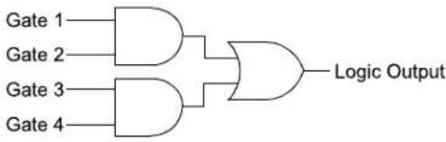 MODE[2:0] = 000 MODE[2:0] = 000 | OR - XOR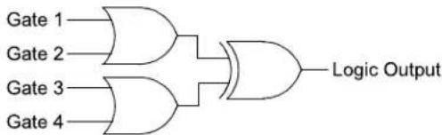 MODE[2:0] = 001 MODE[2:0] = 001 |
4-Input AND MODE[2:0] = 010 MODE[2:0] = 010 | S-R Latch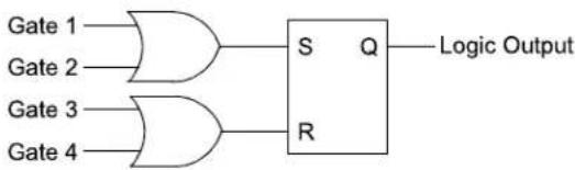 MODE[2:0] = 011 MODE[2:0] = 011 |
1-Input D Flip-Flop with S and R MODE[2:0] = 100 MODE[2:0] = 100 | 2-Input D Flip-Flop with R MODE[2:0] = 101 MODE[2:0] = 101 |
J-K Flip-Flop with R MODE[2:0] = 110 MODE[2:0] = 110 | 1-Input Transparent Latch with S and R MODE[2:0] = 111 MODE[2:0] = 111 |
Figure 23-3. CLCx Input Source Selection Diagram

Note: All controls are undefined at power-up.
23.1 CLC Control Registers
| OffsetName | Bit Pos. 765 | 43210 | ||||||||
| 0xC0 | CLC1CONL | 15:8 | LCEN | INTP INTN | ||||||
| 7:0 | LCOE | LCOUT LCPOL | MODE[2:0] | |||||||
| 0xC2 | CLC1CONH | 15:8 | ||||||||
| 7:0 | G4POL | G3POL | G2POL | G1POL | ||||||
| 0xC4 | CLC1SELL | 15:8 | DS4[2:0] | DS3[2:0] | ||||||
| 7:0 | DS2[2:0] | DS1[2:0] | ||||||||
| 0xC6...0xC7 | Reserved | |||||||||
| 0xC8 | CLC1GLSL | 15:8 | G2D4T | G2D4N | G2D3T | G2D3N | G2D2T | G2D2N | G2D1T | G2D1N |
| 7:0 | G1D4T | G1D4N | G1D3T | G1D3N | G1D2T | G1D2N | G1D1T | G1D1N | ||
| 0xCA | CLC1GLSH | 15:8 | G4D4T | G4D4N | G4D3T | G4D3N | G4D2T | G4D2N | G4D1T | G4D1N |
| 7:0 | G3D4T | G3D4N | G3D3T | G3D3N | G3D2T | G3D2N | G3D1T | G3D1N | ||
| 0xCC | CLC2CONL | 15:8 | LCEN | INTP INTN | ||||||
| 7:0 | LCOE | LCOUT LCPOL | MODE[2:0] | |||||||
| 0xCE | CLC2CONH | 15:8 | ||||||||
| 7:0 | G4POL | G3POL | G2POL | G1POL | ||||||
| 0xD0 | CLC2SELL | 15:8 | DS4[2:0] | DS3[2:0] | ||||||
| 7:0 | DS2[2:0] | DS1[2:0] | ||||||||
| 0xD2...0xD3 | Reserved | |||||||||
| 0xD4 | CLC2GLSL | 15:8 | G2D4T | G2D4N | G2D3T | G2D3N | G2D2T | G2D2N | G2D1T | G2D1N |
| 7:0 | G1D4T | G1D4N | G1D3T | G1D3N | G1D2T | G1D2N2 | G1D1T | G1D1N | ||
| 0xD6 | CLC2GLSH | 15:8 | G4D4T | G4D4N | G4D3T | G4D3N | G4D2T | G4D2N | G4D1T | G4D1N |
| 7:0 | G3D4T | G3D4N | G3D3T | G3D3N | G3D2T | G3D2N2 | G3D1T | G3D1N | ||
| 0xD8 | CLC3CONL | 15:8 | LCEN | INTP INTN | ||||||
| 7:0 | LCOE | LCOUT LCPOL | MODE[2:0] | |||||||
| 0xDA | CLC3CONH | 15:8 | ||||||||
| 7:0 | G4POL | G3POL | G2POL | G1POL | ||||||
| 0xDC | CLC3SELL | 15:8 | DS4[2:0] | DS3[2:0] | ||||||
| 7:0 | DS2[2:0] | DS1[2:0] | ||||||||
| 0xDE...0xDF | Reserved | |||||||||
| 0xE0 | CLC3GLSL | 15:8 | G2D4T | G2D4N | G2D3T | G2D3N | G2D2T | G2D2N | G2D1T | G2D1N |
| 7:0 | G1D4T | G1D4N | G1D3T | G1D3N | G1D2T | G1D2N 2 | G1D1T | G1D1N | ||
| 0xE2 | CLC3GLSH | 15:8 | G4D4T | G4D4N | G4D3T | G4D3N | G4D2T | G4D2N | G4D1T | G4D1N |
| 7:0 | G3D4T | G3D4N | G3D3T | G3D3N | G3D2T | G3D2N 2 | G3D1T | G3D1N | ||
| 0xE4 | CLC4CONL | 15:8 | LCEN | INTP INTN | ||||||
| 7:0 | LCOE | LCOUT | LCPOL MODE[2:0] | |||||||
| 0xE6 | CLC4CONH | 15:8 | ||||||||
| 7:0 | G4POL | G3POL | G2POL | G1POL | ||||||
| 0xE8 | CLC4SELL | 15:8 | DS4[2:0] | DS3[2:0] | ||||||
| 7:0 | DS2[2:0] | DS1[2:0] | ||||||||
| 0xEA...0xEB | Reserved | |||||||||
| 0xEC | CLC4GLSL | 15:8 | G2D4T | G2D4N | G2D3T | G2D3N | G2D2T | G2D2N | G2D1T | G2D1N |
| 7:0 | G1D4T | G1D4N | G1D3T | G1D3N | G1D2T | G1D2N. | G1D1T | G1D1N | ||
| 0xEE | CLC4GLSH | 15:8 | G4D4T | G4D4N | G4D3T | G4D3N | G4D2T | G4D2N | G4D1T | G4D1N |
| 7:0 | G3D4T | G3D4N | G3D3T | G3D3N | G3D2T | G3D2N. | G3D1T | G3D1N | ||
| 0xF0...0xOF27 | Reserved | |||||||||
| 0xOF28 | CLC5CONL | 15:8 | LCEN | INTP INTN | ||||||
| 7:0 | LCOE | LCOUT | LCPOL MODE[2:0] | |||||||
| 0xOF2A | CLC5CONH | 15:8 | ||||||||
| 7:0 | G4POL | G3POL | G2POL | G1POL | ||||||
| OffsetName Bit Pos. 765 43210 | ||||||||||
| 0x0F2C CLC5SELL | 15:8 DS4[2:0] DS3[2:0] | |||||||||
| 7:0 DS2[2:0] DS1[2:0] | ||||||||||
| 0x0F2E ... 0x0F2F | Reserved | |||||||||
| 0x0F30 CLC5GLSL | 15:8 G2D4T G2D4N G2D3T G2D3N G2D2T G2D2N G2D1T G2D1N | |||||||||
| 7:0 G1D4T G1D4N G1D3T G1D3N G1D2T G1D2N G1D1T G1D1N | ||||||||||
| 0x0F32 CLC5GLSH | 15:8 G4D4T G4D4N G4D3T G4D3N G4D2T G4D2N G4D1T G4D1N | |||||||||
| 7:0 G3D4T G3D4N G3D3T G3D3N G3D2T G3D2N G3D1T G3D1N | ||||||||||
| 0x0F34 CLC6CONL | 15:8 | LCEN | INTP | INTN | ||||||
| 7:0 | LCOE | LCOUT | LCPOL | MODE[2:0] | ||||||
| 0x0F36 CLC6CONH | 15:8 | |||||||||
| 7:0 | G4POL G3POL G2POL G1POL | |||||||||
| 0x0F38 CLC6SELL | 15:8 DS4[2:0] DS3[2:0] | |||||||||
| 7:0 DS2[2:0] DS1[2:0] | ||||||||||
| 0x0F3A ... 0x0F3B | Reserved | |||||||||
| 0x0F3C CLC6GLSL | 15:8 G2D4T G2D4N G2D3T G2D3N G2D2T G2D2N G2D1T G2D1N | |||||||||
| 7:0 G1D4T G1D4N G1D3T G1D3N G1D2T G1D2N G1D1T C1D1N | ||||||||||
| 0x0F3E CLC6GLSH | 15:8 G4D4T G4D4N G4D3T G4D3N G4D2T G4D2N G4D1T G4D1N | |||||||||
| 7:0 G3D4T G3D4N G3D3T G3D3N G3D2T G3D2N G3D1T C3D1N | ||||||||||
| 0x0F40 CLC7CONL | 15:8 | LCEN | INTP | INTN | ||||||
| 7:0 | LCOE | LCOUT | LCPOL | MODE[2:0] | ||||||
| 0x0F42 CLC7CONH | 15:8 | |||||||||
| 7:0 | G4POL G3POL G2POL G1POL | |||||||||
| 0x0F44 CLC7SELL | 15:8 DS4[2:0] DS3[2:0] | |||||||||
| 7:0 DS2[2:0] DS1[2:0] | ||||||||||
| 0x0F46 ... 0x0F47 | Reserved | |||||||||
| 0x0F48 CLC7GLSL | 15:8 G2D4T G2D4N G2D3T G2D3N G2D2T G2D2N G2D1T G2D1N | |||||||||
| 7:0 G1D4T G1D4N G1D3T G1D3N G1D2T G1D2N G1D1T A1D1N | ||||||||||
| 0x0F4A CLC7GLSH | 15:8 G4D4T G4D4N G4D3T G4D3N G4D2T G4D2N G4D1T G4D1N | |||||||||
| 7:0 G3D4T G3D4N G3D3T G3D3N G3D2T G3D2N G3D1T A3D1N | ||||||||||
| 0x0F4C CLC8CONL | 15:8 | LCEN | INTP | INTN | ||||||
| 7:0 | LCOE | LCOUT | LCPOL | MODE[2:0] | ||||||
| 0x0F4E CLC8CONH | 15:8 | |||||||||
| 7:0 | G4POL G3POL G2POL G1POL | |||||||||
| 0x0F50 CLC8SELL | 15:8 DS4[2:0] DS3[2:0] | |||||||||
| 7:0 DS2[2:0] DS1[2:0] | ||||||||||
| 0x0F52 ... 0x0F53 | Reserved | |||||||||
| 0x0F54 CLC8GLSL | 15:8 G2D4T G2D4N G2D3T G2D3N G2D2T G2D2N G2D1T G2D1N | |||||||||
| 7:0 G1D4T G1D4N G1D3T G1D3N G1D2T G1D2N G1D1T B1D1N | ||||||||||
| 0x0F56 CLC8GLSH | 15:8 G4D4T G4D4N G4D3T G4D3N G4D2T G4D2N G4D1T G4D1N | |||||||||
| 7:0 G3D4T G3D4N G3D3T G3D3N G3D2T G3D2N G3D1T B3D1N | ||||||||||
23.1.1 CLCx Control Register Low
Name: CLCxCONL
Offset: 0x0C0, 0x0CC, 0x0D8, 0x0E4, 0x0F28, 0xF34, 0xF40, 0xF4C
Bit 15 14 13 12 11 10 9 8
| LCEN | INTP | INTN | |||||||
| Access | R/W | R/W | R/W | ||||||
| Reset | 0 | 0 0 |
Bit 76543210
| LCOE | LCOUT | LCPOL | MODE[2:0] | |||||
| Access | R/W | R | R/W | R/W | R/W | R/W | ||
| Reset | 0 0 0 | 0 0 0 | ||||||
Bit 15 - LCEN CLCx Enable bit
| Value | Description |
| 1 | CLCx is enabled and mixing input signals |
| 0 | CLCx is disabled and has logic zero outputs |
Bit 11 - INTP CLCx Positive Edge Interrupt Enable bit
| Value | Description |
| 1 | Interrupt will be generated when a rising edge occurs on LCOUT |
| 0 | Interrupt will not be generated |
Bit 10 - INTN CLCx Negative Edge Interrupt Enable bit
| Value | Description |
| 1 | Interrupt will be generated when a falling edge occurs on LCOUT |
| 0 | Interrupt will not be generated |
Bit 7 – LCOE CLCx Port Enable bit
| Value | Description |
| 1 | CLCx port pin output is enabled |
| 0 | CLCx port pin output is disabled |
Bit 6 – LCOUT CLCx Data Output Status bit
| Value | Description |
| 1 | CLCx output high |
| 0 | CLCx output low |
Bit 5 – LCPOL CLCx Output Polarity Control bit
| Value | Description |
| 1 | The output of the module is inverted |
| 0 | The output of the module is not inverted |
Bits 2:0 - MODE[2:0] CLCx Mode bits
| Value | Description |
| 111 | Single input transparent latch with S and R |
| 110 | JK flip-flop with R |
| 101 | Two-input D flip-flop with R |
| 100 | Single input D flip-flop with S and R |
| 011 | SR latch |
| 010 | Four-input AND |
| 001 | Four-input OR-XOR |
| 000 | Four-input AND-OR |
23.1.2 CLCx Control Register High
Name: CLCxCONH
Offset: 0x0C2, 0x0CE, 0x0DA, 0x0E6, 0xF2A, 0xF36, 0xF42, 0xF4E
Bit 15 14 13 12 11 10 9 8
| Access Reset |
Bit 76543210
| G4POL G3POL G2POL G1POL | ||||||
| Access Reset | R/W RW 0000 | RW | RW |
Bit 3 – G4POL Gate 4 Polarity Control bit
| Value | Description |
| 1 | Channel 4 logic output is inverted when applied to the logic cell |
| 0 | Channel 4 logic output is not inverted |
Bit 2 – G3POL Gate 3 Polarity Control bit
| Value | Description |
| 1 | Channel 3 logic output is inverted when applied to the logic cell |
| 0 | Channel 3 logic output is not inverted |
Bit 1 – G2POL Gate 2 Polarity Control bit
| Value | Description |
| 1 | Channel 2 logic output is inverted when applied to the logic cell |
| 0 | Channel 2 logic output is not inverted |
Bit 0 - G1POL Gate 1 Polarity Control bit
| Value | Description |
| 1 | Channel 1 logic output is inverted when applied to the logic cell |
| 0 | Channel 1 logic output is not inverted |
23.1.3 CLCx Input MUX Select Register
Name: CLCxSELL
Offset: 0x0C4, 0x0D0, 0x0DC, 0x0E8, 0x0F2C, 0xF38, 0xF44, 0xF50
Bit 15 14 13 12 11 10 9 8
| Value | Description |
| 111 | SCCP4 auxiliary out |
| 110 | SCCP2 auxiliary out |
| 101 | CLC6 Out |
| 100 | REFCLKO output |
Value Description
| 011 | INTRC/LPRC clock source |
| 010 | CLC3 out |
| 001 | System clock ( F_CY ) |
| 000 | CLCINA I/O pin |
23.1.4 CLCx Gate Logic Input Select Low Register
Name: CLCxGLSL
Offset: 0x0C8, 0x0D4, 0x0E0, 0x0EC, 0xF30, 0xF3C, 0xF48, 0xF54
Bit 15 14 13 12 11 10 9 8
| G2D4T G2D | 4N G2D3T G2D3 | N G2D2T G2D2N | G2D1T G2D1N |
Access R/W R/W R/W R/W R/W R/W R/W R/W
Reset 00000000
Bit 76543210
| G1D4TG1D | 4N G1D3TG1D3 | N G1D2TG1D2 | N G1D1TG1D1N |
Access R/W R/W R/W R/W R/W R/W R/W R/W
Reset 00000000
Bit 15 - G2D4T Gate 2 Data Source 4 True Enable bit
| Value Description | |
| 1 | Data Source 4 signal is enabled for Gate 2 |
| 0 | Data Source 4 signal is disabled for Gate 2 |
Bit 14 - G2D4N Gate 2 Data Source 4 Negated Enable bit
| Value Description | |
| 1 | Data Source 4 inverted signal is enabled for Gate 2 |
| 0 | Data Source 4 inverted signal is disabled for Gate 2 |
Bit 13 - G2D3T Gate 2 Data Source 3 True Enable bit
| Value Description | |
| 1 | Data Source 3 signal is enabled for Gate 2 |
| 0 | Data Source 3 signal is disabled for Gate 2 |
Bit 12 - G2D3N Gate 2 Data Source 3 Negated Enable bit
| Value Description | |
| 1 | Data Source 3 inverted signal is enabled for Gate 2 |
| 0 | Data Source 3 inverted signal is disabled for Gate 2 |
Bit 11 - G2D2T Gate 2 Data Source 2 True Enable bit
| Value Description | |
| 1 | Data Source 2 signal is enabled for Gate 2 |
| 0 | Data Source 2 signal is disabled for Gate 2 |
Bit 10 - G2D2N Gate 2 Data Source 2 Negated Enable bit
| Value Description | |
| 1 | Data Source 2 inverted signal is enabled for Gate 2 |
| 0 | Data Source 2 inverted signal is disabled for Gate 2 |
Bit 9 - G2D1T Gate 2 Data Source 1 True Enable bit
| Value Description | |
| 1 | Data Source 1 signal is enabled for Gate 2 |
| 0 | Data Source 1 signal is disabled for Gate 2 |
Bit 8 – G2D1N Gate 2 Data Source 1 Negated Enable bit
| Value Description | |
| 1 | Data Source 1 inverted signal is enabled for Gate 2 |
| 0 | Data Source 1 inverted signal is disabled for Gate 2 |
Bit 7 – G1D4T Gate 1 Data Source 4 True Enable bit
| Value Description | |
| 1 | Data Source 4 signal is enabled for Gate 1 |
| 0 | Data Source 4 signal is disabled for Gate 1 |
Bit 6 – G1D4N Gate 1 Data Source 4 Negated Enable bit
| Value Description | |
| 1 | Data Source 4 inverted signal is enabled for Gate 1 |
| 0 | Data Source 4 inverted signal is disabled for Gate 1 |
Bit 5 – G1D3T Gate 1 Data Source 3 True Enable bit
| Value Description | |
| 1 | Data Source 3 signal is enabled for Gate 1 |
| 0 | Data Source 3 signal is disabled for Gate 1 |
Bit 4 – G1D3N Gate 1 Data Source 3 Negated Enable bit
| Value Description | |
| 1 | Data Source 3 inverted signal is enabled for Gate 1 |
| 0 | Data Source 3 inverted signal is disabled for Gate 1 |
Bit 3 – G1D2T Gate 1 Data Source 2 True Enable bit
| Value Description | |
| 1 | Data Source 2 signal is enabled for Gate 1 |
| 0 | Data Source 2 signal is disabled for Gate 1 |
Bit 2 - G1D2N Gate 1 Data Source 2 Negated Enable bit
| Value Description | |
| 1 | Data Source 2 inverted signal is enabled for Gate 1 |
| 0 | Data Source 2 inverted signal is disabled for Gate 1 |
Bit 1 – G1D1T Gate 1 Data Source 1 True Enable bit
| Value Description | |
| 1 | Data Source 1 signal is enabled for Gate 1 |
| 0 | Data Source 1 signal is disabled for Gate 1 |
Bit 0 - G1D1N Gate 1 Data Source 1 Negated Enable bit
| Value Description | |
| 1 | Data Source 1 inverted signal is enabled for Gate 1 |
| 0 | Data Source 1 inverted signal is disabled for Gate 1 |
23.1.5 CLCx Gate Logic Input Select High Register
Name: CLCxGLSH
Offset: 0x0CA, 0x0D6, 0x0E2, 0x0EE, 0xF32, 0xF3E, 0xF4A, 0xF56
Bit 15 14 13 12 11 10 9 8
| G4D4T G4D | 4N G4D3T G4D3 | N G4D2T G4D2 | N G4D1T G4D1N |
Access R/W R/W R/W R/W R/W R/W R/W R/W
Reset 00000000
Bit 76543210
| G3D4T G3D | 4N | G3D3T G3D3 | N | G3D2T G3D2 | N | G3D1T G3D1N |
Access R/W R/W R/W R/W R/W R/W R/W R/W
Reset 00000000
Bit 15 - G4D4T Gate 4 Data Source 4 True Enable bit
Value Description
| 1 | Data Source 4 signal is enabled for Gate 4 |
| 0 | Data Source 4 signal is disabled for Gate 4 |
Bit 14 - G4D4N Gate 4 Data Source 4 Negated Enable bit
Value Description
| 1 | Data Source 4 inverted signal is enabled for Gate 4 |
| 0 | Data Source 4 inverted signal is disabled for Gate 4 |
Bit 13 - G4D3T Gate 4 Data Source 3 True Enable bit
Value Description
| 1 | Data Source 3 signal is enabled for Gate 4 |
| 0 | Data Source 3 signal is disabled for Gate 4 |
Bit 12 - G4D3N Gate 4 Data Source 3 Negated Enable bit
Value Description
| 1 | Data Source 3 inverted signal is enabled for Gate 4 |
| 0 | Data Source 3 inverted signal is disabled for Gate 4 |
Bit 11 - G4D2T Gate 4 Data Source 2 True Enable bit
Value Description
| 1 | Data Source 2 signal is enabled for Gate 4 |
| 0 | Data Source 2 signal is disabled for Gate 4 |
Bit 10 - G4D2N Gate 4 Data Source 2 Negated Enable bit
Value Description
| 1 | Data Source 2 inverted signal is enabled for Gate 4 |
| 0 | Data Source 2 inverted signal is disabled for Gate 4 |
Bit 9 – G4D1T Gate 4 Data Source 1 True Enable bit
Value Description
| 1 | Data Source 1 signal is enabled for Gate 4 |
| 0 | Data Source 1 signal is disabled for Gate 4 |
Bit 8 – G4D1N Gate 4 Data Source 1 Negated Enable bit
Value Description
| 1 | Data Source 1 inverted signal is enabled for Gate 4 |
| 0 | Data Source 1 inverted signal is disabled for Gate 4 |
Bit 7 – G3D4T Gate 3 Data Source 4 True Enable bit
| Value Description | |
| 1 | Data Source 4 signal is enabled for Gate 3 |
| 0 | Data Source 4 signal is disabled for Gate 3 |
Bit 6 – G3D4N Gate 3 Data Source 4 Negated Enable bit
| Value Description | |
| 1 | Data Source 4 inverted signal is enabled for Gate 3 |
| 0 | Data Source 4 inverted signal is disabled for Gate 3 |
Bit 5 – G3D3T Gate 3 Data Source 3 True Enable bit
| Value Description | |
| 1 | Data Source 3 signal is enabled for Gate 3 |
| 0 | Data Source 3 signal is disabled for Gate 3 |
Bit 4 – G3D3N Gate 3 Data Source 3 Negated Enable bit
| Value Description | |
| 1 | Data Source 3 inverted signal is enabled for Gate 3 |
| 0 | Data Source 3 inverted signal is disabled for Gate 3 |
Bit 3 – G3D2T Gate 3 Data Source 2 True Enable bit
| Value Description | |
| 1 | Data Source 2 signal is enabled for Gate 3 |
| 0 | Data Source 2 signal is disabled for Gate 3 |
Bit 2 - G3D2N Gate 3 Data Source 2 Negated Enable bit
| Value Description | |
| 1 | Data Source 2 inverted signal is enabled for Gate 3 |
| 0 | Data Source 2 inverted signal is disabled for Gate 3 |
Bit 1 – G3D1T Gate 3 Data Source 1 True Enable bit
| Value Description | |
| 1 | Data Source 1 signal is enabled for Gate 3 |
| 0 | Data Source 1 signal is disabled for Gate 3 |
Bit 0 - G3D1N Gate 3 Data Source 1 Negated Enable bit
| Value Description | |
| 1 | Data Source 1 inverted signal is enabled for Gate 3 |
| 0 | Data Source 1 inverted signal is disabled for Gate 3 |
24. Peripheral Trigger Generator (PTG)
Note: This data sheet summarizes the features of the dsPIC33CK1024MP710 family of devices. It is not intended to be a comprehensive reference source. To complement the information in this data sheet, refer to “Peripheral Trigger Generator (PTG)” (www.microchip.com/DS70000669).
The dsPIC33CK1024MP710 family Peripheral Trigger Generator (PTG) module is a user-programmable sequencer that is capable of generating complex trigger signal sequences to coordinate the operation of other peripherals. The PTG module is designed to interface with other modules, such as an Analog-to-Digital Converter (ADC), output compare and PWM modules, timers and interrupt controllers.
24.1 Features
- Behavior is Step Command Driven:
- Step commands are eight bits wide
- Commands are Stored in a Step Queue:
– Queue depth is up to 32 entries
- Programmable Step execution time (Step delay)
• Supports the Command Sequence Loop:
- Can be nested one-level deep
– Conditional or unconditional loop
- Two 16-bit loop counters
• 15 Hardware Input Triggers:
- Sensitive to either positive or negative edges, or a high or low level
• One Software Input Trigger
- Generates up to 32 Unique Output Trigger Signals
- Generates Two Types of Trigger Outputs:
- Individual
- Broadcast
• Strobed Output Port for Literal Data Values:
- 5-bit literal write (literal part of a command)
- 16-bit literal write (literal held in the PTGL0 register)
- Generates up to Ten Unique Interrupt Signals
- Two 16-Bit General Purpose Timers
- Flexible Self-Contained Watchdog Timer (WDT) to Set an Upper Limit to Trigger Wait Time
- Single-Step Command Capability in Debug mode
- Selectable Clock (System, Pulse-Width Modulator (PWM) or ADC)
• Programmable Clock Divider
Figure 24-1. PTG Block Diagram

flowchart
graph TD
    A["PTGHOLD"] --> B["PTGADJ"]
    B --> C["PTGDBTE[31:0"]]
    C --> D["PTGCST[15:0"]]
    D --> E["PTGCON[15:0"]]
    E --> F["PTGDIV[4:0"]]
    F --> G["PTGCLK[2:0"]]
    G --> H["Clock Inputs"]
    H --> I["÷"]
    I --> J["PTGControl Logic"]
    J --> K["PTGLDIM[15:0"]]
    K --> L["PTGCLIM[15:0"]]
    L --> M["PTGGeneral Purpose Timer x"]
    M --> N["PTGLoop Counter x"]
    N --> O["PTGStep Delay Timer"]
    O --> P["Trigger Outputs"]
    P --> Q["PTGO0"]
    P --> R["PTGO31"]
    J --> S["Trigger Inputs"]
    S --> T["PTGQPTR[4:0"]]
    T --> U["PTGQPTR"]
    U --> V["PTGQVE0"]
    U --> W["PTGQVE1"]
    U --> X["PTGQVE2"]
    U --> Y["PTGQVE3"]
    U --> Z["PTGQVE4"]
    U --> AA["PTGQVE5"]
    U --> AB["PTGQVE6"]
    U --> AC["PTGQVE7"]
    U --> AD["..."]
    U --> AE["PTGQVE15"]
    J --> AF["Command Decoder"]
    AF --> AG["PTGWatchdog Timer(1)"]
    AG --> AH["PTGWDTIF"]
    J --> AI["Strobe Output[15:0"]]
    AI --> AJ["PTG0IF"]
    AI --> AK["PTG7IF"]
    J --> AL["Step Command"]
    AL --> AM["Trigger Outputs"]
    AM --> AN["PTGStep Delay Timer"]
    AN --> AO["PTGSDLIM[15:0"]]
    AO --> AP["PTGCLIM[15:0"]]
    AP --> AQ["PTGGeneral Purpose Timer x"]
    AQ --> AR["PTGTxLIM[15:0"]]
    AR --> AS["PTGLO[15:0"]]
    AS --> AT["PTGGL0[15:0"]]
    AT --> AU["PTGCLM[15:0"]]
    AU --> AV["PTGCLM[15:0"]]
    AV --> AW["PTGCLM[15:0"]]
    AW --> AX["PTGCLM[15:0"]]
    AX --> AY["PTGCLM[15:0"]]
    AY --> AZ["PTGCLM[15:0"]]
    AZ --> BA["PTGCLM[15:0"]]
    BA --> BB["PTGCLM[15:0"]]
    BB --> BC["PTGCLM[15:0"]]
    BC --> BD["PTGCLM[15:0"]]
    BD --> BE["PTGCLM[15:0"]]
    BE --> BF["PTGCLM[15:0"]]
    BF --> BG["PTGCLM[15:0"]]
    BG --> BH["PTGCLM[15:0"]]
    BH --> BI["PTGCLM[15:0"]]
    BI --> BJ["PTGCLM[15:0"]]
    BJ --> BK["PTGCLM[15:0"]]
    BK --> BL["PTGCLM[15:0"]]
    BL --> BM["PTGCLM[15:0"]]
    BM --> BN["PTGCLM[15:0"]]
    BN --> BO["PTGCLM[15:0"]]
    BO --> BP["PTGCLM[15:0"]]
    BP --> BQ["PTGCLM[15:0"]]
    BQ --> BR["PTGCLM[15:0"]]
    BR --> BS["PTGCLM[15:0"]]
    BS --> BT["PTGCLM[15:0"]]
    BT --> BU["PTGCLM[15:0"]]
    BU --> BV["PTGCLM[15:0"]]
    BV --> BW["PTGCLM[15:0"]]
    BW --> BX["PTGCLM[15:0"]]
    BX --> BY["PTGCLM[15:0"]]
    BY --> BZ["PTGCLM[15:0"]]
    BZ --> CA["PTGCLM[15:0"]]
    CA --> CB["PTGCLM[15:0"]]
    CB --> CC["PTGCLM[15:0"]]
    CC --> CD["PTGCLM[15:0"]]
    CD --> CE["PTGCLM[15:0"]]
    CE --> CF["PTGCLM[15:0"]]
    CF --> CG["PTGCLM[15:0"]]
    CG --> CH["PTGCLM[15:0"]]
    CH --> CI["PTGCLM[15:0"]]
    CI --> CJ["PTGCLM[15:0"]]
    CJ --> CK["PTGCLM[15:0"]]
    CK --> CL
Note:
1. This is a dedicated Watchdog Timer for the PTG module and is independent of the device Watchdog Timer.
24.2 PTG Registers
| OffsetName | Bit Pos. 765 | 43210 | ||||||||
| 0x0900 | PTGCST | 15:8 | PTGEN | PTGSIDL | PTGTOGL | PTGSWT | PTGSSEN | PTGIVIS | ||
| 7:0 | PTGSTRT | PTGWDTO | PTGBUSY | PTGITM[1:0] | ||||||
| 0x0902 | PTGCON | 15:8 | PTGCLK[2:0] | PTGDIV[4:0] | ||||||
| 7:0 | PTGPWD[3:0] | PTGWDT[2:0] | ||||||||
| 0x0904 | PTGBTE(1) | 15:8 | PTGBTE[15:8] | |||||||
| 7:0 | PTGBTE[7:0] | |||||||||
| 0x0906 | PTGBTEH(1) | 15:8 | PTGBTE[31:24] | |||||||
| 7:0 | PTGBTE[23:17] | |||||||||
| 0x0908 | PTGHOLD(1) | 15:8 | PTGHOLD[15:8] | |||||||
| 7:0 | PTGHOLD[7:0] | |||||||||
| 0x090A...0x090B | Reserved | |||||||||
| 0x090C | PTGTOLIM(1) | 15:8 | PTGTOLIM[15:8] | |||||||
| 7:0 | PTGTOLIM[7:0] | |||||||||
| 0x090E...0x090F | Reserved | |||||||||
| 0x0910 | PTGT1LIM(1) | 15:8 | PTGT1LIM[15:8] | |||||||
| 7:0 | PTGT1LIM[7:0] | |||||||||
| 0x0912...0x0913 | Reserved | |||||||||
| 0x0914 | PTGSDLIM(1) | 15:8 | PTGSDLIM[15:8] | |||||||
| 7:0 | PTGSDLIM[7:0] | |||||||||
| 0x0916...0x0917 | Reserved | |||||||||
| 0x0918 | PTGCOLIM(1) | 15:8 | PTGCOLIM[15:8] | |||||||
| 7:0 | PTGCOLIM[7:0] | |||||||||
| 0x091A...0x091B | Reserved | |||||||||
| 0x091C | PTGC1LIM(1) | 15:8 | PTGC1LIM[15:8] | |||||||
| 7:0 | PTGC1LIM[7:0] | |||||||||
| 0x091E...0x091F | Reserved | |||||||||
| 0x0920 | PTGADJ(1) | 15:8 | PTGADJ[15:8] | |||||||
| 7:0 | PTGADJ[7:0] | |||||||||
| 0x0922...0x0923 | Reserved | |||||||||
| 0x0924 | PTGLO(1,2) | 15:8 | PTGLO[15:8] | |||||||
| 7:0 | PTGLO[7:0] | |||||||||
| 0x0926...0x0927 | Reserved | |||||||||
| 0x0928 | PTGQPTR(1) | 15:8 | ||||||||
| 7:0 | PTGQPTR[4:0] | |||||||||
| 0x092A...0x092F | Reserved | |||||||||
| 0x0930 | PTGQUEO(1) | 15:8 | STEP2n[7:0] | |||||||
| 7:0 | STEP2n[7:0] | |||||||||
| 0x0932 | PTGQUE1(1) | 15:8 | STEP2n[7:0] | |||||||
| 7:0 | STEP2n[7:0] | |||||||||
| 0x0934 | PTGQUE2(1) | 15:8 | STEP2n[7:0] | |||||||
| 7:0 | STEP2n[7:0] | |||||||||
| OffsetName Bit Pos. 7 6 5 4 3 2 1 0 | ||||||||||
| 0x0936 PTGQUE3(1) | 15:8 STEP2n[7:0] | |||||||||
| 7:0 STEP2n[7:0] | ||||||||||
| 0x0938 PTGQUE4(1) | 15:8 STEP2n[7:0] | |||||||||
| 7:0 STEP2n[7:0] | ||||||||||
| 0x093A PTGQUE5(1) | 15:8 STEP2n[7:0] | |||||||||
| 7:0 STEP2n[7:0] | ||||||||||
| 0x093C PTGQUE6(1) | 15:8 STEP2n[7:0] | |||||||||
| 7:0 STEP2n[7:0] | ||||||||||
| 0x093E PTGQUE7(1) | 15:8 STEP2n[7:0] | |||||||||
| 7:0 STEP2n[7:0] | ||||||||||
| 0x0940 PTGQUE8(1) | 15:8 STEP2n[7:0] | |||||||||
| 7:0 STEP2n[7:0] | ||||||||||
| 0x0942 PTGQUE9(1) | 15:8 STEP2n[7:0] | |||||||||
| 7:0 STEP2n[7:0] | ||||||||||
| 0x0944 PTGQUE10(1) | 15:8 STEP2n[7:0] | |||||||||
| 7:0 STEP2n[7:0] | ||||||||||
| 0x0946 PTGQUE11(1) | 15:8 STEP2n[7:0] | |||||||||
| 7:0 STEP2n[7:0] | ||||||||||
| 0x0948 PTGQUE12(1) | 15:8 STEP2n[7:0] | |||||||||
| 7:0 STEP2n[7:0] | ||||||||||
| 0x094A PTGQUE13(1) | 15:8 STEP2n[7:0] | |||||||||
| 7:0 STEP2n[7:0] | ||||||||||
| 0x094C PTGQUE14(1) | 15:8 STEP2n[7:0] | |||||||||
| 7:0 STEP2n[7:0] | ||||||||||
| 0x094E PTGQUE15(1) | 15:8 STEP2n[7:0] | |||||||||
| 7:0 STEP2n[7:0] | ||||||||||
24.2.1 PTG Control/Status Low Register
Name: PTGCST
Offset: 0x900
Notes:
- These bits apply to the PTGWHI and PTGWLO commands only.
- This bit is only used with the PTGCTRL Step command software trigger option.
- The PTGSSEN bit may only be written when in Debug mode.
Bit 15 14 13 12 11 10 9 8
| PTGEN | PTGSIDL | PTGTOGL | PTGSWT | PTGS$EN | PTGIVIS | ||||
| Access | R/W | R/W | R/W | R/W | R/W | R/W | R/W | ||
| Reset | 0 | 0 | 0 | 0 | 0 | 0 | 0 | ||
Bit 76543210
| PTGSTRT | PTGWDTO | PTGBUSY | PTGITM[1:0] | ||||
| Access | R/W | R/W R/W | R/W R/W | ||||
| Reset | 0 0 0 | 0 0 |
Bit 15 – PTGEN PTG Broadcast Trigger Enable bit
| Value | Description |
| 1 | PTG is enabled |
| 0 | PTG is disabled |
Bit 13 – PTGSIDL PTG Freeze in Debug Mode bit
| Value | Description |
| 1 | Halts PTG operation when device is Idle |
| 0 | PTG operation continues when device is Idle |
Bit 12 - PTGTOGL PTG Toggle Trigger Output bit
| Value | Description |
| 1 | Toggles state of TRIG output for each execution of PTGTRIG |
| 0 | Generates a single TRIG pulse for each execution of PTGTRIG |
Bit 10 - PTGSWT PTG Software Trigger bit ^(2)
| Value | Description |
| 1 | If the PTG state machine is executing the “Wait for software trigger” Step command (OPTION[3:0] = 1010 or 1011), the command will complete and execution will continue |
| 0 | No action other than to clear the bit |
Bit 9 – PTGSSEN PTG Single-Step Command bit ^(3)
| Value | Description |
| 1 | Enables single Step when in Debug mode |
| 0 | Disables single Step |
Bit 8 – PTGIVIS PTG Counter/Timer Visibility bit
| Value | Description |
| 1 | Reading the PTGSDLIM, PTGCxLIM or PTGTxLIM register returns the current values of their corresponding Counter/Timer registers (PTGSDLIM, PTGCxLIM and PTGTxLIM) |
| 0 | Reading the PTGSDLIM, PTGCxLIM or PTGTxLIM register returns the value of these Limit registers |
Bit 7 – PTGSTRT PTG Start Sequencer bit
| Value | Description |
| 1 | Starts to sequentially execute the commands (Continuous mode) |
Value Description
| 0 | Stops executing the commands |
Bit 6 – PTGWDTO PTG Watchdog Timer Time-out Status bit
| Value Description | |
| 1 | PTG Watchdog Timer has timed out |
| 0 | PTG Watchdog Timer has not timed out |
Bit 5 – PTGBUSY PTG State Machine Busy bit
| Value Description | |
| 1 | PTG is running on the selected clock source; no SFR writes are allowed to PTGCLK[2:0] or PTGDIV[4:0] |
| 0 | PTG state machine is not running |
Bits 1:0 – PTGITM[1:0] PTG Input Trigger Operation Selection bits ^(1)
| Value Description | |
| 11 | Single-level detect with Step delay not executed on exit of command (regardless of the PTGCTRL command) (Mode 3) |
| 10 | Single-level detect with Step delay executed on exit of command (Mode 2) |
| 01 | Continuous edge detect with Step delay not executed on exit of command (regardless of the PTGCTRL command) (Mode 1) |
| 00 | Continuous edge detect with Step delay executed on exit of command (Mode 0) |
24.2.2 PTG Control/Status Register
Name: PTGCON
Offset: 0x902
Bit 15 14 13 12 11 10 9 8
| PTGCLK[2:0] PTGDIV[4:0] | ||
| Access | R/W R/W R/W R/W R/W R/W R/W R/W R/W | |
| Reset | 0 0 0 0 0 0 0 | |
Bit 76543210
| PTGPWD[3:0] PTGWDT[2:0] | |||
| Access | R/W R/W R/W R/W R/W R/W R/W | ||
| Reset | 0 0 0 0 | 0 0 0 | |
Bits 15:13 – PTGCLK[2:0] PTG Module Clock Source Selection bits
| Value | Description |
| 111 | CLC1 output |
| 110 | F_VCO/4 |
| 101 | Reserved |
| 100 | Reserved |
| 011 | Input from Timer1 Clock pin, T1CK |
| 010 | ADC clock |
| 001 | F_CY |
| 000 | F_P |
Bits 12:8 – PTGDIV[4:0] PTG Module Clock Prescaler (Divider) bits
| Value | Description |
| 11111 | Divide-by-32 |
| 11110 | Divide-by-31 |
| . . . | |
| 00001 | Divide-by-2 |
| 00000 | Divide-by-1 |
Bits 7:4 – PTGPWD[3:0] PTG Trigger Output Pulse-Width (in PTG clock cycles) bits
| Value | Description |
| 1111 | All trigger outputs are 16 PTG clock cycles wide |
| 1110 | All trigger outputs are 15 PTG clock cycles wide |
| ... | |
| 0001 | All trigger outputs are 2 PTG clock cycles wide |
| 0000 | All trigger outputs are 1 PTG clock cycle wide |
Bits 2:0 – PTGWDT[2:0] PTG Watchdog Timer Time-out Selection bits
| Value | Description |
| 111 | Watchdog Timer will time out after 512 PTG clocks |
| 110 | Watchdog Timer will time out after 256 PTG clocks |
| 101 | Watchdog Timer will time out after 128 PTG clocks |
| 100 | Watchdog Timer will time out after 64 PTG clocks |
| 011 | Watchdog Timer will time out after 32 PTG clocks |
| 010 | Watchdog Timer will time out after 16 PTG clocks |
| 001 | Watchdog Timer will time out after 8 PTG clocks |
| 000 | Watchdog Timer is disabled |
24.2.3 PTG Broadcast Trigger Enable Register Low
Name: PTGBTE (1)
Offset: 0x904
Note:
- This register is read-only when the module is executing Step commands.
Bit 15 14 13 12 11 10 9 8
PTGBTE[15:8]
Access R/W R/W R/W R/W R/W R/W R/W R/W
Reset 00000000
Bit 76543210
PTGBTE[7:0]
Access R/W R/W R/W R/W R/W R/W R/W R/W
Reset 00000000
Bits 15:0 – PTGBTE[15:0] PTG Broadcast Trigger Enable bits
Value Description
| 1 | Generates trigger when the broadcast command is executed |
| 0 | Does not generate trigger when the broadcast command is executed |
24.2.4 PTG Broadcast Trigger Enable Low Register
Name: PTGBTEH (1)
Offset: 0x906
Note:
- This register is read-only when the module is executing Step commands.
Bit 15 14 13 12 11 10 9 8
PTGBTE[31:24]
Access R/W R/W R/W R/W R/W R/W R/W R/W
Reset 00000000
Bit 76543210
PTGBTE[23:17]
Access R/W R/W R/W R/W R/W R/W R/W
Reset 0000000
Bits 15:8 – PTGBTE[31:24] PTG Broadcast Trigger Enable bits
Value Description
| 1 | Generates trigger when the broadcast command is executed |
| 0 | Does not generate trigger when the broadcast command is executed |
Bits 6:0 – PTGBTE[23:17] PTG Broadcast Trigger Enable bits
Value Description
| 1 | Generates trigger when the broadcast command is executed |
| 0 | Does not generate trigger when the broadcast command is executed |
24.2.5 PTG Hold Register
Name: PTGHOLD (1)
Offset: 0x908
Note:
- This register is read-only when the module is executing Step commands.
Bit 15 14 13 12 11 10 9 8
PTGHOLD[15:8]
Access R/W R/W R/W R/W R/W R/W R/W R/W
Reset 00000000
Bit 76543210
PTGHOLD[7:0]
Access R/W R/W R/W R/W R/W R/W R/W R/W
Reset 00000000
Bits 15:0 – PTGHOLD[15:0] PTG General Purpose Hold Register bits
This register holds the user-supplied data to be copied to the PTGTxLIM, PTGCxLIM, PTGSDLIM or PTGL0 register using the PTGCOPY command.
24.2.6 PTG Timer0 Limit Register
Name: PTGTOLIM (1)
Offset: 0x90C
Note:
- This register is read-only when the module is executing Step commands.
Bit 15 14 13 12 11 10 9 8
PTGTOLIM[15:8]
Access R/W R/W R/W R/W R/W R/W R/W R/W
Reset 00000000
Bit 76543210
PTGTOLIM[7:0]
Access R/W R/W R/W R/W R/W R/W R/W R/W
Reset 00000000
Bits 15:0 – PTGTOLIM[15:0] PTG Timer0 Limit Register bits
General Purpose Timer0 Limit register.
24.2.7 PTG Timer1 Limit Register
Name: PTGT1LIM (1)
Offset: 0x910
Note:
- This register is read-only when the module is executing Step commands.
Bit 15 14 13 12 11 10 9 8
PTGT1LIM[15:8]
Access R/W R/W R/W R/W R/W R/W R/W R/W
Reset 00000000
Bit 76543210
PTGT1LIM[7:0]
Access R/W R/W R/W R/W R/W R/W R/W R/W
Reset 00000000
Bits 15:0 – PTGT1LIM[15:0] PTG Timer1 Limit Register bits
General Purpose Timer1 Limit register.
24.2.8 PTG Step Delay Limit Register
Name: PTGSDLIM (1)
Offset: 0x914
Note:
- This register is read-only when the module is executing Step commands.
Bit 15 14 13 12 11 10 9 8
PTGSDLIM[15:8]
Access R/W R/W R/W R/W R/W R/W R/W R/W
Reset 00000000
Bit 76543210
PTGSDLIM[7:0]
Access R/W R/W R/W R/W R/W R/W R/W R/W
Reset 00000000
Bits 15:0 – PTGSDLIM[15:0] PTG Step Delay Limit Register bits
This register holds a PTG Step delay value representing the number of additional PTG clocks between the start of a Step command and the completion of a Step command.
24.2.9 PTG Counter 0 Limit Register
Name: PTGCOLIM (1)
Offset: 0x918
Note:
- This register is read-only when the module is executing Step commands.
Bit 15 14 13 12 11 10 9 8
PTGCOLIM[15:8]
Access R/W R/W R/W R/W R/W R/W R/W R/W
Reset 00000000
Bit 76543210
PTGC0LIM[7:0]
Access R/W R/W R/W R/W R/W R/W R/W R/W
Reset 00000000
Bits 15:0 – PTGCOLIM[15:0] PTG Counter 0 Limit Register bits
This register is used to specify the loop count for the PTGJMPC0 Step command or as a Limit register for the General Purpose Counter 0.
24.2.10 PTG Counter 1 Limit Register
Name: PTGC1LIM (1)
Offset: 0x91C
Note:
- This register is read-only when the module is executing Step commands.
Bit 15 14 13 12 11 10 9 8
PTGC1LIM[15:8]
Access R/W R/W R/W R/W R/W R/W R/W R/W
Reset 00000000
Bit 76543210
PTGC1LIM[7:0]
Access R/W R/W R/W R/W R/W R/W R/W R/W
Reset 00000000
Bits 15:0 – PTGC1LIM[15:0] PTG Counter 1 Limit Register bits
This register is used to specify the loop count for the PTGJMPC1 Step command or as a Limit register for the General Purpose Counter 1.
24.2.11 PTG Adjust Register
Name: PTGADJ (1)
Offset: 0x920
Note:
- This register is read-only when the module is executing Step commands.
Bit 15 14 13 12 11 10 9 8
PTGADJ[15:8]
Access R/W R/W R/W R/W R/W R/W R/W R/W
Reset 00000000
Bit 76543210
PTGADJ[7:0]
Access R/W R/W R/W R/W R/W R/W R/W R/W
Reset 00000000
Bits 15:0 – PTGADJ[15:0] PTG Adjust Register bits
This register holds the user-supplied data to be added to the PTGTxLIM, PTGCxLIM, PTGSDLIM or PTGL0 register using the PTGADD command.
24.2.12 PTG Literal 0 Register
Name: PTGLO (1,2)
Offset: 0x924
Notes:
-
This register is read-only when the module is executing Step commands.
-
The PTG strobe output is typically connected to the ADC Channel Select register. This allows the PTG to directly control ADC channel switching. See the specific device data sheet for connections of the PTG output.
Bit 15 14 13 12 11 10 9 8
| PTGLO[15:8] | |
| Access | R/W R/W R/W R/W R/W R/W R/W R/W |
| Reset | 0 0 0 0 0 0 0 |
| Bit | 7 6 5 4 3 2 1 0 |
| PTGLO[7:0] | |
| Access | R/W R/W R/W R/W R/W R/W R/W R/W |
| Reset | 0 0 0 0 0 0 0 |
Bits 15:0 – PTGL0[15:0] PTG Literal 0 Register bits
This register holds the 6-bit value to be written to the CNVCHSEL[5:0] bits (ADCON3L[5:0]) with the PTGCTRL Step command.
24.2.13 PTG Step Queue Pointer Register
Name: PTGQPTR (1)
Offset: 0x928
Note:
- This register is read-only when the module is executing Step commands.

text_image
Bit 15 14 13 12 11 10 9 8 Access Reset Bit 7 6 5 4 3 2 1 0 PTGQPTR[4:0] Access R/W R/W R/W R/W R/W Reset 0 0 0 0 0Bits 4:0 – PTGQPTR[4:0] PTG Step Queue Pointer Register bits This register points to the currently active Step command in the Step queue.
24.2.14 PTG Step Queue x Pointer Register (x = 0-15)
Name: PTGQUEx (1)
Offset: 0x930, 0x932, 0x934, 0x936, 0x938, 0x93A, 0x93C, 0x93E, 0x940, 0x942, 0x944, 0x946, 0x948, 0x94A, 0x94C, 0x94E
Notes:
-
This register is read-only when the module is executing Step commands.
-
Refer to Table 24-1 for the Step command encoding.
Bit 15 14 13 12 11 10 9 8

text_image
STEP2n[7:0] Access R/W R/W R/W R/W R/W R/W R/W R/W Reset 0 0 0 0 0 0 0 0 Bit 7 6 5 4 3 2 1 0 STEP2n[7:0] Access R/W R/W R/W R/W R/W R/W R/W R/W Reset 0 0 0 0 0 0 0 0Bits 15:8 - STEP2n[7:0] PTG Command 2n bits ^(2)
A queue location for storage of the STEP2n command byte, , where 'n' is the even numbered Step Queue Pointers.
Bits 7:0 - STEP2n[7:0] PTG Command 2n bits ^(2)
A queue location for storage of the STEP2n command byte, where 'n' is the odd numbered Step Queue Pointers.
24.3 PTG Step Commands
Table 24-1. PTG Step Command Format and Description
| Step Command Byte | |||
| STEPx[7:0] | |||
| CMD[3:0] OPTION[3:0] | |||
| bit 7 bit 4 bit 3 | bit 0 | ||
Table 24-2. PTG Command Options
| bit 7-4 | Step Command | CMD[3:0] | Command Description |
| FTGCTRL 0000 | Execute the control command as described by the OPTION[3:0] bits. | ||
| PTGADD | 0001 | Add contents of the PTGADI register to the target register as described by the OPTION[3:0] bits. | |
| FTGCOPY | Copy contents of the PTGHOLD register to the target register as described by the OPTION[3:0] bits. | ||
| FTGSTRB 001x | Copy the values contained in the bits, CMD[0]:OPTION[3:0], to the strobe output bits[4:0]. | ||
| PTGWHI | 0103 | Wait for a low-to-high edge input from a selected PTG trigger Input as described by the OPTION[3:0] bits. | |
| PTGMLO | 0101 | Wait for a high-to-low edge input from a selected PTG trigger Input as described by the OPTION[3:0] bits. | |
| — | 0110 | Reserved; do not use.[1] | |
| PTGIRQ | 0111 | Generate Individual Interrupt request as described by the OPTION[3:0] bits. | |
| FTGTRIG 100x | Generate individual trigger output as described by the bits, CMD[0]:OPTION[3:0]. | ||
| FTGJME | 101x | Copy the values contained in the bits, CMD[0]:OPTION[3:0], to the PTGQPTR register and jump to that Step queue. | |
| PTGCMPCO | 110x | PTGCO = PTGCOLIM: Increment the PTGQPTR register. | |
| PTGCO ≠ PTGCOLIM: Increment Counter 0 (PTGCO) and copy the values contained in the bits, CMD[0]:OPTION[3:0], to the PTGQPTR register, and jump to that Step queue. | |||
| PTGZMPCI | 111x | PTGC1 = PTGC1LIM: Increment the PTGQPTR register. | |
| PTGC1 ≠ PTGC1LIM: Increment Counter 1 (PTGC1) and copy the values contained in the bits, CMD[0]:OPTION[3:0], to the PTGQPTR register, and jump to that Step queue. |
| bit 3-0 PTGCTRLM | C000 | NOF. |
| C001 | Reserved; do not use. | |
| C010 | Disable Step delay timer (PTGSD). | |
| C011 | Reserved; do not use. | |
| C100 | Reserved; do not use. | |
| C101 | Reserved; do not use. | |
| C110 | Enable Step delay timer (PTGSD). | |
| C111 | Reserved; do not use. | |
| 1000 | Start and wait for the PTG Timer0 to match the PTGTOLIM register. | |
| 1001 | Start and wait for the PTG Timer1 to match the PTGT1LIM register. | |
| 1010 | Wait for the software trigger (level, PTGSWT = 1). | |
| 1011 | Wait for the software trigger (positive edge, PTGSWT = 0 to 1). | |
| 1100 | Copy the PTGCOLIM register contents to the strobe output. | |
| 1101 | Copy the PTGC1LIM register contents to the strobe output. | |
| 1110 | Copy the PTGL0 register contents to the strobe output. | |
| 1111 | Generate the triggers indicated in the PTGBTE register. | |
| PTGADDM | C000 | Add the PTGADJ register contents to the PTGCOLIM register. |
| C001 | Add the PTGADJ register contents to the PTGC1LIM register. | |
| C010 | Add the PTGADJ register contents to the PTGTOLIM register. | |
| C011 | Add the PTGADJ register contents to the PTGT1LIM register. | |
| C100 | Add the PTGADJ register contents to the PTGSDLIM register. | |
| C101 | Add the PTGADJ register contents to the PTGL0 register. | |
| C110 | Reserved; do not use. | |
| C111 | Reserved; do not use. | |
| PTGCOPYM | 1000 | Copy the PTGHOLD register contents to the PTGCOLIM register. |
| 1001 | Copy the PTGHOLD register contents to the PTGC1LIM register. | |
| 1010 | Copy the PTGHOLD register contents to the PTGTOLIM register. | |
| 1011 | Copy the PTGHOLD register contents to the PTGT1LIM register. | |
| 1100 | Copy the PTGHOLD register contents to the PTGSDLIM register. | |
| 1101 | Copy the PTGHOLD register contents to the PTGL0 register. | |
| 1110 | Reserved; do not use. | |
| 1111 | Reserved; do not use. | |
| PTGWHI® or PTGWLOM | C000 | PTGI0 (see Table 24-3 for input assignments). |
| *** *** | ||
| 1111 | PTGI15 (see Table 24-3 for input assignments). | |
| PTGIRQN | C000 | Generate PTG Interrupt 0. |
| *** *** | ||
| C111 | Generate PTG Interrupt 7. | |
| 1000 | Reserved; do not use. | |
| *** *** | ||
| 1111 | Reserved; do not use. | |
| PTGTRIG C000 | PTGO0 (see Table 24-4 for input assignments). | |
| C001 | PTGO1 (see Table 24-4 for input assignments). | |
| *** *** | ||
| 1110 | PTGO30 (see Table 24-4 for input assignments). | |
| 1111 | PTGO31 (see Table 24-4 for input assignments). | |
| PTGWHI® or PTGWLOM | C000 | PTGI0 (see specific device data sheet for interrupt assignments). |
| *** *** | ||
| 1111 | PTGI15 (see specific device data sheet for interrupt assignments). | |
| PTGIRQN | C000 | Generate PTG Interrupt 0 (see specific device data sheet for interrupt assignments). |
| *** *** | ||
| C111 | Generate PTG Interrupt 7 (see specific device data sheet for interrupt assignments). | |
| 1000 | Reserved; do not use. | |
| *** *** | ||
| 1111 | Reserved; do not use. | |
| PTGTRIG S000 | PTGO0 (see specific device data sheet for interrupt assignments). | |
| C001 | PTGO1 (see specific device data sheet for interrupt assignments). | |
Table 24-3. PTG Input Descriptions
| PTG Input Number PTG Input Description |
| PTG Trigger Input 0 Trigger Input from PWM1 ADC Trigger 2 |
| PTG Trigger Input 1 Trigger Input from PWM2 ADC Trigger 2 |
| PTG Trigger Input 2 Trigger Input from PWM3 ADC Trigger 2 |
| PTG Trigger Input 3 Trigger Input from PWM4 ADC Trigger 2 |
| PTG Trigger Input 4 Trigger Input from PWM5 ADC Trigger 2 |
| PTG Trigger Input 5 Trigger Input from PWM6 ADC Trigger 2 |
| PTG Trigger Input 6 Trigger Input from PWM7 ADC Trigger 2 |
| PTG Trigger Input 7 Trigger Input from APWM1 ADC Trigger 2 |
| PTG Trigger Input 8 Trigger Input from APWM2 ADC Trigger 2 |
| PTG Trigger Input 9 Trigger Input from Comparator 1 |
| PTG Trigger Input 10 Trigger Input from Comparator 2 |
| PTG Trigger Input 11 Trigger Input from Comparator 3 |
| PTG Trigger Input 12 Trigger Input from CLC1 |
| PTG Trigger Input 13 Trigger Input ADC Done Group Interrupt |
| PTG Trigger Input 14 Trigger Input from CLC2 |
| PTG Trigger Input 15 Trigger Input from INT2 PPS |
Table 24-4. PTG Output Descriptions
| PTG Output Number PTG Output Description | |
| PTGO0 to PTGO11 Reserved | |
| PTGO12 ADC TRGSRC[30] | |
| PTGO13 to PTGO23 Reserved | |
| PTGO24 PPS Output RP46 | |
| PTGO25 PPS Output RP47 | |
| PTGO26 PPS Input RP6 | |
| PTGO27 PPS Input RP7 | |
| PTGO28 to PTGO31 Reserved | |
25. 32-Bit Programmable Cyclic Redundancy Check (CRC) Generator
Note: This data sheet summarizes the features of the dsPIC33CK1024MP710 family of devices. It is not intended to be a comprehensive reference source. For more information, refer to "32-Bit Programmable Cyclic Redundancy Check (CRC)" (www.microchip.com/DS30009729).
The 32-bit programmable CRC generator provides a hardware implemented method of quickly generating checksums for various networking and security applications. It offers the following features:
- User-Programmable CRC Polynomial Equation, Up to 32 Bits
• Programmable Shift Direction (little or big-endian) - Independent Data and Polynomial Lengths
- Configurable Interrupt Output
- Data FIFO
Figure 25-1 displays a simplified block diagram of the CRC generator.
Figure 25-1. CRC Module Block Diagram

flowchart
graph TD
    A["CRCDATHCRCDATL"] --> B["Variable FIFO (4x32, 8x16 or 16x8)"]
    B --> C["Shift Buffer"]
    C --> D["LENDIAN"]
    D --> E["CRC Shift Engine"]
    E --> F["Shift Complete"]
    F --> G["CRCISEL"]
    G --> H["FIFO Empty"]
    H --> I["1"]
    I --> J["CRC Interrupt"]
    E --> K["Shifter Clock 2 * FcY"]
    K --> C
    style A fill:#f9f,stroke:#333
    style I fill:#ccf,stroke:#333
25.1 CRC Control Registers
| OffsetName | Bit Pos. 7 6 5 | 4 3 2 1 0 | ||||||||
| 0xB0 | CRCCONL | 15:8 CRCEN CSIDL VWORD[4:0] | ||||||||
| 7:0 CRCFUL CRCMPT CRCISEL CRCGO LENDIAN MOD | ||||||||||
| 0xB2 | CRCCONH | 15:8 | DWIDTH[4:0] | |||||||
| 7:0 | PLEN[4:0] | |||||||||
| 0xB4 | CRCXORL | 15:8 | X[15:8] | |||||||
| 7:0 | X[7:1] | |||||||||
| 0xB6 | CRCXORH | 15:8 | X[31:24] | |||||||
| 7:0 | X[23:16] | |||||||||
25.1.1 CRC Control Register Low
Name: CRCCONL
Offset: 0x0B0
Legend: HC = Hardware Clearable bit, HSC = Hardware Settable/Clearable bit
Bit 15 14 13 12 11 10 9 8
| CRCEN CSIDL VWORD[4:0] | ||
| Access | R/W R/W HSC/R HSC/R HSC/R HSC/R HSC/R | |
| Reset | 0 | 0 0 0 0 0 0 |
Bit 76543210
| CRCFUL | CRCMPT | CRCISEL | CRCGO | LENDIAN | MOD | |||
| Access | HSC/R | HSC/R R/W | HC/R/W | R/W | R/W | |||
| Reset | 0 | 1 | 0 | 0 | 0 |
Bit 15 - CRCEN CRC Enable bit
| Value | Description |
| 1 | Enables module |
| 0 | Disables module |
Bit 13 - CSIDL CRC Stop in Idle Mode bit
| Value | Description |
| 1 | Discontinues module operation when device enters Idle mode |
| 0 | Continues module operation in Idle mode |
Bits 12:8 – VWORD[4:0] Pointer Value bits
Indicates the number of valid words in the FIFO. Has a maximum value of 8 when PLEN[4:0] ≥ 7 or 16 when PLEN[4:0] ≤ 7 .
Bit 7 - CRCFUL CRC FIFO Full bit
| Value | Description |
| 1 | FIFO is full |
| 0 | FIFO is not full |
Bit 6 – CRCMPT CRC FIFO Empty bit
| Value | Description |
| 1 | FIFO is empty |
| 0 | FIFO is not empty |
Bit 5 – CRCISEL CRC Interrupt Selection bit
| Value | Description |
| 1 | Interrupt on FIFO is empty; the final word of data is still shifting through the CRC |
| 0 | Interrupt on shift is complete and results are ready |
Bit 4 - CRCGO CRC Start bit
| Value | Description |
| 1 | Starts CRC serial shifter |
| 0 | CRC serial shifter is turned off |
Bit 3 – LENDIAN Data Shift Direction Select bit
| Value | Description |
| 1 | Data word is shifted into the FIFO, starting with the LSb (little-endian) |
| 0 | Data word is shifted into the FIFO, starting with the MSb (big-endian) |
Bit 2 – MOD CRC Calculation Mode bit
| Value Description | |
| 1 | Alternate mode |
| 0 | Legacy mode bit |
25.1.2 CRC Control Register High
Name: CRCCONH
Offset: 0x0B2
Bit 15 14 13 12 11 10 9 8
| DWIDTH[4:0] | ||
| Access Reset 0 0 0 0 0 | R/W R/W R/W R/W R/W | |
| Bit 7 6 5 4 3 2 1 0 | ||
| PLEN[4:0] | ||
| Access Reset 0 0 0 0 0 | R/W R/W R/W R/W R/W | |
Bits 12:8 – DWIDTH[4:0] Data Word Width Configuration bits
Configures the width of the data word (Data Word Width - 1).
Bits 4:0 – PLEN[4:0] Polynomial Length Configuration bits
Configures the length of the polynomial (Polynomial Length - 1).
25.1.3 CRC XOR Polynomial Register, Low Byte
Name: CRCXORL
Offset: 0x0B4

text_image
Bit 15 14 13 12 11 10 9 8 X[15:8] Access R/W R/W R/W R/W R/W R/W R/W R/W Reset 0 0 0 0 0 0 0 0 Bit 7 6 5 4 3 2 1 0 X[7:1] Access R/W R/W R/W R/W R/W R/W R/W Reset 0 0 0 0 0 0 0Bits 15:8 - X[15:8] XOR of Polynomial Term x^n Enable bits
Bits 7:1 - X[7:1] XOR of Polynomial Term x^n Enable bits
25.1.4 CRC XOR Polynomial Register, High Byte
Name: CRCXORH
Offset: 0x0B6
Bit 15 14 13 12 11 10 9 8
| X[31:24] | |
| Access | R/W R/W R/W R/W R/W R/W R/W R/W |
| Reset | 0 0 0 0 0 0 0 |
| Bit | 7 6 5 4 3 2 1 0 |
| X[23:16] | |
| Access | R/W R/W R/W R/W R/W R/W R/W R/W |
| Reset | 0 0 0 0 0 0 0 |
Bits 15:0 - X[31:16] XOR of Polynomial Term x^n Enable bits
26. Current Bias Generator (CBG)
Note: This data sheet summarizes the features of the dsPIC33CK1024MP710 family of devices. It is not intended to be a comprehensive reference source. To complement the information in this data sheet, refer to "Current Bias Generator (CBG)" (www.microchip.com/DS70005253) in the "dsPIC33/PIC24 Family Reference Manual".
The Current Bias Generator (CBG) consists of two classes of current sources: 10 A and 50 A sources. The major features of each current source are:
• 10 μA Current Sources:
- Current sourcing only
- Up to four independent sources
- 50 μA Current Sources:
- Selectable current sourcing or sinking
– Selectable current mirroring for sourcing and sinking
Table 26-1. CBG Channel Availability
| Package Type ISRCx IBIASx | ||
| 100-Pin 0,1,2,3 0,1,2,3 | ||
| 80-Pin 0,1,2,3 0,1,2,3 | ||
| 64-Pin 0,1,2,3 0,1,2,3 | ||
| 48-Pin 0,1,2,3 0,1,2,3 |
A simplified block diagram of the CBG module is shown in Figure 26-1.
Figure 26-1. Constant-Current Source Module Block Diagram ^(2)
10 μA Source 50 μA Source

text_image
ON I10ENx AVDD ADC RESD(1) I/O Pin
flowchart
graph TD
    A["AV_DD"] --> B["↓"]
    C["SRCEN"] --> B
    D["SNKEN"] --> E["↓"]
    F["AVSS"] --> E
    G["ADC"] --> H["Resd(1)"]
    H --> I["I/O Pin"]
    I --> J["Resd(1)"]
    J --> K["RESD(1)"]
    K --> L["RESD(1)"]
Notes:
- RESD is typically 350 Ohms.
- The ADC analog input is shown only for clarity. Each analog peripheral connected to the pin has a separate Electrostatic Discharge (ESD) resistor.
26.1 Current Bias Generator Control Registers
| OffsetName | Bit Pos. 7 6 5 | 4 3 2 1 0 | ||||||||
| 0x08F0 BIASCON | 15:8 ON | |||||||||
| 7:0 | I10EN3 I10EN2 | I10EN1 I10ENO | ||||||||
| 0x08F2 ... 0x08F3 | Reserved | |||||||||
| 0x08F4 IBIASCONOL | 15:8 | SHRSRCEN1 | SHRSNKEN1 | GENSRCEN1 | GENSNKEN1 | SRCEN1 | SNKEN1 | |||
| 7:0 | SHRSRCENO | SHRSNKENO | GENSRCENO | GENSNKENO | SRCENO | SNKENO | ||||
| 0x08F6 | IBIASCONOH | 15:8 | SHRSRCEN3 | SHRSNKEN3 | GENSRCEN3 | GENSNKEN3 | SRCEN3 | SNKEN3 | ||
| 7:0 | SHRSRCEN2 | SHRSNKEN2 | GENSRCEN2 | GENSNKEN2 | SRCEN2 | SNKEN2 | ||||
26.1.1 Current Bias Generator Control Register
Name: BIASCON
Offset: 0x8F0
Bit 15 14 13 12 11 10 9 8
| ON | ||||||||
| Access | R/W | |||||||
| Reset 0 | ||||||||
Bit 76543210
| I10EN3 I10EN2 I10EN1 I10ENO | ||||||
| Access Reset | R/W | R/W | R/W | R/W | ||
| 0 0 0 0 |
Bit 15 - ON Current Bias Module Enable bit
| Value | Description |
| 1 | Module is enabled |
| 0 | Module is disabled |
Bit 3 - I10EN3 10 μA Enable for Output 3 bit
| Value | Description |
| 1 | 10 μA output is enabled |
| 0 | 10 μA output is disabled |
Bit 2 – I10EN2 10 μA Enable for Output 2 bit
| Value | Description |
| 1 | 10 μA output is enabled |
| 0 | 10 μA output is disabled |
Bit 1 - I10EN1 10 μA Enable for Output 1 bit
| Value | Description |
| 1 | 10 μA output is enabled |
| 0 | 10 μA output is disabled |
Bit 0 - I10ENO 10 μA Enable for Output 0 bit
| Value | Description |
| 1 | 10 μA output is enabled |
| 0 | 10 μA output is disabled |
26.1.2 Current Bias Generator 50 A Current Source Control Low Register
Name: IBIASCONOL
Offset: 0x8F4
Bit 15 14 13 12 11 10 9 8
| SHRSRCEN1 | SHRSNKEN1 | GENSRCEN1 | GENSNKEN1 | SRCEN1 | SNKEN1 | ||||
| Access | R/W | R/W | R/W | R/W | R/W | R/W | |||
| Reset | 0 | 0 | 0 | 0 | 0 | ||||
Bit 76543210
| SHRSRCENO | SHRSNKENO | GENSRCENO | GENSNKENO | SRCENO | SNKENO | ||||
| Access | R/W | R/W | R/W | R/W | R/W | R/W | |||
| Reset | 0 | 0 | 0 | 0 | 0 | ||||
Bit 13 – SHRSRCEN1 Share Source Enable for Output #1 bit
| Value | Description |
| 1 | Sourcing Current Mirror mode is enabled (uses reference from another source) |
| 0 | Sourcing Current Mirror mode is disabled |
Bit 12 – SHRSNKEN1 Share Sink Enable for Output #1 bit
| Value | Description |
| 1 | Sinking Current Mirror mode is enabled (uses reference from another source) |
| 0 | Sinking Current Mirror mode is disabled |
Bit 11 – GENSRCEN1 Generated Source Enable for Output #1 bit
| Value | Description |
| 1 | Source generates the current source mirror reference |
| 0 | Source does not generate the current source mirror reference |
Bit 10 – GENSNKEN1 Generated Sink Enable for Output #1 bit
| Value | Description |
| 1 | Source generates the current source mirror reference |
| 0 | Source does not generate the current source mirror reference |
Bit 9 – SRCEN1 Source Enable for Output #1 bit
| Value | Description |
| 1 | Current source is enabled |
| 0 | Current source is disabled |
Bit 8 – SNKEN1 Sink Enable for Output #1 bit
| Value | Description |
| 1 | Current sink is enabled |
| 0 | Current sink is disabled |
Bit 5 – SHRSRCENO Share Source Enable for Output #0 bit
| Value | Description |
| 1 | Sourcing Current Mirror mode is enabled (uses reference from another source) |
| 0 | Sourcing Current Mirror mode is disabled |
Bit 4 – SHRSNKENO Share Sink Enable for Output #0 bit
| Value | Description |
| 1 | Sinking Current Mirror mode is enabled (uses reference from another source) |
| 0 | Sinking Current Mirror mode is disabled |
Bit 3 – GENSRCENO Generated Source Enable for Output #0 bit
| Value Description | |
| 1 | Source generates the current source mirror reference |
| 0 | Source does not generate the current source mirror reference |
Bit 2 – GENSNKENO Generated Sink Enable for Output #0 bit
| Value Description | |
| 1 | Source generates the current source mirror reference |
| 0 | Source does not generate the current source mirror reference |
Bit 1 – SRCENO Source Enable for Output #0 bit
| Value Description | |
| 1 | Current source is enabled |
| 0 | Current source is disabled |
Bit 0 – SNKENO Sink Enable for Output #0 bit
| Value Description | |
| 1 | Current sink is enabled |
| 0 | Current sink is disabled |
26.1.3 Current Bias Generator 50 μA Current Source Control High Register
Name: IBIASCONOH
Offset: 0x8F6
Bit 15 14 13 12 11 10 9 8
| SHRSRCEN3 | SHRSNKEN3 | GENSRCEN3 | GENSNKEN3 | SRCEN3 | SNKEN3 | ||||
| Access | R/W | R/W | R/W | R/W | R/W | R/W | |||
| Reset | 0 | 0 | 0 | 0 | 0 | ||||
Bit 76543210
| SHRSRCEN2 | SHRSNKEN2 | GENSRCEN2 | GENSNKEN2 | SRCEN2 | SNKEN2 | ||||
| Access | R/W | R/W | R/W | R/W | R/W | R/W | R/W | ||
| Reset | 0 0 0 0 0 0 |
Bit 13 – SHRSRCEN3 Share Source Enable for Output #3 bit
| Value | Description |
| 1 | Sourcing Current Mirror mode is enabled (uses reference from another source) |
| 0 | Sourcing Current Mirror mode is disabled |
Bit 12 – SHRSNKEN3 Share Sink Enable for Output #3 bit
| Value | Description |
| 1 | Sinking Current Mirror mode is enabled (uses reference from another source) |
| 0 | Sinking Current Mirror mode is disabled |
Bit 11 – GENSRCEN3 Generated Source Enable for Output #3 bit
| Value | Description |
| 1 | Source generates the current source mirror reference |
| 0 | Source does not generate the current source mirror reference |
Bit 10 – GENSNKEN3 Generated Sink Enable for Output #3 bit
| Value | Description |
| 1 | Source generates the current source mirror reference |
| 0 | Source does not generate the current source mirror reference |
Bit 9 – SRCEN3 Source Enable for Output #3 bit
| Value | Description |
| 1 | Current source is enabled |
| 0 | Current source is disabled |
Bit 8 – SNKEN3 Sink Enable for Output #3 bit
| Value | Description |
| 1 | Current sink is enabled |
| 0 | Current sink is disabled |
Bit 5 – SHRSRCEN2 Share Source Enable for Output #2 bit
| Value | Description |
| 1 | Sourcing Current Mirror mode is enabled (uses reference from another source) |
| 0 | Sourcing Current Mirror mode is disabled |
Bit 4 – SHRSNKEN2 Share Sink Enable for Output #2 bit
| Value | Description |
| 1 | Sinking Current Mirror mode is enabled (uses reference from another source) |
| 0 | Sinking Current Mirror mode is disabled |
Bit 3 – GENSRCEN2 Generated Source Enable for Output #2 bit
| Value Description | |
| 1 | Source generates the current source mirror reference |
| 0 | Source does not generate the current source mirror reference |
Bit 2 – GENSNKEN2 Generated Sink Enable for Output #2 bit
| Value Description | |
| 1 | Source generates the current source mirror reference |
| 0 | Source does not generate the current source mirror reference |
Bit 1 – SRCEN2 Source Enable for Output #2 bit
| Value Description | |
| 1 | Current source is enabled |
| 0 | Current source is disabled |
Bit 0 – SNKEN2 Sink Enable for Output #2 bit
| Value Description | |
| 1 | Current sink is enabled |
| 0 | Current sink is disabled |
27. Operational Amplifier
Note: Some device variants support only two op amp instances. Refer to dsPIC33CK1024MP710 Product Families for availability.
The dsPIC33CK1024MP710 family implements three instances of operational amplifiers (op amps). The op amps can be used for a wide variety of purposes, including signal conditioning and filtering. The three op amps are functionally identical. The block diagram for a single amplifier is shown in Figure 27-1.
Figure 27-1. Single Operational Amplifier Block Diagram

flowchart
graph LR
    A["OA Austin-"] --> C["+"]
    B["OA Austin+"] --> C["+"]
    C --> D["OA Austin OUT"]
The op amps are controlled by two SFR registers: AMPCON1L and AMPCON1H. They remain in a Low-Power state until the AMPON bit is set. Each op amp can then be enabled independently by setting the corresponding AMPENx bit (x = 1, 2, 3).
The NCHDISx bit provides some flexibility regarding input range versus Integral Nonlinearity (INL). When NCHDISx = 0 (default), the op amps have a wider input voltage range (see 33.2. AC Characteristics and Timing Parameters in 33. Electrical Characteristics). When NCHDISx = 1, the wider input range is traded for improved INL performance (lower INL).
27.1 Operational Amplifier Control Registers
| OffsetName Bit Pos. 7 6 5 4 3 2 1 0 | |||||||||
| 0x08DC AMPCON1L | 15:8 AMPON | ||||||||
| 7:0 | AMPEN3 AMPEN2 AMPEN1 | ||||||||
| 0x08DE AMPCON1H | 15:8 | ||||||||
| 7:0 | NCHDIS3 | NCHDIS2 | NCHDIS1 | ||||||
27.1.1 Op Amp Control Register Low
Name: AMPCON1L
Offset: 0x8DC
Bit 15 14 13 12 11 10 9 8
| AMPON | ||||||||
| Access | R/W | |||||||
| Reset 0 | ||||||||
Bit 76543210
| AMPEN3 | AMPEN2 | AMPEN1 | ||||||
| Access | R/W | R/W | R/W | |||||
| Reset | 0 0 0 |
Bit 15 – AMPON Op Amp Enable/On bit
| Value | Description |
| 1 | Enables op amp modules if their respective AMPENx bits are also asserted |
| 0 | Disables all op amp modules |
Bit 2 – AMPEN3 Op Amp #3 Enable bit
| Value | Description |
| 1 | Enables Op Amp #3 if the AMPON bit is also asserted |
| 0 | Disables Op Amp #3 |
Bit 1 – AMPEN2 Op Amp #2 Enable bit
| Value | Description |
| 1 | Enables Op Amp #2 if the AMPON bit is also asserted |
| 0 | Disables Op Amp #2 |
Bit 0 – AMPEN1 Op Amp #1 Enable bit
| Value | Description |
| 1 | Enables Op Amp #1 if the AMPON bit is also asserted |
| 0 | Disables Op Amp #1 |
27.1.2 Op Amp Control Register High
Name: AMPCON1H
Offset: 0x8DE

text_image
Bit 15 14 13 12 11 10 9 8 Access Reset Bit 7 6 5 4 3 2 1 0 NCHDIS3 NCHDIS2 NCHDIS1 Access R/W R/W R/W Reset 0 0 0Bit 2 – NCHDIS3 Op Amp #3 N Channel Disable bit
| Value | Description |
| 1 | Disables Op Amp #3 N channels input stage; reduced INL, but lowered input voltage range |
| 0 | Wide input range for Op Amp #3 |
Bit 1 – NCHDIS2 Op Amp #2 N Channel Disable bit
| Value | Description |
| 1 | Disables Op Amp #2 N channels input stage; reduced INL, but lowered input voltage range |
| 0 | Wide input range for Op Amp #2 |
Bit 0 - NCHDIS1 Op Amp #1 N Channel Disable bit
| Value | Description |
| 1 | Disables Op Amp #1 N channels input stage; reduced INL, but lowered input voltage range |
| 0 | Wide input range for Op Amp #1 |
28. Deadman Timer (DMT)
Note: This data sheet summarizes the features of the dsPIC33CK1024MP710 family of devices. It is not intended to be a comprehensive reference source. To complement the information in this data sheet, refer to “Deadman Timer (DMT)” (www.microchip.com/DS70005155).
The primary function of the Deadman Timer (DMT) is to interrupt the processor in the event of a software malfunction. The DMT, which works on the system clock, is a free-running instruction fetch timer, which is clocked whenever an instruction fetch occurs, until a count match occurs. Instructions are not fetched when the processor is in Sleep mode.
DMT can be enabled in the Configuration fuse or by software in the DMTCON register by setting the ON bit. The DMT consists of a 32-bit counter with a time-out count match value, as specified by the two 16-bit Configuration Fuse registers: FDMTCNTL and FDMTCNTH.
A DMT is typically used in mission-critical and safety-critical applications, where any single failure of the software functionality and sequencing must be detected.
Figure 28-1 shows a block diagram of the Deadman Timer module.
Figure 28-1. Deadman Timer Block Diagram

flowchart
graph LR
    A["Instruction Fetched Strobe(2)"] --> B["DMT Enable"]
    C["System Clock"] --> B
    B --> D["32-Bit Counter"]
    D --> E["(Counter) = DMT Max Count(1)"]
    E --> F["Improper Sequence Flag"]
    F --> G["DMT Event"]
    H["BAD1"] --> F
    I["BAD2"] --> F
Notes:
- DMT Max Count is controlled by the initial value of the FDMTCNTL and FDMTCNTH Configuration registers.
- DMT window interval is controlled by the value of the FDMTIVTL and FDMTIVTH Configuration registers.
28.1 Deadman Timer Control/Status Registers
| OffsetName | Bit Pos. 7 6 5 | 4 3 2 1 0 | ||||||||
| 0x5C | DMTCON | 15:8 ON | ||||||||
| 7:0 | ||||||||||
| 0x5E...0x5F | Reserved | |||||||||
| 0x60 | DMTPRECLR | 15:8 STEP1[7:0] | ||||||||
| 7:0 | ||||||||||
| 0x62...0x63 | Reserved | |||||||||
| 0x64 | DMTCLR | 15:8 | ||||||||
| 7:0 | STEP2[7:0] | |||||||||
| 0x66...0x67 | Reserved | |||||||||
| 0x68 | DMTSTAT | 15:8 | ||||||||
| 7:0 | BAD1 | BAD2 | DMTEVENT | WINOPN | ||||||
| 0x6A...0x6B | Reserved | |||||||||
| 0x6C | DMTCNTL | 15:8 | COUNTER[15:8] | |||||||
| 7:0 | COUNTER[7:0] | |||||||||
| 0x6E | DMTCNTH | 15:8 | COUNTER[31:24] | |||||||
| 7:0 | COUNTER[23:16] | |||||||||
| 0x70 | DMTHOLDREG(1) | 15:8 | UPRCNT[15:8] | |||||||
| 7:0 | UPRCNT[7:0] | |||||||||
| 0x72...0x73 | Reserved | |||||||||
| 0x74 | PSCNTL | 15:8 | PSCNT[15:8] | |||||||
| 7:0 | PSCNT[7:0] | |||||||||
| 0x76 | PSCNTH | 15:8 | PSCNT[31:24] | |||||||
| 7:0 | PSCNT[23:16] | |||||||||
| 0x78 | PSINTVL | 15:8 | PSINTV[15:8] | |||||||
| 7:0 PSINTV[7:0] | ||||||||||
| 0x7A | PSINTVH | 15:8 | PSINTV[31:24] | |||||||
| 7:0 | PSINTV[23:16] | |||||||||
28.1.1 Deadman Timer Control Register
Name: DMTCON
Offset: 0x05C
Legend: SO = Settable Only bit
Notes:
- This bit has control only when DMTDIS = 0 in the FDMT register.
- DMT cannot be disabled in software. Writing '0' to this bit has no effect.
Bit 15 14 13 12 11 10 9 8
| ON | ||||||||
| Access | R/SO | |||||||
| Reset 0 |
Bit 76543210
| Access Reset | |||||||
Bit 15 - ON DMT Enable bit ^(1,2)
| Value | Description |
| 1 | Deadman Timer is enabled |
| 0 | Deadman Timer is not enabled |
28.1.2 Deadman Timer Preclear Register
Name: DMTPRECLR
Offset: 0x060
Note:
- Bits 15:8 are cleared when the DMT Counter is reset by writing a correct sequence of STEP1 and STEP2. STEP1 is also cleared if DMTCLR[STEP2] is loaded with the correct value in the correct sequence.

text_image
Bit 15 14 13 12 11 10 9 8 STEP1[7:0] Access R/W R/W R/W R/W R/W R/W R/W R/W Reset 0 0 0 0 0 0 0 0 Bit 7 6 5 4 3 2 1 0 Access ResetBits 15:8 – STEP1[7:0] DMT Preclear Enable bits
| Value Description | |
| 01000000 | Enables the Deadman Timer preclear (Step 1) |
| All Other Write Patterns | Sets the BAD1 flag(1) |
28.1.3 Deadman Timer Clear Register
Name: DMTCLR
Offset: 0x064
Note:
- Bits 7:0 are cleared when the DMT Counter is reset by writing a correct sequence of STEP1 and STEP2.

text_image
Bit 15 14 13 12 11 10 9 8 Access Reset Bit 7 6 5 4 3 2 1 0 STEP2[7:0] Access R/W R/W R/W R/W R/W R/W R/W Reset 0 0 0 0 0 0 0Bits 7:0 – STEP2[7:0] DMT Clear Timer bits
| Value Description | |
| 00001000 | Clears STEP1[7:0], STEP2[7:0] and the Deadman Timer if preceded by the correct loading of the STEP1[7:0] bits in the correct sequence. The write to these bits may be verified by reading the DMTCNTL/H registers and observing the counter being reset. |
| All OtherWrite Patterns | Sets the BAD2 bit; the value of STEP1[7:0] will remain unchanged and the new value being written to STEP2[7:0] will be captured.(1) |
28.1.4 Deadman Timer Status Register
Name: DMTSTAT
Offset: 0x068
Note:
- BAD1, BAD2 and DMTEVENT bits are cleared only on a Reset.

text_image
Bit 15 14 13 12 11 10 9 8 Access Reset Bit 7 6 5 4 3 2 1 0 BAD1 BAD2 DMTEVENT WINOPN R/W R/W R/W R/W R/W Access Reset 0 0 0 0Bit 7 - BAD1 Deadman Timer Bad STEP1[7:0] Value Detect bit ^(1)
| Value | Description |
| 1 | Incorrect STEP1[7:0] value was detected |
| 0 | Incorrect STEP1[7:0] value was not detected |
Bit 6 - BAD2 Deadman Timer Bad STEP2[7:0] Value Detect bit ^(1)
| Value | Description |
| 1 | Incorrect STEP2[7:0] value was detected |
| 0 | Incorrect STEP2[7:0] value was not detected |
Bit 5 – DMTEVENT Deadman Timer Event bit ^(1)
| Value | Description |
| 1 | Deadman Timer event was detected (counter expired, or bad STEP1[7:0] or STEP2[7:0] value was entered prior to counter increment) |
| 0 | Deadman Timer event was not detected |
Bit 0 - WINOPN Deadman Timer Clear Window bit
| Value | Description |
| 1 | Deadman Timer clear window is open |
| 0 | Deadman Timer clear window is not open |
28.1.5 Deadman Timer Count Register Low
Name: DMTCNTL
Offset: 0x06C
| Bit 15 14 13 12 11 10 9 8 | |
| COUNTER[15:8] | |
| Access R/W R/W R/W R/W R/W R/W R/W R/W | |
| Reset 0 0 0 0 0 0 0 0 | |
| Bit 7 6 5 4 3 2 1 0 | |
| COUNTER[7:0] | |
| Access R/W R/W R/W R/W R/W R/W R/W R/W | |
| Reset 0 0 0 0 0 0 0 0 | |
Bits 15:0 – COUNTER[15:0] Read Current Contents of Lower DMT Counter bits
28.1.6 Deadman Timer Count Register High
Name: DMTCNTH
Offset: 0x06E
| Bit 15 14 13 12 11 10 9 8 | |
| COUNTER[31:24] | |
| Access R/W R/W R/W R/W R/W R/W R/W R/W | |
| Reset 0 0 0 0 0 0 0 0 | |
| Bit 7 6 5 4 3 2 1 0 | |
| COUNTER[23:16] | |
| Access R/W R/W R/W R/W R/W R/W R/W R/W | |
| Reset 0 0 0 0 0 0 0 0 | |
Bits 15:0 – COUNTER[31:16] Read Current Contents of Higher DMT Counter bits
28.1.7 DMT Hold Register
Name: DMTHOLDREG (1)
Offset: 0x070
Note:
- The DMTHOLDREG register is initialized to '0' on Reset, and is only loaded when the DMTCNTL and DMTCNTH registers are read.
Bit 15 14 13 12 11 10 9 8
UPRCNT[15:8]
Access R/W R/W R/W R/W R/W R/W R/W R/W
Reset 00000000
Bit 76543210
UPRCNT[7:0]
Access R/W R/W R/W R/W R/W R/W R/W R/W
Reset 00000000
Bits 15:0 – UPRCNT[15:0] DMTCNTH Register Value when DMTCNTL and DMTCNTH were Last Read bits
28.1.8 DMT Post-Configure Count Status Register Low
Name: PSCNTL
Offset: 0x074
| Bit 15 14 13 12 11 10 9 8 | |
| PSCNT[15:8] | |
| Access R/W R/W R/W R/W R/W R/W R/W R/W | |
| Reset 0 0 0 0 0 0 0 0 | |
| Bit 7 6 5 4 3 2 1 0 | |
| PSCNT[7:0] | |
| Access R/W R/W R/W R/W R/W R/W R/W R/W | |
| Reset 0 0 0 0 0 0 0 0 | |
Bits 15:0 – PSCNT[15:0] Lower DMT Instruction Count Value Configuration Status bits This is always the value of the FDMTCNTL Configuration register.
28.1.9 DMT Post-Configure Count Status Register High
Name: PSCNTH
Offset: 0x076
| Bit 15 14 13 12 11 10 9 8 | |
| PSCNT[31:24] | |
| Access R/W R/W R/W R/W R/W R/W R/W R/W | |
| Reset 0 0 0 0 0 0 0 0 | |
| Bit 7 6 5 4 3 2 1 0 | |
| PSCNT[23:16] | |
| Access R/W R/W R/W R/W R/W R/W R/W R/W | |
| Reset 0 0 0 0 0 0 0 0 | |
Bits 15:0 – PSCNT[31:16] Higher DMT Instruction Count Value Configuration Status bits This is always the value of the FDMTCNTH Configuration register.
28.1.10 DMT Post-Configure Interval Status Register Low
Name: PSINTVL
Offset: 0x078
| Bit 15 14 13 12 11 10 9 8 | |
| PSINTV[15:8] | |
| Access R/W R/W R/W R/W R/W R/W R/W R/W | |
| Reset 0 0 0 0 0 0 0 0 | |
| Bit 7 6 5 4 3 2 1 0 | |
| PSINTV[7:0] | |
| Access R/W R/W R/W R/W R/W R/W R/W R/W | |
| Reset 0 0 0 0 0 0 0 0 | |
Bits 15:0 – PSINTV[15:0] Lower DMT Window Interval Configuration Status bits This is always the value of the FDMTIVTL Configuration register.
28.1.11 DMT Post-Configure Interval Status Register High
Name: PSINTVH
Offset: 0x07A
Bit 15 14 13 12 11 10 9 8
| PSINTV[31:24] | |
| Access | R/W R/W R/W R/W R/W R/W R/W R/W |
| Reset | 0 0 0 0 0 0 0 |
| Bit | 7 6 5 4 3 2 1 0 |
| PSINTV[23:16] | |
| Access | R/W R/W R/W R/W R/W R/W R/W R/W |
| Reset | 0 0 0 0 0 0 0 |
Bits 15:0 – PSINTV[31:16] Higher DMT Window Interval Configuration Status bits This is always the value of the FDMTIVTH Configuration register.
29. Power-Saving Features
Note: This data sheet summarizes the features of the dsPIC33CK1024MP710 family of devices. It is not intended to be a comprehensive reference source. To complement the information in this data sheet, refer to "Watchdog Timer and Power-Saving Modes" (www.microchip.com/DS70615).
The dsPIC33CK1024MP710 family devices provide the ability to manage power consumption by selectively managing clocking to the CPU and the peripherals. In general, a lower clock frequency and a reduction in the number of peripherals being clocked constitutes lower consumed power.
dsPIC33CK1024MP710 family devices can manage power consumption in four ways:
- Clock Frequency
• Instruction-Based Sleep and Idle modes - Software-Controlled Doze mode
- Selective Peripheral Control in Software
Combinations of these methods can be used to selectively tailor an application's power consumption while still maintaining critical application features, such as timing-sensitive communications.
29.1 Clock Frequency and Clock Switching
The dsPIC33CK1024MP710 family devices allow a wide range of clock frequencies to be selected under application control. If the system clock configuration is not locked, users can choose low-power or high-precision oscillators by simply changing the NOSCx bits (OSCCON[10:8]). The process of changing a system clock during operation, as well as limitations to the process, are discussed in more detail in 9. Oscillator with High-Frequency PLL.
29.2 Instruction-Based Power-Saving Modes
The dsPIC33CK1024MP710 family devices have two special power-saving modes that are entered through the execution of a special PWRSAV instruction. Sleep mode stops clock operation and halts all code execution. Idle mode halts the CPU and code execution, but allows peripheral modules to continue operation. The assembler syntax of the PWRSAV instruction is shown in Example 29-1 and Example 29-2.
Note: SLEEP_MODE and IDLE_MODE are constants defined in the assembler include file for the selected device.
Sleep and Idle modes can be exited as a result of an enabled interrupt, WDT time-out or a device Reset. When the device exits these modes, it is said to “wake-up”.
Example 29-1. PWRSAV Instruction Syntax in Assembly
PWRSAV #SLEEP_MODE ; Put the device into Sleep mode
PWRSAV #IDLE_MODE ; Put the device into Idle mode
Example 29-2. PWRSAV Instruction Syntax in C Language
Sleep() // Put the device into Sleep mode
Idle () // Put the device into Idle mode
29.2.1 Sleep Mode
The following occurs in Sleep mode:
- The system clock source is shut down. If an on-chip oscillator is used, it is turned off.
- The device current consumption is reduced to a minimum, provided that no I/O pin is sourcing current.
- The Fail-Safe Clock Monitor does not operate, since the system clock source is disabled.
- The WDT, if enabled, is automatically cleared prior to entering Sleep or Idle mode.
- Some device features or peripherals can continue to operate. This includes items such as the Input Change Notification on the I/O ports or peripherals that use an External Clock input.
- Any peripheral that requires the system clock source for its operation is disabled.
The device wakes up from Sleep mode on any of these events:
- Any interrupt source that is individually enabled
- Any form of device Reset
• A WDT time-out
On wake-up from Sleep mode, the processor restarts with the same clock source that was active when Sleep mode was entered.
For optimal power savings, the internal regulator and the Flash regulator can be configured to go into standby when Sleep mode is entered by clearing the VREGS (RCON[8]) bit (default configuration).
If the application requires a faster wake-up time and can accept higher current requirements, the VREGS (RCON[8]) bit can be set to keep the internal regulator and the Flash regulator active during Sleep mode. The available Low-Power Sleep modes are shown in Table 29-1. Additional regulator information is available in 30.5. On-Chip Voltage Regulators.
Table 29-1. Low-Power Sleep Modes
| Relative Power LPWREN VREGS Mode | |||
| Highest | 0 | 1 | Full power, active |
| — | 0 | 0 | Full power, standby |
| — 1 | (1) | 1 | Low power, active |
| Lowest 1 | (1) | 0 | Low power, standby |
Note:
1. Low-Power modes, when LPWREN = 1, can only be used in the industrial temperature range.
29.2.2 Idle Mode
The following occurs in Idle mode:
- The CPU stops executing instructions.
• The WDT is automatically cleared. - The system clock source remains active. By default, all peripheral modules continue to operate normally from the system clock source, but can also be selectively disabled (see 29.4. Peripheral Module Disable).
The device wakes up from Idle mode on any of these events:
- Any interrupt that is individually enabled
- Any device Reset
- A WDT time-out
On wake-up from Idle mode, the clock is reapplied to the CPU and instruction execution will begin (two to four clock cycles later), starting with the instruction following the PWRSAV instruction or the first instruction in the ISR.
All peripherals also have the option to discontinue operation when Idle mode is entered to allow for increased power savings. This option is selectable in the control register of each peripheral; for example, the SIDL bit in the Timer1 Control register (T1CON[13]).
29.2.3 Interrupts Coincident with Power Save Instructions
Any interrupt that coincides with the execution of a PWRSAV instruction is held off until entry into Sleep or Idle mode has completed. The device then wakes up from Sleep or Idle mode.
29.3 Doze Mode
The preferred strategies for reducing power consumption are changing clock speed and invoking one of the power-saving modes. In some circumstances, this cannot be practical. For example, it may be necessary for an application to maintain uninterrupted synchronous communication, even while it is doing nothing else. Reducing system clock speed can introduce communication errors, while using a power-saving mode can stop communications completely.
Doze mode is a simple and effective alternative method to reduce power consumption while the device is still executing code. In this mode, the system clock continues to operate from the same source and at the same speed. Peripheral modules continue to be clocked at the same speed, while the CPU clock speed is reduced. Synchronization between the two clock domains is maintained, allowing the peripherals to access the SFRs while the CPU executes code at a slower rate.
Doze mode is enabled by setting the DOZEN bit (CLKDIV[11]). The ratio between peripheral and core clock speed is determined by the DOZE[2:0] bits (CLKDIV[14:12]). There are eight possible configurations, from 1:1 to 1:128, with 1:1 being the default setting.
Programs can use Doze mode to selectively reduce power consumption in event-driven applications. This allows clock-sensitive functions, such as synchronous communications, to continue without interruption while the CPU is not in Idle, waiting for something to invoke an interrupt routine. An automatic return to full-speed CPU operation on interrupts can be enabled by setting the ROI bit (CLKDIV[15]). By default, interrupt events have no effect on Doze mode operation.
29.4 Peripheral Module Disable
The Peripheral Module Disable (PMD) registers provide a method to disable a peripheral module by stopping all clock sources supplied to that module. When a peripheral is disabled using the appropriate PMD control bit, the peripheral is in a Minimum Power Consumption state. The control and status registers associated with the peripheral are also disabled, so writes to those registers do not have any effect and read values are invalid.
A peripheral module is enabled only if both the associated bit in the PMD register is cleared and the peripheral is supported by the specific dsPIC ^® DSC variant. If the peripheral is present in the device, it is enabled in the PMD register by default.
Note: If a PMD bit is set, the corresponding module is disabled after a delay of one instruction cycle. Similarly, if a PMD bit is cleared, the corresponding module is enabled after a delay of one instruction cycle (assuming the module control registers are already configured to enable module operation).
29.5 Power-Saving Resources
Many useful resources are provided on the main product page of the Microchip website for the devices listed in this data sheet. This product page contains the latest updates and additional information.
29.5.1 Key Resources
- "Watchdog Timer and Power-Saving Modes" (www.microchip.com/DS70615)
- Code Samples
- Application Notes
- Software Libraries
- Webinars
- Development Tools
29.6 Power-Saving Control Registers
| OffsetName Bit Pos. 7 6 5 4 3 2 1 0 | ||||||||||
| 0x0FA0 PMDCONL | 15:8 | PMDLOCK | ||||||||
| 7:0 | ||||||||||
| 0x0FA2 ... 0x0FA3 | Reserved | |||||||||
| 0x0FA4 PMD1 | 15:8 | TAMD QEIMD PWMMD | ||||||||
| 7:0 | I2C1MD | U2MD | U1MD | SPI2MD | SPI1MD | C2MD | C1MD | ADC1MD | ||
| 0x0FA6 | PMD2(1) | 15:8 | CCP9MD | |||||||
| 7:0 | CCP8MD | CCP7MD | CCP6MD | CCP5MD | CCP4MD | CCP3MD | CCP2MD | CCP1MD | ||
| 0x0FA8 PMD3 | 15:8 | PMPMD | ||||||||
| 7:0 | CRCMD | QE12MD | U3MD | I2C3MD | I2C2MD | |||||
| 0x0FAA | PMD4 | 15:8 | APWM | CLC8MD | CLC7MD | |||||
| 7:0 | CLC6MD | CLC5MD | REFOMD | |||||||
| 0x0FAC ... 0x0FAD | Reserved | |||||||||
| 0x0FAE PMD6 | 15:8 | DMA7MD | DMA6MD | DMA5MD | DMA4MD | DMA3MD | DMA2MD | DMA1MD | DMA0MD | |
| 7:0 QE13MD | SPI3MD | |||||||||
| 0x0FB0 | PMD7 | 15:8 | PDC6MD | PDC5MD | PDC4MD | PDC3MD | PDC2MD | PDC1MD | ||
| 7:0 | PTGMD | |||||||||
| 0x0FB2 | PMD8 | 15:8 | OPAMPMD | SENT2MD | SENT1MD | DMTMD | ||||
| 7:0 | CLC4MD | CLC3MD | CLC2MD | CLC1MD | BIASMD | |||||
29.6.1 Peripheral Module Disable Control Register Low
Name: PMDCONL
Offset: 0xFA0

text_image
Bit 15 14 13 12 11 10 9 8 PM/DLOCK Access R/W Reset 0 Bit 7 6 5 4 3 2 1 0 Access ResetBit 11 - PMDLOCK PMD Lock bit
| Value | Description |
| 1 | All PMD registers are locked and cannot be written |
| 0 | All PMD registers are unlocked and can be written |
29.6.2 Peripheral Module Disable 1 Register
Name: PMD1
Offset: 0xFA4
Bit 15 14 13 12 11 10 9 8
| TAMD QEIMD PWMMD | ||||||
| Access Reset | R/W R/W R/W | |||||
| 0 0 0 | ||||||
Bit 76543210
| I2C1MD | U2MD | U1MD | SPI2MD | SPI1MD | C2MD | C1MD | ADC1MD | |
| Access | R/W | R/W | R/W | R/W | R/W | R/W | R/W | |
| Reset | 0 | 0 | 0 | 0 | 0 | 0 | 0 |
Bit 11 - TAMD Timer A Module Disable bit
| Value Description | |
| 1 | Timer A module is disabled |
| 0 | Timer A module is enabled |
Bit 10 - QEIMD QEI Module Disable bit
| Value Description | |
| 1 | QEI module is disabled |
| 0 | QEI module is enabled |
Bit 9 – PWMMD PWM Module Disable bit
| Value Description | |
| 1 | PWM module is disabled |
| 0 | PWM module is enabled |
Bit 7 - I2C1MD I2C1 Module Disable bit
| Value Description | |
| 1 | I2C1 module is disabled |
| 0 | I2C1 module is enabled |
Bit 6 – U2MD UART2 Module Disable bit
| Value Description | |
| 1 | UART2 module is disabled |
| 0 | UART2 module is enabled |
Bit 5 – U1MD UART1 Module Disable bit
| Value Description | |
| 1 | UART1 module is disabled |
| 0 | UART1 module is enabled |
Bit 4 – SPI2MD SPI2 Module Disable bit
| Value Description | |
| 1 | SPI2 module is disabled |
| 0 | SPI2 module is enabled |
Bit 3 – SPI1MD SPI1 Module Disable bit
| Value Description | |
| 1 | SPI1 module is disabled |
| 0 | SPI1 module is enabled |
Bit 2 – C2MD CAN2 Module Disable bit
| Value Description | |
| 1 | CAN2 module is disabled |
| 0 | CAN2 module is enabled |
Bit 1-C1MD CAN1 Module Disable bit
| Value Description | |
| 1 | CAN1 module is disabled |
| 0 | CAN1 module is enabled |
Bit 0 - ADC1MD ADC Module Disable bit
| Value Description | |
| 1 | ADC module is disabled |
| 0 | ADC module is enabled |
29.6.3 Peripheral Module Disable 2 Register
Name: PMD2 (1)
Offset: 0xFA6
Note:
- Availability is dependent on the supported peripherals, refer to Table 1 and Table 2.
Bit 15 14 13 12 11 10 9 8

text_image
CCP9MD Access Reset 0 R/WBit 76543210

text_image
CCP8MD CC P7MD CCP6MD CCP5MD CCP4M D CCP3MD CCP2MD CCP1MD Access R/W R/W R/W R/W R/W R/W R/W R/W Reset 0 0 0 0 0 0 0Bit 8 – CCP9MD SCCP9 Module Disable bit
| Value | Description |
| 1 | SCCP9 module is disabled |
| 0 | SCCP9 module is enabled |
Bit 7 – CCP8MD SCCP8 Module Disable bit
| Value | Description |
| 1 | SCCP8 module is disabled |
| 0 | SCCP8 module is enabled |
Bit 6 – CCP7MD SCCP7 Module Disable bit
| Value | Description |
| 1 | SCCP7 module is disabled |
| 0 | SCCP7 module is enabled |
Bit 5 – CCP6MD SCCP6 Module Disable bit
| Value | Description |
| 1 | SCCP6 module is disabled |
| 0 | SCCP6 module is enabled |
Bit 4 – CCP5MD SCCP5 Module Disable bit
| Value | Description |
| 1 | SCCP5 module is disabled |
| 0 | SCCP5 module is enabled |
Bit 3 – CCP4MD SCCP4 Module Disable bit
| Value | Description |
| 1 | SCCP4 module is disabled |
| 0 | SCCP4 module is enabled |
Bit 2 – CCP3MD SCCP3 Module Disable bit
| Value | Description |
| 1 | SCCP3 module is disabled |
| 0 | SCCP3 module is enabled |
Bit 1 – CCP2MD SCCP2 Module Disable bit
| Value | Description |
| 1 | SCCP2 module is disabled |
Value Description
| 0 | SCCP2 module is enabled |
Bit 0 – CCP1MD SCCP1 Module Disable bit
Value Description
| 1 | SCCP1 module is disabled |
| 0 | SCCP1 module is enabled |
29.6.4 Peripheral Module Disable 3 Register
Name: PMD3
Offset: 0xFA8
Bit 15 14 13 12 11 10 9 8
| PMPMD | |||||||
| Access Reset 0 | R/W | ||||||
Bit 76543210
| CRCMD | QE12MD | U3MD | I2C3MD | I2C2MD | ||||
| Access | R/W | R/W | R/W R/W R/W | |||||
| Reset | 0 | 0 | 0 0 0 | |||||
Bit 8 – PMPMD Peripheral Port Module Disable bit
| Value | Description |
| 1 | Peripheral port module is disabled |
| 0 | Peripheral port module is enabled |
Bit 7 – CRCMD CRC Module Disable bit
| Value | Description |
| 1 | CRC module is disabled |
| 0 | CRC module is enabled |
Bit 5 – QEI2MD QEI Module 2 Disable bit
| Value | Description |
| 1 | QE12 module is disabled |
| 0 | QE12 module is enabled |
Bit 3 - U3MD UART3 Module Disable bit
| Value | Description |
| 1 | UART3 module is disabled |
| 0 | UART3 module is enabled |
Bit 2 - I2C3MD I2C3 Module Disable bit
| Value | Description |
| 1 | I2C3 module is disabled |
| 0 | I2C3 module is enabled |
Bit 1 – I2C2MD I2C2 Module Disable bit
| Value | Description |
| 1 | I2C2 module is disabled |
| 0 | I2C2 module is enabled |
29.6.5 Peripheral Module Disable 4 Register
Name: PMD4
Offset: 0xFAA
Bit 15 14 13 12 11 10 9 8
| APWM CLC8MD CLC7MD | ||||||
| Access Reset 0 0 0 | R/W R/W R/W | |||||
Bit 76543210
| CLC6MD CLC5MD | REFOMD | |||||
| Access | R/W R/W | R/W | ||||
| Reset | 0 0 | 0 | ||||
Bit 10 - APWM Auxiliary PWM Disable bit
| Value | Description |
| 1 | Auxiliary PWM is disabled |
| 0 | Auxiliary PWM is enabled |
Bit 9 – CLC8MD CLC8 Module Disable bit
| Value | Description |
| 1 | CLC8 module is disabled |
| 0 | CLC8 module is enabled |
Bit 8 – CLC7MD CLC7 Module Disable bit
| Value | Description |
| 1 | CLC7 module is disabled |
| 0 | CLC7 module is enabled |
Bit 7 – CLC6MD CLC6 Module Disable bit
| Value | Description |
| 1 | CLC6 module is disabled |
| 0 | CLC6 module is enabled |
Bit 6 – CLC5MD CLC5 Module Disable bit
| Value | Description |
| 1 | CLC5 module is disabled |
| 0 | CLC5 module is enabled |
Bit 3 – REFOMD Reference Clock Module Disable bit
| Value | Description |
| 1 | Reference clock module is disabled |
| 0 | Reference clock module is enabled |
29.6.6 Peripheral Module Disable 6 Register
Name: PMD6
Offset: 0xFAE
Bit 15 14 13 12 11 10 9 8
DMA7MD DMA6MD DMA5MD DMA4MD DMA3MD DMA2MD DMA1MD DMA0MD
Access R/W R/W R/W R/W R/W R/W R/W R/W
Reset 00000000
Bit 76543210
| QE13MD | SPI3MD |
Access R/W
Reset 0
R/W
0
Bit 15 - DMA7MD DMA7 Module Disable bit
| Value | Description |
| 1 | DMA7 module is disabled |
| 0 | DMA7 module is enabled |
Bit 14 - DMA6MD DMA6 Module Disable bit
| Value | Description |
| 1 | DMA6 module is disabled |
| 0 | DMA6 module is enabled |
Bit 13 - DMA5MD DMA5 Module Disable bit
| Value | Description |
| 1 | DMA5 module is disabled |
| 0 | DMA5 module is enabled |
Bit 12 - DMA4MD DMA4 Module Disable bit
| Value | Description |
| 1 | DMA4 module is disabled |
| 0 | DMA4 module is enabled |
Bit 11 - DMA3MD DMA3 Module Disable bit
| Value | Description |
| 1 | DMA3 module is disabled |
| 0 | DMA3 module is enabled |
Bit 10 - DMA2MD DMA2 Module Disable bit
| Value | Description |
| 1 | DMA2 module is disabled |
| 0 | DMA2 module is enabled |
Bit 9 – DMA1MD DMA1 Module Disable bit
| Value | Description |
| 1 | DMA1 module is disabled |
| 0 | DMA1 module is enabled |
Bit 8 – DMA0MD DMA0 Module Disable bit
| Value | Description |
| 1 | DMA0 module is disabled |
| 0 | DMA0 module is enabled |
Bit 7 – QEI3MD QEI3 Module Disable bit
| Value Description | |
| 1 | QE13 module is disabled |
| 0 | QE13 module is enabled |
Bit 0 – SPI3MD SPI3 Module Disable bit
| Value Description | |
| 1 | SPI3 module is disabled |
| 0 | SPI3 module is enabled |
29.6.7 Peripheral Module Disable 7 Register
Name: PMD7
Offset: 0xFBO
Bit 15 14 13 12 11 10 9 8
| PDC6MD PDC5MD PDC4MD PDC3MD | PDC2MD PDC1MD | ||||
| Access | R/W R/W R/W R/W R/W R/W | ||||
| Reset 000000 | |||||
Bit 76543210
| PTGMD | |||||||
| Access Reset | R/W | ||||||
| 0 | |||||||
Bit 13 – PDC6MD Peripheral DMA Controller 6 Module Disable bit
| Value | Description |
| 1 | PDC6 module is disabled |
| 0 | PDC6 module is enabled |
Bit 12 – PDC5MD Peripheral DMA Controller 5 Module Disable bit
| Value | Description |
| 1 | PDC5 module is disabled |
| 0 | PDC5 module is enabled |
Bit 11 – PDC4MD Peripheral DMA Controller 4 Module Disable bit
| Value | Description |
| 1 | PDC4 module is disabled |
| 0 | PDC4 module is enabled |
Bit 10 – PDC3MD Peripheral DMA Controller 3 Module Disable bit
| Value | Description |
| 1 | PDC3 module is disabled |
| 0 | PDC3 module is enabled |
Bit 9 – PDC2MD Peripheral DMA Controller 2 Module Disable bit
| Value | Description |
| 1 | PDC2 module is disabled |
| 0 | PDC2 module is enabled |
Bit 8 – PDC1MD Peripheral DMA Controller 1 Module Disable bit
| Value | Description |
| 1 | PDC1 module is disabled |
| 0 | PDC1 module is enabled |
Bit 3 – PTGMD PTG Module Disable bit
| Value | Description |
| 1 | PTG module is disabled |
| 0 | PTG module is enabled |
29.6.8 Peripheral Module Disable 8 Register
Name: PMD8
Offset: 0xFB2
Bit 15 14 13 12 11 10 9 8
| OPAMPMD SENT2MD | SENT1MD | DM1TMD | |||||
| Access Reset | R/W R/W R/W | R/W | |||||
| 0 0 0 | 0 | ||||||
Bit 76543210
| CLC4MD | CLC3MD | CLC2MD | CLC1MD | BIASMD | |||
| Access Reset | R/W R/W R/W R/W | R/W | |||||
| 0 0 0 0 0 | |||||||
Bit 13 - OPAMPMD Op Amp Module Disable bit
| Value | Description |
| 1 | Op amp module is disabled |
| 0 | Op amp module is enabled |
Bit 12 - SENT2MD SENT2 Module Disable bit
| Value | Description |
| 1 | SENT2 module is disabled |
| 0 | SENT2 module is enabled |
Bit 11 - SENT1MD SENT1 Module Disable bit
| Value | Description |
| 1 | SENT1 module is disabled |
| 0 | SENT1 module is enabled |
Bit 8 – DMTMD Deadman Timer Module Disable bit
| Value | Description |
| 1 | Deadman Timer module is disabled |
| 0 | Deadman Timer module is enabled |
Bit 5 – CLC4MD CLC4 Module Disable bit
| Value | Description |
| 1 | CLC4 module is disabled |
| 0 | CLC4 module is enabled |
Bit 4 – CLC3MD CLC3 Module Disable bit
| Value | Description |
| 1 | CLC3 module is disabled |
| 0 | CLC3 module is enabled |
Bit 3 – CLC2MD CLC2 Module Disable bit
| Value | Description |
| 1 | CLC2 module is disabled |
| 0 | CLC2 module is enabled |
Bit 2 – CLC1MD CLC1 Module Disable bit
| Value | Description |
| 1 | CLC1 module is disabled |
| 0 | CLC1 module is enabled |