ATSAMA5D33 - Electronic component Microchip - Free user manual and instructions
Find the device manual for free ATSAMA5D33 Microchip in PDF.

User questions about ATSAMA5D33 Microchip
0 question about this device. Answer the ones you know or ask your own.
Ask a new question about this device
Download the instructions for your Electronic component in PDF format for free! Find your manual ATSAMA5D33 - Microchip and take your electronic device back in hand. On this page are published all the documents necessary for the use of your device. ATSAMA5D33 by Microchip.
USER MANUAL ATSAMA5D33 Microchip
Low-Power Arm® Cortex®-A5 Processor-Based MPU, 536 MHz, FPU, Gigabit Ethernet with IEEE®1588 plus 10/100 Ethernet, Dual CAN, AES, SHA
Description
The Microchip SAMA5D3 series is a high-performance, power-efficient embedded MPU based on the Arm® Cortex®-A5 processor, achieving 536 MHz with power consumption levels below 0.5 mW in low-power mode. The device features a floating point unit for high-precision computing and accelerated data processing, and a high data bandwidth architecture. It integrates advanced user interface and connectivity peripherals and security features.
The SAMA5D3 series features an internal multi-layer bus architecture associated with 39 DMA channels to sustain the high bandwidth required by the processor and the high-speed peripherals. The device offers support for DDR2/LPDDR/LPDDR2 and MLC NAND Flash memory with 24-bit ECC.
The comprehensive peripheral set includes an LCD controller with overlays for hardware-accelerated image composition, a touchscreen interface and a CMOS sensor interface. Connectivity peripherals include Gigabit EMAC with IEEE® 1588, 10/100 EMAC, multiple CAN, UART, SPI and I2C. With its secure boot mechanism, hardware accelerated engines for encryption (AES, TDES) and hash function (SHA), the SAMA5D3 ensures anti-cloning, code protection and secure external data transfers.
The SAMA5D3 series is optimized for control panel/HMI applications and applications that require high levels of connectivity in the industrial and consumer markets. Its low-power consumption levels make the SAMA5D3 particularly suited for battery-powered devices.
There are five SAMA5D3 devices in this series. The table SAMA5D3 Device Differences on page 3 shows the differences in the embedded features. All other features are available on all derivatives; this includes the three USB ports as well as the encryption engine and secure boot features.
Features
• Core
- Arm Cortex-A5 Processor with ARMv7-A Thumb-2 Instruction Set
- CPU Frequency up to 536 MHz
- 32 Kbyte Data Cache, 32 Kbyte Instruction Cache, Virtual Memory System Architecture (VMSA)
- Fully Integrated MMU and Floating Point Unit (VFPv4)
- Memories
- One 160 Kbyte Internal ROM Single-cycle Access at System Speed, Embedded Boot Loader: Boot on 8-bit NAND Flash, SDCard, eMMC, serial DataFlash, selectable Order
- One 128 Kbyte Internal SRAM, Single-cycle Access at System Speed
- High Bandwidth 32-bit Multi-port Dynamic RAM Controller supporting 512 Mbyte 8 bank 32-bit or 2x16-bit SDRAM devices
- Independent Static Memory Controller with datapath scrambling and SLC/MLC NAND Support with up to 24-bit Error Correction Code (PMECC)
• System running up to 166 MHz
- Reset Controller, Shutdown Controller, Periodic Interval Timer, Watchdog Timer and Real-time Clock
- Boot Mode Select Option, Remap Command
- Internal Low-power 32 kHz RC Oscillator and Fast 12 MHz RC Oscillator
- Selectable 32768 Hz Low-power Oscillator and 12 MHz Oscillator
- One 400 to 1000 MHz PLL for the System and one PLL at 480 MHz optimized for USB High Speed
- 39 DMA Channels including two 8-channel 64-bit Central DMA Controllers
- 64-bit Advanced Interrupt Controller
- Three Programmable External Clock Signals
- Programmable Fuse Box with 256 fuse bits (of which 192 are available for users)
- Low Power Management
- Shutdown Controller
- Battery Backup Registers
- Clock Generator and Power Management Controller
- Very Slow Clock Operating Mode, Software Programmable Power Optimization Capabilities
- Peripherals
- LCD TFT Controller with Overlay, Alpha-blending, Rotation, Scaling and Color Space Conversion
- ITU-R BT. 601/656 Image Sensor Interface
- Three HS/FS/LS USB Ports with On-Chip Transceivers
• One Device Controller
● One Host Controller with Integrated Root Hub (3 Downstream Ports)
- One 10/100/1000 Mbps Gigabit Ethernet Media Access Controller (GMAC) with IEEE1588 support
- One 10/100 Mbps Ethernet Media Access Controller (EMAC)
- Two CAN Controllers with 8 Mailboxes, fully compliant with CAN 2.0 Part A and 2.0 Part B
- Softmodem Interface
- Three High Speed Memory Card Hosts (eMMC 4.3 and SD 2.0)
- Two Master/Slave Serial Peripheral Interfaces
- Two Synchronous Serial Controllers
- Three Two-wire Interface up to 400 Kbit/s supporting I2C Protocol and SMBUS
- Four USARTs (ISO7816, IrDA ^® , RS-485, SPI, Manchester and Modem Modes)
Two UARTs
One DBGU
- Two 3-channel 32-bit Timer/Counters
- One 4-channel 16-bit PWM Controller
- One 12-channel 12-bit Analog-to-Digital Converter with Resistive Touchscreen function
- Safety
- Power-on Reset Cells
- Independent Watchdog
- Main Crystal Clock Failure Detection
-
Register Write Protection
-
SHA: Supports Secure Hash Algorithm (SHA1, SHA224, SHA256, SHA384, SHA512)
- Memory Management Unit
- Security
- TRNG: True Random Number Generator
-
Encryption Engine
-
AES: 256-bit, 192-bit, 128-bit Key Algorithm, Compliant with FIPS PUB 197 Specifications
- TDES: Two-key or Three-key Algorithms, Compliant with FIPS PUB 46-3 Specifications
- Secure Boot Solution
• I/O
- Five 32-bit Parallel Input/Output Controllers
- 160 I/Os
- Input Change Interrupt Capability on Each I/O Line, Selectable Schmitt Trigger Input
- Individually Programmable Open-drain, Pull-up and Pull-down Resistor, Synchronous Output, Filtering
- Slew Rate Control on High Speed I/Os
- Impedance Control on DDR I/Os
- Packages
- 324-ball LFBGA, 15 x 15 x 1.4 mm, pitch 0.8 mm
- 324-ball TFBGA, 12 x 12 x 1.2 mm, pitch 0.5 mm
SAMA5D3 Device Differences
| Peripherals SAMA5D31 | SAMA5D33 SAMA5D34 | SAMA5D35 | SAMA5D36 | ||
| CAN0, CAN1 -- √ | √ | √ | |||
| EMAC √ - | - | √ | √ | ||
| GMAC - √ | √ | √ | √ | ||
| HSMCI2 √ - √ | √ | √ | |||
| LCDC √ | √ | √ | - √ | ||
| TC1 -- - √ | √ | ||||
| UART0, UART1 | √ | - | - | √ | √ |
1. Block Diagram
Figure 1-1: SAMA5D3 Block Diagram
(1)
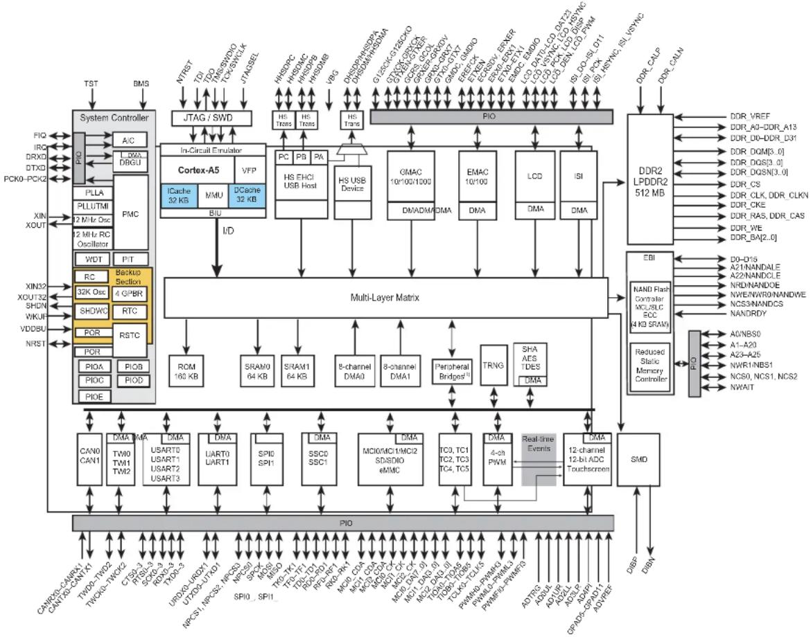
flowchart
System architecture diagram showing data flow between System Controller, Cortex-A5, Multi-Layer Matrix, and memory modules like DDR2 LPDDR2 512 MB and SMD.Note 1: Peripheral Bridge 0 (APB0) connects HSMCI0, SPI0, USART0, USART1, TWI0, TWI1, UART0, SSC0, SMD.
Peripheral Bridge 1 (APB1) connects HSMCI1, HSMCI2, ADC, SSC1, UART1, USART2, USART3, TWI2, DBGU, SPI1, SHA, AES, TDES.
2. Signal Description
Table 2-1 gives details on the signal names classified by peripheral.
Table 2-1: Signal Description List
| Signal Name Function Type Active Level | |||
| Clocks, Oscillators and PLLs | |||
| XIN Main Oscillator Input Input — | |||
| XOUT Main Oscillator Output Output — | |||
| XIN32 Slow Clock Oscillator Input | Input — | ||
| XOUT32 | Slow Clock Oscillator Output | Output — | |
| VBG | Bias Voltage Reference for USB | Analog | — |
| PCK0-PCK2 | Programmable Clock Output | Output — | |
| Shutdown, Wake-up Logic | |||
| SHDN | Shutdown Control | Output — | |
| WKUP | Wake-Up Input | Input — | |
| ICE and JTAG | |||
| TCK/SWCLK | Test Clock/Serial Wire Clock | Input — | |
| TDI | Test Data In | Input — | |
| TDO | Test Data Out | Output — | |
| TMS/SWDIO | Test Mode Select/Serial Wire Input/Output | I/O | — |
| JTAGSEL | JTAG Selection | Input — | |
| Reset/Test | |||
| NRST | Microcontroller Reset | I/O Low | |
| TST | Test Mode Select | Input — | |
| NTRST | Test Reset Signal | Input — | |
| BMS | Boot Mode Select | Input — | |
| Debug Unit - DBGU | |||
| DRXD | Debug Receive Data | Input — | |
| DTXD | Debug Transmit Data | Output — | |
| Advanced Interrupt Controller - AIC | |||
| IRQ | External Interrupt Input | Input — | |
| FIQ Fast Interrupt Input | Input — | ||
| PIO Controller - PIOA - PIOB - PIOC - PIOD - PIOE | |||
| PA0-PAxx | Parallel IO Controller A | I/O | — |
| PB0-PBxx | Parallel IO Controller B | I/O | — |
| PC0-PCxx | Parallel IO Controller C | I/O | — |
| PD0-PDxx | Parallel IO Controller D | I/O | — |
| PE0-PExx | Parallel IO Controller E | I/O | — |
| Signal Name | Function | Type | Active Level |
| External Bus Interface - EBI | |||
| D0-D15 Data Bus I/O — | |||
| A0-A25 Address Bus Output — | |||
| NWAIT External Wait Signal Input Low | |||
| Static Memory Controller - SMC | |||
| NCS0-NCS3 Chip Select Lines Output Low | |||
| NWR0-NWR1 Write Signal Output Low | |||
| NRD | Read Signal | Output Low | |
| NWE | Write Enable | Output Low | |
| NBS0-NBS1 | Byte Mask Signal | Output Low | |
| NANDOE | NAND Flash Output Enable | Output Low | |
| NANDWE | NAND Flash Write Enable | Output Low | |
| DDR2/LPDDR Controller | |||
| DDR_VREF | Reference Voltage | Input | — |
| DDR_CALP | Positive Calibration Reference | Input | — |
| DDR_CALN | Negative Calibration Reference | Input | — |
| DDR_CK, DDR_CKN | DDR2 differential clock | Output — | |
| DDR_CKE | DDR2 Clock Enable | Output | High |
| DDR_CS | DDR2 Controller Chip Select | Output Low | |
| DDR_BA[2..0] | Bank Select | Output Low | |
| DDR_WE | DDR2 Write Enable | Output Low | |
| DDR_RAS, DDR_CAS | Row and Column Signal | Output Low | |
| DDR_A[13..0] | DDR2 Address Bus | Output — | |
| DDR_D[31..0] | DDR2 Data Bus | I/O — | |
| DQS[3..0] | Differential Data Strobe | I/O — | |
| DQSN[3..0] | DQSN must be connected to DDR_VREF for DDR2 memories | I/O | — |
| DQM[3..0] | Write Data Mask | Output — | |
| High Speed Multimedia Card Interface - HSMClx [2..0] | |||
| MCI0_CK, MCI1_CK, MCI2_CK | Multimedia Card Clock | I/O | — |
| MCI0_CDA, MCI1_CDA, MCI2_CDA | Multimedia Card Command | I/O — | |
| MCI0_DA[7..0] | Multimedia Card 0 Data | I/O — | |
| MCI1_DA[3..0] | Multimedia Card 1 Data | I/O — | |
| MCI2_DA[3..0) | Multimedia Card 2 Data | I/O — | |
| Universal Synchronous Asynchronous Receiver Transmitter - USARTx [3..0] | |||
| SCKx USARTx Serial Clock I/O — | |||
| TXDx USARTx Transmit Data Output — | |||
| RXDx USARTx Receive Data Input — | |||
| RTSx USARTx Request To Send Output — | |||
| CTSx USARTx Clear To Send Input — | |||
| Universal Asynchronous Receiver Transmitter - UARTx [1..0] | |||
| UTXDx UARTx Transmit Data | Output — | ||
| URXDx | UARTx Receive Data | Input — | |
| Synchronous Serial Controller - SSCx [1..0] | |||
| TDx | SSC Transmit Data | Output | — |
| RDx | SSC Receive Data | Input — | |
| TKx | SSC Transmit Clock | I/O — | |
| RKx | SSC Receive Clock | I/O — | |
| TFx | SSC Transmit Frame Sync | I/O — | |
| RFx | SSC Receive Frame Sync | I/O — | |
| Timer/Counter - TCx [5..0] | |||
| TCLKx | TC Channel x External Clock Input | Input — | |
| TIOAx | TC Channel x I/O Line A | I/O — | |
| TIOBx | TC Channel x I/O Line B | I/O — | |
| Serial Peripheral Interface - SPIx [1..0] | |||
| SPIx_MISO | Master In Slave Out | I/O — | |
| SPIx_MOSI | Master Out Slave In | I/O — | |
| SPIx_SPCK | SPI Serial Clock | I/O — | |
| SPIx_NPCS0 | SPI Peripheral Chip Select 0 | I/O | Low |
| SPIx_NPCS[3..1] | SPI Peripheral Chip Select | Output | Low |
| Two-Wire Interface - TWIx [2..0] | |||
| TWDx | Two-wire Serial Data | I/O — | |
| TWCKx | Two-wire Serial Clock | I/O — | |
| CAN controller - CANx [1..0] | |||
| CANRXx | CAN input | Input — | |
| CANTXx | CAN output | Output — | |
| Soft Modem - SMD | |||
| DIBN | Soft Modem Signal | I/O — | |
| DIBP | Soft Modem Signal | I/O — | |
| Pulse Width Modulation Controller - PWMC | |||
| PWMH[3..0] PWM Waveform Output High Output — | |||
| PWML[3..0] PWM Waveform Output Low Output — | |||
| PWMFlx PWM Fault Input Input — | |||
| USB Host High Speed Port - UHPHS | |||
| HHSDPA USB Host Port A High Speed | Data + Analog — | ||
| HHSDMA USB Host Port A High Speed | Data - Analog — | ||
| HHSDPB | USB Host Port B High Speed Data + Analog — | ||
| HHSDMB USB Host Port B High Speed | Data - Analog — | ||
| HHSDPC | USB Host Port C High Speed Data + | Analog — | |
| HHSDMC | USB Host Port C High Speed Data - Analog — | ||
| USB Device High Speed Port - UDPHS | |||
| DHSDP | USB Device High Speed Data + | Analog — | |
| DHSDM | USB Device High Speed Data - | Analog — | |
| Glgabit Ethernet 10/100/1000 - GMAC | |||
| GTXCK | Transmit Clock or Reference Clock Output — | ||
| G125CK 125 MHz input Clock | Input — | ||
| G125CKO | 125 MHz output Clock | Output — | |
| GTXEN | Transmit Enable | Output — | |
| GTX[7..0] | Transmit Data | Output — | |
| GTXER | Transmit Coding Error | Output — | |
| GRXCK | Receive Clock | Input — | |
| GRXDV | Receive Data Valid | Input — | |
| GRX[7..0] | Receive Data | Input — | |
| GRXER | Receive Error | Input — | |
| GCRS | Carrier Sense and Data Valid | Input — | |
| GCOL | Collision Detect | Input — | |
| GMDC | Management Data Clock | Output — | |
| GMDIO | Management Data Input/Output | I/O | — |
| Signal Name Function Type Active Level | |||
| RMII Ethernet 10/100 - EMAC | |||
| EREFCK Transmit Clock or Reference | Clock Input — | ||
| ETXEN Transmit Enable Output — | |||
| ETX[1..0] Transmit Data Output — | |||
| ECRSDV Carrier Sense/Data Valid Input — | |||
| ERX[1..0] Receive Data Input — | |||
| ERXER Receive Error | Input — | ||
| EMDC | Management Data Clock | Output — | |
| EMDIO | Management Data Input/Output | I/O | — |
| LCD Controller - LCDC | |||
| LCDDAT[23..0] | LCD Data Bus | Output — | |
| LCDVSYNC | LCD Vertical Synchronization | Output | — |
| LCDHSYNC | LCD Horizontal Synchronization | Output — | |
| LCDPCK LCD pixel Clock | Output — | ||
| LCDDEN | LCD Data Enable | Output — | |
| LCDPWM | LCDPWM for Contrast Control | Output | — |
| LCDDISP | LCD Display ON/OFF | Output — | |
| Image Sensor Interface - ISI | |||
| ISI_D[11..0] | Image Sensor Data | Input — | |
| ISI_HSYNC | Image Sensor Horizontal Synchro | input | — |
| ISI_VSYNC | Image Sensor Vertical Synchro | input | — |
| ISI_PCK | Image Sensor Data clock | input | — |
| Touchscreen Analog-to-Digital Converter - ADC | |||
| AD0_UL | Upper Left Touch Panel | Analog | — |
| AD1_UR | Upper Right Touch Panel | Analog | — |
| AD2_LL | Lower Left Touch Panel | Analog | — |
| AD3_LR | Lower Right Touch Panel | Analog | — |
| AD4_PI | Panel Input | Analog | — |
| AD5-AD11 | 7 Analog Inputs | Analog | — |
| ADTRG | ADC Trigger | Input — | |
| ADVREF ADC Reference | Analog — | ||
3. Package and Pinout
The SAMA5D3 is available in two Green-compliant packages:
• 324-ball LFBGA (15 x 15 x 1.4 mm, pitch 0.8 mm)
• 324-ball TFBGA (12 x 12 x 1.2 mm, pitch 0.5 mm)
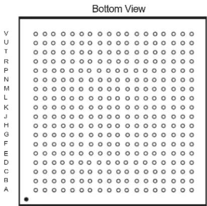
3.1 324-ball LFBGA Package (15 x 15 x 1.4 mm, pitch 0.8 mm)
Figure 3-1 shows the ball map of the 324-ball LFBGA package.
Figure 3-1: 324-ball LFBGA Ball Map
text_image
Bottom View V U T R P N M L K J H G F E D C B A134567891011121314151617218
3.2 324-ball LFBGA Package Pinout
Table 3-1: SAMA5D3 Pinout for 324-ball LFBGA Package
| Pin | Power Rail I/O Type | Primary Alternate PIO Peripheral A PIO Peripheral B PIO Peripheral C | Reset State^(1) | ||||||||||
| Signal | Dir | Signal | Dir | Signal | Dir | Signal | Dir | Signal | Dir | Signal, Dir, PU, PD, HiZ, ST | |||
| E3 | VDDIOP0 | GPIO | PA0 | I/O | — | — | LCDDAT0 | O | — | — | — | — | PIO, I, PU, ST |
| F5 | VDDIOP0 | GPIO | PA1 | I/O | — | — | LCDDAT1 | O | — | — | — | — | PIO, I, PU, ST |
| D2 | VDDIOP0 | GPIO | PA2 | I/O | — | — | LCDDAT2 | O | — | — | — | — | PIO, I, PU, ST |
| F4 | VDDIOP0 | GPIO | PA3 | I/O | — | — | LCDDAT3 | O | — | — | — | — | PIO, I, PU, ST |
| D1 | VDDIOP0 | GPIO | PA4 | I/O | — | — | LCDDAT4 | O | — | — | — | — | PIO, I, PU, ST |
| J10 | VDDIOP0 | GPIO | PA5 | I/O | — | — | LCDDAT5 | O | — | — | — | — | PIO, I, PU, ST |
| G4 | VDDIOP0 | GPIO | PA6 | I/O | — | — | LCDDAT6 | O | — | — | — | — | PIO, I, PU, ST |
| J9 | VDDIOP0 | GPIO | PA7 | I/O | — | — | LCDDAT7 | O | — | — | — | — | PIO, I, PU, ST |
| F3 | VDDIOP0 | GPIO | PA8 | I/O | — | — | LCDDAT8 | O | — | — | — | — | PIO, I, PU, ST |
| J8 | VDDIOP0 | GPIO | PA9 | I/O | — | — | LCDDAT9 | O | — | — | — | — | PIO, I, PU, ST |
| E2 | VDDIOP0 | GPIO | PA10 | I/O | — | — | LCDDAT10 | O | — | — | — | — | PIO, I, PU, ST |
| K8 | VDDIOP0 | GPIO | PA11 | I/O | — | — | LCDDAT11 | O | — | — | — | — | PIO, I, PU, ST |
| F2 | VDDIOP0 | GPIO | PA12 | I/O | — | — | LCDDAT12 | O | — | — | — | — | PIO, I, PU, ST |
| G6 | VDDIOP0 | GPIO | PA13 | I/O | — | — | LCDDAT13 | O | — | — | — | — | PIO, I, PU, ST |
| E1 | VDDIOP0 | GPIO | PA14 | I/O | — | — | LCDDAT14 | O | — | — | — | — | PIO, I, PU, ST |
| H5 | VDDIOP0 | GPIO | PA15 | I/O | — | — | LCDDAT15 | O | — | — | — | — | PIO, I, PU, ST |
| H3 | VDDIOP0 | GPIO | PA16 | I/O | — | — | LCDDAT16 | O | — | — | ISI_D0 | I | PIO, I, PU, ST |
| H6 | VDDIOP0 | GPIO | PA17 | I/O | — | — | LCDDAT17 | O | — | — | ISI_D1 | I | PIO, I, PU, ST |
| H4 | VDDIOP0 | GPIO | PA18 | I/O | — | — | LCDDAT18 | O | TWD2 | I/O | ISI_D2 | I | PIO, I, PU, ST |
| H7 | VDDIOP0 | GPIO | PA19 | I/O | — | — | LCDDAT19 | O | TWCK2 | O | ISI_D3 | I | PIO, I, PU, ST |
| H2 | VDDIOP0 | GPIO | PA20 | I/O | — | — | LCDDAT20 | O | PWMH0 | O | ISI_D4 | I | PIO, I, PU, ST |
| J6 | VDDIOP0 | GPIO | PA21 | I/O | — | — | LCDDAT21 | O | PWML0 | O | ISI_D5 | I | PIO, I, PU, ST |
| G2 | VDDIOP0 | GPIO | PA22 | I/O | — | — | LCDDAT22 | O | PWMH1 | O | ISI_D6 | I | PIO, I, PU, ST |
| J5 | VDDIOP0 | GPIO | PA23 | I/O | — | — | LCDDAT23 | O | PWML1 | O | ISI_D7 | I | PIO, I, PU, ST |
| F1 | VDDIOP0 | GPIO | PA24 | I/O | — | — | LCDPWM | O | — | — | — | — | PIO, I, PU, ST |
| J4 | VDDIOP0 | GPIO | PA25 | I/O | — | — | LCDDISP | O | — | — | — | — | PIO, I, PU, ST |
| G3 | VDDIOP0 | GPIO | PA26 | I/O | — | — | LCDVSYNC | O | — | — | — | — | PIO, I, PU, ST |
| J3 | VDDIOP0 | GPIO | PA27 | I/O | — | — | LCDHSYNC | O | — | — | — | — | PIO, I, PU, ST |
| G1 | VDDIOP0 | GPIO_CLK2 | PA28 | I/O | — | — | LCDPCK | O | — | — | — | — | PIO, I, PU, ST |
| K4 | VDDIOP0 | GPIO | PA29 | I/O | — | — | LCDDEN | O | — | — | — | — | PIO, I, PU, ST |
| H1 | VDDIOP0 | GPIO | PA30 | I/O | — | — | TWD0 | I/O | URXD1 | I | ISI_VSYNC | I | PIO, I, PU, ST |
| K3 | VDDIOP0 | GPIO | PA31 | I/O | — | — | TWCK0 | O | UTXD1 | O | ISI_HSYNC | I | PIO, I, PU, ST |
| T2 | VDDIOP1 | GMAC | PB0 | I/O | — | — | GTX0 | O | PWMH0 | O | — | — | PIO, I, PU, ST |
| N7 | VDDIOP1 | GMAC | PB1 | I/O | — | — | GTX1 | O | PWML0 | O | — | — | PIO, I, PU, ST |
| T3 | VDDIOP1 | GMAC | PB2 | I/O | — | — | GTX2 | O | TK1 | I/O | — | — | PIO, I, PU, ST |
| N6 | VDDIOP1 | GMAC | PB3 | I/O | — | — | GTX3 | O | TF1 | I/O | — | — | PIO, I, PU, ST |
| P5 | VDDIOP1 | GMAC | PB4 | I/O | — | — | GRX0 | I | PWMH1 | O | — | — | PIO, I, PU, ST |
| T4 | VDDIOP1 | GMAC | PB5 | I/O | — | — | GRX1 | I | PWML1 | O | — | — | PIO, I, PU, ST |
| R4 | VDDIOP1 | GMAC | PB6 | I/O | — | — | GRX2 | I | TD1 | O | — | — | PIO, I, PU, ST |
| U1 | VDDIOP1 | GMAC | PB7 | I/O | — | — | GRX3 | I | RK1 | I | — | — | PIO, I, PU, ST |
| Pin | Power Rail | I/O Type | Primary | Alternate | PIO Peripheral A | PIO Peripheral B | PIO Peripheral C | Reset State^(1) | |||||
| Signal | Dir | Signal | Dir | Signal | Dir | Signal | Dir | Signal | Dir | Signal, Dir, PU, PD, HiZ, ST | |||
| R5 | VDDIOP1 | GMAC | PB8 | I/O | — | — | GTXCK | O | PWMH2 | O | — | — | PIO, I, PU, ST |
| P3 VDDIOP1 GMAC PB9 I/O — GTXEN O PWML2 O — PIO, I, PU, ST | |||||||||||||
| R6 | VDDIOP1 | GMAC | PB10 | I/O | — | — | GTXER | O | RF1 | I/O | — | — | PIO, I, PU, ST |
| V3 | VDDIOP1 | GMAC | PB11 | I/O | — | — | GRXCK | I | RD1 | I | — | — | PIO, I, PU, ST |
| P6 | VDDIOP1 | GMAC | PB12 | I/O | — | — | GRXDV | I | PWMH3 | O | — | — | PIO, I, PU, ST |
| V1 | VDDIOP1 | GMAC | PB13 | I/O | — | — | GRXER | I | PWML3 | O | — | — | PIO, I, PU, ST |
| R7 | VDDIOP1 | GMAC | PB14 | I/O | — | — | GCRS | I | CANRX1 | I | — | — | PIO, I, PU, ST |
| U3 VDDIOP1 GMAC PB15 I/O — GCOL I CANTX1 O — | — PIO, I, PU, ST | ||||||||||||
| P7 | VDDIOP1 | GMAC | PB16 | I/O | — | — | GMDC | O | — | — | — | — | PIO, I, PU, ST |
| V2 | VDDIOP1 | GMAC | PB17 | I/O | — | — | GMDIO | I/O | — | — | — | — | PIO, I, PU, ST |
| V5 | VDDIOP1 | GMAC | PB18 | I/O | — | — | G125CK | I | — | — | — | — | PIO, I, PU, ST |
| T6 | VDDIOP1 | GMAC | PB19 | I/O | — | — | MCI1_CDA | I/O | GTX4 | O | — | — | PIO, I, PU, ST |
| N8 | VDDIOP1 | GMAC | PB20 | I/O | — | — | MCI1_DA0 | I/O | GTX5 | O | — | — | PIO, I, PU, ST |
| U4 | VDDIOP1 | GMAC | PB21 | I/O | — | — | MCI1_DA1 | I/O | GTX6 | O | — | — | PIO, I, PU, ST |
| M7 | VDDIOP1 | GMAC | PB22 | I/O | — | — | MCI1_DA2 | I/O | GTX7 | O | — | — | PIO, I, PU, ST |
| U5 | VDDIOP1 | GMAC | PB23 | I/O | — | — | MCI1_DA3 | I/O | GRX4 | I | — | — | PIO, I, PU, ST |
| M8 | VDDIOP1 | GMAC | PB24 | I/O | — | — | MCI1_CK | I/O | GRX5 | I | — | — | PIO, I, PU, ST |
| T5 | VDDIOP1 | GMAC | PB25 | I/O | — | — | SCK1 | I/O | GRX6 | I | — | — | PIO, I, PU, ST |
| N9 | VDDIOP1 | GMAC | PB26 | I/O | — | — | CTS1 | I | GRX7 | I | — | — | PIO, I, PU, ST |
| V4 | VDDIOP1 | GPIO | PB27 | I/O | — | — | RTS1 | O | G125CKO | O | — | — | PIO, I, PU, ST |
| M9 | VDDIOP1 | GPIO | PB28 | I/O | — | — | RXD1 | I | — | — | — | — | PIO, I, PU, ST |
| P8 | VDDIOP1 | GPIO | PB29 | I/O | — | — | TXD1 | O | — | — | — | — | PIO, I, PU, ST |
| M10 | VDDIOP0 | GPIO | PB30 | I/O | — | — | DRXD | I | — | — | — | — | PIO, I, PU, ST |
| R9 | VDDIOP0 | GPIO | PB31 | I/O | — | — | DTXD | O | — | — | — | — | PIO, I, PU, ST |
| D8 | VDDIOP0 | GPIO | PC0 | I/O | — | — | ETX0 | O | TIOA3 | I/O | — | — | PIO, I, PU, ST |
| A4 | VDDIOP0 | GPIO | PC1 | I/O | — | — | ETX1 | O | TIOB3 | I/O | — | — | PIO, I, PU, ST |
| E8 | VDDIOP0 | GPIO | PC2 | I/O | — | — | ERX0 | I | TCLK3 | I | — | — | PIO, I, PU, ST |
| A3 | VDDIOP0 | GPIO | PC3 | I/O | — | — | ERX1 | I | TIOA4 | I/O | — | — | PIO, I, PU, ST |
| A2 | VDDIOP0 | GPIO | PC4 | I/O | — | — | ETXEN | O | TIOB4 | I/O | — | — | PIO, I, PU, ST |
| F8 | VDDIOP0 | GPIO | PC5 | I/O | — | — | ECRSDV | I | TCLK4 | I | — | — | PIO, I, PU, ST |
| B3 | VDDIOP0 | GPIO | PC6 | I/O | — | — | ERXER | I | TIOA5 | I/O | — | — | PIO, I, PU, ST |
| G8 | VDDIOP0 | GPIO | PC7 | I/O | — | — | EREFCK | I | TIOB5 | I/O | — | — | PIO, I, PU, ST |
| B4 | VDDIOP0 | GPIO | PC8 | I/O | — | — | EMDC | O | TCLK5 | I | — | — | PIO, I, PU, ST |
| F7 | VDDIOP0 | GPIO | PC9 | I/O | — | — | EMDIO | I/O | — | — | — | — | PIO, I, PU, ST |
| A1 | VDDIOP0 | GPIO | PC10 | I/O | — | — | MCI2_CDA | I/O | — | — | LCDDAT20 | O | PIO, I, PU, ST |
| D7 | VDDIOP0 | GPIO | PC11 | I/O | — | — | MCI2_DA0 | I/O | — | — | LCDDAT19 | O | PIO, I, PU, ST |
| C6 | VDDIOP0 | GPIO | PC12 | I/O | — | — | MCI2_DA1 | I/O | TIOA1 | I/O | LCDDAT18 | O | PIO, I, PU, ST |
| E7 | VDDIOP0 | GPIO | PC13 | I/O | — | — | MCI2_DA2 | I/O | TIOB1 | I/O | LCDDAT17 | O | PIO, I, PU, ST |
| B2 | VDDIOP0 | GPIO | PC14 | I/O | — | — | MCI2_DA3 | I/O | TCLK1 | I | LCDDAT16 | O | PIO, I, PU, ST |
| F6 | VDDIOP0 | MCI_CLK | PC15 | I/O | — | — | MCI2_CK | I/O | PCK2 | O | LCDDAT21 | O | PIO, I, PU, ST |
| B1 | VDDIOP0 | GPIO | PC16 | I/O | — | — | TK0 | I/O | — | — | — | — | PIO, I, PU, ST |
| E6 | VDDIOP0 | GPIO | PC17 | I/O | — | — | TF0 | I/O | — | — | — | — | PIO, I, PU, ST |
| Pin | Power Rail | I/O Type | Primary | Alternate | PIO Peripheral A | PIO Peripheral B | PIO Peripheral C | Reset State ^(1) | |||||
| Signal | Dir | Signal | Dir | Signal | Dir | Signal | Dir | Signal | Dir | Signal, Dir, PU, PD, HiZ, ST | |||
| C3 | VDDIOP0 | GPIO | PC18 | I/O | — | — | TD0 | O | — | — | — | — | PIO, I, PU, ST |
| D6 VDDIOP0 GPIO PC | 19 I/O — — RK0 | I/O — — — — PIO, I, PU, ST | |||||||||||
| C4 | VDDIOP0 | GPIO | PC20 | I/O | — | — | RF0 | I/O | — | — | — | — | PIO, I, PU, ST |
| D5 VDDIOP0 GPIO PC | 21 I/O — — RD0 | I — — | — — PIO, I, PU, ST | ||||||||||
| C2 | VDDIOP0 | GPIO | PC22 | I/O | — | — | SPI1_MISO | I/O | — | — | — | — | PIO, I, PU, ST |
| G9 | VDDIOP0 | GPIO | PC23 | I/O | — | — | SPI1_MOSI | I/O | — | — | — | — | PIO, I, PU, ST |
| C1 | VDDIOP0 | GPIO_CLK | PC24 | I/O | — | — | SPI1_SPCK | I/O | — | — | — | — | PIO, I, PU, ST |
| H10 | VDDIOP0 | GPIO | PC25 | I/O | — | — | SPI1_NPCS0 | I/O | — | — | — | — | PIO, I, PU, ST |
| H9 | VDDIOP0 | GPIO | PC26 | I/O | — | — | SPI1_NPCS1 | O | TWD1 | I/O | ISI_D11 | I | PIO, I, PU, ST |
| D4 | VDDIOP0 | GPIO | PC27 | I/O | — | — | SPI1_NPCS2 | O | TWCK1 | O | ISI_D10 | I | PIO, I, PU, ST |
| H8 | VDDIOP0 | GPIO | PC28 | I/O | — | — | SPI1_NPCS3 | O | PWMFI0 | I | ISI_D9 | I | PIO, I, PU, ST |
| G5 | VDDIOP0 | GPIO | PC29 | I/O | — | — | URXD0 | I | PWMFI2 | I | ISI_D8 | I | PIO, I, PU, ST |
| D3 | VDDIOP0 | GPIO | PC30 | I/O | — | — | UTXD0 | O | — | — | ISI_PCK | O | PIO, I, PU, ST |
| E4 | VDDIOP0 | GPIO | PC31 | I/O | — | — | FIQ | I | PWMFI1 | I | — | — | PIO, I, PU, ST |
| K5 | VDDIOP1 | GPIO | PD0 | I/O | — | — | MCI0_CDA | I/O | — | — | — | — | PIO, I, PU, ST |
| P1 | VDDIOP1 | GPIO | PD1 | I/O | — | — | MCI0_DA0 | I/O | — | — | — | — | PIO, I, PU, ST |
| K6 | VDDIOP1 | GPIO | PD2 | I/O | — | — | MCI0_DA1 | I/O | — | — | — | — | PIO, I, PU, ST |
| R1 | VDDIOP1 | GPIO | PD3 | I/O | — | — | MCI0_DA2 | I/O | — | — | — | — | PIO, I, PU, ST |
| L7 | VDDIOP1 | GPIO | PD4 | I/O | — | — | MCI0_DA3 | I/O | — | — | — | — | PIO, I, PU, ST |
| P2 | VDDIOP1 | GPIO | PD5 | I/O | — | — | MCI0_DA4 | I/O | TIOA0 | I/O | PWMH2 | O | PIO, I, PU, ST |
| L8 | VDDIOP1 | GPIO | PD6 | I/O | — | — | MCI0_DA5 | I/O | TIOB0 | I/O | PWML2 | O | PIO, I, PU, ST |
| R2 | VDDIOP1 | GPIO | PD7 | I/O | — | — | MCI0_DA6 | I/O | TCLK0 | I | PWMH3 | O | PIO, I, PU, ST |
| K7 | VDDIOP1 | GPIO | PD8 | I/O | — | — | MCI0_DA7 | I/O | — | — | PWML3 | O | PIO, I, PU, ST |
| U2 | VDDIOP1 | MCI_CLK | PD9 | I/O | — | — | MCI0_CK | I/O | — | — | — | — | PIO, I, PU, ST |
| K9 | VDDIOP1 | GPIO | PD10 | I/O | — | — | SPI0_MISO | I/O | — | — | — | — | PIO, I, PU, ST |
| M5 | VDDIOP1 | GPIO | PD11 | I/O | — | — | SPI0_MOSI | I/O | — | — | — | — | PIO, I, PU, ST |
| K10 | VDDIOP1 | GPIO_CLK | PD12 | I/O | — | — | SPI0_SPCK | I/O | — | — | — | — | PIO, I, PU, ST |
| N4 | VDDIOP1 | GPIO | PD13 | I/O | — | — | SPI0_NPCS0 | I/O | — | — | — | — | PIO, I, PU, ST |
| L9 | VDDIOP1 | GPIO | PD14 | I/O | — | — | SCK0 | I/O | SPI0_NPCS1 | O | CANRX0 | I | PIO, I, PU, ST |
| N3 | VDDIOP1 | GPIO | PD15 | I/O | — | — | CTS0 | I | SPI0_NPCS2 | O | CANTX0 | O | PIO, I, PU, ST |
| L10 | VDDIOP1 | GPIO | PD16 | I/O | — | — | RTS0 | O | SPI0_NPCS3 | O | PWMFI3 | I | PIO, I, PU, ST |
| N5 | VDDIOP1 | GPIO | PD17 | I/O | — | — | RXD0 | I | — | — | — | — | PIO, I, PU, ST |
| M6 | VDDIOP1 | GPIO | PD18 | I/O | — | — | TXD0 | O | — | — | — | — | PIO, I, PU, ST |
| T1 | VDDIOP1 | GPIO | PD19 | I/O | — | — | ADTRG | I | — | — | — | — | PIO, I, PU, ST |
| N2 | VDDANA | GPIO_ANA | PD20 | I/O | — | — | AD0 | I | — | — | — | — | PIO, I, PU, ST |
| M3 | VDDANA | GPIO_ANA | PD21 | I/O | — | — | AD1 | I | — | — | — | — | PIO, I, PU, ST |
| M2 | VDDANA | GPIO_ANA | PD22 | I/O | — | — | AD2 | I | — | — | — | — | PIO, I, PU, ST |
| L3 | VDDANA | GPIO_ANA | PD23 | I/O | — | — | AD3 | I | — | — | — | — | PIO, I, PU, ST |
| M1 | VDDANA | GPIO_ANA | PD24 | I/O | — | — | AD4 | I | — | — | — | — | PIO, I, PU, ST |
| N1 | VDDANA | GPIO_ANA | PD25 | I/O | — | — | AD5 | I | — | — | — | — | PIO, I, PU, ST |
| L1 | VDDANA | GPIO_ANA | PD26 | I/O | — | — | AD6 | I | — | — | — | — | PIO, I, PU, ST |
| L2 | VDDANA | GPIO_ANA | PD27 | I/O | — | — | AD7 | I | — | — | — | — | PIO, I, PU, ST |
| K1 | VDDANA | GPIO_ANA | PD28 | I/O | — | — | AD8 | I | — | — | — | — | PIO, I, PU, ST |
| K2 VDDANA GPIO_ANA | A PD29 I/O — — | AD9 I — — — P | IO, I, PU, ST | ||||||||||
| J1 | VDDANA | GPIO_ANA | PD30 | I/O | — | — | AD10 | I | PCK0 | O | — | — | PIO, I, PU, ST |
| J2 | VDDANA | GPIO_ANA | PD31 | I/O | — | — | AD11 | I | PCK1 | O | — | — | PIO, I, PU, ST |
| P13 | VDDIOM | EBI | PE0 | I/O | — | — | A0/NBS0 | O | — | — | — | — | A.I, PD, ST |
| R14 | VDDIOM | EBI | PE1 | I/O | — | — | A1 | O | — | — | — | — | A.I, PD, ST |
| R13 | VDDIOM | EBI | PE2 | I/O | — | — | A2 | O | — | — | — | — | A.I, PD, ST |
| V18 | VDDIOM | EBI | PE3 | I/O | — | — | A3 | O | — | — | — | — | A.I, PD, ST |
| P14 | VDDIOM | EBI | PE4 | I/O | — | — | A4 | O | — | — | — | — | A.I, PD, ST |
| U18 | VDDIOM | EBI | PE5 | I/O | — | — | A5 | O | — | — | — | — | A.I, PD, ST |
| T18 | VDDIOM | EBI | PE6 | I/O | — | — | A6 | O | — | — | — | — | A.I, PD, ST |
| R15 | VDDIOM | EBI | PE7 | I/O | — | — | A7 | O | — | — | — | — | A.I, PD, ST |
| P17 | VDDIOM | EBI | PE8 | I/O | — | — | A8 | O | — | — | — | — | A.I, PD, ST |
| P15 | VDDIOM | EBI | PE9 | I/O | — | — | A9 | O | — | — | — | — | A.I, PD, ST |
| P18 | VDDIOM | EBI | PE10 | I/O | — | — | A10 | O | — | — | — | — | A.I, PD, ST |
| R16 | VDDIOM | EBI | PE11 | I/O | — | — | A11 | O | — | — | — | — | A.I, PD, ST |
| N16 | VDDIOM | EBI | PE12 | I/O | — | — | A12 | O | — | — | — | — | A.I, PD, ST |
| R17 | VDDIOM | EBI | PE13 | I/O | — | — | A13 | O | — | — | — | — | A.I, PD, ST |
| N17 | VDDIOM | EBI | PE14 | I/O | — | — | A14 | O | — | — | — | — | A.I, PD, ST |
| R18 | VDDIOM | EBI | PE15 | I/O | — | — | A15 | O | SCK3 | I/O | — | — | A.I, PD, ST |
| N18 | VDDIOM | EBI | PE16 | I/O | — | — | A16 | O | CTS3 | I | — | — | A.I, PD, ST |
| P16 | VDDIOM | EBI | PE17 | I/O | — | — | A17 | O | RTS3 | O | — | — | A.I, PD, ST |
| M18 | VDDIOM | EBI | PE18 | I/O | — | — | A18 | O | RXD3 | I | — | — | A.I, PD, ST |
| N15 | VDDIOM | EBI | PE19 | I/O | — | — | A19 | O | TXD3 | O | — | — | A.I, PD, ST |
| M15 | VDDIOM | EBI | PE20 | I/O | — | — | A20 | O | SCK2 | I/O | — | — | A.I, PD, ST |
| N14 | VDDIOM | EBI | PE21 | I/O | — | — | A21/NANDALE | O | — | — | — | — | A.I, PD, ST |
| M17 | VDDIOM | EBI | PE22 | I/O | — | — | A22/NANDCLE | O | — | — | — | — | A.I, PD, ST |
| M13 | VDDIOM | EBI | PE23 | I/O | — | — | A23 | O | CTS2 | I | — | — | A.I, PD, ST |
| M16 | VDDIOM | EBI | PE24 | I/O | — | — | A24 | O | RTS2 | O | — | — | A.I, PD, ST |
| N12 | VDDIOM | EBI | PE25 | I/O | — | — | A25 | O | RXD2 | I | — | — | A.I, PD, ST |
| M14 | VDDIOM | EBI | PE26 | I/O | — | — | NCS0 | O | TXD2 | O | — | — | PIO,O, PU, ST |
| M12 | VDDIOM | EBI | PE27 | I/O | — | — | NCS1 | O | TIOA2 | I/O | LCDDAT22 | O | PIO,I, PU, ST |
| L13 | VDDIOM | EBI | PE28 | I/O | — | — | NCS2 | O | TIOB2 | I/O | LCDDAT23 | O | PIO,I, PU, ST |
| L15 | VDDIOM | EBI | PE29 | I/O | — | — | NWR1/NBS1 | O | TCLK2 | I | — | — | PIO,I, PU, ST |
| L14 | VDDIOM | EBI | PE30 | I/O | — | — | NWAIT | I | — | — | — | — | PIO,I, PU, ST |
| L16 | VDDIOM | EBI | PE31 | I/O | — | — | IRQ | I | PWML1 | O | — | — | PIO,I, PU, ST |
| U15 | VDBU | SYSC | TST | I | — | — | — | — | — | — | — | — | I, PD, |
| U9 | VDDIOP0 | SYSC | BMS | I | — | — | — | — | — | — | — | — | I |
| U8 | VDDIOP0 | CLOCK | XIN | I | — | — | — | — | — | — | — | — | I |
| V8 | VDDIOP0 | CLOCK | XOUT | O | — | — | — | — | — | — | — | — | O |
| U16 | VDBU | CLOCK | XIN32 | I | — | — | — | — | — | — | — | — | I |
| V16 | VDBU | CLOCK | XOUT32 | O | — | — | — | — | — | — | — | — | O |
| T12 V | VDDBU SYSC SHDN O — — — — | ——— O | |||||||||||
| T10 V | VDDBU SYSC WKUP I — — — — | ——— I, ST | |||||||||||
| V9 | VDDIOP0 | RSTJTAG | NRST | I/O | — | — | — | — | — | — | — | — | I, PU, ST |
| P11 | VDDIOP0 | RSTJTAG | NTRST | I | — | — | — | — | — | — | — | — | I, PU, ST |
| R8 | VDDIOP0 | RSTJTAG | TDI | I | — | — | — | — | — | — | — | — | I, ST |
| M11 | VDDIOP0 | RSTJTAG | TDO | O | — | — | — | — | — | — | — | — | O |
| N10 | VDDIOP0 | RSTJTAG | TMS | I | SWDIO | I/O | — | — | — | — | — | — | I, ST |
| P9 | VDDIOP0 | RSTJTAG | TCK | I | SWCLK | I | — | — | — | — | — | — | I, ST |
| T9 | VDDBU | SYSC | JTAGSEL | I | — | — | — | — | — | — | — | — | I, PD |
| V6 | VDDIOP0 | DIB | DIBP | O | — | — | — | — | — | — | — | — | O, PU |
| U6 | VDDIOP0 | DIB | DIBN | O | — | — | — | — | — | — | — | — | O, PU |
| K12 | VDDIOM | EBI | D0 | I/O | — | — | — | — | — | — | — | — | I, PD |
| K15 | VDDIOM | EBI | D1 | I/O | — | — | — | — | — | — | — | — | I, PD |
| K14 | VDDIOM | EBI | D2 | I/O | — | — | — | — | — | — | — | — | I, PD |
| K16 | VDDIOM | EBI | D3 | I/O | — | — | — | — | — | — | — | — | I, PD |
| K13 | VDDIOM | EBI | D4 | I/O | — | — | — | — | — | — | — | — | I, PD |
| K17 | VDDIOM | EBI | D5 | I/O | — | — | — | — | — | — | — | — | I, PD |
| J12 | VDDIOM | EBI | D6 | I/O | — | — | — | — | — | — | — | — | I, PD |
| K18 | VDDIOM | EBI | D7 | I/O | — | — | — | — | — | — | — | — | I, PD |
| J14 | VDDIOM | EBI | D8 | I/O | — | — | — | — | — | — | — | — | I, PD |
| J16 | VDDIOM | EBI | D9 | I/O | — | — | — | — | — | — | — | — | I, PD |
| J13 | VDDIOM | EBI | D10 | I/O | — | — | — | — | — | — | — | — | I, PD |
| J17 | VDDIOM | EBI | D11 | I/O | — | — | — | — | — | — | — | — | I, PD |
| J15 | VDDIOM | EBI | D12 | I/O | — | — | — | — | — | — | — | — | I, PD |
| J18 | VDDIOM | EBI | D13 | I/O | — | — | — | — | — | — | — | — | I, PD |
| H16 | VDDIOM | EBI | D14 | I/O | — | — | — | — | — | — | — | — | I, PD |
| H18 | VDDIOM | EBI | D15 | I/O | — | — | — | — | — | — | — | — | I, PD |
| L12 | VDDIOM | EBI | NCS3/NANDCS | O | — | — | — | — | — | — | — | — | O, PU |
| L18 | VDDIOM | EBI | NANDRDY | I | — | — | — | — | — | — | — | — | I, PU |
| L17 | VDDIOM | EBI | NRD/NANDOE | O | — | — | — | — | — | — | — | — | O, PU |
| K11 | VDDIOM | EBI | NWE/NANDWE | O | — | — | — | — | — | — | — | — | O, PU |
| C13 | VDDIODDR | Reference voltage | DDR_VREF I | ——— | ——— | ||||||||
| B10 | VDDIODDR | DDR_IO | DDR_A0 | O | — | — | — | — | — | — | — | — | O |
| C11 | VDDIODDR | DDR_IO | DDR_A1 | O | — | — | — | — | — | — | — | — | O |
| A9 | VDDIODDR | DDR_IO | DDR_A2 | O | — | — | — | — | — | — | — | — | O |
| D11 | VDDIODDR | DDR_IO | DDR_A3 | O | — | — | — | — | — | — | — | — | O |
| B9 | VDDIODDR | DDR_IO | DDR_A4 | O | — | — | — | — | — | — | — | — | O |
| E10 | VDDIODDR | DDR_IO | DDR_A5 | O | — | — | — | — | — | — | — | — | O |
| D10 | VDDIODDR | DDR_IO | DDR_A6 | O | — | — | — | — | — | — | — | — | O |
| A8 | VDDIODDR | DDR_IO | DDR_A7 | O | — | — | — | — | — | — | — | — | O |
| C10 | VDDIODDR | DDR_IO | DDR_A8 | O | — | — | — | — | — | — | — | — | O |
| B8 | VDDIODDR | DDR_IO | DDR_A9 | O | — | — | — | — | — | — | — | — | O |
| F11 | VDDIODDR | DDR_IO | DDR_A10 | O | — | — | — | — | — | — | — | — | O |
| A7 VDDIODDR DDR_IO DDR_A11 | O — — — — — — — — | — — — | O | ||||||||||
| D9 | VDDIODDR | DDR_IO | DDR_A12 | O | — | — | — | — | — | — | — | — | O |
| A6 VDDIODDR DDR_IO DDR_A13 O — — — — — — | — — — O | ||||||||||||
| H12 | VDDIODDR | DDR_IO | DDR_D0 | I/O | — | — | — | — | — | — | — | — | HiZ |
| H17 | VDDIODDR | DDR_IO | DDR_D1 | I/O | — | — | — | — | — | — | — | — | HiZ |
| H13 | VDDIODDR | DDR_IO | DDR_D2 | I/O | — | — | — | — | — | — | — | — | HiZ |
| G17 | VDDIODDR | DDR_IO | DDR_D3 | I/O | — | — | — | — | — | — | — | — | HiZ |
| G16 | VDDIODDR | DDR_IO | DDR_D4 | I/O | — | — | — | — | — | — | — | — | HiZ |
| H15 | VDDIODDR | DDR_IO | DDR_D5 | I/O | — | — | — | — | — | — | — | — | HiZ |
| F17 | VDDIODDR | DDR_IO | DDR_D6 | I/O | — | — | — | — | — | — | — | — | HiZ |
| G15 | VDDIODDR | DDR_IO | DDR_D7 | I/O | — | — | — | — | — | — | — | — | HiZ |
| F16 | VDDIODDR | DDR_IO | DDR_D8 | I/O | — | — | — | — | — | — | — | — | HiZ |
| E17 | VDDIODDR | DDR_IO | DDR_D9 | I/O | — | — | — | — | — | — | — | — | HiZ |
| G14 | VDDIODDR | DDR_IO | DDR_D10 | I/O | — | — | — | — | — | — | — | — | HiZ |
| E16 | VDDIODDR | DDR_IO | DDR_D11 | I/O | — | — | — | — | — | — | — | — | HiZ |
| D17 | VDDIODDR | DDR_IO | DDR_D12 | I/O | — | — | — | — | — | — | — | — | HiZ |
| C18 | VDDIODDR | DDR_IO | DDR_D13 | I/O | — | — | — | — | — | — | — | — | HiZ |
| D16 | VDDIODDR | DDR_IO | DDR_D14 | I/O | — | — | — | — | — | — | — | — | HiZ |
| C17 | VDDIODDR | DDR_IO | DDR_D15 | I/O | — | — | — | — | — | — | — | — | HiZ |
| B16 | VDDIODDR | DDR_IO | DDR_D16 | I/O | — | — | — | — | — | — | — | — | HiZ |
| B18 | VDDIODDR | DDR_IO | DDR_D17 | I/O | — | — | — | — | — | — | — | — | HiZ |
| C15 | VDDIODDR | DDR_IO | DDR_D18 | I/O | — | — | — | — | — | — | — | — | HiZ |
| A18 | VDDIODDR | DDR_IO | DDR_D19 | I/O | — | — | — | — | — | — | — | — | HiZ |
| C16 | VDDIODDR | DDR_IO | DDR_D20 | I/O | — | — | — | — | — | — | — | — | HiZ |
| C14 | VDDIODDR | DDR_IO | DDR_D21 | I/O | — | — | — | — | — | — | — | — | HiZ |
| D15 | VDDIODDR | DDR_IO | DDR_D22 | I/O | — | — | — | — | — | — | — | — | HiZ |
| B14 | VDDIODDR | DDR_IO | DDR_D23 | I/O | — | — | — | — | — | — | — | — | HiZ |
| A15 | VDDIODDR | DDR_IO | DDR_D24 | I/O | — | — | — | — | — | — | — | — | HiZ |
| A14 | VDDIODDR | DDR_IO | DDR_D25 | I/O | — | — | — | — | — | — | — | — | HiZ |
| E12 | VDDIODDR | DDR_IO | DDR_D26 | I/O | — | — | — | — | — | — | — | — | HiZ |
| A11 | VDDIODDR | DDR_IO | DDR_D27 | I/O | — | — | — | — | — | — | — | — | HiZ |
| B11 | VDDIODDR | DDR_IO | DDR_D28 | I/O | — | — | — | — | — | — | — | — | HiZ |
| F12 | VDDIODDR | DDR_IO | DDR_D29 | I/O | — | — | — | — | — | — | — | — | HiZ |
| A10 | VDDIODDR | DDR_IO | DDR_D30 | I/O | — | — | — | — | — | — | — | — | HiZ |
| E11 | VDDIODDR | DDR_IO | DDR_D31 | I/O | — | — | — | — | — | — | — | — | HiZ |
| G12 | VDDIODDR | DDR_IO | DDR_DQM0 | O | — | — | — | — | — | — | — | — | O |
| E15 | VDDIODDR | DDR_IO | DDR_DQM1 | O | — | — | — | — | — | — | — | — | O |
| B15 | VDDIODDR | DDR_IO | DDR_DQM2 | O | — | — | — | — | — | — | — | — | O |
| D12 | VDDIODDR | DDR_IO | DDR_DQM3 | O | — | — | — | — | — | — | — | — | O |
| E18 | VDDIODDR | DDR_IO | DDR_DQS0 | I/O | — | — | — | — | — | — | — | — | I, PD |
| G18 | VDDIODDR | DDR_IO | DDR_DQS1 | I/O | — | — | — | — | — | — | — | — | I, PD |
| Pin | Power Rail | I/O Type | Primary | Alternate | PIO Peripheral A | PIO Peripheral B | PIO Peripheral C | Reset State(1) | |||||
| Signal | Dir | Signal | Dir | Signal | Dir | Signal | Dir | Signal | Dir | Signal, Dir, PU, PD, HiZ, ST | |||
| B17 | VDDIODDR | DDR_IO | DDR_DQS2 | I/O | — | — | — | — | — | — | — | — | I, PD |
| B13 VDDIODDR DDR_IO DDR_DQS3 I/O — — — — — — — I, PD | |||||||||||||
| D18 | VDDIODDR | DDR_IO | DDR_DQSN0 | I/O | — | — | — | — | — | — | — | — | I, PU |
| F18 VDDIODDR DDR_IO DDR_DQSN1 I/O — — — — — — — I, PU | |||||||||||||
| A17 | VDDIODDR | DDR_IO | DDR_DQSN2 | I/O | — | — | — | — | — | — | — | — | I, PU |
| A13 VDDIODDR DDR_IO DDR_DQSN3 | I/O — — — — — — I, PU | ||||||||||||
| C8 | VDDIODDR | DDR_IO | DDR_CS | O | — | — | — | — | — | — | — | — | O |
| B12 | VDDIODDR | DDR_IO | DDR_CLK | O | — | — | — | — | — | — | — | — | O |
| A12 | VDDIODDR | DDR_IO | DDR_CLKN | O | — | — | — | — | — | — | — | — | O |
| B7 | VDDIODDR | DDR_IO | DDR_CKE | O | — | — | — | — | — | — | — | — | O |
| C12 | VDDIODDR | DDR_IO | DDR_CALN | I | — | — | — | — | — | — | — | — | O |
| E13 | VDDIODDR | DDR_IO | DDR_CALP | I | — | — | — | — | — | — | — | — | O |
| G11 | VDDIODDR | DDR_IO | DDR_RAS | O | — | — | — | — | — | — | — | — | O |
| A5 | VDDIODDR | DDR_IO | DDR_CAS | O | — | — | — | — | — | — | — | — | O |
| B5 | VDDIODDR | DDR_IO | DDR_WE | O | — | — | — | — | — | — | — | — | O |
| E9 | VDDIODDR | DDR_IO | DDR_BA0 | O | — | — | — | — | — | — | — | — | O |
| B6 | VDDIODDR | DDR_IO | DDR_BA1 | O | — | — | — | — | — | — | — | — | O |
| F9 | VDDIODDR | DDR_IO | DDR_BA2 | O | — | — | — | — | — | — | — | — | O |
| R11 | VBG | VBG | VBG | I | — | — | — | — | — | — | — | — | I |
| U14 | VDDUTMII | USBHS | HHSDPC | I/O | — | — | — | — | — | — | — | — | O, PD |
| V14 | VDDUTMII | USBHS | HHSDMC | I/O | — | — | — | — | — | — | — | — | O, PD |
| U12 | VDDUTMII | USBHS | HHSDPB | I/O | — | — | — | — | — | — | — | — | O, PD |
| V12 | VDDUTMII | USBHS | HHSDMB | I/O | — | — | — | — | — | — | — | — | O, PD |
| U10 | VDDUTMII | USBHS | HHSDPA | I/O | DHSDP | — | — | — | — | — | — | — | O, PD |
| V10 | VDDUTMII | USBHS | HHSDMA | I/O | DHSDM | — | — | — | — | — | — | — | O, PD |
| V15 | VDDBU | power supply | VDDBU | I | — | — | — | — | — | — | — | — | I |
| T13 | GNDBU | ground | GNDBU | I | — | — | — | — | — | — | — | — | I |
| C5,C7,D14,T15,T7,U17,V7 | VDDCORE | power supply | VDDCORE | I | — | — | — | — | — | — | — | — | I |
| A16,C9,N13,T14,T8,V17 | GNDCORE | ground | GNDCORE | I | — | — | — | — | — | — | — | — | I |
| D13,F14,G10,G13,H11 | VDDIODDR | power supply | VDDIODDR | I | — | — | — | — | — | — | — | — | I |
| E14,F10,F13,F15,H14 | GNDIODDR | ground | GNDIODDR | I | — | — | — | — | — | — | — | — | I |
| P12,T16 | VDDIOM | power supply | VDDIOM | I | — | — | — | — | — | — | — | — | I |
| Pin | Power Rail | I/O Type | Primary | Alternate | PIO Peripheral A | PIO Peripheral B | PIO Peripheral C | Reset State^(1) | |||||
| Signal | Dir | Signal | Dir | Signal | Dir | Signal | Dir | Signal | Dir | Signal, Dir, PU, PD, HiZ, ST | |||
| J11, T17 | GNDIOM | ground | GNDIOM | I | — | — | — | — | — | — | — | — | I |
| G7, V11 | VDDIOP0 | power supply | VDDIOP0 | I | — | — | — | — | — | — | — | — | I |
| L11, M4 | VDDIOP1 | power supply | VDDIOP1 | I | — | — | — | — | — | — | — | — | I |
| E5, J7, N11, U7 | GNDIOP | Ground | GNDIOP | I | — | — | — | — | — | — | — | — | I |
| V13 | VDDUTMIC | Power supply | VDDUTMIC | I | — | — | — | — | — | — | — | — | I |
| U13 | VDDUTMII | Power supply | VDDUTMII | I | — | — | — | — | — | — | — | — | I |
| R12 | GNDUTMI | Ground | GNDUTMI | I | — | — | — | — | — | — | — | — | I |
| R10 | VDDPLLA | Power supply | VDDPLLA | I | — | — | — | — | — | — | — | — | I |
| P10 | GNDPLL | Ground | GNDPLL | I | — | — | — | — | — | — | — | — | I |
| U11 | VDDOSC | Power supply | VDDOSC | I | — | — | — | — | — | — | — | — | I |
| T11 | GNDOSC | Ground | GNDOSC | I | — | — | — | — | — | — | — | — | I |
| L6 | VDDANA | Power supply | VDDANA | I | — | — | — | — | — | — | — | — | I |
| L4 | GNDANA | Ground | GNDANA | I | — | — | — | — | — | — | — | — | I |
| L5 | VDDANA | Power supply | ADVREF | I | — | — | — | — | — | — | — | — | I |
| R3 | VDDFUSE | Power supply | VDDFUSE | I | — | — | — | — | — | — | — | — | I |
| P4 | GNDFUSE | Ground | GNDFUSE | I | — | — | — | — | — | — | — | — | I |
Note 1: The reset state of the GPIOs is not ensured during power-up phase. During this phase, the GPIOs are in Input Pull-Up mode and they take their reset value only after VDDCORE POR reset has been released. If a GPIO must be at level zero at power-up, it is recommended to connect an external pull-down to ensure this state.
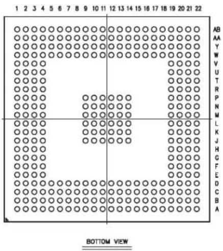
3.3 324-ball TFBGA Package (12 x 12 x 1.2 mm, pitch 0.5 mm)
Figure 3-2 shows the ball map of the 324-ball TFBGA package.
Figure 3-2: 324-ball TFBGA Ball Map
text_image
1 2 3 4 5 6 7 8 9 10 11 12 13 14 15 16 17 18 19 20 21 22 AB AA Y W V U T R P N M L K J H G F E D C B A BOTTOM VIEW3.4 324-ball TFBGA Package Pinout
Table 3-2: SAMA5D3 Pinout for 324-ball TFBGA Package
Note 1: The reset state of the GPIOs is not ensured during power-up phase. During this phase, the GPIOs are in Input Pull-Up mode and they take their reset value only after VDDCORE POR reset has been released. If a GPIO must be at level zero at power-up, it is recommended to connect an external pull down to ensure this state.
3.5 Input/Output Description
Table 3-3: SAMA5D3 I/O Type Description
| I/O Type Voltage Range Analog | Pull-up Pull-down | Schmitt Trigger (2) | |||||
| Type(2) | Typ Value (Ω) | Type | Typ Value (Ω) | ||||
| GPIO | 1.65–3.6V | — | Switchable | (1) | Switchable | (1) | Switchable |
| GPIO_CLK | 1.65–3.6V | — | Switchable | (1) | Switchable | (1) | Switchable |
| GPIO_CLK2 | 1.65–3.6V | — | Switchable | (1) | Switchable | (1) | Switchable |
| GPIO_ANA | 3.0–3.6V | I | Switchable | (1) | — | — | Switchable |
| EBI | 1.65–1.95V, 3.0–3.6V | — | Switchable | 100K | Switchable | 100K | — |
| RSTJTAG | 1.65–3.6V | — | Reset State | 100K | Reset State | 100K | Reset State |
| SYSC | 1.65–3.6V | — | — | — | Reset State | 15K | Reset State |
| USBHS | 3.0–3.6V | I/O | — | — | — | — | — |
| CLOCK | 1.65–3.6V | I/O | — | — | — | — | — |
| DIB | 3.0–3.6V | I/O | — | — | — | — | — |
| GMAC | 2.5V–3.6V | — | Switchable | (1) | Switchable | (1) | Switchable |
Note 1: Refer to Section 54.2 DC Characteristics.
2: When "Reset State" is indicated, the configuration is defined by the "Reset State" column of the Pin Description table (see Table 3-1 on page 11 and Table 3-2 on page 19).
Table 3-4: SAMA5D3 I/O Type Assignment and Frequency
| I/O Type | Max I/O Frequency (MHz) | Load (pF) | Fan-out | Drive Control | Signal Name |
| GPIO | 33 | 40 | — | High/Medium/Low | All PIO lines except the lines indicated further on in this table |
| MCI_CLK | 52 | 20 | — | High/Medium/Low | MCI0CK, MCI1CK, MCI2CK |
| GPIO_CLK | 66 | 20 | — | High/Medium/Low | SPI0CK, SPI1CK, ETXCLK, ERXCLK |
| GPIO_CLK2 | 75 | 20 | — | High/Medium/Low | LCDDOTCK |
| GPIO_ANA | 25 | 20 | 16 mA, 40 mA (peak) | Fixed to Medium | ADx |
| EBI | 66 | 50 | — | High/Medium/Low 1.8V/3.3V | All EBI signals |
| DDR_IO | 166 | 20 | — | High/Medium/Low | All DDR signals |
| RST | 3 | 10 | — | Fixed to Low | NRST, NTRST, BMS |
| JTAG | 10 | 10 | — | Fixed to Medium | TCK, TDI, TMS, TDO |
| SYSC | 0.25 | 10 | — | No | WKUP, SHDN, JTAGSEL, TST |
| VBG | 0.25 | 10 | — | No | VBG |
| USBHS 480 | 20 — No | HHSDPC, HHSDPB, HHSDPA/DHSDP, HHSDMC, HHSDMB, HHSDMA/DHSDM | |||
| CLOCK | 50 | 50 | — | No | XIN, XOUT, XIN32, XOUT32 |
| GMAC | 125 | 15 | — | High/Medium/Low | Gigabit Ethernet I/Os |
4. Power Considerations
4.1 Power Supplies
Table 4-1 defines the voltage of power supply rails.
Table 4-1: SAMA5D3 Power Supplies
| Name | Voltage Range, Nominal | Associated Ground | Items Powered |
| VDDCORE | 1.1–1.32V, 1.2V GNDCORE | Core, including the processor, the embedded memories and the peripherals | |
| VDDIODDR | 1.7–1.9V, 1.8V1.14–1.30, 1.2V | GNDIODDR | LPDDR/DDR2 Interface I/O linesLPDDR2 Interface I/O lines |
| VDDIOM | 1.65–1.95V, 1.8V3.0–3.6V, 3.3V | GNDIOM NAND and | SMC Interface I/O lines |
| VDDIOP0 | 1.65–3.6V | GNDIOP | Peripheral I/O lines |
| VDDIOP1 | 1.65–3.6V | GNDIOP | Peripheral I/O lines |
| VDDBU | 1.65–3.6V | GNDBU | Slow Clock Oscillator, the internal 32 kHz RC Oscillator and a part of the System Controller |
| VDDUTMIC | 1.1–1.32V, 1.2V | GNDUTMI | USB device and host UTMI+ core |
| VDDUTMII | 3.0–3.6V, 3.3V | GNDUTMI | USB device and host UTMI+ interface |
| VDDPLLA | 1.1–1.32V, 1.2V | GNDPLL | PLLA cell |
| VDDOSC | 1.65–3.6V | GNDOSC | Main Oscillator cell and PLL UTMI. If PLL UTMI or USB is used, the range is to be 3.0–3.6V. |
| VDDANA | 2.4–3.6V, 3.3V | GNDANA | Analog-to-Digital Converter |
| VDDFUSE | 2.25–2.75V, 2.5V | GNDFUSE | Fuse box for programmingIt can be tied to ground with a 100 Ω resistor for fuse reading only. It must be powered for Fuse programming and to switch in Secure Mode. |
4.2 Power Sequence Requirements
4.2.1 Power-up Considerations
From a power-up supply sequencing perspective, SAMA5D3x power supply inputs are categorized into two groups:
- Group 1, the core group, containing VDDCORE, VDDUTMIC and VDDPLLA
- Group 2, the periphery group, containing all other power supply inputs.
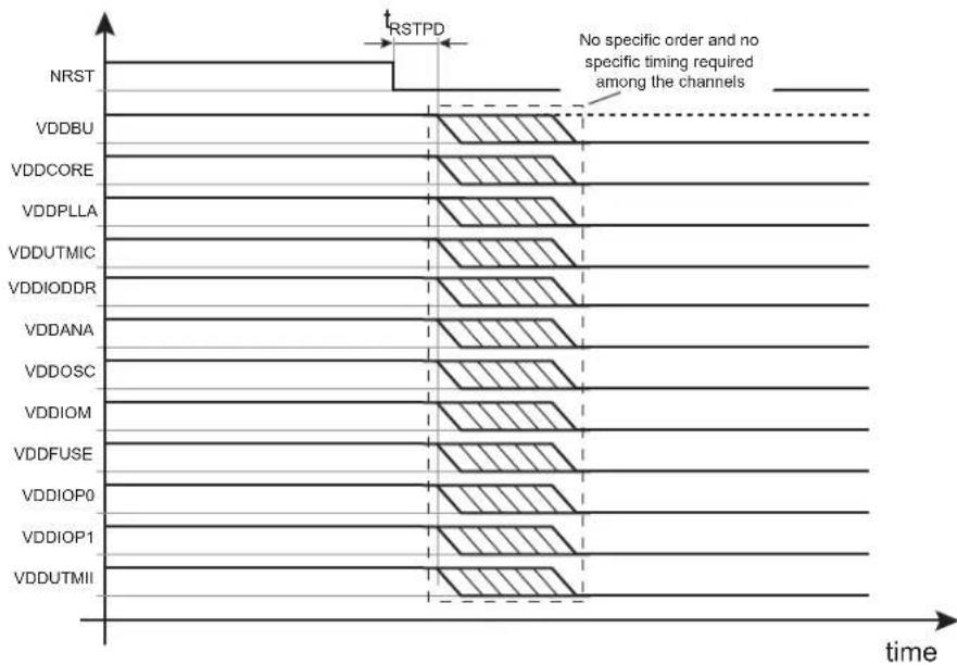
Figure 4-1 shows timing values t_1 and t_2 , with the following clarifications:
- VDDBU, when supplied from a battery is an always-on supply input and is therefore not part of the power supply sequencing. When no backup battery is present in the application, VDDBU is part of Group 2.
- VDDFUSE is the only power supply that may be left un-powered during operation. This is possible if and only if the application does not access the fuse box in write mode. VDDFUSE must be applied when programming the fuse box.
- VDDIODDR may be nominally supplied at 1.2V when the SAMA5D3x is equipped with an LPDDR2 memory. In this case, VDDIODDR can be considered as part of Group 1.
For details, refer to Table 54-42 Power-up Timing Specification.
Figure 4-1: Recommended Power-up Sequence

other
| Channel | Time Segment | |-------------|--------------| | VDDBU | No specific order and no specific timing required among these channels | | VDDANA | No specific order and no specific timing required among these channels | | VDDOSC | No specific order and no specific timing required among these channels | | VDDIOM | No specific order and no specific timing required among these channels | | VDDFUSE | No specific order and no specific timing required among these channels | | VDDIOP0 | No specific order and no specific timing required among these channels | | VDDIOP1 | No specific order and no specific timing required among these channels | | VDDUTMII | No specific order and no specific timing required among these channels | | VDDIODDR | No specific order and no specific timing required among these channels | | VDDCORE | Group 1 | | VDDPLLA | Group 1 | | VDDUTMIC | Group 1 | | NRST | tRSTPU |4.2.2 Power-down Considerations
Figure 4-2 gives the SAMA5D3x power-down sequence that starts by asserting the NRST line to 0. Once NRST is asserted, the supply inputs can be immediately shut down without any specific timing or order. VDDBU may not be shutdown if the application uses a backup battery on this supply input.
Figure 4-2: Recommended Power-down Sequence
text_image
NRST VDDBU VDDCORE VDDPLLA VDDUTMIC VDDIODDR VDDANA VDDOSC VDDIOM VDDFUSE VDDIOP0 VDDIOP1 VDDUTMII RSTPD No specific order and no specific timing required among the channels time5. Memories
The SAMA5D3 embeds a total of 128 Kbytes high-speed SRAM0 and SRAM1. After Remap the SRAM is accessible at address 0 but also at address 0x00300000. Only the ARM core has access to the SRAM at address 0. The others masters (DMA, peripherals, etc.) always access the SRAM at address 0x00300000.
SRAM0 and SRAM1 can be accessed in parallel to improve the overall bandwidth of the system.
5.1.2 Internal ROM
The SAMA5D3 embeds one 160-Kbyte internal ROM containing a standard and a secure bootloader. The secure bootloader is described in a separate document, under NDA. The standard bootloader supports booting from:
• 8-bit NAND Flash with ECC management
- SPI Serial Flash
- SDCARD
• E M M C
• TWI EEPROM
The boot sequence can be selected using the boot order facility (Boot Sequence Controller Configuration Register). The internal ROM embeds Galois field tables that are used to compute NAND Flash ECC. Refer to Figure 11-9 Galois Field Table Mapping in Section 11. Standard Boot Strategies.
For standard boot strategies, refer to Section 11. Standard Boot Strategies.
For secure boot strategies, refer to the application note "SAMA5D3x Secure Boot Strategy" (NDA required).
5.2 External Memory
The SAMA5D3 features interfaces to offer connexion to a wide range of external memories or to parallel peripherals.
5.2.1 DDR2/LPDDR/LPDDR2 Interface
• 32-bit external interface
• 512 Mbytes address space on CS1
• Supports DDR2, LPDDR and LPDDR2 memories
- Drive level control
• I/O impedance control embedded
• Supports 4-banks and 8-banks and up to 512 Mbytes
- Multi-port
5.2.2 Static Memories and NAND Flash
The static memory controller is dedicated to interfacing external memory devices:
The static memory controller is able to drive up to four chip selects. NCS3 is dedicated to the NAND Flash control.
- Asynchronous SRAM-like memories and parallel peripherals
• NAND Flash (8-bit MLC and SLC)
The SMC embeds a NAND Flash Controller (NFC). The NFC can handle automatic transfers, sending the commands and address cycles to the NAND Flash and transferring the contents of the page (for read and write) to the NFC SRAM. It minimizes the CPU overhead.
In order to improve overall system performance the DATA phase of the transfer can be DMA assisted. The static memory embeds a NAND Flash Error Correction Code controller with the features as follows:
- Algorithm based on BCH codes
• Supports also SLC 1-bit (BCH 2-bit), SLC 4-bit (BCH 4-bit) - Programmable Error Correcting Capability:
- 2-bit, 4-bit, 8-bit and 16-bit errors for 512 bytes/sector (4 Kbyte page)
- 24-bit error for 1024 bytes/sector (8 Kbyte page)
- Programmable sector size: 512 bytes or 1024 bytes
-
Programmable number of sector per page: 1, 2, 4 or 8 blocks of data per page
-
Programmable spare area size
• Supports spare area ECC protection
• Supports 8 Kbyte page size using 1024 bytes/sector and 4 Kbyte page size using 512 bytes/sector - Error detection is interrupt driven
- Provides hardware acceleration for error location
• Finds roots of error-locator polynomial - Programmable number of roots
6. Real-time Event Management
The events generated by peripherals are designed to be directly routed to peripherals managing/using these events without processor intervention. Peripherals receiving events contain logic by which to select the one required.
6.1 Embedded Characteristics
Peripherals generate event triggers which are directly routed to event managers such as ADC, for example, to start measurement/conversion without processor intervention.
6.2 Real-time Event Mapping List
Table 6-1: Real-time Event Mapping List
| Event Generator Event Manager Function | ||
| PMC Pulse Width Modulation (PWM) | Safety / Puts the PWM Outputs in Safe Mode (Main Crystal Clock Failure Detection) | |
| Analog-to-Digital Converter (ADC) PWM | Safety / Puts the PWM Outputs in Safe Mode (Overspeed, Overcurrent detection, etc.) | |
7. System Controller
The System Controller is a set of peripherals that allows handling of key elements of the system, such as power, resets, clocks, time, interrupts, watchdog, etc.
The System Controller User Interface also embeds the registers that configure the Matrix and a set of registers for the chip configuration. The chip configuration registers configure the EBI chip select assignment and voltage range for external memories.
The System Controller's peripherals are all mapped within the highest 16 KB of address space, between addresses 0xFFFF D000 and 0xFFFF FFFF.
However, all the registers of System Controller are mapped on the top of the address space. All the registers of the System Controller can be addressed from a single pointer by using the standard ARM instruction set, as the Load/Store instruction have an indexing mode of ±4 KB.
Figure 7-1 on page 36 shows the System Controller block diagram.
Figure 7-1: SAMA5D3 System Controller Block Diagram

flowchart
graph TD
    A["System Controller"] --> B["Advanced Interrupt Controller"]
    B --> C["Cortex-A5"]
    B --> D["Podular Controller"]
    D --> E["BU"]
    D --> F["USB High Speed Host Port"]
    D --> G["USB High Speed Device Port"]
    D --> H["SMD Software Modem"]
    D --> I["Embedded Peripherals"]

    subgraph System Controller
        B1["Advanced Interrupt Controller"]
        B2["Podular Controller"]
        B3["Watchdog Timer"]
        B4["Reset Controller"]
        B5["Real-Time Clock"]
        B6["Shut-Down Controller"]
    end

    subgraph VDDCORE Powered
        C1["Cortex-A5"]
        C2["BU"]
        C3["USB High Speed Host Port"]
        C4["SMD Software Modem"]
        C5["Embedded Peripherals"]
    end

    subgraph Power Management Controller
        D1["Power Management Controller"]
        D2["Fuse Box"]
    end

    subgraph Control Components
        E1["VDDCORE Powered"]
        E2["BU"]
        E3["USB High Speed Host Port"]
        E4["SMD Software Modem"]
        E5["Embedded Peripherals"]
    end

    B1 -->|nirq| C1
    B1 -->|irq_vect| C2
    B1 -->|nfiq| C3
    B1 -->|fiq *}vec| C4
    B2 -->|ntrst| C4
    B2 -->|proc_nreset| C5
    B2 -->|PCK| C5
    B2 -->|debug| C5
    B3 -->|jtag_nreset| C6
    B3 -->|MCK| C6
    B3 -->|periph_nreset| C7
    B4 -->|UPLL CK| C8
    B4 -->|UPLL CK| C9
    B4 -->|UPLL CK| C10
    B5 -->|SMDCK = periph_clk["11"]| C10
    B5 -->|SMDCK = periph_clk["2..49"]| C11
    B6 -->|Ilo | C11
    B6 -->|idla | C12
    B7 -->|SMDCK = periph_clk["11"]| C12
    B7 -->|SMDCK = periph_clk["2..49"]| C13
    B8 -->|in | C13
    B8 -->|out | C14
    B8 -->|enable | C14
    B9 -->|in| C15
    B9 -->|out| C16
    B10 -->|in| C17
    B10 -->|out| C18
    B11 -->|in| C19
    B11 -->|out| C20
    B12 -->|in| C21
    B12 -->|out| C22
    B13 -->|in| C23
    B13 -->|out| C24
    B14 -->|in| C25
    B14 -->|out| C26
    B15 -->|in| C27
    B15 -->|out| C28
    B16 -->|in| C29
    B16 -->|out| C30
    B17 -->|in| C31
    B17 -->|out| C32
    B18 -->|in| C33
    B18 -->|out| C34
    B19 -->|in| C35
    B20 -->|in| C36
    B20 -->|out| C37
    B21 -->|in| C38
    B21 -->|out| C39
    B22 -->|in| C40
    B22 -->|out| C41
    B23 -->|in| C42
    B23 -->|out| C43
    B24 -->|in| C44
    B24 -->|out| C45
    B25 -->|in| C46
    B25 -->|out| C47
    B26 -->|in| C48
    B26 -->|out| C49
    B27 -->|in| C50
    B27 -->|out| C51
    B28 -->|in| C52
    B28 -->|out| C53
    B29 -->|in| C54
    B30 -->|in| C55
    B30 -->|out|
    B31 -->|in| C56
    B31 -->|out|
    B32 -->|in| C57
    B32 -->|out|
    B33 -->|in| C58
    B33 -->|out|
    B34 -->|in| C59
    B34 -->|out|
    B35 -->|in| C60
7.1 Chip Identification
- Chip ID: 0x8A5C07C2 or 0x8A5C07C3
- Extended ID: see Table7-1
• Boundary JTAG ID: 0x05B3103F
• Cortex-A5 JTAG IDCODE: 0x4BA00477
• Cortex-A5 Serial Wire IDCODE: 0x2BA01477
Table 7-1: Chip Identification of SAMA5D3 Devices
| Device Extended ID | |
| SAMA5D31 0x00444300 | |
| SAMA5D33 0x00414300 | |
| SAMA5D34 0x00414301 | |
| SAMA5D35 0x00584300 | |
| SAMA5D36 0x00004301 |
7.2 Backup Section
The SAMA5D3 features a Backup section that embeds:
- RC Oscillator
- Slow Clock Oscillator
- Slow Clock Controller Configuration Register (SCKC_CR)
• Real-time Clock (RTC) - Shutdown Controller (SHDWC)
• 4 Backup Registers (GPBR)
• Part of the Reset Controller (RSTC) - Sequence Controller Configuration (BSC_CR)
This section is powered by the VDDBU rail.
8. Peripherals
8.1 Peripheral Mapping
As shown in Section 5. Memories the peripherals are mapped in the upper 256 Mbytes of the address space between the addresses 0xFFFF7 8000 and 0xFFFFC FFFF.
Each user peripheral is allocated 16 Kbytes of address space.
8.2 Peripheral Identifiers
Table 8-1: Peripheral Identifiers
| Instance Interrupt | Clock TypeID | ||||
| 0 AIC Advanced Interrupt Controller FIQ — SYS_CLK | |||||
| 1 | SYSC | System Controller | — | PMC, RSTC, RTC | SYS_CLK |
| 2 | DBGU | Debug Unit Interrupt | — | — | PCLOCK |
| 3 | PIT | Periodic Interval Timer | — | — | SYS_CLK |
| 4 | WDT | Watchdog Timer | — | — | SYS_CLK |
| 5 | SMC | Multi-bit ECC | — | — | HCLOCK |
| 6 | PIOA | Parallel I/O Controller A | — | — | PCLOCK |
| 7 | PIOB | Parallel I/O Controller B | — | — | PCLOCK |
| 8 | PIOC | Parallel I/O Controller C | — | — | PCLOCK |
| 9 | PIOD | Parallel I/O Controller D | — | — | PCLOCK |
| 10 | PIOE | Parallel I/O Controller E | — | — | PCLOCK |
| 11 | SMD | SMD Soft Modem | — | — | HCLOCK |
| 12 | USART0 | Universal Synchronous Asynchronous Receiver Transmitter 0 | — | — | PCLOCK |
| 13 | USART1 | Universal Synchronous Asynchronous Receiver Transmitter 1 | — | — | PCLOCK |
| 14 | USART2 | Universal Synchronous Asynchronous Receiver Transmitter 2 | — | — | PCLOCK |
| 15 | USART3 | Universal Synchronous Asynchronous Receiver Transmitter 3 | — | — | PCLOCK |
| 16 | UART0 | Universal Asynchronous Receiver Transmitter 0 | — | — | PCLOCK |
| 17 | UART1 | Universal Asynchronous Receiver Transmitter 1 | — | — | PCLOCK |
| 18 | TWI0 | Two-wire Interface 0 | — | — | PCLOCK |
| 19 | TWI1 | Two-wire Interface 1 | — | — | PCLOCK |
| 20 | TWI2 | Two-wire Interface 2 | — | — | PCLOCK |
| 21 | HSMCI0 | High Speed Multimedia Card Interface 0 | — | — | PCLOCK |
| 22 | HSMCI1 | High Speed Multimedia Card Interface 1 | — | — | PCLOCK |
| 23 | HSMCI2 | High Speed Multimedia Card Interface 2 | — | — | PCLOCK |
| 24 | SPI0 | Serial Peripheral Interface 0 | — | — | PCLOCK |
| 25 | SPI1 | Serial Peripheral Interface 1 | — | — | PCLOCK |
| 26 | TC0 | Timer Counter 0 (ch. 0, 1, 2) | — | — | PCLOCK |
| 27 | TC1 | Timer Counter 1 (ch. 3, 4, 5) | — | — | PCLOCK |
| 28 | PWM | Pulse Width Modulation Controller | — | — | PCLOCK |
| Instance | Interrupt | Clock Type | |||
| ID | Name | Description | External | Wired-OR | |
| 29 ADC | Touchscreen | ADC Controller — — PCLOCK | |||
| 30 DMAC0 | DMA Controller 0 — — HCLOCK | ||||
| 31 DMAC1 | DMA Controller 1 — — HCLOCK | ||||
| 32 UHPHS | USB Host | High Speed Port — — HCLOCK | |||
| 33 UDPHS | USB High | Speed Device Port — — HCLOCK | |||
| 34 GMAC | Gigabit | Ethernet MAC — — | HCLOCK +PCLOCK | ||
| 35 | EMAC | Ethernet MAC | — — | HCLOCK +PCLOCK | |
| 36 | LCDC | LCD Controller | — — HCLOCK | ||
| 37 | ISI | Image Sensor Interface | — | — | HCLOCK |
| 38 | SSC0 | Synchronous Serial Controller 0 | — | — | PCLOCK |
| 39 | SSC1 | Synchronous Serial Controller 1 | — | — | PCLOCK |
| 40 | CAN0 | CAN Controller 0 | — — PCLOCK | ||
| 41 | CAN1 | CAN Controller 1 | — — PCLOCK | ||
| 42 | SHA Secure Hash Algorithm | — — PCLOCK | |||
| 43 | AES | Advanced Encryption Standard | — | — | PCLOCK |
| 44 | TDES | Triple Data Encryption Standard | — | — | PCLOCK |
| 45 | TRNG | True Random Number Generator | — | — | PCLOCK |
| 46 | ARM | Performance Monitor Unit | — — | PROC_CLOCK | |
| 47 | AIC | Advanced Interrupt Controller | IRQ | — | SYS_CLK |
| 48 | FUSE | Fuse Controller | — — PCLOCK | ||
| 49 | MPDDRC | MPDDR Controller | — — HCLOCK | ||
| 50–127 | Reserved | — | — | — | — |
8.3 Peripheral Signal Multiplexing on I/O Lines
The SAMA5D3 features five PIO controllers (PIOA, PIOB, PIOC, PIOD and PIOE) which multiplex the I/O lines of the peripheral set.
Each PIO Controller controls 32 lines. Each line can be assigned to one of three peripheral functions: A, B or C. The multiplexing tables (Table 3-1 SAMA5D3 Pinout for 324-ball LFBGA Package and Table 3-2 SAMA5D3 Pinout for 324-ball TFBGA Package) define how the I/O lines of the peripherals A, B and C are multiplexed on the PIO controllers. Note that some output-only peripheral functions might be duplicated within the tables.
The column "Reset State" indicates whether the PIO line resets in I/O mode or in peripheral mode. If I/O is mentioned, the PIO line resets in input with the pull-up enabled, so that the device is maintained in a static state as soon as the reset is released. As a result, the bit corresponding to the PIO line in the register PIO_PSR (Peripheral Status Register) resets low.
If a signal name is mentioned in the "Reset State" column, the PIO line is assigned to this function and the corresponding bit in PIO_PSR resets high. This is the case of pins controlling memories, in particular the address lines, which require the pin to be driven as soon as the reset is released. Note that the pull-up resistor is also enabled in this case.
8.4 Peripheral Clock Type
The SAMA5D3 Series embeds peripherals with five different clock types:
- HCLOCK: AHB Clock, managed with registers PMC_SCER, PMC_SCDR and PMC_SCSR of PMC System Clock
- PCLOCK: APB Clock, managed with registers PMC_PCER, PMC_PCDR, PMC_PCSR and PMC_PCR of Peripheral Clock
- HCLOCK+PCLOCK: Both clock types coexist. The clock is managed with registers PMC_PCER, PMC_PCDR, PMC_PCSR and PMC_PCR of Peripheral Clock
- SYS_CLOCK: This clock cannot be disabled.
- PROC_CLOCK: The clock related to Processor Clock (PCK) and managed with registers PMC_SCDR and PMC_SCSR of PMC System Clock
Refer to Table 8-1 Peripheral Identifiers for details.
9. ARM Cortex-A5
9.1 Description
The ARM Cortex-A5 processor is a high-performance, low-power, ARM macrocell with an L1 cache subsystem that provides full virtual memory capabilities. The Cortex-A5 processor implements the ARMv7 architecture and runs 32-bit ARM instructions, 16-bit and 32-bit Thumb instructions, and 8-bit Java™ byte codes in Jazelle® state.
The Floating-Point Unit (FPU) supports the ARMv7 VFPv4-D16 architecture without Advanced SIMD extensions (NEON). It is tightly integrated to the Cortex-A5 processor pipeline. It provides trapless execution and is optimized for scalar operation. It can generate an Undefined instruction exception on vector instructions that enables the programmer to emulate vector capability in software. See the Cortex-A5 Floating-Point Unit Technical Reference Manual.
Note: All ARM publications referenced in this datasheet can be found at www.arm.com.
9.1.1 Power Management
The Cortex-A5 design supports the following main levels of power management:
- Run Mode
- Standby Mode
9.1.1.1 Run Mode
Run mode is the normal mode of operation where all of the processor functionality is available. Everything, including core logic and embedded RAM arrays, is clocked and powered up.
9.1.1.2 Standby Mode
Standby mode disables most of the clocks of the processor, while keeping it powered up. This reduces the power drawn to the static leakage current, plus a small clock power overhead required to enable the processor to wake up from Standby mode. The transition from Standby mode to Run mode is caused by one of the following:
- the arrival of an interrupt, either masked or unmasked
- the arrival of an event, if standby mode was initiated by a Wait for Event (WFE) instruction
- a debug request, when either debug is enabled or disabled
- a reset.
9.2 Embedded Characteristics
- In-order pipeline with dynamic branch prediction
- ARM, Thumb, and ThumbEE instruction set support
• Harvard level 1 memory system with a Memory Management Unit (MMU)
• 32 Kbytes Data Cache
• 32 Kbytes Instruction Cache - 64-bit AXI master interface
• ARM v7 debug architecture
• VFPv4-D16 FPU with trapless execution
• Jazelle hardware acceleration
9.3 Block Diagram
Figure 9-1: Cortex-A5 Processor Top-level Diagram

flowchart
graph TD
    A["Data processing unit (DPU) Prefetch"] --> B["Data cache unit (DCU)"]
    A --> C["Data micro-TLB Instruction"]
    B --> D["Main translation lookaside buffer (TLB)"]
    C --> E["Instruction cache unit (ICU)"]
    D --> F["Bus interface unit (BIU)"]
    E --> F
    G["Cortex-A5 processor"] --> H["Debug"]
    I["APB interface"] --> H
    J["Embedded trace macrocell (ETM) interface"] --> H
    K["AXI interface"] --> F
    L["CP15"] --> B
    M["STB"] --> B
    N["PCU"] --> B
    O["ICU"] --> E
9.4 Programmer Model
9.4.1 Processor Operating Modes
The following operation modes are present in all states:
- User mode (USR) is the usual ARM program execution state. It is used for executing most application programs.
- Fast Interrupt (FIQ) mode is used for handling fast interrupts. It is suitable for high-speed data transfer or channel process.
- Interrupt (IRQ) mode is used for general-purpose interrupt handling.
• Supervisor mode (SVC) is a protected mode for the operating system. - Abort mode (ABT) is entered after a data or instruction prefetch abort.
- System mode (SYS) is a privileged user mode for the operating system.
- Undefined mode (UND) is entered when an undefined instruction exception occurs.
Mode changes may be made under software control, or may be brought about by external interrupts or exception processing. Most application programs execute in User Mode. The non-user modes, known as privileged modes, are entered in order to service interrupts or exceptions or to access protected resources.
9.4.2 Processor Operating States
The processor has the following instruction set states controlled by the T bit and J bit in the CPSR.
- ARM state:
The processor executes 32-bit, word-aligned ARM instructions. - Thumb state:
The processor executes 16-bit and 32-bit, halfword-aligned Thumb instructions. - ThumbEE state:
The processor executes a variant of the Thumb instruction set designed as a target for dynamically generated code. This is code compiled on the device either shortly before or during execution from a portable bytecode or other intermediate or native representation.
- Jazelle state:
The processor executes variable length, byte-aligned Java bytecodes.
The J bit and the T bit determine the instruction set used by the processor. Table 9-1 shows the encoding of these bits.
Table 9-1: CPSR J and T Bit Encoding
| J T Instruction Set State | ||||||
| 0 | 0 | A | R | M | ||
| 0 | 1 | T | h | u | m | b |
| 1 0 | Jazelle | |||||
| 1 1 | ThumbEE | |||||
Changing between ARM and Thumb states does not affect the processor mode or the register contents. See the ARM Architecture Reference Manual, ARMv7-A and ARMv7-R edition for information on entering and exiting ThumbEE state.
9.4.2.1 Switching State
It is possible to change the instruction set state of the processor between:
- ARM state and Thumb state using the BX and BLX instructions.
- Thumb state and ThumbEE state using the ENTERX and LEAVEX instructions.
• ARM and Jazelle state using the BXJ instruction. - Thumb and Jazelle state using the BXJ instruction.
See the ARM Architecture Reference Manual for more information about changing instruction set state.
9.4.3 Cortex-A5 Registers
This view provides 16 ARM core registers, R0 to R15, that include the Stack Pointer (SP), Link Register (LR), and Program Counter (PC). These registers are selected from a total set of either 31 or 33 registers, depending on whether or not the Security Extensions are implemented. The current execution mode determines the selected set of registers, as shown in Table 9-2. This shows that the arrangement of the registers provides duplicate copies of some registers, with the current register selected by the execution mode. This arrangement is described as banking of the registers, and the duplicated copies of registers are referred to as banked registers.
Table 9-2: Cortex-A5 Modes and Registers Layout
| User and System | Monitor | Supervisor | Abort | Undefined | Interrupt | Fast Interrupt |
| R0 | R0 | R0 | R0 | R0 | R0 | R0 |
| R1 | R1 | R1 | R1 | R1 | R1 | R1 |
| R2 | R2 | R2 | R2 | R2 | R2 | R2 |
| R3 | R3 | R3 | R3 | R3 | R3 | R3 |
| R4 | R4 | R4 | R4 | R4 | R4 | R4 |
| R5 | R5 | R5 | R5 | R5 | R5 | R5 |
| R6 | R6 | R6 | R6 | R6 | R6 | R6 |
| R7 | R7 | R7 | R7 | R7 | R7 | R7 |
| R8 | R8 | R8 | R8 | R8 | R8 | R8_FIQ |
| R9 | R9 | R9 | R9 | R9 | R9 | R9_FIQ |
| R10 | R10 | R10 | R10 | R10 | R10 | R10_FIQ |
| R11 | R11 | R11 | R11 | R11 | R11 | R11_FIQ |
| R12 R12 R12 | R12 R12 R12 | R12_FIQ | ||||
| R13 | R13_MON | R13_SVC | R13_ABT | R13_UND | R13_IRQ | R13_FIQ |
| R14 | R14_MON | R14_SVC | R14_ABT | R14_UND | R14_IRQ | R14_FIQ |
| PC | PC | PC | PC | PC | PC | PC |
| CPSR | CPSR | CPSR | CPSR | CPSR | CPSR | CPSR |
| SPSR_MON | SPSR_SVC | SPSR_ABT | SPSR_UND | SPSR_IRQ | SPSR_FIQ | |
| Mode-specific banked registers |
The core contains one CPSR, and six SPSRs for exception handlers to use. The program status registers:
- hold information about the most recently performed ALU operation
• control the enabling and disabling of interrupts - set the processor operation mode
Figure 9-2: Status Register Format
| 31 | 30 | 29 | 28 | 27 | 24 | 23 | 20 | 19 | 16 | 15 | 10 | 9 | 8 | 7 | 6 | 5 | 4 | 0 | |||
| N | Z | C | V | Q | IT[1:0] | J | Reserved | GE[3:0] | IT[7:2] | E | A | I | F | T | Mode | ||||||
• N: Negative, Z: Zero, C: Carry, and V: Overflow are the four ALU flags
• Q: cumulative saturation flag
- IT: If-Then execution state bits for the Thumb IT (If-Then) instruction
• J: Jazelle bit, see the description of the T bit
- GE: Greater than or Equal flags, for SIMD instructions
- E: Endianness execution state bit. Controls the load and store endianness for data accesses. This bit is ignored by instruction fetches.
- E = 0: Little endian operation
- E = 1: Big endian operation
- A: Asynchronous abort disable bit. Used to mask asynchronous aborts.
- I: Interrupt disable bit. Used to mask IRQ interrupts.
- F: Fast interrupt disable bit. Used to mask FIQ interrupts.
- T: Thumb execution state bit. This bit and the J execution state bit, bit [24], determine the instruction set state of the processor, ARM, Thumb, Jazelle, or ThumbEE.
- Mode: five bits to encode the current processor mode. The effect of setting M[4:0] to a reserved value is UNPREDICTABLE.
Table 9-3: Processor Mode vs. Mode Field
| Mode | M[4:0] |
| USR | 10000 |
| FIQ | 10001 |
| IRQ | 10010 |
| SVC | 10011 |
| ABT | 10111 |
Table 9-3: Processor Mode vs. Mode Field
| Mode | M[4:0] |
| UND 11011 | |
| SYS 11111 | |
| Reserved Other |
9.4.3.1 CP15 Coprocessor
Coprocessor 15, or System Control Coprocessor CP15, is used to configure and control all the items in the list below:
• Cortex A5
- Caches (ICache, DCache and write buffer)
- MMU
- Security
- Other system options
To control these features, CP15 provides 16 additional registers. See Table 9-4.
Table 9-4: CP15 Registers
| Register | Name | Read/Write |
| 0 | ID Code(1) | Read/Unpredictable |
| 0 | Cache type(1) | Read/Unpredictable |
| 1 | Control(1) | Read/Write |
| 1 | Security(1) | Read/Write |
| 2 | Translation Table Base | Read/Write |
| 3 | Domain Access Control | Read/Write |
| 4 | Reserved | None |
| 5 | Data fault Status(1) | Read/Write |
| 5 | Instruction fault status | Read/Write |
| 6 | Fault Address | Read/Write |
| 7 | Cache and MMU Operations(1) | Read/Write |
| 8 | TLB operations | Unpredictable/Write |
| 9 | Cache lockdown(1) | Read/Write |
| 10 | TLB lockdown | Read/Write |
| 11 | Reserved | None |
| 12 | Interrupts management | Read/Write |
| 13 | FCSE PID(1) | Read/Write |
| 13 | Context ID(1) | Read/Write |
| 14 | Reserved | None |
| 15 | Test configuration | Read/Write |
Note 1: This register provides access to more than one register. The register accessed depends on the value of the CRm field or Opcode_2 field.
9.4.4 CP 15 Register Access
CP15 registers can only be accessed in privileged mode by:
- MCR (Move to Coprocessor from ARM Register) instruction is used to write an ARM register to CP15.
- MRC (Move to ARM Register from Coprocessor) instruction is used to read the value of CP15 to an ARM register.
Other instructions such as CDP, LDC, STC can cause an undefined instruction exception.
The assembler code for these instructions is:
MCR/MRC{cond} p15, opcode_1, Rd, CRn, CRm, opcode_2.
The MCR/MRC instructions bit pattern is shown below:
31 30 29 28 27 26 25 24
| cond 1 1 1 0 |
23 22 21 20 19 18 17 16
| opcode_1 L CRn |
15 14 13 12 11 10 9 8
| R | d | 1 | 1 | 1 |
| 7 | 6 | 5 | 4 | 3 | 2 | 1 | 0 |
| opcode_2 1 | CRm |
CRm[3:0]: Specified Coprocessor Action
Determines specific coprocessor action. Its value is dependent on the CP15 register used. For details, refer to CP15 specific register behavior.
opcode_2[7:5]
Determines specific coprocessor operation code. By default, set to 0.
Rd[15:12]: ARM Register
Defines the ARM register whose value is transferred to the coprocessor. If R15 is chosen, the result is unpredictable.
CRn[19:16]: Coprocessor Register
Determines the destination coprocessor register.
L: Instruction Bit
0: MCR instruction
1: MRC instruction
opcode_1[23:20]: Coprocessor Code
Defines the coprocessor specific code. Value is c15 for CP15.
cond [31:28]: Condition
9.4.5 Addresses in the Cortex-A5 processor
The Cortex-A5 processor operates using virtual addresses (VAs). The Memory Management Unit (MMU) translates these VAs into the physical addresses (PAs) used to access the memory system. Translation tables hold the mappings between VAs and PAs.
See the ARM Architecture Reference Manual, ARMv7-A and ARMv7-R edition for more information.
When the Cortex-A5 processor is executing in Non-secure state, the processor performs translation table look-ups using the Non-secure versions of the Translation Table Base Registers. In this situation, any VA can only translate into a Non-secure PA. When it is in Secure state, the Cortex-A5 processor performs translation table look-ups using the Secure versions of the Translation Table Base Registers. In this situation, the security state of any VA is determined by the NS bit of the translation table descriptors for that address.
Following is an example of the address manipulation that occurs when the Cortex-A5 processor requests an instruction:
- The Cortex-A5 processor issues the VA of the instruction as Secure or Non-secure VA accesses according to the state the processor is in.
- The instruction cache is indexed by the bits of the VA. The MMU performs the translation table look-up in parallel with the cache access. If the processor is in the Secure state it uses the Secure translation tables, otherwise it uses the Non-secure translation tables.
- If the protection check carried out by the MMU on the VA does not abort and the PA tag is in the instruction cache, the instruction data is returned to the processor.
- If there is a cache miss, the MMU passes the PA to the AXI bus interface to perform an external access. The external access is always Non-secure when the core is in the Non-secure state. In the Secure state, the external access is Secure or Non-secure according to the NS attribute value in the selected translation table entry. In Secure state, both L1 and L2 translation table walk accesses are marked as Secure, even if the first level descriptor is marked as NS.
9.5 Memory Management Unit
9.5.1 About the MMU
The MMU works with the L1 and L2 memory system to translate virtual addresses to physical addresses. It also controls accesses to and from external memory.
The ARM v7 Virtual Memory System Architecture (VMSA) features include the following:
• Page table entries that support:
- 16 Mbyte supersections. The processor supports supersections that consist of 16 Mbyte blocks of memory.
- 1 Mbyte sections
- 64 Kbyte large pages
- 4 Kbyte small pages
- 16 access domains
- Global and application-specific identifiers to remove the requirement for context switch TLB flushes.
- Extended permissions checking capability.
TLB maintenance and configuration operations are controlled through a dedicated coprocessor, CP15, integrated with the core. This coprocessor provides a standard mechanism for configuring the L1 memory system.
See the ARM Architecture Reference Manual, ARMv7-A and ARMv7-R edition for a full architectural description of the ARMv7 VMSA.
9.5.2 Memory Management System
The Cortex-A5 processor supports the ARM v7 VMSA. The translation of a Virtual Address (VA) used by the instruction set architecture to a Physical Address (PA) used in the memory system and the management of the associated attributes and permissions is carried out using a two-level MMU.
The first level MMU uses a Harvard design with separate micro TLB structures in the PFU for instruction fetches (luTLB) and in the DPU for data read and write requests (DuTLB).
A miss in the micro TLB results in a request to the main unified TLB shared between the data and instruction sides of the memory system. The TLB consists of a 128-entry two-way set-associative RAM based structure. The TLB page-walk mechanism supports page descriptors held in the L1 data cache. The caching of page descriptors is configured globally for each translation table base register, TTBRx, in the system coprocessor, CP15.
The TLB contains a hitmap cache of the page types which have already been stored in the TLB.
9.5.2.1 Memory Types
Although various different memory types can be specified in the page tables, the Cortex-A5 processor does not implement all possible combinations:
- Write-through caches are not supported. Any memory marked as write-through is treated as Non-cacheable.
- The outer shareable attribute is not supported. Anything marked as outer shareable is treated in the same way as inner shareable.
- Write-back no write-allocate is not supported. It is treated as write-back write-allocate.
Table 9-5 shows the treatment of each different memory type in the Cortex-A5 processor in addition to the architectural requirements.
Table 9-5: Treatment of Memory Attributes
| Memory Type Attribute Shareability Other Attributes Notes | |||
| Strongly Ordered — — — | |||
| Device | Non-shareable | — — | |
| Shareable | — — | ||
| Normal | Non-shareable | Non-cacheable | Does not access L1 caches |
| Write-through cacheable | Treated as non-cacheable | ||
| Write-back cacheable, write allocate | Can dynamically switch to no write allocate, if more than three full cache lines are written in succession | ||
| Write-back cacheable, no write allocate | Treated as non-shareable write-back cacheable, write allocate | ||
| Inner shareable | Non-cacheable | — | |
| Write-through cacheable | Treated as inner shareable non-cacheable | ||
| Write-back cacheable, write allocate | Treated as inner shareable non-cacheable unless the SMP bit in the Auxiliary Control Register is set (ACTLR[6] = b1). If this bit is set the area is treated as write-back cacheable write allocate. | ||
| Write-back cacheable, no write allocate | |||
| Outer shareable | Non-cacheable | Treated as inner shareable non-cacheable | |
| Write-through cacheable | |||
| Write-back cacheable, write allocate | Treated as inner shareable non-cacheable unless the SMP bit in the Auxiliary Control Register is set (ACTLR[6] = b1). If this bit is set the area is treated as write-back cacheable write allocate. | ||
| Write-back cacheable, no write allocate | |||
9.5.3 TLB Organization
TLB Organization is described in the sections that follow:
- Micro TLB
- Main TLB
9.5.3.1 Micro TLB
The first level of caching for the page table information is a micro TLB of 10 entries that is implemented on each of the instruction and data sides. These blocks provide a lookup of the virtual addresses in a single cycle.
The micro TLB returns the physical address to the cache for the address comparison, and also checks the access permissions to signal either a Prefetch Abort or a Data Abort.
All main TLB related maintenance operations affect both the instruction and data micro TLBs, causing them to be flushed. In the same way, any change of the following registers causes the micro TLBs to be flushed:
- Context ID Register (CONTEXTIDR)
- Domain Access Control Register (DACR)
• Primary Region Remap Register (PRRR)
• Normal Memory Remap Register (NMRR)
• Translation Table Base Registers (TTBR0 and TTBR1)
9.5.3.2 Main TLB
Misses from the instruction and data micro TLBs are handled by a unified main TLB. Accesses to the main TLB take a variable number of cycles, according to competing requests from each of the micro TLBs and other implementation-dependent factors.
The main TLB is 128-entry two-way set-associative.
TLB match process
Each TLB entry contains a virtual address, a page size, a physical address, and a set of memory properties. Each is marked as being associated with a particular application space (ASID), or as global for all application spaces. The CONTEXTIDR determines the currently selected application space.
A TLB entry matches when these conditions are true:
- Its virtual address matches that of the requested address.
- Its Non-secure TLB ID (NSTID) matches the Secure or Non-secure state of the MMU request.
- Its ASID matches the current ASID in the CONTEXTIDR or is global.
The operating system must ensure that, at most, one TLB entry matches at any time. The TLB can store entries based on the following block sizes:
Supersections Describe 16 Mbyte blocks of memory
Sections Describe 1 Mbyte blocks of memory
Large pages Describe 64 Kbyte blocks of memory
Small pages Describe 4 Kbyte blocks of memory
Supersections, sections and large pages are supported to permit mapping of a large region of memory while using only a single entry in the TLB. If no mapping for an address is found within the TLB, then the translation table is automatically read by hardware and a mapping is placed in the TLB.
9.5.4 Memory Access Sequence
When the processor generates a memory access, the MMU:
- Performs a lookup for the requested virtual address and current ASID and security state in the relevant instruction or data micro TLB.
- If there is a miss in the micro TLB, performs a lookup for the requested virtual address and current ASID and security state in the main TLB.
- If there is a miss in main TLB, performs a hardware translation table walk.
The MMU can be configured to perform hardware translation table walks in cacheable regions by setting the IRGN bits in Translation Table Base Register 0 and Translation Table Base Register 1. If the encoding of the IRGN bits is write-back, an L1 data cache lookup is performed and data is read from the data cache. If the encoding of the IRGN bits is write-through or non-cacheable, an access to external memory is performed. For more information refer to: Cortex-A5 Technical Reference Manual.
The MMU might not find a global mapping, or a mapping for the currently selected ASID, with a matching Non-secure TLB ID (NSTID) for the virtual address in the TLB. In this case, the hardware does a translation table walk if the translation table walk is enabled by the PD0 or PD1 bit in the Translation Table Base Control Register. If translation table walks are disabled, the processor returns a Section Translation fault. For more information refer to: Cortex-A5 Technical Reference Manual.
If the TLB finds a matching entry, it uses the information in the entry as follows:
-
The access permission bits and the domain determine if the access is enabled. If the matching entry does not pass the permission checks, the MMU signals a memory abort. See the ARM Architecture Reference Manual, ARMv7-A and ARMv7-R edition for a description of access permission bits, abort types and priorities, and for a description of the Instruction Fault Status Register (IFSR) and Data Fault Status Register (DFSR).
-
The memory region attributes specified in both the TLB entry and the CP15 c10 remap registers determine if the access is
-
Secure or Non-secure
- Shared or not
- Normal memory, Device, or Strongly-ordered
For more information refer to: Cortex-A5 Technical Reference Manual, Memory region remap.
- The TLB translates the virtual address to a physical address for the memory access.
9.5.5 Interaction with Memory System
The MMU can be enabled or disabled as described in the ARM Architecture Reference Manual, ARMv7-A and ARMv7-R edition.
9.5.6 External Aborts
External memory errors are defined as those that occur in the memory system rather than those that are detected by the MMU. External memory errors are expected to be extremely rare. External aborts are caused by errors flagged by the AXI interfaces when the request goes external to the Cortex-A5 processor. External aborts can be configured to trap to Monitor mode by setting the EA bit in the Secure Configuration Register. For more information refer to: Cortex-A5 Technical Reference Manual.
9.5.6.1 External Aborts on Data Write
Externally generated errors during a data write can be asynchronous. This means that the r14_abt on entry into the abort handler on such an abort might not hold the address of the instruction that caused the exception.
The DFAR is Unpredictable when an asynchronous abort occurs.
Externally generated errors during data read are always synchronous. The address captured in the DFAR matches the address which generated the external abort.
9.5.6.2 Synchronous and Asynchronous Aborts
Chapter 4, System Control in the Cortex-A5 Technical Reference Manual describes synchronous and asynchronous aborts, their priorities, and the IFSR and DFSR. To determine a fault type, read the DFSR for a data abort or the IFSR for an instruction abort.
The processor supports an Auxiliary Fault Status Register for software compatibility reasons only. The processor does not modify this register because of any generated abort.
9.5.7 MMU Software Accessible Registers
The system control coprocessor registers, CP15, in conjunction with page table descriptors stored in memory, control the MMU.
Access all the registers with instructions of the form:
MRC p15, 0,
MCR p15, 0,
CRn is the system control coprocessor register. Unless specified otherwise, CRm and Opcode_2 Should Be Zero.
10. Debug and Test
10.1 Description
The device features a number of complementary debug and test capabilities.
A common JTAG/ICE (In-Circuit Emulator) port is used for standard debugging functions, such as downloading code and single-stepping through programs.
A 2-pin debug port Serial Wire Debug (SWD) replaces the 5-pin JTAG port and provides an easy and risk free alternative to JTAG as the two signals SWDIO and SWCLK are overlaid on the TMS and TCK pins, allowing for bi-modal devices that provide the other JTAG signals. These extra JTAG pins can be switched to other uses when in SWD mode.
The Debug Unit provides a two-pin UART that can be used to upload an application into internal SRAM. It manages the interrupt handling of the internal COMMTX and COMMRX signals that trace the activity of the Debug Communication Channel.
A set of dedicated debug and test input/output pins gives direct access to these capabilities from a PC-based test environment.
10.2 Embedded Characteristics
• Cortex-A5 Real-time In-circuit Emulator
- Two real-time Watchpoint Units
- Two Independent Registers: Debug Control Register and Debug Status Register
- Test Access Port Accessible through JTAG Protocol
- Debug Communications Channel
- Serial Wire Debug
- Debug Unit
- Two-pin UART
- Debug Communication Channel Interrupt Handling
- Chip ID Register
- IEEE1149.1 JTAG Boundary-scan on All Digital Pins
10.3 Block Diagram
Figure 10-1: Debug and Test Block Diagram
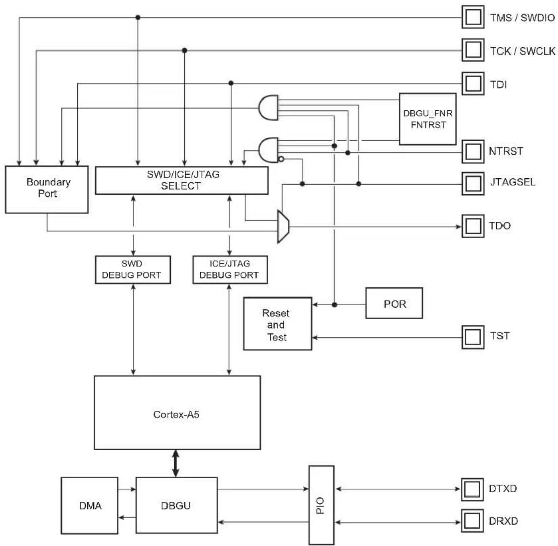
flowchart
graph TD
    A["Cortex-A5"] --> B["DBGU"]
    A --> C["SO Box"]
    A --> D["DMA"]
    A --> E["PIO"]
    A --> F["Reset and Test"]
    A --> G["ICE/JTAG DEBUG PORT"]
    A --> H["SWD/ICE/JTAG SELECT"]
    H --> I["Boundary Port"]
    H --> J["DBGU_FNR FNTRST"]
    H --> K["TMS / SWDIO"]
    H --> L["TCK / SWCLK"]
    H --> M["TDI"]
    H --> N["NTRST"]
    H --> O["JTAGSEL"]
    H --> P["TDO"]
    A --> Q["POR"]
    Q --> R["TST"]
    A --> S["DTXD"]
    A --> T["DRXD"]
10.4 Application Examples
10.4.1 Debug Environment
Figure 10-2 shows a complete debug environment example. The ICE/JTAG interface is used for standard debugging functions, such as downloading code and single-stepping through the program. A software debugger running on a personal computer provides the user interface for configuring a Trace Port interface utilizing the ICE/JTAG interface.
Figure 10-2: Application Debug and Trace Environment Example
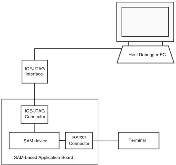
flowchart
graph TD
    A["Host Debugger PC"] --> B["ICE/JTAG Interface"]
    B --> C["ICE/JTAG Connector"]
    C --> D["SAM device"]
    D --> E["RS232 Connector"]
    E --> F["Terminal"]
    G["SAM-based Application Board"] --> D
    G --> E
10.4.2 Test Environment
Figure 10-3 shows a test environment example. Test vectors are sent and interpreted by the tester. In this example, the “board in test” is designed using a number of JTAG-compliant devices. These devices can be connected to form a single scan chain.
Figure 10-3: Application Test Environment Example
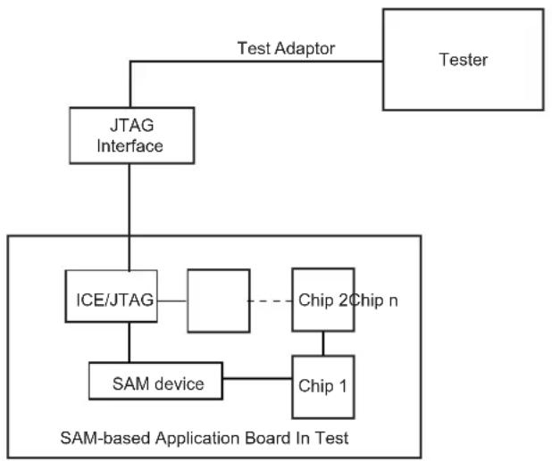
flowchart
graph TD
    A["Tester"] --> B["JTAG Interface"]
    B --> C["ICE/JTAG"]
    C --> D["Chip 2Chip n"]
    C --> E["SAM device"]
    E --> F["Chip 1"]
    B --> G["Test Adaptor"]
    style A fill:#f9f,stroke:#333
    style B fill:#ccf,stroke:#333
    style C fill:#cfc,stroke:#333
    style D fill:#fcc,stroke:#333
    style E fill:#cff,stroke:#333
    style F fill:#ffc,stroke:#333
    style G fill:#fcc,stroke:#333
10.5 Debug and Test Pin Description
Table 10-1: Debug and Test Pin List
| Pin Name Function Type Active Level | |||
| Reset/Test | |||
| NRST Microcontroller Reset Input/Output Low | |||
| TST Test Mode Select Input High | |||
| ICE and JTAG | |||
| NTRST | Test Reset Signal | Input | Low |
| TCK | Test Clock | Input | - |
| TDI | Test Data In | Input | - |
| TDO | Test Data Out | Output | - |
| TMS | Test Mode Select Input | - | |
| JTAGSEL | JTAG Selection | Input | - |
| SWD | |||
| SWCLK | Serial Debug Clock | Input | - |
| SWDIO | Serial Debug IO | Input/Output | - |
| Debug Unit | |||
| DRXD | Debug Receive Data | Input | - |
| DTXD Debug Transmit Data | Output | - | |
10.6 Functional Description
10.6.1 Test Pin
One dedicated pin, TST, is used to define the device operating mode. The user must make sure that this pin is tied at low level to ensure normal operating conditions. Other values associated with this pin are reserved for manufacturing test.
10.6.2 EmbeddedICE
The Cortex-A5 EmbeddedICE-RT ^™ is supported via the ICE/JTAG port. It is connected to a host computer via an ICE interface. The internal state of the Cortex-A5 is examined through an ICE/JTAG port which allows instructions to be serially inserted into the pipeline of the core without using the external data bus. Therefore, when in debug state, a store-multiple (STM) can be inserted into the instruction pipeline. This exports the contents of the Cortex-A5 registers. This data can be serially shifted out without affecting the rest of the system.
There are two scan chains inside the Cortex-A5 processor which support testing, debugging, and programming of the EmbeddedICE-RT. The scan chains are controlled by the ICE/JTAG port.
EmbeddedICE mode is selected when JTAGSEL is low. It is not possible to switch directly between ICE and JTAG operations. A chip reset must be performed after JTAGSEL is changed.
For further details on the EmbeddedICE-RT, see the ARM document:
ARM IHI 0031A_ARM_debug_interface_v5.pdf
10.6.3 JTAG Signal Description
TMS is the Test Mode Select input which controls the transitions of the test interface state machine.
TDI is the Test Data Input line which supplies the data to the JTAG registers (Boundary Scan Register, Instruction Register, or other data registers).
TDO is the Test Data Output line which is used to serially output the data from the JTAG registers to the equipment controlling the test. It carries the sampled values from the boundary scan chain (or other JTAG registers) and propagates them to the next chip in the serial test circuit.
NTRST (optional in IEEE Standard 1149.1) is a Test-ReSeT input which is mandatory in ARM cores and used to reset the debug logic. On Microchip Cortex-A5-based cores, NTRST is a Power On Reset output. It is asserted on power on. If necessary, the user can also reset the debug logic with the NTRST pin assertion during 2.5 MCK periods.
TCK is the Test ClocK input which enables the test interface. TCK is pulsed by the equipment controlling the test and not by the tested device. It can be pulsed at any frequency.
10.6.4 Chip Access Using JTAG Connection
The JTAG connection is not enabled by default on this chip at delivery due to the secure ROM code implementation.
By default, the SAMA5D3 devices boot in Standard mode and not in Secure mode. When the secure ROM code starts, it disables the JTAG access for the entire boot sequence.
If the secure ROM code does not find any program in the external memory, it enables the USB connection and the serial port and waits for a dedicated command to switch the chip into Secure mode.
If any other character is received, the secure ROM code starts the standard SAM-BA ^® monitor, locks access to the ROM memory, and enables the JTAG.
The chip can then be accessed using the JTAG connection.
If the secure ROM code finds a bootable program, it automatically disables ROM access and enables the JTAG connection just before launching the program.
The procedure to enable JTAG access is as follows:
- Connect your computer to the board with JTAG and USB (J20 USB-A)
- Power on the chip
- Open a terminal console (TeraTerm or HyperTerminal, etc.) on your computer and connect to the USB CDC Serial COM port related to the J20 connector on the board
- Send the '#' character. You will see then the prompt '>' character sent by the device (indicating that the Standard SAM-BA Monitor is running)
- Use the Standard SAM-BA Monitor to connect to the chip with JTAG
Note that you don't need to follow this sequence in order to connect the Standard SAM-BA Monitor with USB.
10.6.5 Debug Unit
The Debug Unit provides a two-pin (DXRD and TXRD) USART that can be used for several debug and trace purposes and offers an ideal means for in-situ programming solutions and debug monitor communication. Moreover, the association with two peripheral data controller channels permits packet handling of these tasks with processor time reduced to a minimum.
The Debug Unit also manages the interrupt handling of the COMMTX and COMMRX signals that come from the ICE and that trace the activity of the Debug Communication Channel. The Debug Unit allows blockage of access to the system through the ICE interface.
A specific register, the Debug Unit Chip ID Register, gives information about the product version and its internal configuration.
For further details on the Debug Unit, see Section 42. Debug Unit (DBGU).
10.6.6 IEEE 1149.1 JTAG Boundary Scan
IEEE 1149.1 JTAG Boundary Scan allows pin-level access independent of the device packaging technology.
IEEE 1149.1 JTAG Boundary Scan is enabled when JTAGSEL is high. The SAMPLE, EXTEST and BYPASS functions are implemented. In ICE debug mode, the ARM processor responds with a non-JTAG chip ID that identifies the processor to the ICE system. This is not IEEE 1149.1 JTAG-compliant.
It is not possible to switch directly between JTAG and ICE operations. A chip reset must be performed after JTAGSEL is changed.
A Boundary-scan Descriptor Language (BSDL) file is provided to set up test.
10.7 Boundary JTAG ID Register
Access: Read-only
31 30 29 28 27 26 25 24
VERSION PART NUMBER
23 22 21 20 19 18 17 16
PART NUMBER
15 14 13 12 11 10 9 8
PART NUMBER MANUFACTURER IDENTITY
7 6 5 4 3 2 1 0
MANUFACTURER IDENTITY 1
VERSION[31:28]: Product Version Number
Set to 0x0.
PART NUMBER[27:12]: Product Part Number
Product part Number is 0x5B31
MANUFACTURER IDENTITY[11:1]
Set to 0x01F.
Bit[0] required by IEEE Std. 1149.1.
Set to 0x1.
JTAG ID Code value is 0x05B3_103F.
10.8 Cortex-A5 Debug Port Identification Code Register IDCODE
The Identification Code Register is always present on all debug port implementations. It provides identification information about the ARM Debug Interface.
10.8.1 JTAG Debug Port (JTAG-DP)
It is accessed using its own scan chain.
10.8.2 JTAG-DP Device ID Code Register
Access: Read-only
31 30 29 28 27 26 25 24
| VERSION PART NUMBER |
23 22 21 20 19 18 17 16
PART NUMBER
15 14 13 12 11 10 9 8
| PART NUMBER DESIGNER |
7 6 5 4 3 2 1 0
DESIGNER 1
VERSION[31:28]: Product Version Number
Set to 0x0.
PART NUMBER[27:12]: Product Part Number
Product part number is 0xBA00
DESIGNER[11:1]
Set to 0x23B.
Bit[0] required by IEEE Std. 1149.1.
Set to 0x1.
Cortex-A5 JTAG-DP IDCODE value is 0x0BA0_0477
10.8.3 Serial Wire Debug Port (SW-DP)
It is at address 0x0 on read operations when the APnDP bit = 0. Access to the Identification Code Register is not affected by the value of the CTRLSEL bit in the Select Register.
Access: Read-only
31 30 29 28 27 26 25 24
| VERSION PART NUMBER | ||||||
| 23 22 21 20 19 18 17 16 | ||||||
| PART NUMBER | ||||||
| 15 14 13 12 11 10 9 8 | ||||||
| PART NUMBER DESIGNER | ||||||
| 7 | 6 | 5 | 4 | 3 | 2 | 1 |
| DESIGNER 1 | ||||||
VERSION[31:28]: Product Version Number
Set to 0x0.
PART NUMBER[27:12]: Product Part Number
Product part Number is 0xBA01
DESIGNER[11:1]
Set to 0x23B.
Bit[0] required by IEEE Std. 1149.1.
Set to 0x1.
Cortex-A5 SW-DP IDCODE is 0x0BA0_1477
11. Standard Boot Strategies
11.1 Description
The system always boots from the ROM memory at address 0x0.
The ROM code is a boot program contained in the embedded ROM. It is also called "First level bootloader".
This microcontroller can be configured to run a Standard Boot mode or a Secure Boot mode. More information on how the Secure Boot mode can be enabled, and how the chip operates in this mode, is provided in the application note "SAMA5D3x Secure Boot Strategy", literature number 11165 (NDA required). To obtain this application note and additional information about the secure boot and related tools, contact your local Microchip sales office. Note that a PGP key is required for delivery.
By default, the chip starts in Standard Boot Mode.
Note: JTAG access is disabled during the execution of ROM Code Sequence. It is re-enabled when jumping into SRAM when a valid code has been found on an external NVM, in the same time the ROM memory is hidden. If no valid boot has been found on an external NVM, the ROM Code enables the USB connection and the DBGU serial port, and then waits for a special command to set the chip in Secure mode. If any other character is received, the ROM code starts the standard SAM-BA monitor, locks access to the ROM memory and re-enables the JTAG connection.
The user can choose to boot from an external NOR Flash memory using the BMS pin. The sampling of the BMS pin is done by hardware at reset, and the result is available in the BMS bit of the SFR_EBICFG register.
The first step of the ROM code program is to check the state of this pin by reading this register.
If BMS signal is tied to 0, the BMS bit is read at 0.
The ROM code allows execution of the code contained in the memory connected to Chip Select 0 of the External Bus Interface.
To do so, the following sequence is performed by the ROM code:
- The main clock is the on-chip 12 MHz RC oscillator.
- The Static Memory Controller is configured with timing allowing code execution in CS0 external memory at 12 MHz.
- AXI matrix is configured to remap EBI CS0 address at 0x0.
- 0x0 is loaded in the Program Counter register.
The user software in the external memory must perform the next operation in order to complete the clocks and SMC timings configuration to run at a higher clock frequency:
- Enable the 32768 Hz oscillator if best accuracy is needed.
- Reprogram the SMC setup, cycle, hold, mode timing registers for EBI CS0, to adapt them to the new clock.
- Program the PMC (Main Oscillator Enable or Bypass mode).
- Program and start the PLL.
- Switch the system clock to the new value.
If BMS signal is tied to 1, the BMS bit is read at 1.
The ROM code standard sequence is executed as follows:
- Basic chip initialization: crystal or external clock frequency detection.
- Attempt to retrieve a valid code from external non-volatile memories (NVM).
- Execution of a monitor called SAM-BA Monitor, in case no valid application has been found on any NVM.
11.2 Flow Diagram
The ROM code implements the algorithm shown in Figure 11-1.
Figure 11-1: ROM Code Algorithm Flow Diagram
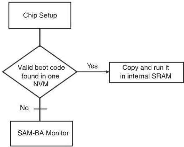
flowchart
graph TD
    A["Chip Setup"] --> B{Valid boot code found in one NVM}
    B -->|Yes| C["Copy and run it in internal SRAM"]
    B -->|No| D["SAM-BA Monitor"]
11.3 Chip Setup
At boot start-up, the processor clock (PCK) and the master clock (MCK) source is the 12 MHz fast RC oscillator. Initialization follows the steps described below:
- Stack Setup for ARM supervisor mode
- Main Oscillator Detection: The Main Clock is switched to the 32 kHz RC oscillator to allow external clock frequency to be measured. Then the Main Oscillator is enabled and set in the bypass mode. If the MOSCSELS bit rises, an external clock is connected, and the next step is Main Clock Selection (3). If not, the bypass mode is cleared to attempt external quartz detection. This detection is successful when the MOSCXTS and MOSCSELS bits rise, else the internal 12 MHz fast RC oscillator is used as the Main Clock.
- Main Clock Selection: The Master Clock source is switched from the Slow Clock to the Main Oscillator without prescaler. The PMC Status Register is polled to wait for MCK Ready. PCK and MCK are now the Main Clock.
- C Variable Initialization: Non zero-initialized data is initialized in the RAM (copy from ROM to RAM). Zero-initialized data is set to 0 in the RAM.
- PLLA Initialization: PLLA is configured to get a PCK at 96 MHz and an MCK at 48 MHz. If an external clock or crystal frequency running at 12, 16, 24 or 48 MHz is found, then the PLLA is configured to allow communication on the USB link for the SAM-BA Monitor; else the Main Clock is switched to the internal 12 MHz fast RC oscillator, but USB will not be activated.
11.4 NVM Boot
11.4.1 NVM Boot Sequence
The boot sequence on external memory devices can be controlled using the Boot Sequence Controller Configuration Register (BSC_CR). The user can then choose to bypass some steps shown in Figure 11-2 "NVM Bootloader Sequence Diagram" according to the BOOT value in the BSC_CR.
Table 11-1: Values of the Boot Sequence Controller Configuration Register
| BOOT Value $PI0 NPCS0 | SD Card / eMMC (MCI0) | SD Card / eMMC (MCI1) | 8-bit NAND Flash SPI0 | NPCS1 TWI E | EPROM | SAM-BA Monitor | |
| 0 | Y | Y | Y | Y | Y | Y | |
| 1 | Y | — | Y | Y | Y | Y | |
| 2 | Y | — | — | Y | Y | Y | |
| 3 | Y | — | — | — | Y | Y | |
| 4 | Y | — | — | — | Y | Y | |
| 5 | — | — | — | — | — | — | Y |
| 6 | — | — | — | — | — | — | Y |
| 7 | — | — | — | — | — | — | Y |
Figure 11-2: NVM Bootloader Sequence Diagram
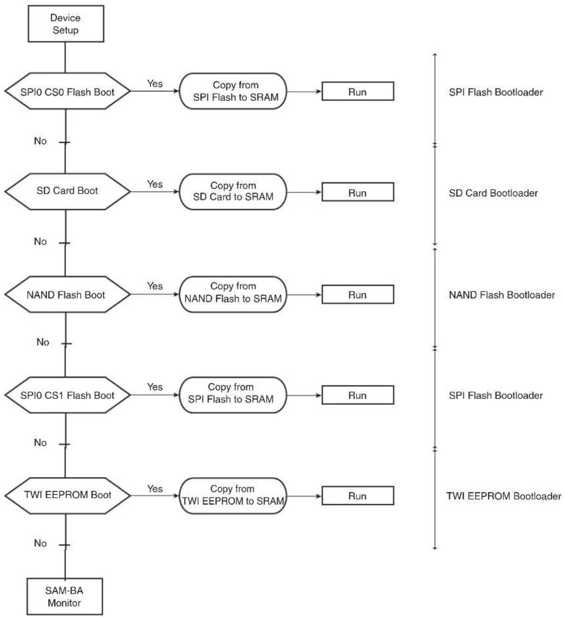
flowchart
graph TD
    A["Device Setup"] --> B{SPI0 CS0 Flash Boot}
    B -->|Yes| C["Copy from SPI Flash to SRAM"]
    C --> D["Run"]
    B -->|No| E{SD Card Boot}
    E -->|Yes| F["Copy from SD Card to SRAM"]
    F --> G["Run"]
    E -->|No| H{NAND Flash Boot}
    H -->|Yes| I["Copy from NAND Flash to SRAM"]
    I --> J["Run"]
    H -->|No| K{SPI0 CS1 Flash Boot}
    K -->|Yes| L["Copy from SPI Flash to SRAM"]
    L --> M["Run"]
    K -->|No| N{TWI EEPROM Boot}
    N -->|Yes| O["Copy from TWI EEPROM to SRAM"]
    O --> P["Run"]
    N -->|No| Q["SAM-BA Monitor"]
11.4.2 NVM Bootloader Program Description
Figure 11-3: NVM Bootloader Program Diagram

flowchart
graph TD
    A["Start"] --> B["Initialize NVM"]
    B --> C{Initialization OK?}
    C -->|No| D["Restore the reset values for the peripherals and Jump to next boot solution"]
    C -->|Yes| E["Valid code detection in NVM"]
    E --> F{NVM contains valid code}
    F -->|No| D
    F -->|Yes| G["Copy the valid code from external NVM to internal SRAM."]
    G --> H["Restore the reset values for the peripherals. Perform the REMAP and set the PC to 0 to jump to the downloaded application"]
    H --> I["End"]
The NVM bootloader program first initializes the PIOs related to the NVM device. Then it configures the right peripheral depending on the NVM and tries to access this memory. If the initialization fails, it restores the reset values for the PIO and the peripheral, and then tries to fulfill the same operations on the next NVM of the sequence.
If the initialization is successful, the NVM bootloader program reads the beginning of the NVM and determines if the NVM contains a valid code.
If the NVM does not contain a valid code, the NVM bootloader program restores the reset value for the peripherals and then tries to fulfill the same operations on the next NVM of the sequence.
If a valid code is found, this code is loaded from the NVM into the internal SRAM and executed by branching at address 0x0000_0000 after remap. This code may be the application code or a second-level bootloader. All the calls to functions are PC relative and do not use absolute addresses.
Figure 11-4: Remap Action after Download Completion

flowchart
graph LR
    A["0x0000_0000"] --> B["Internal ROM"]
    B --> C["Internal SRAM"]
    D["0x0010_0000"] --> E["Internal ROM"]
    E --> F["Internal SRAM"]
    G["0x0030_0000"] --> H["Internal ROM"]
    H --> I["Internal SRAM"]
    J["REMAP"] --> K["Internal SRAM"]
    K --> L["Internal ROM"]
    L --> M["Internal SRAM"]
11.4.3 Valid Code Detection
There are two kinds of valid code detection.
11.4.3.1 ARM Exception Vectors Check
The NVM bootloader program reads and analyzes the first 28 bytes corresponding to the first seven ARM exception vectors. Except for the sixth vector, these bytes must implement the ARM instructions for either branch or load PC with PC relative addressing.
Figure 11-5: LDR Opcode
| 31 | 28 | 27 | 24 | 23 | 20 | 19 | 16 | 15 | 12 | 11 | 0 | ||||||||||||||||||||||||||||||||||||||||
| 1 | 1 | 1 | 0 | 0 | 1 | I | P | U | 1 | W | 0 | Rn | |||||||||||||||||||||||||||||||||||||||
Figure 11-6: B Opcode
| 31 | 28 | 27 | 24 | 23 | 0 | |||||||||||||||
| 1 | 1 | 1 | 0 | 1 | 0 | 1 | 0 | 1 | 0 | Offset (24 bits) | ||||||||||
Unconditional instruction: 0xE for bits 31 to 28.
Load PC with the PC relative addressing instruction:
- Rn = Rd = PC = 0xF
- I==0 (12-bit immediate value)
- P==1 (pre-indexed)
- U offset added (U==1) or subtracted (U==0)
- W = = 1
The sixth vector, at the offset 0x14, contains the size of the image to download. The user must replace this vector with the user's own vector. This procedure is described below.
Figure 11-7: Structure of the ARM Vector 6
| 31 | 0 |
| Size of the code to download in bytes | |
The value has to be smaller than 64 Kbytes.
Example
An example of valid vectors:
| 00 | ea000006 | B | 0x20 |
| 04 | eafffffe | B | 0x04 |
| 08 | ea00002f | B | _main |
| 0c eaffffffe B | 0x0c | ||
| 10 | eafffffe | B | 0x10 |
| 14 00001234 | Code size = 4660 bytes (< 64 Kbytes) | ||
| 18 | eafffffe | B | 0x18 |
11.4.3.2 boot.bin File Check
This method is the one used on FAT formatted SD Card and eMMC. The boot program must be a file named "boot.bin" written in the root directory of the file system. Its size must not exceed the maximum size allowed: 64 Kbytes (0x10000).
11.4.4 Detailed Memory Boot Procedures
11.4.4.1 NAND Flash Boot: NAND Flash Detection
After the NAND Flash interface configuration, a reset command is sent to the memory.
Hardware ECC detection and correction are provided by the PMECC peripheral. Refer to Section 30.18 PMECC Controller Functional Description for more details.
The Boot Program is able to retrieve NAND Flash parameters and ECC requirements using two methods as follows:
- The detection of a specific header written at the beginning of the first page of the NAND Flash,
or - Through the ONFI parameters for the ONFI compliant memories
Note: Booting on 16-bit NAND Flash is not possible; only 8-bit NAND Flash memories are supported.
Figure 11-8: Boot NAND Flash Download
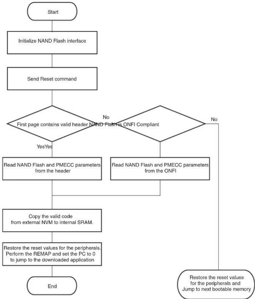
flowchart
graph TD
    A["Start"] --> B["Initialize NAND Flash interface"]
    B --> C["Send Reset command"]
    C --> D{First page contains valid header NAND Flash is ONFI Compliant}
    D -->|No| E{Read NAND Flash and PMECC parameters from the ONFI}
    D -->|Yes| F["Read NAND Flash and PMECC parameters from the header"]
    E --> G["Copy the valid code from external NVM to internal SRAM."]
    G --> H["Restore the reset values for the peripherals. Perform the REMAP and set the PC to 0 to jump to the downloaded application"]
    H --> I["End"]
    E --> J["Restore the reset values for the peripherals and Jump to next bootable memory"]
• NAND Flash Specific Header Detection
This is the first method used to determine NAND Flash parameters. After Initialization and Reset command, the Boot Program reads the first page without an ECC check, to determine if the NAND parameter header is present. The header is made of 52 times the same 32-bit word (for redundancy reasons) which must contain NAND and PMECC parameters used to correctly perform the read of the rest of the data in the NAND. This 32-bit word is described below:
31 30 29 28 27 26 25 24
| key | - | eccOffset |
23 22 21 20 19 18 17 16
| eccOffset sectorSize |
15 14 13 12 11 10 9 8
| eccBitReq spareSize |
| 7 | 6 | 5 | 4 | 3 | 2 | 1 | 0 |
spareSize nbSectorPerPage usePmecc
If the header is valid, the Boot Program continues with the detection of a valid code.
Note: Booting on 16-bit NAND Flash is not possible; only 8-bit NAND Flash memories are supported.
usePmecc: Use PMECC
0: Do not use PMECC to detect and correct the data
1: Use PMECC to detect and correct the data
nbSectorPerPage[2:0]: Number of Sectors per Page
| Value Description | |
| 0 | 1 sector per page |
| 1 | 2 sectors per page |
| 2 | 4 sectors per page |
| 3 | 8 sectors per page |
| 4 | 16 sectors per page |
spareSize: Size of the Spare Zone in Bytes
eccBitReq: Number of ECC Bits Required
| Value Description | |
| 0 2-bit ECC | |
| 1 4-bit ECC | |
| 2 8-bit ECC | |
| 312-bit ECC | |
| 4 24-bit ECC | |
sectorSize: Size of the ECC Sector
0: For 512 bytes
1: For 1024 bytes per sector
Other value for future use.
eccOffset: Offset of the First ECC Byte in the Spare Zone
A value below 2 is not allowed and will be considered as 2.
key: Value 0xC Must be Written here to Validate the Content of the Whole Word.
- ONFI 2.2 Parameters
In case no valid header is found, the Boot Program checks if the NAND Flash is ONFI compliant, sending a Read Id command (0x90) with 0x20 as parameter for the address. If the NAND Flash is ONFI compliant, the Boot Program retrieves the following parameters with the help of the Get Parameter Page command:
• Number of bytes per page (byte 80)
• Number of bytes in spare zone (byte 84)
• Number of ECC bit correction required (byte 112)
- ECC sector size: by default, set to 512 bytes; or to 1024 bytes if the ECC bit capability above is 0xFF
By default, the ONFI NAND Flash detection will turn ON the usePmecc parameter, and the ECC correction algorithm is automatically activated.
Once the Boot Program retrieves the parameter, using one of the two methods described above, it reads the first page again, with or without ECC, depending on the usePmecc parameter. Then it looks for a valid code programmed just after the header offset 0xD0. If the code is valid, the program is copied at the beginning of the internal SRAM.
Note: Booting on 16-bit NAND Flash is not possible; only 8-bit NAND Flash memories are supported.
11.4.4.2 NAND Flash Boot: PMECC Error Detection and Correction
NAND Flash boot procedure uses PMECC to detect and correct errors during NAND Flash read operations in two cases:
- When the usePmecc flag is set in a specific NAND header.
If the flag is not set, no ECC correction is performed during the NAND Flash page read.
- When the NAND Flash has been detected using ONFI parameters.
The ROM memory embeds the Galois field tables. The user does not need to embed them in his own software.
The Galois field tables are mapped in the ROM just after the ROM code, as described in Figure 11-9.
Figure 11-9: Galois Field Table Mapping
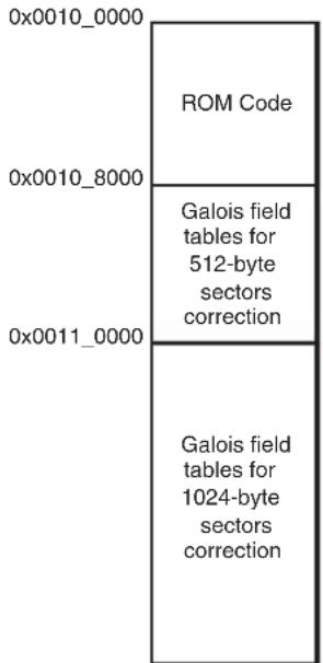
text_image
0x0010_0000 ROM Code 0x0010_8000 Galois field tables for 512-byte sectors correction 0x0011_0000 Galois field tables for 1024-byte sectors correctionFor a full description and an example of how to use the PMECC detection and correction feature, refer to the software package dedicated to this device on the Microchip web site.
11.4.4.3 SD Card/eMMC Boot
The SD Card / eMMC bootloader looks for a "boot.bin" file in the root directory of a FAT12/16/32 file system.
• Supported SD Card Devices
SD Card Boot supports all SD Card memories compliant with the SD Memory Card Specification V2.0. This includes SDHC cards.
Note: The ROM Code implements a 3.4 ms timeout waiting for an answer to the Power-on reset command after the peripheral clock enable. SD/eMMC memories that do not comply with this timing may not be detected correctly during the boot sequence.
11.4.4.4 SPI Flash Boot
Two types of SPI Flash are supported: SPI Serial Flash and SPI DataFlash.
The SPI Flash bootloader tries to boot on SPI0, first looking for SPI Serial Flash, and then for SPI DataFlash.
It uses only one valid code detection: analysis of ARM exception vectors.
The SPI Flash read is done using the Continuous Read command from the address 0x0. This command is 0xE8 for DataFlash and 0x0B for Serial Flash devices.
• Supported DataFlash Devices
The SPI Flash Boot program supports the DataFlash devices listed in Table 11-2.
Table 11-2: DataFlash Devices
| Device Density Page Size (bytes) Number of Pages | |||
| AT45DB011 | 1 Mbit | 264 | 512 |
| AT45DB021 | 2 Mbits | 264 | 1024 |
| AT45DB041 | 4 Mbits | 264 | 2048 |
| AT45DB081 | 8 Mbits | 264 | 4096 |
| AT45DB161 | 16 Mbits | 528 | 4096 |
| AT45DB321 | 32 Mbits | 528 | 8192 |
| AT45DB641 | 64 Mbits | 264 | 32768 |
| AT45DB642 | 64 Mbits | 1056 | 8192 |
• Supported Serial Flash Devices
The SPI Flash Boot program supports all SPI Serial Flash devices responding correctly at both Get Status and Continuous Read commands.
11.4.4.5 TWI EEPROM Boot
The TWI EEPROM Bootloader uses the TWI0. It uses only one valid code detection. It analyzes the ARM exception vectors.
• Supported TWI EEPROM Devices
TWI EEPROM Boot supports all I²C-compatible TWI EEPROM memories using the 7-bit device address 0x50.
11.4.5 Hardware and Software Constraints
The NVM drivers use several PIOs in peripheral mode to communicate with external memory devices. Care must be taken when these PIOs are used by the application. The connected devices could be unintentionally driven at boot time, and thus electrical conflicts between output pins used by the NVM drivers and the connected devices could occur.
To assure the correct functionality, it is recommended to plug in critical devices to other pins, not used by the NVM.
Table 11-3 contains a list of pins that are driven during the boot program execution. These pins are driven during the boot sequence for a period of less than 1 second if no correct boot program is found.
Before performing the jump to the application in the internal SRAM, all the PIOs and peripherals used in the boot program are set to their reset state.
Table 11-3: PIO Driven during Boot Program Execution
| NVM Bootloader Peripheral | Pin PIO Line | ||
| NAND | EBI CS3 SMC NANDOE — | ||
| EBI CS3 SMC NANDWE — | |||
| EBI CS3 SMC NANDCS — | |||
| EBI CS3 SMC NAND ALE — | |||
| EBI CS3 SMC NAND CLE — | |||
| EBI CS3 SMC Cmd/Addr/Data — | |||
| SD Card / eMMC | MCI0 MCI0_CK | PIOD9 | |
| MCI0 MCI0_CDA | PIOD0 | ||
| MCI0 MCI0_D0 | PIOD1 | ||
| MCI0 MCI0_D1 | PIOD2 | ||
| MCI0 MCI0_D2 | PIOD3 | ||
| MCI0 MCI0_D3 | PIOD4 | ||
| MCI1 MCI1_CK | PIOB24 | ||
| MCI1 MCI1_CDA | PIOB19 | ||
| MCI1 MCI1_D0 | PIOB20 | ||
| MCI1 MCI1_D1 | PIOB21 | ||
| MCI1 MCI1_D2 | PIOB22 | ||
| MCI1 MCI1_D3 | PIOB23 | ||
| SPI Flash | SPI0 | MOSI | PIOD11 |
| SPI0 | MISO | PIOD10 | |
| SPI0 | SPCK | PIOD12 | |
| SPI0 | NPCS0 | PIOD13 | |
| SPI0 | NPCS1 | PIOD14 | |
| TWIO EEPROM | TWIO TWD0 | PIOA30 | |
| TWIO TWCK0 | PIOA31 | ||
| SAM-BA Monitor | DBGU | DRXD | PIOB30 |
| DBGU | DTXD | PIOB31 |
11.5 SAM-BA Monitor
If no valid code is found in the NVM during the NVM bootloader sequence, the SAM-BA Monitor program is launched.
The SAM-BA Monitor principle is to:
- Initialize DBGU and USB
- Check if USB Device enumeration occurred
- Check if characters are received on the DBGU
Once the communication interface is identified, the application runs in an infinite loop waiting for different commands as listed in Table 11-4.
Figure 11-10: SAM-BA Monitor Diagram
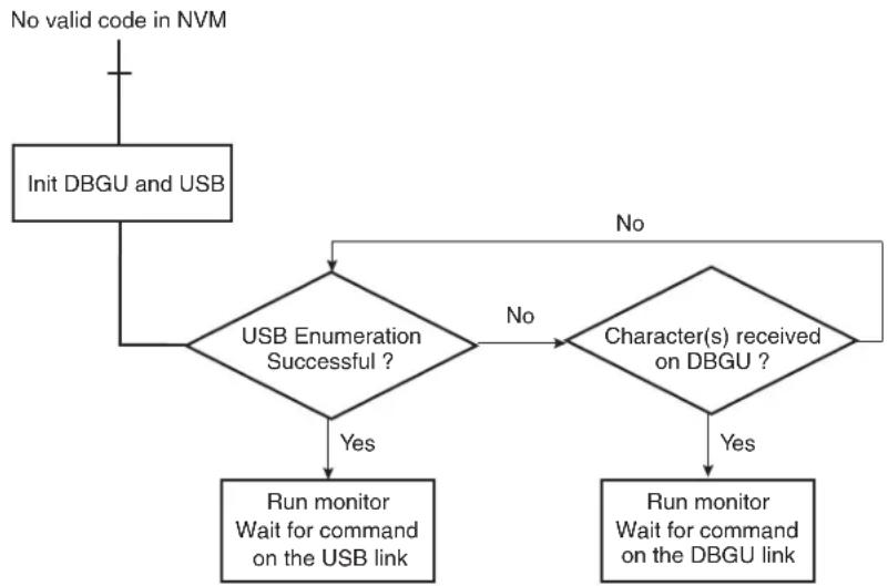
flowchart
graph TD
    A["No valid code in NVM"] --> B["Init DBGU and USB"]
    B --> C{USB Enumeration Successful ?}
    C -->|Yes| D["Run monitor Wait for command on the USB link"]
    C -->|No| E{Character(s) received on DBGU ?}
    E -->|Yes| F["Run monitor Wait for command on the DBGU link"]
    E -->|No| G["End"]
11.5.1 Command List
Table 11-4: Commands Available through the SAM-BA Monitor
| Command Action | Argument(s) Example | ||
| N | Set Normal Mode | No argument | N# |
| T | Set Terminal Mode | No argument | T# |
| O | Write a byte | Address, Value# | O200001,CA# |
| o | Read a byte | Address,# | o200001,# |
| H | Write a half word | Address, Value# | H200002,CAFE# |
| h | Read a half word | Address,# | h200002,# |
| W | Write a word | Address, Value# | W200000,CAFEDECA# |
| w | Read a word | Address,# | w200000,# |
| S | Send a file | Address,# | S200000,# |
| R | Receive a file | Address, NbOfBytes# | R200000,1234# |
| G | Go | Address# | G200200# |
| V | Display version | No argument | V# |
-
Mode commands:
-
Normal mode configures SAM-BA Monitor to send / receive data in binary format,
- Terminal mode configures SAM-BA Monitor to send / receive data in ASCII format.
- Write commands: Write a byte (O), a halfword (H) or a word (W) to the target
- Address: Address in hexadecimal
- Value: Byte, halfword or word to write in hexadecimal - Output: '>'
- Read commands: Read a byte (o), a halfword (h) or a word (w) from the target
- Address: Address in hexadecimal
- Output: The byte, halfword or word read in hexadecimal followed by '>'
- Send a file (S): Send a file to a specified address
- Address: Address in hexadecimal
- Output: '>'
Note: There is a time-out on this command which is reached when the prompt '>' appears before the end of the command execution.
- Receive a file (R): Receive data into a file from a specified address
- Address: Address in hexadecimal
- NbOfBytes: Number of bytes in hexadecimal to receive
- Output: '>'
- Go (G): Jump to a specified address and execute the code
- Address: Address to jump in hexadecimal
- Output: ' >' once returned from the program execution. If the executed program does not handle the link register at its entry and does not return, the prompt will not be displayed
- Get Version (V): Return the Boot Program version
- Output: version, date and time of ROM code followed by '>'
11.5.2 DBGU Serial Port
Communication is performed through the DBGU serial port initialized to 115,200 Baud, 8 bits of data, no parity, 1 stop bit.
11.5.2.1 Supported External Crystal/External Clocks
The SAM-BA Monitor supports a frequency of 12, 16, 24 or 48 MHz to allow DBGU communication for both external crystal and external clock.
11.5.2.2 Xmodem Protocol
The Send and Receive File commands use the Xmodem protocol to communicate. Any terminal performing this protocol can be used to send the application file to the target. The size of the binary file to send depends on the SRAM size embedded in the product. In all cases, the size of the binary file must be lower than the SRAM size because the Xmodem protocol requires some SRAM memory in order to work.
The Xmodem protocol supported is the 128-byte length block. This protocol uses a two-character CRC16 to ensure detection of maximum bit errors.
Xmodem protocol with CRC is supported by successful transmission reports provided both by a sender and by a receiver. Each transfer block is as follows:
- < SOH > = 01 hex
-
- <255-blk #> = 1's complement of the blk#.
-
Figure 11-11 shows a transmission using this protocol.
Figure 11-11: Xmodem Transfer Example

flowchart
sequenceDiagram
    A["Host"] -->|C| B["Device"]
    B -->|SOH_01_FE_Data["128"] CRC CRC| A
    A -->|SOH_02_FD_Data["128"] CRC CRC| B
    B -->|SOH_03_FC_Data["100"] CRC CRC| A
    A -->|ACK| B
    B -->|ACK| A
    A -->|EOT| B
    B -->|ACK| A
11.5.3 USB Device Port
11.5.3.1 Supported External Crystal / External Clocks
The SAM-BA Monitor supports a frequency of 12, 16, 24 or 48 MHz to allow USB communication for both external crystal and external clock.
11.5.3.2 USB Class
The device uses the USB Communication Device Class (CDC) drivers to take advantage of the installed PC Serial Communication software to talk over the USB. The CDC class is implemented in all releases of Windows ^® beginning with Windows 98SE ^® . The CDC document, available at www.usb.org, describes how to implement devices such as ISDN modems and virtual COM ports.
The vendor ID for is ID 0x03EB. The product ID is 0x6124. These references are used by the host operating system to mount the correct driver. On Windows systems, INF files contain the correspondence between vendor ID and product ID.
11.5.3.3 Enumeration Process
The USB protocol is a master/slave protocol. The host starts the enumeration, sending requests to the device through the control endpoint. The device handles standard requests as defined in the USB Specification.
Table 11-5: Handled Standard Requests
| Request Definition | |
| GET_DESCRIPTION Returns the current device configuration value | |
| SET_ADDRESS Sets the device address for all future device access | |
| SET_CONFIGURATION Sets the device configuration | |
| GET_CONFIGURATION Returns the current device configuration value | |
| GET_STATUS Returns status for the specified recipient | |
| SET_FEATURE Used to set or enable a specific feature | |
| CLEAR_FEATURE | Used to clear or disable a specific feature |
The device also handles some class requests defined in the CDC class.
Table 11-6: Handled Class Requests
| Request Definition | |
| SET_LINE_CODING | Configures DTE rate, stop bits, parity and number of character bits |
| GET_LINE_CODING | Requests current DTE rate, stop bits, parity and number of character bits |
| SET_CONTROL_LINE_STATE | RS-232 signal used to indicate to the DCE device that the DTE device is now present |
Unhandled requests are STALLed.
11.5.3.4 Communication Endpoints
Endpoint 0 is used for the enumeration process.
Endpoint 1 (64-byte Bulk OUT) and endpoint 2 (64-byte Bulk IN) are used as communication endpoints.
SAM-BA Boot commands are sent by the host through Endpoint 1. If required, the message is split into several data payloads by the host driver.
If the command requires a response, the host sends IN transactions to pick up the response.
12. Boot Sequence Controller (BSC)
12.1 Description
The System Controller embeds a Boot Sequence Controller (BSC). The boot sequence is programmable through the Boot Sequence Controller Configuration Register (BSC_CR) to save timeout delays on boot.
The BSC_CR is powered by VDDBU. Any modification of the register value is stored and applied after the next reset. The register defaults to the factory value in case of battery removal.
The BSC_CR is programmable with user programs or SAM-BA and is key-protected.
12.2 Embedded Characteristics
• VDDBU powered register
12.3 Product Dependencies
• Product-dependent order
12.4 Boot Sequence Controller (BSC) Registers User Interface
| Offset Register Name Access Reset | ||||
| 0x0 Boot | Sequence Controller Configuration Register BSC_CR Read/Write – | |||
12.4.1 Boot Sequence Controller Configuration Register
Name:BSC_CR
Address:0xFFFFFE54
Access: Read/Write
Factory Value: 0x0000_0000
31 30 29 28 27 26 25 24
| WPKEY | |||||||
| 23 22 21 20 19 18 17 16 | |||||||
| WPKEY | |||||||
| 15 14 13 12 11 10 9 8 | |||||||
| - | - | - | - | - | - | - | - |
| 7 | 6 | 5 | 4 | 3 | 2 | 1 | 0 |
| BOOT | |||||||
BOOT: Boot Media Sequence
This value is defined in the device datasheet section "Standard Boot Strategies". It is only written if WPKEY carries the valid value.
WPKEY: Write Protection Key (Write-only)
| Value Name | Description | |
| 0x6683 PASSWD | Writing any other value in this field aborts the write operation of the BOOT field.Always reads as 0. | |
13. AXI Matrix (AXIMX)
13.1 Description
The AXI Matrix comprises the embedded Advanced Extensible Interface (AXI) bus protocol which supports separate address/control and data phases, unaligned data transfers using byte strobes, burst-based transactions with only start address issued, separate read and write data channels to enable low-cost DMA, ability to issue multiple outstanding addresses, out-of-order transaction completion, and easy addition of register stages to provide timing closure.
13.2 Embedded Characteristics
• High performance AXI network interconnect
• 2 Masters :
- Core
- AHB/AXI bridge from AHB Matrix
• 3 Slaves:
- ROM
- AXI/AHB bridge to AHB Matrix
- Slave0 of MPDDRC
- Single-cycle arbitration
• Full pipelining to prevent master stalls
- 1 remap state
13.3 Operation
13.3.1 Remap
Remap states are managed in the AXI Matrix Remap Register (AXIMX_REMAP): AXIMX_REMAP.REMAP0 (register bit 0) is used to remap RAM @ addr 0x00000000.
Refer to Section 13.4 AXI Matrix (AXIMX) User Interface.
The number of remap states can be defined using eight bits of the AXIMX_REMAP register, and a bit in AXIMX_REMAP controls each remap state.
Each remap state can be used to control the address decoding for one or more slave interfaces. If a slave interface is affected by two remap states that are both asserted, the remap state with the lowest remap bit number takes precedence.
Each slave interface can be configured independently so that a remap state can perform different functions for different masters.
A remap state can:
- Alias a memory region into two different address ranges
- Move an address region
- Remove an address region
Because of the nature of the distributed register subsystem, the masters receive the updated remap bit states in sequence, and not simultaneously.
A slave interface does not update to the latest remap bit setting until:
- The address completion handshake accepts any transaction that is pending
- Any current lock sequence completes
At powerup, ROM is seen at address 0. After powerup, the internal SRAM can be moved down to address 0 by means of the remap bits.
13.4 AXI Matrix (AXIMX) User Interface
SRAM is seen at address 0x00000000 (through AHB slave interface) instead of ROM.
14. Bus Matrix (MATRIX)
14.1 Description
The Bus Matrix (MATRIX) implements a multi-layer AHB, based on the AHB-Lite protocol, that enables parallel access paths between multiple masters and slaves in a system, thus increasing the overall bandwidth.
The MATRIX interconnects 15 masters to 12 slaves. The normal latency to connect a master to a slave is one cycle, except for the default master of the accessed slave which is connected directly (zero cycle latency).
The MATRIX user interface is compliant with the Arm Advanced Peripheral Bus.
14.1.1 Matrix Masters
Table 14-1: List of MATRIX Masters
| Master No. | Description | |||||
| 0 | C | o | r | t | e | x |
| 1, 2, 3DMA | Controller 0 | |||||
| 4, 5, 6 DMA | Controller 1 | |||||
| 7 | G | M | A | C | D | M |
| 8, 9 | LCDC DMA | |||||
| 10 | UHP EHCI DMA | |||||
| 11 | UHP OHCI DMA | |||||
| 12 | UDPHS DMA | |||||
| 13 | EMAC DMA | |||||
| 14 | ISI DMA | |||||
- A 5 A
14.1.2 Matrix Slaves
Table 14-2: List of MATRIX Slaves
| Slave No. | Description |
| 0 | Internal SRAM0 |
| 1 | Internal SRAM1 |
| 2 | NFC SRAM |
| 3 | Internal ROM |
| 4 | Soft Modem (SMD) |
| 5 | USB Device High Speed Dual Port RAM (DPR) |
| USB Host OHCI registers | |
| USB Host EHCI registers | |
| 6 | External Bus Interface/NFC |
| 7 | DDR2 Port 1 |
| 8 | DDR2 Port 2 |
| 9 | DDR2 Port 3 |
| 10 | Peripheral Bridge 0 |
| 11 | Peripheral Bridge 1 |
Note: DDR2 Port 0 and ROM are connected to the core through a dedicated AXI Matrix.
14.1.3 Master to Slave Access
Table 14-3: Master to Slave Access
| Masters | 0 | 1 | 2 | 3 | 4 | 5 | 6 | 7 | 8 | 9 | 10 | 11 | 12 | 13 | 14 | |
| Slaves | Cortex-A5 | DMAC0 DMAC1 | GMAC DMA | LCDC DMA | UHPHS EHCI DMA | UHPHS OHCI DMA | UDPHS DMA | EMAC DMA | ISI DMA | |||||||
| IF0 | IF1 | IF2 | IF0 | IF1 | IF2 | |||||||||||
| 0 | Internal SRAM0 | √ | √ | - | - | √ | - | - | √ | - | - | √ | √ | √ | √ | - |
| 1 | Internal SRAM1 | √ | √ | - | - | √ | - | - | √ | - | - | √ | √ | √ | √ | - |
| 2 | NFC SRAM | √ | √ | - | - | - | - | - | - | - | - | - | - | - | - | - |
| 3 | Internal ROM | -√ | - | - | - | - | - | - | - | - | √ | √ | √ | - | - | |
| 4 | SMD | √ | √ | - | - | - | - | - | - | - | - | - | - | - | - | - |
| 5 | UDPHS RAM | √ | - | - | - | - | - | - | - | - | - | - | - | - | - | - |
| UHP OHCI Registers | ||||||||||||||||
| UHP EHCI Registers | ||||||||||||||||
| 6 | EBI CS0..CS3 | √ | √ | - | - | √ | √ | - | √ | √ | √ | √ | √ | √ | √ | √ |
| NFC Command Register | √ | - | - | - | - | - | - | - | - | - | - | - | - | - | - | |
| 7 | DDR2 Port 1 - | - | √ | - | √ | - | - | √ | - | - | - | - | - | - | - | |
| 8 | DDR2 Port 2 - | √ | - | - | - | √ | - | - | √ | - | - | √ | - | - | - | |
| 9 | DDR2 Port 3 | - | - | √ | - | √ | - | - | √ | - | √ | √ | - | √ | √ | √ |
| 10 | APB 0 | √ | - | - | √ | - | - | - | - | - | - | - | - | - | - | - |
| 11 | APB 1 | √ | - | - | - | - | - | √ | - | - | - | - | - | - | - | - |
14.2 Embedded Characteristics
• 32- or 64-bit Data Bus
• 15 Masters, 12 Slaves
• One Decoder for Each Master
- Several Possible Boot Memories for Each Master before Remap
• One Remap Function for Each Master
• Support for Long Bursts of Length 32, 64, 128 and Up to the Limit of 256-bit Burst Beats of Words
- Enhanced Programmable Mixed Arbitration for Each Slave
- Round-robin
- Fixed priority
- Latency Quality of Service (QoS)
- Programmable Default Master for Each Slave
- No default master
- Last accessed default master
- Fixed default master
• Deterministic Maximum Access Latency for Masters
• Zero or One Cycle Arbitration Latency for the First Access of a Burst
- Bus Lock Forwarding to Slaves
• Master Number Forwarding to Slaves
- Register Write Protection
14.3 Memory Mapping
The MATRIX provides one decoder for every master interface. The decoder offers each master several memory mappings. Each memory area can be assigned to several slaves. Booting at the same address while using different slaves (that is, external RAM, internal ROM or internal Flash, etc.) is possible.
14.4 Special Bus Granting Techniques
The MATRIX provides some speculative bus granting techniques in order to anticipate access requests from masters. Hence, latency is reduced at first access of a burst or, for a single transfer, as long as the slave is free from any other master access. It does not provide any benefit if the slave is continuously accessed by more than one master, since arbitration is pipelined and has no negative effect on the slave bandwidth or access latency.
This bus granting technique sets a different default master for every slave.
At the end of the current access, if no other request is pending, the slave remains connected to its associated default master. A slave can be associated with three kinds of default masters:
- No default master
- Last access master
- Fixed default master
To change from one type of default master to another, the user interface provides Slave Configuration registers (MATRIX_SCFGx), one for every slave, which set a default master for each slave. MATRIX_SCFGx contain two fields to manage master selection: DEFMSTR_TYPE and FIXED_DEFMSTR. The 2-bit DEFMSTR_TYPE field selects the default master type (no default, last access master, fixed default master), whereas the 4-bit FIXED_DEFMSTR field selects a fixed default master provided that DEFMSTR_TYPE is set to fixed default master. Refer to Section 14.10.2 MATRIX Slave Configuration Registers.
14.5 No Default Master
After the end of the current access, if no other request is pending, the slave is disconnected from all masters.
This configuration incurs one latency clock cycle for the first access of a burst after bus Idle. Arbitration without default master may be used for masters that perform significant bursts or several transfers with no Idle cycle in-between, or if the slave bus bandwidth is widely used by one or more masters.
This configuration provides no benefit on access latency or bandwidth when reaching maximum slave bus throughput whatever the number of requesting masters.
14.6 Last Access Master
After the end of the current access, if no other request is pending, the slave remains connected to the last master that performed an access request.
This allows the MATRIX to remove the one latency cycle for the last master that accessed the slave. Other non-privileged masters still get one latency clock cycle if they need to access the same slave. This technique is useful for masters that mainly perform single accesses or short bursts with some Idle cycles in-between.
This configuration provides no benefit on access latency or bandwidth when reaching maximum slave bus throughput whatever is the number of requesting masters.
14.7 Fixed Default Master
After the end of the current access, if no other request is pending, the slave connects to its fixed default master. Unlike the last access master, the fixed default master does not change unless the user modifies it by software (FIXED_DEFMSTR field of the related MATRIX_SCFG).
This allows the MATRIX arbiters to remove the one latency clock cycle for the fixed default master of the slave. All requests attempted by the fixed default master do not cause any arbitration latency, whereas other non-privileged masters get one latency cycle. This technique is useful for a master that mainly performs single accesses or short bursts with Idle cycles in between.
This configuration provides no benefit on access latency or bandwidth when reaching maximum slave bus throughput, regardless of the number of requesting masters.
14.8 Arbitration
The MATRIX provides an arbitration technique that reduces latency when conflicts occur, i.e., when two or more masters try to access the same slave at the same time. One arbiter per slave is provided, thus arbitrating each slave specifically.
The user can choose between two arbitration types or mix them for each slave:
• Round-robin Arbitration (default)
• Fixed Priority Arbitration
The resulting algorithm may be complemented by selecting a default master configuration for each slave.
When re-arbitration must be done, specific conditions apply. See Section 14.8.1 Arbitration Scheduling.
14.8.1 Arbitration Scheduling
Each arbiter has the ability to arbitrate between two or more master requests. In order to avoid burst breaking and also to provide the maximum throughput for slave interfaces, arbitration may only take place during the following cycles:
- Idle Cycles: When a slave is not connected to any master or is connected to a master which is not currently accessing it.
- Single Cycles: When a slave is currently performing a single access.
- End of Burst Cycles: When the current cycle is the last cycle of a burst transfer. For defined length burst, predicted end of burst matches the size of the transfer but is managed differently for undefined length burst. See Section 14.8.1.1 Undefined Length Burst Arbitration.
- Slot Cycle Limit: When the slot cycle counter has reached the limit value indicating that the current master access is too long and must be broken. See Section 14.8.1.2 Slot Cycle Limit Arbitration.
14.8.1.1 Undefined Length Burst Arbitration
To prevent long burst lengths that can lock the access to the slave for an excessive period of time, the user can trigger the re-arbitration before the end of the incremental bursts. The rearbitration period can be selected from the following Undefined Length Burst Type (ULBT) possibilities:
- Unlimited: no predetermined end of burst is generated. This value enables 1 Kbyte burst lengths.
- 1-beat bursts: predetermined end of burst is generated at each single transfer during the INCR transfer.
- 4-beat bursts: predetermined end of burst is generated at the end of each 4-beat boundary during INCR transfer.
- 8-beat bursts: predetermined end of burst is generated at the end of each 8-beat boundary during INCR transfer.
- 16-beat bursts: predetermined end of burst is generated at the end of each 16-beat boundary during INCR transfer.
• 32-beat bursts: predetermined end of burst is generated at the end of each 32-beat boundary during INCR transfer. - 64-beat bursts: predetermined end of burst is generated at the end of each 64-beat boundary during INCR transfer.
• 128-beat bursts: predetermined end of burst is generated at the end of each 128-beat boundary during INCR transfer.
The use of undefined length 8-beat bursts, or less, is discouraged since this may decrease the overall bus bandwidth due to arbitration and slave latencies at each first access of a burst.
Undefined-length bursts lower than 8 beats should not be used since this may decrease the overall bus bandwidth due to arbitration and slave latencies at each first access of a burst.
However, if the length of undefined-length bursts is known for a master, it is recommended to configure MATRIX_MCFG.ULBT accordingly.
14.8.1.2 Slot Cycle Limit Arbitration
The MATRIX contains specific logic to break long accesses, such as very long bursts on a very slow slave (e.g., an external low-speed memory). At each arbitration time, a counter is loaded with the value previously written in MATRIX_SCFGx.SLOT_CYCLE and decreased at each clock cycle. When the counter elapses, the arbiter has the ability to rearbitrate at the end of the current system bus access cycle.
Unless a master has a very tight access latency constraint, which could lead to data overflow or underflow due to a badly undersized internal FIFO with respect to its throughput, the Slot Cycle Limit should be disabled (SLOT_CYCLE = 0) or set to its default maximum value in order not to inefficiently break long bursts performed by some masters.
In most cases, this feature is not needed and should be disabled for power saving.
Warning: This feature cannot prevent any slave from locking its access indefinitely.
14.8.2 Arbitration Priority Scheme
The MATRIX arbitration scheme is organized in priority pools, each corresponding to an access criticality class as shown in the "Latency Quality of Service" column in the table below. When the Latency Quality of Service is enabled for a master-slave pair through the MATRIX, the priority pool number to use for arbitration at the slave port is determined from the master. When the Latency Quality of Service is disabled, it is determined through the MATRIX user interface. See Section 14.10.3 MATRIX Priority Registers A For Slaves.
After reset, the Latency Quality of Service is enabled by default on all of the master ports that are connected to a master driving the Latency Quality of Service signals, as shown in the bit LQOSEN of Section 14.10.3 MATRIX Priority Registers A For Slaves and Section 14.10.4 MATRIX Priority Registers B For Slaves.
Table 14-4: Arbitration Priority Pools
| Priority pool Latency | Quality of Service |
| 3Latency Critical | |
| 2 | Latency Sensitive |
| 1 | Bandwidth Sensitive |
| 0 | Background Transfers |
Round-robin priority is used in the highest and lowest priority pools 3 and 0, whereas fixed level priority is used between priority pools and in the intermediate priority pools 2 and 1.
For each slave, each master is assigned to one of the slave priority pools based on the Latency Quality of Service inputs or to the priority registers for slaves (MxPR fields of MATRIX_PRAS and MATRIX_PRBS). When evaluating master requests, this priority pool level always takes precedence.
After reset, most of the masters belong to the lowest priority pool (MxPR = 0, Background Transfer) and are therefore granted bus access in a true round-robin order.
The highest priority pool must be specifically reserved for masters requiring very low access latency. If more than one master belongs to this pool, they will be granted bus access in a biased round-robin manner which allows tight and deterministic maximum access latency from system bus requests. In the worst case, any currently occurring high-priority master request is granted after the current bus master access has ended and any other high priority pool master requests, if any, have been granted once each.
The lowest priority pool shares the remaining bus bandwidth between masters.
Intermediate priority pools enable fine priority tuning. Typically, a latency-sensitive master or a bandwidth-sensitive master use such a priority level. The higher the priority level (MxPR value), the higher the master priority.
For optimized processor performance, it is recommended to configure processor priority with the default reset value 2 (Latency Sensitive).
All combinations of MxPR values are allowed for all masters and slaves. For example, some masters might be assigned the highest priority pool (round-robin), and remaining masters the lowest priority pool (round-robin), with no master for intermediate fixed priority levels.
14.8.2.1 Fixed Priority Arbitration
The fixed priority arbitration algorithm is the first and only arbitration algorithm applied between masters from distinct priority pools. It is also used in priority pools other than the highest and lowest priority pools (intermediate priority pools).
Fixed priority arbitration allows the MATRIX arbiters to dispatch the requests from different masters to the same slave by using the fixed priority defined by the user in the MxPR field for each master in the registers MATRIX_PRAS and MATRIX_PRBS. If two or more master requests are active at the same time, the master with the highest priority MxPR number is serviced first.
In intermediate priority pools, if two or more master requests with the same priority are active at the same time, the master with the highest number is serviced first.
14.8.2.2 Round-Robin Arbitration
This algorithm is only used in the highest and lowest priority pools. It allows the MATRIX arbiters to properly dispatch requests from different masters to the same slave. If two or more master requests are active at the same time in the priority pool, they are serviced in a round-robin increasing master number order.
14.9 Register Write Protection
To prevent any single software error from corrupting MATRIX behavior, certain registers in the address space can be write-protected by setting the WPEN bit in the MATRIX Write Protection Mode Register (MATRIX_WPMR).
If a write access to a write-protected register is detected, the WPVS flag in the MATRIX Write Protection Status Register (MATRIX_WPSR) is set and the field WPVSRC indicates the register in which the write access has been attempted.
The WPVS flag is reset by writing the MATRIX_WPMR with the appropriate access key WPKEY.
The following registers can be write-protected:
• MATRIX Master Configuration Registers
• MATRIX Slave Configuration Registers
• MATRIX Priority Registers A For Slaves
• MATRIX Priority Registers B For Slaves
• MATRIX Master Remap Control Register
14.10 Matrix (MATRIX) User Interface
Table 14-5: Register Mapping
| Offset Register Name Access Reset | ||||
| 0x0000 | Master Configuration Register 0 | MATRIX_MCFG0 | Read/Write | 0x00000004 |
| 0x0004 | Master Configuration Register 1 | MATRIX_MCFG1 | Read/Write | 0x00000004 |
| 0x0008 | Master Configuration Register 2 | MATRIX_MCFG2 | Read/Write | 0x00000004 |
| 0x000C | Master Configuration Register 3 | MATRIX_MCFG3 | Read/Write | 0x00000004 |
| 0x0010 | Master Configuration Register 4 | MATRIX_MCFG4 | Read/Write | 0x00000004 |
| 0x0014 | Master Configuration Register 5 | MATRIX_MCFG5 | Read/Write | 0x00000004 |
| 0x0018 | Master Configuration Register 6 | MATRIX_MCFG6 | Read/Write | 0x00000004 |
| 0x001C | Master Configuration Register 7 | MATRIX_MCFG7 | Read/Write | 0x00000004 |
| 0x0020 | Master Configuration Register 8 | MATRIX_MCFG8 | Read/Write | 0x00000004 |
| 0x0024 | Master Configuration Register 9 | MATRIX_MCFG9 | Read/Write 0x00000004 | |
| 0x0028 | Master Configuration Register 10 | MATRIX_MCFG10 | Read/Write | 0x00000004 |
| 0x002C | Master Configuration Register 11 | MATRIX_MCFG11 | Read/Write | 0x00000004 |
| 0x0030 | Master Configuration Register 12 | MATRIX_MCFG12 | Read/Write | 0x00000004 |
| 0x0034 | Master Configuration Register 13 | MATRIX_MCFG13 | Read/Write | 0x00000004 |
| 0x0038 | Master Configuration Register 14 | MATRIX_MCFG14 | Read/Write | 0x00000004 |
| 0x003C | Reserved | - | - | - |
| 0x0040 | Slave Configuration Register 0 | MATRIX_SCFG0 | Read/Write | 0x000001FF |
| 0x0044 | Slave Configuration Register 1 | MATRIX_SCFG1 | Read/Write | 0x000001FF |
| 0x0048 | Slave Configuration Register 2 | MATRIX_SCFG2 | Read/Write | 0x000001FF |
| 0x004C | Slave Configuration Register 3 | MATRIX_SCFG3 | Read/Write | 0x000001FF |
| 0x0050 | Slave Configuration Register 4 | MATRIX_SCFG4 | Read/Write | 0x000001FF |
| 0x0054 | Slave Configuration Register 5 | MATRIX_SCFG5 | Read/Write | 0x000001FF |
| 0x0058 | Slave Configuration Register 6 | MATRIX_SCFG6 | Read/Write | 0x000001FF |
| 0x005C | Slave Configuration Register 7 | MATRIX_SCFG7 | Read/Write | 0x000001FF |
| 0x0060 | Slave Configuration Register 8 | MATRIX_SCFG8 | Read/Write | 0x000001FF |
| 0x0064 | Slave Configuration Register 9 | MATRIX_SCFG9 | Read/Write | 0x000001FF |
| 0x0068 | Slave Configuration Register 10 | MATRIX_SCFG10 | Read/Write | 0x000001FF |
| 0x006C | Slave Configuration Register 11 | MATRIX_SCFG11 | Read/Write | 0x000001FF |
| 0x0070-0x007C | Reserved | - | - | - |
| 0x0080 | Priority Register A for Slave 0 | MATRIX_PRAS0 | Read/Write | 0x0000000^(1) |
| 0x0084 | Priority Register B for Slave 0 | MATRIX_PRBS0 | Read/Write | 0x0000000^(1) |
| 0x0088 | Priority Register A for Slave 1 | MATRIX_PRAS1 | Read/Write | 0x0000000^(1) |
| 0x008C | Priority Register B for Slave 1 | MATRIX_PRBS1 | Read/Write | 0x0000000^(1) |
| 0x0090 | Priority Register A for Slave 2 | MATRIX_PRAS2 | Read/Write | 0x0000000^(1) |
| 0x0094 | Priority Register B for Slave 2 | MATRIX_PRBS2 | Read/Write | 0x0000000^(1) |
| Offset | Register | Name | Access | Reset |
| 0x0098 | Priority Register A for Slave 3 | MATRIX_PRAS3 | Read/Write | 0x00000000^(1) |
| 0x009C | Priority Register B for Slave 3 | MATRIX_PRBS3 | Read/Write | 0x00000000^(1) |
| 0x00A0 | Priority Register A for Slave 4 | MATRIX_PRAS4 | Read/Write | 0x00000000^(1) |
| 0x00A4 | Priority Register B for Slave 4 | MATRIX_PRBS4 | Read/Write | 0x00000000^(1) |
| 0x00A8 | Priority Register A for Slave 5 | MATRIX_PRAS5 | Read/Write | 0x00000000^(1) |
| 0x00AC | Priority Register B for Slave 5 | MATRIX_PRBS5 | Read/Write | 0x00000000^(1) |
| 0x00B0 | Priority Register A for Slave 6 | MATRIX_PRAS6 | Read/Write | 0x00000000^(1) |
| 0x00B4 | Priority Register B for Slave 6 | MATRIX_PRBS6 | Read/Write | 0x00000000^(1) |
| 0x00B8 | Priority Register A for Slave 7 | MATRIX_PRAS7 | Read/Write | 0x00000000^(1) |
| 0x00BC | Priority Register B for Slave 7 | MATRIX_PRBS7 | Read/Write | 0x00000000^(1) |
| 0x00C0 | Priority Register A for Slave 8 | MATRIX_PRAS8 | Read/Write | 0x00000000^(1) |
| 0x00C4 | Priority Register B for Slave 8 | MATRIX_PRBS8 | Read/Write | 0x00000000^(1) |
| 0x00C8 | Priority Register A for Slave 9 | MATRIX_PRAS9 | Read/Write | 0x00000000^(1) |
| 0x00CC | Priority Register B for Slave 9 | MATRIX_PRBS9 | Read/Write | 0x00000000^(1) |
| 0x00D0 | Priority Register A for Slave 10 | MATRIX_PRAS10 | Read/Write | 0x00000000^(1) |
| 0x00D4 | Priority Register B for Slave 10 | MATRIX_PRBS10 | Read/Write | 0x00000000^(1) |
| 0x00D8 | Priority Register A for Slave 11 | MATRIX_PRAS11 | Read/Write | 0x00000000^(1) |
| 0x00DC | Priority Register B for Slave 11 | MATRIX_PRBS11 | Read/Write | 0x00000000^(1) |
| 0x00E0-0x00FC | Reserved | - | - | - |
| 0x0100 | Master Remap Control Register | MATRIX_MRCR | Read/Write | 0x00000000 |
| 0x0104-0x01E0 | Reserved | - | - | - |
| 0x01E4 | Write Protect Mode Register | MATRIX_WPMR | Read/Write | 0x00000000 |
| 0x01E8 | Write Protect Status Register | MATRIX_WPSR | Read-only | 0x00000000 |
Note 1: Values in the MATRIX Priority Registers are product-dependent.
14.10.1 MATRIX Master Configuration Registers
Name: MATRIX_MCFG0...MATRIX_MCFG14
Access: Read/Write
| 31 | 30 | 29 | 28 | 27 | 26 | 25 | 24 |
| - | - | - | - | - | - | - | - |
| 23 | 22 | 21 | 20 | 19 | 18 | 17 | 16 |
| - | - | - | - | - | - | - | - |
15 14 1312 11 10 9 8
| - | - | - | - | - | - | - | - |
| 7 | 6 | 5 | 4 | 32 | 1 | 0 | |
| - | - | - | - | - | U | L |
This register can only be written if the WPEN bit is cleared in the MATRIX Write Protection Mode Register.
ULBT: Undefined Length Burst Type
| Value | Name Description | |
| 0 | UNLIMITED | Unlimited Length Burst—No predicted end of burst is generated, therefore INCR bursts coming from this master can only be broken if the Slave Slot Cycle Limit is reached. If the Slot Cycle Limit is not reached, the burst is normally completed by the master, at the latest, on the next system bus 1 Kbyte address boundary, allowing up to 256-beat word bursts or 128-beat double-word bursts.This value should not be used in the very particular case of a master capable of performing back-to-back undefined length bursts on a single slave, since this could indefinitely freeze the slave arbitration and thus prevent another master from accessing this slave. |
| 1 | SINGLE | Single Access—The undefined length burst is treated as a succession of single accesses, allowing re-arbitration at each beat of the INCR burst or bursts sequence. |
| 2 | 4_BEAT | 4-beat Burst—The undefined length burst or bursts sequence is split into 4-beat bursts or less, allowing re-arbitration every 4 beats. |
| 3 | 8_BEAT | 8-beat Burst—The undefined length burst or bursts sequence is split into 8-beat bursts or less, allowing re-arbitration every 8 beats. |
| 4 | 16_BEAT | 16-beat Burst—The undefined length burst or bursts sequence is split into 16-beat bursts or less, allowing re-arbitration every 16 beats. |
| 5 | 32_BEAT | 32-beat Burst—The undefined length burst or bursts sequence is split into 32-beat bursts or less, allowing re-arbitration every 32 beats. |
| 6 | 64_BEAT | 64-beat Burst—The undefined length burst or bursts sequence is split into 64-beat bursts or less, allowing re-arbitration every 64 beats. |
| 7 | 128_BEAT | 128-beat Burst—The undefined length burst or bursts sequence is split into 128-beat bursts or less, allowing re-arbitration every 128 beats.Unless duly needed, the ULBT should be left at its default 0 value for power saving. |
14.10.2 MATRIX Slave Configuration Registers
Name: MATRIX_SCFG0...MATRIX_SCFG11
Access: Read/Write
| 31 | 30 | 29 | 28 | 27 | 26 | 25 | 24 |
| - | - | - | - | - | - | - | - |
| 23 | 22 | 21 | 20 | 19 | 18 | 17 | 16 |
| - | - | FIXED_DEFMSTR | DEFMSTR_TYPE | ||||
15 14 1312 11 10 9 8
| - | - | - | - | - | - | - | SLOT_CYCLE |
| 7 | 6 | 5 | 4 | 32 | 1 | 0 | |
| SLOT_CYCLE | |||||||
This register can only be written if the WPEN bit is cleared in the MATRIX Write Protection Mode Register.
SLOT\_CYCLE: Maximum Bus Grant Duration for Masters
When SLOT_CYCLE system bus clock cycles have elapsed since the last arbitration, a new arbitration takes place to let another master access this slave. If another master is requesting the slave bus, then the current master burst is broken.
If SLOT_CYCLE = 0, the Slot Cycle Limit feature is disabled and bursts always complete unless broken according to the ULBT.
This limit has been placed in order to enforce arbitration so as to meet potential latency constraints of masters waiting for slave access.
This limit must not be too small. Unreasonably small values break every burst and the MATRIX arbitrates without performing any data transfer. The default maximum value is usually an optimal conservative choice.
In most cases, this feature is not needed and should be disabled for power saving.
See Section 14.8.1.2 Slot Cycle Limit Arbitration for details.
DEFMSTR_TYPE: Default Master Type
| Value | Name Description | |
| 0 | NONE | No Default Master—At the end of the current slave access, if no other master request is pending, the slave is disconnected from all masters.This results in a one clock cycle latency for the first access of a burst transfer or for a single access. |
| 1 | LAST | Last Default Master—At the end of the current slave access, if no other master request is pending, the slave stays connected to the last master having accessed it.This results in not having one clock cycle latency when the last master tries to access the slave again. |
| 2 | FIXED | Fixed Default Master—At the end of the current slave access, if no other master request is pending, the slave connects to the fixed master the number that has been written in the FIXED_DEFMSTR field.This results in not having one clock cycle latency when the fixed master tries to access the slave again. |
FIXED\_DEFMSTR: Fixed Default Master
This is the number of the Default Master for this slave. Only used if DEFMSTR_TYPE is 2. Specifying the number of a master which is not connected to the selected slave is equivalent to setting DEFMSTR_TYPE to 0.
14.10.3 MATRIX Priority Registers A For Slaves
Name: MATRIX_PRAS0...MATRIX_PRAS11
Access: Read/Write
| 31 | 30 | 29 | 28 | 27 | 26 | 25 | 24 |
| - | L | O | SEN7 M7 | PR - LQOSEN6 | M6PR | ||
| 23 | 22 | 21 | 20 | 19 | 18 | 17 | 16 |
| - | L | O | SEN5 M5 | PR - LQOSEN4 | M4PR |
15 14 1312 11 10 9 8
| - | LQOSEN3 | M3PR | - | LQOSEN2 | M2PR | |
| 7 | 6 | 5 | 4 | 32 | 1 | 0 |
| - | L Q | O | SEN1 M1 | PR - LQOSEN0 | M0PR | |
This register can only be written if the WPEN bit is cleared in the MATRIX Write Protection Mode Register.
MxPR: Master x Priority
Fixed priority of Master x for accessing the selected slave. The higher the number, the higher the priority.
All the masters programmed with the same MxPR value for the slave make up a priority pool.
Round-robin arbitration is used in the lowest (MxPR = 0) and highest (MxPR = 3) priority pools.
Fixed priority is used in intermediate priority pools (MxPR = 1) and (MxPR = 2).
See Section 14.8.2 Arbitration Priority Scheme for details.
This priority is used by default any time that the Latency Quality of Service propagation from the Master x is not used or not available. Set this field to 0x0 when the LQOSENx bit is set to 1.
LQOSENx: Latency Quality of Service Enable for Master x
0: Disables propagation of Latency Quality of Service from the Master x to the Slave and apply MxPR priority for all access from Master x to the Slave.
1: Enables the propagation of Latency Quality of Service from the Master x to the Slave if supported by the Master x.
14.10.4 MATRIX Priority Registers B For Slaves
Name: MATRIX_PRBS0...MATRIX_PRBS11
Access: Read/Write
| 31 | 30 | 29 | 28 | 27 | 26 | 25 | 24 |
| - | - | - | - | - | L | Q | O |
| 23 | 22 | 21 | 20 | 19 | 18 | 17 | 16 |
| - | LQOSEN13 | M13PR | - | LQOSEN12 | M12PR | ||
| 15 14 1312 11 10 | 9 8 | ||||||
| - | LQOSEN11 | M11PR | - | LQOSEN10 | M10PR | ||
| 7 | 6 | 5 | 4 | 32 | 1 | 0 | |
| - | LQOSEN9 | M9PR | - | LQOSEN8 | M8PR | ||
This register can only be written if the WPEN bit is cleared in the MATRIX Write Protection Mode Register.
MxPR: Master x Priority
Fixed priority of Master x for accessing the selected slave. The higher the number, the higher the priority.
All the masters programmed with the same MxPR value for the slave make up a priority pool.
Round-robin arbitration is used in the lowest (MxPR = 0) and highest (MxPR = 3) priority pools.
Fixed priority is used in intermediate priority pools (MxPR = 1) and (MxPR = 2).
See Section 14.8.2 Arbitration Priority Scheme for details.
This priority is used by default any time that the Latency Quality of Service propagation from the Master x is not used or not available. Set this field to 0x0 when the LQOSENx bit is set to 1.
LQOSENx: Latency Quality of Service Enable for Master x
0: Disables propagation of Latency Quality of Service from the Master x to the Slave and apply MxPR priority for all access from Master x to the Slave.
1: Enables the propagation of Latency Quality of Service from the Master x to the Slave if supported by the Master x.
14.10.5 MATRIX Master Remap Control Register
Name: MATRIX_MRCR
Access: Read/Write
| 31 | 30 | 29 | 28 | 27 | 26 | 25 | 24 |
| - | - | - | - | - | - | - | - |
| 23 | 22 | 21 | 20 | 19 | 18 | 17 | 16 |
| - | - | - | - | - | - | - | - |
15 14 1312 11 10 9 8
| - | RCB14 | RCB13 | RCB12 | RCB11 | RCB10 | RCB9 | RCB8 |
| 7 | 6 | 5 | 4 | 32 | 1 | 0 | |
| RCB7 RCB6 | RCB5 RCB4 R | CB3RCB2 RCB1 | RCB0 |
This register can only be written if the WPEN bit is cleared in the MATRIX Write Protection Mode Register.
RCBx: Remap Command Bit for Master x
0: Disables remapped address decoding for the selected Master.
1: Enables remapped address decoding for the selected Master.
14.10.6 MATRIX Write Protection Mode Register
Name: MATRIX_WPMR
Access: Read/Write
| 31 | 30 | 29 | 28 | 27 | 26 | 25 | 24 |
| WPKEY | |||||||
| 23 | 22 | 21 | 20 | 19 | 18 | 17 | 16 |
| WPKEY | |||||||
15 14 1312 11 10 9 8
| WPKEY | |||||||
| 7 | 6 | 5 | 4 | 32 | 1 | 0 | |
| - | - | - | - | - | - | - | W |
WPEN: Write Protection Enable
0: Disables the write protection if WPKEY corresponds to 0x4D4154 ("MAT" in ASCII).
1: Enables the write protection if WPKEY corresponds to 0x4D4154 ("MAT" in ASCII).
See Section 14.9 Register Write Protection for the list of registers that can be write-protected.
WPKEY: Write Protection Key
| Value Name | Description | |
| 0x4D4154 | PASSWD | Writing any other value in this field aborts the write operation of the WPEN bit. Always reads as 0. |
14.10.7 MATRIX Write Protection Status Register
Name: MATRIX_WPSR
Access: Read-only
| 31 | 30 | 29 | 28 | 27 | 26 | 25 | 24 |
| - | - | - | - | - | - | - | - |
| 23 | 22 | 21 | 20 | 19 | 18 | 17 | 16 |
| WPVSRC | |||||||
15 14 1312 11 10 9 8
| WPVSRC | |||||||
| 7 | 6 | 5 | 4 | 32 | 1 | 0 | |
| - | - | - | - | - | - | - | W |
WPVS: Write Protection Violation Status
0: No write protection violation has occurred since the last write of the MATRIX_WPMR.
1: A write protection violation has occurred since the last write of the MATRIX_WPMR. If this violation is an unauthorized attempt to write a protected register, the associated violation is reported into field WPVSRC.
WPVSRC: Write Protection Violation Source
When WPVS = 1, WPVSRC indicates the register address offset at which a write access has been attempted.
15. Special Function Registers (SFR)
15.1 Description
Special Function Registers (SFR) manage specific aspects of the integrated memory, bridge implementations, processor and other functionality not controlled elsewhere.
15.2 Embedded Characteristics
• 32-bit Special Function Registers control specific behavior of the product
15.3 Special Function Registers (SFR) User Interface
| Offset(1) | Register Name Access Reset | |||
| 0x00 Reserved --- | ||||
| 0x04 | DDR Configuration Register | SFR_DDRCFG | Read/Write | 0x01 |
| 0x08-0x0C | Reserved --- | |||
| 0x10 | OHCI Interrupt Configuration Register | SFR_OHCIICR | Read/Write | 0x0 |
| 0x14 | OHCI Interrupt Status Register | SFR_OHCIISR | Read-only | — |
| 0x18 Reserved --- | ||||
| 0x1C | Reserved – | -- | ||
| 0x20-0x24 | Reserved --- | |||
| 0x28 | Security Configuration Register | SFR_SECURE | Read/Write | 0x0 |
| 0x2C | Reserved – | -- | ||
| 0x30 | UTMI Clock Trimming Register | SFR_UTMICKTRIM | Read/Write | 0x00010000 |
| 0x40 | EBI Configuration Register | SFR_EBICFG | Read/Write | — |
| 0x44 Reserved --- | ||||
| 0x48 Reserved --- | ||||
| 0x4C-0x54 | Reserved | — | -- | |
| 0x58-0x3FFC | Reserved --- | |||
Note 1: If an offset is not listed in the table it must be considered as reserved.
15.3.1 DDR Configuration Register
Name:SFR_DDRCFG
Address:0xF0038004
Access: Read/Write
31 30 29 28 27 26 25 24
| - | - | - | - | - | - | - | - |
| 23 22 21 20 19 18 17 16 | |||||||
| - | - | - | - | - | - | F | D |
| 15 14 13 12 11 10 9 8 | |||||||
| - | - | - | - | - | - | - | - |
| 7 | 6 | 5 | 4 | 3 | 2 | 1 | 0 |
| - | - | - | - | - | - | - | - |
FDQIEN: Force DDR\_DQ Input Buffer Always On
0: DDR_DQ input buffer controlled by DDR controller.
1: DDR_DQ input buffer always on.
0: DDR_DQS input buffer controlled by DDR controller.
1: DDR_DQS input buffer always on.
15.3.2 OHCI Interrupt Configuration Register
Name:SFR_OHCIICR
Address:0xF0038010
Access: Read/Write
31 30 29 28 27 26 25 24
| - | - | - | - | - | - | - | - |
23 22 21 20 19 18 17 16
| U | D | P | P | U | D | I | S |
15 14 13 12 11 10 9 8
| - | - | - | - | - | - | - | - |
| 7 | 6 | 5 | 4 | 3 | 2 | 1 | 0 |
| - | - | APPSTART | ARIE | - | RES2 | RES1 | RES0 |
RESx: USB PORTx RESET
0: Resets USB PORT.
1: Usable USB PORT.
ARIE: OHCI Asynchronous Resume Interrupt Enable
0: Interrupt disabled.
1: Interrupt enabled.
APPSTART: Reserved
0: Must write 0.
UDPPUDIS: USB DEVICE PULL-UP DISABLE
0: USB device pull-up connection is enabled.
1: USB device pull-up connection is disabled.
15.3.3 OHCI Interrupt Status Register
Name:SFR_OHCIISR
Address:0xF0038014
Access: Read/Write
31 30 29 28 27 26 25 24
| - | - | - | - | - | - | - | - |
| 23 22 21 20 19 18 17 16 | |||||||
| - | - | - | - | - | - | - | - |
| 15 14 13 12 11 10 9 8 | |||||||
| - | - | - | - | - | - | - | - |
| 7 | 6 | 5 | 4 | 3 | 2 | 1 | 0 |
| - | - | - | - | - | R | I | S |
RISx: OHCI Resume Interrupt Status Port x
0: OHCI port resume not detected.
1: OHCI port resume detected.
15.3.4 Security Configuration Register
Name:SFR_SECURE
Address:0xF0038028
Access: Read/Write
31 30 29 28 27 26 25 24
| - | - | - | - | - | - | - | - |
| 23 22 21 20 19 18 17 16 | |||||||
| - | - | - | - | - | - | - | - |
| 15 14 13 12 11 10 9 8 | |||||||
| - | - | - | - | - | - | - | F |
| 7 | 6 | 5 | 4 | 3 | 2 | 1 | 0 |
| - | - | - | - | - | - | - | R |
ROM: Disable Access to ROM Code
This bit is writable once only. When the ROM is secured, only reset signal can clear this bit.
0: ROM is enabled.
1: ROM is disabled.
FUSE: Disable Access to Fuse Controller
This bit is writable once only. When the Fuse Controller is secured, only reset signal can clear this bit.
0: Fuse Controller is enabled.
1: Fuse Controller is disabled.
15.3.5 UTMI Clock Trimming Register
Name:SFR_UTMICKTRIM
Address:0xF0038030
Access:Read/Write
31 30 29 28 27 26 25 24
| - | - | - | - | - | - | - | - |
| 23 22 21 20 19 18 17 16 | |||||||
| - | - | - | - | - | - | - | - |
| 15 14 13 12 11 10 9 8 | |||||||
| - | - | - | - | - | - | - | - |
| 7 | 6 | 5 | 4 | 3 | 2 | 1 | 0 |
| - | - | - | - | - | - | F | |
FREQ: UTMI Reference Clock Frequency
| Value Name | Description | |
| 0 12 12 MHz reference clock | ||
| 1 16 16 MHz reference clock | ||
| 2 24 24 MHz reference clock | ||
| 3 48 48 MHz reference clock | ||
15.3.6 EBI Configuration Register
Name:SFR_EBICFG
Address:0xF0038040
Access: Read/Write
31 30 29 28 27 26 25 24
| - | - | - | - | - | - | - | - |
23 22 21 20 19 18 17 16
| - | - | - | - | - | - | - | B |
15 14 13 12 11 10 9 8
| --- SC | H1 PULL1 | DRIVE1 |
7 6 5 4 3 2 1 0
| --- SC | H0 PULL0 | DRIVE0 |
This register controls EBI pins which are not multiplexed with PIO controller lines.
DRIVE0, PULL0, SCH0 control EBI Data pins when applicable.
DRIVE1, PULL1, SCH1 control other EBI pins when applicable.
DRIVEx: EBI Pins Drive Level
Drive level should be programmed depending on target frequency and board characteristics. Refer to pad characteristics to set correct drive level.
| Value | Name | Description |
| 0 | LOW | Low drive level |
| 1 | RESERVED | Low drive level |
| 2 | MEDIUM | Medium drive level |
| 3 | HIGH | High drive level |
PULLx: EBI Pins Pull Value
| Value | Name | Description |
| 0 | UP | Pull-up |
| 1 | NONE | No Pull |
| 2 | RESERVED | No Change (forbidden write value) |
| 3 | DOWN | Pull-down |
SCHx: EBI Pins Schmitt Trigger
0: Schmitt Trigger off.
1: Schmitt Trigger on.
BMS: BMS Sampled Value (Read Only)
This bit examines whether boot is on EBI or ROM.
0 (ROM): Boot on ROM.
1 (EBI): Boot on EBI.
16. Advanced Interrupt Controller (AIC)
16.1 Description
The Advanced Interrupt Controller (AIC) is an 8-level priority, individually maskable, vectored interrupt controller providing handling of up to one hundred and twenty-eight interrupt sources. It is designed to substantially reduce the software and real-time overhead in handling internal and external interrupts.
The AIC drives the nFIQ (fast interrupt request) and the nIRQ (standard interrupt request) inputs of an ARM processor. Inputs of the AIC are either internal peripheral interrupts or external interrupts coming from the product's pins.
The 8-level Priority Controller allows the user to define the priority for each interrupt source, thus permitting higher priority interrupts to be serviced even if a lower priority interrupt is being processed.
Internal interrupt sources can be programmed to be level-sensitive or edge-triggered. External interrupt sources can be programmed to be positive-edge or negative-edge triggered or high-level or low-level sensitive.
The fast-forcing feature redirects any internal or external interrupt source to provide a fast interrupt rather than a normal interrupt.
16.2 Embedded Characteristics
-
Controls the Interrupt Lines (nIRQ and nFIQ) of an ARM Processor
• 128 Individually Maskable and Vectored Interrupt Sources -
Source 0 is Reserved for the Fast Interrupt Input (FIQ)
- Source 1 is Reserved for System Peripheral Interrupts
- Source 2 to Source 127 Control up to 126 Embedded Peripheral Interrupts or External Interrupts
- Programmable Edge-triggered or Level-sensitive Internal Sources
- Programmable Positive/Negative Edge-triggered or High/Low Level-sensitive External Sources
• 8-level Priority Controller
- Drives the Normal Interrupt of the Processor
- Handles Priority of the Interrupt Sources 1 to 127
- Higher Priority Interrupts Can Be Served During Service of Lower Priority Interrupt
- Vectoring
- Optimizes Interrupt Service Routine Branch and Execution
- One 32-bit Vector Register for all Interrupt Sources
-
Interrupt Vector Register Reads the Corresponding Current Interrupt Vector
-
Protect Mode
- Easy Debugging by Preventing Automatic Operations when Protect Models are Enabled
- Fast Forcing
- Permits Redirecting any Normal Interrupt Source to the Fast Interrupt of the Processor
- General Interrupt Mask
- Provides Processor Synchronization on Events Without Triggering an Interrupt
- Register Write Protection
16.3 Block Diagram
Figure 16-1: AIC Block Diagram

flowchart
graph TD
    A["FIQ"] --> B["AIC"]
    C["IRQ0-IRQn"] --> B
    D["Embedded Peripheral"] --> B
    B --> E["ARM Processor"]
    E --> F["nFIQ"]
    E --> G["nIRQ"]
    H["APB"] <--> I["Embedded"]
    I --> J["Embedded Peripheral"]
    J --> B
    style A fill:#f9f,stroke:#333
    style C fill:#f9f,stroke:#333
    style D fill:#ccf,stroke:#333
    style H fill:#cff,stroke:#333
    style I fill:#ffc,stroke:#333
    style J fill:#cfc,stroke:#333
16.4 Application Block Diagram
Figure 16-2: Description of the Application Block
| Standalone Applications | OS-based Applications | ||
| OS Drivers | RTOS Drivers | Hard Real Time Tasks | |
| General OS Interrupt Handler | |||
| Advanced Interrupt Controller | |||
| Embedded Peripherals | External Peripherals (External Interrupts) | ||
16.5 AIC Detailed Block Diagram
Figure 16-3: AIC Detailed Block Diagram

flowchart
graph TD
    A["FIQ"] --> B["PIO Controller"]
    C["IRQ0-IRQn"] --> D["PIOIRQ"]
    B --> E["External Source Input Stage"]
    D --> F["Internal Source Input Stage"]
    G["Embedded Peripherals"] --> H["User Interface"]
    I["APB"] --> J["User Interface"]
    K["Advanced Interrupt Controller"] --> L["Fast Interrupt Controller"]
    L --> M["Interrupt Priority Controller"]
    M --> N["Power Management Controller"]
    N --> O["Wake Up"]
    P["ARM Processor"] --> Q["nFIQ"]
    P --> R["nIRQ"]
    S["Processor Clock"] --> N
    T["Fixed Power"] --> N
    U["Fixed Power"] --> N
    V["Fixed Power"] --> N
    W["Fixed Power"] --> N
    X["Fixed Power"] --> N
    Y["Fixed Power"] --> N
    Z["Fixed Power"] --> N
16.6 I/O Line Description
Table 16-1: I/O Line Description
| Pin Name Pin Description Type | ||
| FIQ Fast Interrupt Input | ||
| IRQ0-IRQn Interrupt 0-Interrupt n Input |
16.7 Product Dependencies
16.7.1 I/O Lines
The interrupt signals FIQ and IRQ0 to IRQn are normally multiplexed through the PIO controllers. Depending on the features of the PIO controller used in the product, the pins must be programmed in accordance with their assigned interrupt functions. This is not applicable when the PIO controller used in the product is transparent on the input path.
Table 16-2: I/O Lines
| Instance Signal I/O Line Peripheral | |||
| AIC FIQ PC31 | A | ||
| AIC | IRQ | PE31 | A |
16.7.2 Power Management
The Advanced Interrupt Controller is continuously clocked. The Power Management Controller has no effect on the Advanced Interrupt Controller behavior.
The assertion of the Advanced Interrupt Controller outputs, either nIRQ or nFIQ, wakes up the ARM processor while it is in Idle mode. The General Interrupt Mask feature enables the AIC to wake up the processor without asserting the interrupt line of the processor, thus providing synchronization of the processor on an event.
16.7.3 Interrupt Sources
Interrupt Source 0 is always located at FIQ. If the product does not feature any FIQ pin, Interrupt Source 0 cannot be used.
Interrupt Source 1 is always located at System Interrupt. This is the result of the OR-wiring of the system peripheral interrupt lines. When a system interrupt occurs, the service routine must first distinguish the cause of the interrupt. This is performed by reading successively the status registers of the above-mentioned system peripherals.
Interrupt sources 2 to 127 can either be connected to the interrupt outputs of an embedded user peripheral, or to external interrupt lines. The external interrupt lines can be connected either directly or through the PIO Controller.
PIO controllers are considered as user peripherals in the scope of interrupt handling. Accordingly, the PIO controller interrupt lines are connected to interrupt sources 2 to 127.
The peripheral identification defined at the product level corresponds to the interrupt source number (as well as the bit number controlling the clock of the peripheral). Consequently, to simplify the description of the functional operations and the user interface, the interrupt sources are named FIQ, SYS, and PID2 to PID127.
16.8 Functional Description
16.8.1 Interrupt Source Control
16.8.1.1 Interrupt Source Mode
The Advanced Interrupt Controller independently programs each interrupt source. The SRCTYPE field of the Source Mode Register (AIC_SMR) selects the interrupt condition of the interrupt source selected by the INTSEL field of the Source Select Register (AIC_SSR).
Note: Configuration registers such as AIC_SMR and AIC_SSR return the values corresponding to the interrupt source selected by INTSEL.
The internal interrupt sources wired on the interrupt outputs of the embedded peripherals can be programmed either in Level-Sensitive mode or in Edge-Triggered mode. The active level of the internal interrupts is not important for the user.
The external interrupt sources can be programmed either in High Level-Sensitive or Low Level-Sensitive modes, or in Positive Edge-Triggered or Negative Edge-Triggered modes.
16.8.1.2 Interrupt Source Enabling
Each interrupt source, including the FIQ in source 0, can be enabled or disabled by using the command registers Interrupt Enable Command Register (AIC_IECR) and Interrupt Disable Command Register (AIC_IDCR). The interrupt mask of the selected interrupt source can be read in the Interrupt Mask Register (AIC_IMR). A disabled interrupt does not affect servicing of other interrupts.
16.8.1.3 Interrupt Clearing and Setting
All interrupt sources programmed to be edge-triggered (including the FIQ in source 0) can be individually set or cleared by writing respectively the Interrupt Set Command Register (AIC_ISCR) and Interrupt Clear Command Register (AIC_ICCR). Clearing or setting interrupt sources programmed in Level-Sensitive mode has no effect.
The clear operation is perfunctory, as the software must perform an action to reset the "memorization" circuitry activated when the source is programmed in Edge-Triggered mode. However, the set operation is available for auto-test or software debug purposes. It can also be used to execute an AIC-implementation of a software interrupt.
The AIC features an automatic clear of the current interrupt when AIC_IVR (Interrupt Vector Register) is read. Only the interrupt source being detected by the AIC as the current interrupt is affected by this operation. (See Section 16.8.3.1 Priority Controller.) The automatic clear reduces the operations required by the interrupt service routine entry code to read AIC_IVR. Note that the automatic interrupt clear is disabled if the interrupt source has the Fast Forcing feature enabled, as it is considered uniquely as an FIQ source. (For further details, see Section 16.8.4.4 Fast Forcing).
The automatic clear of interrupt source 0 is performed when AIC_FVR is read.
16.8.1.4 Interrupt Status
Interrupt Pending Registers (AIC_IPR) represent the state of the interrupt lines, whether they are masked or not. AIC_IMR can be used to define the mask of the interrupt lines.
The Interrupt Status Register (AIC_ISR) reads the number of the current interrupt (see Section 16.8.3.1 Priority Controller) and the Core Interrupt Status Register (AIC_CISR) gives an image of the nIRQ and nFIQ signals driven on the processor.
Each status referred to above can be used to optimize the interrupt handling of the systems.
16.8.1.5 Internal Interrupt Source Input Stage
Figure 16-4: Internal Interrupt Source Input Stage

flowchart
graph TD
    A["Source i"] --> B["Edge Detector"]
    B --> C["ClearSet"]
    C --> D["AIC_ISCR"]
    C --> E["AIC_ICCR"]
    B --> F["Level/Edge"]
    F --> G["AIC_IPR"]
    G --> H["AIC_IMR"]
    H --> I["FF"]
    I --> J["AIC_IECR"]
    I --> K["AIC_IDCR"]
    L["AIC_SMRI (SRCTYPE)"] --> F
    M["Fast Interrupt Controller or Priority Controller"] --> H
16.8.1.6 External Interrupt Source Input Stage
Figure 16-5: External Interrupt Source Input Stage
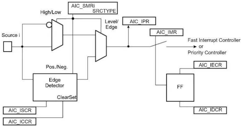
flowchart
graph TD
    Source_i["Source i"] --> AIC_SMRi["SRCTYPE"]
    AIC_SMRi -->|High/Low| B["Pos./Neg."]
    B --> C["Edge Detector"]
    C --> D["ClearSet"]
    D --> E["AIC_ISCR"]
    D --> F["AIC_ICCR"]
    AIC_SMRi --> G["Level/Edge"]
    G --> H["AIC_IPR"]
    G --> I["AIC_IMR"]
    I --> J["FF"]
    J --> K["AIC_IDCR"]
    J --> L["AIC_IECR"]
    J --> M["Fast Interrupt Controller or Priority Controller"]
16.8.2 Interrupt Latencies
Global interrupt latencies depend on several parameters, including:
• The time the software masks the interrupts
- Occurrence, either at the processor level or at the AIC level
- The execution time of the instruction in progress when the interrupt occurs
- The treatment of higher priority interrupts and the resynchronization of the hardware signals
This section addresses hardware resynchronizations only. It gives details about the latency times between the events on an external interrupt leading to a valid interrupt (edge or level) or the assertion of an internal interrupt source and the assertion of the nIRQ or nFIQ line on the processor. The resynchronization time depends on the programming of the interrupt source and on its type (internal or external). For the standard interrupt, resynchronization times are given assuming there is no higher priority in progress.
The PIO Controller multiplexing has no effect on the interrupt latencies of the external interrupt sources.
16.8.2.1 External Interrupt Edge Triggered Source
Figure 16-6: External Interrupt Edge Triggered Source
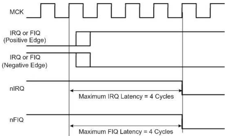
text_image
MCK IRQ or FIQ (Positive Edge) IRQ or FIQ (Negative Edge) nIRQ Maximum IRQ Latency = 4 Cycles nFIQ Maximum FIQ Latency = 4 Cycles16.8.2.2 External Interrupt Level Sensitive Source
Figure 16-7: External Interrupt Level Sensitive Source

text_image
MCK IRQ or FIQ (High Level) IRQ or FIQ (Low Level) nIRQ Maximum IRQ Latency = 3 Cycles nFIQ Maximum FIQ Latency = 3 Cycles16.8.2.3 Internal Interrupt Edge Triggered Source
Figure 16-8: Internal Interrupt Edge Triggered Source
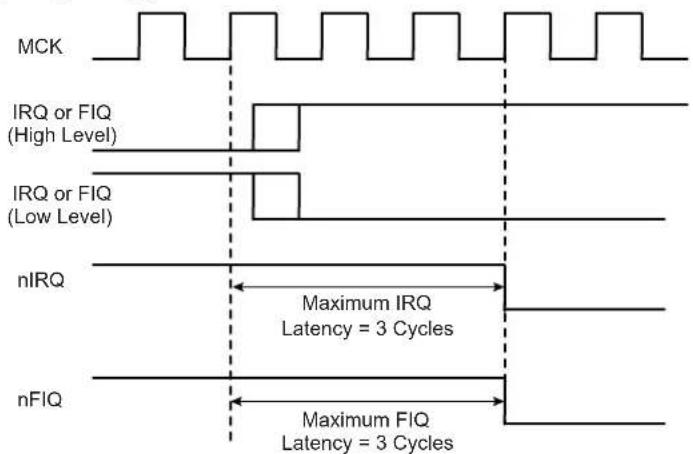
text_image
MCK IRQ or FIQ (High Level) IRQ or FIQ (Low Level) nIRQ Maximum IRQ Latency = 3 Cycles nFIQ Maximum FIQ Latency = 3 Cycles16.8.2.4 Internal Interrupt Level Sensitive Source
Figure 16-9: Internal Interrupt Level Sensitive Source

text_image
MCK nIRQ Maximum IRQ Latency = 3.5 Cycles Peripheral Interrupt Becomes Active16.8.3 Normal Interrupt
16.8.3.1 Priority Controller
An 8-level priority controller drives the nIRQ line of the processor, depending on the interrupt conditions occurring on the interrupt sources 1 to 127 (except for those programmed in Fast Forcing).
Each interrupt source has a programmable priority level of 7 to 0, which is user-definable by writing the PRIOR field of AIC_SMR (Source Mode Register). Level 7 is the highest priority and level 0 the lowest.
As soon as an interrupt condition occurs, as defined by the SRCTYPE field in AIC_SMR (Source Mode Register), the nIRQ line is asserted. As a new interrupt condition might have happened on other interrupt sources since the nIRQ has been asserted, the priority controller determines the current interrupt at the time AIC_IVR (Interrupt Vector Register) is read. The read of AIC_IVR is the entry point of the interrupt handling which allows the AIC to consider that the interrupt has been taken into account by the software.
The current priority level is defined as the priority level of the current interrupt.
If several interrupt sources of equal priority are pending and enabled when AIC_IVR is read, the interrupt with the lowest interrupt source number is serviced first.
The nIRQ line can be asserted only if an interrupt condition occurs on an interrupt source with a higher priority. If an interrupt condition happens (or is pending) during the interrupt treatment in progress, it is delayed until the software indicates to the AIC the end of the current service by writing AIC_EOICR (End of Interrupt Command Register). The write of AIC_EOICR is the exit point of the interrupt handling.
16.8.3.2 Interrupt Nesting
The priority controller utilizes interrupt nesting in order for the high priority interrupt to be handled during the service of lower priority interrupts. This requires the interrupt service routines of the lower interrupts to re-enable the interrupt at the processor level.
When an interrupt of a higher priority happens during an already occurring interrupt service routine, the nIRQ line is re-asserted. If the interrupt is enabled at the core level, the current execution is interrupted and the new interrupt service routine should read AIC_IVR. At this time, the current interrupt number and its priority level are pushed into an embedded hardware stack, so that they are saved and restored when the higher priority interrupt servicing is finished and AIC_EOICR is written.
The AIC is equipped with an 8-level wide hardware stack in order to support up to eight interrupt nestings to match the eight priority levels.
16.8.3.3 Interrupt Handlers
This section gives an overview of the fast interrupt handling sequence when using the AIC. It is assumed that the programmer understands the architecture of the ARM processor, and especially the Processor Interrupt modes and the associated status bits.
It is assumed that:
- The Advanced Interrupt Controller has been programmed, AIC_SVR registers are loaded with corresponding interrupt service routine addresses and interrupts are enabled.
- The instruction at the ARM interrupt exception vector address is required to work with the vectoring. Load the PC with the absolute address of the interrupt handler.
When nIRQ is asserted, if the bit "I" of CPSR is 0, the sequence is as follows:
-
The CPSR is stored in SPSR_irq, the current value of the Program Counter is loaded in the Interrupt link register (R14_irq) and the Program Counter (R15) is loaded with 0x18. In the following cycle during fetch at address 0x1C, the ARM core adjusts R14_irq, decrementing it by four.
-
The ARM core enters Interrupt mode, if it has not already done so.
-
When the instruction loaded at address 0x18 is executed, the program counter is loaded with the value read in AIC_IVR. Reading AIC_IVR has the following effects:
-
Sets the current interrupt to be the pending and enabled interrupt with the highest priority. The current level is the priority level of the current interrupt.
- De-asserts the nIRQ line on the processor. Even if vectoring is not used, AIC_IVR must be read in order to de-assert nIRQ.
- Automatically clears the interrupt, if it has been programmed to be edge-triggered.
- Pushes the current level and the current interrupt number on to the stack.
-
Returns the value written in AIC_SVR corresponding to the current interrupt.
-
The previous step has the effect of branching to the corresponding interrupt service routine. This should start by saving the link register (R14_irq) and SPSR_IRQ. The link register must be decremented by four when it is saved if it is to be restored directly into the program counter at the end of the interrupt. For example, the instruction SUB PC, LR, #4 may be used.
-
Further interrupts can then be unmasked by clearing the "I" bit in CPSR, allowing re-assertion of the nIRQ to be taken into account by the core. This can happen if an interrupt with a higher priority than the current interrupt occurs.
-
The interrupt handler can then proceed as required, saving the registers that will be used and restoring them at the end. During this
phase, an interrupt of higher priority than the current level will restart the sequence from step 1.
Note: If the interrupt is programmed to be level-sensitive, the source of the interrupt must be cleared during this phase.
-
The "I" bit in CPSR must be set in order to mask interrupts before exiting to ensure that the interrupt is completed in an orderly manner.
-
The End of Interrupt Command Register (AIC_EOICR) must be written in order to indicate to the AIC that the current interrupt is finished. This causes the current level to be popped from the stack, restoring the previous current level if one exists on the stack. If another interrupt is pending, with lower or equal priority than the old current level but with higher priority than the new current level, the nIRQ line is re-asserted, but the interrupt sequence does not immediately start because the "I" bit is set in the core. SPSR_irq is restored. Finally, the saved value of the link register is restored directly into the PC. This has the effect of returning from the interrupt to whatever was being executed before, and of loading the CPSR with the stored SPSR, masking or unmasking the interrupts depending on the state saved in SPSR_irq.
Note: The "I" bit in SPSR is significant. If it is set, it indicates that the ARM core was on the verge of masking an interrupt when the mask instruction was interrupted. Hence, when SPSR is restored, the mask instruction is completed (interrupt is masked).
16.8.4 Fast Interrupt
16.8.4.1 Fast Interrupt Source
Interrupt source 0 is the only source which can raise a fast interrupt request to the processor except if fast forcing is used. Interrupt source 0 is generally connected to a FIQ pin of the product, either directly or through a PIO Controller.
16.8.4.2 Fast Interrupt Control
The fast interrupt logic of the AIC has no priority controller. The mode of interrupt source 0 is programmed with AIC_SMR and INTSEL = 0; the PRIOR field of this register is not used even if it reads what has been written. The SRCTYPE field of AIC_SMR enables programming the fast interrupt source to be positive-edge triggered or negative-edge triggered or high-level sensitive or low-level sensitive.
Writing 0x1 in AIC_IECR (Interrupt Enable Command Register) and AIC_IDCR (Interrupt Disable Command Register) respectively enables and disables the fast interrupt when INTSEL = 0. Bit 0 of AIC_IMR indicates whether the fast interrupt is enabled or disabled.
16.8.4.3 Fast Interrupt Handlers
This section gives an overview of the fast interrupt handling sequence when using the AIC. It is assumed that the programmer understands the architecture of the ARM processor, and especially the Processor Interrupt modes and associated status bits.
Assuming that:
- The Advanced Interrupt Controller has been programmed, AIC_SVR is loaded with the fast interrupt service routine address, and interrupt source 0 is enabled.
- The Instruction at address 0x1C (FIQ exception vector address) is required to vector the fast interrupt. Load the PC with the absolute address of the interrupt handler.
- The user does not need nested fast interrupts.
When nFIQ is asserted, if bit "F" of CPSR is 0, the sequence is:
- The CPSR is stored in SPSR_fiq, the current value of the program counter is loaded in the FIQ link register (R14_FIQ) and the program counter (R15) is loaded with 0x1C. In the following cycle, during fetch at address 0x20, the ARM core adjusts R14_fiq, decrementing it by four.
- The ARM core enters FIQ mode.
When the instruction loaded at address 0x1C is executed, the program counter is loaded with the value read in AIC_FVR. Reading AIC_FVR has the effect of automatically clearing the fast interrupt, if it has been programmed to be edge-triggered. In this case only, it de-asserts the nFIQ line on the processor.
- The previous step enables branching to the corresponding interrupt service routine. It is not necessary to save the link register R14_fiq and SPSR_fiq if nested fast interrupts are not needed.
- The Interrupt Handler can then proceed as required. It is not necessary to save registers R8 to R13 because the FIQ mode has its own dedicated registers and registers R8 to R13 are banked. The other registers, R0 to R7, must be saved before being used, and restored at the end (before the next step).
Note: If the fast interrupt is programmed to be level-sensitive, the source of the interrupt must be cleared during this phase in order to de-assert interrupt source 0.
- Finally, Link Register R14_fiq is restored into the PC after decrementing it by four (with instruction SUB PC, LR, #4 for example). This has the effect of returning from the interrupt to whatever was being executed before, loading the CPSR with the SPSR and masking or unmasking the fast interrupt depending on the state saved in the SPSR.
Note: The "F" bit in SPSR is significant. If it is set, it indicates that the ARM core was just about to mask FIQ interrupts when the mask instruction was interrupted. Hence, when the SPSR is restored, the interrupted instruction is completed (FIQ is masked).
Another way to handle the fast interrupt is to map the interrupt service routine at the address of the ARM vector 0x1C. This method does not use vectoring, so that reading AIC_FVR must be performed at the very beginning of the handler operation. However, this method saves the execution of a branch instruction.
16.8.4.4 Fast Forcing
The Fast Forcing feature of the advanced interrupt controller provides redirection of any normal Interrupt source on the fast interrupt controller.
Fast Forcing is enabled or disabled by writing to the Fast Forcing Enable Register (AIC_FFER) and the Fast Forcing Disable Register (AIC_FFDR). Writing to these registers results in an update of the Fast Forcing Status Register (AIC_FFSR) that controls the feature for each internal or external interrupt source.
When Fast Forcing is disabled, the interrupt sources are handled as described in the previous sections.
When Fast Forcing is enabled, the edge/level programming and, in certain cases, edge detection of the interrupt source is still active but the source cannot trigger a normal interrupt to the processor and is not seen by the priority handler.
If the interrupt source is programmed in Level-Sensitive mode and an active level is sampled, Fast Forcing results in the assertion of the nFIQ line to the core.
If the interrupt source is programmed in Edge-Triggered mode and an active edge is detected, Fast Forcing results in the assertion of the nFIQ line to the core.
The Fast Forcing feature does not affect the Source 0 pending bit in AIC_IPR.
The FIQ Vector Register (AIC_FVR) reads the contents of Source Vector Register 0 (AIC_SVR0), whatever the source of the fast interrupt may be. The read of the FVR does not clear Source 0 when the fast forcing feature is used and the interrupt source should be cleared by writing to AIC_ICCR.
All enabled and pending interrupt sources that have the fast forcing feature enabled and that are programmed in Edge-Triggered mode must be cleared by writing to the Interrupt Clear Command Register. In doing so, they are cleared independently and thus lost interrupts are prevented.
The read of AIC_IVR does not clear the source that has the fast forcing feature enabled.
Source 0, reserved to the fast interrupt, continues operating normally and becomes one of the Fast Interrupt sources.
Figure 16-10: Fast Forcing
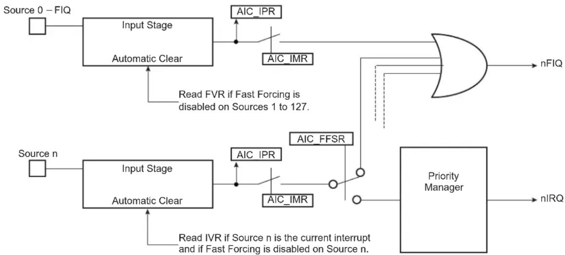
flowchart
graph TD
    Source0["Source 0 – FIQ"] --> A1["Input Stage"]
    A1 --> A2["Automatic Clear"]
    A2 --> A3["AIC_IPR"]
    A3 --> A4["AIC_IMR"]
    A4 --> A5["AND"]
    A5 --> nFIQ["nFIQ"]
    Sourcen["Source n"] --> A6["Input Stage"]
    A6 --> A7["Automatic Clear"]
    A7 --> A8["AIC_IPR"]
    A8 --> A9["AIC_IMR"]
    A9 --> A10["AIC_FFSR"]
    A10 --> A11["AND"]
    A11 --> A12["Priority Manager"]
    A12 --> nIRQ["nIRQ"]
    Note1["Read FVR if Fast Forcing is disabled on Sources 1 to 127."] --> A2
    Note2["Read IVR if Source n is the current interrupt and if Fast Forcing is disabled on Source n."] --> A7
16.8.5 Protect Mode
The Protect mode is used to read the Interrupt Vector Register without performing the associated automatic operations. This is necessary when working with a debug system. When a debugger, working either with a Debug Monitor or the ARM processor's ICE, stops the applications and updates the opened windows, it might read the AIC User Interface and thus the IVR. This has adverse consequences:
- If an enabled interrupt with a higher priority than the current one is pending, it is stacked.
- If there is no enabled pending interrupt, the spurious vector is returned.
In either case, an End of Interrupt command is necessary to acknowledge and restore the context of the AIC. This operation is generally not performed by the debug system, as the debug system would become strongly intrusive and cause the application to enter an undesired state.
This is avoided by using the Protect mode. Writing PROT in AIC_DCR (Debug Control Register) at 0x1 enables the Protect mode.
When the Protect mode is enabled, the AIC performs interrupt stacking only when a write access is performed on AIC_IVR. Therefore, the Interrupt Service Routines must write (arbitrary data) to AIC_IVR just after reading it. The new context of the AIC, including the value of AIC_ISR, is updated with the current interrupt only when AIC_IVR is written.
An AIC_IVR read on its own (e.g., by a debugger) modifies neither the AIC context nor AIC_ISR. Extra AIC_IVR reads perform the same operations. However, it is recommended to not stop the processor between the read and the write of AIC_IVR of the interrupt service routine to make sure the debugger does not modify the AIC context.
To summarize, in normal operating mode, the read of AIC_IVR performs the following operations within the AIC:
- Calculates active interrupt (higher than current or spurious).
- Determines and returns the vector of the active interrupt.
- Memorizes the interrupt.
- Pushes the current priority level onto the internal stack.
- Acknowledges the interrupt.
However, while the Protect mode is activated, only operations 1 to 3 are performed when AIC_IVR is read. Operations 4 and 5 are only performed by the AIC when AIC_IVR is written.
Software that has been written and debugged using the Protect mode runs correctly in normal mode without modification. However, in normal mode, the AIC_IVR write has no effect and can be removed to optimize the code.
16.8.6 Spurious Interrupt
The Advanced Interrupt Controller features a protection against spurious interrupts. A spurious interrupt is defined as being the assertion of an interrupt source long enough for the AIC to assert the nIRQ, but no longer present when AIC_IVR is read. This is most prone to occur when:
- An external interrupt source is programmed in Level-Sensitive mode and an active level occurs for only a short time.
- An internal interrupt source is programmed in level-sensitive and the output signal of the corresponding embedded peripheral is activated for a short time (as is the case for the watchdog).
- An interrupt occurs just a few cycles before the software begins to mask it, thus resulting in a pulse on the interrupt source.
The AIC detects a spurious interrupt at the time AIC_IVR is read while no enabled interrupt source is pending. When this happens, the AIC returns the value stored by the programmer in the Spurious Vector Register (AIC_SPU). The programmer must store the address of a spurious interrupt handler in AIC_SPU as part of the application, to enable an as fast as possible return to the normal execution flow. This handler writes in AIC_EOICR and performs a return from interrupt.
16.8.7 General Interrupt Mask
The AIC features a General Interrupt Mask bit (GMSK in AIC_DCR) to prevent interrupts from reaching the processor. Both the nIRQ and the nFIQ lines are driven to their inactive state if the GMSK is set. However, this mask does not prevent waking up the processor if it has entered Idle mode. This function facilitates synchronizing the processor on a next event and, as soon as the event occurs, performs subsequent operations without having to handle an interrupt. It is strongly recommended to use this mask with caution.
16.8.8 Register Write Protection
To prevent any single software error from corrupting AIC behavior, certain registers in the address space can be write-protected by setting the WPEN bit in the AIC Write Protection Mode Register (AIC_WPMR).
If a write access to a write-protected register is detected, the WPVS flag in the AIC Write Protection Status Register (AIC_WPSR) is set and the field WPVSRC indicates the register in which the write access has been attempted.
The WPVS bit is automatically cleared after reading AIC_WPSR.
The following registers can be write-protected:
• AIC Source Mode Register
• AIC Source Vector Register
• AIC Spurious Interrupt Vector Register
• AIC Debug Control Register
16.9 Advanced Interrupt Controller (AIC) User Interface
Table 16-3: Register Mapping
| Offset Register Name Access Reset | ||||
| 0x00 Source Select | Register AIC_SSR Read/Write 0x0 | |||
| 0x04 | Source Mode Register | AIC_SMR | Read/Write | 0x0 |
| 0x08 Source Vector | Register AIC_SVR Read/Write 0x0 | |||
| 0x0C | Reserved | -- - | ||
| 0x10 Interrupt Vector Register | AIC_IVR | Read-only | 0x0 | |
| 0x14 FIQ Vector Register | AIC_FVR | Read-only | 0x0 | |
| 0x18 Interrupt Status Register | AIC_ISR | Read-only | 0x0 | |
| 0x1C | Reserved | -- - | ||
| 0x20 Interrupt Pending Register 0 (2) | AIC_IPR0 | Read-only | 0x0^(1) | |
| 0x24 Interrupt Pending Register 1 (2) | AIC_IPR1 | Read-only | 0x0^(1) | |
| 0x28 Interrupt Pending Register 2 (2) | AIC_IPR2 | Read-only | 0x0^(1) | |
| 0x2C | Interrupt Pending Register 3^(2) | AIC_IPR3 | Read-only | 0x0^(1) |
| 0x30 Interrupt Mask Register | AIC_IMR | Read-only | 0x0 | |
| 0x34 Core Interrupt Status Register | AIC_CISR | Read-only | 0x0 | |
| 0x38 | End of Interrupt Command Register | AIC_EOICR | Write-only | - |
| 0x3C | Spurious Interrupt Vector Register | AIC_SPU | Read/Write | 0x0 |
| 0x40 | Interrupt Enable Command Register | AIC_IECR | Write-only | - |
| 0x44 | Interrupt Disable Command Register | AIC_IDCR | Write-only | - |
| 0x48 | Interrupt Clear Command Register | AIC_ICCR | Write-only | - |
| 0x4C | Interrupt Set Command Register | AIC_ISCR | Write-only | - |
| 0x50 | Fast Forcing Enable Register | AIC_FFER | Write-only | - |
| 0x54 | Fast Forcing Disable Register | AIC_FFDR | Write-only | - |
| 0x58 | Fast Forcing Status Register | AIC_FFSR | Read-only | 0x0 |
| 0x5C | Reserved | -- - | ||
| 0x60–0x68 | Reserved | -- - | ||
| 0x6C | Debug Control Register | AIC_DCR | Read/Write | 0x0 |
| 0x70–0xE0 | Reserved | -- - | ||
| 0xE4 | Write Protection Mode Register | AIC_WPMR | Read/Write | 0x0 |
| 0xE8 | Write Protection Status Register | AIC_WPSR | Read-only | 0x0 |
| 0xEC–0xFC | Reserved | -- - | ||
Note 1: The reset value of this register depends on the level of the external interrupt source. All other sources are cleared at reset, thus not pending.
2: PID2...PID127 bit fields refer to the identifiers as defined in the Peripheral Identifiers section.
16.9.1 AIC Source Select Register
Name:AIC_SSR
Address:0xFFFF000
Access: Read/Write
31 30 29 28 27 26 25 24
| - | - | - | - | - | - | - | - |
23 22 21 20 19 18 17 16
| - | - | - | - | - | - | - | - |
15 14 13 12 11 10 9 8
| - | - | - | - | - | - | - | - |
| 7 | 6 | 5 | 4 | 3 | 2 | 1 | 0 |
| - | I | N |
INTSEL: Interrupt Line Selection
0-127 = Selects the interrupt line to handle.
See Section 16.8.1.1 Interrupt Source Mode.
16.9.2 AIC Source Mode Register
Name:AIC_SMR
Address:0xFFFF004
Access: Read/Write
31 30 29 28 27 26 25 24
| - | - | - | - | - | - | - | - |
23 22 21 20 19 18 17 16
| - | - | - | - | - | - | - | - |
15 14 13 12 11 10 9 8
| - | - | - | - | - | - | - | - |
| 7 | 6 | 5 | 4 | 3 | 2 | 1 | 0 |
| - SRCTYPE -- PRIOR |
This register can only be written if the WPEN bit is cleared in the AIC Write Protection Mode Register.
PRIOR: Priority Level
Programs the priority level of the source selected by INTSEL except FIQ source (source 0).
The priority level can be between 0 (lowest) and 7 (highest).
The priority level is not used for the FIQ.
SRCTYPE: Interrupt Source Type
The active level or edge is not programmable for the internal interrupt source selected by INTSEL.
| Value Name Description | ||
| 0 INT_LEVEL_SENSITIVE | High level Sensitive for internal sourceLow level Sensitive for external source | |
| 1 INT_EDGE_TRIGGERED | Positive edge triggered for internal sourceNegative edge triggered for external source | |
| 2 EXT_HIGH_LEVEL | High level Sensitive for internal sourceHigh level Sensitive for external source | |
| 3 EXT_POSITIVE_EDGE | Positive edge triggered for internal sourcePositive edge triggered for external source | |
16.9.3 AIC Source Vector Register
Name:AIC_SVR
Address:0xFFFF008
Access:Read/Write
31 30 29 28 27 26 25 24
VECTOR
23 22 21 20 19 18 17 16
VECTOR
15 14 13 12 11 10 9 8
VECTOR
7 6 5 4 3 2 1 0
VECTOR
This register can only be written if the WPEN bit is cleared in the AIC Write Protection Mode Register.
VECTOR: Source Vector
The user may store in this register the address of the corresponding handler for the interrupt source selected by INTSEL.
16.9.4 AIC Interrupt Vector Register
Name: AIC_IVR
Address:0xFFFF010
Access:Read-only
31 30 29 28 27 26 25 24
| IRQV | |||||||
| 23 22 21 20 19 18 17 16 | |||||||
| IRQV | |||||||
| 15 14 13 12 11 10 9 8 | |||||||
| IRQV | |||||||
| 7 | 6 | 5 | 4 | 3 | 2 | 1 | 0 |
| IRQV | |||||||
IRQV: Interrupt Vector Register
The Interrupt Vector Register contains the vector programmed by the user in the Source Vector Register corresponding to the current interrupt.
The Source Vector Register is indexed using the current interrupt number when the Interrupt Vector Register is read.
When there is no current interrupt, the Interrupt Vector Register reads the value stored in AIC_SPU.
16.9.5 AIC FIQ Vector Register
Name: AIC_FVR
Address:0xFFFF014
Access:Read-only
31 30 29 28 27 26 25 24
| FIQV | |||||||
| 23 22 21 20 19 18 17 16 | |||||||
| FIQV | |||||||
| 15 14 13 12 11 10 9 8 | |||||||
| FIQV | |||||||
| 7 | 6 | 5 | 4 | 3 | 2 | 1 | 0 |
| FIQV | |||||||
FIQV: FIQ Vector Register
The FIQ Vector Register contains the vector programmed by the user in the Source Vector Register when INTSEL = 0. When there is no fast interrupt, the FIQ Vector Register reads the value stored in AIC_SPU.
16.9.6 AIC Interrupt Status Register
Name: AIC_ISR
Address:0xFFFF018
Access:Read-only
31 30 29 28 27 26 25 24
| - | - | - | - | - | - | - | - |
23 22 21 20 19 18 17 16
| - | - | - | - | - | - | - | - |
15 14 13 12 11 10 9 8
| - | - | - | - | - | - | - | - |
| 7 | 6 | 5 | 4 | 3 | 2 | 1 | 0 |
| - |
R
IRQID: Current Interrupt Identifier
The Interrupt Status Register returns the current interrupt source number.
16.9.7 AIC Interrupt Pending Register 0
Name: AIC_IPR0
Address:0xFFFF020
Access:Read-only
31 30 29 28 27 26 25 24
| PID31 PID30 PID29 PID28 PID27 PID26 PID25 PID24 |
23 22 21 20 19 18 17 16
| PID23 PID2 | 2 PID21 PID20 | PID19 PID18 PID | 7 PID16 |
15 14 13 12 11 10 9 8
| PID15 PID14 PID13 PID12 PID11 PID10 PID9 PID8 |
| 7 | 6 | 5 | 4 | 3 | 2 | 1 | 0 |
| PID7 PID6 | PID5 PID4 PID3 | PID2 SYS FIQ |
FIQ: Interrupt Pending
0: The corresponding interrupt is not pending.
1: The corresponding interrupt is pending.
SYS: Interrupt Pending
0: The corresponding interrupt is not pending.
1: The corresponding interrupt is pending.
PIDx: Interrupt Pending
0: The corresponding interrupt is not pending.
1: The corresponding interrupt is pending.
16.9.8 AIC Interrupt Pending Register 1
Name: AIC_IPR1
Address:0xFFFF024
Access:Read-only
31 30 29 28 27 26 25 24
| PID63 PID62 PID61 PID60 PID59 PID58 PID57 PID56 |
23 22 21 20 19 18 17 16
| PID55 PID54 PID53 PID52 PID51 PID50 PID49 PID48 |
15 14 13 12 11 10 9 8
| PID47 PID46 PID45 PID44 PID43 PID42 PID41 PID40 |
| 7 | 6 | 5 | 4 | 3 | 2 | 1 | 0 |
| PID39 PID38 PID37 PID36 PID35 PID34 PID33 PID32 |
PIDx: Interrupt Pending
0: The corresponding interrupt is not pending.
1: The corresponding interrupt is pending.
16.9.9 AIC Interrupt Pending Register 2
Name: AIC_IPR2
Address:0xFFFFF028
Access:Read-only
31 30 29 28 27 26 25 24
| PID95 PID94 PID93 PID92 PID91 PID90 PID89 PID88 |
23 22 21 20 19 18 17 16
| PID87 PID86 PID85 PID84 PID83 PID82 PID81 PID80 |
15 14 13 12 11 10 9 8
| PID79 PID78 PID77 PID76 PID75 PID74 PID73 PID72 |
| 7 | 6 | 5 | 4 | 3 | 2 | 1 | 0 |
| PID71 PID70 PID69 PID68 PID67 PID66 PID65 PID64 |
PIDx: Interrupt Pending
0: The corresponding interrupt is not pending.
1: The corresponding interrupt is pending.
16.9.10 AIC Interrupt Pending Register 3
Name: AIC_IPR3
Address:0xFFFFF02C
Access:Read-only
31 30 29 28 27 26 25 24
| PID127 PID1 | 126 PID125 PID1 | 124 PID123 PID1 | 122 PID121 PID1 | 0 |
23 22 21 20 19 18 17 16
| PID119 PID | 118 PID117 PID | 116 PID115 PID1 | 14 PID113 PID1 | 2 |
15 14 13 12 11 10 9 8
| PID111 PID | 110 PID109 PID | 108 PID107 PID106 | PID105 PID104 |
| 7 | 6 | 5 | 4 | 3 | 2 | 1 | 0 |
| PID103 PID | 102 PID101 PID | 100 PID99 PID98 | PID97 PID96 |
PIDx: Interrupt Pending
0: The corresponding interrupt is not pending.
1: The corresponding interrupt is pending.
16.9.11 AIC Interrupt Mask Register
Name:AIC_IMR
Address:0xFFFF030
Access:Read-only
31 30 29 28 27 26 25 24
| - | - | - | - | - | - | - | - |
23 22 21 20 19 18 17 16
| - | - | - | - | - | - | - | - |
15 14 13 12 11 10 9 8
| - | - | - | - | - | - | - | - |
| 7 | 6 | 5 | 4 | 3 | 2 | 1 | 0 |
| - | - | - | - | - | - | - | 1 |
INTM: Interrupt Mask
0: The interrupt source selected by INTSEL is disabled.
1: The interrupt source selected by INTSEL is enabled.
16.9.12 AIC Core Interrupt Status Register
Name: AIC_CISR
Address:0xFFFF034
Access:Read-only
31 30 29 28 27 26 25 24
| - | - | - | - | - | - | - | - |
23 22 21 20 19 18 17 16
| - | - | - | - | - | - | - | - |
15 14 13 12 11 10 9 8
| - | - | - | - | - | - | - | - |
| 7 | 6 | 5 | 4 | 3 | 2 | 1 | 0 |
| - | - | - | - | - | - | N | I |
NFIQ: NFIQ Status
0: nFIQ line is deactivated.
1: nFIQ line is active.
NIRQ: NIRQ Status
0: nIRQ line is deactivated.
1: nIRQ line is active.
16.9.13 AIC End of Interrupt Command Register
Name:AIC_EOICR
Address:0xFFFF038
Access:Write-only
31 30 29 28 27 26 25 24
| - | - | - | - | - | - | - | - |
23 22 21 20 19 18 17 16
| - | - | - | - | - | - | - | - |
15 14 13 12 11 10 9 8
| - | - | - | - | - | - | - | - |
| 7 | 6 | 5 | 4 | 3 | 2 | 1 | 0 |
| - | - | - | - | - | - | - | E |
ENDIT: Interrupt Processing Complete Command
The End of Interrupt Command Register is used by the interrupt routine to indicate that the interrupt treatment is complete. Any value can be written because it is only necessary to make a write to this register location to signal the end of interrupt treatment.
16.9.14 AIC Spurious Interrupt Vector Register
Name:AIC_SPU
Address:0xFFFFF03C
Access:Read/Write
31 30 29 28 27 26 25 24
| SIVR | |||||||
| 23 22 21 20 19 18 17 16 | |||||||
| SIVR | |||||||
| 15 14 13 12 11 10 9 8 | |||||||
| SIVR | |||||||
| 7 | 6 | 5 | 4 | 3 | 2 | 1 | 0 |
| SIVR | |||||||
This register can only be written if the WPEN bit is cleared in the AIC Write Protection Mode Register.
SIVR: Spurious Interrupt Vector Register
The user may store the address of a spurious interrupt handler in this register. The written value is returned in AIC_IVR in case of a spurious interrupt, or in AIC_FVR in case of a spurious fast interrupt.
16.9.15 AIC Interrupt Enable Command Register
Name: AIC_IECR
Address:0xFFFF040
Access:Write-only
31 30 29 28 27 26 25 24
| - | - | - | - | - | - | - | - |
23 22 21 20 19 18 17 16
| - | - | - | - | - | - | - | - |
15 14 13 12 11 10 9 8
| - | - | - | - | - | - | - | - |
| 7 | 6 | 5 | 4 | 3 | 2 | 1 | 0 |
| - | - | - | - | - | - | - | 1 |
INTEN: Interrupt Enable
0: No effect.
1: Enables the interrupt source selected by INTSEL.
16.9.16 AIC Interrupt Disable Command Register
Name: AIC_IDCR
Address:0xFFFF044
Access:Write-only
31 30 29 28 27 26 25 24
| - | - | - | - | - | - | - | - |
23 22 21 20 19 18 17 16
| - | - | - | - | - | - | - | - |
15 14 13 12 11 10 9 8
| - | - | - | - | - | - | - | - |
| 7 | 6 | 5 | 4 | 3 | 2 | 1 | 0 |
| - | - | - | - | - | - | - | 1 |
INTD: Interrupt Disable
0: No effect.
1: Disables the interrupt source selected by INTSEL.
16.9.17 AIC Interrupt Clear Command Register
Name:AIC_ICCR
Address:0xFFFF048
Access:Write-only
31 30 29 28 27 26 25 24
| - | - | - | - | - | - | - | - |
23 22 21 20 19 18 17 16
| - | - | - | - | - | - | - | - |
15 14 13 12 11 10 9 8
| - | - | - | - | - | - | - | - |
| 7 | 6 | 5 | 4 | 3 | 2 | 1 | 0 |
| - | - | - | - | - | - | - | 1 |
INTCLR: Interrupt Clear
Clears one the following depending on the setting of the INTSEL bit FIQ, SYS, PID2-PID127
0: No effect.
1: Clears the interrupt source selected by INTSEL.
16.9.18 AIC Interrupt Set Command Register
Name: AIC_ISCR
Address:0xFFFFF04C
Access:Write-only
31 30 29 28 27 26 25 24
| - | - | - | - | - | - | - | - |
23 22 21 20 19 18 17 16
| - | - | - | - | - | - | - | - |
15 14 13 12 11 10 9 8
| - | - | - | - | - | - | - | - |
| 7 | 6 | 5 | 4 | 3 | 2 | 1 | 0 |
| - | - | - | - | - | - | - | 1 |
INTSET: Interrupt Set
0: No effect.
1: Sets the interrupt source selected by INTSEL.
16.9.19 AIC Fast Forcing Enable Register
Name:AIC_FFER
Address:0xFFFF050
Access:Write-only
31 30 29 28 27 26 25 24
| - | - | - | - | - | - | - | - |
23 22 21 20 19 18 17 16
| - | - | - | - | - | - | - | - |
15 14 13 12 11 10 9 8
| - | - | - | - | - | - | - | - |
| 7 | 6 | 5 | 4 | 3 | 2 | 1 | 0 |
| - | - | - | - | - | - | - | F |
FFEN: Fast Forcing Enable
0: No effect.
1: Enables the fast forcing feature on the interrupt source selected by INTSEL.
16.9.20 AIC Fast Forcing Disable Register
Name:AIC_FFDR
Address:0xFFFFF054
Access:Write-only
31 30 29 28 27 26 25 24
| - | - | - | - | - | - | - | - |
23 22 21 20 19 18 17 16
| - | - | - | - | - | - | - | - |
15 14 13 12 11 10 9 8
| - | - | - | - | - | - | - | - |
| 7 | 6 | 5 | 4 | 3 | 2 | 1 | 0 |
| - | - | - | - | - | - | - | F |
FFDIS: Fast Forcing Disable
0: No effect.
1: Disables the Fast Forcing feature on the interrupt source selected by INTSEL.
16.9.21 AIC Fast Forcing Status Register
Name:AIC_FFSR
Address:0xFFFF058
Access:Read-only
31 30 29 28 27 26 25 24
| - | - | - | - | - | - | - | - |
23 22 21 20 19 18 17 16
| - | - | - | - | - | - | - | - |
15 14 13 12 11 10 9 8
| - | - | - | - | - | - | - | - |
| 7 | 6 | 5 | 4 | 3 | 2 | 1 | 0 |
| - | - | - | - | - | - | - | F |
FFS: Fast Forcing Status
0: The Fast Forcing feature is disabled on the interrupt source selected by INTSEL.
1: The Fast Forcing feature is enabled on the interrupt source selected by INTSEL.
16.9.22 AIC Debug Control Register
Name:AIC_DCR
Address:0xFFFFF06C
Access:Read/Write
31 30 29 28 27 26 25 24
| - | - | - | - | - | - | - | - |
23 22 21 20 19 18 17 16
| - | - | - | - | - | - | - | - |
15 14 13 12 11 10 9 8
| - | - | - | - | - | - | - | - |
| 7 | 6 | 5 | 4 | 3 | 2 | 1 | 0 |
| - | - | - | - | - | - | G | M |
This register can only be written if the WPEN bit is cleared in the AIC Write Protection Mode Register.
PROT: Protection Mode
0: The Protection mode is disabled.
1: The Protection mode is enabled.
GMSK: General Interrupt Mask
0: The nIRQ and nFIQ lines are normally controlled by the AIC.
1: The nIRQ and nFIQ lines are tied to their inactive state.
16.9.23 AIC Write Protection Mode Register
Name:AIC_WPMR
Address:0xFFFFF0E4
Access: Read/Write
31 30 29 28 27 26 25 24
| WPKEY |
23 22 21 20 19 18 17 16
| WPKEY |
15 14 13 12 11 10 9 8
| WPKEY |
| 7 | 6 | 5 | 4 | 3 | 2 | 1 | 0 |
| - | - | - | - | - | - | - | W |
WPEN: Write Protection Enable
0: Disables the write protection if WPKEY corresponds to 0x414943 ("AIC" in ASCII).
1: Enables the write protection if WPKEY corresponds to 0x414943 ("AIC" in ASCII).
See Section 16.8.8 Register Write Protection for the list of registers that can be protected.
WPKEY: Write Protection Key
| Value Name | Description | |
| 0x414943 | PASSWD | Writing any other value in this field aborts the write operation of the WPEN bit.Always reads as 0. |
16.9.24 AIC Write Protection Status Register
Name:AIC_WPSR
Address:0xFFFFF0E8
Access:Read-only
31 30 29 28 27 26 25 24
| - | - | - | - | - | - | - | - |
23 22 21 20 19 18 17 16
| WPVSRC |
15 14 13 12 11 10 9 8
| WPVSRC |
| 7 | 6 | 5 | 4 | 3 | 2 | 1 | 0 |
| - | - | - | - | - | - | - | W |
WPVS: Write Protection Violation Status
0: No write protection violation has occurred since the last read of AIC_WPSR.
1: A write protection violation has occurred since the last read of AIC_WPSR. If this violation is an unauthorized attempt to write a protected register, the associated violation is reported into field WPVSRC.
WPVSRC: Write Protection Violation Source
When WPVS = 1, WPVSRC indicates the register address offset at which a write access has been attempted.
17. Watchdog Timer (WDT)
17.1 Description
The Watchdog Timer (WDT) is used to prevent system lock-up if the software becomes trapped in a deadlock. It features a 12-bit down counter that allows a watchdog period of up to 16 seconds (slow clock around 32 kHz). It can generate a general reset or a processor reset only. In addition, it can be stopped while the processor is in Debug mode or Sleep mode (Idle mode).
17.2 Embedded Characteristics
• 12-bit Key-protected Programmable Counter
- Watchdog Clock is Independent from Processor Clock
- Provides Reset or Interrupt Signals to the System
- Counter May Be Stopped while the Processor is in Debug State or in Idle Mode
17.3 Block Diagram
Figure 17-1: Watchdog Timer Block Diagram

flowchart
graph TD
    A["write WDT_MR"] --> B["WDRSTT"]
    B --> C["AND"]
    C --> D["1 0"]
    D --> E["12-bit Down Counter"]
    E --> F["Current Value"]
    F --> G["= 0"]
    G --> H["WDUNF"]
    H --> I["set"]
    I --> J["WDERR"]
    J --> K["reset"]
    K --> L["read WDT_SR or reset"]
    M["WDT_CR"] --> B
    N["WDT_MR"] --> O["WDV"]
    O --> D
    P["SLCK"] --> Q["1/128"]
    Q --> F
    R["WDT_MR"] --> S["WDRSTEN"]
    S --> T["wdt_fault (to Reset Controller)"]
    U["WDT_MR"] --> V["WDFIEN"]
    V --> W["WDT_MR"]
    X["reload"] --> D
    Y["reload"] --> F
17.4 Functional Description
The Watchdog Timer is used to prevent system lock-up if the software becomes trapped in a deadlock. It is supplied with VDDCORE. It restarts with initial values on processor reset.
The watchdog is built around a 12-bit down counter, which is loaded with the value defined in the field WDV of the Mode register (WDT_MR). The Watchdog Timer uses the slow clock divided by 128 to establish the maximum watchdog period to be 16 seconds (with a typical slow clock of 32.768 kHz).
After a processor reset, the value of WDV is 0xFFFF, corresponding to the maximum value of the counter with the external reset generation enabled (field WDRSTEN at 1 after a backup reset). This means that a default watchdog is running at reset, i.e., at power-up. The user can either disable the WDT by setting bit WDT_MR.WDDIS or reprogram the WDT to meet the maximum watchdog period the application requires.
When setting the WDDIS bit, and while it is set, the fields WDV and WDD must not be modified.
If the watchdog is restarted by writing into the Control register (WDT_CR), WDT_MR must not be programmed during a period of time of three slow clock periods following the WDT_CR write access. In any case, programming a new value in WDT_MR automatically initiates a restart instruction.
WDT_MR can be written only once. Only a processor reset resets it. Writing WDT_MR reloads the timer with the newly programmed mode parameters.
In normal operation, the user reloads the watchdog at regular intervals before the timer underflow occurs, by setting bit WDT_CR.WDRSTT. The watchdog counter is then immediately reloaded from WDT_MR and restarted, and the slow clock 128 divider is reset and restarted. WDT_CR is write-protected. As a result, writing WDT_CR without the correct hard-coded key has no effect. If an underflow does occur, the "wdt_fault" signal to the Reset Controller is asserted if bit WDT_MR.WDRSTEN is set. Moreover, the bit WDUNF is set in the Status register (WDT_SR).
To prevent a software deadlock that continuously triggers the watchdog, the reload of the watchdog must occur while the watchdog counter is within a window between 0 and WDD. WDD is defined in WDT_MR.
Any attempt to restart the watchdog while the watchdog counter is between WDV and WDD results in a watchdog error, even if the watchdog is disabled. The bit WDT_SR.WDERR is updated and the "wdt_fault" signal to the Reset Controller is asserted.
Note that this feature can be disabled by programming a WDD value greater than or equal to the WDV value. In such a configuration, restarting the Watchdog Timer is permitted in the whole range [0; WDV] and does not generate an error. This is the default configuration on reset (the WDD and WDV values are equal).
The status bits WDUNF (Watchdog Underflow) and WDERR (Watchdog Error) trigger an interrupt, provided the bit WDT_MR.WDFIEN is set. The signal "wdt_fault" to the Reset Controller causes a watchdog reset if the WDRSTEN bit is set as already explained in the Reset Controller documentation. In this case, the processor and the Watchdog Timer are reset, and the WDERR and WDUNF flags are reset.
If a reset is generated or if WDT_SR is read, the status bits are reset, the interrupt is cleared, and the "wdt_fault" signal to the reset controller is deasserted.
Writing WDT_MR reloads and restarts the down counter.
While the processor is in debug state or in Sleep mode, the counter may be stopped depending on the value programmed for the bits WDIDLEHLT and WDDBGHLT in WDT_MR.
Figure 17-2: Watchdog Behavior

flowchart
graph TD
    A["FFF"] --> B["Normal behavior"]
    B --> C["Forbidden Window"]
    C --> D["WDD"]
    D --> E["Permitted Window"]
    E --> F["0"]
    G["Watchdog Fault"] --> H["..."]
    H --> I["WDD"]
    I --> J["Permitted Window"]
    J --> K["0"]
    L["Watchdog Error"] --> M["if WDRSTEN is 1"]
    M --> N["Watchdog Underflow"]
    N --> O["if WDRSTEN is 0"]
    O --> P["0"]
    Q["WDT_CR.WDRSTT=1"] --> R["End"]
17.5 Watchdog Timer (WDT) User Interface
| Offset Register | Name Access Reset | |||
| 0x00 Control Register WDT_CR Write-only – | ||||
| 0x04 Mode Register WDT_MR Read/Write Once | 0x3FFF_2FFF | |||
| 0x08 | Status Register | WDT_SR | Read-only | 0x0000_0000 |
17.5.1 Watchdog Timer Control Register
Name:WDT_CR
Address:0xFFFFFE40
Access:Write-only
31 30 29 28 27 26 25 24
| KEY | |||||||
| 23 22 21 20 19 18 17 16 | |||||||
| - | - | - | - | - | - | - | - |
| 15 14 13 12 11 10 9 8 | |||||||
| - | - | - | - | - | - | - | - |
| 7 | 6 | 5 | 4 | 3 | 2 | 1 | 0 |
| - | - | - | - | - | - | - | WDRSTT |
Note: The WDT_CR register values must not be modified within three slow clock periods following a restart of the watchdog performed by a write access in WDT_CR. Any modification will cause the watchdog to trigger an end of period earlier than expected.
WDRSTT: Watchdog Restart
0: No effect.
1: Restarts the watchdog if KEY is written to 0xA5.
KEY: Password
| Value | Name | Description |
| 0xA5 | PASSWD | Writing any other value in this field aborts the write operation. |
17.5.2 Watchdog Timer Mode Register
Name:WDT_MR
Address:0xFFFFFE44
Access: Read/Write Once
31 30 29 28 27 26 25 24
| --WDIDLEHLT WDDBGHLT | WDD |
23 22 21 20 19 18 17 16
| WDD | ||||||
| 15 14 13 12 | 11 | 10 | 9 8 | |||
| WDDIS | WDRPROC | WDRSTEN | WDFIEN | WDV | ||
| 7 | 6 | 5 | 4 | 3 | 2 | 1 |
| WDV | ||||||
Note 1: The first write access prevents any further modification of the value of this register. Read accesses remain possible.
2: The WDT_MR register values must not be modified within three slow clock periods following a restart of the watchdog performed by a write access in WDT_CR. Any modification will cause the watchdog to trigger an end of period earlier than expected.
WDV: Watchdog Counter Value
Defines the value loaded in the 12-bit watchdog counter.
WDFIEN: Watchdog Fault Interrupt Enable
0: A watchdog fault (underflow or error) has no effect on interrupt.
1: A watchdog fault (underflow or error) asserts interrupt.
WDRSTEN: Watchdog Reset Enable
0: A watchdog fault (underflow or error) has no effect on the resets.
1: A watchdog fault (underflow or error) triggers a watchdog reset.
WDRPROC: Watchdog Reset Processor
0: If WDRSTEN is 1, a watchdog fault (underflow or error) activates all resets.
1: If WDRSTEN is 1, a watchdog fault (underflow or error) activates the processor reset.
WDDIS: Watchdog Disable
0: Enables the Watchdog Timer.
1: Disables the Watchdog Timer.
Note: When setting the WDDIS bit, and while it is set, the fields WDV and WDD must not be modified.
WDD: Watchdog Delta Value
Defines the permitted range for reloading the Watchdog Timer.
If the Watchdog Timer value is less than or equal to WDD, setting bit WDT_CR.WDRSTT restarts the timer.
If the Watchdog Timer value is greater than WDD, setting bit WDT_CR.WDRSTT causes a watchdog error.
WDDBGHLT: Watchdog Debug Halt
0: The watchdog runs when the processor is in debug state.
1: The watchdog stops when the processor is in debug state.
WDIDLEHLT: Watchdog Idle Halt
0: The watchdog runs when the system is in idle state.
1: The watchdog stops when the system is in idle state.
17.5.3 Watchdog Timer Status Register
Name:WDT_SR
Address:0xFFFFFE48
AccessRead-only
31 30 29 28 27 26 25 24
| - | - | - | - | - | - | - | - |
23 22 21 20 19 18 17 16
| - | - | - | - | - | - | - | - |
15 14 13 12 11 10 9 8
| - | - | - | - | - | - | - | - |
| 7 | 6 | 5 | 4 | 3 | 2 | 1 | 0 |
| - | - | - | - | - | - | W | D |
WDUNF: Watchdog Underflow (cleared on read)
0: No watchdog underflow occurred since the last read of WDT_SR.
1: At least one watchdog underflow occurred since the last read of WDT_SR.
WDERR: Watchdog Error (cleared on read)
0: No watchdog error occurred since the last read of WDT_SR.
1: At least one watchdog error occurred since the last read of WDT_SR.
18. Reset Controller (RSTC)
18.1 Description
The Reset Controller (RSTC), based on power-on reset cells, handles all the resets of the system without any external components. It reports which reset occurred last.
The Reset Controller also drives independently or simultaneously the external reset and the peripheral and processor resets.
18.2 Embedded Characteristics
- Manages All Resets of the System, Including
- External Devices Through the NRST Pin
- Processor Reset
- Peripheral Set Reset
- Backed-up Peripheral Reset
- Based on 2 Embedded Power-on Reset Cells
- Reset Source Status
- Status of the Last Reset
- Either General Reset, Wake-up Reset, Software Reset, User Reset, Watchdog Reset
• External Reset Signal Shaping
18.3 Block Diagram
Figure 18-1: Reset Controller Block Diagram

flowchart
graph TD
    A["Main Supply POR"] --> B["Startup Counter"]
    C["Backup Supply POR"] --> B
    D["NRST"] --> E["NRST Manager"]
    F["WDRPROC"] --> E
    G["wd_fault"] --> E
    B --> H["Reset State Manager"]
    E --> H
    H --> I["rstc_irq"]
    H --> J["proc_nreset"]
    H --> K["periph_nreset"]
    H --> L["backup_nreset"]
    M["SLCK"] --> H
    N["nrst_out"] --> E
    O["user_reset"] --> H
    P["exter_nreset"] --> E
18.4 Functional Description
18.4.1 Reset Controller Overview
The Reset Controller is made up of an NRST Manager, a Startup Counter and a Reset State Manager. It runs at Slow Clock and generates the following reset signals:
- proc_nreset: Processor reset line. It also resets the Watchdog Timer.
- backup_nreset: Affects all the peripherals powered by VDDBU.
- periph_nreset: Affects the whole set of embedded peripherals.
- nrst_out: Drives the NRST pin.
These reset signals are asserted by the Reset Controller, either on external events or on software action. The Reset State Manager controls the generation of reset signals and provides a signal to the NRST Manager when an assertion of the NRST pin is required.
The NRST Manager shapes the NRST assertion during a programmable time, thus controlling external device resets.
The startup counter waits for the complete crystal oscillator startup. The wait delay is given by the crystal oscillator startup time maximum value that can be found in the section "Crystal Oscillator Characteristics" in the "Electrical Characteristics" section of the product datasheet.
The Mode register (RSTC_MR), used to configure the reset controller, is powered with VDDBU, so that its configuration is saved as long as VDDBU is on.
18.4.2 NRST Manager
After power-up, NRST is an output during the External Reset Length (ERSTL) time defined in the RSTC. When the ERSTL time has elapsed, the pin behaves as an input and all the system is held in reset if NRST is tied to GND by an external signal.
The NRST Manager samples the NRST input pin and drives this pin low when required by the Reset State Manager. Figure 18-2 shows the block diagram of the NRST Manager.
Figure 18-2: NRST Manager
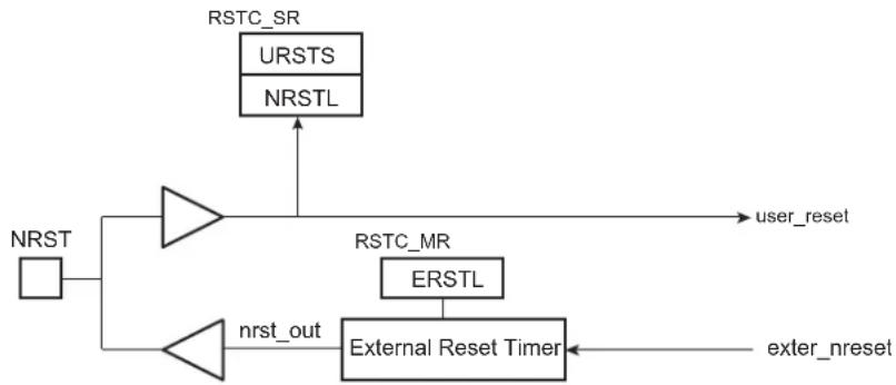
flowchart
graph TD
    A["URSTS"] --> B["NRST"]
    C["NRSTL"] --> D["->"]
    D --> E["user_reset"]
    F["ERSTL"] --> G["->"]
    G --> H["External Reset Timer"]
    I["nrst_out"] --> J["->"]
    J --> H
    K["exter_nreset"] --> H
18.4.2.1 NRST Signal
The NRST Manager handles the NRST input line asynchronously. When the line is low, a User Reset is immediately reported to the Reset State Manager. When the NRST goes from low to high, the internal reset is synchronized with the Slow Clock to provide a safe internal de-assertion of reset.
The level of the pin NRST can be read at any time in the bit NRSTL (NRST level) in the Status register (RSTC_SR). As soon as the pin NRST is asserted, the bit URSTS in the RSTC_SR is set. This bit clears only when RSTC_SR is read.
18.4.2.2 NRST External Reset Control
The Reset State Manager asserts the signal ext_nreset to assert the NRST pin. When this occurs, the "nrst_out" signal is driven low by the NRST Manager for a time programmed by the field ERSTL in the RSTC_MR. This assertion duration, named EXTERNAL_RESET_LENGTH, lasts 2^(ERSTL+1) Slow Clock cycles. This gives the approximate duration of an assertion between 60 s and 2 seconds. Note that ERSTL at 0 defines a two-cycle duration for the NRST pulse.
This feature allows the reset controller to shape the NRST pin level, and thus to ensure that the NRST line is driven low for a time compliant with potential external devices connected on the system reset.
As the field is within RSTC_MR, which is backed-up, this field can be used to shape the system power-up reset for devices requiring a longer startup time than the Slow Clock Oscillator.
18.4.3 BMS Sampling
The product matrix manages a boot memory that depends on the level on the BMS pin at reset. The BMS signal is sampled three slow clock cycles after the Core Power-on Reset output rising edge.
Figure 18-3: BMS Sampling
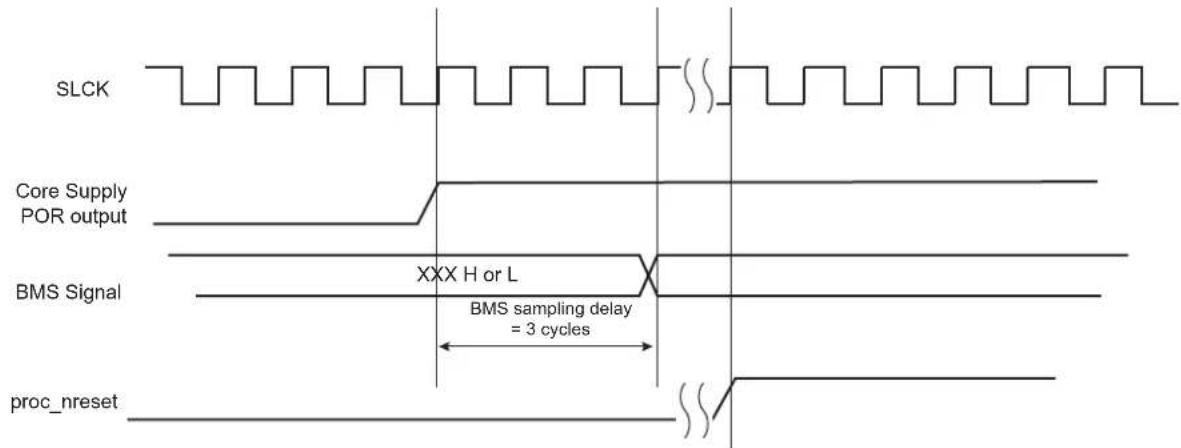
text_image
SLCK Core Supply POR output BMS Signal XXX H or L BMS sampling delay = 3 cycles proc_nreset18.4.4 Reset States
The Reset State Manager handles the different reset sources and generates the internal reset signals. It reports the reset status in the field RSTTYP of the RSTC_SR. The update of the field RSTTYP is performed when the processor reset is released.
18.4.4.1 General Reset
A general reset occurs when VDDBU and VDDCORE are powered on. The backup supply POR cell output rises and is filtered with a Startup Counter, which operates at Slow Clock. The purpose of this counter is to make sure the Slow Clock oscillator is stable before starting up the device. The length of startup time is hardcoded to comply with the Slow Clock Oscillator startup time.
After this time, the processor clock is released at Slow Clock and all the other signals remain valid for 3 cycles for proper processor and logic reset. Then, all the reset signals are released and the field RSTTYP in the RSTC_SR reports a General Reset. As the RSTC_MR is reset, the NRST line rises two cycles after the backup_nreset, as ERSTL defaults at value 0x0.
When VDDBU is detected low by the backup supply POR cell, all resets signals are immediately asserted, even if the main supply POR cell does not report a main supply shutdown.
VDDBU only activates the backup_nreset signal.
The backup_nreset must be released so that any other reset can be generated by VDDCORE (main supply POR output).
Figure 18-4 shows how the General Reset affects the reset signals.
Figure 18-4: General Reset State
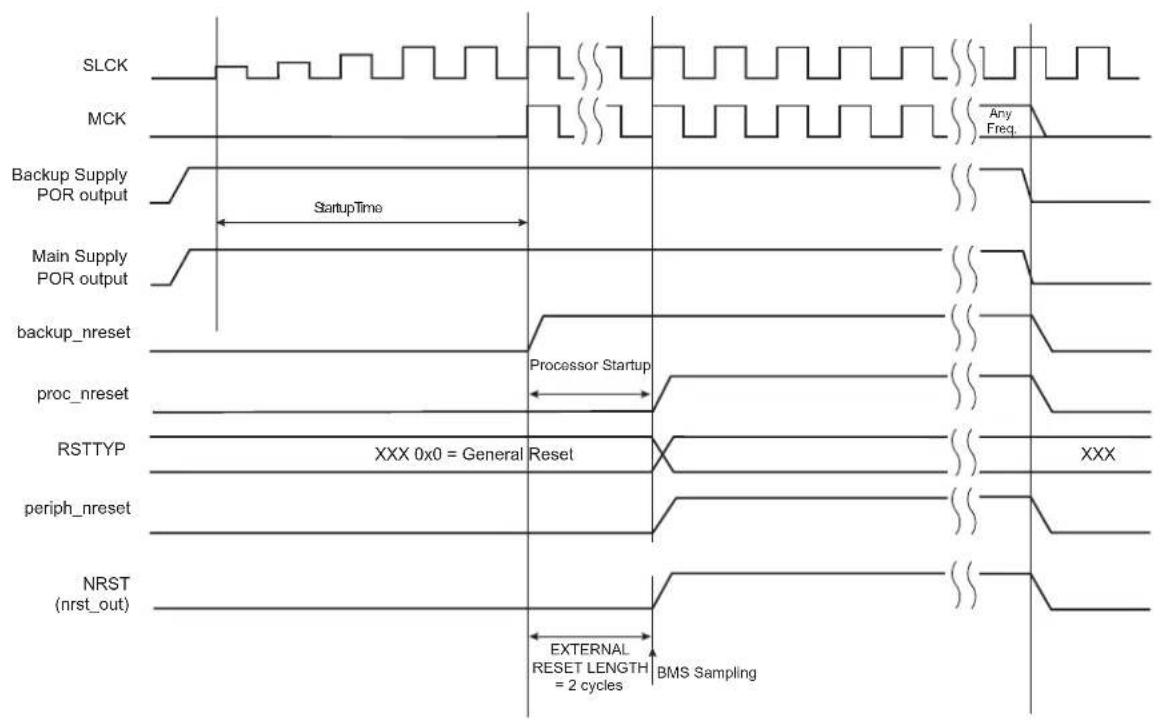
text_image
SLCK MCK Any Freq. Backup Supply POR output StartupTime Main Supply POR output backup_nreset Processor Startup proc_nreset RSTTYP XXX 0x0 = General Reset periph_nreset NRST (nrst_out) EXTERNAL RESET LENGTH = 2 cycles BMS Sampling18.4.4.2 Wake-up Reset
The wake-up reset occurs when the main supply is down. When the main supply POR output is active, all the reset signals are asserted except backup_nreset. When the main supply powers up, the POR output is resynchronized on Slow Clock. The processor clock is then re-enabled during 3 Slow Clock cycles, depending on the requirements of the ARM processor.
At the end of this delay, the processor and other reset signals rise. The field RSTTYP in the RSTC_SR is updated to report a wake-up reset.
The "nrst_out" remains asserted for EXTERNAL_RESET_LENGTH cycles. As RSTC_MR is backed-up, the programmed number of cycles is applicable.
When the main supply is detected falling, the reset signals are immediately asserted. This transition is synchronous with the output of the main supply POR.
Figure 18-5: Wake-up Reset

text_image
SLCK MCK Any Freq. Main Supply POR output backup_nreset Resynch. 2 cycles Processor Startup proc_nreset RSTTYP XXX 0x1 = WakeUp Reset periph_nreset NRST (nrst_out) EXTERNAL RESET LENGTH = 4 cycles (ERSTL = 1)18.4.4.3 User Reset
The User Reset is entered when a low level is detected on the NRST pin. When a falling edge occurs on NRST (reset activation), internal reset lines are immediately asserted.
The Processor Reset and the Peripheral Reset are asserted.
The User Reset is left when NRST rises, after a two-cycle resynchronization time and a 3-cycle processor startup. The processor clock is re-enabled as soon as NRST is confirmed high.
When the processor reset signal is released, the RSTTYP field of the RSTC_SR is loaded with the value 0x4, indicating a User Reset.
The NRST Manager ensures that the NRST line is asserted for EXTERNAL_RESET_LENGTH Slow Clock cycles, as programmed in the field ERSTL. However, if NRST does not rise after EXTERNAL_RESET_LENGTH because it is driven low externally, the internal reset lines remain asserted until NRST actually rises.
Figure 18-6: User Reset State
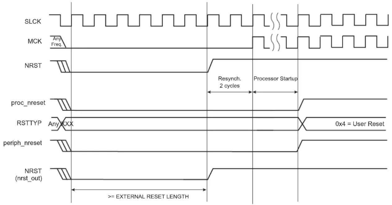
text_image
SLCK MCK Any Freq. NRST Resynch. 2 cycles Processor Startup proc_nreset RSTTYP Any XXX 0x4 = User Reset periph_nreset NRST (nrst_out) >= EXTERNAL RESET LENGTH18.4.4.4 Software Reset
The Reset Controller offers several commands used to assert the different reset signals. These commands are performed by writing the Control register (RSTC_CR) with the following bits at 1:
• PROCRST: Writing a 1 to PROCRST resets the processor and the watchdog timer.
- PERRST: Writing a 1 to PERRST resets all the embedded peripherals, including the memory system, and, in particular, the Remap Command. The Peripheral Reset is generally used for debug purposes.
PERRST must always be used in conjunction with PROCRST (PERRST and PROCRST bot set to 1 simultaneously.)
- EXTRST: Writing a 1 to EXTRST asserts low the NRST pin during a time defined by the field ERSTL in the Mode register (RSTC_MR).
The software reset is entered if at least one of these bits is set by the software. All these commands can be performed independently or simultaneously. The software reset lasts 3 Slow Clock cycles.
The internal reset signals are asserted as soon as the register write is performed. This is detected on the Master Clock (MCK). They are released when the software reset is left, i.e., synchronously to SLCK.
If EXTRST is set, the nrst_out signal is asserted depending on the programming of the field ERSTL. However, the resulting falling edge on NRST does not lead to a User Reset.
If and only if the PROCRST bit is set, the reset controller reports the software status in the field RSTTYP of the RSTC_SR. Other software resets are not reported in RSTTYP.
As soon as a software operation is detected, the bit SRCMP (Software Reset Command in Progress) is set in the RSTC_SR. It is cleared as soon as the software reset is left. No other software reset can be performed while the SRCMP bit is set, and writing any value in the RSTC_CR has no effect.
Figure 18-7: Software Reset

text_image
SLCK MCK Any Freq. Write RSTC_CR Resynch. 1 to 2 cycles Processor Startup = 3 cycles proc_nreset if PROCRST=1 RSTTYP Any XXX 0x3 = Software Reset periph_nreset if PERRST=1 NRST (nrst_out) if EXTRST=1 EXTERNAL RESET LENGTH 8 cycles (ERSTL = 2) SRCMP in RSTC_SR18.4.4.5 Watchdog Reset
The Watchdog Reset is entered when a watchdog fault occurs. This state lasts 3 Slow Clock cycles.
When in Watchdog Reset, assertion of the reset signals depends on the WDRPROC bit in WDT_MR:
- If WDRPROC = 0, the Processor Reset and the Peripheral Reset are asserted. The NRST line is also asserted, depending on how field RSTC_MR.ERSTL is programmed. However, the resulting low level on NRST does not result in a User Reset state.
- If WDRPROC = 1, only the processor reset is asserted.
The Watchdog Timer is reset by the proc_nreset signal. As the watchdog fault always causes a processor reset if WDRSTEN in the WDT_MR is set, the Watchdog Timer is always reset after a Watchdog Reset and the Watchdog is enabled by default and with a period set to a maximum.
When bit WDT_MR.WDRSTEN is reset, the watchdog fault has no impact on the reset controller.
Figure 18-8: Watchdog Reset

text_image
SLCK MCK Any Freq. wd_fault Processor Startup = 3 cycles proc_nreset RSTTYP Any XXX 0x2 = Watchdog Reset periph_nreset Only if WDRPROC = 0 NRST (nrst_out) EXTERNAL RESET LENGTH 8 cycles (ERSTL = 2)18.4.5 Reset State Priorities
The Reset State Manager manages the following priorities between the different reset sources, given in descending order:
- Backup Reset
- Wake-up Reset
- User Reset
- Watchdog Reset
- Software Reset
Particular cases are listed below:
- When in User Reset:
- A watchdog event is impossible because the Watchdog Timer is being reset by the proc_nreset signal.
- A software reset is impossible, since the processor reset is being activated.
- When in Software Reset:
- A watchdog event has priority over the current state.
- The NRST has no effect.
- When in Watchdog Reset:
- The processor reset is active and so a Software Reset cannot be programmed.
- A User Reset cannot be entered.
18.5 Reset Controller (RSTC) User Interface
Note 1: Only power supply VDDCORE rising
2: Both power supplies VDDCORE and VDDBU rising
18.5.1 Reset Controller Control Register
Name:RSTC_CR
Address:0xFFFFFE00
Access:Write-only
31 30 29 28 27 26 25 24
| KEY | |||||||
| 23 22 21 20 19 18 17 16 | |||||||
| - | - | - | - | - | - | - | - |
| 15 14 13 12 11 10 9 8 | |||||||
| - | - | - | - | - | - | - | |
| 7 | 6 | 5 | 4 | 3 | 2 | 1 | 0 |
| - | - | - | - | E | X | T | R |
PROCRST: Processor Reset
0: No effect
1: If KEY value = 0xA5, resets the processor
PERRST: Peripheral Reset
0: No effect
1: If KEY value = 0xA5, resets the peripherals
EXTRST: External Reset
0: No effect
1: If KEY value = 0xA5, asserts the NRST pin and resets the processor and the peripherals
KEY: Write Access Password
| Value | Name | Description |
| 0xA5 | PASSWD | Writing any other value in this field aborts the write operation.Always reads as 0. |
18.5.2 Reset Controller Status Register
Name:RSTC_SR
Address:0xFFFFFE04
Access:Read-only
31 30 29 28 27 26 25 24
| - | - | - | - | - | - | - | - |
23 22 21 20 19 18 17 16
| - | - | - | - | - | - | S | R |
15 14 13 12 11 10 9 8
| - | - | - | - | - | R | S |
| 7 | 6 | 5 | 4 | 3 | 2 | 1 | 0 |
| - | - | - | - | - | - | U |
URSTS: User Reset Status
A high-to-low transition of the NRST pin sets the URSTS bit. This transition is also detected on the Master Clock (MCK) rising edge. Reading the RSTC_SR resets the URSTS bit.
0: No high-to-low edge on NRST happened since the last read of RSTC_SR.
1: At least one high-to-low transition of NRST has been detected since the last read of RSTC_SR.
RSTTYP: Reset Type
This field reports the cause of the last processor reset. Reading this RSTC_SR does not reset this field.
| Value Name | Description | |
| 0 | GENERAL_RST | Both VDDCORE and VDDBU rising |
| 1 | WKUP_RST | VDDCORE rising |
| 2 | WDT_RST | Watchdog fault occurred |
| 3 | SOFT_RST | Processor reset required by the software |
| 4 | USER_RST | NRST pin detected low |
NRSTL: NRST Pin Level
This bit registers the NRST pin level sampled on each Master Clock (MCK) rising edge.
SRCMP: Software Reset Command in Progress
When set, this bit indicates that a Software Reset Command is in progress and that no further software reset should be performed until the end of the current one. This bit is automatically cleared at the end of the current software reset.
0: No software command is being performed by the reset controller. The reset controller is ready for a software command.
1: A software reset command is being performed by the reset controller. The reset controller is busy.
18.5.3 Reset Controller Mode Register
Name:RSTC_MR
Address:0xFFFFFE08
Access: Read/Write
31 30 29 28 27 26 25 24
| KEY | |||||||
| 23 22 21 20 19 18 17 16 | |||||||
| - | - | - | - | - | - | - | |
| 15 14 13 12 11 10 9 8 | |||||||
| - | - | - | - | E | R | S | |
| 7 | 6 | 5 | 4 | 3 | 2 | 1 | 0 |
| - | - | - | - | - | - | ||
ERSTL: External Reset Length
This field defines the external reset length. The external reset is asserted during a time of 2 (ERSTL+1) Slow Clock cycles. This allows the assertion duration to be programmed between 60 s and 2 seconds.
KEY: Write Access Password
| Value Name | Description | |
| 0xA5 PASSWD | Writing any other value in this field aborts the write operation.Always reads as 0. |
19. Shutdown Controller (SHDWC)
19.1 Description
The Shutdown Controller (SHDWC) controls the power supplies VDDIO and VDDCORE and the wake-up detection on debounced input lines.
19.2 Embedded Characteristics
- Shutdown Logic
- Software Assertion of the Shutdown Output Pin (SHDN)
- Programmable De-assertion from the WKUP Input Pins
- Wake-up Logic
- Programmable Assertion from the WKUP Input Pins, and Internal Wake-up Event from RTC
19.3 Block Diagram
Figure 19-1: Shutdown Controller Block Diagram
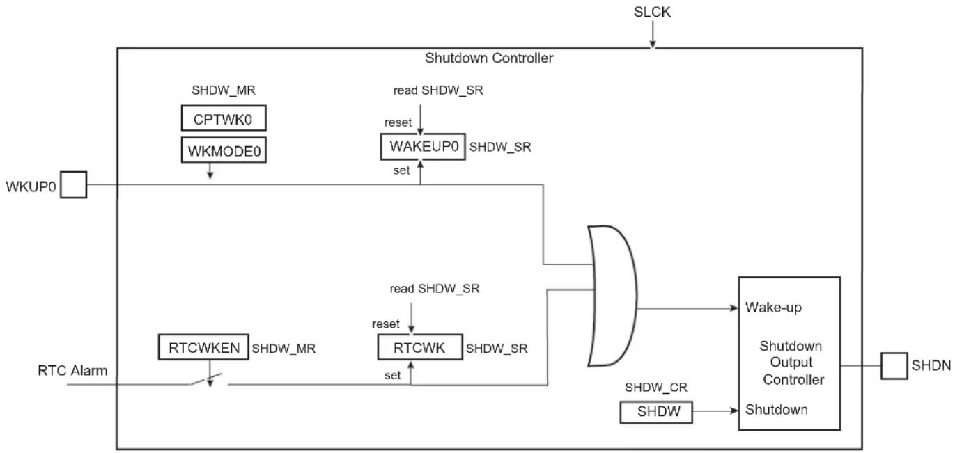
flowchart
graph TD
    A["SLCK"] --> B["Shutdown Controller"]
    C["WKUP0"] --> D["SHDW_MR"]
    D --> E["CPTWK0"]
    E --> F["WKMODE0"]
    F --> G["read SHDW_SR"]
    G --> H["WAKEUP0"]
    H --> I["SHDW_SR"]
    J["RTC Alarm"] --> K["RTCWKEN"]
    K --> L["SHDW_MR"]
    L --> M["read SHDW_SR"]
    M --> N["reset"]
    N --> O["RTCWK"]
    O --> P["SHDW_SR"]
    Q["SHDN"] --> R["Wake-up"]
    R --> S["Shutdown Output Controller"]
    T["SHDW_CR"] --> U["SHDW"]
    U --> V["Shutdown"]
19.4 I/O Lines Description
Table 19-1: I/O Lines Description
| Name Description Type | ||
| WKUP0 Wake-up 0 input Input | ||
| SHDN | Shutdown output | Output |
19.5 Product Dependencies
19.5.1 Power Management
The Shutdown Controller is continuously clocked by the Slow Clock (SLCK). The Power Management Controller has no effect on the behavior of the Shutdown Controller.
19.6 Functional Description
The Shutdown Controller manages the main power supply. To do so, it is supplied with VDDBU and manages wake-up input pins and one output pin, SHDN.
A typical application connects the pin SHDN to the shutdown input of the DC/DC Converter providing the main power supplies of the system, and especially VDDCORE and/or VDDIO. The wake-up inputs (WKUP0) connect to any push-buttons or signal that wake up the system
The software is able to control the pin SHDN by writing the Control register (SHDW_CR) with the bit SHDW at 1. The shutdown is taken into account only two slow clock cycles after the write of SHDW_CR. This register is password-protected and so the value written should contain the correct key for the command to be taken into account. As a result, the system should be powered down.
19.6.1 Wake-up Inputs
A level change on WKUP0 can trigger a wake-up. Wake-up is configured in the Mode register (SHDW_MR). The transition detector can be programmed to detect either a positive or negative transition or any level change on WKUP0. The detection can also be disabled. Programming is performed by defining WKMODE0
Moreover, a debouncing circuit can be programmed for WKUP0. The debouncing circuit filters pulses on WKUP0 shorter than the programmed number of 16 SLCK cycles in CPTWK0 of the SHDW_MR. If the programmed level change is detected on a pin, a counter starts. When the counter reaches the value programmed in the corresponding field, CPTWK0, the SHDN pin is released. If a new input change is detected before the counter reaches the corresponding value, the counter is stopped and cleared. WAKEUP0 of the Status register (SHDW_SR) reports the detection of the programmed events on WKUP0 with a reset after the read of SHDW_SR.
The Shutdown Controller can be programmed so as to activate the wake-up using the RTC alarm(detection of the rising edge event is synchronized with SLCK). This is done by writing the SHDW_MR using the RTCWKEN bit. When enabled, the detection of RTC alarm is reported in the RTCWK bit of SHDW_SR. They are cleared after reading SHDW_SR. When using the RTC alarm to wake up the system, the user must ensure that RTC alarmstatus flag is cleared before shutting down the system. Otherwise, no rising edge of the status flags may be detected and the wake-up will fail.
19.7 Shutdown Controller (SHDWC) User Interface
Table 19-2: Register Mapping
| Offset Register | Name Access Reset | |||
| 0x00 Shutdown | Control Register SHDW_CR Write-only – | |||
| 0x04 Shutdown | Mode Register SHDW_MR Read/Write | 0x0000_0003 | ||
| 0x08 Shutdown | Status Register SHDW_SR | Read-only 0x0000_0000 |
19.7.1 Shutdown Control Register
Name:SHDW_CR
Address:0xFFFFFE10
Access:Write-only
31 30 29 28 27 26 25 24
| KEY | |||||||
| 23 22 21 20 19 18 17 16 | |||||||
| - | - | - | - | - | - | - | - |
| 15 14 13 12 11 10 9 8 | |||||||
| - | - | - | - | - | - | - | - |
| 7 | 6 | 5 | 4 | 3 | 2 | 1 | 0 |
| - | - | - | - | - | - | - | S |
SHDW: Shutdown Command
0: No effect.
1: If KEY value is correct, asserts the SHDN pin.
KEY: Password
| Value Name | Description | |
| 0xA5 | PASSWD | Writing any other value in this field aborts the write operation. |
19.7.2 Shutdown Mode Register
Name:SHDW_MR
Address:0xFFFFFE14
Access: Read/Write
31 30 29 28 27 26 25 24
| - | - | - | - | - | - | - | - |
23 22 21 20 19 18 17 16
| - | - | - | - | - | - | R | T |
15 14 13 12 11 10 9 8
| - | - | - | - | - | - | - | - |
| 7 | 6 | 5 | 4 | 3 | 2 | 1 | 0 |
CPTWK0--WKMODE0
WKMODE0: Wake-up Mode 0
| Value Name | Description | |
| 0 | NO_DETECTION | No detection is performed on the wake-up input |
| 1 | RISING_EDGE | Low to high transition triggers the detection process |
| 2 | FALLING_EDGE | High to low level transition triggers the detection process |
| 3 | ANY_EDGE | Any edge on the wake-up input triggers the detection process |
CPTWK0: Debounce Counter on Wake-up 0
Defines the minimum duration of the WKUP1 pin after the occurrence of the selected triggering edge (WKMODE0).
The SHDN pin is released if the WKUP0 holds the selected level for (CPTWK × 16 + 1) consecutive Slow Clock cycles after the occurrence of the selected triggering edge on WKUP0.
RTCWKEN: Real-time Clock Wake-up Enable
0: The RTC Alarm signal has no effect on the Shutdown Controller.
1: The RTC Alarm signal forces the de-assertion of the SHDN pin.
19.7.3 Shutdown Status Register
Name:SHDW_SR
Address:0xFFFFFE18
Access:Read-only
31 30 29 28 27 26 25 24
| - | - | - | - | - | - | - | - |
23 22 21 20 19 18 17 16
| - | - | - | - | - | - | R | T |
15 14 13 12 11 10 9 8
| - | - | - | - | - | - | - | - |
| 7 | 6 | 5 | 4 | 3 | 2 | 1 | 0 |
| - | - | - | - | - | - | - | W |
WAKEUP0: Wake-up 0 Status
0: No wake-up event occurred on WKUP0 input since the last read of SHDW_SR.
1: At least one wake-up event occurred on WKUP0 input since the last read of SHDW_SR.
RTCWK: Real-time Clock Wake-up
0: No wake-up alarm from the RTC occurred since the last read of SHDW_SR.
1: At least one wake-up alarm from the RTC occurred since the last read of SHDW_SR.
20. General Purpose Backup Registers (GPBR)
20.1 Description
The System Controller embeds 128 bits of General Purpose Backup registers organized as four 32-bit registers.
20.2 Embedded Characteristics
• 128 bits of General Purpose Backup Registers
20.3 General Purpose Backup Registers (GPBR) User Interface
| Offset Register Name Access Reset | ||||
| 0x0 General | Purpose Backup Register 0 SYS_GPBR0 Read | Write 0x00000000 | ||
| ... ... ... ... | ... | |||
| 0x6C | General Purpose Backup Register 3 | SYS_GPBR3 | Read/Write | 0x00000000 |
20.3.1 General Purpose Backup Register x
Name:SYS_GPBRx
Address:0xFFFFFE60
Access: Read/Write
31 30 29 28 27 26 25 24
GPBR_VALUE
23 22 21 20 19 18 17 16
GPBR_VALUE
15 14 13 12 11 10 9 8
GPBR_VALUE
7 6 5 4 3 2 1 0
GPBR_VALUE
These registers are reset at first power-up and on each loss of VDDBU.
GPBR_VALUE: Value of GPBR x
21. Periodic Interval Timer (PIT)
21.1 Description
The Periodic Interval Timer (PIT) provides the operating system's scheduler interrupt. It is designed to offer maximum accuracy and efficient management, even for systems with long response time.
21.2 Embedded Characteristics
• 20-bit Programmable Counter plus 12-bit Interval Counter
- Reset-on-read Feature
• Both Counters Work on Master Clock/16
21.3 Block Diagram
Figure 21-1: Periodic Interval Timer

flowchart
graph TD
    A["Prescaler"] -->|MCK/16| B["20-bit Counter"]
    B --> C["CPIV"]
    C --> D["CPIV PICNT"]
    D --> E["PIT_PIVR"]
    E --> F["PICNT"]
    F --> G["PIT_PIVR"]
    G --> H["12-bit Adder"]
    H --> I["PITS"]
    I --> J["set"]
    J --> K["PIT_SR"]
    K --> L["reset"]
    L --> M["PIT_PIVR"]
    M --> N["PIT_MR"]
    N --> O["PIT_IEN"]
    O --> P["pit_irq"]
    P --> I
    Q["MCK"] --> B
    R["0"] --> S["0 1"]
    T["0"] --> U["0 1"]
    V["0"] --> W["0 1"]
    X["0"] --> Y["0 1"]
    Z["0"] --> AA["0 1"]
    AB["0"] --> AC["0 1"]
    AD["0"] --> AE["0 1"]
    AF["0"] --> AG["0 1"]
    AH["0"] --> AI["0 1"]
    AJ["0"] --> AK["0 1"]
    AL["0"] --> AM["0 1"]
    AN["0"] --> AO["0 1"]
    AP["0"] --> AQ["0 1"]
    AR["0"] --> AS["0 1"]
    AT["0"] --> AU["0 1"]
    AV["0"] --> AW["0 1"]
    AX["0"] --> AY["0 1"]
21.4 Functional Description
The Periodic Interval Timer aims at providing periodic interrupts for use by operating systems.
The PIT provides a programmable overflow counter and a reset-on-read feature. It is built around two counters: a 20-bit CPIV counter and a 12-bit PICNT counter. Both counters work at Master Clock /16.
The first 20-bit CPIV counter increments from 0 up to a programmable overflow value set in the field PIV of the Mode register (PIT_MR). When the counter CPIV reaches this value, it resets to 0 and increments the Periodic Interval Counter, PICNT. The status bit PITS in the Status register (PIT_SR) rises and triggers an interrupt, provided the interrupt is enabled (PITIEN in PIT_MR).
Writing a new PIV value in PIT_MR does not reset/restart the counters.
When CPIV and PICNT values are obtained by reading the Periodic Interval Value register (PIT_PIVR), the overflow counter (PICNT) is reset and the PITS bit is cleared, thus acknowledging the interrupt. The value of PICNT gives the number of periodic intervals elapsed since the last read of PIT_PIVR.
When CPIV and PICNT values are obtained by reading the Periodic Interval Image register (PIT_PIIR), there is no effect on the counters CPIV and PICNT, nor on the bit PITS. For example, a profiler can read PIT_PIIR without clearing any pending interrupt, whereas a timer interrupt clears the interrupt by reading PIT_PIVR.
The PIT may be enabled/disabled using the PITEN bit in the PIT_MR register (disabled on reset). The PITEN bit only becomes effective when the CPIV value is 0. Figure 21-2 illustrates the PIT counting. After the PIT Enable bit is reset (PITEN = 0), the CPIV goes on counting until the PIV value is reached, and is then reset. PIT restarts counting, only if the PITEN is set again.
The PIT is stopped when the core enters debug state.
Figure 21-2: Enabling/Disabling PIT with PITEN

text_image
APB cycle MCK APB cycle MCK Prescaler 0 15 restarts MCK Prescaler PITEN CPIV 1 PIVPX-10 0 PICNT 0 1 0 PITS (PIT_SR) APB Interface read PIT_PIVR21.5 Periodic Interval Timer (PIT) User Interface
Defines the value compared with the primary 20-bit counter of the Periodic Interval Timer (CPIV). The period is equal to (PIV + 1) .
- PITEN: Period Interval Timer Enabled
0: The Periodic Interval Timer is disabled when the PIV value is reached.
1: The Periodic Interval Timer is enabled.
- PITIEN: Periodic Interval Timer Interrupt Enable
0: The bit PITS in PIT_SR has no effect on interrupt.
1: The bit PITS in PIT_SR asserts interrupt.
21.5.2 Periodic Interval Timer Status Register
Name:PIT_SR
Address:0xFFFFFE34
Access:Read-only
31 30 29 28 27 26 25 24
| - | - | - | - | - | - | - | - |
23 22 21 20 19 18 17 16
| - | - | - | - | - | - | - | - |
15 14 13 12 11 10 9 8
| - | - | - | - | - | - | - | - |
| 7 | 6 | 5 | 4 | 3 | 2 | 1 | 0 |
| - | - | - | - | - | - | - | P |
• PITS: Periodic Interval Timer Status
0: The Periodic Interval timer has not reached PIV since the last read of PIT_PIVR.
1: The Periodic Interval timer has reached PIV since the last read of PIT_PIVR.
21.5.3 Periodic Interval Timer Value Register
Name:PIT_PIVR
Address:0xFFFFFE38
Access:Read-only
31 30 29 28 27 26 25 24
PICNT
23 22 21 20 19 18 17 16
PICNT CPIV
15 14 13 12 11 10 9 8
CPIV
7 6 5 4 3 2 1 0
CPIV
Reading this register clears PITS in PIT_SR.
• CPIV: Current Periodic Interval Value
Returns the current value of the periodic interval timer.
• PICNT: Periodic Interval Counter
Returns the number of occurrences of periodic intervals since the last read of PIT_PIVR.
21.5.4 Periodic Interval Timer Image Register
Name:PIT_PIIR
Address:0xFFFFFE3C
Access:Read-only
31 30 29 28 27 26 25 24
| PICNT | |||||||
| 23 22 21 20 19 18 17 16 | |||||||
| PICNT CPIV | |||||||
| 15 14 13 12 11 10 9 8 | |||||||
| CPIV | |||||||
| 7 | 6 | 5 | 4 | 3 | 2 | 1 | 0 |
| CPIV | |||||||
• CPIV: Current Periodic Interval Value
Returns the current value of the periodic interval timer.
• PICNT: Periodic Interval Counter
Returns the number of occurrences of periodic intervals since the last read of PIT_PIVR.
22. Real-time Clock (RTC)
22.1 Description
The Real-time Clock (RTC) peripheral is designed for very low power consumption. For optimal functionality, the RTC requires an accurate external 32.768 kHz clock, which can be provided by a crystal oscillator.
It combines a complete time-of-day clock with alarm and a Gregorian calendar, complemented by a programmable periodic interrupt. The alarm and calendar registers are accessed by a 32-bit data bus.
The time and calendar values are coded in binary-coded decimal (BCD) format. The time format can be 24-hour mode or 12-hour mode with an AM/PM indicator.
Updating time and calendar fields and configuring the alarm fields are performed by a parallel capture on the 32-bit data bus. An entry control is performed to avoid loading registers with incompatible BCD format data or with an incompatible date according to the current month/year/century.
22.2 Embedded Characteristics
• Full Asynchronous Design for Ultra Low Power Consumption
• Gregorian Mode Supported
- Programmable Periodic Interrupt
• Safety/security Features:
- Valid Time and Date Programming Check
22.3 Block Diagram
Figure 22-1: Real-time Clock Block Diagram
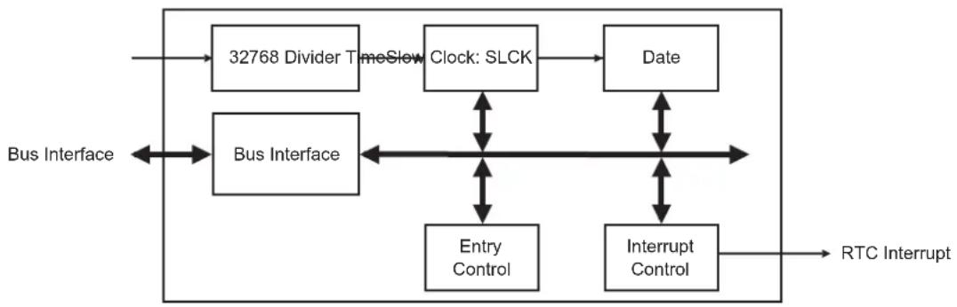
flowchart
graph TD
    A["32768 Divider TimeSlow"] --> B["Clock: SLCK"]
    B --> C["Date"]
    D["Bus Interface"] <--> E["Entry Control"]
    D <--> F["Interrupt Control"]
    G["RTC Interrupt"] --> H["Data"]
    I["Data"] --> B
    J["Data"] --> C
    K["Data"] --> F
22.4 Product Dependencies
22.4.1 Power Management
The Real-time Clock is continuously clocked at 32.768 kHz. The Power Management Controller has no effect on RTC behavior.
22.4.2 Interrupt
Within the System Controller, the RTC interrupt is OR-wired with all the other module interrupts.
Only one System Controller interrupt line is connected on one of the internal sources of the interrupt controller.
RTC interrupt requires the interrupt controller to be programmed first.
When a System Controller interrupt occurs, the service routine must first determine the cause of the interrupt. This is done by reading each status register of the System Controller peripherals successively.
Table 22-1: Peripheral IDs
| Instance ID | |
| RTC 1 |
22.5 Functional Description
The RTC provides a full binary-coded decimal (BCD) clock that includes century (19/20), year (with leap years), month, date, day, hours, minutes and seconds reported in RTC Time Register (RTC_TIMR) and RTC Calendar Register (RTC_CALR).
The valid year range is up to 2099 in Gregorian mode.
The RTC can operate in 24-hour mode or in 12-hour mode with an AM/PM indicator.
Corrections for leap years are included (all years divisible by 4 being leap years except 1900). This is correct up to the year 2099.
22.5.1 Reference Clock
The reference clock is the Slow Clock (SLCK). It can be driven internally or by an external 32.768 kHz crystal.
During low power modes of the processor, the oscillator runs and power consumption is critical. The crystal selection has to take into account the current consumption for power saving and the frequency drift due to temperature effect on the circuit for time accuracy.
22.5.2 Timing
The RTC is updated in real time at one-second intervals in Normal mode for the counters of seconds, at one-minute intervals for the counter of minutes and so on.
Due to the asynchronous operation of the RTC with respect to the rest of the chip, to be certain that the value read in the RTC registers (century, year, month, date, day, hours, minutes, seconds) are valid and stable, it is necessary to read these registers twice. If the data is the same both times, then it is valid. Therefore, a minimum of two and a maximum of three accesses are required.
22.5.3 Alarm
The RTC has five programmable fields: month, date, hours, minutes and seconds.
Each of these fields can be enabled or disabled to match the alarm condition:
- If all the fields are enabled, an alarm flag is generated (the corresponding flag is asserted and an interrupt generated if enabled) at a given month, date, hour/minute/second.
- If only the "seconds" field is enabled, then an alarm is generated every minute.
Depending on the combination of fields enabled, a large number of possibilities are available to the user ranging from minutes to 365/366 days.
Hour, minute and second matching alarm (SECEN, MINEN, HOUREN) can be enabled independently of SEC, MIN, HOUR fields.
Note: To change one of the SEC, MIN, HOUR, DATE, MONTH fields, it is recommended to disable the field before changing the value and then re-enable it after the change has been made. This requires up to three accesses to the RTC_TIMALR or RTC_CALALR. The first access clears the enable corresponding to the field to change (SECEN, MINEN, HOUREN, DATEEN, MTHEN). If the field is already cleared, this access is not required. The second access performs the change of the value (SEC, MIN, HOUR, DATE, MONTH). The third access is required to re-enable the field by writing 1 in SECEN, MINEN, HOUREN, DATEEN, MTHEN fields.
22.5.4 Error Checking when Programming
Verification on user interface data is performed when accessing the century, year, month, date, day, hours, minutes, seconds and alarms. A check is performed on illegal BCD entries such as illegal date of the month with regard to the year and century configured.
If one of the time fields is not correct, the data is not loaded into the register/counter and a flag is set in the validity register. The user can not reset this flag. It is reset as soon as an acceptable value is programmed. This avoids any further side effects in the hardware. The same procedure is followed for the alarm.
The following checks are performed:
- Century (check if it is in range 19–20)
- Year (BCD entry check)
- Date (check range 01–31)
- Month (check if it is in BCD range 01–12, check validity regarding "date")
- Day (check range 1–7)
- Minute (check BCD and range 00–59)
-
Second (check BCD and range 00–59)
-
Hour (BCD checks: in 24-hour mode, check range 00–23 and check that AM/PM flag is not set if RTC is set in 24-hour mode; in 12-hour mode check range 01–12)
Note: If the 12-hour mode is selected by means of the RTC Mode Register (RTC_MR), a 12-hour value can be programmed and the returned value on RTC_TIMR will be the corresponding 24-hour value. The entry control checks the value of the AM/PM indicator (bit 22 of RTC_TIMR) to determine the range to be checked.
22.5.5 Updating Time/Calendar
To update any of the time/calendar fields, the user must first stop the RTC by setting the corresponding field in the Control register (RTC_CR). Bit UPDTIM must be set to update time fields (hour, minute, second) and bit UPDCAL must be set to update calendar fields (century, year, month, date, day).
The ACKUPD bit is automatically set within a second after setting the UPDTIM and/or UPDCAL bit (meaning one second is the maximum duration of the polling or wait for interrupt period). Once ACKUPD is set, it is mandatory to clear this flag by writing the corresponding bit in the RTC_SCCR, after which the user can write to the Time register, the Calendar register, or both.
Once the update is finished, the user must clear UPDTIM and/or UPDCAL in the RTC_CR.
When entering the programming mode of the calendar fields, the time fields remain enabled. When entering the programming mode of the time fields, both time and calendar fields are stopped. This is due to the location of the calendar logic circuitry (downstream for low-power considerations). It is highly recommended to prepare all the fields to be updated before entering programming mode. In successive update operations, the user must wait at least one second after resetting the UPDTIM/UPDCAL bit in the RTC_CR before setting these bits again. This is done by waiting for the SEC flag in the RTC_SR before setting UPDTIM/UPDCAL bit. After clearing UPDTIM/UPDCAL, the SEC flag must also be cleared.
Figure 22-2: Update Sequence
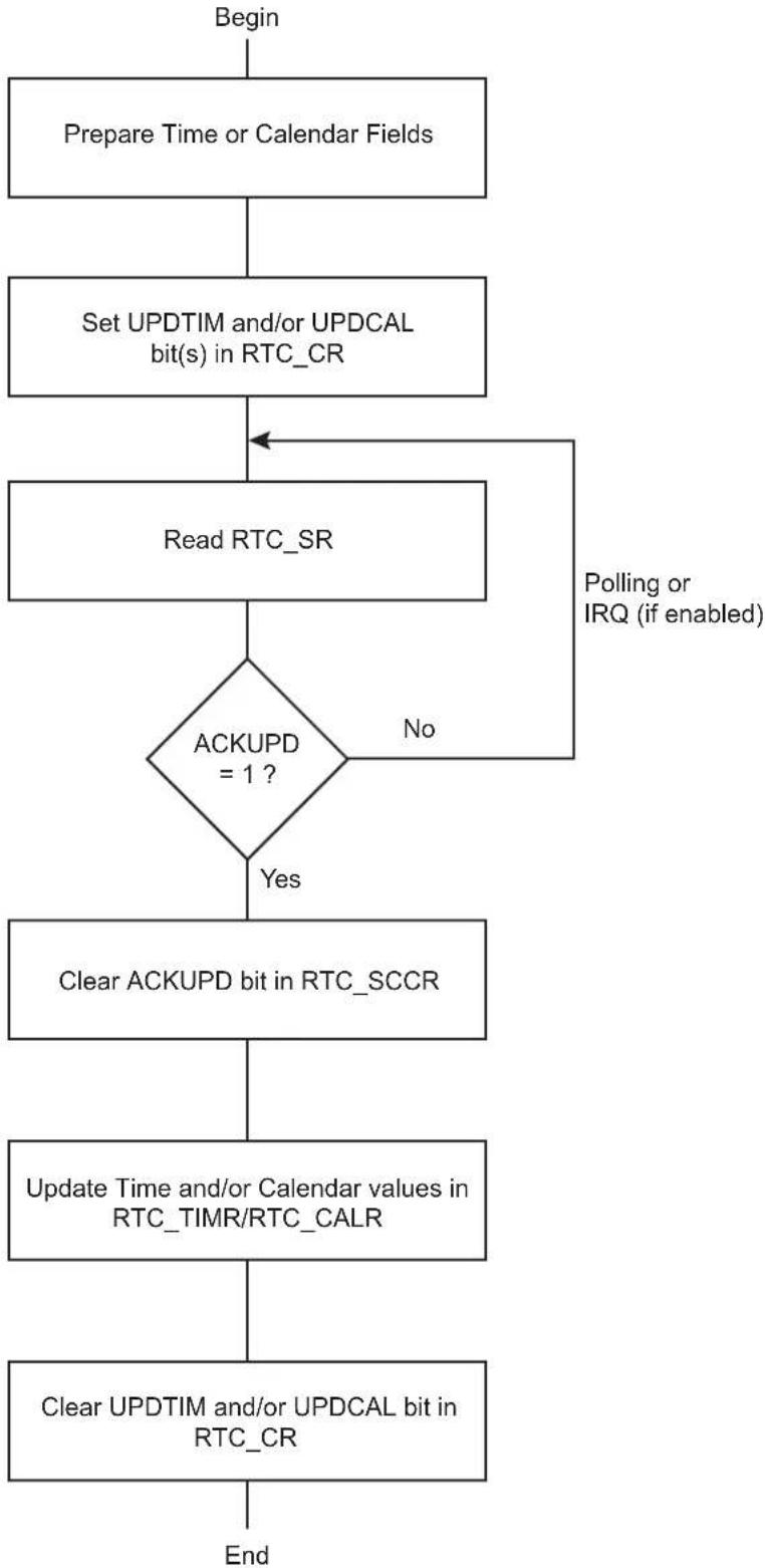
flowchart
graph TD
    A["Begin"] --> B["Prepare Time or Calendar Fields"]
    B --> C["Set UPDTIM and/or UPDCAL bit(s) in RTC_CR"]
    C --> D["Read RTC_SR"]
    D --> E{ACKUPD = 1 ?}
    E -->|No| F["Polling or IRQ (if enabled)"]
    F --> D
    E -->|Yes| G["Clear ACKUPD bit in RTC_SCCR"]
    G --> H["Update Time and/or Calendar values in RTC_TIMR/RTC_CALR"]
    H --> I["Clear UPDTIM and/or UPDCAL bit in RTC_CR"]
    I --> J["End"]
22.6 Real-time Clock (RTC) User Interface
Table 22-2: Register Mapping
| Offset Register Name Access Reset | ||||
| 0x00 Control | Register RTC_CR Read/Write 0x00000000 | |||
| 0x04 Mode | Register RTC_MR Read/Write 0x00000000 | |||
| 0x08 | Time Register | RTC_TIMR | Read/Write | 0x00000000 |
| 0x0C Calendar | ar Register RTC_CALR | Read/Write 0x01810720 | ||
| 0x10 | Time Alarm Register | RTC_TIMALR | Read/Write | 0x00000000 |
| 0x14 Calendar | Alarm Register RTC_CALALR | Read/Write 0x01010000 | ||
| 0x18 | Status Register | RTC_SR | Read-only | 0x00000000 |
| 0x1C | Status Clear Command Register | RTC_SCCR | Write-only | - |
| 0x20 Interrupt | Enable Register RTC_IER Write-only | - | ||
| 0x24 | Interrupt Disable Register | RTC_IDR | Write-only | - |
| 0x28 | Interrupt Mask Register | RTC_IMR | Read-only | 0x00000000 |
| 0x2C | Valid Entry Register | RTC_VER | Read-only | 0x00000000 |
| 0x30–0xC8 | Reserved | - | - | - |
| 0xCC | Reserved | - | - | - |
| 0xD0 Reserved | - | - | - | |
| 0xFC | Reserved | - | - | - |
Note: If an offset is not listed in the table it must be considered as reserved.
22.6.1 RTC Control Register
Name: RTC_CR
Address:0xFFFFFEB0
Access: Read/Write
31 30 29 28 27 26 25 24
| - | - | - | - | - | - | - | - |
| 23 22 21 20 19 18 17 16 | |||||||
| - | - | - | - | - | - | - | C |
| 15 14 13 12 11 10 9 8 | |||||||
| - | - | - | - | - | - | - | T |
| 7 | 6 | 5 | 4 | 3 | 2 | 1 | 0 |
| - | - | - | - | - | - | U | P |
UPDTIM: Update Request Time Register
0: No effect or, if UPDTIM has been previously written to 1, stops the update procedure.
1: Stops the RTC time counting.
Time counting consists of second, minute and hour counters. Time counters can be programmed once this bit is set and acknowledged by the bit ACKUPD of the RTC_SR.
UPDCAL: Update Request Calendar Register
0: No effect or, if UPDCAL has been previously written to 1, stops the update procedure.
1: Stops the RTC calendar counting.
Calendar counting consists of day, date, month, year and century counters. Calendar counters can be programmed once this bit is set and acknowledged by the bit ACKUPD of the RTC_SR.
TIMEVSEL: Time Event Selection
The event that generates the flag TIMEV in RTC_SR depends on the value of TIMEVSEL.
| Value Name | Description | |
| 0 | MINUTE | Minute change |
| 1 | HOUR | Hour change |
| 2 | MIDNIGHT | Every day at midnight |
| 3 | NOON | Every day at noon |
CALEVSEL: Calendar Event Selection
The event that generates the flag CALEV in RTC_SR depends on the value of CALEVSEL
| Value Name | Description | |
| 0 | WEEK | Week change (every Monday at time 00:00:00) |
| 1 | MONTH | Month change (every 01 of each month at time 00:00:00) |
| 2 | YEAR | Year change (every January 1 at time 00:00:00) |
| 3 | - | Reserved |
22.6.2 RTC Mode Register
Name: RTC_MR
Address:0xFFFFFEB4
Access: Read/Write
31 30 29 28 27 26 25 24
| - | - | - | - | - | - | - | - |
| 23 22 21 20 19 18 17 16 | |||||||
| - | - | - | - | - | - | - | - |
| 15 14 13 12 11 10 9 8 | |||||||
| - | - | - | - | - | - | - | - |
| 7 | 6 | 5 | 4 | 3 | 2 | 1 | 0 |
| - | - | - | - | - | - | - | H |
HRMOD: 12-/24-hour Mode
0: 24-hour mode is selected.
1: 12-hour mode is selected.
22.6.3 RTC Time Register
Name: RTC_TIMR
Address:0xFFFFFEB8
Access: Read/Write
31 30 29 28 27 26 25 24
| - | - | - | - | - | - | - | - |
23 22 21 20 19 18 17 16
| - | A | M | P | M | H | O | U |
15 14 13 12 11 10 9 8
| - | MIN |
7 6 5 4 3 2 1 0
- SEC
SEC: Current Second
The range that can be set is 0–59 (BCD).
The lowest four bits encode the units. The higher bits encode the tens.
MIN: Current Minute
The range that can be set is 0–59 (BCD).
The lowest four bits encode the units. The higher bits encode the tens.
HOUR: Current Hour
The range that can be set is 1–12 (BCD) in 12-hour mode or 0–23 (BCD) in 24-hour mode.
AMPM: Ante Meridiem Post Meridiem Indicator
This bit is the AM/PM indicator in 12-hour mode.
0: AM.
1: PM.
22.6.4 RTC Calendar Register
Name: RTC_CALR
Address:0xFFFFEBC
Access: Read/Write
31 30 29 28 27 26 25 24
| - | - | D | A | T | E |
23 22 21 20 19 18 17 16
| DAY MONTH |
15 14 13 12 11 10 9 8
| YEAR |
| 7 | 6 | 5 | 4 | 3 | 2 | 1 | 0 |
| - | C |
E
CENT: Current Century
Only the BCD value 20 can be configured.
The lowest four bits encode the units. The higher bits encode the tens.
YEAR: Current Year
The range that can be set is 00–99 (BCD).
The lowest four bits encode the units. The higher bits encode the tens.
MONTH: Current Month
The range that can be set is 01–12 (BCD).
The lowest four bits encode the units. The higher bits encode the tens.
DAY: Current Day in Current Week
The range that can be set is 1–7 (BCD).
The coding of the number (which number represents which day) is user-defined as it has no effect on the date counter.
DATE: Current Day in Current Month
The range that can be set is 01–31 (BCD).
The lowest four bits encode the units. The higher bits encode the tens.
22.6.5 RTC Time Alarm Register
Name: RTC_TIMALR
Address:0xFFFFEC0
Access: Read/Write
31 30 29 28 27 26 25 24
| - | - | - | - | - | - | - | - |
23 22 21 20 19 18 17 16
| HOUREN AMPM HOUR |
15 14 13 12 11 10 9 8
| MINEN MIN |
| 7 | 6 | 5 | 4 | 3 | 2 | 1 | 0 |
| SECEN | SEC |
Note: To change one of the SEC, MIN, HOUR fields, it is recommended to disable the field before changing the value and then re-enable it after the change has been made. This requires up to three accesses to the RTC_TIMALR. The first access clears the enable corresponding to the field to change (SECEN, MINEN, HOUREN). If the field is already cleared, this access is not required. The second access performs the change of the value (SEC, MIN, HOUR). The third access is required to re-enable the field by writing 1 in SECEN, MINEN, HOUREN fields.
SEC: Second Alarm
This field is the alarm field corresponding to the BCD-coded second counter.
SECEN: Second Alarm Enable
0: The second-matching alarm is disabled.
1: The second-matching alarm is enabled.
MIN: Minute Alarm
This field is the alarm field corresponding to the BCD-coded minute counter.
MINEN: Minute Alarm Enable
0: The minute-matching alarm is disabled.
1: The minute-matching alarm is enabled.
HOUR: Hour Alarm
This field is the alarm field corresponding to the BCD-coded hour counter.
AMPM: AM/PM Indicator
This field is the alarm field corresponding to the BCD-coded hour counter.
HOURN: Hour Alarm Enable
0: The hour-matching alarm is disabled.
1: The hour-matching alarm is enabled.
22.6.6 RTC Calendar Alarm Register
Name: RTC_CALALR
Address:0xFFFFEC4
Access: Read/Write
31 30 29 28 27 26 25 24
DATEEN - DATE
23 22 21 20 19 18 17 16
| MTHEN -- MONTH |
15 14 13 12 11 10 9 8
| - | - | - | - | - | - | - | - |
7 6 5 4 3 2 1 0
| - | - | - | - | - | - | - | - |
Note: To change one of the DATE, MONTH fields, it is recommended to disable the field before changing the value and then re-enable it after the change has been made. This requires up to three accesses to the RTC_CALALR. The first access clears the enable corresponding to the field to change (DATEEN, MTHEN). If the field is already cleared, this access is not required. The second access performs the change of the value (DATE, MONTH). The third access is required to re-enable the field by writing 1 in DATEEN, MTHEN fields.
MONTH: Month Alarm
This field is the alarm field corresponding to the BCD-coded month counter.
MTHEN: Month Alarm Enable
0: The month-matching alarm is disabled.
1: The month-matching alarm is enabled.
DATE: Date Alarm
This field is the alarm field corresponding to the BCD-coded date counter.
DATEEN: Date Alarm Enable
0: The date-matching alarm is disabled.
1: The date-matching alarm is enabled.
22.6.7 RTC Status Register
Name: RTC_SR
Address:0xFFFFEC8
Access: Read-only
| 31 30 29 28 27 26 25 24 | |||||||
| - | - | - | - | - | - | - | - |
| 23 22 21 20 19 18 17 16 | |||||||
| - | - | - | - | - | - | - | - |
| 15 14 13 12 11 10 9 8 | |||||||
| - | - | - | - | - | - | - | - |
| 7 | 6 | 5 | 4 | 3 | 2 | 1 | 0 |
| --- CA LEV TIMEV SEC ALARM ACKUPD | |||||||
ACKUPD: Acknowledge for Update
| Value | Name | Description |
| 0 | FREERUN | Time and calendar registers cannot be updated. |
| 1 | UPDATE | Time and calendar registers can be updated. |
ALARM: Alarm Flag
| Value | Name | Description |
| 0 | NO_ALARMEVENT | No alarm matching condition occurred. |
| 1 | ALARMEVENT | An alarm matching condition has occurred. |
SEC: Second Event
| Value | Name | Description |
| 0 | NO_SECEVENT | No second event has occurred since the last clear. |
| 1 | SECEVENT | At least one second event has occurred since the last clear. |
TIMEV: Time Event
| Value | Name | Description |
| 0 | NO_TIMEVENT | No time event has occurred since the last clear. |
| 1 | TIMEVENT | At least one time event has occurred since the last clear. |
Note: The time event is selected in the TIMEVSEL field in the Control Register (RTC_CR) and can be any one of the following events: minute change, hour change, noon, midnight (day change).
CALEV: Calendar Event
| Value | Name | Description |
| 0 | NO_CALEVENT | No calendar event has occurred since the last clear. |
| 1 | CALEVENT | At least one calendar event has occurred since the last clear. |
Note: The calendar event is selected in the CALEVSEL field in the Control Register (RTC_CR) and can be any one of the following events: week change, month change and year change.
22.6.8 RTC Status Clear Command Register
Name: RTC_SCCR
Address:0xFFFFFECC
Access: Write-only
31 30 29 28 27 26 25 24
| - | - | - | - | - | - | - | - |
23 22 21 20 19 18 17 16
| - | - | - | - | - | - | - | - |
15 14 13 12 11 10 9 8
| - | - | - | - | - | - | - | - |
7 6 5 4 3 2 1 0
| ---CAL | CLR | TIMCLR | SEC | CLR | ALRCLR | ACKCLR |
ACKCLR: Acknowledge Clear
0: No effect.
1: Clears corresponding status flag in the Status Register (RTC_SR).
ALRCLR: Alarm Clear
0: No effect.
1: Clears corresponding status flag in the Status Register (RTC_SR).
SECCLR: Second Clear
0: No effect.
1: Clears corresponding status flag in the Status Register (RTC_SR).
TIMCLR: Time Clear
0: No effect.
1: Clears corresponding status flag in the Status Register (RTC_SR).
CALCLR: Calendar Clear
0: No effect.
1: Clears corresponding status flag in the Status Register (RTC_SR).
22.6.9 RTC Interrupt Enable Register
Name: RTC_IER
Address:0xFFFFED0
Access: Write-only
31 30 29 28 27 26 25 24
| - | - | - | - | - | - | - | - |
23 22 21 20 19 18 17 16
| - | - | - | - | - | - | - | - |
15 14 13 12 11 10 9 8
| - | - | - | - | - | - | - | - |
7 6 5 4 3 2 1 0
| --- CALEN TIMEN SEGEN ALREN ACKEN |
ACKEN: Acknowledge Update Interrupt Enable
0: No effect.
1: The acknowledge for update interrupt is enabled.
ALREN: Alarm Interrupt Enable
0: No effect.
1: The alarm interrupt is enabled.
SECEN: Second Event Interrupt Enable
0: No effect.
1: The second periodic interrupt is enabled.
TIMEN: Time Event Interrupt Enable
0: No effect.
1: The selected time event interrupt is enabled.
CALEN: Calendar Event Interrupt Enable
0: No effect.
1: The selected calendar event interrupt is enabled.
22.6.10 RTC Interrupt Disable Register
Name: RTC_IDR
Address:0xFFFFED4
Access: Write-only
31 30 29 28 27 26 25 24
| - | - | - | - | - | - | - | - |
23 22 21 20 19 18 17 16
| - | - | - | - | - | - | - | - |
15 14 13 12 11 10 9 8
| - | - | - | - | - | - | - | - |
7 6 5 4 3 2 1 0
| ---CAL | DIS TIMDIS SE | CDIS ALRDIS ACKDIS |
ACKDIS: Acknowledge Update Interrupt Disable
0: No effect.
1: The acknowledge for update interrupt is disabled.
ALRDIS: Alarm Interrupt Disable
0: No effect.
1: The alarm interrupt is disabled.
SECDIS: Second Event Interrupt Disable
0: No effect.
1: The second periodic interrupt is disabled.
TIMDIS: Time Event Interrupt Disable
0: No effect.
1: The selected time event interrupt is disabled.
CALDIS: Calendar Event Interrupt Disable
0: No effect.
1: The selected calendar event interrupt is disabled.
22.6.11 RTC Interrupt Mask Register
Name: RTC_IMR
Address:0xFFFFED8
Access: Read-only
31 30 29 28 27 26 25 24
| - | - | - | - | - | - | - | - |
23 22 21 20 19 18 17 16
| - | - | - | - | - | - | - | - |
15 14 13 12 11 10 9 8
| - | - | - | - | - | - | - | - |
| 7 | 6 | 5 | 4 | 3 | 2 | 1 | 0 |
| - | - | - | C | A | L | T | I |
ACK: Acknowledge Update Interrupt Mask
0: The acknowledge for update interrupt is disabled.
1: The acknowledge for update interrupt is enabled.
ALR: Alarm Interrupt Mask
0: The alarm interrupt is disabled.
1: The alarm interrupt is enabled.
SEC: Second Event Interrupt Mask
0: The second periodic interrupt is disabled.
1: The second periodic interrupt is enabled.
TIM: Time Event Interrupt Mask
0: The selected time event interrupt is disabled.
1: The selected time event interrupt is enabled.
CAL: Calendar Event Interrupt Mask
0: The selected calendar event interrupt is disabled.
1: The selected calendar event interrupt is enabled.
22.6.12 RTC Valid Entry Register
Name: RTC_VER
Address:0xFFFFEDC
Access: Read-only
31 30 29 28 27 26 25 24
| - | - | - | - | - | - | - | - |
23 22 21 20 19 18 17 16
| - | - | - | - | - | - | - | - |
15 14 13 12 11 10 9 8
| - | - | - | - | - | - | - | - |
| 7 | 6 | 5 | 4 | 3 | 2 | 1 | 0 |
| - | - | - | - | N | V | C | A |
NVTIM: Non-valid Time
0: No invalid data has been detected in RTC_TIMR (Time Register).
1: RTC_TIMR has contained invalid data since it was last programmed.
NVCAL: Non-valid Calendar
0: No invalid data has been detected in RTC_CALR (Calendar Register).
1: RTC_CALR has contained invalid data since it was last programmed.
NVTIMALR: Non-valid Time Alarm
0: No invalid data has been detected in RTC_TIMALR (Time Alarm Register).
1: RTC_TIMALR has contained invalid data since it was last programmed.
NVCALALR: Non-valid Calendar Alarm
0: No invalid data has been detected in RTC_CALALR (Calendar Alarm Register).
1: RTC_CALALR has contained invalid data since it was last programmed.
23. Slow Clock Controller (SCKC)
23.1 Description
The System Controller embeds a Slow Clock Controller (SCKC). The SCKC selects the slow clock from one of two sources:
• External 32.768 kHz crystal oscillator
- Embedded 32 kHz (typical) RC oscillator
23.2 Embedded Characteristics
• 32 kHz (typical) RC Oscillator or 32.768 kHz Crystal Oscillator Selector
- VDDBU Powered
23.3 Block Diagram
Figure 23-1: SCKC Block Diagram
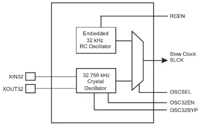
flowchart
graph TD
    A["XIN32"] --> B["32.768 kHz Crystal Oscillator"]
    C["XOUT32"] --> B
    B --> D["Embedded 32 kHz RC Oscillator"]
    D --> E["Slow Clock SLCK"]
    F["OSCSEL"] --> E
    G["OSC32EN"] --> E
    H["OSC32BYP"] --> E
    I["RCEN"] --> D
23.4 Functional Description
The bits RCEN, OSC32EN, OSCSEL, and OSC32BYP are located in the Slow Clock Controller Configuration Register (SCKC_CR) located at the address 0xFFFFFE50 in the backed-up part of the System Controller and, thus, they are preserved while VDDBU is present. The embedded 32 kHz (typical) RC oscillator and the 32.768 kHz crystal oscillator can be enabled by setting to 1, respectively, the RCEN and OSC32EN bits. The Slow Clock Selector command (OSCSEL bit) selects the slow clock source.
The 32.768 kHz crystal oscillator can be bypassed by setting the OSC32BYP bit to accept an external slow clock on XIN32.
After the VDDBU power-on reset, the default configuration is RCEN = 1, OSC32EN = 0 and OSCSEL = 0, allowing the system to start on the embedded 32 kHz (typical) RC oscillator.
The programmer controls the slow clock switching by software and so must take precautions during the switching phase.
23.4.1 Switching from Embedded 32 kHz RC Oscillator to 32.768 kHz Crystal Oscillator
The sequence to switch from the embedded 32 kHz (typical) RC oscillator to the 32.768 kHz crystal oscillator is the following:
- Switch the master clock to a source different from slow clock (PLL or Main Oscillator) through the Power Management Controller.
- Enable the 32.768 kHz crystal oscillator by writing a 1 to the OSC32EN bit.
- Wait for the 32.768 kHz crystal oscillator to stabilize (software loop).
- Switch from the embedded 32 kHz (typical) RC oscillator to the 32.768 kHz crystal oscillator by writing a 1 to the OSCSEL bit.
- Wait 5 slow clock cycles for internal resynchronization.
- Disable the 32 kHz (typical) RC oscillator by writing a 0 to the RCEN bit.
23.4.2 Bypassing the 32.768 kHz Crystal Oscillator
The sequence to bypass the 32.768 kHz crystal oscillator is the following:
-
An external clock must be connected on XIN32.
-
Enable the bypass path by writing a 1 to the OSC32BYP bit.
- Disable the 32.768 kHz crystal oscillator by writing a 0 to the OSC32EN bit.
23.4.3 Switching from 32.768 kHz Crystal Oscillator to Embedded 32 kHz RC Oscillator
The sequence to switch from the 32.768 kHz crystal oscillator to the embedded 32 kHz (typical) RC oscillator is the following:
- Switch the master clock to a source different from slow clock (PLL or Main Oscillator).
- Enable the embedded 32 kHz (typical) RC oscillator for low power by writing a 1 to the RCEN bit.
- Wait for the embedded 32 kHz (typical) RC oscillator to stabilize (software loop).
- Switch from the 32.768 kHz crystal oscillator to the embedded RC oscillator by writing a 0 to the OSCSEL bit.
- Wait 5 slow clock cycles for internal resynchronization.
- Disable the 32.768 kHz crystal oscillator by writing a 0 to the OSC32EN bit.
23.5 Slow Clock Controller (SCKC) User Interface
0: 32 kHz (typical) RC oscillator is disabled.
1: 32 kHz (typical) RC oscillator is enabled.
OSC32EN: 32.768 kHz Crystal Oscillator
0: 32.768 kHz crystal oscillator is disabled.
1: 32.768 kHz crystal oscillator is enabled.
OSC32BYP: 32.768 kHz Crystal Oscillator Bypass
0: 32.768 kHz crystal oscillator is not bypassed.
1: 32.768 kHz crystal oscillator is bypassed and accepts an external slow clock on XIN32.
OSCSEL: Slow Clock Selector
0 (RC): Slow clock is the embedded 32 kHz (typical) RC oscillator.
1 (XTAL): Slow clock is the 32.768 kHz crystal oscillator.
24. Fuse Controller (FUSE)
24.1 Description
The Fuse Controller (FUSE) supports software fuse programming through a 32-bit register. Only fuses set to level '1' are programmed. The fast (main) RC oscillator must be enabled at startup to access the fuse matrix.
It reads the fuse states on startup and stores them into 32-bit registers. The first eight Fuse Status registers (FUSE_SRx) can be masked and will read as a value of '0' regardless of the fuse state when masked.
24.2 Embedded Characteristics
- Software Fuse Programming
- User Write Access for Fuse
- Part of Fuse can be Masked After Read
- 256 FUSE bits:
- 192 bits are dedicated to Users
- 3 bits are dedicated to Special Functions
- The Fuse Controller can be hidden thanks to an SFR write-once bit. Refer to Section 15. Special Function Registers (SFR).
To avoid any malfunctioning, the user must not write the "DO NOT USE (DNU)" FUSE bits.
The user is allowed to set special bits as described in the following table.
Table 24-2: Special Bits
| Bit Number Bit Name Function | |
| 162 B BMS_SAMPLING_DISABLED - BMS sampling is disabled if set | |
| 161 J JTAG_DISABLED - JTAG is disabled if set | |
| 160 W FUSE_WRITE_DISABLED - FUSE bit writing is disabled if set | |
24.3 Block Diagram
Figure 24-1: FUSE Block Diagram
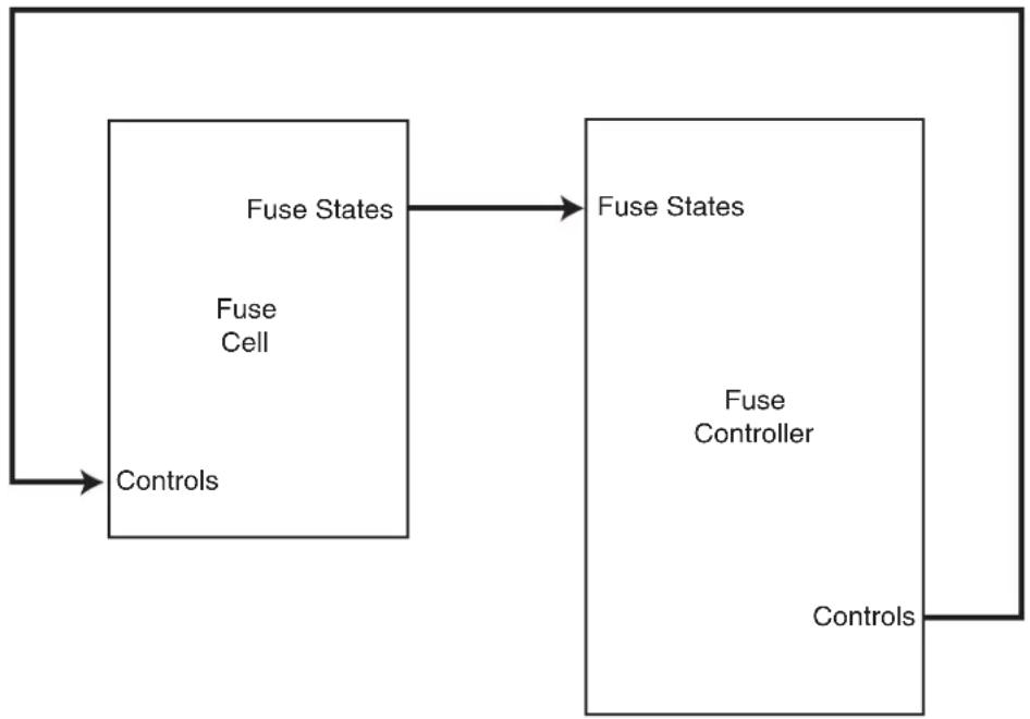
flowchart
graph LR
    A["Controls"] --> B["Fuse States"]
    B --> C["Fuse States"]
    C --> D["Fuse Controller"]
    D --> E["Controls"]
    F["Fuse Cell"] --> B
24.4 Functional Description
24.4.1 Fuse Reading
The fuse states are automatically read on CORE startup and are available for reading in the eight Fuse Status (FUSE_SRx) registers. The fuse states of bits 31 to 0 will be available at FUSE_SR0, the fuse states of bits 63 to 32 will be available at FUSE_SR1 and so on. FUSE_SRx registers can be updated manually by using the RRQ bit of the Fuse Control register (FUSE_CR). RS and WS bits of the Fuse Index register (FUSE_IR) must be at level one before issuing the read request.
Figure 24-2: Fuse Read

text_image
Clock FUSE_SRx outdated up to date RRQ WS RS24.4.2 Fuse Programming
All the fuses, except Microchip reserved fuses, can be written by software. To program fuses, strictly follow the order of the sequence instructions as provided below:
-
Select the word to write, using the WSEL field of the Fuse Index register (FUSE_IR).
-
Write the word to program in the Fuse Data register (FUSE_DR).
-
Check that RS and WS bits of the FUSE_IR are at level one (no read and no write pending).
-
Write the WRQ bit of the Fuse Control register (FUSE_CR) to begin the fuse programming. The KEY field must be written at the same time with a value 0xFB to make the write request valid. Writing the WRQ bit will clear the WS bit.
-
Check the WS bit of FUSE_IR. When WS has a value of '1' the fuse write process is over.
Only fuses to be set to level '1' are written.
Figure 24-3: Fuse Write
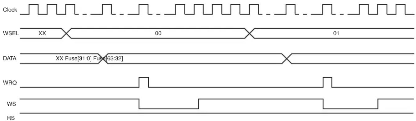
text_image
Clock WSEL XX 00 01 DATA XX Fuse[31:0] Fuse[63:32] WRQ WS RS24.4.3 Fuse Masking
It is possible to mask the first eight FUSE_SRx registers so that they will be read at a value of '0', regardless of the fuse state.
To activate fuse masking on the first eight FUSE_SRx registers, the MSK bit of the Fuse Mode register (FUSE_MR) must be written to level '1'. The MSK bit is write-only. Only a general reset can disable fuse masking.
24.5 Fuse Controller (FUSE) User Interface
Table 24-3: Register Mapping
| Offset Register Name Access Reset | ||||
| 0x00 Fuse Control Register FUSE_CR Write-only | - | |||
| 0x04 | Fuse Mode Register | FUSE_MR | Write-only | - |
| 0x08 | Fuse Index Register | FUSE_IR | Read-write | 0x00000000 |
| 0x0C | Fuse Data Register | FUSE_DR | Read-write | - |
| 0x10 | Fuse Status Register 0 | FUSE_SR0 | Read-only | 0x00000000 |
| 0x14 | Fuse Status Register 1 | FUSE_SR1 | Read-only | 0x00000000 |
| ... | ... | ... | ... | ... |
| 0x2C | Fuse Status Register 7 | FUSE_SR7 | Read-only | 0x00000000 |
| 0x30–0xDC | Reserved | - | - | - |
| 0xE0–0xFC Reserved | - | - | - | |
Note 1: Values in the Version Register vary with the version of the IP block implementation.
24.5.1 Fuse Control Register
Name: FUSE_CR
Address:0xFFFFE400
Access:Write-only
31 30 29 28 27 26 25 24
| - | - | - | - | - | - | - | - |
23 22 21 20 19 18 17 16
| - | - | - | - | - | - | - | - |
15 14 13 12 11 10 9 8
| KEY | |||||||
| 7 | 6 | 5 | 4 | 3 | 2 | 1 | 0 |
| - | - | - | - | - | - | R | R |
WRQ: Write Request
0: No effect.
1: Requests the word DATA to be programmed if KEY field value is 0xFB.
RRQ: Read Request
0: No effect.
1: Requests the fuses to be read and FUSE_SRx registers to be updated if KEY field value is 0xFB.
KEY: Key Code
| Value Name Description | ||
| 0xFB VALID | Writing any other value in this field aborts the write operation of the WRQ and RRQ bits.Always reads as 0. | |
24.5.2 Fuse Mode Register
Name: FUSE_MR
Address:0xFFFFE404
Access:Write-only
31 30 29 28 27 26 25 24
| - | - | - | - | - | - | - | - |
23 22 21 20 19 18 17 16
| - | - | - | - | - | - | - | - |
15 14 13 12 11 10 9 8
| - | - | - | - | - | - | - | - |
7 6 5 4 3 2 1 0
| - | - | - | - | - | - | - | M |
MSK: Mask Fuse Status Registers
0: No effect.
1: Masks the first eight FUSE_SRx registers.
24.5.3 Fuse Index Register
Name: FUSE_IR
Address:0xFFFFE408
Access: Read-write
31 30 29 28 27 26 25 24
| - | - | - | - | - | - | - | - |
23 22 21 20 19 18 17 16
| - | - | - | - | - | - | - | - |
15 14 13 12 11 10 9 8
| - | - | - | - | W | S | E |
| 7 | 6 | 5 | 4 | 3 | 2 | 1 | 0 |
| - | - | - | - | - | - | R | S |
WS: Write Status
0: Write is pending or no write has been requested since general reset.
1: Write of fuses is done.
RS: Read Status
0: Read is pending or no read has been requested since general reset.
1: Read of fuses is done.
WSEL: Word Selection
0–15: Selects the word to write.
24.5.4 Fuse Data Register
Name: FUSE_DR
Address:0xFFFFE40C
Access: Read-write
31 30 29 28 27 26 25 24
| DATA | |||||||
| 23 22 21 20 19 18 17 16 | |||||||
| DATA | |||||||
| 15 14 13 12 11 10 9 8 | |||||||
| DATA | |||||||
| 7 | 6 | 5 | 4 | 3 | 2 | 1 | 0 |
| DATA | |||||||
DATA: Data to Program
Data to program. Only bits with a value of '1' will be programmed.
24.5.5 Fuse Status Register
Name: FUSE_SRx [x=0..7]
Address:0xFFFFE410
Access:Read-only
31 30 29 28 27 26 25 24
| FUSE | |||||||
| 23 22 21 20 19 18 17 16 | |||||||
| FUSE | |||||||
| 15 14 13 12 11 10 9 8 | |||||||
| FUSE | |||||||
| 7 | 6 | 5 | 4 | 3 | 2 | 1 | 0 |
| FUSE | |||||||
FUSE: Fuse Status
Indicates the status of corresponding fuses:
0: Unprogrammed.
1: Programmed.
25. Clock Generator
25.1 Description
The Clock Generator User Interface is embedded within the Power Management Controller and is described in Section 26.17 Power Management Controller (PMC) User Interface. However, the Clock Generator registers are named CKGR_.
25.2 Embedded Characteristics
The Clock Generator is made up of:
- A low-power 32.768 kHz crystal oscillator with Bypass mode
- A low-power embedded 32 kHz (typical) RC oscillator generating the 32 kHz source clock
- An 8 to 48 MHz crystal oscillator or a 12 to 48 MHz XRCGB crystal resonator with Bypass mode
• A 12 MHz RC oscillator
• A 480 MHz UTMI PLL providing a clock for the USB High Speed Device Controller - A 400 to 1000 MHz programmable PLL (input from 8 to 50 MHz), capable of providing the clock MCK to the processor and to the peripherals (HCLOCK and PCLOCK)
The Clock Generator provides the following clocks:
- SLCK, the Slow Clock, which is the only permanent clock within the system
- MAINCK is the output of the main clock oscillator selection: either 8 to 48 MHz crystal oscillator or 12 MHz RC oscillator
- PLLACK is the output of the divider and the 400 to 1000 MHz programmable PLL (PLLA)
- UPLLCK is the output of the 480 MHz UTMI PLL (UPLL)
- SMDCK is the Software Modem Clock
The Power Management Controller also provides the following operations on clocks:
- 8 to 48 MHz crystal oscillator clock failure detector
• 32.768 kHz crystal oscillator frequency monitor - Frequency counter on main clock and an on-the-fly adjustable 12 MHz RC oscillator frequency
25.3 Block Diagram
Figure 25-1: Clock Generator Block Diagram
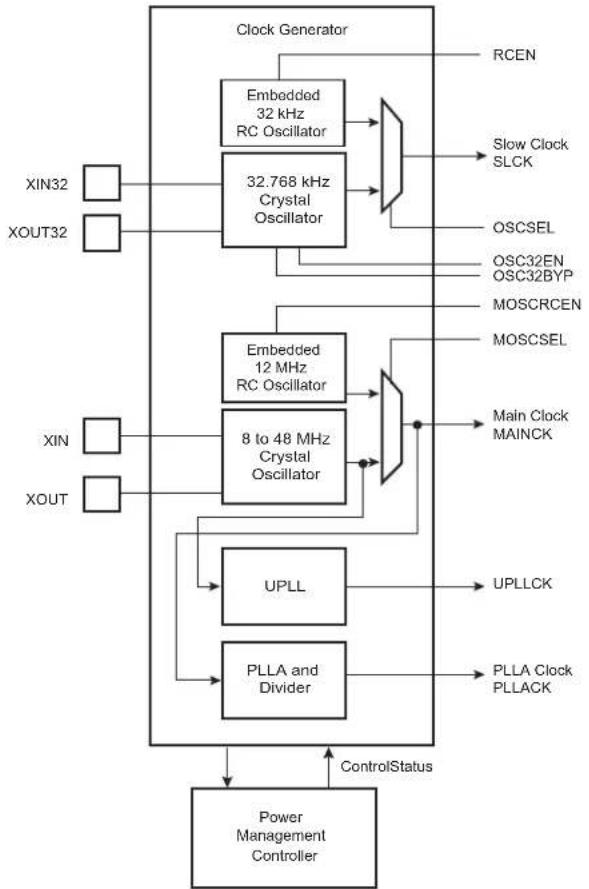
flowchart
graph TD
    A["Clock Generator"] --> B["Embedded 32 kHz RC Oscillator"]
    A --> C["32.768 kHz Crystal Oscillator"]
    B --> D["Slow Clock SLCK"]
    C --> E["OSCSEL"]
    C --> F["OSC32EN OSC32BYP"]
    C --> G["MOSCRCEN"]
    C --> H["MOSCSEL"]
    I["XIN32"] --> J["Power Management Controller"]
    K["XOUT32"] --> J
    L["XIN"] --> M["8 to 48 MHz Crystal Oscillator"]
    N["XOUT"] --> M
    O["UPLL"] --> P["UPLLCK"]
    Q["PLLA and Divider"] --> R["PLLA Clock PLLACK"]
    S["ControlStatus"] --> J
    S --> M
25.4 Slow Clock
The Slow Clock Controller embeds a slow clock generator that is supplied with the VDDBU power supply. As soon as VDDBU is supplied, both the 32.768 kHz crystal oscillator and the embedded 32 kHz (typical) RC oscillator are powered, but only the RC oscillator is enabled. This allows the slow clock to be valid in a short time (about 100 s).
The slow clock is generated either by the 32.768 kHz crystal oscillator or by the embedded 32 kHz (typical) RC oscillator.
The selection of the slow clock source is made via the OSCSEL bit in the Slow Clock Controller Configuration register (SCKC_CR).
SCKC_CR.OSCSEL and PMC_SR.OSCSELS report which oscillator is selected as the slow clock source. PMC_SR.OSCSELS informs when the switch sequence initiated by a new value written in SCKC_CR.OSCSEL is done.
25.4.1 Embedded 32 kHz (typical) RC Oscillator
By default, the embedded 32 kHz (typical) RC oscillator is enabled and selected. The user has to take into account the possible drifts of this oscillator. Refer to Table 54-2 DC Characteristics in Section 54. Electrical Characteristics.
This oscillator is disabled by clearing SCKC_CR.RCEN.
25.4.2 32.768 kHz Crystal Oscillator
The Clock Generator integrates a low-power 32.768 kHz crystal oscillator. To use this oscillator, the XIN32 and XOUT32 pins must be connected to a 32.768 kHz crystal. Two external capacitors must be wired as shown in Figure 25-2. More details are given in the section "DC Characteristics".
Note that the user is not obliged to use the 32.768 kHz crystal oscillator and can use the 32 kHz (typical) RC oscillator instead.
Figure 25-2: Typical 32.768 kHz Crystal Oscillator Connection

text_image
XIN32 XOUT32 GND 32.768 kHz CrystalThe 32.768 kHz crystal oscillator provides a more accurate frequency than the 32 kHz (typical) RC oscillator.
To select the 32.768 kHz crystal oscillator as the source of the slow clock, the bit SCKC_CR.OSCSEL must be set. This results in a sequence which enables the 32.768 kHz crystal oscillator and then disables the 32 kHz (typical) RC oscillator to save power. The switch of the slow clock source is glitch-free.
The user can also set the 32.768 kHz crystal oscillator in Bypass mode instead of connecting a crystal. In this case, the user must provide the external clock signal on XIN32. The input characteristics of the XIN32 pin are given in the section "Electrical Characteristics". To enter Bypass mode, the SCKC_CR.OSC32BYP must be set prior to setting SCKC_CR.OSCSEL.
25.5 Main Clock
The main clock has two sources:
- a 12 MHz RC oscillator with a fast startup time and used at startup
- an 8 to 48 MHz crystal oscillator which can be bypassed
Figure 25-3: Main Clock Block Diagram
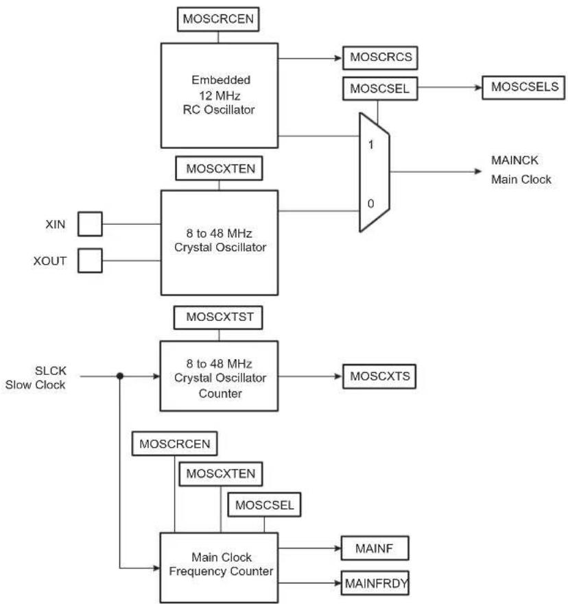
flowchart
graph TD
    A["MOSCRCEN"] --> B["Embedded 12 MHz RC Oscillator"]
    B --> C["MOSCCRCS"]
    B --> D["MOSCSEL"]
    D --> E["MOSCSELS"]
    F["XIN"] --> G["8 to 48 MHz Crystal Oscillator"]
    H["XOUT"] --> G
    I["MOSCXTEN"] --> G
    J["0"] --> K["1"]
    K --> L["0"]
    M["SLCK Slow Clock"] --> N["8 to 48 MHz Crystal Oscillator Counter"]
    N --> O["MOSCXTS"]
    P["MOSCCTEN"] --> Q["Main Clock Frequency Counter"]
    R["MOSCSEL"] --> Q
    S["MAINFRDY"] --> Q
    T["MAINF"] --> Q
25.5.1 12 MHz RC Oscillator
After reset, the 12 MHz RC oscillator is enabled and it is selected as the source of MCK. MCK is the default clock selected to start up the system.
Refer to Table 54-2 DC Characteristics.
The software can disable or enable the 12 MHz RC oscillator with the MOSCRCEN bit in CKGR_MOR.
When disabling the main clock by clearing the MOSCRCEN bit in CKGR_MOR, the MOSCRCS bit in PMC_SR is automatically cleared, indicating the main clock is off.
Setting the MOSCRCS bit in the Interrupt Enable register (PMC_IER) can trigger an interrupt to the processor.
25.5.2 12 MHz RC Oscillator Clock Frequency Adjustment
If an external 32 KHz crystal is used, it is possible for the user to adjust the 12 MHz RC oscillator frequency through the PMC Oscillator Calibration Register (PMC_OCR). By default, the SEL bit in PMC_OCR is low, so the RC oscillator is driven with fuse calibration bits which are programmed during the chip production.
The user can adjust the trimming of the 12 MHz RC oscillator through PMC_OCR in order to obtain more accurate frequency (to compensate derating factors such as temperature and voltage).
In order to calibrate the 12 MHz oscillator frequency, SEL must be set to 1 and a correct frequency value must be configured in the CAL field.
Bit 6 of the field CAL[6:0] is a sign bit. Increasing the CAL field value (highest code) increases the 12 MHz RC oscillator output frequency with a typical 55 kHz step.
| 0111111 Highest code | |
| 0111110 | |
| ...... | |
| 0000010 | |
| 0000001 | |
| 0000000 Middle code | |
| 1111111 | |
| 1111110 | |
| ...... | |
| 1000010 | |
| 1000001 | |
| 1000000 Lowest code | |
It is possible to restart, at anytime, a measurement of the frequency of the selected clock by means of the RCMEAS bit in the Clock Generator Main Clock Frequency register (CKGR_MCFR). Thus, when MAINFRDY flag reads 1, another read access on CKGR_MCFR provides an image of the frequency of the main clock on MAINF field. The software can calculate the error with an expected frequency and correct the CAL field in PMC_OCR accordingly. This may be used to compensate frequency drift due to derating factors such as temperature and/or voltage.
25.5.3 8 to 48 MHz Crystal Oscillator
After reset, the 8 to 48 MHz crystal oscillator is disabled and is not selected as the source of MAINCK.
As the source of MAINCK, the 8 to 48 MHz crystal oscillator provides an accurate frequency. The software enables or disables this oscillator in order to reduce power consumption via CKGR_MOR.MOSCXTEN.
When disabling this oscillator by clearing the CKGR_MOR.MOSCXTEN bit, the PMC_SR.MOSCXTS bit is automatically cleared, indicating the 8 to 48 MHz crystal oscillator is off.
When enabling this oscillator, the user must initiate the startup time counter. This startup time depends on the characteristics of the external device connected to this oscillator. Refer to Section 54. Electrical Characteristics for the startup time.
When CKGR_MOR.MOSCXTEN and CKGR_MOR.MOSCXTST are written to enable this oscillator, the PMC_SR.MOSCXTS bit is cleared and the counter starts counting down on the slow clock divided by 8 from the MOSCXTST value. When the counter reaches 0, the PMC_SR.MOSCXTS is set, indicating that the 8 to 48 MHz crystal oscillator is stabilized. Setting PMC_IMR.MOSCXTS triggers an interrupt to the processor.
25.5.4 Main Clock Source Selection
The main clock is generated by the 8 to 48 MHz crystal oscillator, an XRCGB crystal resonator or by the embedded 12 MHz RC oscillator.
The selection is made by writing CKGR_MOR.MOSCSEL. The switch of the main clock source is glitch-free, so there is no need to run out of SLCK or PLLACK in order to change the selection. PMC_SR.MOSCSELS indicates when the switch sequence is done.
Setting PMC_IMR.MOSCSELS triggers an interrupt to the processor.
The 8 to 48 MHz crystal oscillator can be bypassed by setting the MOSCXTBY bit in CKGR_MOR to accept an external main clock on XIN (refer to Section 25.5.5 Bypassing the 8 to 48 MHz Crystal Oscillator).
Figure 25-4: Main Clock Source Selection
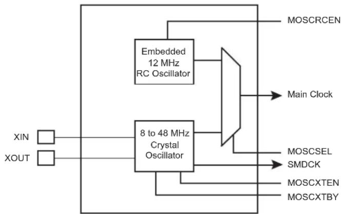
flowchart
graph TD
    A["XIN"] --> B["8 to 48 MHz Crystal Oscillator"]
    C["XOUT"] --> B
    B --> D["MOSCRCEN"]
    B --> E["Main Clock"]
    B --> F["MOSCSEL"]
    B --> G["SMDCK"]
    B --> H["MOSCXTEN"]
    B --> I["MOSCXTBY"]
    D --> J["Embedded 12 MHz RC Oscillator"]
    E --> J
    F --> J
    G --> J
    H --> J
    I --> J
MOSCRCEN, MOSCXTEN, MOSCSEL and MOSCXTBY bits are located in the PMC Clock Generator Main Oscillator Register (CKGR_MOR).
After a VDDBU power-on reset, the default configuration is MOSCRCEN = 1, MOSCXTEN = 0 and MOSCSEL = 0, allowing the 12 MHz RC oscillator to start as Main clock.
25.5.5 Bypassing the 8 to 48 MHz Crystal Oscillator
Prior to bypassing the 8 to 48 MHz crystal oscillator, the external clock frequency provided on the XIN pin must be stable and within the values specified in the XIN Clock characteristics in the section "Electrical Characteristics".
The sequence to bypass the crystal oscillator is the following:
- Ensure that an external clock is connected on XIN.
- Enable the bypass by setting CKGR_MOR.MOSCXTBY.
- Disable the 8 to 48 MHz crystal oscillator by clearing CKGR_MOR.MOSCXTEN.
25.5.6 Main Clock Frequency Counter
The frequency counter is managed by CKGR_MCFR.
During the measurement period, the frequency counter increments at the main clock speed.
A measurement is started in the following cases:
- When the RCMEAS bit of CKGR_MCFR is written to 1.
- When the 12 MHz RC oscillator is selected as the source of the main clock and when this oscillator becomes stable (i.e., when the MOSCRCS bit is set)
- When the 8 to 48 MHz crystal oscillator is selected as the source of the main clock and when this oscillator becomes stable (i.e., when the MOSCXTS bit is set)
- When the main clock source selection is modified
The measurement period ends at the 16th falling edge of the slow clock, the MAINFRDY bit in CKGR_MCFR is set and the counter stops counting. Its value can be read in the MAINF field of CKGR_MCFR and gives the number of main clock cycles during 16 periods of slow clock, so that the frequency of the 12 MHz RC oscillator or the crystal oscillator can be determined.
25.5.7 Switching Main Clock Between the RC Oscillator and the Crystal Oscillator
When switching the source of the main clock between the RC oscillator and the crystal oscillator, both oscillators must be enabled. After completion of the switch, the unused oscillator can be disabled.
If switching to the crystal oscillator, a check must be carried out to ensure that the oscillator is present and that its frequency is valid. Follow the sequence below:
- Select the slow clock as MCK by configuring bit CSS = 0 in the Master Clock register (PMC_MCKR).
- Wait for PMC_SR.MCKRDY flag in PMC_SR to rise.
- Enable the crystal oscillator by setting CKGR_MOR.MOSCXTEN. Configure the CKGR_MOR. MOSCXTST field with the crystal oscillator start-up time as defined in the section "Electrical Characteristics".
- Wait for PMC_SR.MOSCXTS flag to rise, indicating the end of a start-up period of the crystal oscillator.
- Select the crystal oscillator as the source of the main clock by setting CKGR_MOR.MOSCSEL.
- Read CKGR_MOR.MOSCSEL until its value equals 1.
- Check the status of PMC_SR.MOSCSELS flag:
- If MOSCSELS = 1: There is a crystal oscillator connected.
a) Initiate a new frequency measurement by setting CKGR_MCFR.RCMEAS.
b) Read CKGR_MCFR.MAINFRDY unit its value equals 1.
c) Read CKGR_MCFR.MAINF and compute the value of the crystal frequency.
d) If the MAINF value is valid, the main clock can be switched to the crystal oscillator.
- If MOSCSELS = 0: There is no crystal oscillator connected or the crystal oscillator is out of specification.
- Select the RC oscillator as the source of the main clock by clearing CKGR_MOR.MOSCSEL.
25.6 Divider and PLLA Block
The PLLA embeds an input divider to increase the accuracy of the resulting clock signals. However, the user must respect the PLLA minimum input frequency when programming the divider.
Figure 25-5 shows the block diagram of the divider and PLLA block.
Figure 25-5: Divider and PLLA Block Diagram

flowchart
graph LR
    A["MAINCK PLLACK"] --> B["Divider"]
    B --> C["PLLA"]
    C --> D["PLLACOUNT"]
    D --> E["PLLA Counter"]
    E --> F["LOCKA"]
    G["DIVA"] --> B
    H["MULA"] --> C
    I["OUTA"] --> C
    J["SLCK"] --> E
25.6.1 Divider and Phase Lock Loop Programming
The divider can be set between 1 and 255 in steps of 1. When a divider field (DIV) is cleared, the output of the corresponding divider and the PLL output is a continuous signal at level 0. On reset, each DIV field is cleared, thus the corresponding PLL input clock is stuck at 0.
The PLLA allows multiplication of the divider's outputs. The PLLA clock signal has a frequency that depends on the respective source signal frequency and on the parameters DIVA and MULA. The factor applied to the source signal frequency is (MULA + 1)/DIVA . When MULA is written to 0, the PLLA is disabled and its power consumption is saved. Re-enabling the PLLA can be performed by writing a value higher than 0 in the MUL field.
Whenever the PLLA is re-enabled or one of its parameters is changed, the LOCKA bit in PMC_SR is automatically cleared. The values written in the PLLACOUNT field in CKGR_PLLAR are loaded in the PLLA counter. The PLLA counter then decrements at the speed of the slow clock until it reaches 0. At this time, the LOCK bit is set in PMC_SR and can trigger an interrupt to the processor. The user has to load the number of slow clock cycles required to cover the PLLA transient time into the PLLACOUNT field.
The PLLA clock must be divided by 2 by writing the PLLADIV2 bit in PMC_MCKR, if the ratio between Processor Clock (PCK) and MCK is 3 (MDIV = 3).
25.7 UTMI Phase Lock Loop Programming
The source clock of the UTMI PLL is the main clock (MAINCK). The MAINCK must select the fast crystal oscillator to meet the frequency accuracy required by USB.
The crystal frequency selection among 12, 16, 24 or 48 MHz must be configured to the correct value in the field SFR_UTMICKTRIM.FREQ, in order to apply the correct multiplier, x40, x30, x20 or x10, respectively.
Figure 25-6: UTMI PLL Block Diagram
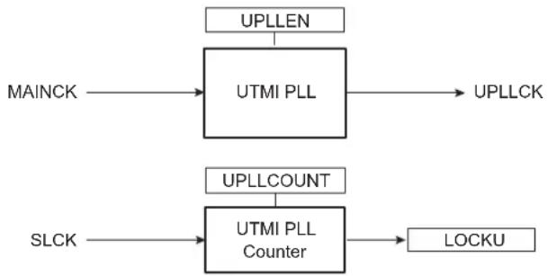
flowchart
graph TD
    A["MAINCK"] --> B["UTMI PLL"]
    C["SLCK"] --> D["UTMI PLL Counter"]
    B --> E["UPLLCK"]
    D --> F["LOCKU"]
    G["UPLLLEN"] --> B
    H["UPLLCOUNT"] --> D
Whenever the UTMI PLL is enabled by writing UPLLEN in CKGR_UCKR, the LOCKU bit in PMC_SR is automatically cleared. The values written in the PLLCOUNT field in CKGR_UCKR are loaded in the UTMI PLL counter. The UTMI PLL counter then decrements at the speed of the slow clock divided by 8 until it reaches 0. At this time, the LOCKU bit is set in PMC_SR and can trigger an interrupt to the processor. The user has to load the number of slow clock cycles required to cover the UTMI PLL transient time into the PLLCOUNT field.
26. Power Management Controller (PMC)
26.1 Description
The Power Management Controller (PMC) optimizes power consumption by controlling all system and user peripheral clocks. The PMC enables/disables the clock inputs to many of the peripherals and the Core.
26.2 Embedded Characteristics
The Power Management Controller provides the following clocks:
- Master Clock (MCK)—programmable from a few hundred Hz to the maximum operating frequency of the device. It is available to the modules running permanently.
- Processor Clock (PCK)—must be switched off when processor is entering Idle mode
• USB Device HS Clock (UDPCK) - Software Modem Clock (SMDCK)
- Peripheral Clocks (typically MCK)—provided to the embedded peripherals (USART, SSC, SPI, TWI, TC, HSMCI, etc.) and independently controllable. In order to reduce the number of clock names in a product, the Peripheral Clocks are named MCK.
- Programmable Clock Outputs can be selected from the clocks provided by the clock generator and driven on the PCKx pins.
26.3 Block Diagram
Figure 26-1: General Clock Block Diagram

flowchart
graph TD
    A["PLLACK"] --> B["/2"]
    B --> C["1 0"]
    C --> D["PLLADIV2"]
    D --> E["USBS"]
    E --> F["USBDIV + 1"]
    F --> G["/4"]
    G --> H["USB OHCI"]
    G --> I["USB EHCI"]
    F --> J["UHP48M"]
    G --> K["UHP12M"]
    J --> L["Master Clock Controller (PMC_MCKR)"]
    K --> M["Processor Clock Controller"]
    L --> N["Prescaler /1, /2, /4,.../64"]
    M --> O["Divider /1, /2, /3, /4"]
    N --> P["Master Clock Controller (PMC_MCKR)"]
    O --> Q["Processor Clock Controller"]
    P --> R["Processor Clock Controller"]
    Q --> S["Processor Clock Controller"]
    R --> T["Processor Clock Controller"]
    S --> U["Processor Clock Controller"]
    T --> V["Processor Clock Controller"]
    U --> W["Processor Clock Controller"]
    V --> X["Processor Clock Controller"]
    W --> Y["Processor Clock Controller"]
    X --> Z["Processor Clock Controller"]
    Y --> AA["Processor Clock Controller"]
    Z --> AB["Processor Clock Controller"]
    AA --> AC["Processor Clock Controller"]
    AB --> AD["Processor Clock Controller"]
    AC --> AE["Processor Clock Controller"]
    AD --> AF["Processor Clock Controller"]
    AE --> AG["Processor Clock Controller"]
    AF --> AH["Processor Clock Controller"]
    AG --> AI["Processor Clock Controller"]
    AH --> AJ["Processor Clock Controller"]
    AI --> AK["Processor Clock Controller"]
    AJ --> AL["Processor Clock Controller"]
    AK --> AM["Processor Clock Controller"]
    AL --> AN["Processor Clock Controller"]
    AM --> AO["Processor Clock Controller"]
    AN --> AP["Processor Clock Controller"]
    AO --> AQ["Processor Clock Controller"]
    AP --> AR["Processor Clock Controller"]
    AQ --> AS["Processor Clock Controller"]
    AR --> AT["Processor Clock Controller"]
    AS --> AU["Processor Clock Controller"]
    AT --> AV["Processor Clock Controller"]
    AU --> AW["Processor Clock Controller"]
    AV --> AX["Processor Clock Controller"]
    AW --> AY["Processor Clock Controller"]
    AX --> AZ["Processor Clock Controller"]
    AY --> BA["Processor Clock Controller"]
    AZ --> BB["Processor Clock Controller"]
    BA --> BC["Processor Clock Controller"]
    BB --> BD["Processor Clock Controller"]
    BC --> BE["Processor Clock Controller"]
    BD --> BF["Processor Clock Controller"]
    BE --> BG["Processor Clock Controller"]
    BF --> BH["Processor Clock Controller"]
    BG --> BI["Processor Clock Controller"]
    BH --> BJ["Processor Clock Controller"]
    BI --> BK["Processor Clock Controller"]
    BJ --> BL["Processor Clock Controller"]
    BK --> BM["Processor Clock Controller"]
    BL --> BN["Processor Clock Controller"]
    BM --> BO["Processor Clock Controller"]
    BN --> BP["Processor Clock Controller"]
    BO --> BQ["Processor Clock Controller"]
26.4 Master Clock Controller
The Master Clock Controller provides selection and division of the Master Clock (MCK). MCK is the source clock of the peripheral clocks. The Master Clock is selected from one of the clocks provided by the Clock Generator. Selecting the slow clock provides a slow clock signal to the whole device. Selecting the main clock saves power consumption of the PLLs.
The Master Clock Controller is made up of a clock selector and a prescaler. It also contains a Master Clock divider which allows the processor clock to be faster than the Master Clock.
The Master Clock selection is made by writing the CSS (Clock Source Selection) field in PMC_MCKR (Master Clock register). The prescaler supports the division by a power of 2 of the selected clock between 1 and 64, and the division by 6. The PRES field in PMC_MCKR programs the prescaler.
Note: It is forbidden to modify MDIV and CSS at the same access. Each field must be modified separately with a wait for MCKRDY flag between the first field modification and the second field modification.
Each time PMC_MCKR is written to define a new Master Clock, the MCKRDY bit is cleared in PMC_SR. It reads 0 until the Master Clock is established. Then, the MCKRDY bit is set and can trigger an interrupt to the processor. This feature is useful when switching from a high-speed clock to a lower one to inform the software when the change is actually done.
Figure 26-2: Master Clock Controller
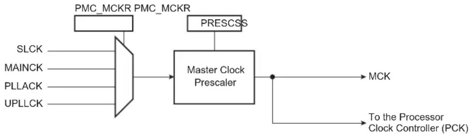
flowchart
graph LR
    A["SLCK"] --> B["Master Clock Prescaler"]
    C["MAINCK"] --> B
    D["PLLACK"] --> B
    E["UPLLCK"] --> B
    F["PMC_MCKR"] --> B
    G["PMC_MCKR"] --> B
    H["PRESCSS"] --> B
    B --> I["MCK"]
    B --> J["To the Processor Clock Controller (PCK)"]
26.5 Processor Clock Controller
The PMC features a Processor Clock (PCK) Controller that implements the processor Idle mode.
The processor clock can be disabled by executing the WFI (WaitForInterrupt) processor instruction.
The processor clock can be disabled by writing the PMC System Clock Disable Register (PMC_SCDR). The status of this clock (at least for debug purposes) can be read in the PMC System Clock Status Register (PMC_SCSR).
The processor clock is enabled after a reset and is automatically re-enabled by any enabled interrupt. The processor Idle mode is achieved by disabling the processor clock, which is automatically re-enabled by any enabled fast or normal interrupt, or by the reset of the product.
When processor Idle mode is entered, the current instruction is finished before the clock is stopped, but this does not prevent data transfers from other masters of the system bus.
26.6 LCDC Clock Controller
In order to have more flexibility on the pixel clock, the LCDC can use MCK or MCKx2, if LCDCK is set in the PMC System Clock Enable Register (PMC_SCER).
Figure 26-3: LCDCLK Clock Configuration
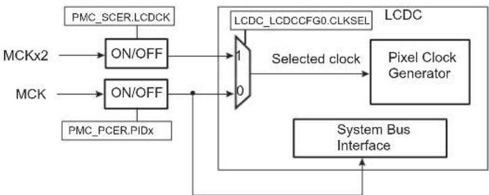
flowchart
graph TD
    A["PMC_SCER.LCDCK"] --> B["ON/OFF"]
    C["MCKx2"] --> B
    D["MCK"] --> E["ON/OFF"]
    F["PMC_PCER.PIDx"] --> E
    B --> G["1"]
    E --> H["0"]
    G --> I["Selected clock"]
    H --> I
    I --> J["LCDC_LCDCCFG0.CLKSEL"]
    J --> K["Pixel Clock Generator"]
    L["System Bus Interface"] --> M["Output"]
26.7 USB Device and Host Clocks
The USB Device and Host High Speed ports (UDPHS and UHPHS) clocks are enabled by the corresponding PIDx bits in PMC_PCERx. To save power on this peripheral when they are not used, the user can set these bits in PMC_PCDR. Corresponding PIDx bits in PMC_PCSR give the status of these clocks.
The PMC also provides the clocks UHP48M and UHP12M to the USB Host OHCI. The USB Host OHCI clocks are controlled by the UHP bit in PMC_SCER. To save power on this peripheral when they are not used, the user can set the UHP bit in PMC_SCDR. The UHP bit in PMC_SCSR gives the status of this clock. The USB host OHCI requires both the 12/48 MHz signal and the Master Clock. The USBDIV field in PMC_USB register is to be programmed to 9 (division by 10) for normal operations.
To further reduce power consumption the user can stop UTMI PLL, in this case USB high-speed operations are not possible. Nevertheless, as the USB OHCI Input clock can be selected with USBS bit (PLLA or UTMI PLL) in PMC_USB register, OHCI full-speed operation remains possible.
The user must program the USB OHCI Input Clock and the USBDIV divider in the PMC_USB register to generate a 48 MHz and a 12 MHz signal with an accuracy of ±0.25%.
The USB clock input is to be defined according to main oscillator via the FREQ field. This field is defined in the UTMI Clock Trimming register (SFR_UTMICKTRIM). Refer to Section 15. Special Function Registers (SFR). This input clock can be 12, 16, 24 or 48 MHz.
26.8 DDR2/LPDDR/LPDDR2 Clock
The PMC controls the clocks of the DDR memory.
The DDR clock can be enabled and disabled with the DDRCK bit respectively in PMC_SCER and PMC_SDER. At reset, the DDR clock is disabled to reduce power consumption.
In case MDIV = 0 (PCK = MCK), the DDRCK clock is not available.
To reduce PLLA power consumption, the user can choose UPLLCK as an input clock for the system. In this case the DDR Controller can drive LPDDR or LPDDR2 at up to 120 MHz.
26.9 Software Modem Clock
The PMC controls the clocks of the Software Modem.
SMDCK is a division of UPLL or PLLA.
26.10 Fast Startup from Ultra Low-power (ULP) Mode
In Ultra Low-power (ULP) mode, the main clock (MAINCK) must be running, thus either the 12 MHz crystal oscillator or the Fast RC oscillator must be enabled. The lowest power consumption that can be achieved in ULP Mode, can be obtained when dividing the selected oscillator frequency by 64 by writing the field PMC_MCKR.PRES to 6. Any interrupt exits the system from ULP Mode. The software must write PMC_MCKR.PRES to 1 to provide MCK with the fastest clock. If the PLL is used, the startup procedure must be done prior to write PMC_MCKR.PRES to 1. Figure 26-4 is an example of startup phase from ULP Mode without use of PLL.
Figure 26-4: Fast Startup from Ultra Low-Power Mode

text_image
MODE 12 MHz RC MCK Any interrupt ULP 187 kHz ACTIVE 12 MHz ULP 187 kHz Write PMC_MCKR.PRES = 0 (no division) Synchronization Period Synchronization Period Write PMC_SCDR.PCK = 1 Write PMC_MCKR.PRES = 6 (divided by 64) PMC_SR.MCKRDYWarning: The duration of the WKUPx pins active level must be greater than 4 MAINCK cycles.
26.11 Peripheral Clock Controller
The PMC controls the clocks of each embedded peripheral by means of the Peripheral Clock Controller. The user can individually enable and disable the clock on the peripherals and select a division factor from MCK. This is done in the Peripheral Control register (PMC_PCR). In order to reduce power consumption, the division factor can be 1, 2, 4 or 8.
The divisor is defined in PMC_PCR. To apply a division factor, PID, CMD and DIV must be written in a single operation. The target peripheral clock is defined by the PID field. The divisor value is defined by DIV and the bit CMD must be set. To read the current division factor associated with a peripheral clock, two separate operations must be performed:
- Write a zero to the CMD bit and configure PID for the target peripheral clock. DIV is not significant for this operation.
- Read PMC_PCR. The value of DIV is the divisor applied to the peripheral clock defined by PID.
When a peripheral clock is disabled, the clock is immediately stopped. The peripheral clocks are automatically disabled after a reset.
In order to stop a peripheral, it is recommended that the system software wait until the peripheral has executed its last programmed operation before disabling the clock. This is to avoid data corruption or erroneous behavior of the system.
The value written in the PID field in PMC_PCR is the Peripheral Identifier defined at the product level (refer to Section 8.2 Peripheral Identifiers). Generally, the field value corresponds to the interrupt source number assigned to the peripheral.
26.12 Programmable Clock Controller
The PMC controls three signals to be outputs on external pins PCKx. Each signal can be independently programmed via the PMC Programmable Clock register (PMC_PCKx).
PCKx can be independently selected between the Slow Clock (SLCK), the Master Clock (MAINCK), the PLLACK, the UTMI PLL output and the Main Clock by writing the CSS field in PMC_PCKx. Each output signal can also be divided by a power of 2 between 1 and 64 by writing the PRES (Prescaler) field in PMC_PCKx.
Each output signal can be enabled and disabled by writing a 1 in the corresponding bit, PCKx of PMC_SCER and PMC_SCDR, respectively. The status of the active programmable output clocks are given in the PCKx bits of PMC_SCSR.
The status bit PCKRDYx in PMC_SR indicates that the Programmable Clock programmed in PMC_PCKx is ready.
As the Programmable Clock Controller does not implement glitch prevention when switching clocks, it is strongly recommended to disable the Programmable Clock before any configuration change and to re-enable it after the change is actually performed.
26.13 Main Clock Failure Detector
The clock failure detector monitors the 8 to 48 MHz crystal oscillator or ceramic resonator-based oscillator to identify a possible failure of this oscillator.
The clock failure detector can be enabled or disabled by bit CFDEN in CKGR_MOR. After a VDDCORE reset, the detector is disabled. However, if the oscillator is disabled (MOSCXTEN = 0), the detector is also disabled.
The sequence to initialize the clock failure detector is the following:
- The RC oscillator must be selected as the source of MAINCK.
- MCK must select MAINCK.
- Enable the clock failure detector by setting the bit CKGR_MOR.CFDEN.
- PMC_SR must be read two slow clock cycles after enabling the clock failure detector. The value read is meaningless.
The clock failure detector is now initialized and MCK can select another clock source by programming field PMC_MCKR.CSS.
A failure is detected by means of a counter incrementing on the main oscillator clock edge and detection logic is triggered by the 32 kHz generated by the 32 kHz (typical) RC oscillator. This oscillator is automatically enabled when CFDEN = 1.
The counter is cleared when the 32 kHz generated by the 32 kHz (typical) RC oscillator clock signal is low, and enabled when the signal is high. Thus, the failure detection time is one RC oscillator period. If, during the high level period of the 32 kHz generated by the 32 kHz (typical) RC oscillator clock signal, less than eight 8 to 48 MHz crystal oscillator clock periods have been counted, then a failure is reported.
If a failure of the main clock is detected, bit PMC_SR.CFDEV indicates a failure event and generates an interrupt if the corresponding interrupt source is enabled. The interrupt remains active until a read occurs in PMC_SR. The user can know the status of the clock failure detection at any time by reading bit PMC_SR.CFDS.
Figure 26-5: Clock Failure Detection (Example)

text_image
Main Crystal Clock SLCK CDFEV CDFS Read PMC_SRNote: Ratio of clock periods is for illustration purposes only.
If the 8 to 48 MHz crystal oscillator or ceramic resonator-based oscillator is selected as the source clock of MAINCK (CKGR_MOR.MOSCSEL = 1), and if MCK source is PLLACK or UPLLCK (PMC_MCKR.CSS = 2 or 3), a clock failure detection automatically forces MAINCK to be the source clock for the master clock (MCK). Then, regardless of the PMC configuration, a clock failure detection automatically forces the 12 MHz RC oscillator to be the source clock for MAINCK. If this oscillator is disabled when a clock failure detection occurs, it is automatically re-enabled by the clock failure detection mechanism.
It takes two 32 kHz (typical) clock cycles to detect and switch from the 8 to 48 MHz crystal oscillator to the 12 MHz RC oscillator if the source master clock (MCK) is main clock (MAINCK), or three 32 kHz (typical) cycles if the source of MCK is PLLACK or UPLLCK.
A clock failure detection activates a fault output that is connected to the Pulse Width Modulator (PWM) Controller. With this connection, the PWM controller is able to force its outputs and to protect the driven device, if a clock failure is detected.
The user can know the status of the clock failure detector at any time by reading bit PMC_SR.FOS.
This fault output remains active until the defect is detected and until it is cleared by the bit FOCLR in the Fault Output Clear register (PMC_FOCR).
26.14 Programming Sequence
- If the 8 to 48 MHz crystal oscillator is not required, PLL can be directly configured (begin with Step 6. or Step 7.) else this oscillator must be started (begin with Step 2.).
-
Enable the 8 to 48 MHz crystal oscillator by setting the MOSCXTEN bit in CKGR_MOR. The user can define a start-up time. This can be achieved by writing a value in the MOSCXTST field in CKGR_MOR. Once this register has been correctly configured, the user must wait for the MOSCXTS field in PMC_SR to be set. This can be done either by polling MOSCXTS in PMC_SR or by waiting for the interrupt line to be raised if the associated interrupt source (MOSCXTS) has been enabled in PMC_IER.
-
Switch the MAINCK to the 8 to 48 MHz crystal oscillator by setting MOSCSEL in CKGR_MOR.
-
Wait for the MOSCSELS to be set in PMC_SR to ensure the switchover is complete.
-
Check the main clock frequency:
The main clock frequency can be measured via the Main Clock Frequency register (CKGR_MCFR).
Read CKGR_MCFR until the MAINFRDY field is set, after which the user can read the field CKGR_MCFR.MAINF by performing an additional read. This provides the number of main clock cycles that have been counted during a period of 16 slow clock cycles.
If MAINF = 0, switch the MAINCK to the 12 MHz RC oscillator by clearing CKGR_MOR.MOSCSEL. If MAINF ≠ 0, proceed to Step 6.
- Setting PLLA and divider (if not required, proceed to Step 7.)
All parameters needed to configure PLLA and the divider are located in CKGR_PLLAR.
The DIVA field is used to control the divider itself. A value between 0 and 255 can be programmed. Divider output is divider input divided by DIVA parameter. By default, the DIVA field is cleared, which means that the divider and PLLA are turned off.
The MULA field is the PLLA multiplier factor. This parameter can be programmed between 0 and 127. If MULA is cleared, PLLA is turned off, otherwise the PLLA output frequency is PLLA input frequency multiplied by (MULA + 1).
The PLLACOUNT field specifies the number of slow clock cycles before LOCKA bit is set in PMC_SR after CKGR_PLLAR has been written.
Once CKGR_PLLAR has been written, the user must wait for the LOCKA bit to be set in PMC_SR. This can be done either by polling LOCKA in PMC_SR or by waiting for the interrupt line to be raised if the associated interrupt source (LOCKA) has been enabled in PMC_IER. All parameters in CKGR_PLLAR can be programmed in a single write operation. If at some stage parameter MULA or DIVA is modified, LOCKA bit goes low to indicate that PLLA is not yet ready. When PLLA is locked, LOCKA is set again.
Once CKGR_PLLAR is written, the user has to write '3' in the IPLL_PLLA field of the PLL Charge Pump Current register (PMC_PLLICPR). The user must perform this step before using the PLLA output clock.
The user must wait for the LOCKA bit to be set before using the PLLA output clock.
- Setting Bias and High-speed PLL (UPLL) for UTMI
The UTMI PLL is enabled by setting the UPLLEN field in CKGR_UCKR. The UTMI Bias must be enabled by setting the BIASEN field in CKGR_UCKR at the same time. In some cases, it may be preferable to define a start-up time. This can be achieved by writing a value in the PLLCOUNT field in CKGR_UCKR.
Once this register has been correctly configured, the user must wait for the LOCKU field in PMC_SR to be set. This can be done either by polling LOCKU in PMC_SR or by waiting for the interrupt line to be raised if the associated interrupt source (LOCKU) has been enabled in PMC_IER.
- Selecting Master Clock and Processor Clock
The Master Clock and the Processor Clock are configurable via PMC_MCKR.
The CSS field is used to select the clock source of the Master Clock and Processor Clock dividers. By default, the selected clock source is the main clock.
The PRES field is used to define the Processor Clock and Master Clock prescaler. The user can choose between different values 1, 2, 4, 8, 16, 32, 64). Prescaler output is the selected clock source frequency divided by the PRES value.
The MDIV field is used to define the Master Clock divider. It is possible to choose between different values (0, 1, 2, 3). The Master Clock output is Processor Clock frequency divided by 1, 2, 3 or 4, depending on the value programmed in MDIV.
By default, MDIV and PLLLADIV2 are cleared, which indicates that Processor Clock is equal to the Master Clock.
Once PMC_MCKR has been written, the user must wait for the MCKRDY bit to be set in PMC_SR. This can be done either by polling MCKRDY in PMC_SR or by waiting for the interrupt line to be raised if the associated interrupt source (MCKRDY) has been enabled in PMC_IER.
PMC_MCKR must not be programmed in a single write operation. The programming sequence for PMC_MCKR is the following:
If a new value for CSS field corresponds to PLL Clock,
a) Program PMC_MCKR.PRES field
b) Wait for PMC_SR.MCKRDY bit to be set
c) Program PMC_MCKR.MDIV field
d) Wait for PMC_SR.MCKRDY bit to be set
e) Program PMC_MCKR.CSS field
f) Wait for PMC_SR.MCKRDY bit to be set
If a new value for CSS field corresponds to main clock or slow clock,
a) Program PMC_MCKR.CSS field
b) Wait for PMC_SR.MCKRDY bit to be set
c) Program PMC_MCKR.PRES field
d) Wait for PMC_SR.MCKRDY bit to be set
If at some stage parameter CSS, MDIV or PRES is modified, the MCKRDY bit goes low to indicate that the Master Clock and the Processor Clock are not yet ready. The user must wait for the MCKRDY bit to be set again before using the Master and Processor Clocks.
Note: If PLLA clock was selected as the Master Clock and the user decides to modify it by writing in CKGR_PLLR, the MCKRDY flag goes low while PLL is unlocked. Once PLL is locked again, LOCKA goes high and MCKRDY is set.
While PLL is unlocked, the Master Clock selection is automatically changed to slow clock. For further information, see Section 26.15.2 Clock Switching Waveforms.
Code Example:
write_register(PMC_MCKR,0x00000001)
wait (MCKRDY=1)
write_register(PMC_MCKR,0x00000011)
wait (MCKRDY=1)
The Master Clock is main clock divided by 2.
The Processor Clock is the Master Clock.
9. Selecting Programmable Clocks
Programmable clocks can be enabled and/or disabled via PMC_SCER and PMC_SCDR. 3 programmable clocks can be used. PMC_SCSR indicates which programmable clock is enabled. By default all programmable clocks are disabled.
PMC_PCKx registers are used to configure programmable clocks.
The PMC_PCKx.CSSfield selects the programmable clock divider source. Five clock options are available: main clock, slow clock, master clock, PLLACK, UPLLCK. The slow clock is the default clock source.
The PRES field is used to control the programmable clock prescaler. It is possible to choose among different values (1, 2, 4, 8, 16, 32, 64). Programmable clock output is prescaler input divided by PRES parameter. By default, the PRES value is cleared which means that PCKx is equal to slow clock.
Once the PMC_PCKx register has been configured, The corresponding programmable clock must be enabled and the user is constrained to wait for the PCKRDYx bit to be set in PMC_SR. This can be done either by polling PCKRDYx in PMC_SR or by waiting for the interrupt line to be raised if the associated interrupt source (PCKRDYx) has been enabled in PMC_IER. All parameters in PMC_PCKx can be programmed in a single write operation.
If the CSS and PRES parameters are to be modified, the corresponding programmable clock must be disabled first. The parameters can then be modified. Once this has been done, the user must re-enable the programmable clock and wait for the PCKRDYx bit to be set.
10. Enabling Peripheral Clocks
Once all of the previous steps have been completed, the peripheral clocks can be enabled and/or disabled via PMC_PCERx and PMC_PCDRx.
26.15 Clock Switching Details
26.15.1 Master Clock Switching Timings
Table 26-1 and Table 26-2 give the worst case timings required for the Master Clock to switch from one selected clock to another one. This is in the event that the prescaler is deactivated. When the prescaler is activated, an additional time of 64 clock cycles of the new selected clock has to be added.
Table 26-1: Clock Switching Timings (Worst Case)
| To | From | ||
| Main Clock SLCK | PLL Clock | ||
| Main Clock – | 4 × SLCK + 2.5 × Main Clock | 3 × PLL Clock + 4 × SLCK + 1 × Main Clock | |
| SLCK | 0.5 × Main Clock + 4.5 × SLCK | – | 3 × PLL Clock + 5 × SLCK |
| PLL Clock | 0.5 × Main Clock + 4 × SLCK + PLLCOUNT × SLCK + 2.5 × PLL Clock | 2.5 × PLL Clock + 5 × SLCK + PLLCOUNT × SLCK | 2.5 × PLL Clock + 4 × SLCK + PLLCOUNT × SLCK |
Note 1: PLL designates either the PLLA or the UPLL Clock.
2: PLLCOUNT designates either PLLACOUNT or UPLLCOUNT.
Table 26-2: Clock Switching Timings Between Two PLLs (Worst Case)
| To | From | |
| PLLA Clock UPLL Clock | ||
| PLLA Clock | 2.5 × PLLA Clock + 4 × SLCK +PLLACOUNT × SLCK | 3 × PLLA Clock + 4 × SLCK + 1.5 × PLLA Clock |
| UPLL Clock | 3 × UPLL Clock + 4 × SLCK + 1.5 × UPLL Clock | 2.5 × UPLL Clock + 4 × SLCK +UPLLCOUNT × SLCK |
26.15.2 Clock Switching Waveforms
Figure 26-6: Switch Master Clock from Slow Clock to PLL Clock

text_image
Slow Clock PLL Clock LOCK MCKRDY Master Clock Write PMC_MCKRFigure 26-7: Switch Master Clock from Main Clock to Slow Clock

text_image
Slow Clock Main Clock MCKRDY Master Clock Write PMC_MCKRFigure 26-8: Change PLLA Programming
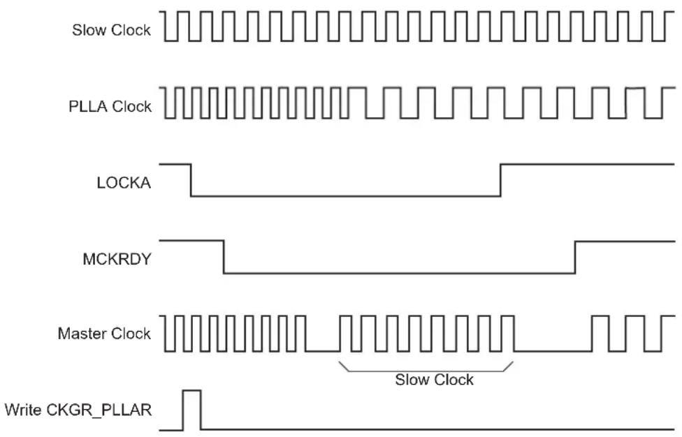
text_image
Slow Clock PLLA Clock LOCKA MCKRDY Master Clock Slow Clock Write CKGR_PLLARFigure 26-9: Programmable Clock Output Programming
text_image
PLL Clock PCKRDY PCKx Output Write PMC_PCKx PLL Clock is selected Write PMC_SCER PCKx is enabled Write PMC_SCDR PCKx is disabled26.16 Register Write Protection
To prevent any single software error from corrupting PMC behavior, certain registers in the address space can be write-protected by setting the WPEN bit in the PMC Write Protection Mode Register (PMC_WPMR).
If a write access to a write-protected register is detected, the WPVS bit in the PMC Write Protection Status Register (PMC_WPSR) is set and the field WPVSRC indicates the register in which the write access has been attempted.
The WPVS bit is automatically cleared after reading PMC_WPSR.
The following registers can be write-protected:
• PMC System Clock Enable Register
• PMC System Clock Disable Register
• PMC Peripheral Clock Enable Register 0
• PMC Peripheral Clock Disable Register 0
- PMC Clock Generator Main Oscillator Register
• PMC Clock Generator Main Clock Frequency Register
• PMC Clock Generator PLLA Register
• PMC Master Clock Register
• PMC USB Clock Register
• PMC Programmable Clock Register
- PLL Charge Pump Current Register
• PMC Peripheral Clock Enable Register 1
• PMC Peripheral Clock Disable Register 1
• PMC Oscillator Calibration Register
26.17 Power Management Controller (PMC) User Interface
Table 26-3: Register Mapping
| Offset Register | Name Access Reset | |||
| 0x0000 System | Clock Enable Register PMC_SCER Write-only – | |||
| 0x0004 System | Clock Disable Register PMC_SCDR Write-only – | |||
| 0x0008 | System Clock Status Register | PMC_SCSR | Read-only | 0x0000_0005 |
| 0x000C | Reserved | – | – | – |
| 0x0010 Peripheral Clock Enable Register 0 | PMC_PCR0 | Write-only – | ||
| 0x0014 Peripheral Clock Disable Register 0 | PMC_PCDR0 | Write-only – | ||
| 0x0018 | Peripheral Clock Status Register 0 | PMC_PCSR0 | Read-only | 0x0000_0000 |
| 0x001C | UTMI Clock Register | CKGR_UCKR | Read/Write | 0x1020_0000 |
| 0x0020 Main Oscillator Register | CKGR_MOR | Read/Write 0x0100_0001 | ||
| 0x0024 | Main Clock Frequency Register | CKGR_MCFR | Read/Write | 0x0000_0000 |
| 0x0028 | PLLA Register | CKGR_PLLAR | Read/Write | 0x0000_3F00 |
| 0x002C | Reserved | – | – | – |
| 0x0030 | Master Clock Register | PMC_MCKR | Read/Write | 0x0000_0001 |
| 0x0034 Reserved | – | – | – | – |
| 0x0038 | USB Clock Register | PMC_USB | Read/Write | 0x0000_0000 |
| 0x003C | Soft Modem Clock Register | PMC_SMD | Read/Write | 0x0000_0000 |
| 0x0040 | Programmable Clock 0 Register | PMC_PCK0 | Read/Write | 0x0000_0000 |
| 0x0044 | Programmable Clock 1 Register | PMC_PCK1 | Read/Write | 0x0000_0000 |
| 0x0048 | Programmable Clock 2 Register | PMC_PCK2 | Read/Write | 0x0000_0000 |
| 0x004C–0x005C | Reserved | – | – | – |
| 0x0060 | Interrupt Enable Register | PMC_IER | Write-only | – |
| 0x0064 | Interrupt Disable Register | PMC_IDR | Write-only | – |
| 0x0068 | Status Register | PMC_SR | Read-only | 0x0001_0008 |
| 0x006C | Interrupt Mask Register | PMC_IMR | Read-only | 0x0000_0000 |
| 0x0070–0x0074 | Reserved | – | – | – |
| 0x0078 | Fault Output Clear Register | PMC_FOCR | Write-only | – |
| 0x007C | Reserved | – | – | – |
| 0x0080 | PLL Charge Pump Current Register | PMC_PLLICPR | Read/Write | 0x0000_0000 |
| 0x0084–0x00E0 | Reserved | – | – | – |
| 0x00E4 | Write Protection Mode Register | PMC_WPMR | Read/Write | 0x0000_0000 |
| 0x00E8 | Write Protection Status Register | PMC_WPSR | Read-only | 0x0000_0000 |
| 0x00EC–0x00FC | Reserved | – | – | – |
| 0x0100 Peripheral Clock Enable Register 1 | PMC_PCR1 | Write-only – | ||
| 0x0104 Peripheral Clock Disable Register 1 | PMC_PCDR1 | Write-only – | ||
| 0x0108 | Peripheral Clock Status Register 1 | PMC_PCSR1 | Read-only | 0x0000_0000 |
Table 26-3: Register Mapping (Continued)
| Offset Register Name Access Reset | |||
| 0x010C Peripheral Control Register PMC_PCR Read/Write 0x0000_0000 | |||
| 0x0110 Oscillator Calibration Register PMC_OCR Read/Write 0x0040_4040 |
26.17.1 PMC System Clock Enable Register
Name:PMC_SCER
Address:0xFFFFC00
Access:Write-only
31 30 29 28 27 26 25 24
| - | - | - | - | - | - | - | - |
23 22 21 20 19 18 17 16
| - | - | - | - | - | - | - | - |
15 14 13 12 11 10 9 8
| - | - | - | - | - | P | C | K |
| 7 | 6 | 5 | 4 | 3 | 2 | 1 | 0 |
| UDP UHP | - SMDCK | LCDCK | DDRCK | -- |
This register can only be written if the WPEN bit is cleared in the PMC Write Protection Mode Register.
DDRCK: DDR Clock Enable
0: No effect.
1: Enables the DDR clock.
LCDCK: MCK2x Clock Enable
0: No effect.
1: Enables the MCK2x clock.
Note: MCK2x is selected as LCD Pixel source clock if LCDC_LCDCFG0.CLKSEL = 1.
SMDCK: SMD Clock Enable
0: No effect.
1: Enables the soft modem clock.
UHP: USB Host OHCI Clocks Enable
0: No effect.
1: Enables the UHP48M and UHP12M OHCI clocks.
UDP: USB Device Clock Enable
0: No effect.
1: Enables the USB Device clock.
PCKx: Programmable Clock x Output Enable
0: No effect.
1: Enables the corresponding Programmable Clock output.
26.17.2 PMC System Clock Disable Register
Name:PMC_SCDR
Address:0xFFFFC04
Access:Write-only
31 30 29 28 27 26 25 24
| - | - | - | - | - | - | - | - |
23 22 21 20 19 18 17 16
| - | - | - | - | - | - | - | - |
15 14 13 12 11 10 9 8
| - | - | - | - | - | P | C | K |
| 7 | 6 | 5 | 4 | 3 | 2 | 1 | 0 |
| UDP UHP | - SMDCK LCDC | K DDRCK | - PCK |
This register can only be written if the WPEN bit is cleared in the PMC Write Protection Mode Register.
PCK: Processor Clock Disable
0: No effect.
1: Disables the Processor clock. This is used to enter the processor in Idle mode.
DDRCK: DDR Clock Disable
0: No effect.
1: Disables the DDR clock.
LCDCK: MCK2x Clock Disable
0: No effect.
1: Disables the MCK2x clock.
SMDCK: SMD Clock Disable
0: No effect.
1: Disables the soft modem clock.
UHP: USB Host OHCI Clock Disable
0: No effect.
1: Disables the UHP48M and UHP12M OHCI clocks.
UDP: USB Device Clock Enable
0: No effect.
1: Disables the USB Device clock.
PCKx: Programmable Clock x Output Disable
0: No effect.
1: Disables the corresponding Programmable Clock output.
26.17.3 PMC System Clock Status Register
Name:PMC_SCSR
Address:0xFFFFFC08
Access:Read-only
31 30 29 28 27 26 25 24
| - | - | - | - | - | - | - | - |
23 22 21 20 19 18 17 16
| - | - | - | - | - | - | - | - |
15 14 13 12 11 10 9 8
| - | - | - | - | - | P | C | K |
| 7 | 6 | 5 | 4 | 3 | 2 | 1 | 0 |
| UDP UHP | - SMDCK | LCDCK | DDRCK | - PCK |
PCK: Processor Clock Status
0: The Processor clock is disabled.
1: The Processor clock is enabled.
DDRCK: DDR Clock Status
0: The DDR clock is disabled.
1: The DDR clock is enabled.
LCDCK: MCK2x Clock Status
0: The MCK2x clock is disabled.
1: The MCK2x clock is enabled.
Note: MCK2x is selected as LCD Pixel source clock if LCDC_LCDCFG0.CLKSEL = 1.
SMDCK: SMD Clock Status
0: The soft modem clock is disabled.
1: The soft modem clock is enabled.
UHP: USB Host Port Clock Status
0: The UHP48M and UHP12M OHCI clocks are disabled.
1: The UHP48M and UHP12M OHCI clocks are enabled.
UDP: USB Device Port Clock Status
0: The USB Device clock is disabled.
1: The USB Device clock is enabled.
PCKx: Programmable Clock x Output Status
0: The corresponding Programmable Clock output is disabled.
1: The corresponding Programmable Clock output is enabled.
26.17.4 PMC Peripheral Clock Enable Register 0
Name: PMC_PCER0
Address:0xFFFFFC10
Access:Write-only
31 30 29 28 27 26 25 24
| PID31 PID30 PID29 PID28 PID27 PID26 PID25 PID24 |
23 22 21 20 19 18 17 16
| PID23 PID2 | 2 PID21 PID20 | PID19 PID18 PID | 7 PID16 |
15 14 13 12 11 10 9 8
| PID15 PID14 PID13 PID12 PID11 PID10 PID9 PID8 |
| 7 | 6 | 5 | 4 | 3 | 2 | 1 | 0 |
| PID7 PID6 | PID5 PID4 PID3 | PID2 -- |
This register can only be written if the WPEN bit is cleared in the PMC Write Protection Mode Register.
PIDx: Peripheral Clock x Enable
0: No effect.
1: Enables the corresponding peripheral clock.
Note: PID2 to PID31 refer to identifiers as defined in Section 8.2 Peripheral Identifiers. Other peripherals can be enabled in PMC_PCER1.
Note: Programming the control bits of the Peripheral ID that are not implemented has no effect on the behavior of the PMC.
26.17.5 PMC Peripheral Clock Disable Register 0
Name:PMC_PCDR0
Address:0xFFFFFC14
Access:Write-only
31 30 29 28 27 26 25 24
| PID31 PID30 PID29 PID28 PID27 PID26 PID25 PID24 |
23 22 21 20 19 18 17 16
| PID23 PID2 | 2 PID21 PID20 | PID19 PID18 PID | 7 PID16 |
15 14 13 12 11 10 9 8
| PID15 PID14 PID13 PID12 PID11 PID10 PID9 PID8 |
| 7 | 6 | 5 | 4 | 3 | 2 | 1 | 0 |
| PID7 PID6 | PID5 PID4 PID3 | PID2 -- |
This register can only be written if the WPEN bit is cleared in the PMC Write Protection Mode Register.
PIDx: Peripheral Clock x Disable
0: No effect.
1: Disables the corresponding peripheral clock.
Note: PID2 to PID31 refer to identifiers as defined in Section 8.2 Peripheral Identifiers. Other peripherals can be disabled in PMC_PCDR1.
26.17.6 PMC Peripheral Clock Status Register 0
Name:PMC_PCSR0
Address:0xFFFFFC18
Access:Read-only
31 30 29 28 27 26 25 24
| PID31 PID30 PID29 PID28 PID27 PID26 PID25 PID24 |
23 22 21 20 19 18 17 16
| PID23 PID2 | 2 PID21 PID20 | PID19 PID18 PID | 7 PID16 |
15 14 13 12 11 10 9 8
| PID15 PID14 PID13 PID12 PID11 PID10 PID9 PID8 |
| 7 | 6 | 5 | 4 | 3 | 2 | 1 | 0 |
| PID7 PID6 | PID5 PID4 PID3 | PID2 | -- |
PIDx: Peripheral Clock x Status
0: The corresponding peripheral clock is disabled.
1: The corresponding peripheral clock is enabled.
Note: PID2 to PID31 refer to identifiers as defined in Section 8.2 Peripheral Identifiers. Other peripherals status can be read in PMC_PCSR1.
26.17.7 PMC UTMI Clock Configuration Register
Name: CKGR_UCKR
Address:0xFFFFFC1C
Access: Read/Write
31 30 29 28 27 26 25 24
| BIASCOUNT --- BIASEN |
23 22 21 20 19 18 17 16
| UPLLCOUNT --- UPLLEN |
15 14 13 12 11 10 9 8
| - | - | - | - | - | - | - | - |
| 7 | 6 | 5 | 4 | 3 | 2 | 1 | 0 |
| - | - | - | - | - | - | - | - |
UPLLEN: UTMI PLL Enable
0: The UTMI PLL is disabled.
1: The UTMI PLL is enabled.
When UPLLEN is set, the LOCKU flag is set once the UTMI PLL startup time is achieved.
UPLLCOUNT: UTMI PLL Start-up Time
Specifies the number of slow clock cycles multiplied by 8 for the UTMI PLL start-up time.
BIASEN: UTMI BIAS Enable
0: The UTMI BIAS is disabled.
1: The UTMI BIAS is enabled.
BIASCOUNT: UTMI BIAS Start-up Time
Specifies the number of slow clock cycles for the UTMI BIAS startup time.
26.17.8 PMC Clock Generator Main Oscillator Register
Name:CKGR_MOR
Address:0xFFFFFC20
Access: Read/Write
31 30 29 28 27 26 25 24
| - - - - - | - CFDEN | MOSCSEL |
23 22 21 20 19 18 17 16
| KEY | |||||||
| 15 14 13 12 | 11 | 10 | 9 8 | ||||
| MOSCXTST | |||||||
| 7 | 6 | 5 | 4 | 3 | 2 | 1 | 0 |
| - | 0 | MOSCRCEN | - | MOSCXTBY | MOSCXTEN | ||
This register can only be written if the WCKGR_MOR_ONEPEN bit is cleared in the PMC Write Protection Mode Register.
Warning: Bits 6:4 must always be configured to 0 when programming CKGR_MOR.
MOSCXTEN: 8 to 48 MHz Crystal Oscillator Enable
A crystal must be connected between XIN and XOUT.
0: The 8 to 48 MHz crystal oscillator is disabled.
1: The 8 to 48 MHz crystal oscillator is enabled. MOSCXTBY must be cleared.
When MOSCXTEN is set, the MOSCXTS flag is set once the crystal oscillator startup time is achieved.
MOSCXTBY: 8 to 48 MHz Crystal Oscillator Bypass
0: No effect.
1: The 8 to 48 MHz crystal oscillator is bypassed. MOSCXTEN must be cleared. An external clock must be connected on XIN.
When MOSCXTBY is set, the MOSCXTS flag in PMC_SR is automatically set.
Clearing MOSCXTEN and MOSCXTBY bits allows resetting the MOSCXTS flag.
Note: When Main Oscillator Bypass is disabled (MOSCXTBY = 0), the MOSCXTS flag must be read as 0 in PMC_SR prior to enabling the main crystal oscillator (MOSCXTEN = 1).
MOSCRCEN: 12 MHz RC Oscillator Enable
0: The 12 MHz RC oscillator is disabled.
1: The 12 MHz RC oscillator is enabled.
When MOSCRCEN is set, the MOSCRCS flag is set once the RC oscillator startup time is achieved.
MOSCXTST: 8 to 48 MHz Crystal Oscillator Startup Time
Specifies the number of slow clock cycles multiplied by 8 for the crystal oscillator start-up time.
KEY: Password
| Value | Name | Description |
| 0x37 | PASSWD | Writing any other value in this field aborts the write operation. |
MOSCSEL: Main Clock Oscillator Selection
0: The 12 MHz oscillator is selected.
1: The 8 to 48 MHz crystal oscillator is selected.
CFDEN: Clock Failure Detector Enable
0: The clock failure detector is disabled.
1: The clock failure detector is enabled.
Note 1: The 32 kHz (typical) RC oscillator is automatically enabled when CFDEN = 1.
2: Refer to Section 26.13 Main Clock Failure Detector for CFDEN initialization.
26.17.9 PMC Clock Generator Main Clock Frequency Register
Name: CKGR_MCFR
Address:0xFFFFC24
Access: Read/Write
31 30 29 28 27 26 25 24
| - | - | - | - | - | - | - | - |
23 22 21 20 19 18 17 16
| - | - | - | R | C | M | E | A |
15 14 13 12 11 10 9 8
| MAINF | |||||||
| 7 | 6 | 5 | 4 | 3 | 2 | 1 | 0 |
| MAINF | |||||||
This register can only be written if the WPEN bit is cleared in the PMC Write Protection Mode Register.
MAINF: Main Clock Frequency
Gives the number of main clock cycles within 16 slow clock periods. To calculate the frequency of the measured clock:
$$ \mathrm{f} _ {\text { MAINCK }} = (\text { MAINF } \times \mathrm{f} _ {\text { SLCK }}) / 1 6 $$
where frequency is in MHz.
MAINFRDY: Main Clock Frequency Measure Ready
0: MAINF value is not valid or the measured oscillator is disabled or a measure has just been started by means of RCMEAS.
1: The measured oscillator has been enabled previously and MAINF value is available.
Note: To ensure that a correct value is read on the MAINF field, the MAINFRDY flag must be read at 1 then another read access must be performed on the register to get a stable value on the MAINF field.
RCMEAS: RC Oscillator Frequency Measure (write-only)
0: No effect.
1: Restarts measuring of the frequency of the main clock source. MAINF will carry the new frequency as soon as a low to high transition occurs on the MAINFRDY flag.
The measure is performed on the main frequency (i.e., not limited to RC oscillator only), but if the main clock frequency source is the 8 to 48 MHz crystal oscillator, the restart of measuring is not needed because of the well known stability of crystal oscillators.
26.17.10 PMC Clock Generator PLLA Register
Name:CKGR_PLLAR
Address:0xFFFFFC28
Access: Read/Write
31 30 29 28 27 26 25 24
| - | - | O | N | E | - | - | - |
23 22 21 20 19 18 17 16
| MULA OUTA |
15 14 13 12 11 10 9 8
| OUTA PLLACOUNT |
| 7 | 6 | 5 | 4 | 3 | 2 | 1 | 0 |
| DIVA | |||||||
This register can only be written if the WPEN bit is cleared in the PMC Write Protection Mode Register.
Possible limitations on PLL input frequencies and multiplier factors should be checked before using the PMC.
DIVA: Divider A
| Value | Name | Description |
| 0 | 0 | Divider output is 0 |
| 1 | BYPASS | Divider is bypassed |
| 2–255 | - | Divider output is the selected clock divided by DIVA. |
PLLACOUNT: PLLA Counter
Specifies the number of slow clock cycles before the LOCKA bit is set in PMC_SR after CKGR_PLLAR is written.
OUTA: PLLA Clock Frequency Range
To be programmed to 0.
MULA: PLLA Multiplier
0: The PLLA is deactivated.
1-127: The PLLA Clock frequency is the PLLA input frequency multiplied by MULA + 1.
ONE: Must Be Set to 1
Bit 29 must always be set to 1 when programming CKGR_PLLAR.
26.17.11 PMC Master Clock Register
Name:PMC_MCKR
Address:0xFFFFFC30
Access: Read/Write
31 30 29 28 27 26 25 24
| - | - | - | - | - | - | - | - |
23 22 21 20 19 18 17 16
| - | - | - | - | - | - | - | - |
15 14 13 12 11 10 9 8
| - | - | - | P | L | L | A | D |
| 7 | 6 | 5 | 4 | 3 | 2 | 1 | 0 |
| - | P | R | E | S |
This register can only be written if the WPEN bit is cleared in the PMC Write Protection Mode Register.
CSS: Master/Processor Clock Source Selection
| Value | Name | Description |
| 0 | SLOW_CLK | Slow clock is selected |
| 1 | MAIN_CLK | Main clock is selected |
| 2 | PLLA_CLK | PLLACK/2 is selected if PLLADIV2 = 1PLLACK is selected if PLLADIV2 = 0 |
| 3 | UPLL_CLK | UPLL Clock is selected |
PRES: Master/Processor Clock Prescaler
| Value | Name | Description |
| 0 | CLOCK | Selected clock |
| 1 | CLOCK_DIV2 | Selected clock divided by 2 |
| 2 | CLOCK_DIV4 | Selected clock divided by 4 |
| 3 | CLOCK_DIV8 | Selected clock divided by 8 |
| 4 | CLOCK_DIV16 | Selected clock divided by 16 |
| 5 | CLOCK_DIV32 | Selected clock divided by 32 |
| 6 | CLOCK_DIV64 | Selected clock divided by 64 |
| 7 | - | Reserved |
MDIV: Master Clock Division
| Value | Name | Description |
| 0 | EQ_PCK | Master Clock is Prescaler Output Clock divided by 1.Warning: DDRCK is not available. |
| 1 | PCK_DIV2 | Master Clock is Prescaler Output Clock divided by 2. DDRCK is equal to MCK. |
| 2 | PCK_DIV4 | Master Clock is Prescaler Output Clock divided by 4. DDRCK is equal to MCK. |
| 3 | PCK_DIV3 | Master Clock is Prescaler Output Clock divided by 3. DDRCK is equal to MCK. |
PLLADIV2: PLLA Divisor by 2
Bit PLLADIV2 must always be set to 1 when MDIV is set to 3.
26.17.12 PMC USB Clock Register
Name:PMC_USB
Address:0xFFFFFC38
Access: Read/Write
31 30 29 28 27 26 25 24
| - | - | - | - | - | - | - | - |
23 22 21 20 19 18 17 16
| - | - | - | - | - | - | - | - |
15 14 13 12 11 10 9 8
| - | - | - | - | U | S | B |
| 7 | 6 | 5 | 4 | 3 | 2 | 1 | 0 |
| - | - | - | - | - | - | - | U |
This register can only be written if the WPEN bit is cleared in the PMC Write Protection Mode Register.
USBS: USB OHCI Input Clock Selection
0: USB Clock Input is PLLA.
1: USB Clock Input is UPLL.
USBDIV: Divider for USB OHCI Clock
USB Clock is Input clock divided by USBDIV + 1.
26.17.13 PMC SMD Clock Register
Name:PMC_SMD
Address:0xFFFFFC3C
Access: Read/Write
31 30 29 28 27 26 25 24
| - | - | - | - | - | - | - | - |
23 22 21 20 19 18 17 16
| - | - | - | - | - | - | - | - |
15 14 13 12 11 10 9 8
| - | - | - | S | M | D | D |
| 7 | 6 | 5 | 4 | 3 | 2 | 1 | 0 |
| - | - | - | - | - | - | - | S |
SMDS: SMD Input Clock Selection
0: SMD clock input is PLLA.
1: SMD clock input is UPLL.
SMDDIV: Divider for SMD Clock
SMD clock is input clock divided by SMD + 1.
26.17.14 PMC Programmable Clock Register
Name: PMC_PCKx[x = 0..2]
Address:0xFFFFFC40
Access: Read/Write
31 30 29 28 27 26 25 24
| - | - | - | - | - | - | - | - |
23 22 21 20 19 18 17 16
| - | - | - | - | - | - | - | - |
15 14 13 12 11 10 9 8
| - | - | - | - | - | - | - | - |
| 7 | 6 | 5 | 4 | 3 | 2 | 1 | 0 |
| - | P | R | E | S |
This register can only be written if the WPEN bit is cleared in the PMC Write Protection Mode Register.
CSS: Master Clock Source Selection
| Value Name Description | ||
| 0 SLOW_CLK Slow clock is selected | ||
| 1 MAIN_CLK | Main clock is selected | |
| 2 PLLA_CLK | PLLACK is selected | |
| 3 UPLL_CLK | UPLL Clock is selected | |
| 4 MCK_CLK | Master Clock is selected | |
PRES: Programmable Clock Prescaler
| Value Name Description | ||
| 0 CLOCK | Selected clock | |
| 1 CLOCK_DIV2 | Selected clock divided by 2 | |
| 2 CLOCK_DIV4 | Selected clock divided by 4 | |
| 3 CLOCK_DIV8 | Selected clock divided by 8 | |
| 4 CLOCK_DIV16 | Selected clock divided by 16 | |
| 5 CLOCK_DIV32 | Selected clock divided by 32 | |
| 6 CLOCK_DIV64 | Selected clock divided by 64 | |
| 7 | - | Reserved |
26.17.15 PMC Interrupt Enable Register
Name:PMC_IER
Address:0xFFFFFC60
Access:Write-only
31 30 29 28 27 26 25 24
| - | - | - | - | - | - | - | - |
23 22 21 20 19 18 17 16
| - | - | - | - | - | C | F | D |
15 14 13 12 11 10 9 8
| - | - | - | - | - | P | C | K |
| 7 | 6 | 5 | 4 | 3 | 2 | 1 | 0 |
| - LOCKU | -- | MCKRDY | - LOCKA | MOSCXTS |
The following configuration values are valid for all listed bit names of this register:
0: No effect
1: Enables the corresponding interrupt
MOSCXTS: 8 to 48 MHz Crystal Oscillator Status Interrupt Enable
LOCKA: PLLA Lock Interrupt Enable
MCKRDY: Master Clock Ready Interrupt Enable
LOCKU: UTMI PLL Lock Interrupt Enable
PCKRDYx: Programmable Clock Ready x Interrupt Enable
MOSCSELS: Main Clock Source Oscillator Selection Status Interrupt Enable
MOSCRCS: 12 MHz RC Oscillator Status Interrupt Enable
CFDEV: Clock Failure Detector Event Interrupt Enable
26.17.16 PMC Interrupt Disable Register
Name:PMC_IDR
Address:0xFFFFFC64
Access:Write-only
31 30 29 28 27 26 25 24
| - | - | - | - | - | - | - | - |
23 22 21 20 19 18 17 16
| - | - | - | - | - | C | F | D |
15 14 13 12 11 10 9 8
| - | - | - | - | - | P | C | K |
| 7 | 6 | 5 | 4 | 3 | 2 | 1 | 0 |
| - LOCKU | -- | MCKRDY | - LOCKA | MOSCXTS |
The following configuration values are valid for all listed bit names of this register:
0: No effect
1: Disables the corresponding interrupt
MOSCXTS: 8 to 48 MHz Crystal Oscillator Status Interrupt Disable
LOCKA: PLLA Lock Interrupt Disable
MCKRDY: Master Clock Ready Interrupt Disable
LOCKU: UTMI PLL Lock Interrupt Enable
PCKRDYx: Programmable Clock Ready x Interrupt Disable
MOSCSELS: Main Oscillator Clock Source Selection Status Interrupt Disable
MOSCRCS: 12 MHz RC Oscillator Status Interrupt Disable
CFDEV: Clock Failure Detector Event Interrupt Disable
26.17.17 PMC Status Register
Name:PMC_SR
Address:0xFFFFFC68
Access:Read-only
31 30 29 28 27 26 25 24
| - | - | - | - | - | - | - | - |
23 22 21 20 19 18 17 16
| --- FOS CFDS CFDEV MOSCRCS MOSCSELS |
15 14 13 12 11 10 9 8
| - | - | - | - | - | P | C | K |
| 7 | 6 | 5 | 4 | 3 | 2 | 1 | 0 |
| OSCSELS | LOCKU | - | - | MCKRDY | - | LOCKA | MOSCXTS |
MOSCXTS: 8 to 48 MHz Crystal Oscillator Status
0: 8 to 48 MHz crystal oscillator is not stabilized.
1: 8 to 48 MHz crystal oscillator is stabilized.
LOCKA: PLLA Lock Status
0: PLLA is not locked.
1: PLLA is locked.
MCKRDY: Master Clock Status
0: Master Clock is not ready.
1: Master Clock is ready.
LOCKU: UPLL Clock Status
0: UPLL Clock is not ready.
1: UPLL Clock is ready.
OSCSELS: Slow Clock Oscillator Selection
0: Embedded 32 kHz RC oscillator is selected.
1: 32.768 kHz crystal oscillator is selected.
PCKRDYx: Programmable Clock Ready Status
0: Programmable Clock x is not ready.
1: Programmable Clock x is ready.
MOSCSELS: Main Oscillator Selection Status
0: Selection is in progress.
1: Selection is done.
MOSCRCS: 12 MHz RC Oscillator Status
0: 12 MHz RC oscillator is not stabilized.
1: 12 MHz RC oscillator is stabilized.
CFDEV: Clock Failure Detector Event
0: No clock failure detection of the 8 to 48 MHz crystal oscillator has occurred since the last read of PMC_SR.
1: At least one clock failure detection of the 8 to 48 MHz crystal oscillator has occurred since the last read of PMC_SR.
CFDS: Clock Failure Detector Status
0: A clock failure of the 8 to 48 MHz crystal oscillator is not detected.
1: A clock failure of the 8 to 48 MHz crystal oscillator is detected.
FOS: Clock Failure Detector Fault Output Status
0: The fault output of the clock failure detector is inactive.
1: The fault output of the clock failure detector is active.
26.17.18 PMC Interrupt Mask Register
Name:PMC_IMR
Address:0xFFFFC6C
Access: Read-only
31 30 29 28 27 26 25 24
| - | - | - | - | - | - | - | - |
23 22 21 20 19 18 17 16
| - | - | - | - | - | C | F | D |
15 14 13 12 11 10 9 8
| - | - | - | - | - | P | C | K |
| 7 | 6 | 5 | 4 | 3 | 2 | 1 | 0 |
| - | - | - | - | M | C | K | R |
The following configuration values are valid for all listed bit names of this register:
0: Corresponding interrupt is not enabled.
1: Corresponding interrupt is enabled.
MOSCXTS: 8 to 48 MHz Crystal Oscillator Status Interrupt Mask
LOCKA: PLLA Lock Interrupt Mask
MCKRDY: Master Clock Ready Interrupt Mask
PCKRDYx: Programmable Clock Ready x Interrupt Mask
MOSCSELS: Main Oscillator Clock Source Selection Status Interrupt Mask
MOSCRCS: 12 MHz RC Oscillator Status Interrupt Mask
CFDEV: Clock Failure Detector Event Interrupt Mask
26.17.19 PMC Fault Output Clear Register
Name:PMC_FOCR
Address:0xFFFFFC78
Access:Write-only
31 30 29 28 27 26 25 24
| - | - | - | - | - | - | - | - |
23 22 21 20 19 18 17 16
| - | - | - | - | - | - | - | - |
15 14 13 12 11 10 9 8
| - | - | - | - | - | - | - | - |
| 7 | 6 | 5 | 4 | 3 | 2 | 1 | 0 |
| - | - | - | - | - | - | - | F |
FOCLR: Fault Output Clear
Clears the clock failure detector fault output.
26.17.20 PLL Charge Pump Current Register
Name:PMC_PLLICPR
Address:0xFFFFFC80
Access: Read/Write
31 30 29 28 27 26 25 24
| - | - | - | - | - | - | | |
23 22 21 20 19 18 17 16
| - | - | - | - | - | - | | |
15 14 13 12 11 10 9 8
| - | - | - | - | - | I | P |
| 7 | 6 | 5 | 4 | 3 | 2 | 1 | 0 |
| - | - | - | - | - | - | | |
This register can only be written if the WPEN bit is cleared in the PMC Write Protection Mode Register.
ICP_PLLA: Must Be Written to Zero
IPLL_PLLA: Engineering Configuration PLLA
Should be written to 3.
ICP_PLLU: Charge Pump Current PLL UTMI
Should be written to 0.
IVCO_PLLU: Voltage Control Output Current PLL UTMI
Should be written to 0.
26.17.21 PMC Write Protection Mode Register
Name:PMC_WPMR
Address:0xFFFFCE4
Access: Read/Write
31 30 29 28 27 26 25 24
| WPKEY |
23 22 21 20 19 18 17 16
| WPKEY |
15 14 13 12 11 10 9 8
| WPKEY |
| 7 | 6 | 5 | 4 | 3 | 2 | 1 | 0 |
| - | - | - | - | - | - | - | W |
WPEN: Write Protection Enable
0: Disables the write protection if WPKEY corresponds to 0x504D43 ("PMC" in ASCII).
1: Enables the write protection if WPKEY corresponds to 0x504D43 ("PMC" in ASCII).
See Section 26.16 Register Write Protection for the list of registers that can be write-protected.
WPKEY: Write Protection Key
| Value Name Description | ||
| 0x504D43 | PASSWD | Writing any other value in this field aborts the write operation of the WPEN bit.Always reads as 0. |
26.17.22 PMC Write Protection Status Register
Name:PMC_WPSR
Address:0xFFFFCE8
Access:Read-only
31 30 29 28 27 26 25 24
| - | - | - | - | - | - | - | - |
23 22 21 20 19 18 17 16
| WPVSRC |
15 14 13 12 11 10 9 8
| WPVSRC |
| 7 | 6 | 5 | 4 | 3 | 2 | 1 | 0 |
| - | - | - | - | - | - | - | W |
WPVS: Write Protection Violation Status
0: No write protection violation has occurred since the last read of PMC_WPSR.
1: A write protection violation has occurred since the last read of PMC_WPSR. If this violation is an unauthorized attempt to write a protected register, the associated violation is reported into field WPVSRC.
WPVSRC: Write Protection Violation Source
When WPVS = 1, WPVSRC indicates the register address offset at which a write access has been attempted.
26.17.23 PMC Peripheral Clock Enable Register 1
Name:PMC_PCER1
Address:0xFFFFD00
Access:Write-only
31 30 29 28 27 26 25 24
| PID63 PID62 PID61 PID60 PID59 PID58 PID57 PID56 |
23 22 21 20 19 18 17 16
| PID55 PID54 PID53 PID52 PID51 PID50 PID49 PID48 |
15 14 13 12 11 10 9 8
| PID47 PID46 PID45 PID44 PID43 PID42 PID41 PID40 |
| 7 | 6 | 5 | 4 | 3 | 2 | 1 | 0 |
| PID39 PID38 PID37 PID36 PID35 PID34 PID33 PID32 |
This register can only be written if the WPEN bit is cleared in the PMC Write Protection Mode Register.
PIDx: Peripheral Clock x Enable
0: No effect.
1: Enables the corresponding peripheral clock.
Note 1: PID32 to PID63 refer to identifiers as defined in Section 8.2 Peripheral Identifiers.
2: Programming the control bits of the Peripheral ID that are not implemented has no effect on the behavior of the PMC.
26.17.24 PMC Peripheral Clock Disable Register 1
Name:PMC_PCDR1
Address:0xFFFFD04
Access:Write-only
31 30 29 28 27 26 25 24
| PID63 PID62 PID61 PID60 PID59 PID58 PID57 PID56 |
23 22 21 20 19 18 17 16
| PID55 PID54 PID53 PID52 PID51 PID50 PID49 PID48 |
15 14 13 12 11 10 9 8
| PID47 PID46 PID45 PID44 PID43 PID42 PID41 PID40 |
| 7 | 6 | 5 | 4 | 3 | 2 | 1 | 0 |
| PID39 PID38 PID37 PID36 PID35 PID34 PID33 PID32 |
This register can only be written if the WPEN bit is cleared in the PMC Write Protection Mode Register.
PIDx: Peripheral Clock x Disable
0: No effect.
1: Disables the corresponding peripheral clock.
Note: PID32 to PID63 refer to identifiers as defined in Section 8.2 Peripheral Identifiers.
26.17.25 PMC Peripheral Clock Status Register 1
Name:PMC_PCSR1
Address:0xFFFFFD08
Access:Read-only
31 30 29 28 27 26 25 24
| PID63 PID62 PID61 PID60 PID59 PID58 PID57 PID56 |
23 22 21 20 19 18 17 16
| PID55 PID54 PID53 PID52 PID51 PID50 PID49 PID48 |
15 14 13 12 11 10 9 8
| PID47 PID46 PID45 PID44 PID43 PID42 PID41 PID40 |
| 7 | 6 | 5 | 4 | 3 | 2 | 1 | 0 |
| PID39 PID38 PID37 PID36 PID35 PID34 PID33 PID32 |
PIDx: Peripheral Clock x Status
0: The corresponding peripheral clock is disabled.
1: The corresponding peripheral clock is enabled.
Note: PID32 to PID63 refer to identifiers as defined in Section 8.2 Peripheral Identifiers.
26.17.26 PMC Peripheral Control Register
Name:PMC_PCR
Address:0xFFFFD0C
Access: Read/Write
31 30 29 28 27 26 25 24
| - | - | - | E | N | - | - | - |
23 22 21 20 19 18 17 16
| - | - | - | - | - | - | D |
15 14 13 12 11 10 9 8
| - | - | - | C | M | D | - | - |
| 7 | 6 | 5 | 4 | 3 | 2 | 1 | 0 |
| - | PID |
PID: Peripheral ID
Peripheral ID selection from PID2 to the maximum PID number. This refers to identifiers as defined in the section "Peripheral Identifiers". Only the following peripherals can have a DIV value greater than 0: ADC, SSCx, CANx, USARTx, UARTx, TWlx, SPIx, and TCx.
CMD: Command
0: Read mode
1: Write mode
DIV: Divisor Value
Only the following peripherals can be configured with divided clock (DIV > 0): ADC, SSCx, CANx, USARTx, UARTx, TWlx, SPIx, and TCx. Among the PIDs supporting the divided clock, some require a DIV value configuration matching the maximum peripheral frequency. Refer to Section 54.3.4 Power Consumption versus Modes in Section 54. Electrical Characteristics.
| Value Name | Description | |
| 0 | PERIPH_DIV_MCK | Peripheral clock is MCK |
| 1 | PERIPH_DIV2_MCK | Peripheral clock is MCK/2 |
| 2 | PERIPH_DIV4_MCK | Peripheral clock is MCK/4 |
| 3 | PERIPH_DIV8_MCK | Peripheral clock is MCK/8 |
DIV must not be changed while peripheral is in use or when the peripheral clock is enabled.
EN: Enable
0: The selected peripheral clock is disabled.
1: The selected peripheral clock is enabled.
26.17.27 PMC Oscillator Calibration Register
Name:PMC_OCR
Address:0xFFFFFD10
Access: Read/Write
31 30 29 28 27 26 25 24
| - | - | - | - | - | - | - | - |
23 22 21 20 19 18 17 16
| - | - | - | - | - | - | - | - |
15 14 13 12 11 10 9 8
| - | - | - | - | - | - | - | - |
| 7 | 6 | 5 | 4 | 3 | 2 | 1 | 0 |
SEL CAL
This register can only be written if the WPEN bit is cleared in the PMC Write Protection Mode Register.
CAL: 12 MHz RC Oscillator Calibration Bits
Calibration bits applied to the RC oscillator when SEL is set.
SEL: Selection of RC Oscillator Calibration Bits
0: Factory determined value.
1: Value written by user in CAL field of this register.
27. Parallel Input/Output Controller (PIO)
27.1 Description
The Parallel Input/Output Controller (PIO) manages up to 32 fully programmable input/output lines. Each I/O line may be dedicated as a general-purpose I/O or be assigned to a function of an embedded peripheral. This ensures effective optimization of the pins of the product.
Each I/O line is associated with a bit number in all of the 32-bit registers of the 32-bit wide user interface.
Each I/O line of the PIO Controller features:
- An input change interrupt enabling level change detection on any I/O line.
- Additional Interrupt modes enabling rising edge, falling edge, low-level or high-level detection on any I/O line.
- A glitch filter providing rejection of glitches lower than one-half of peripheral clock cycle.
- A debouncing filter providing rejection of unwanted pulses from key or push button operations.
- Multi-drive capability similar to an open drain I/O line.
- Control of the pull-up and pull-down of the I/O line.
- Input visibility and output control.
The PIO Controller also features a synchronous output providing up to 32 bits of data output in a single write operation.
27.2 Embedded Characteristics
- Up to 32 Programmable I/O Lines
- Fully Programmable through Set/Clear Registers
- Multiplexing of Four Peripheral Functions per I/O Line
- For each I/O Line (Whether Assigned to a Peripheral or Used as General Purpose I/O)
- Input Change Interrupt
- Programmable Glitch Filter
- Programmable Debouncing Filter
- Multi-drive Option Enables Driving in Open Drain
- Programmable Pull-Up on Each I/O Line
- Pin Data Status Register, Supplies Visibility of the Level on the Pin at Any Time
- Additional Interrupt Modes on a Programmable Event: Rising Edge, Falling Edge, Low-Level or High-Level
- Lock of the Configuration by the Connected Peripheral
- Synchronous Output, Provides Set and Clear of Several I/O Lines in a Single Write
- Register Write Protection
- Programmable Schmitt Trigger Inputs
- Programmable I/O Drive
27.3 Block Diagram
Figure 27-1: Block Diagram
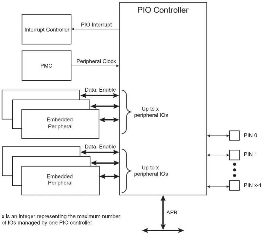
flowchart
graph TD
    A["Interrupt Controller"] -->|PIO Interrupt| B["PIO Controller"]
    C["PMC"] -->|Peripheral Clock| B
    D["Embedded Peripheral"] -->|Data, Enable| B
    E["Embedded Peripheral"] -->|Data, Enable| B
    B --> F["Up to x peripheral IOs"]
    B --> G["Up to x peripheral IOs"]
    F --> H["PIN 0"]
    F --> I["PIN 1"]
    F --> J["..."]
    F --> K["PIN x-1"]
    G --> L["APB"]
    style A fill:#f9f,stroke:#333
    style C fill:#f9f,stroke:#333
    style D fill:#f9f,stroke:#333
    style E fill:#f9f,stroke:#333
    style F fill:#ccf,stroke:#333
    style G fill:#ccf,stroke:#333
    style H fill:#dfd,stroke:#333
    style I fill:#dfd,stroke:#333
    style J fill:#dfd,stroke:#333
    style K fill:#dfd,stroke:#333
    note right of B: "Up to x peripheral IOs"
    note right of G: "Up to x peripheral IOs"
    note left of G: "Data, Enable"
    note right of G: "Data, Enable"
27.4 Product Dependencies
27.4.1 Pin Multiplexing
Each pin is configurable, depending on the product, as either a general-purpose I/O line only, or as an I/O line multiplexed with one or two peripheral I/Os. As the multiplexing is hardware defined and thus product-dependent, the hardware designer and programmer must carefully determine the configuration of the PIO Controllers required by their application. When an I/O line is general-purpose only, i.e., not multiplexed with any peripheral I/O, programming of the PIO Controller regarding the assignment to a peripheral has no effect and only the PIO Controller can control how the pin is driven by the product.
27.4.2 External Interrupt Lines
The interrupt signals FIQ and IRQ0 to IRQn are generally multiplexed through the PIO Controllers. However, it is not necessary to assign the I/O line to the interrupt function as the PIO Controller has no effect on inputs and the external interrupt lines are used only as inputs.
27.4.3 Power Management
The Power Management Controller controls the peripheral clock in order to save power. Writing any of the registers of the user interface does not require the peripheral clock to be enabled. This means that the configuration of the I/O lines does not require the peripheral clock to be enabled.
However, when the clock is disabled, not all of the features of the PIO Controller are available, including glitch filtering. Note that the input change interrupt, the interrupt modes on a programmable event and the read of the pin level require the clock to be validated.
After a hardware reset, the peripheral clock is disabled by default.
The user must configure the Power Management Controller before any access to the input line information.
27.4.4 Interrupt Sources
For interrupt handling, the PIO Controllers are considered as user peripherals. This means that the PIO Controller interrupt lines are connected among the interrupt sources. Refer to the PIO Controller peripheral identifier in the Peripheral Identifiers table to identify the interrupt sources dedicated to the PIO Controllers. Using the PIO Controller requires the Interrupt Controller to be programmed first.
The PIO Controller interrupt can be generated only if the peripheral clock is enabled.
Table 27-1: Peripheral IDs
| Instance ID | |
| PIOA 6 | |
| PIOB 7 | |
| PIOC 8 | |
| PIOD 9 | |
| PIOE 10 |
27.5 Functional Description
The PIO Controller features up to 32 fully-programmable I/O lines. Most of the control logic associated to each I/O is represented in Figure 27-2. In this description each signal shown represents one of up to 32 possible indexes.
Figure 27-2: I/O Line Control Logic
flowchart
graph TD
    A["Clock Divider"] -->|Slow Clock| B["Clock OER[0"]]
    B --> C["PIO_ODR[0"]]
    C --> D["1"]
    D --> E["POI_PUDR[0"]]
    E --> F["VDD"]
    F --> G["Integrated Pull-Up Resistor"]
    H["Peripheral Clock"] --> I["Programmable Glitch or Debouncing Filter"]
    I --> J["0"]
    J --> K["POI_PDDR[0"]]
    K --> L["1"]
    L --> M["POI_PUER[0"]]
    M --> N["VDD"]
    N --> O["Integrated Pull-Down Resistor"]
    P["POI_SCCR"] --> Q["Clock OER[0"]]
    R["POI_IFSCER[0"]] --> S["POI_IFDR[0"]]
    T["POI_IFSDR[0"]] --> U["POI_IFSR[0"]]
    V["POI_IFDR[0"]] --> W["POI_FDR[0"]]
    X["POI_PUDR[0"]] --> Y["POI_PUSR[0"]]
    Z["POI_PDR[0"]] --> AA["POI_PMDR[0"]]
    AB["POI_PDR[0"]] --> AC["POI_MDDR[0"]]
    AD["POI_PDR[0"]] --> AE["POI_MDSR[0"]]
    AF["POI_PDR[0"]] --> AG["POI_PPSR[0"]]
    AH["POI_PPSR[0"]] --> AI["POI_PUR[0"]]
    AJ["POI_PUR[0"]] --> AK["VDD"]
    AL["POI_PUR[0"]] --> AM["VDD"]
    AN["POI_PUR[0"]] --> AO["VDD"]
    AP["POI_PUR[0"]] --> AQ["VDD"]
    AR["POI_PUR[0"]] --> AS["VDD"]
    AT["POI_PUR[0"]] --> AU["VDD"]
    AV["POI_PUR[0"]] --> AW["VDD"]
    AX["POI_PUR[0"]] --> AY["VDD"]
    AZ["POI_PUR[0"]] --> BA["VDD"]
    BB["POI_PUR[0"]] --> BC["VDD"]
    BD["POI_PUR[0"]] --> BE["VDD"]
    BF["POI_PUR[0"]] --> BG["VDD"]
    BH["POI_PUR[0"]] --> BI["VDD"]
    BJ["POI_PUR[0"]] --> BK["VDD"]
    BL["POI_PUR[0"]] --> BLV["VDD"]
    BM["POI_PUR[0"]] --> BN["VDD"]
    BO["POI_PUR[0"]] --> BP["VDD"]
    BQ["POLIO"] --> BR["POLIO"]
    BR --> BS["POLIO"]
    BS --> BT["POLIO"]
    BT --> BU["POLIO"]
    BU --> BV["POLIO"]
    BW["POLIO"] --> BX["POLIO"]
    BX --> BY["POLIO"]
    BY --> BZ["POLIO"]
    BZ --> CA["POLIO"]
    CA --> CB["POLIO"]
    CC["POLIO"] --> CD["POLIO"]
    CD --> CE["POLIO"]
    CE --> CF["POLIO"]
    CF --> CG["POLIO"]
    CG --> CH["POLIO"]
    CH --> CI["POLIO"]
    CI --> CJ["POLIO"]
    CJ --> CK["POLIO"]
27.5.1 Pull-up and Pull-down Resistor Control
Each I/O line is designed with an embedded pull-up resistor and an embedded pull-down resistor. The pull-up resistor can be enabled or disabled by writing to the Pull-up Enable Register (PIO_PUER) or Pull-up Disable Register (PIO_PUDR), respectively. Writing to these registers results in setting or clearing the corresponding bit in the Pull-up Status Register (PIO_PUSR). Reading a one in PIO_PUSR means the pull-up is disabled and reading a zero means the pull-up is enabled. The pull-down resistor can be enabled or disabled by writing the Pull-down Enable Register (PIO_PPDER) or the Pull-down Disable Register (PIO_PPDDR), respectively. Writing in these registers results in setting or clearing the corresponding bit in the Pull-down Status Register (PIO_PPDSR). Reading a one in PIO_PPDSR means the pull-up is disabled and reading a zero means the pull-down is enabled.
Enabling the pull-down resistor while the pull-up resistor is still enabled is not possible. In this case, the write of PIO_PPDER for the relevant I/O line is discarded. Likewise, enabling the pull-up resistor while the pull-down resistor is still enabled is not possible. In this case, the write of PIO_PUER for the relevant I/O line is discarded.
Control of the pull-up resistor is possible regardless of the configuration of the I/O line.
After reset, depending on the I/O, pull-up or pull-down can be set.
27.5.2 I/O Line or Peripheral Function Selection
When a pin is multiplexed with one or two peripheral functions, the selection is controlled with the Enable Register (PIO_PER) and the Disable Register (PIO_PDR). The Status Register (PIO_PSR) is the result of the set and clear registers and indicates whether the pin is controlled by the corresponding peripheral or by the PIO Controller. A value of zero indicates that the pin is controlled by the corresponding on-chip peripheral selected in the ABCD Select registers (PIO_ABCDSR1 and PIO_ABCDSR2). A value of one indicates the pin is controlled by the PIO Controller.
If a pin is used as a general-purpose I/O line (not multiplexed with an on-chip peripheral), PIO_PER and PIO_PDR have no effect and PIO_PSR returns a one for the corresponding bit.
After reset, the I/O lines are controlled by the PIO Controller, i.e., PIO_PSR resets at one. However, in some events, it is important that PIO lines are controlled by the peripheral (as in the case of memory chip select lines that must be driven inactive after reset, or for address lines that must be driven low for booting out of an external memory). Thus, the reset value of PIO_PSR is defined at the product level and depends on the multiplexing of the device.
27.5.3 Peripheral A or B or C or D Selection
The PIO Controller provides multiplexing of up to four peripheral functions on a single pin. The selection is performed by writing PIO_ABCDSR1 and PIO_ABCDSR2.
For each pin:
- The corresponding bit at level zero in PIO_ABCDSR1 and the corresponding bit at level zero in PIO_ABCDSR2 means peripheral A is selected.
- The corresponding bit at level one in PIO_ABCDSR1 and the corresponding bit at level zero in PIO_ABCDSR2 means peripheral B is selected.
- The corresponding bit at level zero in PIO_ABCDSR1 and the corresponding bit at level one in PIO_ABCDSR2 means peripheral C is selected.
- The corresponding bit at level one in PIO_ABCDSR1 and the corresponding bit at level one in PIO_ABCDSR2 means peripheral D is selected.
Note that multiplexing of peripheral lines A, B, C and D only affects the output line. The peripheral input lines are always connected to the pin input (see Figure 27-2).
Writing in PIO_ABCDSR1 and PIO_ABCDSR2 manages the multiplexing regardless of the configuration of the pin. However, assignment of a pin to a peripheral function requires a write in PIO_ABCDSR1 and PIO_ABCDSR2 in addition to a write in PIO_PDR.
After reset, PIO_ABCDSR1 and PIO_ABCDSR2 are zero, thus indicating that all the PIO lines are configured on peripheral A. However, peripheral A generally does not drive the pin as the PIO Controller resets in I/O line mode.
If the software selects a peripheral A, B, C or D which does not exist for a pin, no alternate functions are enabled for this pin and the selection is taken into account. The PIO Controller does not carry out checks to prevent selection of a peripheral which does not exist.
27.5.4 Output Control
When the I/O line is assigned to a peripheral function, i.e., the corresponding bit in PIO_PSR is at zero, the drive of the I/O line is controlled by the peripheral. Peripheral A or B or C or D depending on the value in PIO_ABCDSR1 and PIO_ABCDSR2 determines whether the pin is driven or not.
When the I/O line is controlled by the PIO Controller, the pin can be configured to be driven. This is done by writing the Output Enable Register (PIO_OER) and Output Disable Register (PIO_ODR). The results of these write operations are detected in the Output Status Register (PIO_OSR). When a bit in this register is at zero, the corresponding I/O line is used as an input only. When the bit is at one, the corresponding I/O line is driven by the PIO Controller.
The level driven on an I/O line can be determined by writing in the Set Output Data Register (PIO_SODR) and the Clear Output Data Register (PIO_CODR). These write operations, respectively, set and clear the Output Data Status Register (PIO_ODSR), which represents the data driven on the I/O lines. Writing in PIO_OER and PIO_ODR manages PIO_OSR whether the pin is configured to be controlled by the PIO Controller or assigned to a peripheral function. This enables configuration of the I/O line prior to setting it to be managed by the PIO Controller.
Similarly, writing in PIO_SODR and PIO_CODR affects PIO_ODSR. This is important as it defines the first level driven on the I/O line.
27.5.5 Synchronous Data Output
Clearing one or more PIO line(s) and setting another one or more PIO line(s) synchronously cannot be done by using PIO_SODR and PIO_CODR. It requires two successive write operations into two different registers. To overcome this, the PIO Controller offers a direct control of PIO outputs by single write access to PIO_ODSR. Only bits unmasked by the Output Write Status Register (PIO_OWSR) are written. The mask bits in PIO_OWSR are set by writing to the Output Write Enable Register (PIO_OWNER) and cleared by writing to the Output Write Disable Register (PIO_OWDR).
After reset, the synchronous data output is disabled on all the I/O lines as PIO_OWSR resets at 0x0.
27.5.6 Multi-Drive Control (Open Drain)
Each I/O can be independently programmed in open drain by using the multi-drive feature. This feature permits several drivers to be connected on the I/O line which is driven low only by each device. An external pull-up resistor (or enabling of the internal one) is generally required to ensure a high level on the line.
The multi-drive feature is controlled by the Multi-driver Enable Register (PIO_MDER) and the Multi-driver Disable Register (PIO_MDDR). The multi-drive can be selected whether the I/O line is controlled by the PIO Controller or assigned to a peripheral function. The Multi-driver Status Register (PIO_MDSR) indicates the pins that are configured to support external drivers.
After reset, the multi-drive feature is disabled on all pins, i.e., PIO_MDSR resets at value 0x0.
27.5.7 Output Line Timings
Figure 27-3 shows how the outputs are driven either by writing PIO_SODR or PIO_CODR, or by directly writing PIO_ODSR. This last case is valid only if the corresponding bit in PIO_OWSR is set. Figure 27-3 also shows when the feedback in the Pin Data Status Register (PIO_PDSR) is available.
Figure 27-3: Output Line Timings
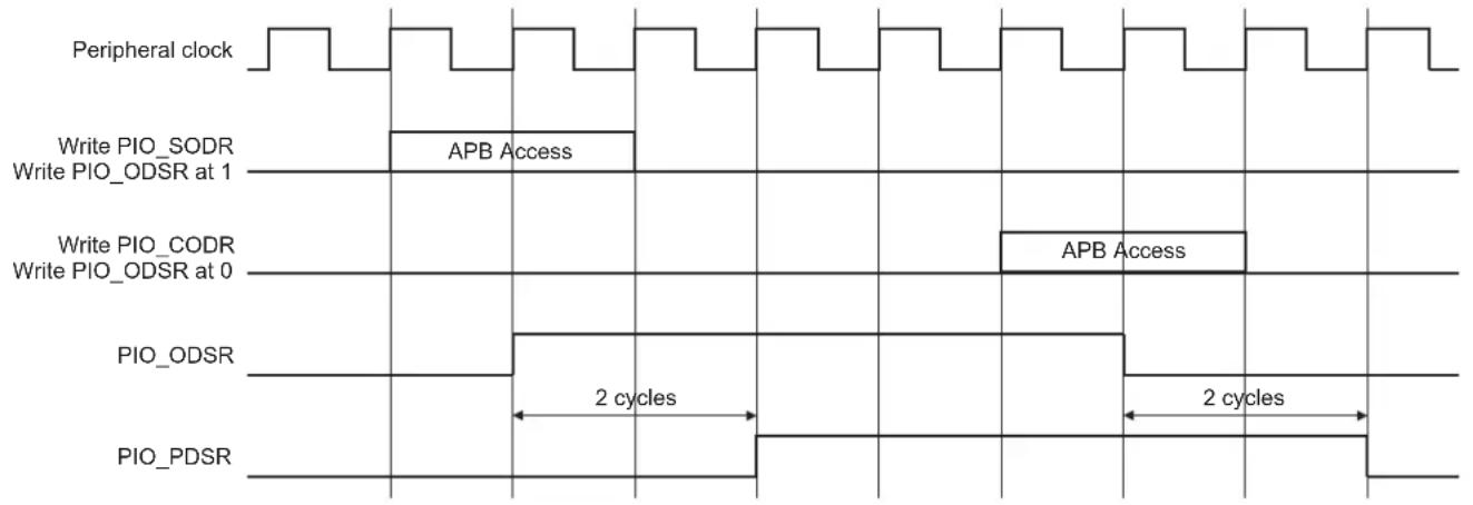
text_image
Peripheral clock Write PIO_SODR Write PIO_ODSR at 1 APB Access Write PIO_CODR Write PIO_ODSR at 0 APB Access PIO_ODSR 2 cycles 2 cycles PIO_PDSR27.5.8 Inputs
The level on each I/O line can be read through PIO_PDSR. This register indicates the level of the I/O lines regardless of their configuration, whether uniquely as an input, or driven by the PIO Controller, or driven by a peripheral.
Reading the I/O line levels requires the clock of the PIO Controller to be enabled, otherwise PIO_PDSR reads the levels present on the I/O line at the time the clock was disabled.
27.5.9 Input Glitch and Debouncing Filters
Optional input glitch and debouncing filters are independently programmable on each I/O line.
The glitch filter can filter a glitch with a duration of less than 1/2 peripheral clock and the debouncing filter can filter a pulse of less than 1/2 period of a programmable divided slow clock.
The selection between glitch filtering or debounce filtering is done by writing in the PIO Input Filter Slow Clock Disable Register (PIO_IFSCDR) and the PIO Input Filter Slow Clock Enable Register (PIO_IFSCER). Writing PIO_IFSCDR and PIO_IFSCER, respectively, sets and clears bits in the Input Filter Slow Clock Status Register (PIO_IFSCSR).
The current selection status can be checked by reading the PIO_IFSCSR.
- If PIO_IFSCSR[i] = 0: The glitch filter can filter a glitch with a duration of less than 1/2 master clock period.
- If PIO_IFSCSR[i] = 1: The debouncing filter can filter a pulse with a duration of less than 1/2 programmable divided slow clock period.
For the debouncing filter, the period of the divided slow clock is defined by writing in the DIV field of the Slow Clock Divider Debouncing Register (PIO_SCDR):
$$ \mathbf {t} _ {\text { div_slck }} = ((\text { DIV } + 1) \times 2) \times \mathbf {t} _ {\text { slck }} $$
When the glitch or debouncing filter is enabled, a glitch or pulse with a duration of less than 1/2 selected clock cycle (selected clock represents peripheral clock or divided slow clock depending on PIO_IFSCDR and PIO_IFSCER programming) is automatically rejected, while a pulse with a duration of one selected clock (peripheral clock or divided slow clock) cycle or more is accepted. For pulse durations between 1/2 selected clock cycle and one selected clock cycle, the pulse may or may not be taken into account, depending on the precise timing of its occurrence. Thus for a pulse to be visible, it must exceed one selected clock cycle, whereas for a glitch to be reliably filtered out, its duration must not exceed 1/2 selected clock cycle.
The filters also introduce some latencies, illustrated in Figure 27-4 and Figure 27-5.
The glitch filters are controlled by the Input Filter Enable Register (PIO_IFER), the Input Filter Disable Register (PIO_IFDR) and the Input Filter Status Register (PIO_IFSR). Writing PIO_IFER and PIO_IFDR respectively sets and clears bits in PIO_IFSR. This last register enables the glitch filter on the I/O lines.
When the glitch and/or debouncing filter is enabled, it does not modify the behavior of the inputs on the peripherals. It acts only on the value read in PIO_PDSR and on the input change interrupt detection. The glitch and debouncing filters require that the peripheral clock is enabled.
Figure 27-4: Input Glitch Filter Timing
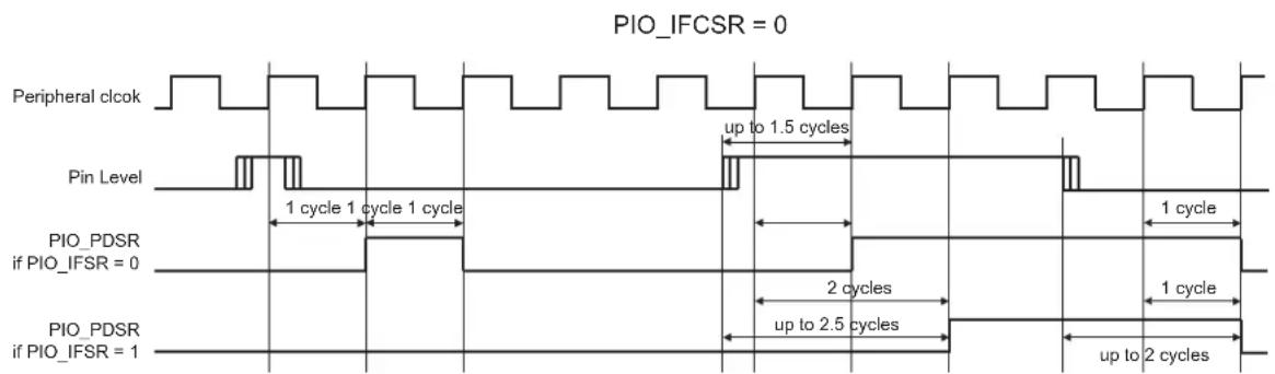
text_image
PIO_IFCSR = 0 Peripheral clcok Pin Level 1 cycle 1 cycle 1 cycle PIO_PDSR if PIO_IFSR = 0 PIO_PDSR if PIO_IFSR = 1 up to 1.5 cycles 1 cycle 2 cycles up to 2.5 cycles up to 2 cyclesFigure 27-5: Input Debouncing Filter Timing

text_image
PIO_IFCSR = 1 Divided Slow Clock (div_slick) Pin Level up to 2 cycles t_peripheral clock up to 2 cycles t_peripheral clock PIO_PDSR if PIO_IFSR = 0 1 cycle t_dv_sick 1 cycle t_dv_sick PIO_PDSR if PIO_IFSR = 1 up to 1.5 cycles t_dv_sick up to 1.5 cycles t_dv_sick up to 2 cycles t_peripheral clock up to 2 cycles t_peripheral clock27.5.10 Input Edge/Level Interrupt
The PIO Controller can be programmed to generate an interrupt when it detects an edge or a level on an I/O line. The Input Edge/Level interrupt is controlled by writing the Interrupt Enable Register (PIO_IER) and the Interrupt Disable Register (PIO_IDR), which enable and disable the input change interrupt respectively by setting and clearing the corresponding bit in the Interrupt Mask Register (PIO_IMR). As input change detection is possible only by comparing two successive samplings of the input of the I/O line, the peripheral clock must be enabled. The Input Change interrupt is available regardless of the configuration of the I/O line, i.e., configured as an input only, controlled by the PIO Controller or assigned to a peripheral function.
By default, the interrupt can be generated at any time an edge is detected on the input.
Some additional interrupt modes can be enabled/disabled by writing in the Additional Interrupt Modes Enable Register (PIO_AIMER) and Additional Interrupt Modes Disable Register (PIO_AIMDR). The current state of this selection can be read through the Additional Interrupt Modes Mask Register (PIO_AIMMR).
These additional modes are:
- Rising edge detection
- Falling edge detection
- Low-level detection
• High-level detection
In order to select an additional interrupt mode:
- The type of event detection (edge or level) must be selected by writing in the Edge Select Register (PIO_ESR) and Level Select Register (PIO_LSR) which select, respectively, the edge and level detection. The current status of this selection is accessible through the Edge/Level Status Register (PIO_ELSR).
- The polarity of the event detection (rising/falling edge or high/low-level) must be selected by writing in the Falling Edge/Low-Level Select Register (PIO_FELLSR) and Rising Edge/High-Level Select Register (PIO_REHLSR) which allow to select falling or rising edge (if edge is selected in PIO_ELSR) edge or high- or low-level detection (if level is selected in PIO_ELSR). The current status of this selection is accessible through the Fall/Rise - Low/High Status Register (PIO_FRLHSR).
When an input edge or level is detected on an I/O line, the corresponding bit in the Interrupt Status Register (PIO_ISR) is set. If the corresponding bit in PIO_IMR is set, the PIO Controller interrupt line is asserted. The interrupt signals of the 32 channels are ORed-wired together to generate a single interrupt signal to the interrupt controller.
When the software reads PIO_ISR, all the interrupts are automatically cleared. This signifies that all the interrupts that are pending when PIO_ISR is read must be handled. When an Interrupt is enabled on a "level", the interrupt is generated as long as the interrupt source is not cleared, even if some read accesses in PIO_ISR are performed.
Figure 27-6: Event Detector on Input Lines (Figure Represents Line 0)

flowchart
graph TD
    A["Resynchronized input on line 0"] --> B["Rising Edge Detector"]
    A --> C["Falling Edge Detector"]
    A --> D["PIO_REHLSR[0"]]
    A --> E["PIO_FRLHSR[0"]]
    A --> F["PIO_FELLSR[0"]]
    A --> G["High Level Detector"]
    A --> H["Low Level Detector"]
    A --> I["Edge Detector"]
    B --> J["1"]
    C --> K["0"]
    D --> L["1"]
    E --> M["0"]
    F --> N["1"]
    G --> O["1"]
    H --> P["0"]
    I --> Q["1"]
    J --> R["0"]
    K --> S["1"]
    L --> T["1"]
    M --> U["1"]
    N --> V["1"]
    O --> W["1"]
    P --> X["1"]
    Q --> Y["1"]
    R --> Z["Event detection on line 0"]
    S --> AA["Event detection on line 0"]
    T --> AB["Event detection on line 0"]
    U --> AC["Event detection on line 0"]
    V --> AD["Event detection on line 0"]
    W --> AE["Event detection on line 0"]
    X --> AF["Event detection on line 0"]
    Y --> AG["Event detection on line 0"]
    Z --> AH["Event detection on line 0"]
Example of interrupt generation on following lines:
- Rising edge on PIO line 0
- Falling edge on PIO line 1
- Rising edge on PIO line 2
- Low-level on PIO line 3
• High-level on PIO line 4
• High-level on PIO line 5 - Falling edge on PIO line 6
- Rising edge on PIO line 7
- Any edge on the other lines
Table 27-2 provides the required configuration for this example.
Table 27-2: Configuration for Example Interrupt Generation
| Configuration Description | |
| Interrupt Mode | All the interrupt sources are enabled by writing 32'hFFFF_FFFF in PIO_IER.Then the additional interrupt mode is enabled for lines 0 to 7 by writing 32'h0000_00FF in PIO_AIMER. |
| Edge or Level Detection | Lines 3, 4 and 5 are configured in level detection by writing 32'h0000_0038 in PIO_LSR.The other lines are configured in edge detection by default, if they have not been previously configured. Otherwise, lines 0, 1, 2, 6 and 7 must be configured in edge detection by writing 32'h0000_00C7 in PIO_ESR. |
| Falling/Rising Edge or Low/High-Level Detection | Lines 0, 2, 4, 5 and 7 are configured in rising edge or high-level detection by writing 32'h0000_00B5 in PIO_REHLSR.The other lines are configured in falling edge or low-level detection by default if they have not been previously configured. Otherwise, lines 1, 3 and 6 must be configured in falling edge/low-level detection by writing 32'h0000_004A in PIO_FELLSR. |
Figure 27-7: Input Change Interrupt Timings When No Additional Interrupt Modes
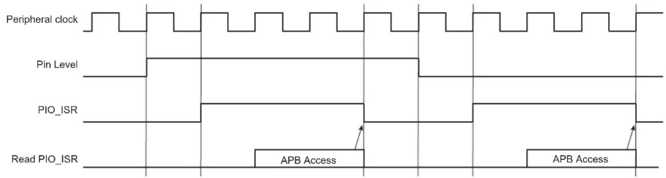
text_image
Peripheral clock Pin Level PIO_ISR Read PIO_ISR APB Access APB Access27.5.11 I/O Lines Lock
When an I/O line is controlled by a peripheral (particularly the Pulse Width Modulation Controller PWM), it can become locked by the action of this peripheral via an input of the PIO Controller. When an I/O line is locked, the write of the corresponding bit in PIO_PER, PIO_PDR, PIO_MDER, PIO_MDDR, PIO_PUDR, PIO_PUER, PIO_ABCDSR1 and PIO_ABCDSR2 is discarded in order to lock its configuration. The user can know at anytime which I/O line is locked by reading the PIO Lock Status Register (PIO_LOCKSR). Once an I/O line is locked, the only way to unlock it is to apply a hardware reset to the PIO Controller.
27.5.12 Programmable I/O Drive
It is possible to configure the I/O drive for pads PA0 to PA31. Refer to Section 54. Electrical Characteristics.
27.5.13 Programmable Schmitt Trigger
It is possible to configure each input for the Schmitt trigger. By default the Schmitt trigger is active. Disabling the Schmitt trigger is requested when using the QTouch® Library.
27.5.14 I/O Lines Programming Example
The programming example shown in Table 27-3 is used to obtain the following configuration:
- 4-bit output port on I/O lines 0 to 3 (should be written in a single write operation), open-drain, with pull-up resistor
- Four output signals on I/O lines 4 to 7 (to drive LEDs for example), driven high and low, no pull-up resistor, no pull-down resistor
- Four input signals on I/O lines 8 to 11 (to read push-button states for example), with pull-up resistors, glitch filters and input change interrupts
- Four input signals on I/O line 12 to 15 to read an external device status (polled, thus no input change interrupt), no pull-up resistor, no glitch filter
- I/O lines 16 to 19 assigned to peripheral A functions with pull-up resistor
- I/O lines 20 to 23 assigned to peripheral B functions with pull-down resistor
- I/O lines 24 to 27 assigned to peripheral C with input change interrupt, no pull-up resistor and no pull-down resistor
- I/O lines 28 to 31 assigned to peripheral D, no pull-up resistor and no pull-down resistor
Table 27-3: Programming Example
| Register Value to be Written | |
| PIO_PER 0x0000_FFFF | |
| PIO_PDR 0xFFFF_0000 | |
| PIO_OER 0x0000_00FF | |
| PIO_ODR | 0xFFFF_FF00 |
| PIO_IFER | 0x0000_0F00 |
| PIO_IFDR | 0xFFFF_F0FF |
| PIO_SODR | 0x0000_0000 |
| PIO_CODR 0x0FFF_FFFF | |
| PIO_IER 0x0F00_0F00 | |
| PIO_IDR 0xF0FF_F0FF | |
| PIO_MDER 0x0000_000F | |
| PIO_MDDR 0xFFFF_FFF0 | |
| PIO_PUDR 0xFFFF0_00F0 | |
| PIO_PUER 0x000F_FF0F | |
| PIO_PPDDR 0xFF0F_FFFF | |
| PIO_PPDER 0x00F0_0000 | |
| PIO_ABCDSR1 0xF0F0_0000 | |
| PIO_ABCDSR2 0xFF00_0000 | |
| PIO_OWNER 0x0000_000F | |
| PIO_OWDR 0x0FFF_FFF0 |
27.5.15 Register Write Protection
To prevent any single software error from corrupting PIO behavior, certain registers in the address space can be write-protected by setting the WPEN bit in the PIO Write Protection Mode Register (PIO_WPMR).
If a write access to a write-protected register is detected, the WPVS flag in the PIO Write Protection Status Register (PIO_WPSR) is set and the field WPVSRC indicates the register in which the write access has been attempted.
The WPVS bit is automatically cleared after reading the PIO_WPSR.
The following registers can be write-protected:
- PIO Enable Register
- PIO Disable Register
• PIO Output Enable Register
• PIO Output Disable Register
• PIO Input Filter Enable Register
• PIO Input Filter Disable Register
• PIO Multi-driver Enable Register
• PIO Multi-driver Disable Register
• PIO Pull-Up Disable Register
• PIO Pull-Up Enable Register
• PIO Peripheral ABCD Select Register 1
• PIO Peripheral ABCD Select Register 2
• PIO Output Write Enable Register
• PIO Output Write Disable Register
• PIO Pad Pull-Down Disable Register - PIO Pad Pull-Down Enable Register
27.6 Parallel Input/Output Controller (PIO) User Interface
Each I/O line controlled by the PIO Controller is associated with a bit in each of the PIO Controller User Interface registers. Each register is 32-bit wide. If a parallel I/O line is not defined, writing to the corresponding bits has no effect. Undefined bits read zero. If the I/O line is not multiplexed with any peripheral, the I/O line is controlled by the PIO Controller and PIO_PSR returns one systematically.
Table 27-4: Register Mapping
| Offset Register Name | Access Reset | |||
| 0x0000 PIO Enable | Register PIO_PER Write-only - | |||
| 0x0004 PIO Disable | Register PIO_PDR Write-only - | |||
| 0x0008 | PIO Status Register | PIO_PSR | Read-only | (1) |
| 0x000C | Reserved | - | - | - |
| 0x0010 Output Enable | Register PIO_OER | Write-only - | ||
| 0x0014 Output Disable | Register PIO_ODR | Write-only - | ||
| 0x0018 | Output Status Register | PIO_OSR | Read-only | 0x00000000 |
| 0x001C | Reserved | - | - | - |
| 0x0020 | Glitch Input Filter Enable Register | PIO_IFER | Write-only | - |
| 0x0024 | Glitch Input Filter Disable Register | PIO_IFDR | Write-only | - |
| 0x0028 | Glitch Input Filter Status Register | PIO_IFSR | Read-only | 0x00000000 |
| 0x002C | Reserved | - | - | - |
| 0x0030 Set Output Data | Register PIO_SODR | Write-only - | ||
| 0x0034 Clear Output | Data Register PIO_CODR | Write-only | ||
| 0x0038 Output Data | Status Register PIO_ODSR | Read-only or (2) Read/Write | - | |
| 0x003C | Pin Data Status Register | PIO_PDSR | Read-only | (3) |
| 0x0040 Interrupt Enable | Register PIO_IER Write-only | - | ||
| 0x0044 Interrupt Disable | Register PIO_IDR Write-only - | |||
| 0x0048 | Interrupt Mask Register | PIO_IMR | Read-only | 0x00000000 |
| 0x004C | Interrupt Status Register^(4) | PIO_ISR Read-only | 0x00000000 | |
| 0x0050 Multi-driver Enable | Register PIO_MDER | Write-only - | ||
| 0x0054 | Multi-driver Disable Register | PIO_MDDR | Write-only | - |
| 0x0058 | Multi-driver Status Register | PIO_MDSR | Read-only | 0x00000000 |
| 0x005C | Reserved | - | - | - |
| 0x0060 Pull-up Disable | Register PIO_PUDR | Write-only - | ||
| 0x0064 Pull-up Enable | Register PIO_PUER | Write-only - | ||
| 0x0068 | Pad Pull-up Status Register | PIO_PUSR | Read-only | (1) |
| 0x006C | Reserved | - | - | - |
| 0x0070 | Peripheral Select Register 1 | PIO_ABCDSR1 | Read/Write | 0x00000000 |
| 0x0074 | Peripheral Select Register 2 | PIO_ABCDSR2 | Read/Write | 0x00000000 |
| 0x0078-0x007C | Reserved | - | - | - |
| 0x0080 | Input Filter Slow Clock Disable Register | PIO_IFSCDR | Write-only | - |
| Offset | Register | Name | Access | Reset |
| 0x0084 Input Filter Slow Clock Enable Register PIO_IFSCER Write-only – | ||||
| 0x0088 | Input Filter Slow Clock Status Register | PIO_IFSCSR | Read-only | 0x00000000 |
| 0x008C Slow Clock Divider Debouncing Register PIO_SCDR Read/Write 0x00000000 | ||||
| 0x0090 | Pad Pull-down Disable Register | PIO_PPDDR | Write-only | – |
| 0x0094 Pad Pull-down Enable Register PIO_PPDER | Write-only – | |||
| 0x0098 | Pad Pull-down Status Register | PIO_PPDSR | Read-only | (1) |
| 0x009C Reserved | – | – | – | |
| 0x00A0 | Output Write Enable | PIO_OWNER Write-only – | ||
| 0x00A4 | Output Write Disable | PIO_OWDR | Write-only | – |
| 0x00A8 | Output Write Status Register | PIO_OWSR | Read-only | 0x00000000 |
| 0x00AC | Reserved | – | – | – |
| 0x00B0 | Additional Interrupt Modes Enable Register | PIO_AIMER | Write-only | – |
| 0x00B4 | Additional Interrupt Modes Disable Register | PIO_AIMDR | Write-only | – |
| 0x00B8 | Additional Interrupt Modes Mask Register | PIO_AIMMR | Read-only | 0x00000000 |
| 0x00BC | Reserved | – | – | – |
| 0x00C0 Edge Select Register PIO_ESR Write-only – | ||||
| 0x00C4 Level Select Register PIO_LSR Write-only – | ||||
| 0x00C8 | Edge/Level Status Register | PIO_ELSR | Read-only | 0x00000000 |
| 0x00CC Reserved | – | – | – | |
| 0x00D0 | Falling Edge/Low-Level Select Register | PIO_FELLSR | Write-only | – |
| 0x00D4 | Rising Edge/High-Level Select Register | PIO_REHLSR | Write-only | – |
| 0x00D8 | Fall/Rise - Low/High Status Register | PIO_FRLHSR | Read-only | 0x00000000 |
| 0x00DC Reserved | – | – | – | |
| 0x00E0 | Lock Status | PIO_LOCKSR | Read-only | 0x00000000 |
| 0x00E4 | Write Protection Mode Register | PIO_WPMR | Read/Write | 0x00000000 |
| 0x00E8 | Write Protection Status Register | PIO_WPSR | Read-only | 0x00000000 |
| 0x00EC-0x00FC | Reserved | – | – | – |
| 0x0100 | Schmitt Trigger Register | PIO_SCHMITT | Read/Write | 0x00000000 |
| 0x0104-0x010C | Reserved | – | – | – |
| 0x0110 | Reserved | – | – | – |
| 0x0114 | Reserved | – | – | – |
| 0x0118 | I/O Drive Register 1 | PIO_DRIVER1 | Read/Write | 0xAAAAAAAA |
| 0x011C | I/O Drive Register 2 | PIO_DRIVER2 | Read/Write | 0xAAAAAAAA |
| 0x0120-0x014C | Reserved | – | – | – |
Note 1: Reset value depends on the product implementation.
2: PIO_ODSR is Read-only or Read/Write depending on PIO_OWSR I/O lines.
3: Reset value of PIO_PDSR depends on the level of the I/O lines. Reading the I/O line levels requires the clock of the PIO Controller to be enabled, otherwise PIO_PDSR reads the levels present on the I/O line at the time the clock was disabled.
4: PIO_ISR is reset at 0x0. However, the first read of the register may read a different value as input changes may have occurred.
5: If an offset is not listed in the table it must be considered as reserved.
27.6.1 PIO Enable Register
Name:PIO_PER
Address:0xFFFFF200 (PIOA), 0xFFFFF400 (PIOB), 0xFFFFF600 (PIOC), 0xFFFFF800 (PIOD), 0xFFFFFA00 (PIOE)
Access:Write-only
| 31 30 29 28 27 26 25 24 | |||||||
| P31 P30 P | 29 P28 P27 P26 | P25 P24 | |||||
| 23 22 21 20 19 18 17 16 | |||||||
| P23 P22 P | 21 P20 P19 P18 | P17 P16 | |||||
| 15 14 13 12 11 10 9 8 | |||||||
| P15 P14 P | 13 P12 P11 P10 | P9 P8 | |||||
| 7 | 6 | 5 | 4 | 3 | 2 | 1 | 0 |
| P7 P6 P5 | P4 P3 P2 P1 P0 | ||||||
This register can only be written if the WPEN bit is cleared in the PIO Write Protection Mode Register.
P0-P31: PIO Enable
0: No effect.
1: Enables the PIO to control the corresponding pin (disables peripheral control of the pin).
27.6.2 PIO Disable Register
Name:PIO_PDR
Address:0xFFFFF204 (PIOA), 0xFFFFF404 (PIOB), 0xFFFFF604 (PIOC), 0xFFFFF804 (PIOD), 0xFFFFFA04 (PIOE)
Access:Write-only
| 31 30 29 28 27 26 25 24 | |||||||
| P31 P30 P | 29 P28 P27 P26 | P25 P24 | |||||
| 23 22 21 20 19 18 17 16 | |||||||
| P23 P22 P | 21 P20 P19 P18 | P17 P16 | |||||
| 15 14 13 12 11 10 9 8 | |||||||
| P15 P14 P | 13 P12 P11 P10 | P9 P8 | |||||
| 7 | 6 | 5 | 4 | 3 | 2 | 1 | 0 |
| P7 P6 P5 | P4 P3 P2 P1 P0 | ||||||
This register can only be written if the WPEN bit is cleared in the PIO Write Protection Mode Register.
P0-P31: PIO Disable
0: No effect.
1: Disables the PIO from controlling the corresponding pin (enables peripheral control of the pin).
27.6.3 PIO Status Register
Name:PIO_PSR
Address:0xFFFFF208 (PIOA), 0xFFFFF408 (PIOB), 0xFFFFF608 (PIOC), 0xFFFFF808 (PIOD), 0xFFFFFA08 (PIOE)
Access: Read-only
| 31 30 29 28 27 26 25 24 | |||||||
| P31 P30 P | 29 P28 P27 P26 | P25 P24 | |||||
| 23 22 21 20 19 18 17 16 | |||||||
| P23 P22 P | 21 P20 P19 P18 | P17 P16 | |||||
| 15 14 13 12 11 10 9 8 | |||||||
| P15 P14 P | 13 P12 P11 P10 | P9 P8 | |||||
| 7 | 6 | 5 | 4 | 3 | 2 | 1 | 0 |
| P7 P6 P5 | P4 P3 P2 P1 P0 | ||||||
P0–P31: PIO Status
0: PIO is inactive on the corresponding I/O line (peripheral is active).
1: PIO is active on the corresponding I/O line (peripheral is inactive).
27.6.4 PIO Output Enable Register
Name:PIO_OER
Address:0xFFFFF210 (PIOA), 0xFFFFF410 (PIOB), 0xFFFFF610 (PIOC), 0xFFFFF810 (PIOD), 0xFFFFFA10 (PIOE)
Access:Write-only
| 31 30 29 28 27 26 25 24 | |||||||
| P31 P30 P | 29 P28 P27 P26 | P25 P24 | |||||
| 23 22 21 20 19 18 17 16 | |||||||
| P23 P22 P | 21 P20 P19 P18 | P17 P16 | |||||
| 15 14 13 12 11 10 9 8 | |||||||
| P15 P14 P | 13 P12 P11 P10 | P9 P8 | |||||
| 7 | 6 | 5 | 4 | 3 | 2 | 1 | 0 |
| P7 P6 P5 | P4 P3 P2 P1 P0 | ||||||
This register can only be written if the WPEN bit is cleared in the PIO Write Protection Mode Register.
P0-P31: Output Enable
0: No effect.
1: Enables the output on the I/O line.
27.6.5 PIO Output Disable Register
Name:PIO_ODR
Address:0xFFFFF214 (PIOA), 0xFFFFF414 (PIOB), 0xFFFFF614 (PIOC), 0xFFFFF814 (PIOD), 0xFFFFFA14 (PIOE)
Access:Write-only
| 31 30 29 28 27 26 25 24 | |||||||
| P31 P30 P | 29 P28 P27 P26 | P25 P24 | |||||
| 23 22 21 20 19 18 17 16 | |||||||
| P23 P22 P | 21 P20 P19 P18 | P17 P16 | |||||
| 15 14 13 12 11 10 9 8 | |||||||
| P15 P14 P | 13 P12 P11 P10 | P9 P8 | |||||
| 7 | 6 | 5 | 4 | 3 | 2 | 1 | 0 |
| P7 P6 P5 | P4 P3 P2 P1 P0 | ||||||
This register can only be written if the WPEN bit is cleared in the PIO Write Protection Mode Register.
1: Disables the output on the I/O line.
27.6.6 PIO Output Status Register
Name:PIO_OSR
Address:0xFFFFF218 (PIOA), 0xFFFFF418 (PIOB), 0xFFFFF618 (PIOC), 0xFFFFF818 (PIOD), 0xFFFFFA18 (PIOE)
Access: Read-only
| 31 30 29 28 27 26 25 24 | |||||||
| P31 P30 P | 29 P28 P27 P26 | P25 P24 | |||||
| 23 22 21 20 19 18 17 16 | |||||||
| P23 P22 P | 21 P20 P19 P18 | P17 P16 | |||||
| 15 14 13 12 11 10 9 8 | |||||||
| P15 P14 P | 13 P12 P11 P10 | P9 P8 | |||||
| 7 | 6 | 5 | 4 | 3 | 2 | 1 | 0 |
| P7 P6 P5 | P4 P3 P2 P1 P0 | ||||||
P0–P31: Output Status
0: The I/O line is a pure input.
1: The I/O line is enabled in output.
27.6.7 PIO Input Filter Enable Register
Name:PIO_IFER
Address:0xFFFFF220 (PIOA), 0xFFFFF420 (PIOB), 0xFFFFF620 (PIOC), 0xFFFFF820 (PIOD), 0xFFFFFA20 (PIOE)
Access:Write-only
| 31 30 29 28 27 26 25 24 | |||||||
| P31 P30 P | 29 P28 P27 P26 | P25 P24 | |||||
| 23 22 21 20 19 18 17 16 | |||||||
| P23 P22 P | 21 P20 P19 P18 | P17 P16 | |||||
| 15 14 13 12 11 10 9 8 | |||||||
| P15 P14 P | 13 P12 P11 P10 | P9 P8 | |||||
| 7 | 6 | 5 | 4 | 3 | 2 | 1 | 0 |
| P7 P6 P5 | P4 P3 P2 P1 P0 | ||||||
This register can only be written if the WPEN bit is cleared in the PIO Write Protection Mode Register.
P0-P31: Input Filter Enable
0: No effect.
1: Enables the input glitch filter on the I/O line.
27.6.8 PIO Input Filter Disable Register
Name:PIO_IFDR
Address:0xFFFFF224 (PIOA), 0xFFFFF424 (PIOB), 0xFFFFF624 (PIOC), 0xFFFFF824 (PIOD), 0xFFFFFA24 (PIOE)
Access:Write-only
| 31 30 29 28 27 26 25 24 | |||||||
| P31 P30 P | 29 P28 P27 P26 | P25 P24 | |||||
| 23 22 21 20 19 18 17 16 | |||||||
| P23 P22 P | 21 P20 P19 P18 | P17 P16 | |||||
| 15 14 13 12 11 10 9 8 | |||||||
| P15 P14 P | 13 P12 P11 P10 | P9 P8 | |||||
| 7 | 6 | 5 | 4 | 3 | 2 | 1 | 0 |
| P7 P6 P5 | P4 P3 P2 P1 P0 | ||||||
This register can only be written if the WPEN bit is cleared in the PIO Write Protection Mode Register.
1: Disables the input glitch filter on the I/O line.
27.6.9 PIO Input Filter Status Register
Name:PIO_IFSR
Address:0xFFFFF228 (PIOA), 0xFFFFF428 (PIOB), 0xFFFFF628 (PIOC), 0xFFFFF828 (PIOD), 0xFFFFFA28 (PIOE)
Access: Read-only
| 31 30 29 28 27 26 25 24 | |||||||
| P31 P30 P | 29 P28 P27 P26 | P25 P24 | |||||
| 23 22 21 20 19 18 17 16 | |||||||
| P23 P22 P | 21 P20 P19 P18 | P17 P16 | |||||
| 15 14 13 12 11 10 9 8 | |||||||
| P15 P14 P | 13 P12 P11 P10 | P9 P8 | |||||
| 7 | 6 | 5 | 4 | 3 | 2 | 1 | 0 |
| P7 P6 P5 | P4 P3 P2 P1 P0 | ||||||
P0–P31: Input Filter Status
0: The input glitch filter is disabled on the I/O line.
1: The input glitch filter is enabled on the I/O line.
27.6.10 PIO Set Output Data Register
Name:PIO_SODR
Address:0xFFFFF230 (PIOA), 0xFFFFF430 (PIOB), 0xFFFFF630 (PIOC), 0xFFFFF830 (PIOD), 0xFFFFFA30 (PIOE)
Access:Write-only
| 31 30 29 28 27 26 25 24 | |||||||
| P31 P30 P | 29 P28 P27 P26 | P25 P24 | |||||
| 23 22 21 20 19 18 17 16 | |||||||
| P23 P22 P | 21 P20 P19 P18 | P17 P16 | |||||
| 15 14 13 12 11 10 9 8 | |||||||
| P15 P14 P | 13 P12 P11 P10 | P9 P8 | |||||
| 7 | 6 | 5 | 4 | 3 | 2 | 1 | 0 |
| P7 P6 P5 | P4 P3 P2 P1 P0 | ||||||
P0–P31: Set Output Data
0: No effect.
1: Sets the data to be driven on the I/O line.
27.6.11 PIO Clear Output Data Register
Name:PIO_CODR
Address:0xFFFFF234 (PIOA), 0xFFFFF434 (PIOB), 0xFFFFF634 (PIOC), 0xFFFFF834 (PIOD), 0xFFFFFA34 (PIOE)
Access:Write-only
| 31 30 29 28 27 26 25 24 | |||||||
| P31 P30 P | 29 P28 P27 P26 | P25 P24 | |||||
| 23 22 21 20 19 18 17 16 | |||||||
| P23 P22 P | 21 P20 P19 P18 | P17 P16 | |||||
| 15 14 13 12 11 10 9 8 | |||||||
| P15 P14 P | 13 P12 P11 P10 | P9 P8 | |||||
| 7 | 6 | 5 | 4 | 3 | 2 | 1 | 0 |
| P7 P6 P5 | P4 P3 P2 P1 P0 | ||||||
P0–P31: Clear Output Data
0: No effect.
1: Clears the data to be driven on the I/O line.
27.6.12 PIO Output Data Status Register
Name:PIO_ODSR
Address:0xFFFFF238 (PIOA), 0xFFFFF438 (PIOB), 0xFFFFF638 (PIOC), 0xFFFFF838 (PIOD), 0xFFFFFA38 (PIOE)
Access: Read-only or Read/Write
| 31 30 29 28 27 26 25 24 | |||||||
| P31 P30 P | 29 P28 P27 P26 | P25 P24 | |||||
| 23 22 21 20 19 18 17 16 | |||||||
| P23 P22 P | 21 P20 P19 P18 | P17 P16 | |||||
| 15 14 13 12 11 10 9 8 | |||||||
| P15 P14 P | 13 P12 P11 P10 | P9 P8 | |||||
| 7 | 6 | 5 | 4 | 3 | 2 | 1 | 0 |
| P7 P6 P5 | P4 P3 P2 P1 P0 | ||||||
P0–P31: Output Data Status
0: The data to be driven on the I/O line is 0.
1: The data to be driven on the I/O line is 1.
27.6.13 PIO Pin Data Status Register
Name:PIO_PDSR
Address:0xFFFFF23C (PIOA), 0xFFFFF43C (PIOB), 0xFFFFF63C (PIOC), 0xFFFFF83C (PIOD), 0xFFFFFA3C (PIOE)
Access: Read-only
| 31 30 29 28 27 26 25 24 | |||||||
| P31 P30 P | 29 P28 P27 P26 | P25 P24 | |||||
| 23 22 21 20 19 18 17 16 | |||||||
| P23 P22 P | 21 P20 P19 P18 | P17 P16 | |||||
| 15 14 13 12 11 10 9 8 | |||||||
| P15 P14 P | 13 P12 P11 P10 | P9 P8 | |||||
| 7 | 6 | 5 | 4 | 3 | 2 | 1 | 0 |
| P7 P6 P5 | P4 P3 P2 P1 P0 | ||||||
P0–P31: Output Data Status
0: The I/O line is at level 0.
1: The I/O line is at level 1.
27.6.14 PIO Interrupt Enable Register
Name:PIO_IER
Address:0xFFFFF240 (PIOA), 0xFFFFF440 (PIOB), 0xFFFFF640 (PIOC), 0xFFFFF840 (PIOD), 0xFFFFFA40 (PIOE)
Access:Write-only
| 31 30 29 28 27 26 25 24 | |||||||
| P31 P30 P | 29 P28 P27 P26 | P25 P24 | |||||
| 23 22 21 20 19 18 17 16 | |||||||
| P23 P22 P | 21 P20 P19 P18 | P17 P16 | |||||
| 15 14 13 12 11 10 9 8 | |||||||
| P15 P14 P | 13 P12 P11 P10 | P9 P8 | |||||
| 7 | 6 | 5 | 4 | 3 | 2 | 1 | 0 |
| P7 P6 P5 | P4 P3 P2 P1 P0 | ||||||
P0–P31: Input Change Interrupt Enable
0: No effect.
1: Enables the input change interrupt on the I/O line.
27.6.15 PIO Interrupt Disable Register
Name:PIO_IDR
Address:0xFFFFF244 (PIOA), 0xFFFFF444 (PIOB), 0xFFFFF644 (PIOC), 0xFFFFF844 (PIOD), 0xFFFFFA44 (PIOE)
Access:Write-only
| 31 30 29 28 27 26 25 24 | |||||||
| P31 P30 P | 29 P28 P27 P26 | P25 P24 | |||||
| 23 22 21 20 19 18 17 16 | |||||||
| P23 P22 P | 21 P20 P19 P18 | P17 P16 | |||||
| 15 14 13 12 11 10 9 8 | |||||||
| P15 P14 P | 13 P12 P11 P10 | P9 P8 | |||||
| 7 | 6 | 5 | 4 | 3 | 2 | 1 | 0 |
| P7 P6 P5 | P4 P3 P2 P1 P0 | ||||||
P0–P31: Input Change Interrupt Disable
0: No effect.
1: Disables the input change interrupt on the I/O line.
27.6.16 PIO Interrupt Mask Register
Name:PIO_IMR
Address:0xFFFFF248 (PIOA), 0xFFFFF448 (PIOB), 0xFFFFF648 (PIOC), 0xFFFFF848 (PIOD), 0xFFFFFA48 (PIOE)
Access: Read-only
| 31 30 29 28 27 26 25 24 | |||||||
| P31 P30 P | 29 P28 P27 P26 | P25 P24 | |||||
| 23 22 21 20 19 18 17 16 | |||||||
| P23 P22 P | 21 P20 P19 P18 | P17 P16 | |||||
| 15 14 13 12 11 10 9 8 | |||||||
| P15 P14 P | 13 P12 P11 P10 | P9 P8 | |||||
| 7 | 6 | 5 | 4 | 3 | 2 | 1 | 0 |
| P7 P6 P5 | P4 P3 P2 P1 P0 | ||||||
P0–P31: Input Change Interrupt Mask
0: Input change interrupt is disabled on the I/O line.
1: Input change interrupt is enabled on the I/O line.
27.6.17 PIO Interrupt Status Register
Name:PIO_ISR
Address:0xFFFFF24C (PIOA), 0xFFFFF44C (PIOB), 0xFFFFF64C (PIOC), 0xFFFFF84C (PIOD), 0xFFFFFA4C (PIOE)
Access: Read-only
| 31 30 29 28 27 26 25 24 | |||||||
| P31 P30 P | 29 P28 P27 P26 | P25 P24 | |||||
| 23 22 21 20 19 18 17 16 | |||||||
| P23 P22 P | 21 P20 P19 P18 | P17 P16 | |||||
| 15 14 13 12 11 10 9 8 | |||||||
| P15 P14 P | 13 P12 P11 P10 | P9 P8 | |||||
| 7 | 6 | 5 | 4 | 3 | 2 | 1 | 0 |
| P7 P6 P5 | P4 P3 P2 P1 P0 | ||||||
P0–P31: Input Change Interrupt Status
0: No input change has been detected on the I/O line since PIO_ISR was last read or since reset.
1: At least one input change has been detected on the I/O line since PIO_ISR was last read or since reset.
27.6.18 PIO Multi-driver Enable Register
Name:PIO_MDER
Address:0xFFFFF250 (PIOA), 0xFFFFF450 (PIOB), 0xFFFFF650 (PIOC), 0xFFFFF850 (PIOD), 0xFFFFFA50 (PIOE)
Access:Write-only
| 31 30 29 28 27 26 25 24 | |||||||
| P31 P30 P | 29 P28 P27 P26 | P25 P24 | |||||
| 23 22 21 20 19 18 17 16 | |||||||
| P23 P22 P | 21 P20 P19 P18 | P17 P16 | |||||
| 15 14 13 12 11 10 9 8 | |||||||
| P15 P14 P | 13 P12 P11 P10 | P9 P8 | |||||
| 7 | 6 | 5 | 4 | 3 | 2 | 1 | 0 |
| P7 P6 P5 | P4 P3 P2 P1 P0 | ||||||
This register can only be written if the WPEN bit is cleared in the PIO Write Protection Mode Register.
P0-P31: Multi-drive Enable
0: No effect.
1: Enables multi-drive on the I/O line.
27.6.19 PIO Multi-driver Disable Register
Name:PIO_MDDR
Address:0xFFFFF254 (PIOA), 0xFFFFF454 (PIOB), 0xFFFFF654 (PIOC), 0xFFFFF854 (PIOD), 0xFFFFFA54 (PIOE)
Access:Write-only
| 31 30 29 28 27 26 25 24 | |||||||
| P31 P30 P | 29 P28 P27 P26 | P25 P24 | |||||
| 23 22 21 20 19 18 17 16 | |||||||
| P23 P22 P | 21 P20 P19 P18 | P17 P16 | |||||
| 15 14 13 12 11 10 9 8 | |||||||
| P15 P14 P | 13 P12 P11 P10 | P9 P8 | |||||
| 7 | 6 | 5 | 4 | 3 | 2 | 1 | 0 |
| P7 P6 P5 | P4 P3 P2 P1 P0 | ||||||
This register can only be written if the WPEN bit is cleared in the PIO Write Protection Mode Register.
P0-P31: Multi-drive Disable
0: No effect.
1: Disables multi-drive on the I/O line.
27.6.20 PIO Multi-driver Status Register
Name:PIO_MDSR
Address:0xFFFFF258 (PIOA), 0xFFFFF458 (PIOB), 0xFFFFF658 (PIOC), 0xFFFFF858 (PIOD), 0xFFFFFA58 (PIOE)
Access: Read-only
| 31 30 29 28 27 26 25 24 | |||||||
| P31 P30 P | 29 P28 P27 P26 | P25 P24 | |||||
| 23 22 21 20 19 18 17 16 | |||||||
| P23 P22 P | 21 P20 P19 P18 | P17 P16 | |||||
| 15 14 13 12 11 10 9 8 | |||||||
| P15 P14 P | 13 P12 P11 P10 | P9 P8 | |||||
| 7 | 6 | 5 | 4 | 3 | 2 | 1 | 0 |
| P7 P6 P5 | P4 P3 P2 P1 P0 | ||||||
P0–P31: Multi-drive Status
0: The multi-drive is disabled on the I/O line. The pin is driven at high- and low-level.
1: The multi-drive is enabled on the I/O line. The pin is driven at low-level only.
27.6.21 PIO Pull-Up Disable Register
Name:PIO_PUDR
Address:0xFFFFF260 (PIOA), 0xFFFFF460 (PIOB), 0xFFFFF660 (PIOC), 0xFFFFF860 (PIOD), 0xFFFFFA60 (PIOE)
Access:Write-only
| 31 30 29 28 27 26 25 24 | |||||||
| P31 P30 P | 29 P28 P27 P26 | P25 P24 | |||||
| 23 22 21 20 19 18 17 16 | |||||||
| P23 P22 P | 21 P20 P19 P18 | P17 P16 | |||||
| 15 14 13 12 11 10 9 8 | |||||||
| P15 P14 P | 13 P12 P11 P10 | P9 P8 | |||||
| 7 | 6 | 5 | 4 | 3 | 2 | 1 | 0 |
| P7 P6 P5 | P4 P3 P2 P1 P0 | ||||||
This register can only be written if the WPEN bit is cleared in the PIO Write Protection Mode Register.
P0-P31: Pull-Up Disable
0: No effect.
1: Disables the pull-up resistor on the I/O line.
27.6.22 PIO Pull-Up Enable Register
Name:PIO_PUER
Address:0xFFFFF264 (PIOA), 0xFFFFF464 (PIOB), 0xFFFFF664 (PIOC), 0xFFFFF864 (PIOD), 0xFFFFFA64 (PIOE)
Access:Write-only
| 31 30 29 28 27 26 25 24 | |||||||
| P31 P30 P | 29 P28 P27 P26 | P25 P24 | |||||
| 23 22 21 20 19 18 17 16 | |||||||
| P23 P22 P | 21 P20 P19 P18 | P17 P16 | |||||
| 15 14 13 12 11 10 9 8 | |||||||
| P15 P14 P | 13 P12 P11 P10 | P9 P8 | |||||
| 7 | 6 | 5 | 4 | 3 | 2 | 1 | 0 |
| P7 P6 P5 | P4 P3 P2 P1 P0 | ||||||
This register can only be written if the WPEN bit is cleared in the PIO Write Protection Mode Register.
P0-P31: Pull-Up Enable
0: No effect.
1: Enables the pull-up resistor on the I/O line.
27.6.23 PIO Pull-Up Status Register
Name:PIO_PUSR
Address:0xFFFFF268 (PIOA), 0xFFFFF468 (PIOB), 0xFFFFF668 (PIOC), 0xFFFFF868 (PIOD), 0xFFFFFA68 (PIOE)
Access: Read-only
| 31 30 29 28 27 26 25 24 | |||||||
| P31 P30 P | 29 P28 P27 P26 | P25 P24 | |||||
| 23 22 21 20 19 18 17 16 | |||||||
| P23 P22 P | 21 P20 P19 P18 | P17 P16 | |||||
| 15 14 13 12 11 10 9 8 | |||||||
| P15 P14 P | 13 P12 P11 P10 | P9 P8 | |||||
| 7 | 6 | 5 | 4 | 3 | 2 | 1 | 0 |
| P7 P6 P5 | P4 P3 P2 P1 P0 | ||||||
P0–P31: Pull-Up Status
0: Pull-up resistor is enabled on the I/O line.
1: Pull-up resistor is disabled on the I/O line.
27.6.24 PIO Peripheral ABCD Select Register 1
Name:PIO_ABCDSR1
Access: Read/Write
31 30 29 28 27 26 25 24
| P31 P30 P | 29 P28 P27 P26 | P25 P24 |
23 22 21 20 19 18 17 16
| P23 P22 R | 21 P20 P19 P18 | P17 P16 |
15 14 13 12 11 10 9 8
This register can only be written if the WPEN bit is cleared in the PIO Write Protection Mode Register.
P0–P31: Peripheral Select
If the same bit is set to 0 in PIO_ABCDSR2:
0: Assigns the I/O line to the Peripheral A function.
1: Assigns the I/O line to the Peripheral B function.
If the same bit is set to 1 in PIO_ABCDSR2:
0: Assigns the I/O line to the Peripheral C function.
1: Assigns the I/O line to the Peripheral D function.
27.6.25 PIO Peripheral ABCD Select Register 2
Name:PIO_ABCDSR2
Access: Read/Write
31 30 29 28 27 26 25 24
| P31 P30 P | 29 P28 P27 P26 | P25 P24 |
23 22 21 20 19 18 17 16
| P23 P22 R | 21 P20 P19 P18 | P17 P16 |
15 14 13 12 11 10 9 8
This register can only be written if the WPEN bit is cleared in the PIO Write Protection Mode Register.
P0–P31: Peripheral Select
If the same bit is set to 0 in PIO_ABCDSR1:
0: Assigns the I/O line to the Peripheral A function.
1: Assigns the I/O line to the Peripheral C function.
If the same bit is set to 1 in PIO_ABCDSR1:
0: Assigns the I/O line to the Peripheral B function.
1: Assigns the I/O line to the Peripheral D function.
27.6.26 PIO Input Filter Slow Clock Disable Register
Name:PIO_IFSCDR
Address:0xFFFFF280 (PIOA), 0xFFFFF480 (PIOB), 0xFFFFF680 (PIOC), 0xFFFFF880 (PIOD), 0xFFFFFA80 (PIOE)
Access:Write-only
| 31 30 29 28 27 26 25 24 | |||||||
| P31 P30 P | 29 P28 P27 P26 | P25 P24 | |||||
| 23 22 21 20 19 18 17 16 | |||||||
| P23 P22 P | 21 P20 P19 P18 | P17 P16 | |||||
| 15 14 13 12 11 10 9 8 | |||||||
| P15 P14 P | 13 P12 P11 P10 | P9 P8 | |||||
| 7 | 6 | 5 | 4 | 3 | 2 | 1 | 0 |
| P7 P6 P5 | P4 P3 P2 P1 P0 | ||||||
P0–P31: Peripheral Clock Glitch Filtering Select
0: No effect.
1: The glitch filter is able to filter glitches with a duration < t_peripheral clock/2 .
27.6.27 PIO Input Filter Slow Clock Enable Register
Name:PIO_IFSCER
Address:0xFFFFF284 (PIOA), 0xFFFFF484 (PIOB), 0xFFFFF684 (PIOC), 0xFFFFF884 (PIOD), 0xFFFFFA84 (PIOE)
Access:Write-only
| 31 30 29 28 27 26 25 24 | |||||||
| P31 P30 P | 29 P28 P27 P26 | P25 P24 | |||||
| 23 22 21 20 19 18 17 16 | |||||||
| P23 P22 P | 21 P20 P19 P18 | P17 P16 | |||||
| 15 14 13 12 11 10 9 8 | |||||||
| P15 P14 P | 13 P12 P11 P10 | P9 P8 | |||||
| 7 | 6 | 5 | 4 | 3 | 2 | 1 | 0 |
| P7 P6 P5 | P4 P3 P2 P1 P0 | ||||||
P0–P31: Slow Clock Debouncing Filtering Select
0: No effect.
1: The debouncing filter is able to filter pulses with a duration < t_div_slck / 2 .
27.6.28 PIO Input Filter Slow Clock Status Register
Name:PIO_IFSCSR
Address:0xFFFFF288 (PIOA), 0xFFFFF488 (PIOB), 0xFFFFF688 (PIOC), 0xFFFFF888 (PIOD), 0xFFFFFA88 (PIOE)
Access: Read-only
| 31 30 29 28 27 26 25 24 | |||||||
| P31 P30 P | 29 P28 P27 P26 | P25 P24 | |||||
| 23 22 21 20 19 18 17 16 | |||||||
| P23 P22 P | 21 P20 P19 P18 | P17 P16 | |||||
| 15 14 13 12 11 10 9 8 | |||||||
| P15 P14 P | 13 P12 P11 P10 | P9 P8 | |||||
| 7 | 6 | 5 | 4 | 3 | 2 | 1 | 0 |
| P7 P6 P5 | P4 P3 P2 P1 P0 | ||||||
P0–P31: Glitch or Debouncing Filter Selection Status
0: The glitch filter is able to filter glitches with a duration < t_peripheral clock/2 .
1: The debouncing filter is able to filter pulses with a duration < t_div_slck / 2 .
27.6.29 PIO Slow Clock Divider Debouncing Register
Name:PIO_SCDR
Address:0xFFFFF28C (PIOA), 0xFFFFF48C (PIOB), 0xFFFFF68C (PIOC), 0xFFFFF88C (PIOD), 0xFFFFFA8C (PIOE)
Access: Read/Write
31 30 29 28 27 26 25 24
| - | - | - | - | - | - | - | - |
23 22 21 20 19 18 17 16
| - | - | - | - | - | - | - | - |
15 14 13 12 11 10 9 8
| - | - | DIV |
7 6 5 4 3 2 1 0
DIV
DIV: Slow Clock Divider Selection for Debouncing
$$ \mathbf {t} _ {\text { div_slck }} = ((\text { DIV } + 1) \times 2) \times \mathbf {t} _ {\text { slck }} $$
27.6.30 PIO Pad Pull-Down Disable Register
Name:PIO_PPDDR
Address:0xFFFFF290 (PIOA), 0xFFFFF490 (PIOB), 0xFFFFF690 (PIOC), 0xFFFFF890 (PIOD), 0xFFFFFA90 (PIOE)
Access:Write-only
| 31 30 29 28 27 26 25 24 | |||||||
| P31 P30 P | 29 P28 P27 P26 | P25 P24 | |||||
| 23 22 21 20 19 18 17 16 | |||||||
| P23 P22 P | 21 P20 P19 P18 | P17 P16 | |||||
| 15 14 13 12 11 10 9 8 | |||||||
| P15 P14 P | 13 P12 P11 P10 | P9 P8 | |||||
| 7 | 6 | 5 | 4 | 3 | 2 | 1 | 0 |
| P7 P6 P5 | P4 P3 P2 P1 P0 | ||||||
This register can only be written if the WPEN bit is cleared in the PIO Write Protection Mode Register.
1: Disables the pull-down resistor on the I/O line.
27.6.31 PIO Pad Pull-Down Enable Register
Name:PIO_PPDER
Address:0xFFFFF294 (PIOA), 0xFFFFF494 (PIOB), 0xFFFFF694 (PIOC), 0xFFFFF894 (PIOD), 0xFFFFFA94 (PIOE)
Access:Write-only
| 31 30 29 28 27 26 25 24 | |||||||
| P31 P30 P | 29 P28 P27 P26 | P25 P24 | |||||
| 23 22 21 20 19 18 17 16 | |||||||
| P23 P22 P | 21 P20 P19 P18 | P17 P16 | |||||
| 15 14 13 12 11 10 9 8 | |||||||
| P15 P14 P | 13 P12 P11 P10 | P9 P8 | |||||
| 7 | 6 | 5 | 4 | 3 | 2 | 1 | 0 |
| P7 P6 P5 | P4 P3 P2 P1 P0 | ||||||
This register can only be written if the WPEN bit is cleared in the PIO Write Protection Mode Register.
P0-P31: Pull-Down Enable
0: No effect.
1: Enables the pull-down resistor on the I/O line.
27.6.32 PIO Pad Pull-Down Status Register
Name:PIO_PPDSR
Address:0xFFFFF298 (PIOA), 0xFFFFF498 (PIOB), 0xFFFFF698 (PIOC), 0xFFFFF898 (PIOD), 0xFFFFFA98 (PIOE)
Access: Read-only
| 31 30 29 28 27 26 25 24 | |||||||
| P31 P30 P | 29 P28 P27 P26 | P25 P24 | |||||
| 23 22 21 20 19 18 17 16 | |||||||
| P23 P22 P | 21 P20 P19 P18 | P17 P16 | |||||
| 15 14 13 12 11 10 9 8 | |||||||
| P15 P14 P | 13 P12 P11 P10 | P9 P8 | |||||
| 7 | 6 | 5 | 4 | 3 | 2 | 1 | 0 |
| P7 P6 P5 | P4 P3 P2 P1 P0 | ||||||
0: Pull-down resistor is enabled on the I/O line.
1: Pull-down resistor is disabled on the I/O line.
27.6.33 PIO Output Write Enable Register
Name:PIO_OWNER
Address:0xFFFFF2A0 (PIOA), 0xFFFFF4A0 (PIOB), 0xFFFFF6A0 (PIOC), 0xFFFFF8A0 (PIOD), 0xFFFFFAA0 (PIOE)
Access:Write-only
| 31 30 29 28 27 26 25 24 | |||||||
| P31 P30 P | 29 P28 P27 P26 | P25 P24 | |||||
| 23 22 21 20 19 18 17 16 | |||||||
| P23 P22 P | 21 P20 P19 P18 | P17 P16 | |||||
| 15 14 13 12 11 10 9 8 | |||||||
| P15 P14 P | 13 P12 P11 P10 | P9 P8 | |||||
| 7 | 6 | 5 | 4 | 3 | 2 | 1 | 0 |
| P7 P6 P5 | P4 P3 P2 P1 P0 | ||||||
This register can only be written if the WPEN bit is cleared in the PIO Write Protection Mode Register.
P0-P31: Output Write Enable
0: No effect.
1: Enables writing PIO_ODSR for the I/O line.
27.6.34 PIO Output Write Disable Register
Name:PIO_OWDR
Address:0xFFFFF2A4 (PIOA), 0xFFFFF4A4 (PIOB), 0xFFFFF6A4 (PIOC), 0xFFFFF8A4 (PIOD), 0xFFFFFAA4 (PIOE)
Access:Write-only
| 31 30 29 28 27 26 25 24 | |||||||
| P31 P30 P | 29 P28 P27 P26 | P25 P24 | |||||
| 23 22 21 20 19 18 17 16 | |||||||
| P23 P22 P | 21 P20 P19 P18 | P17 P16 | |||||
| 15 14 13 12 11 10 9 8 | |||||||
| P15 P14 P | 13 P12 P11 P10 | P9 P8 | |||||
| 7 | 6 | 5 | 4 | 3 | 2 | 1 | 0 |
| P7 P6 P5 | P4 P3 P2 P1 P0 | ||||||
This register can only be written if the WPEN bit is cleared in the PIO Write Protection Mode Register.
P0-P31: Output Write Disable
0: No effect.
1: Disables writing PIO_ODSR for the I/O line.
27.6.35 PIO Output Write Status Register
Name:PIO_OWSR
Address:0xFFFFF2A8 (PIOA), 0xFFFFF4A8 (PIOB), 0xFFFFF6A8 (PIOC), 0xFFFFF8A8 (PIOD), 0xFFFFFAA8 (PIOE)
Access: Read-only
| 31 30 29 28 27 26 25 24 | |||||||
| P31 P30 P | 29 P28 P27 P26 | P25 P24 | |||||
| 23 22 21 20 19 18 17 16 | |||||||
| P23 P22 P | 21 P20 P19 P18 | P17 P16 | |||||
| 15 14 13 12 11 10 9 8 | |||||||
| P15 P14 P | 13 P12 P11 P10 | P9 P8 | |||||
| 7 | 6 | 5 | 4 | 3 | 2 | 1 | 0 |
| P7 P6 P5 | P4 P3 P2 P1 P0 | ||||||
P0–P31: Output Write Status
0: Writing PIO_ODSR does not affect the I/O line.
1: Writing PIO_ODSR affects the I/O line.
27.6.36 PIO Additional Interrupt Modes Enable Register
Name:PIO_AIMER
Address:0xFFFFF2B0 (PIOA), 0xFFFFF4B0 (PIOB), 0xFFFFF6B0 (PIOC), 0xFFFFF8B0 (PIOD), 0xFFFFFAB0 (PIOE)
Access:Write-only
| 31 30 29 28 27 26 25 24 | |||||||
| P31 P30 P | 29 P28 P27 P26 | P25 P24 | |||||
| 23 22 21 20 19 18 17 16 | |||||||
| P23 P22 P | 21 P20 P19 P18 | P17 P16 | |||||
| 15 14 13 12 11 10 9 8 | |||||||
| P15 P14 P | 13 P12 P11 P10 | P9 P8 | |||||
| 7 | 6 | 5 | 4 | 3 | 2 | 1 | 0 |
| P7 P6 P5 | P4 P3 P2 P1 P0 | ||||||
P0–P31: Additional Interrupt Modes Enable
0: No effect.
1: The interrupt source is the event described in PIO_ELSR and PIO_FRLHSR.
27.6.37 PIO Additional Interrupt Modes Disable Register
Name:PIO_AIMDR
Address:0xFFFFF2B4 (PIOA), 0xFFFFF4B4 (PIOB), 0xFFFFF6B4 (PIOC), 0xFFFFF8B4 (PIOD), 0xFFFFFAB4 (PIOE)
Access:Write-only
| 31 30 29 28 27 26 25 24 | |||||||
| P31 P30 P | 29 P28 P27 P26 | P25 P24 | |||||
| 23 22 21 20 19 18 17 16 | |||||||
| P23 P22 P | 21 P20 P19 P18 | P17 P16 | |||||
| 15 14 13 12 11 10 9 8 | |||||||
| P15 P14 P | 13 P12 P11 P10 | P9 P8 | |||||
| 7 | 6 | 5 | 4 | 3 | 2 | 1 | 0 |
| P7 P6 P5 | P4 P3 P2 P1 P0 | ||||||
P0–P31: Additional Interrupt Modes Disable
0: No effect.
1: The interrupt mode is set to the default interrupt mode (both-edge detection).
27.6.38 PIO Additional Interrupt Modes Mask Register
Name:PIO_AIMMR
Address:0xFFFFF2B8 (PIOA), 0xFFFFF4B8 (PIOB), 0xFFFFF6B8 (PIOC), 0xFFFFF8B8 (PIOD), 0xFFFFFAB8 (PIOE)
Access: Read-only
| 31 30 29 28 27 26 25 24 | |||||||
| P31 P30 P | 29 P28 P27 P26 | P25 P24 | |||||
| 23 22 21 20 19 18 17 16 | |||||||
| P23 P22 P | 21 P20 P19 P18 | P17 P16 | |||||
| 15 14 13 12 11 10 9 8 | |||||||
| P15 P14 P | 13 P12 P11 P10 | P9 P8 | |||||
| 7 | 6 | 5 | 4 | 3 | 2 | 1 | 0 |
| P7 P6 P5 | P4 P3 P2 P1 P0 | ||||||
P0–P31: IO Line Index
Selects the IO event type triggering an interrupt.
0: The interrupt source is a both-edge detection event.
1: The interrupt source is described by the registers PIO_ELSR and PIO_FRLHSR.
27.6.39 PIO Edge Select Register
Name:PIO_ESR
Address:0xFFFF2C0 (PIOA), 0xFFFF4C0 (PIOB), 0xFFFF6C0 (PIOC), 0xFFFF8C0 (PIOD), 0xFFFFAC0 (PIOE)
Access:Write-only
| 31 30 29 28 27 26 25 24 | |||||||
| P31 P30 P | 29 P28 P27 P26 | P25 P24 | |||||
| 23 22 21 20 19 18 17 16 | |||||||
| P23 P22 P | 21 P20 P19 P18 | P17 P16 | |||||
| 15 14 13 12 11 10 9 8 | |||||||
| P15 P14 P | 13 P12 P11 P10 | P9 P8 | |||||
| 7 | 6 | 5 | 4 | 3 | 2 | 1 | 0 |
| P7 P6 P5 | P4 P3 P2 P1 P0 | ||||||
P0–P31: Edge Interrupt Selection
0: No effect.
1: The interrupt source is an edge-detection event.
27.6.40 PIO Level Select Register
Name:PIO_LSR
Address:0xFFFF2C4 (PIOA), 0xFFFF4C4 (PIOB), 0xFFFF6C4 (PIOC), 0xFFFF8C4 (PIOD), 0xFFFFFAC4 (PIOE)
Access:Write-only
| 31 30 29 28 27 26 25 24 | |||||||
| P31 P30 P | 29 P28 P27 P26 | P25 P24 | |||||
| 23 22 21 20 19 18 17 16 | |||||||
| P23 P22 P | 21 P20 P19 P18 | P17 P16 | |||||
| 15 14 13 12 11 10 9 8 | |||||||
| P15 P14 P | 13 P12 P11 P10 | P9 P8 | |||||
| 7 | 6 | 5 | 4 | 3 | 2 | 1 | 0 |
| P7 P6 P5 | P4 P3 P2 P1 P0 | ||||||
P0–P31: Level Interrupt Selection
0: No effect.
1: The interrupt source is a level-detection event.
27.6.41 PIO Edge/Level Status Register
Name:PIO_ELSR
Address:0xFFFF2C8 (PIOA), 0xFFFF4C8 (PIOB), 0xFFFF6C8 (PIOC), 0xFFFF8C8 (PIOD), 0xFFFFAC8 (PIOE)
Access: Read-only
| 31 30 29 28 27 26 25 24 | |||||||
| P31 P30 P | 29 P28 P27 P26 | P25 P24 | |||||
| 23 22 21 20 19 18 17 16 | |||||||
| P23 P22 P | 21 P20 P19 P18 | P17 P16 | |||||
| 15 14 13 12 11 10 9 8 | |||||||
| P15 P14 P | 13 P12 P11 P10 | P9 P8 | |||||
| 7 | 6 | 5 | 4 | 3 | 2 | 1 | 0 |
| P7 P6 P5 | P4 P3 P2 P1 P0 | ||||||
P0–P31: Edge/Level Interrupt Source Selection
0: The interrupt source is an edge-detection event.
1: The interrupt source is a level-detection event.
27.6.42 PIO Falling Edge/Low-Level Select Register
Name:PIO_FELLSR
Address:0xFFFFF2D0 (PIOA), 0xFFFFF4D0 (PIOB), 0xFFFFF6D0 (PIOC), 0xFFFFF8D0 (PIOD), 0xFFFFFAD0 (PIOE)
Access:Write-only
| 31 30 29 28 27 26 25 24 | |||||||
| P31 P30 P | 29 P28 P27 P26 | P25 P24 | |||||
| 23 22 21 20 19 18 17 16 | |||||||
| P23 P22 P | 21 P20 P19 P18 | P17 P16 | |||||
| 15 14 13 12 11 10 9 8 | |||||||
| P15 P14 P | 13 P12 P11 P10 | P9 P8 | |||||
| 7 | 6 | 5 | 4 | 3 | 2 | 1 | 0 |
| P7 P6 P5 | P4 P3 P2 P1 P0 | ||||||
P0–P31: Falling Edge/Low-Level Interrupt Selection
0: No effect.
1: The interrupt source is set to a falling edge detection or low-level detection event, depending on PIO_ELSR.
27.6.43 PIO Rising Edge/High-Level Select Register
Name:PIO_REHLSR
Address:0xFFFFF2D4 (PIOA), 0xFFFFF4D4 (PIOB), 0xFFFFF6D4 (PIOC), 0xFFFFF8D4 (PIOD), 0xFFFFFAD4 (PIOE)
Access:Write-only
| 31 30 29 28 27 26 25 24 | |||||||
| P31 P30 P | 29 P28 P27 P26 | P25 P24 | |||||
| 23 22 21 20 19 18 17 16 | |||||||
| P23 P22 P | 21 P20 P19 P18 | P17 P16 | |||||
| 15 14 13 12 11 10 9 8 | |||||||
| P15 P14 P | 13 P12 P11 P10 | P9 P8 | |||||
| 7 | 6 | 5 | 4 | 3 | 2 | 1 | 0 |
| P7 P6 P5 | P4 P3 P2 P1 P0 | ||||||
P0–P31: Rising Edge/High-Level Interrupt Selection
0: No effect.
1: The interrupt source is set to a rising edge detection or high-level detection event, depending on PIO_ELSR.
27.6.44 PIO Fall/Rise - Low/High Status Register
Name:PIO_FRLHSR
Address:0xFFFFF2D8 (PIOA), 0xFFFFF4D8 (PIOB), 0xFFFFF6D8 (PIOC), 0xFFFFF8D8 (PIOD), 0xFFFFFAD8 (PIOE)
Access: Read-only
| 31 30 29 28 27 26 25 24 | |||||||
| P31 P30 P | 29 P28 P27 P26 | P25 P24 | |||||
| 23 22 21 20 19 18 17 16 | |||||||
| P23 P22 P | 21 P20 P19 P18 | P17 P16 | |||||
| 15 14 13 12 11 10 9 8 | |||||||
| P15 P14 P | 13 P12 P11 P10 | P9 P8 | |||||
| 7 | 6 | 5 | 4 | 3 | 2 | 1 | 0 |
| P7 P6 P5 | P4 P3 P2 P1 P0 | ||||||
P0–P31: Edge/Level Interrupt Source Selection
0: The interrupt source is a falling edge detection (if PIO_ELSR = 0) or low-level detection event (if PIO_ELSR = 1).
1: The interrupt source is a rising edge detection (if PIO_ELSR = 0) or high-level detection event (if PIO_ELSR = 1).
27.6.45 PIO Lock Status Register
Name:PIO_LOCKSR
Address:0xFFFFF2E0 (PIOA), 0xFFFFF4E0 (PIOB), 0xFFFFF6E0 (PIOC), 0xFFFFF8E0 (PIOD), 0xFFFFFAE0 (PIOE)
Access: Read-only
| 31 30 29 28 27 26 25 24 | |||||||
| P31 P30 P | 29 P28 P27 P26 | P25 P24 | |||||
| 23 22 21 20 19 18 17 16 | |||||||
| P23 P22 P | 21 P20 P19 P18 | P17 P16 | |||||
| 15 14 13 12 11 10 9 8 | |||||||
| P15 P14 P | 13 P12 P11 P10 | P9 P8 | |||||
| 7 | 6 | 5 | 4 | 3 | 2 | 1 | 0 |
| P7 P6 P5 | P4 P3 P2 P1 P0 | ||||||
P0–P31: Lock Status
0: The I/O line is not locked.
1: The I/O line is locked.
27.6.46 PIO Write Protection Mode Register
Name:PIO_WPMR
Address:0xFFFFF2E4 (PIOA), 0xFFFFF4E4 (PIOB), 0xFFFFF6E4 (PIOC), 0xFFFFF8E4 (PIOD), 0xFFFFFAE4 (PIOE)
Access: Read/Write
31 30 29 28 27 26 25 24
| WPKEY | |||||||
| 23 22 21 20 19 18 17 16 | |||||||
| WPKEY | |||||||
| 15 14 13 12 11 10 9 8 | |||||||
| WPKEY | |||||||
| 7 | 6 | 5 | 4 | 3 | 2 | 1 | 0 |
| - | - | - | - | - | - | - | W |
WPEN: Write Protection Enable
0: Disables the write protection if WPKEY corresponds to 0x50494F ("PIO" in ASCII).
1: Enables the write protection if WPKEY corresponds to 0x50494F ("PIO" in ASCII).
See Section 27.5.15 Register Write Protection for the list of registers that can be protected.
WPKEY: Write Protection Key
| Value Name | Description | |
| 0x50494F PAS | SWD | Writing any other value in this field aborts the write operation of the WPEN bit. Always reads as 0. |
27.6.47 PIO Write Protection Status Register
Name:PIO_WPSR
Address:0xFFFFF2E8 (PIOA), 0xFFFFF4E8 (PIOB), 0xFFFFF6E8 (PIOC), 0xFFFFF8E8 (PIOD), 0xFFFFFAE8 (PIOE)
Access:Read-only
31 30 29 28 27 26 25 24
| - | - | - | - | - | - | - | - |
23 22 21 20 19 18 17 16
WPVSRC
15 14 13 12 11 10 9 8
| WPVSRC |
| 7 | 6 | 5 | 4 | 3 | 2 | 1 | 0 |
| - | - | - | - | - | - | - | W |
WPVS: Write Protection Violation Status
0: No write protection violation has occurred since the last read of the PIO_WPSR.
1: A write protection violation has occurred since the last read of the PIO_WPSR. If this violation is an unauthorized attempt to write a protected register, the associated violation is reported into field WPVSRC.
WPVSRC: Write Protection Violation Source
When WPVS = 1, WPVSRC indicates the register address offset at which a write access has been attempted.
27.6.48 PIO Schmitt Trigger Register
Name:PIO_SCHMITT
Address:0xFFFF300 (PIOA), 0xFFFF500 (PIOB), 0xFFFF700 (PIOC), 0xFFFF900 (PIOD), 0xFFFFB00 (PIOE)
Access: Read/Write
31 30 29 28 27 26 25 24
| SCHMITT31 | SCHMITT30 | SCHMITT29 | SCHMITT28 | SCHMITT27 | SCHMITT26 | SCHMITT25 | SCHMITT24 |
23 22 21 20 19 18 17 16
| SCHMITT23 | SCHMITT22 | SCHMITT21 | SCHMITT20 | SCHMITT19 | SCHMITT18 | SCHMITT17 | SCHMITT16 |
15 14 13 12 11 10 9 8
| SCHMITT15 | SCHMITT14 | SCHMITT13 | SCHMITT12 | SCHMITT11 | SCHMITT10 | SCHMITT9 | SCHMITT8 |
| 7 | 6 | 5 | 4 | 3 | 2 | 1 | 0 |
| SCHMITT7 SCHMITT6 SCHMITT5 SCHMITT4 SCHMITT3 SCHMITT2 SCHMITT1 SCHMITT0 |
SCHMITTx [x=0..31]: Schmitt Trigger Control
0: Schmitt trigger is enabled.
1: Schmitt trigger is disabled.
27.6.49 PIO I/O Drive Register 1
Name:PIO_DRIVER1
Address:0xFFFF318 (PIOA), 0xFFFF518 (PIOB), 0xFFFF718 (PIOC), 0xFFFF918 (PIOD), 0xFFFFFB18 (PIOE)
Access: Read/Write
31 30 29 28 27 26 25 24
| LINE15 LINE14 LINE13 LINE12 | ||||
| 23 22 21 20 19 18 17 16 | ||||
| LINE11 LINE10 LINE9 LINE8 | ||||
| 15 14 13 12 11 10 9 8 | ||||
| LINE7 LINE6 LINE5 | LINE4 | |||
| 7 | 6 | 5 | 4 | 3 |
| LINE3 LINE2 LINE1 | LINE0 | |||
LINEx [x=0..15]: Drive of PIO Line x
| Value Name Description | ||
| 0 | LO_DRIVE | Low drive |
| 1 | LO_DRIVE | Low drive |
| 2 | ME_DRIVE | Medium drive |
| 3 | HI_DRIVE | High drive |
27.6.50 PIO I/O Drive Register 2
Name:PIO_DRIVER2
Address:0xFFFF31C (PIOA), 0xFFFF51C (PIOB), 0xFFFF71C (PIOC), 0xFFFF91C (PIOD), 0xFFFFFB1C (PIOE)
Access:Read/Write
31 30 29 28 27 26 25 24
LINEx [x=16..31]: Drive of PIO line x
| Value Name Description | ||
| 0 LO_DRIVE Low drive | ||
| 1 LO_DRIVE Low drive | ||
| 2 ME_DRIVE Medium drive | ||
| 3 HI_DRIVE High drive |
28. External Memories
The product features:
- Multi-port DDR-SDRAM Controller (MPDDRC)
- External Bus Interface (EBI) that embeds a NAND Flash controller and a Static Memory Controller (SMC)
Figure 28-1: External Memory Controllers

flowchart
graph TD
    A["MPDDRC"] --> B["Port 3"]
    A --> C["Port 2"]
    A --> D["Port 1"]
    A --> E["Port 0"]
    F["LPDDR"] <--> G["DDR2"]
    F <--> H["LPDDR2-S4 Device"]
    I["EBI"] --> J["NAND Flash Controller"]
    I --> K["Static Memory Controller"]
    L["NAND Flash Device"] <--> M["Static Memory Device"]
    N["Bus Matrix"] --> I
    I --> K
The MPDDRC is a standalone multi-port DDRSDR controller. It supports only 32-bit or 2x16-bit DDR2, LPDDR, and LPDDR2-S4 devices. Its user interface is located at 0xFFFFEA00.
The SMC supports Static Memories and MLC/SLC NAND Flashes. It embeds Multi-Bit ECC. Its user interface is located at 0xFFFFC000.
28.1 Multi-port DDR-SDRAM Controller (MPDDRC)
28.1.1 Description
The DDR2 Controller is dedicated to 8-port DDR2/LPDDR/LPDDR2 support. Data transfers are performed through a 32-bit data bus on one chip select. The Controller operates with 1.8V Power Supply for DDR2 and LPDDR, 1.2V Power Supply for LPDDR2.
For full details, see Section 29. Multi-port DDR-SDRAM Controller (MPDDRC).
28.1.2 MPDDR Controller Block Diagram
Figure 28-2: Organization of the MPDDRC
flowchart
graph TD
    A["Address Decoders"] --> B["MPDDR2 LPDDR LPDDR2-S4 Controller"]
    B --> C["User Interface"]
    C --> D["APB"]
    D --> A
    subgraph MPDDR2
        B1["DDR_A0-DDR_A13"]
        B2["DDR_D0-DDR_D31"]
        B3["DDR_CS"]
        B4["DDR_CKE"]
        B5["DDR_RAS, DDR_CAS"]
        B6["DDR_CLK,#DDR_CLK"]
        B7["DDR_DQS[3:0"]]
        B8["DDR_DQSN[3:0"]]
        B9["DDR_DQM[3:0"]]
        B10["DDR_WE"]
        B11["DDR_BA[2:0"]]
        B12["DDR_CALP"]
        B13["DDR_CALN"]
        B14["DDR_VREF"]
    end
    subgraph User Interface
        C1
        C2
        C3
        C4
        C5
        C6
        C7
        C8
        C9
        C10
        C11
        C12
        C13
        C14
    end
    A -->|AHB| B
    B -->|Bus Matrix| A
28.1.3 I/O Lines Description
Table 28-1: DDR2 I/O Lines Description
| Name Function Type Active Level | |||
| DDR2/LPDDR Controller | |||
| VDDIODDR Power Supply of memory interface Input | |||
| DDR_VREF Reference Voltage for DDR2 operations, typically 0.9V Input | |||
| DDR_CALP Pad positive calibration reference for LPDDR2 Input | |||
| DDR_CALN Pad negative calibration reference for LPDDR2 Input | |||
| DDR_D0-DDR_D31 Data Bus | I/O | ||
| DDR_A0-DDR_A13 | Address Bus | Output | |
| DDR_DQM0-DDR_DQM3 | Data Mask | Output | |
| DDR_DQS0-DDR_DQS3 | Data Strobe | Output | |
| DDR_DQSN0-DDR_DQSN3 | Negative Data Strobe | Output | |
| DDR_CS | Chip Select | Output | Low |
| DDR_CLK-DDR_CLK# | DDR2 Differential Clock | Output | |
| DDR_CKE | Clock enable | Output | High |
| DDR_RAS | Row signal | Output | Low |
| DDR_CAS | Column signal | Output | Low |
| DDR_WE | Write enable | Output | Low |
| DDR_BA0-DDR_BA2 | Bank Select | Output | |
The pins used for interfacing the DDR2 memory are not multiplexed with the PIO lines.
Table 28-2: DDR2 I/O Lines Usage vs Operating Modes
| Signal Name | DDR2 Mode | LPDDR2 Mode | LPDDR |
| DDR_VREF | VDDIODDR/2 | VDDIODDR/2 | VDDIODDR/2 |
| DDR_CALP | GND via 200Ω resistor | GND via 240Ω resistor | GND via 200Ω resistor |
| DDR_CALN | VDDIODDR via 200Ω resistor | VDDIODDR via 240Ω resistor | VDDIODDR via 200Ω resistor |
| DDR_CK, DDR_CKN | CLK and CLKN | CLK and CLKN | CLK and CLKN |
| DDR_CKE | CLKE | CLKE | CLKE |
| DDR_CS | CS | CS | CS |
| DDR_BA[2..0] | BA[2..0] | BA[2..0] | BA[2..0] |
| DDR_WE | WE | CA2 | WE |
| DDR_RAS - DDR_CAS | RAS, CAS | CA0, CA1 RAS, CAS | |
| DDR_A[13..0] | A[13:0] | CAx, with x>2 | A[13:0] |
| Signal Name DDR2 Mode | LPDDR2 Mode LPDDR | ||
| DDR_D[31..0] D[31:0] D[31:0] D[31:0] | |||
| DQS[3..0],DQSN[3..0] | DQS[3:0]DQSNconnected to DDR_VREF | DQS[3:0]DQSN[3:0] | DQS[3:0]DQSNconnected to DDR_VREF |
| DQM[3..0] DQM[3..0] DQM[3..0] | |||
28.1.5 Implementation Example
The following hardware configuration is given for illustration only. The user should refer to the memory manufacturer web site to check current device availability.
28.1.5.1 2x16-bit DDR2
- Hardware Configuration
Figure 28-3: 2x16-bit DDR2 Hardware Configuration

text_image
DDR2 SDRAM DDR2 SDRAM DDR2 SDRAM MT47H129M16RT-25E IT MT47H129M16RT-25E IT- Software Configuration
The following configuration has to be performed: - Initialize the DDR2 Controller depending on the DDR2 device and system bus frequency.
The DDR2 initialization sequence is described in Section 29.4.2 DDR2-SDRAM Initialization.
28.1.5.2 2x16-bit LPDDR2
- Hardware Configuration
Figure 28-4: 2x16-bit LPDDR2 Hardware Configuration
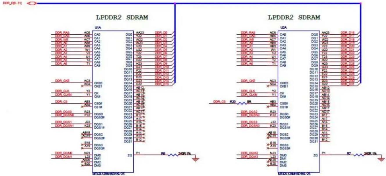
text_image
Circuit schematic diagrams showing LPDDR2 SDRAM and UDA connections with pin labels and signal linesCAx LPDDR2 signals are to be connected as indicated in Table 28-3.
Table 28-3: CAx LPDDR2 Signal Connection
| DDR Controller Signal LPDDR2 Signal | |
| RAS CA0 | |
| CAS CA1 | |
| WE CA2 | |
| DDR_A0 CA3 | |
| DDR_A1 CA4 | |
| DDR_A2 CA5 | |
| DDR_A3 CA6 | |
| DDR_A4 CA7 | |
| DDR_A5 CA8 | |
| DDR_A6 CA9 | |
| Higher addresses Higher CAs |
- Software Configuration
The following configuration has to be performed: - Initialize the DDR2 Controller depending on the LPDDR2 device and system bus frequency.
The DDR2 initialization sequence is described in Section 29.4.3 Low-power DDR2-SDRAM Initialization.
28.2 External Bus Interface (EBI)
28.2.1 Description
The External Bus Interface is designed to ensure the successful data transfer between several external devices and the ARM processor-based device. The External Bus Interface of the device consists of a Static Memory Controller (SMC).
This SMC is capable of handling several types of external memory and peripheral devices, such as SRAM, PSRAM, PROM, EPROM, EEPROM, LCD Module, NOR Flash and NAND Flash.
The SMC generates the signals that control the access to external memory devices or peripheral devices. It has four Chip Selects and a 26-bit address bus. The 16-bit data bus can be configured to interface with 8- or 16-bit external devices. Separate read and write control signals allow for direct memory and peripheral interfacing. Read and write signal waveforms are fully configurable.
The SMC can manage wait requests from external devices to extend the current access. The SMC is provided with an automatic slow clock mode. In slow clock mode, it switches from user-programmed waveforms to slow-rate specific waveforms on read and write signals.
The SMC embeds a NAND Flash Controller (NFC). The NFC can handle automatic transfers, sending the commands and address cycles to the NAND Flash and transferring the contents of the page (for read and write) to the NFC SRAM. It minimizes the CPU overhead.
The SMC includes programmable hardware error correcting code with one-bit error correction capability and supports two-bit error detection. In order to improve the overall system performance, the DATA phase of the transfer can be DMA-assisted. The External Data Bus can be scrambled/unscrambled by means of user keys.
The full description is available in Section 30. Static Memory Controller (SMC).
28.2.2 Implementation Examples
The following hardware configurations are given for illustration only. The user should refer to the memory manufacturer web site to check current device availability.
28.2.2.1 8-bit NAND Flash
- Hardware Configuration
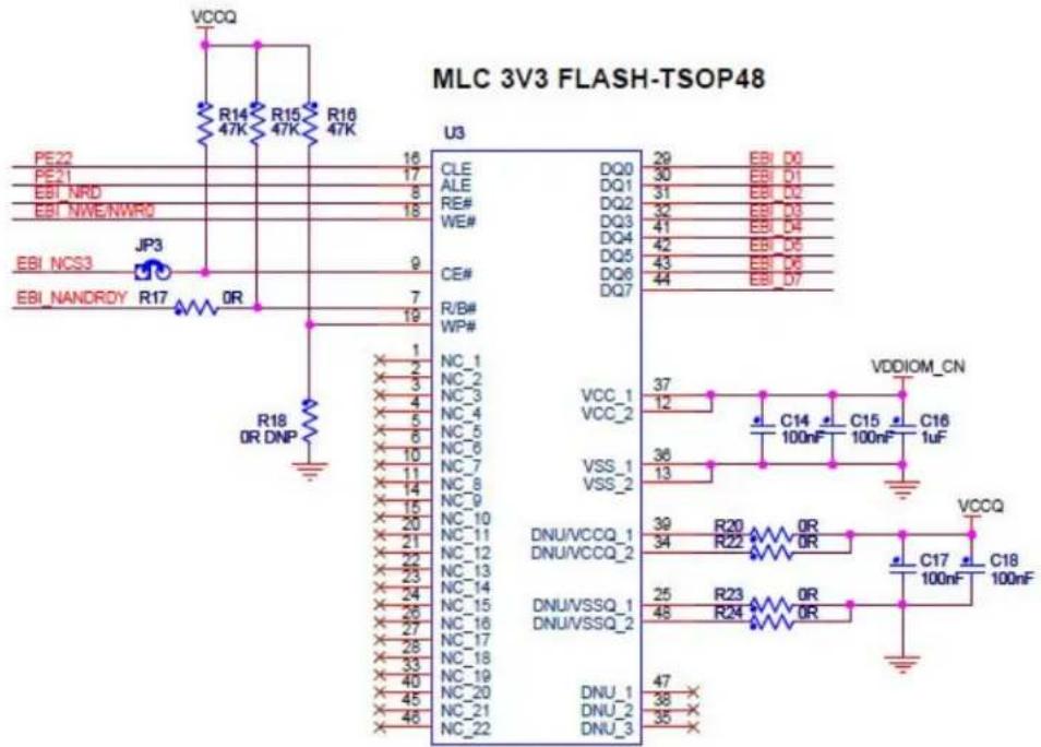
text_image
MLC 3V3 FLASH-TSOP48 U3 PE22 PE21 EBI_NRD EBI_NWE/NWR0 EBI_NCS3 JP3 EBI_NANDRDY R17 OR R18 OR DNP 16 17 8 18 9 7 19 12 NC_1 NC_2 NC_3 NC_4 NC_5 NC_6 NC_7 NC_8 NC_9 NC_10 NC_11 NC_12 NC_13 NC_14 NC_15 NC_16 NC_17 NC_18 NC_19 NC_20 NC_21 NC_22 CLE ALE RE# WE# CE# R/B# WP# VCC_1 VCC_2 VSS_1 VSS_2 DNU/VCCQ_1 DNU/VCCQ_2 DNU/VSSQ_1 DNU/VSSQ_2 DNU_1 DNU_2 DNU_3 29 EBI D0 30 EBI D1 31 EBI D2 32 EBI D3 41 EBI D4 42 EBI D5 43 EBI D6 44 EBI_D7 37 C14 C15 C16 VDDIOM_CN 12 100nF 100nF 1uF VCCQ 36 R20 R22 0R 0R 0R 0R 0R 0R 0R 0R 0R 0R 0R 0R 0R 0R 0R 0R 0R 0R 0R 0R 0R 0R 0R 0R 0R 0R 0R 0R 0R 0R 0R 0R 0R 0R- Software Configuration
The following configuration has to be performed:
- Select the NAND Flash Chip Select by setting the field CSID in the NFC Address Command register.
- Configure the NFC and SMC according to the used NAND Flash.
- Enable the NFC with NFCEN bit in the NFC Control Register.
- Reserve A21/A22 for ALE/CLE functions. Address and Command Latches are controlled respectively by setting to 1 the address bits A21 and A22 during accesses.
- Configure a PIO line as an input to manage the Ready/Busy signal.
- Configure Static Memory Controller CS3 Setup, Pulse, Cycle and Mode accordingly to NAND Flash timings, the data bus width and the system bus frequency.
28.2.2.2 16-bit NAND Flash
- Hardware Configuration
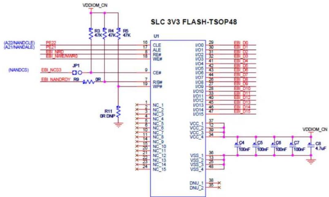
text_image
SLC 3V3 FLASH-TSOP48 VDDIOM_CN R3 R4 R5 47K 47K 47K (A22/NANDCLE) (A21/NANDALE) (EBI_NPO) (EBI_NWE/NWR0) (NANDCS) JP1 EBI_NCS3 EBI_NANDRDY R9 OR OR R11 OR DNP U1 CLE I/O0 29 EBI D0 ALE I/O1 30 EBI D1 RE# I/O2 31 EBI D2 WE# I/O3 32 EBI D3 CE# I/O4 41 EBI D4 I/O5 42 EBI D5 I/O6 43 EBI D6 I/O7 44 EBI D7 R/B# I/O8 26 EBI D8 WP# I/O9 27 EBI D9 I/O10 28 EBI D10 I/O11 33 EBI D11 I/O12 40 EBI D12 I/O13 45 EBI D13 I/O14 46 EBI D14 I/O15 47 EBI D15 NC_1 NC_2 NC_3 NC_4 NC_5 NC_6 NC_7 NC_8 NC_9 NC_10 NC_11 NC_12 NC_13 NC_14 NC_15 VCC_1 VCC_2 VCC_3 VCC_4 VSS_1 VSS_2 VSS_3 VSS_4 DNU_1 DNU_2 VDDIOM_CN C4 C5 C6 C7 C8 100nF 100nF 100nF 100nF 4.7uF- Software Configuration
The software configuration is the same as for an 8-bit NAND Flash except for the data bus width programmed in the HSMC_MODE register.
28.2.2.3 NOR Flash on NCS0
- Hardware Configuration

The default configuration for the Static Memory Controller, byte select mode, 16-bit data bus, Read/Write controlled by Chip Select, allows boot on 16-bit non-volatile memory at slow clock.
For another configuration, configure the Static Memory Controller CS0 Setup, Pulse, Cycle and Mode depending on Flash timings and system bus frequency.
29. Multi-port DDR-SDRAM Controller (MPDDRC)
29.1 Description
The Multi-port DDR-SDRAM Controller (MPDDRC) is a multi-port memory controller. It comprises four slave AHB interfaces. All simultaneous accesses (four independent AHB ports) are interleaved to maximize memory bandwidth and minimize transaction latency due to DDR-SDRAM protocol.
The MPDDRC extends the memory capabilities of a chip by providing the interface to the external32-bit DDR-SDRAM device. The page size supports ranges from 2048 to 16384 rows and from 256 to 4096 columns. It supports dword (64-bit), word (32-bit), half-word (16-bit), and byte (8-bit) accesses.
The MPDDRC supports a read or write burst length of eight locations. This enables the command and address bus to anticipate the next command, thus reducing latency imposed by the DDR-SDRAM protocol and improving the DDR-SDRAM bandwidth. Moreover, MPDDRC keeps track of the active row in each bank, thus maximizing DDR-SDRAM performance, e.g., the application may be placed in one bank and data in other banks. To optimize performance, avoid accessing different rows in the same bank. The MPDDRC supports a CAS latency of 2, 3 and optimizes the read access depending on the frequency.
Self-refresh, Power-down and Deep Power-down modes minimize the consumption of the DDR-SDRAM device.
OCD (Off-chip Driver) and ODT (On-die Termination) modes are not supported.
29.2 Embedded Characteristics
- Four advanced high performance bus (AHB) interfaces, management of all accesses maximizes memory bandwidth and minimizes transaction latency
- Bus transfer: dword, word, half word, byte access
• Supports 32-bit or 2x16-bit low-power DDR2-SDRAM-S4 (LPDDR2), DDR2-SDRAM, low-power DDR1-SDRAM (LPDDR1) -
Numerous configurations supported
-
2K, 4K, 8K, 16K row address memory parts
- DDR-SDRAM with two or four internal banks (low-power DDR1-SDRAM)
- DDR-SDRAM with four or eight internal banks (DDR2-SDRAM/Low-power DDR2-SDRAM-S4)
- DDR-SDRAM with 32-bit data path for system-oriented dword access
- One chip select for SDRAM device (512-Mbyte address space)
- Programming Facilities
- Multibank ping-pong access (up to four or eight banks opened at the same time = reduced average latency of transactions)
- Timing parameters specified by software
- Automatic refresh operation, refresh rate is programmable
- Automatic update of DS, TCR and PASR parameters (low-power DDR-SDRAM devices)
• Energy-saving capabilities
- Self-refresh, Power-down, Active Power-down and Deep Power-down modes supported
• DDR-SDRAM power-up initialization by software
• CAS latency of 2, 3 supported
- Reset function supported (DDR2-SDRAM)
- Auto-refresh per bank supported (low-power DDR2-SDRAM-S4)
• Automatic adjust refresh rate (low-power DDR2-SDRAM-S4)
• Auto-precharge command not used
- OCD (Off-chip Driver) mode, ODT (On-die Termination) are not supported
- Dynamic Scrambling with user key (no impact on bandwidth)
29.3 MPDDRC Module Diagram
MPDDRC is partitioned in two blocks (see Figure 29-1):
- Interconnect Matrix block that manages concurrent accesses on the AHB bus between four AHB masters and integrates an arbiter
- DDR controller that translates AHB requests (read/write) in the DDR-SDRAM protocol
Figure 29-1: MPDDRC Module Diagram

flowchart
graph TD
    subgraph AHB_MPDDR_Controller
        A0["Input Stage"] --> A1["Input Stage"]
        A1 --> A2["Input Stage"]
        A2 --> A3["..."]
        A3 --> A4["Input Stage"]
        A4 --> A5["Output Stage Arbiter"]
    end

    subgraph DDR_Controller
        B0["Power Management"] --> C0["Memory Controller Finite State Machine SDRAM Signal Management"]
        C0 --> D0["Asynchronous Timing Refresh Management"]
    end

    A0 -->|APB| A5
    A5 -->|APB| A6["Interface APB"]
    A6 -->|APB| A7["Interconnect Matrix"]

    B0 -->|clk/nclk| D0
    D0 -->|resetn odt| DDR_Devices["DDR-Devices"]
    D0 -->|data| DDR_RESETN["DDR_RESETN"]

    A7 -->|APB| A6
    A6 -->|APB| A7
    A7 -->|APB| A8["Input Stage"]
    A8 -->|Input Interface 0| A9["AHB Slave Interface 0"]
    A9 --> A10["AHB Slave Interface 1"]
    A10 --> A11["AHB Slave Interface 2"]
    A11 --> A12["AHB Slave Interface n (1)"]
    A12 --> A13["AHB Slave Interface n (1)"]
    A13 --> A14["AHB Slave Interface n (1)"]
    A14 --> A15["AHB Slave Interface n (1)"]
    A15 --> A16["AHB Slave Interface n (1)"]
    A16 --> A17["AHB Slave Interface n (1)"]
    A17 --> A18["AHB Slave Interface n (1)"]
    A18 --> A19["AHB Slave Interface n (1)"]
    A19 --> A20["AHB Slave Interface n (1)"]
    A20 --> A21["AHB Slave Interface n (1)"]
    A21 --> A22["AHB Slave Interface n (1)"]
    A22 --> A23["AHB Slave Interface n (1)"]
    A23 --> A24["AHB Slave Interface n (1)"]
    A24 --> A25["AHB Slave Interface n (1)"]
    A25 --> A26["AHB Slave Interface n (1)"]
    A26 --> A27["AHB Slave Interface n (1)"]
    A27 --> A28["AHB Slave Interface n (1)"]
    A28 --> A29["AHB Slave Interface n (1)"]
    A29 --> A30["AHB Slave Interface n (1)"]
    A30 --> A31["AHB Slave Interface n (1)"]
    A31 --> A32["AHB Slave Interface n (1)"]
    A32 --> A33["AHB Slave Interface n (1)"]
    A33 --> A34["AHB Slave Interface n (1)"]
    A34 --> A35["AHB Slave Interface n (1)"]
    A35 --> A36["AHB Slave Interface n (1)"]
    A36 --> A37["AHB Slave Interface n (1)"]
    A37 --> A38["AHB Slave Interface n (1)"]
    A38 --> A39["AHB Slave Interface n (1)"]
    A39 --> A40["AHB Slave Interface n (1)"]
    A40 --> A41["AHB Slave Interface n (1)"]
    A41 --> A42["AHB Slave Interface n (1)"]
    A42 --> A43["AHB Slave Interface n (1)"]
    A43 --> A44["AHB Slave Interface n (1)"]
    A44 --> A45["AHB Slave Interface n (1)"]
    A45 --> A46["AHB Slave Interface n (1)"]
    A46 --> A47["AHB Slave Interface n (1)"]
    A47 --> A48["AHB Slave Interface n (1)"]
    A48 --> A49["AHB Slave Interface n (1)"]
    A49 --> A50["AHB Slave Interface n (1)"]
    A50 --> A51["AHB Slave Interface n (1)"]
    A51 --> A52["AHB Slave Interface n (1)"]
    A52 --> A53["AHB Slave Interface n (1)"]
    A53 --> A54["AHB Slave Interface n (1)"]
    A54 --> A55["AHB Slave Interface n (1)"]
    A55 --> A56["AHB Slave Interface n (1)"]
    A56 --> A57["AHB Slave Interface n (1)"]
    A57 --> A58["AHB Slave Interface n (1)"]
    A58 --> A59["AHB Slave Interface n (1)"]
    A59 --> A60["AHB Slave Interface n (1)"]
    A60 --> A61["AHB Slave Interface n (1)"]
    A61 --> A62["AHB Slave Interface n (1)"]
    A62 --> A63["AHB Slave Interface n (1)"]
    A63 --> A64["AHB Slave Interface n (1)"]
    A64 --> A65["AHB Slave Interface n (1)"]
    A65 --> A66["AHB Slave Interface n (1)"]
    A66 --> A67["AHB Slave Interface n (1)"]
    A67 --> A68["AHB Slave Interface n (1)"]
    A68 --> A69["AHB Slave Interface n (1)"]
    A69 --> A70["AHB Slave Interface n (1)"]
Notes: 1. "n" can equal 3 or 7 (value is device-specific)
29.4 Product Dependencies, Initialization Sequence
29.4.1 Low-power DDR1-SDRAM Initialization
The initialization sequence is generated by software. Before starting the initialization sequence, the user must force the DDR_DQ and DDR_DQS input buffers to 'always on' by setting the FDQIEN and FDQSIEN bits in the SFR_DDRCFG register. For more information, refer to Section 15. Special Function Registers (SFR).
The low-power DDR1-SDRAM devices are initialized by the following sequence:
-
Program the memory device type in the MPDDRC Memory Device Register (MPDDRC_MD).
-
Program the features of the low-power DDR1-SDRAM device in the MPDDRC Configuration Register (number of columns, rows,
banks, CAS latency and output drive strength) and in the MPDDRC Timing Parameter 0 Register/MPDDRC Timing Parameter 1 Register (asynchronous timing (TRC, TRAS, etc.)).
- Program Temperature Compensated Self-refresh (TCR), Partial Array Self-refresh (PASR) and Drive Strength (DS) parameters in the MPDDRC Low-power Register.
- A NOP command is issued to the low-power DDR1-SDRAM. Program the NOP command in the MPDDRC Mode Register (MPDDRC_MR). The application must write a 1 to the MODE field in the MPDDRC_MR. Read the MPDDRC_MR and add a memory barrier assembler instruction just after the read. Perform a write access to any low-power DDR1-SDRAM address to acknowledge this command. The clocks which drive the low-power DDR1-SDRAM device are now enabled.
- A pause of at least 200 s must be observed before a signal toggle.
- A NOP command is issued to the low-power DDR1-SDRAM. Program the NOP command in the MPDDRC_MR. The application must write a 1 to the MODE field in the MPDDRC_MR. Read the MPDDRC_MR and add a memory barrier assembler instruction just after the read. Perform a write access to any low-power DDR1-SDRAM address to acknowledge this command. A calibration request is now made to the I/O pad.
- An All Banks Precharge command is issued to the low-power DDR1-SDRAM. Program All Banks Precharge command in the MPDDRC_MR. The application must write a 2 to the MODE field in the MPDDRC_MR. Read the MPDDRC_MR and add a memory barrier assembler instruction just after the read. Perform a write access to any low-power DDR1-SDRAM address to acknowledge this command.
- Two auto-refresh (CBR) cycles are provided. Program the Auto Refresh command (CBR) in the MPDDRC_MR. The application must write a 4 to the MODE field in the MPDDRC_MR. Read the MPDDRC_MR and add a memory barrier assembler instruction just after the read. Perform a write access to any low-power DDR1-SDRAM location twice to acknowledge these commands.
- An Extended Mode Register Set (EMRS) cycle is issued to program the low-power DDR1-SDRAM parameters (TCSR, PASR, DS). The application must write a 5 to the MODE field in the MPDDRC_MR. Read the MPDDRC_MR and add a memory barrier assembler instruction just after the read. Perform a write access to the SDRAM to acknowledge this command. The write address must be chosen so that signal BA[1] is set to 1 and BA[0] is set to 0. For example: with a 32-bit, 1-Gbit, low-power DDR1-SDRAM (14 rows, 10 columns, 4 banks), the SDRAM write access should be done at the address: BASE_ADDRESS_DDR + 0x08000000.
Note: This address is given as an example only. The real address depends on implementation in the product.
- A Mode Register Set (MRS) cycle is issued to program parameters of the low-power DDR1-SDRAM devices, in particular CAS latency. The application must write a 3 to the MODE field in the MPDDRC_MR. Read the MPDDRC_MR and add a memory barrier assembler instruction just after the read. Perform a write access to the low-power DDR1-SDRAM to acknowledge this command. The write address must be chosen so that signals BA[1:0] are set to 0. For example, the SDRAM write access should be done at the address: BASE_ADDRESS_DDR.
- The application must enter Normal mode, write a zero to the MODE field in the MPDDRC_MR. Read the MPDDRC_MR and add a memory barrier assembler instruction just after the read. Perform a write access at any location in the low-power DDR1-SDRAM to acknowledge this command.
- Write the refresh rate into the COUNT field in the MPDDRC Refresh Timer Register (MPDDRC_RTR): refresh rate = delay between refresh cycles. The low-power DDR1-SDRAM device requires a refresh every 15.625 μs or 7.81 μs. With a 100 MHz frequency, MPDDRC_RTR must be set with (15.625 × 100 MHz) = 1562 i.e., 0x061A or (7.81 × 100 MHz) = 781 i.e., 0x030D .
After initialization, the low-power DDR1-SDRAM device is fully functional.
29.4.2 DDR2-SDRAM Initialization
The initialization sequence is generated by software. The DDR2-SDRAM devices are initialized by the following sequence:
- Program the memory device type in the MPDDRC Memory Device Register (MPDDRC_MD).
- Program features of the DDR2-SDRAM device in the MPDDRC Configuration Register (number of columns, rows, banks, CAS latency and output driver impedance control) and in the MPDDRC Timing Parameter 0 Register/MPDDRC Timing Parameter 1 Register (asynchronous timing (TRC, TRAS, etc.).
-
A NOP command is issued to the DDR2-SDRAM. Program the NOP command in the MPDDRC Mode Register (MPDDRC_MR). The application must write a 1 to the MODE field in the MPDDRC_MR. Read the MPDDRC_MR and add a memory barrier assembler instruction just after the read. Perform a write access to any DDR2-SDRAM address to acknowledge this command. The clocks which drive the DDR2-SDRAM device are now enabled.
-
A pause of at least 200 s must be observed before a signal toggle.
-
A NOP command is issued to the DDR2-SDRAM. Program the NOP command in the MPDDRC_MR. The application must write a 1 to the MODE field in the MPDDRC_MR. Read the MPDDRC_MR and add a memory barrier assembler instruction just after the read. Perform a write access to any DDR2-SDRAM address to acknowledge this command. CKE is now driven high.
-
An All Banks Precharge command is issued to the DDR2-SDRAM. Program All Banks Precharge command in the MPDDRC_MR. The application must write a 2 to the MODE field in the MPDDRC_MR. Read the MPDDRC_MR and add a memory barrier assem-
bler instruction just after the read. Perform a write access to any DDR2-SDRAM address to acknowledge this command.
- An Extended Mode Register Set (EMRS2) cycle is issued to choose between commercial or high temperature operations. The application must write a 5 to the MODE field in the MPDDRC_MR. Read the MPDDRC_MR and add a memory barrier assembler instruction just after the read. Perform a write access to the DDR2-SDRAM to acknowledge this command. The write address must be chosen so that signal BA[1] is set to 1 and signal BA[0] is set to 0. For example: with a 32-bit, 1-Gbit, DDR2-SDRAM (14 rows, 10 columns, 8 banks), the SDRAM write access should be done at the address: BASE_ADDRESS_DDR + 0x08000000.
Note: This address is given as an example only. The real address depends on implementation in the product.
-
An Extended Mode Register Set (EMRS3) cycle is issued to set the Extended Mode Register to 0. The application must write a 5 to the MODE field in the MPDDRC_MR. Read the MPDDRC_MR and add a memory barrier assembler instruction just after the read. Perform a write access to the DDR2-SDRAM to acknowledge this command. The write address must be chosen so that signal BA[1] is set to 1 and signal BA[0] is set to 1. For example: with a 32-bit, 1-Gbit, DDR2-SDRAM (14 rows, 10 columns, 8 banks), the SDRAM write access should be done at the address: BASE_ADDRESS_DDR + 0x0C000000.
-
An Extended Mode Register Set (EMRS1) cycle is issued to enable DLL and to program D.I.C. (Output Driver Impedance Control). The application must write a 5 to the MODE field in the MPDDRC_MR. Read the MPDDRC_MR and add a memory barrier assembler instruction just after the read. Perform a write access to the DDR2-SDRAM to acknowledge this command. The write address must be chosen so that signal BA[1] is set to 0 and signal BA[0] is set to 1. For example: with a 32-bit, 1-Gbit, DDR2-SDRAM (14 rows, 10 columns, 8 banks), the SDRAM write access should be done at the address: BASE_ADDRESS_DDR + 0x04000000.
-
An additional 200 cycles of clock are required for locking DLL
-
Write a one to the DLL bit (enable DLL reset) in the MPDDRC Configuration Register (MPDDRC_CR).
-
A Mode Register Set (MRS) cycle is issued to reset DLL. The application must write a 3 to the MODE field in the MPDDRC_MR. Read the MPDDRC_MR and add a memory barrier assembler instruction just after the read. Perform a write access to the DDR2-SDRAM to acknowledge this command. The write address must be chosen so that signals BA[1:0] are set to 0. For example, the SDRAM write access should be done at the address: BASE_ADDRESS_DDR.
-
An All Banks Precharge command is issued to the DDR2-SDRAM. Program the All Banks Precharge command in the MPDDRC_MR. The application must write a 2 to the MODE field in the MPDDRC_MR. Read the MPDDRC_MR and add a memory barrier assembler instruction just after the read. Perform a write access to any DDR2-SDRAM address to acknowledge this command.
-
Two auto-refresh (CBR) cycles are provided. Program the Auto Refresh command (CBR) in the MPDDRC_MR. The application must write a 4 to the MODE field in the MPDDRC_MR. Read the MPDDRC_MR and add a memory barrier assembler instruction just after the read. Perform a write access to any DDR2-SDRAM location twice to acknowledge these commands.
-
Write a zero to the DLL bit (disable DLL reset) in the MPDDRC_CR.
-
A Mode Register Set (MRS) cycle is issued to program parameters of the DDR2-SDRAM device, in particular CAS latency and to disable DLL reset. The application must write a 3 to the MODE field in the MPDDRC_MR. Read the MPDDRC_MR and add a memory barrier assembler instruction just after the read. Perform a write access to the DDR2-SDRAM to acknowledge this command. The write address must be chosen so that signals BA[1:0] are set to 0. For example: with a 32-bit, 1-Gbit, DDR2-SDRAM (14 rows, 10 columns, 8 banks), the SDRAM write access should be done at the address: BASE_ADDRESS_DDR.
-
Write a seven to the OCD field (default OCD calibration) in the MPDDRC_CR.
-
An Extended Mode Register Set (EMRS1) cycle is issued to the default OCD value. The application must write a 5 to the MODE field in the MPDDRC_MR. Read the MPDDRC_MR and add a memory barrier assembler instruction just after the read. Perform a write access to the DDR2-SDRAM to acknowledge this command. The write address must be chosen so that signal BA[1] is set to 0 and signal BA[0] is set to 1. For example: with a 32-bit, 1-Gbit, DDR2-SDRAM (14 rows, 10 columns, 8 banks), the SDRAM write access should be done at the address: BASE_ADDRESS_DDR + 0x04000000.
-
Write a zero to the OCD field (exit OCD calibration mode) in the MPDDRC_CR.
-
An Extended Mode Register Set (EMRS1) cycle is issued to enable OCD exit. The application must write a 5 to the MODE field in the MPDDRC_MR. Read the MPDDRC_MR and add a memory barrier assembler instruction just after the read. Perform a write access to the DDR2-SDRAM to acknowledge this command. The write address must be chosen so that signal BA[1] is set to 0 and signal BA[0] is set to 1. For example: with a 32-bit, 1-Gbit, DDR2-SDRAM (14 rows, 10 columns, 8 banks), the SDRAM write access should be done at the address: BASE_ADDRESS_DDR + 0x04000000.
-
A Normal Mode command is provided. Program the Normal mode in the MPDDRC_MR. Read the MPDDRC_MR and add a memory barrier assembler instruction just after the read. Perform a write access to any DDR2-SDRAM address to acknowledge this command.
-
Write the refresh rate into the COUNT field in the MPDDRC Refresh Timer Register (MPDDRC_RTR): refresh rate = delay between refresh cycles. The DDR2-SDRAM device requires a refresh every 15.625 μs or 7.81 μs. With a 133 MHz frequency, the COUNT field in the MPDDRC_RTR must be set with (15.625 × 133 MHz) = 2079 i.e., 0x081F or (7.81 × 133 MHz) = 1039 i.e., 0x040F .
After initialization, the DDR2-SDRAM devices are fully functional.
29.4.3 Low-power DDR2-SDRAM Initialization
The initialization sequence is generated by software. The low-power DDR2-SDRAM devices are initialized by the following sequence:
- Program the memory device type in the MPDDRC Memory Device Register (MPDDRC_MD).
- Program features of the low-power DDR2-SDRAM device into and in the MPDDRC Configuration Register (number of columns, rows, banks, CAS latency and output drive strength) and in the MPDDRC Timing Parameter 0 Register/MPDDRC Timing Parameter 0 Register (asynchronous timing, TRC, TRAS, etc.). If the Adjust Refresh function (register MPDDRC_RTR, bit 16) is used, the application must write a 1 to fields 17 and 16 to open the input buffers in the DDR Configuration Register SFR_DDRCFG (see Section 15. Special Function Registers (SFR)).
- A NOP command is issued to the low-power DDR2-SDRAM. Program the NOP command in the MPDDRC Mode Register (MPDDRC_MR). The application must write a 1 to the MODE field in the MPDDRC_MR. Read the MPDDRC_MR and add a memory barrier assembler instruction just after the read. Perform a write access to any low-power DDR2-SDRAM address to acknowledge this command. The clocks which drive the Low-power DDR2-SDRAM devices are now enabled.
- A pause of at least 100 ns must be observed before a signal toggle.
- A NOP command is issued to the low-power DDR2-SDRAM. Program the NOP command in the MPDDRC_MR. The application must write a 1 to the MODE field in the MPDDRC_MR. Read the MPDDRC_MR and add a memory barrier assembler instruction just after the read. Perform a write access to any low-power DDR2-SDRAM address to acknowledge this command. CKE is now driven high.
- A pause of at least 200 s must be observed before issuing a Reset command.
- A Reset command is issued to the low-power DDR2-SDRAM. In the MPDDR2_MR, configure the MODE field to the LPDDR2_CMD value and configure the MRS field. The application must write a 7 to the MODE field and a 63 to the MRS field. Read the MPDDR2_MR and add a memory barrier assembler instruction just after the read. Perform a write access to any low-power DDR2-SDRAM address to acknowledge this command. The Reset command is now issued.
- A pause of at least t INIT5 must be observed before issuing any commands.
- A Calibration command is issued to the low-power DDR2-SDRAM. Program the type of calibration in the MPDDRC Configuration Register (MPDDRC_CR): set the ZQ field to the RESET value. In the MPDDRC_MR, configure the MODE field to the LPDDR2_CMD value and configure the MRS field. The application must write a 7 to the MODE field and a 10 to the MRS field. Read the MPDDRC_MR and add a memory barrier assembler instruction just after the read. Perform a write access to any low-power DDR2-SDRAM address to acknowledge this command. The ZQ Calibration command is now issued. Program the type of calibration in the MPDDRC_CR: set the ZQ field to the SHORT value.
- A Mode Register Write command is issued to the low-power DDR2-SDRAM. In the MPDDR3_MR, configure the MODE field to the LPDDR2_CMD value and configure the MRS field. The application must write a 7 to the MODE field and a one to the MRS field. Read the MPDDR3_MR and add a memory barrier assembler instruction just after the read. Perform a write access to any low-power DDR2-SDRAM address to acknowledge this command. The Mode Register Write command is now issued.
- A Mode Register Write command is issued to the low-power DDR2-SDRAM. In the MPDDRC_MR, configure the MODE field to the LPDDR2_CMD value and configure the MRS field. The application must write a 7 to the MODE field and a two to the MRS field. The Mode Register Write command cycle is issued to program parameters of the low-power DDR2-SDRAM device, in particular CAS latency. Read the MPDDRC_MR and add a memory barrier assembler instruction just after the read. Perform a write access to any low-power DDR2-SDRAM address to acknowledge this command. The Mode Register Write command is now issued.
- A Mode Register Write command is issued to the low-power DDR2-SDRAM. In the MPDDR2_MR, configure the MODE field to the LPDDR2_CMD value and configure the MRS field. The application must write a 7 to the MODE field and a three to the MRS field. The Mode Register Write command cycle is issued to program parameters of the low-power DDR2-SDRAM device, in particular Drive Strength and Slew Rate. Read the MPDDR2_MR and add a memory barrier assembler instruction just after the read. Perform a write access to any low-power DDR2-SDRAM address to acknowledge this command. The Mode Register Write command is now issued.
- A Mode Register Write command is issued to the low-power DDR2-SDRAM. In the MPDDR2_MR configure the MODE field to the LPDDR2_CMD value and configure the MRS field. The application must write a 7 to the MODE field and a 16 to the MRS field. Mode Register Write command cycle is issued to program parameters of the low-power DDR2-SDRAM device, in particular Partial Array Self Refresh (PASR). Read the MPDDR2_MR and add a memory barrier assembler instruction just after the read. Perform a write access to any low-power DDR2-SDRAM address to acknowledge this command. The Mode Register Write command is now issued.
- A Normal Mode command is provided. Program the Normal mode in the MPDDRC_MR. Read the MPDDRC_MR and add a memory barrier assembler instruction just after the read. Perform a write access to any low-power DDR2-SDRAM address to acknowledge this command.
- In the DDR configuration Register (SFR_DDRCCFG), the application must write a 0 to fields 17 and 16 to close the input buffers. The buffers are then driven by the HMPDDRC controller.
- Write the refresh rate into the COUNT field in the MPDDRC Refresh Timer Register (MPDDRC_RTR): refresh rate = delay between
refresh cycles. The low-power DDR2-SDRAM device requires a refresh every 7.81 s. With a 133 MHz frequency, the COUNT field in the MPDDRRC_RTR must be set with (7.81 × 133 MHz) = 1039 i.e., 0x040F.
After initialization, the low-power DDR2-SDRAM devices are fully functional.
29.5 Functional Description
29.5.1 DDR-SDRAM Controller Write Cycle
The MPDDRC provides burst access or single access in Normal mode (MPDDRC_MR.MODE = 0). Whatever the access type, the MPDDRC keeps track of the active row in each bank, thus maximizing performance.
The DDR-SDRAM device is programmed with a burst length (bl) equal to 8. This determines the length of a sequential data input by the write command that is set to 8. The latency from write command to data input depends on the memory type, as shown in Table 29-1.
Table 29-1: CAS Write Latency
| Memory Devices CAS Write Latency (CWL) | |
| Low-power DDR1-SDRAM 1 | |
| Low-power DDR2-SDRAM 1 | |
| DDR2-SDRAM 2 | |
| Low-power DDR3-SDRAM 1/3 | |
To initiate a single access, the MPDDRC checks if the page access is already open. If row/bank addresses match with the previous row/bank addresses, the controller generates a write command. If the bank addresses are not identical or if bank addresses are identical but the row addresses are not identical, the controller generates a precharge command, activates the new row and initiates a write command. To comply with DDR-SDRAM timing parameters, additional clock cycles are inserted between precharge/active ( t_RP ) commands and active/write ( t_RCD ) command. As the burst length is set to 8, in case of single access, it has to stop the burst, otherwise seven invalid values may be written. In case of the DDR-SDRAM device, the burst stop command is not supported for the burst write operation. Thus, in order to interrupt the write operation, the DM (data mask) input signal must be set to 1 to mask invalid data (see Figure 29-2 and Figure 29-4), and DQS must continue to toggle.
To initiate a burst access, the MPDDRC uses the transfer type signal provided by the master requesting the access. If the next access is a sequential write access, writing to the DDR-SDRAM device is carried out. If the next access is a write non-sequential access, then an automatic access break is inserted, the MPDDRC generates a precharge command, activates the new row and initiates a write command. To comply with DDR-SDRAM timing parameters, additional clock cycles are inserted between precharge/active ( t_RP ) commands and active/write ( t_RCD ) commands.
For the definition of timing parameters, refer to Section 29.7.4 MPDDRC Timing Parameter 0 Register.
Write accesses to the DDR-SDRAM device are burst oriented and the burst length is programmed to 8. It determines the maximum number of column locations that can be accessed for a given write command. When the write command is issued, eight columns are selected. All accesses for that burst take place within these eight columns, thus the burst wraps within these eight columns if a boundary is reached. These eight columns are selected by addr[13:3]. addr[2:0] is used to select the starting location within the block.
In case of incrementing burst (INCR/INCR4/INCR8/INCR16), the addresses can cross the 16-byte boundary of the DDR-SDRAM device. For example, when a transfer (INCR4) starts at address 0x0C, the next access is 0x10, but since the burst length is programmed to 8, the next access is at 0x00. Since the boundary is reached, the burst is wrapped. The MPDDRC takes this feature of the DDR-SDRAM device into account. In case of a transfer starting at address 0x04/0x08/0x0C or starting at address 0x10/0x14/0x18/0x1C, two write commands are issued to avoid wrapping when the boundary is reached. The last write command is subject to DM input logic level. If DM is registered high, the corresponding data input is ignored and the write access is not done. This avoids additional writing.
Figure 29-2: Single Write Access, Row Closed, DDR-SDRAM Devices
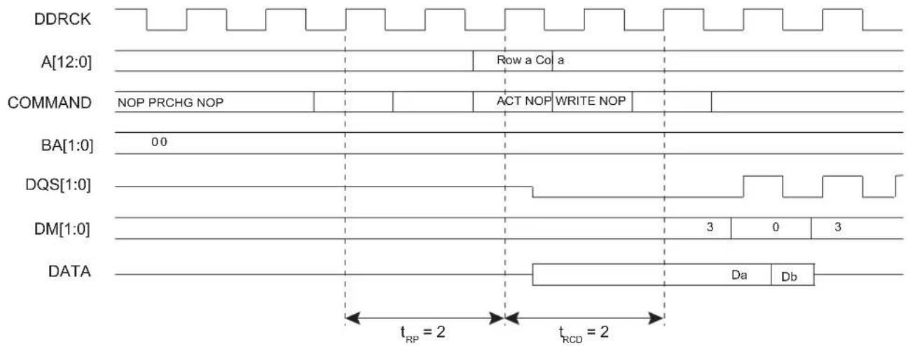
text_image
DDRCK A[12:0] Row a Co a COMMAND NOP PRCHG NOP ACT NOP WRITE NOP BA[1:0] 00 DQS[1:0] DM[1:0] DATA Da Db tRP = 2 tRCD = 2Figure 29-3: Single Write Access, Row Closed, DDR2-SDRAM Devices
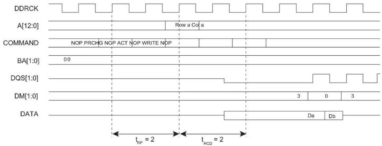
text_image
DDRCK A[12:0] Row a Col a COMMAND NOP PRCHG NOP ACT NOP WRITE NOP BA[1:0] 0.0 DQS[1:0] DM[1:0] DATA Da Db tRP = 2 tRCD = 2Figure 29-4: Burst Write Access, Row Closed, DDR-SDRAM Devices

text_image
DDRCK A[12:0] Row a Col a COMMAND NOP PRCHG NOP ACT NOP WRITE NOP BA[1:0] 0 DQS[1:0] DM[1:0] 3 0 3 DATA Da Db Dc Dd De Df Dg Dh tRP = 2 tRCD = 2Figure 29-5: Burst Write Access, Row Closed, DDR2-SDRAM Devices
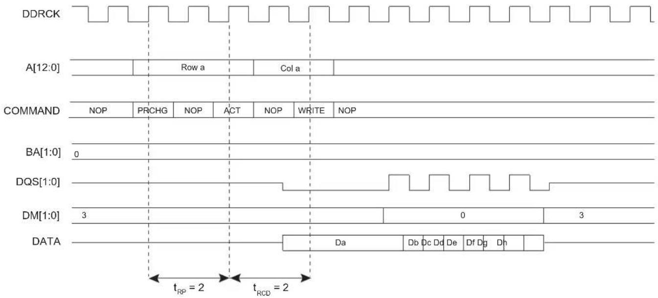
text_image
DDRCK A[12:0] Row a Col a COMMAND NOP PRCHG NOP ACT NOP WRITE NOP BA[1:0] 0 DQS[1:0] DM[1:0] 3 0 3 DATA Da Db Dc Dd De Df Dg Dh tRP = 2 tRCD = 2A write command can be followed by a read command. To avoid breaking the current write burst, t_WTR/t_WRD (bl/2 + 2 = 6 cycles) should be met. See Figure 29-6.
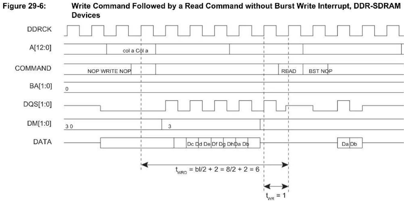
other
| Signal | Time Segment | |------------|----------------------------------| | DDRCK | 0 | | A[12:0] | col a Col a | | COMMAND | NOP WRITE NOP | | BA[1:0] | 0 | | DQS[1:0] | 3 | | DM[1:0] | 3 | | DATA | Dc Dd De Df Dg DhDa Db | | Data | Da Db |In case of a single write access, write operation should be interrupted by a read access but DM must be input 1 cycle prior to the read command to avoid writing invalid data. See Figure 29-7.
Figure 29-7: SINGLE Write Access Followed by a Read Access, DDR-SDRAM Devices

text_image
DDRCK A[12:0] Row a Col a COMMAND NOP PRCHG NOP ACT NOP WRITE NOP READ BST NOP BA[1:0] 0 DQS[1:0] DM[1:0] 3 0 3 DATA Da Db Da Db Data maskedFigure 29-8: SINGLE Write Access Followed by a Read Access, DDR2-SDRAM Devices

text_image
DDRCK A[12:0] Row a Col a COMMAND NOP PRCHG NOP ACT NOP WRITE NOP READ NOP BA[1:0] 0 DQS[1:0] DM[1:0] 3 0 3 DATA Da Db Data masked Da Db tWTR29.5.2 DDR-SDRAM Controller Read Cycle
The MPDDRC provides burst access or single access in Normal mode (MPDDRC_MR.MODE = 0). Whatever the access type, the MPDDRC keeps track of the active row in each bank, thus maximizing performance of the MPDDRC.
The DDR-SDRAM devices are programmed with a burst length equal to 8 which determines the length of a sequential data output by the read command that is set to 8. The latency from read command to data output depends on the memory type, as shown in Table 29-2. This value is programmed during the initialization phase (see Section 29.4 Product Dependencies, Initialization Sequence).
Table 29-2: CAS Read Latency
| Memory Devices CAS Read Latency | |
| Low-power DDR1-SDRAM 2/3 | |
| Low-power DDR2-SDRAM 3 | |
| DDR2-SDRAM 3 | |
| Low-power DDR3-SDRAM 3/6 |
To initiate a single access, the MPDDRC checks if the page access is already open. If row/bank addresses match with the previous row/bank addresses, the controller generates a read command. If the bank addresses are not identical or if bank addresses are identical but the row addresses are not identical, the controller generates a precharge command, activates the new row and initiates a read command. To comply with DDR-SDRAM timing parameters, additional clock cycles are inserted between precharge/active ( t_RP ) commands and active/read ( t_RCD ) command. After a read command, additional wait states are generated to comply with CAS latency. The MPDDRC supports a CAS latency of two to three (2 to 3 clock cycle delay). As the burst length is set to 8, in case of a single access or a burst access inferior to 8 data requests, it has to stop the burst, otherwise an additional seven or X values could be read. The Burst Stop command (BST) is used to stop output during a burst read. If the DDR2-SDRAM Burst Stop command is not supported by the JEDEC® standard, in a single read access, an additional seven unwanted data will be read.
To initiate a burst access, the MPDDRC checks the transfer type signal. If the next accesses are sequential read accesses, reading to the SDRAM device is carried out. If the next access is a read non-sequential access, then an automatic page break can be inserted. If the bank addresses are not identical or if bank addresses are identical but the row addresses are not identical, the controller generates a precharge command, activates the new row and initiates a read command. If page access is already open, a read command is generated.
To comply with DDR-SDRAM timing parameters, additional clock cycles are inserted between precharge/active ( t_RP ) commands and active/read ( t_RCD ) commands. The MPDDRC supports a CAS latency of two to three (2 to 3 clocks delay). During this delay, the controller uses internal signals to anticipate the next access and improve the performance of the controller. Depending on the latency, the MPDDRC anticipates two to three read accesses. In case of burst of specified length, accesses are not anticipated, but if the burst is broken (border, Busy mode, etc.), the next access is treated as an incrementing burst of unspecified length, and depending on the latency, the MPDDRC anticipates two to three read accesses.
For the definition of timing parameters, refer to Section 29.7.3 MPDDRC Configuration Register.
Read accesses to the DDR-SDRAM are burst oriented and the burst length is programmed to 8. The burst length determines the maximum number of column locations that can be accessed for a given read command. When the read command is issued, eight columns are selected. All accesses for that burst take place within these eight columns, meaning that the burst wraps within these eight columns if the boundary is reached. These eight columns are selected by addr[13:3]; addr[2:0] is used to select the starting location within the block.
In case of incrementing burst (INCR/INCR4/INCR8/INCR16), the addresses can cross the 16-byte boundary of the DDR-SDRAM device. For example, when a transfer (INCR4) starts at address 0x0C, the next access is 0x10, but since the burst length is programmed to 8, the next access is 0x00. Since the boundary is reached, the burst wraps. The MPDDRC takes into account this feature of the SDRAM device. In case of the DDR-SDRAM device, transfers start at address 0x04/0x08/0x0C. Two read commands are issued to avoid wrapping when the boundary is reached. The last read command may generate additional reading (1 read cmd = 4 DDR words).
To avoid additional reading, it is possible to use the burst stop command to truncate the read burst and to decrease power consumption. The DDR2-SDRAM devices do not support the burst stop command.
Figure 29-9: Single Read Access, Row Closed, Latency = 2, DDR-SDRAM Devices

text_image
DDRCK A[12:0] Row a col a COMMAND NOP PRCHG NOP ACT NOP READ BST NOP BA[1:0] 0 DM[3:0] 3 D[31:0] DaDb tRP tRCD Latency = 2Figure 29-10: Single Read Access, Row Closed, Latency = 3, DDR2-SDRAM Devices
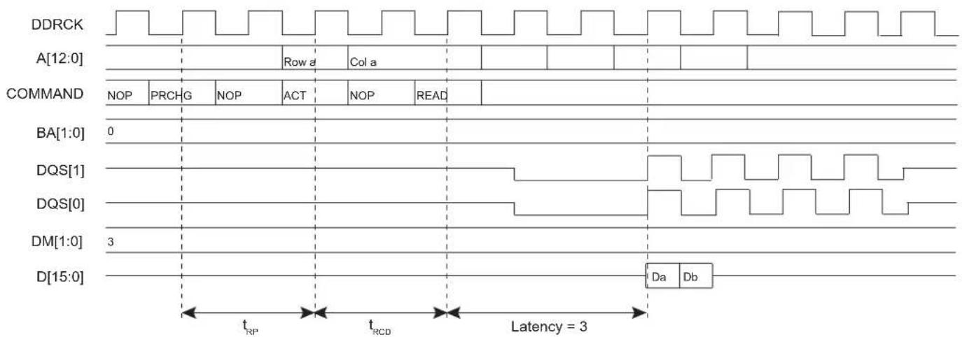
text_image
DDRCK A[12:0] ROW a Col a COMMAND NOP PRCHG NOP ACT NOP READ BA[1:0] 0 DQS[1] DQS[0] DM[1:0] 3 D[15:0] Da Db tRP tRCD Latency = 3Figure 29-11: Burst Read Access, Latency = 2, DDR-SDRAM Devices

text_image
DDRCKN DDRCK A[12:0] Colja COMMAND NOP READ NOP BA[1:0] 0 DQS[1:0] DM[1:0] 3 D[15:0] Da Db Dc Dd De Df Dg Dh Latency = 2Figure 29-12: Burst Read Access, Latency = 3, DDR2-SDRAM Devices

text_image
DDRCKN DDRCK A[12:0] Cola COMMAND NOP READ NOP BA[1:0] 0 DQS[1:0] DM[1:0] 3 D[15:0] Da Db Dc Dd De Df Dg Dh Latency = 329.5.2.1 All Banks Auto Refresh
The All Banks Auto Refresh command performs a refresh operation on all banks. An auto refresh command is used to refresh the external device. Refresh addresses are generated internally by the DDR-SDRAM device and incremented after each auto-refresh automatically. The MPDDRC generates these auto-refresh commands periodically. A timer is loaded in the MPDDRC_RTR with the value that indicates the number of clock cycles between refresh cycles (see Section 29.7.2 MPDDRC Refresh Timer Register). When the MPDDRC initiates a refresh of the DDR-SDRAM device, internal memory accesses are not delayed. However, if the CPU tries to access the DDR-SDRAM device, the slave indicates that the device is busy. A refresh request does not interrupt a burst transfer in progress. This feature is activated by setting Per-bank Refresh bit (REF_PB) to 0 in the MPDDRC_RTR (see Section 29.7.2 MPDDRC Refresh Timer Register).
29.5.2.2 Per-bank Auto Refresh
The low-power DDR2-SDRAM embeds a new Per-bank Refresh command which performs a refresh operation on the bank scheduled by the bank counter in the memory device. The Per-bank Refresh command is executed in a fixed sequence order of round-robin type: "0-1-2-3-4-5-6-7-0-1-...". The bank counter is automatically cleared upon issuing a RESET command or when exiting from Self-refresh mode, in order to ensure the synchronism between SDRAM memory device and the MPDDRC. The bank addressing for the Per-bank Refresh count is the same as established in the Single-bank Precharge command. This feature is activated by setting the Per-bank Refresh bit (REF_PB) to 1 in the MPDDRC_RTR (see Section 29.7.2 MPDDRC Refresh Timer Register). This feature masks the latency due to the refresh procedure. The target bank is inaccessible during the Per-bank Refresh cycle period (t _RFCpb ), however other banks within the device are accessible and may be addressed during the "Per-bank Refresh" cycle. During the REFpb operation, any bank other than the one being refreshed can be maintained in active state or accessed by a read or a write command. When the "Per-bank Refresh" cycle is completed, the affected bank will be in idle state.
29.5.2.3 Adjust Auto Refresh Rate
The low-power DDR2-SDRAM embeds an internal register, Mode Register 19 (Refresh mode). The content of this register allows to adjust the interval of auto-refresh operations according to temperature variation. This feature is activated by setting the Adjust Refresh bit [ADJ_REF] to 1 in the MPDDRC_RTR (see Section 29.7.2 MPDDRC Refresh Timer Register). When this feature is enabled, a Mode Register Read (MRR) command is performed every 16 × t_REF (average time between REFRESH commands). Depending on the read value, the auto refresh interval will be modified. In case of high temperature, the interval is reduced and in case of low temperature, the interval is increased.
29.5.3 Power Management
29.5.3.1 Self-refresh Mode
This mode is activated by writing a 1 to the Low-power Command bit (LPCB) in the MPDDRC Low-power Register (MPDDRC_LPR).
Self-refresh mode is used in Power-down mode, i.e., when no access to the DDR-SDRAM device is possible. In this case, power consumption is very low. In Self-refresh mode, the DDR-SDRAM device retains data without external clocking and provides its own internal clocking, thus performing its own auto refresh cycles. During the self-refresh period, CKE is driven low. As soon as the DDR-SDRAM device is selected, the MPDDRC provides a sequence of commands and exits Self-refresh mode.
The MPDDRC re-enables Self-refresh mode as soon as the DDR-SDRAM device is not selected. It is possible to define when Self-refresh mode is to be enabled by configuring the TIMEOUT field in the MPDDRC_LPR:
0: Self-refresh mode is enabled as soon as the DDR-SDRAM device is not selected.
1: Self-refresh mode is enabled 64 clock cycles after completion of the last access.
2: Self-refresh mode is enabled 128 clock cycles after completion of the last access.
This controller also interfaces the low-power DDR-SDRAM. To optimize power consumption, the Low Power DDR SDRAM provides programmable self-refresh options comprised of Partial Array Self Refresh (full, half, quarter and 1/8 and 1/16 array).
Disabled banks are not refreshed in Self-refresh mode. This feature permits to reduce the self-refresh current. In case of low-power DDR1-SDRAM, the Extended Mode register controls this feature. It includes Temperature Compensated Self-refresh (TSCR) and Partial Array Self-refresh (PASR) parameters and the drive strength (DS) (see Section 29.7.7 MPDDRC Low-power Register). In case of low-power DDR2-SDRAM, the Mode Registers 16 and 17 control this feature, including PASR Bank Mask (BK_MASK) and PASR Segment Mask (SEG_MASK) parameters and drives strength (DS) (see Section 29.7.10 MPDDRC Low-power DDR2 Low-power Register). These parameters are set during the initialization phase. After initialization, as soon as the PASR/DS/TCSR fields or BK_MASK/SEG_MASK/DS are modified, the memory device Extended Mode Register or Mode Registers 3/16/17 are automatically accessed. Thus if MPDDRC does not share an external bus with another controller, PASR/DS/TCSR and BK_MASK/SEG_MASK/DS bits are updated before entering Self-refresh mode or during a refresh command. If MPDDRC does share an external bus with another controller, PASR/DS/TCSR and BK_MASK/SEG_MASK/DS bits are also updated during a pending read or write access. This type of update depends on the UPD_MR bit (see Section 29.7.7 MPDDRC Low-power Register).
The low-power DDR1-SDRAM must remain in Self-refresh mode during the minimum of TRFC periods (see Section 29.7.5 MPDDRC Timing Parameter 1 Register), and may remain in Self-refresh mode for an indefinite period.
The DDR2-SDRAM must remain in Self-refresh mode during the minimum of t_CKE periods (see the memory device datasheet), and may remain in Self-refresh mode for an indefinite period.
The low-power DDR2-SDRAM must remain in Self-refresh mode for the minimum of t_CKESR periods (see the memory device datasheet) and may remain in Self-refresh mode for an indefinite period.
Figure 29-13: Self-refresh Mode Entry, Time-out = 0

text_image
DDRCK A[12:0] COMMAND NOP READ BST NOP PRCHG NOP ARFSH NOP CKE BA[1:0] 0 DQS[0:1] DM[1:0] 3 D[15:0] Da Db Enter Self-refresh Mode tRPFigure 29-14: Self-refresh Mode Entry, Time-out = 1 or 2

text_image
DDRCK A[12:0] COMMAND NOP READ BST NOP CKE BA[1:0] 0 DQS[1:0] DM[1:0] 3 D[15:0] Da Db 64 or 128 Wait states PRCHG NOP ARFSH NOPi tRP Enter Self-refresh ModeFigure 29-15: Self-refresh Mode Exit
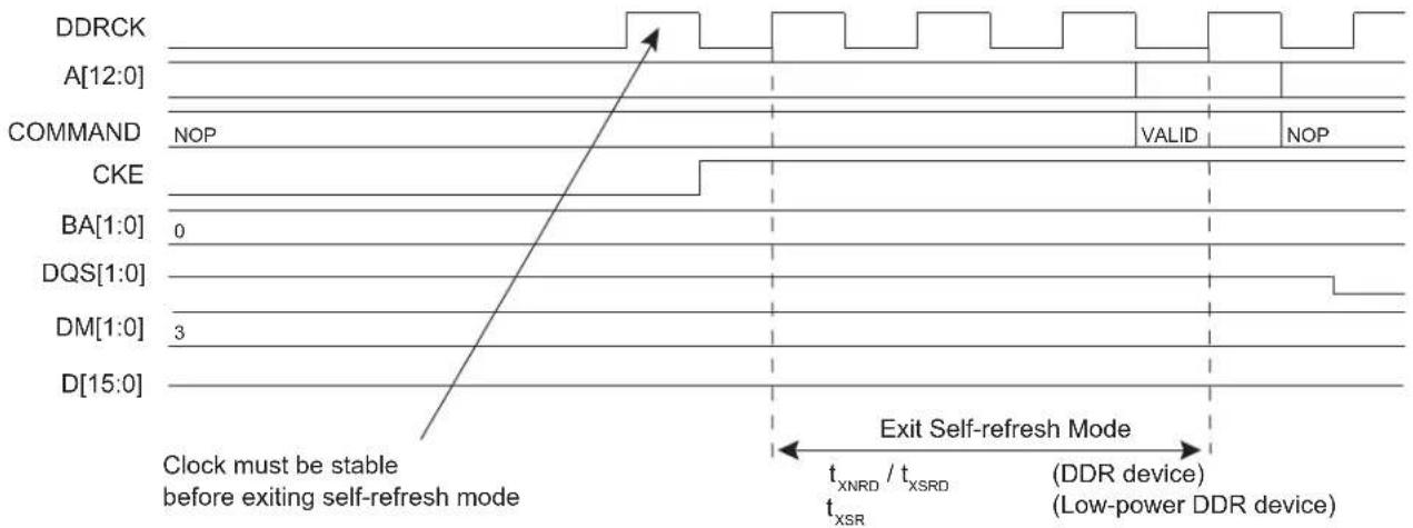
other
| Signal | Clock must be stable before exiting self-refresh mode | Exit Self-refresh Mode | |------------|--------------------------------------------------------|------------------------| | DDRCK | Yes | Yes | | A[12:0] | Yes | Yes | | COMMAND | NOP | Valid | | CKE | Yes | Valid | | BA[1:0] | 0 | Yes | | DQS[1:0] | Yes | Yes | | DM[1:0] | 3 | Yes | | D[15:0] | Yes | Yes |29.5.3.2 Power-down Mode
This mode is activated by writing a 10 to the Low-power Command bit (LPCB).
Power-down mode is used when no access to the DDR-SDRAM device is possible. In this mode, power consumption is greater than in Self-refresh mode. This state is similar to Normal mode (no Low-power mode/no Self-refresh mode), but the CKE pin is low and the input and output buffers are deactivated as soon the DDR-SDRAM device is no longer accessible. In contrast to Self-refresh mode, the DDR-SDRAM device cannot remain in Low-power mode longer than one refresh period (64 ms/32 ms). As no auto-refresh operations are performed in this mode, the MPDDRC carries out the refresh operation. For the low-power DDR-SDRAM devices, a NOP command must be generated for a minimum period defined in the TXP field of the MPDDRC Timing Parameter 1 Register (MPDDRC_TPR1). For DDR-SDRAM devices, a NOP command must be generated for a minimum period defined in the TXP field of MPDDRC_TPR1 (see Section 29.7.5 MPDDRC Timing Parameter 1 Register) and in the TXARD and TXARDS fields of MPDDRC_TPR2 (see Section 29.7.6 MPDDRC Timing Parameter 2 Register) for DDR2_SDRAM devices. In addition, low-power DDR-SDRAM and DDR-SDRAM must remain in Power-down mode for a minimum period corresponding to t_CKE , t_PD , etc. (see the memory device datasheet).
The exit procedure is faster than in Self-refresh mode. See Figure 29-16. The MPDDRC returns to Power-down mode as soon as the DDR-SDRAM device is not selected. It is possible to define when Power-down mode is enabled by configuring the TIMEOUT field in the MPDDRC_LPR:
0: Power-down mode is enabled as soon as the DDR-SDRAM device is not selected.
1: Power-down mode is enabled 64 clock cycles after completion of the last access.
2: Power-down mode is enabled 128 clock cycles after completion of the last access.
Figure 29-16: Power-down Entry/Exit, Time-out = 0
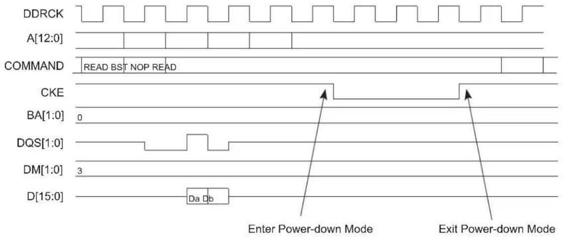
text_image
DDRCK A[12:0] COMMAND READ BST NOP READ CKE BA[1:0] 0 DQS[1:0] DM[1:0] 3 D[15:0] Da Db Enter Power-down Mode Exit Power-down Mode29.5.3.3 Deep Power-down Mode
The Deep Power-down mode is a feature of low-power DDR-SDRAM. When this mode is activated, all internal voltage generators inside the device are stopped and all data is lost.
Deep Power-down mode is activated by writing a 3 to the Low-power Command bit (LPCB). When this mode is enabled, the MPDDRC leaves Normal mode (MPDDRC_MR.MODE = 0) and the controller is frozen. The clock can be stopped during Deep Power-down mode by setting the CLK_FR field to 1.
Before enabling this mode, the user must make sure there is no access in progress. To exit Deep Power-down mode, the Low-power Command bit (LPCB) and clock frozen bit (CLK_FR) must be written to zero and the initialization sequence must be generated by software. See Section 29.4.1 Low-power DDR1-SDRAM Initialization or Section 29.4.3 Low-power DDR2-SDRAM Initialization.
Figure 29-17: Deep Power-down Mode Entry
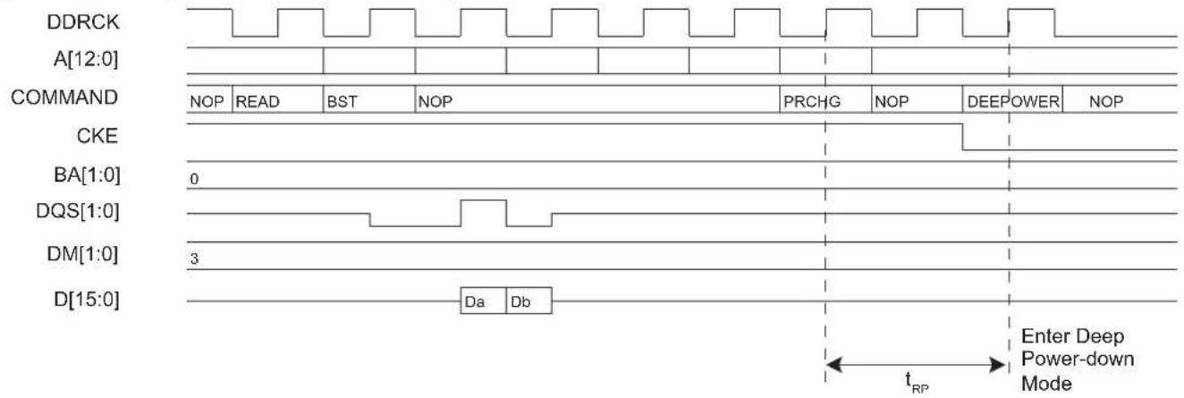
text_image
DDRCK A[12:0] COMMAND NOP READ BST NOP PRCHG NOP DEEPOWER NOP CKE BA[1:0] 0 DQS[1:0] DM[1:0] 3 D[15:0] Da Db Enter Deep Power-down Mode tRP29.5.3.4 Reset Mode
The Reset mode is a feature of DDR2-SDRAM. This mode is activated by writing a 3 to the Low-power Command bit (LPCB) and a one to the Clock Frozen Command bit (CLK_FR) in the MPDDRC Low-power Register.
When this mode is enabled, the MPDDRC leaves Normal mode (MPDDRC_MR.MODE = 0) and the controller is frozen. Before enabling this mode, the user must make sure there is no access in progress.
To exit Reset mode, the Low-power Command bit (LPCB) must be written to zero, the Clock Frozen Command bit (CLK_FR) must be written to zero and the initialization sequence must be generated by software (see Section 29.4.2 DDR2-SDRAM Initialization).
29.5.4 Multi-port Functionality
The DDR-SDRAM protocol imposes a check of timings prior to performing a read or a write access, thus decreasing system performance. An access to DDR-SDRAM is performed if banks and rows are open (or active). To activate a row in a particular bank, the last open row must be deactivated and a new row must be open. Two DDR-SDRAM commands must be performed to open a bank: Precharge command and Activate command with respect to t_RP timing. Before performing a read or write command, t_RCD timing must be checked.
This operation generates a significant bandwidth loss (see Figure 29-18).
Figure 29-18: t RP and t_RCD Timings
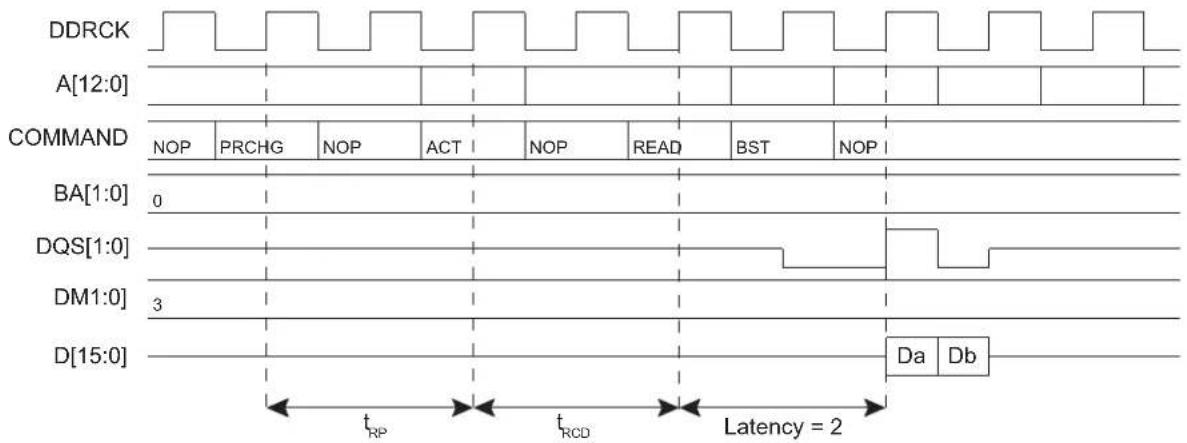
text_image
DDRCK A[12:0] COMMAND NOP PRCHG NOP ACT NOP READ BST NOP BA[1:0] 0 DQS[1:0] DM1:0] 3 D[15:0] Da Db tRP tRCD Latency = 24 cycles before performing a read command
The multi-port controller is designed to mask these timings and thus improve the bandwidth of the system.
The MPDDRC is a multi-port controller whereby four masters can simultaneously reach the controller. This feature improves the bandwidth of the system because it can detect four requests on the AHB slave inputs and thus anticipate the commands that follow, Precharge command and Activate command in bank X during the current access in bank Y. This masks t_RP and t_RCD timings (see Figure 29-19). In the best case, all accesses are done as if the banks and rows were already open. The best condition is met when the four masters work in different banks. In the case of four simultaneous read accesses, when the four or eight banks and associated rows are open, the controller reads with a continuous flow and masks the CAS latency for each access. To allow a continuous flow, the read command must be set at 2 or 3 cycles (CAS latency) before the end of the current access. The arbitration scheme must be changed since the round-robin arbitration cannot be respected. If the controller anticipates a read access, and thus a master with a high priority arises before the end of the current access, then this master will not be serviced.
Figure 29-19: Anticipate Precharge/Activate Command in Bank 2 during Read Access in Bank 1

text_image
DDRCK A[12:0] COMMAND NOP READ NOP BA[1:0] 0 1 2 1 DQS[1:0] DM1:0] 3 D[15:0] NOPPRECH ACT READ Da Db Dc Dd De Df Dg Dh Di Dj Dk DI Anticipate command, Precharge/Active Bank 2 Read Access in Bank 1The arbitration mechanism reduces latency when a conflict occurs, that is when two or more masters try to access the DDR-SDRAM device at the same time.
The arbitration type is round-robin arbitration. This algorithm dispatches requests from different masters to the DDR-SDRAM device in a round-robin manner. If two or more master requests arise at the same time, the master with the lowest number is serviced first, then the others are serviced in a round-robin manner.
To avoid burst breaking and to provide the maximum throughput for the DDR-SDRAM device, arbitration must only take place during the following cycles:
- Idle cycles: when no master is connected to the DDR-SDRAM device.
- Single cycles: when a slave is currently performing a single access.
- End of Burst cycles: when the current cycle is the last cycle of a burst transfer.
- For bursts of defined length, predicted end of burst matches the size of the transfer.
- For bursts of undefined length, predicted end of burst is generated at the end of each four-beat boundary inside the INCR transfer.
- Anticipated Access: when an anticipated read access is done while the current access is not complete, the arbitration scheme can be changed if the anticipated access is not the next access serviced by the arbitration scheme.
29.5.5 Scrambling/Unscrambling Function
The external data bus can be scrambled in order to prevent intellectual property data located in off-chip memories from being easily recovered by analyzing data at the package pin level of either the microcontroller or the memory device.
The scrambling and unscrambling are performed on-the-fly without additional wait states.
The scrambling method depends on two user-configurable key registers, MPDDRC_KEY1 in the MPDDRC OCMS KEY1 Register and MPDDRC_KEY2 in the MPDDRC OCMS KEY2 Register. These key registers are only accessible in Write mode.
The key must be securely stored in a reliable non-volatile memory in order to recover data from the off-chip memory. Any data scrambled with a given key cannot be recovered if the key is lost.
The scrambling/unscrambling function can be enabled or disabled by programming the MPDDRC OCMS Register.
29.5.6 Register Write Protection
To prevent any single software error from corrupting MPDDRC behavior, certain registers in the address space can be write-protected by setting the WPEN bit in the MPDDRC Write Protection Mode Register (MPDDRC_WPMR).
If a write access to a write-protected register is detected, the WPVS flag in the MPDDRC Write Protection Status Register (MPDDRC_WPSR) is set and the field WPVSRC indicates the register in which the write access has been attempted.
The WPVS bit is automatically cleared after reading the MPDDRC_WPSR.
The following registers can be write-protected:
• MPDDRC Mode Register
• MPDDRC Refresh Timer Register
• MPDDRC Configuration Register
• MPDDRC Timing Parameter 0 Register
• MPDDRC Timing Parameter 1 Register
• MPDDRC Memory Device Register
• MPDDRC High Speed Register
• MPDDRC Low-power DDR2 Calibration and MR4 Register
• MPDDRC OCMS Register
• MPDDRC OCMS KEY1 Register
• MPDDRC OCMS KEY2 Register
29.6 Software Interface/SDRAM Organization, Address Mapping
The DDR-SDRAM address space is organized into banks, rows and columns. The MPDDRC maps different memory types depending on values set in the MPDDRC Configuration Register (see Section 29.7.3 MPDDRC Configuration Register). The tables that follow illustrate the relation between CPU addresses and columns, rows and banks addresses for 16-bit memory data bus widths and 32-bit memory data bus widths.
The MPDDRC supports address mapping in Linear mode.
Sequential mode is a method for address mapping where banks alternate at each last DDR-SDRAM page of the current bank.
Interleaved mode is a method for address mapping where banks alternate at each SDRAM end page of the current bank.
The MPDDRC makes the DDR-SDRAM device access protocol transparent to the user. The tables that follow illustrate the DDR-SDRAM device memory mapping seen by the user in correlation with the device structure. Various configurations are illustrated.
29.6.1 DDR-SDRAM Address Mapping for 32-bit Memory Data Bus Width
Table 29-3: Sequential Mapping DDR-SDRAM Configuration Mapping: 2K Rows, 512/1024/2048 Columns, 4 banks
| CPU Address Line | ||||||||||||||||||||||||||||||||||||||||
| 28 | 27 | 26 | 25 | 24 | 23 | 22 | 21 | 20 | 19 | 18 | 17 | 16 | 15 | 14 | 13 | 12 | 11 | 10 | 9 | 8 | 7 | 6 | 5 | 4 | 3 | 2 | 1 | 0 | ||||||||||||
| Bk[1:0] | Row[10:0] Column[8:0] M[1:0] | |||||||||||||||||||||||||||||||||||||||
| Bk[1:0] | Row[10:0] Column[9:0] M[1:0] | |||||||||||||||||||||||||||||||||||||||
| Bk[1:0] | Row[10:0] | Column[10:0] M[1:0] | ||||||||||||||||||||||||||||||||||||||
Table 29-4: Interleaved Mapping DDR-SDRAM Configuration Mapping: 2K Rows, 512/1024/2048 Columns, 4 banks
| CPU Address Line | ||||||||||||||||||||||||||||||||||||||||
| 28 | 27 | 26 | 25 | 24 | 23 | 22 | 21 | 20 | 19 | 18 | 17 | 16 | 15 | 14 | 13 | 12 | 11 | 10 | 9 | 8 | 7 | 6 | 5 | 4 | 3 | 2 | 1 | 0 | ||||||||||||
| Row[10:0] Bk[1:0] | Column[8:0] M[1:0] | |||||||||||||||||||||||||||||||||||||||
| Row[10:0] Bk[1:0] | Column[9:0] M[1:0] | |||||||||||||||||||||||||||||||||||||||
| Row[10:0] Bk[1:0] | Column[10:0] M[1:0] | |||||||||||||||||||||||||||||||||||||||
Table 29-5: Sequential Mapping DDR-SDRAM Configuration Mapping: 4K Rows, 256/512/1024/2048 Columns, 4 banks
| CPU Address Line | |||||||||||||||||||||||||||||||||||||||||
| 28 | 27 | 26 | 25 | 24 | 23 | 22 | 21 | 20 | 19 | 18 | 17 | 16 | 15 | 14 | 13 | 12 | 11 | 10 | 9 | 8 | 7 | 6 | 5 | 4 | 3 | 2 | 1 | 0 | |||||||||||||
| Bk[1:0] | Row[11:0] | Column[7:0] | M[1:0] | ||||||||||||||||||||||||||||||||||||||
| Bk[1:0] | Row[11:0] | Column[8:0] M[1:0] | |||||||||||||||||||||||||||||||||||||||
| Bk[1:0] | Row[11:0] | Column[9:0] M[1:0] | |||||||||||||||||||||||||||||||||||||||
| Bk[1:0] | Row[11:0] | Column[10:0] | M[1:0] | ||||||||||||||||||||||||||||||||||||||
Table 29-6: Interleaved Mapping DDR-SDRAM Configuration Mapping: 4K Rows, 256/512/1024/2048 Columns, 4 banks
| CPU Address Line | |||||||||||||||||||||||||||||||||||||||||
| 28 | 27 | 26 | 25 | 24 | 23 | 22 | 21 | 20 | 19 | 18 | 17 | 16 | 15 | 14 | 13 | 12 | 11 | 10 | 9 | 8 | 7 | 6 | 5 | 4 | 3 | 2 | 1 | 0 | |||||||||||||
| Row[11:0] | Bk[1:0] | Column[7:0] | M[1:0] | ||||||||||||||||||||||||||||||||||||||
| Row[11:0] | Bk[1:0] | Column[8:0] M[1:0] | |||||||||||||||||||||||||||||||||||||||
| Row[11:0] | Bk[1:0] | Column[9:0] M[1:0] | |||||||||||||||||||||||||||||||||||||||
| Row[11:0] | Bk[1:0] | Column[10:0] | M[1:0] | ||||||||||||||||||||||||||||||||||||||
Table 29-7: Sequential Mapping DDR-SDRAM Configuration Mapping: 8K Rows, 512/1024/2048 Columns, 4 banks
| CPU Address Line | |||||||||||||||||||||||||||||||||||||||||
| 28 | 27 | 26 | 25 | 24 | 23 | 22 | 21 | 20 | 19 | 18 | 17 | 16 | 15 | 14 | 13 | 12 | 11 | 10 | 9 | 8 | 7 | 6 | 5 | 4 | 3 | 2 | 1 | 0 | |||||||||||||
| Bk[1:0] | Row[12:0] | Column[8:0] M[1:0] | |||||||||||||||||||||||||||||||||||||||
| Bk[1:0] | Row[12:0] | Column[9:0] M[1:0] | |||||||||||||||||||||||||||||||||||||||
| Bk[1:0] | Row[12:0] | Column[10:0] | M[1:0] | ||||||||||||||||||||||||||||||||||||||
Table 29-8: Interleaved Mapping DDR-SDRAM Configuration Mapping: 8K Rows, 512/1024/2048 Columns, 4 banks
| CPU Address Line | ||||||||||||||||||||||||||||||||||||||||||||||||
| 28 | 27 | 26 | 25 | 24 | 23 | 22 | 21 | 20 | 19 | 18 | 17 | 16 | 15 | 14 | 13 | 12 | 11 | 10 | 9 | 8 | 7 | 6 | 5 | 4 | 3 | 2 | 1 | 0 | ||||||||||||||||||||
| Row[12:0] Bk[1:0] Column[8:0] M[1:0] | ||||||||||||||||||||||||||||||||||||||||||||||||
| Row[12:0] Bk[1:0] Column[9:0] M[1:0] | ||||||||||||||||||||||||||||||||||||||||||||||||
| Row[12:0] Bk[1:0] | Column[10:0] M[1:0] | |||||||||||||||||||||||||||||||||||||||||||||||
Table 29-9: Sequential Mapping DDR-SDRAM Configuration Mapping: 8K Rows, 1024 Columns, 8 banks
| CPU Address Line | ||||||||||||||||||||||||||||
| 28 | 27 | 26 | 25 | 24 | 23 | 22 | 21 | 20 | 19 | 18 | 17 | 16 | 15 | 14 | 13 | 12 | 11 | 10 | 9 | 8 | 7 | 6 | 5 | 4 | 3 | 2 | 1 | 0 |
| Bk[2:0] | Row[12:0] | Column[9:0] M[1:0] | ||||||||||||||||||||||||||
Table 29-10: Interleaved Mapping DDR-SDRAM Configuration Mapping: 8K Rows, 1024 Columns, 8 banks
| CPU Address Line | ||||||||||||||||||||||||||||
| 28 | 27 | 26 | 25 | 24 | 23 | 22 | 21 | 20 | 19 | 18 | 17 | 16 | 15 | 14 | 13 | 12 | 11 | 10 | 9 | 8 | 7 | 6 | 5 | 4 | 3 | 2 | 1 | 0 |
| Row[12:0] | Bk[2:0] | Column[9:0] M[1:0] | ||||||||||||||||||||||||||
Table 29-11: Sequential Mapping DDR-SDRAM Configuration Mapping: 16K Rows, 1024 Columns, 4 banks
| CPU Address Line | ||||||||||||||||||||||||||||
| 28 | 27 | 26 | 25 | 24 | 23 | 22 | 21 | 20 | 19 | 18 | 17 | 16 | 15 | 14 | 13 | 12 | 11 | 10 | 9 | 8 | 7 | 6 | 5 | 4 | 3 | 2 | 1 | 0 |
| Bk[1:0] | Row[13:0] | Column[9:0] M[1:0] | ||||||||||||||||||||||||||
Table 29-12: Interleaved Mapping DDR-SDRAM Configuration Mapping: 16K Rows, 1024 Columns, 4 banks
| CPU Address Line | ||||||||||||||||||||||||||||
| 28 | 27 | 26 | 25 | 24 | 23 | 22 | 21 | 20 | 19 | 18 | 17 | 16 | 15 | 14 | 13 | 12 | 11 | 10 | 9 | 8 | 7 | 6 | 5 | 4 | 3 | 2 | 1 | 0 |
| Row[13:0] | Bk[1:0] | Column[9:0] M[1:0] | ||||||||||||||||||||||||||
Table 29-13: Sequential Mapping DDR-SDRAM Configuration Mapping: 16K Rows, 1024 Columns, 8 banks
| CPU Address Line | ||||||||||||||||||||||||||||
| 28 | 27 | 26 | 25 | 24 | 23 | 22 | 21 | 20 | 19 | 18 | 17 | 16 | 15 | 14 | 13 | 12 | 11 | 10 | 9 | 8 | 7 | 6 | 5 | 4 | 3 | 2 | 1 | 0 |
| Bk[2:0] | Row[13:0] | Column[9:0] M[1:0] | ||||||||||||||||||||||||||
Table 29-14: Interleaved Mapping DDR-SDRAM Configuration Mapping: 16K Rows, 1024 Columns, 8 banks
| CPU Address Line | ||||||||||||||||||||||||||||
| 28 | 27 | 26 | 25 | 24 | 23 | 22 | 21 | 20 | 19 | 18 | 17 | 16 | 15 | 14 | 13 | 12 | 11 | 10 | 9 | 8 | 7 | 6 | 5 | 4 | 3 | 2 | 1 | 0 |
| Row[13:0] | Bk[2:0] | Column[9:0] M[1:0] | ||||||||||||||||||||||||||
Note 1: M[1:0] is the byte address inside a 32-bit word.
2: Bk[2] = BA2, Bk[1] = BA1, Bk[0] = BA0
29.7 AHB Multi-port DDR-SDRAM Controller (MPDDRC) User Interface
The User Interface is connected to the APB bus. The MPDDRC is programmed using the registers listed in Table 29-15.
Table 29-15: Register Mapping
| Offset Register | Name Access Reset | |||
| 0x00 MPDDRC | Mode Register MPDDRC_MR Read/Write 0x00000000 | |||
| 0x04 | MPDDRC Refresh Timer Register | MPDDRC_RTR | Read/Write | 0x03000000 |
| 0x08 | MPDDRC Configuration Register | MPDDRC_CR | Read/Write | 0x00207024 |
| 0x0C | MPDDRC Timing Parameter 0 Register | MPDDRC_TPR0 | Read/Write | 0x20227225 |
| 0x10 | MPDDRC Timing Parameter 1 Register | MPDDRC_TPR1 | Read/Write | 0x3C80808 |
| 0x14 | MPDDRC Timing Parameter 2 Register | MPDDRC_TPR2 | Read/Write | 0x00042062 |
| 0x18 Reserved | - | - | - | |
| 0x1C | MPDDRC Low-power Register | MPDDRC_LPR | Read/Write | 0x00010000 |
| 0x20 MPDDRC | Memory Device Register MPDDRC_MD Read/Write 0x13 | |||
| 0x24 | MPDDRC High Speed Register | MPDDRC_HS | Read/Write | 0x00000008 |
| 0x28 | MPDDRC LPDDR2 Low-power Register | MPDDRC_LPDDR2_LPR | Read/Write | 0x00000000 |
| 0x2C | MPDDRC Low-power DDR2 Calibration and MR4 Register | MPDDRC_LPDDR2_CAL_MR4 | Read/Write | 0x00000000 |
| 0x30 | MPDDRC Low-power DDR2 Timing Calibration Register | MPDDRC_LPDDR2_TIM_CAL | Read/Write | 0x06 |
| 0x34 | MPDDRC IO Calibration | MPDDRC_IO_CALIBR | Read/Write | 0x00870002 |
| 0x38 | MPDDRC OCMS Register | MPDDRC_OCMS | Read/Write | 0x00000000 |
| 0x3C | MPDDRC OCMS KEY1 Register | MPDDRC_OCMS_KEY1 | Write-only | - |
| 0x40 | MPDDRC OCMS KEY2 Register | MPDDRC_OCMS_KEY2 | Write-only | - |
| 0x44-0x70 | Reserved | - | - | - |
| 0x74 | MPDDRC DLL Master Offset Register | MPDDRC_DLL_MO | Read/Write | 0x^-(1) |
| 0x78 | MPDDRC DLL Slave Offset Register | MPDDRC_DLL_SOF | Read/Write | 0x^-(1) |
| 0x7C | MPDDRC DLL Status Master Register | MPDDRC_DLL_MS | Read-only | 0x00000000 |
| 0x80 | MPDDRC DLL Status Slave 0 Register | MPDDRC_DLL_SS0 | Read-only | 0x00000000 |
| 0x84 | MPDDRC DLL Status Slave 1 Register | MPDDRC_DLL_SS1 | Read-only | 0x00000000 |
| 0x88 | MPDDRC DLL Status Slave 2 Register | MPDDRC_DLL_SS2 | Read-only | 0x00000000 |
| 0x8C | MPDDRC DLL Status Slave 3 Register | MPDDRC_DLL_SS3 | Read-only | 0x00000000 |
| 0x90-0xE0 | Reserved | - | - | - |
| 0xE4 | MPDDRC Write Protection Mode Register | MPDDRC_WPMR | Read/Write | 0x00000000 |
| 0xE8 | MPDDRC Write Protection Status Register | MPDDRC_WPSR | Read-only | 0x00000000 |
| 0xEC-0x1FC | Reserved | - | - | - |
Note 1: Values vary with the product implementation.
29.7.1 MPDDRC Mode Register
Name:MPDDRC_MR
Address:0xFFFFEA00
Access: Read/Write
31 30 29 28 27 26 25 24
| - | - | - | - | - | - | - | - |
23 22 21 20 19 18 17 16
| - | - | - | - | - | - | - | - |
15 14 13 12 11 10 9 8
| MRS | |||||||
| 7 | 6 | 5 | 4 | 3 | 2 | 1 | 0 |
| - | - | - | - | M | O | ||
This register can only be written if the WPEN bit is cleared in the MPDDRC Write Protection Mode Register.
MODE: MPDDRC Command Mode
This field defines the command issued by the MPDDRC when the SDRAM device is accessed. This register is used to initialize the SDRAM device and to activate Deep Power-down mode.
| Value | Name Description | |
| 0 | N O R M | Normal Mode. Any access to the MPDDRC is decoded normally. To activate this mode, the command must be followed by a write to the DDR-SDRAM. |
| 1 | N O P _ | The MPDDRC issues a NOP command when the DDR-SDRAM device is accessed regardless of the cycle. To activate this mode, the command must be followed by a write to the DDR-SDRAM. |
| 2 | PRCGALL_CMD | The MPDDRC issues the All Banks Precharge command when the DDR-SDRAM device is accessed regardless of the cycle. To activate this mode, the command must be followed by a write to the SDRAM. |
| 3 | LMR_CMD | The MPDDRC issues a Load Mode Register command when the DDR-SDRAM device is accessed regardless of the cycle. To activate this mode, the command must be followed by a write to the DDR-SDRAM. |
| 4 | RFSH_CMD | The MPDDRC issues an Auto-Refresh command when the DDR-SDRAM device is accessed regardless of the cycle. Previously, an All Banks Precharge command must be issued. To activate this mode, the command must be followed by a write to the DDR-SDRAM. |
| 5 | EXT_LMR_CMD | The MPDDRC issues an Extended Load Mode Register command when the SDRAM device is accessed regardless of the cycle. To activate this mode, the command must be followed by a write to the DDR-SDRAM. The write in the DDR-SDRAM must be done in the appropriate bank. |
| 6 | DEEP_MD | Deep Power mode: Access to Deep Power-down mode |
| 7 | LPDDR2_CMD | The MPDDRC issues an LPDDR2 Mode Register command when the device is accessed regardless of the cycle. To activate this mode, the Mode Register command must be followed by a write to the low-power DDR2-SDRAM. |
MRS: Mode Register Select LPDDR2
Configure this 8-bit field to program all mode registers included in the low-power DDR2-SDRAM device. This field is unique to the low-power DDR2-SDRAM devices.
29.7.2 MPDDRC Refresh Timer Register
Name:MPDDRC_RTR
Address:0xFFFFEA04
Access: Read/Write
31 30 29 28 27 26 25 24
| - | - | - | - | - | - | - | - |
23 22 21 20 19 18 17 16
| - MR4_VALUE -- REF_PB ADJ_REF |
15 14 13 12 11 10 9 8
| - | - | - | - | COUNT | |||
| 7 | 6 | 5 | 4 | 3 | 2 | 1 | 0 |
| COUNT | |||||||
This register can only be written if the WPEN bit is cleared in the MPDDRC Write Protection Mode Register.
COUNT: MPDDRC Refresh Timer Count
This 12-bit field is loaded into a timer which generates the refresh pulse. Each time the refresh pulse is generated, a refresh sequence is initiated.
The SDRAM devices require a refresh of all rows every 64 ms. The value to be loaded depends on the MPDDRC clock frequency (MCK: Master Clock) and the number of rows in the device.
For example, for an SDRAM with 8192 rows and a 100 MHz Master clock, the value of the COUNT field is configured: ((64× 10^-3) / 8192) × 100× 10^6 = 781 or 0x030D .
Low-power DDR2-SDRAM devices support Per Bank Refresh operation. In this configuration, average time between refresh command is 0.975 s. The value of the COUNT field is configured depending on this value. For example, the value of a 100 MHz Master clock refresh timer is 98 or 0x0062.
ADJ\_REF: Adjust Refresh Rate
Reset value is 0.
0: Adjust refresh rate is not enabled.
1: Adjust refresh rate is enabled.
This mode is unique to the low-power DDR2-SDRAM devices.
REF\_PB: Refresh Per Bank
Reset value is 0.
0: Refresh all banks during auto-refresh operation.
1: Refresh the scheduled bank by the bank counter in the memory interface.
This mode is unique to the low-power DDR2-SDRAM devices.
MR4\_VALUE: Content of MR4 Register
Reset value is 3.
This (read-only) field gives the content of MR4 register. This field is updated when MRR command is generated and Adjust Refresh Rate bit is enabled. Update is done when read value is different from MR4_VALUE.
LP-DDR2 JEDEC memory standards impose derating LP-DDR2 AC timings ( t_ACD , t_RC , t_RAS , t_RP and t_RRD ) when the value of MR4 is equal to 6. If the application needs to work in extreme conditions, the derating value must be added to AC timings before the power up sequence.
This mode is unique to the low-power DDR2-SDRAM devices.
29.7.3 MPDDRC Configuration Register
Name:MPDDRC_CR
Address:0xFFFFEA08
Access: Read/Write
31 30 29 28 27 26 25 24
| - | - | - | - | - | - | - | - |
23 22 21 20 19 18 17 16
| - | OCD | ZQ | DIS_DLL | DIC_DS |
| 7 | 6 | 5 | 4 | 3 | 2 | 1 | 0 |
| DLL | CAS | NR | NC | ||||
This register can only be written if the WPEN bit is cleared in the MPDDRC Write Protection Mode Register.
NC: Number of Column Bits
Reset value is 0 (9/8 column bits).
| Value | Name | Description |
| 0 | DDR9_MDDR8_COL_BITS | 9 bits for DDR, 8-bit for low-power DDR1-SDRAM |
| 1 | DDR10_MDDR9_COL_BITS | 10 bits for DDR, 9-bit for low-power DDR1-SDRAM |
| 2 | DDR11_MDDR10_COL_BITS | 11 bits for DDR, 10-bit for low-power DDR1-SDRAM |
| 3 | DDR12_MDDR11_COL_BITS | 12 bits for DDR, 11-bit for low-power DDR1-SDRAM |
NR: Number of Row Bits
Reset value is 1 (12 row bits).
| Value | Name | Description |
| 0 | 11_ROW_BITS | 11 bits to define the row number, up to 2048 rows |
| 1 | 12_ROW_BITS | 12 bits to define the row number, up to 4096 rows |
| 2 | 13_ROW_BITS | 13 bits to define the row number, up to 8192 rows |
| 3 | 14_ROW_BITS | 14 bits to define the row number, up to 16384 rows |
CAS: CAS Latency
Reset value is 2 (2 cycles).
| Value | Name | Description |
| 2 | DDR_CAS2 | LPDDR1 CAS Latency 2 |
| 3 | DDR_CAS3 | DDR2/LPDDR2/LPDDR1 CAS Latency 3 |
DLL: Reset DLL
Reset value is 0.
This bit defines the value of Reset DLL.
| Value Name Description | |
| 0 RESET_DISABLED Disable DLL reset | |
| 1 RESET_ENABLED Enable DLL reset | |
This value is used during the power-up sequence.
This bit is found only in the DDR2-SDRAM devices.
DIC\_DS: Output Driver Impedance Control (Drive Strength)
Reset value is 0.
This bit name is described as "DS" in some memory datasheets. It defines the output drive strength. This value is used during the power-up sequence.
| Value | Name Description | |
| 0 | DDR2_NORMALSTRENGTH Normal drive strength | (DDR2) |
| 1 | DDR2_WEAKSTRENGTH | Weak drive strength (DDR2) |
This bit is found only in the DDR2-SDRAM devices.
DIS\_DLL: DISABLE DLL
Reset value is 0.
0: Enable DLL.
1: Disable DLL.
This value is used during the power-up sequence. It is only found in the DDR2-SDRAM devices.
ZQ: ZQ Calibration
Reset value is 0.
| Value Name | Description |
| 0 INIT | Calibration command after initialization |
| 1 LONG Long calibration | |
| 2 SHORT | Short calibration |
| 3 RESET | ZQ Reset |
This parameter is used to calibrate DRAM On resistance (Ron) values over PVT.
This field is found only in the low-power DDR2-SDRAM devices.
OCD: Off-chip Driver
Reset value is 7.
Note: SDRAM Controller supports only two values for OCD (default calibration and exit from calibration). These values MUST always be programmed during the initialization sequence. The default calibration must be programmed first, after which the exit calibration and maintain settings must be programmed.
This field is found only in the DDR2-SDRAM devices.
| Value | Name | Description |
| 0 | DDR2_EXITCALIB | Exit from OCD Calibration mode and maintain settings |
| 7 DDR2_DEFAULT_CALIB | OCD | calibration default |
DQMS: Mask Data is Shared
Reset value is 0.
| Value | Name Description | |
| 0 | NOT_SHARED DQM is not shared with another controller | |
| 1 | SHARED DQM is shared with another controller |
ENRDM: Enable Read Measure
Reset value is 0.
| Value | Name Description | |
| 0 OFF | DQS/DDR_DATA phase error correction is disabled | |
| 1 ON | DQS/DDR_DATA phase error correction is enabled | |
NB: Number of Banks
Reset value is 0 (4 banks). If LC_LPDDR1 is set to 1, NB is not relevant.
| Value | Name Description | |
| 0 4_BANKS | 4-bank memory devices | |
| 1 | 8_BANKS | 8 banks. Only possible when using the DDR2-SDRAM and low-power DDR2-SDRAM devices. |
NDQS: Not DQS
Reset value is 1 (Not DQS is disabled).
This bit is found only in the DDR2-SDRAM devices.
DECOD: Type of Decoding
Reset value is 0.
| Value Name Description | ||
| 0 | SEQUENTIAL | Method for address mapping where banks alternate at each last DDR-SDRAM page of the current bank. |
| 1 | INTERLEAVED | Method for address mapping where banks alternate at each SDRAM end page of the current bank. |
UNAL: Support Unaligned Access
Reset value is 0 (unaligned access is not supported).
| Value Name | Description |
| 0 UNSUPPORTED | Unaligned access is not supported. |
| 1 SUPPORTED | Unaligned access is supported. |
This mode is enabled with masters which have an AXI interface.
29.7.4 MPDDRC Timing Parameter 0 Register
Name:MPDDRC_TPR0
Address:0xFFFFEA0C
Access: Read/Write
31 30 29 28 27 26 25 24
| TMRD RDC_WRRD TWTR |
23 22 21 20 19 18 17 16
| TRRD TRP |
15 14 13 12 11 10 9 8
| TRC TWR |
| 7 | 6 | 5 | 4 | 3 | 2 | 1 | 0 |
| TRCD TRAS |
This register can only be written if the WPEN bit is cleared in the MPDDRC Write Protection Mode Register.
TRAS: Active to Precharge Delay
Reset value is 5 DDRCK ^(1) clock cycles.
This field defines the delay between an Activate command and a Precharge command in number of DDRCK ^(1) clock cycles. The number of cycles is between 0 and 15.
TRCD: Row to Column Delay
Reset value is 2 DDRCK ^(1) clock cycles.
This field defines the delay between an Activate command and a Read/Write command in number of DDRCK ^(1) clock cycles. The number of cycles is between 0 and 15.
TWR: Write Recovery Delay
Reset value is 2 DDRCK ^(1) clock cycles.
This field defines the Write Recovery Time in number of DDRCK ^(1) clock cycles. The number of cycles is between 1 and 15.
TRC: Row Cycle Delay
Reset value is 7 DDRCK ^(1) clock cycles.
This field defines the delay between an Activate command and a Refresh command in number of DDRCK ^(1) clock cycles. The number of cycles is between 0 and 15.
TRP: Row Precharge Delay
Reset value is 2 DDRCK ^(1) clock cycles.
This field defines the delay between a Precharge command and another command in number of DDRCK ^(1) clock cycles. The number of cycles is between 0 and 15.
TRRD: Active BankA to Active BankB
Reset value is 2 DDRCK ^(1) clock cycles.
This field defines the delay between an Activate command in BankA and an Activate command in BankB in number of DDRCK ^(1) clock cycles. The number of cycles is between 1 and 15.
TWTR: Internal Write to Read Delay
Reset value is 0.
This field defines the internal Write to Read command time in number of DDRCK ^(1) clock cycles. The number of cycles is between 1 and 7.
RDC\_WRRD: Reduce Write to Read Delay
Reset value is 0.
This field reduces the delay between write to read access for the low-power DDR-SDRAM devices with a latency equal to 2. To use this feature, the TWTR field must be equal to 0. Note that some devices do not support this feature.
TMRD: Load Mode Register Command to Activate or Refresh Command
Reset value is 2 DDRCK ^(1) clock cycles.
This field defines the delay between a Load mode register command and an Activate or Refresh command in number of DDRCK ^(1) clock cycles. The number of cycles is between 0 and 15. For low-power DDR2-SDRAM, this field is equivalent to TMRW timing.
Note 1: DDRCK is the clock that drives the SDRAM device.
29.7.5 MPDDRC Timing Parameter 1 Register
Name:MPDDRC_TPR1
Address:0xFFFFEA10
Access: Read/Write
31 30 29 28 27 26 25 24
| - | - | - | - | T | X | P |
23 22 21 20 19 18 17 16
| TXSRD |
15 14 13 12 11 10 9 8
| TXSNR |
| 7 | 6 | 5 | 4 | 3 | 2 | 1 | 0 |
| ---TRFC | |||||||
This register can only be written if the WPEN bit is cleared in the MPDDRC Write Protection Mode Register.
TRFC: Row Cycle Delay
Reset value is 8 DDRCK ^(1) clock cycles.
This field defines the delay between a Refresh command or a Refresh and Activate command in number of DDRCK ^(1) clock cycles. The number of cycles is between 0 and 31.
In case of low-power DDR2-SDRAM, this field is equivalent to t_RFCab timing. If the user enables the function “Refresh Per Bank” (see REF_PB: Refresh Per Bank), this field is equivalent to t_RFCpb .
TXSNR: Exit Self-refresh Delay to Non-Read Command
Reset value is 8 DDRCK ^(1) clock cycles.
This field defines the delay between CKE set high and a Non Read command in number of DDRCKclock cycles. The number of cycles is between 0 and 255. This field is used by the DDR-SDRAM devices. In case of low-power DDR-SDRAM, this field is equivalent to t_XSR timing.
TXSRD: Exit Self-refresh Delay to Read Command
Reset value is 200 DDRCK ^(1) clock cycles.
This field defines the delay between CKE set high and a Read command in number of DDRCK ^(1) clock cycles. The number of cycles is between 0 and 255.
This field is found only in DDR2-SDRAM devices.
TXP: Exit Power-down Delay to First Command
Reset value is 3 DDRCK ^(1) clock cycles.
This field defines the delay between CKE set high and a valid command in number of DDRCK ^(1) clock cycles. The number of cycles is between 0 and 15.
Note 1: DDRCK is the clock that drives the SDRAM device.
29.7.6 MPDDRC Timing Parameter 2 Register
Name:MPDDRC_TPR2
Address:0xFFFFEA14
Access: Read/Write
31 30 29 28 27 26 25 24
| - | - | - | - | - | - | - | - |
23 22 21 20 19 18 17 16
| - | - | - | - | T | F | A |
15 14 13 12 11 10 9 8
| - | T | R | T | P |
| 7 | 6 | 5 | 4 | 3 | 2 | 1 | 0 |
| TXARDS | TXARD |
TXARD: Exit Active Power Down Delay to Read Command in Mode "Fast Exit"
Reset value is 2 DDRCK ^(1) clock cycles.
This field defines the delay between CKE set high and a Read command in number of DDRCK ^(1) clock cycles. The number of cycles is between 0 and 15.
This field is found only in the DDR2-SDRAM devices.
TXARDS: Exit Active Power Down Delay to Read Command in Mode "Slow Exit"
Reset value is 6 DDRCK ^(1) clock cycles.
This field defines the delay between CKE set high and a Read command in number of DDRCK ^(1) clock cycles. The number of cycles is between 0 and 15.
This field is found only in the DDR2-SDRAM devices.
TRPA: Row Precharge All Delay
Reset value is 0 DDRCK ^(1) clock cycles.
This field defines the delay between a Precharge All Banks command and another command in number of DDRCK ^(1) clock cycles. The number of cycles is between 0 and 15.
This field is found only in the DDR2-SDRAM devices.
TRTP: Read to Precharge
Reset value is 2 DDRCK ^(1) clock cycles.
This field defines the delay between a Read command and a Precharge command in number of DDRCK ^(1) clock cycles.
The number of cycles is between 0 and 7.
TFAW: Four Active Windows
Reset value is 4 DDRCK ^(1) clock cycles.
DDR2 devices with eight banks (1 Gbit or larger) have an additional requirement concerning t_FAW timing. This requires that no more than four Activate commands may be issued in any given t_FAW (MIN) period.
The number of cycles is between 0 and 15.
This field is found only in DDR2-SDRAM and LPDDR2-SDRAM devices.
Note 1: DDRCK is the clock that drives the SDRAM device.
29.7.7 MPDDRC Low-power Register
Name:MPDDRC_LPR
Address:0xFFFFEA1C
Access: Read/Write
31 30 29 28 27 26 25 24
| - | - | - | - | - | - | - |
23 22 21 20 19 18 17 16
| - | - | U | P | D | - | M |
15 14 13 12 11 10 9 8
| - | - | T | I | M | E | O |
| 7 | 6 | 5 | 4 | 3 | 2 | 1 | 0 |
| - | PASR | LPDDR2_PWOFF | CLK_FR | LPCB |
LPCB: Low-power Command Bit
Reset value is 0.
| Value | Name | Description |
| 0 | NOLOWPOWER | Low-power feature is inhibited. No Power-down, Self-refresh and Deep-power modes are issued to the DDR-SDRAM device. |
| 1 | SELFREFRESH | The MPDDRC issues a self-refresh command to the DDR-SDRAM device, the clock(s) is/are deactivated and the CKE signal is set low. The DDR-SDRAM device leaves the Self-refresh mode when accessed and reenters it after the access. |
| 2 | POWERDOWN | The MPDDRC issues a Power-down command to the DDR-SDRAM device after each access, the CKE signal is set low. The DDR-SDRAM device leaves the Power-down mode when accessed and reenters it after the access. |
| 3 | DEEPPOWERDOWN | The MPDDRC issues a Deep Power-down command to the low-power DDR-SDRAM device. |
CLK\_FR: Clock Frozen Command Bit
Reset value is 0.
This field sets the clock low during Power-down mode. Some DDR-SDRAM devices do not support freezing the clock during Power-down mode. Refer to the relevant DDR-SDRAM device datasheet for details.
| Value | Name | Description |
| 0 | DISABLED | Clock(s) is/are not frozen. |
| 1 | ENABLED | Clock(s) is/are frozen. |
LPDDR2\_PWOFF: LPDDR2 - LPDDR3 Power Off Bit
Reset value is 0.
LPDDR2 power off sequence must be controlled to preserve the LPDDR2 device. The power failure is handled at system level (IRQ or FIQ) and the LPDDR2 power off sequence is applied using the LPDDR2_PWOFF bit.
LPDDR2_PWOFF bit is used to impose CKE low before a power off sequence. Uncontrolled power off sequence can be applied only up to 400 times in the life of a LPDDR2 device.
| Value Name | Description | |
| 0 DISABLED No power-off sequence applied to LPDDR2. | ||
| 1 ENABLED A power-off sequence is applied to the LPDDR2 device. CKE is forced low. | ||
PASR: Partial Array Self-refresh
Reset value is 0.
This field is unique to low-power DDR1-SDRAM. It is used to specify whether only one-quarter, one-half or all banks of the DDR-SDRAM array are enabled. Disabled banks are not refreshed in Self-refresh mode.
The values of this field are dependent on the low-power DDR-SDRAM devices.
After the initialization sequence, as soon as the PASR field is modified, the Extended Mode Register in the external device memory is accessed automatically and PASR bits are updated. Depending on the UPD_MR bit, update is done before entering Self-refresh mode or during a refresh command and a pending read or write access.
DS: Drive Strength
Reset value is 0.
This field is unique to low-power DDR1-SDRAM. It selects the output drive strength.
| Value | Name Description | |
| 0 DS | FULL Full drive strength | |
| 1 DS | HALF Half drive strength | |
| 2 DS | QUARTER Quarter drive strength | |
| 3 DS | OCTANT Octant drive strength | |
| 4–7 | – | Reserved |
After the initialization sequence, as soon as the DS field is modified, the Extended Mode Register is accessed automatically and DS bits are updated. Depending on the UPD_MR bit, update is done before entering self-refresh mode or during a refresh command and a pending read or write access.
TIMEOUT: Time Between Last Transfer and Low-Power Mode
Reset value is 0.
This field defines when Low-power mode is activated.
| Value | Name Description | |
| 0 | NONE | SDRAM Low-power mode is activated immediately after the end of the last transfer. |
| 1 | DELAY_64_CLK | SDRAM Low-power mode is activated 64 clock cycles after the end of the last transfer. |
| 2 | DELAY_128_CLK | SDRAM Low-power mode is activated 128 clock cycles after the end of the last transfer. |
| 3 | - | Reserved |
APDE: Active Power Down Exit Time
Reset value is 1.
This mode is unique to the DDR2-SDRAM devices.
This mode manages the active Power-down mode which determines performance versus power saving.
| Value | Name Description | |
| 0 | DDR2_FAST_EXIT | Fast Exit from Power Down. DDR2-SDRAM devices only. |
| 1 | DDR2_SLOW_EXIT Slow | Exit from Power Down. DDR2-SDRAM devices only. |
After the initialization sequence, as soon as the APDE field is modified, the Extended Mode Register (located in the memory of the external device) is accessed automatically and APDE bits are updated. Depending on the UPD_MR bit, update is done before entering Self-refresh mode or during a refresh command and a pending read or write access
UPD\_MR: Update Load Mode Register and Extended Mode Register
Reset value is 0.
This bit is used to enable or disable automatic update of the Load Mode Register and Extended Mode Register. This update depends on the MPDDRC integration in a system. MPDDRC can either share or not an external bus with another controller.
| Value | Name Description | |
| 0 | NO_UPDATE | Update of Load Mode and Extended Mode registers is disabled. |
| 1 | UPDATE_SHAREDBUS | MPDDRC shares an external bus. Automatic update is done during a refresh command and a pending read or write access in the SDRAM device. |
| 2 | UPDATE_NOSHAREDBUS | MPDDRC does not share an external bus. Automatic update is done before entering Self-refresh mode. |
| 3 | - R e s | e r v e d |
29.7.8 MPDDRC Memory Device Register
Name:MPDDRC_MD
Address:0xFFFFEA20
Access: Read/Write
31 30 29 28 27 26 25 24
| - | - | - | - | - | - | - | - |
23 22 21 20 19 18 17 16
| - | - | - | - | - | - | - | - |
15 14 13 12 11 10 9 8
| - | - | - | - | - | - | - | - |
| 7 | 6 | 5 | 4 | 3 | 2 | 1 | 0 |
| - | - | - | D | B | W | - |
This register can only be written if the WPEN bit is cleared in the MPDDRC Write Protection Mode Register.
MD: Memory Device
Indicates the type of memory used.
Reset value is that for the DDR-SDRAM device.
| Value | Name Description | |
| 3 | LPDDR_SDRAM | Low-power DDR1-SDRAM |
| 6 | DDR2_SDRAM | DDR2-SDRAM |
| 7 | LPDDR2_SDRAM | Low-power DDR2-SDRAM |
DBW: Data Bus Width
| Value | Name Description | |
| 0 DB | W_32_BITS | Data bus width is 32 bits |
| 1 | RESERVED | Reserved |
29.7.9 MPDDRC High Speed Register
Name:MPDDRC_HS
Address:0xFFFFEA24
Access: Read/Write
31 30 29 28 27 26 25 24
| - | - | - | - | - | - | - | - |
23 22 21 20 19 18 17 16
| - | - | - | - | - | - | - | - |
15 14 13 12 11 10 9 8
| - | - | - | - | - | - | - | - |
| 7 | 6 | 5 | 4 | 3 | 2 | 1 | 0 |
| --EN_CALIB-- | DIS_ANTICIP_READ | - | - |
This register can only be written if the WPEN bit is cleared in the MPDDRC Write Protection Mode Register.
DIS\_ANTICIP\_READ: Disable Anticip Read Access
This field allows DDR read access optimization with the multi-port.
This feature is based on the "bank open policy." Therefore, software must map different buffers in different DDR banks to use the feature.
0: Anticip_read access is enabled (default).
1: Anticip_read access is disabled.
EN\_CALIB: Enable of the Calibration
Reset value is 0.
This field enables calibration for the LPDDR1 and DDR2 devices.
| Value | Name Description | |
| 0 | DISABLE_CALIBRATION Calibration is disabled. | |
| 1 | ENABLE_CALIBRATION Calibration is enabled. | |
29.7.10 MPDDRC Low-power DDR2 Low-power Register
Name:MPDDRC_LPDDR2_LPR
Address:0xFFFFEA28
Access: Read/Write
31 30 29 28 27 26 25 24
| - | - | - | - | D | S |
23 22 21 20 19 18 17 16
SEG_MASK
15 14 13 12 11 10 9 8
SEG_MASK
7 6 5 4 3 2 1 0
BK_MASK_PASR
BK\_MASK\_PASR: Bank Mask Bit/PASR
Partial Array Self-Refresh (low-power DDR2-SDRAM-S4 devices only)
Reset value is 0.
After the initialization sequence, as soon as the BK_MASK_PASR field is modified, Mode Register 16 is accessed automatically and BK_MASK_PASR bits are updated. Depending on the UPD_MR bit, update is done before entering Self-refresh mode or during a refresh command and a pending read or write access.
0: Refresh is enabled (= unmasked).
1: Refresh is disabled (= masked).
This mode is unique to the low-power DDR2-SDRAM-S4 devices. In Self-refresh mode, each bank of LPDDR2 can be independently configured whether a self-refresh operation is taking place or not.
After the initialization sequence, as soon as the BK_MASK_PASR field is modified, the Extended Mode Register is accessed automatically and BK_MASK_PASR bits are updated. Depending on the UPD_MR bit, update is done before entering Self-refresh mode or during a refresh command and a pending read or write access.
SEG\_MASK: Segment Mask Bit
Reset value is 0.
After the initialization sequence, as soon as the SEG_MASK field is modified, Mode Register 17 is accessed automatically and SEG_MASK bits are updated. Depending on the UPD_MR bit, update is done before entering Self-refresh mode or during a refresh command and a pending read or write access.
0: Segment is refreshed (= unmasked).
1: Segment is not refreshed (= masked).
This mode is unique to the low-power DDR2-SDRAM-S4 devices. The number of Segment Mask bits differs with the density. For 1 Gbit density, 8 segments are used. In Self-refresh mode, when the Segment Mask bit is configured, the refresh operation is masked in the segment.
DS: Drive Strength
Reset value is 2.
After the initialization sequence, as soon as the DS field is modified, Mode Register 3 is accessed automatically and DS bits are updated. Depending on the UPD_MR bit, update is done before entering Self-refresh mode or during a refresh command and a pending read or write access.
This field is unique to low-power DDR2-SDRAM. It selects the I/O drive strength:
| Value Name Description | ||
| 0 | - R | e s e r v e d |
| 1 DS_34_3 34.3 ohm typical | ||
| 2 DS_40 | 40 ohm typical (default) | |
| 3 DS_48 | 48 ohm typical | |
| 4 DS_60 | 60 ohm typical | |
| 5 | - R | e s e r v e d |
| 6 DS_80 | 80 ohm typical | |
| 7 DS_120 | 120 ohm typical | |
| 8–15 – Reserved | ||
In case of low-power DDR2-SDRAM the RDIV field in the MPDDRC_IO_CALIBR register must be set to same value of DS field.
29.7.11 MPDDRC Low-power DDR2 Calibration and MR4 Register
Name:MPDDRC_LPDDR2_CAL_MR4
Address:0xFFFFEA2C
Access: Read/Write
31 30 29 28 27 26 25 24
MR4_READ
23 22 21 20 19 18 17 16
MR4_READ
15 14 13 12 11 10 9 8
COUNT_CAL
7 6 5 4 3 2 1 0
COUNT_CAL
This register can only be written if the WPEN bit is cleared in the MPDDRC Write Protection Mode Register.
COUNT\_CAL: LPDDR2Calibration Timer Count
This 16-bit field is loaded into a timer which generates the calibration pulse. Each time the calibration pulse is generated, a ZQCS calibration sequence is initiated.
The ZQCS Calibration command is used to calibrate DRAM Ron values over PVT.
One method for calculating the interval between ZQCS commands gives the temperature ( T_driftrate ) and voltage ( V_driftrate ) drift rates that the SDRAM is subject to in the application. The interval could be defined by the following formula: ZQCorrection/(( T_Sens × T_driftrate ) + ( V_Sens × V_driftrate ))
Where T_Sens = (dRONdTM) and V_Sens = (dRONdVM) define the SDRAM temperature and voltage sensitivities.
For example, if T_Sens = 0.75%/C , V_Sens = 0.2%/mV , T_driftrate = 1C/sec and V_driftrate = 15mV/s , then the interval between ZQCS commands is calculated as:
1.5/((0.75 x 1) + (0.2 x 15)) = 0.4s
In this example, the devices require a calibration every 0.4s. The value to be loaded depends on average time between REFRESH commands, t_REF .
For example, for a device with the time between refresh of 7.8 s, the value of the Calibration Timer Count field is programmed: (0.4/7.8 x 10^-6 ) = 0xC852.
MR4\_READ: Mode Register 4 Read Interval
MR4_READ defines the time period between MR4 reads (for LPDDR2-SDRAM). The formula is (MR4_READ+1) × t_REF . The value to be loaded depends on the average time between REFRESH commands, t_REF . For example, for an LPDDR2-SDRAM with the time between refresh of 7.8 s, if the MR4_READ value is 2, the time period between MR4 reads is 23.4 s.
The LPDDR2-SDRAM devices feature a temperature sensor whose status can be read from MR4 register. This sensor can be used to determine an appropriate refresh rate. Temperature sensor data may be read from MR4 register using the Mode Register Read protocol. The Adjust Refresh Rate bit (ADJ_REF) in the Refresh Timer Register (MPDDRC_RTR) must be written to a one to activate these reads.
29.7.12 MPDDRC Low-power DDR2 Timing Calibration Register
Name:MPDDRC_LPDDR2_TIM_CAL
Address:0xFFFFEA30
Access: Read/Write
31 30 29 28 27 26 25 24
| - | - | - | - | - | - | - | - |
23 22 21 20 19 18 17 16
| - | - | - | - | - | - | - | - |
15 14 13 12 11 10 9 8
| - | - | - | - | - | - | - | - |
| 7 | 6 | 5 | 4 | 3 | 2 | 1 | 0 |
ZQCS
ZQCS: ZQ Calibration Short
Reset value is 6 DDRCK ^(1) clock cycles.
This field defines the delay between the ZQ Calibration command and any valid command in number of DDRCK ^(1) clock cycles.
The number of cycles is between 0 and 255.
Note 1: DDRCK is the clock that drives the SDRAM device.
29.7.13 MPDDRC I/O Calibration Register
Name:MPDDRC_IO_CALIBR
Address:0xFFFFEA34
Access: Read/Write
31 30 29 28 27 26 25 24
| - | - | - | - | - | - | - | - |
23 22 21 20 19 18 17 16
| CALCODEN CALCODEP |
15 14 13 12 11 10 9 8
| - | - | - | - | - | T | Z |
| 7 | 6 | 5 | 4 | 3 | 2 | 1 | 0 |
| - | - | - | - | R | D |
RDIV: Resistor Divider, Output Driver Impedance
Reset value is 2.
With the LPDDR2-SDRAM device, the RDIV field must be equal to the DS (Drive Strength) field of the MPDDRC Low-power DDR2 Low-power Register.
RDIV is used with the external precision resistor RZQ to define the output driver impedance. The value of RZQ is either 240 ohms (LPDDR2 mode) or 200 ohms (DDR2/LPDDR1 device).
| Value | Name | Description |
| 1 | RZQ_34 | LP-DDR2 serial impedance line = 34.3 ohms, DDR2/LP-DDR1 serial impedance line: Not applicable |
| 2 | RZQ_40_RZQ_33_3 | LP-DDR2 serial impedance line = 40 ohms, DDR2/LP-DDR1 serial impedance line = 33.3 ohms |
| 3 | RZQ_48_RZQ_40 | LP-DDR2 serial impedance line = 48 ohms, DDR2/LP-DDR1 serial impedance line = 40 ohms |
| 4 | RZQ_60_RZQ_50 | LP-DDR2 serial impedance line = 60 ohms, DDR2/LP-DDR1 serial impedance line = 50 ohms |
| 6 | RZQ_80_RZQ_66_7 | LP-DDR2 serial impedance line = 80 ohms, DDR2/LP-DDR1 serial impedance line = 66.7 ohms |
| 7 | RZQ_120_RZQ_100 | LP-DDR2 serial impedance line = 120 ohms, DDR2/LP-DDR1 serial impedance line = 100 ohms |
TZQIO: IO Calibration
This field defines the delay between an IO Calibration command and any valid command in number of DDRCK ^(1) clock cycles.
The number of cycles is between 0 and 7.
The TZQIO configuration code must be set correctly depending on the clock frequency using the following formula:
$$ \mathrm{TZQIO} = (\mathrm{DDRCK} \times 2 0 \mathrm{e} - 9) + 1 $$
where DDRCK frequency is in Hz.
For example, for a frequency of 176 MHz, the value of the TZQIO field is configured (176 ×10e6) × (20 ×10e-9) + 1.
CALCODEP: Number of Transistor P
This register is read-only. Reset value is 7.
This value gives the number of transistor P to perform the calibration.
CALCODEN: Number of Transistor N
This register is read-only. Reset value is 8.
This value gives the number of transistor N to perform the calibration.
Note 1: DDRCK is the clock that drives the SDRAM device.
29.7.14 MPDDRC OCMS Register
Name:MPDDRC_OCMS
Address:0xFFFFEA38
Access: Read/Write
31 30 29 28 27 26 25 24
| - | - | - | - | - | - | - | - |
23 22 21 20 19 18 17 16
| - | - | - | - | - | - | - | - |
15 14 13 12 11 10 9 8
| - | - | - | - | - | - | - | - |
| 7 | 6 | 5 | 4 | 3 | 2 | 1 | 0 |
| - | - | - | - | - | - | - | S |
This register can only be written if the WPEN bit is cleared in the MPDDRC Write Protection Mode Register.
SCR\_EN: Scrambling Enable
0: Disables "Off-chip" scrambling for SDRAM access.
1: Enables "Off-chip" scrambling for SDRAM access.
29.7.15 MPDDRC OCMS KEY1 Register
Name:MPDDRC_OCMS_KEY1
Address:0xFFFFEA3C
Access:Write once
31 30 29 28 27 26 25 24
| KEY1 | |||||||
| 23 22 21 20 19 18 17 16 | |||||||
| KEY1 | |||||||
| 15 14 13 12 11 10 9 8 | |||||||
| KEY1 | |||||||
| 7 | 6 | 5 | 4 | 3 | 2 | 1 | 0 |
| KEY1 | |||||||
This register can only be written if the WPEN bit is cleared in the MPDDRC Write Protection Mode Register.
KEY1: Off-chip Memory Scrambling (OCMS) Key Part 1
When Off-chip Memory Scrambling is enabled, the data scrambling depends on KEY1 and KEY2 values.
29.7.16 MPDDRC OCMS KEY2 Register
Name:MPDDRC_OCMS_KEY2
Address:0xFFFFEA40
Access:Write once
31 30 29 28 27 26 25 24
| KEY2 | |||||||
| 23 22 21 20 19 18 17 16 | |||||||
| KEY2 | |||||||
| 15 14 13 12 11 10 9 8 | |||||||
| KEY2 | |||||||
| 7 | 6 | 5 | 4 | 3 | 2 | 1 | 0 |
| KEY2 | |||||||
This register can only be written if the WPEN bit is cleared in the MPDDRC Write Protection Mode Register.
KEY2: Off-chip Memory Scrambling (OCMS) Key Part 2
When Off-chip Memory Scrambling is enabled, the data scrambling depends on KEY1 and KEY2 values.
29.7.17 MPDDRC Write Protection Mode Register
Name:MPDDRC_WPMR
Address:0xFFFFEAE4
Access: Read/Write
31 30 29 28 27 26 25 24
WPKEY
23 22 21 20 19 18 17 16
WPKEY
15 14 13 12 11 10 9 8
WPKEY
7 6 5 4 3 2 1 0
| - | - | - | - | - | - | - | W |
WPEN: Write Protection Enable
0: Disables the write protection if WPKEY corresponds to 0x444452 ("DDR" in ASCII).
1: Enables the write protection if WPKEY corresponds to 0x444452 ("DDR" in ASCII).
See Section 29.7 AHB Multi-port DDR-SDRAM Controller (MPDDRC) User Interface for the list of registers that can be protected.
WPKEY: Write Protection Key
| Value Name Description | ||
| 0x444452 | PASSWD | Writing any other value in this field aborts the write operation of the WPEN bit.Always reads as 0. |
29.7.18 MPDDRC Write Protection Status Register
Name:MPDDRC_WPSR
Address:0xFFFFEAE8
Access: Read-only
31 30 29 28 27 26 25 24
| - | - | - | - | - | - | - | - |
23 22 21 20 19 18 17 16
| WPVSRC |
15 14 13 12 11 10 9 8
| WPVSRC |
| 7 | 6 | 5 | 4 | 3 | 2 | 1 | 0 |
| - | - | - | - | - | - | - | W |
WPVS: Write Protection Enable
0: No write protection violation occurred since the last read of this register (MPDDRC_WPSR).
1: A write protection violation occurred since the last read of this register (MPDDRC_WPSR). If this violation is an unauthorized attempt to write a control register, the associated violation is reported into the WPVSRC field.
WPVSRC: Write Protection Violation Source
When WPVS = 1, WPVSRC indicates the register address offset at which a write access has been attempted.
29.7.19 MPDDRC DLL Master Offset Register
Name:MPDDRC_DLL_MO
Address:0xFFFFEA74
Access: Read/Write
31 30 29 28 27 26 25 24
| - | - | - | - | - | - | - | - |
23 22 21 20 19 18 17 16
| - | - | - | - | - | - | - | S |
15 14 13 12 11 10 9 8
| - | - | - | C | L | K | 9 |
| 7 | 6 | 5 | 4 | 3 | 2 | 1 | 0 |
| - | - | - | - | M | O | F |
A key is needed to write this register. To generate the key, the value of bits 31:24 must be 0xC5.
MOFF: DLL Master Delay Line Offset
The value stored by this field is unsigned. To optimize DDR timings, the recommended value of this field is 7.
When this field is written, the programmable Master delay line offset is written.
When this field is read:
- If SELOFF = 0: The hard-coded Master delay line offset is read.
- If SELOFF = 1: The programmable Master delay line offset is read.
CLK90OFF: DLL CLK90 Delay Line Offset
The value stored by this field is signed. To optimize DDR timings, the recommended value of this field is 0x1F.
When this field is written, the programmable CLK90 delay line offset is written.
When this field is read:
- If SELOFF = 0: The hard-coded CLK90 delay line offset is read.
- If SELOFF = 1: The programmable CLK90 delay line offset is read.
SELOFF: DLL Offset Selection
0: The hard-coded Master/Slave x/CLK90 delay line offsets are selected.
1: The programmable Master/Slave x/CLK90 delay line offsets are selected.
29.7.20 MPDDRC DLL Slave Offset Register
Name:MPDDRC_DLL_SOF
Address:0xFFFFEA78
Access: Read/Write
31 30 29 28 27 26 25 24
| - | - | - | S | 3 | O | F |
23 22 21 20 19 18 17 16
| - | - | - | S | 2 | O | F |
15 14 13 12 11 10 9 8
| - | - | - | S | 1 | O | F |
| 7 | 6 | 5 | 4 | 3 | 2 | 1 | 0 |
| - | - | - | S | 0 | O | F |
SxOFF: DLL Slave x Delay Line Offset ([x = 0..3])
The value stored by this field is signed.
To optimize DDR2 timings, the recommended field values are the following:
S0OFF: 1
S1OFF: 0
S2OFF: 1
S3OFF: 1
To optimize LPDDR2 timings, the recommended field values are the following:
S0OFF: 4
S1OFF: 3
S2OFF: 4
S3OFF: 4
When this field is written, the programmable Slave x delay line offset is written.
When this field is read:
- If MPDDRC_DLL MOR.SELOFF = 0: The hard-coded Slave x delay line offset is read.
- If MPDDRC_DLL MOR.SELOFF = 1: The programmable Slave x delay line offset is read.
29.7.21 MPDDRC DLL Master Status Register
Name:MPDDRC_DLL_MS
Address:0xFFFFEA7C
Access: Read-only
31 30 29 28 27 26 25 24
| - | - | - | - | - | - | - | - |
23 22 21 20 19 18 17 16
| - | - | - | - | - | - | - | - |
15 14 13 12 11 10 9 8
| MDVAL | |||||||
| 7 | 6 | 5 | 4 | 3 | 2 | 1 | 0 |
| - | - | - | - | - | M | D | O |
MDINC: DLL Master Delay Increment
0: The DLL is not incrementing the Master delay counter.
1: The DLL is incrementing the Master delay counter.
MDDEC: DLL Master Delay Decrement
0: The DLL is not decrementing the Master delay counter.
1: The DLL is decrementing the Master delay counter.
MDOVF: DLL Master Delay Overflow Flag
0: The Master delay counter has not reached its maximum value, or the Master is not locked yet
1: The Master delay counter has reached its maximum value, the Master delay counter increment is stopped and the DLL forces the Master lock. If this flag is set, it means the MPDDRC clock frequency is too low compared to Master delay line number of elements.
MDVAL: DLL Master Delay Value
Value of the Master delay counter.
29.7.22 MPDDRC DLL Status Slave x Register
Name:MPDDRC_DLL_SSx
Address:0xFFFFEA80
Access: Read-only
31 30 29 28 27 26 25 24
| - | - | - | - | - | - | - | - |
23 22 21 20 19 18 17 16
SDCVAL
15 14 13 12 11 10 9 8
| SDVAL | |||||||
| 7 | 6 | 5 | 4 | 3 | 2 | 1 | 0 |
| - | - | - | - | - | S | D | E |
SDCOVF: DLL Slave x Delay Correction Overflow Flag
0: Due to the correction, the Slave x delay counter has not reached its maximum value, or the Slave x is not locked yet.
1: Due to the correction, the Slave x delay counter has reached its maximum value, the correction is not optimal because it has not been entirely applied.
SDCUDF: DLL Slave x Delay Correction Underflow Flag
0: Due to the correction, the Slave x delay counter has not reached its minimum value, or the Slave x is not locked yet.
1: Due to the correction, the Slave x delay counter has reached its minimum value, the correction is not optimal because it has not been entirely applied.
SDERF: DLL Slave x Delay Correction Error Flag
0: The DLL has succeeded in computing the Slave x delay correction, or the Slave x is not locked yet.
1: The DLL has not succeeded in computing the Slave x delay correction.
SDVAL: DLL Slave x Delay Value
Value of the Slave x delay counter.
SDCVAL: DLL Slave x Delay Correction Value
Value of the correction applied to the Slave x delay.
30. Static Memory Controller (SMC)
30.1 Description
This Static Memory Controller (SMC) is capable of handling several types of external memory and peripheral devices, such as SRAM, PSRAM, PROM, EPROM, EEPROM, LCD Module, NOR Flash and NAND Flash.
The SMC generates the signals that control the access to external memory devices or peripheral devices. It has 4 Chip Selects and a 26-bit address bus. The 16-bit data bus can be configured to interface with 8- or 16-bit external devices. Separate read and write control signals allow for direct memory and peripheral interfacing. Read and write signal waveforms are fully parametrizable.
The SMC can manage wait requests from external devices to extend the current access. The SMC is provided with an automatic Slow Clock mode. In Slow Clock mode, it switches from user-programmed waveforms to slow-rate specific waveforms on read and write signals.
The SMC embeds a NAND Flash Controller (NFC). The NFC can handle automatic transfers, sending the commands and address cycles to the NAND Flash and transferring the contents of the page (for read and write) to the NFC SRAM. It minimizes the CPU overhead.
The SMC includes programmable hardware error correcting code with one-bit error correction capability and supports two-bit error detection. In order to improve the overall system performance, the DATA phase of the transfer can be DMA-assisted.
The External Data Bus can be scrambled/unscrambled by means of user keys.
30.2 Embedded Characteristics
- 64-Mbyte Address Space per Chip Select
• 8- or 16-bit Data Bus
• Word, Halfword, Byte Transfers - Byte Write or Byte Select Lines
- Programmable Setup, Pulse and Hold Time for Read Signals per Chip Select
- Programmable Setup, Pulse and Hold Time for Write Signals per Chip Select
- Programmable Data Float Time per Chip Select
- External Data Bus Scrambling/Unscrambling Function
- External Wait Request
• Automatic Switch to Slow Clock Mode - Hardware Configurable Number of Chip Selects from 1 to 4
- Programmable Timing on a per Chip Select Basis
• NAND Flash Controller Supporting NAND Flash with Multiplexed Data/Address Buses
• Supports SLC and MLC NAND Flash Technology
• Supports NAND Flash Devices with 8 or 16-bit Data Paths - Multibit Error Correcting Code (ECC) supporting NAND Flash devices with 8-bit only Data Path
- ECC Algorithm Based on Binary Shortened Bose, Chaudhuri and Hocquenghem (BCH) Codes
- Programmable Error Correcting Capability: 2, 4, 8, 12 and 24 bits of Errors per Block
• 8 Kbytes NFC SRAM - Programmable Block Size: 512 bytes or 1024 bytes
- Programmable Number of Block per Page: 1, 2, 4 or 8 Blocks of Data per Page
- Programmable Spare Area Size up to 512 bytes
• Supports Spare Area ECC Protection
• Supports 8 Kbytes Page Size Using 1024 bytes/block and 4 Kbytes Page Size Using 512 bytes/block - Multibit Error Detection Is Interrupt Driven
- Provides Hardware Acceleration for Determining Roots of Polynomials Defined over a Finite Field
- Programmable Finite Field GF(2^13) or GF(2^14)
• Finds Roots of Error-locator Polynomial
• Programmable Number of Roots - Register Write Protection
30.3 Block Diagram
Figure 30-1: Block Diagram
flowchart
graph TD
    A["SMC AHB Interface"] --> B["NAND Flash Controller (NFC)"]
    B --> C["AHB Arbiter"]
    C --> D["SMC Scrambler"]
    D --> E["SMC Interface"]
    E --> F["ECC"]
    F --> G["User Interface Control & Status Registers"]
    G --> H["APB Interface"]
    H --> I["SRAM AHB Interface"]
    I --> J["SRAM Scrambler"]
    J --> K["NFC Internal SRAM"]
    K --> B
    L["D[15:0"] --> A["0/NBS0"] --> M["A[20:1"] --> A21/NANDALE] --> N["A22/NANDCLE"] --> O["A[25:23"] --> NCS["3:0"] --> NRD] --> P["NWR0/NWE"] --> Q["NWR1/NBS1"] --> R["NANDOE"] --> S["NANDWE"] --> T["NANDRDY"] --> U["NWAIT"] --> V["APB Interface"]
30.4 I/O Lines Description
Table 30-1: I/O Line Description
| Name Description Type Active Level | |||
| NCS[3:0] Static Memory Controller Chip Select Lines Output Low | |||
| NRD Read Signal Output Low | |||
| NWR0/NWE Write 0/Write Enable Signal Output Low | |||
| A0/NBS0 | Address Bit 0/Byte 0 Select Signal | Output Low | |
| NWR1/NBS1 | Write 1/Byte 1 Select Signal | Output Low | |
| A[25:1] | Address Bus | Output – | |
| D[15:0] | Data Bus | I/O | – |
| NWAIT | External Wait Signal | Input | Low |
| NANDRDY | NAND Flash Ready/Busy | Input | – |
| NANDWE | NAND Flash Write Enable | Output Low | |
| NANDOE | NAND Flash Output Enable | Output Low | |
| NANDALE NAND Flash Address Latch Enable Output – | |||
| NANDCLE | NAND Flash Command Latch Enable | Output – | |
30.5 Multiplexed Signals
Table 30-2: Static Memory Controller (SMC) Multiplexed Signals
| Multiplexed Signals | Related Function | |
| NWR0 | NWE | Byte-write or Byte-select access, see Section 30.9.2.1 Byte Write Access and Section 30.9.2.2 Byte Select Access |
| A0 | NBS0 | 8-bit or 16-bit data bus, see Section 30.9.1 Data Bus Width |
| A22 | NANDCLE | NAND Flash Command Latch Enable |
| A21 | NANDALE | NAND Flash Address Latch Enable |
| NWR1 | NBS1 | Byte-write or Byte-select access, see Section 30.9.2.1 Byte Write Access and Section 30.9.2.2 Byte Select Access |
| A1 | - | 8-/16-bit data bus, see Section 30.9.1 Data Bus WidthByte-write or Byte-select access, see Section 30.9.2.1 Byte Write Access and Section 30.9.2.2 Byte Select Access |
30.6 Application Example
30.6.1 Hardware Interface
Figure 30-2: SMC Connections to Static Memory Devices

flowchart
graph TD
    A["Static Memory Controller"] --> B["128K x 8 SRAM"]
    B --> C["128K x 8 SRAM"]
    C --> D["D0-D7"]
    C --> E["D0-D7"]
    C --> F["D8-D15"]
    C --> G["D0-D7"]
    B --> H["NRD"]
    B --> I["NWR0/NWE"]
    B --> J["CS"]
    B --> K["OE"]
    B --> L["WE"]
    B --> M["A0 - A16"]
    B --> N["A2 - A18"]
    B --> O["NWR1/NBS1"]
    B --> P["CS"]
    B --> Q["OE"]
    B --> R["WE"]
    B --> S["A0 - A16"]
    B --> T["A2 - A18"]
    A --> U["D0-D15"]
    A --> V["A0/NBS0"]
    A --> W["NWR0/NWE"]
    A --> X["NWR1/NBS1"]
    A --> Y["A1"]
    A --> Z["NCS0"]
    A --> AA["NCS1"]
    A --> AB["NCS2"]
    A --> AC["NCS3"]
    A --> AD["A2 - A23"]
30.7 Product Dependencies
30.7.1 I/O Lines
The pins used for interfacing the Static Memory Controller are multiplexed with the PIO lines. The programmer must first program the PIO controller to assign the Static Memory Controller pins to their peripheral function. If I/O lines of the SMC are not used by the application, they can be used for other purposes by the PIO controller.
Table 30-3: I/O Lines
| Instance Signal I/O Line Peripheral | |||
| SMC A0/NBS0 PE0 A | |||
| SMC A1 PE1 A | |||
| SMC A2 PE2 A | |||
| SMC A3 PE3 A | |||
| SMC A4 PE4 A | |||
| SMC A5 PE5 A | |||
| SMC A6 PE6 A | |||
| SMC A7 PE7 A | |||
| SMC A8 PE8 A | |||
| SMC A9 PE9 A | |||
| SMC | A10 PE10 | A | |
| SMC | A11 | PE11 | A |
| SMC | A12 PE12 | A | |
| SMC | A13 PE13 | A | |
| SMC | A14 PE14 | A | |
| SMC | A15 PE15 | A | |
| SMC | A16 PE16 | A | |
| SMC | A17 PE17 | A | |
| SMC | A18 PE18 | A | |
| SMC | A19 PE19 | A | |
| SMC | A20 PE20 | A | |
| SMC | A21/NANDALE | PE21 | A |
| SMC | A22/NANDCLE | PE22 | A |
| SMC | A23 PE23 | A | |
| SMC | A24 PE24 | A | |
| SMC | A25 PE25 | A | |
| SMC | NCS0 | PE26 | A |
| SMC | NCS1 | PE27 | A |
| SMC | NCS2 | PE28 | A |
| SMC | NWAIT | PE30 | A |
| SMC NWR1/NBS1 PE29 | A | ||
30.7.2 Power Management
The SMC is clocked through the Power Management Controller (PMC), thus the programmer must first configure the PMC to enable the SMC clock.
30.7.3 Interrupt Sources
The SMC has an interrupt line connected to the interrupt controller. Handling the SMC interrupt requires programming the interrupt controller before configuring the SMC.
Table 30-4: Peripheral IDs
| Instance ID | |
| SMC 5 |
30.8 External Memory Mapping
The SMC provides up to 26 address lines, A[25:0]. This allows each chip select line to address up to 64 Mbytes of memory.
If the physical memory device connected on one chip select is smaller than 64 Mbytes, it wraps around and appears to be repeated within this space. The SMC correctly handles any valid access to the memory device within the page (see Figure 30-3).
A[25:0] is only significant for 8-bit memory; A[25:1] is used for 16-bit memory.
Figure 30-3: Memory Connections for External Devices
flowchart
graph TD
    A["SMC"] --> B["NCS[0"] -_NCS["3"]]
    A --> C["NRD"]
    A --> D["NWE"]
    A --> E["A[25:0"]]
    A --> F["D[15:0"]]
    B --> G["NCS3"]
    C --> H["NCS2"]
    D --> I["NCS1"]
    E --> J["NCS0"]
    F --> K["Memory Enable"]
    G --> L["Memory Enable"]
    H --> M["Memory Enable"]
    I --> N["Output Enable"]
    J --> O["Write Enable"]
    K --> P["A[25:0"]]
    L --> Q["D[15:0"] or_D["7:0"]]
    M --> R["8 or 16"]
30.9 Connection to External Devices
30.9.1 Data Bus Width
A data bus width of 8 or 16 bits can be selected for each chip select. This option is controlled by the bit DBW in the SMC Mode Register (HSMC_MODE) for the corresponding chip select.
Figure 30-4 shows how to connect a 512 KB x 8-bit memory on NCS2. Figure 30-5 shows how to connect a 512 KB x 16-bit memory on NCS2.
Figure 30-4: Memory Connection for an 8-bit Data Bus
text_image
SMC D[7:0] θ[7:0] A[18:2] A1 A0 NWE NRD NCS[2] Write Enable Output Enable Memory EnableFigure 30-5: Memory Connection for a 16-bit Data Bus

flowchart
graph LR
    A["SMC"] --> B["D[15:0"] D["15:0"]]
    A --> C["A[19:2"]]
    A --> D["NBS0"]
    A --> E["NBS1 High Byte Enable"]
    A --> F["NWE"]
    A --> G["NRD"]
    A --> H["NCS[2"]]
    I["A[18:1"]] --> J["A[0"]A1]
    J --> K["Low Byte Enable"]
    L["Write Enable"] --> M["Output Enable"]
    M --> N["Memory Enable"]
Each chip select with a 16-bit data bus can operate with one of two different types of write access: Byte Write or Byte Select. This is controlled by the BAT bit of the HSMC_MODE register for the corresponding chip select.
30.9.2.1 Byte Write Access
Byte Write Access is used to connect 2 x 8-bit devices as a 16-bit memory, and supports one write signal per byte of the data bus and a single read signal.
Note that the SMC does not allow boot in Byte Write Access mode.
For 16-bit devices, the SMC provides NWR0 and NWR1 write signals for respectively Byte0 (lower byte) and Byte1 (upper byte) of a 16-bit bus. One single read signal (NRD) is provided.
Byte Select Access is used to connect one 16-bit device. In this mode, read/write operations can be enabled/disabled at Byte level. One Byte-select line per byte of the data bus is provided. One NRD and one NWE signal control read and write.
For 16-bit devices, the SMC provides NBS0 and NBS1 selection signals for respectively Byte0 (lower byte) and Byte1 (upper byte) of a 16-bit bus.
Figure 30-6: Connection of 2 x 8-bit Devices on a 16-bit Bus: Byte Write Option
flowchart
graph TD
    A["SMC"] --> B["D[7:0"]]
    A --> C["D[15:8"]]
    A --> D["A[24:2"]]
    A --> E["A1"]
    A --> F["NWR0"]
    A --> G["NWR1"]
    A --> H["NRD"]
    A --> I["NCS[3"]]
    J["D[7:0"]] --> K["A[23:1"]]
    J --> L["A[0"]]
    J --> M["Write Enable"]
    J --> N["Read Enable"]
    J --> O["Memory Enable"]
    P["D[15:8"]] --> Q["A[23:1"]]
    P --> R["A[0"]]
    P --> S["Write Enable"]
    P --> T["Read Enable"]
    P --> U["Memory Enable"]
30.9.2.3 Signal Multiplexing
Depending on the Byte Access Type (BAT), only the write signals or the byte select signals are used. To save IOs at the external bus interface, control signals at the SMC interface are multiplexed. Table 30-5 shows signal multiplexing depending on the data bus width and the Byte Access Type.
For 16-bit devices, bit A0 of address is unused. When Byte Select Option is selected, NWR1 is unused. When Byte Write option is selected, NBS0 is unused.
Table 30-5: SMC Multiplexed Signal Translation
| Device Type | Signal Name | ||
| 16-bit Bus 8-bit Bus | |||
| 1 x 16-bit 2 x 8-bit 1 x 8-bit | |||
| Byte Access Type (BAT) Byte Select Byte Write – | |||
| NBS0_A0 NBS0 | – | A0 | |
| NWE_NWR0 | NWE | NWR0 | NWE |
| NBS1_NWR1 | NBS1 | NWR1 | – |
| A1 | A1 | A1 | A1 |
30.10 Standard Read and Write Protocols
In the following sections, the Byte Access Type is not considered. Byte select lines (NBS0 to NBS1) always have the same timing as the A address bus. NWE represents either the NWE signal in byte select access type or one of the byte write lines (NWR0 to NWR1) in byte write access type. NWR0 to NWR1 have the same timings and protocol as NWE. In the same way, NCS represents one of the NCS[0..3] chip select lines.
30.10.1 Read Waveforms
The read cycle is shown on Figure 30-7.
The read cycle starts with the address setting on the memory address bus, i.e.,:
{A[25:2], A1, A0} for 8-bit devices
{A[25:2], A1} for 16-bit devices
Figure 30-7: Standard Read Cycle

text_image
MCK A[25:2] NBS0,NBS1, A0,A1 NRD NCS D[15:0] NRD_SETUP NRD_PULSE NRD_HOLD NCS_RD_SETUP NCS_RD_PULSE NCS_RD_HOLD NRD_CYCLE30.10.1.1 NRD Waveform
The NRD signal is characterized by a setup timing, a pulse width and a hold timing:
- NRD_SETUP: The NRD setup time is defined as the setup of address before the NRD falling edge.
- NRD_PULSE: The NRD pulse length is the time between NRD falling edge and NRD rising edge.
- NRD HOLD: The NRD hold time is defined as the hold time of address after the NRD rising edge.
30.10.1.2 NCS Waveform
Similar to the NRD signal, the NCS signal can be divided into a setup time, pulse length and hold time:
- NCS_RD_SETUP: The NCS setup time is defined as the setup time of address before the NCS falling edge.
- NCS_RD_PULSE: The NCS pulse length is the time between NCS falling edge and NCS rising edge.
- NCS_RD_HOLD: The NCS hold time is defined as the hold time of address after the NCS rising edge.
30.10.1.3 Read Cycle
The NRD_CYCLE time is defined as the total duration of the read cycle, that is, from the time where address is set on the address bus to the point where address may change. The total read cycle time is defined as:
NRD_CYCLE = NRD_SETUP + NRD_PULSE + NRD_HOLD,
as well as
NRD_CYCLE = NCS_RD_SETUP + NCS_RD_PULSE + NCS_RD_HOLD
All NRD and NCS timings are defined separately for each chip select as an integer number of Master Clock cycles. The NRD_CYCLE field is common to both the NRD and NCS signals, thus the timing period is of the same duration.
NRD_CYCLE, NRD_SETUP, and NRD_PULSE implicitly define the NRD_HOLD value as:
NRD HOLD = NRD_CYCLE - NRD SETUP - NRD PULSE
NRD_CYCLE, NCS_RD_SETUP, and NCS_RD_PULSE implicitly define the NCS_RD_HOLD value as:
NCS_RD_HOLD = NRD_CYCLE - NCS_RD_SETUP - NCS_RD_PULSE
30.10.2 Read Mode
As NCS and NRD waveforms are defined independently of one another, the SMC needs to know when the read data is available on the data bus. The SMC does not compare NCS and NRD timings to know which signal rises first. The READ_MODE parameter in the HSMC_MODE register of the corresponding chip select indicates which signal of NRD and NCS controls the read operation.
30.10.2.1 Read is Controlled by NRD (READ\_MODE = 1)
Figure 30-8 shows the waveforms of a read operation of a typical asynchronous RAM. The read data is available t_PACC after the falling edge of NRD, and turns to 'Z' after the rising edge of NRD. In this case, the READ_MODE must be set to 1 (read is controlled by NRD), to indicate that data is available with the rising edge of NRD. The SMC samples the read data internally on the rising edge of the Master Clock that generates the rising edge of NRD, whatever the programmed waveform of NCS.
Figure 30-8: READ_MODE = 1: Data is Sampled by SMC before the Rising Edge of NRD
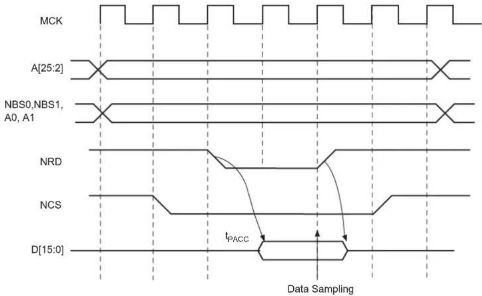
text_image
MCK A[25:2] NBS0,NBS1, A0, A1 NRD NCS D[15:0] tPACC Data Sampling30.10.2.2 Read is Controlled by NCS (READ\_MODE = 0)
Figure 30-9 shows the typical read cycle. The read data is valid t_PACC after the falling edge of the NCS signal and remains valid until the rising edge of NCS. Data must be sampled when NCS is raised. In that case, the READ_MODE must be configured to 0 (read is controlled by NCS): the SMC internally samples the data on the rising edge of the Master Clock that generates the rising edge of NCS, whatever the programmed waveform of NRD.
Figure 30-9: READ_MODE = 0: Data is Sampled by SMC before the Rising Edge of NCS

text_image
MCK A[25:2] NBS0,NBS1, A0, A1 NRD NCS D[15:0] tPACC Data Sampling30.10.3 Write Waveforms
The write protocol is similar to the read protocol. It is depicted in Figure 30-10. The write cycle starts with the address setting on the memory address bus.
30.10.3.1 NWE Waveforms
The NWE signal is characterized by a setup timing, a pulse width and a hold timing:
- NWE_SETUP: The NWE setup time is defined as the setup of address and data before the NWE falling edge.
- NWE_PULSE: The NWE pulse length is the time between NWE falling edge and NWE rising edge.
- NWE_HOLD: The NWE hold time is defined as the hold time of address and data after the NWE rising edge.
The NWE waveforms apply to all byte-write lines in Byte Write Access mode: NWR0 to NWR3.
30.10.3.2 NCS Waveforms
The NCS signal waveforms in write operations are not the same as those applied in read operations, but are separately defined:
- NCS_WR_SETUP: The NCS setup time is defined as the setup time of address before the NCS falling edge.
- NCS_WR_PULSE: The NCS pulse length is the time between NCS falling edge and NCS rising edge.
- NCS_WR_HOLD: The NCS hold time is defined as the hold time of address after the NCS rising edge.
Figure 30-10: Write Cycle

text_image
MCK A[25:2] NBS0, NBS1, A0, A1 NWE NCS NWE_SETUP NWE_PULSE NWE_HOLD NCS_WR_SETUP NCS_WR_PULSE NCS_WR_HOLD NWE_CYCLE30.10.3.3 Write Cycle
The write cycle time is defined as the total duration of the write cycle, that is, from the time where address is set on the address bus to the point where address may change. The total write cycle time is equal to:
NWE_CYCLE = NWE_SETUP + NWE_PULSE + NWE_HOLD,
as well as
NWE_CYCLE = NCS_WR_SETUP + NCS_WR_PULSE + NCS_WR_HOLD
All NWE and NCS (write) timings are defined separately for each chip select as an integer number of Master Clock cycles. The NWE_CYCLE field is common to both the NWE and NCS signals, thus the timing period is of the same duration.
NWE_CYCLE, NWE_SETUP, and NWE_PULSE implicitly define the NWE_HOLD value as:
NWE_HOLD = NWE_CYCLE - NWE_SETUP - NWE_PULSE
NWE_CYCLE, NCS_WR_SETUP, and NCS_WR_PULSE implicitly define the NCS_WR_HOLD value as:
NCS_WR_HOLD = NWE_CYCLE - NCS_WR_SETUP - NCS_WR_PULSE
30.10.4 Write Mode
The WRITE_MODE parameter in the HSMC_MODE register of the corresponding chip select indicates which signal controls the write operation.
30.10.4.1 Write is Controlled by NWE (WRITE\_MODE = 1)
Figure 30-11 shows the waveforms of a write operation with WRITE_MODE set to 1. The data is put on the bus during the pulse and hold steps of the NWE signal. The internal data buffers are switched to Output mode after the NWE_SETUP time, and until the end of the write cycle, regardless of the programmed waveform on NCS.
Figure 30-11: WRITE_MODE = 1. The write operation is controlled by NWE
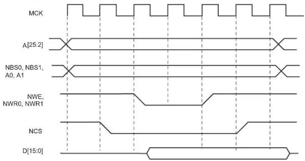
text_image
MCK A[25:2] NBS0, NBS1, A0, A1 NWE, NWR0, NWR1 NCS D[15:0]30.10.4.2 Write is Controlled by NCS (WRITE\_MODE = 0)
Figure 30-12 shows the waveforms of a write operation with WRITE_MODE configured to 0. The data is put on the bus during the pulse and hold steps of the NCS signal. The internal data buffers are switched to Output mode after the NCS_WR_SETUP time, and until the end of the write cycle, regardless of the programmed waveform on NWE.
Figure 30-12: WRITE_MODE = 0. The write operation is controlled by NCS
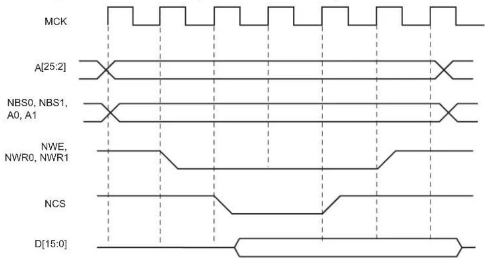
text_image
MCK A[25:2] NBS0, NBS1, A0, A1 NWE, NWR0, NWR1 NCS D[15:0]30.10.5 Coding Timing Parameters
All timing parameters are defined for one chip select and are grouped together in one register according to their type:
- The HSMC_SETUP register groups the definition of all setup parameters: NRD_SETUP, NCS_RD_SETUP, NWE_SETUP, NCS_WR_SETUP
- The HSMC_PULSE register groups the definition of all pulse parameters: NRD_PULSE, NCS_RD_PULSE, NWE_PULSE, NCS_WR_PULSE
- The HSMC_CYCLE register groups the definition of all cycle parameters: NRD_CYCLE, NWE_CYCLE
Table 30-6 shows how the timing parameters are coded and their permitted range.
Table 30-6: Coding and Range of Timing Parameters
| Coded Value Number of Bits Effective | Value | Permitted Range | |
| Coded Value Effective Value | |||
| setup [5:0] 6 128 x setup[5] + setup[4:0] | 0 ≤ setup ≤ 31 | 0..31 | |
| 32 ≤ setup ≤ 63 | 128..(128 + 31) | ||
| pulse [6:0] | 7 | 256 x pulse[6] + pulse[5:0] | 0 ≤ pulse ≤ 63 |
| 64 ≤ pulse ≤ 127 | |||
| cycle[8:0] | 9 | 256 x cycle[8:7] + cycle[6:0] | 0 ≤ cycle ≤ 127 |
| 128 ≤ cycle ≤ 255 | |||
| 256 ≤ cycle ≤ 383 | |||
| 384 ≤ cycle ≤ 511 | |||
30.10.6 Reset Values of Timing Parameters
Table 30-7 gives the default value of timing parameters at reset.
Table 30-7: Reset Values of Timing Parameters
| Register | Reset Value | Description |
| HSMC_SETUP | - | All setup timings are set to 1 |
| HSMC_PULSE | - | All pulse timings are set to 1 |
| HSMC_CYCLE | - | The read and write operations last three Master Clock cycles and provide one hold cycle. |
| WRITE_MODE | 1 | Write is controlled with NWE |
| READ_MODE | 1 | Read is controlled with NRD |
30.10.7 Usage Restriction
The SMC does not check the validity of the user-programmed parameters. If the sum of SETUP and PULSE parameters is larger than the corresponding CYCLE parameter, this leads to an unpredictable behavior of the SMC.
30.10.7.1 For Read Operations
Null but positive setup and hold of address and NRD and/or NCS cannot be guaranteed at the memory interface because of the propagation delay of these signals through external logic and pads. When positive setup and hold values must be verified, then it is strictly recommended to program non-null values so as to cover possible skews between address, NCS and NRD signals.
30.10.7.2 For Write Operations
If a null hold value is programmed on NWE, the SMC can ensure a positive hold of address, byte select lines, and NCS signal after the rising edge of NWE. This is true for WRITE_MODE = 1 only. See Section 30.12.2 Early Read Wait State.
30.10.7.3 For Read and Write Operations
A null value for pulse parameters is forbidden and may lead to an unpredictable behavior.
In read and write cycles, the setup and hold time parameters are defined in reference to the address bus. For external devices that require setup and hold time between NCS and NRD signals (read), or between NCS and NWE signals (write), these setup and hold times must be converted into setup and hold times in reference to the address bus.
30.11 Scrambling/Unscrambling Function
The external data bus D[15:0] can be scrambled in order to prevent intellectual property data located in off-chip memories from being easily recovered by analyzing data at the package pin level of either the microcontroller or the memory device.
The scrambling and unscrambling are performed on-the-fly without additional wait states.
The scrambling method depends on two user-configurable key registers, HSMC_KEY1 and HSMC_KEY2. These key registers are only accessible in Write mode.
The key must be securely stored in a reliable non-volatile memory in order to recover data from the off-chip memory. Any data scrambled with a given key cannot be recovered if the key is lost.
The scrambling/unscrambling function is enabled or disabled by configuring specific bits in the HSMC_OCMS and the HSMC_TIMINGSx registers. The bit configuration values to enable memory scrambling are summarized in Table 30-8.
Table 30-8: Scrambling Function Bit Encoding
| Memories | Bit Values | ||
| HSMC_OCMS.SMSE HSMC | OCMS.SRSE HSMC_TIMINGS | x.OCMS | |
| Off-chip Memories 1 0 1 | |||
| NAND Flash with NFC | 0 1 0 | ||
When the NAND Flash memory content is scrambled, the on-chip NFC SRAM page buffer associated for the transfer is also scrambled.
30.12 Automatic Wait States
Under certain circumstances, the SMC automatically inserts idle cycles between accesses to avoid bus contention or operation conflict.
30.12.1 Chip Select Wait States
The SMC always inserts an idle cycle between two transfers on separate chip selects. This idle cycle ensures that there is no bus contention between the de-activation of one device and the activation of the next one.
During chip select wait state, all control lines are turned inactive: NBS0 to NBS1, NWR0 to NWR1, NCS[0..3], and NRD lines. They are all set to 1.
Figure 30-13 illustrates a chip select wait state between access on Chip Select 0 and Chip Select 2.
Figure 30-13: Chip Select Wait State between a Read Access on NCS0 and a Write Access on NCS2

text_image
MCK A[25:2] NBS0, NBS1, A0,A1 NRD NWE NCS0 NCS2 D[15:0] NRD_CYCLE NWE_CYCLE Read to Write Wait State Chip Select Wait State30.12.2 Early Read Wait State
In some cases, the SMC inserts a wait state cycle between a write access and a read access to allow time for the write cycle to end before the subsequent read cycle begins. This wait state is not generated in addition to a chip select wait state. The early read cycle thus only occurs between a write and read access to the same memory device (same chip select).
An early read wait state is automatically inserted if at least one of the following conditions is valid:
- if the write controlling signal has no hold time and the read controlling signal has no setup time (Figure 30-14).
- in NCS Write Controlled mode (WRITE_MODE = 0), if there is no hold timing on the NCS signal and the NCS_RD_SETUP parameter is configured to 0, regardless of the Read mode (Figure 30-15). The write operation must end with an NCS rising edge. Without an Early Read Wait State, the write operation could not complete properly.
- in NWE Controlled mode (WRITE_MODE = 1) and if there is no hold timing (NWE_HOLD = 0), the feedback of the write control signal is used to control address, data, chip select and byte select lines. If the external write control signal is not inactivated as expected due to load capacitances, an Early Read Wait State is inserted and address, data and control signals are maintained one more cycle. See Figure 30-16.
Figure 30-14: Early Read Wait State: Write with No Hold Followed by Read with No Setup
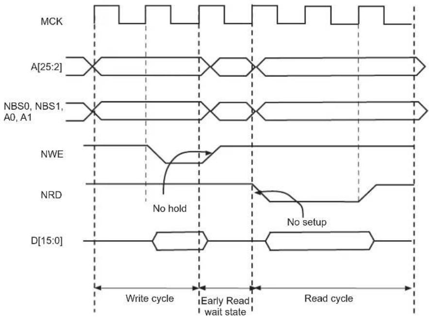
text_image
MCK A[25:2] NBS0, NBS1, A0, A1 NWE NRD D[15:0] Write cycle Early Read wait state Read cycle No hold No setupFigure 30-15: Early Read Wait State: NCS Controlled Write with No Hold Followed by a Read with No NCS Setup

text_image
MCK A[25:2] NBS0, NBS1, A0,A1 NCS NRD D[15:0] Write cycle (WRITE_MODE = 0) Early Read wait state (READ_MODE = 0 or READ_MODE = 1) Read cycleFigure 30-16: Early Read Wait State: NWE-controlled Write with No Hold Followed by a Read with one Set-up Cycle
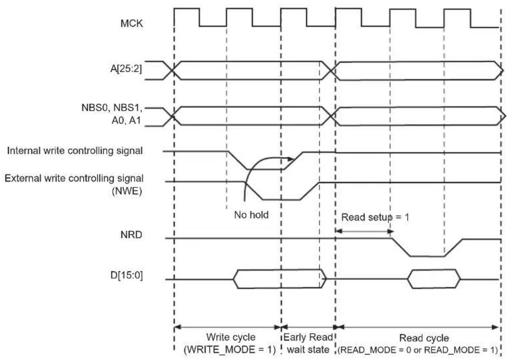
text_image
MCK A[25:2] NBS0, NBS1, A0, A1 Internal write controlling signal External write controlling signal (NWE) No hold Read setup = 1 NRD D[15:0] Write cycle (WRITE_MODE = 1) Early Read wait state Read cycle (READ_MODE = 0 or READ_MODE = 1)30.12.3 Reload User Configuration Wait State
The user may change any of the configuration parameters by writing the SMC user interface.
When detecting that a new user configuration has been written in the user interface, the SMC inserts a wait state before starting the next access. The so called "Reload User Configuration Wait State" is used by the SMC to load the new set of parameters to apply to next accesses.
The Reload Configuration Wait State is not applied in addition to the Chip Select Wait State. If accesses before and after re-programming the user interface are made to different devices (Chip Selects), then one single Chip Select Wait State is applied.
On the other hand, if accesses before and after writing the user interface are made to the same device, a Reload Configuration Wait State is inserted, even if the change does not concern the current Chip Select.
30.12.3.1 User Procedure
To insert a Reload Configuration Wait State, the SMC detects a write access to any HSMC_MODE register of the user interface. If only the timing registers are modified (HSMC_SETUP, HSMC_PULSE, HSMC_CYCLE registers) in the user interface, the user must validate the modification by writing the HSMC_MODE register, even if no change was made on the mode parameters.
30.12.3.2 Slow Clock Mode Transition
A Reload Configuration Wait State is also inserted when the Slow Clock Mode is entered or exited, after the end of the current transfer (see Section 30.15 Slow Clock Mode).
30.12.4 Read to Write Wait State
Due to an internal mechanism, a wait cycle is always inserted between consecutive read and write SMC accesses.
This wait cycle is referred to as a read to write wait state in this document.
This wait cycle is applied in addition to chip select and reload user configuration wait states when they are to be inserted. See Figure 30-13.
30.13 Data Float Wait States
Some memory devices are slow to release the external bus. For such devices, it is necessary to add wait states (data float wait states) after a read access:
- before starting a read access to a different external memory
- before starting a write access to the same device or to a different external one.
The Data Float Output Time ( t_DF ) for each external memory device is programmed in the TDF_CYCLES field of the HSMC_MODE register for the corresponding chip select. The value of TDF_CYCLES indicates the number of data float wait cycles (between 0 and 15) before the external device releases the bus, and represents the time allowed for the data output to go to high impedance after the memory is disabled.
Data float wait states do not delay internal memory accesses. Hence, a single access to an external memory with long t_DF will not slow down the execution of a program from internal memory.
The data float wait states management depends on the READ_MODE and the TDF_MODE bits of the HSMC_MODE register for the corresponding chip select.
30.13.1 READ\_MODE
Setting READ_MODE to 1 indicates to the SMC that the NRD signal is responsible for turning off the tri-state buffers of the external memory device. The Data Float Period then begins after the rising edge of the NRD signal and lasts TDF_CYCLES MCK cycles.
When the read operation is controlled by the NCS signal (READ_MODE = 0), the TDF_CYCLES field in HSMC_MODEx gives the number of MCK cycles during which the data bus remains busy after the rising edge of NCS.
Figure 30-17 illustrates the Data Float Period in NRD-controlled mode (READ_MODE = 1), assuming a data float period of two cycles (TDF_CYCLES = 2). Figure 30-18 shows the read operation when controlled by NCS (READ_MODE = 0) and the TDF_CYCLES parameter equals 3.
Figure 30-17: TDF Period in NRD Controlled Read Access (TDF = 2)

text_image
MCK A[25:2] NBS0, NBS1, A0, A1 NRD NCS D[15:0] tpacc TDF = 2 clock cycles NRD controlled read operationFigure 30-18: TDF Period in NCS Controlled Read Operation (TDF = 3)

text_image
MCK A[25:2] NBS0, NBS1, A0,A1 NRD NCS D[15:0] tpacc TDF = 3 clock cycles NCS controlled read operation30.13.2 TDF Optimization Enabled (TDF\_MODE = 1)
When the TDF_MODE of the HSMC_MODE register is set to 1 (TDF optimization is enabled), the SMC takes advantage of the setup period of the next access to optimize the number of wait states cycle to insert.
Figure 30-19 shows a read access controlled by NRD, followed by a write access controlled by NWE, on Chip Select 0. Chip Select 0 has been programmed with:
NRD_HOLD = 4; READ_MODE = 1 (NRD controlled)
NWE_SETUP = 3; WRITE_MODE = 1 (NWE controlled)
TDF_CYCLES = 6; TDF_MODE = 1 (optimization enabled).
Figure 30-19: TDF Optimization: No TDF wait states are inserted if the TDF period is over when the next access begins

other
| Signal | Description | |--------|--------------------------------| | MCK | Waveform with square pulses | | A[25:2] | Cross wave pattern | | NRD | NRD HOLD = 4 | | NWE | NWE SETUP = 3 | | NCS0 | NCS0 waveform with TDF_CYCLE = 6 | | D[15:0] | D-shaped waveform with TDF_CYCLE = 6 |30.13.3 TDF Optimization Disabled (TDF\_MODE = 0)
When optimization is disabled, TDF wait states are inserted at the end of the read transfer, so that the data float period ends when the second access begins. If the hold period of the read1 controlling signal overlaps the data float period, no additional TDF wait states will be inserted.
Figure 30-20, Figure 30-21 and Figure 30-22 illustrate the cases:
- read access followed by a read access on another chip select,
- read access followed by a write access on another chip select,
- read access followed by a write access on the same chip select,
with no TDF optimization.
Figure 30-20: TDF Optimization Disabled (TDF Mode = 0). TDF wait states between 2 read accesses on different chip selects
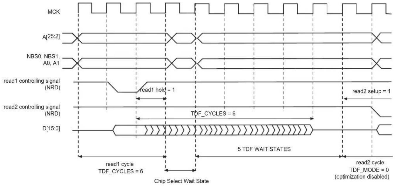
text_image
MCK A[25:2] NBS0, NBS1, A0, A1 read1 controlling signal (NRD) read1 hold = 1 read2 setup = 1 read2 controlling signal (NRD) D[15:0] TDF_CYCLES = 6 5 TDF WAIT STATES read1 cycle TDF_CYCLES = 6 read2 cycle TDF_MODE = 0 (optimization disabled) Chip Select Wait StateFigure 30-21: TDF Mode = 0: TDF wait states between a read and a write access on different chip selects
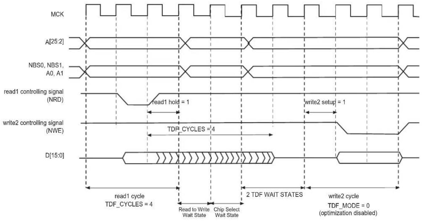
text_image
MCK A[25:2] NBS0, NBS1, A0, A1 read1 controlling signal (NRD) read1 hold = 1 write2 setup = 1 write2 controlling signal (NWE) TDF_CYCLES = 4 D[15:0] read1 cycle TDF_CYCLES = 4 Read to Write Wait State Chip Select Wait State 2 TDF WAIT STATES write2 cycle TDF_MODE = 0 (optimization disabled)Figure 30-22: TDF Mode = 0: TDF wait states between read and write accesses on the same chip select
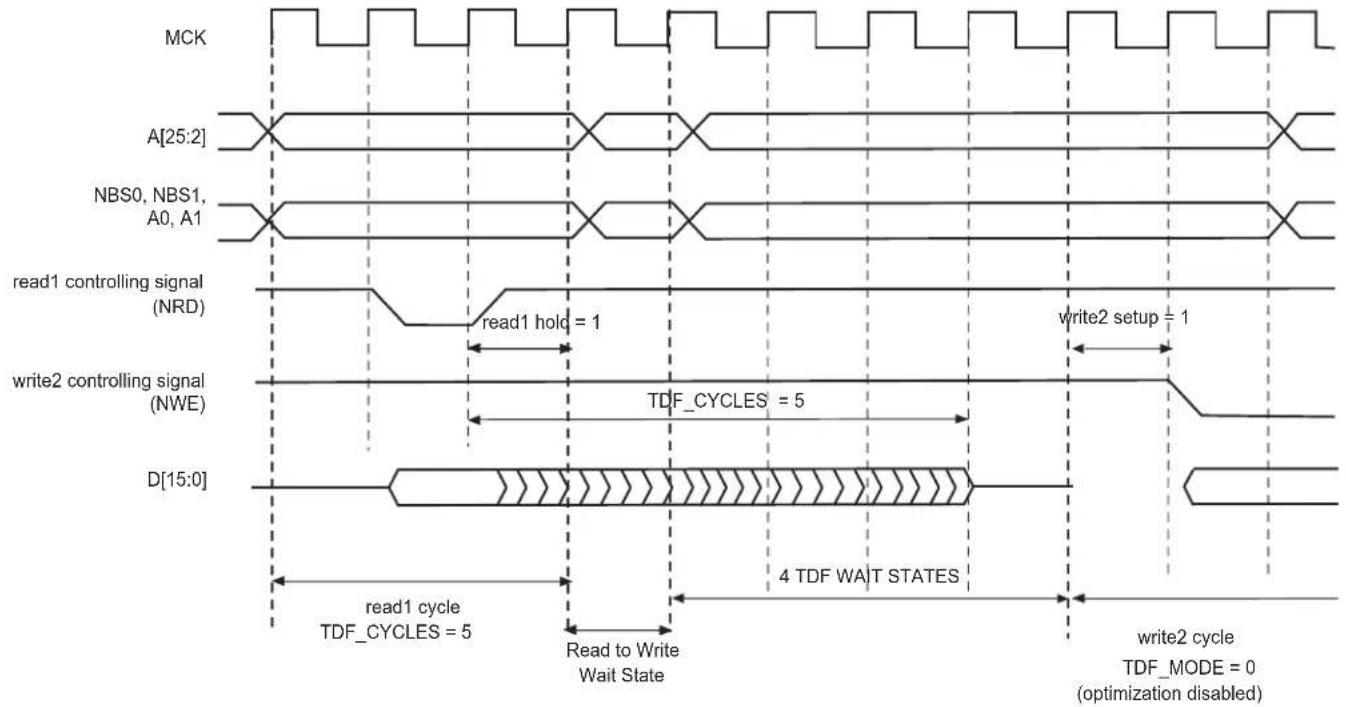
text_image
MCK A[25:2] NBS0, NBS1, A0, A1 read1 controlling signal (NRD) read1 hold = 1 write2 setup = 1 write2 controlling signal (NWE) TDF_CYCLES = 5 D[15:0] read1 cycle TDF_CYCLES = 5 Read to Write Wait State 4 TDF WAIT STATES write2 cycle TDF_MODE = 0 (optimization disabled)30.14 External Wait
Any access can be extended by an external device using the NWAIT input signal of the SMC. The EXNW_MODE field of the HSMC_MODE register on the corresponding chip select must be set to either '10' (Frozen mode) or '11' (Ready mode). When the EXNW_MODE is set to '00' (disabled), the NWAIT signal is simply ignored on the corresponding chip select. The NWAIT signal delays the read or write operation in regards to the read or write controlling signal, depending on the Read and Write modes of the corresponding chip select.
30.14.1 Restriction
When one of the EXNW_MODE is enabled, it is mandatory to program at least one hold cycle for the read/write controlling signal. For that reason, the NWAIT signal cannot be used in Slow Clock Mode (Section 30.15 Slow Clock Mode).
The NWAIT signal is assumed to be a response of the external device to the read/write request of the SMC. NWAIT is then examined by the SMC in the pulse state of the read or write controlling signal. The assertion of the NWAIT signal outside the expected period has no impact on the SMC behavior.
30.14.2 Frozen Mode
When the external device asserts the NWAIT signal (active low), and after an internal synchronization of this signal, the SMC state is frozen, i.e., SMC internal counters are frozen, and all control signals remain unchanged. When the resynchronized NWAIT signal is deasserted, the SMC completes the access, resuming the access from the point where it was stopped. See Figure 30-23. This mode must be selected when the external device uses the NWAIT signal to delay the access and to freeze the SMC.
The assertion of the NWAIT signal outside the expected period is ignored as illustrated in Figure 30-24.
Figure 30-23: Write Access with NWAIT Assertion in Frozen Mode (EXNW_MODE = 10)

other
| Signal | Value | |-----------------|-------| | MCK | 0 | | A[25:2] | 10 | | NBS0, NBS1, A0,A1 | 0 | | NWE | 4 | | NCS | 456 | | D[15:0] | 0 | | NWAIT | 0 | | Internally synchronized NWAIT signal | 0 |NWE_PULSE = 5 NCS_WR_PULSE = 7
Figure 30-24: Read Access with NWAIT Assertion in Frozen Mode (EXNW_MODE = 10)
other
| Signal | Read Cycle | |--------|------------| | MCK | 0 | | A[25:2] | 0 | | NBS0 | 0 | | NBS1 | 0 | | A0,A1 | 0 | | NCS | 4 | | NRD | 1 | | NWAIT | 0 | | Internally synchronized NWAIT signal | 0 |30.14.3 Ready Mode
In Ready mode (EXNW_MODE = 11), the SMC behaves differently. Normally, the SMC begins the access by down counting the setup and pulse counters of the read/write controlling signal. In the last cycle of the pulse phase, the resynchronized NWAIT signal is examined.
If asserted, the SMC suspends the access as shown in Figure 30-25 and Figure 30-26. After deassertion, the access is completed: the hold step of the access is performed.
This mode must be selected when the external device uses deassertion of the NWAIT signal to indicate its ability to complete the read or write operation.
If the NWAIT signal is deasserted before the end of the pulse, or asserted after the end of the pulse of the controlling read/write signal, it has no impact on the access length as shown in Figure 30-26.
Figure 30-25: NWAIT Assertion in Write Access: Ready Mode (EXNW_MODE = 11)

other
| Signal | Value | |-----------------|-------| | MCK | 0 | | A[25:2] | 0 | | NBS0, NBS1, A0,A1 | 0 | | NWE | 4 | | NCS | 456 | | D[15:0] | 0 | | NWAIT | 0 | | Internally synchronized NWAIT signal | 0 |EXNW_MODE = 11 (Ready mode)
WRITE_MODE = 1 (NWE_controlled)
NWE PULSE = 5
NCS_WR_PULSE = 7
Figure 30-26: NWAIT Assertion in Read Access: Ready Mode (EXNW_MODE = 11)

other
| Signal | Value | |-----------------|-------| | MCK | 0 | | A[25:2] | 0 | | NBS0, NBS1, A0,A1 | 0 | | NCS | 456 | | NRD | 456 | | NWAIT | 0 | | Internally synchronized NWAIT signal | 0 |30.14.4 NWAIT Latency and Read/Write Timings
There may be a latency between the assertion of the read/write controlling signal and the assertion of the NWAIT signal by the device. The programmed pulse length of the read/write controlling signal must be at least equal to this latency plus the 2 cycles of resynchronization + 1 cycle. Otherwise, the SMC may enter the hold state of the access without detecting the NWAIT signal assertion. This is true in Frozen mode as well as in Ready mode. This is illustrated on Figure 30-27.
When EXNW_MODE is enabled (ready or frozen), the user must program a pulse length of the read and write controlling signal of at least: minimal pulse length = NWAIT latency + 2 resynchronization cycles + 1 cycle
Figure 30-27: NWAIT Latency
other
| Signal State | Description | | ------------ | --------------------------------- | | MCK | Time wave pulses | | A[25:2] | Linear pulse width | | NBS0, NBS1, A0,A1 | Linear pulse width | | NRD | Minimal pulse length | | NWAIT | Resynchronization cycles | | Internally synchronized NWAIT signal | Read cycle | | Wait STATE | Wait state | | Read_cycle | Read cycle | | EXNW_MODE | MODE = 10 or 11 | | READ_MODE | MODE = 1 (NRD_controlled) | | NRD_PULSE | Pulse length |30.15 Slow Clock Mode
The SMC is able to automatically apply a set of "Slow Clock mode" read/write waveforms when an internal signal driven by the Power Management Controller is asserted because MCK has been configured to a very slow clock rate (typically 32 kHz clock rate). In this mode, the user-programmed waveforms are ignored and the Slow Clock mode waveforms are applied. This mode is provided so as to avoid reprogramming the User Interface with appropriate waveforms at very slow clock rate. When activated, the Slow mode is active on all chip selects.
30.15.1 Slow Clock Mode Waveforms
Figure 30-28 illustrates the read and write operations in Slow Clock mode. They are valid on all chip selects. Table 30-9 indicates the value of read and write parameters in Slow Clock mode.
Figure 30-28: Write/Read Cycles in Slow Clock Mode
text_image
MCK A[25:2] NBS0, NBS1, A0,A1 NWE NCS 1 1 1 NWE_CYCLE = 3 SLOW CLOCK MODE WRITE
text_image
MCK A[25:2] NBS0, NBS1, A0,A1 NRD NCS NRD_CYCLE = 2 SLOW CLOCK MODE READTable 30-9: Read and Write Timing Parameters in Slow Clock Mode
| Read Parameters Duration (cycles) Write Parameters Duration (cycles) | |||
| NRD_SETUP 1 NWE_SETUP 1 | |||
| NRD_PULSE 1 NWE_PULSE 1 | |||
| NCS_RD_SETUP | 0 NCS_WR_SETUP | 0 | |
| NCS_RD_PULSE | 2 NCS_WR_PULSE | 3 | |
| NRD_CYCLE 2 NWE_CYCLE 3 | |||
30.15.2 Switching from (to) Slow Clock Mode to (from) Normal Mode
When switching from Slow Clock mode to Normal mode, the current Slow Clock mode transfer is completed at high clock rate, with the set of Slow Clock mode parameters. See Figure 30-29. The external device may not be fast enough to support such timings.
Figure 30-30 illustrates the recommended procedure to properly switch from one mode to the other.
Figure 30-29: Clock Rate Transition occurs while the SMC is performing a Write Operation
text_image
Slow Clock Mode internal signal from PMC MCK A[25:2] NBS0, NBS1, A0, A1 NWE NCS NWE_CYCLE = 3 SLOW CLOCK MODE WRITE SLOW CLOCK MODE WRITE This write cycle finishes with the slow clock mode set of parameters after the clock rate transition Slow clock mode transition is detected: Reload Configuration Wait State NWE_CYCLE = 7 NORMAL MODE WRITEFigure 30-30: Recommended Procedure to Switch from Slow Clock Mode to Normal Mode or from Normal Mode to Slow Clock Mode
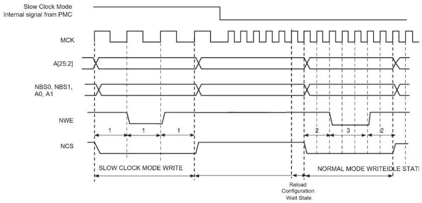
text_image
Slow Clock Mode Internal signal from PMC MCK A[25:2] NBS0, NBS1, A0, A1 NWE NCS SLOW CLOCK MODE WRITE Reload Configuration Wait State NORMAL MODE WRITEIDLE STATI30.16 Register Write Protection
To prevent any single software error that may corrupt SMC behavior, selected registers can be write-protected by setting the WPEN bit in the Write Protection Mode Register (HSMC_WPMR).
If a write access in a write-protected register is detected, then the WPVS flag in the Write Protection Status Register (HSMC_WPSR) is set and the field WPVSRC indicates in which register the write access has been attempted.
The WPVS flag is automatically reset after reading the HSMC_WPSR.
The following registers can be write-protected:
- Setup Register
- Pulse Register
- Cycle Register
- Timings Register
- Mode Register
30.17 NFC Operations
30.17.1 NFC Overview
The NFC handles all the command, address and data sequences of the NAND low level protocol. An SRAM is used as an internal read/write buffer when data is transferred from or to the NAND.
30.17.2 NFC Control Registers
NAND Flash Read and NAND Flash Program operations can be performed through the NFC Command Registers. In order to minimize CPU intervention and latency, commands are posted in a command buffer. This buffer provides zero wait state latency. The detailed description of the command encoding scheme is explained below.
The NFC handles an automatic transfer between the external NAND Flash and the chip via the NFC SRAM. It is done via NFC Command Registers.
The NFC Command Registers are very efficient to use. When writing to these registers:
- the address of the register (NFCADDR_CMD) is the command used
- the data of the register (NFCDATA_ADDT) is the address to be sent to the NAND Flash
So, in one single access the command is sent and immediately executed by the NFC. Two commands can even be programmed within a single access (CMD1, CMD2) depending on the VCMD2 value.
The NFC can send up to five address cycles.
Figure 30-31 shows a typical NAND Flash Page Read Command of a NAND Flash Memory and correspondence with NFC Address Command Register.
Figure 30-31: NFC/NAND Flash Access Example
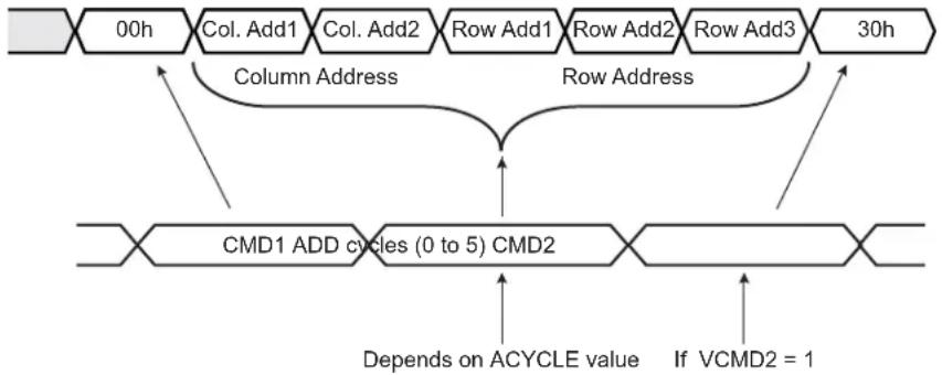
flowchart
graph TD
    A["00h"] --> B["Col. Add1"]
    B --> C["Col. Add2"]
    C --> D["Row Add1"]
    D --> E["Row Add2"]
    E --> F["Row Add3"]
    F --> G["30h"]
    H["Column Address"] --> I["Row Address"]
    I --> J["CMD1 ADD cycles (0 to 5) CMD2"]
    J --> K["Depends on ACYCLE value"]
    J --> L["If VCMD2 = 1"]
For more details refer to Section 30.17.2.2 NFC Address Command.
Reading the NFC Command Register (to any address) will give the status of the NFC. This is especially useful to know if the NFC is busy, for example.
30.17.2.1 Building NFC Address Command Example
The base address is made of HOST_ADDR address.
Page read operation example:
// Build the Address Command (NFCADDR_CMD)
AddressCommand = (HOST_ADDR |
    NFCCMD=1 | // NFC Command Enable
    NFCWR=0    // NFC Read Data from NAND Flash
    DATAEN=1    |    // NFC Data phase Enable.
    CSID=1    |    // Chip Select ID = 1
    ACYCLE=5    |    // Number of address cycle.
    VCMD2=1    |    // CMD2 is sent after Address Cycles
    CMD2=0x30    |    // CMD2 = 30h
    CMD1=0x0)    // CMD1 = Read Command = 00h

// Set the Address for Cycle 0
HSMC_ADDR = Col. Add1

// Write command with the Address Command built above
*AddressCommand = (Col. Add2    | // ADDR_CYCLE1
    Row Add1    | // ADDR_CYCLE2
    Row Add2    | // ADDR_CYCLE3
    Row Add3    )// ADDR_CYCLE4
30.17.2.2 NFC Address Command
Name: NFCADDR_CMD
Access: Read/Write
31 30 29 28 27 26 25 24
| - | - | - | - | - | N | F | C |
23 22 21 20 19 18 17 16
| CSID ACYCLE VCMD2 CMD2 |
| 15 14 13 12 11 10 | 9 | 8 | ||||
| CMD2 | CMD1 | |||||
| 7 | 6 | 5 | 4 | 3 | 2 | 1 |
| CMD1 | - | - | ||||
CMD1: Command Register Value for Cycle 1
If NFCCMD is set, when a read or write access occurs, the NFC sends this command.
CMD2: Command Register Value for Cycle 2
If NFCCMD and VCMD2 field are set to one, the NFC sends this command after CMD1.
VCMD2: Valid Cycle 2 Command
When set to true, the CMD2 field is issued after the address cycle.
ACYCLE: Number of Address Required for the Current Command
When ACYCLE field is different from zero, ACYCLE Address cycles are performed after Command Cycle 1. The maximum number of cycles is 5.
CSID: Chip Select Identifier
Chip select used
DATAEN: NFC Data Phase Enable
When set to true, the NFC will automatically read or write data after the command.
NFCWR: NFC Write Enable
0: NFC reads data from the NAND Flash.
1: NFC writes data into the NAND Flash.
30.17.2.3 NFC Data Address
Name: NFCDATA_ADDT
Access: Write-only
31 30 29 28 27 26 25 24
ADDR_CYCLE4
23 22 21 20 19 18 17 16
ADDR_CYCLE3
15 14 13 12 11 10 9 8
ADDR_CYCLE2
7 6 5 4 3 2 1 0
ADDR_CYCLE1
ADDR\_CYCLE1: NAND Flash Array Address Cycle 1
When less than five address cycles are used, ADDR_CYCLE1 is the first byte written to the NAND Flash.
When five address cycles are used, ADDR_CYCLE1 is the second byte written to NAND Flash.
ADDR\_CYCLE2: NAND Flash Array Address Cycle 2
When less than five address cycles are used, ADDR_CYCLE2 is the second byte written to the NAND Flash.
When five address cycles are used, ADDR_CYCLE2 is the third byte written to the NAND Flash.
ADDR\_CYCLE3: NAND Flash Array Address Cycle 3
When less than five address cycles are used, ADDR_CYCLE3 is the third byte written to the NAND Flash.
When five address cycles are used, ADDR_CYCLE3 is the fourth byte written to the NAND Flash.
ADDR\_CYCLE4: NAND Flash Array Address Cycle 4
When less than five address cycles are used, ADDR_CYCLE4 is the fourth byte written to the NAND Flash.
When five address cycles are used, ADDR_CYCLE4 is the fifth byte written to the NAND Flash.
Note: If five address cycles are used, the first address cycle is ADDR_CYCLE0. Refer to HSMC_ADDR register.
30.17.2.4 NFC DATA Status
Name: NFCDATA_STATUS
Access: Read-only
31 30 29 28 27 26 25 24
| - | - | - | - | N | F | C | B |
23 22 21 20 19 18 17 16
| CSID ACYCLE VCMD2 CMD2 |
| 15 14 13 12 | 11 10 | 9 | 8 | |||
| CMD2 | CMD1 | |||||
| 7 | 6 | 5 | 4 | 3 | 2 | 1 |
| CMD1 | - | - | ||||
CMD1: Command Register Value for Cycle 1
When a Read or Write Access occurs, the Physical Memory Interface drives the IO bus with CMD1 field during the Command Latch cycle 1.
CMD2: Command Register Value for Cycle 2
When VCMD2 bit is set to true, the Physical Memory Interface drives the IO bus with CMD2 field during the Command Latch cycle 2.
VCMD2: Valid Cycle 2 Command
When set to true, the CMD2 field is issued after addressing cycle.
ACYCLE: Number of Address Required for the Current Command
When ACYCLE field is different from zero, ACYCLE Address cycles are performed after Command Cycle 1.
CSID: Chip Select Identifier
Chip select used
DATAEN: NFC Data Phase Enable
When set to true, the NFC data phase is enabled.
NFCWR: NFC Write Enable
0: NFC is in Read mode.
1: NFC is in Write mode.
NFCBUSY: NFC Busy Status Flag
If set to true, it indicates that the NFC is busy.
30.17.3 NFC Initialization
Prior to any Command and Data Transfer, the SMC User Interface must be configured to meet the device timing requirements.
- Write enable Configuration
Use NWE_SETUP, NWE_PULSE and NWE_CYCLE to define the write enable waveform according to the external device datasheet.
Use TADL field in the HSMC_TIMINGS register to configure the timing between the last address latch cycle and the first rising edge of WEN for data input.
Figure 30-32: Write Enable Timing Configuration

text_image
mck wen t_WEN_SETUP t_WEN_PULSE t_WEN_HOLD t_WEN_CYCLESFigure 30-33: Write Enable Timing for NAND Flash Device Data Input Mode
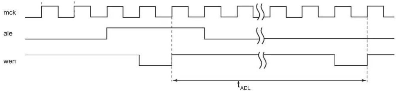
text_image
mck ale wen tADL- Read Enable Configuration
Use NRD_SETUP, NRD_PULSE and NRD_CYCLE to define the read enable waveform according to the external device datasheet.
Use TAR field in the HSMC_TIMINGS register to configure the timings between the address latch enable falling edge to read the enable falling edge.
Use TCLR field in the HSMC_TIMINGS register to configure the timings between the command latch enable falling edge to read the enable falling edge.
Figure 30-34: Read Enable Timing Configuration Working with NAND Flash Device

other
| Signal | Time Segment Start | Time Segment End | |--------|---------------------|-------------------| | mck | 0 | 1 | | cen | 1 | 2 | | ale | 2 | 3 | | cle | 3 | 4 | | ren | 4 | 5 |- Ready/Busy Signal Timing configuration working with a NAND Flash device
Use TWB field in HSMC_TIMINGS register to configure the maximum elapsed time between the rising edge of the wen signal and the falling edge of the rbn signal. Use TRR field in the HSMC_TIMINGS register to program the number of clock cycles between the rising edge of the rbn signal and the falling edge of the ren signal.
Figure 30-35: Ready/Busy Timing Configuration
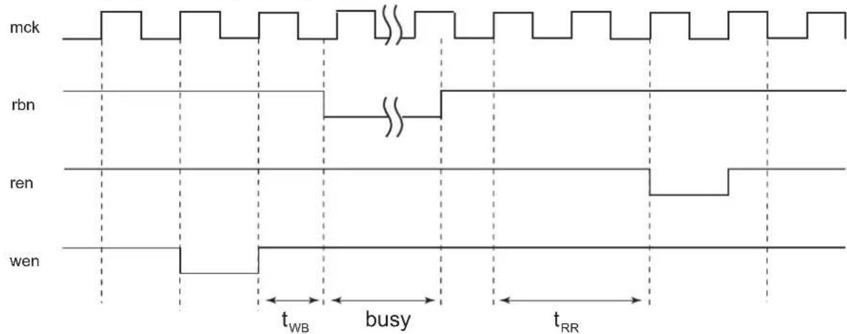
other
| Signal | Time Segment Start | Time Segment End | |--------|---------------------|-------------------| | mck | 0 | 0 | | rbn | 0 | 0 | | ren | 0 | 0 | | wen | 0 | 0 |30.17.3.1 NFC Timing Engine
When the NFC Command register is written, the NFC issues a NAND Flash Command and optionally performs a data transfer between the NFC SRAM and the NAND Flash device. The NFC timing engine ensures valid NAND Flash timings, depending on the set of parameters decoded from the address bus. These timings are defined in the HSMC_TIMINGS register.
For information on the timing used depending on the command, see Figure 30-36.
Figure 30-36: NFC Timing Engine
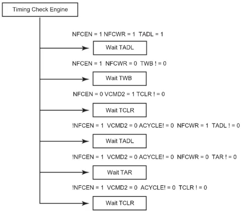
flowchart
graph TD
    A["Timing Check Engine"] --> B["NFCEN = 1 NFCWR = 1 TADL = 1"]
    B --> C["Wait TADL"]
    B --> D["NFCEN = 1 NFCWR = 0 TWB != 0"]
    D --> E["Wait TWB"]
    B --> F["NFCEN = 0 VCMD2 = 1 TCLR != 0"]
    F --> G["Wait TCLR"]
    F --> H["!NFCEN = 1 VCMD2 = 0 ACYCLE != 0 NFCWR = 1 TADL != 0"]
    H --> I["Wait TADL"]
    H --> J["!NFCEN = 1 VCMD2 = 0 ACYCLE != 0 NFCWR = 0 TAR != 0"]
    J --> K["Wait TAR"]
    J --> L["!NFCEN = 1 VCMD2 = 0 ACYCLE != 0 TCLR != 0"]
    L --> M["Wait TCLR"]
See the NFC Address Command register description and the Timings Register.
30.17.4 NFC SRAM
If the NFC is used to read and write data from and to the NAND Flash, the configuration depends on the page size (PAGESIZE field in HSMC_CFG register). See Table 30-10 to Table 30-14 for detailed mapping.
The NFC can handle the NAND Flash with a page size of 8 Kbytes or lower (such as 2 Kbytes, for example). In case of a 4 Kbyte or lower page size, the NFC SRAM can be split into two banks. The BANK bit in the HSMC_BANK register is used to select where NAND flash data are written or read. For an 8 Kbyte page size this field is not relevant.
Note that a “Ping-Pong” mode (write or read to a bank while the NFC writes or reads to another bank) is accessible with the NFC (using two different banks).
If the NFC is not used, the NFC SRAM can be used for a general purpose by the application.
Table 30-10: NFC SRAM Bank Mapping for 512 bytes
| Offset Use Access | ||
| 0x00000000-0x000001FF Main | Area Bank 0 Read/Write | |
| 0x00000200-0x000003FF Spare | Area Bank 0 Read/Write | |
| 0x00001200-0x000013FF Main | Area Bank 1 Read/Write | |
| 0x00001400-0x000015FF Spare | Area Bank 1 Read/Write |
Table 30-11: NFC SRAM Bank Mapping for 1 Kbyte
| Offset Use Access | ||
| 0x00000000-0x000003FF Main Area Bank 0 Read/Write | ||
| 0x00000400-0x000005FF Spare Area Bank 0 Read/Write | ||
| 0x00001200-0x000015FF Main Area Bank 1 Read/Write | ||
| 0x00001600-0x000017FF Spare Area Bank 1 Read/Write |
Table 30-12: NFC SRAM Bank Mapping for 2 Kbytes
| Offset Use Access | ||
| 0x00000000-0x000007FF Main Area Bank 0 Read/Write | ||
| 0x00000800-0x000009FF Spare Area Bank 0 Read/Write | ||
| 0x00001200-0x000019FF Main Area Bank 1 Read/Write | ||
| 0x00001A00-0x00001BFF | Spare Area Bank 1 Read/Write | |
Table 30-13: NFC SRAM Bank Mapping for 4 Kbytes
| Offset Use Access | ||
| 0x00000000-0x00000FFF | Main Area Bank 0 Read/Write | |
| 0x00001000-0x000011FF | Spare Area Bank 0 Read/Write | |
| 0x00001200-0x000021FF Main Area Bank 1 Read/Write | ||
| 0x00002200-0x000023FF Spare Area Bank 1 Read/Write | ||
Table 30-14: NFC SRAM Bank Mapping for 8 Kbytes, only one bank is available
| Offset Use Access | ||
| 0x00000000-0x00001FFF | Main Area Bank 0 Read/Write | |
| 0x00002000-0x000023FF Spare | Area Bank 0 Read/Write |
30.17.4.2 NFC SRAM Access Prioritization Algorithm
When the NFC is reading from or writing to an NFC SRAM bank, the other bank is available. If an NFC SRAM access occurs when the NFC performs a read or write operation in the same bank, then the access is discarded. The write operation is not performed. The read operation returns undefined data. If this situation is encountered, the AWB status flag located in the NFC Status Register is raised and indicates that a shared resource access violation has occurred.
30.17.5 NAND Flash Operations
This section describes the software operations needed to issue commands to the NAND Flash device and to perform data transfers using the NFC.
30.17.5.1 Page Read
Figure 30-37: Page Read Flow Chart

flowchart
graph TD
    A["Configure the device writing in the User Interface"] --> B["Write the NFC Command registers"]
    B --> C["Enable XFRDONE interrupt (SMC_IER)"]
    C --> D["Wait for Interrupt"]
    D --> E["Copy data from NFC SRAM to application memory (via DMA for example)"]
    E --> F["Check Error Correcting Codes"]
    G["Using NFC"] --> B
Note that, instead of using the interrupt, one can poll the NFCBUSY flag.
For more information on the NFC Control Register, see Section 30.17.2.2 NFC Address Command.
30.17.5.2 Program Page
Figure 30-38: Program Page Flow Chart
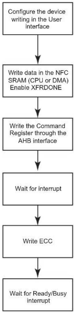
flowchart
graph TD
    A["Configure the device writing in the User interface"] --> B["Write data in the NFC SRAM (CPU or DMA) Enable XFRDONE"]
    B --> C["Write the Command Register through the AHB interface"]
    C --> D["Wait for interrupt"]
    D --> E["Write ECC"]
    E --> F["Wait for Ready/Busy interrupt"]
Writing the ECC cannot be done using the NFC; it needs to be done "manually".
Note that, instead of using the interrupt, one can poll the NFCBUSY flag.
For more information on the NFC Control Register, see Section 30.17.2.2 NFC Address Command.
30.18 PMECC Controller Functional Description
The Programmable Multibit Error Correcting Code (PMECC) controller is a programmable binary BCH (Bose, Chaudhuri and Hocquenghem) encoder/decoder. This controller can be used to generate redundancy information for both SLC and MLC NAND devices. It supports redundancy for correction of 2, 4, 8, 12, or 24 errors per sector of data. The sector size is programmable and can be set to 512 bytes or 1024 bytes. The PMECC module generates redundancy at encoding time, when a NAND write page operation is performed. The redundancy is appended to the page and written in the spare area. This operation is performed by the processor. It moves the content of the PMECCX registers into the NAND flash memory. The number of registers depends on the selected error correction capability (see Table 30-15 Relevant Redundancy Registers). This operation shall be executed for each sector. At decoding time, the PMECC module generates the remainders of the received codeword by the minimal polynomials. When all remainders for a given sector are set to zero, no error occurred. When the remainders are different from zero, the codeword is corrupted and further processing is required.
The PMECC module generates an interrupt indicating that an error occurred. The processor must read the PMECC Interrupt Status Register (HSMC_PMECCISR). This register indicates which sector is corrupted.
The processor must execute the following decoding steps to find the error location within a sector:
- Syndrome computation.
- Finding the error location polynomial.
- Finding the roots of the error location polynomial.
All decoding steps involve finite field computation. It means that a library of finite field arithmetic must be available to perform addition, multiplication and inversion. These arithmetic operations can be performed through the use of a memory mapped look-up table, or direct software implementation. The software implementation presented is based on look-up tables. Two tables named gf_log and gf_antilog are used. If alpha is the primitive element of the field, then a power of alpha is in the field. Assuming that beta = alpha^ index, then beta belongs to the field, and gf_log(beta) = gf_log(alpha^ index) = index. The gf_antilog table provides exponent inverse of the element; if beta = alpha^ index, then gf_antilog(index) = beta.
The first step consists in the syndrome computation. The PMECC module computes the remainders and the software must substitute the power of the primitive element. The procedure implementation is given in Section 30.19.1 Remainder Substitution Procedure.
The second step is the most software intensive. It is the Berlekamp's iterative algorithm for finding the error-location polynomial. The procedure implementation is given in Section 30.19.2 Finding the Error Location Polynomial Sigma(x).
The Last step is finding the root of the error location polynomial. This step can be very software intensive. Indeed there is no straightforward method of finding the roots, except evaluating each element of the field in the error location polynomial. However, a hardware accelerator can be used to find the roots of the polynomial. The PMERRLOC module provides this kind of hardware acceleration.
Figure 30-39: Software Hardware Multibit Error Correction Dataflow
flowchart
graph TD
    A["NAND Flash PROGRAM PAGE Operation"] --> B["Software Hardware"]
    C["NAND Flash READ PAGE Operation"] --> D["Software Accelerator"]
    B --> E["Configure PMECC: error correction capability sector size/page size NAND write field set to true spare area desired layout"]
    E --> F["Move the NAND Page to external Memory whether using DMA or Processor"]
    F --> G["Copy redundancy from PMECC user interface to user-defined spare area using DMA or Processor."]
    D --> H["Configure PMECC: error correction capability sector size/page size NAND write field set to false spare area desired layout"]
    H --> I["Move the NAND Page from external Memory whether using DMA or Processor"]
    I --> J["If a sector is corrupted use the substitute() function to determine the syndromes."]
    J --> K["When the table of syndromes is completed, use the get_sigma() function to get the error location polynomial."]
    K --> L["Find the error positions finding the roots of the error location polynomial And correct the bits."]
    D --> M["Accelerator"]
    M --> N["PMECC computes polynomial remainders as the data is read from external memory"]
    N --> O["PMECC modules indicate if at least one error is detected."]
    O --> P["This step can be hardware-assisted using the PMERRLOC module."]
30.18.1 MLC/SLC Write Page Operation Using PMECC
When an MLC write page operation is performed, the PMECC controller is configured with the NANDWR bit of the PMECCFG register set to one. When the NAND spare area contains file system information and redundancy (PMECCx), the spare area is error protected, then the SPAREEN bit of the PMECCFG register is set. When the NAND spare area contains only redundancy information, the SPAREEN bit is cleared.
When the write page operation is terminated, the user writes the redundancy in the NAND spare area. This operation can be done with DMA assistance.
Table 30-15: Relevant Redundancy Registers
| BCH_ERR Field | Sector Size Set to 512 Bytes | Sector Size Set to 1024 Bytes |
| 0 PMECC0 | PMECC0 | |
| 1 PMECC0 | PMECC1 PMECC0, PMECC1 | |
| 2 PMECC0 | PMECC1, PMECC2, PMECC3 PMECC0, PMECC1 | PMECC2, PMECC3 |
| 3 | PMECC0, PMECC1, PMECC2, PMECC3,PMECC4, PMECC5, PMECC6 | PMECC0, PMECC1, PMECC2, PMECC3,PMECC4, PMECC5, PMECC6 |
| 4 | PMECC0, PMECC1, PMECC2, PMECC3,PMECC4, PMECC5, PMECC6, PMECC7,PMECC8, PMECC9 | PMECC0, PMECC1, PMECC2, PMECC3,PMECC4, PMECC5, PMECC6, PMECC7,PMECC8, PMECC9, PMECC10 |
Table 30-16: Number of Relevant ECC Bytes per Sector, Copied from LSByte to MSByte
| BCH_ERR Field | Sector Size Set to 512 Bytes | Sector Size Set to 1024 Bytes |
| 0 4 bytes | 4 bytes | |
| 1 7 bytes | 7 bytes | |
| 2 13 bytes | 14 bytes | |
| 3 20 bytes | 21 bytes | |
| 4 39 bytes | 42 bytes |
30.18.1.1 SLC/MLC Write Operation with Spare Enable Bit Set
When the SPAREEN bit of the PMECCFG register is set, the spare area of the page is encoded with the stream of data of the last sector of the page. This mode is entered by setting the DATA bit of the PMECCTRL register. When the encoding process is over, the redundancy shall be written to the spare area in User mode. The USER bit of the PMECCTRL register must be set.
Figure 30-40: NAND Write Operation with Spare Encoding
Write NAND operation with SPAREEN = 1

text_image
pagesize = n * sectorsize sparesize Sector 0 Sector 1 Sector 2 Sector 3 Spare 512 or 1024 bytes ecc_area start_addr end_addrECC computation enable signal
30.18.1.2 SLC/MLC Write Operation with Spare Disable
When the SPAREEN bit of PMECCFG is cleared, the spare area is not encoded with the stream of data. This mode is entered by setting the DATA bit of the PMECCTRL register.
Figure 30-41: NAND Write Operation
Write NAND operation with SPAREEN = 0
text_image
pagesize = n * sectorsize Sector 0 Sector 1 Sector 2 Sector 3 512 or 1024 bytesECC computation enable signal
30.18.2 MLC/SLC Read Page Operation Using PMECC
Table 30-17: Relevant Remainder Registers
| BCH_ERR Field | Sector Size Set to 512 Bytes | Sector Size Set to 1024 Bytes |
| 0 PMECCREM0 | PMECCREM0 | |
| 1 PMECCREM0, PMECCREM1 | PMECCREM0, PMECCREM1 | |
| 2 | PMECCREM0, PMECCREM1, PMECCREM2, PMECCREM3, | PMECCREM0, PMECCREM1, PMECCREM2, PMECCREM3 |
| 3 | PMECCREM0, PMECCREM1, PMECCREM2, PMECCREM3, PMECCREM4, PMECCREM5, PMECCREM6, PMECCREM7 | PMECCREM0, PMECCREM1, PMECCREM2, PMECCREM3, PMECCREM4, PMECCREM5, PMECCREM6, PMECCREM7 |
| 4 | PMECCREM0, PMECCREM1, PMECCREM2, PMECCREM3, PMECCREM4, PMECCREM5, PMECCREM6, PMECCREM7, PMECCREM8, PMECCREM9, PMECCREM10, PMECCREM11 | PMECCREM0, PMECCREM1, PMECCREM2, PMECCREM3, PMECCREM4, PMECCREM5, PMECCREM6, PMECCREM7, PMECCREM8, PMECCREM9, PMECCREM10, PMECCREM11 |
30.18.2.1 MLC/SLC Read Operation with Spare Decoding
When the spare area is protected, it contains valid data. As the redundancy may be included in the middle of the information stream, the user shall program the start address and the end address of the ECC area. The controller will automatically skip the ECC area. This mode is entered writing a 1 in the DATA bit of the PMECCTRL register. When the page has been fully retrieved from the NAND, the ECC area shall be read using the User mode, writing a 1 to the USER bit of the PMECCTRL register.
Figure 30-42: Read Operation with Spare Decoding
Read NAND operation with SPAREEN set to One and AUTO set to Zero

text_image
pagesize = n * sectorsize sparesize Sector 0 Sector 1 Sector 2 Sector 3 Spare 512 or 1024 bytes ecc_area start_addr end_addrRemainder computation enable signal
30.18.2.2 MLC/SLC Read Operation
If the spare area is not protected with the error correcting code, the redundancy area is retrieved directly. This mode is entered writing a 1 in the DATA bit of the PMECCTRL register. When AUTO field is set to one, the ECC is retrieved automatically; otherwise, the ECC must be read using the User mode.
Figure 30-43: Read Operation
Read NAND operation with SPAREEN set to Zero and AUTO set to One

text_image
pagesize = n * sectorsize sparesize Sector 0 Sector 1 Sector 2 Sector 3 Spare 512 or 1024 bytes eccess_area start_addr end_addr ECC_BLK0 ECC_BLK1 ECC_BLK2 ECC_BLK3 Remainder computation enable signal30.18.2.3 MLC/SLC User Read ECC Area
This mode allows a manual retrieve of the ECC. It is entered writing a 1 in the USER field of the PMECCTRL register.
Figure 30-44: Read User Mode
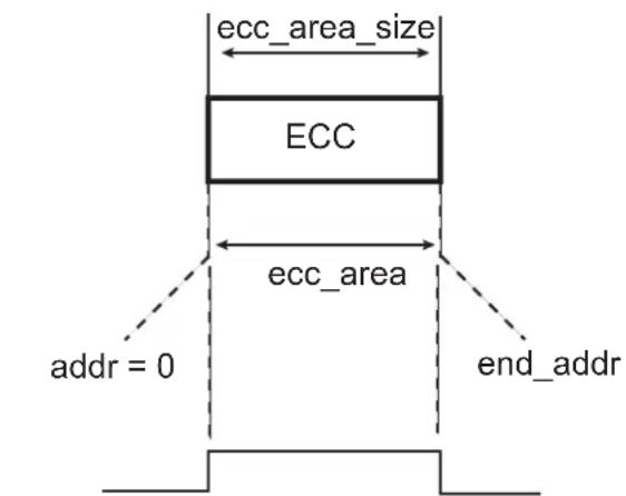
text_image
ecc_area_size ECC ecc_area addr = 0 end_addrRemainder computation enable signal
30.18.2.4 MLC Controller Working with NFC
Table 30-18: MLC Controller Configuration when the Host Controller is Used
| Transfer Type | NFC PMECC | ||||
| RSPARE W$PARE SPAREEN AUTO User Mode | |||||
| Program Page main area is protected, spare is not protected, spare is written manually | 0 | 0 | 0 | 0 | Not used |
| Program Page main area is protected, spare is protected, spare is written by NFC | 0 | 1 | 1 | 0 | Not used |
| Read Page main area is protected, spare is not protected, spare is not retrieved by NFC | 0 | 0 | 0 | 0 | Used |
| Read Page main area is protected, spare is not protected, spare is retrieved by NFC | 1 | 0 | 0 | 1 | Not used |
| Read Page main area is protected, spare is protected, spare is retrieved by NFC | 1 | 0 | 1 | 0 | Used |
30.19 Software Implementation
30.19.1 Remainder Substitution Procedure
The substitute function evaluates the remainder polynomial, with different values of the field primitive element. The addition arithmetic operation is performed with the exclusive OR. The multiplication arithmetic operation is performed through the gf_log and gf_antilog lookup tables.
The REM2NP1 and REMN2NP3 fields of the PMECCREMN registers contain only odd remainders. Each bit indicates whether the coefficient of the remainder polynomial is set to zero or not.
NB_ERROR_MAX defines the maximum value of the error correcting capability.
NB_ERROR defines the error correcting capability selected at encoding/decoding time.
NB_FIELD_ELEMENTS defines the number of elements in the field.
si[] is a table that holds the current syndrome value. An element of that table belongs to the field. This is also a shared variable for the next step of the decoding operation.
oo[] is a table that contains the degree of the remainders.
int substitute()
{
    int i;
    int j;
    for (i = 1; i < 2 * NB_ERROR_MAX; i++)
    {
    si[i] = 0;
    }
    for (i = 1; i < 2 * NB_ERROR; i++)
    {
    for (j = 0; j < ∞[i]; j++)
    {
    if (REM2NPX[i][j])
    {
    si[i] = gf_antilog[(i * j) % NB_FIELD_ELEMENTS]^si[i];
    }
    }
    }
    return 0;
}
30.19.2 Finding the Error Location Polynomial Sigma(x)
The sample code below gives a Berlekamp iterative procedure for finding the value of the error location polynomial.
The input of the procedure is the si[] table defined in the remainder substitution procedure.
The output of the procedure is the error location polynomial named smu (sigma mu). The polynomial coefficients belong to the field. The smu[NB_ERROR+1]] is a table that contains all these coefficients.
NB_ERROR_MAX defines the maximum value of the error correcting capability.
NB_ERROR defines the error correcting capability selected at encoding/decoding time.
NB_FIELD_ELEMENTS defines the number of elements in the field.
int get_sigma()
{
    int i;
    int j;
    int k;
    /* mu */
    int mu[NB_ERROR_MAX+2];
    /* sigma ro */
    int sro[2*NB_ERROR_MAX+1];
    /* discrepancy */
    int dmu[NB_ERROR_MAX+2];
    /* delta order */
    int delta[NB_ERROR_MAX+2];
    /* index of largest delta */
    int ro;
    int largest;
    int diff;
    /*    */
    /* First Row */
    /*    */
    /* Mu */
    mu[0] = -1; /* Actually -1/2 */
    /* Sigma(x) set to 1 */
    for (i = 0; i < (2*NB_ERROR_MAX+1); i++)
    smu[0][i] = 0;
    smu[0][0] = 1;
    /* discrepancy set to 1 */
    dmu[0] = 1;
    /* polynomial order set to 0 */
    lmu[0] = 0;
    /* delta set to -1 */
    delta[0] = (mu[0] * 2 - lmu[0]) >> 1;
    /*    */
    /* Second Row */
    /*    */
    /* Mu */
    mu[1] = 0;
    /* Sigma(x) set to 1 */
    for (i = 0; i < (2*NB_ERROR_MAX+1); i++)
    smu[1][i] = 0;
    smu[1][0] = 1;
    /* discrepancy set to Syndrome 1 */
    dmu[1] = si[1];
    /* polynomial order set to 0 */
    lmu[1] = 0;
    /* delta set to 0 */
    delta[1] = (mu[1] * 2 - lmu[1]) >> 1;
    for (i=1; i <= NB_ERROR; i++)
    {
    mu[i+1] = i << 1;
    /******************************/
    /*    */
    /*    */
    /* Compute Sigma (Mu+1) */
/*
/* check if discrepancy is set to 0 */
if (dmu[i] == 0)
{
    /* copy polynomial */
for (j=0; j<2*NB_ERROR_MAX+1; j++)
{
    smu[i+1][j] = smu[i][j];
}
/* copy previous polynomial order to the next */
lmu[i+1] = lmu[i];
}
else
{
ro    = 0;
largest = -1;
/* find largest delta with dmu != 0 */
for (j=0; j<i; j++)
{
    if (dmu[j])
    {
    if (delta[j] > largest)
    {
    largest = delta[j];
    ro    = j;
    }
    }
}
/* initialize signal ro */
for (k = 0; k < 2*NB_ERROR_MAX+1; k++)
{
    sro[k] = 0;
}
/* compute difference */
diff = (mu[i] - mu[ro]);
/* compute X ^ (2(mu-ro)) */
for (k = 0; k < (2*NB_ERROR_MAX+1); k++)
{
    sro[k+diff] = smu[ro][k];
}
/* multiply by dmu * dmu[ro]^-1 */
for (k = 0; k < 2*NB_ERROR_MAX+1; k++)
{
    /* dmu[ro] is not equal to zero by definition */
    /* check that operand are different from 0 */
    if (sro[k] && dmu[i])
    {
    /* galois inverse */
    sro[k] = gf_antilog[(gf_log[dmu[i]] + (NB_FIELD_ELEMENTS-gf_log[dmu[ro]]) + gf_log[sro[k]]) % NB_FIELD_ELEMENTS];
    }
}
/* multiply by dmu * dmu[ro]^-1 */
for (k = 0; k < 2*NB_ERROR_MAX+1; k++)
{
    smu[i+1][k] = smu[i][k] ^ sro[k];
    if (smu[i+1][k])
    {
    /* find the order of the polynomial */
    lmu[i+1] = k << 1;
    }
}
/* */
/* End Compute Sigma (Mu+1) */
/* And L(mu) */
/******************************************************************************************/
/* In either case compute delta */
delta[i+1] = (mu[i+1] * 2 - lmu[i+1]) >> 1;
/* In either case compute the discrepancy */
for (k = 0; k <= (lmu[i+1] >> 1); k++)
{
    if (k == 0)
    dmu[i+1] = si[2*(i-1)+3];
    /* check if one operand of the multiplier is null, its index is -1 */
    else if (smu[i+1][k] && si[2*(i-1)+3-k])
    dmu[i+1] = gf_antilog[(gf_log[smu[i+1][k]] + gf_log[si[2*(i-1)+3-k]])%nn]^dmu[i+1];
}
return 0;
}
30.19.3 Finding the Error Position
The output of the get_sigma() procedure is a polynomial stored in the smu[NB_ERROR+1]] table. The error positions are the roots of that polynomial. The degree of that polynomial is a very important information, as it gives the number of errors. PMERRLOC module provides hardware accelerator for that step.
30.19.3.1 Error Location
The PMECC Error Location controller provides hardware acceleration for determining roots of polynomials over two finite fields: GF(2^13) and GF(2^14). It integrates 24 fully programmable coefficients. These coefficients belong to GF(2^13) or GF(2^14). The coefficient programmed in the PMERRLOC{i} is the coefficient of X^i in the polynomial.
The search operation is started as soon as a write access is detected in the ELEN register and can be disabled writing to the ELDIS register. The ENINIT field of the ELEN register shall be initialized with the number of galois field elements to test. The set of the roots can be limited to a valid range.
Table 30-19: ENINIT Field Value for a Sector Size of 512 Bytes
| Error Correcting Capability ENINIT Value | |
| 2 4122 | |
| 4 4148 | |
| 8 4200 | |
| 12 4252 | |
| 24 4408 | |
Table 30-20: ENINIT Field Value for a Sector Size of 1024 Bytes
| Error Correcting Capability ENINIT Value | |
| 2 8220 | |
| 4 8248 | |
| 8 8304 | |
| 12 8360 | |
| 24 8528 | |
When the PMECC engine is searching for roots, the BUSY field of the ELSR register remains asserted. An interrupt is asserted at the end of the computation, and the DONE bit of the PMECC Error Location Interrupt Status Register (HSMC_ELSIR) is set. The ERR_CNT field of the HSMC_ELISR indicates the number of errors. The error position can be read in the PMERRLOCX registers.
30.20 Static Memory Controller (SMC) User Interface
The SMC is programmed using the registers listed in Table 30-21. For each chip select, a set of four registers is used to program the parameters of the external device. In Table 30-21, "CS_number" denotes the chip select number. Sixteen bytes per chip select are required.
Table 30-21: Register Mapping
| Offset Register Name Access Reset | ||||
| 0x000 NFC Configuration Register | HSMC_CFG Read/Write | 0x0 | ||
| 0x004 | NFC Control Register | HSMC_CTRL | Write-only | - |
| 0x008 | NFC Status Register | HSMC_SR | Read-only | 0x0 |
| 0x00C | NFC Interrupt Enable Register | HSMC_IER | Write-only | - |
| 0x010 | NFC Interrupt Disable Register | HSMC_IDR | Write-only | - |
| 0x014 | NFC Interrupt Mask Register | HSMC_IMR | Read-only | 0x0 |
| 0x018 | NFC Address Cycle Zero Register | HSMC_ADDR | Read/Write | 0x0 |
| 0x01C | Bank Address Register | HSMC_BANK | Read/Write | 0x0 |
| 0x020-0x06C | Reserved | - | - | - |
| 0x070 | PMECC Configuration Register | HSMC_PMECCFG | Read/Write | 0x0 |
| 0x074 | PMECC Spare Area Size Register | HSMC_PMECCSAREA | Read/Write | 0x0 |
| 0x078 | PMECC Start Address Register | HSMC_PMECCSADDR | Read/Write | 0x0 |
| 0x07C | PMECC End Address Register | HSMC_PMECCEADDR | Read/Write | 0x0 |
| 0x080 Reserved | - | - | - | |
| 0x084 | PMECC Control Register | HSMC_PMECCTRL | Write-only | - |
| 0x088 PMECC Status Register | HSMC_PMECCSR | Read-only 0x0 | ||
| 0x08C | PMECC Interrupt Enable register | HSMC_PMECCIER | Write-only | - |
| 0x090 | PMECC Interrupt Disable Register | HSMC_PMECCIDR | Write-only | - |
| 0x094 | PMECC Interrupt Mask Register | HSMC_PMECCIMR | Read-only | 0x0 |
| 0x098 PMECC Interrupt Status Register | HSMC_PMECCISR | Read-only 0x0 | ||
| 0x09C-0x0AC | Reserved | - | - | - |
| 0x0B0+sec_num*(0x40)+0x00 | PMECC Redundancy 0 Register | HSMC_PMECC0 | Read-only | 0x0 |
| 0x0B0+sec_num*(0x40)+0x04 | PMECC Redundancy 1 Register | HSMC_PMECC1 | Read-only | 0x0 |
| 0x0B0+sec_num*(0x40)+0x08 | PMECC Redundancy 2 Register | HSMC_PMECC2 | Read-only | 0x0 |
| 0x0B0+sec_num*(0x40)+0x0C | PMECC Redundancy 3 Register | HSMC_PMECC3 | Read-only | 0x0 |
| 0x0B0+sec_num*(0x40)+0x10 | PMECC Redundancy 4 Register | HSMC_PMECC4 | Read-only | 0x0 |
| 0x0B0+sec_num*(0x40)+0x14 | PMECC Redundancy 5 Register | HSMC_PMECC5 | Read-only | 0x0 |
| 0x0B0+sec_num*(0x40)+0x18 | PMECC Redundancy 6 Register | HSMC_PMECC6 | Read-only | 0x0 |
| 0x0B0+sec_num*(0x40)+0x1C | PMECC Redundancy 7 Register | HSMC_PMECC7 | Read-only | 0x0 |
| 0x0B0+sec_num*(0x40)+0x20 | PMECC Redundancy 8 Register | HSMC_PMECC8 | Read-only | 0x0 |
| 0x0B0+sec_num*(0x40)+0x24 | PMECC Redundancy 9 Register | HSMC_PMECC9 | Read-only | 0x0 |
| 0x0B0+sec_num*(0x40)+0x28 | PMECC Redundancy 10 Register | HSMC_PMECC10 | Read-only | 0x0 |
| 0x2B0+sec_num*(0x40)+0x00 | PMECC Remainder 0 Register | HSMC_REMO | Read-only | 0x0 |
| Offset | Register | Name | Access | Reset |
| 0x2B0+sec_num*(0x40)+0x04 P | MECC Remainder 1 Register HSMC_REM1 | Read-only 0x0 | ||
| 0x2B0+sec_num*(0x40)+0x08 P | MECC Remainder 2 Register HSMC_REM2 | Read-only 0x0 | ||
| 0x2B0+sec_num*(0x40)+0x0C P | MECC Remainder 3 Register HSMC_REM3 | Read-only 0x0 | ||
| 0x2B0+sec_num*(0x40)+0x10 P | MECC Remainder 4 Register HSMC_REM4 | Read-only 0x0 | ||
| 0x2B0+sec_num*(0x40)+0x14 P | MECC Remainder 5 Register HSMC_REM5 | Read-only 0x0 | ||
| 0x2B0+sec_num*(0x40)+0x18 P | MECC Remainder 6 Register HSMC_REM6 | Read-only 0x0 | ||
| 0x2B0+sec_num*(0x40)+0x1C P | MECC Remainder 7 Register HSMC_REM7 | Read-only 0x0 | ||
| 0x2B0+sec_num*(0x40)+0x20 P | MECC Remainder 8 Register HSMC_REM8 | Read-only 0x0 | ||
| 0x2B0+sec_num*(0x40)+0x24 P | MECC Remainder 9 Register HSMC_REM9 | Read-only 0x0 | ||
| 0x2B0+sec_num*(0x40)+0x28 P | MECC Remainder 10 Register HSMC_REM10 | Read-only 0x0 | ||
| 0x2B0+sec_num*(0x40)+0x2C P | MECC Remainder 11 Register HSMC_REM11 | Read-only 0x0 | ||
| 0x4A0-0x4FC Reserved-- | - | |||
| 0x500 | PMECC Error Location Configuration Register | HSMC_ELCFG | Read/Write | 0x0 |
| 0x504 | PMECC Error Location Primitive Register | HSMC_ELPRIM | Read-only | 0x401A |
| 0x508 | PMECC Error Location Enable Register | HSMC_ELEN | Write-only | - |
| 0x50C | PMECC Error Location Disable Register | HSMC_ELDIS | Write-only | - |
| 0x510 | PMECC Error Location Status Register | HSMC_ELSR | Read-only | 0x0 |
| 0x514 | PMECC Error Location Interrupt Enable register | HSMC_ELIER | Write-only | - |
| 0x518 | PMECC Error Location Interrupt Disable Register | HSMC_ELIDR | Write-only | - |
| 0x51C | PMECC Error Location Interrupt Mask Register | HSMC_ELIMR | Read-only 0x0 | |
| 0x520 | PMECC Error Location Interrupt Status Register | HSMC_ELISR | Read-only 0x0 | |
| 0x524 | Reserved-- | - | ||
| 0x528 | PMECC Error Location SIGMA 0 Register | HSMC_SIGMA0 | Read-only 0x1 | |
| 0x52C | PMECC Error Location SIGMA 1 Register | HSMC_SIGMA1 | Read/Write | 0x0 |
| 0x530 | PMECC Error Location SIGMA 2 Register | HSMC_SIGMA2 | Read/Write | 0x0 |
| 0x534 | PMECC Error Location SIGMA 3 Register | HSMC_SIGMA3 | Read/Write | 0x0 |
| 0x538 | PMECC Error Location SIGMA 4 Register | HSMC_SIGMA4 | Read/Write | 0x0 |
| 0x53C | PMECC Error Location SIGMA 5 Register | HSMC_SIGMA5 | Read/Write | 0x0 |
| Offset Register | Name | Access Reset | ||
| 0x540 | PMECC Error Location SIGMA 6 Register | HSMC_SIGMA6 Read/Write 0x0 | ||
| 0x544 | PMECC Error Location SIGMA 7 Register | HSMC_SIGMA7 Read/Write 0x0 | ||
| 0x548 | PMECC Error Location SIGMA 8 Register | HSMC_SIGMA8 Read/Write 0x0 | ||
| 0x54C | PMECC Error Location SIGMA 9 Register | HSMC_SIGMA9 Read/Write 0x0 | ||
| 0x550 | PMECC Error Location SIGMA 10 Register | HSMC_SIGMA10 Read/Write 0x0 | ||
| 0x554 | PMECC Error Location SIGMA 11 Register | HSMC_SIGMA11 Read/Write 0x0 | ||
| 0x558 | PMECC Error Location SIGMA 12 Register | HSMC_SIGMA12 Read/Write 0x0 | ||
| 0x55C | PMECC Error Location SIGMA 13 Register | HSMC_SIGMA13 Read/Write 0x0 | ||
| 0x560 | PMECC Error Location SIGMA 14 Register | HSMC_SIGMA14 Read/Write 0x0 | ||
| 0x564 | PMECC Error Location SIGMA 15 Register | HSMC_SIGMA15 Read/Write 0x0 | ||
| 0x568 | PMECC Error Location SIGMA 16 Register | HSMC_SIGMA16 Read/Write 0x0 | ||
| 0x56C | PMECC Error Location SIGMA 17 Register | HSMC_SIGMA17 Read/Write 0x0 | ||
| 0x570 | PMECC Error Location SIGMA 18 Register | HSMC_SIGMA18 Read/Write 0x0 | ||
| 0x574 | PMECC Error Location SIGMA 19 Register | HSMC_SIGMA19 Read/Write 0x0 | ||
| 0x578 | PMECC Error Location SIGMA 20 Register | HSMC_SIGMA20 Read/Write 0x0 | ||
| 0x57C | PMECC Error Location SIGMA 21 Register | HSMC_SIGMA21 Read/Write 0x0 | ||
| 0x580 | PMECC Error Location SIGMA 22 Register | HSMC_SIGMA22 Read/Write 0x0 | ||
| 0x584 | PMECC Error Location SIGMA 23 Register | HSMC_SIGMA23 Read/Write 0x0 | ||
| 0x588 | PMECC Error Location SIGMA 24 Register | HSMC_SIGMA24 Read/Write 0x0 | ||
| 0x58C PMECC Error Location 0 | Register HSMC_ERRLOC0 Read-only 0x0 | |||
| ... ... ... ... ... | ||||
| 0x5E8 | PMECC Error Location 23 Register | HSMC_ERRLOC23 | Read-only | 0x0 |
| 0x5EC-0x5FC | Reserved | - | - | - |
| 0x14*CS_number+0x600 | Setup Register | HSMC_SETUP | Read/Write | - |
| Offset | Register | Name | Access | Reset |
| 0x14*CS_number+0x604 Pulse | Register HSMC_PULSE Read/Write – | |||
| 0x14*CS_number+0x608 Cycle | Register HSMC_CYCLE Read/Write – | |||
| 0x14*CS_number+0x60C Timings | Register HSMC_TIMINGS Read/Write – | |||
| 0x14*CS_number+0x610 Mode | Register HSMC_MODE Read/Write – | |||
| 0x6A0 Off Chip Memory Scrambling Register HSMC_OCMS Read/Write 0x0 | ||||
| 0x6A4 | Off Chip Memory Scrambling KEY1 Register | HSMC_KEY1 Write-once | 0x0 | |
| 0x6A8 | Off Chip Memory Scrambling KEY2 Register | HSMC_KEY2 Write-once | 0x0 | |
| 0x6AC-0x6E0 | Reserved | – | – | – |
| 0x6E4 Write Protection Mode Register | HSMC_WPMR | Read/Write 0x0 | ||
| 0x6E8 | Write Protection Status Register | HSMC_WPSR | Read-only | 0x0 |
| 0x6EC-0x6FC | Reserved | – | – | – |
30.20.1 NFC Configuration Register
Name:HSMC_CFG
Address:0xFFFFC000
Access: Read/Write
31 30 29 28 27 26 25 24
- NFCSPARESIZE
23 22 21 20 19 18 17 16
| - | D | T | O | M |
15 14 13 12 11 10 9 8
| -- RBEDGE EDGECTRL | -- | RSPARE | WSPARE |
| 7 | 6 | 5 | 4 | 3 | 2 | 1 | 0 |
| - | - | - | - | - | PAGESIZE | ||
PAGESIZE: Page Size of the NAND Flash Device
| Value | Name | Description |
| 0 | PS512 | Main area 512 bytes |
| 1 | PS1024 | Main area 1024 bytes |
| 2 | PS2048 | Main area 2048 bytes |
| 3 | PS4096 | Main area 4096 bytes |
| 4 | PS8192 | Main area 8192 bytes |
WSPARE: Write Spare Area
0: The NFC skips the spare area in Write mode.
1: The NFC writes both main area and spare area in Write mode.
RSPARE: Read Spare Area
0: The NFC skips the spare area in Read mode.
1: The NFC reads both main area and spare area in Read mode.
EDGECTRL: Rising/Falling Edge Detection Control
0: Rising edge is detected
1: Falling edge is detected
RBEDGE: Ready/Busy Signal Edge Detection
0: When configured to zero, RB_EDGE fields indicate the level of the Ready/Busy lines.
1: When set to one, RB_EDGE fields indicate only transition on Ready/Busy lines.
DTOCYC: Data Timeout Cycle Number
DTOMUL: Data Timeout Multiplier
These fields determine the maximum number of Master Clock cycles that the SMC waits until the detection of a rising edge on Ready/Busy signal.
Data Timeout Multiplier is defined by DTOMUL as shown in the following table:
| Value | Name | Description |
| 0 | X 1 | D T O C Y C |
| 1 | X16 DTOCYC x 16 | |
| 2 | X128 DTOCYC x 128 | |
| 3 | X256 DTOCYC x 256 | |
| 4 | X1024 DTOCYC x 1024 | |
| 5 | X4096 DTOCYC x 4096 | |
| 6 | X65536 DTOCYC x 65536 | |
| 7 | X1048576 DTOCYC x 1048576 |
If the data timeout set by DTOCYC and DTOMUL has been exceeded, the Data Timeout Error flag (DTOE) in the NFC Status Register (NFC_SR) raises.
NFCSPARESIZE: NAND Flash Spare Area Size Retrieved by the Host Controller
The spare size is set to (NFCSPARESIZE + 1) * 4 bytes. The spare area is only retrieved when RSPARE or WSPARE is activated.
30.20.2 NFC Control Register
Name:HSMC_CTRL
Address:0xFFFFC004
Access:Write-only
31 30 29 28 27 26 25 24
| - | - | - | - | - | - | - | - |
23 22 21 20 19 18 17 16
| - | - | - | - | - | - | - | - |
15 14 13 12 11 10 9 8
| - | - | - | - | - | - | - | - |
| 7 | 6 | 5 | 4 | 3 | 2 | 1 | 0 |
| - | - | - | - | - | - | N | F |
NFCEN: NAND Flash Controller Enable
0: No effect
1: Enable the NAND Flash controller.
NFCDIS: NAND Flash Controller Disable
0: No effect
1: Disable the NAND Flash controller.
30.20.3 NFC Status Register
Name:HSMC_SR
Address:0xFFFFC008
Access:Read-only
31 30 29 28 27 26 25 24
| - | - | - | - | - | - | - | R |
23 22 21 20 19 18 17 16
| NFCASE AW | B UNDEF DTOE | -- CMDDONE | XFRDONE |
| 15 14 13 12 | 11 | 10 | 9 8 | ||||
| - | NFCSID | NFCWR | - | - | NFCBUSY | ||
| 7 | 6 | 5 | 4 | 3 | 2 | 1 | 0 |
| - | - | RB_FALL | RB_RISE | - | - | - | SMCSTS |
SMCSTS: NAND Flash Controller Status (this field cannot be reset)
0: NAND Flash Controller disabled
1: NAND Flash Controller enabled
RB\_RISE: Selected Ready Busy Rising Edge Detected
When set to one, this flag indicates that a rising edge on the Ready/Busy Line has been detected. This flag is reset after a status read operation. The Ready/Busy line selected is the decoding of the set NFCCSID, RBNSEL fields.
RB\_FALL: Selected Ready Busy Falling Edge Detected
When set to one, this flag indicates that a falling edge on the Ready/Busy Line has been detected. This flag is reset after a status read operation. The Ready/Busy line is selected through the decoding of the set NFCSID, RBNSEL fields.
NFCBUSY: NFC Busy (this field cannot be reset)
When set to one, this flag indicates that the Controller is activated and accesses the memory device.
NFCWR: NFC Write/Read Operation (this field cannot be reset)
When a command is issued, this field indicates the current Read or Write Operation.
NFCSID: NFC Chip Select ID (this field cannot be reset)
When a command is issued, this field indicates the value of the targeted chip select.
XFRDONE: NFC Data Transfer Terminated
When set to one, this flag indicates that the NFC has terminated the Data Transfer. This flag is reset after a status read operation.
CMDDONE: Command Done
When set to one, this flag indicates that the NFC has terminated the Command. This flag is reset after a status read operation.
DTOE: Data Timeout Error
When set to one, this flag indicates that the Data timeout set be by DTOMUL and DTOCYC has been exceeded. This flag is reset after a status read operation.
UNDEF: Undefined Area Error
When set to one, this flag indicates that the processor performed an access in an undefined memory area. This flag is reset after a status read operation.
AWB: Accessing While Busy
If set to one, this flag indicates that an AHB master has performed an access during the busy phase. This flag is reset after a status read operation.
NFCASE: NFC Access Size Error
If set to one, this flag indicates that an illegal access has been detected in the NFC Memory Area. Only Word Access is allowed within the NFC memory area. This flag is reset after a status read operation.
RB\_EDGEx: Ready/Busy Line x Edge Detected
If set to one, this flag indicates that an edge has been detected on the Ready/Busy Line x. Depending on the EDGE CTRL field located in the HSMC_CFG register, only rising or falling edge is detected. This flag is reset after a status read operation.
30.20.4 NFC Interrupt Enable Register
Name:HSMC_IER
Address:0xFFFFC00C
Access:Write-only
31 30 29 28 27 26 25 24
| - | - | - | - | - | - | - | R |
23 22 21 20 19 18 17 16
| NFCASE AWB UNDEF DTOE | -- CMDDONE | XFRDONE |
15 14 13 12 11 10 98
| - | - | - | - | - | - | - | - |
7 6 5 4 3 2 1 0
| - | - | RB_FALL | RB_RISE | - | - | - | - |
RB\_RISE: Ready Busy Rising Edge Detection Interrupt Enable
0: No effect
1: Interrupt source enabled
RB\_FALL: Ready Busy Falling Edge Detection Interrupt Enable
0: No effect
1: Interrupt source enabled
XFRDONE: Transfer Done Interrupt Enable
0: No effect
1: Interrupt source enabled
CMDDONE: Command Done Interrupt Enable
0: No effect
1: Interrupt source enabled
DTOE: Data Timeout Error Interrupt Enable
0: No effect
1: Interrupt source enabled
UNDEF: Undefined Area Access Interrupt Enable
0: No effect
1: Interrupt source enabled
AWB: Accessing While Busy Interrupt Enable
0: No effect
1: Interrupt source enabled
NFCASE: NFC Access Size Error Interrupt Enable
0: No effect
1: Interrupt source enabled
RB_EDGEx: Ready/Busy Line x Interrupt Enable
0: No effect
1: Interrupt source enabled
30.20.5 NFC Interrupt Disable Register
Name:HSMC_IDR
Address:0xFFFFC010
Access:Write-only
31 30 29 28 27 26 25 24
| - | - | - | - | - | - | - | R |
23 22 21 20 19 18 17 16
| NFCASE AWB UNDEF DTOE | -- CMDDONE | XFRDONE |
15 14 13 12 11 10 9 8
| - | - | - | - | - | - | - | - |
| 7 | 6 | 5 | 4 | 3 | 2 | 1 | 0 |
| - | - | RB_FALL | RB_RISE | - | - | - | - |
RB\_RISE: Ready Busy Rising Edge Detection Interrupt Disable
0: No effect
1: Interrupt source disabled
RB\_FALL: Ready Busy Falling Edge Detection Interrupt Disable
0: No effect
1: Interrupt source disabled
XFRDONE: Transfer Done Interrupt Disable
0: No effect
1: Interrupt source disabled
CMDDONE: Command Done Interrupt Disable
0: No effect
1: Interrupt source disabled
DTOE: Data Timeout Error Interrupt Disable
0: No effect
1: Interrupt source disabled
UNDEF: Undefined Area Access Interrupt Disable
0: No effect
1: Interrupt source disabled
AWB: Accessing While Busy Interrupt Disable
0: No effect
1: Interrupt source disabled
NFCASE: NFC Access Size Error Interrupt Disable
0: No effect
1: Interrupt source disabled
RB_EDGEx: Ready/Busy Line x Interrupt Disable
0: No effect
1: Interrupt source disabled
30.20.6 NFC Interrupt Mask Register
Name:HSMC_IMR
Address:0xFFFFC014
Access:Read-only
31 30 29 28 27 26 25 24
| - | - | - | - | - | - | - | R |
23 22 21 20 19 18 17 16
| NFCASE AWB UNDEF DTOE | -- CMDDONE | XFRDONE |
15 14 13 12 11 10 98
| - | - | - | - | - | - | - | - |
7 6 5 4 3 2 1 0
| - | - | RB_FALL | RB_RISE | - | - | - | - |
RB\_RISE: Ready Busy Rising Edge Detection Interrupt Mask
0: Interrupt source disabled
1: Interrupt source enabled
RB\_FALL: Ready Busy Falling Edge Detection Interrupt Mask
0: Interrupt source disabled
1: Interrupt source enabled
XFRDONE: Transfer Done Interrupt Mask
0: Interrupt source disabled
1: Interrupt source enabled
CMDDONE: Command Done Interrupt Mask
0: Interrupt source disabled
1: Interrupt source enabled
DTOE: Data Timeout Error Interrupt Mask
0: Interrupt source disabled
1: Interrupt source enabled
UNDEF: Undefined Area Access Interrupt Mask5
0: Interrupt source disabled
1: Interrupt source enabled
AWB: Accessing While Busy Interrupt Mask
0: Interrupt source disabled
1: Interrupt source enabled
NFCASE: NFC Access Size Error Interrupt Mask
0: Interrupt source disabled
1: Interrupt source enabled
RB\_EDGEx: Ready/Busy Line x Interrupt Mask
0: Interrupt source disabled
1: Interrupt source enabled
30.20.7 NFC Address Cycle Zero Register
Name:HSMC_ADDR
Address:0xFFFFC018
Access: Read/Write
31 30 29 28 27 26 25 24
| - | - | - | - | - | - | - | - |
23 22 21 20 19 18 17 16
| - | - | - | - | - | - | - | - |
15 14 13 12 11 10 9 8
| - | - | - | - | - | - | - | - |
| 7 | 6 | 5 | 4 | 3 | 2 | 1 | 0 |
ADDR_CYCLE0
ADDR_CYCLE0: NAND Flash Array Address Cycle 0
When five address cycles are used, ADDR_CYCLE0 is the first byte written to the NAND Flash (used by the NFC).
30.20.8 NFC Bank Register
Name:HSMC_BANK
Address:0xFFFFC01C
Access: Read/Write
31 30 29 28 27 26 25 24
| - | - | - | - | - | - | - | - |
23 22 21 20 19 18 17 16
| - | - | - | - | - | - | - | - |
15 14 13 12 11 10 9 8
| - | - | - | - | - | - | - | - |
| 7 | 6 | 5 | 4 | 3 | 2 | 1 | 0 |
| - | - | - | - | - | - | - | B |
BANK: Bank Identifier
0: Bank 0 is used.
1: Bank 1 is used.
30.20.9 PMECC Configuration Register
Name: HSMC_PMECCFG
Address:0xFFFFC070
Access: Read/Write
31 30 29 28 27 26 25 24
| - | - | - | - | - | - | - | - |
23 22 21 20 19 18 17 16
| --- AUTO --- SPAREEN |
15 14 13 12 11 10 9 8
| ---NANDWR---PAGESIZE |
| 7 | 6 | 5 | 4 | 3 | 2 | 1 | 0 |
| --- SECTORSZ - BCH_ERR |
BCH_ERR: Error Correcting Capability
| Value | Name | Description |
| 0 | BCH_ERR2 | 2 errors |
| 1 | BCH_ERR4 | 4 errors |
| 2 | BCH_ERR8 | 8 errors |
| 3 | BCH_ERR12 | 12 errors |
| 4 | BCH_ERR24 | 24 errors |
SECTORSZ: Sector Size
0: The ECC computation is based on a sector of 512 bytes.
1: The ECC computation is based on a sector of 1024 bytes.
PAGESIZE: Number of Sectors in the Page
| Value | Name | Description |
| 0 | PAGESIZE_1SEC | 1 sector for main area (512 or 1024 bytes) |
| 1 | PAGESIZE_2SEC | 2 sectors for main area (1024 or 2048 bytes) |
| 2 | PAGESIZE_4SEC | 4 sectors for main area (2048 or 4096 bytes) |
| 3 | PAGESIZE_8SEC | 8 sectors for main area (4096 or 8192 bytes) |
NANDWR: NAND Write Access
0: NAND read access
1: NAND write access
SPAREEN: Spare Enable
- for NAND write access:
0: The spare area is skipped
1: The spare area is protected with the last sector of data.
- for NAND read access:
0: The spare area is skipped.
1: The spare area contains protected data or only redundancy information.
AUTO: Automatic Mode Enable
This bit is only relevant in NAND Read Mode, when spare enable is activated.
0: Indicates that the spare area is not protected. In that case, the ECC computation takes into account the ECC area located in the spare area. (within the start address and the end address).
1: Indicates that the spare area is error protected. In this case, the ECC computation takes into account the whole spare area minus the ECC area in the ECC computation operation.
30.20.10 PMECC Spare Area Size Register
Name: HSMC_PMECCSAREA
Address:0xFFFFC074
Access: Read/Write
31 30 29 28 27 26 25 24
| - | - | - | - | - | - | - | - |
23 22 21 20 19 18 17 16
| - | - | - | - | - | - | - | - |
15 14 13 12 11 10 9 8
| - | - | - | - | - | - | - | S |
| 7 | 6 | 5 | 4 | 3 | 2 | 1 | 0 |
SPARESIZE
SPARESIZE: Spare Area Size
Number of bytes in the spare area. The spare area size is equal to (SPARESIZE + 1) bytes.
30.20.11 PMECC Start Address Register
Name: HSMC_PMECCSADDR
Address:0xFFFFC078
Access: Read/Write
31 30 29 28 27 26 25 24
| - | - | - | - | - | - | - | - |
23 22 21 20 19 18 17 16
| - | - | - | - | - | - | - | - |
15 14 13 12 11 10 9 8
| - | - | - | - | - | - | - | S |
| 7 | 6 | 5 | 4 | 3 | 2 | 1 | 0 |
STARTADDR
STARTADDR: ECC Area Start Address
This register is programmed with the start ECC start address. When STARTADDR is equal to 0, then the first ECC byte is located at the first byte of the spare area.
30.20.12 PMECC End Address Register
Name: HSMC_PMECCEADDR
Address:0xFFFFC07C
Access: Read/Write
31 30 29 28 27 26 25 24
| - | - | - | - | - | - | - | - |
23 22 21 20 19 18 17 16
| - | - | - | - | - | - | - | - |
15 14 13 12 11 10 9 8
| - | - | - | - | - | - | - | E |
| 7 | 6 | 5 | 4 | 3 | 2 | 1 | 0 |
ENDADDR
ENDADDR: ECC Area End Address
This register is programmed with the start ECC end address. When ENDADDR is equal to N, then the first ECC byte is located at byte N of the spare area.
30.20.13 PMECC Control Register
Name: HSMC_PMECCTRL
Address:0xFFFFC084
Access: Write-only
31 30 29 28 27 26 25 24
| - | - | - | - | - | - | - | - |
23 22 21 20 19 18 17 16
| - | - | - | - | - | - | - | - |
15 14 13 12 11 10 9 8
| - | - | - | - | - | - | - | - |
7 6 5 4 3 2 1 0
| -- DISABLE ENABLE - USER DATA RST |
RST: Reset the PMECC Module
0: No effect
1: Reset the PMECC controller.
DATA: Start a Data Phase
0: No effect
1: The PMECC controller enters a Data phase.
USER: Start a User Mode Phase
0: No effect
1: The PMECC controller enters a User mode phase.
ENABLE: PMECC Enable
0: No effect
1: Enable the PMECC controller.
DISABLE: PMECC Enable
0: No effect
1: Disable the PMECC controller.
30.20.14 PMECC Status Register
Name: HSMC_PMECCSR
Address:0xFFFFC088
Access: Read-only
31 30 29 28 27 26 25 24
| - | - | - | - | - | - | - | - |
23 22 21 20 19 18 17 16
| - | - | - | - | - | - | - | - |
15 14 13 12 11 10 9 8
| - | - | - | - | - | - | - | - |
| 7 | 6 | 5 | 4 | 3 | 2 | 1 | 0 |
| --- ENABLE --- BUSY |
BUSY: The kernel of the PMECC is busy
0: PMECC controller finite state machine reached idle state
1: PMECC controller finite state machine is processing the incoming byte stream
ENABLE: PMECC Enable bit
0: PMECC controller disabled
1: PMECC controller enabled
30.20.15 PMECC Interrupt Enable Register
Name: HSMC_PMECCIER
Address:0xFFFFC08C
Access: Write-only
31 30 29 28 27 26 25 24
| - | - | - | - | - | - | - | - |
23 22 21 20 19 18 17 16
| - | - | - | - | - | - | - | - |
15 14 13 12 11 10 9 8
| - | - | - | - | - | - | - | - |
| 7 | 6 | 5 | 4 | 3 | 2 | 1 | 0 |
| - | - | - | - | - | - | - | E |
ERRIE: Error Interrupt Enable
0: No effect
1: The Multibit Error interrupt is enabled. An interrupt will be raised if at least one error is detected in at least one sector.
30.20.16 PMECC Interrupt Disable Register
Name: HSMC_PMECCIDR
Address:0xFFFFC090
Access: Write-only
31 30 29 28 27 26 25 24
| - | - | - | - | - | - | - | - |
23 22 21 20 19 18 17 16
| - | - | - | - | - | - | - | - |
15 14 13 12 11 10 9 8
| - | - | - | - | - | - | - | - |
| 7 | 6 | 5 | 4 | 3 | 2 | 1 | 0 |
| - | - | - | - | - | - | - | E |
ERRID: Error Interrupt Disable
0: No effect
1: Multibit Error interrupt disabled
30.20.17 PMECC Interrupt Mask Register
Name: HSMC_PMECCIMR
Address:0xFFFFC094
Access: Read-only
31 30 29 28 27 26 25 24
| - | - | - | - | - | - | - | - |
23 22 21 20 19 18 17 16
| - | - | - | - | - | - | - | - |
15 14 13 12 11 10 9 8
| - | - | - | - | - | - | - | - |
| 7 | 6 | 5 | 4 | 3 | 2 | 1 | 0 |
| - | - | - | - | - | - | - | E |
ERRIM: Error Interrupt Mask
0: Multibit Error disabled
1: Multibit Error enabled
30.20.18 PMECC Interrupt Status Register
Name: HSMC_PMECCISR
Address:0xFFFFC098
Access: Read-only
31 30 29 28 27 26 25 24
| - | - | - | - | - | - | - | - |
23 22 21 20 19 18 17 16
| - | - | - | - | - | - | - | - |
15 14 13 12 11 10 9 8
| - | - | - | - | - | - | - | - |
7 6 5 4 3 2 1 0
ERRIS
ERRIS: Error Interrupt Status Register
When set to one, bit i of the HSMC_PMECCISR indicates that sector i is corrupted.
30.20.19 PMECC Redundancy x Register
Name: HSMC_PMECCx [x=0..10] [sec_num=0..7]
Address:0xFFFFC0B0 [0][0] .. 0xFFFFC0D8 [10][0]
0xFFFFC0F0 [0][1] .. 0xFFFFC118 [10][1]
0xFFFFC130 [0][2] .. 0xFFFFC158 [10][2]
0xFFFFC170 [0][3] .. 0xFFFFC198 [10][3]
0xFFFFC1B0 [0][4] .. 0xFFFFC1D8 [10][4]
0xFFFFC1F0 [0][5] .. 0xFFFFC218 [10][5]
0xFFFFC230 [0][6] .. 0xFFFFC258 [10][6]
0xFFFFC270 [0][7] .. 0xFFFFC298 [10][7]
Access: Read-only
31 30 29 28 27 26 25 24
| ECC |
23 22 21 20 19 18 17 16
| ECC |
15 14 13 12 11 10 9 8
| ECC |
7 6 5 4 3 2 1 0
| ECC |
ECC: BCH Redundancy
This register contains the remainder of the division of the codeword by the generator polynomial.
30.20.20 PMECC Remainder x Register
Name: HSMC_REMx [x=0..11] [sec_num=0..7]
Address:0xFFFFC2B0 [0][0] .. 0xFFFFC2DC [11][0]
0xFFFFC2F0 [0][1] .. 0xFFFFC31C [11][1]
0xFFFFC330 [0][2] .. 0xFFFFC35C [11][2]
0xFFFFC370 [0][3] .. 0xFFFFC39C [11][3]
0xFFFFC3B0 [0][4] .. 0xFFFFC3DC [11][4]
0xFFFFC3F0 [0][5] .. 0xFFFFC41C [11][5]
0xFFFFC430 [0][6] .. 0xFFFFC45C [11][6]
0xFFFFC470 [0][7] .. 0xFFFFC49C [11][7]
Access: Read-only
31 30 29 28 27 26 25 24
| - | - | R | E | M | 2 | N |
23 22 21 20 19 18 17 16
REM2NP3
15 14 13 12 11 10 9 8
| - | - | R | E | M | 2 | N |
7 6 5 4 3 2 1 0
REM2NP1
REM2NP1: BCH Remainder 2 \* N + 1
When sector size is set to 512 bytes, bit REM2NP1[13] is not used and read as zero.
If bit i of the REM2NP1 field is set to one, then the coefficient of the X^i is set to one; otherwise, the coefficient is zero.
REM2NP3: BCH Remainder 2 \* N + 3
When sector size is set to 512 bytes, bit REM2NP3[29] is not used and read as zero.
If bit i of the REM2NP3 field is set to one, then the coefficient of the X^ is set to one; otherwise, the coefficient is zero.
30.20.21 PMECC Error Location Configuration Register
Name: HSMC_ELCFG
Address:0xFFFFC500
Access: Read/Write
31 30 29 28 27 26 25 24
| - | - | - | - | - | - | - | - |
23 22 21 20 19 18 17 16
| ---ERRNUM |
15 14 13 12 11 10 9 8
| - | - | - | - | - | - | - | - |
| 7 | 6 | 5 | 4 | 3 | 2 | 1 | 0 |
| - | - | - | - | - | - | - | S |
ERRNUM: Number of Errors
SECTORSZ: Sector Size
0: The ECC computation is based on a 512 bytes sector.
1: The ECC computation is based on a 1024 bytes sector.
30.20.22 PMECC Error Location Primitive Register
Name: HSMC_ELPRIM
Address:0xFFFFC504
Access: Read-only
31 30 29 28 27 26 25 24
| - | - | - | - | - | - | - | - |
23 22 21 20 19 18 17 16
| - | - | - | - | - | - | - | - |
15 14 13 12 11 10 9 8
| PRIMITIV | |||||||
| 7 | 6 | 5 | 4 | 3 | 2 | 1 | 0 |
| PRIMITIV | |||||||
PRIMITIV: Primitive Polynomial
This field indicates the Primitive Polynomial used in the ECC computation.
30.20.23 PMECC Error Location Enable Register
Name: HSMC_ELEN
Address:0xFFFFC508
Access: Write-only
31 30 29 28 27 26 25 24
| - | - | - | - | - | - | - | - |
23 22 21 20 19 18 17 16
| - | - | - | - | - | - | - | - |
15 14 13 12 11 10 9 8
| - | - | E | N | I | N | I |
7 6 5 4 3 2 1 0
ENINIT
ENINIT: Error Location Enable
Initial bit number in the codeword.
30.20.24 PMECC Error Location Disable Register
Name: HSMC_ELDIS
Address:0xFFFFC50C
Access: Write-only
31 30 29 28 27 26 25 24
| - | - | - | - | - | - | - | - |
23 22 21 20 19 18 17 16
| - | - | - | - | - | - | - | - |
15 14 13 12 11 10 9 8
| - | - | - | - | - | - | - | - |
| 7 | 6 | 5 | 4 | 3 | 2 | 1 | 0 |
| - | - | - | - | - | - | - | D |
DIS: Disable Error Location Engine
0: No effect
1: Disable the Error location engine.
30.20.25 PMECC Error Location Status Register
Name: HSMC_ELSR
Address:0xFFFFC510
Access: Read-only
31 30 29 28 27 26 25 24
| - | - | - | - | - | - | - | - |
23 22 21 20 19 18 17 16
| - | - | - | - | - | - | - | - |
15 14 13 12 11 10 9 8
| - | - | - | - | - | - | - | - |
| 7 | 6 | 5 | 4 | 3 | 2 | 1 | 0 |
| - | - | - | - | - | - | - | B |
BUSY: Error Location Engine Busy
0: Error location engine is disabled.
1: Error location engine is enabled and is finding roots of the polynomial.
30.20.26 PMECC Error Location Interrupt Enable Register
Name: HSMC_ELIER
Address:0xFFFFC514
Access: Write-only
31 30 29 28 27 26 25 24
| - | - | - | - | - | - | - | - |
23 22 21 20 19 18 17 16
| - | - | - | - | - | - | - | - |
15 14 13 12 11 10 9 8
| - | - | - | - | - | - | - | - |
| 7 | 6 | 5 | 4 | 3 | 2 | 1 | 0 |
| - | - | - | - | - | - | - | D |
DONE: Computation Terminated Interrupt Enable
0: No effect
1: Interrupt Enable.
30.20.27 PMECC Error Location Interrupt Disable Register
Name: HSMC_ELIDR
Address:0xFFFFC518
Access: Write-only
31 30 29 28 27 26 25 24
| - | - | - | - | - | - | - | - |
23 22 21 20 19 18 17 16
| - | - | - | - | - | - | - | - |
15 14 13 12 11 10 9 8
| - | - | - | - | - | - | - | - |
| 7 | 6 | 5 | 4 | 3 | 2 | 1 | 0 |
| - | - | - | - | - | - | - | D |
DONE: Computation Terminated Interrupt Disable
0: No effect
1: Interrupt disable.
30.20.28 PMECC Error Location Interrupt Mask Register
Name: HSMC_ELIMR
Address:0xFFFFC51C
Access: Read-only
31 30 29 28 27 26 25 24
| - | - | - | - | - | - | - | - |
23 22 21 20 19 18 17 16
| - | - | - | - | - | - | - | - |
15 14 13 12 11 10 9 8
| - | - | - | - | - | - | - | - |
| 7 | 6 | 5 | 4 | 3 | 2 | 1 | 0 |
| - | - | - | - | - | - | - | D |
DONE: Computation Terminated Interrupt Mask
0: Computation Terminated interrupt disabled
1: Computation Terminated interrupt enabled
30.20.29 PMECC Error Location Interrupt Status Register
Name: HSMC_ELISR
Address:0xFFFFC520
Access: Read-only
31 30 29 28 27 26 25 24
| - | - | - | - | - | - | - | - |
23 22 21 20 19 18 17 16
| - | - | - | - | - | - | - | - |
15 14 13 12 11 10 9 8
| - | - | - | E | R | R | - |
| 7 | 6 | 5 | 4 | 3 | 2 | 1 | 0 |
| - | - | - | - | - | - | - | D |
DONE: Computation Terminated Interrupt Status
When set to one, this indicates that the error location engine has completed the root finding algorithm.
ERR\_CNT: Error Counter value
This field indicates the number of roots of the polynomial.
30.20.30 PMECC Error Location SIGMA0 Register
Name: HSMC_SIGMA0
Address:0xFFFFC52C [1] .. 0xFFFFC588 [24], 0xFFFFC528 [0] .. 0xFFFFC588 [24]
Access: Read-only
31 30 29 28 27 26 25 24
| - | - | - | - | - | - | - | - |
23 22 21 20 19 18 17 16
| - | - | - | - | - | - | - | - |
15 14 13 12 11 10 9 8
| --SIGMA0 |
7 6 5 4 3 2 1 0
SIGMA0
SIGMA0: Coefficient of degree 0 in the SIGMA polynomial
SIGMA0 belongs to the finite field GF(2^13) when the sector size is set to 512 bytes.
SIGMA0 belongs to the finite field GF(2^14) when the sector size is set to 1024 bytes.
30.20.31 PMECC Error Location SIGMAx Register
Name: HSMC_SIGMAx [x=1..24]
Address:0xFFFFC52C [1] .. 0xFFFFC588 [24], 0xFFFFC528 [0] .. 0xFFFFC588 [24]
Access: Read/Write
31 30 29 28 27 26 25 24
| - | - | - | - | - | - | - | - |
23 22 21 20 19 18 17 16
| - | - | - | - | - | - | - | - |
15 14 13 12 11 10 9 8
| --SIGMAx |
7 6 5 4 3 2 1 0
SIGMAx
SIGMAx: Coefficient of degree x in the SIGMA polynomial
SIGMAx belongs to the finite field GF(2^13) when the sector size is set to 512 bytes.
SIGMAx belongs to the finite field GF(2^14) when the sector size is set to 1024 bytes.
30.20.32 PMECC Error Location x Register
Name: HSMC_ERRLOCx [x=0..23]
Address:0xFFFFC58C
Access: Read-only
31 30 29 28 27 26 25 24
| - | - | - | - | - | - | - | - |
23 22 21 20 19 18 17 16
| - | - | - | - | - | - | - | - |
15 14 13 12 11 10 9 8
| --ERRLOCN |
7 6 5 4 3 2 1 0
ERRLOCN
ERRLOCN: Error Position within the Set {sector area, spare area}
ERRLOCN points to 1 when the first bit of the main area is corrupted.
If the sector size is set to 512 bytes, the ERRLOCN points to 4096 when the last bit of the sector area is corrupted.
If the sector size is set to 1024 bytes, the ERRLOCN points to 8192 when the last bit of the sector area is corrupted.
If the sector size is set to 512 bytes, the ERRLOCN points to 4097 when the first bit of the spare area is corrupted.
If the sector size is set to 1024 bytes, the ERRLOCN points to 8193 when the first bit of the spare area is corrupted.
30.20.33 Setup Register
Name:HSMC_SETUPx [x=0..3]
Address:0xFFFFC600 [0], 0xFFFFC614 [1], 0xFFFFC628 [2], 0xFFFFC63C [3]
Access:Write-only
31 30 29 28 27 26 25 24
--NCS RD SETUP
23 22 21 20 19 18 17 16
--NRD\SETUP
15 14 13 12 11 10 9 8
-- NCS WR SETUP
7 6 5 4 3 2 1 0
-- NWESETUP
This register can only be written if the WPEN bit is cleared in the Write Protection Mode Register.
NWE\_SETUP: NWE Setup Length
The NWE signal setup length is defined as:
NWE setup length = (128 * NWE_SETUP[5] + NWE_SETUP[4:0]) clock cycles.
NCS\_WR\_SETUP: NCS Setup Length in Write Access
In write access, the NCS signal setup length is defined as:
NCS setup length = (128 * NCS_WR_SETUP[5] + NCS_WR_SETUP[4:0]) clock cycles.
NRD\_SETUP: NRD Setup Length
The NRD signal setup length is defined as:
NRD setup length = (128 * NRD_SETUP[5] + NRD_SETUP[4:0]) clock cycles.
NCS\_RD\_SETUP: NCS Setup Length in Read Access
In Read access, the NCS signal setup length is defined as:
NCS setup length = (128 * NCS_RD_SETUP[5] + NCS_RD_SETUP[4:0]) clock cycles.
30.20.34 Pulse Register
Name:HSMC_PULSEx [x=0..3]
Address:0xFFFFC604 [0], 0xFFFFC618 [1], 0xFFFFC62C [2], 0xFFFFC640 [3]
Access:Write-only
31 30 29 28 27 26 25 24
- NCS_RD_PULSE
23 22 21 20 19 18 17 16
- NRD_PULSE
15 14 13 12 11 10 9 8
- NCS_WR_PULSE
7 6 5 4 3 2 1 0
- | N W
This register can only be written if the WPEN bit is cleared in the Write Protection Mode Register.
NWE\_PULSE: NWE Pulse Length
The NWE signal pulse length is defined as:
NWE pulse length = (256 * NWE_PULSE[6]+NWE_PULSE[5:0]) clock cycles.
The NWE pulse must be at least one clock cycle.
NCS\_WR\_PULSE: NCS Pulse Length in WRITE Access
In Write access, The NCS signal pulse length is defined as:
NCS pulse length = (256 * NCS_WR_PULSE[6] + NCS_WR_PULSE[5:0]) clock cycles.
The NCS pulse must be at least one clock cycle.
NRD\_PULSE: NRD Pulse Length
The NRD signal pulse length is defined as:
NRD pulse length = (256 * NRD_PULSE[6] + NRD_PULSE[5:0]) clock cycles.
The NRD pulse width must be as least 1 clock cycle.
NCS\_RD\_PULSE: NCS Pulse Length in READ Access
In READ mode, The NCS signal pulse length is defined as:
NCS pulse length = (256 * NCS_RD_PULSE[6] + NCS_RD_PULSE[5:0]) clock cycles.
30.20.35 Cycle Register
Name:HSMC_CYCLEx [x=0..3]
Address:0xFFFFC608 [0], 0xFFFFC61C [1], 0xFFFFC630 [2], 0xFFFFC644 [3]
Access: Read/Write
31 30 29 28 27 26 25 24
| - | - | - | - | - | - | - | NRD_CYCLE |
23 22 21 20 19 18 17 16
NRD_CYCLE
15 14 13 12 11 10 9 8
| - | - | - | - | - | - | - | N |
7 6 5 4 3 2 1 0
NWE_CYCLE
This register can only be written if the WPEN bit is cleared in the Write Protection Mode Register.
NWE\_CYCLE: Total Write Cycle Length
The total write cycle length is the total duration in clock cycles of the write cycle. It is equal to the sum of the setup, pulse and hold steps of the NWE and NCS signals. It is defined as:
Write cycle length = (NWE_CYCLE[8:7] * 256) + NWE_CYCLE[6:0] clock cycles.
NRD\_CYCLE: Total Read Cycle Length
The total read cycle length is the total duration in clock cycles of the read cycle. It is equal to the sum of the setup, pulse and hold steps of the NRD and NCS signals. It is defined as:
Read cycle length = (NRD_CYCLE[8:7] * 256) + NRD_CYCLE[6:0] clock cycles.
30.20.36 Timings Register
Name:HSMC_TIMINGSx [x=0..3]
Address:0xFFFFC60C [0], 0xFFFFC620 [1], 0xFFFFC634 [2], 0xFFFFC648 [3]
Access: Read/Write
31 30 29 28 27 26 25 24
| NFSEL RBNSEL TWB |
23 22 21 20 19 18 17 16
| - | - | - | - | T | R | R |
15 14 13 12 11 10 9 8
| - | - | - | O | C | M | S |
| 7 | 6 | 5 | 4 | 3 | 2 | 1 | 0 |
| TADL | TCLR |
This register can only be written if the WPEN bit is cleared in the Write Protection Mode Register.
TCLR: CLE to REN Low Delay
Command Latch Enable falling edge to Read Enable falling edge timing.
Latch Enable Falling to Read Enable Falling = (TCLR[3] * 64) + TCLR[2:0] clock cycles.
TADL: ALE to Data Start
Last address latch cycle to the first rising edge of WEN for data input.
Last address latch to first rising edge of WEN = (TADL[3] * 64) + TADL[2:0] clock cycles.
TAR: ALE to REN Low Delay
Address Latch Enable falling edge to Read Enable falling edge timing.
Address Latch Enable to Read Enable = (TAR[3] * 64) + TAR[2:0] clock cycles.
OCMS: Off Chip Memory Scrambling Enable
When set to one, the memory scrambling is activated. (Value must be zero if external memory is NAND Flash and NFC is used).
TRR: Ready to REN Low Delay
Ready/Busy signal to Read Enable falling edge timing.
Read to REN = (TRR[3] * 64) + TRR[2:0] clock cycles.
TWB: WEN High to REN to Busy
Write Enable rising edge to Ready/Busy falling edge timing.
Write Enable to Read/Busy = (TWB[3] * 64) + TWB[2:0] clock cycles.
RBNSEL: Ready/Busy Line Selection
This field indicates the selected Ready/Busy Line from the RBN bundle.
NFSEL: NAND Flash Selection
If this bit is set to one, the chip select is assigned to NAND Flash write enable and read enable lines drive the Error Correcting Code module.
30.20.37 Mode Register
Name:HSMC_MODEx [x=0..3]
Address:0xFFFFC610 [0], 0xFFFFC624 [1], 0xFFFFC638 [2], 0xFFFFC64C [3]
Access: Read/Write
31 30 29 28 27 26 25 24
| - | - | - | - | - | - | - | - |
23 22 21 20 19 18 17 16
| --- TDF_MODE TDF_CYCLES |
15 14 13 12 11 10 9 8
| - | - | - | D | B | W | - | - |
| 7 | 6 | 5 | 4 | 3 | 2 | 1 | 0 |
| -- EXNW_MODE -- | WRITE_MODE READ_MODE | ||||||
This register can only be written if the WPEN bit is cleared in the Write Protection Mode Register.
READ_MODE: Selection of the Control Signal for Read Operation
| Value | Name | Description |
| 0 | NCS_CTRL | The Read operation is controlled by the NCS signal. |
| 1 | NRD_CTRL | The Read operation is controlled by the NRD signal. |
WRITE_MODE: Selection of the Control Signal for Write Operation
| Value | Name | Description |
| 0 | NCS_CTRL | The Write operation is controller by the NCS signal. |
| 1 | NWE_CTRL | The Write operation is controlled by the NWE signal |
EXNW\_MODE: NWAIT Mode
The NWAIT signal is used to extend the current read or write signal. It is only taken into account during the pulse phase Read and Write controlling signal. When the use of NWAIT is enabled, at least one cycle hold duration must be programmed for the read and write controlling signal.
| Value | Name | Description |
| 0 | DISABLED | Disabled—The NWAIT input signal is ignored on the corresponding Chip Select. |
| 1 | — | Reserved |
| 2 | FROZEN | Frozen Mode—If asserted, the NWAIT signal freezes the current read or write cycle. After deassertion, the read/write cycle is resumed from the point where it was stopped. |
| 3 | READY | Ready Mode—The NWAIT signal indicates the availability of the external device at the end of the pulse of the controlling read or write signal, to complete the access. If high, the access normally completes. If low, the access is extended until NWAIT returns high. |
BAT: Byte Access Type
This field is used only if DBW defines a 16-bit data bus.
| Value Name Description | ||
| 0 BYTE_SELECT | Byte select access type:- Write operation is controlled using NCS, NWE, NBS0, NBS1.- Read operation is controlled using NCS, NRD, NBS0, NBS1. | |
| 1 BYTE_WRITE | Byte write access type:- Write operation is controlled using NCS, NWR0, NWR1.- Read operation is controlled using NCS and NRD. | |
DBW: Data Bus Width
| Value Name Description | |
| 0 BIT_8 8-bit bus | |
| 1 BIT_16 16-bit bus |
TDF\_CYCLES: Data Float Time
This field gives the integer number of clock cycles required by the external device to release the data after the rising edge of the read controlling signal. The SMC always provide one full cycle of bus turnaround after the TDF_CYCLES period. The external bus cannot be used by another chip select during TDF_CYCLES + 1 cycles. From 0 up to 15 TDF_CYCLES can be set.
TDF\_MODE: TDF Optimization
1: TDF optimization enabled
- The number of TDF wait states is optimized using the setup period of the next read/write access.
0: TDF optimization disabled
- The number of TDF wait states is inserted before the next access begins.
30.20.38 Off Chip Memory Scrambling Register
Name:HSMC_OCMS
Address:0xFFFFC6A0
Access: Read/Write
31 30 29 28 27 26 25 24
| - | - | - | - | - | - | - | - |
23 22 21 20 19 18 17 16
| - | - | - | - | - | - | - | - |
15 14 13 12 11 10 9 8
| - | - | - | - | - | - | - | - |
| 7 | 6 | 5 | 4 | 3 | 2 | 1 | 0 |
| - | - | - | - | - | - | S | R |
SMSE: Static Memory Controller Scrambling Enable
0: Disable "Off Chip" Scrambling for SMC access.
1: Enable "Off Chip" Scrambling for SMC access. (If OCMS bit is set in the corresponding HSMC_TIMINGSx register.)
SRSE: NFC Internal SRAM Scrambling Enable
0: Disable Scrambling for NFC internal SRAM access.
1: Enable Scrambling for NFC internal SRAM access. (OCMS bit must be cleared in the corresponding HSMC_TIMINGSx register.)
30.20.39 Off Chip Memory Scrambling Key1 Register
Name:HSMC_KEY1
Address:0xFFFFC6A4
Access:Write-once
31 30 29 28 27 26 25 24
| KEY1 | |||||||
| 23 22 21 20 19 18 17 16 | |||||||
| KEY1 | |||||||
| 15 14 13 12 11 10 9 8 | |||||||
| KEY1 | |||||||
| 7 | 6 | 5 | 4 | 3 | 2 | 1 | 0 |
| KEY1 | |||||||
KEY1: Off Chip Memory Scrambling (OCMS) Key Part 1
When Off Chip Memory Scrambling is enabled by setting the HSMC_OCMS and HSMC_TIMINGS registers in accordance, the data scrambling depends on KEY1 and KEY2 values.
30.20.40 Off Chip Memory Scrambling Key2 Register
Name:HSMC_KEY2
Address:0xFFFFC6A8
Access:Write-once
31 30 29 28 27 26 25 24
| KEY2 |
23 22 21 20 19 18 17 16
| KEY2 |
15 14 13 12 11 10 9 8
| KEY2 |
7 6 5 4 3 2 1 0
| KEY2 |
KEY2: Off Chip Memory Scrambling (OCMS) Key Part 2
When Off Chip Memory Scrambling is enabled by setting the HSMC_OCMS and HSMC_TIMINGS registers in accordance, the data scrambling depends on KEY2 and KEY1 values.
30.20.41 Write Protection Mode Register
Name:HSMC_WPMR
Address:0xFFFFC6E4
Access: Read/Write
31 30 29 28 27 26 25 24
WPKEY
23 22 21 20 19 18 17 16
WPKEY
15 14 13 12 11 10 9 8
WPKEY
7 6 5 4 3 2 1 0
| - | - | - | - | - | - | - | W |
WPEN: Write Protection Enable
0: Disables write protection if WPKEY value corresponds to 0x534D43 ("SMC" in ASCII)
1: Enables write protection if WPKEY value corresponds to 0x534D43 ("SMC" in ASCII)
See Section 30.16 Register Write Protection for list of write-protected registers.
WPKEY: Write Protection Key
| Value Name | Description | |
| 0x534D43 PAS | SWD | Writing any other value in this field aborts the write operation of bit WPEN. Always reads as 0. |
30.20.42 Write Protection Status Register
Name:HSMC_WPSR
Address:0xFFFFC6E8
Access: Read-only
31 30 29 28 27 26 25 24
| - | - | - | - | - | - | - | - |
23 22 21 20 19 18 17 16
| WPVSRC |
15 14 13 12 11 10 9 8
| WPVSRC |
| 7 | 6 | 5 | 4 | 3 | 2 | 1 | 0 |
| - | - | - | - | - | - | - | W |
WPVS: Write Protection Violation Status
0: No write protect violation has occurred since the last read of the HSMC_WPSR.
1: A write protect violation has occurred since the last read of the HSMC_WPSR. If this violation is an unauthorized attempt to write a protected register, the associated violation is reported into field WPVSRC.
WPVSRC: Write Protection Violation Source
When WPVS = 1, WPVSRC indicates the register address offset at which a write access has been attempted.
31. DMA Controller (DMAC)
31.1 Description
The DMA Controller (DMAC) is an AHB-central DMA controller core that transfers data from a source peripheral to a destination peripheral over one or more AMBA buses. One channel is required for each source/destination pair. In the most basic configuration, the DMAC has one master interface and one channel. The master interface reads the data from a source and writes it to a destination. Two AMBA transfers are required for each DMAC data transfer. This is also known as a dual-access transfer.
The DMAC is programmed via the APB interface.
31.2 Embedded Characteristics
• 3 AHB-Lite Master Interfaces
- DMA Module Supports the Following Transfer Schemes: Peripheral-to-Memory, Memory-to-Peripheral, Peripheral-to-Peripheral and Memory-to-Memory
- Source and Destination Operate independently on BYTE (8-bit), HALF-WORD (16-bit) and WORD (32-bit)
• Supports Hardware and Software Initiated Transfers
• Supports Multiple Buffer Chaining Operations
• Supports Incrementing/decrementing/fixed Addressing Mode Independently for Source and Destination
• Supports Programmable Address Increment/decrement on User-defined Boundary Condition to Enable Picture-in-Picture Mode
- Programmable Arbitration Policy, Modified Round Robin and Fixed Priority are Available
• Supports Specified Length and Unspecified Length AMBA AHB Burst Access to Maximize Data Bandwidth
• AMBA APB Interface Used to Program the DMA Controller
• 8 DMA Channels on DMAC0
• 8 DMA Channels on DMAC1
• 16 External Request Lines on DMAC0
• 22 External Request Lines on DMAC1
- Embedded FIFO
• Channel Locking and Bus Locking Capability
- Register Write Protection
31.3 DMA Controller Peripheral Connections
The DMA Controller handles the transfer between peripherals and memory and receives triggers from the peripherals listed in the following tables.
For each listed DMA channel number, the SIF and/or DIF fields in the Channel x Control B Register (DMAC_CTRLBx) must be programmed with a value compatible with the MATRIX "Master to Slave Access" definition provided in the "Bus Matrix (MATRIX)" section of the product datasheet. See Section 31.8.17 DMAC Channel x [x = 0..7] Control B Register (where x is the DMA Channel Number).
Depending on transfer descriptor location, the DSCR_IF field must be programmed with a value compatible with the MATRIX "Master to Slave Access" definition provided in the "Bus Matrix (MATRIX)" section of the product datasheet. See Section 31.8.15 DMAC Channel x [x = 0..7] Descriptor Address Register (where x is the DMA Channel Number).
31.3.1 DMA Controller 0
The DMA Controller 0 handles the transfer between peripherals and memory and receives triggers from the peripherals connected on APB0 (see Table31-1).
Table 31-1: DMA Channels Definition (DMAC0)
| Instance name C | Channel T/R Interface | number |
| HSMCI0 Receive/transmit 0 | ||
| SPI0 Transmit | 1 | |
| SPI0 Receive | 2 | |
| USART0 | Transmit | 3 |
| USART0 | Receive | 4 |
| USART1 | Transmit | 5 |
| USART1 | Receive | 6 |
| TWI0 | Transmit | 7 |
| TWI0 | Receive | 8 |
| TWI1 | Transmit | 9 |
| TWI1 | Receive | 10 |
| UART0 | Transmit | 11 |
| UART0 | Receive | 12 |
| SSC0 | Transmit | 13 |
| SSC0 | Receive | 14 |
| SMD | Transmit | 15 |
| SMD | Receive | 16 |
31.3.2 DMA Controller 1
The DMA Controller 1 handles the transfer between peripherals and memory and receives triggers from the peripherals connected on APB1 (see Table31-2).
Table 31-2: DMA Channels Definition (DMAC1)
| Instance name Channel T/R Interface Number | ||
| HSMCI1 Receive/transmit 0 | ||
| HSMCI2 Receive/transmit 1 | ||
| ADC Receive 2 | ||
| SSC1 Transmit | 3 | |
| SSC1 Receive 4 | ||
| UART1 | Transmit | 5 |
| UART1 | Receive 6 | |
| USART2 | Transmit | 7 |
| USART2 | Receive 8 | |
| USART3 | Transmit | 9 |
| USART3 | Receive | 10 |
| TWI2 | Transmit | 11 |
| TWI2 | Receive | 12 |
| DBGU | Transmit | 13 |
| DBGU | Receive | 14 |
| SPI1 | Transmit | 15 |
| SPI1 | Receive | 16 |
| SHA | Transmit | 17 |
| AES | Transmit | 18 |
| AES | Receive | 19 |
| TDES | Transmit | 20 |
| TDES | Receive | 21 |
31.4 Block Diagram
Figure 31-1: DMA Controller (DMAC) Block Diagram
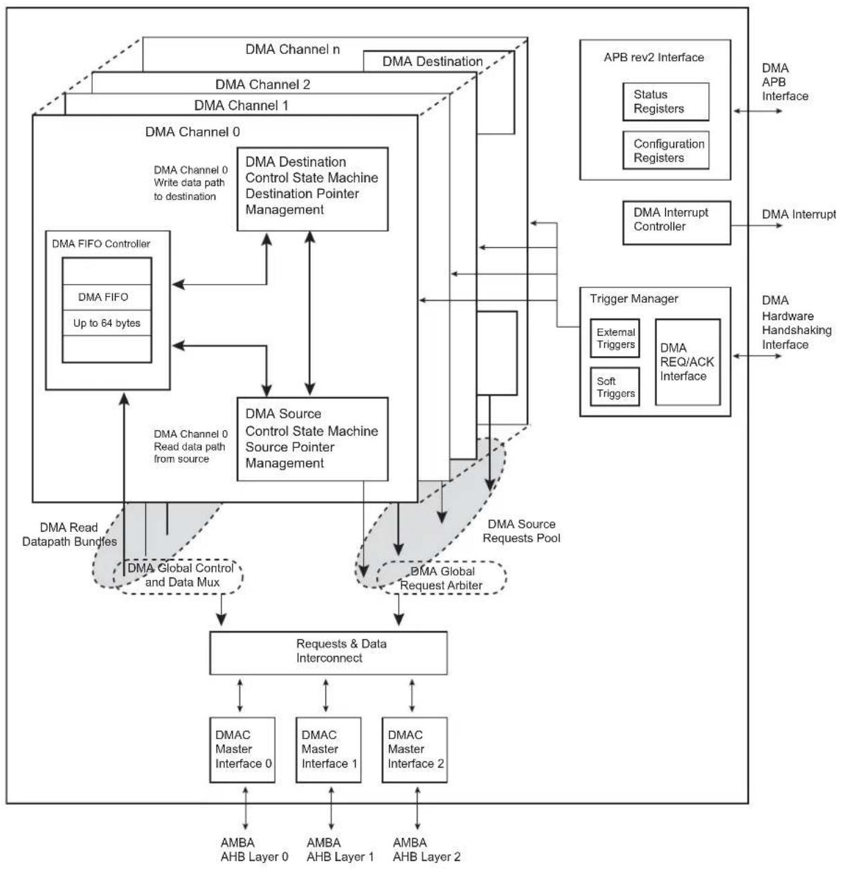
flowchart
graph TD
    A["DMA Channel 0"] -->|DMA Channel 0 Write data path to destination| B["DMA Channel 1"]
    A -->|DMA Channel 0 Write data path to destination| C["DMA Channel 2"]
    A -->|DMA Channel 0 Write data path to destination| D["DMA Channel n"]
    A -->|DMA Channel 0 Write data path to destination| E["DMA Destination Control State Machine Destination Pointer Management"]
    A -->|DMA Channel 0 Write data path to destination| F["DMA Source Control State Machine Source Pointer Management"]
    A -->|DMA Channel 0 Write data path to destination| G["DMA Source Control State Machine Source Pointer Management"]
    A -->|DMA Channel 0 Write data path to destination| H["DMA Source Control State Machine Source Pointer Management"]
    A -->|DMA Channel 0 Write data path to destination| I["DMA Source Control State Machine Source Pointer Management"]
    A -->|DMA Channel 0 Write data path to destination| J["DMA Source Control State Machine Source Pointer Management"]
    A -->|DMA Channel 0 Write data path to destination| K["DMA Source Control State Machine Source Pointer Management"]
    A -->|DMA Channel 0 Write data path to destination| L["DMA Source Control State Machine Source Pointer Management"]
    A -->|DMA Channel 0 Write data path to destination| M["DMA Source Control State Machine Source Pointer Management"]
    A -->|DMA Channel 0 Write data path to destination| N["DMA Source Control State Machine Source Pointer Management"]
    A -->|DMA Channel 0 Write data path to destination| O["DMA Source Control State Machine Source Pointer Management"]
    A -->|DMA Channel 0 Write data path to destination| P["DMA Source Control State Machine Source Pointer Management"]
    A -->|DMA Channel 0 Write data path to destination| Q["DMA Source Control State Machine Source Pointer Management"]
    A -->|DMA Channel 0 Write data path to destination| R["DMA Source Control State Machine Source Pointer Management"]
    A -->|DMA Channel 0 Write data path to destination| S["DMA Source Control State Machine Source Pointer Management"]
    A -->|DMA Channel 0 Write data path to destination| T["DMA Source Control State Machine Source Pointer Management"]
    A -->|DMA Channel 0 Write data path to destination| U["DMA Source Control State Machine Source Pointer Management"]
    A -->|DMA Channel 0 Write data path to destination| V["DMA Source Control State Machine Source Pointer Management"]
    A -->|DMA Channel 0 Write data path to destination| W["DMA Source Control State Machine Source Pointer Management"]
    A -->|DMA Channel 0 Write data path to destination| X["DMA Source Control State Machine Source Pointer Management"]
    A -->|DMA Channel 0 Write data path to destination| Y["DMA Source Control State Machine Source Pointer Management"]
    A -->|DMA Channel 0 Write data path to destination| Z["DMA Source Control State Machine Source Pointer Management"]
    A -->|DMA Channel 0 Write data path to destination| AA["DMA Source Control State Machine Source Pointer Management"]
    A -->|DMA Channel 0 Write data path to destination| AB["DMA Source Control State Machine Source Pointer Management"]
    A -->|DMA Channel 0 Write data path to destination| AC["DMA Source Control State Machine Source Pointer Management"]
    A -->|DMA Channel 0 Write data path to destination| AD["DMA Source Control State Machine Source Pointer Management"]
    A -->|DMA Channel 0 Write data path to destination| AE["DMA Source Control State Machine Source Pointer Management"]
    A -->|DMA Channel 0 Write data path to destination| AF["DMA Source Control State Machine Source Pointer Management"]
    A -->|DMA Channel 0 Write data path to destination| AG["DMA Source Control State Machine Source Pointer Management"]
    A -->|DMA Channel 0 Write data path to destination| AH["DMA Source Control State Machine Source Pointer Management"]
    A -->|DMA Channel 0 Write data path to destination| AI["DMA Source Control State Machine Source Pointer Management"]
    A -->|DMA Channel 0 Write data path to destination| AJ["DMA Source Control State Machine Source Pointer Management"]
    A -->|DMA Channel 0 Write data path to destination| AK["DMA Source Control State Machine Source Pointer Management"]
    A -->|DMA Channel 0 Write data path to destination| AL["DMA Source Control State Machine Source Pointer Management"]
    A -->|DMA Channel 0 Write data path to destination| AM["DMA Source Control State Machine Source Pointer Management"]
    A -->|DMA Channel 0 Write data path to destination| AN["DMA Source Control State Machine Source Pointer Management"]
    A -->|DMA Channel 0 Write data path to destination| AO["DMA Source Control State Machine Source Pointer Management"]
    A -->|DMA Channel 0 Write data path to destination| AP["APB rev2 Interface"]
    AP --> AP1["Status Registers"]
    AP --> AP2["Configuration Registers"]
    AP --> AP3["APB Interface"]
    AP --> AP4["APB Interface"]
    AP --> AP5["APB Interface"]
    AP --> AP6["APB Interface"]
    AP --> AP7["APB Interface"]
    AP --> AP8["APB Interface"]
    AP --> AP9["APB Interface"]
    AP --> AP10["APB Interface"]
    AP --> AP11["APB Interface"]
    AP --> AP12["APB Interface"]
    AP --> AP13["APB Interface"]
    AP --> AP14["APB Interface"]
    AP --> AP15["APB Interface"]
    AP --> AP16["APB Interface"]
    AP --> AP17["APB Interface"]
    AP --> AP18["APB Interface"]
    AP --> AP19["APB Interface"]
    AP --> AP20["APB Interface"]
    AP --> AP21["APB Interface"]
    AP --> AP22["APB Interface"]
    AP --> AP23["APB Interface"]
    AP --> AP24["APB Interface"]
    AP --> AP25["APB Interface"]
    AP --> AP26["APB Interface"]
    AP --> AP27["APB Interface"]
    AP --> AP28["APB Interface"]
    AP --> AP29["APB Interface"]
    AP --> AP30["APB Interface"]
    AP --> AP31["APB Interface"]
    AP --> AP32["APB Interface"]
    AP --> AP33["APB Interface"]
    AP --> AP34["APB Interface"]
    AP --> AP35["APB Interface"]
    AP --> AP36["APB Interface"]
    AP --> AP37["APB Interface"]
    AP --> AP38["APB Interface"]
    AP --> AP39["APB Interface"]
    AP --> AP40["APB Interface"]
    AP --> AP41["APB Interface"]
    AP --> AP42["APB Interface"]
    AP --> AP43["APB Interface"]
    AP --> AP44["APB Interface"]
    AP --> AP45["APB Interface"]
    AP --> AP46["APB Interface"]
    AP --> AP47["APB Interface"]
    AP --> AP48["APB Interface"]
    AP --> AP49["APB Interface"]
    AP --> AP50["APB Interface"]
    AP --> AP51["APB Interface"]
    AP --> AP52["APB Interface"]
    AP --> AP53["APB Interface"]
    AP --> AP54["APB Interface"]
    AP --> AP55["APB Interface"]
    AP --> AP56["APB Interface"]
    AP --> AP57["APB Interface"]
    AP --> AP58["APB Interface"]
    AP --> AP59["APB Interface"]
    AP --> AP60["APB Interface"]
    AP --> AP61["APB Interface"]
    AP --> AP62["APB Interface"]
    AP --> AP63["APB Interface"]
    AP --> AP64["APB Interface"]
    AP --> AP65["APB Interface"]
    AP --> AP66["APB Interface"]
    AP --> AP67["APB Interface"]
    AP --> AP68["APB Interface"]
    AP --> AP69["APB Interface"]
    AP --> AP70["APB Interface"]
    AP --> AP71["APB Interface"]
    AP --> AP72["APB Interface"]
    AP --> AP73["APB Interface"]
    AP --> AP74["APB Interface"]
    AP --> AP75["APB Interface"]
    AP --> AP76["APB Interface"]
    AP --> AP77["APB Interface"]
    AP --> AP78["APB Interface"]
    AP --> AP79["APB Interface"]
    AP --> AP80["APB Interface"]
31.5 Product Dependencies
31.5.1 Interrupt Sources
The DMAC interrupt line is connected to one of the internal sources of the interrupt controller. Using the DMAC interrupt requires prior programming of the interrupt controller.
Table 31-3: Peripheral IDs
| Instance ID | |
| DMAC0 30 | |
| DMAC1 31 |
31.6 Functional Description
31.6.1 Basic Definitions
Source peripheral: Device on an AMBA layer from where the DMAC reads data, which is then stored in the channel FIFO. The source peripheral teams up with a destination peripheral to form a channel.
Destination peripheral: Device to which the DMAC writes the stored data from the FIFO (previously read from the source peripheral).
Memory: Source or destination that is always “ready” for a DMAC transfer and does not require a handshaking interface to interact with the DMAC.
Programmable Arbitration Policy: Modified Round Robin and Fixed Priority are available by means of the ARB_CFG bit in the Global Configuration Register (DMAC_GCFG). The fixed priority is linked to the channel number. The highest DMAC channel number has the highest priority.
Channel: Read/write datapath between a source peripheral on one configured AMBA layer and a destination peripheral on the same or different AMBA layer that occurs through the channel FIFO. If the source peripheral is not memory, then a source handshaking interface is assigned to the channel. If the destination peripheral is not memory, then a destination handshaking interface is assigned to the channel. Source and destination handshaking interfaces can be assigned dynamically by programming the channel registers.
Master interface: DMAC is a master on the AHB bus reading data from the source and writing it to the destination over the AHB bus.
Slave interface: The APB interface over which the DMAC is programmed. The slave interface in practice could be on the same layer as any of the master interfaces or on a separate layer.
Handshaking interface: A set of signal registers that conform to a protocol and handshake between the DMAC and source or destination peripheral to control the transfer of a single or chunk transfer between them. This interface is used to request, acknowledge, and control a DMAC transaction. A channel can receive a request through one of two types of handshaking interface: hardware or software.
Hardware handshaking interface: Uses hardware signals to control the transfer of a single or chunk transfer between the DMAC and the source or destination peripheral.
Software handshaking interface: Uses software registers to control the transfer of a single or chunk transfer between the DMAC and the source or destination peripheral. No special DMAC handshaking signals are needed on the I/O of the peripheral. This mode is useful for interfacing an existing peripheral to the DMAC without modifying it.
Transfer hierarchy: Figure 31-2 illustrates the hierarchy between DMAC transfers, buffer transfers, chunk or single, and AMBA transfers (single or burst) for non-memory peripherals. Figure 31-3 shows the transfer hierarchy for memory.
Figure 31-2: DMAC Transfer Hierarchy for Non-Memory Peripheral

flowchart
graph TD
    A["DMAC Transfer"] --> B["Buffer"]
    A --> C["Buffer Buffer"]
    A --> D["..."]
    C --> E["Chunk Transfer"]
    C --> F["Chunk Transfer"]
    C --> G["Chunk Transfer"]
    C --> H["Single Transfer"]
    H --> I["AMBA Single Transfer"]
    H --> J["AMBA Burst Transfer"]
    H --> K["AMBA Burst Transfer"]
    H --> L["AMBA Burst Transfer"]
    style A fill:#f9f,stroke:#333
    style B fill:#ccf,stroke:#333
    style C fill:#ccf,stroke:#333
    style D fill:#ccf,stroke:#333
    style E fill:#cfc,stroke:#333
    style F fill:#cfc,stroke:#333
    style G fill:#cfc,stroke:#333
    style H fill:#cfc,stroke:#333
    style I fill:#fcc,stroke:#333
    style J fill:#fcc,stroke:#333
    style K fill:#fcc,stroke:#333
    style L fill:#fcc,stroke:#333
Figure 31-3: DMAC Transfer Hierarchy for Memory
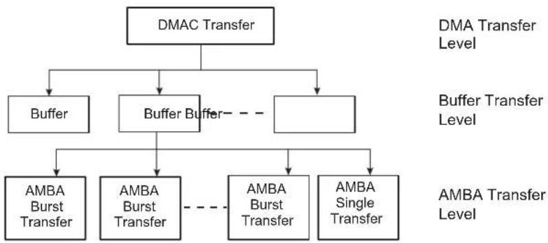
flowchart
graph TD
    A["DMAC Transfer"] --> B["Buffer"]
    A --> C["Buffer Buffer"]
    A --> D["AmBA Single Transfer"]
    C --> E["AMBA Burst Transfer"]
    C --> F["AMBA Burst Transfer"]
    C --> G["AMBA Burst Transfer"]
    D --> H["AMBA Single Transfer"]
    style A fill:#f9f,stroke:#333
    style B fill:#ccf,stroke:#333
    style C fill:#ccf,stroke:#333
    style D fill:#ccf,stroke:#333
    style E fill:#cfc,stroke:#333
    style F fill:#cfc,stroke:#333
    style G fill:#cfc,stroke:#333
Buffer: A buffer of DMAC data. The amount of data (length) is determined by the flow controller. For transfers between the DMAC and memory, a buffer is broken directly into a sequence of AMBA bursts and AMBA single transfers.
For transfers between the DMAC and a non-memory peripheral, a buffer is broken into a sequence of DMAC transactions (single and chunks). These are in turn broken into a sequence of AMBA transfers.
Transaction: A basic unit of a DMAC transfer as determined by either the hardware or software handshaking interface. A transaction is only relevant for transfers between the DMAC and a source or destination peripheral if the source or destination peripheral is a non-memory device. There are two types of transactions: single transfer and chunk transfer.
- Single transfer: The length of a single transaction is always 1 and is converted to a single AMBA access.
- Chunk transfer: The length of a chunk is programmed into the DMAC. The chunk is then converted into a sequence of AHB access.DMAC executes each AMBA burst transfer by performing incremental bursts that are no longer than 16 beats.
DMAC transfer: Software controls the number of buffers in a DMAC transfer. Once the DMAC transfer has completed, then hardware within the DMAC disables the channel and can generate an interrupt to signal the completion of the DMAC transfer. It is then possible to reprogram the channel for a new DMAC transfer.
Single-buffer DMAC transfer: Consists of a single buffer.
Multi-buffer DMAC transfer: A DMAC transfer may consist of multiple DMAC buffers. Multi-buffer DMAC transfers are supported through buffer chaining (linked list pointers), auto-reloading of channel registers, and contiguous buffers. The source and destination can independently select which method to use.
- Linked lists (buffer chaining) – A descriptor pointer (DSCR) points to the location in system memory where the next linked list item (LLI) exists. The LLI is a set of registers that describe the next buffer (buffer descriptor) and a descriptor pointer register. The DMAC fetches the LLI at the beginning of every buffer when buffer chaining is enabled.
- Replay – The DMAC automatically reloads the channel registers at the end of each buffers to the value when the channel was first enabled.
- Contiguous buffers – Where the address of the next buffer is selected to be a continuation from the end of the previous buffer. Picture-in-Picture Mode: DMAC contains a Picture-in-Picture mode support. When this mode is enabled, addresses are automatically incremented by a programmable value when the DMAC channel transfer count reaches a user defined boundary.
Figure 31-4 illustrates a memory mapped image 4:2:2 encoded located at image_base_address in memory. A user defined start address is defined at Picture_start_address. The incremented value is set to memory_hole_size = image_width - picture_width, and the boundary is set to picture_width.
Figure 31-4: Picture-In-Picture Mode Support
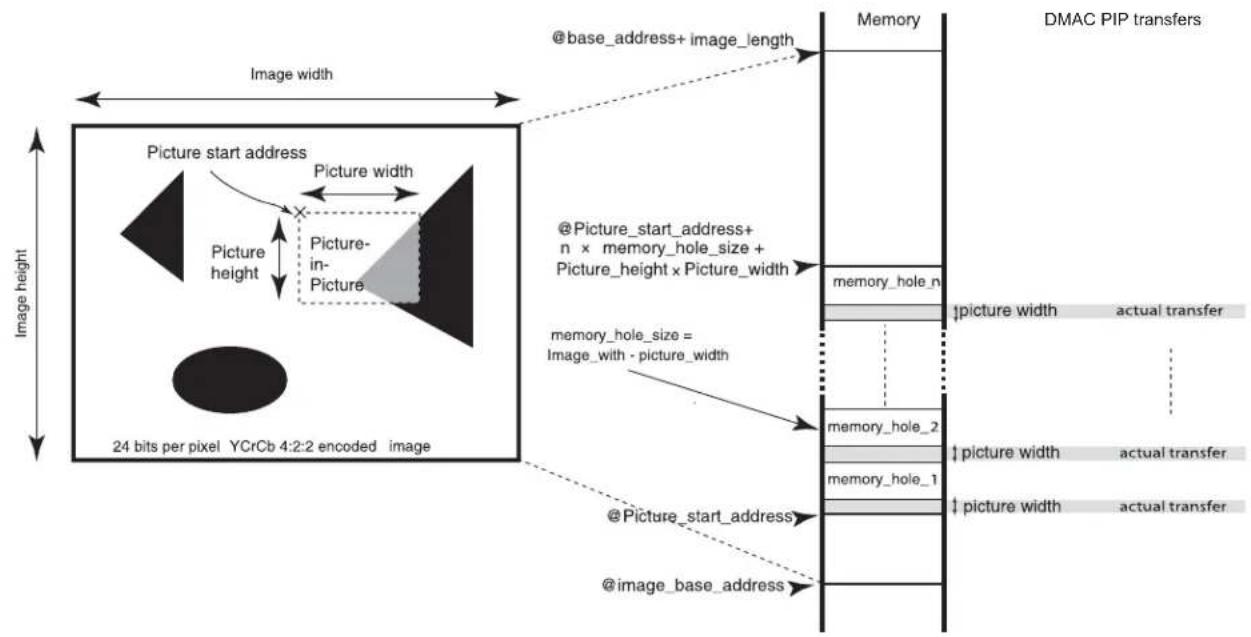
flowchart
graph TD
    A["Image width"] --> B["Picture start address"]
    B --> C["Picture height"]
    C --> D["Picture in Picture"]
    D --> E["24 bits per pixel YCrCb 4:2:2 encoded image"]
    E --> F["@image_base_address"]
    F --> G["@Picture_start_address"]
    G --> H["@image_with - picture_width"]
    H --> I["memory_hole_n"]
    I --> J["memory_hole_1"]
    I --> K["memory_hole_2"]
    J --> L["DMAC PIP transfers"]
    K --> L
    L --> M["@base_address+ image_length"]
    M --> N["Memory"]
    N --> O["Actual Transfer"]
    style A fill:#f9f,stroke:#333
    style B fill:#ccf,stroke:#333
    style C fill:#cfc,stroke:#333
    style D fill:#fcc,stroke:#333
    style E fill:#cff,stroke:#333
    style F fill:#ffc,stroke:#333
    style G fill:#cfc,stroke:#333
    style H fill:#fcc,stroke:#333
    style I fill:#ffc,stroke:#333
    style J fill:#cfc,stroke:#333
    style K fill:#fcc,stroke:#333
    style L fill:#ffc,stroke:#333
    style M fill:#cfc,stroke:#333
Channel locking: Software can program a channel to keep the AHB master interface by locking the arbitration for the master bus interface for the duration of a DMAC transfer, buffer, or chunk.
Bus locking: Software can program a channel to maintain control of the AMBA bus by asserting hmastlock for the duration of a DMAC transfer, buffer, or transaction (single or chunk). Channel locking is asserted for the duration of bus locking at a minimum.
31.6.2 Memory Peripherals
Figure 31-3 on page 493 shows the DMAC transfer hierarchy of the DMAC for a memory peripheral. There is no handshaking interface with the DMAC, and therefore the memory peripheral can never be a flow controller. Once the channel is enabled, the transfer proceeds immediately without waiting for a transaction request. The alternative to not having a transaction-level handshaking interface is to allow the DMAC to attempt AMBA transfers to the peripheral once the channel is enabled. If the peripheral slave cannot accept these AMBA transfers, it inserts wait states onto the bus until it is ready; it is not recommended that more than 16 wait states be inserted onto the bus. By using the handshaking interface, the peripheral can signal to the DMAC that it is ready to transmit/receive data, and then the DMAC can access the peripheral without the peripheral inserting wait states onto the bus.
31.6.3 Handshaking Interface
Handshaking interfaces are used at the transaction level to control the flow of single or chunk transfers. The operation of the handshaking interface is different and depends on whether the peripheral or the DMAC is the flow controller.
The peripheral uses the handshaking interface to indicate to the DMAC that it is ready to transfer/accept data over the AMBA bus. A non-memory peripheral can request a DMAC transfer through the DMAC using one of two handshaking interfaces:
• Hardware handshaking
- Software handshaking
Software selects between the hardware or software handshaking interface on a per-channel basis. Software handshaking is accomplished through memory-mapped registers, while hardware handshaking is accomplished using a dedicated handshaking interface.
31.6.3.1 Software Handshaking
When the slave peripheral requires the DMAC to perform a DMAC transaction, it communicates this request by sending an interrupt to the CPU or interrupt controller.
The interrupt service routine then uses the software registers to initiate and control a DMAC transaction. These software registers are used to implement the software handshaking interface.
The SRC_H2SEL/DST_H2SEL bit in the Channel Configuration Register (DMAC_CFGx) must be cleared to enable software handshaking.
When the peripheral is not the flow controller, then the Software Last Transfer Flag Register (DMAC_LAST) is not used, and the values in these registers are ignored.
- Chunk Transactions
Writing a '1' to the Software Chunk Transfer Request Register (DMAC_CREQ[2x]) starts a source chunk transaction request, where x is the channel number. Writing a '1' to the DMAC_CREQ[2x+1] register starts a destination chunk transfer request, where x is the channel number.
Upon completion of the chunk transaction, the hardware clears the DMAC_CREQ[2x] or DMAC_CREQ[2x+1].
- Single Transactions
Writing a '1' to the Software Single Request Register (DMAC_SREQ[2x]) starts a source single transaction request, where x is the channel number. Writing a '1' to the DMAC_SREQ[2x+1] register starts a destination single transfer request, where x is the channel number.
Upon completion of the chunk transaction, the hardware clears the DMAC_SREQ[x] or DMAC_SREQ[2x+1].
The software can poll the relevant channel bit in the DMAC_CREQ[2x]/DMAC_CREQ[2x+1] and DMAC_SREQ[x]/DMAC_SREQ[2x+1] registers. When both are 0, then either the requested chunk or single transaction has completed.
31.6.4 DMAC Transfer Types
A DMAC transfer may consist of single or multi-buffer transfers. On successive buffers of a multi-buffer transfer, DMAC_SADDRx/DMAC_DADDRx in the DMAC are reprogrammed using either of the following methods:
- Buffer chaining using linked lists
- Replay mode
- Contiguous address between buffers
On successive buffers of a multi-buffer transfer, the DMAC_CTRLAx and DMAC_CTRLBx registers in the DMAC are reprogrammed using either of the following methods:
- Buffer chaining using linked lists
- Replay mode
When buffer chaining using linked lists is the multi-buffer method of choice, and on successive buffers, DMAC_DSCRx in the DMAC is reprogrammed using the following method:
• Buffer chaining using linked lists
A buffer descriptor (LLI) consists of the following registers: DMAC_SADDRx, DMAC_DADDRx, DMAC_DSCRx, DMAC_CTRLAX, and DMAC_CTRLBx. These registers, along with DMAC_CFGx, are used by the DMAC to set up and describe the buffer transfer.
31.6.4.1 Multi-buffer Transfers
- Buffer Chaining Using Linked Lists
In this case, the DMAC reprograms the channel registers prior to the start of each buffer by fetching the buffer descriptor for that buffer from system memory. This is known as an LLI update.
DMAC buffer chaining is supported by using a descriptor pointer register (DMAC_DSCRx) that stores the address in memory of the next buffer descriptor. Each buffer descriptor contains the corresponding buffer descriptor (DMAC_SADDRx, DMAC_DADDRx, DMAC_DSCRx, DMAC_CTRLAx DMAC_CTRLBx).
To set up buffer chaining, a sequence of linked lists must be programmed in memory.
DMAC_SADDRx, DMAC_DADDRx, DMAC_DSCRx, DMAC_CTRLAx and DMAC_CTRLBx are fetched from system memory on an LLI update. The updated content of DMAC_CTRLAx is written back to memory on buffer completion. Figure 31-5 on page 496 shows how to use chained linked lists in memory to define multi-buffer transfers using buffer chaining.
The Linked List multi-buffer transfer is initiated by programming DMAC_DSCRx with DSCRx(0) (LLI(0) base address) different from zero. Other fields and registers are ignored and overwritten when the descriptor is retrieved from memory.
The last transfer descriptor must be written to memory with its next descriptor address set to 0.
Figure 31-5: Multi-Buffer Transfer Using Linked List
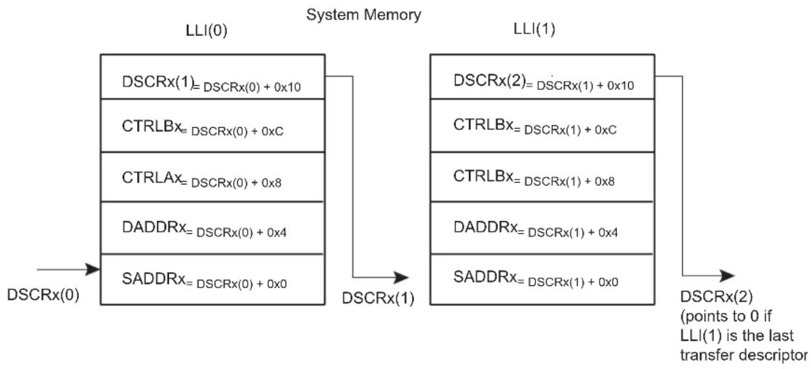
flowchart
graph LR
    A["DSCRx(0)"] --> B["LLI(0)"]
    B --> C["DSCRx(1)"]
    C --> D["LLI(1)"]
    D --> E["DSCRx(2) (points to 0 if LLI(1) is the last transfer descriptor)"]

    subgraph System Memory
        F["DSCRx(1)=DSCRx(0)+0x10"]
        G["CTRLBx=DSCRx(0)+0xC"]
        H["CTRLAx=DSCRx(0)+0x8"]
        I["DADDRx=DSCRx(0)+0x4"]
        J["SADDRx=DSCRx(0)+0x0"]
    end

    subgraph DSCRx(1)
        K["DSCRx(1)"]
        L["DSCRx(2)"]
    end
- Descriptor Integrity Check
When the Descriptor Integrity Check is enabled, a cyclic redundancy check information is attached to the descriptor. When fetched from the memory, the descriptor is verified through the use of a CRC16-CCIT (0x1021 polynom) by the DMAC channel. If a CRC error is detected, then the DICERR flag is set in the DMAC Error, Buffer Transfer and Chained Buffer Transfer Status Register (DMAC_EBCISR). The CRC16 is computed from MSB to LSB. The BTSIZE field and DONE bit in DMAC_CTRLAx are ignored and cleared.
Figure 31-6: Linked List with CRC16 Attached
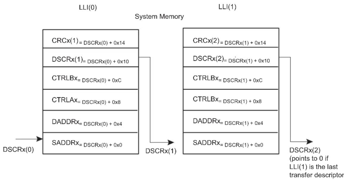
flowchart
graph LR
    subgraph System Memory
        A["LLI(0)"] --> B["CRCx(1)=DSCRx(0)+0x14"]
        A --> C["DSCRx(1)=DSCRx(0)+0x10"]
        A --> D["CTRLBx=DSCRx(0)+0xC"]
        A --> E["CTRLAx=DSCRx(0)+0x8"]
        A --> F["DADDRx=DSCRx(0)+0x4"]
        A --> G["SADDRx=DSCRx(0)+0x0"]
    end

    subgraph DSCRX(1) |
        H["LLI(1)"] --> I["CRCx(2)=DSCRx(1)+0x14"]
        H --> J["DSCRx(2)=DSCRx(1)+0x10"]
        H --> K["CTRLBx=DSCRx(1)+0xC"]
        H --> L["CTRLBx=DSCRx(1)+0x8"]
        H --> M["DADDRx=DSCRx(1)+0x4"]
        H --> N["SADDRx=DSCRx(1)+0x0"]
    end

    O["DSCRx(0)"] --> P["LLI(0)"]
    Q["DSCRx(2) (points to 0 if LLI(1) is the last transfer descriptor)"] --> R["DSCRx(2)"]
31.6.4.2 Programming DMAC for Multiple Buffer Transfers
Table 31-4: Multiple Buffers Transfer Management Table
| Transfer Type AUTO SRC_REP DST_REP SRC_DSCR DST_DSCR BTSIZE DSCR SADDR DADDR | Other Fields | |||||||||
| 1 | Single Buffer or Last Buffer of a multiple buffer transfer | 0 | - | - | - | (1)_ | 0 USRSR(1) | USR^(1) | USR^(1) | |
| 2 | Multi-buffer transfer with contiguous DADDR | 0 | - | 0 | 0 | 1 | LLI^(5) | USR^(1) | LLI^(5) | CONT^(2) |
| 3 | Multi-buffer transfer with contiguous SADDR | 0 | 0 | - | 1 | 0 | LLI^(5) | USR^(1) | CONT^(2) | LLI^(5) |
| 4 | Multi-buffer transfer with LLI support | 0 | - | - | 0 | 0 | LLI^(5) | USR^(1) | LLI^(5) | LLI^(5) |
| 5 | Multi-buffer transfer with DADDR reloaded | 0 | - | 1 | 0 | 1 | LLI^(5) | USR^(1) | LLI^(5) | REP^(3) |
| 6 | Multi-buffer transfer with SADDR reloaded | 0 | 1 | - | 1 | 0 | LLI^(5) | USR^(1) | REP^(3) | LLI^(5) |
| 7 | Multi-buffer transfer with BTSIZE reloaded and contiguous DADDR | 1 | - | 0 | 0 | (3)1 | USR^(1) | LLI^(5) | CONT^(2) | |
| 8 | Multi-buffer transfer with BTSIZE reloaded and contiguous SADDR | 1 | 0 | - | 1 | (3)0 | USR^(1) | CONT^(2) | LLI^(5) | |
| 9 | Automatic mode channel is stalling(4)BTsize is reloaded | 1 | 0 | 0 | 1 | (3)1 | USR^(1) | CONT^(2) | CONT^(2) | |
| 10 | Automatic mode BTSIZE, SADDR and DADDR reloaded | 1 | 1 | 1 | 1 | (3)1 | USR^(1) | REP^(3) | REP^(3) | |
| 11 | Automatic mode BTSIZE, SADDR reloaded and DADDR contiguous | 1 | 1 | 0 | 1 | (3)1 | USR^(1) | REP^(3) | CONT^(2) | |
Note 1: USR means that the register field is manually programmed by the user.
2: CONT means that address are contiguous.
3: REP means that the register field is updated with its previous value. If the transfer is the first one, then the user must manually program the value.
4: Channel stalled is true if the relevant BTC interrupt is not masked.
5: LLI means that the register field is updated with the content of the linked list item.
- Replay Mode of Channel Registers
During automatic replay mode, the channel registers are reloaded with their initial values at the completion of each buffer and the new values used for the new buffer. Depending on the row number in Table 31-4, some or all of the DMAC_SADDRx, DMAC_DADDRx, DMAC_CTRLAx and DMAC_CTRLBx channel registers are reloaded from their initial value at the start of a buffer transfer. - Contiguous Address Between Buffers
In this case, the address between successive buffers is selected to be a continuation from the end of the previous buffer. Enabling the source or destination address to be contiguous between buffers is a function of the fields DMAC_CTRLAx.SRC_DSCR, DMAC_CFGx.DST_REP, DMAC_CFGx.SRC_REP and DMAC_CTRLAx.DST_DSCR. - Suspension of Transfers Between Buffers
At the end of every buffer transfer, an end of buffer interrupt is asserted if: - the channel buffer interrupt is unmasked, DMAC_EBCIMR.BTCx = '1', where x is the channel number.
Note: The Buffer Transfer Completed Interrupt is generated at the completion of the buffer transfer to the destination.
At the end of a chain of multiple buffers, an end of linked list interrupt is asserted if:
- the channel end of the Chained Buffer Transfer Completed Interrupt is unmasked, DMAC_EBCIMR.CBTCx = '1', when n is the channel number.
31.6.4.3 Ending Multi-buffer Transfers
All multi-buffer transfers must end as shown in Row 1 of Table 31-4 on page 498. At the end of every buffer transfer, the DMAC samples the row number, and if the DMAC is in Row 1 state, then the previous buffer transferred was the last buffer and the DMAC transfer is terminated.
For rows 9, 10 and 11 of Table 31-4 on page 498, (DMAC_DSCRx = 0 and DMAC_CTRLBx.AUTO is set), multi-buffer DMAC transfers continue until the automatic mode is disabled by clearing the DMAC_CTRLBx.AUTO bit. This bit should be programmed to zero in the end of buffer interrupt service routine that services the next-to-last buffer transfer. This puts the DMAC into Row 1 state.
For rows 2, 3, 4, 5, and 6 (DMAC_CRTLBx.AUTO cleared), the user must set up the last buffer descriptor in memory so that LLI.DMAC_DSCRx is set to 0.
31.6.5 Programming a Channel
Four registers, DMAC_DSCRx, DMAC_CTRLAx, DMAC_CTRLBx and DMAC_CFGx, need to be programmed to set up whether single or multi-buffer transfers take place, and which type of multi-buffer transfer is used. The different transfer types are shown in Table 31-4 on page 498.
The "BTSIZE", "SADDR" and "DADDR" columns in the table indicate where the values of DMAC_SADDRx, DMAC_DADDRx, DMAC_CTRLAx, DMAC_CTRLBx, and DMAC_DSCRx are obtained for the next buffer transfer when multi-buffer DMAC transfers are enabled.
31.6.5.1 Programming Examples
• Single-buffer Transfer (Row 1)
- Read the ENAx bit in the DMAC Channel Handler Status Register (DMAC_CHSR) to choose a free (disabled) channel.
- Clear any pending interrupts on the channel from the previous DMAC transfer by reading the DMAC Error, Buffer Transfer and Chained Buffer Transfer Status Register (DMAC_EBCISR).
3. Program the following channel registers:
a) Write the starting source address in DMAC_SADDRx for channel x.
b) Write the starting destination address in DMAC_DADDRx for channel x.
c) Write the next descriptor address in DMA_DSCRx for channel x with 0x0.
d) Program DMAC_CTRLAx, DMAC_CTRLBx and DMAC_CFGx according to Row 1 as shown in Table 31-4 on page 498. Program DMAC_CTRLBx with both AUTO bits cleared.
e) Write the control information for the DMAC transfer in DMAC_CTRLAx and DMAC_CTRLBx for channel x. For example, in the register, it is possible to program the following:
- i. Set up the transfer type (memory or non-memory peripheral for source and destination) and flow control device by programming the FC field in DMAC_CTRLBx.
-
ii. Set up the transfer characteristics, such as:
-
Transfer width for the source in the SRC_WIDTH field.
- Transfer width for the destination in the DST_WIDTH field.
- Source AHB Master interface layer in the SIF field where source resides.
- Destination AHB Master Interface layer in the DIF field where destination resides.
- Incrementing/decrementing or fixed address for source in SRC_INCR field.
- Incrementing/decrementing or fixed address for destination in DST_INCR field.
f) Write the channel configuration information into DMAC_CFGx for channel x.
- i. Designate the handshaking interface type (hardware or software) for the source and destination peripherals. This is not required for memory. This step requires programming the SRC_H2SEL/DST_H2SEL bits, respectively. Writing a '1' activates the hardware handshaking interface to handle source/destination requests. Writing a '0' activates the software handshaking interface to handle source/destination requests.
- ii. If the hardware handshaking interface is activated for the source or destination peripheral, assign a handshaking interface to the source and destination peripheral. This requires programming the SRC_PER and DST_PER bits, respectively.
g) If source Picture-in-Picture mode is enabled (DMAC_CTRLBx.SRC_PIP is enabled), program DMAC_SPIPx for channel x.
h) If destination Picture-in-Picture mode is enabled (DMAC_CTRLBx.DST_PIP is enabled), program DMAC_DPIPx for channel x.
- After the DMAC selected channel has been programmed, enable the channel by setting the ENAx bit in the DMAC Channel Handler Enable Register (DMAC_CHER), where x is the channel number. Make sure that the ENABLE bit (register bit 0) in DMAC_EN is set.
- Source and destination request single and chunk DMAC transactions to transfer the buffer of data (assuming non-memory peripherals). The DMAC acknowledges at the completion of every transaction (chunk and single) in the buffer and carries out the buffer transfer.
- Once the transfer completes, the hardware sets the interrupts and disables the channel. At this time, you can either respond to the Buffer Transfer Completed Interrupt or Chained Buffer Transfer Completed Interrupt, or poll for the DMAC_CHSR.ENAx bit until it is cleared by hardware, to detect when the transfer is complete.
- Multi-buffer Transfer with Linked List for Source and Linked List for Destination (Row 4)
-
Read the DMAC_CHSR to choose a free (disabled) channel.
-
Set up the chain of Linked List Items (otherwise known as buffer descriptors) in memory. Write the control information in the LLI.DMAC_CTRLAx and LLI.DMAC_CTRLBx registers location of the buffer descriptor for each LLI in memory (see Figure 31-7 on page 502) for channel x. For example, in the register, it is possible to program the following:
a) Set up the transfer type (memory or non-memory peripheral for source and destination) and flow control device by programming the FC field in DMAC_CTRLBx.
b) Set up the transfer characteristics, such as:
- i. Transfer width for the source in the SRC WIDTH field.
- ii. Transfer width for the destination in the DST_WIDTH field.
- iii. Source AHB master interface layer in the SIF field where source resides.
- iv. Destination AHB master interface layer in the DIF field where destination resides.
- v. Incrementing/decrementing or fixed address for source in SRC_INCR field.
- vi. Incrementing/decrementing or fixed address for destination DST_INCR field.
- Write the channel configuration information into DMAC_CFGx for channel x.
a) Designate the handshaking interface type (hardware or software) for the source and destination peripherals. This is not required for memory. This step requires programming the SRC_H2SEL/DST_H2SEL bits, respectively. Writing a '1' activates the hardware handshaking interface to handle source/destination requests for the specific channel. Writing a '0' activates the software handshaking interface to handle source/destination requests.
b) If the hardware handshaking interface is activated for the source or destination peripheral, assign the handshaking interface to the source and destination peripheral. This requires programming the SRC_PER and DST_PER bits, respectively.
-
Make sure that the LLI.DMAC_CTRLBx register locations of all LLI entries in memory (except the last) are set as shown in Row 4 of Table 31-4 on page 498. The LLI.DMAC_CTRLBx register of the last Linked List Item must be set as described in Row 1 of Table 31-4. Figure 31-5 on page 496 shows a Linked List example with two list items.
-
Make sure that the LLI.DMAC_DSCRx register locations of all LLI entries in memory (except the last) are non-zero and point to the base address of the next Linked List Item.
-
Make sure that the LLI.DMAC_SADDRx/LLI.DMAC_DADDRx register locations of all LLI entries in memory point to the start source/destination buffer address preceding that LLI fetch.
-
Make sure that the LLI.DMAC_CTRLAx.DONE bit of the LLI.DMAC_CTRLAx register locations of all LLI entries in memory are cleared.
-
If source Picture-in-Picture mode is enabled (DMAC_CTRLBx.SRC_PIP is enabled), program DMAC_SPIPx for channel x.
-
If destination Picture-in-Picture is enabled (DMAC_CTRLBx.DST_PIP is enabled), program DMAC_DPIPx for channel x.
-
Clear any pending interrupts on the channel from the previous DMAC transfer by reading DMAC_EBCISR.
-
Program DMAC_CTRLBx and DMAC_CFGx according to Row 4 as shown in Table 31-4 on page 498.
-
Program DMAC_DSCRx with DMAC_DSCRx(0), the pointer to the first Linked List item.
-
Finally, enable the channel by setting the DMAC_CHER.ENAx bit, where x is the channel number. The transfer is performed.
-
The DMAC fetches the first LLI from the location pointed to by DMAC_DSCRx(0).
Note: The LLI.DMAC_SADDRx, LLI.DMAC_DADDRx, LLI.DMAC_DSCRx, LLI.DMAC_CTRLAx and LLI.DMAC_CTRLBx registers are fetched. The DMAC automatically reprograms the DMAC_SADDRx, DMAC_DADDRx, DMAC_DSCRx, DMAC_CTRLBx and DMAC_CTRLAx channel registers from the DMAC_DSCRx(0).
-
Source and destination request single and chunk DMAC transactions to transfer the buffer of data (assuming non-memory peripheral). The DMAC acknowledges at the completion of every transaction (chunk and single) in the buffer and carries out the buffer transfer.
-
Once the buffer of data is transferred, the DMAC_CTRLAx register is written out to system memory at the same location and on the same layer (DMAC_DSCRx.DSCR_IF) where it was originally fetched, that is, the location of the DMAC_CTRLAx register of the linked list item fetched prior to the start of the buffer transfer. Only DMAC_CTRLAx register is written out because only the DMAC_CTRLAx.BTSIZE and DMAC_CTRLAX.DONE bits have been updated by DMAC hardware. Additionally, the DMAC_CTRLAx.DONE bit is asserted when the buffer transfer has completed.
Note: Do not poll the DMAC_CTRLAx.DONE bit in the DMAC memory map. Instead, poll the LLI.DMAC_CTRLAx.DONE bit in the LLI for that buffer. If the poll LLI.DMAC_CTRLAx.DONE bit is asserted, then this buffer transfer has completed. This LLI.DMAC_CTRLAx.DONE bit was cleared at the start of the transfer.
- The DMAC does not wait for the buffer interrupt to be cleared, but continues fetching the next LLI from the memory location pointed to by current DMAC_DSCRx and automatically reprograms the DMAC_SADDRx, DMAC_DADDRx, DMAC_DSCRx, DMAC_CTRLAx and DMAC_CTRLBx channel registers. The DMAC transfer continues until the DMAC determines that the
DMAC_CTRLBx and DMAC_DSCRx registers at the end of a buffer transfer match as described in Row 1 of Table 31-4 on page 498. The DMAC then knows that the previous buffer transferred was the last buffer in the DMAC transfer. The DMAC transfer might look like that shown in Figure 31-7.
Figure 31-7: Multi-buffer with Linked List Address for Source and Destination

flowchart
graph TD
    A["Address of Source Layer"] --> B["SADDR(2)"]
    B --> C["Buffer 2"]
    C --> D["DADDR(2)"]
    D --> E["Buffer 2"]
    F["SADDR(1)"] --> G["Buffer 1"]
    G --> H["DADDR(1)"]
    H --> I["Buffer 1"]
    J["SADDR(0)"] --> K["Buffer 0"]
    K --> L["DADDR(0)"]
    L --> M["Buffer 0"]
    N["Address of Destination Layer"] --> O["Address of Source Layer"]
    O --> P["SADDR(2)"]
    P --> Q["Buffer 2"]
    Q --> R["DADDR(2)"]
    R --> S["Buffer 2"]
    T["SADDR(1)"] --> U["Buffer 1"]
    U --> V["DADDR(1)"]
    V --> W["Buffer 1"]
    X["SADDR(0)"] --> Y["Buffer 0"]
    Y --> Z["DADDR(0)"]
    Z --> AA["Buffer 0"]
Source Buffers Destination Buffers
If the user needs to execute a DMAC transfer where the source and destination address are contiguous but the amount of data to be transferred is greater than the maximum buffer size DMAC_CTRLAx.BTSIZE, then this can be achieved using the type of multi-buffer transfer as shown in Figure 31-8.
Figure 31-8: Multi-buffer with Linked Address for Source and Destination Buffers are Contiguous

flowchart
graph LR
    A["Address of Source Layer"] --> B["Source Buffers"]
    B --> C["Buffer 0"]
    B --> D["Buffer 1"]
    B --> E["Buffer 2"]
    B --> F["Buffer 3"]
    G["Address of Destination Layer"] --> H["Destination Buffers"]
    H --> I["Buffer 0"]
    H --> J["Buffer 1"]
    H --> K["Buffer 2"]
    H --> L["DADDR(0)"]
 D --> M["DADDR(1)"]
    D --> N["DADDR(2)"]
    D --> O["DADDR(3)"]
    P["SADDR(0) --> Source Buffers"]
The DMAC transfer flow is shown in Figure 31-9.
Figure 31-9: DMAC Transfer Flow for Source and Destination Linked List Address
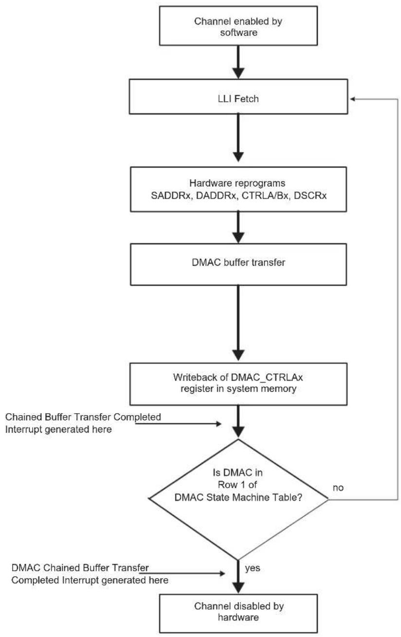
flowchart
graph TD
    A["Channel enabled by software"] --> B["LLI Fetch"]
    B --> C["Hardware reprograms SADDRx, DADDRx, CTRLA/Bx, DSCRx"]
    C --> D["DMAC buffer transfer"]
    D --> E["Writeback of DMAC_CTRLAx register in system memory"]
    E --> F{Is DMAC in Row 1 of DMAC State Machine Table?}
    F -->|yes| G["Channel disabled by hardware"]
    F -->|no| H["Chained Buffer Transfer Completed Interrupt generated here"]
    H --> E
    I["Chained buffer transfer Completed Interrupt generated here"] --> F
- Multi-buffer Transfer with Source Address Auto-reloaded and Destination Address Auto-reloaded (Row 10)
-
Read the DMAC_CHSR to choose an available (disabled) channel.
-
Clear any pending interrupts on the channel from the previous DMAC transfer by reading the interrupt status register. Program the following channel registers:
a) Write the starting source address in DMAC_SADDRx for channel x.
b) Write the starting destination address in DMAC_DADDRx for channel x.
c) Program DMAC_CTRLAx, DMAC_CTRLBx and DMAC_CFGx according to Row 10 as shown in Table 31-4 on page 498. Program DMAC_DSCRx with 0.
d) Write the control information for the DMAC transfer in DMAC_CTRLAx and DMAC_CTRLBx for channel x. For example, in the register, it is possible to program the following:
- i. Set up the transfer type (memory or non-memory peripheral for source and destination) and flow control device by programming the FC field in DMAC_CTRLBx.
- ii. Set up the transfer characteristics, such as:
- Transfer width for the source in the SRC_WIDTH field.
- Transfer width for the destination in the DST_WIDTH field.
- Source AHB master interface layer in the SIF field where source resides.
- Destination AHB master interface layer in the DIF field where destination resides.
- Incrementing/decrementing or fixed address for source in SRC_INCR field.
- Incrementing/decrementing or fixed address for destination in DST_INCR field.
e) If source Picture-in-Picture mode is enabled (DMAC_CTRLBx.SPIP is enabled), program DMAC_SPIPx for channel x.
f) If destination Picture-in-Picture is enabled (DMAC_CTRLBx.DPIP), program DMAC_DPIPx for channel x.
g) Write the channel configuration information into DMAC_CFGx for channel x. Ensure that the reload bits, DMAC_CFGx.SRC_REP, DMAC_CFGx.DST_REP and DMAC_CTRLBx.AUTO are enabled.
- i. Designate the handshaking interface type (hardware or software) for the source and destination peripherals. This is not required for memory. This step requires programming the SRC_H2SEL/DST_h2SEL bits, respectively. Writing a '1' activates the hardware handshaking interface to handle source/destination requests for the specific channel. Writing a '0' activates the software handshaking interface to handle source/destination requests.
- ii. If the hardware handshaking interface is activated for the source or destination peripheral, assign handshaking interface to the source and destination peripheral. This requires programming the SRC_PER and DST_PER bits, respectively.
-
After the DMAC selected channel has been programmed, enable the channel by setting the DMAC_CHER.ENAx bit where x is the channel number. Make sure that the ENABLE bit (register bit 0) in DMAC_EN is set.
-
Source and destination request single and chunk DMAC transactions to transfer the buffer of data (assuming non-memory peripherals). The DMAC acknowledges on completion of each chunk/single transaction and carries out the buffer transfer.
-
When the buffer transfer has completed, the DMAC reloads DMAC_SADDRx, DMAC_DADDRx and DMAC_CTRLAX. The hardware sets the Buffer Transfer Completed Interrupt. The DMAC then samples the row number as shown in Table 31-4 on page 498. If the DMAC is in Row 1, then the DMAC transfer has completed. The hardware sets the Chained Buffer Transfer Completed Interrupt and disables the channel. You can either respond to the Buffer Transfer Completed Interrupt or Chained Buffer Transfer Completed Interrupt, or poll for the DMAC_CHSR.ENAX until it is disabled, to detect when the transfer is complete. If the DMAC is not in Row 1, the next step is performed.
-
The DMAC transfer proceeds as follows:
a) If the Buffer Transfer Completed Interrupt is unmasked (DMAC_EBCIMR.BTCx = '1', where x is the channel number), the hardware sets the Buffer Transfer Completed Interrupt when the buffer transfer has completed. It then stalls until the STALx bit of DMAC_CHSR is cleared by software, writing '1' to DMAC_CHER.KEEPx bit, where x is the channel number. If the next buffer is to be the last buffer in the DMAC transfer, then the buffer complete ISR (interrupt service routine) should clear the automatic mode bit in the DMAC_CTRLBx.AUTO bit. This puts the DMAC into Row 1 as shown in Table 31-4 on page 498. If the next buffer is not the last buffer in the DMAC transfer, then the reload bits should remain enabled to keep the DMAC in Row 4.
b) If the Buffer Transfer Completed Interrupt is masked (DMAC_EBCIMR.BTCx = '0', where x is the channel number), the hardware does not stall until it detects a write to the Buffer Transfer Completed Interrupt Enable register DMAC_EBCIER register, but starts the next buffer transfer immediately. In this case, the software must clear the automatic mode bit in the DMAC_CTRLB to put the DMAC into ROW 1 of Table 31-4 on page 498 before the last buffer of the DMAC transfer has completed. The transfer is similar to that shown in Figure 31-10. The DMAC transfer flow is shown in Figure 31-11 on page 507.
Figure 31-10: Multi-buffer DMAC Transfer with Source and Destination Address Auto-reloaded
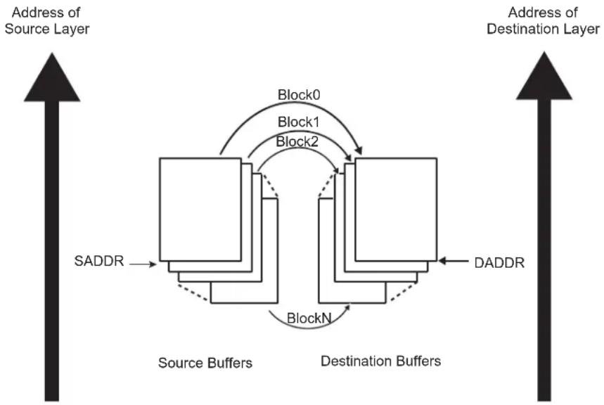
flowchart
graph TD
    A["Address of Source Layer"] --> B["Source Buffers"]
    B --> C["Destination Buffers"]
    C --> D["DADDR"]
    D --> E["SADDR"]
    E --> F["Block0"]
    F --> G["Block1"]
    G --> H["Block2"]
    H --> I["BlockN"]
    I --> J["Source Buffers"]
    J --> K["DADDR"]
    K --> L["Destination Buffers"]
    L --> M["SADDR"]
    M --> N["Address of Destination Layer"]
Figure 31-11: DMAC Transfer Flow for Source and Destination Address Auto-reloaded

flowchart
graph TD
    A["Channel enabled by software"] --> B["Buffer Transfer"]
    B --> C["Replay mode for SADDRx, DADDRx, CTRLAx, CTRLBx"]
    C --> D{Is DMAC in Row 1 of DMAC State Machine table?}
    D -->|yes| E["DMAC Chained Buffer Transfer Completed Interrupt generated here"]
    D -->|no| F{EBCIMR["x"]=1?}
    F -->|yes| G["Stall until STALLx is cleared by writing to KEEPx field"]
    F -->|no| H["Channel disabled by hardware"]
    I["Buffer Transfer Completed Interrupt generated here"] --> C
- Multi-buffer Transfer with Source Address Auto-reloaded and Linked List Destination Address (Row 6)
- Read the DMAC_CHSR to choose a free (disabled) channel.
- Set up the chain of linked list items (otherwise known as buffer descriptors) in memory. Write the control information in the LLI.DMAC_CTRLAx and DMAC_CTRLBx registers location of the buffer descriptor for each LLI in memory for channel x. For example, in the register, it is possible to program the following:
a) Set up the transfer type (memory or non-memory peripheral for source and destination) and flow control peripheral by programming the FC field in DMAC_CTRLBx.
b) Set up the transfer characteristics, such as:
- i. Transfer width for the source in the SRC WIDTH field.
- ii. Transfer width for the destination in the DST_WIDTH field.
- iii. Source AHB master interface layer in the SIF field where source resides.
- iv. Destination AHB master interface layer in the DIF field where destination resides.
- v. Incrementing/decrementing or fixed address for source in SRC_INCR field.
-
vi. Incrementing/decrementing or fixed address for destination DST_INCR field.
-
Write the starting source address in DMAC_SADDRx for channel x.
Note: The values in the LLI.DMAC_SADDRx register locations of each of the Linked List Items (LLIs) set up in memory, although fetched during an LLI fetch, are not used.
4. Write the channel configuration information into DMAC_CFGx for channel x.
a) Designate the handshaking interface type (hardware or software) for the source and destination peripherals. This is not required for memory. This step requires programming the SRC_H2SEL/DST_H2SEL bits, respectively. Writing a '1' activates the hardware handshaking interface to handle source/destination requests for the specific channel. Writing a '0' activates the software handshaking interface source/destination requests.
b) If the hardware handshaking interface is activated for the source or destination peripheral, assign handshaking interface to the source and destination peripheral. This requires programming the SRC_PER and DST_PER bits, respectively.
- Make sure that the LLI.DMAC_CTRLBx register locations of all LLIs in memory (except the last one) are set as shown in Row 6 of Table 31-4 on page 498 while the LLI.DMAC_CTRLBx register of the last Linked List item must be set as described in Row 1 of Table 31-4. Figure 31-5 on page 496 shows a Linked List example with two list items.
- Make sure that the LLI.DMAC_DSCRx register locations of all LLIs in memory (except the last one) are non-zero and point to the next Linked List Item.
- Make sure that the LLI.DMAC_DADDRx register locations of all LLIs in memory point to the start destination buffer address proceeding that LLI fetch.
- Make sure that the LLI.DMAC_CTRLAx.DONE bit of the LLI.DMAC_CTRLAx register locations of all LLIs in memory is cleared.
- If source Picture-in-Picture is enabled (DMAC_CTRLBx.SPIP is enabled), program DMAC_SPIPx for channel x.
- If destination Picture-in-Picture is enabled (DMAC_CTRLBx.DPIP is enabled), program DMAC_DPIPx for channel x.
- Clear any pending interrupts on the channel from the previous DMAC transfer by reading DMAC_EBCISR.
- Program DMAC_CTRLAx, DMAC_CTRLBx and DMAC_CFGx according to Row 6 as shown in Table 31-4 on page 498.
- Program DMAC_DSCRx with DMAC_DSCRx(0), the pointer to the first Linked List item.
- Finally, enable the channel by setting the DMAC_CHER.ENAx bit, where x is the channel number. The transfer is performed. Make sure that the ENABLE bit (register bit 0) in DMAC_EN is set.
- The DMAC fetches the first LLI from the location pointed to by DMAC_DSCRx(0).
Note: The LLI.DMAC_SADDRx, LLI.DMAC_DADDRx, LLI.DMAC_DSCRx, LLI.DMAC_CTRLAx and LLI.DMAC_CTRLBx registers are fetched. The LLI.DMAC_SADDRx register, although fetched, is not used.
- Source and destination request single and chunk DMAC transactions to transfer the buffer of data (assuming non-memory peripherals). DMAC acknowledges at the completion of every transaction (chunk and single) in the buffer and carries out the buffer transfer.
- The DMAC_CTRLAx register is written out to the system memory. The DMAC_CTRLAx register is written out to the same location on the same layer (DMAC_DSCRx.DSCR_IF) where it was originally fetched, that is the location of the DMAC_CTRLAx register of the linked list item fetched prior to the start of the buffer transfer. Only DMAC_CTRLAx register is written out, because only the DMAC_CTRLAx.BTSIZE and DMAC_CTRLAx.DONE fields have been updated by hardware within the DMAC. The LLI.DMAC_CTRLAx.DONE bit is asserted to indicate buffer completion. Therefore, the software can poll the LLI.DMAC_CTRLAx.DONE bit of the DMAC_CTRLAx register in the LLi to ascertain when a buffer transfer has completed.
Note: Do not poll the DMAC_CTRLAx.DONE bit in the DMAC memory map. Instead, poll the LLI.DMAC_CTRLAx.DONE bit in the LLI for that buffer. If the polled LLI.DMAC_CTRLAx.DONE bit is asserted, then this buffer transfer has completed. This LLI.DMAC_CTRLA.DONE bit was cleared at the start of the transfer.
- The DMAC reloads DMAC_SADDRx from the initial value. The hardware sets the Buffer Transfer Completed Interrupt. The DMAC samples the row number as shown in Table 31-4 on page 498. If the DMAC is in Row 1, then the DMAC transfer has completed. The hardware sets the Chained Buffer Transfer Completed Interrupt and disables the channel. You can either respond to the Buffer Transfer Completed Interrupt or Chained Buffer Transfer Completed Interrupt, or poll for the DMAC_CHSR.ENAx bit until it is cleared by hardware, to detect when the transfer is complete. If the DMAC is not in Row 1 as shown in Table 31-4 on page 498, the following step is performed.
- The DMAC fetches the next LLI from the memory location pointed to by the current DMAC_DSCRx register, and automatically reprograms the DMAC_DADDRx, DMAC_CTRLAx, DMAC_CTRLBx and DMAC_DSCRx channel registers. Note that the DMAC_SADDRx is not reprogrammed as the reloaded value is used for the next DMAC buffer transfer. If the next buffer is the last buffer of the DMAC transfer, then the DMAC_CTRLBx and DMAC_DSCRx registers just fetched from the LLI should match Row 1 of Table 31-4 on page 498. The DMAC transfer might look like that shown in Figure 31-12 on page 509.
Figure 31-12: Multi-buffer DMAC Transfer with Source Address Auto-reloaded and Linked List Destination
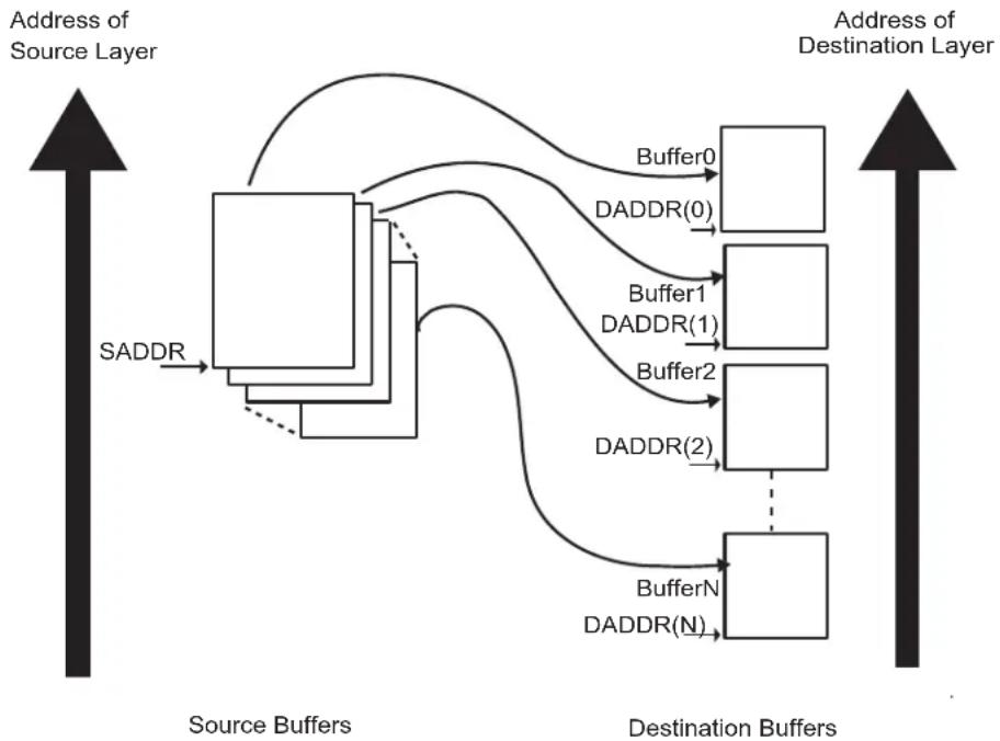
flowchart
graph TD
    A["Source Buffers"] -->|SADDR| B["Source Layer"]
    B --> C["Destination Buffer1"]
    B --> D["Destination Buffer2"]
    B --> E["Destination BufferN"]
    C --> F["Buffer0"]
    D --> G["DADDR(0)"]
    D --> H["DADDR(1)"]
    D --> I["DADDR(2)"]
    E --> J["DADDR(N)"]
    style A fill:#f9f,stroke:#333
    style B fill:#ccf,stroke:#333
    style C fill:#cfc,stroke:#333
    style D fill:#cfc,stroke:#333
    style E fill:#cfc,stroke:#333
    style F fill:#fcc,stroke:#333
    style G fill:#fcc,stroke:#333
    style H fill:#fcc,stroke:#333
    style I fill:#fcc,stroke:#333
    style J fill:#fcc,stroke:#333
Address
The DMAC Transfer flow is shown in Figure 31-13 on page 510.
Figure 31-13: DMAC Transfer Flow for Replay Mode at Source and Linked List Destination Address
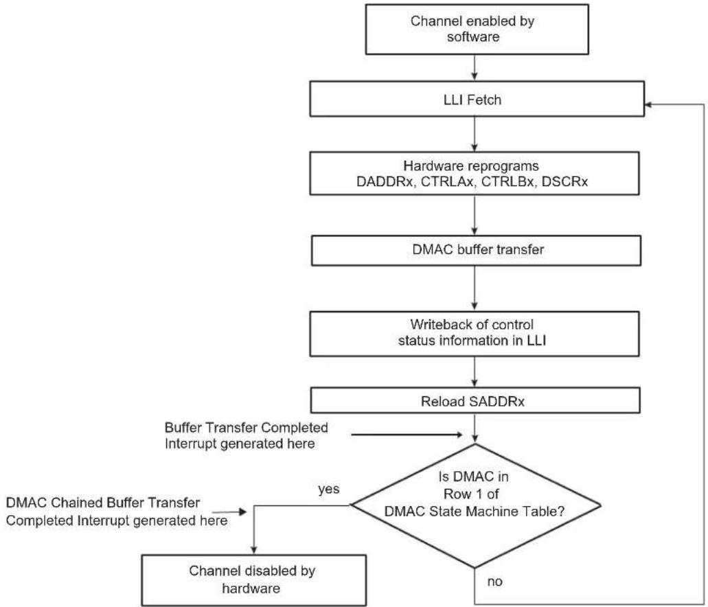
flowchart
graph TD
    A["Channel enabled by software"] --> B["LLI Fetch"]
    B --> C["Hardware reprograms DADDRx, CTRLAx, CTRLBx, DSCRx"]
    C --> D["DMAC buffer transfer"]
    D --> E["Writeback of control status information in LLI"]
    E --> F["Reload SADDRx"]
    F --> G{Is DMAC in Row 1 of DMAC State Machine Table?}
    G -->|yes| H["DMAC Chained Buffer Transfer Completed Interrupt generated here"]
    H --> I["Channel disabled by hardware"]
    I --> F
    G -->|no| J["End"]
    K["Buffer Transfer Completed Interrupt generated here"] --> G
- Multi-buffer Transfer with Source Address Auto-reloaded and Contiguous Destination Address (Row 11)
- Read the DMAC_CHSR to choose a free (disabled) channel.
- Clear any pending interrupts on the channel from the previous DMAC transfer by reading to the Interrupt Status Register.
- Program the following channel registers:
a) Write the starting source address in DMAC_SADDRx for channel x.
b) Write the starting destination address in DMAC_DADDRx for channel x.
c) Program DMAC_CTRLAx, DMAC_CTRLBx and DMAC_CFGx according to Row 11 as shown in Table 31-4 on page 498. Program DMAC_DSCRx with '0'. DMAC_CTRLBx.AUTO bit is set to '1' to enable automatic mode support.
d) Write the control information for the DMAC transfer in DMAC_CTRLBx and DMAC_CTRLAx for channel x. For example, in this register, it is possible to program the following:
- i. Set up the transfer type (memory or non-memory peripheral for source and destination) and flow control device by programming the FC field in DMAC_CTRLBx.
- ii. Set up the transfer characteristics, such as:
- Transfer width for the source in the SRC_WIDTH field.
- Transfer width for the destination in the DST_WIDTH field.
- Source AHB master interface layer in the SIF field where source resides.
- Destination AHB master interface master layer in the DIF field where destination resides.
- Incrementing/decrementing or fixed address for source in SRC_INCR field.
- Incrementing/decrementing or fixed address for destination in DST_INCR field.
e) If source Picture-in-Picture is enabled (DMAC_CTRLBx.SPIP is enabled), program DMAC_SPIPx for channel x.
f) If destination Picture-in-Picture is enabled (DMAC_CTRLBx.DPIP), program DMAC_DPIPx for channel x.
g) Write the channel configuration information into DMAC_CFGx for channel x.
- i. Designate the handshaking interface type (hardware or software) for the source and destination peripherals. This is not required for memory. This step requires programming the SRC_H2SEL/DST_H2SEL bits, respectively. Writing a '1' activates the hardware handshaking interface to handle source/destination requests for the specific channel. Writing a '0' activates the software handshaking interface to handle source/destination requests.
-
ii. If the hardware handshaking interface is activated for the source or destination peripheral, assign the handshaking interface to the source and destination peripheral. This requires programming the SRC_PER and DST_PER bits, respectively.
-
After the DMAC channel has been programmed, enable the channel by setting the DMAC_CHER.ENAx bit, where x is the channel number. Make sure that the ENABLE bit (register bit 0) in DMAC_EN is set.
-
Source and destination request single and chunk DMAC transactions to transfer the buffer of data (assuming non-memory peripherals). The DMAC acknowledges at the completion of every transaction (chunk and single) in the buffer and carries out the buffer transfer.
-
When the buffer transfer has completed, the DMAC reloads DMAC_SADDRx. DMAC_DADDRx remains unchanged. The hardware sets the Buffer Transfer Completed Interrupt. The DMAC then samples the row number as shown in Table 31-4 on page 498. If the DMAC is in Row 1, then the DMAC transfer has completed. The hardware sets the Chained Buffer Transfer Completed Interrupt and disables the channel. You can either respond to the Buffer Transfer Completed Interrupt or Chained Buffer Transfer Completed Interrupt, or poll for the DMAC_CHSR.ENAx bit until it is cleared by hardware, to detect when the transfer is complete. If the DMAC is not in Row 1, the next step is performed.
-
The DMAC transfer proceeds as follows:
a) If the Buffer Transfer Completed Interrupt is unmasked (DMAC_EBCIMR.BTCx = '1', where x is the channel number), the hardware sets the Buffer Transfer Completed Interrupt when the buffer transfer has completed. It then stalls until STALx bit of DMAC_CHSR is cleared by writing in the KEEPx bit of DMAC_CHER, where x is the channel number. If the next buffer is to be the last buffer in the DMAC transfer, then the buffer complete ISR (interrupt service routine) should clear the automatic mode bit, DMAC_CTRLBx.AUTO. This puts the DMAC into Row 1 as shown in Table 31-4 on page 498. If the next buffer is not the last buffer in the DMAC transfer, then the automatic transfer mode bit should remain enabled to keep the DMAC in Row 11 as shown in Table 31-4 on page 498.
b) If the Buffer Transfer Completed Interrupt is masked (DMAC_EBCIMR.BTCx = '0', where x is the channel number), the hardware does not stall until it detects a write to the Buffer Transfer Completed Interrupt Enable register, but starts the next buffer transfer immediately. In this case, the software must clear the automatic mode bit, DMAC_CTRLBx.AUTO, to put the device into Row 1 of Table 31-4 on page 498 before the last buffer of the DMAC transfer has completed.
The transfer is similar to that shown in Figure 31-14.
The DMAC Transfer flow is shown in Figure 31-15 on page 513.
Figure 31-14: Multi-buffer Transfer with Source Address Auto-reloaded and Contiguous Destination Address
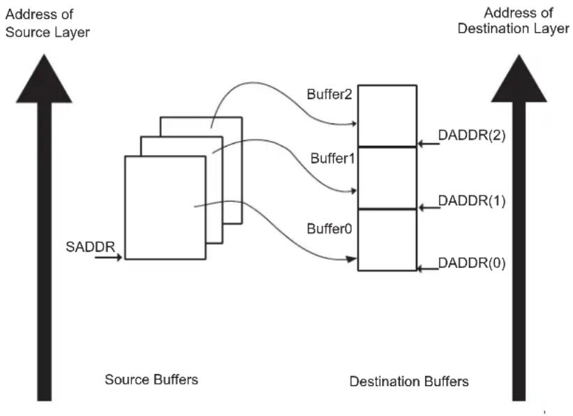
flowchart
graph LR
    A["Address of Source Layer"] --> B["SADDR"]
    B --> C["Source Buffers"]
    C --> D["Buffer0"]
    C --> E["Buffer1"]
    C --> F["Buffer2"]
    D --> G["DADDR(0)"]
    D --> H["DADDR(1)"]
    E --> I["DADDR(2)"]
    F --> J["Address of Destination Layer"]
Figure 31-15: DMAC Transfer Replay Mode is Enabled for the Source and Contiguous Destination Address
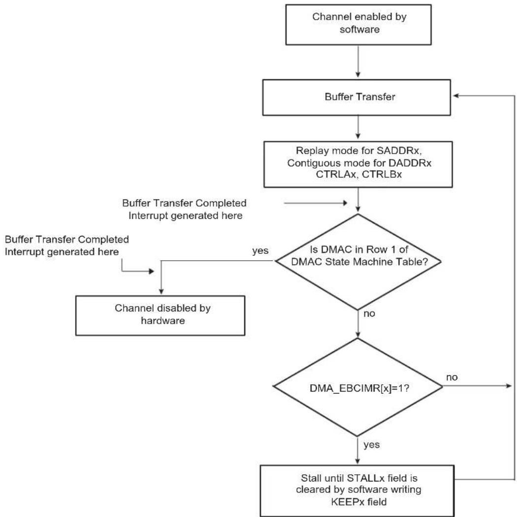
flowchart
graph TD
    A["Channel enabled by software"] --> B["Buffer Transfer"]
    B --> C["Replay mode for SADDRx, Contiguous mode for DADDRx CTRLAx, CTRLBx"]
    C --> D{Is DMAC in Row 1 of DMAC State Machine Table?}
    D -->|yes| E["Buffer Transfer Completed Interrupt generated here"]
    D -->|no| F{DMA_EBCIMR["x"]=1?}
    F -->|yes| G["Stall until STALLx field is cleared by software writing KEEPx field"]
    F -->|no| H["Channel disabled by hardware"]
    I["Buffer Transfer Completed Interrupt generated here"] --> E
- Multi-buffer DMAC Transfer with Linked List for Source and Contiguous Destination Address (Row 2)
-
Read the DMAC_CHSR to choose a free (disabled) channel.
-
Set up the linked list in memory. Write the control information in the LLI.DMAC_CTRLAx and LLI.DMAC_CTRLBx register location of the buffer descriptor for each LLI in memory for channel x. For example, in the register, it is possible to program the following:
a) Set up the transfer type (memory or non-memory peripheral for source and destination) and flow control device by programming the FC field in DMAC_CTRLBx.
b) Set up the transfer characteristics, such as:
- i. Transfer width for the source in the SRC_WIDTH field.
- ii. Transfer width for the destination in the DST_WIDTH field.
- iii. Source AHB master interface layer in the SIF field where source resides.
- iv. Destination AHB master interface layer in the DIF field where destination resides.
- v. Incrementing/decrementing or fixed address for source in SRC_INCR field.
- vi. Incrementing/decrementing or fixed address for destination DST_INCR field.
- Write the starting destination address in DMAC_DADDRx for channel x.
Note: The values in the LLI.DMAC_DADDRx register location of each Linked List Item (LLI) in memory, although fetched during an LLI fetch, are not used.
- Write the channel configuration information into DMAC_CFGx for channel x.
a) Designate the handshaking interface type (hardware or software) for the source and destination peripherals. This is not required for memory. This step requires programming the SRC_H2SEL/DST_H2SEL bits, respectively. Writing a '1' activates the hardware handshaking interface to handle source/destination requests for the specific channel. Writing a '0' activates the software handshaking interface to handle source/destination requests.
b) If the hardware handshaking interface is activated for the source or destination peripheral, assign the handshaking interface to the source and destination peripherals. This requires programming the SRC_PER and DST_PER bits, respectively.
-
Make sure that all LLI.DMAC_CTRLBx register locations of the LLI (except the last) are set as shown in Row 2 of Table 31-4 on page 498, while the LLI.DMAC_CTRLBx register of the last Linked List item must be set as described in Row 1 of Table 31-4. Figure 31-5 on page 496 shows a Linked List example with two list items.
-
Make sure that the LLI.DMAC_DSCRx register locations of all LLIs in memory (except the last) are non-zero and point to the next Linked List Item.
-
Make sure that the LLI.DMAC_SADDRx register locations of all LLIs in memory point to the start source buffer address proceeding that LLI fetch.
-
Make sure that the LLI.DMAC_CTRLAx.DONE bit of the LLI.DMAC_CTRLAx register locations of all LLIs in memory is cleared.
-
If source Picture-in-Picture is enabled (DMAC_CTRLBx.SPIP is enabled), program DMAC_SPIPx for channel x.
-
If destination Picture-in-Picture is enabled (DMAC_CTRLBx.DPIP is enabled), program DMAC_DPIPx for channel x.
-
Clear any pending interrupts on the channel from the previous DMAC transfer by reading the interrupt status register.
-
Program DMAC_CTRLAx, DMAC_CTRLBx and DMAC_CFGx according to Row 2 as shown in Table 31-4 on page 498
-
Program DMAC_DSCRx with DMAC_DSCRx(0), the pointer to the first Linked List item.
-
Finally, enable the channel by setting the DMAC_CHER.ENAx bit. The transfer is performed. Make sure that the ENABLE bit (register bit 0) in DMAC_EN is set.
-
The DMAC fetches the first LLI from the location pointed to by DMAC_DSCRx(0).
Note: The LLI.DMAC_SADDRx, LLI.DMAC_DADDRx, LLI.DMAC_DSCRx and LLI.DMAC_CTRLA/Bx registers are fetched. The LLI.DMAC_DADDRx register location of the LLI, although fetched, is not used. The DMAC_DADDRx register in the DMAC remains unchanged.
-
Source and destination requests single and chunk DMAC transactions to transfer the buffer of data (assuming non-memory peripherals). The DMAC acknowledges at the completion of every transaction (chunk and single) in the buffer and carries out the buffer transfer.
-
Once the buffer of data is transferred, the DMAC_CTRLAx register is written out to the system memory at the same location and on the same layer (DMAC_DSCRx.DSCR_IF) where it was originally fetched, that is, the location of the DMAC_CTRLAx register of the linked list item fetched prior to the start of the buffer transfer. Only DMAC_CTRLAx register is written out because only the DMAC_CTRLAx.BTSIZE and DMAC_CTRLAX.DONE fields have been updated by DMAC hardware. Additionally, the DMAC_CTRLAx.DONE bit is asserted when the buffer transfer has completed.
Note: Do not poll the DMAC_CTRLAx.DONE bit in the DMAC memory map. Instead, poll the LLI.DMAC_CTRLAx.DONE bit in the LLI for that buffer. If the poll LLI.DMAC_CTRLAx.DONE bit is asserted, then this buffer transfer has completed. This LLI.DMAC_CTRLAx.DONE bit was cleared at the start of the transfer.
- The DMAC does not wait for the buffer interrupt to be cleared, but continues and fetches the next LLI from the memory location pointed to by the current DMAC_DSCRx register, then automatically reprograms the DMAC_SADDRx, DMAC_CTRLAx, DMAC_CTRLBx and DMAC_DSCRx channel registers. DMAC_DADDRx is left unchanged. The DMAC transfer continues until the DMAC samples the DMAC_CTRLAx, DMAC_CTRLBx and DMAC_DSCRx registers at the end of a buffer transfer match that described in Row 1 of Table 31-4 on page 498. The DMAC then knows that the previous buffer transferred was the last buffer in the DMAC transfer.
The DMAC transfer might look like that shown in Figure 31-16. Note that the destination address is decrementing.
Figure 31-16: DMAC Transfer with Linked List Source Address and Contiguous Destination Address
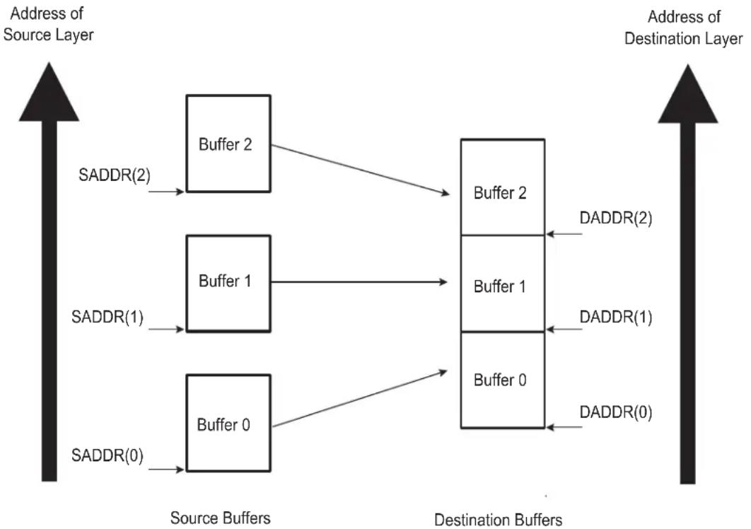
flowchart
graph LR
    A["Address of Source Layer"] --> B["Source Buffers"]
    B --> C["Destination Buffers"]
    C --> D["Address of Destination Layer"]

    subgraph Source_Layer
        E1["Buffer 0"] --> F1["Buffer 1"]
        E1 --> F2["Buffer 2"]
        E2["Buffer 0"] --> F2
        E3["Buffer 1"] --> F3["Buffer 2"]
    end

    subgraph Destination_Layer
        G1["Buffer 0"] --> H1["Buffer 1"]
        G1 --> H2["Buffer 2"]
        G2["Buffer 0"] --> H2
        G3["Buffer 1"] --> H3["Buffer 2"]
    end

    E1 -->|SADDR(0)| F1
    E2 -->|SADDR(1)| F2
    E3 -->|SADDR(2)| F3
    G1 -->|DADDR(0)| H1
    G2 -->|DADDR(1)| H2
    G3 -->|DADDR(2)| H3
The DMAC transfer flow is shown in Figure 31-17 on page 516.
Figure 31-17: DMAC Transfer Flow for Linked List Source Address and Contiguous Destination Address

flowchart
graph TD
    A["Channel enabled by software"] --> B["LLI Fetch"]
    B --> C["Hardware reprograms SADDRx, CTRLAx,CTRLBx, DSCRx"]
    C --> D["DMAC buffer transfer"]
    D --> E["Writeback of control information of LLI"]
    E --> F{Is DMAC in Row 1 ?}
    F -->|yes| G["DMAC Chained Buffer Transfer Completed Interrupt generated here"]
    F -->|no| H["Channel disabled by hardware"]
    G --> I["Buffer Transfer Completed Interrupt generated here"]
    H --> J["LLI Fetch"]
31.6.6 Disabling a Channel Prior to Transfer Completion
Under normal operation, the software enables a channel by setting the DMAC_CHER.ENAx bit, and the hardware disables a channel on transfer completion by clearing the DMAC_CHSR.ENAx bit.
The recommended way for software to disable a channel without losing data is to use the SUSPx bit in conjunction with the EMPTx bit in the DMAC_CHSR.
- If the software chooses to disable a channel n prior to the DMAC transfer completion, then it can set the DMAC_CHER.SUSPx bit to instruct the DMAC to halt all transfers from the source peripheral. Therefore, the channel FIFO receives no new data.
- The software can now poll the DMAC_CHSR.EMPTx bit until it indicates that the channel n FIFO is empty, where n is the channel number.
- The DMAC_CHER.ENAx bit can then be cleared by software once the channel n FIFO is empty, where n is the channel number.
When DMAC_CTRLAx.SRC_WIDTH is less than DMAC_CTRLAx.DST_WIDTH and the DMAC_CHSRx.SUSPx bit is high, the DMAC_CHSRx.EMPTx is asserted once the contents of the FIFO does not permit a single word of DMAC_CTRLAx.DST_WIDTH to be formed. However, there may still be data in the channel FIFO but not enough to form a single transfer of DMAC_CTRLAx.DST_WIDTH width. In this configuration, once the channel is disabled, the remaining data in the channel FIFO are not transferred to the destination peripheral. It is permitted to remove the channel from the suspension state by setting the DMAC_CHDR.RESx bit. The DMAC transfer completes in the normal manner. n defines the channel number.
Note: If a channel is disabled by software, an active single or chunk transaction is not guaranteed to receive an acknowledgement.
31.6.6.1 Abnormal Transfer Termination
A DMAC transfer may be terminated abruptly by software by clearing the channel enable bit, DMAC_CHER.ENAx, where x is the channel number. This does not mean that the channel is disabled immediately after the DMAC_CHSR.ENAx bit is cleared over the APB interface. Consider this as a request to disable the channel. The DMAC_CHSR.ENAx must be polled and then it must be confirmed that the channel is disabled by reading back 0.
The software may terminate all channels abruptly by clearing the general enable bit in the DMAC Enable Register (DMAC_EN. ENABLE). Again, this does not mean that all channels are disabled immediately after the DMAC_EN. ENABLE bit is cleared over the APB slave interface. Consider this as a request to disable all channels. The DMAC_CHSR. ENABLE must be polled and then it must be confirmed that all channels are disabled by reading back '0'.
Note: If the channel enable bit is cleared while there is data in the channel FIFO, this data is not sent to the destination peripheral and is not present when the channel is re-enabled. For read sensitive source peripherals, such as a source FIFO, this data is therefore lost. When the source is not a read sensitive device (i.e., memory), disabling a channel without waiting for the channel FIFO to empty may be acceptable as the data is available from the source peripheral upon request and is not lost.
Note: If a channel is disabled by software, an active single or chunk transaction is not guaranteed to receive an acknowledgement.
31.6.7 Register Write Protection
To prevent any single software error from corrupting DMAC behavior, certain registers in the address space can be write-protected by setting the WPEN bit in the DMAC Write Protection Mode Register (DMAC_WPMR).
If a write access to a write-protected register is detected, the WPVS bit in the DMAC Write Protection Status Register (DMAC_WPSR) is set and the field WPVSRC indicates the register in which the write access has been attempted.
The WPVS bit is automatically cleared after reading the DMAC_WPSR.
The following registers can be write-protected:
• DMAC Global Configuration Register
- DMAC Enable Register
- DMAC Channel x [x = 0..7] Source Address Register
- DMAC Channel x [x = 0..7] Destination Address Register
- DMAC Channel x [x = 0..7] Descriptor Address Register
- DMAC Channel x [x = 0..7] Control A Register
- DMAC Channel x [x = 0..7] Control B Register
- DMAC Channel x [x = 0..7] Configuration Register
31.7 DMAC Software Requirements
- There must not be any write operation to channel registers in an active channel after the channel enable is made HIGH. If any channel parameters must be reprogrammed, this can only be done after disabling the DMAC channel.
- The channel registers DMAC_SADDRx and DMAC_DADDRx must be programmed with a byte, half-word and word aligned address depending on the source width and destination width.
- After the software disables a channel by writing into the DMAC Channel Handler Disable Register, it must re-enable the channel only after it has polled a '0' in the DMAC Channel Handler Status Register. This is because the current AHB Burst must terminate properly.
- If the value of field DMAC_CTRLAx.BTSIZE is configured to zero and the DMAC has been defined as the flow controller, the channel is automatically disabled.
- Multiple transfers involving the same peripheral must not be programmed and enabled on different channels, unless this peripheral integrates several hardware handshaking interfaces.
- When a peripheral has been defined as the flow controller, the targeted DMAC channel must be enabled before the peripheral. If this is not done and the first DMAC request is also the last transfer, the DMAC channel might miss a Last Transfer Flag.
- When the AUTO bit is set to TRUE, the BTSIZE field is automatically reloaded from its previous value. BTSIZE must be initialized to a non-zero value if the first transfer is initiated with the AUTO bit set to TRUE, even if LLI mode is enabled, because the LLI fetch operation will not update this field.
31.8 DMA Controller (DMAC) User Interface
Table 31-5: Register Mapping
| Offset Register Name Access Reset | ||||
| 0x000 DMAC Global Configuration Register DMAC_GCFG Read/Write 0x10 | ||||
| 0x004 DMAC Enable Register DMAC_EN Read/Write 0x0 | ||||
| 0x008 | DMAC Software Single Request Register | DMAC_SREQ | Read/Write | 0x0 |
| 0x00C | DMAC Software Chunk Transfer Request Register | DMAC_CREQ Read/Write 0x0 | ||
| 0x010 | DMAC Software Last Transfer Flag Register | DMAC_LAST | Read/Write | 0x0 |
| 0x014 Reserved | - - | - | ||
| 0x018 | DMAC Error, Chained Buffer Transfer Completed Interrupt and Buffer Transfer Completed Interrupt Enable Register | DMAC_EBCIER | Write-only | - |
| 0x01C | DMAC Error, Chained Buffer Transfer Completed Interrupt and Buffer Transfer Completed Interrupt Disable Register | DMAC_EBCIDR | Write-only | - |
| 0x020 | DMAC Error, Chained Buffer Transfer Completed Interrupt and Buffer transfer completed Mask Register | DMAC_EBCIMR | Read-only | 0x0 |
| 0x024 | DMAC Error, Chained Buffer Transfer Completed Interrupt and Buffer transfer completed Status Register | DMAC_EBCISR | Read-only | 0x0 |
| 0x028 | DMAC Channel Handler Enable Register | DMAC_CHER | Write-only | - |
| 0x02C | DMAC Channel Handler Disable Register | DMAC_CHDR | Write-only | - |
| 0x030 | DMAC Channel Handler Status Register | DMAC_CHSR | Read-only | 0x00FF0000 |
| 0x034-0x038 | Reserved | - | - | - |
| 0x03C+ch_num*(0x28)+(0x0) | DMAC Channel Source Address Register | DMAC_SADDR | Read/Write | 0x0 |
| 0x03C+ch_num*(0x28)+(0x4) | DMAC Channel Destination Address Register | DMAC_DADDR | Read/Write | 0x0 |
| 0x03C+ch_num*(0x28)+(0x8) | DMAC Channel Descriptor Address Register | DMAC_DSCR | Read/Write | 0x0 |
| 0x03C+ch_num*(0x28)+(0xC) | DMAC Channel Control A Register | DMAC_CTRLA | Read/Write | 0x0 |
| 0x03C+ch_num*(0x28)+(0x10) | DMAC Channel Control B Register | DMAC_CTRLB | Read/Write | 0x0 |
| 0x03C+ch_num*(0x28)+(0x14) | DMAC Channel Configuration Register | DMAC_CFG | Read/Write | 0x01000000 |
| 0x03C+ch_num*(0x28)+(0x18) | DMAC Channel Source Picture-in-Picture Configuration Register | DMAC_SPIP | Read/Write 0x0 | |
| 0x03C+ch_num*(0x28)+(0x1C) | DMAC Channel Destination Picture-in-Picture Configuration Register | DMAC_DPIP | Read/Write 0x0 | |
| 0x03C+ch_num*(0x28)+(0x20) | Reserved | - | - | - |
| 0x03C+ch_num*(0x28)+(0x24) | Reserved | - | - | - |
| 0x1E4 | DMAC Write Protection Mode Register | DMAC_WPMR | Read/Write | 0x0 |
| 0x1E8 | DMAC Write Protection Status Register | DMAC_WPSR | Read-only | 0x0 |
| 0x1EC-0x1FC | Reserved | - | - | - |
31.8.1 DMAC Global Configuration Register
Name: DMAC_GCFG
Address:0xFFFFE600 (0), 0xFFFFE800 (1)
Access: Read/Write
31 30 29 28 27 26 25 24
| - | - | - | - | - | - | - | - |
23 22 21 20 19 18 17 16
| - | - | - | - | - | - | - | - |
15 14 13 12 11 10 9 8
| - | - | - | - | - | - | - | D |
| 7 | 6 | 5 | 4 | 3 | 2 | 1 | 0 |
| - | - | - | A | R | B | _ | C |
Note: Bit fields 0, 1, 2, and 3 have a default value of 0. This should not be changed.
This register can only be written if the WPEN bit is cleared in DMAC Write Protection Mode Register.
ARB_CFG: Arbiter Configuration
| Value Name | Description | |
| 0 | FIXED | Fixed priority arbiter (seeBasic Definitions) |
| 1 ROUND_ROBIN | Modified round robin arbiter. | |
DICEN: Descriptor Integrity Check
0: Descriptor Integrity Check Interface is Disabled.
1: Descriptor Integrity Check Interface is Enabled.
31.8.2 DMAC Enable Register
Name: DMAC_EN
Address:0xFFFFE604 (0), 0xFFFFE804 (1)
Access: Read/Write
31 30 29 28 27 26 25 24
| - | - | - | - | - | - | - | - |
23 22 21 20 19 18 17 16
| - | - | - | - | - | - | - | - |
15 14 13 12 11 10 9 8
| - | - | - | - | - | - | - | - |
| 7 | 6 | 5 | 4 | 3 | 2 | 1 | 0 |
| - | - | - | - | - | - | - | E |
This register can only be written if the WPEN bit is cleared in DMAC Write Protection Mode Register.
ENABLE: General Enable of DMA
0: DMA Controller is disabled.
1: DMA Controller is enabled.
31.8.3 DMAC Software Single Request Register
Name:DMAC_SREQ
Address:0xFFFFE608 (0), 0xFFFFE808 (1)
Access: Read/Write
31 30 29 28 27 26 25 24
| - | - | - | - | - | - | - | - |
23 22 21 20 19 18 17 16
| - | - | - | - | - | - | - | - |
15 14 13 12 11 10 9 8
Request a destination single transfer on channel i.
SSREQx: Source Request
Request a source single transfer on channel i.
31.8.4 DMAC Software Chunk Transfer Request Register
Name:DMAC_CREQ
Address:0xFFFFE60C (0), 0xFFFFE80C (1)
Access: Read/Write
31 30 29 28 27 26 25 24
| - | - | - | - | - | - | - | - |
23 22 21 20 19 18 17 16
| - | - | - | - | - | - | - | - |
15 14 13 12 11 10 9 8
| DCREQ7 SCREQ7 DCREQ6 | SCREQ6 DCREQ5 SCREQ5 DCREQ4 SCREQ4 |
| 7 | 6 | 5 | 4 | 3 | 2 | 1 | 0 |
| DCREQ3 SCREQ3 DCREQ2 | SCREQ2 DCREQ1 SCREQ1 DCREQ0 SCREQ0 |
DCREQx: Destination Chunk Request
Request a destination chunk transfer on channel i.
SCREQx: Source Chunk Request
Request a source chunk transfer on channel i.
31.8.5 DMAC Software Last Transfer Flag Register
Name:DMAC_LAST
Address:0xFFFFE610 (0), 0xFFFFE810 (1)
Access: Read/Write
31 30 29 28 27 26 25 24
| - | - | - | - | - | - | - | - |
23 22 21 20 19 18 17 16
| - | - | - | - | - | - | - | - |
15 14 13 12 11 10 9 8
| DLAST7 SLAST7 DLAST6 SLAST6 DLAST5 SLAST5 DLAST4 SLAST4 |
| 7 | 6 | 5 | 4 | 3 | 2 | 1 | 0 |
Writing one to DLASTx prior to writing one to DSREQx or DCREQx indicates that this destination request is the last transfer of the buffer.
SLASTx: Source Last
Writing one to SLASTx prior to writing one to SSREQx or SCREQx indicates that this source request is the last transfer of the buffer.
31.8.6 DMAC Error, Buffer Transfer and Chained Buffer Transfer Interrupt Enable Register
Name: DMAC_EBCIER
Address:0xFFFFE618 (0), 0xFFFFE818 (1)
Access: Write-only
31 30 29 28 27 26 25 24
| DICERR7 DICERR6 DICERR5 DICERR4 DICERR3 DICERR2 DICERR1 DICERR0 |
23 22 21 20 19 18 17 16
| ERR7 ERR6 ERR5 ERR4 ERR3 ERR2 ERR1 ERR0 |
15 14 13 12 11 10 9 8
| CBTC7 CBTC6 CBTC5 CBTC4 CBTC3 CBTC2 CBTC1 CBTC0 |
| 7 | 6 | 5 | 4 | 3 | 2 | 1 | 0 |
| BTC7 BTC6 BTC5 BTC4 BT | C3 BTC2 BTC1 | BTC0 |
BTCx: Buffer Transfer Completed [7:0]
Buffer Transfer Completed Interrupt Enable Register. Set the relevant bit in the BTC field to enable the interrupt for channel i.
CBTCx: Chained Buffer Transfer Completed [7:0]
Chained Buffer Transfer Completed Interrupt Enable Register. Set the relevant bit in the CBTC field to enable the interrupt for channel i.
ERRx: Access Error [7:0]
Access Error Interrupt Enable Register. Set the relevant bit in the ERR field to enable the interrupt for channel i.
DICERRx: Descriptor Integrity Check Error [7:0]
Descriptor Integrity Check Error Interrupt Enable Register. Set the relevant bit in the DICERR field to enable the interrupt for channel i.
31.8.7 DMAC Error, Buffer Transfer and Chained Buffer Transfer Interrupt Disable Register
Name: DMAC_EBCIDR
Address:0xFFFFE61C (0), 0xFFFFE81C (1)
Access:Write-only
31 30 29 28 27 26 25 24
| DICERR7 DICERR6 DICERR5 DICERR4 DICERR3 DICERR2 DICERR1 DICERR0 |
23 22 21 20 19 18 17 16
| ERR7 ERR6 ERR5 ERR4 ERR3 ERR2 ERR1 ERR0 |
15 14 13 12 11 10 9 8
| CBTC7 CBTC6 CBTC5 CBTC4 CBTC3 CBTC2 CBTC1 CBTC0 |
| 7 | 6 | 5 | 4 | 3 | 2 | 1 | 0 |
| BTC7 BTC6 BTC5 BTC4 BT | C3 BTC2 BTC1 | BTC0 |
BTCx: Buffer Transfer Completed [7:0]
Buffer transfer completed Disable Interrupt Register. When set, a bit of the BTC field disables the interrupt from the relevant DMAC channel.
CBTCx: Chained Buffer Transfer Completed [7:0]
Chained Buffer transfer completed Disable Register. When set, a bit of the CBTC field disables the interrupt from the relevant DMAC channel.
ERRx: Access Error [7:0]
Access Error Interrupt Disable Register. When set, a bit of the ERR field disables the interrupt from the relevant DMAC channel.
DICERRx: Descriptor Integrity Check Error [7:0]
Descriptor Integrity Check Error Interrupt Disable Register, When set, a bit of the DICERR field disables the interrupt from the relevant DMAC channel.
31.8.8 DMAC Error, Buffer Transfer and Chained Buffer Transfer Interrupt Mask Register
Name:DMAC_EBCIMR
Address:0xFFFFE620 (0), 0xFFFFE820 (1)
Access: Read-only
31 30 29 28 27 26 25 24
| DICERR7 DICERR6 DICERR5 DICERR4 DICERR3 DICERR2 DICERR1 DICERR0 |
23 22 21 20 19 18 17 16
| ERR7 ERR6 ERR5 ERR4 ERR3 ERR2 ERR1 ERR0 |
15 14 13 12 11 10 9 8
| CBTC7 CBTC6 CBTC5 CBTC4 CBTC3 CBTC2 CBTC1 CBTC0 |
| 7 | 6 | 5 | 4 | 3 | 2 | 1 | 0 |
| BTC7 BTC6 BTC5 BTC4 BT | C3 BTC2 BTC1 | BTC0 |
BTCx: Buffer Transfer Completed [7:0]
0: Buffer Transfer Completed Interrupt is disabled for channel i.
1: Buffer Transfer Completed Interrupt is enabled for channel i.
CBTCx: Chained Buffer Transfer Completed [7:0]
0: Chained Buffer Transfer interrupt is disabled for channel i.
1: Chained Buffer Transfer interrupt is enabled for channel i.
ERRx: Access Error [7:0]
0: Transfer Error Interrupt is disabled for channel i.
1: Transfer Error Interrupt is enabled for channel i.
DICERRx: Descriptor Integrity Check Error [7:0]
0: Descriptor Integrity Check Error Interrupt is disabled for channel i.
1: Descriptor Integrity Check Error Interrupt is enabled for channel i.
31.8.9 DMAC Error, Buffer Transfer and Chained Buffer Transfer Status Register
Name:DMAC_EBCISR
Address:0xFFFFE624 (0), 0xFFFFE824 (1)
Access:Read-only
31 30 29 28 27 26 25 24
| DICERR7 DICERR6 DICERR5 DICERR4 DICERR3 DICERR2 DICERR1 DICERR0 |
23 22 21 20 19 18 17 16
| ERR7 ERR6 ERR5 ERR4 ERR3 ERR2 ERR1 ERR0 |
15 14 13 12 11 10 9 8
| CBTC7 CBTC6 CBTC5 CBTC4 CBTC3 CBTC2 CBTC1 CBTC0 |
| 7 | 6 | 5 | 4 | 3 | 2 | 1 | 0 |
| BTC7 BTC6 BTC5 BTC4 BT | C3 BTC2 BTC1 | BTC0 |
BTCx: Buffer Transfer Completed [7:0]
When BTC[i] is set, Channel i buffer transfer has terminated.
CBTCx: Chained Buffer Transfer Completed [7:0]
When CBTC[i] is set, Channel i Chained buffer has terminated. LLI Fetch operation is disabled.
ERRx: Access Error [7:0]
When ERR[i] is set, Channel i has detected an AHB Read or Write Error Access.
DICERRx: Descriptor Integrity Check Error [7:0]
When DICERR[i] is set, Channel i has detected a Descriptor Integrity Check Error.
31.8.10 DMAC Channel Handler Enable Register
Name: DMAC_CHER
Address:0xFFFFE628 (0), 0xFFFFE828 (1)
Access:Write-only
31 30 29 28 27 26 25 24
| KEEP7 KEEP | P6 KEEP5 KEEP | P4 KEEP3 KEEP2 KEEP1 KEEP0 |
23 22 21 20 19 18 17 16
| - | - | - | - | - | - | - | - |
15 14 13 12 11 10 9 8
| SUSP7 SUSP6 SUSP5 SUSP4 SUSP3 SUSP2 SUSP1 SUSP0 |
| 7 | 6 | 5 | 4 | 3 | 2 | 1 | 0 |
| ENA7 ENA6 | ENA5 ENA4 ENA3 | ENA2 ENA1 | ENA0 |
ENAx: Enable [7:0]
When set, a bit of the ENA field enables the relevant channel.
SUSPx: Suspend [7:0]
When set, a bit of the SUSP field freezes the relevant channel and its current context.
KEEPx: Keep on [7:0]
When set, a bit of the KEEP field resumes the current channel from an automatic stall state.
31.8.11 DMAC Channel Handler Disable Register
Name: DMAC_CHDR
Address:0xFFFFE62C (0), 0xFFFFE82C (1)
Access: Write-only
31 30 29 28 27 26 25 24
| - | - | - | - | - | - | - | - |
23 22 21 20 19 18 17 16
| - | - | - | - | - | - | - | - |
15 14 13 12 11 10 9 8
| RES7 RES6 | RES5 RES4 | RES3 RES2 | RES1 | RES0 |
| 7 | 6 | 5 | 4 | 3 | 2 | 1 | 0 |
| DIS7 DIS6 | DIS5 DIS4 DIS3 | DIS2 DIS1 DIS0 |
DISx: Disable [7:0]
Write one to this field to disable the relevant DMAC Channel. The content of the FIFO is lost and the current AHB access is terminated. Software must poll DIS[7:0] field in the DMAC_CHSR register to be sure that the channel is disabled.
RESx: Resume [7:0]
Write one to this field to resume the channel transfer restoring its context.
31.8.12 DMAC Channel Handler Status Register
Name:DMAC_CHSR
Address:0xFFFFE630 (0), 0xFFFFE830 (1)
Access:Read-only
31 30 29 28 27 26 25 24
| STAL7 STAL6 STAL5 STAL4 STAL3 STAL2 STAL1 STAL0 |
23 22 21 20 19 18 17 16
| EMPT7 EMPT6 EMPT5 EMPT4 EMPT3 EMPT2 EMPT1 EMPT0 |
15 14 13 12 11 10 9 8
| SUSP7 SUSP6 SUSP5 SUSP4 SUSP3 SUSP2 SUSP1 SUSP0 |
| 7 | 6 | 5 | 4 | 3 | 2 | 1 | 0 |
| ENA7 ENA6 | ENA5 ENA4 ENA3 | ENA2 ENA1 | ENA0 |
ENAx: Enable [7:0]
A one in any position of this field indicates that the relevant channel is enabled.
SUSPx: Suspend [7:0]
A one in any position of this field indicates that the channel transfer is suspended.
EMPTx: Empty [7:0]
A one in any position of this field indicates that the relevant channel is empty.
STALx: Stalled [7:0]
A one in any position of this field indicates that the relevant channel is stalling.
31.8.13 DMAC Channel x [x = 0..7] Source Address Register
Name:DMAC_SADDRx [x = 0..7]
Address:0xFFFFE63C (0)[0], 0xFFFFE664 (0)[1], 0xFFFFE68C (0)[2], 0xFFFFE6B4 (0)[3], 0xFFFFE6DC (0)[4], 0xFFFFE704 (0)[5], 0xFFFFE72C (0)[6], 0xFFFFE754 (0)[7], 0xFFFFE83C (1)[0], 0xFFFFE864 (1)[1], 0xFFFFE88C (1)[2], 0xFFFFE8B4 (1)[3], 0xFFFFE8DC (1)[4], 0xFFFFE904 (1)[5], 0xFFFFE92C (1)[6], 0xFFFFE954 (1)[7]
Access: Read/Write
31 30 29 28 27 26 25 24
SADDR
23 22 21 20 19 18 17 16
SADDR
15 14 13 12 11 10 9 8
SADDR
7 6 5 4 3 2 1 0
SADDR
This register can only be written if the WPEN bit is cleared in DMAC Write Protection Mode Register.
SADDR: Channel x Source Address
This register must be aligned with the source transfer width.
31.8.14 DMAC Channel x [x = 0..7] Destination Address Register
Name:DMAC_DADDRx [x = 0..7]
Address:0xFFFFE640 (0)[0], 0xFFFFE668 (0)[1], 0xFFFFE690 (0)[2], 0xFFFFE6B8 (0)[3], 0xFFFFE6E0 (0)[4], 0xFFFFE708 (0)[5], 0xFFFFE730 (0)[6], 0xFFFFE758 (0)[7], 0xFFFFE840 (1)[0], 0xFFFFE868 (1)[1], 0xFFFFE890 (1)[2], 0xFFFFE8B8 (1)[3], 0xFFFFE8E0 (1)[4], 0xFFFFE908 (1)[5], 0xFFFFE930 (1)[6], 0xFFFFE958 (1)[7]
Access: Read/Write
31 30 29 28 27 26 25 24
DADDR
23 22 21 20 19 18 17 16
DADDR
15 14 13 12 11 10 9 8
DADDR
7 6 5 4 3 2 1 0
DADDR
This register can only be written if the WPEN bit is cleared in DMAC Write Protection Mode Register.
DADDR: Channel x Destination Address
This register must be aligned with the destination transfer width.
31.8.15 DMAC Channel x [x = 0..7] Descriptor Address Register
Name: DMAC_DSCRx [x = 0..7]
Address:0xFFFFE644 (0)[0], 0xFFFFE66C (0)[1], 0xFFFFE694 (0)[2], 0xFFFFE6BC (0)[3], 0xFFFFE6E4 (0)[4], 0xFFFFE70C (0)[5], 0xFFFFE734 (0)[6], 0xFFFFE75C (0)[7], 0xFFFFE844 (1)[0], 0xFFFFE86C (1)[1], 0xFFFFE894 (1)[2], 0xFFFFE8BC (1)[3], 0xFFFFE8E4 (1)[4], 0xFFFFE90C (1)[5], 0xFFFFE934 (1)[6], 0xFFFFE95C (1)[7]
Access: Read/Write
31 30 29 28 27 26 25 24
| DSCR | |||||||
| 23 22 21 20 19 18 17 16 | |||||||
| DSCR | |||||||
| 15 14 13 12 11 10 9 8 | |||||||
| DSCR | |||||||
| 7 | 6 | 5 | 4 | 3 | 2 | 1 | 0 |
| DSCR DSCR_IF | |||||||
This register can only be written if the WPEN bit is cleared in DMAC Write Protection Mode Register.
DSCR_IF: Descriptor Interface Selection
| Value Name Description | ||
| 0 | AHB_IF0 | The buffer transfer descriptor is fetched via AHB-Lite Interface 0 (first DMA Master Interface) |
| 1 | AHB_IF1 | The buffer transfer descriptor is fetched via AHB-Lite Interface 1 (second DMA Master Interface) |
| 2 | AHB_IF2 | The buffer transfer descriptor is fetched via AHB-Lite Interface 2 (third DMA Master Interface) |
DSCR: Buffer Transfer Descriptor Address
This address is word aligned.
31.8.16 DMAC Channel x [x = 0..7] Control A Register
Name: DMAC_CTRLAx [x = 0..7]
Address:0xFFFFE648 (0)[0], 0xFFFFE670 (0)[1], 0xFFFFE698 (0)[2], 0xFFFFE6C0 (0)[3], 0xFFFFE6E8 (0)[4], 0xFFFFE710 (0)[5], 0xFFFFE738 (0)[6], 0xFFFFE760 (0)[7], 0xFFFFE848 (1)[0], 0xFFFFE870 (1)[1], 0xFFFFE898 (1)[2], 0xFFFFE8C0 (1)[3], 0xFFFFE8E8 (1)[4], 0xFFFFE910 (1)[5], 0xFFFFE938 (1)[6], 0xFFFFE960 (1)[7]
Access: Read/Write
31 30 29 28 27 26 25 24
| DONE - DST_WIDTH -- SRC_WIDTH |
23 22 21 20 19 18 17 16
| - DCSIZE - SCSIZE |
15 14 13 12 11 10 9 8
| BTSIZE |
| 7 | 6 | 5 | 4 | 3 | 2 | 1 | 0 |
| BTSIZE | |||||||
This register can only be written if the WPEN bit is cleared in DMAC Write Protection Mode Register.
BTSIZE: Buffer Transfer Size
The transfer size relates to the number of transfers to be performed, that is, for writes it refers to the number of source width transfers to perform when DMAC is flow controller. For reads, BTSIZE refers to the number of transfers completed on the Source Interface. When this field is cleared, the DMAC module is automatically disabled when the relevant channel is enabled.
SCSIZE: Source Chunk Transfer Size
| Value Name | Description | |
| 000 | CHK_1 | 1 data transferred |
| 001 | CHK_4 | 4 data transferred |
| 010 | CHK_8 | 8 data transferred |
| 011 | CHK_16 | 16 data transferred |
DCSIZE: Destination Chunk Transfer Size
| Value | Name | Description |
| 000 | CHK_1 | 1 data transferred |
| 001 | CHK_4 | 4 data transferred |
| 010 | CHK_8 | 8 data transferred |
| 011 | CHK_16 | 16 data transferred |
SRC_WIDTH: Transfer Width for the Source
| Value | Name | Description |
| 00 | BYTE | The transfer size is set to 8-bit width |
| 01 | HALF_WORD | The transfer size is set to 16-bit width |
| 10 | WORD | The transfer size is set to 32-bit width |
| 11 | DWORD | The transfer size is set to 64-bit width |
DST_WIDTH: Transfer Width for the Destination
| Value Name Description | ||
| 00 BYTE The transfer size is set to 8-bit width | ||
| 01 HALF_WORD The transfer size is set to 16-bit width | ||
| 10 WORD The transfer size is set to 32-bit width | ||
| 11 DWORD The transfer size is set to 64-bit width | ||
DONE: Current Descriptor Stop Command and Transfer Completed Memory Indicator
0: The transfer is performed.
1: If SOD bit in DMAC_CFG is set to true, then the DMAC is automatically disabled when an LLI updates the content of this register. The DONE bit is written back to memory at the end of the current descriptor transfer.
31.8.17 DMAC Channel x [x = 0..7] Control B Register
Name:DMAC_CTRLBx [x = 0..7]
Address:0xFFFFE64C (0)[0], 0xFFFFE674 (0)[1], 0xFFFFE69C (0)[2], 0xFFFFE6C4 (0)[3], 0xFFFFE6EC (0)[4], 0xFFFFE714 (0)[5], 0xFFFFE73C (0)[6], 0xFFFFE764 (0)[7], 0xFFFFE84C (1)[0], 0xFFFFE874 (1)[1], 0xFFFFE89C (1)[2], 0xFFFFE8C4 (1)[3], 0xFFFFE8EC (1)[4], 0xFFFFE914 (1)[5], 0xFFFFE93C (1)[6], 0xFFFFE964 (1)[7]
Access: Read/Write
31 30 29 28 27 26 25 24
| AUTO IEN DST_INCR -- SRC_INCR |
23 22 21 20 19 18 17 16
| -FC DST_DSCR---SRC_DSCR |
15 14 13 12 11 10 98
| - | - | - | DST_PIP | - | - | - | SRC_PIP |
7 6 5 4 3 2 1 0
| - | - | DIF | - | - | SIF |
This register can only be written if the WPEN bit is cleared in DMAC Write Protection Mode Register.
SIF: Source Interface Selection Field
| Value | Name | Description |
| 0 | AHB_IF0 | The source transfer is done via AHB_Lite Interface 0 (first DMA Master Interface) |
| 1 | AHB_IF1 | The source transfer is done via AHB_Lite Interface 1 (second DMA Master Interface) |
| 2 | AHB_IF2 | The source transfer is done via AHB_Lite Interface 2 (third DMA Master Interface) |
DIF: Destination Interface Selection Field
| Value | Name | Description |
| 0 | AHB_IF0 | The destination transfer is done via AHB_Lite Interface 0 (first DMA Master Interface) |
| 1 | AHB_IF1 | The destination transfer is done via AHB_Lite Interface 1 (second DMA Master Interface) |
| 2 | AHB_IF2 | The destination transfer is done via AHB_Lite Interface 2 (third DMA Master Interface) |
SRC\_PIP: Source Picture-in-Picture Mode
0 (DISABLE): Picture-in-Picture mode is disabled. The source data area is contiguous.
1 (ENABLE): Picture-in-Picture mode is enabled. When the source PIP counter reaches the programmable boundary, the address is automatically incremented by a user defined amount.
DST\_PIP: Destination Picture-in-Picture Mode
0 (DISABLE): Picture-in-Picture mode is disabled. The Destination data area is contiguous.
1 (ENABLE): Picture-in-Picture mode is enabled. When the Destination PIP counter reaches the programmable boundary the address is automatically incremented by a user-defined amount.
SRC\_DSCR: Source Address Descriptor
0 (FETCH_FROM_MEM): Source address is updated when the descriptor is fetched from the memory.
1 (FETCH_DISABLE): Buffer Descriptor Fetch operation is disabled for the source.
DST\_DSCR: Destination Address Descriptor
0 (FETCH_FROM_MEM): Destination address is updated when the descriptor is fetched from the memory.
1 (FETCH_DISABLE): Buffer Descriptor Fetch operation is disabled for the destination.
FC: Flow Control
This field defines which device controls the size of the buffer transfer, also referred to as the Flow Controller.
| Value Name Description | ||
| 00 MEM2MEM_DMA_FC Memory-to-Memory Transfer DMAC is flow controller | ||
| 01 MEM2PER_DMA_FC Memory-to-Peripheral Transfer DMAC is flow controller | ||
| 10 PER2MEM_DMA_FC Peripheral-to-Memory Transfer DMAC is flow controller | ||
| 11 PER2PER_DMA_FC Peripheral-to-Peripheral Transfer DMAC is flow controller | ||
SRC_INCR: Incrementing, Decrementing or Fixed Address for the Source
| Value Name Description | ||
| 00 INCREMENTING | The source address is incremented | |
| 01 DECREMENTING | The source address is decremented | |
| 10 FIXED | The source address remains unchanged | |
DST_INCR: Incrementing, Decrementing or Fixed Address for the Destination
| Value | Name | Description |
| 00 | INCREMENTING | The destination address is incremented |
| 01 | DECREMENTING | The destination address is decremented |
| 10 | FIXED | The destination address remains unchanged |
IEN: Interrupt Enable Not
0: When the buffer transfer is completed, the BTCx flag is set in the DMAC_EBCISR. This bit is active low.
1: When the buffer transfer is completed, the BTCx flag is not set.
If this bit is cleared, when the buffer transfer is completed, the BTCx flag is set in the DMAC_EBCISR.
AUTO: Automatic Multiple Buffer Transfer
0 (DISABLE): Automatic multiple buffer transfer is disabled.
1 (ENABLE): Automatic multiple buffer transfer is enabled. This bit enables replay mode or contiguous mode when several buffers are transferred.
31.8.18 DMAC Channel x [x = 0..7] Configuration Register
Name: DMAC_CFGx [x = 0..7]
Address:0xFFFFE650 (0)[0], 0xFFFFE678 (0)[1], 0xFFFFE6A0 (0)[2], 0xFFFFE6C8 (0)[3], 0xFFFFE6F0 (0)[4], 0xFFFFE718 (0)[5], 0xFFFFE740 (0)[6], 0xFFFFE768 (0)[7], 0xFFFFE850 (1)[0], 0xFFFFE878 (1)[1], 0xFFFFE8A0 (1)[2], 0xFFFFE8C8 (1)[3], 0xFFFFE8F0 (1)[4], 0xFFFFE918 (1)[5], 0xFFFFE940 (1)[6], 0xFFFFE968 (1)[7]
Access: Read/Write
31 30 29 28 27 26 25 24
--FIFOCFG-AHB_PROT
23 22 21 20 19 18 17 16
- LOCK_IF_L LOCK_B LOCK_IF --- SOD
15 14 13 12 11 10
98
| DST_PER_MSB | DST_H2SEL | DST_REP | SRC_PER_MSB | SRC_H2SEL | SRC_REP | ||
| 7 | 6 | 5 | 4 | 3 | 2 | 1 | 0 |
| DST_PER | SRC_PER | ||||||
This register can only be written if the WPEN bit is cleared in DMAC Write Protection Mode Register
SRC\_PER: Source with Peripheral identifier
Channel x Source Request is associated with peripheral identifier coded SRC_PER handshaking interface.
DST\_PER: Destination with Peripheral identifier
Channel x Destination Request is associated with peripheral identifier coded DST_PER handshaking interface.
SRC\_REP: Source Reloaded from Previous
0 (CONTIGUOUS_ADDR): When automatic mode is activated, source address is contiguous between two buffers.
1 (RELOAD_ADDR): When automatic mode is activated, the source address and the control register are reloaded from previous transfer.
SRC\_H2SEL: Software or Hardware Selection for the Source
0 (SW): Software handshaking interface is used to trigger a transfer request.
1 (HW): Hardware handshaking interface is used to trigger a transfer request.
SRC\_PER\_MSB: SRC\_PER Most Significant Bits
This field indicates the Most Significant bits of the SRC_PER field.
DST\_REP: Destination Reloaded from Previous
0 (CONTIGUOUS_ADDR): When automatic mode is activated, destination address is contiguous between two buffers.
1 (RELOAD_ADDR): When automatic mode is activated, the destination and the control register are reloaded from the previous transfer.
DST\_H2SEL: Software or Hardware Selection for the Destination
0 (SW): Software handshaking interface is used to trigger a transfer request.
1 (HW): Hardware handshaking interface is used to trigger a transfer request.
DST\_PER\_MSB: DST\_PER Most Significant Bits
This field indicates the Most Significant bits of the DST_PER field.
SOD: Stop On Done
0 (DISABLE): STOP ON DONE disabled, the descriptor fetch operation ignores the DMAC_CTRLAx.DONE bit.
1 (ENABLE): STOP ON DONE activated, the DMAC module is automatically disabled if DMAC_CTRLAx.DONE bit is set.
LOCK\_IF: Interface Lock
0 (DISABLE): Interface Lock capability is disabled
1 (ENABLE): Interface Lock capability is enabled
LOCK\_B: Bus Lock
0 (DISABLE): AHB Bus Locking capability is disabled.
1(ENABLE): AHB Bus Locking capability is enabled.
LOCK\_IF\_L: Master Interface Arbiter Lock
0 (CHUNK): The Master Interface Arbiter is locked by the channel x for a chunk transfer.
1 (BUFFER): The Master Interface Arbiter is locked by the channel x for a buffer transfer.
AHB\_PROT: AHB Protection
AHB_PROT field provides additional information about a bus access and is primarily used to implement some level of protection.
| HPROT[3] HPROT[2] HPROT[1] HPROT[0] Description | ||||
| 1 Data access | ||||
| AHB_PROT[0] | 0: User Access1: Privileged Access | |||
| AHB_PROT[1] | 0: Not Bufferable1: Bufferable | |||
| AHB_PROT[2] | 0: Not cacheable1: Cacheable | |||
FIFOCFG: FIFO Configuration
| Value Name | Description | |
| 00 | ALAP_CFG | The largest defined length AHB burst is performed on the destination AHB interface. |
| 01 HALF_CFG | When half FIFO size is available/filled, a source/destination request is serviced. | |
| 10 ASAP_CFG | When there is enough space/data available to perform a single AHB access, then the request is serviced. | |
31.8.19 DMAC Channel x [x = 0..7] Source Picture-in-Picture Configuration Register
Name: DMAC_SPIPx [x = 0..7]
Address:0xFFFFE654 (0)[0], 0xFFFFE67C (0)[1], 0xFFFFE6A4 (0)[2], 0xFFFFE6CC (0)[3], 0xFFFFE6F4 (0)[4], 0xFFFFE71C (0)[5], 0xFFFFE744 (0)[6], 0xFFFFE76C (0)[7], 0xFFFFE854 (1)[0], 0xFFFFE87C (1)[1], 0xFFFFE8A4 (1)[2], 0xFFFFE8CC (1)[3], 0xFFFFE8F4 (1)[4], 0xFFFFE91C (1)[5], 0xFFFFE944 (1)[6], 0xFFFFE96C (1)[7]
Access: Read/Write
31 30 29 28 27 26 25 24
| - | - | - | - | - | - | S | P |
23 22 21 20 19 18 17 16
SPIP_BOUNDARY
15 14 13 12 11 10 9 8
SPIP_HOLE
7 6 5 4 3 2 1 0
SPIP_HOLE
SPIP\_HOLE: Source Picture-in-Picture Hole
This field indicates the value to add to the address when the programmable boundary has been reached.
SPIP\_BOUNDARY: Source Picture-in-Picture Boundary
This field indicates the number of source transfers to perform before the automatic address increment operation.
31.8.20 DMAC Channel x [x = 0..7] Destination Picture-in-Picture Configuration Register
Name:DMAC_DPIPx [x = 0..7]
Address:0xFFFFE658 (0)[0], 0xFFFFE680 (0)[1], 0xFFFFE6A8 (0)[2], 0xFFFFE6D0 (0)[3], 0xFFFFE6F8 (0)[4], 0xFFFFE720 (0)[5], 0xFFFFE748 (0)[6], 0xFFFFE770 (0)[7], 0xFFFFE858 (1)[0], 0xFFFFE880 (1)[1], 0xFFFFE8A8 (1)[2], 0xFFFFE8D0 (1)[3], 0xFFFFE8F8 (1)[4], 0xFFFFE920 (1)[5], 0xFFFFE948 (1)[6], 0xFFFFE970 (1)[7]
Access: Read/Write
31 30 29 28 27 26 25 24
| - | - | - | - | - | - | D | P |
23 22 21 20 19 18 17 16
DPIP_BOUNDARY
| DPIP_BOUNDARY | |||||||
| 15 14 13 12 11 10 9 8 | |||||||
| DPIP_HOLE | |||||||
| 7 | 6 | 5 | 4 | 3 | 2 | 1 | 0 |
| DPIP_HOLE | |||||||
DPIP\_HOLE: Destination Picture-in-Picture Hole
This field indicates the value to add to the address when the programmable boundary has been reached.
DPIP\_BOUNDARY: Destination Picture-in-Picture Boundary
This field indicates the number of source transfers to perform before the automatic address increment operation.
31.8.21 DMAC Write Protection Mode Register
Name:DMAC_WPMR
Address:0xFFFFE7E4 (0), 0xFFFFE9E4 (1)
Access: Read/Write
31 30 29 28 27 26 25 24
| WPKEY |
23 22 21 20 19 18 17 16
| WPKEY |
15 14 13 12 11 10 9 8
| WPKEY |
| 7 | 6 | 5 | 4 | 3 | 2 | 1 | 0 |
| - | - | - | - | - | - | - | W |
WPEN: Write Protection Enable
0: Disables the Write Protection if WPKEY corresponds to 0x444D41 ("DMA" in ASCII).
1: Enables the Write Protection if WPKEY corresponds to 0x444D41 ("DMA" in ASCII).
See Section 31.6.7 Register Write Protection for the list of registers that can be write-protected.
WPKEY: Write Protection Key
| Value Name | Description | |
| 0x444D41 | PASSWD | Writing any other value in this field aborts the write operation of the WPEN bit.Always reads as 0. |
31.8.22 DMAC Write Protection Status Register
Name:DMAC_WPSR
Address:0xFFFFE7E8 (0), 0xFFFFE9E8 (1)
Access:Read-only
31 30 29 28 27 26 25 24
| - | - | - | - | - | - | - | - |
23 22 21 20 19 18 17 16
| WPVSRC |
15 14 13 12 11 10 9 8
| WPVSRC |
| 7 | 6 | 5 | 4 | 3 | 2 | 1 | 0 |
| - | - | - | - | - | - | - | W |
WPVS: Write Protection Violation Status
0: No write protection violation has occurred since the last read of the DMAC_WPSR.
1: A write protection violation has occurred since the last read of the DMAC_WPSR. If this violation is an unauthorized attempt to write a protected register, the associated violation is reported into field WPVSRC.
WPVSRC: Write Protection Violation Source
When WPVS = 1, WPVSRC indicates the register address offset at which a write access has been attempted.
32. LCD Controller (LCDC)
32.1 Description
The LCD Controller (LCDC) consists of logic for transferring LCD image data from an external display buffer to an LCD module. The LCD has one display input buffer per overlay that fetches pixels through the dual AHB master interface and a lookup table to allow palletized display configurations. The LCD controller is programmable on a per overlay basis, and supports different LCD resolutions, window sizes, image formats and pixel depths.
The LCD is connected to the ARM Advanced High Performance Bus (AHB) as a master for reading pixel data. It also integrates an APB interface to configure its registers.
32.2 Embedded Characteristics
• Dual AHB Master Interface
• Supports Single Scan Active TFT Display
• Supports 12-, 16-, 18- and 24-bit Output Mode through the Spatial Dithering Unit
- Asynchronous Output Mode Supported (at synthesis time)
• 1, 2, 4, 8 bits per Pixel (Palletized)
• 12, 16, 18, 19, 24, 25 and 32 bits per Pixel (Non-palletized)
• Supports One Base Layer (Background)
• Supports Two Overlay Layer Windows
• Supports One High End Overlay (HEO) Window
• Supports One Hardware Cursor, Fixed or Free Size
- Hardware Cursor Fixed Size on the following patterns: 32x32, 64x64 and 128x128
• Little Endian Memory Organization
- Programmable Timing Engine, with Integer Clock Divider
- Programmable Polarity for Data, Line Synchro and Frame Synchro
- Display Size up to 2048x2048, or up to 720p in video format
• Color Lookup Table with up to 256 Entries and Predefined 8-bit Alpha
- Programmable Negative and Positive Row Striding for all Layers
- Programmable Negative and Positive Pixel Striding for all Overlay1, Overlay2 and HEO Layers
• High End Overlay supports 4:2:0 Planar Mode and Semiplanar Mode
• High End Overlay supports 4:2:2 Planar Mode, Semiplanar Mode and Packed
• High End Overlay includes Chroma Upsampling Unit
• Horizontal and Vertical Rescaling unit with Edge Interpolation and Independent Non-Integer Ratio
- Hidden Layer Removal supported
• Integrates Fully Programmable Color Space Conversion
• Overlay1, Overlay2 and High End Overlay Integrate Rotation Engine: 90, 180, 270
- Blender Function Supports Arbitrary 8-bit Alpha Value and Chroma Keying
- DMA User Interface uses Linked List Structure and Add-to-queue Structure
32.3 Block Diagram
Figure 32-1: Block Diagram
flowchart
graph LR
    A["64-bit Dual AHB Master Interface"] --> B["DEAG Unit"]
    B --> C["PP Layer"]
    B --> D["HCC Layer"]
    B --> E["OVR2 Layer"]
    B --> F["OVR1 Layer"]
    B --> G["HEO Layer"]
    B --> H["Base Layer"]
    C <--> I["GAB Unit"]
    D <--> I
    E <--> I
    F <--> I
    G <--> I
    H <--> I
    I --> J["LTE Unit"]
    K["AHB Bus"] --> A
    L["LCD_DAT[23:0"]] --> J
    M["LCD_VSYNC"] --> J
    N["LCD_HSYNC"] --> J
    O["LCD_PCLK"] --> J
    P["LCD_DEN"] --> J
    Q["LCD_PWM"] --> J
    R["LCD_DISP"] --> J
HEO: High End Overlay
CUE: Chroma Upsampling Engine
CSC: Color Space Conversion
2DSC: Two Dimension Scaler
DEAG: DMA Engine Address Generation
HCC: Hardware Cursor Channel
GAB: Global Alpha Blender
LTE: LCD Timing Engine
ROT: Hardware Rotation
OVRx: Overlay
32.4 I/O Lines Description
Table 32-1: I/O Lines Description
| Name Description Type | ||
| LCD_PWM Contrast control signal, using Pulse Width Modulation Output | ||
| LCD_HSYNC Horizontal Synchronization Pulse Output | ||
| LCD_VSYNC Vertical Synchronization Pulse Output | ||
| LCD_DAT[23:0] | LCD 24-bit data bus | Output |
| LCD_DEN | Data Enable | Output |
| LCD_DISP | Display Enable signal | Output |
| LCD_PCLK | Pixel Clock | Output |
32.5 Product Dependencies
32.5.1 I/O Lines
The pins used for interfacing the LCD Controller may be multiplexed with PIO lines. The programmer must first program the PIO Controller to assign the pins to their peripheral function. If I/O lines of the LCD Controller are not used by the application, they can be used for other purposes by the PIO Controller.
Table 32-2: I/O Lines
| Instance | Signal | I/O Line | Peripheral |
| LCDC | LCDDAT0 | PA0 | A |
| LCDC | LCDDAT1 | PA1 | A |
| LCDC | LCDDAT2 | PA2 | A |
| LCDC | LCDDAT3 | PA3 | A |
| LCDC | LCDDAT4 | PA4 | A |
| LCDC | LCDDAT5 | PA5 | A |
| LCDC | LCDDAT6 | PA6 | A |
| LCDC | LCDDAT7 | PA7 | A |
| LCDC | LCDDAT8 | PA8 | A |
| LCDC | LCDDAT9 | PA9 | A |
| LCDC | LCDDAT10 | PA10 | A |
| LCDC | LCDDAT11 | PA11 | A |
| LCDC | LCDDAT12 | PA12 | A |
| LCDC | LCDDAT13 | PA13 | A |
| LCDC | LCDDAT14 | PA14 | A |
| LCDC | LCDDAT15 | PA15 | A |
| LCDC | LCDDAT16 | PA16 | A |
| LCDC | LCDDAT16 | PC14 | C |
| LCDC | LCDDAT17 | PA17 | A |
| LCDC | LCDDAT17 | PC13 | C |
| LCDC | LCDDAT18 | PA18 | A |
| LCDC LCDDAT18 | PC12 C | ||
| LCDC LCDDAT19 | PA19 A | ||
| LCDC LCDDAT19 | PC11 C | ||
| LCDC LCDDAT20 | PA20 A | ||
| LCDC LCDDAT20 | PC10 C | ||
| LCDC LCDDAT21 | PA21 A | ||
| LCDC LCDDAT21 | PC15 C | ||
| LCDC LCDDAT22 | PA22 A | ||
| LCDC LCDDAT22 | PE27 C | ||
| LCDC LCDDAT23 | PA23 A | ||
| LCDC LCDDAT23 | PE28 C | ||
| LCDC LCDDEN | PA29 A | ||
| LCDC | LCDDISP | PA25 A | |
| LCDC | LCDHSYNC | PA27 A | |
| LCDC LCDPCK | PA28 A | ||
| LCDC | LCDPWM | PA24 A | |
| LCDC | LCDVSYNC | PA26 A |
32.5.2 Power Management
The LCD Controller is not continuously clocked. The user must first enable the LCD Controller clock in the Power Management Controller (PMC_PCER) before using it.
32.5.3 Interrupt Sources
The LCD Controller interrupt line is connected to one of the internal sources of the interrupt controller. Using the LCD Controller interrupt requires prior programming of the interrupt controller.
Table 32-3: Peripheral IDs
| Instance | ID |
| LCDC | 36 |
32.6 Functional Description
The LCD module integrates the following digital blocks:
- DMA Engine Address Generation (DEAG)—This block performs data prefetch and requests access to the AHB interface.
- Input Overlay FIFO—stores the stream of pixels
- Color Lookup Table (CLUT)—These 256 RAM-based lookup table entries are selected when the color depth is set to 1, 2, 4 or 8 bpp.
- Chroma Upsampling Engine (CUE)—This block is selected when the input image sampling format is YUV (Y'CbCr) 4:2:0 and converts it to higher quality 4:4:4 image.
• Color Space Conversion (CSC)—changes the color spare from YUV to RGB - Two Dimension Scaler (2DSC)—resizes the image
- Global Alpha Blender (GAB)—performs programmable 256 level alpha blending
- Output FIFO—stores the blended pixel prior to display
- LCD Timing Engine—provides a fully programmable HSYNC-VSYNC interface
The DMA controller reads the image through the AHB master interface. The LCD controller engine formats the display data, then the GAB performs alpha blending if required, and writes the final pixel into the output FIFO. The programmable timing engine drives a valid pixel onto the LCD_DAT[23:0] display bus.
32.6.1 Timing Engine Configuration
32.6.1.1 Pixel Clock Period Configuration
The pixel clock (PCLK) generated by the timing engine is the source clock (SCLK) divided by the field CLKDIV in the LCDC_LCDCFG0 register. The source clock can be selected between the system clock and the 2x system clock with the field CLKSEL located in the LCDC_LCDCFG0 register.
Pixel Clock period formula:
$$ P C L K = \frac {S C L K}{C L K D I V 2 +} $$
The pixel clock polarity is also programmable.
32.6.1.2 Horizontal and Vertical Synchronization Configuration
The following fields are used to configure the timing engine:
• LCDC_LCDCFG1.HSPW
• LCDC_LCDCFG1.VSPW
• LCDC_LCDCFG2.VFPW
• LCDC_LCDCFG2.VBPW
• LCDC_LCDCFG3.HFPW
• LCDC_LCDCFG3.HBPW
• LCDC LCDCFG4.PPL
• LCDC_LCDCFG4.RPF
The polarity of output signals is also programmable.
32.6.1.3 Timing Engine Power Up Software Operation
The following sequence is used to enable the display:
- Configure LCD timing parameters, signal polarity and clock period.
- Enable the Pixel Clock by writing a one to bit LCDC_LCDEN.CLKEN.
- Poll bit LCDC_LCDSR.CLKSTS to check that the clock is running.
- Enable Horizontal and Vertical Synchronization by writing a one to bit LCDC_LCDEN.SYNCEN.
- Poll bit LCDC_LCDSR.LCDSTS to check that the synchronization is up.
- Enable the display power signal by writing a one to bit LCDC_LCDEN.DISPEN.
- Poll bit LCDC_LCDSR.DISPSTS to check that the power signal is activated.
The field LCDC_LCDCFG5.GUARDTIME is used to configure the number of frames before the assertion of the DISP signal.
32.6.1.4 Timing Engine Power Down Software Operation
The following sequence is used to disable the display:
- Disable the DISP signal by writing bit LCDC_LCDDIS.DISPDIS.
- Poll bit LCDC_LCDSR.DISPSTS to verify that the DISP is no longer activated.
- Disable the HSYNC and VSYNC signals by writing a one to bit LCDC_LCDDIS.SYNCDIS.
- Poll bit LCDC_LCDSR.LCDSTS to check that the synchronization is off.
- Disable the Pixel clock by writing a one to bit LCDC_LCDDIS.CLKDIS.
32.6.2 DMA Software Operations
32.6.2.1 DMA Channel Descriptor (DSCR) Alignment and Structure
The DMA Channel Descriptor (DSCR) must be aligned on a 64-bit boundary.
The DMA Channel Descriptor structure contains three fields:
- DSCR.CHXADDR: Frame Buffer base address register
• DSCR.CHXCTRL: Transfer Control register
• DSCR.CHXNEXT: Next Descriptor Address register
Table 32-4: DMA Channel Descriptor Structure
| System Memory Structure Field for Channel CHX | |
| DSCR + 0x0 ADDR | |
| DSCR + 0x4 CTRL | |
| DSCR + 0x8 NEXT | |
32.6.2.2 Programming a DMA Channel
- Check the status of the channel by reading the CHXCHSR register.
- Write the channel descriptor (DSCR) structure in the system memory by writing DSCR.CHXADDR Frame base address, DSCR.CHXCTRL channel control and DSCR.CHXNEXT next descriptor location.
- If more than one descriptor is expected, the field DFETCH of DSCR.CHXCTRL is set to one to enable the descriptor fetch operation.
- Write the DSCR.CHXNEXT register with the address location of the descriptor structure and set DFETCH field of the DSCR.CHX-CTRL register to one.
- Enable the relevant channel by writing one to the CHEN field of the CHXCHER register.
- An interrupt may be raised if unmasked when the descriptor has been loaded.
32.6.2.3 Disabling a DMA channel
- Clearing the DFETCH bit in the DSCR.CHXCTRL field of the DSCR structure will disable the channel at the end of the frame.
- Setting the DSCR.CHXNEXT field of the DSCR structure will disable the channel at the end of the frame.
- Writing one to the CHDIS field of the CHXCHDR register will disable the channel at the end of the frame.
- Writing one to the CHRST field of the CHXCHDR register will disable the channel immediately. This may occur in the middle of the image.
- Polling CHSR field in the CHXCHSR register until the channel is successfully disabled.
32.6.2.4 DMA Dynamic Linking of a New Transfer Descriptor
- Write the new descriptor structure in the system memory.
- Write the address of the new structure in the CHXHEAD register.
- Add the new structure to the queue of descriptors by writing one to the A2QEN field of the CHXCHER register.
- The new descriptor will be added to the queue on the next frame.
- An interrupt will be raised if unmasked, when the head descriptor structure has been loaded by the DMA channel.
32.6.2.5 DMA Interrupt Generation
The DMA controller operation sets the following interrupt flags in the interrupt status register CHXISR:
• DMA field indicates that the DMA transfer is completed.
- DSCR field indicates that the descriptor structure is loaded in the DMA controller.
- ADD field indicates that a descriptor has been added to the descriptor queue.
- DONE field indicates that the channel transfer has terminated and the channel is automatically disabled.
32.6.2.6 DMA Address Alignment Requirements
When programming the DSCR.CHXADDR field of the DSCR structure the following requirement must be met.
Table 32-5: DMA Address Alignment when CLUT Mode is Selected
| CLUT Mode DMA Address Alignment | |
| 1 bpp 8 bits | |
| 2 bpp 8 bits | |
| 4 bpp 8 bits | |
| 8 bpp 8 bits |
Table 32-6: DMA Address Alignment when RGB Mode is Selected
| RGB Mode DMA Address Alignment | |
| 12 bpp RGB 444 16 bits | |
| 16 bpp ARGB 4444 16 bits | |
| 16 bpp RGBA 4444 16 bits | |
| 16 bpp RGB 565 16 bits | |
| 16 bpp TRGB 1555 16 bits | |
| 18 bpp RGB 666 32 bits | |
| 18 bpp RGB 666 PACKED 8 bits | |
| 19 bpp TRGB 1666 32 bits | |
| 19 bpp TRGB 1666 8 bits | |
| 24 bpp RGB 888 32 bits | |
| 24 bpp RGB 888 PACKED 8 bits | |
| 25 bpp TRGB 1888 32 bits | |
| 32 bpp ARGB 8888 32 bits | |
| 32 bpp RGBA 8888 32 bits |
Table 32-7: DMA Address Alignment when YUV Mode is Selected
| YUV Mode DMA Address Alignment | |
| 32 bpp AYCrCb | 32 bits |
| 16 bpp YCrCb 4:2:2 | 32 bits |
| 16 bpp semiplanar YCrCb 4:2:2 | Y 8 bits |
| CrCb 16 bits | |
| 16 bpp planar YCrCb 4:2:2 | Y 8 bits |
| Cr 8 bits | |
| Cb 8 bits | |
| 12 bpp YCrCb 4:2:0 | Y 8 bits |
| CrCb 16 bits | |
| YUV Mode | DMA Address Alignment |
| 12 bpp YCrCb 4:2:0 | Y 8 bits |
| Cr 8 bits | |
| Cb 8 bits |
32.6.3 Overlay Software Configuration
32.6.3.1 System Bus Access Attributes
These attributes are defined to improve bandwidth of the overlay.
- LOCKDIS bit: When set to one the AHB lock signal is not asserted when the PSTRIDE value is different from zero (rotation in progress).
- ROTDIS bit: When set to one the Pixel Striding optimization is disabled.
- DLBO bit: When set to one only defined burst lengths are performed when the DMA channel retrieves the data from the memory.
- BLEN field: defines the maximum burst length of the DMA channel
- SIF bit: defines the targeted DMA interface
32.6.3.2 Color Attributes
- CLUTMODE field: selects the Color Lookup Table mode
- RGBMODE field: selects the RGB mode
- YUVMODE field: selects the Luminance Chrominance mode
32.6.3.3 Window Position, Size, Scaling and Striding Attributes
- XPOS and YPOS fields define the position of the overlay window.
- XSIZE and YSIZE fields define the size of the displayed window.
- XMEMSIZE and YMEMSIZE fields define the size of the image frame buffer.
- XSTRIDE and PSTRIDE fields define the line and pixel striding.
- XFACTOR and YFACTOR fields define the scaling ratio.
The position and size attributes are to be programmed to keep the window within the display area.
When the Color Lookup Table mode is enabled, the restrictions detailed in the following table apply on the horizontal and vertical window sizes.
Table 32-8: Color Lookup Table Mode and Window Size
| CLUT Mode X-Y Size Requirement | |
| 1 bpp Multiple of 8 pixels | |
| 2 bpp Multiple of 4 pixels | |
| 4 bpp Multiple of 2 pixels | |
| 8 bpp Free size |
Pixel striding is disabled when CLUT mode is enabled.
When YUV mode is enabled the restrictions detailed in the following table apply on the window size.
Table 32-9: YUV Mode and Window Size
| YUV Mode X-Y Requirement, Scaling Turned Off X-Y Requirement, Scaling Turned On | ||
| AYUV Free size X-Y size is greater than 5 | ||
| YUV 4:2:2 packed | XSIZE is greater than 2 pixels | X-Y size is greater than 5 |
| YUV 4:2:2 semiplanar | XSIZE is greater than 2 pixels | X-Y size is greater than 5 |
| YUV 4:2:2 planar | XSIZE is greater than 2 pixels | X-Y size is greater than 5 |
| YUV 4:2:0 semiplanar XSIZE | is greater that 2 pixels X-Y size is greater than 5 | |
| YUV 4:2:0 planar | XSIZE is greater than 2 pixels | X-Y size is greater than 5 |
In RGB mode, there is no restriction on the line length.
32.6.3.4 Overlay Blender Attributes
When two or more video layers are used, alpha blending is performed to define the final image displayed. Each window has its own blending attributes.
- CRKEY bit: enables the chroma keying and match logic.
- INV bit: performs bit inversion at pixel level.
- ITER2BL bit: when set, the iterated data path is selected.
- ITER bit: when set, the iterated value is used in the iterated data path, otherwise the iterated value is set to 0.
- REVALPHA bit: uses the reverse alpha value.
- GAEN bit: enables the global alpha value in the data path.
- LAEN bit: enables the local alpha value from the pixel.
- OVR bit: when set, the overlay is selected as an input of the blender.
• DMA bit: the DMA data path is activated. - REP bit: enables the bit replication to fill the 24-bit internal data path.
- DSTKEY bit: when set, Destination keying is enabled.
• GA field: defines the global alpha value.
32.6.3.5 Overlay Attributes Software Operation
- When required, write the overlay attributes configuration registers.
- Set UPDATEEN field of the CHXCHER register.
- Poll UPDATESR field in the CHXCHSR, the update applies when that field is reset.
32.6.4 RGB Frame Buffer Memory Bitmap
32.6.4.1 1 bpp Through Color Lookup Table
Table 32-10: 1 bpp Memory Mapping, Little Endian Organization
| Mem addr 0x3 | 0x2 0x1 0x0 | ||||||||||||||||||||||||||||||||||||||||||||||||||||||||||||||||||||||||||||||||||||||||||||||||||||||||||||||||||||||||||||||||||||||||||||||||||||||||||||||||||||||||||||||||||||||||||||||||||||||||||||||||||||||||||||||||||||||||||||||||||||||||||||||||||||||||||||||||||||||||||||||||||||||||||||||||||||||||||||||||||||||||||||||||||||||||||||||||||||||||||||
| B | i | t | 3 | 1 | 3 | 0 | 2 | 9 | 2 | 8 | 2 | 7 | 2 | 6 | 2 | 5 | 2 | 4 | 2 | 3 | 2 | 2 | 2 | 1 | 2 | 0 | 1 | 9 | 1 | 8 | 1 | 7 | 1 | 6 | 1 | 5 | 1 | 4 | 1 | 3 | 1 | 2 | 1 | 1 | 1 | 0 | 9 | 8 | |||||||||||||||||||||||||||||||||||||||||||||||||||||||||||||||||||||||||||||||||||||||||||||||||||||||||||||||||||||||||||||||||||||||||||||||||||||||||||||||||||||||||||||||||||||||||||||||||||||||||||||||||||||||||||||||||||||||||||||||||||||||||||||||||||||||||||||||||||||||||||||||||||||||||||||||||||||||||||||
| Pixel 1 bpp | p31 | p30 | p29 | p28 | p27 | p26 | p25 | p24 | p23 | p22 | p21 | p20 | p19 | p18 | p17 | p16 | p15 | p14 | p13 | p12 | p11 | p10 | p9 | p8 | p7 | p6 | p5 | p4 | p3 | p2 | p1 | p0 | |||||||||||||||||||||||||||||||||||||||||||||||||||||||||||||||||||||||||||||||||||||||||||||||||||||||||||||||||||||||||||||||||||||||||||||||||||||||||||||||||||||||||||||||||||||||||||||||||||||||||||||||||||||||||||||||||||||||||||||||||||||||||||||||||||||||||||||||||||||||||||||||||||||||||||||||||||||||||||||||||||||||||||||
32.6.4.2 2 bpp Through Color Lookup Table
Table 32-11: 2 bpp Memory Mapping, Little Endian Organization
| Mem addr | 0x3 0x2 | 0x1 | 0x0 | ||||||||||||||||||||||||||||||||||||||||||
| B i t | 3 | 1 | 3 | 0 | 2 | 9 | 2 | 8 | 2 | 7 | 2 | 6 | 2 | 5 | 2 | 4 | 2 | 3 | 2 | 2 | 2 | 1 | 2 | 0 | 1 | 9 | 1 | 8 | 1 | 7 | 1 | 6 | 1 | 5 | 1 | 4 | 1 | 3 | 1 | 2 | 1 | 1 | 1 | 0 | |
| Pixel 2 bpp | p15 | p14 | p13 | p12 | p11 | p10 | p9 | p8 | p7 | p6 | p5 | p4 | p3 | p2 | p1 | p0 | |||||||||||||||||||||||||||||
32.6.4.3 4 bpp Through Color Lookup Table
Table 32-12: 4 bpp Memory Mapping, Little Endian Organization
| Mem addr 0x3 0x2 0x1 | 0x0 | ||||||||||||||||||||||||||||||||
| Bit | 31 | 30 | 29 | 28 | 27 | 26 | 25 | 24 | 23 | 22 | 21 | 20 | 19 | 18 | 17 | 16 | 15 | 14 | 13 | 12 | 11 | 10 | 9 | 8 | 7 | 6 | 5 | 4 | 3 | 2 | 1 | 0 | |
| Pixel 4 bpp | p7 | p6 | p5 | p4 | p3 | p2 | p1 | p0 | |||||||||||||||||||||||||
32.6.4.4 8 bpp Through Color Lookup Table
Table 32-13: 8 bpp Memory Mapping, Little Endian Organization
| Mem addr 0x3 | 0x2 | 0x1 | ||||||||||||||||||||||||||||||||||||||||||||||||||||||||||||||||||||||||||||||||||||||||||||||||||||||||||||||||||||||||||||||||||||||||||||||||
| B i t | 3 | 1 | 3 | 0 | 2 | 9 | 2 | 8 | 2 | 7 | 2 | 6 | 2 | 5 | 2 | 4 | 2 | 3 | 2 | 2 | 2 | 1 | 2 | 0 | 1 | 9 | 1 | 8 | 1 | 7 | 1 | 6 | 1 | 5 | 1 | 4 | 1 | 3 | 1 | 2 | 1 | 1 | 1 | 0 | 0 | 0 | 0 | 0 | 0 | 0 | 0 | 0 | 0 | 0 | 0 | 0 | 0 | 0 | 0 | 0 | 0 | 0 | 0 | 0 | 0 | 0 | 0 | 0 | 0 | 0 | 0 | 0 | 0 | 0 | 0 | 0 | 0 | 0 | 0 | 0 | 0 | 0 | 0 | 0 | 0 | 0 | 0 | 0 | 0 | 0 | 0 | 0 | 0 | 1 | 1 | 1 | 1 | 1 | 1 | 1 | 1 | 1 | 1 | 1 | 1 | 1 | 1 | 1 | 1 | 1 | 1 | 1 | 1 | 1 | 1 | 1 | 1 | 1 | 1 | 1 | 1 | 1 | 1 | 1 | 1 | 1 | 1 | 1 | 1 | 1 | 1 | 1 | 1 | 1 | 1 | 1 | 1 | 1 | 1 | 1 | 1 | 1 | 1 | 0 | ||
| Pixel 8 bpp | p3 | p2 | p1 | |||||||||||||||||||||||||||||||||||||||||||||||||||||||||||||||||||||||||||||||||||||||||||||||||||||||||||||||||||||||||||||||||||||||||||||||
32.6.4.5 12 bpp Memory Mapping, RGB 4:4:4
Table 32-14: 12 bpp Memory Mapping, Little Endian Organization
| Mem addr 0x3 0x2 0x1 0x0 | |||||||||||||||||||||||||||||||||
| Bit | 31 | 30 | 29 | 28 | 27 | 26 | 25 | 24 | 23 | 22 | 21 | 20 | 19 | 18 | 17 | 16 | 15 | 14 | 13 | 12 | 11 | 10 | 9 | 8 | 7 | 6 | 5 | 4 | 3 | 2 | 1 | 0 | |
| Pixel 12 bpp | - | R1[3:0] | G1[3:0] | B1[3:0] | - | R0[3:0] | G0[3:0] | B0[3:0] | |||||||||||||||||||||||||
32.6.4.6 16 bpp Memory Mapping with Alpha Channel, ARGB 4:4:4:4
Table 32-15: 16 bpp Memory Mapping, Little Endian Organization
| Mem addr 0x3 0x2 0x1 0x0 | ||||||||||||||||||||||||||||||||
| Bit | 31 | 30 | 29 | 28 | 27 | 26 | 25 | 24 | 23 | 22 | 21 | 20 | 19 | 18 | 17 | 16 | 15 | 14 | 13 | 12 | 11 | 10 | 9 | 8 | 7 | 6 | 5 | 4 | 3 | 2 | 1 | 0 |
| Pixel 16 bpp | A1[3:0] | R1[3:0] | G1[3:0] | B1[3:0] | A0[3:0] | R0[3:0] | G0[3:0] | B0[3:0] | ||||||||||||||||||||||||
32.6.4.7 16 bpp Memory Mapping with Alpha Channel, RGBA 4:4:4:4
Table 32-16: 16 bpp Memory Mapping, Little Endian Organization
| Mem addr 0x3 0x2 0x1 0x0 | |||||||||||||||||||||||||||||||||||||||||||||
| B i t 3 1 | 3 | 0 | 2 | 9 | 2 | 8 | 2 | 7 | 2 | 6 | 2 | 5 | 2 | 4 | 2 | 3 | 2 | 2 | 2 | 1 | 2 | 0 | 1 | 9 | 1 | 8 | 1 | 7 | 1 | 6 | 1 | 5 | 1 | 4 | 1 | 3 | 1 | 2 | 1 | 1 | 1 | 0 | 9 | 8 | |
| Pixel 16 bpp | R1[3:0] | G13:0] | B1[3:0] | A1[3:0] | R0[3:0] | G0[3:0] | B0[3:0] | A0[3:0] | |||||||||||||||||||||||||||||||||||||
32.6.4.8 16 bpp Memory Mapping with Alpha Channel, RGB 5:6:5
Table 32-17: 16 bpp Memory Mapping, Little Endian Organization
| Mem addr 0x3 0x2 | 0x1 0x0 | ||||||||||||||||||||||||||||||||
| Bit | 31 | 30 | 29 | 28 | 27 | 26 | 25 | 24 | 23 | 22 | 21 | 20 | 19 | 18 | 17 | 16 | 15 | 14 | 13 | 12 | 11 | 10 | 9 | 8 | 7 | 6 | 5 | 4 | 3 | 2 | 1 | 0 | |
| Pixel 16bpp | R1[4:0] | G1[5:0] | B1[4:0] | R0[4:0] | G0[5:0] | B0[4:0] | |||||||||||||||||||||||||||
32.6.4.9 16 bpp Memory Mapping with Transparency Bit, ARGB 1:5:5:5
Table 32-18: 16 bpp Memory Mapping, Little Endian Organization
| Mem addr 0x3 0x2 0x1 0x0 | ||||||||||||||||||||||||||||||||||
| Bit | 31 | 30 | 29 | 28 | 27 | 26 | 25 | 24 | 23 | 22 | 21 | 20 | 19 | 18 | 17 | 16 | 15 | 14 | 13 | 12 | 11 | 10 | 9 | 8 | 7 | 6 | 5 | 4 | 3 | 2 | 1 | 0 | ||
| Pixel 4 bpp | A1 | R1[4:0] | G1[4:0] | B1[4:0] | A0 | R0[4:0] | G0[4:0] | B0[4:0] | ||||||||||||||||||||||||||
32.6.4.10 18 bpp Unpacked Memory Mapping with Transparency Bit, RGB 6:6:6
Table 32-19: 18 bpp Unpacked Memory Mapping, Little Endian Organization
| Mem addr 0x3 0x2 | 0x1 0x0 | |||||||||||||||||||||||||||||||
| Bit | 31 | 30 | 29 | 28 | 27 | 26 | 25 | 24 | 23 | 22 | 21 | 20 | 19 | 18 | 17 | 16 | 15 | 14 | 13 | 12 | 11 | 10 | 9 | 8 | 7 | 6 | 5 | 4 | 3 | 2 | 1 | 0 |
| Pixel 18 bpp | - | - | R0[5:0] | G0[5:0] | B0[5:0] | |||||||||||||||||||||||||||
32.6.4.11 18 bpp Packed Memory Mapping with Transparency Bit, RGB 6:6:6
Table 32-20: 18 bpp Packed Memory Mapping, Little Endian Organization at Address 0x0, 0x1, 0x2, 0x3
| Mem addr 0x3 | 0x2 | 0x1 | 0x0 | ||||||||||||||||||||||||||||||
| Bit | 31 | 30 | 29 | 28 | 27 | 26 | 25 | 24 | 23 | 22 | 21 | 20 | 19 | 18 | 17 | 16 | 15 | 14 | 13 | 12 | 11 | 10 | 9 | 8 | 7 | 6 | 5 | 4 | 3 | 2 | 1 | 0 | |
| Pixel 18 bpp | G1[1:0] | B1[5:0] | - | R0[5:0] | G0[5:0] | B0[5:0] | |||||||||||||||||||||||||||
Table 32-21: 18 bpp Packed Memory Mapping, Little Endian Organization at Address 0x4, 0x5, 0x6, 0x7
| Mem addr 0x | 7 0x6 | 0x5 0x4 | |||||||||||||||||||||||||||||||
| Bit | 31 | 30 | 29 | 28 | 27 | 26 | 25 | 24 | 23 | 22 | 21 | 20 | 19 | 18 | 17 | 16 | 15 | 14 | 13 | 12 | 11 | 10 | 9 | 8 | 7 | 6 | 5 | 4 | 3 | 2 | 1 | 0 | |
| Pixel 18 bpp | R2[3:0] | G2[5:0] | B2[5:0] | - | R1[5:2] | G1[5:2] | |||||||||||||||||||||||||||
Table 32-22: 18 bpp Packed Memory Mapping, Little Endian Organization at Address 0x8, 0x9, 0xA, 0xB
| Mem addr 0xB | 0xA | 0x9 | 0x8 | |||||||||||||||||||||||||||||
| Bit | 31 | 30 | 29 | 28 | 27 | 26 | 25 | 24 | 23 | 22 | 21 | 20 | 19 | 18 | 17 | 16 | 15 | 14 | 13 | 12 | 11 | 10 | 9 | 8 | 7 | 6 | 5 | 4 | 3 | 2 | 1 | 0 |
| Pixel 18 bpp | G4[1:0] | B4[5:0] | - | R3[5:0] | G3[5:0] | B3[3:0] | R2[5:4] | |||||||||||||||||||||||||
32.6.4.12 19 bpp Unpacked Memory Mapping with Transparency Bit, RGB 1:6:6:6
Table 32-23: 19 bpp Unpacked Memory Mapping, Little Endian Organization
| Mem addr 0x3 0x2 0x1 0x0 | ||||||||||||||||||||||||||||||||||||||||||||
| B i t 3 1 | 3 0 | 2 | 9 | 2 | 8 | 2 | 7 | 2 | 6 | 2 | 5 | 2 | 4 | 2 | 3 | 2 | 2 | 2 | 1 | 2 | 0 | 1 | 9 | 1 | 8 | 1 | 7 | 1 | 6 | 1 | 5 | 1 | 4 | 1 | 3 | 1 | 2 | 1 | 1 | 1 | 0 | 9 | 8 | |
| Pixel 19 bpp | – | – | A0 | R0[5:0] | G0[5:0] | B0[5:0] | ||||||||||||||||||||||||||||||||||||||
32.6.4.13 19 bpp Packed Memory Mapping with Transparency Bit, ARGB 1:6:6:6
Table 32-24: 19 bpp Packed Memory Mapping, Little Endian Organization at Address 0x0, 0x1, 0x2, 0x3
| Mem addr 0x3 | 0x2 | 0x1 | 0x0 | |||||||||||||||||||||||||||||
| Bit | 31 | 30 | 29 | 28 | 27 | 26 | 25 | 24 | 23 | 22 | 21 | 20 | 19 | 18 | 17 | 16 | 15 | 14 | 13 | 12 | 11 | 10 | 9 | 8 | 7 | 6 | 5 | 4 | 3 | 2 | 1 | 0 |
| Pixel 19 bpp | G1[1:0] | B1[5:0] | - | A0 | R0[5:0] | G0[5:0] | B0[5:0] | |||||||||||||||||||||||||
Table 32-25: 19 bpp Packed Memory Mapping, Little Endian Organization at Address 0x4, 0x5, 0x6, 0x7
| Mem addr 0x7 0x6 0x5 0x4 | ||||||||||||||||||||||||||||||||||||||||||||
| B i t 3 1 | 3 0 | 2 | 9 | 2 | 8 | 2 | 7 | 2 | 6 | 2 | 5 | 2 | 4 | 2 | 3 | 2 | 2 | 2 | 1 | 2 | 0 | 1 | 9 | 1 | 8 | 1 | 7 | 1 | 6 | 1 | 5 | 1 | 4 | 1 | 3 | 1 | 2 | 1 | 1 | 1 | 0 | 9 | 8 | |
| Pixel 19 bpp | R2[3:0] | G2[5:0] | B2[5:0] | - | A1 | R1[5:2] | G1[5:2] | |||||||||||||||||||||||||||||||||||||
Table 32-26: 18 bpp Packed Memory Mapping, Little Endian Organization at Address 0x8, 0x9, 0xA, 0xB
| Mem addr 0xB | 0xA | 0x9 | 0x8 | |||||||||||||||||||||||||||||||||||||||||||||||||||||||||||||||||||||||||||||||||||||||||||||||||||||||||||||||||||||||||||||||||||||||||||||||||||||||||||||||||||||||||||||||||||||||||||||||||||||||||||||||||||||||||||||||||||||
| B | i | t | 3 | 1 | 3 | 0 | 2 | 9 | 2 | 8 | 2 | 7 | 2 | 6 | 2 | 5 | 2 | 4 | 2 | 3 | 2 | 2 | 2 | 1 | 2 | 0 | 1 | 9 | 1 | 8 | 1 | 7 | 1 | 6 | 1 | 5 | 1 | 4 | 1 | 3 | 1 | 2 | 1 | 1 | 1 | 0 | 9 | 8 | ||||||||||||||||||||||||||||||||||||||||||||||||||||||||||||||||||||||||||||||||||||||||||||||||||||||||||||||||||||||||||||||||||||||||||||||||||||||||||||||||||||||||||||||||||||||||
| Pixel 19 bpp | G4[1:0] | B4[5:0] | - | A3 | R3[5:0] | G3[5:0] | R2[5:4] | |||||||||||||||||||||||||||||||||||||||||||||||||||||||||||||||||||||||||||||||||||||||||||||||||||||||||||||||||||||||||||||||||||||||||||||||||||||||||||||||||||||||||||||||||||||||||||||||||||||||||||||||||||||||||||||||||
32.6.4.14 24 bpp Unpacked Memory Mapping, RGB 8:8:8
Table 32-27: 24 bpp Memory Mapping, Little Endian Organization
| Mem addr 0x3 0x2 0x1 | 0x0 | |||||||||||||||||||||||||||||||||||||||||||||
| B i t | 3 | 1 | 3 | 0 | 2 | 9 | 2 | 8 | 2 | 7 | 2 | 6 | 2 | 5 | 2 | 4 | 2 | 3 | 2 | 2 | 2 | 1 | 2 | 0 | 1 | 9 | 1 | 8 | 1 | 7 | 1 | 6 | 1 | 5 | 1 | 4 | 1 | 3 | 1 | 2 | 1 | 1 | 1 | 0 | ||
| Pixel 24 bpp | - R0[7:0] | G0[7:0] | B0[7:0] | |||||||||||||||||||||||||||||||||||||||||||
32.6.4.15 24 bpp Packed Memory Mapping, RGB 8:8:8
Table 32-28: 24 bpp Packed Memory Mapping, Little Endian Organization at Address 0x0, 0x1, 0x2, 0x3
| Mem addr 0x3 0x2 0x1 | 0x0 | |||||||||||||||||||||||||||||||||||||||||||||||||
| B i t | 3 | 1 | 3 | 0 | 2 | 9 | 2 | 8 | 2 | 7 | 2 | 6 | 2 | 5 | 2 | 4 | 2 | 3 | 2 | 2 | 2 | 1 | 2 | 0 | 1 | 9 | 1 | 8 | 1 | 7 | 1 | 6 | 1 | 5 | 1 | 4 | 1 | 3 | 1 | 2 | 1 | 1 | 1 | 0 | ||||||
| Pixel 24 bpp | B1[7:0] | R0[7:0] | G0[7:0] | B0[7:0] | ||||||||||||||||||||||||||||||||||||||||||||||
Table 32-29: 24 bpp Packed Memory Mapping, Little Endian Organization at Address 0x4, 0x5, 0x6, 0x7
| Mem addr 0x | 7 0x6 0x5 | 0x4 | |||||||||||||||||||||||||||||||
| Bit | 31 | 30 | 29 | 28 | 27 | 26 | 25 | 24 | 23 | 22 | 21 | 20 | 19 | 18 | 17 | 16 | 15 | 14 | 13 | 12 | 11 | 10 | 9 | 8 | 7 | 6 | 5 | 4 | 3 | 2 | 1 | 0 | |
| Pixel 24 bpp | G2[7:0] | B2[7:0] | R1[7:0] | G1[7:0] | |||||||||||||||||||||||||||||
32.6.4.16 25 bpp Memory Mapping, ARGB 1:8:8:8
Table 32-30: 25 bpp Memory Mapping, Little Endian Organization
| Mem addr 0x3 0x2 0x1 0x0 | |||||||||||||||||||||||||||||||||
| Bit | 31 | 30 | 29 | 28 | 27 | 26 | 25 | 24 | 23 | 22 | 21 | 20 | 19 | 18 | 17 | 16 | 15 | 14 | 13 | 12 | 11 | 10 | 9 | 8 | 7 | 6 | 5 | 4 | 3 | 2 | 1 | 0 | |
| Pixel 25 bpp | – | A0 | R0[7:0] | G0[7:0] | B0[7:0] | ||||||||||||||||||||||||||||
32.6.4.17 32 bpp Memory Mapping, ARGB 8:8:8:8
Table 32-31: 32 bpp Memory Mapping, Little Endian Organization
| Mem addr 0x3 0x2 | 0x1 0x0 | ||||||||||||||||||||||||||||||||
| Bit | 31 | 30 | 29 | 28 | 27 | 26 | 25 | 24 | 23 | 22 | 21 | 20 | 19 | 18 | 17 | 16 | 15 | 14 | 13 | 12 | 11 | 10 | 9 | 8 | 7 | 6 | 5 | 4 | 3 | 2 | 1 | 0 | |
| Pixel 32 bpp | A0[7:0] | R0[7:0] | G0[7:0] | B0[7:0] | |||||||||||||||||||||||||||||
32.6.4.18 32 bpp Memory Mapping, RGBA 8:8:8:8
Table 32-32: 32 bpp Memory Mapping, Little Endian Organization
| Mem addr 0x3 0x2 0x1 0x0 | |||||||||||||||||||||||||||||||||
| Bit | 31 | 30 | 29 | 28 | 27 | 26 | 25 | 24 | 23 | 22 | 21 | 20 | 19 | 18 | 17 | 16 | 15 | 14 | 13 | 12 | 11 | 10 | 9 | 8 | 7 | 6 | 5 | 4 | 3 | 2 | 1 | 0 | |
| Pixel 32 bpp | R0[7:0] | G0[7:0] | B0[7:0] | A0[7:0] | |||||||||||||||||||||||||||||
32.6.5 YUV Frame Buffer Memory Mapping
32.6.5.1 AYCbCr 4:4:4 Interleaved Frame Buffer Memory Mapping
Table 32-33: 32 bpp Memory Mapping, Little Endian Organization
| Mem addr 0x3 0x2 0x1 0x0 | |||||||||||||||||||||||||||||||||
| Bit | 31 | 30 | 29 | 28 | 27 | 26 | 25 | 24 | 23 | 22 | 21 | 20 | 19 | 18 | 17 | 16 | 15 | 14 | 13 | 12 | 11 | 10 | 9 | 8 | 7 | 6 | 5 | 4 | 3 | 2 | 1 | 0 | |
| Pixel 16 bpp | A0[7:0] | Y0[7:0] | Cb0[7:0] | Cr0[7:0] | |||||||||||||||||||||||||||||
32.6.5.2 4:2:2 Interleaved Mode Frame Buffer Memory Mapping
Table 32-34: 16 bpp 4:2:2 interleaved Mode 0
| Mem addr 0x3 0x2 0x1 0x0 | |||||||||||||||||||||||||||||||||
| Bit | 31 | 30 | 29 | 28 | 27 | 26 | 25 | 24 | 23 | 22 | 21 | 20 | 19 | 18 | 17 | 16 | 15 | 14 | 13 | 12 | 11 | 10 | 9 | 8 | 7 | 6 | 5 | 4 | 3 | 2 | 1 | 0 | |
| Pixel 16 bpp | Cr0[7:0] | Y1[7:0] | Cb0[7:0] | Y0[7:0] | |||||||||||||||||||||||||||||
Table 32-35: 16 bpp 4:2:2 interleaved Mode 1
| Mem addr 0x3 0x2 | 0x1 0x0 | ||||||||||||||||||||||||||||||||
| Bit | 31 | 30 | 29 | 28 | 27 | 26 | 25 | 24 | 23 | 22 | 21 | 20 | 19 | 18 | 17 | 16 | 15 | 14 | 13 | 12 | 11 | 10 | 9 | 8 | 7 | 6 | 5 | 4 | 3 | 2 | 1 | 0 | |
| Pixel 16 bpp | Y1[7:0] | Cr0[7:0] | Y0[7:0] | Cb0[7:0] | |||||||||||||||||||||||||||||
Table 32-36: 16 bpp 4:2:2 interleaved Mode 2
| Mem addr 0x3 0x2 0x1 0x0 | |||||||||||||||||||||||||||||||||
| Bit | 31 | 30 | 29 | 28 | 27 | 26 | 25 | 24 | 23 | 22 | 21 | 20 | 19 | 18 | 17 | 16 | 15 | 14 | 13 | 12 | 11 | 10 | 9 | 8 | 7 | 6 | 5 | 4 | 3 | 2 | 1 | 0 | |
| Pixel 16 bpp | Cb0[7:0] | Y1[7:0] | Cr0[7:0] | Y0[7:0] | |||||||||||||||||||||||||||||
Table 32-37: 16 bpp 4:2:2 interleaved Mode 3
| Mem addr 0x3 0x2 0x1 0x0 | ||||||||||||||||||||||||||||||||||||||||||||||
| B i t 3 1 | 3 0 | 2 | 9 | 2 | 8 | 2 | 7 | 2 | 6 | 2 | 5 | 2 | 4 | 2 | 3 | 2 | 2 | 2 | 1 | 2 | 0 | 1 | 9 | 1 | 8 | 1 | 7 | 1 | 6 | 1 | 5 | 1 | 4 | 1 | 3 | 1 | 2 | 1 | 1 | 1 | 0 | 9 | 8 | |||
| Pixel 16 bpp | Y1[7:0] | Cb0[7:0] | Y0[7:0] | Cr0[7:0] | ||||||||||||||||||||||||||||||||||||||||||
32.6.5.3 4:2:2 Semiplanar Mode Frame Buffer Memory Mapping
Table 32-38: 4:2:2 Semiplanar Luminance Memory Mapping, Little Endian Organization for Byte 0x0, 0x1, 0x2, 0x3
| Mem addr 0x3 0x2 0x1 0x0 | ||||||||||||||||||||||||||||||||||||||||||||||
| B i t | 3 | 1 | 3 | 0 | 2 | 9 | 2 | 8 | 2 | 7 | 2 | 6 | 2 | 5 | 2 | 4 | 2 | 3 | 2 | 2 | 2 | 1 | 2 | 0 | 1 | 9 | 1 | 8 | 1 | 7 | 1 | 6 | 1 | 5 | 1 | 4 | 1 | 3 | 1 | 2 | 1 | 1 | 1 | 0 | 9 | 8 |
| Pixel 16 bpp | Y3[7:0] | Y2[7:0] | Y1[7:0] | Y0[7:0] | ||||||||||||||||||||||||||||||||||||||||||
Table 32-39: 4:2:2 Semiplanar Chrominance Memory Mapping, Little Endian Organization for Byte 0x0, 0x1, 0x2, 0x3
| Mem addr 0x3 0x2 0x1 0x0 | ||||||||||||||||||||||||||||||||||||||||||||||
| B i t 3 1 | 3 0 | 2 | 9 | 2 | 8 | 2 | 7 | 2 | 6 | 2 | 5 | 2 | 4 | 2 | 3 | 2 | 2 | 2 | 1 | 2 | 0 | 1 | 9 | 1 | 8 | 1 | 7 | 1 | 6 | 1 | 5 | 1 | 4 | 1 | 3 | 1 | 2 | 1 | 1 | 1 | 0 | 9 | 8 | |||
| Pixel 16 bpp | Cb2[7:0] | Cr2[7:0] | Cb0[7:0] | Cr0[7:0] | ||||||||||||||||||||||||||||||||||||||||||
32.6.5.4 4:2:2 Planar Mode Frame Buffer Memory Mapping
Table 32-40: 4:2:2 Planar Mode Luminance Memory Mapping, Little Endian Organization for Byte 0x0, 0x1, 0x2, 0x3
| Mem addr 0x3 0x2 0x1 0x0 | ||||||||||||||||||||||||||||||||||||||||||||||||||||||||||||||||||||||||||||||||||||||||||||||||||||||||||||||||||||||||||||||||||||||||||||||||||||||||||||||||||||||||||||||||||||||||||||||||||||||||||||||||||||||||||||||
| B | i | t | 3 | 1 | 3 | 0 | 2 | 9 | 2 | 8 | 2 | 7 | 2 | 6 | 2 | 5 | 2 | 4 | 2 | 3 | 2 | 2 | 2 | 1 | 2 | 0 | 1 | 9 | 1 | 8 | 1 | 7 | 1 | 6 | 1 | 5 | 1 | 4 | 1 | 3 | 1 | 2 | 1 | 1 | 1 | 0 | 9 | 8 | ||||||||||||||||||||||||||||||||||||||||||||||||||||||||||||||||||||||||||||||||||||||||||||||||||||||||||||||||||||||||||||||||||||||||||||||||||||||||||||||||||||||||||||||
| Pixel 16 bpp | Y3[7:0] | Y2[7:0] | Y1[7:0] | Y0[7:0] | ||||||||||||||||||||||||||||||||||||||||||||||||||||||||||||||||||||||||||||||||||||||||||||||||||||||||||||||||||||||||||||||||||||||||||||||||||||||||||||||||||||||||||||||||||||||||||||||||||||||||||||||||||||||||||
Table 32-41: 4:2:2 Planar Mode Chrominance Memory Mapping, Little Endian Organization for Byte 0x0, 0x1, 0x2, 0x3
| Mem addr 0x3 0x2 0x1 0x0 | ||||||||||||||||||||||||||||||||||||||||||||||
| B i t 3 1 | 3 0 | 2 | 9 | 2 | 8 | 2 | 7 | 2 | 6 | 2 | 5 | 2 | 4 | 2 | 3 | 2 | 2 | 2 | 1 | 2 | 0 | 1 | 9 | 1 | 8 | 1 | 7 | 1 | 6 | 1 | 5 | 1 | 4 | 1 | 3 | 1 | 2 | 1 | 1 | 1 | 0 | 9 | 8 | |||
| Pixel 16 bpp | C3[7:0] | C2[7:0] | C1[7:0] | C0[7:0] | ||||||||||||||||||||||||||||||||||||||||||
32.6.5.5 4:2:0 Planar Mode Frame Buffer Memory Mapping
In Planar Mode, the three video components Y, Cr and Cb are split into three memory areas and stored in a raster-scan order. These three memory planes are contiguous and always aligned on a 32-bit boundary.
Table 32-42: 4:2:0 Planar Mode Luminance Memory Mapping, Little Endian Organization for Byte 0x0, 0x1, 0x2, 0x3
| Mem addr 0x3 0x2 0x1 0x0 | ||||||||||||||||||||||||||||||||||||||||||||||||||||||||||||||||||||||||||||||||||||||||||||||||||||||||||||||||||||||||||||||||||||||||||||||||||||||||||||||||||||||||||||||||||||||||||||||||||||||||||||||||||||||||||||||
| B | i | t | 3 | 1 | 3 | 0 | 2 | 9 | 2 | 8 | 2 | 7 | 2 | 6 | 2 | 5 | 2 | 4 | 2 | 3 | 2 | 2 | 2 | 1 | 2 | 0 | 1 | 9 | 1 | 8 | 1 | 7 | 1 | 6 | 1 | 5 | 1 | 4 | 1 | 3 | 1 | 2 | 1 | 1 | 1 | 0 | 9 | 8 | ||||||||||||||||||||||||||||||||||||||||||||||||||||||||||||||||||||||||||||||||||||||||||||||||||||||||||||||||||||||||||||||||||||||||||||||||||||||||||||||||||||||||||||||
| Pixel 12 bpp | Y3[7:0] | Y2[7:0] | Y1[7:0] | Y0[7:0] | ||||||||||||||||||||||||||||||||||||||||||||||||||||||||||||||||||||||||||||||||||||||||||||||||||||||||||||||||||||||||||||||||||||||||||||||||||||||||||||||||||||||||||||||||||||||||||||||||||||||||||||||||||||||||||
Table 32-43: 4:2:0 Planar Mode Luminance Memory Mapping, Little Endian Organization for Byte 0x4, 0x5, 0x6, 0x7
| Mem addr 0x7 0x6 0x5 0x4 | |||||||||||||||||||||||||||||||||||||||||||||
| B i t 3 1 | 3 0 | 2 | 9 | 2 | 8 | 2 | 7 | 2 | 6 | 2 | 5 | 2 | 4 | 2 | 3 | 2 | 2 | 2 | 1 | 2 | 0 | 1 | 9 | 1 | 8 | 1 | 7 | 1 | 6 | 1 | 5 | 1 | 4 | 1 | 3 | 1 | 2 | 1 | 1 | 1 | 0 | 9 | 8 | ||
| Pixel 12 bpp Y7[7:0] Y6[7:0] Y5[7:0] Y4[7:0] | |||||||||||||||||||||||||||||||||||||||||||||
Table 32-44: 4:2:0 Planar Mode Chrominance Memory Mapping, Little Endian Organization for Byte 0x0, 0x1, 0x2, 0x3
| Mem addr 0x3 0x2 0x1 0x0 | |||||||||||||||||||||||||||||||||
| Bit | 31 | 30 | 29 | 28 | 27 | 26 | 25 | 24 | 23 | 22 | 21 | 20 | 19 | 18 | 17 | 16 | 15 | 14 | 13 | 12 | 11 | 10 | 9 | 8 | 7 | 6 | 5 | 4 | 3 | 2 | 1 | 0 | |
| Pixel 12 bpp | C3[7:0] | C2[7:0] | C1[7:0] | C0[7:0] | |||||||||||||||||||||||||||||
Table 32-45: 4:2:0 Planar Mode Chrominance Memory Mapping, Little Endian Organization for Byte 0x4, 0x5, 0x6, 0x7
| Mem addr 0x7 0x6 0x5 0x4 | |||||||||||||||||||||||||||||||||
| Bit | 31 | 30 | 29 | 28 | 27 | 26 | 25 | 24 | 23 | 22 | 21 | 20 | 19 | 18 | 17 | 16 | 15 | 14 | 13 | 12 | 11 | 10 | 9 | 8 | 7 | 6 | 5 | 4 | 3 | 2 | 1 | 0 | |
| Pixel 12 bpp | C7[7:0] | C6:[7:0] | C5[7:0] | C4[7:0] | |||||||||||||||||||||||||||||
32.6.5.6 4:2:0 Semiplanar Frame Buffer Memory Mapping
Table 32-46: 4:2:0 Semiplanar Mode Luminance Memory Mapping, Little Endian Organization
| Mem addr 0x7 0x6 0x5 0x4 | ||||||||||||||||||||||||||||||||||||||||||||||||||||
| B | i | t | 3 | 1 | 3 | 0 | 2 | 9 | 2 | 8 | 2 | 7 | 2 | 6 | 2 | 5 | 2 | 4 | 2 | 3 | 2 | 2 | 2 | 1 | 2 | 0 | 1 | 9 | 1 | 8 | 1 | 7 | 1 | 6 | 1 | 5 | 1 | 4 | 1 | 3 | 1 | 2 | 1 | 1 | 1 | 0 | 9 | 8 | ||||
| Pixel 12 bpp Y3[7:0] Y2[7:0] Y1[7:0] Y0[7:0] | ||||||||||||||||||||||||||||||||||||||||||||||||||||
Table 32-47: 4:2:0 Semiplanar Mode Chrominance Memory Mapping, Little Endian Organization
| Mem addr 0x3 0x2 0x1 0x0 | |||||||||||||||||||||||||||||||||||||||||||||
| B i t 3 1 | 3 0 | 2 | 9 | 2 | 8 | 2 | 7 | 2 | 6 | 2 | 5 | 2 | 4 | 2 | 3 | 2 | 2 | 2 | 1 | 2 | 0 | 1 | 9 | 1 | 8 | 1 | 7 | 1 | 6 | 1 | 5 | 1 | 4 | 1 | 3 | 1 | 2 | 1 | 1 | 1 | 0 | 9 | 8 | ||
| Pixel 12 bpp | Cb1[7:0] | Cr1[7:0] | Cb0[7:0] | Cr0[7:0] | |||||||||||||||||||||||||||||||||||||||||
32.6.6 Chrominance Upsampling Unit
Both 4:2:2 and 4:2:0 input formats are supported by the LCD module. In 4:2:2, the two chrominance components are sampled at half the sample rate of the luminance. The horizontal chrominance resolution is halved. When this input format is selected, the chrominance upsampling unit uses two chrominances to interpolate the missing component.
In 4:2:0, Cr and Cb components are subsampled at a factor of two vertically and horizontally. When this input mode is selected, the chrominance upsampling unit uses two and four chroma components to generate the missing horizontal and vertical components.
Figure 32-2: 4:2:2 Upsampling Algorithm
Vertical and Horizontal upsampling 4:2:2 to 4:4:4 conversion 0 or 180 degree
flowchart
graph TD
    A["C[0,0"]] --> B["C[x/2,0"]]
    B --> C["C[x,0"]]
    D["C[0,y/2"]] --> E["C[x/2,y/2"]]
    E --> F["C[x,y/2"]]
    G["C[0,y"]] --> H["C[x/2,y"]]
    H --> I["C[x,y"]]
    style A stroke-dasharray: 5 5
    style B stroke-dasharray: 5 5
    style C stroke-dasharray: 5 5
    style D stroke-dasharray: 5 5
    style E stroke-dasharray: 5 5
    style F stroke-dasharray: 5 5
    style G stroke-dasharray: 5 5
    style H stroke-dasharray: 5 5
    style I stroke-dasharray: 5 5
Y sample
★ Cr Cb calculated at encoding time
Cr Cb interpolated from 2 Chroma Component
Figure 32-3: 4:2:2 Packed Upsampling Algorithm
Vertical and Horizontal upsampling 4:2:2 to 4:4:4 conversion 90 or 270 degree

text_image
C[0,0] C[x/2,0] C[x,0] C[0,y/2] C[x/2,y/2] C[x,y/2] C[0,y] C[x/2,y] C[x,y]Y sample
Cr Cb calculated at encoding time
Cr Cb from the previous line (interpolated)
Figure 32-4:
4:2:2 Semiplanar and Planar Upsampling Algorithm - 90 or 270 Degree R Rotation Activated
Vertical and Horizontal upsampling 4:2:2 to 4:4:4 conversion 90 or 270 degree
text_image
C[0,0] C[x/2,0] C[x,0] C[0,y/2] C[x/2,y/2] C[x,y/2] C[0,y] C[x/2,y] C[x,y]Y sample
Cr Cb calculated at encoding time
Cr Cb interpolated
Figure 32-5: 4:2:0 Upsampling Algorithm
Vertical and Horizontal upsampling 4:2:0 to 4:4:4 conversion
flowchart
graph TD
    A["C[0,0"]] --> B["C[x/2,0"] C["x,0"]]
    B --> C["C[x,y/2"]]
    C --> D["C[x/2,y/2"]]
    D --> E["C[x,y/2"]]
    E --> F["C[x,y"]]
    F --> G["C[x/2,y"]]
    G --> H["C[0,y"]]
    H --> I["C[0,y"]]
    style A fill:#fff,stroke:#000
    style B fill:#fff,stroke:#000
    style C fill:#fff,stroke:#000
    style D fill:#fff,stroke:#000
    style E fill:#fff,stroke:#000
    style F fill:#fff,stroke:#000
    style G fill:#fff,stroke:#000
    style H fill:#fff,stroke:#000
Y sample
★ Cr Cb calculated at encoding time
Cr Cb interpolated from 2 Chroma Component
Cr Cb interpolated from 4 Chroma Component
$$ C h r o m a \left[ \frac {x}{2} 0, \right] = \frac {C r [ 0 , 0 ] + C r [ 0 , x ]}{2} $$
$$ C h r o m a \left[ 0, \frac {y}{2} \right] = \frac {C r [ 0 , 0 ] + C [ 0 , y ]}{2} $$
$$ \operatorname{Chroma} \left[ \frac {x}{2}, \frac {y}{2} \right] = \frac {\operatorname{Cr} [ 0 , 0 ] + \operatorname{Cr} [ x , 0 ] + \operatorname{Cr} [ y , 0 ] + \operatorname{Cr} [ x , y ]}{4} $$
$$ C h r o m a \left[ x, \frac {y}{2} \right] = \frac {C r [ x , 0 ] + C r [ x , y ]}{2} $$
$$ \text { Chroma } \left[ \frac {x}{2} y, \right] = \frac {\operatorname{Cr} [ 0 , y ] + \operatorname{Cr} [ x , y ]}{2} $$
32.6.6.1 Chrominance Upsampling Algorithm
- Read line n from chrominance cache and interpolate [x/2,0] chrominance component filling the 1 x 2 kernel with line n. If the chrominance cache is empty, then fetch the first line from external memory and interpolate from the external memory. Duplicate the last chrominance at the end of line.
- Fetch line n+1 from external memory, write line n + 1 to chrominance cache, read line n from the chrominance cache. interpolate [0,y/2], [x/2,y/2] and [x, y/2] filling the 2x2 kernel with line n and n+1. Duplicate the last chrominance line to generate the last interpolated line.
- Repeat step 1 and step 2.
32.6.7 Line and Pixel Striding
The LCD module includes a mechanism to increment the memory address by a programmable amount when the end of line has been reached, this offset is referred to as XSTRIDE and is defined on a per overlay basis. It also contains a PSTRIDE field that allows a programmable jump at the pixel level. Pixel stride is the value from one pixel to the next.
32.6.7.1 Line Striding
When the end of line has been reached, the DMA address counter points to the next pixel address. The channel DMA address register is added to the XSTRIDE field, and then updated. If XSTRIDE is set to zero, the DMA address register remains unchanged. The XSTRIDE field of the channel configuration register is aligned to the pixel size boundary. The XSTRIDE field is a two's complement number. The following formula applies at the line boundary and indicates how the DMA controller computes the next pixel address. The function Sizeof() returns the number of bytes required to store a pixel.
$$ N e x t P i x e l A d d r e s s = C u r r e n t P i x e l A d d r e s s + S i z e o f (p i x e l) + X S T R I D E $$
32.6.7.2 Pixel Striding
The DMA channel engine may optionally fetch non contiguous pixels. The channel DMA address register is added to the PSTRIDE field and then updated. If PSTRIDE is set to zero, the DMA address register remains unchanged and pixels are contiguous. The PSTRIDE field of the channel configuration register is aligned to the pixel size boundary. The PSTRIDE is a two's complement number. The following formula applies at the pixel boundary and indicates how the DMA controller computes the next pixel address. The function Sizeof() returns the number of bytes required to store a pixel.
$$ N e x t P i x e l A d d r e s s = C u r r e n t P i x e l A d d r e s s + S i z e o f (p i x e l) + P S T R I D E $$
32.6.8 Color Space Conversion Unit
The color space conversion unit converts Luminance Chrominance color space into the Red Green Blue color space. The conversion matrix is defined below and is fully programmable through the LCD user interface.
$$ \left[ \begin{array}{l} R \ G \ B \end{array} \right] = \left[ \begin{array}{l l l} C S C R Y & C S C R U & C S C R V \ C S C G Y & C S C G U & C S C G V \ C S C B Y & C S C B U & C S C B V \end{array} \right] \cdot \left[ \begin{array}{l} Y - Y o f f \ C b - C b o f f \ C r - C r o f f \end{array} \right] $$
Color space conversion coefficients are defined with the following equation:
$$ C S C _ {i j} = \frac {1}{2 ^ {7}} \cdot \left[ - 2 ^ {9} \cdot c _ {9} + \sum_ {n = 0} ^ {8} c _ {n} \cdot 2 ^ {n} \right] $$
Color space conversion coefficients are defined with one sign bit, 2 integer bits and 7 fractional bits. The range of the CSCij coefficients is defined below with a step of 1/128.
$$ - 4 \leq C S C _ {i j} \leq 3. 9 9 2 1 8 7 5 $$
Additionally, a set scaling factor {Yoff, Cboff, Croff} can be applied.
32.6.9 Two Dimension Scaler
The High End Overlay (HEO) data path includes a hardware scaler that allows an image resize in both horizontal and vertical directions.
32.6.9.1 Video Scaler Description
The scaling operation is based on a vertical and horizontal resampling algorithm. The sampling rate of the original image is increased when the video is upscaled, and decreased when the video is downscaled. A Vertical resampler is used to perform a vertical interpolation by a factor of vI , and a decimation by a factor of vD . A Horizontal resampler is used to perform a vertical interpolation by a factor of hI , and a decimation by a factor of hD . Both horizontal and vertical low pass filters are designed to minimize the aliasing effect. The frequency response of the low pass filter has the following characteristics:
$$ H \omega (\neq \left{ \begin{array}{c c} I & \text {when} 0 \omega \text {in} n \ & 0 \quad \text {otherwise} \end{array} \right. \quad \frac {\pi}{I} \frac {\pi}{D} (, \quad) \leq \quad \leq $$
Taking into account the linear phase condition and anticipating the filter length M, the desired frequency response is modified.
$$ H \omega (\neq \left{ \begin{array}{l l} I e ^ {- j \omega \frac {M}{2}} & \text { when } 0 \omega | n | n \ & 0 \quad \text { otherwise } \end{array} \right. \quad \frac {\pi}{I} \frac {\pi}{D} (, \mathbf {\nabla}) \leq \quad \leq $$
Figure 32-6: Video Resampler Architecture

flowchart
graph TD
    A["Input video stream"] --> B["Vertical Resampler"]
    B --> C["Vertical upsampler ↑vl"]
    C --> D["Low Pass Filter"]
    D --> E["Vertical downsampler ↓vD"]
    E --> F["Horizontal Resampler"]
    F --> G["Horizontal upsampler ↑hl"]
    G --> H["Low Pass Filter"]
    H --> I["Horizontal downsampler ↓hD"]
    I --> J["output video stream"]
The impulse response of the low pass filter defined is:
$$ h (n) = \left{ \begin{array}{c} I \times \frac {\omega_ {c}}{\pi} \text {when} n = 0 \ I \times \frac {\omega_ {c}}{\pi} \times \frac {\sin (\omega_ {c} n)}{\omega_ {c} n} \text {otherwise} \end{array} \right. $$
Or, for the filter of length M:
$$ h (n) = \left{ \begin{array}{c} I \times \frac {\omega_ {c}}{\pi} \text {when} n = \frac {M}{2} \ I \times \frac {\omega_ {c}}{\pi} \times \frac {\sin \left(\omega_ {c} \left(n - \frac {M}{2}\right)\right)}{\omega_ {c} \left(n - \frac {M}{2}\right)} \text {otherwise} \end{array} \right. $$
This ideal filter is non-causal and cannot be realized. The unit sample response h(n) is infinite in duration and must be truncated depending on the expected length M of the filter. This truncation is equivalent to the multiplication of the impulse response by a window function w(n) .
Table 32-48: Window Function for a Filter Length M
| Name of Window Function Time Domain Sequence w(n) | |
| Barlett |  |
| Blackman | 0.42 - 0.5 × 2 nM1- + 0.08 × 4 nM1- |
| Hamming | 0.54 - 0.46 × 2 nM1- |
| Hanning | 0.5 - 0.5 × 2 nM1- |
The horizontal resampler includes an 8-phase 5-tap filter equivalent to a 40-tap FIR described in Figure 32-7. The vertical resampler includes an 8-phase 3-tap filter equivalent to a 24-tap FIR described in Figure 32-8.
Figure 32-7: Horizontal Resampler Filter Architecture

flowchart
graph TD
    A["x(n)"] --> B["z⁻¹"]
    B --> C["z⁻¹"]
    C --> D["z⁻¹"]
    D --> E["z⁻¹"]
    E --> F["×"]
    F --> G["×"]
    G --> H["×"]
    H --> I["×"]
    I --> J["×"]
    J --> K["×"]
    K --> L["×"]
    L --> M["Σ"]
    M --> N["Σ"]
    N --> O["Σ"]
    O --> P["Σ"]
    P --> Q["y(m)"]
    R["Coefficient storage"] --> S["×"]
    S --> T["×"]
    T --> U["×"]
    U --> V["×"]
    V --> W["×"]
    W --> X["×"]
    X --> Y["×"]
    Y --> Z["×"]
    Z --> AA["×"]
    AA --> AB["×"]
    AB --> AC["×"]
    AC --> AD["×"]
    AD --> AE["×"]
    AE --> AF["×"]
    AF --> AG["×"]
    AG --> AH["×"]
    AH --> AI["×"]
    AI --> AJ["×"]
    AJ --> AK["×"]
    AK --> AL["×"]
    AL --> AM["×"]
    AM --> AN["×"]
    AN --> AO["×"]
    AO --> AP["×"]
    AP --> AQ["×"]
    AQ --> AR["×"]
    AR --> AS["×"]
    AS --> AT["×"]
    AT --> AU["×"]
    AU --> AV["×"]
    AV --> AW["×"]
    AW --> AX["×"]
    AX --> AY["×"]
    AY --> AZ["×"]
    AZ --> BA["×"]
    BA --> BB["×"]
    BB --> BC["×"]
    BC --> BD["×"]
    BD --> BE["×"]
    BE --> BF["×"]
    BF --> BG["×"]
    BG --> BH["×"]
    BH --> BI["×"]
    BI --> BJ["×"]
    BJ --> BK["×"]
    BK --> BL["×"]
    BL --> BM["×"]
    BM --> BN["×"]
    BN --> BO["×"]
    BO --> BP["×"]
    BP --> BQ["×"]
    BQ --> BR["×"]
    BR --> BS["×"]
    BS --> BT["×"]
    BT --> BU["×"]
    BU --> BV["×"]
    BV --> BW["×"]
    BW --> BX["×"]
    BX --> BY["×"]
    BY --> BZ["×"]
    BZ --> CA["×"]
    CA --> CB["×"]
    CB --> CC["×"]
    CC --> CD["×"]
    CD --> CE["×"]
    CE --> CF["×"]
    CF --> CG["×"]
    CG --> CH["×"]
    CH --> CI["×"]
    CI --> CJ["×"]
    CJ --> CK["×"]
    CK --> CR["×"]
    CR --> CS["×"]
    CS --> CT["×"]
    CT --> CU["×"]
    CU --> CV["×"]
    CV --> CW["×"]
    CW --> CX["×"]
    CX --> CY["×"]
    CY --> CZ["×"]
Figure 32-8: Vertical Resampler Filter Architecture
flowchart
graph TD
    A["x(n)"] --> B["L⁻¹"]
    B --> C["L⁻¹"]
    C --> D["×"]
    D --> E["coeff2"]
    D --> F["×"]
    F --> G["coeff1"]
    F --> H["×"]
    H --> I["coeff0"]
    I --> J["×"]
    J --> K["Σ"]
    K --> L["Σ"]
    L --> M["y(m)"]
    N["Coefficient storage"] --> D
    N --> F
    N --> H
32.6.9.2 Horizontal Scaler
The XMEMSIZE field of the LCDC_HEOCFG4 register indicates the horizontal size minus one of the image in the system memory. The XSIZE field of the LCDC_HEOCFG3 register contains the horizontal size minus one of the window. The SCALEN bit of the LCDC_HEOCFG13 register is set to one. The scaling factor is programmed in the XFACTOR field of the LCDC_HEOCFG13 register. Use the following algorithm to find the XFACTOR value:
$$ X F A C T O R _ {1 s t} = f l o o r \left(\frac {8 \times 2 5 6 \times X M E M S I Z E - 2 5 6 \times X P H I D E F}{X S I Z E}\right) $$
$$ X F A C T O R _ {1 s t} = X F A C T O R _ {1 s t} + 1 $$
$$ X M E M S I Z E _ {m a x} = f l o o r \left(\frac {X F A C T O R _ {1 s t} \times X S I Z E + 2 5 6 \times X P H I D E F}{2 0 4 8}\right) $$
$$ \left{ \begin{array}{c c} X F A C T O R = X F A C T O R _ {1 s t} - 1 & \text { when } (X M E M S I Z E _ {m a x} > X M E M S I Z E) \ X F A C T O R = X F A C T O R _ {1 s t} & \text { otherwise } \end{array} \right. $$
32.6.9.3 Vertical Scaler
The YMEMSIZE field of the LCDC_HEOCFG4 register indicates the vertical size minus one of the image in the system memory. The YSIZE field of the LCDC_HEOCFG3 register contains the vertical size minus one of the window. The SCALEN bit of the LCDC_HEOCFG13 register is set to one. The scaling factor is programmed in the YFACTOR field of the LCDC_HEOCFG13 register.
$$ Y F A C T O R _ {1 s t} = f l o o r \left(\frac {8 \times 2 5 6 \times Y M E M S I Z E - 2 5 6 \times Y P H I D E F}{Y S I Z E}\right) $$
$$ Y F A C T O R _ {1 s t} = Y F A C T O R _ {1 s t} + 1 $$
$$ Y M E M S I Z E _ {m a x} = f l o o r \left(\frac {Y F A C T O R _ {1 s t} \times Y S I Z E + 2 5 6 \times Y P H I D E F}{2 0 4 8}\right) $$
$$ \left{ \begin{array}{c c} Y F A C T O R = Y F A C T O R _ {1 s t} - 1 & \text { when } (Y M E M S I Z E _ {m a x} > Y M E M S I Z E) \ Y F A C T O R = Y F A C T O R _ {1 s t} & \text { otherwise } \end{array} \right. $$
32.6.10 Hardware Cursor
The LCD module integrates a hardware cursor database. This layer features only a minimal set of color among 1, 2, 4 and 8 bpp palletized and 16 bpp to 32 bpp true color. The cursor size is limited to 128 x 128 pixels.
32.6.11 Color Combine Unit
32.6.11.1 Window Overlay
The LCD module provides hardware support for multiple "overlay plane" that can be used to display windows on top of the image without destroying the image located below. The overlay image can use any color depth. Using the overlay alleviates the need to re-render the occluded portion of the image. When pixels are combined together through the alpha blending unit, a new color is created. This new pixel is called an iterated pixel and is passed to the next blending stage. Then, this pixel may be combined again with another pixel. The VIDPRI bit located in the LCDC_HEOCFG12 register configures the video priority algorithm used to display the layers. When the VIDPRI bit is cleared, the OVR1 layer is located above the HEO layer. When the VIDPRI bit is set, OVR1 is located below the HEO layer.
Figure 32-9: Overlay Example with Two Different Video Prioritization Algorithms
text_image
HEO width OVR1 width Base width o0(x,y) HEO o1(x,y) OVR1 HCC Base height HEO height OVR1 height Base ImageVideo Prioritization Algorithm 1 : HCC > OVR1 > HEO > BASE
text_image
Base Image OVR1 HEO HCCVideo Prioritization Algorithm 2 : HCC > HEO > OVR1 > BASE
32.6.11.2 Base Layer with Window Overlay Optimization
When the base layer is combined with at least one active overlay, the whole base layer frame is retrieved from the memory though it is not visible. A set of registers is used to disable the Base DMA when this condition is met. These registers are the following:
• LCDC_BASECFG5:
- field DISCXPOS (Discard Area Horizontal Position)
- field DISCYPOS (Discard Area Vertical Position)
• LCDC_BASECFG6:
- field DISCXSIZE (Discard Area Horizontal Size)
- field DISCYSIZE (Discard Area Vertical Size)
- LCDC_BASECFG4: bit DISCEN (Discard Area Enable)
Figure 32-10: Base Layer Discard Area

32.6.11.3 Overlay Blending
The blending function requires two pixels (one iterated from the previous blending stage and one from the current overlay color) and a set of blending configuration parameters. These parameters define the color operation.
Figure 32-11: Alpha Blender Function

flowchart
graph TD
    A["From Shadow Registers"] --> B["GA"]
    A --> C["OVR"]
    A --> D["LAEN"]
    A --> E["REVALPHA"]
    A --> F["ITER"]
    A --> G["ITER2BL"]
    A --> H["CRKEY"]
    A --> I["INV"]
    A --> J["DMA"]
    A --> K["GAEN"]
    A --> L["RGBKEY"]
    A --> M["RGBMASK"]
    A --> N["OVRDEF"]
    B --> O["Blending Function"]
    C --> O
    D --> O
    E --> O
    F --> O
    G --> O
    H --> O
    I --> O
    J --> O
    K --> O
    L --> O
    M --> O
    N --> O
    O --> P["itern-1"] la ovr
    O --> Q["itern"]
Figure 32-12: Alpha Blender Database

flowchart
graph TD
    A["OVR"] --> B["0"]
    C["ITER"] --> D["0"]
    E["OVRDEF"] --> F["0"]
    G["GA"] --> H["0"]
    I["GAEN"] --> J["0"]
    K["DMA"] --> L["0"]
    M["LAEN"] --> N["0"]
    O["REVALPHA"] --> P[""Alpha * ovr + (1 - Alpha) * iter[n-1"]"]
    Q["RGBKEY"] --> R["MATCH LOGIC"]
    S["RGBMASK"] --> T["0"]
    U["CRKEY"] --> V["0"]
    W["INV"] --> X["0"]
    Y["iter[n"]] --> Z[""iter[n-1"]la"]
    style A fill:#f9f,stroke:#333
    style C fill:#f9f,stroke:#333
    style E fill:#f9f,stroke:#333
    style G fill:#f9f,stroke:#333
    style I fill:#f9f,stroke:#333
    style K fill:#f9f,stroke:#333
    style M fill:#f9f,stroke:#333
    style O fill:#f9f,stroke:#333
    style Q fill:#f9f,stroke:#333
    style U fill:#f9f,stroke:#333
    style W fill:#f9f,stroke:#333
    style Y fill:#f9f,stroke:#333
    style Z fill:#f9f,stroke:#333
32.6.11.4 Global Alpha Blender
Figure 32-13: Global Alpha Blender
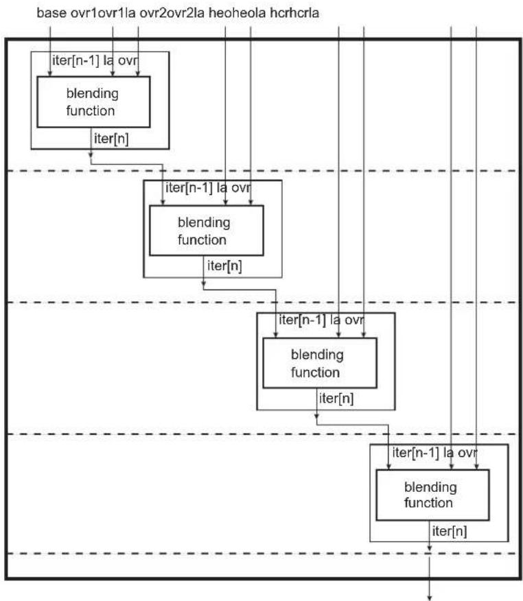
flowchart
graph TD
    A["iter[n-1"] la ovr] --> B["blending function"]
    B --> C["iter[n"]]
    C --> D["iter[n-1"] la ovr]
    D --> E["blending function"]
    E --> F["iter[n"]]
    F --> G["iter[n-1"] la ovr]
    G --> H["blending function"]
    H --> I["iter[n"]]
    I --> J["iter[n-1"] la ovr]
    J --> K["blending function"]
    K --> L["iter[n"]]
    L --> M["blending function"]
    M --> N["iter[n"]]
    N --> O["blending function"]
    O --> P["iter[n"]]
    P --> Q["blending function"]
32.6.11.5 Window Blending
Figure 32-14: 256-level Alpha Blending
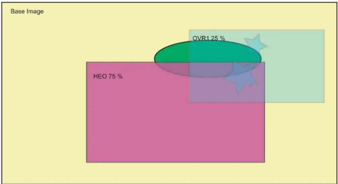
other
Base Image | Category | Percentage (%) | | :--- | :--- | | HEO | 75 | | OVR1 | 25 |Video Prioritization Algorithm 1: OVR1 > HEO > BASE
32.6.11.6 Color Keying
Color keying involves a method of bit-block image transfer (Blit). This entails blitting one image onto another where not all the pixels are copied. Blitting usually involves two bitmaps, a source bitmap and a destination bitmap. A raster operation (ROP) is performed to define whether the iterated color or the overlay color is to be visible or not.
Source Color Keying
If the masked overlay color matches the color key then the iterated color is selected, Source Color Keying is activated using the following configuration sequence:
- Select the Overlay to Blit
- Clear DSTKEY bit
- Activate Color Keying—set CRKEY bit
- Program Color Key writing RKEY, GKEY and BKEY fields
- Program Color Mask writing RKEY, GKEY and BKEY fields
When the field RMASK, GMASK, or BMASK is set to zero, the comparison is disabled and the raster operation is activated.
Destination Color Keying
If the iterated masked color matches the color key then the overlay color is selected, Destination Color Keying is activated using the following configuration sequence:
- Select the Overlay to Blit
- Set DSTKEY bit
- Activate Color Keying—set CRKEY bit
- Program Color Key writing RKEY, GKEY and BKEY fields
- Program Color Mask writing RKEY, GKEY and BKEY fields
When the field RMASK, GMASK, or BMASK is set to zero, the comparison is disabled and the raster operation is activated.
32.6.12 LCDC PWM Controller
This block generates the LCD contrast control signal (LCD_PWM) to make possible the control of the display's contrast by software. This is an 8-bit PWM (Pulse Width Modulation) signal that can be converted to an analog voltage with a simple passive filter.
The PWM module has a free-running counter whose value is compared against a compare register (PWM CVAL field of the LCDC_LCDCFG6 register). If the value in the counter is less than that in the register, the output brings the value of the signal polarity (PWMPOL) bit in the PWM control register: LCDC_LCDCFG6. Otherwise, the opposite value is output. Thus, a periodic waveform with a pulse width proportional to the value in the compare register is generated.
Due to the comparison mechanism, the output pulse has a width between zero and 255 PWM counter cycles. Thus by adding a simple passive filter outside the chip, an analog voltage between 0 and (255/256) × V DD can be obtained (for the positive polarity case, or between (1/256) × V DD and V _DD for the negative polarity case). Other voltage values can be obtained by adding active external circuitry.
For PWM mode, the counter frequency can be adjusted to four different values using the PWMPS field of the LCDC_LCDCFG6 register.
The PWM module can be fed with the slow clock or the system clock, depending on the CLKPWMSEL bit of the LCDC_CFG0 register.
32.6.13 Post Processing Controller
The output stream of pixels can be either displayed on the screen or written to the memory using the Post Processing Controller (PPC). When the PPC is used, the screen display is disabled, but synchronization signals remain active (if enabled). The stream of pixel can be written in RGB mode or encoded in YCbCr 422 mode. A programmable color space conversion stage is available.
$$ \left[ \begin{array}{l} Y \ U \ V \end{array} \right] = \left[ \begin{array}{l l l} C S C Y R & C S C Y G & C S C Y B \ C S C U R & C S C U G & C S C U B \ C S C V R & C S C V G & C S C U B \end{array} \right] \bullet \left[ \begin{array}{l} R \ G \ B \end{array} \right] + \left[ \begin{array}{l} Y _ {o f f} \ U _ {o f f} \ V _ {o f f} \end{array} \right] $$
32.6.14 LCD Overall Performance
32.6.14.1 Color Lookup Table (CLUT)
Table 32-49: CLUT Pixel Performance
| CLUT Mode Pixels/Cycle Rotation Scaling | |||
| 1 bpp 64 | Not supported | Supported | |
| 2 bpp 32 | Not supported | Supported | |
| 3 bpp 16 | Not supported | Supported | |
| 4 bpp 8 | Not supported | Supported | |
32.6.14.2 RGB Mode Fetch Performance
Table 32-50: RGB Mode Performance
| RGB Mode | Pixels/Cycle Memory Burst Mode | Rotation Peak Random Memory Access (pixels/cycle) | Scaling Burst Mode or Rotation Optimization AvailableRotation C | |
| (1) | Normal Mode | |||
| 12 bpp 4 1 0.2 Supported | ||||
| 16 bpp 4 1 0.2 Supported | ||||
| 18 bpp 2 1 0.2 Supported | ||||
| 18 bpp RGB PACKED | 2.666 | Not supported | 0.2 | Supported |
| 19 bpp | 2 1 0.2 Supported | |||
| 19 bpp PACKED | 2.666 | Not Supported | 0.2 | Supported |
| 24 bpp | 2 1 0.2 Supported | |||
| 24 bpp PACKED | 2.666 | Not Supported | 0.2 | Supported |
| 25 bpp | 2 1 0.2 Supported | |||
| 32 bpp | 2 1 0.2 Supported | |||
Note 1: Rotation optimization = AHB lock asserted on consecutive single access.
32.6.14.3 YUV Mode Fetch Performance
Table 32-51: Single Stream for 0 Wait State Memory
| YUV Mode | Pixels/Cycle Memory Burst Mode | Rotation Peak Random Memory Access (pixels/cycle) Scaling | Rotation Optimization Is AvailableRotation Optimization | |
| (1) | Normal Mode | |||
| 32 bpp AYUV 2 1 0.2 | Supported | |||
| 16 bpp 422 | 4 | Not Supported | Not Supported | Supported |
Note 1: Rotation optimization = AHB lock asserted on consecutive single access
Table 32-52: Multiple Stream for 0 Wait State Memory
| YUV Mode | Comp/Cycle Memory Burst Mode | Rotation Peak Random Memory Access (pixels/cycle) | Scaling Burst Mode or Rotation Optimization Is Available | |
| Rotation Optimization | Normal Mode | |||
| 16 bpp 422 semiplanar | 8 Y, 4 UV | 1 Y, 1 UV (2 streams) | 0.2 Y 0.2 UV (2 streams) | Supported |
| 16 bpp 422 planar | 8 Y, 8 U, 8 V | 1 Y, 1 U, 1 V (3 streams) | 0.2 Y, 0.2 U, 0.2 V (3 streams) | Supported |
| 12 bpp 4:2:0 semiplanar | 8 Y, 4 UV | 1 Y, 1 UV (2 streams) | 0.2 Y 0.2 UV (2 streams) | Supported |
| 12 bpp 4:2:0 planar | 8 Y, 8 U, 8 V | 1 Y, 1 U, 1 V (3 streams) | 0.2 Y, 0.2 U, 0.2 V (3 streams) | Supported |
Note: In order to provide more bandwidth, when multiple streams are used to transfer Y, UV, U or V components, two AHB interfaces are recommended or multiple AXI ID are required.
Table 32-53: YUV Planar Overall Performance 1 AHB Interface for 0 Wait State Memory
| YUV Mode | Pix/Cycle Memory Burst Mode | Rotation Peak Random Memory Access (pixels/cycle) | Scaling Burst Mode or Rotation Optimization Is Available | |
| Rotation Optimization | Normal Mode | |||
| 16 bpp 422 semiplanar | 4 | 0.66 | 0.132 | Supported |
| 16 bpp 422 planar | 4 | 0.5 | 0.1 | Supported |
| 12 bpp 4:2:0 semiplanar | 5.32 | 0.8 | 0.16 | Supported |
| 12 bpp 4:2:0 planar | 5.32 | 0.66 | 0.132 | Supported |
Note: In order to provide more bandwidth, when multiple streams are used to transfer Y, UV, U or V components, two AHB interfaces are recommended or multiple AXI ID are required.
32.6.15 Input FIFO
The LCD module includes one input FIFO per overlay. These input FIFOs are used to buffer the AHB burst and serialize the stream of pixels.
32.6.16 Output FIFO
The LCD module includes one output FIFO that stores the blended pixel.
32.6.17 Output Timing Generation
32.6.17.1 Active Display Timing Mode
Figure 32-15: Active Display Timing

text_image
LCD_PCLK LCD_VSYNC LCD_HSYNC LCD_BIAS_DEN LCD_DAT[23:0] HSW V SW VBP HBP LCD_PCLK LCD_VSYNC LCD_HSYNC LCD_BIAS_DEN LCD_DAT[23:0] HSW HBP PPL HFP HSW HBP LCD_PCLK LCD_VSYNC LCD_HSYNC LCD_BIAS_DEN LCD_DAT[23:0] HFPPPL HSW VFPFigure 32-16: Vertical Synchronization Timing (part 1)
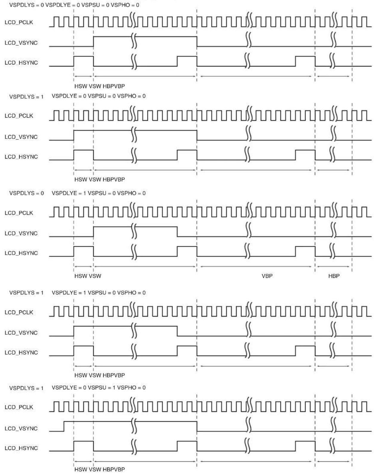
text_image
VSPDLYS = 0 VSPDLYE = 0 VSPSU = 0 VSPHO = 0 LCD_PCLK LCD_VSYNC LCD_HSYNC HSW VSW HBPVBP VSPDLYS = 1 VSPDLYE = 0 VSPSU = 0 VSPHO = 0 LCD_PCLK LCD_VSYNC LCD_HSYNC HSW VSW HBPVBP VSPDLYS = 0 VSPDLYE = 1 VSPSU = 0 VSPHO = 0 LCD_PCLK LCD_VSYNC LCD_HSYNC HSW VSW VBP HBP VSPDLYS = 1 VSPDLYE = 1 VSPSU = 0 VSPHO = 0 LCD_PCLK LCD_VSYNC LCD_HSYNC HSW VSW HBPVBP VSPDLYS = 1 VSPDLYE = 0 VSPSU = 1 VSPHO = 0 LCD_PCLK LCD_VSYNC LCD_HSYNC HSW VSW HBPVBPFigure 32-17: Vertical Synchronization Timing (part 2)

text_image
VSPDLYS = 1 VSPDLYE = 0 VSPSU = 0 VSPHO = 1 LCD_PCLK LCD_VSYNC LCD_HSYNC HSW VSW VBP HBP VSPDLYS = 1 VSPDLYE = 0 VSPSU = 1 VSPHO = 1 LCD_PCLK LCD_VSYNC LCD_HSYNC HSW VSW VBP HBPFigure 32-18: DISP Signal Timing Diagram
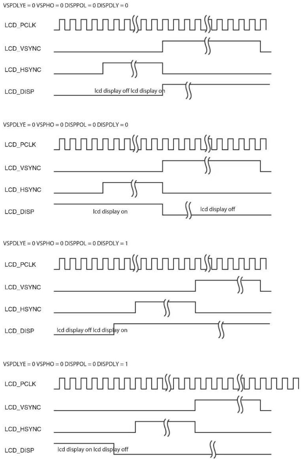
text_image
VSPDLYE = 0 VSPHO = 0 DISPPOL = 0 DISPDLY = 0 LCD_PCLK LCD_VSYNC LCD_HSYNC LCD_DISP Icd display off Icd display on VSPDLYE = 0 VSPHO = 0 DISPPOL = 0 DISPDLY = 0 LCD_PCLK LCD_VSYNC LCD_HSYNC LCD_DISP Icd display on Icd display off VSPDLYE = 0 VSPHO = 0 DISPPOL = 0 DISPDLY = 1 LCD_PCLK LCD_VSYNC LCD_HSYNC LCD_DISP Icd display off Icd display on VSPDLYE = 0 VSPHO = 0 DISPPOL = 0 DISPDLY = 1 LCD_PCLK LCD_VSYNC LCD_HSYNC LCD_DISP Icd display on Icd display off32.6.18 Output Format
32.6.18.1 Active Mode Output Pin Assignment
Table 32-54: Active Mode Output with 24-bit Bus Interface Configuration
| Pin ID TFT 24 bits | TFT 18 bits TFT 16 bits | TFT 12 bits | ||
| LCD_DAT[23] R[7] | -- | |||
| LCD_DAT[22] R[6] | -- | |||
| LCD_DAT[21] R[5] | -- | |||
| LCD_DAT[20] R[4] | -- | |||
| LCD_DAT[19] R[3] | -- | |||
| LCD_DAT[18] R[2] | -- | |||
| LCD_DAT[17] R[1] R[5] | -- | |||
| LCD_DAT[16] R[0] R[4] | -- | |||
| LCD_DAT[15] G[7] R[3] R[4] | - | |||
| LCD_DAT[14] G[6] R[2] R[3] | - | |||
| LCD_DAT[13] G[5] R[1] R[2] | - | |||
| LCD_DAT[12] G[4] R[0] R[1] | - | |||
| LCD_DAT[11] | G[3] G[5] R[0] R[3] | |||
| LCD_DAT[10] G[2] G[4] G[5] R[2] | ||||
| LCD_DAT[9] | G[1] G[3] G[4] R[1] | |||
| LCD_DAT[8] | G[0] G[2] G[3] R[0] | |||
| LCD_DAT[7] | B[7] | G[1] G[2] G[3] | ||
| LCD_DAT[6] | B[6] | G[0] G[1] G[2] | ||
| LCD_DAT[5] | B[5] | B[5] | G[0] G[1] | |
| LCD_DAT[4] | B[4] | B[4] | B[4] | G[0] |
| LCD_DAT[3] | B[3] | B[3] | B[3] | B[3] |
| LCD_DAT[2] | B[2] | B[2] | B[2] | B[2] |
| LCD_DAT[1] | B[1] | B[1] | B[1] | B[1] |
| LCD_DAT[0] | B[0] | B[0] | B[0] | B[0] |
32.7 LCD Controller (LCDC) User Interface
Table 32-55: Register Mapping
| Offset Register Name Access Reset | ||||
| 0x00000000 | LCD Controller Configuration Register 0 | LCDC_LCDCFG0 | Read/Write | 0x00000000 |
| 0x00000004 | LCD Controller Configuration Register 1 | LCDC_LCDCFG1 | Read/Write | 0x00000000 |
| 0x00000008 | LCD Controller Configuration Register 2 | LCDC_LCDCFG2 | Read/Write | 0x00000000 |
| 0x0000000C | LCD Controller Configuration Register 3 | LCDC_LCDCFG3 | Read/Write | 0x00000000 |
| 0x00000010 | LCD Controller Configuration Register 4 | LCDC_LCDCFG4 | Read/Write | 0x00000000 |
| 0x00000014 | LCD Controller Configuration Register 5 | LCDC_LCDCFG5 | Read/Write | 0x00000000 |
| 0x00000018 | LCD Controller Configuration Register 6 | LCDC_LCDCFG6 | Read/Write | 0x00000000 |
| 0x0000001C Reserved - - - | ||||
| 0x00000020 | LCD Controller Enable Register | LCDC_LCDEN | Write-only | - |
| 0x00000024 | LCD Controller Disable Register | LCDC_LCDDIS | Write-only | - |
| 0x00000028 | LCD Controller Status Register | LCDC_LCDSR | Read-only | 0x00000000 |
| 0x0000002C | LCD Controller Interrupt Enable Register | LCDC_LCDIER | Write-only | - |
| 0x00000030 | LCD Controller Interrupt Disable Register | LCDC_LCDIDR | Write-only | - |
| 0x00000034 | LCD Controller Interrupt Mask Register | LCDC_LCDIMR | Read-only | 0x00000000 |
| 0x00000038 | LCD Controller Interrupt Status Register | LCDC_LCDISR | Read-only | 0x00000000 |
| 0x0000003C | LCD Controller Attribute Register | LCDC_ATTR | Write-only | - |
| 0x00000040 | Base Layer Channel Enable Register | LCDC_BASECHER | Write-only | - |
| 0x00000044 | Base Layer Channel Disable Register | LCDC_BASECHDR | Write-only | - |
| 0x00000048 | Base Layer Channel Status Register | LCDC_BASECHSR | Read-only | 0x00000000 |
| 0x0000004C | Base Layer Interrupt Enable Register | LCDC_BASEIER | Write-only | - |
| 0x00000050 | Base Layer Interrupt Disabled Register | LCDC_BASEIDR | Write-only | - |
| 0x00000054 | Base Layer Interrupt Mask Register | LCDC_BASEIMR | Read-only | 0x00000000 |
| 0x00000058 | Base Layer Interrupt Status Register | LCDC_BASEISR | Read-only | 0x00000000 |
| 0x0000005C | Base DMA Head Register | LCDC_BASEHEAD | Read/Write | 0x00000000 |
| 0x00000060 | Base DMA Address Register | LCDC_BASEADDR | Read/Write | 0x00000000 |
| 0x00000064 | Base DMA Control Register | LCDC_BASECTRL | Read/Write | 0x00000000 |
| 0x00000068 | Base DMA Next Register | LCDC_BASENEXT | Read/Write | 0x00000000 |
| 0x0000006C | Base Layer Configuration Register 0 | LCDC_BASECFG0 | Read/Write | 0x00000000 |
| 0x00000070 | Base Layer Configuration Register 1 | LCDC_BASECFG1 | Read/Write | 0x00000000 |
| 0x00000074 | Base Layer Configuration Register 2 | LCDC_BASECFG2 | Read/Write | 0x00000000 |
| 0x00000078 | Base Layer Configuration Register 3 | LCDC_BASECFG3 | Read/Write | 0x00000000 |
| 0x0000007C | Base Layer Configuration Register 4 | LCDC_BASECFG4 | Read/Write | 0x00000000 |
| 0x00000080 | Base Layer Configuration Register 5 | LCDC_BASECFG5 | Read/Write | 0x00000000 |
| 0x00000084 | Base Layer Configuration Register 6 | LCDC_BASECFG6 | Read/Write | 0x00000000 |
| 0x00000088-0x0000013C | Reserved -- - | |||
| Offset | Register | Name | Access | Reset |
| 0x00000140 Overlay 1 | Channel Enable Register LCDC_OVR1CHER Write-only – | |||
| 0x00000144 Overlay 1 | Channel Disable Register LCDC_OVR1CHDR Write-only – | |||
| 0x00000148 Overlay 1 | Channel Status Register LCDC_OVR1CHSR Read-only 0x00000000 | |||
| 0x0000014C Overlay 1 | Interrupt Enable Register LCDC_OVR1IER Write-only – | |||
| 0x00000150 Overlay 1 | Interrupt Disable Register LCDC_OVR1IDR Write-only – | |||
| 0x00000154 Overlay 1 | Interrupt Mask Register LCDC_OVR1IMR Read-only 0x00000000 | |||
| 0x00000158 Overlay 1 | Interrupt Status Register LCDC_OVR1ISR Read-only 0x00000000 | |||
| 0x0000015C | Overlay 1 DMA Head Register | LCDC_OVR1HEAD | Read/Write | 0x00000000 |
| 0x00000160 | Overlay 1 DMA Address Register | LCDC_OVR1ADDR | Read/Write | 0x00000000 |
| 0x00000164 | Overlay 1 DMA Control Register | LCDC_OVR1CTRL | Read/Write | 0x00000000 |
| 0x00000168 | Overlay 1 DMA Next Register | LCDC_OVR1NEXT | Read/Write | 0x00000000 |
| 0x0000016C | Overlay 1 Configuration Register 0 | LCDC_OVR1CFG0 | Read/Write | 0x00000000 |
| 0x00000170 | Overlay 1 Configuration Register 1 | LCDC_OVR1CFG1 | Read/Write | 0x00000000 |
| 0x00000174 | Overlay 1 Configuration Register 2 | LCDC_OVR1CFG2 | Read/Write | 0x00000000 |
| 0x00000178 | Overlay 1 Configuration Register 3 | LCDC_OVR1CFG3 | Read/Write | 0x00000000 |
| 0x0000017C | Overlay 1 Configuration Register 4 | LCDC_OVR1CFG4 | Read/Write | 0x00000000 |
| 0x00000180 | Overlay 1 Configuration Register 5 | LCDC_OVR1CFG5 | Read/Write | 0x00000000 |
| 0x00000184 | Overlay 1 Configuration Register 6 | LCDC_OVR1CFG6 | Read/Write | 0x00000000 |
| 0x00000188 | Overlay 1 Configuration Register 7 | LCDC_OVR1CFG7 | Read/Write | 0x00000000 |
| 0x0000018C | Overlay 1 Configuration Register 8 | LCDC_OVR1CFG8 | Read/Write | 0x00000000 |
| 0x00000190 | Overlay 1 Configuration Register 9 | LCDC_OVR1CFG9 | Read/Write | 0x00000000 |
| 0x00000194–0x0000023C | Reserved | – | – | – |
| 0x00000240 Overlay 2 | Channel Enable Register LCDC_OVR2CHER Write-only – | |||
| 0x00000244 Overlay 2 | Channel Disable Register LCDC_OVR2CHDR Write-only – | |||
| 0x00000248 Overlay 2 | Channel Status Register LCDC_OVR2CHSR Read-only 0x00000000 | |||
| 0x0000024C Overlay 2 | Interrupt Enable Register LCDC_OVR2IER Write-only – | |||
| 0x00000250 Overlay 2 | Interrupt Disable Register LCDC_OVR2IDR Write-only – | |||
| 0x00000254 Overlay 2 | Interrupt Mask Register LCDC_OVR2IMR Read-only 0x00000000 | |||
| 0x00000258 Overlay 2 | Interrupt Status Register LCDC_OVR2ISR Read-only 0x00000000 | |||
| 0x0000025C | Overlay 2 DMA Head Register | LCDC_OVR2HEAD | Read/Write | 0x00000000 |
| 0x00000260 | Overlay 2 DMA Address Register | LCDC_OVR2ADDR | Read/Write | 0x00000000 |
| 0x00000264 | Overlay 2 DMA Control Register | LCDC_OVR2CTRL | Read/Write | 0x00000000 |
| 0x00000268 | Overlay 2 DMA Next Register | LCDC_OVR2NEXT | Read/Write | 0x00000000 |
| 0x0000026C | Overlay 2 Configuration Register 0 | LCDC_OVR2CFG0 | Read/Write | 0x00000000 |
| 0x00000270 | Overlay 2 Configuration Register 1 | LCDC_OVR2CFG1 | Read/Write | 0x00000000 |
| 0x00000274 | Overlay 2 Configuration Register 2 | LCDC_OVR2CFG2 | Read/Write | 0x00000000 |
| 0x00000278 Overlay 2 | Configuration Register 3 LCDC_OVR2CFG3 Read/Write 0x00000000 | |||
| 0x0000027C Overlay 2 | Configuration Register 4 LCDC_OVR2CFG4 Read/Write 0x00000000 | |||
| 0x00000280 Overlay 2 | Configuration Register 5 LCDC_OVR2CFG5 Read/Write 0x00000000 | |||
| 0x00000284 Overlay 2 | Configuration Register 6 LCDC_OVR2CFG6 Read/Write 0x00000000 | |||
| 0x00000288 Overlay 2 | Configuration Register 7 LCDC_OVR2CFG7 Read/Write 0x00000000 | |||
| 0x0000028C Overlay 2 | Configuration Register 8 LCDC_OVR2CFG8 Read/Write 0x00000000 | |||
| 0x00000290 Overlay 2 | Configuration Register 8 LCDC_OVR2CFG9 Read/Write 0x00000000 | |||
| 0x00000294-0x0000033C Reserved - - - | ||||
| 0x00000340 High End | Overlay Channel Enable Register LCDC_HEOCHER Write-only - | |||
| 0x00000344 | High End Overlay Channel Disable Register | LCDC_HEOCHDR | Write-only | - |
| 0x00000348 | High End Overlay Channel Status Register | LCDC_HEOCHSR | Read-only | 0x00000000 |
| 0x0000034C | High End Overlay Interrupt Enable Register | LCDC_HEOIER | Write-only | - |
| 0x00000350 | High End Overlay Interrupt Disable Register | LCDC_HEOIDR | Write-only | - |
| 0x00000354 | High End Overlay Interrupt Mask Register | LCDC_HEOIMR | Read-only | 0x00000000 |
| 0x00000358 | High End Overlay Interrupt Status Register | LCDC_HEOISR | Read-only | 0x00000000 |
| 0x0000035C | High End Overlay DMA Head Register | LCDC_HEOHEAD | Read/Write | 0x00000000 |
| 0x00000360 | High End Overlay DMA Address Register | LCDC_HEOADDR | Read/Write | 0x00000000 |
| 0x00000364 | High End Overlay DMA Control Register | LCDC_HEOCTRL | Read/Write | 0x00000000 |
| 0x00000368 | High End Overlay DMA Next Register | LCDC_HEONEXT | Read/Write | 0x00000000 |
| 0x0000036C | High End Overlay U-UV DMA Head Register | LCDC_HEOUHEAD | Read/Write | 0x00000000 |
| 0x00000370 | High End Overlay U-UV DMA Address Register | LCDC_HEOUADDR | Read/Write | 0x00000000 |
| 0x00000374 | High End Overlay U-UV DMA Control Register | LCDC_HEOUCTRL | Read/Write | 0x00000000 |
| 0x00000378 | High End Overlay U-UV DMA Next Register | LCDC_HEOUNEXT | Read/Write | 0x00000000 |
| 0x0000037C | High End Overlay V DMA Head Register | LCDC_HEOVHEAD | Read/Write | 0x00000000 |
| 0x00000380 | High End Overlay V DMA Address Register | LCDC_HEOVADDR | Read/Write | 0x00000000 |
| 0x00000384 | High End Overlay V DMA Control Register | LCDC_HEOVCTRL | Read/Write | 0x00000000 |
| 0x00000388 | High End Overlay V DMA Next Register | LCDC_HEOVNEXT | Read/Write | 0x00000000 |
| 0x0000038C | High End Overlay Configuration Register 0 | LCDC_HEOCFG0 | Read/Write | 0x00000000 |
| 0x00000390 | High End Overlay Configuration Register 1 | LCDC_HEOCFG1 | Read/Write | 0x00000000 |
| 0x00000394 | High End Overlay Configuration Register 2 | LCDC_HEOCFG2 | Read/Write | 0x00000000 |
| 0x00000398 | High End Overlay Configuration Register 3 | LCDC_HEOCFG3 | Read/Write | 0x00000000 |
| 0x0000039C | High End Overlay Configuration Register 4 | LCDC_HEOCFG4 | Read/Write | 0x00000000 |
| 0x000003A0 | High End Overlay Configuration Register 5 | LCDC_HEOCFG5 | Read/Write | 0x00000000 |
| 0x000003A4 | High End Overlay Configuration Register 6 | LCDC_HEOCFG6 | Read/Write | 0x00000000 |
| 0x000003A8 | High End Overlay Configuration Register 7 | LCDC_HEOCFG7 | Read/Write | 0x00000000 |
| 0x000003AC | High End Overlay Configuration Register 8 | LCDC_HEOCFG8 | Read/Write | 0x00000000 |
| 0x000003B0 | High End Overlay Configuration Register 9 | LCDC_HEOCFG9 | Read/Write | 0x00000000 |
| 0x000003B4 | High End Overlay Configuration Register 10 | LCDC_HEOCFG10 | Read/Write | 0x00000000 |
| 0x000003B8 | High End Overlay Configuration Register 11 | LCDC_HEOCFG11 | Read/Write | 0x00000000 |
| 0x000003BC | High End Overlay Configuration Register 12 | LCDC_HEOCFG12 | Read/Write | 0x00000000 |
| 0x000003C0 High End | Overlay Configuration Register 13 LCDC_HEOCFG13 Read/Write 0x00000000 | |||
| 0x000003C4 High End | Overlay Configuration Register 14 LCDC_HEOCFG14 Read/Write 0x00000000 | |||
| 0x000003C8 High End | Overlay Configuration Register 15 LCDC_HEOCFG15 Read/Write 0x00000000 | |||
| 0x000003CC | High End Overlay Configuration Register 16 | LCDC_HEOCFG16 | Read/Write | 0x00000000 |
| 0x000003D0 High End | Overlay Configuration Register 17 LCDC_HEOCFG17 Read/Write 0x00000000 | |||
| 0x000003D4 High End | Overlay Configuration Register 18 LCDC_HEOCFG18 Read/Write 0x00000000 | |||
| 0x000003D8 High End | Overlay Configuration Register 19 LCDC_HEOCFG19 Read/Write 0x00000000 | |||
| 0x000003DC | High End Overlay Configuration Register 20 | LCDC_HEOCFG20 | Read/Write | 0x00000000 |
| 0x000003E0 | High End Overlay Configuration Register 21 | LCDC_HEOCFG21 | Read/Write | 0x00000000 |
| 0x000003E4 | High End Overlay Configuration Register 22 | LCDC_HEOCFG22 | Read/Write | 0x00000000 |
| 0x000003E8 | High End Overlay Configuration Register 23 | LCDC_HEOCFG23 | Read/Write | 0x00000000 |
| 0x000003EC | High End Overlay Configuration Register 24 | LCDC_HEOCFG24 | Read/Write | 0x00000000 |
| 0x000003F0 High End | Overlay Configuration Register 25 LCDC_HEOCFG25 Read/Write 0x00000000 | |||
| 0x000003F4 High End | Overlay Configuration Register 26 LCDC_HEOCFG26 Read/Write 0x00000000 | |||
| 0x000003F8 High End | Overlay Configuration Register 27 LCDC_HEOCFG27 Read/Write 0x00000000 | |||
| 0x000003FC | High End Overlay Configuration Register 28 | LCDC_HEOCFG28 | Read/Write | 0x00000000 |
| 0x00000400 High End | Overlay Configuration Register 29 LCDC_HEOCFG29 Read/Write 0x00000000 | |||
| 0x00000404 High End | Overlay Configuration Register 30 LCDC_HEOCFG30 Read/Write 0x00000000 | |||
| 0x00000408 High End | Overlay Configuration Register 31 LCDC_HEOCFG31 Read/Write 0x00000000 | |||
| 0x0000040C High End | Overlay Configuration Register 32 LCDC_HEOCFG32 Read/Write 0x00000000 | |||
| 0x00000410 High End | Overlay Configuration Register 33 LCDC_HEOCFG33 Read/Write 0x00000000 | |||
| 0x00000414 High End | Overlay Configuration Register 34 LCDC_HEOCFG34 Read/Write 0x00000000 | |||
| 0x00000418 High End | Overlay Configuration Register 35 LCDC_HEOCFG35 Read/Write 0x00000000 | |||
| 0x0000041C High End | Overlay Configuration Register 36 LCDC_HEOCFG36 Read/Write 0x00000000 | |||
| 0x00000420 High End | Overlay Configuration Register 37 LCDC_HEOCFG37 Read/Write 0x00000000 | |||
| 0x00000424 High End | Overlay Configuration Register 38 LCDC_HEOCFG38 Read/Write 0x00000000 | |||
| 0x00000428 High End | Overlay Configuration Register 39 LCDC_HEOCFG39 Read/Write 0x00000000 | |||
| 0x0000042C High End | Overlay Configuration Register 40 LCDC_HEOCFG40 Read/Write 0x00000000 | |||
| 0x00000430 High End | Overlay Configuration Register 41 LCDC_HEOCFG41 Read/Write 0x00000000 | |||
| 0x00000434-0x0000043C | Reserved | - | - | - |
| 0x00000440 | Hardware Cursor Channel Enable Register | LCDC_HCRCHER | Write-only | - |
| 0x00000444 Hardware | Cursor Channel Disable Register LCDC_HCRCHDR Write-only - | |||
| 0x00000448 Hardware | Cursor Channel Status Register LCDC_HCRCHSR Read-only 0x00000000 | |||
| 0x0000044C | Hardware Cursor Interrupt Enable Register | LCDC_HCRIER | Write-only | - |
| 0x00000450 Hardware | Cursor Interrupt Disable Register LCDC_HCRIDR Write-only - | |||
| 0x00000454 Hardware | Cursor Interrupt Mask Register LCDC_HCRIMR Read-only 0x00000000 | |||
| 0x00000458 Hardware | Cursor Interrupt Status Register LCDC_HCRISR Read-only 0x00000000 | |||
| 0x0000045C | Hardware Cursor DMA Head Register | LCDC_HCRHEAD | Read/Write | 0x00000000 |
| 0x00000460 | Hardware cursor DMA Address Register | LCDC_HCRADDR | Read/Write | 0x00000000 |
| 0x00000464 | Hardware Cursor DMA Control Register | LCDC_HCRCTRL | Read/Write | 0x00000000 |
| 0x00000468 Hardware | Cursor DMA Next Register LCDC_HCRNEXT Read/Write 0x00000000 | |||
| 0x0000046C | Hardware Cursor Configuration Register 0 | LCDC_HCRCFG0 | Read/Write | 0x00000000 |
| 0x00000470 | Hardware Cursor Configuration Register 1 | LCDC_HCRCFG1 | Read/Write | 0x00000000 |
| 0x00000474 | Hardware Cursor Configuration Register 2 | LCDC_HCRCFG2 | Read/Write | 0x00000000 |
| 0x00000478 | Hardware Cursor Configuration Register 3 | LCDC_HCRCFG3 | Read/Write | 0x00000000 |
| 0x0000047C | Hardware Cursor Configuration Register 4 | LCDC_HCRCFG4 | Read/Write | 0x00000000 |
| 0x00000480 Reserved | - | - | - | |
| 0x00000484 | Hardware Cursor Configuration Register 6 | LCDC_HCRCFG6 | Read/Write | 0x00000000 |
| 0x00000488 | Hardware Cursor Configuration Register 7 | LCDC_HCRCFG7 | Read/Write | 0x00000000 |
| 0x0000048C | Hardware Cursor Configuration Register 8 | LCDC_HCRCFG8 | Read/Write | 0x00000000 |
| 0x00000490 | Hardware Cursor Configuration Register 9 | LCDC_HCRCFG9 | Read/Write | 0x00000000 |
| 0x00000494-0x0000053C | Reserved | - | - | - |
| 0x00000540 | Post Processing Channel Enable Register | LCDC_PPCHER | Write-only | - |
| 0x00000544 | Post Processing Channel Disable Register | LCDC_PPCHDR | Write-only | - |
| 0x00000548 | Post Processing Channel Status Register | LCDC_PPCHSR | Read-only | 0x00000000 |
| 0x0000054C | Post Processing Interrupt Enable Register | LCDC_PPIER | Write-only | - |
| 0x00000550 | Post Processing Interrupt Disable Register | LCDC_PPIDR | Write-only | - |
| 0x00000554 | Post Processing Interrupt Mask Register | LCDC_PPIMR | Read-only | 0x00000000 |
| 0x00000558 | Post Processing Interrupt Status Register | LCDC_PPISR | Read-only | 0x00000000 |
| 0x0000055C | Post Processing Head Register | LCDC_PPHEAD | Read/Write | 0x00000000 |
| 0x00000560 | Post Processing Address Register | LCDC_PPADDR | Read/Write | 0x00000000 |
| 0x00000564 | Post Processing Control Register | LCDC_PPCTRL | Read/Write | 0x00000000 |
| 0x00000568 | Post Processing Next Register | LCDC_PPNEXT | Read/Write | 0x00000000 |
| 0x0000056C | Post Processing Configuration Register 0 | LCDC_PPCFG0 | Read/Write | 0x00000000 |
| 0x00000570 | Post Processing Configuration Register 1 | LCDC_PPCFG1 | Read/Write | 0x00000000 |
| 0x00000574 | Post Processing Configuration Register 2 | LCDC_PPCFG2 | Read/Write | 0x00000000 |
| 0x00000578 | Post Processing Configuration Register 3 | LCDC_PPCFG3 | Read/Write | 0x00000000 |
| 0x0000057C | Post Processing Configuration Register 4 | LCDC_PPCFG4 | Read/Write | 0x00000000 |
| 0x00000580 | Post Processing Configuration Register 5 | LCDC_PPCFG5 | Read/Write | 0x00000000 |
| 0x00000584-0x000005FC Reserved - - - | ||||
| 0x00000600 Base CLUT Register 0 LCDC_BASECLUT0 Read/Write 0x00000000 | ||||
| ... | ... | ... | ... | ... |
| 0x000008FC | Base CLUT Register 255 | LCDC_BASECLUT255 | Read/Write | 0x00000000 |
| 0x00000A00 | Overlay 1 CLUT Register 0 | LCDC_OVR1CLUT0 | Read/Write | 0x00000000 |
| ... | ... | ... | ... | ... |
| 0x00000DFC | Overlay 1 CLUT Register 255 | LCDC_OVR1CLUT255 | Read/Write | 0x00000000 |
| 0x00000E00 | Overlay 2 CLUT Register 0 | LCDC_OVR2CLUT0 | Read/Write | 0x00000000 |
| ... | ... | ... | ... | ... |
| 0x000011FC | Overlay 2 CLUT Register 255 | LCDC_OVR2CLUT255 | Read/Write | 0x00000000 |
| 0x00001200 | High End Overlay CLUT Register 0 | LCDC_HEOCLUT0 | Read/Write | 0x00000000 |
| ... | ... | ... | ... | ... |
| 0x000015FC | High End Overlay CLUT Register 255 | LCDC_HEOCLUT255 | Read/Write | 0x00000000 |
| 0x00001600 | Hardware Cursor CLUT Register 0 | LCDC_HCRCLUT0 | Read/Write | 0x00000000 |
| ... | ... | ... | ... | ... |
| 0x000019FC | Hardware Cursor CLUT Register 255 | LCDC_HCRCLUT255 | Read/Write | 0x00000000 |
| 0x00001A00-0x00001FFC | Reserved - - - | |||
Note 1: The CLUT registers are located in the RAM.
32.7.1 LCD Controller Configuration Register 0
Name: LCDC_LCDCFG0
Address:0xF0030000
Access: Read/Write
31 30 29 28 27 26 25 24
| - | - | - | - | - | - | - | - |
23 22 21 20 19 18 17 16
CLKDIV
15 14 13 12 11 10 9 8
-- CGDISPP CGDISHCR CGDISHEO CGDISOVR2 CGDISOVR1 CGDISBASE
7 6 5 4 3 2 1 0
| - | - | - | - | CLKPWMSEL | CLKSEL | - | CLKPOL |
CLKPOL: LCD Controller Clock Polarity
0: Data/Control signals are launched on the rising edge of the Pixel Clock.
1: Data/Control signals are launched on the falling edge of the Pixel Clock.
CLKSEL: LCD Controller Clock Source Selection
0: The Asynchronous output stage of the LCD controller is fed by the System Clock.
1: The Asynchronous output state of the LCD controller is fed by the 2x System Clock.
CLKPWMSEL: LCD Controller PWM Clock Source Selection
0: The slow clock is selected and feeds the PWM module.
1: The system clock is selected and feeds the PWM module.
CGDISBASE: Clock Gating Disable Control for the Base Layer
0: Automatic Clock Gating is enabled for the Base Layer.
1: Clock is running continuously.
CGDISOVR1: Clock Gating Disable Control for the Overlay 1 Layer
0: Automatic Clock Gating is enabled for the Overlay 1 Layer.
1: Clock is running continuously.
CGDISOVR2: Clock Gating Disable Control for the Overlay 2 Layer
0: Automatic Clock Gating is enabled for the Overlay 2 Layer.
1: Clock is running continuously.
CGDISHEO: Clock Gating Disable Control for the High End Overlay
0: Automatic Clock Gating is enabled for the High End Overlay Layer.
1: Clock is running continuously.
CGDISHCR: Clock Gating Disable Control for the Hardware Cursor Layer
0: Automatic Clock Gating is enabled for the Hardware Cursor Layer.
1: Clock is running continuously.
CGDISPP: Clock Gating Disable Control for the Post Processing Layer
0: Automatic Clock Gating is enabled for the Post Processing Layer.
1: Clock is running continuously.
CLKDIV: LCD Controller Clock Divider
8-bit width clock divider for pixel clock LCD_PCLK.
pixel_clock = selected_clock / (CLKDIV+2)
where
selected_clock is equal to system_clock when CLKSEL field is set to 0 and system_clock2x when CLKSEL is set to 1.
32.7.2 LCD Controller Configuration Register 1
Name: LCDC_LCDCFG1
Address:0xF0030004
Access: Read/Write
31 30 29 28 27 26 25 24
| - | - | - | - | - | - | - | - |
23 22 21 20 19 18 17 16
| -- VSPW |
15 14 13 12 11 10 9 8
| - | - | - | - | - | - | - | - |
| 7 | 6 | 5 | 4 | 3 | 2 | 1 | 0 |
| -- HSPW |
HSPW: Horizontal Synchronization Pulse Width
Width of the LCD_HSYNC pulse, given in pixel clock cycles. Width is (HSPW+1) LCD_PCLK cycles.
VSPW: Vertical Synchronization Pulse Width
Width of the LCD_VSYNC pulse, given in number of lines. Width is (VSPW+1) lines.
32.7.3 LCD Controller Configuration Register 2
Name: LCDC_LCDCFG2
Address:0xF0030008
Access: Read/Write
31 30 29 28 27 26 25 24
| - | - | - | - | - | - | - | - |
23 22 21 20 19 18 17 16
| -- VBPW |
15 14 13 12 11 10 9 8
| - | - | - | - | - | - | - | - |
| 7 | 6 | 5 | 4 | 3 | 2 | 1 | 0 |
| -- VFPW |
VFPW: Vertical Front Porch Width
This field indicates the number of lines at the end of the Frame. The blanking interval is equal to (VFPW+1) lines.
VBPW: Vertical Back Porch Width
This field indicates the number of lines at the beginning of the Frame. The blanking interval is equal to VBPW lines.
32.7.4 LCD Controller Configuration Register 3
Name: LCDC_LCDCFG3
Address:0xF003000C
Access: Read/Write
31 30 29 28 27 26 25 24
| - | - | - | - | - | - | - | H |
23 22 21 20 19 18 17 16
HBPW
15 14 13 12 11 10 9 8
| - | - | - | - | - | - | - | H |
| 7 | 6 | 5 | 4 | 3 | 2 | 1 | 0 |
HFPW
HFPW: Horizontal Front Porch Width
Number of pixel clock cycles inserted at the end of the active line. The interval is equal to (HFPW+1) LCD_PCLK cycles.
HBPW: Horizontal Back Porch Width
Number of pixel clock cycles inserted at the beginning of the line. The interval is equal to (HBPW+1) LCD_PCLK cycles.
32.7.5 LCD Controller Configuration Register 4
Name: LCDC_LCDCFG4
Address:0xF0030010
Access: Read/Write
31 30 29 28 27 26 25 24
| - | - | - | - | - | R | P |
23 22 21 20 19 18 17 16
| RPF |
15 14 13 12 11 10 9 8
| - | - | - | - | - | P | P |
| 7 | 6 | 5 | 4 | 3 | 2 | 1 | 0 |
| PPL |
RPF: Number of Active Row Per Frame
Number of active lines in the frame. The frame height is equal to (RPF+1) lines.
PPL: Number of Pixels Per Line
Number of pixel in the frame. The number of active pixels in the frame is equal to (PPL+1) pixels.
32.7.6 LCD Controller Configuration Register 5
Name: LCDC_LCDCFG5
Address:0xF0030014
Access: Read/Write
31 30 29 28 27 26 25 24
| - | - | - | - | - | - | - | - |
23 22 21 20 19 18 17 16
| - | - | - | G | U | A | R |
15 14 13 12 11 10 9 8
| -- VSPH | O VSPSU - | PP | MODE |
| 7 | 6 | 5 | 4 | 3 | 2 | 1 | 0 |
| DISPDLY | DITHER | - | DISPPOL | VSPDLYE | VSPDLYS | VSPOL | HSPOL |
HSPOL: Horizontal Synchronization Pulse Polarity
0: Active High
1: Active Low
VSPOL: Vertical Synchronization Pulse Polarity
0: Active High
1: Active Low
VSPDLYS: Vertical Synchronization Pulse Start
0: The first active edge of the Vertical synchronization pulse is synchronous with the second edge of the horizontal pulse.
1: The first active edge of the Vertical synchronization pulse is synchronous with the first edge of the horizontal pulse.
VSPDLYE: Vertical Synchronization Pulse End
0: The second active edge of the Vertical synchronization pulse is synchronous with the second edge of the horizontal pulse.
1: The second active edge of the Vertical synchronization pulse is synchronous with the first edge of the horizontal pulse.
DISPPOL: Display Signal Polarity
0: Active High
1: Active Low
DITHER: LCD Controller Dithering
0: Dithering logical unit is disabled
1: Dithering logical unit is activated
DISPDLY: LCD Controller Display Power Signal Synchronization
0: The LCD_DISP signal is asserted synchronously with the second active edge of the horizontal pulse.
1: The LCD_DISP signal is asserted asynchronously with both edges of the horizontal pulse.
MODE: LCD Controller Output Mode
| Value Name Description | ||
| 0 OUTPUT_12 | BPP LCD Output mode is set to 12 | bits per pixel |
| 1 OUTPUT_16 | BPP LCD Output mode is set to 16 | bits per pixel |
| 2 OUTPUT_18 | BPP LCD Output mode is set to 18 | bits per pixel |
| 3 OUTPUT_24 | BPP LCD Output mode is set to 24 | bits per pixel |
PP: Post Processing Enable
0: The blended pixel is pushed into the output FIFO.
1: The blended pixel is written back to memory, the post-processing stage is enabled.
VSPSU: LCD Controller Vertical synchronization Pulse Setup Configuration
0: The vertical synchronization pulse is asserted synchronously with horizontal pulse edge.
1: The vertical synchronization pulse is asserted one pixel clock cycle before the horizontal pulse.
VSPHO: LCD Controller Vertical synchronization Pulse Hold Configuration
0: The vertical synchronization pulse is asserted synchronously with horizontal pulse edge.
1: The vertical synchronization pulse is held active one pixel clock cycle after the horizontal pulse.
GUARDTIME: LCD DISPLAY Guard Time
Number of frames inserted during start up before LCD_DISP assertion.
Number of frames inserted after LCD_DISP reset.
32.7.7 LCD Controller Configuration Register 6
Name: LCDC_LCDCFG6
Address:0xF0030018
Access: Read/Write
31 30 29 28 27 26 25 24
| - | - | - | - | - | - | - | - |
23 22 21 20 19 18 17 16
| - | - | - | - | - | - | - | - |
15 14 13 12 11 10 9 8
| PWMVAL | |||||||
| 7 | 6 | 5 | 4 | 3 | 2 | 1 | 0 |
| --- PWM | MPOL-PWMPS | ||||||
PWMPS: PWM Clock Prescaler
Selects the configuration of the counter prescaler module.
| Value Name | Description | |
| 000 DIV_1 | The counter advances at a rate of f | COUNTER = f_PWM\_SELECTED\_CLOCK |
| 001 DIV_2 | The counter advances at a rate of f | COUNTER = f_PWM\_SELECTED\_CLOCK/2 |
| 010 DIV_4 | The counter advances at a rate of f | COUNTER = f_PWM\_SELECTED\_CLOCK/4 |
| 011 | DIV_8 The counter advances at a rate of f | COUNTER = f_PWM\_SELECTED\_CLOCK/8 |
| 100 DIV_16 | The counter advances at a rate of f | COUNTER = f_PWM\_SELECTED\_CLOCK/16 |
| 101 DIV_32 | The counter advances at a of rate f | COUNTER = f_PWM\_SELECTED\_CLOCK/32 |
| 110 | DIV_64 | The counter advances at a of rate f_COUNTER = f_PWM\_SELECTED\_CLOCK/64 |
PWMPOL: LCD Controller PWM Signal Polarity
This bit defines the polarity of the PWM output signal.
0: The output pulses are low level.
1: The output pulses are high level (the output will be high whenever the value in the counter is less than the value CVAL).
PWMVAL: LCD Controller PWM Compare Value
PWM compare value. Used to adjust the analog value obtained after an external filter to control the contrast of the display.
32.7.8 LCD Controller Enable Register
Name: LCDC_LCDEN
Address:0xF0030020
Access: Write-only
31 30 29 28 27 26 25 24
| - | - | - | - | - | - | - | - |
23 22 21 20 19 18 17 16
| - | - | - | - | - | - | - | - |
15 14 13 12 11 10 9 8
| - | - | - | - | - | - | - | - |
| 7 | 6 | 5 | 4 | 3 | 2 | 1 | 0 |
| - | - | - | - | P | W | M | E |
CLKEN: LCD Controller Pixel Clock Enable
0: No effect
1: Pixel clock logical unit is activated.
SYNCEN: LCD Controller Horizontal and Vertical Synchronization Enable
0: No effect
1: Both horizontal and vertical synchronization (LCD_VSYNC and LCD_HSYNC) signals are generated.
DISPEN: LCD Controller DISP Signal Enable
0: No effect
1: LCD_DISP signal is generated.
PWMEN: LCD Controller Pulse Width Modulation Enable
0: No effect
1: PWM is enabled.
32.7.9 LCD Controller Disable Register
Name: LCDC_LCDDIS
Address:0xF0030024
Access: Write-only
31 30 29 28 27 26 25 24
| - | - | - | - | - | - | - | - |
23 22 21 20 19 18 17 16
| - | - | - | - | - | - | - | - |
15 14 13 12 11 10 9 8
| - | - | - | - | P | W | M | R |
| 7 | 6 | 5 | 4 | 3 | 2 | 1 | 0 |
| - | - | - | - | P | W | M | D |
CLKDIS: LCD Controller Pixel Clock Disable
0: No effect
1: Disables the pixel clock
SYNCDIS: LCD Controller Horizontal and Vertical Synchronization Disable
0: No effect
1: Disables the synchronization signals after the end of the frame
DISPDIS: LCD Controller DISP Signal Disable
0: No effect
1: Disables the DISP signal
PWMDIS: LCD Controller Pulse Width Modulation Disable
0: No effect
1: Disables the pulse width modulation signal
CLKRST: LCD Controller Clock Reset
0: No effect
1: Resets the pixel clock generator module. The pixel clock duty cycle may be violated.
SYNCRST: LCD Controller Horizontal and Vertical Synchronization Reset
0: No effect
1: Resets the timing engine. Both Horizontal and vertical pulse width are violated.
DISPRST: LCD Controller DISP Signal Reset
0: No effect
1: Resets the DISP signal
PWMRST: LCD Controller PWM Reset
0: No effect
1: Resets the PWM module. The duty cycle may be violated.
32.7.10 LCD Controller Status Register
Name: LCDC_LCDSR
Address:0xF0030028
Access: Read-only
31 30 29 28 27 26 25 24
| - | - | - | - | - | - | - | - |
23 22 21 20 19 18 17 16
| - | - | - | - | - | - | - | - |
15 14 13 12 11 10 9 8
| - | - | - | - | - | - | - | - |
7 6 5 4 3 2 1 0
--- SIPSTS PWMSTS DISPSTS LCDSTS CLKSTS
CLKSTS: Clock Status
0: Pixel Clock is disabled
1: Pixel Clock is running
LCDSTS: LCD Controller Synchronization status
0: Timing Engine is disabled
1: Timing Engine is running
DISPSTS: LCD Controller DISP Signal Status
0: DISP is disabled
1: DISP signal is activated
PWMSTS: LCD Controller PWM Signal Status
0: PWM is disabled
1: PWM signal is activated
SIPSTS: Synchronization In Progress
0: Clock domain synchronization is terminated
1: Synchronization is in progress. Access to the registers LCDC_LCDCCFG[0..6], LCDC_LCDEN and LCDC_LCDDIS has no effect.
32.7.11 LCD Controller Interrupt Enable Register
Name: LCDC_LCDIER
Address:0xF003002C
Access: Write-only
31 30 29 28 27 26 25 24
| - | - | - | - | - | - | - | - |
23 22 21 20 19 18 17 16
| - | - | - | - | - | - | - | - |
15 14 13 12 11 10 9 8
| -- PPIE | HCRIE | HEOIE | OVR2IE | OVR1IE | BASEIE |
| 7 | 6 | 5 | 4 | 3 | 2 | 1 | 0 |
| ---FIFOERRIE- | DISPIE DISIE SOFIE |
SOFIE: Start of Frame Interrupt Enable
0: No effect
1: Enables the interrupt
DISIE: LCD Disable Interrupt Enable
0: No effect
1: Enables the interrupt
DISPIE: Power UP/Down Sequence Terminated Interrupt Enable
0: No effect
1: Enables the interrupt
FIFOERRIE: Output FIFO Error Interrupt Enable
0: No effect
1: Enables the interrupt
BASEIE: Base Layer Interrupt Enable
0: No effect
1: Enables the interrupt
OVR1IE: Overlay 1 Interrupt Enable
0: No effect
1: Enables the interrupt
OVR2IE: Overlay 2 Interrupt Enable
0: No effect
1: Enables the interrupt
HEOIE: High End Overlay Interrupt Enable
0: No effect
1: Enables the interrupt
HCRIE: Hardware Cursor Interrupt Enable
0: No effect
1: Enables the interrupt
PPIE: Post Processing Interrupt Enable
0: No effect
1: Enables the interrupt
32.7.12 LCD Controller Interrupt Disable Register
Name: LCDC_LCDIDR
Address:0xF0030030
Access: Write-only
31 30 29 28 27 26 25 24
| - | - | - | - | - | - | - | - |
23 22 21 20 19 18 17 16
| - | - | - | - | - | - | - | - |
15 14 13 12 11 10 9 8
32.7.13 LCD Controller Interrupt Mask Register
Name: LCDC_LCDIMR
Address:0xF0030034
Access: Read-only
31 30 29 28 27 26 25 24
| - | - | - | - | - | - | - | - |
23 22 21 20 19 18 17 16
| - | - | - | - | - | - | - | - |
15 14 13 12 11 10 9 8
0: Interrupt source is disabled
1: Interrupt source is enabled
DISIM: LCD Disable Interrupt Mask
0: Interrupt source is disabled
1: Interrupt source is enabled
DISPIM: Power UP/Down Sequence Terminated Interrupt Mask
0: Interrupt source is disabled
1: Interrupt source is enabled
FIFOERRIM: Output FIFO Error Interrupt Mask
0: Interrupt source is disabled
1: Interrupt source is enabled
BASEIM: Base Layer Interrupt Mask
0: Interrupt source is disabled
1: Interrupt source is enabled
OVR1IM: Overlay 1 Interrupt Mask
0: Interrupt source is disabled
1: Interrupt source is enabled
OVR2IM: Overlay 2 Interrupt Mask
0: Interrupt source is disabled
1: Interrupt source is enabled
HEOIM: High End Overlay Interrupt Mask
0: Interrupt source is disabled
1: Interrupt source is enabled
HCRIM: Hardware Cursor Interrupt Mask
0: Interrupt source is disabled
1: Interrupt source is enabled
PPIM: Post Processing Interrupt Mask
0: Interrupt source is disabled
1: Interrupt source is enabled
32.7.14 LCD Controller Interrupt Status Register
Name: LCDC_LCDISR
Address:0xF0030038
Access: Read-only
31 30 29 28 27 26 25 24
| - | - | - | - | - | - | - | - |
23 22 21 20 19 18 17 16
| - | - | - | - | - | - | - | - |
15 14 13 12 11 10 9 8
| -- PP HCR HEO OVR2 OVR1 BASE |
| 7 | 6 | 5 | 4 | 3 | 2 | 1 | 0 |
| ---FIFOERR- | DISP | DIS | SOF |
SOF: Start of Frame Interrupt Status
0: No detection since last read of LCDC_LCDISR
1: Indicates that a start of frame event has been detected. This flag is reset after a read operation.
DIS: LCD Disable Interrupt Status
0: Horizontal and vertical timing generator has not yet been disabled
1: Indicates that the horizontal and vertical timing generator has been disabled. This flag is reset after a read operation.
DISP: Power-up/Power-down Sequence Terminated Interrupt Status
0: Power-up sequence or power-down sequence has not yet terminated
1: Indicates the power-up sequence or power-down sequence has terminated. This flag is reset after a read operation.
FIFOERR: Output FIFO Error
0: No underflow has occurred in the output FIFO since last read of LCDC_LCDISR
1: Indicates that an underflow has occurred in the output FIFO. This flag is reset after a read operation.
BASE: Base Layer Raw Interrupt Status
0: No base layer interrupt detected since last read of LCDC_BASEISR
1: Indicates that a base layer interrupt is pending. This flag is reset as soon as the LCDC_BASEISR is read.
OVR1: Overlay 1 Raw Interrupt Status
0: No Overlay 1 layer interrupt detected since last read of LCDC_OVR1ISR
1: Indicates that an Overlay 1 layer interrupt is pending. This flag is reset as soon as the LCDC_OVR1ISR is read.
OVR2: Overlay 2 Raw Interrupt Status
0: No Overlay 2 layer interrupt detected since last read of LCDC_OVR2ISR
1: Indicates that an Overlay 2 layer interrupt is pending. This flag is reset as soon as the LCDC_OVR2ISR is read.
HEO: High End Overlay Raw Interrupt Status
0: No High End layer interrupt detected since last read of LCDC_HEOISR
1: Indicates that a High End layer interrupt is pending. This flag is reset as soon as the LCDC_HEOISR is read.
HCR: Hardware Cursor Raw Interrupt Status
0: No Hardware Cursor layer interrupt detected since last read of LCDC_HCRISR
1: Indicates that a Hardware Cursor layer interrupt is pending. This flag is reset as soon as the LCDC_HCRISR is read.
PP: Post Processing Raw Interrupt Status
0: No Post Processing interrupt detected since last read of LCDC_PPISR
1: Indicates that Post Processing interrupt is pending. This flag is reset as soon as the LCDC_PPISR is read.
32.7.15 LCD Controller Attribute Register
Name: LCDC_ATTR
Address:0xF003003C
Access: Write-only
31 30 29 28 27 26 25 24
| - | - | - | - | - | - | - | - |
23 22 21 20 19 18 17 16
| - | - | - | - | - | - | - | - |
15 14 13 12 11 10 9 8
| -- PPA2Q HCRA2Q HECA2Q OVR2A2Q DVR1A2Q BASEA2Q |
| 7 | 6 | 5 | 4 | 3 | 2 | 1 | 0 |
| - | - | PP | HCR | HEO | OVR2 | OVR1 | BASE |
BASE: Base Layer Update Attribute
0: No effect
1: Update the BASE window attributes.
OVR1: Overlay 1 Update Attribute
0: No effect
1: Update the OVR1 window attribute
OVR2: Overlay 2 Update Attribute
0: No effect
1: Update the OVR2 window attribute
HEO: High End Overlay Update Attribute
0: No effect
1: Update the HEO window attribute
HCR: Hardware Cursor Update Attribute
0: No effect
1: Update the BCH window attribute
PP: Post-Processing Update Attribute
0: No effect
1: Update the PP window attribute
BASEA2Q: Base Layer Update Add To Queue
0: No effect
1: Add the descriptor pointed to by the LCDC_BASEHEAD register to the descriptor list.
OVR1A2Q: Overlay 1 Update Add To Queue
0: No effect
1: Add the descriptor pointed to by the LCDC_OVR1HEAD register to the descriptor list.
OVR2A2Q: Overlay 2 Update Add to Queue
0: No effect
1: Add the descriptor pointed to by the LCDC_OVR2HEAD register to the descriptor list.
HEOA2Q: High End Overlay Update Add To Queue
0: No effect
1: Add the descriptor pointed to by the LCDC_HEOHEAD register to the descriptor list.
HCRA2Q: Hardware Cursor Update Add To Queue
0: No effect
1: Add the descriptor pointed to by the LCDC_HCRHEAD register to the descriptor list.
PPA2Q: Post-Processing Update Add To Queue
0: No effect
1: Add the descriptor pointed to by the LCDC_PPHEAD register to the descriptor list.
32.7.16 Base Layer Channel Enable Register
Name: LCDC_BASECHER
Address:0xF0030040
Access: Write-only
31 30 29 28 27 26 25 24
| - | - | - | - | - | - | - | - |
23 22 21 20 19 18 17 16
| - | - | - | - | - | - | - | - |
15 14 13 12 11 10 9 8
| - | - | - | - | - | - | - | - |
| 7 | 6 | 5 | 4 | 3 | 2 | 1 | 0 |
| - | - | - | - | - | A | 2 | Q |
CHEN: Channel Enable
0: No effect
1: Enables the DMA channel
UPDATEEN: Update Overlay Attributes Enable
0: No effect
1: Updates windows attributes on the next start of frame.
A2QEN: Add To Queue Enable
0: No effect
1: Indicates that a valid descriptor has been written to memory, its memory location should be written to the DMA head pointer. The A2QSR status bit is set to one, and it is reset by hardware as soon as the descriptor pointed to by the DMA head pointer is added to the list.
32.7.17 Base Layer Channel Disable Register
Name: LCDC_BASECHDR
Address:0xF0030044
Access: Write-only
31 30 29 28 27 26 25 24
| - | - | - | - | - | - | - | - |
23 22 21 20 19 18 17 16
| - | - | - | - | - | - | - | - |
15 14 13 12 11 10 9 8
| - | - | - | - | - | - | - | C |
| 7 | 6 | 5 | 4 | 3 | 2 | 1 | 0 |
| - | - | - | - | - | - | - | C |
CHDIS: Channel Disable
0: No effect
1: Disables the layer at the end of the current frame. The frame is completed.
CHRST: Channel Reset
0: No effect
1: Resets the layer immediately. The frame is aborted.
32.7.18 Base Layer Channel Status Register
Name: LCDC_BASECHSR
Address:0xF0030048
Access: Read-only
31 30 29 28 27 26 25 24
| - | - | - | - | - | - | - | - |
23 22 21 20 19 18 17 16
| - | - | - | - | - | - | - | - |
15 14 13 12 11 10 9 8
| - | - | - | - | - | - | - | - |
| 7 | 6 | 5 | 4 | 3 | 2 | 1 | 0 |
| - | - | - | - | - | A | 2 | Q |
CHSR: Channel Status
0: Layer disabled
1: Layer enabled
UPDATESR: Update Overlay Attributes In Progress Status
0: No update pending
1: Overlay attributes will be updated on the next frame
A2QSR: Add To Queue Status
0: Add to queue not pending
1: Add to queue pending
32.7.19 Base Layer Interrupt Enable Register
Name: LCDC_BASEIER
Address:0xF003004C
Access: Write-only
31 30 29 28 27 26 25 24
| - | - | - | - | - | - | - | - |
23 22 21 20 19 18 17 16
| - | - | - | - | - | - | - | - |
15 14 13 12 11 10 9 8
| - | - | - | - | - | - | - | - |
7 6 5 4 3 2 1 0
| - OVR DONE ADD DSCR DMA -- |
DMA: End of DMA Transfer Interrupt Enable
0: No effect
1: Interrupt source is enabled
DSCR: Descriptor Loaded Interrupt Enable
0: No effect
1: Interrupt source is enabled
ADD: Head Descriptor Loaded Interrupt Enable
0: No effect
1: Interrupt source is enabled
DONE: End of List Interrupt Enable
0: No effect
1: Interrupt source is enabled
OVR: Overflow Interrupt Enable
0: No effect
1: Interrupt source is enabled
32.7.20 Base Layer Interrupt Disable Register
Name: LCDC_BASEIDR
Address:0xF0030050
Access: Write-only
31 30 29 28 27 26 25 24
| - | - | - | - | - | - | - | - |
23 22 21 20 19 18 17 16
| - | - | - | - | - | - | - | - |
15 14 13 12 11 10 9 8
| - | - | - | - | - | - | - | - |
| 7 | 6 | 5 | 4 | 3 | 2 | 1 | 0 |
| - OVR DONE ADD DSCR DMA -- |
DMA: End of DMA Transfer Interrupt Disable
0: No effect
1: Interrupt source is disabled
DSCR: Descriptor Loaded Interrupt Disable
0: No effect
1: Interrupt source is disabled
ADD: Head Descriptor Loaded Interrupt Disable
0: No effect
1: Interrupt source is disabled
DONE: End of List Interrupt Disable
0: No effect
1: Interrupt source is disabled
OVR: Overflow Interrupt Disable
0: No effect
1: Interrupt source is disabled
32.7.21 Base Layer Interrupt Mask Register
Name: LCDC_BASEIMR
Address:0xF0030054
Access: Read-only
31 30 29 28 27 26 25 24
| - | - | - | - | - | - | - | - |
23 22 21 20 19 18 17 16
| - | - | - | - | - | - | - | - |
15 14 13 12 11 10 9 8
| - | - | - | - | - | - | - | - |
7 6 5 4 3 2 1 0
| - OVR DONE ADD DSCR DMA -- |
DMA: End of DMA Transfer Interrupt Mask
0: Interrupt source is disabled
1: Interrupt source is enabled
DSCR: Descriptor Loaded Interrupt Mask
0: Interrupt source is disabled
1: Interrupt source is enabled
ADD: Head Descriptor Loaded Interrupt Mask
0: Interrupt source is disabled
1: Interrupt source is enabled
DONE: End of List Interrupt Mask
0: Interrupt source is disabled
1: Interrupt source is enabled
OVR: Overflow Interrupt Mask
0: Interrupt source is disabled
1: Interrupt source is enabled
32.7.22 Base Layer Interrupt Status Register
Name: LCDC_BASEISR
Address:0xF0030058
Access: Read-only
31 30 29 28 27 26 25 24
| - | - | - | - | - | - | - | - |
23 22 21 20 19 18 17 16
| - | - | - | - | - | - | - | - |
15 14 13 12 11 10 9 8
| - | - | - | - | - | - | - | - |
7 6 5 4 3 2 1 0
| - OVR DONE ADD DSCR DMA -- |
DMA: End of DMA Transfer
0: No end of DMA transfer has been detected since last read of LCDC_BASEISR
1: End of Transfer has been detected. This flag is reset after a read operation.
DSCR: DMA Descriptor Loaded
0: No descriptor has been loaded since last read of LCDC_BASEISR
1: A descriptor has been loaded successfully. This flag is reset after a read operation.
ADD: Head Descriptor Loaded
0: No descriptor has been loaded since last read of LCDC_BASEISR
1: The descriptor pointed to by the LCDC_BASEHEAD register has been loaded successfully. This flag is reset after a read operation.
DONE: End of List Detected
0: No End of List condition occurred since last read of LCDC_BASEISR
1: End of List condition has occurred. This flag is reset after a read operation.
OVR: Overflow Detected
0: No overflow occurred since last read of LCDC_BASEISR
1: An overflow occurred. This flag is reset after a read operation.
32.7.23 Base DMA Head Register
Name: LCDC_BASEHEAD
Address:0xF003005C
Access: Read/Write
31 30 29 28 27 26 25 24
| HEAD | |||||||
| 23 22 21 20 19 18 17 16 | |||||||
| HEAD | |||||||
| 15 14 13 12 11 10 9 8 | |||||||
| HEAD | |||||||
| 7 | 6 | 5 | 4 | 3 | 2 | 1 | 0 |
| HEAD -- | |||||||
HEAD: DMA Head Pointer
The Head Pointer points to a new descriptor.
32.7.24 Base DMA Address Register
Name: LCDC_BASEADDR
Address:0xF0030060
Access: Read/Write
31 30 29 28 27 26 25 24
ADDR
23 22 21 20 19 18 17 16
ADDR
15 14 13 12 11 10 9 8
ADDR
7 6 5 4 3 2 1 0
ADDR
ADDR: DMA Transfer Start Address
Frame buffer base address
32.7.25 Base DMA Control Register
Name: LCDC_BASECTRL
Address:0xF0030064
Access: Read/Write
31 30 29 28 27 26 25 24
| - | - | - | - | - | - | - | - |
23 22 21 20 19 18 17 16
| - | - | - | - | - | - | - | - |
15 14 13 12 11 10 9 8
| - | - | - | - | - | - | - | - |
7 6 5 4 3 2 1 0
0: Transfer Descriptor fetch is disabled
1: Transfer Descriptor fetch is enabled
LFETCH: Lookup Table Fetch Enable
0: Lookup Table DMA fetch is disabled
1: Lookup Table DMA fetch is enabled
DMAIEN: End of DMA Transfer Interrupt Enable
0: DMA transfer completed interrupt is enabled
1: DMA transfer completed interrupt is disabled
DSCRIEN: Descriptor Loaded Interrupt Enable
0: Transfer descriptor loaded interrupt is enabled
1: Transfer descriptor loaded interrupt is disabled
ADDIEN: Add Head Descriptor to Queue Interrupt Enable
0: Transfer descriptor added to queue interrupt is enabled
1: Transfer descriptor added to queue interrupt is enabled
DONEIEN: End of List Interrupt Enable
0: End of list interrupt is disabled
1: End of list interrupt is enabled
32.7.26 Base DMA Next Register
Name: LCDC_BASENEXT
Address:0xF0030068
Access: Read/Write
31 30 29 28 27 26 25 24
NEXT
23 22 21 20 19 18 17 16
NEXT
15 14 13 12 11 10 9 8
NEXT
7 6 5 4 3 2 1 0
NEXT
NEXT: DMA Descriptor Next Address
The transfer descriptor address must be aligned on a 64-bit boundary.
32.7.27 Base Layer Configuration Register 0
Name: LCDC_BASECFG0
Address:0xF003006C
Access: Read/Write
31 30 29 28 27 26 25 24
| - | - | - | - | - | - | - | - |
23 22 21 20 19 18 17 16
| - | - | - | - | - | - | - | - |
15 14 13 12 11 10 9 8
| - | - | - | - | - | - | - | D |
| 7 | 6 | 5 | 4 | 3 | 2 | 1 | 0 |
| -- BLEN | --- SIF |
SIF: Source Interface
0: Base Layer data is retrieved through AHB interface 0.
1: Base Layer data is retrieved through AHB interface 1.
BLEN: AHB Burst Length
| Value Name Description | ||
| 0 AHB_SINGLE | AHB Access is started as soon as there is enough space in the FIFO to store one data. SINGLE, INCR, INCR4, INCR8 and INCR16 bursts are used. INCR is used for a burst of 2 and 3 beats. | |
| 1 AHB_INCR4 | AHB Access is started as soon as there is enough space in the FIFO to store a total amount of 4 data. An AHB INCR4 Burst is used. SINGLE, INCR and INCR4 bursts are used. INCR is used for a burst of 2 and 3 beats. | |
| 2 AHB_INCR8 | AHB Access is started as soon as there is enough space in the FIFO to store a total amount of 8 data. An AHB INCR8 Burst is used. SINGLE, INCR, INCR4 and INCR8 bursts are used. INCR is used for a burst of 2 and 3 beats. | |
| 3 AHB_INCR16 | AHB Access is started as soon as there is enough space in the FIFO to store a total amount of 16 data. An AHB INCR16 Burst is used. SINGLE, INCR, INCR4, INCR8 and INCR16 bursts are used. INCR is used for a burst of 2 and 3 beats. | |
DLBO: Defined Length Burst Only For Channel Bus Transaction
0: Undefined length INCR burst is used for a burst of 2 and 3 beats.
1: Only Defined Length burst is used (SINGLE, INCR4, INCR8 and INCR16).
32.7.28 Base Layer Configuration Register 1
Name: LCDC_BASECFG1
Address:0xF0030070
Access: Read/Write
31 30 29 28 27 26 25 24
| - | - | - | - | - | - | - | - |
23 22 21 20 19 18 17 16
| - | - | - | - | - | - | - | - |
15 14 13 12 11 10 9 8
| - | - | - |
7 6 5 4 3 2 1 0
RGBMODE --- CLUTEN
CLUTEN: Color Lookup Table Mode Enable
0: RGB mode is selected.
1: Color Lookup Table mode is selected.
RGBMODE: RGB Mode Input Selection
| Value | Name | Description |
| 0 | 12BPP_RGB_444 | 12 bpp RGB 444 |
| 1 | 16BPP_ARGB_4444 | 16 bpp ARGB 4444 |
| 2 | 16BPP_RGBA_4444 | 16 bpp RGBA 4444 |
| 3 | 16BPP_RGB_565 | 16 bpp RGB 565 |
| 4 | 16BPP_TRGB_1555 | 16 bpp TRGB 1555 |
| 5 | 18BPP_RGB_666 | 18 bpp RGB 666 |
| 6 | 18BPP_RGB_666PACKED | 18 bpp RGB 666 PACKED |
| 7 | 19BPP_TRGB_1666 | 19 bpp TRGB 1666 |
| 8 | 19BPP_TRGB_PACKED | 19 bpp TRGB 1666 PACKED |
| 9 | 24BPP_RGB_888 | 24 bpp RGB 888 |
| 10 | 24BPP_RGB_888_PACKED | 24 bpp RGB 888 PACKED |
| 11 | 25BPP_TRGB_1888 | 25 bpp TRGB 1888 |
| 12 | 32BPP_ARGB_8888 | 32 bpp ARGB 8888 |
| 13 | 32BPP_RGBA_8888 | 32 bpp RGBA 8888 |
CLUTMODE: Color Lookup Table Mode Input Selection
| Value | Name | Description |
| 0 | CLUT_1BPP | Color Lookup Table mode set to 1 bit per pixel |
| 1 | CLUT_2BPP | Color Lookup Table mode set to 2 bits per pixel |
| 2 | CLUT_4BPP | Color Lookup Table mode set to 4 bits per pixel |
| 3 | CLUT_8BPP | Color Lookup Table mode set to 8 bits per pixel |
32.7.29 Base Layer Configuration Register 2
Name: LCDC_BASECFG2
Address:0xF0030074
Access: Read/Write
31 30 29 28 27 26 25 24
XSTRIDE
23 22 21 20 19 18 17 16
XSTRIDE
15 14 13 12 11 10 9 8
XSTRIDE
7 6 5 4 3 2 1 0
XSTRIDE
XSTRIDE: Horizontal Stride
XSTRIDE represents the memory offset, in bytes, between two rows of the image memory.
32.7.30 Base Layer Configuration Register 3
Name: LCDC_BASECFG3
Address:0xF0030078
Access: Read/Write
31 30 29 28 27 26 25 24
| - | - | - | - | - | - | - | - |
23 22 21 20 19 18 17 16
| RDEF |
15 14 13 12 11 10 9 8
| GDEF |
| 7 | 6 | 5 | 4 | 3 | 2 | 1 | 0 |
| BDEF |
RDEF: Red Default
Default Red color when the Base DMA channel is disabled
GDEF: Green Default
Default Green color when the Base DMA channel is disabled
BDEF: Blue Default
Default Blue color when the Base DMA channel is disabled
32.7.31 Base Layer Configuration Register 4
Name: LCDC_BASECFG4
Address:0xF003007C
Access: Read/Write
31 30 29 28 27 26 25 24
| - | - | - | - | - | - | - | - |
23 22 21 20 19 18 17 16
| - | - | - | - | - | - | - | - |
15 14 13 12 11 10 9 8
| - | - | - | - | D | I | S | C |
| 7 | 6 | 5 | 4 | 3 | 2 | 1 | 0 |
| - | - | - | - | - | - | - | - |
DMA: Use DMA Data Path
0: The default color is used on the Base Layer.
1: The DMA channel retrieves the pixels stream from the memory.
REP: Use Replication logic to expand RGB color to 24 bits
0: When the selected pixel depth is less than 24 bpp the pixel is shifted and least significant bits are set to 0.
1: When the selected pixel depth is less than 24 bpp the pixel is shifted and the least significant bit replicates the msb.
DISCEN: Discard Area Enable
0: The whole frame is retrieved from memory.
1: The DMA channel discards the area located at screen coordinate {DISCXPOS, DISCYPOS}.
32.7.32 Base Layer Configuration Register 5
Name: LCDC_BASECFG5
Address:0xF0030080
Access: Read/Write
31 30 29 28 27 26 25 24
| - | - | - | - | - | D | I |
23 22 21 20 19 18 17 16
DISCYPOS
15 14 13 12 11 10 9 8
| - | - | - | - | D | I | S |
| 7 | 6 | 5 | 4 | 3 | 2 | 1 | 0 |
DISCXPOS
DISCXPOS: Discard Area Horizontal Coordinate
Horizontal Position of the Discard Area
DISCYPOS: Discard Area Vertical Coordinate
Vertical Position of the Discard Area
32.7.33 Base Layer Configuration Register 6
Name: LCDC_BASECFG6
Address:0xF0030084
Access: Read/Write
31 30 29 28 27 26 25 24
| - | - | - | - | - | D | I |
23 22 21 20 19 18 17 16
DISCYSIZE
15 14 13 12 11 10 9 8
| - | - | - | - | D | I | S |
| 7 | 6 | 5 | 4 | 3 | 2 | 1 | 0 |
DISCXSIZE
DISCXSIZE: Discard Area Horizontal Size
Discard Horizontal size in pixels. The Discard size is set to (DISCXSIZE + 1) pixels horizontally.
DISCYSIZE: Discard Area Vertical Size
Discard Vertical size in pixels. The Discard size is set to (DISCYSIZE + 1) pixels vertically.
32.7.34 Overlay 1 Channel Enable Register
Name: LCDC_OVR1CHER
Address:0xF0030140
Access: Write-only
31 30 29 28 27 26 25 24
| - | - | - | - | - | - | - | - |
23 22 21 20 19 18 17 16
| - | - | - | - | - | - | - | - |
15 14 13 12 11 10 9 8
| - | - | - | - | - | - | - | - |
| 7 | 6 | 5 | 4 | 3 | 2 | 1 | 0 |
| - | - | - | - | - | A | 2 | Q |
CHEN: Channel Enable
0: No effect
1: Enables the DMA channel
UPDATEEN: Update Overlay Attributes Enable
0: No effect
1: Updates window attributes (size, alpha-blending, etc.) on the next start of frame.
A2QEN: Add To Queue Enable
0: No effect
1: Indicates that a valid descriptor has been written to memory, its memory location should be written to the DMA head pointer. The A2QSR status bit is set to one, and it is reset by hardware as soon as the descriptor pointed to by the DMA head pointer is added to the list.
32.7.35 Overlay 1 Channel Disable Register
Name: LCDC_OVR1CHDR
Address:0xF0030144
Access: Write-only
31 30 29 28 27 26 25 24
| - | - | - | - | - | - | - | - |
23 22 21 20 19 18 17 16
| - | - | - | - | - | - | - | - |
15 14 13 12 11 10 9 8
| - | - | - | - | - | - | - | C |
| 7 | 6 | 5 | 4 | 3 | 2 | 1 | 0 |
| - | - | - | - | - | - | - | C |
CHDIS: Channel Disable
0: No effect
1: Disables the layer at the end of the current frame. The frame is completed.
CHRST: Channel Reset
0: No effect
1: Resets the layer immediately. The frame is aborted.
32.7.36 Overlay 1 Channel Status Register
Name: LCDC_OVR1CHSR
Address:0xF0030148
Access: Read-only
31 30 29 28 27 26 25 24
| - | - | - | - | - | - | - | - |
23 22 21 20 19 18 17 16
| - | - | - | - | - | - | - | - |
15 14 13 12 11 10 9 8
| - | - | - | - | - | - | - | - |
| 7 | 6 | 5 | 4 | 3 | 2 | 1 | 0 |
| - | - | - | - | - | A | 2 | Q |
CHSR: Channel Status
0: Layer disabled
1: Layer enabled
UPDATESR: Update Overlay Attributes In Progress Status
0: No update pending
1: Overlay attributes will be updated on the next frame
A2QSR: Add To Queue Status
0: Add to queue not pending
1: Add to queue pending
32.7.37 Overlay 1 Interrupt Enable Register
Name: LCDC_OVR1IER
Address:0xF003014C
Access: Write-only
31 30 29 28 27 26 25 24
| - | - | - | - | - | - | - | - |
23 22 21 20 19 18 17 16
| - | - | - | - | - | - | - | - |
15 14 13 12 11 10 9 8
| - | - | - | - | - | - | - | - |
7 6 5 4 3 2 1 0
| - OVR DONE ADD DSCR DMA -- |
DMA: End of DMA Transfer Interrupt Enable
0: No effect
1: Interrupt source is enabled
DSCR: Descriptor Loaded Interrupt Enable
0: No effect
1: Interrupt source is enabled
ADD: Head Descriptor Loaded Interrupt Enable
0: No effect
1: Interrupt source is enabled
DONE: End of List Interrupt Enable
0: No effect
1: Interrupt source is enabled
OVR: Overflow Interrupt Enable
0: No effect
1: Interrupt source is enabled
32.7.38 Overlay 1 Interrupt Disable Register
Name: LCDC_OVR1IDR
Address:0xF0030150
Access: Write-only
31 30 29 28 27 26 25 24
| - | - | - | - | - | - | - | - |
23 22 21 20 19 18 17 16
| - | - | - | - | - | - | - | - |
15 14 13 12 11 10 9 8
| - | - | - | - | - | - | - | - |
| 7 | 6 | 5 | 4 | 3 | 2 | 1 | 0 |
| - OVR DONE ADD DSCR DMA -- |
DMA: End of DMA Transfer Interrupt Disable
0: No effect
1: Interrupt source is disabled
DSCR: Descriptor Loaded Interrupt Disable
0: No effect
1: Interrupt source is disabled
ADD: Head Descriptor Loaded Interrupt Disable
0: No effect
1: Interrupt source is disabled
DONE: End of List Interrupt Disable
0: No effect
1: Interrupt source is disabled
OVR: Overflow Interrupt Disable
0: No effect
1: Interrupt source is disabled
32.7.39 Overlay 1 Interrupt Mask Register
Name: LCDC_OVR1IMR
Address:0xF0030154
Access: Read-only
31 30 29 28 27 26 25 24
| - | - | - | - | - | - | - | - |
23 22 21 20 19 18 17 16
| - | - | - | - | - | - | - | - |
15 14 13 12 11 10 9 8
| - | - | - | - | - | - | - | - |
7 6 5 4 3 2 1 0
| - OVR DONE ADD DSCR DMA -- |
DMA: End of DMA Transfer Interrupt Mask
0: Interrupt source is disabled
1: Interrupt source is enabled
DSCR: Descriptor Loaded Interrupt Mask
0: Interrupt source is disabled
1: Interrupt source is enabled
ADD: Head Descriptor Loaded Interrupt Mask
0: Interrupt source is disabled
1: Interrupt source is enabled
DONE: End of List Interrupt Mask
0: Interrupt source is disabled
1: Interrupt source is enabled
OVR: Overflow Interrupt Mask
0: Interrupt source is disabled
1: Interrupt source is enabled
32.7.40 Overlay 1 Interrupt Status Register
Name: LCDC_OVR1ISR
Address:0xF0030158
Access: Read-only
31 30 29 28 27 26 25 24
| - | - | - | - | - | - | - | - |
23 22 21 20 19 18 17 16
| - | - | - | - | - | - | - | - |
15 14 13 12 11 10 9 8
| - | - | - | - | - | - | - | - |
| 7 | 6 | 5 | 4 | 3 | 2 | 1 | 0 |
| - OVR DONE ADD DSCR DMA -- |
DMA: End of DMA Transfer
0: No End of Transfer has been detected since last read of LCDC_OVR1ISR
1: End of Transfer has been detected. This flag is reset after a read operation.
DSCR: DMA Descriptor Loaded
0: No descriptor has been loaded since last read of LCDC_OVR1ISR
1: A descriptor has been loaded successfully. This flag is reset after a read operation.
ADD: Head Descriptor Loaded
0: No descriptor has been loaded since last read of LCDC_OVR1ISR
1: The descriptor pointed to by the LCDC_OVR1HEAD register has been loaded successfully. This flag is reset after a read operation.
DONE: End of List Detected
0: No End of List condition has occurred since last read of LCDC_OVR1ISR
1: End of List condition has occurred. This flag is reset after a read operation.
OVR: Overflow Detected
0: No overflow occurred since last read of LCDC_OVR1ISR
1: An overflow occurred. This flag is reset after a read operation.
32.7.41 Overlay 1 Head Register
Name: LCDC_OVR1HEAD
Address:0xF003015C
Access: Read/Write
31 30 29 28 27 26 25 24
| HEAD | |||||||
| 23 22 21 20 19 18 17 16 | |||||||
| HEAD | |||||||
| 15 14 13 12 11 10 9 8 | |||||||
| HEAD | |||||||
| 7 | 6 | 5 | 4 | 3 | 2 | 1 | 0 |
| HEAD -- | |||||||
HEAD: DMA Head Pointer
The Head Pointer points to a new descriptor.
32.7.42 Overlay 1 Address Register
Name: LCDC_OVR1ADDR
Address:0xF0030160
Access: Read/Write
31 30 29 28 27 26 25 24
| ADDR | |||||||
| 23 22 21 20 19 18 17 16 | |||||||
| ADDR | |||||||
| 15 14 13 12 11 10 9 8 | |||||||
| ADDR | |||||||
| 7 | 6 | 5 | 4 | 3 | 2 | 1 | 0 |
| ADDR | |||||||
ADDR: DMA Transfer Overlay 1 Address
Overlay 1 frame buffer base address
32.7.43 Overlay 1 Control Register
Name: LCDC_OVR1CTRL
Address:0xF0030164
Access: Read/Write
31 30 29 28 27 26 25 24
| - | - | - | - | - | - | - | - |
23 22 21 20 19 18 17 16
| - | - | - | - | - | - | - | - |
15 14 13 12 11 10 9 8
| - | - | - | - | - | - | - | - |
7 6 5 4 3 2 1 0
0: Transfer Descriptor fetch is disabled
1: Transfer Descriptor fetch is enabled
LFETCH: Lookup Table Fetch Enable
0: Lookup Table DMA fetch is disabled
1: Lookup Table DMA fetch is enabled
DMAIEN: End of DMA Transfer Interrupt Enable
0: DMA transfer completed interrupt is enabled
1: DMA transfer completed interrupt is disabled
DSCRIEN: Descriptor Loaded Interrupt Enable
0: Transfer descriptor loaded interrupt is enabled
1: Transfer descriptor loaded interrupt is disabled
ADDIEN: Add Head Descriptor to Queue Interrupt Enable
0: Transfer descriptor added to queue interrupt is enabled
1: Transfer descriptor added to queue interrupt is enabled
DONEIEN: End of List Interrupt Enable
0: End of list interrupt is disabled
1: End of list interrupt is enabled
32.7.44 Overlay 1 Next Register
Name: LCDC_OVR1NEXT
Address:0xF0030168
Access: Read/Write
31 30 29 28 27 26 25 24
| NEXT | |||||||
| 23 22 21 20 19 18 17 16 | |||||||
| NEXT | |||||||
| 15 14 13 12 11 10 9 8 | |||||||
| NEXT | |||||||
| 7 | 6 | 5 | 4 | 3 | 2 | 1 | 0 |
| NEXT | |||||||
NEXT: DMA Descriptor Next Address
The transfer descriptor address must be aligned on a 64-bit boundary.
32.7.45 Overlay 1 Configuration Register 0
Name: LCDC_OVR1CFG0
Address:0xF003016C
Access: Read/Write
31 30 29 28 27 26 25 24
| - | - | - | - | - | - | - | - |
23 22 21 20 19 18 17 16
| - | - | - | - | - | - | - | - |
15 14 13 12 11 10 9 8
| -- LOCK | DIS ROTDIS -- | - DLBO |
| 7 | 6 | 5 | 4 | 3 | 2 | 1 | 0 |
| -- BLEN | --- SIF |
SIF: Source Interface
0: Base Layer data is retrieved through AHB interface 0.
1: Base Layer data is retrieved through AHB interface 1.
BLEN: AHB Burst Length
| Value | Name | Description |
| 0 | AHB_BLEN_SINGLE | AHB Access is started as soon as there is enough space in the FIFO to store one data. SINGLE, INCR, INCR4, INCR8 and INCR16 bursts are used. INCR is used for a burst of 2 and 3 beats. |
| 1 | AHB_BLEN_INCR4 | AHB Access is started as soon as there is enough space in the FIFO to store a total amount of 4 data. An AHB INCR4 Burst is used. SINGLE, INCR and INCR4 bursts are used. INCR is used for a burst of 2 and 3 beats. |
| 2 | AHB_BLEN_INCR8 | AHB Access is started as soon as there is enough space in the FIFO to store a total amount of 8 data. An AHB INCR8 Burst is used. SINGLE, INCR, INCR4 and INCR8 bursts are used. INCR is used for a burst of 2 and 3 beats. |
| 3 | AHB_BLEN_INCR16 | AHB Access is started as soon as there is enough space in the FIFO to store a total amount of 16 data. An AHB INCR16 Burst is used. SINGLE, INCR, INCR4, INCR8 and INCR16 bursts are used. INCR is used for a burst of 2 and 3 beats. |
DLBO: Defined Length Burst Only for Channel Bus Transaction
0: Undefined length INCR burst is used for a burst of 2 and 3 beats.
1: Only Defined Length burst is used (SINGLE, INCR4, INCR8 and INCR16).
ROTDIS: Hardware Rotation Optimization Disable
0: Rotation optimization is enabled.
1: Rotation optimization is disabled.
LOCKDIS: Hardware Rotation Lock Disable
0: AHB lock signal is asserted when a rotation is performed.
1: AHB lock signal is cleared when a rotation is performed.
32.7.46 Overlay 1 Configuration Register 1
Name: LCDC_OVR1CFG1
Address:0xF0030170
Access: Read/Write
31 30 29 28 27 26 25 24
| - | - | - | - | - | - | - | - |
23 22 21 20 19 18 17 16
| - | - | - | - | - | - | - | - |
15 14 13 12 11 10 9 8
| - | - | - | - | - | - | C |
| 7 | 6 | 5 | 4 | 3 | 2 | 1 | 0 |
RGBMODE --- CLUTEN
CLUTEN: Color Lookup Table Mode Enable
0: RGB mode is selected.
1: Color Lookup Table mode is selected.
RGBMODE: RGB Mode Input Selection
| Value | Name Description | |
| 0 | 12BPP_RGB_444 | 12 bpp RGB 444 |
| 1 | 16BPP_ARGB_4444 | 16 bpp ARGB 4444 |
| 2 | 16BPP_RGBA_4444 | 16 bpp RGBA 4444 |
| 3 | 16BPP_RGB_565 | 16 bpp RGB 565 |
| 4 | 16BPP_TRGB_1555 | 16 bpp TRGB 1555 |
| 5 | 18BPP_RGB_666 | 18 bpp RGB 666 |
| 6 | 18BPP_RGB_666PACKED | 18 bpp RGB 666 PACKED |
| 7 | 19BPP_TRGB_1666 | 19 bpp TRGB 1666 |
| 8 | 19BPP_TRGB_PACKED | 19 bpp TRGB 1666 PACKED |
| 9 | 24BPP_RGB_888 | 24 bpp RGB 888 |
| 10 | 24BPP_RGB_888_PACKED | 24 bpp RGB 888 PACKED |
| 11 | 25BPP_TRGB_1888 | 25 bpp TRGB 1888 |
| 12 | 32BPP_ARGB_8888 | 32 bpp ARGB 8888 |
| 13 | 32BPP_RGBA_8888 | 32 bpp RGBA 8888 |
CLUTMODE: Color Lookup Table Mode Input Selection
| Value | Name Description | |
| 0 | CLUT_1BPP | Color Lookup Table mode set to 1 bit per pixel |
| 1 | CLUT_2BPP | Color Lookup Table mode set to 2 bits per pixel |
| 2 | CLUT_4BPP | Color Lookup Table mode set to 4 bits per pixel |
| 3 | CLUT_8BPP | Color Lookup Table mode set to 8 bits per pixel |
32.7.47 Overlay 1 Configuration Register 2
Name: LCDC_OVR1CFG2
Address:0xF0030174
Access: Read/Write
31 30 29 28 27 26 25 24
| - | - | - | - | - | Y | P |
23 22 21 20 19 18 17 16
| YPOS |
15 14 13 12 11 10 9 8
| - | - | - | - | - | X | P |
| 7 | 6 | 5 | 4 | 3 | 2 | 1 | 0 |
| XPOS |
XPOS: Horizontal Window Position
Overlay 1 Horizontal window position.
YPOS: Vertical Window Position
Overlay 1 Vertical window position.
32.7.48 Overlay 1 Configuration Register 3
Name: LCDC_OVR1CFG3
Address:0xF0030178
Access: Read/Write
31 30 29 28 27 26 25 24
| - | - | - | - | - | Y | S |
23 22 21 20 19 18 17 16
YSIZE
15 14 13 12 11 10 9 8
| - | - | - | - | - | X | S |
| 7 | 6 | 5 | 4 | 3 | 2 | 1 | 0 |
XSIZE
XSIZE: Horizontal Window Size
Overlay 1 window width in pixels. The window width is set to (XSIZE + 1).
The following constraint must be met: XPOS + XSIZE ≤ PPL
YSIZE: Vertical Window Size
Overlay 1 window height in pixels. The window height is set to (YSIZE + 1).
The following constraint must be met: YPOS + YSIZE ≤ RPF
32.7.49 Overlay 1 Configuration Register 4
Name: LCDC_OVR1CFG4
Address:0xF003017C
Access: Read/Write
31 30 29 28 27 26 25 24
XSTRIDE
23 22 21 20 19 18 17 16
XSTRIDE
15 14 13 12 11 10 9 8
XSTRIDE
7 6 5 4 3 2 1 0
XSTRIDE
XSTRIDE: Horizontal Stride
XSTRIDE represents the memory offset, in bytes, between two rows of the image memory.
32.7.50 Overlay 1 Configuration Register 5
Name: LCDC_OVR1CFG5
Address:0xF0030180
Access: Read/Write
31 30 29 28 27 26 25 24
PSTRIDE
23 22 21 20 19 18 17 16
PSTRIDE
15 14 13 12 11 10 9 8
PSTRIDE
7 6 5 4 3 2 1 0
PSTRIDE
PSTRIDE: Pixel Stride
PSTRIDE represents the memory offset, in bytes, between two pixels of the image.
32.7.51 Overlay 1 Configuration Register 6
Name: LCDC_OVR1CFG6
Address:0xF0030184
Access: Read/Write
31 30 29 28 27 26 25 24
| - | - | - | - | - | - | - | - |
23 22 21 20 19 18 17 16
| RDEF |
15 14 13 12 11 10 9 8
| GDEF |
7 6 5 4 3 2 1 0
| BDEF |
RDEF: Red Default
Default Red color when the Overlay 1 DMA channel is disabled.
GDEF: Green Default
Default Green color when the Overlay 1 DMA channel is disabled.
BDEF: Blue Default
Default Blue color when the Overlay 1 DMA channel is disabled.
32.7.52 Overlay 1 Configuration Register 7
Name: LCDC_OVR1CFG7
Address:0xF0030188
Access: Read/Write
31 30 29 28 27 26 25 24
| - | - | - | - | - | - | - | - |
23 22 21 20 19 18 17 16
| RKEY |
15 14 13 12 11 10 9 8
| GKEY |
7 6 5 4 3 2 1 0
| BKEY |
RKEY: Red Color Component Chroma Key
Reference Red chroma key used to match the Red color of the current overlay.
GKEY: Green Color Component Chroma Key
Reference Green chroma key used to match the Green color of the current overlay.
BKEY: Blue Color Component Chroma Key
Reference Blue chroma key used to match the Blue color of the current overlay.
32.7.53 Overlay 1 Configuration Register 8
Name: LCDC_OVR1CFG8
Address:0xF003018C
Access: Read/Write
31 30 29 28 27 26 25 24
| - | - | - | - | - | - | - | - |
23 22 21 20 19 18 17 16
| RMASK |
15 14 13 12 11 10 9 8
| GMASK |
7 6 5 4 3 2 1 0
| BMASK |
RMASK: Red Color Component Chroma Key Mask
Red Mask used when the compare function is used. If a bit is set then this bit is compared.
GMASK: Green Color Component Chroma Key Mask
Green Mask used when the compare function is used. If a bit is set then this bit is compared.
BMASK: Blue Color Component Chroma Key Mask
Blue Mask used when the compare function is used. If a bit is set then this bit is compared.
32.7.54 Overlay 1 Configuration Register 9
Name: LCDC_OVR1CFG9
Address:0xF0030190
Access: Read/Write
31 30 29 28 27 26 25 24
| - | - | - | - | - | - | - | - |
23 22 21 20 19 18 17 16
| GA |
15 14 13 12 11 10 9 8
| - | - | - | - | - | D | S | T |
| 7 | 6 | 5 | 4 | 3 | 2 | 1 | 0 |
| OVR | LAEN | GAEN | REVALPHA | ITER | ITER2BL | INV | CRKEY |
CRKEY: Blender Chroma Key Enable
0: Chroma key matching is disabled.
1: Chroma key matching is enabled.
INV: Blender Inverted Blender Output Enable
0: Iterated pixel is the blended pixel.
1: Iterated pixel is the inverted pixel.
ITER2BL: Blender Iterated Color Enable
0: Final adder stage operand is set to 0.
1: Final adder stage operand is set to the iterated pixel value.
ITER: Blender Use Iterated Color
0: Pixel difference is set to 0.
1: Pixel difference is set to the iterated pixel value.
REVALPHA: Blender Reverse Alpha
0: Pixel difference is multiplied by alpha.
1: Pixel difference is multiplied by 1 - alpha.
GAEN: Blender Global Alpha Enable
0: Global alpha blending coefficient is disabled.
1: Global alpha blending coefficient is enabled.
LAEN: Blender Local Alpha Enable
0: Local alpha blending coefficient is disabled.
1: Local alpha blending coefficient is enabled.
OVR: Blender Overlay Layer Enable
0: Overlay pixel color is set to the default overlay pixel color.
1: Overlay pixel color is set to the DMA channel pixel color.
DMA: Blender DMA Layer Enable
0: The default color is used on the Overlay 1 Layer.
1: The DMA channel retrieves the pixels stream from the memory.
REP: Use Replication logic to expand RGB color to 24 bits
0: When the selected pixel depth is less than 24 bpp the pixel is shifted and least significant bits are set to 0.
1: When the selected pixel depth is less than 24 bpp the pixel is shifted and the least significant bit replicates the msb.
DSTKEY: Destination Chroma Keying
0: Source Chroma keying is enabled.
1: Destination Chroma keying is used.
GA: Blender Global Alpha
Global alpha blender for the current layer.
32.7.55 Overlay 2 Channel Enable Register
Name: LCDC_OVR2CHER
Address:0xF0030240
Access: Write-only
31 30 29 28 27 26 25 24
| - | - | - | - | - | - | - | - |
23 22 21 20 19 18 17 16
| - | - | - | - | - | - | - | - |
15 14 13 12 11 10 9 8
| - | - | - | - | - | - | - | - |
| 7 | 6 | 5 | 4 | 3 | 2 | 1 | 0 |
| - | - | - | - | - | A | 2 | Q |
CHEN: Channel Enable
0: No effect
1: Enables the DMA channel
UPDATEEN: Update Overlay Attributes Enable
0: No effect
1: Updates windows attributes on the next start of frame.
A2QEN: Add To Queue Enable
0: No effect
1: Indicates that a valid descriptor has been written to memory, its memory location should be written to the DMA head pointer. The A2QSR status bit is set to one, and it is reset by hardware as soon as the descriptor pointed to by the DMA head pointer is added to the list.
32.7.56 Overlay 2 Channel Disable Register
Name: LCDC_OVR2CHDR
Address:0xF0030244
Access: Write-only
31 30 29 28 27 26 25 24
| - | - | - | - | - | - | - | - |
23 22 21 20 19 18 17 16
| - | - | - | - | - | - | - | - |
15 14 13 12 11 10 9 8
| - | - | - | - | - | - | - | C |
| 7 | 6 | 5 | 4 | 3 | 2 | 1 | 0 |
| - | - | - | - | - | - | - | C |
CHDIS: Channel Disable
0: No effect
1: Disables the layer at the end of the current frame. The frame is completed.
CHRST: Channel Reset
0: No effect
1: Resets the layer immediately. The frame is aborted.
32.7.57 Overlay 2 Channel Status Register
Name: LCDC_OVR2CHSR
Address:0xF0030248
Access: Read-only
31 30 29 28 27 26 25 24
| - | - | - | - | - | - | - | - |
23 22 21 20 19 18 17 16
| - | - | - | - | - | - | - | - |
15 14 13 12 11 10 9 8
| - | - | - | - | - | - | - | - |
| 7 | 6 | 5 | 4 | 3 | 2 | 1 | 0 |
| - | - | - | - | - | A | 2 | Q |
CHSR: Channel Status
0: Layer disabled
1: Layer enabled
UPDATESR: Update Overlay Attributes In Progress Status
0: No update pending
1: Overlay attributes will be updated on the next frame
A2QSR: Add To Queue Status
0: Add to queue not pending
1: Add to queue pending
32.7.58 Overlay 2 Interrupt Enable Register
Name: LCDC_OVR2IER
Address:0xF003024C
Access: Write-only
31 30 29 28 27 26 25 24
| - | - | - | - | - | - | - | - |
23 22 21 20 19 18 17 16
| - | - | - | - | - | - | - | - |
15 14 13 12 11 10 9 8
| - | - | - | - | - | - | - | - |
7 6 5 4 3 2 1 0
| - OVR DONE ADD DSCR DMA -- |
DMA: End of DMA Transfer Interrupt Enable
0: No effect
1: Interrupt source is enabled
DSCR: Descriptor Loaded Interrupt Enable
0: No effect
1: Interrupt source is enabled
ADD: Head Descriptor Loaded Interrupt Enable
0: No effect
1: Interrupt source is enabled
DONE: End of List Interrupt Enable
0: No effect
1: Interrupt source is enabled
OVR: Overflow Interrupt Enable
0: No effect
1: Interrupt source is enabled
32.7.59 Overlay 2 Interrupt Disable Register
Name: LCDC_OVR2IDR
Address:0xF0030250
Access: Write-only
31 30 29 28 27 26 25 24
| - | - | - | - | - | - | - | - |
23 22 21 20 19 18 17 16
| - | - | - | - | - | - | - | - |
15 14 13 12 11 10 9 8
| - | - | - | - | - | - | - | - |
| 7 | 6 | 5 | 4 | 3 | 2 | 1 | 0 |
| - OVR DONE ADD DSCR DMA -- |
DMA: End of DMA Transfer Interrupt Disable
0: No effect
1: Interrupt source is disabled
DSCR: Descriptor Loaded Interrupt Disable
0: No effect
1: Interrupt source is disabled
ADD: Head Descriptor Loaded Interrupt Disable
0: No effect
1: Interrupt source is disabled
DONE: End of List Interrupt Disable
0: No effect
1: Interrupt source is disabled
OVR: Overflow Interrupt Disable
0: No effect
1: Interrupt source is disabled
32.7.60 Overlay 2 Interrupt Mask Register
Name: LCDC_OVR2IMR
Address:0xF0030254
Access: Read-only
31 30 29 28 27 26 25 24
| - | - | - | - | - | - | - | - |
23 22 21 20 19 18 17 16
| - | - | - | - | - | - | - | - |
15 14 13 12 11 10 9 8
| - | - | - | - | - | - | - | - |
7 6 5 4 3 2 1 0
| - OVR DONE ADD DSCR DMA -- |
DMA: End of DMA Transfer Interrupt Mask
0: Interrupt source is disabled
1: Interrupt source is enabled
DSCR: Descriptor Loaded Interrupt Mask
0: Interrupt source is disabled
1: Interrupt source is enabled
ADD: Head Descriptor Loaded Interrupt Mask
0: Interrupt source is disabled
1: Interrupt source is enabled
DONE: End of List Interrupt Mask
0: Interrupt source is disabled
1: Interrupt source is enabled
OVR: Overflow Interrupt Mask
0: Interrupt source is disabled
1: Interrupt source is enabled
32.7.61 Overlay 2 Interrupt Status Register
Name: LCDC_OVR2ISR
Address:0xF0030258
Access: Read-only
31 30 29 28 27 26 25 24
| - | - | - | - | - | - | - | - |
23 22 21 20 19 18 17 16
| - | - | - | - | - | - | - | - |
15 14 13 12 11 10 9 8
| - | - | - | - | - | - | - | - |
| 7 | 6 | 5 | 4 | 3 | 2 | 1 | 0 |
| - OVR DONE ADD DSCR DMA -- |
DMA: End of DMA Transfer
0: No End of Transfer has been detected since last read of LCDC_OVR2ISR
1: End of Transfer has been detected. This flag is reset after a read operation.
DSCR: DMA Descriptor Loaded
0: No descriptor has been loaded since last read of LCDC_OVR2ISR
1: A descriptor has been loaded successfully. This flag is reset after a read operation.
ADD: Head Descriptor Loaded
0: No descriptor has been loaded since last read of LCDC_OVR2ISR
1: The descriptor pointed to by the LCDC_OVR2HEAD register has been loaded successfully. This flag is reset after a read operation.
DONE: End of List Detected
0: No End of List condition occurred since last read of LCDC_OVR2ISR
1: End of List condition has occurred. This flag is reset after a read operation.
OVR: Overflow Detected
0: No overflow occurred since last read of LCDC_OVR2ISR
1: An overflow occurred. This flag is reset after a read operation.
32.7.62 Overlay 2 Head Register
Name: LCDC_OVR2HEAD
Address:0xF003025C
Access: Read/Write
31 30 29 28 27 26 25 24
| HEAD | |||||||
| 23 22 21 20 19 18 17 16 | |||||||
| HEAD | |||||||
| 15 14 13 12 11 10 9 8 | |||||||
| HEAD | |||||||
| 7 | 6 | 5 | 4 | 3 | 2 | 1 | 0 |
| HEAD -- | |||||||
HEAD: DMA Head Pointer
The Head Pointer points to a new descriptor.
32.7.63 Overlay 2 Address Register
Name: LCDC_OVR2ADDR
Address:0xF0030260
Access: Read/Write
31 30 29 28 27 26 25 24
| ADDR | |||||||
| 23 22 21 20 19 18 17 16 | |||||||
| ADDR | |||||||
| 15 14 13 12 11 10 9 8 | |||||||
| ADDR | |||||||
| 7 | 6 | 5 | 4 | 3 | 2 | 1 | 0 |
| ADDR | |||||||
ADDR: DMA Transfer Overlay 2 Address
Overlay 2 frame buffer base address.
32.7.64 Overlay 2 Control Register
Name: LCDC_OVR2CTRL
Address:0xF0030264
Access: Read/Write
31 30 29 28 27 26 25 24
| - | - | - | - | - | - | - | - |
23 22 21 20 19 18 17 16
| - | - | - | - | - | - | - | - |
15 14 13 12 11 10 9 8
| - | - | - | - | - | - | - | - |
7 6 5 4 3 2 1 0
0: Transfer Descriptor fetch is disabled.
1: Transfer Descriptor fetch is enabled.
LFETCH: Lookup Table Fetch Enable
0: Lookup Table DMA fetch is disabled.
1: Lookup Table DMA fetch is enabled.
DMAIEN: End of DMA Transfer Interrupt Enable
0: DMA transfer completed interrupt is enabled.
1: DMA transfer completed interrupt is disabled.
DSCRIEN: Descriptor Loaded Interrupt Enable
0: Transfer descriptor loaded interrupt is enabled.
1: Transfer descriptor loaded interrupt is disabled.
ADDIEN: Add Head Descriptor to Queue Interrupt Enable
0: Transfer descriptor added to queue interrupt is enabled.
1: Transfer descriptor added to queue interrupt is enabled.
DONEIEN: End of List Interrupt Enable
0: End of list interrupt is disabled.
1: End of list interrupt is enabled.
32.7.65 Overlay 2 Next Register
Name: LCDC_OVR2NEXT
Address:0xF0030268
Access: Read/Write
31 30 29 28 27 26 25 24
NEXT
23 22 21 20 19 18 17 16
NEXT
15 14 13 12 11 10 9 8
NEXT
7 6 5 4 3 2 1 0
NEXT
NEXT: DMA Descriptor Next Address
The transfer descriptor address must be aligned on a 64-bit boundary.
32.7.66 Overlay 2 Configuration Register 0
Name: LCDC_OVR2CFG0
Address:0xF003026C
Access: Read/Write
31 30 29 28 27 26 25 24
| - | - | - | - | - | - | - | - |
23 22 21 20 19 18 17 16
| - | - | - | - | - | - | - | - |
15 14 13 12 11 10 9 8
| -- LOCK | DIS ROTDIS -- | - DLBO |
| 7 | 6 | 5 | 4 | 3 | 2 | 1 | 0 |
| - | - | B | L | E | N |
BLEN: AHB Burst Length
| Value | Name | Description |
| 0 | AHB_SINGLE | AHB Access is started as soon as there is enough space in the FIFO to store one data. SINGLE, INCR, INCR4, INCR8 and INCR16 bursts are used. INCR is used for a burst of 2 and 3 beats. |
| 1 | AHB_INCR4 | AHB Access is started as soon as there is enough space in the FIFO to store a total amount of 4 data. An AHB INCR4 Burst is used. SINGLE, INCR and INCR4 bursts are used. INCR is used for a burst of 2 and 3 beats. |
| 2 | AHB_INCR8 | AHB Access is started as soon as there is enough space in the FIFO to store a total amount of 8 data. An AHB INCR8 Burst is used. SINGLE, INCR, INCR4 and INCR8 bursts are used. INCR is used for a burst of 2 and 3 beats. |
| 3 | AHB_INCR16 | AHB Access is started as soon as there is enough space in the FIFO to store a total amount of 16 data. An AHB INCR16 Burst is used. SINGLE, INCR, INCR4, INCR8 and INCR16 bursts are used. INCR is used for a burst of 2 and 3 beats. |
DLBO: Defined Length Burst Only For Channel Bus Transaction
0: Undefined length INCR burst is used for 2 and 3 beats burst.
1: Only Defined Length burst is used (SINGLE, INCR4, INCR8 and INCR16).
ROTDIS: Hardware Rotation Optimization Disable
0: Rotation optimization is enabled.
1: Rotation optimization is disabled.
LOCKDIS: Hardware Rotation Lock Disable
0: AHB lock signal is asserted when a rotation is performed.
1: AHB lock signal is cleared when a rotation is performed.
32.7.67 Overlay 2 Configuration Register 1
Name: LCDC_OVR2CFG1
Address:0xF0030270
Access: Read/Write
31 30 29 28 27 26 25 24
| - | - | - | - | - | - | - | - |
23 22 21 20 19 18 17 16
| - | - | - | - | - | - | - | - |
15 14 13 12 11 10 9 8
| - | - | - | - | - | - | C |
| 7 | 6 | 5 | 4 | 3 | 2 | 1 | 0 |
RGBMODE --- CLUTEN
CLUTEN: Color Lookup Table Mode Enable
0: RGB mode is selected.
1: Color Lookup Table mode is selected.
RGBMODE: RGB Mode Input Selection
| Value | Name Description | |
| 0 | 12BPP_RGB_444 | 12 bpp RGB 444 |
| 1 | 16BPP_ARGB_4444 | 16 bpp ARGB 4444 |
| 2 | 16BPP_RGBA_4444 | 16 bpp RGBA 4444 |
| 3 | 16BPP_RGB_565 | 16 bpp RGB 565 |
| 4 | 16BPP_TRGB_1555 | 16 bpp TRGB 1555 |
| 5 | 18BPP_RGB_666 | 18 bpp RGB 666 |
| 6 | 18BPP_RGB_666PACKED | 18 bpp RGB 666 PACKED |
| 7 | 19BPP_TRGB_1666 | 19 bpp TRGB 1666 |
| 8 | 19BPP_TRGB_PACKED | 19 bpp TRGB 1666 PACKED |
| 9 | 24BPP_RGB_888 | 24 bpp RGB 888 |
| 10 | 24BPP_RGB_888_PACKED 24 | 24 bpp RGB 888 PACKED |
| 11 | 25BPP_TRGB_1888 | 25 bpp TRGB 1888 |
| 12 | 32BPP_ARGB_8888 | 32 bpp ARGB 8888 |
| 13 | 32BPP_RGBA_8888 | 32 bpp RGBA 8888 |
CLUTMODE: Color Lookup Table Mode Input Selection
| Value | Name | Description |
| 0 | CLUT_1BPP | Color Lookup Table mode set to 1 bit per pixel |
| 1 | CLUT_2BPP | Color Lookup Table mode set to 2 bits per pixel |
| 2 | CLUT_4BPP | Color Lookup Table mode set to 4 bits per pixel |
| 3 | CLUT_8BPP | Color Lookup Table mode set to 8 bits per pixel |
32.7.68 Overlay 2 Configuration Register 2
Name: LCDC_OVR2CFG2
Address:0xF0030274
Access: Read/Write
31 30 29 28 27 26 25 24
| - | - | - | - | - | Y | P |
23 22 21 20 19 18 17 16
| YPOS |
15 14 13 12 11 10 9 8
| - | - | - | - | - | X | P |
| 7 | 6 | 5 | 4 | 3 | 2 | 1 | 0 |
| XPOS |
XPOS: Horizontal Window Position
Overlay 2 Horizontal window position.
YPOS: Vertical Window Position
Overlay 2 Vertical window position.
32.7.69 Overlay 2 Configuration Register 3
Name: LCDC_OVR2CFG3
Address:0xF0030278
Access: Read/Write
31 30 29 28 27 26 25 24
| - | - | - | - | - | Y | S |
23 22 21 20 19 18 17 16
YSIZE
15 14 13 12 11 10 9 8
| - | - | - | - | - | X | S |
| 7 | 6 | 5 | 4 | 3 | 2 | 1 | 0 |
XSIZE
XSIZE: Horizontal Window Size
Overlay 2 window width in pixels. The window width is set to (XSIZE + 1).
The following constraint must be met: XPOS + XSIZE ≤ PPL
YSIZE: Vertical Window Size
Overlay 2 window height in pixels. The window height is set to (YSIZE + 1).
The following constraint must be met: YPOS + YSIZE ≤ RPF
32.7.70 Overlay 2 Configuration Register 4
Name: LCDC_OVR2CFG4
Address:0xF003027C
Access: Read/Write
31 30 29 28 27 26 25 24
XSTRIDE
23 22 21 20 19 18 17 16
XSTRIDE
15 14 13 12 11 10 9 8
XSTRIDE
7 6 5 4 3 2 1 0
XSTRIDE
XSTRIDE: Horizontal Stride
XSTRIDE represents the memory offset, in bytes, between two rows of the image memory.
32.7.71 Overlay 2 Configuration Register 5
Name: LCDC_OVR2CFG5
Address:0xF0030280
Access: Read/Write
31 30 29 28 27 26 25 24
PSTRIDE
23 22 21 20 19 18 17 16
PSTRIDE
15 14 13 12 11 10 9 8
PSTRIDE
7 6 5 4 3 2 1 0
PSTRIDE
PSTRIDE: Pixel Stride
PSTRIDE represents the memory offset, in bytes, between two pixels of the image memory.
32.7.72 Overlay 2 Configuration Register 6
Name: LCDC_OVR2CFG6
Address:0xF0030284
Access: Read/Write
31 30 29 28 27 26 25 24
| - | - | - | - | - | - | - | - |
23 22 21 20 19 18 17 16
| RDEF |
15 14 13 12 11 10 9 8
| GDEF |
7 6 5 4 3 2 1 0
| BDEF |
RDEF: Red Default
Default Red color when the Overlay 1 DMA channel is disabled.
GDEF: Green Default
Default Green color when the Overlay 1 DMA channel is disabled.
BDEF: Blue Default
Default Blue color when the Overlay 1 DMA channel is disabled.
32.7.73 Overlay 2 Configuration Register 7
Name: LCDC_OVR2CFG7
Address:0xF0030288
Access: Read/Write
31 30 29 28 27 26 25 24
| - | - | - | - | - | - | - | - |
23 22 21 20 19 18 17 16
| RKEY |
15 14 13 12 11 10 9 8
| GKEY |
7 6 5 4 3 2 1 0
| BKEY |
RKEY: Red Color Component Chroma Key
Reference Red chroma key used to match the Red color of the current overlay.
GKEY: Green Color Component Chroma Key
Reference Green chroma key used to match the Green color of the current overlay.
BKEY: Blue Color Component Chroma Key
Reference Blue chroma key used to match the Blue color of the current overlay.
32.7.74 Overlay 2 Configuration Register 8
Name: LCDC_OVR2CFG8
Address:0xF003028C
Access: Read/Write
31 30 29 28 27 26 25 24
| - | - | - | - | - | - | - | - |
23 22 21 20 19 18 17 16
| RMASK |
15 14 13 12 11 10 9 8
| GMASK |
7 6 5 4 3 2 1 0
BMASK
RMASK: Red Color Component Chroma Key Mask
Red Mask used when the compare function is used. If a bit is set then this bit is compared.
GMASK: Green Color Component Chroma Key Mask
Green Mask used when the compare function is used. If a bit is set then this bit is compared.
BMASK: Blue Color Component Chroma Key Mask
Blue Mask used when the compare function is used. If a bit is set then this bit is compared.
32.7.75 Overlay 2 Configuration Register 9
Name: LCDC_OVR2CFG9
Address:0xF0030290
Access: Read/Write
31 30 29 28 27 26 25 24
| - | - | - | - | - | - | - | - |
23 22 21 20 19 18 17 16
| GA |
15 14 13 12 11 10 9 8
| - | - | - | - | - | D | S | T |
| 7 | 6 | 5 | 4 | 3 | 2 | 1 | 0 |
| OVR | LAEN | GAEN | REVALPHA | ITER | ITER2BL | INV | CRKEY |
CRKEY: Blender Chroma Key Enable
0: Chroma key matching is disabled.
1: Chroma key matching is enabled.
INV: Blender Inverted Blender Output Enable
0: Iterated pixel is the blended pixel.
1: Iterated pixel is the inverted pixel.
ITER2BL: Blender Iterated Color Enable
0: Final adder stage operand is set to 0.
1: Final adder stage operand is set to the iterated pixel value.
ITER: Blender Use Iterated Color
0: Pixel difference is set to 0.
1: Pixel difference is set to the iterated pixel value.
REVALPHA: Blender Reverse Alpha
0: Pixel difference is multiplied by alpha.
1: Pixel difference is multiplied by 1 - alpha.
GAEN: Blender Global Alpha Enable
0: Global alpha blending coefficient is disabled.
1: Global alpha blending coefficient is enabled.
LAEN: Blender Local Alpha Enable
0: Local alpha blending coefficient is disabled.
1: Local alpha blending coefficient is enabled.
OVR: Blender Overlay Layer Enable
0: Overlay pixel color is set to the default overlay pixel color.
1: Overlay pixel color is set to the DMA channel pixel color.
DMA: Blender DMA Layer Enable
0: The default color is used on the Overlay 1 Layer.
1: The DMA channel retrieves the pixels stream from the memory.
REP: Use Replication logic to expand RGB color to 24 bits
0: When the selected pixel depth is less than 24 bpp the pixel is shifted and least significant bits are set to 0.
1: When the selected pixel depth is less than 24 bpp the pixel is shifted and the least significant bit replicates the msb.
DSTKEY: Destination Chroma Keying
0: Source Chroma keying is enabled.
1: Destination Chroma keying is used.
GA: Blender Global Alpha
Global alpha blender for the current layer.
32.7.76 High End Overlay Channel Enable Register
Name: LCDC_HEOCHER
Address:0xF0030340
Access: Write-only
31 30 29 28 27 26 25 24
| - | - | - | - | - | - | - | - |
23 22 21 20 19 18 17 16
| - | - | - | - | - | - | - | - |
15 14 13 12 11 10 9 8
| - | - | - | - | - | - | - | - |
| 7 | 6 | 5 | 4 | 3 | 2 | 1 | 0 |
| - | - | - | - | - | A | 2 | Q |
CHEN: Channel Enable
0: No effect
1: Enables the DMA channel
UPDATEEN: Update Overlay Attributes Enable
0: No effect
1: Updates windows attributes on the next start of frame.
A2QEN: Add To Queue Enable
0: No effect
1: Indicates that a valid descriptor has been written to memory, its memory location should be written to the DMA head pointer. The A2QSR status bit is set to one, and it is reset by hardware as soon as the descriptor pointed to by the DMA head pointer is added to the list.
32.7.77 High End Overlay Channel Disable Register
Name: LCDC_HEOCHDR
Address:0xF0030344
Access: Write-only
31 30 29 28 27 26 25 24
| - | - | - | - | - | - | - | - |
23 22 21 20 19 18 17 16
| - | - | - | - | - | - | - | - |
15 14 13 12 11 10 9 8
| - | - | - | - | - | - | - | C |
| 7 | 6 | 5 | 4 | 3 | 2 | 1 | 0 |
| - | - | - | - | - | - | - | C |
CHDIS: Channel Disable
0: No effect
1: Disables the layer at the end of the current frame. The frame is completed.
CHRST: Channel Reset
0: No effect
1: Resets the layer immediately. The frame is aborted.
32.7.78 High End Overlay Channel Status Register
Name: LCDC_HEOCHSR
Address:0xF0030348
Access: Read-only
31 30 29 28 27 26 25 24
| - | - | - | - | - | - | - | - |
23 22 21 20 19 18 17 16
| - | - | - | - | - | - | - | - |
15 14 13 12 11 10 9 8
| - | - | - | - | - | - | - | - |
| 7 | 6 | 5 | 4 | 3 | 2 | 1 | 0 |
| - | - | - | - | - | A | 2 | Q |
CHSR: Channel Status
0: Layer disabled
1: Layer enabled
UPDATESR: Update Overlay Attributes In Progress Status
0: No update pending
1: Overlay attributes will be updated on the next frame
A2QSR: Add To Queue Status
0: Add to queue not pending
1: Add to queue pending
32.7.79 High End Overlay Interrupt Enable Register
Name: LCDC_HEOIER
Address:0xF003034C
Access: Write-only
31 30 29 28 27 26 25 24
| - | - | - | - | - | - | - | - |
23 22 21 20 19 18 17 16
| - VOVR VDONE VADD VDSCR VDMA -- |
15 14 13 12 11 10 9 8
| - UOVR UDONE UADD UDSCR UDMA - - |
| 7 | 6 | 5 | 4 | 3 | 2 | 1 | 0 |
| - | OVR | DONE | ADD | DSCR | DMA | - | - |
DMA: End of DMA Transfer Interrupt Enable
0: No effect
1: Interrupt source is enabled
DSCR: Descriptor Loaded Interrupt Enable
0: No effect
1: Interrupt source is enabled
ADD: Head Descriptor Loaded Interrupt Enable
0: No effect
1: Interrupt source is enabled
DONE: End of List Interrupt Enable
0: No effect
1: Interrupt source is enabled
OVR: Overflow Interrupt Enable
0: No effect
1: Interrupt source is enabled
UDMA: End of DMA Transfer for U or UV Chrominance Interrupt Enable
0: No effect
1: Interrupt source is enabled
UDSCR: Descriptor Loaded for U or UV Chrominance Interrupt Enable
0: No effect
1: Interrupt source is enabled
UADD: Head Descriptor Loaded for U or UV Chrominance Interrupt Enable
0: No effect
1: Interrupt source is enabled
UDONE: End of List for U or UV Chrominance Interrupt Enable
0: No effect
1: Interrupt source is enabled
UOVR: Overflow for U or UV Chrominance Interrupt Enable
0: No effect
1: Interrupt source is enabled
VDMA: End of DMA for V Chrominance Transfer Interrupt Enable
0: No effect
1: Interrupt source is enabled
VDSCR: Descriptor Loaded for V Chrominance Interrupt Enable
0: No effect
1: Interrupt source is enabled
VADD: Head Descriptor Loaded for V Chrominance Interrupt Enable
0: No effect
1: Interrupt source is enabled
VDONE: End of List for V Chrominance Interrupt Enable
0: No effect
1: Interrupt source is enabled
VOVR: Overflow for V Chrominance Interrupt Enable
0: No effect
1: Interrupt source is enabled
32.7.80 High End Overlay Interrupt Disable Register
Name: LCDC_HEOIDR
Address:0xF0030350
Access: Write-only
31 30 29 28 27 26 25 24
| - | - | - | - | - | - | - | - |
23 22 21 20 19 18 17 16
| - VOVR VDONE VADD VIDSCR VDMA -- |
15 14 13 12 11 10 9 8
| - UOVR UDONE UADD UDSCR UDMA - - |
| 7 | 6 | 5 | 4 | 3 | 2 | 1 | 0 |
| - | OVR | DONE | ADD | DSCR | DMA | - | - |
DMA: End of DMA Transfer Interrupt Disable
0: No effect
1: Interrupt source is disabled
DSCR: Descriptor Loaded Interrupt Disable
0: No effect
1: Interrupt source is disabled
ADD: Head Descriptor Loaded Interrupt Disable
0: No effect
1: Interrupt source is disabled
DONE: End of List Interrupt Disable
0: No effect
1: Interrupt source is disabled
OVR: Overflow Interrupt Disable
0: No effect
1: Interrupt source is disabled
UDMA: End of DMA Transfer for U or UV Chrominance Component Interrupt Disable
0: No effect
1: Interrupt source is disabled
UDSCR: Descriptor Loaded for U or UV Chrominance Component Interrupt Disable
0: No effect
1: Interrupt source is disabled
UADD: Head Descriptor Loaded for U or UV Chrominance Component Interrupt Disable
0: No effect
1: Interrupt source is disabled
UDONE: End of List Interrupt for U or UV Chrominance Component Disable
0: No effect
1: Interrupt source is disabled
UOVR: Overflow Interrupt for U or UV Chrominance Component Disable
0: No effect
1: Interrupt source is disabled
VDMA: End of DMA Transfer for V Chrominance Component Interrupt Disable
0: No effect
1: Interrupt source is disabled
VDSCR: Descriptor Loaded for V Chrominance Component Interrupt Disable
0: No effect
1: Interrupt source is disabled
VADD: Head Descriptor Loaded for V Chrominance Component Interrupt Disable
0: No effect
1: Interrupt source is disabled
VDONE: End of List for V Chrominance Component Interrupt Disable
0: No effect
1: Interrupt source is disabled
VOVR: Overflow for V Chrominance Component Interrupt Disable
0: No effect
1: Interrupt source is disabled
32.7.81 High End Overlay Interrupt Mask Register
Name: LCDC_HEOIMR
Address:0xF0030354
Access: Read-only
31 30 29 28 27 26 25 24
| - | - | - | - | - | - | - | - |
23 22 21 20 19 18 17 16
| - VOVR VDONE VADD VDSCR VDMA -- |
15 14 13 12 11 10 9 8
| - UOVR UDONE UADD UDSCR UDMA | -- |
| 7 | 6 | 5 | 4 | 3 | 2 | 1 | 0 |
| - | OVR | DONE | ADD | DSCR | DMA | - | - |
DMA: End of DMA Transfer Interrupt Mask
0: Interrupt source is disabled
1: Interrupt source is enabled
DSCR: Descriptor Loaded Interrupt Mask
0: Interrupt source is disabled
1: Interrupt source is enabled
ADD: Head Descriptor Loaded Interrupt Mask
0: Interrupt source is disabled
1: Interrupt source is enabled
DONE: End of List Interrupt Mask
0: Interrupt source is disabled
1: Interrupt source is enabled
OVR: Overflow Interrupt Mask
0: Interrupt source is disabled
1: Interrupt source is enabled
UDMA: End of DMA Transfer for U or UV Chrominance Component Interrupt Mask
0: Interrupt source is disabled
1: Interrupt source is enabled
UDSCR: Descriptor Loaded for U or UV Chrominance Component Interrupt Mask
0: Interrupt source is disabled
1: Interrupt source is enabled
UADD: Head Descriptor Loaded for U or UV Chrominance Component Mask
0: Interrupt source is disabled
1: Interrupt source is enabled
UDONE: End of List for U or UV Chrominance Component Mask
0: Interrupt source is disabled
1: Interrupt source is enabled
UOVR: Overflow for U Chrominance Interrupt Mask
0: Interrupt source is disabled
1: Interrupt source is enabled
VDMA: End of DMA Transfer for V Chrominance Component Interrupt Mask
0: Interrupt source is disabled
1: Interrupt source is enabled
VDSCR: Descriptor Loaded for V Chrominance Component Interrupt Mask
0: Interrupt source is disabled
1: Interrupt source is enabled
VADD: Head Descriptor Loaded for V Chrominance Component Mask
0: Interrupt source is disabled
1: Interrupt source is enabled
VDONE: End of List for V Chrominance Component Mask
0: Interrupt source is disabled
1: Interrupt source is enabled
VOVR: Overflow for V Chrominance Interrupt Mask
0: Interrupt source is disabled
1: Interrupt source is enabled
32.7.82 High End Overlay Interrupt Status Register
Name: LCDC_HEOISR
Address:0xF0030358
Access: Read-only
31 30 29 28 27 26 25 24
| - | - | - | - | - | - | - | - |
23 22 21 20 19 18 17 16
| - VOVR VDONE VADD VDSCR VDMA -- |
15 14 13 12 11 10 9 8
| - UOVR UDONE UADD UDSCR UDMA - - |
| 7 | 6 | 5 | 4 | 3 | 2 | 1 | 0 |
| - | OVR | DONE | ADD | DSCR | DMA | - | - |
DMA: End of DMA Transfer
0: No end of transfer has been detected since last read of LCDC_HEOISR
1: End of Transfer has been detected. This flag is reset after a read operation.
DSCR: DMA Descriptor Loaded
0: No descriptor has been loaded since last read of LCDC_HEOISR
1: A descriptor has been loaded successfully. This flag is reset after a read operation.
ADD: Head Descriptor Loaded
0: No descriptor has been loaded since last read of LCDC_HEOISR
1: The descriptor pointed to by the LCDC_HEOHEAD register has been loaded successfully. This flag is reset after a read operation.
DONE: End of List Detected
0: No End of List condition occurred since last read of LCDC_HEOISR
1: End of List condition has occurred. This flag is reset after a read operation.
OVR: Overflow Detected
0: No overflow occurred since last read of LCDC_HEOISR
1: An overflow occurred. This flag is reset after a read operation.
UDMA: End of DMA Transfer for U Component
0: No End of Transfer has been detected since last read of LCDC_HEOISR
1: End of Transfer has been detected. This flag is reset after a read operation.
UDSCR: DMA Descriptor Loaded for U Component
0: No descriptor has been loaded since last read of LCDC_HEOISR
1: A descriptor has been loaded successfully. This flag is reset after a read operation.
UADD: Head Descriptor Loaded for U Component
0: No descriptor has been loaded since last read of LCDC_HEOISR
1: The descriptor pointed to by the LCDC_HEOUHEAD register has been loaded successfully. This flag is reset after a read operation.
UDONE: End of List Detected for U Component
0: No End of List condition occurred since last read of LCDC_HEOISR
1: End of List condition has occurred. This flag is reset after a read operation.
UOVR: Overflow Detected for U Component
0: No overflow occurred since last read of LCDC_HEOISR
1: An overflow occurred. This flag is reset after a read operation.
VDMA: End of DMA Transfer for V Component
0: No End of Transfer has been detected since last read of LCDC_HEOISR
1: End of Transfer has been detected. This flag is reset after a read operation.
VDSCR: DMA Descriptor Loaded for V Component
0: No descriptor has been loaded since last read of LCDC_HEOISR
1: A descriptor has been loaded successfully. This flag is reset after a read operation.
VADD: Head Descriptor Loaded for V Component
0: No descriptor has been loaded since last read of LCDC_HEOISR
1: The descriptor pointed to by the LCDC_HEOVHEAD register has been loaded successfully. This flag is reset after a read operation.
VDONE: End of List Detected for V Component
0: No End of List condition occurred since last read of LCDC_HEOISR
1: End of List condition has occurred. This flag is reset after a read operation.
VOVR: Overflow Detected for V Component
0: No overflow occurred since last read of LCDC_HEOISR
1: An overflow occurred. This flag is reset after a read operation.
32.7.83 High End Overlay DMA Head Register
Name: LCDC_HEOHEAD
Address:0xF003035C
Access: Read/Write
31 30 29 28 27 26 25 24
| HEAD |
23 22 21 20 19 18 17 16
| HEAD |
15 14 13 12 11 10 9 8
| HEAD |
| 7 | 6 | 5 | 4 | 3 | 2 | 1 | 0 |
| HEAD -- | |||||||
HEAD: DMA Head Pointer
The Head Pointer points to a new descriptor.
32.7.84 High End Overlay DMA Address Register
Name: LCDC_HEOADDR
Address:0xF0030360
Access: Read/Write
31 30 29 28 27 26 25 24
| ADDR | |||||||
| 23 22 21 20 19 18 17 16 | |||||||
| ADDR | |||||||
| 15 14 13 12 11 10 9 8 | |||||||
| ADDR | |||||||
| 7 | 6 | 5 | 4 | 3 | 2 | 1 | 0 |
| ADDR | |||||||
ADDR: DMA Transfer Start Address
Frame Buffer Base Address.
32.7.85 High End Overlay DMA Control Register
Name: LCDC_HEOCTRL
Address:0xF0030364
Access: Read/Write
31 30 29 28 27 26 25 24
| - | - | - | - | - | - | - | - |
23 22 21 20 19 18 17 16
| - | - | - | - | - | - | - | - |
15 14 13 12 11 10 9 8
| - | - | - | - | - | - | - | - |
7 6 5 4 3 2 1 0
0: Transfer Descriptor fetch is disabled.
1: Transfer Descriptor fetch is enabled.
LFETCH: Lookup Table Fetch Enable
0: Lookup Table DMA fetch is disabled.
1: Lookup Table DMA fetch is enabled.
DMAIEN: End of DMA Transfer Interrupt Enable
0: DMA transfer completed interrupt is enabled.
1: DMA transfer completed interrupt is disabled.
DSCRIEN: Descriptor Loaded Interrupt Enable
0: Transfer descriptor loaded interrupt is enabled.
1: Transfer descriptor loaded interrupt is disabled.
ADDIEN: Add Head Descriptor to Queue Interrupt Enable
0: Transfer descriptor added to queue interrupt is enabled.
1: Transfer descriptor added to queue interrupt is enabled.
DONEIEN: End of List Interrupt Enable
0: End of list interrupt is disabled.
1: End of list interrupt is enabled.
32.7.86 High End Overlay DMA Next Register
Name: LCDC_HEONEXT
Address:0xF0030368
Access: Read/Write
31 30 29 28 27 26 25 24
NEXT
23 22 21 20 19 18 17 16
NEXT
15 14 13 12 11 10 9 8
NEXT
7 6 5 4 3 2 1 0
NEXT
NEXT: DMA Descriptor Next Address
The transfer descriptor address must be aligned on a 64-bit boundary.
32.7.87 High End Overlay U-UV DMA Head Register
Name: LCDC_HEOUHEAD
Address:0xF003036C
Access: Read/Write
31 30 29 28 27 26 25 24
| UHEAD | |||||||
| 23 22 21 20 19 18 17 16 | |||||||
| UHEAD | |||||||
| 15 14 13 12 11 10 9 8 | |||||||
| UHEAD | |||||||
| 7 | 6 | 5 | 4 | 3 | 2 | 1 | 0 |
| UHEAD | |||||||
UHEAD: DMA Head Pointer
The Head Pointer points to a new descriptor.
32.7.88 High End Overlay U-UV DMA Address Register
Name: LCDC_HEOUADDR
Address:0xF0030370
Access: Read/Write
31 30 29 28 27 26 25 24
| UADDR | |||||||
| 23 22 21 20 19 18 17 16 | |||||||
| UADDR | |||||||
| 15 14 13 12 11 10 9 8 | |||||||
| UADDR | |||||||
| 7 | 6 | 5 | 4 | 3 | 2 | 1 | 0 |
| UADDR | |||||||
UADDR: DMA Transfer Start Address for U or UV Chrominance
U or UV frame buffer address.
32.7.89 High End Overlay U-UV DMA Control Register
Name: LCDC_HEOUCTRL
Address:0xF0030374
Access: Read/Write
31 30 29 28 27 26 25 24
| - | - | - | - | - | - | - | - |
23 22 21 20 19 18 17 16
| - | - | - | - | - | - | - | - |
15 14 13 12 11 10 9 8
| - | - | - | - | - | - | - | - |
7 6 5 4 3 2 1 0
0: Transfer Descriptor fetch is disabled.
1: Transfer Descriptor fetch is enabled.
UDMAIEN: End of DMA Transfer Interrupt Enable
0: DMA transfer completed interrupt is enabled.
1: DMA transfer completed interrupt is disabled.
UDSCRIEN: Descriptor Loaded Interrupt Enable
0: Transfer descriptor loaded interrupt is enabled.
1: Transfer descriptor loaded interrupt is disabled.
UADDIEN: Add Head Descriptor to Queue Interrupt Enable
0: Transfer descriptor added to queue interrupt is enabled.
1: Transfer descriptor added to queue interrupt is enabled.
UDONEIEN: End of List Interrupt Enable
0: End of list interrupt is disabled.
1: End of list interrupt is enabled.
32.7.90 High End Overlay U-UV DMA Next Register
Name: LCDC_HEOUNEXT
Address:0xF0030378
Access: Read/Write
31 30 29 28 27 26 25 24
UNEXT
23 22 21 20 19 18 17 16
UNEXT
15 14 13 12 11 10 9 8
UNEXT
7 6 5 4 3 2 1 0
UNEXT
UNEXT: DMA Descriptor Next Address
The transfer descriptor address must be aligned on a 64-bit boundary.
32.7.91 High End Overlay V DMA Head Register
Name: LCDC_HEOVHEAD
Address:0xF003037C
Access: Read/Write
31 30 29 28 27 26 25 24
VHEAD
23 22 21 20 19 18 17 16
VHEAD
15 14 13 12 11 10 9 8
VHEAD
7 6 5 4 3 2 1 0
VHEAD
VHEAD: DMA Head Pointer
The Head Pointer points to a new descriptor.
32.7.92 High End Overlay V DMA Address Register
Name: LCDC_HEOVADDR
Address:0xF0030380
Access: Read/Write
31 30 29 28 27 26 25 24
VADDR
23 22 21 20 19 18 17 16
VADDR
15 14 13 12 11 10 9 8
VADDR
7 6 5 4 3 2 1 0
VADDR
VADDR: DMA Transfer Start Address for V Chrominance
Frame Buffer Base Address.
32.7.93 High End Overlay V DMA Control Register
Name: LCDC_HEOVCTRL
Address:0xF0030384
Access: Read/Write
31 30 29 28 27 26 25 24
| - | - | - | - | - | - | - | - |
23 22 21 20 19 18 17 16
| - | - | - | - | - | - | - | - |
15 14 13 12 11 10 9 8
| - | - | - | - | - | - | - | - |
7 6 5 4 3 2 1 0
| -- VDONEIEN VADDIEN | VDSCRIEN VDMAIEN - VDFETCH |
VDFETCH: Transfer Descriptor Fetch Enable
0: Transfer Descriptor fetch is disabled.
1: Transfer Descriptor fetch is enabled.
VDMAIEN: End of DMA Transfer Interrupt Enable
0: DMA transfer completed interrupt is enabled.
1: DMA transfer completed interrupt is disabled.
VDSCRIEN: Descriptor Loaded Interrupt Enable
0: Transfer descriptor loaded interrupt is enabled.
1: Transfer descriptor loaded interrupt is disabled.
VADDIEN: Add Head Descriptor to Queue Interrupt Enable
0: Transfer descriptor added to queue interrupt is enabled.
1: Transfer descriptor added to queue interrupt is enabled.
VDONEIEN: End of List Interrupt Enable
0: End of list interrupt is disabled.
1: End of list interrupt is enabled.
32.7.94 High End Overlay V DMA Next Register
Name: LCDC_HEOVNEXT
Address:0xF0030388
Access: Read/Write
31 30 29 28 27 26 25 24
VNEXT
23 22 21 20 19 18 17 16
VNEXT
15 14 13 12 11 10 9 8
VNEXT
7 6 5 4 3 2 1 0
VNEXT
VNEXT: DMA Descriptor Next Address
The transfer descriptor address must be aligned on a 64-bit boundary.
32.7.95 High End Overlay Configuration Register 0
Name: LCDC_HEOCFG0
Address:0xF003038C
Access: Read/Write
31 30 29 28 27 26 25 24
| - | - | - | - | - | - | - | - |
23 22 21 20 19 18 17 16
| - | - | - | - | - | - | - | - |
15 14 13 12 11 10 9 8
| -- LOCK | DIS ROTDIS -- | - DLBO |
| 7 | 6 | 5 | 4 | 3 | 2 | 1 | 0 |
BLENUV BLEN --- SIF
SIF: Source Interface
0: Base Layer data is retrieved through AHB interface 0.
1: Base Layer data is retrieved through AHB interface 1.
BLEN: AHB Burst Length
| Value Name | Description |
| 0 | AHB_BLEN_SINGLE |
| 1 | AHB_BLEN_INCR4 |
| 2 | AHB_BLEN_INCR8 |
| 3 | AHB_BLEN_INCR16 |
BLENUV: AHB Burst Length for U-V Channel
| Value Name | Description |
| 0 | AHB_SINGLE |
| 1 | AHB_INCR4 |
| 2 | AHB_INCR8 |
| 3 | AHB_INCR16 |
DLBO: Defined Length Burst Only For Channel Bus Transaction
0: Undefined length INCR burst is used for a burst of 2 and 3 beats.
1: Only Defined Length burst is used (SINGLE, INCR4, INCR8 and INCR16).
ROTDIS: Hardware Rotation Optimization Disable
0: Rotation optimization is enabled.
1: Rotation optimization is disabled.
LOCKDIS: Hardware Rotation Lock Disable
0: AHB lock signal is asserted when a rotation is performed.
1: AHB lock signal is cleared when a rotation is performed.
32.7.96 High End Overlay Configuration Register 1
Name: LCDC_HEOCFG1
Address:0xF0030390
Access: Read/Write
31 30 29 28 27 26 25 24
| - | - | - | - | - | - | - | - |
23 22 21 20 19 18 17 16
| --- DSCALEOPT -- YUV422SWP YUV422ROT |
15 14 13 12 11 10 9 8
| YUVMODE -- CLUTMODE |
| 7 | 6 | 5 | 4 | 3 | 2 | 1 | 0 |
| RGBMODE -- | YUVEN | CLUTEN | |||||
CLUTEN: Color Lookup Table Mode Enable
0: RGB mode is selected.
1: Color Lookup Table mode is selected.
YUVEN: YUV Color Space Enable
0: Color space is RGB
1: Color Space is YUV
RGBMODE: RGB Mode Input Selection
| Value | Name | Description |
| 0 | 12BPP_RGB_444 | 12 bpp RGB 444 |
| 1 | 16BPP_ARGB_4444 | 16 bpp ARGB 4444 |
| 2 | 16BPP_RGBA_4444 | 16 bpp RGBA 4444 |
| 3 | 16BPP_RGB_565 | 16 bpp RGB 565 |
| 4 | 16BPP_TRGB_1555 16 bpp TRGB | 1555 |
| 5 | 18BPP_RGB_666 | 18 bpp RGB 666 |
| 6 | 18BPP_RGB_666PACKED | 18 bpp RGB 666 PACKED |
| 7 | 19BPP_TRGB_1666 19 bpp TRGB | 1666 |
| 8 | 19BPP_TRGB_PACKED | 19 bpp TRGB 1666 PACKED |
| 9 | 24BPP_RGB_888 | 24 bpp RGB 888 |
| 10 | 24BPP_RGB_888_PACKED | 24 bpp RGB 888 PACKED |
| 11 | 25BPP_TRGB_1888 25 bpp TRGB | 1888 |
| 12 | 32BPP_ARGB_8888 | 32 bpp ARGB 8888 |
| 13 | 32BPP_RGBA_8888 | 32 bpp RGBA 8888 |
CLUTMODE: Color Lookup Table Mode Input Selection
| Value | Name Description | |
| 0 | CLUT_1BPP Color Lookup Table mode set to 1 bit per pixel | |
| 1 | CLUT_2BPP Color Lookup Table mode set to 2 bits per pixel | |
| 2 | CLUT_4BPP Color Lookup Table mode set to 4 bits per pixel | |
| 3 | CLUT_8BPP Color Lookup Table mode set to 8 bits per pixel | |
YUVMODE: YUV Mode Input Selection
| Value | Name Description | |
| 0 32BPP_AYCBCR 32 bpp AYCbCr 444 | ||
| 1 16BPP_YCBCR_MODE0 16 bpp Cr(n)Y(n+1)Cb(n)Y(n) 422 | ||
| 2 16BPP_YCBCR_MODE1 16 bpp Y(n+1)Cr(n)Y(n)Cb(n) 422 | ||
| 3 16BPP_YCBCR_MODE2 16 bpp Cb(n)Y(+1)Cr(n)Y(n) 422 | ||
| 4 16BPP_YCBCR_MODE3 16 bpp Y(n+1)Cb(n)Y(n)Cr(n) 422 | ||
| 5 16BPP_YCBCR_SEMIPLANAR 16 bpp Semiplanar 422 YCbCr | ||
| 6 16BPP_YCBCR_PLANAR 16 bpp Planar 422 YCbCr | ||
| 7 12BPP_YCBCR_SEMIPLANAR 12 bpp Semiplanar 420 YCbCr | ||
| 8 12BPP_YCBCR_PLANAR 12 bpp Planar 420 YCbCr | ||
YUV422ROT: YUV 4:2:2 Rotation
0: Chroma Upsampling kernel is configured to use 0 and 180 degrees algorithm
1: Indicates that the Chroma Upsampling kernel is configured to use the 4:2:2 Rotation Algorithm. This bit is relevant only when a rotation angle of 90 degrees or 270 degrees is used.
YUV422SWP: YUV 4:2:2 Swap
0: The two Y components of the YUV 4:2:2 packed data stream are not swapped.
1: The two Y components of the YUV 4:2:2 packed data stream are swapped.
DSCALEOPT: Down Scaling Bandwidth Optimization
0: Scaler Optimization is disabled.
1: Scaler Optimization is enabled, only relevant pixels are retrieved from memory to fill the scaler filter.
32.7.97 High End Overlay Configuration Register 2
Name: LCDC_HEOCFG2
Address:0xF0030394
Access: Read/Write
31 30 29 28 27 26 25 24
| - | - | - | - | - | Y | P |
23 22 21 20 19 18 17 16
| YPOS |
15 14 13 12 11 10 9 8
| - | - | - | - | - | X | P |
| 7 | 6 | 5 | 4 | 3 | 2 | 1 | 0 |
| XPOS |
XPOS: Horizontal Window Position
High End Overlay Horizontal window position.
YPOS: Vertical Window Position
High End Overlay Vertical window position.
32.7.98 High End Overlay Configuration Register 3
Name: LCDC_HEOCFG3
Address:0xF0030398
Access: Read/Write
31 30 29 28 27 26 25 24
| - | - | - | - | - | Y | S |
23 22 21 20 19 18 17 16
YSIZE
15 14 13 12 11 10 9 8
| - | - | - | - | - | X | S |
| 7 | 6 | 5 | 4 | 3 | 2 | 1 | 0 |
XSIZE
XSIZE: Horizontal Window Size
High End Overlay window width in pixels. The window width is set to (XSIZE + 1).
The following constraint must be met: XPOS + XSIZE ≤ PPL
YSIZE: Vertical Window Size
High End Overlay window height in pixels. The window height is set to (YSIZE + 1).
The following constraint must be met: YPOS + YSIZE ≤ RPF
32.7.99 High End Overlay Configuration Register 4
Name: LCDC_HEOCFG4
Address:0xF003039C
Access: Read/Write
31 30 29 28 27 26 25 24
| - | - | - | - | - | Y | M |
23 22 21 20 19 18 17 16
YMEMSIZE
| 15 14 13 12 11 10 9 8 | ||||||
| - | - | - | - | - | X | M |
| 7 | 6 | 5 | 4 | 3 | 2 | 1 |
| XMEMSIZE | ||||||
XMEMSIZE: Horizontal image Size in Memory
High End Overlay image width in pixels. The image width is set to (XMEMSIZE + 1).
YMEMSIZE: Vertical image Size in Memory
High End Overlay image height in pixels. The image height is set to (YMEMSIZE + 1).
32.7.100 High End Overlay Configuration Register 5
Name: LCDC_HEOCFG5
Address:0xF00303A0
Access: Read/Write
31 30 29 28 27 26 25 24
XSTRIDE
23 22 21 20 19 18 17 16
XSTRIDE
15 14 13 12 11 10 9 8
XSTRIDE
7 6 5 4 3 2 1 0
XSTRIDE
XSTRIDE: Horizontal Stride
XSTRIDE represents the memory offset, in bytes, between two rows of the image memory.
32.7.101 High End Overlay Configuration Register 6
Name: LCDC_HEOCFG6
Address:0xF00303A4
Access: Read/Write
31 30 29 28 27 26 25 24
PSTRIDE
23 22 21 20 19 18 17 16
PSTRIDE
15 14 13 12 11 10 9 8
PSTRIDE
7 6 5 4 3 2 1 0
PSTRIDE
PSTRIDE: Pixel Stride
PSTRIDE represents the memory offset, in bytes, between two pixels of the image memory.
32.7.102 High End Overlay Configuration Register 7
Name: LCDC_HEOCFG7
Address:0xF00303A8
Access: Read/Write
31 30 29 28 27 26 25 24
| UVXSTRIDE | |||||||
| 23 22 21 20 19 18 17 16 | |||||||
| UVXSTRIDE | |||||||
| 15 14 13 12 11 10 9 8 | |||||||
| UVXSTRIDE | |||||||
| 7 | 6 | 5 | 4 | 3 | 2 | 1 | 0 |
| UVXSTRIDE | |||||||
UVXSTRIDE: UV Horizontal Stride
UVXSTRIDE represents the memory offset, in bytes, between two rows of the image memory.
32.7.103 High End Overlay Configuration Register 8
Name: LCDC_HEOCFG8
Address:0xF00303AC
Access: Read/Write
31 30 29 28 27 26 25 24
| UVPSTRIDE | |||||||
| 23 22 21 20 19 18 17 16 | |||||||
| UVPSTRIDE | |||||||
| 15 14 13 12 11 10 9 8 | |||||||
| UVPSTRIDE | |||||||
| 7 | 6 | 5 | 4 | 3 | 2 | 1 | 0 |
| UVPSTRIDE | |||||||
UVPSTRIDE: UV Pixel Stride
UVPSTRIDE represents the memory offset, in bytes, between two pixels of the image memory.
32.7.104 High End Overlay Configuration Register 9
Name: LCDC_HEOCFG9
Address:0xF00303B0
Access: Read/Write
31 30 29 28 27 26 25 24
| - | - | - | - | - | - | - | - |
23 22 21 20 19 18 17 16
| RDEF |
15 14 13 12 11 10 9 8
| GDEF |
| 7 | 6 | 5 | 4 | 3 | 2 | 1 | 0 |
| BDEF | |||||||
RDEF: Red Default
Default Red color when the High End Overlay DMA channel is disabled.
GDEF: Green Default
Default Green color when the High End Overlay DMA channel is disabled.
BDEF: Blue Default
Default Blue color when the High End Overlay DMA channel is disabled.
32.7.105 High End Overlay Configuration Register 10
Name: LCDC_HEOCFG10
Address:0xF00303B4
Access: Read/Write
31 30 29 28 27 26 25 24
| - | - | - | - | - | - | - | - |
23 22 21 20 19 18 17 16
| RKEY |
15 14 13 12 11 10 9 8
| GKEY |
7 6 5 4 3 2 1 0
| BKEY |
RKEY: Red Color Component Chroma Key
Reference Red chroma key used to match the Red color of the current overlay.
GKEY: Green Color Component Chroma Key
Reference Green chroma key used to match the Green color of the current overlay.
BKEY: Blue Color Component Chroma Key
Reference Blue chroma key used to match the Blue color of the current overlay.
32.7.106 High End Overlay Configuration Register 11
Name: LCDC_HEOCFG11
Address:0xF00303B8
Access: Read/Write
31 30 29 28 27 26 25 24
| - | - | - | - | - | - | - | - |
23 22 21 20 19 18 17 16
| RMASK |
15 14 13 12 11 10 9 8
| GMASK |
7 6 5 4 3 2 1 0
| BMASK |
RMASK: Red Color Component Chroma Key Mask
Red Mask used when the compare function is used. If a bit is set then this bit is compared.
GMASK: Green Color Component Chroma Key Mask
Green Mask used when the compare function is used. If a bit is set then this bit is compared.
BMASK: Blue Color Component Chroma Key Mask
Blue Mask used when the compare function is used. If a bit is set then this bit is compared.
32.7.107 High End Overlay Configuration Register 12
Name: LCDC_HEOCFG12
Address:0xF00303BC
Access: Read/Write
31 30 29 28 27 26 25 24
| - | - | - | - | - | - | - | - |
23 22 21 20 19 18 17 16
| GA |
15 14 13 12 11 10 9 8
| --- VID PRI - DSTKEY REP DMA |
| 7 | 6 | 5 | 4 | 3 | 2 | 1 | 0 |
| OVR | LAEN | GAEN | REVALPHA | ITER | ITER2BL | INV | CRKEY |
CRKEY: Blender Chroma Key Enable
0: Chroma key matching is disabled.
1: Chroma key matching is enabled.
INV: Blender Inverted Blender Output Enable
0: Iterated pixel is the blended pixel.
1: Iterated pixel is the inverted pixel.
ITER2BL: Blender Iterated Color Enable
0: Final adder stage operand is set to 0.
1: Final adder stage operand is set to the iterated pixel value.
ITER: Blender Use Iterated Color
0: Pixel difference is set to 0.
1: Pixel difference is set to the iterated pixel value.
REVALPHA: Blender Reverse Alpha
0: Pixel difference is multiplied by alpha.
1: Pixel difference is multiplied by 1 - alpha.
GAEN: Blender Global Alpha Enable
0: Global alpha blending coefficient is disabled.
1: Global alpha blending coefficient is enabled.
LAEN: Blender Local Alpha Enable
0: Local alpha blending coefficient is disabled.
1: Local alpha blending coefficient is enabled.
OVR: Blender Overlay Layer Enable
0: Overlay pixel color is set to the default overlay pixel color.
1: Overlay pixel color is set to the DMA channel pixel color.
DMA: Blender DMA Layer Enable
0: The default color is used on the Overlay 1 Layer.
1: The DMA channel retrieves the pixels stream from the memory.
REP: Use Replication logic to expand RGB color to 24 bits
0: When the selected pixel depth is less than 24 bpp the pixel is shifted and least significant bits are set to 0.
1: When the selected pixel depth is less than 24 bpp the pixel is shifted and the least significant bit replicates the msb.
DSTKEY: Destination Chroma Keying
0: Source Chroma keying is enabled.
1: Destination Chroma keying is used.
VIDPRI: Video Priority
0: OVR1 layer is above HEO layer.
1: OVR1 layer is below HEO layer.
GA: Blender Global Alpha
Global alpha blender for the current layer.
32.7.108 High End Overlay Configuration Register 13
Name: LCDC_HEOCFG13
Address:0xF00303C0
Access: Read/Write
31 30 29 28 27 26 25 24
SCALEN - YFACTOR
23 22 21 20 19 18 17 16
YFACTOR
15 14 13 12 11 10 9 8
-- XFACTOR
7 6 5 4 3 2 1 0
XFACTOR
SCALEN: Hardware Scaler Enable
0: Scaler is disabled
1: Scaler is enabled.
YFACTOR: Vertical Scaling Factor
Scaler Vertical Factor.
XFACTOR: Horizontal Scaling Factor
Scaler Horizontal Factor.
32.7.109 High End Overlay Configuration Register 14
Name: LCDC_HEOCFG14
Address:0xF00303C4
Access: Read/Write
31 30 29 28 27 26 25 24
- CSCYQFF CSCRV
23 22 21 20 19 18 17 16
CSCRV CSCRU
15 14 13 12 11 10 9 8
| CSCRU CSCRY | |||||||
| 7 | 6 | 5 | 4 | 3 | 2 | 1 | 0 |
| CSCRY | |||||||
CSCRY: Color Space Conversion Y coefficient for Red Component 1:2:7 format
Color Space Conversion coefficient format is 1 sign bit, 2 magnitude bits and 7 fractional bits.
CSCRU: Color Space Conversion U coefficient for Red Component 1:2:7 format
Color Space Conversion coefficient format is 1 sign bit, 2 magnitude bits and 7 fractional bits.
CSCRV: Color Space Conversion V coefficient for Red Component 1:2:7 format
Color Space Conversion coefficient format is 1 sign bit, 2 magnitude bits and 7 fractional bits.
CSCYOFF: Color Space Conversion Offset
0: Offset is set to 0
1: Offset is set to 16
32.7.110 High End Overlay Configuration Register 15
Name: LCDC_HEOCFG15
Address:0xF00303C8
Access: Read/Write
31 30 29 28 27 26 25 24
- CSCUQFF CSCGV
23 22 21 20 19 18 17 16
CSCGV CSCGU
15 14 13 12 11 10 9 8
| CSCGU CSCGY | |||||||
| 7 | 6 | 5 | 4 | 3 | 2 | 1 | 0 |
| CSCGY | |||||||
CSCGY: Color Space Conversion Y coefficient for Green Component 1:2:7 format
Color Space Conversion coefficient format is 1 sign bit, 2 magnitude bits and 7 fractional bits.
CSCGU: Color Space Conversion U coefficient for Green Component 1:2:7 format
Color Space Conversion coefficient format is 1 sign bit, 2 magnitude bits and 7 fractional bits.
CSCGV: Color Space Conversion V coefficient for Green Component 1:2:7 format
Color Space Conversion coefficient format is 1 sign bit, 2 magnitude bits and 7 fractional bits.
CSCUOFF: Color Space Conversion Offset
0: Offset is set to 0
1: Offset is set to 128
32.7.111 High End Overlay Configuration Register 16
Name: LCDC_HEOCFG16
Address:0xF00303CC
Access: Read/Write
31 30 29 28 27 26 25 24
- CSCVQFF CSCBV
23 22 21 20 19 18 17 16
CSCBV CSCBU
15 14 13 12 11 10 9 8
| CSCBU CSCBY | |||||||
| 7 | 6 | 5 | 4 | 3 | 2 | 1 | 0 |
| CSCBY | |||||||
CSCBY: Color Space Conversion Y coefficient for Blue Component 1:2:7 format
Color Space Conversion coefficient format is 1 sign bit, 2 magnitude bits and 7 fractional bits.
CSCBU: Color Space Conversion U coefficient for Blue Component 1:2:7 format
Color Space Conversion coefficient format is 1 sign bit, 2 magnitude bits and 7 fractional bits.
CSCBV: Color Space Conversion V coefficient for Blue Component 1:2:7 format
Color Space Conversion coefficient format is 1 sign bit, 2 magnitude bits and 7 fractional bits.
CSCVOFF: Color Space Conversion Offset
0: Offset is set to 0
1: Offset is set to 128
32.7.112 High End Overlay Configuration Register 17
Name: LCDC_HEOCFG17
Address:0xF00303D0
Access: Read/Write
31 30 29 28 27 26 25 24
XPHI0COEFF3
23 22 21 20 19 18 17 16
XPHI0COEFF2
15 14 13 12 11 10 9 8
XPHI0COEFF1
7 6 5 4 3 2 1 0
XPHI0COEFF0
XPHI0COEFF0: Horizontal Coefficient for phase 0 tap 0
Coefficient format is 1 sign bit and 7 fractional bits.
XPHI0COEFF1: Horizontal Coefficient for phase 0 tap 1
Coefficient format is 1 sign bit and 7 fractional bits.
XPHI0COEFF2: Horizontal Coefficient for phase 0 tap 2
Coefficient format is 1 magnitude bit and 7 fractional bits.
XPHI0COEFF3: Horizontal Coefficient for phase 0 tap 3
Coefficient format is 1 sign bit and 7 fractional bits.
32.7.113 High End Overlay Configuration Register 18
Name: LCDC_HEOCFG18
Address:0xF00303D4
Access: Read/Write
31 30 29 28 27 26 25 24
| - | - | - | - | - | - | - | - |
23 22 21 20 19 18 17 16
| - | - | - | - | - | - | - | - |
15 14 13 12 11 10 9 8
| - | - | - | - | - | - | - | - |
7 6 5 4 3 2 1 0
XPHI0COEFF4
XPHI0COEFF4: Horizontal Coefficient for phase 0 tap 4
Coefficient format is 1 sign bit and 7 fractional bits.
32.7.114 High End Overlay Configuration Register 19
Name: LCDC_HEOCFG19
Address:0xF00303D8
Access: Read/Write
31 30 29 28 27 26 25 24
XPHI1COEFF3
23 22 21 20 19 18 17 16
XPHI1COEFF2
15 14 13 12 11 10 9 8
XPHI1COEFF1
7 6 5 4 3 2 1 0
XPHI1COEFF0
XPHI1COEFF0: Horizontal Coefficient for phase 1 tap 0
Coefficient format is 1 sign bit and 7 fractional bits.
XPHI1COEFF1: Horizontal Coefficient for phase 1 tap 1
Coefficient format is 1 sign bit and 7 fractional bits.
XPHI1COEFF2: Horizontal Coefficient for phase 1 tap 2
Coefficient format is 1 magnitude bit and 7 fractional bits.
XPHI1COEFF3: Horizontal Coefficient for phase 1 tap 3
Coefficient format is 1 sign bit and 7 fractional bits.
32.7.115 High End Overlay Configuration Register 20
Name: LCDC_HEOCFG20
Address:0xF00303DC
Access: Read/Write
31 30 29 28 27 26 25 24
| - | - | - | - | - | - | - | - |
23 22 21 20 19 18 17 16
| - | - | - | - | - | - | - | - |
15 14 13 12 11 10 9 8
| - | - | - | - | - | - | - | - |
7 6 5 4 3 2 1 0
XPHI1COEFF4
XPHI1COEFF4: Horizontal Coefficient for phase 1 tap 4
Coefficient format is 1 sign bit and 7 fractional bits.
32.7.116 High End Overlay Configuration Register 21
Name: LCDC_HEOCFG21
Address:0xF00303E0
Access: Read/Write
31 30 29 28 27 26 25 24
XPHI2COEFF3
23 22 21 20 19 18 17 16
XPHI2COEFF2
15 14 13 12 11 10 9 8
XPHI2COEFF1
7 6 5 4 3 2 1 0
XPHI2COEFF0
XPHI2COEFF0: Horizontal Coefficient for phase 2 tap 0
Coefficient format is 1 sign bit and 7 fractional bits.
XPHI2COEFF1: Horizontal Coefficient for phase 2 tap 1
Coefficient format is 1 sign bit and 7 fractional bits.
XPHI2COEFF2: Horizontal Coefficient for phase 2 tap 2
Coefficient format is 1 magnitude bit and 7 fractional bits.
XPHI2COEFF3: Horizontal Coefficient for phase 2 tap 3
Coefficient format is 1 sign bit and 7 fractional bits.
32.7.117 High End Overlay Configuration Register 22
Name: LCDC_HEOCFG22
Address:0xF00303E4
Access: Read/Write
31 30 29 28 27 26 25 24
| - | - | - | - | - | - | - | - |
23 22 21 20 19 18 17 16
| - | - | - | - | - | - | - | - |
15 14 13 12 11 10 9 8
| - | - | - | - | - | - | - | - |
7 6 5 4 3 2 1 0
XPHI2COEFF4
XPHI2COEFF4: Horizontal Coefficient for phase 2 tap 4
Coefficient format is 1 sign bit and 7 fractional bits.
32.7.118 High End Overlay Configuration Register 23
Name: LCDC_HEOCFG23
Address:0xF00303E8
Access: Read/Write
31 30 29 28 27 26 25 24
XPHI3COEFF3
23 22 21 20 19 18 17 16
XPHI3COEFF2
15 14 13 12 11 10 9 8
XPHI3COEFF1
7 6 5 4 3 2 1 0
XPHI3COEFF0
XPHI3COEFF0: Horizontal Coefficient for phase 3 tap 0
Coefficient format is 1 sign bit and 7 fractional bits.
XPHI3COEFF1: Horizontal Coefficient for phase 3 tap 1
Coefficient format is 1 sign bit and 7 fractional bits.
XPHI3COEFF2: Horizontal Coefficient for phase 3 tap 2
Coefficient format is 1 magnitude bit and 7 fractional bits.
XPHI3COEFF3: Horizontal Coefficient for phase 3 tap 3
Coefficient format is 1 sign bit and 7 fractional bits.
32.7.119 High End Overlay Configuration Register 24
Name: LCDC_HEOCFG24
Address:0xF00303EC
Access: Read/Write
31 30 29 28 27 26 25 24
| - | - | - | - | - | - | - | - |
23 22 21 20 19 18 17 16
| - | - | - | - | - | - | - | - |
15 14 13 12 11 10 9 8
| - | - | - | - | - | - | - | - |
7 6 5 4 3 2 1 0
XPHI3COEFF4
XPHI3COEFF4: Horizontal Coefficient for phase 3 tap 4
Coefficient format is 1 sign bit and 7 fractional bits.
32.7.120 High End Overlay Configuration Register 25
Name: LCDC_HEOCFG25
Address:0xF00303F0
Access: Read/Write
31 30 29 28 27 26 25 24
XPHI4COEFF3
23 22 21 20 19 18 17 16
XPHI4COEFF2
15 14 13 12 11 10 9 8
XPHI4COEFF1
7 6 5 4 3 2 1 0
XPHI4COEFF0
XPHI4COEFF0: Horizontal Coefficient for phase 4 tap 0
Coefficient format is 1 sign bit and 7 fractional bits.
XPHI4COEFF1: Horizontal Coefficient for phase 4 tap 1
Coefficient format is 1 sign bit and 7 fractional bits.
XPHI4COEFF2: Horizontal Coefficient for phase 4 tap 2
Coefficient format is 1 magnitude bit and 7 fractional bits.
XPHI4COEFF3: Horizontal Coefficient for phase 4 tap 3
Coefficient format is 1 sign bit and 7 fractional bits.
32.7.121 High End Overlay Configuration Register 26
Name: LCDC_HEOCFG26
Address:0xF00303F4
Access: Read/Write
31 30 29 28 27 26 25 24
| - | - | - | - | - | - | - | - |
23 22 21 20 19 18 17 16
| - | - | - | - | - | - | - | - |
15 14 13 12 11 10 9 8
| - | - | - | - | - | - | - | - |
7 6 5 4 3 2 1 0
XPHI4COEFF4
XPHI4COEFF4: Horizontal Coefficient for phase 4 tap 4
Coefficient format is 1 sign bit and 7 fractional bits.
32.7.122 High End Overlay Configuration Register 27
Name: LCDC_HEOCFG27
Address:0xF00303F8
Access: Read/Write
31 30 29 28 27 26 25 24
XPHI5COEFF3
23 22 21 20 19 18 17 16
XPHI5COEFF2
15 14 13 12 11 10 9 8
XPHI5COEFF1
7 6 5 4 3 2 1 0
XPHI5COEFF0
XPHI5COEFF0: Horizontal Coefficient for phase 5 tap 0
Coefficient format is 1 sign bit and 7 fractional bits.
XPHI5COEFF1: Horizontal Coefficient for phase 5 tap 1
Coefficient format is 1 sign bit and 7 fractional bits.
XPHI5COEFF2: Horizontal Coefficient for phase 5 tap 2
Coefficient format is 1 magnitude bit and 7 fractional bits.
XPHI5COEFF3: Horizontal Coefficient for phase 5 tap 3
Coefficient format is 1 sign bit and 7 fractional bits.
32.7.123 High End Overlay Configuration Register 28
Name: LCDC_HEOCFG28
Address:0xF00303FC
Access: Read/Write
31 30 29 28 27 26 25 24
| - | - | - | - | - | - | - | - |
23 22 21 20 19 18 17 16
| - | - | - | - | - | - | - | - |
15 14 13 12 11 10 9 8
| - | - | - | - | - | - | - | - |
7 6 5 4 3 2 1 0
XPHI5COEFF4
XPHI5COEFF4: Horizontal Coefficient for phase 5 tap 4
Coefficient format is 1 sign bit and 7 fractional bits.
32.7.124 High End Overlay Configuration Register 29
Name: LCDC_HEOCFG29
Address:0xF0030400
Access: Read/Write
31 30 29 28 27 26 25 24
XPHI6COEFF3
23 22 21 20 19 18 17 16
XPHI6COEFF2
15 14 13 12 11 10 9 8
XPHI6COEFF1
7 6 5 4 3 2 1 0
XPHI6COEFF0
XPHI6COEFF0: Horizontal Coefficient for phase 6 tap 0
Coefficient format is 1 sign bit and 7 fractional bits.
XPHI6COEFF1: Horizontal Coefficient for phase 6 tap 1
Coefficient format is 1 sign bit and 7 fractional bits.
XPHI6COEFF2: Horizontal Coefficient for phase 6 tap 2
Coefficient format is 1 magnitude bit and 7 fractional bits.
XPHI6COEFF3: Horizontal Coefficient for phase 6 tap 3
Coefficient format is 1 sign bit and 7 fractional bits.
32.7.125 High End Overlay Configuration Register 30
Name: LCDC_HEOCFG30
Address:0xF0030404
Access: Read/Write
31 30 29 28 27 26 25 24
| - | - | - | - | - | - | - | - |
23 22 21 20 19 18 17 16
| - | - | - | - | - | - | - | - |
15 14 13 12 11 10 9 8
| - | - | - | - | - | - | - | - |
7 6 5 4 3 2 1 0
XPHI6COEFF4
XPHI6COEFF4: Horizontal Coefficient for phase 6 tap 4
Coefficient format is 1 sign bit and 7 fractional bits.
32.7.126 High End Overlay Configuration Register 31
Name: LCDC_HEOCFG31
Address:0xF0030408
Access: Read/Write
31 30 29 28 27 26 25 24
XPHI7COEFF3
23 22 21 20 19 18 17 16
XPHI7COEFF2
15 14 13 12 11 10 9 8
XPHI7COEFF1
7 6 5 4 3 2 1 0
XPHI7COEFF0
XPHI7COEFF0: Horizontal Coefficient for phase 7 tap 0
Coefficient format is 1 sign bit and 7 fractional bits.
XPHI7COEFF1: Horizontal Coefficient for phase 7 tap 1
Coefficient format is 1 sign bit and 7 fractional bits.
XPHI7COEFF2: Horizontal Coefficient for phase 7 tap 2
Coefficient format is 1 magnitude bit and 7 fractional bits.
XPHI7COEFF3: Horizontal Coefficient for phase 7 tap 3
Coefficient format is 1 sign bit and 7 fractional bits.
32.7.127 High End Overlay Configuration Register 32
Name: LCDC_HEOCFG32
Address:0xF003040C
Access: Read/Write
31 30 29 28 27 26 25 24
| - | - | - | - | - | - | - | - |
23 22 21 20 19 18 17 16
| - | - | - | - | - | - | - | - |
15 14 13 12 11 10 9 8
| - | - | - | - | - | - | - | - |
7 6 5 4 3 2 1 0
XPHI7COEFF4
XPHI7COEFF4: Horizontal Coefficient for phase 7 tap 4
Coefficient format is 1 sign bit and 7 fractional bits.
32.7.128 High End Overlay Configuration Register 33
Name: LCDC_HEOCFG33
Address:0xF0030410
Access: Read/Write
31 30 29 28 27 26 25 24
| - | - | - | - | - | - | - | - |
23 22 21 20 19 18 17 16
| YPHI0COEFF2 |
15 14 13 12 11 10 9 8
| YPHI0COEFF1 |
| 7 | 6 | 5 | 4 | 3 | 2 | 1 | 0 |
| YPHI0COEFF0 | |||||||
YPHI0COEFF0: Vertical Coefficient for phase 0 tap 0
Coefficient format is 1 sign bit and 7 fractional bits.
YPHI0COEFF1: Vertical Coefficient for phase 0 tap 1
Coefficient format is 1 magnitude bit and 7 fractional bits.
YPHI0COEFF2: Vertical Coefficient for phase 0 tap 2
Coefficient format is 1 sign bit and 7 fractional bits.
32.7.129 High End Overlay Configuration Register 34
Name: LCDC_HEOCFG34
Address:0xF0030414
Access: Read/Write
31 30 29 28 27 26 25 24
| - | - | - | - | - | - | - | - |
23 22 21 20 19 18 17 16
| YPHI1COEFF2 |
15 14 13 12 11 10 9 8
| YPHI1COEFF1 |
| 7 | 6 | 5 | 4 | 3 | 2 | 1 | 0 |
YPHI1COEFF0
YPHI1COEFF0: Vertical Coefficient for phase 1 tap 0
Coefficient format is 1 sign bit and 7 fractional bits.
YPHI1COEFF1: Vertical Coefficient for phase 1 tap 1
Coefficient format is 1 magnitude bit and 7 fractional bits.
YPHI1COEFF2: Vertical Coefficient for phase 1 tap 2
Coefficient format is 1 sign bit and 7 fractional bits.
32.7.130 High End Overlay Configuration Register 35
Name: LCDC_HEOCFG35
Address:0xF0030418
Access: Read/Write
31 30 29 28 27 26 25 24
| - | - | - | - | - | - | - | - |
23 22 21 20 19 18 17 16
| YPHI2COEFF2 |
15 14 13 12 11 10 9 8
| YPHI2COEFF1 |
| 7 | 6 | 5 | 4 | 3 | 2 | 1 | 0 |
| YPHI2COEFF0 | |||||||
YPHI2COEFF0: Vertical Coefficient for phase 2 tap 0
Coefficient format is 1 sign bit and 7 fractional bits.
YPHI2COEFF1: Vertical Coefficient for phase 2 tap 1
Coefficient format is 1 magnitude bit and 7 fractional bits.
YPHI2COEFF2: Vertical Coefficient for phase 2 tap 2
Coefficient format is 1 sign bit and 7 fractional bits.
32.7.131 High End Overlay Configuration Register 36
Name: LCDC_HEOCFG36
Address:0xF003041C
Access: Read/Write
31 30 29 28 27 26 25 24
| - | - | - | - | - | - | - | - |
23 22 21 20 19 18 17 16
| YPHI3COEFF2 |
15 14 13 12 11 10 9 8
| YPHI3COEFF1 |
| 7 | 6 | 5 | 4 | 3 | 2 | 1 | 0 |
| YPHI3COEFF0 | |||||||
YPHI3COEFF0: Vertical Coefficient for phase 3 tap 0
Coefficient format is 1 sign bit and 7 fractional bits.
YPHI3COEFF1: Vertical Coefficient for phase 3 tap 1
Coefficient format is 1 magnitude bit and 7 fractional bits.
YPHI3COEFF2: Vertical Coefficient for phase 3 tap 2
Coefficient format is 1 sign bit and 7 fractional bits.
32.7.132 High End Overlay Configuration Register 37
Name: LCDC_HEOCFG37
Address:0xF0030420
Access: Read/Write
31 30 29 28 27 26 25 24
| - | - | - | - | - | - | - | - |
23 22 21 20 19 18 17 16
| YPHI4COEFF2 |
15 14 13 12 11 10 9 8
| YPHI4COEFF1 |
| 7 | 6 | 5 | 4 | 3 | 2 | 1 | 0 |
| YPHI4COEFF0 | |||||||
YPHI4COEFF0: Vertical Coefficient for phase 4 tap 0
Coefficient format is 1 sign bit and 7 fractional bits.
YPHI4COEFF1: Vertical Coefficient for phase 4 tap 1
Coefficient format is 1 magnitude bit and 7 fractional bits.
YPHI4COEFF2: Vertical Coefficient for phase 4 tap 2
Coefficient format is 1 sign bit and 7 fractional bits.
32.7.133 High End Overlay Configuration Register 38
Name: LCDC_HEOCFG38
Address:0xF0030424
Access: Read/Write
31 30 29 28 27 26 25 24
| - | - | - | - | - | - | - | - |
23 22 21 20 19 18 17 16
| YPHI5COEFF2 |
15 14 13 12 11 10 9 8
| YPHI5COEFF1 |
| 7 | 6 | 5 | 4 | 3 | 2 | 1 | 0 |
YPHI5COEFF0
YPHI5COEFF0: Vertical Coefficient for phase 5 tap 0
Coefficient format is 1 sign bit and 7 fractional bits.
YPHI5COEFF1: Vertical Coefficient for phase 5 tap 1
Coefficient format is 1 magnitude bit and 7 fractional bits.
YPHI5COEFF2: Vertical Coefficient for phase 5 tap 2
Coefficient format is 1 sign bit and 7 fractional bits.
32.7.134 High End Overlay Configuration Register 39
Name: LCDC_HEOCFG39
Address:0xF0030428
Access: Read/Write
31 30 29 28 27 26 25 24
| - | - | - | - | - | - | - | - |
23 22 21 20 19 18 17 16
| YPHI6COEFF2 |
15 14 13 12 11 10 9 8
| YPHI6COEFF1 |
| 7 | 6 | 5 | 4 | 3 | 2 | 1 | 0 |
| YPHI6COEFF0 | |||||||
YPHI6COEFF0: Vertical Coefficient for phase 6 tap 0
Coefficient format is 1 sign bit and 7 fractional bits.
YPHI6COEFF1: Vertical Coefficient for phase 6 tap 1
Coefficient format is 1 magnitude bit and 7 fractional bits.
YPHI6COEFF2: Vertical Coefficient for phase 6 tap 2
Coefficient format is 1 sign bit and 7 fractional bits.
32.7.135 High End Overlay Configuration Register 40
Name: LCDC_HEOCFG40
Address:0xF003042C
Access: Read/Write
31 30 29 28 27 26 25 24
| - | - | - | - | - | - | - | - |
23 22 21 20 19 18 17 16
| YPHI7COEFF2 |
15 14 13 12 11 10 9 8
| YPHI7COEFF1 |
| 7 | 6 | 5 | 4 | 3 | 2 | 1 | 0 |
YPHI7COEFF0
YPHI7COEFF0: Vertical Coefficient for phase 7 tap 0
Coefficient format is 1 sign bit and 7 fractional bits.
YPHI7COEFF1: Vertical Coefficient for phase 7 tap 1
Coefficient format is 1 magnitude bit and 7 fractional bits.
YPHI7COEFF2: Vertical Coefficient for phase 7 tap 2
Coefficient format is 1 sign bit and 7 fractional bits.
32.7.136 High End Overlay Configuration Register 41
Name: LCDC_HEOCFG41
Address:0xF0030430
Access: Read/Write
31 30 29 28 27 26 25 24
| - | - | - | - | - | - | - | - |
23 22 21 20 19 18 17 16
| - | - | - | - | - | Y | P |
15 14 13 12 11 10 9 8
| - | - | - | - | - | - | - | - |
| 7 | 6 | 5 | 4 | 3 | 2 | 1 | 0 |
| - | - | - | - | - | X | P |
XPHIDEF: Horizontal Filter Phase Offset
XPHIDEF defines the index of the first coefficient set used when the horizontal resampling operation is started.
YPHIDEF: Vertical Filter Phase Offset
XPHIDEF defines the index of the first coefficient set used when the vertical resampling operation is started.
32.7.137 Hardware Cursor Channel Enable Register
Name: LCDC_HCRCHER
Address:0xF0030440
Access: Write-only
31 30 29 28 27 26 25 24
| - | - | - | - | - | - | - | - |
23 22 21 20 19 18 17 16
| - | - | - | - | - | - | - | - |
15 14 13 12 11 10 9 8
| - | - | - | - | - | - | - | - |
| 7 | 6 | 5 | 4 | 3 | 2 | 1 | 0 |
| - | - | - | - | - | A | 2 | Q |
CHEN: Channel Enable
0: No effect
1: Enables the DMA channel
UPDATEEN: Update Overlay Attributes Enable
0: No effect
1: Updates windows attributes on the next start of frame
A2QEN: Add To Queue Enable
0: No effect
1: Indicates that a valid descriptor has been written to memory, its memory location should be written to the DMA head pointer. The A2QSR status bit is set to one, and it is reset by hardware as soon as the descriptor pointed to by the DMA head pointer is added to the list.
32.7.138 Hardware Cursor Channel Disable Register
Name: LCDC_HCRCHDR
Address:0xF0030444
Access: Write-only
31 30 29 28 27 26 25 24
| - | - | - | - | - | - | - | - |
23 22 21 20 19 18 17 16
| - | - | - | - | - | - | - | - |
15 14 13 12 11 10 9 8
| - | - | - | - | - | - | - | C |
| 7 | 6 | 5 | 4 | 3 | 2 | 1 | 0 |
| - | - | - | - | - | - | - | C |
CHDIS: Channel Disable
0: No effect
1: Disables the layer at the end of the current frame. The frame is completed.
CHRST: Channel Reset
0: No effect
1: Resets the layer immediately. The frame is aborted.
32.7.139 Hardware Cursor Channel Status Register
Name: LCDC_HCRCHSR
Address:0xF0030448
Access: Read-only
31 30 29 28 27 26 25 24
| - | - | - | - | - | - | - | - |
23 22 21 20 19 18 17 16
| - | - | - | - | - | - | - | - |
15 14 13 12 11 10 9 8
| - | - | - | - | - | - | - | - |
| 7 | 6 | 5 | 4 | 3 | 2 | 1 | 0 |
| - | - | - | - | - | A | 2 | Q |
CHSR: Channel Status
0: Layer disabled
1: Layer enabled
UPDATESR: Update Overlay Attributes In Progress Status
0: No update pending
1: Overlay attributes will be updated on the next frame
A2QSR: Add To Queue Status
0: Add to queue not pending
1: Add to queue pending
32.7.140 Hardware Cursor Interrupt Enable Register
Name: LCDC_HCRIER
Address:0xF003044C
Access: Write-only
31 30 29 28 27 26 25 24
| - | - | - | - | - | - | - | - |
23 22 21 20 19 18 17 16
| - | - | - | - | - | - | - | - |
15 14 13 12 11 10 9 8
| - | - | - | - | - | - | - | - |
7 6 5 4 3 2 1 0
| - OVR DONE ADD DSCR DMA -- |
DMA: End of DMA Transfer Interrupt Enable
0: No effect
1: Interrupt source is enabled
DSCR: Descriptor Loaded Interrupt Enable
0: No effect
1: Interrupt source is enabled
ADD: Head Descriptor Loaded Interrupt Enable
0: No effect
1: Interrupt source is enabled
DONE: End of List Interrupt Enable
0: No effect
1: Interrupt source is enabled
OVR: Overflow Interrupt Enable
0: No effect
1: Interrupt source is enabled
32.7.141 Hardware Cursor Interrupt Disable Register
Name: LCDC_HCRIDR
Address:0xF0030450
Access: Write-only
31 30 29 28 27 26 25 24
| - | - | - | - | - | - | - | - |
23 22 21 20 19 18 17 16
| - | - | - | - | - | - | - | - |
15 14 13 12 11 10 9 8
| - | - | - | - | - | - | - | - |
| 7 | 6 | 5 | 4 | 3 | 2 | 1 | 0 |
| - OVR DONE ADD DSCR DMA -- |
DMA: End of DMA Transfer Interrupt Disable
0: No effect
1: Interrupt source is disabled
DSCR: Descriptor Loaded Interrupt Disable
0: No effect
1: Interrupt source is disabled
ADD: Head Descriptor Loaded Interrupt Disable
0: No effect
1: Interrupt source is disabled
DONE: End of List Interrupt Disable
0: No effect
1: Interrupt source is disabled
OVR: Overflow Interrupt Disable
0: No effect
1: Interrupt source is disabled
32.7.142 Hardware Cursor Interrupt Mask Register
Name: LCDC_HCRIMR
Address:0xF0030454
Access: Read-only
31 30 29 28 27 26 25 24
| - | - | - | - | - | - | - | - |
23 22 21 20 19 18 17 16
| - | - | - | - | - | - | - | - |
15 14 13 12 11 10 9 8
| - | - | - | - | - | - | - | - |
7 6 5 4 3 2 1 0
| - OVR DONE ADD DSCR DMA -- |
DMA: End of DMA Transfer Interrupt Mask
0: Interrupt source is disabled
1: Interrupt source is enabled
DSCR: Descriptor Loaded Interrupt Mask
0: Interrupt source is disabled
1: Interrupt source is enabled
ADD: Head Descriptor Loaded Interrupt Mask
0: Interrupt source is disabled
1: Interrupt source is enabled
DONE: End of List Interrupt Mask
0: Interrupt source is disabled
1: Interrupt source is enabled
OVR: Overflow Interrupt Mask
0: Interrupt source is disabled
1: Interrupt source is enabled
32.7.143 Hardware Cursor Interrupt Status Register
Name: LCDC_HCRISR
Address:0xF0030458
Access: Read-only
31 30 29 28 27 26 25 24
| - | - | - | - | - | - | - | - |
23 22 21 20 19 18 17 16
| - | - | - | - | - | - | - | - |
15 14 13 12 11 10 9 8
| - | - | - | - | - | - | - | - |
7 6 5 4 3 2 1 0
| - OVR DONE ADD DSCR DMA -- |
DMA: End of DMA Transfer
0: No End of Transfer has been detected since last read of LCDC_HCRISR
1: End of Transfer has been detected. This flag is reset after a read operation.
DSCR: DMA Descriptor Loaded
0: No descriptor has been loaded since last read of LCDC_HCRISR
1: A descriptor has been loaded successfully. This flag is reset after a read operation.
ADD: Head Descriptor Loaded
0: No descriptor has been loaded since last read of LCDC_HCRISR
1: The descriptor pointed to by the LCDC_HCRHEAD register has been loaded successfully. This flag is reset after a read operation.
DONE: End of List Detected
0: No End of List condition occurred since last read of LCDC_HCRISR
1: End of List condition has occurred. This flag is reset after a read operation.
OVR: Overflow Detected
0: No overflow occurred since last read of LCDC_HCRISR
1: An overflow occurred. This flag is reset after a read operation.
32.7.144 Hardware Cursor Head Register
Name: LCDC_HCRHEAD
Address:0xF003045C
Access: Read/Write
31 30 29 28 27 26 25 24
| HEAD | |||||||
| 23 22 21 20 19 18 17 16 | |||||||
| HEAD | |||||||
| 15 14 13 12 11 10 9 8 | |||||||
| HEAD | |||||||
| 7 | 6 | 5 | 4 | 3 | 2 | 1 | 0 |
| HEAD -- | |||||||
HEAD: DMA Head Pointer
The Head Pointer points to a new descriptor.
32.7.145 Hardware Cursor Address Register
Name: LCDC_HCRADDR
Address:0xF0030460
Access: Read/Write
31 30 29 28 27 26 25 24
| ADDR | |||||||
| 23 22 21 20 19 18 17 16 | |||||||
| ADDR | |||||||
| 15 14 13 12 11 10 9 8 | |||||||
| ADDR | |||||||
| 7 | 6 | 5 | 4 | 3 | 2 | 1 | 0 |
| ADDR | |||||||
ADDR: DMA Transfer Start Address
Frame buffer start address.
32.7.146 Hardware Cursor Control Register
Name: LCDC_HCRCTRL
Address:0xF0030464
Access: Read/Write
31 30 29 28 27 26 25 24
| - | - | - | - | - | - | - | - |
23 22 21 20 19 18 17 16
| - | - | - | - | - | - | - | - |
15 14 13 12 11 10 9 8
| - | - | - | - | - | - | - | - |
7 6 5 4 3 2 1 0
0: Transfer Descriptor fetch is disabled.
1: Transfer Descriptor fetch is enabled.
LFETCH: Lookup Table Fetch Enable
0: Lookup Table DMA fetch is disabled.
1: Lookup Table DMA fetch is enabled.
DMAIEN: End of DMA Transfer Interrupt Enable
0: DMA transfer completed interrupt is enabled.
1: DMA transfer completed interrupt is disabled.
DSCRIEN: Descriptor Loaded Interrupt Enable
0: Transfer descriptor loaded interrupt is enabled.
1: Transfer descriptor loaded interrupt is disabled.
ADDIEN: Add Head Descriptor to Queue Interrupt Enable
0: Transfer descriptor added to queue interrupt is enabled.
1: Transfer descriptor added to queue interrupt is enabled.
DONEIEN: End of List Interrupt Enable
0: End of list interrupt is disabled.
1: End of list interrupt is enabled.
32.7.147 Hardware Cursor Next Register
Name: LCDC_HCRNEXT
Address:0xF0030468
Access: Read/Write
31 30 29 28 27 26 25 24
NEXT
23 22 21 20 19 18 17 16
NEXT
15 14 13 12 11 10 9 8
NEXT
7 6 5 4 3 2 1 0
NEXT
NEXT: DMA Descriptor Next Address
The transfer descriptor address must be aligned on a 64-bit boundary.
32.7.148 Hardware Cursor Configuration Register 0
Name: LCDC_HCRCFG0
Address:0xF003046C
Access: Read/Write
31 30 29 28 27 26 25 24
| - | - | - | - | - | - | - | - |
23 22 21 20 19 18 17 16
| - | - | - | - | - | - | - | - |
15 14 13 12 11 10 9 8
| - | - | - | - | - | - | - | D |
| 7 | 6 | 5 | 4 | 3 | 2 | 1 | 0 |
| -- BLEN | --- SIF |
SIF: Source Interface
0: Base Layer data is retrieved through AHB interface 0.
1: Base Layer data is retrieved through AHB interface 1.
BLEN: AHB Burst Length
| Value | Name Description | |
| 0 | AHB_BLEN_SINGLE | AHB Access is started as soon as there is enough space in the FIFO to store one data. SINGLE, INCR, INCR4, INCR8 and INCR16 bursts are used. INCR is used for a burst of 2 and 3 beats. |
| 1 | AHB_BLEN_INCR4 | AHB Access is started as soon as there is enough space in the FIFO to store a total amount of 4 data. An AHB INCR4 Burst is used. SINGLE, INCR and INCR4 bursts are used. INCR is used for a burst of 2 and 3 beats. |
| 2 | AHB_BLEN_INCR8 | AHB Access is started as soon as there is enough space in the FIFO to store a total amount of 8 data. An AHB INCR8 Burst is used. SINGLE, INCR, INCR4 and INCR8 bursts are used. INCR is used for a burst of 2 and 3 beats. |
| 3 | AHB_BLEN_INCR16 | AHB Access is started as soon as there is enough space in the FIFO to store a total amount of 16 data. An AHB INCR16 Burst is used. SINGLE, INCR, INCR4, INCR8 and INCR16 bursts are used. INCR is used for a burst of 2 and 3 beats. |
DLBO: Defined Length Burst Only for Channel Bus Transaction
0: Undefined length INCR burst is used for a burst of 2 and 3 beats.
1: Only Defined Length burst is used (SINGLE, INCR4, INCR8 and INCR16).
32.7.149 Hardware Cursor Configuration Register 1
Name: LCDC_HCRCFG1
Address:0xF0030470
Access: Read/Write
31 30 29 28 27 26 25 24
| - | - | - | - | - | - | - | - |
23 22 21 20 19 18 17 16
| - | - | - | - | - | - | - | - |
15 14 13 12 11 10 9 8
| - | - | - |
7 6 5 4 3 2 1 0
RGBMODE --- CLUTEN
CLUTEN: Color Lookup Table Mode Enable
0: RGB mode is selected.
1: Color Lookup Table mode is selected.
RGBMODE: RGB Mode Input Selection
| Value Name | Description | |
| 0 | 12BPP_RGB_444 | 12 bpp RGB 444 |
| 1 | 16BPP_ARGB_4444 | 16 bpp ARGB 4444 |
| 2 | 16BPP_RGBA_4444 | 16 bpp RGBA 4444 |
| 3 | 16BPP_RGB_565 | 16 bpp RGB 565 |
| 4 | 16BPP_TRGB_1555 | 16 bpp TRGB 1555 |
| 5 | 18BPP_RGB_666 | 18 bpp RGB 666 |
| 6 | 18BPP_RGB_666PACKED | 18 bpp RGB 666 PACKED |
| 7 | 19BPP_TRGB_1666 | 19 bpp TRGB 1666 |
| 8 | 19BPP_TRGB_PACKED | 19 bpp TRGB 1666 PACKED |
| 9 | 24BPP_RGB_888 | 24 bpp RGB 888 |
| 10 24BPP_RGB_888_PACKED | 24 bpp RGB 888 PACKED | |
| 11 | 25BPP_TRGB_1888 | 25 bpp TRGB 1888 |
| 12 32BPP_ARGB_8888 | 32 bpp ARGB 8888 | |
| 13 32BPP_RGBA_8888 | 32 bpp RGBA 8888 | |
CLUTMODE: Color Lookup Table Mode Input Selection
| Value | Name | Description |
| 0 | CLUT_1BPP | Color Lookup Table mode set to 1 bit per pixel |
| 1 | CLUT_2BPP | Color Lookup Table mode set to 2 bits per pixel |
| 2 | CLUT_4BPP | Color Lookup Table mode set to 4 bits per pixel |
| 3 | CLUT_8BPP | Color Lookup Table mode set to 8 bits per pixel |
32.7.150 Hardware Cursor Configuration Register 2
Name: LCDC_HCRCFG2
Address:0xF0030474
Access: Read/Write
31 30 29 28 27 26 25 24
| - | - | - | - | - | Y | P |
23 22 21 20 19 18 17 16
| YPOS |
15 14 13 12 11 10 9 8
| - | - | - | - | - | X | P |
| 7 | 6 | 5 | 4 | 3 | 2 | 1 | 0 |
| XPOS |
XPOS: Horizontal Window Position
Hardware Cursor Horizontal window position.
YPOS: Vertical Window Position
Hardware Cursor Vertical window position.
32.7.151 Hardware Cursor Configuration Register 3
Name: LCDC_HCRCFG3
Address:0xF0030478
Access: Read/Write
31 30 29 28 27 26 25 24
| - | - | - | - | - | Y | S |
23 22 21 20 19 18 17 16
YSIZE
15 14 13 12 11 10 9 8
| - | - | - | - | - | X | S |
| 7 | 6 | 5 | 4 | 3 | 2 | 1 | 0 |
XSIZE
XSIZE: Horizontal Window Size
Hardware cursor width is limited to 128 pixels
Hardware Cursor window width in pixels. The window width is set to (XSIZE + 1).
The following constraint must be met: XPOS + XSIZE ≤ PPL
YSIZE: Vertical Window Size
Hardware cursor height is limited to 128 pixels
Hardware Cursor window height in pixels. The window height is set to (YSIZE + 1).
The following constraint must be met: YPOS + YSIZE ≤ RPF
32.7.152 Hardware Cursor Configuration Register 4
Name: LCDC_HCRCFG4
Address:0xF003047C
Access: Read/Write
31 30 29 28 27 26 25 24
XSTRIDE
23 22 21 20 19 18 17 16
XSTRIDE
15 14 13 12 11 10 9 8
XSTRIDE
7 6 5 4 3 2 1 0
XSTRIDE
XSTRIDE: Horizontal Stride
XSTRIDE represents the memory offset, in bytes, between two rows of the image memory.
32.7.153 Hardware Cursor Configuration Register 6
Name: LCDC_HCRCFG6
Address:0xF0030484
Access: Read/Write
31 30 29 28 27 26 25 24
| - | - | - | - | - | - | - | - |
23 22 21 20 19 18 17 16
| RDEF |
15 14 13 12 11 10 9 8
| GDEF |
| 7 | 6 | 5 | 4 | 3 | 2 | 1 | 0 |
| BDEF | |||||||
RDEF: Red Default
Default Red color when the Hardware Cursor DMA channel is disabled.
GDEF: Green Default
Default Green color when the Hardware Cursor DMA channel is disabled.
BDEF: Blue Default
Default Blue color when the Hardware Cursor DMA channel is disabled.
32.7.154 Hardware Cursor Configuration Register 7
Name: LCDC_HCRCFG7
Address:0xF0030488
Access: Read/Write
31 30 29 28 27 26 25 24
| - | - | - | - | - | - | - | - |
23 22 21 20 19 18 17 16
| RKEY |
15 14 13 12 11 10 9 8
| GKEY |
7 6 5 4 3 2 1 0
| BKEY |
RKEY: Red Color Component Chroma Key
Reference Red chroma key used to match the Red color of the current overlay.
GKEY: Green Color Component Chroma Key
Reference Green chroma key used to match the Green color of the current overlay.
BKEY: Blue Color Component Chroma Key
Reference Blue chroma key used to match the Blue color of the current overlay.
32.7.155 Hardware Cursor Configuration Register 8
Name: LCDC_HCRCFG8
Address:0xF003048C
Access: Read/Write
31 30 29 28 27 26 25 24
| - | - | - | - | - | - | - | - |
23 22 21 20 19 18 17 16
| RMASK |
15 14 13 12 11 10 9 8
| GMASK |
7 6 5 4 3 2 1 0
| BMASK |
RMASK: Red Color Component Chroma Key Mask
Red Mask used when the compare function is used. If a bit is set then this bit is compared.
GMASK: Green Color Component Chroma Key Mask
Green Mask used when the compare function is used. If a bit is set then this bit is compared.
BMASK: Blue Color Component Chroma Key Mask
Blue Mask used when the compare function is used. If a bit is set then this bit is compared.
32.7.156 Hardware Cursor Configuration Register 9
Name: LCDC_HCRCFG9
Address:0xF0030490
Access: Read/Write
31 30 29 28 27 26 25 24
| - | - | - | - | - | - | - | - |
23 22 21 20 19 18 17 16
| GA |
15 14 13 12 11 10 9 8
| - | - | - | - | - | D | S | T |
| 7 | 6 | 5 | 4 | 3 | 2 | 1 | 0 |
| OVR | LAEN | GAEN | REVALPHA | ITER | ITER2BL | INV | CRKEY |
CRKEY: Blender Chroma Key Enable
0: Chroma key matching is disabled.
1: Chroma key matching is enabled.
INV: Blender Inverted Blender Output Enable
0: Iterated pixel is the blended pixel.
1: Iterated pixel is the inverted pixel.
ITER2BL: Blender Iterated Color Enable
0: Final adder stage operand is set to 0.
1: Final adder stage operand is set to the iterated pixel value.
ITER: Blender Use Iterated Color
0: Pixel difference is set to 0.
1: Pixel difference is set to the iterated pixel value.
REVALPHA: Blender Reverse Alpha
0: Pixel difference is multiplied by alpha.
1: Pixel difference is multiplied by 1 - alpha.
GAEN: Blender Global Alpha Enable
0: Global alpha blending coefficient is disabled.
1: Global alpha blending coefficient is enabled.
LAEN: Blender Local Alpha Enable
0: Local alpha blending coefficient is disabled.
1: Local alpha blending coefficient is enabled.
OVR: Blender Overlay Layer Enable
0: Overlay pixel color is set to the default overlay pixel color.
1: Overlay pixel color is set to the DMA channel pixel color.
DMA: Blender DMA Layer Enable
0: The default color is used on the Overlay 1 Layer.
1: The DMA channel retrieves the pixels stream from the memory.
REP: Use Replication logic to expand RGB color to 24 bits
0: When the selected pixel depth is less than 24 bpp the pixel is shifted and least significant bits are set to 0.
1: When the selected pixel depth is less than 24 bpp the pixel is shifted and the least significant bit replicates the msb.
DSTKEY: Destination Chroma Keying
0: Source Chroma keying is enabled.
1: Destination Chroma keying is used.
GA: Blender Global Alpha
Global alpha blender for the current layer.
32.7.157 Post Processing Channel Enable Register
Name: LCDC_PPCHER
Address:0xF0030540
Access: Write-only
31 30 29 28 27 26 25 24
| - | - | - | - | - | - | - | - |
23 22 21 20 19 18 17 16
| - | - | - | - | - | - | - | - |
15 14 13 12 11 10 9 8
| - | - | - | - | - | - | - | - |
| 7 | 6 | 5 | 4 | 3 | 2 | 1 | 0 |
| - | - | - | - | - | A | 2 | Q |
CHEN: Channel Enable
0: No effect
1: Enables the DMA channel
UPDATEEN: Update Overlay Attributes Enable
0: No effect
1: Updates windows attributes on the next start of frame.
A2QEN: Add To Queue Enable
0: No effect
1: Indicates that a valid descriptor has been written to memory, its memory location should be written to the DMA head pointer. The A2QSR status bit is set to one, and it is reset by hardware as soon as the descriptor pointed to by the DMA head pointer is added to the list.
32.7.158 Post Processing Channel Disable Register
Name: LCDC_PPCHDR
Address:0xF0030544
Access: Write-only
31 30 29 28 27 26 25 24
| - | - | - | - | - | - | - | - |
23 22 21 20 19 18 17 16
| - | - | - | - | - | - | - | - |
15 14 13 12 11 10 9 8
| - | - | - | - | - | - | - | C |
| 7 | 6 | 5 | 4 | 3 | 2 | 1 | 0 |
| - | - | - | - | - | - | - | C |
CHDIS: Channel Disable
0: No effect
1: Disables the layer at the end of the current frame. The frame is completed.
CHRST: Channel Reset
0: No effect
1: Resets the layer immediately. The frame is aborted.
32.7.159 Post Processing Channel Status Register
Name: LCDC_PPCHSR
Address:0xF0030548
Access:Read-only
31 30 29 28 27 26 25 24
| - | - | - | - | - | - | - | - |
23 22 21 20 19 18 17 16
| - | - | - | - | - | - | - | - |
15 14 13 12 11 10 9 8
| - | - | - | - | - | - | - | - |
| 7 | 6 | 5 | 4 | 3 | 2 | 1 | 0 |
| - | - | - | - | - | A | 2 | Q |
CHSR: Channel Status
0: Layer disabled
1: Layer enabled
UPDATESR: Update Overlay Attributes In Progress Status
0: No update pending
1: Overlay attributes will be updated on the next frame
A2QSR: Add To Queue Status
0: Add to queue not pending
1: Add to queue pending
32.7.160 Post Processing Interrupt Enable Register
Name: LCDC_PPIER
Address:0xF003054C
Access: Write-only
31 30 29 28 27 26 25 24
| - | - | - | - | - | - | - | - |
23 22 21 20 19 18 17 16
| - | - | - | - | - | - | - | - |
15 14 13 12 11 10 9 8
| - | - | - | - | - | - | - | - |
7 6 5 4 3 2 1 0
| --DONE ADD DSCR DMA -- |
DMA: End of DMA Transfer Interrupt Enable
0: No effect
1: Interrupt source is enabled
DSCR: Descriptor Loaded Interrupt Enable
0: No effect
1: Interrupt source is enabled
ADD: Head Descriptor Loaded Interrupt Enable
0: No effect
1: Interrupt source is enabled
DONE: End of List Interrupt Enable
0: No effect
1: Interrupt source is enabled
32.7.161 Post Processing Interrupt Disable Register
Name: LCDC_PPIDR
Address:0xF0030550
Access: Write-only
31 30 29 28 27 26 25 24
| - | - | - | - | - | - | - | - |
23 22 21 20 19 18 17 16
| - | - | - | - | - | - | - | - |
15 14 13 12 11 10 9 8
| - | - | - | - | - | - | - | - |
7 6 5 4 3 2 1 0
| --DONE ADD DSCR DMA -- |
DMA: End of DMA Transfer Interrupt Disable
0: No effect
1: Interrupt source is disabled
DSCR: Descriptor Loaded Interrupt Disable
0: No effect
1: Interrupt source is disabled
ADD: Head Descriptor Loaded Interrupt Disable
0: No effect
1: Interrupt source is disabled
DONE: End of List Interrupt Disable
0: No effect
1: Interrupt source is disabled
32.7.162 Post Processing Interrupt Mask Register
Name: LCDC_PPIMR
Address:0xF0030554
Access: Read-only
31 30 29 28 27 26 25 24
| - | - | - | - | - | - | - | - |
23 22 21 20 19 18 17 16
| - | - | - | - | - | - | - | - |
15 14 13 12 11 10 9 8
| - | - | - | - | - | - | - | - |
7 6 5 4 3 2 1 0
| --DONE ADD DSCR DMA -- |
DMA: End of DMA Transfer Interrupt Mask
0: Interrupt source is disabled
1: Interrupt source is enabled
DSCR: Descriptor Loaded Interrupt Mask
0: Interrupt source is disabled
1: Interrupt source is enabled
ADD: Head Descriptor Loaded Interrupt Mask
0: Interrupt source is disabled
1: Interrupt source is enabled
DONE: End of List Interrupt Mask
0: Interrupt source is disabled
1: Interrupt source is enabled
32.7.163 Post Processing Interrupt Status Register
Name: LCDC_PPISR
Address:0xF0030558
Access: Read-only
31 30 29 28 27 26 25 24
| - | - | - | - | - | - | - | - |
23 22 21 20 19 18 17 16
| - | - | - | - | - | - | - | - |
15 14 13 12 11 10 9 8
| - | - | - | - | - | - | - | - |
7 6 5 4 3 2 1 0
| --DONE ADD DSCR DMA -- |
DMA: End of DMA Transfer
0: No End of Transfer has been detected since last read of LCDC_PPISR
1: End of Transfer has been detected. This flag is reset after a read operation.
DSCR: DMA Descriptor Loaded
0: No descriptor has been loaded since last read of LCDC_PPISR
1: A descriptor has been loaded successfully. This flag is reset after a read operation.
ADD: Head Descriptor Loaded
0: No descriptor has been loaded since last read of LCDC_PPISR
1: The descriptor pointed to by the LCDC_PPHEAD register has been loaded successfully. This flag is reset after a read operation.
DONE: End of List Detected
0: No End of List condition has occurred since last read of LCDC_PPISR
1: End of List condition has occurred. This flag is reset after a read operation.
32.7.164 Post Processing Head Register
Name: LCDC_PPHEAD
Address:0xF003055C
Access: Read/Write
31 30 29 28 27 26 25 24
HEAD
23 22 21 20 19 18 17 16
HEAD
15 14 13 12 11 10 9 8
HEAD
7 6 5 4 3 2 1 0
HEAD --
HEAD: DMA Head Pointer
The Head Pointer points to a new descriptor.
32.7.165 Post Processing Address Register
Name: LCDC_PPADDR
Address:0xF0030560
Access: Read/Write
31 30 29 28 27 26 25 24
| ADDR | |||||||
| 23 22 21 20 19 18 17 16 | |||||||
| ADDR | |||||||
| 15 14 13 12 11 10 9 8 | |||||||
| ADDR | |||||||
| 7 | 6 | 5 | 4 | 3 | 2 | 1 | 0 |
| ADDR | |||||||
ADDR: DMA Transfer Start Address
Post Processing Destination frame buffer address.
32.7.166 Post Processing Control Register
Name: LCDC_PPCTRL
Address:0xF0030564
Access: Read/Write
31 30 29 28 27 26 25 24
| - | - | - | - | - | - | - | - |
23 22 21 20 19 18 17 16
| - | - | - | - | - | - | - | - |
15 14 13 12 11 10 9 8
| - | - | - | - | - | - | - | - |
7 6 5 4 3 2 1 0
0: Transfer Descriptor fetch is disabled.
1: Transfer Descriptor fetch is enabled.
DMAIEN: End of DMA Transfer Interrupt Enable
0: DMA transfer completed interrupt is enabled.
1: DMA transfer completed interrupt is disabled.
DSCRIEN: Descriptor Loaded Interrupt Enable
0: Transfer descriptor loaded interrupt is enabled.
1: Transfer descriptor loaded interrupt is disabled.
ADDIEN: Add Head Descriptor to Queue Interrupt Enable
0: Transfer descriptor added to queue interrupt is enabled.
1: Transfer descriptor added to queue interrupt is enabled.
DONEIEN: End of List Interrupt Enable
0: End of list interrupt is disabled.
1: End of list interrupt is enabled.
32.7.167 Post Processing Next Register
Name: LCDC_PPNEXT
Address:0xF0030568
Access: Read/Write
31 30 29 28 27 26 25 24
NEXT
23 22 21 20 19 18 17 16
NEXT
15 14 13 12 11 10 9 8
NEXT
7 6 5 4 3 2 1 0
NEXT
NEXT: DMA Descriptor Next Address
The transfer descriptor address must be aligned on a 64-bit boundary.
32.7.168 Post Processing Configuration Register 0
Name: LCDC_PPCFG0
Address:0xF003056C
Access: Read/Write
31 30 29 28 27 26 25 24
| - | - | - | - | - | - | - | - |
23 22 21 20 19 18 17 16
| - | - | - | - | - | - | - | - |
15 14 13 12 11 10 9 8
| - | - | - | - | - | - | - | D |
| 7 | 6 | 5 | 4 | 3 | 2 | 1 | 0 |
| -- BLEN | --- SIF |
SIF: Source Interface
0: Base Layer data is retrieved through AHB interface 0.
1: Base Layer data is retrieved through AHB interface 1.
BLEN: AHB Burst Length
| Value Name Description | ||
| 0 AHB_BLEN_SINGLE | AHB Access is started as soon as there is enough space in the FIFO to store one data. SINGLE, INCR, INCR4, INCR8 and INCR16 bursts are used. INCR is used for a burst of 2 and 3 beats. | |
| 1 AHB_BLEN_INCR4 | AHB Access is started as soon as there is enough space in the FIFO to store a total amount of 4 data. An AHB INCR4 Burst is used. SINGLE, INCR and INCR4 bursts are used. INCR is used for a burst of 2 and 3 beats. | |
| 2 AHB_BLEN_INCR8 | AHB Access is started as soon as there is enough space in the FIFO to store a total amount of 8 data. An AHB INCR8 Burst is used. SINGLE, INCR, INCR4 and INCR8 bursts are used. INCR is used for a burst of 2 and 3 beats. | |
| 3 AHB_BLEN_INCR16 | AHB Access is started as soon as there is enough space in the FIFO to store a total amount of 16 data. An AHB INCR16 Burst is used. SINGLE, INCR, INCR4, INCR8 and INCR16 bursts are used. INCR is used for a burst of 2 and 3 beats. | |
DLBO: Defined Length Burst Only For Channel Bus Transaction
0: Undefined length INCR burst is used for 2 and 3 beats burst.
1: Only Defined Length burst is used (SINGLE, INCR4, INCR8 and INCR16).
32.7.169 Post Processing Configuration Register 1
Name: LCDC_PPCFG1
Address:0xF0030570
Access: Read/Write
31 30 29 28 27 26 25 24
| - | - | - | - | - | - | - | - |
23 22 21 20 19 18 17 16
| - | - | - | - | - | - | - | - |
15 14 13 12 11 10 9 8
| - | - | - | - | - | - | - | - |
| 7 | 6 | 5 | 4 | 3 | 2 | 1 | 0 |
| - | - | - | I | T | U | B | T |
PPMODE: Post Processing Output Format Selection
| Value | Name Description | |
| 0 | PPMODE_RGB_16BPP | RGB 16 bpp |
| 1 | PPMODE_RGB_24BPP_PACKED | RGB 24 bpp PACKED |
| 2 | PPMODE_RGB_24BPP_UNPACKED | RGB 24 bpp UNPACKED |
| 3 | PPMODE_YCBCR_422_MODE0 YCbCr 422 | 16 bpp (Mode 0) |
| 4 | PPMODE_YCBCR_422_MODE1 YCbCr 422 | 16 bpp (Mode 1) |
| 5 | PPMODE_YCBCR_422_MODE2 YCbCr 422 | 16 bpp (Mode 2) |
| 6 | PPMODE_YCBCR_422_MODE3 YCbCr 422 | 16 bpp (Mode 3) |
ITUBT601: Color Space Conversion Luminance
0: Luminance and chrominance range is [0;255]
1: Luminance values are clamped to [16;235] range. Chrominance values are clamped to [16;240] range.
32.7.170 Post Processing Configuration Register 2
Name: LCDC_PPCFG2
Address:0xF0030574
Access: Read/Write
31 30 29 28 27 26 25 24
XSTRIDE
23 22 21 20 19 18 17 16
XSTRIDE
15 14 13 12 11 10 9 8
XSTRIDE
7 6 5 4 3 2 1 0
XSTRIDE
XSTRIDE: Horizontal Stride
XSTRIDE represents the memory offset, in bytes, between two rows of the image memory.
32.7.171 Post Processing Configuration Register 3
Name: LCDC_PPCFG3
Address:0xF0030578
Access: Read/Write
31 30 29 28 27 26 25 24
- CSCYQFF CSCYB
23 22 21 20 19 18 17 16
CSCYB CSCYG
15 14 13 12 11 10 9 8
| CSCYG CSCYR | |||||||
| 7 | 6 | 5 | 4 | 3 | 2 | 1 | 0 |
| CSCYR | |||||||
CSCYR: Color Space Conversion R coefficient for Luminance component, signed format, step set to 1/1024
Color Space Conversion coefficient format is 1 sign bit, 9 fractional bits.
CSCYG: Color Space Conversion G coefficient for Luminance component, signed format, step set to 1/512
Color Space Conversion coefficient format is 1 sign bit, 9 fractional bits.
CSCYB: Color Space Conversion B coefficient for Luminance component, signed format, step set to 1/1024
Color Space Conversion coefficient format is 1 sign bit, 9 fractional bits.
CSCYOFF: Color Space Conversion Luminance Offset
0: The Yoff parameter value is set to 0.
1: The Yoff parameter value is set to 16.
32.7.172 Post Processing Configuration Register 4
Name: LCDC_PPCFG4
Address:0xF003057C
Access: Read/Write
31 30 29 28 27 26 25 24
- CSCUQFF CSCUB
23 22 21 20 19 18 17 16
CSCUB CSCUG
15 14 13 12 11 10 9 8
| CSCUG CSCUR | |||||||
| 7 | 6 | 5 | 4 | 3 | 2 | 1 | 0 |
| CSCUR | |||||||
CSCUR: Color Space Conversion R coefficient for Chrominance B component, signed format. (step 1/1024)
Color Space Conversion coefficient format is 1 sign bit, 9 fractional bits.
CSCUG: Color Space Conversion G coefficient for Chrominance B component, signed format. (step 1/512)
Color Space Conversion coefficient format is 1 sign bit, 9 fractional bits.
CSCUB: Color Space Conversion B coefficient for Chrominance B component, signed format. (step 1/512)
Color Space Conversion coefficient format is 1 sign bit, 9 fractional bits.
CSCUOFF: Color Space Conversion Chrominance B Offset
0: The Cboff parameter value is set to 0.
1: The Cboff parameter value is set to 128.
32.7.173 Post Processing Configuration Register 5
Name: LCDC_PPCFG5
Address:0xF0030580
Access: Read/Write
31 30 29 28 27 26 25 24
- CSCVQFF CSCVB
23 22 21 20 19 18 17 16
CSCVB CSCVG
15 14 13 12 11 10 9 8
| CSCVG CSCVR | |||||||
| 7 | 6 | 5 | 4 | 3 | 2 | 1 | 0 |
| CSCVR | |||||||
CSCVR: Color Space Conversion R coefficient for Chrominance R component, signed format. (step 1/1024)
Color Space Conversion coefficient format is 1 sign bit, 9 fractional bits.
CSCVG: Color Space Conversion G coefficient for Chrominance R component, signed format. (step 1/512)
Color Space Conversion coefficient format is 1 sign bit, 9 fractional bits.
CSCVB: Color Space Conversion B coefficient for Chrominance R component, signed format. (step 1/1024)
Color Space Conversion coefficient format is 1 sign bit, 9 fractional bits.
CSCVOFF: Color Space Conversion Chrominance R Offset
0: The Croff parameter value is set to 0.
1: The Croff parameter value is set to 128.
32.7.174 Base CLUT Register x
Name: LCDC_BASECLUTx [x=0..255]
Address:0xF0030600
Access: Read/Write
31 30 29 28 27 26 25 24
| - | - | - | - | - | - | - | - |
23 22 21 20 19 18 17 16
| RCLUT |
15 14 13 12 11 10 9 8
| GCLUT |
| 7 | 6 | 5 | 4 | 3 | 2 | 1 | 0 |
| BCLUT | |||||||
BCLUT: Blue Color Entry
This field indicates the 8-bit width Blue color of the color lookup table.
GCLUT: Green Color Entry
This field indicates the 8-bit width Green color of the color lookup table.
RCLUT: Red Color Entry
This field indicates the 8-bit width Red color of the color lookup table.
32.7.175 Overlay 1 CLUT Register x
Name: LCDC_OVR1CLUTx [x=0..255]
Address:0xF0030A00
Access: Read/Write
31 30 29 28 27 26 25 24
ACLUT
23 22 21 20 19 18 17 16
RCLUT
15 14 13 12 11 10 9 8
GCLUT
7 6 5 4 3 2 1 0
BCLUT
BCLUT: Blue Color Entry
This field indicates the 8-bit width Blue color of the color lookup table.
GCLUT: Green Color Entry
This field indicates the 8-bit width Green color of the color lookup table.
RCLUT: Red Color Entry
This field indicates the 8-bit width Red color of the color lookup table.
ACLUT: Alpha Color Entry
This field indicates the 8-bit width Alpha channel of the color lookup table.
32.7.176 Overlay 2 CLUT Register x
Name: LCDC_OVR2CLUTx [x=0..255]
Address:0xF0030E00
Access: Read/Write
31 30 29 28 27 26 25 24
ACLUT
23 22 21 20 19 18 17 16
RCLUT
15 14 13 12 11 10 9 8
GCLUT
7 6 5 4 3 2 1 0
BCLUT
BCLUT: Blue Color Entry
This field indicates the 8-bit width Blue color of the color lookup table.
GCLUT: Green Color Entry
This field indicates the 8-bit width Green color of the color lookup table.
RCLUT: Red Color Entry
This field indicates the 8-bit width Red color of the color lookup table.
ACLUT: Alpha Color Entry
This field indicates the 8-bit width Alpha channel of the color lookup table.
32.7.177 High End Overlay CLUT Register x
Name: LCDC_HEOCLUTx [x=0..255]
Address:0xF0031200
Access: Read/Write
31 30 29 28 27 26 25 24
ACLUT
23 22 21 20 19 18 17 16
RCLUT
15 14 13 12 11 10 9 8
GCLUT
7 6 5 4 3 2 1 0
BCLUT
BCLUT: Blue Color Entry
This field indicates the 8-bit width Blue color of the color lookup table.
GCLUT: Green Color Entry
This field indicates the 8-bit width Green color of the color lookup table.
RCLUT: Red Color Entry
This field indicates the 8-bit width Red color of the color lookup table.
ACLUT: Alpha Color Entry
This field indicates the 8-bit width Alpha channel of the color lookup table.
32.7.178 Hardware Cursor CLUT Register x
Name: LCDC_HCRCLUTx [x=0..255]
Address:0xF0031600
Access: Read/Write
31 30 29 28 27 26 25 24
ACLUT
23 22 21 20 19 18 17 16
RCLUT
15 14 13 12 11 10 9 8
GCLUT
7 6 5 4 3 2 1 0
BCLUT
BCLUT: Blue Color Entry
This field indicates the 8-bit width Blue color of the color lookup table.
GCLUT: Green Color Entry
This field indicates the 8-bit width Green color of the color lookup table.
RCLUT: Red Color Entry
This field indicates the 8-bit width Red color of the color lookup table.
ACLUT: Alpha Color Entry
This field indicates the 8-bit width Alpha channel of the color lookup table.
33. Image Sensor Interface (ISI)
33.1 Description
The Image Sensor Interface (ISI) connects a CMOS-type image sensor to the processor and provides image capture in various formats. The ISI performs data conversion, if necessary, before the storage in memory through DMA.
The ISI supports color CMOS image sensor and grayscale image sensors with a reduced set of functionalities.
In grayscale mode, the data stream is stored in memory without any processing and so is not compatible with the LCD controller.
Internal FIFOs on the preview and codec paths are used to store the incoming data. The RGB output on the preview path is compatible with the LCD controller. This module outputs the data in RGB format (LCD compatible) and has scaling capabilities to make it compliant to the LCD display resolution (see Table 33-5 on page 788).
Several input formats such as preprocessed RGB or YCbCr are supported through the data bus interface.
The ISI supports two modes of synchronization:
- Hardware with ISI_VSYNC and ISI_HSYNC signals
- International Telecommunication Union Recommendation ITU-R BT.656-4 Start-of-Active-Video (SAV) and End-of-Active-Video (EAV) synchronization sequence
Using EAV/SAV for synchronization reduces the pin count (ISI_VSYNC, ISI_HSYNC not used). The polarity of the synchronization pulse is programmable to comply with the sensor signals.
Table 33-1: I/O Description
| Signal Direction Description | ||
| ISI_VSYNC In Vertical Synchronization | ||
| ISI_HSYNC In Horizontal Synchronization | ||
| ISI_DATA[11..0] | In Sensor Pixel Data | |
| ISI_MCK | Out | Master Clock Provided to the Image Sensor |
| ISI_PCK | In Pixel Clock Provided by the Image Sensor | |
Figure 33-1: ISI Connection Example
flowchart
graph LR
    A["data[11..0"]] --> B["ISI_DATA[11..0"]]
    C["CLK"] <--_D["PCLK"]
    E["VSYNC"] --> F["ISI_VSYNC"]
    G["HSYNC"] --> H["ISI_HSYNC"]
33.2 Embedded Characteristics
- ITU-R BT. 601/656 8-bit Mode External Interface Support
• Supports up to 12-bit Grayscale CMOS Sensors
• Support for ITU-R BT.656-4 SAV and EAV Synchronization
• Vertical and Horizontal Resolutions up to 2048 × 2048 - Preview Path up to 640 × 480 in RGB Mode
• Codec Path up to 2048 × 2048
• 32-byte FIFO on Codec Path
• 32-byte FIFO on Preview Path - Support for Packed Data Formatting for YCbCr 4:2:2 Formats
- Preview Scaler to Generate Smaller Size image
• Programmable Frame Capture Rate
• VGA, QVGA, CIF, QCIF Formats Supported for LCD Preview
- Custom Formats with Horizontal and Vertical Preview Size as Multiples of 16 Also Supported for LCD Preview
33.3 Block Diagram
Figure 33-2: ISI Block Diagram
flowchart
graph TD
    A["Hsync/Line enable Vsync/Frame enable"] --> B["Timing Signals Interface"]
    C["CMOS Sensor Pixel Input up to 12 bits YCbCr 4:2:2 RGB 8:8:8 5:6:5"] --> D["CCIR-656 Embedded Timing Decoder(SAV/EAV)"]
    D --> E["Camera Interrupt Controller"]
    E --> F["Configuration Registers"]
    F --> G["APB Interface"]
    G --> H["AHB bus APB bus"]

    I["CMOS Sensor Pixel Clock input"] --> J["Pixel Sampling Module"]
    J --> K["Frame Rate"]
    K --> L["Clipping + Color Conversion YCC to RGB"]
    L --> M["2-D Image Scaler"]
    M --> N["Pixel Formatter"]
    N --> O["Rx Direct Display FIFO"]
    O --> P["Core Video Arbiter"]
    P --> Q["Camera AHB Master Interface Scatter Mode Support"]

    R["Preview path"] --> S["Clipping + Color Conversion RGB to YCC"]
    S --> T["Codec on"]
    T --> U["2-D Image Scaler"]
    U --> V["Pixel Formatter"]
    V --> W["Rx Direct Display FIFO"]
    W --> X["Packed Formatter"]
    X --> Y["Rx Direct Capture FIFO"]
    Y --> Z["Core Video Arbiter"]
    Z --> AA["Camera AHB Master Interface Scatter Mode Support"]

    AB["From Rx buffers"] --> E
    AC["From Rx buffers"] --> E
    AD["From Rx buffers"] --> E
33.4 Product Dependencies
33.4.1 I/O Lines
The pins used for interfacing the compliant external devices can be multiplexed with PIO lines. The programmer must first program the PIO controllers to assign the ISI pins to their peripheral functions.
Table 33-2: I/O Lines
| Instance Signal I/O Line Peripheral | |||
| ISI ISI_D0 PA16 C | |||
| ISI ISI_D1 PA17 C | |||
| ISI ISI_D2 PA18 C | |||
| ISI ISI_D3 PA19 C | |||
| ISI ISI_D4 PA20 C | |||
| ISI ISI_D5 PA21 C | |||
| ISI ISI_D6 PA22 C | |||
| ISI ISI_D7 PA23 C | |||
| ISI ISI_D8 PC29 C | |||
| ISI ISI_D9 PC28 C | |||
| ISI | ISI_D10 | PC27 C | |
| ISI | ISI_D11 | PC26 C | |
| ISI | ISI_HSYNC | PA31 C | |
| ISI | ISI_PCK | PC30 C | |
| ISI | ISI_VSYNC | PA30 C | |
33.4.2 Power Management
The ISI can be clocked through the Power Management Controller (PMC), thus the programmer must first configure the PMC to enable the ISI clock.
Note: The pixel clock frequency must be lower than the bus clock frequency (peripheral clock).
33.4.3 Interrupt Sources
The ISI interface has an interrupt line connected to the interrupt controller. Handling the ISI interrupt requires programming the interrupt controller before configuring the ISI.
Table 33-3: Peripheral IDs
| Instance | ID |
| ISI | 37 |
33.5 Functional Description
The Image Sensor Interface (ISI) supports direct connection to the ITU-R BT. 601/656 8-bit mode compliant sensors and up to 12-bit gray-scale sensors. It receives the image data stream from the image sensor on the 12-bit data bus.
This module receives up to 12 bits for data, the horizontal and vertical synchronizations and the pixel clock. The reduced pin count alternative for synchronization is supported for sensors that embed SAV (start of active video) and EAV (end of active video) delimiters in the data stream.
The Image Sensor Interface interrupt line is connected to the Advanced Interrupt Controller and can trigger an interrupt at the beginning of each frame and at the end of a DMA frame transfer. If the SAV/EAV synchronization is used, an interrupt can be triggered on each delimiter event.
For 8-bit color sensors, the data stream received can be in several possible formats: YCbCr 4:2:2, RGB 8:8:8, RGB 5:6:5 and may be processed before the storage in memory. When the preview DMA channel is configured and enabled, the preview path is activated and an 'RGB frame' is moved to memory. The preview path frame rate is configured with the FRATE field of the ISI_CFG1 register. When the codec DMA channel is configured and enabled, the codec path is activated and a 'YCbCr 4:2:2 frame' is captured as soon as the ISI_CDC bit of the ISI Control Register (ISI_CR) is set.
When the FULL bit of the ISI_CFG1 register is set, both preview DMA channel and codec DMA channel can operate simultaneously. When a zero is written to the FULL bit of the ISI_CFG1 register, a hardware scheduler checks the FRATE field. If its value is zero, a preview frame is skipped and a codec frame is moved to memory instead. If its value is other than zero, at least one free frame slot is available. The scheduler postpones the codec frame to that free available frame slot.
The data stream may be sent on both preview path and codec path if the value of bit ISI_CDC in the ISI_CR is one. To optimize the bandwidth, the codec path should be enabled only when a capture is required.
In grayscale mode, the input data stream is stored in memory without any processing. The 12-bit data, which represent the grayscale level for the pixel, is stored in memory one or two pixels per word, depending on the GS_MODE bit in the ISI_CFG2 register. The codec datapath is not available when grayscale image is selected.
A frame rate counter allows users to capture all frames or 1 out of every 2 to 8 frames.
33.5.1 Data Timing
33.5.1.1 VSYNC/HSYNC Data Timing
In the VSYNC/HSYNC synchronization, the valid data is captured with the active edge of the pixel clock (ISI_PCK), after SFD lines of vertical blanking and SLD pixel clock periods delay programmed in the ISI_CR.
The data timing using horizontal and vertical synchronization are shown in Figure 33-4.
Figure 33-3: HSYNC and VSYNC Synchronization

text_image
Frame ISI_VSYNC 1 line ISI_HSYNC ISI_PCK ISI_DATA[7..0] Y 0 Y 0 Y 0 Y 0 Y 0 Y 033.5.1.2 SAV/EAV Data Timing
The ITU-RBT.656-4 standard defines the functional timing for an 8-bit wide interface.
There are two timing reference signals, one at the beginning of each video data block SAV (0xFF000080) and one at the end of each video data block EAV (0xFF00009D). Only data sent between EAV and SAV is captured. Horizontal blanking and vertical blanking are ignored. Use of the SAV and EAV synchronization eliminates the ISI_VSYNC and ISI_HSYNC signals from the interface, thereby reducing the pin count. In order to retrieve both frame and line synchronization properly, at least one line of vertical blanking is mandatory.
The data timing using EAV/SAV sequence synchronization are shown in Figure 33-4.
Figure 33-4: SAV and EAV Sequence Synchronization
text_image
ISII_PCK ISI_DATA[7..0] FF 00 00 80 Y Cb Y Cr Cr Y G Y CA FF 00 SAV Active Video EAV33.5.2 Data Ordering
The RGB color space format is required for viewing images on a display screen preview, and the YCbCr color space format is required for encoding.
All the sensors do not output the YCbCr or RGB components in the same order. The ISI allows the user to program the same component order as the sensor, reducing software treatments to restore the right format.
Table 33-4: Data Ordering in YCbCr Mode
| Mode Byte 0 Byte 1 Byte 2 Byte 3 | |||
| Default Cb( i) Y( i) Cr( i) Y( i + 1) | |||
| Mode 1 Cr(i) Y(i) Cb(i) Y(i+1) | |||
| Mode 2 Y(i) Cb(i) Y(i+1) Cr(i) | |||
| Mode 3 Y(i) Cr(i) Y(i+1) Cb(i) |
Table 33-5: RGB Format in Default Mode, RGB_CFG = 00, No Swap
| Mode | Byte | D7 | D6 | D5 | D4 | D3 | D2 | D1 | D0 |
| RGB 8:8:8 | Byte 0 | R7(i) | R6(i) | R5(i) | R4(i) | R3(i) | R2(i) | R1(i) | R0(i) |
| Byte 1 | G7(i) | G6(i) | G5(i) | G4(i) | G3(i) | G2(i) | G1(i) | G0(i) | |
| Byte 2 | B7(i) | B6(i) | B5(i) | B4(i) | B3(i) | B2(i) | B1(i) | B0(i) | |
| Byte 3 | R7(i+1) | R6(i+1) | R5(i+1) | R4(i+1) | R3(i+1) | R2(i+1) | R1(i+1) | R0(i+1) | |
| RGB 5:6:5 | Byte 0 | R4(i) | R3(i) | R2(i) | R1(i) | R0(i) | G5(i) | G4(i) | G3(i) |
| Byte 1 | G2(i) | G1(i) | G0(i) | B4(i) | B3(i) | B2(i) | B1(i) | B0(i) | |
| Byte 2 | R4(i+1) | R3(i+1) | R2(i+1) | R1(i+1) | R0(i+1) | G5(i+1) | G4(i+1) | G3(i+1) | |
| Byte 3 | G2(i+1) | G1(i+1) | G0(i+1) | B4(i+1) | B3(i+1) | B2(i+1) | B1(i+1) | B0(i+1) |
Table 33-6: RGB Format, RGB_CFG = 10 (Mode 2), No Swap
| Mode | Byte | D7 | D6 | D5 | D4 | D3 | D2 | D1 | D0 |
| RGB 5:6:5 | Byte 0 | G2(i) | G1(i) | G0(i) | R4(i) | R3(i) | R2(i) | R1(i) | R0(i) |
| Byte 1 | B4(i) | B3(i) | B2(i) | B1(i) | B0(i) | G5(i) | G4(i) | G3(i) | |
| Byte 2 | G2(i+1) | G1(i+1) | G0(i+1) | R4(i+1) | R3(i+1) | R2(i+1) | R1(i+1) | R0(i+1) | |
| Byte 3 | B4(i+1) | B3(i+1) | B2(i+1) | B1(i+1) | B0(i+1) | G5(i+1) | G4(i+1) | G3(i+1) |
Table 33-7: RGB Format in Default Mode, RGB_CFG = 00, Swap Activated
| Mode | Byte | D7 | D6 | D5 | D4 | D3 | D2 | D1 | D0 |
| RGB 8:8:8 | Byte 0 | R0(i) | R1(i) | R2(i) | R3(i) | R4(i) | R5(i) | R6(i) | R7(i) |
| Byte 1 | G0(i) | G1(i) | G2(i) | G3(i) | G4(i) | G5(i) | G6(i) | G7(i) | |
| Byte 2 | B0(i) | B1(i) | B2(i) | B3(i) | B4(i) | B5(i) | B6(i) | B7(i) | |
| Byte 3 | R0(i+1) | R1(i+1) | R2(i+1) | R3(i+1) | R4(i+1) | R5(i+1) | R6(i+1) | R7(i+1) | |
| RGB 5:6:5 | Byte 0 | G3(i) | G4(i) | G5(i) | R0(i) | R1(i) | R2(i) | R3(i) | R4(i) |
| Byte 1 | B0(i) | B1(i) | B2(i) | B3(i) | B4(i) | G0(i) | G1(i) | G2(i) | |
| Byte 2 | G3(i+1) | G4(i+1) | G5(i+1) | R0(i+1) | R1(i+1) | R2(i+1) | R3(i+1) | R4(i+1) | |
| Byte 3 | B0(i+1) | B1(i+1) | B2(i+1) | B3(i+1) | B4(i+1) | G0(i+1) | G1(i+1) | G2(i+1) |
The RGB 5:6:5 input format is processed to be displayed as RGB 5:6:5 format, compliant with the 16-bit mode of the LCD controller.
33.5.3 Clocks
The sensor master clock (ISI_MCK) can be generated either by the Advanced Power Management Controller (APMC) through a Programmable Clock output or by an external oscillator connected to the sensor.
None of the sensors embed a power management controller, so providing the clock by the APMC is a simple and efficient way to control power consumption of the system.
Care must be taken when programming the system clock. The ISI has two clock domains, the sensor master clock and the pixel clock provided by sensor. The two clock domains are not synchronized, but the sensor master clock must be faster than the pixel clock.
33.5.4 Preview Path
33.5.4.1 Scaling, Decimation (Subsampling)
This module resizes captured 8-bit color sensor images to fit the LCD display format. The resize module performs only downscaling. The same ratio is applied for both horizontal and vertical resize, then a fractional decimation algorithm is applied.
The decimation factor is a multiple of 1/16; values 0 to 15 are forbidden.
Table 33-8: Decimation Factor
| Decimation Value 0 | 15 16 17 1 | 8 19 ... 124 | 125 126 127 | |||||||
| Decimation Factor | — | 1 | 1.063 | 1.125 | 1.188 | ... | 7.750 | 7.813 | 7.875 | 7.938 |
Table 33-9: Decimation and Scaler Offset Values
| OUTPUT | INPUT | 352 × 288 | 640 × 480 | 800 × 600 | 1280 × 1024 | 1600 × 1200 | 2048 × 1536 |
| VGA640 × 480 | F | — | 16 | 20 | 32 | 40 | 51 |
| QVGA320 × 240 | F | 16 | 32 | 40 | 64 | 80 | 102 |
| CIF352 × 288 | F | 16 | 26 | 33 | 56 | 66 | 85 |
| QCIF176 × 144 | F | 32 | 53 | 66 | 113 | 133 | 170 |
Example:
$$ \text { Input } 1 2 8 0 \times 1 0 2 4 \text { Output } = 6 4 0 \times 4 8 0 $$
$$ \text { H r a t i o } = 1 2 8 0 / 6 4 0 = 2 $$
$$ \text { Vratio } = 1 0 2 4 / 4 8 0 = 2. 1 3 3 3 $$
The decimation factor is 2 so 32/16.
Figure 33-5: Resize Examples

33.5.4.2 Color Space Conversion
This module converts YCrCb or YUV pixels to RGB color space. Clipping is performed to ensure that the samples value do not exceed the allowable range. The conversion matrix is defined below and is fully programmable:
$$ \left[ \begin{array}{l} R \ G \ B \end{array} \right] \quad \left[ \begin{array}{c c c} C _ {0} & 0 & C _ {1} \ C _ {0} & - \boldsymbol {C} _ {2} - _ {3} \ C _ {0} & C _ {4} & 0 \end{array} \right] \times = \left[ \begin{array}{l} Y - Y _ {\text {off}} \ C _ {b} - C _ {\text {boff}} \ C _ {r} - C _ {\text {roff}} \end{array} \right] $$
Example of programmable value to convert YCrCb to RGB:
$$ \left{ \begin{array}{l} R = 1. 1 6 4 \cdot (Y - 1 6) + 1. 5 9 6 \cdot (C _ {r} - 1 2 8) \ G = 1. 1 6 4 \cdot (Y - 1 6) - 0. 8 1 3 \cdot (C _ {r} - 1 2 8) - 0. 3 9 2 \cdot (C _ {b} - 1 2 8) \ B = 1. 1 6 4 \cdot (Y - 1 6) + 2. 1 0 7 \cdot (C _ {b} - 1 2 8) \end{array} \right. $$
An example of programmable value to convert from YUV to RGB:
$$ \left{ \begin{array}{l} R = Y + 1. 5 9 6 \cdot V \ G = Y - 0. 3 9 4 \cdot U - 0. 4 3 6 \cdot V \ B = Y + 2. 0 3 2 \cdot U \end{array} \right. $$
33.5.4.3 Memory Interface
- RGB Mode
The preview datapath contains a data formatter that converts 8:8:8 pixel to RGB 5:6:5 format compliant with the 16-bit format of the LCD controller. In general, when converting from a color channel with more bits to one with fewer bits, the formatter module discards the lower-order bits.
For example, converting from RGB 8:8:8 to RGB 5:6:5, the formatter module discards the three LSBs from the red and blue channels, and two LSBs from the green channel.
• 12-bit Grayscale Mode
ISI_DATA[11:0] is the physical interface to the ISI. These bits are sampled and written to memory.
When 12-bit grayscale mode is enabled, two memory formats are supported:
ISI_CFG2.GS_MODE = 0: two pixels per word
ISI_CFG2.GS_MODE = 1: one pixel per word
The following tables illustrate the memory mapping for the two formats.
Table 33-10: Grayscale Memory Mapping Configuration for 12-bit Data (ISI_CFG2.GS_MODE = 0: two pixels per word)
| 31 30 29 28 27 26 25 24 | ||||||
| Pixel 0 [11:4] | ||||||
| 23 22 21 20 19 18 17 16 | ||||||
| P | i | x | e | l | 0 | |
| 15 14 13 12 11 10 9 | 8 | |||||
| Pixel 1 [11:4] | ||||||
| 7 | 6 | 5 | 4 | 3 | 2 | 1 |
| P | i | x | e | l | 1 | |
Table 33-11: Grayscale Memory Mapping Configuration for 12-bit Data (ISI_CFG2.GS_MODE = 1: one pixel per word)
| Pixel 0 [11:4] | |||||||
| 23 22 21 20 19 18 17 16 | |||||||
| P | i | x | e | l | 0 | ||
| 15 14 13 12 11 10 9 | 8 | ||||||
| - | - | - | - | - | - | - | - |
| 7 | 6 | 5 | 4 | 3 | 2 | 1 | 0 |
| - | - | - | - | - | - | - | - |
- 8-bit Grayscale Mode
For 8-bit grayscale mode, ISI_DATA[7:0] on the 12-bit data bus is the physical interface to the ISI. These bits are sampled and written to memory.
To enable 8-bit grayscale mode, configure ISI_CFG2 as follows:
- Clear ISI CFG2.GRAYSCALE.
- Clear ISI_CFG2.RGB_SWAP.
- Clear ISI_CFG2.COL_SPACE.
- Configure the field ISI_CFG2.YCC_SWAP to value 0.
- Configure the field ISI_CFG2.IM_VSIZE with the vertical resolution of the image minus 1.
- Configure the field ISI_CFG2.IM_HSIZE with the horizontal resolution of the image divided by 2. The horizontal resolution must be a multiple of 2.
The codec datapath is used to capture the 8-bit grayscale image. Use the following configuration:
- Set ISI_DMA_C_CTRL.C_FETCH.
- Configure ISI_DMA_C_DSCR.C_DSCR with the descriptor address.
- Write a one to the bit ISI_DMA_CHER.C_CH_EN.
Table 33-12: Memory Mapping for 8-bit Grayscale Mode
| 31 30 29 28 27 26 25 24 | |||||||
| Pixel 3 | |||||||
| 23 22 21 20 19 18 17 16 | |||||||
| Pixel 2 | |||||||
| 15 14 13 12 11 10 9 8 | |||||||
| Pixel 1 | |||||||
| 7 | 6 | 5 | 4 | 3 | 2 | 1 | 0 |
| Pixel 0 | |||||||
33.5.4.4 FIFO and DMA Features
Both preview and codec datapaths contain FIFOs. These asynchronous buffers are used to safely transfer formatted pixels from the pixel clock domain to the AHB clock domain. A video arbiter is used to manage FIFO thresholds and triggers a relevant DMA request through the AHB master interface. Thus, depending on the FIFO state, a specified length burst is asserted. Regarding AHB master interface, it supports Scatter DMA mode through linked list operation. This mode of operation improves flexibility of image buffer location and allows the user to allocate two or more frame buffers. The destination frame buffers are defined by a series of Frame Buffer Descriptors (FBD). Each FBD controls the transfer of one entire frame and then optionally loads a further FBD to switch the DMA operation at another frame buffer address. The FBD is defined by a series of three words. The first one defines the current frame buffer address (named DMA_X_ADDR register), the second defines control information (named DMA_X_CTRL register) and the third defines the next descriptor address (named DMA_X_DSCR). DMA transfer mode with linked list support is available for both codec and preview datapath. The data to be transferred described by an FBD requires several burst accesses. In the following example, the use of two ping-pong frame buffers is described.
Example:
The first FBD, stored at address 0x00030000, defines the location of the first frame buffer. This address is programmed in the ISI user interface DMA_P_DSCR. To enable the descriptor fetch operation, the value 0x00000001 must be written to the DMA_P_CTRL register. LLI_0 and LLI_1 are the two descriptors of the linked list.
Destination address: frame buffer ID0 0x02A000 (LLI_0.DMA_P_ADDR)
Transfer 0 Control Information, fetch and writeback: 0x00000003 (LLI_0.DMA_P_CTRL)
Next FBD address: 0x00030010 (LLI_0.DMA_P_DSCR)
Second FBD, stored at address 0x00030010, defines the location of the second frame buffer.
Destination address: frame buffer ID1 0x0003A000 (LLI_1.DMA_P_ADDR)
Transfer 1 Control information fetch and writeback: 0x00000003 (LLI_1.DMA_P_CTRL)
Next FBD address: 0x00030000, wrapping to first FBD (LLI_1.DMA_P_DSCR)
Using this technique, several frame buffers can be configured through the linked list. Figure 33-6 illustrates a typical three frame buffer application. Frame n is mapped to frame buffer 0, frame n+1 is mapped to frame buffer 1, frame n+2 is mapped to frame buffer 2, further frames wrap. A codec request occurs, and the full-size 4:2:2 encoded frame is stored in a dedicated memory space.
Figure 33-6: Three Frame Buffers Application and Memory Mapping

flowchart
graph TD
    A["Codec Request"] --> B["frame n frame n+1"]
    B --> C["frame n+2frame n-1"]
    C --> D["frame n+3 frame n+4"]
    E["Codec Done"] --> F["Frame Buffer 0"]
    F --> G["Frame Buffer 1"]
    G --> H["ISI config Space"]
    I["Memory Space"] --> J["Frame Buffer 3"]
    J --> K["Frame Buffer 0"]
    K --> L["Frame Buffer 1"]
    L --> M["4:2.2 Image Full ROI"]
33.5.5 Codec Path
33.5.5.1 Color Space Conversion
Depending on user selection, this module can be bypassed so that input YCrCb stream is directly connected to the format converter module. If the RGB input stream is selected, this module converts RGB to YCrCb color space with the formulas given below:
$$ \left[ \begin{array}{l} Y \ C _ {r} \ C _ {b} \end{array} \right] = \left[ \begin{array}{c c c} C _ {0} & C _ {1} & C _ {2} \ C _ {3} & C _ {\overline {{4}}} & C _ {\overline {{5}}} \ C _ {\overline {{6}}} & C _ {\overline {{7}}} & C _ {8} \end{array} \right] \times \left[ \begin{array}{l} R \ G \ B \end{array} \right] + \left[ \begin{array}{l} Y _ {o f f} \ C r _ {o f f} \ C b _ {o f f} \end{array} \right] $$
An example of coefficients is given below:
$$ \left{ \begin{array}{l} Y = 0. 2 5 7 \cdot R + 0. 5 0 4 \cdot G + 0. 0 9 8 \cdot B + 1 6 \ C _ {r} = 0. 4 3 9 \cdot R - 0. 3 6 8 \cdot G - 0. 0 7 1 \cdot B + 1 2 8 \ C _ {b} = - 0. 1 4 8 \cdot R - 0. 2 9 1 \cdot G + 0. 4 3 9 \cdot B + 1 2 8 \end{array} \right. $$
33.5.5.2 Memory Interface
Dedicated FIFOs are used to support packed memory mapping. YCrCb pixel components are sent in a single 32-bit word in a contiguous space (packed). Data is stored in the order of natural scan lines. Planar mode is not supported.
33.5.5.3 DMA Features
Like preview datapath, codec datapath DMA mode uses linked list operation.
33.6 Register Write Protection
To prevent any single software error from corrupting ISI behavior, certain registers in the address space can be write-protected by setting the bit WPEN in the "ISI Write Protection Mode Register" (ISI_WPMR).
The following registers are write-protected when ISI_WPMR.WPEN is set:
• ISI Configuration 1 Register
• ISI Configuration 2 Register
• ISI Preview Size Register
• ISI Preview Decimation Factor Register
• ISI Color Space Conversion YCrCb to RGB Set 0 Register
• ISI Color Space Conversion YCrCb to RGB Set 1 Register
• ISI Color Space Conversion RGB to YCrCb Set 0 Register
• ISI Color Space Conversion RGB to YCrCb Set 1 Register
• ISI Color Space Conversion RGB to YCrCb Set 2 Register
33.7 Image Sensor Interface (ISI) User Interface
Table 33-13: Register Mapping
| Offset Register Name Access Reset Value | ||||
| 0x00 ISI Configuration 1 Register ISI_CFG1 Read/Write 0x00000000 | ||||
| 0x04 ISI Configuration 2 Register ISI_CFG2 Read/Write 0x00000000 | ||||
| 0x08 ISI Preview Size Register ISI_PSIZE Read/Write 0x00000000 | ||||
| 0x0C | ISI Preview Decimation Factor Register | ISI_PDECF | Read/Write | 0x00000010 |
| 0x10 | ISI Color Space Conversion YCrCb To RGB Set 0 Register | ISI_Y2R_SET0 | Read/Write | 0x6832CC95 |
| 0x14 | ISI Color Space Conversion YCrCb To RGB Set 1 Register | ISI_Y2R_SET1 | Read/Write | 0x00007102 |
| 0x18 | ISI Color Space Conversion RGB To YCrCb Set 0 Register | ISI_R2Y_SET0 | Read/Write | 0x01324145 |
| 0x1C | ISI Color Space Conversion RGB To YCrCb Set 1 Register | ISI_R2Y_SET1 | Read/Write | 0x01245E38 |
| 0x20 | ISI Color Space Conversion RGB To YCrCb Set 2 Register | ISI_R2Y_SET2 | Read/Write | 0x01384A4B |
| 0x24 | ISI Control Register | ISI_CR | Write-only | - |
| 0x28 | ISI Status Register | ISI_SR | Read-only | 0x00000000 |
| 0x2C | ISI Interrupt Enable Register | ISI_IER | Write-only | - |
| 0x30 | ISI Interrupt Disable Register | ISI_IDR | Write-only | - |
| 0x34 | ISI Interrupt Mask Register | ISI_IMR | Read-only | 0x00000000 |
| 0x38 | DMA Channel Enable Register | ISI_DMA_CHER | Write-only | - |
| 0x3C | DMA Channel Disable Register | ISI_DMA_CHDR | Write-only | - |
| 0x40 | DMA Channel Status Register | ISI_DMA_CHSR | Read-only | 0x00000000 |
| 0x44 | DMA Preview Base Address Register | ISI_DMA_P_ADDR | Read/Write | 0x00000000 |
| 0x48 | DMA Preview Control Register | ISI_DMA_P_CTRL | Read/Write | 0x00000000 |
| 0x4C | DMA Preview Descriptor Address Register | ISI_DMA_P_DSCR | Read/Write | 0x00000000 |
| 0x50 | DMA Codec Base Address Register | ISI_DMA_C_ADDR | Read/Write | 0x00000000 |
| 0x54 | DMA Codec Control Register | ISI_DMA_C_CTRL | Read/Write | 0x00000000 |
| 0x58 | DMA Codec Descriptor Address Register | ISI_DMA_C_DSCR | Read/Write | 0x00000000 |
| 0x5C-0xE0 | Reserved | - | - | - |
| 0xE4 | Write Protection Mode Register | ISI_WPMR | Read/Write | 0x00000000 |
| 0xE8 | Write Protection Status Register | ISI_WPSR | Read-only | 0x00000000 |
| 0xEC-0xF8 Reserved | - | - | ||
| 0xFC | Reserved | - | - | - |
Note: Several parts of the ISI controller use the pixel clock provided by the image sensor (ISI_PCK). Thus the user must first program the image sensor to provide this clock (ISI_PCK) before programming the Image Sensor Controller.
33.7.1 ISI Configuration 1 Register
Name: ISI_CFG1
Address:0xF0034000
Access: Read/Write
31 30 29 28 27 26 25 24
SFD
23 22 21 20 19 18 17 16
SLD
15 14 13 12 11 10 9 8
- THMASK FULL DISCR FRATE
| 7 | 6 | 5 | 4 | 3 | 2 | 1 | 0 |
| CRC_SYNC | EMB_SYNC | - | PIXCLK_POL | VSYNC_POL | HSYNC_POL | - | - |
This register can only be written if WPEN is cleared in the "ISI Write Protection Mode Register".
HSYNC\_POL: Horizontal Synchronization Polarity
0: HSYNC active high.
1: HSYNC active low.
VSYNC\_POL: Vertical Synchronization Polarity
0: VSYNC active high.
1: VSYNC active low.
PIXCLK\_POL: Pixel Clock Polarity
0: Data is sampled on rising edge of pixel clock.
1: Data is sampled on falling edge of pixel clock.
EMB\_SYNC: Embedded Synchronization
0: Synchronization by HSYNC, VSYNC.
1: Synchronization by embedded synchronization sequence SAV/EAV.
CRC\_SYNC: Embedded Synchronization Correction
0: No CRC correction is performed on embedded synchronization.
1: CRC correction is performed. If the correction is not possible, the current frame is discarded and the CRC_ERR bit is set in the ISI_SR.
FRATE: Frame Rate [0..7]
0: All the frames are captured, else one frame every FRATE + 1 is captured.
DISCR: Disable Codec Request
0: Codec datapath DMA interface requires a request to restart.
1: Codec datapath DMA automatically restarts.
FULL: Full Mode is Allowed
0: The codec frame is transferred to memory when an available frame slot is detected.
1: Both preview and codec DMA channels are operating simultaneously.
THMASK: Threshold Mask
| Value Name | Description | |
| 0 BEATS_ | 4 Only 4 beats AHB burst allowed | |
| 1 BEATS_ | 8 Only 4 and 8 beats AHB burst allowed | |
| 2 BEATS_ | 16 4, 8 and 16 beats AHB burst allowed |
SLD: Start of Line Delay
SLD pixel clock periods to wait before the beginning of a line.
SFD: Start of Frame Delay
SFD lines are skipped at the beginning of the frame.
33.7.2 ISI Configuration 2 Register
Name:ISI_CFG2
Address:0xF0034004
Access: Read/Write
31 30 29 28 27 26 25 24
RGB_CFG YCC_SWAP - IM_HSIZE
23 22 21 20 19 18 17 16
IM_HSIZE
15 14 13 12 11 10 9 8
| COL_SPACE | RGB_SWAP | GRAYSCALE | RGB_MODE | GS_MODE | IM_VSIZE | ||
| 7 | 6 | 5 | 4 | 3 | 2 | 1 | 0 |
| IM_VSIZE | |||||||
This register can only be written if WPEN is cleared in the "ISI Write Protection Mode Register".
IM\_VSIZE: Vertical Size of the Image Sensor [0..2047]
IM_VSIZE = Vertical size - 1
GS\_MODE: Grayscale Pixel Format Mode
0: 2 pixels per word.
GRAYSCALE: Grayscale Mode Format Enable
0: Grayscale mode is disabled.
1: Input image is assumed to be grayscale-coded.
RGB\_SWAP: RGB Format Swap Mode
0: D7 → R7.
1: D0 → R7.
The RGB_SWAP has no effect when grayscale mode is enabled.
COL\_SPACE: Color Space for the Image Data
0: YCbCr.
1: RGB.
IM\_HSIZE: Horizontal Size of the Image Sensor [0..2047]
If 8-bit grayscale mode is enabled, IM_HSIZE = (Horizontal size/2) - 1.
Else IM_HSIZE = Horizontal size - 1.
YCC\_SWAP: YCrCb Format Swap Mode
Defines the YCC image data.
Defines RGB pattern when RGB_MODE is set to 1.
| Value Name Description | ||
| 0 DEFAULT | Byte 0 R/G(MSB)Byte 1 G(LSB)/BByte 2 R/G(MSB)Byte 3 G(LSB)/B | |
| 1 | M | Byte 0 B/G(MSB)Byte 1 G(LSB)/R DByte 2 B/G(MSB)Byte 3 G(LSB)/R |
| 2 | M | Byte 0 G(LSB)/RByte 1 B/G(MSB) DByte 2 G(LSB)/RByte 3 B/G(MSB) |
| 3 | M | Byte 0 G(LSB)/BByte 1 R/G(MSB) DByte 2 G(LSB)/BByte 3 R/G(MSB) |
If RGB_MODE is set to RGB 8:8:8, then RGB_CFG = 0 implies RGB color sequence, else it implies BGR color sequence.
33.7.3 ISI Preview Size Register
Name: ISI_PSIZE
Address:0xF0034008
Access: Read/Write
31 30 29 28 27 26 25 24
| - | - | - | - | - | - | P |
23 22 21 20 19 18 17 16
PREV_HSIZE
15 14 13 12 11 10 9 8
| - | - | - | - | - | - | P |
| 7 | 6 | 5 | 4 | 3 | 2 | 1 | 0 |
PREV_VSIZE
This register can only be written if WPEN is cleared in the "ISI Write Protection Mode Register".
PREV_VSIZE: Vertical Size for the Preview Path
PREV_VSIZE = Vertical Preview size - 1 (480 max only in RGB mode).
PREV_HSIZE: Horizontal Size for the Preview Path
PREV_HSIZE = Horizontal Preview size - 1 (640 max only in RGB mode).
33.7.4 ISI Preview Decimation Factor Register
Name: ISI_PDECF
Address:0xF003400C
Access: Read/Write
31 30 29 28 27 26 25 24
| - | - | - | - | - | - | - | - |
23 22 21 20 19 18 17 16
| - | - | - | - | - | - | - | - |
15 14 13 12 11 10 9 8
| - | - | - | - | - | - | - | - |
7 6 5 4 3 2 1 0
DEC_FACTOR
This register can only be written if WPEN is cleared in the "ISI Write Protection Mode Register".
DEC_FACTOR: Decimation Factor
DEC_FACTOR is 8-bit width, range is from 16 to 255. Values from 0 to 16 do not perform any decimation.
33.7.5 ISI Color Space Conversion YCrCb to RGB Set 0 Register
Name:ISI_Y2R_SET0
Address:0xF0034010
Access: Read/Write
31 30 29 28 27 26 25 24
| C3 |
23 22 21 20 19 18 17 16
| C2 |
15 14 13 12 11 10 9 8
| C1 |
7 6 5 4 3 2 1 0
| C0 |
This register can only be written if WPEN is cleared in the "ISI Write Protection Mode Register".
C0: Color Space Conversion Matrix Coefficient C0
C0 element default step is 1/128, ranges from 0 to 1.9921875.
C1: Color Space Conversion Matrix Coefficient C1
C1 element default step is 1/128, ranges from 0 to 1.9921875.
C2: Color Space Conversion Matrix Coefficient C2
C2 element default step is 1/128, ranges from 0 to 1.9921875.
C3: Color Space Conversion Matrix Coefficient C3
C3 element default step is 1/128, ranges from 0 to 1.9921875.
33.7.6 ISI Color Space Conversion YCrCb to RGB Set 1 Register
Name:ISI_Y2R_SET1
Address:0xF0034014
Access: Read/Write
31 30 29 28 27 26 25 24
| - | - | - | - | - | - | - | - |
23 22 21 20 19 18 17 16
| - | - | - | - | - | - | - | - |
15 14 13 12 11 10 9 8
| - Cboff Croff Yoff --- C4 |
| 7 | 6 | 5 | 4 | 3 | 2 | 1 | 0 |
C4
This register can only be written if WPEN is cleared in the "ISI Write Protection Mode Register".
C4: Color Space Conversion Matrix Coefficient C4
C4 element default step is 1/128, ranges from 0 to 3.9921875.
Yoff: Color Space Conversion Luminance Default Offset
0: No offset.
1: Offset = 128.
Croff: Color Space Conversion Red Chrominance Default Offset
0: No offset.
1: Offset = 16.
Cboff: Color Space Conversion Blue Chrominance Default Offset
0: No offset.
1: Offset = 16.
33.7.7 ISI Color Space Conversion RGB to YCrCb Set 0 Register
Name: ISI_R2Y_SET0
Address:0xF0034018
Access: Read/Write
31 30 29 28 27 26 25 24
| - | - | - | - | - | - | - | R |
23 22 21 20 19 18 17 16
| - | C2 |
15 14 13 12 11 10 9 8
| - | C1 |
| 7 | 6 | 5 | 4 | 3 | 2 | 1 | 0 |
| - | C0 |
This register can only be written if WPEN is cleared in the "ISI Write Protection Mode Register".
C0: Color Space Conversion Matrix Coefficient C0
C0 element default step is 1/256, from 0 to 0.49609375.
C1: Color Space Conversion Matrix Coefficient C1
C1 element default step is 1/128, from 0 to 0.9921875.
C2: Color Space Conversion Matrix Coefficient C2
C2 element default step is 1/512, from 0 to 0.2480468875.
Roff: Color Space Conversion Red Component Offset
0: No offset
1: Offset = 16
33.7.8 ISI Color Space Conversion RGB to YCrCb Set 1 Register
Name: ISI_R2Y_SET1
Address:0xF003401C
Access: Read/Write
31 30 29 28 27 26 25 24
| - | - | - | - | - | - | - | G |
23 22 21 20 19 18 17 16
| - | C5 |
15 14 13 12 11 10 9 8
| - | C4 |
| 7 | 6 | 5 | 4 | 3 | 2 | 1 | 0 |
| - | C3 |
This register can only be written if WPEN is cleared in the "ISI Write Protection Mode Register".
C3: Color Space Conversion Matrix Coefficient C3
C0 element default step is 1/128, ranges from 0 to 0.9921875.
C4: Color Space Conversion Matrix Coefficient C4
C1 element default step is 1/256, ranges from 0 to 0.49609375.
C5: Color Space Conversion Matrix Coefficient C5
C1 element default step is 1/512, ranges from 0 to 0.2480468875.
Goff: Color Space Conversion Green Component Offset
0: No offset.
1: Offset = 128.
33.7.9 ISI Color Space Conversion RGB to YCrCb Set 2 Register
Name: ISI_R2Y_SET2
Address:0xF0034020
Access: Read/Write
31 30 29 28 27 26 25 24
| - | - | - | - | - | - | - | B |
23 22 21 20 19 18 17 16
| - | C8 |
15 14 13 12 11 10 9 8
| - | C7 |
| 7 | 6 | 5 | 4 | 3 | 2 | 1 | 0 |
| - | C6 |
This register can only be written if WPEN is cleared in the "ISI Write Protection Mode Register".
C6: Color Space Conversion Matrix Coefficient C6
C6 element default step is 1/512, ranges from 0 to 0.2480468875.
C7: Color Space Conversion Matrix Coefficient C7
C7 element default step is 1/256, ranges from 0 to 0.49609375.
C8: Color Space Conversion Matrix Coefficient C8
C8 element default step is 1/128, ranges from 0 to 0.9921875.
Boff: Color Space Conversion Blue Component Offset
0: No offset.
1: Offset = 128.
33.7.10 ISI Control Register
Name: ISI_CR
Address:0xF0034024
Access:Write-only
31 30 29 28 27 26 25 24
| - | - | - | - | - | - | - | - |
23 22 21 20 19 18 17 16
| - | - | - | - | - | - | - | - |
15 14 13 12 11 10 9 8
| - | - | - | - | - | - | - | 1 |
| 7 | 6 | 5 | 4 | 3 | 2 | 1 | 0 |
| - | - | - | - | - | I | S | I |
ISI\_EN: ISI Module Enable Request
Write a one to this bit to enable the module. Software must poll the ENABLE bit in the ISI_SR to verify that the command has successfully completed.
ISI\_DIS: ISI Module Disable Request
Write a one to this bit to disable the module. If both ISI_EN and ISI_DIS are asserted at the same time, the disable request is not taken into account. Software must poll the DIS_DONE bit in the ISI_SR to verify that the command has successfully completed.
ISI\_SRST: ISI Software Reset Request
Write a one to this bit to request a software reset of the module. Software must poll the SRST bit in the ISI_SR to verify that the software request command has terminated.
ISI\_CDC: ISI Codec Request
Write a one to this bit to enable the codec datapath and capture a full resolution frame. A new request cannot be taken into account while CDC_PND bit is active in the ISI_SR.
33.7.11 ISI Status Register
Name:ISI_SR
Address:0xF0034028
Access:Read-only
31 30 29 28 27 26 25 24
| - | - | - | - | F | R | - | O |
23 22 21 20 19 18 17 16
| - | - | - | - | S | I | P | - |
15 14 13 12 11 10
9 8
| - | - | - | - | - | VSYNC | - | CDC_PND |
7 6 5 4 3 2 1 0
| - | - | - | - | - | S | R | S |
ENABLE: Module Enable
0: Module is disabled.
1: Module is enabled.
DIS\_DONE: Module Disable Request has Terminated (cleared on read)
0: Indicates that the request is not completed (if a request was issued).
1: Disable request has completed. This flag is reset after a read operation.
SRST: Module Software Reset Request has Terminated (cleared on read)
0: Indicates that the request is not completed (if a request was issued).
1: Software reset request has completed. This flag is reset after a read operation.
CDC\_PND: Pending Codec Request
0: Indicates that no codec request is pending
1: Indicates that the request has been taken into account but cannot be serviced within the current frame. The operation is postponed to the next frame.
VSYNC: Vertical Synchronization (cleared on read)
0: Indicates that the vertical synchronization has not been detected since the last read of the ISI_SR.
1: Indicates that a vertical synchronization has been detected since the last read of the ISI_SR.
PXFR\_DONE: Preview DMA Transfer has Terminated (cleared on read)
0: Preview transfer done not detected.
1: Preview transfer done detected. When set, this bit indicates that the data transfer on the preview channel has completed since the last read of ISI_SR.
CXFR\_DONE: Codec DMA Transfer has Terminated (cleared on read)
0: Codec transfer done not detected.
1: Codec transfer done detected. When set, this bit indicates that the data transfer on the codec channel has completed since the last read of ISI_SR.
SIP: Synchronization in Progress
When the status of the preview or codec DMA channel is modified, a minimum amount of time is required to perform the clock domain synchronization.
0: The clock domain synchronization process is terminated.
1: This bit is set when the clock domain synchronization operation occurs. No modification of the channel status is allowed when this bit is set, to ensure data integrity.
P\_OVR: Preview Datapath Overflow (cleared on read)
0: No overflow
1: An overrun condition has occurred in input FIFO on the preview path. The overrun happens when the FIFO is full and an attempt is made to write a new sample to the FIFO since the last read of ISI_SR.
C\_OVR: Codec Datapath Overflow (cleared on read)
0: No overflow
1: An overrun condition has occurred in input FIFO on the codec path. The overrun happens when the FIFO is full and an attempt is made to write a new sample to the FIFO since the last read of ISI_SR.
CRC\_ERR: CRC Synchronization Error (cleared on read)
0: No CRC error in the embedded synchronization frame (SAV/EAV)
1: Embedded Synchronization Correction is enabled (CRC_SYNC bit is set) in the ISI_CR and an error has been detected and not corrected since the last read of ISI_SR. The frame is discarded and the ISI waits for a new one.
FR\_OVR: Frame Rate Overrun (cleared on read)
0: No frame overrun
1: Frame overrun. The current frame is being skipped because a vsync signal has been detected while flushing FIFOs since the last read of ISI_SR.
33.7.12 ISI Interrupt Enable Register
Name: ISI_IER
Address:0xF003402C
Access: Read/Write
31 30 29 28 27 26 25 24
| - | - | - | - | F | R | - | O |
23 22 21 20 19 18 17 16
| - | - | - | - | - | - | C | X |
15 14 13 12 11 10
9
8
| - | - | - | - | - | V | S | Y |
7
6
5
4
3
2
1
0
| - | - | - | - | - | S | R | S |
DIS\_DONE: Disable Done Interrupt Enable
0: No effect.
1: Enables the corresponding interrupt.
SRST: Software Reset Interrupt Enable
0: No effect.
1: Enables the corresponding interrupt.
VSYNC: Vertical Synchronization Interrupt Enable
0: No effect.
1: Enables the corresponding interrupt.
PXFR\_DONE: Preview DMA Transfer Done Interrupt Enable
0: No effect.
1: Enables the corresponding interrupt.
CXFR\_DONE: Codec DMA Transfer Done Interrupt Enable
0: No effect.
1: Enables the corresponding interrupt.
P\_OVR: Preview Datapath Overflow Interrupt Enable
0: No effect.
1: Enables the corresponding interrupt.
C\_OVR: Codec Datapath Overflow Interrupt Enable
0: No effect.
1: Enables the corresponding interrupt.
CRC_ERR: Embedded Synchronization CRC Error Interrupt Enable
0: No effect.
1: Enables the corresponding interrupt.
FR_OVR: Frame Rate Overflow Interrupt Enable
0: No effect.
1: Enables the corresponding interrupt.
33.7.13 ISI Interrupt Disable Register
Name:ISI_IDR
Address:0xF0034030
Access: Read/Write
31 30 29 28 27 26 25 24
| - | - | - | - | F | R | - | O |
23 22 21 20 19 18 17 16
| - | - | - | - | - | - | C | X |
15 14 13 12 11 10
9
8
| - | - | - | - | - | V | S | Y |
| 7 | 6 | 5 | 4 | 3 | 2 | 1 | 0 |
| - | - | - | - | - | S | R | S |
DIS\_DONE: Disable Done Interrupt Disable
0: No effect.
1: Disables the corresponding interrupt.
SRST: Software Reset Interrupt Disable
0: No effect.
1: Disables the corresponding interrupt.
VSYNC: Vertical Synchronization Interrupt Disable
0: No effect.
1: Disables the corresponding interrupt.
PXFR\_DONE: Preview DMA Transfer Done Interrupt Disable
0: No effect.
1: Disables the corresponding interrupt.
CXFR\_DONE: Codec DMA Transfer Done Interrupt Disable
0: No effect.
1: Disables the corresponding interrupt.
P\_OVR: Preview Datapath Overflow Interrupt Disable
0: No effect.
1: Disables the corresponding interrupt.
C\_OVR: Codec Datapath Overflow Interrupt Disable
0: No effect.
1: Disables the corresponding interrupt.
CRC\_ERR: Embedded Synchronization CRC Error Interrupt Disable
0: No effect.
1: Disables the corresponding interrupt.
FR\_OVR: Frame Rate Overflow Interrupt Disable
0: No effect.
1: Disables the corresponding interrupt.
33.7.14 ISI Interrupt Mask Register
Name: ISI_IMR
Address:0xF0034034
Access: Read/Write
31 30 29 28 27 26 25 24
| - | - | - | - | F | R | - | O |
23 22 21 20 19 18 17 16
| - | - | - | - | - | - | C | X |
15 14 13 12 11 10
9
8
| - | - | - | - | - | V | S | Y |
7
6
5
4
3
2
1
0
| - | - | - | - | - | S | R | S |
DIS\_DONE: Module Disable Operation Completed
0: The Module Disable Operation Completed interrupt is disabled.
1: The Module Disable Operation Completed interrupt is enabled.
SRST: Software Reset Completed
0: The Software Reset Completed interrupt is disabled.
1: The Software Reset Completed interrupt is enabled.
VSYNC: Vertical Synchronization
0: The Vertical Synchronization interrupt is disabled.
1: The Vertical Synchronization interrupt is enabled.
PXFR\_DONE: Preview DMA Transfer Completed
0: The Preview DMA Transfer Completed interrupt is disabled.
1: The Preview DMA Transfer Completed interrupt is enabled.
CXFR\_DONE: Codec DMA Transfer Completed
0: The Codec DMA Transfer Completed interrupt is disabled.
1: The Codec DMA Transfer Completed interrupt is enabled.
P\_OVR: Preview FIFO Overflow
0: The Preview FIFO Overflow interrupt is disabled.
1: The Preview FIFO Overflow interrupt is enabled.
C\_OVR: Codec FIFO Overflow
0: The Codec FIFO Overflow interrupt is disabled.
1: The Codec FIFO Overflow interrupt is enabled.
CRC\_ERR: CRC Synchronization Error
0: The CRC Synchronization Error interrupt is disabled.
1: The CRC Synchronization Error interrupt is enabled.
FR\_OVR: Frame Rate Overrun
0: The Frame Rate Overrun interrupt is disabled.
1: The Frame Rate Overrun is enabled.
33.7.15 DMA Channel Enable Register
Name: ISI_DMA_CHER
Address:0xF0034038
Access:Write-only
31 30 29 28 27 26 25 24
| - | - | - | - | - | - | - | - |
23 22 21 20 19 18 17 16
| - | - | - | - | - | - | - | - |
15 14 13 12 11 10 9 8
| - | - | - | - | - | - | - | - |
| 7 | 6 | 5 | 4 | 3 | 2 | 1 | 0 |
| - | - | - | - | - | - | C | - |
P\_CH\_EN: Preview Channel Enable
Write a one to this bit to enable the preview DMA channel.
C\_CH\_EN: Codec Channel Enable
Write a one to this bit to enable the codec DMA channel.
33.7.16 DMA Channel Disable Register
Name: ISI_DMA_CHDR
Address:0xF003403C
Access: Read/Write
31 30 29 28 27 26 25 24
| - | - | - | - | - | - | - | - |
23 22 21 20 19 18 17 16
| - | - | - | - | - | - | - | - |
15 14 13 12 11 10 9 8
| - | - | - | - | - | - | - | - |
| 7 | 6 | 5 | 4 | 3 | 2 | 1 | 0 |
| - | - | - | - | - | - | C | - |
P\_CH\_DIS: Preview Channel Disable Request
0: No effect.
1: Disables the channel. Poll P_CH_S in DMA_CHSR to verify that the preview channel status has been successfully modified.
C\_CH\_DIS: Codec Channel Disable Request
0: No effect.
1: Disables the channel. Poll C_CH_S in DMA_CHSR to verify that the codec channel status has been successfully modified.
33.7.17 DMA Channel Status Register
Name: ISI_DMA_CHSR
Address:0xF0034040
Access: Read-only
31 30 29 28 27 26 25 24
| - | - | - | - | - | - | - | - |
23 22 21 20 19 18 17 16
| - | - | - | - | - | - | - | - |
15 14 13 12 11 10 9 8
| - | - | - | - | - | - | - | - |
| 7 | 6 | 5 | 4 | 3 | 2 | 1 | 0 |
| - | - | - | - | - | - | C | - |
P\_CH\_S: Preview DMA Channel Status
0: Indicates that the Preview DMA channel is disabled.
1: Indicates that the Preview DMA channel is enabled.
C\_CH\_S: Code DMA Channel Status
0: Indicates that the Codec DMA channel is disabled.
1: Indicates that the Codec DMA channel is enabled.
33.7.18 DMA Preview Base Address Register
Name: ISI_DMA_P_ADDR
Address:0xF0034044
Access: Read/Write
31 30 29 28 27 26 25 24
| P_ADDR |
23 22 21 20 19 18 17 16
| P_ADDR |
15 14 13 12 11 10 9 8
| P_ADDR |
| 7 | 6 | 5 | 4 | 3 | 2 | 1 | 0 |
| P_ADDR -- | |||||||
P_ADDR: Preview Image Base Address
This address is word-aligned.
33.7.19 DMA Preview Control Register
Name: ISI_DMA_P_CTRL
Address:0xF0034048
Access: Read/Write
31 30 29 28 27 26 25 24
| - | - | - | - | - | - | - | - |
23 22 21 20 19 18 17 16
| - | - | - | - | - | - | - | - |
15 14 13 12 11 10 9 8
| - | - | - | - | - | - | - | - |
| 7 | 6 | 5 | 4 | 3 | 2 | 1 | 0 |
| - | - | - | - | P | - | D | O |
P\_FETCH: Descriptor Fetch Control Bit
0: Preview channel fetch operation is disabled.
1: Preview channel fetch operation is enabled.
P\_WB: Descriptor Writeback Control Bit
0: Preview channel writeback operation is disabled.
1: Preview channel writeback operation is enabled.
P\_IEN: Transfer Done Flag Control
0: Preview transfer done flag generation is enabled.
1: Preview transfer done flag generation is disabled.
P\_DONE: Preview Transfer Done
This bit is only updated in the memory.
0: The transfer related to this descriptor has not been performed.
1: The transfer related to this descriptor has completed. This bit is updated in memory at the end of the transfer, when writeback operation is enabled.
33.7.20 DMA Preview Descriptor Address Register
Name: ISI_DMA_P_DSCR
Address:0xF003404C
Access: Read/Write
31 30 29 28 27 26 25 24
P_DSCR
23 22 21 20 19 18 17 16
P_DSCR
15 14 13 12 11 10 9 8
P_DSCR
7 6 5 4 3 2 1 0
P_DSCR --
P_DSCR: Preview Descriptor Base Address
This address is word-aligned.
33.7.21 DMA Codec Base Address Register
Name: ISI_DMA_C_ADDR
Address:0xF0034050
Access: Read/Write
31 30 29 28 27 26 25 24
C_ADDR
23 22 21 20 19 18 17 16
C_ADDR
15 14 13 12 11 10 9 8
C_ADDR
7 6 5 4 3 2 1 0
C_ADDR --
C_ADDR: Codec Image Base Address
This address is word-aligned.
33.7.22 DMA Codec Control Register
Name: ISI_DMA_C_CTRL
Address:0xF0034054
Access: Read/Write
31 30 29 28 27 26 25 24
| - | - | - | - | - | - | - | - |
23 22 21 20 19 18 17 16
| - | - | - | - | - | - | - | - |
15 14 13 12 11 10 9 8
| - | - | - | - | - | - | - | - |
| 7 | 6 | 5 | 4 | 3 | 2 | 1 | 0 |
| - | - | - | - | C | - | D | O |
C\_FETCH: Descriptor Fetch Control Bit
0: Codec channel fetch operation is disabled.
1: Codec channel fetch operation is enabled.
C\_WB: Descriptor Writeback Control Bit
0: Codec channel writeback operation is disabled.
1: Codec channel writeback operation is enabled.
C\_IEN: Transfer Done Flag Control
0: Codec transfer done flag generation is enabled.
1: Codec transfer done flag generation is disabled.
C\_DONE: Codec Transfer Done
This bit is only updated in the memory.
0: The transfer related to this descriptor has not been performed.
1: The transfer related to this descriptor has completed. This bit is updated in memory at the end of the transfer when writeback operation is enabled.
33.7.23 DMA Codec Descriptor Address Register
Name: ISI_DMA_C_DSCR
Address:0xF0034058
Access: Read/Write
31 30 29 28 27 26 25 24
C_DSCR
23 22 21 20 19 18 17 16
C_DSCR
15 14 13 12 11 10 9 8
C_DSCR
7 6 5 4 3 2 1 0
C_DSCR --
C_DSCR: Codec Descriptor Base Address
This address is word-aligned.
33.7.24 ISI Write Protection Mode Register
Name:ISI_WPMR
Address:0xF00340E4
Access: Read/Write
31 30 29 28 27 26 25 24
| WPKEY |
23 22 21 20 19 18 17 16
| WPKEY |
15 14 13 12 11 10 9 8
| WPKEY |
| 7 | 6 | 5 | 4 | 3 | 2 | 1 | 0 |
| - | - | - | - | - | - | - | W |
WPEN: Write Protection Enable
0: Disables the write protection if WPKEY corresponds to 0x495349 ("ISI" in ASCII).
1: Enables the write protection if WPKEY corresponds to 0x495349 ("ISI" in ASCII).
WPKEY: Write Protection Key Password
| Value Name Description | ||
| 0x495349 PASSWD | Writing any other value in this field aborts the write operation of the WPEN bit.Always reads as 0. | |
33.7.25 ISI Write Protection Status Register
Name: ISI_WPSR
Address:0xF00340E8
Access: Read/Write
31 30 29 28 27 26 25 24
| - | - | - | - | - | - | - | - |
23 22 21 20 19 18 17 16
| WPVSRC |
15 14 13 12 11 10 9 8
| WPVSRC | |||||||
| 7 | 6 | 5 | 4 | 3 | 2 | 1 | 0 |
| - | - | - | - | - | - | - | W |
WPVS: Write Protection Violation Status
| Value Description | |
| 0 | No write protection violation occurred since the last read of ISI_WPSR. |
| 1 | A write protection violation has occurred since the last read of the ISI_WPSR. If this violation is an unauthorized attempt to write a protected register, the associated violation is reported into field WPVSRC. |
WPVSRC: Write Protection Violation Source
When WPVS = 1, WPVSRC indicates the register address offset at which a write access has been attempted.
34. USB High Speed Device Port (UDPHS)
34.1 Description
The USB High Speed Device Port (UDPHS) is compliant with the Universal Serial Bus (USB), rev 2.0 High Speed device specification. Each endpoint can be configured in one of several USB transfer types. It can be associated with one, two or three banks of a Dual-port RAM used to store the current data payload. If two or three banks are used, one DPR bank is read or written by the processor, while the other is read or written by the USB device peripheral. This feature is mandatory for isochronous endpoints.
34.2 Embedded Characteristics
- 1 Device High Speed
- 1 UTMI transceiver shared between Host and Device
- USB v2.0 High Speed Compliant, 480 Mbit/s
• 16 Endpoints up to 1024 bytes - Embedded Dual-port RAM for Endpoints
- Suspend/Resume Logic (Command of UTMI)
- Up to Three Memory Banks for Endpoints (Not for Control Endpoint)
• 8 Kbytes of DPRAM
34.3 Block Diagram
Figure 34-1: Block Diagram
flowchart
graph TD
    A["APB bus"] --> B["APB Interface"]
    C["AHB bus"] --> D["AHB Switch"]
    E["AHB bus"] --> F["AHB1 DMA AHB0"]
    G["AHB bus"] --> H["Local AHB Slave interface"]
    I["PMC"] --> J["Local AHB Slave interface"]
    K["APB bus"] --> L["APB Interface"]
    M["APB bus"] --> N["APB Interface"]
    O["APB bus"] --> P["APB Interface"]
    Q["APB bus"] --> R["APB Interface"]
    S["APB bus"] --> T["APB Interface"]
    U["APB bus"] --> V["APB Interface"]
    W["APB bus"] --> X["APB Interface"]
    Y["APB bus"] --> Z["APB Interface"]
    AA["APB bus"] --> AB["APB Interface"]
    AC["APB bus"] --> AD["APB Interface"]
    AE["APB bus"] --> AF["APB Interface"]
    AG["APB bus"] --> AH["APB Interface"]
    AI["APB bus"] --> AJ["APB Interface"]
    AK["APB bus"] --> AL["APB Interface"]
    AM["APB bus"] --> AN["APB Interface"]
    AO["APB bus"] --> APB_2.0_CORE
    APB_2.0_CORE <--> AU["ctrl status"]
    AU --> AV["Rd/Wr/Ready"]
    AV --> AW["USB2.0 CORE"]
    AW --> AX["EPT Alloc"]
    AX --> AY["DPRAM"]
    AY --> AZ["32 bits"]
    AZ --> BA["DPRAM"]
    BA --> BB["16/8 bits"]
    BB --> BC["DPRAM"]
    BC --> AD
    AD --> AD
    AD --> AV
    AD --> AW
    AD --> AX
    AD --> BA
    AD --> BB
    AD --> AC
    AD --> AF
    AD --> AK
    AD --> BM["UTMI"]
    BM --> BN["DFSDP/DHSDP DP"]
    BM --> BO["DFSDM/DHSDM DM"]
    APB_2.0_CORE <--> AU
    APB_2.0_CORE <--> AW
34.4 Typical Connection
Figure 34-2: Board Schematic
text_image
"B" Receptacle 1 = VBUS 2 = D- 3 = D+ 4 = GND 15kΩ(1) 22kΩ(1) C_RPB Shell = Shield 5K62 ± 1% Ω 10 pF(3) PIO (VBUS DETECT) DHSDM/DFSDM DHSDP/DFSDP VBG GNDUTMINote 1: The values shown on the 22 kΩ and 15 kΩ resistors are only valid with 3V3-supplied PIOs.
2: CRPB: Upstream Facing Port Bypass Capacitance of 1 μF to 10 μF (refer to "DC Electrical Characteristics" in Universal Serial Bus Specification Rev. 2)
3: 10 pF capacitor on VBG is a provision and may not be populated.
34.5 Product Dependencies
34.5.1 Power Management
The UDPHS is not continuously clocked.
For using the UDPHS, the programmer must first enable the UDPHS Clock in the Power Management Controller Peripheral Clock Enable Register (PMC_PCER). Then enable the PLL in the PMC UTMI Clock Configuration Register (CKGR_UCKR). Finally, enable BIAS in CKGR_UCKR.
However, if the application does not require UDPHS operations, the UDPHS clock can be stopped when not needed and restarted later.
34.5.2 Interrupt Sources
The UDPHS interrupt line is connected on one of the internal sources of the interrupt controller. Using the UDPHS interrupt requires the interrupt controller to be programmed first.
Table 34-1: Peripheral IDs
| Instance ID | |
| UDPHS 33 |
34.6 Functional Description
34.6.1 UTMI transceivers Sharing
The High Speed USB Host Port A is shared with the High Speed USB Device port and connected to the second UTMI transceiver. The selection between Host Port A and USB Device is controlled by the UDPHS enable bit (EN_UDPHS) located in the UDPHS_CTRL register.
Figure 34-3: USB Selection
flowchart
graph TD
    A["HS USB Device"] -->|0| B["Other Transceivers"]
    A -->|1| C["HS Transceiver"]
    D["Others Ports"] -->|PA| E["HS USB Host HS EHCI FS OHCI"]
    F["DMA"] --> G["DMA"]
    H["EN_UDPHS"] --> A
34.6.2 USB V2.0 High Speed Device Port Introduction
The USB V2.0 High Speed Device Port provides communication services between host and attached USB devices. Each device is offered with a collection of communication flows (pipes) associated with each endpoint. Software on the host communicates with a USB Device through a set of communication flows.
34.6.3 USB V2.0 High Speed Transfer Types
A communication flow is carried over one of four transfer types defined by the USB device.
A device provides several logical communication pipes with the host. To each logical pipe is associated an endpoint. Transfer through a pipe belongs to one of the four transfer types:
- Control Transfers: Used to configure a device at attach time and can be used for other device-specific purposes, including control of other pipes on the device.
- Bulk Data Transfers: Generated or consumed in relatively large burst quantities and have wide dynamic latitude in transmission constraints.
- Interrupt Data Transfers: Used for timely but reliable delivery of data, for example, characters or coordinates with human-perceptible echo or feedback response characteristics.
- Isochronous Data Transfers: Occupy a prenegotiated amount of USB bandwidth with a prenegotiated delivery latency. (Also called streaming real time transfers.)
As indicated below, transfers are sequential events carried out on the USB bus.
Endpoints must be configured according to the transfer type they handle.
Table 34-2: USB Communication Flow
| Transfer Direction Bandwidth Endpoint Size Error Detection Retrying | |||||
| Control | Bidirectional | Not guaranteed | 8, 16, 32, 64 | Yes | Automatic |
| Isochronous | Unidirectional | Guaranteed | 8–1024 | Yes | No |
| Interrupt | Unidirectional | Not guaranteed | 8–1024 | Yes | Yes |
| Bulk | Unidirectional | Not guaranteed | 8–512 | Yes | Yes |
34.6.4 USB Transfer Event Definitions
A transfer is composed of one or several transactions as shown in the following table.
Table 34-3: USB Transfer Events
| Transfer | TransactionDirection Type | |
| CONTROL (bidirectional) | Control Transfer ^(1) | Setup transaction → Data IN transactions → Status OUT transactionSetup transaction → Data OUT transactions → Status IN transactionSetup transaction → Status IN transaction |
| IN (device toward host) | Bulk IN Transfer | Data IN transaction → Data IN transaction |
| Interrupt IN Transfer | Data IN transaction → Data IN transaction | |
| Isochronous IN Transfer ^(2) | Data IN transaction → Data IN transaction | |
| OUT (host toward device) | Bulk OUT Transfer | Data OUT transaction → Data OUT transaction |
| Interrupt OUT Transfer | Data OUT transaction → Data OUT transaction | |
| Isochronous OUT Transfer ^(2) | Data OUT transaction → Data OUT transaction | |
Note 1: Control transfer must use endpoints with one bank and can be aborted using a stall handshake.
2: Isochronous transfers must use endpoints configured with two or three banks.
An endpoint handles all transactions related to the type of transfer for which it has been configured.
Table 34-4: UDPHS Endpoint Description
| Endpoint # Mnemonic | Nb | Bank | DMA | High Band Width | Max. Endpoint Size | Endpoint Type | |
| 0 | EPT_0 | 1 | N | N | 64 | Control | |
| 1 | EPT_1 | 3 | Y | Y | 1024 | Ctrl/Bulk/Iso ^(1) /Interrupt | |
| 2 | EPT_2 | 3 | Y | Y | 1024 | Ctrl/Bulk/Iso ^(1) /Interrupt | |
| 3 | EPT_3 | 2 | Y | N | 1024 | Ctrl/Bulk/Iso ^(1) /Interrupt | |
| 4 | EPT_4 | 2 | Y | N | 1024 | Ctrl/Bulk/Iso ^(1) /Interrupt | |
| 5 | EPT_5 | 2 | Y | N | 1024 | Ctrl/Bulk/Iso ^(1) /Interrupt | |
| 6 | EPT_6 | 2 | Y | N | 1024 | Ctrl/Bulk/Iso ^(1) /Interrupt | |
| 7 | EPT_7 | 2 | Y | N | 1024 | Ctrl/Bulk/Iso ^(1) /Interrupt | |
| 8 | EPT_8 | 2 | N | N | 1024 | Ctrl/Bulk/Iso ^(1) /Interrupt | |
| 9 | EPT_9 | 2 | N | N | 1024 | Ctrl/Bulk/Iso ^(1) /Interrupt | |
| 10 | EPT_10 | 2 | N | N | 1024 | Ctrl/Bulk/Iso ^(1) /Interrupt | |
| 11 | EPT_11 | 2 | N | N | 1024 | Ctrl/Bulk/Iso ^(1) /Interrupt | |
| 12 | EPT_12 | 2 | N | N | 1024 | Ctrl/Bulk/Iso ^(1) /Interrupt | |
| 13 | EPT_13 | 2 | N | N | 1024 | Ctrl/Bulk/Isov/Interrupt | |
| 14 | EPT_14 | 2 | N | N | 1024 | Ctrl/Bulk/Iso ^(1) /Interrupt | |
| 15 | EPT_15 | 2 | N | N | 1024 | Ctrl/Bulk/Iso ^(1) /Interrupt |
Note 1: In Isochronous (Iso) mode, it is preferable that High Band Width capability is available.
The size of internal DPRAM is 8 KB.
Suspend and resume are automatically detected by the UDPHS device, which notifies the processor by raising an interrupt.
34.6.5 USB V2.0 High Speed BUS Transactions
Each transfer results in one or more transactions over the USB bus.
There are five kinds of transactions flowing across the bus in packets:
- Setup Transaction
- Data IN Transaction
- Data OUT Transaction
- Status IN Transaction
- Status OUT Transaction
Figure 34-4: Control Read and Write Sequences

flowchart
graph TD
    A["Control Write"] --> B["Setup TX Data"]
    B --> C["OUT TX Data OUT TX"]
    C --> D["Status IN TX"]
    E["Control Read"] --> F["Setup TX"]
    F --> G["Data IN TX Data IN TX"]
    G --> H["Status OUT TX"]
    I["No Data Control"] --> J["Setup TX"]
    J --> K["Status IN TX"]
    style A fill:#f9f,stroke:#333
    style E fill:#f9f,stroke:#333
    style I fill:#ccf,stroke:#333
A status IN or OUT transaction is identical to a data IN or OUT transaction.
34.6.6 Endpoint Configuration
The endpoint 0 is always a control endpoint, it must be programmed and active in order to be enabled when the End Of Reset interrupt occurs.
To configure the endpoints:
- Fill the configuration register (UDPHS_EPTCFG) with the endpoint size, direction (IN or OUT), type (CTRL, Bulk, IT, ISO) and the number of banks.
- Fill the number of transactions (NB_TRANS) for isochronous endpoints.
Note: For control endpoints the direction has no effect.
- Verify that the EPT_MAPD flag is set. This flag is set if the endpoint size and the number of banks are correct compared to the FIFO maximum capacity and the maximum number of allowed banks.
- Configure control flags of the endpoint and enable it in UDPHS_EPTCTLENBx according to UDPHS Endpoint Control Disable Register (Isochronous Endpoint).
Control endpoints can generate interrupts and use only 1 bank.
All endpoints (except endpoint 0) can be configured either as Bulk, Interrupt or Isochronous. See Table 34-4 UDPHS Endpoint Description.
The maximum packet size they can accept corresponds to the maximum endpoint size.
Note: The endpoint size of 1024 is reserved for isochronous endpoints.
The size of the DPRAM is 8 KB. The DPR is shared by all active endpoints. The memory size required by the active endpoints must not exceed the size of the DPRAM.
SIZE_DPRAM = SIZE_EPT0
+ NB_BANK_EPT1 x SIZE_EPT1
+ NB_BANK_EPT2 x SIZE_EPT2
+ NB_BANK_EPT3 x SIZE_EPT3
+ NB_BANK_EPT4 x SIZE_EPT4
+ NB_BANK_EPT5 x SIZE_EPT5
+ NB_BANK_EPT6 x SIZE_EPT6
+ ... (refer to Section 34.7.8 UDPH
If a user tries to configure endpoints with a size the sum of which is greater than the DPRAM, then the EPT_MAPD is not set.
The application has access to the physical block of DPR reserved for the endpoint through a 64 KB logical address space.
The physical block of DPR allocated for the endpoint is remapped all along the 64 KB logical address space. The application can write a 64 KB buffer linearly.
Figure 34-5: Logical Address Space for DPR Access
flowchart
graph TD
    A["Logical address"] --> B["64 KB EP0"]
    A --> C["64 KB EP1"]
    A --> D["..."]
    A --> E["64 KB EP2"]
    A --> F["64 KB EP3"]
    G["DPR"] --> H["8 to 64 B"]
    G --> I["8 to 1024 B"]
    G --> J["y banks"]
    G --> K["z banks"]
    H --> L["1 bank"]
    I --> M["x banks"]
    J --> N["y banks"]
    K --> O["z banks"]
Configuration examples of UDPHS_EPTCTLx (UDPHS Endpoint Control Disable Register (Isochronous Endpoint)) for Bulk IN endpoint type follow below.
- With DMA
- AUTO_VALID: Automatically validate the packet and switch to the next bank.
- EPT_ENABL: Enable endpoint.
- Without DMA:
- TXRDY: An interrupt is generated after each transmission.
- EPT_ENABL: Enable endpoint.
Configuration examples of Bulk OUT endpoint type follow below.
- With DMA
- AUTO_VALID: Automatically validate the packet and switch to the next bank.
- EPT_ENABL: Enable endpoint.
- Without DMA
- RXRDY_TXKL: An interrupt is sent after a new packet has been stored in the endpoint FIFO.
- EPT_ENABL: Enable endpoint.
34.6.7 DPRAM Management
Endpoints can only be allocated in ascending order, from the endpoint 0 to the last endpoint to be allocated. The user shall therefore configure them in the same order.
The allocation of an endpoint x starts when the Number of Banks field in the UDPHS Endpoint Configuration Register (UDPHS_EPTCFGx.BK_NUMBER) is different from zero. Then, the hardware allocates a memory area in the DPRAM and inserts it between the x-1 and x+1 endpoints. The x+1 endpoint memory window slides up and its data is lost. Note that the following endpoint memory windows (from x+2) do not slide.
Disabling an endpoint, by writing a one to the Endpoint Disable bit in the UDPHS Endpoint Control Disable Register (UDPHS_EPTCTLDISx.EPT_DISABL), does not reset its configuration:
- Endpoint Banks (UDPHS_EPTCFGx.BK_NUMBER)
- Endpoint Size (UDPHS_EPTCFGx.EPT_SIZE)
- Endpoint Direction (UDPHS_EPTCFGx.EPT_DIR)
- Endpoint Type (UDPHS_EPTCFGx.EPT_TYPE)
To free its memory, the user shall write a zero to the UDPHS_EPTCFGx.BK_NUMBER field. The x+1 endpoint memory window then slides down and its data is lost. Note that the following endpoint memory windows (from x+2) do not slide.
Figure 34-6 illustrates the allocation and reorganization of the DPRAM in a typical example.
Figure 34-6: Example of DPRAM Allocation and Reorganization
flowchart
graph TD
    A["Device: UDPHS_EPTCTLENBx.EPT_ENABLE = 1\nUDPHS_EPTCFGx.BK_NUMBER <> 0"] --> B["Free Memory"]
    B --> C["EPT5"]
    C --> D["EPT4"]
    D --> E["EPT3"]
    E --> F["EPT2"]
    F --> G["EPT1"]
    G --> H["EPT0"]
    H --> I["Endpoint 0..5 Enabled (Step 1)"]

    B --> J["Free Memory"]
    J --> K["EPT5"]
    K --> L["EPT4"]
    L --> M["EPT3 (always allocated)"]
    M --> N["EPT2"]
    N --> O["EPT1"]
    O --> P["EPT0"]

    J --> Q["Free Memory"]
    Q --> R["EPT5"]
    R --> S["EPT4 Lost Memory"]
    S --> T["EPT4"]
    T --> U["EPT2"]
    U --> V["EPT1"]
    V --> W["EPT0"]

    Q --> X["Free Memory"]
    X --> Y["EPT5"]
    Y --> Z["EPT4"]
    Z --> AA["EPT3 (larger size)"]
    AA --> AB["EPT2"]
    AB --> AC["EPT1"]
    AC --> AD["EPT0"]

    X --> AE["Device: UDPHS_EPTCTLENB3.EPT_ENABLE = 1\nUDPHS_EPTCFG3.BK_NUMBER <> 0"]
DPRAM allocation sequence:
- The endpoints 0 to 5 are enabled, configured and allocated in ascending order. Each endpoint then owns a memory area in the DPRAM.
- The endpoint 3 is disabled, but its memory is kept allocated by the controller.
- In order to free its memory, its UDPHS_EPTCFGx.BK_NUMBER field is written to zero. The endpoint 4 memory window slides down, but the endpoint 5 does not move.
- If the user chooses to reconfigure the endpoint 3 with a larger size, the controller allocates a memory area after the endpoint 2 memory area and automatically slides up the endpoint 4 memory window. The endpoint 5 does not move and a memory conflict appears as the memory windows of the endpoints 4 and 5 overlap. The data of these endpoints is potentially lost.
Note 1: There is no way the data of the endpoint 0 can be lost (except if it is de-allocated) as the memory allocation and de-allocation may affect only higher endpoints.
2: Deactivating then reactivating the same endpoint with the same configuration only modifies temporarily the controller DPRAM pointer and size for this endpoint. Nothing changes in the DPRAM, higher endpoints seem not to have been moved and their data is preserved as far as nothing has been written or received into them while changing the allocation state of the first endpoint.
3: When the user writes a value different from zero to the UDPHS_EPTCFGx.BK_NUMBER field, the Endpoint Mapped bit (UDPHS_EPTCFGx.EPT_MAPD) is set only if the configured size and number of banks are correct as compared to the endpoint maximal allowed values and to the maximal FIFO size (i.e., the DPRAM size). The UDPHS_EPTCFGx.EPT_MAPD value does not consider memory allocation conflicts.
34.6.8 Transfer With DMA
USB packets of any length may be transferred when required by the UDPHS device. These transfers always feature sequential addressing.
Packet data AHB bursts may be locked on a DMA buffer basis for drastic overall AHB bus bandwidth performance boost with paged memories. These clock-cycle consuming memory row (or bank) changes will then likely not occur, or occur only once instead of several times, during a single big USB packet DMA transfer in case another AHB master addresses the memory. The locked bursts result in up to 128-word single-cycle unbroken AHB bursts for bulk endpoints and 256-word single-cycle unbroken bursts for isochronous endpoints.
This maximum burst length is then controlled by the lowest programmed USB endpoint size (EPT_SIZE field in the UDPHS_EPTCFGx register) and DMA Size (BUFF_LENGTH field in the UDPHS_DMACONTROLx register).
The USB 2.0 device average throughput may be up to nearly 60 Mbyte/s. Its internal slave average access latency decreases as burst length increases due to the 0 wait-state side effect of unchanged endpoints. If at least 0 wait-state word burst capability is also provided by the external DMA AHB bus slaves, each of both DMA AHB busses need less than 50% bandwidth allocation for full USB 2.0 bandwidth usage at 30 MHz, and less than 25% at 60 MHz.
The UDPHS DMA Channel Transfer Descriptor is described in Section 34.7.21 UDPHS DMA Channel Transfer Descriptor.
Note: In case of debug, be careful to address the DMA to an SRAM address even if a remap is done.
Figure 34-7: Example of DMA Chained List
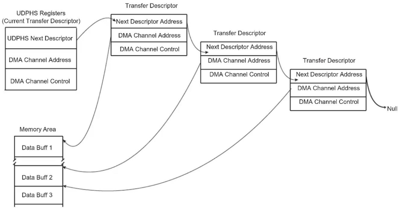
flowchart
graph TD
    A["UDPHS Registers (Current Transfer Descriptor)"] --> B["Transfer Descriptor"]
    B --> C["Next Descriptor Address"]
    B --> D["DMA Channel Address"]
    B --> E["DMA Channel Control"]
    F["UDPHS Next Descriptor"] --> B
    G["DMA Channel Address"] --> B
    H["DMA Channel Control"] --> B
    I["Data Buff 1"] --> J["Transfer Descriptor"]
    K["Data Buff 2"] --> J
    L["Data Buff 3"] --> J
    M["Memory Area"] --> J
    J --> N["Next Descriptor Address"]
    J --> O["DMA Channel Address"]
    J --> P["DMA Channel Control"]
    Q["Null"] --> N
34.6.9 Transfer Without DMA
Important: If the DMA is not to be used, it is necessary to disable it, otherwise it can be enabled by previous versions of software without warning. If this should occur, the DMA can process data before an interrupt without knowledge of the user.
The recommended means to disable DMA are as follows:
// Reset IP UDPHS
    AT91C_BASE_UDPHS->UDPHS_CTRL &= ~AT91C_UDPHS_EN_UDPHS;
    AT91C_BASE_UDPHS->UDPHS_CTRL |= AT91C_UDPHS_EN_UDPHS;
// With OR without DMA !!!
    for( i=1; i<=(AT91C_BASE_UDPHS->UDPHS_IPFEATURES &
    AT91C_UDPHS_DMA_CHANNEL_NBR)>>4); i++) {
    // RESET endpoint canal DMA:
    // DMA stop channel command
    AT91C_BASE_UDPHS->UDPHS_DMA[i].UDPHS_DMACONTROL = 0;    // STOP command
    // Disable endpoint
    AT91C_BASE_UDPHS->UDPHS_EPT[i].UDPHS_EPTCTLDIS |= 0XFFFFFFF;
    // Reset endpoint config
    AT91C_BASE_UDPHS->UDPHS_EPT[i].UDPHS_EPTCTLCFG = 0;
    // Reset DMA channel (Buff count and Control field)
    AT91C_BASE_UDPHS->UDPHS_DMA[i].UDPHS_DMACONTROL = 0x02;    // NON STOP command
    // Reset DMA channel 0 (STOP)
    AT91C_BASE_UDPHS->UDPHS_DMA[i].UDPHS_DMACONTROL = 0;    // STOP command
    // Clear DMA channel status (read the register for clear it)
    AT91C_BASE_UDPHS->UDPHS_DMA[i].UDPHS_DMASTATUS =
    AT91C_BASE_UDPHS->UDPHS_DMA[i].UDPHS_DMASTATUS;
}
34.6.10 Handling Transactions with USB V2.0 Device Peripheral
34.6.10.1 Setup Transaction
The setup packet is valid in the DPR while RX_SETUP is set. Once RX_SETUP is cleared by the application, the UDPHS accepts the next packets sent over the device endpoint.
When a valid setup packet is accepted by the UDPHS:
- The UDPHS device automatically acknowledges the setup packet (sends an ACK response)
- Payload data is written in the endpoint
- Sets the RX_SETUP interrupt
- The BYTE_COUNT field in the UDPHS_EPTSTAx register is updated
An endpoint interrupt is generated while RX_SETUP in the UDPHS_EPTSTAx register is not cleared. This interrupt is carried out to the microcontroller if interrupts are enabled for this endpoint.
Thus, firmware must detect RX_SETUP polling UDPHS_EPTSTAx or catching an interrupt, read the setup packet in the FIFO, then clear the RX_SETUP bit in the UDPHS_EPTCLRSTA register to acknowledge the setup stage.
If STALL_SNT was set to 1, then this bit is automatically reset when a setup token is detected by the device. Then, the device still accepts the setup stage. (See Section 34.6.10.5 STALL).
34.6.10.2 NYET
NYET is a High Speed only handshake. It is returned by a High Speed endpoint as part of the PING protocol.
High Speed devices must support an improved NAK mechanism for Bulk OUT and control endpoints (except setup stage). This mechanism allows the device to tell the host whether it has sufficient endpoint space for the next OUT transfer (see USB 2.0 spec 8.5.1 NAK Limiting via Ping Flow Control).
The NYET/ACK response to a High Speed Bulk OUT transfer and the PING response are automatically handled by hardware in the UDPHS_EPTCTLx register (except when the user wants to force a NAK response by using the NYET_DIS bit).
If the endpoint responds instead to the OUT/DATA transaction with an NYET handshake, this means that the endpoint accepted the data but does not have room for another data payload. The host controller must return to using a PING token until the endpoint indicates it has space available.
Figure 34-8: NYET Example with Two Endpoint Banks

flowchart
graph TD
    A["Data 0"] --> B["ACK data 1"]
    B --> C["NYET PING ACK"]
    C --> D["data 0 NYET PING NACK"]
    D --> E["PING ACK"]
    E --> F["End"]
    style A fill:#f9f,stroke:#333
    style B fill:#ccf,stroke:#333
    style C fill:#cfc,stroke:#333
    style D fill:#fcc,stroke:#333
    style E fill:#cff,stroke:#333
    style F fill:#ffc,stroke:#333
    note right of A
        E: empty
        E': begin to empty
        F: full
    end
34.6.10.3 Data IN
- Bulk IN or Interrupt IN
Data IN packets are sent by the device during the data or the status stage of a control transfer or during an (interrupt/bulk/isochronous) IN transfer. Data buffers are sent packet by packet under the control of the application or under the control of the DMA channel.
There are three ways for an application to transfer a buffer in several packets over the USB:
- packet by packet (see Bulk IN or Interrupt IN: Sending a Packet Under Application Control (Device to Host) below)
- 64 KB (see Bulk IN or Interrupt IN: Sending a Packet Under Application Control (Device to Host) below)
• DMA (see Bulk IN or Interrupt IN: Sending a Buffer Using DMA (Device to Host) below) - Bulk IN or Interrupt IN: Sending a Packet Under Application Control (Device to Host)
The application can write one or several banks.
A simple algorithm can be used by the application to send packets regardless of the number of banks associated to the endpoint.
Algorithm Description for Each Packet:
- The application waits for TXRDY flag to be cleared in the UDPHS_EPTSTAx register before it can perform a write access to the DPR.
- The application writes one USB packet of data in the DPR through the 64 KB endpoint logical memory window.
- The application sets TXRDY flag in the UDPHS_EPTSETSTAx register.
The application is notified that it is possible to write a new packet to the DPR by the TXRDY interrupt. This interrupt can be enabled or masked by setting the TXRDY bit in the UDPHS_EPTCTLENB/UDPHS_EPTCTLDIS register.
Algorithm Description to Fill Several Packets:
Using the previous algorithm, the application is interrupted for each packet. It is possible to reduce the application overhead by writing linearly several banks at the same time. The AUTO_VALID bit in the UDPHS_EPTCTLx must be set by writing the AUTO_VALID bit in the UDPHS_EPTCTLENBx register.
The auto-valid-bank mechanism allows the transfer of data (IN and OUT) without the intervention of the CPU. This means that bank validation (set TXRDY or clear the RXRDY_TXKL bit) is done by hardware.
- The application checks the BUSY_BANK_STA field in the UDPHS_EPTSTAx register. The application must wait that at least one bank is free.
- The application writes a number of bytes inferior to the number of free DPR banks for the endpoint. Each time the application writes the last byte of a bank, the TXRDY signal is automatically set by the UDPHS.
- If the last packet is incomplete (i.e., the last byte of the bank has not been written) the application must set the TXRDY bit in the UDPHS_EPTSETSTAx register.
The application is notified that all banks are free, so that it is possible to write another burst of packets by the BUSY_BANK interrupt. This interrupt can be enabled or masked by setting the BUSY_BANK flag in the UDPHS_EPTCTLENB and UDPHS_EPTCTLDIS registers.
This algorithm must not be used for isochronous transfer. In this case, the ping-pong mechanism does not operate.
A Zero Length Packet can be sent by setting just the TXRDY flag in the UDPHS_EPTSETSTAx register.
- Bulk IN or Interrupt IN: Sending a Buffer Using DMA (Device to Host)
The UDPHS integrates a DMA host controller. This DMA controller can be used to transfer a buffer from the memory to the DPR or from the DPR to the processor memory under the UDPHS control. The DMA can be used for all transfer types except control transfer.
Example DMA configuration:
-
Program UDPHS_DMAADDRESS x with the address of the buffer that should be transferred.
-
Enable the interrupt of the DMA in UDPHS_IEN
-
Program UDPHS_DMACONTROLx:
-
Size of buffer to send: size of the buffer to be sent to the host.
- END_B_EN: The endpoint can validate the packet (according to the values programmed in the AUTO_VALID and SHRT_PCKT fields of UDPHS_EPTCTLx.) (See Section 34.7.12 UDPHS Endpoint Control Disable Register (Isochronous Endpoint) and Figure 34-13)
- END_BUFFIT: generate an interrupt when the BUFF_COUNT in UDPHS_DMASTATUSx reaches 0.
- CHANN_ENB: Run and stop at end of buffer
The auto-valid-bank mechanism allows the transfer of data (IN & OUT) without the intervention of the CPU. This means that bank validation (set TXRDY or clear the RXRDY_TXKL bit) is done by hardware.
A transfer descriptor can be used. Instead of programming the register directly, a descriptor should be programmed and the address of this descriptor is then given to UDPHS_DMANXTDSC to be processed after setting the LDNXT_DSC field (Load Next Descriptor Now) in UDPHS_DMACONTROLx register.
The structure that defines this transfer descriptor must be aligned.
Each buffer to be transferred must be described by a DMA Transfer descriptor (see Section 34.7.21 UDPHS DMA Channel Transfer Descriptor). Transfer descriptors are chained. Before executing transfer of the buffer, the UDPHS may fetch a new transfer descriptor from the memory address pointed by the UDPHS_DMANXTDSCx register. Once the transfer is complete, the transfer status is updated in the UDPHS_DMASTATUSx register.
To chain a new transfer descriptor with the current DMA transfer, the DMA channel must be stopped. To do so, INTDIS_DMA and TXRDY may be set in the UDPHS_EPTCTLENBx register. It is also possible for the application to wait for the completion of all transfers. In this case the LDNXT_DSC bit in the last transfer descriptor UDPHS_DMACONTROLx register must be set to 0 and the CHANN_ENB bit set to 1.
Then the application can chain a new transfer descriptor.
The INTDIS_DMA can be used to stop the current DMA transfer if an enabled interrupt is triggered. This can be used to stop DMA transfers in case of errors.
The application can be notified at the end of any buffer transfer (ENB_BUFFIT bit in the UDPHS_DMACONTROLx register).
Figure 34-9: Data IN Transfer for Endpoint with One Bank

flowchart
graph LR
    A["Previous Data IN TX Microcontroller Loads Data in FIFO Data is Sent on USB Bus"] --> B["USB Bus Packets"]
    B --> C["Token IN"]
    C --> D["Data IN 1"]
    D --> E["ACK"]
    E --> F["Token IN"]
    F --> G["NAK"]
    G --> H["Token IN"]
    H --> I["Data IN 2"]
    I --> J["ACK"]
    J --> K["TXRDY Flag (UDPHS_EPTSTAx)"]
    K --> L["Set by firmware Cleared by hardware"]
    L --> M["Set by the firmware Cleared by hardware"]
    M --> N["Interrupt Pending"]
    N --> O["TX_COMPLT Flag (UDPHS_EPTSTAx)"]
    O --> P["Set by hardware"]
    P --> Q["Cleared by firmware"]
    Q --> R["Payload in FIFO"]
    R --> S["Cleared by firmware"]
    S --> T["Interrupt Pending"]
    T --> U["FIFO Content"]
    U --> V["Data IN 1"]
    V --> W["Load in progress"]
    W --> X["Data IN 2"]
    X --> Y["DPR access by firmware"]
    Y --> Z["DPR access by hardware"]
Figure 34-10: Data IN Transfer for Endpoint with Two Banks

flowchart
graph TD
    A["USB Bus Packets"] --> B["Token IN"]
    B --> C["ACK Token IN ACK"]
    C --> D["Data IN Data IN"]

    subgraph Timeframe
        E["Set by Firmware, Data Payload Written in FIFO Bank 0"] --> F["Virtual TXRDY bank 0 (UDPHS_EPTSTAx)"]
        G["Cleared by Hardware switch to next bank"] --> H["Virtual TXRDY bank 1 (UDPHS_EPTSTAx)"]
        I["Set by Firmware, Data Payload Written in FIFO Bank 1"] --> J["TX_COMPLT Flag (UDPHS_EPTSTAx)"]
        K["Set by Hardware Set by Hardware"] --> L["FIFO (DPR) Bank 0"]
        M["Interrupt Pending"] --> N["Interrupt Cleared by Firmware"]
    end

    style A fill:#f9f,stroke:#333
    style B fill:#ccf,stroke:#333
    style C fill:#cfc,stroke:#333
    style D fill:#fcc,stroke:#333
    style E fill:#ffc,stroke:#333
    style F fill:#cff,stroke:#333
    style G fill:#ffc,stroke:#333
    style H fill:#ffc,stroke:#333
    style I fill:#ffc,stroke:#333
    style J fill:#ffc,stroke:#333
    style K fill:#ffc,stroke:#333
    style L fill:#ffc,stroke:#333
    style M fill:#ffc,stroke:#333
    style N fill:#ffc,stroke:#333
    style_O["FIFO (DPR) Bank 0"] --> P["Written by Microcontroller"]
    P --> Q["Read by USB Device"]
    Q --> R["Written by Microcontroller"]
    R --> S["FIFO (DPR) Bank 1"] --> T["Written by Microcontroller"]
    T --> U["Read by UDPHS Device"]
Figure 34-11: Data IN Followed By Status OUT Transfer at the End of a Control Transfer
flowchart
graph TD
    A["USB Bus Packets"] --> B["Token IN"]
    B --> C["Data IN"]
    C --> D["ACK"]
    D --> E["Token OUT"]
    E --> F["Data OUT (ZLP)"]
    F --> G["ACK"]
    G --> H["Token OUT"]
    H --> I["Data OUT (ZLP)"]
    I --> J["ACK"]
    J --> K["Interrupt Pending"]
    L["RXRDY (UDPHS_EPTSTAx)"] --> M["Set by Hardware"]
    N["TX_COMPLT (UDPHS_EPTSTAx)"] --> O["Set by Hardware"]
    P["Cleared by Firmware"] --> Q["Cleared by Firmware"]
    style A fill:#f9f,stroke:#333
    style L fill:#f9f,stroke:#333
    style N fill:#f9f,stroke:#333
    style P fill:#f9f,stroke:#333
    style Q fill:#f9f,stroke:#333
Note: A NAK handshake is always generated at the first status stage token.
Figure 34-12: Data OUT Followed by Status IN Transfer
flowchart
graph TD
    A["Host Sends the Last Data Payload to the Device"] --> B["Device Sends a Status IN to the Host"]
    B --> C["Token INACK Data OUTToken OUT ACK Data IN"]
    C --> D["Interrupt Pending"]
    D --> E["Cleared by Firmware"]
    E --> F["Set by Hardware"]
    F --> G["TXRDY (UDPHS_EPTSTAx)"]
    G --> H["Set by Firmware"]
    H --> I["Clear by Hardware"]
Note: Before proceeding to the status stage, the software should determine that there is no risk of extra data from the host (data stage). If not certain (non-predictable data stage length), then the software should wait for a NAK-IN interrupt before proceeding to the status stage. This precaution should be taken to avoid collision in the FIFO.
Figure 34-13: Autovalid with DMA
flowchart
graph TD
    A["Bank (system)"] --> B["Bank 0"]
    B --> C["Bank 1"]
    C --> D["Bank 0"]
    D --> E["Bank 1"]
    F["Write write bank 0"] --> G["Write bank 0"]
    H["Write write bank 1"] --> I["Write bank 0"]
    J["Write write bank 0"] --> K["Write bank 1"]
    L["Write write bank 1"] --> M["Write bank 0"]
    N["Write write bank 0"] --> O["Write bank 1"]
    P["Write write bank 1"] --> Q["Write bank 0"]
    R["Write write bank 0"] --> S["Write bank 1"]
    T["Write write bank 1"] --> U["Write bank 0"]
    V["Write write bank 0"] --> W["Write bank 1"]
    X["Write write bank 1"] --> Y["Write bank 0"]
    Z["Write write bank 0"] --> AA["Write bank 1"]
    AB["Write write bank 1"] --> AC["Write bank 0"]
    AD["Write write bank 0"] --> AE["Write bank 1"]
    AF["Write write bank 1"] --> AG["Write bank 0"]
    AH["Write write bank 0"] --> AI["Write bank 1"]
    AJ["Write write bank 1"] --> AK["Write bank 0"]
    AL["Write write bank 0"] --> AM["Write bank 1"]
    AN["Write write bank 1"] --> AO["Write bank 0"]
    AP["IN data 0"] --> AQ["IN data 1"]
    AR["IN data 0"] --> AS["IN data 1"]
    AT["Bank 0"] --> AU["Bank 1"]
    AV["Bank 1"] --> AW["Bank 0Bank (usb)"]
    AX["Virtual TXRDY Bank 0"] --> AY["Virtual TXRDY Bank 1"]
    AZ["Virtual TXRDY Bank 1"] --> BA["Virtual TXRDY (Virtual 0 & Virtual 1)"]
    BB["TXRDY"] --> BC["TXRDY (Virtual 0 & Virtual 1)"]
Note: In the illustration above Autovalid validates a bank as full, although this might not be the case, in order to continue processing data and to send to DMA.
- Isochronous IN
Isochronous-IN is used to transmit a stream of data whose timing is implied by the delivery rate. Isochronous transfer provides periodic, continuous communication between host and device.
It ensures bandwidth and low latencies appropriate for telephony, audio, video, etc.
If the endpoint is not available (TXRDY_TRER = 0), then the device does not answer to the host. An ERR_FL_ISO interrupt is generated in the UDPHS_EPTSTAx register and once enabled, then sent to the CPU.
The STALL_SNT command bit is not used for an ISO-IN endpoint.
• High Bandwidth Isochronous Endpoint Handling: IN Example
For high bandwidth isochronous endpoints, the DMA can be programmed with the number of transactions (BUFF_LENGTH field in UDPHS_DMACONTROLx) and the system should provide the required number of packets per microframe, otherwise, the host will notice a sequencing problem.
A response should be made to the first token IN recognized inside a microframe under the following conditions:
- If at least one bank has been validated, the correct DATAx corresponding to the programmed Number Of Transactions per Microframe (NB_TRANS) should be answered. In case of a subsequent missed or corrupted token IN inside the microframe, the USB 2.0 Core available data bank(s) that should normally have been transmitted during that microframe shall be flushed at its end. If this flush occurs, an error condition is flagged (ERR_FLUSH is set in UDPHS_EPTSTAx).
- If no bank is validated yet, the default DATA0 ZLP is answered and underflow is flagged (ERR_FL_ISO is set in UDPHS_EPTSTAx). Then, no data bank is flushed at microframe end.
- If no data bank has been validated at the time when a response should be made for the second transaction of NB_TRANS = 3 transactions microframe, a DATA1 ZLP is answered and underflow is flagged (ERR_FL_ISO is set in UDPHS_EPTSTAx). If and only if remaining untransmitted banks for that microframe are available at its end, they are flushed and an error condition is flagged (ERR_FLUSH is set in UDPHS_EPTSTAx).
- If no data bank has been validated at the time when a response should be made for the last programmed transaction of a microframe, a DATA0 ZLP is answered and underflow is flagged (ERR_FL_ISO is set in UDPHS_EPTSTAx). If and only if the remaining untransmitted data bank for that microframe is available at its end, it is flushed and an error condition is flagged (ERR_FLUSH is set in UDPHS_EPTSTAx).
- If at the end of a microframe no valid token IN has been recognized, no data bank is flushed and no error condition is reported.
At the end of a microframe in which at least one data bank has been transmitted, if less than NB_TRANS banks have been validated for that microframe, an error condition is flagged (ERR_TRANS is set in UDPHS_EPTSTAx).
Cases of Error (in UDPHS_EPTSTAx)
- ERR_FL_ISO: There was no data to transmit inside a microframe, so a ZLP is answered by default.
- ERR_FLUSH: At least one packet has been sent inside the microframe, but the number of token IN received is lesser than the number of transactions actually validated (TXRDY_TRER) and likewise with the NB_TRANS programmed.
- ERR_TRANS: At least one packet has been sent inside the microframe, but the number of token IN received is lesser than the number of programmed NB_TRANS transactions and the packets not requested were not validated.
- ERR_FL_ISO + ERR_FLUSH: At least one packet has been sent inside the microframe, but the data has not been validated in time to answer one of the following token IN.
- ERR_FL_ISO + ERR_TRANS: At least one packet has been sent inside the microframe, but the data has not been validated in time to answer one of the following token IN and the data can be discarded at the microframe end.
- ERR_FLUSH + ERR_TRANS: The first token IN has been answered and it was the only one received, a second bank has been validated but not the third, whereas NB_TRANS was waiting for three transactions.
- ERR_FL_ISO + ERR_FLUSH + ERR_TRANS: The first token IN has been treated, the data for the second Token IN was not available in time, but the second bank has been validated before the end of the microframe. The third bank has not been validated, but three transactions have been set in NB_TRANS.
34.6.10.4 Data OUT
- Bulk OUT or Interrupt OUT
Like data IN, data OUT packets are sent by the host during the data or the status stage of control transfer or during an interrupt/bulk/isochronous OUT transfer. Data buffers are sent packet by packet under the control of the application or under the control of the DMA channel.
- Bulk OUT or Interrupt OUT: Receiving a Packet Under Application Control (Host to Device)
Algorithm Description for Each Packet:
- The application enables an interrupt on RXRDY_TXKL.
- When an interrupt on RXRDY_TXKL is received, the application knows that UDPHS_EPTSTAx register BYTE_COUNT bytes have been received.
- The application reads the BYTE_COUNT bytes from the endpoint.
• The application clears RXRDY_TXKL.
Note: If the application does not know the size of the transfer, it may not be a good option to use AUTO_VALID. Because if a zero-length-packet is received, the RXRDY_TXKL is automatically cleared by the AUTO_VALID hardware and if the endpoint interrupt is triggered, the software will not find its originating flag when reading the UDPHS_EPTSTAx register.
Algorithm to Fill Several Packets:
- The application enables the interrupts of BUSY_BANK and AUTO_VALID.
- When a BUSY_BANK interrupt is received, the application knows that all banks available for the endpoint have been filled. Thus, the application can read all banks available.
If the application does not know the size of the receive buffer, instead of using the BUSY_BANK interrupt, the application must use RXRDY_TXKL.
- Bulk OUT or Interrupt OUT: Sending a Buffer Using DMA (Host To Device)
To use the DMA setting, the AUTO_VALID field is mandatory.
See Bulk IN or Interrupt IN: Sending a Buffer Using DMA (Device to Host) for more information.
DMA Configuration Example:
- First program UDPHS_DMAADDRESSx with the address of the buffer that should be transferred.
- Enable the interrupt of the DMA in UDPHS_IEN
- Program the DMA Channelx Control Register:
- Size of buffer to be sent.
- END_B_EN: Can be used for OUT packet truncation (discarding of unbuffered packet data) at the end of DMA buffer.
- END_BUFFIT: Generate an interrupt when BUFF_COUNT in the UDPHS_DMASTATUSx register reaches 0.
- END_TR_EN: End of transfer enable, the UDPHS device can put an end to the current DMA transfer, in case of a short packet.
- END_TR_IT: End of transfer interrupt enable, an interrupt is sent after the last USB packet has been transferred by the DMA, if the USB transfer ended with a short packet. (Beneficial when the receive size is unknown.)
- CHANN_ENB: Run and stop at end of buffer.
For OUT transfer, the bank will be automatically cleared by hardware when the application has read all the bytes in the bank (the bank is empty).
Note 1: When a zero-length-packet is received, RXRDY_TXKL bit in UDPHS_EPTSTAx is cleared automatically by AUTO_VALID, and the application knows of the end of buffer by the presence of the END_TR_IT.
2: If the host sends a zero-length packet, and the endpoint is free, then the device sends an ACK. No data is written in the endpoint, the RXRDY_TXKL interrupt is generated, and the BYTE_COUNT field in UDPHS_EPTSTAx is null.
Figure 34-14: Data OUT Transfer for Endpoint with One Bank

flowchart
graph LR
    A["Host Sends Data Payload"] --> B["Microcontroller Transfers Data"]
    B --> C["Host Sends the Next Data Payload"]
    C --> D["Host Resends the Next Data Payload"]

    subgraph USB Bus Packets
        E["Token OUT"] --> F["Data OUT 1"]
        F --> G["Data OUT 2"]
        G --> H["Data OUT 2"]
        H --> I["ACKToken OUTNAKT"]
    end

    subgraph RXRDY (UDPHS_EPTSTAx)
        J["Set by Hardware"] --> K["Interrupt Pending"]
        K --> L["Cleared by Firmware, Data Payload Written in FIFO"]
    end

    subgraph FIFO (DPR) Content
        M["Data OUT 1"] --> N["Data OUT 1"]
        N --> O["Microcontroller Read"]
        O --> P["Data OUT 2"]
        P --> Q["Written by UDPHS Device"]
        Q --> R["Write by UDPHS Device"]
    end
Figure 34-15: Data OUT Transfer for an Endpoint with Two Banks
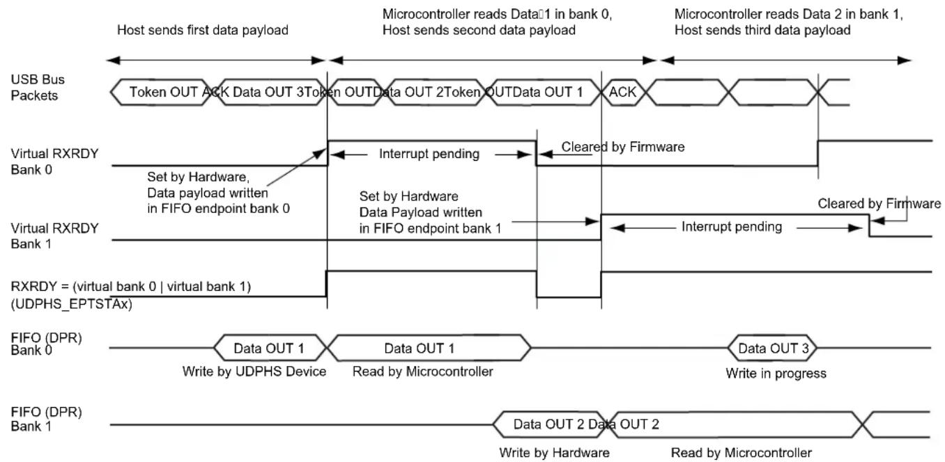
flowchart
graph TD
    A["USB Bus Packets"] --> B["Token OUT ACK Data OUT 3Token OUTData OUT 2Token OUTData OUT 1"]
    B --> C["ACK"]
    C --> D["Microcontroller reads Data 1 in bank 0, Host sends second data payload"]
    D --> E["Microcontroller reads Data 2 in bank 1, Host sends third data payload"]

    F["Virtual RXRDY Bank 0"] --> G["Set by Hardware, Data payload written in FIFO endpoint bank 0"]
    G --> H["Interrupt pending"]
    H --> I["Cleared by Firmware"]
    I --> J["Set by Hardware, Data Payload written in FIFO endpoint bank 1"]
    J --> K["Interrupt pending"]
    K --> L["Cleared by Firmware"]

    M["Virtual RXRDY Bank 1"] --> N["Set by Hardware, Data Payload written in FIFO endpoint bank 1"]
    N --> O["Set by Hardware, Data Payload written in FIFO endpoint bank 1"]
    O --> P["Interrupt pending"]
    P --> Q["Set by Hardware, Data Payload written in FIFO endpoint bank 1"]

    R["RXRDY = (virtual bank 0 | virtual bank 1) (UDPHS_EPTSTAx)"] --> S["Data OUT 1"]
    S --> T["Write by UDPHS Device"]
    T --> U["Data OUT 1"]
    U --> V["Read by Microcontroller"]
    V --> W["Data OUT 3"]
    W --> X["Write in progress"]

    Y["FIFO (DPR) Bank 0"] --> Z["Data OUT 1"]
    Z --> AA["Write by UDPHS Device"]
    AA --> AB["Data OUT 1"]
    AB --> AC["Write by Microcontroller"]
    AC --> AD["Data OUT 3"]
    AD --> AE["Write in progress"]

    AF["FIFO (DPR) Bank 1"] --> AG["Data OUT 2"]
    AG --> AH["Write by Hardware"]
    AH --> AI["Data OUT 2"]
    AI --> AJ["Write by Microcontroller"]
    AJ --> AK["Data OUT 3"]
    AK --> AL["Write in progress"]
• High Bandwidth Isochronous Endpoint OUT
USB 2.0 supports individual High Speed isochronous endpoints that require data rates up to 192 Mb/s (24 MB/s): 3x1024 data bytes per microframe.
To support such a rate, two or three banks may be used to buffer the three consecutive data packets. The microcontroller (or the DMA) should be able to empty the banks very rapidly (at least 24 MB/s on average).
NB_TRANS field in UDPHS_EPTCFGx register = Number Of Transactions per Microframe.
If NB_TRANS > 1 then it is High Bandwidth.
Example:
- If NB_TRANS = 3, the sequence should be either
- MData0
- MData0/Data1
- MData0/Data1/Data2
- If NB_TRANS = 2, the sequence should be either
- M Data 0
- MData0/Data1
- If NB_TRANS = 1, the sequence should be
- Data0
Figure 34-16: Bank Management, Example of Three Transactions per Microframe

flowchart
graph LR
    A["USB bus Transactions"] --> B["MDATA0"]
    B --> C["MDATA1"]
    C --> D["DATA2"]
    D --> E["t = 0"]
    E --> F["RXRDY"]
    F --> G["Read Bank 1"]
    G --> H["Microcontroller FIFO (DPR) Access"]
    H --> I["t = 52.5 μs (40% of 125 μs)"]
    I --> J["Read Bank 2"]
    J --> K["Read Bank 3"]
    K --> L["Microcontroller FIFO (DPR) Access"]
    L --> M["t = 125 μs"]
    M --> N["Read Bank 1"]
    N --> O["RXRDY"]
    O --> P["Read Bank 1"]
    P --> Q["Microcontroller FIFO (DPR) Access"]
    Q --> R["t = 125 μs"]
    R --> S["Read Bank 3"]
    S --> T["Microcontroller FIFO (DPR) Access"]
    T --> U["t = 125 μs"]
    U --> V["RXRDY"]
    V --> W["Read Bank 1"]
    W --> X["Microcontroller FIFO (DPR) Access"]
    X --> Y["t = 125 μs"]
    Y --> Z["Read Bank 3"]
    Z --> AA["Microcontroller FIFO (DPR) Access"]
    AA --> AB["t = 125 μs"]
    AB --> AC["RXRDY"]
    AC --> AD["Read Bank 1"]
    AD --> AE["Microcontroller FIFO (DPR) Access"]
- Isochronous Endpoint Handling: OUT Example
The user can ascertain the bank status (free or busy), and the toggle sequencing of the data packet for each bank with the UDPHS_EPTSTAx register in the three fields as follows: - TOGGLESQ_STA: PID of the data stored in the current bank
- CURBK: Number of the bank currently being accessed by the microcontroller.
- BUSY_BANK_STA: Number of busy bank
This is particularly useful in case of a missing data packet.
If the inter-packet delay between the OUT token and the Data is greater than the USB standard, then the ISO-OUT transaction is ignored. (Payload data is not written, no interrupt is generated to the CPU.)
If there is a data CRC (Cyclic Redundancy Check) error, the payload is, none the less, written in the endpoint. The ERR_CRC_NTR flag is set in UDPHS_EPTSTAx register.
If the endpoint is already full, the packet is not written in the DPRAM. The ERR_FL_ISO flag is set in UDPHS_EPTSTAx.
If the payload data is greater than the maximum size of the endpoint, then the ERR_OVFLW flag is set. It is the task of the CPU to manage this error. The data packet is written in the endpoint (except the extra data).
If the host sends a Zero Length Packet, and the endpoint is free, no data is written in the endpoint, the RXRDY_TXKL flag is set, and the BYTE_COUNT field in UDPHS_EPTSTAx register is null.
The FRCESTALL command bit is unused for an isochronous endpoint.
Otherwise, payload data is written in the endpoint, the RXRDY_TXKL interrupt is generated and the BYTE_COUNT in UDPHS_EPTSTAx register is updated.
34.6.10.5 STALL
STALL is returned by a function in response to an IN token or after the data phase of an OUT or in response to a PING transaction. STALL indicates that a function is unable to transmit or receive data, or that a control pipe request is not supported.
• OUT
To stall an endpoint, set the FRCESTALL bit in UDPHS_EPTSETSTAx register and after the STALL_SNT flag has been set, set the TOGGLE_SEG bit in the UDPHS_EPTCLRSTAx register.
• IN
Set the FRCESTALL bit in UDPHS_EPTSETSTAx register.
Figure 34-17: Stall Handshake Data OUT Transfer
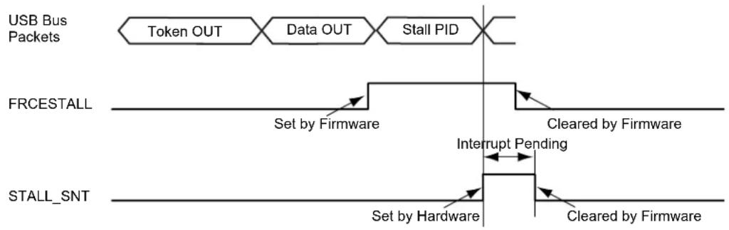
flowchart
graph LR
    A["USB Bus Packets"] --> B["Token OUT"]
    B --> C["Data OUT"]
    C --> D["Stall PID"]
    D --> E["FRCESTALL"]
    E --> F["Set by Firmware"]
    F --> G["Cleared by Firmware"]
    G --> H["Interrupt Pending"]
    H --> I["STALL_SNT"]
    I --> J["Set by Hardware"]
    J --> K["Cleared by Firmware"]
Figure 34-18: Stall Handshake Data IN Transfer
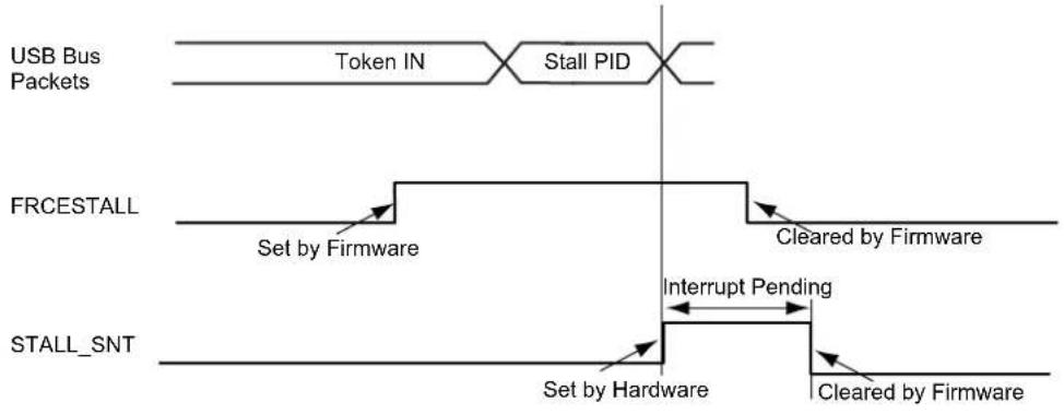
flowchart
graph LR
    A["USB Bus Packets"] --> B["Token IN"]
    B --> C["Stall PID"]
    C --> D["FRCESTALL"]
    D --> E["Set by Firmware"]
    E --> F["Interrupt Pending"]
    F --> G["STALL_SNT"]
    G --> H["Set by Hardware"]
    H --> I["Cleared by Firmware"]
    I --> J["End"]
34.6.11 Speed Identification
The high speed reset is managed by hardware.
At the connection, the host makes a reset which could be a classic reset (full speed) or a high speed reset.
At the end of the reset process (full or high), the ENDRESET interrupt is generated.
Then the CPU should read the SPEED bit in UDPHS_INTSTAx to ascertain the speed mode of the device.
34.6.12 USB V2.0 High Speed Global Interrupt
Interrupts are defined in Section 34.7.3 UDPHS Interrupt Enable Register (UDPHS_IEN) and in Section 34.7.4 UDPHS Interrupt Status Register (UDPHS_INTSTA).
34.6.13 Endpoint Interrupts
Interrupts are enabled in UDPHS_IEN (see Section 34.7.3 UDPHS Interrupt Enable Register) and individually masked in UDPHS_EPTCTLENBx (see Section 34.7.9 UDPHS Endpoint Control Enable Register (Control, Bulk, Interrupt Endpoints)).
Table 34-5: Endpoint Interrupt Source Masks
| SHRT_PCKT Short Packet Interrupt | |
| BUSY_BANK Busy Bank Interrupt | |
| NAK_OUT NAKOUT Interrupt | |
| NAK_IN/ERR_FLUSH NAKIN/Error | Flush Interrupt |
| STALL_SNT/ERR_CRC_NTR | Stall Sent/CRC error/Number of Transaction Error Interrupt |
| RX_SETUP/ERR_FL_ISO | Received SETUP/Error Flow Interrupt |
| TXRDY_TRER | TX Packet Read/Transaction Error Interrupt |
| TX_COMPLT Transmitted IN Data | Complete Interrupt |
| RXRDY_TXKL | Received OUT Data Interrupt |
| ERR_OVFLW | Overflow Error Interrupt |
| MDATA_RX | MDATA Interrupt |
| DATAX_RX | DATAx Interrupt |
Figure 34-19: UDPHS Interrupt Control Interface
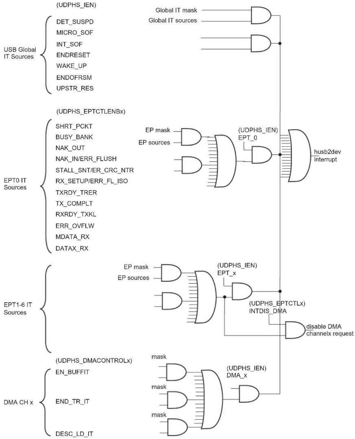
flowchart
graph TD
    A["USB Global IT Sources"] --> B["(UDPHS_IEN)"]
    A --> C["(DET_SUSPD)"]
    A --> D["(MICRO_SOF)"]
    A --> E["(INT_SOF)"]
    A --> F["(ENDRESET)"]
    A --> G["(WAKE_UP)"]
    A --> H["(ENDOFRSM)"]
    A --> I["(UPSTR_RES)"]

    J["EPT0 IT Sources"] --> K["(UDPHS_EPTCTLENBx)"]
    J --> L["SHRT_PCKT"]
    J --> M["BUSY_BANK"]
    J --> N["NAK_OUT"]
    J --> O["NAK_IN/ERR_FLUSH"]
    J --> P["STALL_SNT/ER_CRC_NTR"]
    J --> Q["RX_SETUP/ERR_FL_ISO"]
    J --> R["TXRDY_TRER"]
    J --> S["TX_COMPLT"]
    J --> T["RXRDY_TXKL"]
    J --> U["ERR_OVFLW"]
    J --> V["MDATA_RX"]
    J --> W["DATAx_RX"]

    X["EPT1-6 IT Sources"] --> Y["(UDPHS_DMACONTROLx)"]
    X --> Z["(END_BUFFIT)"]
    X --> AA["(END_TR_IT)"]
    X --> AB["(DESC_LD_IT)"]

    AC["(USDPS_IEN)"] --> AD["Global IT mask"]
    AC --> AE["Global IT sources"]

    AF["(USDPS_EPTCTLx)"] --> AG["(USDPS_IEN)"]
    AF --> AH["EPT_0"]
    AI["(USDPS_IEN) INTDIS_DMA"] --> AJ["Disable DMA channelx request"]
    AK["(USDPS_IEN) DMA_x"] --> AL["mask"]
    AM["(USDPS_IEN) DMA_x"] --> AN["mask"]

    style A fill:#f9f,stroke:#333
    style J fill:#f9f,stroke:#333
    style X fill:#f9f,stroke:#333
34.6.14 Power Modes
34.6.14.1 Controlling Device States
A USB device has several possible states. Refer to Chapter 9 (USB Device Framework) of the Universal Serial Bus Specification, Rev 2.0.
Figure 34-20: UDPHS Device State Diagram
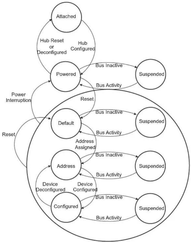
flowchart
graph TD
    A["Attached"] -->|Hub Reset or Deconfigured| B["Powered"]
    B -->|Bus Inactive| C["Suspended"]
    B -->|Bus Activity| D["Default"]
    D -->|Reset| E["Address"]
    E -->|Address Assigned| D
    E -->|Bus Inactive| F["Suspended"]
    E -->|Bus Activity| G["Address"]
    G -->|Device Deconfigured| H["Configured"]
    H -->|Device Configured| I["Configuration"]
    I -->|Bus Inactive| J["Suspended"]
    I -->|Bus Activity| K["Suspended"]
    style A fill:#f9f,stroke:#333
    style B fill:#ccf,stroke:#333
    style C fill:#cfc,stroke:#333
    style D fill:#fcc,stroke:#333
    style E fill:#cff,stroke:#333
    style F fill:#ffc,stroke:#333
    style G fill:#cfc,stroke:#333
    style H fill:#fcc,stroke:#333
    style I fill:#cfc,stroke:#333
    style J fill:#cfc,stroke:#333
    style K fill:#cfc,stroke:#333
Movement from one state to another depends on the USB bus state or on standard requests sent through control transactions via the default endpoint (endpoint 0).
After a period of bus inactivity, the USB device enters Suspend mode. Accepting Suspend/Resume requests from the USB host is mandatory. Constraints in Suspend mode are very strict for bus-powered applications; devices may not consume more than 500 A on the USB bus.
While in Suspend mode, the host may wake up a device by sending a resume signal (bus activity) or a USB device may send a wake-up request to the host, e.g., waking up a PC by moving a USB mouse.
The wake-up feature is not mandatory for all devices and must be negotiated with the host.
34.6.14.2 Not Powered State
Self powered devices can detect 5V VBUS using a PIO. When the device is not connected to a host, device power consumption can be reduced by the DETACH bit in UDPHS_CTRL. Disabling the transceiver is automatically done. HSDM, HSDP, FSDP and FSDP lines are tied to GND pull-downs integrated in the hub downstream ports.
34.6.14.3 Entering Attached State
When no device is connected, the USB FSDP and FSDM signals are tied to GND by 15 KΩ pull-downs integrated in the hub downstream ports. When a device is attached to an hub downstream port, the device connects a 1.5 KΩ pull-up on FSDP. The USB bus line goes into IDLE state, FSDP is pulled-up by the device 1.5 KΩ resistor to 3.3V and FSDM is pulled-down by the 15 KΩ resistor to GND of the host.
After pull-up connection, the device enters the powered state. The transceiver remains disabled until bus activity is detected.
In case of low power consumption need, the device can be stopped. When the device detects the VBUS, the software must enable the USB transceiver by enabling the EN_UDPHS bit in UDPHS_CTRL register.
The software can detach the pull-up by setting DETACH bit in UDPHS_CTRL register.
34.6.14.4 From Powered State to Default State (Reset)
After its connection to a USB host, the USB device waits for an end-of-bus reset. The unmasked flag ENDRESET is set in the UDPHS_IEN register and an interrupt is triggered.
Once the ENDRESET interrupt has been triggered, the device enters Default State. In this state, the UDPHS software must:
- Enable the default endpoint, setting the EPT_ENABL flag in the UDPHS_EPTCTLENB[0] register and, optionally, enabling the interrupt for endpoint 0 by writing 1 in EPT_0 of the UDPHS_IEN register. The enumeration then begins by a control transfer.
- Configure the Interrupt Mask Register which has been reset by the USB reset detection
- Enable the transceiver.
In this state, the EN_UDPHS bit in UDPHS_CTRL register must be enabled.
34.6.14.5 From Default State to Address State (Address Assigned)
After a Set Address standard device request, the USB host peripheral enters the address state.
Warning: Before the device enters address state, it must achieve the Status IN transaction of the control transfer, i.e., the UDPHS device sets its new address once the TX_COMPLT flag in the UDPHS_EPTCTL[0] register has been received and cleared.
To move to address state, the driver software sets the DEV_ADDR field and the FADDR_EN flag in the UDPHS_CTRL register.
34.6.14.6 From Address State to Configured State (Device Configured)
Once a valid Set Configuration standard request has been received and acknowledged, the device enables endpoints corresponding to the current configuration. This is done by setting the BK_NUMBER, EPT_TYPE, EPT_DIR and EPT_SIZE fields in the UDPHS_EPTCFGx registers and enabling them by setting the EPT_ENABL flag in the UDPHS_EPTCTLENBx registers, and, optionally, enabling corresponding interrupts in the UDPHS_IEN register.
34.6.14.7 Entering Suspend State (Bus Activity)
When a Suspend (no bus activity on the USB bus) is detected, the DET_SUSPD signal in the UDPHS_STA register is set. This triggers an interrupt if the corresponding bit is set in the UDPHS_IEN register. This flag is cleared by writing to the UDPHS_CLRINT register. Then the device enters Suspend mode.
In this state bus powered devices must drain less than 500 A from the 5V VBUS. As an example, the microcontroller switches to slow clock, disables the PLL and main oscillator, and goes into Idle mode. It may also switch off other devices on the board.
The UDPHS device peripheral clocks can be switched off. Resume event is asynchronously detected.
34.6.14.8 Receiving a Host Resume
In Suspend mode, a resume event on the USB bus line is detected asynchronously, transceiver and clocks disabled (however the pull-up should not be removed).
Once the resume is detected on the bus, the signal WAKE_UP in the UDPHS_INTSTA is set. It may generate an interrupt if the corresponding bit in the UDPHS_IEN register is set. This interrupt may be used to wake-up the core, enable PLL and main oscillators and configure clocks.
34.6.14.9 Sending an External Resume
In Suspend State it is possible to wake-up the host by sending an external resume.
The device waits at least 5 ms after being entered in Suspend State before sending an external resume.
The device must force a K state from 1 to 15 ms to resume the host.
34.6.15 Test Mode
A device must support the TEST_MODE feature when in the Default, Address or Configured High Speed device states.
TEST_MODE can be:
- Test_J
- Test_K
- Test_Packet
- Test_SEO_NAK
(See Section 34.7.7 UDPHS Test Register for definitions of each test mode.)
const char test_packet_buffer[] = {
    0x00, 0x00, 0x00, 0x00, 0x00, 0x00, 0x00, 0x00, 0x00, 0x00, 0x00, 0x00, 0x00, 0x00, 0x00, 0x00, 0x00, 0xEE, 0xEE, 0xEE, 0xEE, 0xEE, 0xEE, 0xEE, 0xEE, 0xFE, 0xFF, 0xFF, 0xFF, 0xFF, 0xFF, 0xFF, 0xFF, 0xFF, 0xFF, 0xFF, 0xFF, 0xFF, 0xFF, 0xFF, 0xFF, 0xFF, 0xFF, 0xFF, 0xFF, 0xFF, 0xFF, 0xFF, 0xFF, 0xFF, 0xFF, 0FF
}; // JKJKJKJK * 9
// JJKKJJJKK * 8
// JJKKJJJKK * 8
// JJJJJJJKKKKKKK * 8
// JJJJJJJKJKKKKKKK * 8
// JJJJJJJKJK * 8
// JJKKKKKKK * 10}, JK
34.7 USB High Speed Device Port (UDPHS) User Interface
Table 34-6: Register Mapping
| Offset Register Name Access | Reset | |||
| 0x00 | UDPHS Control Register | UDPHS_CTRL | Read/Write | 0x0000_0200 |
| 0x04 | UDPHS Frame Number Register | UDPHS_FNUM | Read-only | 0x0000_0000 |
| 0x08-0x0C | Reserved - - | - | ||
| 0x10 | UDPHS Interrupt Enable Register | UDPHS_IEN | Read/Write | 0x0000_0010 |
| 0x14 | UDPHS Interrupt Status Register | UDPHS_INTSTA | Read-only | 0x0000_0000 |
| 0x18 | UDPHS Clear Interrupt Register | UDPHS_CLRINT | Write-only | - |
| 0x1C | UDPHS Endpoints Reset Register | UDPHS_EPTRST | Write-only | - |
| 0x20-0xCC | Reserved - - | - | ||
| 0xE0 | UDPHS Test Register | UDPHS_TST | Read/Write | 0x0000_0000 |
| 0xE4-0xFC | Reserved - - | - | ||
| 0x100 + endpoint * 0x20 + 0x00 | UDPHS Endpoint Configuration Register | UDPHS_EPTCFG | Read/Write | 0x0000_0000 |
| 0x100 + endpoint * 0x20 + 0x04 | UDPHS Endpoint Control Enable Register | UDPHS_EPTCTLENB | Write-only | - |
| 0x100 + endpoint * 0x20 + 0x08 | UDPHS Endpoint Control Disable Register | UDPHS_EPTCTLDIS Write-only - | ||
| 0x100 + endpoint * 0x20 + 0x0C | UDPHS Endpoint Control Register | UDPHS_EPTCTL | Read-only | 0x0000\_0000^(1) |
| 0x100 + endpoint * 0x20 + 0x10 | Reserved (for endpoint) | - | - | - |
| 0x100 + endpoint * 0x20 + 0x14 | UDPHS Endpoint Set Status Register | UDPHS_EPTSETSTA | Write-only | - |
| 0x100 + endpoint * 0x20 + 0x18 | UDPHS Endpoint Clear Status Register | UDPHS_EPTCLRSTA | Write-only | - |
| 0x100 + endpoint * 0x20 + 0x1C | UDPHS Endpoint Status Register | UDPHS_EPTSTA | Read-only | 0x0000_0040 |
| 0x120-0x2FC UDPHS Endpoint1 | to 15 (2) Registers | - | - | - |
| 0x300 + channel * 0x10 + 0x00 | UDPHS DMA Next Descriptor Address Register | UDPHS_DMANXTDSC | Read/Write | 0x0000_0000 |
| 0x300 + channel * 0x10 + 0x04 | UDPHS DMA Channel Address Register | UDPHS_DMAADDRESS | Read/Write | 0x0000_0000 |
| 0x300 + channel * 0x10 + 0x08 | UDPHS DMA Channel Control Register | UDPHS_DMACONTROL | Read/Write | 0x0000_0000 |
| 0x300 + channel * 0x10 + 0x0C | UDPHS DMA Channel Status Register | UDPHS_DMASTATUS | Read/Write | 0x0000_0000 |
| 0x310-0x36C | DMA Channel1 to 6 (3) Registers | - | - | - |
Note 1: The reset value for UDPHS_EPTCTL0 is 0x0000_0001.
2: The addresses for the UDPHS Endpoint registers shown here are for UDPHS Endpoint0. The structure of this group of registers is repeated successively for each endpoint according to the consecution of endpoint registers located between 0x120 and 0x2FC.
3: The DMA channel index refers to the corresponding EP number. When no DMA channel is assigned to one EP, the associated registers are reserved. This is the case for EP0, so DMA Channel 0 registers are reserved.
34.7.1 UDPHS Control Register
Name: UDPHS_CTRL
Address:0xF8030000
Access: Read/Write
31 30 29 28 27 26 25 24
| - | - | - | - | - | - | - | - |
23 22 21 20 19 18 17 16
| - | - | - | - | - | - | - | - |
15 14 13 12 11 10 9 8
| - | - | - | - | P | U | L | L |
| 7 | 6 | 5 | 4 | 3 | 2 | 1 | 0 |
| FADDR_EN | DEV_ADDR |
DEV\_ADDR: UDPHS Address (cleared upon USB reset)
This field contains the default address (0) after power-up or UDPHS bus reset (read), or it is written with the value set by a SET_ADDRESS request received by the device firmware (write).
FADDR\_EN: Function Address Enable (cleared upon USB reset)
0: Device is not in address state (read), or only the default function address is used (write).
1: Device is in address state (read), or this bit is set by the device firmware after a successful status phase of a SET_ADDRESS transaction (write). When set, the only address accepted by the UDPHS controller is the one stored in the UDPHS Address field. It will not be cleared afterwards by the device firmware. It is cleared by hardware on hardware reset, or when UDPHS bus reset is received.
EN\_UDPHS: UDPHS Enable
0: UDPHS is disabled (read), or this bit disables and resets the UDPHS controller (write). Switch the host to UTMI.
1: UDPHS is enabled (read), or this bit enables the UDPHS controller (write). Switch the host to UTMI.
DETACH: Detach Command
0: UDPHS is attached (read), or this bit pulls up the DP line (attach command) (write).
1: UDPHS is detached, UTMI transceiver is suspended (read), or this bit simulates a detach on the UDPHS line and forces the UTMI transceiver into suspend state (Suspend M = 0) (write).
See PULLD_DIS description below.
REWAKEUP: Send Remote Wake Up (cleared upon USB reset)
0: Remote Wake Up is disabled (read), or this bit has no effect (write).
1: Remote Wake Up is enabled (read), or this bit forces an external interrupt on the UDPHS controller for Remote Wake UP purposes.
An Upstream Resume is sent only after the UDPHS bus has been in SUSPEND state for at least 5 ms.
This bit is automatically cleared by hardware at the end of the Upstream Resume.
PULLD\_DIS: Pull-Down Disable (cleared upon USB reset)
When set, there is no pull-down on DP & DM. (DM Pull-Down = DP Pull-Down = 0).
Note: If the DETACH bit is also set, device DP & DM are left in high impedance state.
(See DETACH description above.)
| DETACH PULLD_DIS DP DM Condition | ||||
| 0 0 Pull up Pull down Not recommended | ||||
| 0 1 Pull up High impedance state VBUS present | ||||
| 1 0 Pull down Pull down No VBUS | ||||
| 1 | 1 | High impedance state | High impedance state | VBUS present & software disconnect |
34.7.2 UDPHS Frame Number Register
Name: UDPHS_FNUM
Address:0xF8030004
Access: Read-only
31 30 29 28 27 26 25 24
| F | N | U | M | - | E | R | R |
23 22 21 20 19 18 17 16
| - | - | - | - | - | - | - | - |
15 14 13 12 11 10 9 8
| --FRAME_NUMBER |
7 6 5 4 3 2 1 0
FRAME_NUMBER MICRO_FRAME_NUM
MICRO\_FRAME\_NUM: Microframe Number (cleared upon USB reset)
Number of the received microframe (0 to 7) in one frame. This field is reset at the beginning of each new frame (1 ms).
One microframe is received each 125 microseconds (1 ms/8).
FRAME\_NUMBER: Frame Number as defined in the Packet Field Formats (cleared upon USB reset)
This field is provided in the last received SOF packet (see INT_SOF in the UDPHS Interrupt Status Register).
FNUM\_ERR: Frame Number CRC Error (cleared upon USB reset)
This bit is set by hardware when a corrupted Frame Number in Start of Frame packet (or Micro SOF) is received.
This bit and the INT_SOF (or MICRO_SOF) interrupt are updated at the same time.
34.7.3 UDPHS Interrupt Enable Register
Name: UDPHS_IEN
Address:0xF8030010
Access: Read/Write
31 30 29 28 27 26 25 24
| DMA_7 DMA_6 DMA_5 DMA_4 DMA_3 DMA_2 DMA_1- |
23 22 21 20 19 18 17 16
| EPT_15 EPT_14 EPT_13 EPT_12 EPT_11 EPT_10 EPT_9 EPT_8 |
15 14 13 12 11 10 9 8
| EPT_7 | EPT_6 | EPT_5 | EPT_4 | EPT_3 | EPT_2 | EPT_1 | EPT_0 |
| 7 | 6 | 5 | 4 | 3 | 2 | 1 | 0 |
| UPSTR_RES | ENDOFRSM | WAKE_UP | ENDRESET | INT_SOF | MICRO_SOF | DET_SUSPD | - |
DET\_SUSPD: Suspend Interrupt Enable (cleared upon USB reset)
0: Disable Suspend Interrupt.
1: Enable Suspend Interrupt.
MICRO\_SOF: Micro-SOF Interrupt Enable (cleared upon USB reset)
0: Disable Micro-SOF Interrupt.
1: Enable Micro-SOF Interrupt.
INT\_SOF: SOF Interrupt Enable (cleared upon USB reset)
0: Disable SOF Interrupt.
1: Enable SOF Interrupt.
ENDRESET: End Of Reset Interrupt Enable (cleared upon USB reset)
0: Disable End Of Reset Interrupt.
1: Enable End Of Reset Interrupt. Automatically enabled after USB reset.
WAKE\_UP: Wake Up CPU Interrupt Enable (cleared upon USB reset)
0: Disable Wake Up CPU Interrupt.
1: Enable Wake Up CPU Interrupt.
ENDOFRSM: End Of Resume Interrupt Enable (cleared upon USB reset)
0: Disable Resume Interrupt.
1: Enable Resume Interrupt.
UPSTR\_RES: Upstream Resume Interrupt Enable (cleared upon USB reset)
0: Disable Upstream Resume Interrupt.
1: Enable Upstream Resume Interrupt.
EPT\_x: Endpoint x Interrupt Enable (cleared upon USB reset)
0: Disable the interrupts for this endpoint.
1: Enable the interrupts for this endpoint.
DMA\_x: DMA Channel x Interrupt Enable (cleared upon USB reset)
0: Disable the interrupts for this channel.
1: Enable the interrupts for this channel.
34.7.4 UDPHS Interrupt Status Register
Name: UDPHS_INTSTA
Address:0xF8030014
Access: Read-only
31 30 29 28 27 26 25 24
| DMA_7 DMA_6 DMA_5 DMA_4 DMA_3 DMA_2 DMA_1 - |
23 22 21 20 19 18 17 16
| EPT_15 EPT_14 EPT_13 EPT_12 EPT_11 EPT_10 EPT_9 EPT_8 |
15 14 13 12 11 10
9
8
| EPT_7 | EPT_6 | EPT_5 | EPT_4 | EPT_3 | EPT_2 | EPT_1 | EPT_0 |
| 7 | 6 | 5 | 4 | 3 | 2 | 1 | 0 |
| UPSTR_RES | ENDOFRSM | WAKE_UP | ENDRESET | INT_SOF | MICRO_SOF | DET_SUSPD | SPEED |
SPEED: Speed Status
0: Reset by hardware when the hardware is in Full Speed mode.
1: Set by hardware when the hardware is in High Speed mode.
DET\_SUSPD: Suspend Interrupt
0: Cleared by setting the DET_SUSPD bit in UDPHS_CLRINT register.
1: Set by hardware when a UDPHS Suspend (Idle bus for three frame periods, a J state for 3 ms) is detected. This triggers a UDPHS interrupt when the DET_SUSPD bit is set in UDPHS_IEN register.
MICRO\_SOF: Micro Start Of Frame Interrupt
0: Cleared by setting the MICRO_SOF bit in UDPHS_CLRINT register.
1: Set by hardware when an UDPHS micro start of frame PID (SOF) has been detected (every 125 us) or synthesized by the macro. This triggers a UDPHS interrupt when the MICRO_SOF bit is set in UDPHS_IEN. In case of detected SOF, the MICRO_FRAME_NUM field in UDPHS_FNUM register is incremented and the FRAME_NUMBER field does not change.
Note: The Micro Start Of Frame Interrupt (MICRO_SOF), and the Start Of Frame Interrupt (INT_SOF) are not generated at the same time.
INT\_SOF: Start Of Frame Interrupt
0: Cleared by setting the INT_SOF bit in UDPHS_CLRINT.
1: Set by hardware when an UDPHS Start Of Frame PID (SOF) has been detected (every 1 ms) or synthesized by the macro. This triggers a UDPHS interrupt when the INT_SOF bit is set in UDPHS_IEN register. In case of detected SOF, in High Speed mode, the MICRO_FRAME_NUMBER field is cleared in UDPHS_FNUM register and the FRAME_NUMBER field is updated.
ENDRESET: End Of Reset Interrupt
0: Cleared by setting the ENDRESET bit in UDPHS_CLRINT.
1: Set by hardware when an End Of Reset has been detected by the UDPHS controller. This triggers a UDPHS interrupt when the ENDRESET bit is set in UDPHS_IEN.
WAKE\_UP: Wake Up CPU Interrupt
0: Cleared by setting the WAKE_UP bit in UDPHS_CLRINT.
1: Set by hardware when the UDPHS controller is in SUSPEND state and is re-activated by a filtered non-idle signal from the UDPHS line (not by an upstream resume). This triggers a UDPHS interrupt when the WAKE_UP bit is set in UDPHS_IEN register. When receiving this interrupt, the user has to enable the device controller clock prior to operation.
Note: this interrupt is generated even if the device controller clock is disabled.
ENDOFRSM: End Of Resume Interrupt
0: Cleared by setting the ENDOFRSM bit in UDPHS_CLRINT.
1: Set by hardware when the UDPHS controller detects a good end of resume signal initiated by the host. This triggers a UDPHS interrupt when the ENDOFRSM bit is set in UDPHS_IEN.
UPSTR\_RES: Upstream Resume Interrupt
0: Cleared by setting the UPSTR_RES bit in UDPHS_CLRINT.
1: Set by hardware when the UDPHS controller is sending a resume signal called "upstream resume". This triggers a UDPHS interrupt when the UPSTR_RES bit is set in UDPHS_IEN.
EPT\_x: Endpoint x Interrupt (cleared upon USB reset)
0: Reset when the UDPHS_EPTSTAx interrupt source is cleared.
1: Set by hardware when an interrupt is triggered by the UDPHS_EPTSTAx register and this endpoint interrupt is enabled by the EPT_x bit in UDPHS_IEN.
DMA\_x: DMA Channel x Interrupt
0: Reset when the UDPHS_DMASTATUSx interrupt source is cleared.
1: Set by hardware when an interrupt is triggered by the DMA Channelx and this endpoint interrupt is enabled by the DMA_x bit in UDPHS_IEN.
34.7.5 UDPHS Clear Interrupt Register
Name: UDPHS_CLRINT
Address:0xF8030018
Access: Write-only
31 30 29 28 27 26 25 24
| - | - | - | - | - | - | - | - |
23 22 21 20 19 18 17 16
| - | - | - | - | - | - | - | - |
15 14 13 12 11 10 9 8
| - | - | - | - | - | - | - | - |
7 6 5 4 3 2 1 0
| UPSTR_RES ENDOFRSM WAKE_UP ENDRESET INT_SOF MICRO_SOF DET $USPD | + |
DET\_SUSPD: Suspend Interrupt Clear
0: No effect.
1: Clear the DET_SUSPD bit in UDPHS_INTSTA.
MICRO\_SOF: Micro Start Of Frame Interrupt Clear
0: No effect.
1: Clear the MICRO_SOF bit in UDPHS_INTSTA.
INT\_SOF: Start Of Frame Interrupt Clear
0: No effect.
1: Clear the INT_SOF bit in UDPHS_INTSTA.
ENDRESET: End Of Reset Interrupt Clear
0: No effect.
1: Clear the ENDRESET bit in UDPHS_INTSTA.
WAKE\_UP: Wake Up CPU Interrupt Clear
0: No effect.
1: Clear the WAKE_UP bit in UDPHS_INTSTA.
ENDOFRSM: End Of Resume Interrupt Clear
0: No effect.
1: Clear the ENDOFRSM bit in UDPHS_INTSTA.
UPSTR\_RES: Upstream Resume Interrupt Clear
0: No effect.
1: Clear the UPSTR_RES bit in UDPHS_INTSTA.
34.7.6 UDPHS Endpoints Reset Register
Name: UDPHS_EPTRST
Address:0xF803001C
Access: Write-only
31 30 29 28 27 26 25 24
| - | - | - | - | - | - | - | - |
23 22 21 20 19 18 17 16
| - | - | - | - | - | - | - | - |
15 14 13 12 11 10 9 8
| EPT_15 EPT_14 EPT_13 EPT_12 EPT_11 EPT_10 EPT_9 EPT_8 |
| 7 | 6 | 5 | 4 | 3 | 2 | 1 | 0 |
| EPT_7 EPT_6 EPT_5 EPT_4 EPT_3 EPT_2 EPT_1 EPT_0 |
EPT\_x: Endpoint x Reset
0: No effect.
1: Reset the Endpointx state.
Setting this bit clears all bits in the Endpoint status UDPHS_EPTSTAx register except the TOGGLESQ_STA field.
34.7.7 UDPHS Test Register
Name: UDPHS_TST
Address:0xF80300E0
Access: Read/Write
31 30 29 28 27 26 25 24
| - | - | - | - | - | - | - | - |
23 22 21 20 19 18 17 16
| - | - | - | - | - | - | - | - |
15 14 13 12 11 10 9 8
| - | - | - | - | - | - | - | - |
| 7 | 6 | 5 | 4 | 3 | 2 | 1 | 0 |
| -- OPMODE2 TST_PKT TST_K TST_J | SPEED_CFG |
SPEED_CFG: Speed Configuration
| Value | Name | Description |
| 0 | NORMAL | Normal mode: The macro is in Full Speed mode, ready to make a High Speed identification, if the host supports it and then to automatically switch to High Speed mode. |
| 1 | - | Reserved |
| 2 | HIGH_SPEED | Force High Speed: Set this value to force the hardware to work in High Speed mode. Only for debug or test purpose. |
| 3 | FULL_SPEED | Force Full Speed: Set this value to force the hardware to work only in Full Speed mode. In this configuration, the macro will not respond to a High Speed reset handshake. |
TST\_J: Test J Mode
0: No effect.
1: Set to send the J state on the UDPHS line. This enables the testing of the high output drive level on the D+ line.
TST\_K: Test K Mode
0: No effect.
1: Set to send the K state on the UDPHS line. This enables the testing of the high output drive level on the D-line.
TST\_PKT: Test Packet Mode
0: No effect.
1: Set to repetitively transmit the packet stored in the current bank. This enables the testing of rise and fall times, eye patterns, jitter, and any other dynamic waveform specifications.
OPMODE2: OpMode2
0: No effect.
1: Set to force the OpMode signal (UTMI interface) to "10", to disable the bit-stuffing and the NRZI encoding.
Note: For the Test mode, Test_SE0_NAK (see Universal Serial Bus Specification, Revision 2.0: 7.1.20, Test Mode Support). Force the device in High Speed mode, and configure a bulk-type endpoint. Do not fill this endpoint for sending NAK to the host. Upon command, a port's transceiver must enter the High Speed Receive mode and remain in that mode until the exit action is taken. This enables the testing of output impedance, low level output voltage and loading characteristics. In addition, while in this mode, upstream facing ports (and only upstream facing ports) must respond to any IN token packet with a NAK handshake (only if the packet CRC is determined to be correct) within the normal allowed device response time. This enables testing of the device squelch level circuitry and, additionally, provides a general purpose stimulus/response test for basic functional testing.
34.7.8 UDPHS Endpoint Configuration Register
Name: UDPHS_EPTCFGx [x=0..15]
Address:0xF8030100 [0], 0xF8030120 [1], 0xF8030140 [2], 0xF8030160 [3], 0xF8030180 [4], 0xF80301A0 [5],
0xF80301C0 [6], 0xF80301E0 [7], 0xF8030200 [8], 0xF8030220 [9], 0xF8030240 [10], 0xF8030260 [11],
0xF8030280 [12], 0xF80302A0 [13], 0xF80302C0 [14], 0xF80302E0 [15]
Access: Read/Write
31 30 29 28 27 26 25 24
| E | P | T | - | M | A | P | D |
23 22 21 20 19 18 17 16
| - | - | - | - | - | - | - | - |
15 14 13 12 11 10 9 8
| - | - | - | - | - | - | N |
| 7 | 6 | 5 | 4 | 3 | 2 | 1 | 0 |
| BK_NUMBER EPT_TYPE | EPT_DIR | EPT_SIZE |
EPT\_SIZE: Endpoint Size (cleared upon USB reset)
Set this field according to the endpoint size ^(1) in bytes (see Section 34.6.6 Endpoint Configuration).
| Value | Name | Description |
| 0 | 8 | 8 bytes |
| 1 | 16 | 16 bytes |
| 2 | 32 | 32 bytes |
| 3 | 64 | 64 bytes |
| 4 | 128 | 128 bytes |
| 5 | 256 | 256 bytes |
| 6 | 512 | 512 bytes |
| 7 | 1024 | 1024 bytes |
Note 1: 1024 bytes is only for isochronous endpoint.
EPT\_DIR: Endpoint Direction (cleared upon USB reset)
0: Clear this bit to configure OUT direction for Bulk, Interrupt and Isochronous endpoints.
1: Set this bit to configure IN direction for Bulk, Interrupt and Isochronous endpoints.
For Control endpoints this bit has no effect and should be left at zero.
EPT\_TYPE: Endpoint Type (cleared upon USB reset)
Set this field according to the endpoint type (see Section 34.6.6 Endpoint Configuration).
(Endpoint 0 should always be configured as control)
| Value | Name | Description |
| 0 | CTRL8 | Control endpoint |
| 1 | ISO | Isochronous endpoint |
| 2 | BULK | Bulk endpoint |
| 3 | INT | Interrupt endpoint |
BK\_NUMBER: Number of Banks (cleared upon USB reset)
Set this field according to the endpoint's number of banks (see Section 34.6.6 Endpoint Configuration).
| Value Name | Description | |
| 0 0 Zero | bank, the endpoint is not mapped in memory | |
| 1 1 One | bank (bank 0) | |
| 2 2 Double | bank (Ping-Pong: bank0/bank1) | |
| 3 3 Triple | bank (bank0/bank1/bank2) | |
NB\_TRANS: Number Of Transaction per Microframe (cleared upon USB reset)
The Number of transactions per microframe is set by software.
Note: Meaningful for high bandwidth isochronous endpoint only.
EPT\_MAPD: Endpoint Mapped (cleared upon USB reset)
0: The user should reprogram the register with correct values.
1: Set by hardware when the endpoint size (EPT_SIZE) and the number of banks (BK_NUMBER) are correct regarding:
- The FIFO max capacity (FIFO_MAX_SIZE in UDPHS_IPFEATURES register)
– The number of endpoints/banks already allocated
– The number of allowed banks for this endpoint
34.7.9 UDPHS Endpoint Control Enable Register (Control, Bulk, Interrupt Endpoints)
Name: UDPHS_EPTCTLENBx [x=0..15]
Address:0xF8030104 [0], 0xF8030124 [1], 0xF8030144 [2], 0xF8030164 [3], 0xF8030184 [4], 0xF80301A4 [5],
0xF80301C4 [6], 0xF80301E4 [7], 0xF8030204 [8], 0xF8030224 [9], 0xF8030244 [10], 0xF8030264 [11],
0xF8030284 [12], 0xF80302A4 [13], 0xF80302C4 [14], 0xF80302E4 [15]
Access: Write-only
31 30 29 28 27 26 25 24
| S | H | R | T | - | P | C | K |
23 22 21 20 19 18 17 16
| - | - | - | - | - | B | U | S |
15 14 13 12 11 10 9 8
| NAK_OUT | NAK_IN | STALL_SNT | RX_SETUP | TXRDY | TX_COMPLT | RXRDY_TXKL | ERR_OVFLW |
| 7 | 6 | 5 | 4 | 3 | 2 | 1 | 0 |
| - | - | - | NYET_DIS | INTDIS_DMA | - | AUTO_VALID | EPT_ENABL |
This register view is relevant only if EPT_TYPE = 0x0, 0x2 or 0x3 in UDPHS Endpoint Configuration Register.
For additional information, see UDPHS Endpoint Control Register (Control, Bulk, Interrupt Endpoints).
EPT\_ENABL: Endpoint Enable
0: No effect.
1: Enable endpoint according to the device configuration.
AUTO\_VALID: Packet Auto-Valid Enable
0: No effect.
1: Enable this bit to automatically validate the current packet and switch to the next bank for both IN and OUT transfers.
INTDIS\_DMA: Interrupts Disable DMA
0: No effect.
1: If set, when an enabled endpoint-originated interrupt is triggered, the DMA request is disabled.
NYET\_DIS: NYET Disable (Only for High Speed Bulk OUT endpoints)
0: No effect.
1: Forces an ACK response to the next High Speed Bulk OUT transfer instead of a NYET response.
ERR\_OVFLW: Overflow Error Interrupt Enable
0: No effect.
1: Enable Overflow Error Interrupt.
RXRDY\_TXKL: Received OUT Data Interrupt Enable
0: No effect.
1: Enable Received OUT Data Interrupt.
TX\_COMPLT: Transmitted IN Data Complete Interrupt Enable
0: No effect.
1: Enable Transmitted IN Data Complete Interrupt.
TXRDY: TX Packet Ready Interrupt Enable
0: No effect.
1: Enable TX Packet Ready/Transaction Error Interrupt.
RX\_SETUP: Received SETUP
0: No effect.
1: Enable RX_SETUP Interrupt.
STALL\_SNT: Stall Sent Interrupt Enable
0: No effect.
1: Enable Stall Sent Interrupt.
NAK\_IN: NAKIN Interrupt Enable
0: No effect.
1: Enable NAKIN Interrupt.
NAK\_OUT: NAKOUT Interrupt Enable
0: No effect.
1: Enable NAKOUT Interrupt.
BUSY\_BANK: Busy Bank Interrupt Enable
0: No effect.
1: Enable Busy Bank Interrupt.
SHRT\_PCKT: Short Packet Send/Short Packet Interrupt Enable
For OUT endpoints:
0: No effect.
1: Enable Short Packet Interrupt.
For IN endpoints: Ensures short packet at end of DMA Transfer if the UDPHS_DMACONTROLx register END_B_EN and UDPHS_EPTCTLx register AUTOVALID bits are also set.
34.7.10 UDPHS Endpoint Control Enable Register (Isochronous Endpoints)
Name: UDPHS_EPTCTLENBx [x=0..15] (ISOENDPT)
Address:0xF8030104 [0], 0xF8030124 [1], 0xF8030144 [2], 0xF8030164 [3], 0xF8030184 [4], 0xF80301A4 [5],
0xF80301C4 [6], 0xF80301E4 [7], 0xF8030204 [8], 0xF8030224 [9], 0xF8030244 [10], 0xF8030264 [11],
0xF8030284 [12], 0xF80302A4 [13], 0xF80302C4 [14], 0xF80302E4 [15]
Access: Write-only
31 30 29 28 27 26 25 24
| S | H | R | T | - | P | C | K |
23 22 21 20 19 18 17 16
| - | - | - | - | - | B | U | S |
15 14 13 12 11 10 9 8
| - | ERR_FLUSH | ERR_CRC_NTR | ERR_FL_ISO | TXRDY_TRER | TX_COMPLT | RXRDY_TXKL | ERR_OVFLW |
| 7 | 6 | 5 | 4 | 3 | 2 | 1 | 0 |
| MDATA_RX | DATAX_RX | - | - | INTDIS_DMA | - | AUTO_VALID | EPT_ENABL |
This register view is relevant only if EPT_TYPE = 0x1 in UDPHS Endpoint Configuration Register.
For additional information, see UDPHS Endpoint Control Register (Isochronous Endpoint).
EPT\_ENABL: Endpoint Enable
0: No effect.
1: Enable endpoint according to the device configuration.
AUTO\_VALID: Packet Auto-Valid Enable
0: No effect.
1: Enable this bit to automatically validate the current packet and switch to the next bank for both IN and OUT transfers.
INTDIS\_DMA: Interrupts Disable DMA
0: No effect.
1: If set, when an enabled endpoint-originated interrupt is triggered, the DMA request is disabled.
DATAX\_RX: DATAx Interrupt Enable (Only for high bandwidth Isochronous OUT endpoints)
0: No effect.
1: Enable DATAx Interrupt.
MDATA\_RX: MDATA Interrupt Enable (Only for high bandwidth Isochronous OUT endpoints)
0: No effect.
1: Enable MDATA Interrupt.
ERR\_OVFLW: Overflow Error Interrupt Enable
0: No effect.
1: Enable Overflow Error Interrupt.
RXRDY\_TXKL: Received OUT Data Interrupt Enable
0: No effect.
1: Enable Received OUT Data Interrupt.
TX\_COMPLT: Transmitted IN Data Complete Interrupt Enable
0: No effect.
1: Enable Transmitted IN Data Complete Interrupt.
TXRDY\_TRER: TX Packet Ready/Transaction Error Interrupt Enable
0: No effect.
1: Enable TX Packet Ready/Transaction Error Interrupt.
ERR\_FL\_ISO: Error Flow Interrupt Enable
0: No effect.
1: Enable Error Flow ISO Interrupt.
ERR\_CRC\_NTR: ISO CRC Error/Number of Transaction Error Interrupt Enable
0: No effect.
1: Enable Error CRC ISO/Error Number of Transaction Interrupt.
ERR\_FLUSH: Bank Flush Error Interrupt Enable
0: No effect.
1: Enable Bank Flush Error Interrupt.
BUSY\_BANK: Busy Bank Interrupt Enable
0: No effect.
1: Enable Busy Bank Interrupt.
SHRT\_PCKT: Short Packet Send/Short Packet Interrupt Enable
For OUT endpoints:
0: No effect.
1: Enable Short Packet Interrupt.
For IN endpoints: Ensures short packet at end of DMA Transfer if the UDPHS_DMACONTROLx register END_B_EN and UDPHS_EPTCTLx register AUTOVALID bits are also set.
34.7.11 UDPHS Endpoint Control Disable Register (Control, Bulk, Interrupt Endpoints)
Name: UDPHS_EPTCTLDISx [x=0..15]
Address:0xF8030108 [0], 0xF8030128 [1], 0xF8030148 [2], 0xF8030168 [3], 0xF8030188 [4], 0xF80301A8 [5],
0xF80301C8 [6], 0xF80301E8 [7], 0xF8030208 [8], 0xF8030228 [9], 0xF8030248 [10], 0xF8030268 [11],
0xF8030288 [12], 0xF80302A8 [13], 0xF80302C8 [14], 0xF80302E8 [15]
Access: Write-only
31 30 29 28 27 26 25 24
| S | H | R | T | - | P | C | K |
23 22 21 20 19 18 17 16
| - | - | - | - | - | B | U | S |
15 14 13 12 11 10 9 8
| NAK_OUT | NAK_IN | STALL_SNT | RX_SETUP | TXRDY | TX_COMPLT | RXRDY_TXKL | ERR_OVFLW |
| 7 | 6 | 5 | 4 | 3 | 2 | 1 | 0 |
| - | - | - | NYET_DIS | INTDIS_DMA | - | AUTO_VALID | EPT_DISABL |
This register view is relevant only if EPT_TYPE = 0x0, 0x2 or 0x3 in UDPHS Endpoint Configuration Register.
For additional information, see UDPHS Endpoint Control Register (Control, Bulk, Interrupt Endpoints).
EPT\_DISABL: Endpoint Disable
0: No effect.
1: Disable endpoint.
AUTO\_VALID: Packet Auto-Valid Disable
0: No effect.
1: Disable this bit to not automatically validate the current packet.
INTDIS\_DMA: Interrupts Disable DMA
0: No effect.
1: Disable the "Interrupts Disable DMA".
NYET\_DIS: NYET Enable (Only for High Speed Bulk OUT endpoints)
0: No effect.
1: Let the hardware handle the handshake response for the High Speed Bulk OUT transfer.
ERR\_OVFLW: Overflow Error Interrupt Disable
0: No effect.
1: Disable Overflow Error Interrupt.
RXRDY\_TXKL: Received OUT Data Interrupt Disable
0: No effect.
1: Disable Received OUT Data Interrupt.
TX\_COMPLT: Transmitted IN Data Complete Interrupt Disable
0: No effect.
1: Disable Transmitted IN Data Complete Interrupt.
TXRDY: TX Packet Ready Interrupt Disable
0: No effect.
1: Disable TX Packet Ready/Transaction Error Interrupt.
RX\_SETUP: Received SETUP Interrupt Disable
0: No effect.
1: Disable RX_SETUP Interrupt.
STALL\_SNT: Stall Sent Interrupt Disable
0: No effect.
1: Disable Stall Sent Interrupt.
NAK\_IN: NAKIN Interrupt Disable
0: No effect.
1: Disable NAKIN Interrupt.
NAK\_OUT: NAKOUT Interrupt Disable
0: No effect.
1: Disable NAKOUT Interrupt.
BUSY\_BANK: Busy Bank Interrupt Disable
0: No effect.
1: Disable Busy Bank Interrupt.
SHRT\_PCKT: Short Packet Interrupt Disable
For OUT endpoints:
0: No effect.
1: Disable Short Packet Interrupt.
For IN endpoints: Never automatically add a zero length packet at end of DMA transfer.
34.7.12 UDPHS Endpoint Control Disable Register (Isochronous Endpoint)
Name: UDPHS_EPTCTLDISx [x=0..15] (ISOENDPT)
Address:0xF8030108 [0], 0xF8030128 [1], 0xF8030148 [2], 0xF8030168 [3], 0xF8030188 [4], 0xF80301A8 [5],
0xF80301C8 [6], 0xF80301E8 [7], 0xF8030208 [8], 0xF8030228 [9], 0xF8030248 [10], 0xF8030268 [11],
0xF8030288 [12], 0xF80302A8 [13], 0xF80302C8 [14], 0xF80302E8 [15]
Access: Write-only
31 30 29 28 27 26 25 24
| S | H | R | T | - | P | C | K |
23 22 21 20 19 18 17 16
| - | - | - | - | - | B | U | S |
15 14 13 12 11 10 9 8
| - ERR_FLUSH | ERR_CRC_NTR | ERR_FL_ISO | TXRDY_TRER | TX_COMPLT | RXRDY_TXKL | ERR_OVFLW |
| 7 | 6 | 5 | 4 | 3 | 2 | 1 | 0 |
| MDATA_RX | DATAX_RX | - | - | INTDIS_DMA | - | AUTO_VALID | EPT_DISABL |
This register view is relevant only if EPT_TYPE = 0x1 in UDPHS Endpoint Configuration Register.
For additional information, see UDPHS Endpoint Control Register (Isochronous Endpoint).
EPT\_DISABL: Endpoint Disable
0: No effect.
1: Disable endpoint.
AUTO\_VALID: Packet Auto-Valid Disable
0: No effect.
1: Disable this bit to not automatically validate the current packet.
INTDIS\_DMA: Interrupts Disable DMA
0: No effect.
1: Disable the "Interrupts Disable DMA".
DATAX\_RX: DATAx Interrupt Disable (Only for High Bandwidth Isochronous OUT endpoints)
0: No effect.
1: Disable DATAx Interrupt.
MDATA\_RX: MDATA Interrupt Disable (Only for High Bandwidth Isochronous OUT endpoints)
0: No effect.
1: Disable MDATA Interrupt.
ERR\_OVFLW: Overflow Error Interrupt Disable
0: No effect.
1: Disable Overflow Error Interrupt.
RXRDY\_TXKL: Received OUT Data Interrupt Disable
0: No effect.
1: Disable Received OUT Data Interrupt.
TX\_COMPLT: Transmitted IN Data Complete Interrupt Disable
0: No effect.
1: Disable Transmitted IN Data Complete Interrupt.
TXRDY\_TRER: TX Packet Ready/Transaction Error Interrupt Disable
0: No effect.
1: Disable TX Packet Ready/Transaction Error Interrupt.
ERR\_FL\_ISO: Error Flow Interrupt Disable
0: No effect.
1: Disable Error Flow ISO Interrupt.
ERR\_CRC\_NTR: ISO CRC Error/Number of Transaction Error Interrupt Disable
0: No effect.
1: Disable Error CRC ISO/Error Number of Transaction Interrupt.
ERR\_FLUSH: bank flush error Interrupt Disable
0: No effect.
1: Disable Bank Flush Error Interrupt.
BUSY\_BANK: Busy Bank Interrupt Disable
0: No effect.
1: Disable Busy Bank Interrupt.
SHRT\_PCKT: Short Packet Interrupt Disable
For OUT endpoints:
0: No effect.
1: Disable Short Packet Interrupt.
For IN endpoints: Never automatically add a zero length packet at end of DMA transfer.
34.7.13 UDPHS Endpoint Control Register (Control, Bulk, Interrupt Endpoints)
Name: UDPHS_EPTCTLx [x=0..15]
Address: 0xF803010C [0], 0xF803012C [1], 0xF803014C [2], 0xF803016C [3], 0xF803018C [4], 0xF80301AC [5], 0xF80301CC [6], 0xF80301EC [7], 0xF803020C [8], 0xF803022C [9], 0xF803024C [10], 0xF803026C [11], 0xF803028C [12], 0xF80302AC [13], 0xF80302CC [14], 0xF80302EC [15]
Access: Read-only
31 30 29 28 27 26 25 24
| S | H | R | T | - | P | C | K |
23 22 21 20 19 18 17 16
| - | - | - | - | - | B | U | S |
15 14 13 12 11 10 9 8
| NAK_OUT | NAK_IN | STALL_SNT | RX_SETUP | TXRDY | TX_COMPLT | RXRDY_TXKL | ERR_OVFLW |
| 7 | 6 | 5 | 4 | 3 | 2 | 1 | 0 |
| - | - | - | NYET_DIS | INTDIS_DMA | - | AUTO_VALID | EPT_ENABL |
This register view is relevant only if EPT_TYPE = 0x0, 0x2 or 0x3 in UDPHS Endpoint Configuration Register.
EPT\_ENABL: Endpoint Enable (cleared upon USB reset)
0: The endpoint is disabled according to the device configuration. Endpoint 0 should always be enabled after a hardware or UDPHS bus reset and participate in the device configuration.
1: The endpoint is enabled according to the device configuration.
AUTO\_VALID: Packet Auto-Valid Enabled (Not for CONTROL Endpoints) (cleared upon USB reset)
Set this bit to automatically validate the current packet and switch to the next bank for both IN and OUT endpoints.
For IN Transfer:
If this bit is set, the UDPHS_EPTSTAx register TXRDY bit is set automatically when the current bank is full and at the end of DMA buffer if the UDPHS_DMACONTROLx register END_B_EN bit is set.
The user may still set the UDPHS_EPTSTAx register TXRDY bit if the current bank is not full, unless the user needs to send a Zero Length Packet by software.
For OUT Transfer:
If this bit is set, the UDPHS_EPTSTAx register RXRDY_TXKL bit is automatically reset for the current bank when the last packet byte has been read from the bank FIFO or at the end of DMA buffer if the UDPHS_DMACONTROLx register END_B_EN bit is set. For example, to truncate a padded data packet when the actual data transfer size is reached.
The user may still clear the UDPHS_EPTSTAx register RXRDY_TXKL bit, for example, after completing a DMA buffer by software if UDPHS_DMACONTROLx register END_B_EN bit was disabled or in order to cancel the read of the remaining data bank(s).
INTDIS\_DMA: Interrupt Disables DMA (cleared upon USB reset)
If set, when an enabled endpoint-originated interrupt is triggered, the DMA request is disabled regardless of the UDPHS_IEN register EPT_x bit for this endpoint. Then, the firmware will have to clear or disable the interrupt source or clear this bit if transfer completion is needed.
If the exception raised is associated with the new system bank packet, then the previous DMA packet transfer is normally completed, but the new DMA packet transfer is not started (not requested).
If the exception raised is not associated to a new system bank packet (NAK_IN, NAK_OUT...), then the request cancellation may happen at any time and may immediately stop the current DMA transfer.
This may be used, for example, to identify or prevent an erroneous packet to be transferred into a buffer or to complete a DMA buffer by software after reception of a short packet.
NYET\_DIS: NYET Disable (Only for High Speed Bulk OUT Endpoints) (cleared upon USB reset)
0: Lets the hardware handle the handshake response for the High Speed Bulk OUT transfer.
1: Forces an ACK response to the next High Speed Bulk OUT transfer instead of a NYET response.
Note: According to the Universal Serial Bus Specification, Rev 2.0 (8.5.1.1 NAK Responses to OUT/DATA During PING Protocol), a NAK response to an HS Bulk OUT transfer is expected to be an unusual occurrence.
ERR\_OVFLW: Overflow Error Interrupt Enabled (cleared upon USB reset)
0: Overflow Error Interrupt is masked.
1: Overflow Error Interrupt is enabled.
RXRDY\_TXKL: Received OUT Data Interrupt Enabled (cleared upon USB reset)
0: Received OUT Data Interrupt is masked.
1: Received OUT Data Interrupt is enabled.
TX\_COMPLT: Transmitted IN Data Complete Interrupt Enabled (cleared upon USB reset)
0: Transmitted IN Data Complete Interrupt is masked.
1: Transmitted IN Data Complete Interrupt is enabled.
TXRDY: TX Packet Ready Interrupt Enabled (cleared upon USB reset)
0: TX Packet Ready Interrupt is masked.
1: TX Packet Ready Interrupt is enabled.
Caution: Interrupt source is active as long as the corresponding UDPHS_EPTSTAx register TXRDY flag remains low. If there are no more banks available for transmitting after the software has set UDPHS_EPTSTAx/TXRDY for the last transmit packet, then the interrupt source remains inactive until the first bank becomes free again to transmit at UDPHS_EPTSTAx/TXRDY hardware clear.
RX\_SETUP: Received SETUP Interrupt Enabled (cleared upon USB reset)
0: Received SETUP is masked.
1: Received SETUP is enabled.
STALL\_SNT: Stall Sent Interrupt Enabled (cleared upon USB reset)
0: Stall Sent Interrupt is masked.
1: Stall Sent Interrupt is enabled.
NAK\_IN: NAKIN Interrupt Enabled (cleared upon USB reset)
0: NAKIN Interrupt is masked.
1: NAKIN Interrupt is enabled.
NAK\_OUT: NAKOUT Interrupt Enabled (cleared upon USB reset)
0: NAKOUT Interrupt is masked.
1: NAKOUT Interrupt is enabled.
BUSY\_BANK: Busy Bank Interrupt Enabled (cleared upon USB reset)
0: BUSY_BANK Interrupt is masked.
1: BUSY_BANK Interrupt is enabled.
For OUT endpoints: an interrupt is sent when all banks are busy.
For IN endpoints: an interrupt is sent when all banks are free.
SHRT_PCKT: Short Packet Interrupt Enabled (cleared upon USB reset)
For OUT endpoints: send an Interrupt when a Short Packet has been received.
0: Short Packet Interrupt is masked.
1: Short Packet Interrupt is enabled.
For IN endpoints: a Short Packet transmission is ensured upon end of the DMA Transfer, thus signaling a BULK or INTERRUPT end of transfer, but only if the UDPHS_DMACONTROLx register END_B_EN and UDPHS_EPTCTLx register AUTO_VALID bits are also set.
34.7.14 UDPHS Endpoint Control Register (Isochronous Endpoint)
Name: UDPHS_EPTCTLx [x=0..15] (ISOENDPT)
Address: 0xF803010C [0], 0xF803012C [1], 0xF803014C [2], 0xF803016C [3], 0xF803018C [4], 0xF80301AC [5], 0xF80301CC [6], 0xF80301EC [7], 0xF803020C [8], 0xF803022C [9], 0xF803024C [10], 0xF803026C [11], 0xF803028C [12], 0xF80302AC [13], 0xF80302CC [14], 0xF80302EC [15]
Access: Read-only
31 30 29 28 27 26 25 24
| S | H | R | T | - | P | C | K |
23 22 21 20 19 18 17 16
| - | - | - | - | - | B | U | S |
15 14 13 12 11 10 9 8
| - | ERR_FLUSH | ERR_CRC_NTR | ERR_FL_ISO | TXRDY_TRER | TX_COMPLT | RXRDY_TXKL | ERR_OVFLW |
| 7 | 6 | 5 | 4 | 3 | 2 | 1 | 0 |
| MDATA_RX | DATAX_RX | - | - | INTDIS_DMA | - | AUTO_VALID | EPT_ENABL |
This register view is relevant only if EPT_TYPE = 0x1 in UDPHS Endpoint Configuration Register.
EPT\_ENABL: Endpoint Enable (cleared upon USB reset)
0: The endpoint is disabled according to the device configuration. Endpoint 0 should always be enabled after a hardware or UDPHS bus reset and participate in the device configuration.
1: The endpoint is enabled according to the device configuration.
AUTO\_VALID: Packet Auto-Valid Enabled (cleared upon USB reset)
Set this bit to automatically validate the current packet and switch to the next bank for both IN and OUT endpoints.
For IN Transfer:
If this bit is set, the UDPHS_EPTSTAx register TXRDY_TRER bit is set automatically when the current bank is full and at the end of DMA buffer if the UDPHS_DMACONTROLx register END_B_EN bit is set.
The user may still set the UDPHS_EPTSTAx register TXRDY_TRER bit if the current bank is not full, unless the user needs to send a Zero Length Packet by software.
For OUT Transfer:
If this bit is set, the UDPHS_EPTSTAx register RXRDY_TXKL bit is automatically reset for the current bank when the last packet byte has been read from the bank FIFO or at the end of DMA buffer if the UDPHS_DMACONTROLx register END_B_EN bit is set. For example, to truncate a padded data packet when the actual data transfer size is reached.
The user may still clear the UDPHS_EPTSTAx register RXRDY_TXKL bit, for example, after completing a DMA buffer by software if UDPHS_DMACONTROLx register END_B_EN bit was disabled or in order to cancel the read of the remaining data bank(s).
INTDIS\_DMA: Interrupt Disables DMA (cleared upon USB reset)
If set, when an enabled endpoint-originated interrupt is triggered, the DMA request is disabled regardless of the UDPHS_IEN register EPT_x bit for this endpoint. Then, the firmware will have to clear or disable the interrupt source or clear this bit if transfer completion is needed.
If the exception raised is associated with the new system bank packet, then the previous DMA packet transfer is normally completed, but the new DMA packet transfer is not started (not requested).
If the exception raised is not associated to a new system bank packet (ex: ERR_FL_ISO), then the request cancellation may happen at any time and may immediately stop the current DMA transfer.
This may be used, for example, to identify or prevent an erroneous packet to be transferred into a buffer or to complete a DMA buffer by software after reception of a short packet, or to perform buffer truncation on ERR_FL_ISO interrupt for adaptive rate.
DATAX\_RX: DATAx Interrupt Enabled (Only for High Bandwidth Isochronous OUT endpoints) (cleared upon USB reset)
0: No effect.
1: Send an interrupt when a DATA2, DATA1 or DATA0 packet has been received meaning the whole microframe data payload has been received.
MDATA\_RX: MDATA Interrupt Enabled (Only for High Bandwidth Isochronous OUT endpoints) (cleared upon USB reset)
0: No effect.
1: Send an interrupt when an MDATA packet has been received and so at least one packet of the microframe data payload has been received.
ERR\_OVFLW: Overflow Error Interrupt Enabled (cleared upon USB reset)
0: Overflow Error Interrupt is masked.
1: Overflow Error Interrupt is enabled.
RXRDY\_TXKL: Received OUT Data Interrupt Enabled (cleared upon USB reset)
0: Received OUT Data Interrupt is masked.
1: Received OUT Data Interrupt is enabled.
TX\_COMPLT: Transmitted IN Data Complete Interrupt Enabled (cleared upon USB reset)
0: Transmitted IN Data Complete Interrupt is masked.
1: Transmitted IN Data Complete Interrupt is enabled.
TXRDY\_TRER: TX Packet Ready/Transaction Error Interrupt Enabled (cleared upon USB reset)
0: TX Packet Ready/Transaction Error Interrupt is masked.
1: TX Packet Ready/Transaction Error Interrupt is enabled.
Caution: Interrupt source is active as long as the corresponding UDPHS_EPTSTAx register TXRDY_TRER flag remains low. If there are no more banks available for transmitting after the software has set UDPHS_EPTSTAx/TXRDY_TRER for the last transmit packet, then the interrupt source remains inactive until the first bank becomes free again to transmit at UDPHS_EPTSTAx/TXRDY_TRER hardware clear.
ERR\_FL\_ISO: Error Flow Interrupt Enabled (cleared upon USB reset)
0: Error Flow Interrupt is masked.
1: Error Flow Interrupt is enabled.
ERR\_CRC\_NTR: ISO CRC Error/Number of Transaction Error Interrupt Enabled (cleared upon USB reset)
0: ISO CRC error/number of Transaction Error Interrupt is masked.
1: ISO CRC error/number of Transaction Error Interrupt is enabled.
ERR\_FLUSH: Bank Flush Error Interrupt Enabled (cleared upon USB reset)
0: Bank Flush Error Interrupt is masked.
1: Bank Flush Error Interrupt is enabled.
BUSY\_BANK: Busy Bank Interrupt Enabled (cleared upon USB reset)
0: BUSY_BANK Interrupt is masked.
1: BUSY_BANK Interrupt is enabled.
For OUT endpoints: An interrupt is sent when all banks are busy.
For IN endpoints: An interrupt is sent when all banks are free.
SHRT_PCKT: Short Packet Interrupt Enabled (cleared upon USB reset)
For OUT endpoints: send an Interrupt when a Short Packet has been received.
0: Short Packet Interrupt is masked.
1: Short Packet Interrupt is enabled.
For IN endpoints: A Short Packet transmission is ensured upon end of the DMA Transfer, thus signaling an end of isochronous (micro-)frame data, but only if the UDPHS_DMACONTROLx register END_B_EN and UDPHS_EPTCTLx register AUTO_VALID bits are also set.
34.7.15 UDPHS Endpoint Set Status Register (Control, Bulk, Interrupt Endpoints)
Name: UDPHS_EPTSETSTAX [x=0..15]
Address:0xF8030114 [0], 0xF8030134 [1], 0xF8030154 [2], 0xF8030174 [3], 0xF8030194 [4], 0xF80301B4 [5],
0xF80301D4 [6], 0xF80301F4 [7], 0xF8030214 [8], 0xF8030234 [9], 0xF8030254 [10], 0xF8030274 [11],
0xF8030294 [12], 0xF80302B4 [13], 0xF80302D4 [14], 0xF80302F4 [15]
Access: Write-only
31 30 29 28 27 26 25 24
| - | - | - | - | - | - | - | - |
23 22 21 20 19 18 17 16
| - | - | - | - | - | - | - | - |
15 14 13 12 11 10 9 8
| - | - | - | - | T | X | R | D |
| 7 | 6 | 5 | 4 | 3 | 2 | 1 | 0 |
| - | - | F | R | C | E | S | TA |
This register view is relevant only if EPT_TYPE = 0x0, 0x2 or 0x3 in UDPHS Endpoint Configuration Register.
For additional information, see UDPHS Endpoint Status Register (Control, Bulk, Interrupt Endpoints).
FRCESTALL: Stall Handshake Request Set
0: No effect.
1: Set this bit to request a STALL answer to the host for the next handshake
Refer to chapters 8.4.5 (Handshake Packets) and 9.4.5 (Get Status) of the Universal Serial Bus Specification, Rev 2.0 for more information on the STALL handshake.
RXRDY\_TXKL: KILL Bank Set (for IN Endpoint)
0: No effect.
1: Kill the last written bank.
TXRDY: TX Packet Ready Set
0: No effect.
1: Set this bit after a packet has been written into the endpoint FIFO for IN data transfers
- This flag is used to generate a Data IN transaction (device to host).
- Device firmware checks that it can write a data payload in the FIFO, checking that TXRDY is cleared.
- Transfer to the FIFO is done by writing in the "Buffer Address" register.
- Once the data payload has been transferred to the FIFO, the firmware notifies the UDPHS device setting TXRDY to one.
– UDPHS bus transactions can start.
– TXCOMP is set once the data payload has been received by the host.
– Data should be written into the endpoint FIFO only after this bit has been cleared. - Set this bit without writing data to the endpoint FIFO to send a Zero Length Packet.
34.7.16 UDPHS Endpoint Set Status Register (Isochronous Endpoint)
Name: UDPHS_EPTSETSTAX [x=0..15] (ISOENDPT)
Address:0xF8030114 [0], 0xF8030134 [1], 0xF8030154 [2], 0xF8030174 [3], 0xF8030194 [4], 0xF80301B4 [5],
0xF80301D4 [6], 0xF80301F4 [7], 0xF8030214 [8], 0xF8030234 [9], 0xF8030254 [10], 0xF8030274 [11],
0xF8030294 [12], 0xF80302B4 [13], 0xF80302D4 [14], 0xF80302F4 [15]
Access: Write-only
31 30 29 28 27 26 25 24
| - | - | - | - | - | - | - | - |
23 22 21 20 19 18 17 16
| - | - | - | - | - | - | - | - |
15 14 13 12 11 10 9 8
| - | - | - | - | T | X | R | D |
| 7 | 6 | 5 | 4 | 3 | 2 | 1 | 0 |
| - | - | - | - | - | - | - | - |
This register view is relevant only if EPT_TYPE = 0x1 in UDPHS Endpoint Configuration Register.
For additional information, see UDPHS Endpoint Status Register (Isochronous Endpoint).
RXRDY\_TXKL: KILL Bank Set (for IN Endpoint)
0: No effect.
1: Kill the last written bank.
TXRDY\_TRER: TX Packet Ready Set
0: No effect.
1: Set this bit after a packet has been written into the endpoint FIFO for IN data transfers
- This flag is used to generate a Data IN transaction (device to host).
- Device firmware checks that it can write a data payload in the FIFO, checking that TXRDY_TRER is cleared.
- Transfer to the FIFO is done by writing in the "Buffer Address" register.
- Once the data payload has been transferred to the FIFO, the firmware notifies the UDPHS device setting TXRDY_TRER to one.
– UDPHS bus transactions can start.
– TXCOMP is set once the data payload has been sent.
– Data should be written into the endpoint FIFO only after this bit has been cleared. - Set this bit without writing data to the endpoint FIFO to send a Zero Length Packet.
34.7.17 UDPHS Endpoint Clear Status Register (Control, Bulk, Interrupt Endpoints)
Name: UDPHS_EPTCLRSTAx [x=0..15]
Address:0xF8030118 [0], 0xF8030138 [1], 0xF8030158 [2], 0xF8030178 [3], 0xF8030198 [4], 0xF80301B8 [5],
0xF80301D8 [6], 0xF80301F8 [7], 0xF8030218 [8], 0xF8030238 [9], 0xF8030258 [10], 0xF8030278 [11],
0xF8030298 [12], 0xF80302B8 [13], 0xF80302D8 [14], 0xF80302F8 [15]
Access: Write-only
31 30 29 28 27 26 25 24
| - | - | - | - | - | - | - | - |
23 22 21 20 19 18 17 16
| - | - | - | - | - | - | - | - |
15 14 13 12 11 10 9 8
| NAK_OUT NAK_IN STALL_SNT RX_SETUP - | TX_COMPLT | RXRDY_TXKL | - |
| 7 | 6 | 5 | 4 | 3 | 2 | 1 | 0 |
| - | TOGGLESQ | FRCESTALL | - | - | - | - | - |
This register view is relevant only if EPT_TYPE = 0x0, 0x2 or 0x3 in UDPHS Endpoint Configuration Register.
For additional information, see UDPHS Endpoint Status Register (Control, Bulk, Interrupt Endpoints).
FRCESTALL: Stall Handshake Request Clear
0: No effect.
1: Clear the STALL request. The next packets from host will not be STALLed.
TOGGLESQ: Data Toggle Clear
0: No effect.
1: Clear the PID data of the current bank
For OUT endpoints, the next received packet should be a DATA0.
For IN endpoints, the next packet will be sent with a DATA0 PID.
RXRDY\_TXKL: Received OUT Data Clear
0: No effect.
1: Clear the RXRDY_TXKL flag of UDPHS_EPTSTAx.
TX\_COMPLT: Transmitted IN Data Complete Clear
0: No effect.
1: Clear the TX_COMPLT flag of UDPHS_EPTSTAx.
RX\_SETUP: Received SETUP Clear
0: No effect.
1: Clear the RX_SETUP flags of UDPHS_EPTSTAx.
STALL\_SNT: Stall Sent Clear
0: No effect.
1: Clear the STALL_SNT flags of UDPHS_EPTSTAx.
NAK\_IN: NAKIN Clear
0: No effect.
1: Clear the NAK_IN flags of UDPHS_EPTSTAx.
NAK\_OUT: NAKOUT Clear
0: No effect.
1: Clear the NAK_OUT flag of UDPHS_EPTSTAx.
34.7.18 UDPHS Endpoint Clear Status Register (Isochronous Endpoint)
Name: UDPHS_EPTCLRSTAx [x=0..15] (ISOENDPT)
Address:0xF8030118 [0], 0xF8030138 [1], 0xF8030158 [2], 0xF8030178 [3], 0xF8030198 [4], 0xF80301B8 [5],
0xF80301D8 [6], 0xF80301F8 [7], 0xF8030218 [8], 0xF8030238 [9], 0xF8030258 [10], 0xF8030278 [11],
0xF8030298 [12], 0xF80302B8 [13], 0xF80302D8 [14], 0xF80302F8 [15]
Access: Write-only
31 30 29 28 27 26 25 24
| - | - | - | - | - | - | - | - |
23 22 21 20 19 18 17 16
| - | - | - | - | - | - | - | - |
15 14 13 12 11 10 9 8
| - | ERR_FLUSH | ERR_CRC_NTR | ERR_FL_ISO | - | TX_COMPLT | RXRDY_TXKL | - |
| 7 | 6 | 5 | 4 | 3 | 2 | 1 | 0 |
| - | TOGGLESQ | - | - | - | - | - | - |
This register view is relevant only if EPT_TYPE = 0x1 in UDPHS Endpoint Configuration Register.
For additional information, see UDPHS Endpoint Status Register (Isochronous Endpoint).
TOGGLESQ: Data Toggle Clear
0: No effect.
1: Clear the PID data of the current bank
For OUT endpoints, the next received packet should be a DATA0.
For IN endpoints, the next packet will be sent with a DATA0 PID.
RXRDY\_TXKL: Received OUT Data Clear
0: No effect.
1: Clear the RXRDY_TXKL flag of UDPHS_EPTSTAx.
TX\_COMPLT: Transmitted IN Data Complete Clear
0: No effect.
1: Clear the TX_COMPLT flag of UDPHS_EPTSTAx.
ERR\_FL\_ISO: Error Flow Clear
0: No effect.
1: Clear the ERR_FL_ISO flags of UDPHS_EPTSTAx.
ERR\_CRC\_NTR: Number of Transaction Error Clear
0: No effect.
1: Clear the ERR_CRC_NTR flags of UDPHS_EPTSTAx.
ERR\_FLUSH: Bank Flush Error Clear
0: No effect.
1: Clear the ERR_FLUSH flags of UDPHS_EPTSTAx.
34.7.19 UDPHS Endpoint Status Register (Control, Bulk, Interrupt Endpoints)
Name: UDPHS_EPTSTAx [x=0..15]
Address:0xF803011C [0], 0xF803013C [1], 0xF803015C [2], 0xF803017C [3], 0xF803019C [4], 0xF80301BC [5],
0xF80301DC [6], 0xF80301FC [7], 0xF803021C [8], 0xF803023C [9], 0xF803025C [10], 0xF803027C [11],
Access: Read-only
31 30 29 28 27 26 25 24
SHRT_PCKT BYTE_COUNT
23 22 21 20 19 18 17 16
| BYTE_COUNT BUSY_BANK_STA CURBK_CTLDIR |
15 14 13 12 11 10 9 8
| NAK_OUT | NAK_IN | STALL_SNT | RX_SETUP | TXRDY | TX_COMPLT | RXRDY_TXKL | ERR_OVFLW |
| 7 | 6 | 5 | 4 | 3 | 2 | 1 | 0 |
| TOGGLESQ_STA | FRCESTALL | - | - | - | - | - | |
This register view is relevant only if EPT_TYPE = 0x0, 0x2 or 0x3 in UDPHS Endpoint Configuration Register.
FRCESTALL: Stall Handshake Request (cleared upon USB reset)
0: No effect.
1: If set a STALL answer will be done to the host for the next handshake.
This bit is reset by hardware upon received SETUP.
TOGGLESQ\_STA: Toggle Sequencing (cleared upon USB reset)
Toggle Sequencing:
– IN endpoint: It indicates the PID Data Toggle that will be used for the next packet sent. This is not relative to the current bank.
- CONTROL and OUT endpoint:
These bits are set by hardware to indicate the PID data of the current bank:
| Value | Name | Description |
| 0 | DATA0 | DATA0 |
| 1 | DATA1 | DATA1 |
| 2 | DATA2 | Reserved for High Bandwidth Isochronous Endpoint |
| 3 | MDATA | Reserved for High Bandwidth Isochronous Endpoint |
Note 1: In OUT transfer, the Toggle information is meaningful only when the current bank is busy (Received OUT Data = 1).
2: These bits are updated for OUT transfer:
- A new data has been written into the current bank.
- The user has just cleared the Received OUT Data bit to switch to the next bank.
3: This field is reset to DATA1 by the UDPHS_EPTCLRSTAx register TOGGLESQ bit, and by UDPHS_EPTCTLDISx (disable endpoint).
ERR\_OVFLW: Overflow Error (cleared upon USB reset)
This bit is set by hardware when a new too-long packet is received.
Example: If the user programs an endpoint 64 bytes wide and the host sends 128 bytes in an OUT transfer, then the Overflow Error bit is set.
This bit is updated at the same time as the BYTE_COUNT field.
This bit is reset by UDPHS_EPTRST register EPT_x (reset endpoint) and by UDPHS_EPTCTLDISx (disable endpoint).
RXRDY_TXKL: Received OUT Data/KILL Bank (cleared upon USB reset)
– Received OUT Data (for OUT endpoint or Control endpoint):
This bit is set by hardware after a new packet has been stored in the endpoint FIFO.
This bit is cleared by the device firmware after reading the OUT data from the endpoint.
For multi-bank endpoints, this bit may remain active even when cleared by the device firmware, this if an other packet has been received meanwhile.
Hardware assertion of this bit may generate an interrupt if enabled by the UDPHS_EPTCTLx register RXRDY_TXKL bit.
This bit is reset by UDPHS_EPTRST register EPT_x (reset endpoint) and by UDPHS_EPTCTLDISx (disable endpoint).
- KILL Bank (for IN endpoint):
- The bank is really cleared or the bank is sent, BUSY_BANK_STA is decremented.
- The bank is not cleared but sent on the IN transfer, TX_COMPLT
- The bank is not cleared because it was empty. The user should wait that this bit is cleared before trying to clear another packet.
Note: "Kill a packet" may be refused if at the same time, an IN token is coming and the current packet is sent on the UDPHS line. In this case, the TX_COMPLT bit is set. Take notice however, that if at least two banks are ready to be sent, there is no problem to kill a packet even if an IN token is coming. In fact, in that case, the current bank is sent (IN transfer) and the last bank is killed.
TX_COMPLT: Transmitted IN Data Complete (cleared upon USB reset)
This bit is set by hardware after an IN packet has been accepted (ACK'ed) by the host.
This bit is reset by UDPHS_EPTRST register EPT_x (reset endpoint), and by UDPHS_EPTCTLDISx (disable endpoint).
TXRDY: TX Packet Ready (cleared upon USB reset)
This bit is cleared by hardware after the host has acknowledged the packet.
For Multi-bank endpoints, this bit may remain clear even after software is set if another bank is available to transmit.
Hardware clear of this bit may generate an interrupt if enabled by the UDPHS_EPTCTLx register TXRDY bit.
This bit is reset by UDPHS_EPTRST register EPT_x (reset endpoint), and by UDPHS_EPTCTLDISx (disable endpoint).
RX_SETUP: Received SETUP (cleared upon USB reset)
– (for Control endpoint only)
This bit is set by hardware when a valid SETUP packet has been received from the host.
It is cleared by the device firmware after reading the SETUP data from the endpoint FIFO.
This bit is reset by UDPHS_EPTRST register EPT_x (reset endpoint), and by UDPHS_EPTCTLDISx (disable endpoint).
STALL_SNT: Stall Sent (cleared upon USB reset)
– (for Control, Bulk and Interrupt endpoints)
This bit is set by hardware after a STALL handshake has been sent as requested by the UDPHS_EPTSTAx register FRCESTALL bit.
This bit is reset by UDPHS_EPTRST register EPT_x (reset endpoint) and by UDPHS_EPTCTLDISx (disable endpoint).
NAK_IN: NAK IN (cleared upon USB reset)
This bit is set by hardware when a NAK handshake has been sent in response to an IN request from the Host.
This bit is cleared by software.
NAK_OUT: NAK OUT (cleared upon USB reset)
This bit is set by hardware when a NAK handshake has been sent in response to an OUT or PING request from the Host.
This bit is reset by UDPHS_EPTRST register EPT_x (reset endpoint) and by EPT_CTL_DISx (disable endpoint).
CURBK_CT LDIR: Current Bank/Control Direction (cleared upon USB reset)
– Current Bank (not relevant for Control endpoint):
These bits are set by hardware to indicate the number of the current bank.
| Value Name Description | |
| 0 BANK0 Bank 0 (or single bank) | |
| 1 BANK1 Bank 1 | |
| 2 BANK2 Bank 2 | |
Note: The current bank is updated each time the user:
- Sets the TX Packet Ready bit to prepare the next IN transfer and to switch to the next bank.
- Clears the received OUT data bit to access the next bank.
This bit is reset by UDPHS_EPTRST register EPT_x (reset endpoint) and by UDPHS_EPTCTLDISx (disable endpoint).
– Control Direction (for Control endpoint only):
0: A Control Write is requested by the Host.
1: A Control Read is requested by the Host.
Note 1: This bit corresponds with the 7th bit of the bmRequestType (Byte 0 of the Setup Data).
2: This bit is updated after receiving new setup data.
BUSY\_BANK\_STA: Busy Bank Number (cleared upon USB reset)
These bits are set by hardware to indicate the number of busy banks.
IN endpoint: It indicates the number of busy banks filled by the user, ready for IN transfer.
OUT endpoint: It indicates the number of busy banks filled by OUT transaction from the Host.
| Value Name Description | |
| 0 0BUS YBANK All banks are free | |
| 1 1BUS YBANK 1 busy bank | |
| 2 2BUS YBANKS 2 busy banks | |
| 3 3BUS YBANKS 3 busy banks | |
BYTE\_COUNT: UDPHS Byte Count (cleared upon USB reset)
Byte count of a received data packet.
This field is incremented after each write into the endpoint (to prepare an IN transfer).
This field is decremented after each reading into the endpoint (OUT transfer).
This field is also updated at RXRDY_TXKL flag clear with the next bank.
This field is also updated at TXRDY flag set with the next bank.
This field is reset by EPT_x of UDPHS_EPTRST register.
SHRT\_PCKT: Short Packet (cleared upon USB reset)
An OUT Short Packet is detected when the receive byte count is less than the configured UDPHS_EPTCFGx register EPT_Size.
This bit is updated at the same time as the BYTE_COUNT field.
This bit is reset by UDPHS_EPTRST register EPT_x (reset endpoint) and by UDPHS_EPTCTLDISx (disable endpoint).
34.7.20 UDPHS Endpoint Status Register (Isochronous Endpoint)
Name: UDPHS_EPTSTAx [x=0..15] (ISOENDPT)
Address:0xF803011C [0], 0xF803013C [1], 0xF803015C [2], 0xF803017C [3], 0xF803019C [4], 0xF80301BC [5],
0xF80301DC [6], 0xF80301FC [7], 0xF803021C [8], 0xF803023C [9], 0xF803025C [10], 0xF803027C [11],
0xF803029C [12], 0xF80302BC [13], 0xF80302DC [14], 0xF80302FC [15]
Access: Read-only
31 30 29 28 27 26 25 24
SHRT_PCKT BYTE_COUNT
23 22 21 20 19 18 17 16
| BYTE_COUNT BUSY_BANK_STA CURBK | |||||||
| 15 | 14 | 13 | 12 | 11 | 10 | 9 | 8 |
| - | ERR_FLUSH | ERR_CRC_NTR | ERR_FL_ISO | TXRDY_TRER | TX_COMPLT | RXRDY_TXKL | ERR_OVFLW |
| 7 | 6 | 5 | 4 | 3 | 2 | 1 | 0 |
| TOGGLESQ_STA | - | - | - | - | - | - | |
This register view is relevant only if EPT_TYPE = 0x1 in UDPHS Endpoint Configuration Register.
TOGGLESQ\_STA: Toggle Sequencing (cleared upon USB reset)
Toggle Sequencing:
- IN endpoint: It indicates the PID Data Toggle that will be used for the next packet sent. This is not relative to the current bank.
- OUT endpoint:
These bits are set by hardware to indicate the PID data of the current bank:
| Value | Name | Description |
| 0 | DATA0 | DATA0 |
| 1 | DATA1 | DATA1 |
| 2 | DATA2 | Data2 (only for High Bandwidth Isochronous Endpoint) |
| 3 | MDATA | MData (only for High Bandwidth Isochronous Endpoint) |
Note 1: In OUT transfer, the Toggle information is meaningful only when the current bank is busy (Received OUT Data = 1).
2: These bits are updated for OUT transfer:
- A new data has been written into the current bank.
- The user has just cleared the Received OUT Data bit to switch to the next bank.
3: For High Bandwidth Isochronous Out endpoint, it is recommended to check the UDPHS_EPTSTAx/TXRDY_TRER bit to know if the toggle sequencing is correct or not.
4: This field is reset to DATA1 by the UDPHS_EPTCLRSTAx register TOGGLESQ bit, and by UDPHS_EPTCTLDISx (disable endpoint).
ERR\_OVFLW: Overflow Error (cleared upon USB reset)
This bit is set by hardware when a new too-long packet is received.
Example: If the user programs an endpoint 64 bytes wide and the host sends 128 bytes in an OUT transfer, then the Overflow Error bit is set.
This bit is updated at the same time as the BYTE_COUNT field.
This bit is reset by UDPHS_EPTRST register EPT_x (reset endpoint) and by UDPHS_EPTCTLDISx (disable endpoint).
RXRDY_TXKL: Received OUT Data/KILL Bank (cleared upon USB reset)
– Received OUT Data (for OUT endpoint or Control endpoint):
This bit is set by hardware after a new packet has been stored in the endpoint FIFO.
This bit is cleared by the device firmware after reading the OUT data from the endpoint.
For multi-bank endpoints, this bit may remain active even when cleared by the device firmware, this if an other packet has been received meanwhile.
Hardware assertion of this bit may generate an interrupt if enabled by the UDPHS_EPTCTLx register RXRDY_TXKL bit.
This bit is reset by UDPHS_EPTRST register EPT_x (reset endpoint) and by UDPHS_EPTCTLDISx (disable endpoint).
- KILL Bank (for IN endpoint):
- The bank is really cleared or the bank is sent, BUSY_BANK_STA is decremented.
- The bank is not cleared but sent on the IN transfer, TX_COMPLT
- The bank is not cleared because it was empty. The user should wait that this bit is cleared before trying to clear another packet.
Note: "Kill a packet" may be refused if at the same time, an IN token is coming and the current packet is sent on the UDPHS line. In this case, the TX_COMPLT bit is set. Take notice however, that if at least two banks are ready to be sent, there is no problem to kill a packet even if an IN token is coming. In fact, in that case, the current bank is sent (IN transfer) and the last bank is killed.
TX\_COMPLT: Transmitted IN Data Complete (cleared upon USB reset)
This bit is set by hardware after an IN packet has been sent.
This bit is reset by UDPHS_EPTRST register EPT_x (reset endpoint), and by UDPHS_EPTCTLDISx (disable endpoint).
TXRDY\_TRER: TX Packet Ready/Transaction Error (cleared upon USB reset)
- TX Packet Ready:
This bit is cleared by hardware, as soon as the packet has been sent.
For Multi-bank endpoints, this bit may remain clear even after software is set if another bank is available to transmit.
Hardware clear of this bit may generate an interrupt if enabled by the UDPHS_EPTCTLx register TXRDY_TRER bit.
This bit is reset by UDPHS_EPTRST register EPT_x (reset endpoint), and by UDPHS_EPTCTLDISx (disable endpoint).
- Transaction Error (for high bandwidth isochronous OUT endpoints) (Read-Only):
This bit is set by hardware when a transaction error occurs inside one microframe.
If one toggle sequencing problem occurs among the n-transactions (n = 1, 2 or 3) inside a microframe, then this bit is still set as long as the current bank contains one "bad" n-transaction (see CURBK: Current Bank (cleared upon USB reset)). As soon as the current bank is relative to a new "good" n-transactions, then this bit is reset.
Note 1: A transaction error occurs when the toggle sequencing does not comply with the Universal Serial Bus Specification, Rev 2.0 (5.9.2 High Bandwidth Isochronous endpoints) (Bad PID, missing data....)
2: When a transaction error occurs, the user may empty all the "bad" transactions by clearing the Received OUT Data flag (RXRDY_TXKL).
If this bit is reset, then the user should consider that a new n-transaction is coming.
This bit is reset by UDPHS_EPTRST register EPT_x (reset endpoint), and by UDPHS_EPTCTLDISx (disable endpoint).
ERR\_FL\_ISO: Error Flow (cleared upon USB reset)
This bit is set by hardware when a transaction error occurs.
– Isochronous IN transaction is missed, the micro has no time to fill the endpoint (underflow).
– Isochronous OUT data is dropped because the bank is busy (overflow).
This bit is reset by UDPHS_EPTRST register EPT_x (reset endpoint) and by UDPHS_EPTCTLDISx (disable endpoint).
ERR\_CRC\_NTR: CRC ISO Error/Number of Transaction Error (cleared upon USB reset)
- CRC ISO Error (for Isochronous OUT endpoints) (Read-only):
This bit is set by hardware if the last received data is corrupted (CRC error on data).
This bit is updated by hardware when new data is received (Received OUT Data bit).
- Number of Transaction Error (for High Bandwidth Isochronous IN endpoints):
This bit is set at the end of a microframe in which at least one data bank has been transmitted, if less than the number of transactions per micro-frame banks (UDPHS_EPTCFGx register NB_TRANS) have been validated for transmission inside this microframe.
This bit is reset by UDPHS_EPTRST register EPT_x (reset endpoint) and by UDPHS_EPTCTLDISx (disable endpoint).
ERR\_FLUSH: Bank Flush Error (cleared upon USB reset)
– (for High Bandwidth Isochronous IN endpoints)
This bit is set when flushing unsent banks at the end of a microframe.
This bit is reset by UDPHS_EPTRST register EPT_x (reset endpoint) and by EPT_CTL_DISx (disable endpoint).
CURBK: Current Bank (cleared upon USB reset)
- Current Bank:
These bits are set by hardware to indicate the number of the current bank.
| Value Name Description | |
| 0 BANK0 Bank 0 (or single bank) | |
| 1 BANK1 Bank 1 | |
| 2 BANK2 Bank 2 | |
Note: The current bank is updated each time the user:
- Sets the TX Packet Ready bit to prepare the next IN transfer and to switch to the next bank.
- Clears the received OUT data bit to access the next bank.
This bit is reset by UDPHS_EPTRST register EPT_x (reset endpoint) and by UDPHS_EPTCTLDISx (disable endpoint).
BUSY\_BANK\_STA: Busy Bank Number (cleared upon USB reset)
These bits are set by hardware to indicate the number of busy banks.
- IN endpoint: It indicates the number of busy banks filled by the user, ready for IN transfer.
– OUT endpoint: It indicates the number of busy banks filled by OUT transaction from the Host.
| Value Name Description | |
| 0 0BUSYBANK All banks are free | |
| 1 1BUSYBANK 1 busy bank | |
| 2 2BUSYBANKS 2 busy banks | |
| 3 3BUSYBANKS 3 busy banks | |
BYTE\_COUNT: UDPHS Byte Count (cleared upon USB reset)
Byte count of a received data packet.
This field is incremented after each write into the endpoint (to prepare an IN transfer).
This field is decremented after each reading into the endpoint (OUT transfer).
This field is also updated at RXRDY_TXKL flag clear with the next bank.
This field is also updated at TXRDY_TRER flag set with the next bank.
This field is reset by EPT_x of UDPHS_EPTRST register.
SHRT\_PCKT: Short Packet (cleared upon USB reset)
An OUT Short Packet is detected when the receive byte count is less than the configured UDPHS_EPTCFGx register EPT_Size.
This bit is updated at the same time as the BYTE_COUNT field.
This bit is reset by UDPHS_EPTRST register EPT_x (reset endpoint) and by UDPHS_EPTCTLDISx (disable endpoint).
34.7.21 UDPHS DMA Channel Transfer Descriptor
The DMA channel transfer descriptor is loaded from the memory.
Be careful with the alignment of this buffer.
The structure of the DMA channel transfer descriptor is defined by three parameters as described below:
Offset 0:
The address must be aligned: 0xXXXX0
Next Descriptor Address Register: UDPHS_DMANXTDSCx
Offset 4:
The address must be aligned: 0xXXXX4
DMA Channelx Address Register: UDPHS_DMAADDRESSx
Offset 8:
The address must be aligned: 0xXXXX8
DMA Channelx Control Register: UDPHS_DMACONTROLx
To use the DMA channel transfer descriptor, fill the structures with the correct value (as described in the following pages).
Then write directly in UDPHS_DMANXTDSCx the address of the descriptor to be used first.
Then write 1 in the LDNXT_DSC bit of UDPHS_DMACONTROLx (load next channel transfer descriptor). The descriptor is automatically loaded upon Endpointx request for packet transfer.
34.7.22 UDPHS DMA Next Descriptor Address Register
Name: UDPHS_DMANXTDSCx [x = 0..6]
Address: 0xF8030300 [0], 0xF8030310 [1], 0xF8030320 [2], 0xF8030330 [3], 0xF8030340 [4], 0xF8030350 [5], 0xF8030360 [6]
Access: Read/Write
31 30 29 28 27 26 25 24
NXT_DSC_ADD
23 22 21 20 19 18 17 16
NXT_DSC_ADD
15 14 13 12 11 10 9 8
NXT_DSC_ADD
7 6 5 4 3 2 1 0
NXT_DSC_ADD
Note: Channel 0 is not used.
NXT\_DSC\_ADD: Next Descriptor Address
This field points to the next channel descriptor to be processed. This channel descriptor must be aligned, so bits 0 to 3 of the address must be equal to zero.
34.7.23 UDPHS DMA Channel Address Register
Name: UDPHS_DMAADDRESSx [x = 0..6]
Address:0xF8030304 [0], 0xF8030314 [1], 0xF8030324 [2], 0xF8030334 [3], 0xF8030344 [4], 0xF8030354 [5], 0xF8030364 [6]
Access: Read/Write
31 30 29 28 27 26 25 24
BUFF_ADD
23 22 21 20 19 18 17 16
BUFF_ADD
15 14 13 12 11 10 9 8
BUFF_ADD
7 6 5 4 3 2 1 0
BUFF_ADD
Note: Channel 0 is not used.
BUFF\_ADD: Buffer Address
This field determines the AHB bus starting address of a DMA channel transfer.
Channel start and end addresses may be aligned on any byte boundary.
The firmware may write this field only when the UDPHS_DMASTATUS register CHANN_ENB bit is clear.
This field is updated at the end of the address phase of the current access to the AHB bus. It is incrementing of the access byte width. The access width is 4 bytes (or less) at packet start or end, if the start or end address is not aligned on a word boundary.
The packet start address is either the channel start address or the next channel address to be accessed in the channel buffer.
The packet end address is either the channel end address or the latest channel address accessed in the channel buffer.
The channel start address is written by software or loaded from the descriptor, whereas the channel end address is either determined by the end of buffer or the UDPHS device, USB end of transfer if the UDPHS_DMACONTROLx register END_TR_EN bit is set.
34.7.24 UDPHS DMA Channel Control Register
Name: UDPHS_DMACONTROLx [x = 0..6]
Address:0xF8030308 [0], 0xF8030318 [1], 0xF8030328 [2], 0xF8030338 [3], 0xF8030348 [4], 0xF8030358 [5], 0xF8030368 [6]
Access: Read/Write
31 30 29 28 27 26 25 24
BUFF_LENGTH
23 22 21 20 19 18 17 16
BUFF_LENGTH
15 14 13 12 11 10 9 8
| - | - | - | - | - | - | - | - |
| 7 | 6 | 5 | 4 | 3 | 2 | 1 | 0 |
| BURST_LCK | DESC_LD_IT | END_BUFFIT | END_TR_IT | END_B_EN | END_TR_EN | LDNXT_DSC | CHANN_ENB |
Note: Channel 0 is not used.
CHANN\_ENB: (Channel Enable Command)
0: DMA channel is disabled at and no transfer will occur upon request. This bit is also cleared by hardware when the channel source bus is disabled at end of buffer.
If the UDPHS_DMACONTROL register LDNXT_DSC bit has been cleared by descriptor loading, the firmware will have to set the corresponding CHANN_ENB bit to start the described transfer, if needed.
If the UDPHS_DMACONTROL register LDNXT_DSC bit is cleared, the channel is frozen and the channel registers may then be read and/or written reliably as soon as both UDPHS_DMASTATUS register CHANN_ENB and CHANN_ACT flags read as 0.
If a channel request is currently serviced when this bit is cleared, the DMA FIFO buffer is drained until it is empty, then the UDPHS_DMASTATUS register CHANN_ENB bit is cleared.
If the LDNXT_DSC bit is set at or after this bit clearing, then the currently loaded descriptor is skipped (no data transfer occurs) and the next descriptor is immediately loaded.
1: UDPHS_DMASTATUS register CHANN_ENB bit will be set, thus enabling DMA channel data transfer. Then any pending request will start the transfer. This may be used to start or resume any requested transfer.
LDNXT\_DSC: Load Next Channel Transfer Descriptor Enable (Command)
0: No channel register is loaded after the end of the channel transfer.
1: The channel controller loads the next descriptor after the end of the current transfer, i.e., when the UDPHS_DMASTATUS/CHANN_ENB bit is reset.
If the UDPHS_DMA CONTROL/CHANN_ENB bit is cleared, the next descriptor is immediately loaded upon transfer request.
DMA Channel Control Command Summary
| LDNXT_DSC | CHANN_ENB | Description |
| 0 | 0 | Stop now |
| 0 | 1 | Run and stop at end of buffer |
| 1 | 0 | Load next descriptor now |
| 1 | 1 | Run and link at end of buffer |
END\_TR\_EN: End of Transfer Enable (Control)
Used for OUT transfers only.
0: USB end of transfer is ignored.
1: UDPHS device can put an end to the current buffer transfer.
When set, a BULK or INTERRUPT short packet or the last packet of an ISOCHRONOUS (micro) frame (DATAX) will close the current buffer and the UDPHS_DMASTATUSx register END_TR_ST flag will be raised.
This is intended for UDPHS non-prenegotiated end of transfer (BULK or INTERRUPT) or ISOCHRONOUS microframe data buffer closure.
END\_B\_EN: End of Buffer Enable (Control)
0: DMA Buffer End has no impact on USB packet transfer.
1: Endpoint can validate the packet (according to the values programmed in the UDPHS_EPTCTLx register AUTO_VALID and SHRT_PCKT fields) at DMA Buffer End, i.e., when the UDPHS_DMASTATUS register BUFF_COUNT reaches 0.
This is mainly for short packet IN validation initiated by the DMA reaching end of buffer, but could be used for OUT packet truncation (discarding of unwanted packet data) at the end of DMA buffer.
END\_TR\_IT: End of Transfer Interrupt Enable
0: UDPHS device initiated buffer transfer completion will not trigger any interrupt at UDPHS_STATUSx/END_TR_ST rising.
1: An interrupt is sent after the buffer transfer is complete, if the UDPHS device has ended the buffer transfer.
Use when the receive size is unknown.
END\_BUFFIT: End of Buffer Interrupt Enable
0: UDPHS_DMA_STATUSx/END_BF_ST rising will not trigger any interrupt.
1: An interrupt is generated when the UDPHS_DMASTATUSx register BUFF_COUNT reaches zero.
DESC\_LD\_IT: Descriptor Loaded Interrupt Enable
0: UDPHS_DMASTATUSx/DESC_LDST rising will not trigger any interrupt.
1: An interrupt is generated when a descriptor has been loaded from the bus.
BURST LCK: Burst Lock Enable
0: The DMA never locks bus access.
1: USB packets AHB data bursts are locked for maximum optimization of the bus bandwidth usage and maximization of fly-by AHB burst duration.
BUFF\_LENGTH: Buffer Byte Length (Write-only)
This field determines the number of bytes to be transferred until end of buffer. The maximum channel transfer size (64 Kbytes) is reached when this field is 0 (default value). If the transfer size is unknown, this field should be set to 0, but the transfer end may occur earlier under UDPHS device control.
When this field is written, The UDPHS_DMASTATUSx register BUFF_COUNT field is updated with the write value.
Note 1: Bits [31:2] are only writable when issuing a channel Control Command other than "Stop Now".
2: For reliability it is highly recommended to wait for both UDPHS_DMASTATUSx register CHAN_ACT and CHAN_ENB flags are at 0, thus ensuring the channel has been stopped before issuing a command other than "Stop Now".
34.7.25 UDPHS DMA Channel Status Register
Name: UDPHS_DMASTATUSx [x = 0..6]
Address:0xF803030C [0], 0xF803031C [1], 0xF803032C [2], 0xF803033C [3], 0xF803034C [4], 0xF803035C [5], 0xF803036C [6]
Access: Read/Write
31 30 29 28 27 26 25 24
BUFF_COUNT
23 22 21 20 19 18 17 16
BUFF_COUNT
15 14 13 12 11 10 9 8
| - | - | - | - | - | - | - | - |
| 7 | 6 | 5 | 4 | 3 | 2 | 1 | 0 |
| - DESC | LDST END_BF | ST END_TR_ST | -- CHANN_ACT | CHANN_ENB |
Note: Channel 0 is not used.
CHANN\_ENB: Channel Enable Status
0: The DMA channel no longer transfers data, and may load the next descriptor if the UDPHS_DMACONTROLx register LDNXT_DSC bit is set.
When any transfer is ended either due to an elapsed byte count or a UDPHS device initiated transfer end, this bit is automatically reset.
1: The DMA channel is currently enabled and transfers data upon request.
This bit is normally set or cleared by writing into the UDPHS_DMACONTROLx register CHANN_ENB bit either by software or descriptor loading.
If a channel request is currently serviced when the UDPHS_DMACONTROLx register CHANN_ENB bit is cleared, the DMA FIFO buffer is drained until it is empty, then this status bit is cleared.
CHANN\_ACT: Channel Active Status
0: The DMA channel is no longer trying to source the packet data.
When a packet transfer is ended this bit is automatically reset.
1: The DMA channel is currently trying to source packet data, i.e., selected as the highest-priority requesting channel.
When a packet transfer cannot be completed due to an END_BF_ST, this flag stays set during the next channel descriptor load (if any) and potentially until UDPHS packet transfer completion, if allowed by the new descriptor.
END\_TR\_ST: End of Channel Transfer Status
0: Cleared automatically when read by software.
1: Set by hardware when the last packet transfer is complete, if the UDPHS device has ended the transfer.
Valid until the CHANN_ENB flag is cleared at the end of the next buffer transfer.
END\_BF\_ST: End of Channel Buffer Status
0: Cleared automatically when read by software.
1: Set by hardware when the BUFF_COUNT downcount reach zero.
Valid until the CHANN_ENB flag is cleared at the end of the next buffer transfer.
DESC\_LDST: Descriptor Loaded Status
0: Cleared automatically when read by software.
1: Set by hardware when a descriptor has been loaded from the system bus.
Valid until the CHANN_ENB flag is cleared at the end of the next buffer transfer.
BUFF\_COUNT: Buffer Byte Count
This field determines the current number of bytes still to be transferred for this buffer.
This field is decremented from the AHB source bus access byte width at the end of this bus address phase.
The access byte width is 4 by default, or less, at DMA start or end, if the start or end address is not aligned on a word boundary.
At the end of buffer, the DMA accesses the UDPHS device only for the number of bytes needed to complete it.
This field value is reliable (stable) only if the channel has been stopped or frozen (UDPHS_EPTCTLx register NT_DIS_DMA bit is used to disable the channel request) and the channel is no longer active CHANN_ACT flag is 0.
Note: For OUT endpoints, if the receive buffer byte length (BUFF_LENGTH) has been defaulted to zero because the USB transfer length is unknown, the actual buffer byte length received will be 0x10000-BUFF_COUNT.
35. USB Host High Speed Port (UHPHS)
35.1 Description
The USB Host High Speed Port (UHPHS) interfaces the USB with the host application. It handles Open HCI protocol (Open Host Controller Interface) as well as Enhanced HCI protocol (Enhanced Host Controller Interface).
35.2 Embedded Characteristics
- Compliant with Enhanced HCI Rev 1.0 Specification
- Compliant with USB V2.0 High-speed
- Supports High-speed 480 Mbps
- Compliant with OpenHCI Rev 1.0 Specification
- Compliant with USB V2.0 Full-speed and Low-speed Specification
- Supports both Low-speed 1.5 Mbps and Full-speed 12 Mbps USB devices
- Root Hub Integrated with 3 Downstream USB HS Ports
- Embedded USB Transceivers
• Supports Power Management
• 3 Hosts (A, B, and C) High Speed (EHCI), Port A shared with UDPHS
35.3 Block Diagram
Figure 35-1: Block Diagram
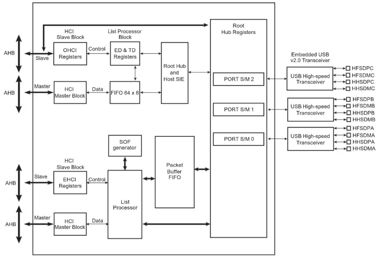
flowchart
graph TD
    A["AHB"] --> B["Slave"]
    B --> C["HCISlave Block"]
    C --> D["OHCI Registers"]
    D --> E["Control"]
    E --> F["ED & TD Registers"]
    F --> G["List Processor Block"]
    G --> H["Root Hub and Host SIE"]
    H --> I["Port Hub Registers"]
    I --> J["USB High-speed Transceiver"]
    J --> K["Embedded USB v2.0 Transceiver"]
    K --> L["HFSDPC"]
    K --> M["HFSDMC"]
    K --> N["HHSDPC"]
    K --> O["HHSDMC"]
    H --> P["FIFO 64 x 8"]
    P --> Q["Data"]
    Q --> R["HCI Master Block"]
    R --> S["Master"]
    S --> T["FIFO 64 x 8"]
    T --> U["Data"]
    U --> V["FIFO 64 x 8"]
    V --> W["Data"]
    W --> X["FIFO 64 x 8"]
    X --> Y["Data"]
    Y --> Z["FIFO 64 x 8"]
    Z --> AA["Data"]
    AA --> AB["FIFO 64 x 8"]
    AB --> AC["Data"]
    AC --> AD["FIFO 64 x 8"]
    AD --> AE["Data"]
    AE --> AF["FIFO 64 x 8"]
    AF --> AG["Data"]
    AG --> AH["FIFO 64 x 8"]
    AH --> AI["Data"]
    AI --> AJ["FIFO 64 x 8"]
    AJ --> AK["Data"]
    AK --> AL["FIFO 64 x 8"]
    AL --> AM["Data"]
    AM --> AN["FIFO 64 x 8"]
    AN --> AO["Data"]
    AO --> AP["FIFO 64 x 8"]
    AP --> AQ["Data"]
    AQ --> AR["FIFO 64 x 8"]
    AR --> AS["Data"]
    AS --> AT["FIFO 64 x 8"]
    AT --> AU["Data"]
    AU --> AV["FIFO 64 x 8"]
    AV --> AW["Data"]
    AW --> AX["FIFO 64 x 8"]
    AX --> AY["Data"]
    AY --> AZ["FIFO 64 x 8"]
    AZ --> BA["Data"]
    BA --> BB["FIFO 64 x 8"]
    BB --> BC["Data"]
    BC --> BD["FIFO 64 x 8"]
    BD --> BE["Data"]
    BE --> BF["FIFO 64 x 8"]
    BF --> BG["Data"]
    BG --> BH["FIFO 64 x 8"]
    BH --> BI["Data"]
    BI --> BJ["FIFO 64 x 8"]
    BJ --> BK["Data"]
    BK --> BL["FIFO 64 x 8"]
    BL --> BM["Data"]
    BM --> BN["FIFO 64 x 8"]
    BN --> BO["Data"]
    BO --> BP["FIFO 64 x 8"]
    BP --> BQ["Data"]
    BQ --> BR["FIFO 64 x 8"]
    BR --> BS["Data"]
    BS --> BT["FIFO 64 x 8"]
    BT --> BU["Data"]
    BU --> BV["FIFO 64 x 8"]
    BV --> BW["Data"]
    BW --> BX["FIFO 64 x 8"]
    BX --> BY["Data"]
    BY --> BZ["FIFO 64 x 8"]
    BZ --> CA["Data"]
    CA --> CB["FIFO 64 x 8"]
    CB --> CC["Data"]
    CC --> CD["FIFO 64 x 8"]
    CD --> CE["Data"]
    CE --> CF["FIFO 64 x 8"]
    CF --> CG["Data"]
    CG --> CH["FIFO 64 x 8"]
    CH --> CI["Data"]
    CI --> CJ["FIFO 64 x 8"]
    CJ --> CK["Data"]
    CK --> CL["FIFO 64 x 8"]
    CL --> CM["Data"]
    CM --> CN["FIFO 64 x 8"]
    CN --> CO["Data"]
    CO --> CP["FIFO 64 x 8"]
    CP --> CQ["Data"]
    CQ --> CR["FIFO 64 x 8"]
    CR --> CS["Data"]
    CS --> CT["FIFO 64 x 8"]
    CT --> CU["Data"]
    CU --> CV["FIFO 64 x 8"]
    CV --> CW["Data"]
    CW --> CX["FIFO 64 x 8"]
    CX --> CY["Data"]
    CY --> CZ["FIFO 64 x 8"]
    CZ --> DA["Data"]
    DA --> DB["FIFO 64 x 8"]
    DB --> DC["Data"]
    DC --> DD["FIFO 64 x 8"]
    DD --> DE["Data"]
    DE --> DF["FIFO 64 x 8"]
    DF --> DG["Data"]
    DG --> DH["FIFO 64 x 8"]
    DH --> DI["Data"]
    DI --> DJ["FIFO 64 x 8"]
    DJ --> DE
Access to the USB host operational registers is achieved through the AHB bus slave interface. The Open HCI host controller and Enhanced HCI host controller initialize master DMA transfers through the AHB bus master interface as follows:
- Fetches endpoint descriptors and transfer descriptors
- Access to endpoint data from system memory
- Access to the HC communication area
- Write status and retire transfer descriptor
Memory access errors (abort, misalignment) lead to an “Unrecoverable Error” indicated by the corresponding flag in the host controller operational registers.
The USB root hub is integrated in the USB host. Several USB downstream ports are available. The number of downstream ports can be determined by the software driver reading the root hub's operational registers. Device connection is automatically detected by the USB host port logic.
USB physical transceivers are integrated in the product and driven by the root hub's ports.
Over current protection on ports can be activated by the USB host controller. The Microchip standard product does not dedicate pads to external over current protection.
35.4 Typical Connection
Figure 35-2: Board Schematic to Interface UHP High-speed Host Controller
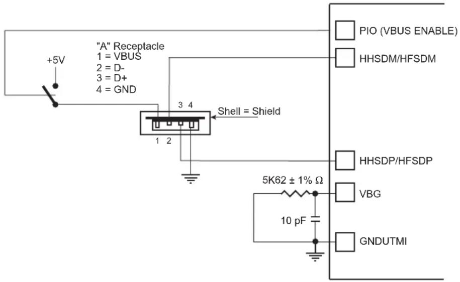
text_image
"A" Receptacle 1 = VBUS 2 = D- 3 = D+ 4 = GND +5V Shell = Shield 5K62 ± 1% Ω 10 pF PIO (VBUS ENABLE) HHSDM/HFSDM HHSDP/HFSDP VBG GNDUTMINote 1: 10 pF capacitor on VBG is a provision and may not be populated.
35.5 Product Dependencies
35.5.1 I/O Lines
HFSDPs, HFSDMs, HHSDPs and HHSDMs are not controlled by any PIO controllers. The embedded USB High Speed physical transceivers are controlled by the USB host controller.
One transceiver is shared with the USB High Speed Device (port A). The selection between Host Port A and USB Device is controlled by the UDPHS enable bit (EN_UDPHS) located in the UDPHS_CTRL register.
In the case the port A is driven by the USB High Speed Device, the output signals are DFSDP, DFSDM, DHSDP and DHSDM. The transceiver is automatically selected for Device operation once the USB High Speed Device is enabled.
In the case the port A is driven by the USB High Speed Host, the output signals are HFSDPA, HFSDMA, HHSDPA and HHSDMA.
35.5.2 Power Management
The system embeds 3 transceivers.
The USB Host High Speed requires a 480 MHz clock for the embedded High-speed transceivers. This clock (UPLLCK) is provided by the UTMI PLL.
In case power consumption is saved by stopping the UTMI PLL, high-speed operations are not possible. Nevertheless, OHCI Full-speed operations remain possible by selecting PLLACK as the input clock of OHCI.
The High-speed transceiver returns a 30 MHz clock to the USB Host controller.
The USB Host controller requires 48 MHz and 12 MHz clocks for OHCI full-speed operations. These clocks must be generated by a PLL with a correct accuracy of ±0.25% using the USBDIV field.
Thus the USB Host peripheral receives three clocks from the Power Management Controller (PMC): the Peripheral Clock (MCK domain), the UHP48M and the UHP12M (built-in UHP48M divided by four) used by the OHCI to interface with the bus USB signals (recovered 12 MHz domain) in Full-speed operations.
For High-speed operations, the user has to perform the following:
- Enable UHP peripheral clock in PMC_PCER.
- Write PLLCOUNT field in CKGR_UCKR.
- Enable UPLL with UPLLEN bit in CKGR_UCKR.
- Wait until UTMI_PLL is locked (LOCKU bit in PMC_SR).
- Enable BIAS with BIASEN bit in CKGR_UCKR.
- Select UPLLCK as Input clock of OHCI part (USBS bit in PMC_USB register).
- Program OHCI clocks (UHP48M and UHP12M) with USBDIV field in PMC_USB register. USBDIV must be 9 (division by 10) if UPLLCK is selected.
- Enable OHCI clocks with UHP bit in PMC_SCER.
For OHCI Full-speed operations only, the user has to perform the following:
- Enable UHP peripheral clock in PMC_PCER.
- Select PLLACK as Input clock of OHCI part (USBS bit in PMC_USB register).
- Program OHCI clocks (UHP48M and UHP12M) with USBDIV field in PMC_USB register. USBDIV value is to be calculated according to the PLLACK value and USB Full-speed accuracy.
- Enable the OHCI clocks with UHP bit in PMC_SCER.
Figure 35-3: UHP Clock Trees

flowchart
graph TD
    A["UPLL (480 MHz)"] --> B["UTMI transceiver"]
    B --> C["30 MHz"]
    C --> D["UTMI transceiver"]
    D --> E["30 MHz"]
    E --> F["UTMI transceiver"]
    F --> G["30 MHz"]
    G --> H["Port Router"]
    H --> I["USB 2.0 EHCI Host Controller"]
    I --> J["EHCI Master Interface"]
    I --> K["EHCI User Interface"]
    I --> L["OHCI Master Interface"]
    I --> M["OHCI User Interface"]
    I --> N["USB 1.1 OHCI Host Controller"]
    N --> O["Root Hub and Host SIE"]
    P["AHB"] --> I
    Q["MCK"] --> I
    R["UHP12M"] --> N
    S["UHP48M"] --> N
    T["OHCI clocks"] --> N
35.5.3 Interrupt Sources
The USB host interface has an interrupt line connected to the interrupt controller.
Handling USB host interrupts requires programming the interrupt controller before configuring the UHPHS.
35.6 Functional Description
35.6.1 UTMI Transceivers Sharing
The High Speed USB Host Port A is shared with the High Speed USB Device port and connected to the second UTMI transceiver. The selection between Host Port A and USB device is controlled by the UDPHS enable bit (EN_UDPHS) located in the UDPHS_CTRL register.
Figure 35-4: USB Selection
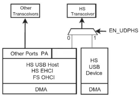
flowchart
graph TD
    A["Other Ports PA"] --> B["HS USB Host HS EHCI FS OHCI"]
    B --> C["DMA"]
    D["HS Transceiver"] --> E["0"]
    E --> F["1"]
    F --> G["EN_UDPHS"]
    H["Other Transceivers"] --> I["0"]
    I --> J["1"]
    J --> K["DMA"]
35.6.2 EHCl
The USB Host Port controller is fully compliant with the Enhanced HCI specification. The USB Host Port User Interface (registers description) can be found in the Enhanced HCI Rev 1.0 Specification available on www.usb.org. The standard EHCI USB stack driver can be easily ported to Microchip architecture in the same way all existing class drivers run, without hardware specialization.
35.6.3 OHCI
The USB Host Port integrates a root hub and transceivers on downstream ports. It provides several Full-speed half-duplex serial communication ports at a baud rate of 12 Mbit/s. Up to 127 USB devices (printer, camera, mouse, keyboard, disk, etc.) and the USB hub can be connected to the USB host in the USB "tiered star" topology.
The USB Host Port controller is fully compliant with the Open HCI specification. The USB Host Port User Interface (registers description) can be found in the Open HCI Rev 1.0 Specification available on www.usb.org. The standard OHCI USB stack driver can be easily ported to Microchip architecture, in the same way all existing class drivers run without hardware specialization.
This means that all standard class devices are automatically detected and available to the user's application. As an example, integrating an HID (Human Interface Device) class driver provides a plug & play feature for all USB keyboards and mouses.
35.7 USB Host High Speed Port (UHPHS) User Interface
The Enhanced USB Host Controller contains two sets of software-accessible hardware registers – Memory-mapped Host Controller Registers and optional PCI configuration registers. Note that the PCI configuration registers are only needed for PCI devices that implement the Host Controller.
- Memory-mapped USB Host Controller Registers. This block of registers is memory-mapped into non-cacheable memory. This memory space must begin on a DWord (32-bit) boundary. This register space is divided into two sections: a set of read-only capability registers and a set of read/write operational registers. Table 35-1 describes each register space.
Table 35-1: Enhanced Interface Register Sets
| Offset Register Set Explanation | ||
| 0 to N-1 Capability Registers | The capability registers specify the limits, restrictions, and capabilities of a host controller implementation.These values are used as parameters to the host controller driver. | |
| N to N+M-1 Operational Registers | The operational registers are used by system software to control and monitor the operational state of the host controller. | |
Note: Host controllers are not required to support exclusive-access mechanisms (such as PCI LOCK) for accesses to the memory-mapped register space. Therefore, if software attempts exclusive-access mechanisms to the host controller memory-mapped register space, the results are undefined.
- PCI Configuration Registers (for PCI devices). In addition to the normal PCI header, power management, and device-specific registers, two registers are needed in the PCI configuration space to support USB. The normal PCI header and device-specific registers are beyond the scope of this document (the UHPHS_CLASSC register is shown in this document). Note that HCD does not interact with the PCI configuration space. This space is used only by the PCI enumerator to identify the USB Host Controller, and assign the appropriate system resources.
Table 35-2: Register Mapping
| Offset Register Name | Access | Reset | ||
| Host Controller Capability Registers | ||||
| 0x00 | UHPHS Host Controller Capability Register | UHPHS_HCCAPBASE | Read-only | 0x0100 0010 |
| 0x04 | UHPHS Host Controller Structural Parameters Register | UHPHS_HCSPARAMS | Read-only | 0x0000 1116 |
| 0x08 | UHPHS Host Controller Capability Parameters Register | UHPHS_HCCPARAMS | Read-only | 0x0000 A010 |
| Host Controller Operational Registers | ||||
| 0x10 | UHPHS USB Command Register | UHPHS_USBCMD | Read/Write^(1) | 0x0008 0000 or 0x0008 0B00(2) |
| 0x14 | UHPHS USB Status Register | UHPHS_USBSTS | Read/Write^(1) | 0x0000 1000 |
| 0x18 | UHPHS USB Interrupt Enable Register | UHPHS_USBINTR | Read/Write | 0x0000 0000 |
| 0x1C | UHPHS USB Frame Index Register | UHPHS_FRINDEX | Read/Write | 0x0000 0000 |
| 0x20 | UHPHS Control Data Structure Segment Register | UHPHS_CTRLDSSEGMENT | Read/Write | 0x0000 0000 |
| 0x24 | UHPHS Periodic Frame List Base Address Register | UHPHS_PERIODICLISTBASE | Read/Write | 0x0000 0000 |
| 0x28 | UHPHS Asynchronous List Address Register | UHPHS_ASYNCLISTADDR | Read/Write | 0x0000 0000 |
| 0x2C - 0x4F Reserved | - | - | - | |
| 0x50 | UHPHS Configured Flag Register | UHPHS_CONFIGFLAG | Read/Write | 0x0000 0000 |
Table 35-2: Register Mapping (Continued)
| Offset Register | Name | Access | Reset |
| 0x54 UHPHS | Port Status and Control Register 0 UHPHS_PORTSC_0 | Read/Write(1) | 0x0000 2000 or 0x0000 3000(3) |
| 0x58 UHPHS | Port Status and Control Register 1 UHPHS_PORTSC_1 | Read/Write(1) | 0x0000 2000 or 0x0000 3000(3) |
| 0x5C UHPHS | Port Status and Control Register 2 UHPHS_PORTSC_2 | Read/Write(1) | 0x0000 2000 or 0x0000 3000(3) |
| 0x90 EHCI | Synopsys-Specific Registers 00 UHPHS_INSNREG00 | Read/Write(1) | 0x0000 0000 |
| 0x94 EHCI | Synopsys-Specific Registers 01 UHPHS_INSNREG01 | Read/Write(1) | 0x0020 0020 |
| 0x98 EHCI | Synopsys-Specific Registers 02 UHPHS_INSNREG02 | Read/Write(1) | (5) |
| 0x9C EHCI | Synopsys-Specific Registers 03 UHPHS_INSNREG03 | Read/Write(1) | 0x0000 0001 |
| 0xA0 EHCI | Synopsys-Specific Registers 04 UHPHS_INSNREG04 | Read/Write(1) | 0x0000 0000 |
| 0xA4 EHCI | Synopsys-Specific Registers 05 UHPHS_INSNREG05 | Read/Write(1) | 0x0000 1000 |
| 0xA8 EHCI | Synopsys-Specific Registers 06 UHPHS_INSNREG06 | Read/Write(1) | 0x0000 0000 |
| 0xAC EHCI | Synopsys-Specific Registers 07 UHPHS_INSNREG07 | Read/Write(1) | 0x0000 0000 |
| 0xB0 EHCI | Synopsys-Specific Registers 08 UHPHS_INSNREG08 | Read/Write(1) | 0x0000 0000 |
Note 1: Field-dependent.
2: The default value depends on whether the Asynchronous Schedule Park Capability (ASPC) field in the UHPHS_HCCPARAMS register is enabled. Disabled (set to 0) = 0x0008 0000h; Enabled (set to 1) = 0x0008 0B00h.
3: The default value depends on the value of the Port Power Control (PPC) field in the UHPHS_HCSPARAMS register. 0x0000 2000h (with PPC set to 1); 0x0000 3000h (with PPC set to 0).
4: Software should not assume reserved bits are always 0 and should preserve these bits when writing to modifiable registers.
5: This value is determined by coreConsultant.
35.7.1 UHPHS Host Controller Capability Register
Name:UHPHS_HCCAPBASE
Access:Read-only
31 30 29 28 27 26 25 24
| HCIVERSION | |||||||
| 23 22 21 20 19 18 17 16 | |||||||
| HCIVERSION | |||||||
| 15 14 13 12 11 10 9 8 | |||||||
| - | |||||||
| 7 | 6 | 5 | 4 | 3 | 2 | 1 | 0 |
| CAPLENGTH | |||||||
CAPLENGTH: Capability Registers Length
10h: Default value.
This field is used as an offset to add to register base to find the beginning of the Operational Register Space.
HCIVERSION: Host Controller Interface Version Number
0100h: Default value.
This is a two-byte field containing a BCD encoding of the EHCI revision number supported by this host controller. The most significant byte of this field represents a major revision and the least significant byte is the minor revision.
35.7.2 UHPHS Host Controller Structural Parameters Register
Name:UHPHS_HCSPARAMS
Access: Read-only
31 30 29 28 27 26 25 24
| - | ||||||
| 23 22 21 20 19 18 17 16 | ||||||
| N_DP- | P_INDICATOR | |||||
| 15 14 13 12 11 10 9 8 | ||||||
| N_CC N_PCC | ||||||
| 7 | 6 | 5 | 4 | 3 | 2 | 1 |
| - PPC | N_PORTS | |||||
This is a set of fields that are structural parameters: number of downstream ports, etc.
N PORTS: Number of Ports
This field specifies the number of physical downstream ports implemented on this host controller. The value of this field determines how many port registers are addressable in the Operational Register Space. Valid values are in the range of 1H to FH.
A zero in this field is undefined.
PPC: Port Power Control
This field indicates whether the host controller implementation includes port power control. A one in this bit indicates the ports have port power switches. A zero in this bit indicates the ports do not have port power switches. The value of this field affects the functionality of the Port Power field in each port status and control register (see Section 35.7.12 UHPHS Port Status and Control Register).
N\_PCC: Number of Ports per Companion Controller
This field indicates the number of ports supported per companion host controller. It is used to indicate the port routing configuration to system software.
For example, if N_PORTS has a value of 6 and N_CC has a value of 2, then N_PCC could have a value of 3. The convention is that the first N_PCC ports are assumed to be routed to companion controller 1, the next N_PCC ports to companion controller 2, etc. In the previous example, the N_PCC could have been 4, where the first four are routed to companion controller 1 and the last two are routed to companion controller 2.
The number in this field must be consistent with N_PORTS and N_CC.
N\_CC: Number of Companion Controllers
This field indicates the number of companion controllers associated with this USB 2.0 host controller.
A zero in this field indicates there are no companion host controllers. Port-ownership hand-off is not supported. Only high-speed devices are supported on the host controller root ports.
A value larger than zero in this field indicates there are companion USB 1.1 host controller(s). Port-ownership hand-offs are supported. High, Full- and Low-speed devices are supported on the host controller root ports.
P\_INDICATOR: Port Indicators
This bit indicates whether the ports support port indicator control. When this bit is a 1, the port status and control registers include a read/writeable field for controlling the state of the port indicator. See Section 35.7.12 UHPHS Port Status and Control Register for definition of the port indicator control field.
N\_DP: Debug Port Number
Optional. This register identifies which of the host controller ports is the debug port. The value is the port number (1-based) of the debug port. A non-zero value in this field indicates the presence of a debug port. The value in this register must not be greater than N_PORTS (see above).
35.7.3 UHPHS Host Controller Capability Parameters Register
Name:UHPHS_HCCPARAMS
Access: Read-only
31 30 29 28 27 26 25 24
23 22 21 20 19 18 17 16
15 14 13 12 11 10 9 8
一
| EECP | |||||||
| 7 | 6 | 5 | 4 | 3 | 2 | 1 | 0 |
| IST- | ASPC | PFLF | AC | ||||
This is a set of fields that are capability parameters: Multiple Mode control (time-base bit functionality), addressing capability, etc.
AC: 64-bit Addressing Capability
This field documents the addressing range capability of this implementation. The value of this field determines whether software should use 32-bit or 64-bit data structures.
Values for this field have the following interpretation:
0: Data structures using 32-bit address memory pointers
1: Data structures using 64-bit address memory pointers
Note: This is not tightly coupled with the UHPHS_USBBASE address register mapping control. The 64-bit Addressing Capability bit indicates whether the host controller can generate 64-bit addresses as a master. The UHPHS_USBBASE register indicates the host controller only needs to decode 32-bit addresses as a slave.
PFLF: Programmable Frame List Flag
The default value is implementation-dependent.
If this bit is set to 0, then system software must use a frame list length of 1024 elements with this host controller. The UHPHS_USBCMD register Frame List Size field is a read-only register and should be set to 0.
If set to 1, then system software can specify and use a smaller frame list and configure the host controller via the UHPHS_USBCMD register Frame List Size field. The frame list must always be aligned on a 4-kbyte page boundary. This requirement ensures that the frame list is always physically contiguous.
ASPC: Asynchronous Schedule Park Capability
The default value is Implementation dependent.
If this bit is set to 1, then the host controller supports the park feature for high-speed queue heads in the Asynchronous Schedule. The feature can be disabled or enabled and set to a specific level by using the Asynchronous Schedule Park Mode Enable and Asynchronous Schedule Park Mode Count fields in the UHPHS_USBCMD register.
IST: Isochronous Scheduling Threshold
The default value is Implementation dependent.
This field indicates, relative to the current position of the executing host controller, where software can reliably update the isochronous schedule. When bit [7] is 0, the value of the least significant 3 bits indicates the number of micro-frames a host controller can hold a set of isochronous data structures (one or more) before flushing the state. When bit [7] is set to 1, then host software assumes the host controller may cache an isochronous data structure for an entire frame.
EECP: EHCI Extended Capabilities Pointer
The default value is Implementation dependent.
This optional field indicates the existence of a capabilities list. A value of 00h indicates no extended capabilities are implemented. A non-zero value in this register indicates the offset in PCI configuration space of the first EHCI extended capability. The pointer value must be 40h or greater if implemented to maintain the consistency of the PCI header defined for this class of device.
35.7.4 UHPHS USB Command Register
Name:UHPHS_USBCMD
Access: Read/Write
31 30 29 28 27 26 25 24
| - | |
| 23 22 21 20 19 18 17 16 | |
| ITC | |
15 14 13 12 11 10 9 8
| - ASPME | - | ASPMC | |||||
| 7 | 6 | 5 | 4 | 3 | 2 | 1 | 0 |
| LHCR | IAAD ASE | PSE | FLS HCRESET | RS | |||
The Command Register indicates the command to be executed by the serial bus host controller. Writing to the register causes a command to be executed.
RS: Run/Stop (read/write)
0: Stop (default value).
1: Run.
When set to 1, the Host Controller proceeds with execution of the schedule. The Host Controller continues execution as long as this bit is set to 1. When this bit is set to 0, the Host Controller completes the current and any actively pipelined transactions on the USB and then halts. The Host Controller must halt within 16 micro-frames after software clears the Run bit. The HC Halted bit in the status register indicates when the Host Controller has finished its pending pipelined transactions and has entered the stopped state. Software must not write 1 to this field unless the host controller is in the Halted state (i.e., HCHalted in the UHPHS_USBSTS register is 1). Doing so will yield undefined results.
HCRESET: Host Controller Reset (read/write)
This control bit is used by software to reset the host controller. The effects of this on Root Hub registers are similar to a Chip Hardware Reset.
When software writes a 1 to this bit, the Host Controller resets its internal pipelines, timers, counters, state machines, etc. to their initial value. Any transaction currently in progress on USB is immediately terminated. A USB reset is not driven on downstream ports.
PCI Configuration registers are not affected by this reset. All operational registers, including port registers and port state machines, are set to their initial values. Port ownership reverts to the companion host controller(s) with side effects. Software must reinitialize the host controller in order to return the host controller to an operational state.
This bit is set to 0 by the Host Controller when the reset process is complete. Software cannot terminate the reset process early by writing a 0 to this register.
Software should not set this bit to 1 when the HCHalted bit in the UHPHS_USBSTS register is 0. Attempting to reset an actively running host controller will result in undefined behavior.
FLS: Frame List Size (read/write or read-only)
This field is R/W only if Programmable Frame List Flag in the UHPHS_HCCPARAMS registers is set to 1. This field specifies the size of the frame list. The size of the frame list controls which bits in the Frame Index Register should be used for the Frame List Current index.
00b: 1024 elements (4096 bytes) (default value).
01b: 512 elements (2048 bytes).
10b: 256 elements (1024 bytes), for resource-constrained environments.
11b: Reserved.
PSE: Periodic Schedule Enable (read/write)
This bit controls whether the host controller skips processing the Periodic Schedule.
0: Do not process the Periodic Schedule (default value).
1: Use the UHPHS_PERIODICLISTBASE register to access the Periodic Schedule.
ASE: Asynchronous Schedule Enable (read/write)
This bit controls whether the host controller skips processing the Asynchronous Schedule.
0: Do not process the Asynchronous Schedule (default value).
1: Use the UHPHS_ASYNCLISTADDR register to access the Asynchronous Schedule.
IAAD: Interrupt on Async Advance Doorbell (read/write)
This bit is used as a doorbell by software to tell the host controller to issue an interrupt the next time it advances asynchronous schedule. Software must write a 1 to this bit to ring the doorbell.
When the host controller has evicted all appropriate cached schedule state, it sets the Interrupt on Async Advance status bit in the UHPHS_USBSTS register. If the Interrupt on Async Advance Enable bit in the UHPHS_USBINTR register is set to 1, then the host controller will assert an interrupt at the next interrupt threshold.
The host controller sets this bit to 0 after it has set the Interrupt on Async Advance status bit in the UHPHS_USBSTS register to 1.
Software should not write a 1 to this bit when the asynchronous schedule is disabled. Doing so will yield undefined results.
LHCR: Light Host Controller Reset (optional) (read/write)
This control bit is not required. If implemented, it allows the driver to reset the EHCI controller without affecting the state of the ports or the relationship to the companion host controllers. For example, the UHPHS_PORTSC registers should not be reset to their default values and the CF bit setting should not go to 0 (retaining port ownership relationships).
A host software read of this bit as 0 indicates the Light Host Controller Reset has completed and it is safe for host software to re-initialize the host controller. A host software read of this bit as 1 indicates the Light Host Controller Reset has not yet completed.
If not implemented, a read of this field will always return a 0.
ASPMC: Asynchronous Schedule Park Mode Count (optional) (read/write or read-only)
If the Asynchronous Park Capability bit in the UHPHS_HCCPARAMS register is set to 1, then this field defaults to 3h and is R/W. Otherwise it defaults to 0 and is RO. It contains a count of the number of successive transactions the host controller is allowed to execute from a high-speed queue head on the Asynchronous schedule before continuing traversal of the Asynchronous schedule. Valid values are 1h to 3h. Software must not write a 0 to this bit when Park Mode Enable is set to 1 as this will result in undefined behavior.
ASPME: Asynchronous Schedule Park Mode Enable (optional) (read/write or read-only)
If the Asynchronous Park Capability bit in the UHPHS_HCCPARAMS register is set to 1, then this bit defaults to a 1h and is R/W. Otherwise the bit must be a 0 and is RO. Software uses this bit to enable or disable Park mode. When this bit is set to 1, Park mode is enabled. When this bit is set to 0, Park mode is disabled.
ITC: Interrupt Threshold Control (read/write)
This field is used by system software to select the maximum rate at which the host controller will issue interrupts. The only valid values are defined below. If software writes an invalid value to this register, the results are undefined.
| Value Maximum | Interrupt Interval |
| 00h Reserved | |
| 01h 1 micro-frame | |
| 02h 2 micro-frames | |
| 04h 4 micro-frames | |
| 08h 8 micro-frames (default, equates to 1 ms) | |
| 10h 16 micro-frames (2 ms) | |
| 20h 32 micro-frames (4 ms) | |
| 40h 64 micro-frames (8 ms) |
Any other value in this register yields undefined results.
Software modifications to this bit while HCHalted bit is equal to 0 results in undefined behavior.
35.7.5 UHPHS USB Status Register
Name:UHPHS_USBSTS
Access: Read/Write
31 30 29 28 27 26 25 24
| - | |
| 23 22 21 20 19 18 17 16 | |
| - |
15 14 13 12 11 10 9 8
| ASS | PSS RCM | HCHLT | - | ||||
| 7 | 6 | 5 | 4 | 3 | 2 | 1 | 0 |
| - | IAA HSE | FLR | PCD | USBERRINT | USBINT | ||
This register indicates pending interrupts and various states of the Host Controller. The status resulting from a transaction on the serial bus is not indicated in this register. Software sets a bit to 0 in this register by writing a 1 to it.
USBINT: USB Interrupt (read/write clear)
The Host Controller sets this bit to 1 on the completion of a USB transaction, which results in the retirement of a Transfer Descriptor that had its IOC bit set.
The Host Controller also sets this bit to 1 when a short packet is detected (the actual number of bytes received was less than the expected number of bytes).
USBERRINT: USB Error Interrupt (read/write clear)
The Host Controller sets this bit to 1 when completion of a USB transaction results in an error condition (e.g., error counter underflow). If the TD on which the error interrupt occurred also had its IOC bit set, both this bit and USBINT bit are set.
PCD: Port Change Detect (read/write clear)
The Host Controller sets this bit to 1 when any port for which the Port Owner bit is set to 0 (see Section 35.7.12 UHPHS Port Status and Control Register) has a change bit transition from 0 to 1 or a Force Port Resume bit transition from 0 to 1 as a result of a J-K transition detected on a suspended port. This bit will also be set as a result of the Connect Status Change being set to 1 after system software has relinquished ownership of a connected port by writing 1 to a port's Port Owner bit.
This bit is allowed to be maintained in the Auxiliary power well. Alternatively, it is also acceptable that on a D3 to D0 transition of the EHCI HC device, this bit is loaded with the OR of all of the PORTSC change bits (including: Force Port Resume, Over-Current Change, Enable/Disable Change and Connect Status Change).
FLR: Frame List Rollover (read/write clear)
The Host Controller sets this bit to 1 when the Frame List Index (see Section 35.7.7 UHPHS USB Frame Index Register) rolls over from its maximum value to 0. The exact value at which the rollover occurs depends on the frame list size. For example, if the frame list size (as programmed in the Frame List Size field of the UHPHS_USBCMD register) is 1024, the Frame Index Register rolls over every time FRINDEX[13] toggles. Similarly, if the size is 512, the Host Controller sets this bit to 1 every time FRINDEX[12] toggles.
HSE: Host System Error (read/write clear)
The Host Controller sets this bit to 1 when a serious error occurs during a host system access involving the Host Controller module. In a PCI system, conditions that set this bit to 1 include PCI Parity error, PCI Master Abort, and PCI Target Abort. When this error occurs, the Host Controller clears the Run/Stop bit in the Command register to prevent further execution of the scheduled TDs.
IAA: Interrupt on Async Advance (read/write clear)
0: Default.
System software can force the host controller to issue an interrupt the next time the host controller advances the asynchronous schedule by writing 1 to the Interrupt on the Async Advance Doorbell bit in the UHPHS_USBCMD register. This status bit indicates the assertion of that interrupt source.
HCHLT: HCHalted (read-only)
1: Default.
This bit is 0 whenever the Run/Stop bit is 1. The Host Controller sets this bit to 1 after it has stopped executing as a result of the Run/Stop bit being set to 0, either by software or by the Host Controller hardware (e.g. internal error).
RCM: Reclamation (read-only)
0: Default.
This is a read-only status bit used to detect any empty asynchronous schedule.
PSS: Periodic Schedule Status (read-only)
0: Default.
The bit reports the current real status of the Periodic Schedule. If this bit is set to 0, then the status of the Periodic Schedule is disabled. If this bit is set to 1, then the status of the Periodic Schedule is enabled. The Host Controller is not required to immediately disable or enable the Periodic Schedule when software transitions the Periodic Schedule Enable bit in the UHPHS_USBCMD register. When this bit and the Periodic Schedule Enable bit are the same value, the Periodic Schedule is either enabled (1) or disabled (0).
ASS: Asynchronous Schedule Status (read-only)
0: Default.
The bit reports the current real status of the Asynchronous Schedule. If this bit is set to 0, then the status of the Asynchronous Schedule is disabled. If this bit is set to 1, then the status of the Asynchronous Schedule is enabled. The Host Controller is not required to immediately disable or enable the Asynchronous Schedule when software transitions the Asynchronous Schedule Enable bit in the UHPHS_USBCMD register. When this bit and the Asynchronous Schedule Enable bit are the same value, the Asynchronous Schedule is either enabled (1) or disabled (0).
35.7.6 UHPHS USB Interrupt Enable Register
Name:UHPHS_USBINTR
Access: Read/Write
31 30 29 28 27 26 25 24
| - | ||||||
| 23 22 21 20 19 18 17 16 | ||||||
| - | ||||||
| 15 14 13 12 11 10 9 8 | ||||||
| - | ||||||
| 7 | 6 | 5 | 4 | 3 | 2 | 1 |
| - | IAAE HSEE | FLRE | PCIE | USBEIE | ||
This register enables and disables reporting of the corresponding interrupt to the software. When a bit is set and the corresponding interrupt is active, an interrupt is generated to the host. Interrupt sources that are disabled in this register still appear in the UHPHS_USBSTS to allow the software to poll for events.
Each interrupt enable bit description indicates whether it is dependent on the interrupt threshold mechanism.
For all enable register bits, 1= Enabled, 0= Disabled.
USBIE: USB Interrupt Enable
When this bit is set to 1, and the USBINT bit in the UHPHS_USBSTS register is 1, the host controller will issue an interrupt at the next interrupt threshold. The interrupt is acknowledged by software clearing the USBINT bit.
USBEIE: USB Error Interrupt Enable
When this bit is set to 1, and the USBERRINT bit in the UHPHS_USBSTS register is 1, the host controller will issue an interrupt at the next interrupt threshold. The interrupt is acknowledged by software clearing the USBERRINT bit.
PCIE: Port Change Interrupt Enable
When this bit is set to 1, and the Port Change Detect bit in the UHPHS_USBSTS register is 1, the host controller will issue an interrupt. The interrupt is acknowledged by software clearing the Port Change Detect bit.
FLRE: Frame List Rollover Enable
When this bit is set to 1, and the Frame List Rollover bit in the UHPHS_USBSTS register is 1, the host controller will issue an interrupt. The interrupt is acknowledged by software clearing the Frame List Rollover bit.
HSEE: Host System Error Enable
When this bit is set to 1, and the Host System Error Status bit in the UHPHS_USBSTS register is 1, the host controller will issue an interrupt. The interrupt is acknowledged by software clearing the Host System Error bit.
IAAE: Interrupt on Async Advance Enable
When this bit is set to 1, and the Interrupt on Async Advance bit in the UHPHS_USBSTS register is 1, the host controller will issue an interrupt at the next interrupt threshold. The interrupt is acknowledged by software clearing the Interrupt on Async Advance bit.
35.7.7 UHPHS USB Frame Index Register
Name:UHPHS_FRINDEX
Access: Read/Write
31 30 29 28 27 26 25 24
| - | |||||||
| 23 22 21 20 19 18 17 16 | |||||||
| - | |||||||
| 15 14 13 12 11 10 9 8 | |||||||
| - | FI | ||||||
| 7 | 6 | 5 | 4 | 3 | 2 | 1 | 0 |
| FI | |||||||
This register is used by the host controller to index into the periodic frame list. The register updates every 125 microseconds (once each micro-frame). Bits [N:3] are used to select a particular entry in the Periodic Frame List during periodic schedule execution. The number of bits used for the index depends on the size of the frame list as set by system software in the Frame List Size field in the UHPHS_USBCMD register (see Section 35.7.4 UHPHS USB Command Register).
This register must be written as a DWord. Byte writes produce undefined results. This register cannot be written unless the Host Controller is in the Halted state as indicated by the HCHalted bit (UHPHS_USBSTS register, Section 35.7.5 UHPHS USB Status Register). A write to this register while the Run/Stop bit is set to 1 (UHPHS_USBCMD register, Section 35.7.4 UHPHS USB Command Register) produces undefined results. Writes to this register also affect the SOF value.
Fl: Frame Index
The value in this register increments at the end of each time frame (e.g. micro-frame). Bits [N:3] are used for the Frame List current index. This means that each location of the frame list is accessed eight times (frames or micro-frames) before moving to the next index. The following illustrates values of N based on the value of the Frame List Size field in the UHPHS_USBCMD register.
| USBCMD [Frame List Size] Number Elements N | ||
| 00b (1024) 12 | ||
| 01b (512) | 11 | |
| 10b (256) | 10 | |
| 11b | Reserved | |
The SOF frame number value for the bus SOF token is derived or alternatively managed from this register. The value of FRINDEX must be 125 ?sec (1 micro-frame) ahead of the SOF token value. The SOF value may be implemented as an 11-bit shadow register. For this discussion, this shadow register is 11 bits and is named SOFV. SOFV updates every eight micro-frames (1 millisecond). An example implementation to achieve this behavior is to increment SOFV each time the FRINDEX[2:0] increments from 0 to 1.
Software must use the value of FRINDEX to derive the current micro-frame number, both for high-speed isochronous scheduling purposes and to provide the "get micro-frame number" function required for client drivers. Therefore, the value of FRINDEX and the value of SOFV must be kept consistent if chip is reset or software writes to FRINDEX. Writes to FRINDEX must also write-through FRINDEX[13:3] to SOFV[10:0]. In order to keep the update as simple as possible, software should never write a FRINDEX value where the three least significant bits are 111b or 000b.
35.7.8 UHPHS Control Data Structure Segment Register
Name:UHPHS_CTRLDSSEGMENT
Access: Read/Write
This 32-bit register corresponds to the most significant address bits [63:32] for all EHCI data structures. If the 64-bit Addressing Capability field in UHPHS_HCCPARAMS is set to 0, then this register is not used. Software cannot write to it and a read from this register will return zeros.
If the 64-bit Addressing Capability field in UHPHS_HCCPARAMS is 1, then this register is used with the link pointers to construct 64-bit addresses to EHCI control data structures. This register is concatenated with the link pointer from either the UHPHS_PERIODICLISTBASE, UHPHS_ASYNCLISTADDR, or any control data structure link field to construct a 64-bit address.
This register must be written as a DWord. Byte writes produce undefined results. This register allows the host software to locate all control data structures within the same 4-Gigabyte memory segment.
35.7.9 UHPHS Periodic Frame List Base Address Register
Name:UHPHS_PERIODICLISTBASE
Access: Read/Write
31 30 29 28 27 26 25 24
| BA | |||||||
| 23 22 21 20 19 18 17 16 | |||||||
| BA | |||||||
| 15 14 13 12 11 10 9 8 | |||||||
| BA | - | ||||||
| 7 | 6 | 5 | 4 | 3 | 2 | 1 | 0 |
| - | |||||||
This 32-bit register contains the beginning address of the Periodic Frame List in the system memory. If the host controller is in 64-bit mode (as indicated by a 1 in the 64-bit Addressing Capability field in the UHPHS_HCCSPARAMS register), then the most significant 32 bits of every control data structure address comes from the UHPHS_CTRLDSSEGMENT register (see Section 35.7.8 UHPHS Control Data Structure Segment Register). System software loads this register prior to starting the schedule execution by the Host Controller. The memory structure referenced by this physical memory pointer is assumed to be 4-Kbyte aligned. The contents of this register are combined with the Frame Index Register (UHPHS_FRINDEX) to enable the Host Controller to step through the Periodic Frame List in sequence. This register must be written as a DWord. Byte writes produce undefined results.
BA: Base Address (Low)
These bits correspond to memory address signals [31:12], respectively.
35.7.10 UHPHS Asynchronous List Address Register
Name:UHPHS_ASYNCLISTADDR
Access: Read/Write
31 30 29 28 27 26 25 24
| LPL | |||||||
| 23 22 21 20 19 18 17 16 | |||||||
| LPL | |||||||
| 15 14 13 12 11 10 9 8 | |||||||
| LPL | |||||||
| 7 | 6 | 5 | 4 | 3 | 2 | 1 | 0 |
| LPL | - | ||||||
This 32-bit register contains the address of the next asynchronous queue head to be executed. If the host controller is in 64-bit mode (as indicated by a 1 in the 64-bit Addressing Capability field in the UHPHS_HCCPARAMS register), then the most significant 32 bits of every control data structure address comes from the UHPHS_CTRLDSSEGMENT register (See Section 35.7.8 UHPHS Control Data Structure Segment Register). Bits [4:0] of this register cannot be modified by system software and will always return a zero when read. The memory structure referenced by this physical memory pointer is assumed to be 32-byte (cache line) aligned. This register must be written as a DWord. Byte writes produce undefined results.
LPL: Link Pointer Low
These bits correspond to memory address signals [31:5], respectively. This field may only reference a Queue Head (QH).
35.7.11 UHPHS Configure Flag Register
Name:UHPHS_CONFIGFLAG
Access: Read/Write
31 30 29 28 27 26 25 24
23 22 21 20 19 18 17 16
15 14 13 12 11 10 9 8
7 6 5 4 3 2 1 0
-
This register is in the auxiliary power well. It is only reset by hardware when the auxiliary power is initially applied or in response to a host controller reset.
CF: Configure Flag (read/write)
Host software sets this bit as the last action in its process of configuring the Host Controller. This bit controls the default port-routing control logic. Bit values and side-effects are listed below.
0: Port routing control logic default-routes each port to an implementation-dependent classic host controller (default value).
1: Port routing control logic default-routes all ports to this host controller.
35.7.12 UHPHS Port Status and Control Register
Name:UHPHS_PORTSC_x[x = 0..2]
Access: Read/Write
31 30 29 28 27 26 25 24
| - | |||||||
| 23 22 21 20 19 18 17 16 | |||||||
| - | W | KWKDSCNNT_G | WKCNNCT_E | PTC | _ | E | |
| 15 14 13 12 11 10 9 8 | |||||||
| PIC | PO PP | LS | - | PR | |||
| 7 | 6 | 5 | 4 | 3 | 2 | 1 | 0 |
| SUS | FPR | OCC | OCA | PEDC | PED | CSC | CCS |
A host controller must implement one or more port registers. The number of port registers implemented by a particular instantiation of a host controller is documented in the UHPHS_HCSPARAMS register (Section 35.7.2 UHPHS Host Controller Structural Parameters Register). Software uses this information as an input parameter to determine how many ports need to be serviced. All ports have the structure defined below.
This register is in the auxiliary power well. It is only reset by hardware when the auxiliary power is initially applied or in response to a host controller reset. The initial conditions of a port are:
- No device connected
- Port disabled
If the port has port power control, software cannot change the state of the port until after it applies power to the port by setting port power to a 1. Software must not attempt to change the state of the port until after power is stable on the port. The host is required to have power stable to the port within 20 milliseconds of the 0 to 1 transition.
Note 1: When a device is attached, the port state transitions to the connected state and system software will process this as with any status change notification.
2: If a port is being used as the Debug Port, then the port may report device connected and enabled when the Configured Flag is set to 0.
CCS: Current Connect Status (read-only)
0: No device is present (default value).
1: Device is present on port.
This value reflects the current state of the port, and may not correspond directly to the event that caused the Connect Status Change bit (Bit 1) to be set.
This field is 0 if Port Power is 0.
CSC: Connect Status Change (read/write clear)
0: No change (default value).
1: Change in Current Connect Status.
Indicates a change has occurred in the port's Current Connect Status. The host controller sets this bit for all changes to the port device connect status, even if system software has not cleared an existing connect status change. For example, the insertion status changes twice before system software has cleared the changed condition, hub hardware will be "setting" an already-set bit (i.e., the bit will remain set). Software sets this bit to 0 by writing a 1 to it.
This field is 0 if Port Power is 0.
PED: Port Enabled/Disabled (read/write)
0: Disable (default value).
1: Enable.
Ports can only be enabled by the host controller as a part of the reset and enable. Software cannot enable a port by writing a 1 to this field. The host controller will only set this bit to 1 when the reset sequence determines that the attached device is a high-speed device.
Ports can be disabled by either a fault condition (disconnect event or other fault condition) or by host software. Note that the bit status does not change until the port state actually changes. There may be a delay in disabling or enabling a port due to other host controller and bus events.
When the port is disabled (0b), downstream propagation of data is blocked on this port, except for reset.
This field is 0 if Port Power is 0.
PEDC: Port Enable/Disable Change (read/write clear)
0: No change (default value).
1: Port enabled/disabled status has changed.
For the root hub, this bit gets set to 1 only when a port is disabled due to the appropriate conditions existing at the EOF2 point (See Chapter 11 of the USB Specification for the definition of a Port Error). Software clears this bit by writing a 1 to it.
This field is 0 if Port Power is 0.
OCA: Over-current Active (read-only)
0: This port does not have an over-current condition (default value).
1: This port currently has an over-current condition.
This bit will automatically transition from 1 to 0 when the over current condition is removed.
OCC: Over-current Change (read/write clear)
0: Default value.
1: This bit gets set to 1 when there is a change to Over-current Active.
Software clears this bit by writing 1 to this bit position.
FPR: Force Port Resume (read/write)
0: No resume (K-state) detected/driven on port (default value).
1: Resume detected/driven on port.
This functionality defined for manipulating this bit depends on the value of the Suspend bit. For example, if the port is not suspended (Suspend and Enabled bits are set to 1) and software transitions this bit to 1, then the effects on the bus are undefined.
Software sets this bit to a 1 to drive resume signaling. The Host Controller sets this bit to 1 if a J-to-K transition is detected while the port is in the Suspend state. When this bit transitions to 1 because a J-to-K transition is detected, the Port Change Detect bit in the UHPHS_USBSTS register is also set to 1. If software sets this bit to 1, the host controller must not set the Port Change Detect bit.
Note that when the EHCI controller owns the port, the resume sequence follows the defined sequence documented in the USB Specification Revision 2.0. The resume signaling (Full-speed 'K') is driven on the port as long as this bit remains set to 1. Software must appropriately time the Resume and set this bit to 0 when the appropriate amount of time has elapsed. Writing a 0 (from 1) causes the port to return to High-Speed mode (forcing the bus below the port into a high-speed idle). This bit will remain set to 1 until the port has switched to the high-speed idle. The host controller must complete this transition within 2 milliseconds of software setting this bit to 0.
This field is 0 if Port Power is 0.
SUS: Suspend (read/write)
0: Port not in suspend state (default value).
1: Port in suspend state.
Port Enabled Bit and Suspend bit of this register define the port states as follows:
| Bits [Port Enabled, Suspend] Port State | |
| 0X Disable | |
| 10 Enable | |
| 11 Suspend | |
When in suspend state, downstream propagation of data is blocked on this port, except for port reset. The blocking occurs at the end of the current transaction, if a transaction was in progress when this bit was written to 1. In the suspend state, the port is sensitive to resume detection. Note that the bit status does not change until the port is suspended and that there may be a delay in suspending a port if there is a transaction currently in progress on the USB.
A write of 0 to this bit is ignored by the host controller. The host controller will unconditionally set this bit to 0 when:
- Software sets the Force Port Resume bit to 0 (from 1).
- Software sets the Port Reset bit to 1 (from 0).
If host software sets this bit to 1 when the port is not enabled (i.e., Port Enabled bit set to 0), the results are undefined.
This field is 0 if Port Power is set to 0.
PR: Port Reset (read/write)
0: Port is not in Reset (default value).
1: Port is in Reset.
When software writes a 1 to this bit (from 0), the bus reset sequence as defined in the USB Specification Revision 2.0 is started. Software writes a 0 to this bit to terminate the bus reset sequence. Software must keep this bit set to 1 long enough to ensure the reset sequence, as specified in the USB Specification Revision 2.0, completes. Note: when software writes this bit to 1, it must also write 0 to the Port Enable bit.
When software writes a 0 to this bit, there may be a delay before the bit status changes to 0. The bit status will not read as 0 until after the reset has completed. If the port is in High-Speed mode after reset is complete, the host controller will automatically enable this port (e.g. set the Port Enable bit to 1). A host controller must terminate the reset and stabilize the state of the port within 2 milliseconds of software transitioning this bit from 1 to 0. For example: if the port detects that the attached device is high-speed during reset, then the host controller must have the port in the enabled state within 2 ms of software writing this bit to 0.
The HCHalted bit in the UHPHS_USBSTS register should be set to 0 before software attempts to use this bit. The host controller may hold Port Reset asserted to 1 when the HCHalted bit is 1.
This field is 0 if Port Power is 0.
LS: Line Status (read-only)
These bits reflect the current logical levels of the D+ (bit 11) and D- (bit 10) signal lines. These bits are used for detection of low-speed USB devices prior to the port reset and enable sequence. This field is valid only when the port enable bit is 0 and the current connect status bit is set to 1.
Bits are encoded as follows:
| Bits[11:10] USB State Interpretation | ||
| 00b SE0 Not a low-speed device, perform EHCI reset | ||
| 10b J-state Not a low-speed device, perform EHCI reset | ||
| 01b K-state Low-speed device, release ownership of port | ||
| 11b Undefined Not a low-speed device, perform EHCI reset | ||
This value of this field is undefined if Port Power is 0.
PP: Port Power (read/write or read-only)
The function of this bit depends on the value of the Port Power Control (PPC) field in the UHPHS_HCSPARAMS register. The behavior is as follows:
| PPC PP Operation | ||
| 0b | 1b | Read-only.Host controller does not have port power control switches. Each port is hard-wired to power. |
| 1b | 1b/0b | Read/write.Host controller has port power control switches. This bit represents the current setting of the switch (0 = off, 1 = on). When power is not available on a port (i.e., PP at 0), the port is non-functional and will not report attaches, detaches, etc. |
When an over-current condition is detected on a powered port and PPC is set to 1, the PP bit in each affected port may be transitioned by the host controller from 1 to 0 (removing power from the port).
PO: Port Owner (read/write)
0: This bit unconditionally goes to a 0 when the Configured bit in the UHPHS_CONFIGFLAG register makes a 0 to 1 transition.
1: This bit unconditionally goes to 1 whenever the Configured bit is 0 (default value).
System software uses this field to release ownership of the port to a selected host controller (in the event that the attached device is not a high-speed device). Software writes 1 to this bit when the attached device is not a high-speed device. A 1 in this bit means that a companion host controller owns and controls the port.
PIC: Port Indicator Control (read/write)
00b: Default value.
Writing to these bits has no effect if the P_INDICATOR bit in the UHPHS_HCSPARAMS register is set to 0. If the P_INDICATOR bit is set to 1, then the bits are encoded as follows:
| Bit Value Meaning | |
| 00b Port indicators are off | |
| 01b Amber | |
| 10b Green | |
| 11b Undefined | |
Refer to the USB Specification Revision 2.0 for a description on how these bits are to be used.
This field is 0 if Port Power is 0.
PTC: Port Test Control (read/write)
0000b: Default value.
When this field is set to 0, the port is NOT operating in a test mode. A non-zero value indicates that it is operating in test mode and the specific test mode is indicated by the specific value.
Test mode bits are encoded as follows (0110b - 1111b are reserved):
| Bits Test Mode |
| 0000b Test mode not enabled |
| 0001b Test J_STATE |
| 0010b Test K_STATE |
| 0011b Test SEO_NAK |
| 0100b Test Packet |
| 0101b Test FORCE_ENABLE |
Refer to the USB Specification Revision 2.0, Chapter 7, for details on each test mode.
WKCNNT\_E: Wake on Connect Enable (read/write)
0: Default value.
Writing this bit to 1 enables the port to be sensitive to device connects as wake-up events.
This field is 0 if Port Power is 0.
WKDSCNNT\_E: Wake on Disconnect Enable (read/write)
0: Default value.
Writing this bit to 1 enables the port to be sensitive to device disconnects as wake-up events.
This field is 0 if Port Power is 0.
WKOC_E: Wake on Over-current Enable (read/write)
0: Default value.
Writing this bit to 1 enables the port to be sensitive to over-current conditions as wake-up events.
This field is 0 if Port Power is 0.
35.7.13 EHCl: REG00 - Programmable Microframe Base Value
Name:UHPHS_INSNREG00
Access: Read/Write
31 30 29 28 27 26 25 24
| - | |||||
| 23 22 21 20 19 18 17 16 | |||||
| - Debug | |||||
| 15 14 13 12 11 10 9 8 | |||||
| Debug | MFC_8 | MFC_16 | |||
| 7 6 | 5 4 | 3 | 2 | 1 | 0 |
| MFC_16 | En | ||||
The Programmable Microframe Base Value is used to change the microframe length value (default is microframe SOF = 125 ?s) in order to reduce simulation time.
En: Enable this Register
0: Register disabled (default value).
1: Register enabled.
Note: Do not enable this register for the gate-level netlist.
MFC\_16: Microframe Counter with Word Byte Interface
This value is used as the 1-microframe counter with 16-bit interface.
MFC\_8: Microframe Counter with Byte Interface
This value is used as the 1-microframe counter with 8-bit interface.
Debug: Debug Purposes
This field is used for debug purposes only.
In Heterogeneous mode, if the per port clock gets out of sync (but still within the ppm limits) of the phy_clk, then the per port SOF counter needs some correction relative to the global SOF counter. The RTL corrects itself if this happens.
This field controls the SOF correction, in case some debugging is required for the correction.
If bit 14 is set to 1, then it enables the RTL to use the value in bits 19:15 to perform the correction.
In normal operating mode, these bits should not be written.
Note:
The "value" in bits [31:1] must be programmed as follows: (value + 32/64) * Clock Period = microframe timer duration
Factor 32 is used for a 16-bit interface and factor 64 is used for an 8-bit interface. For example, for the full (125 sec) microframe duration:
- In 8-bit, 60-MHz mode, the value is h1D0C (=7436), so (7436 + 64) * 16.67 ns = 125 μs
- In 16-bit, 30-MHz mode, the value is hE86 (=3718), so (3718 + 32) * 33.33 ns = 125 μs
For a 50 sec microframe duration:
- In 8-bit, 60-MHz mode, the value is hB77 (=2395), so (2395 + 64) * 16.67 ns = 50 μs
- In 16-bit, 30-MHz mode, the value is h5BC (=1468), so (1468 + 32) * 33.33 ns = 50 μs
35.7.14 EHCI: REG01 - Programmable Packet Buffer OUT/IN Thresholds
Name:UHPHS_INSNREG01
Access: Read/Write
31 30 29 28 27 26 25 24
| Out_Threshold | |||||||
| 23 22 21 20 19 18 17 16 | |||||||
| Out_Threshold | |||||||
| 15 14 13 12 11 10 9 8 | |||||||
| In_Threshold | |||||||
| 7 | 6 | 5 | 4 | 3 | 2 | 1 | 0 |
| In_Threshold | |||||||
Programmable Packet Buffer OUT/IN thresholds (in CONFIG1 mode only, not applicable in Config2 mode).
The value specified here is the number of DWORDs (32-bit entries).
In\_Threshold: Amount of Data Available in the IN Packet Buffer
The IN threshold is used to start the memory transfer as soon as the IN threshold amount of data is available in the Packet Buffer. It is also used to disconnect the data write, if the threshold amount of data is not available in the Packet Buffer.
Out\_Threshold: Amount of Data Available in the OUT Packet Buffer
The OUT threshold is used to start the USB transfer as soon as the OUT threshold amount of data is fetched from system memory. It is also used to disconnect the data fetch, if the threshold amount of space is not available in the Packet Buffer.
The minimum OUT and IN threshold amount that can be programmed through INSN registers is 16 bytes.
For INCRX configurations, the minimum threshold amount that can be programmed is the highest possible INCRX burst value. For example, if the value of the strap signals {ss_ena_incr16_i, ss_ena_incr8_i, ss_ena_incr4_i} is 3'b011 (for example, INCR16 burst is disabled, INCR8/INCR4 bursts are enabled), then the minimum OUT and IN threshold values should be 32 bytes (8 DWords).
OUT and IN threshold values can be equal to the packet buffer depth only when one of the following conditions is met:
- The packet buffer depth is equal to 512 bytes and isochronous/interrupt transactions are not initiated by the host controller.
- The packet buffer depth is equal to 1024 bytes.
The threshold default value depends on one of the following packet buffer configurations:
• 1024 bytes depth, 256 bytes IN and OUT thresholds
- 512 bytes depth, 128 bytes IN and OUT thresholds
• 256 bytes depth, 64 bytes IN and OUT thresholds
• 128 bytes depth, 64 bytes IN and OUT thresholds
- 64 bytes depth, 60 bytes IN and OUT thresholds
For INCRX configurations, the Break Memory Transfer bit is always enabled.
Depending on the different packet buffer settings, not all MSB bits are used.
35.7.15 EHCl: REG02 - Programmable Packet Buffer Depth
Name:UHPHS_INSNREG02
Access: Read/Write
31 30 29 28 27 26 25 24
23 22 21 20 19 18 17 16
15 14 13 12 11 10 9 8
7 6 5 4 3 2 1 0
Dwords
Programmable Packet Buffer Depth (in CONFIG1 mode only, not applicable in Config2 mode).
The value specified here is the number of DWORDs (32-bit entries).
Dwords: Number of Entries
For a maximum 256 entries for 1-Kbyte packet buffer, bits [8:0] are sufficient.
35.7.16 EHCI: REG03
Name:UHPHS_INSNREG03
Access: Read/Write
31 30 29 28 27 26 25 24
| - | |
| 23 22 21 20 19 18 17 16 | |
| - |
15 14 13 12 11 10 9 8
| - | EN_CK256 Ignore_LS Tx_Tx | Per_Frame | TA_Offset | ||||
| 7 | 6 | 5 | 4 | 3 | 2 | 1 | 0 |
| TA_Offset Break_Mem | |||||||
The default value for INSNREG03[0] depends on the host core configuration. So, if INCRx support is enabled, this bit is 1 after reset. Otherwise, it should stay at 0.
Break\_Mem: Break Memory Transfer (in CONFIG1 mode only, not applicable in CONFIG2 mode)
0: Disables this function.
1: Enables this function.
Used in conjunction with INSNREG01 to enable breaking memory transactions into chunks once the OUT/IN threshold value is reached.
TA\_Offset: Time-Available Offset
This value indicates the additional number of bytes to be accommodated for the time-available calculation. The USB traffic on the bus can be started only when sufficient time is available to complete the packet within the EOF1 point.
Refer to the USB 2.0 specification for details of the EOF1 point. This time-available calculation is done in the hardware, and can be further offset by programming a value in this location.
Note: Time-available calculation is added for future flexibility. The application is not required to program this field by default.
Per\_Frame: Periodic Frame List Fetch
In CONFIG1 mode only ("EHCI Descriptor/Data Prefetching" is disabled in core configuration), setting this bit forces the host controller to fetch the periodic frame list in every microframe of a frame. If not set, then the periodic frame list is fetched only in microframe 0 of every frame.
The default is 0 (not set). This bit can be changed only during core initialization and should not be changed afterwards.
Tx\_Tx: Tx-Tx turnaround Delay Add-on
This field specifies the extra delays in phy_clks to be added to the "Transmit to Transmit turnaround delay" value maintained in the core. The default value of this register field is 0. This default value of 0 is sufficient for most PHYs. But for some PHYs which enter wait states during the token packet, it may be required to program a value greater than 0 to meet the transmit-to-transmit minimum turnaround time.
It is recommended to use default value 0 and to change it only if there is an issue with minimum transmit-to-transmit turnaround time.
This value should be programmed during core initialization and should not be changed afterwards.
Ignore\_LS: Ignore Linestate during TestSE0 Nak
When set to 1 (default), the core ignores the linestate checking when transmitting SOF in SE0_NAK Test mode.
When set to 0, the port state machine disables the port if it does not find the linestate to be in SE0 when transmitting SOF during the SE0_NAK test.
While performing impedance measurement during the SE0_NAK test, the linestate could go to non SE0 forcing the core to disable the port. This bit is used to control the port behavior during this operation.
EN\_CK256: Enable 256 Clock Checking
This bit controls the End of Resume sequence of the EHCI host controller.
By default, the value of this bit is 0 and during the End of Resume sequence, the host controller waits for SEO on the linestate before switching the PHY to High-Speed.
When set to 1, during the End of Resume sequence, the controller waits for SE0 or 256 clocks before switching the PHY to High-Speed.
Setting this bit to 1 enables the 256-clock check. Some of the UTMI PHYs do not present SE0 on the linestate during the End of Resume sequence. For such PHYs, this bit should be set, so that the core does not wait forever for SE0.
This bit should be set only during initialization.
35.7.17 EHCI: REG04
Name:UHPHS_INSNREG04
Access: Read/Write
31 30 29 28 27 26 25 24
| - | |||||||
| 23 22 21 20 19 18 17 16 | |||||||
| - | |||||||
| 15 14 13 12 11 10 9 8 | |||||||
| - | |||||||
| 7 | 6 | 5 | 4 | 3 | 2 | 1 | 0 |
| -EN_AutoFunc | NAK_RF | - | SDPE_TIME | HCCPARAMS_BW | HCSPARAMS_W | ||
Bits [2:0] are used for debug purposes. Bits [(5+UHC2_N_PORTS):4] are functional bits where UHC2_N_PORTS indicates the number of physical USB ports.
HCSPARAMS\_W: HCSPARAMS Write
When set, the HCSPARAMS register becomes writable. Upon system reset, this bit is 0.
HCCPARAMS\_BW: HCCPARAMS Bits Write
When set, the HCCPARAMS register's bits 17, 15:4, and 2:0 become writable. Upon system reset, these bits are 0.
SDPE\_TIME: Scales Down Port Enumeration Time
When set, Scales Down Port Enumeration Time is enabled. Reset value is 1'b0.
Note: This bit can be used for both RTL and Gate level simulations.
NAK\_RF: NAK Reload Fix (Read/Write)
0: Enables this function.
1: Disables this function
Incorrect NAK reload transition at the end of a microframe for backward compatibility with Release 2.40c. For more information, see the USB 2.0 Host-AHB Release Notes. Reset value is 1'b0.
EN\_AutoFunc: Enable Automatic Feature
0: Enables the automatic feature.
The Suspend signal is deasserted (logic level 1'b1) when run/stop is reset by software, but the hchalted bit is not set yet.
1: Disables the automatic feature, which takes all ports out of suspend when software clears the run/stop bit. This is for backward compatibility.
Bit [5] has an added functionality in release 2.80a and later. For systems where the host is halted without waking up all ports out of suspend, the port can remain suspended because the PHYCLK is not running when the halt is programmed. To avoid this, the DWC H20AHB host core automatically pulls ports out of suspend when the host is halted by software.
This bit is used to disable this automatic function.
Reset value is 0.
35.7.18 EHCl: REG05 - UTMI Configuration
Name:UHPHS_INSNREG05
Access: Read/Write
31 30 29 28 27 26 25 24
| - | ||||||
| 23 22 21 20 19 18 17 16 | ||||||
| - VBusy | VPort | |||||
| 15 14 13 12 11 10 9 8 | ||||||
| VPort VControlLoadM VControl | ||||||
| 7 | 6 | 5 | 4 | 3 | 2 | 1 |
| VStatus | ||||||
Control and Status Register, used to read the UTMI registers from the following signals:
VStatus: Vendor Status (Software RO)
VControl: Vendor Control (Software R/W)
VControlLoadM: Vendor Control Load Microframe
0: Load.
1: NOP (software R/W)
VPort: Vendor Port (Software R/W)
Valid values range from 1 to 15 depending on coreConsultant configuration.
For example, if the number of ports is 3, then software should only write values 1, 2, and 3 to this field and not any other values in the range, that is, 0 or 4 to 15. For example, if the software writes value 4 to VPort, from that write onwards, any write to this register is ignored and the read value will always be 4.
VBusy: Vendor Busy (Software RO)
Hardware indicator that a write to this register has occurred and the hardware is currently processing the operation defined by the data written. When processing is finished, this bit is cleared.
35.7.19 EHCl: REG06 - AHB Error Status
Name:UHPHS_INSNREG06
Access: Read/Write
31 30 29 28 27 26 25 24
| AHB_ERR | |||||||
| 23 22 21 20 19 18 17 16 | |||||||
| - | |||||||
| 15 14 13 12 11 10 9 8 | |||||||
| - HBURST | Nb_Burst | ||||||
| 7 | 6 | 5 | 4 | 3 | 2 | 1 | 0 |
| Nb_Burst | Nb_Success_Burst | ||||||
Control and Status Register, used to read the UTMI registers from the following signals:
Nb\_Success\_Burst: Number of Successful Bursts (read-only) ^(1)
Number of successfully completed beats in the current burst before the AHB error occurred.
Nb\_Burst: Number of Bursts (read-only) ^(1)
Number of beats expected in the burst at which the AHB error occurred. Valid values are 0 to 16.
5'b10001-5b11111: Reserved
5'b00000-5b10000: Valid
HBURST: Burst Value (read-only) ^1
Value of the control phase at which the AHB error occurred.
Note 1: This field applies to AHB INCRX-enabled configurations only.
AHB\_ERR: AHB Error
AHB Error Captured Indicator that an AHB error was encountered and values were captured. To clear this field the application must write a 0 to it.
EHCI:
- When no error, 0 is written to INSNREG[8:4].
- When INCR4 and an error occur, 4 is written to INSNREG[8:4].
- When INCR8 and an error occur, 8 is written to INSNREG[8:4].
- When INCR16 and an error occur, 16 is written to INSNREG[8:4].
- Other values except 4, 8, and 16 are not written to INSNREG[8:4].
OHCl:
- When no error, 0 is written to INSNREG[8:4].
- When INCR4 and error occur, 4 is written to INSNREG[8:4].
- Other values except 4 are not written to INSNREG[8:4].
35.7.20 EHCI: REG07 - AHB Master Error Address
Name:UHPHS_INSNREG07
Access: Read Only
31 30 29 28 27 26 25 24
| AHB_ADDR | |||||||
| 23 22 21 20 19 18 17 16 | |||||||
| AHB_ADDR | |||||||
| 15 14 13 12 11 10 9 8 | |||||||
| AHB_ADDR | |||||||
| 7 | 6 | 5 | 4 | 3 | 2 | 1 | 0 |
| AHB_ADDR | |||||||
AHB_ADDR: AHB Address (read only)
AHB address of the control phase at which the AHB error occurred.
35.7.21 EHCI: REG08 - HSIC Enable/Disable
Name:UHPHS_INSNREG08
Access: Read / Write
31 30 29 28 27 26 25 24
| - | |||||||
| 23 22 21 20 19 18 17 16 | |||||||
| - | |||||||
| 15 14 13 12 11 10 9 8 | |||||||
| - | |||||||
| 7 | 6 | 5 | 4 | 3 | 2 | 1 | 0 |
| - HSIC_EN | - | ||||||
HSIC\_EN: HSIC Enable/Disable
This register has R/W access to the host driver and gives control to the host driver to enable/disable the HSIC interface of PORT C.
0: PORT C is in the HSIC Disable state (see High-Speed Inter-Chip USB Electrical Specification, Version 1.0, Section 3.1.2). HSIC is in the Disabled state after a power-on reset.
1: PORT C is in the HSIC Enable state (see High-Speed Inter-Chip USB Electrical Specification, Version 1.0, Section 3.1.2).
36. Gigabit Ethernet MAC (GMAC)
36.1 Description
The Gigabit Ethernet MAC (GMAC) module implements a 10/100/1000 Mbps Ethernet MAC compatible with the IEEE 802.3 standard. The GMAC can operate in either half or full duplex mode at all supported speeds. The GMAC Network Configuration Register is used to select the speed, duplex mode and interface type (MII, GMII or RGMII).
36.2 Embedded Characteristics
- Compatible with IEEE Standard 802.3
• 10, 100 and 1000 Mbps Operation
• Full and Half Duplex Operation at all Supported Speeds of Operation
• Statistics Counter Registers for RMON/MIB - MII/GMII/RGMIIv1.3 Interface to the Physical Layer
• Integrated Physical Coding - Direct Memory Access (DMA) Interface to External Memory
- Programmable Burst Length and Endianism for DMA
- Interrupt Generation to Signal Receive and Transmit Completion, Errors or Other Events
• Automatic Pad and Cyclic Redundancy Check (CRC) Generation on Transmitted Frames
• Frame Extension and Frame Bursting at 1000 Mbps in Half Duplex Mode
• Automatic Discard of Frames Received with Errors - Receive and Transmit IP, TCP and UDP Checksum Offload. Both IPv4 and IPv6 Packet Types Supported
- Address Checking Logic for Four Specific 48-bit Addresses, Four Type IDs, Promiscuous Mode, Hash Matching of Unicast and Multicast Destination Addresses and Wake-on-LAN
- Management Data Input/Output (MDIO) Interface for Physical Layer Management
- Support for Jumbo Frames up to 10240 Bytes
• Full Duplex Flow Control with Recognition of Incoming Pause Frames and Hardware Generation of Transmitted Pause Frames - Half Duplex Flow Control by Forcing Collisions on Incoming Frames
• Support for 802.1Q VLAN Tagging with Recognition of Incoming VLAN and Priority Tagged Frames
• Support for 802.1Qbb Priority-based Flow Control - Programmable Inter Packet Gap (IPG) Stretch
• Recognition of IEEE 1588 PTP Frames
• IEEE 1588 Timestamp Unit (TSU) - Support for 802.1AS Timing and Synchronization
36.3 Block Diagram
Figure 36-1: Block Diagram
flowchart
graph TD
    APB --> RegisterInterface["Register Interface"]
    APB <--> RegisterInterface
    RegisterInterface --> Status&StatisticRegisters["Status & Statistic Registers"]
    RegisterInterface --> ControlRegisters["Control Registers"]
    ControlRegisters --> MDIO["MDIO"]
    ControlRegisters --> FIFO_Interface["FIFO Interface"]
    ControlRegisters --> MAC_Transmitter["MAC Transmitter"]
    Control_Registers --> MediaInterface["Media Interface"]
    Control_Registers --> MediaInterface
    AHB <--> AHBDMA_Interface["AHB DMA Interface"]
    AHBDMA_Interface --> PacketBufferMemories["Packet Buffer Memories"]
    AHBDMA_Interface --> MediaInterface
    AHBDMA_Interface --> MediaInterface
    MHzTransmitter --> MediaInterface
    MHzTransmitter --> MediaInterface
    MHzTransmitter --> MediaInterface
    MHzTransmitter --> MediaInterface
    MHzTransmitter --> FrameFiltering["Frame Filtering"]
    MHzTransmitter --> MediaInterface
36.4 Signal Interface
The GMAC includes the following signal interfaces:
• MII, GMII and RGMII to an external PHY
• MDIO interface for external PHY management
- Slave APB interface for accessing GMAC registers
- Master AHB interface for memory access
Table 36-1: GMAC Connections in Different Modes
| Signal Name Function | MII GMII RGMII | |||
| GTXCK Transmit Clock or Reference Clock TXCK Not Used | TXCK | |||
| G125CK | 125 MHz input Clock | Not Used | 125 MHz Ref Clk | 125 MHz Ref Clk |
| G125CKO | 125 MHz output Clock | Not Used | TXCK | Not Used |
| GTXEN Transmit Enable TXEN TXEN | TXCTL | |||
| GTX[7..0] | Transmit Data | TXD[3:0] | TXD[7:0] | TXD[3:0] |
| GTXER Transmit Coding Error TXER TXER | Not Used | |||
| GRXCK | Receive Clock | RXCK | RXCK | RXCK |
| GRXDV | Receive Data Valid | RXDV | RXDV | Not Used |
| GRX[7..0] | Receive Data | RXD[3:0] | RXD[7:0] | RXD[3:0] |
| GRXER | Receive Error | RXER | RXER | RXCTL |
| Signal Name | Function | MII | GMII | RGMII |
| GCRS Carrier Sense and Data Valid CRS CRS Not Used | ||||
| GCOL Collision Detect COL COL Not Used | ||||
| GMDC Management Data Clock MDC | MDC | MDC | ||
| GMDIO | Management Data Input/Output | MDIO | MDIO | MDIO |
36.5 Product Dependencies
36.5.1 I/O Lines
The pins used for interfacing the GMAC may be multiplexed with PIO lines. The programmer must first program the PIO Controller to assign the pins to their peripheral function. If I/O lines of the GMAC are not used by the application, they can be used for other purposes by the PIO Controller.
Table 36-2: I/O Lines
| Instance | Signal | I/O Line | Peripheral |
| GMAC | GCOL PB15 A | ||
| GMAC | GCRS | PB14 A | |
| GMAC | GMDC | PB16 A | |
| GMAC | GMDIO | PB17 A | |
| GMAC | GRXCK | PB11 | A |
| GMAC | GRXDV | PB12 A | |
| GMAC | GRXER | PB13 A | |
| GMAC | GRX0 | PB4 | A |
| GMAC | GRX1 | PB5 | A |
| GMAC | GRX2 | PB6 | A |
| GMAC | GRX3 | PB7 | A |
| GMAC | GRX4 | PB23 B | |
| GMAC | GRX5 | PB24 B | |
| GMAC | GRX6 | PB25 B | |
| GMAC | GRX7 | PB26 B | |
| GMAC | GTXCK | PB8 | A |
| GMAC | GTXEN | PB9 | A |
| GMAC | GTXER | PB10 A | |
| GMAC | GTX0 | PB0 | A |
| GMAC | GTX1 | PB1 | A |
| GMAC | GTX2 | PB2 | A |
| GMAC | GTX3 | PB3 | A |
| GMAC | GTX4 | PB19 B | |
| GMAC | GTX5 | PB20 B | |
| GMAC | GTX6 | PB21 B |
Table 36-2: I/O Lines
| GMAC GTX7 | PB22 B | ||
| GMAC | G125CK | PB18 A | |
| GMAC | G125CKO | PB27 B |
36.5.2 Power Management
The GMAC is not continuously clocked. The user must first enable the GMAC clock in the Power Management Controller before using it.
36.5.3 Interrupt Sources
The GMAC interrupt line is connected to one of the internal sources of the interrupt controller. Using the GMAC interrupt requires prior programming of the interrupt controller.
Table 36-3: Peripheral IDs
| Instance | ID |
| GMAC | 34 |
36.6 Functional Description
36.6.1 Media Access Controller
The Media Access Controller (MAC) transmit block takes data from FIFO, adds preamble and, if necessary, pad and frame check sequence (FCS). Both half duplex and full duplex Ethernet modes of operation are supported. When operating in half duplex mode, the MAC transmit block generates data according to the carrier sense multiple access with collision detect (CSMA/CD) protocol. The start of transmission is deferred if carrier sense (CRS) is active. If collision (COL) becomes active during transmission, a jam sequence is asserted and the transmission is retried after a random back off. The CRS and COL signals have no effect in full duplex mode. When operating in gigabit mode half duplex, both carrier extension and frame bursting are performed in accordance with the IEEE 802.3 standard.
The MAC receive block checks for valid preamble, FCS, alignment and length, and presents received frames to the MAC address checking block and FIFO. Software can configure the GMAC to receive jumbo frames up to 10240 bytes. It can optionally strip CRC from the received frame prior to transfer to FIFO.
The address checker recognizes four specific 48-bit addresses, can recognize four different type ID values, and contains a 64-bit Hash register for matching multicast and unicast addresses as required. It can recognize the broadcast address of all ones and copy all frames. The MAC can also reject all frames that are not VLAN tagged and recognize Wake on LAN events.
The MAC receive block supports offloading of IP, TCP and UDP checksum calculations (both IPv4 and IPv6 packet types supported), and can automatically discard bad checksum frames.
36.6.2 1588 Timestamp Unit
The 1588 timestamp unit (TSU) is implemented as a 94-bit timer.
The 48 upper bits [93:46] of the timer count seconds and are accessible in the GMAC 1588 Timer Seconds High Register (GMAC_TSH) and GMAC 1588 Timer Seconds Low Register (GMAC_TSL). The 30 lower bits [45:16] of the timer count nanoseconds and are accessible in the GMAC 1588 Timer Nanoseconds Register (GMAC_TN). The lowest 16 bits [15:0] of the timer count sub-nanoseconds.
The 46 lower bits roll over when they have counted to one second. The timer increments by a programmable period (to approximately 15.2 femtoseconds resolution) with each MCK period and can also be adjusted in 1ns resolution (incremented or decremented) through APB register accesses.
36.6.3 AHB Direct Memory Access Interface
The GMAC DMA controller is connected to the MAC FIFO interface and provides a scatter-gather type capability for packet data storage.
The DMA implements packet buffering where dual-port memories are used to buffer multiple frames.
36.6.3.1 Packet Buffer DMA
- Easier to ensure maximum line rate due to the ability to store multiple frames in the packet buffer, where the number of frames is limited by the amount of packet buffer memory and Ethernet frame size
• Full store and forward, or partial store and forward programmable options (partial store will cater for shorter latency requirements) - Support for Transmit TCP/IP checksum offload
• Support for priority queueing
- When a collision on the line occurs during transmission, the packet will be automatically replayed directly from the packet buffer memory rather than having to re-fetch through the AHB (full store and forward ONLY)
- Received errored packets are automatically dropped before any of the packet is presented to the AHB (full store and forward ONLY), thus reducing AHB activity
• Supports manual RX packet flush capabilities
- Optional RX packet flush when there is lack of AHB resource
36.6.3.2 Partial Store and Forward Using Packet Buffer DMA
The DMA uses SRAM-based packet buffers, and can be programmed into a low latency mode, known as Partial Store and Forward. This allows for a reduced latency as the full packet is not buffered before forwarding. Note that this option is only available when the device is configured for full duplex operation. This feature is enabled via the programmable TX and RX Partial Store and Forward registers (GMAC_TPSF and GMAC_RPSF). When the transmit Partial Store and Forward mode is activated, the transmitter will only begin to forward the packet to the MAC when there is enough packet data stored in the packet buffer. Likewise, when the receive Partial Store and Forward mode is activated, the receiver will only begin to forward the packet to the AHB when enough packet data is stored in the packet buffer. The amount of packet data required to activate the forwarding process is programmable via watermark registers which are located at the same address as the partial store and forward enable bits. Note that the minimum operational value for the TX partial store and forward watermark is 20. There is no operational limit for the RX partial store and forward watermark. Enabling partial store and forward is a useful means to reduce latency, but there are performance implications. The GMAC DMA uses separate transmit and receive lists of buffer descriptors, with each descriptor describing a buffer area in memory. This allows Ethernet packets to be broken up and scattered around the AHB memory space.
36.6.3.3 Receive AHB Buffers
Received frames, optionally including FCS, are written to receive AHB buffers stored in memory. The receive buffer depth is programmable in the range of 64 bytes to 16 Kbytes through the DMA Configuration register (GMAC_DCFGR), with the default being 128 bytes.
The start location for each receive AHB buffer is stored in memory in a list of receive buffer descriptors at an address location pointed to by the receive buffer queue pointer. The base address for the receive buffer queue pointer is configured in software using the Receive Buffer Queue Base Address register (GMAC_RBQB).
Each list entry consists of two words. The first is the address of the receive AHB buffer and the second the receive status. If the length of a receive frame exceeds the AHB buffer length, the status word for the used buffer is written with zeroes except for the "start of frame" bit, which is always set for the first buffer in a frame. Bit zero of the address field is written to 1 to show the buffer has been used. The receive buffer manager then reads the location of the next receive AHB buffer and fills that with the next part of the received frame data. AHB buffers are filled until the frame is complete and the final buffer descriptor status word contains the complete frame status. Refer to Table 36-4 for details of the receive buffer descriptor list.
Each receive AHB buffer start location is a word address. The start of the first AHB buffer in a frame can be offset by up to three bytes, depending on the value written to bits 14 and 15 of the Network Configuration register (GMAC_NCFGR). For 64-bit datapaths, the start of the frame can be offset by up to a further four bytes if bit 2 of the AHB buffer start location in the buffer descriptor is set. If the start location of the AHB buffer is offset, the available length of the first AHB buffer is reduced by the corresponding number of bytes.
To receive frames, the AHB buffer descriptors must be initialized by writing an appropriate address to bits 31:2 in the first word of each
Table 36-4: Receive Buffer Descriptor Entry
| Bit Function | |
| Word 0 | |
| 31:2 Address of beginning of buffer | |
| 1 Wrap—marks last descriptor in receive buffer descriptor list. | |
| 0 | Ownership—needs to be zero for the GMAC to write data to the receive buffer. The GMAC sets this to one once it has successfully written a frame to memory.Software has to clear this bit before the buffer can be used again. |
| Word 1 | |
| 31 Global all ones broadcast address detected | |
| 30 Multicast hash match | |
| 29 Unicast hash match | |
| 28 | - |
| 27 | Specific Address Register match found, bit 25 and bit 26 indicate which Specific Address Register causes the match. |
| 26:25 | Specific Address Register match. Encoded as follows:00: Specific Address Register 1 match01: Specific Address Register 2 match10: Specific Address Register 3 match11: Specific Address Register 4 matchIf more than one specific address is matched only one is indicated with priority 4 down to 1. |
| 24 | This bit has a different meaning depending on whether RX checksum offloading is enabled.With RX checksum offloading disabled:(bit 24 clear in Network Configuration Register)Type ID register match found, bit 22 and bit 23 indicate which type ID register causes the match.With RX checksum offloading enabled:(bit 24 set in Network Configuration Register)0: The frame was not SNAP encoded and/or had a VLAN tag with the Canonical Format Indicator (CFI) bit set.1: The frame was SNAP encoded and had either no VLAN tag or a VLAN tag with the CFI bit not set. |
| 23:22 | This bit has a different meaning depending on whether RX checksum offloading is enabled.With RX checksum offloading disabled:(bit 24 clear in Network Configuration)Type ID register match. Encoded as follows:00: Type ID register 1 match01: Type ID register 2 match10: Type ID register 3 match11: Type ID register 4 matchIf more than one Type ID is matched only one is indicated with priority 4 down to 1.With RX checksum offloading enabled:(bit 24 set in Network Configuration Register)00: Neither the IP header checksum nor the TCP/UDP checksum was checked.01: The IP header checksum was checked and was correct. Neither the TCP nor UDP checksum was checked.10: Both the IP header and TCP checksum were checked and were correct.11: Both the IP header and UDP checksum were checked and were correct. |
| 21 | VLAN tag detected—type ID of 0x8100. For packets incorporating the stacked VLAN processing feature, this bit will be set if the second VLAN tag has a type ID of 0x8100 |
| 20 | Priority tag detected—type ID of 0x8100 and null VLAN identifier. For packets incorporating the stacked VLAN processing feature, this bit will be set if the second VLAN tag has a type ID of 0x8100 and a null VLAN identifier. |
| 19:17 VLAN priority—only valid if bit 21 is set. | |
| 16 | Canonical format indicator (CFI) bit (only valid if bit 21 is set). |
| 15 | End of frame—when set the buffer contains the end of a frame. If end of frame is not set, then the only valid status bit is start of frame (bit 14). |
| 14 | Start of frame—when set the buffer contains the start of a frame. If both bits 15 and 14 are set, the buffer contains a whole frame. |
| 13 | This bit has a different meaning depending on whether jumbo frames and ignore FCS modes are enabled. If neither mode is enabled this bit will be zero.With jumbo frame mode enabled:(bit 3 set in Network Configuration Register) Additional bit for length of frame (bit[13]), that is concatenated with bits[12:0]With ignore FCS mode enabled and jumbo frames disabled:(bit 26 set in Network Configuration Register and bit 3 clear in Network Configuration Register) This indicates per frame FCS status as follows:0: Frame had good FCS1: Frame had bad FCS, but was copied to memory as ignore FCS enabled. |
| 12:0 | These bits represent the length of the received frame which may or may not include FCS depending on whether FCS discard mode is enabled.With FCS discard mode disabled:(bit 17 clear in Network Configuration Register)Least significant 12 bits for length of frame including FCS. If jumbo frames are enabled, these 12 bits are concatenated with bit[13] of the descriptor above.With FCS discard mode enabled:(bit 17 set in Network Configuration Register)Least significant 12 bits for length of frame excluding FCS. If jumbo frames are enabled, these 12 bits are concatenated with bit[13] of the descriptor above. |
list entry. Bit 0 must be written with zero. Bit 1 is the wrap bit and indicates the last entry in the buffer descriptor list.
The start location of the receive buffer descriptor list must be written with the receive buffer queue base address before reception is enabled (receive enable in the Network Control (GMAC_NCR) register). Once reception is enabled, any writes to the Receive Buffer Queue Base Address register are ignored. When read, it will return the current pointer position in the descriptor list, though this is only valid and stable when receive is disabled.
If the filter block indicates that a frame should be copied to memory, the receive data DMA operation starts writing data into the receive buffer. If an error occurs, the buffer is recovered.
An internal counter within the GMAC represents the receive buffer queue pointer and it is not visible through the CPU interface. The receive buffer queue pointer increments by two words after each buffer has been used. It re-initializes to the receive buffer queue base address if any descriptor has its wrap bit set.
As receive AHB buffers are used, the receive AHB buffer manager sets bit zero of the first word of the descriptor to logic one indicating the AHB buffer has been used.
Software should search through the "used" bits in the AHB buffer descriptors to find out how many frames have been received, checking the start of frame and end of frame bits.
When the DMA is configured in the packet buffer Partial Store And Forward mode, received frames are written out to the AHB buffers as soon as enough frame data exists in the packet buffer. For both cases, this may mean several full AHB buffers are used before some error conditions can be detected. If a receive error is detected the receive buffer currently being written will be recovered. Previous buffers will not be recovered. As an example, when receiving frames with cyclic redundancy check (CRC) errors or excessive length, it is possible that a frame fragment might be stored in a sequence of AHB receive buffers. Software can detect this by looking for start of frame bit set in a buffer following a buffer with no end of frame bit set.
To function properly, a 10/100/1000 Ethernet system should have no excessive length frames or frames greater than 128 bytes with CRC errors. Collision fragments will be less than 128 bytes long, therefore it will be a rare occurrence to find a frame fragment in a receive AHB buffer, when using the default value of 128 bytes for the receive buffers size.
When in packet buffer full store and forward mode, only good received frames are written out of the DMA, so no fragments will exist in the AHB buffers due to MAC receiver errors. There is still the possibility of fragments due to DMA errors, for example used bit read on the second buffer of a multi-buffer frame.
If bit zero of the receive buffer descriptor is already set when the receive buffer manager reads the location of the receive AHB buffer, then the buffer has been already used and cannot be used again until software has processed the frame and cleared bit zero. In this case, the "buffer not available" bit in the receive status register is set and an interrupt triggered. The receive resource error statistics register is also incremented.
When the DMA is configured in the packet buffer full store and forward mode, the user can optionally select whether received frames should be automatically discarded when no AHB buffer resource is available. This feature is selected via bit 24 of the DMA Configuration register (by default, the received frames are not automatically discarded). If this feature is off, then received packets will remain to be stored in the SRAM-based packet buffer until AHB buffer resource next becomes available. This may lead to an eventual packet buffer overflow if packets continue to be received when bit zero (used bit) of the receive buffer descriptor remains set. Note that after a used bit has been read, the receive buffer manager will re-read the location of the receive buffer descriptor every time a new packet is received. When the DMA is not configured in the packet buffer full store and forward mode and a used bit is read, the frame currently being received will be automatically discarded.
When the DMA is configured in the packet buffer full store and forward mode, a receive overrun condition occurs when the receive SRAM-based packet buffer is full, or because HRESP was not OK. In all other modes, a receive overrun condition occurs when either the AHB bus was not granted quickly enough, or because HRESP was not OK, or because a new frame has been detected by the receive block, but the status update or write back for the previous frame has not yet finished. For a receive overrun condition, the receive overrun interrupt is asserted and the buffer currently being written is recovered. The next frame that is received whose address is recognized reuses the buffer.
In any packet buffer mode, a write to bit 18 of GMAC_NCR will force a packet from the external SRAM-based receive packet buffer to be flushed. This feature is only acted upon when the RX DMA is not currently writing packet data out to AHB, i.e., it is in an IDLE state. If the RX DMA is active, a write to this bit is ignored.
36.6.3.4 Transmit AHB Buffers
Frames to transmit are stored in one or more transmit AHB buffers. Transmit frames can be between 1 and 16384 bytes long, so it is possible to transmit frames longer than the maximum length specified in the IEEE 802.3 standard. It should be noted that zero length AHB buffers are allowed and that the maximum number of buffers permitted for each transmit frame is 128.
The start location for each transmit AHB buffer is stored in memory in a list of transmit buffer descriptors at a location pointed to by the transmit buffer queue pointer. The base address for this queue pointer is set in software using the Transmit Buffer Queue Base Address register. Each list entry consists of two words. The first is the byte address of the transmit buffer and the second containing the transmit control and status. For the packet buffer DMA, the start location for each AHB buffer is a byte address, the bottom bits of the address being used to offset the start of the data from the data-word boundary (i.e., bits 2,1 and 0 are used to offset the address for 64-bit datapaths).
For bus widths of 64 or 128-bits however, the address of the buffer must be aligned to the correct 64-bit or 128-bit boundary, plus an offset of less than 4 bytes. (Note this alignment restriction in FIFO-based DMA mode only should be sufficient for applications as the main purpose is to allow alignment of the encapsulated IP packet. Given the 14 bytes of MAC encapsulation, an offset of 2 will always align the IP header to a 128-bit boundary.)
Frames can be transmitted with or without automatic CRC generation. If CRC is automatically generated, pad will also be automatically generated to take frames to a minimum length of 64 bytes. When CRC is not automatically generated (as defined in word 1 of the transmit buffer descriptor), the frame is assumed to be at least 64 bytes long and pad is not generated.
An entry in the transmit buffer descriptor list is described in Table 36-5.
To transmit frames, the buffer descriptors must be initialized by writing an appropriate byte address to bits [31:0] in the first word of each descriptor list entry.
The second word of the transmit buffer descriptor is initialized with control information that indicates the length of the frame, whether or not the MAC is to append CRC and whether the buffer is the last buffer in the frame.
After transmission the status bits are written back to the second word of the first buffer along with the used bit. Bit 31 is the used bit which must be zero when the control word is read if transmission is to take place. It is written to one once the frame has been transmitted. Bits[29:20] indicate various transmit error conditions. Bit 30 is the wrap bit which can be set for any buffer within a frame. If no wrap bit is encountered the queue pointer continues to increment.
The Transmit Buffer Queue Base Address register can only be updated while transmission is disabled or halted; otherwise any attempted write will be ignored. When transmission is halted the transmit buffer queue pointer will maintain its value. Therefore when transmission is restarted the next descriptor read from the queue will be from immediately after the last successfully transmitted frame, while transmit is disabled (bit 3 of the Network Control register set low), the transmit buffer queue pointer resets to point to the address indicated by the Transmit Buffer Queue Base Address register. Note that disabling receive does not have the same effect on the receive buffer queue pointer.
Once the transmit queue is initialized, transmit is activated by writing to the transmit start bit (bit 9) of the Network Control register. Transmit is halted when a buffer descriptor with its used bit set is read, a transmit error occurs, or by writing to the transmit halt bit of the Network Control register. Transmission is suspended if a pause frame is received while the pause enable bit is set in the Network Configuration register. Rewriting the start bit while transmission is active is allowed. This is implemented with TXGO variable which is readable in the Transmit Status register at bit location 3. The TXGO variable is reset when:
- Transmit is disabled.
- A buffer descriptor with its ownership bit set is read.
- Bit 10, THALT, of the Network Control register is written.
- There is a transmit error such as too many retries, late collision (gigabit mode only) or a transmit underrun.
To set TXGO, write TSTART to the bit 9 of the Network Control register. Transmit halt does not take effect until any ongoing transmit finishes.
If the DMA is configured for packet buffer Partial Store and Forward mode and a collision occurs during transmission of a multi-buffer frame, transmission will automatically restart from the first buffer of the frame. For packet buffer mode, the entire contents of the frame are read into the transmit packet buffer memory, so the retry attempt will be replayed directly from the packet buffer memory rather than having to re-fetch through the AHB.
If a used bit is read midway through transmission of a multi-buffer frame, this is treated as a transmit error. Transmission stops, GTXER is asserted and the FCS will be bad.
If transmission stops due to a transmit error or a used bit being read, transmission restarts from the first buffer descriptor of the frame being transmitted when the transmit start bit is rewritten.
Table 36-5: Transmit Buffer Descriptor Entry
| Bit Function | |
| Word 0 | |
| 31:0 Byte address of buffer | |
| Word 1 | |
| 31 | Used—must be zero for the GMAC to read data to the transmit buffer. The GMAC sets this to one for the first buffer of a frame once it has been successfully transmitted. Software must clear this bit before the buffer can be used again. |
| 30 | Wrap—marks last descriptor in transmit buffer descriptor list. This can be set for any buffer within the frame. |
| 29 Retry limit exceeded, transmit error detected | |
| 28 Reserved. | |
| 27 | Transmit frame corruption due to AHB error—set if an error occurs while midway through reading transmit frame from the AHB, including HRESP errors and buffers exhausted mid frame (if the buffers run out during transmission of a frame then transmission stops, FCS shall be bad and GTXER asserted).Also set if single frame is too large for configured packet buffer memory size. |
| 26 | Late collision, transmit error detected. Late collisions only force this status bit to be set in gigabit mode. |
| 25:23 Reserved | |
| 22:20 | Transmit IP/TCP/UDP checksum generation offload errors:000: No Error.001: The Packet was identified as a VLAN type, but the header was not fully complete, or had an error in it.010: The Packet was identified as a SNAP type, but the header was not fully complete, or had an error in it.011: The Packet was not of an IP type, or the IP packet was invalidly short, or the IP was not of type IPv4/IPv6.100: The Packet was not identified as VLAN, SNAP or IP.101: Non supported packet fragmentation occurred. For IPv4 packets, the IP checksum was generated and inserted.110: Packet type detected was not TCP or UDP. TCP/UDP checksum was therefore not generated. For IPv4 packets, the IP checksum was generated and inserted.111: A premature end of packet was detected and the TCP/UDP checksum could not be generated. |
| 19:17 Reserved | |
| 16 | No CRC to be appended by MAC. When set, this implies that the data in the buffers already contains a valid CRC, hence no CRC or padding is to be appended to the current frame by the MAC.This control bit must be set for the first buffer in a frame and will be ignored for the subsequent buffers of a frame.Note that this bit must be clear when using the transmit IP/TCP/UDP checksum generation offload, otherwise checksum generation and substitution will not occur. |
| 15 | Last buffer, when set this bit will indicate the last buffer in the current frame has been reached. |
| 14 Reserved | |
| 13:0 Length of buffer | |
36.6.3.5 DMA Bursting on the AHB
The DMA will always use SINGLE, or INCR type AHB accesses for buffer management operations. When performing data transfers, the AHB burst length used can be programmed using bits 4:0 of the DMA Configuration register so that either SINGLE, INCR or fixed length incrementing bursts (INCR4, INCR8 or INCR16) are used where possible.
When there is enough space and enough data to be transferred, the programmed fixed length bursts will be used. If there is not enough data or space available, for example when at the beginning or the end of a buffer, SINGLE type accesses are used. Also SINGLE type accesses are used at 1024 byte boundaries, so that the 1 Kbyte boundaries are not burst over as per AHB requirements.
The DMA will not terminate a fixed length burst early, unless an error condition occurs on the AHB or if receive or transmit are disabled in the Network Control register.
36.6.3.6 DMA Packet Buffer
The DMA uses packet buffers for both transmit and receive paths. This mode allows multiple packets to be buffered in both transmit and receive directions. This allows the DMA to withstand far greater access latencies on the AHB and make more efficient use of the AHB bandwidth. There are two modes of operation—Full Store and Forward and Partial Store and Forward.
As described above (Section 36.6.3.2 Partial Store and Forward Using Packet Buffer DMA), the DMA can be programmed into a low latency mode, known as Partial Store and Forward. For further details of this mode, see Section 36.6.3.2 Partial Store and Forward Using Packet Buffer DMA.
When the DMA is in full store and forward mode, full packets are buffered which provides the possibility to:
- Discard packets with error on the receive path before they are partially written out of the DMA, thus saving AHB bus bandwidth and driver processing overhead,
- Retry collided transmit frames from the buffer, thus saving AHB bus bandwidth,
- Implement transmit IP/TCP/UDP checksum generation offload.
With the packet buffers included, the structure of the GMAC data paths is shown in Figure 36-2.
Figure 36-2: Data Paths with Packet Buffers Included
flowchart
graph TD
    APB --> RegisterInterface["Register Interface"]
    MDIO --> ControlInterface["Control Interface"]
    RegisterInterface --> RegisterInterface
    RegisterInterface --> StatusStatisticRegisters["Status and Statistic Registers"]
    StateStatisticRegisters --> TXPacketBuffer["TX Packet Buffer"]
    TXPacketBuffer --> MACTransmitter["MAC Transmitter"]
    MACTransmitter --> TXGMII["TX GMII"]
    TXPacketBuffer --> TXPacketBuffer
    TXPacketBuffer --> TXDMATTX["TX DMA"]
    TXPacketBuffer --> RXDMA["RX DMA"]
    TXDMATTX <--> AHBDMA["AHB DMA"]
    TXDMA <--> AHBDMA
    RXDMA <--> AHBDMA
    RXDMA --> RXPacketBuffer["RX Packet Buffer"]
    RXPacketBuffer --> RXGMI1["RX Packet Buffer DPSRAM"]
    RXPacketBuffer --> RXGMI2["RX GMI"]
    RXGMI1 --> FrameFiltering["Frame Filtering"]
    RXGMI2 --> FrameFiltering
    FrameFiltering --> RXGMI1
    FrameFiltering --> RXGMI2
    APB <--> RegisterInterface
    StateStatisticRegisters <--> TXPacketBuffer
    TXPacketBuffer <--> MACTransmitter
    TXPMI1 <--> TXPMI2
    TXPMI2 <--> AHBDMA
    AHBDMA <--> AHBDMA
    AHBDMA <--> RXDMA
36.6.3.7 Transmit Packet Buffer
The transmitter packet buffer will continue attempting to fetch frame data from the AHB system memory until the packet buffer itself is full, at which point it will attempt to maintain its full level.
To accommodate the status and statistics associated with each frame, three words per packet (or two if the GMAC is configured in 64-bit datapath mode) are reserved at the end of the packet data. If the packet is bad and requires to be dropped, the status and statistics are the only information held on that packet. Storing the status in the DPRAM is required in order to decouple the DMA interface of the buffer from the MAC interface, to update the MAC status/statistics and to generate interrupts in the order in which the packets that they represent were fetched from the AHB memory.
If any errors occur on the AHB while reading the transmit frame, the fetching of packet data from AHB memory is halted. The MAC transmitter will continue to fetch packet data, thereby emptying the packet buffer and allowing any good non-errored frames to be transmitted successfully. Once these have been fully transmitted, the status/statistics for the errored frame will be updated and software will be informed via an interrupt that an AHB error occurred. This way, the error is reported in the correct packet order.
The transmit packet buffer will only attempt to read more frame data from the AHB when space is available in the packet buffer memory. If space is not available it must wait until the a packet fetched by the MAC completes transmission and is subsequently removed from the packet buffer memory. Note that if full store and forward mode is active and if a single frame is fetched that is too large for the packet buffer
memory, the frame is flushed and the DMA halted with an error status. This is because a complete frame must be written into the packet buffer before transmission can begin, and therefore the minimum packet buffer memory size should be chosen to satisfy the maximum frame to be transmitted in the application.
In full store and forward mode, once the complete transmit frame is written into the packet buffer memory, a trigger is sent across to the MAC transmitter, which will then begin reading the frame from the packet buffer memory. Since the whole frame is present and stable in the packet buffer memory an underflow of the transmitter is not possible. The frame is kept in the packet buffer until notification is received from the MAC that the frame data has either been successfully transmitted or can no longer be retransmitted (too many retries in half duplex mode). When this notification is received the frame is flushed from memory to make room for a new frame to be fetched from AHB system memory.
In Partial Store and Forward mode, a trigger is sent across to the MAC transmitter as soon as sufficient packet data is available, which will then begin fetching the frame from the packet buffer memory. If, after this point, the MAC transmitter is able to fetch data from the packet buffer faster than the AHB DMA can fill it, an underflow of the transmitter is possible. In this case, the transmission is terminated early, and the packet buffer is completely flushed. Transmission can only be restarted by writing to the transmit START bit.
In half duplex mode, the frame is kept in the packet buffer until notification is received from the MAC that the frame data has either been successfully transmitted or can no longer be retransmitted (too many retries in half duplex mode). When this notification is received the frame is flushed from memory to make room for a new frame to be fetched from AHB system memory.
In full duplex mode, the frame is removed from the packet buffer on the fly.
Other than underflow, the only MAC related errors that can occur are due to collisions during half duplex transmissions. When a collision occurs the frame still exists in the packet buffer memory so can be retried directly from there. Only once the MAC transmitter has failed to transmit after sixteen attempts is the frame finally flushed from the packet buffer.
36.6.3.8 Receive Packet Buffer
The receive packet buffer stores frames from the MAC receiver along with their status and statistics. Frames with errors are flushed from the packet buffer memory, while good frames are pushed onto the DMA AHB interface.
The receiver packet buffer monitors the FIFO write interface from the MAC receiver and translates the FIFO pushes into packet buffer writes. At the end of the received frame the status and statistics are buffered so that the information can be used when the frame is read out. When programmed in full store and forward mode, if the frame has an error the frame data is immediately flushed from the packet buffer memory allowing subsequent frames to utilise the freed up space. The status and statistics for bad frames are still used to update the GMAC registers.
To accommodate the status and statistics associated with each frame, three words per packet (or two if configured in 64-bit datapath mode) are reserved at the end of the packet data. If the packet is bad and requires to be dropped, the status and statistics are the only information held on that packet.
The receiver packet buffer will also detect a full condition so that an overflow condition can be detected. If this occurs, subsequent packets are dropped and an RX overflow interrupt is raised.
For full store and forward, the DMA only begins packet fetches once the status and statistics for a frame are available. If the frame has a bad status due to a frame error, the status and statistics are passed on to the GMAC registers. If the frame has a good status, the information is used to read the frame from the packet buffer memory and burst onto the AHB using the DMA buffer management protocol. Once the last frame data has been transferred to the packet buffer, the status and statistics are updated to the GMAC registers.
If Partial Store and Forward mode is active, the DMA will begin fetching the packet data before the status is available. As soon as the status becomes available, the DMA will fetch this information as soon as possible before continuing to fetch the remainder of the frame. Once the last frame data has been transferred to the packet buffer, the status and statistics are updated to the GMAC registers.
36.6.4 MAC Transmit Block
The MAC transmitter can operate in either half duplex or full duplex mode and transmits frames in accordance with the Ethernet IEEE 802.3 standard. In half duplex mode, the CSMA/CD protocol of the IEEE 802.3 specification is followed.
A small input buffer receives data through the FIFO interface which, depending on the DMA bus width control bits in the Network Configuration register, will extract data in 32-bit or 64-bit form. All subsequent processing prior to the final output is performed in bytes.
Transmit data can be output using the GMII/MII interface.
Frame assembly starts by adding preamble and the start frame delimiter. Data is taken from the transmit FIFO interface a word at a time. When the GMAC is configured for gigabit operation, the data output to the PHY uses all eight bits of the txd[7:0] output. In 10/100 mode, transmit data to the PHY is nibble wide and least significant nibble first using txd[3:0] with txd[7:4] tied to logic 0.
If necessary, padding is added to take the frame length to 60 bytes. CRC is calculated using an order 32-bit polynomial. This is inverted and appended to the end of the frame taking the frame length to a minimum of 64 bytes. If the no CRC bit is set in the second word of the last buffer descriptor of a transmit frame, neither pad nor CRC are appended. The no CRC bit can also be set through the FIFO interface.
In full duplex mode (at all data rates), frames are transmitted immediately. Back to back frames are transmitted at least 96 bit times apart to ensure the interframe gap.
In half duplex mode, the transmitter checks carrier sense. If asserted, the transmitter waits for the signal to become inactive, and then starts transmission after the interframe gap of 96 bit times. If the collision signal is asserted during transmission, the transmitter will transmit a jam sequence of 32 bits taken from the data register and then retry transmission after the back off time has elapsed. If the collision occurs during either the preamble or Start Frame Delimiter (SFD), then these fields will be completed prior to generation of the jam sequence.
The back off time is based on an XOR of the 10 least significant bits of the data coming from the transmit FIFO interface and a 10-bit pseudo random number generator. The number of bits used depends on the number of collisions seen. After the first collision 1 bit is used, then the second 2 bits and so on up to the maximum of 10 bits. All 10 bits are used above ten collisions. An error will be indicated and no further attempts will be made if 16 consecutive attempts cause collision. This operation is compliant with the description in Clause 4.2.3.2.5 of the IEEE 802.3 standard which refers to the truncated binary exponential back off algorithm.
In 10/100 mode, both collisions and late collisions are treated identically, and back off and retry will be performed up to 16 times. When operating in gigabit mode, late collisions are treated as an exception and transmission is aborted, without retry. This condition is reported in the transmit buffer descriptor word 1 (late collision, bit 26) and also in the Transmit Status register (late collision, bit 7). An interrupt can also be generated (if enabled) when this exception occurs, and bit 5 in the Interrupt Status register will be set.
When operating in gigabit mode (half duplex) both carrier extension and frame bursting are performed in accordance with the IEEE 802.3 standard. For frames less than 512 bytes carrier extension is used to ensure the minimum slot time is not violated.
Frame bursting is used by the transmitter in gigabit mode (half duplex) when more than one frame is queued for transmission. The first frame of a burst must be carrier extended (if necessary) to ensure the minimum slot time of 512 bytes is achieved, after which all subsequent frames within the burst must only satisfy the minimum frame length of 64 bytes or greater. Each interframe gap within the burst is filled by the transmitter with carrier extensions, thus ensuring control of the medium is not given up. Several frames may be transmitted up to the burst limit of 65,536 bytes. The transmitter relinquishes control of the medium when there are no more frames queued for transmission or the burst limit is exceeded.
In gigabit mode any collisions occurring after the minimum slot time for the first frame within a burst are treated as a late collision. The burst is terminated upon this event.
In all modes of operation, if the transmit DMA underruns, a bad CRC is automatically appended using the same mechanism as jam insertion and the GTXER signal is asserted. For a properly configured system this should never happen and also it is impossible if configured to use the DMA with packet buffers, as the complete frame is buffered in local packet buffer memory.
By setting when bit 28 is set in the Network Configuration register, the Inter Packet Gap (IPG) may be stretched beyond 96 bits depending on the length of the previously transmitted frame and the value written to the IPG Stretch register (GMAC_IPGS). The least significant 8 bits of the IPG Stretch register multiply the previous frame length (including preamble). The next significant 8 bits (+1 so as not to get a divide by zero) divide the frame length to generate the IPG. IPG stretch only works in full duplex mode and when bit 28 is set in the Network Configuration register. The IPG Stretch register cannot be used to shrink the IPG below 96 bits.
If the back pressure bit is set in the Network Control register, or if the HDFC configuration bit is set in the GMAC_UR register (10M or 100M half duplex mode), the transmit block transmits 64 bits of data, which can consist of 16 nibbles of 1011 or in bit rate mode 64 1s, whenever it sees an incoming frame to force a collision. This provides a way of implementing flow control in half duplex mode. Note that this feature is not available in gigabit half duplex mode.
36.6.5 MAC Receive Block
All processing within the MAC receive block is implemented using a 16-bit data path. The MAC receive block checks for valid preamble, FCS, alignment and length, presents received frames to the FIFO interface and stores the frame destination address for use by the address checking block.
If, during the frame reception, the frame is found to be too long, a bad frame indication is sent to the FIFO interface. The receiver logic ceases to send data to memory as soon as this condition occurs.
At end of frame reception the receive block indicates to the DMA block whether the frame is good or bad. The DMA block will recover the current receive buffer if the frame was bad.
Ethernet frames are normally stored in DMA memory complete with the FCS. Setting the FCS remove bit in the network configuration (bit 17) causes frames to be stored without their corresponding FCS. The reported frame length field is reduced by four bytes to reflect this operation.
The receive block signals to the register block to increment the alignment, CRC (FCS), short frame, long frame, jabber or receive symbol errors when any of these exception conditions occur.
If bit 26 is set in the network configuration, CRC errors will be ignored and CRC errored frames will not be discarded, though the Frame Check Sequence Errors statistic register will still be incremented. Additionally, if not enabled for jumbo frames mode, then bit[13] of the receiver descriptor word 1 will be updated to indicate the FCS validity for the particular frame. This is useful for applications such as EtherCAT whereby individual frames with FCS errors must be identified.
Received frames can be checked for length field error by setting the length field error frame discard bit of the Network Configuration register (bit-16). When this bit is set, the receiver compares a frame's measured length with the length field (bytes 13 and 14) extracted from the frame. The frame is discarded if the measured length is shorter. This checking procedure is for received frames between 64 bytes and 1518 bytes in length.
Each discarded frame is counted in the 10-bit length field error statistics register. Frames where the length field is greater than or equal to 0x0600 hex will not be checked.
When operating in gigabit mode (half duplex), the receiver will discard frames which do not meet the minimal slot time of 512 bytes. If a burst is detected, the first frame is checked to ensure it meets the slot time, but all subsequent frames of the burst are checked to ensure they meet the minimum frame size of 64 bytes.
In gigabit mode (half duplex), carrier extension errors are detected by the receiver during the minimum slot time, and the frame discarded. An error of this nature causes the receive symbol errors statistic register to be incremented. Carrier extension errors occurring during the inter packet gap period are ignored and have no effect on the statistics.
36.6.6 Checksum Offload for IP, TCP and UDP
The GMAC can be programmed to perform IP, TCP and UDP checksum offloading in both receive and transmit directions, which is enabled by setting bit 24 in the Network Configuration register for receive and bit 11 in the DMA Configuration register for transmit.
IPv4 packets contain a 16-bit checksum field, which is the 16-bit 1's complement of the 1's complement sum of all 16-bit words in the header. TCP and UDP packets contain a 16-bit checksum field, which is the 16-bit 1's complement of the 1's complement sum of all 16-bit words in the header, the data and a conceptual IP pseudo header.
To calculate these checksums in software requires each byte of the packet to be processed. For TCP and UDP this can use a large amount of processing power. Offloading the checksum calculation to hardware can result in significant performance improvements.
For IP, TCP or UDP checksum offload to be useful, the operating system containing the protocol stack must be aware that this offload is available so that it can make use of the fact that the hardware can either generate or verify the checksum.
36.6.6.1 Receiver Checksum Offload
When receive checksum offloading is enabled in the GMAC, the IPv4 header checksum is checked as per RFC 791, where the packet meets the following criteria:
- If present, the VLAN header must be four octets long and the CFI bit must not be set.
- Encapsulation must be RFC 894 Ethernet Type Encoding or RFC 1042 SNAP Encoding.
- IPv4 packet
- IP header is of a valid length
The GMAC also checks the TCP checksum as per RFC 793, or the UDP checksum as per RFC 768, if the following criteria are met:
- IPv4 or IPv6 packet
• Good IP header checksum (if IPv4) - No IP fragmentation
- TCP or UDP packet
When an IP, TCP or UDP frame is received, the receive buffer descriptor gives an indication if the GMAC was able to verify the checksums. There is also an indication if the frame had SNAP encapsulation. These indication bits will replace the type ID match indication bits when the receive checksum offload is enabled. For details of these indication bits refer to Table 36-4 Receive Buffer Descriptor Entry.
If any of the checksums are verified as incorrect by the GMAC, the packet is discarded and the appropriate statistics counter incremented.
36.6.6.2 Transmitter Checksum Offload
The transmitter checksum offload is only available if the full store and forward mode is enabled. This is because the complete frame to be transmitted must be read into the packet buffer memory before the checksum can be calculated and written back into the headers at the beginning of the frame.
Transmitter checksum offload is enabled by setting bit [11] in the DMA Configuration register. When enabled, it will monitor the frame as it is written into the transmitter packet buffer memory to automatically detect the protocol of the frame. Protocol support is identical to the receiver checksum offload.
For transmit checksum generation and substitution to occur, the protocol of the frame must be recognized and the frame must be provided without the FCS field, by making sure that bit [16] of the transmit descriptor word 1 is clear. If the frame data already had the FCS field, this would be corrupted by the substitution of the new checksum fields.
If these conditions are met, the transmit checksum offload engine will calculate the IP, TCP and UDP checksums as appropriate. Once the full packet is completely written into packet buffer memory, the checksums will be valid and the relevant DPRAM locations will be updated for the new checksum fields as per standard IP/TCP and UDP packet structures.
If the transmitter checksum engine is prevented from generating the relevant checksums, bits [22:20] of the transmitter DMA writeback status will be updated to identify the reason for the error. Note that the frame will still be transmitted but without the checksum substitution, as typically the reason that the substitution did not occur was that the protocol was not recognized.
36.6.7 MAC Filtering Block
The filter block determines which frames should be written to the FIFO interface and on to the DMA.
Whether a frame is passed depends on what is enabled in the Network Configuration register, the state of the external matching pins, the contents of the specific address, type and Hash registers and the frame's destination address and type field.
If bit 25 of the Network Configuration register is not set, a frame will not be copied to memory if the GMAC is transmitting in half duplex mode at the time a destination address is received.
Ethernet frames are transmitted a byte at a time, least significant bit first. The first six bytes (48 bits) of an Ethernet frame make up the destination address. The first bit of the destination address, which is the LSB of the first byte of the frame, is the group or individual bit. This is one for multicast addresses and zero for unicast. The all ones address is the broadcast address and a special case of multicast.
The GMAC supports recognition of four specific addresses. Each specific address requires two registers, Specific Address register Bottom and Specific Address register Top. Specific Address register Bottom stores the first four bytes of the destination address and Specific Address register Top contains the last two bytes. The addresses stored can be specific, group, local or universal.
The destination address of received frames is compared against the data stored in the Specific Address registers once they have been activated. The addresses are deactivated at reset or when their corresponding Specific Address register Bottom is written. They are activated when Specific Address register Top is written. If a receive frame address matches an active address, the frame is written to the FIFO interface and on to DMA memory.
Frames may be filtered using the type ID field for matching. Four type ID registers exist in the register address space and each can be enabled for matching by writing a one to the MSB (bit 31) of the respective register. When a frame is received, the matching is implemented as an OR function of the various types of match.
The contents of each type ID register (when enabled) are compared against the length/type ID of the frame being received (e.g., bytes 13 and 14 in non-VLAN and non-SNAP encapsulated frames) and copied to memory if a match is found. The encoded type ID match bits (Word 0, Bit 22 and Bit 23) in the receive buffer descriptor status are set indicating which type ID register generated the match, if the receive checksum offload is disabled.
The reset state of the type ID registers is zero, hence each is initially disabled.
The following example illustrates the use of the address and type ID match registers for a MAC address of 21:43:65:87:A9:CB:
Preamble 55
SFD D5
DA (Octet 0 - LSB) 21
DA (Octet 1) 43
DA (Octet 2) 65
DA (Octet 3) 87
DA (Octet 4) A9
DA (Octet 5 - MSB) CB
SA (LSB)
00(1)
SA
00 ^(1)
SA 00(1)
SA 00(1)
SA 00(1)
SA (MSB) 00(1)
Type ID (MSB) 43
Type ID (LSB) 21
Note 1: Contains the address of the transmitting device
The sequence above shows the beginning of an Ethernet frame. Byte order of transmission is from top to bottom as shown. For a successful match to specific address 1, the following address matching registers must be set up:
Specific Address 1 Bottom register (GMAC_SAB1) (Address 0x088) 0x87654321
Specific Address 1 Top register (GMAC_SAT1) (Address 0x08C) 0x0000CBA9
For a successful match to the type ID, the following Type ID Match 1 register must be set up:
Type ID Match 1 register (GMAC_TIDM1) (Address 0x0A8) 0x80004321
36.6.8 Broadcast Address
Frames with the broadcast address of 0xFFFFFFFFFFF are stored to memory only if the 'no broadcast' bit in the Network Configuration register is set to zero.
36.6.9 Hash Addressing
The hash address register is 64 bits long and takes up two locations in the memory map. The least significant bits are stored in Hash Register Bottom and the most significant bits in Hash Register Top.
The unicast hash enable and the multicast hash enable bits in the Network Configuration register enable the reception of hash matched frames. The destination address is reduced to a 6-bit index into the 64-bit Hash register using the following hash function: The hash function is an XOR of every sixth bit of the destination address.
hash_index[05] = da[05] ^ da[11] ^ da[17] ^ da[23] ^ da[29] ^ da[35] ^ da[41] ^ da[47]
hash_index[04] = da[04] ^ da[10] ^ da[16] ^ da[22] ^ da[28] ^ da[34] ^ da[40] ^ da[46]
hash_index[03] = da[03] ^ da[09] ^ da[15] ^ da[21] ^ da[27] ^ da[33] ^ da[39] ^ da[45]
hash_index[02] = da[02] ^ da[08] ^ da[14] ^ da[20] ^ da[26] ^ da[32] ^ da[38] ^ da[44]
hash_index[01] = da[01] ^ da[07] ^ da[13] ^ da[19] ^ da[25] ^ da[31] ^ da[37] ^ da[43]
hash_index[00] = da[00] ^ da[06] ^ da[12] ^ da[18] ^ da[24] ^ da[30] ^ da[36] ^ da[42]
da[0]
represents the least significant bit of the first byte received, that is, the multicast/unicast indicator, and da[47] represents the most significant bit of the last byte received.
If the hash index points to a bit that is set in the Hash register then the frame will be matched according to whether the frame is multicast or unicast.
A multicast match will be signalled if the multicast hash enable bit is set, da [0] is logic 1 and the hash index points to a bit set in the Hash register.
A unicast match will be signalled if the unicast hash enable bit is set, da[0] is logic 0 and the hash index points to a bit set in the Hash register.
To receive all multicast frames, the Hash register should be set with all ones and the multicast hash enable bit should be set in the Network Configuration register.
36.6.10 Copy all Frames (Promiscuous Mode)
If the Copy All Frames bit is set in the Network Configuration register then all frames (except those that are too long, too short, have FCS errors or have GRXER asserted during reception) will be copied to memory. Frames with FCS errors will be copied if bit 26 is set in the Network Configuration register.
36.6.11 Disable Copy of Pause Frames
Pause frames can be prevented from being written to memory by setting the disable copying of pause frames control bit 23 in the Network Configuration register. When set, pause frames are not copied to memory regardless of the Copy All Frames bit, whether a hash match is found, a type ID match is identified or if a destination address match is found.
36.6.12 VLAN Support
The following table describes an Ethernet encoded 802.1Q VLAN tag.
Table 36-6: 802.1Q VLAN Tag
| TPID (Tag Protocol Identifier) 16 bits TCI (Tag Control Information) 16 bits |
| 0x8100 First 3 bits priority, then CFI bit, last 12 bits VID |
The VLAN tag is inserted at the 13th byte of the frame adding an extra four bytes to the frame. To support these extra four bytes, the GMAC can accept frame lengths up to 1536 bytes by setting bit 8 in the Network Configuration register.
If the VID (VLAN identifier) is null (0x000) this indicates a priority-tagged frame.
The following bits in the receive buffer descriptor status word give information about VLAN tagged frames:-
- Bit 21 set if receive frame is VLAN tagged (i.e., type ID of 0x8100).
- Bit 20 set if receive frame is priority tagged (i.e., type ID of 0x8100 and null VID). (If bit 20 is set, bit 21 will be set also.)
- Bit 19, 18 and 17 set to priority if bit 21 is set.
- Bit 16 set to CFI if bit 21 is set.
The GMAC can be configured to reject all frames except VLAN tagged frames by setting the discard non-VLAN frames bit in the Network Configuration register.
36.6.13 Wake on LAN Support
The receive block supports Wake on LAN by detecting the following events on incoming receive frames:
- Magic packet
- Address Resolution Protocol (ARP) request to the device IP address
- Specific address 1 filter match
- Multicast hash filter match
These events can be individually enabled through bits [19:16] of the Wake on LAN register. Also, for Wake on LAN detection to occur, receive enable must be set in the Network Control register, however a receive buffer does not have to be available.
In case of an ARP request, specific address 1 or multicast filter events will occur even if the frame is errored. For magic packet events, the frame must be correctly formed and error free.
A magic packet event is detected if all of the following are true:
- Magic packet events are enabled through bit 16 of the Wake on LAN register
- The frame's destination address matches specific address 1
- The frame is correctly formed with no errors
- The frame contains at least 6 bytes of 0xFF for synchronization
- There are 16 repetitions of the contents of Specific Address 1 register immediately following the synchronization
An ARP request event is detected if all of the following are true:
- ARP request events are enabled through bit 17 of the Wake on LAN register
- Broadcasts are allowed by bit 5 in the Network Configuration register
- The frame has a broadcast destination address (bytes 1 to 6)
- The frame has a type ID field of 0x0806 (bytes 13 and 14)
- The frame has an ARP operation field of 0x0001 (bytes 21 and 22)
- The least significant 16 bits of the frame's ARP target protocol address (bytes 41 and 42) match the value programmed in bits[15:0] of the Wake on LAN register
The decoding of the ARP fields adjusts automatically if a VLAN tag is detected within the frame. The reserved value of 0x0000 for the Wake on LAN target address value will not cause an ARP request event, even if matched by the frame.
A specific address 1 filter match event will occur if all of the following are true:
- Specific address 1 events are enabled through bit 18 of the Wake on LAN register
- The frame's destination address matches the value programmed in the Specific Address 1 registers
A multicast filter match event will occur if all of the following are true: - Multicast hash events are enabled through bit 19 of the Wake on LAN register
- Multicast hash filtering is enabled through bit 6 of the Network Configuration register
- The frame destination address matches against the multicast hash filter
- The frame destination address is not a broadcast
36.6.14 IEEE 1588 Support
IEEE 1588 is a standard for precision time synchronization in local area networks. It works with the exchange of special Precision Time Protocol (PTP) frames. The PTP messages can be transported over IEEE 802.3/Ethernet, over Internet Protocol Version 4 or over Internet Protocol Version 6 as described in the annex of IEEE P1588.D2.1.
The GMAC indicates the message time-stamp point (asserted on the start packet delimiter and de-asserted at end of frame) for all frames and the passage of PTP event frames (asserted when a PTP event frame is detected and de-asserted at end of frame).
IEEE 802.1AS is a subset of IEEE 1588. One difference is that IEEE 802.1AS uses the Ethernet multicast address 0180C200000E for sync frame recognition whereas IEEE 1588 does not. GMAC is designed to recognize sync frames with both IEEE 802.1AS and IEEE 1588 addresses and so can support both 1588 and 802.1AS frame recognition simultaneously.
Synchronization between master and slave clocks is a two stage process.
First, the offset between the master and slave clocks is corrected by the master sending a sync frame to the slave with a follow up frame containing the exact time the sync frame was sent. Hardware assist modules at the master and slave side detect exactly when the sync frame was sent by the master and received by the slave. The slave then corrects its clock to match the master clock.
Second, the transmission delay between the master and slave is corrected. The slave sends a delay request frame to the master which sends a delay response frame in reply. Hardware assist modules at the master and slave side detect exactly when the delay request frame was sent by the slave and received by the master. The slave will now have enough information to adjust its clock to account for delay. For example, if the slave was assuming zero delay, the actual delay will be half the difference between the transmit and receive time of the delay request frame (assuming equal transmit and receive times) because the slave clock will be lagging the master clock by the delay time already.
The time-stamp is taken when the message time-stamp point passes the clock time-stamp point. This can generate an interrupt if enabled (GMAC_IER). However, MAC Filtering configuration is needed to actually 'copy' the message to memory. For Ethernet, the message timestamp point is the SFD and the clock time-stamp point is the MII interface. (The IEEE 1588 specification refers to sync and delay_req messages as event messages as these require time-stamping. These events are captured in the registers GMAC_EFTx and GMAC_EFRx, respectively. Follow up, delay response and management messages do not require time-stamping and are referred to as general messages.)
1588 version 2 defines two additional PTP event messages. These are the peer delay request (Pdelay_Req) and peer delay response (Pdelay_Resp) messages. These events are captured in the registers GMAC_PEFTx and GMAC_PEFRx, respectively. These messages are used to calculate the delay on a link. Nodes at both ends of a link send both types of frames (regardless of whether they contain a master or slave clock). The Pdelay_Resp message contains the time at which a Pdelay_Req was received and is itself an event message. The time at which a Pdelay_Resp message is received is returned in a Pdelay_Resp_Follow_Up message.
1588 version 2 introduces transparent clocks of which there are two kinds, peer-to-peer (P2P) and end-to-end (E2E). Transparent clocks measure the transit time of event messages through a bridge and amend a correction field within the message to allow for the transit time. P2P transparent clocks additionally correct for the delay in the receive path of the link using the information gathered from the peer delay frames. With P2P transparent clocks delay_req messages are not used to measure link delay. This simplifies the protocol and makes larger systems more stable.
The GMAC recognizes four different encapsulations for PTP event messages:
- 1588 version 1 (UDP/IPv4 multicast)
- 1588 version 2 (UDP/IPv4 multicast)
- 1588 version 2 (UDP/IPv6 multicast)
- 1588 version 2 (Ethernet multicast)
Table 36-7: Example of Sync Frame in 1588 Version 1 Format
| Frame Segment Value | |
| Preamble/SFD 555555555555555D5 | |
| Frame Segment | Value |
| DA (Octets 0–5) — | |
| SA (Octets 6–11) — | |
| Type (Octets 12–13) 0800 | |
| IP stuff (Octets 14–22) — | |
| UDP (Octet 23) 11 | |
| IP stuff (Octets 24–29) — | |
| IP DA (Octets 30–32) E00001 | |
| IP DA (Octet 33) 81 or 82 or 83 or 84 | |
| Source IP port (Octets 34–35) — | |
| Dest IP port (Octets 36–37) 013F | |
| Other stuff (Octets 38–42) — | |
| Version PTP (Octet 43) 01 | |
| Other stuff (Octets 44–73) — | |
| Control (Octet 74) 00 | |
| Other stuff (Octets 75–168) | — |
Table 36-8: Example of Delay Request Frame in 1588 Version 1 Format
| Frame Segment | Value |
| Preamble/SFD | 555555555555555D5 |
| DA (Octets 0–5) — | |
| SA (Octets 6–11) — | |
| Type (Octets 12–13) 0800 | |
| IP stuff (Octets 14–22) — | |
| UDP (Octet 23) 11 | |
| IP stuff (Octets 24–29) — | |
| IP DA (Octets 30–32) E00001 | |
| IP DA (Octet 33) 81 or 82 or 83 or 84 | |
| Source IP port (Octets 34–35) — | |
| Dest IP port (Octets 36–37) 013F | |
| Other stuff (Octets 38–42) — | |
| Version PTP (Octet 43) 01 | |
| Other stuff (Octets 44–73) — | |
| Control (Octet 74) 01 | |
| Other stuff (Octets 75–168) | — |
For 1588 version 1 messages, sync and delay request frames are indicated by the GMAC if the frame type field indicates TCP/IP, UDP protocol is indicated, the destination IP address is 224.0.1.129/130/131 or 132, the destination UDP port is 319 and the control field is correct.
The control field is 0x00 for sync frames and 0x01 for delay request frames.
For 1588 version 2 messages, the type of frame is determined by looking at the message type field in the first byte of the PTP frame. Whether a frame is version 1 or version 2 can be determined by looking at the version PTP field in the second byte of both version 1 and version 2 PTP frames.
In version 2 messages sync frames have a message type value of 0x0, delay_req have 0x1, Pdelay_Req have 0x2 and Pdelay_Resp have 0x3.
Table 36-9: Example of Sync Frame in 1588 Version 2 (UDP/IPv4) Format
| Frame Segment Value | |
| Preamble/SFD 555555555555555D5 | |
| DA (Octets 0–5) — | |
| SA (Octets 6–11) — | |
| Type (Octets 12–13) 0800 | |
| IP stuff (Octets 14–22) — | |
| UDP (Octet 23) 11 | |
| IP stuff (Octets 24–29) — | |
| IP DA (Octets 30–33) E0000181 | |
| Source IP port (Octets 34–35) | — |
| Dest IP port (Octets 36–37) | 013F |
| Other stuff (Octets 38–41) | — |
| Message type (Octet 42) | 00 |
| Version PTP (Octet 43) | 02 |
Table 36-10: Example of Pdelay_Req Frame in 1588 Version 2 (UDP/IPv4) Format
| Frame Segment Value | |
| Preamble/SFD 555555555555555D5 | |
| DA (Octets 0–5) — | |
| SA (Octets 6–11) — | |
| Type (Octets 12–13) 0800 | |
| IP stuff (Octets 14–22) — | |
| UDP (Octet 23) 11 | |
| IP stuff (Octets 24–29) — | |
| IP DA (Octets 30–33) E000006B | |
| Source IP port (Octets 34–35) | — |
| Dest IP port (Octets 36–37) | 013F |
| Other stuff (Octets 38–41) | — |
| Message type (Octet 42) | 02 |
| Version PTP (Octet 43) 02 |
Table 36-11: Example of Sync Frame in 1588 Version 2 (UDP/IPv6) Format
| Frame Segment Value | |
| Preamble/SFD 555555555555555D5 | |
| DA (Octets 0–5) — | |
| SA (Octets 6–11) — | |
| Type (Octets 12–13) 86dd | |
| IP stuff (Octets 14–19) — | |
| UDP (Octet 20) 11 | |
| IP stuff (Octets 21–37) — | |
| IP DA (Octets 38–53) FF0X00000000018 | |
| Source IP port (Octets 54–55) | — |
| Dest IP port (Octets 56–57) | 013F |
| Other stuff (Octets 58–61) | — |
| Message type (Octet 62) | 00 |
| Other stuff (Octets 63–93) | — |
| Version PTP (Octet 94) 02 |
Table 36-12: Example of Pdelay_Resp Frame in 1588 Version 2 (UDP/IPv6) Format
| Frame Segment Value | |
| Preamble/SFD 555555555555555D5 | |
| DA (Octets 0–5) — | |
| SA (Octets 6–11) — | |
| Type (Octets 12–13) 86dd | |
| IP stuff (Octets 14–19) — | |
| UDP (Octet 20) 11 | |
| IP stuff (Octets 21–37) — | |
| IP DA (Octets 38–53) FF0200000000006B | |
| Source IP port (Octets 54–55) | — |
| Dest IP port (Octets 56–57) | 013F |
| Other stuff (Octets 58–61) | — |
| Message type (Octet 62) | 03 |
| Other stuff (Octets 63–93) | — |
| Version PTP (Octet 94) 02 |
For the multicast address 011B19000000 sync and delay request frames are recognized depending on the message type field, 00 for sync and 01 for delay request.
Table 36-13: Example of Sync Frame in 1588 Version 2 (Ethernet Multicast) Format
| Frame Segment Value | |
| Preamble/SFD 555555555555555D5 | |
| DA (Octets 0–5) 011B19000000 | |
| SA (Octets 6–11) — | |
| Type (Octets 12–13) 88F7 | |
| Message type (Octet 14) 00 | |
| Version PTP (Octet 15) 02 |
Pdelay request frames need a special multicast address so they can pass through ports blocked by the spanning tree protocol. For the multicast address 0180C200000E sync, Pdelay_Req and Pdelay_Resp frames are recognized depending on the message type field, 00 for sync, 02 for pdelay request and 03 for pdelay response.
Table 36-14: Example of Pdelay_Req Frame in 1588 Version 2 (Ethernet Multicast) Format
| Frame Segment Value | |
| Preamble/SFD 555555555555555D5 | |
| DA (Octets 0–5) 0180C200000E | |
| SA (Octets 6–11) — | |
| Type (Octets 12–13) 88F7 | |
| Message type (Octet 14) 00 | |
| Version PTP (Octet 15) 02 |
36.6.15 Timestamp Unit
The TSU consists of a timer and registers to capture the time at which PTP event frames cross the message timestamp point. An interrupt is issued when a capture register is updated.
The timer is implemented as a 94-bit register with the upper 48 bits counting seconds, the next 30 bits counting nanoseconds and the lowest 16 bits counting sub-nanoseconds. The lower 46 bits rolls over when they have counted to one second. An interrupt is generated when the seconds increment. The timer value can be read, written and adjusted through the APB interface. The timer is clocked by MCK.
The amount by which the timer increments each clock cycle is controlled by the timer increment registers (GMAC_TI). Bits 7:0 are the default increment value in nanoseconds and an additional 16 bits of sub-nanosecond resolution are available using the Timer Increment Sub-nanoseconds register (GMAC_TISUBN). If the rest of the register is written with zero, the timer increments by the value in [7:0], plus the value of GMAC_TISUBN, each clock cycle.
The GMAC_TISUBN register allows a resolution of approximately 15 femtoseconds.
Bits 15:8 of the increment register are the alternative increment value in nanoseconds and bits 23:16 are the number of increments after which the alternative increment value is used. If 23:16 are zero then the alternative increment value will never be used.
Taking the example of 10.2 MHz, there are 102 cycles every ten microseconds or 51 every five microseconds. So a timer with a 10.2 MHz clock source is constructed by incrementing by 98 ns for fifty cycles and then incrementing by 100 ns ( 98 × 50 + 100 = 5000 ). This is programmed by setting the 1588 Timer Increment register to 0x00326462.
For a 49.8 MHz clock source it would be 20 ns for 248 cycles followed by an increment of 40 ns (20 × 248 + 40 = 5000) programmed as 0x00F82814.
Having eight bits for the “number of increments” field allows frequencies up to 50 MHz to be supported with 200 kHz resolution.
Without the alternative increment field the period of the clock would be limited to an integer number of nanoseconds, resulting in supported clock frequencies of 8, 10, 20, 25, 40, 50, 100, 125, 200 and 250 MHz.
There are eight additional 80-bit registers that capture the time at which PTP event frames are transmitted and received. An interrupt is issued when these registers are updated. The TSU timer count value can be compared to a programmable comparison value. For the comparison, the 48 bits of the seconds value and the upper 22 bits of the nanoseconds value are used. An interrupt can also be generated (if enabled) when the TSU timer count value and comparison value are equal, mapped to bit 29 of the interrupt status register.
36.6.16 MAC 802.3 Pause Frame Support
Note: See Clause 31, and Annex 31A and 31B of the IEEE standard 802.3 for a full description of MAC 802.3 pause operation.
The following table shows the start of a MAC 802.3 pause frame.
Table 36-15: Start of an 802.3 Pause Frame
| Address | Type(MAC Control Frame) | Pause | ||
| Destination Source | Opcode Time | |||
| 0x0180C2000001 6 bytes | 0x8808 0x0001 | 2 bytes | ||
The GMAC supports both hardware controlled pause of the transmitter, upon reception of a pause frame, and hardware generated pause frame transmission.
36.6.16.1 802.3 Pause Frame Reception
Bit 13 of the Network Configuration register is the pause enable control for reception. If this bit is set, transmission will pause if a non zero pause quantum frame is received.
If a valid pause frame is received then the Pause Time register is updated with the new frame's pause time, regardless of whether a previous pause frame is active or not. An interrupt (either bit 12 or bit 13 of the Interrupt Status register) is triggered when a pause frame is received, but only if the interrupt has been enabled (bit 12 and bit 13 of the Interrupt Mask register). Pause frames received with non zero quantum are indicated through the interrupt bit 12 of the Interrupt Status register. Pause frames received with zero quantum are indicated on bit 13 of the Interrupt Status register.
Once the Pause Time register is loaded and the frame currently being transmitted has been sent, no new frames are transmitted until the pause time reaches zero. The loading of a new pause time, and hence the pausing of transmission, only occurs when the GMAC is configured for full duplex operation. If the GMAC is configured for half duplex there will be no transmission pause, but the pause frame received interrupt will still be triggered. A valid pause frame is defined as having a destination address that matches either the address stored in Specific Address register 1 or if it matches the reserved address of 0x0180C2000001. It must also have the MAC control frame type ID of 0x8808 and have the pause opcode of 0x0001.
Pause frames that have frame check sequence (FCS) or other errors will be treated as invalid and will be discarded. 802.3 Pause frames that are received after Priority-based Flow Control (PFC) has been negotiated will also be discarded. Valid pause frames received will increment the pause frames received statistic register.
The pause time register decrements every 512 bit times once transmission has stopped. For test purposes, the retry test bit can be set (bit 12 in the Network Configuration register) which causes the Pause Time register to decrement every GTXCK cycle once transmission has stopped.
The interrupt (bit 13 in the Interrupt Status register) is asserted whenever the Pause Time register decrements to zero (assuming it has been enabled by bit 13 in the Interrupt Mask register). This interrupt is also set when a zero quantum pause frame is received.
36.6.16.2 802.3 Pause Frame Transmission
Automatic transmission of pause frames is supported through the transmit pause frame bits of the Network Control register. If either bit 11 or bit 12 of the Network Control register is written with logic 1, an 802.3 pause frame will be transmitted, providing full duplex is selected in the Network Configuration register and the transmit block is enabled in the Network Control register.
Pause frame transmission will happen immediately if transmit is inactive or if transmit is active between the current frame and the next frame due to be transmitted.
Transmitted pause frames comprise the following:
• A destination address of 01-80-C2-00-00-01
- A source address taken from Specific Address register 1
• A type ID of 88-08 (MAC control frame)
• A pause opcode of 00-01
• A pause quantum register
- Fill of 00 to take the frame to minimum frame length
- Valid FCS
The pause quantum used in the generated frame will depend on the trigger source for the frame as follows:
- If bit 11 is written with a one, the pause quantum will be taken from the Transmit Pause Quantum register. The Transmit Pause Quantum register resets to a value of 0xFFFF giving maximum pause quantum as default.
- If bit 12 is written with a one, the pause quantum will be zero.
After transmission, a pause frame transmitted interrupt will be generated (bit 14 of the Interrupt Status register) and the only statistics register that will be incremented will be the Pause Frames Transmitted register.
Pause frames can also be transmitted by the MAC using normal frame transmission methods.
36.6.17 MAC PFC Priority-based Pause Frame Support
Note: Refer to the 802.1Qbb standard for a full description of priority-based pause operation.
The following table shows the start of a Priority-based Flow Control (PFC) pause frame.
Table 36-16: Start of a PFC Pause Frame
| Address | Type (Mac Control Frame) | Pause Opcode Priority Enable Vector Pause Time Destination Source | |||
| 0x0180C2000001 | 6 bytes | 0x8808 | 0x1001 | 2 bytes | 8 × 2 bytes |
The GMAC supports PFC priority-based pause transmission and reception. Before PFC pause frames can be received, bit 16 of the Network Control register must be set.
36.6.17.1 PFC Pause Frame Reception
The ability to receive and decode priority-based pause frames is enabled by setting bit 16 of the Network Control register. When this bit is set, the GMAC will match either classic 802.3 pause frames or PFC priority-based pause frames. Once a priority-based pause frame has been received and matched, then from that moment on the GMAC will only match on priority-based pause frames (this is an 802.1Qbb requirement, known as PFC negotiation). Once priority-based pause has been negotiated, any received 802.3x format pause frames will not be acted upon.
If a valid priority-based pause frame is received then the GMAC will decode the frame and determine which, if any, of the eight priorities require to be paused. Up to eight Pause Time registers are then updated with the eight pause times extracted from the frame regardless of whether a previous pause operation is active or not. An interrupt (either bit 12 or bit 13 of the Interrupt Status register) is triggered when a pause frame is received, but only if the interrupt has been enabled (bit 12 and bit 13 of the Interrupt Mask register). Pause frames received with non zero quantum are indicated through the interrupt bit 12 of the Interrupt Status register. Pause frames received with zero quantum are indicated on bit 13 of the Interrupt Status register. The loading of a new pause time only occurs when the GMAC is configured for full duplex operation. If the GMAC is configured for half duplex, the pause time counters will not be loaded, but the pause frame received interrupt will still be triggered. A valid pause frame is defined as having a destination address that matches either the address stored in Specific Address register 1 or if it matches the reserved address of 0x0180C2000001. It must also have the MAC control frame type ID of 0x8808 and have the pause opcode of 0x0101.
Pause frames that have frame check sequence (FCS) or other errors will be treated as invalid and will be discarded. Valid pause frames received will increment the Pause Frames Received Statistic register.
The Pause Time registers decrement every 512 bit times immediately following the PFC frame reception. For test purposes, the retry test bit can be set (bit 12 in the Network Configuration register) which causes the Pause Time register to decrement every GRXCK cycle once transmission has stopped.
The interrupt (bit 13 in the Interrupt Status register) is asserted whenever the Pause Time register decrements to zero (assuming it has been enabled by bit 13 in the Interrupt Mask register). This interrupt is also set when a zero quantum pause frame is received.
36.6.17.2 PFC Pause Frame Transmission
Automatic transmission of pause frames is supported through the transmit priority-based pause frame bit of the Network Control register. If bit 17 of the Network Control register is written with logic 1, a PFC pause frame will be transmitted providing full duplex is selected in the Network Configuration register and the transmit block is enabled in the Network Control register. When bit 17 of the Network Control register is set, the fields of the priority-based pause frame will be built using the values stored in the Transmit PFC Pause register.
Pause frame transmission will happen immediately if transmit is inactive or if transmit is active between the current frame and the next frame due to be transmitted.
Transmitted pause frames comprise the following:
• A destination address of 01-80-C2-00-00-01
- A source address taken from Specific Address register 1
• A type ID of 88-08 (MAC control frame)
• A pause opcode of 01-01
- A priority enable vector taken from Transmit PFC Pause register
• 8 pause quantum registers
- Fill of 00 to take the frame to minimum frame length
- Valid FCS
The pause quantum registers used in the generated frame will depend on the trigger source for the frame as follows:
- If bit 17 of the Network Control register is written with a one, then the priority enable vector of the priority-based pause frame will be set equal to the value stored in the Transmit PFC Pause register [7:0]. For each entry equal to zero in the Transmit PFC Pause register [15:8], the pause quantum field of the pause frame associated with that entry will be taken from the transmit pause quantum register. For each entry equal to one in the Transmit PFC Pause register [15:8], the pause quantum associated with that entry will be zero.
- The Transmit Pause Quantum register resets to a value of 0xFFFF giving maximum pause quantum as default.
After transmission, a pause frame transmitted interrupt will be generated (bit 14 of the Interrupt Status register) and the only statistics register that will be incremented will be the Pause Frames Transmitted register.
PFC Pause frames can also be transmitted by the MAC using normal frame transmission methods.
36.6.18 PHY Interface
Different PHY interfaces are supported by the Gigabit Ethernet MAC:
• GMII
• MII
• RGMIIv1.3
The GMII and RGMII should only be used for 1000 Mbps operation. The MII interface is provided for 10/100 operation and uses txd[3:0] and rxd[3:0].
36.6.19 10/100/1000 Operation
The gigabit select bit in the Network Configuration register selects between 10/100 Mbps Ethernet operation and 1000 Mbps mode. The 10/100 Mbps speed bit in the Network Configuration register is used to select between 10 Mbps and 100 Mbps.
36.6.20 Jumbo Frames
The jumbo frames enable bit in the Network Configuration register allows the GMAC, in its default configuration, to receive jumbo frames up to 10240 bytes in size. This operation does not form part of the IEEE 802.3 specification and is normally disabled. When jumbo frames are enabled, frames received with a frame size greater than 10240 bytes are discarded.
36.7 Programming Interface
36.7.1 Initialization
36.7.1.1 Configuration
Initialization of the GMAC configuration (e.g., Loopback mode, frequency ratios) must be done while the transmit and receive circuits are disabled. See Section 36.9.1 GMAC Network Control Register and Section 36.9.2 GMAC Network Configuration Register.
To change Loopback mode, the following sequence of operations must be followed:
- Write to Network Control register to disable transmit and receive circuits.
- Write to Network Control register to change Loopback mode.
- Write to Network Control register to re-enable transmit or receive circuits.
Note: These writes to the Network Control register cannot be combined in any way.
36.7.1.2 Receive Buffer List
Receive data is written to areas of data (i.e., buffers) in system memory. These buffers are listed in another data structure that also resides in main memory. This data structure (receive buffer queue) is a sequence of descriptor entries as defined in Table 36-4 Receive Buffer Descriptor Entry.
The Receive Buffer Queue Pointer register points to this data structure.
Figure 36-3: Receive Buffer List
flowchart
graph TD
    A["Receive Buffer Queue Pointer (MAC Register)"] --> B["Receive Buffer Descriptor List (In memory)"]
    B --> C["Receive Buffer N (In memory)"]
    B --> D["Receive Buffer 0"]
    B --> E["Receive Buffer 1"]
To create the list of buffers:
- Allocate a number (N) of buffers of X bytes in system memory, where X is the DMA buffer length programmed in the DMA Configuration register.
- Allocate an area 8N bytes for the receive buffer descriptor list in system memory and create N entries in this list. Mark all entries in this list as owned by GMAC, i.e., bit 0 of word 0 set to 0.
- Mark the last descriptor in the queue with the wrap bit (bit 1 in word 0 set to 1).
- Write address of receive buffer descriptor list and control information to GMAC register receive buffer queue pointer
- The receive circuits can then be enabled by writing to the address recognition registers and the Network Control register.
36.7.1.3 Transmit Buffer List
Transmit data is read from areas of data (the buffers) in system memory. These buffers are listed in another data structure that also resides in main memory. This data structure (Transmit Buffer Queue) is a sequence of descriptor entries as defined in Table 36-5 Transmit Buffer Descriptor Entry.
The Transmit Buffer Queue Pointer register points to this data structure.
To create this list of buffers:
- Allocate a number (N) of buffers of between 1 and 2047 bytes of data to be transmitted in system memory. Up to 128 buffers per frame are allowed.
- Allocate an area 8N bytes for the transmit buffer descriptor list in system memory and create N entries in this list. Mark all entries in this list as owned by GMAC, i.e., bit 31 of word 1 set to 0.
- Mark the last descriptor in the queue with the wrap bit (bit 30 in word 1 set to 1).
- Write address of transmit buffer descriptor list and control information to GMAC register transmit buffer queue pointer.
- The transmit circuits can then be enabled by writing to the Network Control register.
36.7.1.4 Address Matching
The GMAC register pair hash address and the four Specific Address register pairs must be written with the required values. Each register pair comprises of a bottom register and top register, with the bottom register being written first. The address matching is disabled for a particular register pair after the bottom register has been written and re-enabled when the top register is written. Each register pair may be written at any time, regardless of whether the receive circuits are enabled or disabled.
As an example, to set Specific Address register 1 to recognize destination address 21:43:65:87:A9:CB, the following values are written to Specific Address register 1 bottom and Specific Address register 1 top:
- Specific Address register 1 bottom bits 31:0 (0x98): 0x8765_4321.
- Specific Address register 1 top bits 31:0 (0x9C): 0x0000_CBA9.
36.7.1.5 PHY Maintenance
The PHY Maintenance register is implemented as a shift register. Writing to the register starts a shift operation which is signalled as complete when bit two is set in the Network Status register (about 2000 MCK cycles later when bits 18:16 are set to 010 in the Network Configuration register). An interrupt is generated as this bit is set.
During this time, the MSB of the register is output on the MDIO pin and the LSB updated from the MDIO pin with each Management Data Clock (MDC) cycle. This causes the transmission of a PHY management frame on MDIO. See section 22.2.4.5 of the IEEE 802.3 standard.
Reading during the shift operation will return the current contents of the shift register. At the end of the management operation the bits will have shifted back to their original locations. For a read operation the data bits are updated with data read from the PHY. It is important to write the correct values to the register to ensure a valid PHY management frame is produced.
The Management Data Clock (MDC) should not toggle faster than 2.5 MHz (minimum period of 400 ns), as defined by the IEEE 802.3 standard. MDC is generated by dividing down MCK. Three bits in the Network Configuration register determine by how much MCK should be divided to produce MDC.
36.7.1.6 Interrupts
There are 18 interrupt conditions that are detected within the GMAC. The conditions are ORed to make a single interrupt. Depending on the overall system design this may be passed through a further level of interrupt collection (interrupt controller). On receipt of the interrupt signal, the CPU enters the interrupt handler. Refer to the device interrupt controller documentation to identify that it is the GMAC that is generating the interrupt. To ascertain which interrupt, read the Interrupt Status register. Note that in the default configuration this register will clear itself after being read, though this may be configured to be write-one-to-clear if desired.
At reset all interrupts are disabled. To enable an interrupt, write to Interrupt Enable register with the pertinent interrupt bit set to 1. To disable an interrupt, write to Interrupt Disable register with the pertinent interrupt bit set to 1. To check whether an interrupt is enabled or disabled, read Interrupt Mask register. If the bit is set to 1, the interrupt is disabled.
36.7.1.7 Transmitting Frames
The procedure to set up a frame for transmission is the following:
- Enable transmit in the Network Control register.
- Allocate an area of system memory for transmit data. This does not have to be contiguous, varying byte lengths can be used if they conclude on byte borders.
- Set-up the transmit buffer list by writing buffer addresses to word zero of the transmit buffer descriptor entries and control and length to word one.
- Write data for transmission into the buffers pointed to by the descriptors.
- Write the address of the first buffer descriptor to transmit buffer descriptor queue pointer.
- Enable appropriate interrupts.
- Write to the transmit start bit (TSTART) in the Network Control register.
36.7.1.8 Receiving Frames
When a frame is received and the receive circuits are enabled, the GMAC checks the address and, in the following cases, the frame is written to system memory:
- If it matches one of the four Specific Address registers.
- If it matches one of the four type ID registers.
- If it matches the hash address function.
- If it is a broadcast address (0xFFFFFFFFFFF) and broadcasts are allowed.
- If the GMAC is configured to "copy all frames".
The register receive buffer queue pointer points to the next entry in the receive buffer descriptor list and the GMAC uses this as the address in system memory to write the frame to.
Once the frame has been completely and successfully received and written to system memory, the GMAC then updates the receive buffer descriptor entry (see Table 36-4 Receive Buffer Descriptor Entry) with the reason for the address match and marks the area as being owned by software. Once this is complete, a receive complete interrupt is set. Software is then responsible for copying the data to the application area and releasing the buffer (by writing the ownership bit back to 0).
If the GMAC is unable to write the data at a rate to match the incoming frame, then a receive overrun interrupt is set. If there is no receive buffer available, i.e., the next buffer is still owned by software, a receive buffer not available interrupt is set. If the frame is not successfully received, a statistics register is incremented and the frame is discarded without informing software.
36.8 Statistics Registers
Statistics registers are described in the User Interface beginning with Section 36.9.47 GMAC Octets Transmitted Low Register and ending with Section 36.9.91 GMAC UDP Checksum Errors Register.
The statistics register block begins at 0x100 and runs to 0x1B0, and comprises the registers listed below.
Octets Transmitted Low Register Broadcast Frames Received Register
Octets Transmitted High Register Multicast Frames Received Register
Frames Transmitted Register Pause Frames Received Register
Broadcast Frames Transmitted Register 64 Byte Frames Received Register
Multicast Frames Transmitted Register 65 to 127 Byte Frames Received Register
Pause Frames Transmitted Register 128 to 255 Byte Frames Received Register
64 Byte Frames Transmitted Register 256 to 511 Byte Frames Received Register
65 to 127 Byte Frames Transmitted Register 512 to 1023 Byte Frames Received Register
128 to 255 Byte Frames Transmitted Register 1024 to 1518 Byte Frames Received Register
256 to 511 Byte Frames Transmitted Register 1519 to Maximum Byte Frames Received Register
512 to 1023 Byte Frames Transmitted Register Undersize Frames Received Register
1024 to 1518 Byte Frames Transmitted Register Oversize Frames Received Register
Greater Than 1518 Byte Frames Transmitted Register Jabbers Received Register
Transmit Underruns Register Frame Check Sequence Errors Register
Single Collision Frames Register Length Field Frame Errors Register
Multiple Collision Frames Register Receive Symbol Errors Register
Excessive Collisions Register Alignment Errors Register
Late Collisions Register Receive Resource Errors Register
Deferred Transmission Frames Register Receive Overrun Register
Carrier Sense Errors Register IP Header Checksum Errors Register
Octets Received Low Register TCP Checksum Errors Register
Octets Received High Register UDP Checksum Errors Register
Frames Received Register
These registers reset to zero on a read and stick at all ones when they count to their maximum value. They should be read frequently enough to prevent loss of data.
The receive statistics registers are only incremented when the receive enable bit (RXEN) is set in the Network Control register.
Once a statistics register has been read, it is automatically cleared. When reading the Octets Transmitted and Octets Received registers, bits 31:0 should be read prior to bits 47:32 to ensure reliable operation.
36.9 Gigabit Ethernet MAC (GMAC) User Interface
Table 36-17: Register Mapping
| Offset(1)(2) | Register Name Access Reset | |||
| 0x000 Network | Control Register GMAC_NCR Read/Write 0x0000_0000 | |||
| 0x004 Network | Configuration Register GMAC_NCFGR Read/Write 0x0008_0000 | |||
| 0x008 Network | Status Register GMAC_NSR Read-only 0b01x0 | |||
| 0x00C | User Register | GMAC_UR | Read/Write | 0x0000_0000 |
| 0x010 DMA Configuration Register | GMAC_DCFGR Read/Write 0x0002_0004 | |||
| 0x014 Transmit | Status Register GMAC_TSR Read/Write 0x0000_0000 | |||
| 0x018 | Receive Buffer Queue Base Address Register | GMAC_RBQB | Read/Write | 0x0000_0000 |
| 0x01C | Transmit Buffer Queue Base Address Register | GMAC_TBQB | Read/Write | 0x0000_0000 |
| 0x020 Receive Status Register | GMAC_RSR Read/Write 0x0000_0000 | |||
| 0x024 | Interrupt Status Register | GMAC_ISR | Read-only | 0x0000_0000 |
| 0x028 | Interrupt Enable Register | GMAC_IER | Write-only | - |
| 0x02C | Interrupt Disable Register | GMAC_IDR | Write-only | - |
| 0x030 | Interrupt Mask Register | GMAC_IMR | Read/Write | 0x07FF_FFFF |
| 0x034 | PHY Maintenance Register | GMAC_MAN | Read/Write | 0x0000_0000 |
| 0x038 | Received Pause Quantum Register | GMAC_RPQ | Read-only | 0x0000_0000 |
| 0x03C | Transmit Pause Quantum Register | GMAC_TPQ | Read/Write | 0x0000_FFFF |
| 0x040 | TX Partial Store and Forward Register | GMAC_TPSF | Read/Write | 0x0000_0FFF |
| 0x044 | RX Partial Store and Forward Register | GMAC_RPSF | Read/Write | 0x0000_0FFF |
| 0x048 | RX Jumbo Frame Max Length Register | GMAC_RJFML | Read/Write | 0x0000_3FFF |
| 0x4C-0x07C | Reserved | - | - | - |
| 0x080 Hash Register Bottom | GMAC_HRB Read/Write 0x0000_0000 | |||
| 0x084 Hash Register Top | GMAC_HRT Read/Write 0x0000_0000 | |||
| 0x088 | Specific Address 1 Bottom Register | GMAC_SAB1 | Read/Write | 0x0000_0000 |
| 0x08C | Specific Address 1 Top Register | GMAC_SAT1 | Read/Write | 0x0000_0000 |
| 0x090 | Specific Address 2 Bottom Register | GMAC_SAB2 | Read/Write | 0x0000_0000 |
| 0x094 | Specific Address 2 Top Register | GMAC_SAT2 | Read/Write | 0x0000_0000 |
| 0x098 | Specific Address 3 Bottom Register | GMAC_SAB3 | Read/Write | 0x0000_0000 |
| 0x09C | Specific Address 3 Top Register | GMAC_SAT3 | Read/Write | 0x0000_0000 |
| 0x0A0 | Specific Address 4 Bottom Register | GMAC_SAB4 | Read/Write | 0x0000_0000 |
| 0x0A4 | Specific Address 4 Top Register | GMAC_SAT4 | Read/Write | 0x0000_0000 |
| 0x0A8 | Type ID Match 1 Register | GMAC_TIDM1 | Read/Write | 0x0000_0000 |
| 0x0AC | Type ID Match 2 Register | GMAC_TIDM2 | Read/Write | 0x0000_0000 |
| 0x0B0 | Type ID Match 3 Register | GMAC_TIDM3 | Read/Write | 0x0000_0000 |
| 0x0B4 | Type ID Match 4 Register | GMAC_TIDM4 | Read/Write | 0x0000_0000 |
| 0x0B8 | Wake on LAN Register | GMAC_WOL | Read/Write | 0x0000_0000 |
| Offset(1)(2) | Register | Name | Access | Reset |
| 0x0BC IPG Stretch Register GMAC_IPGS Read/Write 0x0000_0000 | ||||
| 0x0C0 Stacked VLAN Register GMAC_SVLAN Read/Write 0x0000_0000 | ||||
| 0x0C4 Transmit PFC Pause Register GMAC_TPFCP Read/Write 0x0000_0000 | ||||
| 0x0C8 | Specific Address 1 Mask Bottom Register | GMAC_SAMB1 | Read/Write | 0x0000_0000 |
| 0x0CC | Specific Address 1 Mask Top Register | GMAC_SAMT1 | Read/Write | 0x0000_0000 |
| 0x0D0-0x0D8 | Reserved | - | - | - |
| 0x0DC | 1588 Timer Nanosecond Comparison Register | GMAC_NSC | Read/Write | 0x0000_0000 |
| 0x0E0 | 1588 Timer Second Comparison Low Register | GMAC_SCL | Read/Write | 0x0000_0000 |
| 0x0E4 | 1588 Timer Second Comparison High Register | GMAC_SCH | Read/Write | 0x0000_0000 |
| 0x0E8 | PTP Event Frame Transmitted Seconds High Register | GMAC_EFTSH | Read-only | 0x0000_0000 |
| 0x0EC | PTP Event Frame Received Seconds High Register | GMAC_EFRSH | Read-only | 0x0000_0000 |
| 0x0F0 | PTP Peer Event Frame Transmitted Seconds High Register | GMAC_PEFTSH | Read-only | 0x0000_0000 |
| 0x0F4 | PTP Peer Event Frame Received Seconds High Register | GMAC_PEFRSH | Read-only | 0x0000_0000 |
| 0x0E8-0x0FC | Reserved | - | - | - |
| 0x100 | Octets Transmitted Low Register | GMAC_OTLO | Read-only | 0x0000_0000 |
| 0x104 | Octets Transmitted High Register | GMAC_OTHI | Read-only | 0x0000_0000 |
| 0x108 | Frames Transmitted Register | GMAC_FT | Read-only | 0x0000_0000 |
| 0x10C | Broadcast Frames Transmitted Register | GMAC_BCFT | Read-only | 0x0000_0000 |
| 0x110 | Multicast Frames Transmitted Register | GMAC_MFT | Read-only | 0x0000_0000 |
| 0x114 | Pause Frames Transmitted Register | GMAC_PFT | Read-only | 0x0000_0000 |
| 0x118 | 64 Byte Frames Transmitted Register | GMAC_BFT64 | Read-only | 0x0000_0000 |
| 0x11C | 65 to 127 Byte Frames Transmitted Register | GMAC_TBFT127 | Read-only | 0x0000_0000 |
| 0x120 | 128 to 255 Byte Frames Transmitted Register | GMAC_TBFT255 | Read-only | 0x0000_0000 |
| 0x124 | 256 to 511 Byte Frames Transmitted Register | GMAC_TBFT511 | Read-only | 0x0000_0000 |
| 0x128 | 512 to 1023 Byte Frames Transmitted Register | GMAC_TBFT1023 | Read-only | 0x0000_0000 |
| 0x12C | 1024 to 1518 Byte Frames Transmitted Register | GMAC_TBFT1518 | Read-only | 0x0000_0000 |
| 0x130 | Greater Than 1518 Byte Frames Transmitted Register | GMAC_GTBFT1518 | Read-only | 0x0000_0000 |
| 0x134 | Transmit Underruns Register | GMAC_TUR | Read-only | 0x0000_0000 |
| 0x138 | Single Collision Frames Register | GMAC_SCF | Read-only | 0x0000_0000 |
| 0x13C | Multiple Collision Frames Register | GMAC_MCF | Read-only | 0x0000_0000 |
| 0x140 | Excessive Collisions Register | GMAC_EC | Read-only | 0x0000_0000 |
| 0x144 | Late Collisions Register | GMAC_LC | Read-only | 0x0000_0000 |
| 0x148 | Deferred Transmission Frames Register | GMAC_DTF | Read-only | 0x0000_0000 |
| 0x14C | Carrier Sense Errors Register | GMAC_CSE | Read-only | 0x0000_0000 |
| 0x150 | Octets Received Low Received Register | GMAC_ORLO | Read-only | 0x0000_0000 |
| 0x154 | Octets Received High Received Register | GMAC_ORHI | Read-only | 0x0000_0000 |
| 0x158 Frames | Received Register GMAC_FR Read-only 0x0000_0000 | |||
| 0x15C Broadcast | Frames Received Register GMAC_BCFR Read-only 0x0000_0000 | 0000 | ||
| 0x160 Multicast | Frames Received Register GMAC_MFR Read-only 0x0000_0000 | |||
| 0x164 Pause Frames | Frames Received Register GMAC_PFR Read-only 0x0000_0000 | |||
| 0x168 64 Byte Frames | Frames Received Register GMAC_BFR64 Read-only 0x0000_0000 | |||
| 0x16C | 65 to 127 Byte Frames Received Register | GMAC_TBFR127 | Read-only | 0x0000_0000 |
| 0x170 | 128 to 255 Byte Frames Received Register | GMAC_TBFR255 | Read-only | 0x0000_0000 |
| 0x174 | 256 to 511 Byte Frames Received Register | GMAC_TBFR511 | Read-only | 0x0000_0000 |
| 0x178 | 512 to 1023 Byte Frames Received Register | GMAC_TBFR1023 | Read-only | 0x0000_0000 |
| 0x17C | 1024 to 1518 Byte Frames Received Register | GMAC_TBFR1518 | Read-only | 0x0000_0000 |
| 0x180 | 1519 to Maximum Byte Frames Received Register | GMAC_TMXBFR | Read-only | 0x0000_0000 |
| 0x184 | Undersize Frames Received Register | GMAC_UFR | Read-only | 0x0000_0000 |
| 0x188 Oversize Frames | Frames Received Register GMAC_OFR Read-only 0x0000_0000 | |||
| 0x18C Jabbers | Received Register GMAC_JR Read-only 0x0000_0000 | |||
| 0x190 | Frame Check Sequence Errors Register | GMAC_FCSE | Read-only | 0x0000_0000 |
| 0x194 | Length Field Frame Errors Register | GMAC_LFFE | Read-only | 0x0000_0000 |
| 0x198 | Receive Symbol Errors Register | GMAC_RSE | Read-only | 0x0000_0000 |
| 0x19C Alignment Errors Register | GMAC_AE Read-only 0x0000_0000 | |||
| 0x1A0 | Receive Resource Errors Register | GMAC_RRE | Read-only | 0x0000_0000 |
| 0x1A4 | Receive Overrun Register | GMAC_ROE Read-only 0x0000_0000 | ||
| 0x1A8 | IP Header Checksum Errors Register | GMAC_IHCE | Read-only | 0x0000_0000 |
| 0x1AC | TCP Checksum Errors Register | GMAC_TCE Read-only 0x0000_0000 | ||
| 0x1B0 | UDP Checksum Errors Register | GMAC_UCE | Read-only | 0x0000_0000 |
| 0x1B4-0x1B8 | Reserved | - | - | - |
| 0x1BC | 1588 Timer Increment Sub-nanoseconds Register | GMAC_TISUBN | Read/Write | 0x0000_0000 |
| 0x1C0 | 1588 Timer Seconds High Register | GMAC_TSH | Read/Write | 0x0000_0000 |
| 0x1C4-0x1CC | Reserved | - | - | - |
| 0x1D0 | 1588 Timer Seconds Low Register | GMAC_TSL | Read/Write | 0x0000_0000 |
| 0x1D4 | 1588 Timer Nanoseconds Register | GMAC_TN | Read/Write | 0x0000_0000 |
| 0x1D8 | 1588 Timer Adjust Register | GMAC_TA | Write-only | - |
| 0x1DC | 1588 Timer Increment Register | GMAC_TI | Read/Write | 0x0000_0000 |
| 0x1E0 | PTP Event Frame Transmitted Seconds Low Register | GMAC_EFTSL | Read-only | 0x0000_0000 |
| 0x1E4 | PTP Event Frame Transmitted Nanoseconds Register | GMAC_EFTN | Read-only | 0x0000_0000 |
| 0x1E8 | PTP Event Frame Received Seconds Low Register | GMAC_EFRSL | Read-only | 0x0000_0000 |
| 0x1EC | PTP Event Frame Received Nanoseconds Register | GMAC_EFRN | Read-only | 0x0000_0000 |
| 0x1F0 | PTP Peer Event Frame Transmitted Seconds Low Register | GMAC_PEFTSL | Read-only | 0x0000_0000 |
| Offset(1) (2) | Register | Name | Access Reset | |
| 0x1F4 | PTP Peer Event Frame Transmitted Nanoseconds Register | GMAC_PEFTN | Read-only | 0x0000_0000 |
| 0x1F8 | PTP Peer Event Frame Received Seconds Low Register | GMAC_PEFRSL | Read-only | 0x0000_0000 |
| 0x1FC | PTP Peer Event Frame Received Nanoseconds Register | GMAC_PEFRN | Read-only | 0x0000_0000 |
| 0x200-0x7FC R | Reserved - - - | |||
Note 1: If an offset is not listed in the Register Mapping, it must be considered as 'reserved'.
2: Some register groups are not continuous in memory.
36.9.1 GMAC Network Control Register
Name:GMAC_NCR
Address:0xF0028000
Access: Read/Write
31 30 29 28 27 26 25 24
| - | - | - | - | - | - | - | - |
23 22 21 20 19 18 17 16
| - | - | - | - | - | F | N | P |
15 14 13 12 11 10 9 8
| SRTSM | - | - | TXZQPF | TXPF | THALT | TSTART | BP |
| 7 | 6 | 5 | 4 | 3 | 2 | 1 | 0 |
| WESTAT | INCSTAT | CLRSTAT | MPE | TXEN | RXEN | LBL | - |
LBL: Loopback Local
Connects GTX to GRX, GTXEN to GRXDV and forces full duplex mode. GRXCK and GTXCK may malfunction as the GMAC is switched into and out of internal loopback. It is important that receive and transmit circuits have already been disabled when making the switch into and out of internal loopback.
RXEN: Receive Enable
When set, RXEN enables the GMAC to receive data. When reset frame reception stops immediately and the receive pipeline will be cleared. The Receive Queue Pointer Register is unaffected.
TXEN: Transmit Enable
When set, TXEN enables the GMAC transmitter to send data. When reset transmission will stop immediately, the transmit pipeline and control registers will be cleared and the Transmit Queue Pointer Register will reset to point to the start of the transmit descriptor list.
MPE: Management Port Enable
Set to one to enable the management port. When zero, forces MDIO to high impedance state and MDC low.
CLRSTAT: Clear Statistics Registers
This bit is write-only. Writing a one clears the statistics registers.
INCSTAT: Increment Statistics Registers
This bit is write-only. Writing a one increments all the statistics registers by one for test purposes.
WESTAT: Write Enable for Statistics Registers
Setting this bit to one makes the statistics registers writable for functional test purposes.
BP: Back pressure
If set in 10M or 100M half duplex mode, forces collisions on all received frames. Ignored in gigabit half duplex mode.
TSTART: Start Transmission
Writing one to this bit starts transmission.
THALT: Transmit Halt
Writing one to this bit halts transmission as soon as any ongoing frame transmission ends.
TXPF: Transmit Pause Frame
Writing one to this bit causes a pause frame to be transmitted.
TXZQPF: Transmit Zero Quantum Pause Frame
Writing one to this bit causes a pause frame with zero quantum to be transmitted.
SRTSM: Store Receive Timestamp to Memory
0: Normal operation.
1: Causes the CRC of every received frame to be replaced with the value of the nanoseconds field of the 1588 timer that was captured as the receive frame passed the message timestamp point.
ENPBPR: Enable PFC Priority-based Pause Reception
Enables PFC Priority Based Pause Reception capabilities. Setting this bit enables PFC negotiation and recognition of priority-based pause frames.
TXPBPF: Transmit PFC Priority-based Pause Frame
Takes the values stored in the Transmit PFC Pause Register.
FNP: Flush Next Packet
Flush the next packet from the external RX DPRAM. Writing one to this bit will only have an effect if the DMA is not currently writing a packet already stored in the DPRAM to memory.
36.9.2 GMAC Network Configuration Register
Name:GMAC_NCFGR
Address:0xF0028004
Access: Read/Write
31 30 29 28 27 26 25 24
| - IRXER | RXBP IPGSEN | IRXFCS EFRHD | RXCOEN |
23 22 21 20 19 18 17 16
| DCPF DBW | CLK | RFCS | LFERD | ||||
| 15 | 14 | 13 | 12 | 11 | 10 | 9 | 8 |
| RXBUFO | PEN | RTY | - | GBE | - | MAXFS | |
| 7 | 6 | 5 | 4 | 3 | 2 | 1 | 0 |
| UNIHEN | MTI HEN | NBC | CAF | JFRAME | DNVLAN | FD | SPD |
SPD: Speed
Set to logic one to indicate 100 Mbps operation, logic zero for 10 Mbps.
FD: Full Duplex
If set to logic one, the transmit block ignores the state of collision and carrier sense and allows receive while transmitting.
DNVLAN: Discard Non-VLAN FRAMES
When set only VLAN tagged frames will be passed to the address matching logic.
JFRAME: Jumbo Frame Size
Set to one to enable jumbo frames up to 10240 bytes to be accepted. The default length is 10240 bytes.
CAF: Copy All Frames
When set to logic one, all valid frames will be accepted.
NBC: No Broadcast
When set to logic one, frames addressed to the broadcast address of all ones will not be accepted.
MTIHEN: Multicast Hash Enable
When set, multicast frames will be accepted when the 6-bit hash function of the destination address points to a bit that is set in the Hash Register.
UNIHEN: Unicast Hash Enable
When set, unicast frames will be accepted when the 6-bit hash function of the destination address points to a bit that is set in the Hash Register.
MAXFS: 1536 Maximum Frame Size
Setting this bit means the GMAC will accept frames up to 1536 bytes in length. Normally the GMAC would reject any frame above 1518 bytes.
GBE: Gigabit Mode Enable
Setting this bit configures the GMAC for 1000 Mbps operation.
0: 10/100 operation using MII interface.
1: Gigabit operation using GMII interface.
RTY: Retry Test
Must be set to zero for normal operation. If set to one the backoff between collisions will always be one slot time. Setting this bit to one helps test the too many retries condition. Also used in the pause frame tests to reduce the pause counter's decrement time from 512 bit times, to every GRXCK cycle.
PEN: Pause Enable
When set, transmission will pause if a non-zero 802.3 classic pause frame is received and PFC has not been negotiated.
RXBUFO: Receive Buffer Offset
Indicates the number of bytes by which the received data is offset from the start of the receive buffer
LFERD: Length Field Error Frame Discard
Setting this bit causes frames with a measured length shorter than the extracted length field (as indicated by bytes 13 and 14 in a non-VLAN tagged frame) to be discarded. This only applies to frames with a length field less than 0x0600.
RFCS: Remove FCS
Setting this bit will cause received frames to be written to memory without their frame check sequence (last 4 bytes). The frame length indicated will be reduced by four bytes in this mode.
CLK: MDC CLock Division
Set according to MCK speed. These three bits determine the number MCK will be divided by to generate Management Data Clock (MDC). For conformance with the 802.3 specification, MDC must not exceed 2.5 MHz (MDC is only active during MDIO read and write operations).
| Value Name | Description | |
| 0 MCK_8 | MCK divided by 8 (MCK up to 20 MHz) | |
| 1 MCK_16 | MCK divided by 16 (MCK up to 40 MHz) | |
| 2 MCK_32 | MCK divided by 32 (MCK up to 80 MHz) | |
| 3 MCK_48 | MCK divided by 48 (MCK up to 120 MHz) | |
| 4 MCK_64 | MCK divided by 64 (MCK up to 160 MHz) | |
| 5 MCK_96 | MCK divided by 96 (MCK up to 240 MHz) |
DBW: Data Bus Width
The default value for this register is 64 bits.
| Value Name | Description | |
| 0 DBW32 | 32-bit data bus width | |
| 1 DBW64 | 64-bit data bus width |
DCPF: Disable Copy of Pause Frames
Set to one to prevent valid pause frames being copied to memory. When set, pause frames are not copied to memory regardless of the state of the Copy All Frames bit, whether a hash match is found or whether a type ID match is identified. If a destination address match is found, the pause frame will be copied to memory. Note that valid pause frames received will still increment pause statistics and pause the transmission of frames as required.
RXCOEN: Receive Checksum Offload Enable
When set, the receive checksum engine is enabled. Frames with bad IP, TCP or UDP checksums are discarded.
EFRHD: Enable Frames Received in Half Duplex
Enable frames to be received in half-duplex mode while transmitting.
IRXFCS: Ignore RX FCS
When set, frames with FCS/CRC errors will not be rejected. FCS error statistics will still be collected for frames with bad FCS and FCS status will be recorded in frame's DMA descriptor. For normal operation this bit must be set to zero.
IPGSEN: IP Stretch Enable
When set, the transmit IPG can be increased above 96 bit times depending on the previous frame length using the IPG Stretch Register.
RXBP: Receive Bad Preamble
When set, frames with non-standard preamble are not rejected.
IRXER: Ignore IPG GRXER
When set, GRXER has no effect on the GMAC's operation when GRXDV is low. Set this bit when using the RGMII wrapper in half-duplex mode.
36.9.3 GMAC Network Status Register
Name:GMAC_NSR
Address:0xF0028008
Access: Read-only
31 30 29 28 27 26 25 24
| - | - | - | - | - | - | - | - |
23 22 21 20 19 18 17 16
| - | - | - | - | - | - | - | - |
15 14 13 12 11 10 9 8
| - | - | - | - | - | - | - | - |
| 7 | 6 | 5 | 4 | 3 | 2 | 1 | 0 |
| - | - | - | - | - | I | D | L |
MDIO: MDIO Input Status
Returns status of the GMDIO pin.
IDLE: PHY Management Logic Idle
The PHY management logic is idle (i.e., has completed).
36.9.4 GMAC User Register
Name:GMAC_UR
Address:0xF002800C
Access: Read/Write
31 30 29 28 27 26 25 24
| - | - | - | - | - | - | - | - |
23 22 21 20 19 18 17 16
| - | - | - | - | - | - | - | - |
15 14 13 12 11 10 9 8
| - | - | - | - | - | - | - | - |
| 7 | 6 | 5 | 4 | 3 | 2 | 1 | 0 |
| - | - | - | - | - | - | - | R |
RGMII: Reduced GMII Mode
0: GMII mode is selected (default).
1: RGMII mode is selected.
36.9.5 GMAC DMA Configuration Register
Name:GMAC_DCFGR
Address:0xF0028010
Access: Read/Write
31 30 29 28 27 26 25 24
| - | - | - | - | - | - | - | D |
23 22 21 20 19 18 17 16
| DRBS |
15 14 13 12 11 10 9 8
| - | - | - | - | T | X | C | O |
| 7 | 6 | 5 | 4 | 3 | 2 | 1 | 0 |
| ESPA ESMA | - | FBLDO | |||||
FBLDO: Fixed Burst Length for DMA Data Operations:
Selects the burst length to attempt to use on the AHB when transferring frame data. Not used for DMA management operations and only used where space and data size allow. Otherwise SINGLE type AHB transfers are used.
One-hot priority encoding enforced automatically on register writes as follows, where 'x' represents don't care:
| Value | Name | Description |
| 0 | - | Reserved |
| 1 | SINGLE | 00001: Always use SINGLE AHB bursts |
| 2 | - | Reserved |
| 4 | INCR4 | 001xx: Attempt to use INCR4 AHB bursts (Default) |
| 8 | INCR8 | 01xxx: Attempt to use INCR8 AHB bursts |
| 16 | INCR16 | 1xxxx: Attempt to use INCR16 AHB bursts |
ESMA: Endian Swap Mode Enable for Management Descriptor Accesses
When set, selects swapped endianism for AHB transfers. When clear, selects little endian mode.
ESPA: Endian Swap Mode Enable for Packet Data Accesses
When set, selects swapped endianism for AHB transfers. When clear, selects little endian mode.
RXBMS: Receiver Packet Buffer Memory Size Select
The default receive packet buffer size is 4 Kbytes. The table below shows how to configure this memory to FULL, HALF, QUARTER or EIGHTH of the default size.
| Value | Name | Description |
| 0 | EIGHTH | 4/8 Kbyte Memory Size |
| 1 | QUARTER | 4/4 Kbytes Memory Size |
| 2 | HALF | 4/2 Kbytes Memory Size |
| 3 | FULL | 4 Kbytes Memory Size |
TXPBMS: Transmitter Packet Buffer Memory Size Select
Having this bit at zero halves the amount of memory used for the transmit packet buffer. This reduces the amount of memory used by the GMAC. It is important to set this bit to one if the full configured physical memory is available. The value in brackets below represents the size that would result for the default maximum configured memory size of 4 Kbytes.
0: Do not use top address bit (2 Kbytes).
1: Use full configured addressable space (4 Kbytes).
TXCOEN: Transmitter Checksum Generation Offload Enable
Transmitter IP, TCP and UDP checksum generation offload enable. When set, the transmitter checksum generation engine is enabled to calculate and substitute checksums for transmit frames. When clear, frame data is unaffected.
DRBS: DMA Receive Buffer Size
DMA receive buffer size in AHB system memory. The value defined by these bits determines the size of buffer to use in main AHB system memory when writing received data.
The value is defined in multiples of 64 bytes, thus a value of 0x01 corresponds to buffers of 64 bytes, 0x02 corresponds to 128 bytes etc.
For example:
- 0x02: 128 bytes
- 0x18: 1536 bytes (1 × max length frame/buffer)
- 0xA0: 10240 bytes (1 × 10K jumbo frame/buffer)
Note that this value should never be written as zero.
DDRP: DMA Discard Receive Packets
When set, the GMAC DMA will automatically discard receive packets from the receiver packet buffer memory when no AHB resource is available.
When low, the received packets will remain to be stored in the SRAM based packet buffer until AHB buffer resource next becomes available.
A write to this bit is ignored if the DMA is not configured in the packet buffer full store and forward mode.
36.9.6 GMAC Transmit Status Register
Name:GMAC_TSR
Address:0xF0028014
Access: Read/Write
31 30 29 28 27 26 25 24
| - | - | - | - | - | - | - | - |
23 22 21 20 19 18 17 16
| - | - | - | - | - | - | - | - |
15 14 13 12 11 10 9 8
| - | - | - | - | - | - | - | H |
| 7 | 6 | 5 | 4 | 3 | 2 | 1 | 0 |
| LCO - TXCOMP TFC TXG∅ RLE COL | UBR |
UBR: Used Bit Read
Set when a transmit buffer descriptor is read with its used bit set. Writing a one clears this bit.
COL: Collision Occurred
Set by the assertion of collision. Writing a one clears this bit. When operating in 10/100 mode, this status indicates either a collision or a late collision. In gigabit mode, this status is not set for a late collision.
RLE: Retry Limit Exceeded
Writing a one clears this bit.
TXGO: Transmit Go
Transmit go, if high transmit is active. When using the DMA interface this bit represents the TXGO variable as specified in the transmit buffer description.
TFC: Transmit Frame Corruption Due to AHB Error
Transmit frame corruption due to AHB error. Set if an error occurs while midway through reading transmit frame from the AHB, including HRESP errors and buffers exhausted mid frame (if the buffers run out during transmission of a frame then transmission stops, FCS shall be bad and GTXER asserted).
Also set in DMA packet buffer mode if single frame is too large for configured packet buffer memory size.
Writing a one clears this bit.
TXCOMP: Transmit Complete
Set when a frame has been transmitted. Writing a one clears this bit.
LCO: Late Collision Occurred
Only set if the condition occurs in gigabit mode, as retry is not attempted. Writing a one clears this bit.
HRESP: HRESP Not OK
Set when the DMA block sees HRESP not OK. Writing a one clears this bit.
36.9.7 GMAC Receive Buffer Queue Base Address Register
Name:GMAC_RBQB
Address:0xF0028018
Access: Read/Write
31 30 29 28 27 26 25 24
| ADDR |
23 22 21 20 19 18 17 16
| ADDR |
15 14 13 12 11 10 9 8
| ADDR |
| 7 | 6 | 5 | 4 | 3 | 2 | 1 | 0 |
| ADDR -- | |||||||
This register holds the start address of the receive buffer queue (receive buffers descriptor list). The receive buffer queue base address must be initialized before receive is enabled through bit 2 of the Network Control Register. Once reception is enabled, any write to the Receive Buffer Queue Base Address Register is ignored. Reading this register returns the location of the descriptor currently being accessed. This value increments as buffers are used. Software should not use this register for determining where to remove received frames from the queue as it constantly changes as new frames are received. Software should instead work its way through the buffer descriptor queue checking the "used" bits.
In terms of AMBA AHB operation, the descriptors are read from memory using a single 32-bit AHB access. When the datapath is configured at 64 bits, the descriptors should be aligned at 64-bit boundaries and each pair of 32-bit descriptors is written to by using a single AHB access. The descriptors should be aligned at 32-bit boundaries and the descriptors are written to using two individual non-sequential accesses for 32-bit datapaths.
ADDR: Receive Buffer Queue Base Address
Written with the address of the start of the receive queue.
36.9.8 GMAC Transmit Buffer Queue Base Address Register
Name:GMAC_TBQB
Address:0xF002801C
Access: Read/Write
31 30 29 28 27 26 25 24
| ADDR |
23 22 21 20 19 18 17 16
| ADDR |
15 14 13 12 11 10 9 8
| ADDR |
| 7 | 6 | 5 | 4 | 3 | 2 | 1 | 0 |
| ADDR -- | |||||||
This register holds the start address of the transmit buffer queue (transmit buffers descriptor list). The Transmit Buffer Queue Base Address Register must be initialized before transmit is started through bit 9 of the Network Control Register. Once transmission has started, any write to the Transmit Buffer Queue Base Address Register is illegal and therefore ignored.
Note that due to clock boundary synchronization, it takes a maximum of four MCK cycles from the writing of the transmit start bit before the transmitter is active. Writing to the Transmit Buffer Queue Base Address Register during this time may produce unpredictable results.
Reading this register returns the location of the descriptor currently being accessed. Since the DMA handles two frames at once, this may not necessarily be pointing to the current frame being transmitted.
In terms of AMBA AHB operation, the descriptors are written to memory using a single 32-bit AHB access. When the datapath is configured at 64 bits, the descriptors should be aligned at 64-bit boundaries and each pair of 32-bit descriptors is read from memory using a single AHB access. The descriptors should be aligned at 32-bit boundaries and the descriptors are read from memory using two individual non-sequential accesses for 32-bit datapaths.
ADDR: Transmit Buffer Queue Base Address
Written with the address of the start of the transmit queue.
36.9.9 GMAC Receive Status Register
Name:GMAC_RSR
Address:0xF0028020
Access: Read/Write
31 30 29 28 27 26 25 24
| - | - | - | - | - | - | - | - |
23 22 21 20 19 18 17 16
| - | - | - | - | - | - | - | - |
15 14 13 12 11 10 9 8
| - | - | - | - | - | - | - | - |
| 7 | 6 | 5 | 4 | 3 | 2 | 1 | 0 |
| - | - | - | - | H | N | O | R |
This register, when read, provides receive status details. Once read, individual bits may be cleared by writing a one to them. It is not possible to set a bit to 1 by writing to the register.
BNA: Buffer Not Available
An attempt was made to get a new buffer and the pointer indicated that it was owned by the processor. The DMA will re-read the pointer each time an end of frame is received until a valid pointer is found. This bit is set following each descriptor read attempt that fails, even if consecutive pointers are unsuccessful and software has in the mean time cleared the status flag. Writing a one clears this bit.
REC: Frame Received
One or more frames have been received and placed in memory. Writing a one clears this bit.
RXOVR: Receive Overrun
This bit is set if the receive status was not taken at the end of the frame. This bit is also set if the packet buffer overflows. The buffer will be recovered if an overrun occurs. Writing a one clears this bit.
HNO: HRESP Not OK
Set when the DMA block sees HRESP not OK. Writing a one clears this bit.
36.9.10 GMAC Interrupt Status Register
Name:GMAC_ISR
Address:0xF0028024
Access: Read-only
31 30 29 28 27 26 25 24
| -- TSUTIMCOMP WOL | - SRI PDRSFT PDRQFT |
23 22 21 20 19 18 17 16
| PDRSFR | PDRQFR | SFT | DRQFT | SFR | DRQFR | - | - |
15 14 13 12 11 10 9 8
| - | PFTR | PTZ | PFNZ | HRESP | ROVR | - | - |
7 6 5 4 3 2 1 0
| TCOMP | TFC | RLEX | TUR | TXUBR | RXUBR | RCOMP | MFS |
This register indicates the source of the interrupt. In order that the bits of this register read 1, the corresponding interrupt source must be enabled in the mask register. If any bit is set in this register, the GMAC interrupt signal will be asserted in the system.
MFS: Management Frame Sent
The PHY Maintenance Register has completed its operation. Cleared on read.
RCOMP: Receive Complete
A frame has been stored in memory. Cleared on read.
RXUBR: RX Used Bit Read
Set when a receive buffer descriptor is read with its used bit set. Cleared on read.
TXUBR: TX Used Bit Read
Set when a transmit buffer descriptor is read with its used bit set. Cleared on read.
TUR: Transmit Underrun
This interrupt is set if the transmitter was forced to terminate a frame that it has already begun transmitting due to further data being unavailable.
This interrupt is set if a transmitter status write back has not completed when another status write back is attempted.
This interrupt is also set when the transmit DMA has written the SOP data into the FIFO and either the AHB bus was not granted in time for further data, or because an AHB not OK response was returned, or because the used bit was read.
RLEX: Retry Limit Exceeded or Late Collision
Transmit error. Late collision will only cause this status bit to be set in gigabit mode, as a retry is not attempted. Cleared on read.
TFC: Transmit Frame Corruption Due to AHB Error
Transmit frame corruption due to AHB error. Set if an error occurs while midway through reading transmit frame from the AHB, including HRESP errors and buffers exhausted mid frame.
TCOMP: Transmit Complete
Set when a frame has been transmitted. Cleared on read.
ROVR: Receive Overrun
Set when the receive overrun status bit is set. Cleared on read.
HRESP: HRESP Not OK
Set when the DMA block sees HRESP not OK. Cleared on read.
PFNZ: Pause Frame with Non-zero Pause Quantum Received
Indicates a valid pause has been received that has a non-zero pause quantum field. Cleared on read.
PTZ: Pause Time Zero
Set when either the Pause Time Register at address 0x38 decrements to zero, or when a valid pause frame is received with a zero pause quantum field. Cleared on read.
PFTR: Pause Frame Transmitted
Indicates a pause frame has been successfully transmitted after being initiated from the Network Control Register. Cleared on read.
DRQFR: PTP Delay Request Frame Received
Indicates a PTP delay_req frame has been received. Cleared on read.
SFR: PTP Sync Frame Received
Indicates a PTP sync frame has been received. Cleared on read.
DRQFT: PTP Delay Request Frame Transmitted
Indicates a PTP delay_req frame has been transmitted. Cleared on read.
SFT: PTP Sync Frame Transmitted
Indicates a PTP sync frame has been transmitted. Cleared on read.
PDRQFR: PDelay Request Frame Received
Indicates a PTP pdelay_req frame has been received. Cleared on read.
PDRSFR: PDelay Response Frame Received
Indicates a PTP pdelay_resp frame has been received. Cleared on read.
PDRQFT: PDelay Request Frame Transmitted
Indicates a PTP pdelay_req frame has been transmitted. Cleared on read.
PDRSFT: PDelay Response Frame Transmitted
Indicates a PTP pdelay_resp frame has been transmitted. Cleared on read.
SRI: TSU Seconds Register Increment
Indicates the register has incremented. Cleared on read.
WOL: Wake On LAN
WOL interrupt. Indicates a WOL event has been received.
TSUTIMCOMP: TSU Timer Comparison
Indicates when TSU timer count value is equal to programmed value. Cleared on read.
36.9.11 GMAC Interrupt Enable Register
Name:GMAC_IER
Address:0xF0028028
Access: Write-only
31 30 29 28 27 26 25 24
| -- TSUTIMCOMP WOL - SRI PDRSFT PDRQFT |
23 22 21 20 19 18 17 16
| PDRSFR | PDRQFR | SFT | DRQFT | SFR | DRQFR | - | - |
15 14 13 12
11 10 9
8
| EXINT | PFTR | PTZ | PFNZ | HRESP | ROVR | - | - |
| 7 | 6 | 5 | 4 | 3 | 2 | 1 | 0 |
| TCOMP | TFC | RLEX | TUR | TXUBR | RXUBR | RCOMP | MFS |
This register is write-only and when read will return zero.
The following values are valid for all listed bit names of this register:
0: No effect.
1: Enables the corresponding interrupt.
MFS: Management Frame Sent
RCOMP: Receive Complete
RXUBR: RX Used Bit Read
TXUBR: TX Used Bit Read
TUR: Transmit Underrun
RLEX: Retry Limit Exceeded or Late Collision
TFC: Transmit Frame Corruption Due to AHB Error
TCOMP: Transmit Complete
ROVR: Receive Overrun
HRESP: HRESP Not OK
PFNZ: Pause Frame with Non-zero Pause Quantum Received
PTZ: Pause Time Zero
PFTR: Pause Frame Transmitted
EXINT: External Interrupt
DRQFR: PTP Delay Request Frame Received
SFR: PTP Sync Frame Received
DRQFT: PTP Delay Request Frame Transmitted
SFT: PTP Sync Frame Transmitted
PDRQFR: PDelay Request Frame Received
PDRSFR: PDelay Response Frame Received
PDRQFT: PDelay Request Frame Transmitted
PDRSFT: PDelay Response Frame Transmitted
SRI: TSU Seconds Register Increment
WOL: Wake On LAN
TSUTIMCOMP: TSU Timer Comparison
36.9.12 GMAC Interrupt Disable Register
Name:GMAC_IDR
Address:0xF002802C
Access: Write-only
31 30 29 28 27 26 25 24
| -- TSUTIMCOMP WOL | - SRI PDRSFT PDRQFT |
23 22 21 20 19 18 17 16
| PDRSFR | PDRQFR | SFT | DRQFT | SFR | DRQFR | - | - |
15 14 13 12
11 10
9
8
| EXINT | PFTR | PTZ | PFNZ | HRESP | ROVR | - | - |
| 7 | 6 | 5 | 4 | 3 | 2 | 1 | 0 |
| TCOMP | TFC | RLEX | TUR | TXUBR | RXUBR | RCOMP | MFS |
This register is write-only and when read will return zero.
The following values are valid for all listed bit names of this register:
0: No effect.
1: Disables the corresponding interrupt.
MFS: Management Frame Sent
RCOMP: Receive Complete
RXUBR: RX Used Bit Read
TXUBR: TX Used Bit Read
TUR: Transmit Underrun
RLEX: Retry Limit Exceeded or Late Collision
TFC: Transmit Frame Corruption Due to AHB Error
TCOMP: Transmit Complete
ROVR: Receive Overrun
HRESP: HRESP Not OK
PFNZ: Pause Frame with Non-zero Pause Quantum Received
PTZ: Pause Time Zero
PFTR: Pause Frame Transmitted
EXINT: External Interrupt
DRQFR: PTP Delay Request Frame Received
SFR: PTP Sync Frame Received
DRQFT: PTP Delay Request Frame Transmitted
SFT: PTP Sync Frame Transmitted
PDRQFR: PDelay Request Frame Received
PDRSFR: PDelay Response Frame Received
PDRQFT: PDelay Request Frame Transmitted
PDRSFT: PDelay Response Frame Transmitted
SRI: TSU Seconds Register Increment
WOL: Wake On LAN
TSUTIMCOMP: TSU Timer Comparison
36.9.13 GMAC Interrupt Mask Register
Name:GMAC_IMR
Address:0xF0028030
Access: Read/Write
31 30 29 28 27 26 25 24
| -- TSUTIMCOMP WOL | - SRI PDRSFT | PDRQFT |
23 22 21 20 19 18 17 16
| PDRSFR | PDRQFR | SFT | DRQFT | SFR | DRQFR | - | - |
15 14 13 12
11 10
9
8
| EXINT | PFTR | PTZ | PFNZ | HRESP | ROVR | - | - |
7 6
5
4
3
2
1
0
| TCOMP | TFC | RLEX | TUR | TXUBR | RXUBR | RCOMP | MFS |
The Interrupt Mask Register is a read-only register indicating which interrupts are masked. All bits are set at reset and can be reset individually by writing to the Interrupt Enable Register or set individually by writing to the Interrupt Disable Register. Having separate address locations for enable and disable saves the need for performing a read modify write when updating the Interrupt Mask Register.
For test purposes there is a write-only function to this register that allows the bits in the Interrupt Status Register to be set or cleared, regardless of the state of the mask register. A write to this register directly affects the state of the corresponding bit in the Interrupt Status Register, causing an interrupt to be generated if a 1 is written.
The following values are valid for all listed bit names of this register when read:
0: The corresponding interrupt is enabled.
1: The corresponding interrupt is not enabled.
MFS: Management Frame Sent
RCOMP: Receive Complete
RXUBR: RX Used Bit Read
TXUBR: TX Used Bit Read
TUR: Transmit Underrun
RLEX: Retry Limit Exceeded or Late Collision
TFC: Transmit Frame Corruption Due to AHB Error
TCOMP: Transmit Complete
ROVR: Receive Overrun
HRESP: HRESP Not OK
PFNZ: Pause Frame with Non-zero Pause Quantum Received
PTZ: Pause Time Zero
PFTR: Pause Frame Transmitted
EXINT: External Interrupt
DRQFR: PTP Delay Request Frame Received
SFR: PTP Sync Frame Received
DRQFT: PTP Delay Request Frame Transmitted
SFT: PTP Sync Frame Transmitted
PDRQFR: PDelay Request Frame Received
PDRSFR: PDelay Response Frame Received
PDRQFT: PDelay Request Frame Transmitted
PDRSFT: PDelay Response Frame Transmitted
SRI: TSU Seconds Register Increment
WOL: Wake On LAN
TSUTIMCOMP: TSU Timer Comparison
36.9.14 GMAC PHY Maintenance Register
Name:GMAC_MAN
Address:0xF0028034
Access: Read/Write
31 30 29 28 27 26 25 24
| WZO CLTTO OP PHYA |
23 22 21 20 19 18 17 16
| PHYA REGA WTN |
15 14 13 12 11 10 9 8
| DATA |
7 6 5 4 3 2 1 0
DATA
The PHY Maintenance Register is implemented as a shift register. Writing to the register starts a shift operation which is signalled as complete when bit 2 is set in the Network Status Register. It takes about 2000 MCK cycles to complete, when MDC is set for MCK divide by 32 in the Network Configuration Register. An interrupt is generated upon completion.
During this time, the MSB of the register is output on the MDIO pin and the LSB updated from the MDIO pin with each MDC cycle. This causes transmission of a PHY management frame on MDIO. See Section 22.2.4.5 of the IEEE 802.3 standard.
Reading during the shift operation returns the current contents of the shift register. At the end of management operation, the bits will have shifted back to their original locations. For a read operation, the data bits are updated with data read from the PHY. It is important to write the correct values to the register to ensure a valid PHY management frame is produced.
The MDIO interface can read IEEE 802.3 clause 45 PHYs as well as clause 22 PHYs. To read clause 45 PHYs, bit 30 should be written with a 0 rather than a 1. To write clause 45 PHYs, bits 31:28 should be written as 0x0001. See Table 36-18.
Table 36-18: Clause 22/Clause 45 PHYs Read/Write Access Configuration (GMAC_MAN Bits 31:28)
| PHY | Access | Bit Value | |||
| WZO | CLTTO | OP[1] | OP[0] | ||
| Clause 22 | Read | 0 | 1 | 1 | 0 |
| Write | 0 | 1 | 0 | 1 | |
| Clause 45 | Read | 0 | 0 | 1 | 1 |
| Write | 0 | 0 | 0 | 1 | |
| Read + Address | 0 | 0 | 1 | 0 | |
For a description of MDC generation, see Section 36.9.2 GMAC Network Configuration Register.
DATA: PHY Data
For a write operation this field is written with the data to be written to the PHY. After a read operation this field contains the data read from the PHY.
WTN: Write Ten
Must be written to 10.
REGA: Register Address
Specifies the register in the PHY to access.
PHYA: PHY Address
OP: Operation
01: Write
10: Read
CLTTO: Clause 22 Operation
0: Clause 45 operation
1: Clause 22 operation
WZO: Write ZERO
Must be written with 0.
36.9.15 GMAC Receive Pause Quantum Register
Name:GMAC_RPQ
Address:0xF0028038
Access: Read-only
31 30 29 28 27 26 25 24
| - | - | - | - | - | - | - | - |
23 22 21 20 19 18 17 16
| - | - | - | - | - | - | - | - |
15 14 13 12 11 10 9 8
| RPQ |
7 6 5 4 3 2 1 0
RPQ
RPQ: Received Pause Quantum
Stores the current value of the Receive Pause Quantum Register which is decremented every 512 bit times.
36.9.16 GMAC Transmit Pause Quantum Register
Name:GMAC_TPQ
Address:0xF002803C
Access: Read/Write
31 30 29 28 27 26 25 24
| - | - | - | - | - | - | - | - |
23 22 21 20 19 18 17 16
| - | - | - | - | - | - | - | - |
15 14 13 12 11 10 9 8
| TPQ |
7 6 5 4 3 2 1 0
TPQ
TPQ: Transmit Pause Quantum
Written with the pause quantum value for pause frame transmission.
36.9.17 GMAC TX Partial Store and Forward Register
Name:GMAC_TPSF
Address:0xF0028040
Access: Read/Write
31 30 29 28 27 26 25 24
| E | N | T | X | P | - | - | - |
23 22 21 20 19 18 17 16
| - | - | - | - | - | - | - | - |
15 14 13 12 11 10 9 8
| - | - | - | - | T | P | B |
| 7 | 6 | 5 | 4 | 3 | 2 | 1 | 0 |
TPB1ADR
TPB1ADR: Transmit Partial Store and Forward Address
Watermark value. Reset = 1.
ENTXP: Enable TX Partial Store and Forward Operation
36.9.18 GMAC RX Partial Store and Forward Register
Name:GMAC_RPSF
Address:0xF0028044
Access: Read/Write
31 30 29 28 27 26 25 24
| E | N | R | X | P | - | - | - |
23 22 21 20 19 18 17 16
| - | - | - | - | - | - | - | - |
15 14 13 12 11 10 9 8
| - | - | - | - | R | P | B |
| 7 | 6 | 5 | 4 | 3 | 2 | 1 | 0 |
RPB1ADR
RPB1ADR: Receive Partial Store and Forward Address
Watermark value. Reset = 1.
ENRXP: Enable RX Partial Store and Forward Operation
36.9.19 GMAC RX Jumbo Frame Max Length Register
Name: GMAC_RJFML
Address:0xF0028048
Access: Read/Write
31 30 29 28 27 26 25 24
| - | - | - | - | - | - | - | - |
23 22 21 20 19 18 17 16
| - | - | - | - | - | - | - | - |
15 14 13 12 11 10 9 8
| - | - | F | M | L |
7 6 5 4 3 2 1 0
FML
FML: Frame Max Length
Rx jumbo frame maximum length.
36.9.20 GMAC Hash Register Bottom
Name:GMAC_HRB
Address:0xF0028080
Access: Read-only
31 30 29 28 27 26 25 24
| ADDR | |||||||
| 23 22 21 20 19 18 17 16 | |||||||
| ADDR | |||||||
| 15 14 13 12 11 10 9 8 | |||||||
| ADDR | |||||||
| 7 | 6 | 5 | 4 | 3 | 2 | 1 | 0 |
| ADDR | |||||||
The unicast hash enable (UNIHEN) and the multicast hash enable (MITIHEN) bits in the Network Configuration Register (Section 36.9.2 GMAC Network Configuration Register) enable the reception of hash matched frames. See Section 36.6.9 Hash Addressing.
ADDR: Hash Address
The first 32 bits of the Hash Address Register.
36.9.21 GMAC Hash Register Top
Name:GMAC_HRT
Address:0xF0028084
Access: Read-only
31 30 29 28 27 26 25 24
| ADDR | |||||||
| 23 22 21 20 19 18 17 16 | |||||||
| ADDR | |||||||
| 15 14 13 12 11 10 9 8 | |||||||
| ADDR | |||||||
| 7 | 6 | 5 | 4 | 3 | 2 | 1 | 0 |
| ADDR | |||||||
The unicast hash enable (UNIHEN) and the multicast hash enable (MITIHEN) bits in the GMAC Network Configuration Register enable the reception of hash matched frames. See Section 36.6.9 Hash Addressing.
ADDR: Hash Address
Bits 63 to 32 of the Hash Address Register.
36.9.22 GMAC Specific Address 1 Bottom Register
Name:GMAC_SAB1
Address:0xF0028088
Access: Read/Write
31 30 29 28 27 26 25 24
| ADDR | |||||||
| 23 22 21 20 19 18 17 16 | |||||||
| ADDR | |||||||
| 15 14 13 12 11 10 9 8 | |||||||
| ADDR | |||||||
| 7 | 6 | 5 | 4 | 3 | 2 | 1 | 0 |
| ADDR | |||||||
The addresses stored in the Specific Address Registers are deactivated at reset or when their corresponding Specific Address Register Bottom is written. They are activated when Specific Address Register Top is written.
ADDR: Specific Address 1
Least significant 32 bits of the destination address, that is, bits 31:0. Bit zero indicates whether the address is multicast or unicast and corresponds to the least significant bit of the first byte received.
36.9.23 GMAC Specific Address 1 Top Register
Name:GMAC_SAT1
Address:0xF002808C
Access: Read/Write
31 30 29 28 27 26 25 24
| - | - | - | - | - | - | - | - |
23 22 21 20 19 18 17 16
| - | - | - | - | - | - | - | - |
15 14 13 12 11 10 9 8
| ADDR | |||||||
| 7 | 6 | 5 | 4 | 3 | 2 | 1 | 0 |
| ADDR | |||||||
The addresses stored in the Specific Address Registers are deactivated at reset or when their corresponding Specific Address Register Bottom is written. They are activated when Specific Address Register Top is written.
ADDR: Specific Address 1
The most significant bits of the destination address, that is, bits 47:32.
36.9.24 GMAC Specific Address 2 Bottom Register
Name:GMAC_SAB2
Address:0xF0028090
Access: Read/Write
31 30 29 28 27 26 25 24
| ADDR | |||||||
| 23 22 21 20 19 18 17 16 | |||||||
| ADDR | |||||||
| 15 14 13 12 11 10 9 8 | |||||||
| ADDR | |||||||
| 7 | 6 | 5 | 4 | 3 | 2 | 1 | 0 |
| ADDR | |||||||
The addresses stored in the Specific Address Registers are deactivated at reset or when their corresponding Specific Address Register Bottom is written. They are activated when Specific Address Register Top is written.
ADDR: Specific Address 2
Least significant 32 bits of the destination address, that is, bits 31:0. Bit zero indicates whether the address is multicast or unicast and corresponds to the least significant bit of the first byte received.
36.9.25 GMAC Specific Address 2 Top Register
Name:GMAC_SAT2
Address:0xF0028094
Access: Read/Write
31 30 29 28 27 26 25 24
| - | - | - | - | - | - | - | - |
23 22 21 20 19 18 17 16
| - | - | - | - | - | - | - | - |
15 14 13 12 11 10 9 8
| ADDR | |||||||
| 7 | 6 | 5 | 4 | 3 | 2 | 1 | 0 |
| ADDR | |||||||
The addresses stored in the Specific Address Registers are deactivated at reset or when their corresponding Specific Address Register Bottom is written. They are activated when Specific Address Register Top is written.
ADDR: Specific Address 2
The most significant bits of the destination address, that is, bits 47:32.
36.9.26 GMAC Specific Address 3 Bottom Register
Name:GMAC_SAB3
Address:0xF0028098
Access: Read/Write
31 30 29 28 27 26 25 24
| ADDR | |||||||
| 23 22 21 20 19 18 17 16 | |||||||
| ADDR | |||||||
| 15 14 13 12 11 10 9 8 | |||||||
| ADDR | |||||||
| 7 | 6 | 5 | 4 | 3 | 2 | 1 | 0 |
| ADDR | |||||||
The addresses stored in the Specific Address Registers are deactivated at reset or when their corresponding Specific Address Register Bottom is written. They are activated when Specific Address Register Top is written.
ADDR: Specific Address 3
Least significant 32 bits of the destination address, that is, bits 31:0. Bit zero indicates whether the address is multicast or unicast and corresponds to the least significant bit of the first byte received.
36.9.27 GMAC Specific Address 3 Top Register
Name:GMAC_SAT3
Address:0xF002809C
Access: Read/Write
31 30 29 28 27 26 25 24
| - | - | - | - | - | - | - | - |
23 22 21 20 19 18 17 16
| - | - | - | - | - | - | - | - |
15 14 13 12 11 10 9 8
| ADDR | |||||||
| 7 | 6 | 5 | 4 | 3 | 2 | 1 | 0 |
| ADDR | |||||||
The addresses stored in the Specific Address Registers are deactivated at reset or when their corresponding Specific Address Register Bottom is written. They are activated when Specific Address Register Top is written.
ADDR: Specific Address 3
The most significant bits of the destination address, that is, bits 47:32.
36.9.28 GMAC Specific Address 4 Bottom Register
Name:GMAC_SAB4
Address:0xF00280A0
Access: Read/Write
31 30 29 28 27 26 25 24
| ADDR | |||||||
| 23 22 21 20 19 18 17 16 | |||||||
| ADDR | |||||||
| 15 14 13 12 11 10 9 8 | |||||||
| ADDR | |||||||
| 7 | 6 | 5 | 4 | 3 | 2 | 1 | 0 |
| ADDR | |||||||
The addresses stored in the Specific Address Registers are deactivated at reset or when their corresponding Specific Address Register Bottom is written. They are activated when Specific Address Register Top is written.
ADDR: Specific Address 4
Least significant 32 bits of the destination address, that is, bits 31:0. Bit zero indicates whether the address is multicast or unicast and corresponds to the least significant bit of the first byte received.
36.9.29 GMAC Specific Address 4 Top Register
Name:GMAC_SAT4
Address:0xF00280A4
Access: Read/Write
31 30 29 28 27 26 25 24
| - | - | - | - | - | - | - | - |
23 22 21 20 19 18 17 16
| - | - | - | - | - | - | - | - |
15 14 13 12 11 10 9 8
| ADDR | |||||||
| 7 | 6 | 5 | 4 | 3 | 2 | 1 | 0 |
| ADDR | |||||||
The addresses stored in the Specific Address Registers are deactivated at reset or when their corresponding Specific Address Register Bottom is written. They are activated when Specific Address Register Top is written.
ADDR: Specific Address 4
The most significant bits of the destination address, that is, bits 47:32.
36.9.30 GMAC Type ID Match 1 Register
Name:GMAC_TIDM1
Address:0xF00280A8
Access: Read/Write
31 30 29 28 27 26 25 24
| E | N | I | D | 1 | - | - | - |
23 22 21 20 19 18 17 16
| - | - | - | - | - | - | - | - |
15 14 13 12 11 10 9 8
| TID |
| 7 | 6 | 5 | 4 | 3 | 2 | 1 | 0 |
TID
TID: Type ID Match 1
For use in comparisons with received frames type ID/length frames.
ENID1: Enable Copying of TID Matched Frames
0: TID is not part of the comparison match.
1: TID is processed for the comparison match.
36.9.31 GMAC Type ID Match 2 Register
Name:GMAC_TIDM2
Address:0xF00280AC
Access: Read/Write
31 30 29 28 27 26 25 24
| E | N | I | D | 2 | - | - | - |
23 22 21 20 19 18 17 16
| - | - | - | - | - | - | - | - |
15 14 13 12 11 10 9 8
| TID | |||||||
| 7 | 6 | 5 | 4 | 3 | 2 | 1 | 0 |
| TID | |||||||
TID: Type ID Match 2
For use in comparisons with received frames type ID/length frames.
ENID2: Enable Copying of TID Matched Frames
0: TID is not part of the comparison match.
1: TID is processed for the comparison match.
36.9.32 GMAC Type ID Match 3 Register
Name:GMAC_TIDM3
Address:0xF00280B0
Access: Read/Write
31 30 29 28 27 26 25 24
| E | N | I | D | 3 | - | - | - |
23 22 21 20 19 18 17 16
| - | - | - | - | - | - | - | - |
15 14 13 12 11 10 9 8
| TID |
| 7 | 6 | 5 | 4 | 3 | 2 | 1 | 0 |
TID
TID: Type ID Match 3
For use in comparisons with received frames type ID/length frames.
ENID3: Enable Copying of TID Matched Frames
0: TID is not part of the comparison match.
1: TID is processed for the comparison match.