dsPIC33CH128MP502 - Microcontroller Microchip - Free user manual and instructions
Find the device manual for free dsPIC33CH128MP502 Microchip in PDF.

User questions about dsPIC33CH128MP502 Microchip
0 question about this device. Answer the ones you know or ask your own.
Ask a new question about this device
Download the instructions for your Microcontroller in PDF format for free! Find your manual dsPIC33CH128MP502 - Microchip and take your electronic device back in hand. On this page are published all the documents necessary for the use of your device. dsPIC33CH128MP502 by Microchip.
USER MANUAL dsPIC33CH128MP502 Microchip
28/36/48/64/80-Pin Dual Core, 16-Bit Digital Signal Controllers with High-Resolution PWM and CAN Flexible Data (CAN FD)
Operating Conditions
• 3V to 3.6V, -40°C to +125°C:
- Main Core: DC to 90 MIPS
- Secondary Core: DC to 100 MIPS
- 3V to 3.6V, -40°C to +150°C:
- Main Core: DC to 60 MIPS
- Secondary Core: DC to 60 MIPS
Core: Dual 16-Bit dsPIC33CH CPU
• Main/Secondary Core Operation
• Independent Peripherals for Main Core and Secondary Core
- Dual Partition for Secondary PRAM LiveUpdate
- Configurable Shared Resources for Main Core and Secondary Core
- Main Core with 64-128 Kbytes of Program Flash with ECC and 16K RAM
• Secondary Core with 24 Kbytes of Program RAM (PRAM) with ECC and 4K Data Memory RAM
- Fast Six-Cycle Divide
- Message Boxes and FIFO to Communicate Between Main and Secondary (MSI)
• Code Efficient (C and Assembly) Architecture
• 40-Bit Wide Accumulators
- Single-Cycle (MAC/MPY) with Dual Data Fetch
- Single-Cycle, Mixed-Sign MUL Plus Hardware Divide
• 32-Bit Multiply Support
- Five Sets of Interrupt Context Selected Registers and Accumulators per Core for Fast Interrupt Response
- Zero Overhead Looping
Clock Management
- Internal Oscillator
- Programmable PLLs and Oscillator Clock Sources
- Main Reference Clock Output
• Secondary Reference Clock Output
• Fail-Safe Clock Monitor (FSCM) - Fast Wake-up and Start-up
- Backup Internal Oscillator
- LPRC Oscillator
Power Management
- Low-Power Management Modes (Sleep, Idle, Doze)
- Integrated Power-on Reset and Brown-out Reset
High-Resolution PWM with Fine Edge Placement
- Up to 12 PWM Pairs:
- Four pairs for Main
- Eight pairs for Secondary
• 250 ps PWM Resolution
- Applications Include:
- DC/DC Converters
- AC/DC power supplies
- Uninterruptable Power Supply (UPS)
- Motor Control: BLDC, PMSM, SR, ACIM
Timers/Output Compare/Input Capture
- Two General Purpose 16-Bit Timers:
- One each for Main and Secondary
• Peripheral Trigger Generator (PTG) Module:
- One module for Main
- Secondary can interrupt on select PTG sources
- Useful for automating complex sequences
• 12 SCCP Modules:
- Eight modules for Main
- Four modules for Secondary
- Timer, Capture/Compare and PWM Modes
- 16 or 32-bit time base
- 16 or 32-bit capture
- Four-deep capture buffer
- Fully Asynchronous Operation, Available in Sleep Modes
Advanced Analog Features
- Four ADC Modules:
- One module for Main core
- Three modules for Secondary core
- 12-bit, 3.5 Msps ADC
- Up to 18 conversion channels
• Four DAC/Analog Comparator Modules:
- One module for Main core
- Three modules for Secondary core
- 12-bit DACs with hardware slope compensation
- 15 ns analog comparators
- Three PGA Modules:
- Three modules for Secondary core
- Can be read by Host ADC
- Option to interface with Host ADC
• Shared DAC/Analog Output:
- DAC/analog comparator outputs
- PGA outputs
Communication Interfaces
- Three UART Modules:
- Two modules for Main core
- One module for Secondary core
- Support for LIN/J2602 protocols
• Three 4-Wire SPI/I ^2 S Modules:
- Two modules for Main core
- One module for Secondary core
• CAN Flexible Data-Rate (FD) Module for the MainCore
- Three I ^2 C Modules:
- Two modules for Main
- One module for Secondary
- Support for SMBus
Other Features
- PPS to Allow Function Remap
- Programmable Cyclic Redundancy Check (CRC) for the Main
- Two SENT Modules for the Main
Direct Memory Access (DMA)
• Eight DMA Channels:
- Six DMA channels available for the Main core
- Two DMA channels available for the Secondary core
Debugger Development Support
• In-Circuit and In-Application Programming
- Simultaneous Debugging Support for Main and Secondary Cores
- Main Only Debug and Secondary Only Debug Support
- Main with Three Complex, Five Simple Breakpoints and Secondary with One Complex, Two Simple Breakpoints
- IEEE 1149.2 Compatible (JTAG) Boundary Scan
- Trace Buffer and Run-Time Watch
Safety Features
- DMT (Deadman Timer)
- ECC (Error Correcting Code)
• WDT (Watchdog Timer)
• CodeGuard™ Security
• CRC (Cyclic Redundancy Check) - Two-Speed Start-up
- Fail-Safe Clock Monitoring
- Backup FRC (BFRC)
• Capless Internal Voltage Regulator
• Virtual Pins for Redundancy and Monitoring
Functional Safety Readiness – ISO 26262/IEC 61508/IEC 60730
• To learn about the Functional Safety Readiness of this device family and various Functional Safety standards an application can target using this device family, visit www.microchip.com/dsPIC33-Functional-Safety
Qualification and Class B Support
- AEC-Q100 REVG (Grade 1: -40°C to +125°C) Compliant
• Class B Safety Library, IEC 60730
TABLE 1: MAIN AND SECONDARY CORE FEATURES
| Feature Main Core Secondary Core Shared | |||
| Core Frequency 90 MIPS @ 180 MHz | 100 MIPS @ 200 MHz — | ||
| Program Memory 64K-128 Kbytes 24 | Kbytes (PRAM) | (2) | — |
| Internal Data RAM | 16 Kbytes | 4 Kbytes | — |
| 16-Bit Timer | 1 | 1 | — |
| DMA | 6 | 2 | — |
| SCCP (Capture/Compare/Timer) | 8 | 4 | — |
| UART | 2 | 1 | — |
| SPI/I ^2 S | 2 | 1 | — |
| I ^2 C | 2 | 1 | — |
| CAN FD | 1 | — | — |
| SENT | 2 | — | — |
| CRC | 1 | — | — |
| QEI | 1 | 1 | — |
| PTG | 1 | — | — |
| CLC | 4 | 4 | — |
| 16-Bit High-Speed PWM | 4 | 8 | — |
| ADC 12-Bit | 1 | 3 | — |
| Digital Comparator | 4 | 4 | — |
| 12-Bit DAC/Analog CMP Module | 1 | 3 | — |
| Watchdog Timer | 1 | 1 | — |
| Deadman Timer | 1 | — | — |
| Input/Output | 69 | 69 | 69 |
| Simple Breakpoints | 5 | 2 | — |
| PGAs ^(1) | — | 3 | 3 |
| DAC Output Buffer | — | — | 1 |
| Oscillator | 1 | 1 | 1 |
Note 1: Secondary owns the peripheral/feature, but it is shared with the Main.
2: Dual Partition feature is available on Secondary PRAM.
dsPIC33CH128MP508 PRODUCT FAMILIES
The device names, pin counts, memory sizes and peripheral availability of each device are listed in Table 2. The following pages show their pinout diagrams.
TABLE 2: dsPIC33CHXXXMP50X FAMILY
| Product Core | Pins | Flash^(1) | Data RAM | 12-ADC Modules^(2) | ADC Channels | GPIO | PPS | Timers | SCCP | CAN FD | SENT | UART | SPI^2S | I^2C | QEI | CLC | PTG | CRC | PWM Pairs (High Resolution) | Analog Comparators | PGA | Current Bias Source | REFO | |
| dsPIC33CH64MP502 | Main | 28 | 64K | 16K | 1 | 12 | 21 | 16 | 1 | 8 | 1 | 2 | 2 | 2 | 2 | 1 | 4 | 1 | 1 | 4 | 1 | — | 1 | 1 |
| Secondary | 24K | 4K | 3 | 11 | 21 | 16 | 1 | 4 | — | — | 1 | 1 | 1 | 1 | 4 | — | — | 8 | 3 | 3 | — | 1 | ||
| dsPIC33CH128MP502 | Main | 28 | 128K | 16K | 1 | 12 | 21 | 16 | 1 | 8 | 1 | 2 | 2 | 2 | 2 | 1 | 4 | 1 | 1 | 4 | 1 | — | 1 | 1 |
| Secondary | 24K | 4K | 3 | 11 | 21 | 16 | 1 | 4 | — | — | 1 | 1 | 1 | 1 | 4 | — | — | 8 | 3 | — | 1 | 1 | ||
| dsPIC33CH64MP503 | Main | 36 | 64K | 16K | 1 | 15 | 27 | 19 | 1 | 8 | 1 | 2 | 2 | 2 | 2 | 1 | 4 | 1 | 1 | 4 | 1 | — | 1 | 1 |
| Secondary | 24K | 4K | 3 | 15 | 27 | 19 | 1 | 4 | — | — | 1 | 1 | 1 | 1 | 4 | — | — | 8 | 3 | 3 | — | 1 | ||
| dsPIC33CH128MP503 | Main | 36 | 128K | 16K | 1 | 15 | 27 | 19 | 1 | 8 | 1 | 2 | 2 | 2 | 2 | 1 | 4 | 1 | 1 | 4 | 1 | — | 1 | 1 |
| Secondary | 24K | 4K | 3 | 16 | 27 | 19 | 1 | 4 | — | — | 1 | 1 | 1 | 1 | 4 | — | — | 8 | 3 | 3 | — | 1 | ||
| dsPIC33CH64MP505 | Main | 48 | 64K | 16K | 1 | 16 | 35 | 30 | 1 | 8 | 1 | 2 | 2 | 2 | 2 | 1 | 4 | 1 | 1 | 4 | 1 | — | 1 | 1 |
| Secondary | 24K | 4K | 3 | 16 | 35 | 30 | 1 | 4 | — | — | 1 | 1 | 1 | 1 | 4 | — | — | 8 | 3 | 3 | — | 1 | ||
| dsPIC33CH128MP505 | Main | 48 | 128K | 16K | 1 | 16 | 35 | 30 | 1 | 8 | 1 | 2 | 2 | 2 | 2 | 1 | 4 | 1 | 1 | 4 | 1 | — | 1 | 1 |
| Secondary | 24K | 4K | 3 | 16 | 35 | 30 | 1 | 4 | — | — | 1 | 1 | 1 | 1 | 4 | — | — | 8 | 3 | — | 1 | 1 | ||
| dsPIC33CH64MP506 | Main | 64 | 64K | 16K | 1 | 16 | 53 | 40 | 1 | 8 | 1 | 2 | 2 | 2 | 2 | 1 | 4 | 1 | 1 | 4 | 1 | — | 1 | 1 |
| Secondary | 24K | 4K | 3 | 18 | 53 | 40 | 1 | 4 | — | — | 1 | 1 | 1 | 1 | 4 | — | — | 8 | 3 | 3 | — | 1 | ||
| dsPIC33CH128MP506 | Main | 64 | 128K | 16K | 1 | 16 | 53 | 40 | 1 | 8 | 1 | 2 | 2 | 2 | 2 | 1 | 4 | 1 | 1 | 4 | 1 | — | 1 | 1 |
| Secondary | 24K | 4K | 3 | 18 | 53 | 40 | 1 | 4 | — | — | 1 | 1 | 1 | 1 | 4 | — | — | 8 | 3 | — | 1 | 1 | ||
| dsPIC33CH64MP508 | Main | 80 | 64K | 16K | 1 | 16 | 69 | 40 | 1 | 8 | 1 | 2 | 2 | 2 | 2 | 1 | 4 | 1 | 1 | 4 | 1 | — | 1 | 1 |
| Secondary | 24K | 4K | 3 | 18 | 69 | 40 | 1 | 4 | — | — | 1 | 1 | 1 | 1 | 4 | — | — | 8 | 3 | 3 | — | 1 | ||
| dsPIC33CH128MP508 | Main | 80 | 128K | 16K | 1 | 16 | 69 | 40 | 1 | 8 | 1 | 2 | 2 | 2 | 2 | 1 | 4 | 1 | 1 | 4 | 1 | — | 1 | 1 |
| Secondary | 24K | 4K | 3 | 18 | 69 | 40 | 1 | 4 | — | — | 1 | 1 | 1 | 1 | 4 | — | — | 8 | 3 | — | 1 | 1 |
Note 1: For the Secondary core, the implemented program memory of 24K is PRAM.
2: Number of ADC modules implemented in the Main and Secondary cores.
TABLE 3: dsPIC33CHXXXMP20X FAMILY WITH NO CAN FD
| Product Core | Pins | Flash^(1) | Data RAM | ADC Modules^(2) | ADC Channels | GPIO | PPS | Timers | SCCP | CAN FD | SENT | UART | SPI/2S | I^2C | QEI | CLC | PTG | CRC | PWM Pairs (High Resolution) | Analog Comparators | PGA | Current Bias Source | REFO | |
| dsPIC33CH64MP202 | Main | 28 | 64K | 16K | 1 | 12 | 21 | 16 | 1 | 8 | — | 2 | 2 | 2 | 2 | 1 | 4 | 1 | 1 | 4 | 1 | — | 1 | 1 |
| Secondary | 24K | 4K | 3 | 11 | 21 | 16 | 1 | 4 | — | — | 1 | 1 | 1 | 1 | 4 | — | — | 8 | 3 | 3 | — | 1 | ||
| dsPIC33CH128MP202 | Main | 28 | 128K | 16K | 1 | 12 | 21 | 16 | 1 | 8 | — | 2 | 2 | 2 | 2 | 1 | 4 | 1 | 1 | 4 | 1 | — | 1 | 1 |
| Secondary | 24K | 4K | 3 | 11 | 21 | 16 | 1 | 4 | — | — | 1 | 1 | 1 | 1 | 4 | — | — | 8 | 3 | — | 1 | 1 | ||
| dsPIC33CH64MP203 | Main | 36 | 64K | 16K | 1 | 15 | 27 | 19 | 1 | 8 | — | 2 | 2 | 2 | 2 | 1 | 4 | 1 | 1 | 4 | 1 | — | 1 | 1 |
| Secondary | 24K | 4K | 3 | 15 | 27 | 19 | 1 | 4 | — | — | 1 | 1 | 1 | 1 | 4 | — | — | 8 | 3 | 3 | — | 1 | ||
| dsPIC33CH128MP203 | Main | 36 | 128K | 16K | 1 | 15 | 27 | 19 | 1 | 8 | — | 2 | 2 | 2 | 2 | 1 | 4 | 1 | 1 | 4 | 1 | — | 1 | 1 |
| Secondary | 24K | 4K | 3 | 16 | 27 | 19 | 1 | 4 | — | — | 1 | 1 | 1 | 1 | 4 | — | — | 8 | 3 | 3 | — | 1 | ||
| dsPIC33CH64MP205 | Main | 48 | 64K | 16K | 1 | 16 | 35 | 30 | 1 | 8 | — | 2 | 2 | 2 | 2 | 1 | 4 | 1 | 1 | 4 | 1 | — | 1 | 1 |
| Secondary | 24K | 4K | 3 | 16 | 35 | 30 | 1 | 4 | — | — | 1 | 1 | 1 | 1 | 4 | — | — | 8 | 3 | 3 | — | 1 | ||
| dsPIC33CH128MP205 | Main | 48 | 128K | 16K | 1 | 16 | 35 | 30 | 1 | 8 | — | 2 | 2 | 2 | 2 | 1 | 4 | 1 | 1 | 4 | 1 | — | 1 | 1 |
| Secondary | 24K | 4K | 3 | 16 | 35 | 30 | 1 | 4 | — | — | 1 | 1 | 1 | 1 | 4 | — | — | 8 | 3 | — | 1 | 1 | ||
| dsPIC33CH64MP206 | Main | 64 | 64K | 16K | 1 | 16 | 53 | 40 | 1 | 8 | — | 2 | 2 | 2 | 2 | 1 | 4 | 1 | 1 | 4 | 1 | — | 1 | 1 |
| Secondary | 24K | 4K | 3 | 18 | 53 | 40 | 1 | 4 | — | — | 1 | 1 | 1 | 1 | 4 | — | — | 8 | 3 | 3 | — | 1 | ||
| dsPIC33CH128MP206 | Main | 64 | 128K | 16K | 1 | 16 | 53 | 40 | 1 | 8 | — | 2 | 2 | 2 | 2 | 1 | 4 | 1 | 1 | 4 | 1 | — | 1 | 1 |
| Secondary | 24K | 4K | 3 | 18 | 53 | 40 | 1 | 4 | — | — | 1 | 1 | 1 | 1 | 4 | — | — | 8 | 3 | — | 1 | 1 | ||
| dsPIC33CH64MP208 | Main | 80 | 64K | 16K | 1 | 16 | 69 | 40 | 1 | 8 | — | 2 | 2 | 2 | 2 | 1 | 4 | 1 | 1 | 4 | 1 | — | 1 | 1 |
| Secondary | 24K | 4K | 3 | 18 | 69 | 40 | 1 | 4 | — | — | 1 | 1 | 1 | 1 | 4 | — | — | 8 | 3 | 3 | — | 1 | ||
| dsPIC33CH128MP208 | Main | 80 | 128K | 16K | 1 | 16 | 69 | 40 | 1 | 8 | — | 2 | 2 | 2 | 2 | 1 | 4 | 1 | 1 | 4 | 1 | — | 1 | 1 |
| Secondary | 24K | 4K | 3 | 18 | 69 | 40 | 1 | 4 | — | — | 1 | 1 | 1 | 1 | 4 | — | — | 8 | 3 | — | 1 | 1 |
Note 1: For the Secondary core, the implemented program memory of 24K is PRAM.
2: Number of ADC modules implemented in the Main and Secondary cores.
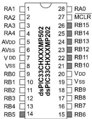
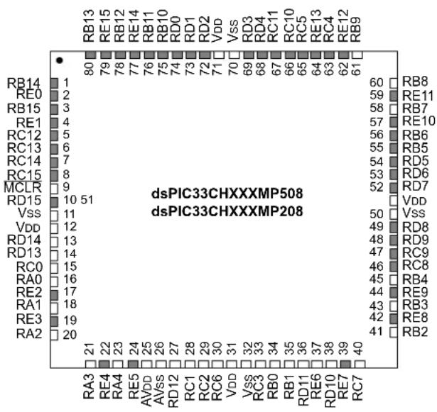
Pin Diagrams
28-Pin SSOP ^(1)
text_image
RA1 1 28 RA0 RA2 2 27 MCLR RA3 3 26 RB15 RA4 4 25 RB14 AVDD 5 24 RB13 AVss 6 23 RB12 VDD 7 22 RB11 Vss 8 21 RB10 RB0 9 20 VDD RB1 10 dsPIC33CHXXXMP502 dsPIC33CHXXXMP202 RB2 11 19 Vss RB3 12 18 RB9 RB4 13 17 RB8 RB5 14 16 RB7 15 RB6Note 1: Shaded pins are up to 5.5 Vdc tolerant (refer to Table 3-29). For the list of analog ports, refer to Table 3-28 and Table4-25.
TABLE 4: 28-PIN SSOP
| Pin # Main Core Secondary Core | ||
| 1 | AN1/RA1 S1AN15/S1RA1 | |
| 2 | AN2/RA2 S1AN16/S1RA2 | |
| 3 | AN3/IBIAS0/RA3 S1AN0/S1CMP1A/S1PGA1P1/S1RA3 | |
| 4 | AN4/IBIAS1/RA4 S1MCLR3/S1AN1/S1CMP2A/S1PGA2P1/S1PGA3P2/S1RA4 | |
| 5 | AVDD | AVDD |
| 6 | AVss | AVss |
| 7 | VDD | VDD |
| 8 | Vss | Vss |
| 9 | OSCI/CLKI/AN5/RP32/RB0 | S1AN5/S1RP32/S1RB0 |
| 10 | OSCO/CLKO/AN6/IBIAS2/RP33/RB1 ^(2) | S1AN4/S1RP33/S1RB1 ^(2) |
| 11 | DACOUT1/AN7/CMP1D/RP34/INT0/RB2 | S1MCLR2/S1AN3/S1ANC0/S1ANC1/S1CMP1D/S1CMP2D/S1CMP3D/S1RP34/S1INT0/S1RB2 |
| 12 | PGD2/AN8/RP35/RB3 | S1PGD2/S1AN18/S1CMP3A/S1PGA3P1/S1RP35/S1RB3 |
| 13 | PGC2/RP36/RB4 | S1PGC2/S1AN9/S1RP36/S1PWM5L/S1RB4 |
| 14 | PGD3/RP37/SDA2/RB5 | S1PGD3/S1RP37/S1RB5 |
| 15 | PGC3/RP38/SCL2/RB6 | S1PGC3/S1RP38/S1RB6 |
| 16 | TDO/AN9/RP39/RB7 | S1MCLR1/S1AN6/S1RP39/S1PWM5H/S1RB7 |
| 17 | PGD1/AN10/RP40/SCL1/RB8 | S1PGD1/S1AN7/S1RP40/S1SCL1/S1RB8 |
| 18 | PGC1/AN11/RP41/SDA1/RB9 | S1PGC1/S1RP41/S1SDA1/S1RB9 |
| 19 | Vss | Vss |
| 20 | VDD | VDD |
| 21 | TMS/RP42/PWM3H/RB10 ^(1) | S1RP42/S1PWM3H/S1RB10 ^(1) |
| 22 | TCK/RP43/PWM3L/RB11 | S1RP43/S1PWM8H/S1PWM3L/S1RB11 |
| 23 | TDI/RP44/PWM2H/RB12 | S1RP44/S1PWM2H/S1RB12 |
| 24 | RP45/PWM2L/RB13 | S1RP45/S1PWM7H/S1PWM2L/S1RB13 |
| 25 | RP46/PWM1H/RB14 | S1RP46/S1PWM1H/S1RB14 |
| 26 | RP47/PWM1L/RB15 | S1RP47/S1PWM6H/S1PWM1L/S1RB15 |
| 27 | MCLR | — |
| 28 | AN0/CMP1A/RA0 | S1RA0 |
Legend: RPn represents remappable peripheral functions.
Note 1: A pull-up resistor is connected to this pin when device is erased (JTAG enabled) and during programming.
2: This pin is toggled during programming.
Pin Diagrams (Continued)
28-Pin UQFN ^(1,2)

other
dsPIC33CHXXXMP502 dsPIC33CHXXXMP202 | Pin | Value | |---|---| | RB14 | 1 | | RB15 | 2 | | MCLR | 3 | | RA0 | 4 | | RA1 | 5 | | RA2 | 6 | | RA3 | 7 | | RB13 | 28 | | RB12 | 27 | | RB11 | 26 | | RB10 | 25 | | VDD | 24 | | VSS | 23 | | RB9 | 22 | | RB8 | 21 | | RB7 | 20 | | RB6 | 19 | | RB5 | 18 | | RB4 | 17 | | RB3 | 16 | | RB2 | 15 | | RA4 | 8 | | AVDD | 9 | | AVSS | 10 | | VDD | 11 | | VSS | 12 | | RB0 | 13 | | RB1 | 14 |Note 1: Shaded pins are up to 5.5 VDC tolerant (refer to Table 3-29). For the list of analog ports, refer to Table 3-28 and Table 4-25.
2: The large center pad on the bottom of the package may be left floating or connected to Vss. The four-corner anchor pads are internally connected to the large bottom pad, and therefore, must be connected to the same net as the large center pad.
TABLE 5: 28-PIN UQFN
| Pin # | Main Core Secondary Core | |
| 1 | RP46/PWM1H/RB14 S1RP46/S1PWM1H/S1RB14 | |
| 2 | RP47/PWM1L/RB15 | S1RP47/S1PWM6H/S1PWM1L/S1RB15 |
| 3 | MCLR — | |
| 4 | AN0/CMP1A/RA0 S1RA0 | |
| 5 | AN1/RA1 S1AN15/S1RA1 | |
| 6 | AN2/RA2 S1AN16/S1RA2 | |
| 7 | AN3/IBIAS0/RA3 S1AN0/S1CMP1A/S1PGA1P1/S1RA3 | |
| 8 | AN4/IBIAS1/RA4 S1MCLR3/S1AN1/S1CMP2A/S1PGA2P1/S1PGA3P2/S1RA4 | |
| 9 | AVDD AVDD | |
| 10 | AVss | AVss |
| 11 | VDD | VDD |
| 12 | Vss | Vss |
| 13 | OSCI/CLKI/AN5/RP32/RB0 | S1AN5/S1RP32/S1RB0 |
| 14 | OSCO/CLKO/AN6/IBIAS2/RP33/RB1(2) | S1AN4/S1RP33/S1RB1(2) |
| 15 | DACOUT1/AN7/CMP1D/RP34/INT0/RB2 | S1MCLR2/S1AN3/S1ANC0/S1ANC1/S1CMP1D/S1CMP2D/S1CMP3D/S1RP34/S1INT0/S1RB2 |
| 16 | PGD2/AN8/RP35/RB3 | S1PGD2/S1AN18/S1CMP3A/S1PGA3P1/S1RP35/S1RB3 |
| 17 | PGC2/RP36/RB4 | S1PGC2/S1AN9/S1RP36/S1PWM5L/S1RB4 |
| 18 | PGD3/RP37/SDA2/RB5 | S1PGD3/S1RP37/S1RB5 |
| 19 | PGC3/RP38/SCL2/RB6 | S1PGC3/S1RP38/S1RB6 |
| 20 | TDO/AN9/RP39/RB7 | S1MCLR1/S1AN6/S1RP39/S1PWM5H/S1RB7 |
| 21 | PGD1/AN10/RP40/SCL1/RB8 | S1PGD1/S1AN7/S1RP40/S1SCL1/S1RB8 |
| 22 | PGC1/AN11/RP41/SDA1/RB9 | S1PGC1/S1RP41/S1SDA1/S1RB9 |
| 23 | Vss | Vss |
| 24 | VDD | VDD |
| 25 | TMS/RP42/PWM3H/RB10(1) | S1RP42/S1PWM3H/S1RB10(1) |
| 26 | TCK/RP43/PWM3L/RB11 | S1RP43/S1PWM8H/S1PWM3L/S1RB11 |
| 27 | TDI/RP44/PWM2H/RB12 | S1RP44/S1PWM2H/S1RB12 |
| 28 | RP45/PWM2L/RB13 | S1RP45/S1PWM7H/S1PWM2L/S1RB13 |
Legend: RPn represents remappable peripheral functions.
Note 1: A pull-up resistor is connected to this pin when device is erased (JTAG enabled) and during programming.
2: This pin is toggled during programming.
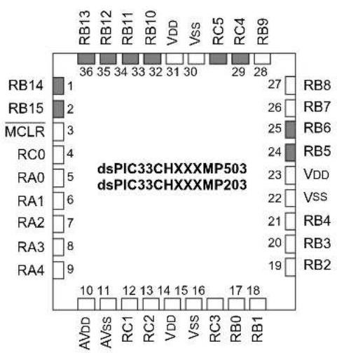
Pin Diagrams (Continued)
36-Pin UQFN ^(1,2)
other
dsPIC33CHXXXMP503 | Category | Pin Number | |---|---| | RB13 | 36 | | RB12 | 35 | | RB11 | 34 | | RB10 | 33 | | VDD | 32 | | VSS | 31 | | RC5 | 30 | | RC4 | 29 | | RB9 | 28 | | RB14 | 1 | | RB15 | 2 | | MCLR | 3 | | RC0 | 4 | | RA0 | 5 | | RA1 | 6 | | RA2 | 7 | | RA3 | 8 | | RA4 | 9 | AVDD | 10 | | AVss | 11 | | RC1 | 12 | | RC2 | 13 | | VDD | 14 | | VSS | 15 | | RC3 | 16 | | RB0 | 17 | | RB1 | 18 | RVB8: RS8 RVB7: RS7 RVB6: RS6 RVB5: RS5 VDD: RS4 VSS: RS3 RVB4: RS2 RVB3: RS1 RVB2: RS0Note 1: Shaded pins are up to 5.5 Vdc tolerant (refer to Table 3-29). For the list of analog ports, refer to Table 3-28 and Table 4-25.
2: The large center pad on the bottom of the package may be left floating or connected to Vss. The four-corner anchor pads are internally connected to the large bottom pad, and therefore, must be connected to the same net as the large center pad.
TABLE 6: 36-PIN UQFN
| Pin # | Main Core Secondary Core | |
| 1 | RP46/PWM1H/RB14 S1RP46/S1PWM1H/S1RB14 | |
| 2 | RP47/PWM1L/RB15 | S1RP47/S1PWM6H/S1PWM1L/S1RB15 |
| 3 | MCLR — | |
| 4 | AN12/IBIAS3/RP48/RC0 | S1AN10/S1RP48/S1RC0 |
| 5 | AN0/CMP1A/RA0 S1RA0 | |
| 6 | AN1/RA1 S1AN15/S1RA1 | |
| 7 | AN2/RA2 S1AN16/S1RA2 | |
| 8 | AN3/IBIAS0/RA3 S1AN0/S1CMP1A/S1PGA1P1/S1RA3 | |
| 9 | AN4/IBIAS1/RA4 S1MCLR3/S1AN1/S1CMP2A/S1PGA2P1/S1PGA3 | P2/S1RA4 |
| 10 | AVDD | AVDD |
| 11 | AVss | AVss |
| 12 | AN13/ISRC0/RP49/RC1 | S1ANA1/S1RP49/S1RC1 |
| 13 | AN14/ISRC1/RP50/RC2 | S1ANA0/S1RP50/S1RC2 |
| 14 | VDD | VDD |
| 15 | Vss | Vss |
| 16 | CMP1B/RP51/RC3 | S1AN8/S1CMP3B/S1RP51/S1RC3 |
| 17 | OSCI/CLKI/AN5/RP32/RB0 | S1AN5/S1RP32/S1RB0 |
| 18 | OSCO/CLKO/AN6/IBIAS2/RP33/RB1(2) | S1AN4/S1RP33/S1RB1(2) |
| 19 | DACOUT1/AN7/CMP1D/RP34/INT0/RB2 | S1MCLR2/S1AN3/S1ANC0/S1ANC1/S1CMP1D/S1CMP2D/S1CMP3D/S1RP34/S1INT0/S1RB2 |
| 20 | PGD2/AN8/RP35/RB3 | S1PGD2/S1AN18/S1CMP3A/S1PGA3P1/S1RP35/S1RB3 |
| 21 | PGC2/RP36/RB4 | S1PGC2/S1AN9/S1RP36/S1PWM5L/S1RB4 |
| 22 | Vss | Vss |
| 23 | VDD | VDD |
| 24 | PGD3/RP37/SDA2/RB5 | S1PGD3/S1RP37/S1RB5 |
| 25 | PGC3/RP38/SCL2/RB6 | S1PGC3/S1RP38/S1RB6 |
| 26 | TDO/AN9/RP39/RB7 | S1MCLR1/S1AN6/S1RP39/S1PWM5H/S1RB7 |
| 27 | PGD1/AN10/RP40/SCL1/RB8 | S1PGD1/S1AN7/S1RP40/S1SCL1/S1RB8 |
| 28 | PGC1/AN11/RP41/SDA1/RB9 | S1PGC1/S1RP41/S1SDA1/S1RB9 |
| 29 | RP52/RC4 | S1RP52/S1PWM2H/S1RC4 |
| 30 | RP53/RC5 | S1RP53/S1PWM2L/S1RC5 |
| 31 | Vss | Vss |
| 32 | VDD | VDD |
| 33 | TMS/RP42/PWM3H/RB10(1) | S1RP42/S1PWM3H/S1RB10(1) |
| 34 | TCK/RP43/PWM3L/RB11 | S1RP43/S1PWM8H/S1PWM3L/S1RB11 |
| 35 | TDI/RP44/PWM2H/RB12 | S1RP44/S1PWM7L/S1RB12 |
| 36 | RP45/PWM2L/RB13 S1RP45/S1PWM7H/S1RB13 |
Legend: RPn represents remappable peripheral functions.
Note 1: A pull-up resistor is connected to this pin when device is erased (JTAG enabled) and during programming.
2: This pin is toggled during programming.
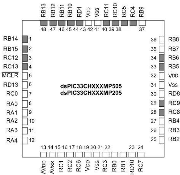
Pin Diagrams (Continued)
48-Pin TQFP/UQFN ^(1,2)
heatmap
dsPIC33CHXXXMP505 dsPIC33CHXXXMP205 | Category | Value | |---|---| | RB13 | 48 | | RB12 | 47 | | RB11 | 46 | | RB10 | 45 | | RD1 | 44 | | VDD | 43 | | VSS | 42 | | RC11 | 41 | | RC10 | 40 | | RC5 | 39 | | RC4 | 38 | | RB9 | 37 | | RB14 | 1 | | RB15 | 2 | | RC12 | 3 | | RC13 | 4 | | MCLR | 5 | | RD13 | 6 | | RC0 | 7 | | RA0 | 8 | | RA1 | 9 | | RA2 | 10 | | RA3 | 11 | | RA4 | 12 | | AVDD | 13 | | AVss | 14 | | RC1 | 15 | | RC2 | 16 | | RC6 | 17 | | VDD | 18 | | VSS | 19 | | RC3 | 20 | | RB0 | 21 | | RB1 | 22 | | RD10 | 23 | | RC7 | 24 | | RB8 | 36 | | RB7 | 35 | | RB6 | 34 | | RB5 | 33 | | VDD | 32 | | Vss | 31 | | RD8 | 30 | | RC9 | 29 | | RC8 | 28 | | RB4 | 27 | | RB3 | 26 | | RB2 | 25 |Note 1: Shaded pins are up to 5.5 VDC tolerant (refer to Table 3-29). For the list of analog ports, refer to Table 3-28 and Table4-25.
2: The large center pad on the bottom of the package may be left floating or connected to Vss. The four-corner anchor pads are internally connected to the large bottom pad, and therefore, must be connected to the same net as the large center pad.
TABLE 7: 48-PIN TQFP/UQFN
| Pin # | Main Core Secondary Core | |
| 1 | RP46/PWM1H/RB14 S1RP46/S1PWM6L/S1RB14 | |
| 2 | RP47/PWM1L/RB15 S1RP47/S1PWM6H/S1RB15 | |
| 3 | RP60/RC12 | S1RP60/S1PWM3H/S1RC12 |
| 4 | RP61/RC13 | S1RP61/S1PWM3L/S1RC13 |
| 5 | MCLR — | |
| 6 | RD13 S1ANN0/S1PGA1N2/S1RD13 | |
| 7 | AN12/IBIAS3/RP48/RC0 | S1AN10/S1RP48/S1RC0 |
| 8 | AN0/CMP1A/RA0 | S1RA0 |
| 9 | AN1/RA1 | S1AN15/S1RA1 |
| 10 | AN2/RA2 | S1AN16/S1RA2 |
| 11 | AN3/IBIAS0/RA3 | S1AN0/S1CMP1A/S1PGA1P1/S1RA3 |
| 12 | AN4/IBIAS1/RA4 | STMCLR3/S1AN1/S1CMP2A/S1PGA2P1/S1PGA3P2/S1RA4 |
| 13 | AVDD | AVDD |
| 14 | AVss | AVss |
| 15 | AN13/ISRC0/RP49/RC1 | S1ANA1/S1RP49/S1RC1 |
| 16 | AN14/ISRC1/RP50/RC2 | S1ANA0/S1RP50/S1RC2 |
| 17 | RP54/RC6 | S1AN11/S1CMP1B/S1RP54/S1RC6 |
| 18 | VDD | VDD |
| 19 | Vss | Vss |
| 20 | CMP1B/RP51/RC3 | S1AN8/S1CMP3B/S1RP51/S1RC3 |
| 21 | OSCI/CLKI/AN5/RP32/RB0 | S1AN5/S1RP32/S1RB0 |
| 22 | OSCO/CLKO/AN6/IBIAS2/RP33/RB1(2) | S1AN4/S1RP33/S1RB1(2) |
| 23 | ISRC3/RD10 | S1AN13/S1CMP2B/S1RD10 |
| 24 | AN15/ISRC2/RP55/RC7 | S1AN12/S1RP55/S1RC7 |
| 25 | DACOUT1/AN7/CMP1D/RP34/INT0/RB2 | S1MCLR2/S1AN3/S1ANC0/S1ANC1/S1CMP1D/S1CMP2D/S1CMP3D/S1RP34/S1INT0/S1RB2 |
| 26 | PGD2/AN8/RP35/RB3 | S1PGD2/S1AN18/S1CMP3A/S1PGA3P1/S1RP35/S1RB3 |
| 27 | PGC2/RP36/RB4 | S1PGC2/S1AN9/S1RP36/S1PWM5L/S1RB4 |
| 28 | RP56/ASDA1/SCK2/RC8 | S1RP56/S1ASDA1/S1SCK1/S1RC8 |
| 29 | RP57/ASCL1/SDI2/RC9 | S1RP57/S1ASCL1/S1SDI1/S1RC9 |
| 30 | SDO2/PCI19/RD8 | S1SDO1/S1PCI19/S1RD8 |
| 31 | Vss | Vss |
| 32 | VDD | VDD |
| 33 | PGD3/RP37/SDA2/RB5 | S1PGD3/S1RP37/S1RB5 |
| 34 | PGC3/RP38/SCL2/RB6 | S1PGC3/S1RP38/S1RB6 |
| 35 | TDO/AN9/RP39/RB7 | STMCLR7/S1AN6/S1RP39/S1PWM5H/S1RB7 |
| 36 | PGD1/AN10/RP40/SCL1/RB8 | S1PGD1/S1AN7/S1RP40/S1SCL1/S1RB8 |
| 37 | PGC1/AN11/RP41/SDA1/RB9 | S1PGC1/S1RP41/S1SDA1/S1RB9 |
| 38 | RP52/RC4 | S1RP52/S1PWM2H/S1RC4 |
| 39 | RP53/RC5 | S1RP53/S1PWM2L/S1RC5 |
| 40 | RP58/RC10 S1RP58/S1PWM1H/S1RC10 | |
| 41 | RP59/RC11 | S1RP59/S1PWM1L/S1RC11 |
| 42 | Vss | Vss |
| 43 | VDD | VDD |
| 44 | RP65/RD1 | S1RP65/S1PWM4H/S1RD1 |
| 45 | TMS/RP42/PWM3H/RB10(1) | S1RP42/S1PWM8L/S1RB10(1) |
| 46 | TCK/RP43/PWM3L/RB11 | S1RP43/S1PWM8H/S1RB11 |
| 47 | TDI/RP44/PWM2H/RB12 | S1RP44/S1PWM7L/S1RB12 |
| 48 | RP45/PWM2L/RB13 S1RP45/S1PWM7H/S1RB13 |
Legend: RPn represents remappable peripheral functions.
Note 1: A pull-up resistor is connected to this pin when device is erased (JTAG enabled) and during programming.
2: This pin is toggled during programming.
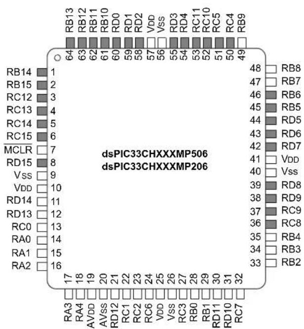
Pin Diagrams (Continued)
64-Pin TQFP/QFN ^(1,2)
other
| Chip | Pin Number | |-------|----------| | RB13 | 64 | | RB12 | 63 | | RB11 | 62 | | RB10 | 61 | | RD0 | 60 | | RD1 | 59 | | RD2 | 58 | | VDD | 57 | | VSS | 56 | | RD3 | 55 | | RD4 | 54 | | RC11 | 53 | | RC10 | 52 | | RC5 | 51 | | RC4 | 50 | | RB9 | 49 | | RB8 | 48 | | RB7 | 47 | | RB6 | 46 | | RB5 | 45 | | RD5 | 44 | | RD6 | 43 | | RD7 | 42 | | VDD | 41 | | Vss | 40 | | RD8 | 39 | | RD9 | 38 | | RC9 | 37 | | RC8 | 36 | | RB4 | 35 | | RB3 | 34 | | RB2 | 33 | | RS1 | 32 | | RS2 | 31 | | RS3 | 30 | | RS4 | 29 | | RS5 | 28 | | RS6 | 27 | | RS7 | 26 | | RS8 | 25 | | RS9 | 24 | | RS10 | 23 | | RS11 | 22 | | RS12 | 21 | | RS13 | 20 | | RS14 | 19 | | RS15 | 18 | | MCLR | 17 | | RD15 | 16 | | VSS | 15 | | VDD | 14 | | RD14 | 13 | | RD13 | 12 | | RC0 | 11 | | RA0 | 10 | | RA1 | 9 | | RA2 | 8 | | RA3 | 7 | | RA4 | 6 | | AVDD | 5 | | AVSS | 4 | | RD12 | 3 | | RC1 | 2 | | RC2 | 1 | | RC6 | 0 | | VDD | -1 | | RS3 | -2 | | RB0 | -3 | | RB1 | -4 | | RD11 | -5 | | RD10 | -6 | | RC7 | -7 |Note 1: Shaded pins are up to 5.5 V DC tolerant (refer to Table 3-29). For the list of analog ports, refer to Table 3-28 and Table 4-25.
2: The large center pad on the bottom of the package may be left floating or connected to Vss. The four-corner anchor pads are internally connected to the large bottom pad, and therefore, must be connected to the same net as the large center pad.
TABLE 8: 64-PIN TQFP/QFN
| Pin # | Main Core Secondary Core | |
| 1 | RP46/PWM1H/RB14 S1RP46/S1RB14 | |
| 2 | RP47/PWM1L/RB15 S1RP47/S1RB15 | |
| 3 | RP60/PWM4H/RC12 | S1RP60/S1RC12 |
| 4 | RP61/PWM4L/RC13 S1RP61/S1RC13 | |
| 5 | RP62/RC14 S1RP62/S1PWM7H/S1RC14 | |
| 6 | RP63/RC15 S1RP63/S1PWM7L/S1RC15 | |
| 7 | MCLR — | |
| 8 | PCI22/RD15 | S1PCI22/S1RD15 |
| 9 | Vss | Vss |
| 10 | VDD | VDD |
| 11 | PCI21/RD14 | S1ANN1/S1PGA2N2/S1PCI21/S1RD14 |
| 12 | RD13 | S1ANN0/S1PGA1N2/S1RD13 |
| 13 | AN12/IBIAS3/RP48/RC0 | S1AN10/S1RP48/S1RC0 |
| 14 | AN0/CMP1A/RA0 | S1RA0 |
| 15 | AN1/RA1 | S1AN15/S1RA1 |
| 16 | AN2/RA2 | S1AN16/S1RA2 |
| 17 | AN3/IBIAS0/RA3 | S1AN0/S1CMP1A/S1PGA1P1/S1RA3 |
| 18 | AN4/IBIAS1/RA4 | S1MCLR3/S1AN1/S1CMP2A/S1PGA2P1/S1PGA3P2/S1RA4 |
| 19 | AVDD | AVDD |
| 20 | AVss | AVss |
| 21 | RD12 | S1AN14/S1PGA2P2/S1RD12 |
| 22 | AN13/ISRC0/RP49/RC1 | S1ANA1/S1RP49/S1RC1 |
| 23 | AN14/ISRC1/RP50/RC2 | S1ANA0/S1RP50/S1RC2 |
| 24 | RP54/RC6 | S1AN11/S1CMP1B/S1RP54/S1RC6 |
| 25 | VDD | VDD |
| 26 | Vss | Vss |
| 27 | CMP1B/RP51/RC3 | S1AN8/S1CMP3B/S1RP51/S1RC3 |
| 28 | OSCI/CLKI/AN5/RP32/RB0 | S1AN5/S1RP32/S1RB0 |
| 29 | OSCO/CLKO/AN6/IBIAS2/RP33/RB1(2) | S1AN4/S1RP33/S1RB1(2) |
| 30 | RD11 | S1AN17/S1PGA1P2/S1RD11 |
| 31 | ISRC3/RD10 | S1AN13/S1CMP2B/S1RD10 |
| 32 | AN15/ISRC2/RP55/RC7 | S1AN12/S1RP55/S1RC7 |
| 33 | DACOUT1/AN7/CMP1D/RP34/INT0/RB2 | S1MCLR2/S1AN3/S1ANC0/S1ANC1/S1CMP1D/S1CMP2D/S1CMP3D/S1RP34/S1INT0/S1RB2 |
| 34 | PGD2/AN8/RP35/RB3 | S1PGD2/S1AN18/S1CMP3A/S1PGA3P1/S1RP35/S1RB3 |
| 35 | PGC2/RP36/RB4 | S1PGC2/S1AN9/S1RP36/S1PWM5L/S1RB4 |
| 36 | RP56/ASDA1/SCK2/RC8 | S1RP56/S1ASDA1/S1SCK1/S1RC8 |
| 37 | RP57/ASCL1/SDI2/RC9 | S1RP57/S1ASCL1/S1SDI1/S1RC9 |
| 38 | PCI20/RD9 | S1PCI20/S1RD9 |
| 39 | SDO2/PCI19/RD8 | S1SDO1/S1PCI19/S1RD8 |
| 40 | Vss | Vss |
| 41 | VDD | VDD |
| 42 | RP71/RD7 | S1RP71/S1PWM8H/S1RD7 |
| 43 | RP70/RD6 | S1RP70/S1PWM6H/S1RD6 |
| 44 | RP69/RD5 | S1RP69/S1PWM6L/S1RD5 |
| 45 | PGD3/RP37/SDA2/RB5 | S1PGD3/S1RP37/S1RB5 |
| 46 | PGC3/RP38/SCL2/RB6 | S1PGC3/S1RP38/S1RB6 |
| 47 | TDO/AN9/RP39/RB7 | S1MCLR1/S1AN6/S1RP39/S1PWM5H/S1RB7 |
| 48 | PGD1/AN10/RP40/SCL1/RB8 | S1PGD1/S1AN7/S1RP40/S1SCL1/S1RB8 |
| 49 | PGC1/AN11/RP41/SDA1/RB9 | S1PGC1/S1RP41/S1SDA1/S1RB9 |
| 50 | RP52/RC4 | S1RP52/S1PWM2H/S1RC4 |
Legend: RPn represent remappable peripheral functions.
Note 1: A pull-up resistor is connected to this pin when device is erased (JTAG enabled) and during programming.
2: This pin is toggled during programming.
TABLE 8: 64-PIN TQFP/QFN (CONTINUED)
| Pin # | Main Core | Secondary Core |
| 51 | RP53/RC5 S1RP53/S1PWM2L/S1RC5 | |
| 52 | RP58/RC10 S1RP58/S1PWM1H/S1RC10 | |
| 53 | RP59/RC11 S1RP59/S1PWM1L/S1RC11 | |
| 54 | RP68/RD4 S1RP68/S1PWM3H/S1RD4 | |
| 55 | RP67/RD3 S1RP67/S1PWM3L/S1RD3 | |
| 56 | Vss Vss | |
| 57 | VDD VDD | |
| 58 | RP66/RD2 S1RP66/S1PWM8L/S1RD2 | |
| 59 | RP65/RD1 S1RP65/S1PWM4H/S1RD1 | |
| 60 | RP64/RD0 S1RP64/S1PWM4L/S1RD0 | |
| 61 | TMS/RP42/PWM3H/RB10(1) | S1RP42/S1RB10(1) |
| 62 | TCK/RP43/PWM3L/RB11 | S1RP43/S1RB11 |
| 63 | TDI/RP44/PWM2H/RB12 | S1RP44/S1RB12 |
| 64 | RP45/PWM2L/RB13 S1RP45/S1RB13 |
Legend: RPN represent remappable peripheral functions.
Note 1: A pull-up resistor is connected to this pin when device is erased (JTAG enabled) and during programming.
2: This pin is toggled during programming.
Pin Diagrams (Continued)
80-Pin TQFP ^(1)
geo
dsPIC33CHXXXMP508 | Chip | Pin Number | Pin Label | | :--- | :--- | :--- | | RB13 | 80 | RB13 | | RB14 | 79 | RB14 | | RB15 | 78 | RB15 | | RB16 | 77 | RB16 | | RB17 | 76 | RB17 | | RB18 | 75 | RB18 | | RB19 | 74 | RB19 | | RB20 | 73 | RB20 | | RB21 | 72 | RB21 | | RB22 | 71 | RB22 | | RB23 | 70 | RB23 | | RB24 | 69 | RB24 | | RB25 | 68 | RB25 | | RB26 | 67 | RB26 | | RB27 | 66 | RB27 | | RB28 | 65 | RB28 | | RB29 | 64 | RB29 | | RB30 | 63 | RB30 | | RB31 | 62 | RB31 | | RB32 | 61 | RB32 | | VDD | 50 | VDD | | VSS | 51 | VSS | | VDD̅ | 50 | VSS̅ | | VSS̅̅ | 49 | VSS̅̅ | | VSS̅ | 48 | VSS̅ | | VSS̅̅̅ | 47 | VSS̅̅̅ | | VSS̅̅̅̅ | 46 | VSS̅ | | VSS̅̅̅̅̅̅ | 45 | VSS̅ | | VSS̅̅̅̅̅̅̅̅̅̅̅̅̅̅̅̅̅̅̅̅̅̅̅̅̅̅̅̅̅̅̅̅̅̅̅̅̅̅̅̅̅̅̅̅̅̅̅̅̅̅̆̇ | 44 | VSS̅ | | VSS̅̅̅̅̅̅̅̅̅̅̅̅̅̅̅̅̅̅̅̅̅̅̅̅̅̅̅̅̅̅̅̅̅̅̅̅̅̅̅̅̅̅̅̅̅ \n RA0 | 43 | RD0 | | RA0 | 42 | RD0 | | RA1 | 41 | RD1 | | RA2 | 40 | RD2 | RA3 | 21 | RA3 | | RA4 | 22 | RA4 | | RA5 | 23 | RA5 | | RA6 | 24 | RA6 | | RA7 | 25 | RA7 | | RA8 | 26 | RA8 | | RA9 | 27 | RA9 | | RA10 | 28 | RA10 | | RA11 | 29 | RA11 | | RA12 | 30 | RA12 | | RA13 | 31 | RA13 | | RA14 | 32 | RA14 | | RA15 | 33 | RA15 | | RA16 | 34 | RA16 | | RA17 | 35 | RA17 | | RA18 | 36 | RA18 | | RA19 | 37 | RA19 | | RA20 | 38 | RA20 | | RA21 | 39 | RA21 | | RA22 | 40 | RA22 | RB8: RS8 RB8: RS9 RB8: RS10 RB8: RS11 RB8: RS12 RB8: RS13 RB8: RS14 RB8: RS15 RB8: RS16 RB8: RS17 RB8: RS18 RB8: RS19 RB8: RS20 RB8: RS21 RB8: RS22 RB8: RS23 RB8: RS24 RB8: RS25 RB8: RS26 RB8: RS27 RB8: RS28 RB8: RS29 RB8: RS30 RB8: RS31 RB8: RS32 RB8: RS33 RB8: RS34 RB8: RS35 RB8: RS36 RB8: RS37 RB8: RS38 RB8: RS39 RB8: RS40 RB8: RS41 RB8: RS42 RB8: RS43 RB8: RS44 RB8: RS45 RB8: RS46 RB8: RS47 RB8: RS48 RB8: RS49 RB8: RS50 RB8: RS51 RB8: RS52 RB8: RS53 RB8: RS54 RB8: RS55 RB8: RS56 RB8: RS57 RB8: RS58 RB8: RS59 RB8: RS60 RB8: RS61 VDD: VDD, VSS, VSS'| RVDS: RDDS, RDDS, RDDS, RDDS, RDDS, RDDS, RDDS, RDDS, RDDS, RDDS, RDDS, RDDS, RDDS, RDDS, RDDS, RDDS, RDDS, RDDS, RDDS, RDDS, RDDS, RDDS, RDDS, RDDS, RDDS, RDDS, RDDS, RDDS, RDDS, RDDS, RDDS, RDDS, RDDS, RDDS, RC7Note 1: Shaded pins are up to 5.5 VDC tolerant (refer to Table 3-29). For the list of analog ports, refer to Table 3-28 and Table 4-25.
TABLE 9: 80-PIN TQFP
| Pin # | Main Core Secondary Core | |
| 1 | RP46/PWM1H/RB14 S1RP46/S1RB14 | |
| 2 RE0 | S1RE0 | |
| 3 | RP47/PWM1L/RB15 S1RP47/S1RB15 | |
| 4 | RE1 S1RE1 | |
| 5 | RP60/PWM4H/RC12 | S1RP60/S1RC12 |
| 6 | RP61/PWM4L/RC13 S1RP61/S1RC13 | |
| 7 | RP62/RC14 S1RP62/S1PWM7H/S1RC14 | |
| 8 | RP63/RC15 S1RP63/S1PWM7L/S1RC15 | |
| 9 | MCLR — | |
| 10 | PCI22/RD15 | S1PCI22/S1RD15 |
| 11 | Vss | Vss |
| 12 | VDD | VDD |
| 13 | PCI21/RD14 | S1ANN1/S1PGA2N2/S1PCI21/S1RD14 |
| 14 | RD13 | S1ANN0/S1PGA1N2/S1RD13 |
| 15 | AN12/IBIAS3/RP48/RC0 | S1AN10/S1RP48/S1RC0 |
| 16 | AN0/CMP1A/RA0 | S1RA0 |
| 17 | RE2 S1RE2 | |
| 18 | AN1/RA1 | S1AN15/S1RA1 |
| 19 | RE3 S1RE3 | |
| 20 | AN2/RA2 | S1AN16/S1RA2 |
| 21 | AN3/IBIAS0/RA3 | S1AN0/S1CMP1A/S1PGA1P1/S1RA3 |
| 22 | RE4 S1RE4 | |
| 23 | AN4/IBIAS1/RA4 | S1MCLR3/S1AN1/S1CMP2A/S1PGA2P1/S1PGA3P2/S1RA4 |
| 24 | RE5 S1RE5 | |
| 25 | AVDD | AVDD |
| 26 | AVss | AVss |
| 27 | RD12 | S1AN14/S1PGA2P2/S1RD12 |
| 28 | AN13/ISRC0/RP49/RC1 | S1ANA1/S1RP49/S1RC1 |
| 29 | AN14/ISRC1/RP50/RC2 | S1ANA0/S1RP50/S1RC2 |
| 30 | RP54/RC6 | S1AN11/S1CMP1B/S1RP54/S1RC6 |
| 31 | VDD | VDD |
| 32 | Vss | Vss |
| 33 | CMP1B/RP51/RC3 | S1AN8/S1CMP3B/S1RP51/S1RC3 |
| 34 | OSCI/CLKI/AN5/RP32/RB0 | S1AN5/S1RP32/S1RB0 |
| 35 | OSCO/CLKO/AN6/IBIAS2/RP33/RB1(2) | S1AN4/S1RP33/S1RB1(2) |
| 36 | RD11 | S1AN17/S1PGA1P2/S1RD11 |
| 37 | RE6 S1PGA3N2/S1RE6 | |
| 38 | ISRC3/RD10 | S1AN13/S1CMP2B/S1RD10 |
| 39 | RE7 S1RE7 | |
| 40 | AN15/ISRC2/RP55/RC7 | S1AN12/S1RP55/S1RC7 |
| 41 | DACOUT1/AN7/CMP1D/RP34/INT0/RB2 | S1MCLR2/S1AN3/S1ANC0/S1ANC1/S1CMP1D/S1CMP2D/S1CMP3D/S1RP34/S1INT0/S1RB2 |
| 42 | RE8 S1RE8 | |
| 43 | PGD2/AN8/RP35/RB3 | S1PGD2/S1AN18/S1CMP3A/S1PGA3P1/S1RP35/S1RB3 |
| 44 | RE9 S1RE9 | |
| 45 | PGC2/RP36/RB4 | S1PGC2/S1AN9/S1RP36/S1PWM5L/S1RB4 |
| 46 | RP56/ASDA1/SCK2/RC8 | S1RP56/S1ASDA1/S1SCK1/S1RC8 |
| 47 | RP57/ASCL1/SDI2/RC9 | S1RP57/S1ASCL1/S1SDI1/S1RC9 |
| 48 | PCI20/RD9 | S1PCI20/S1RD9 |
Legend: RPn represent remappable peripheral functions.
Note 1: A pull-up resistor is connected to this pin when device is erased (JTAG enabled) and during programming.
2: This pin is toggled during programming.
TABLE 9: 80-PIN TQFP (CONTINUED)
| Pin # | Main Core | Secondary Core |
| 49 S | DO2/PCI19/RD8 S1SDO1/S1PCI19/S1RD8 | |
| 50 | Vss Vss | |
| 51 VDD VDD | ||
| 52 | RP71/RD7 | S1RP71/S1PWM8H/S1RD7 |
| 53 | RP70/RD6 S1RP70/S1PWM6H/S1RD6 | |
| 54 | RP69/RD5 S1RP69/S1PWM6L/S1RD5 | |
| 55 | PGD3/RP37/SDA2/RB5 | S1PGD3/S1RP37/S1RB5 |
| 56 | PGC3/RP38/SCL2/RB6 | S1PGC3/S1RP38/S1RB6 |
| 57 | RE10 S1RE10 | |
| 58 | TDO/AN9/RP39/RB7 | 1MCLR1 /S1AN6/S1RP39/S1PWM5H/S1RB7 |
| 59 | RE11 S1RE11 | |
| 60 | PGD1/AN10/RP40/SCL1/RB8 | S1PGD1/S1AN7/S1RP40/S1SCL1/S1RB8 |
| 61 | PGC1/AN11/RP41/SDA1/RB9 | S1PGC1/S1RP41/S1SDA1/S1RB9 |
| 62 | ASCL2/RE12 | S1RE12 |
| 63 | RP52/RC4 S1RP52/S1PWM2H/S1RC4 | |
| 64 | ASDA2/RE13 | S1RE13 |
| 65 | RP53/RC5 S1RP53/S1PWM2L/S1RC5 | |
| 66 | RP58/RC10 | S1RP58/S1PWM1H/S1RC10 |
| 67 | RP59/RC11 | S1RP59/S1PWM1L/S1RC11 |
| 68 | RP68/RD4 S1RP68/S1PWM3H/S1RD4 | |
| 69 | RP67/RD3 S1RP67/S1PWM3L/S1RD3 | |
| 70 | Vss Vss | |
| 71 VDD VDD | ||
| 72 | RP66/RD2 | S1RP66/S1PWM8L/S1RD2 |
| 73 | RP65/RD1 S1RP65/S1PWM4H/S1RD1 | |
| 74 | RP64/RD0 S1RP64/S1PWM4L/S1RD0 | |
| 75 | TMS/RP42/PWM3H/RB10 ^(1) | S1RP42/S1RB10^(1) |
| 76 | TCK/RP43/PWM3L/RB11 | S1RP43/S1RB11 |
| 77 | RE14 S1RE14 | |
| 78 | TDI/RP44/PWM2H/RB12 | S1RP44/S1RB12 |
| 79 | RE15 S1RE15 | |
| 80 | RP45/PWM2L/RB13 | S1RP45/S1RB13 |
Legend: RPn represent remappable peripheral functions.
Note 1: A pull-up resistor is connected to this pin when device is erased (JTAG enabled) and during programming.
2: This pin is toggled during programming.
Table of Contents
dsPIC33CH128MP508 Product Families 4
1.0 Device Overview 23
2.0 Guidelines for Getting Started with 16-Bit Digital Signal Controllers....31
3.0 Main Modules 38
4.0 Secondary Modules 265
5.0 Main Secondary Interface (MSI) 425
6.0 Oscillator with High-Frequency PLL 439
7.0 Power-Saving Features (Main and Secondary) 481
8.0 Direct Memory Access (DMA) Controller 499
9.0 High-Resolution PWM (HSPWM) with Fine Edge Placement 509
10.0 Capture/Compare/PWM/Timer Modules (SCCP) 543
11.0 High-Speed Analog Comparator with Slope Compensation DAC 561
12.0 Quadrature Encoder Interface (QEI) (Main/Secondary) 573
13.0 Universal Asynchronous Receiver Transmitter (UART) 589
14.0 Serial Peripheral Interface (SPI)....611
15.0 Inter-Integrated Circuit (I 2C) 629
16.0 Single-Edge Nibble Transmission (SENT) 639
17.0 Timer1 649
18.0 Configurable Logic Cell (CLC) 653
19.0 32-Bit Programmable Cyclic Redundancy Check (CRC) Generator 665
20.0 Current Bias Generator (CBG) 669
21.0 Special Features 675
22.0 Instruction Set Summary 721
23.0 Development Support....731
24.0 Electrical Characteristics 733
25.0 High-Temperature Electrical Characteristics 777
26.0 Packaging Information....791
Appendix A: Revision History 817
Index 820
The Microchip Website 830
Customer Change Notification Service 830
Customer Support 830
Product Identification System....832
TO OUR VALUED CUSTOMERS
It is our intention to provide our valued customers with the best documentation possible to ensure successful use of your Microchip products. To this end, we will continue to improve our publications to better suit your needs. Our publications will be refined and enhanced as new volumes and updates are introduced.
If you have any questions or comments regarding this publication, please contact the Marketing Communications Department via E-mail at docerrors@microchip.com. We welcome your feedback.
Most Current Data Sheet
To obtain the most up-to-date version of this data sheet, please register at our Worldwide Website at:
http://www.microchip.com
You can determine the version of a data sheet by examining its literature number found on the bottom outside corner of any page. The last character of the literature number is the version number, (e.g., DS30000000A is version A of document DS30000000).
Errata
An errata sheet, describing minor operational differences from the data sheet and recommended workarounds, may exist for current devices. As device/documentation issues become known to us, we will publish an errata sheet. The errata will specify the revision of silicon and revision of document to which it applies.
To determine if an errata sheet exists for a particular device, please check with one of the following:
- Microchip's Worldwide Website; http://www.microchip.com
- Your local Microchip sales office (see last page)
When contacting a sales office, please specify which device, revision of silicon and data sheet (include literature number) you are using.
Customer Notification System
Register on our website at www.microchip.com to receive the most current information on all of our products.
Referenced Sources
This device data sheet is based on the following individual chapters of the "dsPIC33/PIC24 Family Reference Manual". These documents should be considered as the general reference for the operation of a particular module or device feature.
Note 1: To access the documents listed below, browse to the documentation section of the dsPIC33CH128MP508 product page of the Microchip website (www.microchip.com) or select a family reference manual section from the following list.
In addition to parameters, features and other documentation, the resulting page provides links to the related family reference manual sections.
- “Introduction” (www.microchip.com/DS70000573)
- “Enhanced CPU” (www.microchip.com/DS70005158)
- “dsPIC33/PIC24 Program Memory” (www.microchip.com/DS70000613)
• “Data Memory” (www.microchip.com/DS70000595) - “Dual Partition Flash Program Memory” (www.microchip.com/DS70005156)
- “Flash Programming” (www.microchip.com/DS70000609)
- “Reset” (www.microchip.com/DS70000602)
- “Interrupts” (www.microchip.com/DS70000600)
- "I/O Ports with Edge Detect" (www.microchip.com/DS70005322)
- “Deadman Timer” (www.microchip.com/DS70005155)
- “CAN Flexible Data-Rate (FD) Protocol Module” (www.microchip.com/DS70005340)
- “12-Bit High-Speed, Multiple SARs A/D Converter (ADC)” (www.microchip.com/DS70005213)
- “Peripheral Trigger Generator (PTG)” (www.microchip.com/DS70000669)
- “Programmable Gain Amplifier (PGA)” (www.microchip.com/DS70005146)
- “Main Secondary Interface (MSI) Module” (www.microchip.com/DS70005278)
- “Watchdog Timer and Power-Saving Modes” (www.microchip.com/DS70000615)
- “Oscillator Module with High-Speed PLL” (www.microchip.com/DS70005255)
- “Timer1 Module” (www.microchip.com/DS70005279)
- “Direct Memory Access Controller (DMA)” (www.microchip.com/DS30009742)
- “Capture/Compare/PWM/Timer (MCCP and SCCP)” (www.microchip.com/DS30003035)
- “High-Resolution PWM with Fine Edge Placement” (www.microchip.com/DS70005320)
- “Serial Peripheral Interface (SPI) with Audio Codec Support” (www.microchip.com/DS70005136)
- “Inter-Integrated Circuit (I ^2 C)” (www.microchip.com/DS70000195)
- "Multiprotocol Universal Asynchronous Receiver Transmitter (UART) Module" (www.microchip.com/DS70005288)
- “Single-Edge Nibble Transmission (SENT) Module” (www.microchip.com/DS70005145)
- “32-Bit Programmable Cyclic Redundancy Check (CRC)” (www.microchip.com/DS30009729)
- “Configurable Logic Cell (CLC)” (www.microchip.com/DS70005298)
- “Quadrature Encoder Interface (QEI)” (www.microchip.com/DS70000601)
- “High-Speed Analog Comparator Module” (www.microchip.com/DS70005280)
- “Current Bias Generator (CBG)” (www.microchip.com/DS70005253)
- “Dual Watchdog Timer” (www.microchip.com/DS70005250)
- “Programming and Diagnostics” (www.microchip.com/DS70000608)
- “CodeGuard™ Security” (www.microchip.com/DS70005182)
Terminology Cross Reference
Table 10 provides updated terminology for depreciated naming conventions. Register and bit names remain unchanged, however, descriptions and usage guidance may have been updated.
TABLE 10: TERMINOLOGY CROSS REFERENCES
| Use Case | Deprecated Term | New Term | |
| CPU Master Initiator | |||
| DMA Master Initiator | |||
| I2C Master Host | |||
| Slave Client | |||
| SPI Master Host | |||
| Slave Client | |||
| PMP Master Host | |||
| Slave Client | |||
| UART, LIN mode Master Commander | |||
| Slave | Responder | ||
| PWM | Master Host | ||
| Slave Client | |||
NOTES:
dsPIC33CH128MP508 FAMILY
1.0 DEVICE OVERVIEW
Note 1: This data sheet summarizes the features of the dsPIC33CH128MP508 family of devices. It is not intended to be a comprehensive resource. To complement the information in this data sheet, refer to the related section of the “dsPIC33/PIC24 Family Reference Manual”, which is available from the Microchip website (www.microchip.com).
2: Some registers and associated bits described in this section may not be available on all devices. Refer to Section 3.2 "Main Memory Organization" and Section 4.2 "Secondary Memory Organization" in this data sheet for device-specific register and bit information.
This document contains device-specific information for the dsPIC33CH128MP508 Digital Signal Controller (DSC) and Microcontroller (MCU) devices.
dsPIC33CH128MP508 devices contain extensive Digital Signal Processor (DSP) functionality with a high-performance, 16-bit MCU architecture.
Figure 1-2 shows a general block diagram of the cores and peripheral modules of the Main and Secondary. Table 1-1 lists the functions of the various pins shown in the pinout diagrams.
The Main core and Secondary core can operate independently and can be programmed and debugged separately during the application development. Both processor (Main and Secondary) subsystems have their own interrupt controllers, clock generators, ICD, port logic, I/O MUXes and PPS. The device is equivalent to having two complete dsPIC ^ DSCs on a single die.
The Main core will execute the code from Program Flash Memory (PFM) and the Secondary core will operate from Program RAM Memory (PRAM).
Once the code development is complete, the Main Flash will be programmed with the Main code as well as the Secondary code. After a Power-on Reset (POR), the Secondary code from Host Flash will be loaded to the PRAM (program memory of the Secondary) and the Secondary can execute the code independently of the Main. The Main and Secondary can communicate and exchange data with each other using the Main Secondary Interface (MSI) peripheral.
Figure 1-1 shows the block diagram of the device operation during a POR and the process of transferring the Secondary code from the Main to Secondary PRAM.
The I/O ports are shared between the Main and Secondary. Table1 shows the number of peripherals and the shared peripherals that the Main and Secondary own. There are Configuration bits in the Flash memory that specify the ownership (Main or Secondary) of each device pin.
The default (erased) state of the Flash assigns all of the device pins to the Main.
The two cores (Main and Secondary) can both be connected to debug tools, which support independent and simultaneous debugging. When the Secondary core or Main core is debugged (non-Dual Debug mode), the S1MCLRx is not used. MCLR is used for programming and debugging both the Main core and the Secondary core. S1MCLRx is only used when debugging both the cores at the same time.
In normal operation, the “owner” of a device pin is responsible for full control of that pin; this includes both the digital and analog functionality.
The pin owner's GPIO registers control all aspects of the I/O pad, including the ANSELx, CNPUx, CNPDx, ODCx registers and slew rate control.
Note: Both the Main and Secondary cores can monitor a pin as an input, regardless of pin ownership. Pin ownership is valid only for the output functionality of the port.
FIGURE 1-1: SECONDARY CORE CODE TRANSFER BLOCK DIAGRAM
Before a POR:

flowchart
graph TD
    A["Code to Transfer Secondary Code to Secondary PRAM"] --> B["Main Code"]
    B --> C["Secondary Code"]
    D["Main CPU"] --> E["Main RAM"]
    F["No Code"] --> G["Secondary RAM"]
    H["Secondary CPU"] --> I["Secondary RAM"]
After a POR, it is the Main code's responsibility to load the Secondary PRAM with the Secondary code. Once the Secondary code is loaded to PRAM, the Main can enable the Secondary to start Secondary code execution:
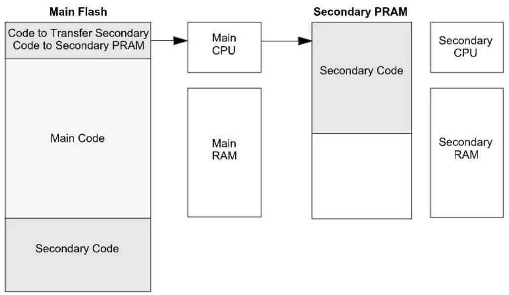
flowchart
graph LR
    A["Code to Transfer Secondary Code to Secondary PRAM"] --> B["Main CPU"]
    C["Main Code"] --> D["Main RAM"]
    E["Secondary Code"] --> F["Secondary CPU"]
    B --> G["Secondary Code"]
    D --> G
    F --> H["Secondary RAM"]
FIGURE 1-2: dsPIC33CH128MP508 FAMILY BLOCK DIAGRAM (1)

flowchart
graph TD
    A["CLC (4)"] --> B["WDT/DMT"]
    C["QEI (1)"] --> D["CRC (1)"]
    E["SENT (2)"] --> F["PTG (1)"]
    G["CAN FD (1)"] --> H["HS PWM (4)"]
    I["ADC (1)"] --> J["Timer1 (1)"]
    K["DMA (6)"] --> L["DAC/Comparator (1)"]
    M["SCCP (8)"] --> N["SPI/I²S (2)"]
    O["I²C (2)"] --> P["UART (2)"]
    Q["OSCI/CLKI"] --> R["Timing Generation"]
    R --> S["Timing Generation"]
    S --> T["Oscillator Start-up Timer"]
    T --> U["MSI (Main Secondary Interface)"]
    U --> V["Secondary CPU"]
    V --> W["PORTA(2)"]
    V --> X["PORTB(2)"]
    V --> Y["PORTC(2)"]
    V --> Z["PORTD(2)"]
    V --> AA["PORTE(2)"]
    V --> AB["Remappable Pins(3)"]
    V --> AC["I²C (1)"]
    AD["QEI (1)"] --> AE["WDT"]
    AF["PGA (3)"] --> AG["PLC (4)"]
    AH["CLC (4)"] --> AI["ADC (3)"]
    AJ["Timer1 (1)"] --> AK["DMA (2)"]
    AL["DAC/Comparator (3)"] --> AM["SCI/PWM (8)"]
    AN["SPI/I²S (1)"] --> AO["UART (1)"]
    AP["VDD, VSS AVDD, AVss"] --> AQ["MCLR"]
    AR["S1MCLRx"] --> AS["POR/BOR"]
    AT["Watchdog Timer/Deadman Timer"] --> AU["POR/BOR"]
    AV["Main CPU"] --> AW["Main CPU"]
    AX["Secondary CPU"] --> AY["Main CPU"]
    AZ["OSCI/CLKI"] --> BA["Timing Generation"]
    BB["MCLR"] --> BC["MT"]
    BD["S1MCLRx"] --> BE["POR/BOR"]
    BF["VDD, VSS AVDD, AVss"] --> BG["MCLR"]
    BH["MSI (Main Secondary Interface)"] --> BI["MSI (Main Secondary Interface)"]
    BJ["PORTA(2)"] --> BK["PORTB(2)"]
    BL["PORTB(2)"] --> BM["PORTC(2)"]
    BN["PORTD(2)"] --> BO["PORTD(2)"]
    BP["PORTE(2)"] --> BQ["Porter(2)"]
    BR["Remappable Pins(3)"] --> BS["I²C (1)"]
Note 1: The numbers in the parentheses are the number of instantiations of the module indicated.
2: Not all I/O pins or features are implemented on all device pinout configurations. See Table 1-1 for specific implementations by pin count.
3: Some peripheral I/Os are only accessible through remappable pins.
TABLE 1-1: PINOUT I/O DESCRIPTIONS
| Pin Name(1) | Pin Type | Buffer Type | PPS | Description |
| AN0-AN18 | I | Analog | No | Main core analog input channels |
| S1AN0-S1AN18 | I | Analog | No | Secondary core analog input channels |
| S1ANA0, S1ANA1 | I | Analog | No | Secondary core alternate analog inputs |
| S1ANC0, S1ANC1 | I | Analog | No | Secondary core dedicated analog input channels |
| ADCTRG I ST Yes ADC Trigger Input 31 | ||||
| CAN1RX | I | ST | Yes | CAN1 receive input |
| CAN1 | O | — | Yes | CAN1 transmit output |
| CLKI | I | ST/CMOS | No | External Clock (EC) source input. Always associated with OSCI pin function. |
| CLKO | O | — | No | Oscillator crystal output. Connects to crystal or resonator in Crystal Oscillator mode. Optionally functions as CLKO in RC and EC modes. Always associated with OSCO pin function. |
| OSCI | I | ST/CMOS | No | Oscillator crystal input. ST buffer when configured in RC mode; CMOS otherwise. |
| OSCO | I/O | — | No | Oscillator crystal output. Connects to crystal or resonator in Crystal Oscillator mode. Optionally functions as CLKO in RC and EC modes. |
| REFOI/S1REFOI I ST Yes Reference clock input | ||||
| REFCLKO/S1REFCLKO(3) | O — | Yes | Reference clock output | |
| INT0/S1INT0(3) | I | ST | No | External Interrupt 0 |
| INT1/S1INT1(3) | I | ST | Yes | External Interrupt 1 |
| INT2/S1INT2(3) | I | ST | Yes | External Interrupt 2 |
| INT3/S1INT3(3) | I | ST | Yes | External Interrupt 3 |
| IOCA[4:0]/S1IOCA[4:0](3) | I | ST | No | Interrupt-on-Change input for PORTA |
| IOCB[15:0]/S1IOCB[15:0](3) | I | ST | No | Interrupt-on-Change input for PORTB |
| IOCC[15:0]/S1IOCC[15:0](3) | I | ST | No | Interrupt-on-Change input for PORTC |
| IOCD[15:0]/S1IOCD[15:0](3) | I | ST | No | Interrupt-on-Change input for PORTD |
| IOCE[15:0]/S1IOCE[15:0](3) | I | ST | No | Interrupt-on-Change input for PORTE |
| QEIA1 | I | ST | Yes | QEI Input A |
| QEIB1 | I | ST | Yes | QEI Input B |
| QEINDX1 | I | ST | Yes | QEI Index 1 input |
| QEIHOM1 | I | ST | Yes | QEI Home 1 input |
| QEICMP | O | — | Yes | QEI comparator output |
| RA0-RA4/S1RA0-S1RA4(3) | I/O | ST | No | PORTA is a bidirectional I/O port |
| RB0-RB15/S1RB0-S1RB15(3) | I/O | ST | No | PORTB is a bidirectional I/O port |
| RC0-RC15/S1RC0-S1RC15(3) | I/O | ST | No | PORTC is a bidirectional I/O port |
| RD0-RD15/S1RD0-S1RD15(3) | I/O | ST | No | PORTD is a bidirectional I/O port |
| RE0-RE15/S1RE0-S1RE15(3) | I/O | ST | No | PORTE is a bidirectional I/O port |
| T1CK/S1T1CK(3) | I ST | Yes Timer1 | external clock input | |
Legend: CMOS = CMOS compatible input or output ST = Schmitt Trigger input with CMOS levels PPS = Peripheral Pin Select
Analog = Analog input O = Output TTL = TTL input buffer
P = Power
I = Input
Note 1: Not all pins are available in all package variants. See the "Pin Diagrams" section for pin availability.
2: These pins are remappable as well as dedicated. Some of the pins are associated with the Secondary function and have S1 attached to the beginning of the name. For example, AN0 for the Secondary is S1AN0.
3: S1 attached to the beginning of the name indicates the Secondary feature for that function. For example, AN0 for the Secondary is S1AN0.
4: Only 48, 64 and 80-pin devices have all eight PWM output pairs on dedicated pins. Refer to pinout diagrams for PWM pin availability on other packages.
TABLE 1-1: PINOUT I/O DESCRIPTIONS (CONTINUED)
| Pin Name(1) | Pin Type | Buffer Type | PPS | Description |
| 1CTS/1U1CTS^(3) | I | ST | Yes | UART1 Clear-to-Send |
| 1RTS/1U1RTS^(3) | O | — | Yes | UART1 Request-to-Send |
| U1RX/S1U1RX^(3) | I | ST | Yes | UART1 receive |
| 1TX/1U1TX^(3) | O | — | Yes | UART1 transmit |
| 1DSR/1U1DSR | I | ST | Yes | UART1 Data-Set-Ready |
| U1DTR/S1U1DTR | O | — | Yes | UART1 Data-Terminal-Ready |
| 2CTS | I | ST | Yes | UART2 Clear-to-Send |
| 2RTS | O | — | Yes | UART2 Request-to-Send |
| U2RX | I | ST | Yes | UART2 receive |
| U2TX | O | — | Yes | UART2 transmit |
| 2DSR | I | ST | Yes | UART2 Data-Set-Ready |
| U2DTR | O | — | Yes | UART2 Data-Terminal-Ready |
| SENT1 | I | ST | Yes | SENT1 input |
| SENT2 | I | ST | Yes | SENT2 input |
| SENT1OUT | O | — | Yes | SENT1 output |
| SENT2OUT | O | — | Yes | SENT2 output |
| PTGTRG24 | O | — | Yes | PTG Trigger Output 24 |
| PTGTRG25 | O | — | Yes | PTG Trigger Output 25 |
| TCKI1-TCKI8/ S1TCKI1-S1TCKI4^(3) | I | ST | Yes | SCCP Timer Inputs 1 through 8/1 through 4 |
| ICM1-ICM8/ S1ICM1-S1ICM4^(3) | I | ST | Yes | SCCP Capture Inputs 1 through 8/1 through 4 |
| OCFA-OCFB/ S1OCFA-S1OCFB^(3) | I | ST | Yes | SCCP Fault Inputs A through B |
| OCM1-OCM8/ S1OCM1-S1OCM4^(3) | O | — | Yes | SCCP Compare Outputs 1 through 8/1 through 4 |
| SCK1/S1SCK1(3) | I/O | ST | Yes | Synchronous serial clock input/output for SPI1 |
| SDI1/S1SDI1(3) | I | ST | Yes | SPI1 data in |
| SDO1/S1SDO1^(3) | O | — | Yes | SPI1 data out |
| 1/S1SS1^(3) | I/O | ST | Yes | SPI1 Secondary synchronization or frame pulse I/O |
| SCK2 | I/O | ST | Yes | Synchronous serial clock input/output for SPI2 |
| SDI2 | I | ST | Yes | SPI2 data in |
| SDO2 | O | — | Yes | SPI2 data out |
| 2 | I/O | ST | Yes | SPI2 Secondary synchronization or frame pulse I/O |
| SCL1/S1SCL1(3) | I/O | ST | No | Synchronous serial clock input/output for I2C1 |
| SDA1/S1SDA1^(3) | I/O | ST | No | Synchronous serial data input/output for I2C1 |
| ASCL1 | I/O | ST | No | Alternate synchronous serial clock input/output for I2C1 |
| ASDA1 | I/O | ST | No | Alternate synchronous serial data input/output for I2C1 |
| SCL2 | I/O | ST | No | Synchronous serial clock input/output for I2C2 |
| SDA2 | I/O | ST | No | Synchronous serial data input/output for I2C2 |
| ASCL2 | I/O | ST | No | Alternate synchronous serial clock input/output for I2C2 |
| ASDA2 | I/O | ST | No | Alternate synchronous serial data input/output for I2C2 |
Legend: CMOS = CMOS compatible input or output Analog = Analog input P = Power
ST = Schmitt Trigger input with CMOS levels O = Output I = Input
PPS = Peripheral Pin Select TTL = TTL input buffer
Note 1: Not all pins are available in all package variants. See the "Pin Diagrams" section for pin availability.
2: These pins are remappable as well as dedicated. Some of the pins are associated with the Secondary function and have S1 attached to the beginning of the name. For example, AN0 for the Secondary is S1AN0.
3: S1 attached to the beginning of the name indicates the Secondary feature for that function. For example, AN0 for the Secondary is S1AN0.
4: Only 48, 64 and 80-pin devices have all eight PWM output pairs on dedicated pins. Refer to pinout diagrams for PWM pin availability on other packages.
TABLE 1-1: PINOUT I/O DESCRIPTIONS (CONTINUED)
| Pin Name(1) | Pin Type | Buffer Type | PPS | Description |
| TMS | I | ST | No | JTAG Test mode select pin |
| TCK | I | ST | No | JTAG test clock input pin |
| TDI | I | ST | No | JTAG test data input pin |
| TDO | O | — | No | JTAG test data output pin |
| PCI8-PCI18/S1PCI8-S1PCI18 | I | ST | Yes | PWM Inputs 8 through 18 |
| PWMEA-PWMED/S1PWMEA-S1PWMED | O | — | Yes | PWM Event Outputs A through D |
| PCI19-PCI22/S1PCI19-S1PCI22(3) | I | ST | No | PWM Inputs 19 through 22 |
| PWM1L-PWM4L/S1PWM1L/S1PWM8L(3,4) | O | — | No | PWM Low Outputs 1 through 8 |
| PWM1H-PWM4H/S1PWM1H-S1PWM8H(2,3,4) | O | — | PWM High Outputs 1 through 8 | |
| CLCINA-CLCIND/S1CLCINA-S1CLCIND(3) | I | ST | Yes | CLC Inputs A through D |
| CLC1OUT-CLC4OUT | O | — | Yes | CLC Outputs 1 through 4 |
| CMP1 | O | — | Yes | Comparator 1 output |
| CMP1A/S1CMP1A-S1CMP3A(3) | I | Analog | No | Comparator Channels 1A through 3A inputs |
| CMP1B/S1CMP1B-S1CMP3B(3) | I | Analog | No | Comparator Channels 1B through 3B inputs |
| CMP1D/S1CMP1D-S1CMP3D(3) | I | Analog | No | Comparator Channels 1D through 3D inputs |
| DACOUT1 O — No DAC output voltage | ||||
| IBIAS3, IBIAS2, IBIAS1,IBIAS0/ISRC3, ISRC2,ISRC1, ISRC0 | O Analog No Constant-Current Outputs 0 through 3 | |||
| S1PGA1P2 I Analog No PGA1 | Positive Input 2 | |||
| S1PGA1N2 I Analog No PGA1 | Negative Input 2 | |||
| S1PGA2P2 I Analog No PGA2 | Positive Input 2 | |||
| S1PGA2N2 I Analog No PGA2 | Negative Input 2 | |||
| S1PGA3P1-S1PGA3P2 | I Analog No PGA3 Positive Inputs 1 through 2 | |||
| S1PGA3N2 I Analog No PGA3 | Negative Input 2 | |||
Legend: CMOS = CMOS compatible input or output ST = Schmitt Trigger input with CMOS levels PPS = Peripheral Pin Select
Analog = Analog input O = Output TTL = TTL input buffer
P = Power
I = Input
Note 1: Not all pins are available in all package variants. See the "Pin Diagrams" section for pin availability.
2: These pins are remappable as well as dedicated. Some of the pins are associated with the Secondary function and have S1 attached to the beginning of the name. For example, AN0 for the Secondary is S1AN0.
3: S1 attached to the beginning of the name indicates the Secondary feature for that function. For example, AN0 for the Secondary is S1AN0.
4: Only 48, 64 and 80-pin devices have all eight PWM output pairs on dedicated pins. Refer to pinout diagrams for PWM pin availability on other packages.
TABLE 1-1: PINOUT I/O DESCRIPTIONS (CONTINUED)
| Pin Name(1) | Pin Type | Buffer Type | PPS | Description |
| PGD1/S1PGD1(3) | I/O | ST | No | Data I/O pin for Programming/Debugging Communication Channel 1 |
| PGC1/S1PGC1(3) | I | ST | No | Clock input pin for Programming/Debugging Communication Channel 1 |
| PGD2/S1PGD2(3) | I/O | ST | No | Data I/O pin for Programming/Debugging Communication Channel 2 |
| PGC2/S1PGC2(3) | I | ST | No | Clock input pin for Programming/Debugging Communication Channel 2 |
| PGD3/S1PGD3(3) | I/O | ST | No | Data I/O pin for Programming/Debugging Communication Channel 3 |
| PGC3/S1PGC3(3) | I | ST | No | Clock input pin for Programming/Debugging Communication Channel 3 |
| MCLR/S1MCLR1/S1MCLR2/S1MCLR3 | I/P | ST No Master Q | Clear (Reset) input. This pin is an active-low Reset to the device. S1MCLRx is valid only for Secondary debug in Dual Debug mode. | |
| AVDD | P | P | No | Positive supply for analog modules. This pin must be connected at all times. |
| AVss | P | P | No | Ground reference for analog modules. This pin must be connected at all times. |
| VDD P — No Positive supply for peripheral logic and I/O pins | ||||
| Vss | P — No Ground reference for logic and I/O pins | |||
Legend: CMOS = CMOS compatible input or output
ST = Schmitt Trigger input with CMOS levels
PPS = Peripheral Pin Select
Analog = Analog input
O = Output
P = Power
I = Input
TTL = TTL input buffer
Note 1: Not all pins are available in all package variants. See the "Pin Diagrams" section for pin availability.
2: These pins are remappable as well as dedicated. Some of the pins are associated with the Secondary function and have S1 attached to the beginning of the name. For example, AN0 for the Secondary is S1AN0.
3: S1 attached to the beginning of the name indicates the Secondary feature for that function. For example, AN0 for the Secondary is S1AN0.
4: Only 48, 64 and 80-pin devices have all eight PWM output pairs on dedicated pins. Refer to pinout diagrams for PWM pin availability on other packages.
NOTES:
2.0 GUIDELINES FOR GETTING STARTED WITH 16-BIT DIGITAL SIGNAL CONTROLLERS
2.1 Basic Connection Requirements
Getting started with the family devices of the dsPIC33CH128MP508 requires attention to a minimal set of device pin connections before proceeding with development. The following is a list of pin names which must always be connected:
- All V DD and Vss pins (see Section 2.2 "Decoupling Capacitors")
- All AV DD and AVss pins regardless if ADC module is not used (see Section 2.2 "Decoupling Capacitors")
- MCLR pin (see Section 2.3 "Master Clear (MCLR) Pin")
- PGCx/PGDx pins used for In-Circuit Serial Programming™ (ICSP™) and debugging purposes (see Section 2.4 "ICSP Pins")
- OSCI and OSCO pins when an external oscillator source is used (see Section 2.5 "External Oscillator Pins")
2.2 Decoupling Capacitors
The use of decoupling capacitors on every pair of power supply pins, such as VDD, Vss, AVDD and AVss is required.
Consider the following criteria when using decoupling capacitors:
- Value and type of capacitor: Recommendation of 0.1 F (100 nF), 10-20V. This capacitor should be a low-ESR and have resonance frequency in the range of 20 MHz and higher. It is recommended to use ceramic capacitors.
- Placement on the printed circuit board: The decoupling capacitors should be placed as close to the pins as possible. It is recommended to place the capacitors on the same side of the board as the device. If space is constricted, the capacitor can be placed on another layer on the PCB using a via; however, ensure that the trace length from the pin to the capacitor is within one-quarter inch (6 mm) in length.
- Handling high-frequency noise: If the board is experiencing high-frequency noise, above tens of MHz, add a second ceramic-type capacitor in parallel to the above described decoupling capacitor. The value of the second capacitor can be in the range of 0.01 F to 0.001 F . Place this second capacitor next to the primary decoupling capacitor. In high-speed circuit designs, consider implementing a decade pair of capacitances as close to the power and ground pins as possible. For example, 0.1 F in parallel with 0.001 F .
- Maximizing performance: On the board layout from the power supply circuit, run the power and return traces to the decoupling capacitors first, and then to the device pins. This ensures that the decoupling capacitors are first in the power chain. Equally important is to keep the trace length between the capacitor and the power pins to a minimum, thereby reducing PCB track inductance.
FIGURE 2-1: RECOMMENDED MINIMUM CONNECTION
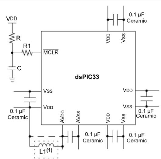
text_image
VDD R R1 C MCLR dsPIC33 0.1 µF Ceramic VDD VSS VDD VSS 0.1 µF Ceramic 0.1 µF Ceramic AVDD AVSS VDD VSS 0.1 µF Ceramic 0.1 µF Ceramic L1(1)Note 1: As an option, instead of a hard-wired connection, an inductor (L1) can be substituted between VDD and AVDD to improve ADC noise rejection. The inductor impedance should be less than 1 and the inductor capacity greater than 10 mA.
Where:
$$ f \quad \frac {F C N V}{2} = \quad (\text { i.e., ADC Conversion Rate / 2 }) $$
$$ f = \frac {1}{(2 \pi \sqrt {L C})} $$
$$ L = \left(\frac {1}{(2 \pi f \sqrt {C})}\right) ^ {2} $$
2.2.1 BULK CAPACITORS
On boards with power traces running longer than six inches in length, it is suggested to use a bulk capacitor for integrated circuits, including DSCs, to supply a local power source. The value of the bulk capacitor should be determined based on the trace resistance that connects the power supply source to the device and the maximum current drawn by the device in the application. In other words, select the bulk capacitor so that it meets the acceptable voltage sag at the device. Typical values range from 4.7 F to 47 F.
2.3 Master Clear (MCLR) Pin
The MCLR pin provides two specific device functions:
- Device Reset
• Device Programming and Debugging.
During device programming and debugging, the resistance and capacitance that can be added to the pin must be considered. Device programmers and debuggers drive the MCLR pin. Consequently, specific voltage levels (VIH and VIL) and fast signal transitions must not be adversely affected. Therefore, specific values of R and C will need to be adjusted based on the application and PCB requirements.
For example, as shown in Figure 2-2, it is recommended that the capacitor, C, be isolated from the MCLR pin during programming and debugging operations.
Place the components, as shown in Figure 2-2, within one-quarter inch (6 mm) from the MCLR pin.
Note 1: There are the S1MCLR1, S1MCLR2 and S1MCLR3 pins and they are used for Secondary debug during the dual debug process. Those pins do not reset the Secondary core during normal operation.
FIGURE 2-2: EXAMPLE OF MCLR PIN CONNECTIONS

text_image
VDD R(1) R1(2) JP C MCLR dsPIC33Note 1: R ≤ 10 kΩ is recommended. A suggested starting value is 10 kΩ. Ensure that the MCLR pin VIH and VIL specifications are met.
2: R1 ≤ 470Ω will limit any current flowing into MCLR from the external capacitor, C, in the event of MCLR pin breakdown due to Electrostatic Discharge (ESD) or Electrical Overstress (EOS). Ensure that the MCLR pin VIH and VIL specifications are met.
2.4 ICSP Pins
The PGCx and PGDx pins are used for ICSP and debugging purposes. It is recommended to keep the trace length between the ICSP connector and the ICSP pins on the device as short as possible. If the ICSP connector is expected to experience an ESD event, a series resistor is recommended, with the value in the range of a few tens of Ohms, not to exceed 100 Ohms.
Pull-up resistors, series diodes and capacitors on the PGCx and PGDx pins are not recommended as they will interfere with the programmer/debugger communications to the device. If such discrete components are an application requirement, they should be removed from the circuit during programming and debugging. Alternatively, refer to the AC/DC characteristics and timing requirements information in the respective device Flash programming specification for information on capacitive loading limits and pin Voltage Input High (VIH) and Voltage Input Low (VIL) requirements.
Ensure that the "Communication Channel Select" (i.e., PGCx/PGDx pins) programmed into the device matches the physical connections for the ICSP to PICkit™ 3, MPLAB® ICD 3 or MPLAB REAL ICE™ emulator.
For more information on MPLAB ICD 2, MPLAB ICD 3 and REAL ICE emulator connection requirements, refer to the following documents that are available on the Microchip website.
- "Using MPLAB ^ ICD 3 In-Circuit Debugger" (poster) (DS51765)
- "Development Tools Design Advisory" (DS51764)
- "MPLAB ^ REAL ICE ^TM In-Circuit Emulator User's Guide" (DS51616)
- "Using MPLAB ^ REAL ICE ^TM In-Circuit Emulator" (poster) (DS51749)
2.5 External Oscillator Pins
When the Primary Oscillator (POSC) circuit is used to connect a crystal oscillator, special care and consideration is needed to ensure proper operation. The POSC circuit should be tested across the environmental conditions that the end product is intended to be used.
The load capacitors specified in the crystal oscillator data sheet can be used as a starting point, however, the parasitic capacitance from the PCB traces can affect the circuit and the values may need to be altered to ensure proper start-up and operation. Excessive trace length and other physical interaction can lead to poor signal quality. Poorly tuned oscillator circuits can have reduced amplitude, incorrect frequency (runt pulses), distorted waveforms and long start-up times that may result in unpredictable application behavior, such as instruction mis-execution, illegal op code fetch, etc.
Ensure that the crystal oscillator circuit is at full amplitude and correct frequency before the system begins to execute code. In planning the application's routing and I/O assignments, ensure that adjacent port pins, and other signals in close proximity to the oscillator, do not have high frequencies, short rise and fall times and other similar noise. For further information on the Primary Oscillator, see Primary Oscillator (POSC). A suggested layout is shown in Figure 2-3.
2.6 External Oscillator Layout Guidance
Use best practices during PCB layout to ensure robust start-up and operation. The oscillator circuit should be placed on the same side of the board as the device. Also, place the oscillator circuit close to the respective oscillator pins, not exceeding one-half inch (12 mm) distance between them. The load capacitors should be placed next to the oscillator itself, on the same side of the board. Use a grounded copper pour around the oscillator circuit to isolate it from surrounding circuits. The grounded copper pour should be routed directly to the MCU ground. Do not run any signal traces or power traces inside the ground pour. If using a two-sided board, avoid any traces on the other side of the board where the crystal is placed. Suggested layouts are shown in Figure 2-3.
With fine-pitch packages, it is not always possible to completely surround the pins and components. A suitable solution is to tie the broken guard sections to a mirrored ground layer. In all cases, the guard trace(s) must be returned to ground. For additional information and design guidance on oscillator circuits, please refer to these Microchip Application Notes, available at the Microchip website (www.microchip.com):
- AN943, "Practical PICmicro® Oscillator Analysis and Design"
• AN949, "Making Your Oscillator Work"
• AN1798, "Crystal Selection for Low-Power Secondary Oscillator
FIGURE 2-3: SUGGESTED PLACEMENT OF THE OSCILLATOR CIRCUIT
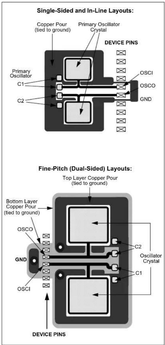
text_image
Single-Sided and In-Line Layouts: Copper Pour (tied to ground) Primary Oscillator Crystal DEVICE PINS Primary Oscillator C1 C2 OSCI OSCO GND Fine-Pitch (Dual-Sided) Layouts: Top Layer Copper Pour (tied to ground) Bottom Layer Copper Pour (tied to ground) OSCO C2 Oscillator Crystal GND C1 OSCI DEVICE PINS2.7 Oscillator Value Conditions on Device Start-up
If the PLL of the target device is enabled and configured for the device start-up oscillator, the maximum oscillator source frequency must be limited to a certain frequency (see Section 6.0 "Oscillator with High-Frequency PLL") to comply with device PLL start-up conditions. This means that if the external oscillator frequency is outside this range, the application must start up in the FRC mode first. The default PLL settings after a POR with an oscillator frequency outside this range will violate the device operating speed.
Once the device powers up, the application firmware can initialize the PLL SFRs, CLKDIV and PLLFBD, to a suitable value, and then perform a clock switch to the Oscillator + PLL clock source. Note that clock switching must be enabled in the device Configuration Word.
2.8 Unused I/Os
Unused I/O pins should be configured as outputs and driven to a logic low state.
Alternatively, connect a 1k to 10k resistor between Vss and unused pins, and drive the output to logic low.
2.9 Targeted Applications
• Power Factor Correction (PFC):
- Interleaved PFC
- Critical Conduction PFC
- Bridgeless PFC
- DC/DC Converters:
- Buck, Boost, Forward, Flyback, Push-Pull
- Half/Full-Bridge
- Phase-Shift Full-Bridge
- Resonant Converters
- DC/AC:
- Half/Full-Bridge Inverter
- Resonant Inverter
- Motor Control
- B L D C
- P M S M
- SR
- A C I M
Examples of typical application connections are shown in Figure 2-4 through Figure 2-6.
FIGURE 2-4: INTERLEAVED PFC

flowchart
graph TD
    A["ADC Channel"] --> B["PGA/ADC Channel"]
    B --> C["dsPIC33CH128MP508"]
    D["VAC"] --> E["Diode +"]
    E --> F["Resistor"]
    F --> G["Inverter"]
    G --> H["Current Source"]
    I["VOUT+"] --> J["Resistor"]
    J --> K["Capacitor"]
    L["FET Driver"] --> M["Resistor"]
    M --> N["Current Source"]
    O["FET Driver"] --> P["Resistor"]
    P --> Q["Current Source"]
    R["VOUT-"] --> S["Resistor"]
    S --> T["Capacitor"]
    U["VOUT-"] --> V["Resistor"]
    V --> W["Current Source"]
FIGURE 2-5: PHASE-SHIFTED FULL-BRIDGE CONVERTER

flowchart
graph TD
    A["Gate 1"] --> B["S1"]
    C["Gate 2"] --> D["S1"]
    E["Gate 3"] --> F["S3"]
    G["Gate 4"] --> H["S3"]
    I["Gate 5"] --> J["S3"]
    K["Gate 6"] --> L["S3"]
    M["VIN+"] --> N["Gate 1"]
    O["VIN-"] --> P["Gate 2"]
    Q["VOUT+"] --> R["Gate 6"]
    S["VOUT-"] --> T["Gate 6"]
    U["Analog Ground"] --> V["FET Driver"]
    W["k1"] --> X["PWM PGA/ADC Channel"]
    X --> Y["PWM ADC Channel"]
    Y --> Z["dsPIC33CH128MP508"]
    AA["FET Driver"] --> AB["S3"]
    AC["FET Driver"] --> AD["S3"]
    AE["FET Driver"] --> AF["S3"]
    AG["PWM"] --> AH["Ground"]
    AI["Ground"] --> AJ["Ground"]
FIGURE 2-6: OFF-LINE UPS

flowchart
graph TD
    subgraph Push-Pull Converter
        A["VBAT"] --> B["FET Driver"]
        C["GND"] --> D["FET Driver"]
        E["k3"] --> F["PWM PWM/RCM ADC or Analog Comp. dsPIC33CH128MP508"]
        F --> G["ADC"]
        H["k6"] --> I["PWM"]
        J["VDC"] --> K["Full-Bridge Inverter"]
        L["GND"] --> M["FET Driver"]
        N["FET Driver"] --> O["FET Driver"]
        P["k4"] --> Q["FET Driver"]
        R["k5"] --> S["FET Driver"]
    end
    subgraph Full-Bridge Inverter
        T["VOUT+"] --> U["AC"]
        V["VOUT-"] --> W["AC"]
        X["ADC"] --> Y["PWM"]
        Z["ADC"] --> AA["PWM"]
        AB["FET Driver"] --> AC["+"]
        AD["+"] --> AE["Ground"]
    end
    subgraph Battery Charger
        AF["Ground"] --> AG["AC"]
        AH["AC"] --> AI["AC"]
    end
3.0 MAIN MODULES
3.1 Main CPU
Note 1: This data sheet summarizes the features of the dsPIC33CH128MP508 family of devices. It is not intended to be a comprehensive reference source. To complement the information in this data sheet, refer to “Enhanced CPU” (www.microchip.com/DS70005158), which is available from the Microchip website (www.microchip.com).
There are two independent CPU cores in the dsPIC33CH128MP508 family. The Main and Secondary cores are similar, except for the fact that the Secondary core can run at a higher speed than the Main core.
The Secondary core fetches instructions from the PRAM and the Main core fetches the code from the Flash. The Main and Secondary cores can run independently asynchronously, at the same speed or at a different speed. This section discusses the Main core.
Note: All of the associated register names are the same on the Main, as well as on the Secondary. The Secondary code will be developed in a separate project in MPLAB X IDE with the device selection, dsPIC33CH128MP508S1, where the S1 indicates the Secondary device.
The dsPIC33CH128MP508 family CPU has a 16-bit (data) modified Harvard architecture with an enhanced instruction set, including significant support for Digital Signal Processing (DSP). The CPU has a 24-bit instruction word with a variable length opcode field. The Program Counter (PC) is 23 bits wide and addresses up to 4M x 24 bits of user program memory space.
An instruction prefetch mechanism helps maintain throughput and provides predictable execution. Most instructions execute in a single-cycle effective execution rate, with the exception of instructions that change the program flow, the double-word move (MOV.D) instruction, PSV accesses and the table instructions. Overhead-free program loop constructs are supported using the DO and REPEAT instructions, both of which are interruptible at any point.
3.1.1 REGISTERS
The dsPIC33CH128MP508 devices have sixteen, 16-bit Working registers in the programmer's model. Each of the Working registers can act as a Data, Address or Address Offset register. The 16th Working register (W15) operates as a Software Stack Pointer for interrupts and calls.
In addition, the dsPIC33CH128MP508 devices include four Alternate Working register sets, which consist of W0 through W14. The Alternate Working registers can be made persistent to help reduce the saving and restoring of register content during Interrupt Service Routines (ISRs). The Alternate Working registers can be assigned to a specific Interrupt Priority Level (IPL1 through IPL7) by configuring the CTXTx[2:0] bits in the FALTREG Configuration register. The Alternate Working registers can also be accessed manually by using the CTXTSWP instruction. The CCTXI[2:0] and MCTXI[2:0] bits in the CTXTSTAT register can be used to identify the current, and most recent, manually selected Working register sets.
3.1.2 INSTRUCTION SET
The instruction set for dsPIC33CH128MP508 devices has two classes of instructions: the MCU class of instructions and the DSP class of instructions. These two instruction classes are seamlessly integrated into the architecture and execute from a single execution unit. The instruction set includes many addressing modes and was designed for optimum C compiler efficiency.
3.1.3 DATA SPACE ADDRESSING
The base Data Space (DS) can be addressed as up to 4K words or 8 Kbytes, and is split into two blocks, referred to as X and Y data memory. Each memory block has its own independent Address Generation Unit (AGU). The MCU class of instructions operates solely through the X memory AGU, which accesses the entire memory map as one linear Data Space. Certain DSP instructions operate through the X and Y AGUs to support dual operand reads, which splits the data address space into two parts. The X and Y Data Space boundary is device-specific.
The upper 32 Kbytes of the Data Space memory map can optionally be mapped into Program Space (PS) at any 16K program word boundary. The program-to-Data Space mapping feature, known as Program Space Visibility (PSV), lets any instruction access Program Space as if it were Data Space. Refer to "Data Memory" (www.microchip.com/DS70000595) for more details on PSV and table accesses.
On dsPIC33CH128MP508 family devices, overhead-free circular buffers (Modulo Addressing) are supported in both X and Y address spaces. The Modulo Addressing removes the software boundary checking overhead for DSP algorithms. The X AGU Circular Addressing can be used with any of the MCU class of instructions. The X AGU also supports Bit-Reversed Addressing to greatly simplify input or output data re-ordering for radix-2 FFT algorithms.
3.1.4 ADDRESSING MODES
The CPU supports these addressing modes:
- Inherent (no operand)
- Relative
- Literal
- Memory Direct
- Register Direct
- Register Indirect
Each instruction is associated with a predefined addressing mode group, depending upon its functional requirements. As many as six addressing modes are supported for each instruction.
FIGURE 3-1: dsPIC33CH128MP508 FAMILY (MAIN) CPU BLOCK DIAGRAM
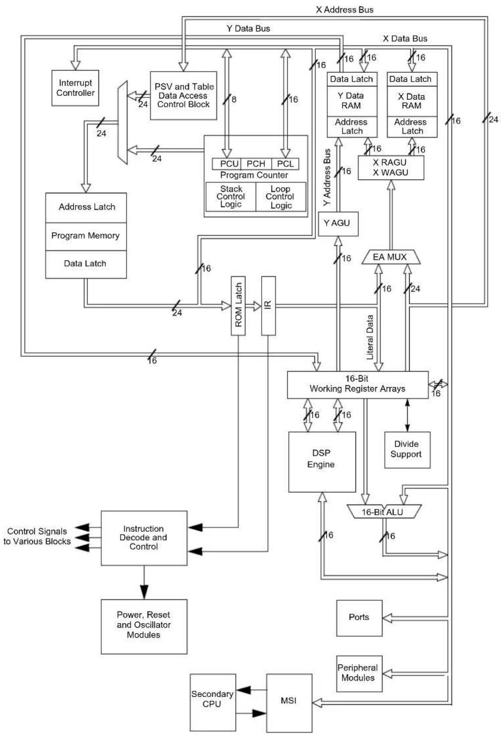
flowchart
graph TD
    A["X Address Bus"] --> B["Interrupt Controller"]
    A --> C["PSV and Table Data Access Control Block"]
    A --> D["PCU PCH PCL Program Counter"]
    A --> E["Y Data Bus"]
    A --> F["X Data Bus"]
    B --> G["Address Latch"]
    C --> H["Program Memory"]
    C --> I["Data Latch"]
    D --> J["Stack Control Logic"]
    D --> K["Loop Control Logic"]
    E --> L["Y AGU"]
    F --> M["X RAGU X WAGU"]
    G --> N["ROM Latch"]
    H --> O["IR"]
    I --> N
    J --> N
    K --> N
    L --> N
    M --> N
    N --> O
    O --> P["16-Bit Working Register Arrays"]
    P --> Q["DSP Engine"]
    P --> R["Divide Support"]
    P --> S["16-Bit ALU"]
    S --> T["Ports"]
    S --> U["Peripheral Modules"]
    T --> V["Secondary CPU"]
    U --> V
    V --> W["MSI"]
    W --> X["Power, Reset and Oscillator Modules"]
    X --> Y["Instruction Decode and Control"]
    Y --> Z["Control Signals to Various Blocks"]
    P --> AA["Literal Data"]
    AA --> AB["Data Latch"]
    AB --> AC["Y Data RAM"]
    AB --> AD["Address Latch"]
    AB --> AE["X Data RAM"]
    AB --> AF["Address Latch"]
    AB --> AG["X RAGU X WAGU"]
3.1.5 PROGRAMMER'S MODEL
The programmer's model for the dsPIC33CH128MP508 family is shown in Figure 3-2. All registers in the programmer's model are memory-mapped and can be manipulated directly by instructions. Table 3-1 lists a description of each register.
In addition to the registers contained in the programmer's model, the dsPIC33CH128MP508 devices contain control registers for Modulo Addressing, Bit-Reversed Addressing and interrupts. These registers are described in subsequent sections of this document.
All registers associated with the programmer's model are memory-mapped, as shown in Figure 3-3 and Figure 3-4.
TABLE 3-1: PROGRAMMER'S MODEL REGISTER DESCRIPTIONS
| Register(s) Name Description | |
| W0 through W15(1) | Working Register Array |
| W0 through W14(1) | Alternate Working Register Array 1 |
| W0 through W14(1) | Alternate Working Register Array 2 |
| W0 through W14(1) | Alternate Working Register Array 3 |
| W0 through W14(1) | Alternate Working Register Array 4 |
| ACCA, ACCB 40-Bit DSP Accumulators | (Additional 4 Alternate Accumulators) |
| PC 23-Bit Program Counter | |
| SR ALU and DSP Engine STATUS Register | |
| SPLIM Stack Pointer Limit Value Register | |
| TBLPAG Table Memory Page Address | Register |
| DSRPAG Extended Data Space (EDS) | Read Page Register |
| RCOUNT REPEAT Loop Counter Register | |
| DCOUNT DO Loop Counter Register | |
| DOSTARTH, DOSTARTL(2) | DO Loop Start Address Register (High and Low) |
| DOENDH, DOENDL | DO Loop End Address Register (High and Low) |
| CORCON | Contains DSP Engine, DO Loop Control and Trap Status bits |
Note 1: Memory-mapped W0 through W14 represent the value of the register in the currently active CPU context. 2: The DOSTARTH and DOSTARTL registers are read-only.
FIGURE 3-2: PROGRAMMER'S MODEL (INITIATOR)

flowchart
graph TD
    A["Working/Address Registers"] --> B["W0-W3"]
    A --> C["DSP Operand Registers"]
    A --> D["DSP Address Registers"]
    B --> E["W0 (WREG)"]
    C --> F["W1"]
    C --> G["W2"]
    C --> H["W3"]
    C --> I["W4"]
    C --> J["W5"]
    C --> K["W6"]
    C --> L["W7"]
    C --> M["W8"]
    C --> N["W9"]
    C --> O["W10"]
    C --> P["W11"]
    C --> Q["W12"]
    C --> R["W13"]
    D --> S["Frame Pointer/W14"]
    D --> T["Stack Pointer/W15"]
    D --> U["Alternate Working/Address Registers"]

    V["DSP Accumulators(1)"] --> W["ACCA"]
    V --> X["ACCB"]

    Y["Program Counter"] --> Z["Program Counter"]
    Y --> AA["TBLPAG"]
    Y --> AB["X Data Space Read Page Address"]

    AC["DO Loop Counter and Stack"] --> AD["DO Loop Counter and Stack"]

    AE["DO Loop Start Address and Stack"] --> AF["DO Loop Start Address and Stack"]

    AG["CPU Core Control Register"] --> AH["CPU Core Control Register"]

    AI["SRL"] --> AJ["OA OB SA SB"]
    AI --> AK["OAB SAB"]
    AI --> AL["DA DC IPL2 IPL1 IPL0 RA N O V Z CSTATUS Register"]
3.1.6 CPU RESOURCES
Many useful resources are provided on the main product page of the Microchip website for the devices listed in this data sheet. This product page contains the latest updates and additional information.
3.1.6.1 Key Resources
- “Enhanced CPU” (www.microchip.com/DS70005158)
- Code Samples
- Application Notes
- Software Libraries
- Webinars
- All related "dsPIC33/PIC24 Family Reference Manual" Sections
- Development Tools
3.1.7 CPU CONTROL/STATUS REGISTERS
REGISTER 3-1: SR: CPU STATUS REGISTER
| R/W-0 R/W-0 R/W-0 R/W-0 R/C-0 R/C-0 R-0 R/W-0 | |||||||
| OA OB SA | (3) | SB(3) | OAB SAB | DA DC | |||
| bit 15 bit 8 | |||||||
| R/W-0^(2) | R/W-0^(2) | R/W-0^(2) | R-0 | R/W-0 | R/W-0 | R/W-0 | R/W-0 |
| IPL2^(1) | IPL1^(1) | IPL0^(1) | RA | N | OV | Z | C |
| bit 7 bit 0 | |||||||
| Legend: | C = Clearable bit | ||
| R = Readable bit | W = Writable bit | U = Unimplemented bit, read as ‘0’ | |
| -n = Value at POR | ‘1’= Bit is set | ‘0’ = Bit is cleared | x = Bit is unknown |
bit 15 OA: Accumulator A Overflow Status bit
1 = Accumulator A has overflowed
0 = Accumulator A has not overflowed
bit 14 OB: Accumulator B Overflow Status bit
1 = Accumulator B has overflowed
0 = Accumulator B has not overflowed
bit 13 SA: Accumulator A Saturation 'Sticky' Status bit ^(3)
1 = Accumulator A is saturated or has been saturated at some time
0 = Accumulator A is not saturated
bit 12 SB: Accumulator B Saturation 'Sticky' Status bit ^(3)
1 = Accumulator B is saturated or has been saturated at some time
0 = Accumulator B is not saturated
bit 11 OAB: OA || OB Combined Accumulator Overflow Status bit
1 = Accumulator A or B has overflowed
0 = Neither Accumulator A or B has overflowed
bit 10 SAB: SA || SB Combined Accumulator 'Sticky' Status bit
1 = Accumulator A or B is saturated or has been saturated at some time
0 = Neither Accumulator A or B is saturated
bit 9 DA: DO Loop Active bit
1 = DO loop is in progress
0 = DO loop is not in progress
bit 8 DC: MCU ALU Half Carry/Borrow bit
1 = A carry-out from the 4th low-order bit (for byte-sized data) or 8th low-order bit (for word-sized data) of the result occurred
0 = No carry-out from the 4th low-order bit (for byte-sized data) or 8th low-order bit (for word-sized data) of the result occurred
Note 1: The IPL[2:0] bits are concatenated with the IPL[3] bit (CORCON[3]) to form the CPU Interrupt Priority Level. The value in parentheses indicates the IPL, if IPL[3] = 1. User interrupts are disabled when IPL[3] = 1.
2: The IPL[2:0] Status bits are read-only when the NSTDIS bit (INTCON1[15]) = 1.
3: A data write to the SR register can modify the SA and SB bits by either a data write to SA and SB or by clearing the SAB bit. To avoid a possible SA or SB bit write race condition, the SA and SB bits should not be modified using bit operations.
REGISTER 3-1: SR: CPU STATUS REGISTER (CONTINUED)
bit 7-5 IPL[2:0]: CPU Interrupt Priority Level Status bits (1,2)
111 = CPU Interrupt Priority Level is 7 (15); user interrupts are disabled
110 = CPU Interrupt Priority Level is 6 (14)
101 = CPU Interrupt Priority Level is 5 (13)
100 = CPU Interrupt Priority Level is 4 (12)
011 = CPU Interrupt Priority Level is 3 (11)
010 = CPU Interrupt Priority Level is 2 (10)
001 = CPU Interrupt Priority Level is 1 (9)
000 = CPU Interrupt Priority Level is 0 (8)
bit 4 RA: REPEAT Loop Active bit
1 = REPEAT loop is in progress
0 = REPEAT loop is not in progress
bit 3 N: MCU ALU Negative bit
1 = Result was negative
0 = Result was non-negative (zero or positive)
bit 2 OV: MCU ALU Overflow bit
This bit is used for signed arithmetic (two's complement). It indicates an overflow of the magnitude that causes the sign bit to change state.
1 = Overflow occurred for signed arithmetic (in this arithmetic operation)
0 = No overflow occurred
bit 1 Z: MCU ALU Zero bit
1 = An operation that affects the Z bit has set it at some time in the past
0 = The most recent operation that affects the Z bit has cleared it (i.e., a non-zero result)
bit 0 C: MCU ALU Carry/Borrow bit
1 = A carry-out from the Most Significant bit of the result occurred
0 = No carry-out from the Most Significant bit of the result occurred
Note 1: The IPL[2:0] bits are concatenated with the IPL[3] bit (CORCON[3]) to form the CPU Interrupt Priority Level. The value in parentheses indicates the IPL, if IPL[3] = 1. User interrupts are disabled when IPL[3] = 1.
2: The IPL[2:0] Status bits are read-only when the NSTDIS bit (INTCON1[15]) = 1.
3: A data write to the SR register can modify the SA and SB bits by either a data write to SA and SB or by clearing the SAB bit. To avoid a possible SA or SB bit write race condition, the SA and SB bits should not be modified using bit operations.
REGISTER 3-2: CORCON: CORE CONTROL REGISTER
| R/W-0 U-0 R/W-0 R/W-0 R/W-0 R-0 R-0 R-0 | |||||||
| VAR | — US1 US0 EDT | (1) | DL2 DL1 | DL0 | |||
| bit 15 bit 8 | |||||||
| R/W-0 | R/W-0 | R/W-1 | R/W-0 | R/C-0 | R-0 | R/W-0 | R/W-0 |
| SATA | SATB | SATDW | ACCSAT | IPL3^(2) | SFA | RND IF | |
| bit 7 bit 0 | |||||||
| Legend: | C = Clearable bit | ||
| R = Readable bit | W = Writable bit | U = Unimplemented bit, read as ‘0’ | |
| -n = Value at POR | ‘1’ = Bit is set | ‘0’ = Bit is cleared | x = Bit is unknown |
bit 15 VAR: Variable Exception Processing Latency Control bit
1 = Variable exception processing is enabled
0 = Fixed exception processing is enabled
bit 14 Unimplemented: Read as '0'
bit 13-12 US[1:0]: DSP Multiply Unsigned/Signed Control bits
11 = Reserved
10 = DSP engine multiplies are mixed sign
01 = DSP engine multiplies are unsigned
00 = DSP engine multiplies are signed
bit 11 EDT: Early DO Loop Termination Control bit ^(1)
1 = Terminates executing DO loop at the end of the current loop iteration
0 = No effect
bit 10-8 DL[2:0]: DO Loop Nesting Level Status bits
111 = Seven DO loops are active
...
001 = One DO loop is active
000 = Zero DO loops are active
bit 7 SATA: ACCA Saturation Enable bit
1 = Accumulator A saturation is enabled
0 = Accumulator A saturation is disabled
bit 6 SATB: ACCB Saturation Enable bit
1 = Accumulator B saturation is enabled
0 = Accumulator B saturation is disabled
bit 5 SATDW: Data Space Write from DSP Engine Saturation Enable bit
1 = Data Space write saturation is enabled
0 = Data Space write saturation is disabled
bit 4 ACCSAT: Accumulator Saturation Mode Select bit
1 = 9.31 saturation (super saturation)
0 = 1.31 saturation (normal saturation)
bit 3 IPL3: CPU Interrupt Priority Level Status bit 3 (2)
1 = CPU Interrupt Priority Level is greater than 7
0 = CPU Interrupt Priority Level is 7 or less
Note 1: This bit is always read as '0'.
2: The IPL3 bit is concatenated with the IPL[2:0] bits (SR[7:5]) to form the CPU Interrupt Priority Level.
REGISTER 3-2: CORCON: CORE CONTROL REGISTER (CONTINUED)
bit 2 SFA: Stack Frame Active Status bit
1 = Stack frame is active; W14 and W15 address 0x0000 to 0xFFFF, regardless of DSRPAG
0 = Stack frame is not active; W14 and W15 address the base Data Space
bit 1 RND: Rounding Mode Select bit
1 = Biased (conventional) rounding is enabled
0 = Unbiased (convergent) rounding is enabled
bit 0 IF: Integer or Fractional Multiplier Mode Select bit
1 = Integer mode is enabled for DSP multiply
0 = Fractional mode is enabled for DSP multiply
Note 1: This bit is always read as '0'.
2: The IPL3 bit is concatenated with the IPL[2:0] bits (SR[7:5]) to form the CPU Interrupt Priority Level.
REGISTER 3-3: CTXTSTAT: CPU W REGISTER CONTEXT STATUS REGISTER
| U-0 U-0 U-0 U-0 U-0 | R-0 R-0 | R-0 | |||
| — | — | — | — | — | CCTXI[2:0] |
| bit 15 | bit 8 | ||||
| U-0 U-0 U-0 U-0 U-0 | R-0 R-0 | R-0 | |||
| — | — | — | — | — | MCTXI[2:0] |
| bit 7 bit 0 | |||||
Legend:
| R = Readable bit | W = Writable bit | U = Unimplemented bit, read as '0' |
| -n = Value at POR | '1' = Bit is set | '0' = Bit is cleared x = Bit is unknown |
bit 15-11 Unimplemented: Read as '0'
bit 10-8 CCTXI[2:0]: Current (W Register) Context Identifier bits
111 = Reserved
•
•
.
100 = Alternate Working Register Set 4 is currently in use
011 = Alternate Working Register Set 3 is currently in use
010 = Alternate Working Register Set 2 is currently in use
001 = Alternate Working Register Set 1 is currently in use
000 = Default register set is currently in use
bit 7-3 Unimplemented: Read as '0'
bit 2-0 MCTXI[2:0]: Manual (W Register) Context Identifier bits
111 = Reserved
.
.
.
100 = Alternate Working Register Set 4 was most recently manually selected
011 = Alternate Working Register Set 3 was most recently manually selected
010 = Alternate Working Register Set 2 was most recently manually selected
001 = Alternate Working Register Set 1 was most recently manually selected
000 = Default register set was most recently manually selected
REGISTER 3-4: Y PAGE REGISTER
| U-0 U-0 U-0 U-0 U-0 U-0 U-0 U-0 | |||||||
| —— | —— | —— | |||||
| bit 15 | bit 8 | ||||||
| R/W-0 | R/W-0 | R/W-0 | R/W-0 | R/W-0 | R/W-0 | R/W-0 | R/W-0 |
| YPAG[7:0] | |||||||
| bit 7 | bit 0 | ||||||
| Legend: | |||
| R = Readable bit | W = Writable bit | U = Unimplemented bit, read as '0' | |
| -n = Value at POR | '1' = Bit is set | '0' = Bit is cleared | x = Bit is unknown |
bit 7-0 YPAG[7:0]: Y Page bits
Note: When implemented, YPAG is a R/W SFR register that resets to 0x0001. When not implemented, YPAG is a read-only SFR register which will always return the fixed Y RAM page value, 0x0001.
REGISTER 3-5: MSTRPR: DATA SPACE BUS MASTER PRIORITY CONTROL REGISTER (MAIN)
| U-0 U-0 U-0 U-0 U-0 U-0 U-0 U-0 | |||||||
| —— | ——— | ||||||
| bit 15 | bit 8 | ||||||
| U-0 | U-0 | R/W-0 | R/W-0 | U-0 | U-0 | U-0 | R/W-0 |
| — | — | DMAPR | CANPR | — | — | — | NVMPR |
| bit 7 bit 0 | |||||||
| Legend: | |||
| R = Readable bit | W = Writable bit | U = Unimplemented bit, read as ‘0’ | |
| -n = Value at POR | ‘1’ = Bit is set | ‘0’ = Bit is cleared | x = Bit is unknown |
bit 15-6 Unimplemented: Read as '0'
bit 5 DMAPR: Modify DMA Controller Bus Master Priority Relative to CPU bit
1 = Raises DMA Controller bus Master priority to above that of the CPU
0 = No change to DMA Controller bus Master priority
bit 4 CANPR: Modify CAN1 Bus Master Priority Relative to CPU bit
1 = Raises CAN1 bus Master priority to above that of the CPU
0 = No change to CAN1 bus Master priority
bit 3-1 Unimplemented: Read as '0'
bit 0 NVMPR: Modify NVM Controller Bus Master Priority Relative to CPU bit
1 = Raises NVM Controller bus Master priority to above that of the CPU
0 = No change to NVM Controller bus Master priority
3.1.8 ARITHMETIC LOGIC UNIT (ALU)
The dsPIC33CH128MP508 family ALU is 16 bits wide and is capable of addition, subtraction, bit shifts and logic operations. Unless otherwise mentioned, arithmetic operations are two's complement in nature. Depending on the operation, the ALU can affect the values of the Carry (C), Zero (Z), Negative (N), Overflow (OV) and Digit Carry (DC) Status bits in the SR register. The C and DC Status bits operate as Borrow and Digit Borrow bits, respectively, for subtraction operations.
The ALU can perform 8-bit or 16-bit operations, depending on the mode of the instruction that is used. Data for the ALU operation can come from the W register array or data memory, depending on the addressing mode of the instruction. Likewise, output data from the ALU can be written to the W register array or a data memory location.
Refer to the "16-Bit MCU and DSC Programmer's Reference Manual" (DS70000157) for information on the SR bits affected by each instruction.
The core CPU incorporates hardware support for both multiplication and division. This includes a dedicated hardware multiplier and support hardware for 16-bit divisor division.
3.1.8.1 Multiplier
Using the high-speed, 17-bit x 17-bit multiplier, the ALU supports unsigned, signed or mixed-sign operation in several MCU multiplication modes:
- 16-bit x 16-bit signed
- 16-bit x 16-bit unsigned
• 16-bit signed x 5-bit (literal) unsigned
• 16-bit signed x 16-bit unsigned
• 16-bit unsigned x 5-bit (literal) unsigned
• 16-bit unsigned x 16-bit signed - 8-bit unsigned x 8-bit unsigned
3.1.8.2 Divider
The divide block supports 32-bit/16-bit and 16-bit/16-bit signed and unsigned integer divide operations with the following data sizes:
• 32-bit signed/16-bit signed divide
• 32-bit unsigned/16-bit unsigned divide
• 16-bit signed/16-bit signed divide
• 16-bit unsigned/16-bit unsigned divide
The 16-bit signed and unsigned DIV instructions can specify any W register for both the 16-bit divisor (Wn) and any W register (aligned) pair (W(m + 1):Wm) for the 32-bit dividend. The divide algorithm takes one cycle per bit of divisor, so both 32-bit/16-bit and 16-bit/16-bit instructions take the same number of cycles to execute. There are additional instructions: DIV2 and DIVF2. Divide instructions will complete in six cycles.
3.1.9 DSP ENGINE
The DSP engine consists of a high-speed 17-bit x 17-bit multiplier, a 40-bit barrel shifter and a 40-bit adder/subtracter (with two target accumulators, round and saturation logic).
The DSP engine can also perform inherent accumulator-to-accumulator operations that require no additional data. These instructions are, ADD, SUB, NEG, MIN and MAX.
The DSP engine has options selected through bits in the CPU Core Control register (CORCON), as listed below:
• Fractional or integer DSP multiply (IF)
- Signed, unsigned or mixed-sign DSP multiply (USx)
- Conventional or convergent rounding (RND)
• Automatic saturation on/off for ACCA (SATA)
• Automatic saturation on/off for ACCB (SATB)
• Automatic saturation on/off for writes to data memory (SATDW)
- Accumulator Saturation mode selection (ACCSAT)
TABLE 3-2: DSP INSTRUCTIONS SUMMARY
| Instruction | Algebraic Operation | ACC Write-Back |
| CLR A = 0 Yes | ||
| ED A = (x - y) | ^2 | No |
| EDAC A = A + (x - y) | ^2 | No |
| MAC | A = A + (x · y) | Yes |
| MAC A = A + x | ^2 | No |
| MOVSAC | No change in A | Yes |
| MPY | A = x · y | No |
| MPY A = x | ^2 | No |
| MPY, N | A = -x · y | No |
| MSC | A = A - x · y | Yes |
3.2 Main Memory Organization
Note: This data sheet summarizes the features of the dsPIC33CH128MP508 family of devices. It is not intended to be a comprehensive reference source. To complement the information in this data sheet, refer to "dsPIC33/PIC24 Program Memory" (www.microchip.com/DS70000613), which is available from the Microchip website (www.microchip.com).
The dsPIC33CH128MP508 family architecture features separate program and data memory spaces, and buses. This architecture also allows the direct access of program memory from the Data Space (DS) during code execution.
3.2.1 PROGRAM ADDRESS SPACE
The program address memory space of the dsPIC33CH128MP508 family devices is 4M instructions. The space is addressable by a 24-bit value derived either from the 23-bit PC during program execution, or from table operation or Data Space remapping, as described in Section 3.2.9 "Interfacing Program and Data Memory Spaces".
User application access to the program memory space is restricted to the lower half of the address range (0x000000 to 0x7FFFFFF). The exception is the use of TBLRD operations, which use TBLPAG[7] to permit access to calibration data and Device ID sections of the configuration memory space.
The program memory maps for the Main dsPIC33CHXXXMPX08 device are shown in Figure 3-3 and Figure 3-4.
FIGURE 3-3: PROGRAM MEMORY MAP FOR MAIN dsPIC33CH128MPXXX DEVICES ^(1)

text_image
GOTO Instruction Reset Address Interrupt Vector Table User Program Flash Memory (44K instructions) Device Configuration Unimplemented (Read '0's) Reserved Calibration Data(2,3) User OTP Memory Reserved Write Latches Reserved DEVID Reserved User Memory Space 0x000000 0x000002 0x000004 0x0001FE 0x000200 0x015EFE 0x015F00 0x015FFE 0x016000 0x7FFFFFE 0x800000 0x800FFE 0x801000 0x8016FC 0x801700 0x8017FE 0x801800 0xF9FFFE 0xFA0000 0xFA0002 0xFA0004 0xFEFFFFE 0xFF0000 0xFF0002 0xFF0004 0xFFFFFENote 1: Memory areas are not shown to scale.
2: Calibration data area must be maintained during programming.
3: Calibration data area includes UDID locations.
FIGURE 3-4: PROGRAM MEMORY MAP FOR MAIN dsPIC33CH64MPXXX DEVICES (1)

text_image
GOTO Instruction Reset Address Interrupt Vector Table User Program Flash Memory (22K instructions) Device Configuration Unimplemented (Read '0's) Reserved Calibration Data(2,3) User OTP Memory Reserved Write Latches Reserved DEVID Reserved 0x000000 0x000002 0x000004 0x0001FE 0x000200 0x00AEFE 0x00AF00 0x00AFFE 0x00B000 0x7FFFFE 0x800000 0x800FFE 0x800100 0x8016FC 0x801700 0x8017FE 0x801800 0xF9FFFE 0xFA0000 0xFA0002 0xFA0004 0xFEFFF 0xFF0000 0xFF0002 0xFF0004 0xFFFFFENote 1: Memory areas are not shown to scale.
2: Calibration data area must be maintained during programming.
3: Calibration data area includes UDID locations.
3.2.1.1 Program Memory Organization
The program memory space is organized in word-addressable blocks. Although it is treated as 24 bits wide, it is more appropriate to think of each address of the program memory as a lower and upper word, with the upper byte of the upper word being unimplemented. The lower word always has an even address, while the upper word has an odd address (Figure 3-5).
Program memory addresses are always word-aligned on the lower word, and addresses are incremented or decremented, by two, during code execution. This arrangement provides compatibility with data memory space addressing and makes data in the program memory space accessible.
3.2.1.2 Interrupt and Trap Vectors
All dsPIC33CH128MP508 family devices reserve the addresses between 0x000000 and 0x000200 for hard-coded program execution vectors. A hardware Reset vector is provided to redirect code execution from the default value of the PC on device Reset to the actual start of code. A GOTO instruction is programmed by the user application at address, 0x000000, of Flash memory, with the actual address for the start of code at address, 0x000002, of Flash memory.
A more detailed discussion of the Interrupt Vector Tables (IVTs) is provided in Section 3.5 "Main Interrupt Controller".
FIGURE 3-5: PROGRAM MEMORY ORGANIZATION
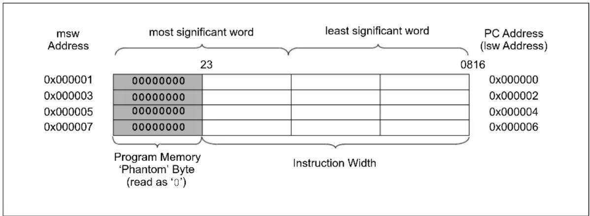
text_image
msw Address most significant word least significant word PC Address (Isw Address) 23 0816 0x000001 0x000003 0x000005 0x000007 Program Memory 'Phantom' Byte (read as '0') Instruction Width 0x000000 0x000002 0x000004 0x0000063.2.2 UNIQUE DEVICE IDENTIFIER (UDID)
All dsPIC33CH128MP508 family devices are individually encoded during final manufacturing with a Unique Device Identifier or UDID. The UDID cannot be erased by a bulk erase command or any other user-accessible means. This feature allows for manufacturing traceability of Microchip Technology devices in applications where this is a requirement. It may also be used by the application manufacturer for any number of things that may require unique identification, such as:
- Tracking the device
- Unique serial number
- Unique security key
The UDID comprises five 24-bit program words. When taken together, these fields form a unique 120-bit identifier.
The UDID is stored in five read-only locations, located between 0x801200 and 0x801208 in the device configuration space. Table3-3 lists the addresses of the identifier words and shows their contents
TABLE 3-3: UDID ADDRESSES
| UDID | Address | Description |
| UDID1 | 0x801200 | UDID Word 1 |
| UDID2 | 0x801202 | UDID Word 2 |
| UDID3 | 0x801204 | UDID Word 3 |
| UDID4 | 0x801206 | UDID Word 4 |
| UDID5 | 0x801208 | UDID Word 5 |
3.2.3 DATA ADDRESS SPACE (MAIN)
The dsPIC33CH128MP508 family CPU has a separate 16-bit wide data memory space. The Data Space is accessed using separate Address Generation Units (AGUs) for read and write operations. The data memory map is shown in Figure 3-6.
All Effective Addresses (EAs) in the data memory space are 16 bits wide and point to bytes within the Data Space. This arrangement gives a base Data Space address range of 64 Kbytes or 32K words.
The lower half of the data memory space (i.e., when EA[15] = 0) is used for implemented memory addresses, while the upper half (EA[15] = 1) is reserved for the Program Space Visibility (PSV).
The dsPIC33CH128MP508 family devices implement up to 16 Kbytes of data memory. If an EA points to a location outside of this area, an all-zero word or byte is returned.
3.2.3.1 Data Space Width
The data memory space is organized in byte-addressable, 16-bit wide blocks. Data are aligned in data memory and registers as 16-bit words, but all Data Space EAs resolve to bytes. The Least Significant Bytes (LSBs) of each word have even addresses, while the Most Significant Bytes (MSBs) have odd addresses.
3.2.3.2 Data Memory Organization and Alignment
To maintain backward compatibility with PIC ^® MCU devices and improve Data Space memory usage efficiency, the dsPIC33CH128MP508 family instruction set supports both word and byte operations. As a consequence of byte accessibility, all Effective Address calculations are internally scaled to step through word-aligned memory. For example, the core recognizes that Post-Modified Register Indirect Addressing mode [Ws++] results in a value of Ws + 1 for byte operations and Ws + 2 for word operations.
A data byte read, reads the complete word that contains the byte, using the LSb of any EA to determine which byte to select. The selected byte is placed onto the LSB of the data path. That is, data memory and registers are organized as two parallel, byte-wide entities with shared (word) address decode, but separate write lines. Data byte writes only write to the corresponding side of the array or register that matches the byte address.
All word accesses must be aligned to an even address. Misaligned word data fetches are not supported, so care must be taken when mixing byte and word operations, or translating from 8-bit MCU code. If a misaligned read or write is attempted, an address error trap is generated. If the error occurred on a read, the instruction underway is completed. If the error occurred on a write, the instruction is executed but the write does not occur. In either case, a trap is then executed, allowing the system and/or user application to examine the machine state prior to execution of the address Fault.
All byte loads into any W register are loaded into the LSB; the MSB is not modified.
A Sign-Extend (SE) instruction is provided to allow user applications to translate 8-bit signed data to 16-bit signed values. Alternatively, for 16-bit unsigned data, user applications can clear the MSB of any W register by executing a Zero-Extend (ZE) instruction on the appropriate address.
3.2.3.3 SFR Space
The first 4 Kbytes of the Near Data Space, from 0x0000 to 0x0FFF, is primarily occupied by Special Function Registers (SFRs). These are used by the dsPIC33CH128MP508 family core and peripheral modules for controlling the operation of the device.
SFRs are distributed among the modules that they control and are generally grouped together by module. Much of the SFR space contains unused addresses; these are read as '0'.
Note: The actual set of peripheral features and interrupts varies by the device. Refer to the corresponding device tables and pinout diagrams for device-specific information.
3.2.3.4 Near Data Space
The 8-Kbyte area, between 0x0000 and 0x1FFF, is referred to as the Near Data Space. Locations in this space are directly addressable through a 13-bit absolute address field within all memory direct instructions. Additionally, the whole Data Space is addressable using MOV instructions, which support Memory Direct Addressing mode with a 16-bit address field, or by using Indirect Addressing mode using a Working register as an Address Pointer.
FIGURE 3-6: DATA MEMORY MAP FOR dsPIC33CH128MP508 DEVICES
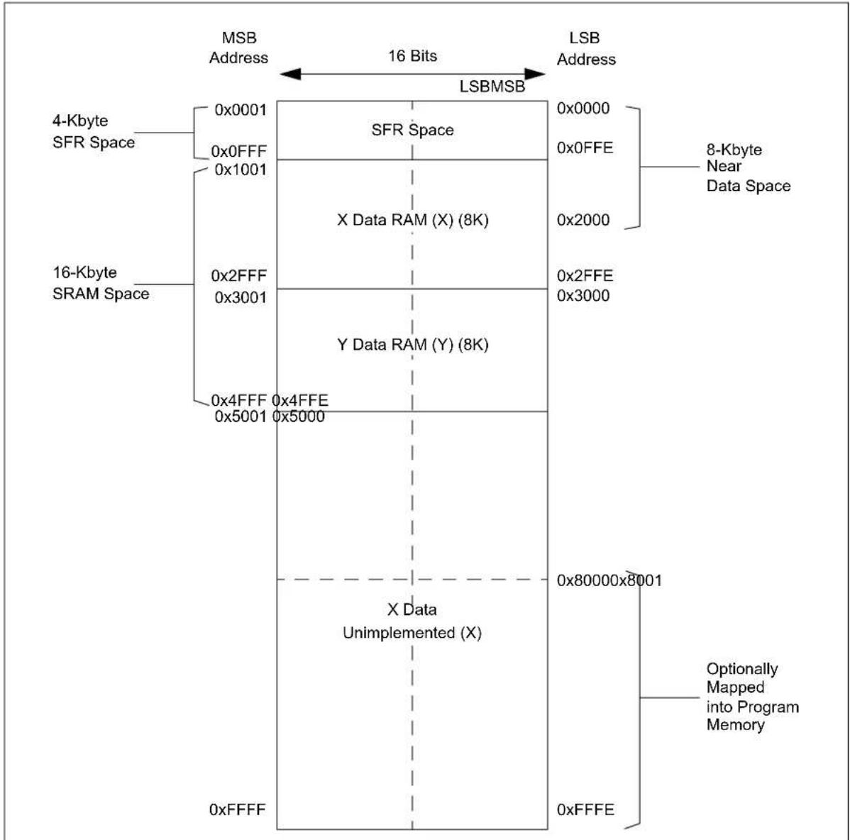
flowchart
graph TD
    A["4-Kbyte SFR Space"] --> B["0x0001"]
    A --> C["0x0FFF"]
    A --> D["0x1001"]
    E["16-Kbyte SRAM Space"] --> F["0x2FFF"]
    E --> G["0x3001"]
    E --> H["0x4FFF"]
    E --> I["0x5001"]
    J["SFR Space"] --> K["X Data RAM (X) (8K)"]
    K --> L["Y Data RAM (Y) (8K)"]
    M["X Data Unimplemented (X)"] --> N["0x80000x8001"]
    O["Optionally Mapped into Program Memory"] --> P["0xFFFE"]
    Q["LSB Address"] --> R["LSBMSB"]
    S["LSB Address"] --> T["8-Kbyte Near Data Space"]
    U["0x0000"] --> V["0x0FFE"]
    W["0x2000"] --> X["0x3000"]
    Y["0x80000x8001"] --> Z["Optionally Mapped into Program Memory"]
Note: Memory areas are not shown to scale.
3.2.3.5 X and Y Data Spaces
The dsPIC33CH128MP508 family core has two Data Spaces, X and Y. These Data Spaces can be considered either separate (for some DSP instructions) or as one unified linear address range (for MCU instructions). The Data Spaces are accessed using two Address Generation Units (AGUs) and separate data paths. This feature allows certain instructions to concurrently fetch two words from RAM, thereby enabling efficient execution of DSP algorithms, such as Finite Impulse Response (FIR) filtering and Fast Fourier Transform (FFT).
The X Data Space is used by all instructions and supports all addressing modes. X Data Space has separate read and write data buses. The X read data bus is the read data path for all instructions that view Data Space as combined X and Y address space. It is also the X data prefetch path for the dual operand DSP instructions (MAC class).
The Y Data Space is used in concert with the X Data Space by the MAC class of instructions (CLR, ED, EDAC, MAC, MOVSAC, MPY, MPY.N and MSC) to provide two concurrent data read paths.
Both the X and Y Data Spaces support Modulo Addressing mode for all instructions, subject to addressing mode restrictions. Bit-Reversed Addressing mode is only supported for writes to X Data Space.
All data memory writes, including in DSP instructions, view Data Space as combined X and Y address space. The boundary between the X and Y Data Spaces is device-dependent and is not user-programmable.
3.2.4 MEMORY RESOURCES
Many useful resources are provided on the main product page of the Microchip website for the devices listed in this data sheet. This product page contains the latest updates and additional information.
3.2.4.1 Key Resources
- "Enhanced CPU" (www.microchip.com/DS70005158)
- Code Samples
- Application Notes
- Software Libraries
- Webinars
- All Related "dsPIC33/PIC24 Family Reference Manual" Sections
• Development Tools
3.2.5 SFR MAPS
The following tables show dsPIC33CH128MP508 family Main SFR names, addresses and Reset values. These tables contain all registers applicable to the
dsPIC33CH128MP508 family. Not all registers are present on all device variants. Refer to Table1 and Table 2 for peripheral availability. Table 4-25 shows port availability for the different package options.
TABLE 3-4: MAIN SFR BLOCK 000h
| Register Address All | Resets Register Address | All Resets Register | Address All Resets | |||||
| Core | MODCON | 046 | 00--000000000000 | CRC | ||||
| WREG0 | 000 | 000000000000000 | XMODSRT | 048 | xxxxxxxxxxxxxx0 | CRCCONL | 0B0 | 0-00000010000-- |
| WREG1 | 002 | 000000000000000 | XMODEND | 04A | xxxxxxxxxxxxxx1 | CRCCONH | 0B2 | ---00000---00000 |
| WREG2 | 004 | 000000000000000 | YMODSRT | 04C | xxxxxxxxxxxxxx0 | CRCXORL | 0B4 | 00000000000000- |
| WREG3 | 006 | 000000000000000 | YMODEND | 04E | xxxxxxxxxxxxxx1 | CRCXORH | 0B6 | 000000000000000 |
| WREG4 | 008 | 000000000000000 | XBREV | 050 | 0xxxxxxxxxxxxxx | CRCDATL | 0B8 | 000000000000000 |
| WREG5 | 00A | 000000000000000 | DISICNT | 052 | xxxxxxxxxxxxxx00 | CRCDATH | 0BA | 000000000000000 |
| WREG6 | 00C | 000000000000000 | TBLPAG | 054 | ----00000000 | CRCWDATL | 0BC | 000000000000000 |
| WREG7 | 00E | 000000000000000 | YPAG | 056 | ----00000001 | CRCWDATH | 0BE | 000000000000000 |
| WREG8 | 010 | 000000000000000 | MSTRPR | 058 | ----00---0 | CLC | ||
| WREG9 | 012 | 000000000000000 | CTXTSTAT | 05A | 000000000000000 | CLC1CONL | 0C0 | 0-0-0C--000--000 |
| WREG10 | 014 | 000000000000000 | DMTCON | 05C | 000000000000000 | CLC1CONH | 0C2 | ----0000 |
| WREG11 | 016 | 000000000000000 | DMTPRECLR | 060 | 000000000000000 | CLC1SEL | 0C4 | -000-000-000-000 |
| WREG12 | 018 | 000000000000000 | DMTCLR | 064 | 000000000000000 | CLC1GLSL | 0C8 | 000000000000000 |
| WREG13 | 01A | 000000000000000 | DMTSTAT | 068 | 000000000000000 | CLC1GLSH | 0CA | 00000000000000 |
| WREG14 | 01C | 000000000000000 | DMTCNTL | 06C | 000000000000000 | CLC2CONL | 0CC | 0-0-00--000--000 |
| WREG15 | 01E | 000010000000000 | DMTCNTH | 06E | 000000000000000 | CLC2CONH | 0CE | ----0000 |
| SPLIM | 020 | xxxxxxxxxxxxxx | DMTHOLDREG | 070 | 00000000000000 | CLC2SEL | 0D0 | -000-000-000-000 |
| ACCAL | 022 | xxxxxxxxxxxxxx | DMTPSCNTL | 074 | 00000000000000 | CLC2GLSL | 0D4 | 00000000000000 |
| ACCAH | 024 | xxxxxxxxxxxxxx | DMTPSCNTH | 076 | 0000000000000 | CLC2GLSH | 0D6 | 0000000000000 |
| ACCAU | 026 | xxxxxxxxxxxxxx | DMTPSINTVL | 078 | 0000000000000 | CLC3CONL | 0D8 | 0-0-0C--00C--0C |
| ACCBL | 028 | xxxxxxxxxxxxxx | DMTPSINTVH | 07A | 0000000000000 | CLC3CONH | 0DA | ----000 |
| ACCBH | 02A | xxxxxxxxxxxxxx | SENT | CLC3SEL | 0DC | -000-000-000-00 | ||
| ACCBU | 02C | xxxxxxxxxxxxxx | SENT1CON1 | 080 | 0000000000000 | CLC3GLSL | 0E0 | 000000000000 |
| PCL | 02E | 0000000000000 | SENT1CON2 | 084 | 000000000000 | CLC3GLSH | 0E2 | 00000000000 |
| PCH | 030 | ----000000 | SENT1CON3 | 088 | 00000000000 | CLC4CONL | 0E4 | 0-0-0C--0C |
| DSRPAG | 032 | ----00C | SENT1STAT | 08C | 0000000000 | CLC4CONH | 0E6 | ----00C |
| DSWPAG | 034 | ----00C | SENT1SYNC | 090 | 000000000 | CLC4SEL | 0E8 | -30C-30C-30C-30C |
| RCOUNT | 036 | xxxxxxxxxx | SENT1DATL | 094 | 000000000 | CLC4GLSL | 0EC | 000000000 |
| DCOUNT | 038 | xxxxxxxxxx | SENT1DATH | 096 | 00C | CLC4GLSH | EE | 00C |
| DOSTART | 03A | 111111111111111 | SENT2CON1 | 098 | 00C | ECCCONL | OF | ----C |
| DOSTARTL | 03A | 111111111111111 | SENT2CON2 | 09C | C | ECCCONH | OF2 | C |
| DOSTARTH | 03C | C | SENT2CON3 | OA | C | ECCADDRL | OF4 | C |
| DOENDL | 03E | xxxxxxxxxx | SENT2STAT | OA4 | C | ECCADDRH | OF6 | C |
| DOENDH | 040 | ----xxxxx | SENT2SYNC | OA8 | C | ECCSTATL | OF8 | C |
| SR | 042 | C | SENT2DATL | OAC | C | ECCSTATH | OFA | ----C |
| CORCON | 044 | x-xxC | SENT2DATH | OAE | C | C | ||
Legend: x = unknown or indeterminate value; “-” = unimplemented bits. Address and Reset values are in hexadecimal and binary, respectively. Note 1: SFR shown is for the superset 80-pin device.
TABLE 3-5: MAIN SFR BLOCK 100h
| Register Address All | Resets Register Address | All Resets | Register Address All Resets | ||||
| Timers | INT1TMRH | 15E | 0000000000000000 | MSI1MBX3D | 1E0 | ||
| T1CON | 100 | 0-0000000-00-00- | INT1HLDL | 160 | 0000000000000000 | MSI1MBX4D | 1E2 |
| TMR1 | 104 | 0000000000000000 | INT1HLDH | 162 | 0000000000000000 | MSI1MBX5D | 1E4 |
| PR1 | 108 | 0000000000000000 | INDX1CNTL | 164 | 0000000000000000 | MSI1MBX6D | 1E6 |
| QEI | INDX1CNTH | 166 | 0000000000000000 | MSI1MBX7D | 1E8 | ||
| QEI1CON | 140 | 0000000000000000 | INDX1HLDL | 168 | 0000000000000000 | MSI1MBX8D | 1EA |
| QEI1IOCL | 144 | 00000000000xxxx | INDX1HLDH | 16A | 0000000000000000 | MSI1MBX9D | 1EC |
| QEI1IOCH | 146 | ----0 | QEI1GECL | 16C | 0000000000000000 | MSI1MBX10D | 1EE |
| QEI1STAT | 148 | --00000000000000 | QEI1GECH | 16E | 0000000000000000 | MSI1MBX11D | 1F0 |
| POS1CNTL | 14C | 0000000000000000 | QEI1LECL | 170 | 0000000000000000 | MSI1MBX12D | 1F2 |
| POS1CNTH | 14E | 0000000000000000 | QEI1LECH | 172 | 0000000000000000 | MSI1MBX13D | 1F4 |
| POS1HLDL | 150 | 000000000000000 | MSI1CON | 1D2 | 0----xx0000000000 | MSI1MBX14D | 1F6 |
| POS1HLDH | 152 | 000000000000000 | MSI1STAT | 1D4 | 000000000000000 | MSI1MBX15D | 1F8 |
| VEL1CNTL | 154 | 000000000000000 | MSI1KEY | 1D6 | ----0000000 | MSI1FIFOCS | 1FA |
| VEL1CNTH | 156 | 00000000000000 | MSI1MBXS | 1D8 | ----0000000 | MRSWFDATA | 1FC |
| VEL1HLDL | 158 | 000000000000000 | MSI1MBX0D | 1DA | 000000000000000 | MWSRFDATA | 1FE |
| VEL1HLDH | 15A | 00000000000000 | MSI1MBX1D | 1DC | 000000000000000 | ||
| INT1TMRL | 15C | 00000000000000 | MSI1MBX2D | 1DE | 00000000000000 | ||
Legend: x = unknown or indeterminate value; "-" = unimplemented bits. Address and Reset values are in hexadecimal and binary, respectively.
TABLE 3-6: MAIN SFR BLOCK 200h
| Register Address All | Resets Register Address | All Resets | Register Address All Resets | |||||
| I2C | U1P2 | 24E | ----00000000 | SPI1CON1H | 2AE | 000000000000000 | ||
| I2C1CONL | 200 | 0-0100000000000 | U1P3 | 250 | 000000000000000 | SPI1CON2L | 2B0 | ----0000 |
| I2C1CONH | 202 | ----0000000 | U1P3H | 252 | ----0000000 | SPI1CON2H | 2B2 | ---- |
| I2C1STAT | 204 | 000--0000000000 | U1TXCHK | 254 | ----0000000 | SPI1STATL | 2B4 | ---00--0001-1-00 |
| I2C1ADD | 208 | ----000000000 | U1RXCHK | 256 | ----0000000 | SPI1STATH | 2B6 | --00000--00000 |
| I2C1MSK | 20C | ----000000000 | U1SCCON | 258 | ----00000- | SPI1BUFL | 2B8 | 000000000000000 |
| I2C1BRG | 210 | 00000000000000 | U1SCINT | 25A | --00-000--00-000 | SPI1BUFH | 2BA | 000000000000000 |
| I2C1TRN | 214 | ----1111111 | U1INT | 25C | ----00--0-- | SPI1BRGL | 2BC | ----xxxxxxxxxxxx |
| I2C1RCV | 218 | ----0000000 | U2MODE | 260 | 0-000-000000000 | SPI1BRGH | 2BE | ---- |
| I2C2CONL | 21C | 0-0100000000000 | U2MODEH | 262 | 00---000000000 | SPI1IMSKL | 2C0 | ---00--0000-0-00 |
| I2C2CONH | 21E | ----000000 | U2STA | 264 | 00000001000000 | SPI1IMSKH | 2C2 | 0-000000-00000 |
| I2C2STAT | 220 | 000--000000000 | U2STAH | 266 | -000-0000101110 | SPI1URDTL | 2C4 | 00000000000000 |
| I2C2ADD | 224 | ----00000000 | U2BRG | 268 | 00000000000000 | SPI1URDTH | 2C6 | 0000000000000 |
| I2C2MSK | 228 | ----00000000 | U2BRGH | 26A | ----0000 | SPI2CON1L | 2C8 | 0-00000000000 |
| I2C2BRG | 22C | 00000000000000 | U2RXREG | 26C | ----xxxxxxxx | SPI2CON1H | 2CA | 000000000000 |
| I2C2TRN | 230 | ----1111111 | U2TXREG | 270 | ----xxxxxxxx | SPI2CON2L | 2CC | ----0000 |
| I2C2RCV | 234 | ----0000000 | U2P1 | 274 | ----0000000 | SPI2CON2H | 2CE | ---- |
| UART | U2P2 | 276 | ----0000000 | SPI2STATL | 2D0 | ---00--0001-1-00 | ||
| U1MODE | 238 | 0-000-00000000 | U2P3 | 278 | 0000000000000 | SPI2STATH | 2D2 | --00000--0000 |
| U1MODEH | 23A | 00---00000000 | U2P3H | 27A | ----000000 | SPI2BUFL | 2D4 | 000000000000 |
| U1STA | 23C | 0000000100000 | U2TXCHK | 27C | ----000000 | SPI2BUFH | 2D6 | 00000000000 |
| U1STAH | 23E | -000-000010111 | U2RXCHK | 27E | ----000000 | SPI2BRGL | 2D8 | ----xxxxxxxxxxxx |
| U1BRG | 240 | 0000000000000 | U2SCCON | 280 | ----0000- | SPI2BRGH | 2DA | ---- |
| U1BRGH | 242 | ----000 | U2SCINT | 282 | --00-00--00-00 | SPI2IMSKL | 2DC | ---00--000-0-00 |
| U1RXREG | 244 | ----xxxxxxxx | U2INT | 284 | ----00--0-- | SPI2IMSKH | 2DE | 0-000000-0000 |
| U1TXREG | 248 | ----xxxxxxxx | SPI | SPI2URDTL | 2E0 | 00000000000 | ||
| U1P1 | 24C | ----0000000 | SPI1CON1L | 2AC | 0-0000000000 | SPI2URDTH | 2E2 | 00000000000 |
Legend: x = unknown or indeterminate value; “-” = unimplemented bits. Address and Reset values are in hexadecimal and binary, respectively.
TABLE 3-7: MAIN SFR BLOCK 300h-400h
| Register Address All | Resets Register Address | ss All Resets | Register Address All Resets | |||||
| High-Speed PWM | PG1TRIGB | 356 | 0000000000000000 | PG3FFPCIH | 3AE | 0000-00000000000 | ||
| PCLKCON | 300 | 00----0--00--00 | PG1TRIGC | 358 | 0000000000000000 | PG3SPCIL | 3B0 | 000000000000000 |
| FSCL | 302 | 0000000000000000 | PG1DTL | 35A | --00000000000000 | PG3SPCIH | 3B2 | 0000-00000000000 |
| FSMINPER | 304 | 0000000000000000 | PG1DTH | 35C | --00000000000000 | PG3LEBL | 3B4 | 000000000000000 |
| MPHASE | 306 | 0000000000000000 | PG1CAP | 35E | 000000000000000 | PG3LEBH | 3B6 | ----000----0000 |
| MDC | 308 | 0000000000000000 | PG2CONL | 360 | 0-0000000000000 | PG3PHASE | 3B8 | 000000000000000 |
| MPER | 30A | 0000000000000000 | PG2CONH | 362 | 000-00000--0000 | PG3DC | 3BA | 00000000000000 |
| LFSR | 30C | 0000000000000000 | PG2STAT | 364 | 000000000000000 | PG3DCA | 3BC | ----0000000 |
| CMBTRIGL | 30E | ----0000000 | PG2IOCONL | 366 | 000000000000000 | PG3PER | 3BE | 00000000000000 |
| CMBTRIGH | 310 | ----0000000 | PG2IOCONH | 368 | -000---0---0000 | PG3TRIGA | 3C0 | 00000000000000 |
| LOGCONA | 312 | 00000000000-000 | PG2EVTL | 36A | 0000000---0000 | PG3TRIGB | 3C2 | 0000000000000 |
| LOGCONB | 314 | 0000000000-000 | PG2EVTH | 36C | 0000--00000000 | PG3TRIGC | 3C4 | 0000000000000 |
| LOGCONC | 316 | 000000000-000 | PG2FPCIL | 36E | 0000000000000 | PG3DTL | 3C6 | --00000000000 |
| LOGCOND | 318 | 00000000-000 | PG2FPCIH | 370 | 0000-00000000 | PG3DTH | 3C8 | --00000000000 |
| LOGCONE | 31A | 00000000-000 | PG2CLPCIL | 372 | 000000000000 | PG3CAP | 3CA | 00000000000 |
| LOGCONF | 31C | 00000000-000 | PG2CLPCIH | 374 | 0000-00000000 | PG4CONL | 3CC | 0-0000000000 |
| PWMEVTA | 31E | 0000----000-000 | PG2FFPCIL | 376 | 000000000000 | PG4CONH | 3CE | 000-00000--000 |
| PWMEVTB | 320 | 0000----000-000 | PG2FFPCIH | 378 | 0000-00000000 | PG4STAT | 3D0 | 00000000000 |
| PWMEVTC | 322 | 0000----000-000 | PG2SPCIL | 37A | 000000000000 | PG4IOCONL | 3D2 | 0000000000 |
| PWMEVTD | 324 | 0000----000-000 | PG2SPCIH | 37C | 000-00000000 | PG4IOCONH | 3D4 | -000---0---0 |
| PWMEVTE | 326 | 0000----000-000 | PG2LEBL | 37E | 00000000000 | PG4EVTL | 3D6 | 000000---0 |
| PWMEVTF | 328 | 0000----000-000 | PG2LEBH | 380 | ----00----00 | PG4EVTH | 3D8 | 0000--0000 |
| PG1CONL | 32A | 0-0000000000 | PG2PHASE | 382 | 0000000000 | PG4FPCIL | 3DA | 000000000 |
| PG1CONH | 32C | 00-0000--00 | PG2DC | 384 | 000000000 | PG4FPCIH | 3DC | 000-0000 |
| PG1STAT | 32E | 000000000 | PG2DCA | 386 | ----00 | PG4CLPCIL | 3DE | 00000000 |
| PG1IOCONL | 330 | 00000000 | PG2PER | 388 | 00000000 | PG4CLPCIH | 3E0 | 000-000 |
| PG1IOCONH | 332 | -00---0---0 | PG2TRIGA | 38A | 00000000 | PG4FFPCIL | 3E2 | 0000000 |
| PG1EVTL | 334 | 000000-- | PG2TRIGB | 38C | 00000000 | PG4FFPCIH | 3E4 | 000-00 |
| PG1EVTH | 336 | 000--00 | PG2TRIGC | 38E | 00000000 | PG4SPCIL | 3E6 | 000000 |
| PG1FPCIL | 338 | 0000000 | PG2DTL | 390 | --00 | PG4SPCIH | 3E8 | 000-00 |
| PG1FPCIH | 33A | 000-00 | PG2DTH | 392 | --00 | PG4LEBL | 3EA | 0000 |
| PG1CLPCIL | 33C | 0000000 | PG2CAP | 394 | 0000000 | PG4LEBH | 3EC | ----0C--- |
| PG1CLPCIH | 33E | 000-00 | PG3CONL | 396 | 0-00 | PG4PHASE | 3EE | 000 |
| PG1FFPCIL | 340 | 0000-00 | PG3CONH | 398 | 00-00 | PG4DC | 3F0 | 000 |
| PG1FFPCIH | 342 | 00C-0C | PG3STAT | 39A | 0000000 | PG4DCA | 3F2 | ---- |
| PG1SPCIL | 344 | 0000-0C | PG3IOCONL | 39C | 0000000 | PG4PER | 3F4 | 0C |
| PG1SPCH | 346 | 00C-0C | PG3IOCONH | 39E | -0C--C--C | PG4TRIGA | 3F6 | C |
| PG1LEBL | 348 | C | PG3EVTL | 3A | C | PG4TRIGB | 3F8 | C |
| PG1LEBH | 34A | ----C | PG3EVTH | 3A2 | C | PG4TRIGC | 3FA | C |
| PG1PHASE | 34C | C | PG3FPCIL | 3A4 | C | PG4DTL | 3FC | -- |
| PG1DC | 34E | C | PG3FPCIH | 3A6 | C | PG4DTH | 3FE | -- |
| PG1DCA | 350 | ----C | PG3CLPCIL | 3A8 | C | PG4CAP | 400 | C |
| PG1PER | 352 | C | PG3CLPCIH | 3AA | C | C | ||
| PG1TRIGA | 354 | C | PG3FFPCIL | 3AC | C | C | ||
Legend: x = unknown or indeterminate value; "-" = unimplemented bits. Address and Reset values are in hexadecimal and binary, respectively.
TABLE 3-8: MAIN SFR BLOCK 500h
| Register Address All | Resets Register Address | Ass All Resets | Register Address All Resets | ||||
| CAN FD | C1TSCONL | 5D4 | ----000000000 | C1RXOVIFH | 5EA | ||
| C1CONL | 5C0 | 0-00011101100000 | C1TSCONH | 5D6 | ----000 | C1TXATIFL | 5EC |
| C1CONH | 5C2 | 0000010010011000 | C1VECL | 5D8 | ---00000-1000000 | C1TXATIFH | 5EE |
| C1NBTCFGL | 5C4 | -0001111-0001111 | C1VECH | 5DA | -10000---1000000 | C1TXREQL | 5F0 |
| C1NBTCFGH | 5C6 | 0000000000111110 | C1INTL | 5DC | 000000----00000 | C1TXREQH | 5F2 |
| C1DBTCFGL | 5C8 | ----0011----0011 | C1INTH | 5DE | 00000000---00000 | C1TRECL | 5F4 |
| C1DBTCFGH | 5CA | 00000000----01110 | C1RXIFL | 5E0 | 00000000000000- | C1TRECH | 5F6 |
| C1TDCL | 5CC | -0010000--000000 | C1RXIFH | 5E2 | 000000000000000 | C1BDIAGOL | 5F8 |
| C1TDCH | 5CE | ----00----10 | C1TXIFL | 5E4 | 000000000000000 | C1BDIAGOH | 5FA |
| C1TBCL | 5D0 | 0000000000000000 | C1TXIFH | 5E6 | 000000000000000 | C1BDIAG1L | 5FC |
| C1TBCH | 5D2 | 0000000000000000 | C1RXOVIFL | 5E8 | 00000000000000- | C1BDIAG1H | 5FE |
Legend: x = unknown or indeterminate value; "-" = unimplemented bits. Address and Reset values are in hexadecimal and binary, respectively.
TABLE 3-9: MAIN SFR BLOCK 600h
| Register Address All Resets Register Address All Resets Register Address All Resets | ||||||||
| CAN FD (Continued) | C1FIFOCON6H | 65A | 00000000-1100000 | C1MASK5L | 6AC | 0000000000000000 | ||
| C1TEFCONL | 600 | ----100--0-0000 | C1FIFOSTA6 | 65C | ---0000000000000 | C1MASK5H | 6AE | 0000000000000000 |
| C1TEFCONH | 602 | ---00000---- | C1FIFOUA6L | 660 | xxxxxxxxxxxxxxxxxx | C1FLTOBJ6L | 6B0 | 0000000000000000 |
| C1TEFSTA | 604 | ----0000 | C1FIFOUA6H | 662 | xxxxxxxxxxxxxxxxxx | C1FLTOBJ6H | 6B2 | 0000000000000000 |
| C1TEFUAL | 608 | xxxxxxxxxxxxxxxxxx | C1FIFOCON7L | 664 | ----1000000000 | C1MASK6L | 6B4 | 0000000000000000 |
| C1TEFUAH | 60A | xxxxxxxxxxxxxxxxxx | C1FIFOCON7H | 666 | 0000000-1100000 | C1MASK6H | 6B6 | 0000000000000000 |
| C1FIFOBAL | 60C | 000000000000000 | C1FIFOSTA7 | 668 | ---0000000000000 | C1FLTOBJ7L | 7B8 | 0000000000000000 |
| C1FIFOBAH | 60E | 000000000000000 | C1FIFOUA7L | 66C | xxxxxxxxxxxxxxxxxx | C1FLTOBJ7H | 6BA | 000000000000000 |
| C1TXQCONL | 610 | ----1001--0-0-0 | C1FIFOUA7H | 66E | xxxxxxxxxxxxxxxxxx | C1MASK7L | 6BC | 000000000000000 |
| C1TXQCONH | 612 | 00000000-1100000 | C1FLTCON0L | 670 | 0--00000--00000 | C1MASK7H | 6BE | 000000000000000 |
| C1TXQSTA | 614 | ---00000000-0-0 | C1FLTCON0H | 672 | 0--00000--00000 | C1FLTOBJ8L | 6C0 | 00000000000000 |
| C1TXQUAL | 618 | xxxxxxxxxxxxxxxxxx | C1FLTCON1L | 674 | 0--00000--00000 | C1FLTOBJ8H | 6C2 | 00000000000000 |
| C1TXQUAH | 61A | xxxxxxxxxxxxxxxxxx | C1FLTCON1H | 676 | 0--00000--00000 | C1MASK8L | 6C4 | 00000000000000 |
| C1FIFOCON1L | 61C | ----1000000000 | C1FLTCON2L | 678 | 0--00000--00000 | C1MASK8H | 6C6 | 0000000000000 |
| C1FIFOCON1H | 61E | 00000000-110000 | C1FLTCON2H | 67A | 0--00000--00000 | C1FLTOBJ9L | 6C8 | 0000000000000 |
| C1FIFOSTA1 | 620 | ---00000000000 | C1FLTCON3L | 67C | 0--00000--0000 | C1FLTOBJ9H | 6CA | 0000000000000 |
| C1FIFOUA1L | 624 | xxxxxxxxxxxxxxxxxx | C1FLTCON3H | 67E | 0--00000--0000 | C1MASK9L | 6CC | 0000000000000 |
| C1FIFOUA1H | 626 | xxxxxxxxxxxxxxxxxx | C1FLTOBJOL | 680 | 0000000000000 | C1MASK9H | 6CE | 000000000000 |
| C1FIFOCON2L | 628 | ----100000000 | C1FLTOBJOH | 682 | 000000000000 | C1FLTOBJ10L | 6D0 | 000000000000 |
| C1FIFOCON2H | 62A | 00000000-110000 | C1MASKOL | 684 | 000000000000 | C1FLTOBJ10H | 6D2 | 00000000000 |
| C1FIFOSTA2 | 62C | ---00000000000 | C1MASKOH | 686 | 000000000000 | C1MASK10L | 6D4 | 00000000000 |
| C1FIFOUA2L | 630 | xxxxxxxxxxxxxxxxxx | C1FLTOBJ1L | 688 | 000000000000 | C1MASK10H | 6D6 | 00000000000 |
| C1FIFOUA2H | 632 | xxxxxxxxxxxxxxxxxx | C1FLTOBJ1H | 68A | 00000000000 | C1FLTOBJ11L | 6D8 | 00000000000 |
| C1FIFOCON3L | 634 | ----100000000 | C1MASK1L | 68C | 00000000000 | C1FLTOBJ11H | 6DA | 00000000000 |
| C1FIFOCON3H | 636 | 00000000-110000 | C1MASK1H | 68E | 00000000000 | C1MASK11L | 6DC | 0000000000 |
| C1FIFOSTA3 | 638 | ---000000000 | C1FLTOBJ2L | 690 | 0000000000 | C1MASK11H | 6DE | 0000000000 |
| C1FIFOUA3L | 63C | xxxxxxxxxxxxxxxxxx | C1FLTOBJ2H | 692 | 0000000000 | C1FLTOBJ12L | 6E0 | 000000000 |
| C1FIFOUA3H | 63E | xxxxxxxxxxxxxxxxxx | C1MASK2L | 694 | 000000000 | C1FLTOBJ12H | 6E2 | 000000000 |
| C1FIFOCON4L | 640 | ----100000000 | C1MASK2H | 696 | 000000000 | C1MASK12L | 6E4 | 000000000 |
| C1FIFOCON4H | 642 | 0000000-110000 | C1FLTOBJ3L | 698 | 000000000 | C1MASK12H | 6E6 | 00000000 |
| C1FIFOSTA4 | 644 | ---00000000 | C1FLTOBJ3H | 69A | 00000000 | C1FLTOBJ13L | 6E8 | 00000000 |
| C1FIFOUA4L | 648 | xxxxxxxxxxxxxxxxxx | C1MASK3L | 69C | 00000000 | C1FLTOBJ13H | 6EA | 00000000 |
| C1FIFOUA4H | 64A | xxxxxxxxxxxxxxxxxx | C1MASK3H | 69C | 00000000 | C1MASK13L | 6EC | 0000000 |
| C1FIFOCON5L | 64C | ----10000000 | C1FLTOBJ4L | 6A0 | 00000000 | C1MASK13H | 6EE | 000 |
| C1FIFOCON5H | 64E | 0000000-11000 | C1FLTOBJ4H | 6A2 | 00000000 | C1FLTOBJ14L | 6F0 | 000 |
| C1FIFOSTA5 | 650 | ---00000000 | C1MASK4L | 6A4 | 00000000 | C1FLTOBJ14H | 6F2 | 000 |
| C1FIFOUA5L | 654 | xxxxxxxxxxxxxxxxxx | C1MASK4H | 6A6 | 00000000 | |||
| C1FIFOUA5H | 656 | xxxxxxxxxxxxxxxxxx | C1FLTOBJ5L | 6A8 | 00000000 | |||
| C1FIFOCON6L | 658 | ----10000000 | C1FLTOBJ5H | 6AA | 00000000 | |||
Legend: x = unknown or indeterminate value; "-" = unimplemented bits. Address and Reset values are in hexadecimal and binary, respectively.
TABLE 3-10: MAIN SFR BLOCK 700h
| Register Address All | Resets Register Address | Ass All Resets | Register Address All Resets | |||||
| CAN FD (Continued) | C1FLTOBJ15L | 6F8 | 0000000000000000 | C1MASK15H | 6FE | |||
| C1MASK14L | 6F4 | 0000000000000000 | C1FLTOBJ15H | 6FA | -0000000000000000 | |||
| C1MASK14H | 6F6 | -000000000000000 | C1MASK15L | 6FC | 0000000000000000 | |||
Legend: x = unknown or indeterminate value; “-” = unimplemented bits. Address and Reset values are in hexadecimal and binary, respectively.
TABLE 3-11: MAIN SFR BLOCK 800h
| Register | Address | All Resets | Register | Address | All Resets | Register | Address | All Resets |
| Interrupts | IPC3 | 846 | -100-100-100-100 | IPC33 | 882 | -100-100-100-100 | ||
| IFS0 | 800 | 0000000000-00000 | IPC4 | 848 | -100-100-100-100 | IPC34 | 884 | -100-100-100-100 |
| IFS1 | 802 | 000000000000000 | IPC5 | 84A | -100-100-100-100 | IPC35 | 886 | ----100-100 |
| IFS2 | 804 | 00000-00-00000-- | IPC6 | 84C | -100-100-100-100 | IPC35 | 886 | ----100-100 |
| IFS3 | 806 | 000----00000 | IPC7 | 84E | -100-100-100-100 | IPC36 | 888 | ----100---- |
| IFS4 | 808 | --000----0000-00 | IPC8 | 850 | -100-100---- | IPC37 | 88A | ----100-100---- |
| IFS5 | 80A | 000000000000000- | IPC9 | 852 | ----100-100-100 | IPC38 | 88C | ----100-100 |
| IFS6 | 80C | 000000000000000 | IPC10 | 854 | -100----100-100 | IPC39 | 88E | ----100---- |
| IFS7 | 80E | 000000000000--- | IPC11 | 856 | -100-100-100-100 | IPC42 | 894 | -100-100-100-100 |
| IFS8 | 810 | --0000000000000- | IPC12 | 858 | -100-100-100-100 | IPC43 | 896 | -100-100-100-100 |
| IFS9 | 812 | --0---00-00--0-- | IPC13 | 85A | ----100 | IPC44 | 898 | -100-100-100-100 |
| IFS10 | 814 | 00000000---- | IPC15 | 85E | -100-100-100---- | IPC45 | 89A | ----100 |
| IFS11 | 816 | -00----00000 | IPC16 | 860 | -100----100-100 | IPC47 | 89E | ----100-100---- |
| IEC0 | 820 | 000000000-00000 | IPC17 | 862 | ----100-100-100 | INTCON1 | 8C0 | 00000000000000- |
| IEC1 | 822 | 000000000000000 | IPC18 | 864 | -100---- | INTCON2 | 8C2 | 000----0----0000 |
| IEC2 | 824 | 00000-00-0000-- | IPC19 | 866 | ----100-100 | INTCON3 | 8C4 | ----0----0----0 |
| IEC3 | 826 | 000----00000 | IPC20 | 868 | -100-100-100---- | INTCON4 | 8C6 | ----00 |
| IEC4 | 828 | --000----0000-00 | IPC21 | 86A | -100-100-100-100 | INTTREG | 8C8 | 000-00000000000 |
| IEC5 | 82A | 00000000000000- | IPC22 | 86C | -100-100-100-100 | Flash | ||
| IEC6 | 82C | 00000000000000 | IPC23 | 86E | -100-100-100-100 | NVMCON | 8D0 | 0000--00----0000 |
| IEC7 | 82E | 000000000000-- | IPC24 | 870 | -100-100-100-100 | NVMADR | 8D2 | 00000000000000 |
| IEC8 | 830 | --000000000000- | IPC25 | 872 | -100-100-100-100 | NVMADRU | 8D4 | ----0000000 |
| IEC8 | 830 | --000000000000- | IPC26 | 874 | -100-100-100-100 | NVMKEY | 8D6 | ----0000000 |
| IEC9 | 832 | --0---00-00--0-- | IPC27 | 876 | -100-100-100-100 | NVMSRCADRL | 8D8 | 00000000000000 |
| IEC10 | 834 | 0000000----00 | IPC28 | 878 | -100---- | NVMSRCADRH | 8DA | ----0000000 |
| IEC11 | 836 | -00----00000 | IPC29 | 87A | -100-100-100-100 | CBG | ||
| IPC0 | 840 | -100-100-100-100 | IPC30 | 87C | -100-100-100-100 | BIASCON | 8F0 | ----0----0000 |
| IPC1 | 842 | -100-100----100 | IPC31 | 87E | -100-100-100-100 | IBIASCONL | 8F4 | --00000--00000 |
| IPC2 | 844 | -100-100-100-100 | IPC32 | 880 | -100-100-100---- | IBIASCONH | 8F6 | --00000--00000 |
Legend: x = unknown or indeterminate value; “-” = unimplemented bits. Address and Reset values are in hexadecimal and binary, respectively.
TABLE 3-12: MAIN SFR BLOCK 900h
| Register Address All | Resets Register Address | Ass All Resets | Register Address All Resets | |||||
| PTG | CCP1CON2L | 954 | 0C-0----00000000 | CCP3TMRH | 9AA | |||
| PTGCST | 900 | 0-00-00000x---00 | CCP1CON2H | 956 | 0----100-00000 | CCP3PRL | 9AC | |
| PTGCON | 902 | ----00000000000 | CCP1CON3H | 95A | 0000----0-00-- | CCP3PRH | 9AE | |
| PTGBTE | 904 | xxxxxxxxxxxxxxxx | CCP1STATL | 95C | ----0--00xx0000 | CCP3RAL | 9B0 | |
| PTGBTEH | 906 | ---- | CCP1TMRL | 960 | 000000000000000 | CCP3RBL | 9B4 | |
| PTGHOLD | 908 | 000000000000000 | CCP1TMRH | 962 | 000000000000000 | CCP3BUFL | 9B8 | |
| PTGTOLIM | 90C | 000000000000000 | CCP1PRL | 964 | 111111111111111 | CCP3BUFH | 9BA | |
| PTGT1LIM | 910 | 000000000000000 | CCP1PRH | 966 | 111111111111111 | CCP4CON1L | 9BC | |
| PTGSDLIM | 914 | 000000000000000 | CCP1RAL | 968 | 000000000000000 | CCP4CON1H | 9BE | |
| PTGCOLIM | 918 | 000000000000000 | CCP1RBL | 96C | 000000000000000 | CCP4CON2L | 9C0 | |
| PTGC1LIM | 91C | 000000000000000 | CCP1BUFL | 970 | 000000000000000 | CCP4CON2H | 9C2 | |
| PTGADJ | 920 | 000000000000000 | CCP1BUFH | 972 | 000000000000000 | CCP4CON3H | 9C6 | |
| PTGL0 | 924 | 000000000000000 | CCP2CON1L | 974 | 0-0000000000000 | CCP4STATL | 9C8 | |
| PTGQPTR | 928 | ----00000 | CCP2CON1H | 976 | 00--00000000000 | CCP4TMRL | 9CC | |
| PTGQUE0 | 930 | xxxxxxxxxxxxxxxx | CCP2CON2L | 978 | 00-0----00000000 | CCP4TMRH | 9CE | |
| PTGQUE1 | 932 | xxxxxxxxxxxxxxxx | CCP2CON2H | 97A | 0----100-00000 | CCP4PRL | 9D0 | |
| PTGQUE2 | 934 | xxxxxxxxxxxxxxxx | CCP2CON3H | 97E | 0000----0-00-- | CCP4PRH | 9D2 | |
| PTGQUE3 | 936 | xxxxxxxxxxxxxxxx | CCP2STATL | 980 | ----0--00xx0000 | CCP4RAL | 9D4 | |
| PTGQUE4 | 938 | xxxxxxxxxxxxxxxx | CCP2TMRL | 984 | 000000000000000 | CCP4RBL | 9D8 | |
| PTGQUE5 | 93A | xxxxxxxxxxxxxxxx | CCP2TMRH | 986 | 000000000000000 | CCP4BUFL | 9DC | |
| PTGQUE6 | 93C | xxxxxxxxxxxxxxxx | CCP2PRL | 988 | 111111111111111 | CCP4BUFH | 9DE | |
| PTGQUE7 | 93E | xxxxxxxxxxxxxxxx | CCP2PRH | 98A | 111111111111111 | CCP5CON1L | 9E0 | |
| PTGQUE8 | 940 | xxxxxxxxxxxxxxxx | CCP2RAL | 98C | 000000000000000 | CCP5CON1H | 9E2 | |
| PTGQUE9 | 942 | xxxxxxxxxxxxxxxx | CCP2RBL | 990 | 000000000000000 | CCP5CON2L | 9E4 | |
| PTGQUE10 | 944 | xxxxxxxxxxxxxxxx | CCP2BUFL | 994 | 000000000000000 | CCP5CON2H | 9E6 | |
| PTGQUE11 | 946 | xxxxxxxxxxxxxxxx | CCP2BUFH | 996 | 000000000000000 | CCP5CON3H | 9EA | |
| PTGQUE12 | 948 | xxxxxxxxxxxxxxxx | CCP3CON1L | 998 | 0-0000000000000 | CCP5STATL | 9EC | |
| PTGQUE13 | 94A | xxxxxxxxxxxxxxxx | CCP3CON1H | 99A | 00--00000000000 | CCP5TMRL | 9F0 | |
| PTGQUE14 | 94C | xxxxxxxxxxxxxxxx | CCP3CON2L | 99C | 00-0----0000000 | CCP5TMRH | 9F2 | |
| PTGQUE15 | 94E | xxxxxxxxxxxxxxxx | CCP3CON2H | 99E | 0----100-0000 | CCP5PRL | 9F4 | |
| CCP | CCP3CON3H | 9A2 | 0000----0-00-- | CCP5PRH | 9F6 | |||
| CCP1CON1L | 950 | 0-0000000000000 | CCP3STATL | 9A4 | ----0--00xx0000 | CCP5RAL | 9F8 | |
| CCP1CON1H | 952 | 00--00000000000 | CCP3TMRL | 9A8 | 00000000000000 | CCP5RBL | 9FC | |
Legend: x = unknown or indeterminate value; “-” = unimplemented bits. Address and Reset values are in hexadecimal and binary, respectively.
TABLE 3-13: MAIN SFR BLOCK A00h
| Register Address All | Resets Register Address | Press All Resets | Register Address All Resets | |||||
| CCP (Continued) | CCP7RAL | A40 | 000000000000000 | DMACNT0 | ACC | 000000000000001 | ||
| CCP5BUFL | A00 | 000000000000000 | CCP7RBL | A44 | 000000000000000 | DMACH1 | ACE | ---0-0000000000 |
| CCP5BUFH | A02 | 000000000000000 | CCP7BUFL | A48 | 000000000000000 | DMAINT1 | AD0 | 000000000000--0 |
| CCP6CON1L | A04 | 0-00000000000000 | CCP7BUFH | A4A | 000000000000000 | DMASRC1 | AD2 | 000000000000000 |
| CCP6CON1H | A06 | 00--000000000000 | CCP8CON1L | A4C | 0-00000000000000 | DMADST1 | AD4 | 000000000000000 |
| CCP6CON2L | A08 | 00-0----0000000 | CCP8CON1H | A4E | 00--000000000000 | DMACNT1 | AD6 | 000000000000001 |
| CCP6CON2H | A0A | 0----100-00000 | CCP8CON2L | A50 | 00-0----0000000 | DMACH2 | AD8 | ---0-0000000000 |
| CCP6CON3H | A0E | 0000----0-00-- | CCP8CON2H | A52 | 0----100-0000 | DMAINT2 | ADA | 000000000000--0 |
| CCP6STATL | A10 | ----0--00xx0000 | CCP8STATL | A58 | ----0--00xx000 | DMASRC2 | ADC | 00000000000000 |
| CCP6TMRL | A14 | 00000000000000 | CCP8STATH | A5A | ----0000 | DMADST2 | ADE | 00000000000000 |
| CCP6TMRH | A16 | 00000000000000 | CCP8TMRL | A5C | 00000000000000 | DMACNT2 | AE0 | 00000000000001 |
| CCP6PRL | A18 | 111111111111111 | CCP8TMRH | A5E | 00000000000000 | DMACH3 | AE2 | ---0-000000000 |
| CCP6PRH | A1A | 111111111111111 | CCP8PRL | A60 | 111111111111111 | DMAINT3 | AE4 | 00000000000--0 |
| CCP6RAL | A1C | 00000000000000 | CCP8PRH | A62 | 111111111111111 | DMASRC3 | AE6 | 0000000000000 |
| CCP6RBL | A20 | 00000000000000 | CCP8RAL | A64 | 00000000000000 | DMADST3 | AE8 | 0000000000000 |
| CCP6BUFL | A24 | 00000000000000 | CCP8RBL | A68 | 0000000000000 | DMACNT3 | AEA | 0000000000001 |
| CCP6BUFH | A26 | 00000000000000 | CCP8BUFL | A6C | 0000000000000 | DMACH4 | AEC | ---0-000000000 |
| CCP7CON1L | A28 | 0-000000000000 | CCP8BUFH | A6E | 000000000000 | DMAINT4 | AEE | 00000000000--0 |
| CCP7CON1H | A2A | 0--0000000000 | DMA | DMASRC4 | AF0 | 000000000000 | ||
| CCP7CON2L | A2C | 00-0----000000 | DMACON | ABC | 0---- | DMADST4 | AF2 | 000000000000 |
| CCP7CON2H | A2E | 0----100-0000 | DMABUF | ABE | 000000000000 | DMACNT4 | AF4 | 0000000000001 |
| CCP7CON3H | A32 | C0C-----C-0C-- | DMAL | ACO | 000000000000 | DMACH5 | AF6 | ---0-00000000 |
| CCP7STATL | A34 | ----0--0xx00 | DMAH | AC2 | 00100C0C | DMAINT5 | AF8 | 0000000000--0 |
| CCP7TMRL | A38 | 00C0C0C0C0C | DMACHO | AC4 | ---0-0C | DMASRC5 | AFA | 00000000000 |
| CCP7TMRH | A3A | 00C0C0C0C | DMAINTO | AC6 | 00C | DMADST5 | AFC | 00C |
| CCP7PRL | A3C | 111111111111111 | DMASRCO | AC8 | 0C | DMACNT5 | AFE | 0C |
| CCP7PRH | A3E | 111111111111111 | DMADSTO | ACA | C | D | D | D |
Legend: x = unknown or indeterminate value; "-" = unimplemented bits. Address and Reset values are in hexadecimal and binary, respectively.
TABLE 3-14: MAIN SFR BLOCK B00h
| Register Address All | Resets Register Address All Resets | Register Address All Resets | ||||||
| ADC | ADCMP1ENH | B42 | ----00000 | ADTRIG0H | B82 | 0000000000000000 | ||
| ADCON1L | B00 | 000-00000----000 | ADCMP1LO | B44 | 000000000000000 | ADTRIG1L | B84 | 0000000000000000 |
| ADCON1H | B02 | ----01---- | ADCMP1HI | B46 | 000000000000000 | ADTRIG1H | B86 | 0000000000000000 |
| ADCON2L | B04 | 00-0000000000000 | ADCMP2ENL | B48 | 000000000000000 | ADTRIG2L | B88 | 0000000000000000 |
| ADCON2H | B06 | 00-0000000000000 | ADCMP2ENH | B4A | ----00000 | ADTRIG2H | B8A | 0000000000000000 |
| ADCON3L | B08 | 00000x000000000 | ADCMP2LO | B4C | 000000000000000 | ADTRIG3L | B8C | 0000000000000000 |
| ADCON3H | B0A | 00000000---- | ADCMP2HI | B4E | 000000000000000 | ADTRIG3H | B8E | 0000000000000000 |
| ADMODOL | B10 | -0-0-0-0-0-0-0 | ADCMP3ENL | B50 | 000000000000000 | ADTRIG4L | B90 | 0000000000000000 |
| ADMODOH | B12 | -0-0-0-0-0-0-0 | ADCMP3ENH | B52 | ----00000 | ADTRIG4H | B92 | 0000000000000000 |
| ADMOD1L | B14 | ----0-0-0-0 | ADCMP3LO | B54 | 000000000000000 | ADTRIG5L | B94 | 000----0000000 |
| ADIEL | B20 | xxxxxxxxxxxxxx | ADCMP3HI | B56 | 000000000000000 | ADCMP0CON | BA0 | 000000000000000 |
| ADIEH | B22 | ----xxxxx | ADFL0DAT | B68 | 000000000000000 | ADCMP1CON | BA4 | 000000000000000 |
| ADCSS1L | B28 | 00000000000000 | ADFL0CON | B6A | 0xx000000000000 | ADCMP2CON | BA8 | 00000000000000 |
| ADSTATL | B30 | 00000000000000 | ADFL1DAT | B6C | 00000000000000 | ADCMP3CON | BAC | 00000000000000 |
| ADSTATH | B32 | ----0000 | ADFL1CON | B6E | 0xx00000000000 | ADLVLTRGL | BD0 | 0000000000000 |
| ADCMP0ENL | B38 | 0000000000000 | ADFL2DAT | B70 | 0000000000000 | ADLVLTRGH | BD2 | ----xxxxx |
| ADCMP0ENH | B3A | ----0000 | ADFL2CON | B72 | 0xx00000000000 | ADEIEL | BF0 | xxxxxxxxxxxxxx |
| ADCMP0LO | B3C | 0000000000000 | ADFL3DAT | B74 | 0000000000000 | ADEIEH | BF2 | ----xxxxx |
| ADCMP0HI | B3E | 000000000000 | ADFL3CON | B76 | 0xx0000000000 | ADEISTATL | BF8 | xxxxxxxxxxxxxx |
| ADCMP1ENL | B40 | 000000000000 | ADTRIGOL | B80 | 000000000000 | ADEISTATH | BFA | ----xxxxx |
Legend: x = unknown or indeterminate value; “-” = unimplemented bits. Address and Reset values are in hexadecimal and binary, respectively.
TABLE 3-15: MAIN SFR BLOCK C00h
| Register Address All | Resets Register Address | Address All Resets | Register Address All Resets | ||||
| ADC (Continued) | ADCBUF9 | C1E | 0000000000000000 | DAC | |||
| ADCON5L | C00 | 0----0---- | ADCBUF10 | C20 | 0000000000000000 | DACCTRL1L | C80 |
| ADCON5H | C02 | 0----xxxx0---- | ADCBUF11 | C22 | 0000000000000000 | DACCTRL2L | C84 |
| ADCAL1H | C0A | 00000-00-000---- | ADCBUF12 | C24 | 0000000000000000 | DACCTRL2H | C86 |
| ADCBUF0 | C0C | 0000000000000000 | ADCBUF13 | C26 | 0000000000000000 | DAC1CONL | C88 |
| ADCBUF1 | C0E | 0000000000000000 | ADCBUF14 | C28 | 0000000000000000 | DAC1CONH | C8A |
| ADCBUF2 | C10 | 0000000000000000 | ADCBUF15 | C2A | 0000000000000000 | DAC1DATL | C8C |
| ADCBUF3 | C12 | 0000000000000000 | ADCBUF16 | C2C | 0000000000000000 | DAC1DATH | C8E |
| ADCBUF4 | C14 | 0000000000000000 | ADCBUF17 | C2E | 0000000000000000 | SLP1CONL | C90 |
| ADCBUF5 | C16 | 0000000000000000 | ADCBUF18 | C30 | 0000000000000000 | SLP1CONH | C92 |
| ADCBUF6 | C18 | 0000000000000000 | ADCBUF19 | C32 | 0000000000000000 | SLP1DAT | C94 |
| ADCBUF7 | C1A | 0000000000000000 | ADCBUF20 | C34 | 0000000000000000 | VREGCON | CFC |
| ADCBUF8 | C1C | 0000000000000000 | |||||
Legend: x = unknown or indeterminate value; “-” = unimplemented bits. Address and Reset values are in hexadecimal and binary, respectively.
TABLE 3-16: MAIN SFR BLOCK D00h
| Register Address All | Resets Register Address All Resets | Register Address All Resets | ||||||
| I/O Ports | RPINR19 | D2A | 1111111111111111 | RPOR4 | D88 | --000000--000000 | ||
| RPCON | D00 | ----0---- | RPINR20 | D2C | 1111111111111111 | RPOR5 | D8A | --000000--000000 |
| RPINR0 | D04 | 11111111---- | RPINR21 | D2E | 1111111111111111 | RPOR6 | D8C | --000000--000000 |
| RPINR1 | D06 | 1111111111111111 | RPINR22 | D30 | 1111111111111111 | RPOR7 | D8E | --000000--000000 |
| RPINR2 | D08 | 11111111---- | RPINR23 | D32 | 111111111111111 | RPOR8 | D90 | --000000--000000 |
| RPINR3 | D0A | 1111111111111111 | RPINR26 | D38 | ----1111111 | RPOR9 | D92 | --000000--000000 |
| RPINR4 | D0C | 1111111111111111 | RPINR30 | D40 | 11111111---- | RPOR10 | D94 | --000000--000000 |
| RPINR5 | D0E | 1111111111111111 | RPINR37 | D4E | 11111111---- | RPOR11 | D96 | --000000--000000 |
| RPINR6 | D10 | 1111111111111111 | RPINR38 | D50 | ----1111111 | RPOR12 | D98 | --000000--000000 |
| RPINR7 | D12 | 1111111111111111 | RPINR42 | D58 | 1111111111111111 | RPOR13 | D9A | --000000--000000 |
| RPINR8 | D14 | 1111111111111111 | RPINR43 | D5A | 1111111111111111 | RPOR14 | D9C | --000000--000000 |
| RPINR9 | D16 | 1111111111111111 | RPINR44 | D5C | 1111111111111111 | RPOR15 | D9E | --000000--000000 |
| RPINR10 | D18 | 1111111111111111 | RPINR45 | D5E | 1111111111111111 | RPOR16 | DA0 | --000000--000000 |
| RPINR11 | D1A | 1111111111111111 | RPINR46 | D60 | 1111111111111111 | RPOR17 | DA2 | --000000--000000 |
| RPINR12 | D1C | 1111111111111111 | RPINR47 | D62 | 1111111111111111 | RPOR18 | DA4 | --000000--000000 |
| RPINR13 | D1E | 1111111111111111 | RPOR0 | D80 | --000000--000000 | RPOR19 | DA6 | --000000--000000 |
| RPINR14 | D20 | 1111111111111111 | RPOR1 | D82 | --000000--000000 | RPOR20 | DA8 | --000000--000000 |
| RPINR15 | D22 | 1111111111111111 | RPOR2 | D84 | --000000--000000 | RPOR21 | DAA | --000000--000000 |
| RPINR18 | D28 | 1111111111111111 | RPOR3 | D86 | --000000--000000 | RPOR22 | DAC | --000000--000000 |
Legend: x = unknown or indeterminate value; "-" = unimplemented bits. Address and Reset values are in hexadecimal and binary, respectively.
TABLE 3-17: MAIN SFR BLOCK E00h
| Register Address All | Resets Register Address | less All Resets | Register Address All Resets | ||||
| I/O Ports (Continued) | CNCONB | E2A | 0----0---- | LATD | E5A | ||
| ANSELA | E00 | ----11111 | CNEN0B | E2C | 0000000000000000 | ODCD | E5C |
| TRISA | E02 | ----11111 | CNSTATB | E2E | 0000000000000000 | CNPUD | E5E |
| PORTA | E04 | ----xxxxx | CNEN1B | E30 | 0000000000000000 | CNPDD | E60 |
| LATA | E06 | ----xxxxx | CNFB | E32 | 0000000000000000 | CNCOND | E62 |
| ODCA | E08 | ----00000 | ANSELC | E38 | ----1----1111 | CNEN0D | E64 |
| CNPUA | E0A | ----00000 | TRISC | E3A | 1111111111111111 | CNSTATD | E66 |
| CNPDA | E0C | ----00000 | PORTC | E3C | xxxxxxxxxxxxxxxxxx | CNEN1D | E68 |
| CNCONA | E0E | 0----0---- | LATC | E3E | xxxxxxxxxxxxxxxxxx | CNFD | E6A |
| CNEN0A | E10 | ----00000 | ODCC | E40 | 0000000000000000 | TRISE | E72 |
| CNSTATA | E12 | ----00000 | CNPUC | E42 | 0000000000000000 | PORTE | E74 |
| CNEN1A | E14 | ----00000 | CNPDC | E44 | 0000000000000000 | LATE | E76 |
| CNFA | E16 | ----00000 | CNCONC | E46 | 0----0---- | ODCE | E78 |
| ANSELB | E1C | ----111---1111 | CNEN0C | E48 | 0000000000000000 | CNPUE | E7A |
| TRISB | E1E | 1111111111111111 | CNSTATC | E4A | 0000000000000000 | CNPDE | E7C |
| PORTB | E20 | xxxxxxxxxxxxxxxxx | CNEN1C | E4C | 0000000000000000 | CNCONE | E7E |
| LATB | E22 | xxxxxxxxxxxxxxxxx | CNFC | E4E | 0000000000000000 | CNEN0E | E80 |
| ODCB | E24 | 0000000000000000 | ANSELD | E54 | ----1---- | CNSTATE | E82 |
| CNPUB | E26 | 0000000000000000 | TRISD | E56 | 1111111111111111 | CNEN1E | E84 |
| CNPDB | E28 | 0000000000000000 | PORTD | E58 | xxxxxxxxxxxxxxxxx | CNFE | E86 |
Legend: x = unknown or indeterminate value; "-" = unimplemented bits. Address and Reset values are in hexadecimal and binary, respectively.
TABLE 3-18: MAIN SFR BLOCK F00h
| Register Address All | Resets Register Address All Resets | Register Address All Resets | ||||||
| Reset | PMD2 | FA6 | ----00000000 | PCTRAPH | FC2 | ----00000000 | ||
| RCON | F80 | 00--x-0000000011 | PMD3 | FA8 | ----0----0- | FEXL | FC4 | xxxxxxxxxxxxxx |
| Oscillator | PMD4 | FAA | ----0--- | FEXH | FC6 | ----xxxxxxxxxx | ||
| OSCCON | F84 | -000-yyy0-0-0--0 | PMD6 | FAE | --000000---- | DPCL | FCE | xxxxxxxxxxxxxxxxxx |
| CLKDIV | F86 | 00110000--000001 | PMD7 | FB0 | ----x----0--- | DPCH | FD0 | ----xxxxxxxxxx |
| PLLFBD | F88 | ----000010010110 | PMD8 | FB2 | ----00--0--xx000- | APPO | FD2 | xxxxxxxxxxxxxxxxxx |
| PLLDIV | F8A | ----00-011-001 | WDT | APPI | FD4 | xxxxxxxxxxxxxxxxxx | ||
| OSCTUN | F8C | ----000000 | WDTCONL | FB4 | 0--0000000000000 | APPS | FD6 | ----xxxxxx |
| ACLKCON1 | F8E | 00----0--000001 | WDTCONH | FB6 | 000000000000000 | STROUTL | FD8 | xxxxxxxxxxxxxxxxxx |
| APLLFBD1 | F90 | ----000010010110 | REFOCONL | FB8 | 0-000-00----0000 | STROUTH | FDA | xxxxxxxxxxxxxxxxxx |
| APLLDIV1 | F92 | ----00-011-001 | REFOCONH | FBA | -000000000000000 | STROVCNT | FDC | xxxxxxxxxxxxxxxxxx |
| CANCLKCON | F9A | ----xxxx-xxxxxxxx | REFOTRIMH | FBE | 000000000---- | JDATAH | FFA | xxxxxxxxxxxxxxxxxx |
| PMD | PCTRAPL | FC0 | 000000000000000 | JDATAL | FFC | xxxxxxxxxxxxxxxxxx | ||
| PMD1 | FA4 | ----000-00000-00 | ||||||
Legend: x = unknown or indeterminate value; "-" = unimplemented bits; y = value set by Configuration bits. Address and Reset values are in hexadecimal and binary, respectively.
3.2.5.1 Paged Memory Scheme
The dsPIC33CH128MP508 architecture extends the available Data Space through a paging scheme, which allows the available Data Space to be accessed using MOV instructions in a linear fashion for pre- and post-modified Effective Addresses (EAs). The upper half of the base Data Space address is used in conjunction with the Data Space Read Page (DSRPAG) register to form the Program Space Visibility (PSV) address.
The Data Space Read Page (DSRPAG) register is located in the SFR space. Construction of the PSV address is shown in Figure 3-7. When DSRPAG[9] = 1 and the base address bit, EA[15] = 1, the DSRPAG[8:0] bits are concatenated onto EA[14:0] to form the 24-bit PSV read address.
The paged memory scheme provides access to multiple 32-Kbyte windows in the PSV memory. The Data Space Read Page (DSRPAG) register, in combination with the upper half of the Data Space address, can provide up to 8 Mbytes of PSV address space. The paged data memory space is shown in Figure 3-8.
The Program Space (PS) can be accessed with a DSRPAG of 0x200 or greater. Only reads from PS are supported using the DSRPAG.
FIGURE 3-7: PROGRAM SPACE VISIBILITY (PSV) READ ADDRESS GENERATION

flowchart
graph TD
    A["Select DSRPAG"] --> B{DSRPAG["9"] = 1}
    B -->|No EDS Access| C["0"]
    B -->|Select DSRPAG| D["1"]
    C --> E["EA[15"]]
    D --> F["EA[8:0"]]
    E --> G["Byte Select16-Bit DS EA"]
    F --> H["Byte24-Bit PSV EA Select"]
    style A fill:#f9f,stroke:#333
    style B fill:#ccf,stroke:#333
    style C fill:#cfc,stroke:#333
    style D fill:#fcc,stroke:#333
    style E fill:#ffc,stroke:#333
    style F fill:#fcc,stroke:#333
    style G fill:#fff,stroke:#333
    style H fill:#fff,stroke:#333
Note: DS read access when DSRPAG = 0x000 will force an address error trap.
FIGURE 3-8: PAGED DATA MEMORY SPACE

flowchart
graph TD
    A["Local Data Space"] --> B["DS_Addr[14:0"]]
    B --> C["(DSRPAG = 0x200) No Writes Allowed"]
    C --> D["(DSRPAG = 0x2FF) No Writes Allowed"]
    D --> E["(DSRPAG = 0x300) No Writes Allowed"]
    E --> F["(DSRPAG = 0x3FF) No Writes Allowed"]
    F --> G["(DSRPAG = 0x3FF) No Writes Allowed"]
    G --> H["(DSRPAG = 0x300) No Writes Allowed"]
    H --> I["(DSRPAG = 0x3FF) No Writes Allowed"]
    I --> J["(DSRPAG = 0x300) No Writes Allowed"]
    J --> K["(DSRPAG = 0x300) No Writes Allowed"]
    K --> L["(DSRPAG = 0x300) No Writes Allowed"]
    L --> M["(DSRPAG = 0x300) No Writes Allowed"]
    M --> N["(DSRPAG = 0x300) No Writes Allowed"]
    N --> O["(DSRPAG = 0x300) No Writes Allowed"]
    O --> P["(DSRPAG = 0x300) No Writes Allowed"]
    P --> Q["(DSRPAG = 0x300) No Writes Allowed"]
    Q --> R["(DSRPAG = 0x300) No Writes Allowed"]
    R --> S["(DSRPAG = 0x300) No Writes Allowed"]
    S --> T["(DSRPAG = 0x300) No Writes Allowed"]
    T --> U["(DSRPAG = 0x300) No Writes Allowed"]
    U --> V["(DSRPAG = 0x300) No Writes Allowed"]
    V --> W["(DSRPAG = 0x300) No Writes Allowed"]
    W --> X["(DSRPAG = 0x300) No Writes Allowed"]
    X --> Y["(DSRPAG = 0x300) No Writes Allowed"]
    Y --> Z["(DSRPAG = 0x300) No Writes Allowed"]
    Z --> AA["(DSRPAG = 0x300) No Writes Allowed"]
    AA --> AB["(DSRPAG = 0x300) No Writes Allowed"]
    AB --> AC["(DSRPAG = 0x300) No Writes Allowed"]
    AC --> AD["(DSRPAG = 0x300) No Writes Allowed"]
    AD --> AE["(DSRPAG = 0x300) No Writes Allowed"]
    AE --> AF["(DSRPAG = 0x300) No Writes Allowed"]
    AF --> AG["(DSRPAG = 0x300) No Writes Allowed"]
    AG --> AH["(DSRPAG = 0x300) No Writes Allowed"]
    AH --> AI["(DSRPAG = 0x300) No Writes Allowed"]
    AI --> AJ["(DSRPAG = 0x300) No Writes Allowed"]
    AJ --> AK["(DSRPAG = 0x300) No Writes Allowed"]
    AK --> AL["(DSRPAG = 0x300) No Writes Allowed"]
    AL --> AM["(DSRPAG = 0x300) No Writes Allowed"]
    AM --> AN["(DSRPAG = 0x300) No Writes Allowed"]
    AN --> AO["(DSRPAG = 0x300) No Writes Allowed"]
    AO --> AP["(DSRPAG = 0x300) No Writes Allowed"]
    AP --> AQ["(DSRPAG = 0x300) No Writes Allowed"]
    AQ --> AR["(DSRPAG = 0x300) No Writes Allowed"]
    AR --> AS["(DSRPAG = 0x300) No Writes Allowed"]
    AS --> AT["(DSRPAG = 0x3FF) No Writes Allowed"]
    AT --> AU["(DSRPAG = 0x3FF) No Writes Allowed"]
    AU --> AV["(DSRPAG = 0x3FF) No Writes Allowed"]
    AV --> AW["(DSRPAG = 0x3FF) No Writes Allowed"]
    AW --> AX["(DSRPAG = 0x3FF) No Writes Allowed"]
    AX --> AY["(DSRPAG = 0x3FF) No Writes Allowed"]
    AY --> AZ["(DSRPAG = 0x3FF) No Writes Allowed"]
    AZ --> BA["(DSRPAG = 0x3FF) No Writes Allowed"]
    BA --> BB["(DSRPAG = 0x3FF) No Writes Allowed"]
    BB --> BC["(DSRPAG = 0x3FF) No Writes Allowed"]
    BC --> BD["(DSRPAG = 0x3FF) No Writes Allowed"]
    BD --> BE["(DSRPAG = 0x3FF) No Writes Allowed"]
    BE --> BF["(DSRPAG = 0x3FF) No Writes Allowed"]
    BF --> BG["(DSRPAG = 0x3FF) No Writes Allowed"]
    BG --> BH["(DSRPAG = 0x3FF) No Writes Allowed"]
    BH --> BI["(DSRPAG = 0x3FF) No Writes Allowed"]
    AI --> BJ["(DSRPAG = 15:1.1)"]
    BJ --> BK["(TBLPAG = 15:1.1)"]
    BK --> BL["TBLPAG = 15:1.1)"]
    BL --> BM["TBLPAG = 15:1.1)"]
    BM --> BN["TBLPAG = 15:1.1)"]
    BN --> BO["TBLPAG = 15:1.1)"]
    BO --> BP["TBLPAG = 15:1.1)"]
    AP --> BQ["TBLPAG = 15:1.1)"]
    AP --> BR["TBLPAG = 15:1.1"]
    BR --> BS["TBLPAG = 15:1.1"]
    CA["Table Address Space (TBLPAG[7:1.1"])] --> CB["DS_Addr[15:1.1"]]
    CB --> CC["TSW - [15:1.1"]]
    CC --> DD["TSW - [15:1.1"]]
    DD --> DE["TSW - [15:1.1"]]
    DE --> DF["TSW - [15:1.1"]]
    DF --> DG["TSW - [15:1.1"]]
    DG --> DH["TSW - [15:1.1"]]
When a PSV page overflow or underflow occurs, EA[15] is cleared as a result of the register indirect EA calculation. An overflow or underflow of the EA in the PSV pages can occur at the page boundaries when:
- The initial address, prior to modification, addresses the PSV page
- The EA calculation uses Pre- or Post-Modified Register Indirect Addressing; however, this does not include Register Offset Addressing
In general, when an overflow is detected, the DSRPAG register is incremented and the EA[15] bit is set to keep the base address within the PSV window. When an underflow is detected, the DSRPAG register is decremented and the EA[15] bit is set to keep the base address within the PSV window. This creates a linear PSV address space, but only when using Register Indirect Addressing modes.
Exceptions to the operation described above arise when entering and exiting the boundaries of Page 0 and PSV spaces. Table 3-19 lists the effects of overflow and underflow scenarios at different boundaries.
In the following cases, when overflow or underflow occurs, the EA[15] bit is set and the DSRPAG is not modified; therefore, the EA will wrap to the beginning of the current page:
- Register Indirect with Register Offset Addressing
- Modulo Addressing
- Bit-Reversed Addressing
TABLE 3-19: OVERFLOW AND UNDERFLOW SCENARIOS AT PAGE 0 AND PSV SPACE BOUNDARIES ^(2,3,4)
| O/U,R/W | Operation | Before After | |||||
| DSRPAG | DSEA[15] | PageDescription | DSRPAG | DSEA[15] | PageDescription | ||
| O,Read | [++Wn]or[Wn++] | DSRPAG = 0x2FF 1 | PSV: Last lswpage | DSRPAG = 0x300 1 | PSV: First MSBpage | ||
| O,Read | DSRPAG = 0x3FF 1 | PSV: Last MSBpage | DSRPAG = 0x3FF | 0 | See Note 1 | ||
| U,Read | [--Wn]or[Wn--] | DSRPAG = 0x001 | 1 | PSV page | DSRPAG = 0x001 | 0 | See Note 1 |
| U,Read | DSRPAG = 0x200 1 | PSV: First lswpage | DSRPAG = 0x200 | 0 | See Note 1 | ||
| U,Read | DSRPAG = 0x300 1 | PSV: First MSBpage | DSRPAG = 0x2FF 1 | PSV: Last lswpage | |||
Legend: O = Overflow, U = Underflow, R = Read, W = Write
Note 1: The Register Indirect Addressing now addresses a location in the base Data Space (0x0000-0x8000).
2: An EDS access, with DSRPAG = 0x000, will generate an address error trap.
3: Only reads from PS are supported using DSRPAG.
4: Pseudolinear Addressing is not supported for large offsets.
3.2.5.2 Extended X Data Space
The lower portion of the base address space range, between 0x0000 and 0x7FFF, is always accessible, regardless of the contents of the Data Space Read Page register. It is indirectly addressable through the register indirect instructions. It can be regarded as being located in the default EDS Page 0 (i.e., EDS address range of 0x000000 to 0x007FFF with the base address bit, EA[15] = 0, for this address range). However, Page 0 cannot be accessed through the upper 32 Kbytes, 0x8000 to 0xFFFF, of base Data Space in combination with DSRPAG = 0x00. Consequently, DSRPAG is initialized to 0x001 at Reset.
Note 1: DSRPAG should not be used to access Page 0. An EDS access with DSRPAG set to 0x000 will generate an address error trap.
2: Clearing the DSRPAG in software has no effect.
The remaining PSV pages are only accessible using the DSRPAG register in combination with the upper 32 Kbytes, 0x8000 to 0xFFFF, of the base address, where the base address bit, EA[15] = 1.
3.2.5.3 Software Stack
The W15 register serves as a dedicated Software Stack Pointer (SSP), and is automatically modified by exception processing, subroutine calls and returns; however, W15 can be referenced by any instruction in the same manner as all other W registers. This simplifies reading, writing and manipulating the Stack Pointer (for example, creating stack frames).
Note: To protect against misaligned stack accesses, W15[0] is fixed to '0' by the hardware.
W15 is initialized to 0x1000 during all Resets. This address ensures that the SSP points to valid RAM in all dsPIC33CH128MP508 devices and permits stack availability for non-maskable trap exceptions. These can occur before the SSP is initialized by the user software. You can reprogram the SSP during initialization to any location within Data Space.
The Software Stack Pointer always points to the first available free word and fills the software stack, working from lower toward higher addresses. Figure 3-9 illustrates how it pre-decrements for a stack pop (read) and post-increments for a stack push (writes).
When the PC is pushed onto the stack, PC[15:0] are pushed onto the first available stack word, then PC[22:16] are pushed into the second available stack location. For a PC push during any CALL instruction, the MSB of the PC is zero-extended before the push, as shown in Figure 3-9. During exception processing, the MSB of the PC is concatenated with the lower eight bits of the CPU STATUS Register, SR. This allows the contents of SRL to be preserved automatically during interrupt processing.
Note 1: To maintain system Stack Pointer (W15) coherency, W15 is never subject to (EDS) paging, and is therefore, restricted to an address range of 0x0000 to 0xFFFF. The same applies to the W14 when used as a Stack Frame Pointer (SFA = 1).
2: As the stack can be placed in, and can access X and Y spaces, care must be taken regarding its use, particularly with regard to local automatic variables in a C development environment
FIGURE 3-9: CALL STACK FRAME

text_image
0x0000 Stack Grows Toward Higher Address 015 CALL SUBR PC[15:1] b'000000003' PC[22:16] [Free Word] W15 (before CALL) W15 (after CALL)3.2.6 INSTRUCTION ADDRESSING MODES
The addressing modes shown in Table 3-20 form the basis of the addressing modes optimized to support the specific features of individual instructions. The addressing modes provided in the MAC class of instructions differ from those in the other instruction types.
3.2.6.1 File Register Instructions
Most file register instructions use a 13-bit address field (f) to directly address data present in the first 8192 bytes of data memory (Near Data Space). Most file register instructions employ a Working register, W0, which is denoted as WREG in these instructions. The destination is typically either the same file register or WREG (with the exception of the MUL instruction), which writes the result to a register or register pair. The MOV instruction allows additional flexibility and can access the entire Data Space.
3.2.6.2 MCU Instructions
The three-operand MCU instructions are of the form:
Operand 3 = Operand 1
where Operand 1 is always a Working register (that is, the addressing mode can only be Register Direct), which is referred to as Wb. Operand 2 can be a W register fetched from data memory or a 5-bit literal. The result location can either be a W register or a data memory location. The following addressing modes are supported by MCU instructions:
- Register Direct
- Register Indirect
- Register Indirect Post-Modified
- Register Indirect Pre-Modified
- 5-Bit or 10-Bit Literal
Note: Not all instructions support all the addressing modes given above. Individual instructions can support different subsets of these addressing modes.
TABLE 3-20: FUNDAMENTAL ADDRESSING MODES SUPPORTED
| Addressing Mode Description | |
| File Register Direct | The address of the file register is specified explicitly. |
| Register Direct | The contents of a register are accessed directly. |
| Register Indirect | The contents of Wn form the Effective Address (EA). |
| Register Indirect Post-Modified | The contents of Wn form the EA. Wn is post-modified (incremented or decremented) by a constant value. |
| Register Indirect Pre-Modified | Wn is pre-modified (incremented or decremented) by a signed constant value to form the EA. |
| Register Indirect with Register Offset (Register Indexed) | The sum of Wn and Wb forms the EA. |
| Register Indirect with Literal Offset | The sum of Wn and a literal forms the EA. |
3.2.6.3 Move and Accumulator Instructions
Move instructions, and the DSP accumulator class of instructions, provide a greater degree of addressing flexibility than other instructions. In addition to the addressing modes supported by most MCU instructions, move and accumulator instructions also support Register Indirect with Register Offset Addressing mode, also referred to as Register Indexed mode.
Note: For the MOV instructions, the addressing mode specified in the instruction can differ for the source and destination EA. However, the 4-bit Wb (Register Offset) field is shared by both source and destination (but typically only used by one).
In summary, the following addressing modes are supported by move and accumulator instructions:
- Register Direct
- Register Indirect
- Register Indirect Post-Modified
- Register Indirect Pre-Modified
- Register Indirect with Register Offset (Indexed)
- Register Indirect with Literal Offset
- 8-Bit Literal
• 16-Bit Literal
Note: Not all instructions support all the addressing modes given above. Individual instructions may support different subsets of these addressing modes.
3.2.6.4 MAC Instructions
The dual source operand DSP instructions (CLR, ED, EDAC, MAC, MPY, MPY.N, MOVSAC and MSC), also referred to as MAC instructions, use a simplified set of addressing modes to allow the user application to effectively manipulate the Data Pointers through register indirect tables.
The two-source operand prefetch registers must be members of the set {W8, W9, W10, W11}. For data reads, W8 and W9 are always directed to the X RAGU, and W10 and W11 are always directed to the Y AGU. The Effective Addresses generated (before and after modification) must therefore, be valid addresses within X Data Space for W8 and W9, and Y Data Space for W10 and W11.
Note: Register Indirect with Register Offset Addressing mode is available only for W9 (in X space) and W11 (in Y space).
In summary, the following addressing modes are supported by the MAC class of instructions:
- Register Indirect
- Register Indirect Post-Modified by 2
- Register Indirect Post-Modified by 4
- Register Indirect Post-Modified by 6
- Register Indirect with Register Offset (Indexed)
3.2.6.5 Other Instructions
Besides the addressing modes outlined previously, some instructions use literal constants of various sizes. For example, BRA (branch) instructions use 16-bit signed literals to specify the branch destination directly, whereas the DISI instruction uses a 14-bit unsigned literal field. In some instructions, such as ULNK, the source of an operand or result is implied by the opcode itself. Certain operations, such as a NOP, do not have any operands.
3.2.7 MODULO ADDRESSING
Modulo Addressing mode is a method of providing an automated means to support circular data buffers using hardware. The objective is to remove the need for software to perform data address boundary checks when executing tightly looped code, as is typical in many DSP algorithms.
Modulo Addressing can operate in either Data or Program Space (since the Data Pointer mechanism is essentially the same for both). One circular buffer can be supported in each of the X (which also provides the pointers into Program Space) and Y Data Spaces. Modulo Addressing can operate on any W Register Pointer. However, it is not advisable to use W14 or W15 for Modulo Addressing since these two registers are used as the Stack Frame Pointer and Stack Pointer, respectively.
In general, any particular circular buffer can be configured to operate in only one direction, as there are certain restrictions on the buffer start address (for incrementing buffers) or end address (for decrementing buffers), based upon the direction of the buffer.
The only exception to the usage restrictions is for buffers that have a power-of-two length. As these buffers satisfy the start and end address criteria, they can operate in a Bidirectional mode (that is, address boundary checks are performed on both the lower and upper address boundaries).
3.2.7.1 Start and End Address
The Modulo Addressing scheme requires that a starting and ending address be specified and loaded into the 16-bit Modulo Buffer Address registers: XMODSRT, XMODEND, YMODSRT and YMODEND (see Table 3-4).
Note: Y space Modulo Addressing EA calculations assume word-sized data (LSb of every EA is always clear).
The length of a circular buffer is not directly specified. It is determined by the difference between the corresponding start and end addresses. The maximum possible length of the circular buffer is 32K words (64 Kbytes).
3.2.7.2 W Address Register Selection
The Modulo and Bit-Reversed Addressing Control register, MODCON[15:0], contains enable flags, as well as a W register field to specify the W Address registers. The XWM and YWM fields select the registers that operate with Modulo Addressing:
- If XWM = 1111, X RAGU and X WAGU Modulo Addressing is disabled
- I f Y W M = 1111, Y AGU Modulo Addressing is disabled
The X Address Space Pointer W (XWM) register, to which Modulo Addressing is to be applied, is stored in MODCON[3:0] (see Table 3.2.1). Modulo Addressing is enabled for X Data Space when XWM is set to any value other than '1111' and the XMODEN bit is set (MODCON[15]).
The Y Address Space Pointer W (YWM) register, to which Modulo Addressing is to be applied, is stored in MODCON[7:4]. Modulo Addressing is enabled for Y Data Space when YWM is set to any value other than '1111' and the YMODEN bit (MODCON[14]) is set.
FIGURE 3-10: MODULO ADDRESSING OPERATION EXAMPLE

text_image
Byte Address 0x1100 0x1163 Start Addr = 0x1100 End Addr = 0x1163 Length = 0x0032 words MOV #0x1100, W0 MOV W0, XMODSRT ;set modulo start address MOV #0x1163, W0 MOV W0, MODEND ;set modulo end address MOV #0x8001, W0 MOV W0, MODCON ;enable W1, X AGU for modulo MOV #0x0000, W0 ;W0 holds buffer fill value MOV #0x1110, W1 ;point W1 to buffer DO AGAIN, #0x31 ;fill the 50 buffer locations MOV W0, [W1++] ;fill the next location AGAIN: INC W0, W0 ;increment the fill value3.2.7.3 Modulo Addressing Applicability
Modulo Addressing can be applied to the Effective Address (EA) calculation associated with any W register. Address boundaries check for addresses equal to:
- The upper boundary addresses for incrementing buffers
- The lower boundary addresses for decrementing buffers
It is important to realize that the address boundaries check for addresses less than, or greater than, the upper (for incrementing buffers) and lower (for decrementing buffers) boundary addresses (not just equal to). Address changes can, therefore, jump beyond boundaries and still be adjusted correctly.
Note: The modulo corrected Effective Address is written back to the register only when Pre-Modify or Post-Modify Addressing mode is used to compute the Effective Address. When an address offset (such as [W7 + W2]) is used, Modulo Addressing correction is performed, but the contents of the register remain unchanged.
3.2.8 BIT-REVERSED ADDRESSING
Bit-Reversed Addressing mode is intended to simplify data reordering for radix-2 FFT algorithms. It is supported by the X AGU for data writes only.
The modifier, which can be a constant value or register contents, is regarded as having its bit order reversed. The address source and destination are kept in normal order. Thus, the only operand requiring reversal is the modifier.
3.2.8.1 Bit-Reversed Addressing Implementation
Bit-Reversed Addressing mode is enabled in any of these situations:
- BWMx bits (W register selection) in the MODCON register are any value other than '1111' (the stack cannot be accessed using Bit-Reversed Addressing)
• The BREN bit is set in the XBREV register
- The addressing mode used is Register Indirect with Pre-Increment or Post-Increment
If the length of a bit-reversed buffer is M = 2^N bytes, the last 'N' bits of the data buffer start address must be zeros.
XB[14:0] is the Bit-Reversed Addressing modifier, or 'pivot point', which is typically a constant. In the case of an FFT computation, its value is equal to half of the FFT data buffer size.
Note: All bit-reversed EA calculations assume word-sized data (LSb of every EA is always clear). The XB value is scaled accordingly to generate compatible (byte) addresses.
When enabled, Bit-Reversed Addressing is executed only for Register Indirect with Pre-Increment or Post-Increment Addressing and word-sized data writes. It does not function for any other addressing mode or for byte-sized data and normal addresses are generated instead. When Bit-Reversed Addressing is active, the W Address Pointer is always added to the address modifier (XB) and the offset associated with the Register Indirect Addressing mode is ignored. In addition, as word-sized data are a requirement, the LSb of the EA is ignored (and always clear).
Note: Modulo Addressing and Bit-Reversed Addressing can be enabled simultaneously using the same W register, but Bit-Reversed Addressing operation will always take precedence for data writes when enabled.
If Bit-Reversed Addressing has already been enabled by setting the BREN (XBREV[15]) bit, a write to the XBREV register should not be immediately followed by an indirect read operation using the W register that has been designated as the Bit-Reversed Pointer.
FIGURE 3-11: BIT-REVERSED ADDRESSING EXAMPLE

flowchart
graph TD
    A["Sequential Address"] --> B["b15 b14 b13 b12 b11 b10 b9 b8 b7 b6 b5 b4 b3 b2 b1 0"]
    B --> C["b15 b14 b13 b12 b11 b10 b9 b8 b7 b6 b5 b1 b2 b3 b4 0"]
    C --> D["Pivot Point"]
    D --> E["Bit-Reversed Address"]
    E --> F["XB = 0x0008 for a 16-Word Bit-Reversed Buffer"]
    style A fill:#f9f,stroke:#333
    style B fill:#ccf,stroke:#333
    style C fill:#cfc,stroke:#333
    style D fill:#fcc,stroke:#333
    style E fill:#ffc,stroke:#333
    style F fill:#fcc,stroke:#333
TABLE 3-21: BIT-REVERSED ADDRESSING SEQUENCE (16-ENTRY)
| Normal Address Bit-Reversed Address | |||||||||
| A3 A2 | A1 A0 | Decimal | A3 A2 A1 | A0 Decimal | |||||
| 0 | 0 | 0 | 0 | 0 0 | 0 | 0 | 0 | 0 | |
| 0 | 0 | 0 | 1 | 1 1 | 0 | 0 | 0 | 8 | |
| 0 | 0 | 1 | 0 | 2 0 | 1 | 0 | 0 | 4 | |
| 0 | 0 | 1 | 1 | 3 1 | 1 | 0 | 0 | 12 | |
| 0 | 1 | 0 | 0 | 4 0 | 0 | 1 | 0 | 2 | |
| 0 | 1 | 0 | 1 | 5 1 | 0 | 1 | 0 | 10 | |
| 0 | 1 | 1 | 0 | 6 0 | 1 | 1 | 0 | 6 | |
| 0 | 1 | 1 | 1 | 7 1 | 1 | 1 | 0 | 14 | |
| 1 | 0 | 0 | 0 | 8 0 | 0 | 0 | 1 | 1 | |
| 1 | 0 | 0 | 1 | 9 1 | 0 | 0 | 1 | 9 | |
| 1 | 0 | 1 | 0 | 10 | 0 | 1 | 0 | 1 | 5 |
| 1 | 0 | 1 | 1 | 11 | 1 | 1 | 0 | 1 | 13 |
| 1 | 1 | 0 | 0 | 12 | 0 | 0 | 1 | 1 | 3 |
| 1 | 1 | 0 | 1 | 13 | 1 | 0 | 1 | 1 | 11 |
| 1 | 1 | 1 | 0 | 14 | 0 | 1 | 1 | 1 | 7 |
| 1 | 1 | 1 | 1 | 15 | 1 | 1 | 1 | 1 | 15 |
3.2.9 INTERFACING PROGRAM AND DATA MEMORY SPACES
The dsPIC33CH128MP508 family architecture uses a 24-bit wide Program Space (PS) and a 16-bit wide Data Space (DS). The architecture is also a modified Harvard scheme, meaning that data can also be present in the Program Space. To use these data successfully, they must be accessed in a way that preserves the alignment of information in both spaces.
Aside from normal execution, the architecture of the dsPIC33CH128MP508 family devices provides two methods by which Program Space can be accessed during operation:
- Using table instructions to access individual bytes or words anywhere in the Program Space
- Remapping a portion of the Program Space into the Data Space (Program Space Visibility)
Table instructions allow an application to read or write to small areas of the program memory. This capability makes the method ideal for accessing data tables that need to be updated periodically. It also allows access to all bytes of the program word. The remapping method allows an application to access a large block of data on a read-only basis, which is ideal for look-ups from a large table of static data. The application can only access the least significant word of the program word.
TABLE 3-22: PROGRAM SPACE ADDRESS CONSTRUCTION
| Access Type | Access Space | Program Space Address | ||||
| [23] [22:16] [15] [14:1] [0] | ||||||
| Instruction Access (Code Execution) | User 0 PC[22:1] 0 | |||||
| 0xxx xxxx xxxx xxxx xxxx xxxx | ||||||
| TBLRD/TBLWT (Byte/Word Read/Write) | User | TBLPAG[7:0] | Data EA[15:0] | |||
| 0xxx xxxx | xxxx xxxx xxxx xxxx | |||||
| Configuration | TBLPAG[7:0] | Data EA[15:0] | ||||
| 1xxx xxxx | xxxx xxxx xxxx xxxx | |||||
FIGURE 3-12: DATA ACCESS FROM PROGRAM SPACE ADDRESS GENERATION

text_image
Program Counter(1) 0 Program Counter 0 23 Bits EA 1/0 Table Operations(2) 1/0 TBLPAG 8 Bits 16 Bits 24 Bits User/Configuration Space Select Byte SelectNote 1: The Least Significant bit (LSb) of Program Space addresses is always fixed as '0' to maintain word alignment of data in the Program and Data Spaces.
2: Table operations are not required to be word-aligned. Table Read operations are permitted in the configuration memory space.
3.2.9.1 Data Access from Program Memory Using Table Instructions
The TBLRDL and TBLWTL instructions offer a direct method of reading or writing the lower word of any address within the Program Space without going through Data Space. The TBLRDH and TBLWTH instructions are the only method to read or write the upper eight bits of a Program Space word as data.
The PC is incremented by two for each successive 24-bit program word. This allows program memory addresses to directly map to Data Space addresses. Program memory can thus be regarded as two 16-bit wide word address spaces, residing side by side, each with the same address range. TBLRDL and TBLWTL access the space that contains the least significant data word. TBLRDH and TBLWTH access the space that contains the upper data byte.
Two table instructions are provided to move byte or word-sized (16-bit) data to and from Program Space. Both function as either byte or word operations.
• TBLRDL (Table Read Low):
- In Word mode, this instruction maps the lower word of the Program Space location (P[15:0]) to a data address (D[15:0])
- In Byte mode, either the upper or lower byte of the lower program word is mapped to the lower byte of a data address. The upper byte is selected when Byte Select is '1'; the lower byte is selected when it is '0'.
• TBLRDH (Table Read High):
- In Word mode, this instruction maps the entire upper word of a program address (P[23:16]) to a data address. The 'phantom' byte (D[15:8]) is always '0'.
- In Byte mode, this instruction maps the upper or lower byte of the program word to D[7:0] of the data address in the TBLRDL instruction. The data are always '0' when the upper 'phantom' byte is selected (Byte Select = 1).
In a similar fashion, two table instructions, TBLWTH and TBLWTL, are used to write individual bytes or words to a Program Space address. The details of their operation are explained in Section 3.3 "Main Flash Program Memory".
For all table operations, the area of program memory space to be accessed is determined by the Table Page register (TBLPAG). TBLPAG covers the entire program memory space of the device, including user application and configuration spaces. When TBLPAG[7] = 0, the table page is located in the user memory space. When TBLPAG[7] = 1, the page is located in configuration space.
FIGURE 3-13: ACCESSING PROGRAM MEMORY WITH TABLE INSTRUCTIONS
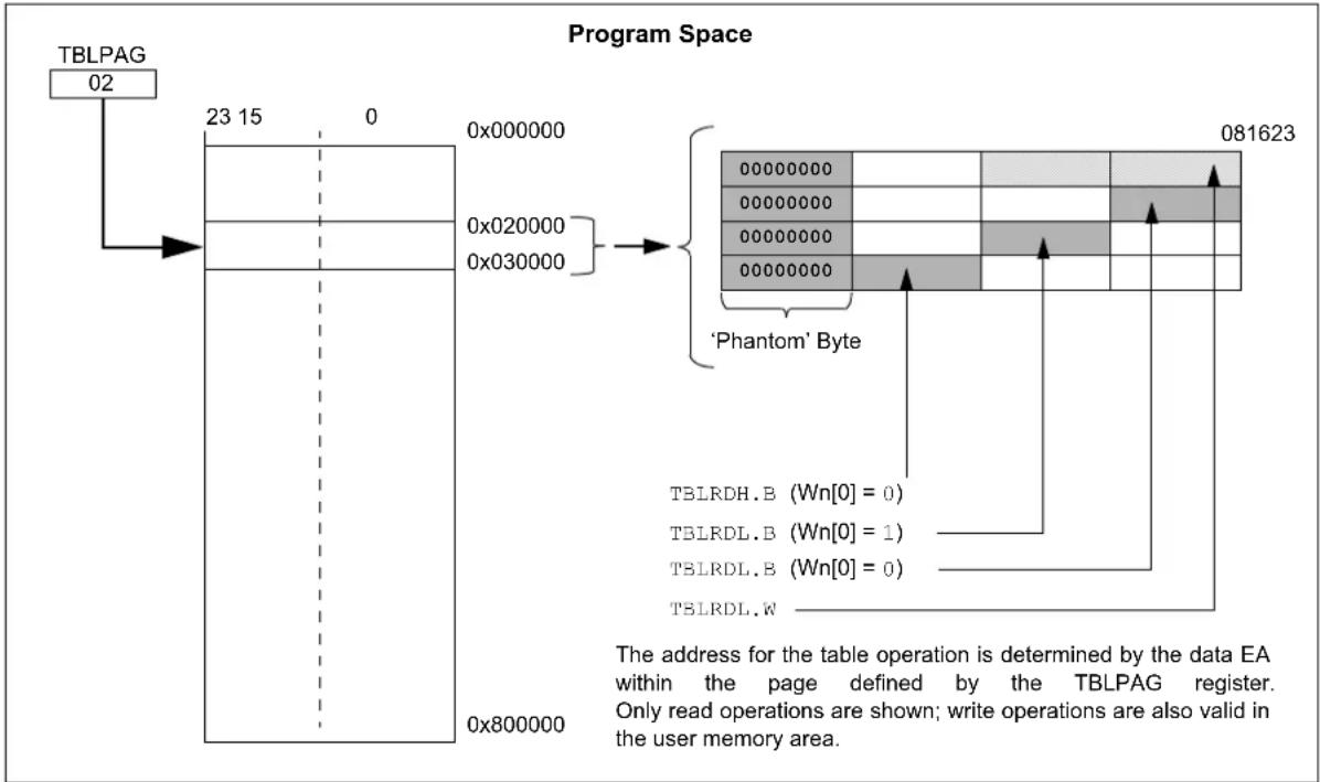
flowchart
graph TD
    A["TBLPAG 02"] --> B["Program Space"]
    B --> C["0x000000"]
    B --> D["0x020000"]
    B --> E["0x030000"]
    C --> F["081623"]
    D --> F
    E --> F
    F --> G["'Phantom' Byte"]
    G --> H["TBLRDH.B (Wn[0"] = 0)]
    G --> I["TBLRDL.B (Wn[0"] = 1)]
    G --> J["TBLRDL.B (Wn[0"] = 0)]
    G --> K["TSLRDL.W"]
    style A fill:#f9f,stroke:#333
    style B fill:#ccf,stroke:#333
    style C fill:#cfc,stroke:#333
    style D fill:#fcc,stroke:#333
    style E fill:#cff,stroke:#333
    style F fill:#ffc,stroke:#333
    style G fill:#cfc,stroke:#333
    style H fill:#fcc,stroke:#333
    style I fill:#fcc,stroke:#333
    style J fill:#fcc,stroke:#333
    style K fill:#fcc,stroke:#333
3.3 Main Flash Program Memory
Note 1: This data sheet summarizes the features of the dsPIC33CH128MP508 family of devices. It is not intended to be a comprehensive reference source. To complement the information in this data sheet, refer to “Flash Programming” (www.microchip.com/DS70000609), which is available from the Microchip website (www.microchip.com).
2: This section refers to the “Dual Partition Flash Program Memory” (www.microchip.com/DS70005156), but the Dual Partition is not implemented in the Main Flash.
The dsPIC33CH128MP508 family devices contain internal Flash program memory for storing and executing application code. The memory is readable, writable and erasable during normal operation over the entire VDD range.
Flash memory can be programmed in three ways:
• In-Circuit Serial Programming (ICSP) programming capability
- Enhanced In-Circuit Serial Programming (Enhanced ICSP)
• Run-Time Self-Programming (RTSP)
ICSP allows for a dsPIC33CH128MP508 family device to be serially programmed while in the end application circuit. This is done with a Programming Clock and Programming Data (PGCx/PGDx) line, and three other lines for power (VDD), ground (Vss) and Master Clear (MCLR). This allows customers to manufacture boards with unprogrammed devices and then program the device just before shipping the product. This also allows the most recent firmware or a custom firmware to be programmed.
Enhanced In-Circuit Serial Programming uses an on-board bootloader, known as the Program Executive, to manage the programming process. Using an SPI data frame format, the Program Executive can erase, program and verify program memory. For more information on Enhanced ICSP, see the device programming specification.
RTSP allows the Main Flash user application code to update itself during run time. The feature is capable of writing a single program memory word (two instructions) or an entire row as needed.
3.3.1 FLASH PROGRAMMING OPERATIONS
For ICSP and RTSP programming of the Main Flash, TBLWTL and TBLWTH instructions are used to write to the NVM write latches. An NVM write operation then writes the contents of both latches to the Flash, starting at the address defined by the contents of TBLPAG, and the NVMADR and NVMADRU registers.
Programmers can program two adjacent words (24 bits x 2) of Program Flash Memory at a time on every other word address boundary (0x000002, 0x000006, 0x00000A, etc.). To do this, it is necessary to erase the page that contains the desired address of the location the user wants to change. For protection against accidental operations, the write initiate sequence for NVMKEY must be used to allow any erase or program operation to proceed. After the programming command has been executed, the user application must wait for the programming time until programming is complete.
Regardless of the method used to program the Flash, a few basic requirements should be met:
- A full 48-bit double instruction word should always be programmed to a Flash location. Either instruction may simply be a NOP to fulfill this requirement. This ensures a valid ECC value is generated for each pair of instructions written.
• Assuming the above step is followed, the last 24-bit location in implemented program space should never be executed. The penultimate instruction must contain a program flow change instruction, such as a RETURN or BRA instruction.
FIGURE 3-14: ADDRESSING FOR TABLE REGISTERS
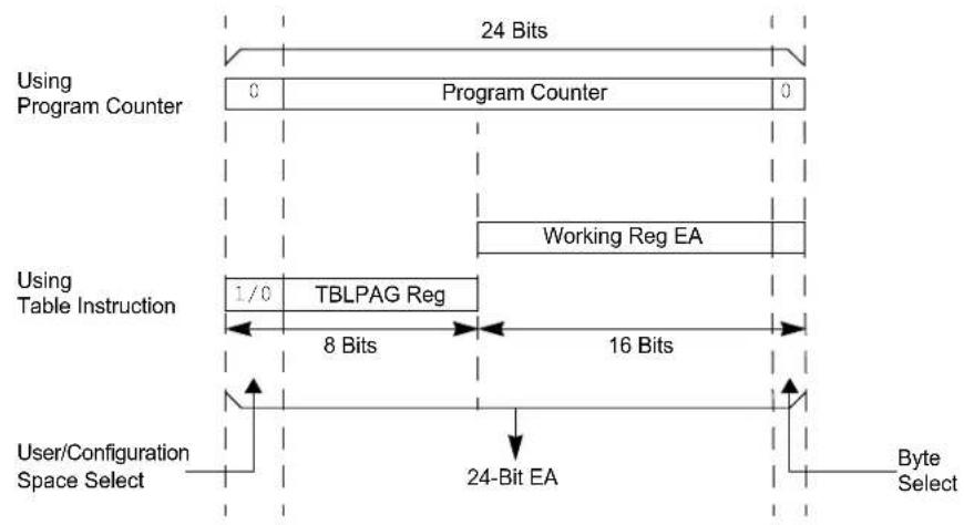
text_image
Using Program Counter 24 Bits 0 Program Counter 0 Working Reg EA Using Table Instruction 1/0 TBLPAG Reg 8 Bits 16 Bits User/Configuration Space Select 24-Bit EA Byte SelectRTSP allows the user application to program one double instruction word or one row at a time. The double instruction word write blocks and single row write blocks are edge-aligned, from the beginning of program memory, on boundaries of one double instruction word and 64 double instruction words, respectively.
The basic sequence for RTSP programming is to first load two 24-bit instructions into the NVM write latches found in configuration memory space. Refer to Figure 3-3
through Figure 3-4 for write latch addresses. Then, the WR bit in the NVMCON register is set to initiate the write process. The processor stalls (waits) until the programming operation is finished. The WR bit is automatically cleared when the operation is finished.
Double instruction word writes are performed by manually loading both write latches, using TBLWTL and TBLWTH instructions, and then initiating the NVM write while the NVMOPx bits are set to '0x1'. The program space destination address is defined by the NVMADR/U registers.
EXAMPLE 3-1: FLASH WRITE/READ
/////Flash write///////
//Sample code for writing 0x123456 to address locations 0x10000 / 10002
NVMCON = 0x4001;
TBLPAG = 0xFA; // write latch upper address
NVMADR = 0x0000; // set target write address of general segment
NVMADRU = 0x0001;
__builtin_tblwt1(0, 0x3456); // load write latches
__builtin_tblwth (0, 0x12);

__builtin_tblwt1(2, 0x3456); // load write latches
__builtin_tblwth (2, 0x12);

asm volatile ("disi #5");
__builtin_write_NVM();
while(_WR == 1);

/////Flash Read///////
//Sample code to read the Flash content of address 0x10000
// readDataL/ readDataH variables need to defined
TBLPAG = 0x0001;
readDataL = __builtin_tblrdl(0x0000);
readDataH = __builtin_tblrdh(0x0000);
Row programming is performed by first loading 128 instructions into data RAM and then loading the address of the first instruction in that row into the NVMSRCADRL/H registers. Once the write has been initiated, the device will automatically load two instructions into the write latches and write them to the program space destination address defined by the NVMADR/U registers.
The operation will increment the NVMSRCADRL/H and the NVMADR/U registers until all double instruction words have been programmed.
The RPDF bit (NVMCON[9]) selects the format of the stored data in RAM to be either compressed or uncompressed. See Figure 3-15 for data formatting. Compressed data help to reduce the amount of required RAM by using the upper byte of the second word for the MSB of the second instruction.
All erase and program operations may optionally use the NVM interrupt to signal the successful completion of the operation.
FIGURE 3-15: UNCOMPRESSED/
COMPRESSED FORMAT

text_image
715 0 LSW1 Even Byte Address MSB10x00 LSW2 MSB20x00 UNCOMPRESSED FORMAT (RPDF = 0) 715 0 LSW1 Even Byte Address MSB1MSB2 LSW2 COMPRESSED FORMAT (RPDF = 1)3.3.3 ERROR CORRECTING CODE (ECC)
In order to improve program memory performance and durability, the devices include Error Correcting Code functionality (ECC) as an integral part of the Flash memory controller. ECC can determine the presence of single bit errors in program data, including which bit is in error, and correct the data automatically without user intervention. ECC cannot be disabled.
When data are written to program memory, ECC generates a 7-bit Hamming code parity value for every two (24-bit) instruction words. The data are stored in blocks of 48 data bits and seven parity bits; parity data are not memory-mapped and are inaccessible. When the data are read back, the ECC calculates the parity on it and compares it to the previously stored parity value. If a parity mismatch occurs, there are two possible outcomes:
- Single bit error has occurred and has been automatically corrected on readback.
- Double-bit error has occurred and the read data are not changed.
Single bit error occurrence can be identified by the state of the ECCSBEIF (IFS0[13]) bit. An interrupt can be generated when the corresponding interrupt enable bit is set, ECCSBEIE (IEC0[13]). The ECCSTATL register contains the parity information for single bit errors. The SECOUT[7:0] bit field contains the expected calculated SEC parity and SECIN[7:0] bits contain the actual value from a Flash read operation. The SECSYNDx bits (ECCSTATH[7:0]) indicate the bit position of the single bit error within the 48-bit pair of instruction words. When no error is present, SECINx equals SECOUTx and SECSYNDx is zero.
Double-bit errors result in a generic hard trap. The ECCDBE bit (INTCON4[1]) will be set to identify the source of the hard trap. If no Interrupt Service Routine is implemented for the hard trap, a device Reset will also occur. The ECCSTATH register contains double-bit error status information. The DEDOUT bit is the expected calculated DED parity and DEDIN is the actual value from a Flash read operation. When no error is present, DEDIN equals DEDOUT.
3.3.3.1 ECC Fault Injection
To test Fault handling, an EEC error can be generated. Both single and double-bit errors can be generated in both the read and write data paths. Read path Fault injection first reads the Flash data and then modifies them prior to entering the ECC logic. Write path Fault injection modifies the actual data prior to them being written into the target Flash and will cause an EEC error on subsequent Flash read. The following procedure is used to inject a Fault:
- Load Flash target address into the ECCADDR register.
- Select 1st Fault bit determined by FLT1PTRx (ECCCONH[7:0]). The target bit is inverted to create the Fault.
- If a double Fault is desired, select the 2nd Fault bit determined by FLT2PTRx (ECCCONH[15:8]), otherwise set to all '1's.
- Write the NVMKEY unlock sequence.
- Enable the ECC Fault injection logic by setting the FLTINJ bit (ECCCONL[0])
- Perform a read or write to the Flash target address.
3.3.4 CONTROL REGISTERS
Five SFRs are used to write and erase the Program Flash Memory: NVMCON, NVMKEY, NVMADR, NVMADRU and NVMSRCADRL/H.
The NVMCON register (Register 3-6) selects the operation to be performed (page erase, word/row program, Inactive Partition erase) and initiates the program or erase cycle.
NVMKEY (Register 3-9) is a write-only register that is used for write protection. To start a programming or erase sequence, the user application must consecutively write 0x55 and 0xAA to the NVMKEY register.
There are two NVM Address registers: NVMADR and NVMADRU. These two registers, when concatenated, form the 24-bit Effective Address (EA) of the selected word/row for programming operations, or the selected page for erase operations. The NVMADRU register is used to hold the upper eight bits of the EA, while the NVMADR register is used to hold the lower 16 bits of the EA.
For row programming operation, data to be written to Program Flash Memory are written into data memory space (RAM) at an address defined by the NVMSRCADRL/H register (location of first element in row programming data).
3.3.5 NVM CONTROL REGISTERS
REGISTER 3-6: NVMCON: NONVOLATILE MEMORY (NVM) CONTROL REGISTER
| R/SO-0^(1) | R/W-0^(1) | R/W-0^(1) | R/W-0 | U-0 | U-0 | R/W-0 | R/C-0 | |
| WR WREN | WRERR NV | MSIDL | (2) | — — | RP | DF URERR | ||
| bit 15 bit 8 | ||||||||
| U-0 U-0 | U-0 | U-0 | R/W-0 | (1) | R/W-0^(1) | R/W-0^(1) | R/W-0^(1) |
| — | — | — | — | NVMOP[3:0] ^(3,4) | |||
| bit 7 bit 0 | |||||||
| Legend: | C = Clearable bit | SO = Settable Only bit | |
| R = Readable bit | W = Writable bit | U = Unimplemented bit, read as ‘0’ | |
| -n = Value at POR | ‘1’ = Bit is set | ‘0’ = Bit is cleared | x = Bit is unknown |
bit 15 WR: Write Control bit ^(1)
1 = Initiates a Flash memory program or erase operation; the operation is self-timed and the bit is cleared by hardware once the operation is complete
0 = Program or erase operation is complete and inactive
bit 14 WREN: Write Enable bit ^(1)
1 = Enables Flash program/erase operations
0 = Inhibits Flash program/erase operations
bit 13 WRERR: Write Sequence Error Flag bit ^(1)
1 = An improper program or erase sequence attempt, or termination has occurred (bit is set automatically on any set attempt of the WR bit)
0 = The program or erase operation completed normally
bit 12 NVMSIDL: NVM Stop in Idle Control bit ^(2)
1 = Flash voltage regulator goes into Standby mode during Idle mode
0 = Flash voltage regulator is active during Idle mode
bit 11-10 Unimplemented: Read as '0'
bit 9 RPDF: Row Programming Data Format bit
1 = Row data to be stored in RAM are in compressed format
0 = Row data to be stored in RAM are in uncompressed format
bit 8 URERR: Row Programming Data Underrun Error bit
1 = Indicates row programming operation has been terminated
0 = No data underrun error is detected
bit 7-4 Unimplemented: Read as '0'
Note 1: These bits can only be reset on a POR.
2: If this bit is set, there will be minimal power savings (IIDLE), and upon exiting Idle mode, there is a delay (TVREG) before Flash memory becomes operational.
3: All other combinations of NVMOP[3:0] are unimplemented.
4: Execution of the PWRSAV instruction is ignored while any of the NVM operations are in progress.
5: Two adjacent words on a 4-word boundary are programmed during execution of this operation.
REGISTER 3-6: NVMCON: NONVOLATILE MEMORY (NVM) CONTROL REGISTER (CONTINUED)
bit 3-0 NVMOP[3:0]: NVM Operation Select bits (1,3,4)
1111 = Reserved 1110 = User memory bulk erase operation 1101 = Reserved 1100 = Reserved 1011 = Reserved 1010 = Reserved 1001 = Reserved 1000 = Reserved 0111 = Reserved 0101 = Reserved 0100 = Reserved 0011 = Memory page erase operation 0010 = Memory row program operation 0001 = Memory double-word operation ^(5) 0000 = Reserved
Note 1: These bits can only be reset on a POR.
2: If this bit is set, there will be minimal power savings (1 IDLE), and upon exiting Idle mode, there is a delay (TVREG) before Flash memory becomes operational.
3: All other combinations of NVMOP[3:0] are unimplemented.
4: Execution of the PWRSAV instruction is ignored while any of the NVM operations are in progress.
5: Two adjacent words on a 4-word boundary are programmed during execution of this operation.
REGISTER 3-7: NVMADR: NONVOLATILE MEMORY LOWER ADDRESS REGISTER
| R/W-x R/W-x R/W-x R/W-x R/W-x R/W-x R/W-x R/W-x |
| NVMADR[15:8] |
| bit 15 bit 8 |
| R/W-x R/W-x R/W-x R/W-x R/W-x R/W-x R/W-x R/W-x |
| NVMADR[7:0] |
| bit 7 bit 0 |
Legend:
R = Readable bit W = Writable bit U = Unimplemented bit, read as '0'
-n = Value at POR '1' = Bit is set '0' = Bit is cleared x = Bit is unknown
bit 15-0 NVMADR[15:0]: Nonvolatile Memory Lower Write Address bits
Selects the lower 16 bits of the location to program or erase in Program Flash Memory. This register may be read or written to by the user application.
REGISTER 3-8: NVMADRU: NONVOLATILE MEMORY UPPER ADDRESS REGISTER
| R/W-x R/W-x R/W-x R/W-x R/W-x R/W-x R/W-x R/W-x |
| NVMADRU[23:16] |
| bit 7 bit 0 |
Legend:
R = Readable bit W = Writable bit U = Unimplemented bit, read as '0'
-n = Value at POR '1' = Bit is set '0' = Bit is cleared x = Bit is unknown
bit 15-8 Unimplemented: Read as '0'
bit 7-0 NVMADRU[23:16]: Nonvolatile Memory Upper Write Address bits
Selects the upper eight bits of the location to program or erase in Program Flash Memory. This register may be read or written to by the user application.
REGISTER 3-9: NVMKEY: NONVOLATILE MEMORY KEY REGISTER
| U-0 U-0 U-0 U-0 U-0 U-0 U-0 U-0 | |||||||
| — — — + | + | + — | — | ||||
| bit 15 | bit 8 | ||||||
| W-0 | W-0 | W-0 | W-0 | W-0 | W-0 | W-0 | W-0 |
| NVMKEY[7:0] | |||||||
| bit 7 | bit 0 | ||||||
Legend:
| R = Readable bit | W = Writable bit | U = Unimplemented bit, read as '0' |
| -n = Value at POR | '1' = Bit is set | '0' = Bit is cleared x = Bit is unknown |
bit 15-8 Unimplemented: Read as '0'
bit 7-0 NVMKEY[7:0]: NVM Key Register bits (write-only)
REGISTER 3-10: NVMSRCADRL: NVM SOURCE DATA ADDRESS REGISTER LOW
| R/W-0 R/W-0 R/W-0 R/W-0 R/W-0 R/W-0 R/W-0 R/W-0 |
| NVMSRCADR[15:8] |
| bit 15 bit 8 |
| R/W-0 R/W-0 R/W-0 R/W-0 R/W-0 R/W-0 R/W-0 R/W-0 |
| NVMSRCADR[7:0] |
| bit 7 bit 0 |
| Legend: | |||
| R = Readable bit W = Writable bit U = Unimplemented bit, read as ‘0’ | |||
| -n = Value at POR | ‘1’ = Bit is set | ‘0’ = Bit is cleared | x = Bit is unknown |
bit 15-0 NVMSRCADR[15:0]: NVM Source Data Address bits
The RAM address of the data to be programmed into Flash when the NVMOP[3:0] bits are set to row programming.
REGISTER 3-11: NVMSRCADRH: NVM SOURCE DATA ADDRESS REGISTER HIGH
| R/W-0 R/W-0 R/W-0 R/W-0 R/W-0 R/W-0 R/W-0 R/W-0 |
| NVMSRCADR[23:16] |
| bit 7 bit 0 |
| Legend: | |||
| R = Readable bit W = Writable bit U = Unimplemented bit, read as ‘0’ | |||
| -n = Value at POR | ‘1’ = Bit is set | ‘0’ = Bit is cleared | x = Bit is unknown |
bit 15-8 Unimplemented: Read as '0'
bit 7-0 NVMSRCADR[23:16]: NVM Source Data Address bits
The RAM address of the data to be programmed into Flash when the NVMOP[3:0] bits are set to row programming.
3.3.6 ECC CONTROL REGISTERS
REGISTER 3-12: ECCCONL: ECC FAULT INJECTION CONFIGURATION REGISTER LOW
| R = Readable bit | W = Writable bit | U = Unimplemented bit, read as '0' |
| -n = Value at POR | ‘1’ = Bit is set | ‘0’ = Bit is cleared x = Bit is unknown |
bit 15-1 Unimplemented: Read as '0'
bit 0 FLTINJ: Fault Injection Sequence Enable bit
1 = Enabled
0 = Disabled
REGISTER 3-13: ECCCONH: ECC FAULT INJECTION CONFIGURATION REGISTER HIGH
| R/W-0 | R/W-0 | R/W-0 | R/W-0 | R/W-0 | R/W-0 | R/W-0 | R/W-0 |
| FLT2PTR[7:0] | |||||||
| bit 15 | bit 8 | ||||||
| R/W-0 | R/W-0 | R/W-0 | R/W-0 | R/W-0 | R/W-0 | R/W-0 | R/W-0 |
| FLT1PTR[7:0] | |||||||
| bit 7 | bit 0 | ||||||
Legend:
| R = Readable bit | W = Writable bit | U = Unimplemented bit, read as '0' |
| -n = Value at POR | ‘1’ = Bit is set | ‘0’ = Bit is cleared x = Bit is unknown |
bit 15-8 FLT2PTR[7:0]: ECC Fault Injection Bit Pointer 2
11111111-00111000 = No Fault injection occurs
00110111 = Fault injection (bit inversion) occurs on bit 55 of ECC bit order
...
00000001 = Fault injection (bit inversion) occurs on bit 1 of ECC bit order
00000000 = Fault injection (bit inversion) occurs on bit 0 of ECC bit order
bit 7-0 FLT1PTR[7:0]: ECC Fault Injection Bit Pointer 1
11111111-00111000 = No Fault injection occurs
00110111 = Fault injection occurs on bit 55 of ECC bit order
...
00000001 = Fault injection occurs on bit 1 of ECC bit order
00000000 = Fault injection occurs on bit 0 of ECC bit order
REGISTER 3-14: ECCADDRL: ECC FAULT INJECT ADDRESS COMPARE REGISTER LOW
| R/W-0 R/W-0 R/W-0 R/W-0 R/W-0 R/W-0 R/W-0 R/W-0 |
| ECCADDR[15:8] |
| bit 15 bit 8 |
| R/W-0 R/W-0 R/W-0 R/W-0 R/W-0 R/W-0 R/W-0 R/W-0 |
| ECCADDR[7:0] |
| bit 7 bit 0 |
Legend:
| R = Readable bit W = Writable bit U = Unimplemented bit, read as '0' | ||
| -n = Value at POR | '1' = Bit is set | '0' = Bit is cleared x = Bit is unknown |
bit 15-0 ECCADDR[15:0]: ECC Fault Injection NVM Address Match Compare bits
REGISTER 3-15: ECCADDRH: ECC FAULT INJECT ADDRESS COMPARE REGISTER HIGH
| R/W-0 R/W-0 R/W-0 R/W-0 R/W-0 R/W-0 R/W-0 R/W-0 |
| ECCADDR[31:24] |
| bit 15 bit 8 |
| R/W-0 R/W-0 R/W-0 R/W-0 R/W-0 R/W-0 R/W-0 R/W-0 |
| ECCADDR[23:16] |
| bit 7 bit 0 |
Legend:
| R = Readable bit W = Writable bit U = Unimplemented bit, read as '0' | ||
| -n = Value at POR | '1' = Bit is set | '0' = Bit is cleared x = Bit is unknown |
bit 15-0 ECCADDR[31:16]: ECC Fault Injection NVM Address Match Compare bits
REGISTER 3-16: ECCSTATL: ECC SYSTEM STATUS DISPLAY REGISTER LOW
| R-0 R-0 R-0 R-0 R-0 R-0 R-0 R-0 |
| SECOUT[7:0] |
| bit 15 bit 8 |
| R-0 R-0 R-0 R-0 R-0 R-0 R-0 R-0 |
| SECIN[7:0 |
| bit 7 bit 0 |
Legend:
| R = Readable bit W = Writable bit U = Unimplemented bit, read as '0' | ||
| -n = Value at POR | '1' = Bit is set | '0' = Bit is cleared x = Bit is unknown |
bit 15-8 SECOUT[7:0]: Calculated Single Error Correction Parity Value bits
bit 7-0 SECIN[7:0]: Read Single Error Correction Parity Value bits
Bits are the actual parity value of a Flash read operation.
REGISTER 3-17: ECCSTATH: ECC SYSTEM STATUS DISPLAY REGISTER HIGH
| U-0 U-0 U-0 U-0 U-0 R-0 R-0 | |||||||
| — | — | — | — | — | — | DEDOUT | DEDIN |
| bit 15 bit 8 | |||||||
| R-0 R-0 R-0 R-0 R-0 R-0 R-0 R-0 |
| SECSYND[7:0] |
| bit 7 bit 0 |
Legend:
| R = Readable bit W = Writable bit U = Unimplemented bit, read as '0' | |||
| -n = Value at POR | '1' = Bit is set | '0' = Bit is cleared | x = Bit is unknown |
bit 15-10 Unimplemented: Read as '0'
bit 9 DEDOUT: Calculated Dual Bit Error Detection Parity bit
bit 8 DEDIN: Read Dual Bit Error Detection Parity bit
bit 7-0 SECSYND[7:0]: Calculated ECC Syndrome Value bits
Indicates the bit location that contains the error.
3.4 Master Resets
Note 1: This data sheet summarizes the features of the dsPIC33CH128MP508 family of devices. It is not intended to be a comprehensive reference source. To complement the information in this data sheet, refer to “Reset” (www.microchip.com/DS70000602), which is available from the Microchip website (www.microchip.com).
The Reset module combines all Reset sources and controls the device Master Reset Signal, SYSRST. The following is a list of device Reset sources:
- POR: Power-on Reset
• BOR: Brown-out Reset
• M C LMBster Clear Pin Reset - S W R : RESET Instruction
- WDTO: Watchdog Timer Time-out Reset
• CM: Configuration Mismatch Reset
• TRAPR: Trap Conflict Reset
• IOPUWR: Illegal Condition Device Reset - Illegal Opcode Reset
- Uninitialized W Register Reset
- Security Reset
A simplified block diagram of the Reset module is shown in Figure 3-16.
Any active source of Reset will make the SYSRST signal active. On system Reset, some of the registers associated with the CPU and peripherals are forced to a known Reset state, and some are unaffected.
Note: Refer to the specific peripheral section or Section 3.2 "Main Memory Organization" of this data sheet for register Reset states.
All types of device Reset set a corresponding status bit in the RCON register to indicate the type of Reset (see Register 3-18).
A POR clears all the bits, except for the BOR and POR bits (RCON[1:0]) that are set. The user application can set or clear any bit, at any time, during code execution. The RCON bits only serve as status bits. Setting a particular Reset status bit in software does not cause a device Reset to occur.
The RCON register also has other bits associated with the Watchdog Timer and device power-saving states. The function of these bits is discussed in other sections of this data sheet.
Note: The status bits in the RCON register should be cleared after they are read so that the next RCON register value after a device Reset is meaningful.
For all Resets, the default clock source is determined by the FNOSC[2:0] bits in the FOSCSEL Configuration register. The value of the FNOSCx bits is loaded into the NOSC[2:0] (OSCCON[10:8]) bits on Reset, which in turn, initializes the system clock.
FIGURE 3-16: MASTER RESET SYSTEM BLOCK DIAGRAM
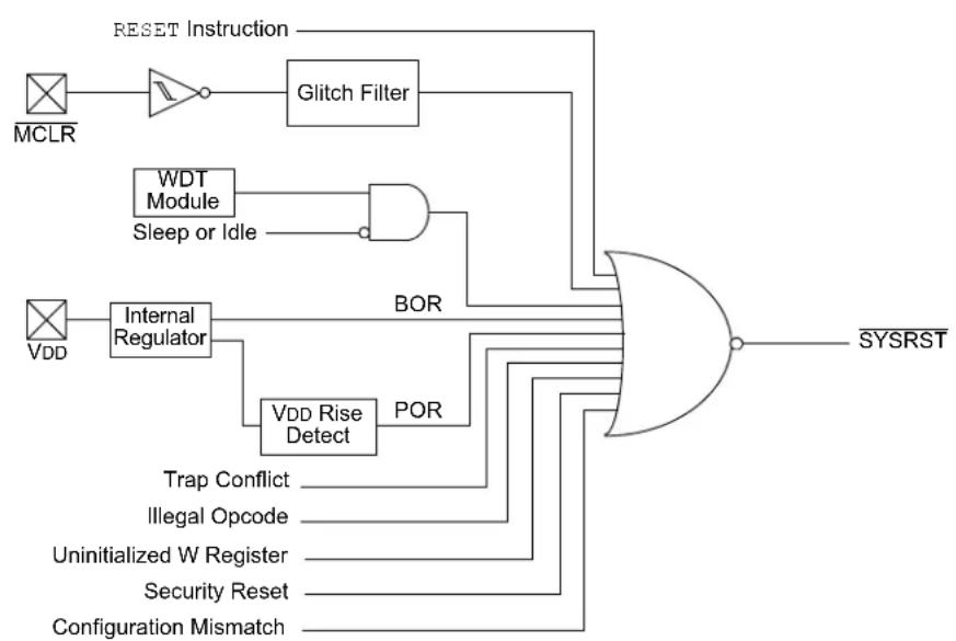
flowchart
graph TD
    A["MCLR"] --> B["Reset Instruction"]
    B --> C["Glitch Filter"]
    C --> D["AND"]
    E["WDT Module\nSleep or Idle"] --> D
    F["VDD"] --> G["Internal Regulator"]
    G --> H["BOR"]
    H --> I["AND"]
    I --> J["SYSRST"]
    K["VDD Rise Detect"] --> L["POR"]
    L --> I
    M["Trap Conflict"] --> I
    N["Illegal Opcode"] --> I
    O["Uninitialized W Register"] --> I
    P["Security Reset"] --> I
    Q["Configuration Mismatch"] --> I
3.4.1 RESET RESOURCES
Many useful resources are provided on the main product page of the Microchip website for the devices listed in this data sheet. This product page contains the latest updates and additional information.
- “Reset” (www.microchip.com/DS70000602)
- Code Samples
- Application Notes
- Software Libraries
- Webinars
- All Related "dsPIC33/PIC24 Family Reference Manual" Sections
- Development Tools
3.4.2 RESET CONTROL REGISTER
REGISTER 3-18: RCON: RESET CONTROL REGISTER (1)
| R/W-0 R/W-0 U-0 U-0 U-0 R/W-0 R/W-0 | |||||||
| TRAPR | IOPUWR | — | — | — | — | CM | VREGS |
| bit 15 bit 8 | |||||||
| R/W-0 | R/W-0 | U-0 | R/W-0 | R/W-0 | R/W-0 | R/W-1 | R/W-1 |
| EXTR SWR | — | WDTO | SLEEP | IDLE | BOR | POR | |
| bit 7 bit 0 | |||||||
Legend:
| R = Readable bit | W = Writable bit | U = Unimplemented bit, read as '0' |
| -n = Value at POR | '1' = Bit is set | '0' = Bit is cleared x = Bit is unknown |
bit 15 TRAPR: Trap Reset Flag bit
1 = A Trap Conflict Reset has occurred
0 = A Trap Conflict Reset has not occurred
bit 14 IOPUWR: Illegal Opcode or Uninitialized W Register Access Reset Flag bit
1 = An illegal opcode detection, an illegal address mode or Uninitialized W register used as an Address Pointer caused a Reset
0 = An illegal opcode or Uninitialized W Register Reset has not occurred
bit 13-10 Unimplemented: Read as '0'
bit 9 CM: Configuration Mismatch Flag bit
1 = A Configuration Mismatch Reset has occurred.
0 = A Configuration Mismatch Reset has not occurred
bit 8 VREGS: Voltage Regulator Standby During Sleep bit
1 = Voltage regulator is active during Sleep
0 = Voltage regulator goes into Standby mode during Sleep
bit 7 EXTR: External Reset (MCLR) Pin bit
1 = A Master Clear (pin) Reset has occurred
0 = A Master Clear (pin) Reset has not occurred
bit 6 SWR: Software RESET (Instruction) Flag bit
1 = A RESET instruction has been executed
0 = A RESET instruction has not been executed
bit 5 Unimplemented: Read as '0'
bit 4 WDTO: Watchdog Timer Time-out Flag bit
1 = WDT time-out has occurred
0 = WDT time-out has not occurred
bit 3 SLEEP: Wake-up from Sleep Flag bit
1 = Device has been in Sleep mode
0 = Device has not been in Sleep mode
bit 2 IDLE: Wake-up from Idle Flag bit
1 = Device has been in Idle mode
0 = Device has not been in Idle mode
bit 1 BOR: Brown-out Reset Flag bit
1 = A Brown-out Reset has occurred
0 = A Brown-out Reset has not occurred
Note 1: All of the Reset status bits can be set or cleared in software. Setting one of these bits in software does not cause a device Reset.
REGISTER 3-18: RCON: RESET CONTROL REGISTER (1) (CONTINUED)
bit 0 POR: Power-on Reset Flag bit
1 = A Power-on Reset has occurred
0 = A Power-on Reset has not occurred
Note 1: All of the Reset status bits can be set or cleared in software. Setting one of these bits in software does not cause a device Reset.
3.5 Main Interrupt Controller
Note 1: This data sheet summarizes the features of the dsPIC33CH128MP508 family of devices. It is not intended to be a comprehensive reference source. To complement the information in this data sheet, refer to “Interrupts” (www.microchip.com/DS70000600), which is available from the Microchip website (www.microchip.com).
The dsPIC33CH128MP508 family interrupt controller reduces the numerous peripheral interrupt request signals to a single interrupt request signal to the dsPIC33CH128MP508 family CPU.
The interrupt controller has the following features:
- Six Processor Exceptions and Software Traps
- Seven User-Selectable Priority Levels
- Interrupt Vector Table (IVT) with a Unique Vector for each Interrupt or Exception Source
- Fixed Priority within a Specified User Priority Level
• Fixed Interrupt Entry and Return Latencies - Alternate Interrupt Vector Table (AIVT) for Debug Support
3.5.1 INTERRUPT VECTOR TABLE
The dsPIC33CH128MP508 family Interrupt Vector Table (IVT), shown in Figure 3-17, resides in program memory, starting at location, 000004h. The IVT contains six non-maskable trap vectors and up to 246 sources of interrupts. In general, each interrupt source has its own vector. Each interrupt vector contains a 24-bit wide address. The value programmed into each interrupt vector location is the starting address of the associated Interrupt Service Routine (ISR).
Interrupt vectors are prioritized in terms of their natural priority. This priority is linked to their position in the vector table. Lower addresses generally have a higher natural priority. For example, the interrupt associated with Vector 0 takes priority over interrupts at any other vector address.
3.5.1.1 Alternate Interrupt Vector Table
The Alternate Interrupt Vector Table (AIVT), shown in Figure 3-18, is available only when the Boot Segment (BS) is defined and the AIVT has been enabled. To enable the Alternate Interrupt Vector Table, the Configuration bit, AIVTDIS in the FSEC register, must be programmed and the AIVTEN bit must be set (INTCON2[8] = 1). When the AIVT is enabled, all interrupt and exception processes use the alternate vectors instead of the default vectors. The AIVT begins at the start of the last page of the Boot Segment, defined by BSLIM[12:0]. The second half of the page is no longer usable space. The Boot Segment must be at least two pages to enable the AIVT.
Note: Although the Boot Segment must be enabled in order to enable the AIVT, application code does not need to be present inside of the Boot Segment. The AIVT (and IVT) will inherit the Boot Segment code protection.
The AIVT supports debugging by providing a means to switch between an application and a support environment without requiring the interrupt vectors to be reprogrammed. This feature also enables switching between applications for evaluation of different software algorithms at run time.
3.5.2 RESET SEQUENCE
A device Reset is not a true exception because the interrupt controller is not involved in the Reset process. The dsPIC33CH128MP508 family devices clear their registers in response to a Reset, which forces the PC to zero. The device then begins program execution at location, 0x000000. A GOTO instruction at the Reset address can redirect program execution to the appropriate start-up routine.
Note: Any unimplemented or unused vector locations in the IVT should be programmed with the address of a default interrupt handler routine that contains a RESET instruction.
FIGURE 3-17: dsPIC33CH128MP508 FAMILY MAIN INTERRUPT VECTOR TABLE

bar_stacked
| Interrupt Vector | Value | | :--- | :--- | | Interrupt Vector 0 | 0x000012 | | Interrupt Vector 1 | 0x000014 | | :--- | :--- | | :--- | :--- | | :--- | :--- | | Interrupt Vector 52 | 0x00007C | | Interrupt Vector 53 | 0x00007E | | Interrupt Vector 54 | 0x000080 | | :--- | :--- | | :--- | :--- | | :--- | :--- | | Interrupt Vector 116 | 0x0000FC | | Interrupt Vector 117 | 0x0000FE | | Interrupt Vector 118 | 0x000100 | | Interrupt Vector 119 | 0x000102 | | Interrupt Vector 120 | 0x000104 | | :--- | :--- | | :--- | :--- | | :--- | :--- | | Interrupt Vector 244 | 0x0001FC | | Interrupt Vector 245 | 0x0001FE | | START OF CODE | 0x000200 | The image displays a vertical arrow labeled 'IVT' pointing to the left side of the chart, which is used as a stylistic or textual representation rather than a chart type (e.g., bar, line, pie). The text 'See Table 3-19 for Interrupt Vector Details' appears in the rightmost corner.FIGURE 3-18: dsPIC33CH128MP508 ALTERNATE MAIN INTERRUPT VECTOR TABLE
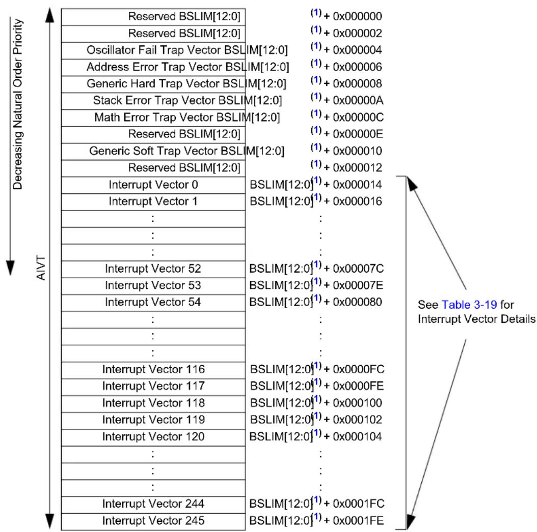
Note 1: The address depends on the size of the Boot Segment defined by BSLIM[12:0]: [([12:0]-1)×0x800]+Offset.
TABLE 3-23: TRAP TABLE
| Trap Description | MPLAB®XC16 Trap ISR Name | Vector # | IVT Address | Trap Bit Location | |||
| Generic Flag | Source Flag | Enable | Priority Level | ||||
| Oscillator Failure Trap _OscillatorFail 0 0x00000 | 04 INTCON1[1] | — — | 1 | 5 | |||
| Address Error Trap _AddressError 1 0x00000 | 006 INTCON1[3] | — — | 1 | 4 | |||
| Generic Hard Trap – ECCDBE | _HardTrapError | 2 | 0x000008 | — | INTCON4[1] | — | 1 |
| Generic Hard Trap – SGHT _HardTrapError | 2 0x000008 | — | INTCON4[0] | INTCON2[13] | 13 | ||
| Stack Error Trap | _StackError | 3 | 0x00000A | INTCON1[2] | — — | 1 | 2 |
| Math Error Trap – OVAERR | _MathError | 4 | 0x00000C | INTCON1[4] | INTCON1[14] | INTCON1[10] | 11 |
| Math Error Trap – OVBERR | _MathError | 4 | 0x00000C | INTCON1[4] | INTCON1[13] | INTCON1[9] | 11 |
| Math Error Trap – COVAERR | _MathError | 4 | 0x00000C | INTCON1[4] | INTCON1[12] | INTCON1[8] | 11 |
| Math Error Trap – COVBERR | _MathError | 4 | 0x00000C | INTCON1[4] | INTCON1[11] | INTCON1[8] | 11 |
| Math Error Trap – SFTACERR | _MathError | 4 | 0x00000C | INTCON1[4] | INTCON1[7] | INTCON1[8] | 11 |
| Math Error Trap – DIV0ERR | _MathError | 4 | 0x00000C | INTCON1[4] | INTCON1[6] | INTCON1[8] | 11 |
| Reserved | Reserved | 5 | 0x00000E | — | — | — | — |
| Generic Soft Trap – CAN | _SoftTrapError | 6 0x000010 | — | INTCON3[9] | — | 9 | |
| Generic Soft Trap – NAE | _SoftTrapError | 6 0x000010 | — | INTCON3[8] | — | 9 | |
| Generic Soft Trap – CAN2 | _SoftTrapError | 6 0x000010 | — | INTCON3[6] | — | 9 | |
| Generic Soft Trap – DAE | _SoftTrapError | 6 0x000010 | — | INTCON3[5] | — | 9 | |
| Generic Soft Trap – DOOVR | _SoftTrapError | 6 0x000010 | — | INTCON3[4] | — | 9 | |
| Generic Soft Trap – APLL Lock | _SoftTrapError | 6 | 0x000010 | — | INTCON3[0] | — | 9 |
| Reserved | Reserved | 7 | 0x000012 | — | — | — | — |
TABLE 3-24: MAIN INTERRUPT VECTOR DETAILS (1)
| Interrupt Description | MPLAB® XC16ISR Name | Vector# | IRQ# | IVT Address | Interrupt Bit Location | ||
| Flag Enable Priority | |||||||
| External Interrupt 0 | _INT0Interrupt | 8 | 0 | 0x000014 | IFS0[0] | IEC0[0] | IPC0[2:0] |
| Timer1 | _T1Interrupt | 9 | 1 | 0x000016 | IFS0[1] | IEC0[1] | IPC0[6:4] |
| Change Notice Interrupt A | _CNAInterrupt | 10 | 2 | 0x000018 | IFS0[2] | IEC0[2] | IPC0[10:8] |
| Change Notice Interrupt B | _CNBInterrupt | 11 | 3 | 0x00001A | IFS0[3] | IEC0[3] | IPC0[14:12] |
| DMA Channel 0 | _DMA0Interrupt | 12 | 4 | 0x00001C | IFS0[4] | IEC0[4] | IPC1[2:0] |
| Reserved | Reserved | 13 | 5 | 0x00001E | — | — | — |
| Input Capture/Output Compare 1 | _CCP1Interrupt | 14 | 6 | 0x000020 | IFS0[6] | IEC0[6] | IPC1[10:8] |
| CCP1 Timer | _CCT1Interrupt | 15 | 7 | 0x000022 | IFS0[7] | IEC0[7] | IPC1[14:12] |
| DMA Channel 1 | _DMA1Interrupt | 16 | 8 | 0x000024 | IFS0[8] | IEC0[8] | IPC2[2:0] |
| SPI1 Receiver | _SPI1RXInterrupt | 17 | 9 | 0x000026 | IFS0[9] | IEC0[9] | IPC2[6:4] |
| SPI1 Transmitter | _SPI1TXInterrupt | 18 | 10 | 0x000028 | IFS0[10] | IEC0[10] | IPC2[10:8] |
| UART1 Receiver | _U1RXInterrupt | 19 | 11 | 0x00002A | IFS0[11] | IEC0[11] | IPC2[14:12] |
| UART1 Transmitter | _U1TXInterrupt | 20 | 12 | 0x00002C | IFS0[12] | IEC0[12] | IPC3[2:0] |
| ECC Single Bit Error | _ECCSBEInterrupt | 21 | 13 | 0x00002E | IFS0[13] | IEC0[13] | IPC3[6:4] |
| NVM Write Complete | _NVMInterrupt | 22 | 14 | 0x000030 | IFS0[14] | IEC0[14] | IPC3[10:8] |
| External Interrupt 1 | _INT1Interrupt | 23 | 15 | 0x000032 | IFS0[15] | IEC0[15] | IPC3[14:12] |
| I2C1 Client Event | _SI2C1Interrupt | 24 | 16 | 0x000034 | IFS1[0] | IEC1[0] | IPC4[2:0] |
| I2C1 Host Event | _MI2C1Interrupt | 25 | 17 | 0x000036 | IFS1[1] | IEC1[1] | IPC4[6:4] |
| DMA Channel 2 | _DMA2Interrupt | 26 | 18 | 0x000038 | IFS1[2] | IEC1[2] | IPC4[10:8] |
| Change Notice Interrupt C | _CNCInterrupt | 27 | 19 | 0x00003A | IFS1[3] | IEC1[3] | IPC4[14:12] |
| External Interrupt 2 | _INT2Interrupt | 28 | 20 | 0x00003C | IFS1[4] | IEC1[4] | IPC5[2:0] |
| DMA Channel 3 | _DMA3Interrupt | 29 | 21 | 0x00003E | IFS1[5] | IEC1[5] | IPC5[6:4] |
| DMA Channel 4 | _DMA4Interrupt | 30 | 22 | 0x000040 | IFS1[6] | IEC1[6] | IPC5[10:8] |
| Input Capture/Output Compare 2 | _CCP2Interrupt | 31 | 23 | 0x000042 | IFS1[7] | IEC1[7] | IPC5[14:12] |
| CCP2 Timer | _CCT2Interrupt | 32 | 24 | 0x000044 | IFS1[8] | IEC1[8] | IPC6[2:0] |
| CAN1 Combined Error | _CAN1Interrupt | 33 | 25 | 0x000046 | IFS1[9] | IEC1[9] | IPC6[6:4] |
| External Interrupt 3 | _INT3Interrupt | 34 | 26 | 0x000048 | IFS1[10] | IEC1[10] | IPC6[10:8] |
| UART2 Receiver | _U2RXInterrupt | 35 | 27 | 0x00004A | IFS1[11] | IEC1[11] | IPC6[14:12] |
| UART2 Transmitter | _U2TXInterrupt | 36 | 28 | 0x00004C | IFS1[12] | IEC1[12] | IPC7[2:0] |
| SPI2 Receiver | _SPI2RXInterrupt | 37 | 29 | 0x00004E | IFS1[13] | IEC1[13] | IPC7[6:4] |
| SPI2 Transmitter | _SPI2TXInterrupt | 38 | 30 | 0x000050 | IFS1[14] | IEC1[14] | IPC7[10:8] |
| CAN1 RX Data Ready | _C1RXInterrupt | 39 | 31 | 0x000052 | IFS1[15] | IEC1[15] | IPC7[14:12] |
| Reserved | Reserved | 40-41 | 32-33 | 0x000054-0x000056 | — | — | — |
| DMA Channel 5 | _DMA5Interrupt | 42 | 34 | 0x000058 | IFS2[2] | IEC2[2] | IPC8[10:8] |
| Input Capture/Output Compare 3 | _CCP3Interrupt | 43 | 35 | 0x00005A | IFS2[3] | IEC2[3] | IPC8[14:12] |
| CCP3 Timer | _CCT3Interrupt | 44 | 36 | 0x00005C | IFS2[4] | IEC2[4] | IPC9[2:0] |
| I2C2 Client Event | _SI2C2Interrupt | 45 | 37 | 0x00005E | IFS2[5] | IEC2[5] | IPC9[6:4] |
| I2C2 Host Event | _MI2C2Interrupt | 46 | 38 | 0x000060 | IFS2[6] | IEC2[6] | IPC9[10:8] |
| Reserved | Reserved | 47 | 39 | 0x000062 | — | — | — |
| Input Capture/Output Compare 4 | _CCP4Interrupt | 48 | 40 | 0x000064 | IFS2[8] | IEC2[8] | IPC10[2:0] |
| CCP4 Timer | _CCT4Interrupt | 49 | 41 | 0x000066 | IFS2[9] | IEC2[9] | IPC10[6:4] |
| Reserved | Reserved | 50 | 42 | 0x000068 | — | — | — |
| Input Capture/Output Compare 5 | _CCP5Interrupt | 51 | 43 | 0x00006A | IFS2[11] | IEC2[11] | IPC10[14:12] |
| CCP5 Timer | _CCT5Interrupt | 52 | 44 | 0x00006C | IFS2[12] | IEC2[12] | IPC11[2:0] |
| Deadman Timer | _DMTInterrupt | 53 | 45 | 0x00006E | IFS2[13] | IEC2[13] | IPC11[6:4] |
| Interrupt Description | MPLAB ^ XC16ISR Name | Vector # | IRQ # | IVT Address | Interrupt Bit Location | ||
| Flag Enable | Priority | ||||||
| Input Capture/Output Compare 6 | _CCP6Interrupt | 54 | 46 | 0x000070 | IFS2[14] | IEC2[14] | IPC11[10:8] |
| CCP6 Timer _CCT6Interrupt 55 47 | 0x000072 IFS2[15] | IEC2[15] | IPC11[14:12] | ||||
| QEI Position Counter Compare | _QEI1Interrupt | 56 | 48 | 0x000074 | IFS3[0] | IEC3[0] | IPC12[2:0] |
| UART1 Error | _U1EInterrupt | 57 | 49 | 0x000076 | IFS3[1] | IEC3[1] | IPC12[6:4] |
| UART2 Error | _U2EInterrupt | 58 | 50 | 0x000078 | IFS3[2] | IEC3[2] | IPC12[10:8] |
| CRC Generator | _CRCInterrupt | 59 | 51 | 0x00007A | IFS3[3] | IEC3[3] | IPC12[14:12] |
| CAN1 TX Data Request | _C1TXInterrupt | 60 | 52 | 0x00007C | IFS3[4] | IEC3[4] | IPC13[2:0] |
| Reserved | Reserved | 61-68 | 53-60 | 0x00007E-0x00008C | — | — | — |
| In-Circuit Debugger | _ICDInterrupt | 69 | 61 | 0x00008E | IFS3[13] | IEC3[13] | IPC15[6:4] |
| JTAG Programming | _JTAGInterrupt | 70 | 62 | 0x000090 | IFS3[14] | IEC3[14] | IPC15[10:8] |
| PTG Step | _PTGSTEPInterrupt | 71 | 63 | 0x000092 | IFS3[15] | IEC3[15] | IPC15[14:12] |
| I2C1 Bus Collision | _I2C1BCInterrupt | 72 | 64 | 0x000094 | IFS4[0] | IEC4[0] | IPC16[2:0] |
| I2C2 Bus Collision | _I2C2BCInterrupt | 73 | 65 | 0x000096 | IFS4[1] | IEC4[1] | IPC16[6:4] |
| Reserved | Reserved | 74 | 66 | 0x000098 | — | — | — |
| PWM Generator 1 | _PWM1Interrupt | 75 | 67 | 0x00009A | IFS4[3] | IEC4[3] | IPC16[14:12] |
| PWM Generator 2 | _PWM2Interrupt | 76 | 68 | 0x00009C | IFS4[4] | IEC4[4] | IPC17[2:0] |
| PWM Generator 3 | _PWM3Interrupt | 77 | 69 | 0x00009E | IFS4[5] | IEC4[5] | IPC17[6:4] |
| PWM Generator 4 | _PWM4Interrupt | 78 | 70 | 0x0000A0 | IFS4[6] | IEC4[6] | IPC17[10:8] |
| Reserved | Reserved | 79-82 | 71-74 | 0x0000A2-0x0000A8 | — | — | — |
| Change Notice D | _CNDInterrupt | 83 | 75 | 0x0000AA | IFS4[11] | IEC4[11] | IPC18[14:12] |
| Change Notice E | _CNEInterrupt | 84 | 76 | 0x0000AC | IFS4[12] | IEC4[12] | IPC19[2:0] |
| Comparator 1 | _CMP1Interrupt | 85 | 77 | 0x0000AE | IFS4[13] | IEC4[13] | IPC19[6:4] |
| Reserved | Reserved | 86-88 | 78-80 | 0x0000B0-0x0000B4 | — | — | — |
| PTG Watchdog Timer Time-out | _PTGWDTInterrupt | 89 | 81 | 0x0000B6 | IFS5[1] | IEC5[1] | IPC20[6:4] |
| PTG Trigger 0 | _PTG0Interrupt | 90 | 82 | 0x0000B8 | IFS5[2] | IEC5[2] | IPC20[10:8] |
| PTG Trigger 1 | _PTG1Interrupt | 91 | 83 | 0x0000BA | IFS5[3] | IEC5[3] | IPC20[14:12] |
| PTG Trigger 2 | _PTG2Interrupt | 92 | 84 | 0x0000BC | IFS5[4] | IEC5[4] | IPC21[2:0] |
| PTG Trigger 3 | _PTG3Interrupt | 93 | 85 | 0x0000BE | IFS5[5] | IEC5[6] | IPC21[6:4] |
| SENT1 TX/RX | _SENT1Interrupt | 94 | 86 | 0x0000C0 | IFS5[6] | IEC5[6] | IPC21[10:8] |
| SENT1 Error | _SENT1EInterrupt | 95 | 87 | 0x0000C2 | IFS5[7] | IEC5[7] | IPC21[14:12] |
| SENT2 TX/RX | _SENT2Interrupt | 96 | 88 | 0x0000C4 | IFS5[8] | IEC5[8] | IPC22[2:0] |
| SENT2 Error | _SENT2EInterrupt | 97 | 89 | 0x0000C6 | IFS5[9] | IEC5[9] | IPC22[6:4] |
| ADC Global Interrupt | _ADCInterrupt | 98 | 90 | 0x0000C8 | IFS5[10] | IEC5[10] | IPC22[10:8] |
| ADC AN0 Interrupt | _ADCAN0Interrupt | 99 | 91 | 0x0000CA | IFS5[11] | IEC5[11] | IPC22[14:12] |
| ADC AN1 Interrupt | _ADCAN1Interrupt | 100 | 92 | 0x0000CC | IFS5[12] | IEC5[12] | IPC23[2:0] |
| ADC AN2 Interrupt | _ADCAN2Interrupt | 101 | 93 | 0x0000CE | IFS5[13] | IEC5[13] | IPC23[6:4] |
| ADC AN3 Interrupt | _ADCAN3Interrupt | 102 | 94 | 0x0000D0 | IFS5[14] | IEC5[14] | IPC23[10:8] |
| ADC AN4 Interrupt | _ADCAN4Interrupt | 103 | 95 | 0x0000D2 | IFS5[15] | IEC5[15] | IPC23[14:12] |
| ADC AN5 Interrupt | _ADCAN5Interrupt | 104 | 96 | 0x0000D4 | IFS6[0] | IEC6[0] | IPC24[2:0] |
| ADC AN6 Interrupt | _ADCAN6Interrupt | 105 | 97 | 0x0000D6 | IFS6[1] | IEC6[1] | IPC24[6:4] |
| ADC AN7 Interrupt | _ADCAN7Interrupt | 106 | 98 | 0x0000D8 | IFS6[2] | IEC6[2] | IPC24[10:8] |
| ADC AN8 Interrupt | _ADCAN8Interrupt | 107 | 99 | 0x0000DA | IFS6[3] | IEC6[3] | IPC24[14:12] |
| ADC AN9 Interrupt | _ADCAN9Interrupt | 108 | 100 | 0x0000DC | IFS6[4] | IEC6[4] | IPC25[2:0] |
| ADC AN10 Interrupt | _ADCAN10Interrupt | 109 | 101 | 0x0000DE | IFS6[5] | IEC6[5] | IPC25[6:4] |
| ADC AN11 Interrupt | _ADCAN11Interrupt | 110 | 102 | 0x0000E0 | IFS6[6] | IEC6[6] | IPC25[10:8] |
| Interrupt Description | MPLAB® XC16ISR Name | Vector # | IRQ # | IVT Address | Interrupt Bit Location | ||
| Flag | Enable | Priority | |||||
| ADC AN12 Interrupt _ADCAN12Int | interrupt 111 103 0x00 | 00E2 IFS | 6[7] IEC6 | [7] IPC25[14:12] | |||
| ADC AN13 Interrupt _ADCAN13Int | interrupt 112 104 0x00 | 00E4 IFS | 6[8] IEC6 | [8] IPC26[2:0] | |||
| ADC AN14 Interrupt _ADCAN14Int | interrupt 113 105 0x00 | 00E6 IFS | 6[9] IEC6 | [9] IPC26[6:4] | |||
| ADC AN15 Interrupt | _ADCAN15Interrupt | 114 | 106 | 0x0000E8 | IFS6[10] | IEC6[10] | IPC26[10:8] |
| ADC AN16 Interrupt | _ADCAN16Interrupt | 115 | 107 | 0x0000EA | IFS6[11] | IEC6[11] | IPC26[14:12] |
| ADC AN17 Interrupt | _ADCAN17Interrupt | 116 | 108 | 0x0000EC | IFS6[12] | IEC6[12] | IPC27[2:0] |
| ADC AN18 Interrupt | _ADCAN18Interrupt | 117 | 109 | 0x0000EE | IFS6[13] | IEC6[13] | IPC27[6:4] |
| ADC AN19 Interrupt | _ADCAN19Interrupt | 118 | 110 | 0x0000F0 | IFS6[14] | IEC6[14] | IPC27[10:8] |
| ADC AN20 Interrupt | _ADCAN20Interrupt | 119 | 111 | 0x0000F2 | IFS6[15] | IEC6[15] | IPC27[14:12] |
| Reserved | Reserved | 120-122 | 112-114 | 0x0000F4-0x0000F8 | — | — | — |
| ADC Fault | _ADFLTInterrupt | 123 | 115 | 0x0000FA | IFS7[3] | IEC7[3] | IPC28[14:12] |
| ADC Digital Comparator 0 | _ADCMP0Interrupt | 124 | 116 | 0x0000FC | IFS7[4] | IEC7[4] | IPC29[2:0] |
| ADC Digital Comparator 1 | _ADCMP1Interrupt | 125 | 117 | 0x0000FE | IFS7[5] | IEC7[5] | IPC29[6:4] |
| ADC Digital Comparator 2 | _ADCMP2Interrupt | 126 | 118 | 0x000100 | IFS7[6] | IEC7[6] | IPC29[10:8] |
| ADC Digital Comparator 3 | _ADCMP3Interrupt | 127 | 119 | 0x000102 | IFS7[7] | IEC7[7] | IPC29[14:12] |
| ADC Oversample Filter 0 | _ADFLTR0Interrupt | 128 | 120 | 0x000104 | IFS7[8] | IEC7[8] | IPC30[2:0] |
| ADC Oversample Filter 1 | _ADFLTR1Interrupt | 129 | 121 | 0x000106 | IFS7[9] | IEC7[9] | IPC30[6:4] |
| ADC Oversample Filter 2 | _ADFLTR2Interrupt | 130 | 122 | 0x000108 | IFS7[10] | IEC7[10] | IPC30[10:8] |
| ADC Oversample Filter 3 | _ADFLTR3Interrupt | 131 | 123 | 0x00010A | IFS7[11] | IEC7[11] | IPC30[14:12] |
| CLC1 Positive Edge | _CLC1PInterrupt | 132 | 124 | 0x00010C | IFS7[12] | IEC7[12] | IPC31[2:0] |
| CLC2 Positive Edge | _CLC2PInterrupt | 133 | 125 | 0x00010E | IFS7[13] | IEC7[13] | IPC31[6:4] |
| SPI1 Error | _SPI1GInterrupt | 134 | 126 | 0x000110 | IFS7[14] | IEC7[14] | IPC31[10:8] |
| SPI2 Error | _SPI2GInterrupt | 135 | 127 | 0x000112 | IFS7[15] | IEC7[15] | IPC31[14:12] |
| Reserved | Reserved | 136 | 128 | 0x000114 | — | — | — |
| MSI Client Initiated Interrupt | _MSIS1Interrupt | 137 | 129 | 0x000116 | IFS8[1] | IEC8[1] | IPC32[6:4] |
| MSI Protocol A | _MSIAInterrupt | 138 | 130 | 0x000118 | IFS8[2] | IEC8[2] | IPC32[10:8] |
| MSI Protocol B | _MSIBInterrupt | 139 | 131 | 0x00011A | IFS8[3] | IEC8[3] | IPC32[14:12] |
| MSI Protocol C | _MSICInterrupt | 140 | 132 | 0x00011C | IFS8[4] | IEC8[4] | IPC33[2:0] |
| MSI Protocol D | _MSIDInterrupt | 141 | 133 | 0x00011E | IFS8[5] | IEC8[5] | IPC33[6:4] |
| MSI Protocol E | _MSIEInterrupt | 142 | 134 | 0x000120 | IFS8[6] | IEC8[6] | IPC33[10:8] |
| MSI Protocol F | _MSIFInterrupt | 143 | 135 | 0x000122 | IFS8[7] | IEC8[7] | IPC33[14:12] |
| MSI Protocol G | _MSIGInterrupt | 144 | 136 | 0x000124 | IFS8[8] | IEC8[8] | IPC34[2:0] |
| MSI Protocol H | _MSIHInterrupt | 145 | 137 | 0x000126 | IFS8[9] | IEC8[9] | IPC34[6:4] |
| Host Read FIFO Data Ready | _MSIDInterrupt | 146 | 138 | 0x000128 | IFS8[10] | IEC8[10] | IPC34[10:8] |
| Host Write FIFO Empty | _MSIWFEInterrupt | 147 | 139 | 0x00012A | IFS8[11] | IEC8[11] | IPC34[14:12] |
| Read or Write FIFO Fault (Over/Underflow) | _MSIFLTInterrupt | 148 | 140 | 0x00012C | IFS8[12] | IEC8[12] | IPC35[2:0] |
| MSI Client Reset | _S1RSTInterrupt | 149 | 141 | 0x00012E | IFS8[13] | IEC8[13] | IPC35[6:4] |
| Reserved | Reserved | 150-153 | 142-145 | 0x000130-0x000136 | — | — | — |
| Secondary Break | _S1BRKInterrupt | 154 | 146 | 0x000138 | IFS9[2] | IEC9[2] | IPC36[10:8] |
| Reserved | Reserved | 155-156 | 147-148 | 0x00013A-0x00013C | — | — | — |
| Input Capture/Output Compare 7 | _CCP7Interrupt | 157 | 149 | 0x00013E | IFS9[5] | IEC9[5] | IPC37[6:4] |
| CCP7 Timer | _CCT7Interrupt | 158 | 150 | 0x000140 | IFS9[6] | IEC9[6] | IPC37[10:8] |
| Reserved | Reserved | 159 | 151 | 0x000142 | — | — | — |
| Input Capture/Output Compare 8 | _CCP8Interrupt | 160 | 152 | 0x000144 | IFS9[8] | IEC9[8] | IPC38[2:0] |
| CCP8 Timer _CCT8Interrupt 161 | 153 0x000146 IFS9[9] | IEC9[9] | IPC38[6:4] | ||||
| Reserved | Reserved | 162-164 | 154-156 | 0x000148-0x00014C | — | — | — |
| Client Clock Fail | _S1CLKFInterrupt | 165 | 157 | 0x00014E | IFS9[13] | IEC9[13] | IPC39[6:4] |
| Reserved | Reserved | 166-175 | 158-167 | 0x000150-0x000162 | — | — | — |
| ADC FIFO Ready | _ADFIFOInterrupt | 176 | 168 | 0x000164 | IFS10[8] | IEC10[8] | IPC42[2:0] |
| PWM Event A | _PEVTAInterrupt | 177 | 169 | 0x000166 | IFS10[9] | IEC10[9] | IPC42[6:4] |
| PWM Event B | _PEVTBInterrupt | 178 | 170 | 0x000168 | IFS10[10] | IEC10[10] | IPC42[10:8] |
| PWM Event C | _PEVTCInterrupt | 179 | 171 | 0x00016A | IFS10[11] | IEC10[11] | IPC42[14:12] |
| PWM Event D | _PEVTDInterrupt | 180 | 172 | 0x00016C | IFS10[12] | IEC10[12] | IPC43[2:0] |
| PWM Event E | _PEVTEInterrupt | 181 | 173 | 0x00016E | IFS10[13] | IEC10[13] | IPC43[6:4] |
| PWM Event F | _PEVTFInterrupt | 182 | 174 | 0x000170 | IFS10[14] | IEC10[14] | IPC43[10:8] |
| CLC3 Positive Edge | _CLC3PInterrupt | 183 | 175 | 0x000172 | IFS10[15] | IEC10[15] | IPC43[14:12] |
| CLC4 Positive Edge | _CLC4PInterrupt | 184 | 176 | 0x000174 | IFS11[0] | IEC11[0] | IPC44[2:0] |
| CLC1 Negative Edge | _CLC1NInterrupt | 185 | 177 | 0x000176 | IFS11[1] | IEC11[1] | IPC44[6:4] |
| CLC2 Negative Edge | _CLC2NInterrupt | 186 | 178 | 0x000178 | IFS11[2] | IEC11[2] | IPC44[10:8] |
| CLC3 Negative Edge | _CLC3NInterrupt | 187 | 179 | 0x00017A | IFS11[3] | IEC11[3] | IPC44[14:12] |
| CLC4 Negative Edge | _CLC4NInterrupt | 188 | 180 | 0x00017C | IFS11[4] | IEC11[4] | IPC45[2:0] |
| Reserved | Reserved | 189-196 | 181-188 | 0x0017E-0x0018C | — | — | — |
| UART1 Event | _U1EVTInterrupt | 197 | 189 | 0x00018E | IFS11[13] | IF2C11[13] | IPC47[6:4] |
| UART2 Event | _U2EVTInterrupt | 198 | 190 | 0x000190 | IFS11[14] | IF2C11[14] | IPC47[12:8] |
Note 1: Not all interrupts are available on all packages. Make sure the selected device variant has the interrupt available on the device.
TABLE 3-25: MAIN INTERRUPT FLAG REGISTERS
| Register | Address | Bit 15 | Bit14 Bit | 13 Bit 12 Bit | 11 Bit 10 Bit 9 | Bit 8 Bit 7 Bit | 6 Bit 5 Bit 4 | Bit 3 Bit 2 Bit 1 | Bit 0 | |||||||||
| IFS0 | 800h | INT1IF | NVMIf | ECCSBEIF | U1TXIF | U1RXIF | SPI1TXIF | SPI1RXIF | DMA1IF | CCT1IF | CCP1IF | — | DMA0IF | CNBIF | CNAIF | T1IF | INT0IF | |
| IFS1 | 802h | C1RXIF | SPI2TXIF | SPI2RXIF | U2TXIF | U2RXIF | INT3IF | C1IF | CCT2IF | CCP2IF | DMA4IF | DMA3IF | INT2IF | CNCIF | DMA2IF | MI2C1IF | SI2C1IF | |
| IFS2 | 804h | CCT6IF | CCP6IF | DMTIF | CCT5IF | CCP5IF | — | CCT4IF | CCP4IF | — | MI2C2IF | SI2C2IF | CCT3IF | CCP3IF | DMA5IF | — | — | |
| IFS3 806h | PTGSTEPIF | JTAGIF | ICDIF | — | — | — | — | — | — | — | — | C1TXIF | CRCIF | U2EIF | U1EIF | QEI1IF | ||
| IFS4 808h | — | — | CMP1IF | CNEIF | CNDIF | — | — | — | — | PWM4IF | PWM3IF | PWM2IF | PWM1IF | — | I2C2BCIF | I2C1BCIF | ||
| IFS5 | 80Ah | ADCAN4IF | ADCAN3IF | ADCAN2IF | ADCAN1IF | ADCAN0IF | ADCIF | SENT2EIF | SENT2IF | SENT1EIF | SENT1IF | PTG3IF | PTG2IF | PTG1IF | PTG0IF | PTGWDTIF | — | |
| IFS6 | 80Ch | ADCAN20IF | ADCAN19IF | ADCAN18IF | ADCAN17IF | ADCAN16IF | ADCAN15IF | ADCAN14IF | ADCAN13IF | ADCAN12IF | ADCAN11IF | ADCAN10IF | ADCAN9IF | ADCAN8IF | ADCAN7IF | ADCAN6IF | ADCAN5IF | |
| IFS7 | 80Eh | SPI2GIF | SPI1GIF | CLC2PIF | CLC1PIF | ADFLTR3IF | ADFLTR2IF | ADFLTR1IF | ADFLTR0IF | ADCMP3IF | ADCMP2IF | ADCMP1IF | ADCMP0IF | ADFLTIF | — | — | — | |
| IFS8 810h | — | — | S1SRSTIF | MSIFLTIF | MSIWFEIF | MSIDTIF | MSIHIF | MSIGIF | MSIFIF | MSIEIF | MSIDIF | MSICIF | MSIBIF | MSIAIF | MSIS1IF | — | ||
| IFS9 812h | — | — | S1CLKIF | — | — | — | CCT8IF | CCP8IF | — | CCT7IF | CCP7IF | — | — | S1BRKIF | — | — | ||
| IFS10 | 814h | CLC3PIF | PEVTFIF | PEVTEIF | PEVTDIF | PEVTCIF | PEVTBIF | PEVTAIF | ADFIFOIF | — | — | — | — | — | — | — | — | |
| IFS11 | 816h | — | U2EVTIF | U1EVTIF | — | — | — | — | — | — | — | — | CLC4NIF | CLC3NIF | CLC2NIF | CLC1NIF | CLC4PIF |
Legend: — = Unimplemented.
TABLE 3-26: MAIN INTERRUPT ENABLE REGISTERS
| Register | Address | Bit 15 | Bit14 | Bit 13 | Bit 12 | Bit 11 | Bit 10 | Bit 9 | Bit 8 | Bit 7 | Bit 6 | Bit 5 | Bit 4 | Bit 3 | Bit 2 | Bit 1 | Bit 0 |
| IEC0 | 820h | INT1IE | NVMIIE | ECCSBEIE | U1TXIE | U1RXIE | SPI1TXIE | SPI1RXIE | DMA1IE | CCT1IE | CCP1IE | — | DMA0IE | CNBIE | CNAIE | T1IE | INT0IE |
| IEC1 | 822h | C1RXIE | SPI2TXIE | SPI2RXIE | U2TXIE | U2RXIE | INT3IE | C1IE | CCT2IE | CCP2IE | DMA4IE | DMA3IE | INT2IE | CNCIE | DMA2IE | MI2C1IE | SI2C1IE |
| IEC2 | 824h | CCT6IE | CCP6IE | DMTIE | CCT5IE | CCP5IE | — | CCT4IE | CCP4IE | — | MI2C2IE | SI2C2IE | CCT3IE | CCP3IE | DMA5IE | — | — |
| IEC3 | 826h | PTGSTEPIE | JTAGIE | ICDIE | — | — | — | — | — | — | — | — | C1TXIE | CRCIE | U2EIE | U1EIE | QE11IE |
| IEC4 | 828h | — | — | CMP1IE | CNEIE | CNDIE | — | — | — | — | PWM4IE | PWM3IE | PWM2IE | PWM1IE | — | I2C2BCIE | I2C1BCIE |
| IEC5 | 82Ah | ADCAN4IE | ADCAN3IE | ADCAN2IE | ADCAN1IE | ADCAN0IE | ADCIE | SENT2EIE | SENT2IE | SENT1EIE | SENT1IE | PTG3IE | PTG2IE | PTG1IE | PTG0IE | PTGWDTIE | — |
| IEC6 | 82Ch | ADCAN20IE | ADCAN19IE | ADCAN18IE | ADCAN17IE | ADCAN16IE | ADCAN15IE | ADCAN14IE | ADCAN13IE | ADCAN12IE | ADCAN11IE | ADCAN10IE | ADCAN9IE | ADCAN8IE | ADCAN7IE | ADCAN6IE | ADCAN5IE |
| IEC7 | 82Eh | SPI2GIE | SPI1GIE | CLC2PIE | CLC1PIE | ADFLTR3IE | ADFLTR2IE | ADFLTR1IE | ADFLTR0IE | ADCMP3IE | ADCMP2IE | ADCMP1IE | ADCMP0IE | ADFLTIE | — | — | — |
| IEC8 | 830h | — | — | S1SRSTIE | MSIFLTIE | MSIWFEIE | MSIDTIE | MSIHE | MSIGIE | MSIFIE | MSIEIE | MSIDIE | MSICIE | MSIBIE | MSIAIE | MSIS1IE | — |
| IEC9 | 832h | — | — | S1CLKFIE | — | — | — | CCT8IE | CCP8IE | — | CCT7IE | CCP7IE | — | — | S1BRKIE | — | — |
| IEC10 | 834h | CLC3PIE | PEVTFIE | PEVTEIE | PEVTDIE | PEVTCIE | PEVTBIE | PEVTAIE | ADFIFOIE | — | — | — | — | — | — | — | — |
| IEC11 836h | — | U2EVTIE | U1EVTIE | — | — | — | — | — | — | — | — | CLC4NIE | CLC3NIE | CLC2NIE | CLC1NIE | CLC4PIE |
Legend: — = Unimplemented.
TABLE 3-27: MAIN INTERRUPT PRIORITY REGISTERS
| Register | Address | Bit 15 | Bit14 | Bit 13 | Bit 12 | Bit 11 | Bit 10 | Bit 9 | Bit 8 | Bit 7 | Bit 6 | Bit 5 | Bit 4 | Bit 3 | Bit 2 | Bit 1 | Bit 0 |
| IPC0 | 840h | — | CNBIP2 | CNBIP1 | CNBIP0 | — | CNAIP2 | CNAIP1 | CNAIP0 | — | T1IP2 | T1IP1 | T1IP0 | — | INT0IP2 | INT0IP1 | INT0IP0 |
| IPC1 | 842h | — | CCT1IP2 | CCT1IP1 | CCT1IP0 | — | CCP1IP2 | CCP1IP1 | CCP1IP0 | — | — | — | — | — | DMA0IP2 | DMA0IP1 | DMA0IP0 |
| IPC2 | 844h | — | U1RXIP2 | U1RXIP1 | U1RXIP0 | — | SPI1TXIP2 | SPI1TXIP1 | SPI1TXIP0 | — | SPI1RXIP2 | SPI1RXIP1 | SPI1RXIP0 | — | DMA1IP2 | DMA1IP1 | DMA1IP0 |
| IPC3 | 846h | — | INT1IP2 | INT1IP1 | INT1IP0 | — | NVMIIP2 | NVMIIP1 | NVMIIP0 | — | ECCSBEIP2 | ECCSBEIP1 | ECCSBEIP0 | — | U1TXIP2 | U1TXIP1 | U1TXIP0 |
| IPC4 | 848h | — | CNCIP2 | CNCIP1 | CNCIP0 | — | DMA2IP2 | DMA2IP1 | DMA2IP0 | — | MI2C1IP2 | MI2C1IP1 | MI2C1IP0 | — | SI2C1IP2 | SI2C1IP1 | SI2C1IP0 |
| IPC5 | 84Ah | — | CCP2IP2 | CCP2IP1 | CCP2IP0 | — | DMA4IP2 | DMA4IP1 | DMA4IP0 | — | DMA3IP2 | DMA3IP1 | DMA3IP20 | — | INT2IP2 | INT2IP1 | INT2IP0 |
| IPC6 | 84Ch | — | U2RXIP2 | U2RXIP1 | U2RXIP0 | — | INT3IP2 | INT3IP1 | INT3IP0 | — | CAN1IP2 | CAN1IP1 | CAN1IP0 | — | CCT2IP2 | CCT2IP1 | CCT2IP0 |
| IPC7 | 84Eh | — | C1RXIP2 | C1RXIP1 | C1RXIP0 | — | SPI2TXIP2 | SPI2TXIP1 | SPI2TXIP0 | — | SPI2RXIP2 | SPI2RXIP1 | SPI2RXIP0 | — | U2TXIP2 | U2TXIP1 | U2TXIP0 |
| IPC8 | 850h | — | CCP3IP2 | CCP3IP1 | CCP3IP0 | — | DMA5IP2 | DMA5IP1 | DMA5IP0 | — | — | — | — | — | — | — | — |
| IPC9 | 852h | — | — | — | — | — | MI2C2IP2 | MI2C2IP1 | MI2C2IP0 | — | SI2C2IP2 | SI2C2IP1 | SI2C2IP0 | — | CCT3IP2 | CCT3IP1 | CCT3IP0 |
| IPC10 854h | — | CCP5IP2 | CCP5IP1 | CCP5IP0 | — | — | — | — | — | CCT4IP2 | CCT4IP1 | CCT4IP0 | — | CCP4IP2 | CCP4IP1 | CCP4IP0 | |
| IPC11 | 856h | — | CCT6IP2 | CCT6IP1 | CCT6IP0 | — | CCP6IP2 | CCP6IP1 | CCP6IP0 | — | DMTP2 | DMTP1 | DMTP0 | — | CCT5IP2 | CCT5IP1 | CCT5IP0 |
| IPC12 858h | — | CRCIP2 | CRCIP1 | CRCIP0 | — | U2EIP2 | U2EIP1 | U2EIP0 | — | U1EIP2 | U1EIP1 | U1EIP0 | — | QE1IP2 | QE1IP1 | QE1IP0 | |
| IPC13 | 85Ah | — | — | — | — | — | — | — | — | — | — | — | — | — | C1TXIP2 | C1TXIP1 | C1TXIP0 |
| IPC14 | 85Ch | — | — | — | — | — | — | — | — | — | — | — | — | — | |||
| IPC15 | 85Eh | — | PTGSTEPIP2 | PTGSTEPIP1 | PTGSTEPIP0 | — | JTAGIP2 | JTAGIP1 | JTAGIP0 | — | ICDIP2 | ICDIP1 | ICDIP0 | — | — | — | — |
| IPC16 860h | — | PWM1IP2 | PWM1IP1 | PWM1IP0 | — | — | — | — | — | I2C2BCIP2 | I2C2BCIP1 | I2C2BCIP0 | — | I2C1BCIP2 | I2C19CIP1 | I2C1BCIP0 | |
| IPC17 862h | — | — | — | — | — | PWM4IP2 | PWM4IP1 | PWM4IP0 | — | PWM3IP2 | PWM3IP1 | PWM3IP0 | — | PWM2IP2 | PWM2IP1 | PWM2IP0 | |
| IPC18 864h | — | CNDIP2 | CNDIP1 | CNDIP0 | — | — | — | — | — | — | — | — | — | — | — | — | |
| IPC19 866h | — | — | — | — | — | — | — | — | — | CMP1IP2 | CMP1IP1 | CMP1IP0 | — | CNEIP2 | CNEIP1 | CNEIP0 | |
| IPC20 868h | — | PTG1IP2 | PTG1IP1 | PTG1IP0 | — | PTG0IP2 | PTG0IP1 | PTG0IP0 | — | PTGWDTIP2 | PTGWDTIP1 | PTGWDTIP0 | — | — | — | — | |
| IPC21 | 86Ah | — | SENT1EIP2 | SENT1EIP1 | SENT1EIP0 | — | SENT1IP2 | SENT1IP1 | SENT1IP0 | — | PTG3IP2 | PTG3IP1 | PTG3IP0 | — | PTG2IP2 | PTG2IP1 | PTG2IP0 |
| IPC22 | 86Ch | — | ADCAN0IP2 | ADCAN0IP1 | ADCAN0IP0 | — | ADCIP2 | ADCIP1 | ADCIP0 | — | SENT2EIP2 | SENT2EIP1 | SENT2EIP0 | — | SENT2IP2 | SENT2IP1 | SENT2IP0 |
| IPC23 | 86Eh | — | ADCAN4IP2 | ADCAN4IP1 | ADCAN4IP0 | — | ADCAN3IP2 | ADCAN3IP1 | ADCAN3IP0 | — | ADCAN2IP2 | ADCAN2IP1 | ADCAN2IP0 | — | ADCAN1IP2 | ADCAN1IP1 | ADCAN1IP0 |
| IPC24 870h | — | ADCAN8IP2 | ADCAN8IP1 | ADCAN8IP0 | — | ADCAN7IP2 | ADCAN7IP1 | ADCAN7IP0 | — | ADCAN6IP2 | ADCAN6IP1 | ADCAN6IP0 | — | ADCAN5IP2 | ADCAN5IP1 | ADCAN5IP0 | |
| IPC25 872h | — | ADCAN12IP2 | ADCAN12IP1 | ADCAN12IP0 | — | ADCAN11IP2 | ADCAN11IP1 | ADCAN11IP0 | — | ADCAN10IP2 | ADCAN10IP1 | ADCAN10IP0 | — | ADCAN8IP2 | ADCAN9IP1 | ADCAN9IP0 | |
| IPC26 874h | — | ADCAN16IP2 | ADCAN16IP2 | ADCAN16IP2 | — | ADCAN15IP2 | ADCAN15IP1 | ADCAN15IP0 | — | ADCAN14IP2 | ADCAN14IP1 | ADCAN14IP0 | — | ADCAN13IP2 | ADCAN13IP1 | ADCAN13IP0 | |
| IPC27 876h | — | ADCAN20IP2 | ADCAN20IP1 | ADCAN20IP0 | — | ADCAN19IP2 | ADCAN19IP1 | ADCAN19IP0 | — | ADCAN18IP2 | ADCAN18IP1 | ADCAN18IP0 | — | ADCAN17IP2 | ADCAN17IP1 | ADCAN17IP0 | |
| IPC28 878h | — | ADFLTIP2 | ADFLTIP1 | ADFLTIP0 | — | — | — | — | — | — | — | — | — | — | — | — | |
| IPC29 | 87Ah | — | ADCMP3IP2 | ADCMP3IP1 | ADCMP3IP0 | — | ADCMP2IP2 | ADCMP2IP1 | ADCMP2IP0 | — | ADCMP1IP2 | ADCMP1IP1 | ADCMP1IP0 | — | ADCMP0IP2 | ADCMP0IP1 | ADCMP0IP0 |
| IPC30 | 87Ch | — | ADFLTR3IP2 | ADFLTR3IP1 | ADFLTR3IP0 | — | ADFLTR2IP2 | ADFLTR2IP1 | ADFLTR2IP0 | — | ADFLTR1IP2 | ADFLTR1IP1 | ADFLTR1IP0 | — | ADFLTR0IP2 | ADFLTR0IP1 | ADFLTR0IP0 |
| IPC31 | 87Eh | — | SPI2GIP0 | SPI2GIP1 | SPI2GIP0 | — | SPI1GIP2 | SPI1GIP1 | SPI1GIP0 | — | CLC2PIP2 | CLC2PIP1 | CLC2PIP0 | — | CLC1PIP2 | CLC1PIP1 | CLC1PIP0 |
| IPC32 880h | — | MSIBIP2 | MSIBIP1 | MSIBIP0 | — | MSIAIP2 | MSIAIP1 | MSIAIP0 | — | MSIS1IP2 | MSIS1IP1 | MSIS1IP0 | — | — | — | — | |
| IPC33 882h | — | MSIFIP2 | MSIFIP1 | MSIFIP0 | — | MSIEIP2 | MSIEIP1 | MSIEIP0 | — | MSIDIP2 | MSIDIP1 | MSIDIP0 | — | MSICIP2 | MSICIP1 | MSICIP0 | |
| IPC34 884h | — | MSIWFEIP2 | MSIWFEIP1 | MSIWFEIP0 | — | MSIDITIP2 | MSIDITIP1 | MSIDITIP0 | — | MSIHIP2 | MSIHIP1 | MSIHIP0 | — | MSIGIP2 | MSIGIP1 | MSIGIP0 | |
| IPC35 | 586h | — | — | — | — | — | — | — | — | — | S1SRSTIP2 | S1SRSTIP1 | S1SRSTIP0 | — | MSIFLTIP2 | MSIFLTIP1 | MSIFLTIP0 |
| IPC36 888h | — | — | — | — | — | S1BRKIP2 | S1BRKIP1 | S1BRKIP0 | — | — | — | — | — | — | — | — | |
| IPC37 | 88Ah | — | — | — | — | — | CCT7IP2 | CCT7IP1 | CCT7IP0 | — | CCPTIP2 | CCPTIP1 | CCPTIP0 | — | — | — | — |
| IPC38 | 88Ch | — | — | — | — | — | — | — | — | — | CCT8IP2 | CCT8IP1 | CCT8IP0 | — | CCP8IP2 | CCP8IP1 | CCP8IP0 |
| IPC39 | 88Eh | — | — | — | — | — | — | — | — | — | S1CLKFIP2 | S1CLKFIP1 | S1CLKFIP0 | — | — | — | — |
| IPC40 | 890h | — | — | — | — | — | — | — | — | — | — | — | — | — | — | — | — |
| IPC41 | 592h | — | — | — | — | — | — | — | — | — | — | — | — | — | — | — | — |
| IPC42 894h | — | PEVTCIP2 | PEVTCIP1 | PEVTCIP0 | — | PEVTBIP2 | PEVTBIP1 | PEVTBIP0 | — | PEVTAIP2 | PEVTAIP1 | PEVTAIP0 | — | ADFIFOIP2 | ADFIFOIP1 | ADFIFOIP0 | |
| IPC43 896h | — | CLC3PIP2 | CLC3PIP1 | CLC3PIP0 | — | PEVTFIP2 | PEVTFIP1 | PEVTFIP0 | — | PEVTEIP2 | PEVTEIP1 | PEVTEIP0 | — | PEVTDIP2 | PEVTDIP1 | PEVTDIP0 | |
| IPC44 898h | — | CLC3NIP2 | CLC3NIP1 | CLC3NIP0 | — | CLC2NIP2 | CLC2NIP1 | CLC2NIP0 | — | CLC1NIP2 | CLC1NIP1 | CLC1NIP0 | — | CLC4IPIP2 | CLC4IPIP1 | CLC4IPIP0 | |
| IPC45 | 89Ah | — | — | — | — | — | — | — | — | — | — | — | — | — | CLC4NIP2 | CLC4NIP1 | CLC4NIP0 |
| IPC46 | 89Ch | — | — | — | — | — | — | — | — | — | — | — | — | — | — | — | — |
| IPC47 | 89Eh | — | — | — | — | — | U2EVTP2 | U2EVTP1 | U2EVTP0 | — | U1EVTP2 | U1EVTP1 | U1EVTP0 | — | — | — | — |
Legend: — = Unimplemented.
3.5.3 INTERRUPT RESOURCES
Many useful resources are provided on the main product page of the Microchip website for the devices listed in this data sheet. This product page contains the latest updates and additional information.
3.5.3.1 Key Resources
- "Interrupts" (www.microchip.com/DS70000600)
- Code Samples
- Application Notes
- Software Libraries
- Webinars
- All Related "dsPIC33/PIC24 Family Reference Manual" Sections
- Development Tools
3.5.4 INTERRUPT CONTROL AND STATUS REGISTERS
The dsPIC33CH128MP508 family devices implement the following registers for the interrupt controller:
- INTCON1
- INTCON2
- INTCON3
- INTCON4
• I N T T R E G
3.5.4.1 INTCON1 through INTCON4
Global interrupt control functions are controlled from INTCON1, INTCON2, INTCON3 and INTCON4.
INTCON1 contains the Interrupt Nesting Disable bit (NSTDIS), as well as the control and status flags for the processor trap sources.
The INTCON2 register controls external interrupt request signal behavior, contains the Global Interrupt Enable bit (GIE) and the Alternate Interrupt Vector Table Enable bit (AIVTEN).
INTCON3 contains the status flags for the Auxiliary PLL and DO stack overflow status trap sources.
The INTCON4 register contains the Software Generated Hard Trap Status bit (SGHT).
3.5.4.2 IFSx
The IFSx registers maintain all of the interrupt request flags. Each source of interrupt has a status bit, which is set by the respective peripherals or external signal and is cleared via software.
3.5.4.3 IECx
The IECx registers maintain all of the interrupt enable bits. These control bits are used to individually enable interrupts from the peripherals or external signals.
3.5.4.4 IPCx
The IPCx registers are used to set the Interrupt Priority Level (IPL) for each source of interrupt. Each user interrupt source can be assigned to one of seven priority levels.
3.5.4.5 INTTREG
The INTTREG register contains the associated interrupt vector number and the new CPU Interrupt Priority Level, which are latched into the Vector Number (VECNUM[7:0]) and Interrupt Level bits (ILR[3:0]) fields in the INTTREG register. The new Interrupt Priority Level is the priority of the pending interrupt.
The interrupt sources are assigned to the IFSx, IECx and IPCx registers in the same sequence as they are listed in Table3-24. For example, INT0 (External Interrupt 0) is shown as having Vector Number 8 and a natural order priority of 0. Thus, the INT0IF bit is found in IFS0[0], the INT0IE bit in IEC0[0] and the INT0IP[2:0] bits in the first position of IPC0 (IPC0[2:0]).
3.5.4.6 Status/Control Registers
Although these registers are not specifically part of the interrupt control hardware, two of the CPU Control registers contain bits that control interrupt functionality. For more information on these registers, refer to "Enhanced CPU" (www.microchip.com/DS70005158).
- The CPU STATUS Register, SR, contains the IPL[2:0] bits (SR[7:5]). These bits indicate the current CPU Interrupt Priority Level. The user software can change the current CPU Interrupt Priority Level by writing to the IPLx bits.
- The CORCON register contains the IPL3 bit, which together with IPL[2:0], also indicates the current CPU priority level. IPL3 is a read-only bit so that trap events cannot be masked by the user software.
All Interrupt registers are described in Register 3-21 through Register 3-25 in the following pages.
3.5.4.7 Cross Core Interrupts
There are three interrupts that can occur in the Main core based on the Secondary events:
- S1RSTIF is a Client Reset interrupt which gets set in the Main if the Secondary gets a Reset. This interrupt is enabled only when the SRTSIE bit (MSI1CON[7]) is set.
- S1CLKIF is a Main interrupt which gets set if the Secondary core loses its system clock.
- S1BRKIF is the Client Break interrupt. This interrupt gets set in the Main if the Secondary stops at a breakpoint (valid only when the Secondary is being debugged).
Cross core breakpoints are also available to assist in dual-core debugging scenarios. Please reference AN2721, Getting Started with Dual Core for instructions on how to configure a cross-core breakpoint.
3.5.5 INTERRUPT STATUS/CONTROL REGISTERS
REGISTER 3-19: SR: CPU STATUS REGISTER (1)
| R/W-0 R/W-0 R/W-0 R/W-0 R/C-0 R/C-0 R-0 R/W-0 | |||||||
| OA | OB | SA | SB | OAB | SAB | DA | DC |
| bit 15 bit 8 | |||||||
| R/W-0^(3) | R/W-0^(3) | R/W-0^(3) | R-0 R/W-0 | R/W-0 R/W-0 R/W-0 | |||
| IPL2^(2) | IPL1^(2) | IPL0^(2) | RA | N | OV | Z | C |
| bit 7 bit 0 | |||||||
Legend: C = Clearable bit
R = Readable bit W = Writable bit U = Unimplemented bit, read as '0'
-n = Value at POR '1' = Bit is set '0' = Bit is cleared x = Bit is unknown
bit 7-5 IPL[2:0]: CPU Interrupt Priority Level Status bits ^(2,3)
111 = CPU Interrupt Priority Level is 7 (15); user interrupts are disabled
110 = CPU Interrupt Priority Level is 6 (14)
101 = CPU Interrupt Priority Level is 5 (13)
100 = CPU Interrupt Priority Level is 4 (12)
011 = CPU Interrupt Priority Level is 3 (11)
010 = CPU Interrupt Priority Level is 2 (10)
001 = CPU Interrupt Priority Level is 1 (9)
000 = CPU Interrupt Priority Level is 0 (8)
Note 1: For complete register details, see Register 3-1.
2: The IPL[2:0] bits are concatenated with the IPL[3] bit (CORCON[3]) to form the CPU Interrupt Priority Level. The value in parentheses indicates the IPL, if IPL[3] = 1. User interrupts are disabled when IPL[3] = 1.
3: The IPL[2:0] Status bits are read-only when the NSTDIS bit (INTCON1[15]) = 1.
REGISTER 3-20: CORCON: CORE CONTROL REGISTER (1)
| R/W-0 U-0 R/W-0 R/W-0 R/W-0 R-0 R-0 R-0 | |||||||
| VAR | — | US1 | US0 | EDT | DL2 | DL1 | DL0 |
| bit 15 bit 8 | |||||||
| R/W-0 | R/W-0 | R/W-1 | R/W-0 | R/C-0 | R-0 | R/W-0 | R/W-0 |
| SATA | SATB | SATDW | ACCSAT | IPL3^(2) | SFA | RND | IF |
| bit 7 bit 0 | |||||||
| Legend: | C = Clearable bit | ||
| R = Readable bit | W = Writable bit | U = Unimplemented bit, read as ‘0’ | |
| -n = Value at POR | ‘1’= Bit is set | ‘0’ = Bit is cleared | x = Bit is unknown |
bit 15 VAR: Variable Exception Processing Latency Control bit
1 = Variable exception processing is enabled
0 = Fixed exception processing is enabled
bit 3 IPL3: CPU Interrupt Priority Level Status bit 3 (2)
1 = CPU Interrupt Priority Level is greater than 7
0 = CPU Interrupt Priority Level is 7 or less
Note 1: For complete register details, see Register 3-2.
2: The IPL3 bit is concatenated with the IPL[2:0] bits (SR[7:5]) to form the CPU Interrupt Priority Level.
REGISTER 3-21: INTCON1: INTERRUPT CONTROL REGISTER 1
| R/W-0 R/W-0 R/W-0 R/W-0 R/W-0 R/W-0 R/W-0 R/W-0 | ||||||
| NSTDIS OVAERR OVBERR COVAERR COVBERR | OVATE OVBTE COVTE | |||||
| bit 15 bit 8 | ||||||
| R/W-0 | R/W-0 | U-0 | R/W-0 | R/W-0 | R/W-0 | R/W-0 | U-0 |
| SFTACERR | DIV0ERR | — | MATHERR | ADDRERR | STKERR | OSCFAIL | — |
| bit 7 bit 0 | |||||||
Legend:
| R = Readable bit | W = Writable bit | U = Unimplemented bit, read as '0' |
| -n = Value at POR | '1' = Bit is set | '0' = Bit is cleared x = Bit is unknown |
bit 15 NSTDIS: Interrupt Nesting Disable bit
1 = Interrupt nesting is disabled
0 = Interrupt nesting is enabled
bit 14 OVAERR: Accumulator A Overflow Trap Flag bit
1 = Trap was caused by an overflow of Accumulator A
0 = Trap was not caused by an overflow of Accumulator A
bit 13 OVBERR: Accumulator B Overflow Trap Flag bit
1 = Trap was caused by an overflow of Accumulator B
0 = Trap was not caused by an overflow of Accumulator B
bit 12 COVAERR: Accumulator A Catastrophic Overflow Trap Flag bit
1 = Trap was caused by a catastrophic overflow of Accumulator A
0 = Trap was not caused by a catastrophic overflow of Accumulator A
bit 11 COVBERR: Accumulator B Catastrophic Overflow Trap Flag bit
1 = Trap was caused by a catastrophic overflow of Accumulator B
0 = Trap was not caused by a catastrophic overflow of Accumulator B
bit 10 OVATE: Accumulator A Overflow Trap Enable bit
1 = Trap overflow of Accumulator A
0 = Trap is disabled
bit 9 OVBTE: Accumulator B Overflow Trap Enable bit
1 = Trap overflow of Accumulator B
0 = Trap is disabled
bit 8 COVTE: Catastrophic Overflow Trap Enable bit
1 = Trap catastrophic overflow of Accumulator A or B is enabled
0 = Trap is disabled
bit 7 SFTACERR: Shift Accumulator Error Status bit
1 = Math error trap was caused by an invalid accumulator shift
0 = Math error trap was not caused by an invalid accumulator shift
bit 6 DIV0ERR: Divide-by-Zero Error Status bit
1 = Math error trap was caused by a divide-by-zero
0 = Math error trap was not caused by a divide-by-zero
bit 5 Unimplemented: Read as '0'
bit 4 MATHERR: Math Error Status bit
1 = Math error trap has occurred
0 = Math error trap has not occurred
bit 3 ADDRERR: Address Error Trap Status bit
1 = Address error trap has occurred
0 = Address error trap has not occurred
REGISTER 3-21: INTCON1: INTERRUPT CONTROL REGISTER 1 (CONTINUED)
bit 2 STKERR: Stack Error Trap Status bit
1 = Stack error trap has occurred
0 = Stack error trap has not occurred
bit 1 OSCFAIL: Oscillator Failure Trap Status bit
1 = Oscillator failure trap has occurred
0 = Oscillator failure trap has not occurred
bit 0 Unimplemented: Read as '0'
REGISTER 3-22: INTCON2: INTERRUPT CONTROL REGISTER 2
| R/W-1 R/W-0 R/W-0 U-0 U-0 U-0 U-0 R/W-0 | |||||||
| GIE DISI $WTRAP | — | — | — | — | AIVTEN | ||
| bit 15 bit 8 | |||||||
| U-0 | U-0 | U-0 | U-0 | R/W-0 | R/W-0 | R/W-0 | R/W-0 |
| — | — | — | — | INT3EP | INT2EP | INT1EP | INT0EP |
| bit 7 bit 0 | |||||||
Legend:
| R = Readable bit | W = Writable bit | U = Unimplemented bit, read as '0' |
| -n = Value at POR | '1' = Bit is set | '0' = Bit is cleared x = Bit is unknown |
bit 15 GIE: Global Interrupt Enable bit
1 = Interrupts and associated IE bits are enabled 0 = Interrupts are disabled, but traps are still enabled
bit 14 DISI: DISI Instruction Status bit
1 = DISI instruction is active 0 = DISI instruction is not active
bit 13 SWTRAP: Software Trap Status bit
1 = Software trap is enabled 0 = Software trap is disabled
bit 12-9 Unimplemented: Read as '0'
bit 8 AIVTEN: Alternate Interrupt Vector Table Enable bit 1 = Uses Alternate Interrupt Vector Table 0 = Uses standard Interrupt Vector Table
bit 7-4 Unimplemented: Read as '0'
bit 3 INT3EP: External Interrupt 3 Edge Detect Polarity Select bit 1 = Interrupt on negative edge 0 = Interrupt on positive edge
bit 2 INT2EP: External Interrupt 2 Edge Detect Polarity Select bit 1 = Interrupt on negative edge 0 = Interrupt on positive edge
bit 1 INT1EP: External Interrupt 1 Edge Detect Polarity Select bit 1 = Interrupt on negative edge 0 = Interrupt on positive edge
bit 0 INT0EP: External Interrupt 0 Edge Detect Polarity Select bit 1 = Interrupt on negative edge 0 = Interrupt on positive edge
REGISTER 3-23: INTCON3: INTERRUPT CONTROL REGISTER 3
| U-0 U-0 U-0 U-0 U-0 R/W-0 R/W-0 | |||||||
| — | — | — | — | — | — | CAN | NAE |
| bit 15 bit 8 | |||||||
| U-0 | U-0 | R/W-0 | R/W-0 | U-0 | U-0 | U-0 | R/W-0 |
| — | — | DAE | DOOVR | — | — | — | APLL |
| bit 7 bit 0 | |||||||
Legend:
| R = Readable bit | W = Writable bit | U = Unimplemented bit, read as '0' |
| -n = Value at POR | '1' = Bit is set | '0' = Bit is cleared x = Bit is unknown |
bit 15-10 Unimplemented: Read as '0'
bit 9 CAN: CAN Address Error Soft Trap Status bit 1 = CAN address error soft trap has occurred 0 = CAN address error soft trap has not occurred
bit 8 NAE: NVM Address Error Soft Trap Status bit 1 = NVM address error soft trap has occurred 0 = NVM address error soft trap has not occurred
bit 7-6 Unimplemented: Read as '0'
bit 5 DAE: DMA Address Error (Soft) Trap Status bit 1 = DMA address error trap has occurred 0 = DMA address error trap has not occurred
bit 4 DOOVR: DO Stack Overflow Soft Trap Status bit 1 = DO stack overflow soft trap has occurred 0 = DO stack overflow soft trap has not occurred
bit 3-1 Unimplemented: Read as '0'
bit 0 APLL: Auxiliary PLL Loss of Lock Soft Trap Status bit 1 = APLL lock soft trap has occurred 0 = APLL lock soft trap has not occurred
REGISTER 3-24: INTCON4: INTERRUPT CONTROL REGISTER 4
| R = Readable bit | W = Writable bit U = Unimplemented bit, read as '0' | ||
| -n = Value at POR | '1' = Bit is set | '0' = Bit is cleared | x = Bit is unknown |
bit 15-2 Unimplemented: Read as '0'
bit 1 ECCDBE: ECC Double-Bit Error Trap bit
1 = ECC double-bit error trap has occurred
0 = ECC double-bit error trap has not occurred
bit 0 SGHT: Software Generated Hard Trap Status bit
1 = Software generated hard trap has occurred
0 = Software generated hard trap has not occurred
REGISTER 3-25: INTTREG: INTERRUPT CONTROL AND STATUS REGISTER
| U-0 U-0 R/W-0 U-0 R-0 R-0 R-0 R-0 | |||||||
| — | — | VHOLD | — | ILR3 | ILR2 | ILR1 | ILR0 |
| bit 15 bit 8 | |||||||
| R-0 R-0 | R-0 | R-0 R-0 R-0 R-0 R-0 | |
| VECNUM[7:0] | |||
| bit 7 | bit 0 | ||
Legend:
| R = Readable bit | W = Writable bit | U = Unimplemented bit, read as ‘0’ |
| -n = Value at POR | ‘1’ = Bit is set | ‘0’ = Bit is cleared x = Bit is unknown |
bit 15-14 Unimplemented: Read as '0'
bit 13 VHOLD: Vector Number Capture Enable bit
1 = VECNUM[7:0] bits read current value of vector number encoding tree (i.e., highest priority pending interrupt)
0 = Vector number latched into VECNUM[7:0] at Interrupt Acknowledge and retained until next IACK
bit 12 Unimplemented: Read as '0'
bit 11-8 ILR[3:0]: New CPU Interrupt Priority Level bits
1111 = CPU Interrupt Priority Level is 15
...
0001 = CPU Interrupt Priority Level is 1
0000 = CPU Interrupt Priority Level is 0
bit 7-0 VECNUM[7:0]: Vector Number of Pending Interrupt bits
11111111 = 255, Reserved; do not use
...
00001001 = 9, IC1 - Input Capture 1
00001000 = 8, INT0 - External Interrupt 0
00000111 = 7, Reserved; do not use
00000110 = 6, Generic soft error trap
00000101 = 5, Reserved; do not use
00000100 = 4, Math error trap
00000011 = 3, Stack error trap
00000010 = 2, Generic hard trap
00000001 = 1, Address error trap
00000000 = 0, Oscillator fail trap
3.6 Main I/O Ports
Note 1: This data sheet summarizes the features of the dsPIC33CH128MP508 family of devices. It is not intended to be a comprehensive reference source. To complement the information in this data sheet, refer to "I/O Ports with Edge Detect" (www.microchip.com/DS70005322), which is available from the Microchip website (www.microchip.com).
2: The I/O ports are shared by the Main core and Secondary core. All input goes to both the Main and Secondary. The I/O ownership is defined by the Configuration bits.
3: The TMS pin function may be active multiple times during ICSP device erase, programming and debugging. When the TMS function is active, the integrated pull-up resistor will pull the pin to VDD. Proper care should be taken if there are sensitive circuits connected on the TMS pin during programming/erase and debugging.
Many of the device pins are shared among the peripherals and the Parallel I/O ports. All I/O input ports feature Schmitt Trigger inputs for improved noise immunity. The Main and Secondary have the same number of I/O ports and are shared. The Main PORT registers are located in the Main SFR and the Secondary PORT registers are located in the Secondary SFR, respectively.
Some of the key features of the I/O ports are:
- Individual Output Pin Open-Drain Enable/Disable
- Individual Input Pin Weak Pull-up and Pull-Down
- Monitor Selective Inputs and Generate Interrupt when Change in Pin State is Detected
• Operation during Sleep and Idle modes
Note: The output functionality of the ports is defined by the Configuration registers, FCFGPRA0 to FCFGPRE0. When these Configuration bits are maintained as '1', the Main owns the pin (only the output function); when the bits are '0', the ownership of that specific pin belongs to the Secondary. The input function of the I/O is valid for both Main and Secondary. The Configuration registers, FCFGPRA0 to FCFGPRE0, do not have any control over the input function.
3.6.1 PARALLEL I/O (PIO) PORTS
All port pins have 12 registers directly associated with their operation as digital I/Os. The Data Direction register (TRISx) determines whether the pin is an input or an output. If the data direction bit is a '1', then the pin is an input.
All port pins are defined as inputs after a Reset. Reads from the latch (LATx), read the latch. Writes to the latch, write the latch. Reads from the port (PORTx), read the port pins, while writes to the port pins, write the latch. Any bit and its associated data and control registers that are not valid for a particular device are disabled. This means the corresponding LATx and TRISx registers, and the port pin are read as zeros.
When a pin is shared with another peripheral or function that is defined as an input only, it is nevertheless regarded as a dedicated port because there is no other competing source of outputs. Table 3-28 shows the pin availability. Table 3-29 shows the 5V input tolerant pins across this device.
TABLE 3-28: PIN AND ANSELx AVAILABILITY
| Device Rx15 Rx | 14 Rx1 | 3 Rx12 | Rx11 | Rx10 | Rx9 Rx8 | Rx7 | Rx6 Rx5 | Rx4 Rx3 | Rx2 Rx1 Rx0 | ||||||
| PORTA | |||||||||||||||
| dsPIC33XXXMP508/208 | — | — | — | — | — | — | — | — | — | — | X | X | X | X | X |
| dsPIC33XXXMP506/206 | — | — | — | — | — | — | — | — | — | — | X | X | X | X | X |
| dsPIC33XXXMP505/205 | — | — | — | — | — | — | — | — | — | — | X | X | X | X | X |
| dsPIC33XXXMP503/203 | — | — | — | — | — | — | — | — | — | — | X | X | X | X | X |
| dsPIC33XXXMP502/202 | — | — | — | — | — | — | — | — | — | — | X | X | X | X | X |
| ANSELA | — | — | — | — | — | — | — | — | — | — | X | X | X | X | X |
| PORTB | |||||||||||||||
| dsPIC33XXXMP508/208 | X | X | X | X | X | X | X | X | X | X | X | X | X | X | X |
| dsPIC33XXXMP506/206 | X | X | X | X | X | X | X | X | X | X | X | X | X | X | X |
| dsPIC33XXXMP505/205 | X | X | X | X | X | X | X | X | X | X | X | X | X | X | X |
| dsPIC33XXXMP503/203 | X | X | X | X | X | X | X | X | X | X | X | X | X | X | X |
| dsPIC33XXXMP502/202 | X | X | X | X | X | X | X | X | X | X | X | X | X | X | X |
| ANSELB | — | — | — | — | — | — | X | X | X | — | — | — | X | X | X |
| PORTC | |||||||||||||||
| dsPIC33XXXMP508/208 | X | X | X | X | X | X | X | X | X | X | X | X | X | X | X |
| dsPIC33XXXMP506/206 | X | X | X | X | X | X | X | X | X | X | X | — | X | X | X |
| dsPIC33XXXMP505/205 | — | — | X | X | X | X | X | X | X | X | X | X | X | X | X |
| dsPIC33XXXMP503/203 | — | — | — | — | — | — | — | — | — | — | X | X | X | X | X |
| dsPIC33XXXMP502/202 | — | — | — | — | — | — | — | — | — | — | — | — | — | — | — |
| ANSELC | — | — | — | — | — | — | — | — | X | — | — | — | X | X | X |
| PORTD | |||||||||||||||
| dsPIC33XXXMP508/208 | X | X | X | X | X | X | X | X | X | X | X | X | X | X | X |
| dsPIC33XXXMP506/206 | X | X | X | X | X | X | X | X | X | X | X | - | X | X | X |
| dsPIC33XXXMP505/205 | — | — | X | — | — | X | — | X | — | — | — | — | — | X | — |
| dsPIC33XXXMP503/203 | — | — | — | — | — | — | — | — | — | — | — | — | — | — | — |
| dsPIC33XXXMP502/202 | — | — | — | — | — | — | — | — | — | — | — | — | — | — | — |
| ANSELD | — | — | — | — | — | X | — | — | — | — | — | — | — | — | — |
| PORTE | |||||||||||||||
| dsPIC33XXXMP508/208 | X | X | X | X | X | X | X | X | X | X | X | X | X | X | X |
| dsPIC33XXXMP506/206 | — | — | — | — | — | — | — | — | — | — | — | — | — | — | — |
| dsPIC33XXXMP505/205 | — | — | — | — | — | — | — | — | — | — | — | — | — | — | — |
| dsPIC33XXXMP503/203 | — | — | — | — | — | — | — | — | — | — | — | — | — | — | — |
| dsPIC33XXXMP502/202 | — | — | — | — | — | — | — | — | — | — | — | — | — | — | — |
TABLE 3-29: 5V INPUT TOLERANT PORTS
| PORTA | — | — | — | — | — | — | — | — | — | — | — | RA4 | RA3 | RA2 | RA1 | RA0 |
| PORTB | RB15 | RB14 | RB13 | RB12 | RB11 | RB10 | RB9 | RB8 | RB7 | RB6 | RB5 | RB4 | RB3 | RB2 | RB1 | RB0 |
| PORTC | RC15 | RC14 | RC13 | RC12 | RC11 | RC10 | RC9 | RC8 | RC7 | RC6 | RC5 | RC4 | RC3 | RC2 | RC1 | RC0 |
| PORTD | RD15 | RD14 | RD13 | RD12 | RD11 | RD10 | RD9 | RD8 | RD7 | RD6 | RD5 | RD4 | RD3 | RD2 | RD1 | RD0 |
| PORTE | RE15 | RE14 | RE13 | RE12 | RE11 | RE10 | RE9 | RE8 | RE7 | RE6 | RE5 | RE4 | RE3 | RE2 | RE1 | RE0 |
Legend: Shaded pins are up to 5.5 VDC input tolerant.
FIGURE 3-19: BLOCK DIAGRAM OF A TYPICAL SHARED PORT STRUCTURE

flowchart
graph TD
    subgraph Peripheral Module
        A["Peripheral Input Data"] --> B["Peripheral Module Enable"]
        B --> C["Peripheral Output Enable"]
        C --> D["Peripheral Output Data"]
    end

    subgraph Output Multiplexers
        E["1"] --> F["0"]
        G["1"] --> H["0"]
        I["0"] --> J["Output Enable"]
        K["1"] --> L["0"]
        M["I/O Pin"] --> N["I/O Pin"]
    end

    subgraph PIO Module
        O["TRISx Latch"] --> P["D Q"]
        P --> Q["Data Bus"]
        P --> R["WR TRISx"]
        P --> S["WR LATx + WR PORTx"]
        P --> T["Data Latch"]
        U["Read TRISx"] --> V["AND"]
        W["Read LATx"] --> X["AND"]
        Y["Read PORTx"] --> Z["AND"]
    end

    subgraph Input Data
        AA["Input Data"] --> AB["I/O Pin"]
    end
3.6.1.1 Open-Drain Configuration
In addition to the PORTx, LATx and TRISx registers for data control, port pins can also be individually configured for either digital or open-drain output. This is controlled by the Open-Drain Enable for PORTx register, ODCx, associated with each port. Setting any of the bits configures the corresponding pin to act as an open-drain output.
The open-drain feature allows the generation of outputs, other than VDD, by using external pull-up resistors. The maximum open-drain voltage allowed on any pin is the same as the maximum VIH specification for that particular pin.
3.6.2 CONFIGURING ANALOG AND DIGITAL PORT PINS
The ANSELx registers control the operation of the analog port pins. The port pins that are to function as analog inputs or outputs must have their corresponding ANSELx and TRISx bits set. In order to use port pins for I/O functionality with digital modules, such as timers, UARTs, etc., the corresponding ANSELx bit must be cleared.
The ANSELx registers have a default value of 0xFFFF; therefore, all pins that share analog functions are analog (not digital) by default.
Pins with analog functions affected by the ANSELx registers are listed with a buffer type of analog in the Pinout I/O Descriptions (see Table 1-1).
If the TRISx bit is cleared (output) while the ANSELx bit is set, the digital output level (VOH or VOL) is converted by an analog peripheral, such as the ADC module or comparator module.
When the PORTx register is read, all pins configured as analog input channels are read as cleared (a low level).
Pins configured as digital inputs do not convert an analog input. Analog levels on any pin, defined as a digital input (including the ANx pins), can cause the input buffer to consume current that exceeds the device specifications.
3.6.2.1 I/O Port Write/Read Timing
One instruction cycle is required between a port direction change or port write operation and a read operation of the same port. Typically, this instruction would be a NOP.
The following registers are in the PORT module:
- Register 3-26: ANSELx (one per port)
- Register 3-27: TRISx (one per port)
- Register 3-28: PORTx (one per port)
- Register 3-29: LATx (one per port)
- Register 3-30: ODCx (one per port)
- Register 3-31: CNPUx (one per port)
- Register 3-32: CNPDx (one per port)
- Register 3-33: CNCONx (one per port – optional)
- Register 3-34: CNEN0x (one per port)
- Register 3-35: CNSTATx (one per port – optional)
- Register 3-36: CNEN1x (one per port)
- Register 3-37: CNFx (one per port)
3.6.3 MAIN PORT CONTROL REGISTERS
REGISTER 3-26: ANSELx: ANALOG SELECT FOR PORTx REGISTER
| R/W-1 R/W-1 R/W-1 R/W-1 R/W-1 R/W-1 R/W-1 R/W-1 |
| ANSELx[15:8] |
| bit 15 bit 8 |
| R/W-1 R/W-1 R/W-1 R/W-1 R/W-1 R/W-1 R/W-1 R/W-1 |
| ANSELx[7:0] |
| bit 7 bit 0 |
Legend:
R = Readable bit W = Writable bit U = Unimplemented bit, read as '0'
-n = Value at POR
'1' = Bit is set
'0' = Bit is cleared
x = Bit is unknown
bit 15-0 ANSELx[15:0]: Analog Select for PORTx bits
1 = Analog input is enabled and digital input is disabled on the PORTx[n] pin
0 = Analog input is disabled and digital input is enabled on the PORTx[n] pin
REGISTER 3-27: TRISx: OUTPUT ENABLE FOR PORTx REGISTER
| R/W-1 R/W-1 R/W-1 R/W-1 R/W-1 R/W-1 R/W-1 R/W-1 |
| TRISx[15:8] |
| bit 15 bit 8 |
| R/W-1 R/W-1 R/W-1 R/W-1 R/W-1 R/W-1 R/W-1 R/W-1 |
| TRISx[7:0] |
| bit 7 bit 0 |
Legend:
| R = Readable bit W = Writable bit U = Unimplemented bit, read as '0' | ||
| -n = Value at POR | '1' = Bit is set | '0' = Bit is cleared x = Bit is unknown |
bit 15-0 TRISx[15:0]: Output Enable for PORTx bits
1 = LATx[n] is not driven on the PORTx[n] pin
0 = LATx[n] is driven on the PORTx[n] pin
REGISTER 3-28: PORTx: INPUT DATA FOR PORTx REGISTER
| R/W-1 | R/W-1 | R/W-1 | R/W-1 | R/W-1 | R/W-1 | R/W-1 | R/W-1 |
| PORTx[15:8] | |||||||
| bit 15 bit 8 | |||||||
| R/W-1 | R/W-1 | R/W-1 | R/W-1 | R/W-1 | R/W-1 | R/W-1 | R/W-1 |
| PORTx[7:0] | |||||||
| bit 7 bit 0 | |||||||
Legend:
| R = Readable bit | W = Writable bit | U = Unimplemented bit, read as '0' |
| -n = Value at POR | '1' = Bit is set | '0' = Bit is cleared x = Bit is unknown |
bit 15-0 PORTx[15:0]: PORTx Data Input Value bits
REGISTER 3-29: LATx: OUTPUT DATA FOR PORTx REGISTER
| R/W-x R/W-x R/W-x R/W-x R/W-x R/W-x R/W-x R/W-x |
| LATx[15:8] |
| bit 15 bit 8 |
| R/W-x R/W-x R/W-x R/W-x R/W-x R/W-x R/W-x R/W-x |
| LATx[7:0] |
| bit 7 bit 0 |
Legend:
| R = Readable bit W = Writable bit | U = Unimplemented bit, read as '0' | ||
| -n = Value at POR | '1' = Bit is set | '0' = Bit is cleared | x = Bit is unknown |
bit 15-0 LATx[15:0]: PORTx Data Output Value bits
REGISTER 3-30: ODCx: OPEN-DRAIN ENABLE FOR PORTx REGISTER
| R/W-0 | R/W-0 | R/W-0 | R/W-0 | R/W-0 | R/W-0 | R/W-0 | R/W-0 |
| ODCx[15:8] | |||||||
| bit 15 bit 8 | |||||||
| R/W-0 | R/W-0 | R/W-0 | R/W-0 | R/W-0 | R/W-0 | R/W-0 | R/W-0 |
| ODCx[7:0] | |||||||
| bit 7 bit 0 | |||||||
Legend:
| R = Readable bit W = Writable bit | U = Unimplemented bit, read as '0' | ||
| -n = Value at POR | '1' = Bit is set | '0' = Bit is cleared | x = Bit is unknown |
bit 15-0
ODCx[15:0]: PORTx Open-Drain Enable bits
1 = Open-drain is enabled on the PORTx pin
0 = Open-drain is disabled on the PORTx pin
REGISTER 3-31: CNPUx: CHANGE NOTIFICATION PULL-UP ENABLE FOR PORTx REGISTER
| R/W-0 R/W-0 R/W-0 R/W-0 R/W-0 R/W-0 R/W-0 R/W-0 |
| CNPUx[15:8] |
| bit 15 bit 8 |
| R/W-0 R/W-0 R/W-0 R/W-0 R/W-0 R/W-0 R/W-0 R/W-0 | ||
| CNPUx[7:0] | ||
| bit 7 | bit | 0 |
Legend:
| R = Readable bit W = Writable bit U = Unimplemented bit, read as '0' | ||
| -n = Value at POR | '1' = Bit is set | '0' = Bit is cleared x = Bit is unknown |
bit 15-0 CNPUx[15:0]: Change Notification Pull-up Enable for PORTx bits
1 = The pull-up for PORTx[n] is enabled – takes precedence over the pull-down selection
0 = The pull-up for PORTx[n] is disabled
REGISTER 3-32: CNPDx: CHANGE NOTIFICATION PULL-DOWN ENABLE FOR PORTx REGISTER
| R/W-0 R/W-0 R/W-0 R/W-0 R/W-0 R/W-0 R/W-0 R/W-0 |
| CNPDx[15:8] |
| bit 15 bit 8 |
| R/W-0 R/W-0 R/W-0 R/W-0 R/W-0 R/W-0 R/W-0 R/W-0 | |
| CNPDx[7:0] | |
| bit 7 | bit 0 |
Legend:
| R = Readable bit W = Writable bit U = Unimplemented bit, read as '0' | ||
| -n = Value at POR | '1' = Bit is set | '0' = Bit is cleared x = Bit is unknown |
bit 15-0 CNPDx[15:0]: Change Notification Pull-Down Enable for PORTx bits
1 = The pull-down for PORTx[n] is enabled (if the pull-up for PORTx[n] is not enabled)
0 = The pull-down for PORTx[n] is disabled
REGISTER 3-33: CNCONx: CHANGE NOTIFICATION CONTROL FOR PORTx REGISTER
| R/W-0 U-0 U-0 U-0 R/W-0 U-0 U-0 U-0 | |||||||
| ON | — | — | — | CNSTYLE | — | — | — |
| bit 15 bit 8 | |||||||
| R = Readable bit | W = Writable bit | U = Unimplemented bit, read as '0' |
| -n = Value at POR | '1' = Bit is set | '0' = Bit is cleared x = Bit is unknown |
bit 15 ON: Change Notification (CN) Control for PORTx On bit
1 = CN is enabled
0 = CN is disabled
bit 14-12 Unimplemented: Read as '0'
bit 11 CNSTYLE: Change Notification Style Selection bit
1 = Edge style (detects edge transitions, CNFx[15:0] bits are used for a Change Notification event)
0 = Mismatch style (detects change from last port read, CNSTATx[15:0] bits are used for a Change Notification event)
bit 10-0 Unimplemented: Read as '0'
REGISTER 3-34: CNEN0x: INTERRUPT CHANGE NOTIFICATION ENABLE FOR PORTx REGISTER
| R/W-0 | R/W-0 | R/W-0 | R/W-0 | R/W-0 | R/W-0 | R/W-0 | R/W-0 |
| CNEN0x[15:8] | |||||||
| bit 15 | bit 8 | ||||||
| R/W-0 | R/W-0 | R/W-0 | R/W-0 | R/W-0 | R/W-0 | R/W-0 | R/W-0 |
| CNEN0x[7:0] | |||||||
| bit 7 | bit 0 | ||||||
Legend:
| R = Readable bit | W = Writable bit | U = Unimplemented bit, read as '0' |
| -n = Value at POR | '1' = Bit is set | '0' = Bit is cleared x = Bit is unknown |
bit 15-0 CNEN0x[15:0]: Interrupt Change Notification Enable for PORTx bits
1 = Interrupt-on-change (from the last read value) is enabled for PORTx[n]
0 = Interrupt-on-change is disabled for PORTx[n]
REGISTER 3-35: CNSTATx: INTERRUPT CHANGE NOTIFICATION STATUS FOR PORTx REGISTER
| R-0 R-0 R-0 R-0 R-0 R-0 R-0 R-0 |
| CNSTATx[15:8] |
| bit 15 bit 8 |
| R-0 R-0 R-0 R-0 R-0 R-0 R-0 R-0 |
| CNSTATx[7:0] |
| bit 7 bit 0 |
Legend:
| R = Readable bit | W = Writable bit | U = Unimplemented bit, read as '0' |
| -n = Value at POR | '1' = Bit is set | '0' = Bit is cleared x = Bit is unknown |
bit 15-0 CNSTATx[15:0]: Interrupt Change Notification Status for PORTx bits
When CNSTYLE (CNCONx[11]) = 0:
1 = Change occurred on PORTx[n] since last read of PORTx[n]
0 = Change did not occur on PORTx[n] since last read of PORTx[n]
REGISTER 3-36: CNEN1x: INTERRUPT CHANGE NOTIFICATION EDGE SELECT FOR PORTx REGISTER
| R/W-0 | R/W-0 | R/W-0 | R/W-0 | R/W-0 | R/W-0 | R/W-0 | R/W-0 |
| CNEN1x[15:8] | |||||||
| bit 15 bit 8 | |||||||
| R/W-0 | R/W-0 | R/W-0 | R/W-0 | R/W-0 | R/W-0 | R/W-0 | R/W-0 |
| CNEN1x[7:0] | |||||||
| bit 7 bit 0 | |||||||
Legend:
| R = Readable bit | W = Writable bit | U = Unimplemented bit, read as ‘0’ |
| -n = Value at POR | ‘1’ = Bit is set | ‘0’ = Bit is cleared x = Bit is unknown |
bit 15-0 CNEN1x[15:0]: Interrupt Change Notification Edge Select for PORTx bits
REGISTER 3-37: CNFx: INTERRUPT CHANGE NOTIFICATION FLAG FOR PORTx REGISTER
| R/W-0 R/W-0 R/W-0 R/W-0 R/W-0 R/W-0 R/W-0 R/W-0 |
| CNFx[15:8] |
| bit 15 bit 8 |
| R/W-0 R/W-0 R/W-0 R/W-0 R/W-0 R/W-0 R/W-0 R/W-0 |
| CNFx[7:0] |
| bit 7 bit 0 |
Legend:
R = Readable bit W = Writable bit U = Unimplemented bit, read as '0'
-n = Value at POR
'1' = Bit is set
'0' = Bit is cleared
x = Bit is unknown
bit 15-CNFX[15:0]: Interrupt Change Notification Flag for PORTx bits
When CNSTYLE (CNCONx[11]) = 1:
1 = An enabled edge event occurred on the PORTx[n] pin
0 = An enabled edge event did not occur on the PORTx[n] pin
3.6.4 INPUT CHANGE NOTIFICATION (ICN)
The Input Change Notification function of the I/O ports allows the dsPIC33CH128MP508 family devices to generate interrupt requests to the processor in response to a Change-of-State (COS) on selected input pins. This feature can detect input Change-of-States, even in Sleep mode, when the clocks are disabled. Every I/O port pin can be selected (enabled) for generating an interrupt request on a Change-of-State. Five control registers are associated with the Change Notification (CN) functionality of each I/O port. To enable the Change Notification feature for the port, the ON bit (CNCONx[15]) must be set.
The CNEN0x and CNEN1x registers contain the CN interrupt enable control bits for each of the input pins. The setting of these bits enables a CN interrupt for the corresponding pins. Also, these bits, in combination with the CNSTYLE bit (CNCONx[11]), define a type of transition when the interrupt is generated. Possible CN event options are listed in Table 3-30.
TABLE 3-30: CHANGE NOTIFICATION EVENT OPTIONS
| CNSTYLE Bit (CNCONx[11]) | CNEN1x Bit | CNEN0x Bit | Change Notification Event Description |
| 0 Does not matter | 0 Disabled | ||
| 0 Does not matter | 1 Detects a mismatch between the last read state and the current state of the pin | ||
| 1 | 0 | 0 | Disabled |
| 1 | 0 | 1 | Detects a positive transition only (from ‘0’ to ‘1’) |
| 1 | 1 | 0 | Detects a negative transition only (from ‘1’ to ‘0’) |
| 1 | 1 | 1 | Detects both positive and negative transitions |
The CNSTATx register indicates whether a change occurred on the corresponding pin since the last read of the PORTx bit. In addition to the CNSTATx register, the CNFx register is implemented for each port. This register contains flags for Change Notification events. These flags are set if the valid transition edge, selected in the CNEN0x and CNEN1x registers, is detected. CNFx stores the occurrence of the event. CNFx bits must be cleared in software to get the next Change Notification interrupt. The CN interrupt is generated only for the I/Os configured as inputs (corresponding TRISx bits must be set).
Note: Pull-ups and pull-downs on Input Change Notification pins should always be disabled when the port pin is configured as a digital output.
3.6.5 PERIPHERAL PIN SELECT (PPS)
A major challenge in general purpose devices is providing the largest possible set of peripheral features, while minimizing the conflict of features on I/O pins. The challenge is even greater on low pin count devices. In an application where more than one peripheral needs to be assigned to a single pin, inconvenient work arounds in application code, or a complete redesign, may be the only option.
Peripheral Pin Select configuration provides an alternative to these choices by enabling peripheral set selection and placement on a wide range of I/O pins. By increasing the pinout options available on a particular device, users can better tailor the device to their entire application, rather than trimming the application to fit the device.
The Peripheral Pin Select configuration feature operates over a fixed subset of digital I/O pins. Users may independently map the input and/or output of most digital peripherals to any one of these I/O pins. Hardware safeguards are included that prevent accidental or spurious changes to the peripheral mapping once it has been established.
3.6.6 AVAILABLE PINS
The number of available pins is dependent on the particular device and its pin count. Pins that support the Peripheral Pin Select feature include the label, "RPn", in their full pin designation, where "n" is the remappable pin number. "RP" is used to designate pins that support both remappable input and output functions.
3.6.7 AVAILABLE PERIPHERALS
The peripherals managed by the Peripheral Pin Select are all digital only peripherals. These include general serial communications (UART and SPI), general purpose timer clock inputs, timer-related peripherals (input capture and output compare) and interrupt-on-change inputs.
In comparison, some digital only peripheral modules are never included in the Peripheral Pin Select feature. This is because the peripheral's function requires special I/O circuitry on a specific port and cannot be easily connected to multiple pins. One example includes I^2C modules. A similar requirement excludes all modules with analog inputs, such as the A/D Converter (ADC)
A key difference between remappable and non-remappable peripherals is that remappable peripherals are not associated with a default I/O pin. The peripheral must always be assigned to a specific I/O pin before it can be used. In contrast, non-remappable peripherals are always available on a default pin, assuming that the peripheral is active and not conflicting with another peripheral.
When a remappable peripheral is active on a given I/O pin, it takes priority over all other digital I/Os and digital communication peripherals associated with the pin. Priority is given regardless of the type of peripheral that is mapped. Remappable peripherals never take priority over any analog functions associated with the pin.
3.6.8 CONTROLLING CONFIGURATION CHANGES
Because peripheral mapping can be changed during run time, some restrictions on peripheral remapping are needed to prevent accidental configuration changes. The dsPIC33CH128MP508 devices have implemented the control register lock sequence.
3.6.8.1 CONTROL REGISTER LOCK
Under normal operation, writes to the RPINRx and RPORx registers are not allowed. Attempted writes will appear to execute normally, but the contents of the registers will remain unchanged. To change these registers, they must be unlocked in hardware. The register lock is controlled by the IOLOCK bit (RPCON[11]). Setting IOLOCK prevents writes to the control registers; clearing IOLOCK allows writes.
To set or clear IOLOCK, the NVMKEY unlock sequence must be executed:
- Write 0x55 to NVMKEY.
- Write 0xAA to NVMKEY.
- Clear (or set) IOLOCK as a single operation.
IOLOCK remains in one state until changed. This allows all of the Peripheral Pin Selects to be configured with a single unlock sequence, followed by an update to all of the control registers. Then, IOLOCK can be set with a second lock sequence.
Note: MPLAB XC16 provides a built-in C language function for unlocking and modifying the RPCON register:
    _builtin_write_RPCON(value);
For more information, see the MPLAB XC16 Help files.
3.6.9 CONSIDERATIONS FOR PERIPHERAL PIN SELECTION
The ability to control Peripheral Pin Selection introduces several considerations into application design that most users would never think of otherwise. This is particularly true for several common peripherals, which are only available as remappable peripherals.
The main consideration is that the Peripheral Pin Selects are not available on default pins in the device's default (Reset) state. More specifically, because all RPINRx registers reset to '1's and RPORx registers reset to '0's, this means all PPS inputs are tied to Vss, while all PPS outputs are disconnected. This means that before any other application code is executed, the user must initialize the device with the proper peripheral configuration. Because the IOLOCK bit resets in the unlocked state, it is not necessary to execute the unlock sequence after the device has come out of Reset. For application safety, however, it is always better to set IOLOCK and lock the configuration after writing to the control registers.
The NVMKEY unlock sequence must be executed as an Assembly language routine. If the bulk of the application is written in C, or another high-level language, the unlock sequence should be performed by writing in-line assembly or by using the ____builtin_write_RPCON(value) function provided by the compiler.
Choosing the configuration requires a review of all Peripheral Pin Selects and their pin assignments, particularly those that will not be used in the application. In all cases, unused pin-selectable peripherals should be disabled completely. Unused peripherals should have their inputs assigned to an unused RPn pin function. I/O pins with unused RPn functions should be configured with the null peripheral output.
3.6.10 INPUT MAPPING
The inputs of the Peripheral Pin Select options are mapped on the basis of the peripheral. That is, a control register associated with a peripheral dictates the pin it will be mapped to. The RPINRx registers are used to configure peripheral input mapping. Each register contains sets of 8-bit fields, with each set associated with one of the remappable peripherals. Programming a given peripheral's bit field with an appropriate 8-bit index value maps the RPn pin with the corresponding value, or internal signal, to that peripheral. See Table 3-31 for a list of available inputs.
For example, Figure 3-20 illustrates remappable pin selection for the U1RX input.
FIGURE 3-20: REMAPPABLE INPUT FOR U1RX

flowchart
graph LR
    A["Vss"] --> B["U1RXR[7:0"]]
    C["CMP1"] --> B
    D["RP32"] --> B
    E["..."] --> B
    F["RP181"] --> B
    B --> G["U1RX Input to Peripheral"]
Note: For input only, Peripheral Pin Select functionality does not have priority over TRISx settings. Therefore, when configuring an RPn pin for input, the corresponding bit in the TRISx register must also be configured for input (set to '1'). Physical connection to a pin can be made through RP32 through RP71. There are internal signals and virtual pins that can be connected to an input. Table 3-31 shows the details of the input assignment.
EXAMPLE 3-2: CONFIGURING UART1 INPUT AND OUTPUT FUNCTIONS
| // |
| ************************** |
| // Unlock Registers |
| ************************** |
| __builtin_write_RPCON(0x0000); |
| //************************** |
| // Configure Input Functions (See Table 3-32) |
| // Assign U1Rx To Pin RP35 |
| //************************** |
| U1RXR = 35; |
| // Assign ULCTS To Pin RP36 |
| //************************** |
| U1CTSR = 36; |
| //************************** |
| // Configure Output Functions (See Table 3-34) |
| //************************** |
| // Assign ULTx To Pin RP37 |
| //************************** |
| RP37 = 1; |
| //************************** |
| // Assign ULRTS To Pin RP38 |
| //************************** |
| RP38 = 2; |
| //************************** |
| // Lock Registers |
| //************************** |
| __builtin_write_RPCON(0x0800); |
Example 3-2 provides a configuration for bidirectional communication with flow control using UART1. The following input and output functions are used:
- Input Functions: U1RX, U1CTS
• Output Functions: U1TX, U1RTS
TABLE 3-31: MAIN CORE REMAPPABLE PIN INPUTS
| RPINRx[15:8] or RPINRx[7:0] | Function Available on Ports | |
| 0 | Vss Internal | |
| 1 Host Comparator 1 Internal | ||
| 2 Client Comparator 1 Internal | ||
| 3 Client Comparator 2 Internal | ||
| 4 Client Comparator 3 Internal | ||
| 5 Client REFCLKO Internal | ||
| 6 Host PTG Trigger 26 Internal | ||
| 7 Host PTG Trigger 27 Internal | ||
| 8 | Client PWM Event Output C | Internal |
| 9 | Client PWM Event Output D | Internal |
| 10 | Client PWM Event Output E | Internal |
| 11 | Host PWM Event Output C | Internal |
| 12 | Host PWM Event Output D | Internal |
| 13 | Host PWM Event Output E | Internal |
| 14-31 | RP14-RP31 | Reserved |
| 32 | RP32 | Port Pin RB0 |
| 33 | RP33 | Port Pin RB1 |
| 34 | RP34 | Port Pin RB2 |
| 35 | RP35 | Port Pin RB3 |
| 36 | RP36 | Port Pin RB4 |
| 37 | RP37 | Port Pin RB5 |
| 38 | RP38 | Port Pin RB6 |
| 39 | RP39 | Port Pin RB7 |
| 40 | RP40 | Port Pin RB8 |
| 41 | RP41 | Port Pin RB9 |
| 42 | RP42 | Port Pin RB10 |
| 43 | RP43 | Port Pin RB11 |
| 44 | RP44 | Port Pin RB12 |
| 45 | RP45 | Port Pin RB13 |
| 46 | RP46 | Port Pin RB14 |
| 47 | RP47 | Port Pin RB15 |
| 48 | RP48 | Port Pin RC0 |
| 49 | RP49 | Port Pin RC1 |
| 50 | RP50 | Port Pin RC2 |
| 51 | RP51 | Port Pin RC3 |
| 52 | RP52 | Port Pin RC4 |
| 53 | RP53 | Port Pin RC5 |
| 54 | RP54 | Port Pin RC6 |
| 55 | RP55 | Port Pin RC7 |
| 56 | RP56 | Port Pin RC8 |
| 57 | RP57 | Port Pin RC9 |
| 58 | RP58 | Port Pin RC10 |
| 59 | RP59 | Port Pin RC11 |
| RPINRx[15:8] or RPINRx[7:0] | Function | Available on Ports |
| 60 RP60 Port Pin RC12 | ||
| 61 RP61 Port Pin RC13 | ||
| 62 RP62 Port Pin RC14 | ||
| 63 RP63 Port Pin RC15 | ||
| 64 RP64 Port Pin RD0 | ||
| 65 RP65 Port Pin RD1 | ||
| 66 RP66 Port Pin RD2 | ||
| 67 RP67 Port Pin RD3 | ||
| 68 RP68 Port Pin RD4 | ||
| 69 RP69 Port Pin RD5 | ||
| 70 RP70 Port Pin RD6 | ||
| 71 RP71 Port Pin RD7 | ||
| 72-167 Reserved Reserved | ||
| 168 DAC1 pwm_req_on Internal | ||
| 169 DAC1 pwm_req_off Internal | ||
| 170 RP170 Secondary Virtual S1RPV0 | ||
| 171 RP171 Secondary Virtual S1RPV1 | ||
| 172 RP172 Secondary Virtual S1RPV2 | ||
| 173 RP173 Secondary Virtual S1RPV3 | ||
| 174 RP174 Secondary Virtual S1RPV4 | ||
| 175 RP175 Secondary Virtual S1RPV5 | ||
| 176 RP176 Main Virtual RPV0 | ||
| 177 RP177 Main Virtual RPV1 | ||
| 178 RP178 Main Virtual RPV2 | ||
| 179 RP179 Main Virtual RPV3 | ||
| 180 RP180 Main Virtual RPV4 | ||
| 181 RP181 Main Virtual RPV5 | ||
3.6.11 VIRTUAL CONNECTIONS
The dsPIC33CH128MP508 devices support six Host virtual RPn pins (RP176-RP181) that are identical in functionality to all other RPn pins, with the exception of pinouts. These six pins are internal to the devices and are not connected to a physical device pin.
These pins provide a simple way for inter-peripheral connection without utilizing a physical pin. For example, the output of the analog comparator can be connected to RP176 and the PWM Fault input can be configured for RP176 as well. This configuration allows the analog comparator to trigger PWM Faults without the use of an actual physical pin on the device.
3.6.12 SECONDARY PPS INPUTS TO MAIN CORE PPS
The dsPIC33CH128MP508 Secondary core subsystem PPS has connections to the Main core subsystem virtual PPS (RPV5-RPV0) output blocks. These inputs are mapped as S1RP175, S1RP174, S1RP173, S1RP172, S1RP171 and S1RP170.
The RPn inputs, RP1-RP13, are connected to internal signals from both the Main and Secondary core sub-systems. Additionally, the Main core virtual output PPS blocks (RPV5-RPV0) are connected to the Secondary core PPS circuitry.
There are virtual pins in PPS to share between Main and Secondary:
• RP181 is for Host input (RPV5)
• RP180 is for Host input (RPV4)
• RP179 is for Host input (RPV3)
• RP178 is for Host input (RPV2)
• RP177 is for Host input (RPV1)
• RP176 is for Host input (RPV0)
• RP175 is for Client input (S1RPV5)
• RP174 is for Client input (S1RPV4)
• RP173 is for Client input (S1RPV3)
• RP172 is for Client input (S1RPV2)
• RP171 is for Client input (S1RPV1)
• RP170 is for Client input (S1RPV0)
The idea of the RPVn (Remappable Pin Virtual) is to interconnect between the Main and Secondary without an I/O pin. For example, the Main UART receiver can be connected to the Secondary UART transmit using RPVn, and data communication can happen from Secondary to Main without using any physical pin.
3.7 Cross-Core Signal Mapping
The list of input signals in Table 3-31 cannot be easily used by the Secondary core. The concept of a virtual pin is an output direction pin. Even though the signals in Table 3-31 are outputs, they can only be assigned to inputs, and therefore NOT the virtual output pins that allow cross-core signaling. In order to use these outputs, another resource like the CLC must be used to connect them.
The following method can be used for cross-core signal mapping:
- Map DAC 'pwm_req' signal to Client PWM.
- Map Host CLC output to virtual output.
- Map Host virtual output to Client PWM PCI.
Only the list of outputs in Table 3-34 and Table 4-31 can be assigned to any RP out. Register bit width is six bits resulting in a max count of 64. Signals in Table 3-31 and Table 4-27 cannot be written to RPORx registers, only RPINx.
EXAMPLE 3-3: CONFIGURING CLC AS A BUFFER
CLC1GLSLbits.GID1T = 1; // Connect GID1
CLC1CONHbits.G2POL = 1; // Invert to get a
// logic '1' on gate 2
CLC1CONHbits.G3POL = 1; // Invert to get a logic
'1' on gate 3
CLC1CONHbits.G4POL = 1; // Invert to get a logic
// '1' on gate 4
CLC1CONLbits.MODE = 2; // 4 in AND
CLC1CONLbits.LCEN = 1;
An unselected gate input is a logic '0'. Inverting this yields a logic '1', which allows AND to pass the other gate signals.
TABLE 3-32: SELECTABLE INPUT SOURCES (MAPS INPUT TO FUNCTION)
| Input Name^(1) | Function Name Register | Register Bits | |
| External Interrupt 1 INT1 RPINR0 INT1R[7:0] | |||
| External Interrupt 2 INT2 RPINR1 INT2R[7:0] | |||
| External Interrupt 3 INT3 RPINR1 INT3R[7:0] | |||
| Timer1 External Clock T1CK RPINR2 T1CK[7:0] | |||
| SCCP Timer1 | TCKI1 | RPINR3 | TCKI1R[7:0] |
| SCCP Capture 1 | ICM1 | RPINR3 | ICM1R[7:0] |
| SCCP Timer2 | TCKI2 | RPINR4 | TCKI2R[7:0] |
| SCCP Capture 2 | ICM2 | RPINR4 | ICM2R[7:0] |
| SCCP Timer3 | TCKI3 | RPINR5 | TCKI3R[7:0] |
| SCCP Capture 3 | ICM3 | RPINR5 | ICM3R[7:0] |
| SCCP Timer4 | TCKI4 | RPINR6 | TCKI4R[7:0] |
| SCCP Capture 4 | ICM4 | RPINR6 | ICM4R[7:0] |
| SCCP Timer5 | TCKI5 | RPINR7 | TCKI5R[7:0] |
| SCCP Capture 5 | ICM5 | RPINR7 | ICM5R[7:0] |
| SCCP Timer6 | TCKI6 | RPINR8 | TCKI6R[7:0] |
| SCCP Capture 6 | ICM6 | RPINR8 | ICM6R[7:0] |
| SCCP Timer7 | TCKI7 | RPINR9 | TCKI7R[7:0] |
| SCCP Capture 7 | ICM7 | RPINR9 | ICM7R[7:0] |
| SCCP Timer8 | TCKI8 | RPINR10 | TCKI8R[7:0] |
| SCCP Capture 8 | ICM8 | RPINR10 | ICM8R[7:0] |
| SCCP Fault A | OCFA | RPINR11 | OCFAR[7:0] |
| SCCP Fault B | OCFB | RPINR11 | OCFBR[7:0] |
| PWM PCI Input 8 | PCI8 | RPINR12 | PCI8R[7:0] |
| PWM PCI Input 9 | PCI9 | RPINR12 | PCI9R[7:0] |
| PWM PCI Input 10 | PCI10 | RPINR13 | PCI10R[7:0] |
| PWM PCI Input 11 | PCI11 | RPINR13 | PCI11R[7:0] |
| QEI Input A | QEIA1 | RPINR14 | QEIA1R[7:0] |
| QEI Input B | QEIB1 | RPINR14 | QEIB1R[7:0] |
| QEI Index 1 Input | QEINDX1 | RPINR15 | QEINDX1R[7:0] |
| QEI Home 1 Input | QEIHOM1 | RPINR15 | QEIHOM1R[7:0] |
| UART1 Receive | U1RX | RPINR18 | U1RXR[7:0] |
| UART1 Data-Set-Ready | 1DSR | RPINR18 | U1DSRR[7:0] |
| UART2 Receive | U2RX | RPINR19 | U2RXR[7:0] |
| UART2 Data-Set-Ready | 2DSR | RPINR19 | U2DSRR[7:0] |
| SPI1 Data Input | SDI1 | RPINR20 | SDI1R[7:0] |
| SPI1 Clock Input | SCK1IN | RPINR20 | SCK1R[7:0] |
| SPI1 Client Select | 1 | RPINR21 | SS1R[7:0] |
| Reference Clock Input | REFOI | RPINR21 | REFOIR[7:0] |
| SPI2 Data Input | SDI2 | RPINR22 | SDI2R[7:0] |
| SPI2 Clock Input | SCK2IN | RPINR22 | SCK2R[7:0] |
| SPI2 Client Select | 2 | RPINR23 | SS2R[7:0] |
| UART1 Clear-to-Send | 1CTS | RPINR23 U1CTSR[7:0] | |
| Input Name^(1) | Function Name | Register Register Bits | |
| CAN1 Input CAN1RX RPINR26 CAN1RXR[7:0] | |||
| UART2 Clear-to-Send U2 | CTS RPINR30 | U2CTSR[7:0] | |
| PWM PCI Input 17 PCI17 RPINR37 PCI17R[7:0] | |||
| PWM PCI Input 18 PCI18 RPINR38 PCI18R[7:0] | |||
| PWM PCI Input 12 PCI12 RPINR42 PCI12R[7:0] | |||
| PWM PCI Input 13 PCI13 RPINR42 PCI13R[7:0] | |||
| PWM PCI Input 14 PCI14 RPINR43 PCI14R[7:0] | |||
| PWM PCI Input 15 PCI15 RPINR43 PCI15R[7:0] | |||
| PWM PCI Input 16 PCI16 RPINR44 PCI16R[7:0] | |||
| SENT1 Input SENT1 RPINR44 SENT1R[7:0] | |||
| SENT2 Input SENT2 RPINR45 SENT2R[7:0] | |||
| CLC Input A | CLCINA | RPINR45 | CLCINAR[7:0] |
| CLC Input B | CLCINB | RPINR46 | CLCINBR[7:0] |
| CLC Input C CLCINC | RPINR46 | CLCINCR[7:0] | |
| CLC Input D CLCIND | RPINR47 | CLCINDR[7:0] | |
| ADC Trigger Input (ADTRIG31) | ADCTRG | RPINR47 | ADCTRGR[7:0] |
Note 1: Unless otherwise noted, all inputs use the Schmitt Trigger input buffers.
3.7.1 OUTPUT MAPPING
In contrast to inputs, the outputs of the Peripheral Pin Select options are mapped on the basis of the pin. In this case, a control register associated with a particular pin dictates the peripheral output to be mapped. The RPORx registers are used to control output mapping. Each register contains sets of 6-bit fields, with each set associated with one RPn pin (see Register 3-71 through Register 3-93). The value of the bit field corresponds to one of the peripherals and that peripheral's output is mapped to the pin (see Table 3-34 and Figure 3-21).
A null output is associated with the output register Reset value of '0'. This is done to ensure that remappable outputs remain disconnected from all output pins by default.
FIGURE 3-21: MULTIPLEXING REMAPPABLE OUTPUTS FOR RPn

text_image
RPnR[5:0] Default U1TX Output U1RTS Output 2 Output Data RP32-RP71 (Physical Pins) U1DTR Output 52 U2DTR Output 53 RP170-RP181 (Internal Virtual Output Ports)Note 1: There are six virtual output ports which are not connected to any I/O ports (RP176-RP181). These virtual ports can be accessed by RPOR20, RPOR21 and RPOR22.
3.7.2 MAPPING LIMITATIONS
The control schema of the peripheral select pins is not limited to a small range of fixed peripheral configurations. There are no mutual or hardware-enforced lockouts between any of the peripheral mapping SFRs. Literally, any combination of peripheral mappings, across any or all of the RPn pins, is possible. This includes both many-to-one and one-to-many mappings of peripheral inputs, and outputs to pins. While such mappings may be technically possible from a configuration point of view, they may not be supportable from an electrical point of view (see Table 3-33).
TABLE 3-33: MAIN REMAPPABLE OUTPUT PIN REGISTERS (1)
| Register RP Pin I/O Port | ||
| RPOR0[5:0] RP32 Port Pin RB0 | ||
| RPOR0[13:8] RP33 Port Pin RB1 | ||
| RPOR1[5:0] RP34 Port Pin RB2 | ||
| RPOR1[13:8] RP35 Port Pin RB3 | ||
| RPOR2[5:0] RP36 Port Pin RB4 | ||
| RPOR2[13:8] RP37 Port Pin RB5 | ||
| RPOR3[5:0] RP38 Port Pin RB6 | ||
| RPOR3[13:8] RP39 Port Pin RB7 | ||
| RPOR4[5:0] RP40 Port Pin RB8 | ||
| RPOR4[13:8] RP41 Port Pin RB9 | ||
| RPOR5[5:0] RP42 Port Pin RB10 | ||
| RPOR5[13:8] RP43 Port Pin RB11 | ||
| RPOR6[5:0] RP44 Port Pin RB12 | ||
| RPOR6[13:8] RP45 Port Pin RB13 | ||
| RPOR7[5:0] RP46 Port Pin RB14 | ||
| RPOR7[13:8] RP47 Port Pin RB15 | ||
| RPOR8[5:0] RP48 Port Pin RC0 | ||
| RPOR8[13:8] RP49 Port Pin RC1 | ||
| RPOR9[5:0] RP50 Port Pin RC2 | ||
| RPOR9[13:8] RP51 Port Pin RC3 | ||
| RPOR10[5:0] RP52 Port Pin RC4 | ||
| RPOR10[13:8] RP53 Port Pin RC5 | ||
| RPOR11[5:0] RP54 Port Pin RC6 | ||
| RPOR11[13:8] | RP55 Port Pin RC7 | |
| RPOR12[5:0] RP56 Port Pin RC8 | ||
| RPOR12[13:8] RP57 Port Pin RC9 | ||
| RPOR13[5:0] RP58 Port Pin RC10 | ||
| RPOR13[13:8] RP59 Port Pin RC11 | ||
| RPOR14[5:0] RP60 Port Pin RC12 | ||
| RPOR14[13:8] RP61 Port Pin RC13 | ||
| RPOR15[5:0] RP62 Port Pin RC14 | ||
| RPOR15[13:8] RP63 Port Pin RC15 | ||
| RPOR16[5:0] RP64 Port Pin RD0 | ||
| RPOR16[13:8] RP65 Port Pin RD1 | ||
| RPOR17[5:0] RP66 Port Pin RD2 | ||
| RPOR17[13:8] RP67 Port Pin RD3 | ||
| RPOR18[5:0] RP68 Port Pin RD4 | ||
| RPOR18[13:8] RP69 Port Pin RD5 | ||
| RPOR19[5:0] RP70 Port Pin RD6 | ||
| RPOR19[13:8] RP71 Port Pin RD7 | ||
| RPOR20[5:0] | RP176 | Virtual Pin RPV0 |
| RPOR20[13:8] | RP177 | Virtual Pin RPV1 |
| RPOR21[5:0] | RP178 | Virtual Pin RPV2 |
| RPOR21[13:8] | RP179 | Virtual Pin RPV3 |
| RPOR22[5:0] | RP180 | Virtual Pin RPV4 |
| RPOR22[13:8] | RP181 | Virtual Pin RPV5 |
Note 1: Not all RP pins are available on all packages. Make sure the selected device variant has the feature available on the device.
TABLE 3-34: OUTPUT SELECTION FOR REMAPPABLE PINS (RPn) ^(1)
| Function RPnR[5:0] Output Name | ||
| Default PORT 0 RPn tied to Default Pin | ||
| U1TX 1 RPn tied to UART1 Transmit | ||
| 1RTS | 2 RPn tied to UART1 Request-to-Send | |
| U2TX 3 RPn tied to UART2 Transmit | ||
| 2RTS | 4 RPn tied to UART2 Request-to-Send | |
| SDO1 5 RPn tied to SPI1 | Data Output | |
| SCK1 6 RPn tied to SPI1 | Clock Output | |
| 1 7 RPn tied to SPI1 Client Select | ||
| SDO2 8 RPn tied to SPI2 | Data Output | |
| SCK2 9 RPn tied to SPI2 | Clock Output | |
| 2 | 10 RPn tied to SPI2 Client Select | |
| REFCLKO | 14 RPn tied to Reference Clock Output | |
| OCM1 | 15 RPn tied to SCCP1 Output | |
| OCM2 | 16 RPn tied to SCCP2 Output | |
| OCM3 | 17 RPn tied to SCCP3 Output | |
| OCM4 | 18 RPn tied to SCCP4 Output | |
| OCM5 | 19 RPn tied to SCCP5 Output | |
| OCM6 | 20 RPn tied to SCCP6 Output | |
| CAN1 | 21 RPn tied to CAN1 Output | |
| CMP1 | 23 RPn tied to Comparator 1 Output | |
| PWM4H | 34 RPn tied to PWM4H Output | |
| PWM4L | 35 RPn tied to PWM4L Output | |
| PWMEA | 36 RPn tied to PWM Event A Output | |
| PWMEB | 37 RPn tied to PWM Event B Output | |
| QEICMP | 38 RPn tied to QEI Comparator Output | |
| CLC1OUT | 40 RPn tied to CLC1 Output | |
| CLC2OUT | 41 RPn tied to CLC2 Output | |
| OCM7 | 42 RPn tied to SCCP7 Output | |
| OCM8 | 43 RPn tied to SCCP8 Output | |
| PWMEC | 44 RPn tied to PWM Event C Output | |
| PWMED | 45 RPn tied to PWM Event D Output | |
| PTGTRG24 | 46 PTG Trigger Output 24 | |
| PTGTRG25 | 47 PTG Trigger Output 25 | |
| SENT1OUT | 48 RPn tied to SENT1 Output | |
| SENT2OUT | 49 RPn tied to SENT2 Output | |
| CLC3OUT | 50 RPn tied to CLC3 Output | |
| CLC4OUT | 51 RPn tied to CLC4 Output | |
| U1DTR | 52 Data Terminal Ready Output 1 | |
| U2DTR | 53 Data Terminal Ready Output 2 | |
Note 1: Not all RP are available on all packages. Make sure the selected device variant has the feature available on the device.
3.7.3 I/O HELPFUL TIPS
- In some cases, certain pins, as defined in Table 24-19 under "Injection Current", have internal protection diodes to VDD and Vss. The term, "Injection Current", is also referred to as "Clamp Current". On designated pins, with sufficient external current-limiting precautions by the user, I/O pin input voltages are allowed to be greater or lesser than the data sheet absolute maximum ratings, with respect to the Vss and VDD supplies. Note that when the user application forward biases either of the high or low-side internal input clamp diodes, that the resulting current being injected into the device that is clamped internally by the VDD and Vss power rails, may affect the ADC accuracy by four to six counts.
- I/O pins that are shared with any analog input pin (i.e., ANx) are always analog pins, by default, after any Reset. Consequently, configuring a pin as an analog input pin automatically disables the digital input pin buffer and any attempt to read the digital input level by reading PORTx or LATx will always return a '0', regardless of the digital logic level on the pin. To use a pin as a digital I/O pin on a shared ANx pin, the user application needs to configure the Analog Select for PORTx registers in the I/O ports module (i.e., ANSELx) by setting the appropriate bit that corresponds to that I/O port pin to a '0'.
Note: Although it is not possible to use a digital input pin when its analog function is enabled, it is possible to use the digital I/O output function, TRISx = 0x0, while the analog function is also enabled. However, this is not recommended, particularly if the analog input is connected to an external analog voltage source, which would create signal contention between the analog signal and the output pin driver.
- Most I/O pins have multiple functions. Referring to the device pin diagrams in this data sheet, the priorities of the functions allocated to any pins are indicated by reading the pin name, from left-to-right. The left most function name takes precedence over any function to its right in the naming convention. For example: AN14/ISRC1/RP50/RC2; this indicates that AN14 is the highest priority in this example and will supersede all other functions to its right in the list. Those other functions to its right, even if enabled, would not work as long as any other function to its left was enabled. This rule applies to all of the functions listed for a given pin.
- Each pin has an internal weak pull-up resistor and pull-down resistor that can be configured using the CNPUx and CNPDx registers, respectively. These resistors eliminate the need for external resistors in certain applications. The internal pull-up is up to \~(VDD - 0.8), not VDD. This value is still above the minimum VIH of CMOS and TTL devices.
- When driving LEDs directly, the I/O pin can source or sink more current than what is specified in the VOH/LOH and VOL/LOL DC characteristics specification. The respective LOH and IOL current rating only applies to maintaining the corresponding output at or above the VOH, and at or below the VOL levels. However, for LEDs, unlike digital inputs of an externally connected device, they are not governed by the same minimum VIH/VIIL levels. An I/O pin output can safely sink or source any current less than that listed in the Absolute Maximum Ratings in Section 24.0, Electrical Characteristics of this data sheet. For example:
$$ \mathrm{VOH} = 2. 4 \mathrm{v} @ \mathrm{IOH} = - 8 \mathrm{mA} \text { and } \mathrm{VDD} = 3. 3 \mathrm{V} $$
The maximum output current sourced by any 8 mA I/O pin = 12 mA.
LED source current < 12 mA is technically permitted. Refer to the VOH/LOH graphs in Section 24.1 "DC Characteristics" for additional information.
- The Peripheral Pin Select (PPS) pin mapping rules are as follows:
a) Only one "output" function can be active on a given pin at any time, regardless if it is a dedicated or remappable function (one pin, one output).
b) It is possible to assign a "remappable output" function to multiple pins and externally short or tie them together for increased current drive.
c) If any "dedicated output" function is enabled on a pin, it will take precedence over any remappable "output" function.
d) If any "dedicated digital" (input or output) function is enabled on a pin, any number of "input" remappable functions can be mapped to the same pin.
e) If any "dedicated analog" function(s) are enabled on a given pin, "digital input(s)" of any kind will all be disabled, although a single "digital output", at the user's cautionary discretion, can be enabled and active as long as there is no signal contention with an external analog input signal. For example, it is possible for the ADC to convert the digital output logic level, or to toggle a digital output on a comparator or ADC input, provided there is no external analog input, such as for a built-in self-test.
f) Any number of "input" remappable functions can be mapped to the same pin(s) at the same time, including to any pin with a single output from either a dedicated or remappable "output".
g) The TRISx registers control only the digital I/O output buffer. Any other dedicated or remappable active "output" will automatically override the TRISx setting. The TRISx register does not control the digital logic "input" buffer. Remappable digital "inputs" do not automatically override TRISx settings, which means that the TRISx bit must be set to input for pins with only remappable input function(s) assigned.
h) All analog pins are enabled by default after any Reset and the corresponding digital input buffer on the pin has been disabled. Only the Analog Select for PORTx (ANSELx) registers control the digital input buffer, not the TRISx register. The user must disable the analog function on a pin using the Analog Select for PORTx registers in order to use any "digital input(s)" on a corresponding pin, no exceptions.
3.7.4 I/O PORTS RESOURCES
Many useful resources are provided on the main product page of the Microchip website for the devices listed in this data sheet. This product page contains the latest updates and additional information.
3.7.4.1 Key Resources
- "I/O Ports with Edge Detect" (www.microchip.com/DS70005322)
- Code Samples
- Application Notes
- Software Libraries
- Webinars
- All Related "dsPIC33/PIC24 Family Reference Manual" Sections
- Development Tools
TABLE 3-35: PORTA REGISTER SUMMARY
| R = Readable bit | W = Writable bit | U = Unimplemented bit, read as '0' |
| -n = Value at POR | '1' = Bit is set | '0' = Bit is cleared x = Bit is unknown |
bit 15-12 Unimplemented: Read as '0'
bit 11 IOLOCK: Peripheral Remapping Register Lock bit
1 = All Peripheral Remapping registers are locked and cannot be written
0 = All Peripheral Remapping registers are unlocked and can be written
bit 10-0 Unimplemented: Read as '0'
Note 1: Writing to this register needs an unlock sequence.
REGISTER 3-39: RPINR0: PERIPHERAL PIN SELECT INPUT REGISTER
| R/W-0 | R/W-0 | R/W-0 | R/W-0 | R/W-0 | R/W-0 | R/W-0 | R/W-0 |
| INT1R7 | INT1R6 | INT1R5 | INT1R4 | INT1R3 | INT1R2 | INT1R1 | INT1R0 |
| bit 15 bit 8 | |||||||
| R = Readable bit | W = Writable bit | U = Unimplemented bit, read as '0' |
| -n = Value at POR | '1' = Bit is set | '0' = Bit is cleared x = Bit is unknown |
bit 15-8 INT1R[7:0]: Assign External Interrupt 1 (INT1) to the Corresponding RPn Pin bits See Table 3-31.
bit 7-0 Unimplemented: Read as '0'
REGISTER 3-40: RPINR1: PERIPHERAL PIN SELECT INPUT REGISTER 1
| R/W-0 R/W-0 R/W-0 R/W-0 R/W-0 R/W-0 R/W-0 | |||||||
| INT3R7 | INT3R6 | INT3R5 | INT3R4 | INT3R3 | INT3R2 | INT3R1 | INT3R0 |
| bit 15 bit 8 | |||||||
| R/W-0 R/W-0 R/W-0 R/W-0 R/W-0 R/W-0 R/W-0 R/W-0 | |||||||
| INT2R7 | INT2R6 | INT2R5 | INT2R4 | INT2R3 | INT2R2 | INT2R1 | INT2R0 |
| bit 7 bit 0 | |||||||
Legend:
| R = Readable bit | W = Writable bit | U = Unimplemented bit, read as ‘0’ |
| -n = Value at POR | ‘1’ = Bit is set | ‘0’ = Bit is cleared x = Bit is unknown |
bit 15-8 INT3R[7:0]: Assign External Interrupt 3 (INT3) to the Corresponding RPn Pin bits See Table 3-31.
bit 7-0 INT2R[7:0]: Assign External Interrupt 2 (INT2) to the Corresponding RPn Pin bits See Table 3-31.
REGISTER 3-41: RPINR2: PERIPHERAL PIN SELECT INPUT REGISTER 2
| R/W-0 R/W-0 R/W-0 R/W-0 R/W-0 R/W-0 R/W-0 | |||||||
| T1CKR7 | T1CKR6 | T1CKR5 | T1CKR4 | T1CKR3 | T1CKR2 | T1CKR1 | T1CKR0 |
| bit 15 bit 8 | |||||||
| R = Readable bit | W = Writable bit | U = Unimplemented bit, read as ‘0’ |
| -n = Value at POR | ‘1’ = Bit is set | ‘0’ = Bit is cleared x = Bit is unknown |
bit 15-8 T1CKR[7:0]: Assign Timer1 External Clock (T1CK) to the Corresponding RPn Pin bits See Table 3-31.
bit 7-0 Unimplemented: Read as '0'
REGISTER 3-42: RPINR3: PERIPHERAL PIN SELECT INPUT REGISTER 3
| R/W-0 R/W-0 R/W-0 R/W-0 R/W-0 R/W-0 R/W-0 | |||||||
| ICM1R7 | ICM1R6 | ICM1R5 | ICM1R4 | ICM1R3 | ICM1R2 | ICM1R1 | ICM1R0 |
| bit 15 bit 8 | |||||||
| R/W-0 R/W-0 R/W-0 R/W-0 R/W-0 R/W-0 R/W-0 R/W-0 | |||||||
| TCKI1R7 | TCKI1R6 | TCKI1R5 | TCKI1R4 | TCKI1R3 | TCKI1R2 | TCKI1R1 | TCKI1R0 |
| bit 7 bit 0 | |||||||
Legend:
| R = Readable bit | W = Writable bit | U = Unimplemented bit, read as ‘0’ |
| -n = Value at POR | ‘1’ = Bit is set | ‘0’ = Bit is cleared x = Bit is unknown |
bit 15-8 ICM1R[7:0]: Assign SCCP Capture 1 (ICM1) Input to the Corresponding RPn Pin bits See Table 3-31.
bit 7-0 TCKI1[7:0]: Assign SCCP Timer1 (TCKI1) Input to the Corresponding RPn Pin bits See Table 3-31.
REGISTER 3-43: RPINR4: PERIPHERAL PIN SELECT INPUT REGISTER 4
| R/W-0 R/W-0 R/W-0 R/W-0 R/W-0 R/W-0 R/W-0 | |||||||
| ICM2R7 | ICM2R6 | ICM2R5 | ICM2R4 | ICM2R3 | ICM2R2 | ICM2R1 | ICM2R0 |
| bit 15 bit 8 | |||||||
| R/W-0 R/W-0 R/W-0 R/W-0 R/W-0 R/W-0 R/W-0 R/W-0 | |||||||
| TCKI2R7 | TCKI2R6 | TCKI2R5 | TCKI2R4 | TCKI2R3 | TCKI2R2 | TCKI2R1 | TCKI2R0 |
| bit 7 bit 0 | |||||||
Legend:
| R = Readable bit | W = Writable bit | U = Unimplemented bit, read as '0' |
| -n = Value at POR | '1' = Bit is set | '0' = Bit is cleared x = Bit is unknown |
bit 15-8 ICM2R[7:0]: Assign SCCP Capture 2 (ICM2) Input to the Corresponding RPn Pin bits See Table 3-31.
bit 7-0 TCKI2R[7:0]: Assign SCCP Timer2 (TCKI2) Input to the Corresponding RPn Pin bits See Table 3-31.
REGISTER 3-44: RPINR5: PERIPHERAL PIN SELECT INPUT REGISTER 5
| R/W-0 R/W-0 R/W-0 R/W-0 R/W-0 R/W-0 R/W-0 R/W-0 | ||||||
| ICM3R7 ICM3R6 ICM3R5 | ICM3R4 ICM3R3 ICM3R2 | ICM3R1 | ICM3R0 | |||
| bit 15 bit 8 | ||||||
| R/W-0 R/W-0 R/W-0 R/W-0 R/W-0 R/W-0 R/W-0 R/W-0 | |||||||
| TCKI3R7 | TCKI3R6 | TCKI3R5 | TCKI3R4 | TCKI3R3 | TCKI3R2 | TCKI3R1 | TCKI3R0 |
| bit 7 bit 0 | |||||||
Legend:
| R = Readable bit | W = Writable bit | U = Unimplemented bit, read as ‘0’ |
| -n = Value at POR | ‘1’ = Bit is set | ‘0’ = Bit is cleared x = Bit is unknown |
bit 15-8 ICM3R[7:0]: Assign SCCP Capture 3 (ICM3) Input to the Corresponding RPn Pin bits See Table 3-31.
bit 7-0 TCKI3R[7:0]: Assign SCCP Timer3 (TCKI3) Input to the Corresponding RPn Pin bits See Table 3-31.
REGISTER 3-45: RPINR6: PERIPHERAL PIN SELECT INPUT REGISTER 6
| R/W-0 R/W-0 R/W-0 R/W-0 R/W-0 R/W-0 R/W-0 R/W-0 | |||||||
| ICM4R7 ICM4R6 ICM4R5 | ICM4R4 ICM4R3 ICM4R2 | ICM4R1 | ICM4R0 | ||||
| bit 15 bit 8 | |||||||
| R/W-0 R/W-0 R/W-0 R/W-0 R/W-0 R/W-0 R/W-0 R/W-0 | |||||||
| TCKI4R7 | TCKI4R6 | TCKI4R5 | TCKI4R4 | TCKI4R3 | TCKI4R2 | TCKI4R1 | TCKI4R0 |
| bit 7 bit 0 | |||||||
Legend:
| R = Readable bit | W = Writable bit | U = Unimplemented bit, read as ‘0’ |
| -n = Value at POR | ‘1’ = Bit is set | ‘0’ = Bit is cleared x = Bit is unknown |
bit 15-8 ICM4R[7:0]: Assign SCCP Capture 4 (ICM4) Input to the Corresponding RPn Pin bits See Table 3-31.
bit 7-0 TCKI4R[7:0]: Assign SCCP Timer4 (TCKI4) Input to the Corresponding RPn Pin bits See Table 3-31.
REGISTER 3-46: RPINR7: PERIPHERAL PIN SELECT INPUT REGISTER 7
| R/W-0 R/W-0 R/W-0 R/W-0 R/W-0 R/W-0 R/W-0 | |||||||
| ICM5R7 | ICM5R6 | ICM5R5 | ICM5R4 | ICM5R3 | ICM5R2 | ICM5R1 | ICM5R0 |
| bit 15 bit 8 | |||||||
| R/W-0 R/W-0 R/W-0 R/W-0 R/W-0 R/W-0 R/W-0 R/W-0 | |||||||
| TCKI5R7 | TCKI5R6 | TCKI5R5 | TCKI5R4 | TCKI5R3 | TCKI5R2 | TCKI5R1 | TCKI5R0 |
| bit 7 bit 0 | |||||||
Legend:
| R = Readable bit | W = Writable bit | U = Unimplemented bit, read as ‘0’ |
| -n = Value at POR | ‘1’ = Bit is set | ‘0’ = Bit is cleared x = Bit is unknown |
bit 15-8 ICM5R[7:0]: Assign SCCP Capture 5 (ICM5) Input to the Corresponding RPn Pin bits See Table 3-31.
bit 7-0 TCKI5R[7:0]: Assign SCCP Timer5 (TCKI5) Input to the Corresponding RPn Pin bits See Table 3-31.
REGISTER 3-47: RPINR8: PERIPHERAL PIN SELECT INPUT REGISTER 8
| R/W-0 R/W-0 R/W-0 R/W-0 R/W-0 R/W-0 R/W-0 | |||||||
| ICM6R7 | ICM6R6 | ICM6R5 | ICM6R4 | ICM6R3 | ICM6R2 | ICM6R1 | ICM6R0 |
| bit 15 bit 8 | |||||||
| R/W-0 R/W-0 R/W-0 R/W-0 R/W-0 R/W-0 R/W-0 R/W-0 | |||||||
| TCKI6R7 | TCKI6R6 | TCKI6R5 | TCKI6R4 | TCKI6R3 | TCKI6R2 | TCKI6R1 | TCKI6R0 |
| bit 7 bit 0 | |||||||
Legend:
| R = Readable bit | W = Writable bit | U = Unimplemented bit, read as '0' |
| -n = Value at POR | '1' = Bit is set | '0' = Bit is cleared x = Bit is unknown |
bit 15-8 ICM6R[7:0]: Assign SCCP Capture 6 (ICM6) Input to the Corresponding RPn Pin bits See Table 3-31.
bit 7-0 TCKI6R[7:0]: Assign SCCP Timer6 (TCKI6) Input to the Corresponding RPn Pin bits See Table 3-31.
REGISTER 3-48: RPINR9: PERIPHERAL PIN SELECT INPUT REGISTER 9
| R/W-0 R/W-0 R/W-0 R/W-0 R/W-0 R/W-0 R/W-0 R/W-0 | |||||||
| ICM7R7 ICM7R6 ICM7R5 | ICM7R4 ICM7R3 ICM7R2 | ICM7R1 | ICM7R0 | ||||
| bit 15 bit 8 | |||||||
| R/W-0 R/W-0 R/W-0 R/W-0 R/W-0 R/W-0 R/W-0 | |||||||
| TCKI7R7 | TCKI7R6 | TCKI7R5 | TCKI7R4 | TCKI7R3 | TCKI7R2 | TCKI7R1 | TCKI7R0 |
| bit 7 bit 0 | |||||||
| Legend: | |||
| R = Readable bit | W = Writable bit | U = Unimplemented bit, read as ‘0’ | |
| -n = Value at POR | ‘1’ = Bit is set | ‘0’ = Bit is cleared | x = Bit is unknown |
bit 15-8 ICM7R[7:0]: Assign SCCP Capture 7 (ICM7) Input to the Corresponding RPn Pin bits See Table 3-31.
bit 7-0 TCKI7R[7:0]: Assign SCCP Timer7 (TCKI7) Input to the Corresponding RPn Pin bits See Table 3-31.
REGISTER 3-49: RPINR10: PERIPHERAL PIN SELECT INPUT REGISTER 10
| R/W-0 R/W-0 R/W-0 R/W-0 R/W-0 R/W-0 R/W-0 R/W-0 | |||||||
| ICM8R7 ICM8R6 ICM8R5 | ICM8R4 ICM8R3 ICM8R2 | ICM8R1 | ICM8R0 | ||||
| bit 15 bit 8 | |||||||
| R/W-0 R/W-0 R/W-0 R/W-0 R/W-0 R/W-0 R/W-0 | |||||||
| TCKI8R7 | TCKI8R6 | TCKI8R5 | TCKI8R4 | TCKI8R3 | TCKI8R2 | TCKI8R1 | TCKI8R0 |
| bit 7 bit 0 | |||||||
| Legend: | |||
| R = Readable bit | W = Writable bit | U = Unimplemented bit, read as ‘0’ | |
| -n = Value at POR | ‘1’ = Bit is set | ‘0’ = Bit is cleared | x = Bit is unknown |
bit 15-8 ICM8R[7:0]: Assign SCCP Capture 8 (ICM8) Input to the Corresponding RPn Pin bits See Table 3-31.
bit 7-0 TCKI8R[7:0]: Assign SCCP Timer8 (TCKI8) Input to the Corresponding RPn Pin bits See Table 3-31.
REGISTER 3-50: RPINR11: PERIPHERAL PIN SELECT INPUT REGISTER 11
| R/W-0 R/W-0 R/W-0 R/W-0 R/W-0 R/W-0 R/W-0 R/W-0 | ||||||
| OCFBR7 OCFBR6 OCFBR5 OCFBR4 OCFBR3 OCFBR2 OCFBR1 | OCFBR0 | |||||
| bit 15 bit 8 | ||||||
| R/W-0 R/W-0 R/W-0 R/W-0 R/W-0 R/W-0 R/W-0 R/W-0 | |||||||
| OCFAR7 | OCFAR6 | OCFAR5 | OCFAR4 | OCFAR3 | OCFAR2 | OCFAR1 | OCFAR0 |
| bit 7 bit 0 | |||||||
Legend:
| R = Readable bit | W = Writable bit | U = Unimplemented bit, read as '0' |
| -n = Value at POR | '1' = Bit is set | '0' = Bit is cleared x = Bit is unknown |
bit 15-8 OCFBR[7:0]: Assign SCCP Fault B (OCFB) Input to the Corresponding RPn Pin bits See Table 3-31.
bit 7-0 OCFAR[7:0]: Assign SCCP Fault A (OCFA) Input to the Corresponding RPn Pin bits See Table 3-31.
REGISTER 3-51: RPINR12: PERIPHERAL PIN SELECT INPUT REGISTER 12
| R/W-0 R/W-0 R/W-0 R/W-0 R/W-0 R/W-0 R/W-0 | |||||||
| PCI9R7 | PCI9R6 | PCI9R5 | PCI9R4 | PCI9R3 | PCI9R2 | PCI9R1 | PCI9R0 |
| bit 15 bit 8 | |||||||
| R/W-0 R/W-0 R/W-0 R/W-0 R/W-0 R/W-0 R/W-0 R/W-0 | |||||||
| PCI8R7 | PCI8R6 | PCI8R5 | PCI8R4 | PCI8R3 | PCI8R2 | PCI8R1 | PCI8R0 |
| bit 7 bit 0 | |||||||
Legend:
| R = Readable bit | W = Writable bit | U = Unimplemented bit, read as '0' |
| -n = Value at POR | '1' = Bit is set | '0' = Bit is cleared x = Bit is unknown |
bit 15-8 PCI9R[7:0]: Assign PWM Input 9 (PCI9) to the Corresponding RPn Pin bits See Table 3-31.
bit 7-0 PCI8R[7:0]: Assign PWM Input 8 (PCI8) to the Corresponding RPn Pin bits See Table 3-31.
REGISTER 3-52: RPINR13: PERIPHERAL PIN SELECT INPUT REGISTER 13
| R/W-0 R/W-0 R/W-0 R/W-0 R/W-0 R/W-0 R/W-0 R/W-0 | ||||||||
| PCI11R7 PCI11R6 PCI11R5 PCI11R4 PCI11R3 | PCI11R2 PCI11 | R1 | PCI11R0 | |||||
| bit 15 bit 8 | ||||||||
| R/W-0 R/W-0 R/W-0 R/W-0 R/W-0 R/W-0 R/W-0 R/W-0 | |||||||
| PCI10R7 | PCI10R6 | PCI10R5 | PCI10R4 | PCI10R3 | PCI10R2 | PCI10R1 | PCI10R0 |
| bit 7 bit 0 | |||||||
| Legend: | |||
| R = Readable bit | W = Writable bit | U = Unimplemented bit, read as ‘0’ | |
| -n = Value at POR | ‘1’ = Bit is set | ‘0’ = Bit is cleared | x = Bit is unknown |
bit 15-8 PCI11R[7:0]: Assign PWM Input 11 (PCI11) to the Corresponding RPn Pin bits See Table 3-31.
bit 7-0 PCI10R[7:0]: Assign PWM Input 10 (PCI10) to the Corresponding RPn Pin bits See Table 3-31.
REGISTER 3-53: RPINR14: PERIPHERAL PIN SELECT INPUT REGISTER 14
| R/W-0 R/W-0 R/W-0 R/W-0 R/W-0 R/W-0 R/W-0 | |||||||
| QEIB1R7 | QEIB1R6 | QEIB1R5 | QEIB1R4 | QEIB1R3 | QEIB1R2 | QEIB1R1 | QEIB1R0 |
| bit 15 bit 8 | |||||||
| R/W-0 R/W-0 R/W-0 R/W-0 R/W-0 R/W-0 R/W-0 R/W-0 | |||||||
| QEIA1R7 | QEIA1R6 | QEIA1R5 | QEIA1R4 | QEIA1R3 | QEIA1R2 | QEIA1R1 | QEIA1R0 |
| bit 7 bit 0 | |||||||
| Legend: | |||
| R = Readable bit | W = Writable bit | U = Unimplemented bit, read as ‘0’ | |
| -n = Value at POR | ‘1’ = Bit is set | ‘0’ = Bit is cleared | x = Bit is unknown |
bit 15-8 QEIB1R[7:0]: Assign QEI Input B (QEIB1) to the Corresponding RPn Pin bits See Table 3-31.
bit 7-0 QEIA1R[7:0]: Assign QEI Input A (QEIA1) to the Corresponding RPn Pin bits See Table 3-31.
REGISTER 3-54: RPINR15: PERIPHERAL PIN SELECT INPUT REGISTER 15
| R/W-0 R/W-0 R/W-0 R/W-0 R/W-0 R/W-0 R/W-0 R/W-0 | |||||||||
| QEIHOM1R7 | QEIHOM1R6 | QEIHOM1R5 | QEIHOM1R4 | QEIHOM1R3 | QEIHOM1R2 | QEIHOM1R1 | QEIHOM1R0 | ||
| bit 15 bit 8 | |||||||||
| R/W-0 R/W-0 R/W-0 R/W-0 R/W-0 R/W-0 R/W-0 R/W-0 | |||||||
| QEINDX1R7 | QEINDX1R6 | QEINDX1R5 | QEINDX1R4 | QEINDX1R3 | QEINDX1R2 | QEINDX1R1 | QEINDX1R0 |
| bit 7 bit 0 | |||||||
| Legend: | |||
| R = Readable bit | W = Writable bit | U = Unimplemented bit, read as ‘0’ | |
| -n = Value at POR | ‘1’ = Bit is set | ‘0’ = Bit is cleared | x = Bit is unknown |
bit 15-8 QEIHOM1R[7:0]: Assign QEI Home 1 Input (QEIHOM1) to the Corresponding RPn Pin bits See Table 3-31.
bit 7-0 QEINDX1R[7:0]: Assign QEI Index 1 Input (QEINDX1) to the Corresponding RPn Pin bits See Table 3-31.
REGISTER 3-55: RPINR18: PERIPHERAL PIN SELECT INPUT REGISTER 18
| R/W-0 R/W-0 R/W-0 | R/W-0 | R/W-0 R/W-0 R/W-0 R/W-0 | |||||
| U1DSRR7 | U1DSRR6 | U1DSRR5 | U1DSRR4 | U1DSRR3 | U1DSRR2 | U1DSRR1 | U1DSRR0 |
| bit 15 bit 8 | |||||||
| R/W-0 R/W-0 R/W-0 | R/W-0 | R/W-0 R/W-0 R/W-0 R/W-0 | |||||
| U1RXR7 | U1RXR6 | U1RXR5 | U1RXR4 | U1RXR3 | U1RXR2 | U1RXR1 | U1RXR0 |
| bit 7 bit 0 | |||||||
| Legend: | |||
| R = Readable bit | W = Writable bit | U = Unimplemented bit, read as ‘0’ | |
| -n = Value at POR | ‘1’ = Bit is set | ‘0’ = Bit is cleared | x = Bit is unknown |
bit 15-8 U1DSRR[7:0]: Assign UART1 Data-Set-Ready (U1 See Table 3-31.
bit 7-0 U1RXR[7:0]: Assign UART1 Receive (U1RX) to the Corresponding RPn Pin bits See Table 3-31.
REGISTER 3-56: RPINR19: PERIPHERAL PIN SELECT INPUT REGISTER 19
| R/W-0 R/W-0 R/W-0 R/W-0 R/W-0 R/W-0 R/W-0 R/W-0 | ||||||||
| U2DSRR7 U2DSRR6 U2DSRR5 U2DSRR4 U2DSRR3 U2DSRR2 U2DSRR1 U2DSRR0 | ||||||||
| bit 15 bit 8 | ||||||||
| R/W-0 R/W-0 R/W-0 R/W-0 R/W-0 R/W-0 R/W-0 R/W-0 | |||||||
| U2RXR7 | U2RXR6 | U2RXR5 | U2RXR4 | U2RXR3 | U2RXR2 | U2RXR1 | U2RXR0 |
| bit 7 bit 0 | |||||||
Legend:
| R = Readable bit | W = Writable bit | U = Unimplemented bit, read as ‘0’ |
| -n = Value at POR | ‘1’ = Bit is set | ‘0’ = Bit is cleared x = Bit is unknown |
bit 15-8 U2DSRR[7:0]: Assign UART2 Data-Set-Ready (U2 DSR) to the Corresponding RPn Pin bits See Table 3-31.
bit 7-0 U2RXR[7:0]: Assign UART2 Receive (U2RX) to the Corresponding RPn Pin bits See Table 3-31.
REGISTER 3-57: RPINR20: PERIPHERAL PIN SELECT INPUT REGISTER 20
| R/W-0 R/W-0 R/W-0 R/W-0 R/W-0 R/W-0 R/W-0 R/W-0 | |||||||
| SCK1R7 | SCK1R6 | SCK1R5 | SCK1R4 | SCK1R3 | SCK1R2 | SCK1R1 | SCK1R0 |
| bit 15 bit 8 | |||||||
| R/W-0 R/W-0 R/W-0 R/W-0 R/W-0 R/W-0 R/W-0 R/W-0 | |||||||
| SDI1R7 | SDI1R6 | SDI1R5 | SDI1R4 | SDI1R3 | SDI1R2 | SDI1R1 | SDI1R0 |
| bit 7 bit 0 | |||||||
Legend:
| R = Readable bit | W = Writable bit | U = Unimplemented bit, read as ‘0’ |
| -n = Value at POR | ‘1’ = Bit is set | ‘0’ = Bit is cleared x = Bit is unknown |
bit 15-8 SCK1R[7:0]: Assign SPI1 Clock Input (SCK1IN) to the Corresponding RPn Pin bits See Table 3-31.
bit 7-0 SDI1R[7:0]: Assign SPI1 Data Input (SDI1) to the Corresponding RPn Pin bits See Table 3-31.
REGISTER 3-58: RPINR21: PERIPHERAL PIN SELECT INPUT REGISTER 21
| R/W-0 R/W-0 R/W-0 R/W-0 R/W-0 R/W-0 R/W-0 R/W-0 | |||||||
| REFOIR7 REFOIR6 REFO | R5 REFOIR4 | REFOIR3 | REFOIR2 RE | FOIR1 | REF | OIR0 | |
| bit 15 bit 8 | |||||||
| R/W-0 R/W-0 R/W-0 R/W-0 R/W-0 R/W-0 R/W-0 R/W-0 | |||||||
| SS1R7 | SS1R6 | SS1R5 | SS1R4 | SS1R3 | SS1R2 | SS1R1 | SS1R0 |
| bit 7 bit 0 | |||||||
Legend:
| R = Readable bit | W = Writable bit | U = Unimplemented bit, read as '0' |
| -n = Value at POR | '1' = Bit is set | '0' = Bit is cleared x = Bit is unknown |
bit 15-8 REFOIR[7:0]: Assign Reference Clock Input (REFOI) to the Corresponding RPn Pin bits See Table 3-31.
bit 7-0 SS1R[7:0]: Assign SPI1 Client Select (SS1) to the Corresponding RPn Pin bits See Table 3-31.
REGISTER 3-59: RPINR22: PERIPHERAL PIN SELECT INPUT REGISTER 22
| R/W-0 R/W-0 R/W-0 R/W-0 R/W-0 R/W-0 R/W-0 | |||||||
| SCK2R7 | SCK2R6 | SCK2R5 | SCK2R4 | SCK2R3 | SCK2R2 | SCK2R1 | SCK2R0 |
| bit 15 bit 8 | |||||||
| R/W-0 R/W-0 R/W-0 R/W-0 R/W-0 R/W-0 R/W-0 R/W-0 | |||||||
| SDI2R7 | SDI2R6 | SDI2R5 | SDI2R4 | SDI2R3 | SDI2R2 | SDI2R1 | SDI2R0 |
| bit 7 bit 0 | |||||||
Legend:
| R = Readable bit | W = Writable bit | U = Unimplemented bit, read as '0' |
| -n = Value at POR | '1' = Bit is set | '0' = Bit is cleared x = Bit is unknown |
bit 15-8 SCK2R[7:0]: Assign SPI2 Clock Input (SCK2IN) to the Corresponding RPn Pin bits See Table 3-31.
bit 7-0 SDI2R[7:0]: Assign SPI2 Data Input (SDI2) to the Corresponding RPn Pin bits See Table 3-31.
REGISTER 3-60: RPINR23: PERIPHERAL PIN SELECT INPUT REGISTER 23
| R/W-0 R/W-0 R/W-0 R/W-0 R/W-0 R/W-0 R/W-0 R/W-0 | ||||||||
| U1CTSR7 U1 | CTSR6 U1CT | SR5 U1 | CTSR4 U1 | CTSR3 U1 | CTSR2 U1CT | TSR1 | U1CT | SR0 |
| bit 15 bit 8 | ||||||||
| R/W-0 R/W-0 R/W-0 R/W-0 R/W-0 R/W-0 R/W-0 R/W-0 | |||||||
| SS2R7 | SS2R6 | SS2R5 | SS2R4 | SS2R3 | SS2R2 | SS2R1 | SS2R0 |
| bit 7 bit 0 | |||||||
| Legend: | |||
| R = Readable bit | W = Writable bit | U = Unimplemented bit, read as ‘0’ | |
| -n = Value at POR | ‘1’ = Bit is set | ‘0’ = Bit is cleared | x = Bit is unknown |
bit 15-8 U1CTSR[7:0]: Assign UART1 Clear-to-Send (U1CTS) to the Corresponding RPn Pin bits See Table 3-31.
bit 7-0 SS2R[7:0]: Assign SPI2 Client Select (SS2) to the Corresponding RPn Pin bits See Table 3-31.
REGISTER 3-61: RPINR26: PERIPHERAL PIN SELECT INPUT REGISTER 26
| Legend: | |||
| R = Readable bit | W = Writable bit | U = Unimplemented bit, read as ‘0’ | |
| -n = Value at POR | ‘1’ = Bit is set | ‘0’ = Bit is cleared | x = Bit is unknown |
bit 15-8 Unimplemented: Read as '0'
bit 7-0 CAN1RXR[7:0]: Assign CAN1 Input (CAN1RX) to the Corresponding RPn Pin bits See Table 3-31.
REGISTER 3-62: RPINR30: PERIPHERAL PIN SELECT INPUT REGISTER 30
| R/W-0 R/W-0 R/W-0 R/W-0 R/W-0 R/W-0 R/W-0 R/W-0 | |||||||
| U2CTSR7 U2CTSR6 U2CTSR5 U2CTSR4 U2CTSR3 | U2CTSR2 U2CTSR1 U2CTSR0 | ||||||
| bit 15 bit 8 | |||||||
| U-0 | U-0 | U-0 | U-0 | U-0 | U-0 | U-0 | U-0 |
| — | — | — | — | — | — | — | — |
| bit 7 bit 0 | |||||||
| Legend: | |||
| R = Readable bit | W = Writable bit | U = Unimplemented bit, read as ‘0’ | |
| -n = Value at POR | ‘1’ = Bit is set | ‘0’ = Bit is cleared | x = Bit is unknown |
bit 15-8 U2CTSR[7:0]: Assign UART2 Clear-to-Send (U2 CTS) to the Corresponding RPn Pin bits See Table 3-31.
bit 7-0 Unimplemented: Read as '0'
REGISTER 3-63: RPINR37: PERIPHERAL PIN SELECT INPUT REGISTER 37
| R/W-0 R/W-0 R/W-0 R/W-0 R/W-0 R/W-0 R/W-0 R/W-0 | |||||||
| PCI17R7 | PCI17R6 | PCI17R5 | PCI17R4 | PCI17R3 | PCI17R2 | PCI17R1 | PCI17R0 |
| bit 15 bit 8 | |||||||
| Legend: | |||
| R = Readable bit | W = Writable bit | U = Unimplemented bit, read as '0' | |
| -n = Value at POR | '1' = Bit is set | '0' = Bit is cleared | x = Bit is unknown |
bit 15-8 PCI17R[7:0]: Assign PWM Input 17 (PCI17) to the Corresponding RPn Pin bits See Table 3-31.
bit 7-0 Unimplemented: Read as '0'
REGISTER 3-64: RPINR38: PERIPHERAL PIN SELECT INPUT REGISTER 38
| U-0 U-0 U-0 U-0 U-0 U-0 U-0 | |||||||
| —— | —— | — | |||||
| bit 15 bit 8 | |||||||
| R/W-0 | R/W-0 | R/W-0 | R/W-0 | R/W-0 | R/W-0 | R/W-0 | R/W-0 |
| PCI18R7 | PCI18R6 | PCI18R5 | PCI18R4 | PCI18R3 | PCI18R2 | PCI18R1 | PCI18R0 |
| bit 7 bit 0 | |||||||
Legend:
| R = Readable bit | W = Writable bit U = Unimplemented bit, read as '0' | ||
| -n = Value at POR | '1' = Bit is set | '0' = Bit is cleared | x = Bit is unknown |
bit 15-8 Unimplemented: Read as '0'
bit 7-0 PCI18R[7:0]: Assign PWM Input 18 (PCI18) to the Corresponding RPn Pin bits See Table 3-31.
REGISTER 3-65: RPINR42: PERIPHERAL PIN SELECT INPUT REGISTER 42
| R/W-0 | R/W-0 | R/W-0 | R/W-0 | R/W-0 | R/W-0 | R/W-0 | R/W-0 |
| PCI13R7 | PCI13R6 | PCI13R5 | PCI13R4 | PCI13R3 | PCI13R2 | PCI13R1 | PCI13R0 |
| bit 15 bit 8 | |||||||
| R/W-0 | R/W-0 | R/W-0 | R/W-0 | R/W-0 | R/W-0 | R/W-0 | R/W-0 |
| PCI12R7 | PCI12R6 | PCI12R5 | PCI12R4 | PCI12R3 | PCI12R2 | PCI12R1 | PCI12R0 |
| bit 7 bit 0 | |||||||
Legend:
| R = Readable bit | W = Writable bit U = Unimplemented bit, read as '0' | ||
| -n = Value at POR | '1' = Bit is set | '0' = Bit is cleared | x = Bit is unknown |
bit 15-8 PCI13R[7:0]: Assign PWM Input 13 (PCI13) to the Corresponding RPn Pin bits See Table 3-31.
bit 7-0 PCI12R[7:0]: Assign PWM Input 12 (PCI12) to the Corresponding RPn Pin bits See Table 3-31.
REGISTER 3-66: RPINR43: PERIPHERAL PIN SELECT INPUT REGISTER 43
| R/W-0 R/W-0 R/W-0 R/W-0 R/W-0 R/W-0 R/W-0 | |||||||
| PCI15R7 | PCI15R6 | PCI15R5 | PCI15R4 | PCI15R3 | PCI15R2 | PCI15R1 | PCI15R0 |
| bit 15 bit 8 | |||||||
| R/W-0 R/W-0 R/W-0 R/W-0 R/W-0 R/W-0 R/W-0 R/W-0 | |||||||
| PCI14R7 | PCI14R6 | PCI14R5 | PCI14R4 | PCI14R3 | PCI14R2 | PCI14R1 | PCI14R0 |
| bit 7 bit 0 | |||||||
Legend:
| R = Readable bit | W = Writable bit | U = Unimplemented bit, read as ‘0’ |
| -n = Value at POR | ‘1’ = Bit is set | ‘0’ = Bit is cleared x = Bit is unknown |
bit 15-8 PCI15R[7:0]: Assign PWM Input 15 (PCI15) to the Corresponding RPn Pin bits See Table 3-31.
bit 7-0 PCI14R[7:0]: Assign PWM Input 14 (PCI14) to the Corresponding RPn Pin bits See Table 3-31.
REGISTER 3-67: RPINR44: PERIPHERAL PIN SELECT INPUT REGISTER 44
| R/W-0 R/W-0 R/W-0 R/W-0 R/W-0 R/W-0 R/W-0 | |||||||
| SENT1R7 | SENT1R6 | SENT1R5 | SENT1R4 | SENT1R3 | SENT1R2 | SENT1R1 | SENT1R0 |
| bit 15 bit 8 | |||||||
| R/W-0 R/W-0 R/W-0 R/W-0 R/W-0 R/W-0 R/W-0 R/W-0 | |||||||
| PCI16R7 | PCI16R6 | PCI16R5 | PCI16R4 | PCI16R3 | PCI16R2 | PCI16R1 | PCI16R0 |
| bit 7 bit 0 | |||||||
Legend:
| R = Readable bit | W = Writable bit | U = Unimplemented bit, read as '0' |
| -n = Value at POR | '1' = Bit is set | '0' = Bit is cleared x = Bit is unknown |
bit 15-8 SENT1R[7:0]: Assign SENT1 Input (SENT1) to the Corresponding RPn Pin bits See Table 3-31.
bit 7-0 PCI16[7:0]: Assign PWM Input 16 (PCI16) to the Corresponding RPn Pin bits See Table 3-31.
REGISTER 3-68: RPINR45: PERIPHERAL PIN SELECT INPUT REGISTER 45
| R/W-0 R/W-0 R/W-0 R/W-0 R/W-0 R/W-0 R/W-0 R/W-0 | |||||||
| CLCINAR7 CLCINAR6 CLCINAR5 CLCINAR4 CLCINAR3 CLCINAR2 | CLCINAR1 | CLCINAR0 | |||||
| bit 15 | bit 8 | ||||||
| R/W-0 R/W-0 R/W-0 R/W-0 R/W-0 R/W-0 R/W-0 R/W-0 | |||||||
| SENT2R7 | SENT2R6 | SENT2R5 | SENT2R4 | SENT2R3 | SENT2R2 | SENT2R1 | SENT2R0 |
| bit 7 bit 0 | |||||||
| Legend: | |||
| R = Readable bit | W = Writable bit | U = Unimplemented bit, read as ‘0’ | |
| -n = Value at POR | ‘1’ = Bit is set | ‘0’ = Bit is cleared | x = Bit is unknown |
bit 15-8 CLCINAR[7:0]: Assign CLC Input A (CLCINA) to the Corresponding RPn Pin bits See Table 3-31.
bit 7-0 SENT2R[7:0]: Assign SENT2 Input (SENT2) to the Corresponding RPn Pin bits See Table 3-31.
REGISTER 3-69: RPINR46: PERIPHERAL PIN SELECT INPUT REGISTER 46
| R/W-0 R/W-0 R/W-0 R/W-0 R/W-0 R/W-0 R/W-0 R/W-0 | |||||||
| CLCINCR7 | CLCINCR6 | CLCINCR5 | CLCINCR4 | CLCINCR3 | CLCINCR2 | CLCINCR1 | CLCINCR0 |
| bit 15 bit 8 | |||||||
| R/W-0 R/W-0 R/W-0 R/W-0 R/W-0 R/W-0 R/W-0 R/W-0 | |||||||
| CLCINBR7 | CLCINBR6 | CLC | NBR5 | CLCINBR4 | CLCINBR3 | CLCINBR2 | CLCINBR1 |
| bit 7 | bit 0 | ||||||
| Legend: | |||
| R = Readable bit | W = Writable bit | U = Unimplemented bit, read as ‘0’ | |
| -n = Value at POR | ‘1’ = Bit is set | ‘0’ = Bit is cleared | x = Bit is unknown |
bit 15-8 CLCINCR[7:0]: Assign CLC Input C (CLCINC) to the Corresponding RPn Pin bits See Table 3-31.
bit 7-0 CLCINBR[7:0]: Assign CLC Input B (CLCINB) to the Corresponding RPn Pin bits See Table 3-31.
REGISTER 3-70: RPINR47: PERIPHERAL PIN SELECT INPUT REGISTER 47
| R/W-0 R/W-0 R/W-0 R/W-0 R/W-0 R/W-0 R/W-0 R/W-0 | |||||||
| ADCTRGR7 | ADCTRGR6 | ADCTRGR5 | ADCTRGR4 | ADCTRGR3 | ADCTRGR2 | ADCTRGR1 | ADCTRGR0 |
| bit 15 bit 8 | |||||||
| R/W-0 R/W-0 R/W-0 R/W-0 R/W-0 R/W-0 R/W-0 R/W-0 | |||||||
| CLCINDR7 | CLCINDR6 | CLCINDR5 | CLCINDR4 | CLCINDR3 | CLCINDR2 | CLCINDR1 | CLCINDR0 |
| bit 7 bit 0 | |||||||
| Legend: | |||
| R = Readable bit | W = Writable bit | U = Unimplemented bit, read as '0' | |
| -n = Value at POR | '1' = Bit is set | '0' = Bit is cleared | x = Bit is unknown |
bit 15-8 ADCTRGR[7:0]: Assign ADC Trigger Input (ADCTRG) to the Corresponding RPn Pin bits See Table 3-31.
bit 7-0 CLCINDR[7:0]: Assign CLC Input D (CLCIND) to the Corresponding RPn Pin bits See Table 3-31.
REGISTER 3-71: RPOR0: PERIPHERAL PIN SELECT OUTPUT REGISTER 0
| U-0 U-0 R/W-0 R/W-0 R/W-0 R/W-0 R/W-0 R/W-0 | |||||||
| — | — | RP33R5 | RP33R4 | RP33R3 | RP33R2 | RP33R1 | RP33R0 |
| bit 15 bit 8 | |||||||
| U-0 U-0 R/W-0 R/W-0 R/W-0 R/W-0 R/W-0 R/W-0 | |||||||
| — | — | RP32R5 | RP32R4 | RP32R3 | RP32R2 | RP32R1 | RP32R0 |
| bit 7 bit 0 | |||||||
| Legend: | |||
| R = Readable bit | W = Writable bit | U = Unimplemented bit, read as ‘0’ | |
| -n = Value at POR | ‘1’ = Bit is set | ‘0’ = Bit is cleared | x = Bit is unknown |
bit 15-14 Unimplemented: Read as '0'
bit 13-8 RP33R[5:0]: Peripheral Output Function is Assigned to RP33 Output Pin bits (see Table 3-34 for peripheral function numbers)
bit 7-6 Unimplemented: Read as '0'
bit 5-0 RP32R[5:0]: Peripheral Output Function is Assigned to RP32 Output Pin bits (see Table 3-34 for peripheral function numbers)
REGISTER 3-72: RPOR1: PERIPHERAL PIN SELECT OUTPUT REGISTER 1
| U-0 U-0 R/W-0 R/W-0 R/W-0 R/W-0 R/W-0 R/W-0 | |||||||
| — | — | RP35R5 | RP35R4 | RP35R3 | RP35R2 | RP35R1 | RP35R0 |
| bit 15 bit 8 | |||||||
| U-0 U-0 R/W-0 R/W-0 R/W-0 R/W-0 R/W-0 R/W-0 | |||||||
| — | — | RP34R5 | RP34R4 | RP34R3 | RP34R2 | RP34R1 | RP34R0 |
| bit 7 bit 0 | |||||||
| Legend: | |||
| R = Readable bit | W = Writable bit | U = Unimplemented bit, read as ‘0’ | |
| -n = Value at POR | ‘1’ = Bit is set | ‘0’ = Bit is cleared | x = Bit is unknown |
bit 15-14 Unimplemented: Read as '0'
bit 13-8 RP35R[5:0]: Peripheral Output Function is Assigned to RP35 Output Pin bits (see Table 3-34 for peripheral function numbers)
bit 7-6 Unimplemented: Read as '0'
bit 5-0 RP34R[5:0]: Peripheral Output Function is Assigned to RP34 Output Pin bits (see Table 3-34 for peripheral function numbers)
REGISTER 3-73: RPOR2: PERIPHERAL PIN SELECT OUTPUT REGISTER 2
| U-0 U-0 R/W-0 R/W-0 R/W-0 R/W-0 R/W-0 R/W-0 | |||||||
| — | — | RP37R5 | RP37R4 | RP37R3 | RP37R2 | RP37R1 | RP37R0 |
| bit 15 bit 8 | |||||||
| U-0 U-0 R/W-0 R/W-0 R/W-0 R/W-0 R/W-0 R/W-0 | |||||||
| — | — | RP36R5 | RP36R4 | RP36R3 | RP36R2 | RP36R1 | RP36R0 |
| bit 7 bit 0 | |||||||
Legend:
| R = Readable bit | W = Writable bit | U = Unimplemented bit, read as ‘0’ |
| -n = Value at POR | ‘1’ = Bit is set | ‘0’ = Bit is cleared x = Bit is unknown |
bit 15-14 Unimplemented: Read as '0'
bit 13-8 RP37R[5:0]: Peripheral Output Function is Assigned to RP37 Output Pin bits (see Table 3-34 for peripheral function numbers)
bit 7-6 Unimplemented: Read as '0'
bit 5-0 RP36R[5:0]: Peripheral Output Function is Assigned to RP36 Output Pin bits (see Table 3-34 for peripheral function numbers)
REGISTER 3-74: RPOR3: PERIPHERAL PIN SELECT OUTPUT REGISTER 3
| U-0 U-0 R/W-0 R/W-0 R/W-0 R/W-0 R/W-0 R/W-0 | |||||||
| — | — | RP39R5 | RP39R4 | RP39R3 | RP39R2 | RP39R1 | RP39R0 |
| bit 15 bit 8 | |||||||
| U-0 U-0 R/W-0 R/W-0 R/W-0 R/W-0 R/W-0 R/W-0 | |||||||
| — | — | RP38R5 | RP38R5 | RP38R5 | RP38R5 | RP38R5 | RP38R5 |
| bit 7 bit 0 | |||||||
Legend:
| R = Readable bit | W = Writable bit | U = Unimplemented bit, read as '0' |
| -n = Value at POR | '1' = Bit is set | '0' = Bit is cleared x = Bit is unknown |
bit 15-14 Unimplemented: Read as '0'
bit 13-8 RP39R[5:0]: Peripheral Output Function is Assigned to RP39 Output Pin bits (see Table 3-34 for peripheral function numbers)
bit 7-6 Unimplemented: Read as '0'
bit 5-0 RP38R[5:0]: Peripheral Output Function is Assigned to RP38 Output Pin bits (see Table 3-34 for peripheral function numbers)
REGISTER 3-75: RPOR4: PERIPHERAL PIN SELECT OUTPUT REGISTER 4
| U-0 U-0 R/W-0 R/W-0 R/W-0 R/W-0 R/W-0 R/W-0 | |||||||
| — | — | RP41R5 | RP41R4 | RP41R3 | RP41R2 | RP41R1 | RP41R0 |
| bit 15 bit 8 | |||||||
| U-0 U-0 R/W-0 R/W-0 R/W-0 R/W-0 R/W-0 R/W-0 | |||||||
| — | — | RP40R5 | RP40R4 | RP40R3 | RP40R2 | RP40R1 | RP40R0 |
| bit 7 bit 0 | |||||||
| Legend: | |||
| R = Readable bit | W = Writable bit | U = Unimplemented bit, read as ‘0’ | |
| -n = Value at POR | ‘1’ = Bit is set | ‘0’ = Bit is cleared | x = Bit is unknown |
bit 15-14 Unimplemented: Read as '0'
bit 13-8 RP41R[5:0]: Peripheral Output Function is Assigned to RP41 Output Pin bits (see Table 3-34 for peripheral function numbers)
bit 7-6 Unimplemented: Read as '0'
bit 5-0 RP40R[5:0]: Peripheral Output Function is Assigned to RP40 Output Pin bits (see Table 3-34 for peripheral function numbers)
REGISTER 3-76: RPOR5: PERIPHERAL PIN SELECT OUTPUT REGISTER 5
| U-0 U-0 R/W-0 R/W-0 R/W-0 R/W-0 R/W-0 R/W-0 | |||||||
| — | — | RP43R5 | RP43R4 | RP43R3 | RP43R2 | RP43R1 | RP43R0 |
| bit 15 bit 8 | |||||||
| U-0 U-0 R/W-0 R/W-0 R/W-0 R/W-0 R/W-0 R/W-0 | |||||||
| — | — | RP42R5 | RP42R4 | RP42R3 | RP42R2 | RP42R1 | RP42R0 |
| bit 7 bit 0 | |||||||
| Legend: | |||
| R = Readable bit | W = Writable bit | U = Unimplemented bit, read as ‘0’ | |
| -n = Value at POR | ‘1’ = Bit is set | ‘0’ = Bit is cleared | x = Bit is unknown |
bit 15-14 Unimplemented: Read as '0'
bit 13-8 RP43R[5:0]: Peripheral Output Function is Assigned to RP43 Output Pin bits (see Table 3-34 for peripheral function numbers)
bit 7-6 Unimplemented: Read as '0'
bit 5-0 RP42R[5:0]: Peripheral Output Function is Assigned to RP42 Output Pin bits (see Table 3-34 for peripheral function numbers)
REGISTER 3-77: RPOR6: PERIPHERAL PIN SELECT OUTPUT REGISTER 6
| U-0 U-0 R/W-0 R/W-0 R/W-0 R/W-0 R/W-0 R/W-0 | |||||||
| — | — | RP45R5 | RP45R4 | RP45R3 | RP45R2 | RP45R1 | RP45R0 |
| bit 15 bit 8 | |||||||
| U-0 U-0 R/W-0 R/W-0 R/W-0 R/W-0 R/W-0 R/W-0 | |||||||
| — | — | RP44R5 | RP44R4 | RP44R3 | RP44R2 | RP44R1 | RP44R0 |
| bit 7 bit 0 | |||||||
Legend:
| R = Readable bit | W = Writable bit | U = Unimplemented bit, read as ‘0’ |
| -n = Value at POR | ‘1’ = Bit is set | ‘0’ = Bit is cleared x = Bit is unknown |
bit 15-14 Unimplemented: Read as '0'
bit 13-8 RP45R[5:0]: Peripheral Output Function is Assigned to RP45 Output Pin bits (see Table 3-34 for peripheral function numbers)
bit 7-6 Unimplemented: Read as '0'
bit 5-0 RP44R[5:0]: Peripheral Output Function is Assigned to RP44 Output Pin bits (see Table 3-34 for peripheral function numbers)
REGISTER 3-78: RPOR7: PERIPHERAL PIN SELECT OUTPUT REGISTER 7
| U-0 U-0 R/W-0 R/W-0 R/W-0 R/W-0 R/W-0 R/W-0 | |||||||
| — | — | RP47R5 | RP47R4 | RP47R3 | RP47R2 | RP47R1 | RP47R0 |
| bit 15 bit 8 | |||||||
| U-0 U-0 R/W-0 R/W-0 R/W-0 R/W-0 R/W-0 R/W-0 | |||||||
| — | — | RP46R5 | RP46R4 | RP46R3 | RP46R2 | RP46R1 | RP46R0 |
| bit 7 bit 0 | |||||||
Legend:
| R = Readable bit | W = Writable bit | U = Unimplemented bit, read as '0' |
| -n = Value at POR | '1' = Bit is set | '0' = Bit is cleared x = Bit is unknown |
bit 15-14 Unimplemented: Read as '0'
bit 13-8 RP47R[5:0]: Peripheral Output Function is Assigned to RP47 Output Pin bits (see Table 3-34 for peripheral function numbers)
bit 7-6 Unimplemented: Read as '0'
bit 5-0 RP46R[5:0]: Peripheral Output Function is Assigned to RP46 Output Pin bits (see Table 3-34 for peripheral function numbers)
REGISTER 3-79: RPOR8: PERIPHERAL PIN SELECT OUTPUT REGISTER 8
| U-0 U-0 R/W-0 R/W-0 R/W-0 R/W-0 R/W-0 R/W-0 | |||||||
| — | — | RP49R5 | RP49R4 | RP49R3 | RP49R2 | RP49R1 | RP49R0 |
| bit 15 bit 8 | |||||||
| U-0 U-0 R/W-0 R/W-0 R/W-0 R/W-0 R/W-0 R/W-0 | |||||||
| — | — | RP48R5 | RP48R4 | RP48R3 | RP48R2 | RP48R1 | RP48R0 |
| bit 7 bit 0 | |||||||
| Legend: | |||
| R = Readable bit | W = Writable bit | U = Unimplemented bit, read as ‘0’ | |
| -n = Value at POR | ‘1’ = Bit is set | ‘0’ = Bit is cleared | x = Bit is unknown |
bit 15-14 Unimplemented: Read as '0'
bit 13-8 RP49R[5:0]: Peripheral Output Function is Assigned to RP49 Output Pin bits (see Table 3-34 for peripheral function numbers)
bit 7-6 Unimplemented: Read as '0'
bit 5-0 RP48R[5:0]: Peripheral Output Function is Assigned to RP48 Output Pin bits (see Table 3-34 for peripheral function numbers)
REGISTER 3-80: RPOR9: PERIPHERAL PIN SELECT OUTPUT REGISTER 9
| U-0 U-0 R/W-0 R/W-0 R/W-0 R/W-0 R/W-0 R/W-0 | |||||||
| — | — | RP51R5 | RP51R4 | RP51R3 | RP51R2 | RP51R1 | RP51R0 |
| bit 15 bit 8 | |||||||
| U-0 U-0 R/W-0 R/W-0 R/W-0 R/W-0 R/W-0 R/W-0 | |||||||
| — | — | RP50R5 | RP50R4 | RP50R3 | RP50R2 | RP50R1 | RP50R0 |
| bit 7 bit 0 | |||||||
| Legend: | |||
| R = Readable bit | W = Writable bit | U = Unimplemented bit, read as ‘0’ | |
| -n = Value at POR | ‘1’ = Bit is set | ‘0’ = Bit is cleared | x = Bit is unknown |
bit 15-14 Unimplemented: Read as '0'
bit 13-8 RP51R[5:0]: Peripheral Output Function is Assigned to RP51 Output Pin bits (see Table 3-34 for peripheral function numbers)
bit 7-6 Unimplemented: Read as '0'
bit 5-0 RP50R[5:0]: Peripheral Output Function is Assigned to RP50 Output Pin bits (see Table 3-34 for peripheral function numbers)
REGISTER 3-81: RPOR10: PERIPHERAL PIN SELECT OUTPUT REGISTER 10
| U-0 U-0 R/W-0 R/W-0 R/W-0 R/W-0 R/W-0 R/W-0 | |||||||
| — | — | RP53R5 | RP53R4 | RP53R3 | RP53R2 | RP53R1 | RP53R0 |
| bit 15 bit 8 | |||||||
| U-0 U-0 R/W-0 R/W-0 R/W-0 R/W-0 R/W-0 R/W-0 | |||||||
| — | — | RP52R5 | RP52R4 | RP52R3 | RP52R2 | RP52R1 | RP52R0 |
| bit 7 bit 0 | |||||||
Legend:
| R = Readable bit | W = Writable bit | U = Unimplemented bit, read as ‘0’ |
| -n = Value at POR | ‘1’ = Bit is set | ‘0’ = Bit is cleared x = Bit is unknown |
bit 15-14 Unimplemented: Read as '0'
bit 13-8 RP53[5:0]: Peripheral Output Function is Assigned to RP53 Output Pin bits (see Table 3-34 for peripheral function numbers)
bit 7-6 Unimplemented: Read as '0'
bit 5-0 RP52R[5:0]: Peripheral Output Function is Assigned to RP52 Output Pin bits (see Table 3-34 for peripheral function numbers)
REGISTER 3-82: RPOR11: PERIPHERAL PIN SELECT OUTPUT REGISTER 11
| U-0 U-0 R/W-0 R/W-0 R/W-0 R/W-0 R/W-0 R/W-0 | |||||||
| — | — | RP55R5 | RP55R4 | RP55R3 | RP55R2 | RP55R1 | RP55R0 |
| bit 15 bit 8 | |||||||
| U-0 U-0 R/W-0 R/W-0 R/W-0 R/W-0 R/W-0 R/W-0 | |||||||
| — | — | RP54R5 | RP54R4 | RP54R3 | RP54R2 | RP54R1 | RP54R0 |
| bit 7 bit 0 | |||||||
Legend:
| R = Readable bit | W = Writable bit | U = Unimplemented bit, read as '0' |
| -n = Value at POR | '1' = Bit is set | '0' = Bit is cleared x = Bit is unknown |
bit 15-14 Unimplemented: Read as '0'
bit 13-8 RP55R[5:0]: Peripheral Output Function is Assigned to RP55 Output Pin bits (see Table 3-34 for peripheral function numbers)
bit 7-6 Unimplemented: Read as '0'
bit 5-0 RP54R[5:0]: Peripheral Output Function is Assigned to RP54 Output Pin bits (see Table 3-34 for peripheral function numbers)
REGISTER 3-83: RPOR12: PERIPHERAL PIN SELECT OUTPUT REGISTER 12
| U-0 U-0 R/W-0 R/W-0 R/W-0 R/W-0 R/W-0 R/W-0 | |||||||
| — | — | RP57R5 | RP57R4 | RP57R3 | RP57R2 | RP57R1 | RP57R0 |
| bit 15 bit 8 | |||||||
| U-0 U-0 R/W-0 R/W-0 R/W-0 R/W-0 R/W-0 R/W-0 | |||||||
| — | — | RP56R5 | RP56R4 | RP56R3 | RP56R2 | RP56R1 | RP56R0 |
| bit 7 bit 0 | |||||||
| Legend: | |||
| R = Readable bit | W = Writable bit | U = Unimplemented bit, read as ‘0’ | |
| -n = Value at POR | ‘1’ = Bit is set | ‘0’ = Bit is cleared | x = Bit is unknown |
bit 15-14 Unimplemented: Read as '0'
bit 13-8 RP57R[5:0]: Peripheral Output Function is Assigned to RP57 Output Pin bits (see Table 3-34 for peripheral function numbers)
bit 7-6 Unimplemented: Read as '0'
bit 5-0 RP56R[5:0]: Peripheral Output Function is Assigned to RP56 Output Pin bits (see Table 3-34 for peripheral function numbers)
REGISTER 3-84: RPOR13: PERIPHERAL PIN SELECT OUTPUT REGISTER 13
| U-0 U-0 R/W-0 R/W-0 R/W-0 R/W-0 R/W-0 R/W-0 | |||||||
| — | — | RP59R5 | RP59R4 | RP59R3 | RP59R2 | RP59R1 | RP59R0 |
| bit 15 bit 8 | |||||||
| U-0 U-0 R/W-0 R/W-0 R/W-0 R/W-0 R/W-0 R/W-0 | |||||||
| — | — | RP58R5 | RP58R4 | RP58R3 | RP58R2 | RP58R1 | RP58R0 |
| bit 7 bit 0 | |||||||
| Legend: | |||
| R = Readable bit | W = Writable bit | U = Unimplemented bit, read as ‘0’ | |
| -n = Value at POR | ‘1’ = Bit is set | ‘0’ = Bit is cleared | x = Bit is unknown |
bit 15-14 Unimplemented: Read as '0'
bit 13-8 RP59R[5:0]: Peripheral Output Function is Assigned to RP59 Output Pin bits (see Table 3-34 for peripheral function numbers)
bit 7-6 Unimplemented: Read as '0'
bit 5-0 RP58R[5:0]: Peripheral Output Function is Assigned to RP58 Output Pin bits (see Table 3-34 for peripheral function numbers)
REGISTER 3-85: RPOR14: PERIPHERAL PIN SELECT OUTPUT REGISTER 14
| U-0 U-0 R/W-0 R/W-0 R/W-0 R/W-0 R/W-0 R/W-0 | |||||||
| — | — | RP61R5 | RP61R4 | RP61R3 | RP61R2 | RP61R1 | RP61R0 |
| bit 15 bit 8 | |||||||
| U-0 U-0 R/W-0 R/W-0 R/W-0 R/W-0 R/W-0 R/W-0 | |||||||
| — | — | RP60R5 | RP60R4 | RP60R3 | RP60R2 | RP60R1 | RP60R0 |
| bit 7 bit 0 | |||||||
Legend:
| R = Readable bit | W = Writable bit | U = Unimplemented bit, read as ‘0’ |
| -n = Value at POR | ‘1’ = Bit is set | ‘0’ = Bit is cleared x = Bit is unknown |
bit 15-14 Unimplemented: Read as '0'
bit 13-8 RP61R[5:0]: Peripheral Output Function is Assigned to RP61 Output Pin bits (see Table 3-34 for peripheral function numbers)
bit 7-6 Unimplemented: Read as '0'
bit 5-0 RP60R[5:0]: Peripheral Output Function is Assigned to RP60 Output Pin bits (see Table 3-34 for peripheral function numbers)
REGISTER 3-86: RPOR15: PERIPHERAL PIN SELECT OUTPUT REGISTER 15
| U-0 U-0 R/W-0 R/W-0 R/W-0 R/W-0 R/W-0 R/W-0 | |||||||
| — | — | RP63R5 | RP63R4 | RP63R3 | RP63R2 | RP63R1 | RP63R0 |
| bit 15 bit 8 | |||||||
| U-0 U-0 R/W-0 R/W-0 R/W-0 R/W-0 R/W-0 R/W-0 | |||||||
| — | — | RP62R5 | RP62R4 | RP62R3 | RP62R2 | RP62R1 | RP62R0 |
| bit 7 bit 0 | |||||||
Legend:
| R = Readable bit | W = Writable bit | U = Unimplemented bit, read as ‘0’ |
| -n = Value at POR | ‘1’ = Bit is set | ‘0’ = Bit is cleared x = Bit is unknown |
bit 15-14 Unimplemented: Read as '0'
bit 13-8 RP63R[5:0]: Peripheral Output Function is Assigned to RP63 Output Pin bits (see Table 3-34 for peripheral function numbers)
bit 7-6 Unimplemented: Read as '0'
bit 5-0 RP62R[5:0]: Peripheral Output Function is Assigned to RP62 Output Pin bits (see Table 3-34 for peripheral function numbers)
REGISTER 3-87: RPOR16: PERIPHERAL PIN SELECT OUTPUT REGISTER 16
| U-0 U-0 R/W-0 R/W-0 R/W-0 R/W-0 R/W-0 R/W-0 | |||||||
| — | — | RP65R5 | RP65R4 | RP65R3 | RP65R2 | RP65R1 | RP65R0 |
| bit 15 bit 8 | |||||||
| U-0 U-0 R/W-0 R/W-0 R/W-0 R/W-0 R/W-0 R/W-0 | |||||||
| — | — | RP64R5 | RP64R4 | RP64R3 | RP64R2 | RP64R1 | RP64R0 |
| bit 7 bit 0 | |||||||
| Legend: | |||
| R = Readable bit | W = Writable bit | U = Unimplemented bit, read as ‘0’ | |
| -n = Value at POR | ‘1’ = Bit is set | ‘0’ = Bit is cleared | x = Bit is unknown |
bit 15-14 Unimplemented: Read as '0'
bit 13-8 RP65R[5:0]: Peripheral Output Function is Assigned to RP65 Output Pin bits (see Table 3-34 for peripheral function numbers)
bit 7-6 Unimplemented: Read as '0'
bit 5-0 RP64R[5:0]: Peripheral Output Function is Assigned to RP64 Output Pin bits (see Table 3-34 for peripheral function numbers)
REGISTER 3-88: RPOR17: PERIPHERAL PIN SELECT OUTPUT REGISTER 17
| U-0 U-0 R/W-0 R/W-0 R/W-0 R/W-0 R/W-0 R/W-0 | |||||||
| — | — | RP67R5 | RP67R4 | RP67R3 | RP67R2 | RP67R1 | RP67R0 |
| bit 15 bit 8 | |||||||
| U-0 U-0 R/W-0 R/W-0 R/W-0 R/W-0 R/W-0 R/W-0 | |||||||
| — | — | RP66R5 | RP66R4 | RP66R3 | RP66R2 | RP66R1 | RP66R0 |
| bit 7 bit 0 | |||||||
| Legend: | |||
| R = Readable bit | W = Writable bit | U = Unimplemented bit, read as ‘0’ | |
| -n = Value at POR | ‘1’ = Bit is set | ‘0’ = Bit is cleared | x = Bit is unknown |
bit 15-14 Unimplemented: Read as '0'
bit 13-8 RP67R[5:0]: Peripheral Output Function is Assigned to RP67 Output Pin bits (see Table 3-34 for peripheral function numbers)
bit 7-6 Unimplemented: Read as '0'
bit 5-0 RP66R[5:0]: Peripheral Output Function is Assigned to RP66 Output Pin bits (see Table 3-34 for peripheral function numbers)
REGISTER 3-89: RPOR18: PERIPHERAL PIN SELECT OUTPUT REGISTER 18
| U-0 U-0 R/W-0 R/W-0 R/W-0 R/W-0 R/W-0 R/W-0 | |||||||
| — | — | RP69R5 | RP69R4 | RP69R3 | RP69R2 | RP69R1 | RP69R0 |
| bit 15 bit 8 | |||||||
| U-0 U-0 R/W-0 R/W-0 R/W-0 R/W-0 R/W-0 R/W-0 | |||||||
| — | — | RP68R5 | RP68R4 | RP68R3 | RP68R2 | RP68R1 | RP68R0 |
| bit 7 bit 0 | |||||||
| Legend: | |||
| R = Readable bit | W = Writable bit | U = Unimplemented bit, read as ‘0’ | |
| -n = Value at POR | ‘1’ = Bit is set | ‘0’ = Bit is cleared | x = Bit is unknown |
bit 15-14 Unimplemented: Read as '0'
bit 13-8 RP69R[5:0]: Peripheral Output Function is Assigned to RP69 Output Pin bits (see Table 3-34 for peripheral function numbers)
bit 7-6 Unimplemented: Read as '0'
bit 5-0 RP68R[5:0]: Peripheral Output Function is Assigned to RP68 Output Pin bits (see Table 3-34 for peripheral function numbers)
REGISTER 3-90: RPOR19: PERIPHERAL PIN SELECT OUTPUT REGISTER 19
| U-0 U-0 R/W-0 R/W-0 R/W-0 R/W-0 R/W-0 R/W-0 | |||||||
| — | — | RP71R5 | RP71R4 | RP71R3 | RP71R2 | RP71R1 | RP71R0 |
| bit 15 bit 8 | |||||||
| U-0 U-0 R/W-0 R/W-0 R/W-0 R/W-0 R/W-0 R/W-0 | |||||||
| — | — | RP70R5 | RP70R4 | RP70R3 | RP70R2 | RP70R1 | RP70R0 |
| bit 7 bit 0 | |||||||
| Legend: | |||
| R = Readable bit | W = Writable bit | U = Unimplemented bit, read as ‘0’ | |
| -n = Value at POR | ‘1’ = Bit is set | ‘0’ = Bit is cleared | x = Bit is unknown |
bit 15-14 Unimplemented: Read as '0'
bit 13-8 RP71R[5:0]: Peripheral Output Function is Assigned to RP71 Output Pin bits (see Table 3-34 for peripheral function numbers)
bit 7-6 Unimplemented: Read as '0'
bit 5-0 RP70R[5:0]: Peripheral Output Function is Assigned to RP70 Output Pin bits (see Table 3-34 for peripheral function numbers)
REGISTER 3-91: RPOR20: PERIPHERAL PIN SELECT OUTPUT REGISTER 20
| U-0 U-0 R/W-0 R/W-0 R/W-0 R/W-0 R/W-0 R/W-0 | ||||||||
| — — | R | P | 1(1) | RP177R4(1) | RP1R7R3(1) | 5 RP177R2(1) | RP177R1(1) | RP177R0(1) |
| bit 15 bit 8 | ||||||||
| U-0 U-0 R/W-0 R/W-0 R/W-0 R/W-0 R/W-0 R/W-0 | ||||||||
| — — | R | P | 1(1) | RP176R4(1) | RP1R6R3(1) | 5 RP176R2(1) | RP176R1(1) | RP176R0(1) |
| bit 7 bit 0 | ||||||||
| Legend: | |||
| R = Readable bit | W = Writable bit | U = Unimplemented bit, read as ‘0’ | |
| -n = Value at POR | ‘1’ = Bit is set | ‘0’ = Bit is cleared | x = Bit is unknown |
bit 15-14 Unimplemented: Read as '0'
bit 13-8 RP177R[5:0]: Peripheral Output Function is Assigned to RP177 Output Pin bits ^(1) (see Table 3-34 for peripheral function numbers)
bit 7-6 Unimplemented: Read as '0'
bit 5-0 RP176R[5:0]: Peripheral Output Function is Assigned to RP176 Output Pin bits ^(1) (see Table 3-34 for peripheral function numbers)
Note 1: These are virtual output ports.
REGISTER 3-92: RPOR21: PERIPHERAL PIN SELECT OUTPUT REGISTER 21
| U-0 U-0 R/W-0 R/W-0 R/W-0 R/W-0 R/W-0 R/W-0 | ||||||||
| — — | R | P | 1(1) | RP179R4(1) | RP1R9R3(1) | 5 RP179R2(1) | RP179R1(1) | RP179R0(1) |
| bit 15 bit 8 | ||||||||
| U-0 U-0 R/W-0 R/W-0 R/W-0 R/W-0 R/W-0 R/W-0 | ||||||||
| —— | R | P | 1(1) | RP178R4(1) | RP1R8R3(1) | 5 RP178R2(1) | RP178R1(1) | RP178R0(1) |
| bit 7 bit 0 | ||||||||
| Legend: | |||
| R = Readable bit | W = Writable bit | U = Unimplemented bit, read as ‘0’ | |
| -n = Value at POR | ‘1’ = Bit is set | ‘0’ = Bit is cleared | x = Bit is unknown |
bit 15-14 Unimplemented: Read as '0'
bit 13-8 RP179R[5:0]: Peripheral Output Function is Assigned to RP179 Output Pin bits ^(1) (see Table 3-34 for peripheral function numbers)
bit 7-6 Unimplemented: Read as '0'
bit 5-0 RP178R[5:0]: Peripheral Output Function is Assigned to RP178 Output Pin bits ^(1) (see Table 3-34 for peripheral function numbers)
Note 1: These are virtual output ports.
REGISTER 3-93: RPOR22: PERIPHERAL PIN SELECT OUTPUT REGISTER 22
| U-0 U-0 R/W-0 R/W-0 R/W-0 R/W-0 R/W-0 R/W-0 | ||||||||
| — — | R | P | 1(1) | RP181R4(1) | RP181R3(1) | 5RP181R2(1) | RP181R1(1) | RP181R0(1) |
| bit 15 bit 8 | ||||||||
| U-0 U-0 R/W-0 R/W-0 R/W-0 R/W-0 R/W-0 R/W-0 | |||||||
| — — | R | P | 1(1) | RP180R4(1) | RP180R3(1) | 5 RP180R2(1) | RP180R1(1) |
| bit 7 bit 0 | |||||||
Legend:
| R = Readable bit | W = Writable bit | U = Unimplemented bit, read as ‘0’ |
| -n = Value at POR | ‘1’ = Bit is set | ‘0’ = Bit is cleared x = Bit is unknown |
bit 15-14 Unimplemented: Read as '0'
bit 13-8 RP181R[5:0]: Peripheral Output Function is Assigned to RP181 Output Pin bits (see Table 3-34 for peripheral function numbers)
bit 7-6 Unimplemented: Read as '0'
bit 5-0 RP180R[5:0]: Peripheral Output Function is Assigned to RP180 Output Pin bits (see Table 3-34 for peripheral function numbers)
Note 1: These are virtual output ports.
TABLE 3-40: MAIN PPS INPUT CONTROL REGISTERS
| Register | Bit 15 Bit 14 Bit | 13 Bit 12 Bit | 11 Bit 10 Bit 9 | Bit 8 Bit 7 Bit | 6 Bit 5 Bit 4 | Bit 3 Bit 2 Bit 1 | Bit 0 | |||||||||
| RPCON | — | — | — | — | IOLOCK | — | — | — | — | — | — | — | — | — | — | — |
| RPINR0 | INT1R7 | INT1R6 | INT1R5 | INT1R4 | INT1R3 | INT1R2 | INT1R1 | INT1R0 | — | — | — | — | — | — | — | — |
| RPINR1 | INT3R7 | INT3R6 | INT3R5 | INT3R4 | INT3R3 | INT3R2 | INT3R1 | INT3R0 | INT2R7 | INT2R5 | INT2R5 | INT2R4 | INT2R3 | INT2R2 | INT2R1 | INT2R0 |
| RPINR2 | T1CKR7 | T1CKR6 | T1CKR5 | T1CKR4 | T1CKR3 | T1CKR2 | T1CKR1 | T1CKR0 | — | — | — | — | — | — | — | — |
| RPINR3 | ICM1R7 | ICM1R6 | ICM1R5 | ICM1R4 | ICM1R3 | ICM1R2 | ICM1R1 | ICM1R0 | TCKI1R7 | TCKI1R6 | TCKI1R5 | TCKI1R4 | TCKI1R3 | TCKI1R2 | TCKI1R1 | TCKI1R0 |
| RPINR4 | ICM2R7 | ICM2R6 | ICM2R5 | ICM2R4 | ICM2R3 | ICM2R2 | ICM2R1 | ICM2R0 | TCKI2R7 | TCKI2R6 | TCKI2R5 | TCKI2R4 | TCKI2R3 | TCKI2R2 | TCKI2R1 | TCKI2R0 |
| RPINR5 | ICM3R7 | ICM3R6 | ICM3R5 | ICM3R4 | ICM3R3 | ICM3R2 | ICM3R1 | ICM3R0 | TCKI3R7 | TCKI3R6 | TCKI3R5 | TCKI3R4 | TCKI3R3 | TCKI3R2 | TCKI3R1 | TCKI3R0 |
| RPINR6 | ICM4R7 | ICM4R6 | ICM4R5 | ICM4R4 | ICM4R3 | ICM4R2 | ICM4R1 | ICM4R0 | TCKI4R7 | TCKI4R6 | TCKI4R5 | TCKI4R4 | TCKI4R3 | TCKI4R2 | TCKI4R1 | TCKI4R0 |
| RPINR7 | ICM5R7 | ICM5R6 | ICM5R5 | ICM5R4 | ICM5R3 | ICM5R2 | ICM5R1 | ICM5R0 | TCKI5R7 | TCKI5R6 | TCKI5R5 | TCKI5R4 | TCKI5R3 | TCKI5R2 | TCKI5R1 | TCKI5R0 |
| RPINR8 | ICM6R7 | ICM6R6 | ICM6R5 | ICM6R4 | ICM6R3 | ICM6R2 | ICM6R1 | ICM6R0 | TCKI6R7 | TCKI6R6 | TCKI6R5 | TCKI6R4 | TCKI6R3 | TCKI6R2 | TCKI6R1 | TCKI6R0 |
| RPINR9 | ICM7R7 | ICM7R6 | ICM7R5 | ICM7R4 | ICM7R3 | ICM7R2 | ICM7R1 | ICM7R0 | TCKI7R7 | TCKI7R6 | TCKI7R5 | TCKI7R4 | TCKI7R3 | TCKI7R2 | TCKI7R1 | TCKI7R0 |
| RPINR10 | ICM8R7 | ICM8R6 | ICM8R5 | ICM8R4 | ICM8R3 | ICM8R2 | ICM8R1 | ICM8R0 | TCKI8R7 | TCKI8R6 | TCKI8R5 | TCKI8R4 | TCKI8R3 | TCKI8R2 | TCKI8R1 | TCKI8R0 |
| RPINR11 | OCFBR7 | OCFBR6 | OCFBR5 | OCFBR4 | OCFBR3 | OCFBR2 | OCFBR1 | OCFBR0 | OCFAR7 | OCFAR6 | OCFAR5 | OCFAR4 | OCFAR3 | OCFAR2 | OCFAR1 | OCFAR0 |
| RPINR12 | PCI9R7 | PCI9R6 | PCI9R5 | PCI9R4 | PCI9R3 | PCI9R2 | PCI9R1 | PCI9R0 | PCI8R7 | PCI8R6 | PCI8R5 | PCI8R4 | PCI8R3 | PCI8R2 | PCI8R1 | PCI8R0 |
| RPINR13 | PCI11R7 | PCI11R6 | PCI11R5 | PCI11R4 | PCI11R3 | PCI11R2 | PCI11R1 | PCI11R0 | PCI10R6 | PCI10R5 | PCI10R4 | PCI10R3 | PCI10R2 | PCI10R1 | PCI10R0 | PCI10R0 |
| RPINR14 | QEIB1R7 | QEIB1R6 | QEIB1R5 | QEIB1R4 | QEIB1R3 | QEIB1R2 | QEIB1R1 | QEIB1R0 | QEIA1R7 | QEIA1R6 | QEIA1R5 | QEIA1R4 | QEIA1R3 | QEIA1R2 | QEIA1R1 | QEIA1R0 |
| RPINR15 | QEIHOM1R7 | QEIHOM1R6 | QEIHOM1R5 | QEIHOM1R4 | QEIHOM1R3 | QEIHOM1R2 | QEIHOM1R1 | QEIHOM1R0 | QEINDX1R7 | QEINDX1R5 | QEINDX1R5 | QEINDX1R4 | QEINDX1R3 | QEINDX1R2 | QEINDX1R1 | QEINDX1R0 |
| RPINR18 | U1DSRR7 | U1DSRR6 | U1DSRR5 | U1DSRR4 | U1DSRR3 | U1DSRR2 | U1DSRR1 | U1DSRR0 | U1RXR7 | U1RXR6 | U1RXR5 | U1RXR4 | U1RXR3 | U1RXR2 | U1RXR1 | U1RXR0 |
| RPINR19 | U2DSRR7 | U2DSRR6 | U2DSRR5 | U2DSRR4 | U2DSRR3 | U2DSRR2 | U2DSRR1 | U2DSRR0 | U2RXR7 | U2RXR6 | U2RXR5 | U2RXR4 | U2RXR3 | U2RXR2 | U2RXR1 | U2RXR0 |
| RPINR20 | SCK1R7 | SCK1R6 | SCK1R5 | SCK1R4 | SCK1R3 | SCK1R2 | SCK1R1 | SCK1R0 | SDI1R7 | SDI1R6 | SDI1R5 | SDI1R4 | SDI1R3 | SDI1R2 | SDI1R1 | SDI1R0 |
| RPINR21 | REFOIR7 | REFOIR6 | REFOIR5 | REFOIR4 | REFOIR3 | REFOIR2 | REFOIR1 | REFOIR0 | SS1R7 | SS1R5 | SS1R5 | SS1R4 | SS1R3 | SS1R2 | SS1R1 | SS1R0 |
| RPINR22 | SCK2R7 | SCK2R6 | SCK2R5 | SCK2R4 | SCK2R3 | SCK2R2 | SCK2R1 | SCK2R0 | SDI2R7 | SDI2R6 | SDI2R5 | SDI2R4 | SDI2R3 | SDI2R2 | SDI2R1 | SDI2R0 |
| RPINR23 | U1CTSR7 | U1CTSR6 | U1CTSR5 | U1CTSR4 | U1CTSR3 | U1CTSR2 | U1CTSR1 | U1CTSR0 | SS2R7 | SS2R6 | SS2R5 | SS2R4 | SS2R3 | SS2R2 | SS2R1 | SS2R0 |
| RPINR26 | — | — | — | — | — | — | — | — | CAN1RXR7 | CAN1RXR6 | CAN1RXR5 | CAN1RXR4 | CAN1RXR3 | CAN1RXR2 | CAN1RXR1 | CAN1RXR0 |
| RPINR30 | U2CTSR7 | U2CTSR6 | U2CTSR5 | U2CTSR4 | U2CTSR3 | U2CTSR2 | U2CTSR1 | U2CTSR0 | — | — | — | — | — | — | — | — |
| RPINR37 | PCI17R7 | PCI17R6 | PCI17R5 | PCI17R4 | PCI17R3 | PCI17R2 | PCI17R1 | PCI17R0 | — | — | — | — | — | — | — | — |
| RPINR38 | — | — | — | — | — | — | — | — | PCI18R7 | PCI18R6 | PCI18R5 | PCI18R4 | PCI18R3 | PCI18R2 | PCI18R1 | PCI18R0 |
| RPINR42 | PCI13R7 | PCI13R6 | PCI13R5 | PCI13R4 | PCI13R3 | PCI13R2 | PCI13R1 | PCI13R0 | PCI12R7 | PCI12R6 | PCI12R5 | PCI12R4 | PCI12R3 | PCI12R2 | PCI12R1 | PCI12R0 |
| RPINR43 | PCI15R7 | PCI15R6 | PCI15R5 | PCI15R4 | PCI15R3 | PCI15R2 | PCI15R1 | PCI15R0 | PCI14R7 | PCI14R6 | PCI14R5 | PCI14R4 | PCI14R3 | PCI14R2 | PCI14R1 | PCI14R0 |
| RPINR44 | SENT1R7 | SENT1R6 | SENT1R5 | SENT1R4 | SENT1R3 | SENT1R2 | SENT1R1 | SENT1R0 | PCI16R7 | PCI16R6 | PCI16R5 | PCI16R4 | PCI16R3 | PCI16R2 | PCI16R1 | PCI16R0 |
| RPINR45 | CLCINAR7 | CLCINAR6 | CLCINAR5 | CLCINAR4 | CLCINAR3 | CLCINAR2 | CLCINAR1 | CLCINAR0 | SENT2R7 | SENT2R6 | SENT2R5 | SENT2R4 | SENT2R3 | SENT2R2 | SENT2R1 | SENT2R0 |
| RPINR46 | CLCINCR7 | CLCINCR6 | CLCINCR5 | CLCINCR4 | CLCINCR3 | CLCINCR2 | CLCINCR1 | CLCINCR0 | CLCINBR7 | CLCINBR6 | CLCINBR5 | CLCINBR4 | CLCINBR3 | CLCINBR2 | CLCINBR1 | CLCINBR0 |
| RPINR47 | ADCTRGR7 | ADCTRGR6 | ADCTRGR5 | ADCTRGR4 | ADCTRGR3 | ADCTRGR2 | ADCTRGR1 | ADCTRGR0 | CLCINDR7 | CLCINDR6 | CLCINDR5 | CLCINDR4 | CLCINDR3 | CLCINDR2 | CLCINDR1 | CLCINDR0 |
TABLE 3-41: MAIN PPS OUTPUT CONTROL REGISTERS (1)
| Register Bit | 15 Bit 14 | Bit 13 | Bit 12 | Bit 11 | Bit 10 | Bit 9 | Bit 8 | Bit 7 | Bit 6 | Bit 5 | Bit 4 | Bit 3 | Bit 2 | Bit 1 | Bit 0 | ||||||||||
| RPOR0 | — | — | RP33R5 | RP33R4 | RP33R3 | RP33R2 | RP33R1 | RP33R0 | — | — | — | RP32R5 | RP32R4 | RP32R3 | RP32R2 | RP32R1 | RP32R0 | ||||||||
| RPOR1 | — | — | RP35R5 | RP35R4 | RP35R3 | RP35R2 | RP35R1 | RP35R0 | — | — | — | RP34R5 | RP34R4 | RP34R3 | RP34R2 | RP34R1 | RP34R0 | ||||||||
| RPOR2 | — | — | RP37R5 | RP37R4 | RP37R3 | RP37R2 | RP37R1 | RP37R0 | — | — | — | RP36R5 | RP36R4 | RP36R3 | RP36R2 | RP36R1 | RP36R0 | ||||||||
| RPOR3 | — | — | RP39R5 | RP39R4 | RP39R3 | RP39R2 | RP39R1 | RP39R0 | — | — | — | RP38R5 | RP38R4 | RP38R3 | RP38R2 | RP38R1 | RP38R0 | ||||||||
| RPOR4 | — | — | RP41R5 | RP41R4 | RP41R3 | RP41R2 | RP41R1 | RP41R0 | — | — | — | RP40R5 | RP40R4 | RP40R3 | RP40R2 | RP40R1 | RP40R0 | ||||||||
| RPOR5 | — | — | RP43R5 | RP43R4 | RP43R3 | RP43R2 | RP43R1 | RP43R0 | — | — | — | RP42R5 | RP42R4 | RP42R3 | RP42R2 | RP42R1 | RP42R0 | ||||||||
| RPOR6 | — | — | RP45R5 | RP45R4 | RP45R3 | RP45R2 | RP45R1 | RP45R0 | — | — | — | RP44R5 | RP44R4 | RP44R3 | RP44R2 | RP44R1 | RP44R0 | ||||||||
| RPOR7 | — | — | RP47R5 | RP47R4 | RP47R3 | RP47R2 | RP47R1 | RP47R0 | — | — | — | RP46R5 | RP46R4 | RP46R3 | RP46R2 | RP46R1 | RP46R0 | ||||||||
| RPOR8 | — | — | RP49R5 | RP49R4 | RP49R3 | RP49R2 | RP49R1 | RP49R0 | — | — | — | RP48R5 | RP48R4 | RP48R3 | RP48R2 | RP48R1 | RP48R0 | ||||||||
| RPOR9 | — | — | RP51R5 | RP51R4 | RP51R3 | RP51R2 | RP51R1 | RP51R0 | — | — | — | RP50R5 | RP50R4 | RP50R3 | RP50R2 | RP50R1 | RP50R0 | ||||||||
| RPOR10 | — | — | RP53R5 | RP53R4 | RP53R3 | RP53R2 | RP53R1 | RP53R0 | — | — | — | RP52R5 | RP52R4 | RP52R3 | RP52R2 | RP52R1 | RP52R0 | ||||||||
| RPOR11 | — | — | RP55R5 | RP55R4 | RP55R3 | RP55R2 | RP55R1 | RP55R0 | — | — | — | RP54R5 | RP54R4 | RP54R3 | RP54R2 | RP54R1 | RP54R0 | ||||||||
| RPOR12 | — | — | RP57R5 | RP57R4 | RP57R3 | RP57R2 | RP57R1 | RP57R0 | — | — | — | RP56R5 | RP56R4 | RP56R3 | RP56R2 | RP56R1 | RP56R0 | ||||||||
| RPOR13 | — | — | RP59R5 | RP59R4 | RP59R3 | RP59R2 | RP59R1 | RP59R0 | — | — | — | RP58R5 | RP58R4 | RP58R3 | RP58R2 | RP58R1 | RP58R0 | ||||||||
| RPOR14 | — | — | RP61R5 | RP61R4 | RP61R3 | RP61R2 | RP61R1 | RP61R0 | — | — | — | RP60R5 | RP60R4 | RP60R3 | RP60R2 | RP60R1 | RP60R0 | ||||||||
| RPOR15 | — | — | RP63R5 | RP63R4 | RP63R3 | RP63R2 | RP63R1 | RP63R0 | — | — | — | RP62R5 | RP62R4 | RP62R3 | RP62R2 | RP62R1 | RP62R0 | ||||||||
| RPOR16 | — | — | RP65R5 | RP65R4 | RP65R3 | RP65R2 | RP65R1 | RP65R0 | — | — | — | RP64R5 | RP64R4 | RP64R3 | RP64R2 | RP64R1 | RP64R0 | ||||||||
| RPOR17 | — | — | RP67R5 | RP67R4 | RP67R3 | RP67R2 | RP67R1 | RP67R0 | — | — | — | RP66R5 | RP66R4 | RP66R3 | RP66R2 | RP66R1 | RP66R0 | ||||||||
| RPOR18 | — | — | RP69R5 | RP69R4 | RP69R3 | RP69R2 | RP69R1 | RP69R0 | — | — | — | RP68R5 | RP68R4 | RP68R3 | RP68R2 | RP68R1 | RP68R0 | ||||||||
| RPOR19 | — | — | RP71R5 | RP71R4 | RP71R3 | RP71R2 | RP71R1 | RP71R0 | — | — | — | RP70R5 | RP70R4 | RP70R3 | RP70R2 | RP70R1 | RP70R0 | ||||||||
| RPOR20 | — | — | RP177R5 | RP177R4 | RP177R3 | RP177R2 | RP177R1 | RP177R0 | — | — | — | RP176R5 | RP176R4 | RP176R3 | RP176R2 | RP176R1 | RP176R0 | ||||||||
| RPOR21 | — | — | RP179R5 | RP179R4 | RP179R3 | RP179R2 | RP179R1 | RP179R0 | — | — | — | RP178R5 | RP178R4 | RP178R3 | RP178R2 | RP178R1 | RP178R0 | ||||||||
| RPOR22 | — | — | RP181R5 | RP181R4 | RP181R3 | RP181R2 | RP181R1 | RP181R0 | — | — | — | RP180R5 | RP180R4 | RP180R3 | RP180R2 | RP180R1 | RP180R0 |
Note 1: Not all RP pins are available on all packages. Make sure the selected device variant has the feature available on the device.
3.8 Deadman Timer (DMT) (Main Only)
Note 1: This data sheet summarizes the features of the dsPIC33CH128MP508 family of devices. It is not intended to be a comprehensive reference source. To complement the information in this data sheet, refer to “Deadman Timer (DMT)” (www.microchip.com/DS70005155), which is available from the Microchip website (www.microchip.com).
2: The Secondary core does not have any DMT module; only the Main has the DMT.
The primary function of the Deadman Timer (DMT) is to interrupt the processor in the event of a software malfunction. The DMT, which works on the system clock, is a free-running instruction fetch timer, which is clocked whenever an instruction fetch occurs, until a count match occurs. Instructions are not fetched when the processor is in Sleep mode.
DMT can be enabled in the Configuration fuse or by software in the DMTCON register by setting the ON bit. The DMT consists of a 32-bit counter with a time-out count match value, as specified by the two 16-bit Configuration Fuse registers: FDMTCNTL and FDMTCNTH.
A DMT is typically used in mission-critical and safety-critical applications, where any single failure of the software functionality and sequencing must be detected. Table 3-42 shows an overview of the DMT module.
TABLE 3-42: DMT MODULE OVERVIEW
| No. of DMT Modules | Identical (Modules) | |
| Main Core 1 No | ||
| Secondary Core None | NA | |
Figure 3-22 shows a block diagram of the Deadman Timer module.
flowchart
graph LR
    A["Instruction Fetched Strobe(2)"] --> B["DMT Enable"]
    C["System Clock"] --> B
    B --> D["32-Bit Counter"]
    D --> E["(Counter) = DMT Max Count(1)"]
    E --> F["Improper Sequence Flag"]
    F --> G["DMT Event"]
    H["BAD1"] --> F
    I["BAD2"] --> F
Note 1: DMT Max Count is controlled by the initial value of the FDMTCNTL and FDMTCNTH Configuration registers.
2: DMT window interval is controlled by the value of the FDMTIVTL and FDMTIVTH Configuration registers.
3.8.1 DEADMAN TIMER CONTROL/STATUS REGISTERS
REGISTER 3-94: DMTCON: DEADMAN TIMER CONTROL REGISTER
| R = Readable bit | W = Writable bit | U = Unimplemented bit, read as ‘0’ |
| -n = Value at POR | ‘1’ = Bit is set | ‘0’ = Bit is cleared x = Bit is unknown |
bit 15 ON: DMT Module Enable bit (1)
1 = Deadman Timer module is enabled
0 = Deadman Timer module is not enabled
bit 14-0 Unimplemented: Read as '0'
Note 1: This bit has control only when DMTDIS = 0 in the FDMT register.
REGISTER 3-95: DMTPRECLR: DEADMAN TIMER PRECLEAR REGISTER
| R/W-0 | R/W-0 | R/W-0 | R/W-0 | R/W-0 | R/W-0 | R/W-0 | R/W-0 |
| STEP1[7:0] | |||||||
| bit 15 | bit 8 | ||||||
| R = Readable bit | W = Writable bit | U = Unimplemented bit, read as ‘0’ |
| -n = Value at POR | ‘1’ = Bit is set | ‘0’ = Bit is cleared x = Bit is unknown |
bit 15-8 STEP1[7:0]: DMT Preclear Enable bits
01000000 = Enables the Deadman Timer preclear (Step 1)
All Other
Write Patterns = Sets the BAD1 flag; these bits are cleared when a DMT Reset event occurs. STEP1[7:0] bits are also cleared if the STEP2[7:0] bits are loaded with the correct value in the correct sequence.
bit 7-0 Unimplemented: Read as '0'
REGISTER 3-96: DMTCLR: DEADMAN TIMER CLEAR REGISTER
| U-0 U-0 U-0 U-0 U-0 U-0 U-0 | |||||||
| —— | —— | — | |||||
| bit 15 bit 8 | |||||||
| R/W-0 | R/W-0 | R/W-0 | R/W-0 | R/W-0 | R/W-0 | R/W-0 | R/W-0 |
| STEP2[7:0] | |||||||
| bit 7 bit 0 | |||||||
| Legend: | |||
| R = Readable bit | W = Writable bit | U = Unimplemented bit, read as ‘0’ | |
| -n = Value at POR | ‘1’ = Bit is set | ‘0’ = Bit is cleared | x = Bit is unknown |
bit 15-8 Unimplemented: Read as '0'
bit 7-0 STEP2[7:0]: DMT Clear Timer bits
00001000 = Clears STEP1[7:0], STEP2[7:0] and the Deadman Timer if preceded by the correct loading of the STEP1[7:0] bits in the correct sequence. The write to these bits may be verified by reading the DMTCNTL/H register and observing the counter being reset.
All Other
Write Patterns = Sets the BAD2 bit; the value of STEP1[7:0] will remain unchanged and the new value being written to STEP2[7:0] will be captured. These bits are cleared when a DMT Reset event occurs.
REGISTER 3-97: DMTSTAT: DEADMAN TIMER STATUS REGISTER
| Legend: | HC = Hardware Clearable bit | ||
| R = Readable bit | W = Writable bit | U = Unimplemented bit, read as '0' | |
| -n = Value at POR | '1' = Bit is set | '0' = Bit is cleared | x = Bit is unknown |
bit 15-8 Unimplemented: Read as '0'
bit 7 BAD1: Deadman Timer Bad STEP1[7:0] Value Detect bit
1 = Incorrect STEP1[7:0] value was detected
0 = Incorrect STEP1[7:0] value was not detected
bit 6 BAD2: Deadman Timer Bad STEP2[7:0] Value Detect bit
1 = Incorrect STEP2[7:0] value was detected
0 = Incorrect STEP2[7:0] value was not detected
bit 5 DMTEVENT: Deadman Timer Event bit
1 = Deadman Timer event was detected (counter expired, or bad STEP1[7:0] or STEP2[7:0] value was entered prior to counter increment)
0 = Deadman Timer event was not detected
bit 4-1 Unimplemented: Read as '0'
bit 0 WINOPN: Deadman Timer Clear Window bit
1 = Deadman Timer clear window is open
0 = Deadman Timer clear window is not open
REGISTER 3-98: DMTCNTL: DEADMAN TIMER COUNT REGISTER LOW
| R/W-0 R/W-0 R/W-0 R/W-0 R/W-0 R/W-0 R/W-0 R/W-0 |
| COUNTER[15:8] |
| bit 15 bit 8 |
| R/W-0 R/W-0 R/W-0 R/W-0 R/W-0 R/W-0 R/W-0 R/W-0 |
| COUNTER[7:0] |
| bit 7 bit 0 |
| Legend: | |||
| R = Readable bit | W = Writable bit | U = Unimplemented bit, read as ‘0’ | |
| -n = Value at POR | ‘1’ = Bit is set | ‘0’ = Bit is cleared | x = Bit is unknown |
bit 15-0 COUNTER[15:0]: Read Current Contents of Lower DMT Counter bits
REGISTER 3-99: DMTCNTH: DEADMAN TIMER COUNT REGISTER HIGH
| R/W-0 | R/W-0 | R/W-0 | R/W-0 | R/W-0 | R/W-0 | R/W-0 | R/W-0 |
| COUNTER[31:24] | |||||||
| bit 15 | bit 8 | ||||||
| R/W-0 | R/W-0 | R/W-0 | R/W-0 | R/W-0 | R/W-0 | R/W-0 | R/W-0 |
| COUNTER[23:16] | |||||||
| bit 7 | bit 0 | ||||||
| Legend: | |||
| R = Readable bit | W = Writable bit | U = Unimplemented bit, read as ‘0’ | |
| -n = Value at POR | ‘1’ = Bit is set | ‘0’ = Bit is cleared | x = Bit is unknown |
bit 15-0 COUNTER[31:16]: Read Current Contents of Higher DMT Counter bits
REGISTER 3-100: DMTPSCNTL: DMT POST-CONFIGURE COUNT STATUS REGISTER LOW
| R/W-0 R/W-0 R/W-0 R/W-0 R/W-0 R/W-0 R/W-0 R/W-0 |
| PSCNT[15:8] |
| bit 15 bit 8 |
| R/W-0 R/W-0 R/W-0 R/W-0 R/W-0 R/W-0 R/W-0 R/W-0 |
| PSCNT[7:0] |
| bit 7 bit 0 |
| Legend: | |||
| R = Readable bit | W = Writable bit | U = Unimplemented bit, read as ‘0’ | |
| -n = Value at POR | ‘1’ = Bit is set | ‘0’ = Bit is cleared | x = Bit is unknown |
bit 15-0
PSCNT[15:0]: Lower DMT Instruction Count Value Configuration Status bits
This is always the value of the FDMTCNTL Configuration register.
REGISTER 3-101: DMTPSCNTH: DMT POST-CONFIGURE COUNT STATUS REGISTER HIGH
| R/W-0 R/W-0 R/W-0 R/W-0 R/W-0 R/W-0 R/W-0 R/W-0 |
| PSCNT[31:24] |
| bit 15 bit 8 |
| R/W-0 R/W-0 R/W-0 R/W-0 R/W-0 R/W-0 R/W-0 R/W-0 |
| PSCNT[23:16] |
| bit 7 bit 0 |
| Legend: | |||
| R = Readable bit | W = Writable bit | U = Unimplemented bit, read as ‘0’ | |
| -n = Value at POR | ‘1’ = Bit is set | ‘0’ = Bit is cleared | x = Bit is unknown |
bit 15-0
PSCNT[31:16]: Higher DMT Instruction Count Value Configuration Status bits
This is always the value of the FDMTCNTH Configuration register.
REGISTER 3-102: DMTPSINTVL: DMT POST-CONFIGURE INTERVAL STATUS REGISTER LOW
| R/W-0 R/W-0 R/W-0 R/W-0 R/W-0 R/W-0 R/W-0 R/W-0 |
| PSINTV[15:8] |
| bit 15 bit 8 |
| R/W-0 R/W-0 R/W-0 R/W-0 R/W-0 R/W-0 R/W-0 R/W-0 |
| PSINTV[7:0] |
| bit 7 bit 0 |
| Legend: | |||
| R = Readable bit | W = Writable bit | U = Unimplemented bit, read as ‘0’ | |
| -n = Value at POR | ‘1’ = Bit is set | ‘0’ = Bit is cleared | x = Bit is unknown |
bit 15-0 PSINTV[15:0]: Lower DMT Window Interval Configuration Status bits
This is always the value of the FDMTIVTL Configuration register.
REGISTER 3-103: DMTPSINTVH: DMT POST-CONFIGURE INTERVAL STATUS REGISTER HIGH
| R/W-0 R/W-0 R/W-0 R/W-0 R/W-0 R/W-0 R/W-0 R/W-0 |
| PSINTV[31:24] |
| bit 15 bit 8 |
| R/W-0 R/W-0 R/W-0 R/W-0 R/W-0 R/W-0 R/W-0 R/W-0 |
| PSINTV[23:16] |
| bit 7 bit 0 |
| Legend: | |||
| R = Readable bit | W = Writable bit | U = Unimplemented bit, read as ‘0’ | |
| -n = Value at POR | ‘1’ = Bit is set | ‘0’ = Bit is cleared | x = Bit is unknown |
bit 15-0 PSINTV[31:16]: Higher DMT Window Interval Configuration Status bits
This is always the value of the FDMTIVTH Configuration register.
REGISTER 3-104: DMTHOLDREG: DMT HOLD REGISTER (1)
| R/W-0 R/W-0 R/W-0 R/W-0 R/W-0 R/W-0 R/W-0 R/W-0 |
| UPRCNT[15:8] |
| bit 15 bit 8 |
| R/W-0 R/W-0 R/W-0 R/W-0 R/W-0 R/W-0 R/W-0 R/W-0 |
| UPRCNT[7:0] |
| bit 7 bit 0 |
Legend:
| R = Readable bit | W = Writable bit | U = Unimplemented bit, read as ‘0’ |
| -n = Value at POR | ‘1’ = Bit is set | ‘0’ = Bit is cleared x = Bit is unknown |
bit 15-0 UPRCNT[15:0]: DMTCNTH Register Value when DMTCNTL and DMTCNTH were Last Read bits
Note 1: The DMTHOLDREG register is initialized to '0' on Reset, and is only loaded when the DMTCNTL and DMTCNTH registers are read.
3.9 Controller Area Network (CAN FD) Module (Host Only)
Note 1: This data sheet summarizes the features of the dsPIC33CH128MP508 family of devices. It is not intended to be a comprehensive reference source. To complement the information in this data sheet, refer to “CAN Flexible Data-Rate (FD) Protocol Module” (www.microchip.com/DS70005340), which is available from the Microchip website (www.microchip.com).
2: Only the Main core has a CAN FD module.
Table 3-43 shows an overview of the CAN FD module.
TABLE 3-43: CAN FD MODULE OVERVIEW
| Number of CAN Modules | Identical (Modules) | |
| Main Core 1 NA | ||
| Secondary Core | None NA |
3.9.1 FEATURES
The CAN FD module has the following features:
General
• Nominal (Arbitration) Bit Rate up to 1 Mbps
• Data Bit Rate up to 8 Mbps
• CAN FD Controller modes:
- Mixed CAN 2.0B and CAN FD mode
- CAN 2.0B mode
• Conforms to ISO11898-1:2015
Message FIFOs
- Seven FIFOs, Configurable as Transmit or Receive FIFOs
• One Transmit Queue (TXQ)
• Transmit Event FIFO (TEF) with 32-Bit Timestamp
Message Transmission
- Message Transmission Prioritization:
- Based on priority bit field, and/or
- Message with lowest ID gets transmitted first using the TXQ
- Programmable Automatic Retransmission Attempts: Unlimited, Three Attempts or Disabled
Message Reception
• 16 Flexible Filter and Mask Objects.
• Each Object can be Configured to Filter either:
- Standard ID + first 18 data bits or
- Extended ID
- 32-Bit Timestamp.
- The CAN FD Bit Stream Processor (BSP) Implements the Medium Access Control of the CAN FD Protocol Described in ISO11898-1:2015. It serializes and deserializes the bit stream, encodes and decodes the CAN FD frames, manages the medium access, Acknowledges frames, and detects and signals errors.
- The TX Handler Prioritizes the Messages that are Requested for Transmission by the Transmit FIFOs. It uses the RAM interface to fetch the transmit data from RAM and provides them to the BSP for transmission.
- The BSP provides Received Messages to the RX Handler. The RX handler uses acceptance filters to filter out messages that shall be stored in the Receive FIFOs. It uses the RAM interface to store received data into RAM.
• Each FIFO can be Configured either as a Transmit or Receive FIFO. The FIFO control keeps track of the FIFO head and tail, and calculates the user address. In a TX FIFO, the user address points to the address in RAM where the data for the next transmit message shall be stored. In an RX FIFO, the user address points to the address in RAM where the data of the next receive message shall be read. The user notifies the FIFO that a message was written to or read from RAM by incrementing the head/tail of the FIFO.
- The Transmit Queue (TXQ) is a Special Transmit FIFO that Transmits the Messages based on the ID of the Messages Stored in the Queue.
- The Transmit Event FIFO (TEF) Stores the Message IDs of the Transmitted Messages.
- A Free-Running Time Base Counter is used to Timestamp Received Messages. Messages in the TEF can also be timestamped.
- The CAN FD Controller module Generates Interrupts when New Messages are Received or when Messages were Transmitted Successfully.
Figure 3-23 shows the CAN FD system block diagram.
| Note: | CAN is available only on the dsPIC33CHXXXMP50X devices. |
FIGURE 3-23: CAN FD MODULE BLOCK DIAGRAM
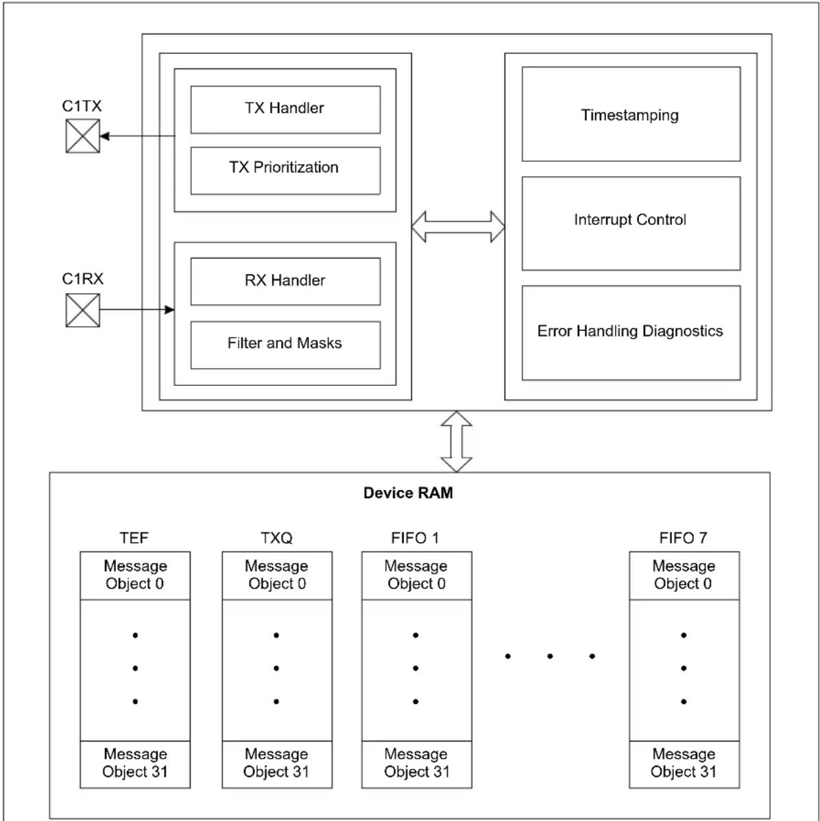
flowchart
graph TD
    subgraph Device RAM
        A["C1TX"] --> B["TX Handler"]
        A --> C["TX Prioritization"]
        D["C1RX"] --> E["RX Handler"]
        D --> F["Filter and Masks"]
    end

    subgraph Media Bytes
        G["TEF"] --> H["Message Object 0"]
        G --> I["TXQ"] --> J["Message Object 0"]
        G --> K["FIFO 1"] --> L["Message Object 0"]
        G --> M["FIFO 7"] --> N["Message Object 0"]
        G --> O["Message Object 31"]
        I --> P["Message Object 31"]
        J --> Q["Message Object 31"]
        K --> R["Message Object 31"]
        L --> S["Message Object 31"]
        N --> T["Message Object 31"]
        O --> U["Message Object 31"]
    end

    B <--> E
    C <--> F
    E <--> L
    style Device RAM fill:#f9f9f9,stroke:#333
    style Media Bytes fill:#e6f7ff,stroke:#333
3.9.2 CAN CONTROL/STATUS REGISTERS
REGISTER 3-105: C1CONH: CAN CONTROL REGISTER HIGH (2)
| R/W-0 R/W-0 R/W-0 R/W-0 S/HC-0 R/W-1 R/W-0 R/W-0 | |||||||
| TXBWS3 | TXBWS2 | TXBWS1 | TXBWS0 | ABAT | REQOP2 | REQOP1 | REQOP0 |
| bit 15 bit 8 | |||||||
| R-1 | R-0 | R-0 | R/W-1 | R/W-1 | R/W-0 | R/W-0 | R/W-0 |
| OPMOD2 | OPMOD1 | OPMOD0 | TXQEN(1) | STEF^(1) | SERRLOM^(1) | ESIGM^(1) | RTXAT^(1) |
| bit 7 bit 0 | |||||||
| Legend: | S = Settable bit | HC = Hardware Clearable bit |
| R = Readable bit | W = Writable bit | U = Unimplemented bit, read as ‘0’ |
| -n = Value at POR | ‘1’ = Bit is set | ‘0’ = Bit is cleared x = Bit is unknown |
bit 15-12 TXBWS[3:0]: Transmit Bandwidth Sharing bits
1111-1100 = 4096
1011 = 2048
1010 = 1024
1001 = 512
1000 = 256
0111 = 128
0110 = 64
0101 = 32
0100 = 16
0011 = 8
0010 = 4
0001 = 2
0000 = No delay
bit 11 ABAT: Abort All Pending Transmissions bit
1 = Signals all transmit buffers to abort transmission
0 = Module will clear this bit when all transmissions are aborted
bit 10-8 REQOP[2:0]: Request Operation Mode bits
111 = Sets Restricted Operation mode
110 = Sets Normal CAN 2.0 mode; error frames on CAN FD frames
101 = Sets External Loopback mode
100 = Sets Configuration mode
011 = Sets Listen Only mode
010 = Sets Internal Loopback mode
001 = Sets Disable mode
000 = Sets Normal CAN FD mode; supports mixing of full CAN FD and classic CAN 2.0 frames
bit 7-5 OPMOD[2:0]: Operation Mode Status bits
111 = Module is in Restricted Operation mode
110 = Module is in Normal CAN 2.0 mode; error frames on CAN FD frames
101 = Module is in External Loopback mode
100 = Module is in Configuration mode
011 = Module is in Listen Only mode
010 = Module is in Internal Loopback mode
001 = Module is in Disable mode
000 = Module is in Normal CAN FD mode; supports mixing of full CAN FD and classic CAN 2.0 frames
Note 1: These bits can only be modified in Configuration mode (OPMOD[2:0] = 100).
2: CAN is available only on the dsPIC33CHXXXMP50X devices.
REGISTER 3-105: C1CONH: CAN CONTROL REGISTER HIGH (2) (CONTINUED)
bit 4 TXQEN: Enable Transmit Queue bit (1)
1 = Enables Transmit Message Queue (TXQ) and reserves space in RAM
0 = Does not reserve space in RAM for TXQ
bit 3 STEF: Store in Transmit Event FIFO bit
(1)
1 = Saves transmitted messages in TEF
0 = Does not save transmitted messages in TEF
bit 2 SERRLOM: Transition to Listen Only Mode on System Error bit ^(1)
1 = Transitions to Listen Only mode
0 = Transitions to Restricted Operation mode
bit 1 ESIGM: Transmit ESI in Gateway Mode bit
(1)
1 = ESI is transmitted as recessive when ESI of the message is high or CAN controller is error passive
0 = ESI reflects error status of CAN controller
bit 0 RTXAT: Restrict Retransmission Attempts bit
(1)
1 = Restricted retransmission attempts, uses TXAT[1:0] bits (C1TXQCONH[6:5])
0 = Unlimited number of retransmission attempts, TXAT[1:0] bits will be ignored
Note 1: These bits can only be modified in Configuration mode (OPMOD[2:0] = 100).
2: CAN is available only on the dsPIC33CHXXXMP50X devices.
REGISTER 3-106: C1CONL: CAN CONTROL REGISTER LOW (2)
| R/W-0 U-0 R/W-0 R/W-0 R/W-0 R/W-1 R/W-1 R/W-1 | ||||||
| CON — SIDL BRSDIS BUSY WFT1 WFT0 WAKFIL | (1) | |||||
| bit 15 bit 8 | ||||||
| R/W-0 | R/W-1 | R/W-1 | R/W-0 | R/W-0 | R/W-0 | R/W-0 | R/W-0 |
| CLKSEL(1) | PXEDIS(1) | ISOCRCEN(1) | DNCNT4 | DNCNT3 | DNCNT2 | DNCNT1 | DNCNT0 |
| bit 7 bit 0 | |||||||
Legend:
| R = Readable bit | W = Writable bit | U = Unimplemented bit, read as '0' |
| -n = Value at POR | '1' = Bit is set | '0' = Bit is cleared x = Bit is unknown |
bit 15 CON: CAN Enable bit
1 = CAN module is enabled
0 = CAN module is disabled
bit 14 Unimplemented: Read as '0'
bit 13 SIDL: CAN Stop in Idle Control bit
1 = Stops module operation in Idle mode
0 = Does not stop module operation in Idle mode
bit 12 BRSDIS: Bit Rate Switching (BRS) Disable bit
1 = Bit Rate Switching is disabled, regardless of BRS in the transmit message object
0 = Bit Rate Switching depends on BRS in the transmit message object
bit 11 BUSY: CAN Module is Busy bit
1 = The CAN module is active
0 = The CAN module is inactive
bit 10-9 WFT[1:0]: Selectable Wake-up Filter Time bits
11 = T11FILTER
10 = T10FILTER
01 = T01FILTER
00 = T00FILTER
bit 8 WAKFIL: Enable CAN Bus Line Wake-up Filter bit ^(1)
1 = Uses CAN bus line filter for wake-up
0 = CAN bus line filter is not used for wake-up
bit 7 CLKSEL: Module Clock Source Select bit (1)
1 = AFPLLO is selected as the source
0 = FCAN is selected as the source
bit 6 PXEDIS: Protocol Exception Event Detection Disabled bit ^(1)
A recessive "reserved bit" following a recessive FDF bit is called a Protocol Exception.
1 = Protocol Exception is treated as a form error
0 = If a Protocol Exception is detected, CAN will enter the bus integrating state
bit 5 ISOCRCEN: Enable ISO CRC in CAN FD Frames bit ^(1)
1 = Includes stuff bit count in CRC field and uses non-zero CRC initialization vector
0 = Does not include stuff bit count in CRC field and uses CRC initialization vector with all zeros
bit 4-0 DNCNT[4:0]: DeviceNet™ Filter Bit Number bits
10011-11111 = Invalid selection (compares up to 18 bits of data with EID)
10010 = Compares up to Data Byte 2, bit 6 with EID17
...
00001 = Compares up to Data Byte 0, bit 7 with EID0
00000 = Does not compare data bytes
Note 1: These bits can only be modified in Configuration mode (OPMOD[2:0] = 100).
2: CAN is available only on the dsPIC33CHXXXMP50X devices.
REGISTER 3-107: C1NBTCFGH: CAN NOMINAL BIT TIME CONFIGURATION REGISTER HIGH (1,2)
| R/W-0 R/W-0 R/W-0 R/W-0 R/W-0 R/W-0 R/W-0 R/W-0 |
| BRP[7:0] |
| bit 15 bit 8 |
| R/W-0 R/W-0 R/W-1 R/W-1 R/W-1 R/W-1 R/W-0 R/W-0 |
| TSEG1[7:0] |
| bit 7 bit 0 |
Legend:
| R = Readable bit W = Writable bit | U = Unimplemented bit, read as '0' | ||
| -n = Value at POR | '1' = Bit is set | '0' = Bit is cleared | x = Bit is unknown |
bit 15-8 BRP[7:0]: Baud Rate Prescaler bits
$$ 1 1 1 1 \quad 1 1 1 1 = T Q = 2 5 6 / F s y s $$
$$ 0 0 0 0 \quad 0 0 0 0 = T _ {Q} = 1 / F s y s $$
bit 7-0 TSEG1[7:0]: Time Segment 1 bits (Propagation Segment + Phase Segment 1)
$$ 1 1 1 1 \quad 1 1 1 1 = \text { Length is } 2 5 6 \times T _ {Q} $$
$$ \dots \quad 0 0 0 0 \quad 0 0 0 0 = \text { Length is } 1 \times T _ {Q} $$
Note 1: These bits can only be modified in Configuration mode (OPMOD[2:0] = 100).
2: CAN is available only on the dsPIC33CHXXXMP50X devices.
REGISTER 3-108: C1NBTCFGL: CAN NOMINAL BIT TIME CONFIGURATION REGISTER LOW ^(1,2)
| U-0 | R/W-0 R/W-0 R/W-0 R/W-1 R/W-1 R/W-1 R/W-1 |
| — | TSEG2[6:0] |
| bit 15 bit 8 | |
| U-0 | R/W-0 R/W-0 R/W-0 R/W-1 R/W-1 R/W-1 R/W-1 |
| — | SJW[6:0] |
| bit 7 bit 0 | |
Legend:
| R = Readable bit W = Writable bit | U = Unimplemented bit, read as '0' | ||
| -n = Value at POR | '1' = Bit is set | '0' = Bit is cleared | x = Bit is unknown |
bit 15 Unimplemented: Read as '0'
bit 14-8 TSEG2[6:0]: Time Segment 2 bits (Phase Segment 2)
$$ 1 1 1 \quad 1 1 1 1 = \text { Length is } 1 2 8 \times T _ {Q} $$
$$ 0 0 0 0 0 0 0 0 = \text { Length is } 1 \times T _ {Q} $$
bit 7 Unimplemented: Read as '0'
bit 6-0 SJW[6:0]: Synchronization Jump Width bits
$$ 1 1 1 \quad 1 1 1 1 = \text { Length is } 1 2 8 \times T _ {Q} $$
$$ \dots \quad 0 0 0 \quad 0 0 0 0 = \text { Length is } 1 \times T _ {Q} $$
Note 1: These bits can only be modified in Configuration mode (OPMOD[2:0] = 100).
2: CAN is available only on the dsPIC33CHXXXMP50X devices.
REGISTER 3-109: C1DBTCFGH: CAN DATA BIT TIME CONFIGURATION REGISTER HIGH (1,2)
| R/W-0 R/W-0 R/W-0 R/W-0 R/W-0 R/W-0 R/W-0 R/W-0 |
| BRP[7:0] |
| bit 15 bit 8 |
| U-0 U-0 U-0 R/W-0 R/W-1 R/W-1 R/W-1 R/W-0 | |||
| — | — | — | TSEG1[4:0] |
| bit 7 | bit 0 | ||
Legend:
| R = Readable bit | W = Writable bit | U = Unimplemented bit, read as '0' |
| -n = Value at POR | '1' = Bit is set | '0' = Bit is cleared x = Bit is unknown |
bit 15-8 BRP[7:0]: Baud Rate Prescaler bits
1111 1111 = TQ = 256/Fsys
...
0000 0000 = TQ = 1/Fsys
bit 7-5 Unimplemented: Read as '0'
bit 4-0 TSEG1[4:0]: Time Segment 1 bits (Propagation Segment + Phase Segment 1)
1 1111 = Length is 32 x Tq
...
0 0000 = Length is 1 x TQ
Note 1: This register can only be modified in Configuration mode (OPMOD[2:0] = 100).
2: CAN is available only on the dsPIC33CHXXXMP50X devices.
REGISTER 3-110: C1DBTCFGL: CAN DATA BIT TIME CONFIGURATION REGISTER LOW ^(1,2)
| U-0 U-0 U-0 | U-0 R/W-0 R/W-0 R/W-1 | R/W-1 | ||
| — | — | — | — | TSEG2[3:0] |
| bit 15 bit 8 | ||||
| U-0 U-0 U-0 | U-0 R/W-0 R/W-0 R/W-1 | R/W-1 | ||
| — | — | — | — | SJW[3:0] |
| bit 7 bit 0 | ||||
Legend:
| R = Readable bit | W = Writable bit | U = Unimplemented bit, read as '0' |
| -n = Value at POR | ‘1’ = Bit is set | ‘0’ = Bit is cleared x = Bit is unknown |
bit 15-12 Unimplemented: Read as '0'
bit 11-8 TSEG2[3:0]: Time Segment 2 bits (Phase Segment 2)
1111 = Length is 16 x TQ
...
0000 = Length is 1 x TQ
bit 7-4 Unimplemented: Read as '0'
Note 1: This register can only be modified in Configuration mode (OPMOD[2:0] = 100).
2: CAN is available only on the dsPIC33CHXXXMP50X devices.
REGISTER 3-110: C1DBTCFGL: CAN DATA BIT TIME CONFIGURATION REGISTER LOW ^(1,2)
bit 3-0 SJW[3:0]: Synchronization Jump Width bits
1111 = Length is 16 x TQ
+ + *
0000 = Length is 1 x TQ
Note 1: This register can only be modified in Configuration mode (OPMOD[2:0] = 100).
2: CAN is available only on the dsPIC33CHXXXMP50X devices.
REGISTER 3-111: C1TDCH: CAN TRANSMITTER DELAY COMPENSATION REGISTER HIGH (1,2)
| U-0 U-0 U-0 U-0 U-0 R/W-0 R/W-0 | |||||||
| — | — | — | — | — | — | EDGFLTEN | SID11EN |
| bit 15 bit 8 | |||||||
| U-0 U-0 U-0 U-0 U-0 R/W-1 R/W-0 | |||||||
| — | — | — | — | — | — | TDCMOD1 | TDCMOD0 |
| bit 7 bit 0 | |||||||
| Legend: | |||
| R = Readable bit | W = Writable bit | U = Unimplemented bit, read as ‘0’ | |
| -n = Value at POR | ‘1’ = Bit is set | ‘0’ = Bit is cleared | x = Bit is unknown |
bit 15-10 Unimplemented: Read as '0'
bit 9 EDGFLTEN: Enable Edge Filtering During Bus Integration State bit
1 = Edge filtering is enabled according to ISO11898-1:2015
0 = Edge filtering is disabled
bit 8 SID11EN: Enable 12-Bit SID in CAN FD Base Format Messages bit
1 = RRS is used as SID11 in CAN FD base format messages: SID[11:0] = {SID[10:0], SID11}
0 = Does not use RRS; SID[10:0]
bit 7-2 Unimplemented: Read as '0'
bit 1-0 TDCMOD[1:0]: Transmitter Delay Compensation Mode bits (Secondary Sample Point (SSP))
10-11 = Auto: Measures delay and adds TDCO[6:0]
01 = Manual: Does not measure, uses TDCV[5:0] + TDCO[6:0] from register
00 = Disable
Note 1: This register can only be modified in Configuration mode (OPMOD[2:0] = 100).
2: CAN is available only on the dsPIC33CHXXXMP50X devices.
REGISTER 3-112: C1TDCL: CAN TRANSMITTER DELAY COMPENSATION REGISTER LOW (1,2,3)
| U-0 R/W-0 R/W-0 R/W-1 R/W-0 R/W-0 R/W-0 R/W-0 |
| — TDCO[6:0] |
| bit 15 bit 8 |
| U-0 U-0 R/W-0 R/W-0 R/W-0 R/W-0 R/W-0 R/W-0 | ||
| — | — | TDCV[5:0] |
| bit 7 bit 0 | ||
Legend:
| R = Readable bit | W = Writable bit | U = Unimplemented bit, read as '0' |
| -n = Value at POR | '1' = Bit is set | '0' = Bit is cleared x = Bit is unknown |
bit 15 Unimplemented: Read as '0'
bit 14-8 TDCO[6:0]: Transmitter Delay Compensation Offset bits (Secondary Sample Point (SSP))
111 1111 = -64 x TCAN
...
011 1111 = 63 x TCAN
...
000 0000 = 0 x TCAN
bit 7-6 Unimplemented: Read as '0'
bit 5-0 TDCV[5:0]: Transmitter Delay Compensation Value bits (Secondary Sample Point (SSP))
11 1111 = 63 x TSYSCLK
...
00 0000 = 0 x TSYSCLK
Note 1: This register can only be modified in Configuration mode (OPMOD[2:0] = 100).
2: CAN is available only on the dsPIC33CHXXXMP50X devices.
3: TCAN = 1/FCAN. FCAN is the clock which comes out of CAN clock generator.
REGISTER 3-113: C1TBCH: CAN TIME BASE COUNTER REGISTER HIGH (1,2,3)
| R/W-0 R/W-0 R/W-0 R/W-0 R/W-0 R/W-0 R/W-0 R/W-0 |
| TBC[31:24] |
| bit 15 bit 8 |
| R/W-0 R/W-0 R/W-0 R/W-0 R/W-0 R/W-0 R/W-0 R/W-0 |
| TBC[23:16] |
| bit 7 bit 0 |
Legend:
| R = Readable bit W = Writable bit U = Unimplemented bit, read as '0' | ||
| -n = Value at POR | '1' = Bit is set | '0' = Bit is cleared x = Bit is unknown |
bit 15-0 TBC[31:16]: CAN Time Base Counter bits
This is a free-running timer that increments every TBCPREx clock when TBCEN is set.
Note 1: The Time Base Counter (TBC) will be stopped and reset when TBCEN = 0 to save power.
2: The TBC prescaler count will be reset on any write to C1TBCH/L (TBCPREx will be unaffected).
3: CAN is available only on the dsPIC33CHXXXMP50X devices.
REGISTER 3-114: C1TBCL: CAN TIME BASE COUNTER REGISTER LOW (1,2,3)
| R/W-0 R/W-0 R/W-0 R/W-0 R/W-0 R/W-0 R/W-0 R/W-0 |
| TBC[15:8] |
| bit 15 bit 8 |
| R/W-0 R/W-0 R/W-0 R/W-0 R/W-0 R/W-0 R/W-0 R/W-0 |
| TBC[7:0] |
| bit 7 bit 0 |
Legend:
| R = Readable bit W = Writable bit U = Unimplemented bit, read as '0' | ||
| -n = Value at POR | '1' = Bit is set | '0' = Bit is cleared x = Bit is unknown |
bit 15-0 TBC[15:0]: CAN Time Base Counter bits
This is a free-running timer that increments every TBCPREx clock when TBCEN is set.
Note 1: The TBC will be stopped and reset when TBCEN = 0 to save power.
2: The TBC prescaler count will be reset on any write to C1TBCH/L (TBCPREx will be unaffected).
3: CAN is available only on the dsPIC33CHXXXMP50X devices.
REGISTER 3-115: C1TSCONH: CAN TIMESTAMP CONTROL REGISTER HIGH (1)
| U-0 U-0 U-0 U-0 U-0 U-0 U-0 | |||||||
| —— | —— | — | |||||
| bit 15 | bit 8 | ||||||
| U-0 U-0 U-0 U-0 U-0 | R/W-0 | R/W-0 | R/W-0 | ||||
| — | — | — | — | — | TSRES | TSEOF | TBCEN |
| bit 7 bit 0 | |||||||
| Legend: | |||
| R = Readable bit | W = Writable bit | U = Unimplemented bit, read as '0' | |
| -n = Value at POR | '1' = Bit is set | '0' = Bit is cleared | x = Bit is unknown |
bit 15-3 Unimplemented: Read as '0'
bit 2 TSRES: Timestamp Reset bit (CAN FD frames only)
1 = At sample point of the bit following the FDF bit
0 = At sample point of Start-of-Frame (SOF)
bit 1 TSEOF: Timestamp End-of-Frame (EOF) bit
1 = Timestamp when frame is taken valid (11898-1 10.7):
- RX no error until last, but one bit of EOF
- TX no error until the end of EOF
0 = Timestamp at "beginning" of frame:
- Classical Frame: At sample point of SOF
- FD Frame: See TSRES bit
bit 0 TBCEN: Time Base Counter Enable bit
1 = Enables TBC
0 = Stops and resets TBC
Note 1: CAN is available only on the dsPIC33CHXXXMP50X devices.
REGISTER 3-116: C1TSCONL: CAN TIMESTAMP CONTROL REGISTER LOW ^(1)
| U-0 U-0 U-0 U-0 U-0 U-0 | R/W-0 | R/W-0 | |||
| —— | —— | TBCPRE[9:8] | |||
| bit 15 | bit 8 | ||||
| R/W-0 | R/W-0 | R/W-0 | R/W-0 | R/W-0 | R/W-0 | R/W-0 | R/W-0 |
| TBCPRE[7:0] | |||||||
| bit 7 | bit 0 | ||||||
| Legend: | |||
| R = Readable bit | W = Writable bit | U = Unimplemented bit, read as '0' | |
| -n = Value at POR | '1' = Bit is set | '0' = Bit is cleared | x = Bit is unknown |
bit 15-10 Unimplemented: Read as '0'
bit 9-0 TBCPRE[9:0]: CAN Time Base Counter Prescaler bits
1023 = TBC increments every 1024 clocks
...
0 = TBC increments every 1 clock
Note 1: CAN is available only on the dsPIC33CHXXXMP50X devices.
REGISTER 3-117: C1VECH: CAN INTERRUPT CODE REGISTER HIGH (1)
U-0 R-1 R-0 R-0 R-0 R-0 R-0 R-0
— RXCODE[6:0]
bit 15 bit 8
U-0 R-1 R-0 R-0 R-0 R-0 R-0 R-0
— TXCODE[6:0]
bit 7 bit 0
Legend:
R = Readable bit W = Writable bit    U = Unimplemented bit, read as '0'
-n = Value at POR    '1' = Bit is set    '0' = Bit is cleared    x = Bit is unknown
bit 15 Unimplemented: Read as '0'
bit 14-8 RXCODE[6:0]: Receive Interrupt Flag Code bits
    1000001-1111111 = Reserved
    1000000 = No interrupt
    0001000-0111111 = Reserved
    0000111 = FIFO 7 interrupt (RFIF7 is set)
    ...
    0000010 = FIFO 2 interrupt (RFIF2 is set)
    0000001 = FIFO 1 interrupt (RFIF1 is set)
    0000000 = Reserved; FIFO 0 cannot receive
bit 7 Unimplemented: Read as '0'
bit 6-0 TXCODE[6:0]: Transmit Interrupt Flag Code bits
    1000001-1111111 = Reserved
    1000000 = No interrupt
    0001000-0111111 = Reserved
    0000111 = FIFO 7 interrupt (TFIF7 is set)
    ...
    0000001 = FIFO 1 interrupt (TFIF1 is set)
    0000000 = FIFO 0 interrupt (TFIF0 is set)
Note 1: CAN is available only on the dsPIC33CHXXXMP50X devices.
REGISTER 3-118: C1VECL: CAN INTERRUPT CODE REGISTER LOW (1)
| U-0 U-0 U-0 R-0 R-0 R-0 R-0 R-0 | |||
| — — — | FILHIT[4:0] | ||
| bit 15 bit 8 | |||
| U-0 R-1 R-0 R-0 R-0 R-0 R-0 R-0 | |
| — | ICODE[6:0] |
| bit 7 | bit 0 |
| Legend: | |||
| R = Readable bit | W = Writable bit | U = Unimplemented bit, read as ‘0’ | |
| -n = Value at POR | ‘1’ = Bit is set | ‘0’ = Bit is cleared | x = Bit is unknown |
bit 15-13 Unimplemented: Read as '0'
bit 12-8 FILHIT[4:0]: Filter Hit Number bits
01111 = Filter 15
01110 = Filter 14
...
00001 = Filter 1
00000 = Filter 0
bit 7 Unimplemented: Read as '0'
bit 6-0 ICODE[6:0]: Interrupt Flag Code bits
1001011-1111111 = Reserved
1001010 = Transmit attempt interrupt (any bit in C1TXATIF is set)
1001001 = Transmit event FIFO interrupt (any bit in C1TEFSTA is set)
1001000 = Invalid message occurred (IVMIF/IE)
1000111 = CAN module mode change occurred (MODIF/IE)
1000110 = CAN timer overflow (TBCIF/IE)
1000101 = RX/TX MAB overflow/underflow (RX: Message received before previous message was saved to memory; TX: Can't feed TX MAB fast enough to transmit consistent data)
1000100 = Address error interrupt (illegal FIFO address presented to system)
1000011 = Receive FIFO overflow interrupt (any bit in C1RXOVIF is set)
1000010 = Wake-up interrupt (WAKIF/WAKIE)
1000001 = Error interrupt (CERRIF/IE)
1000000 = No interrupt
0001000-0111111 = Reserved
0000111 = FIFO 7 interrupt (TFIF7 or RFIF7 is set)
* * *
0000001 = FIFO 1 interrupt (TFIF1 or RFIF1 is set)
0000000 = FIFO 0 interrupt (TFIF0 is set)
Note 1: CAN is available only on the dsPIC33CHXXXMP50X devices.
REGISTER 3-119: C1INTH: CAN INTERRUPT REGISTER HIGH (1)
| R/W-0 R/W-0 R/W-0 R/W-0 R/W-0 R/W-0 U-0 U-0 | ||||||
| IVMIE WAKIE CERRIE S | ERRIE RXOVIE | TXATIE | — | — | ||
| bit 15 bit 8 | ||||||
| U-0 | U-0 | U-0 | R/W-0 | R/W-0 | R/W-0 | R/W-0 | R/W-0 |
| — | — | — | TEFIE | MODIE | TBCIE | RXIE | TXIE |
| bit 7 bit 0 | |||||||
| Legend: | |||
| R = Readable bit | W = Writable bit | U = Unimplemented bit, read as ‘0’ | |
| -n = Value at POR | ‘1’ = Bit is set | ‘0’ = Bit is cleared | x = Bit is unknown |
| bit 15 | IVMIE: Invalid Message Interrupt Enable bit1 = Invalid message interrupt is enabled0 = Invalid message interrupt is disabled |
| bit 14 | WAKIE: Bus Wake-up Activity Interrupt Enable bit1 = Wake-up activity interrupt is enabled0 = Wake-up Activity Interrupt is disabled |
| bit 13 | CERRIE: CAN Bus Error Interrupt Enable bit1 = CAN bus error interrupt is enabled0 = CAN bus error interrupt is disabled |
| bit 12 | SERRIE: System Error Interrupt Enable bit1 = System error interrupt is enabled0 = System error interrupt is disabled |
| bit 11 | RXOVIE: Receive Buffer Overflow Interrupt Enable bit1 = Receive buffer overflow interrupt is enabled0 = Receive buffer overflow interrupt is disabled |
| bit 10 | TXATIE: Transmit Attempt Interrupt Enable bit1 = Transmit attempt interrupt is enabled0 = Transmit attempt interrupt is disabled |
| bit 9-5 | Unimplemented: Read as '0' |
| bit 4 | TEFIE: Transmit Event FIFO Interrupt Enable bit1 = Transmit event FIFO interrupt is enabled0 = Transmit event FIFO interrupt is disabled |
| bit 3 | MODIE: Mode Change Interrupt Enable bit1 = Mode change interrupt is enabled0 = Mode change interrupt is disabled |
| bit 2 | TBCIE: CAN Timer Interrupt Enable bit1 = CAN timer interrupt is enabled0 = CAN timer interrupt is disabled |
| bit 1 | RXIE: Receive Object Interrupt Enable bit1 = Receive object interrupt is enabled0 = Receive object interrupt is disabled |
| bit 0 | TXIE: Transmit Object Interrupt Enable bit1 = Transmit object interrupt is enabled0 = Transmit object interrupt is disabled |
Note 1: CAN is available only on the dsPIC33CHXXXMP50X devices.
REGISTER 3-120: C1INTL: CAN INTERRUPT REGISTER LOW (2)
| HS/C-0 HS/C-0 HS/C-0 HS/C-0 R-0 R-0 U-0 U-0 | |||||||
| IVMIF(1) | WAKIF(1) | CERRIF(1) | SERRIF(1) | RXOVIF TXATIF | — | — | |
| bit 15 bit 8 | |||||||
| U-0 | U-0 | U-0 | R-0 | HS/C-0 | HS/C-0 | R-0 | R-0 |
| — | — | — | TEFIF | MODIF^(1) | TBCIF^(1) | RXIF | TXIF |
| bit 7 bit 0 | |||||||
| Legend: | C = Clearable bit | HS = Hardware Settable bit |
| R = Readable bit | W = Writable bit | U = Unimplemented bit, read as ‘0’ |
| -n = Value at POR | ‘1’ = Bit is set | ‘0’ = Bit is cleared x = Bit is unknown |
bit 15 IVMIF: Invalid Message Interrupt Flag bit ^(1)
1 = Invalid message interrupt occurred
0 = No invalid message interrupt
bit 14 WAKIF: Bus Wake-up Activity Interrupt Flag bit ^(1)
1 = Wake-up activity interrupt occurred
0 = No wake-up activity interrupt
bit 13 CERRIF: CAN Bus Error Interrupt Flag bit ^(1)
1 = CAN bus error interrupt occurred
0 = No CAN bus error interrupt
bit 12 SERRIF: System Error Interrupt Flag bit ^(1)
1 = System error interrupt occurred
0 = No system error interrupt
bit 11 RXOVIF: Receive Buffer Overflow Interrupt Flag bit
1 = Receive buffer overflow interrupt occurred
0 = No receive buffer overflow interrupt
bit 10 TXATIF: Transmit Attempt Interrupt Flag bit
1 = Transmit attempt interrupt occurred
0 = No Transmit Attempt Interrupt
bit 9-5 Unimplemented: Read as '0'
bit 4 TEFIF: Transmit Event FIFO Interrupt Flag bit
1 = Transmit event FIFO interrupt occurred
0 = No transmit event FIFO interrupt
bit 3 MODIF: CAN Mode Change Interrupt Flag bit (1)
1 = CAN module mode change occurred (OPMOD[2:0] have changed to reflect REQOP[2:0])
0 = No mode change occurred
bit 2 TBCIF: CAN Timer Overflow Interrupt Flag bit (1)
1 = TBC has overflowed
0 = TBC has not overflowed
bit 1 RXIF: Receive Object Interrupt Flag bit
1 = Receive object interrupt is pending
0 = No receive object interrupts are pending
bit 0 TXIF: Transmit Object Interrupt Flag bit
1 = Transmit object interrupt is pending
0 = No transmit object interrupts are pending
Note 1: C1INTL: Flags are set by hardware and cleared by application.
2: CAN is available only on the dsPIC33CHXXXMP50X devices.
REGISTER 3-121: C1RXIFH: CAN RECEIVE INTERRUPT STATUS REGISTER HIGH (1,2)
| R-0 R-0 R-0 R-0 R-0 R-0 R-0 R-0 |
| RFIF[31:24] |
| bit 15 bit 8 |
| R-0 R-0 R-0 R-0 R-0 R-0 R-0 R-0 |
| RFIF[23:16] |
| bit 7 bit 0 |
| Legend: | |||
| R = Readable bit W = Writable bit | U = Unimplemented bit, read as ‘0’ | ||
| -n = Value at POR | ‘1’ = Bit is set | ‘0’ = Bit is cleared | x = Bit is unknown |
bit 15-0 RFIF[31:16]: Unimplemented
Note 1: C1RXIFH: FIFO: RFIFx = 'or' of enabled RX FIFO flags (flags need to be cleared in the FIFO register).
2: CAN is available only on the dsPIC33CHXXXMP50X devices.
REGISTER 3-122: C1RXIFL: CAN RECEIVE INTERRUPT STATUS REGISTER LOW ^(1,2)
| R-0 R-0 R-0 R-0 R-0 R-0 R-0 R-0 |
| RFIF[15:8] |
| bit 15 bit 8 |
| R-0 R-0 R-0 R-0 R-0 R-0 R-0 U-0 | |
| RFIF[7:1] | — |
| bit 7 bit 0 | |
| Legend: | |||
| R = Readable bit W = Writable bit | U = Unimplemented bit, read as ‘0’ | ||
| -n = Value at POR | ‘1’ = Bit is set | ‘0’ = Bit is cleared | x = Bit is unknown |
bit 15-8 RFIF[15:8]: Unimplemented
bit 7-1 RFIF[7:1]: Receive FIFO Interrupt Pending bits
1 = One or more enabled receive FIFO interrupts are pending
0 = No enabled receive FIFO interrupts are pending
bit 0 Unimplemented: Read as '0'
Note 1: C1RXIFL: FIFO: RFIFx = 'or' of enabled RX FIFO flags (flags need to be cleared in the FIFO register).
2: CAN is available only on the dsPIC33CHXXXMP50X devices.
REGISTER 3-123: C1RXOVIFH: CAN RECEIVE OVERFLOW INTERRUPT STATUS REGISTER HIGH (1,2)
| R-0 R-0 R-0 R-0 R-0 R-0 R-0 R-0 |
| RFOVIF[31:24] |
| bit 15 bit 8 |
| R-0 R-0 R-0 R-0 R-0 R-0 R-0 R-0 |
| RFOVIF[23:16] |
| bit 7 bit 0 |
Legend:
| R = Readable bit W = Writable bit | U = Unimplemented bit, read as '0' | ||
| -n = Value at POR | '1' = Bit is set | '0' = Bit is cleared | x = Bit is unknown |
bit 15-0 RFOVIF[31:16]: Unimplemented
Note 1: C1RXOVIFH: FIFO: RFOVIFx (flag needs to be cleared in the FIFO register).
2: CAN is available only on the dsPIC33CHXXXMP50X devices.
REGISTER 3-124: C1RXOVIFL: CAN RECEIVE OVERFLOW INTERRUPT STATUS REGISTER LOW ^(1,2)
| R-0 R-0 R-0 R-0 R-0 R-0 R-0 R-0 |
| RFOVIF[15:8] |
| bit 15 bit 8 |
| R-0 R-0 R-0 R-0 R-0 R-0 R-0 U-0 | |
| RFOVIF[7:1] | — |
| bit 7 bit 0 | |
Legend:
| R = Readable bit W = Writable bit | U = Unimplemented bit, read as '0' | ||
| -n = Value at POR | '1' = Bit is set | '0' = Bit is cleared | x = Bit is unknown |
bit 15-8 RFOVIF[15:8]: Unimplemented
bit 7-1 RFOVIF[7:1]: Receive FIFO Overflow Interrupt Pending bits
1 = Interrupt is pending
0 = Interrupt is not pending
bit 0 Unimplemented: Read as '0'
Note 1: C1RXOVIFL: FIFO: RFOVIFx (flag needs to be cleared in the FIFO register).
2: CAN is available only on the dsPIC33CHXXXMP50X devices.
REGISTER 3-125: C1TXIFH: CAN TRANSMIT INTERRUPT STATUS REGISTER HIGH (1,2)
| R-0 R-0 R-0 R-0 R-0 R-0 R-0 R-0 |
| TFIF[31:24] |
| bit 15 bit 8 |
| R-0 R-0 R-0 R-0 R-0 R-0 R-0 R-0 |
| TFIF[23:16] |
| bit 7 bit 0 |
| Legend: | |||
| R = Readable bit W = Writable bit U = Unimplemented bit, read as ‘0’ | |||
| -n = Value at POR | ‘1’ = Bit is set | ‘0’ = Bit is cleared | x = Bit is unknown |
bit 15-0 TFIF[31:16]: Unimplemented
Note 1: C1TXIFH: FIFO: TFIFx = 'or' of the enabled TX FIFO flags (flags need to be cleared in the FIFO register).
2: CAN is available only on the dsPIC33CHXXXMP50X devices.
REGISTER 3-126: C1TXIFL: CAN TRANSMIT INTERRUPT STATUS REGISTER LOW ^(1,3)
| R-0 R-0 R-0 R-0 R-0 R-0 R-0 R-0 |
| TFIF[15:8] |
| bit 15 bit 8 |
| R-0 R-0 R-0 R-0 R-0 R-0 R-0 R-0 |
| TFIF[7:0](2) |
| bit 7 bit 0 |
| Legend: | |||
| R = Readable bit W = Writable bit U = Unimplemented bit, read as ‘0’ | |||
| -n = Value at POR | ‘1’ = Bit is set | ‘0’ = Bit is cleared | x = Bit is unknown |
bit 15-8 TFIF[15:8]: Unimplemented
bit 7-0 TFIF[7:0]: Transmit FIFO/TXQ Interrupt Pending bits ^(2)
1 = One or more enabled transmit FIFO/TXQ interrupts are pending
0 = No enabled transmit FIFO/TXQ interrupts are pending
Note 1: C1TXIFL: FIFO: TFIFx = 'or' of the enabled TX FIFO flags (flags need to be cleared in the FIFO register).
2: TFIF0 is for the transmit queue.
3: CAN is available only on the dsPIC33CHXXXMP50X devices.
REGISTER 3-127: C1TXATIFH: CAN TRANSMIT ATTEMPT INTERRUPT STATUS REGISTER HIGH ^(1,2)
| R-0 R-0 R-0 R-0 R-0 R-0 R-0 R-0 |
| TFATIF[31:24] |
| bit 15 bit 8 |
| R-0 R-0 R-0 R-0 R-0 R-0 R-0 R-0 |
| TFATIF[23:16] |
| bit 7 bit 0 |
Legend:
| R = Readable bit W = Writable bit | U = Unimplemented bit, read as '0' | ||
| -n = Value at POR | '1' = Bit is set | '0' = Bit is cleared | x = Bit is unknown |
bit 15-0 TFATIF[31:16]: Unimplemented
Note 1: C1TXATIFH: FIFO: TFATIFx (flag needs to be cleared in the FIFO register).
2: CAN is available only on the dsPIC33CHXXXMP50X devices.
REGISTER 3-128: C1TXATIFL: CAN TRANSMIT ATTEMPT INTERRUPT STATUS REGISTER LOW ^(1,3)
| R-0 R-0 R-0 R-0 R-0 R-0 R-0 R-0 |
| TFATIF[15:8] |
| bit 15 bit 8 |
| R-0 R-0 R-0 R-0 R-0 R-0 R-0 R-0 |
| TFATIF[7:0](2) |
| bit 7 bit 0 |
Legend:
| R = Readable bit W = Writable bit | U = Unimplemented bit, read as '0' | ||
| -n = Value at POR | '1' = Bit is set | '0' = Bit is cleared | x = Bit is unknown |
bit 15-8 TFATIF[15:8]: Unimplemented
bit 7-0 TFATIF[7:0]: Transmit FIFO/TXQ Attempt Interrupt Pending bits ^(2)
1 = Interrupt is pending
0 = Interrupt is not pending
Note 1: C1TXATIFL: FIFO: TFATIFx (flag needs to be cleared in the FIFO register).
2: TFATIF0 is for the transmit queue.
3: CAN is available only on the dsPIC33CHXXXMP50X devices.
REGISTER 3-129: C1TXREQH: CAN TRANSMIT REQUEST REGISTER HIGH (1)
| S/HC-0 S/HC-0 S/HC-0 S/HC-0 S/HC-0 S/HC-0 S/HC-0 S/HC-0 |
| TXREQ[31:24] |
| bit 15 bit 8 |
| R/W-0 R/W-0 R/W-0 R/W-0 R/W-0 R/W-0 R/W-0 S/HC-0 | |
| TXREQ[23:16] | |
| bit 7 | bit 0 |
| Legend: | S = Settable bit | HC = Hardware Clearable bit |
| R = Readable bit | W = Writable bit | U = Unimplemented bit, read as ‘0’ |
| -n = Value at POR | ‘1’ = Bit is set | ‘0’ = Bit is cleared x = Bit is unknown |
bit 15-0 TXREQ[31:16]: Unimplemented
Note 1: CAN is available only on the dsPIC33CHXXXMP50X devices.
REGISTER 3-130: C1TXREQL: CAN TRANSMIT REQUEST REGISTER LOW (1)
| S/HC-0 S/HC-0 S/HC-0 S/HC-0 S/HC-0 S/HC-0 S/HC-0 S/HC-0 |
| TXREQ[15:8] |
| bit 15 bit 8 |
| S/HC-0 S/HC-0 S/HC-0 S/HC-0 S/HC-0 S/HC-0 S/HC-0 S/HC-0s | |
| TXREQ[7:1] | TXREQ0 |
| bit 7 | bit 0 |
| Legend: | S = Settable bit | HC = Hardware Clearable bit |
| R = Readable bit | W = Writable bit | U = Unimplemented bit, read as ‘0’ |
| -n = Value at POR | ‘1’ = Bit is set | ‘0’ = Bit is cleared x = Bit is unknown |
bit 15-8 TXREQ[15:8]: Unimplemented
bit 7-1 TXREQ[7:1]: Message Send Request bits
TXEN = 1 (object configured as a transmit object):
Setting this bit to '1' requests sending a message. The bit will automatically clear when the message(s) queued in the object is (are) successfully sent. This bit can NOT be used for aborting a transmission.
TXEN = 0 (object configured as a receive object):
This bit has no effect.
bit 0 TXREQ0: Transmit Queue Message Send Request bit
Setting this bit to '1' requests sending a message. The bit will automatically clear when the message(s) queued in the object is (are) successfully sent. This bit can NOT be used for aborting a transmission.
Note 1: CAN is available only on the dsPIC33CHXXXMP50X devices.
REGISTER 3-131: C1FIFOBAH: CAN MESSAGE MEMORY BASE ADDRESS REGISTER HIGH (1)
| R/W-0 R/W-0 R/W-0 R/W-0 R/W-0 R/W-0 R/W-0 R/W-0 |
| FIFOBA[31:24] |
| bit 15 bit 8 |
| R/W-0 R/W-0 R/W-0 R/W-0 R/W-0 R/W-0 R/W-0 R/W-0 |
| FIFOBA[23:16] |
| bit 7 bit 0 |
Legend:
| R = Readable bit W = Writable bit U = Unimplemented bit, read as '0' | ||
| -n = Value at POR | '1' = Bit is set | '0' = Bit is cleared |
bit 15-0 FIFOBA[31:16]: Message Memory Base Address bits
Defines the base address for the transmit event FIFO followed by the message objects.
Note 1: CAN is available only on the dsPIC33CHXXXMP50X devices.
REGISTER 3-132: C1FIFOBAL: CAN MESSAGE MEMORY BASE ADDRESS REGISTER LOW (1)
| R/W-0 R/W-0 R/W-0 R/W-0 R/W-0 R/W-0 R/W-0 R/W-0 |
| FIFOBA[15:8] |
| bit 15 bit 8 |
| R/W-0 R/W-0 R/W-0 R/W-0 R/W-0 R/W-0 | R-0 | R-0 |
| FIFOBA[7:0] | ||
| bit 7 bit 0 | ||
Legend:
| R = Readable bit W = Writable bit U = Unimplemented bit, read as '0' | ||
| -n = Value at POR | '1' = Bit is set | '0' = Bit is cleared x = Bit is unknown |
bit 15-0 FIFOBA[15:0]: Message Memory Base Address bits
Defines the base address for the transmit event FIFO followed by the message objects.
Note 1: CAN is available only on the dsPIC33CHXXXMP50X devices.
REGISTER 3-133: C1TXQCONH: CAN TRANSMIT QUEUE CONTROL REGISTER HIGH (2)
| R/W-0 R/W-0 R/W-0 R/W-0 R/W-0 R/W-0 R/W-0 R/W-0 | |||||||
| PLSIZE2(1) | PLSIZE1(1) | PLSIZE0(1) | FSIZE4(1) | FSIZE3(1) | FSIZE2(1) | FSIZE1(1) | FSIZE0(1) |
| bit 15 bit 8 | |||||||
| U-0 R/W-1 R/W-1 R/W-0 R/W-0 R/W-0 R/W-0 R/W-0 | |||||||
| — | TXAT1 | TXAT0 | TXPRI4 | TXPRI3 | TXPRI2 | TXPRI1 | TXPRI0 |
| bit 7 bit 0 | |||||||
| Legend: | |||
| R = Readable bit | W = Writable bit | U = Unimplemented bit, read as ‘0’ | |
| -n = Value at POR | ‘1’ = Bit is set | ‘0’ = Bit is cleared | x = Bit is unknown |
bit 15-13 PLSIZE[2:0]: Payload Size bits ^(1)
111 = 64 data bytes
110 = 48 data bytes
101 = 32 data bytes
100 = 24 data bytes
011 = 20 data bytes
010 = 16 data bytes
001 = 12 data bytes
000 = 8 data bytes
bit 12-8 FSIZE[4:0]: FIFO Size bits ^(1)
11111 = FIFO is 32 messages deep
...
00010 = FIFO is 3 messages deep
00001 = FIFO is 2 messages deep
00000 = FIFO is 1 message deep
bit 7 Unimplemented: Read as '0'
bit 6-5 TXAT[1:0]: Retransmission Attempts bits
This feature is enabled when RTXAT (C1CONH[0]) is set.
11 = Unlimited number of retransmission attempts
10 = Unlimited number of retransmission attempts
01 = Three retransmission attempts
00 = Disables retransmission attempts
bit 4-0 TXPRI[4:0]: Message Transmit Priority bits
11111 = Highest message priority
• • •
00000 = Lowest message priority
Note 1: These bits can only be modified in Configuration mode (OPMOD[2:0] = 100).
2: CAN is available only on the dsPIC33CHXXXMP50X devices.
REGISTER 3-134: C1TXQCONL: CAN TRANSMIT QUEUE CONTROL REGISTER LOW (1)
| U-0 U-0 U-0 U-0 U-0 R/W-0 R/W-0 R/W-0 | |||||||
| —— | ——FRESET | TXREQ | UINC | ||||
| bit 15 | bit 8 | ||||||
| R-0 | U-0 | U-0 | HS/C-0 | U-0 | R/W-0 | U-0 | R/W-0 |
| TXEN | — | — | TXATIE | — | TXQEIE | — | TXQNIE |
| bit 7 bit 0 | |||||||
| Legend: | HS = Hardware Settable bit | C = Clearable bit | |
| R = Readable bit | W = Writable bit | U = Unimplemented bit, read as ‘0’ | |
| -n = Value at POR | ‘1’ = Bit is set | ‘0’ = Bit is cleared | x = Bit is unknown |
bit 15-11 Unimplemented: Read as '0'
bit 10 FRESET: FIFO Reset bit
1 = FIFO will be reset when bit is set, cleared by hardware when FIFO is reset; user should poll whether this bit is clear before taking any action 0 = No effect
bit 9 TXREQ: Message Send Request bit
1 = Requests sending a message; the bit will automatically clear when all the messages queued in the TXQ are successfully sent 0 = Clearing the bit to '0' while set ('1') will request a message abort
bit 8 UINC: Increment Head/Tail bit
When this bit is set, the FIFO head will increment by a single message.
bit 7 TXEN: TX Enable bit
bit 6-5 Unimplemented: Read as '0'
bit 4 TXATIE: Transmit Attempts Exhausted Interrupt Enable bit
1 = Enables interrupt 0 = Disables interrupt
bit 3 Unimplemented: Read as '0'
bit 2 TXQEIE: Transmit Queue Empty Interrupt Enable bit
1 = Interrupt is enabled for TXQ empty 0 = Interrupt is disabled for TXQ empty
bit 1 Unimplemented: Read as '0'
bit 0 TXQNIE: Transmit Queue Not Full Interrupt Enable bit
1 = Interrupt is enabled for TXQ not full 0 = Interrupt is disabled for TXQ not full
Note 1: CAN is available only on the dsPIC33CHXXXMP50X devices.
REGISTER 3-135: C1TXQSTA: CAN TRANSMIT QUEUE STATUS REGISTER (3)
| U-0 U-0 U-0 R-0 R-0 R-0 R-0 R-0 | |||||||
| ——— | T | X | Q | C(1) | TXQCI3(1)4 | TXQCI2(1) | TXQCI1(1) |
| bit 15 bit 8 | |||||||
| R-0 R-0 R-0 HS/C-0 U-0 R-1 U-0 R-1 | |||||||
| TXABT(2) | TXLARB | TXERR | TXATIF | — | TXQEIF | — | TXQNIF |
| bit 7 bit 0 | |||||||
| Legend: | HS = Hardware Settable bit | C = Clearable bit | |
| R = Readable bit | W = Writable bit | U = Unimplemented bit, read as ‘0’ | |
| -n = Value at POR | ‘1’ = Bit is set | ‘0’ = Bit is cleared | x = Bit is unknown |
bit 15-13 Unimplemented: Read as '0'
bit 12-8 TXQCI[4:0]: Transmit Message Queue Index bits ^(1)
A read of this register will return an index to the message that the FIFO will next attempt to transmit.
bit 7 TXABT: Message Aborted Status bit ^(2)
1 = Message was aborted
0 = Message completed successfully
bit 6 TXLARB: Message Lost Arbitration Status bit
1 = Message lost arbitration while being sent
0 = Message did not lose arbitration while being sent
bit 5 TXERR: Error Detected During Transmission bit
1 = A bus error occurred while the message was being sent
0 = A bus error did not occur while the message was being sent
bit 4 TXATIF: Transmit Attempts Exhausted Interrupt Pending bit
1 = Interrupt is pending
0 = Interrupt is not pending
bit 3 Unimplemented: Read as '0'
bit 2 TXQEIF: Transmit Queue Empty Interrupt Flag bit
1 = TXQ is empty
0 = TXQ is not empty, at least one message is queued to be transmitted
bit 1 Unimplemented: Read as '0'
bit 0 TXQNIF: Transmit Queue Not Full Interrupt Flag bit
1 = TXQ is not full
0 = TXQ is full
Note 1: The TXQCI[4:0] bits give a zero-indexed value to the message in the TXQ. If the TXQ is four messages deep (FSIZE[4:0] = 3), TXQCIX will take on a value of 0 to 3, depending on the state of the TXQ.
2: This bit is updated when a message completes (or aborts) or when the TXQ is reset.
3: CAN is available only on the dsPIC33CHXXXMP50X devices.
REGISTER 3-136: C1FIFOCONxH: CAN FIFO CONTROL REGISTER x (x = 1 TO 7) HIGH ^(2)
| R/W-0 R/W-0 R/W-0 R/W-0 R/W-0 R/W-0 R/W-0 R/W-0 | |||||||
| PLSIZE2(1) | PLSIZE1(1) | PLSIZE0(1) | FSIZE4(1) | FSIZE3(1) | FSIZE2(1) | FSIZE1(1) | FSIZE0(1) |
| bit 15 bit 8 | |||||||
| U-0 R/W-1 R/W-1 R/W-0 R/W-0 R/W-0 R/W-0 R/W-0 | |||||||
| — | TXAT1 | TXAT0 | TXPRI4 | TXPRI3 | TXPRI2 | TXPRI1 | TXPRI0 |
| bit 7 bit 0 | |||||||
Legend:
| R = Readable bit | W = Writable bit | U = Unimplemented bit, read as '0' |
| -n = Value at POR | ‘1’ = Bit is set | ‘0’ = Bit is cleared x = Bit is unknown |
bit 15-13 PLSIZE[2:0]: Payload Size bits ^(1)
111 = 64 data bytes
110 = 48 data bytes
101 = 32 data bytes
100 = 24 data bytes
011 = 20 data bytes
010 = 16 data bytes
001 = 12 data bytes
000 = 8 data bytes
bit 12-8 FSIZE[4:0]: FIFO Size bits (1)
11111 = FIFO is 32 messages deep
• • •
00010 = FIFO is 3 messages deep
00001 = FIFO is 2 messages deep
00000 = FIFO is 1 message deep
bit 7 Unimplemented: Read as '0'
bit 6-5 TXAT[1:0]: Retransmission Attempts bits
This feature is enabled when RTXAT (C1CONH[0]) is set.
11 = Unlimited number of retransmission attempts
10 = Unlimited number of retransmission attempts
01 = Three retransmission attempts
00 = Disables retransmission attempts
bit 4-0 TXPRI[4:0]: Message Transmit Priority bits
11111 = Highest message priority
• • •
00000 = Lowest message priority
Note 1: These bits can only be modified in Configuration mode (OPMOD[2:0] = 100).
2: CAN is available only on the dsPIC33CHXXXMP50X devices.
REGISTER 3-137: C1FIFOCONxL: CAN FIFO CONTROL REGISTER x (x = 1 TO 7) LOW ^(2)
| U-0 U-0 U-0 U-0 U-0 S/HC-1 R/W/HC-0 S/HC-0 | |||||||
| — — — | — — FRESET | TXREQ | UINC | ||||
| bit 15 bit 8 | |||||||
| R/W-0 | R/W-0 | R/W-0 | R/W-0 | R/W-0 | R/W-0 | R/W-0 | R/W-0 |
| TXEN | RTREN RX | TSEN (1) | TXATIE | RXOVIE | TFERFFIE | TFHRFHIE | TFNRFNIE |
| bit 7 bit 0 | |||||||
| Legend: | S = Settable bit | HC = Hardware Clearable bit |
| R = Readable bit | W = Writable bit | U = Unimplemented bit, read as ‘0’ |
| -n = Value at POR | ‘1’ = Bit is set | ‘0’ = Bit is cleared x = Bit is unknown |
bit 15-11 Unimplemented: Read as '0'
bit 10 FRESET: FIFO Reset bit
1 = FIFO will be reset when bit is set, cleared by hardware when FIFO is reset; user should poll whether this bit is clear before taking any action 0 = No effect
bit 9 TXREQ: Message Send Request bit
TXEN = 1 (FIFO configured as a transmit FIFO):
1 = Requests sending a message; the bit will automatically clear when all the messages queued in the FIFO are successfully sent 0 = Clearing the bit to '0' while set ('1') will request a message abort TXEN = 0 (FIFO configured as a receive FIFO): This bit has no effect.
bit 8 UINC: Increment Head/Tail bit
TXEN = 1 (FIFO configured as a transmit FIFO):
When this bit is set, the FIFO head will increment by a single message.
TXEN = 0 (FIFO configured as a receive FIFO):
When this bit is set, the FIFO tail will increment by a single message.
bit 7 TXEN: TX/RX Buffer Selection bit
1 = Transmits message object
0 = Receives message object
bit 6 RTREN: Auto-Remote Transmit (RTR) Enable bit
1 = When a Remote Transmit is received, TXREQ will be set
0 = When a Remote Transmit is received, TXREQ will be unaffected
bit 5 RXTSEN: Received Message Timestamp Enable bit ^(1)
1 = Captures timestamp in received message object in RAM 0 = Does not capture timestamp
bit 4 TXATIE: Transmit Attempts Exhausted Interrupt Enable bit
1 = Enables interrupt 0 = Disables interrupt
RXOVIE: Overflow Interrupt Enable bit
1 = Interrupt is enabled for overflow event 0 = Interrupt is disabled for overflow event
Note 1: This bit can only be modified in Configuration mode (OPMOD[2:0] = 100).
2: CAN is available only on the dsPIC33CHXXXMP50X devices.
REGISTER 3-137: C1FIFOCONxL: CAN FIFO CONTROL REGISTER x (x = 1 TO 7) LOW ^(2) (CONTINUED)
bit 2 TFERFFIE: Transmit/Receive FIFO Empty/Full Interrupt Enable bit
TXEN = 1 (FIFO configured as a transmit FIFO):
Transmit FIFO Empty Interrupt Enable
1 = Interrupt is enabled for FIFO empty
0 = Interrupt is disabled for FIFO empty
TXEN = 0 (FIFO configured as a receive FIFO):
Receive FIFO Full Interrupt Enable
1 = Interrupt is enabled for FIFO full
0 = Interrupt is disabled for FIFO full
bit 1 TFHRFHIE: Transmit/Receive FIFO Half Empty/Half Full Interrupt Enable bit
TXEN = 1 (FIFO configured as a transmit FIFO):
Transmit FIFO Half Empty Interrupt Enable
1 = Interrupt is enabled for FIFO half empty
0 = Interrupt is disabled for FIFO half empty
TXEN = 0 (FIFO configured as a receive FIFO):
Receive FIFO Half Full Interrupt Enable
1 = Interrupt is enabled for FIFO half full
0 = Interrupt is disabled for FIFO half full
bit 0 TFNRFNIE: Transmit/Receive FIFO Not Full/Not Empty Interrupt Enable bit
TXEN = 1 (FIFO configured as a transmit FIFO):
Transmit FIFO Not Full Interrupt Enable
1 = Interrupt is enabled for FIFO not full
0 = Interrupt is disabled for FIFO not full
TXEN = 0 (FIFO configured as a receive FIFO):
Receive FIFO Not Empty Interrupt Enable
1 = Interrupt is enabled for FIFO not empty
0 = Interrupt is disabled for FIFO not empty
Note 1: This bit can only be modified in Configuration mode (OPMOD[2:0] = 100).
2: CAN is available only on the dsPIC33CHXXXMP50X devices.
REGISTER 3-138: C1FIFOSTAx: CAN FIFO STATUS REGISTER x (x = 1 TO 7) ^(4)
| U-0 U-0 U-0 R-0 R-0 R-0 R-0 R-0 | |||||||
| — — — | FIFOCI4 | (1) | FIFOCI3^(1) | FIFOCI2^(1) | FIFOCI1^(1) | FIFOCI0^(1) | |
| bit 15 bit 8 | |||||||
| R-0 R-0 R-0 HS/C-0 | HS/C-0 | R-0 R-0 R-0 | ||||||
| TXABT(3) | TXLARB(2) | TXERR(2) | TXATIF | RXOVIF | TFERFFIF | TFHRFHIF | TFNRFNIF | |
| bit 7 bit 0 | ||||||||
| Legend: | C = Clearable bit | HS = Hardware Settable bit |
| R = Readable bit | W = Writable bit | U = Unimplemented bit, read as ‘0’ |
| -n = Value at POR | ‘1’ = Bit is set | ‘0’ = Bit is cleared x = Bit is unknown |
bit 15-13 Unimplemented: Read as '0'
bit 12-8 FIFOCI[4:0]: FIFO Message Index bits ^(1)
TXEN = 1 (FIFO configured as a transmit buffer):
A read of this register will return an index to the message that the FIFO will next attempt to transmit.
TXEN = 0 (FIFO configured as a receive buffer):
A read of this register will return an index to the message that the FIFO will use to save the next message.
bit 7 TXABT: Message Aborted Status bit ^(3)
1 = Message was aborted
0 = Message completed successfully
bit 6 TXLARB: Message Lost Arbitration Status bit ^(2)
1 = Message lost arbitration while being sent
0 = Message did not lose arbitration while being sent
bit 5 TXERR: Error Detected During Transmission bit ^(2)
1 = A bus error occurred while the message was being sent
0 = A bus error did not occur while the message was being sent
bit 4 TXATIF: Transmit Attempts Exhausted Interrupt Pending bit
TXEN = 1 (FIFO configured as a transmit buffer):
1 = Interrupt is pending
0 = Interrupt is not pending
TXEN = 0 (FIFO configured as a receive buffer):
Unused, read as '0'.
bit 3 RXOVIF: Receive FIFO Overflow Interrupt Flag bit
TXEN = 1 (FIFO configured as a transmit buffer):
Unused, read as '0'.
TXEN = 0 (FIFO configured as a receive buffer):
1 = Overflow event has occurred
0 = No overflow event has occurred
Note 1: FIFOCI[4:0] gives a zero-indexed value to the message in the FIFO. If the FIFO is four messages deep (FSIZE[4:0] = 3), FIFOCIx will take on a value of 0 to 3, depending on the state of the FIFO.
2: These bits are updated when a message completes (or aborts) or when the FIFO is reset.
3: This bit is reset on any read of this register or when the TXQ is reset. The bits are cleared when TXREQ is set or using an SPI write.
4: CAN is available only on the dsPIC33CHXXXMP50X devices.
REGISTER 3-138: C1FIFOSTAx: CAN FIFO STATUS REGISTER x (x = 1 TO 7) ^(4) (CONTINUED)
bit 2 TFERFFIF: Transmit/Receive FIFO Empty/Full Interrupt Flag bit
TXEN = 1 (FIFO configured as a transmit FIFO):
Transmit FIFO Empty Interrupt Flag
1 = FIFO is empty
0 = FIFO is not empty, at least one message is queued to be transmitted
TXEN = 0 (FIFO configured as a receive FIFO):
Receive FIFO Full Interrupt Flag
1 = FIFO is full
0 = FIFO is not full
bit 1 TFHRFHIF: Transmit/Receive FIFO Half Empty/Half Full Interrupt Flag bit
TXEN = 1 (FIFO configured as a transmit FIFO):
Transmit FIFO Half Empty Interrupt Flag
1 = FIFO is ≤ half full
0 = FIFO is > half full
TXEN = 0 (FIFO configured as a receive FIFO):
Receive FIFO Half Full Interrupt Flag
1 = FIFO is ≥ half full
0 = FIFO is < half full
bit 0 TFNRFNIF: Transmit/Receive FIFO Not Full/Not Empty Interrupt Flag bit
TXEN = 1 (FIFO configured as a transmit FIFO):
Transmit FIFO Not Full Interrupt Flag
1 = FIFO is not full
0 = FIFO is full
TXEN = 0 (FIFO configured as a receive FIFO):
Receive FIFO Not Empty Interrupt Flag
1 = FIFO is not empty, has at least one message
0 = FIFO is empty
Note 1: FIFOCI[4:0] gives a zero-indexed value to the message in the FIFO. If the FIFO is four messages deep (FSIZE[4:0] = 3), FIFOClx will take on a value of 0 to 3, depending on the state of the FIFO.
2: These bits are updated when a message completes (or aborts) or when the FIFO is reset.
3: This bit is reset on any read of this register or when the TXQ is reset. The bits are cleared when TXREQ is set or using an SPI write.
4: CAN is available only on the dsPIC33CHXXXMP50X devices.
REGISTER 3-139: C1TEFCONH: CAN TRANSMIT EVENT FIFO CONTROL REGISTER HIGH (2)
| U-0 U-0 U-0 R/W-0 R/W-0 R/W-0 R/W-0 R/W-0 | |||
| — — — | FSIZE[4:0] | (1) | |
| bit 15 bit 8 | |||
| R = Readable bit | W = Writable bit | U = Unimplemented bit, read as '0' |
| -n = Value at POR | '1' = Bit is set | '0' = Bit is cleared x = Bit is unknown |
bit 15-13 Unimplemented: Read as '0'
bit 12-8 FSIZE[4:0]: FIFO Size bits ^(1)
11111 = FIFO is 32 messages deep
...
00010 = FIFO is 3 messages deep
00001 = FIFO is 2 messages deep
00000 = FIFO is 1 message deep
bit 7-0 Unimplemented: Read as '0'
Note 1: These bits can only be modified in Configuration mode (OPMOD[2:0] = 100).
2: CAN is available only on the dsPIC33CHXXXMP50X devices.
REGISTER 3-140: C1TEFCONL: CAN TRANSMIT EVENT FIFO CONTROL REGISTER LOW ^(2)
| U-0 U-0 U-0 U-0 U-0 S/HC-0 U-0 S/HC-0 | |||||||
| — | — | — | — | — | FRESET | — | UINC |
| bit 15 bit 8 | |||||||
| U-0 | U-0 | R/W-0 | U-0 | R/W-0 | R/W-0 | R/W-0 | R/W-0 |
| — — | TEFTSEN | (1) | — | TEFOVIE | TEFFIE | TEFHIE | TEFNEIE |
| bit 7 bit 0 | |||||||
| Legend: | S = Settable bit | HC = Hardware Clearable bit |
| R = Readable bit | W = Writable bit | U = Unimplemented bit, read as ‘0’ |
| -n = Value at POR | ‘1’ = Bit is set | ‘0’ = Bit is cleared x = Bit is unknown |
bit 15-11 Unimplemented: Read as '0'
bit 10 FRESET: FIFO Reset bit
1 = FIFO will be reset when bit is set, cleared by hardware when FIFO is reset; the user should poll whether this bit is clear before taking any action 0 = No effect
bit 9 Unimplemented: Read as '0'
bit 8 UINC: Increment Tail bit
1 = When this bit is set, the FIFO tail will increment by a single message 0 = FIFO tail will not increment
bit 7-6 Unimplemented: Read as '0'
bit 5 TEFTSEN: Transmit Event FIFO Timestamp Enable bit ^(1)
1 = Timestamps elements in TEF 0 = Does not timestamp elements in TEF
bit 4 Unimplemented: Read as '0'
bit 3 TEFOVIE: Transmit Event FIFO Overflow Interrupt Enable bit
1 = Interrupt is enabled for overflow event 0 = Interrupt is disabled for overflow event
bit 2 TEFFIE: Transmit Event FIFO Full Interrupt Enable bit
1 = Interrupt is enabled for FIFO full 0 = Interrupt is disabled for FIFO full
bit 1 TEFHIE: Transmit Event FIFO Half Full Interrupt Enable bit
1 = Interrupt is enabled for FIFO half full 0 = Interrupt is disabled for FIFO half full
bit 0 TEFNEIE: Transmit Event FIFO Not Empty Interrupt Enable bit
1 = Interrupt is enabled for FIFO not empty 0 = Interrupt is disabled for FIFO not empty
Note 1: These bits can only be modified in Configuration mode (OPMOD[2:0] = 100).
2: CAN is available only on the dsPIC33CHXXXMP50X devices.
REGISTER 3-141: C1TEFSTA: CAN TRANSMIT EVENT FIFO STATUS REGISTER (2)
| U-0 U-0 U-0 U-0 U-0 U-0 U-0 | |||||||
| —— | ——— | ||||||
| bit 15 bit 8 | |||||||
| U-0 U-0 U-0 U-0 | S/HC-0 | R-0 R-0 R-0 | ||||||
| ——— | — | TEF | OVIF | TEFFIF | (1) | TEFHIF(1) | TEFNEIF(1) | |
| bit 7 bit 0 | ||||||||
| Legend: | HC = Hardware Clearable bit | S = Settable by ‘1’ bit | |
| R = Readable bit | W = Writable bit | U = Unimplemented bit, read as ‘0’ | |
| -n = Value at POR | ‘1’ = Bit is set | ‘0’ = Bit is cleared | x = Bit is unknown |
bit 15-4 Unimplemented: Read as '0'
bit 3 TEFOVIF: Transmit Event FIFO Overflow Interrupt Flag bit
1 = Overflow event has occurred
0 = No overflow event has occurred
bit 2 TEFFIF: Transmit Event FIFO Full Interrupt Flag bit ^(1)
1 = FIFO is full
0 = FIFO is not full
bit 1 TEFHIF: Transmit Event FIFO Half Full Interrupt Flag bit ^(1)
1 = FIFO is ≥ half full
0 = FIFO is < half full
bit 0 TEFNEIF: Transmit Event FIFO Not Empty Interrupt Flag bit ^(1)
1 = FIFO is not empty
0 = FIFO is empty
Note 1: These bits are read-only and reflect the status of the FIFO.
2: CAN is available only on the dsPIC33CHXXXMP50X devices.
REGISTER 3-142: C1FIFOUAHx: CAN FIFO USER ADDRESS HIGH x (x = 1 TO 7) REGISTER ^(1,2)
| R-x R-x R-x R-x R-x R-x R-x R-x |
| FIFOUA[31:24] |
| bit 15 bit 8 |
| R-x R-x R-x R-x R-x R-x R-x R-x |
| FIFOUA[23:16] |
| bit 7 bit 0 |
Legend:
R = Readable bit W = Writable bit U = Unimplemented bit, read as '0'
-n = Value at POR '1' = Bit is set '0' = Bit is cleared x = Bit is unknown
bit 15-0 FIFOUA[31:16]: FIFO User Address bits
TXEN = 1 (FIFO configured as a transmit buffer):
A read of this register will return the address where the next message is to be written (FIFO head).
TXEN = 0 (FIFO configured as a receive buffer):
A read of this register will return the address where the next message is to be read (FIFO tail).
Note 1: This register is not ensured to read correctly in Configuration mode and should only be accessed when the module is not in Configuration mode.
2: CAN is available only on the dsPIC33CHXXXMP50X devices.
REGISTER 3-143: C1FIFOUALx: CAN FIFO USER ADDRESS LOW x (x = 1 TO 7) REGISTER ^(1,2)
| R-x R-x R-x R-x R-x R-x R-x R-x |
| FIFOUA[15:8] |
| bit 15 bit 8 |
| R-x R-x R-x R-x R-x R-x R-x R-x |
| FIFOUA[7:0] |
| bit 7 bit 0 |
Legend:
R = Readable bit W = Writable bit U = Unimplemented bit, read as '0'
-n = Value at POR '1' = Bit is set '0' = Bit is cleared x = Bit is unknown
bit 15-0 FIFOUA[15:0]: FIFO User Address bits
TXEN = 1 (FIFO configured as a transmit buffer):
A read of this register will return the address where the next message is to be written (FIFO head).
TXEN = 0 (FIFO configured as a receive buffer):
A read of this register will return the address where the next message is to be read (FIFO tail).
Note 1: This register is not ensured to read correctly in Configuration mode and should only be accessed when the module is not in Configuration mode.
2: CAN is available only on the dsPIC33CHXXXMP50X devices.
REGISTER 3-144: C1TEFUAH: CAN TRANSMIT EVENT FIFO USER ADDRESS REGISTER HIGH (1,2)
| R-x R-x R-x R-x R-x R-x R-x R-x |
| TEFUA[31:24] |
| bit 15 bit 8 |
| R-x R-x R-x R-x R-x R-x R-x R-x |
| TEFUA[23:16] |
| bit 7 bit 0 |
Legend:
R = Readable bit W = Writable bit U = Unimplemented bit, read as '0'
-n = Value at POR
'1' = Bit is set
'0' = Bit is cleared
x = Bit is unknown
bit 15-0 TEFUA[31:16]: Transmit Event FIFO User Address bits
A read of this register will return the address where the next event is to be read (FIFO tail).
Note 1: This register is not ensured to read correctly in Configuration mode and should only be accessed when the module is not in Configuration mode.
2: CAN is available only on the dsPIC33CHXXXMP50X devices.
REGISTER 3-145: C1TEFUAL: CAN TRANSMIT EVENT FIFO USER ADDRESS REGISTER LOW (1,2)
| R-x R-x R-x R-x R-x R-x R-x R-x |
| TEFUA[15:8] |
| bit 15 bit 8 |
| R-x R-x R-x R-x R-x R-x R-x R-x |
| TEFUA[7:0] |
| bit 7 bit 0 |
Legend:
R = Readable bit W = Writable bit U = Unimplemented bit, read as '0'
-n = Value at POR
'1' = Bit is set
'0' = Bit is cleared
x = Bit is unknown
bit 15-0 TEFUA[15:0]: Transmit Event FIFO User Address bits
A read of this register will return the address where the next event is to be read (FIFO tail).
Note 1: This register is not ensured to read correctly in Configuration mode and should only be accessed when the module is not in Configuration mode.
2: CAN is available only on the dsPIC33CHXXXMP50X devices.
REGISTER 3-146: C1TXQUAH: CAN TRANSMIT QUEUE USER ADDRESS REGISTER HIGH (1,2)
| R-x R-x R-x R-x R-x R-x R-x R-x |
| TXQUA[31:24] |
| bit 15 bit 8 |
| R-x R-x R-x R-x R-x R-x R-x R-x |
| TXQUA[23:16] |
| bit 7 bit 0 |
Legend:
| R = Readable bit W = Writable bit U = Unimplemented bit, read as '0' | ||
| -n = Value at POR | '1' = Bit is set | '0' = Bit is cleared x = Bit is unknown |
bit 15-0 TXQUA[31:16]: TXQ User Address bits
A read of this register will return the address where the next message is to be written (TXQ head).
Note 1: This register is not ensured to read correctly in Configuration mode and should only be accessed when the module is not in Configuration mode.
2: CAN is available only on the dsPIC33CHXXXMP50X devices.
REGISTER 3-147: C1TXQUAL: CAN TRANSMIT QUEUE USER ADDRESS REGISTER LOW ^(1,2)
| R-x R-x R-x R-x R-x R-x R-x R-x |
| TXQUA[15:8] |
| bit 15 bit 8 |
| R-x R-x R-x R-x R-x R-x R-x R-x |
| TXQUA[7:0] |
| bit 7 bit 0 |
Legend:
| R = Readable bit W = Writable bit U = Unimplemented bit, read as '0' | ||
| -n = Value at POR | '1' = Bit is set | '0' = Bit is cleared x = Bit is unknown |
bit 15-0 TXQUA[15:0]: TXQ User Address bits
A read of this register will return the address where the next message is to be written (TXQ head).
Note 1: This register is not ensured to read correctly in Configuration mode and should only be accessed when the module is not in Configuration mode.
2: CAN is available only on the dsPIC33CHXXXMP50X devices.
REGISTER 3-148: C1TRECH: CAN TRANSMIT/RECEIVE ERROR COUNT REGISTER HIGH ^(1)
| U-0 U-0 U-0 U-0 U-0 U-0 U-0 | |||||||
| —— | ——— | ||||||
| bit 15 bit 8 | |||||||
| U-0 U-0 R-1 R-0 R-0 R-0 R-0 R-0 | |||||||
| — | — | TXBO | TXBP | RXBP | TXWARN | RXWARN | EWARN |
| bit 7 bit 0 | |||||||
| Legend: | |||
| R = Readable bit | W = Writable bit | U = Unimplemented bit, read as ‘0’ | |
| -n = Value at POR | ‘1’ = Bit is set | ‘0’ = Bit is cleared | x = Bit is unknown |
bit 15-6 Unimplemented: Read as '0'
bit 5 TXBO: Transmitter in Error State Bus Off bit (TERRCNT[7:0] > 255)
In Configuration mode, TXBO is set since the module is not on the bus.
bit 4 TXBP: Transmitter in Error State Bus Passive bit (TERRCNT[7:0] > 127)
bit 3 RXBP: Receiver in Error State Bus Passive bit (RERRCNT[7:0] > 127)
bit 2 TXWARN: Transmitter in Error State Warning bit (128 > TERRCNT[7:0] > 95)
bit 1 RXWARN: Receiver in Error State Warning bit (128 > RERRCNT[7:0] > 95)
bit 0 EWARN: Transmitter or Receiver in Error State Warning bit
Note 1: CAN is available only on the dsPIC33CHXXXMP50X devices.
REGISTER 3-149: C1TRECL: CAN TRANSMIT/RECEIVE ERROR COUNT REGISTER LOW (1)
| R-0 | R-0 | R-0 | R-0 | R-0 | R-0 | R-0 | R-0 |
| TERRCNT[7:0] | |||||||
| bit 15 | bit 8 | ||||||
| R-0 | R-0 | R-0 | R-0 | R-0 | R-0 | R-0 | R-0 |
| RERRCNT[7:0] | |||||||
| bit 7 | bit 0 | ||||||
| Legend: | |||
| R = Readable bit W = Writable bit | U = Unimplemented bit, read as ‘0’ | ||
| -n = Value at POR | ‘1’ = Bit is set | ‘0’ = Bit is cleared | x = Bit is unknown |
bit 15-8 TERRCNT[7:0]: Transmit Error Counter bits
bit 7-0 RERRCNT[7:0]: Receive Error Counter bits
Note 1: CAN is available only on the dsPIC33CHXXXMP50X devices.
REGISTER 3-150: C1BDIAG0H: CAN BUS DIAGNOSTICS REGISTER 0 HIGH (1)
| R/W-0 R/W-0 R/W-0 R/W-0 R/W-0 R/W-0 R/W-0 R/W-0 |
| DTERRCNT[7:0] |
| bit 15 bit 8 |
| R/W-0 R/W-0 R/W-0 R/W-0 R/W-0 R/W-0 R/W-0 R/W-0 |
| DRERRCNT[7:0] |
| bit 7 bit 0 |
Legend:
R = Readable bit W = Writable bit U = Unimplemented bit, read as '0'
-n = Value at POR '1' = Bit is set '0' = Bit is cleared x = Bit is unknown
bit 15-8 DTERRCNT[7:0]: Data Bit Rate Transmit Error Counter bits
bit 7-0 DRERRCNT[7:0]: Data Bit Rate Receive Error Counter bits
Note 1: CAN is available only on the dsPIC33CHXXXMP50X devices.
REGISTER 3-151: C1BDIAG0L: CAN BUS DIAGNOSTICS REGISTER 0 LOW (1)
| R/W-0 R/W-0 R/W-0 R/W-0 R/W-0 R/W-0 R/W-0 R/W-0 |
| NTERRCNT[7:0] |
| bit 15 bit 8 |
| R/W-0 R/W-0 R/W-0 R/W-0 R/W-0 R/W-0 R/W-0 R/W-0 |
| NRERRCNT[7:0] |
| bit 7 bit 0 |
Legend:
R = Readable bit W = Writable bit U = Unimplemented bit, read as '0'
-n = Value at POR '1' = Bit is set '0' = Bit is cleared x = Bit is unknown
bit 15-8 NTERRCNT[7:0]: Nominal Bit Rate Transmit Error Counter bits
bit 7-0 NRERRCNT[7:0]: Nominal Bit Rate Receive Error Counter bits
Note 1: CAN is available only on the dsPIC33CHXXXMP50X devices.
REGISTER 3-152: C1BDIAG1H: CAN BUS DIAGNOSTICS REGISTER 1 HIGH (1)
| R/W-0 R/W-0 R/C-0 R/W-0 R/W-0 U-0 R/W-0 R/W-0 | |||||||
| DLCMM E | SI DCRCERR | DSTUFERR DF | ORMERR | — DBIT1 | ERR DBIT0ERR | R | |
| bit 15 bit 8 | |||||||
| R/W-0 U-0 R/W-0 | R/W-0 R/W-0 | R/W-0 R/W-0 R/W-0 | ||||||
| TXBOERR | — NCR | ERR NSTUFE | RR NFORMERR | NACKERR | NBIT1ERR | NBIT0ERR | ||
| bit 7 bit 0 | ||||||||
| Legend: | C = Clearable bit | ||
| R = Readable bit | W = Writable bit | U = Unimplemented bit, read as ‘0’ | |
| -n = Value at POR | ‘1’ = Bit is set | ‘0’ = Bit is cleared | x = Bit is unknown |
| bit 15 | DLCMM: DLC Mismatch bitDuring a transmission or reception, the specified DLC is larger than the PLSIZE[2:0] of the FIFO element. |
| bit 14 | ESI: ESI Flag of a Received CAN FD Message Set bit |
| bit 13 | DCRCERR: Same as for nominal bit rate |
| bit 12 | DSTUFERR: Same as for nominal bit rate |
| bit 11 | DFORMERR: Same as for nominal bit rate |
| bit 10 | Unimplemented: Read as ‘0’ |
| bit 9 | DBIT1ERR: Same as for nominal bit rate |
| bit 8 | DBIT0ERR: Same as for nominal bit rate |
| bit 7 | TXBOERR: Device Went to Bus Off bit (and auto-recovered) |
| bit 6 | Unimplemented: Read as ‘0’ |
| bit 5 | NCRCERR: Received Message with CRC Incorrect Checksum bitThe CRC checksum of a received message was incorrect. The CRC of an incoming message does not match with the CRC calculated from the received data. |
| bit 4 | NSTUFERR: Received Message with Illegal Sequence bitMore than 5 equal bits in a sequence have occurred in a part of a received message where this is not allowed. |
| bit 3 | NFORMERR: Received Frame Fixed Format bitA fixed format part of a received frame has the wrong format. |
| bit 2 | NACKERR: Transmitted Message Not Acknowledged bitTransmitted message was not acknowledged. |
| bit 1 | NBIT1ERR: Transmitted Message Recessive Level bitDuring the transmission of a message (with the exception of the arbitration field), the device wanted to send a recessive level (bit of logical value ‘1’), but the monitored bus value was dominant. |
| bit 0 | NBIT0ERR: Transmitted Message Dominant Level bitDuring the transmission of a message (or Acknowledge bit, active error flag or overload flag), the device wanted to send a dominant level (data or identifier bit of logical value ‘0’), but the monitored bus value was recessive. During bus off recovery, this status is set each time a sequence of 11 recessive bits has been monitored. This enables the CPU to monitor the proceeding of the bus off recovery sequence (indicating the bus is not stuck at dominant or continuously disturbed). |
Note 1: CAN is available only on the dsPIC33CHXXXMP50X devices.
REGISTER 3-153: C1BDIAG1L: CAN BUS DIAGNOSTICS REGISTER 1 LOW (1)
| R/W-0 R/W-0 R/W-0 R/W-0 R/W-0 R/W-0 R/W-0 R/W-0 |
| EFMSGCNT[15:8] |
| bit 15 bit 8 |
| R/W-0 R/W-0 R/W-0 R/W-0 R/W-0 R/W-0 R/W-0 R/W-0 |
| EFMSGCNT[7:0] |
| bit 7 bit 0 |
Legend:
| R = Readable bit W = Writable bit U = Unimplemented bit, read as '0' | ||
| -n = Value at POR | '1' = Bit is set | '0' = Bit is cleared x = Bit is unknown |
bit 15-0 EFMSGCNT[15:0]: Error-Free Message Counter bits
Note 1: CAN is available only on the dsPIC33CHXXXMP50X devices.
REGISTER 3-154: C1FLTCONxH: CAN FILTER CONTROL REGISTER x HIGH (x = 0 TO 3; c = 2, 6, 10, 14; d = 3, 7, 11, 15) ^(1)
| R/W-0 U-0 U-0 R/W-0 R/W-0 R/W-0 R/W-0 R/W-0 | |||||||
| FLTENd | — — FdB4 | FdB3 | FdB2 | FdB1 | FdBPO | ||
| bit 15 bit 8 | |||||||
| R/W-0 U-0 U-0 R/W-0 R/W-0 R/W-0 R/W-0 R/W-0 | |||||||
| FLTENc | — | — | FcBP4 | FcBP3 | FcBP2 | FcBP1 | FcBP0 |
| bit 7 bit 0 | |||||||
| Legend: | |||
| R = Readable bit | W = Writable bit | U = Unimplemented bit, read as '0' | |
| -n = Value at POR | '1' = Bit is set | '0' = Bit is cleared | x = Bit is unknown |
bit 15 FLTENd: Enable Filter d to Accept Messages bit
1 = Filter is enabled
0 = Filter is disabled

bit 14-13 Unimplemented: Read as '0'
bit 12-8 FdBP[4:0]: Pointer to Object When Filter d Hits bits
11111 to 11000 = Reserved
00111 = Message matching filter is stored in Object 7
00110 = Message matching filter is stored in Object 6
...
00010 = Message matching filter is stored in Object 2
00001 = Message matching filter is stored in Object 1
00000 = Reserved; Object 0 is the TX Queue and can't receive messages
bit 7 FLTENc: Enable Filter c to Accept Messages bit
1 = Filter is enabled
0 = Filter is disabled

bit 6-5 Unimplemented: Read as '0'
bit 4-0 FcBP[4:0]: Pointer to Object When Filter c Hits bits
11111 to 11000 = Reserved
00111 = Message matching filter is stored in Object 7
00110 = Message matching filter is stored in Object 6
...
00010 = Message matching filter is stored in Object 2
00001 = Message matching filter is stored in Object 1
00000 = Reserved; Object 0 is the TX Queue and can't receive messages
Note 1: CAN is available only on the dsPIC33CHXXXMP50X devices.
REGISTER 3-155: C1FLTCONxL: CAN FILTER CONTROL REGISTER x LOW (x = 0 TO 3; a = 0, 4, 8, 12; b = 1, 5, 9, 13) ^(1)
| R/W-0 U-0 U-0 R/W-0 R/W-0 R/W-0 R/W-0 R/W-0 | |||||||
| FLTENb | — | — | FbBP4 | FbBP3 | FbBP2 | FbBP1 | FbBP0 |
| bit 15 bit 8 | |||||||
| R/W-0 U-0 U-0 R/W-0 R/W-0 R/W-0 R/W-0 R/W-0 | |||||||
| FLTENa | — | — | FaBP4 | FaBP3 | FaBP2 | FaBP1 | FaBP0 |
| bit 7 bit 0 | |||||||
| Legend: | |||
| R = Readable bit | W = Writable bit | U = Unimplemented bit, read as '0' | |
| -n = Value at POR | '1' = Bit is set | '0' = Bit is cleared | x = Bit is unknown |
bit 15 FLTENb: Enable Filter b to Accept Messages bit
1 = Filter is enabled
0 = Filter is disabled
bit 14-13 Unimplemented: Read as '0'
bit 12-8 FbBP[4:0]: Pointer to Object When Filter b Hits bits
11111 to 11000 = Reserved
00111 = Message matching filter is stored in Object 7
00110 = Message matching filter is stored in Object 6
...
00010 = Message matching filter is stored in Object 2
00001 = Message matching filter is stored in Object 1
00000 = Reserved; Object 0 is the TX Queue and can't receive messages
bit 7 FLTENa: Enable Filter a to Accept Messages bit
1 = Filter is enabled
0 = Filter is disabled
bit 6-5 Unimplemented: Read as '0'
bit 4-0 FaBP[4:0]: Pointer to Object When Filter a Hits bits
11111 to 11000 = Reserved
00111 = Message matching filter is stored in Object 7
00110 = Message matching filter is stored in Object 6
• • •
00010 = Message matching filter is stored in Object 2
00001 = Message matching filter is stored in Object 1
00000 = Reserved; Object 0 is the TX Queue and can't receive messages
Note 1: CAN is available only on the dsPIC33CHXXXMP50X devices.
REGISTER 3-156: C1FLTOBJxH: CAN FILTER OBJECT REGISTER x HIGH (x = 0 TO 15) ^(1)
| U-0 R/W-0 R/W-0 R/W-0 R/W-0 R/W-0 R/W-0 R/W-0 | |||||||
| — EXIDE SID11 EID17 | EID16 EID15 | EID14 EID13 | |||||
| bit 15 bit 8 | |||||||
| R/W-0 R/W-0 R/W-0 R/W-0 R/W-0 R/W-0 R/W-0 R/W-0 | |||||||
| EID12 | EID11 | EID10 | EID9 | EID8 | EID7 | EID6 | EID5 |
| bit 7 bit 0 | |||||||
| Legend: | |||
| R = Readable bit | W = Writable bit | U = Unimplemented bit, read as '0' | |
| -n = Value at POR | '1' = Bit is set | '0' = Bit is cleared | x = Bit is unknown |
bit 15 Unimplemented: Read as '0'
bit 14 EXIDE: Extended Identifier Enable bit
If MIDE = 1:
1 = Matches only messages with Extended Identifier addresses
0 = Matches only messages with Standard Identifier addresses
bit 13 SID11: Standard Identifier Filter bit
bit 12-0 EID[17:5]: Extended Identifier Filter bits
In DeviceNet ^™ mode, these are the filter bits for the first two data bytes.
Note 1: CAN is available only on the dsPIC33CHXXXMP50X devices.
REGISTER 3-157: C1FLTOBJxL: CAN FILTER OBJECT REGISTER x LOW (x = 0 TO 15) ^(1)
| R/W-0 R/W-0 R/W-0 R/W-0 R/W-0 R/W-0 R/W-0 R/W-0 | |||||||
| EID4 | EID3 | EID2 | EID1 | EID0 | SID10 | SID9 | SID8 |
| bit 15 bit 8 | |||||||
| R/W-0 R/W-0 R/W-0 R/W-0 R/W-0 R/W-0 R/W-0 R/W-0 | |||||||
| SID7 | SID6 | SID5 | SID4 | SID3 | SID2 | SID1 | SID0 |
| bit 7 bit 0 | |||||||
| Legend: | |||
| R = Readable bit | W = Writable bit | U = Unimplemented bit, read as ‘0’ | |
| -n = Value at POR | ‘1’ = Bit is set | ‘0’ = Bit is cleared | x = Bit is unknown |
bit 15-11 EID[4:0]: Extended Identifier Filter bits
In DeviceNet™ mode, these are the filter bits for the first two data bytes.
bit 10-0 SID[10:0]: Standard Identifier Filter bits
Note 1: CAN is available only on the dsPIC33CHXXXMP50X devices.
REGISTER 3-158: C1MASKxH: CAN MASK REGISTER x HIGH (x = 0 TO 15) ^(1)
| U-0 R/W-0 R/W-0 R/W-0 R/W-0 R/W-0 R/W-0 R/W-0 | |||||||
| — MIDE | MSID11 MEID | 17 MEID16 MEID | 15 MEID14 | MEID13 | |||
| bit 15 bit 8 | |||||||
| R/W-0 | R/W-0 | R/W-0 | R/W-0 | R/W-0 | R/W-0 | R/W-0 | R/W-0 |
| MEID12 | MEID11 | MEID10 | MEID9 | MEID8 | MEID7 | MEID6 | MEID5 |
| bit 7 bit 0 | |||||||
| Legend: | |||
| R = Readable bit | W = Writable bit | U = Unimplemented bit, read as '0' | |
| -n = Value at POR | '1' = Bit is set | '0' = Bit is cleared | x = Bit is unknown |
bit 15 Unimplemented: Read as '0'
bit 14 MIDE: Identifier Receive Mode bit
1 = Matches only message types (standard or extended address) that correspond to the EXIDE bit in the filter 0 = Matches either standard or extended address message if filters match (i.e., if (Filter SID) = (Message SID) or if (Filter SID/EID) = (Message SID/EID))
bit 13 MSID11: Standard Identifier Mask bit
bit 12-0 MEID[17:5]: Extended Identifier Mask bits
In DeviceNet ^™ mode, these are the mask bits for the first two data bytes.
Note 1: CAN is available only on the dsPIC33CHXXXMP50X devices.
REGISTER 3-159: C1MASKxL: CAN MASK REGISTER x LOW (x = 0 TO 15) ^(1)
| R/W-0 | R/W-0 | R/W-0 | R/W-0 | R/W-0 | R/W-0 | R/W-0 | R/W-0 |
| MEID4 | MEID3 | MEID2 | MEID1 | MEID0 | MSID10 | MSID9 | MSID8 |
| bit 15 bit 8 | |||||||
| R/W-0 | R/W-0 | R/W-0 | R/W-0 | R/W-0 | R/W-0 | R/W-0 | R/W-0 |
| MSID7 | MSID6 | MSID5 | MSID4 | MSID3 | MSID2 | MSID1 | MSID0 |
| bit 7 bit 0 | |||||||
| Legend: | |||
| R = Readable bit | W = Writable bit | U = Unimplemented bit, read as '0' | |
| -n = Value at POR | '1' = Bit is set | '0' = Bit is cleared | x = Bit is unknown |
bit 15-11 MEID[4:0]: Extended Identifier Mask bits
In DeviceNet ^™ mode, these are the mask bits for the first two data bytes.
bit 10-0 MSID[10:0]: Standard Identifier Mask bits
Note 1: CAN is available only on the dsPIC33CHXXXMP50X devices.
3.10 High-Speed, 12-Bit
Analog-to-Digital Converter (Main ADC)
Note 1: This data sheet summarizes the features of the dsPIC33CH128MP508 family of devices. It is not intended to be a comprehensive reference source. To complement the information in this data sheet, refer to “12-Bit High-Speed, Multiple SARs A/D Converter (ADC)” (www.microchip.com/DS70005213), which is available from the Microchip website (www.microchip.com).
2: This section describes the Host ADC module, which implements one shared core and no dedicated cores.
dsPIC33CH128MP508 devices have a high-speed, 12-bit Analog-to-Digital Converter (ADC) that features a low conversion latency, high resolution and oversampling capabilities to improve performance in AC/DC and DC/DC power converters. The Host implements one SAR core ADC.
3.10.1 HOST ADC FEATURES OVERVIEW
The high-speed, 12-bit multiple SARs Analog-to-Digital Converter (ADC) includes the following features:
• One Shared (common) Core
- User-Configurable Resolution of up to 12 Bits
- Up to 3.5 Msps Conversion Rate per Channel at 12-Bit Resolution
- Low Latency Conversion
- Up to 20 Analog Input Channels, with a Separate 16-Bit Conversion Result Register for each Input Channel
- Conversion Result can be Formatted as Unsigned or Signed Data, on a per Channel Basis, for All Channels
• Channel Scan Capability
- Multiple Conversion Trigger Options, including:
- PWM triggers from Main and Secondary CPU cores
- SCCP modules triggers
- CLC modules triggers
- External pin trigger event (ADTRG31)
- Software trigger
- Four Integrated Digital Comparators with Dedicated Interrupts:
- Multiple comparison options
- Assignable to specific analog inputs
- Four Oversampling Filters with Dedicated Interrupts:
- Provide increased resolution
- Assignable to a specific analog input
Simplified block diagrams of the 12-bit ADC are shown in Figure 3-24 and Figure 3-25.
The analog inputs (channels) are connected through multiplexers and switches to the Sample-and-Hold (S&H) circuit of the ADC core. The core uses the channel information (the output format, the Measurement mode and the input number) to process the analog sample. When conversion is complete, the result is stored in the result buffer for the specific analog input, and passed to the digital filter and digital comparator if they were configured to use data from this particular channel.
The ADC provides each analog input the ability to specify its own trigger source. This capability allows the ADC to sample and convert analog inputs that are associated with PWM generators operating on independent time bases.
FIGURE 3-24: ADC MODULE BLOCK DIAGRAM

flowchart
graph TD
    A["AVDD AVSS"] --> B["Voltage Reference (REFSEL[2:0"])]
    B --> C["Digital Comparator 0"]
    B --> D["Digital Comparator 1"]
    B --> E["Digital Comparator 2"]
    B --> F["Digital Comparator 3"]
    C --> G["ADCMP0 Interrupt"]
    D --> H["ADCMP1 Interrupt"]
    E --> I["ADCMP2 Interrupt"]
    F --> J["ADCMP3 Interrupt"]
    K["AN0"] --> L["Shared ADC Core"]
    M["AN15"] --> L
    N["SPGA1 (AN16)"] --> L
    O["SPGA2 (AN17)"] --> L
    P["SPGA3 (AN18)"] --> L
    Q["Temperature Sensor (AN19)"] --> L
    R["Band Gap 1.2V (AN20)"] --> L
    S["Reference"] --> T["Output Data"]
    U["Clock"] --> V["Divider (CLKDIV[5:0"])]
    V --> W["Clock Selection (CLKSEL[1:0"])]
    W --> X["Fvco/4 AFvcodiv FP (Fosc/2)"]
    W --> Y["Fosc"]
Note: SPGA1, SPGA2 and SPGA3 are internal analog inputs and are not available on device pins.
FIGURE 3-25: SHARED CORE BLOCK DIAGRAM

flowchart
graph TD
    A["AN0"] --> B["AND"]
    C["AN15"] --> B
    D["SPGA1 (AN16)"] --> E["AND"]
    F["SPGA2 (AN17)"] --> E
    G["SPGA3 (AN18)"] --> H["AND"]
    I["Temperature Sensor (AN19)"] --> J["AND"]
    K["Band Gap 1.2V (AN20)"] --> L["AND"]
    M["AVss"] --> N["Analog Channel Number from Current Trigger"]
    O["Shared Sample-and-Hold"] --> P["12-Bit SAR ADC"]
    P --> Q["ADC Core Clock Divider"]
    Q --> R["SHRSAMC[9:0"]]
    S["Sampling Time"] --> T["Ground"]
    U["Reference"] --> P
    V["Output Data"] --> P
    W["Clock"] --> Q
    X["SHRADCS[6:0"]] --> Q
3.10.2 SAMPLING TIME REQUIREMENTS
The analog input model of the ADC is shown in the figure below.
FIGURE: ADC ANALOG INPUT MODEL

text_image
Signal Source Source Resistance Rs Pin Capacitance CPIN(1) Total Interconnect Resistance Rc(2) Sampling Switch Sample and Hold Capacitance CHOLD(3)Note 1: The CPIN value depends on the device package and is not tested. The effect of the CPIN is negligible if Rs ≤ 5 kΩ.
2: See the AD62 parameter in Table 24-43.
3: See the AD60 and AD61 parameters in Table 24-43.
The total acquisition time for the Analog-to-Digital conversion is a function of the Holding Capacitor (CHOLD) charge time. For the ADC module to meet its specified accuracy, the Holding Capacitor (CHOLD) must be allowed to fully charge to the voltage level on the analog input pin. The Signal Source Impedance (Rs) and the Interconnect Impedance (Ric) combine to affect the time required to charge the CHOLD. The total
resistance (Rs + Ric) must therefore, be small enough to fully charge the Holding Capacitor within the selected sample time.
3.10.3 TEMPERATURE SENSOR
The ADC channel, AN19, is connected to a forward biased diode; it can be used to measure die temperature. This diode provides a voltage output that can be monitored by the ADC. To get the exact gain and offset numbers, two-point temperature calibration is recommended.
The temperature coefficient is listed in Table 24-44 in Section 24.0, Electrical Characteristics. To get the exact gain and offset numbers, the two temperature points calibration is recommended.
3.10.4 ANALOG-TO-DIGITAL CONVERTER RESOURCES
Many useful resources are provided on the main product page of the Microchip website for the devices listed in this data sheet. This product page contains the latest updates and additional information.
3.10.4.1 Key Resources
- “12-Bit High-Speed, Multiple SARs A/D Converter (ADC)” (www.microchip.com/DS70005213)
- Code Samples
- Application Notes
- Software Libraries
- Webinars
- All Related "dsPIC33/PIC24 Family Reference Manual" Sections
- Development Tools
3.10.5 ADC CONTROL/STATUS REGISTERS
REGISTER 3-160: ADCON1L: ADC CONTROL REGISTER 1 LOW
| R/W-0 U-0 R/W-0 U-0 U-0 U-0 U-0 U-0 | ||||||||
| ADON^(1) | — | A | D | S | I | D | L | —— |
| bit 15 bit 8 | ||||||||
| U-0 U-0 U-0 U-0 U-0 U-0 U-0 U-0 | |||||||
| ——— | ——— — | ||||||
| bit 7 bit 0 | |||||||
| Legend: | |||
| R = Readable bit W = Writable bit U = Unimplemented bit, read as '0' | |||
| -n = Value at POR | '1' = Bit is set | '0' = Bit is cleared | x = Bit is unknown |
bit 15 ADON: ADC Enable bit ^(1)
1 = ADC module is enabled
0 = ADC module is off
bit 14 Unimplemented: Read as '0'
bit 13 ADSIDL: ADC Stop in Idle Mode bit
1 = Discontinues module operation when device enters Idle mode
0 = Continues module operation in Idle mode
bit 12-0 Unimplemented: Read as '0'
Note 1: Set the ADON bit only after the ADC module has been configured. Changing ADC Configuration bits when ADON = 1 will result in unpredictable behavior.
REGISTER 3-161: ADCON1H: ADC CONTROL REGISTER 1 HIGH
| R = Readable bit W = Writable bit | U = Unimplemented bit, read as ‘0’ | ||
| -n = Value at POR | ‘1’ = Bit is set | ‘0’ = Bit is cleared | x = Bit is unknown |
bit 15-8 Unimplemented: Read as '0'
bit 7 FORM: Fractional Data Output Format bit
1 = Fractional
0 = Integer
bit 6-5 SHRRES[1:0]: Shared ADC Core Resolution Selection bits
11 = 12-bit resolution
10 = 10-bit resolution
01 = 8-bit resolution
00 = 6-bit resolution
bit 4-0 Unimplemented: Read as '0'
REGISTER 3-162: ADCON2L: ADC CONTROL REGISTER 2 LOW
| R/W-0 R/W-0 U-0 R/W-0 R/W-0 R/W-0 R/W-0 R/W-0 | ||||||
| REFCIE REFERCIE | — EIEN | PTGEN SHREISEL2 | (1) | SHREISEL1(1) | SHREISEL0(1) | |
| bit 15 bit 8 | ||||||
| U-0 R/W-0 R/W-0 R/W-0 R/W-0 R/W-0 R/W-0 R/W-0 | |
| — | SHRADCS[6:0] |
| bit 7 | bit 0 |
| Legend: | |||
| R = Readable bit | W = Writable bit | U = Unimplemented bit, read as ‘0’ | |
| -n = Value at POR | ‘1’ = Bit is set | ‘0’ = Bit is cleared | x = Bit is unknown |
| bit 15 | REFCIE: Band Gap and Reference Voltage Ready Common Interrupt Enable bit1 = Common interrupt will be generated when the band gap becomes ready0 = Common interrupt is disabled for the band gap ready event |
| bit 14 | REFERCIE: Band Gap or Reference Voltage Error Common Interrupt Enable bit1 = Common interrupt will be generated when a band gap or reference voltage error is detected0 = Common interrupt is disabled for the band gap and reference voltage error event |
| bit 13 | Unimplemented: Read as ‘0’ |
| bit 12 | EIEN: Early Interrupts Enable bit1 = The early interrupt feature is enabled for the input channel interrupts (when the EISTATx flag is set)0 = The individual interrupts are generated when conversion is done (when the ANxRDY flag is set) |
| bit 11 | PTGEN: External Conversion Request Interface bitSetting this bit will enable the PTG to request conversion of an ADC input. |
| bit 10-8 | SHREISEL[2:0]: Shared Core Early Interrupt Time Selection bits(1)111 = Early interrupt is set and interrupt is generated 8 TADCORE clocks prior to when the data are ready110 = Early interrupt is set and interrupt is generated 7 TADCORE clocks prior to when the data are ready101 = Early interrupt is set and interrupt is generated 6 TADCORE clocks prior to when the data are ready100 = Early interrupt is set and interrupt is generated 5 TADCORE clocks prior to when the data are ready011 = Early interrupt is set and interrupt is generated 4 TADCORE clocks prior to when the data are ready010 = Early interrupt is set and interrupt is generated 3 TADCORE clocks prior to when the data are ready001 = Early interrupt is set and interrupt is generated 2 TADCORE clocks prior to when the data are ready000 = Early interrupt is set and interrupt is generated 1 TADCORE clock prior to when the data are ready |
| bit 7 | Unimplemented: Read as ‘0’ |
| bit 6-0 | SHRADCS[6:0]: Shared ADC Core Input Clock Divider bitsThese bits determine the number of TCORESRC (Source Clock Periods) for one shared TADCORE (Core Clock Period).1111111 = 254 Source Clock Periods...0000011 = 6 Source Clock Periods0000010 = 4 Source Clock Periods0000001 = 2 Source Clock Periods0000000 = 2 Source Clock Periods |
Note 1: For the 6-bit shared ADC core resolution (SHRES[1:0] = 00), the SHREISEL[2:0] settings, from '100' to '111', are not valid and should not be used. For the 8-bit shared ADC core resolution (SHRES[1:0] = 01), the SHREISEL[2:0] settings, '110' and '111', are not valid and should not be used.
REGISTER 3-163: ADCON2H: ADC CONTROL REGISTER 2 HIGH
| HSC/R-0 HSC/R-0 U-0 r-0 r-0 R/W-0 R/W-0 | |||||||
| REFRDY REFERR | — — — | — SHRSAMC9 | SHRSAMC8 | ||||
| bit 15 | bit 8 | ||||||
| R/W-0 R/W-0 R/W-0 R/W-0 R/W-0 R/W-0 R/W-0 R/W-0 | |||||||
| SHRSAMC7 | SHRSAMC6 | SHRSAMC5 S | HRSAMC4 SH | RSAMC3 SHR | SAMC2 SHRS | AMC1 SHRSA | MC0 |
| bit 7 bit 0 | |||||||
| Legend: | r = Reserved bit | U = Unimplemented bit, read as ‘0’ |
| R = Readable bit | W = Writable bit | HSC = Hardware Settable/Clearable bit |
| -n = Value at POR | ‘1’ = Bit is set | ‘0’ = Bit is cleared x = Bit is unknown |
bit 15 REFRDY: Band Gap and Reference Voltage Ready Flag bit
1 = Band gap is ready
0 = Band gap is not ready
bit 14 REFERR: Band Gap or Reference Voltage Error Flag bit
1 = Band gap was removed after the ADC module was enabled (ADON = 1)
0 = No band gap error was detected
bit 13 Unimplemented: Read as '0'
bit 12-10 Reserved: Maintain as '0'
bit 9-0 SHRSAMC[9:0]: Shared ADC Core Sample Time Selection bits
These bits specify the number of shared ADC Core Clock Periods (TADCORE) for the shared ADC core sample time (Sample Time = (SHRSAMC[9:0] + 2) * TADCORE).
1111111111 = 1025 TADCORE
...
0000000001 = 3 TADCORE
0000000000 = 2 TADCORE
REGISTER 3-164: ADCON3L: ADC CONTROL REGISTER 3 LOW
| R/W-0 R/W-0 R/W-0 R/W-0 R/W-0 | HSC/R-0 | R/W-0 | HSC/R-0 | |||||
| REFSEL2 | REFSEL1 | REFSEL0 | SUSPEND | SUSPCIE | SU | SPRDY SHRS | AMP CNVRTCH | |
| bit 15 bit 8 | ||||||||
| R/W-0 | HSC/R-0 | R/W-0 | R/W-0 | R/W-0 | R/W-0 | R/W-0 | R/W-0 | |
| SWLCTRG | SWCTRG | CNVCHSEL5 | CNVCHSEL4 | CNVCHSEL3 | CNVCHSEL2 | CNVCHSEL1 | CNVCHSEL0 | |
| bit 7 bit 0 | ||||||||
| Legend: | U = Unimplemented bit, read as ‘0’ | ||
| R = Readable bit | W = Writable bit | HSC = Hardware Settable/Clearable bit | |
| -n = Value at POR | ‘1’ = Bit is set | ‘0’ = Bit is cleared | x = Bit is unknown |
bit 15-13 REFSEL[2:0]: ADC Reference Voltage Selection bits
| Value | VREFH | VREFL |
| 000 | AVDD | AVSS |
001-111 = Unimplemented: Do not use
bit 12 SUSPEND: All ADC Core Triggers Disable bit
| 1 = All new trigger events for all ADC cores are disabled |
| 0 = All ADC cores can be triggered |
bit 11 SUSPCIE: Suspend All ADC Cores Common Interrupt Enable bit
| 1 = Common interrupt will be generated when ADC core triggers are suspended (SUSPEND bit = 1) and all previous conversions are finished (SUSPRDY bit becomes set) |
| 0 = Common interrupt is not generated for suspend ADC cores event |
bit 10 SUSPRDY: All ADC Cores Suspended Flag bit
| 1 = ADC core is suspended (SUSPEND bit = 1) and has no conversions in progress |
| 0 = ADC cores have previous conversions in progress |
bit 9 SHRSAMP: Shared ADC Core Sampling Direct Control bit
| This bit should be used with the individual channel conversion trigger controlled by the CNVRTCH bit. It connects an analog input, specified by the CNVCHSEL[5:0] bits, to the shared ADC core and allows extending the sampling time. This bit is not controlled by hardware and must be cleared before the conversion starts (setting CNVRTCH to '1'). |
| 1 = Shared ADC core samples an analog input specified by the CNVCHSEL[5:0] bits |
| 0 = Sampling is controlled by the shared ADC core hardware |
bit 8 CNVRTCH: Software Individual Channel Conversion Trigger bit
| 1 = Single trigger is generated for an analog input specified by the CNVCHSEL[5:0] bits; when the bit is set, it is automatically cleared by hardware on the next instruction cycle |
| 0 = Next individual channel conversion trigger can be generated |
bit 7 SWLCTRG: Software Level-Sensitive Common Trigger bit
| 1 = Triggers are continuously generated for all channels with the software; level-sensitive common trigger selected as a source in the ADTRIGnL and ADTRIGnH registers |
| 0 = No software, level-sensitive common triggers are generated |
bit 6 SWCTRG: Software Common Trigger bit
| 1 = Single trigger is generated for all channels with the software; common trigger selected as a source in the ADTRIGnL and ADTRIGnH registers; when the bit is set, it is automatically cleared by hardware on the next instruction cycle |
| 0 = Ready to generate the next software common trigger |
bit 5-0 CNVCHSEL [5:0]: Channel Number Selection for Software Individual Channel Conversion Trigger bits
| These bits define a channel to be converted when the CNVRTCH bit is set. |
REGISTER 3-165: ADCON3H: ADC CONTROL REGISTER 3 HIGH
| R/W-0 R/W-0 R/W-0 R/W-0 R/W-0 R/W-0 R/W-0 R/W-0 | |||||||
| CLKSEL1 | CLKSEL0 | CLKDIV5 | CLKDIV4 | CLKDIV3 | CLKDIV2 | CLKDIV1 | CLKDIV0 |
| bit 15 bit 8 | |||||||
| R/W-0 U-0 U-0 U-0 U-0 U-0 U-0 | |||||||
| SHREN | ——— | ——— | |||||
| bit 7 bit 0 | |||||||
Legend:
| R = Readable bit W = Writable bit | U = Unimplemented bit, read as ‘0’ | ||
| -n = Value at POR | ‘1’ = Bit is set | ‘0’ = Bit is cleared | x = Bit is unknown |
bit 15-14 CLKSEL[1:0]: ADC Module Clock Source Selection bits
11 = Fvco/4
10 = AFVCODIV
01 = Fosc
00 = FP (Fosc/2)
bit 13-8 CLKDIV[5:0]: ADC Module Clock Source Divider bits
The divider forms a TCORESRC clock used by all ADC cores (shared and dedicated), from the TSRC ADC module clock source, selected by the CLKSEL[1:0] bits. Then, each ADC core individually divides the TCORESRC clock to get a core-specific TADCORE clock using the ADCS[6:0] bits in the ADCORExH register or the SHRADCS[6:0] bits in the ADCON2L register.
111111 = 64 Source Clock Periods
000011 = 4 Source Clock Periods
000010 = 3 Source Clock Periods
000001 = 2 Source Clock Periods
000000 = 1 Source Clock Period
bit 7 SHREN: Shared ADC Core Enable bit
1 = Shared ADC core is enabled
0 = Shared ADC core is disabled
bit 6-0 Unimplemented: Read as '0'
REGISTER 3-166: ADCON5L: ADC CONTROL REGISTER 5 LOW
| HSC/R-0 U-0 U-0 U-0 U-0 U-0 U-0 | |||||||
| SHRRDY | ——— | ——— | |||||
| bit 15 bit 8 | |||||||
| R/W-0 U-0 U-0 U-0 U-0 U-0 U-0 | |||||||
| SHRPWR | —— | —— | |||||
| bit 7 bit 0 | |||||||
| Legend: U = Unimplemented bit, read as '0' | |||
| R = Readable bit W = Writable bit HSC = Hardware Settable/Clearable bit | |||
| -n = Value at POR | '1' = Bit is set | '0' = Bit is cleared | x = Bit is unknown |
| bit 15 | SHRRDY: Shared ADC Core Ready Flag bit1 = ADC core is powered and ready for operation0 = ADC core is not ready for operation |
| bit 14-8 | Unimplemented: Read as '0' |
| bit 7 | SHRPWR: Shared ADC Core Power Enable bit1 = ADC core is powered0 = ADC core is off |
| bit 6-0 | Unimplemented: Read as '0' |
REGISTER 3-167: ADCON5H: ADC CONTROL REGISTER 5 HIGH
| U-0 U-0 U-0 U-0 R/W-0 R/W-0 R/W-0 R/W-0 | ||||
| — — — | — WARMTIME[3:0] | |||
| bit 15 bit 8 | ||||
| R/W-0 | U-0 | U-0 | U-0 | U-0 | U-0 | U-0 | U-0 |
| SHRCIE | — | — | — | — | — | — | — |
| bit 7 bit 0 | |||||||
Legend:
| R = Readable bit | W = Writable bit | U = Unimplemented bit, read as '0' |
| -n = Value at POR | '1' = Bit is set | '0' = Bit is cleared x = Bit is unknown |
bit 15-12 Unimplemented: Read as '0'
bit 11-8 WARMTIME[3:0]: ADC Dedicated Core Power-up Delay bits
These bits determine the power-up delay in the number of the Core Source Clock Periods (TCORESRC) for all ADC cores.
1111 = 32768 Source Clock Periods
1110 = 16384 Source Clock Periods
1101 = 8192 Source Clock Periods
1100 = 4096 Source Clock Periods
1011 = 2048 Source Clock Periods
1010 = 1024 Source Clock Periods
1001 = 512 Source Clock Periods
1000 = 256 Source Clock Periods
0111 = 128 Source Clock Periods
0110 = 64 Source Clock Periods
0101 = 32 Source Clock Periods
0100 = 16 Source Clock Periods
00xx = 16 Source Clock Periods
bit 7 SHRCIE: Shared ADC Core Ready Common Interrupt Enable bit
1 = Common interrupt will be generated when ADC core is powered and ready for operation
0 = Common interrupt is disabled for an ADC core ready event
bit 6-0 Unimplemented: Read as '0'
REGISTER 3-168: ADLVLTRGL: ADC LEVEL-SENSITIVE TRIGGER CONTROL REGISTER LOW
| R/W-0 R/W-0 R/W-0 R/W-0 R/W-0 R/W-0 R/W-0 R/W-0 |
| LVLEN[15:8] |
| bit 15 bit 8 |
| R/W-0 R/W-0 R/W-0 R/W-0 R/W-0 R/W-0 R/W-0 R/W-0 |
| LVLEN[7:0] |
| bit 7 bit 0 |
Legend:
R = Readable bit W = Writable bit U = Unimplemented bit, read as '0'
-n = Value at POR '1' = Bit is set '0' = Bit is cleared x = Bit is unknown
bit 15-0 LVLEN[15:0]: Level Trigger for Corresponding Analog Input Enable bits
1 = Input trigger is level-sensitive
0 = Input trigger is edge-sensitive
REGISTER 3-169: ADLVLTRGH: ADC LEVEL-SENSITIVE TRIGGER CONTROL REGISTER HIGH
R = Readable bit W = Writable bit U = Unimplemented bit, read as '0'
-n = Value at POR '1' = Bit is set '0' = Bit is cleared x = Bit is unknown
bit 15-5 Unimplemented: Read as '0'
bit 4-0 LVLEN[20:16]: Level Trigger for Corresponding Analog Input Enable bits
1 = Input trigger is level-sensitive
0 = Input trigger is edge-sensitive
REGISTER 3-170: ADEIEL: ADC EARLY INTERRUPT ENABLE REGISTER LOW
| R/W-0 R/W-0 R/W-0 R/W-0 R/W-0 R/W-0 R/W-0 R/W-0 |
| EIEN[15:8] |
| bit 15 bit 8 |
| R/W-0 R/W-0 R/W-0 R/W-0 R/W-0 R/W-0 R/W-0 R/W-0 |
| EIEN[7:0] |
| bit 7 bit 0 |
Legend:
R = Readable bit W = Writable bit U = Unimplemented bit, read as '0'
-n = Value at POR '1' = Bit is set '0' = Bit is cleared x = Bit is unknown
bit 15-0 EIEN[15:0]: Early Interrupt Enable for Corresponding Analog Input bits
1 = Early interrupt is enabled for the channel
0 = Early interrupt is disabled for the channel
REGISTER 3-171: ADEIEH: ADC EARLY INTERRUPT ENABLE REGISTER HIGH
R = Readable bit W = Writable bit U = Unimplemented bit, read as '0'
-n = Value at POR '1' = Bit is set '0' = Bit is cleared x = Bit is unknown
bit 15-5 Unimplemented: Read as '0'
bit 4-0 EIEN[20:16]: Early Interrupt Enable for Corresponding Analog Input bits
1 = Early interrupt is enabled for the channel
0 = Early interrupt is disabled for the channel
REGISTER 3-172: ADEISTATL: ADC EARLY INTERRUPT STATUS REGISTER LOW
| R/W-0 R/W-0 R/W-0 R/W-0 R/W-0 R/W-0 R/W-0 R/W-0 |
| EISTAT[15:8] |
| bit 15 bit 8 |
| R/W-0 R/W-0 R/W-0 R/W-0 R/W-0 R/W-0 R/W-0 R/W-0 |
| EISTAT[7:0] |
| bit 7 bit 0 |
Legend:
R = Readable bit W = Writable bit U = Unimplemented bit, read as '0'
-n = Value at POR '1' = Bit is set '0' = Bit is cleared x = Bit is unknown
bit 15-0 EISTAT[15:0]: Early Interrupt Status for Corresponding Analog Input bits
1 = Early interrupt was generated
0 = Early interrupt was not generated since the last ADCBUFx read
REGISTER 3-173: ADEISTATH: ADC EARLY INTERRUPT STATUS REGISTER HIGH
R = Readable bit W = Writable bit U = Unimplemented bit, read as '0'
-n = Value at POR '1' = Bit is set '0' = Bit is cleared x = Bit is unknown
bit 15-5 Unimplemented: Read as '0'
bit 4-0 EISTAT[20:16]: Early Interrupt Status for Corresponding Analog Input bits
1 = Early interrupt was generated
0 = Early interrupt was not generated since the last ADCBUFx read
REGISTER 3-174: ADMOD0L: ADC INPUT MODE CONTROL REGISTER 0 LOW
| U-0 R/W-0 U-0 R/W-0 U-0 R/W-0 U-0 R/W-0 | |||||||||
| — | S | I | G | N | 7 | — | S | I | G |
| bit 15 bit 8 | |||||||||
| U-0 R/W-0 U-0 R/W-0 U-0 R/W-0 U-0 R/W-0 | |||||||||
| — | S | I | G | N | 3 | — | S | I | G |
| bit 7 bit 0 | |||||||||
Legend:
| R = Readable bit | W = Writable bit | U = Unimplemented bit, read as '0' |
| -n = Value at POR | '1' = Bit is set | '0' = Bit is cleared x = Bit is unknown |
bit 15-1 (odd) Unimplemented: Read as '0'
bit 14-0 (even) SIGNn (n = 7 to 0): Output Data Sign for Corresponding Analog Input bits
1 = Channel output data are signed
0 = Channel output data are unsigned
REGISTER 3-175: ADMOD0H: ADC INPUT MODE CONTROL REGISTER 0 HIGH
| U-0 R/W-0 U-0 R/W-0 U-0 R/W-0 U-0 R/W-0 | |||||||
| — | SIGN15 | — | SIGN14 | — | SIGN13 | — | SIGN12 |
| bit 15 bit 8 | |||||||
| U-0 R/W-0 U-0 R/W-0 U-0 R/W-0 U-0 R/W-0 | |||||||
| — | SIGN11 | — | SIGN10 | — | SIGN9 | — | SIGN8 |
| bit 7 bit 0 | |||||||
Legend:
| R = Readable bit | W = Writable bit | U = Unimplemented bit, read as '0' |
| -n = Value at POR | '1' = Bit is set | '0' = Bit is cleared x = Bit is unknown |
bit 15-1 (odd) Unimplemented: Read as '0'
bit 14-0 (even) SIGNn (n = 15 to 8): Output Data Sign for Corresponding Analog Input bits
1 = Channel output data are signed
0 = Channel output data are unsigned
REGISTER 3-176: ADMOD1L: ADC INPUT MODE CONTROL REGISTER 1 LOW
| U-0 U-0 U-0 U-0 U-0 U-0 R/W-0 | ||||||||
| —— | —— | S | I | G | N | 2 | 0 | |
| bit 15 bit 8 | ||||||||
| U-0 R/W-0 U-0 R/W-0 U-0 R/W-0 U-0 R/W-0 | |||||||
| — | SIGN19 | — | SIGN18 | — | SIGN17 | — | SIGN16 |
| bit 7 bit 0 | |||||||
| Legend: | |||
| R = Readable bit | W = Writable bit | U = Unimplemented bit, read as ‘0’ | |
| -n = Value at POR | ‘1’ = Bit is set | ‘0’ = Bit is cleared | x = Bit is unknown |
bit 15-9 Unimplemented: Read as '0'
bit 7-1 (odd) Unimplemented: Read as '0'
bit 8-0 (even) SIGNn (n = 20 to 16): Output Data Sign for Corresponding Analog Input bits
1 = Channel output data are signed
0 = Channel output data are unsigned
REGISTER 3-177: ADIEL: ADC INTERRUPT ENABLE REGISTER LOW
| R/W-0 R/W-0 R/W-0 R/W-0 R/W-0 R/W-0 R/W-0 R/W-0 |
| IE[15:8] |
| bit 15 bit 8 |
| R/W-0 R/W-0 R/W-0 R/W-0 R/W-0 R/W-0 R/W-0 R/W-0 |
| IE[7:0] |
| bit 7 bit 0 |
Legend:
R = Readable bit W = Writable bit U = Unimplemented bit, read as '0'
-n = Value at POR '1' = Bit is set '0' = Bit is cleared x = Bit is unknown
bit 15-0 IE[15:0]: Common Interrupt Enable bits
1 = Common and individual interrupts are enabled for the corresponding channel
0 = Common and individual interrupts are disabled for the corresponding channel
REGISTER 3-178: ADIEH: ADC INTERRUPT ENABLE REGISTER HIGH
R = Readable bit W = Writable bit U = Unimplemented bit, read as '0'
-n = Value at POR '1' = Bit is set '0' = Bit is cleared x = Bit is unknown
bit 15-5 Unimplemented: Read as '0'
bit 4-0 IE[20:16]: Common Interrupt Enable bits
1 = Common and individual interrupts are enabled for the corresponding channel
0 = Common and individual interrupts are disabled for the corresponding channel
REGISTER 3-179: ADSTATL: ADC DATA READY STATUS REGISTER LOW
| HSC/R-0 HSC/R-0 HSC/R-0 HSC/R-0 HSC/R-0 HSC/R-0 HSC/R-0 HSC/R-0 |
| AN[15:8]RDY |
| bit 15 bit 8 |
| HSC/R-0 HSC/R-0 HSC/R-0 HSC/R-0 HSC/R-0 HSC/R-0 HSC/R-0 HSC/R-0 |
| AN[7:0]RDY |
| bit 7 bit 0 |
| Legend: U = Unimplemented bit, read as '0' |
| R = Readable bit W = Writable bit HSC = Hardware Settable/Clearable bit -n = Value at POR '1' = Bit is set '0' = Bit is cleared x = Bit is unknown |
bit 15-0
AN[15:0]RDY: Common Interrupt Enable for Corresponding Analog Input bits
1 = Channel conversion result is ready in the corresponding ADCBUFx register
0 = Channel conversion result is not ready
REGISTER 3-180: ADSTATH: ADC DATA READY STATUS REGISTER HIGH
| U-0 | U-0 | U-0 | HSC/R-0 HSC/R-0 HSC/R-0 HSC/R-0 HSC/R-0 |
| — | — | — | AN[20:16]RDY |
| bit 7 bit 0 | |||
| Legend: U = Unimplemented bit, read as '0' |
| R = Readable bit W = Writable bit HSC = Hardware Settable/Clearable bit |
| -n = Value at POR '1' = Bit is set '0' = Bit is cleared x = Bit is unknown |
bit 15-5 Unimplemented: Read as '0'
bit 4-0 AN[20:16]RDY: Common Interrupt Enable for Corresponding Analog Input bits 1 = Channel conversion result is ready in the corresponding ADCBUFx register 0 = Channel conversion result is not ready
REGISTER 3-181: ADTRIGnL AND ADTRIGnH: ADC CHANNEL TRIGGER n(x) SELECTION REGISTERS LOW AND HIGH (x = 0 TO 19; n = 0 TO 4)
| U-0 U-0 U-0 R/W-0 R/W-0 R/W-0 R/W-0 R/W-0 | |
| — — + TRGSRC(x+1)[4:0] | |
| bit 15 bit 8 | |
| U-0 U-0 U-0 R/W-0 R/W-0 R/W-0 R/W-0 R/W-0 | ||
| — — + TRGSRCx[4:0] | ||
| bit 7 bit 0 | ||
| Legend: | |||
| R = Readable bit | W = Writable bit | U = Unimplemented bit, read as '0' | |
| -n = Value at POR | '1' = Bit is set | '0' = Bit is cleared | x = Bit is unknown |
bit 15-13 Unimplemented: Read as '0'
bit 12-8 TRGSRC(x+1)[4:0]: Trigger Source Selection for Corresponding Analog Input bits
(TRGSRC1 to TRGSRC19 – Odd)
11111 = ADTRG31 (PPS input)
11110 = Host PTG
11101 = Client CLC1
11100 = Host CLC1
11011 = Client PWM8 Trigger 2
11010 = Client PWM5 Trigger 2
11001 = Client PWM3 Trigger 2
11000 = Client PWM1 Trigger 2
10111 = Host SCCP4 input capture/output compare
10110 = Host SCCP3 input capture/output compare
10101 = Host SCCP2 input capture/output compare
10100 = Host SCCP1 input capture/output compare
10011 = Reserved
10010 = Reserved
10001 = Reserved
10000 = Reserved
01111 = Reserved
01110 = Reserved
01101 = Reserved
01100 = Reserved
01011 = Host PWM4 Trigger 2
01010 = Host PWM4 Trigger 1
01001 = Host PWM3 Trigger 2
01000 = Host PWM3 Trigger 1
00111 = Host PWM2 Trigger 2
00110 = Host PWM2 Trigger 1
00101 = Host PWM1 Trigger 2
00100 = Host PWM1 Trigger 1
00011 = Reserved
00010 = Level software trigger
00001 = Common software trigger
00000 = No trigger is enabled

bit 7-5 Unimplemented: Read as 'o'
REGISTER 3-181: ADTRIGnL AND ADTRIGnH: ADC CHANNEL TRIGGER n(x) SELECTION REGISTERS LOW AND HIGH (x = 0 TO 19; n = 0 TO 4) (CONTINUED)
| bit 4-0 | TRGSRCx[4:0]: Common Interrupt Enable for Corresponding Analog Input bits (TRGSRCx0 to TRGSRCx20 – Even) |
| 11111 = ADTRG31 (PPS input) | |
| 11110 = Host PTG | |
| 11101 = Client CLC1 | |
| 11100 = Host CLC1 | |
| 11011 = Client PWM8 Trigger 2 | |
| 11010 = Client PWM5 Trigger 2 | |
| 11001 = Client PWM3 Trigger 2 | |
| 11000 = Client PWM1 Trigger 2 | |
| 10111 = Host SCCP4 input capture/output compare | |
| 10110 = Host SCCP3 input capture/output compare | |
| 10101 = Host SCCP2 input capture/output compare | |
| 10100 = Host SCCP1 input capture/output compare | |
| 10011 = Reserved | |
| 10010 = Reserved | |
| 10001 = Reserved | |
| 10000 = Reserved | |
| 01111 = Reserved | |
| 01110 = Reserved | |
| 01101 = Reserved | |
| 01100 = Reserved | |
| 01011 = Host PWM4 Trigger 2 | |
| 01010 = Host PWM4 Trigger 1 | |
| 01001 = Host PWM3 Trigger 2 | |
| 01000 = Host PWM3 Trigger 1 | |
| 00111 = Host PWM2 Trigger 2 | |
| 00110 = Host PWM2 Trigger 1 | |
| 00101 = Host PWM1 Trigger 2 | |
| 00100 = Host PWM1 Trigger 1 | |
| 00011 = Reserved | |
| 00010 = Level software trigger | |
| 00001 = Common software trigger | |
| 00000 = No trigger is enabled |
REGISTER 3-182: ADCMPxCON: ADC DIGITAL COMPARATOR x CONTROL REGISTER (x =0, 1, 2, 3)
| U-0 U-0 U-0 | HSC/R-0 HSC/R-0 HSC/R-0 HSC/R-0 | HSC/R-0 | ||
| — — — | CHNL[4:0] | |||
| bit 15 bit 8 | ||||
| R/W-0 | R/W-0 | HC/HS/R-0 | R/W-0 | R/W-0 | R/W-0 | R/W-0 | R/W-0 |
| CMPEN | IE | STAT | BTWN | HIHI | HILO | LOHI | LOLO |
| bit 7 bit 0 | |||||||
| Legend: | HC = Hardware Clearable bit | U = Unimplemented bit, read as '0' | |
| R = Readable bit W = Writable bit | HSC = Hardware Settable/Clearable bit | ||
| -n = Value at POR | ‘1’ = Bit is set | ‘0’ = Bit is cleared | HS = Hardware Settable bit |
bit 15-13 Unimplemented: Read as '0'
bit 12-8 CHNL[4:0]: Input Channel Number bits
11111 = Reserved
• • •
10101 = Reserved
10100 = Band gap, 1.2V (AN20)
10011 = Temperature sensor (AN19)
10010 = SPGA3 (AN18)
10001 = SPGA2 (AN17)
10000 = SPGA1 (AN16)
01111 = AN15
...
00000 = AN0
bit 7 CMPEN: Comparator Enable bit
1 = Comparator is enabled
0 = Comparator is disabled and the STAT status bit is cleared
bit 6 IE: Comparator Common ADC Interrupt Enable bit
1 = Common ADC interrupt will be generated if the comparator detects a comparison event
0 = Common ADC interrupt will not be generated for the comparator
bit 5 STAT: Comparator Event Status bit
This bit is cleared by hardware when the channel number is read from the CHNL[4:0] bits.
1 = A comparison event has been detected since the last read of the CHNL[4:0] bits
0 = A comparison event has not been detected since the last read of the CHNL[4:0] bits
bit 4 BTWN: Between Low/High Comparator Event bit
1 = Generates a comparator event when ADCMPxLO ≤ ADCBUFx < ADCMPxHI
0 = Does not generate a digital comparator event when ADCMPxLO ≤ ADCBUFx < ADCMPxHI
bit 3 HIHI: High/High Comparator Event bit
1 = Generates a digital comparator event when ADCBUFx ≥ ADCMPxHI
0 = Does not generate a digital comparator event when ADCBUFx ≥ ADCMPxHI
bit 2 HILO: High/Low Comparator Event bit
1 = Generates a digital comparator event when ADCBUFx < ADCMPxHI
0 = Does not generate a digital comparator event when ADCBUFx < ADCMPxHI
bit 1 LOHI: Low/High Comparator Event bit
1 = Generates a digital comparator event when ADCBUFx ≥ ADCMPxLO
0 = Does not generate a digital comparator event when ADCBUFx ≥ ADCMPxLO
bit 0 LOLO: Low/Low Comparator Event bit
1 = Generates a digital comparator event when ADCBUFx < ADCMPxLO
0 = Does not generate a digital comparator event when ADCBUFx < ADCMPxLO
REGISTER 3-183: ADCMPxENL: ADC DIGITAL COMPARATOR x CHANNEL ENABLE REGISTER LOW (x = 0, 1, 2, 3)
| R/W-0 R/W-0 R/W-0 R/W-0 R/W-0 R/W-0 R/W-0 R/W-0 |
| CMPEN[15:8] |
| bit 15 bit 8 |
| R/W/0 R/W-0 R/W-0 R/W-0 R/W-0 R/W-0 R/W-0 R/W-0 |
| CMPEN[7:0] |
| bit 7 bit 0 |
Legend:
R = Readable bit W = Writable bit U = Unimplemented bit, read as '0' -n = Value at POR '1' = Bit is set '0' = Bit is cleared x = Bit is unknown
bit 15-0 CMPEN[15:0]: Comparator Enable for Corresponding Input Channel bits
1 = Conversion result for corresponding channel is used by the comparator
0 = Conversion result for corresponding channel is not used by the comparator
REGISTER 3-184: ADCMPxENH: ADC DIGITAL COMPARATOR x CHANNEL ENABLE REGISTER HIGH (x = 0, 1, 2, 3)
R = Readable bit W = Writable bit U = Unimplemented bit, read as '0' -n = Value at POR '1' = Bit is set '0' = Bit is cleared x = Bit is unknown
bit 15-5 Unimplemented: Read as '0'
bit 4-0 CMPEN[20:16]: Comparator Enable for Corresponding Input Channel bits
1 = Conversion result for corresponding channel is used by the comparator
0 = Conversion result for corresponding channel is not used by the comparator
REGISTER 3-185: ADFLxCON: ADC DIGITAL FILTER x CONTROL REGISTER
(x = 0, 1, 2, 3)
| R/W-0 R/W-0 R/W-0 R/W-0 R/W-0 R/W-0 R/W-0 HSC/R-0 | |||||
| FLEN MODE1 MODE0 OVRSAM2 OVR SAM1 OVRSAM0 IE RDY | |||||
| bit 15 bit 8 | |||||
| U-0 | U-0 | U-0 | R/W-0 | R/W-0 | R/W-0 | R/W-0 | R/W-0 |
| — | — | — | FLCHSEL[4:0] | ||||
| bit 7 bit 0 | |||||||
| Legend: | U = Unimplemented bit, read as '0' | ||
| R = Readable bit | W = Writable bit | HSC = Hardware Settable/Clearable bit | |
| -n = Value at POR | '1' = Bit is set | '0' = Bit is cleared | x = Bit is unknown |
bit 15 FLEN: Filter Enable bit
1 = Filter is enabled
0 = Filter is disabled and the RDY bit is cleared
bit 14-13 MODE[1:0]: Filter Mode bits
11 = Averaging mode
10 = Reserved
01 = Reserved
00 = Oversampling mode
bit 12-10 OVRSAM[2:0]: Filter Averaging/Oversampling Ratio bits
If MODE[1:0] = 00:
111 = 128x (16-bit result in the ADFLxDAT register is in 12.4 format)
110 = 32x (15-bit result in the ADFLxDAT register is in 12.3 format)
101 = 8x (14-bit result in the ADFLxDAT register is in 12.2 format)
100 = 2x (13-bit result in the ADFLxDAT register is in 12.1 format)
011 = 256x (16-bit result in the ADFLxDAT register is in 12.4 format)
010 = 64x (15-bit result in the ADFLxDAT register is in 12.3 format)
001 = 16x (14-bit result in the ADFLxDAT register is in 12.2 format)
000 = 4x (13-bit result in the ADFLxDAT register is in 12.1 format)
If MODE[1:0] = 11 (12-bit result in the ADFLxDAT register in all instances):
111 = 256x
110 = 128x
101 = 64x
100 = 32x
011 = 16x
110 = 8x
001 = 4x
000 = 2x
bit 9 IE: Filter Interrupts Enable bit
1 = Individual and common interrupts will be generated when the filter result is ready
0 = Individual and common interrupts will not be generated for the filter
bit 8 RDY: Oversampling Filter Data Ready Flag bit
This bit is cleared by hardware when the result is read from the ADFLxDAT register.
1 = Data in the ADFLxDAT register are ready
0 = The ADFLxDAT register has been read and new data in the ADFLxDAT register are not ready
bit 7-5 Unimplemented: Read as '0'
REGISTER 3-185: ADFLxCON: ADC DIGITAL FILTER x CONTROL REGISTER (x = 0, 1, 2, 3) (CONTINUED)
bit 4-0 FLCHSEL[4:0]: Oversampling Filter Input Channel Selection bits
11111 = Reserved
...
10101 = Reserved
10100 = Band gap, 1.2V (AN20)
10011 = Temperature sensor (AN19)
10010 = SPGA3 (AN18)
10001 = SPGA2 (AN17)
10000 = SPGA1 (AN16)
01111 = AN15
• • •
00000 = ANO
3.11 Peripheral Trigger Generator (PTG)
| Note 1: This data sheet summarizes the features of the dsPIC33CH128MP508 family of devices. It is not intended to be a comprehensive reference source. To complement the information in this data sheet, refer to “Peripheral Trigger Generator (PTG)” (www.microchip.com/DS70000669), which is available from the Microchip website (www.microchip.com) |
Table 3-44 shows an overview of the PTG module.
TABLE 3-44: PTG MODULE OVERVIEW
| No. of PTG Modules | Identical (Modules) | |
| Host 1 NA | ||
| Client None | NA |
The dsPIC33CH128MP508 family Peripheral Trigger Generator (PTG) module is a user-programmable sequencer that is capable of generating complex trigger signal sequences to coordinate the operation of other peripherals. The PTG module is designed to interface with the modules, such as an Analog-to-Digital Converter (ADC), output compare and PWM modules, timers and interrupt controllers.
3.11.1 FEATURES
- Behavior is Step Command-Driven:
- Step commands are eight bits wide
- Commands are Stored in a Step Queue:
- Queue depth is parameterized (8-32 entries)
- Programmable Step execution time (Step delay)
• Supports the Command Sequence Loop:
- Can be nested one-level deep
- Conditional or unconditional loop
- Two 16-bit loop counters
• 16 Hardware Input Triggers:
- Sensitive to either positive or negative edges, or a high or low level
• One Software Input Trigger
- Generates up to 32 Unique Output Trigger Signals
- Generates Two Types of Trigger Outputs:
- Individual
- Broadcast
• Strobed Output Port for Literal Data Values:
- 5-bit literal write (literal part of a command)
- 16-bit literal write (literal held in the PTGL0 register)
- Generates up to Ten Unique Interrupt Signals
- Two 16-Bit General Purpose Timers
- Flexible Self-Contained Watchdog Timer (WDT) to Set an Upper Limit to Trigger Wait Time
- Single-Step Command Capability in Debug mode
- Selectable Clock (system, Pulse-Width Modulator (PWM) or ADC)
- Programmable Clock Divider
FIGURE 3-26: PTG BLOCK DIAGRAM

flowchart
graph TD
    A["PTGHOLD"] --> B["PTGADJ"]
    C["PTGOLD"] --> D["PTGADJ"]
    B --> E["PTGADJ"]
    D --> E
    E --> F["PTGADJ"]
    F --> G["PTGADJ"]
    G --> H["PTGADJ"]
    H --> I["PTGADJ"]
    I --> J["PTGADJ"]
    J --> K["PTGADJ"]
    K --> L["PTGADJ"]
    L --> M["PTGADJ"]
    M --> N["PTGADJ"]
    N --> O["PTGADJ"]
    O --> P["PTGADJ"]
    P --> Q["PTGADJ"]
    Q --> R["PTGADJ"]
    R --> S["PTGADJ"]
    S --> T["PTGADJ"]
    T --> U["PTGADJ"]
    U --> V["PTGADJ"]
    V --> W["PTGADJ"]
    W --> X["PTGADJ"]
    X --> Y["PTGADJ"]
    Y --> Z["PTGADJ"]
    Z --> AA["PTGADJ"]
    AA --> AB["PTGADJ"]
    AB --> AC["PTGADJ"]
    AC --> AD["PTGADJ"]
    AD --> AE["PTGADJ"]
    AE --> AF["PTGADJ"]
    AF --> AG["PTGADJ"]
    AG --> AH["PTGADJ"]
    AH --> AI["PTGADJ"]
    AI --> AJ["PTGADJ"]
    AJ --> AK["PTGADJ"]
    AK --> AL["PTGADJ"]
    AL --> AM["PTGADJ"]
    AM --> AN["PTGADJ"]
    AN --> AO["PTGADJ"]
    AO --> AP["PTGADJ"]
    AP --> AQ["PTGADJ"]
    AQ --> AR["PTGADJ"]
    AR --> AS["PTGADJ"]
    AS --> AT["PTGADJ"]
    AT --> AU["PTGADJ"]
    AU --> AV["PTGADJ"]
    AV --> AW["PTGADJ"]
    AW --> AX["PTGADJ"]
    AX --> AY["PTGADJ"]
    AY --> AZ["PTGADJ"]
    AZ --> BA["PTGADJ"]
    BA --> BB["PTGADJ"]
    BB --> BC["PTGADJ"]
    BC --> BD["PTGADJ"]
    BD --> BE["PTGADJ"]
    BE --> BF["PTGADJ"]
    BF --> BG["PTGADJ"]
    BG --> BH["PTGADJ"]
    BH --> BI["PTGADJ"]
    BI --> BJ["PTGADJ"]
    BJ --> BK["PTGADJ"]
    BK --> BL["PTGADJ"]
    BL --> BM["PTGADJ"]
    BM --> BN["PTGADJ"]
    BN --> BO["PTGADJ"]
    BO --> BP["PTGADJ"]
    BP --> BQ["PTGADJ"]
    BQ --> BR["PTGADJ"]
    BR --> BS["PTGADJ"]
    BS --> BT["PTGADJ"]
    BT --> BU["PTGADJ"]
    BU --> BV["PTGADJ"]
    BV --> BW["PTGADJ"]
    BW --> BX["PTGADJ"]
    BX --> BY["PTGADJ"]
    BY --> BZ["PTGADJ"]
    BZ --> CA["PTGADJ"]
    CA --> CB["PTGADJ"]
    CB --> CC["PTGADJ"]
    CC --> CD["PTGADJ"]
    CD --> CE["PTGADJ"]
    CE --> CF["PTGADJ"]
    CF --> CG["PTGADJ"]
    CG --> CH["PTGADJ"]
    CH --> CI["PTGADJ"]
    CI --> CJ["PTGADJ"]
    CJ --> CK["PTGADJ"]
    CK --> CL["PTGADJ"]
    CL --> CM["PTGADJ"]
    CM --> CN["PTGADJ"]
    CN --> CO["PTGADJ"]
    CO --> CP["PTGADJ"]
    CP --> CQ["PTGADJ"]
    CQ --> CR["PTGADJ"]
    CR --> CS["PTGADJ"]
    CS --> CT["PTGADJ"]
    CT --> CU["PTGADJ"]
    CU --> CV["PTGADJ"]
    CV --> CW["PTGADJ"]
    CW --> CX["PTGADJ"]
    CX --> CY["PTGADJ"]
    CY --> CZ["PTGADJ"]
    CZ --> DA["PTGADJ"]
    DA --> DB["PTGADJ"]
    DB --> DC["PTGADJ"]
    DC --> DD["PTGADJ"]
    DD --> DE["PTGADJ"]
    DE --> DF["PTGADJ"]
    DF --> DG["PTGADJ"]
    DG --> DH["PTGADJ"]
    DH --> DI["PTGADJ"]
    DI --> DJ["PTGADJ"]
    DJ --> DK["PTGADJ"]
    DK --> DL["PTGADJ"]
    DL --> DV["PTGADJ"]
    DV --> DW["PTGADJ"]
    DW --> DX["PTGADJ"]
    DX --> DY["PTGADJ"]
Note 1: This is a dedicated Watchdog Timer for the PTG module and is independent of the device Watchdog Timer.
2: See Figure 4-11.
3: See Figure 4-9.
4: See Figure 4-2.
3.11.2 PTG CONTROL/STATUS REGISTERS
REGISTER 3-186: PTGCST: PTG CONTROL/STATUS LOW REGISTER
| R/W-0 U-0 R/W-0 R/W-0 U-0 HC/R/W-0 R/W-0 R/W-0 | |||||||
| PTGEN | — | PTGSIDL | PTGTOGL | — | PTGSWT ^(2) | PTGSSEN ^(3) | PTGIVIS |
| bit 15 bit 8 | |||||||
| HC/R/W-0 | HS/R/W-0 | HS/HC/R/W-0 | U-0 | U-0 | U-0 | R/W-0 | R/W-0 |
| PTGSTRT | PTGWDTO | PTGBUSY | — | — | — | PTGITM1^(1) | PTGITM0^(1) |
| bit 7 bit 0 | |||||||
| Legend: | HC = Hardware Clearable bit | HS = Hardware Settable bit |
| R = Readable bit | W = Writable bit | U = Unimplemented bit, read as ‘0’ |
| -n = Value at POR | ‘1’ = Bit is set | ‘0’ = Bit is cleared x = Bit is unknown |
bit 15 PTGEN: PTG Enable bit
1 = PTG is enabled
0 = PTG is disabled
bit 14 Unimplemented: Read as '0'
bit 13 PTGSIDL: PTG Freeze in Debug Mode bit
1 = Halts PTG operation when device is Idle
0 = PTG operation continues when device is Idle
bit 12 PTGTOGL: PTG Toggle Trigger Output bit
1 = Toggles state of TRIG output for each execution of PTGTRIG
0 = Generates a single TRIG pulse for each execution of PTGTRIG
bit 11 Unimplemented: Read as '0'
bit 10 PTGSWT: PTG Software Trigger bit ^(2)
1 = If the PTG state machine is executing a "Wait for software trigger" Step command (OPTION[3:0] = 1010 or 1011), the command will complete and execution will continue
0 = No action other than to clear the bit
bit 9 PTGSSEN: PTG Single-Step Command bit ^(3)
1 = Enables single Step when in Debug mode
0 = Disables single Step
bit 8 PTGIVIS: PTG Counter/Timer Visibility bit
1 = Reading the PTGSDLIM, PTGCxLIM or PTGTxLIM registers returns the current values of their corresponding Counter/Timer registers (PTGSDLIM, PTGCxLIM and PTGTxLIM)
0 = Reading the PTGSDLIM, PTGCxLIM or PTGTxLIM registers returns the value of these Limit registers
bit 7 PTGSTRT: PTG Start Sequencer bit
1 = Starts to sequentially execute the commands (Continuous mode)
0 = Stops executing the commands
bit 6 PTGWDTO: PTG Watchdog Timer Time-out Status bit
1 = PTG Watchdog Timer has timed out
0 = PTG Watchdog Timer has not timed out
bit 5 PTGBUSY: PTG State Machine Busy bit
1 = PTG is running on the selected clock source; no SFR writes are allowed to PTGCLK[2:0] or PTGDIV[4:0]
0 = PTG state machine is not running
Note 1: These bits apply to the PTGWHI and PTGWLO commands only.
2: This bit is only used with the PTGCTRL Step command software trigger option.
3: The PTGSSEN bit may only be written when in Debug mode.
REGISTER 3-186: PTGCST: PTG CONTROL/STATUS LOW REGISTER (CONTINUED)
bit 4-2 Unimplemented: Read as '0'
bit 1-0 PTGITM[1:0]: PTG Input Trigger Operation Selection bit ^(1)
11 = Single-level detect with Step delay not executed on exit of command (regardless of the PTGCTRL command) (Mode 3)
10 = Single-level detect with Step delay executed on exit of command (Mode 2)
01 = Continuous edge detect with Step delay not executed on exit of command (regardless of the PTGCTRL command) (Mode 1)
00 = Continuous edge detect with Step delay executed on exit of command (Mode 0)
Note 1: These bits apply to the PTGWHI and PTGWLO commands only.
2: This bit is only used with the PTGCTRL Step command software trigger option.
3: The PTGSSEN bit may only be written when in Debug mode.
REGISTER 3-187: PTGCON: PTG CONTROL/STATUS HIGH REGISTER
| R/W-0 R/W-0 R/W-0 R/W-0 R/W-0 R/W-0 R/W-0 R/W-0 | |||||||
| PTGCLK2 P | TGCLK1 | PTGCLK0 | PTGDIV4 | PTGDIV3 | PTGDIV2 | PTGDIV1 | PTGDIV0 |
| bit 15 bit 8 | |||||||
| R/W-0 | R/W-0 | R/W-0 | R/W-0 | U-0 | R/W-0 | R/W-0 | R/W-0 |
| PTGPWD3 | PTGPWD2 | PTGPWD1 | PTGPWD0 | — | PTGWDT2 | PTGWDT1 | PTGWDT0 |
| bit 7 bit 0 | |||||||
| Legend: | |||
| R = Readable bit | W = Writable bit | U = Unimplemented bit, read as ‘0’ | |
| -n = Value at POR | ‘1’ = Bit is set | ‘0’ = Bit is cleared | x = Bit is unknown |
bit 15-13 PTGCLK[2:0]: PTG Module Clock Source Selection bits
111 = Reserved
110 = PLL VCO DIV 4 output
101 = PTG module clock source will be SCCP7
100 = PTG module clock source will be SCCP8
011 = Input from Timer1 Clock pin, T1CK
010 = PTG module clock source will be ADC clock
001 = PTG module clock source will be Fosc
000 = PTG module clock source will be Fosc/2 (FP)
bit 12-8 PTGDIV[4:0]: PTG Module Clock Prescaler (Divider) bits
11111 = Divide-by-32
11110 = Divide-by-31
...
00001 = Divide-by-2
00000 = Divide-by-1
bit 7-4 PTGPWD[3:0]: PTG Trigger Output Pulse-Width (in PTG clock cycles) bits
1111 = All trigger outputs are 16 PTG clock cycles wide
1110 = All trigger outputs are 15 PTG clock cycles wide
...
0001 = All trigger outputs are 2 PTG clock cycles wide
0000 = All trigger outputs are 1 PTG clock cycle wide
bit 3 Unimplemented: Read as '0'
bit 2-0 PTGWDT[2:0]: PTG Watchdog Timer Time-out Selection bits
111 = Watchdog Timer will time out after 512 PTG clocks
110 = Watchdog Timer will time out after 256 PTG clocks
101 = Watchdog Timer will time out after 128 PTG clocks
100 = Watchdog Timer will time out after 64 PTG clocks
011 = Watchdog Timer will time out after 32 PTG clocks
010 = Watchdog Timer will time out after 16 PTG clocks
001 = Watchdog Timer will time out after 8 PTG clocks
000 = Watchdog Timer is disabled
REGISTER 3-188: PTGBTE: PTG BROADCAST TRIGGER ENABLE LOW REGISTER (1)
| R/W-0 R/W-0 R/W-0 R/W-0 R/W-0 R/W-0 R/W-0 R/W-0 |
| PTGBTE[15:8] |
| bit 15 bit 8 |
| R/W-0 R/W-0 R/W-0 R/W-0 R/W-0 R/W-0 R/W-0 R/W-0 |
| PTGBTE[7:0] |
| bit 7 bit 0 |
Legend:
R = Readable bit W = Writable bit U = Unimplemented bit, read as '0'
-n = Value at POR '1' = Bit is set '0' = Bit is cleared x = Bit is unknown
bit 15-0 PTGBTE[15:0]: PTG Broadcast Trigger Enable bits
1 = Generates trigger when the broadcast command is executed
0 = Does not generate trigger when the broadcast command is executed
Note 1: These bits are read-only when the module is executing Step commands.
REGISTER 3-189: PTGBTEH: PTG BROADCAST TRIGGER ENABLE HIGH REGISTER (1)
| R/W-0 | R/W-0 | R/W-0 | R/W-0 | R/W-0 | R/W-0 | R/W-0 | R/W-0 |
| PTGBTE[31:24] | |||||||
| bit 15 | bit 8 | ||||||
| R/W-0 | R/W-0 | R/W-0 | R/W-0 | R/W-0 | R/W-0 | R/W-0 | R/W-0 |
| PTGBTE[23:16] | |||||||
| bit 7 | bit 0 | ||||||
Legend:
R = Readable bit W = Writable bit U = Unimplemented bit, read as '0'
-n = Value at POR '1' = Bit is set '0' = Bit is cleared x = Bit is unknown
bit 15-0 PTGBTE[31:16]: PTG Broadcast Trigger Enable bits
1 = Generates trigger when the broadcast command is executed
0 = Does not generate trigger when the broadcast command is executed
Note 1: These bits are read-only when the module is executing Step commands.
REGISTER 3-190: PTGHOLD: PTG HOLD REGISTER (1)
| R/W-0 R/W-0 R/W-0 R/W-0 R/W-0 R/W-0 R/W-0 R/W-0 |
| PTGHOLD[15:8] |
| bit 15 bit 8 |
| R/W-0 R/W-0 R/W-0 R/W-0 R/W-0 R/W-0 R/W-0 R/W-0 |
| PTGHOLD[7:0] |
| bit 7 bit 0 |
Legend:
| R = Readable bit W = Writable bit | U = Unimplemented bit, read as '0' | ||
| -n = Value at POR | '1' = Bit is set | '0' = Bit is cleared | x = Bit is unknown |
bit 15-0 PTGHOLD[15:0]: PTG General Purpose Hold Register bits
This register holds the user-supplied data to be copied to the PTGTxLIM, PTGCxLIM, PTGSDLIM or PTGL0 register using the PTGCOPY command.
Note 1: These bits are read-only when the module is executing Step commands.
REGISTER 3-191: PTGT0LIM: PTG TIMER0 LIMIT REGISTER (1)
| R/W-0 | R/W-0 | R/W-0 | R/W-0 | R/W-0 | R/W-0 | R/W-0 | R/W-0 |
| PTGTOLIM[15:8] | |||||||
| bit 15 | bit 8 | ||||||
| R/W-0 | R/W-0 | R/W-0 | R/W-0 | R/W-0 | R/W-0 | R/W-0 | R/W-0 |
| PTGTOLIM[7:0] | |||||||
| bit 7 | bit 0 | ||||||
Legend:
| R = Readable bit | W = Writable bit | U = Unimplemented bit, read as '0' |
| -n = Value at POR | '1' = Bit is set | '0' = Bit is cleared x = Bit is unknown |
bit 15-0 PTGTOLIM[15:0]: PTG Timer0 Limit Register bits
General Purpose Timer0 Limit register.
Note 1: These bits are read-only when the module is executing Step commands.
REGISTER 3-192: PTGT1LIM: PTG TIMER1 LIMIT REGISTER (1)
| R/W-0 R/W-0 R/W-0 R/W-0 R/W-0 R/W-0 R/W-0 R/W-0 |
| PTGT1LIM[15:8] |
| bit 15 bit 8 |
| R/W-0 R/W-0 R/W-0 R/W-0 R/W-0 R/W-0 R/W-0 R/W-0 |
| PTGT1LIM[7:0] |
| bit 7 bit 0 |
Legend:
R = Readable bit W = Writable bit U = Unimplemented bit, read as '0' -n = Value at POR '1' = Bit is set '0' = Bit is cleared x = Bit is unknown
bit 15-0 PTGT1LIM[15:0]: PTG Timer1 Limit Register bits
General Purpose Timer1 Limit register.
Note 1: These bits are read-only when the module is executing Step commands.
REGISTER 3-193: PTGSDLIM: PTG STEP DELAY LIMIT REGISTER (1)
| R/W-0 | R/W-0 | R/W-0 | R/W-0 | R/W-0 | R/W-0 | R/W-0 | R/W-0 |
| PTGSDLIM[15:8] | |||||||
| bit 15 bit 8 | |||||||
| R/W-0 | R/W-0 | R/W-0 | R/W-0 | R/W-0 | R/W-0 | R/W-0 | R/W-0 |
| PTGSDLIM[7:0] | |||||||
| bit 7 bit 0 | |||||||
Legend:
R = Readable bit W = Writable bit U = Unimplemented bit, read as '0' -n = Value at POR '1' = Bit is set '0' = Bit is cleared x = Bit is unknown
bit 15-0 PTGSDLIM[15:0]: PTG Step Delay Limit Register bits
This register holds a PTG Step delay value representing the number of additional PTG clocks between the start of a Step command and the completion of a Step command.
Note 1: These bits are read-only when the module is executing Step commands.
REGISTER 3-194: PTGC0LIM: PTG COUNTER 0 LIMIT REGISTER (1)
| R/W-0 R/W-0 R/W-0 R/W-0 R/W-0 R/W-0 R/W-0 R/W-0 |
| PTGC0LIM[15:8] |
| bit 15 bit 8 |
| R/W-0 R/W-0 R/W-0 R/W-0 R/W-0 R/W-0 R/W-0 R/W-0 |
| PTGC0LIM[7:0] |
| bit 7 bit 0 |
Legend:
R = Readable bit W = Writable bit U = Unimplemented bit, read as '0'
-n = Value at POR '1' = Bit is set '0' = Bit is cleared x = Bit is unknown
bit 15-0 PTGC0LIM[15:0]: PTG Counter 0 Limit Register bits
This register is used to specify the loop count for the PTGJMPC0 Step command or as a Limit register for the General Purpose Counter 0.
Note 1: These bits are read-only when the module is executing Step commands.
REGISTER 3-195: PTGC1LIM: PTG COUNTER 1 LIMIT REGISTER (1)
| R/W-0 | R/W-0 R/W-0 R/W-0 R/W-0 R/W-0 | R/W-0 R/W-0 |
| PTGC1LIM[15:8] | ||
| bit 15 bit 8 | ||
| R/W-0 | R/W-0 | R/W-0 | R/W-0 | R/W-0 | R/W-0 | R/W-0 | R/W-0 |
| PTGC1LIM[7:0] | |||||||
| bit 7 bit 0 | |||||||
Legend:
| R = Readable bit | W = Writable bit | U = Unimplemented bit, read as '0' |
| -n = Value at POR | '1' = Bit is set | '0' = Bit is cleared x = Bit is unknown |
bit 15-0 PTGC1LIM[15:0]: PTG Counter 1 Limit Register bits
This register is used to specify the loop count for the PTGJMPC1 Step command or as a Limit register for the General Purpose Counter 1.
Note 1: These bits are read only when the module is executing step commands.
REGISTER 3-196: PTGADJ: PTG ADJUST REGISTER (1)
| R/W-0 R/W-0 R/W-0 R/W-0 R/W-0 R/W-0 R/W-0 R/W-0 |
| PTGADJ[15:8] |
| bit 15 bit 8 |
| R/W-0 R/W-0 R/W-0 R/W-0 R/W-0 R/W-0 R/W-0 R/W-0 |
| PTGADJ[7:0] |
| bit 7 bit 0 |
Legend:
R = Readable bit W = Writable bit U = Unimplemented bit, read as '0'
-n = Value at POR
'1' = Bit is set
'0' = Bit is cleared
x = Bit is unknown
bit 15-0
PTGADJ[15:0]: PTG Adjust Register bits
This register holds the user-supplied data to be added to the PTGTxLIM, PTGCxLIM, PTGSDLIM or PTGL0 register using the PTGADD command.
Note 1: These bits are read-only when the module is executing Step commands.
REGISTER 3-197: PTGL0: PTG LITERAL 0 REGISTER (1,2)
| R/W-0 R/W-0 R/W-0 R/W-0 R/W-0 R/W-0 R/W-0 R/W-0 |
| PTGL0[15:8] |
| bit 15 bit 8 |
| R/W-0 R/W-0 R/W-0 R/W-0 R/W-0 R/W-0 R/W-0 R/W-0 |
| PTGL0[7:0] |
| bit 7 bit 0 |
Legend:
R = Readable bit W = Writable bit U = Unimplemented bit, read as '0'
-n = Value at POR
'1' = Bit is set
'0' = Bit is cleared
x = Bit is unknown
bit 15-0 PTGL0[15:0]: PTG Literal 0 Register bits
This register holds the 6-bit value to be written to the CNVCHSEL[5:0] bits (ADCON3L[5:0]) with the PTGCTRL Step command.
Note 1: These bits are read-only when the module is executing Step commands.
2: The PTG strobe output is typically connected to the ADC Channel Select register. This allows the PTG to directly control ADC channel switching. See the specific device data sheet for connections of the PTG output.
REGISTER 3-198: PTGQPTR: PTG STEP QUEUE POINTER REGISTER (1)
| R = Readable bit | W = Writable bit | U = Unimplemented bit, read as '0' |
| -n = Value at POR | '1' = Bit is set | '0' = Bit is cleared x = Bit is unknown |
bit 15-5 Unimplemented: Read as '0'
bit 4-0 PTGQPTR[4:0]: PTG Step Queue Pointer Register bits
This register points to the currently active Step command in the Step queue.
Note 1: These bits are read only when the module is executing step commands.
REGISTER 3-199: PTGQUEn: PTG STEP QUEUE n POINTER REGISTER (n = 0-15) ^(1,2)
| R/W-0 | R/W-0 | R/W-0 | R/W-0 | R/W-0 | R/W-0 | R/W-0 | R/W-0 |
| STEP2n+1[7:0] | |||||||
| bit 15 | bit 8 | ||||||
| R/W-0 | R/W-0 | R/W-0 | R/W-0 | R/W-0 | R/W-0 | R/W-0 | R/W-0 |
| STEP2n[7:0] | |||||||
| bit 7 | bit 0 | ||||||
Legend:
| R = Readable bit | W = Writable bit | U = Unimplemented bit, read as '0' |
| -n = Value at POR | '1' = Bit is set | '0' = Bit is cleared x = Bit is unknown |
bit 15-8 STEP2n+1[7:0]: PTG Command 4n+1 bits
A queue location for storage of the STEP2n+1 command byte, where 'n' is from PTGQUEn.
bit STEP2n[7:0]: PTG Command 4n+2 bits
A queue location for storage of the STEP2n command byte, where 'n' are the odd numbered Step Queue Pointers.
Note 1: These bits are read-only when the module is executing Step commands.
2: Refer to Table 3-1 for the Step command encoding.
TABLE 3-45: PTG STEP COMMAND FORMAT AND DESCRIPTION
| Step Command Byte | |
| STEPx[7:0] | |
| CMD[3:0] OPTION[3:0] | |
| bit 7 bit 4 bit 3 bit 0 | |
| bit 7-4 | Step Command | CMD[3:0] Command Description |
| PTGCTRL 0000 Execute the control command as described by the OPTION[3:0] bits. | ||
| PTGADD | 0001 Add contents of the PTGADJ register to the target register as described by the OPTION[3:0] bits. | |
| PTGCOPY | ||
| PTGSTRB | 001x Copy the values contained in the bits, CMD[0]:OPTION[3:0], to the strobe output bits[4:0]. | |
| PTGWHI 0100 Wait for a low-to-high edge input from a selected PTG trigger input as described by the OPTION[3:0] bits. | ||
| PTGWLO 0101 Wait for a high-to-low edge input from a selected PTG trigger input as described by the OPTION[3:0] bits. | ||
| — 0110 Reserved; do not use. (1) | ||
| PTGIRQ | 0111 Generate individual interrupt request as described by the OPTION[3:0] bits. | |
| PTGTRIG 100x Generate individual trigger output as described by the bits, CMD[0]:OPTION[3:0]. | ||
| PTGJMP | 101x Copy the values contained in the bits, CMD[0]:OPTION[3:0], to the PTGQPTR register and jump to that Step queue. | |
| PTGJMPC0 | 110x PTGC0 = PTGC0LIM: Increment the PTGQPTR register. | |
| PTGC0 ≠ PTGC0LIM: Increment Counter 0 (PTGC0) and copy the values contained in the bits, CMD[0]:OPTION[3:0], to the PTGQPTR register, and jump to that Step queue. | ||
| PTGJMPC1 | 111x PTGC1 = PTGC1LIM: Increment the PTGQPTR register. | |
Note 1: All reserved commands or options will execute, but they do not have any affect (i.e., execute as a NOP instruction).
TABLE 3-46: PTG COMMAND OPTIONS
| bit 3-0 | Step Command | OPTION[3:0] | Command Description |
| PTGWHI^(1) or PTGWLO^(1) | 0000 | PTGI0 (seeTable 3-47for input assignments). | |
| ····· | ····· | ||
| 1111 | PTGI15 (seeTable 3-47for input assignments). | ||
| PTGIRQ^(1) | 0000 Generate PTG Interrupt 0. | ||
| ····· | ····· | ||
| 0111 Generate PTG Interrupt 7. | |||
| 1000 Reserved; do not use. | |||
| ····· | ····· | ||
| 1111 Reserved; do not use. | |||
| PTGTRIG | 0000 | PTGO0 (seeTable 3-48for output assignments). | |
| 0001 | PTGO1 (seeTable 3-48for output assignments). | ||
| ····· | ····· | ||
| 1110 | PTGO30 (seeTable 3-48for output assignments). | ||
| 1111 | PTGO31 (seeTable 3-48for output assignments). | ||
Note 1: All reserved commands or options will execute, but they do not have any affect (i.e., execute as a NOP instruction).
TABLE 3-47: PTG INPUT DESCRIPTIONS
| PTG Input Number PTG Input | Description |
| PTG Trigger Input 0 Trigger Input from | Main Core PWM1 ADC Trigger 2 |
| PTG Trigger Input 1 Trigger Input from | Main Core PWM2 ADC Trigger 2 |
| PTG Trigger Input 2 Trigger Input from | Main Core PWM3 ADC Trigger 2 |
| PTG Trigger Input 3 Trigger Input from | Main Core PWM4 ADC Trigger 2 |
| PTG Trigger Input 4 Trigger Input from | Secondary Core PWM1 ADC Trigger 2 |
| PTG Trigger Input 5 Trigger Input from | Secondary Core PWM2 ADC Trigger 2 |
| PTG Trigger Input 6 Trigger Input from | Secondary Core PWM3 ADC Trigger 2 |
| PTG Trigger Input 7 Trigger Input from | Main Core SCCP4 IC/OC |
| PTG Trigger Input 8 Trigger Input from | Secondary Core SCCP4 IC/OC |
| PTG Trigger Input 9 Trigger Input from | Main Core Comparator 1 |
| PTG Trigger Input 10 Trigger Input from | Secondary Core Comparator 1 |
| PTG Trigger Input 11 Trigger Input from | Secondary Core Comparator 2 |
| PTG Trigger Input 12 Trigger Input from | Secondary Core Comparator 3 |
| PTG Trigger Input 13 Trigger Input Main | Core ADC Done Group Interrupt |
| PTG Trigger Input 14 Trigger Input Secondary | Core ADC Done Group Interrupt |
| PTG Trigger Input 15 Trigger Input from | INT2 PPS |
TABLE 3-48: PTG OUTPUT DESCRIPTIONS
| PTG Output Number PTG | Output Description |
| PTGO0 to PTGO11 Reserved | |
| PTGO12 Trigger for Main Core ADC TRGSRC[30] | |
| PTGO13 Trigger for Secondary Core ADC TRGSRC[30] | |
| PTGO16 to PTGO23 Reserved | |
| PTGO24 PPS Main Core Output | RP46 |
| PTGO25 PPS Main Core Output | RP47 |
| PTGO26 PPS Main Core Input RP6 | |
| PTGO27 PPS Main Core Input RP7 | |
| PTGO28 PPS Secondary Core Output RP46 | |
| PTGO29 PPS Secondary Core Output RP47 | |
| PTGO30 PPS Secondary Core Input RP6 | |
| PTGO31 PPS Secondary Core Input RP7 | |
4.0 SECONDARY MODULES
4.1 Target CPU
Note 1: This data sheet summarizes the features of the dsPIC33CH128MP508 family of devices. It is not intended to be a comprehensive reference source. To complement the information in this data sheet, refer to “Enhanced CPU” (www.microchip.com/DS70005158), which is available from the Microchip website (www.microchip.com).
The Target CPU fetches instructions from the PRAM (Program RAM Memory for the Secondary). The Main core and Secondary core can run independently asynchronously, at the same speed, or at a different speed.
On a POR, the PRAM will not have the user code. The Main core will load the Secondary code from the Host Flash to the Client PRAM, and once the code is verified, the Main core will release the Secondary core to start executing the code (SLVEN (MSI1CON[15] = 1).
Note: All of the associated register names are the same on the Main as well as the Secondary. The Secondary code will be developed in a separate project in MPLAB X IDE with the device selection, MP50XS1/20XS1, where S1 indicates the Secondary device.
The dsPIC33CH128MP508S1 family CPU has a 16-bit (data) modified Harvard architecture with an enhanced instruction set, including significant support for Digital Signal Processing (DSP). The CPU has a 24-bit instruction word with a variable length opcode field. The Program Counter (PC) is 23 bits wide and addresses up to 4M x 24 bits of user program memory space.
Most instructions execute in a single-cycle effective execution rate, with the exception of instructions that change the program flow, the double-word move (MOV.D) instruction, PSV accesses and the table instructions. Overhead-free program loop constructs are supported using the DO and REPEAT instructions, both of which are interruptible at any point.
4.1.1 REGISTERS
The dsPIC33CH128MP508S1 devices have sixteen, 16-bit Working registers in the programmer's model. Each of the Working registers can act as a data, address or address offset register. The 16th Working register (W15) operates as a Software Stack Pointer for interrupts and calls.
In addition, the dsPIC33CH128MP508S1 devices include four Alternate Working register sets, which consist of W0 through W14. The Alternate Working registers can be made persistent to help reduce the saving and restoring of register content during Interrupt Service Routines (ISRs). The Alternate Working registers can be assigned to a specific Interrupt Priority Level (IPL1 through IPL7) by configuring the CTXTx[2:0] bits in the FALTREG Configuration register. The Alternate Working registers can also be accessed manually by using the CTXTSWP instruction. The CCTXI[2:0] and MCTXI[2:0] bits in the CTXTSTAT register can be used to identify the current and most recent, manually selected Working register sets.
4.1.2 INSTRUCTION SET
The instruction set for dsPIC33CH128MP508S1 devices has two classes of instructions: the MCU class of instructions and the DSP class of instructions. These two instruction classes are seamlessly integrated into the architecture and execute from a single execution unit. The instruction set includes many addressing modes and was designed for optimum C compiler efficiency.
Note 1: Unlike the Main core, there is no prefetch of the instruction implemented for the Secondary core.
4.1.3 DATA SPACE ADDRESSING
The base Data Space can be addressed as up to 4K words or 8 Kbytes, and is split into two blocks, referred to as X and Y data memory. Each memory block has its own independent Address Generation Unit (AGU). The MCU class of instructions operates solely through the X memory AGU, which accesses the entire memory map as one linear Data Space. Certain DSP instructions operate through the X and Y AGUs to support dual operand reads, which splits the data address space into two parts. The X and Y Data Space boundary is device-specific.
The upper 32 Kbytes of the Data Space memory map can optionally be mapped into Program Space (PS) at any 16K program word boundary. The program-to-Data Space mapping feature, known as Program Space Visibility (PSV), lets any instruction access Program Space as if it were Data Space. Refer to "Data Memory" (DS70595) for more details on PSV and table accesses.
On dsPIC33CH128MP508S1 family devices, overhead-free circular buffers (Modulo Addressing) are supported in both X and Y address spaces. The Modulo Addressing removes the software boundary checking overhead for DSP algorithms. The X AGU Circular Addressing can be used with any of the MCU class of instructions. The X AGU also supports Bit-Reversed Addressing to greatly simplify input or output data re-ordering for radix-2 FFT algorithms.
4.1.4 ADDRESSING MODES
The CPU supports these addressing modes:
- Inherent (no operand)
- Relative
- Literal
- Memory Direct
- Register Direct
- Register Indirect
Each instruction is associated with a predefined addressing mode group, depending upon its functional requirements. As many as six addressing modes are supported for each instruction.
FIGURE 4-1: dsPIC33CH128MP508S1 FAMILY (SECONDARY) CPU BLOCK DIAGRAM
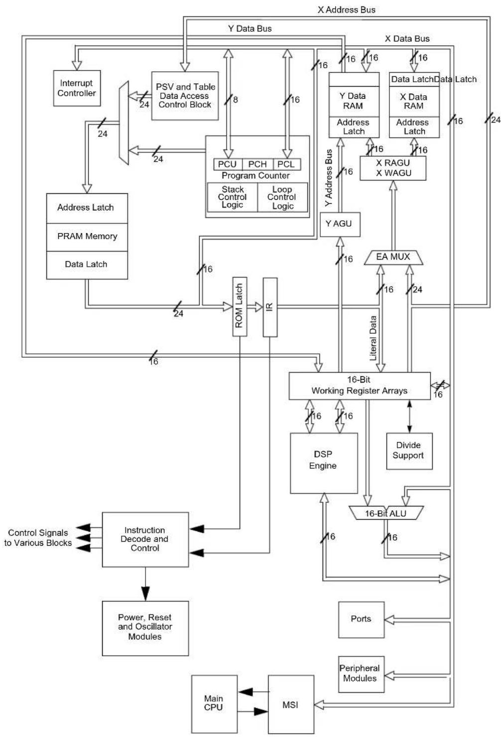
flowchart
graph TD
    A["X Address Bus"] --> B["Interrupt Controller"]
    A --> C["PSV and Table Data Access Control Block"]
    A --> D["Program Counter"]
    A --> E["Y Data Bus"]
    A --> F["X Data Bus"]
    B --> G["Address Latch"]
    C --> H["PRAM Memory"]
    C --> I["Data Latch"]
    D --> J["PCU PCH PCL"]
    D --> K["Stack Control Logic Loop Control Logic"]
    E --> L["Y Data RAM"]
    E --> M["Address Latch"]
    F --> N["X Data RAM"]
    F --> O["Address Latch"]
    F --> P["X RAGU X WAGU"]
    F --> Q["Y AGU"]
    F --> R["EA MUX"]
    R --> S["16-Bit Working Register Arrays"]
    S --> T["DSP Engine"]
    S --> U["Divide Support"]
    S --> V["16-Bit ALU"]
    V --> W["Ports"]
    V --> X["Peripheral Modules"]
    V --> Y["Main CPU"]
    V --> Z["MSI"]
    Z --> AA["Instruction Decode and Control"]
    AA --> AB["Power, Reset and Oscillator Modules"]
    AB --> AC["Control Signals to Various Blocks"]
    S --> AD["Literal Data"]
    AD --> AE["16-Bit Working Register Arrays"]
    AE --> AF["DSP Engine"]
    AE --> AG["Divide Support"]
    AE --> AH["16-Bit ALU"]
4.1.5 PROGRAMMER'S MODEL
The programmer's model for the dsPIC33CH128MP508S1 family is shown in Figure 4-2. All registers in the programmer's model are memory-mapped and can be manipulated directly by instructions. Table4-1 lists a description of each register.
In addition to the registers contained in the programmer's model, the dsPIC33CH128MP508S1 devices contain control registers for Modulo Addressing, Bit-Reversed Addressing and interrupts. These registers are described in subsequent sections of this document.
All registers associated with the programmer's model are memory-mapped, as shown in Figure 4-3.
TABLE 4-1: PROGRAMMER'S MODEL REGISTER DESCRIPTIONS
| Register(s) Name Description | |
| W0 through W15(1) | Working Register Array |
| W0 through W14(1) | Alternate 1 Working Register Array |
| W0 through W14(1) | Alternate 2 Working Register Array |
| W0 through W14(1) | Alternate 3 Working Register Array |
| W0 through W14(1) | Alternate 4 Working Register Array |
| ACCA, ACCB 40-Bit DSP Accumulators | (Additional 4 Alternate Accumulators) |
| PC 23-Bit Program Counter | |
| SR ALU and DSP Engine STATUS Register | |
| SPLIM Stack Pointer Limit Value Register | |
| TBLPAG | Table Memory Page Address Register |
| DSRPAG | Extended Data Space (EDS) Read Page Register |
| RCOUNT | REPEAT Loop Counter Register |
| DCOUNT | DO Loop Counter Register |
| DOSTARTH(2), DOSTARTL(2) | DO Loop Start Address Register (High and Low) |
| DOENDH, DOENDL | DO Loop End Address Register (High and Low) |
| CORCON | Contains DSP Engine, DO Loop Control and Trap Status bits |
Note 1: Memory-mapped W0 through W14 represent the value of the register in the currently active CPU context.
2: The DOSTARTH and DOSTARTL registers are read-only.
FIGURE 4-2: PROGRAMMER'S MODEL (SECONDARY)

flowchart
graph TD
    A["Working/Address Registers"] --> B["W0-W3"]
    A --> C["DSP Operand Registers"]
    A --> D["DSP Address Registers"]
    B --> E["W0 (WREG)"]
    C --> F["W1"]
    C --> G["W2"]
    C --> H["W3"]
    C --> I["W4"]
    C --> J["W5"]
    C --> K["W6"]
    C --> L["W7"]
    C --> M["W8"]
    C --> N["W9"]
    C --> O["W10"]
    C --> P["W11"]
    C --> Q["W12"]
    C --> R["W13"]
    C --> S["Frame Pointer/W14"]
    C --> T["Stack Pointer/W15"]

    U["DSP Accumulators(1)"] --> V["ACCA"]
    U --> W["ACCB"]

    X["Alternate Working/Address Registers"] --> Y["SPLIM"]
    X --> Z["Stack Pointer Limit"]

    AA["Program Counter"] --> AB["Program Counter"]

    AC["Data Table Page Address"] --> AD["TBLPAG"]
    AD --> AE["X Data Space Read Page Address"]

    AF["Data Table Page Address"] --> AG["Data Table Page Address"]

    AH["Data Table Page Address"] --> AI["Data Table Page Address"]

    AJ["Data Table Page Address"] --> AK["X Data Space Read Page Address"]

    AL["Data Table Page Address"] --> AM["Data Table Page Address"]

    AN["Data Table Page Address"] --> AO["X Data Space Read Page Address"]

    AP["Data Table Page Address"] --> AQ["X Data Space Read Page Address"]

    AR["Data Table Page Address"] --> AS["X Data Space Read Page Address"]

    AT["Data Table Page Address"] --> AU["X Data Space Read Page Address"]

    AV["Data Table Page Address"] --> AW["X Data Space Read Page Address"]

    AX["Data Table Page Address"] --> AY["X Data Space Read Page Address"]

    AZ["Data Table Page Address"] --> BA["X Data Space Read Page Address"]

    BB["Data Table Page Address"] --> BC["X Data Space Read Page Address"]

    BD["Data Table Page Address"] --> BE["X Data Space Read Page Address"]

    BF["Data Table Page Address"] --> BG["X Data Space Read Page Address"]

    BH["Data Table Page Address"] --> BH1["X Data Space Read Page Address"]

    BI["Data Table Page Address"] --> BJ["X Data Space Read Page Address"]

    BK["Data Table Page Address"] --> BL["X Data Space Read Page Address"]

    BM["Data Table Page Address"] --> BM1["X Data Space Read Page Address"]

    BN["Data Table Page Address"] --> BN1["X Data Space Read Page Address"]

    BO["Data Table Page Address"] --> BP["X Data Space Read Page Address"]

    BQ["DO Loop Counter and Stack"] --> BR["DO Loop Counter and Stack"]

    BS["DO Loop Start Address and Stack"] --> BT["DO Loop Start Address and Stack"]

    BU["DO Loop End Address and Stack"] --> BV["DO Loop End Address and Stack"]

    BW["DO Loop End Address and Stack"] --> BX["DO Loop End Address and Stack"]

    BY["DO Loop End Address and Stack"] --> BY1["DO Loop End Address and Stack"]

    CA["DO Loop End Address and Stack"] --> CB["DO Loop End Address and Stack"]

    CC["CPU Core Control Register"] --> DD["CPU Core Control Register"]

    DE["SRL"] --> DF["SRL"]

    DG["OA OB SA SB"] --> DH["OAB SAB DA DC IPL2 IPL1 IPL0 RA N O V 2 CSTATUS Register"]
4.1.6 CPU RESOURCES
Many useful resources are provided on the main product page of the Microchip website for the devices listed in this data sheet. This product page contains the latest updates and additional information.
4.1.6.1 Key Resources
- “Enhanced CPU” (www.microchip.com/DS70005158)
- Code Samples
- Application Notes
- Software Libraries
- Webinars
- All related "dsPIC33/PIC24 Family Reference Manual" Sections
- Development Tools
4.1.7 CPU CONTROL/STATUS REGISTERS
REGISTER 4-1: SR: CPU STATUS REGISTER
| R/W-0 R/W-0 R/W-0 R/W-0 R/C-0 R/C-0 R-0 R/W-0 | |||||||
| OA OB SA | (3) | SB(3) | OAB SAB | DA | DC | ||
| bit 15 bit 8 | |||||||
| R/W-0^(2) | R/W-0^(2) | R/W-0^(2) | R-0 | R/W-0 | R/W-0 | R/W-0 | R/W-0 |
| IPL2^(1) | IPL1^(1) | IPL0^(1) | RA | N | OV | Z | C |
| bit 7 bit 0 | |||||||
| Legend: | C = Clearable bit | ||
| R = Readable bit | W = Writable bit | U = Unimplemented bit, read as ‘0’ | |
| -n = Value at POR | ‘1’= Bit is set | ‘0’ = Bit is cleared | x = Bit is unknown |
bit 15 OA: Accumulator A Overflow Status bit
1 = Accumulator A has overflowed
0 = Accumulator A has not overflowed
bit 14 OB: Accumulator B Overflow Status bit
1 = Accumulator B has overflowed
0 = Accumulator B has not overflowed
bit 13 SA: Accumulator A Saturation 'Sticky' Status bit ^(3)
1 = Accumulator A is saturated or has been saturated at some time
0 = Accumulator A is not saturated
bit 12 SB: Accumulator B Saturation 'Sticky' Status bit ^(3)
1 = Accumulator B is saturated or has been saturated at some time
0 = Accumulator B is not saturated
bit 11 OAB: OA || OB Combined Accumulator Overflow Status bit
1 = Accumulator A or B has overflowed
0 = Neither Accumulator A or B has overflowed
bit 10 SAB: SA || SB Combined Accumulator 'Sticky' Status bit
1 = Accumulator A or B is saturated or has been saturated at some time
0 = Neither Accumulator A or B is saturated
bit 9 DA: DO Loop Active bit
1 = DO loop is in progress
0 = DO loop is not in progress
bit 8 DC: MCU ALU Half Carry/Borrow bit
1 = A carry-out from the 4th low-order bit (for byte-sized data) or 8th low-order bit (for word-sized data) of the result occurred
0 = No carry-out from the 4th low-order bit (for byte-sized data) or 8th low-order bit (for word-sized data) of the result occurred
Note 1: The IPL[2:0] bits are concatenated with the IPL[3] bit (CORCON[3]) to form the CPU Interrupt Priority Level. The value in parentheses indicates the IPL, if IPL[3] = 1. User interrupts are disabled when IPL[3] = 1.
2: The IPL[2:0] Status bits are read-only when the NSTDIS bit (INTCON1[15]) = 1.
3: A data write to the SR register can modify the SA and SB bits by either a data write to SA and SB or by clearing the SAB bit. To avoid a possible SA or SB bit write race condition, the SA and SB bits should not be modified using bit operations.
REGISTER 4-1: SR: CPU STATUS REGISTER (CONTINUED)
bit 7-5 IPL[2:0]: CPU Interrupt Priority Level Status bits
(1,2)
111 = CPU Interrupt Priority Level is 7 (15); user interrupts are disabled
110 = CPU Interrupt Priority Level is 6 (14)
101 = CPU Interrupt Priority Level is 5 (13)
100 = CPU Interrupt Priority Level is 4 (12)
011 = CPU Interrupt Priority Level is 3 (11)
010 = CPU Interrupt Priority Level is 2 (10)
001 = CPU Interrupt Priority Level is 1 (9)
000 = CPU Interrupt Priority Level is 0 (8)
bit 4 RA: REPEAT Loop Active bit
1 = REPEAT loop is in progress
0 = REPEAT loop is not in progress
bit 3 N: MCU ALU Negative bit
1 = Result was negative
0 = Result was non-negative (zero or positive)
bit 2 OV: MCU ALU Overflow bit
This bit is used for signed arithmetic (2's complement). It indicates an overflow of the magnitude that causes the sign bit to change state.
1 = Overflow occurred for signed arithmetic (in this arithmetic operation)
0 = No overflow occurred
bit 1 Z: MCU ALU Zero bit
1 = An operation that affects the Z bit has set it at some time in the past
0 = The most recent operation that affects the Z bit has cleared it (i.e., a non-zero result)
bit 0 C: MCU ALU Carry/Borrow bit
1 = A carry-out from the Most Significant bit of the result occurred
0 = No carry-out from the Most Significant bit of the result occurred
Note 1: The IPL[2:0] bits are concatenated with the IPL[3] bit (CORCON[3]) to form the CPU Interrupt Priority Level. The value in parentheses indicates the IPL, if IPL[3] = 1. User interrupts are disabled when IPL[3] = 1.
2: The IPL[2:0] Status bits are read-only when the NSTDIS bit (INTCON1[15]) = 1.
3: A data write to the SR register can modify the SA and SB bits by either a data write to SA and SB or by clearing the SAB bit. To avoid a possible SA or SB bit write race condition, the SA and SB bits should not be modified using bit operations.
REGISTER 4-2: CORCON: CORE CONTROL REGISTER
| R/W-0 U-0 R/W-0 R/W-0 R/W-0 R-0 R-0 R-0 | ||||||
| VAR | — US1 US0 EDT | (1) | DL2 DL1 DL0 | |||
| bit 15 bit 8 | ||||||
| R/W-0 | R/W-0 | R/W-1 | R/W-0 | R/C-0 | R-0 | R/W-0 | R/W-0 |
| SATA | SATB | SATDW | ACCSAT | IPL3^(2) | SFA | RND IF | |
| bit 7 bit 0 | |||||||
| Legend: | C = Clearable bit | ||
| R = Readable bit | W = Writable bit | U = Unimplemented bit, read as ‘0’ | |
| -n = Value at POR | ‘1’ = Bit is set | ‘0’ = Bit is cleared | x = Bit is unknown |
bit 15 VAR: Variable Exception Processing Latency Control bit
1 = Variable exception processing is enabled
0 = Fixed exception processing is enabled
bit 14 Unimplemented: Read as '0'
bit 13-12 US[1:0]: DSP Multiply Unsigned/Signed Control bits
11 = Reserved
10 = DSP engine multiplies are mixed sign
01 = DSP engine multiplies are unsigned
00 = DSP engine multiplies are signed
bit 11 EDT: Early DO Loop Termination Control bit ^(1)
1 = Terminates executing DO loop at the end of the current loop iteration
0 = No effect
bit 10-8 DL[2:0]: DO Loop Nesting Level Status bits
111 = Seven DO loops are active
• • •
001 = One DO loop is active
000 = Zero DO loops are active
bit 7 SATA: ACCA Saturation Enable bit
1 = Accumulator A saturation is enabled
0 = Accumulator A saturation is disabled
bit 6 SATB: ACCB Saturation Enable bit
1 = Accumulator B saturation is enabled
0 = Accumulator B saturation is disabled
bit 5 SATDW: Data Space Write from DSP Engine Saturation Enable bit
1 = Data Space write saturation is enabled
0 = Data Space write saturation is disabled
bit 4 ACCSAT: Accumulator Saturation Mode Select bit
1 = 9.31 saturation (super saturation)
0 = 1.31 saturation (normal saturation)
bit 3 IPL3: CPU Interrupt Priority Level Status bit 3 ^(2)
1 = CPU Interrupt Priority Level is greater than 7
0 = CPU Interrupt Priority Level is 7 or less
Note 1: This bit is always read as '0'.
2: The IPL3 bit is concatenated with the IPL[2:0] bits (SR[7:5]) to form the CPU Interrupt Priority Level.
REGISTER 4-2: CORCON: CORE CONTROL REGISTER (CONTINUED)
bit 2 SFA: Stack Frame Active Status bit
1 = Stack frame is active; W14 and W15 address 0x0000 to 0xFFFF, regardless of DSRPAG
0 = Stack frame is not active; W14 and W15 address the base Data Space
bit 1 RND: Rounding Mode Select bit
1 = Biased (conventional) rounding is enabled
0 = Unbiased (convergent) rounding is enabled
bit 0 IF: Integer or Fractional Multiplier Mode Select bit
1 = Integer mode is enabled for DSP multiply
0 = Fractional mode is enabled for DSP multiply
Note 1: This bit is always read as '0'.
2: The IPL3 bit is concatenated with the IPL[2:0] bits (SR[7:5]) to form the CPU Interrupt Priority Level.
REGISTER 4-3: CTXTSTAT: CPU W REGISTER CONTEXT STATUS REGISTER
| U-0 U-0 U-0 U-0 R-0 R-0 R-0 | |||||
| — | — | — | — | — | CCTXI[2:0] |
| bit 15 | bit 8 | ||||
| U-0 U-0 U-0 U-0 U-0 R-0 R-0 R-0 | |||||
| — | — | — | — | — | MCTXI[2:0] |
| bit 7 bit 0 | |||||
| Legend: | |||
| R = Readable bit | W = Writable bit | U = Unimplemented bit, read as ‘0’ | |
| -n = Value at POR | ‘1’ = Bit is set | ‘0’ = Bit is cleared | x = Bit is unknown |
bit 15-11 Unimplemented: Read as '0'
bit 10-8 CCTXI[2:0]: Current (W Register) Context Identifier bits
111 = Reserved
...
100 = Alternate Working Register Set 4 is currently in use
011 = Alternate Working Register Set 3 is currently in use
010 = Alternate Working Register Set 2 is currently in use
001 = Alternate Working Register Set 1 is currently in use
000 = Default register set is currently in use
bit 7-3 Unimplemented: Read as '0'
bit 2-0 MCTXI[2:0]: Manual (W Register) Context Identifier bits
111 = Reserved
...
100 = Alternate Working Register Set 4 was most recently manually selected
011 = Alternate Working Register Set 3 was most recently manually selected
010 = Alternate Working Register Set 2 was most recently manually selected
001 = Alternate Working Register Set 1 was most recently manually selected
000 = Default register set was most recently manually selected
REGISTER 4-4: MSTRPR: DATA SPACE BUS MASTER PRIORITY CONTROL REGISTER (SECONDARY)
| R = Readable bit | W = Writable bit | U = Unimplemented bit, read as '0' |
| -n = Value at POR | '1' = Bit is set | '0' = Bit is cleared x = Bit is unknown |
bit 15-6 Unimplemented: Read as '0'
bit 5 DMAPR: Modify DMA Controller Bus Master Priority Relative to CPU bit
1 = Raise DMA Controller bus Master priority to above that of the CPU
0 = No change to DMA Controller bus Master priority
bit 4-0 Unimplemented: Read as '0'
4.1.8 ARITHMETIC LOGIC UNIT (ALU)
The dsPIC33CH128MP508S1 family ALU is 16 bits wide and is capable of addition, subtraction, bit shifts and logic operations. Unless otherwise mentioned, arithmetic operations are two's complement in nature. Depending on the operation, the ALU can affect the values of the Carry (C), Zero (Z), Negative (N), Overflow (OV) and Digit Carry (DC) Status bits in the SR register. The C and DC Status bits operate as Borrow and Digit Borrow bits, respectively, for subtraction operations.
The ALU can perform 8-bit or 16-bit operations, depending on the mode of the instruction that is used. Data for the ALU operation can come from the W register array or data memory, depending on the addressing mode of the instruction. Likewise, output data from the ALU can be written to the W register array or a data memory location.
Refer to the "16-Bit MCU and DSC Programmer's Reference Manual" (DS70000157) for information on the SR bits affected by each instruction.
The core CPU incorporates hardware support for both multiplication and division. This includes a dedicated hardware multiplier and support hardware for 16-bit divisor division.
4.1.8.1 Multiplier
Using the high-speed, 17-bit x 17-bit multiplier, the ALU supports unsigned, signed or mixed-sign operation in several MCU Multiplication modes:
- 16-bit x 16-bit signed
- 16-bit x 16-bit unsigned
• 16-bit signed x 5-bit (literal) unsigned
• 16-bit signed x 16-bit unsigned
• 16-bit unsigned x 5-bit (literal) unsigned
• 16-bit unsigned x 16-bit signed - 8-bit unsigned x 8-bit unsigned
4.1.8.2 Divider
The divide block supports 32-bit/16-bit and 16-bit/16-bit signed and unsigned integer divide operations with the following data sizes:
• 32-bit signed/16-bit signed divide
• 32-bit unsigned/16-bit unsigned divide
• 16-bit signed/16-bit signed divide
• 16-bit unsigned/16-bit unsigned divide
The quotient for all divide instructions ends up in W0 and the remainder in W1. 16-bit signed and unsigned DIV instructions can specify any W register for both the 16-bit divisor (Wn) and any W register (aligned) pair (W(m + 1):Wm) for the 32-bit dividend. The divide algorithm takes one cycle per bit of divisor, so both 32-bit/16-bit and 16-bit/16-bit instructions take the same number of cycles to execute.
4.1.9 DSP ENGINE
The DSP engine consists of a high-speed, 17-bit x 17-bit multiplier, a 40-bit barrel shifter and a 40-bit adder/subtracter (with two target accumulators, round and saturation logic).
The DSP engine can also perform inherent accumulator-to-accumulator operations that require no additional data. These instructions are, ADD, SUB and NEG.
The DSP engine has options selected through bits in the CPU Core Control register (CORCON), as listed below:
• Fractional or integer DSP multiply (IF)
• Signed, unsigned or mixed-sign DSP multiply (USx)
- Conventional or convergent rounding (RND)
• Automatic saturation on/off for ACCA (SATA)
• Automatic saturation on/off for ACCB (SATB)
• Automatic saturation on/off for writes to data memory (SATDW)
- Accumulator Saturation mode selection (ACCSAT)
TABLE 4-2: DSP INSTRUCTIONS SUMMARY
| Instruction | Algebraic Operation | ACC Write-Back |
| CLR A = 0 Yes | ||
| ED A = (x - y) | ^2 | No |
| EDAC | A = A + (x - y)^2 | No |
| MAC | A = A + (x · y) | Yes |
| MAC A = A + x | ^2 | No |
| MOVSAC | No change in A | Yes |
| MPY | A = x · y | No |
| MPY A = x | ^2 | No |
| MPY.N | A = -x · y | No |
| MSC | A = A - x · y | Yes |
4.2 Secondary Memory Organization
Note: This data sheet summarizes the features of the dsPIC33CH128MP508 family of devices. It is not intended to be a comprehensive reference source. To complement the information in this data sheet, refer to “dsPIC33/PIC24 Program Memory” (www.microchip.com/DS70000613), which is available from the Microchip website (www.microchip.com).
The dsPIC33CH128MP508S1 family architecture features separate program and data memory spaces, and buses. This architecture also allows the direct access of program memory from the Data Space (DS) during code execution.
4.2.1 PROGRAM ADDRESS SPACE
The program address memory space of the dsPIC33CH128MP508S1 family devices is 4M instructions. The space is addressable by a 24-bit value derived either from the 23-bit PC during program execution, or from table operation or Data Space remapping, as described in Section 4.2.8 "Interfacing Program and Data Memory Spaces".
User application access to the program memory space is restricted to the lower half of the address range (0x000000 to 0x7FFFFFF). The exception is the use of
TBLRD operations, which use TBLPAG[7] to permit access to calibration data and Device ID sections of the configuration memory space.
The PRAM for the Secondary dsPIC33CH128MP508S1 devices implements two 12-Kbyte PRAM panels with a total of 24 Kbytes of PRAM available for the Secondary device. All variants of the Secondary have the same amount of PRAM available, irrespective of the size of the Flash available on the Host Flash program memory, as shown in Figure 4-3.
FIGURE 4-3: PRAM (PROGRAM MEMORY) FOR SECONDARY dsPIC33CH128MP508S1 DEVICES
Normal Operation or Single Partition
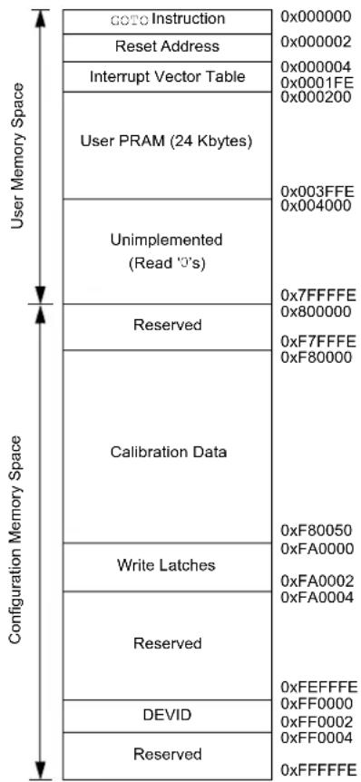
text_image
coto Instruction Reset Address Interrupt Vector Table User PRAM (24 Kbytes) Unimplemented (Read '0's) Reserved Calibration Data Write Latches Reserved DEVID Reserved 0x000000 0x000002 0x000004 0x0001FE 0x000200 0x003FFE 0x004000 0x7FFFFE 0x800000 0xF7FFFE 0xF80000 0xF80050 0xFA0000 0xFA0002 0xFA0004 0xFEFFF 0xFF0000 0xFF0002 0xFF0004 0xFFFFFENote: Memory areas are not shown to scale.
Dual Partition PRAM Organization

text_image
GOTO Instruction Reset Address Interrupt Vector Table User Program Memory (12 Kbytes) Unimplemented (Read '0's) GOTO Instruction Reset Address Interrupt Vector Table User Program Memory (12 Kbytes) Unimplemented (Read '0's) 0x000000 0x000002 0x000004 0x0001FE 0x000200 0x000200 0x3FFFFFE 0x400000 0x400002 0x400004 0x4001FE 0x400200 0x401FFE 0x402000 0x7FFFFFE4.2.1.1 Program Memory Organization
The program memory space is organized in word-addressable blocks. Although it is treated as 24 bits wide, it is more appropriate to think of each address of the program memory as a lower and upper word, with the upper byte of the upper word being unimplemented. The lower word always has an even address, while the upper word has an odd address (Figure 4-4).
Program memory addresses are always word-aligned on the lower word, and addresses are incremented, or decremented, by two, during code execution. This arrangement provides compatibility with data memory space addressing and makes data in the program memory space accessible.
4.2.1.2 Interrupt and Trap Vectors
All dsPIC33CH128MP508S1 family devices reserve the addresses between 0x000000 and 0x000200 for hard-coded program execution vectors. A hardware Reset vector is provided to redirect code execution from the default value of the PC on device Reset to the actual start of code. A GOTO instruction is programmed by the user application at address, 0x000000, of PRAM memory, with the actual address for the start of code at address, 0x000200, of PRAM memory.
A more detailed discussion of the Interrupt Vector Tables (IVTs) is provided in Table 4-21.
FIGURE 4-4: PROGRAM MEMORY ORGANIZATION
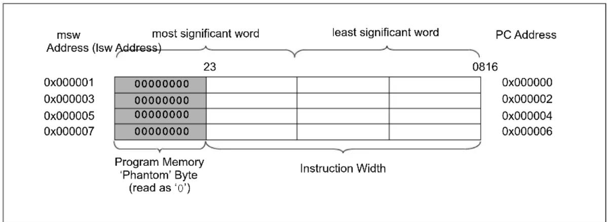
text_image
msw Address (Isw Address) most significant word least significant word PC Address 0x000001 0x000003 0x000005 0x000007 23 0816 Program Memory 'Phantom' Byte (read as '0') Instruction Width 0x000000 0x000002 0x000004 0x0000064.2.2 DATA ADDRESS SPACE (SECONDARY)
The dsPIC33CH128MP508S1 family CPU has a separate 16-bit wide data memory space. The Data Space is accessed using separate Address Generation Units (AGUs) for read and write operations. The data memory map is shown in Figure 4-5.
All Effective Addresses (EAs) in the data memory space are 16 bits wide and point to bytes within the Data Space. This arrangement gives a base Data Space address range of 64 Kbytes or 32K words.
The lower half of the data memory space (i.e., when EA[15] = 0) is used for implemented memory addresses, while the upper half (EA[15] = 1) is reserved for the Program Space Visibility (PSV).
The dsPIC33CH128MP508S1 family devices implement up to 4 Kbytes of data memory. If an EA points to a location outside of this area, an all-zero word or byte is returned.
4.2.2.1 Data Space Width
The data memory space is organized in byte-addressable, 16-bit wide blocks. Data are aligned in data memory and registers as 16-bit words, but all Data Space EAs resolve to bytes. The Least Significant Bytes (LSBs) of each word have even addresses, while the Most Significant Bytes (MSBs) have odd addresses.
4.2.2.2 Data Memory Organization and Alignment
To maintain backward compatibility with PIC® MCU devices and improve Data Space memory usage efficiency, the dsPIC33CH128MP508S1 family instruction set supports both word and byte operations. As a consequence of byte accessibility, all Effective Address calculations are internally scaled to step through word-aligned memory. For example, the core recognizes that Post-Modified Register Indirect Addressing mode [Ws++] results in a value of Ws + 1 for byte operations and Ws + 2 for word operations.
A data byte read, reads the complete word that contains the byte, using the LSb of any EA to determine which byte to select. The selected byte is placed onto the LSB of the data path. That is, data memory and registers are organized as two parallel, byte-wide entities with shared (word) address decode, but separate write lines. Data byte writes only write to the corresponding side of the array or register that matches the byte address.
All word accesses must be aligned to an even address. Misaligned word data fetches are not supported, so care must be taken when mixing byte and word operations, or translating from 8-bit MCU code. If a misaligned read or write is attempted, an address error trap is generated. If the error occurred on a read, the instruction underway is completed. If the error occurred on a write, the instruction is executed but the write does not occur. In either case, a trap is then executed, allowing the system and/or user application to examine the machine state prior to execution of the address Fault.
All byte loads into any W register are loaded into the LSB; the MSB is not modified.
A Sign-Extend (SE) instruction is provided to allow user applications to translate 8-bit signed data to 16-bit signed values. Alternatively, for 16-bit unsigned data, user applications can clear the MSB of any W register by executing a Zero-Extend (ZE) instruction on the appropriate address.
4.2.2.3 SFR Space
The first 4 Kbytes of the Near Data Space, from 0x0000 to 0x0FFF, is primarily occupied by Special Function Registers (SFRs). These are used by the dsPIC33CH128MP508S1 family core and peripheral modules for controlling the operation of the device.
SFRs are distributed among the modules that they control and are generally grouped together by module. Much of the SFR space contains unused addresses; these are read as '0'.
Note: The actual set of peripheral features and interrupts varies by the device. Refer to the corresponding device tables and pinout diagrams for device-specific information.
4.2.2.4 Near Data Space
The 8-Kbyte area, between 0x0000 and 0x1FFF, is referred to as the Near Data Space. Locations in this space are directly addressable through a 13-bit absolute address field within all memory direct instructions. Additionally, the whole Data Space is addressable using MOV instructions, which support Memory Direct Addressing mode with a 16-bit address field, or by using Indirect Addressing mode using a Working register as an Address Pointer.
FIGURE 4-5: DATA MEMORY MAP FOR SECONDARY dsPIC33CH128MP508S1 DEVICES
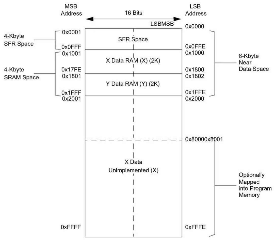
text_image
MSB Address 16 Bits LSBMSB 0x0000 0x0FFE 0x1000 0x1800 0x1802 0x1FFE 0x2000 4-Kbyte SFR Space 0x0001 SFR Space X Data RAM (X) (2K) Y Data RAM (Y) (2K) 4-Kbyte SRAM Space 0x17FE 0x1801 0x1FFF 0x2001 8-Kbyte Near Data Space X Data Unimplemented (X) Optionally Mapped into Program Memory 0xFFFF 0xFFFFNote: Memory areas are not shown to scale.
4.2.2.5 X and Y Data Spaces
The dsPIC33CH128MP508S1 family core has two Data Spaces, X and Y. These Data Spaces can be considered either separate (for some DSP instructions) or as one unified linear address range (for MCU instructions). The Data Spaces are accessed using two Address Generation Units (AGUs) and separate data paths. This feature allows certain instructions to concurrently fetch two words from RAM, thereby enabling efficient execution of DSP algorithms, such as Finite Impulse Response (FIR) filtering and Fast Fourier Transform (FFT).
The X Data Space is used by all instructions and supports all addressing modes. X Data Space has separate read and write data buses. The X read data bus is the read data path for all instructions that view Data Space as combined X and Y address space. It is also the X data prefetch path for the dual operand DSP instructions (MAC class).
The Y Data Space is used in concert with the X Data Space by the MAC class of instructions (CLR, ED, EDAC, MAC, MOVSAC, MPY, MPY.N and MSC) to provide two concurrent data read paths.
Both the X and Y Data Spaces support Modulo Addressing mode for all instructions, subject to addressing mode restrictions. Bit-Reversed Addressing mode is only supported for writes to X Data Space.
All data memory writes, including in DSP instructions, view Data Space as combined X and Y address space. The boundary between the X and Y Data Spaces is device-dependent and is not user-programmable.
4.2.3 MEMORY RESOURCES
Many useful resources are provided on the main product page of the Microchip website for the devices listed in this data sheet. This product page contains the latest updates and additional information.
4.2.3.1 Key Resources
- "dsPIC33/ PIC24 Program Memory" (www.microchip.com/DS70000613)
- Code Samples
- Application Notes
- Software Libraries
- Webinars
- All Related "dsPIC33/PIC24 Family Reference Manual" Sections
- Development Tools
4.2.4 SFR MAPS
The following tables show dsPIC33CH128MP508 family Secondary SFR names, addresses and Reset values. These tables contain all registers applicable to the
dsPIC33CH128MP508S1 family. Not all registers are present on all device variants. Refer to Table1 and Table 2 for peripheral availability. Table 4-25 details port availability for the different package options.
TABLE 4-3: SECONDARY SFR BLOCK 000h
| Register | Address | All Resets | Register | Address | All Resets | Register | Address | All Resets |
| Core | DSRPAG | 032 | ----000000001 | CLC1GLSL | 0C8 | 000000000000000 | ||
| WREG0 | 000 | 000000000000000 | DSWPAG | 034 | ----0000000001 | CLC1GLSH | 0CA | 000000000000000 |
| WREG1 | 002 | 000000000000000 | RCOUNT | 036 | xxxxxxxxxxxxxx | CLC2CONL | 0CC | 0-0-00--000--000 |
| WREG2 | 004 | 000000000000000 | DCOUNT | 038 | xxxxxxxxxxxxxx | CLC2CONH | 0CE | ----0000 |
| WREG3 | 006 | 000000000000000 | DOSTART | 03A | 111111111111111 | CLC2SELL | 0D0 | -000-000-000-000 |
| WREG4 | 008 | 000000000000000 | DOSTARTL | 03A | 111111111111110 | CLC2SELH | 0D2 | ---- |
| WREG5 | 00A | 000000000000000 | DOSTARTH | 03C | 000000011111111 | CLC2GLSL | 0D4 | 000000000000000 |
| WREG6 | 00C | 000000000000000 | DOENDL | 03E | xxxxxxxxxxxxxx0 | CLC2GLSH | 0D6 | 00000000000000 |
| WREG7 | 00E | 000000000000000 | DOENDH | 040 | ----xxxxxx | CLC3CONL | 0D8 | 0-0-00--000--000 |
| WREG8 | 010 | 000000000000000 | SR | 042 | 000000000000000 | CLC3CONH | 0DA | ----0000 |
| WREG9 | 012 | 000000000000000 | CORCON | 044 | x-xx00000100000 | CLC3SELL | 0DC | -000-000-000-000 |
| WREG10 | 014 | 000000000000000 | MODCON | 046 | 00--0000000000 | CLC3GLSL | 0E0 | 00000000000000 |
| WREG11 | 016 | 000000000000000 | XMODSRT | 048 | xxxxxxxxxxxxxx0 | CLC3GLSH | 0E2 | 00000000000000 |
| WREG12 | 018 | 000000000000000 | XMODEND | 04A | xxxxxxxxxxxxxx1 | CLC4CONL | 0E4 | 0-0-00--000--000 |
| WREG13 | 01A | 000000000000000 | YMODSRT | 04C | xxxxxxxxxxxxxx0 | CLC4CONH | 0E6 | ----0000 |
| WREG14 | 01C | 000000000000000 | YMODEND | 04E | xxxxxxxxxxxxxx1 | CLC4SELL | 0E8 | -000-000-000-000 |
| WREG15 | 01E | 00010000000000 | XBREV | 050 | 0xxxxxxxxxxxxxx | CLC4GLSL | 0EC | 00000000000000 |
| SPLIM | 020 | xxxxxxxxxxxxxx | DISICNT | 052 | xxxxxxxxxxxxxx00 | CLC4GLSH | 0EE | 0000000000000 |
| ACCAL | 022 | xxxxxxxxxxxxxx | TBLPAG | 054 | ----0000000 | ECCCONL | 0F0 | ----0 |
| ACCAH | 024 | xxxxxxxxxxxxxx | YPAG | 056 | ----0000001 | ECCCONH | 0F2 | 0000000000000 |
| ACCAU | 026 | xxxxxxxxxxxxxx | MSTRPR | 058 | ----0---- | ECCADDRL | 0F4 | 0000000000000 |
| ACCBL | 028 | xxxxxxxxxxxxxx | CTXTSTAT | 05A | 00C0C0C0C0C0C0C | ECCADDRH | 0F6 | 0000000000000 |
| ACCBH | 02A | xxxxxxxxxxxxxx | CLC | ECCSTATL | 0F8 | 000000000000 | ||
| ACCBU | 02C | xxxxxxxxxxxxxx | CLC1CONL | 0C0 | 0-0-00--000--000 | ECCSTATH | 0FA | ----000C0C |
| PCL | 02E | 00000000000000 | CLC1CONH | 0C2 | ----0000 | |||
| PCH | 030 | ----00C0C0C | CLC1SELL | 0C4 | -000-000-000-00 | |||
Legend: x = unknown or indeterminate value; "-" = unimplemented bits. Address and Reset values are in hexadecimal and binary, respectively.
TABLE 4-4: SECONDARY SFR BLOCK 100h
| Register Address All | Resets Register Address All Resets | Register Address All Resets | |||||||
| Timers | INT1TMRL | 15C | 0000000000000000 | SI1MBX2D | 1DE | 0000000000000000 | |||
| T1CON | 100 | 0-000000-00-00- | INT1TMRH | 15E | 0000000000000000 | SI1MBX3D | 1E0 | 0000000000000000 | |
| TMR1 | 104 | 000000000000000 | INT1HLDL | 160 | 0000000000000000 | SI1MBX4D | 1E2 | 0000000000000000 | |
| PR1 | 108 | 000000000000000 | INT1HLDH | 162 | 0000000000000000 | SI1MBX5D | 1E4 | 0000000000000000 | |
| QEI | INDX1CNTL | 164 | 0000000000000000 | SI1MBX6D | 1E6 | 0000000000000000 | |||
| QEI1CON | 140 | 000000000000000 | INDX1CNTH | 166 | 0000000000000000 | SI1MBX7D | 1E8 | 0000000000000000 | |
| QEI1IOCL | 144 | 00000000000xxxx | INDX1HLDL | 168 | 0000000000000000 | SI1MBX8D | 1EA | 0000000000000000 | |
| QEI1IOCH | 146 | ----0 | INDX1HLDH | 16A | 0000000000000000 | SI1MBX9D | 1EC | 0000000000000000 | |
| QEI1STAT | 148 | --0000000000000 | QEI1GECL | 16C | 000000000000000 | SI1MBX10D | 1EE | 0000000000000000 | |
| POS1CNTL | 14C | 00000000000000 | QEI1GECH | 16E | 000000000000000 | SI1MBX11D | 1F0 | 000000000000000 | |
| POS1CNTH | 14E | 00000000000000 | QEI1LECL | 170 | 000000000000000 | SI1MBX12D | 1F2 | 000000000000000 | |
| POS1HLDL | 150 | 0000000000000 | QEI1LECH | 172 | 000000000000000 | SI1MBX13D | 1F4 | 000000000000000 | |
| POS1HLDH | 152 | 000000000000 | SI1CON | 1D2 | 0---xx00000000 | SI1MBX14D | 1F6 | 000000000000000 | |
| VEL1CNTL | 154 | 00000000000 | SI1STAT | 1D4 | 000000000000 | SI1MBX15D | 1F8 | ||
| VEL1CNTH | 156 | 0000000000 | SI1MBXS | 1D8 | ----0000 | SI1FIFOCS | 1FA | ||
| VEL1HLDL | 158 | 000000000 | SI1MBXOD | 1DA | 000000000 | SWMRFDATA | 1FC | ||
| VEL1HLDH | 15A | 000000000 | SI1MBX1D | 1DC | 00000000 | SRMWFDATA | 1FE | ||
Legend: x = unknown or indeterminate value; "-" = unimplemented bits. Address and Reset values are in hexadecimal and binary, respectively.
TABLE 4-5: SECONDARY SFR BLOCK 200h
| Register | Address | All Resets | Register | Address | All Resets | Register | Address | All Resets |
| I2C | U1BRGH | 242 | ----0000 | SPI1CON2L | 2B0 | ----00000 | ||
| I2C1CONL | 200 | 0-01000000000000 | U1RXREG | 244 | ----xxxxxxxx | SPI1CON2H | 2B2 | ---- |
| I2C1CONH | 202 | ----0000000 | U1TXREG | 248 | ----xxxxxxxx | SPI1STATL | 2B4 | ---00--0001-1-00 |
| I2C1STAT | 204 | 000--0000000000 | U1P1 | 24C | ----00000000 | SPI1STATH | 2B6 | --000000--000000 |
| I2C1ADD | 208 | ----000000000 | U1P2 | 24E | ----00000000 | SPI1BUFL | 2B8 | 000000000000000 |
| I2C1MSK | 20C | ----000000000 | U1P3 | 250 | 00000000000000 | SPI1BUFH | 2BA | 000000000000000 |
| I2C1BRG | 210 | 000000000000000 | U1P3H | 252 | ----0000000 | SPI1BRGL | 2BC | ---xxxxxxxxxxxxx |
| I2C1TRN | 214 | ----1111111 | U1TXCHK | 254 | ----0000000 | SPI1BRGH | 2BE | ---- |
| I2C1RCV | 218 | ----0000000 | U1RXCHK | 256 | ----0000000 | SPI1IMSKL | 2C0 | ---00--0000-0-00 |
| UART | U1SCCON | 258 | ----00000- | SPI1IMSKH | 2C2 | 0-0000000-000000 | ||
| U1MODE | 238 | 0-000-000000000 | U1SCINT | 25A | --00-000--00-000 | SPI1URDTL | 2C4 | 00000000000000 |
| U1MODEH | 23A | 00----000000000 | U1INT | 25C | ----00--0-- | SPI1URDTH | 2C6 | 00000000000000 |
| U1STA | 23C | 00000001000000 | SPI | |||||
| U1STAH | 23E | -000-00000101110 | SPI1CON1L | 2AC | 0-0000000000000 | |||
| U1BRG | 240 | 00000000000000 | SPI1CON1H | 2AE | 00000000000000 | |||
Legend: x = unknown or indeterminate value; “-” = unimplemented bits. Address and Reset values are in hexadecimal and binary, respectively.
TABLE 4-6: SECONDARY SFR BLOCK 300h
| Register Address All | Resets Register Address | All Resets | Register Address All Resets | ||||
| High-Speed PWM | PG1TRIGB | 356 | 0000000000000000 | PG3FFPCIH | 3AE | ||
| PCLKCON | 300 | 00----0--00--00 | PG1TRIGC | 358 | 0000000000000000 | PG3SPCIL | 3B0 |
| FSCL | 302 | 0000000000000000 | PG1DTL | 35A | --000000000000000 | PG3SPCIH | 3B2 |
| FSMINPER | 304 | 0000000000000000 | PG1DTH | 35C | --000000000000000 | PG3LEBL | 3B4 |
| MPHASE | 306 | 0000000000000000 | PG1CAP | 35E | 0000000000000000 | PG3LEBH | 3B6 |
| MDC | 308 | 0000000000000000 | PG2CONL | 360 | 0-000000000000000 | PG3PHASE | 3B8 |
| MPER | 30A | 0000000000000000 | PG2CONH | 362 | 000-00000--0000 | PG3DC | 3BA |
| LFSR | 30C | 0000000000000000 | PG2STAT | 364 | 0000000000000000 | PG3DCA | 3BC |
| CMBTRIGL | 30E | ----00000000 | PG2IOCONL | 366 | 0000000000000000 | PG3PER | 3BE |
| CMBTRIGH | 310 | ----00000000 | PG2IOCONH | 368 | -000--0--00000 | PG3TRIGA | 3C0 |
| LOGCONA | 312 | 00000000000-000 | PG2EVTL | 36A | 0000000--00000 | PG3TRIGB | 3C2 |
| LOGCONB | 314 | 00000000000-000 | PG2EVTH | 36C | 0000--00000000 | PG3TRIGC | 3C4 |
| LOGCONC | 316 | 00000000000-000 | PG2FPCIL | 36E | 000000000000000 | PG3DTL | 3C6 |
| LOGCOND | 318 | 0000000000-000 | PG2FPCIH | 370 | 0000-00000000 | PG3DTH | 3C8 |
| LOGCONE | 31A | 0000000000-000 | PG2CLPCIL | 372 | 000000000000000 | PG3CAP | 3CA |
| LOGCONF | 31C | 0000000000-000 | PG2CLPCIH | 374 | 0000-00000000 | PG4CONL | 3CC |
| PWMEVTA | 31E | 0000----0000-000 | PG2FFPCIL | 376 | 000000000000000 | PG4CONH | 3CE |
| PWMEVTB | 320 | 0000----000-000 | PG2FFPCIH | 378 | 0000-00000000 | PG4STAT | 3D0 |
| PWMEVTC | 322 | 0000----000-000 | PG2SPCIL | 37A | 000000000000000 | PG4IOCONL | 3D2 |
| PWMEVTD | 324 | 0000----000-000 | PG2SPCIH | 37C | 0000-00000000 | PG4IOCONH | 3D4 |
| PWMEVTE | 326 | 0000----000-000 | PG2LEBL | 37E | 000000000000000 | PG4EVTL | 3D6 |
| PWMEVTF | 328 | 0000----000-000 | PG2LEBH | 380 | ----00----000 | PG4EVTH | 3D8 |
| PG1CONL | 32A | 0-00000000000000 | PG2PHASE | 382 | 00000000000000 | PG4FPCIL | 3DA |
| PG1CONH | 32C | 000-00000--000 | PG2DC | 384 | 00000000000000 | PG4FPCIH | 3DC |
| PG1STAT | 32E | 00000000000000 | PG2DCA | 386 | ----00000 | PG4CLPCIL | 3DE |
| PG1IOCONL | 330 | 0000000000000 | PG2PER | 388 | 0000000000000 | PG4CLPCIH | 3E0 |
| PG1IOCONH | 332 | -000--0--000 | PG2TRIGA | 38A | 000000000000 | PG4FFPCIL | 3E2 |
| PG1EVTL | 334 | 000000--000 | PG2TRIGB | 38C | 000000000000 | PG4FFPCIH | 3E4 |
| PG1EVTH | 336 | 0000--0000000 | PG2TRIGC | 38E | 000000000000 | PG4SPCIL | 3E6 |
| PG1FPCIL | 338 | 00000000000 | PG2DTL | 390 | --000000000 | PG4SPCIH | 3E8 |
| PG1FPCIH | 33A | 0000-0000000 | PG2DTH | 392 | --000000000 | PG4LEBL | 3EA |
| PG1CLPCIL | 33C | 0000000000 | PG2CAP | 394 | 000000000 | PG4LEBH | 3EC |
| PG1CLPCIH | 33E | 0000-0000000 | PG3CONL | 396 | 0-00000000 | PG4PHASE | 3EE |
| PG1FFPCIL | 340 | 000000000 | PG3CONH | 398 | 000-0000--0 | PG4DC | 3F0 |
| PG1FFPCIH | 342 | 0000-0000000 | PG3STAT | 39A | 000000000 | PG4DCA | 3F2 |
| PG1SPCIL | 344 | 000000000 | PG3IOCONL | 39C | 000000000 | PG4PER | 3F4 |
| PG1SPCIH | 346 | 0000-0000000 | PG3IOCONH | 39E | -00--0--0 | PG4TRIGA | 3F6 |
| PG1LEBL | 348 | 00000000 | PG3EVTL | 3A0 | 00000--0--0 | PG4TRIGB | 3F8 |
| PG1LEBH | 34A | ----00----0 | PG3EVTH | 3A2 | 000--00000 | PG4TRIGC | 3FA |
| PG1PHASE | 34C | 00000000 | PG3FPCIL | 3A4 | 00000000 | PG4DTL | 3FC |
| PG1DC | 34E | 00000000 | PG3FPCIH | 3A6 | 000--00000 | PG4DTH | 3FE |
| PG1DCA | 350 | ----0000 | PG3CLPCIL | 3A8 | 00000000 | PG4CAP | 400 |
| PG1PER | 352 | 00000000 | PG3CLPCIH | 3AA | 000--0000 | ||
| PG1TRIGA | 354 | 00000000 | PG3FFPCIL | 3AC | 00000000 | ||
Legend: x = unknown or indeterminate value; "-" = unimplemented bits. Address and Reset values are in hexadecimal and binary, respectively.
TABLE 4-7: SECONDARY SFR BLOCK 400h
| Register Address All | Resets Register Address | All Resets | Register Address All Resets | |||
| High-Speed PWM (Continued) | PG6CLPCIL | 44A | 000000000000000 | PG7DC | 492 | |
| PG5CONL | 402 | 0-00000000000000 | PG6CLPCIH | 44C | 0000-0000000000 | PG7DCA |
| PG5CONH | 404 | 000-00000--0000 | PG6FFPCIL | 44E | 000000000000000 | PG7PER |
| PG5STAT | 406 | 000000000000000 | PG6FFPCIH | 450 | 0000-0000000000 | PG7TRIGA |
| PG5IOCONL | 408 | 000000000000000 | PG6SPCIL | 452 | 00000000000000 | PG7TRIGB |
| PG5IOCONH | 40A | -000--0--00000 | PG6SPCIH | 454 | 0000-0000000000 | PG7TRIGC |
| PG5EVTL | 40C | 0000000--0000 | PG6LEBL | 456 | 00000000000000 | PG7DTL |
| PG5EVTH | 40E | 000--0000000 | PG6LEBH | 458 | ----000----000 | PG7DTH |
| PG5FPCIL | 410 | 00000000000000 | PG6PHASE | 45A | 00000000000000 | PG7CAP |
| PG5FPCIH | 412 | 0000-000000000 | PG6DC | 45C | 00000000000000 | PG8CONL |
| PG5CLPCIL | 414 | 00000000000000 | PG6DCA | 45E | ----000000 | PG8CONH |
| PG5CLPCIH | 416 | 0000-000000000 | PG6PER | 460 | 00000000000000 | PG8STAT |
| PG5FFPCIL | 418 | 0000000000000 | PG6TRIGA | 462 | 0000000000000 | PG8IOCONL |
| PG5FFPCIH | 41A | 0000-000000000 | PG6TRIGB | 464 | 0000000000000 | PG8IOCONH |
| PG5SPCIL | 41C | 0000000000000 | PG6TRIGC | 466 | 0000000000000 | PG8EVTL |
| PG5SPCIH | 41E | 0000-000000000 | PG6DTL | 468 | --00000000000 | PG8EVTH |
| PG5LEBL | 420 | 000000000000 | PG6DTH | 46A | --00000000000 | PG8FPCIL |
| PG5LEBH | 422 | ----000----000 | PG6CAP | 46C | 000000000000 | PG8FPCIH |
| PG5PHASE | 424 | 000000000000 | PG7CONL | 46E | 0-0000000000 | PG8CLPCIL |
| PG5DC | 426 | 000000000000 | PG7CONH | 470 | 00-0000--000 | PG8CLPCIH |
| PG5DCA | 428 | ----000000 | PG7STAT | 472 | 000000000000 | PG8FFPCIL |
| PG5PER | 42A | 000000000000 | PG7IOCONL | 474 | 000000000000 | PG8FFPCIH |
| PG5TRIGA | 42C | 000000000000 | PG7IOCONH | 476 | -000--0--000 | PG8SPCIL |
| PG5TRIGB | 42E | 00000000000 | PG7EVTL | 478 | 000000--000 | PG8SPCIH |
| PG5TRIGC | 430 | 00000000000 | PG7EVTH | 47A | 000--0000000 | PG8LEBL |
| PG5DTL | 432 | --000000000 | PG7FPCIL | 47C | 00000000000 | PG8LEBH |
| PG5DTH | 434 | --000000000 | PG7FPCIH | 47E | 000-0000000 | PG8PHASE |
| PG5CAP | 436 | 0000000000 | PG7CLPCIL | 480 | 0000000000 | PG8DC |
| PG6CONL | 438 | 0-000000000 | PG7CLPCIH | 482 | 000-0000000 | PG8DCA |
| PG6CONH | 43A | 00-0000--0 | PG7FFPCIL | 484 | 0000000000 | PG8PER |
| PG6STAT | 43C | 000000000 | PG7FFPCIH | 486 | 000-0000000 | PG8TRIGA |
| PG6IOCONL | 43E | 000000000 | PG7SPCIL | 488 | 000000000 | PG8TRIGB |
| PG6IOCONH | 440 | -000--0--0 | PG7SPCIH | 48A | 00C-00C | PG8TRIGC |
| PG6EVTL | 442 | 000000--0 | PG7LEBL | 48C | 000000000 | PG8DTL |
| PG6EVTH | 444 | 00C--00C | PG7LEBH | 48E | ----0C--0C | PG8DTH |
| PG6FPCIL | 446 | 000000000 | PG7PHASE | 490 | 000000000 | PG8CAP |
| PG6FPCIH | 448 00-0-0-0-0-0-0-0- | |||||
Legend: x = unknown or indeterminate value; “-” = unimplemented bits. Address and Reset values are in hexadecimal and binary, respectively.
TABLE 4-8: SECONDARY SFR BLOCK 800h
| Register Address All | Resets Register Address | All Resets | Register Address All Resets | ||||
| Interrupts | IPC2 | 844 | -100-100-100-100 | IPC34 | 884 | ||
| IFS0 | 800 | 0000000000-00000 | IPC3 | 846 | -100-100-100-100 | IPC35 | 886 |
| IFS1 | 802 | 000000000000000 | IPC4 | 848 | -100-100-100-100 | IPC35 | 886 |
| IFS2 | 804 | 00000-00-0000-- | IPC5 | 84A | -100-100-100-100 | IPC36 | 888 |
| IFS3 | 806 | 000----00000 | IPC6 | 84C | -100-100-100-100 | IPC42 | 894 |
| IFS4 | 808 | --000----0000-00 | IPC8 | 850 | -100-100---- | IPC43 | 896 |
| IFS5 | 80A | 000000000000000- | IPC9 | 852 | ----100-100-100 | IPC44 | 898 |
| IFS6 | 80C | 000000000000000 | IPC10 | 854 | -100----100-100 | IPC45 | 89A |
| IFS7 | 80E | 000000000000--- | IPC12 | 858 | -100-100-100-100 | IPC47 | 89E |
| IFS8 | 810 | --000000000000- | IPC15 | 85E | -100-100-100---- | INTCON1 | 8C0 |
| IFS9 | 812 | --0----00-00--0-- | IPC16 | 860 | -100----100-100 | INTCON2 | 8C2 |
| IFS10 | 814 | 00000000---- | IPC17 | 862 | ----100-100-100 | INTCON3 | 8C4 |
| IFS11 | 816 | -00----00000 | IPC18 | 864 | -100---- | INTCON4 | 8C6 |
| IEC0 | 820 | 000000000-00000 | IPC19 | 866 | ----100-100 | INTTREG | 8C8 |
| IEC1 | 822 | 000000000000000 | IPC20 | 868 | -100-100-100---- | Flash | |
| IEC2 | 824 | 00000-00-0000-- | IPC21 | 86A | -100-100-100-100 | NVMCON | 8D0 |
| IEC3 | 826 | 000----00000 | IPC22 | 86C | -100-100-100-100 | NVMADR | 8D2 |
| IEC4 | 828 | --000----0000-00 | IPC23 | 86E | -100-100-100-100 | NVMADRU | 8D4 |
| IEC5 | 82A | 00000000000000- | IPC24 | 870 | -100-100-100-100 | NVMKEY | 8D6 |
| IEC6 | 82C | 000000000000000 | IPC25 | 872 | -100-100-100-100 | NVMSRCADRL | 8D8 |
| IEC7 | 82E | 000000000000--- | IPC26 | 874 | -100-100-100-100 | NVMSRCADRH | 8DA |
| IEC8 | 830 | --000000000000- | IPC27 | 876 | -100-100-100-100 | PGA1CON | 8E0 |
| IEC8 | 830 | --000000000000- | IPC28 | 878 | -100---- | PGA1CAL | 8E2 |
| IEC9 | 832 | --0----00-00--0-- | IPC29 | 87A | -100-100-100-100 | PGA2CON | 8E4 |
| IEC10 | 834 | 00000000----00 | IPC30 | 87C | -100-100-100-100 | PGA2CAL | 8E6 |
| IEC11 | 836 | -00----00000 | IPC31 | 87E | -100-100-100-100 | PGA3CON | 8E8 |
| IPC0 | 840 | -100-100-100-100 | IPC32 | 880 | -100-100-100---- | PGA3CAL | 8EA |
| IPC1 | 842 | -100-100----100 | IPC33 | 882 | -100-100-100-100 | ||
Legend: x = unknown or indeterminate value; "-" = unimplemented bits. Address and Reset values are in hexadecimal and binary, respectively.
TABLE 4-9: SECONDARY SFR BLOCK 900h
| Register Address All | Resets Register Address | Ass All Resets | Register Address All Resets | ||||||
| CCP | CCP2CON3H | 97E | 0000----0-00-- | CCP3PRH | 9AE | 1111111111111111 | |||
| CCP1CON1L | 950 | 0-00000000000000 | CCP2STATL | 980 | ----0--00xx0000 | CCP3RAL | 9B0 | 000000000000000 | |
| CCP1CON1H | 952 | 00--000000000000 | CCP2TMRL | 984 | 000000000000000 | CCP3RBL | 9B4 | 000000000000000 | |
| CCP1CON2L | 954 | 0C-0----0000000 | CCP2TMRH | 986 | 000000000000000 | CCP3BUFL | 9B8 | 000000000000000 | |
| CCP1CON2H | 956 | 0----100-00000 | CCP2PRL | 988 | 111111111111111 | CCP3BUFH | 9BA | 000000000000000 | |
| CCP1CON3H | 95A | 0000----0-00-- | CCP2PRH | 98A | 111111111111111 | CCP4CON1L | 9BC | 0-00000000000000 | |
| CCP1STATL | 95C | ----0--00xx0000 | CCP2RAL | 98C | 000000000000000 | CCP4CON1H | 9BE | 00--000000000000 | |
| CCP1TMRL | 960 | 000000000000000 | CCP2RBL | 990 | 000000000000000 | CCP4CON2L | 9C0 | 00-0----00000000 | |
| CCP1TMRH | 962 | 000000000000000 | CCP2BUFL | 994 | 000000000000000 | CCP4CON2H | 9C2 | 0----100-0000 | |
| CCP1PRL | 964 | 111111111111111 | CCP2BUFH | 996 | 000000000000000 | CCP4CON3H | 9C6 | 0000----0-00-- | |
| CCP1PRH | 966 | 111111111111111 | CCP3CON1L | 998 | 0-0000000000000 | CCP4STATL | 9C8 | ----0--00xx000 | |
| CCP1RAL | 968 | 00000000000000 | CCP3CON1H | 99A | 00--00000000000 | CCP4TMRL | 9CC | 00000000000000 | |
| CCP1RBL | 96C | 00000000000000 | CCP3CON2L | 99C | 0C-0----0000000 | CCP4TMRH | 9CE | 00000000000000 | |
| CCP1BUFL | 970 | 00000000000000 | CCP3CON2H | 99E | 0----100-0000 | CCP4PRL | 9D0 | 111111111111111 | |
| CCP1BUFH | 972 | 00000000000000 | CCP3CON3H | 9A2 | 0000----0-00-- | CCP4PRH | 9D2 | 111111111111111 | |
| CCP2CON1L | 974 | 0-000000000000 | CCP3STATL | 9A4 | ----0--00xx000 | CCP4RAL | 9D4 | 00000000000000 | |
| CCP2CON1H | 976 | 00--000000000 | CCP3TMRL | 9A8 | 00000000000000 | CCP4RBL | 9D8 | 00000000000000 | |
| CCP2CON2L | 978 | 0C-0----00000 | CCP3TMRH | 9AA | 00000000000000 | CCP4BUFL | 9DC | 00000000000000 | |
| CCP2CON2H | 97A | 0----100-0000 | CCP3PRL | 9AC | 111111111111111 | CCP4BUFH | 9DE | 00000000000000 | |
Legend: x = unknown or indeterminate value; "-" = unimplemented bits. Address and Reset values are in hexadecimal and binary, respectively.
TABLE 4-10: SECONDARY SFR BLOCK A00h
| Register Address All Resets Register Address All Resets | ||||||||
| DMA | DMACH0 | AC4 | ---C-00000000000 | DMACH1 | ACE | ---C-00000000000 | ||
| DMACON | ABC | 0-0----0 | DMAINT0 | AC6 | 000000000000--0 | DMAINT1 | AD0 | 000000000000--0 |
| DMABUF | ABE | 00000000000000 | DMASRC0 | AC8 | 00000000000000 | DMASRC1 | AD2 | 00000000000000 |
| DMAL | AC0 | 000100000000000 | DMADST0 | ACA | 00000000000000 | DMADST1 | AD4 | 00000000000000 |
| DMAH | AC2 | 00010000000000 | DMACNT0 | ACC | 000000000000001 | DMACNT1 | AD6 | 00000000000001 |
Legend: x = unknown or indeterminate value; "-" = unimplemented bits. Address and Reset values are in hexadecimal and binary, respectively.
TABLE 4-11: SECONDARY SFR BLOCK B00h
| Register Address All | Resets Register Address | Ass All Resets | Register Address All Resets | |||||
| ADC | ADCMP1ENH | B42 | ----00000 | ADTRIG2L | B88 | |||
| ADCON1L | B00 | 000-00000----000 | ADCMP1LO | B44 | 0000000000000000 | ADTRIG2H | B8A | |
| ADCON1H | B02 | ----011---- | ADCMP1HI | B46 | 0000000000000000 | ADTRIG3L | B8C | |
| ADCON2L | B04 | 00-0000000000000 | ADCMP2ENL | B48 | 0000000000000000 | ADTRIG3H | B8E | |
| ADCON2H | B06 | 00-000000000000 | ADCMP2ENH | B4A | ----00000 | ADTRIG4L | B90 | |
| ADCON3L | B08 | 0000x000000000 | ADCMP2LO | B4C | 0000000000000000 | ADTRIG4H | B92 | |
| ADCON3H | B0A | 00000000---- | ADCMP2HI | B4E | 0000000000000000 | ADTRIG5L | B94 | |
| ADCON4L | B0C | 0----000----xx | ADCMP3ENL | B50 | 0000000000000000 | ADCMP0CON | BA0 | |
| ADCON4H | B0E | 00----0000 | ADCMP3ENH | B52 | ----00000 | ADCMP1CON | BA4 | |
| ADMOD0L | B10 | -0-0-0-0-0-00000 | ADCMP3LO | B54 | 0000000000000000 | ADCMP2CON | BA8 | |
| ADMOD0H | B12 | -0-0-0-0-0-0-0-0 | ADCMP3HI | B56 | 0000000000000000 | ADCMP3CON | BAC | |
| ADMOD1L | B14 | ----0-0-0-0-0 | ADFL0DAT | B68 | 0000000000000000 | ADLVLTRGL | BD0 | |
| ADIEL | B20 | xxxxxxxxxxxxxxxx | ADFL0CON | B6A | 0xx0000000000000 | ADLVLTRGH | BD2 | |
| ADIEH | B22 | ----xxxx | ADFL1DAT | B6C | 0000000000000000 | ADCORE0L | BD4 | |
| ADCSS1L | B28 | 00000000000000 | ADFL1CON | B6E | 0xx0000000000000 | ADCORE0H | BD6 | |
| ADCSS1H | B2A | ----000 | ADFL2DAT | B70 | 0000000000000000 | ADCORE1L | BD8 | |
| ADSTATL | B30 | 00000000000000 | ADFL2CON | B72 | 0xx0000000000000 | ADCORE1H | BDA | |
| ADSTATH | B32 | ----0000 | ADFL3DAT | B74 | 000000000000000 | ADEIEL | BF0 | |
| ADCMP0ENL | B38 | 0000000000000 | ADFL3CON | B76 | 0xx0000000000000 | ADEIEH | BF2 | |
| ADCMP0ENH | B3A | ----0000 | ADTRIG0L | B80 | 000000000000000 | ADEISTATL | BF8 | |
| ADCMP0LO | B3C | 000000000000 | ADTRIG0H | B82 | 000000000000000 | ADEISTATH | BFA | |
| ADCMP0HI | B3E | 00000000000 | ADTRIG1L | B84 | 0000000000000 | |||
| ADCMP1ENL | B40 | 00000000000 | ADTRIG1H | B86 | 000000000000 | |||
Legend: x = unknown or indeterminate value; "-" = unimplemented bits. Address and Reset values are in hexadecimal and binary, respectively.
TABLE 4-12: SECONDARY SFR BLOCK C00h
| Register Address All | Resets Register Address All Resets | Register Address All Resets | ||||||
| ADC (Continued) | ADCBUF12 | C24 | 000000000000000 | SLP1CONL | C90 | 000000000000000 | ||
| ADCON5L | C00 | 0----0---- | ADCBUF13 | C26 | 000000000000000 | SLP1CONH | C92 | 0----000---- |
| ADCON5H | C02 | 0----xxxx0---- | ADCBUF14 | C28 | 000000000000000 | SLP1DAT | C94 | 000000000000000 |
| ADCAL0L | C04 | 000000000000000 | ADCBUF15 | C2A | 000000000000000 | DAC2CONL | C98 | 000--000x000000 |
| ADCAL1H | C0A | 00000-00-000---- | ADCBUF16 | C2C | 000000000000000 | DAC2CONH | C9A | ----000000000 |
| ADCBUF0 | C0C | 000000000000000 | ADCBUF17 | C2E | 000000000000000 | DAC2DATL | C9C | 000000000000000 |
| ADCBUF1 | C0E | 000000000000000 | ADCBUF18 | C30 | 000000000000000 | DAC2DATH | C9E | 000000000000000 |
| ADCBUF2 | C10 | 000000000000000 | ADCBUF19 | C32 | 000000000000000 | SLP2CONL | CA0 | 000000000000000 |
| ADCBUF3 | C12 | 000000000000000 | DAC | SLP2CONH | CA2 | 0----000---- | ||
| ADCBUF4 | C14 | 000000000000000 | DACCTRL1L | C80 | 000----0000-000 | SLP2DAT | CA4 | 000000000000000 |
| ADCBUF5 | C16 | 000000000000000 | DACCTRL2L | C84 | ----0001C101C1 | DAC3CONL | CA8 | 000--000x000000 |
| ADCBUF6 | C18 | 000000000000000 | DACCTRL2H | C86 | ----0010001010 | DAC3CONH | CAA | ----000000000 |
| ADCBUF7 | C1A | 000000000000000 | DAC1CONL | C88 | 000--000x000000 | DAC3DATL | CAC | 000000000000000 |
| ADCBUF8 | C1C | 000000000000000 | ADCBUF12 | C24 | 000000000000000 | DAC3DATH | CAE | 000000000000000 |
| ADCBUF9 | C1E | 000000000000000 | DAC1CONH | C8A | ----000000000 | SLP3CONL | CB0 | 000000000000000 |
| ADCBUF10 | C20 | 000000000000000 | DAC1DATL | C8C | 000000000000000 | SLP3CONH | CB2 | 0----000---- |
| ADCBUF11 | C22 | 000000000000000 | DAC1DATH | C8E | 000000000000000 | SLP3DAT | CB4 | 000000000000000 |
Legend: x = unknown or indeterminate value; "-" = unimplemented bits. Address and Reset values are in hexadecimal and binary, respectively.
TABLE 4-13: SECONDARY SFR BLOCK D00h
| Register Address All | Resets Register Address All Resets | Register Address All Resets | |||||||
| I/O Ports | RPINR23 | D32 | 1111111111111111 | RPOR8 | D90 | --000000--000000 | |||
| RPCON | D00 | ----0---- | RPINR37 | D4E | 11111111---- | RPOR9 | D92 | --000000--000000 | |
| RPINR0 | D04 | 11111111---- | RPINR38 | D50 | ----1111111 | RPOR10 | D94 | --000000--000000 | |
| RPINR1 | D06 | 1111111111111111 | RPINR42 | D58 | 1111111111111111 | RPOR11 | D96 | --000000--000000 | |
| RPINR2 | D08 | 11111111---- | RPINR43 | D5A | 111111111111111 | RPOR12 | D98 | --000000--000000 | |
| RPINR3 | D0A | 111111111111111 | RPINR44 | D5C | 111111111111111 | RPOR13 | D9A | --000000--000000 | |
| RPINR4 | D0C | 111111111111111 | RPINR45 | D5E | 111111111111111 | RPOR14 | D9C | --000000--000000 | |
| RPINR5 | D0E | 111111111111111 | RPINR46 | D60 | 111111111111111 | RPOR15 | D9E | --000000--000000 | |
| RPINR6 | D10 | 11111111111111 | RPINR47 | D62 | 111111111111111 | RPOR16 | DA0 | --000000--000000 | |
| RPINR11 | D1A | 11111111111111 | RPOR0 | D80 | --000000--000000 | RPOR17 | DA2 | --000000--000000 | |
| RPINR12 | D1C | 1111111111111 | RPOR1 | D82 | --000000--000000 | RPOR18 | DA4 | --000000--000000 | |
| RPINR13 | D1E | 111111111111 | RPOR2 | D84 | --000000--000000 | RPOR19 | DA6 | --000000--000000 | |
| RPINR14 | D20 | 111111111111 | RPOR3 | D86 | --000000--000000 | RPOR20 | DA8 | --000000--000000 | |
| RPINR15 | D22 | 11111111111 | RPOR4 | D88 | --000000--000000 | RPOR21 | DAA | --000000--000000 | |
| RPINR18 | D28 | 11111111111 | RPOR5 | D8A | --000000--000000 | RPOR22 | DAC | --000000--000000 | |
| RPINR20 | D2C | 1111111111 | RPOR6 | D8C | --000000--000000 | ||||
| RPINR21 | D2E | 1111111111 | RPOR7 | D8E | --000000--000000 | ||||
Legend: x = unknown or indeterminate value; “-” = unimplemented bits. Address and Reset values are in hexadecimal and binary, respectively.
TABLE 4-14: SECONDARY SFR BLOCK E00h
| Register Address All | Resets Register Address All Resets | Register Address All Resets | |||||
| I/O Ports (Continued) | CNEN0B | E2C | 0000000000000000 | CNPUD | E5E | ||
| ANSELA | E00 | ----1111- | CNSTATB | E2E | 0000000000000000 | CNPDD | E60 |
| TRISA | E02 | ----11111 | CNEN1B | E30 | 0000000000000000 | CNCOND | E62 |
| PORTA | E04 | ----xxxxx | CNFB | E32 | 0000000000000000 | CNEN0D | E64 |
| LATA | E06 | ----xxxxx | ANSELC | E38 | ----11--1111 | CNSTATD | E66 |
| ODCA | E08 | ----00000 | TRISC | E3A | 1111111111111111 | CNEN1D | E68 |
| CNPUA | E0A | ----00000 | PORTC | E3C | xxxxxxxxxxxxxxxxxx | CNFD | E6A |
| CNPDA | E0C | ----00000 | LATC | E3E | xxxxxxxxxxxxxxxxxx | ANSELE | E70 |
| CNEN0A | E10 | ----00000 | ODCC | E40 | 0000000000000000 | TRISE | E72 |
| CNSTATA | E12 | ----00000 | CNPUC | E42 | 0000000000000000 | PORTE | E74 |
| CNEN1A | E14 | ----00000 | CNPDC | E44 | 0000000000000000 | LATE | E76 |
| CNFA | E16 | ----00000 | CNCONC | E46 | 0---0---- | ODCE | E78 |
| ANSELB | E1C | ----11--11111 | CNEN0C | E48 | 0000000000000000 | CNPUE | E7A |
| TRISB | E1E | 1111111111111111 | CNSTATC | E4A | 0000000000000000 | CNPDE | E7C |
| PORTB | E20 | xxxxxxxxxxxxxxxxxx | CNEN1C | E4C | 0000000000000000 | CNCONE | E7E |
| LATB | E22 | xxxxxxxxxxxxxxxxxx | CNFC | E4E | 0000000000000000 | CNEN0E | E80 |
| ODCB | E24 | 0000000000000000 | ANSELD | E54 | -11111---- | CNSTATE | E82 |
| CNPUB | E26 | 0000000000000000 | TRISD | E56 | 1111111111111111 | CNEN1E | E84 |
| CNPDB | E28 | 0000000000000000 | PORTD | E58 | xxxxxxxxxxxxxxxxxx | CNFE | E86 |
| CNEN0A | E10 | ----00000 | LATD | E5A | xxxxxxxxxxxxxxxxxx | ||
| CNCONB | E2A | 0---0---- | ODCD | E5C | 0000000000000000 | ||
Legend: x = unknown or indeterminate value; "-" = unimplemented bits. Address and Reset values are in hexadecimal and binary, respectively.
TABLE 4-15: SECONDARY SFR BLOCK F00h
| Register Address All | Resets Register Address All Resets | Register Address All Resets | |||||||
| Reset | PMD1 | FA4 | ----000-00000-00 | REFOTRIMH | FBE | 000000000---- | |||
| RCON | F80 | 00--x-0000000011 | PMD2 | FA6 | ----00000000 | PCTRAPL | FBF | 000000000000000 | |
| Oscillator | PMD4 | FAA | ----0--- | PCTRAPL | FC0 | 000000000000000 | |||
| OSCCON | F84 | -000-xxx0-0-0--0 | PMD6 | FAE | --000000---- | PCTRAPH | FC2 | ----0000000 | |
| CLKDIV | F86 | 00110000--000001 | PMD7 | FB0 | ----x----0--- | ||||
| PLLFBD | F88 | ----000010010110 | PMD8 | FB2 | ----00--0--xx000- | ||||
| PLLDIV | F8A | ----00-011-001 | WDT | ||||||
| APLLFBD1 | F90 | ----00010010110 | WDTCONL | FB4 | 0--0000000000000 | ||||
| APLLDIV1 | F92 | ----00-011-001 | WDTCONH | FB6 | 000000000000000 | ||||
| PMD | REFOCONL | FB8 | 0-000-00----0000 | ||||||
| PMDCON | FA0 | ----0---- | REFOCONH | FBA | -000000000000000 | ||||
Legend: x = unknown or indeterminate value; "-" = unimplemented bits. Reset and address values are in hexadecimal.
4.2.4.1 Paged Memory Scheme
The dsPIC33CH128MP508S1 architecture extends the available Data Space through a paging scheme, which allows the available Data Space to be accessed using MOV instructions in a linear fashion for pre- and post-modified Effective Addresses (EAs). The upper half of the base Data Space address is used in conjunction with the Data Space Read Page (DSRPAG) register to form the Program Space Visibility (PSV) address.
The Data Space Read Page (DSRPAG) register is located in the SFR space. Construction of the PSV address is shown in Figure 4-6. When DSRPAG[9] = 1 and the base address bit, EA[15] = 1, the DSRPAG[8:0] bits are concatenated onto EA[14:0] to form the 24-bit PSV read address.
The paged memory scheme provides access to multiple 32-Kbyte windows in the PSV memory. The Data Space Read Page (DSRPAG) register, in combination with the upper half of the Data Space address, can provide up to 8 Mbytes of PSV address space. The paged data memory space is shown in Figure 4-7.
The Program Space (PS) can be accessed with a DSRPAG of 0x200 or greater. Only reads from PS are supported using the DSRPAG.
FIGURE 4-6: PROGRAM SPACE VISIBILITY (PSV) READ ADDRESS GENERATION
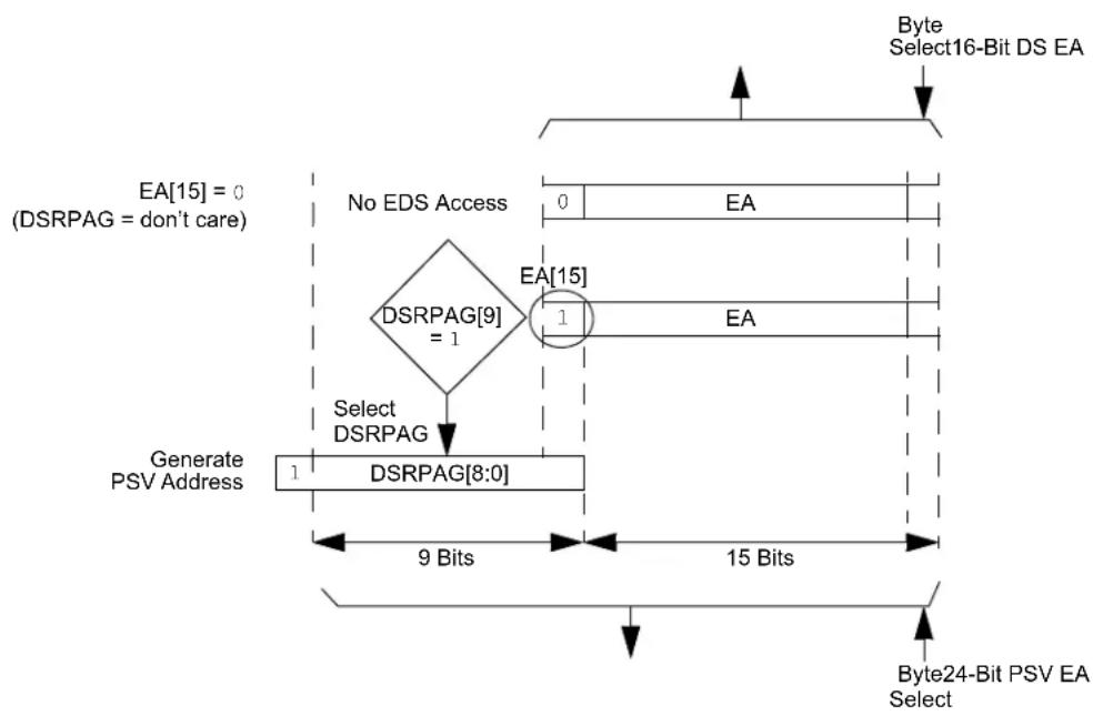
flowchart
graph TD
    A["Select DSRPAG"] --> B["DSRPAG[8:0"]]
    B --> C["DAIR"]
    C --> D["DAIR"]
    D --> E["Select16-Bit DS EA"]
    E --> F["Data Bus"]
    G["Generate PSV Address"] --> H["Select DSRPAG"]
    H --> I["DAIR"]
    I --> J["Data Bus"]
    K["DAIR"] --> L["DAIR"]
    L --> M["Data Bus"]
    N["DAIR"] --> O["DAIR"]
    O --> P["Data Bus"]
    Q["DAIR"] --> R["DAIR"]
    R --> S["Data Bus"]
    T["DAIR"] --> U["DAIR"]
    U --> V["Data Bus"]
    W["DAIR"] --> X["DAIR"]
    X --> Y["Data Bus"]
    Z["DAIR"] --> AA["DAIR"]
    AA --> AB["Data Bus"]
    AC["DAIR"] --> AD["DAIR"]
    AD --> AE["Data Bus"]
    AF["DAIR"] --> AG["DAIR"]
    AG --> AH["Data Bus"]
    AI["DAIR"] --> AJ["DAIR"]
    AJ --> AK["Data Bus"]
    AL["DAIR"] --> AM["DAIR"]
    AM --> AN["Data Bus"]
    AO["DAIR"] --> AP["DAIR"]
    AP --> AQ["Data Bus"]
    AR["DAIR"] --> AS["DAIR"]
    AS --> AT["Data Bus"]
    AU["DAIR"] --> AV["DAIR"]
    AV --> AW["Data Bus"]
    AX["DAIR"] --> AY["DAIR"]
    AY --> AZ["Data Bus"]
    BA["DAIR"] --> BB["DAIR"]
    BB --> BC["Data Bus"]
    BD["DAIR"] --> BE["DAIR"]
    BE --> BF["Data Bus"]
    BG["DAIR"] --> BH["DAIR"]
    BH --> BI["Data Bus"]
    BJ["DAIR"] --> BK["DAIR"]
    BK --> BL["Data Bus"]
    BM["DAIR"] --> BN["DAIR"]
    BN --> BO["Data Bus"]
    BP["DAIR"] --> BQ["DAIR"]
    BQ --> BR["Data Bus"]
    BS["DSRPAG[9"] = 1] --> BT["DSRPAG[9"]]
    BT --> BU["DSRPAG[9"]]
    BU --> BV["DSRPAG[9"]]
    BW["DSRPAG[8:0"]] --> BX["DSRPAG[8:0"]]
    BX --> BY["DSRPAG[8:0"]]
    BZ["DSRPAG[9"] = 1] --> CA["DSRPAG[9"]]
    CA --> CB["DSRPAG[9"]]
    CC["DSRPAG[8:0"]] --> CD["DSRPAG[8:0"]]
    CD --> CE["DSRPAG[8:0"]]
Note: DS read access when DSRPAG = 0x000 will force an address error trap.
FIGURE 4-7: PAGED DATA MEMORY SPACE
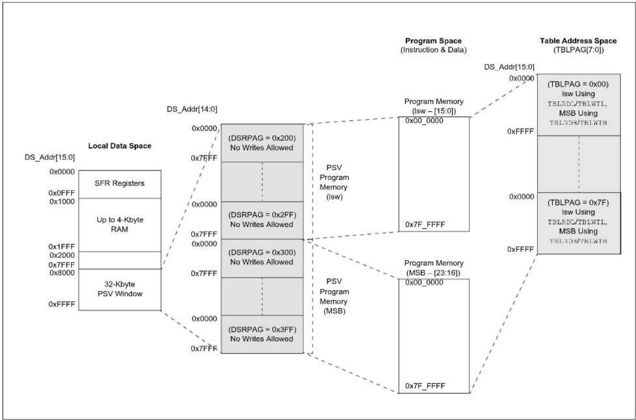
flowchart
graph TD
    A["Local Data Space"] --> B["DS_Addr[14:0"]]
    B --> C["(DSRPAG = 0x200) No Writes Allowed"]
    B --> D["(DSRPAG = 0x2FF) No Writes Allowed"]
    B --> E["(DSRPAG = 0x300) No Writes Allowed"]
    B --> F["(DSRPAG = 0x3FF) No Writes Allowed"]
    C --> G["Program Memory (Isw - [15:0"])]
    D --> H["Program Memory (MSB - [23:16"])]
    E --> I["Program Memory (Isw - [15:0"])]
    F --> J["Program Memory (MSB - [23:16"])]
    style A fill:#f9f,stroke:#333
    style B fill:#ccf,stroke:#333
    style C fill:#cfc,stroke:#333
    style D fill:#cfc,stroke:#333
    style E fill:#cfc,stroke:#333
    style F fill:#cfc,stroke:#333
    style G fill:#fcc,stroke:#333
    style H fill:#fcc,stroke:#333
    style I fill:#fcc,stroke:#333
    style J fill:#fcc,stroke:#333
When a PSV page overflow or underflow occurs, EA[15] is cleared as a result of the register indirect EA calculation. An overflow or underflow of the EA in the PSV pages can occur at the page boundaries when:
- The initial address, prior to modification, addresses the PSV page
- The EA calculation uses Pre- or Post-Modified Register Indirect Addressing; however, this does not include Register Offset Addressing
In general, when an overflow is detected, the DSRPAG register is incremented and the EA[15] bit is set to keep the base address within the PSV window. When an underflow is detected, the DSRPAG register is decremented and the EA[15] bit is set to keep the base address within the PSV window. This creates a linear PSV address space, but only when using Register Indirect Addressing modes.
Exceptions to the operation described above arise when entering and exiting the boundaries of Page 0 and PSV spaces. Table 4-16 lists the effects of overflow and underflow scenarios at different boundaries.
In the following cases, when overflow or underflow occurs, the EA[15] bit is set and the DSRPAG is not modified; therefore, the EA will wrap to the beginning of the current page:
- Register Indirect with Register Offset Addressing
- Modulo Addressing
- Bit-Reversed Addressing
TABLE 4-16: OVERFLOW AND UNDERFLOW SCENARIOS AT PAGE 0 AND PSV SPACE BOUNDARIES ^(2,3,4)
| O/U,R/W | Operation | Before After | |||||
| DSRPAG | DSEA[15] | PageDescription | DSRPAG | DSEA[15] | PageDescription | ||
| O,Read | [++Wn]or[Wn++] | DSRPAG = 0x2FF 1 | PSV: Last lswpage | DSRPAG = 0x300 1 | PSV: First MSBpage | ||
| O,Read | DSRPAG = 0x3FF 1 | PSV: Last MSBpage | DSRPAG = 0x3FF | 0 | See Note 1 | ||
| U,Read | [--Wn]or[Wn--] | DSRPAG = 0x001 | 1 | PSV page | DSRPAG = 0x001 | 0 | See Note 1 |
| U,Read | DSRPAG = 0x200 1 | PSV: First lswpage | DSRPAG = 0x200 | 0 | See Note 1 | ||
| U,Read | DSRPAG = 0x300 1 | PSV: First MSBpage | DSRPAG = 0x2FF 1 | PSV: Last lswpage | |||
Legend: O = Overflow, U = Underflow, R = Read, W = Write
Note 1: The Register Indirect Addressing now addresses a location in the base Data Space (0x0000-0x8000).
2: An EDS access, with DSRPAG = 0x000, will generate an address error trap.
3: Only reads from PS are supported using DSRPAG.
4: Pseudolinear Addressing is not supported for large offsets.
4.2.4.2 Extended X Data Space
The lower portion of the base address space range, between 0x0000 and 0x7FFF, is always accessible, regardless of the contents of the Data Space Read Page register. It is indirectly addressable through the register indirect instructions. It can be regarded as being located in the default EDS Page 0 (i.e., EDS address range of 0x000000 to 0x007FFF with the base address bit, EA[15] = 0, for this address range). However, Page 0 cannot be accessed through the upper 32 Kbytes, 0x8000 to 0xFFFF, of base Data Space in combination with DSRPAG = 0x00. Consequently, DSRPAG is initialized to 0x001 at Reset.
Note 1: DSRPAG should not be used to access Page 0. An EDS access with DSRPAG set to 0x000 will generate an address error trap.
2: Clearing the DSRPAG in software has no effect.
The remaining PSV pages are only accessible using the DSRPAG register in combination with the upper 32 Kbytes, 0x8000 to 0xFFFF, of the base address, where base address bit, EA[15] = 1.
4.2.4.3 Software Stack
The W15 register serves as a dedicated Software Stack Pointer (SSP), and is automatically modified by exception processing, subroutine calls and returns; however, W15 can be referenced by any instruction in the same manner as all other W registers. This simplifies reading, writing and manipulating the Stack Pointer (for example, creating stack frames).
Note: To protect against misaligned stack accesses, W15[0] is fixed to '0' by the hardware.
W15 is initialized to 0x1000 during all Resets. This address ensures that the SSP points to valid RAM in all dsPIC33CH128MP508S1 devices and permits stack availability for non-maskable trap exceptions. These can occur before the SSP is initialized by the user software. You can reprogram the SSP during initialization to any location within Data Space.
The Software Stack Pointer always points to the first available free word and fills the software stack, working from lower toward higher addresses. Figure 4-8 illustrates how it pre-decrements for a stack pop (read) and post-increments for a stack push (writes).
When the PC is pushed onto the stack, PC[15:0] are pushed onto the first available stack word, then PC[22:16] are pushed into the second available stack location. For a PC push during any CALL instruction, the MSB of the PC is zero-extended before the push, as shown in Figure 4-8. During exception processing, the MSB of the PC is concatenated with the lower eight bits of the CPU STATUS Register, SR. This allows the contents of SRL to be preserved automatically during interrupt processing.
Note 1: To maintain system Stack Pointer (W15) coherency, W15 is never subject to (EDS) paging, and is therefore, restricted to an address range of 0x0000 to 0xFFFF. The same applies to W14 when used as a Stack Frame Pointer (SFA = 1).
2: As the stack can be placed in, and can access X and Y spaces, care must be taken regarding its use, particularly with regard to local automatic variables in a C development environment
FIGURE 4-8: CALL STACK FRAME
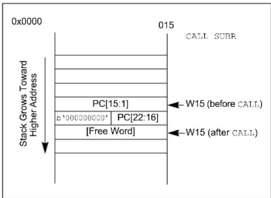
text_image
0x0000 Stack Grows Toward Higher Address 015 CALL SUBR PC[15:1] b'000000000' PC[22:16] [Free Word] W15 (before CALL) W15 (after CALL)4.2.5 INSTRUCTION ADDRESSING MODES
The addressing modes shown in Table 4-17 form the basis of the addressing modes optimized to support the specific features of individual instructions. The addressing modes provided in the MAC class of instructions differ from those in the other instruction types.
4.2.5.1 File Register Instructions
Most file register instructions use a 13-bit address field (f) to directly address data present in the first 8192 bytes of data memory (Near Data Space). Most file register instructions employ a Working register, W0, which is denoted as WREG in these instructions. The destination is typically either the same file register or WREG (with the exception of the MUL instruction), which writes the result to a register or register pair. The MOV instruction allows additional flexibility and can access the entire Data Space.
4.2.5.2 MCU Instructions
The three-operand MCU instructions are of the form:
Operand 3 = Operand 1
where Operand 1 is always a Working register (that is, the addressing mode can only be Register Direct), which is referred to as Wb. Operand 2 can be a W register fetched from data memory or a 5-bit literal. The result location can either be a W register or a data memory location. The following addressing modes are supported by MCU instructions:
- Register Direct
- Register Indirect
- Register Indirect Post-Modified
- Register Indirect Pre-Modified
- 5-Bit or 10-Bit Literal
Note: Not all instructions support all the addressing modes given above. Individual instructions can support different subsets of these addressing modes.
TABLE 4-17: FUNDAMENTAL ADDRESSING MODES SUPPORTED
| Addressing Mode Description | |
| File Register Direct | The address of the file register is specified explicitly. |
| Register Direct | The contents of a register are accessed directly. |
| Register Indirect | The contents of Wn form the Effective Address (EA). |
| Register Indirect Post-Modified | The contents of Wn form the EA. Wn is post-modified (incremented or decremented) by a constant value. |
| Register Indirect Pre-Modified | Wn is pre-modified (incremented or decremented) by a signed constant value to form the EA. |
| Register Indirect with Register Offset (Register Indexed) | The sum of Wn and Wb forms the EA. |
| Register Indirect with Literal Offset | The sum of Wn and a literal forms the EA. |
4.2.5.3 Move and Accumulator Instructions
Move instructions, and the DSP accumulator class of instructions, provide a greater degree of addressing flexibility than other instructions. In addition to the addressing modes supported by most MCU instructions, move and accumulator instructions also support Register Indirect with Register Offset Addressing mode, also referred to as Register Indexed mode.
Note:
For the MOV instructions, the addressing mode specified in the instruction can differ for the source and destination EA. However, the 4-bit Wb (Register Offset) field is shared by both source and destination (but typically only used by one).
In summary, the following addressing modes are supported by move and accumulator instructions:
- Register Direct
- Register Indirect
- Register Indirect Post-Modified
- Register Indirect Pre-Modified
- Register Indirect with Register Offset (Indexed)
- Register Indirect with Literal Offset
- 8-Bit Literal
- 16-Bit Literal
Note: Not all instructions support all the addressing modes given above. Individual instructions may support different subsets of these addressing modes.
4.2.5.4 MAC Instructions
The dual source operand DSP instructions (CLR, ED, EDAC, MAC, MPY, MPY.N, MOVSAC and MSC), also referred to as MAC instructions, use a simplified set of addressing modes to allow the user application to effectively manipulate the Data Pointers through register indirect tables.
The two-source operand prefetch registers must be members of the set {W8, W9, W10, W11}. For data reads, W8 and W9 are always directed to the X RAGU, and W10 and W11 are always directed to the Y AGU. The Effective Addresses generated (before and after modification) must therefore, be valid addresses within X Data Space for W8 and W9, and Y Data Space for W10 and W11.
Note: Register Indirect with Register Offset Addressing mode is available only for W9 (in X space) and W11 (in Y space).
In summary, the following addressing modes are supported by the MAC class of instructions:
- Register Indirect
- Register Indirect Post-Modified by 2
- Register Indirect Post-Modified by 4
- Register Indirect Post-Modified by 6
- Register Indirect with Register Offset (Indexed)
4.2.5.5 Other Instructions
Besides the addressing modes outlined previously, some instructions use literal constants of various sizes. For example, BRA (branch) instructions use 16-bit signed literals to specify the branch destination directly, whereas the DISI instruction uses a 14-bit unsigned literal field. In some instructions, such as ULNK, the source of an operand or result is implied by the opcode itself. Certain operations, such as a NOP, do not have any operands.
4.2.6 MODULO ADDRESSING
Modulo Addressing mode is a method of providing an automated means to support circular data buffers using hardware. The objective is to remove the need for software to perform data address boundary checks when executing tightly looped code, as is typical in many DSP algorithms.
Modulo Addressing can operate in either Data or Program Space (since the Data Pointer mechanism is essentially the same for both). One circular buffer can be supported in each of the X (which also provides the pointers into Program Space) and Y Data Spaces. Modulo Addressing can operate on any W Register Pointer. However, it is not advisable to use W14 or W15 for Modulo Addressing since these two registers are used as the Stack Frame Pointer and Stack Pointer, respectively.
In general, any particular circular buffer can be configured to operate in only one direction, as there are certain restrictions on the buffer start address (for incrementing buffers) or end address (for decrementing buffers), based upon the direction of the buffer.
The only exception to the usage restrictions is for buffers that have a power-of-two length. As these buffers satisfy the start and end address criteria, they can operate in a Bidirectional mode (that is, address boundary checks are performed on both the lower and upper address boundaries).
4.2.6.1 Start and End Address
The Modulo Addressing scheme requires that a starting and ending address be specified and loaded into the 16-bit Modulo Buffer Address registers: XMODSRT, XMODEND, YMODSRT and YMODEND (see Table 4-1).
Note: Y space Modulo Addressing EA calculations assume word-sized data (LSb of every EA is always clear).
The length of a circular buffer is not directly specified. It is determined by the difference between the corresponding start and end addresses. The maximum possible length of the circular buffer is 32K words (64 Kbytes).
4.2.6.2 W Address Register Selection
The Modulo and Bit-Reversed Addressing Control register, MODCON[15:0], contains enable flags, as well as a W register field to specify the W Address registers. The XWM and YWM fields select the registers that operate with Modulo Addressing:
- If XWM = 1111, X RAGU and X WAGU Modulo Addressing is disabled
- I f Y W M = 1111, Y AGU Modulo Addressing is disabled
The X Address Space Pointer W (XWM) register, to which Modulo Addressing is to be applied, is stored in MODCON[3:0] (see Table4-1). Modulo Addressing is enabled for X Data Space when XWM is set to any value other than '1111' and the XMODEN bit is set (MODCON[15]).
The Y Address Space Pointer W (YWM) register, to which Modulo Addressing is to be applied, is stored in MODCON[7:4]. Modulo Addressing is enabled for Y Data Space when YWM is set to any value other than '1111' and the YMODEN bit (MODCON[14]) is set.
FIGURE 4-9: MODULO ADDRESSING OPERATION EXAMPLE

text_image
Byte Address 0x1100 0x1163 MOV #0x1100, W0 MOV W0, XMODSRT ;set modulo start address MOV #0x1163, W0 MOV W0, MODEND ;set modulo end address MOV #0x8001, W0 MOV W0, MODCON ;enable W1, X AGU for modulo MOV #0x0000, W0 ;W0 holds buffer fill value MOV #0x1110, W1 ;point W1 to buffer DO AGAIN, #0x31 ;fill the 50 buffer locations MOV W0, [W1++] ;fill the next location AGAIN: INC W0, W0 ;increment the fill value Start Addr = 0x1100 End Addr = 0x1163 Length = 0x0032 words4.2.6.3 Modulo Addressing Applicability
Modulo Addressing can be applied to the Effective Address (EA) calculation associated with any W register. Address boundaries check for addresses equal to:
- The upper boundary addresses for incrementing buffers
- The lower boundary addresses for decrementing buffers
It is important to realize that the address boundaries check for addresses less than, or greater than, the upper (for incrementing buffers) and lower (for decrementing buffers) boundary addresses (not just equal to). Address changes can, therefore, jump beyond boundaries and still be adjusted correctly.
Note: The modulo corrected Effective Address is written back to the register only when Pre-Modify or Post-Modify Addressing mode is used to compute the Effective Address. When an address offset (such as [W7 + W2]) is used, Modulo Addressing correction is performed, but the contents of the register remain unchanged.
4.2.7 BIT-REVERSED ADDRESSING
Bit-Reversed Addressing mode is intended to simplify data reordering for radix-2 FFT algorithms. It is supported by the X AGU for data writes only.
The modifier, which can be a constant value or register contents, is regarded as having its bit order reversed. The address source and destination are kept in normal order. Thus, the only operand requiring reversal is the modifier.
4.2.7.1 Bit-Reversed Addressing Implementation
Bit-Reversed Addressing mode is enabled in any of these situations:
- BWMx bits (W register selection) in the MODCON register are any value other than '1111' (the stack cannot be accessed using Bit-Reversed Addressing)
• The BREN bit is set in the XBREV register
- The addressing mode used is Register Indirect with Pre-Increment or Post-Increment
If the length of a bit-reversed buffer is M = 2^N bytes, the last 'N' bits of the data buffer start address must be zeros.
XB[14:0] is the Bit-Reversed Addressing modifier, or 'pivot point', which is typically a constant. In the case of an FFT computation, its value is equal to half of the FFT data buffer size.
Note: All bit-reversed EA calculations assume word-sized data (LSb of every EA is always clear). The XB value is scaled accordingly to generate compatible (byte) addresses.
When enabled, Bit-Reversed Addressing is executed only for Register Indirect with Pre-Increment or Post-Increment Addressing and word-sized data writes. It does not function for any other addressing mode or for byte-sized data and normal addresses are generated instead. When Bit-Reversed Addressing is active, the W Address Pointer is always added to the address modifier (XB) and the offset associated with the Register Indirect Addressing mode is ignored. In addition, as word-sized data are a requirement, the LSb of the EA is ignored (and always clear).
Note: Modulo Addressing and Bit-Reversed Addressing can be enabled simultaneously using the same W register, but Bit-Reversed Addressing operation will always take precedence for data writes when enabled.
If Bit-Reversed Addressing has already been enabled by setting the BREN (XBREV[15]) bit, a write to the XBREV register should not be immediately followed by an indirect read operation using the W register that has been designated as the Bit-Reversed Pointer.
FIGURE 4-10: BIT-REVERSED ADDRESSING EXAMPLE

flowchart
graph TD
    A["Sequential Address"] --> B["b15 b14 b13 b12 b11 b10 b9 b8 b7 b6 b5 b4 b3 b2 b1 0"]
    B --> C["b15 b14 b13 b12 b11 b10 b9 b8 b7 b6 b5 b1 b2 b3 b4 0"]
    C --> D["Pivot Point"]
    D --> E["Bit-Reversed Address"]
    E --> F["XB = 0x0008 for a 16-Word Bit-Reversed Buffer"]
    style A fill:#f9f,stroke:#333
    style B fill:#ccf,stroke:#333
    style C fill:#cfc,stroke:#333
    style D fill:#fcc,stroke:#333
    style E fill:#ffc,stroke:#333
    style F fill:#fcc,stroke:#333
TABLE 4-18: BIT-REVERSED ADDRESSING SEQUENCE (16-ENTRY)
| Normal Address Bit-Reversed Address | |||||||||
| A3 A2 | A1 A0 | Decimal | A3 A2 A1 | A0 Decimal | |||||
| 0 | 0 | 0 | 0 | 0 0 | 0 | 0 | 0 | 0 | |
| 0 | 0 | 0 | 1 | 1 1 | 0 | 0 | 0 | 8 | |
| 0 | 0 | 1 | 0 | 2 0 | 1 | 0 | 0 | 4 | |
| 0 | 0 | 1 | 1 | 3 1 | 1 | 0 | 0 | 12 | |
| 0 | 1 | 0 | 0 | 4 0 | 0 | 1 | 0 | 2 | |
| 0 | 1 | 0 | 1 | 5 1 | 0 | 1 | 0 | 10 | |
| 0 | 1 | 1 | 0 | 6 0 | 1 | 1 | 0 | 6 | |
| 0 | 1 | 1 | 1 | 7 1 | 1 | 1 | 0 | 14 | |
| 1 | 0 | 0 | 0 | 8 0 | 0 | 0 | 1 | 1 | |
| 1 | 0 | 0 | 1 | 9 1 | 0 | 0 | 1 | 9 | |
| 1 | 0 | 1 | 0 | 10 | 0 | 1 | 0 | 1 | 5 |
| 1 | 0 | 1 | 1 | 11 | 1 | 1 | 0 | 1 | 13 |
| 1 | 1 | 0 | 0 | 12 | 0 | 0 | 1 | 1 | 3 |
| 1 | 1 | 0 | 1 | 13 | 1 | 0 | 1 | 1 | 11 |
| 1 | 1 | 1 | 0 | 14 | 0 | 1 | 1 | 1 | 7 |
| 1 | 1 | 1 | 1 | 15 | 1 | 1 | 1 | 1 | 15 |
4.2.8 INTERFACING PROGRAM AND DATA MEMORY SPACES
The dsPIC33CH128MP508S1 family architecture uses a 24-bit wide Program Space (PS) and a 16-bit wide Data Space (DS). The architecture is also a modified Harvard scheme, meaning that data can also be present in the Program Space. To use these data successfully, they must be accessed in a way that preserves the alignment of information in both spaces.
Aside from normal execution, the architecture of the dsPIC33CH128MP508S1 family devices provides two methods by which Program Space can be accessed during operation:
- Using table instructions to access individual bytes or words anywhere in the Program Space
- Remapping a portion of the Program Space into the Data Space (Program Space Visibility)
Table instructions allow an application to read small areas of the program memory. This capability makes the method ideal for accessing data tables that need to be updated periodically. It also allows access to all bytes of the program word. The remapping method allows an application to access a large block of data on a read-only basis, which is ideal for look-ups from a large table of static data. However, this method only provides visibility to the lower 16 bits in each location addressed.
TABLE 4-19: PROGRAM SPACE ADDRESS CONSTRUCTION
| Access Type | Access Space | Program Space Address | ||||
| [23] [22:16] [15] [14:1] [0] | ||||||
| Instruction Access (Code Execution) | User 0 PC[22:1] 0 | |||||
| 0xxxx xxxx xxxx xxxx xxxx xxxx | ||||||
| TBLRD (Byte/Word Read) | User TBLPAG[7:0] | Data EA[15:0] | ||||
| 0xxxx xxxx | xxxx xxxx xxxx | |||||
FIGURE 4-11: DATA ACCESS FROM PROGRAM SPACE ADDRESS GENERATION
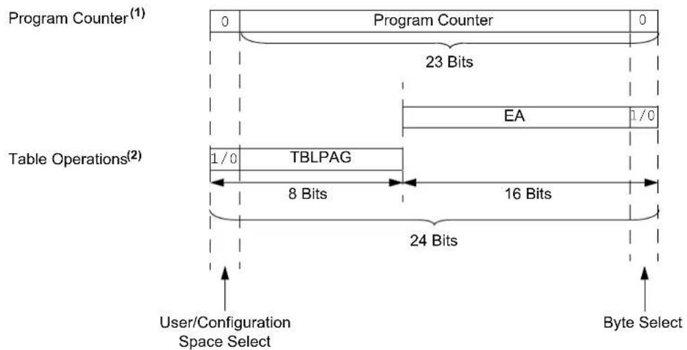
flowchart
graph TD
    A["Program Counter(1)"] --> B["0"]
    B --> C["Program Counter"]
    C --> D["0"]
    D --> E["23 Bits"]
    E --> F["EA"]
    F --> G["1/0"]
    G --> H["Table Operations(2)"]
    H --> I["1/0"]
    I --> J["TBLPAG"]
    J --> K["8 Bits"]
    K --> L["16 Bits"]
    L --> M["24 Bits"]
    M --> N["User/Configuration Space Select"]
    M --> O["Byte Select"]
Note 1: The Least Significant bit (LSb) of Program Space addresses is always fixed as '0' to maintain word alignment of data in the Program and Data Spaces.
2: Table operations are not required to be word-aligned. Table Read operations are permitted in the configuration memory space.
4.2.8.1 Data Access from Program Memory Using Table Instructions
The TBLRDL instruction offers a direct method of reading the lower word of any address within the Program Space without going through Data Space. The TBLRDH instruction is the only method to read the upper eight bits of a Program Space word as data.
This allows program memory addresses to directly map to Data Space addresses. Program memory can thus be regarded as two 16-bit wide word address spaces, residing side by side, each with the same address range. TBLRDL accesses the space that contains the least significant data word. TBLRDH accesses the space that contains the upper data byte.
Two table instructions are provided to read byte or word-sized (16-bit) data from Program Space. Both function as either byte or word operations.
• TBLRDL (Table Read Low):
- In Word mode, this instruction maps the lower word of the Program Space location (P[15:0]) to a data address (D[15:0]).
- In Byte mode, either the upper or lower byte of the lower program word is mapped to the lower byte of a data address. The upper byte is selected when Byte Select is '1'; the lower byte is selected when it is '0'.
• TBLRDH (Table Read High):
- In Word mode, this instruction maps the entire upper word of a program address (P[23:16]) to a data address. The 'phantom' byte (D[15:8]) is always '0'.
- In Byte mode, either the upper or lower byte of the upper program word is mapped to the lower byte of a data address. The upper byte is selected when Byte Select is '1'; the lower byte is selected when it is '0'. When the upper byte is selected, the 'phantom' byte is read as '0'.
FIGURE 4-12: ACCESSING PROGRAM MEMORY WITH TABLE INSTRUCTIONS
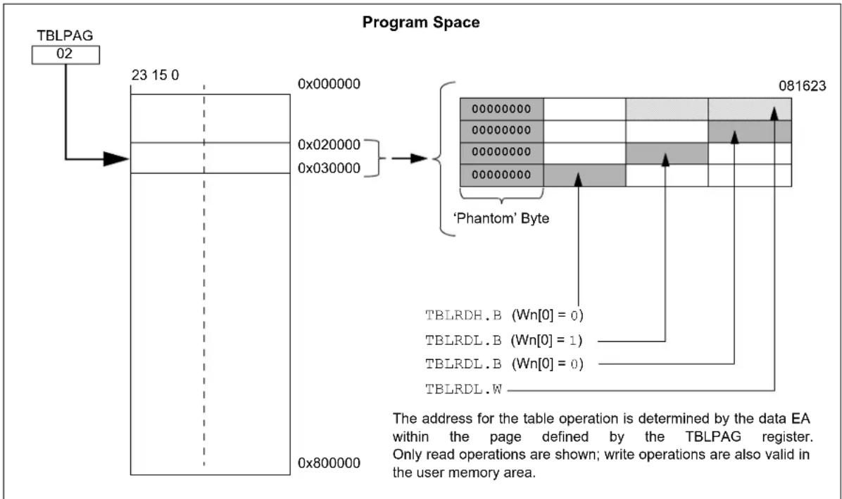
flowchart
graph TD
    A["TBLPAG 02"] --> B["23 15 0"]
    B --> C["0x000000"]
    C --> D["0x020000"]
    D --> E["0x030000"]
    E --> F["0x800000"]
    F --> G["0x800000"]
    G --> H["0x800000"]
    H --> I["0x800000"]
    I --> J["0x800000"]
    J --> K["0x800000"]
    K --> L["0x800000"]
    L --> M["0x800000"]
    M --> N["0x800000"]
    N --> O["0x800000"]
    O --> P["0x800000"]
    P --> Q["0x800000"]
    Q --> R["0x800000"]
    R --> S["0x800000"]
    S --> T["0x800000"]
    T --> U["0x800000"]
    U --> V["0x800000"]
    V --> W["0x800000"]
    W --> X["0x800000"]
    X --> Y["0x800000"]
    Y --> Z["0x800000"]
    Z --> AA["0x800000"]
    AA --> AB["0x800000"]
    AB --> AC["0x800000"]
    AC --> AD["0x800000"]
    AD --> AE["0x800000"]
    AE --> AF["0x800000"]
    AF --> AG["0x800000"]
    AG --> AH["0x800000"]
    AH --> AI["0x800000"]
    AI --> AJ["0x800000"]
    AJ --> AK["0x800000"]
    AK --> AL["0x800000"]
    AL --> AM["O81623"]
    subgraph 'Phantom' Byte
        B
        C
        D
        E
        F
        G
        H
        I
        J
        K
        L
        M
        N
        O
        P
        Q
        R
        S
        T
        U
        V
        W
        X
        Y
        Z
        AA
        AB
        AC
        AD
        AE
        AF
        AG
        AH
        AI
        AJ
        AK
        AL
        AM
        AN
        AO
        AP
        AQ
        AR
        AS
        AT
        AU
        AV
        AW
        AX
        AY
        AZ
        BA
        BB
        BC
        BD
        BE
        BF
        BG
        BH
        BI
        BJ
        BK
        BL
        BM
        BN
        BO
        BP
        BPB
        BW
        BWB
        BWN
        BWN1
        BWN2
        BWN3
        BWN4
        BWN5
        BWN6
        BWN7
        BWN8
        BWN9
        BWN11
        BWN12
        BWN13
        BWN14
        BWN15
        BWN16
        BWN17
        BWN18
        BWN19
        BWN21
        BWN22
        BWN23
        BWN24
        BWN25
        BWN26
        BWN27
        BWN28
        BWN29
        BWN31
        BWN32
        BWN33
        BWN34
        BWN35
        BWN36
        BWN37
        BWN38
        BWN39
        BWN41
        BWN42
        BWN43
        BWN44
        BWN45
        BWN46
        BWN47
        BWN48
        BWN49
        BWN51
        BWN52
        BWN53
        BWN54
        BWN55
        BWN56
        BWN57
        BWN58
        BWN59
        BWN61
    end
4.3 Secondary PRAM Program Memory
Note 1: This data sheet summarizes the features of the dsPIC33CH128MP508 family of devices. It is not intended to be a comprehensive reference source. To complement the information in this data sheet, refer to “Dual Partition Flash Program Memory” (www.microchip.com/DS70005156).
2: Though the reference to the chapter is "Dual Partition Flash Program Memory" (www.microchip.com/DS70005156), the program memory for the Secondary code is PRAM. Therefore, after each POR, the Host will have to reload the content of the Client PRAM.
The dsPIC33CH128MP508S1 family devices contain internal PRAM program memory for storing and executing application code. The PRAM program memory array is organized into rows of 128 instructions or 64 double instruction words. Though the PRAM is volatile, it is writable during normal operation over the entire VDD range.
PRAM memory can be programmed in two ways:
• In-Circuit Serial Programming (ICSP)
- Main to Secondary Image Loading (MSIL)
ICSP allows for a dsPIC33CH128MP508S1 family device to be serially programmed in the application circuit. Since the Secondary PRAM is volatile, Secondary PRAM ICSP programming is supported only as a development and debugging feature.
Main to Secondary Image Loading (MSIL) allows the Host user code to load the Client PRAM at run time. A Client PRAM compatible image is stored in Host Flash memory. At run time, the Host user code is responsible for loading and verifying the contents of the Client PRAM.
Note: In an actual application mode, the Client PRAM is loaded by the Host, so the ICSP mode of PRAM operation is valid only for the Debug mode during the code development.
4.3.1 PRAM PROGRAMMING OPERATIONS
Unlike when self-programming the Host Flash, TBLWTL and TBLWTH instructions are not supported during user application mode. This means that RTSP programming of the PRAM is not supported.
For ICSP programming of the Secondary PRAM, TBLWTL and TBLWTH instructions are used to write to the NVM write latches. An NVM write operation then writes the contents of both latches to the PRAM, starting at the address defined in the NVMADR and NVMADRU registers.
For Main to Secondary Image Loading (MSIL) of the Client PRAM, the Host user code is responsible for transferring the Client image contents, stored in the Host Flash, to the Client PRAM. The LDSLV instruction is used, along with the DSRPAG and DSWPAG registers, to transfer a single 24-bit instruction to the Client PRAM.
The VFSLV instruction allows the Host user code to verify that the PRAM has been loaded correctly.
Note: Main to Secondary Image Loading is the only supported method for programming the Client PRAM in a final user application.
Regardless of the method used to program the PRAM, a few basic requirements should be met:
- A full 48-bit double instruction word should always be programmed to a PRAM location. Either instruction may simply be a NOP to fulfill this requirement. This ensures a valid ECC value is generated for each pair of instructions written.
• Assuming the above step is followed, the last 24-bit location in implemented Program Space, or prior to any unprogrammed region in Program Space, should never be executed. The penultimate instruction, in either case, must contain a program flow change instruction, such as a RETURN or a BRA instruction.
4.3.2 MAIN TO SECONDARY IMAGE LOADING (MSIL)
Main to Secondary Image Loading (MSIL) allows the Host user application code to transfer the Client image, stored in the Host Flash, to the Client PRAM. This is the only supported method for programming the Client PRAM in a final user application.
The LDSLV instruction is executed by the Host user application to transfer a single 24-bit instruction from the Host Flash address, defined by Ws[14:0] (DSRPAG), to the Client PRAM address, defined by Wd[14:0] (DSWPAG).
The LDSLV instruction should be executed in pairs to ensure correct ECC value generation for each double instruction word that is loaded into the Client PRAM. The Client image instruction found at a given even address should be loaded first. This will be the lower instruction word of a 48-bit double instruction word. The upper instruction word should then be loaded from the following odd address. After the pair of LDSLV instructions is executed by the Host user application, both 24-bit Client image instructions and the generated 7-bit ECC value are actually loaded into the PRAM destination address locations.
The VFSLV instruction allows the Host user application to verify that the PRAM has been loaded correctly. The VFSLV instruction compares the 24-bit instruction word stored in the Host Flash address, defined by Ws[14:0] (DSRPAG), to the 24 bit instruction written to the Client PRAM address, defined by Wd[14:0] (DSWPAG).
The VESLV instruction should also be executed in pairs. The lower instruction word found on a given even address should be verified first. The upper instruction word found in the following odd address should then be verified. Then, the Client image instruction pair read from the Host Flash will have a valid generated ECC value. This full double instruction word with ECC is then compared to the 55-bit value that was actually loaded into the PRAM destination locations. The entire Secondary image may be loaded into the PRAM first and then subsequently verified.
4.3.3 USING DEVELOPMENT TOOL SUPPORTED FUNCTIONS
The Microchip development environment provides some utility functions to simplify loading the Secondary image and starting the Secondary core operation. The _program_secondary() routine within the libpic30.h library programs the Secondary core with the specified Secondary image created within the Microchip language tool format.
The _program_secondary() routine uses the "verify" parameter as a switch to either load or verify the Secondary image using the LDSLV or VFSLV instructions. A '0' will load the entire Secondary image to the PRAM and a '1' will verify the entire Secondary image in the PRAM. An example of how this routine can be used to load and verify the contents of the Secondary PRAM is shown in Example 4-1.
EXAMPLE 4-1: SECONDARY PRAM LOAD AND VERIFY ROUTINE
#include [libpic30.h]
// _program_Secondary(core#, verify,
//&secondary_image)
if (_program_secondary(1, 0, &secondary_image)
== 0)
{
    /* now verify */
    if (_program_secondary(1, 1,
&secondary_image) ==
    ESLV_VERIFY_FAIL)
    {
    asm("reset"); // try again
    }
}
Secondary PRAM images not following the Microchip language tool format will require a custom routine that follows all requirements for the PRAM Main to Secondary Image Loading process described in this chapter.
The __start_secondary routine is used to start the Secondary core after it has had its image loaded by the Main core. If an application requires the Secondary core to be stopped, the __stop_secondary routine is also provided. Example usage of these routines are shown in Example 4-2.
EXAMPLE 4-2: SECONDARY START AND STOP EXAMPLE
#include [libpic30.h]
int main()
{
    // Main initialization code
    _start_secondary(); // Start Secondary core
    // Main application code
    _stop_secondary(); // Stop Secondary core
    while(1);
}
The __start_secondary and __stop_secondary routines perform the MSI1KEY unlock sequence and set or clear the SLVEN bit (MSI1CON[15]).
4.3.4 PRAM DUAL PARTITION CONSIDERATIONS
For dsPIC33CH512MP508S1 family devices operating in Dual Partition PRAM Program Memory modes, both partitions would be loaded using the Main to Secondary Image Loading process. The Main can load the Active Partition of the PRAM only when SLVEN = 0 (Secondary is not running). The Main can load the PRAM Inactive Partition any time. To support LiveUpdate, the Main would load the PRAM Inactive Partition while the Secondary is running and then the Secondary would execute the BOOTSWP instruction to swap partitions.
4.3.4.1 PRAM Partition Swapping
At device Reset, the default PRAM partition is Partition 1. The BOOTSWP instruction provides the means of swapping the Active and Inactive Partitions (soft swap) without the need for a device Reset. The BOOTSWP must always be followed by a GOTO instruction. The BOOTSWP instruction swaps the Active and Inactive Partitions, and the PC vectors to the location specified by the GOTO instruction in the newly Active Partition.
It is important to note that interrupts should temporarily be disabled while performing the soft swap sequence, and that after the partition swap, all peripherals and interrupts, which were enabled remain enabled. Additionally, the RAM and stack will maintain their state after the switch. As a result, it is recommended that applications using soft swaps jump to a routine that will reinitialize the device in order to ensure the firmware runs as expected. The Configuration registers will have no effect during a soft swap.
4.3.5 ERROR CORRECTING CODE (ECC)
In order to improve program memory performance and durability, these devices include Error Correcting Code functionality (ECC) as an integral part of the PRAM memory controller. ECC can determine the presence of single bit errors in program data, including which bit is in error, and correct the data automatically without user intervention. ECC cannot be disabled.
When data are written to program memory, ECC generates a 7-bit Hamming code parity value for every two (24-bit) instruction words. The data are stored in blocks of 48 data bits and seven parity bits; parity data are not memory-mapped and are inaccessible. When the data are read back, the ECC calculates the parity on them and compares it to the previously stored parity value. If a parity mismatch occurs, there are two possible outcomes:
- Single bit errors are automatically identified and corrected on read back. An optional device-level interrupt (ECCSBEIF) is also generated.
- Double-bit errors will generate a generic hard trap and the read data are not changed. If special exception handling for the trap is not implemented, a device Reset will also occur.
To use the single bit error interrupt, set the ECC Single Bit Error Interrupt Enable bit (ECCSBEIE) and configure the ECCSBEIPx bits to set the appropriate interrupt priority. Except for the single bit error interrupt, error events are not captured or counted by hardware. This functionality can be implemented in the software application, but it is the user's responsibility to do so.
4.3.6 CONTROL REGISTERS
Six SFRs are used to write and erase the Program Flash Memory: NVMCON, NVMKEY, NVMADR, NVMADRU, NVMSRCADRL and NVMSRCADRH.
The NVMCON register (Register 4-5) selects the operation to be performed (page erase, word/row program, Inactive Partition erase) and initiates the program or erase cycle.
NVMKEY (Register 4-8) is a write-only register that is used for write protection. To start a programming or erase sequence, the user application must consecutively write 0x55 and 0xAA to the NVMKEY register.
There are two NVM Address registers: NVMADRU and NVMADR. These two registers, when concatenated, form the 24-bit Effective Address (EA) of the selected word/row for programming operations, or the selected page for erase operations. The NVMADRU register is used to hold the upper eight bits of the EA, while the NVMADR register is used to hold the lower 16 bits of the EA.
For row programming operation, data to be written to the Secondary PRAM are written into Secondary data memory space (RAM) at an address defined by the NVMSRCADRL/H registers (location of first element in row programming data).
4.3.7 SECONDARY PROGRAM MEMORY CONTROL/STATUS REGISTERS
REGISTER 4-5: NVMCON: PROGRAM MEMORY SECONDARY CONTROL REGISTER
| R/SO-0^(1) | R/W-0^(1) | R/W-0^(1) | R/W-0 | R/C-0 | R/C-0 | R/W-0 | R/C-0 |
| WR WRE | N WRERR NV | MSIDL | (2) | SFTSWP P2 | ACTIV RPDF | URERR | |
| bit 15 | bit 8 | ||||||
| U-0 | U-0 | U-0 | U-0 | R/W-0^(1) | R/W-0^(1) | R/W-0^(1) | R/W-0^(1) |
| — | — | — | — | NVMOP[3:0] ^(3,4) | |||
| bit 7 bit 0 | |||||||
| Legend: | C = Clearable bit | SO = Settable Only bit |
| R = Readable bit | W = Writable bit | U = Unimplemented bit, read as ‘0’ |
| -n = Value at POR | ‘1’ = Bit is set | ‘0’ = Bit is cleared x = Bit is unknown |
bit 15 WR: Write Control bit ^(1)
1 = Initiates a PRAM memory program or erase operation; the operation is self-timed and the bit is cleared by hardware once the operation is complete
0 = Program or erase operation is complete and inactive
bit 14 WREN: Write Enable bit ^(1)
1 = Enables program/erase operations
0 = Inhibits program/erase operations
bit 13 WRERR: Write Sequence Error Flag bit ^(1)
1 = An improper program or erase sequence attempt, or termination has occurred (bit is set automatically on any set attempt of the WR bit)
0 = The program or erase operation completed normally
bit 12 NVMSIDL: PRAM Stop in Idle Control bit ^(2)
1 = PRAM voltage regulator goes into Standby mode during Idle mode
0 = PRAM voltage regulator is active during Idle mode
bit 11 SFTSWP: Soft Swap Status bit
1 = Panels have been successfully swapped using the BOOTSWP instruction
0 = Awaiting for panels to be successfully swapped using the BOOTSWP instruction
bit 10 P2ACTIV: Dual Boot Active Region Status bit
1 = Panel 2 PRAM is mapped into the active region
0 = Panel 1 PRAM is mapped into the active region
bit 9 RPDF: Row Programming Data Format bit
1 = Row data to be stored in PRAM are in compressed format
0 = Row data to be stored in PRAM are in uncompressed format
bit 8 URERR: Row Programming Data Underrun Error bit
1 = Indicates row programming operation has been terminated
0 = No data underrun error is detected
bit 7-4 Unimplemented: Read as '0'
Note 1: These bits can only be reset on a POR.
2: If this bit is set, there will be minimal power savings (IIDLE) and upon exiting Idle mode, there is a delay (TVREG) before PRAM memory becomes operational.
3: All other combinations of NVMOP[3:0] are unimplemented.
4: Execution of the PWRSAV instruction is ignored while any of the NVM operations are in progress.
5: Two adjacent words on a 4-word boundary are programmed during execution of this operation.
REGISTER 4-5: NVMCON: PROGRAM MEMORY SECONDARY CONTROL REGISTER
bit 3-0 NVMOP[3:0]: NVM Operation Select bits (1,3,4)
1111 = Reserved
...
0101 = Reserved
0100 = Inactive Partition memory erase operation
0011 = Reserved
0010 = Reserved
0001 = Memory double-word program operation ^(5)
0000 = Reserved
Note 1: These bits can only be reset on a POR.
2: If this bit is set, there will be minimal power savings (IIDLE) and upon exiting Idle mode, there is a delay (TVREG) before PRAM memory becomes operational.
3: All other combinations of NVMOP[3:0] are unimplemented.
4: Execution of the PWRSAV instruction is ignored while any of the NVM operations are in progress.
5: Two adjacent words on a 4-word boundary are programmed during execution of this operation.
REGISTER 4-6: NVMADR: SECONDARY PROGRAM MEMORY LOWER ADDRESS REGISTER
| R/W-x R/W-x R/W-x R/W-x R/W-x R/W-x R/W-x R/W-x |
| NVMADR[15:8] |
| bit 15 bit 8 |
| R/W-x R/W-x R/W-x R/W-x R/W-x R/W-x R/W-x R/W-x |
| NVMADR[7:0] |
| bit 7 bit 0 |
Legend:
R = Readable bit W = Writable bit U = Unimplemented bit, read as '0'
-n = Value at POR '1' = Bit is set '0' = Bit is cleared x = Bit is unknown
bit 15-0 NVMADR[15:0]: PRAM Memory Lower Write Address bits
Selects the lower 16 bits of the location to program or erase in PRAM. This register may be read or written to by the user application.
REGISTER 4-7: NVMADRU: SECONDARY PROGRAM MEMORY UPPER ADDRESS REGISTER
| R/W-x R/W-x R/W-x R/W-x R/W-x R/W-x R/W-x R/W-x | R/W-x |
| NVMADRU[23:16] | |
| bit 7 bit 0 | |
Legend:
R = Readable bit W = Writable bit U = Unimplemented bit, read as '0'
-n = Value at POR '1' = Bit is set '0' = Bit is cleared x = Bit is unknown
bit 15-8 Unimplemented: Read as '0'
bit 7-0 NVMADRU[23:16]: PRAM Memory Upper Write Address bits
Selects the upper eight bits of the location to program or erase in PRAM. This register may be read or written to by the user application.
REGISTER 4-8: NVMKEY: SECONDARY NONVOLATILE MEMORY KEY REGISTER
| U-0 U-0 U-0 U-0 U-0 U-0 U-0 U-0 | |||||||
| —— | —— | —— | — | ||||
| bit 15 | bit 8 | ||||||
| W-0 | W-0 | W-0 | W-0 | W-0 | W-0 | W-0 | W-0 |
| NVMKEY[7:0] | |||||||
| bit 7 | bit 0 | ||||||
| Legend: | |||
| R = Readable bit | W = Writable bit | U = Unimplemented bit, read as ‘0’ | |
| -n = Value at POR | ‘1’ = Bit is set | ‘0’ = Bit is cleared | x = Bit is unknown |
bit 15-8 Unimplemented: Read as '0'
bit 7-0 NVMKEY[7:0]: NVM Key Register bits (write-only)
REGISTER 4-9: NVMSRCADRL: SECONDARY NVM SOURCE DATA ADDRESS REGISTER LOW
| R/W-0 R/W-0 R/W-0 R/W-0 R/W-0 R/W-0 R/W-0 R/W-0 |
| NVMSRCADR[15:8] |
| bit 15 bit 8 |
| R/W-0 R/W-0 R/W-0 R/W-0 R/W-0 R/W-0 R/W-0 R/W-0 |
| NVMSRCADR[7:0] |
| bit 7 bit 0 |
Legend:
| R = Readable bit W = Writable bit | U = Unimplemented bit, read as '0' | ||
| -n = Value at POR | '1' = Bit is set | '0' = Bit is cleared | x = Bit is unknown |
bit 15-0 NVMSRCADR[15:0]: NVM Source Data Address bits
The RAM address of the data to be programmed into PRAM when the NVMOP[3:0] bits are set to row programming.
REGISTER 4-10: NVMSRCADRH: SECONDARY NVM SOURCE DATA ADDRESS REGISTER HIGH
| R/W-0 R/W-0 R/W-0 R/W-0 R/W-0 R/W-0 R/W-0 R/W-0 |
| NVMSRCADR[23:16] |
| bit 7 bit 0 |
Legend:
| R = Readable bit W = Writable bit | U = Unimplemented bit, read as '0' | ||
| -n = Value at POR | '1' = Bit is set | '0' = Bit is cleared | x = Bit is unknown |
bit 15-8 Unimplemented: Read as '0'
bit 7-0 NVMSRCADR[23:16]: NVM Source Data Address bits
The RAM address of the data to be programmed into PRAM when the NVMOP[3:0] bits are set to row programming.
4.3.8 SECONDARY ECC CONTROL/STATUS REGISTERS
REGISTER 4-11: ECCCONL: ECC FAULT INJECTION CONFIGURATION REGISTER LOW
| R = Readable bit | W = Writable bit | U = Unimplemented bit, read as '0' |
| -n = Value at POR | '1' = Bit is set | '0' = Bit is cleared x = Bit is unknown |
bit 15-1 Unimplemented: Read as '0'
bit 0 FLTINJ: Fault Injection Sequence Enable bit
1 = Enabled
0 = Disabled
REGISTER 4-12: ECCCONH: ECC FAULT INJECTION CONFIGURATION REGISTER HIGH
| R/W-0 | R/W-0 | R/W-0 | R/W-0 | R/W-0 | R/W-0 | R/W-0 | R/W-0 |
| FLT2PTR[7:0] | |||||||
| bit 15 | bit 8 | ||||||
| R/W-0 | R/W-0 | R/W-0 | R/W-0 | R/W-0 | R/W-0 | R/W-0 | R/W-0 |
| FLT1PTR[7:0] | |||||||
| bit 7 | bit 0 | ||||||
Legend:
| R = Readable bit | W = Writable bit | U = Unimplemented bit, read as '0' |
| -n = Value at POR | '1' = Bit is set | '0' = Bit is cleared x = Bit is unknown |
bit 15-8 FLT2PTR[7:0]: ECC Fault Injection Bit Pointer 2 bits
11111111-10001001 = No Fault injection occurs
10001000 = Fault injection (bit inversion) occurs on bit 136 of ECC bit order
* * *
00000001 = Fault injection occurs on bit 1 of ECC bit order
00000000 = Fault injection occurs on bit 0 of ECC bit order
bit 7-0 FLT1PTR[7:0]: ECC Fault Injection Bit Pointer 1 bits
1111111-10001001 = No Fault injection occurs
10001000 = Fault injection (bit inversion) occurs on bit 136 of ECC bit order
...
00000001 = Fault injection (bit inversion) occurs on bit 1 of ECC bit order
00000000 = Fault injection (bit inversion) occurs on bit 0 of ECC bit order
REGISTER 4-13: ECCADDRL: ECC FAULT INJECT ADDRESS COMPARE REGISTER LOW
| R/W-0 R/W-0 R/W-0 R/W-0 R/W-0 R/W-0 R/W-0 R/W-0 |
| ECCADDR[15:8] |
| bit 15 bit 8 |
| R/W-0 R/W-0 R/W-0 R/W-0 R/W-0 R/W-0 R/W-0 R/W-0 |
| ECCADDR[7:0] |
| bit 7 bit 0 |
| Legend: | |||
| R = Readable bit W = Writable bit U = Unimplemented bit, read as ‘0’ | |||
| -n = Value at POR | ‘1’ = Bit is set | ‘0’ = Bit is cleared | x = Bit is unknown |
bit 15-0 ECCADDR[15:0]: ECC Fault Injection NVM Address Match Compare bits
REGISTER 4-14: ECCADDRH: ECC FAULT INJECT ADDRESS COMPARE REGISTER HIGH
| R/W-0 R/W-0 R/W-0 R/W-0 R/W-0 R/W-0 R/W-0 R/W-0 |
| ECCADDR[31:24] |
| bit 15 bit 8 |
| R/W-0 R/W-0 R/W-0 R/W-0 R/W-0 R/W-0 R/W-0 R/W-0 |
| ECCADDR[23:16] |
| bit 7 bit 0 |
| Legend: | |||
| R = Readable bit W = Writable bit U = Unimplemented bit, read as ‘0’ | |||
| -n = Value at POR | ‘1’ = Bit is set | ‘0’ = Bit is cleared | x = Bit is unknown |
bit 15-0 ECCADDR[31:16]: ECC Fault Injection NVM Address Match Compare bits
REGISTER 4-15: ECCSTATL: ECC SYSTEM STATUS DISPLAY REGISTER LOW
| R/W-0 R/W-0 R/W-0 R/W-0 R/W-0 R/W-0 R/W-0 R/W-0 |
| SECOUT[7:0] |
| bit 15 bit 8 |
| R/W-0 R/W-0 R/W-0 R/W-0 R/W-0 R/W-0 R/W-0 R/W-0 |
| SECIN[7:0] |
| bit 7 bit 0 |
Legend:
R = Readable bit W = Writable bit U = Unimplemented bit, read as '0'
-n = Value at POR '1' = Bit is set '0' = Bit is cleared x = Bit is unknown
bit 15-8 SECOUT[7:0]: Calculated Single Error Correction Parity Value bits
Indicates the latches' SEC output parity bits, generated by the ECC XOR tree logic, based on the data portion of the word being read.
bit 7-0 SECIN[7:0]: Read Single Error Correction Parity Value bits
Indicates the latched value of input parity from a previous read address match.
REGISTER 4-16: ECCSTATH: ECC SYSTEM STATUS DISPLAY REGISTER HIGH
| U-0 | U-0 | U-0 | U-0 | U-0 | U-0 | R/W-0 | R/W-0 |
| — | — | — | — | — | — | DEDOUT | DEDIN |
| bit 15 bit 8 | |||||||
| R/W-0 R/W-0 R/W-0 R/W-0 R/W-0 R/W-0 R/W-0 R/W-0 |
| SECSYND[7:0] |
| bit 7 bit 0 |
Legend:
R = Readable bit W = Writable bit U = Unimplemented bit, read as '0'
-n = Value at POR '1' = Bit is set '0' = Bit is cleared x = Bit is unknown
bit 15-10 Unimplemented: Read as '0'
bit 9 DEDOUT: Dual Bit Error Detection Flag bit
Indicates the latched value of the DED parity out from a previous read address match.
1 = Dual bit error has occurred
0 = No dual bit error has occurred
bit 8 DEDIN: Dual Bit Error Read Parity bit
1 = DED in parity is set
0 = DED in parity is not set
bit 7-0 SECSYND[7:0]: Calculated ECC Syndrome Value bits
4.4 Secondary Resets
Note 1: This data sheet summarizes the features of the dsPIC33CH128MP508 family of devices. It is not intended to be a comprehensive reference source. To complement the information in this data sheet, refer to "Reset" (www.microchip.com/DS70000602), which is available from the Microchip website (www.microchip.com).
The Reset module combines all Reset sources and controls the device Master Reset Signal, SYSRST. The following is a list of device Reset sources:
- POR: Power-on Reset
• BOR: Brown-out Reset
• M C LMBster Clear Pin Reset - S W R : RESET Instruction
- WDTO: Watchdog Timer Time-out Reset
• CM: Configuration Mismatch Reset
• TRAPR: Trap Conflict Reset
• IOPUWR: Illegal Condition Device Reset - Illegal Opcode Reset
- Uninitialized W Register Reset
- Security Reset
A simplified block diagram of the Reset module is shown in Figure 4-13.
Any active source of Reset will make the SYSRST signal active. On system Reset, some of the registers associated with the CPU and peripherals are forced to a known Reset state, and some are unaffected.
Note: Refer to the specific peripheral section or Section 4.2 "Secondary Memory Organization" of this data sheet for register Reset states.
All types of device Reset set a corresponding status bit in the RCON register to indicate the type of Reset (see Register 4-17).
A POR clears all the bits, except for the BOR and POR bits (RCON[1:0]) that are set. The user application can set or clear any bit, at any time, during code execution. The RCON bits only serve as status bits. Setting a particular Reset status bit in software does not cause a device Reset to occur.
The RCON register also has other bits associated with the Watchdog Timer and device power-saving states. The function of these bits is discussed in other sections of this data sheet.
Note: The status bits in the RCON register should be cleared after they are read so that the next RCON register value after a device Reset is meaningful.
For all Resets, the default clock source is determined by the FNOSC[2:0] bits in the FOSCSEL Configuration register. The value of the FNOSCx bits is loaded into the NOSC[2:0] (OSCCON[10:8]) bits on Reset, which in turn, initializes the system clock.
FIGURE 4-13: RESET SYSTEM BLOCK DIAGRAM
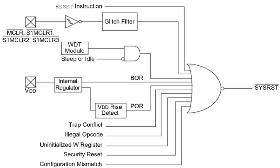
flowchart
graph TD
    A["MCLR, S1MCLR1, S1MCLR2, S1MCLR3"] --> B["RESET Instruction"]
    B --> C["Glitch Filter"]
    C --> D["AND Gate"]
    D --> E["Internal Regulator"]
    E --> F["VDD Rise Detect"]
    F --> G["POR"]
    G --> H["SYSRST"]
    I["WDT Module"] --> J["Sleep or Idle"]
    K["Trap Conflict"] --> L["Uninitialized W Register"]
    M["Illegal Opcode"] --> L
    N["Security Reset"] --> L
    O["Configuration Mismatch"] --> L
    P["BOR"] --> D
4.4.1 RESET RESOURCES
Many useful resources are provided on the main product page of the Microchip website for the devices listed in this data sheet. This product page contains the latest updates and additional information.
4.4.1.1 Key Resources
- “Reset” (www.microchip.com/DS70000602)
- Code Samples
- Application Notes
- Software Libraries
- Webinars
- All Related "dsPIC33/PIC24 Family Reference Manual" Sections
- Development Tools
4.4.2 SECONDARY RESET CONTROL REGISTER
REGISTER 4-17: RCON: RESET CONTROL REGISTER (1)
| R/W-0 R/W-0 U-0 U-0 U-0 R/W-0 R/W-0 | |||||||
| TRAPR IOP | UWR | — | — | — | — | CM | VREGS |
| bit 15 bit 8 | |||||||
| R/W-0 | R/W-0 | U-0 | R/W-0 | R/W-0 | R/W-0 | R/W-1 | R/W-1 |
| EXTR SWR | — | WDTO | SLEEP | IDLE | BOR | POR | |
| bit 7 bit 0 | |||||||
Legend:
| R = Readable bit | W = Writable bit | U = Unimplemented bit, read as '0' |
| -n = Value at POR | '1' = Bit is set | '0' = Bit is cleared x = Bit is unknown |
bit 15 TRAPR: Trap Reset Flag bit
1 = A Trap Conflict Reset has occurred
0 = A Trap Conflict Reset has not occurred
bit 14 IOPUWR: Illegal Opcode or Uninitialized W Register Access Reset Flag bit
1 = An Illegal Opcode, an Illegal Address mode or Uninitialized W Register used as an Address Pointer caused a Reset
0 = An Illegal Opcode or Uninitialized W Register Reset has not occurred
bit 13-10 Unimplemented: Read as '0'
bit 9 CM: Configuration Mismatch Flag bit
1 = A Configuration Mismatch Reset has occurred.
0 = A Configuration Mismatch Reset has not occurred
bit 8 VREGS: Voltage Regulator Standby During Sleep bit
1 = Voltage regulator is active during Sleep
0 = Voltage regulator goes into Standby mode during Sleep
bit 7 EXTR: External Reset (MCLR, S1MCLRx) Pin bit
1 = A Master Clear (pin) Reset has occurred
0 = A Master Clear (pin) Reset has not occurred
bit 6 SWR: Software RESET (Instruction) Flag bit
1 = A RESET instruction has been executed
0 = A RESET instruction has not been executed
bit 5 Unimplemented: Read as '0'
bit 4 WDTO: Watchdog Timer Time-out Flag bit
1 = WDT time-out has occurred
0 = WDT time-out has not occurred
bit 3 SLEEP: Wake-up from Sleep Flag bit
1 = Device has been in Sleep mode
0 = Device has not been in Sleep mode
bit 2 IDLE: Wake-up from Idle Flag bit
1 = Device has been in Idle mode
0 = Device has not been in Idle mode
bit 1 BOR: Brown-out Reset Flag bit
1 = A Brown-out Reset has occurred
0 = A Brown-out Reset has not occurred
Note 1: All of the Reset status bits can be set or cleared in software. Setting one of these bits in software does not cause a device Reset.
REGISTER 4-17: RCON: RESET CONTROL REGISTER (1) (CONTINUED)
bit 0 POR: Power-on Reset Flag bit
1 = A Power-on Reset has occurred
0 = A Power-on Reset has not occurred
Note 1: All of the Reset status bits can be set or cleared in software. Setting one of these bits in software does not cause a device Reset.
4.5 Secondary Interrupt Controller
Note 1: This data sheet summarizes the features of the dsPIC33CH128MP508 family of devices. It is not intended to be a comprehensive reference source. To complement the information in this data sheet, refer to “Interrupts” (www.microchip.com/DS70000600), which is available from the Microchip website (www.microchip.com).
The dsPIC33CH128MP508S1 family interrupt controller reduces the numerous peripheral interrupt request signals to a single interrupt request signal to the dsPIC33CH128MP508S1 family CPU.
The interrupt controller has the following features:
- Six Processor Exceptions and Software Traps
- Seven User-Selectable Priority Levels
- Interrupt Vector Table (IVT) with a Unique Vector for each Interrupt or Exception Source
- Fixed Priority within a Specified User Priority Level
• Fixed Interrupt Entry and Return Latencies
Note: There is no Alternate Interrupt Vector Table (AIVT) for the Secondary.
4.5.1 INTERRUPT VECTOR TABLE
The dsPIC33CH128MP508S1 family Interrupt Vector Table (IVT), shown in Figure 4-14, resides in program memory, starting at location, 000004h. The IVT contains six non-maskable trap vectors and up to 246 sources of interrupts. In general, each interrupt source has its own vector. Each interrupt vector contains a 24-bit wide address. The value programmed into each interrupt vector location is the starting address of the associated Interrupt Service Routine (ISR).
Interrupt vectors are prioritized in terms of their natural priority. This priority is linked to their position in the vector table. Lower addresses generally have a higher natural priority. For example, the interrupt associated with Vector 0 takes priority over interrupts at any other vector address.
4.5.2 RESET SEQUENCE
A device Reset is not a true exception because the interrupt controller is not involved in the Reset process. The dsPIC33CH128MP508S1 family devices clear their registers in response to a Reset, which forces the PC to zero. The device then begins program execution at location, 0x000000. A GOTO instruction at the Reset address can redirect program execution to the appropriate start-up routine.
Note: Any unimplemented or unused vector locations in the IVT should be programmed with the address of a default interrupt handler routine that contains a RESET instruction.
FIGURE 4-14: dsPIC33CH128MP508S1 FAMILY INTERRUPT VECTOR TABLE

text_image
Reset - GOTO Instruction 0x000000 Reset - GOTO Address 0x000002 Oscillator Fail Trap Vector 0x000004 Address Error Trap Vector 0x000006 Generic Hard Trap Vector 0x000008 Stack Error Trap Vector 0x00000A Math Error Trap Vector 0x00000C Reserved 0x00000E Generic Soft Trap Vector 0x000010 Reserved 0x000012 Interrupt Vector 0 0x000014 Interrupt Vector 1 0x000016 : : : Interrupt Vector 52 0x00007C Interrupt Vector 53 0x00007E Interrupt Vector 54 0x000080 : : : Interrupt Vector 116 0x0000FC Interrupt Vector 117 0x0000FE Interrupt Vector 118 0x000100 Interrupt Vector 119 0x000102 Interrupt Vector 120 0x000104 : : : Interrupt Vector 244 0x0001FC Interrupt Vector 245 0x0001FE START OF CODE 0x000200 See Table 4-21 for Interrupt Vector DetailsNote: In Dual Partition modes, each partition has a dedicated Interrupt Vector Table.
TABLE 4-20: TRAP TABLE
| Trap Description | MPLAB® XC16 Trap ISR Name | Vector # | IVT Address | Trap Bit Location | |||
| Generic Flag | Source Flag | Enable | Priority Level | ||||
| Oscillator Failure Trap _OscillatorFail 0 0x000004 INTCON1[1] | — — | 1 | 5 | ||||
| Address Error Trap _AddressError 1 0x000006 INTCON1[3] | — — | 1 | 4 | ||||
| Generic Hard Trap – ECCDBE | _HardTrapError | 2 | 0x000008 | — | INTCON4[1] | — 1 | 3 |
| Generic Hard Trap – SGHT | _HardTrapError | 2 0x000008 | — | INTCON4[0] | INTCON2[13] | 13 | |
| Stack Error Trap | _StackError | 3 | 0x00000A | INTCON1[2] | — — | 1 | 2 |
| Math Error Trap – OVAERR | _MathError | 4 | 0x00000C | INTCON1[4] | INTCON1[14] | INTCON1[10] | 11 |
| Math Error Trap – OVBERR | _MathError | 4 | 0x00000C | INTCON1[4] | INTCON1[13] | INTCON1[9] | 11 |
| Math Error Trap – COVAERR | _MathError | 4 | 0x00000C | INTCON1[4] | INTCON1[12] | INTCON1[8] | 11 |
| Math Error Trap – COVBERR | _MathError | 4 | 0x00000C | INTCON1[4] | INTCON1[11] | INTCON1[8] | 11 |
| Math Error Trap – SFTACERR | _MathError | 4 | 0x00000C | INTCON1[4] | INTCON1[7] | INTCON1[8] | 11 |
| Math Error Trap – DIV0ERR | _MathError | 4 | 0x00000C | INTCON1[4] | INTCON1[6] | INTCON1[8] | 11 |
| Reserved | Reserved | 5 | 0x00000E | — | — | — | — |
| Generic Soft Trap – CAN _SoftTrapError 6 0x0000010 | — | INTCON3[9] | — 9 | ||||
| Generic Soft Trap – NAE | _SoftTrapError 6 0x0000010 | — | INTCON3[8] | — 9 | |||
| Generic Soft Trap – CAN2 | _SoftTrapError 6 0x000010 | — | INTCON3[6] | — 9 | |||
| Generic Soft Trap – DAE | _SoftTrapError 6 0x000010 | — | INTCON3[5] | — 9 | |||
| Generic Soft Trap – DOOVR | _SoftTrapError 6 0x000010 | — | INTCON3[4] | — 9 | |||
| Generic Soft Trap – APLL Lock | _SoftTrapError 6 0x000010 | — | INTCON3[0] | — 9 | |||
| Reserved | Reserved | 7 | 0x000012 | — | — | — | — |
TABLE 4-21: SECONDARY INTERRUPT VECTOR DETAILS (1)
| Interrupt Description | MPLAB® XC16ISR Name | Vector # | IRQ # | IVT Address | Interrupt Bit Location | ||
| Flag Enable Priority | |||||||
| External Interrupt 0_INT0Interrupt | 8 0 0x000014 IFS0[0] | IEC0[0] | IPC0[2:0] | ||||
| Timer1_T1Interrupt 9 1 0x000016 | IFS0[1] IEC0[1] IPC0[6:4] | ||||||
| Change Notice Interrupt A | _CNAInterrupt | 10 | 2 | 0x000018 | IFS0[2] | IEC0[2] | IPC0[10:8] |
| Change Notice Interrupt B | _CNBInterrupt | 11 | 3 | 0x00001A | IFS0[3] | IEC0[3] | IPC0[14:12] |
| DMA Channel 0 | _DMA0Interrupt | 12 | 4 | 0x00001C | IFS0[4] | IEC0[4] | IPC1[2:0] |
| Reserved | Reserved | 13 | 5 | 0x00001E | — | — | — |
| Input Capture/Output Compare 1 | _CCP1Interrupt | 14 | 6 | 0x000020 | IFS0[6] | IEC0[6] | IPC1[10:8] |
| CCP1 Timer | _CCT1Interrupt | 15 | 7 | 0x000022 | IFS0[7] | IEC0[7] | IPC1[14:12] |
| DMA Channel 1 | _DMA1Interrupt | 16 | 8 | 0x000024 | IFS0[8] | IEC0[8] | IPC2[2:0] |
| SPI1 Receiver | _SPI1RXInterrupt | 17 | 9 | 0x000026 | IFS0[9] | IEC0[9] | IPC2[6:4] |
| SPI1 Transmitter | _SPI1TXInterrupt | 18 | 10 | 0x000028 | IFS0[10] | IEC0[10] | IPC2[10:8] |
| UART1 Receiver | _U1RXInterrupt | 19 | 11 | 0x00002A | IFS0[11] | IEC0[11] | IPC2[14:12] |
| UART1 Transmitter | _U1TXInterrupt | 20 | 12 | 0x00002C | IFS0[12] | IEC0[12] | IPC3[2:0] |
| ECC Single Bit Error | _ECCSBElnterrupt | 21 | 13 | 0x00002E | IFS0[13] | IEC0[13] | IPC3[6:4] |
| NVM Write Complete | _NVMInterrupt | 22 | 14 | 0x000030 | IFS0[14] | IEC0[14] | IPC3[10:8] |
| External Interrupt 1 | _INT1Interrupt | 23 | 15 | 0x000032 | IFS0[15] | IEC0[15] | IPC3[14:12] |
| I2C1 Secondary Event | _SI2C1Interrupt | 24 | 16 | 0x000034 | IFS1[0] | IEC1[0] | IPC4[2:0] |
| I2C1 Main Event | _MI2C1Interrupt | 25 | 17 | 0x000036 | IFS1[1] | IEC1[1] | IPC4[6:4] |
| Reserved | Reserved | 26 | 18 | 0x000038 | — | — | — |
| Change Notice Interrupt C | _CNCInterrupt | 27 | 19 | 0x00003A | IFS1[3] | IEC1[3] | IPC4[14:12] |
| External Interrupt 2 | _INT2Interrupt | 28 | 20 | 0x00003C | IFS1[4] | IEC1[4] | IPC5[2:0] |
| Reserved | Reserved | 29-30 | 21-22 | 0x00003E-0x000040 | — | — | — |
| Input Capture/Output Compare 2 | _CCP2Interrupt | 31 | 23 | 0x000042 | IFS1[7] | IEC1[7] | IPC5[14:12] |
| CCP2 Timer | _CCT2Interrupt | 32 | 24 | 0x000044 | IFS1[8] | IEC1[8] | IPC6[2:0] |
| Reserved | Reserved | 33 | 25 | 0x000046 | IFS1[9] | IEC1[9] | IPC6[6:4] |
| External Interrupt 3 | _INT3Interrupt | 34 | 26 | 0x000048 | IFS1[10] | IEC1[10] | IPC6[10:8] |
| Reserved | Reserved | 35-42 | 27-34 | 0x00004A-0x000058 | — | — | — |
| Input Capture/Output Compare 3 | _CCP3Interrupt | 43 | 35 | 0x00005A | IFS2[3] | IEC2[3] | IPC8[14:12] |
| CCP3 Timer | _CCT3Interrupt | 44 | 36 | 0x00005C | IFS2[4] | IEC2[4] | IPC9[2:0] |
| Reserved | Reserved | 45-47 | 37-39 | 0x00005E-0x000062 | — | — | — |
| Input Capture/Output Compare 4 | _CCP4Interrupt | 48 | 40 | 0x000064 | IFS2[8] | IEC2[8] | IPC10[2:0] |
| CCP4 Timer | _CCT4Interrupt | 49 | 41 | 0x000066 | IFS2[9] | IEC2[9] | IPC10[6:4] |
| Reserved | Reserved | 50-55 | 42-47 | 0x000068-0x000072 | — | — | — |
| QEI Position Counter Compare | _QEI1Interrupt | 56 | 48 | 0x000074 | IFS3[0] | IEC3[0] | IPC12[2:0] |
| UART1 Error | _U1Elnterrupt | 57 | 49 | 0x000076 | IFS3[1] | IEC3[1] | IPC12[6:4] |
| Reserved | Reserved | 58-68 | 50-60 | 0x000078-0x00008C | — | — | — |
| In-Circuit Debugger | _ICDInterrupt | 69 | 61 | 0x00008E | IFS3[13] | IEC3[13] | IPC15[6:4] |
| Reserved | Reserved | 70-71 | 62-63 | 0x000090-0x000092 | — | — | — |
| I2C1 Bus Collision | _I2C1BCInterrupt | 72 | 64 | 0x000094 | IFS4[0] | IEC4[0] | IPC16[2:0] |
| Reserved | Reserved | 73-74 | 65-66 | 0x000096-0x000098 | — | — | — |
| PWM Generator 1 | _PWM1Interrupt | 75 | 67 | 0x00009A | IFS4[3] | IEC4[3] | IPC16[14:12] |
| PWM Generator 2 | _PWM2Interrupt | 76 | 68 | 0x00009C | IFS4[4] | IEC4[4] | IPC17[2:0] |
| PWM Generator 3 | _PWM3Interrupt | 77 | 69 | 0x00009E | IFS4[5] | IEC4[5] | IPC17[6:4] |
| PWM Generator 4 | _PWM4Interrupt | 78 | 70 | 0x0000A0 | IFS4[6] | IEC4[6] | IPC17[10:8] |
| PWM Generator 5 | _PWM5Interrupt | 79 | 71 | 0x0000A2 | IFS4[7] | IEC4[7] | IPC17[14:12] |
| PWM Generator 6 | _PWM6Interrupt | 80 | 72 | 0x0000A4 | IFS4[8] | IEC4[8] | IPC18[2:0] |
| PWM Generator 7 | _PWM7Interrupt | 81 | 73 | 0x0000A6 | IFS4[9] | IEC4[9] | IPC18[6:4] |
| PWM Generator 8 _PWM8Interrupt | 82 74 0x0000A8 IFS4[10] IEC4[10] IPC18[10:8] | ||||||
| Change Notice D | _CNDInterrupt | 83 | 75 | 0x0000AA | IFS4[11] | IEC4[11] | IPC18[14:12] |
| Change Notice E | _CNEInterrupt | 84 | 76 | 0x0000AC | IFS4[12] | IEC4[12] | IPC19[2:0] |
| Reserved | Reserved | 85 | 77 | 0x0000AE | — | — | — |
| Secondary Comparator 1 | _CMP1Interrupt | 86 | 78 | 0x0000B0 | IFS4[14] | IEC4[14] | IPC19[10:8] |
| Secondary Comparator 2 | _CMP2Interrupt | 87 | 79 | 0x0000B2 | IFS4[15] | IEC4[15] | IPC19[14:12] |
| Secondary Comparator 3 | _CMP3Interrupt | 88 | 80 | 0x0000B4 | IFS5[0] | IEC5[0] | IPC20[2:0] |
| Reserved | Reserved | 89 | 81 | 0x0000B6 | — | — | — |
| Main Core PTG Trigger 4 | _PTG4Interrupt | 90 | 82 | 0x0000B8 | IFS5[2] | IEC5[2] | IPC20[10:8] |
| Main Core PTG Trigger 5 | _PTG5Interrupt | 91 | 83 | 0x0000BA | IFS5[3] | IEC5[3] | IPC20[14:12] |
| Main Core PTG Trigger 6 | _PTG6Interrupt | 92 | 84 | 0x0000BC | IFS5[4] | IEC5[4] | IPC21[2:0] |
| Main Core PTG Trigger 7 | _PTG7Interrupt | 93 | 85 | 0x0000BE | IFS5[5] | IEC5[5] | IPC21[6:4] |
| Reserved | Reserved | 94-97 | 86-89 | 0x0000C0-0x0000C6 | — | — | — |
| ADC Global Interrupt | _ADCInterrupt | 98 | 90 | 0x0000C8 | IFS5[10] | IEC5[10] | IPC22[10:8] |
| ADC AN0 Interrupt | _ADCAN0Interrupt | 99 | 91 | 0x0000CA | IFS5[11] | IEC5[11] | IPC22[14:12] |
| ADC AN1 Interrupt | _ADCAN1Interrupt | 100 | 92 | 0x0000CC | IFS5[12] | IEC5[12] | IPC23[2:0] |
| ADC AN2 Interrupt | _ADCAN2Interrupt | 101 | 93 | 0x0000CE | IFS5[13] | IEC5[13] | IPC23[6:4] |
| ADC AN3 Interrupt | _ADCAN3Interrupt | 102 | 94 | 0x0000D0 | IFS5[14] | IEC5[14] | IPC23[10:8] |
| ADC AN4 Interrupt | _ADCAN4Interrupt | 103 | 95 | 0x0000D2 | IFS5[15] | IEC5[15] | IPC23[14:12] |
| ADC AN5 Interrupt | _ADCAN5Interrupt | 104 | 96 | 0x0000D4 | IFS6[0] | IEC6[0] | IPC24[2:0] |
| ADC AN6 Interrupt | _ADCAN6Interrupt | 105 | 97 | 0x0000D6 | IFS6[1] | IEC6[1] | IPC24[6:4] |
| ADC AN7 Interrupt | _ADCAN7Interrupt | 106 | 98 | 0x0000D8 | IFS6[2] | IEC6[2] | IPC24[10:8] |
| ADC AN8 Interrupt | _ADCAN8Interrupt | 107 | 99 | 0x0000DA | IFS6[3] | IEC6[3] | IPC24[14:12] |
| ADC AN9 Interrupt | _ADCAN9Interrupt | 108 | 100 | 0x0000DC | IFS6[4] | IEC6[4] | IPC25[2:0] |
| ADC AN10 Interrupt | _ADCAN10Interrupt | 109 | 101 | 0x0000DE | IFS6[5] | IEC6[5] | IPC25[6:4] |
| ADC AN11 Interrupt | _ADCAN11Interrupt | 110 | 102 | 0x0000E0 | IFS6[6] | IEC6[6] | IPC25[10:8] |
| ADC AN12 Interrupt | _ADCAN12Interrupt | 111 | 103 | 0x0000E2 | IFS6[7] | IEC6[7] | IPC25[14:12] |
| ADC AN13 Interrupt | _ADCAN13Interrupt | 112 | 104 | 0x0000E4 | IFS6[8] | IEC6[8] | IPC26[2:0] |
| ADC AN14 Interrupt | _ADCAN14Interrupt | 113 | 105 | 0x0000E6 | IFS6[9] | IEC6[9] | IPC26[6:4] |
| ADC AN15 Interrupt | _ADCAN15Interrupt | 114 | 106 | 0x0000E8 | IFS6[10] | IEC6[10] | IPC26[10:8] |
| ADC AN16 Interrupt | _ADCAN16Interrupt | 115 | 107 | 0x0000EA | IFS6[11] | IEC6[11] | IPC26[14:12] |
| ADC AN17 Interrupt | _ADCAN17Interrupt | 116 | 108 | 0x0000EC | IFS6[12] | IEC6[12] | IPC27[2:0] |
| ADC AN18 Interrupt | _ADCAN18Interrupt | 117 | 109 | 0x0000EE | IFS6[13] | IEC6[13] | IPC27[6:4] |
| ADC AN19 Interrupt | _ADCAN19Interrupt | 118 | 110 | 0x0000F0 | IFS6[14] | IEC6[14] | IPC27[10:8] |
| ADC AN20 Interrupt | _ADCAN20Interrupt | 119 | 111 | 0x0000F2 | IFS6[15] | IEC6[15] | IPC27[14:12] |
| Reserved | Reserved | 120-122 | 112-114 | 0x0000F4-0x0000F8 | — | — | — |
| ADC Fault | _ADFLTInterrupt | 123 | 115 | 0x0000FA | IFS7[3] | IEC7[3] | IPC28[14:12] |
| ADC Digital Comparator 0 | _ADCMP0Interrupt | 124 | 116 | 0x0000FC | IFS7[4] | IEC7[4] | IPC29[2:0] |
| ADC Digital Comparator 1 | _ADCMP1Interrupt | 125 | 117 | 0x0000FE | IFS7[5] | IEC7[5] | IPC29[6:4] |
| ADC Digital Comparator 2 | _ADCMP2Interrupt | 126 | 118 | 0x000100 | IFS7[6] | IEC7[6] | IPC29[10:8] |
| ADC Digital Comparator 3 | _ADCMP3Interrupt | 127 | 119 | 0x000102 | IFS7[7] | IEC7[7] | IPC29[14:12] |
| ADC Oversample Filter 0 | _ADFLTR0Interrupt | 128 | 120 | 0x000104 | IFS7[8] | IEC7[8] | IPC30[2:0] |
| ADC Oversample Filter 1 | _ADFLTR1Interrupt | 129 | 121 | 0x000106 | IFS7[9] | IEC7[9] | IPC30[6:4] |
| ADC Oversample Filter 2 | _ADFLTR2Interrupt | 130 | 122 | 0x000108 | IFS7[10] | IEC7[10] | IPC30[10:8] |
| ADC Oversample Filter 3 | _ADFLTR3Interrupt | 131 | 123 | 0x00010A | IFS7[11] | IEC7[11] | IPC30[14:12] |
| CLC1 Positive Edge | _CLC1PInterrupt | 132 | 124 | 0x00010C | IFS7[12] | IEC7[12] | IPC31[2:0] |
| CLC2 Positive EdgeSPI1 Error _SPI1GInterrupt 134 1 | _CLC2PInterrupt26 0x000110 IFS7[14] | 133IEC7[14] | 125IPC31[10:8] | 0x00010E | IFS7[13] | IEC7[13] | IPC31[6:4] |
| Reserved | Reserved | 135-136 | 127-128 | 0x000112-0x000114 | — | — | — |
| MSI Main Initiated Interrupt | _MSIS1Interrupt | 137 | 129 | 0x000116 | IFS8[1] | IEC8[1] | IPC32[6:4] |
| MSIA - MSI Protocol A | _MSIAInterrupt | 138 | 130 | 0x000118 | IFS8[2] | IEC8[2] | IPC32[10:8] |
| MSIB - MSI Protocol B | _MSIBInterrupt | 139 | 131 | 0x00011A | IFS8[3] | IEC8[3] | IPC32[14:12] |
| MSIC - MSI Protocol C | _MSICInterrupt | 140 | 132 | 0x00011C | IFS8[4] | IEC8[4] | IPC33[2:0] |
| MSID - MSI Protocol D | _MSIDInterrupt | 141 | 133 | 0x00011E | IFS8[5] | IEC8[5] | IPC33[6:4] |
| MSIE - MSI Protocol E | _MSIEInterrupt | 142 | 134 | 0x000120 | IFS8[6] | IEC8[6] | IPC33[10:8] |
| MSIF - MSI Protocol F | _MSIFInterrupt | 143 | 135 | 0x000122 | IFS8[7] | IEC8[7] | IPC33[14:12] |
| MSIG - MSI Protocol G | _MSIGInterrupt | 144 | 136 | 0x000124 | IFS8[8] | IEC8[8] | IPC34[2:0] |
| MSIH - MSI Protocol H | _MSIHInterrupt | 145 | 137 | 0x000126 | IFS8[9] | IEC8[9] | IPC34[6:4] |
| MSI Secondary Read FIFO Data Ready | _MSIDInterrupt | 146 | 138 | 0x000128 | IFS8[10] | IEC8[10] | IPC34[10:8] |
| MSI Secondary Write FIFO Empty | _MSIWFEInterrupt | 147 | 139 | 0x00012A | IFS8[11] | IEC8[11] | IPC34[14:12] |
| Read or Write FIFO Fault (Over/Underflow) | _MSIFLTInterrupt | 148 | 140 | 0x00012C | IFS8[12] | IEC8[12] | IPC35[2:0] |
| MSI Secondary Reset | _MSTSRSTInterrupt | 149 | 141 | 0x00012E | IFS8[13] | IEC8[13] | IPC35[6:4] |
| Reserved | Reserved | 150-152 | 142-144 | 0x000130-0x000136 | — | — | — |
| Main Core Break | _MSTBRKInterrupt | 153 | 145 | 0x000138 | IFS9[1] | IEC9[1] | IPC36[6:4] |
| Reserved | Reserved | 154-163 | 146-155 | 0x00013A-0x00014C | — | — | — |
| Main Core Clock Fail | _MCLKFInterrupt | 164 | 156 | 0x00014E | IFS9[12] | IEC9[12] | IPC39[2:0] |
| Reserved | Reserved | 165-175 | 157-167 | 0x000150-0x000162 | — | — | — |
| ADC FIFO Ready | _ADFIFOInterrupt | 176 | 168 | 0x000164 | IFS10[8] | IEC10[8] | IPC42[2:0] |
| PWM Event A | _PEVTALntrupt | 177 | 169 | 0x000166 | IFS10[9] | IEC10[9] | IPC42[6:4] |
| PWM Event B | _PEVTBInterrupt | 178 | 170 | 0x000168 | IFS10[10] | IEC10[10] | IPC42[10:8] |
| PWM Event C | _PEVTCInterrupt | 179 | 171 | 0x00016A | IFS10[11] | IEC10[11] | IPC42[14:12] |
| PWM Event D | _PEVTDInterrupt | 180 | 172 | 0x00016C | IFS10[12] | IEC10[12] | IPC43[2:0] |
| PWM Event E | _PEVTEInterrupt | 181 | 173 | 0x00016E | IFS10[13] | IEC10[13] | IPC43[6:4] |
| PWM Event F | _PEVTFInterrupt | 182 | 174 | 0x000170 | IFS10[14] | IEC10[14] | IPC43[10:8] |
| CLC3 Positive Edge | _CLC3PInterrupt | 183 | 175 | 0x000172 | IFS10[15] | IEC10[15] | IPC43[14:12] |
| CLC4 Positive Edge | _CLC4PInterrupt | 184 | 176 | 0x000174 | IFS11[0] | IEC11[0] | IPC44[2:0] |
| CLC1 Negative Edge | _CLC1NInterrupt | 185 | 177 | 0x000176 | IFS11[1] | IEC11[1] | IPC44[6:4] |
| CLC2 Negative Edge | _CLC2NInterrupt | 186 | 178 | 0x000178 | IFS11[2] | IEC11[2] | IPC44[10:8] |
| CLC3 Negative Edge | _CLC3NInterrupt | 187 | 179 | 0x00017A | IFS11[3] | IEC11[3] | IPC44[14:] |
| CLC4 Negative Edge | _CLC4NInterrupt | 188 | 180 | 0x00017C | IFS11[4] | IEC11[4] | IPC45[2:0] |
| Reserved | Reserved | 189-196 | 181-188 | 0x0017E- 0x0018C | — | — | — |
| UART1 Event | _U1EVTInterrupt | 197 | 189 | 0x00018E | IFS11[13] | IEC11[13] | IPC47[6:4] |
Note 1: Not all interrupts are available on all packages. Make sure the selected device variant has the interrupt available on the device.
TABLE 4-22: SECONDARY INTERRUPT FLAG REGISTERS
| Register | Bit 15 Bit 14 | Bit 13 Bit 12 | Bit 11 Bit 10 | Bit 9 Bit 8 Bit 7 | Bit 6 Bit 5 Bit 4 | Bit 3 Bit 2 | Bit 1 Bit 0 | |||||||||
| IFS0 | INT1IF | NVMIF | ECCSBEIF | U1TXIF | U1RXIF | SPI1TXIF | SPI1RXIF | DMA1IF | CCT1IF | CCP1IF | — | DMA0IF | CNBIF | CNAIF | T1IF | INT0IF |
| IFS1 | — | — | — | — | — | INT3IF | — | CCT2IF | CCP2IF | — | — | INT2IF | CNCIF | — | MI2C1IF | SI2C1IF |
| IFS2 | — | — | — | — | — | — | CCT4IF | CCP4IF | — | — | — | CCT3IF | CCP3IF | — | — | — |
| IFS3 | — | — | ICDIF | — | — | — | — | — | — | — | — | — | — | — | U1EIF | QE11IF |
| IFS4 CMP2IF CMP1IF | — | CNEIF | CNDIF | PWM8IF | PWM7IF | PWM6IF | PWM5IF | PWM4IF | PWM3IF | PWM2IF | PWM1IF | — | — | I2C1BCIF | ||
| IFS5 | ADCAN4IF | ADCAN3IF | ADCAN2IF | ADCAN1IF | ADCAN0IF | ADCIF | — | — | — | — | PTG7IF | PTG6IF | PTG5IF | PTG4IF | — | CMP3IF |
| IFS6 | ADCAN20IF | ADCAN19IF | ADCAN18IF | ADCAN17IF | ADCAN16IF | ADCAN15IF | ADCAN14IF | ADCAN13IF | ADCAN12IF | ADCAN11IF | ADCAN10IF | ADCAN9IF | ADCAN8IF | ADCAN7IF | ADCAN6IF | ADCAN5IF |
| IFS7 | — | SPI1IF | CLC2PIF | CLC1PIF | ADFLTR3IF | ADFLTR2IF | ADFLTR1IF | ADFLTR0IF | ADCMP3IF | ADCMP2IF | ADCMP1IF | ADCMP0IF | ADFLTIF | — | — | — |
| IFS8 | — | — | MSIMRSTIF | MSIFLTIF | MSIWFEIF | MSIDTIF | MSIHIF | MSIGIF | MSIFIF | MSIEIF | MSIDIF | MSICIF | MSIBIF | MSIAIF | MSIMIF | — |
| IFS9 | — | — | — | MCLKFIF | — | — | — | — | — | — | — | — | — | — | MSTBRKIF | — |
| IFS10 | CLC3PIF | PEVTFIF | PEVTEIF | PEVTDIF | PEVTCIF | PEVTBIF | PEVTAIF | ADFIFOIF | — | — | — | — | — | — | — | — |
| IFS11 | — | — | U1EVTIF | — | — | — | — | — | — | — | — | CLC4NIF | CLC3NIF | CLC2NIF | CLC1NIF | CLC4PIF |
TABLE 4-23: SECONDARY INTERRUPT ENABLE REGISTERS
| Register | Bit 15 | Bit 14 | Bit 13 | Bit 12 | Bit 11 | Bit 10 | Bit 9 | Bit 8 | Bit 7 | Bit 6 | Bit 5 | Bit 4 | Bit 3 | Bit 2 | Bit 1 | Bit 0 |
| IEC0 | INT1IE | NVMIE | ECCSBEIE | U1TXIE | U1RXIE | SPI1TXIE | SPI1RXIE | DMA1IE | CCT1IE | CCP1IE | — | DMA0IE | CNBIE | CNAIE | T1IE | INT0IE |
| IEC1 | — | — | — | — | — | INT3IE | — | CCT2IE | CCP2IE | — | — | INT2IE | CNCIE | — | MI2C1IE | SI2C1IE |
| IEC2 | — | — | — | — | — | — | CCT4IE | CCP4IE | — | — | — | CCT3IE | CCP3IE | — | — | — |
| IEC3 | — | — | ICDIE | — | — | — | — | — | — | — | — | — | — | — | U1EIE | QE1IIE |
| IEC4 CMP2IE CMP1IE | — | CNEIE | CNDIE | PWM8IE | PWM7IE | PWM6IE | PWM5IE | PWM4IE | PWM3IE | PWM2IE | PWM1IE | — | — | I2C1BCIE | ||
| IEC5 | ADCAN4IE | ADCAN3IE | ADCAN2IE | ADCAN1IE | ADCAN0IE | ADCIE | — | — | — | — | PTG7IE | PTG6IE | PTG5IE | PTG4IE | — | CMP3IE |
| IEC6 | ADCAN20IE | ADCAN19IE | ADCAN18IE | ADCAN17IE | ADCAN16IE | ADCAN15IE | ADCAN14IE | ADCAN13IE | ADCAN12IE | ADCAN11IE | ADCAN10IE | ADCAN9IE | ADCAN8IE | ADCAN7IE | ADCAN6IE | ADCAN5IE |
| IEC7 | — | SP1IE | CLC2PIE | CLC1PIE | ADFLTR3IE | ADFLTR2IE | ADFLTR1IE | ADFLTR0IE | ADCMP3IE | ADCMP2IE | ADCMP1IE | ADCMP0IE | ADFLTIE | — | — | — |
| IEC8 | — | — | MSIMRSTIE | MSIFLTIE | MSIWFEIE | MSIDTIE | MSIHIE | MSIGIE | MSIFIE | MSIEIE | MSIDIE | MSICIE | MSIBIE | MSIAIE | MSIMIF | — |
| IEC9 | — | — | — | MCLKFIE | — | — | — | — | — | — | — | — | — | — | MSTBRKIE | — |
| IEC10 | CLC3PIE | PEVTFIE | PEVTEIE | PEVTDIE | PEVTCIE | PEVTBIE | PEVTAIE | ADFIFOIE | — | — | — | — | — | — | — | — |
| IEC11 | — | — | U1EVTIE | — | — | — | — | — | — | — | — | CLC4NIE | CLC3NIE | CLC2NIE | CLC1NIE | CLC4PIE |
TABLE 4-24: SECONDARY INTERRUPT PRIORITY REGISTERS
| Register | Bit 15 | Bit 14 | Bit 13 | Bit 12 | Bit 11 | Bit 10 | Bit 9 | Bit 8 | Bit 7 | Bit 6 | Bit 5 | Bit 4 | Bit 3 | Bit 2 | Bit 1 | Bit 0 |
| IPC0 | — | CNBIP2 | CNBIP1 | CNBIP0 | — | CNAIP2 | CNAIP1 | CNAIP0 | — | T1IP2 | T1IP1 | T1IP0 | — | INT0IP2 | INT0IP1 | INT0IP0 |
| IPC1 | — | CCT1IP2 | CCT1IP1 | CCT1IP0 | — | CCP1IP2 | CCP1IP1 | CCP1IP0 | — | — | — | — | — | DMA0IP2 | DMA0IP1 | DMA0IP0 |
| IPC2 | — | U1RXIP2 | U1RXIP1 | U1RXIP0 | — | SPI1TXIP2 | SPI1TXIP1 | SPI1TXIP0 | — | SPI1RXIP2 | SPI1RXIP1 | SPI1RXIP0 | — | DMA1IP2 | DMA1IP1 | DMA1IP0 |
| IPC3 | — | INT1IP2 | INT1IP1 | INT1IP0 | — | NVMIP2 | NVMIP1 | NVMIP0 | — | ECCSBEIP2 | ECCSBEIP1 | ECCSBEIP0 | — | U1TXIP2 | U1TXIP1 | U1TXIP0 |
| IPC4 | — | CNCIP2 | CNCIP1 | CNCIP0 | — | — | — | — | — | MI2C1IP2 | MI2C1IP1 | MI2C1IP0 | — | SI2C1IP2 | SI2C1IP1 | SI2C1IP0 |
| IPC5 | — | CCP2IP2 | CCP2IP1 | CCP2IP0 | — | — | — | — | — | — | — | — | — | INT2IP2 | INT2IP1 | INT2IP0 |
| IPC6 | — | — | — | — | — | INT3IP2 | INT3IP1 | INT3IP0 | — | — | — | — | — | CCT2IP2 | CCT2IP1 | CCT2IP0 |
| IPC7 | — | — | — | — | — | — | — | — | — | — | — | — | — | — | — | — |
| IPC8 | — | CCP3IP2 | CCP3IP1 | CCP3IP0 | — | — | — | — | — | — | — | — | — | — | — | — |
| IPC9 | — | — | — | — | — | — | — | — | — | — | — | — | — | CCT3IP2 | CCT3IP1 | CCT3IP0 |
| IPC10 | — | — | — | — | — | — | — | — | — | CCT4IP2 | CCT4IP1 | CCT4IP0 | — | CCP4IP2 | CCP4IP1 | CCP4IP0 |
| IPC11 | — | — | — | — | — | — | — | — | — | — | — | — | — | — | — | — |
| IPC12 | — | — | — | — | — | — | — | — | — | U1EIP2 | U1EIP1 | U1EIP0 | — | QE11IP2 | QE11IP1 | QE11IP0 |
| IPC13 | — | — | — | — | — | — | — | — | — | — | — | — | — | — | — | — |
| IPC14 | — | — | — | — | — | — | — | — | — | — | — | — | — | — | — | — |
| IPC15 | — | — | — | — | — | JTAGIP2 | JTAGIP1 | JTAGIP0 | — | ICDIP2 | ICDIP1 | ICDIP0 | — | — | — | — |
| IPC16 | — | PWM1IP2 | PWM1IP1 | PWM1IP0 | — | — | — | — | — | — | — | — | — | I2C1BCIP2 | I2C1BCIP1 | I2C1BCIP0 |
| IPC17 | — | PWM5IP2 | PWM5IP1 | PWM5IP0 | — | PWM4IP2 | PWM4IP1 | PWM4IP0 | — | PWM3IP2 | PWM3IP1 | PWM3IP0 | — | PWM2IP2 | PWM2IP1 | PWM2IP0 |
| IPC18 | — | CNDIP2 | CNDIP1 | CNDIP0 | — | PWM8IP2 | PWM8IP1 | PWM8IP0 | — | PWM7IP2 | PWM7IP1 | PWM7IP0 | — | PWM6IP2 | PWM6IP1 | PWM6IP0 |
| IPC19 | — | CMP2IP2 | CMP2IP1 | CMP2IP0 | — | CMP1IP2 | CMP1IP1 | CMP1IP0 | — | — | — | — | — | CNEIP2 | CNEIP1 | CNEIP0 |
| IPC20 | — | PTG5IP2 | PTG5IP1 | PTG5IP0 | — | PTG4IP2 | PTG4IP1 | PTG4IP0 | — | — | — | — | — | CMP3IP2 | CMP3IP1 | CMP3IP0 |
| IPC21 | — | — | — | — | — | — | — | — | — | PTG7IP2 | PTG7IP1 | PTG7IP0 | — | PTG6IP2 | PTG6IP1 | PTG6IP0 |
| IPC22 | — | ADCAN0IP2 | ADCAN0IP1 | ADCAN0IP0 | — | ADCIP2 | ADCIP1 | ADCIP | — | — | — | — | — | — | — | — |
| IPC23 | — | ADCAN4IP2 | ADCAN4IP1 | ADCAN4IP0 | — | ADCAN3IP2 | ADCAN3IP1 | ADCAN3IP0 | — | ADCAN2IP2 | ADCAN2IP1 | ADCAN2IP0 | — | ADCAN1IP2 | ADCAN1IP1 | ADCAN1IP0 |
| IPC24 | — | ADCAN8IP2 | ADCAN8IP1 | ADCAN8IP0 | — | ADCAN7IP2 | ADCAN7IP1 | ADCAN7IP0 | — | ADCAN6IP2 | ADCAN6IP1 | ADCAN6IP0 | — | ADCAN5IP2 | ADCAN5IP1 | ADCAN5IP0 |
| IPC25 | — | ADCAN12IP2 | ADCAN12IP1 | ADCAN12IP0 | — | ADCAN11IP2 | ADCAN11IP1 | ADCAN11IP0 | — | ADCAN10IP2 | ADCAN10IP1 | ADCAN10IP0 | — | ADCAN9IP2 | ADCAN9IP1 | ADCAN9IP0 |
| IPC26 | — | ADCAN16IP2 | ADCAN16IP1 | ADCAN16IP0 | — | ADCAN15IP2 | ADCAN15IP1 | ADCAN15IP0 | — | ADCAN14IP2 | ADCAN14IP1 | ADCAN14IP0 | — | ADCAN13IP2 | ADCAN13IP1 | ADCAN13IP0 |
| IPC27 | — | ADCAN20IP2 | ADCAN20IP1 | ADCAN20IP0 | — | ADCAN19IP2 | ADCAN19IP1 | ADCAN19IP0 | — | ADCAN18IP2 | ADCAN18IP1 | ADCAN18IP0 | — | ADCAN17IP2 | ADCAN17IP1 | ADCAN17IP0 |
| IPC28 | — | ADFLTIP2 | ADFLTIP1 | ADFLTIP0 | — | — | — | — | — | — | — | — | — | ADCAN21IP2 | ADCAN21IP1 | ADCAN21IP0 |
| IPC29 | — | ADCMP3IP2 | ADCMP3IP1 | ADCMP3IP0 | — | ADCMP2IP2 | ADCMP2IP1 | ADCMP2IP0 | — | ADCMP1IP2 | ADCMP1IP1 | ADCMP1IP0 | — | ADCMP0IP2 | ADCMP0IP1 | ADCMP0IP0 |
| IPC30 | — | ADFLTR3IP2 | ADFLTR3IP1 | ADFLTR3IP0 | — | ADFLTR2IP2 | ADFLTR2IP1 | ADFLTR2IP0 | — | ADFLTR1IP2 | ADFLTR1IP1 | ADFLTR1IP0 | — | ADFLTR0IP2 | ADFLTR0IP1 | ADFLTR0IP0 |
| IPC31 | — | — | — | — | — | SPI1IP2 | SPI1IP1 | SPI1IP0 | — | CLC2PEIP2 | CLC2PEIP1 | CLC2PEIP0 | — | CLC1PEIP2 | CLC1PEIP1 | CLC1PEIP0 |
| IPC32 | — | MSIBIP2 | MSIBIP1 | MSIBIP0 | — | MSIAIP2 | MSIAIP1 | MSIAIP0 | — | MSMIP2 | MSMIP1 | MSMIP0 | — | — | — | — |
| IPC33 | — | MSIFIP2 | MSIFIP1 | MSIFIP0 | — | MSIEIP2 | MSIEIP1 | MSIEIP0 | — | MSIDIP2 | MSIDIP1 | MSIDIP0 | — | MSICIP2 | MSICIP1 | MSICIP0 |
| IPC34 | — | MSIWFEIP2 | MSIWFEIP1 | MSIWFEIP0 | — | MSIDTIP2 | MSIDTIP1 | MSIDTIP0 | — | MSIHP2 | MSIHP1 | MSIHP0 | — | MSIGIP2 | MSIGIP1 | MSIGIP0 |
| IPC35 | — | — | — | — | — | — | — | — | — | MSIMRSTIP2 | MSIMRSTIP1 | MSIMRSTIP0 | — | MSIFLTIP2 | MSIFLTIP1 | MSIFLTIP0 |
| IPC36 — | — — — | — — — | MSTBRKIP2 MSTBRKIP1 MSTBRKIP0 — — | — — | ||||||||||||
| IPC37 — | — — — | — — — | — — — | |||||||||||||
| IPC38 — | — — — | — — — | — — — | |||||||||||||
| IPC39 | — | — | — | — | — | — | — | — | — | — | — | — | — | MCLKFIP2 | MCLKFIP1 | MCLKFIP0 |
| IPC40 | — | — | — | — | — | — | — | — | — | ADC1IP2 | ADC1IP1 | ADC1IP0 | — | ADC0IP2 | ADC0IP1 | ADC0IP0 |
| IPC41 — | — — — | — — — | — — — | |||||||||||||
| IPC42 | — | PEVTCIP2 | PEVTCIP1 | PEVTCIP0 | — | PEVTBIP2 | PEVTBIP1 | PEVTBIP0 | — | PEVTAIP2 | PEVTAIP1 | PEVTAIP0 | — | ADFIFOIP2 | ADFIFOIP1 | ADFIFOIP0 |
| IPC43 | — | CLC3PIP2 | CLC3PIP1 | CLC3PIP0 | — | PEVTFIP2 | PEVTFIP1 | PEVTFIP0 | — | PEVTEIP2 | PEVTEIP1 | PEVTEIP0 | — | PEVTDIP2 | PEVTDIP1 | PEVTDIP0 |
| IPC44 | — | CLC3NIP2 | CLC3NIP1 | CLC3NIP0 | — | CLC2NIP2 | CLC2NIP1 | CLC2NIP0 | — | CLC1NIP2 | CLC1NIP1 | CLC1NIP0 | — | CLC4PIP2 | CLC4PIP1 | CLC4PIP0 |
| IPC45 | — | — | — | — | — | — | — | — | — | — | — | — | — | CLC4NIP2 | CLC4NIP1 | CLC4NIP0 |
| IPC46 — | — — — | — — — | — — — | |||||||||||||
| IPC47 | — | — | — | — | — | — | — | — | — | U1EVTIP2 | U1EVTIP1 | U1EVTIP0 | — | — | — | — |
4.5.3 INTERRUPT RESOURCES
Many useful resources are provided on the main product page of the Microchip website for the devices listed in this data sheet. This product page contains the latest updates and additional information.
4.5.3.1 Key Resources
- "Interrupts" (www.microchip.com/DS70000600)
- Code Samples
- Application Notes
- Software Libraries
- Webinars
- All Related "dsPIC33/PIC24 Family Reference Manual" Sections
• Development Tools
4.5.4 INTERRUPT CONTROL AND STATUS REGISTERS
The dsPIC33CH128MP508S1 family devices implement the following registers for the interrupt controller:
- INTCON1
- INTCON2
- INTCON3
- INTCON4
• INT TREG
4.5.4.1 INTCON1 through INTCON4
Global interrupt control functions are controlled from INTCON1, INTCON2, INTCON3 and INTCON4.
INTCON1 contains the Interrupt Nesting Disable bit (NSTDIS), as well as the control and status flags for the processor trap sources.
The INTCON2 register controls external interrupt request signal behavior and contains the Global Interrupt Enable bit (GIE).
INTCON3 contains the status flags for the Auxiliary PLL and DO stack overflow status trap sources.
The INTCON4 register contains the Software Generated Hard Trap Status bit (SGHT).
4.5.4.2 IFSx
The IFSx registers maintain all of the interrupt request flags. Each source of interrupt has a status bit, which is set by the respective peripherals or external signal and is cleared via software.
4.5.4.3 IECx
The IECx registers maintain all of the interrupt enable bits. These control bits are used to individually enable interrupts from the peripherals or external signals.
4.5.4.4 IPCx
The IPCx registers are used to set the Interrupt Priority Level (IPL) for each source of interrupt. Each user interrupt source can be assigned to one of seven priority levels.
4.5.5 INTTREG
The INTTREG register contains the associated interrupt vector number and the new CPU Interrupt Priority Level, which are latched into the Vector Number (VECNUM[7:0]) and Interrupt Level bits (ILR[3:0]) fields in the INTTREG register. The new Interrupt Priority Level is the priority of the pending interrupt.
The interrupt sources are assigned to the IFSx, IECx and IPCx registers in the same sequence as they are listed in Table 4-21. For example, INT0 (External Interrupt 0) is shown as having Vector Number 8 and a natural order priority of 0. Thus, the INT0IF bit is found in IFS0[0], the INT0IE bit in IEC0[0] and the INT0IP[2:0] bits in the first position of IPC0 (IPC0[2:0]).
4.5.6 STATUS/CONTROL REGISTERS
Although these registers are not specifically part of the interrupt control hardware, two of the CPU Control registers contain bits that control interrupt functionality. For more information on these registers, refer to "Enhanced CPU" (www.microchip.com/DS70005158).
- The CPU STATUS Register, SR, contains the IPL[2:0] bits (SR[7:5]). These bits indicate the current CPU Interrupt Priority Level. The user software can change the current CPU Interrupt Priority Level by writing to the IPLx bits.
- The CORCON register contains the IPL3 bit which, together with IPL[2:0], also indicates the current CPU priority level. IPL3 is a read-only bit so that trap events cannot be masked by the user software.
All Interrupt registers are described in Register 4-20 through Register 4-24 on the following pages.
4.5.7 CROSS CORE INTERRUPTS
There are three interrupts that can occur in the Secondary core based on the Main events:
- MSIMRSTIF is a Main Reset interrupt which gets set in the Secondary if the Main gets a Reset. This interrupt is enabled only when the MRTSIE bit (SI1CON[7]) is set
- MCLKIF is a Secondary interrupt which gets set if the Main core loses its system clock.
- MSTBRKIF is the Main Core Break interrupt. This interrupt gets set in the Secondary if the Main core stops at a breakpoint (valid only when the Main is being debugged).
4.5.8 SECONDARY INTERRUPT CONTROL/STATUS REGISTERS
REGISTER 4-18: SR: CPU STATUS REGISTER (1)
| R/W-0 R/W-0 R/W-0 R/W-0 R/C-0 R/C-0 R-0 R/W-0 | |||||||
| OA | OB | SA | SB | OAB | SAB | DA | DC |
| bit 15 bit 8 | |||||||
| R/W-0^(3) | R/W-0^(3) | R/W-0^(3) | R-0 R/W-0 | R/W-0 R/W-0 R/W-0 | |||
| IPL2^(2) | IPL1^(2) | IPL0^(2) | RA | N | OV | Z | C |
| bit 7 bit 0 | |||||||
| Legend: | C = Clearable bit | ||
| R = Readable bit | W = Writable bit | U = Unimplemented bit, read as ‘0’ | |
| -n = Value at POR | ‘1’= Bit is set | ‘0’ = Bit is cleared | x = Bit is unknown |
bit 7-5 IPL[2:0]: CPU Interrupt Priority Level Status bits ^(2,3)
111 = CPU Interrupt Priority Level is 7 (15); user interrupts are disabled
110 = CPU Interrupt Priority Level is 6 (14)
101 = CPU Interrupt Priority Level is 5 (13)
100 = CPU Interrupt Priority Level is 4 (12)
011 = CPU Interrupt Priority Level is 3 (11)
010 = CPU Interrupt Priority Level is 2 (10)
001 = CPU Interrupt Priority Level is 1 (9)
000 = CPU Interrupt Priority Level is 0 (8)
Note 1: For complete register details, see Register 4-1.
2: The IPL[2:0] bits are concatenated with the IPL[3] bit (CORCON[3]) to form the CPU Interrupt Priority Level. The value in parentheses indicates the IPL, if IPL[3] = 1. User interrupts are disabled when IPL[3] = 1.
3: The IPL[2:0] Status bits are read-only when the NSTDIS bit (INTCON1[15]) = 1.
REGISTER 4-19: CORCON: SECONDARY CORE CONTROL REGISTER (1)
| R/W-0 U-0 R/W-0 R/W-0 R/W-0 R-0 R-0 R-0 | |||||||
| VAR | — | US1 | US0 | EDT | DL2 | DL1 | DL0 |
| bit 15 bit 8 | |||||||
| R/W-0 | R/W-0 | R/W-1 | R/W-0 | R/C-0 | R-0 | R/W-0 | R/W-0 |
| SATA | SATB | SATDW | ACCSAT | IPL3^(2) | SFA | RND | IF |
| bit 7 bit 0 | |||||||
| Legend: | C = Clearable bit | ||
| R = Readable bit | W = Writable bit | U = Unimplemented bit, read as ‘0’ | |
| -n = Value at POR | ‘1’= Bit is set | ‘0’ = Bit is cleared | x = Bit is unknown |
bit 15 VAR: Variable Exception Processing Latency Control bit
1 = Variable exception processing is enabled
0 = Fixed exception processing is enabled
bit 3 IPL3: CPU Interrupt Priority Level Status bit 3 (2)
1 = CPU Interrupt Priority Level is greater than 7
0 = CPU Interrupt Priority Level is 7 or less
Note 1: For complete register details, see Register 4-2.
2: The IPL3 bit is concatenated with the IPL[2:0] bits (SR[7:5]) to form the CPU Interrupt Priority Level.
REGISTER 4-20: INTCON1: SECONDARY INTERRUPT CONTROL REGISTER 1
| R/W-0 R/W-0 R/W-0 R/W-0 R/W-0 R/W-0 R/W-0 | |||||||
| NSTDIS | OVAERR | OVBERR | COVAERR | COVBERR | OVATE | OVBTE | COVTE |
| bit 15 bit 8 | |||||||
| R/W-0 | R/W-0 | U-0 | R/W-0 | R/W-0 | R/W-0 | R/W-0 | U-0 |
| SFTACERR | DIV0ERR | — | MATHERR | ADDRERR | STKERR | OSCFAIL | — |
| bit 7 bit 0 | |||||||
| Legend: | |||
| R = Readable bit | W = Writable bit | U = Unimplemented bit, read as ‘0’ | |
| -n = Value at POR | ‘1’ = Bit is set | ‘0’ = Bit is cleared | x = Bit is unknown |
| bit 15 | NSTDIS: Interrupt Nesting Disable bit1 = Interrupt nesting is disabled0 = Interrupt nesting is enabled |
| bit 14 | OVAERR: Accumulator A Overflow Trap Flag bit1 = Trap was caused by overflow of Accumulator A0 = Trap was not caused by overflow of Accumulator A |
| bit 13 | OVBERR: Accumulator B Overflow Trap Flag bit1 = Trap was caused by overflow of Accumulator B0 = Trap was not caused by overflow of Accumulator B |
| bit 12 | COVAERR: Accumulator A Catastrophic Overflow Trap Flag bit1 = Trap was caused by catastrophic overflow of Accumulator A0 = Trap was not caused by catastrophic overflow of Accumulator A |
| bit 11 | COVBERR: Accumulator B Catastrophic Overflow Trap Flag bit1 = Trap was caused by catastrophic overflow of Accumulator B0 = Trap was not caused by catastrophic overflow of Accumulator B |
| bit 10 | OVATE: Accumulator A Overflow Trap Enable bit1 = Trap overflow of Accumulator A0 = Trap is disabled |
| bit 9 | OVBTE: Accumulator B Overflow Trap Enable bit1 = Trap overflow of Accumulator B0 = Trap is disabled |
| bit 8 | COVTE: Catastrophic Overflow Trap Enable bit1 = Trap on catastrophic overflow of Accumulator A or B is enabled0 = Trap is disabled |
| bit 7 | SFTACERR: Shift Accumulator Error Status bit1 = Math error trap was caused by an invalid accumulator shift0 = Math error trap was not caused by an invalid accumulator shift |
| bit 6 | DIV0ERR: Divide-by-Zero Error Status bit1 = Math error trap was caused by a divide-by-zero0 = Math error trap was not caused by a divide-by-zero |
| bit 5 | Unimplemented: Read as ‘0’ |
| bit 4 | MATHERR: Math Error Status bit1 = Math error trap has occurred0 = Math error trap has not occurred |
| bit 3 | ADDRERR: Address Error Trap Status bit1 = Address error trap has occurred0 = Address error trap has not occurred |
REGISTER 4-20: INTCON1: SECONDARY INTERRUPT CONTROL REGISTER 1 (CONTINUED)
bit 2 STKERR: Stack Error Trap Status bit
1 = Stack error trap has occurred
0 = Stack error trap has not occurred
bit 1 OSCFAIL: Oscillator Failure Trap Status bit
1 = Oscillator failure trap has occurred
0 = Oscillator failure trap has not occurred
bit 0 Unimplemented: Read as '0'
REGISTER 4-21: INTCON2: SECONDARY INTERRUPT CONTROL REGISTER 2
| R/W-1 R/W-0 R/W-0 U-0 U-0 U-0 U-0 U-0 | |||||||
| GIE DISI $WTRAP | — — | — | — | — | |||
| bit 15 bit 8 | |||||||
| U-0 | U-0 | U-0 | U-0 | R/W-0 | R/W-0 | R/W-0 | R/W-0 |
| — | — | — | — | INT3EP | INT2EP | INT1EP | INT0EP |
| bit 7 bit 0 | |||||||
Legend:
| R = Readable bit | W = Writable bit | U = Unimplemented bit, read as '0' |
| -n = Value at POR | '1' = Bit is set | '0' = Bit is cleared x = Bit is unknown |
bit 15 GIE: Global Interrupt Enable bit
1 = Interrupts and associated IE bits are enabled
0 = Interrupts are disabled, but traps are still enabled
bit 14 DISI: DISI Instruction Status bit
1 = DISI instruction is active
0 = DISI instruction is not active
bit 13 SWTRAP: Software Trap Status bit
1 = Software trap is enabled
0 = Software trap is disabled
bit 12-4 Unimplemented: Read as '0'
bit 3 INT3EP: External Interrupt 3 Edge Detect Polarity Select bit
1 = Interrupt on negative edge
0 = Interrupt on positive edge
bit 2 INT2EP: External Interrupt 2 Edge Detect Polarity Select bit
1 = Interrupt on negative edge
0 = Interrupt on positive edge
bit 1 INT1EP: External Interrupt 1 Edge Detect Polarity Select bit
1 = Interrupt on negative edge
0 = Interrupt on positive edge
bit 0 INT0EP: External Interrupt 0 Edge Detect Polarity Select bit
1 = Interrupt on negative edge
0 = Interrupt on positive edge
REGISTER 4-22: INTCON3: SECONDARY INTERRUPT CONTROL REGISTER 3
| U-0 U-0 U-0 U-0 U-0 U-0 R/W-0 | |||||||
| — | — | — | — | — | — | — | NAE |
| bit 15 bit 8 | |||||||
| U-0 U-0 | R/W-0 | R/W-0 | U-0 U-0 | U-0 R/W-0 | |||
| — | — | DAE | DOOVR | — | — | — | APLL |
| bit 7 bit 0 | |||||||
| Legend: | |||
| R = Readable bit | W = Writable bit U = Unimplemented bit, read as ‘0’ | ||
| -n = Value at POR | ‘1’ = Bit is set | ‘0’ = Bit is cleared | x = Bit is unknown |
bit 15-9 Unimplemented: Read as '0'
bit 8 NAE: NVM Address Error Soft Trap Status bit
1 = NVM address error soft trap has occurred
0 = NVM address error soft trap has not occurred
bit 7-6 Unimplemented: Read as '0'
bit 5 DAE: DMA Address Error (Soft) Trap Status bit
1 = DMA address error trap has occurred
0 = DMA address error trap has not occurred
bit 4 DOOVR: DO Stack Overflow Soft Trap Status bit
1 = DO stack overflow soft trap has occurred
0 = DO stack overflow soft trap has not occurred
bit 3-1 Unimplemented: Read as '0'
bit 0 APLL: Auxiliary PLL Loss of Lock Soft Trap Status bit
1 = APLL lock soft trap has occurred
0 = APLL lock soft trap has not occurred
REGISTER 4-23: INTCON4: SECONDARY INTERRUPT CONTROL REGISTER 4
| Legend: | |||
| R = Readable bit | W = Writable bit U = Unimplemented bit, read as '0' | ||
| -n = Value at POR | '1' = Bit is set | '0' = Bit is cleared | x = Bit is unknown |
bit 15-1 Unimplemented: Read as '0'
bit 0 SGHT: Software Generated Hard Trap Status bit
1 = Software generated hard trap has occurred
0 = Software generated hard trap has not occurred
REGISTER 4-24: INTTREG: SECONDARY INTERRUPT CONTROL AND STATUS REGISTER
| U-0 U-0 R-0 U-0 R-0 R-0 R-0 R-0 | |||||||
| — | — | VHOLD | — | ILR3 | ILR2 | ILR1 | ILR0 |
| bit 15 bit 8 | |||||||
| R-0 R-0 R-0 R-0 R-0 R-0 R-0 R-0 | |
| VECNUM[7:0] | |
| bit 7 | bit 0 |
Legend:
| R = Readable bit | W = Writable bit | U = Unimplemented bit, read as '0' |
| -n = Value at POR | '1' = Bit is set | '0' = Bit is cleared x = Bit is unknown |
bit 15-14 Unimplemented: Read as '0'
bit 13 VHOLD: Vector Number Capture Enable bit
1 = VECNUM[7:0] bits read current value of vector number encoding tree (i.e., highest priority pending interrupt) 0 = Vector number latched into VECNUM[7:0] at Interrupt Acknowledge and retained until next IACK
bit 12 Unimplemented: Read as '0'
bit 11-8 ILR[3:0]: New CPU Interrupt Priority Level bits
1111 = CPU Interrupt Priority Level is 15
• • •
0001 = CPU Interrupt Priority Level is 1
0000 = CPU Interrupt Priority Level is 0
bit 7-0 VECNUM[7:0]: Vector Number of Pending Interrupt bits
11111111 = 255, Reserved; do not use
...
00001001 = 9, IC1 - Input Capture 1
00001000 = 8, INT0 - External Interrupt 0
00000111 = 7, Reserved; do not use
00000110 = 6, Generic soft error trap
00000101 = 5, Reserved; do not use
00000100 = 4, Math error trap
00000011 = 3, Stack error trap
00000010 = 2, Generic hard trap
00000001 = 1, Address error trap
00000000 = 0, Oscillator fail trap
4.6 Secondary I/O Ports
Note 1: This data sheet summarizes the features of the dsPIC33CH128MP508 family of devices. It is not intended to be a comprehensive reference source. To complement the information in this data sheet, refer to "I/O Ports with Edge Detect" (www.microchip.com/DS70005322), which is available from the Microchip website (www.microchip.com).
2: The I/O ports are shared by the Main core and Secondary core. All input goes to both the Main and Secondary. The I/O ownership is defined by the Configuration bits.
3: The TMS pin function may be active multiple times during ICSP device erase, programming and debugging. When the TMS function is active, the integrated pull-up resistor will pull the pin to VDD. Proper care should be taken if there are sensitive circuits connected on the TMS pin during programming/erase and debugging.
Many of the device pins are shared among the peripherals and the Parallel I/O ports. All I/O input ports feature Schmitt Trigger inputs for improved noise immunity. The Main and the Secondary have the same number of I/O ports and are shared. The Main PORT registers are located in the Main SFR and the Secondary PORT registers are located in the Secondary SFR, respectively.
All of the input goes to both Main and Secondary. For example, a high in RA0 can be read as high on both Main and Secondary as long as the TRISA0 bit is maintained as an input of both Main and Secondary. The ownership of the output functionality is assigned by the Configuration registers, FCFGPRA0 to FCFGPRE0. Setting the bits in the FCFGPRA0 to FCFGPRE0 registers assigns ownership to the Main or Secondary pin.
4.6.1 PARALLEL I/O (PIO) PORTS
Generally, a Parallel I/O port that shares a pin with a peripheral is subservient to the peripheral. The peripheral's output buffer data and control signals are provided to a pair of multiplexers. The multiplexers select whether the peripheral or the associated port has ownership of the output data and control signals of the I/O pin. The logic also prevents "loop through", in which a port's digital output can drive the input of a peripheral that shares the same pin. Figure 4-15 illustrates how ports are shared with other peripherals and the associated I/O pin to which they are connected.
When a peripheral is enabled and the peripheral is actively driving an associated pin, the use of the pin as a general purpose output pin is disabled. The I/O pin can be read, but the output driver for the parallel port bit is disabled. If a peripheral is enabled, but the peripheral is not actively driving a pin, that pin can be driven by a port.
All port pins have twelve registers directly associated with their operation as digital I/Os. The Data Direction register (TRISx) determines whether the pin is an input or an output. If the data direction bit is a '1', then the pin is an input.
All port pins are defined as inputs after a Reset. Reads from the latch (LATx), read the latch. Writes to the latch, write the latch. Reads from the port (PORTx), read the port pins, while writes to the port pins, write the latch. Any bit and its associated data and control registers that are not valid for a particular device are disabled. This means the corresponding LATx and TRISx registers, and the port pin are read as zeros.
When a pin is shared with another peripheral or function that is defined as an input only, it is nevertheless regarded as a dedicated port because there is no other competing source of outputs. Table4-25 shows the pin availability. Table 3-29 shows the 5V input tolerant pins across this device.
TABLE 4-25: PIN AND ANSELx AVAILABILITY
| Device Rx15 Rx | 14 Rx1 | 13 Rx12 | Rx11 | Rx10 | Rx9 Rx8 | Rx7 | Rx6 Rx5 | Rx4 | Rx3 | Rx2 Rx1 Rx0 | ||||||
| PORTA | ||||||||||||||||
| dsPIC33XXXMP508/208 | — | — | — | — | — | — | — | — | — | — | — | X | X | X | X | X |
| dsPIC33XXXMP506/206 | — | — | — | — | — | — | — | — | — | — | — | X | X | X | X | X |
| dsPIC33XXXMP505/205 | — | — | — | — | — | — | — | — | — | — | — | X | X | X | X | X |
| dsPIC33XXXMP503/203 | — | — | — | — | — | — | — | — | — | — | — | X | X | X | X | X |
| dsPIC33XXXMP502/202 | — | — | — | — | — | — | — | — | — | — | — | X | X | X | X | X |
| ANSELA | — | — | — | — | — | — | — | — | — | — | — | X | X | X | X | — |
| PORTB | ||||||||||||||||
| dsPIC33XXXMP508/208 | X | X | X | X | X | X | X | X | X | X | X | X | X | X | X | X |
| dsPIC33XXXMP506/206 | X | X | X | X | X | X | X | X | X | X | X | X | X | X | X | X |
| dsPIC33XXXMP505/205 | X | X | X | X | X | X | X | X | X | X | X | X | X | X | X | X |
| dsPIC33XXXMP503/203 | X | X | X | X | X | X | X | X | X | X | X | X | X | X | X | X |
| dsPIC33XXXMP502/202 | X | X | X | X | X | X | X | X | X | X | X | X | X | X | X | X |
| ANSELB | — | — | — | — | — | — | — | X | X | — | — | X | X | X | X | X |
| PORTC | ||||||||||||||||
| dsPIC33XXXMP508/208 | X | X | X | X | X | X | X | X | X | X | X | X | X | X | X | X |
| dsPIC33XXXMP506/206 | X | X | X | X | X | X | X | X | X | X | X | X | X | X | X | |
| dsPIC33XXXMP505/205 | — | — | X | X | X | X | X | X | X | X | X | X | X | X | X | X |
| dsPIC33XXXMP503/203 | — | — | — | — | — | — | — | — | — | — | X | X | X | X | X | X |
| dsPIC33XXXMP502/202 | — | — | — | — | — | — | — | — | — | — | — | — | — | — | — | — |
| ANSELC | — | — | — | — | — | — | — | — | X | X | — | — | X | X | X | X |
| PORTD | ||||||||||||||||
| dsPIC33XXXMP508/208 | X | X | X | X | X | X | X | X | X | X | X | X | X | X | X | X |
| dsPIC33XXXMP506/206 | X | X | X | X | X | X | X | X | X | X X | X | X | X | X | X | X |
| dsPIC33XXXMP505/205 | — | — | X | — | — | X | — | X | — | — | — | — | — | — | X | — |
| dsPIC33XXXMP503/203 | — | — | — | — | — | — | — | — | — | — | — | — | — | — | — | — |
| dsPIC33XXXMP502/202 | — | — | — | — | — | — | — | — | — | — | — | — | — | — | — | — |
| ANSELD | — | X | X | X | X | X | — | — | — | — | — | — | — | — | — | — |
| PORTE | ||||||||||||||||
| dsPIC33XXXMP508/208 | X | X | X | X | X | X | X | X | X | X X | X | X | X | X | X | X |
| dsPIC33XXXMP506/206 | — | — | — | — | — | — | — | — | — | — | — | — | — | — | — | — |
| dsPIC33XXXMP505/205 | — | — | — | — | — | — | — | — | — | — | — | — | — | — | — | — |
| dsPIC33XXXMP503/203 | — | — | — | — | — | — | — | — | — | — | — | — | — | — | — | — |
| dsPIC33XXXMP502/202 | — | — | — | — | — | — | — | — | — | — | — | — | — | — | — | — |
FIGURE 4-15: BLOCK DIAGRAM OF A TYPICAL SHARED PORT STRUCTURE
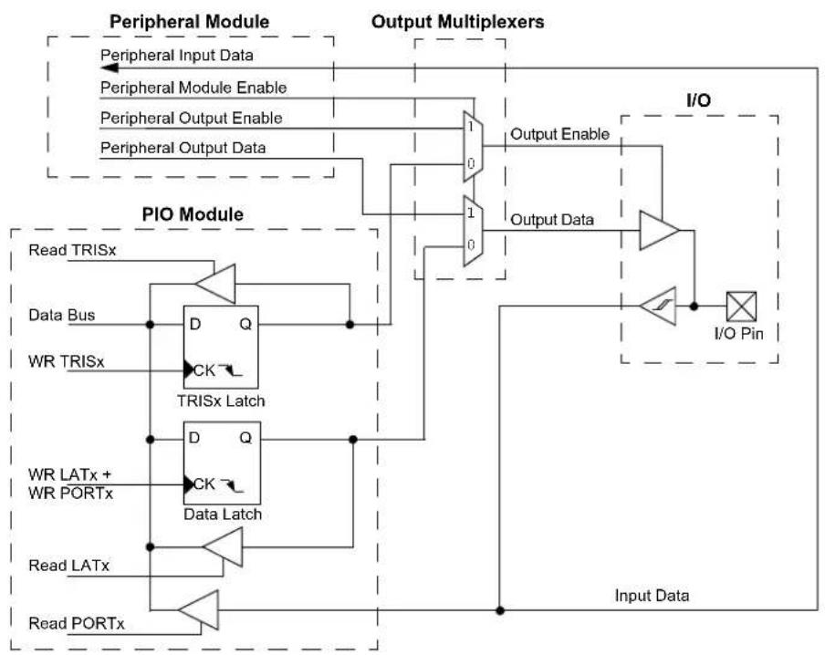
flowchart
graph TD
    subgraph Peripheral Module
        A["Peripheral Input Data"] --> B["Peripheral Module Enable"]
        B --> C["Peripheral Output Enable"]
        C --> D["Peripheral Output Data"]
    end

    subgraph Output Multiplexers
        E["1"] --> F["0"]
        G["1"] --> H["0"]
        I["0"] --> J["Output Enable"]
        K["1"] --> L["0"]
        M["I/O Pin"] --> N["I/O Pin"]
    end

    subgraph PIO Module
        O["TRISx Latch"] --> P["D Q"]
        P --> Q["Data Latch"]
        Q --> R["Read LATx"]
        Q --> S["Read PORTx"]
        T["Data Bus"] --> U["TRISx"]
        V["WR TRISx"] --> W["CK"]
        X["WR LATx + WR PORTx"] --> Y["CK"]
    end

    style Peripheral Module fill:#f9f,stroke:#333
    style Output Multiplexers fill:#ccf,stroke:#333
    style PIO Module fill:#cfc,stroke:#333
4.6.1.1 Open-Drain Configuration
In addition to the PORTx, LATx and TRISx registers for data control, port pins can also be individually configured for either digital or open-drain output. This is controlled by the Open-Drain Control x register, ODCx, associated with each port. Setting any of the bits configures the corresponding pin to act as an open-drain output.
The open-drain feature allows the generation of outputs, other than VDD, by using external pull-up resistors. The maximum open-drain voltage allowed on any pin is the same as the maximum VIH specification for that particular pin.
See the "Pin Diagrams" section for the available 5V tolerant pins and Table 24-19 for the maximum VIH specification for each pin.
4.6.2 CONFIGURING ANALOG AND DIGITAL PORT PINS
The ANSELx register controls the operation of the analog port pins. The port pins that are to function as analog inputs or outputs must have their corresponding ANSELx and TRISx bits set. In order to use port pins for I/O functionality with digital modules, such as timers, UARTs, etc., the corresponding ANSELx bit must be cleared.
The ANSELx register has a default value of 0xFFFF; therefore, all pins that share analog functions are analog (not digital) by default.
Pins with analog functions affected by the ANSELx registers are listed with a buffer type of analog in the Pinout I/O Descriptions (see Table 1-1).
If the TRISx bit is cleared (output) while the ANSELx bit is set, the digital output level (VOH or VOL) is converted by an analog peripheral, such as the ADC module or comparator module.
When the PORTx register is read, all pins configured as analog input channels are read as cleared (a low level).
Pins configured as digital inputs do not convert an analog input. Analog levels on any pin, defined as a digital input (including the ANx pins), can cause the input buffer to consume current that exceeds the device specifications.
4.6.2.1 I/O Port Write/Read Timing
One instruction cycle is required between a port direction change or port write operation and a read operation of the same port. Typically, this instruction would be a NOP, as shown in Example 4-3.
The following registers are in the PORT module:
- Register 4-25: ANSELx (one per port)
- Register 4-26: TRISx (one per port)
- Register 4-27: PORTx (one per port)
- Register 4-28: LATx (one per port)
- Register 4-29: ODCx (one per port)
- Register 4-30: CNPUx (one per port)
- Register 4-31: CNPDx (one per port)
- Register 4-32: CNCONx (one per port – optional)
- Register 4-33: CNEN0x (one per port)
- Register 4-34: CNSTATx (one per port – optional)
- Register 4-35: CNEN1x (one per port)
- Register 4-36: CNFx (one per port)
4.6.3 SECONDARY PORT CONTROL/STATUS REGISTERS
REGISTER 4-25: ANSELx: ANALOG SELECT FOR PORTx REGISTER
| R/W-1 R/W-1 R/W-1 R/W-1 R/W-1 R/W-1 R/W-1 R/W-1 |
| ANSELx[15:8] |
| bit 15 bit 8 |
| R/W-1 R/W-1 R/W-1 R/W-1 R/W-1 R/W-1 R/W-1 R/W-1 |
| ANSELx[7:0] |
| bit 7 bit 0 |
Legend:
| R = Readable bit W = Writable bit | U = Unimplemented bit, read as '0' | ||
| -n = Value at POR | '1' = Bit is set | '0' = Bit is cleared | x = Bit is unknown |
bit 15-0 ANSELx[15:0]: Analog Select for PORTx bits
1 = Analog input is enabled and digital input is disabled on PORTx[n] pin
0 = Analog input is disabled and digital input is enabled on PORTx[n] pin
REGISTER 4-26: TRISx: OUTPUT ENABLE FOR PORTx REGISTER
| R/W-1 R/W-1 R/W-1 R/W-1 R/W-1 R/W-1 R/W-1 R/W-1 |
| TRISx[15:8] |
| bit 15 bit 8 |
| R/W-1 R/W-1 R/W-1 R/W-1 R/W-1 R/W-1 R/W-1 R/W-1 |
| TRISx[7:0] |
| bit 7 bit 0 |
Legend:
| R = Readable bit W = Writable bit U = Unimplemented bit, read as '0' | ||
| -n = Value at POR | '1' = Bit is set | '0' = Bit is cleared x = Bit is unknown |
bit 15-0 TRISx[15:0]: Output Enable for PORTx bits
1 = LATx[n] is not driven on PORTx[n] pin
0 = LATx[n] is driven on PORTx[n] pin
REGISTER 4-27: PORTx: INPUT DATA FOR PORTx REGISTER
| R/W-1 | R/W-1 | R/W-1 | R/W-1 | R/W-1 | R/W-1 | R/W-1 | R/W-1 |
| PORTx[15:8] | |||||||
| bit 15 | bit 8 | ||||||
| R/W-1 | R/W-1 | R/W-1 | R/W-1 | R/W-1 | R/W-1 | R/W-1 | R/W-1 |
| PORTx[7:0] | |||||||
| bit 7 | bit 0 | ||||||
Legend:
| R = Readable bit | W = Writable bit | U = Unimplemented bit, read as '0' |
| -n = Value at POR | '1' = Bit is set | '0' = Bit is cleared x = Bit is unknown |
bit 15-0
PORTx[15:0]: PORTx Data Input Value bits
REGISTER 4-28: LATx: OUTPUT DATA FOR PORTx REGISTER
| R/W-x R/W-x R/W-x R/W-x R/W-x R/W-x R/W-x R/W-x |
| LATx[15:8] |
| bit 15 bit 8 |
| R/W-x R/W-x R/W-x R/W-x R/W-x R/W-x R/W-x R/W-x |
| LATx[7:0] |
| bit 7 bit 0 |
Legend:
| R = Readable bit W = Writable bit | U = Unimplemented bit, read as '0' | ||
| -n = Value at POR | '1' = Bit is set | '0' = Bit is cleared | x = Bit is unknown |
bit 15-0 LATx[15:0]: PORTx Data Output Value bits
REGISTER 4-29: ODCx: OPEN-DRAIN ENABLE FOR PORTx REGISTER
| R/W-0 | R/W-0 | R/W-0 | R/W-0 | R/W-0 | R/W-0 | R/W-0 | R/W-0 |
| ODCx[15:8] | |||||||
| bit 15 bit 8 | |||||||
| R/W-0 | R/W-0 | R/W-0 | R/W-0 | R/W-0 | R/W-0 | R/W-0 | R/W-0 |
| ODCx[7:0] | |||||||
| bit 7 bit 0 | |||||||
Legend:
| R = Readable bit W = Writable bit | U = Unimplemented bit, read as '0' | ||
| -n = Value at POR | '1' = Bit is set | '0' = Bit is cleared | x = Bit is unknown |
bit 15-0 ODCx[15:0]: PORTx Open-Drain Enable bits
1 = Open-drain is enabled on PORTx pin
0 = Open-drain is disabled on PORTx pin
REGISTER 4-30: CNPUx: CHANGE NOTIFICATION PULL-UP ENABLE FOR PORTx REGISTER
| R/W-0 R/W-0 R/W-0 R/W-0 R/W-0 R/W-0 R/W-0 R/W-0 |
| CNPUx[15:8] |
| bit 15 bit 8 |
| R/W-0 R/W-0 R/W-0 R/W-0 R/W-0 R/W-0 R/W-0 R/W-0 | ||
| CNPUx[7:0] | ||
| bit 7 | bit | 0 |
Legend:
| R = Readable bit W = Writable bit U = Unimplemented bit, read as '0' | ||
| -n = Value at POR | '1' = Bit is set | '0' = Bit is cleared x = Bit is unknown |
bit 15-0 CNPUx[15:0]: Change Notification Pull-up Enable for PORTx bits
1 = The pull-up for PORTx[n] is enabled – takes precedence over pull-down selection
0 = The pull-up for PORTx[n] is disabled
REGISTER 4-31: CNPDx: CHANGE NOTIFICATION PULL-DOWN ENABLE FOR PORTx REGISTER
| R/W-0 R/W-0 R/W-0 R/W-0 R/W-0 R/W-0 R/W-0 R/W-0 |
| CNPDx[15:8] |
| bit 15 bit 8 |
| R/W-0 R/W-0 R/W-0 R/W-0 R/W-0 R/W-0 R/W-0 R/W-0 | |
| CNPDx[7:0] | |
| bit 7 | bit 0 |
Legend:
| R = Readable bit W = Writable bit U = Unimplemented bit, read as '0' | ||
| -n = Value at POR | '1' = Bit is set | '0' = Bit is cleared x = Bit is unknown |
bit 15-0 CNPDx[15:0]: Change Notification Pull-Down Enable for PORTx bits
1 = The pull-down for PORTx[n] is enabled (if the pull-up for PORTx[n] is not enabled)
0 = The pull-down for PORTx[n] is disabled
REGISTER 4-32: CNCONx: CHANGE NOTIFICATION CONTROL FOR PORTx REGISTER
| R/W-0 U-0 U-0 U-0 R/W-0 U-0 U-0 U-0 | |||||||
| ON | — | — | — | CNSTYLE | — | — | — |
| bit 15 bit 8 | |||||||
| U-0 U-0 U-0 U-0 U-0 U-0 U-0 | |||||||
| — | — | — | — | — | — | — | — |
| bit 7 bit 0 | |||||||
| Legend: | |||
| R = Readable bit | W = Writable bit | U = Unimplemented bit, read as ‘0’ | |
| -n = Value at POR | ‘1’ = Bit is set | ‘0’ = Bit is cleared | x = Bit is unknown |
bit 15 ON: Change Notification (CN) Control for PORTx On bit
1 = CN is enabled
0 = CN is disabled
bit 14-12 Unimplemented: Read as '0'
bit 11 CNSTYLE: Change Notification Style Selection bit
1 = Edge style (detects edge transitions, CNFx[15:0] bits are used for a Change Notification event)
0 = Mismatch style (detects change from last port read, CNSTATx[15:0] bits are used for a Change Notification event)
bit 10-0 Unimplemented: Read as '0'
REGISTER 4-33: CNEN0x: INTERRUPT CHANGE NOTIFICATION ENABLE FOR PORTx REGISTER
| R/W-0 | R/W-0 | R/W-0 | R/W-0 | R/W-0 | R/W-0 | R/W-0 | R/W-0 |
| CNEN0x[15:8] | |||||||
| bit 15 | bit 8 | ||||||
| R/W-0 | R/W-0 | R/W-0 | R/W-0 | R/W-0 | R/W-0 | R/W-0 | R/W-0 |
| CNEN0x[7:0] | |||||||
| bit 7 | bit 0 | ||||||
| Legend: | |||
| R = Readable bit | W = Writable bit | U = Unimplemented bit, read as '0' | |
| -n = Value at POR | '1' = Bit is set | '0' = Bit is cleared | x = Bit is unknown |
bit 15-0 CNEN0x[15:0]: Interrupt Change Notification Enable for PORTx bits
1 = Interrupt-on-change (from the last read value) is enabled for PORTx[n]
0 = Interrupt-on-change is disabled for PORTx[n]
REGISTER 4-34: CNSTATx: INTERRUPT CHANGE NOTIFICATION STATUS FOR PORTx REGISTER
| R-0 R-0 R-0 R-0 R-0 R-0 R-0 R-0 |
| CNSTATx[15:8] |
| bit 15 bit 8 |
| R-0 R-0 R-0 R-0 R-0 R-0 R-0 R-0 |
| CNSTATx[7:0] |
| bit 7 bit 0 |
Legend:
| R = Readable bit W = Writable bit | U = Unimplemented bit, read as '0' | ||
| -n = Value at POR | '1' = Bit is set | '0' = Bit is cleared | x = Bit is unknown |
bit 15-0
CNSTAT[15:0]: Interrupt Change Notification Status for PORTx bits
When CNSTYLE (CNCONx[11]) = 0:
1 = Change occurred on PORTx[n] since last read of PORTx[n]
0 = Change did not occur on PORTx[n] since last read of PORTx[n]
REGISTER 4-35: CNEN1x: INTERRUPT CHANGE NOTIFICATION EDGE SELECT FOR PORTx REGISTER
| R/W-0 | R/W-0 | R/W-0 | R/W-0 | R/W-0 | R/W-0 | R/W-0 | R/W-0 |
| CNEN1x[15:8] | |||||||
| bit 15 bit 8 | |||||||
| R/W-0 | R/W-0 | R/W-0 | R/W-0 | R/W-0 | R/W-0 | R/W-0 | R/W-0 |
| CNEN1x[7:0] | |||||||
| bit 7 bit 0 | |||||||
Legend:
| R = Readable bit W = Writable bit | U = Unimplemented bit, read as '0' | ||
| -n = Value at POR | '1' = Bit is set | '0' = Bit is cleared | x = Bit is unknown |
bit 15-0
CNEN1x[15:0]: Interrupt Change Notification Edge Select for PORTx bits
REGISTER 4-36: CNFx: INTERRUPT CHANGE NOTIFICATION FLAG FOR PORTx REGISTER
| R/W-0 R/W-0 R/W-0 R/W-0 R/W-0 R/W-0 R/W-0 R/W-0 |
| CNFx[15:8] |
| bit 15 bit 8 |
| R/W-0 R/W-0 R/W-0 R/W-0 R/W-0 R/W-0 R/W-0 R/W-0 |
| CNFx[7:0] |
| bit 7 bit 0 |
Legend:
R = Readable bit W = Writable bit U = Unimplemented bit, read as '0'
-n = Value at POR
'1' = Bit is set
'0' = Bit is cleared
x = Bit is unknown
bit 15-0
CNFx[15:0]: Interrupt Change Notification Flag for PORTx bits
When CNSTYLE (CNCONx[11]) = 1:
1 = An enabled edge event occurred on PORTx[n] pin
0 = An enabled edge event did not occur on PORTx[n] pin
4.6.4 INPUT CHANGE NOTIFICATION (ICN)
The Input Change Notification function of the I/O ports allows the dsPIC33CH128MP508S1 family devices to generate interrupt requests to the processor in response to a Change-of-State (COS) on selected input pins. This feature can detect input Change-of-States, even in Sleep mode, when the clocks are disabled. Every I/O port pin can be selected (enabled) for generating an interrupt request on a Change-of-State. Five control registers are associated with the Change Notification (CN) functionality of each I/O port. To enable the Change Notification feature for the port, the ON bit (CNCONx[15]) must be set.
The CNEN0x and CNEN1x registers contain the CN interrupt enable control bits for each of the input pins. The setting of these bits enables a CN interrupt for the corresponding pins. Also, these bits, in combination with the CNSTYLE bit (CNCONx[11]), define a type of transition when the interrupt is generated. Possible CN event options are listed in Table 4-26.
The CNSTATx register indicates whether a change occurred on the corresponding pin since the last read of the PORTx bit. In addition to the CNSTATx register, the CNFx register is implemented for each port. This register contains flags for Change Notification events. These flags are set if the valid transition edge, selected in the CNEN0x and CNEN1x registers, is detected. CNFx stores the occurrence of the event. CNFx bits must be cleared in software to get the next Change Notification interrupt. The CN interrupt is generated only for the I/Os configured as inputs (corresponding TRISx bits must be set).
TABLE 4-26: CHANGE NOTIFICATION EVENT OPTIONS
| CNSTYLE Bit (CNCONx[11]) | CNEN1x Bit | CNEN0x Bit | Change Notification Event Description |
| 0 Does not matter | 0 Disabled | ||
| 0 Does not matter | 1 Detects a mismatch between the last read state and the current state of the pin | ||
| 1 | 0 | 0 | Disabled |
| 1 | 0 | 1 | Detects a positive transition only (from ‘0’ to ‘1’) |
| 1 | 1 | 0 | Detects a negative transition only (from ‘1’ to ‘0’) |
| 1 | 1 | 1 | Detects both positive and negative transitions |
Note: Pull-ups and pull-downs on Input Change Notification pins should always be disabled when the port pin is configured as a digital output.
EXAMPLE 4-3: PORT WRITE/READ EXAMPLE
| MOV 0xFF00, W0 ; Configure PORTB<15:8> | |
| ; as inputs | |
| MOV W0, TRISB | ; and PORTB<7:0> |
| ; as outputs | |
| NOP | ; Delay 1 cycle |
| BTSS PORTB, #13 | ; Next Instruction |
4.6.5 PERIPHERAL PIN SELECT (PPS)
A major challenge in general purpose devices is providing the largest possible set of peripheral features, while minimizing the conflict of features on I/O pins. The challenge is even greater on low pin count devices. In an application where more than one peripheral needs to be assigned to a single pin, inconvenient work arounds in application code, or a complete redesign, may be the only option.
Peripheral Pin Select configuration provides an alternative to these choices by enabling peripheral set selection and placement on a wide range of I/O pins. By increasing the pinout options available on a particular device, users can better tailor the device to their entire application, rather than trimming the application to fit the device.
The Peripheral Pin Select configuration feature operates over a fixed subset of digital I/O pins. Users may independently map the input and/or output of most digital peripherals to any one of these I/O pins. Hardware safeguards are included that prevent accidental or spurious changes to the peripheral mapping once it has been established.
4.6.5.1 Available Pins
The number of available pins is dependent on the particular device and its pin count. Pins that support the Peripheral Pin Select feature include the label, "S1RPn", in their full pin designation, where "n" is the remappable pin number. "S1RP" is used to designate pins that support both remappable input and output functions.
4.6.5.2 Available Peripherals
The peripherals managed by the Peripheral Pin Select are all digital only peripherals. These include general serial communications (UART and SPI), general purpose timer clock inputs, timer-related peripherals (input capture and output compare) and interrupt-on-change inputs.
In comparison, some digital only peripheral modules are never included in the Peripheral Pin Select feature. This is because the peripheral's function requires special I/O circuitry on a specific port and cannot be easily connected to multiple pins. One example includes I^2C modules. A similar requirement excludes all modules with analog inputs, such as the ADC Converter.
A key difference between remappable and non-remappable peripherals is that remappable peripherals are not associated with a default I/O pin. The peripheral must always be assigned to a specific I/O pin before it can be used. In contrast, non-remappable peripherals are always available on a default pin, assuming that the peripheral is active and not conflicting with another peripheral.
When a remappable peripheral is active on a given I/O pin, it takes priority over all other digital I/Os and digital communication peripherals associated with the pin. Priority is given regardless of the type of peripheral that is mapped. Remappable peripherals never take priority over any analog functions associated with the pin.
4.6.5.3 Controlling Configuration Changes
Because peripheral mapping can be changed during run time, some restrictions on peripheral remapping are needed to prevent accidental configuration changes. The dsPIC33CH128MP508 devices have implemented the control register lock sequence to prevent accidental changes.
4.6.5.4 Control Register Lock
Under normal operation, writes to the RPINRx and RPORx registers are not allowed. Attempted writes will appear to execute normally, but the contents of the registers will remain unchanged. To change these registers, they must be unlocked in hardware. The register lock is controlled by the IOLOCK bit (RPCON[11]).
Setting IOLOCK prevents writes to the control registers; clearing IOLOCK allows writes.
To set or clear IOLOCK, the NVMKEY unlock sequence must be executed:
- Write 0x55 to NVMKEY.
- Write 0xAA to NVMKEY.
- Clear (or set) IOLOCK as a single operation.
IOLOCK remains in one state until changed. This allows all of the Peripheral Pin Selects to be configured with a single unlock sequence, followed by an update to all of the control registers. Then, IOLOCK can be set with a second lock sequence.
4.6.5.5 Considerations for Peripheral Pin Selection
The ability to control Peripheral Pin Selection introduces several considerations into application design that most users would never think of otherwise. This is particularly true for several common peripherals, which are only available as remappable peripherals.
The main consideration is that the Peripheral Pin Selects are not available on default pins in the device's default (Reset) state. More specifically, because all RPINRx registers reset to '1's and RPORx registers reset to '0's, this means all PPS inputs are tied to Vss, while all PPS outputs are disconnected. This means that before any other application code is executed, the user must initialize the device with the proper peripheral configuration. Because the IOLOCK bit resets in the unlocked state, it is not necessary to execute the unlock sequence after the device has come out of Reset. For application safety, however, it is always better to set IOLOCK and lock the configuration after writing to the control registers.
The NVMKEY unlock sequence must be executed as an assembly language routine. If the bulk of the application is written in C, or another high-level language, the unlock sequence should be performed by writing in-line assembly or by using the _builtin_write_RPCON(value) function provided by the compiler.
Choosing the configuration requires a review of all Peripheral Pin Selects and their pin assignments, particularly those that will not be used in the application. In all cases, unused pin-selectable peripherals should be disabled completely. Unused peripherals should have their inputs assigned to an unused RPn pin function. I/O pins with unused RPn functions should be configured with the null peripheral output.
Note: MPLAB XC16 provides a built-in C language function for unlocking and modifying the RPCON register: _builtin_write_RPCON(value); For more information, see the MPLAB XC16 Help files.
The inputs of the Peripheral Pin Select options are mapped on the basis of the peripheral. That is, a control register associated with a peripheral dictates the pin it will be mapped to. The RPINRx registers are used to configure peripheral input mapping (see Register 4-38 through Register 4-61). Each register contains sets of 8-bit fields, with each set associated with one of the remappable peripherals. Programming a given peripheral's bit field with an appropriate 8-bit index value maps the S1RPn pin with the corresponding value, or internal signal, to that peripheral. See Table 4-27 for a list of available inputs.
For example, Figure 4-16 illustrates remappable pin selection for the U1RX input.
FIGURE 4-16: REMAPPABLE INPUT FOR U1RX
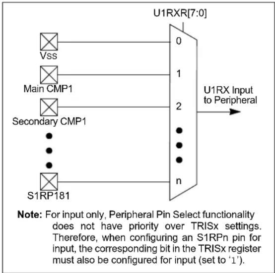
flowchart
graph LR
    A["Vss"] --> B["U1RXR[7:0"]]
    C["Main CMP1"] --> B
    D["Secondary CMP1"] --> B
    E["S1RP181"] --> B
    B --> F["U1RX Input to Peripheral"]
    style B fill:#f9f,stroke:#333
    note right of B
        Note: For input only, Peripheral Pin Select functionality does not have priority over TRISx settings. Therefore, when configuring an S1RPn pin for input, the corresponding bit in the TRISx register must also be configured for input (set to '1').
    Note
Example 4-4 provides a configuration for bidirectional communication with flow control using UART1. The following input and output functions are used:
- Input Functions: U1RX, U1CTS
• Output Functions: U1TX, U1RTS
EXAMPLE 4-4: CONFIGURING UART1 INPUT AND OUTPUT FUNCTIONS
//
**************************
// Unlock Registers
**************************
__builtin_write_RPCON(0x0000);
// **************************
// Configure Input Functions (See Table 4-28)
// Assign U1Rx To Pin RP35
// **************************
__U1RXR = 35;
// Assign U1CTS To Pin RP36
// ***************************
__U1CTSR = 36;
// **************************
// Configure Output Functions (See Table 4-31)
// **************************
// Assign U1Tx To Pin RP37
// ***************************
__RP37 = 1;
// **************************
// Assign U1RTS To Pin RP38
// ***************************
__RP38 = 2;
// **************************
// Lock Registers
// ***************************
__builtin_write_RPCON(0x0800);
TABLE 4-27: SECONDARY CORE REMAPPABLE PIN INPUTS
| RPINRx[15:8] or RPINRx[7:0] | Function Available on Ports | |
| 0 | Vss Internal | |
| 1 Main Core Comparator 1 Internal | ||
| 2 Secondary Comparator 1 Internal | ||
| 3 Secondary Comparator 2 Internal | ||
| 4 Secondary Comparator 3 Internal | ||
| 5 Main Core REFCLKO Internal | ||
| 6 Main Core PTG Trigger 30 Internal | ||
| 7 Main Core PTG Trigger 31 Internal | ||
| 8 Secondary PWM Event Output C | Internal | |
| 9 Secondary PWM Event Output D | Internal | |
| 10 | Secondary PWM Event Output E | Internal |
| 11 | Main Core PWM Event Output C | Internal |
| 12 | Main Core PWM Event Output D | Internal |
| 13 | Main Core PWM Event Output E | Internal |
| 14-31 | Reserved | Reserved |
| 32 | S1RP32 | Port Pin RB0 |
| 33 | S1RP33 | Port Pin RB1 |
| 34 | S1RP34 | Port Pin RB2 |
| 35 | S1RP35 | Port Pin RB3 |
| 36 | S1RP36 | Port Pin RB4 |
| 37 | S1RP37 | Port Pin RB5 |
| 38 | S1RP38 | Port Pin RB6 |
| 39 | S1RP39 | Port Pin RB7 |
| 40 | S1RP40 | Port Pin RB8 |
| 41 | S1RP41 | Port Pin RB9 |
| 42 | S1RP42 | Port Pin RB10 |
| 43 | S1RP43 | Port Pin RB11 |
| 44 | S1RP44 | Port Pin RB12 |
| 45 | S1RP45 | Port Pin RB13 |
| 46 | S1RP46 | Port Pin RB14 |
| 47 | S1RP47 | Port Pin RB15 |
| 48 | S1RP48 | Port Pin RC0 |
| 49 | S1RP49 | Port Pin RC1 |
| 50 | S1RP50 | Port Pin RC2 |
| 51 | S1RP51 | Port Pin RC3 |
| 52 | S1RP52 | Port Pin RC4 |
| 53 | S1RP53 | Port Pin RC5 |
| 54 | S1RP54 | Port Pin RC6 |
| 55 | S1RP55 | Port Pin RC7 |
| 56 | S1RP56 | Port Pin RC8 |
| 57 | S1RP57 | Port Pin RC9 |
| 58 | S1RP58 | Port Pin RC10 |
| 59 | S1RP59 | Port Pin RC11 |
| RPINRx[15:8] or RPINRx[7:0] | Function | Available on Ports |
| 60 S1RP60 | Port Pin RC12 | |
| 61 S1RP61 | Port Pin RC13 | |
| 62 S1RP62 | Port Pin RC14 | |
| 63 S1RP63 | Port Pin RC15 | |
| 64 S1RP64 | Port Pin RD0 | |
| 65 S1RP65 | Port Pin RD1 | |
| 66 S1RP66 | Port Pin RD2 | |
| 67 S1RP67 | Port Pin RD3 | |
| 68 S1RP68 | Port Pin RD4 | |
| 69 S1RP69 | Port Pin RD5 | |
| 70 S1RP70 | Port Pin RD6 | |
| 71 S1RP71 | Port Pin RD7 | |
| 72-161 Reserved Reserved | ||
| 162 DAC3 pwm_req_on Internal | ||
| 163 DAC3 pwm_req_off Internal | ||
| 164 DAC2 pwm_req_on Internal | ||
| 165 DAC2 pwm_req_off Internal | ||
| 166 DAC1 pwm_req_on Internal | ||
| 167 DAC1 pwm_req_off Internal | ||
| 168-169 Reserved Reserved | ||
| 170 S1RP170 Main RPV0 | ||
| 171 S1RP171 Main RPV1 | ||
| 172 S1RP172 Main RPV2 | ||
| 173 S1RP173 Main RPV3 | ||
| 174 S1RP174 Main RPV4 | ||
| 175 S1RP175 Main RPV5 | ||
| 176 S1RP176 Secondary RPV0 | ||
| 177 S1RP177 Secondary RPV1 | ||
| 178 S1RP178 Secondary RPV2 | ||
| 179 S1RP179 Secondary RPV3 | ||
| 180 S1RP180 Secondary RPV4 | ||
| 181 S1RP181 Secondary RPV5 | ||
4.6.5.7 Virtual Connections
The dsPIC33CH128MP508S1 family devices support six virtual S1RPn pins (S1RP170-S1RP175), which are identical in functionality to all other S1RPn pins, with the exception of pinouts. These six pins are internal to the devices and are not connected to a physical device pin.
These pins provide a simple way for inter-peripheral connection without utilizing a physical pin. For example, the output of the analog comparator can be connected to S1RP170 and the PWM control input can be configured for S1RP170 as well. This configuration allows the analog comparator to trigger PWM Faults without the use of an actual physical pin on the device.
4.6.5.8 Secondary PPS Inputs to Main Core PPS
The dsPIC33CH128MP508S1 Secondary core subsystem PPS has connections to the Main core subsystem virtual PPS (S1RPV5-S1RPV0) output blocks. These inputs are mapped as S1RP175, S1RP174, S1RP173, S1RP172, S1RP171 and S1RP170.
The S1RPn inputs, S1RP1-S1RP13, are connected to internal signals from both the Main and Secondary core subsystems. Additionally, the Main core virtual PPS output blocks (RPV5-RPV0) are connected to the Secondary core PPS circuitry.
There are virtual pins in PPS to share between Main and Secondary:
• RP181 is for Main input (RPV5)
• RP180 is for Main input (RPV4)
• RP179 is for Main input (RPV3)
• RP178 is for Main input (RPV2)
• RP177 is for Main input (RPV1)
- RP176 is for Main input (RPV0)
• S1RP175 is for Secondary input (S1RPV5)
• S1RP174 is for Secondary input (S1RPV4)
• S1RP173 is for Secondary input (S1RPV3)
• S1RP172 is for Secondary input (S1RPV2)
• S1RP171 is for Secondary input (S1RPV1)
• S1RP170 is for Secondary input (S1RPV0)
The idea of the S1RPVn (Remappable Pin Virtual) is to interconnect between Main and Secondary without an I/O pin. For example, the Main UART receiver can be connected to the Secondary UART transmit using S1RPVn and data communication can happen from Secondary to Main without using any physical pin.
TABLE 4-28: SELECTABLE INPUT SOURCES (MAPS INPUT TO FUNCTION)
| Input Name^(1) | Function Name Reg | ster Configuration Bits | |
| External Interrupt 1 S1INT1 RPINR0 INT1R[7:0] | |||
| External Interrupt 2 S1INT2 RPINR1 INT2R[7:0] | |||
| External Interrupt 3 S1INT3 RPINR1 INT3R[7:0] | |||
| Timer1 External Clock S1T1CK RPINR2 T1CKR[7:0] | |||
| SCCP Timer1 S1TCKI1 | RPINR3 | TCKI1R[7:0] | |
| SCCP Capture 1 | S1ICM1 | RPINR3 | ICM1R[7:0] |
| SCCP Timer2 S1TCKI2 | RPINR4 | TCKI2R[7:0] | |
| SCCP Capture 2 | S1ICM2 | RPINR4 | ICM2R[7:0] |
| SCCP Timer3 S1TCKI3 | RPINR5 | TCKI3R[7:0] | |
| SCCP Capture 3 | S1ICM3 | RPINR5 | ICM3R[7:0] |
| SCCP Timer4 S1TCKI4 | RPINR6 | TCKI4R[7:0] | |
| SCCP Capture 4 | S1ICM4 | RPINR6 | ICM4R[7:0] |
| Output Compare Fault A | S1OCFA | RPINR11 | OCFAR[7:0] |
| Output Compare Fault B | S1OCFB | RPINR11 | OCFBR[7:0] |
| PWM PCI Input 8 | S1PCI8 | RPINR12 | PCI8R[7:0] |
| PWM PCI Input 9 | S1PCI9 | RPINR12 | PCI9R[7:0] |
| PWM PCI Input 10 | S1PCI10 | RPINR13 | PCI10R[7:0] |
| PWM PCI Input 11 | S1PCI11 | RPINR13 | PCI11R[7:0] |
| QEI Input A | S1QEIA1 | RPINR14 | QEIA1R[7:0] |
| QEI Input B | S1QEIB1 | RPINR14 | QEIB1R[7:0] |
| QEI Index 1 Input | S1QEINDX1 | RPINR15 QEINDX1R[7:0] | |
| QEI Home 1 Input | S1QEIHOM1 | RPINR15 | QEIHOM1R[7:0] |
| UART1 Receive | S1U1RX | RPINR18 | U1RXR[7:0] |
| UART1 Data-Set-Ready | 1U1DSR | RPINR18 | U1DSRR[7:0] |
| SPI1 Data Input | S1SDI1 | RPINR20 | SDI1R[7:0] |
| SPI1 Clock Input | S1SCK1 | RPINR20 | SCK1R[7:0] |
| SPI1 Secondary Select | 1SS1 | RPINR21 | SS1R[7:0] |
| Reference Clock Input | S1REFOI RPINR21 | REFOIR[7:0] | |
| UART1 Clear-to-Send | 1U1CTS | RPINR23 | U1CTSR[7:0] |
| PWM PCI Input 17 | S1PCI17 | RPINR37 | PCI17R[7:0] |
| PWM PCI Input 18 | S1PCI18 | RPINR38 | PCI18R[7:0] |
| PWM PCI Input 12 | S1PCI12 | RPINR42 | PCI12R[7:0] |
| PWM PCI Input 13 | S1PCI13 | RPINR42 | PCI13R[7:0] |
| PWM PCI Input 14 | S1PCI14 | RPINR43 | PCI14R[7:0] |
| PWM PCI Input 15 | S1PCI15 | RPINR43 | PCI15R[7:0] |
| PWM PCI Input 16 | S1PCI16 | RPINR44 | PCI16R[7:0] |
| CLC Input A | S1CLCINA | RPINR45 | CLCINAR[7:0] |
| CLC Input B | S1CLCINB | RPINR46 | CLCINBR[7:0] |
| CLC Input C | S1CLCINC | RPINR46 | CLCINCR[7:0] |
| CLC Input D | S1CLCIND | RPINR47 | CLCINDR[7:0] |
| ADC External Trigger Input (ADTRIG31) | S1ADCTRG | RPINR47 | ADCTRGR[7:0] |
Note 1: Unless otherwise noted, all inputs use the Schmitt Trigger input buffers.
TABLE 4-29: SECONDARY PPS INPUT CONTROL REGISTERS
| Register | Bit 15 Bit 14 Bit | Bit 13 Bit 12 Bit | Bit 11 Bit 10 Bit 9 | Bit 8 Bit 7 Bit 6 | Bit 5 Bit 4 Bit | Bit 3 Bit 2 Bit 1 Bit 0 | ||||||||||
| RPCONL | — | — | — | — | IOLOCK | — | — | — | — | — | — | — | — | — | — | — |
| RPINR0 | INT1R7 | INT1R6 | INT1R5 | INT1R4 | INT1R3 | INT1R2 | INT1R1 | INT1R0 | — | — | — | — | — | — | — | — |
| RPINR1 | INT3R7 | INT3R6 | INT3R5 | INT3R4 | INT3R3 | INT3R2 | INT3R1 | INT3R0 | INT2R7 | INT2R6 | INT2R5 | INT2R4 | INT2R3 | INT2R2 | INT2R1 | INT2R0 |
| RPINR2 | T1CKR7 | T1CKR6 | T1CKR5 | T1CKR4 | T1CKR3 | T1CKR2 | T1CKR1 | T1CKR0 | — | — | — | — | — | — | — | — |
| RPINR3 | ICM1R7 | ICM1R6 | ICM1R5 | ICM1R4 | ICM1R3 | ICM1R2 | ICM1R1 | ICM1R0 | TCKI1R7 | TCKI1R6 | TCKI1R5 | TCKI1R4 | TCKI1R3 | TCKI1R2 | TCKI1R1 | TCKI1R0 |
| RPINR4 | ICM2R7 | ICM2R6 | ICM2R5 | ICM2R4 | ICM2R3 | ICM2R2 | ICM2R1 | ICM2R0 | TCKI2R7 | TCKI2R6 | TCKI2R5 | TCKI2R4 | TCKI2R3 | TCKI2R2 | TCKI2R1 | TCKI2R0 |
| RPINR5 | ICM3R7 | ICM3R6 | ICM3R5 | ICM3R4 | ICM3R3 | ICM3R2 | ICM3R1 | ICM3R0 | TCKI3R7 | TCKI3R6 | TCKI3R5 | TCKI3R4 | TCKI3R3 | TCKI3R2 | TCKI3R1 | TCKI3R0 |
| RPINR6 | ICM4R7 | ICM4R6 | ICM4R5 | ICM4R4 | ICM4R3 | ICM4R2 | ICM4R1 | ICM4R0 | TCKI4R7 | TCKI4R6 | TCKI4R5 | TCKI4R4 | TCKI4R3 | TCKI4R2 | TCKI4R1 | TCKI4R0 |
| RPINR11 | OCFBR7 | OCFBR6 | OCFBR5 | OCFBR4 | OCFBR3 | OCFBR2 | OCFBR1 | OCFBR0 | OCFAR7 | OCFAR6 | OCFAR5 | OCFAR4 | OCFAR3 | OCFAR2 | OCFAR1 | OCFAR0 |
| RPINR12 | PCI9R7 | PCI9R6 | PCI9R5 | PCI9R4 | PCI9R3 | PCI9R2 | PCI9R1 | PCI9R0 | PCI8R7 | PCI8R6 | PCI8R5 | PCI8R4 | PCI8R3 | PCI8R2 | PCI8R1 | PCI8R0 |
| RPINR13 | PCI11R7 | PCI11R6 | PCI11R5 | PCI11R4 | PCI11R3 | PCI11R2 | PCI11R1 | PCI11R0 | PCI10R7 | PCI10R6 | PCI10R5 | PCI10R4 | PCI10R3 | PCI10R2 | PCI10R1 | PCI10R0 |
| RPINR14 | QEIB1R7 | QEIB1R6 | QEIB1R5 | QEIB1R4 | QEIB1R3 | QEIB1R2 | QEIB1R1 | QEIB1R0 | QEIA1R7 | QEIA1R6 | QEIA1R5 | QEIA1R4 | QEIA1R3 | QEIA1R2 | QEIA1R1 | QEIA1R0 |
| RPINR15 | QEIHOM1R7 | QEIHOM1R6 | QEIHOM1R5 | QEIHOM1R4 | QEIHOM1R3 | QEIHOM1R2 | QEIHOM1R1 | QEIHOM1R0 | QEINDX1R7 | QEINDX1R6 | QEINDX1R5 | QEINDX1R4 | QEINDX1R3 | QEINDX1R2 | QEINDX1R1 | QEINDX1R0 |
| RPINR18 | U1DSRR7 | U1DSRR6 | U1DSRR5 | U1DSRR4 | U1DSRR3 | U1DSRR2 | U1DSRR1 | U1DSRR0 | U1RXR7 | U1RXR6 | U1RXR5 | U1RXR4 | U1RXR3 | U1RXR2 | U1RXR1 | U1RXR0 |
| RPINR20 | SCK1R7 | SCK1R6 | SCK1R5 | SCK1R4 | SCK1R3 | SCK1R2 | SCK1R1 | SCK1R0 | SDI1R7 | SDI1R6 | SDI1R5 | SDI1R4 | SDI1R3 | SDI1R2 | SDI1R1 | SDI1R0 |
| RPINR21 | REFOIR7 | REFOIR6 | REFOIR5 | REFOIR4 | REFOIR3 | REFOIR2 | REFOIR1 | REFOIR0 | SS1R7 | SS1R6 | SS1R5 | SS1R4 | SS1R3 | SS1R2 | SS1R1 | SS1R0 |
| RPINR23 | U1CTSR7 | U1CTSR6 | U1CTSR5 | U1CTSR4 | U1CTSR3 | U1CTSR2 | U1CTSR1 | U1CTSR0 | — | — | — | — | — | — | — | — |
| RPINR37 | PCI17R7 | PCI17R6 | PCI17R5 | PCI17R4 | PCI17R3 | PCI17R2 | PCI17R1 | PCI17R0 | — | — | — | — | — | — | — | — |
| RPINR38 | — | — | — | — | — | — | — | — | PCI18R7 | PCI18R6 | PCI18R5 | PCI18R4 | PCI18R3 | PCI18R2 | PCI18R1 | PCI18R0 |
| RPINR42 | PCI13R7 | PCI13R6 | PCI13R5 | PCI13R4 | PCI13R3 | PCI13R2 | PCI13R1 | PCI13R0 | PCI12R7 | PCI12R6 | PWM12R5 | PWM12R4 | PWM12R3 | PWM12R2 | PWM12R1 | PWM12R0 |
| RPINR43 | PCI15R7 | PCI15R6 | PCI15R5 | PCI15R4 | PCI15R3 | PCI15R2 | PCI15R1 | PCI15R0 | PCI14R7 | PCI14R6 | PCI14R5 | PCI14R4 | PCI14R3 | PCI14R2 | PCI14R1 | PCI14R0 |
| RPINR44 | — | — | — | — | — | — | — | — | PCI16R7 | PCI16R6 | PCI16R5 | PCI16R4 | PCI16R3 | PCI16R2 | PCI16R1 | PCI16R0 |
| RPINR45 | CLCINAR7 | CLCINAR6 | CLCINAR5 | CLCINAR4 | CLCINAR3 | CLCINAR2 | CLCINAR1 | CLCINAR0 | — | — | — | — | — | — | — | — |
| RPINR46 | CLCINCR7 | CLCINCR6 | CLCINCR5 | CLCINCR4 | CLCINCR3 | CLCINCR2 | CLCINCR1 | CLCINCR0 | CLCINBR7 | CLCINBR6 | CLCINBR5 | CLCINBR4 | CLCINBR3 | CLCINBR2 | CLCINBR1 | CLCINBR0 |
| RPINR47 | ADCTRGR7 | ADCTRGR6 | ADCTRGR5 | ADCTRGR4 | ADCTRGR3 | ADCTRGR2 | ADCTRGR1 | ADCTRGR0 | CLCINDR7 | CLCINDR6 | CLCINDR5 | CLCINDR4 | CLCINDR3 | CLCINDR2 | CLCINDR1 | CLCINDR0 |
4.6.5.9 Output Mapping
In contrast to inputs, the outputs of the Peripheral Pin Select options are mapped on the basis of the pin. In this case, a control register associated with a particular pin dictates the peripheral output to be mapped. The RPORx registers are used to control output mapping. Each register contains sets of 6-bit fields, with each set associated with one S1RPn pin (see Register 4-62 through Register 4-84). The value of the bit field corresponds to one of the peripherals and that peripheral's output is mapped to the pin (see Table 4-31 and Figure 4-17).
A null output is associated with the PPS Output register Reset value of '0'. This is done to ensure that remappable outputs remain disconnected from all output pins by default.
FIGURE 4-17: MULTIPLEXING REMAPPABLE OUTPUTS FOR S1RPn
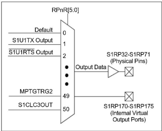
flowchart
graph TD
    A["S1U1TX Output"] --> B["Default"]
    C["S1U1RTS Output"] --> D["Default"]
    E["MPTGTRG2"] --> F["Output Data"]
    G["S1CLC3OUT"] --> H["Output Data"]
    I["RPnR[5:0"]] --> J["S1RP32-S1RP71 (Physical Pins)"]
    K["S1RP170-S1RP175 (Internal Virtual Output Ports)"] --> L["S1RP170-S1RP175 (Internal Virtual Output Ports)"]
Note 1: There are six virtual output ports which are not connected to any I/O ports (S1RP170-S1RP175). These virtual ports can be accessed by RPOR20, RPOR21 and RPOR22.
4.6.5.10 Mapping Limitations
The control schema of the peripheral select pins is not limited to a small range of fixed peripheral configurations. There are no mutual or hardware-enforced lockouts between any of the peripheral mapping SFRs. Literally any combination of peripheral mappings, across any or all of the S1RPn pins, is possible. This includes both many-to-one and one-to-many mappings of peripheral inputs, and outputs to pins. While such mappings may be technically possible from a configuration point of view, they may not be supportable from an electrical point of view.
TABLE 4-30: SECONDARY REMAPPABLE OUTPUT PIN REGISTERS
| Register S1RP Pin I/O Port | ||
| RPOR0[5:0] S1RP32 Port Pin S1RB0 | ||
| RPOR0[13:8] S1RP33 Port Pin S1RB1 | ||
| RPOR1[5:0] S1RP34 Port Pin S1RB2 | ||
| RPOR1[13:8] S1RP35 Port Pin S1RB3 | ||
| RPOR2[5:0] S1RP36 Port Pin S1RB4 | ||
| RPOR2[13:8] S1RP37 Port Pin S1RB5 | ||
| RPOR3[5:0] S1RP38 Port Pin S1RB6 | ||
| RPOR3[13:8] S1RP39 Port Pin S1RB7 | ||
| RPOR4[5:0] S1RP40 Port Pin S1RB8 | ||
| RPOR4[13:8] S1RP41 Port Pin S1RB9 | ||
| RPOR5[5:0] S1RP42 Port Pin S1RB10 | ||
| RPOR5[13:8] S1RP43 Port Pin S1RB11 | ||
| RPOR6[5:0] S1RP44 Port Pin S1RB12 | ||
| RPOR6[13:8] S1RP45 Port Pin S1RB13 | ||
| RPOR7[5:0] S1RP46 Port Pin S1RB14 | ||
| RPOR7[13:8] S1RP47 Port Pin S1RB15 | ||
| RPOR8[5:0] S1RP48 Port Pin S1RC0 | ||
| RPOR8[13:8] S1RP49 Port Pin S1RC1 | ||
| RPOR9[5:0] S1RP50 Port Pin S1RC2 | ||
| RPOR9[13:8] S1RP51 Port Pin S1RC3 | ||
| RPOR10[5:0] S1RP52 Port Pin S1RC4 | ||
| RPOR10[13:8] S1RP53 Port Pin S1RC5 | ||
| RPOR11[5:0] S1RP54 Port Pin S1RC6 | ||
| RPOR11[13:8] S1RP55 Port Pin S1RC7 | ||
| RPOR12[5:0] S1RP56 Port Pin S1RC8 | ||
| RPOR12[13:8] S1RP57 Port Pin S1RC9 | ||
| RPOR13[5:0] S1RP58 Port Pin S1RC10 | ||
| RPOR13[13:8] S1RP59 Port Pin S1RC11 | ||
| RPOR14[5:0] S1RP60 Port Pin S1RC12 | ||
| RPOR14[13:8] S1RP61 Port Pin S1RC13 | ||
| RPOR15[5:0] S1RP62 Port Pin S1RC14 | ||
| RPOR15[13:8] S1RP63 Port Pin S1RC15 | ||
| RPOR16[5:0] S1RP64 Port Pin S1RD0 | ||
| RPOR16[13:8] S1RP65 Port Pin S1RD1 | ||
| RPOR17[5:0] S1RP66 Port Pin S1RD2 | ||
| RPOR17[13:8] S1RP67 Port Pin S1RD3 | ||
| RPOR18[5:0] S1RP68 Port Pin S1RD4 | ||
| RPOR18[13:8] S1RP69 Port Pin S1RD5 | ||
| RPOR19[5:0] S1RP70 Port Pin S1RD6 | ||
| RPOR19[13:8] S1RP71 Port Pin S1RD7 | ||
| RPOR20[5:0] S1RP170 | Virtual Pin S1RPV0 | |
| RPOR20[13:8] S1RP171 | Virtual Pin S1RPV1 | |
| RPOR21[5:0] S1RP172 | Virtual Pin S1RPV2 | |
| RPOR21[13:8] S1RP173 | Virtual Pin S1RPV3 | |
| RPOR22[5:0] S1RP174 | Virtual Pin S1RPV4 | |
| RPOR22[13:8] S1RP175 | Virtual Pin S1RPV5 | |
TABLE 4-31: OUTPUT SELECTION FOR REMAPPABLE PINS (S1RPn)
| Function RPnR[5:0] Output Name | ||
| Default PORT | 0 | S1RPn tied to Default Pin |
| S1U1TX 1 S1RPn tied to UART1 Transmit | ||
| 1U1RTS | 2 | S1RPn tied to UART1 Request-to-Send |
| S1SDO1 3 S1RPn tied to SPI1 Data Output | ||
| S1SCK1OUT 6 S1RPn tied to SPI1 Clock Output | ||
| 1SS1OUT | 7 | S1RPn tied to SPI1 Secondary Select |
| S1REFCLKO 14 S1RPn tied to Reference Clock Output | ||
| S1OCM1 | 15 S1RPn tied to SCCP1 Output | |
| S1OCM2 | 16 S1RPn tied to SCCP2 Output | |
| S1OCM3 | 17 S1RPn tied to SCCP3 Output | |
| S1OCM4 | 18 S1RPn tied to SCCP4 Output | |
| S1CMP1 | 23 S1RPn tied to Comparator 1 Output | |
| S1CMP2 | 24 S1RPn tied to Comparator 2 Output | |
| S1CMP3 | 25 S1RPn tied to Comparator 3 Output | |
| S1PWMH4 | 34 S1RPn tied to PWM4H Output | |
| S1PWML4 | 35 S1RPn tied to PWM4L Output | |
| S1PWMEA | 36 S1RPn tied to PWM Event A Output | |
| S1PWMEB | 37 S1RPn tied to PWM Event B Output | |
| S1QEICMP1 | 38 S1RPn tied to QEI Comparator Output | |
| S1CLC1OUT | 40 S1RPn tied to CLC1 Output | |
| S1CLC2OUT | 41 S1RPn tied to CLC2 Output | |
| S1PWMEC | 44 S1RPn tied to PWM Event C Output | |
| S1PWMED | 45 S1RPn tied to PWM Event D Output | |
| MPTGTRG1 | 46 Main PTG24 Output | |
| MPTGTRG2 | 47 | Main PTG25 Output |
| S1CLC3OUT | 50 S1RPn tied to CLC3 Output | |
TABLE 4-32: SECONDARY PPS OUTPUT CONTROL REGISTERS
| Register Bit 15 Bit 14 Bit 13 Bit 12 Bit 11 Bit 10 Bit 9 Bit 8 Bit 7 Bit 6 Bit 5 Bit 4 Bit 3 Bit 2 Bit 1 Bit 0 | ||||||||||||||||
| RPOR0 | — | — | RP33R5 | RP33R4 | RP33R3 | RP33R2 | RP33R1 | RP33R0 | — | — | RP32R5 | RP32R4 | RP32R3 | RP32R2 | RP32R1 | RP32R0 |
| RPOR1 | — | — | RP35R5 | RP35R4 | RP35R3 | RP35R2 | RP35R1 | RP35R0 | — | — | RP34R5 | RP34R4 | RP34R3 | RP34R2 | RP34R1 | RP34R0 |
| RPOR2 | — | — | RP37R5 | RP37R4 | RP37R3 | RP37R2 | RP37R1 | RP37R0 | — | — | RP36R5 | RP36R4 | RP36R3 | RP36R2 | RP36R1 | RP36R0 |
| RPOR3 | — | — | RP39R5 | RP39R4 | RP39R3 | RP39R2 | RP39R1 | RP39R0 | — | — | RP38R5 | RP38R4 | RP38R3 | RP38R2 | RP38R1 | RP38R0 |
| RPOR4 | — | — | RP41R5 | RP41R4 | RP41R3 | RP41R2 | RP41R1 | RP41R0 | — | — | RP40R5 | RP40R4 | RP40R3 | RP40R2 | RP40R1 | RP40R0 |
| RPOR5 | — | — | RP43R5 | RP43R4 | RP43R3 | RP43R2 | RP43R1 | RP43R0 | — | — | RP42R5 | RP42R4 | RP42R3 | RP42R2 | RP42R1 | RP42R0 |
| RPOR6 | — | — | RP45R5 | RP45R4 | RP45R3 | RP45R2 | RP45R1 | RP45R0 | — | — | RP44R5 | RP44R4 | RP44R3 | RP44R2 | RP44R1 | RP44R0 |
| RPOR7 | — | — | RP47R5 | RP47R4 | RP47R3 | RP47R2 | RP47R1 | RP47R0 | — | — | RP46R5 | RP46R4 | RP46R3 | RP46R2 | RP46R1 | RP46R0 |
| RPOR8 | — | — | RP49R5 | RP49R4 | RP49R3 | RP49R2 | RP49R1 | RP49R0 | — | — | RP48R5 | RP48R4 | RP48R3 | RP48R2 | RP48R1 | RP48R0 |
| RPOR9 | — | — | RP51R5 | RP51R4 | RP51R3 | RP51R2 | RP51R1 | RP51R0 | — | — | RP50R5 | RP50R4 | RP50R3 | RP50R2 | RP50R1 | RP50R0 |
| RPOR10 | — | — | RP53R5 | RP53R4 | RP53R3 | RP53R2 | RP53R1 | RP53R0 | — | — | RP52R5 | RP52R4 | RP52R3 | RP52R2 | RP52R1 | RP52R0 |
| RPOR11 | — | — | RP55R5 | RP55R4 | RP55R3 | RP55R2 | RP55R1 | RP55R0 | — | — | RP54R5 | RP54R4 | RP54R3 | RP54R2 | RP54R1 | RP54R0 |
| RPOR12 | — | — | RP57R5 | RP57R4 | RP57R3 | RP57R2 | RP57R1 | RP57R0 | — | — | RP56R5 | RP56R4 | RP56R3 | RP56R2 | RP56R1 | RP56R0 |
| RPOR13 | — | — | RP59R5 | RP59R4 | RP59R3 | RP59R2 | RP59R1 | RP59R0 | — | — | RP58R5 | RP58R4 | RP58R3 | RP58R2 | RP58R1 | RP58R0 |
| RPOR14 | — | — | RP61R5 | RP61R4 | RP61R3 | RP61R2 | RP61R1 | RP61R0 | — | — | RP60R5 | RP60R4 | RP60R3 | RP60R2 | RP60R1 | RP60R0 |
| RPOR15 | — | — | RP63R5 | RP63R4 | RP63R3 | RP63R2 | RP63R1 | RP63R0 | — | — | RP62R5 | RP62R4 | RP62R3 | RP62R2 | RP62R1 | RP62R0 |
| RPOR16 | — | — | RP65R5 | RP65R4 | RP65R3 | RP65R2 | RP65R1 | RP65R0 | — | — | RP64R5 | RP64R4 | RP64R3 | RP64R2 | RP64R1 | RP64R0 |
| RPOR17 | — | — | RP67R5 | RP67R4 | RP67R3 | RP67R2 | RP67R1 | RP67R0 | — | — | RP66R5 | RP66R4 | RP66R3 | RP66R2 | RP66R1 | RP66R0 |
| RPOR18 | — | — | RP69R5 | RP69R4 | RP69R3 | RP69R2 | RP69R1 | RP69R0 | — | — | RP68R5 | RP68R4 | RP68R3 | RP68R2 | RP68R1 | RP68R0 |
| RPOR19 | — | — | RP71R5 | RP71R4 | RP71R3 | RP71R2 | RP71R1 | RP71R0 | — | — | RP70R5 | RP70R4 | RP70R3 | RP70R2 | RP70R1 | RP70R0 |
| RPOR20^(1) | — | — | RP171R5 | RP171R4 | RP171R3 | RP177R2 | RP171R1 | RP171R0 | — | — | RP170R5 | RP170R4 | RP170R3 | RP170R2 | RP170R1 | RP170R0 |
| RPOR21^(1) | — | — | RP173R5 | RP173R4 | RP173R3 | RP173R2 | RP173R1 | RP173R0 | — | — | RP172R5 | RP172R4 | RP172R3 | RP172R2 | RP172R1 | RP172R0 |
| RPOR22^(1) | — | — | RP175R5 | RP175R4 | RP175R3 | RP175R2 | RP175R1 | RP175R0 | — | — | RP174R5 | RP174R4 | RP174R3 | RP174R2 | RP174R1 | RP174R0 |
Note 1: The RPOR20, RPOR21 and RPOR22 registers are for virtual output pins.
4.6.6 I/O HELPFUL TIPS
-
In some cases, certain pins, as defined in Table 24-19 under "Injection Current", have internal protection diodes to VDD and Vss. The term, "Injection Current", is also referred to as "Clamp Current". On designated pins, with sufficient external current-limiting precautions by the user, I/O pin input voltages are allowed to be greater or lesser than the data sheet absolute maximum ratings, with respect to the Vss and VDD supplies. Note that when the user application forward biases either of the high or low-side internal input clamp diodes, that the resulting current being injected into the device, that is clamped internally by the VDD and Vss power rails, may affect the ADC accuracy by four to six counts.
-
I/O pins that are shared with any analog input pin (i.e., ANx) are always analog pins, by default, after any Reset. Consequently, configuring a pin as an analog input pin automatically disables the digital input pin buffer and any attempt to read the digital input level by reading PORTx or LATx will always return a '0', regardless of the digital logic level on the pin. To use a pin as a digital I/O pin on a shared ANx pin, the user application needs to configure the Analog Select for PORTx registers, in the I/O ports module (i.e., ANSELx), by setting the appropriate bit that corresponds to that I/O port pin to a '0'.
Note: Although it is not possible to use a digital input pin when its analog function is enabled, it is possible to use the digital I/O output function, TRISx = 0x0, while the analog function is also enabled. However, this is not recommended, particularly if the analog input is connected to an external analog voltage source, which would create signal contention between the analog signal and the output pin driver.
-
Most I/O pins have multiple functions. Referring to the device pin diagrams in this data sheet, the priorities of the functions allocated to any pins are indicated by reading the pin name, from left-to-right. The left most function name takes precedence over any function to its right in the naming convention. For example: AN16/T2CK/T7CK/RC1; this indicates that AN16 is the highest priority in this example and will supersede all other functions to its right in the list. Those other functions to its right, even if enabled, would not work as long as any other function to its left was enabled. This rule applies to all of the functions listed for a given pin.
-
Each pin has an internal weak pull-up resistor and pull-down resistor that can be configured using the CNPUx and CNPDx registers, respectively. These resistors eliminate the need for external resistors in certain applications. The internal pull-up is up to \~(VDD - 0.8), not VDD. This value is still above the minimum VIH of CMOS and TTL devices.
-
When driving LEDs directly, the I/O pin can source or sink more current than what is specified in the VOH/IOH and VOL/IOL DC characteristics specification. The respective IOH and IOL current rating only applies to maintaining the corresponding output at or above the VOH, and at or below the VOL levels. However, for LEDs, unlike digital inputs of an externally connected device, they are not governed by the same minimum VIH/VIIL levels. An I/O pin output can safely sink or source any current less than that listed in the Absolute Maximum Ratings in Section 24.0, Electrical Characteristics of this data sheet. For example:
V_OH = 2.4v @ I_OH = -8 mA and V_DD = 3.3V
The maximum output current sourced by any 8 mA I/O pin = 12 mA.
LED source current < 12 mA is technically permitted.
- The Peripheral Pin Select (PPS) pin mapping rules are as follows:
a) Only one "output" function can be active on a given pin at any time, regardless if it is a dedicated or remappable function (one pin, one output).
b) It is possible to assign a "remappable output" function to multiple pins and externally short or tie them together for increased current drive.
c) If any "dedicated output" function is enabled on a pin, it will take precedence over any remappable "output" function.
d) If any "dedicated digital" (input or output) function is enabled on a pin, any number of "input" remappable functions can be mapped to the same pin.
e) If any “dedicated analog” function(s) are enabled on a given pin, “digital input(s)” of any kind will all be disabled, although a single “digital output”, at the user's cautionary discretion, can be enabled and active as long as there is no signal contention with an external analog input signal. For example, it is possible for the ADC to convert the digital output logic level, or to toggle a digital output on a comparator or ADC input, provided there is no external analog input, such as for a Built-In Self-Test.
f) Any number of "input" remappable functions can be mapped to the same pin(s) at the same time, including to any pin with a single output from either a dedicated or remappable "output".
g) The TRISx registers control only the digital I/O output buffer. Any other dedicated or remappable active "output" will automatically override the TRISx setting. The TRISx register does not control the digital logic "input" buffer. Remappable digital "inputs" do not automatically override TRISx settings, which means that the TRISx bit must be set to input for pins with only remappable input function(s) assigned.
h) All analog pins are enabled by default after any Reset and the corresponding digital input buffer on the pin has been disabled. Only the Analog Select for PORTx (ANSELx) registers control the digital input buffer, not the TRISx register. The user must disable the analog function on a pin using the Analog Select for PORTx registers in order to use any "digital input(s)" on a corresponding pin, no exceptions.
4.6.7 I/O PORTS RESOURCES
Many useful resources are provided on the main product page of the Microchip website for the devices listed in this data sheet. This product page contains the latest updates and additional information.
4.6.7.1 Key Resources
- "I/O Ports with Edge Detect" (www.microchip.com/DS70005322)
- Code Samples
- Application Notes
- Software Libraries
- Webinars
- All Related "dsPIC33/PIC24 Family Reference Manual" Sections
- Development Tools
4.6.8 PERIPHERAL PIN SELECT REGISTERS
REGISTER 4-37: RPCON: PERIPHERAL REMAPPING CONFIGURATION REGISTER
| R = Readable bit | W = Writable bit | U = Unimplemented bit, read as '0' |
| -n = Value at POR | '1' = Bit is set | '0' = Bit is cleared x = Bit is unknown |
bit 15-12 Unimplemented: Read as '0'
bit 11 IOLOCK: Peripheral Remapping Register Lock bit
1 = All Peripheral Remapping registers are locked and cannot be written
0 = All Peripheral Remapping registers are unlocked and can be written
bit 10-0 Unimplemented: Read as '0'
REGISTER 4-38: RPINR0: PERIPHERAL PIN SELECT INPUT REGISTER 0
| R/W-0 | R/W-0 | R/W-0 | R/W-0 | R/W-0 | R/W-0 | R/W-0 | R/W-0 |
| INT1R7 | INT1R6 | INT1R5 | INT1R4 | INT1R3 | INT1R2 | INT1R1 | INT1R0 |
| bit 15 bit 8 | |||||||
| R = Readable bit | W = Writable bit | U = Unimplemented bit, read as '0' |
| -n = Value at POR | '1' = Bit is set | '0' = Bit is cleared x = Bit is unknown |
bit 15-8 INT1R[7:0]: Assign External Interrupt 1 (S1INT1) to the Corresponding S1RPn Pin bits See Table 4-27.
bit 7-0 Unimplemented: Read as '0'
REGISTER 4-39: RPINR1: PERIPHERAL PIN SELECT INPUT REGISTER 1
| R/W-0 R/W-0 R/W-0 R/W-0 R/W-0 R/W-0 R/W-0 | |||||||
| INT3R15 | INT3R14 | INT3R13 | INT3R12 | INT3R11 | INT3R10 | INT3R9 | INT3R8 |
| bit 15 bit 8 | |||||||
| R/W-0 R/W-0 R/W-0 R/W-0 R/W-0 R/W-0 R/W-0 R/W-0 | |||||||
| INT2R7 | INT2R6 | INT2R5 | INT2R4 | INT2R3 | INT2R2 | INT2R1 | INT2R0 |
| bit 7 bit 0 | |||||||
Legend:
| R = Readable bit | W = Writable bit | U = Unimplemented bit, read as ‘0’ |
| -n = Value at POR | ‘1’ = Bit is set | ‘0’ = Bit is cleared x = Bit is unknown |
bit 15-8 INT3R[15:8]: Assign External Interrupt 3 (S1INT3) to the Corresponding S1RPn Pin bits See Table 4-27.
bit 7-0 INT2R[7:0]: Assign External Interrupt 2 (S1INT2) to the Corresponding S1RPn Pin bits See Table 4-27.
REGISTER 4-40: RPINR2: PERIPHERAL PIN SELECT INPUT REGISTER 2
| R/W-0 R/W-0 R/W-0 R/W-0 R/W-0 R/W-0 R/W-0 | |||||||
| T1CKR7 | T1CKR6 | T1CKR5 | T1CKR4 | T1CKR3 | T1CKR2 | T1CKR1 | T1CKR0 |
| bit 15 bit 8 | |||||||
| R = Readable bit | W = Writable bit | U = Unimplemented bit, read as '0' |
| -n = Value at POR | '1' = Bit is set | '0' = Bit is cleared x = Bit is unknown |
bit 15-8 T1CKR[7:0]: Assign Timer1 External Clock (S1T1CK) to the Corresponding S1RPn Pin bits See Table 4-27.
bit 7-0 Unimplemented: Read as '0'
REGISTER 4-41: RPINR3: PERIPHERAL PIN SELECT INPUT REGISTER 3
| R/W-0 R/W-0 R/W-0 R/W-0 R/W-0 R/W-0 R/W-0 | |||||||
| ICM1R7 | ICM1R6 | ICM1R5 | ICM1R4 | ICM1R3 | ICM1R2 | ICM1R1 | ICM1R0 |
| bit 15 bit 8 | |||||||
| R/W-0 R/W-0 R/W-0 R/W-0 R/W-0 R/W-0 R/W-0 R/W-0 | |||||||
| TCKI1R7 | TCKI1R6 | TCKI1R5 | TCKI1R4 | TCKI1R3 | TCKI1R2 | TCKI1R1 | TCKI1R0 |
| bit 7 bit 0 | |||||||
Legend:
| R = Readable bit | W = Writable bit | U = Unimplemented bit, read as ‘0’ |
| -n = Value at POR | ‘1’ = Bit is set | ‘0’ = Bit is cleared x = Bit is unknown |
bit 15-8 ICM1R[7:0]: Assign SCCP Capture 1 (S1ICM1) to the Corresponding S1RPn Pin bits See Table 4-27.
bit 7-0 TCKI1R[7:0]: Assign SCCP Timer1 (S1TCKI1) to the Corresponding S1RPn Pin bits See Table 4-27.
REGISTER 4-42: RPINR4: PERIPHERAL PIN SELECT INPUT REGISTER 4
| R/W-0 R/W-0 R/W-0 R/W-0 R/W-0 R/W-0 R/W-0 | |||||||
| ICM2R7 | ICM2R6 | ICM2R5 | ICM2R4 | ICM2R3 | ICM2R2 | ICM2R1 | ICM2R0 |
| bit 15 bit 8 | |||||||
| R/W-0 R/W-0 R/W-0 R/W-0 R/W-0 R/W-0 R/W-0 R/W-0 | |||||||
| TCKI2R7 | TCKI2R6 | TCKI2R5 | TCKI2R4 | TCKI2R3 | TCKI2R2 | TCKI2R1 | TCKI2R0 |
| bit 7 bit 0 | |||||||
Legend:
| R = Readable bit | W = Writable bit | U = Unimplemented bit, read as '0' |
| -n = Value at POR | '1' = Bit is set | '0' = Bit is cleared x = Bit is unknown |
bit 15-8 ICM2R[7:0]: Assign SCCP Capture 2 (S1ICM2) to the Corresponding S1RPn Pin bits See Table 4-27.
bit 7-0 TCKI2R[7:0]: Assign SCCP Timer2 (S1TCKI2) to the Corresponding S1RPn Pin bits See Table 4-27.
REGISTER 4-43: RPINR5: PERIPHERAL PIN SELECT INPUT REGISTER 5
| R/W-0 R/W-0 R/W-0 R/W-0 R/W-0 R/W-0 R/W-0 R/W-0 | |||||||
| ICM3R7 ICM3R6 ICM3R5 | ICM3R4 ICM3R3 ICM3R2 | ICM3R1 | ICM3R0 | ||||
| bit 15 bit 8 | |||||||
| R/W-0 R/W-0 R/W-0 R/W-0 R/W-0 R/W-0 R/W-0 R/W-0 | |||||||
| TCKI3R7 | TCKI3R6 | TCKI3R5 | TCKI3R4 | TCKI3R3 | TCKI3R2 | TCKI3R1 | TCKI3R0 |
| bit 7 bit 0 | |||||||
| Legend: | |||
| R = Readable bit | W = Writable bit | U = Unimplemented bit, read as ‘0’ | |
| -n = Value at POR | ‘1’ = Bit is set | ‘0’ = Bit is cleared | x = Bit is unknown |
bit 15-8 ICM3R[7:0]: Assign SCCP Capture 3 (S1ICM3) to the Corresponding S1RPn Pin bits See Table 4-27.
bit 7-0 TCKI3R[7:0]: Assign SCCP Timer3 (S1TCKI3) to the Corresponding S1RPn Pin bits See Table 4-27.
REGISTER 4-44: RPINR6: PERIPHERAL PIN SELECT INPUT REGISTER 6
| R/W-0 R/W-0 R/W-0 R/W-0 R/W-0 R/W-0 R/W-0 R/W-0 | |||||||
| ICM4R7 ICM4R6 ICM4R5 | ICM4R4 ICM4R3 ICM4R2 | ICM4R1 | ICM4R0 | ||||
| bit 15 bit 8 | |||||||
| R/W-0 R/W-0 R/W-0 R/W-0 R/W-0 R/W-0 R/W-0 R/W-0 | |||||||
| TCKI4R7 | TCKI4R6 | TCKI4R5 | TCKI4R4 | TCKI4R3 | TCKI4R2 | TCKI4R1 | TCKI4R0 |
| bit 7 bit 0 | |||||||
| Legend: | |||
| R = Readable bit | W = Writable bit | U = Unimplemented bit, read as ‘0’ | |
| -n = Value at POR | ‘1’ = Bit is set | ‘0’ = Bit is cleared | x = Bit is unknown |
bit 15-8 ICM4R[7:0]: Assign SCCP Capture 4 (S1ICM4) to the Corresponding S1RPn Pin bits See Table 4-27.
bit 7-0 TCKI4R[7:0]: Assign SCCP Timer4 (S1TCKI4) to the Corresponding S1RPn Pin bits See Table 4-27.
REGISTER 4-45: RPINR11: PERIPHERAL PIN SELECT INPUT REGISTER 11
| R/W-0 R/W-0 R/W-0 R/W-0 R/W-0 R/W-0 R/W-0 R/W-0 | ||||||
| OCFBR7 OCFBR6 OCFBR5 OCFBR4 OCFBR3 OCFBR2 OCFBR1 | OCFBR0 | |||||
| bit 15 bit 8 | ||||||
| R/W-0 R/W-0 R/W-0 R/W-0 R/W-0 R/W-0 R/W-0 R/W-0 | |||||||
| OCFAR7 | OCFAR6 | OCFAR5 | OCFAR4 | OCFAR3 | OCFAR2 | OCFAR1 | OCFAR0 |
| bit 7 bit 0 | |||||||
Legend:
| R = Readable bit | W = Writable bit | U = Unimplemented bit, read as '0' |
| -n = Value at POR | '1' = Bit is set | '0' = Bit is cleared x = Bit is unknown |
bit 15-8 OCFBR[7:0]: Assign Output Compare Fault B (S1OCFB) to the Corresponding S1RPn Pin bits See Table 4-27
bit 7-0 OCFBA[7:0]: Assign Output Compare Fault A (S1OCFA) to the Corresponding S1RPn Pin bits See Table 4-27
REGISTER 4-46: RPINR12: PERIPHERAL PIN SELECT INPUT REGISTER 12
| R/W-0 R/W-0 R/W-0 R/W-0 R/W-0 R/W-0 R/W-0 | |||||||
| PCI9R7 | PCI9R6 | PCI9R5 | PCI9R4 | PCI9R3 | PCI9R2 | PCI9R1 | PCI9R0 |
| bit 15 bit 8 | |||||||
| R/W-0 R/W-0 R/W-0 R/W-0 R/W-0 R/W-0 R/W-0 R/W-0 | |||||||
| PCI8R7 | PCI8R6 | PCI8R5 | PCI8R4 | PCI8R3 | PCI8R2 | PCI8R1 | PCI8R0 |
| bit 7 bit 0 | |||||||
Legend:
| R = Readable bit | W = Writable bit | U = Unimplemented bit, read as '0' |
| -n = Value at POR | '1' = Bit is set | '0' = Bit is cleared x = Bit is unknown |
bit 15-8 PCI9R[7:0]: Assign PWM Input 9 (S1PCI9) to the Corresponding S1RPn Pin bits See Table 4-27.
bit 7-0 PCI8R[7:0]: Assign PWM Input 8 (S1PCI8) to the Corresponding S1RPn Pin bits See Table 4-27.
REGISTER 4-47: RPINR13: PERIPHERAL PIN SELECT INPUT REGISTER 13
| R/W-0 R/W-0 R/W-0 R/W-0 R/W-0 R/W-0 R/W-0 R/W-0 | ||||||||
| PCI11R7 PCI11R6 PCI11R5 PCI11R4 PCI11R3 | PCI11R2 PCI11 | R1 | PCI11R0 | |||||
| bit 15 bit 8 | ||||||||
| R/W-0 R/W-0 R/W-0 R/W-0 R/W-0 R/W-0 R/W-0 R/W-0 | |||||||
| PCI10R7 | PCI10R6 | PCI10R5 | PCI10R4 | PCI10R3 | PCI10R2 | PCI10R1 | PCI10R0 |
| bit 7 bit 0 | |||||||
| Legend: | |||
| R = Readable bit | W = Writable bit | U = Unimplemented bit, read as ‘0’ | |
| -n = Value at POR | ‘1’ = Bit is set | ‘0’ = Bit is cleared | x = Bit is unknown |
bit 15-8 PCI11R[7:0]: Assign PWM Input 11 (S1PCI11) to the Corresponding S1RPn Pin bits See Table 4-27.
bit 7-0 PCI10R[7:0]: Assign PWM Input 10 (S1PCI10) to the Corresponding S1RPn Pin bits See Table 4-27.
REGISTER 4-48: RPINR14: PERIPHERAL PIN SELECT INPUT REGISTER 14
| R/W-0 R/W-0 R/W-0 R/W-0 R/W-0 R/W-0 R/W-0 | |||||||
| QEIB1R7 | QEIB1R6 | QEIB1R5 | QEIB1R4 | QEIB1R3 | QEIB1R2 | QEIB1R1 | QEIB1R0 |
| bit 15 bit 8 | |||||||
| R/W-0 R/W-0 R/W-0 R/W-0 R/W-0 R/W-0 R/W-0 | |||||||
| QEIA1R7 | QEIA1R6 | QEIA1R5 | QEIA1R4 | QEIA1R3 | QEIA1R2 | QEIA1R1 | QEIA1R0 |
| bit 7 bit 0 | |||||||
| Legend: | |||
| R = Readable bit | W = Writable bit | U = Unimplemented bit, read as ‘0’ | |
| -n = Value at POR | ‘1’ = Bit is set | ‘0’ = Bit is cleared | x = Bit is unknown |
bit 15-8 QEIB1R[7:0]: Assign QEI Input B (S1QEIB1) to the Corresponding S1RPn Pin bits See Table 4-27.
bit 7-0 QEIA1R[7:0]: Assign QEI Input A (S1QEIA1) to the Corresponding S1RPn Pin bits See Table 4-27.
REGISTER 4-49: RPINR15: PERIPHERAL PIN SELECT INPUT REGISTER 15
| R/W-0 R/W-0 R/W-0 R/W-0 R/W-0 R/W-0 R/W-0 | |||||||
| QEIHOM1R7 | QEIHOM1R6 | QEIHOM1R5 | QEIHOM1R4 | QEIHOM1R3 | QEIHOM1R2 | QEIHOM1R1 | QEIHOM1R0 |
| bit 15 bit 8 | |||||||
| R/W-0 R/W-0 R/W-0 R/W-0 R/W-0 R/W-0 R/W-0 | |||||||
| QEINDX1R7 | QEINDX1R6 | QEINDX1R5 | QEINDX1R4 | QEINDX1R3 | QEINDX1R2 | QEINDX1R1 | QEINDX1R0 |
| bit 7 bit 0 | |||||||
| Legend: | |||
| R = Readable bit | W = Writable bit | U = Unimplemented bit, read as ‘0’ | |
| -n = Value at POR | ‘1’ = Bit is set | ‘0’ = Bit is cleared | x = Bit is unknown |
bit 15-8 QEIHOM1R[7:0]: Assign QEI Home 1 Input (S1QEIHOM1) to the Corresponding S1RPn Pin bits See Table 4-27.
bit 7-0 QEINDX1R[7:0]: Assign QEI Index 1 Input (S1QEINDX1) to the Corresponding S1RPn Pin bits See Table 4-27.
REGISTER 4-50: RPINR18: PERIPHERAL PIN SELECT INPUT REGISTER 18
| R/W-0 R/W-0 R/W-0 | R/W-0 | R/W-0 R/W-0 R/W-0 R/W-0 | |||||
| U1DSRR7 | U1DSRR6 | U1DSRR5 | U1DSRR4 | U1DSRR3 | U1DSRR2 | U1DSRR1 | U1DSRR0 |
| bit 15 bit 8 | |||||||
| R/W-0 R/W-0 R/W-0 | R/W-0 | R/W-0 R/W-0 R/W-0 R/W-0 | |||||
| U1RXR7 | U1RXR6 | U1RXR5 | U1RXR4 | U1RXR3 | U1RXR2 | U1RXR1 | U1RXR0 |
| bit 7 bit 0 | |||||||
| Legend: | |||
| R = Readable bit | W = Writable bit | U = Unimplemented bit, read as ‘0’ | |
| -n = Value at POR | ‘1’ = Bit is set | ‘0’ = Bit is cleared | x = Bit is unknown |
bit 15-8 U1DSRR[7:0]: Assign UART1 Data-Set-Ready (S1U1DSR) to the Corresponding S1RPn Pin bits See Table 4-27.
bit 7-0 U1RXR[7:0]: Assign UART1 Receive (S1U1RX) to the Corresponding S1RPn Pin bits See Table 4-27.
REGISTER 4-51: RPINR20: PERIPHERAL PIN SELECT INPUT REGISTER 20
| R/W-0 R/W-0 R/W-0 R/W-0 R/W-0 R/W-0 R/W-0 R/W-0 | |||||||
| SCK1R7 SCK1R6 SCK1R5 SCK1R4 SCK1R3 SCK1R2 SCK1R1 | SCK1R0 | ||||||
| bit 15 bit 8 | |||||||
| R/W-0 R/W-0 R/W-0 R/W-0 R/W-0 R/W-0 R/W-0 R/W-0 | |||||||
| SDI1R7 | SDI1R6 | SDI1R5 | SDI1R4 | SDI1R3 | SDI1R2 | SDI1R1 | SDI1R0 |
| bit 7 bit 0 | |||||||
Legend:
| R = Readable bit | W = Writable bit | U = Unimplemented bit, read as ‘0’ |
| -n = Value at POR | ‘1’ = Bit is set | ‘0’ = Bit is cleared x = Bit is unknown |
bit 15-8 SCK1R[7:0]: Assign SPI1 Clock Input (S1SCK1) to the Corresponding S1RPn Pin bits See Table 4-27.
bit 7-0 SDI1R[7:0]: Assign SPI1 Data Input (S1SDI1) to the Corresponding S1RPn Pin bits See Table 4-27.
REGISTER 4-52: RPINR21: PERIPHERAL PIN SELECT INPUT REGISTER 21
| R/W-0 R/W-0 R/W-0 R/W-0 R/W-0 R/W-0 R/W-0 R/W-0 | |||||||
| REFOIR7 | REFOIR6 | REFOIR5 | REFOIR4 | REFOIR3 | REFOIR2 | REFOIR1 | REFOIR0 |
| bit 15 bit 8 | |||||||
| R/W-0 R/W-0 R/W-0 R/W-0 R/W-0 R/W-0 R/W-0 | |||||||
| SS1R7 | SS1R6 | SS1R5 | SS1R4 | SS1R3 | SS1R2 | SS1R1 | SS1R0 |
| bit 7 bit 0 | |||||||
Legend:
| R = Readable bit | W = Writable bit | U = Unimplemented bit, read as '0' |
| -n = Value at POR | '1' = Bit is set | '0' = Bit is cleared x = Bit is unknown |
bit 15-8 REFOIR[7:0]: Assign Reference Clock Input (S1REFOI) to the Corresponding S1RPn Pin bits See Table 4-27.
bit 7-0 SS1R[7:0]: Assign SPI1 Secondary Select (S1SS1) to the Corresponding S1RPn Pin bits See Table 4-27.
REGISTER 4-53: RPINR23: PERIPHERAL PIN SELECT INPUT REGISTER 23
| R/W-0 R/W-0 R/W-0 R/W-0 R/W-0 R/W-0 R/W-0 R/W-0 | |||||||||
| U1CTSR7 U1 | CTSR6 U1 | TSR5 U1 | CTSR4 U1 | CTSR3 | U1 | CTSR2 U1 | TSR1 U1 | CTSR0 | |
| bit 15 bit 8 | |||||||||
| Legend: | |||
| R = Readable bit | W = Writable bit | U = Unimplemented bit, read as ‘0’ | |
| -n = Value at POR | ‘1’ = Bit is set | ‘0’ = Bit is cleared | x = Bit is unknown |
bit 15-8 U1CTSR[7:0]: Assign UART1 Clear-to-Send (S1U1CTS) to the Corresponding S1RPn Pin bits See Table 4-27.
bit 7-0 Unimplemented: Read as '0'
REGISTER 4-54: RPINR37: PERIPHERAL PIN SELECT INPUT REGISTER 37
| R/W-0 R/W-0 R/W-0 R/W-0 R/W-0 R/W-0 R/W-0 R/W-0 | |||||||
| PCI17R7 | PCI17R6 | PCI17R5 | PCI17R4 | PCI17R3 | PCI17R2 | PCI17R1 | PCI17R0 |
| bit 15 bit 8 | |||||||
| Legend: | |||
| R = Readable bit | W = Writable bit | U = Unimplemented bit, read as '0' | |
| -n = Value at POR | '1' = Bit is set | '0' = Bit is cleared | x = Bit is unknown |
bit 15-8 PCI7R[7:0]: Assign PWM Input 17 (S1PCI17) to the Corresponding S1RPn Pin bits See Table 4-27.
bit 7-0 Unimplemented: Read as '0'
REGISTER 4-55: RPINR38: PERIPHERAL PIN SELECT INPUT REGISTER 38
| U-0 U-0 U-0 U-0 U-0 U-0 U-0 | |||||||
| —— | —— | — | |||||
| bit 15 bit 8 | |||||||
| R/W-0 | R/W-0 | R/W-0 | R/W-0 | R/W-0 | R/W-0 | R/W-0 | R/W-0 |
| PCI18R7 | PCI18R6 | PCI18R5 | PCI18R4 | PCI18R3 | PCI18R2 | PCI18R1 | PCI18R0 |
| bit 7 bit 0 | |||||||
| Legend: | |||
| R = Readable bit | W = Writable bit U = Unimplemented bit, read as ‘0’ | ||
| -n = Value at POR | ‘1’ = Bit is set | ‘0’ = Bit is cleared | x = Bit is unknown |
bit 15-8 Unimplemented: Read as '0'
bit 7-0 PCI18R[7:0]: Assign PWM Input 18 (S1PCI18) to the Corresponding S1RPn Pin bits See Table 4-27.
REGISTER 4-56: RPINR42: PERIPHERAL PIN SELECT INPUT REGISTER 42
| R/W-0 | R/W-0 | R/W-0 | R/W-0 | R/W-0 | R/W-0 | R/W-0 | R/W-0 |
| PCI13R7 | PCI13R6 | PCI13R5 | PCI13R4 | PCI13R3 | PCI13R2 | PCI13R1 | PCI13R0 |
| bit 15 bit 8 | |||||||
| R/W-0 | R/W-0 | R/W-0 | R/W-0 | R/W-0 | R/W-0 | R/W-0 | R/W-0 |
| PCI12R7 | PCI12R6 | PCI12R5 | PCI12R4 | PCI12R3 | PCI12R2 | PCI12R1 | PCI12R0 |
| bit 7 bit 0 | |||||||
| Legend: | |||
| R = Readable bit | W = Writable bit U = Unimplemented bit, read as ‘0’ | ||
| -n = Value at POR | ‘1’ = Bit is set | ‘0’ = Bit is cleared | x = Bit is unknown |
bit 15-8 PCI13R[7:0]: Assign PWM Input 13 (S1PCI13) to the Corresponding S1RPn Pin bits See Table 4-27.
bit 7-0 PCI12R[7:0]: Assign PWM Input 12 (S1PCI12) to the Corresponding S1RPn Pin bits See Table 4-27.
REGISTER 4-57: RPINR43: PERIPHERAL PIN SELECT INPUT REGISTER 43
| R/W-0 R/W-0 R/W-0 R/W-0 R/W-0 R/W-0 R/W-0 | |||||||
| PCI15R7 | PCI15R6 | PCI15R5 | PCI15R4 | PCI15R3 | PCI15R2 | PCI15R1 | PCI15R0 |
| bit 15 bit 8 | |||||||
| R/W-0 R/W-0 R/W-0 R/W-0 R/W-0 R/W-0 R/W-0 R/W-0 | |||||||
| PCI14R7 | PCI14R6 | PCI14R5 | PCI14R4 | PCI14R3 | PCI14R2 | PCI14R1 | PCI14R0 |
| bit 7 bit 0 | |||||||
Legend:
| R = Readable bit | W = Writable bit | U = Unimplemented bit, read as ‘0’ |
| -n = Value at POR | ‘1’ = Bit is set | ‘0’ = Bit is cleared x = Bit is unknown |
bit 15-8 PCI15R[7:0]: Assign PWM Input 15 (S1PCI15) to the Corresponding S1RPn Pin bits See Table 4-27.
bit 7-0 PCI14R[7:0]: Assign PWM Input 14 (S1PCI14) to the Corresponding S1RPn Pin bits See Table 4-27.
REGISTER 4-58: RPINR44: PERIPHERAL PIN SELECT INPUT REGISTER 44
| R = Readable bit | W = Writable bit | U = Unimplemented bit, read as '0' |
| -n = Value at POR | '1' = Bit is set | '0' = Bit is cleared x = Bit is unknown |
bit 15-8 Unimplemented: Read as '0'
bit 7-0 PCI16[7:0]: Assign PWM Input 16 (S1PCI16) to the Corresponding S1RPn Pin bits See Table 4-27.
REGISTER 4-59: RPINR45: PERIPHERAL PIN SELECT INPUT REGISTER 45
| R/W-0 R/W-0 R/W-0 R/W-0 R/W-0 R/W-0 R/W-0 R/W-0 | |||||||
| CLCINAR7 CLCINAR6 CLCINAR5 CLCINAR4 CLCINAR3 CLCINAR2 | CLCINAR1 | CLCINAR0 | |||||
| bit 15 | bit 8 | ||||||
| Legend: | |||
| R = Readable bit | W = Writable bit | U = Unimplemented bit, read as ‘0’ | |
| -n = Value at POR | ‘1’ = Bit is set | ‘0’ = Bit is cleared | x = Bit is unknown |
bit 15-8 CLCINAR[7:0]: Assign CLC Input A (S1CLCINA) to the Corresponding S1RPn Pin bits See Table 4-27.
bit 7-0 Unimplemented: Read as '0'
REGISTER 4-60: RPINR46: PERIPHERAL PIN SELECT INPUT REGISTER 46
| R/W-0 R/W-0 R/W-0 R/W-0 R/W-0 R/W-0 R/W-0 R/W-0 | |||||||
| CLCINCR7 | CLCINCR6 | CLCINCR5 | CLCINCR4 | CLCINCR3 | CLCINCR2 | CLCINCR1 | CLCINCR0 |
| bit 15 bit 8 | |||||||
| R/W-0 R/W-0 R/W-0 R/W-0 R/W-0 R/W-0 R/W-0 R/W-0 | |||||||
| CLCINBR7 CLCINBR6 CLC | NBR5 CLCINBR4 CLCINBR3 CLCINBR2 | CLCINBR1 | CLCINBR0 | ||||
| bit 7 bit 0 | |||||||
| Legend: | |||
| R = Readable bit | W = Writable bit | U = Unimplemented bit, read as ‘0’ | |
| -n = Value at POR | ‘1’ = Bit is set | ‘0’ = Bit is cleared | x = Bit is unknown |
bit 15-8 CLCINCR[7:0]: Assign CLC Input C (S1CLCINC) to the Corresponding S1RPn Pin bits See Table 4-27.
bit 7-0 CLCINBR[7:0]: Assign CLC Input B (S1CLCINB) to the Corresponding S1RPn Pin bits See Table 4-27.
REGISTER 4-61: RPINR47: PERIPHERAL PIN SELECT INPUT REGISTER 47
| R/W-0 R/W-0 R/W-0 R/W-0 R/W-0 R/W-0 R/W-0 R/W-0 | |||||||
| ADCTRGR7 | ADCTRGR6 | ADCTRGR5 | ADCTRGR4 | ADCTRGR3 | ADCTRGR2 | ADCTRGR1 | ADCTRGR0 |
| bit 15 bit 8 | |||||||
| R/W-0 R/W-0 R/W-0 R/W-0 R/W-0 R/W-0 R/W-0 R/W-0 | |||||||
| CLCINDR7 | CLCINDR6 | CLCINDR5 | CLCINDR4 | CLCINDR3 | CLCINDR2 | CLCINDR1 | CLCINDR0 |
| bit 7 bit 0 | |||||||
| Legend: | |||
| R = Readable bit | W = Writable bit | U = Unimplemented bit, read as ‘0’ | |
| -n = Value at POR | ‘1’ = Bit is set | ‘0’ = Bit is cleared | x = Bit is unknown |
bit 15-8 ADCTRGR[7:0]: Assign ADC External Trigger Input (S1ADCTRG) to the Corresponding S1RPn Pin bits See Table 4-27.
bit 7-0 CLCINDR[7:0]: Assign CLC Input D (S1CLCIND) to the Corresponding S1RPn Pin bits See Table 4-27.
REGISTER 4-62: RPOR0: PERIPHERAL PIN SELECT OUTPUT REGISTER 0
| U-0 U-0 R/W-0 R/W-0 R/W-0 R/W-0 R/W-0 R/W-0 | |||||||
| — | — | RP33R5 | RP33R4 | RP33R3 | RP33R2 | RP33R1 | RP33R0 |
| bit 15 bit 8 | |||||||
| U-0 U-0 R/W-0 R/W-0 R/W-0 R/W-0 R/W-0 R/W-0 | |||||||
| — | — | RP32R5 | RP32R4 | RP32R3 | RP32R2 | RP32R1 | RP32R0 |
| bit 7 bit 0 | |||||||
| Legend: | |||
| R = Readable bit | W = Writable bit | U = Unimplemented bit, read as ‘0’ | |
| -n = Value at POR | ‘1’ = Bit is set | ‘0’ = Bit is cleared | x = Bit is unknown |
bit 15-14 Unimplemented: Read as '0'
bit 13-8 RP33R[5:0]: Peripheral Output Function is Assigned to S1RP33 Output Pin bits (see Table 4-31 for peripheral function numbers)
bit 7-6 Unimplemented: Read as '0'
bit 5-0 RP32R[5:0]: Peripheral Output Function is Assigned to S1RP32 Output Pin bits (see Table 4-31 for peripheral function numbers)
REGISTER 4-63: RPOR1: PERIPHERAL PIN SELECT OUTPUT REGISTER 1
| U-0 U-0 R/W-0 R/W-0 R/W-0 R/W-0 R/W-0 R/W-0 | |||||||
| — | — | RP35R5 | RP35R4 | RP35R3 | RP35R2 | RP35R1 | RP35R0 |
| bit 15 bit 8 | |||||||
| U-0 U-0 R/W-0 R/W-0 R/W-0 R/W-0 R/W-0 R/W-0 | |||||||
| — | — | RP34R5 | RP34R4 | RP34R3 | RP34R2 | RP34R1 | RP34R0 |
| bit 7 bit 0 | |||||||
| Legend: | |||
| R = Readable bit | W = Writable bit | U = Unimplemented bit, read as ‘0’ | |
| -n = Value at POR | ‘1’ = Bit is set | ‘0’ = Bit is cleared | x = Bit is unknown |
bit 15-14 Unimplemented: Read as '0'
bit 13-8 RP35R[5:0]: Peripheral Output Function is Assigned to S1RP35 Output Pin bits (see Table 4-31 for peripheral function numbers)
bit 7-6 Unimplemented: Read as '0'
bit 5-0 RP34R[5:0]: Peripheral Output Function is Assigned to S1RP34 Output Pin bits (see Table 4-31 for peripheral function numbers)
REGISTER 4-64: RPOR2: PERIPHERAL PIN SELECT OUTPUT REGISTER 2
| U-0 U-0 R/W-0 R/W-0 R/W-0 R/W-0 R/W-0 R/W-0 | |||||||
| — | — | RP37R5 | RP37R4 | RP37R3 | RP37R2 | RP37R1 | RP37R0 |
| bit 15 bit 8 | |||||||
| U-0 U-0 R/W-0 R/W-0 R/W-0 R/W-0 R/W-0 R/W-0 | |||||||
| — | — | RP36R5 | RP36R4 | RP36R3 | RP36R2 | RP36R1 | RP36R0 |
| bit 7 bit 0 | |||||||
Legend:
| R = Readable bit | W = Writable bit | U = Unimplemented bit, read as ‘0’ |
| -n = Value at POR | ‘1’ = Bit is set | ‘0’ = Bit is cleared x = Bit is unknown |
bit 15-14 Unimplemented: Read as '0'
bit 13-8 RP37R[5:0]: Peripheral Output Function is Assigned to S1RP37 Output Pin bits (see Table 4-31 for peripheral function numbers)
bit 7-6 Unimplemented: Read as '0'
bit 5-0 RP36R[5:0]: Peripheral Output Function is Assigned to S1RP36 Output Pin bits (see Table 4-31 for peripheral function numbers)
REGISTER 4-65: RPOR3: PERIPHERAL PIN SELECT OUTPUT REGISTER 3
| U-0 U-0 R/W-0 R/W-0 R/W-0 R/W-0 R/W-0 R/W-0 | |||||||
| — | — | RP39R5 | RP39R4 | RP39R3 | RP39R2 | RP39R1 | RP39R0 |
| bit 15 bit 8 | |||||||
| U-0 U-0 R/W-0 R/W-0 R/W-0 R/W-0 R/W-0 R/W-0 | |||||||
| — | — | RP38R5 | RP38R4 | RP38R3 | RP38R2 | RP38R1 | RP38R0 |
| bit 7 bit 0 | |||||||
Legend:
| R = Readable bit | W = Writable bit | U = Unimplemented bit, read as '0' |
| -n = Value at POR | '1' = Bit is set | '0' = Bit is cleared x = Bit is unknown |
bit 15-14 Unimplemented: Read as '0'
bit 13-8 RP39R[5:0]: Peripheral Output Function is Assigned to S1RP39 Output Pin bits (see Table 4-31 for peripheral function numbers)
bit 7-6 Unimplemented: Read as '0'
bit 5-0 RP38R[5:0]: Peripheral Output Function is Assigned to S1RP38 Output Pin bits (see Table 4-31 for peripheral function numbers)
REGISTER 4-66: RPOR4: PERIPHERAL PIN SELECT OUTPUT REGISTER 4
| U-0 U-0 R/W-0 R/W-0 R/W-0 R/W-0 R/W-0 R/W-0 | |||||||
| — | — | RP41R5 | RP41R4 | RP41R3 | RP41R2 | RP41R1 | RP41R0 |
| bit 15 bit 8 | |||||||
| U-0 U-0 R/W-0 R/W-0 R/W-0 R/W-0 R/W-0 R/W-0 | |||||||
| — | — | RP40R5 | RP40R4 | RP40R3 | RP40R2 | RP40R1 | RP40R0 |
| bit 7 bit 0 | |||||||
| Legend: | |||
| R = Readable bit | W = Writable bit | U = Unimplemented bit, read as ‘0’ | |
| -n = Value at POR | ‘1’ = Bit is set | ‘0’ = Bit is cleared | x = Bit is unknown |
bit 15-14 Unimplemented: Read as '0'
bit 13-8 RP41R[5:0]: Peripheral Output Function is Assigned to S1RP41 Output Pin bits (see Table 4-31 for peripheral function numbers)
bit 7-6 Unimplemented: Read as '0'
bit 5-0 RP40R[5:0]: Peripheral Output Function is Assigned to S1RP40 Output Pin bits (see Table 4-31 for peripheral function numbers)
REGISTER 4-67: RPOR5: PERIPHERAL PIN SELECT OUTPUT REGISTER 5
| U-0 U-0 R/W-0 R/W-0 R/W-0 R/W-0 R/W-0 R/W-0 | |||||||
| — | — | RP43R5 | RP43R4 | RP43R3 | RP43R2 | RP43R1 | RP43R0 |
| bit 15 bit 8 | |||||||
| U-0 U-0 R/W-0 R/W-0 R/W-0 R/W-0 R/W-0 R/W-0 | |||||||
| — | — | RP42R5 | RP42R4 | RP42R3 | RP42R2 | RP42R1 | RP42R0 |
| bit 7 bit 0 | |||||||
| Legend: | |||
| R = Readable bit | W = Writable bit | U = Unimplemented bit, read as ‘0’ | |
| -n = Value at POR | ‘1’ = Bit is set | ‘0’ = Bit is cleared | x = Bit is unknown |
bit 15-14 Unimplemented: Read as '0'
bit 13-8 RP43R[5:0]: Peripheral Output Function is Assigned to S1RP43 Output Pin bits (see Table 4-31 for peripheral function numbers)
bit 7-6 Unimplemented: Read as '0'
bit 5-0 RP42R[5:0]: Peripheral Output Function is Assigned to S1RP42 Output Pin bits (see Table 4-31 for peripheral function numbers)
REGISTER 4-68: RPOR6: PERIPHERAL PIN SELECT OUTPUT REGISTER 6
| U-0 U-0 R/W-0 R/W-0 R/W-0 R/W-0 R/W-0 R/W-0 | |||||||
| — | — | RP45R5 | RP45R4 | RP45R3 | RP45R2 | RP45R1 | RP45R0 |
| bit 15 bit 8 | |||||||
| U-0 U-0 R/W-0 R/W-0 R/W-0 R/W-0 R/W-0 R/W-0 | |||||||
| — | — | RP44R5 | RP44R4 | RP44R3 | RP44R2 | RP44R1 | RP44R0 |
| bit 7 bit 0 | |||||||
| Legend: | |||
| R = Readable bit | W = Writable bit | U = Unimplemented bit, read as ‘0’ | |
| -n = Value at POR | ‘1’ = Bit is set | ‘0’ = Bit is cleared | x = Bit is unknown |
bit 15-14 Unimplemented: Read as '0'
bit 13-8 RP45R[5:0]: Peripheral Output Function is Assigned to S1RP45 Output Pin bits (see Table 4-31 for peripheral function numbers)
bit 7-6 Unimplemented: Read as '0'
bit 5-0 RP44R[5:0]: Peripheral Output Function is Assigned to S1RP44 Output Pin bits (see Table 4-31 for peripheral function numbers)
REGISTER 4-69: RPOR7: PERIPHERAL PIN SELECT OUTPUT REGISTER 7
| U-0 U-0 R/W-0 R/W-0 R/W-0 R/W-0 R/W-0 R/W-0 | |||||||
| — | — | RP47R5 | RP47R4 | RP47R3 | RP47R2 | RP47R1 | RP47R0 |
| bit 15 bit 8 | |||||||
| U-0 U-0 R/W-0 R/W-0 R/W-0 R/W-0 R/W-0 R/W-0 | |||||||
| — | — | RP46R5 | RP46R4 | RP46R3 | RP46R2 | RP46R1 | RP46R0 |
| bit 7 bit 0 | |||||||
| Legend: | |||
| R = Readable bit | W = Writable bit | U = Unimplemented bit, read as ‘0’ | |
| -n = Value at POR | ‘1’ = Bit is set | ‘0’ = Bit is cleared | x = Bit is unknown |
bit 15-14 Unimplemented: Read as '0'
bit 13-8 RP47R[5:0]: Peripheral Output Function is Assigned to S1RP47 Output Pin bits (see Table 4-31 for peripheral function numbers)
bit 7-6 Unimplemented: Read as '0'
bit 5-0 RP46R[5:0]: Peripheral Output Function is Assigned to S1RP46 Output Pin bits (see Table 4-31 for peripheral function numbers)
REGISTER 4-70: RPOR8: PERIPHERAL PIN SELECT OUTPUT REGISTER 8
| U-0 U-0 R/W-0 R/W-0 R/W-0 R/W-0 R/W-0 R/W-0 | |||||||
| — | — | RP49R5 | RP49R4 | RP49R3 | RP49R2 | RP49R1 | RP49R0 |
| bit 15 bit 8 | |||||||
| U-0 U-0 R/W-0 R/W-0 R/W-0 R/W-0 R/W-0 R/W-0 | |||||||
| — | — | RP48R5 | RP48R4 | RP48R3 | RP48R2 | RP48R1 | RP48R0 |
| bit 7 bit 0 | |||||||
| Legend: | |||
| R = Readable bit | W = Writable bit | U = Unimplemented bit, read as ‘0’ | |
| -n = Value at POR | ‘1’ = Bit is set | ‘0’ = Bit is cleared | x = Bit is unknown |
bit 15-14 Unimplemented: Read as '0'
bit 13-8 RP49R[5:0]: Peripheral Output Function is Assigned to S1RP49 Output Pin bits (see Table 4-31 for peripheral function numbers)
bit 7-6 Unimplemented: Read as '0'
bit 5-0 RP48R[5:0]: Peripheral Output Function is Assigned to S1RP48 Output Pin bits (see Table 4-31 for peripheral function numbers)
REGISTER 4-71: RPOR9: PERIPHERAL PIN SELECT OUTPUT REGISTER 9
| U-0 U-0 R/W-0 R/W-0 R/W-0 R/W-0 R/W-0 R/W-0 | |||||||
| — | — | RP51R5 | RP51R4 | RP51R3 | RP51R2 | RP51R1 | RP51R0 |
| bit 15 bit 8 | |||||||
| U-0 U-0 R/W-0 R/W-0 R/W-0 R/W-0 R/W-0 R/W-0 | |||||||
| — | — | RP50R5 | RP50R4 | RP50R3 | RP50R2 | RP50R1 | RP50R0 |
| bit 7 bit 0 | |||||||
| Legend: | |||
| R = Readable bit | W = Writable bit | U = Unimplemented bit, read as ‘0’ | |
| -n = Value at POR | ‘1’ = Bit is set | ‘0’ = Bit is cleared | x = Bit is unknown |
bit 15-14 Unimplemented: Read as '0'
bit 13-8 RP51R[5:0]: Peripheral Output Function is Assigned to S1RP51 Output Pin bits (see Table 4-31 for peripheral function numbers)
bit 7-6 Unimplemented: Read as '0'
bit 5-0 RP50R[5:0]: Peripheral Output Function is Assigned to S1RP50 Output Pin bits (see Table 4-31 for peripheral function numbers)
REGISTER 4-72: RPOR10: PERIPHERAL PIN SELECT OUTPUT REGISTER 10
| U-0 U-0 R/W-0 R/W-0 R/W-0 R/W-0 R/W-0 R/W-0 | |||||||
| — | — | RP53R5 | RP53R4 | RP53R3 | RP53R2 | RP53R1 | RP53R0 |
| bit 15 bit 8 | |||||||
| U-0 U-0 R/W-0 R/W-0 R/W-0 R/W-0 R/W-0 R/W-0 | |||||||
| — | — | RP52R5 | RP52R4 | RP52R3 | RP52R2 | RP52R1 | RP52R0 |
| bit 7 bit 0 | |||||||
| Legend: | |||
| R = Readable bit | W = Writable bit | U = Unimplemented bit, read as ‘0’ | |
| -n = Value at POR | ‘1’ = Bit is set | ‘0’ = Bit is cleared | x = Bit is unknown |
bit 15-14 Unimplemented: Read as '0'
bit 13-8 RP53R[5:0]: Peripheral Output Function is Assigned to S1RP53 Output Pin bits (see Table 4-31 for peripheral function numbers)
bit 7-6 Unimplemented: Read as '0'
bit 5-0 RP52R[5:0]: Peripheral Output Function is Assigned to S1RP52 Output Pin bits (see Table 4-31 for peripheral function numbers)
REGISTER 4-73: RPOR11: PERIPHERAL PIN SELECT OUTPUT REGISTER 11
| U-0 U-0 R/W-0 R/W-0 R/W-0 R/W-0 R/W-0 R/W-0 | |||||||
| — | — | RP55R5 | RP55R4 | RP55R3 | RP55R2 | RP55R1 | RP55R0 |
| bit 15 bit 8 | |||||||
| U-0 U-0 R/W-0 R/W-0 R/W-0 R/W-0 R/W-0 R/W-0 | |||||||
| — | — | RP54R5 | RP54R4 | RP54R3 | RP54R2 | RP54R1 | RP54R0 |
| bit 7 bit 0 | |||||||
| Legend: | |||
| R = Readable bit | W = Writable bit | U = Unimplemented bit, read as ‘0’ | |
| -n = Value at POR | ‘1’ = Bit is set | ‘0’ = Bit is cleared | x = Bit is unknown |
bit 15-14 Unimplemented: Read as '0'
bit 13-8 RP55R[5:0]: Peripheral Output Function is Assigned to S1RP55 Output Pin bits (see Table 4-31 for peripheral function numbers)
bit 7-6 Unimplemented: Read as '0'
bit 5-0 RP54R[5:0]: Peripheral Output Function is Assigned to S1RP54 Output Pin bits (see Table 4-31 for peripheral function numbers)
REGISTER 4-74: RPOR12: PERIPHERAL PIN SELECT OUTPUT REGISTER 12
| U-0 U-0 R/W-0 R/W-0 R/W-0 R/W-0 R/W-0 R/W-0 | |||||||
| — | — | RP57R5 | RP57R4 | RP57R3 | RP57R2 | RP57R1 | RP57R0 |
| bit 15 bit 8 | |||||||
| U-0 U-0 R/W-0 R/W-0 R/W-0 R/W-0 R/W-0 R/W-0 | |||||||
| — | — | RP56R5 | RP56R4 | RP56R3 | RP56R2 | RP56R1 | RP56R0 |
| bit 7 bit 0 | |||||||
| Legend: | |||
| R = Readable bit | W = Writable bit | U = Unimplemented bit, read as ‘0’ | |
| -n = Value at POR | ‘1’ = Bit is set | ‘0’ = Bit is cleared | x = Bit is unknown |
bit 15-14 Unimplemented: Read as '0'
bit 13-8 RP57R[5:0]: Peripheral Output Function is Assigned to S1RP57 Output Pin bits (see Table 4-31 for peripheral function numbers)
bit 7-6 Unimplemented: Read as '0'
bit 5-0 RP56R[5:0]: Peripheral Output Function is Assigned to S1RP56 Output Pin bits (see Table 4-31 for peripheral function numbers)
REGISTER 4-75: RPOR13: PERIPHERAL PIN SELECT OUTPUT REGISTER 13
| U-0 U-0 R/W-0 R/W-0 R/W-0 R/W-0 R/W-0 R/W-0 | |||||||
| — | — | RP59R5 | RP59R4 | RP59R3 | RP59R2 | RP59R1 | RP59R0 |
| bit 15 bit 8 | |||||||
| U-0 U-0 R/W-0 R/W-0 R/W-0 R/W-0 R/W-0 R/W-0 | |||||||
| — | — | RP58R5 | RP58R4 | RP58R3 | RP58R2 | RP58R1 | RP58R0 |
| bit 7 bit 0 | |||||||
| Legend: | |||
| R = Readable bit | W = Writable bit | U = Unimplemented bit, read as ‘0’ | |
| -n = Value at POR | ‘1’ = Bit is set | ‘0’ = Bit is cleared | x = Bit is unknown |
bit 15-14 Unimplemented: Read as '0'
bit 13-8 RP59R[5:0]: Peripheral Output Function is Assigned to S1RP59 Output Pin bits (see Table 4-31 for peripheral function numbers)
bit 7-6 Unimplemented: Read as '0'
bit 5-0 RP58R[5:0]: Peripheral Output Function is Assigned to S1RP58 Output Pin bits (see Table 4-31 for peripheral function numbers)
REGISTER 4-76: RPOR14: PERIPHERAL PIN SELECT OUTPUT REGISTER 14
| U-0 U-0 R/W-0 R/W-0 R/W-0 R/W-0 R/W-0 R/W-0 | |||||||
| — | — | RP61R5 | RP61R4 | RP61R3 | RP61R2 | RP61R1 | RP61R0 |
| bit 15 bit 8 | |||||||
| U-0 U-0 R/W-0 R/W-0 R/W-0 R/W-0 R/W-0 R/W-0 | |||||||
| — | — | RP60R5 | RP60R4 | RP60R3 | RP60R2 | RP60R1 | RP60R0 |
| bit 7 bit 0 | |||||||
Legend:
| R = Readable bit | W = Writable bit | U = Unimplemented bit, read as ‘0’ |
| -n = Value at POR | ‘1’ = Bit is set | ‘0’ = Bit is cleared x = Bit is unknown |
bit 15-14 Unimplemented: Read as '0'
bit 13-8 RP61R[5:0]: Peripheral Output Function is Assigned to S1RP61 Output Pin bits (see Table 4-31 for peripheral function numbers)
bit 7-6 Unimplemented: Read as '0'
bit 5-0 RP60R[5:0]: Peripheral Output Function is Assigned to S1RP60 Output Pin bits (see Table 4-31 for peripheral function numbers)
REGISTER 4-77: RPOR15: PERIPHERAL PIN SELECT OUTPUT REGISTER 15
| U-0 U-0 R/W-0 R/W-0 R/W-0 R/W-0 R/W-0 R/W-0 | |||||||
| — | — | RP63R5 | RP63R4 | RP63R3 | RP63R2 | RP63R1 | RP63R0 |
| bit 15 bit 8 | |||||||
| U-0 U-0 R/W-0 R/W-0 R/W-0 R/W-0 R/W-0 R/W-0 | |||||||
| — | — | RP62R5 | RP62R4 | RP62R3 | RP62R2 | RP62R1 | RP62R0 |
| bit 7 bit 0 | |||||||
Legend:
| R = Readable bit | W = Writable bit | U = Unimplemented bit, read as '0' |
| -n = Value at POR | '1' = Bit is set | '0' = Bit is cleared x = Bit is unknown |
bit 15-14 Unimplemented: Read as '0'
bit 13-8 RP63R[5:0]: Peripheral Output Function is Assigned to S1RP63 Output Pin bits (see Table 4-31 for peripheral function numbers)
bit 7-6 Unimplemented: Read as '0'
bit 5-0 RP62R[5:0]: Peripheral Output Function is Assigned to S1RP62 Output Pin bits (see Table 4-31 for peripheral function numbers)
REGISTER 4-78: RPOR16: PERIPHERAL PIN SELECT OUTPUT REGISTER 16
| U-0 U-0 R/W-0 R/W-0 R/W-0 R/W-0 R/W-0 R/W-0 | |||||||
| — | — | RP65R5 | RP65R4 | RP65R3 | RP65R2 | RP65R1 | RP65R0 |
| bit 15 bit 8 | |||||||
| U-0 U-0 R/W-0 R/W-0 R/W-0 R/W-0 R/W-0 R/W-0 | |||||||
| — | — | RP64R5 | RP64R4 | RP64R3 | RP64R2 | RP64R1 | RP64R0 |
| bit 7 bit 0 | |||||||
| Legend: | |||
| R = Readable bit | W = Writable bit | U = Unimplemented bit, read as ‘0’ | |
| -n = Value at POR | ‘1’ = Bit is set | ‘0’ = Bit is cleared | x = Bit is unknown |
bit 15-14 Unimplemented: Read as '0'
bit 13-8 RP65R[5:0]: Peripheral Output Function is Assigned to S1RP65 Output Pin bits (see Table 4-31 for peripheral function numbers)
bit 7-6 Unimplemented: Read as '0'
bit 5-0 RP64R[5:0]: Peripheral Output Function is Assigned to S1RP64 Output Pin bits (see Table 4-31 for peripheral function numbers)
REGISTER 4-79: RPOR17: PERIPHERAL PIN SELECT OUTPUT REGISTER 17
| U-0 U-0 R/W-0 R/W-0 R/W-0 R/W-0 R/W-0 R/W-0 | |||||||
| — | — | RP67R5 | RP67R4 | RP67R3 | RP67R2 | RP67R1 | RP67R0 |
| bit 15 bit 8 | |||||||
| U-0 U-0 R/W-0 R/W-0 R/W-0 R/W-0 R/W-0 R/W-0 | |||||||
| — | — | RP66R5 | RP66R4 | RP66R3 | RP66R2 | RP66R1 | RP66R0 |
| bit 7 bit 0 | |||||||
| Legend: | |||
| R = Readable bit | W = Writable bit | U = Unimplemented bit, read as ‘0’ | |
| -n = Value at POR | ‘1’ = Bit is set | ‘0’ = Bit is cleared | x = Bit is unknown |
bit 15-14 Unimplemented: Read as '0'
bit 13-8 RP67R[5:0]: Peripheral Output Function is Assigned to S1RP67 Output Pin bits (see Table 4-31 for peripheral function numbers)
bit 7-6 Unimplemented: Read as '0'
bit 5-0 RP66R[5:0]: Peripheral Output Function is Assigned to S1RP66 Output Pin bits (see Table 4-31 for peripheral function numbers)
REGISTER 4-80: RPOR18: PERIPHERAL PIN SELECT OUTPUT REGISTER 18
| U-0 U-0 R/W-0 R/W-0 R/W-0 R/W-0 R/W-0 R/W-0 | |||||||
| — | — | RP69R5 | RP69R4 | RP69R3 | RP69R2 | RP69R1 | RP69R0 |
| bit 15 bit 8 | |||||||
| U-0 U-0 R/W-0 R/W-0 R/W-0 R/W-0 R/W-0 R/W-0 | |||||||
| — | — | RP68R5 | RP68R4 | RP68R3 | RP68R2 | RP68R1 | RP68R0 |
| bit 7 bit 0 | |||||||
| Legend: | |||
| R = Readable bit | W = Writable bit | U = Unimplemented bit, read as ‘0’ | |
| -n = Value at POR | ‘1’ = Bit is set | ‘0’ = Bit is cleared | x = Bit is unknown |
bit 15-14 Unimplemented: Read as '0'
bit 13-8 RP69R[5:0]: Peripheral Output Function is Assigned to S1RP69 Output Pin bits (see Table 4-31 for peripheral function numbers)
bit 7-6 Unimplemented: Read as '0'
bit 5-0 RP68R[5:0]: Peripheral Output Function is Assigned to S1RP68 Output Pin bits (see Table 4-31 for peripheral function numbers)
REGISTER 4-81: RPOR19: PERIPHERAL PIN SELECT OUTPUT REGISTER 19
| U-0 U-0 R/W-0 R/W-0 R/W-0 R/W-0 R/W-0 R/W-0 | |||||||
| — | — | RP71R5 | RP71R4 | RP71R3 | RP71R2 | RP71R1 | RP71R0 |
| bit 15 bit 8 | |||||||
| U-0 U-0 R/W-0 R/W-0 R/W-0 R/W-0 R/W-0 R/W-0 | |||||||
| — | — | RP70R5 | RP70R4 | RP70R3 | RP70R2 | RP70R1 | RP70R0 |
| bit 7 bit 0 | |||||||
| Legend: | |||
| R = Readable bit | W = Writable bit | U = Unimplemented bit, read as ‘0’ | |
| -n = Value at POR | ‘1’ = Bit is set | ‘0’ = Bit is cleared | x = Bit is unknown |
bit 15-14 Unimplemented: Read as '0'
bit 13-8 RP71R[5:0]: Peripheral Output Function is Assigned to S1RP71 Output Pin bits (see Table 4-31 for peripheral function numbers)
bit 7-6 Unimplemented: Read as '0'
bit 5-0 RP70R[5:0]: Peripheral Output Function is Assigned to S1RP70 Output Pin bits (see Table 4-31 for peripheral function numbers)
REGISTER 4-82: RPOR20: PERIPHERAL PIN SELECT OUTPUT REGISTER 20
| U-0 U-0 R/W-0 R/W-0 R/W-0 R/W-0 R/W-0 R/W-0 | ||||||||
| — — | R | P | 1(1) | RP171R4(1) | RP1R1R3(1) | 5 RP171R2(1) | RP171R1(1) | RP171R0(1) |
| bit 15 bit 8 | ||||||||
| U-0 U-0 R/W-0 R/W-0 R/W-0 R/W-0 R/W-0 R/W-0 | ||||||||
| — — | R | P | 1(1) | RP170R4(1) | RP1R0R3(1) | 5 RP170R2(1) | RP170R1(1) | RP170R0(1) |
| bit 7 bit 0 | ||||||||
| Legend: | |||
| R = Readable bit | W = Writable bit | U = Unimplemented bit, read as ‘0’ | |
| -n = Value at POR | ‘1’ = Bit is set | ‘0’ = Bit is cleared | x = Bit is unknown |
bit 15-14 Unimplemented: Read as '0'
bit 13-8 RP171R[5:0]: Peripheral Output Function is Assigned to S1RP171 Output Pin bits ^(1) (see Table 4-31 for peripheral function numbers)
bit 7-6 Unimplemented: Read as '0'
bit 5-0 RP170R[5:0]: Peripheral Output Function is Assigned to S1RP170 Output Pin bits ^(1) (see Table 4-31 for peripheral function numbers)
Note 1: These are virtual output ports.
REGISTER 4-83: RPOR21: PERIPHERAL PIN SELECT OUTPUT REGISTER 21
| Legend: | |||
| R = Readable bit | W = Writable bit | U = Unimplemented bit, read as ‘0’ | |
| -n = Value at POR | ‘1’ = Bit is set | ‘0’ = Bit is cleared | x = Bit is unknown |
bit 15-14 Unimplemented: Read as '0'
bit 13-8 RP173R[5:0]: Peripheral Output Function is Assigned to S1RP173 Output Pin bits ^(1) (see Table 4-31 for peripheral function numbers)
bit 7-6 Unimplemented: Read as '0'
bit 5-0 RP172R[5:0]: Peripheral Output Function is Assigned to S1RP172 Output Pin bits ^(1) (see Table 4-31 for peripheral function numbers)
Note 1: These are virtual output ports.
REGISTER 4-84: RPOR22: PERIPHERAL PIN SELECT OUTPUT REGISTER 22
| U-0 U-0 R/W-0 R/W-0 R/W-0 R/W-0 R/W-0 R/W-0 | ||||||||
| — — | R | P | 1(1) | RP175R4(1) | RP1R5R3(1) | 5RP175R2(1) | RP175R1(1) | RP175R0(1) |
| bit 15 bit 8 | ||||||||
| U-0 U-0 R/W-0 R/W-0 R/W-0 R/W-0 R/W-0 R/W-0 | |||||||
| — — | R | P | 1(1) | RP174R4(1) | RP1R4R3(1) | 5 RP174R2(1) | RP174R1(1) |
| bit 7 bit 0 | |||||||
Legend:
| R = Readable bit | W = Writable bit | U = Unimplemented bit, read as ‘0’ |
| -n = Value at POR | ‘1’ = Bit is set | ‘0’ = Bit is cleared x = Bit is unknown |
bit 15-14 Unimplemented: Read as '0'
bit 13-8 RP175R[5:0]: Peripheral Output Function is Assigned to S1RP175 Output Pin bits ^(1) (see Table 4-31 for peripheral function numbers)
bit 7-6 Unimplemented: Read as '0'
bit 5-0 RP174R[5:0]: Peripheral Output Function is Assigned to S1RP174 Output Pin bits ^(1) (see Table 4-31 for peripheral function numbers)
Note 1: These are virtual output ports.
TABLE 4-33: PORTA REGISTER SUMMARY
4.7 High-Speed, 12-Bit Analog-to-Digital Converter (Secondary ADC)
Note 1: This data sheet summarizes the features of the dsPIC33CH128MP508 family of devices. It is not intended to be a comprehensive reference source. To complement the information in this data sheet, refer to “12-Bit High-Speed, Multiple SARs A/D Converter (ADC)” (www.microchip.com/DS70005213), which is available from the Microchip website (www.microchip.com).
2: This section describes the Secondary ADC.
dsPIC33CH128MP508S1 devices have a high-speed, 12-bit Analog-to-Digital Converter (ADC) that features a low conversion latency, high resolution and oversampling capabilities to improve performance in AC/DC, DC/DC power converters. The Secondary implements the ADC with three SAR cores, two dedicated and one shared.
4.7.1 SECONDARY ADC FEATURES OVERVIEW
The High-Speed, 12-Bit Multiple SARs Analog-to-Digital Converter (ADC) includes the following features:
- Three ADC Cores: Two Dedicated Cores and One Shared (common) Core
- User-Configurable Resolution of up to 12 Bits for each Core
- Up to 3.5 Msps Conversion Rate per Channel at 12-Bit Resolution
- Low-Latency Conversion
- Up to 20 Analog Input Channels, with a Separate 16-Bit Conversion Result Register for each Input
-
Conversion Result can be Formatted as Unsigned or Signed Data, on a per Channel Basis, for All Channels
-
Simultaneous Sampling of up to Three Analog Inputs
• Channel Scan Capability - Multiple Conversion Trigger Options for each Core, including:
- PWM triggers from Main and Secondary CPU cores
- SCCP modules triggers
- CLC modules triggers
- External pin trigger event (ADTRG31)
- Software trigger
- Four Integrated Digital Comparators with Dedicated Interrupts:
- Multiple comparison options
- Assignable to specific analog inputs
- Four Oversampling Filters with Dedicated Interrupts:
- Provide increased resolution
- Assignable to a specific analog input
The module consists of three independent SAR ADC cores. Simplified block diagrams of the Multiple SARs 12-Bit ADC are shown in Figure 4-18 and Figure 4-19.
The analog inputs (channels) are connected through multiplexers and switches to the Sample-and-Hold (S&H) circuit of each ADC core. The core uses the channel information (the output format, the Measurement mode and the input number) to process the analog sample. When conversion is complete, the result is stored in the result buffer for the specific analog input, and passed to the digital filter and digital comparator if they were configured to use data from this particular channel.
The ADC module can sample up to three inputs at a time (two inputs from the dedicated SAR cores and one from the shared SAR core). If multiple ADC inputs request conversion on the shared core, the module will convert them in a sequential manner, starting with the lowest order input.
The ADC provides each analog input the ability to specify its own trigger source. This capability allows the ADC to sample and convert analog inputs that are associated with PWM generators operating on independent time bases.
FIGURE 4-18: ADC MODULE BLOCK DIAGRAM
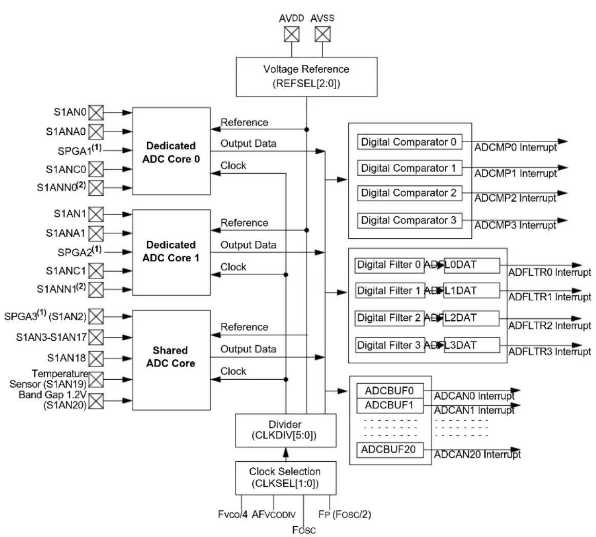
flowchart
graph TD
    A["AVDD AVSS"] --> B["Voltage Reference (REFSEL[2:0"])]
    B --> C["Dedicated ADC Core 0"]
    C --> D["Output Data"]
    C --> E["Clock"]
    B --> F["Dedicated ADC Core 1"]
    F --> G["Output Data"]
    F --> H["Clock"]
    B --> I["Shared ADC Core"]
    I --> J["Output Data"]
    I --> K["Clock"]
    B --> L["Divider (CLKDIV[5:0"])]
    L --> M["Clock Selection (CLKSEL[1:0"])]
    M --> N["Fvco/4 AFVCODIV FP (Fosc/2)"]
    M --> O["Fosc"]
    C --> P["Digital Comparator 0 ADCMP0 Interrupt"]
    C --> Q["Digital Comparator 1 ADCMP1 Interrupt"]
    C --> R["Digital Comparator 2 ADCMP2 Interrupt"]
    C --> S["Digital Comparator 3 ADCMP3 Interrupt"]
    I --> T["Digital Filter 0 ADFLTR0 Interrupt"]
    I --> U["Digital Filter 1 ADFLTR1 Interrupt"]
    I --> V["Digital Filter 2 ADFLTR2 Interrupt"]
    I --> W["Digital Filter 3 ADFLTR3 Interrupt"]
    L --> X["ADCBUF0 ADCAN0 Interrupt"]
    L --> Y["ADCBUF1 ADCAN1 Interrupt"]
    L --> Z["ADCBUF20 ADCAN20 Interrupt"]
    style A fill:#f9f,stroke:#333
    style B fill:#ccf,stroke:#333
    style C fill:#cfc,stroke:#333
    style D fill:#fcc,stroke:#333
    style E fill:#fcc,stroke:#333
    style F fill:#fcc,stroke:#333
    style G fill:#fcc,stroke:#333
    style H fill:#fcc,stroke:#333
    style I fill:#fcc,stroke:#333
    style J fill:#fcc,stroke:#333
    style K fill:#fcc,stroke:#333
    style L fill:#cff,stroke:#333
    style M fill:#ffc,stroke:#333
    style N fill:#ffc,stroke:#333
    style O fill:#ffc,stroke:#333
    style P fill:#ffc,stroke:#333
    style Q fill:#ffc,stroke:#333
    style R fill:#ffc,stroke:#333
    style S fill:#ffc,stroke:#333
    style T fill:#ffc,stroke:#333
    style U fill:#ffc,stroke:#333
    style V fill:#ffc,stroke:#333
    style W fill:#ffc,stroke:#333
Note 1: SPGA1, SPGA2, SPGA3 and Band Gap Reference (VBG) are internal analog inputs and are not available on device pins.
2: These pins are the negative input for the corresponding analog input channel when in differential mode.
FIGURE 4-19: ADC SHARED CORE BLOCK DIAGRAM
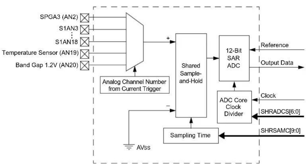
flowchart
graph TD
    A["SPGA3 (AN2)"] --> B["Organizer"]
    C["S1AN3"] --> B
    D["S1AN18"] --> B
    E["Temperature Sensor (AN19)"] --> B
    F["Band Gap 1.2V (AN20)"] --> B
    B --> G["Shared Sample-and-Hold"]
    G --> H["12-Bit SAR ADC"]
    H --> I["ADC Core Clock Divider"]
    I --> J["Sampling Time"]
    J --> K["AVss"]
    L["Reference"] --> H
    M["Output Data"] --> H
    N["Clock"] --> I
    O["SHRADCS[6:0"]] --> I
    P["SHRSAMC[9:0"]] --> I
    Q["+"] --> G
    R["-"] --> G
FIGURE 4-20: DEDICATED ADC CORE
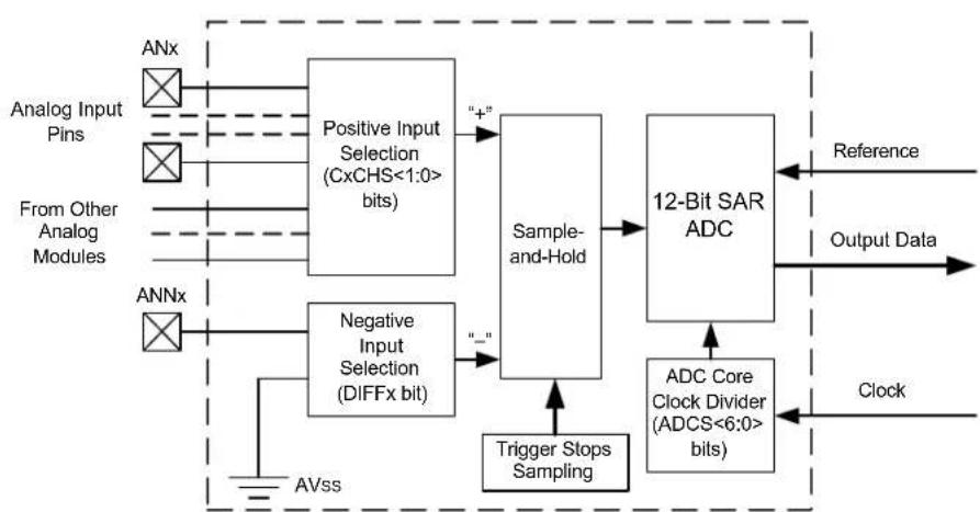
flowchart
graph TD
    A["Analog Input Pins"] --> B["Positive Input Selection (CxCHS<1:0> bits)"]
    C["From Other Analog Modules"] --> B
    D["ANNx"] --> E["Negative Input Selection (DIFFx bit)"]
    B --> F["Sample-and-Hold"]
    E --> F
    F --> G["12-Bit SAR ADC"]
    G --> H["ADC Core Clock Divider (ADCS<6:0> bits)"]
    H --> I["Trigger Stops Sampling"]
    I --> J["AVss"]
    G --> K["Reference"]
    G --> L["Output Data"]
    G --> M["Clock"]
4.7.2 SAMPLING TIME REQUIREMENTS
The analog input model of the ADC is shown in the figure below.
FIGURE: ADC ANALOG INPUT MODEL
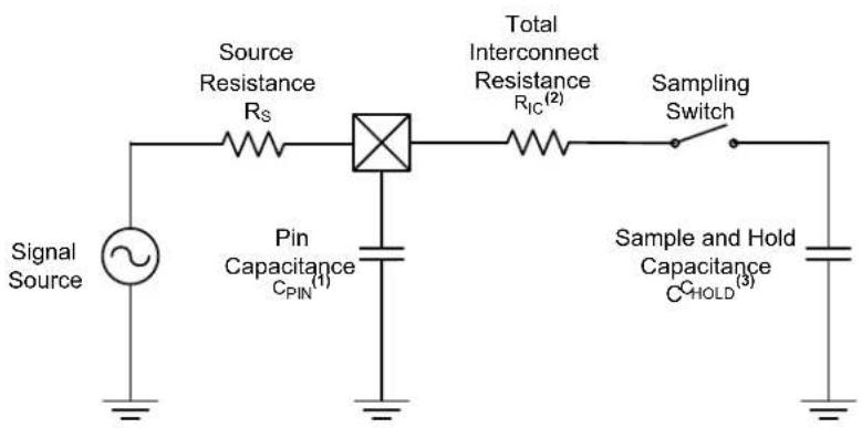
text_image
Signal Source Source Resistance R_S Pin Capacitance C_PIN (1) Total Interconnect Resistance R_IC (2) Sampling Switch Sample and Hold Capacitance C_HOLD (3)Note 1: The CPIN value depends on the device package and is not tested. The effect of the CPIN is negligible if Rs ≤ 5 kΩ.
2: See the AD62 parameter in Table 24-43.
3: See the AD60 and AD61 parameters in Table 24-43.
The total acquisition time for the Analog-to-Digital conversion is a function of the Holding Capacitor (CHOLD) charge time. For the ADC module to meet its specified accuracy, the Holding Capacitor (CHOLD) must be allowed to fully charge to the voltage level on the analog input pin. The Signal Source Impedance (Rs) and the Interconnect Impedance (Ric) combine to affect the time required to charge the CHOLD. The total resistance (Rs + Ric) must therefore be small enough to fully charge the Holding Capacitor within the selected sample time.
4.7.3 TEMPERATURE SENSOR
The ADC channel, S1AN19, is connected to a forward biased diode; it can be used to measure die temperature. This diode provides an output with a temperature coefficient of approximately -1.5 mV/C that can be monitored by the ADC. To get the exact gain and offset numbers, two-point temperature calibration is recommended.
4.7.4 ANALOG-TO-DIGITAL CONVERTER RESOURCES
Many useful resources are provided on the main product page of the Microchip website for the devices listed in this data sheet. This product page contains the latest updates and additional information.
4.7.4.1 Key Resources
- "12-Bit High-Speed, Multiple SARs A/D Converter (ADC)" (www.microchip.com/DS70005213)
- Code Samples
• Application Notes - Software Libraries
- Webinars
- All Related "dsPIC33/PIC24 Family Reference Manual" Sections
- Development Tools
4.7.5 ADC CONTROL/STATUS REGISTERS
REGISTER 4-85: ADCON1L: ADC CONTROL REGISTER 1 LOW
| R/W-0 U-0 R/W-0 U-0 r-0 U-0 U-0 U-0 | ||||||||
| ADON^(1) | — | A | D | S | I | D | L | —— |
| bit 15 bit 8 | ||||||||
| U-0 U-0 U-0 U-0 U-0 U-0 U-0 U-0 | |||||||
| —— | —— | —— | |||||
| bit 7 bit 0 | |||||||
| Legend: | r = Reserved bit | ||
| R = Readable bit | W = Writable bit | U = Unimplemented bit, read as ‘0’ | |
| -n = Value at POR | ‘1’ = Bit is set | ‘0’ = Bit is cleared | x = Bit is unknown |
bit 15 ADON: ADC Enable bit ^(1)
1 = ADC module is enabled
0 = ADC module is off
bit 14 Unimplemented: Read as '0'
bit 13 ADSIDL: ADC Stop in Idle Mode bit
1 = Discontinues module operation when device enters Idle mode
0 = Continues module operation in Idle mode
bit 12 Unimplemented: Read as '0'
bit 11 Reserved: Maintain as '0'
bit 10-0 Unimplemented: Read as '0'
Note 1: Set the ADON bit only after the ADC module has been configured. Changing ADC Configuration bits when ADON = 1 will result in unpredictable behavior.
REGISTER 4-86: ADCON1H: ADC CONTROL REGISTER 1 HIGH
| U-0 U-0 U-0 U-0 U-0 U-0 U-0 U-0 | |||||||
| —— | —— | —— | |||||
| bit 15 bit 8 | |||||||
| R/W-0 R/W-1 R/W-1 U-0 U-0 U-0 U-0 U-0 | |||||||
| FORM SHRRES1 SHRRES0 | — — — | — — | |||||
| bit 7 bit 0 | |||||||
Legend:
R = Readable bit W = Writable bit U = Unimplemented bit, read as '0'
-n = Value at POR '1' = Bit is set '0' = Bit is cleared x = Bit is unknown
bit 15-8 Unimplemented: Read as '0'
bit 7 FORM: Fractional Data Output Format bit
1 = Fractional
0 = Integer
bit 6-5 SHRRES[1:0]: Shared ADC Core Resolution Selection bits
11 = 12-bit resolution
10 = 10-bit resolution
01 = 8-bit resolution
00 = 6-bit resolution
bit 4-0 Unimplemented: Read as '0'
REGISTER 4-87: ADCON2L: ADC CONTROL REGISTER 2 LOW
| R/W-0 R/W-0 U-0 R/W-0 R/W-0 R/W-0 R/W-0 R/W-0 | |||||||
| REFCIE REFERCIE | — EIEN | PTGEN SHREISEL2 | (1) | SHREISEL1(1) | SHREISEL0(1) | ||
| bit 15 bit 8 | |||||||
| U-0 | R/W-0 R/W-0 R/W-0 R/W-0 R/W-0 R/W-0 | R/W-0 |
| — | SHRADCS[6:0] | |
| bit 7 | bit 0 | |
| Legend: | |||
| R = Readable bit | W = Writable bit | U = Unimplemented bit, read as ‘0’ | |
| -n = Value at POR | ‘1’ = Bit is set | ‘0’ = Bit is cleared | x = Bit is unknown |
| bit 15 | REFCIE: Band Gap and Reference Voltage Ready Common Interrupt Enable bit1 = Common interrupt will be generated when the band gap will become ready0 = Common interrupt is disabled for the band gap ready event |
| bit 14 | REFERCIE: Band Gap or Reference Voltage Error Common Interrupt Enable bit1 = Common interrupt will be generated when a band gap or reference voltage error is detected0 = Common interrupt is disabled for the band gap and reference voltage error event |
| bit 13 | Unimplemented: Read as '0' |
| bit 12 | EIEN: Early Interrupts Enable bit1 = The early interrupt feature is enabled for the input channel interrupts (when the EISTATx flag is set)0 = The individual interrupts are generated when conversion is done (when the ANxRDY flag is set) |
| bit 11 | PTGEN: External Conversion Request Interface bitSetting this bit will enable the PTG to request conversion of an ADC input. |
| bit 10-8 | SHREISEL[2:0]: Shared Core Early Interrupt Time Selection bits ^(1) 111 = Early interrupt is set and interrupt is generated 8 TADCORE clocks prior to when the data are ready110 = Early interrupt is set and interrupt is generated 7 TADCORE clocks prior to when the data are ready101 = Early interrupt is set and interrupt is generated 6 TADCORE clocks prior to when the data are ready100 = Early interrupt is set and interrupt is generated 5 TADCORE clocks prior to when the data are ready011 = Early interrupt is set and interrupt is generated 4 TADCORE clocks prior to when the data are ready010 = Early interrupt is set and interrupt is generated 3 TADCORE clocks prior to when the data are ready001 = Early interrupt is set and interrupt is generated 2 TADCORE clocks prior to when the data are ready000 = Early interrupt is set and interrupt is generated 1 TADCORE clock prior to when the data are ready |
| bit 7 | Unimplemented: Read as '0' |
| bit 6-0 | SHRADCS[6:0]: Shared ADC Core Input Clock Divider bitsThese bits determine the number of TCORESRC (Source Clock Periods) for one shared TADCORE (Core Clock Period).1111111 = 254 Source Clock Periods...0000011 = 6 Source Clock Periods0000010 = 4 Source Clock Periods0000001 = 2 Source Clock Periods0000000 = 2 Source Clock Periods |
Note 1: For the 6-bit shared ADC core resolution (SHRES[1:0] = 00), the SHREISEL[2:0] settings, from '100' to '111', are not valid and should not be used. For the 8-bit shared ADC core resolution (SHRES[1:0] = 01), the SHREISEL[2:0] settings, '110' and '111', are not valid and should not be used.
REGISTER 4-88: ADCON2H: ADC CONTROL REGISTER 2 HIGH
| HSC/R-0 HSC/R-0 U-0 r-0 r-0 r-0 R/W-0 R/W-0 | |||||
| REFRDY REFERR | — r r r S | HRSAMC[9:8] | |||
| bit 15 bit 8 | |||||
| R/W-0 R/W-0 R/W-0 R/W-0 R/W-0 R/W-0 R/W-0 R/W-0 | |
| SHRSAMC[7:0] | |
| bit 7 | bit 0 |
| Legend: | r = Reserved bit | U = Unimplemented bit, read as '0' |
| R = Readable bit | W = Writable bit | HSC = Hardware Settable/Clearable bit |
| -n = Value at POR | '1' = Bit is set | '0' = Bit is cleared x = Bit is unknown |
| bit 15 | REFRDY: Band Gap and Reference Voltage Ready Flag bit1 = Band gap is ready0 = Band gap is not ready |
| bit 14 | REFERR: Band Gap or Reference Voltage Error Flag bit1 = Band gap was removed after the ADC module was enabled (ADON = 1)0 = No band gap error was detected |
| bit 13 | Unimplemented: Read as '0' |
| bit 12-10 | Reserved: Maintain as '0' |
| bit 9-0 | SHRSAMC[9:0]: Shared ADC Core Sample Time Selection bitsThese bits specify the number of shared ADC Core Clock Periods (TADCORE) for the shared ADC core sample time.1111111111 = 1025 TADCORE...0000000001 = 3 TADCORE000000000 = 2 TADCORE |
REGISTER 4-89: ADCON3L: ADC CONTROL REGISTER 3 LOW
| R/W-0 R/W-0 R/W-0 R/W-0 R/W-0 HSC/R-0 R/W-0 HSC/R-0 | |||||||||
| REFSEL2 | REFSEL1 | REFS | EL0 | SUSPEND | SUSPCIE | SU | SPRDY SHRS | AMP CNVRTCH | |
| bit 15 bit 8 | |||||||||
| R/W-0 HSC/R-0 R/W-0 R/W-0 R/W-0 R/W-0 R/W-0 R/W-0 | |||||||
| SWLCTRG | SWCTRG | CNVCHSEL5 | CNVCHSEL4 | CNVCHSEL3 | CNVCHSEL2 | CNVCHSEL1 | CNVCHSEL0 |
| bit 7 bit 0 | |||||||
| Legend: | U = Unimplemented bit, read as ‘0’ | ||
| R = Readable bit | W = Writable bit | HSC = Hardware Settable/Clearable bit | |
| -n = Value at POR | ‘1’ = Bit is set | ‘0’ = Bit is cleared | x = Bit is unknown |
bit 15-13 REFSEL[2:0]: ADC Reference Voltage Selection bits
| Value | VREFH | VREFL |
| 000 | AVDD | AVss |
001-111 = Unimplemented: Do not use
bit 12 SUSPEND: All ADC Core Triggers Disable bit
1 = All new trigger events for all ADC cores are disabled
0 = All ADC cores can be triggered
bit 11 SUSPCIE: Suspend All ADC Cores Common Interrupt Enable bit
1 = Common interrupt will be generated when ADC core triggers are suspended (SUSPEND bit = 1) and all previous conversions are finished (SUSPRDY bit becomes set)
0 = Common interrupt is not generated for suspend ADC cores event
bit 10 SUSPRDY: All ADC Cores Suspended Flag bit
1 = All ADC cores are suspended (SUSPEND bit = 1) and have no conversions in progress
0 = ADC cores have previous conversions in progress
bit 9 SHRSAMP: Shared ADC Core Sampling Direct Control bit
This bit should be used with the individual channel conversion trigger controlled by the CNVRTCH bit. It connects an analog input, specified by the CNVCHSEL[5:0] bits, to the shared ADC core and allows extending the sampling time. This bit is not controlled by hardware and must be cleared before the conversion starts (setting CNVRTCH to '1').
1 = Shared ADC core samples an analog input specified by the CNVCHSEL[5:0] bits
0 = Sampling is controlled by the shared ADC core hardware
bit 8 CNVRTCH: Software Individual Channel Conversion Trigger bit
1 = Single trigger is generated for an analog input specified by the CNVCHSEL[5:0] bits; when the bit is set, it is automatically cleared by hardware on the next instruction cycle
0 = Next individual channel conversion trigger can be generated
bit 7 SWLCTRG: Software Level-Sensitive Common Trigger bit
1 = Triggers are continuously generated for all channels with the software, level-sensitive common trigger selected as a source in the ADTRIGnL and ADTRIGnH registers
0 = No software, level-sensitive common triggers are generated
bit 6 SWCTRG: Software Common Trigger bit
1 = Single trigger is generated for all channels with the software; common trigger selected as a source in the ADTRIGnL and ADTRIGnH registers; when the bit is set, it is automatically cleared by hardware on the next instruction cycle
0 = Ready to generate the next software common trigger
bit 5-0 CNVCHSEL [5:0]: Channel Number Selection for Software Individual Channel Conversion Trigger bits
These bits define a channel to be converted when the CNVRTCH bit is set.
REGISTER 4-90: ADCON3H: ADC CONTROL REGISTER 3 HIGH
| R/W-0 R/W-0 R/W-0 R/W-0 R/W-0 R/W-0 R/W-0 R/W-0 | |||||||
| CLKSEL1 CL | KSEL0 CLKD | IV5 CLKDIV4 | CLKDIV3 CLKDIV2 CLKDIV1 | CLKDIV0 | |||
| bit 15 bit 8 | |||||||
| R/W-0 U-0 U-0 U-0 U-0 R/W-0 R/W-0 | ||||||
| SHREN | — — — | — — C1EN COEN | ||||
| bit 7 bit 0 | ||||||
| Legend: | |||
| R = Readable bit | W = Writable bit | U = Unimplemented bit, read as ‘0’ | |
| -n = Value at POR | ‘1’ = Bit is set | ‘0’ = Bit is cleared | x = Bit is unknown |
bit 15-14 CLKSEL[1:0]: ADC Module Clock Source Selection bits ^(1)
11 = Fvco/4
10 = AFVCODIV
01 = Fosc
00 = FP (Fosc/2)
bit 13-8 CLKDIV[5:0]: ADC Module Clock Source Divider bits ^(2)
The divider forms a TCORESRC clock used by all ADC cores (shared and dedicated) from the TSRC ADC module clock source selected by the CLKSEL[1:0] bits. Then, each ADC core individually divides the TCORESRC clock to get a core-specific TADCORE clock using the ADCS[6:0] bits in the ADCORExH register or the SHRADCS[6:0] bits in the ADCON2L register.
111111 = 64 Source Clock Periods
• • •
000011 = 4 Source Clock Periods
000010 = 3 Source Clock Periods
000001 = 2 Source Clock Periods
000000 = 1 Source Clock Period
bit 7 SHREN: Shared ADC Core Enable bit
1 = Shared ADC core is enabled
0 = Shared ADC core is disabled
bit 6-2 Unimplemented: Read as '0'
bit 1 C1EN: Dedicated ADC Core 1 Enable bits
1 = Dedicated ADC Core 1 is enabled
0 = Dedicated ADC Core 1 is disabled
bit 0 C0EN: Dedicated ADC Core 0 Enable bits
1 = Dedicated ADC Core 0 is enabled
0 = Dedicated ADC Core 0 is disabled
Note 1: The ADC input clock frequency, selected by the CLKSEL[1:0] bits, must not exceed AD67 listed in Table 24-44.
2: The ADC clock frequency, after the divider selected by the CLKDIV[5:0] bits, must not exceed AD67 listed in Table 24-44.
REGISTER 4-91: ADCON4L: ADC CONTROL REGISTER 4 LOW
| U-0 U-0 U-0 U-0 U-0 U-0 r-0 r-0 | |||||||
| —— | —— | —— | |||||
| bit 15 bit 8 | |||||||
| U-0 U-0 U-0 U-0 U-0 R/W-0 R/W-0 | |||||||
| —— | —— SAMC1EN SAMC0EN | ||||||
| bit 7 bit 0 | |||||||
| Legend: | r = Reserved bit | ||
| R = Readable bit | W = Writable bit | U = Unimplemented bit, read as ‘0’ | |
| -n = Value at POR | ‘1’ = Bit is set | ‘0’ = Bit is cleared | x = Bit is unknown |
bit 15-10 Unimplemented: Read as '0'
bit 9-8 Reserved: Must be written as '0'
bit 7-2 Unimplemented: Read as '0'
bit 1 SAMC1EN: Dedicated ADC Core 1 Conversion Delay Enable bit
1 = After trigger, the conversion will be delayed and the ADC core will continue sampling during the time specified by the SAMC[9:0] bits in the ADCORE1L register
0 = After trigger, the sampling will be stopped immediately and the conversion will be started on the next core clock cycle
bit 0 SAMC0EN: Dedicated ADC Core 0 Conversion Delay Enable bit
1 = After trigger, the conversion will be delayed and the ADC core will continue sampling during the time specified by the SAMC[9:0] bits in the ADCORE0L register
0 = After trigger, the sampling will be stopped immediately and the conversion will be started on the next core clock cycle
REGISTER 4-92: ADCON4H: ADC CONTROL REGISTER 4 HIGH
| U-0 U-0 U-0 U-0 U-0 U-0 U-0 U-0 | |||||||
| ——— | ——— —— | ||||||
| bit 15 bit 8 | |||||||
| U-0 U-0 U-0 U-0 R/W-0 R/W-0 R/W-0 R/W-0 | ||||||
| — — — | — C1CHS1 C1 | CHS0 C0CHS | 1 C0CHS0 | |||
| bit 7 bit 0 | ||||||
Legend:
R = Readable bit W = Writable bit U = Unimplemented bit, read as '0'
-n = Value at POR '1' = Bit is set '0' = Bit is cleared x = Bit is unknown
bit 15-4 Unimplemented: Read as '0'
bit 3-2 C1CHS[1:0]: Dedicated ADC Core 1 Input Channel Selection bits
11 = S1ANC1
10 = SPGA2
01 = S1ANA1
00 = S1AN1
bit 1-0 C0CHS[1:0]: Dedicated ADC Core 0 Input Channel Selection bits
11 = S1ANC0
10 = SPGA1
01 = S1ANA0
00 = S1AN0
REGISTER 4-93: ADCON5L: ADC CONTROL REGISTER 5 LOW
| HSC/R-0 U-0 U-0 U-0 U-0 HSC/R-0 HSC/R-0 | ||||||
| SHRRDY | — — — | — — C1RDY | C0RDY | |||
| bit 15 bit 8 | ||||||
| R/W-0 U-0 U-0 U-0 U-0 R/W-0 R/W-0 | |||||||||
| SHRPWR | ——— | —— | C | 1 | P | W | R | C | 0 |
| bit 7 bit 0 | |||||||||
| Legend: | U = Unimplemented bit, read as '0' | ||
| R = Readable bit | W = Writable bit | HSC = Hardware Settable/Clearable bit | |
| -n = Value at POR | ‘1’ = Bit is set | ‘0’ = Bit is cleared | x = Bit is unknown |
| bit 15 | SHRRDY: Shared ADC Core Ready Flag bit1 = ADC core is powered and ready for operation0 = ADC core is not ready for operation |
| bit 14-10 | Unimplemented: Read as '0' |
| bit 9 | C1RDY: Dedicated ADC Core 1 Ready Flag bit1 = ADC Core 1 is powered and ready for operation0 = ADC Core 1 is not ready for operation |
| bit 8 | C0RDY: Dedicated ADC Core 0 Ready Flag bit1 = ADC Core 0 is powered and ready for operation0 = ADC Core 0 is not ready for operation |
| bit 7 | SHRPWR: Shared ADC Core Power Enable bit1 = ADC core is powered0 = ADC core is off |
| bit 6-2 | Unimplemented: Read as '0' |
| bit 1 | C1PWR: Dedicated ADC Core 1 Power Enable bit1 = ADC Core 1 is powered0 = ADC Core 1 is off |
| bit 0 | C0PWR: Dedicated ADC Core 0 Power Enable bit1 = ADC Core 0 is powered0 = ADC Core 0 is off |
REGISTER 4-94: ADCON5H: ADC CONTROL REGISTER 5 HIGH
| U-0 U-0 U-0 U-0 R/W-0 R/W-0 R/W-0 R/W-0 | |||
| — — — | — WARMTIME[3:0] | ||
| bit 15 bit 8 | |||
| R/W-0 U-0 U-0 U-0 U-0 R/W-0 R/W-0 | |||||||
| SHRCIE | — | — | — | — | — | C1CIE | C0CIE |
| bit 7 bit 0 | |||||||
| Legend: | |||
| R = Readable bit | W = Writable bit | U = Unimplemented bit, read as '0' | |
| -n = Value at POR | '1' = Bit is set | '0' = Bit is cleared | x = Bit is unknown |
bit 15-12 Unimplemented: Read as '0'
bit 11-8 WARMTIME[3:0]: ADC Dedicated Core x Power-up Delay bits
These bits determine the power-up delay in the number of the Core Source Clock Periods (TCORESRC) for all ADC cores.
1111 = 32768 Source Clock Periods
1110 = 16384 Source Clock Periods
1101 = 8192 Source Clock Periods
1100 = 4096 Source Clock Periods
1011 = 2048 Source Clock Periods
1010 = 1024 Source Clock Periods
1001 = 512 Source Clock Periods
1000 = 256 Source Clock Periods
0111 = 128 Source Clock Periods
0110 = 64 Source Clock Periods
0101 = 32 Source Clock Periods
0100 = 16 Source Clock Periods
00xx = 16 Source Clock Periods
bit 7 SHRCIE: Shared ADC Core Ready Common Interrupt Enable bit
1 = Common interrupt will be generated when ADC core is powered and ready for operation
0 = Common interrupt is disabled for an ADC core ready event
bit 6-2 Unimplemented: Read as '0'
bit 1 C1CIE: Dedicated ADC Core 1 Ready Common Interrupt Enable bit
1 = Common interrupt will be generated when ADC Core 1 is powered and ready for operation
0 = Common interrupt is disabled for an ADC Core 1 ready event
bit 0 COCIE: Dedicated ADC Core 0 Ready Common Interrupt Enable bit
1 = Common interrupt will be generated when ADC Core 0 is powered and ready for operation
0 = Common interrupt is disabled for an ADC Core 0 ready event
REGISTER 4-95: ADCORExL: DEDICATED ADC CORE x CONTROL REGISTER LOW (x = 0 TO 1)
| U-0 U-0 U-0 U-0 U-0 R/W-0 R/W-0 | |||||
| — — — | — — | — | SAMC[9:8] | ||
| bit 15 bit 8 | |||||
| R/W-0 | R/W-0 | R/W-0 | R/W-0 | R/W-0 | R/W-0 | R/W-0 | R/W-0 |
| SAMC[7:0] | |||||||
| bit 7 | bit 0 | ||||||
Legend:
| R = Readable bit | W = Writable bit U = Unimplemented bit, read as '0' | ||
| -n = Value at POR | '1' = Bit is set | '0' = Bit is cleared | x = Bit is unknown |
bit 15-10 Unimplemented: Read as '0'
bit 9-0 SAMC[9:0]: Dedicated ADC Core x Conversion Delay Selection bits
These bits determine the time between the trigger event and the start of conversion in the number of the Core Clock Periods (TADCORE). During this time, the ADC Core x still continues sampling. This feature is enabled by the SAMCxEN bits in the ADCON4L register.
1111111111 = 1025 TADCORE
...
0000000001 = 3 TADCORE
0000000000 = 2 TADCORE
REGISTER 4-96: ADCORExH: DEDICATED ADC CORE x CONTROL REGISTER HIGH (x = 0 TO 1)
| U-0 U-0 U-0 R/W-0 R/W-0 R/W-0 R/W-0 R/W-0 | |||||||
| — | — | — | EISEL2 | EISEL1 | EISEL0 | RES1 | RES2 |
| bit 15 bit 8 | |||||||
| U-0 | R/W-0 | R/W-0 | R/W-0 | R/W-0 | R/W-0 | R/W-0 | R/W-0 |
| — | ADCS[6:0] | ||||||
| bit 7 | bit 0 | ||||||
Legend:
| R = Readable bit | W = Writable bit | U = Unimplemented bit, read as '0' |
| -n = Value at POR | '1' = Bit is set | '0' = Bit is cleared x = Bit is unknown |
bit 15-13 Unimplemented: Read as '0'
bit 12-10 EISEL[2:0]: ADC Core x Early Interrupt Time Selection bits
111 = Early interrupt is set and an interrupt is generated 8 TADCORE clocks prior to when the data are ready 110 = Early interrupt is set and an interrupt is generated 7 TADCORE clocks prior to when the data are ready 101 = Early interrupt is set and an interrupt is generated 6 TADCORE clocks prior to when the data are ready 100 = Early interrupt is set and an interrupt is generated 5 TADCORE clocks prior to when the data are ready 011 = Early interrupt is set and an interrupt is generated 4 TADCORE clocks prior to when the data are ready 010 = Early interrupt is set and an interrupt is generated 3 TADCORE clocks prior to when the data are ready 001 = Early interrupt is set and an interrupt is generated 2 TADCORE clocks prior to when the data are ready 000 = Early interrupt is set and an interrupt is generated 1 TADCORE clock prior to when the data are ready
bit 9-8 RES[1:0]: ADC Core x Resolution Selection bits
11 = 12-bit resolution 10 = 10-bit resolution 01 = 8-bit resolution ^(1) 00 = 6-bit resolution ^(1)
bit 7 Unimplemented: Read as '0'
bit 6-0 ADCS[6:0]: ADC Core x Input Clock Divider bits
These bits determine the number of Source Clock Periods (TCORESRC) for one Core Clock Period (TADCORE). 1111111 = 254 Source Clock Periods
0000011 = 6 Source Clock Periods 0000010 = 4 Source Clock Periods 0000001 = 2 Source Clock Periods 0000000 = 2 Source Clock Periods
Note 1: For the 6-bit ADC core resolution (RES[1:0] = 00), the EISEL[2:0] bits settings, from '100' to '111', are not valid and should not be used. For the 8-bit ADC core resolution (RES[1:0] = 01), the EISEL[2:0] bits settings, '110' and '111', are not valid and should not be used.
REGISTER 4-97: ADLVLTRGL: ADC LEVEL-SENSITIVE TRIGGER CONTROL REGISTER LOW
| R/W-0 R/W-0 R/W-0 R/W-0 R/W-0 R/W-0 R/W-0 R/W-0 |
| LVLEN[15:8] |
| bit 15 bit 8 |
| R/W-0 R/W-0 R/W-0 R/W-0 R/W-0 R/W-0 R/W-0 R/W-0 |
| LVLEN[7:0] |
| bit 7 bit 0 |
Legend:
R = Readable bit W = Writable bit U = Unimplemented bit, read as '0'
-n = Value at POR '1' = Bit is set '0' = Bit is cleared x = Bit is unknown
bit 15-0 LVLEN[15:0]: Level Trigger for Corresponding Analog Input Enable bits
1 = Input trigger is level-sensitive
0 = Input trigger is edge-sensitive
REGISTER 4-98: ADLVLTRGH: ADC LEVEL-SENSITIVE TRIGGER CONTROL REGISTER HIGH
R = Readable bit W = Writable bit U = Unimplemented bit, read as '0'
-n = Value at POR '1' = Bit is set '0' = Bit is cleared x = Bit is unknown
bit 15-5 Unimplemented: Read as '0'
bit 4-0 LVLEN[20:16]: Level Trigger for Corresponding Analog Input Enable bits
1 = Input trigger is level-sensitive
0 = Input trigger is edge-sensitive
REGISTER 4-99: ADEIEL: ADC EARLY INTERRUPT ENABLE REGISTER LOW
| R/W-0 R/W-0 R/W-0 R/W-0 R/W-0 R/W-0 R/W-0 R/W-0 |
| EIEN[15:8] |
| bit 15 bit 8 |
| R/W-0 R/W-0 R/W-0 R/W-0 R/W-0 R/W-0 R/W-0 R/W-0 |
| EIEN[7:0] |
| bit 7 bit 0 |
Legend:
R = Readable bit W = Writable bit U = Unimplemented bit, read as '0'
-n = Value at POR '1' = Bit is set '0' = Bit is cleared x = Bit is unknown
bit 15-0 EIEN[15:0]: Early Interrupt Enable for Corresponding Analog Inputs bits
1 = Early interrupt is enabled for the channel
0 = Early interrupt is disabled for the channel
REGISTER 4-100: ADEIEH: ADC EARLY INTERRUPT ENABLE REGISTER HIGH
R = Readable bit W = Writable bit U = Unimplemented bit, read as '0'
-n = Value at POR '1' = Bit is set '0' = Bit is cleared x = Bit is unknown
bit 15-5 Unimplemented: Read as '0'
bit 4-0 EIEN[20:16]: Early Interrupt Enable for Corresponding Analog Inputs bits
1 = Early interrupt is enabled for the channel
0 = Early interrupt is disabled for the channel
REGISTER 4-101: ADEISTATL: ADC EARLY INTERRUPT STATUS REGISTER LOW
| R/W-0 R/W-0 R/W-0 R/W-0 R/W-0 R/W-0 R/W-0 R/W-0 |
| EISTAT[15:8] |
| bit 15 bit 8 |
| R/W-0 R/W-0 R/W-0 R/W-0 R/W-0 R/W-0 R/W-0 R/W-0 |
| EISTAT[7:0] |
| bit 7 bit 0 |
Legend:
R = Readable bit W = Writable bit U = Unimplemented bit, read as '0'
-n = Value at POR '1' = Bit is set '0' = Bit is cleared x = Bit is unknown
bit 15-0
EISTAT[15:0]: Early Interrupt Status for Corresponding Analog Inputs bits
1 = Early interrupt was generated
0 = Early interrupt was not generated since the last ADCBUFx read
REGISTER 4-102: ADEISTATH: ADC EARLY INTERRUPT STATUS REGISTER HIGH
R = Readable bit W = Writable bit U = Unimplemented bit, read as '0'
-n = Value at POR '1' = Bit is set '0' = Bit is cleared x = Bit is unknown
bit 15-5 Unimplemented: Read as '0'
bit 4-0 EISTAT[20:16]: Early Interrupt Status for Corresponding Analog Inputs bits
1 = Early interrupt was generated
0 = Early interrupt was not generated since the last ADCBUFx read
REGISTER 4-103: ADMODOL: ADC INPUT MODE CONTROL REGISTER 0 LOW
| U-0 R/W-0 U-0 R/W-0 U-0 R/W-0 U-0 R/W-0 | ||||||||
| — SIGN7 — S | I | G | N | 6 | — | S | I | |
| bit 15 bit 8 | ||||||||
| U-0 R/W-0 U-0 R/W-0 R/W-0 R/W-0 R/W-0 R/W-0 | |||||||
| — | SIGN3 | — | SIGN2 | DIFF1 | SIGN1 | DIFF0 | SIGN0 |
| bit 7 bit 0 | |||||||
| Legend: | |||
| R = Readable bit | W = Writable bit | U = Unimplemented bit, read as ‘0’ | |
| -n = Value at POR | ‘1’ = Bit is set | ‘0’ = Bit is cleared | x = Bit is unknown |
bit 15-5 (odd) Unimplemented: Read as '0'
bit 14-0 (even) SIGNn (n = 7 to 0): Output Data Sign for Corresponding Analog Inputs bits
1 = Channel output data are signed
0 = Channel output data are unsigned
bit 3-1 (odd) DIFFn (n = 1 to 0): Differential-Mode for Corresponding Analog Inputs bits
1 = Channel is differential
0 = Channel is single-ended
REGISTER 4-104: ADMOD0H: ADC INPUT MODE CONTROL REGISTER 0 HIGH
| U-0 R/W-0 U-0 R/W-0 U-0 R/W-0 U-0 R/W-0 | |||||||
| — | SIGN15 | — | SIGN14 | — | SIGN13 | — | SIGN12 |
| bit 15 bit 8 | |||||||
| U-0 R/W-0 U-0 R/W-0 U-0 R/W-0 U-0 R/W-0 | |||||||
| — | SIGN11 | — | SIGN10 | — | SIGN9 | — | SIGN8 |
| bit 7 bit 0 | |||||||
| Legend: | |||
| R = Readable bit | W = Writable bit | U = Unimplemented bit, read as ‘0’ | |
| -n = Value at POR | ‘1’ = Bit is set | ‘0’ = Bit is cleared | x = Bit is unknown |
bit 15-1 (odd) Unimplemented: Read as '0'
bit 14-0 (even) SIGNn (n = 15 to 8): Output Data Sign for Corresponding Analog Input bits
1 = Channel output data are signed
0 = Channel output data are unsigned
REGISTER 4-105: ADMOD1L: ADC INPUT MODE CONTROL REGISTER 1 LOW
| U-0 U-0 U-0 U-0 U-0 U-0 R/W-0 | ||||||||
| ——— | ——— | S | I | G | N | 2 | 0 | |
| bit 15 bit 8 | ||||||||
| U-0 R/W-0 U-0 R/W-0 U-0 R/W-0 U-0 R/W-0 | |||||||
| — | SIGN19 | — | SIGN18 | — | SIGN17 | — | SIGN16 |
| bit 7 bit 0 | |||||||
Legend:
| R = Readable bit | W = Writable bit | U = Unimplemented bit, read as '0' |
| -n = Value at POR | '1' = Bit is set | '0' = Bit is cleared x = Bit is unknown |
bit 15-9 Unimplemented: Read as '0'
bit 7-1 (odd) Unimplemented: Read as '0'
bit 8-0 (even) SIGNn (n = 20 to 16): Output Data Sign for Corresponding Analog Input bits
1 = Channel output data are signed
0 = Channel output data are unsigned
REGISTER 4-106: ADIEL: ADC INTERRUPT ENABLE REGISTER LOW
| R/W-0 R/W-0 R/W-0 R/W-0 R/W-0 R/W-0 R/W-0 R/W-0 |
| IE[15:8] |
| bit 15 bit 8 |
| R/W-0 R/W-0 R/W-0 R/W-0 R/W-0 R/W-0 R/W-0 R/W-0 |
| IE[7:0] |
| bit 7 bit 0 |
Legend:
R = Readable bit W = Writable bit U = Unimplemented bit, read as '0'
-n = Value at POR '1' = Bit is set '0' = Bit is cleared x = Bit is unknown
bit 15-0 IE[15:0]: Common Interrupt Enable bits
1 = Common and individual interrupts are enabled for the corresponding channel
0 = Common and individual interrupts are disabled for the corresponding channel
REGISTER 4-107: ADIEH: ADC INTERRUPT ENABLE REGISTER HIGH
R = Readable bit W = Writable bit U = Unimplemented bit, read as '0'
-n = Value at POR '1' = Bit is set '0' = Bit is cleared x = Bit is unknown
bit 15-5 Unimplemented: Read as '0'
bit 4-0 IE[20:16]: Common Interrupt Enable bits
1 = Common and individual interrupts are enabled for the corresponding channel
0 = Common and individual interrupts are disabled for the corresponding channel
REGISTER 4-108: ADSTATL: ADC DATA READY STATUS REGISTER LOW
| HSC/R-0 HSC/R-0 HSC/R-0 HSC/R-0 HSC/R-0 HSC/R-0 HSC/R-0 HSC/R-0 |
| AN[15:8]RDY |
| bit 15 bit 8 |
| HSC/R-0 HSC/R-0 HSC/R-0 HSC/R-0 HSC/R-0 HSC/R-0 HSC/R-0 HSC/R-0 |
| AN[7:0]RDY |
| bit 7 bit 0 |
| Legend: U = Unimplemented bit, read as '0' |
| R = Readable bit W = Writable bit HSC = Hardware Settable/Clearable bit -n = Value at POR '1' = Bit is set '0' = Bit is cleared x = Bit is unknown |
bit 15-0
AN[15:0]RDY: Common Interrupt Enable for Corresponding Analog Inputs bits
1 = Channel conversion result is ready in the corresponding ADCBUFx register
0 = Channel conversion result is not ready
REGISTER 4-109: ADSTATH: ADC DATA READY STATUS REGISTER HIGH
| U-0 | U-0 | U-0 | HSC/R-0 HSC/R-0 HSC/R-0 HSC/R-0 HSC/R-0 |
| — | — | — | AN[20:16]RDY |
| bit 7 bit 0 | |||
| Legend: U = Unimplemented bit, read as '0' |
| R = Readable bit W = Writable bit HSC = Hardware Settable/Clearable bit |
| -n = Value at POR '1' = Bit is set '0' = Bit is cleared x = Bit is unknown |
bit 15-5 Unimplemented: Read as '0'
bit 4-0 AN[20:16]RDY: Common Interrupt Enable for Corresponding Analog Inputs bits
1 = Channel conversion result is ready in the corresponding ADCBUFx register
0 = Channel conversion result is not ready
REGISTER 4-110: ADTRIGnL/ADTRIGnH: ADC CHANNEL TRIGGER n(x) SELECTION REGISTERS LOW AND HIGH (x = 0 TO 19; n = 0 TO 4)
| U-0 U-0 U-0 R/W-0 R/W-0 R/W-0 R/W-0 R/W-0 | |
| — — + TRGSRC(x+1)[4:0] | |
| bit 15 bit 8 | |
| U-0 U-0 U-0 R/W-0 R/W-0 R/W-0 R/W-0 R/W-0 | |
| — — + TRGSRCx[4:0] | |
| bit 7 bit 0 | |
| Legend: | |||
| R = Readable bit | W = Writable bit | U = Unimplemented bit, read as ‘0’ | |
| -n = Value at POR | ‘1’ = Bit is set | ‘0’ = Bit is cleared | x = Bit is unknown |
bit 15-13 Unimplemented: Read as '0'
bit 12-8 TRGSRC(x+1)[4:0]: Trigger Source Selection for Corresponding Analog Inputs bits (TRGSRC1 to TRGSRC19 – Odd)
11111 = ADTRG31 (PPS input)
11110 = Main PTG
11101 = Secondary CLC1
11100 = Main CLC1
11011 = Reserved
11010 = Reserved
11001 = Main PWM3 Trigger 2
11000 = Main PWM1 Trigger 2
10111 = Secondary SCCP4 input capture/output compare
10110 = Secondary SCCP3 input capture/output compare
10101 = Secondary SCCP2 input capture/output compare
10100 = Secondary SCCP1 input capture/output compare
10011 = Reserved
10010 = Reserved
10001 = Reserved
10000 = Reserved
01111 = Secondary PWM8 Trigger 1
01110 = Secondary PWM7 Trigger 1
01101 = Secondary PWM6 Trigger 1
01100 = Secondary PWM5 Trigger 1
01011 = Secondary PWM4 Trigger 2
01010 = Secondary PWM4 Trigger 1
01001 = Secondary PWM3 Trigger 2
01000 = Secondary PWM3 Trigger 1
00111 = Secondary PWM2 Trigger 2
00110 = Secondary PWM2 Trigger 1
00101 = Secondary PWM1 Trigger 2
00100 = Secondary PWM1 Trigger 1
00011 = Reserved
00010 = Level software trigger
00001 = Common software trigger
00000 = No trigger is enabled

bit 7-5 Unimplemented: Read as 'c'
REGISTER 4-110: ADTRIGnL/ADTRIGnH: ADC CHANNEL TRIGGER n(x) SELECTION REGISTERS LOW AND HIGH (x = 0 TO 19; n = 0 TO 4) (CONTINUED)
| bit 4-0 | TRGSRCx[4:0]: Common Interrupt Enable for Corresponding Analog Inputs bits (TRGSRC0 to TRGSRC20 – Even) |
| 11111 = ADTRG31 (PPS input) | |
| 11110 = Main PTG | |
| 11101 = Secondary CLC1 | |
| 11100 = Main CLC1 | |
| 11011 = Reserved | |
| 11010 = Reserved | |
| 11001 = Main PWM3 Trigger 2 | |
| 11000 = Main PWM1 Trigger 2 | |
| 10111 = Secondary SCCP4 input capture/output compare | |
| 10110 = Secondary SCCP3 input capture/output compare | |
| 10101 = Secondary SCCP2 input capture/output compare | |
| 10100 = Secondary SCCP1 input capture/output compare | |
| 10011 = Reserved | |
| 10010 = Reserved | |
| 10001 = Reserved | |
| 10000 = Reserved | |
| 01111 = Secondary PWM8 Trigger 1 | |
| 01110 = Secondary PWM7 Trigger 1 | |
| 01101 = Secondary PWM6 Trigger 1 | |
| 01100 = Secondary PWM5 Trigger 1 | |
| 01011 = Secondary PWM4 Trigger 2 | |
| 01010 = Secondary PWM4 Trigger 1 | |
| 01001 = Secondary PWM3 Trigger 2 | |
| 01000 = Secondary PWM3 Trigger 1 | |
| 00111 = Secondary PWM2 Trigger 2 | |
| 00110 = Secondary PWM2 Trigger 1 | |
| 00101 = Secondary PWM1 Trigger 2 | |
| 00100 = Secondary PWM1 Trigger 1 | |
| 00011 = Reserved | |
| 00010 = Level software trigger | |
| 00001 = Common software trigger | |
| 00000 = No trigger is enabled |
REGISTER 4-111: ADCAL1H: ADC CALIBRATION REGISTER 1 HIGH
| HS/R/W-0 U-0 U-0 U-0 U-0 r-0 R/W-0 R/W-0 | |||||||
| CSHRRDY | — — — | — — CSHREN | CSHRRUN | ||||
| bit 15 bit 8 | |||||||
| Legend: | HS = Hardware Settable bit | r = Reserved bit | |
| R = Readable bit | W = Writable bit | U = Unimplemented bit, read as '0' | |
| -n = Value at POR | '1' = Bit is set | '0' = Bit is cleared | x = Bit is unknown |
bit 15 CSHRRDY: Shared ADC Core Calibration Status Flag bit
1 = Shared ADC core calibration is finished
0 = Shared ADC core calibration is in progress
bit 14-11 Unimplemented: Read as '0'
bit 10 Reserved: Maintain as '0'
bit 9 CSHREN: Shared ADC Core Calibration Enable bit
1 = Shared ADC core calibration bits (CSHRRDY and CSHRRUN) can be accessed by software
0 = Shared ADC core calibration bits are disabled
bit 8 CSHRRUN: Shared ADC Core Calibration Start bit
1 = If this bit is set by software, the shared ADC core calibration cycle is started; this bit is cleared automatically by hardware
0 = Software can start the next calibration cycle
bit 7-0 Unimplemented: Read as '0'
REGISTER 4-112: ADCMPxCON: ADC DIGITAL COMPARATOR x CONTROL REGISTER (x = 0, 1, 2, 3)
| U-0 U-0 U-0 | HSC/R-0 HSC/R-0 HSC/R-0 HSC/R-0 | HSC/R-0 | ||
| — — — | CHNL[4:0] | |||
| bit 15 bit 8 | ||||
| R/W-0 R/W-0 HC/HS/R-0 R/W-0 R/W-0 R/W-0 R/W-0 R/W-0 | |||||||
| CMPEN | IE | STAT | BTWN | HIHI | HILO | LOHI | LOLO |
| bit 7 bit 0 | |||||||
| Legend: | HC = Hardware Clearable bit | U = Unimplemented bit, read as '0' | |
| R = Readable bit | W = Writable bit | HSC = Hardware Settable/Clearable bit | |
| -n = Value at POR | ‘1’ = Bit is set | ‘0’ = Bit is cleared | HS = Hardware Settable bit |
bit 15-13 Unimplemented: Read as '0'
bit 12-8 CHNL[4:0]: Input Channel Number bits
If the comparator has detected an event for a channel, this channel number is written to these bits.
11111 = Reserved
• • •
10101 = Reserved
10100 = Band gap, 1.2V (AN20)
10011 = Temperature sensor (AN19)
10010 = S1AN18
• • •
00011 = S1AN3
00010 = S1AN2
00001 = S1AN1
00000 = S1AN0
bit 7 CMPEN: Comparator Enable bit
1 = Comparator is enabled
0 = Comparator is disabled and the STAT status bit is cleared
bit 6 IE: Comparator Common ADC Interrupt Enable bit
1 = Common ADC interrupt will be generated if the comparator detects a comparison event
0 = Common ADC interrupt will not be generated for the comparator
bit 5 STAT: Comparator Event Status bit
This bit is cleared by hardware when the channel number is read from the CHNL[4:0] bits.
1 = A comparison event has been detected since the last read of the CHNL[4:0] bits
0 = A comparison event has not been detected since the last read of the CHNL[4:0] bits
bit 4 BTWN: Between Low/High Comparator Event bit
1 = Generates a comparator event when ADCMPxLO ≤ ADCBUFx < ADCMPxHI
0 = Does not generate a digital comparator event when ADCMPxLO ≤ ADCBUFx < ADCMPxHI
bit 3 HIHI: High/High Comparator Event bit
1 = Generates a digital comparator event when ADCBUFx ≥ ADCMPxHI
0 = Does not generate a digital comparator event when ADCBUFx ≥ ADCMPxHI
bit 2 HILO: High/Low Comparator Event bit
1 = Generates a digital comparator event when ADCBUFx < ADCMPxHI
0 = Does not generate a digital comparator event when ADCBUFx < ADCMPxHI
bit 1 LOHI: Low/High Comparator Event bit
1 = Generates a digital comparator event when ADCBUFx ≥ ADCMPxLO
0 = Does not generate a digital comparator event when ADCBUFx ≥ ADCMPxLO
bit 0 LOLO: Low/Low Comparator Event bit
1 = Generates a digital comparator event when ADCBUFx < ADCMPxLO
0 = Does not generate a digital comparator event when ADCBUFx < ADCMPxLO
REGISTER 4-113: ADCMPxENL: ADC DIGITAL COMPARATOR x CHANNEL ENABLE REGISTER LOW (x = 0, 1, 2, 3)
| R/W-0 R/W-0 R/W-0 R/W-0 R/W-0 R/W-0 R/W-0 R/W-0 |
| CMPEN[15:8] |
| bit 15 bit 8 |
| R/W/0 R/W-0 R/W-0 R/W-0 R/W-0 R/W-0 R/W-0 R/W-0 |
| CMPEN[7:0] |
| bit 7 bit 0 |
Legend:
| R = Readable bit W = Writable bit U = Unimplemented bit, read as '0' | ||
| -n = Value at POR | '1' = Bit is set | '0' = Bit is cleared x = Bit is unknown |
bit 15-0 CMPEN[15:0]: Comparator Enable for Corresponding Input Channels bits
1 = Conversion result for corresponding channel is used by the comparator
0 = Conversion result for corresponding channel is not used by the comparator
REGISTER 4-114: ADCMPxENH: ADC DIGITAL COMPARATOR x CHANNEL ENABLE REGISTER HIGH (x = 0, 1, 2, 3)
| R = Readable bit W = Writable bit U = Unimplemented bit, read as '0' | ||
| -n = Value at POR | '1' = Bit is set | '0' = Bit is cleared x = Bit is unknown |
bit 15-5 Unimplemented: Read as '0'
bit 4-0 CMPEN[20:16]: Comparator Enable for Corresponding Input Channels bits
1 = Conversion result for corresponding channel is used by the comparator
0 = Conversion result for corresponding channel is not used by the comparator
REGISTER 4-115: ADFLxCON: ADC DIGITAL FILTER x CONTROL REGISTER
(x = 0, 1, 2, 3)
| R/W-0 R/W-0 R/W-0 R/W-0 R/W-0 R/W-0 R/W-0 HSC/R-0 | ||||
| FLEN MODE1 MODE0 OVRSAM2 OVRSAM1 OVRSAM0 IE RDY | ||||
| bit 15 bit 8 | ||||
| U-0 | U-0 | U-0 | R/W-0 | R/W-0 | R/W-0 | R/W-0 | R/W-0 |
| — | — | — | FLCHSEL[4:0] | ||||
| bit 7 bit 0 | |||||||
| Legend: | U = Unimplemented bit, read as '0' | ||
| R = Readable bit | W = Writable bit | HSC = Hardware Settable/Clearable bit | |
| -n = Value at POR | '1' = Bit is set | '0' = Bit is cleared | x = Bit is unknown |
bit 15 FLEN: Filter Enable bit
1 = Filter is enabled
0 = Filter is disabled and the RDY bit is cleared
bit 14-13 MODE[1:0]: Filter Mode bits
11 = Averaging mode
1.0 = Reserved
01 = Reserved
00 = Oversampling mode
bit 12-10 OVRSAM[2:0]: Filter Averaging/Oversampling Ratio bits
If MODE[1:0] = 00:
111 = 128x (16-bit result in the ADFLxDAT register is in 12.4 format)
110 = 32x (15-bit result in the ADFLxDAT register is in 12.3 format)
101 = 8x (14-bit result in the ADFLxDAT register is in 12.2 format)
100 = 2x (13-bit result in the ADFLxDAT register is in 12.1 format)
011 = 256x (16-bit result in the ADFLxDAT register is in 12.4 format)
010 = 64x (15-bit result in the ADFLxDAT register is in 12.3 format)
001 = 16x (14-bit result in the ADFLxDAT register is in 12.2 format)
000 = 4x (13-bit result in the ADFLxDAT register is in 12.1 format)
If MODE[1:0] = 11 (12-bit result in the ADFLxDAT register in all instances):
111 = 256x
110 = 128x
101 = 64x
100 = 32x
011 = 16x
110 = 8x
001 = 4x
000 = 2x
bit 9 IE: Filter Common ADC Interrupt Enable bit
1 = Common ADC interrupt will be generated when the filter result will be ready
0 = Common ADC interrupt will not be generated for the filter
bit 8 RDY: Oversampling Filter Data Ready Flag bit
This bit is cleared by hardware when the result is read from the ADFLxDAT register.
1 = Data in the ADFLxDAT register are ready
0 = The ADFLxDAT register has been read and new data in the ADFLxDAT register are not ready
bit 7-5 Unimplemented: Read as '0'
REGISTER 4-115: ADFLxCON: ADC DIGITAL FILTER x CONTROL REGISTER (x = 0, 1, 2, 3) (CONTINUED)
bit 4-0 FLCHSEL[4:0]: Oversampling Filter Input Channel Selection bits
11111 = Reserved
...
10100 = Reserved
10100 = Band gap, 1.2V (AN20)
10011 = Temperature sensor (AN19)
10010 = S1AN18
...
00011 = S1AN3
00010 = SPGA3 (S1AN2)
00001 = S1AN1
00000 = S1AN0
4.8 Programmable Gain Amplifier (PGA) Secondary
Note 1: This data sheet summarizes the features of the dsPIC33CH128MP508 family of devices. It is not intended to be a comprehensive reference source. To complement the information in this data sheet, refer to “Programmable Gain Amplifier (PGA)” (www.microchip.com/DS70005146), which is available from the Microchip website (www.microchip.com).
The dsPIC33CH128MP508S1 family devices have three Programmable Gain Amplifiers (PGA1, PGA2, PGA3). The PGA is an op amp-based, noninverting amplifier with user-programmable gains. The output of the PGA can be connected to a number of dedicated Sample-and-Hold inputs of the Analog-to-Digital Converter and/or to the high-speed analog comparator module. The PGA has four selectable gains and may
be used as a ground referenced amplifier (single-ended) or used with an independent ground reference point.
Key features of the PGA module include:
- Single-Ended or Independent Ground Reference
- Selectable Gains: 4x, 8x, 16x and 32x (and 6x, 12x, 24x and 48x with the 1.5 gain)
• High-Gain Bandwidth
• Rail-to-Rail Output Voltage - Wide Input Voltage Range
Table 4-38 shows an overview of the PGA module.
TABLE 4-38: PGA MODULE OVERVIEW (1)
| Number of PGA Modules | Identical (Modules) | |
| Main None | (1) | NA |
| Secondary 3 NA |
Note 1: The Secondary owns the PGA module, but it is shared with the Main.
FIGURE 4-21: PGAx MODULE BLOCK DIAGRAM

flowchart
graph TD
    A["PGACAL[7:0"]] --> B["AMPx"]
    C["HIGAIN"] --> D["PGAx Negative Input"]
    D --> E["PGACAL[7:0"]]
    F["GAIN[2:0"] = 5] --> G["Gain of 32x"]
    H["GAIN[2:0"] = 4] --> I["Gain of 16x"]
    J["GAIN[2:0"] = 3] --> K["Gain of 8x"]
    L["GAIN[2:0"] = 2] --> M["Gain of 4x"]
    N["PGACAL[7:0"]] --> O["+"]
    P["PGACAL[7:0"]] --> Q["-"]
    R["PGACAL[7:0"]] --> S["+"]
    T["PGACAL[7:0"]] --> U["-"]
    V["PGACAL[7:0"]] --> W["-"]
    X["PGACAL[7:0"]] --> Y["-"]
    Z["PGACAL[7:0"]] --> AA["-"]
    AB["PGACAL[7:0"]] --> AC["-"]
    AD["PGACAL[7:0"]] --> AE["-"]
    AF["PGACAL[7:0"]] --> AG["-"]
    AH["PGACAL[7:0"]] --> AI["-"]
    AJ["PGACAL[7:0"]] --> AK["-"]
    AL["PGACAL[7:0"]] --> AM["-"]
    AN["PGACAL[7:0"]] --> AO["-"]
    AP["PGACAL[7:0"]] --> AQ["-"]
    AR["PGACAL[7:0"]] --> AS["-"]
    AT["PGACAL[7:0"]] --> AU["-"]
    AV["PGACAL[7:0"]] --> AW["-"]
    AX["PGACAL[7:0"]] --> AY["-"]
    AZ["PGACAL[7:0"]] --> BA["-"]
    BB["PGACAL[7:0"]] --> BC["-"]
    BD["PGACAL[7:0"]] --> BE["-"]
    BF["PGACAL[7:0"]] --> BG["-"]
    BH["PGACAL[7:0"]] --> BI["-"]
    BJ["PGACAL[7:0"]] --> BK["-"]
    BL["PGACAL[7:0"]] --> BM["-"]
    BN["HIGAIN"] --> BO["HIGAIN"]
    BP["HIGAIN"] --> BP["HIGAIN"]
4.8.1 MODULE DESCRIPTION
The Programmable Gain Amplifiers are used to amplify small voltages (i.e., voltages across burden/shunt resistors) to improve the Signal-to-Noise Ratio (SNR) of the measured signal. The PGAx output voltage can be read by any of the four dedicated Sample-and-Hold circuits on the ADC module. The output voltage can also be fed to the comparator module for overcurrent/voltage protection. Figure 4-22 shows a functional block diagram of the PGAx module. Refer to Section 3.10 "High-Speed, 12-Bit Analog-to-Digital Converter (Main ADC)" for more interconnection details.
The gain of the PGAx module is selectable via the GAIN[2:0] bits in the PGAxCON register. There are four gains, ranging from 4x to 48x (with a 1.5 gain multiplier). The SELPI[2:0] and SELNI[2:0] bits in the PGAxCON register select one of the positive/negative inputs to the PGAx module. For single-ended applications, the SELNI[2:0] bits will select the ground as the negative input source. To provide an independent ground reference, S1PGAxN2 is available as the negative input source to the PGAx module.
Note 1: Not all PGA positive/negative inputs are available on all devices. Refer to the specific device pinout for available input source pins.
The output voltage of the PGAx module can be connected to the DACOUT1 pin by setting the PGAOEN bit in the PGAxCON register. When the PGAOEN bit is enabled, the output voltage of PGA1 is connected to DACOUT1. There is only one DACOUT1 pin.
If all three of the DACx output voltages and PGAx output voltages are connected to the DACOUT1 pin, the resulting output voltage would be a combination of signals. There is no assigned priority between the PGAx module and the DACx module.
FIGURE 4-22: PGAx FUNCTIONAL BLOCK DIAGRAM

flowchart
graph TD
    A["S1PGAxP1"] --> B["SELPI[2:0"]]
    C["S1PGAxP2"] --> D["SELPI[2:0"]]
    E["GND"] --> F["SELNI[2:0"]]
    G["GND"] --> H["SELNI[2:0"]]
    I["S1PGAxN2"] --> J["SELNI[2:0"]]
    K["GND"] --> L["SELNI[2:0"]]
    M["PGAEN"] --> N["+"]
    O["GAIN[2:0"]] --> N
    P["PGACAL[7:0"]] --> N
    Q["PGAxCON(1)"] --> N
    R["PGAxCAL(1)"] --> N
    S["PGAx(1)"] --> T["-"]
    U["PGAOEN"] --> V["To DACOUT1 Pin(2)"]
    W["INSEL[2:0"] (DACxCONL)] --> X["DACX"]
    Y["ADC TS&H"] --> Z["ADC"]
    style A fill:#f9f,stroke:#333
    style C fill:#f9f,stroke:#333
    style E fill:#f9f,stroke:#333
    style G fill:#f9f,stroke:#333
    style I fill:#f9f,stroke:#333
    style K fill:#f9f,stroke:#333
    style M fill:#f9f,stroke:#333
    style Q fill:#f9f,stroke:#333
    style N fill:#ccf,stroke:#333
    style U fill:#ccf,stroke:#333
    style V fill:#ccf,stroke:#333
    style W fill:#ccf,stroke:#333
    style X fill:#ccf,stroke:#333
    style Y fill:#ccf,stroke:#333
    style Z fill:#ccf,stroke:#333
4.8.2 PGA RESOURCES
Many useful resources are provided on the main product page of the Microchip website for the devices listed in this data sheet. This product page contains the latest updates and additional information.
4.8.2.1 Key Resources
- "Programmable Gain Amplifier (PGA)" (www.microchip.com/DS70005146)
- Code Samples
- Application Notes
- Software Libraries
- Webinars
- All Related "dsPIC33/PIC24 Family Reference Manual" Sections
- Development Tools
4.8.3 PGA CONTROL REGISTERS
REGISTER 4-116: PGAxCON: PGAx CONTROL REGISTER
| R/W-0 R/W-0 R/W-0 R/W-0 R/W-0 R/W-0 R/W-0 R/W-0 | |||||||
| PGAEN | PGAOEN | SELPI2 | SELPI1 | SELPI0 | SELNI2 | SELNI1 | SELNI0 |
| bit 15 bit 8 | |||||||
| U-0 | U-0 | U-0 | R/W-0 | U-0 | R/W-0 | R/W-0 | R/W-0 |
| — | — | — | HIGAIN | — | GAIN2 | GAIN1 | GAIN0 |
| bit 7 bit 0 | |||||||
Legend:
| R = Readable bit | W = Writable bit | U = Unimplemented bit, read as '0' |
| -n = Value at POR | '1' = Bit is set | '0' = Bit is cleared x = Bit is unknown |
bit 15
PGAEN: PGAx Enable bit
1 = PGAx module is enabled
0 = PGAx module is disabled (reduces power consumption)
bit 14
PGAOEN: PGAx Output Enable bit
1 = PGAx output is connected to the DACOUT1 pin
0 = PGAx output is not connected to the DACOUT1 pin
bit 13-11
SELPI[2:0]: PGAx Positive Input Selection bits
111 = Reserved
110 = Reserved
101 = Reserved
100 = Reserved
011 = Ground
010 = Ground
001 = S1PGAxP2
000 = S1PGAxP1
bit 10-8 SELNI[2:0]: PGAx Negative Input Selection bits
111 = Reserved
110 = Reserved
101 = Reserved
100 = Reserved
011 = Ground (Single-Ended mode)
010 = Reserved
001 = S1PGAxN2
000 = Ground (Single-Ended mode)
bit 7-5
Unimplemented: Read as '0'
bit 4
HIGAIN: High-Gain Select bit
This bit, when asserted, enables a 50% increase in gain as specified by the GAIN[2:0] bits.
bit 3
Unimplemented: Read as '0'
bit 2-0
GAIN[2:0]: PGAx Gain Selection bits
111 = Reserved
110 = Reserved
101 = Gain of 32x
100 = Gain of 16x
011 = Gain of 8x
010 = Gain of 4x
001 = Reserved
000 = Reserved
REGISTER 4-117: PGAxCAL: PGAx CALIBRATION REGISTER
| U-0 U-0 U-0 U-0 U-0 U-0 U-0 | |||||||
| —— | —— | —— | |||||
| bit 15 bit 8 | |||||||
| R/W-0 | R/W-0 | R/W-0 | R/W-0 | R/W-0 | R/W-0 | R/W-0 | R/W-0 |
| PGACAL[7:0] | |||||||
| bit 7 bit 0 | |||||||
| Legend: | |||
| R = Readable bit | W = Writable bit | U = Unimplemented bit, read as ‘0’ | |
| -n = Value at POR | ‘1’ = Bit is set | ‘0’ = Bit is cleared | x = Bit is unknown |
bit 15-8 Unimplemented: Read as '0'
bit 7-0 PGACAL[7:0]: PGAx Offset Calibration bits
The calibration values for PGA1, PGA2 and PGA3 must be copied from Flash addresses, 0xF8001C, 0xF8001CE and 0xF800120, respectively, into these bits before the module is enabled. Refer to the calibration data address table (Table 21-4) in Section 21.0, Special Features for more information.
NOTES:
5.0 MAIN SECONDARY INTERFACE (MSI)
Note 1: This data sheet summarizes the features of the dsPIC33CH128MP508 family of devices. It is not intended to be a comprehensive reference source. To complement the information in this data sheet, refer to “Main Secondary Interface (MSI) Module” (www.microchip.com/DS70005278), which is available from the Microchip website (www.microchip.com).
The Main Secondary Interface (MSI) module is a bridge between the Main and a Secondary processor system, each of which operates within independent clock domains. The Main and Secondary have their own registers to communicate between the MSI modules; the Main MSI registers are located in the Main SFR space and the Secondary MSI registers are in the Secondary SFR space. The Main Secondary Interface (MSI) includes these characteristics:
• 16 Unidirectional Data Mailbox Registers:
- Direction of each Mailbox register is fuse-selectable
- Byte and word-addressable
• Eight Mailbox Data Flow Control Protocol Blocks:
- Individual fuse enables
- Write port active; read port passive (i.e., no read data request required)
- Automatic, interrupt driven (or polled), data flow control mechanism across MSI clock boundary
- Fuse assignable to any of the Mailbox registers, supports any length data buffers (up to the number of available Mailbox registers)
- DMA transfer compatible
- Main to Secondary and Secondary to Main Interrupt Request with Acknowledge Data Flow Control
- Two-Channel FIFO Memory Structure:
- One read and one write channel, each 32 words deep
- Circular operation with empty and full status, and interrupts
- Overflow/underflow detection with interrupts to Main core and Secondary core
- Interrupt-based, software polled or DMA transfer compatible
- Main and Secondary Processor Cross-Boundary Control and Status:
- Readable operating mode status for both processors
- Secondary enable from Main (subject to satisfying a hardware write interlock sequencer)
- Main interrupt when Secondary is reset during code execution
- Secondary interrupt when Main is reset during code execution
- Optional (fuse) Decoupling of Main and Secondary Resets; POR/BOR/MCLR always Resets Main and Secondary; Influence of Remaining Run-Time Resets on the Secondary Enable is Fuse-Programmable
5.1 Main MSI Control Registers
The following registers are associated with the Main MSI module and are located in the Main SFR space.
- Register 5-1: MSI1CON
• Register 5-2: MSI1STAT
- Register 5-3: MSI1KEY
- Register 5-4: MSI1MBXS
• Register 5-5: MSI1MBXnD
• Register 5-6: MSI1FIFOCS
• Register 5-7: MRSWFDATA
- Register 5-8: MWSRFDATA
REGISTER 5-1: MSI1CON: MSI1 MAIN CONTROL REGISTER
| R/W-0 U-0 U-0 U-0 R/W-0 R/W-0 R/W-0 R/W-0 | |||||||
| SLVEN | — | — | — | RFITSEL1 | RFITSEL0 | MTSIRQ | STMIACK |
| bit 15 bit 8 | |||||||
| Legend: | r = Reserved bit | ||
| R = Readable bit | W = Writable bit | U = Unimplemented bit, read as ‘0’ | |
| -n = Value at POR | ‘1’ = Bit is set | ‘0’ = Bit is cleared | x = Bit is unknown |
| bit 15 | SLVEN: Secondary Enable bitThis bit enables the Secondary processor subsystem. Writing to the SLVEN bit is subject to satisfying the MSI1KEY unlock sequence.1 = Secondary processor is enabled, Secondary Reset is released and execution is permitted0 = Secondary processor is disabled and held in Reset |
| bit 14-12 | Unimplemented: Read as ‘0’ |
| bit 11-10 | RFITSEL[1:0]: Read FIFO Interrupt Threshold Select bits11 = Trigger data valid interrupt when FIFO is full after Secondary write10 = Trigger data valid interrupt when FIFO is 75% full after Secondary write01 = Trigger data valid interrupt when FIFO is 50% full after Secondary write00 = Trigger data valid interrupt when 1st FIFO entry is written by Secondary |
| bit 9 | MTSIRQ: Main to Secondary Interrupt Request bit1 = Main has issued an interrupt request to the Secondary0 = Main has not issued a Secondary interrupt request |
| bit 8 | STMIACK: Main to Secondary Interrupt Acknowledge bit (to Acknowledge the Secondary interrupt)1 = If STMIRQ = 1, Main Acknowledges Secondary interrupt request, else protocol error0 = If STMIRQ = 0, Main has not yet Acknowledged Secondary interrupt request, else no Secondary to Main interrupt request is pending |
| bit 7 | SRSTIE: Secondary Reset Event Interrupt Enable bit1 = Main Secondary Reset event interrupt occurs when Secondary enters Reset state0 = Main Secondary Reset event interrupt does not occur when Secondary enters Reset state |
| bit 6-0 | Reserved: Read as ‘0’ |
REGISTER 5-2: MSI1STAT: MSI1 MAIN STATUS REGISTER
| R-0 R/W-0 R-0 R-0 R/W-0 R-0 R-0 R-0 | |||||||
| SLVRST | SLVWDRST | SLVPWR1 | SLVPWR0 | VERFERR | SLVP2ACT | STMIRQ | MTSIACK |
| bit 15 bit 8 | |||||||
| Legend: | r = Reserved bit | ||
| R = Readable bit | W = Writable bit | U = Unimplemented bit, read as '0' | |
| -n = Value at POR | '1' = Bit is set | '0' = Bit is cleared | x = Bit is unknown |
bit 15 SLVRST: Secondary Reset Status bit
Indicates when the Secondary is in Reset as the result of any Reset source. Generates a Secondary Reset event interrupt to the Main on leading edge of being set when MTSIRQ (MSI1CON[9]) = 1.
1 = Secondary is in Reset
0 = Secondary is not in Reset
bit 14 SLVWDRST: Secondary Watchdog Timer (WDT) Reset Status bit
Indicates when the Secondary has been reset as the result of a WDT time-out. The SLVRST bit will also get set (at the same time this bit is set) by the hardware.
1 = Secondary has been reset by the WDT
0 = Secondary has not been reset by the WDT
bit 13-12 SLVPWR[1:0]: Secondary Low-Power Operating Mode Status bits
11 = Reserved
10 = Secondary is in Sleep mode
01 = Secondary is in Idle mode
00 = Secondary is not in a Low-Power mode
bit 11 VERFERR: PRAM Verify Error Status bit
1 = Error detected during execution of VFSLV (PRAM write verify) instruction
0 = No error detected during execution of VFSLV (PRAM write verify) instruction
bit 10 SLVP2ACT: Secondary PRAM Panel 2 Active Status bit
This bit is a reflection of the Secondary NVM controller, P2ACTIV (NVMCON[10]) status bit, which is toggled after successful execution of a BOOTSWP instruction (during a Secondary PRAM LiveUpdate operation).
1 = Secondary NVM controller, P2ACTIV (NVMCON[10]) = 1
0 = Secondary NVM controller P2ACTIV (NVMCON[10]) = 0
bit 9 STMIRQ: Secondary to Main Interrupt Request Status bit
1 = Secondary has issued an interrupt request to the Main
0 = Secondary has not issued a Main interrupt request
bit 8 MTSIACK: Acknowledge Status bit (Secondary acknowledged)
1 = If MTSIRQ = 1, Secondary Acknowledges Main interrupt request, else protocol error
0 = If MTSIRQ = 1, Secondary has not yet Acknowledged Main interrupt request, else no Main to Secondary interrupt request is pending
bit 7 SLVDBG: Secondary Debug Mode Status bit
1 = Secondary is operating in Debug mode
0 = Secondary is operating in Mission or Application mode
bit 6-0 Reserved: Read as '0'
REGISTER 5-3: MSI1KEY: MSI1 MAIN INTERLOCK KEY REGISTER
| U-0 U-0 U-0 U-0 U-0 U-0 U-0 U-0 | |||||||
| —— | —— | — | |||||
| bit 15 bit 8 | |||||||
| W-0 | W-0 | W-0 | W-0 | W-0 | W-0 | W-0 | W-0 |
| MSI1KEY[7:0] | |||||||
| bit 7 | bit 0 | ||||||
Legend:
| R = Readable bit | W = Writable bit U = Unimplemented bit, read as ‘0’ | |
| -n = Value at POR | ‘1’ = Bit is set ‘0’ = Bit is cleared x = Bit is unknown | |
bit 15-8 Unimplemented: Read as '0'
bit 7-0 MSI1KEY[7:0]: MSI1 Key bits
The MSI1KEYx bits are monitored for specific write values.
REGISTER 5-4: MSI1MBXS: MSI1 MAIN MAILBOX DATA TRANSFER STATUS REGISTER
| R = Readable bit | W = Writable bit U = Unimplemented bit, read as ‘0’ | ||
| -n = Value at POR | ‘1’ = Bit is set | ‘0’ = Bit is cleared | x = Bit is unknown |
bit 15-8 Unimplemented: Read as '0'
bit 7-0 DTRDY[H:A]: Data Ready Status bits
1 = Data transmitter has indicated that data are available to be read by data receiver in MSI1MBXnD (DTRDYx is automatically set by a data transmitter processor write to assigned MSI1MBXnD); Meaning when configured as a:
- Transmitter: Data are written. Waiting for receiver to read.
- Receiver: New data are ready to read.
0 = No data are available to be read by receiver in MSI1MBXnD (or the handshake protocol logic block is disabled)
REGISTER 5-5: MSI1MBXnD: MSI1 MAIN MAILBOX n DATA REGISTER (n = 0 to 15)
| R/W-0 R/W-0 R/W-0 R/W-0 R/W-0 R/W-0 R/W-0 R/W-0 |
| MSIMBXnD[15:8] |
| bit 15 bit 8 |
| R/W-0 R/W-0 R/W-0 R/W-0 R/W-0 R/W-0 R/W-0 R/W-0 |
| MSIMBXnD[7:0] |
| bit 7 bit 0 |
Legend:
| R = Readable bit W = Writable bit U = Unimplemented bit, read as '0' | ||
| -n = Value at POR | '1' = Bit is set | '0' = Bit is cleared x = Bit is unknown |
bit 15-0
MSIMBXnD[15:0]: MSI1 Mailbox n Data bits
When Configuration bit, MBXMx = 1 (programmed):
Mailbox Data Direction: Main read, Secondary write; Main MSIMBXnD[15:0] bits become R-0 (a Main write to MSIMBXnD[15:0] will have no effect).
When Configuration bit, MBXMx = 0 (programmed):
Mailbox Data Direction: Main write, Secondary read; Main MSIMBXnD[15:0] bits become R/W-0.
REGISTER 5-6: MSI1FIFOCS: MSI1 MAIN FIFO CONTROL/STATUS REGISTER
| R/W-0 U-0 U-0 U-0 R/C-0 R-0 R-0 R-1 | |||||||
| WFEN — | — — WFOF | (1) | WFUF(1) | WFFULL(1) | WFEMPTY(2) | ||
| bit 15 bit 8 | |||||||
| R/W-0 U-0 U-0 U-0 | R-0 R/C-0 | R-0 R-1 | |||||
| RFEN | — | — | — | RFOF | RFUF | RFFULL | RFEMPTY |
| bit 7 bit 0 | |||||||
| Legend: | C = Clearable bit | ||
| R = Readable bit | W = Writable bit | U = Unimplemented bit, read as ‘0’ | |
| -n = Value at POR | ‘1’ = Bit is set | ‘0’ = Bit is cleared | x = Bit is unknown |
bit 15 WFEN: Write FIFO Enable bit
1 = Enables (Main) Write FIFO
0 = Disables and initializes (Main) Write FIFO
bit 14-12 Unimplemented: Read as '0'
bit 11 WFOF: Write FIFO Overflow bit ^(1)
1 = Write FIFO overflow is detected
0 = No Write FIFO overflow is detected
bit 10 WFUF: Write FIFO Underflow bit ^(1)
1 = Write FIFO underflow is detected
0 = No Write FIFO underflow is detected
bit 9 WFFULL: Write FIFO Full Status bit (1)
1 = Write FIFO is full, last write by Main to Write FIFO (WFDATA) was into the last free location
0 = Write FIFO is not full
bit 8 WFEMPTY: Write FIFO Empty Status bit (2)
1 = Write FIFO is empty; last read by Secondary from Write FIFO (WFDATA) emptied the FIFO of all valid data or FIFO is disabled (and initialized to the empty state)
0 = Write FIFO contains valid data not yet read by the Secondary
bit 7 RFEN: Read FIFO Enable bit
1 = Enables (Main) the Read FIFO
0 = Disables and initializes the (Main) Read FIFO
bit 6-4 Unimplemented: Read as '0'
bit 3 RFOF: Read FIFO Overflow bit
1 = Read FIFO overflow is detected
0 = No Read FIFO overflow is detected
bit 2 RFUF: Read FIFO Underflow bit
1 = Read FIFO underflow is detected
0 = No Read FIFO underflow is detected
bit 1 RFFULL: Read FIFO Full Status bit
1 = Read FIFO is full; last write by Secondary to Read FIFO (RFDATA) was into the last free location
0 = Read FIFO is not full
bit 0 RFEMPTY: Read FIFO Empty Status bit
1 = Read FIFO is empty; last read by Main from Read FIFO (RFDATA) emptied the FIFO of all valid data or FIFO is disabled (and initialized to the empty state)
0 = Read FIFO contains valid data not yet read by the Main
Note 1: Once set, these bits can be cleared by making WFEN = 0.
2: Clearing WFEN will also cause the WFEMPTY status bit to be set. After WFEN is subsequently set, WFEMPTY will remain set until the Main writes data into the Write FIFO.
REGISTER 5-7: MRSWFDATA: MAIN READ (SECONDARY WRITE) FIFO DATA REGISTER
| R-0 R-0 R-0 R-0 R-0 R-0 R-0 R-0 |
| MRSWFDATA[15:8] |
| bit 15 bit 8 |
| R-0 R-0 R-0 R-0 R-0 R-0 R-0 R-0 |
| MRSWFDATA[7:0] |
| bit 7 bit 0 |
| Legend: | |||
| R = Readable bit W = Writable bit | U = Unimplemented bit, read as ‘0’ | ||
| -n = Value at POR | ‘1’ = Bit is set | ‘0’ = Bit is cleared | x = Bit is unknown |
bit 15-0 MRSWFDATA[15:0]: Read FIFO Data Out Register bits
REGISTER 5-8: MWSRFDATA: MAIN WRITE (SECONDARY READ) FIFO DATA REGISTER
| R-0 R-0 R-0 R-0 R-0 R-0 | R-0 | R-0 |
| MWSRFDATA[15:8] | ||
| bit 15 bit 8 | ||
| R-0 R-0 R-0 R-0 R-0 R-0 | R-0 | R-0 |
| MWSRFDATA[7:0] | ||
| bit 7 bit 0 | ||
| Legend: | |||
| R = Readable bit | W = Writable bit | U = Unimplemented bit, read as ‘0’ | |
| -n = Value at POR | ‘1’ = Bit is set | ‘0’ = Bit is cleared | x = Bit is unknown |
bit 15-0 MWSRFDATA[15:0]: Write FIFO Data Out Register bits
5.2 Secondary MSI Control Registers
The following registers are associated with the Secondary MSI module and are located in the Secondary SFR space.
- Register 5-9: SI1CON
- Register 5-10: SI1STAT
- Register 5-11: SI1MBX
- Register 5-12: SI1MBXnD
• Register 5-13: SI1FIFOCS
• Register 5-14: SWMRFDATA - Register 5-15: SRMWFDATA
REGISTER 5-9: SI1CON: MSI1 SECONDARY CONTROL REGISTER
| U-0 U-0 U-0 U-0 R/W-0 R/W-0 R/W-0 | |||||||
| — | — | — | — | RFITSEL1 | RFITSEL0 | STMIRQ | MTSIACK |
| bit 15 bit 8 | |||||||
| R/W-0 | U-0 | U-0 | U-0 | U-0 | U-0 | U-0 | U-0 |
| MRSTIE | — | — | — | — | — | — | — |
| bit 7 bit 0 | |||||||
Legend:
| R = Readable bit | W = Writable bit | U = Unimplemented bit, read as '0' |
| -n = Value at POR | ‘1’ = Bit is set | ‘0’ = Bit is cleared x = Bit is unknown |
bit 15-12 Unimplemented: Read as '0'
bit 11-10 RFITSEL[1:0]: Read FIFO Interrupt Threshold Select bits
11 = Triggers data valid interrupt when FIFO is full after Secondary write
10 = Triggers data valid interrupt when FIFO is 75% full after Secondary write
01 = Triggers data valid interrupt when FIFO is 50% full after Secondary write
00 = Triggers data valid interrupt when 1st FIFO entry is written by Secondary
bit 9 STMIRQ: Secondary to Main Interrupt Request bit
1 = Interrupts the Main
0 = Does not interrupt the Main
bit 8 MTSIACK: Secondary to Acknowledge Main Interrupt bit
1 = If MTSIRQ = 1, Secondary Acknowledges Main interrupt request, else protocol error
0 = If MTSIRQ = 0, Secondary has not yet Acknowledged Main interrupt request, else no Main to Secondary interrupt request is pending
bit 7 MRSTIE: Main Reset Event Interrupt Enable bit
1 = Secondary Main Reset event interrupt occurs when Main enters Reset state
0 = Secondary Main Reset event interrupt does not occur when Main enters Reset state
bit 6-0 Unimplemented: Read as '0'
REGISTER 5-10: SI1STAT: MSI1 SECONDARY STATUS REGISTER
| R-0 U-0 R-0 R-0 U-0 U-0 R-0 R-0 | |||||||
| MSTRST | — | MSTPWR1 | MSTPWR0 | — | — | MTSIRQ | STMIACK |
| bit 15 bit 8 | |||||||
| Legend: | |||
| R = Readable bit | W = Writable bit | U = Unimplemented bit, read as '0' | |
| -n = Value at POR | '1' = Bit is set | '0' = Bit is cleared | x = Bit is unknown |
bit 15 MSTRST: Main Reset Status bit Indicates when the Main is in Reset as the result of any Reset source. Generates a Main Reset event interrupt to the Secondary on the leading edge of being set when STMIRQ (SI1CON[9]) = 1. 1 = Main is in Reset 0 = Main is not in Reset
bit 14 Unimplemented: Read as '0'
bit 13-12 MSTPWR[1:0]: Main Low-Power Operating Mode Status bits
11 = Reserved
10 = Main is in Sleep mode
01 = Main is in Idle mode
00 = Main is not in a Low-Power mode
bit 11-10 Unimplemented: Read as '0'
bit 9 MTSIRQ: Main interrupt Secondary bit
1 = Main has issued an interrupt request to the Secondary
0 = Main has not issued a Secondary interrupt request
bit 8 STMIACK: Main Acknowledgment Status bit
1 = If STMIRQ = 1, Main Acknowledges Secondary interrupt request, else protocol error
0 = If STMIRQ = 0, Main has not yet Acknowledged Secondary interrupt request, else no Secondary to Main interrupt request is pending
bit 7-0 Unimplemented: Read as '0'
REGISTER 5-11: SI1MBX: MSI1 SECONDARY MAILBOX DATA TRANSFER STATUS REGISTER
| R = Readable bit | W = Writable bit | U = Unimplemented bit, read as ‘0’ |
| -n = Value at POR | ‘1’ = Bit is set | ‘0’ = Bit is cleared x = Bit is unknown |
bit 15-8 Unimplemented: Read as '0'
bit 7-0 DTRDY[H:A]: Data Ready Status bits
1 = Data transmitter has indicated that data are available to be read by data receiver in MSI1MBXnD (DTRDYx is automatically set by a data transmitter processor write to assigned MSI1MBXnD) Meaning when configured as a:
- Transmitter: Data are written. Waiting for receiver to read.
- Receiver: New data are ready to read.
0 = No data are available to be read in receiver, MSI1MBXnD (or the handshake protocol logic block is disabled)
REGISTER 5-12: SI1MBXnD: MSI1 SECONDARY MAILBOX n DATA REGISTER (n = 0 TO 15)
| R/W-0 | R/W-0 | R/W-0 | R/W-0 | R/W-0 | R/W-0 | R/W-0 | R/W-0 |
| SIMBXnD[15:8] | |||||||
| bit 15 | bit 8 | ||||||
| R/W-0 | R/W-0 | R/W-0 | R/W-0 | R/W-0 | R/W-0 | R/W-0 | R/W-0 |
| SIMBXnD[7:0] | |||||||
| bit 7 | bit 0 | ||||||
Legend:
| R = Readable bit | W = Writable bit | U = Unimplemented bit, read as '0' |
| -n = Value at POR | '1' = Bit is set | '0' = Bit is cleared x = Bit is unknown |
bit 15-0 SIMBXnD[15:0]: MSI1 Secondary Mailbox Data n bits
When Configuration bit, MBXMx = 1 (programmed):
Mailbox Data Direction: Main read, Secondary writes Main; SIMBXnD[15:0] bits become R-0 (a Main write to SIMBXnD[15:0] will have no effect).
When Configuration bit, MBXMx = 0 (programmed):
Mailbox Data Direction: Main write, Secondary reads Main; SIMBXnD[15:0] bits become R/W-0.
REGISTER 5-13: SI1FIFOCS: MSI1 SECONDARY FIFO STATUS REGISTER
| R-0 U-0 U-0 U-0 R-0 R/C-0 R-0 R-1 | |||||||
| SRFEN | — | — | — | SRFOF | SRFUF | SRFFULL | SRFEMPTY |
| bit 15 bit 8 | |||||||
| R-0 U-0 U-0 U-0 | R/C-0 R-0 | R-0 R-1 | |||||
| SWFEN | — | — | — | SWFOF | SWFUF | SWFFULL | SWFEMPTY |
| bit 7 bit 0 | |||||||
| Legend: | C = Clearable bit | ||
| R = Readable bit | W = Writable bit | U = Unimplemented bit, read as ‘0’ | |
| -n = Value at POR | ‘1’ = Bit is set | ‘0’ = Bit is cleared | x = Bit is unknown |
bit 15 SRFEN: Secondary Read (Main Write) FIFO Enable bit
1 = Enables Secondary Read (Main Write) FIFO
0 = Disables Secondary Read (Main Write) FIFO
bit 14-12 Unimplemented: Read as '0'
bit 11 SRFOF: Secondary Read (Main Write) FIFO Overflow bit
1 = Secondary Read FIFO overflow is detected
0 = No Secondary Read FIFO overflow is detected
bit 10 SRFUF: Secondary Read (Main Write) FIFO Underflow bit
1 = Secondary Read (Main Write) FIFO underflow is detected
0 = No Secondary Read (Main Write) FIFO underflow is detected
bit 9 SRFFULL: Secondary Read (Main Write) FIFO Full Status bit
1 = Secondary Read (Main Write) FIFO is full; last write by Main to Secondary Read FIFO (SRMWF-DATA) was into the last free location
0 = Secondary Read (Main Write) FIFO is not full
bit 8 SRFEMPTY: Secondary Read (Main Write) FIFO Empty Status bit
1 = Secondary Read (Main Write) FIFO is empty; last read by Secondary from Read FIFO (SRMWF-DATA) emptied the FIFO of all valid data or FIFO is disabled (and initialized to the empty state)
0 = Secondary Read (Main Write) FIFO contains valid data not yet read by the Secondary
bit 7 SWFEN: Secondary Write (Main Read) FIFO Enable bit
1 = Enables Secondary Write (Main Read) FIFO
0 = Disables Secondary Write (Main Read) FIFO
bit 6-4 Unimplemented: Read as '0'
bit 3 SWFOF: Secondary Write (Main Read) FIFO Overflow bit
1 = Secondary Write (Main Read) FIFO overflow is detected
0 = No Secondary Write (Main Read) FIFO overflow is detected
bit 2 SWFUF: Secondary Write (Main Read) FIFO Underflow bit
1 = Secondary Write (Main Read) FIFO underflow is detected
0 = No Secondary Write (Main Read) FIFO underflow is detected
bit 1 SWFFULL: Secondary Write (Main Read) FIFO Full Status bit
1 = Secondary Write (Main Read) FIFO is full; last write by Secondary to FIFO (SWMRFDATA) was into the last free location
0 = Secondary Write (Main Read) FIFO is not full
bit 0 SWFEMPTY: Secondary Write (Main Read) FIFO Empty Status bit
1 = Secondary Write (Main Read) FIFO is empty; last read by Main from Read FIFO emptied the FIFO of all valid data or FIFO is disabled (and initialized to the empty state)
0 = Secondary Write (Main Read) FIFO contains valid data not yet read by the Main
REGISTER 5-14: SWMRFDATA: SECONDARY WRITE (MAIN READ) FIFO DATA REGISTER
| W-0 W-0 W-0 W-0 W-0 W-0 W-0 W-0 |
| SWMRFDATA[15:8] |
| bit 15 bit 8 |
| W-0 W-0 W-0 W-0 W-0 W-0 W-0 W-0 |
| SWMRFDATA[7:0] |
| bit 7 bit 0 |
Legend:
R = Readable bit W = Writable bit U = Unimplemented bit, read as '0'
-n = Value at POR '1' = Bit is set '0' = Bit is cleared x = Bit is unknown
bit 15-0 SWMRFDATA[15:0]: Read FIFO Data Out Register bits
REGISTER 5-15: SRMWFDATA: SECONDARY READ (MAIN WRITE) FIFO DATA REGISTER
| R-0 | R-0 | R-0 | R-0 | R-0 | R-0 | R-0 | R-0 |
| SRMWFDATA[15:8] | |||||||
| bit 15 bit 8 | |||||||
| R-0 | R-0 | R-0 | R-0 | R-0 | R-0 | R-0 | R-0 |
| SRMWFDATA[7:0] | |||||||
| bit 7 bit 0 | |||||||
Legend:
R = Readable bit W = Writable bit U = Unimplemented bit, read as '0'
-n = Value at POR '1' = Bit is set '0' = Bit is cleared x = Bit is unknown
bit 15-0 SRMWFDATA[15:0]: Write FIFO Data Out Register bits
5.3 Secondary Processor Control
The MSI contains three control bits related to Secondary processor control within the MSI1CON register.
5.3.1 SECONDARY ENABLE (SLVEN) CONTROL
The SLVEN (MSI1CON[15]) control bit provides a means for the Main processor to enable or disable the Secondary processor.
The Secondary is disabled when SLVEN (MSI1CON[15]) = 0. In this state:
• The Secondary is held in the Reset state
- The Main has access to the Secondary PRAM (to load it out of a device Reset)
- The Secondary Reset status bit, SLVRST (MSI1STAT[15]) = 1
The Secondary is enabled when SLVEN (MSI1CON[15]) = 1. In this state:
- The Secondary Reset is released and it will start to execute code in whatever mode it is configured to operate in
- The Main processor will no longer have access to the Secondary PRAM
- The Secondary Reset status bit, SLVRST (MSI1STAT[15]) = 0
Note: The SLVRST (MSI1STAT[15]) status bit indicates when the Secondary is in Reset. The associated interrupt only occurs when the Secondary enters the Reset state after having previously not been in Reset. That is, no interrupt can be generated until the Secondary is first enabled.
The SLVEN bit may only be modified after satisfying the hardware write interlock. The SLVEN bit is protected from unexpected writes through a software unlocking sequence that is based on the MSI1KEY register. Given the critical nature of the MSI control interface, the MSI macro unlock mechanism is independent from that of the Flash controller for added robustness.
Completing a predefined data write sequence to the MSI1KEY register will open a window. The SLVEN bit should be written on the first instruction that follows the unlock sequence. No other bits within the MSI1CON register are affected by the interlock. The MSI1KEY register is not a physical register. A read of the MSI1KEY register will read all '0's.
When the SLVEN bit lock is enabled (i.e., the bits are locked and cannot be modified), the instruction sequence shown in Example 5-1 must be executed to open the lock. The unlock sequence is a prerequisite to both setting and clearing the target control bit.
Note: It is recommended to enable SRSTIE (MSI1CON[7]) = 1 prior to enabling the SLVEN bit. This will make the design robust and will update the Main with the Reset state of the Secondary.
EXAMPLE 5-1: MSI ENABLE OPERATION
//Unlock Key to allow MSI Enable control
MOV.b #0x55, WO
MOV.b WREG, MSILKEY
MOV.b #0xAA, WO
MOV.b WREG, MSILKEY
// Enable MSI
BSET MSILCON, SLVEN
EXAMPLE 5-2: MSI ENABLE OPERATION IN C CODE
#include <libpic30.h>
_start_Secondary();
5.4 Secondary Reset Coupling Control
In all operating modes, the user may couple or decouple the Main Run-Time Resets to the Secondary Reset by using the Main Secondary Reset Enable (S1MSRE) fuse. The Resets are effectively coupled by directing the selected Reset source to the SLVEN bit Reset.
In all operating modes, the user may also choose whether the SLVEN bit is reset or not in the event of a Secondary Run-Time Reset by using the Secondary Reset Enable (S1SSRE) fuse.
A user may choose to reset SLVEN in the event of a Secondary Reset because that event could be an indicator of a problem with Secondary execution. The Secondary would be placed in Reset and the Main alerted (via the Secondary Reset event interrupt, need to make SRSTIE (MSI1CON[7] = 1) to attempt to rectify the problem. The Main must re-enable the Secondary by setting the SLVEN bit again.
Alternatively, the user may choose to not halt the Secondary in the event of a Secondary Reset, and just allow it to restart execution after a Reset and continue operation as soon as possible. The Secondary Reset event interrupt would still occur, but could be ignored by the Main.
TABLE 5-1: APPLICATION MODE SLVEN RESET CONTROL TRUTH TABLE
| S1MSRE | S1SSRE | SLVEN Bit Reset Source | Application Effect |
| 0 | 0 | Main Resets^(1) | Secondary is reset and disabled in the event of a POR, BOR or MCLR Reset. Main must re-enable Secondary.Secondary Run-Time Resets will not disable Secondary. Secondary will reset and continue execution (and may optionally interrupt Main). |
| 1 | 0 | Main Resets^(1) | Secondary is reset and disabled in the event of a POR, BOR or MCLR Reset. Main must re-enable Secondary.Secondary Run-Time Resets will not disable Secondary. Secondary will reset and continue execution (and may optionally interrupt Main). |
| 0 | 1 | Main Resets^(1) and Secondary Resets^(2) | Secondary is reset and disabled in the event of any Secondary Run-Time Reset (and may optionally interrupt Main). Main must re-enable Secondary to execute the Secondary code.Main Run-Time Resets will not affect Secondary operation. |
| 1 | 1 | POR/BOR/MCLR Secondary Resets^(2) | Secondary is reset and disabled in the event of any Secondary Run-Time Reset or Main Reset. Main must re-enable Secondary. This represents the default state (S1MSRE and S1SSRE are unprogrammed). |
Note 1: Main Resets include any Main Reset, such as POR/BOR/MCLR Resets.
2: Secondary Resets include any Secondary Reset, plus POR/BOR/MCLR Resets (in Application mode).
5.4.1 INTER-PROCESSOR INTERRUPT REQUEST AND ACKNOWLEDGE
The Main and Secondary processors may interrupt each other directly. The Main may issue an interrupt request to the Secondary by asserting the MTSIRQ (MSI1CON[9]) control bit. Similarly, the Secondary may issue an interrupt request to the Main by asserting the STMIRQ (MSI1STAT[9]) control bit.
The interrupts are Acknowledged through the use of the Interrupt Acknowledge bits, MTSIACK (MSI1STAT[8]) for the Main to Secondary interrupt request and STMIACK (MSI1CON[8]) for the Secondary to Main interrupt request.
5.4.2 READ ADDRESS POINTERS FOR FIFOs
The MSI macro may also include a set of two FIFOs, one for data reads from the Secondary and the other for data writes to the Secondary. The Read Address Pointers for the Read and Write FIFOs are held in the RDPTR[6:0] bits (MSI1CON[6:0]) and WRPTR[6:0] bits (MSI1STAT[6:0]), respectively. These bits are accessible only from within Debug mode.
6.0 OSCILLATOR WITH HIGH-FREQUENCY PLL
Note 1: This data sheet summarizes the features of the dsPIC33CH128MP508 family of devices. It is not intended to be a comprehensive reference source. To complement the information in this data sheet, refer to "Oscillator Module with High-Speed PLL" (www.microchip.com/DS70005255), which is available from the Microchip website (www.microchip.com).
The dsPIC33CH128MP508 family oscillator with high-frequency PLL includes these characteristics:
• Main and Core Subsystems
- Internal and External Oscillator Sources Shared between Main and Secondary Cores
- Main and Secondary Independent On-Chip Phase-Locked Loop (PLL) to Boost Internal Operating Frequency on Select Internal and External Oscillator Sources
- Main and Secondary Independent Auxiliary PLL (APLL) Clock Generator to Boost Operating Frequency for Peripherals
- Main and Secondary Independent Doze mode for System Power Savings
- Main and Secondary Independent Scalable Reference Clock Output (REFCLKO)
- On-the-Fly Clock Switching between Various Clock Sources
- Fail-Safe Clock Monitoring (FSCM) that Detects Clock Failure and Permits Safe Application Recovery or Shutdown
A block diagram of the dsPIC33CH128MP508 oscillator system is shown in Figure 6-1.
FIGURE 6-1: MAIN AND SECONDARY CORE SHARED CLOCK SOURCES BLOCK DIAGRAM

flowchart
graph TD
    A["TUN[5:0"](1)] --> B["BFRC 8 MHz"]
    A --> C["FRC 8 MHz"]
    A --> D["POSC(2)"]
    A --> E["LPRC 32 kHz"]
    B --> F["Main Core Clock Selection and PLL/DIV Subsystem"]
    C --> F
    D --> F
    E --> F
    F --> G["Main FCY"]
    F --> H["Main FP"]
    F --> I["Main Fosc"]
    F --> J["Main VCO Outputs"]
    F --> K["Main APLL and AVCO Outputs"]
    F --> L["Main REFCLKO"]
    M["OSCO"] --> N["POS"]
    O["OSCI"] --> P["POS"]
    Q["BFC"] --> R["BFCCLK"]
    S["FRC"] --> T["FRCCLK"]
    U["POSC"] --> V["POSCCLK"]
    W["LPRC"] --> X["LPRCCLK"]
    Y["LPRC"] --> Z["LPRCCLK"]
    AA["Secondary Core Clock Selection and PLL/DIV Subsystem"] --> AB["Secondary FCY"]
    AA --> AC["Secondary FP"]
    AA --> AD["Secondary Fosc"]
    AA --> AE["Secondary VCO Outputs"]
    AA --> AF["Secondary APLL and AVCO Outputs"]
    AA --> AG["Secondary REFCLKO"]
Note 1: FRC Oscillator tuning bits are configured in the Main core OSCTUN register.
2: POSC is configured through the POSCMD[1:0] bits in the Main FOSC Configuration register.
FIGURE 6-2: MAIN CORE OSCILLATOR SUBSYSTEM

flowchart
graph TD
    subgraph_Main_Core["PLL module"]
        A["Fvco(3)"] --> B["VCO Divider"]
        C["COSC[2:0"]] --> D["S1"]
        E["POSCCLK(1)"] --> F["S3"]
        G["FRCCLK(1)"] --> H["FRCDIVN"]
        I["FRCDIV[2:0"]] --> J["Clock Clock"]
        K["SwitchFail"] --> L["Reset"]
    end

    subgraph_Secondary_Core["PLL module"]
        M["Fvco/2(8)"]
        N["Fvco/3"]
        O["Fvco/4(7)"]
        P["FVCODIV"]
        Q["FPLLO(6,8)"] --> R["PLL(2)"]
        S["FPCO/2(5)"] --> T["÷2"]
        U["FRCCLK"] --> V["POSCLK(1)"]
        W["FRCDIVN"] --> X["BFCRCLK(1)"]
        Y["LPRCLK(1)"] --> Z["S1/S3"]
        AA["S2"] --> AB["S0"]
        AC["S6"] --> AD["S5"]
    end

    subgraph_Auxiliary_Core["PLL module"]
        AE["REFOI (PPS) Pin"] --> AF["÷N"]
        AG["REFCLKO"] --> AH["ROSEL[3:0"]]
        AI["ROSEL[3:0"]] --> AJ["APLL"]
        AK["FVCO/4"] --> AL["APVCO(6,8)"]
        AM["BFRC"] --> AN["FRCSEL"]
        AO["LPRC"] --> AP["AVCO Divider"]
        AQ["FRC"] --> AR["AFVCO(4)"]
        AS["POSC"] --> AT["AFVCO/2(6,8)"]
        AU["FP"] --> AV["AFVCO/3"]
        AW["Fosc"] --> AX["AFVCO/4"]
        AY["AVCO DIVID(7)"] --> AZ["÷N"]
        BA["AVCODIV[1:0"]] --> BB["CANDIV[6:0"]]
    end

    subgraph_CAN_Core["Generator"]
        BC["No Clock"] --> BD["÷N"]
        BE["CANDIV[6:0"]] --> BF["÷N"]
        BG["CANDIV[6:0"]] --> BH["CANDIV[6:0"]]
    end

    style Main_Core fill:#f9f,stroke:#333
    style Secondary_Core fill:#ccf,stroke:#333
    style CAN_Core fill:#cfc,stroke:#333
FIGURE 6-3: SECONDARY CORE OSCILLATOR SUBSYSTEM
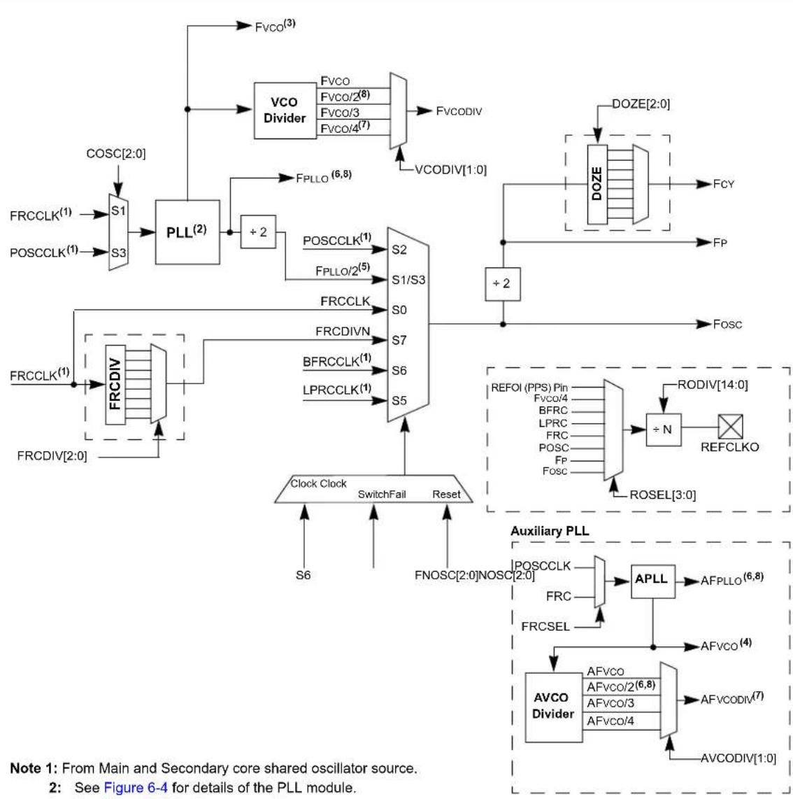
flowchart
graph TD
    A["Main Core Shared Oscillator Source"] --> B["PLL(2)"]
    C["Secondary Core Shared Oscillator Source"] --> D["PLL(2)"]
    B --> E["+2"]
    D --> F["+2"]
    E --> G["DOZE"]
    F --> H["DOZE"]
    G --> I["FCY"]
    H --> J["FP"]
    I --> K["Fosc"]
    L["Clock Clock"] --> M["SwitchFail"]
    M --> N["Reset"]
    O["S6"] --> N
    P["FNOSC[2:0"]NOSC["2:0"]] --> Q["APLL"]
    Q --> R["AFPLLO(6,8)"]
    R --> S["AFVCO(4)"]
    S --> T["AVCO Divider"]
    T --> U["AFVCO/2(6,8)"]
    T --> V["AFVCO/3"]
    T --> W["AFVCO/4"]
    X["COSC[2:0"]] --> Y["S1"]
    Y --> Z["S3"]
    Z --> AA["S2"]
    AA --> AB["S1/S3"]
    AB --> AC["S0"]
    AC --> AD["S7"]
    AD --> AE["S6"]
    AE --> AF["S5"]
    AG["FRCCLK(1)"] --> AH["S1"]
    AH --> AI["S3"]
    AI --> AJ["S2"]
    AJ --> AK["S1/S3"]
    AL["FRCDIV(1)"] --> AM["FRCDIV"]
    AM --> AN["FRCDIV(2:0)"]
    AO["FOSC(2:0)"] --> AP["S1"]
    AP --> AQ["S3"]
    AQ --> AR["S2"]
    AR --> AS["S1/S3"]
    AT["S6"] --> AU["SwitchFail"]
    AV["FNOSC[2:0"]NOSC["2:0"]] --> AW["S2"]
    AW --> AX["S1/S3"]
    AY["FRCCLK(1)"] --> AZ["S1"]
    AZ --> BA["S3"]
    BB["FRCDIV(1)"] --> BC["S2"]
    BC --> BD["S1/S3"]
    BE["FRCCLK(1)"] --> BF["S3"]
    BF --> BG["S2"]
    BH["FRCDIV(1)"] --> BI["S2"]
    BI --> BJ["S1/S3"]
    BK["FRCCLK(1)"] --> BL["S3"]
    BL --> BM["S2"]
    BN["FRCDIV(1)"] --> BO["S2"]
    BO --> BP["S1/S3"]
    BQ["FRCCLK(1)"] --> BR["S3"]
    BR --> BS["S2"]
    BT["FRCDIV(1)"] --> BU["S2"]
    BU --> BV["S1/S3"]
    BW["FRCCLK(1)"] --> BX["S3"]
    BX --> BY["S2"]
    BZ["FRCDIV(1)"] --> CA["S2"]
    CA --> CB["S1/S3"]
    CC["FRCCLK(1)"] --> CD["S3"]
    CD --> CE["S2"]
    CF["FRCDIV(1)"] --> CG["S2"]
    CG --> CH["S1/S3"]
    CI["FRCCLK(1)"] --> CJ["S3"]
    CJ --> CK["S2"]
    CL["FRCDIV(1)"] --> CD
    CM["FRCCLK(1)"] --> CN["S3"]
    CN --> CO["S2"]
    CP["FRCDIV(1)"] --> CR["S2"]
    CR --> CS["S1/S3"]
    CT["FRCCLK(1)"] --> CU["S3"]
    CU --> CV["S2"]
    CW["FRCDIV(1)"] --> CX["S2"]
    CX --> CY["S1/S3"]
    DD["FRCCLK(1)"] --> DE["S3"]
    DE --> DF["S2"]
    DG["FRCDIV(1)"] --> DH["S2"]
    DH --> DI["S1/S3"]
    DJ["FRCCLK(1)"] --> DK["S3"]
    DK --> DL["S2"]
    DV["FRCDIV(1)"] --> DW["S2"]
    DW --> DX["S1/S3"]
    DB["FRCCLK(1)"] --> DC["S3"]
    DC --> DV
Note 1: From Main and Secondary core shared oscillator source.
2: See Figure 6-4 for details of the PLL module.
3: See Figure 6-4 for the source of Fvco.
4: See Figure 6-4 for the source of AVCO.
5: XTPLL, HSPLL, ECPLL, FRCPLL (F PLLO).
6: Clock option for PWM.
7: Clock option for ADC.
8: Clock option for DAC.
6.1 Primary PLL
The Primary Oscillator and internal FRC Oscillator sources can optionally use an on-chip PLL to obtain higher operating speeds. There are two independent instantiations of PLL for the Main and Secondary clock subsystems. Figure 6-4 illustrates a block diagram of the Main/Secondary core PLL module.
For PLL operation, the following requirements must be met at all times without exception:
- The PLL Input Frequency (F PLLI) must be in the range of 8 MHz to 64 MHz
- The PFD Input Frequency (F PFD) must be in the range of 8 MHz to (Fvco/16) MHz
The VCO Output Frequency (Fvco) must be in the range of 400 MHz to 1600 MHz
FIGURE 6-4: MAIN/SECONDARY CORE PLL AND VCO DETAIL
flowchart
graph TD
    A["FRCCLK(1)"] --> B["S1"]
    C["POSCCLK(1)"] --> D["S3"]
    B --> E["DIV 1-8"]
    D --> E
    E --> F["PFD"]
    F --> G["Lock Detect"]
    G --> H["VCO"]
    H --> I["DIV 1-7"]
    I --> J["DIV 1-7"]
    K["COSC[2:0"]] --> B
    L["PLLPRE[3:0"]] --> E
    M["PLL Ready (LOCK)"] --> G
    N["POST1DIV[2:0"]] --> I
    O["POST2DIV[2:0"]] --> J
    P["Feedback Divider 16-200"] --> G
    Q["VCO Divider"] --> R["Fvco"]
    S["VCO Divider"] --> T["Fvco/2(4)"]
    S --> U["Fvco/3"]
    S --> V["Fvco/4(3)"]
    W["FPLLO(2,4)"] --> J
    X["FVCO"] --> I
    Y["FVCODIV"] --> J
    Z["VCODIV[1:0"]] --> Y
Note 1: From Main and Secondary core shared oscillator source.
2: Clock option for PWM.
3: Clock option for ADC.
4: Clock option for DAC.
Equation 6-1 provides the relationship between the PLL Input Frequency (FPLLI) and VCO Output Frequency (Fvco).
EQUATION 6-1: MAIN/SECONDARY CORE Fvco CALCULATION
$$ F V C O = F P L L I \times \left(\frac {M}{N 1}\right) = F P L L I \times \left(\frac {P L L F B D I V [ 7 : 0 ]}{P L L P R E [ 3 : 0 ]}\right) $$
Equation 6-2 provides the relationship between the PLL Input Frequency (FPLLI) and PLL Output Frequency (FPLLO).
EQUATION 6-2: MAIN/SECONDARY CORE FPLLO CALCULATION
$$ F P L L O = F P L L I \times \left(\frac {M}{N 1 \times N 2 \times N 3}\right) = F P L L I \times \left(\frac {P L L F B D I V [ 7 : 0 ]}{P L L P R E [ 3 : 0 ] \times P O S T 1 D I V [ 2 : 0 ] \times P O S T 2 D I V [ 2 : 0 ]}\right) $$
Where:
$$ M = P L L F B D I V [ 7: 0 ] $$
$$ N 1 = P L L P R E [ 3: 0 ] $$
$$ N 2 = P O S T I D I V [ 2: 0 ] $$
$$ N 3 = P O S T 2 D I V [ 2: 0 ] $$
Note: The PLL Phase Detector Input Divider Select (PLLPREx) bits and the PLL Feedback Divider (PLLFBDIVx) bits should not be changed when operating in PLL mode. Therefore, the user must start on either a non-PLL source or clock switch to a non-PLL source (e.g., internal FRC Oscillator) to make any necessary changes and then clock switch to the desired PLL source.
Using Two-Speed Start-up (IESO, FOSCSEL[7]) with a PLL source will start the device on the FRC while preparing the PLL. Once the PLL is ready, the device will switch automatically to the new source. This mode should not be used if changes are needed to the PLLPREx and PLLFBDIVx bits because the PLL may be running before user code execution begins.
Also, it is not permitted to directly clock switch from one PLL clock source to a different PLL clock source. The user would need to transition between PLL clock sources with a clock switch to a non-PLL clock source.
EXAMPLE 6-1: CODE EXAMPLE FOR USING MAIN PRIMARY PLL WITH 8 MHz INTERNAL FRC
//code example for 50 MIPS system clock using 8MHz FRC
// Select FRC on POR
#pragma config FNOSC = FRC // Oscillator Source Selection (Internal Fast RC (FRC))
#pragma config IESO = OFF
// Enable Clock Switching
#pragma config FCKSM = CSECMD
int main()
{
    // Configure PLL prescaler, both PLL postscalers, and PLL feedback divider
CLKDIVbits.PLLPRE = 1; // N1=1
PLLFBDbits.PLLFBDIV = 125; // M = 125
PLLDIVbits.POST1DIV = 5; // N2=5
PLLDIVbits.POST2DIV = 1; // N3=1
// Initiate Clock Switch to FRC with PLL (NOSC=0b001)
__builtin_write_OSCCONH(0x01);
__builtin_write_OSCCONL(OSCCON | 0x01);
// Wait for Clock switch to occur
while (OSCCONbits.OSWEN!= 0);
}
Note: FPLLO = FPLLI * M/(N1 * N2 * N3); FPLLI = 8; M = 125; N1 = 1; N2 = 5; N3 = 1;
so FPLLO = 8 * 125/(1 * 5 * 1) = 200 MHz or 50 MIPS.
EXAMPLE 6-2: CODE EXAMPLE FOR USING SECONDARY PRIMARY PLL WITH 8 MHz INTERNAL FRC
//code example for 60 MIPS system clock using 8MHz FRC
// Select Internal FRC at POR
// Select FRC on POR
#pragma config S1FNOSC = FRC    // Oscillator Source Selection (Internal Fast RC (FRC))
#pragma config S1IESO = OFF    // Two-speed Oscillator Start-up Enable bit (Start up with user-selected oscillator source)
// Enable Clock Switching
#pragma config S1FCKSM = CSECMD
int    main()
{
    // Configure PLL prescaler, both PLL postscalers, and PLL feedback divider
CLKDIVbits.PLLPRE = 1; // N1=1
PLLFBDbits.PLLFBDIV = 150; // M = 150
PLLDIVbits.POST1DIV = 5; // N2=5
PLLDIVbits.POST2DIV = 1; // N3=1
// Initiate Clock Switch to FRC with PLL (NOSC-0b001)
__builtin_write_OSCCONH(0x01);
__builtin_write_OSCCONL(OSCCON | 0x01);
// Wait for Clock switch to occur
while    (OSCCONbits.OSWEN!= 0);
}
Note: FPLLO = FPLLI * M/(N1 * N2 * N3); FPLLI = 8; M = 150; N1 = 1; N2 = 5; N3 = 1;
so FPLLO = 8 * 150/(1 * 5 * 1) = 240 MHz or 60 MIPS.
6.2 Auxiliary PLL
The dsPIC33CH128MP508 device family implements an Auxiliary PLL (APLL) module for each core present. There are two independent instantiations of APLL for the Main and Secondary clock subsystems. The APLL is used to generate various peripheral clock sources independent of the system clock. Figure 6-5 shows a block diagram of the Main/Secondary core APLL module.
For APLL operation, the following requirements must be met at all times without exception:
- The APLL Input Frequency (AF PLLI) must be in the range of 8 MHz to 64 MHz
• The APFD Input Frequency (AF PFD) must be in the range of 8 MHz to (AFvco/16) MHz
• The AVCO Output Frequency (AF vco) must be in the range of 400 MHz to 1600 MHz
FIGURE 6-5: MAIN/SECONDARY CORE APLL AND VCO DETAIL
flowchart
graph TD
    A["FRCCLK(1)"] --> B["DIV 1-8"]
    C["POSCLK(1)"] --> B
    B --> D["APFD"]
    D --> E["Lock Detect"]
    E --> F["AVCO"]
    F --> G["DIV 1-7"]
    G --> H["DIV 1-7"]
    H --> I["0"]
    I --> J["APLLEN"]
    J --> K["AFPLLO(2,4)"]
    L["FRCSEL"] --> B
    M["APLLPRE[3:0"]] --> D
    N["APLL Ready (APLLCLK)"] --> E
    O["APOST1DIV[2:0"]] --> G
    P["APOST2DIV[2:0"]] --> H
    Q["Feedback Divider 16-200"] --> F
    R["APLLFBDIV[7:0"]] --> F
    S["AFVCO"] --> H
    T["AVCO Divider"] --> U["AFVCO/2(2,4)"]
    T --> V["AFVCO/3"]
    T --> W["AFVCO/4"]
    X["AVCODIV[1:0"]] --> Y["AFVCODIV(3)"]
Equation 6-3 provides the relationship between the APLL Input Frequency (AFPLLI) and the AVCO Output Frequency (AFvco).
EQUATION 6-3: MAIN/SECONDARY CORE AFvco CALCULATION
$$ A F V C O = A F P L L I \times \left(\frac {M}{N 1}\right) = A F P L L I \times \left(\frac {A P L L F B D I V [ 7 : 0 ]}{A P L L P R E [ 3 : 0 ]}\right) $$
Equation 6-4 provides the relationship between the APLL Input Frequency (AFPLLI) and APLL Output Frequency (AFPLLO).
EQUATION 6-4: MAIN/SECONDARY CORE AFPLLO CALCULATION
$$ A F P L L O - A F P L L I \times \left(\frac {M}{N 1 \times N 2 \times N 3}\right) - A F P L L I \times \left(\frac {A P L L F B D I V [ 7 : 0 ]}{A P L L P R E [ 3 : 0 ] \times A P O S T 1 D I V [ 2 : 0 ] \times A P O S T 2 D I V [ 2 : 0 ]}\right) $$
Where:
M = APLLFBDIV[7:0] N1 = APLLPRE[3:0] N2 = APOST1DIV[2:0] N3 = APOST2DIV[2:0]
EXAMPLE 6-3: CODE EXAMPLE FOR USING MAIN OR SECONDARY AUXILIARY PLL WITH THE INTERNAL FRC OSCILLATOR
//code example for AFVCO = 1 GHz and AFPLLO = 500 MHz using 8 MHz internal FRC
// Configure the source clock for the APLL
ACLKCON1bits.FRCSEL = 1; // Select internal FRC as the clock source
// Configure the APLL prescaler, APLL feedback divider, and both APLL postscalers.
ACLKCON1bits.APLLPRE = 1; // N1 = 1
APLLFBD1bits.APLLFBDIV = 125; // M = 125
APLLDIV1bits.APOST1DIV = 2; // N2 = 2
APLLDIV1bits.APOST2DIV = 1; // N3 = 1
// Enable APLL
ACLKCON1bits.APLLEN = 1;
Note: Even with the APLLEN bit set, another peripheral must generate a clock request before the APLL will start.
6.3 CPU Clocking
While the Main and Secondary subsystems share access to a single set of oscillator sources, all other clocking logic is implemented individually. The Main and Secondary core can be configured independently to use any of the following clock configurations:
• Primary Oscillator (POSC) on the OSCI and OSCO pins
- Internal Fast RC Oscillator (FRC) with optional clock divider
- Internal Low-Power RC Oscillator (LPRC)
• Primary Oscillator with PLL (ECPLL, HSPLL, XTPLL)
- Internal Fast RC Oscillator with PLL (FRCPLL)
- Backup Internal Fast RC Oscillator (BFRC)
Each core's system clock source is divided by two to produce the internal instruction cycle clock. In this document, the instruction cycle clock is denoted by Fcy. The timing diagram in Figure 6-6 illustrates the relationship between the system clock (Fosc), the instruction cycle clock (Fcγ) and the Program Counter (PC).
The internal instruction cycle clock (FcY) can be output on the OSCO I/O pin if the Primary Oscillator mode (POSCMD[1:0]) is not configured as HS/XT. Refer to Table 6-3 for the dual core function of the OSCO pin.
FIGURE 6-6: CLOCK AND INSTRUCTION CYCLE TIMING
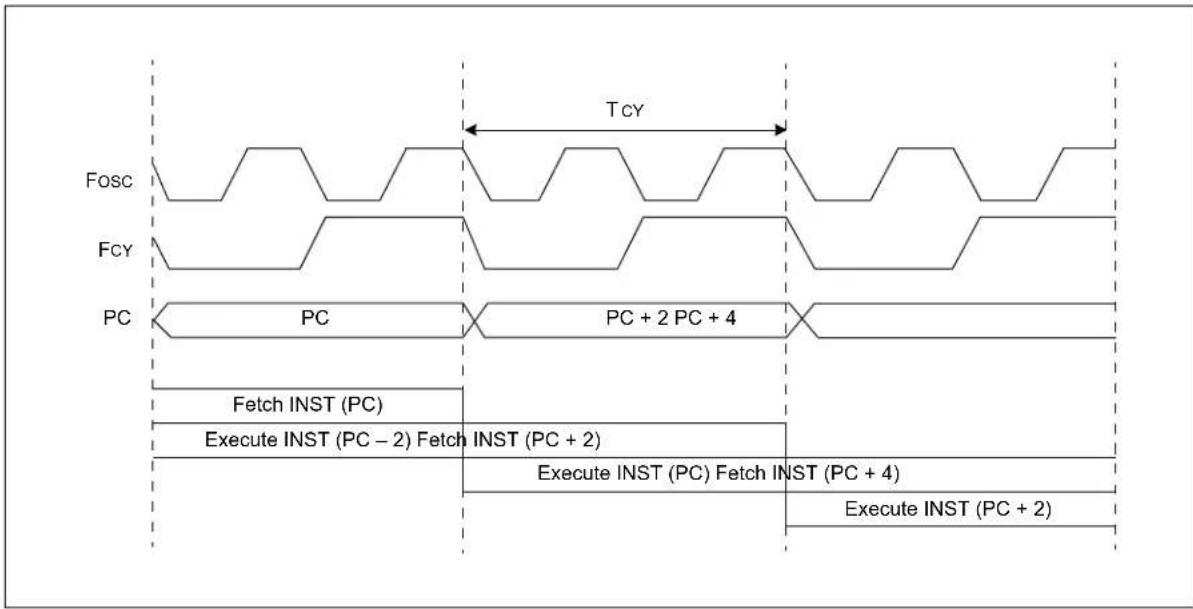
text_image
Fosc Tcy FcY PC PC + 2 PC + 4 Fetch INST (PC) Execute INST (PC - 2) Fetch INST (PC + 2) Execute INST (PC) Fetch INST (PC + 4) Execute INST (PC + 2)6.4 Primary Oscillator (POSC)
The dsPIC33CH128MP508 family devices contain one instance of the Primary Oscillator (POSC), which is available to both the Main and Secondary clock subsystems. The Primary Oscillator is available on the OSCI and OSCO pins of the dsPIC33CH devices. This connection enables an external crystal (or ceramic resonator) to provide the clock to the device. The Primary Oscillator provides three modes of operation:
• Medium Speed Oscillator (XT Mode):
The XT mode is a Medium Gain, Medium Frequency mode used to work with crystal frequencies of 3.5 MHz to 10 MHz.
• High-Speed Oscillator (HS Mode):
The HS mode is a High-Gain, High-Frequency mode used to work with crystal frequencies of 10 MHz to 32 MHz.
- External Clock Source Operation (EC Mode): If the on-chip oscillator is not used, the EC mode allows the internal oscillator to be bypassed. The device clocks are generated from an external source (0 MHz to up to 64 MHz) and input on the OSCI pin.
Note: The Primary Oscillator (POSC) is shared between Main and Secondary.
6.5 Internal Fast RC (FRC) Oscillator
The dsPIC33CH128MP508 family devices contain one instance of the internal Fast RC (FRC) Oscillator, which is available to both the Main and Secondary clock subsystems. The FRC Oscillator provides a nominal 8 MHz clock without requiring an external crystal or ceramic resonator, which results in system cost savings for applications that do not require a precise clock reference.
The application software can tune the frequency of the oscillator using the FRC Oscillator Tuning bits (TUN[5:0]) in the FRC Oscillator Tuning register (OSCTUN[5:0]).
Note: The FRC is shared between Main and Secondary; the OSCTUN register is used to tune the FRC as a part of the Main oscillator configuration.
6.6 Low-Power RC (LPRC) Oscillator
The dsPIC33CH128MP508 family devices contain one instance of the Low-Power RC (LPRC) Oscillator that is available to both the Main and Secondary clock subsystems. The LPRC Oscillator provides a nominal clock frequency of 32 kHz and is the clock source for the Watchdog Timer (WDT) and Fail-Safe Clock Monitor (FSCM) circuits in each core clock subsystem.
The LPRC Oscillator is the clock source for the WDT and FSCM in both the Main and Secondary cores. The LPRC Oscillator is enabled at power-on.
The LPRC Oscillator remains enabled under these conditions:
• The Main or Secondary FSCM is enabled
• The Main or Secondary WDT is enabled
- The LPRC Oscillator is selected as the system clock
If none of these conditions are true, the LPRC is shut off in Sleep mode.
Note: The LPRC is shared between Main and Secondary.
6.7 Backup Internal Fast RC (BFRC) Oscillator
The oscillator block provides a stable reference clock source for the Fail-Safe Clock Monitor (FSCM). When FSCM is enabled in the FCKSM[1:0] Configuration bits (FOSC[7:6]), it constantly monitors the main clock source against a reference signal from the 8 MHz Backup Internal Fast RC (BFRC) Oscillator. In case of a clock failure, the Fail-Safe Clock Monitor switches the clock to the BFRC Oscillator, allowing for continued low-speed operation or a safe application shutdown.
6.8 Reference Clock Output
In addition to the CLKO output (Fosc/2), the dsPIC33CH128MP508 family devices can be configured to provide a reference clock output signal to a port pin. This feature is available in all oscillator configurations and allows the user to select a greater range of clock sub-
multiples to drive external devices in the application. CLKO is enabled by Configuration bit, OSCIOFNC, and is independent of the REFCLKO reference clock. REFCLKO is mappable to any I/O pin that has mapped output capability. The reference clock output module block diagram is shown in Figure 6-7.
FIGURE 6-7: REFERENCE CLOCK GENERATOR

flowchart
graph LR
    A["REFOI (PPS) Pin"] --> B["1000"]
    C["Fvco/4"] --> D["0110"]
    E["BFRC"] --> F["0101"]
    G["LPRC"] --> H["0100"]
    I["FRC"] --> J["0011"]
    K["POSC"] --> L["0010"]
    M["Peripheral Clock (FP)"] --> N["0001"]
    O["System Clock (Fosc)"] --> P["0000"]
    Q["ROSEL[3:0"]] --> R["Divider"]
    S["ROTRIM[8:0"]] --> R
    T["RODIV[14:0"]] --> R
    U["ROOUT"] --> V["REFCLKO (PPS)"]
    W["To SPI, CCP, CLC"] --> X["Output"]
This reference clock output is controlled by the REFOCONL and REFOCONH registers. Setting the ROEN bit (REFOCONL[15]) makes the clock signal available on the REFCLKO pin. The RODIV[14:0] bits (REFOCONH[14:0]) and ROTRIM[8:0] bits (REFOTRIMH[15:7]) enable the selection of different clock divider options. The formula for determining the final frequency output is shown in Equation 6-5. The ROSWEN bit (REFOCONL[9]) indicates that the clock divider has been successfully switched. In order to switch the REFCLKO divider, the user should ensure that this bit reads as '0'. Write the updated values to the RODIV[14:0] or ROTRIM[8:0] bits, set the ROSWEN bit and then wait until it is cleared before assuming that the REFCLKO clock is valid.
EQUATION 6-5: CALCULATING FREQUENCY OUTPUT
$$ F _ {R E F O U T} = \frac {F _ {R E F I N}}{2 \cdot (R O D I V [ 1 4 : 0 ] + R O T R I M [ 8 : 0 ] / 5 1 2)} $$
Where: FREFOUT = Output Frequency FREFIN = Input Frequency When RODIV[14:0] = 0 , the output clock is the same as the input clock.
The ROSEL[3:0] bits (REFOCONL[3:0]) determine which clock source is used for the reference clock output. The ROSLP bit (REFOCONL[11]) determines if the reference source is available on REFCLKO when the device is in Sleep mode.
To use the reference clock output in Sleep mode, both the ROSLP bit must be set and the clock selected by the ROSEL[3:0] bits must be enabled for operation during Sleep mode, if possible. Clearing the ROSEL[3:0] bits allows the reference output frequency to change, as the system clock changes during any clock switches. The ROOUT bit enables/disables the reference clock output on the REFCLKO pin.
The ROACTIV bit (REFOCONL[8]) indicates that the module is active; it can be cleared by disabling the module (setting ROEN to '0'). The user must not change the reference clock source, or adjust the divider when the ROACTIV bit indicates that the module is active. To avoid glitches, the user should not disable the module until the ROACTIV bit is '1'.
6.9 OSCCON Unlock Sequence
The OSCCON register is protected against unintended writes through a lock mechanism. The upper and lower bytes of OSCCON have their own unlock sequence, and both must be used when writing to both bytes of the register. Before OSCCON can be written to, the following unlock sequence must be used:
- Execute the unlock sequence for the OSCCON high byte.
In two back-to-back instructions:
• Write 0x78 to OSCCON[15:8]
• Write 0x9A to OSCCON[15:8]
-
In the instruction immediately following the unlock sequence, the OSCCON[15:8] bits can be modified.
-
Execute the unlock sequence for the OSCCON low byte.
In two back-to-back instructions:
• Write 0x46 to OSCCON[7:0]
• Write 0x57 to OSCCON[7:0]
- In the instruction immediately following the unlock sequence, the OSCCON[7:0] bits can be modified.
| Note: MPLAB XC16 provides a built-in C language function, including the unlocking sequence to modify high and low bytes in the OSCCON register:_builtin_write_OSCCONH(value)_builtin_write_OSCCONL(value) |
Example 6-4 illustrates code for using the PLL
(50 MIPS) with the Primary Oscillator.
EXAMPLE 6-4: CODE EXAMPLE FOR USING MAIN PLL (50 MIPS) WITH PRIMARY OSCILLATOR (POSC)
//code example for 50 MIPS system clock using POSC with 10 MHz external crystal
// Select Internal FRC at POR
// Select FRC on POR
#pragma config FNOSC = FRC // Oscillator Source Selection (Internal Fast RC (FRC))
#pragma config IESO = OFF
/// Enable Clock Switching and Configure POSC in XT mode
#pragma config POSCMD = XT
#pragma config FCKSM = CSECMD

int main()
{
    // Configure PLL prescaler, both PLL postscalers, and PLL feedback divider
    CLKDIVbits.PLLPRE = 1;    // N1=1
    PLLFBDbits.PLLFBDIV = 100;    // M = 100
    PLLDIVbits.POST1DIV = 5;    // N2=5
    PLLDIVbits.POST2DIV = 1;    // N3=1

    // Initiate Clock Switch to Primary Oscillator with PLL (NOSC=0b011)
    __builtin_write_OSCCONH(0x03);
    __builtin_write_OSCCONL(OSCCON | 0x01);

    // Wait for Clock switch to occur
    while (OSCCONbits.OSWEN!= 0);

    // Wait for PLL to lock
    while (OSCCONbits.LOCK!= 1);
}

Note: FPLLO = FPLLI * M/(NI * N2 * N3); FPLLI = 10; M = 100; NI = 1; N2 = 5; N3 = 1;
so FPLLO = 10 * 100/(1 * 5 * 1) = 200 MHz or 50 MIPS.
Example 6-5 illustrates code for using the PLL (60 MIPS) with the Primary Oscillator.
6.10 Primary Oscillator Pin Functionality
The Primary Oscillator pins (OSCI and OSCO) can be used for other functions when the primary oscillator is not being used. The POSCMD<1:0> Configuration bits in the Oscillator Configuration register (FOSC<1:0>)
determine the oscillator pin function. The OSCIOFNC bit (FOSC<2>) determines the OSCO/CLKO pin function. By default, the CLKO function is active and the pin will output a clock frequency of Fcy. A clock signal is present on the OSCO/CLKO pin when device is unprogrammed or during the programming sequence. Care should be taken when OSCO/CLKO pin is used to drive other circuitry.
EXAMPLE 6-5: CODE EXAMPLE FOR USING SECONDARY PLL (60 MIPS) WITH PRIMARY OSCILLATOR (POSC)
//code example for 60 MIPS system clock using POSC with 10 MHz external crystal
// Select Internal FRC at POR
// Select FRC on POR
#pragma config S1FNOSC = FRC // Oscillator Source Selection (Internal Fast RC (FRC))
#pragma config S1IESO = OFF    // Two-speed Oscillator Start-up Enable bit (Start up with user-selected oscillator source)
// Enable Clock Switching
#pragma config S1FCKSM = CSECMD

//Configure POSC in XT mode in Main core FOSC configuration register
#pragma config POSCMD = XT

int main()
{
    // Configure PLL prescaler, both PLL postscalers, and PLL feedback divider
    CLKDIVbits.PLLPRE = 1;    // N1=1
    PLLFBDBits.PLLFBDIV = 120;    // M = 120
    PLLDIVbits.POST1DIV = 5;    // N2=5
    PLLDIVbits.POST2DIV = 1;    // N3=1

    // Initiate Clock Switch to Primary Oscillator with PLL (NOSC=0b011)
    __builtin_write_OSCCONH(0x03);
    __builtin_write_OSCCONL(OSCCON | 0x01);

    // Wait for Clock switch to occur
    while (OSCCONbits.OSWEN!= 0);

    // Wait for PLL to lock
    while (OSCCONbits.LOCK!= 1);
}
Example 6-6 illustrates code for using the Main PLL with an 8 MHz internal FRC.
EXAMPLE 6-6: CODE EXAMPLE FOR USING MAIN PLL (50 MIPS) WITH 8 MHz INTERNAL FRC
//code example for 50 MIPS system clock using 8MHz FRC

// Select FRC on POR
#pragma config FNOSC = FRC    // Oscillator Source Selection (Internal Fast RC (FRC))
#pragma config IESO = OFF
/// Enable Clock Switching
#pragma config FCKSM = CSECMD

int main()
{
    // Configure PLL prescaler, both PLL postscalers, and PLL feedback divider
    CLKDIVbits.PLLPRE = 1;    // N1=1
    PLLFBDBits.PLLFBDIV = 125;    // M = 125
    PLLDIVbits.POST1DIV = 5;    // N2=5
    PLLDIVbits.POST2DIV = 1;    // N3=1

    // Initiate Clock Switch to FRC with PLL (NOSC=0b001)
    __builtin_write_OSCCONH(0x01);
    __builtin_write_OSCCONL(OSCCON | 0x01);

    // Wait for Clock switch to occur
    while (OSCCONbits.OSWEN!= 0);

    // Wait for PLL to lock
    while (OSCCONbits.LOCK!= 1);
}

Note: FPLLO = FPLLII * M/(N1 * N2 * N3); FPLLII = 8; M = 125; N1 = 1; N2 = 5; N3 = 1;
so FPLLO = 8 * 125/(1 * 5 * 1) = 200 MHz or 50 MIPS.
Example 6-7 illustrates code for using the Secondary
PLL with an 8 MHz internal FRC.
EXAMPLE 6-7: CODE EXAMPLE FOR USING SECONDARY PLL (60 MIPS) WITH 8 MHz INTERNAL FRC
//code example for 60 MIPS system clock using 8MHz FRC

// Select FRC on POR
#pragma config S1FNOSC = FRC // Oscillator Source Selection (Internal Fast RC (FRC))
#pragma config S1IESO = OFF // Two-speed Oscillator Start-up Enable bit (Start up with user-selected oscillator source)

// Enable Clock Switching
#pragma config S1FCKSM = CSECMD

int main()
{
    // Configure PLL prescaler, both PLL postscalers, and PLL feedback divider
    CLKDIVbits.PLLPRE = 1; // N1=1
    PLLFBDbits.PLLFBDIV = 150; // M = 150
    PLLDIVbits.POST1DIV = 5; // N2=5
    PLLDIVbits.POST2DIV = 1; // N3=1

    // Initiate Clock Switch to FRC with PLL (NOSC=0b001)
    __builtin_write_OSCCONH(0x01);
    __builtin_write_OSCCONL(OSCCON | 0x01);

    // Wait for Clock switch to occur
    while (OSCCONbits.OSWEN!= 0);
    // Wait for PLL to lock
    while (OSCCONbits.LOCK!= 1);
}

Note: FPLLO = FPLLI * M/(N1 * N2 * N3); FPLLI = 8; M = 150; N1 = 1; N2 = 5; N3 = 1;
so FPLLO = 8 * 150/(1 * 5 * 1) = 240 MHz or 60 MIPS.
6.11 Main Oscillator Configuration Registers
Table 6-1 lists the configuration settings that select the device's Main core oscillator source and operating mode at a POR.
TABLE 6-1: CONFIGURATION BIT VALUES FOR CLOCK SELECTION FOR THE MAIN
| Oscillator Source | Oscillator Mode | FNOSC[2:0] Value | POSCMD[1:0] Value ^(3) | Notes |
| S0 Fast RC Oscillator (FRC) 000 xx 1 | ||||
| S1 Fast RC Oscillator with PLL (FRCPLL) 001 xx 1 | ||||
| S2 Primary Oscillator (EC) 010 00 1 | ||||
| S2 Primary Oscillator (XT) 010 01 | ||||
| S2 Primary Oscillator (HS) 010 10 | ||||
| S3 Primary Oscillator with PLL (ECPLL) | 011 | 00 | 1 | |
| S3 Primary Oscillator with PLL (XTPLL) | 011 01 | |||
| S3 Primary Oscillator with PLL (HSPLL) | 011 10 | |||
| S4 Reserved | 100 xx | |||
| S5 | Low-Power RC Oscillator (LPRC) | 101 | xx | 1 |
| S6 | Backup FRC (BFRC) | 110 | xx | 1 |
| S7 | Fast RC Oscillator with ÷ N Divider (FRCDIVN) | 111 | xx | 1, 2 |
Note 1: The OSCO pin function is determined by the OSCIOFNC Configuration bit.
2: This is the default oscillator mode for an unprogrammed (erased) device.
3: The POSCMDx bits are only available in the Main FOSC Configuration register.
6.12 Secondary Oscillator Configuration Registers
Table 6-2 lists the configuration settings that select the device's Secondary core oscillator source and operating mode at a POR.
TABLE 6-2: CONFIGURATION BIT VALUES FOR CLOCK SELECTION FOR THE SECONDARY
| Oscillator Source | Oscillator Mode | S1FNOSC[2:0] Value | POSCMD[1:0] Value (3) | Notes |
| S0 Fast | RC Oscillator (FRC) 000 xx 1 | |||
| S1 Fast | RC Oscillator with PLL (FRCPLL) 001 xx 1 | |||
| S2 Primary Oscillator (EC) 010 00 1 | ||||
| S2 Primary Oscillator (XT) 010 01 | ||||
| S2 Primary Oscillator (HS) 010 10 | ||||
| S3 | Primary Oscillator with PLL (ECPLL) | 011 | 00 | 1 |
| S3 Primary Oscillator with PLL (XTPLL) | 011 01 | |||
| S3 Primary Oscillator with PLL (HSPLL) | 011 10 | |||
| S4 Reserved | 100 xx 1 | |||
| S5 | Low-Power RC Oscillator (LPRC) | 101 | xx | 1 |
| S6 | Backup FRC (BFRC) | 110 | xx | 1 |
| S7 | Fast RC Oscillator with ÷ N Divider (FRCDIVN) | 111 | xx | 1, 2 |
Note 1: The OSCO pin function is determined by the S1OSCIOFNC Configuration bit. If both the Main core OSCIOFNC and Secondary core S1OSCIOFNC bits are set, the Main core OSCIOFNC bit has priority.
2: This is the default oscillator mode for an unprogrammed (erased) device.
3: The POSCMD[1:0] bits are only available in the Main Oscillator Configuration register, FOSC. This setting configures the Primary Oscillator for use by either core.
TABLE 6-3: OSCO FUNCTION FOR THE MAIN AND SECONDARY CORE (1)
| [OSCIOFNC:S1OSCIOFNC] | RB1 or OSCO pin function |
| 1:1 | Main clock output on OSCO pin |
| 1:0 | Main clock output on OSCO pin |
| 0:1 | Secondary clock output on OSCO pin |
| 0:0 | Clock out disabled, RB1 works as an I/O port; output function is based on pin ownership (CPRB1 = 1 or 0) |
Note 1: The RB1 pin will toggle during programming or debugging time, irrespective of the OSCIOFNC or S1OSCIOFNC settings.
6.13 Main Special Function Registers
These Special Function Registers provide run-time control and status of the Main core's oscillator system.
6.13.1 MAIN OSCILLATOR CONTROL REGISTERS
REGISTER 6-1: OSCCON: OSCILLATOR CONTROL REGISTER (MAIN) ^(1)
| U-0 R-0 R-0 R-0 U-0 R/W-y R/W-y R/W-y | ||||||||
| — COSC2 COSC1 CO | SC0 — | N | O | S | C | ^(2)_2 | NOSC1 ^(2) | NOSC0 ^(2) |
| bit 15 | bit 8 | |||||||
| R/W-0 U-0 R-0 U-0 | R/C-0 | U-0 U-0 R/W-0 | |||||
| CLKLOCK | — | LOCK | — | CF^(3) | — | — | OSWEN |
| bit 7 bit 0 | |||||||
| Legend: | y = Value set from Configuration bits on POR | C = Clearable | |
| R = Readable bit | W = Writable bit | U = Unimplemented bit, read as ‘0’ | |
| -n = Value at POR | ‘1’ = Bit is set | ‘0’ = Bit is cleared | x = Bit is unknown |
bit 15 Unimplemented: Read as '0'
bit 14-12 COSC[2:0]: Current Oscillator Selection bits (read-only)
111 = Fast RC Oscillator (FRC) with Divide-by-n (FRCDIVN)
110 = Backup FRC (BFRC)
101 = Low-Power RC Oscillator (LPRC)
100 = Reserved - default to FRC
011 = Primary Oscillator (XT, HS, EC) with PLL (XTPLL, HSPLL, ECPLL)
010 = Primary Oscillator (XT, HS, EC)
001 = Fast RC Oscillator (FRC) with PLL (FRCPLL)
000 = Fast RC Oscillator (FRC)
bit 11 Unimplemented: Read as '0'
bit 10-8 NOSC[2:0]: New Oscillator Selection bits ^(2)
111 = Fast RC Oscillator (FRC) with Divide-by-n (FRCDIVN)
110 = Backup FRC (BFRC)
101 = Low-Power RC Oscillator (LPRC)
100 = Reserved - default to FRC
011 = Primary Oscillator (XT, HS, EC) with PLL (XTPLL, HSPLL, ECPLL)
010 = Primary Oscillator (XT, HS, EC)
001 = Fast RC Oscillator (FRC) with PLL (FRCPLL)
000 = Fast RC Oscillator (FRC)
bit 7 CLKLOCK: Clock Lock Enable bit
1 = If (FCKSM0 = 1), then clock and PLL configurations are locked; if (FCKSM0 = 0), then clock and PLL configurations may be modified
0 = Clock and PLL selections are not locked, configurations may be modified
bit 6 Unimplemented: Read as '0'
Note 1: Writes to this register require an unlock sequence.
2: Direct clock switches between any Primary Oscillator mode with PLL and FRCPLL mode are not permitted. This applies to clock switches in either direction. In these instances, the application must switch to FRC mode as a transitional clock source between the two PLL modes.
3: This bit can only be cleared in software. Setting the bit in software (= 1) will have the same effect as an actual oscillator failure and will trigger an oscillator failure trap. Setting this bit will not cause an FSCM event.
REGISTER 6-1: OSCCON: OSCILLATOR CONTROL REGISTER (MAIN) ^(1) (CONTINUED)
bit 5 LOCK: PLL Lock Status bit (read-only)
1 = Indicates that PLL is in lock or PLL start-up timer is satisfied
0 = Indicates that PLL is out of lock, start-up timer is in progress or PLL is disabled
bit 4 Unimplemented: Read as '0'
bit 3 CF: Clock Fail Detect bit (3)
1 = FSCM has detected a clock failure
0 = FSCM has not detected a clock failure
bit 2-1 Unimplemented: Read as '0'
bit 0 OSWEN: Oscillator Switch Enable bit
1 = Requests oscillator switch to the selection specified by the NOSC[2:0] bits
0 = Oscillator switch is complete
Note 1: Writes to this register require an unlock sequence.
2: Direct clock switches between any Primary Oscillator mode with PLL and FRCPLL mode are not permitted. This applies to clock switches in either direction. In these instances, the application must switch to FRC mode as a transitional clock source between the two PLL modes.
3: This bit can only be cleared in software. Setting the bit in software (= 1) will have the same effect as an actual oscillator failure and will trigger an oscillator failure trap. Setting this bit will not cause an FSCM event.
REGISTER 6-2: CLKDIV: CLOCK DIVIDER REGISTER (MAIN)
| R/W-0 R/W-0 R/W-1 R/W-1 R/W-0 R/W-0 R/W-0 R/W-0 | |||||||
| ROI DOZE2 (1) | DOZE1(1) | DOZE0(1) | DOZEN(2,3) | FRCDIV2 FR | FRCDIV1 FRCDIV0 | ||
| bit 15 bit 8 | |||||||
| U-0 U-0 r-0 r-0 R/W-0 R/W-0 R/W-0 R/W-1 | |||
| — — — | — PLLPRE[3:0] | (4) | |
| bit 7 bit 0 | |||
| Legend: | r = Reserved bit | ||
| R = Readable bit | W = Writable bit | U = Unimplemented bit, read as ‘0’ | |
| -n = Value at POR | ‘1’ = Bit is set | ‘0’ = Bit is cleared | x = Bit is unknown |
bit 15 ROI: Recover on Interrupt bit 1 = Interrupts will clear the DOZEN bit and the processor clock, and the peripheral clock ratio is set to 1:1 0 = Interrupts have no effect on the DOZEN bit
bit 14-12 DOZE[2:0]: Processor Clock Reduction Select bits ^(1) 111 = FP divided by 128
110 = FP divided by 64
101 = FP divided by 32
100 = FP divided by 16
011 = FP divided by 8 (default)
010 = FP divided by 4
001 = FP divided by 2
000 = FP divided by 1
bit 11 DOZEN: Doze Mode Enable bit ^(2,3) 1 = DOZE[2:0] field specifies the ratio between the peripheral clocks and the processor clocks
0 = Processor clock and peripheral clock ratio is forced to 1:1
bit 10-8 FRCDIV[2:0]: Internal Fast RC Oscillator Postscaler bits 111 = FRC divided by 256 110 = FRC divided by 64 101 = FRC divided by 32 100 = FRC divided by 16 011 = FRC divided by 8 010 = FRC divided by 4 001 = FRC divided by 2 000 = FRC divided by 1 (default)
bit 7-6 Unimplemented: Read as '0' bit 5-4 Reserved: Read as '0'
Note 1: The DOZE[2:0] bits can only be written to when the DOZEN bit is clear. If DOZEN = 1, any writes to DOZE[2:0] are ignored.
2: This bit is cleared when the ROI bit is set and an interrupt occurs.
3: The DOZEN bit cannot be set if DOZE[2:0] = 000. If DOZE[2:0] = 000, any attempt by user software to set the DOZEN bit is ignored.
4: PLLPRE[3:0] may be updated while the PLL is operating, but the VCO may overshoot.
REGISTER 6-2: CLKDIV: CLOCK DIVIDER REGISTER (MAIN) (CONTINUED)
bit 3-0 PLLPRE[3:0]: PLL Phase Detector Input Divider Select bits (also denoted as 'N1', PLL prescaler) ^(4) 11111 = Reserved
...
1001 = Reserved
1000 = Input divided by 8
0111 = Input divided by 7
0110 = Input divided by 6
0101 = Input divided by 5
0100 = Input divided by 4
0011 = Input divided by 3
0010 = Input divided by 2
0001 = Input divided by 1 (power-on default selection)
0000 = Reserved
Note 1: The DOZE[2:0] bits can only be written to when the DOZEN bit is clear. If DOZEN = 1, any writes to DOZE[2:0] are ignored.
2: This bit is cleared when the ROI bit is set and an interrupt occurs.
3: The DOZEN bit cannot be set if DOZE[2:0] = 000. If DOZE[2:0] = 000, any attempt by user software to set the DOZEN bit is ignored.
4: PLLPRE[3:0] may be updated while the PLL is operating, but the VCO may overshoot.
REGISTER 6-3: PLLFBD: PLL FEEDBACK DIVIDER REGISTER (MAIN)
| U-0 U-0 U-0 U-0 r-0 r-0 r-0 r-0 | |||||||
| —— | —— | —— | |||||
| bit 15 bit 8 | |||||||
| R | / | W | - | 1 | R | / | W | - | 0 | R | / |
| PLLFBDIV[7:0] | |||||||||||
| bit 7 bit 0 | |||||||||||
| Legend: r = Reserved bit | |||
| R = Readable bit W = Writable bit | U = Unimplemented bit, read as ‘0’ | ||
| -n = Value at POR | ‘1’ = Bit is set | ‘0’ = Bit is cleared | x = Bit is unknown |
bit 15-12 Unimplemented: Read as '0'
bit 11-8 Reserved: Maintain as '0'
bit 7-0 PLLFBDIV[7:0]: PLL Feedback Divider bits (also denoted as 'M', PLL multiplier)
11111111 = Reserved ... 11001000 = 200 Maximum ^(1) ... 10010110 = 150 (default) ... 00010000 = 16 Minimum ^(1) ... 00000010 = Reserved 00000001 = Reserved 00000000 = Reserved
Note 1: The allowed range is 16-200 (decimal). The rest of the values are reserved and should be avoided. The power on the default feedback divider is 150 (decimal) with an 8 MHz FRC input clock. The VCO frequency is 1.2 GHz.
REGISTER 6-4: OSCTUN: FRC OSCILLATOR TUNING REGISTER (MAIN)
| U-0 U-0 U-0 U-0 U-0 U-0 U-0 U-0 | |||||||
| —— | —— | —— | |||||
| bit 15 bit 8 | |||||||
| U-0 U-0 R/W-0 R/W-0 R/W-0 R/W-0 R/W-0 R/W-0 | |
| — — TUN[5:0] | |
| bit 7 bit 0 | |
Legend:
R = Readable bit W = Writable bit U = Unimplemented bit, read as '0'
-n = Value at POR '1' = Bit is set '0' = Bit is cleared x = Bit is unknown
bit 15-6 Unimplemented: Read as '0'
bit 5-0 TUN[5:0]: FRC Oscillator Tuning bits
011111 = Maximum frequency deviation of 1.74% (MHz)
011110 = Center frequency + 1.693% (MHz)
* * *
000001 = Center frequency + 0.047% (MHz)
000000 = Center frequency (8.00 MHz nominal)
111111 = Center frequency - 0.047% (MHz)
* * *
100001 = Center frequency - 1.693% (MHz)
100000 = Minimum frequency deviation of -1.74% (MHz)
REGISTER 6-5: PLLDIV: PLL OUTPUT DIVIDER REGISTER (MAIN)
| U-0 U-0 U-0 U-0 U-0 R/W-0 R/W-0 | |||||
| — — + — — — VCODIV[1:0] | |||||
| bit 15 bit 8 | |||||
| U-0 | R/W-1 | R/W-0 | R/W-0 | U-0 | R/W-0 | R/W-0 | R/W-1 |
| — | POST1DIV[2:0](1,2) | — | POST2DIV[2:0](1,2) | ||||
| bit 7 bit 0 | |||||||
| Legend: | |||
| R = Readable bit | W = Writable bit U = Unimplemented bit, read as ‘0’ | ||
| -n = Value at POR | ‘1’ = Bit is set | ‘0’ = Bit is cleared | x = Bit is unknown |
bit 15-10 Unimplemented: Read as '0'
bit 9-8 VCODIV[1:0]: PLL VCO Output Divider Select bits
11 = Fvco
10 = Fvco/2
01 = Fvco/3
00 = Fvco/4
bit 7 Unimplemented: Read as '0'
bit 6-4 POST1DIV[2:0]: PLL Output Divider #1 Ratio bits ^(1,2)
POST1DIV[2:0] can have a valid value, from 1 to 7 (POST1DIVx value should be greater than or equal to the POST2DIVx value). The POST1DIVx divider is designed to operate at higher clock rates than the POST2DIVx divider.
bit 3 Unimplemented: Read as '0'
bit 2-0 POST2DIV[2:0]: PLL Output Divider #2 Ratio bits ^(1,2)
POST2DIV[2:0] can have a valid value, from 1 to 7 (POST2DIVx value should be less than or equal to the POST1DIVx value). The POST1DIVx divider is designed to operate at higher clock rates than the POST2DIVx divider.
Note 1: The POST1DIVx and POST2DIVx divider values must not be changed while the PLL is operating.
2: The default values for POST1DIVx and POST2DIVx are 4 and 1, respectively, yielding a 150 MHz system source clock.
REGISTER 6-6: ACLKCON1: AUXILIARY CLOCK CONTROL REGISTER (MAIN)
| R/W-0 R/W-0 U-0 U-0 U-0 U-0 R/W-0 | |||||||
| APLLEN(1) | APLLCK — | — — — — FRCSEL | |||||
| bit 15 bit 8 | |||||||
| U-0 U-0 r-0 r-0 R/W-0 R/W-0 R/W-0 R/W-1 | |||
| — — — | — APLLPRE[3:0] | ||
| bit 7 bit 0 | |||
| Legend: | r = Reserved bit | ||
| R = Readable bit | W = Writable bit | U = Unimplemented bit, read as '0' | |
| -n = Value at POR | '1' = Bit is set | '0' = Bit is cleared | x = Bit is unknown |
bit 15 APLLEN: Auxiliary PLL Enable/Bypass select bit ^(1) 1 = AFPLLO is connected to the APLL post-divider output (bypass disabled)
0 = AFPLLO is connected to the APLL input clock (bypass enabled)
bit 14 APLLCK: APLL Phase-Locked State Status bit
1 = Auxiliary PLL is in lock
0 = Auxiliary PLL is not in lock
bit 13-9 Unimplemented: Read as '0'
bit 8 FRCSEL: FRC Clock Source Select bit 1 = FRC is the clock source for APLL 0 = Primary Oscillator is the clock source for APLL
bit 7-6 Unimplemented: Read as '0'
bit 5-4 Reserved: Maintain as '0'
bit 3-0 APLLPRE[3:0]: Auxiliary PLL Phase Detector Input Divider bits
1111 = Reserved
...
1001 = Reserved
1000 = Input divided by 8
0111 = Input divided by 7
0110 = Input divided by 6
0101 = Input divided by 5
0100 = Input divided by 4
0011 = Input divided by 3
0010 = Input divided by 2
0001 = Input divided by 1 (power-on default selection)
0000 = Reserved
Note 1: Even with the APLLEN bit set, another peripheral must generate a clock request before the APLL will start.
REGISTER 6-7: APLLFBD1: APLL FEEDBACK DIVIDER REGISTER (MAIN)
| Legend: | r = Reserved bit | ||
| R = Readable bit W = Writable bit | U = Unimplemented bit, read as '0' | ||
| -n = Value at POR | ‘1’ = Bit is set | ‘0’ = Bit is cleared | x = Bit is unknown |
bit 15-12 Unimplemented: Read as '0'
bit 11-8 Reserved: Maintain as '0'
bit 7-0 APLLFBDIV[7:0]: APLL Feedback Divider bits
11111111 = Reserved
11001000 = 200 maximum ^(1)
10010110 = 150 (default)
00010000 = 16 minimum ^(1)
00000010 = Reserved 00000001 = Reserved 00000000 = Reserved
Note 1: The allowed range is 16-200 (decimal). The rest of the values are reserved and should be avoided. The power-on default feedback divider is 150 (decimal) with an 8 MHz FRC input clock; the VCO frequency is 1.2 GHz.
REGISTER 6-8: APLLDIV1: APLL OUTPUT DIVIDER REGISTER (MAIN)
| U-0 U-0 U-0 U-0 U-0 R/W-0 R/W-0 | |||||
| ——— | ——— AVCODIV[1:0] | ||||
| bit 15 bit 8 | |||||
| U-0 | R/W-1 | R/W-0 | R/W-0 | U-0 | R/W-0 | R/W-0 | R/W-1 |
| — | APOST1DIV[2:0]^(1,2) | — | APOST2DIV[2:0]^(1,2) | ||||
| bit 7 bit 0 | |||||||
| Legend: | |||
| R = Readable bit | W = Writable bit | U = Unimplemented bit, read as '0' | |
| -n = Value at POR | '1' = Bit is set | '0' = Bit is cleared | x = Bit is unknown |
bit 15-10 Unimplemented: Read as '0'
bit 9-8 AVCODIV[1:0]: APLL VCO Output Divider Select bits
11 = AFvco
10 = AFvco/2
01 = AFvco/3
00 = AFvco/4
bit 7 Unimplemented: Read as '0'
bit 6-4 APOST1DIV[2:0]: APLL Output Divider #1 Ratio bits ^(1,2)
APOST1DIV[2:0] can have a valid value, from 1 to 7 (the APOST1DIVx value should be greater than or equal to the APOST2DIVx value). The APOST1DIVx divider is designed to operate at higher clock rates than the APOST2DIVx divider.
bit 3 Unimplemented: Read as '0'
bit 2-0 APOST2DIV[2:0]: APLL Output Divider #2 Ratio bits ^(1,2)
APOST2DIV[2:0] can have a valid value, from 1 to 7 (the APOST2DIVx value should be less than or equal to the APOST1DIVx value). The APOST1DIVx divider is designed to operate at higher clock rates than the APOST2DIVx divider.
Note 1: The APOST1DIVx and APOST2DIVx values must not be changed while the PLL is operating.
2: The default values for APOST1DIVx and APOST2DIVx are 4 and 1, respectively, yielding a 150 MHz system source clock.
REGISTER 6-9: CANCLKCON: CAN CLOCK CONTROL REGISTER
| R/W-0 U-0 U-0 U-0 R/W-0 R/W-0 R/W-0 R/W-0 | |||
| CANCLKEN | — — — | CANCLKSEL[3:0] | (1) |
| bit 15 bit 8 | |||
| U-0 R/W-0 R/W-0 R/W-0 R/W-0 R/W-0 R/W-0 R/W-0 | |
| — CANCLKDIV[6:0] | (2,3) |
| bit 7 | bit 0 |
| Legend: | |||
| R = Readable bit | W = Writable bit | U = Unimplemented bit, read as '0' | |
| -n = Value at POR | '1' = Bit is set | '0' = Bit is cleared | x = Bit is unknown |
bit 15 CANCLKEN: Enables the CAN Clock Generator bit
1 = CAN clock generation circuitry is enabled
0 = CAN clock generation circuitry is disabled
bit 14-12 Unimplemented: Read as '0'
bit 11-8 CANCLKSEL[3:0]: CAN Clock Source Select bits ^(1)
1011-1111 = Reserved (no clock selected)
1010 = AFvco/4
1001 = AFvco/3
1000 = AFvco/2
0111 = AFvco
0110 = AFPLLO
0101 = Fvco/4
0100 = Fvco/3
0011 = Fvco/2
0010 = FPLLO
0001 = Fvco
0000 = 0 (no clock selected)
bit 7 Unimplemented: Read as '0'
bit 6-0 CANCLKDIV[6:0]: CAN Clock Divider Select bits ^(2,3)
1111111 = Divide-by-128
...
0000010 = Divide-by-3
0000001 = Divide-by-2
0000000 = Divide-by-1
Note 1: The user must ensure the input clock source is 640 MHz or less. Operation with input reference frequency above 640 MHz will result in unpredictable behavior.
2: The CANCLKDIVx divider value must not be changed during CAN module operation.
3: The user must ensure the maximum clock output frequency of the divider is 80 MHz or less.
REGISTER 6-10: REFOCONL: REFERENCE CLOCK CONTROL LOW REGISTER (MAIN)
| R/W-0 | U-0 | R/W-0 | R/W-0 | R/W-0 | U-0 | HC/R/W-0 |
| ROEN | — ROS | IDL ROOUT RO | SLP — ROSW | EN ROACTIV | ||
| bit 15 bit 8 | ||||||
| U-0 | U-0 | U-0 | U-0 | R/W-0 | R/W-0 | R/W-0 | R/W-0 |
| — | — | — | — | ROSEL[3:0] | |||
| bit 7 | bit 0 | ||||||
| Legend: | HC = Hardware Clearable bit | HSC = Hardware Settable/Clearable bit |
| R = Readable bit | W = Writable bit | U = Unimplemented bit, read as ‘0’ |
| -n = Value at POR | ‘1’ = Bit is set | ‘0’ = Bit is cleared x = Bit is unknown |
bit 15 ROEN: Reference Clock Enable bit
1 = Reference Oscillator is enabled on the REFCLKO pin
0 = Reference Oscillator is disabled
bit 14 Unimplemented: Read as '0'
bit 13 ROSIDL: Reference Clock Stop in Idle bit
1 = Reference Oscillator continues to run in Idle mode
0 = Reference Oscillator is disabled in Idle mode
bit 12 ROOUT: Reference Clock Output Enable bit
1 = Reference clock external output is enabled and available on the REFCLKO pin
0 = Reference clock external output is disabled
bit 11 ROSLP: Reference Clock Stop in Sleep bit
1 = Reference Oscillator continues to run in Sleep modes
0 = Reference Oscillator is disabled in Sleep modes
bit 10 Unimplemented: Read as '0'
bit 9 ROSWEN: Reference Clock Output Enable bit
1 = Clock divider change (requested by changes to RODIVx) is requested or is in progress (set in software, cleared by hardware upon completion)
0 = Clock divider change has completed or is not pending
bit 8 ROACTIV: Reference Clock Status bit
1 = Reference clock is active; do not change clock source
0 = Reference clock is stopped; clock source and configuration may be safely changed
bit 7-4 Unimplemented: Read as '0'
bit 3-0 ROSEL[3:0]: Reference Clock Source Select bits
1111 = Reserved
... = Reserved
1000 = Reserved
0111 = REFOI (PPS) pin
0110 = Fvco/4
0101 = BFRC
0100 = LPRC
0011 = FRC
0010 = Primary Oscillator
0001 = Peripheral clock (FP)
0000 = System clock (Fosc)
REGISTER 6-11: REFOCONH: REFERENCE CLOCK CONTROL HIGH REGISTER (MAIN)
| U-0 | R/W-0 | R/W-0 | R/W-0 | R/W-0 | R/W-0 | R/W-0 | R/W-0 |
| — RODIV[14:8] | |||||||
| bit 15 bit 8 | |||||||
| R/W-0 | R/W-0 | R/W-0 | R/W-0 | R/W-0 | R/W-0 | R/W-0 | R/W-0 |
| RODIV[7:0] | |||||||
| bit 7 bit 0 | |||||||
Legend:
R = Readable bit W = Writable bit U = Unimplemented bit, read as '0'
-n = Value at POR '1' = Bit is set '0' = Bit is cleared x = Bit is unknown
bit 15 Unimplemented: Read as '0'
bit 14-0 RODIV[14:0]: Reference Clock Integer Divider Select bits
Divider for the selected input clock source is two times the selected value.
111 1111 1111 1111 = Base clock value divided by 65,534 (2 * 7FFFh)
111 1111 1111 1110 = Base clock value divided by 65,532 (2 * 7FFEh)
111 1111 1111 1101 = Base clock value divided by 65,530 (2 * 7FFDh)
...
000 0000 0000 0010 = Base clock value divided by 4 (2 * 2)
000 0000 0000 0001 = Base clock value divided by 2 (2 * 1)
000 0000 0000 0000 = Base clock value
REGISTER 6-12: REFOTRIMH: REFERENCE OSCILLATOR TRIM REGISTER (MAIN)
| R/W-0 | R/W-0 | R/W-0 | R/W-0 | R/W-0 | R/W-0 | R/W-0 | R/W-0 |
| ROTRIM[8:1] | |||||||
| bit 15 bit 8 | |||||||
| R/W-0 | U-0 | U-0 | U-0 | U-0 | U-0 | U-0 | U-0 |
| ROTRIMO | — | — | — | — | — | — | — |
| bit 7 bit 0 | |||||||
Legend:
R = Readable bit W = Writable bit U = Unimplemented bit, read as '0'
-n = Value at POR '1' = Bit is set '0' = Bit is cleared x = Bit is unknown
bit 15-7 ROTRIM[8:0]: REFO Trim bits
These bits provide a fractional additive to the RODIV[14:0] value for the 1/2 period of the REFO clock.
000000000 = 0/512 (0.0 divisor added to the RODIV[14:0] value)
000000001 = 1/512 (0.001953125 divisor added to the RODIV[14:0] value)
000000010 = 2/512 (0.00390625 divisor added to the RODIV[14:0] value)
...
100000000 = 256/512 (0.5000 divisor added to the RODIV[14:0] value)
...
111111110 = 510/512 (0.99609375 divisor added to the RODIV[14:0] value)
111111111 = 511/512 (0.998046875 divisor added to the RODIV[14:0] value)
bit 6-0 Unimplemented: Read as '0'
6.14 Secondary Special Function Registers
These Special Function Registers provide run-time control and status of the Secondary core's oscillator system.
6.14.1 SECONDARY OSCILLATOR CONTROL REGISTERS
REGISTER 6-13: OSCCON: OSCILLATOR CONTROL REGISTER (SECONDARY) ^(1)
| U-0 R-0 R-0 R-0 U-0 R/W-y R/W-y R/W-y | |||||||||
| — COSC2 COSC1 COSC0 — | N | O | S | C | ^(2)_2 | NOSC1 ^(2) | NOSC0 ^(2) | ||
| bit 15 | bit 8 | ||||||||
| R/W-0 U-0 R-0 U-0 | R/C-0 | U-0 U-0 R/W-0 | |||||
| CLKLOCK | — | LOCK | — | CF^(3) | — | — | OSWEN |
| bit 7 bit 0 | |||||||
| Legend: | y = Value Set from Configuration bits on POR | C = Clearable | |
| R = Readable bit | W = Writable bit | U = Unimplemented bit, read as ‘0’ | |
| -n = Value at POR | ‘1’ = Bit is set | ‘0’ = Bit is cleared | x = Bit is unknown |
bit 15 Unimplemented: Read as '0'
bit 14-12 COSC[2:0]: Current Oscillator Selection bits (read-only)
111 = Fast RC Oscillator (FRC) with Divide-by-n (FRCDIVN)
110 = Backup FRC (BFRC)
101 = Low-Power RC Oscillator (LPRC)
100 = Reserved
011 = Primary Oscillator (XT, HS, EC) with PLL (XTPLL, HSPLL, ECPLL)
010 = Primary Oscillator (XT, HS, EC)
001 = Fast RC Oscillator (FRC) with PLL (FRCPLL)
000 = Fast RC Oscillator (FRC)
bit 11 Unimplemented: Read as '0'
bit 10-8 NOSC[2:0]: New Oscillator Selection bits ^(2)
111 = Fast RC Oscillator (FRC) with Divide-by-n (FRCDIVN)
110 = Backup FRC (BFRC)
101 = Low-Power RC Oscillator (LPRC)
100 = Reserved
011 = Primary Oscillator (XT, HS, EC) with PLL (XTPLL, HSPLL, ECPLL)
010 = Primary Oscillator (XT, HS, EC)
001 = Fast RC Oscillator (FRC) with PLL (FRCPLL)
000 = Fast RC Oscillator (FRC)
Note 1: Writes to this register require an unlock sequence.
2: Direct clock switches between any Primary Oscillator mode with PLL and FRCPLL mode are not permitted. This applies to clock switches in either direction. In these instances, the application must switch to FRC mode as a transitional clock source between the two PLL modes.
3: This bit can only be cleared in software. Setting the bit in software (= 1) will have the same effect as an actual oscillator failure and will trigger an oscillator failure trap. Setting this bit will not cause an FSCM event.
REGISTER 6-13: OSCCON: OSCILLATOR CONTROL REGISTER (SECONDARY) ^(1) (CONTINUED)
bit 7 CLKLOCK: Clock Lock Enable bit
1 = If (FCKSM0 = 1), then clock and PLL configurations are locked; if (FCKSM0 = 0), then clock and PLL configurations may be modified
0 = Clock and PLL selections are not locked, configurations may be modified
bit 6 Unimplemented: Read as '0'
bit 5 LOCK: PLL Lock Status bit (read-only)
1 = Indicates that PLL is in lock or PLL start-up timer is satisfied
0 = Indicates that PLL is out of lock, start-up timer is in progress or PLL is disabled
bit 4 Unimplemented: Read as '0'
bit 3 CF: Clock Fail Detect bit (3)
1 = FSCM has detected a clock failure
0 = FSCM has not detected a clock failure
bit 2-1 Unimplemented: Read as '0'
bit 0 OSWEN: Oscillator Switch Enable bit
1 = Requests oscillator switch to the selection specified by the NOSC[2:0] bits
0 = Oscillator switch is complete
Note 1: Writes to this register require an unlock sequence.
2: Direct clock switches between any Primary Oscillator mode with PLL and FRCPLL mode are not permitted. This applies to clock switches in either direction. In these instances, the application must switch to FRC mode as a transitional clock source between the two PLL modes.
3: This bit can only be cleared in software. Setting the bit in software (= 1) will have the same effect as an actual oscillator failure and will trigger an oscillator failure trap. Setting this bit will not cause an FSCM event.
REGISTER 6-14: CLKDIV: CLOCK DIVIDER REGISTER (SECONDARY)
| R/W-0 R/W-0 R/W-1 R/W-1 R/W-0 R/W-0 R/W-0 R/W-0 | ||||||
| ROI DOZE2 (1) | DOZE1(1) | DOZE0(1) | DOZEN(2,3) | FRCDIV2 FR | FRCDIV1 FRCDIV0 | |
| bit 15 bit 8 | ||||||
| U-0 U-0 r-0 r-0 R/W-0 R/W-0 R/W-0 R/W-0 | |||
| — — — | — PLLPRE[3:0] | (4) | |
| bit 7 bit 0 | |||
| Legend: | r = Reserved bit | ||
| R = Readable bit | W = Writable bit | U = Unimplemented bit, read as ‘0’ | |
| -n = Value at POR | ‘1’ = Bit is set | ‘0’ = Bit is cleared | x = Bit is unknown |
bit 15 ROI: Recover on Interrupt bit 1 = Interrupts will clear the DOZEN bit and the processor clock, and the peripheral clock ratio is set to 1:1 0 = Interrupts have no effect on the DOZEN bit
bit 14-12 DOZE[2:0]: Processor Clock Reduction Select bits ^(1) 111 = FP divided by 128
110 = FP divided by 64
101 = FP divided by 32
100 = FP divided by 16
011 = FP divided by 8 (default)
010 = FP divided by 4
001 = FP divided by 2
000 = FP divided by 1
bit 11 DOZEN: Doze Mode Enable bit ^(2,3) 1 = DOZE[2:0] field specifies the ratio between the peripheral clocks and the processor clocks
0 = Processor clock and peripheral clock ratio is forced to 1:1
bit 10-8 FRCDIV[2:0]: Internal Fast RC Oscillator Postscaler bits 111 = FRC divided by 256 110 = FRC divided by 64 101 = FRC divided by 32 100 = FRC divided by 16 011 = FRC divided by 8 010 = FRC divided by 4 001 = FRC divided by 2 000 = FRC divided by 1 (default)
bit 7-6 Unimplemented: Read as '0' bit 5-4 Reserved: Read as '0'
Note 1: The DOZE[2:0] bits can only be written to when the DOZEN bit is clear. If DOZEN = 1, any writes to DOZE[2:0] are ignored.
2: This bit is cleared when the ROI bit is set and an interrupt occurs.
3: The DOZEN bit cannot be set if DOZE[2:0] = 000. If DOZE[2:0] = 000, any attempt by user software to set the DOZEN bit is ignored.
4: PLLPRE[3:0] may be updated while the PLL is operating, but the VCO may overshoot.
REGISTER 6-14: CLKDIV: CLOCK DIVIDER REGISTER (SECONDARY) (CONTINUED)
bit 3-0 PLLPRE[3:0]: PLL Phase Detector Input Divider Select bits (also denoted as 'N1', PLL prescaler) ^(4) 11111 = Reserved
...
1001 = Reserved
1000 = Input divided by 8
0111 = Input divided by 7
0110 = Input divided by 6
0101 = Input divided by 5
0100 = Input divided by 4
0011 = Input divided by 3
0010 = Input divided by 2
0001 = Input divided by 1 (power-on default selection)
0000 = Reserved
Note 1: The DOZE[2:0] bits can only be written to when the DOZEN bit is clear. If DOZEN = 1, any writes to DOZE[2:0] are ignored.
2: This bit is cleared when the ROI bit is set and an interrupt occurs.
3: The DOZEN bit cannot be set if DOZE[2:0] = 000. If DOZE[2:0] = 000, any attempt by user software to set the DOZEN bit is ignored.
4: PLLPRE[3:0] may be updated while the PLL is operating, but the VCO may overshoot.
REGISTER 6-15: PLLFBD: PLL FEEDBACK DIVIDER REGISTER (SECONDARY)
| U-0 U-0 U-0 U-0 r-0 r-0 r-0 r-0 | |||||||
| —— | —— | —— | |||||
| bit 15 bit 8 | |||||||
| R | / | W | - | 1 | R | / | W | - | 0 | R | / |
| PLLFBDIV[7:0] | |||||||||||
| bit 7 bit 0 | |||||||||||
| Legend: r = Reserved bit | |||
| R = Readable bit W = Writable bit | U = Unimplemented bit, read as ‘0’ | ||
| -n = Value at POR | ‘1’ = Bit is set | ‘0’ = Bit is cleared | x = Bit is unknown |
bit 15-12 Unimplemented: Read as '0'
bit 11-8 Reserved: Maintain as '0'
bit 7-0 PLLFBDIV[7:0]: PLL Feedback Divider bits (also denoted as 'M', PLL multiplier)
11111111 = Reserved
11001000 = 200 maximum ^(1)
...
10010110 = 150 (default)
...
00010000 = 16 minimum ^(1)
...
00000010 = Reserved
00000001 = Reserved
00000000 = Reserved
Note 1: The allowed range is 16-200 (decimal). The rest of the values are reserved and should be avoided. The power on the default feedback divider is 150 (decimal) with an 8 MHz FRC input clock. The VCO frequency is 1.2 GHz.
REGISTER 6-16: PLLDIV: PLL OUTPUT DIVIDER REGISTER (SECONDARY)
| U-0 U-0 U-0 U-0 U-0 R/W-0 R/W-0 | |||||
| — — — | — — — VCODIV[1:0] | ||||
| bit 15 bit 8 | |||||
| U-0 | R/W-1 | R/W-0 | R/W-0 | U-0 | R/W-0 | R/W-0 | R/W-1 |
| — | POST1DIV[2:0](1,2) | — | POST2DIV[2:0](1,2) | ||||
| bit 7 bit 0 | |||||||
| Legend: | |||
| R = Readable bit | W = Writable bit | U = Unimplemented bit, read as ‘0’ | |
| -n = Value at POR | ‘1’ = Bit is set | ‘0’ = Bit is cleared | x = Bit is unknown |
bit 15-10 Unimplemented: Read as '0'
bit 9-8 VCODIV[1:0]: PLL VCO Output Divider Select bits
11 = Fvco
10 = Fvco/2
01 = Fvco/3
00 = Fvco/4
bit 7 Unimplemented: Read as '0'
bit 6-4 POST1DIV[2:0]: PLL Output Divider #1 Ratio bits ^(1,2)
POST1DIV[2:0] can have a valid value, from 1 to 7 (POST1DIVx value should be greater than or equal to the POST2DIVx value). The POST1DIVx divider is designed to operate at higher clock rates than the POST2DIVx divider.
bit 3 Unimplemented: Read as '0'
bit 2-0 POST2DIV[2:0]: PLL Output Divider #2 Ratio bits ^(1,2)
POST2DIV[2:0] can have a valid value, from 1 to 7 (POST2DIVx value should be less than or equal to the POST1DIVx value). The POST1DIVx divider is designed to operate at higher clock rates than the POST2DIVx divider.
Note 1: The POST1DIVx and POST2DIVx divider values must not be changed while the PLL is operating.
2: The default values for POST1DIVx and POST2DIVx are 4 and 1, respectively, yielding a 150 MHz system source clock.
REGISTER 6-17: ACLKCON1: AUXILIARY CLOCK CONTROL REGISTER (SECONDARY)
| R/W-0 R/W-0 U-0 U-0 U-0 U-0 R/W-0 | |||||||
| APLLEN(1) | APLLCK — | — — — — FRCSEL | |||||
| bit 15 bit 8 | |||||||
| U-0 U-0 r-0 r-0 R/W-0 R/W-0 R/W-0 R/W-0 | |||
| — — — | — APLLPRE[3:0] | ||
| bit 7 bit 0 | |||
| Legend: | r = Reserved bit | ||
| R = Readable bit | W = Writable bit | U = Unimplemented bit, read as '0' | |
| -n = Value at POR | '1' = Bit is set | '0' = Bit is cleared | x = Bit is unknown |
bit 15 APLLEN: Auxiliary PLL Enable/Bypass Select bit ^(1) 1 = AFPLLO is connected to APLL post-divider output (bypass is disabled)
0 = AFPLLO is connected to APLL input clock (bypass is enabled)
bit 14 APLLCK: APLL Phase-Locked State Status bit 1 = Auxiliary PLL is in lock 0 = Auxiliary PLL is not in lock
bit 13-9 Unimplemented: Read as '0' bit 8 FRCSEL: FRC Clock Source Select bit
bit 7-6 Unimplemented: Read as '0' bit 5-4 Reserved: Read as '0'
bit 3-0 APLLPRE[3:0]: Auxiliary PLL Phase Detector Input Divider bits 111111 = Reserved
1001 = Reserved
1000 = Input divided by 8
0111 = Input divided by 7
0110 = Input divided by 6
0101 = Input divided by 5
0100 = Input divided by 4
0011 = Input divided by 3
0010 = Input divided by 2
0001 = Input divided by 1 (power-on default selection)
0000 = Reserved
Note 1: Even with the APLLEN bit set, another peripheral must generate a clock request before the APLL will start.
REGISTER 6-18: APLLFBD1: APLL FEEDBACK DIVIDER REGISTER (SECONDARY)
| U-0 U-0 U-0 U-0 r-0 r-0 r-0 r-0 | |||||||
| ——— | ——— —— | ||||||
| bit 15 bit 8 | |||||||
| R/W-1 | R/W-0 | R/W-0 | R/W-1 | R/W-0 | R/W-1 | R/W-1 | R/W-0 |
| APLLFBDIV[7:0] | |||||||
| bit 7 | bit 0 | ||||||
| Legend: | r = Reserved bit | ||
| R = Readable bit | W = Writable bit | U = Unimplemented bit, read as '0' | |
| -n = Value at POR | '1' = Bit is set | '0' = Bit is cleared | x = Bit is unknown |
bit 15-12 Unimplemented: Read as '0'
bit 11-8 Reserved: Maintain as '0'
bit 7-0 APLLFBDIV[7:0]: APLL Feedback Divider bits
11111111 = Reserved
11001000 = 200 maximum ^(1)
10010110 = 150 (default)
00010000 = 16 minimum ^(1)
00000010 = Reserved 00000001 = Reserved 00000000 = Reserved
Note 1: The allowed range is 16-200 (decimal). The rest of the values are reserved and should be avoided. The power-on default feedback divider is 150 (decimal) with an 8 MHz FRC input clock; the VCO frequency is 1.2 GHz.
REGISTER 6-19: APLLDIV: APLL OUTPUT DIVIDER REGISTER (SECONDARY)
| U-0 U-0 U-0 U-0 U-0 R/W-0 R/W-0 | ||||||
| — — — | — — | — | AVCODIV[1:0] | |||
| bit 15 bit 8 | ||||||
| U-0 | R/W-1 | R/W-0 | R/W-0 | U-0 | R/W-0 | R/W-0 R/W-1 |
| — | APOST1DIV[2:0]^(1,2) | — | APOST2DIV[2:0]^(1,2) | |||
| bit 7 bit 0 | ||||||
| Legend: | |||
| R = Readable bit W = Writable bit | U = Unimplemented bit, read as '0' | ||
| -n = Value at POR | '1' = Bit is set | '0' = Bit is cleared | x = Bit is unknown |
bit 15-10 Unimplemented: Read as '0'
bit 9-8 AVCODIV[1:0]: APLL VCO Output Divider Select bits
11 = AFvco
10 = AFvco/2
01 = AFvco/3
00 = AFvco/4
bit 7 Unimplemented: Read as '0'
bit 6-4 APOST1DIV[2:0]: APLL Output Divider #1 Ratio bits ^(1,2)
APOST1DIV[2:0] can have a valid value, from 1 to 7 (APOST1DIVx value should be greater than or equal to the APOST2DIVx value). The APOST1DIVx divider is designed to operate at higher clock rates than the APOST2DIVx divider.
bit 3 Unimplemented: Read as '0'
bit 2-0 APOST2DIV[2:0]: APLL Output Divider #2 Ratio bits ^(1,2)
APOST2DIV[2:0] can have a valid value, from 1 to 7 (APOST2DIVx value should be less than or equal to the APOST1DIVx value). The APOST1DIVx divider is designed to operate at higher clock rates than the APOST2DIVx divider.
Note 1: The APOST1DIVx and APOST2DIVx divider values must not be changed while the PLL is operating.
2: The default values for APOST1DIVx and APOST2DIVx are 1 and 1, respectively, yielding a 150 MHz system source clock.
REGISTER 6-20: REFOCONL: REFERENCE CLOCK CONTROL LOW REGISTER (SECONDARY)
| R/W-0 | U-0 | R/W-0 | R/W-0 | R/W-0 | U-0 | HC/R/W-0 |
| ROEN | — ROS | IDL ROOUT RO | OSLP — ROSW | EN ROACT | IV | |
| bit 15 bit 8 | ||||||
| U-0 | U-0 | U-0 | U-0 | R/W-0 | R/W-0 | R/W-0 | R/W-0 |
| — | — | — | — | ROSEL[3:0] | |||
| bit 7 bit 0 | |||||||
| Legend: | HC = Hardware Clearable bit | HSC = Hardware Settable/Clearable bit |
| R = Readable bit | W = Writable bit | U = Unimplemented bit, read as ‘0’ |
| -n = Value at POR | ‘1’ = Bit is set | ‘0’ = Bit is cleared x = Bit is unknown |
bit 15 ROEN: Reference Clock Enable bit
1 = Reference Oscillator is enabled on the REFCLKO pin
0 = Reference Oscillator is disabled
bit 14 Unimplemented: Read as '0'
bit 13 ROSIDL: Reference Clock Stop in Idle bit
1 = Reference Oscillator is disabled in Idle mode
0 = Reference Oscillator continues to run in Idle mode
bit 12 ROOUT: Reference Clock Output Enable bit
1 = Reference clock external output is enabled and available on the REFCLKO pin
0 = Reference clock external output is disabled
bit 11 ROSLP: Reference Clock Stop in Sleep bit
1 = Reference Oscillator continues to run in Sleep modes
0 = Reference Oscillator is disabled in Sleep modes
bit 10 Unimplemented: Read as '0'
bit 9 ROSWEN: Reference Clock Output Enable bit
1 = Clock divider change (requested by changes to RODIVx) is requested or is in progress (set in software, cleared by hardware upon completion)
0 = Clock divider change has completed or is not pending
bit 8 ROACTIV: Reference Clock Status bit
1 = Reference clock is active; do not change clock source
0 = Reference clock is stopped; clock source and configuration may be safely changed
bit 7-4 Unimplemented: Read as '0'
bit 3-0 ROSEL[3:0]: Reference Clock Source Select bits
1111 =
... = Reserved
1000 = Reserved
0111 = REFOI (PPS) pin
0110 = Fvco/4
0101 = BFRC
0100 = LPRC
0011 = FRC
0010 = Primary Oscillator
0001 = Peripheral clock (FP)
0000 = System clock (Fosc)
REGISTER 6-21: REFOCONH: REFERENCE CLOCK CONTROL HIGH REGISTER (SECONDARY)
| U-0 | R/W-0 | R/W-0 | R/W-0 | R/W-0 | R/W-0 | R/W-0 | R/W-0 |
| — RODIV[14:8] | |||||||
| bit 15 bit 8 | |||||||
| R/W-0 | R/W-0 | R/W-0 | R/W-0 | R/W-0 | R/W-0 | R/W-0 | R/W-0 |
| RODIV[7:0] | |||||||
| bit 7 bit 0 | |||||||
Legend:
R = Readable bit W = Writable bit U = Unimplemented bit, read as '0'
-n = Value at POR '1' = Bit is set '0' = Bit is cleared x = Bit is unknown
bit 15 Unimplemented: Read as '0'
bit 14-0 RODIV[14:0]: Reference Clock Integer Divider Select bits
Divider for the selected input clock source is two times the selected value.
111 1111 1111 1111 = Base clock value divided by 65,534 (2 * 7FFFh)
111 1111 1111 1110 = Base clock value divided by 65,532 (2 * 7FFEh)
111 1111 1111 1101 = Base clock value divided by 65,530 (2 * 7FFDh)
...
000 0000 0000 0010 = Base clock value divided by 4 (2 * 2)
000 0000 0000 0001 = Base clock value divided by 2 (2 * 1)
000 0000 0000 0000 = Base clock value
7.0 POWER-SAVING FEATURES (MAIN AND SECONDARY)
Note 1: This data sheet summarizes the features of the dsPIC33CH128MP508 family of devices. It is not intended to be a comprehensive reference source. To complement the information in this data sheet, refer to “Watchdog Timer and Power-Saving Modes” (www.microchip.com DS70000615), which is available from the Microchip website (www.microchip.com). The power saving section is only relevant for this device. The WDT has its own family reference manual section.
2: This chapter is applicable to both the Main core and the Secondary core. There are registers associated with PMD that are listed separately for Main and Secondary at the end of this section. Other features related to power saving that are discussed are applicable to both the Main and Secondary core.
3: All associated register names are the same on the Main core and the Secondary core. The Secondary code will be developed in a separate project in MPLAB X IDE with the device selection, dsPIC33CH128MP508S1, where S1 indicates the Secondary device.
The dsPIC33CH128MP508 family devices provide the ability to manage power consumption by selectively managing clocking to the CPU and the peripherals. In general, a lower clock frequency and a reduction in the number of peripherals being clocked constitutes lower consumed power.
dsPIC33CH128MP508 family devices can manage power consumption in four ways:
- Clock Frequency
- Instruction-Based Sleep and Idle modes
- Software-Controlled Doze mode
- Selective Peripheral Control in Software
Combinations of these methods can be used to selectively tailor an application's power consumption while still maintaining critical application features, such as timing-sensitive communications.
7.1 Clock Frequency and Clock Switching
The dsPIC33CH128MP508 family devices allow a wide range of clock frequencies to be selected under application control. If the system clock configuration is not locked, users can choose low-power or high-precision oscillators by simply changing the NOSCx bits (OSCCON[10:8]). The process of changing a system clock during operation, as well as limitations to the process, are discussed in more detail in Section 6.0 "Oscillator with High-Frequency PLL".
7.2 Instruction-Based Power-Saving Modes
The dsPIC33CH128MP508 family devices have two special power-saving modes that are entered through the execution of a special PWRSAV instruction. Sleep mode stops clock operation and halts all code execution. Idle mode halts the CPU and code execution, but allows peripheral modules to continue operation. The assembler syntax of the PWRSAV instruction is shown in Example 7-1.
Note: SLEEP_MODE and IDLE_MODE are constants defined in the assembler include file for the selected device.
Sleep and Idle modes can be exited as a result of an enabled interrupt, WDT time-out or a device Reset. When the device exits these modes, it is said to "wake-up".
EXAMPLE 7-1: PWRSAV INSTRUCTION SYNTAX
PWRSAV #SLEEP_MODE ; Put the device into Sleep mode PWRSAV #IDLE_MODE ; Put the device into Idle mode
7.2.1 SLEEP MODE
The following occurs in Sleep mode:
- The system clock source is shut down. If an on-chip oscillator is used, it is turned off.
- The device current consumption is reduced to a minimum, provided that no I/O pin is sourcing current.
- The Fail-Safe Clock Monitor does not operate, since the system clock source is disabled.
- The LPRC clock continues to run in Sleep mode if the WDT is enabled.
- The WDT, if enabled, is automatically cleared prior to entering Sleep mode.
- Some device features or peripherals can continue to operate. This includes items such as the Input Change Notification on the I/O ports or peripherals that use an External Clock input.
- Any peripheral that requires the system clock source for its operation is disabled.
The device wakes up from Sleep mode on any of the these events:
- Any interrupt source that is individually enabled
- Any form of device Reset
- A WDT time-out
On wake-up from Sleep mode, the processor restarts with the same clock source that was active when Sleep mode was entered.
For optimal power savings, the internal regulator and the Flash regulator can be configured to go into standby when Sleep mode is entered by clearing the VREGS (RCON[8]) bit.
7.2.2 IDLE MODE
The following occurs in Idle mode:
• The CPU stops executing instructions.
• The WDT is automatically cleared.
- The system clock source remains active. By default, all peripheral modules continue to operate normally from the system clock source, but can also be selectively disabled (see Section 7.4 "Peripheral Module Disable").
- If the WDT or FSCM is enabled, the LPRC also remains active.
The device wakes from Idle mode on any of these events:
- Any interrupt that is individually enabled
- Any device Reset
- A WDT time-out
On wake-up from Idle mode, the clock is reapplied to the CPU and instruction execution will begin (two-four clock cycles later), starting with the instruction following the PWRSAV instruction or the first instruction in the ISR.
All peripherals also have the option to discontinue operation when Idle mode is entered to allow for increased power savings. This option is selectable in the control register of each peripheral; for example, the SIDL bit in the Timer1 Control register (T1CON[13]).
7.2.3 INTERRUPTS COINCIDENT WITH POWER SAVE INSTRUCTIONS
Any interrupt that coincides with the execution of a PWRSAV instruction is held off until entry into Sleep or Idle mode has completed. The device then wakes up from Sleep or Idle mode.
7.3 Doze Mode
The preferred strategies for reducing power consumption are changing clock speed and invoking one of the power-saving modes. In some circumstances, this cannot be practical. For example, it may be necessary for an application to maintain uninterrupted synchronous communication, even while it is doing nothing else. Reducing system clock speed can introduce communication errors, while using a power-saving mode can stop communications completely.
Doze mode is a simple and effective alternative method to reduce power consumption while the device is still executing code. In this mode, the system clock continues to operate from the same source and at the same speed. Peripheral modules continue to be clocked at the same speed, while the CPU clock speed is reduced. Synchronization between the two clock domains is maintained, allowing the peripherals to access the SFRs while the CPU executes code at a slower rate.
Doze mode is enabled by setting the DOZEN bit (CLKDIV[11]). The ratio between peripheral and core clock speed is determined by the DOZE[2:0] bits (CLKDIV[14:12]). There are eight possible configurations, from 1:1 to 1:128, with 1:1 being the default setting.
Programs can use Doze mode to selectively reduce power consumption in event-driven applications. This allows clock-sensitive functions, such as synchronous communications, to continue without interruption while the CPU Idles, waiting for something to invoke an interrupt routine. An automatic return to full-speed CPU operation on interrupts can be enabled by setting the ROI bit (CLKDIV[15]). By default, interrupt events have no effect on Doze mode operation.
7.4 Peripheral Module Disable
The Peripheral Module Disable (PMD) registers provide a method to disable a peripheral module by stopping all clock sources supplied to that module. When a peripheral is disabled using the appropriate PMD control bit, the peripheral is in a minimum power consumption state. The control and status registers associated with the peripheral are also disabled, so writes to those registers do not have any effect and read values are invalid.
A peripheral module is enabled only if both the associated bit in the PMD register is cleared and the peripheral is supported by the specific dsPIC DSC variant. If the peripheral is present in the device, it is enabled in the PMD register by default.
Note 1: If a PMD bit is set, the corresponding module is disabled after a delay of one instruction cycle. Similarly, if a PMD bit is cleared, the corresponding module is enabled after a delay of one instruction cycle (assuming the module control registers are already configured to enable module operation).
2: The PMD bits are different for the Main core and Secondary core. The Main has its own PMD bits which can be disabled/enabled independently of the Secondary peripherals. The Secondary has its own PMD bits which can be disabled/enabled independently of the Main peripherals. The register names are the same for the Main and the Secondary, but the PMD registers have different addresses in the Main and Secondary SFR.
7.5 Power-Saving Resources
Many useful resources are provided on the main product page of the Microchip website for the devices listed in this data sheet. This product page contains the latest updates and additional information.
7.5.1 KEY RESOURCES
- "Watchdog Timer and Power-Saving Modes" (www.microchip.com/DS70000615)
- Code Samples
- Application Notes
- Software Libraries
- Webinars
- All related "dsPIC33/PIC24 Family Reference Manual" Sections
- Development Tools
7.6 PMD Control Registers
REGISTER 7-1: PMD1: MAIN PERIPHERAL MODULE DISABLE 1 CONTROL REGISTER LOW
| U-0 U-0 U-0 U-0 R/W-0 R/W-0 R/W-0 U-0 | ||||||
| — — — | — T1MD QEIMD PWMMD — | |||||
| bit 15 bit 8 | ||||||
| R/W-0 R/W-0 R/W-0 R/W-0 R/W-0 U-0 R/W-0 R/W-0 | |||||||
| I2C1MD U2 | MD U1MD SP | 2MD | SP | 1MD | — | C1MD ADC1MD | |
| bit 7 bit 0 | |||||||
| Legend: | |||
| R = Readable bit | W = Writable bit | U = Unimplemented bit, read as ‘0’ | |
| -n = Value at POR | ‘1’ = Bit is set | ‘0’ = Bit is cleared | x = Bit is unknown |
bit 15-12 Unimplemented: Read as '0'
bit 11 T1MD: Timer1 Module Disable bit
1 = Timer1 module is disabled
0 = Timer1 module is enabled
bit 10 QEIMD: QEI Module Disable bit
1 = QEI module is disabled
0 = QEI module is enabled
bit 9 PWMMD: PWM Module Disable bit
1 = PWM module is disabled
0 = PWM module is enabled
bit 8 Unimplemented: Read as '0'
bit 7 I2C1MD: I2C1 Module Disable bit
1 = I2C1 module is disabled
0 = I2C1 module is enabled
bit 6 U2MD: UART2 Module Disable bit
1 = UART2 module is disabled
0 = UART2 module is enabled
bit 5 U1MD: UART1 Module Disable bit
1 = UART1 module is disabled
0 = UART1 module is enabled
bit 4 SPI2MD: SPI2 Module Disable bit
1 = SPI2 module is disabled
0 = SPI2 module is enabled
bit 3 SPI1MD: SPI1 Module Disable bit
1 = SPI1 module is disabled
0 = SPI1 module is enabled
bit 2 Unimplemented: Read as '0'
bit 1 C1MD: CAN1 Module Disable bit
1 = CAN1 module is disabled
0 = CAN1 module is enabled
bit 0 ADC1MD: ADC Module Disable bit
1 = ADC module is disabled
0 = ADC module is enabled
REGISTER 7-2: PMD2: MAIN PERIPHERAL MODULE DISABLE 2 CONTROL REGISTER HIGH
| U-0 U-0 U-0 U-0 U-0 U-0 U-0 U-0 | |||||||
| —— | —— | —— | |||||
| bit 15 bit 8 | |||||||
| R/W-0 R/W-0 R/W-0 R/W-0 R/W-0 R/W-0 R/W-0 R/W-0 | |||||||||
| CCP8MD | CCP7MD | CCP6MD | CCP5MD | CCP4MD | CCP3MD | CCP2MD | CCP1MD | ||
| bit 7 bit 0 | |||||||||
Legend:
R = Readable bit W = Writable bit U = Unimplemented bit, read as '0'
-n = Value at POR '1' = Bit is set '0' = Bit is cleared x = Bit is unknown
bit 15-8 Unimplemented: Read as '0'
bit 7 CCP8MD: SCCP8 Module Disable bit
1 = SCCP8 module is disabled
0 = SCCP8 module is enabled
bit 6 CCP7MD: SCCP7 Module Disable bit
1 = SCCP7 module is disabled
0 = SCCP7 module is enabled
bit 5 CCP6MD: SCCP6 Module Disable bit
1 = SCCP6 module is disabled
0 = SCCP6 module is enabled
bit 4 CCP5MD: SCCP5 Module Disable bit
1 = SCCP5 module is disabled
0 = SCCP5 module is enabled
bit 3 CCP4MD: SCCP4 Module Disable bit
1 = SCCP4 module is disabled
0 = SCCP4 module is enabled
bit 2 CCP3MD: SCCP3 Module Disable bit
1 = SCCP3 module is disabled
0 = SCCP3 module is enabled
bit 1 CCP2MD: SCCP2 Module Disable bit
1 = SCCP2 module is disabled
0 = SCCP2 module is enabled
bit 0 CCP1MD: SCCP1 Module Disable bit
1 = SCCP1 module is disabled
0 = SCCP1 module is enabled
REGISTER 7-3: PMD3: MAIN PERIPHERAL MODULE DISABLE 3 CONTROL REGISTER LOW (1)
| U-0 U-0 U-0 U-0 U-0 U-0 U-0 U-0 | |||||||
| —— | ——— | ||||||
| bit 15 bit 8 | |||||||
| R/W-0 U-0 U-0 U-0 U-0 R/W-0 U-0 | |||||||
| CRCMD | — — — | — — I2C2MD | — | ||||
| bit 7 bit 0 | |||||||
Legend:
R = Readable bit W = Writable bit U = Unimplemented bit, read as '0'
-n = Value at POR '1' = Bit is set '0' = Bit is cleared x = Bit is unknown
bit 15-8 Unimplemented: Read as '0'
bit 7 CRCMD: CRC Module Disable bit
1 = CRC module is disabled
0 = CRC module is enabled
bit 6-2 Unimplemented: Read as '0'
bit 1 I2C2MD: I2C2 Module Disable bit
1 = I2C2 module is disabled
0 = I2C2 module is enabled
bit 0 Unimplemented: Read as '0'
Note 1: This register is only available in the Main core.
REGISTER 7-4: PMD4: MAIN PERIPHERAL MODULE DISABLE 4 CONTROL REGISTER
| U-0 U-0 U-0 U-0 U-0 U-0 U-0 U-0 | |||||||
| —— | —— | —— | |||||
| bit 15 bit 8 | |||||||
| U-0 U-0 U-0 U-0 R/W-0 U-0 U-0 U-0 | ||||||||
| ——— | — | R | E | F | O | M | D | ——— |
| bit 7 bit 0 | ||||||||
Legend:
| R = Readable bit W = Writable bit | U = Unimplemented bit, read as '0' | ||
| -n = Value at POR | '1' = Bit is set | '0' = Bit is cleared | x = Bit is unknown |
bit 15-4 Unimplemented: Read as '0'
bit 3 REFOMD: Reference Clock Module Disable bit
1 = Reference clock module is disabled
0 = Reference clock module is enabled
bit 2-0 Unimplemented: Read as '0'
REGISTER 7-5: PMD6: MAIN PERIPHERAL MODULE DISABLE 6 CONTROL REGISTER HIGH
| U-0 U-0 R/W-0 R/W-0 R/W-0 R/W-0 R/W-0 R/W-0 | ||||||
| — — DMA5MD DMA41MD DMA3MD DMA2MD DMA1MD DMA0MD | ||||||
| bit 15 bit 8 | ||||||
| U-0 U-0 U-0 U-0 U-0 U-0 U-0 U-0 | |||||||
| ——— | ——— —— | ||||||
| bit 7 bit 0 | |||||||
Legend:
| R = Readable bit W = Writable bit U = Unimplemented bit, read as '0' | ||
| -n = Value at POR | '1' = Bit is set | '0' = Bit is cleared x = Bit is unknown |
bit 15-14 Unimplemented: Read as '0'
bit 13 DMA5MD: DMA5 Module Disable bit
1 = DMA5 module is disabled
0 = DMA5 module is enabled
bit 12 DMA4MD: DMA4 Module Disable bit
1 = DMA4 module is disabled
0 = DMA4 module is enabled
bit 11 DMA3MD: DMA3 Module Disable bit
1 = DMA3 module is disabled
0 = DMA3 module is enabled
bit 10 DMA2MD: DMA2 Module Disable bit
1 = DMA2 module is disabled
0 = DMA2 module is enabled
bit 9 DMA1MD: DMA1 Module Disable bit
1 = DMA1 module is disabled
0 = DMA1 module is enabled
bit 8 DMA0MD: DMA0 Module Disable bit
1 = DMA0 module is disabled
0 = DMA0 module is enabled
bit 7-0 Unimplemented: Read as '0'
REGISTER 7-6: PMD7: MAIN PERIPHERAL MODULE DISABLE 7 CONTROL REGISTER LOW
| U-0 U-0 U-0 U-0 U-0 U-0 R/W-0 | ||||||||
| — — — | — — — — | C | M | P | 1 | M | D | |
| bit 15 bit 8 | ||||||||
| U-0 U-0 U-0 U-0 R/W-0 U-0 U-0 U-0 | ||||||||
| ——— | — | P | T | G | M | D | ——— | |
| bit 7 bit 0 | ||||||||
| Legend: | |||
| R = Readable bit | W = Writable bit | U = Unimplemented bit, read as '0' | |
| -n = Value at POR | '1' = Bit is set | '0' = Bit is cleared | x = Bit is unknown |
bit 15-9 Unimplemented: Read as '0'
bit 8 CMP1MD: Comparator 1 Module Disable bit
1 = Comparator 1 module is disabled
0 = Comparator 1 module is enabled
bit 7-4 Unimplemented: Read as '0'
bit 3 PTGMD: PTG Module Disable bit
1 = PTG module is disabled
0 = PTG module is enabled
bit 2-0 Unimplemented: Read as '0'
REGISTER 7-7: PMD8: MAIN PERIPHERAL MODULE DISABLE 8 CONTROL REGISTER (1)
| U-0 U-0 U-0 R/W-0 R/W-0 U-0 U-0 U-0 | ||||||
| — — — | SENT2MD SENT1MD — — | |||||
| bit 15 bit 8 | ||||||
| U-0 U-0 R/W-0 R/W-0 R/W-0 R/W-0 R/W-0 U-0 | ||||||
| — — CLC4MD CLC3MDCLC2MD CLC1MD BIASMD — | ||||||
| bit 7 | bit 0 | |||||
| Legend: | |||
| R = Readable bit | W = Writable bit | U = Unimplemented bit, read as ‘0’ | |
| -n = Value at POR | ‘1’ = Bit is set | ‘0’ = Bit is cleared | x = Bit is unknown |
bit 15-13 Unimplemented: Read as '0'
bit 12 SENT2MD: SENT2 Module Disable bit
1 = SENT2 module is disabled
0 = SENT2 module is enabled
bit 11 SENT1MD: SENT1 Module Disable bit
1 = SENT1 module is disabled
0 = SENT1 module is enabled
bit 10-6 Unimplemented: Read as '0'
bit 5 CLC4MD: CLC4 Module Disable bit
1 = CLC4 module is disabled
0 = CLC4 module is enabled
bit 4 CLC3MD: CLC3 Module Disable bit
1 = CLC3 module is disabled
0 = CLC3 module is enabled
bit 3 CLC2MD: CLC2 Module Disable bit
1 = CLC2 module is disabled
0 = CLC2 module is enabled
bit 2 CLC1MD: CLC1 Module Disable bit
1 = CLC1 module is disabled
0 = CLC1 module is enabled
bit 1 BIASMD: Constant-Current Source Module Disable bit
1 = Constant-current source module is disabled
0 = Constant-current source module is enabled
bit 0 Unimplemented: Read as '0'
Note 1: This register is only available in the Main core.
REGISTER 7-8: PMDCON: SECONDARY PMD CONTROL REGISTER
| U-0 U-0 U-0 U-0 R/W-0 U-0 U-0 U-0 | |||||||||
| — — — | — | P | M | D | L | O | C | K | — — — |
| bit 15 bit 8 | |||||||||
| U-0 U-0 U-0 U-0 U-0 U-0 U-0 U-0 | |||||||
| —— | —— | —— | |||||
| bit 7 bit 0 | |||||||
Legend:
| R = Readable bit W = Writable bit | U = Unimplemented bit, read as '0' | ||
| -n = Value at POR | '1' = Bit is set | '0' = Bit is cleared | x = Bit is unknown |
bit 15-12 Unimplemented: Read as '0'
bit 11 PMDLOCK: PMD Lock bit
1 = PMD bits can be written
0 = PMD bits are not allowed to be written
bit 10-0 Unimplemented: Read as '0'
REGISTER 7-9: PMD1: SECONDARY PERIPHERAL MODULE DISABLE 1 CONTROL REGISTER
| U-0 U-0 U-0 U-0 R/W-0 R/W-0 R/W-0 U-0 | ||||||
| — — — | — T1MD QEIMD PWMMD — | |||||
| bit 15 bit 8 | ||||||
| R/W-0 U-0 R/W-0 | U-0 R/W-0 U-0 U-0 R/W-0 | ||||||
| I2C1MD | — | U1MD | — | SPI1MD | — | — | ADC1MD |
| bit 7 bit 0 | |||||||
| Legend: | |||
| R = Readable bit | W = Writable bit | U = Unimplemented bit, read as ‘0’ | |
| -n = Value at POR | ‘1’ = Bit is set | ‘0’ = Bit is cleared | x = Bit is unknown |
bit 15-12 Unimplemented: Read as '0'
bit 11 T1MD: Timer1 Module Disable bit
1 = Timer1 module is disabled
0 = Timer1 module is enabled
bit 10 QEIMD: QEI Module Disable bit
1 = QEI module is disabled
0 = QEI module is enabled
bit 9 PWMMD: PWM Module Disable bit
1 = PWM module is disabled
0 = PWM module is enabled
bit 8 Unimplemented: Read as '0'
bit 7 I2C1MD: I2C1 Module Disable bit
1 = I2C1 module is disabled
0 = I2C1 module is enabled
bit 6 Unimplemented: Read as '0'
bit 5 U1MD: UART1 Module Disable bit
1 = UART1 module is disabled
0 = UART1 module is enabled
bit 4 Unimplemented: Read as '0'
bit 3 SPI1MD: SPI1 Module Disable bit
1 = SPI1 module is disabled
0 = SPI1 module is enabled
bit 2-1 Unimplemented: Read as '0'
bit 0 ADC1MD: ADC Module Disable bit
1 = ADC module is disabled
0 = ADC module is enabled
REGISTER 7-10: PMD2: SECONDARY PERIPHERAL MODULE DISABLE 2 CONTROL REGISTER
| U-0 U-0 U-0 U-0 U-0 U-0 U-0 U-0 | |||||||
| —— | —— | —— | |||||
| bit 15 bit 8 | |||||||
| U-0 U-0 U-0 U-0 R/W-0 R/W-0 R/W-0 R/W-0 | |||||||
| — — — | — CCP4MD | CCP3MD | CCP2 | MD | CCP1MD | ||
| bit 7 bit 0 | |||||||
| Legend: | |||
| R = Readable bit | W = Writable bit | U = Unimplemented bit, read as ‘0’ | |
| -n = Value at POR | ‘1’ = Bit is set | ‘0’ = Bit is cleared | x = Bit is unknown |
bit 15-4 Unimplemented: Read as '0'
bit 3 CCP4MD: SCCP4 Module Disable bit
1 = SCCP4 module is disabled
0 = SCCP4 module is enabled
bit 2 CCP3MD: SCCP3 Module Disable bit
1 = SCCP3 module is disabled
0 = SCCP3 module is enabled
bit 1 CCP2MD: SCCP2 Module Disable bit
1 = SCCP2 module is disabled
0 = SCCP2 module is enabled
bit 0 CCP1MD: SCCP1 Module Disable bit
1 = SCCP1 module is disabled
0 = SCCP1 module is enabled
REGISTER 7-11: PMD4: SECONDARY PERIPHERAL MODULE DISABLE 4 CONTROL REGISTER
| U-0 U-0 U-0 U-0 U-0 U-0 U-0 U-0 | |||||||
| —— | ——— | ||||||
| bit 15 bit 8 | |||||||
| U-0 U-0 U-0 U-0 R/W-0 U-0 U-0 U-0 | ||||||||
| — — — | — | R | E | F | O | M | D | — — — |
| bit 7 bit 0 | ||||||||
Legend:
R = Readable bit W = Writable bit U = Unimplemented bit, read as '0'
-n = Value at POR '1' = Bit is set '0' = Bit is cleared x = Bit is unknown
bit 15-4 Unimplemented: Read as '0'
bit 3 REFOMD: Reference Clock Module Disable bit
1 = Reference clock module is disabled
0 = Reference clock module is enabled
bit 2-0 Unimplemented: Read as '0'
REGISTER 7-12: PMD6: SECONDARY PERIPHERAL MODULE DISABLE 6 CONTROL REGISTER HIGH
| U-0 U-0 U-0 U-0 U-0 U-0 R/W-0 R/W-0 | ||||||
| — — — | — — — DMA1 | MD DMA0 | MD | |||
| bit 15 bit 8 | ||||||
| U-0 U-0 U-0 U-0 U-0 U-0 U-0 U-0 | |||||||
| —— | —— | —— | |||||
| bit 7 bit 0 | |||||||
Legend:
| R = Readable bit | W = Writable bit | U = Unimplemented bit, read as '0' |
| -n = Value at POR | '1' = Bit is set | '0' = Bit is cleared x = Bit is unknown |
bit 15-10 Unimplemented: Read as '0'
bit 9 DMA1MD: DMA1 Module Disable bit
1 = DMA1 module is disabled
0 = DMA1 module is enabled
bit 8 DMA0MD: DMA0 Module Disable bit
1 = DMA0 module is disabled
0 = DMA0 module is enabled
bit 7-0 Unimplemented: Read as '0'
REGISTER 7-13: PMD7: SECONDARY PERIPHERAL MODULE DISABLE 7 CONTROL REGISTER LOW
| U-0 U-0 U-0 U-0 U-0 R/W-0 R/W-0 R/W-0 | |||||
| — — — | — — CMP3MD | CMP2MD | CMP1MD | ||
| bit 15 bit 8 | |||||
| U-0 U-0 U-0 U-0 U-0 U-0 R/W-0 U-0 | ||||||||
| —— | —— | P | G | A | 1 | M | D | — |
| bit 7 bit 0 | ||||||||
| Legend: | |||
| R = Readable bit | W = Writable bit | U = Unimplemented bit, read as ‘0’ | |
| -n = Value at POR | ‘1’ = Bit is set | ‘0’ = Bit is cleared | x = Bit is unknown |
bit 15-11 Unimplemented: Read as '0'
bit 10 CMP3MD: Comparator 3 disable bit
1 = Comparator 3 module is disabled
0 = Comparator 3 module is enabled
bit 9 CMP2MD: Comparator 2 disable bit
1 = Comparator 2 module is disabled
0 = Comparator 2 module is enabled
bit 8 CMP1MD: Comparator 1 disable bit
1 = Comparator 1 module is disabled
0 = Comparator 1 module is enabled
bit 7-2 Unimplemented: Read as '0'
bit 1 PGA1MD: PGA module disable bit
1 = PGA module is disabled
0 = PGA module is enabled
bit 0 Unimplemented: Read as '0'
REGISTER 7-14: PMD8: SECONDARY PERIPHERAL MODULE DISABLE 8 CONTROL REGISTER
| U-0 R/W-0 U-0 U-0 U-0 R/W-0 U-0 U-0 | |||||||||
| — | P | G | A | 3 | M | D | ——— | P | G |
| bit 15 bit 8 | |||||||||
| U-0 U-0 R/W-0 R/W-0 R/W-0 R/W-0 U-0 U-0 | ||||||
| — — CL | C4MD | CLC3MD | CLC2MD | CLC1MD — — | ||
| bit 7 bit 0 | ||||||
| Legend: | |||
| R = Readable bit | W = Writable bit | U = Unimplemented bit, read as ‘0’ | |
| -n = Value at POR | ‘1’ = Bit is set | ‘0’ = Bit is cleared | x = Bit is unknown |
bit 15 Unimplemented: Read as '0'
bit 14 PGA3MD: PGA3 Module Disable bit
1 = PGA3 module is disabled
0 = PGA3 module is enabled
bit 13-11 Unimplemented: Read as '0'
bit 10 PGA2MD: PGA2 Module Disable bit
1 = PGA2 module is disabled
0 = PGA2 module is enabled
bit 9-6 Unimplemented: Read as '0'
bit 5 CLC4MD: CLC4 Module Disable bit
1 = CLC4 module is disabled
0 = CLC4 module is enabled
bit 4 CLC3MD: CLC3 Module Disable bit
1 = CLC3 module is disabled
0 = CLC3 module is enabled
bit 3 CLC2MD: CLC2 Module Disable bit
1 = CLC2 module is disabled
0 = CLC2 module is enabled
bit 2 CLC1MD: CLC1 Module Disable bit
1 = CLC1 module is disabled
0 = CLC1 module is enabled
bit 1-0 Unimplemented: Read as '0'
TABLE 7-1: MAIN PMD REGISTERS
Note 1: This data sheet summarizes the features of this group of dsPIC33 devices. It is not intended to be a comprehensive reference source. For more information, refer to “Direct Memory Access Controller (DMA)” (chip.com/DS30009742), which is available from the Microchip website (www.micro-chip.com).
2: The DMA is identical for both Main core and Secondary core. The x is common for both Main and Secondary (where the x represents the number of the specific module being addressed).
3: All associated register names are the same on the Main core and the Secondary core. The Secondary code will be developed in a separate project in MPLAB X IDE with the device selection, dsPIC33CH128MP508S1, where S1 indicates the Secondary device.
Table 8-1 shows an overview of the DMA module.
TABLE 8-1: DMA MODULE OVERVIEW
| Number of DMA Modules | Identical (Modules) | |
| Main Core 6 | Yes | |
| Secondary Core | 2 | Yes |
The Direct Memory Access (DMA) Controller is designed to service high data throughput peripherals operating on the SFR bus, allowing them to access data memory directly and alleviating the need for CPU-intensive management. By allowing these data-intensive peripherals to share their own data path, the main data bus is also deloaded, resulting in additional power savings.
The DMA Controller functions both as a peripheral and a direct extension of the CPU. It is located on the microcontroller data bus, between the CPU and DMA-enabled peripherals, with direct access to SRAM. This partitions the SFR bus into two buses, allowing the DMA Controller access to the DMA-capable peripherals located on the new DMA SFR bus. The controller serves as a Main device on the DMA SFR bus, controlling data flow from DMA-capable peripherals.
The controller also monitors CPU instruction processing directly, allowing it to be aware of when the CPU requires access to peripherals on the DMA bus and automatically relinquishing control to the CPU as needed. This increases the effective bandwidth for handling data without DMA operations, causing a processor Stall. This makes the controller essentially transparent to the user.
The DMA Controller has these features:
• A Total of Eight (Six Main, Two Secondary), Independently Programmable Channels
- Concurrent Operation with the CPU (no DMA caused Wait states)
- DMA Bus Arbitration
- Five Programmable Address modes
- Four Programmable Transfer modes
- Four Flexible Internal Data Transfer modes
- Byte or Word Support for Data Transfer
- 16-Bit Source and Destination Address Register for each Channel, Dynamically Updated and Reloadable
- 16-Bit Transaction Count Register, Dynamically Updated and Reloadable
• Upper and Lower Address Limit Registers
• Counter Half-Full Level Interrupt
- Software Triggered Transfer
- Null Write mode for Symmetric Buffer Operations
A simplified block diagram of the DMA Controller is shown if Figure 8-1.
FIGURE 8-1: DMA FUNCTIONAL BLOCK DIAGRAM
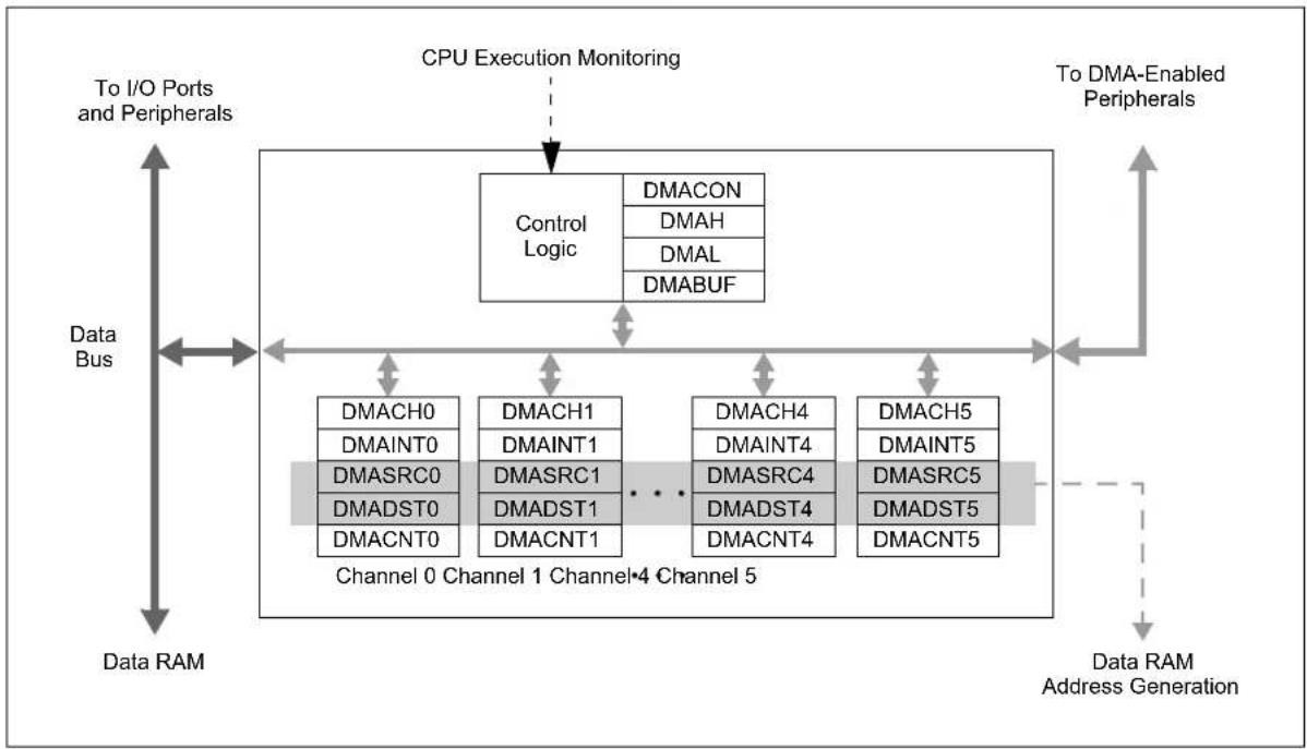
flowchart
graph TD
    A["CPU Execution Monitoring"] --> B["Control Logic"]
    B --> C["DMACON"]
    B --> D["DMAH"]
    B --> E["DMAL"]
    B --> F["DMABUF"]
    G["Data RAM"] --> H["Channel 0"]
    H --> I["Channel 1"]
    I --> J["Channel 4"]
    J --> K["Channel 5"]
    K --> L["Data RAM Address Generation"]
    M["To I/O Ports and Peripherals"] --> N["Data Bus"]
    O["To DMA-Enabled Peripherals"] --> P["Data RAM Address Generation"]
    style A fill:#f9f,stroke:#333
    style G fill:#ccf,stroke:#333
    style O fill:#cfc,stroke:#333
8.1 Summary of DMA Operations
The DMA Controller is capable of moving data between addresses according to a number of different parameters. Each of these parameters can be independently configured for any transaction. In addition, any or all of the DMA channels can independently perform a different transaction at the same time. Transactions are classified by these parameters:
- Source and destination (SFRs and data RAM)
- Data size (byte or word)
- Trigger source
- Transfer mode (One-Shot, Repeated or Continuous)
- Addressing modes (Fixed Address or Address Blocks with or without Address Increment/Decrement)
In addition, the DMA Controller provides channel priority arbitration for all channels.
8.1.1 SOURCE AND DESTINATION
Using the DMA Controller, data may be moved between any two addresses in the Data Space. The SFR space (0000h to 0FFFh) or the data RAM space (Main is 1000h to 4FFFh and Secondary is 1000 to 1FFFh) can serve as either the source or the destination. Data can be moved between these areas in either direction or between addresses in either area. The four different combinations are shown in Figure 8-2.
If it is necessary to protect areas of data RAM, the DMA Controller allows the user to set upper and lower address boundaries for operations in the Data Space above the SFR space. The boundaries are set by the DMAH and DMAL Limit registers. If a DMA channel attempts an operation outside of the address boundaries, the transaction is terminated and an interrupt is generated.
8.1.2 DATA SIZE
The DMA Controller can handle both 8-bit and 16-bit transactions. Size is user-selectable using the SIZE bit (DMACHn[1]). By default, each channel is configured for word-size transactions. When byte-size transactions are chosen, the LSB of the source and/or destination address determines if the data represent the upper or lower byte of the data RAM location.
8.1.3 TRIGGER SOURCE
The DMA Controller can use 82 of the device's interrupt sources to initiate a transaction. The DMA trigger sources occur in reverse order from their natural interrupt priority and are shown in Table 8-2. Since the source and destination addresses for any transaction can be programmed independently of the trigger source, the DMA Controller can use any trigger to perform an operation on any peripheral. This also allows DMA channels to be cascaded to perform more complex transfer operations.
8.1.4 TRANSFER MODE
The DMA Controller supports four types of data transfers, based on the volume of data to be moved for each trigger.
- One-Shot: A single transaction occurs for each trigger.
- Continuous: A series of back-to-back transactions occur for each trigger; the number of transactions is determined by the DMACNTn transaction counter.
- Repeated One-Shot: A single transaction is performed repeatedly, once per trigger, until the DMA channel is disabled.
- Repeated Continuous: A series of transactions are performed repeatedly, one cycle per trigger, until the DMA channel is disabled.
All transfer modes allow the option to have the source and destination addresses, and counter value, automatically reloaded after the completion of a transaction.
8.1.5 ADDRESSING MODES
The DMA Controller also supports transfers between single addresses or address ranges. The four basic options are:
• Fixed-to-Fixed: Between two constant addresses
- Fixed-to-Block: From a constant source address to a range of destination addresses
- Block-to-Fixed: From a range of source addresses to a single, constant destination address
- Block-to-Block: From a range of source addresses to a range of destination addresses
The option to select auto-increment or auto-decrement of source and/or destination addresses is available for Block Addressing modes.
In addition to the four basic modes, the DMA Controller also supports Peripheral Indirect Addressing (PIA) mode, where the source or destination address is generated jointly by the DMA Controller and a PIA-capable peripheral. When enabled, the DMA channel provides a base source and/or destination address, while the peripheral provides a fixed range offset address.
FIGURE 8-2: TYPES OF DMA DATA TRANSFERS
Peripheral to Memory Memory to Peripheral

text_image
SFR Area DMASRCn 0FFFh 1000h Data RAM DMA RAM Area DMAL DMADSTn DMAH
text_image
SFR Area DMADSTn 0FFFh 1000h Data RAM DMA RAM Area DMAL DMASRCn DMAHPeripheral to Peripheral Memory to Memory

text_image
SFR Area DMASRCn DMADSTn 0FFFh 1000h Data RAM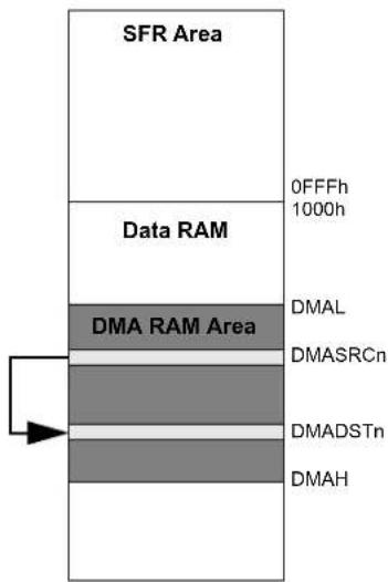
text_image
SFR Area Data RAM 0FFFh 1000h DMA RAM Area DMAL DMASRCn DMADSTn DMAHNote: Relative sizes of memory areas are not shown to scale.
8.1.6 CHANNEL PRIORITY
Each DMA channel functions independently of the others, but also competes with the others for access to the data and DMA buses. When access collisions occur, the DMA Controller arbitrates between the channels using a user-selectable priority scheme. Two schemes are available:
- Round Robin: When two or more channels collide, the lower numbered channel receives priority on the first collision. On subsequent collisions, the higher numbered channels each receive priority based on their channel number.
- Fixed: When two or more channels collide, the lowest numbered channel always receives priority, regardless of past history; however, any channel being actively processed is not available for an immediate retrigger. If a higher priority channel is continually requesting service, it will be scheduled for service after the next lower priority channel with a pending request.
8.2 Typical Setup
To set up a DMA channel for a basic data transfer:
- Enable the DMA Controller (DMAEN = 1) and select an appropriate channel priority scheme by setting or clearing PRSSEL.
- Program DMAH and DMAL with appropriate upper and lower address boundaries for data RAM operations.
- Select the DMA channel to be used and disable its operation (CHEN = 0).
- Program the appropriate source and destination addresses for the transaction into the channel's DMASRCn and DMADSTn registers. For PIA mode addressing, use the base address value.
- Program the DMACNTn register for the number of triggers per transfer (One-Shot or Continuous modes) or the number of words (bytes) to be transferred (Repeated modes).
- Set or clear the SIZE bit to select the data size.
- Program the TRMODE[1:0] bits to select the Data Transfer mode.
- Program the SAMODE[1:0] and DAMODE[1:0] bits to select the addressing mode.
- Enable the DMA channel by setting CHEN.
- Enable the trigger source interrupt.
8.3 Peripheral Module Disable
The channels of the DMA Controller can be individually powered down using the Peripheral Module Disable (PMD) registers.
8.4 Registers
The DMA Controller uses a number of registers to control its operation. The number of registers depends on the number of channels implemented for a particular device.
There are always four module-level registers (one control and three buffer/address):
- DMACON: DMA Engine Control Register (Register 8-1)
- DMAH and DMAL: DMA High and Low Address Limit Registers
• DMABUF: DMA Transfer Data Buffer
Each of the DMA channels implements five registers (two control and three buffer/address):
- DMACHn: DMA Channel n Control Register (Register 8-2)
- DMAINTn: DMA Channel n Interrupt Register (Register 8-3)
- DMASRCn: DMA Data Source Address Pointer for Channel n Register
- DMADSTn: DMA Data Destination Source for Channel n Register
- DMACNTn: DMA Transaction Counter for Channel n Register
For dsPIC33CH128MP508 devices, there are a total of 34 registers.
8.5 DMA Control Registers
REGISTER 8-1: DMACON: DMA ENGINE CONTROL REGISTER
R = Readable bit W = Writable bit U = Unimplemented bit, read as '0'
-n = Value at POR
'1' = Bit is set
'0' = Bit is cleared
x = Bit is unknown
bit 15
DMAEN: DMA Module Enable bit
1 = Enables module
0 = Disables module and terminates all active DMA operation(s)
bit 14-1
Unimplemented: Read as '0'
bit 0
PRSSEL: Channel Priority Scheme Selection bit
1 = Round robin scheme
0 = Fixed priority scheme
REGISTER 8-2: DMACHn: DMA CHANNEL n CONTROL REGISTER
| U-0 U-0 U-0 r-0 R/W-0 R/W-0 R/W-0 R/W-0 | |||||||
| — — — | — — NULLW | RELOAD | (1) | CHREQ(3) | |||
| bit 15 bit 8 | |||||||
| R/W-0 R/W-0 R/W-0 R/W-0 R/W-0 R/W-0 R/W-0 R/W-0 | |||||||
| SAMODE1 | SAMODE0 | DAMODE1 | DAMODE0 | TRMODE1 | TRMODE0 | SIZE | CHEN |
| bit 7 bit 0 | |||||||
| Legend: | r = Reserved bit | ||
| R = Readable bit | W = Writable bit | U = Unimplemented bit, read as '0' | |
| -n = Value at POR | '1' = Bit is set | '0' = Bit is cleared | x = Bit is unknown |
bit 15-13 Unimplemented: Read as '0'
bit 12 Reserved: Maintain as '0'
bit 11 Unimplemented: Read as '0'
bit 10 NULLW: Null Write Mode bit
1 = A dummy write is initiated to DMASRCn for every write to DMADSTn
0 = No dummy write is initiated
bit 9 RELOAD: Address and Count Reload bit ^(1)
1 = DMASRCn, DMADSTn and DMACNTn registers are reloaded to their previous values upon the start of the next operation
0 = DMASRCn, DMADSTn and DMACNTn are not reloaded on the start of the next operation ^(2)
bit 8 CHREQ: DMA Channel Software Request bit ^(3)
1 = A DMA request is initiated by software; automatically cleared upon completion of a DMA transfer
0 = No DMA request is pending
bit 7-6 SAMODE[1:0]: Source Address Mode Selection bits
11 = DMASRCn is used in Peripheral Indirect Addressing and remains unchanged
10 = DMASRCn is decremented based on the SIZE bit after a transfer completion
01 = DMASRCn is incremented based on the SIZE bit after a transfer completion
00 = DMASRCn remains unchanged after a transfer completion
bit 5-4 DAMODE[1:0]: Destination Address Mode Selection bits
11 = DMADSTn is used in Peripheral Indirect Addressing and remains unchanged
10 = DMADSTn is decremented based on the SIZE bit after a transfer completion
01 = DMADSTn is incremented based on the SIZE bit after a transfer completion
00 = DMADSTn remains unchanged after a transfer completion
bit 3-2 TRMODE[1:0]: Transfer Mode Selection bits
11 = Repeated Continuous
10 = Continuous
01 = Repeated One-Shot
00 = One-Shot
bit 1 SIZE: Data Size Selection bit
1 = Byte (8-bit)
0 = Word (16-bit)
bit 0 CHEN: DMA Channel Enable bit
1 = The corresponding channel is enabled
0 = The corresponding channel is disabled
Note 1: Only the original DMACNTn is required to be stored to recover the original DMASRCn and DMADSTn values.
2: DMACNTn will always be reloaded in Repeated mode transfers, regardless of the state of the RELOAD bit.
3: The number of transfers executed while CHREQ is set depends on the configuration of TRMODE[1:0].
REGISTER 8-3: DMAINTn: DMA CHANNEL n INTERRUPT REGISTER
| R-0 R/W-0 R/W-0 R/W-0 R/W-0 R/W-0 R/W-0 R/W-0 | |||||||
| DBUFWF(1) | CHSEL6 CH | HSEL5 CHSEL4 | CHSEL3 CH | SEL2 CHSEL1 | CHSEL0 | ||
| bit 15 bit 8 | |||||||
| R/W-0 R/W-0 R/W-0 R/W-0 R/W-0 U-0 U-0 R/W-0 | |||||||
| HIGHIF^(1,2) | LOWIF^(1,2) | DONEIF^(1) | HALFIF^(1) | OVRUNIF^(1) | — — | H | A L |
| bit 7 bit 0 | |||||||
Legend:
| R = Readable bit W = Writable bit U = Unimplemented bit, read as '0' | ||
| -n = Value at POR | '1' = Bit is set | '0' = Bit is cleared x = Bit is unknown |
bit 15 DBUFWF: DMA Buffered Data Write Flag bit ^(1)
1 = The content of the DMA buffer has not been written to the location specified in DMADSTn or DMASRCn in Null Write mode 0 = The content of the DMA buffer has been written to the location specified in DMADSTn or DMASRCn in Null Write mode
bit 14-8 CHSEL[6:0]: DMA Channel Trigger Selection bits See Table 8-2 for a complete list.
bit 7 HIGHIF: DMA High Address Limit Interrupt Flag bit ^(1,2)
1 = The DMA channel has attempted to access an address higher than DMAH or the upper limit of the data RAM space 0 = The DMA channel has not invoked the high address limit interrupt
bit 6 LOWIF: DMA Low Address Limit Interrupt Flag bit ^(1,2)
1 = The DMA channel has attempted to access the DMA SFR address lower than DMAL, but above the SFR range (07FFh) 0 = The DMA channel has not invoked the low address limit interrupt
bit 5 DONEIF: DMA Complete Operation Interrupt Flag bit ^(1)
If CHEN = 1: 1 = The previous DMA session has ended with completion 0 = The current DMA session has not yet completed If CHEN = 0: 1 = The previous DMA session has ended with completion 0 = The previous DMA session has ended without completion
bit 4 HALFIF: DMA 50% Watermark Level Interrupt Flag bit ^(1)
1 = DMACNTn has reached the halfway point to 0000h 0 = DMACNTn has not reached the halfway point
bit 3 OVRUNIF: DMA Channel Overrun Flag bit ^(1)
1 = The DMA channel is triggered while it is still completing the operation based on the previous trigger 0 = The overrun condition has not occurred
bit 2-1 Unimplemented: Read as '0'
bit 0 HALFEN: Halfway Completion Watermark bit
1 = Interrupts are invoked when DMACNTn has reached its halfway point and at completion 0 = An interrupt is invoked only at the completion of the transfer
Note 1: Setting these flags in software does not generate an interrupt.
2: Testing for address limit violations (DMASRCn or DMADSTn is either greater than DMAH or less than DMAL) is NOT done before the actual access.
TABLE 8-2: DMA CHANNEL TRIGGER SOURCES (MAIN)
| CHSEL[6:0] | Trigger (Interrupt) | CHSEL[6:0] | Trigger (Interrupt) | CHSEL[6:0] | Trigger (Interrupt) |
| 00h INTO - External Interrupt 0 23h (Reserved, do not use) 45h CLC2 Positive Edge Interrupt | |||||
| 01h SCCP1 IC/OC 24h PWM Event C 46h | SPI1 - Fault Interrupt | ||||
| 02h | SPI1 Receiver | 25h | SENT1 TX/RX | 47h | SPI2 - Fault Interrupt |
| 03h | SPI1 Transmitter | 26h | SENT2 TX/RX | 48h | (Reserved, do not use) |
| 04h | UART1 Receiver | 27h | ADC1 Group Convert Done | 49h | (Reserved, do not use) |
| 05h | UART1 Transmitter | 28h | ADC Done AN0 | 4Ah | MSI Secondary Initiated Second-ary IRQ |
| 06h | ECC Single Bit Error | 29h | ADC Done AN1 | 4Bh | MSI Protocol A |
| 07h | NVM Write Complete | 2Ah | ADC Done AN2 | 4Ch | MSI Protocol B |
| 08h | INT1 - External Interrupt 1 | 2Bh | ADC Done AN3 | 4Dh | MSI Protocol C |
| 09h | SI2C1 - I2C1 Secondary Event | 2Ch | ADC Done AN4 | 4Eh | MSI Protocol D |
| 0Ah | MI2C1 - I2C1 Main Event | 2Dh | ADC Done AN5 | 4Fh | MSI Protocol E |
| 0Bh | INT2 - External Interrupt 2 | 2Eh | ADC Done AN6 | 50h | MSI Protocol F |
| 0Ch | SCCP2 IC/OC | 2Fh | ADC Done AN7 | 51h | MSI Protocol G |
| 0Dh | INT3 - External Interrupt 3 | 30h | ADC Done AN8 | 52h | MSI Protocol H |
| 0Eh | UART2 Receiver | 31h | ADC Done AN9 | 53h | MSI Main Read FIFO Data Ready IRQ |
| 0Fh | UART2 Transmitter | 32h | ADC Done AN10 | 54h | MSI Main Write FIFO Empty IRQ |
| 10h | SPI2 Receiver | 33h | ADC Done AN11 | 55h | MSI Fault (Over/Underflow) |
| 11h | SPI2 Transmitter | 34h | ADC Done AN12 | 56h | MSI Main Reset IRQ |
| 12h | SCCP3 IC/OC | 35h | ADC Done AN13 | 57h | PWM Event D |
| 13h | SI2C2 - I2C2 Secondary Event | 36h | ADC Done AN14 | 58h | PWM Event E |
| 14h | MI2C2 - I2C1 Main Event | 37h | ADC Done AN15 | 59h | PWM Event F |
| 15h | SCCP4 IC/OC | 38h | ADC Done AN16 | 5Ah | Secondary ICD Breakpoint Inter-rupt |
| 16h | SCCP5 IC/OC | 39h | ADC Done AN17 | 5Bh | (Reserved, do not use) |
| 17h | SCCP6 IC/OC | 3Ah | (Reserved, do not use) | 5Ch | SCCP7 Interrupt |
| 18h | CRC Generator Interrupt | 3Bh | (Reserved, do not use) | 5Dh | SCCP8 Interrupt |
| 19h | PWM Event A | 3Ch | (Reserved, do not use) | 5Eh | Secondary Clock Fail Interrupt |
| 1Bh | PWM Event B | 3Dh | (Reserved, do not use) | 5Fh | ADC FIFO Ready Interrupt |
| 1Ch | PWM Generator 1 | 3Eh | (Reserved, do not use) | 60h | CLC3 Positive Edge Interrupt |
| 1Dh | PWM Generator 2 | 3Fh | (Reserved, do not use) | 61h | CLC4 Positive Edge Interrupt |
| 1Eh | PWM Generator 3 | 40h | AD1FLTR1 - Oversample Filter 1 | 62h | (Reserved, do not use) |
| 1Fh | PWM Generator 4 | 41h | AD1FLTR2 - Oversample Filter 2 | ... | |
| 20h | (Reserved, do not use) | 42h | AD1FLTR3 - Oversample Filter 3 | 7Fh | |
| 21h | (Reserved, do not use) | 43h | AD1FLTR4 - Oversample Filter 4 | ||
| 22h | (Reserved, do not use) | 44h | CLC1 Positive Edge Interrupt | ||
TABLE 8-3: DMA CHANNEL TRIGGER SOURCES (SECONDARY)
| CHSEL[6:0] | Trigger (Interrupt) CHSEL[6:0] | Trigger (Interrupt) CHSEL[6:0] | Trigger (Interrupt) | |||||
| 0000000 | 00h | INT0 – External Interrupt 0 | 0100010 | 22h | PWM Generator 7 | 1000100 | 44h | CLC1 Positive Edge Interrupt |
| 0000001 | 01h | SCCP1 IC/OC | 0100011 | 23h | PWM Generator 8 | 1000101 | 45h | CLC2 Positive Edge Interrupt |
| 0000010 | 02h | SPI1 Receiver | 0100100 | 24h | PWM Event C | 1000110 | 46h | SPI1 – Fault Interrupt |
| 0000011 | 03h | SPI1 Transmitter | 0100101 | 25h | (Reserved, do not use) | 1000111 | 47h | (Reserved, do not use) |
| 0000100 | 04h | UART1 Receiver | 0100110 | 26h | (Reserved, do not use) | 1001000 | 48h | (Reserved, do not use) |
| 0000101 | 05h | UART1 Transmitter | 0100111 | 27h | ADC1 Group Convert Done | 1001001 | 49h | (Reserved, do not use) |
| 0000110 | 06h | ECC Single Bit Error | 0101000 | 28h | ADC Done AN0 | 1001010 | 4Ah | MSI Main Initiated Secondary IRQ |
| 0000111 | 07h | NVM Write Complete | 0101001 | 29h | ADC Done AN1 | 1001011 | 4Bh | MSI Protocol A |
| 0001000 | 08h | INT1 – External Interrupt 1 | 0101010 | 2Ah | ADC Done AN2 | 1001100 | 4Ch | MSI Protocol B |
| 0001001 | 09h | SI2C1 – I2C1 Secondary Event | 0101011 | 2Bh | ADC Done AN3 | 1001101 | 4Dh | MSI Protocol C |
| 0001010 | 0Ah | MI2C1 – I2C1 Main Event | 0101100 | 2Ch | ADC Done AN4 | 1001110 | 4Eh | MSI Protocol D |
| 0001010 | 0Bh | INT2 – External Interrupt 2 | 0101101 | 2Dh | ADC Done AN5 | 1001111 | 4Fh | MSI Protocol E |
| 0001100 | 0Ch | SCCP2 IC/OC | 0101110 | 2Eh | ADC Done AN6 | 1010000 | 50h | MSI Protocol F |
| 0001101 | 0Dh | INT3 – External Interrupt 3 | 0101111 | 2Fh | ADC Done AN7 | 1010001 | 51h | MSI Protocol G |
| 0001110 | 0Eh | (Reserved, do not use) | 0110000 | 30h | ADC Done AN8 | 1010010 | 52h | MSI Protocol H |
| 0001111 | 0Fh | (Reserved, do not use) | 0110001 | 31h | ADC Done AN9 | 1010011 | 53h | MSI Secondary Read FIFO Data Ready IRQ |
| 0010000 | 10h | (Reserved, do not use) | 0110010 | 32h | ADC Done AN10 | 1010100 | 54h | MSI Secondary Write FIFO Empty IRQ |
| 0010001 | 11h | (Reserved, do not use) | 0110011 | 33h | ADC Done AN11 | 1010101 | 55h | MSI FIFO Fault (Over/Underflow) |
| 0010010 | 12h | SCCP3 IC/OC | 0110100 | 34h | ADC Done AN12 | 1010110 | 56h | MSI Main Reset IRQ |
| 0010011 | 13h | (Reserved, do not use) | 0110101 | 35h | ADC Done AN13 | 1010111 | 57h | PWM Event D |
| 0010100 | 14h | (Reserved, do not use) | 0110110 | 36h | ADC Done AN14 | 1011000 | 58h | PWM Event E |
| 0010101 | 15h | SCCP4 IC/OC | 0110111 | 37h | ADC Done AN15 | 1011001 | 59h | PWM Event F |
| 0010110 | 16h | (Reserved, do not use) | 0111000 | 38h | ADC Done AN16 | 1011010 | 5Ah | Main ICD Breakpoint Interrupt |
| 0010111 | 17h | (Reserved, do not use) | 0111001 | 39h | ADC Done AN17 | 1011011 | 5Bh | (Reserved, do not use) |
| 0011000 | 18h | (Reserved, do not use) | 0111010 | 3Ah | (Reserved, do not use) | 1011100 | 5Ch | (Reserved, do not use) |
| 0011001 | 19h | PWM Event A | 0111010 | 3Bh | ADC Done AN19 | 1011101 | 5Dh | (Reserved, do not use) |
| 0011010 | 1Ah | (Reserved, do not use) | 0111100 | 3Ch | (Reserved, do not use) | 1011110 | 5Eh | Main Clock Fail Interrupt |
| 0011011 | 1Bh | PWM Event B | 0111101 | 3Dh | (Reserved, do not use) | 1011111 | 5Fh | ADC FIFO Ready Interrupt |
| 0011100 | 1Ch | PWM Generator 1 | 0111110 | 3Eh | (Reserved, do not use) | 1100000 | 60h | CLC3 Positive Edge Interrupt |
| 0011101 | 1Dh | PWM Generator 2 | 0111111 | 3Fh | (Reserved, do not use) | 1100001 | 61h | CLC4 Positive Edge Interrupt |
| 0011110 | 1Eh | PWM Generator 3 | 1000000 | 40h | AD1FLTR1 – Oversample Filter 1 | 1100001 | 62h | (Reserved, do not use) |
| 0011111 | 1Fh | PWM Generator 4 | 1000001 | 41h | AD1FLTR2 – Oversample Filter 2 | ... | ... | |
| 0100000 | 20h | PWM Generator 5 | 1000010 | 42h | AD1FLTR3 – Oversample Filter 3 | 1111111 | 7Fh | (Reserved, do not use) |
| 0100001 | 21h | PWM Generator 6 | 1000011 | 43h | AD1FLTR4 – Oversample Filter 4 | |||
9.0 HIGH-RESOLUTION PWM (HSPWM) WITH FINE EDGE PLACEMENT
Note 1: This data sheet summarizes the features of the dsPIC33CH128MP508 family of devices. It is not intended to be a comprehensive reference source. To complement the information in this data sheet, refer to “High-Resolution PWM with Fine Edge Placement” (www.microchip.com/DS70005320), which is available from the Microchip website (www.microchip.com).
2: The PWM is identical for both Main core and Secondary core. The x is common for both Main core and Secondary core (where the x represents the number of the specific module being addressed). The number of HSPWM modules available on the Main core and Secondary core is different and they are located in different SFR locations.
3: All associated register names are the same on the Main core and the Secondary core. The Secondary code will be developed in a separate project in MPLAB X IDE with the device selection, dsPIC33CH128MP508S1, where the S1 indicates the Secondary device. The Main is PWM1 to PWM4 and the Secondary is PWM1 to PWM8.
Table 9-1 shows an overview of the PWM module.
TABLE 9-1: PWM MODULE OVERVIEW
| Number of PWM Modules | Identical (Modules) | |
| Main Core 4 Yes | ||
| Secondary Core | 8 | Yes |
The High-Speed PWM (HSPWM) module is a Pulse-Width Modulated (PWM) module to support both motor control and power supply applications. This flexible module provides features to support many types of Motor Control (MC) and Power Control (PC) applications, including:
- AC-to-DC Converters
- DC-to-DC Converters
• AC and DC Motors: BLDC, PMSM, ACIM, SRM, etc.
• Inverters - Battery Chargers
- Digital Lighting
• Power Factor Correction (PFC)
9.1 Features
- Up to Eight Independent PWM Generators for Secondary Core, each with Dual Outputs
- Up to Four Independent PWM Generators for Main Core, each with Dual Outputs
- Operating modes:
- Independent Edge mode
- Variable Phase PWM mode
- Center-Aligned mode
- Double Update Center-Aligned mode
- Dual Edge Center-Aligned mode
- Dual PWM mode
- Output modes:
- Complementary
- Independent
- Push-Pull
- Dead-Time Generator
- Leading-Edge Blanking (LEB)
- Output Override for Fault Handling
- Flexible Period/Duty Cycle Updating Options
• Programmable Control Inputs (PCI)
- Advanced Triggering Options
- Six Combinatorial Logic Outputs
- Six PWM Event Outputs
9.2 Architecture Overview
The PWM module consists of a common set of controls and features, and multiple instantiations of PWM Generators (PGs). Each PWM Generator can be independently configured or multiple PWM Generators can
be used to achieve complex multiphase systems. PWM Generators can also be used to implement sophisticated triggering, protection and logic functions. A high-level block diagram is shown in Figure 9-1.
FIGURE 9-1: PWM HIGH-LEVEL BLOCK DIAGRAM
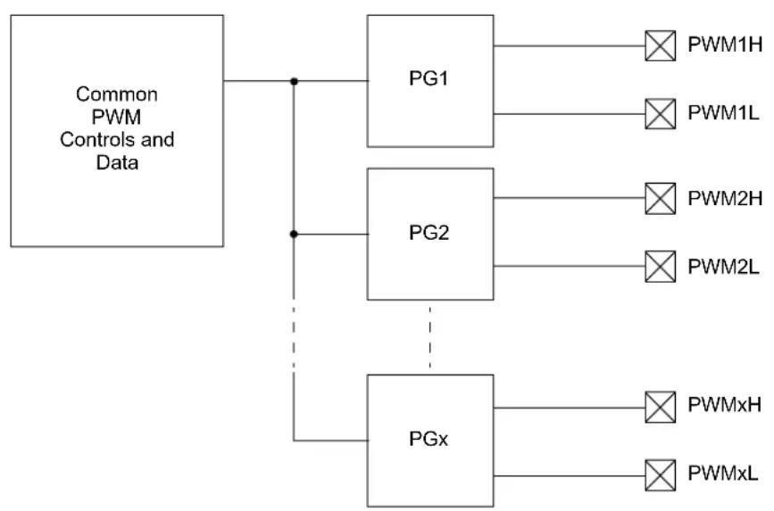
flowchart
graph TD
    A["Common PWM Controls and Data"] --> B["PG1"]
    A --> C["PG2"]
    A --> D["PGx"]
    B --> E["PWM1H"]
    B --> F["PWM1L"]
    C --> G["PWM2H"]
    C --> H["PWM2L"]
    D --> I["PWMxH"]
    D --> J["PWMxL"]
9.3 PWM4H/L Output on Peripheral Pin Select
All devices support the capability to output PWM4H and PWM4L signals via Peripheral Pin Select (PPS) onto any RPn pin. This feature is intended for lower pin count devices that do not have PWM4H/L on dedicated pins. If PWM4H/L PPS output functions are used on devices that also have fixed PWM4H/L pins, the output signal will be present on both dedicated and RPn pins. The output port enable bits, PENH and PENL (PGxIOCONH[3:2]), control both dedicated and PPS pins together; it is not possible to disable the dedicated pins and use only PPS.
Given the natural priority of the RPn functions above that of the PWM, it is possible to use the PPS output functions on the dedicated PWM4H/L pins while the PWM4 signals are routed to other pins via PPS. Any of the peripheral outputs listed in Table 3-32 and Table 4-28, with the exception of 'Default Port', can be used.
Input functions, including the ports and peripherals listed in Table 3-33 and Table 4-31, cannot be used through the RPn function on dedicated PWM4H/L pins when PWM4 is active.
9.4 PWM Control Registers
There are two categories of Special Function Registers (SFRs) used to control the operation of the PWM module:
• Common, shared by all PWM Generators
- PWM Generator-specific
An 'x' in the register name denotes an instance of a PWM Generator.
A 'y' in the register name denotes an instance of the common function.
REGISTER 9-1: PCLKCON: PWM CLOCK CONTROL REGISTER
| R/W-0 R/W-0 U-0 U-0 U-0 U-0 R/W-0 | |||||||
| HRRDY | HRERR | — | — | — | — | — | LOCK^(1) |
| bit 15 bit 8 | |||||||
| U-0 | U-0 | R/W-0 | R/W-0 | U-0 | U-0 | R/W-0 | R/W-0 |
| — | — | DIVSEL1 | DIVSEL0 | — | — | MCLKSEL1 ^(2) | MCLKSEL0 ^(2) |
| bit 7 bit 0 | |||||||
Legend:
| R = Readable bit | W = Writable bit | U = Unimplemented bit, read as '0' |
| -n = Value at POR | '1' = Bit is set | '0' = Bit is cleared x = Bit is unknown |
bit 15 HRRDY: High-Resolution Ready bit
1 = The high-resolution circuitry is ready
0 = The high-resolution circuitry is not ready
bit 14 HRERR: High-Resolution Error bit
1 = An error has occurred; PWM signals will have limited resolution
0 = No error has occurred; PWM signals will have full resolution when HRRDY = 1
bit 13-9 Unimplemented: Read as '0'
bit 8 LOCK: Lock bit ^(1)
1 = Write-protected registers and bits are locked
0 = Write-protected registers and bits are unlocked
bit 7-6 Unimplemented: Read as '0'
bit 5-4 DIVSEL[1:0]: PWM Clock Divider Selection bits
11 = Divide ratio is 1:16
10 = Divide ratio is 1:8
01 = Divide ratio is 1:4
00 = Divide ratio is 1:2
bit 3-2 Unimplemented: Read as '0'
bit 1-0 MCLKSEL[1:0]: PWM Main Clock Selection bits (2)
11 = AFPLLO - Auxiliary PLL post-divider output
10 = FPLLO - Primary PLL post-divider output
01 = AFvco/2 - Auxiliary VCO/2
00 = Fosc
Note 1: A device-specific unlock sequence must be performed before this bit can be cleared.
2: Changing the MCLKSEL[1:0] bits while ON (PGxCONL[15]) = 1 is not recommended.
REGISTER 9-2: FSCL: FREQUENCY SCALE REGISTER
| R/W-0 R/W-0 R/W-0 R/W-0 R/W-0 R/W-0 R/W-0 R/W-0 |
| FSCL[15:8] |
| bit 15 bit 8 |
| R/W-0 R/W-0 R/W-0 R/W-0 R/W-0 R/W-0 R/W-0 R/W-0 |
| FSCL[7:0] |
| bit 7 bit 0 |
| Legend: | |||
| R = Readable bit W = Writable bit U = Unimplemented bit, read as ‘0’ | |||
| -n = Value at POR | ‘1' = Bit is set | ‘0' = Bit is cleared | x = Bit is unknown |
bit 15-0 FSCL[15:0]: Frequency Scale Register bits
The value in this register is added to the frequency scaling accumulator at each pwm_clk. When the accumulated value exceeds the value of FSMINPER, a clock pulse is produced.
REGISTER 9-3: FSMINPER: FREQUENCY SCALING MINIMUM PERIOD REGISTER
| R/W-0 | R/W-0 | R/W-0 | R/W-0 | R/W-0 | R/W-0 | R/W-0 | R/W-0 |
| FSMINPER[15:8] | |||||||
| bit 15 | bit 8 | ||||||
| R/W-0 | R/W-0 | R/W-0 | R/W-0 | R/W-0 | R/W-0 | R/W-0 | R/W-0 |
| FSMINPER[7:0] | |||||||
| bit 7 | bit 0 | ||||||
| Legend: | |||
| R = Readable bit | W = Writable bit | U = Unimplemented bit, read as ‘0’ | |
| -n = Value at POR | ‘1’ = Bit is set | ‘0’ = Bit is cleared | x = Bit is unknown |
bit 15-0 FSMINPER[15:0]: Frequency Scaling Minimum Period Register bits
This register holds the minimum clock period (maximum clock frequency) that can be produced by the frequency scaling circuit.
REGISTER 9-4: MPHASE: MAIN PHASE REGISTER
| R/W-0 R/W-0 R/W-0 R/W-0 R/W-0 R/W-0 R/W-0 R/W-0 |
| MPHASE[15:8] |
| bit 15 bit 8 |
| R/W-0 R/W-0 R/W-0 R/W-0 R/W-0 R/W-0 R/W-0 R/W-0 |
| MPHASE[7:0] |
| bit 7 bit 0 |
Legend:
| R = Readable bit W = Writable bit U = Unimplemented bit, read as '0' | ||
| -n = Value at POR | '1' = Bit is set | '0' = Bit is cleared x = Bit is unknown |
bit 15-0
MPHASE[15:0]: Main Phase Register bits
REGISTER 9-5: MDC: MAIN DUTY CYCLE REGISTER
| R/W-0 R/W-0 R/W-0 R/W-0 R/W-0 R/W-0 R/W-0 R/W-0 |
| MDC[15:8] |
| bit 15 bit 8 |
| R/W-0 R/W-0 R/W-0 R/W-0 R/W-0 R/W-0 R/W-0 R/W-0 |
| MDC[7:0] |
| bit 7 bit 0 |
Legend:
| R = Readable bit W = Writable bit U = Unimplemented bit, read as '0' | ||
| -n = Value at POR | '1' = Bit is set | '0' = Bit is cleared x = Bit is unknown |
bit 15-0
MDC[15:0]: Main Duty Cycle Register bits
REGISTER 9-6: MPER: MAIN PERIOD REGISTER
| R/W-0 R/W-0 R/W-0 R/W-0 R/W-0 R/W-0 R/W-0 R/W-0 |
| MPER[15:8](1) |
| bit 15 bit 8 |
| R/W-0 R/W-0 R/W-0 R/W-0 R/W-0 R/W-0 R/W-0 R/W-0 |
| MPER[7:0](1) |
| bit 7 bit 0 |
Legend:
| R = Readable bit W = Writable bit U = Unimplemented bit, read as '0' | ||
| -n = Value at POR | '1' = Bit is set | '0' = Bit is cleared x = Bit is unknown |
bit 15-0 MPER[15:0]: Main Period Register bits ^(1)
Note 1: Period values less than '0x0010' should not be selected.
REGISTER 9-7: CMBTRIGL: COMBINATIONAL TRIGGER REGISTER LOW
| Legend: | |||
| R = Readable bit | W = Writable bit | U = Unimplemented bit, read as '0' | |
| -n = Value at POR | '1' = Bit is set | '0' = Bit is cleared | x = Bit is unknown |
bit 15-8 Unimplemented: Read as '0'
bit 7 CTA8EN: Enable Trigger Output from PWM Generator #8 as Source for Combinational Trigger A bit 1 = Enables specified trigger signal to be OR'd into the Combinatorial Trigger A signal 0 = Disabled
bit 6 CTA7EN: Enable Trigger Output from PWM Generator #7 as Source for Combinational Trigger A bit 1 = Enables specified trigger signal to be OR'd into the Combinatorial Trigger A signal 0 = Disabled
bit 5 CTA6EN: Enable Trigger Output from PWM Generator #6 as Source for Combinational Trigger A bit 1 = Enables specified trigger signal to be OR'd into the Combinatorial Trigger A signal 0 = Disabled
bit 4 CTA5EN: Enable Trigger Output from PWM Generator #5 as Source for Combinational Trigger A bit 1 = Enables specified trigger signal to be OR'd into the Combinatorial Trigger A signal 0 = Disabled
bit 3 CTA4EN: Enable Trigger Output from PWM Generator #4 as Source for Combinational Trigger A bit 1 = Enables specified trigger signal to be OR'd into the Combinatorial Trigger A signal 0 = Disabled
bit 2 CTA3EN: Enable Trigger Output from PWM Generator #3 as Source for Combinational Trigger A bit 1 = Enables specified trigger signal to be OR'd into the Combinatorial Trigger A signal 0 = Disabled
bit 1 CTA2EN: Enable Trigger Output from PWM Generator #2 as Source for Combinational Trigger A bit 1 = Enables specified trigger signal to be OR'd into the Combinatorial Trigger A signal 0 = Disabled
bit 0 CTA1EN: Enable Trigger Output from PWM Generator #1 as Source for Combinational Trigger A bit 1 = Enables specified trigger signal to be OR'd into the Combinatorial Trigger A signal 0 = Disabled
REGISTER 9-8: CMBTRIGH: COMBINATIONAL TRIGGER REGISTER HIGH
| R = Readable bit | W = Writable bit U = Unimplemented bit, read as '0' | |
| -n = Value at POR | ‘1’ = Bit is set ‘0’ = Bit is cleared x = Bit is unknown | |
bit 15-8 Unimplemented: Read as '0'
bit 7 CTB8EN: Enable Trigger Output from PWM Generator #8 as Source for Combinational Trigger B bit 1 = Enables specified trigger signal to be OR'd into the Combinatorial Trigger B signal 0 = Disabled
bit 6 CTB7EN: Enable Trigger Output from PWM Generator #7 as Source for Combinational Trigger B bit 1 = Enables specified trigger signal to be OR'd into the Combinatorial Trigger B signal 0 = Disabled
bit 5 CTB6EN: Enable Trigger Output from PWM Generator #6 as Source for Combinational Trigger B bit 1 = Enables specified trigger signal to be OR'd into the Combinatorial Trigger B signal 0 = Disabled
bit 4 CTB5EN: Enable Trigger Output from PWM Generator #5 as Source for Combinational Trigger B bit 1 = Enables specified trigger signal to be OR'd into the Combinatorial Trigger B signal 0 = Disabled
bit 3 CTB4EN: Enable Trigger Output from PWM Generator #4 as Source for Combinational Trigger B bit 1 = Enables specified trigger signal to be OR'd into the Combinatorial Trigger B signal 0 = Disabled
bit 2 CTB3EN: Enable Trigger Output from PWM Generator #3 as Source for Combinational Trigger B bit 1 = Enables specified trigger signal to be OR'd into the Combinatorial Trigger B signal 0 = Disabled
bit 1 CTB2EN: Enable Trigger Output from PWM Generator #2 as Source for Combinational Trigger B bit 1 = Enables specified trigger signal to be OR'd into the Combinatorial Trigger B signal 0 = Disabled
bit 0 CTB1EN: Enable Trigger Output from PWM Generator #1 as Source for Combinational Trigger B bit 1 = Enables specified trigger signal to be OR'd into the Combinatorial Trigger B signal 0 = Disabled
REGISTER 9-9: LOGCONy: COMBINATORIAL PWM LOGIC CONTROL REGISTER y ^(2)
| R/W-0 R/W-0 R/W-0 R/W-0 R/W-0 R/W-0 R/W-0 R/W-0 | |||||||
| PWMS1y3(1) | PWMS1y2(1) | PWMS1y1(1) | PWMS1y0(1) | PWMS2y3(1) | PWMS2y2(1) | PWMS2y1(1) | PWMS2y0(1) |
| bit 15 bit 8 | |||||||
| R/W-0 R/W-0 R/W-0 R/W-0 U-0 R/W-0 R/W-0 R/W-0 | |||||||
| S1yPOL | S2yPOL | PWMLFy1 | PWMLFy0 | — | PWMLFyD2 | PWMLFyD1 | PWMLFyD0 |
| bit 7 bit 0 | |||||||
| Legend: | |||
| R = Readable bit | W = Writable bit | U = Unimplemented bit, read as '0' | |
| -n = Value at POR | '1' = Bit is set | '0' = Bit is cleared | x = Bit is unknown |
bit 15-12 PWMS1y[3:0]: Combinatorial PWM Logic Source #1 Selection bits ^(1)
1111 = PWM8L
1110 = PWM8H
1101 = PWM7L
1100 = PWM7H
1011 = PWM6L
1010 = PWM6H
1001 = PWM5L
1000 = PWM5H
0111 = PWM4L
0110 = PWM4H
0101 = PWM3L
0100 = PWM3H
0011 = PWM2L
0010 = PWM2H
0001 = PWM1L
0000 = PWM1H
bit 11-8 PWMS2y[3:0]: Combinatorial PWM Logic Source #2 Selection bits ^(1)
1111 = PWM8L
1110 = PWM8H
1101 = PWM7L
1100 = PWM7H
1011 = PWM6L
1010 = PWM6H
1001 = PWM5L
1000 = PWM5H
0111 = PWM4L
0110 = PWM4H
0101 = PWM3L
0100 = PWM3H
0011 = PWM2L
0010 = PWM2H
0001 = PWM1L
0000 = PWM1H
Note 1: Logic function input will be connected to '0' if the PWM channel is not present.
2: Instances of y = A, C, E of LOGCONy assign logic function output to the PWMxH pin. Instances of y = B, D, F of LOGCONy assign logic function to the PWMxL pin.
REGISTER 9-9: LOGCONy: COMBINATORIAL PWM LOGIC CONTROL REGISTER y ^(2) (CONTINUED)
| bit 7 | S1yPOL: Combinatorial PWM Logic Source #1 Polarity bit1 = Input is inverted0 = Input is positive logic |
| bit 6 | S2yPOL: Combinatorial PWM Logic Source #2 Polarity bit1 = Input is inverted0 = Input is positive logic |
| bit 5-4 | PWMLFy[1:0]: Combinatorial PWM Logic Function Selection bits11 = Reserved10 = PWMS1 ^ PWMS2 (XOR)01 = PWMS1 & PWMS2 (AND)00 = PWMS1 | PWMS2 (OR) |
| bit 3 | Unimplemented: Read as ‘0’ |
| bit 2-0 | PWMLFyD[2:0]: Combinatorial PWM Logic Destination Selection bits111 = Logic function is assigned to the PWM8H or PWM8L pin110 = Logic function is assigned to the PWM7H or PWM7L pin101 = Logic function is assigned to the PWM6H or PWM6L pin100 = Logic function is assigned to the PWM5H or PWM5Lpin011 = Logic function is assigned to the PWM4H or PWM4Lpin010 = Logic function is assigned to the PWM3H or PWM3Lpin001 = Logic function is assigned to the PWM2H or PWM2Lpin000 = No assignment, combinatorial PWM logic function is disabled |
Note 1: Logic function input will be connected to '0' if the PWM channel is not present.
2: Instances of y = A, C, E of LOGCONy assign logic function output to the PWMxH pin. Instances of y = B, D, F of LOGCONy assign logic function to the PWMxL pin.
REGISTER 9-10: PWMEVTy: PWM EVENT OUTPUT CONTROL REGISTER y (5)
| R/W-0 R/W-0 R/W-0 R/W-0 U-0 U-0 U-0 U-0 | |||||||
| EVTyOEN EVTyPOL EVTySTRD EVTySYNC | — — | — | — | ||||
| bit 15 bit 8 | |||||||
| R/W-0 | R/W-0 | R/W-0 | R/W-0 | U-0 | R/W-0 | R/W-0 | R/W-0 |
| EVTySEL3 | EVTySEL2 | EVTySEL1 | EVTySEL0 | — | EVTyPGS2(2) | EVTyPGS1(2) | EVTyPGS0(2) |
| bit 7 bit 0 | |||||||
| Legend: | |||
| R = Readable bit | W = Writable bit | U = Unimplemented bit, read as ‘0’ | |
| -n = Value at POR | ‘1’ = Bit is set | ‘0’ = Bit is cleared | x = Bit is unknown |
| bit 15 | EVTyOEN: PWM Event Output Enable bit1 = Event output signal is output on PWMEy pin0 = Event output signal is internal only |
| bit 14 | EVTyPOL: PWM Event Output Polarity bit1 = Event output signal is active-low0 = Event output signal is active-high |
| bit 13 | EVTySTRD: PWM Event Output Stretch Disable bit1 = Event output signal pulse width is not stretched0 = Event output signal is stretched to eight PWM clock cycles minimum ^(1) |
| bit 12 | EVTySYNC: PWM Event Output Sync bit1 = Event output signal is synchronized to the system clock0 = Event output is not synchronized to the system clockEvent output signal pulse will be two system clocks when this bit is set and EVTySTRD = 1. |
| bit 11-8 | Unimplemented: Read as '0' |
| bit 7-4 | EVTySEL[3:0]: PWM Event Selection bits1111 = High-resolution error event signal1110-1010 = Reserved1001 = ADC Trigger 2 signal1000 = ADC Trigger 1 signal0111 = STEER signal (available in Push-Pull Output modes only) ^(4) 0110 = CAHALF signal (available in Center-Aligned modes only) ^(4) 0101 = PCI Fault active output signal0100 = PCI current-limit active output signal0011 = PCI feed-forward active output signal0010 = PCI Sync active output signal0001 = PWM Generator output signal ^(3) 0000 = Source is selected by the PGTRGSEL[2:0] bits |
| bit 3 | Unimplemented: Read as '0' |
Note 1: The event signal is stretched using the peripheral clock because different PGs may be operating from different clock sources. The leading edge of the event pulse is produced in the clock domain of the PWM Generator. The trailing edge of the stretched event pulse is produced in the peripheral clock domain.
2: No event will be produced if the selected PWM Generator is not present.
3: This is the PWM Generator output signal prior to output mode logic and any output override logic.
4: This signal should be the PGx_clk domain signal prior to any synchronization into the system clock domain.
5: 'y' denotes a common instance (A-F).
REGISTER 9-10: PWMEVTy: PWM EVENT OUTPUT CONTROL REGISTER y (5) (CONTINUED)
bit 2-0 EVTyPGS[2:0]: PWM Event Source Selection bits (2)
111 = P G 8
110 = P G 7
101 = P G 6
100 = P G 5
011 = P G 4
010 = P G 3
001 = P G 2
000 = P G 1
Note 1: The event signal is stretched using the peripheral clock because different PGs may be operating from different clock sources. The leading edge of the event pulse is produced in the clock domain of the PWM Generator. The trailing edge of the stretched event pulse is produced in the peripheral clock domain.
2: No event will be produced if the selected PWM Generator is not present.
3: This is the PWM Generator output signal prior to output mode logic and any output override logic.
4: This signal should be the PGx_clk domain signal prior to any synchronization into the system clock domain.
5: 'y' denotes a common instance (A-F).
REGISTER 9-11: LFSR: LINEAR FEEDBACK SHIFT REGISTER
| U-0 R/W-0 R/W-0 R/W-0 R/W-0 R/W-0 R/W-0 R/W-0 |
| — LFSR[14:8] |
| bit 15 bit 8 |
| R/W-0 R/W-0 R/W-0 R/W-0 R/W-0 R/W-0 R/W-0 R/W-0 |
| LFSR[7:0] |
| bit 7 bit 0 |
Legend:
| R = Readable bit | W = Writable bit | U = Unimplemented bit, read as '0' |
| -n = Value at POR | '1' = Bit is set | '0' = Bit is cleared x = Bit is unknown |
bit 15 Unimplemented: Read as '0'
bit 14-0 LFSR[14:0]: Linear Feedback Shift Register bits
A read of this register will provide a 15-bit pseudorandom value.
REGISTER 9-12: PGxCONL: PWM GENERATOR x CONTROL REGISTER LOW
| R/W-0 r-0 U-0 U-0 U-0 R/W-0 R/W-0 R/W-0 | |||||||
| ON | — — — | — TRGCNT2 | TRGCNT1 | TRGCNT0 | |||
| bit 15 bit 8 | |||||||
| R/W-0 U-0 U-0 | R/W-0 | R/W-0 R/W-0 R/W-0 R/W-0 | |||||
| HREN | — | — | CLKSEL1 | CLKSEL0 | MODSEL2 | MODSEL1 | MODSEL0 |
| bit 7 bit 0 | |||||||
| Legend: | r = Reserved bit | ||
| R = Readable bit | W = Writable bit | U = Unimplemented bit, read as ‘0’ | |
| -n = Value at POR | ‘1’ = Bit is set | ‘0’ = Bit is cleared | x = Bit is unknown |
bit 15 ON: Enable bit
1 = PWM Generator is enabled
0 = PWM Generator is not enabled
bit 14 Reserved: Maintain as '0'
bit 13-11 Unimplemented: Read as '0'
bit 10-8 TRGCNT[2:0]: Trigger Count Select bits
111 = PWM Generator produces eight PWM cycles after triggered
110 = PWM Generator produces seven PWM cycles after triggered
101 = PWM Generator produces six PWM cycles after triggered
100 = PWM Generator produces five PWM cycles after triggered
011 = PWM Generator produces four PWM cycles after triggered
010 = PWM Generator produces three PWM cycles after triggered
001 = PWM Generator produces two PWM cycles after triggered
000 = PWM Generator produces one PWM cycle after triggered
bit 7 HREN: PWM Generator x High-Resolution Enable bit
1 = PWM Generator x operates in High-Resolution mode ^(2)
0 = PWM Generator x operates in standard resolution
bit 6-5 Unimplemented: Read as '0'
bit 4-3 CLKSEL[1:0]: Clock Selection bits
11 = PWM Generator uses Main clock scaled by frequency scaling circuit ^(1)
10 = PWM Generator uses Main clock divided by clock divider circuit(1)
01 = PWM Generator uses Main clock selected by the MCLKSEL[1:0] (PCLKCON[1:0]) control bits
00 = No clock selected, PWM Generator is in lowest power state (default)
bit 2-0 MODSEL[2:0]: Mode Selection bits
111 = Dual Edge Center-Aligned PWM mode (interrupt/register update twice per cycle)
110 = Dual Edge Center-Aligned PWM mode (interrupt/register update once per cycle)
101 = Double-Update Center-Aligned PWM mode
100 = Center-Aligned PWM mode
011 = Reserved
010 = Independent Edge PWM mode, dual output
001 = Variable Phase PWM mode
Note 1: The PWM Generator time base operates from the frequency scaling circuit clock, effectively scaling the duty cycle and period of the PWM Generator output.
2: Input frequency of 500 MHz must be used for High-Resolution mode.
REGISTER 9-13: PGxCONH: PWM GENERATOR x CONTROL REGISTER HIGH
| R/W-0 R/W-0 R/W-0 U-0 R/W-0 R/W-0 R/W-0 R/W-0 | |||||||
| MDCSEL MPERSEL MPHSEL | — MSTEN | UPDMOD2 | UPDMOD1 | UPDMOD0 | |||
| bit 15 | bit 8 | ||||||
| r-0 | R/W-0 | U-0 | U-0 | R/W-0 | R/W-0 | R/W-0 | R/W-0 |
| — | TRGMOD | — | — | SOCS3^(1,2,3) | SOCS2^(1,2,3) | SOCS1^(1,2,3) | SOCS0^(1,2,3) |
| bit 7 bit 0 | |||||||
| Legend: | r = Reserved bit | ||
| R = Readable bit W = Writable bit | U = Unimplemented bit, read as '0' | ||
| -n = Value at POR | '1' = Bit is set | '0' = Bit is cleared | x = Bit is unknown |
bit 15 MDCSEL: Main Duty Cycle Register Select bit
1 = PWM Generator uses the MDC register instead of PGxDC
0 = PWM Generator uses the PGxDC register
bit 14 MPERSEL: Main Period Register Select bit
1 = PWM Generator uses the MPER register instead of PGxPER
0 = PWM Generator uses the PGxPER register
bit 13 MPHSEL: Main Phase Register Select bit
1 = PWM Generator uses the MPHASE register instead of PGxPHASE
0 = PWM Generator uses the PGxPHASE register
bit 12 Unimplemented: Read as '0'
bit 11 MSTEN: Main Update Enable bit
1 = PWM Generator broadcasts software set/clear of the UPDATE status bit and EOC signal to other PWM Generators
0 = PWM Generator does not broadcast the UPDATE status bit state or EOC signal
bit 10-8 UPDMOD[2:0]: PWM Buffer Update Mode Selection bits
011 = Secondaryd immediate update Data registers update immediately, or as soon as possible, when a Main update request is received. A Main update request will be transmitted if MSTEN = 1 and UPDREQ = 1 for the requesting PWM Generator.
010 = Secondaryd SOC update Data registers update at start of next cycle if a Main update request is received. A Main update request will be transmitted if MSTEN = 1 and UPDREQ = 1 for the requesting PWM Generator.
001 = Immediate update Data registers update immediately, or as soon as possible, if UPDREQ = 1. The UPDATE status bit will be cleared automatically after the update occurs.
000 = SOC update Data registers update at start of next PWM cycle if UPDREQ = 1. The UPDATE status bit will be cleared automatically after the update occurs.
bit 7 Reserved: Maintain as '0'
Note 1: The PCI selected Sync signal is always available to be OR'd with the selected SOC signal per the SOCS[3:0] bits if the PCI Sync function is enabled.
2: The source selected by the SOCS[3:0] bits MUST operate from the same clock source as the local PWM Generator. If not, the source must be routed through the PCI Sync logic so the trigger signal may be synchronized to the PWM Generator clock domain.
3: PWM Generators are grouped into groups of four: PG1-PG4 and PG5-PG8, if available. Any generator within a group of four may be used to trigger another generator within the same group.
REGISTER 9-13: PGxCONH: PWM GENERATOR x CONTROL REGISTER HIGH (CONTINUED)
bit 6 TRGMOD: PWM Generator Trigger Mode Selection bit
1 = PWM Generator operates in Retriggerable mode
0 = PWM Generator operates in Single Trigger mode
bit 5-4 Unimplemented: Read as '0'
bit 3-0 SOCS[3:0]: Start-of-Cycle Selection bits (1,2,3)
1111 = TRIG bit or PCI Sync function only (no hardware trigger source is selected)
1110-0101 = Reserved
0100 = PWM4(8) PG4 or PG8 trigger output selected by PGTRGSEL[2:0] (PGxEVT[2:0])
0011 = PWM3(7) PG3 or PG7 trigger output selected by PGTRGSEL[2:0] (PGxEVT[2:0])
0010 = PWM2(6) PG2 or PG6 trigger output selected by PGTRGSEL[2:0] (PGxEVT[2:0])
0001 = PWM1(5) PG1 or PG5 trigger output selected by PGTRGSEL[2:0] (PGxEVT[2:0])
0000 = Local EOC - PWM Generator is self-triggered
Note 1: The PCI selected Sync signal is always available to be OR'd with the selected SOC signal per the SOCS[3:0] bits if the PCI Sync function is enabled.
2: The source selected by the SOCS[3:0] bits MUST operate from the same clock source as the local PWM Generator. If not, the source must be routed through the PCI Sync logic so the trigger signal may be synchronized to the PWM Generator clock domain.
3: PWM Generators are grouped into groups of four: PG1-PG4 and PG5-PG8, if available. Any generator within a group of four may be used to trigger another generator within the same group.
REGISTER 9-14: PGxSTAT: PWM GENERATOR x STATUS REGISTER
| HS/C-0 HS/C-0 HS/C-0 HS/C-0 R-0 R-0 R-0 R-0 | |||||||
| SEVT | FLTEVT | CLEVT | FFEVT | SACT | FLTACT | CLACT | FFACT |
| bit 15 bit 8 | |||||||
| W-0 | W-0 | HS/R-0 | R-0 | W-0 | R-0 | R-0 | R-0 | |
| TRSET TR | CLR | CAP | (1) | UPDATE | UPDREQ | STEER | CAHALF TRIG | |
| bit 7 bit 0 | ||||||||
| Legend: | C = Clearable bit | HS = Hardware Settable bit |
| R = Readable bit | W = Writable bit | ‘0’ = Bit is cleared x = Bit is unknown |
| -n = Value at POR | ‘1’ = Bit is set | U = Unimplemented bit, read as ‘0’ |
| bit 15 | SEVT: PCI Sync Event bit1 = A PCI Sync event has occurred (rising edge on PCI Sync output or PCI Sync output is high when module is enabled)0 = No PCI Sync event has occurred |
| bit 14 | FLTEVT: PCI Fault Active Status bit1 = A Fault event has occurred (rising edge on PCI Fault output or PCI Fault output is high when module is enabled)0 = No Fault event has occurred |
| bit 13 | CLEVT: PCI Current-Limit Status bit1 = A PCI current-limit event has occurred (rising edge on PCI current-limit output or PCI current-limit output is high when module is enabled)0 = No PCI current-limit event has occurred |
| bit 12 | FFEVT: PCI Feed-Forward Active Status bit1 = A PCI feed-forward event has occurred (rising edge on PCI feed-forward output or PCI feed-forward output is high when module is enabled)0 = No PCI feed-forward event has occurred |
| bit 11 | SACT: PCI Sync Status bit1 = PCI Sync output is active0 = PCI Sync output is inactive |
| bit 10 | FLTACT: PCI Fault Active Status bit1 = PCI Fault output is active0 = PCI Fault output is inactive |
| bit 9 | CLACT: PCI Current-Limit Status bit1 = PCI current-limit output is active0 = PCI current-limit output is inactive |
| bit 8 | FFACT: PCI Feed-Forward Active Status bit1 = PCI feed-forward output is active0 = PCI feed-forward output is inactive |
| bit 7 | TRSET: PWM Generator Software Trigger Set bitUser software writes a '1' to this bit location to trigger a PWM Generator cycle. The bit location always reads as '0'. The TRIG bit will indicate '1' when the PWM Generator is triggered. |
| bit 6 | TRCLR: PWM Generator Software Trigger Clear bitUser software writes a '1' to this bit location to stop a PWM Generator cycle. The bit location always reads as '0'. The TRIG bit will indicate '0' when the PWM Generator is not triggered. |
Note 1: The CAP status bit will be set when the capture event has occurred. No further captures will occur until CAP is cleared by software.
REGISTER 9-14: PGxSTAT: PWM GENERATOR x STATUS REGISTER (CONTINUED)
bit 5 CAP: Capture Status bit (1)
1 = PWM Generator time base value has been captured in PGxCAP
0 = No capture has occurred
bit 4 UPDATE: PWM Data Register Update Status bit
1 = PWM Data register update is pending - user Data registers are not writable
0 = No PWM Data register update is pending
bit 3 UPDREQ: PWM Data Register Update Request bit
User software writes a '1' to this bit location to request a PWM Data register update. The bit location always reads as '0'. The UPDATE status bit will indicate '1' when an update is pending.
bit 2 STEER: Output Steering Status bit (Push-Pull Output mode only)
1 = PWM Generator is in 2nd cycle of Push-Pull mode
0 = PWM Generator is in 1st cycle of Push-Pull mode
bit 1 CAHALF: Half Cycle Status bit (Center-Aligned modes only)
1 = PWM Generator is in 2nd half of time base cycle
0 = PWM Generator is in 1st half of time base cycle
bit 0 TRIG: PWM Trigger Status bit
1 = PWM Generator is triggered and PWM cycle is in progress
0 = No PWM cycle is in progress
Note 1: The CAP status bit will be set when the capture event has occurred. No further captures will occur until CAP is cleared by software.
REGISTER 9-15: PGxIOCONL: PWM GENERATOR x I/O CONTROL REGISTER LOW
| R/W-0 R/W-0 R/W-0 R/W-0 R/W-0 R/W-0 R/W-0 R/W-0 | |||||||
| CLMOD | SWAP | OVRENH | OVRENL | OVRDAT1 | OVRDAT0 | OSYNC1 | OSYNC0 |
| bit 15 bit 8 | |||||||
| R/W-0 | R/W-0 | R/W-0 | R/W-0 | R/W-0 | R/W-0 | R/W-0 | R/W-0 |
| FLTDAT1 | FLTDAT0 | CLDAT1 | CLDAT0 | FFDAT1 | FFDAT0 | DBDAT1 | DBDAT0 |
| bit 7 bit 0 | |||||||
| Legend: | |||
| R = Readable bit | W = Writable bit | U = Unimplemented bit, read as ‘0’ | |
| -n = Value at POR | ‘1’ = Bit is set | ‘0’ = Bit is cleared | x = Bit is unknown |
bit 15 CLMOD: Current-Limit Mode Select bit 1 = If PCI current limit is active, then the PWMxH and PWMxL output signals are inverted (bit flipping), and the CLDAT[1:0] bits are not used 0 = If PCI current limit is active, then the CLDAT[1:0] bits define the PWM output levels
bit 14 SWAP: Swap PWM Signals to PWMxH and PWMxL Device Pins bit 1 = The PWMxH signal is connected to the PWMxL pin and the PWMxL signal is connected to the PWMxH pin 0 = PWMxH/L signals are mapped to their respective pins
bit 13 OVRENH: User Override Enable for PWMxH Pin bit 1 = OVRDAT1 provides data for output on the PWMxH pin 0 = PWM Generator provides data for the PWMxH pin
bit 12 OVRENL: User Override Enable for PWMxL Pin bit 1 = OVRDAT0 provides data for output on the PWMxL pin 0 = PWM Generator provides data for the PWMxL pin
bit 11-10 OVRDAT[1:0]: Data for PWMxH/PWMxL Pins if Override is Enabled bits If OVERENH = 1, then OVRDAT1 provides data for PWMxH. If OVERENL = 1, then OVRDAT0 provides data for PWMxL.
bit 9-8 OSYNC[1:0]: User Output Override Synchronization Control bits 11 = Reserved 10 = User output overrides via the OVRENH/L and OVRDAT[1:0] bits occur when specified by the UPDMOD[2:0] bits in the PGxCONH register 01 = User output overrides via the OVRENH/L and OVRDAT[1:0] bits occur immediately (as soon as possible) 00 = User output overrides via the OVRENH/L and OVRDAT[1:0] bits are synchronized to the local PWM time base (next Start-of-Cycle)
bit 7-6 FLTDAT[1:0]: Data for PWMxH/PWMxL Pins if Fault Event is Active bits If Fault is active, then FLTDAT1 provides data for PWMxH. If Fault is active, then FLTDAT0 provides data for PWMxL.
bit 5-4 CLDAT[1:0]: Data for PWMxH/PWMxL Pins if Current-Limit Event is Active bits If current limit is active, then CLDAT1 provides data for PWMxH. If current limit is active, then CLDAT0 provides data for PWMxL.
bit 3-2 FFDAT[1:0]: Data for PWMxH/PWMxL Pins if Feed-Forward Event is Active bits If feed-forward is active, then FFDAT1 provides data for PWMxH. If feed-forward is active, then FFDAT0 provides data for PWMxL.
bit 1-0 DBDAT[1:0]: Data for PWMxH/PWMxL Pins if Debug Mode is Active bits If Debug mode is active and PTFRZ = 1, then DBDAT1 provides data for PWMxH. If Debug mode is active and PTFRZ = 1, then DBDAT0 provides data for PWMxL.
REGISTER 9-16: PGxIOCONH: PWM GENERATOR x I/O CONTROL REGISTER HIGH
| U-0 R/W-0 R/W-0 R/W-0 U-0 U-0 U-0 R/W-0 | |||||||
| — CAPSRC2 (1) | CAPSRC1(1) | CAPSRC0(1) | — — — | DTCMPSEL | |||
| bit 15 bit 8 | |||||||
| U-0 | U-0 | R/W-0 | R/W-0 | R/W-0 | R/W-0 | R/W-0 | R/W-0 |
| — | — | PMOD1 | PMOD0 | PENH | PENL | POLH | POLL |
| bit 7 bit 0 | |||||||
| Legend: | |||
| R = Readable bit | W = Writable bit | U = Unimplemented bit, read as ‘0’ | |
| -n = Value at POR | ‘1’ = Bit is set | ‘0’ = Bit is cleared | x = Bit is unknown |
| bit 15 | Unimplemented: Read as ‘0’ |
| bit 14-12 | CAPSRC[2:0]: Time Base Capture Source Selection bits(1) |
| 111 = Reserved | |
| 110 = Reserved | |
| 101 = Reserved | |
| 100 = Capture time base value at assertion of selected PCI Fault signal | |
| 011 = Capture time base value at assertion of selected PCI current-limit signal | |
| 010 = Capture time base value at assertion of selected PCI feed-forward signal | |
| 001 = Capture time base value at assertion of selected PCI Sync signal | |
| 000 = No hardware source selected for time base capture – software only | |
| bit 11-9 | Unimplemented: Read as ‘0’ |
| bit 8 | DTCMPSEL: Dead-Time Compensation Select bit |
| 1 = Dead-time compensation is controlled by PCI feed-forward limit logic | |
| 0 = Dead-time compensation is controlled by PCI Sync logic | |
| bit 7-6 | Unimplemented: Read as ‘0’ |
| bit 5-4 | PMOD[1:0]: PWM Generator Output Mode Selection bits |
| 11 = Reserved | |
| 10 = PWM Generator outputs operate in Push-Pull mode | |
| 01 = PWM Generator outputs operate in Independent mode | |
| 00 = PWM Generator outputs operate in Complementary mode | |
| bit 3 | PENH: PWMxH Output Port Enable bit |
| 1 = PWM Generator controls the PWMxH output pin | |
| 0 = PWM Generator does not control the PWMxH output pin | |
| bit 2 | PENL: PWMxL Output Port Enable bit |
| 1 = PWM Generator controls the PWMxL output pin | |
| 0 = PWM Generator does not control the PWMxL output pin | |
| bit 1 | POLH: PWMxH Output Polarity bit |
| 1 = Output pin is active-low | |
| 0 = Output pin is active-high | |
| bit 0 | POLL: PWMxL Output Polarity bit |
| 1 = Output pin is active-low | |
| 0 = Output pin is active-high |
Note 1: A capture may be initiated in software at any time by writing a '1' to CAP (PGxSTAT[5]).
REGISTER 9-17: PGxyPCIL: PWM GENERATOR xy PCI REGISTER LOW (x = PWM GENERATOR #; y = F, CL, FF OR S)
| R/W-0 R/W-0 R/W-0 R/W-0 R/W-0 R/W-0 R/W-0 | |||||||
| TSYNCDIS | TERM2 | TERM1 | TERM0 | AQPS | AQSS2 | AQSS1 | AQSS0 |
| bit 15 bit 8 | |||||||
| R/W-0 | R/W-0 | R/W-0 | R/W-0 | R/W-0 | R/W-0 | R/W-0 | R/W-0 |
| SWTERM | PSYNC | PPS | PSS4 | PSS3 | PSS2 | PSS1 | PSS0 |
| bit 7 bit 0 | |||||||
Legend:
| R = Readable bit | W = Writable bit | U = Unimplemented bit, read as '0' |
| -n = Value at POR | '1' = Bit is set | '0' = Bit is cleared x = Bit is unknown |
bit 15 TSYNCDIS: Termination Synchronization Disable bit
1 = Termination of latched PCI occurs immediately
0 = Termination of latched PCI occurs at PWM EOC
bit 14-12 TERM[2:0]: Termination Event Selection bits
111 = Selects PCI Source #9
110 = Selects PCI Source #8
101 = Selects PCI Source #1 (PWM Generator output selected by the PWMPCI[2:0] bits)
100 = PGxTRIGC trigger event
011 = PGxTRIGB trigger event
010 = PGxTRIGA trigger event
001 = Auto-Terminate: Terminate when PCI source transitions from active to inactive
000 = Manual Terminate: Terminate on a write of '1' to the SWTERM bit location
bit 11 AQPS: Acceptance Qualifier Polarity Select bit
1 = Inverted
0 = Not inverted
bit 10-8 AQSS[2:0]: Acceptance Qualifier Source Selection bits
111 = SWPCI control bit only (qualifier forced to '0')
110 = Selects PCI Source #9
101 = Selects PCI Source #8
100 = Selects PCI Source #1 (PWM Generator output selected by the PWMPCI[2:0] bits)
011 = PWM Generator is triggered
010 = LEB is active
001 = Duty cycle is active (base PWM Generator signal)
000 = No acceptance qualifier is used (qualifier forced to '1')
bit 7 SWTERM: PCI Software Termination bit
A write of '1' to this location will produce a termination event. This bit location always reads as '0'.
bit 6 PSYNC: PCI Synchronization Control bit
1 = PCI source is synchronized to PWM EOC
0 = PCI source is not synchronized to PWM EOC
bit 5 PPS: PCI Polarity Select bit
1 = Inverted
0 = Not inverted
REGISTER 9-17: PGxyPCIL: PWM GENERATOR xy PCI REGISTER LOW
(x = PWM GENERATOR #; y = F, CL, FF OR S) (CONTINUED)
bit 4-0 PSS[4:0]: PCI Source Selection bits
For Main:
11111 = Main CLC1
11110 = Secondary Comparator 3 output
11101 = Secondary Comparator 2 output
11100 = Secondary Comparator 1 output
11011 = Main Comparator 1 output
11010 = Secondary PWM Event F
11001 = Secondary PWM Event E
11000 = Secondary PWM Event D
10111 = Secondary PWM Event C
10110 = Device pin, PCI[22]
10101 = Device pin, PCI[21]
10100 = Device pin, PCI[20]
10011 = Device pin, PCI[19]
10010 = Main RPn input, Main PCI18R
10001 = Main RPn input, Main PCI17R
10000 = Main RPn input, Main PCI16R
01111 = Main RPn input, Main PCI15R
01110 = Main RPn input, Main PCI14R
01101 = Main RPn input, Main PCI13R
01100 = Main RPn input, Main PCI12R
01011 = Main RPn input, Main PCI11R
01010 = Main RPn input, Main PCI10R
01001 = Main RPn input, Main PCI9R
01000 = Main RPn input, Main PCI8R
00111 = Reserved
00110 = Reserved
00101 = Reserved
00100 = Reserved
00011 = Internally connected to Combo Trigger B
00010 = Internally connected to Combo Trigger A
00001 = Internally connected to the output of PWMPCI[2:0] MUX
00000 = Tied to '0'
REGISTER 9-17: PGxyPCIL: PWM GENERATOR xy PCI REGISTER LOW
(x = PWM GENERATOR #; y = F, CL, FF OR S) (CONTINUED)
For Secondary:
PWM_PCI[n] Source
00111 = Reserved
00110 = Reserved
00101 = Reserved
00100 = Reserved
00011 = Internally connected to Combo Trigger B
00010 = Internally connected to Combo Trigger A
00001 = Internally connected to the output of PWMPCI[2:0] MUX
00000 = Internally connect to '1'b0
11111 = Secondary CLC1
11110 = Secondary Comparator Output 3
11101 = Secondary Comparator Output 2
11100 = Secondary Comparator Output 1
11011 = Main Comparator Output 1
11010 = Main PWM Event F
11001 = Main PWM Event E
11000 = Main PWM Event D
10111 = Main PWM Event C
10110 = PCI[22] device pin device none PCI[22]
10101 = PCI[21] device pin device none PCI[21]
10100 = PCI[20] device pin device none PCI[20]
10011 = Device pin device none PCI[19]
10010 = Secondary S1RPn input Secondary PCI18R
10001 = Secondary S1RPn input Secondary PCI17R
10000 = Secondary S1RPn input Secondary PCI16R
01111 = Secondary S1RPn input Secondary PCI15R
01110 = Secondary S1RPn input Secondary PCI14R
01101 = Secondary S1RPn input Secondary PCI13R
01100 = Secondary S1RPn input Secondary PCI12R
01011 = Secondary S1RPn input Secondary PCI11R
01010 = Secondary S1RPn input Secondary PCI10R
01001 = Secondary S1RPn input Secondary PCI9R
01000 = Secondary S1RPn input Secondary PCI8R
REGISTER 9-18: PGxyPCIH: PWM GENERATOR xy PCI REGISTER HIGH (x = PWM GENERATOR #; y = F, CL, FF OR S)
| R/W-0 R/W-0 R/W-0 R/W-0 U-0 R/W-0 R/W-0 R/W-0 | |||||||
| BPEN BR | SEL2(1) | BPSEL1(1) | BPSEL0(1) | — ACP2 | ACP1 | ACP0 | |
| bit 15 | bit 8 | ||||||
| R/W-0 | R/W-0 | R/W-0 | R/W-0 | R/W-0 | R/W-0 | R/W-0 | R/W-0 |
| SWPCI | SWPCIM1 | SWPCIM0 | LATMOD | TQPS | TQSS2 | TQSS1 | TQSS0 |
| bit 7 bit 0 | |||||||
Legend:
| R = Readable bit | W = Writable bit | U = Unimplemented bit, read as '0' |
| -n = Value at POR | '1' = Bit is set | '0' = Bit is cleared x = Bit is unknown |
bit 15 BPEN: PCI Bypass Enable bit
1 = PCI function is enabled and local PCI logic is bypassed; PWM Generator will be controlled by PCI function in the PWM Generator selected by the BPSEL[2:0] bits 0 = PCI function is not bypassed
bit 14-12 BPSEL[2:0]: PCI Bypass Source Selection bits ^(1)
111 = PCI control is sourced from PWM Generator 8 PCI logic when BPEN = 1 110 = PCI control is sourced from PWM Generator 7 PCI logic when BPEN = 1 101 = PCI control is sourced from PWM Generator 6 PCI logic when BPEN = 1 100 = PCI control is sourced from PWM Generator 5 PCI logic when BPEN = 1 011 = PCI control is sourced from PWM Generator 4 PCI logic when BPEN = 1 010 = PCI control is sourced from PWM Generator 3 PCI logic when BPEN = 1 001 = PCI control is sourced from PWM Generator 2 PCI logic when BPEN = 1 000 = PCI control is sourced from PWM Generator 1 PCI logic when BPEN = 1
bit 11 Unimplemented: Read as '0'
bit 10-8 ACP[2:0]: PCI Acceptance Criteria Selection bits
111 = Reserved 110 = Reserved 101 = Latched any edge 100 = Latched rising edge 011 = Latched 010 = Any edge 001 = Rising edge 000 = Level-sensitive
bit 7 SWPCI: Software PCI Control bit
1 = Drives a '1' to PCI logic assigned to by the SWPCIM[1:0] control bits 0 = Drives a '0' to PCI logic assigned to by the SWPCIM[1:0] control bits
bit 6-5 SWPCIM[1:0]: Software PCI Control Mode bits
11 = Reserved 10 = SWPCI bit is assigned to termination qualifier logic 01 = SWPCI bit is assigned to acceptance qualifier logic 00 = SWPCI bit is assigned to PCI acceptance logic
bit 4 LATMOD: PCI SR Latch Mode bit
1 = SR latch is Reset-dominant in Latched Acceptance modes 0 = SR latch is Set-dominant in Latched Acceptance modes
Note 1: Selects '0' if selected PWM Generator is not present.
REGISTER 9-18: PGxyPCIH: PWM GENERATOR xy PCI REGISTER HIGH
(x = PWM GENERATOR #; y = F, CL, FF OR S) (CONTINUED)
bit 3 TQPS: Termination Qualifier Polarity Select bit
1 = Inverted
0 = Not inverted
bit 2-0 TQSS[2:0]: Termination Qualifier Source Selection bits
111 = SWPCI control bit only (qualifier forced to '0')
110 = Selects PCI Source #9
101 = Selects PCI Source #8
100 = Selects PCI Source #1 (PWM Generator output selected by the PWMPCI[2:0] bits)
011 = PWM Generator is triggered
010 = LEB is active
001 = Duty cycle is active (base PWM Generator signal)
000 = No termination qualifier used (qualifier forced to '1')
Note 1: Selects '0' if selected PWM Generator is not present.
REGISTER 9-19: PGxEVTL: PWM GENERATOR x EVENT REGISTER LOW
| R/W-0 R/W-0 R/W-0 R/W-0 R/W-0 R/W-0 R/W-0 | |||||||
| ADTR1PS4 | ADTR1PS3 | ADTR1PS2 | ADTR1PS1 | ADTR1PS0 | ADTR1EN3 | ADTR1EN2 | ADTR1EN1 |
| bit 15 bit 8 | |||||||
| U-0 | U-0 | U-0 | R/W-0 | R/W-0 | R/W-0 | R/W-0 | R/W-0 |
| — | — | — | UPDTRG1 | UPDTRG0 | PGTRGSEL2 ^(1) | PGTRGSEL1 ^(1) | PGTRGSEL0 ^(1) |
| bit 7 bit 0 | |||||||
| Legend: | |||
| R = Readable bit | W = Writable bit | U = Unimplemented bit, read as '0' | |
| -n = Value at POR | '1' = Bit is set | '0' = Bit is cleared | x = Bit is unknown |
bit 15-11 ADTR1PS[4:0]: ADC Trigger 1 Postscaler Selection bits
11111 = 1:32
...
00010 = 1:3
00001 = 1:2
00000 = 1:1
bit 10 ADTR1EN3: ADC Trigger 1 Source is PGxTRIGC Compare Event Enable bit
1 = PGxTRIGC register compare event is enabled as trigger source for ADC Trigger 1
0 = PGxTRIGC register compare event is disabled as trigger source for ADC Trigger 1
bit 9 ADTR1EN2: ADC Trigger 1 Source is PGxTRIGB Compare Event Enable bit
1 = PGxTRIGB register compare event is enabled as trigger source for ADC Trigger 1
0 = PGxTRIGB register compare event is disabled as trigger source for ADC Trigger 1
bit 8 ADTR1EN1: ADC Trigger 1 Source is PGxTRIGA Compare Event Enable bit
1 = PGxTRIGA register compare event is enabled as trigger source for ADC Trigger 1
0 = PGxTRIGA register compare event is disabled as trigger source for ADC Trigger 1
bit 7-5 Unimplemented: Read as '0'
bit 4-3 UPDTRG[1:0]: Update Trigger Select bits
11 = A write of the PGxTRIGA register automatically sets the UPDATE bit
10 = A write of the PGxPHASE register automatically sets the UPDATE bit
01 = A write of the PGxDC register automatically sets the UPDATE bit
00 = User must set the UPDREQ bit (PGxSTAT[4]) manually
bit 2-0 PGTRGSEL[2:0]: PWM Generator Trigger Output Selection bits ^(1)
111 = Reserved
110 = Reserved
101 = Reserved
100 = Reserved
011 = PGxTRIGC compare event is the PWM Generator trigger
010 = PGxTRIGB compare event is the PWM Generator trigger
001 = PGxTRIGA compare event is the PWM Generator trigger
000 = EOC event is the PWM Generator trigger
Note 1: These events are derived from the internal PWM Generator time base comparison events.
REGISTER 9-20: PGxEVTH: PWM GENERATOR x EVENT REGISTER HIGH
| R/W-0 R/W-0 R/W-0 R/W-0 U-0 U-0 R/W-0 R/W-0 | |||||||
| FLTIEN^(1) | CLIEN^(2) | FFIEN^(3) | SIEN^(4) | — — IEVTSEL1 IEVTSEL0 | |||
| bit 15 bit 8 | |||||||
| R/W-0 | R/W-0 | R/W-0 | R/W-0 | R/W-0 | R/W-0 | R/W-0 | R/W-0 |
| ADTR2EN3 | ADTR2EN2 | ADTR2EN1 | ADTR1OFS4 | ADTR1OFS3 | ADTR1OFS2 | ADTR1OFS1 | ADTR1OFS0 |
| bit 7 bit 0 | |||||||
Legend:
| R = Readable bit | W = Writable bit | U = Unimplemented bit, read as '0' |
| -n = Value at POR | '1' = Bit is set | '0' = Bit is cleared x = Bit is unknown |
bit 15 FLTIEN: PCI Fault Interrupt Enable bit ^(1)
1 = Fault interrupt is enabled
0 = Fault interrupt is disabled
bit 14 CLIEN: PCI Current-Limit Interrupt Enable bit ^(2)
1 = Current-limit interrupt is enabled
0 = Current-limit interrupt is disabled
bit 13 FFIEN: PCI Feed-Forward Interrupt Enable bit ^(3)
1 = Feed-forward interrupt is enabled
0 = Feed-forward interrupt is disabled
bit 12 SIEN: PCI Sync Interrupt Enable bit ^(4)
1 = Sync interrupt is enabled
0 = Sync interrupt is disabled
bit 11-10 Unimplemented: Read as '0'
bit 9-8 IEVTSEL[1:0]: Interrupt Event Selection bits
11 = Time base interrupts are disabled (Sync, Fault, current-limit and feed-forward events can be independently enabled)
10 = Interrupts CPU at ADC Trigger 1 event
01 = Interrupts CPU at TRIGA compare event
00 = Interrupts CPU at EOC
bit 7 ADTR2EN3: ADC Trigger 2 Source is PGxTRIGC Compare Event Enable bit
1 = PGxTRIGC register compare event is enabled as trigger source for ADC Trigger 2
0 = PGxTRIGC register compare event is disabled as trigger source for ADC Trigger 2
bit 6 ADTR2EN2: ADC Trigger 2 Source is PGxTRIGB Compare Event Enable bit
1 = PGxTRIGB register compare event is enabled as trigger source for ADC Trigger 2
0 = PGxTRIGB register compare event is disabled as trigger source for ADC Trigger 2
bit 5 ADTR2EN1: ADC Trigger 2 Source is PGxTRIGA Compare Event Enable bit
1 = PGxTRIGA register compare event is enabled as trigger source for ADC Trigger 2
0 = PGxTRIGA register compare event is disabled as trigger source for ADC Trigger 2
Note 1: An interrupt is only generated on the rising edge of the PCI Fault active signal.
2: An interrupt is only generated on the rising edge of the PCI current-limit active signal.
3: An interrupt is only generated on the rising edge of the PCI feed-forward active signal.
4: An interrupt is only generated on the rising edge of the PCI Sync active signal.
REGISTER 9-20: PGxEVTH: PWM GENERATOR x EVENT REGISTER HIGH (CONTINUED)
bit 4-0 ADTR1OFS[4:0]: ADC Trigger 1 Offset Selection bits
11111 = Offset by 31 trigger events
...
00010 = Offset by 2 trigger events
00001 = Offset by 1 trigger event
00000 = No offset
Note 1: An interrupt is only generated on the rising edge of the PCI Fault active signal.
2: An interrupt is only generated on the rising edge of the PCI current-limit active signal.
3: An interrupt is only generated on the rising edge of the PCI feed-forward active signal.
4: An interrupt is only generated on the rising edge of the PCI Sync active signal.
REGISTER 9-21: PGxLEBL: PWM GENERATOR x LEADING-EDGE BLANKING REGISTER LOW
| R/W-0 R/W-0 R/W-0 R/W-0 R/W-0 R/W-0 R/W-0 R/W-0 |
| LEB[15:8] |
| bit 15 bit 8 |
| R/W-0 | R/W-0 | R/W-0 | R/W-0 | R/W-0 | R-0 | R-0 | R-0 |
| LEB[7:0]^(1) | |||||||
| bit 7 | bit 0 | ||||||
Legend:
| R = Readable bit | W = Writable bit | U = Unimplemented bit, read as '0' |
| -n = Value at POR | '1' = Bit is set | '0' = Bit is cleared x = Bit is unknown |
bit 15-0 LEB[15:0]: Leading-Edge Blanking Period bits ^(1)
Note 1: Bits[2:0] are read-only and always remain as '0'.
REGISTER 9-22: PGxLEBH: PWM GENERATOR x LEADING-EDGE BLANKING REGISTER HIGH
| U-0 U-0 U-0 U-0 U-0 R/W-0 R/W-0 R/W-0 | |||||
| — — — | — — PWMP | CI[2:0] | (1) | ||
| bit 15 bit 8 | |||||
| U-0 | U-0 | U-0 | U-0 | R/W-0 | R/W-0 | R/W-0 | R/W-0 |
| — — — | — PHR PHF | PLR | PLF | ||||
| bit 7 bit 0 | |||||||
Legend:
| R = Readable bit | W = Writable bit | U = Unimplemented bit, read as '0' |
| -n = Value at POR | '1' = Bit is set | '0' = Bit is cleared x = Bit is unknown |
bit 15-11 Unimplemented: Read as '0'
bit 10-8 PWMPCI[2:0]: PWM Source for PCI Selection bits ^(1)
111 = PWM Generator #8 output is made available to PCI logic
110 = PWM Generator #7 output is made available to PCI logic
101 = PWM Generator #6 output is made available to PCI logic
100 = PWM Generator #5 output is made available to PCI logic
011 = PWM Generator #4 output is made available to PCI logic
010 = PWM Generator #3 output is made available to PCI logic
001 = PWM Generator #2 output is made available to PCI logic
000 = PWM Generator #1 output is made available to PCI logic
bit 7-4 Unimplemented: Read as '0'
bit 3 PHR: PWMxH Rising bit
1 = Rising edge of PWMxH will trigger the LEB duration counter
0 = LEB ignores the rising edge of PWMxH
bit 2 PHF: PWMxH Falling bit
1 = Falling edge of PWMxH will trigger the LEB duration counter
0 = LEB ignores the falling edge of PWMxH
bit 1 PLR: PWMxL Rising bit
1 = Rising edge of PWMxL will trigger the LEB duration counter
0 = LEB ignores the rising edge of PWMxL
bit 0 PLF: PWMxL Falling bit
1 = Falling edge of PWMxL will trigger the LEB duration counter
0 = LEB ignores the falling edge of PWMxL
Note 1: The selected PWM Generator source does not affect the LEB counter. This source can be optionally used as a PCI input, PCI qualifier, PCI terminator or PCI terminator qualifier (see the description in Register 9-17 and Register 9-18 for more information).
REGISTER 9-23: PGxPHASE: PWM GENERATOR x PHASE REGISTER
| R/W-0 R/W-0 R/W-0 R/W-0 R/W-0 R/W-0 R/W-0 R/W-0 |
| PGxPHASE[15:8] |
| bit 15 bit 8 |
| R/W-0 R/W-0 R/W-0 R/W-0 R/W-0 R/W-0 R/W-0 R/W-0 |
| PGxPHASE[7:0] |
| bit 7 bit 0 |
| Legend: | |||
| R = Readable bit W = Writable bit U = Unimplemented bit, read as ‘0’ | |||
| -n = Value at POR | ‘1’ = Bit is set | ‘0’ = Bit is cleared | x = Bit is unknown |
bit 15-0 PGxPHASE[15:0]: PWM Generator x Phase Register bits
REGISTER 9-24: PGxDC: PWM GENERATOR x DUTY CYCLE REGISTER
| R/W-0 | R/W-0 | R/W-0 | R/W-0 | R/W-0 | R/W-0 | R/W-0 | R/W-0 |
| PGxDC[15:8] | |||||||
| bit 15 | bit 8 | ||||||
| R/W-0 | R/W-0 | R/W-0 | R/W-0 | R/W-0 | R/W-0 | R/W-0 | R/W-0 |
| PGxDC[7:0] | |||||||
| bit 7 | bit 0 | ||||||
| Legend: | |||
| R = Readable bit | W = Writable bit | U = Unimplemented bit, read as '0' | |
| -n = Value at POR | '1' = Bit is set | '0' = Bit is cleared | x = Bit is unknown |
bit 15-0 PGxDC[15:0]: PWM Generator x Duty Cycle Register bits
REGISTER 9-25: PGxDCA: PWM GENERATOR x DUTY CYCLE ADJUSTMENT REGISTER
| U-0 U-0 U-0 U-0 U-0 U-0 U-0 | |||||||
| —— | —— | — | — | ||||
| bit 15 | bit 8 | ||||||
| R/W-0 | R/W-0 | R/W-0 | R/W-0 | R/W-0 | R/W-0 | R/W-0 | R/W-0 |
| PGxDCA[7:0] | |||||||
| bit 7 | bit 0 | ||||||
Legend:
| R = Readable bit W = Writable bit | U = Unimplemented bit, read as '0' | ||
| -n = Value at POR | '1' = Bit is set | '0' = Bit is cleared | x = Bit is unknown |
bit 15-8 Unimplemented: Read as '0'
bit 7-0 PGxDCA[7:0]: PWM Generator x Duty Cycle Adjustment Value bits
Depending on the state of the selected PCI source, the PGxDCA value will be added to the value in the PGxDC register to create the effective duty cycle. When the PCI source is active, PGxDCA is added. When the PCI source is inactive, no adjustment is made. Duty cycle adjustment is disabled when PGxDCA[7:0] = 0. The PCI source is selected using the DTCMPSEL bit.
REGISTER 9-26: PGxPER: PWM GENERATOR x PERIOD REGISTER
| R/W-0 | R/W-0 | R/W-0 | R/W-0 | R/W-0 | R/W-0 | R/W-0 | R/W-0 |
| PGxPER[15:8](1) | |||||||
| bit 15 | bit 8 | ||||||
| R/W-0 | R/W-0 | R/W-0 | R/W-0 | R/W-0 | R/W-0 | R/W-0 | R/W-0 |
| PGxPER[7:0](1) | |||||||
| bit 7 | bit 0 | ||||||
Legend:
| R = Readable bit W = Writable bit | U = Unimplemented bit, read as '0' | ||
| -n = Value at POR | '1' = Bit is set | '0' = Bit is cleared | x = Bit is unknown |
bit 15-0 PGxPER[15:0]: PWM Generator x Period Register bits ^(1)
Note 1: Period values less than '0x0010' should not be selected.
REGISTER 9-27: PGxTRIGA: PWM GENERATOR x TRIGGER A REGISTER
| R/W-0 R/W-0 R/W-0 R/W-0 R/W-0 R/W-0 R/W-0 R/W-0 |
| PGxTRIGA[15:8] |
| bit 15 bit 8 |
| R/W-0 R/W-0 R/W-0 R/W-0 R/W-0 R/W-0 R/W-0 R/W-0 |
| PGxTRIGA[7:0] |
| bit 7 bit 0 |
| Legend: | |||
| R = Readable bit W = Writable bit U = Unimplemented bit, read as '0' | |||
| -n = Value at POR | '1' = Bit is set | '0' = Bit is cleared | x = Bit is unknown |
bit 15-0 PGxTRIGA[15:0]: PWM Generator x Trigger A Register bits
REGISTER 9-28: PGxTRIGB: PWM GENERATOR x TRIGGER B REGISTER
| R/W-0 R/W-0 R/W-0 R/W-0 R/W-0 R/W-0 R/W-0 R/W-0 |
| PGxTRIGB[15:8] |
| bit 15 bit 8 |
| R/W-0 R/W-0 R/W-0 R/W-0 R/W-0 R/W-0 R/W-0 R/W-0 |
| PGxTRIGB[7:0] |
| bit 7 bit 0 |
| Legend: | |||
| R = Readable bit W = Writable bit U = Unimplemented bit, read as ‘0’ | |||
| -n = Value at POR | ‘1’ = Bit is set | ‘0’ = Bit is cleared | x = Bit is unknown |
bit 15-0 PGxTRIGB[15:0]: PWM Generator x Trigger B Register bits
REGISTER 9-29: PGxTRIGC: PWM GENERATOR x TRIGGER C REGISTER
| R/W-0 R/W-0 R/W-0 R/W-0 R/W-0 R/W-0 R/W-0 R/W-0 |
| PGxTRIGC[15:8] |
| bit 15 bit 8 |
| R/W-0 R/W-0 R/W-0 R/W-0 R/W-0 R/W-0 R/W-0 R/W-0 |
| PGxTRIGC[7:0] |
| bit 7 bit 0 |
| Legend: | |||
| R = Readable bit W = Writable bit U = Unimplemented bit, read as ‘0’ | |||
| -n = Value at POR | ‘1’ = Bit is set | ‘0’ = Bit is cleared | x = Bit is unknown |
bit 15-0 PGxTRIGC[15:0]: PWM Generator x Trigger C Register bits
REGISTER 9-30: PGxDTL: PWM GENERATOR x DEAD-TIME REGISTER LOW
| U-0 U-0 R/W-0 R/W-0 R/W-0 R/W-0 R/W-0 R/W-0 | |
| — — DTL[13:8] | (1) |
| bit 15 bit 8 | |
| R/W-0 | R/W-0 | R/W-0 | R/W-0 | R/W-0 | R/W-0 | R/W-0 | R/W-0 |
| DTL[7:0] | |||||||
| bit 7 | bit 0 | ||||||
Legend:
| R = Readable bit | W = Writable bit | U = Unimplemented bit, read as '0' |
| -n = Value at POR | '1' = Bit is set | '0' = Bit is cleared x = Bit is unknown |
bit 15-14 Unimplemented: Read as '0'
bit 13-0 DTL[13:0]: PWMxL Dead-Time Delay bits ^(1)
Note 1: DTL[13:11] bits are not available when HREN (PGxCONL[7]) = 0.
REGISTER 9-31: PGxDTH: PWM GENERATOR x DEAD-TIME REGISTER HIGH
| U-0 U-0 R/W-0 R/W-0 R/W-0 | R/W-0 R/W-0 R/W-0 | ||
| — | — | DTH[13:8]^(1) | |
| bit 15 bit 8 | |||
| R/W-0 | R/W-0 | R/W-0 | R/W-0 | R/W-0 | R/W-0 | R/W-0 | R/W-0 |
| DTH[7:0] | |||||||
| bit 7 | bit 0 | ||||||
Legend:
| R = Readable bit | W = Writable bit | U = Unimplemented bit, read as '0' |
| -n = Value at POR | '1' = Bit is set | '0' = Bit is cleared x = Bit is unknown |
bit 15-14 Unimplemented: Read as '0'
bit 13-0 DTH[13:0]: PWMxH Dead-Time Delay bits ^(1)
Note 1: DTH[13:11] bits are not available when HREN (PGxCONL[7]) = 0.
REGISTER 9-32: PGxCAP: PWM GENERATOR x CAPTURE REGISTER
| R-0 R-0 R-0 R-0 R-0 R-0 R-0 R-0 |
| PGxCAP[15:8] |
| bit 15 bit 8 |
| R-0 R-0 R-0 R-0 R-0 R-0 R-0 R-0 |
| PGxCAP[7:0](1) |
| bit 7 bit 0 |
Legend:
R = Readable bit W = Writable bit U = Unimplemented bit, read as '0'
-n = Value at POR
'1' = Bit is set
'0' = Bit is cleared
x = Bit is unknown
bit 15-0 PGxCAP[15:0]: PGx Time Base Capture bits ^(1)
Note 1: A capture event can be manually initiated in software by writing a '1' to PGxCAP[0]. The CAP bit (PGxSTAT[5]) will indicate when a new capture value is available. A read of PGxCAP will automatically clear the CAP bit and allow a new capture event to occur. PGxCAP[1:0] will always read as '0'. In High-Resolution mode, PGxCAP[4:0] will always read as '0'.
10.0 CAPTURE/COMPARE/PWM/TIMER MODULES (SCCP)
Note 1: This data sheet summarizes the features of the dsPIC33CH128MP508 family of devices. It is not intended to be a comprehensive reference source. For more information on the MCCP/SCCP modules, refer to “Capture/Compare/PWM/Timer (MCCP and SCCP)” (www.microchip.com/DS30003035).
2: The SCCP is identical for both Main core and Secondary core. The x is common for both Main and Secondary (where the x represents the number of the specific module being addressed).
3: All associated register names are the same on the Main core and the Secondary core. The Secondary code will be developed in a separate project in MPLAB X IDE with the device selection dsPIC33CH128MP508S1, where S1 indicates the Secondary device. The Main SCCP modules are SCCP1, SCCP2, SCCP3, SCCP4, SSCCP5, SCCP6, SCCP7 and SCCP8. The Secondary SCCP modules are SCCP1, SCCP2, SCCP3 and SCCP4.
Table 10-1 shows an overview of the SCCP module.
TABLE 10-1: SCCP MODULE OVERVIEW
| Number of SCCP Modules | Identical (Modules) | |
| Main Core 8 Yes | ||
| Secondary Core 4 | Yes |
dsPIC33CH128MP508 family devices include several Capture/Compare/PWM/Timer base modules, which provide the functionality of three different peripherals from earlier PIC24F devices. The module can operate in one of three major modes:
- General Purpose Timer
- Input Capture
- Output Compare/PWM
Single CCP (SCCP) output modules provide only one PWM output.
The SCCP module can be operated only in one of the three major modes at any time. The other modes are not available unless the module is reconfigured for the new mode.
A conceptual block diagram for the module is shown in Figure 10-1. All three modes share a time base generator and a common Timer register pair (CCPxTMRH/L); other shared hardware components are added as a particular mode requires.
Each module has a total of six control and status registers:
- CCPxCON1L (Register 10-1)
- CCPxCON1H (Register 10-2)
- CCPxCON2L (Register 10-3)
• CCPxCON2H (Register 10-4)
• CCPxCON3H (Register 10-5)
• CCPxSTATL (Register 10-6)
Each module also includes eight buffer/counter registers that serve as Timer Value registers or data holding buffers:
- CCPxTMRH/CCPxTMRL (CCPx Timer High/Low Counters)
- CCPxPRH/CCPxPRL (CCPx Timer Period High/Low)
- CCPxRA (CCPx Primary Output Compare Data Buffer)
- CCPxRB (CCPx Secondary Output Compare Data Buffer)
- CCPxBUFH/CCPxBUFL (CCPx Input Capture High/Low Buffers)
FIGURE 10-1: SCCPx CONCEPTUAL BLOCK DIAGRAM
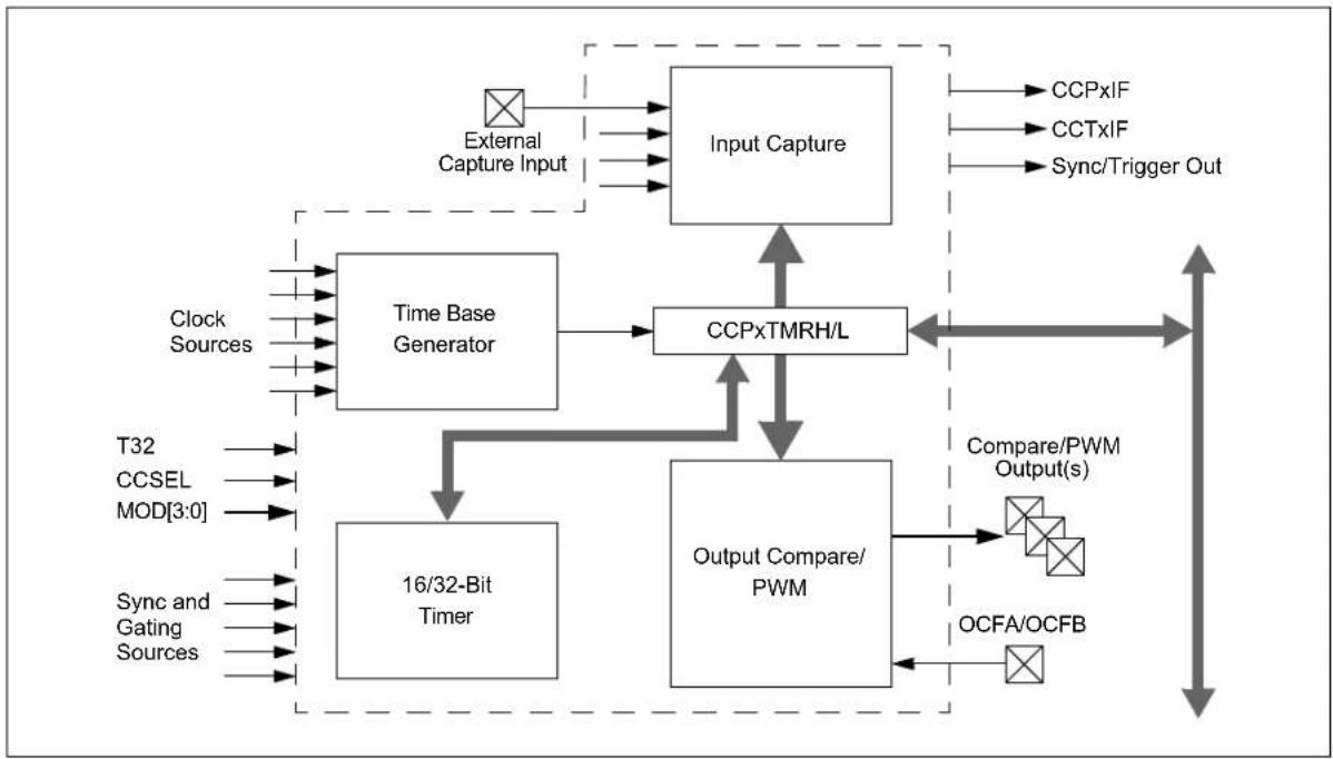
flowchart
graph TD
    A["Clock Sources"] --> B["Time Base Generator"]
    C["External Capture Input"] --> D["Input Capture"]
    D --> E["CCPS TMRH/L"]
    E --> F["Output Compare/PWM"]
    F --> G["Compare/PWM Output(s)"]
    G --> H["OCFA/OCFB"]
    H --> I["Output"]
    J["16/32-Bit Timer"] --> F
    K["T32"] --> J
    L["CCSEL"] --> J
    M["MOD[3:0"]] --> J
    N["Sync and Gating Sources"] --> J
    O["Clock"] --> J
    P["Clock"] --> J
    Q["Clock"] --> J
    R["Clock"] --> J
    S["Clock"] --> J
    T["Clock"] --> J
    U["Clock"] --> J
    V["Clock"] --> J
    W["Clock"] --> J
    X["Clock"] --> J
    Y["Clock"] --> J
    Z["Clock"] --> J
    AA["Clock"] --> J
    AB["Clock"] --> J
    AC["Clock"] --> J
    AD["Clock"] --> J
    AE["Clock"] --> J
    AF["Clock"] --> J
    AG["Clock"] --> J
    AH["Clock"] --> J
    AI["Clock"] --> J
    AJ["Clock"] --> J
    AK["Clock"] --> J
    AL["Clock"] --> J
    AM["Clock"] --> J
    AN["Clock"] --> J
    AO["Clock"] --> J
    AP["Clock"] --> J
    AQ["Clock"] --> J
    AR["Clock"] --> J
    AS["Clock"] --> J
    AT["Clock"] --> J
    AU["Clock"] --> J
    AV["Clock"] --> J
    AW["Clock"] --> J
    AX["Clock"] --> J
    AY["Clock"] --> AJ
    AZ["Clock"] --> AJ
    BA["Clock"] --> AJ
    BB["Clock"] --> AJ
    BC["Clock"] --> AJ
    BD["Clock"] --> AJ
    BE["Clock"] --> AJ
    BF["Clock"] --> AJ
    BG["Clock"] --> AJ
    BH["Clock"] --> AJ
    BI["Clock"] --> AJ
    BJ["Clock"] --> AJ
    BK["Clock"] --> AJ
    BL["Clock"] --> AJ
    BM["Clock"] --> AJ
    BN["Clock"] --> AJ
    BO["Clock"] --> AJ
    BP["Clock"] --> AJ
    BQ["Clock"] --> AJ
    BR["Clock"] --> AJ
    BS["Clock"] --> AJ
    BT["Clock"] --> AJ
    BU["Clock"] --> AJ
    BV["Clock"] --> AJ
    BW["Clock"] --> AJ
10.1 Time Base Generator
The Timer Clock Generator (TCG) generates a clock for the module's internal time base, using one of the clock signals already available on the microcontroller. This is used as the time reference for the module in its three major modes. The internal time base is shown in Figure 10-2.
There are eight inputs available to the clock generator, which are selected using the CLKSEL[2:0] bits (CCPxCON1L[10:8]). Available sources include the FRC and LPRC, the Secondary Oscillator and the TCLKI External Clock inputs. The system clock is the default source (CLKSEL[2:0] = 000).
FIGURE 10-2: TIMER CLOCK GENERATOR
flowchart
graph LR
    A["Clock Sources"] --> B["Prescaler"]
    C["CLKSEL[2:0"]] --> B
    B --> D["Clock Synchronizer"]
    E["TMRPS[1:0"]] --> B
    F["TMRSYNC"] --> D
    G["SSDG"] --> D
    D --> H["Gate(1)"]
    H --> I["To Rest of Module"]
10.2 General Purpose Timer
Timer mode is selected when CCSEL = 0 and MOD[3:0] = 0000. The timer can function as a 32-bit timer or a dual 16-bit timer, depending on the setting of the T32 bit (Table 10-2).
Dual 16-Bit Timer mode provides a simple timer function with two independent 16-bit timer/counters. The primary timer uses CCPxTMRL and CCPxPRL. Only the primary timer can interact with other modules on the device. It generates the SCCPx sync out signals for use by other SCCP modules. It can also use the SYNC[4:0] bits signal generated by other modules.
The secondary timer uses CCPxTMRH and CCPxPRH. It is intended to be used only as a periodic interrupt source for scheduling CPU events. It does not generate an output sync/trigger signal like the primary time base. In Dual Timer mode, the CCPx Secondary Timer Period register, CCPxPRH, generates the SCCP compare event (CCPxIF) used by many other modules on the device.
The 32-Bit Timer mode uses the CCPxTMRL and CCPxTMRH registers, together, as a single 32-bit timer. When CCPxTMRL overflows, CCPxTMRH increments by one. This mode provides a simple timer function when it is important to track long time periods. Note that the T32 bit (CCPxCON1L[5]) should be set before the CCPxTMRL or CCPxPRH registers are written to initialize the 32-bit timer.
In both 16-bit and 32-bit modes, the timer can also function in either synchronization ("sync") or trigger operation. Both use the SYNC[4:0] bits (CCPxCON1H[4:0]) to determine the input signal source. The difference is how that signal affects the timer.
In sync operation, the timer Reset or clear occurs when the input selected by SYNC[4:0] is asserted. The timer immediately begins to count again from zero unless it is held for some other reason. Sync operation is used whenever the TRIGEN bit (CCPxCON1H[7]) is cleared. SYNC[4:0] can have any value, except '11111'.
In trigger operation, the timer is held in Reset until the input selected by SYNC[4:0] is asserted; when it occurs, the timer starts counting. Trigger operation is used whenever the TRIGEN bit is set. In Trigger mode, the timer will continue running after a trigger event as long as the CCPTRIG bit (CCPxSTATL[7]) is set. To clear CCPTRIG, the TRCLR bit (CCPxSTATL[5]) must be set to clear the trigger event, reset the timer and hold it at zero until another trigger event occurs. On dsPIC33CH128MP508 family devices, trigger operation can only be used when the system clock is the time base source (CLKSEL[2:0] = 000).
FIGURE 10-3: DUAL 16-BIT TIMER MODE
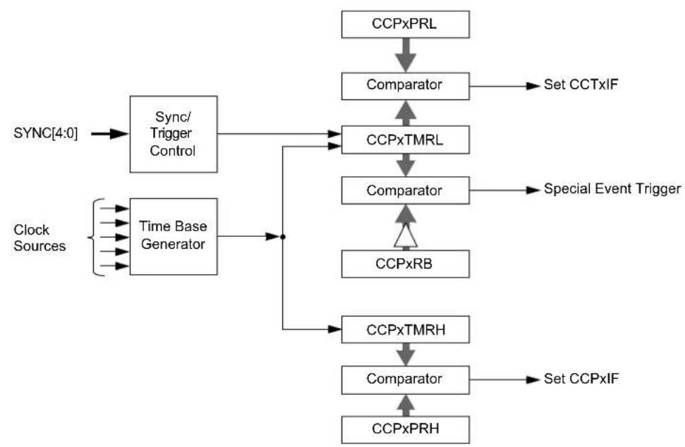
flowchart
graph TD
    A["SYNC[4:0"]] --> B["Sync/Trigger Control"]
    C["Clock Sources"] --> D["Time Base Generator"]
    B --> E["Comparator"]
    D --> F["Comparator"]
    E --> G["Set CCTxIF"]
    F --> H["Special Event Trigger"]
    D --> I["CCPxRB"]
    I --> J["CCPxTMRH"]
    J --> K["Comparator"]
    K --> L["Set CCPxIF"]
    K --> M["CCPxPRH"]
    M --> N["CCPxPRL"]
FIGURE 10-4: 32-BIT TIMER MODE
flowchart
graph TD
    A["SYNC[4:0"]] --> B["Sync/ Trigger Control"]
    C["Clock Sources"] --> D["Time Base Generator"]
    D --> E["CCPxTMRH"]
    D --> F["CCPxTMRL"]
    E --> G["Comparator"]
    F --> G
    G --> H["Set CCTxIF"]
    I["CCPxPRH"] --> G
    J["CCPxPRL"] --> G
10.3 Output Compare Mode
Output Compare mode compares the Timer register value with the value of one or two Compare registers, depending on its mode of operation. The Output Compare x module, on compare match events, has the ability to generate a single output transition or a train of
output pulses. Like most PIC ^® MCU peripherals, the Output Compare x module can also generate interrupts on a compare match event.
Table 10-3 shows the various modes available in Output Compare modes.
TABLE 10-3: OUTPUT COMPARE x/PWMx MODES
| MOD[3:0](CCPxCON1L[3:0]) | T32(CCPxCON1L[5]) | Operating Mode | |
| 0001 0 Output High on Compare (16-bit) | Single Edge Mode | ||
| 0001 1 Output High on Compare (32-bit) | |||
| 0010 0 Output Low on Compare (16-bit) | |||
| 0010 1 Output Low on Compare (32-bit) | |||
| 0011 0 Output Toggle on Compare (16-bit) | |||
| 0011 1 Output Toggle on Compare (32-bit) | |||
| 0100 0 Dual Edge Compare (16-bit) Dual Edge Mode | |||
| 0101 | 0 | Dual Edge Compare (16-bit buffered) | PWM Mode |
FIGURE 10-5: OUTPUT COMPARE x BLOCK DIAGRAM
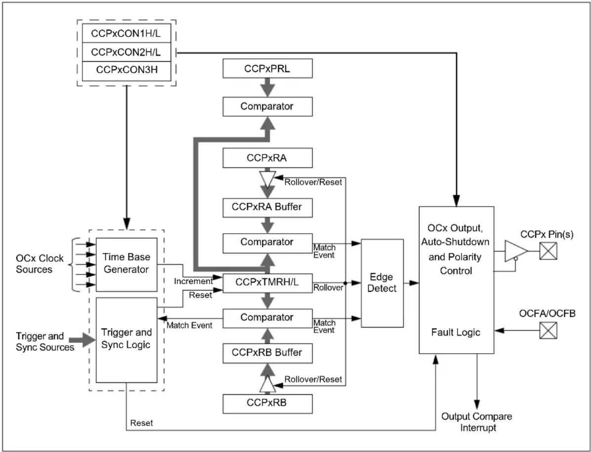
flowchart
graph TD
    A["CCPxCON1H/L"] --> B["Comparator"]
    C["CCPxCON2H/L"] --> B
    D["CCPxCON3H"] --> B
    B --> E["CCPxPRL"]
    E --> F["Comparator"]
    G["CCPxRA"] --> H["CCPxRA Buffer"]
    H --> I["Comparator"]
    I --> J["CCPxTMRH/L"]
    J --> K["Comparator"]
    K --> L["CCPxRB Buffer"]
    L --> M["CCPxRB"]
    M --> N["Output Compare Interrupt"]
    O["OCx Clock Sources"] --> P["Time Base Generator"]
    Q["Trigger and Sync Sources"] --> R["Trigger and Sync Logic"]
    S["Increment Reset"] --> J
    T["Match Event"] --> K
    U["Rollover/Reset"] --> I
    V["Match Event"] --> K
    W["Edge Detect"] --> K
    X["OCx Output, Auto-Shutdown and Polarity Control"] --> Y["Fault Logic"]
    Z["CCPx Pin(s)"] --> AA["Output Compare Interrupt"]
    AB["OCFA/OCFB"] --> AC["Output Compare Interrupt"]
10.4 Input Capture Mode
Input Capture mode is used to capture a timer value from an independent timer base, upon an event, on an input pin or other internal trigger source. The input capture features are useful in applications requiring frequency (time period) and pulse measurement. Figure 10-6 depicts a simplified block diagram of Input Capture mode.
Input Capture mode uses a dedicated 16/32-bit, synchronous, up counting timer for the capture function. The timer value is written to the FIFO when a capture event occurs. The internal value may be read (with a synchronization delay) using the CCPxTMRH/L register.
To use Input Capture mode, the CCSEL bit (CCPxCON1L[4]) must be set. The T32 and the MOD[3:0] bits are used to select the proper Capture mode, as shown in Table 10-4.
TABLE 10-4: INPUT CAPTURE x MODES
| MOD[3:0](CCPxCON1L[3:0]) | T32(CCPxCON1L[5]) | Operating Mode |
| 0000 0 Edge Detect (16-bit capture) | ||
| 0000 1 Edge Detect (32-bit capture) | ||
| 0001 0 Every Rising (16-bit capture) | ||
| 0001 1 Every Rising (32-bit capture) | ||
| 0010 0 Every Falling (16-bit capture) | ||
| 0010 1 Every Falling (32-bit capture) | ||
| 0011 0 | Every Rising/Falling (16-bit capture) | |
| 0011 1 | Every Rising/Falling (32-bit capture) | |
| 0100 0 | Every 4th Rising (16-bit capture) | |
| 0100 1 | Every 4th Rising (32-bit capture) | |
| 0101 0 | Every 16th Rising (16-bit capture) | |
| 0101 1 | Every 16th Rising (32-bit capture) | |
FIGURE 10-6: INPUT CAPTURE x BLOCK DIAGRAM

flowchart
graph TD
    A["ICx Clock Sources"] --> B["Clock Select"]
    C["Trigger and Sync Sources"] --> D["Trigger and Sync Logic"]
    B --> E["Edge Detect Logic and Clock Synchronizer"]
    D --> F["Reset"]
    E --> G["Increment"]
    F --> H["CCPxTMRH/L"]
    H --> I["T32"]
    I --> J["4-Level FIFO Buffer"]
    J --> K["CCPxBUFx"]
    K --> L["System Bus"]
    M["ICS[2:0"]] --> B
    N["MOD[3:0"]] --> E
    O["OPS[3:0"]] --> F
    P["Set CCPxIF"] --> J
    Q["16"] --> J
    R["16"] --> K
10.5 Auxiliary Output
The SCCPx modules have an auxiliary (secondary) output that provides other peripherals access to internal module signals. The auxiliary output is intended to connect to other SCCP modules, or other digital peripherals, to provide these types of functions:
• Time Base Synchronization
• Peripheral Trigger and Clock Inputs
- Signal Gating
The type of output signal is selected using the AUXOUT[1:0] control bits (CCPxCON2H[4:3]). The type of output signal is also dependent on the module operating mode.
TABLE 10-5: AUXILIARY OUTPUT
| AUXOUT[1:0] CCSEL MOD[3:0] Comments Signal Description | ||||
| 00 | x | xxxx | Auxiliary output disabled | No Output |
| 01 | 0 | 0000 | Time Base modes | Time Base Period Reset or Rollover |
| 10 | Special Event Trigger Output | |||
| 11 | No Output | |||
| 01 0 0001 | through 1111 | Output Compare modes | Time Base Period Reset or Rollover | |
| 10 | Output Compare Event Signal | |||
| 11 | Output Compare Signal | |||
| 01 | 1 | xxxx | Input Capture modes | Time Base Period Reset or Rollover |
| 10 | Reflects the Value of the ICDIS bit | |||
| 11 | Input Capture Event Signal | |||
10.6 SCCP Control/Status Registers
REGISTER 10-1: CCPxCON1L: CCPx CONTROL 1 LOW REGISTERS
| R/W-0 U-0 R/W-0 R/W-0 R/W-0 R/W-0 R/W-0 R/W-0 | |||||||
| CCPON | — CCPS | IDL CCPSLP | TMRSYNC CLK | KSEL2 | (1) | CLKSEL1(1) | CLKSEL0(1) |
| bit 15 bit 8 | |||||||
| R/W-0 R/W-0 R/W-0 R/W-0 R/W-0 R/W-0 R/W-0 R/W-0 | ||||||
| TMRPS1 TMRPS0 T32 CCSEL MOD3 MOD2 MOD1 MOD0 | ||||||
| bit 7 bit 0 | ||||||
Legend:
| R = Readable bit | W = Writable bit | U = Unimplemented bit, read as '0' |
| -n = Value at POR | '1' = Bit is set | '0' = Bit is cleared x = Bit is unknown |
bit 15 CCPON: CCPx Module Enable bit
1 = Module is enabled with an operating mode specified by the MOD[3:0] control bits 0 = Module is disabled
bit 14 Unimplemented: Read as '0'
bit 13 CCPSIDL: CCPx Stop in Idle Mode bit
1 = Discontinues module operation when device enters Idle mode 0 = Continues module operation in Idle mode
bit 12 CCPSLP: CCPx Sleep Mode Enable bit
1 = Module continues to operate in Sleep modes 0 = Module does not operate in Sleep modes
bit 11 TMRSYNC: Time Base Clock Synchronization bit
1 = Asynchronous module time base clock is selected and synchronized to the internal system clocks (CLKSEL[2:0] ≠ 000) 0 = Synchronous module time base clock is selected and does not require synchronization (CLKSEL[2:0] = 000)
bit 10-8 CLKSEL[2:0]: CCPx Time Base Clock Select bits ^(1)
111 = External T1CK input 110 = Secondary CLC2 101 = Secondary CLC1 100 = Main CLC2 011 = Main CLC1 010 = Fosc 001 = Reference Clock (RB) 000 = Fosc/2 (FP)
bit 7-6 TMRPS[1:0]: Time Base Prescale Select bits
11 = 1:64 Prescaler 10 = 1:16 Prescaler 01 = 1:4 Prescaler 00 = 1:1 Prescaler
bit 5 T32: 32-Bit Time Base Select bit
1 = Uses 32-bit time base for timer, single edge output compare or input capture function 0 = Uses 16-bit time base for timer, single edge output compare or input capture function
Note 1: Clock selection is the same for the Main and the Secondary.
2: Not available in SCCP instances 1-8.
REGISTER 10-1: CCPxCON1L: CCPx CONTROL 1 LOW REGISTERS (CONTINUED)
bit 4 CCSEL: Capture/Compare Mode Select bit
1 = Input Capture peripheral
0 = Output Compare/PWM/Timer peripheral (exact function is selected by the MOD[3:0] bits)
bit 3-0 MOD[3:0]: CCPx Mode Select bits
For CCSEL = 1 (Input Capture modes):
1xxx = Reserved
011x = Reserved
0101 = Capture every 16th rising edge
0100 = Capture every 4th rising edge
0011 = Capture every rising and falling edge
0010 = Capture every falling edge
0001 = Capture every rising edge
0000 = Capture every rising and falling edge (Edge Detect mode)
For CCSEL = 0 (Output Compare/Timer modes):
1111 = External Input mode: Pulse generator is disabled, source is selected by ICS[2:0]
1110 = Reserved
110x = Reserved
10xx = Reserved
0111 = Reserved
0110 = Center-aligned PWM mode ^(2)
0101 = Dual Edge Compare mode, buffered
0001 = 16-Bit/32-Bit Single Edge mode, drives output high on compare match
0000 = 16-Bit/32-Bit Timer mode, output functions are disabled
Note 1: Clock selection is the same for the Main and the Secondary.
2: Not available in SCCP instances 1-8.
REGISTER 10-2: CCPxCON1H: CCPx CONTROL 1 HIGH REGISTERS
| R/W-0 R/W-0 U-0 U-0 R/W-0 R/W-0 R/W-0 R/W-0 | ||||||
| OPSSRC(1) | RTRGEN(2) | — — OPS3 | (3) | OPS2(3) | OPS1(3) | OPS0(3) |
| bit 15 bit 8 | ||||||
| R/W-0 R/W-0 R/W-0 R/W-0 R/W-0 R/W-0 R/W-0 R/W-0 | |||||||
| TRIGEN | ONESHOT | ALTSYNC | SYNC4 | SYNC3 | SYNC2 | SYNC1 | SYNC0 |
| bit 7 bit 0 | |||||||
| Legend: | |||
| R = Readable bit | W = Writable bit | U = Unimplemented bit, read as ‘0’ | |
| -n = Value at POR | ‘1’ = Bit is set | ‘0’ = Bit is cleared | x = Bit is unknown |
bit 15 OPSSRC: Output Postscaler Source Select bit ^(1) 1 = Output postscaler scales module trigger output events
0 = Output postscaler scales time base interrupt events
bit 14 RTRGEN: Retrigger Enable bit ^(2) 1 = Time base can be retriggered when TRIGEN bit = 1 0 = Time base may not be retriggered when TRIGEN bit = 1
bit 13-12 Unimplemented: Read as '0'
bit 11-8 OPS3[3:0]: CCPx Interrupt Output Postscale Select bits ^(3) 1111 = Interrupt every 16th time base period match
1110 = Interrupt every 15th time base period match
...
0100 = Interrupt every 5th time base period match
0011 = Interrupt every 4th time base period match or 4th in
0010 = Interrupt every 3rd time base period match or 3rd in
0001 = Interrupt every 2nd time base period match or 2nd
0000 = Interrupt after each time base period match or input
bit 7 TRIGEN: CCPx Trigger Enable bit 1 = Trigger operation of time base is enabled 0 = Trigger operation of time base is disabled
bit 6 ONESHOT: One-Shot Trigger Mode Enable bit 1 = One-Shot Trigger mode is enabled; trigger duration is set by OSCNT[2:0] 0 = One-Shot Trigger mode is disabled
bit 5 ALTSYNC: CCPx Alternate Synchronization Output Signal Select bit 1 = An alternate signal is used as the module synchronization output signal 0 = The module synchronization output signal is the Time Base Reset/rollover event
bit 4-0 SYNC[4:0]: CCPx Synchronization Source Select bits See Table 10-6 and Table 10-7 for the definition of inputs.
Note 1: This control bit has no function in Input Capture modes.
2: This control bit has no function when TRIGEN = 0.
3: Output postscale settings, from 1:5 to 1:16 (0100-1111), will result in a FIFO buffer overflow for Input Capture modes.
TABLE 10-6: SYNCHRONIZATION SOURCES (MAIN)
| SYNC[4:0] Synchronization Source | |
| 00000 None; Timer with Rollover on CCPxPR Match or FFFFh | |
| 00001 Module's Own Timer Sync Out | |
| 00010 Sync Output SCCP1 | |
| 00011 Sync Output SCCP2 | |
| 00100 Sync Output SCCP3 | |
| 00101 Sync Output SCCP4 | |
| 00110 Sync Output SCCP5 | |
| 00111 Sync Output SCCP6 | |
| 01000 Sync Output SCCP7 | |
| 01001 INT0 | |
| 01010 INT1 | |
| 01011 INT2 | |
| 01100-01111 Reserved | |
| 10000 Main CLC1 Output | |
| 10001 Main CLC2 Output | |
| 10010 Secondary CLC1 Output | |
| 10011 Secondary CLC2 Output | |
| 10100-10110 Reserved | |
| 10111 Comparator 1 Output | |
| 11000 Secondary Comparator 1 Output | |
| 11001 Secondary Comparator 2 Output | |
| 11010 Secondary Comparator 3 Output | |
| 11011-11110 Reserved | |
| 11111 | None; Timer with Auto-Rollover (FFFFh → 0000h) |
TABLE 10-7: SYNCHRONIZATION SOURCES (SECONDARY)
| SYNC[4:0] Synchronization Source | |
| 00000 None; Timer with Rollover on CCPxPR Match or FFFFh | |
| 00001 Module's Own Timer Sync Out | |
| 00010 Sync Output SCCP1 | |
| 00011 Sync Output SCCP2 | |
| 00100 Sync Output SCCP3 | |
| 00101 Sync Output SCCP4 | |
| 00110-01000 Reserved | |
| 01001 INT0 | |
| 01010 INT1 | |
| 01011 INT2 | |
| 01100-01111 Reserved | |
| 10000 Main CLC1 Output | |
| 10001 Main CLC2 Output | |
| 10010 Secondary CLC1 Output | |
| 10011 Secondary CLC2 Output | |
| 10100-10110 Reserved | |
| 10111 Main Comparator 1 Output | |
| 11000 Secondary Comparator 1 Output | |
| 11001 Secondary Comparator 2 Output | |
| 11010 Secondary Comparator 3 Output | |
| 11011-11110 Reserved | |
| 11111 | None; Timer with Auto-Rollover (FFFFh → 0000h) |
REGISTER 10-3: CCPxCON2L: CCPx CONTROL 2 LOW REGISTERS
| R/W-0 R/W-0 U-0 R/W-0 U-0 U-0 U-0 U-0 | |||||
| PWMRSEN ASDGM | — SSDG — — — — | ||||
| bit 15 bit 8 | |||||
| R/W-0 R/W-0 R/W-0 R/W-0 R/W-0 R/W-0 R/W-0 R/W-0 |
| ASDG[7:0] |
| bit 7 bit 0 |
Legend:
| R = Readable bit W = Writable bit U = Unimplemented bit, read as '0' | ||
| -n = Value at POR | '1' = Bit is set | '0' = Bit is cleared x = Bit is unknown |
bit 15 PWMRSEN: CCPx PWM Restart Enable bit
| 1 = ASEVT bit clears automatically at the beginning of the next PWM period, after the shutdown input has ended |
| 0 = ASEVT bit must be cleared in software to resume PWM activity on output pins |
bit 14 ASDGM: CCPx Auto-Shutdown Gate Mode Enable bit
| 1 = Waits until the next Time Base Reset or rollover for shutdown to occur |
| 0 = Shutdown event occurs immediately |
bit 13 Unimplemented: Read as '0'
| bit 12 | SSDG: CCPx Software Shutdown/Gate Control bit |
| 1 = Manually forces auto-shutdown, timer clock gate or input capture signal gate event (setting of ASDGM bit still applies) | |
| 0 = Normal module operation |
bit 11-8 Unimplemented: Read as '0'
| bit 7-0 | ASDG[7:0]: CCPx Auto-Shutdown/Gating Source Enable bits1 = ASDGx Source n is enabled (see Table 10-8 and Table 10-9 for auto-shutdown/gating sources)0 = ASDGx Source n is disabled |
TABLE 10-8: AUTO-SHUTDOWN AND GATING SOURCES (MAIN)
| ASDG[x]Bit | Auto-Shutdown/Gating Source | |||||||
| SCCP1 SCCP2 SCCP3 SCCP4 SCCP5 SCCP6 SCCP7 SCCP8 | ||||||||
| 0 Main | Comparator 1 Output | |||||||
| 1 Secondary Comparator 1 Output | ||||||||
| 2 Secondary Comparator 2 Output | ||||||||
| 3 Secondary Comparator 3 Output | ||||||||
| 4 | MICM1(1) | aMainICM2(1) | i Main nICM3(1) | MainICM4(1) | MainICM5(1) | MainICM6(1) | MainICM7(1) | MainICM8(1) |
| 5 Main | CLC1 (1) | |||||||
| 6 | M (1) a | |||||||
| 7 | M (1) a | |||||||
Note 1: Selected by Peripheral Pin Select (PPS).
TABLE 10-9: AUTO-SHUTDOWN AND GATING SOURCES (SECONDARY)
| ASDG[x] Bit | Auto-Shutdown/Gating Source | |||
| SCCP1 | SCCP2 | SCCP3 | SCCP4 | |
| 0 Main | Comparator 1 Output | |||
| 1 Secondary Comparator 1 Output | ||||
| 2 Secondary Comparator 2 Output | ||||
| 3 Secondary Comparator 3 Output | ||||
| 4 | Secondary ICM1(1) | Secondary ICM2(1) | Secondary ICM3(1) | Secondary ICM4(1) |
| 5 | Secondary CLC1(1) | |||
| 6 | Secondary OCFA(1) | |||
| 7 | Secondary OCFB(1) | |||
Note 1: Selected by Peripheral Pin Select (PPS).
REGISTER 10-4: CCPxCON2H: CCPx CONTROL 2 HIGH REGISTERS
| R/W-0 U-0 U-0 U-0 U-0 U-0 R/W-0 | |||||||
| OENSYNC | —— | —— OCAEN | |||||
| bit 15 bit 8 | |||||||
| R/W-0 R/W-0 U-0 R/W-0 R/W-0 R/W-0 R/W-0 R/W-0 | ||||||
| ICGSM1 IC | GSM0 | — AUXOUT1 AUXOUT | 0 ICS2 | (1) | ICS1(1) | ICS0(1) |
| bit 7 bit 0 | ||||||
| Legend: | |||
| R = Readable bit | W = Writable bit | U = Unimplemented bit, read as ‘0’ | |
| -n = Value at POR | ‘1’ = Bit is set | ‘0’ = Bit is cleared | x = Bit is unknown |
| bit 15 | OENSYNC: Output Enable Synchronization bit1 = Update by output enable bits occurs on the next Time Base Reset or rollover0 = Update by output enable bits occurs immediately |
| bit 14-9 | Unimplemented: Read as '0' |
| bit 8 | OCAEN: Output Enable/Steering Control bit1 = OCx pin is controlled by the CCPx module and produces an output compare or PWM signal0 = OCx pin is not controlled by the CCPx module; the pin is available to the port logic or another peripheral multiplexed on the pin |
| bit 7-6 | ICGSM[1:0]: Input Capture Gating Source Mode Control bits11 = Reserved10 = One-Shot mode: Falling edge from gating source disables future capture events (ICDIS = 1)01 = One-Shot mode: Rising edge from gating source enables future capture events (ICDIS = 0)00 = Level-Sensitive mode: A high level from gating source will enable future capture events; a low level will disable future capture events |
| bit 5 | Unimplemented: Read as '0' |
| bit 4-3 | AUXOUT[1:0]: Auxiliary Output Signal on Event Selection bits11 = Input capture or output compare event; no signal in Timer mode10 = Signal output is defined by module operating mode (see Table 10-5)01 = Time base rollover event (all modes)00 = Disabled |
| bit 2-0 | ICS[2:0]: Input Capture Source Select bits(1)111 = Secondary CLC2 output110 = Secondary CLC1 output101 = Main CLC2 output100 = Main CLC1 output011 = Secondary Comparator 2 output010 = Secondary Comparator 1 output001 = Main Comparator 1 output000 = SCCP Input Capture x (ICx) pin (PPS) |
Note 1: Common for both the Main and the Secondary.
REGISTER 10-5: CCPxCON3H: CCPx CONTROL 3 HIGH REGISTERS
| R/W-0 R/W-0 R/W-0 R/W-0 U-0 U-0 U-0 U-0 | ||||||
| OETRIG O$CNT2 OSCNT1 OSCNT0 | — — — | — | ||||
| bit 15 bit 8 | ||||||
| U-0 U-0 R/W-0 U-0 R/W-0 R/W-0 U-0 U-0 | |||||||
| — — | P | O | L | A | C | E | — PSSACE1 PSSACE0 — — |
| bit 7 bit 0 | |||||||
| Legend: | |||
| R = Readable bit W = Writable bit | U = Unimplemented bit, read as '0' | ||
| -n = Value at POR | '1' = Bit is set | '0' = Bit is cleared | x = Bit is unknown |
bit 15 OETRIG: Output Enable on Trigger Control bit 1 = For Triggered mode (TRIGEN = 1): Module does not drive enabled output pins until triggered 0 = Normal output pin operation
bit 14-12 OSCNT[2:0]: One-Shot Event Count bits 111 = Extends one-shot event by seven time base periods (eight time base periods total) 110 = Extends one-shot event by six time base periods (seven time base periods total) 101 = Extends one-shot event by five time base periods (six time base periods total) 100 = Extends one-shot event by four time base periods (five time base periods total) 011 = Extends one-shot event by three time base periods (four time base periods total) 010 = Extends one-shot event by two time base periods (three time base periods total) 001 = Extends one-shot event by one time base period (two time base periods total) 000 = Does not extend one-shot trigger event
bit 11-6 Unimplemented: Read as '0' bit 5 POLACE: CCPx Output Pin OCxA Polarity Control bit 1 = Output pin polarity is active low 0 = Output pin polarity is active high bit 4 Unimplemented: Read as '0' bit 3-2 PSSACE[1:0]: PWMx Output Pin OCxA Shutdown State Control bits 11 = Pin is driven active when a shutdown event occurs 10 = Pin is driven inactive when a shutdown event occurs 0x = Pin is in high-impedance state when a shutdown event occurs bit 1-0 Unimplemented: Read as '0'
REGISTER 10-6: CCPxSTATL: CCPx STATUS REGISTER
| U-0 U-0 U-0 U-0 U-0 U-0 U-0 U-0 | |||||||
| —— | —— | —— | |||||
| bit 15 bit 8 | |||||||
| R-0 W1-0 W1-0 R/C-0 R/C-0 R/C-0 R/C-0 R/C-0 | |||||||
| CCPTRIG | TRSET | TRCLR | ASEVT | SCEVT | ICDIS | ICOV | ICBNE |
| bit 7 bit 0 | |||||||
| Legend: | C = Clearable bit | ||
| R = Readable bit | W1 = Write ‘1’ Only bit | U = Unimplemented bit, read as ‘0’ | |
| -n = Value at POR | ‘1’ = Bit is set | ‘0’ = Bit is cleared | x = Bit is unknown |
bit 15-8 Unimplemented: Read as '0'
bit 7 CCPTRIG: CCPx Trigger Status bit
1 = Timer has been triggered and is running
0 = Timer has not been triggered and is held in Reset
bit 6 TRSET: CCPx Trigger Set Request bit
Writes '1' to this location to trigger the timer when TRIGEN = 1 (location always reads as '0').
bit 5 TRCLR: CCPx Trigger Clear Request bit
Writes '1' to this location to cancel the timer trigger when TRIGEN = 1 (location always reads as '0').
bit 4 ASEVT: CCPx Auto-Shutdown Event Status/Control bit
1 = A shutdown event is in progress; CCPx outputs are in the shutdown state
0 = CCPx outputs operate normally
bit 3 SCEVT: Single Edge Compare Event Status bit
1 = A single edge compare event has occurred
0 = A single edge compare event has not occurred
bit 2 ICDIS: Input Capture x Disable bit
1 = Event on Input Capture x pin (ICx) does not generate a capture event
0 = Event on Input Capture x pin will generate a capture event
bit 1 ICOV: Input Capture x Buffer Overflow Status bit
1 = The Input Capture x FIFO buffer has overflowed
0 = The Input Capture x FIFO buffer has not overflowed
bit 0 ICBNE: Input Capture x Buffer Status bit
1 = Input Capture x buffer has data available
0 = Input Capture x buffer is empty
NOTES:
11.0 HIGH-SPEED ANALOG COMPARATOR WITH SLOPE COMPENSATION DAC
Note 1: This data sheet summarizes the features of the dsPIC33CH128MP508 family of devices. It is not intended to be a comprehensive reference source. To complement the information in this data sheet, refer to “High-Speed Analog Comparator Module” (www.microchip.com, DS70005280), which is available from the Microchip website (www.microchip.com).
2: Some registers and associated bits described in this section may not be available on all devices. Refer to Section 3.2 "Main Memory Organization" in this data sheet for device-specific register and bit information.
3: The comparator and DAC are identical for both Main core and Secondary core. The module is similar for both Main core and Secondary core (where the x represents the number of the specific modules being addressed in Main or Secondary).
The high-speed analog comparator module provides a method to monitor voltage, current and other critical signals in a power conversion application that may be too fast for the CPU and ADC to capture. There are a total of four comparator modules, one of which is controlled by the Main core and the remaining three by the Secondary core. The analog comparator module can be used to implement Peak Current mode control, Critical Conduction mode (variable frequency) and Hysteretic Control mode. Table 11-1 shows an overview of the comparator/DAC module.
TABLE 11-1: COMPARATOR/DAC MODULE OVERVIEW
| Number of Comparator Modules | Identical (Modules) | |
| Main Core 1 Yes | ||
| Secondary Core | 3 Yes |
11.1 Overview
The high-speed analog comparator module is comprised of a high-speed comparator, Pulse Density Modulation (PDM) DAC and a slope compensation unit. The slope compensation unit provides a user-defined slope which can be used to alter the DAC output. This feature is useful in applications, such as Peak Current mode control, where slope compensation is required to maintain the stability of the power supply. The user simply specifies the direction and rate of change for the slope compensation and the output of the DAC is modified accordingly.
The DAC consists of a PDM unit, followed by a digitally controlled multiphase RC filter. The PDM unit uses a phase accumulator circuit to generate an output stream of pulses. The density of the pulse stream is proportional to the input data value, relative to the maximum value supported by the bit width of the accumulator. The output pulse density is representative of the desired output voltage. The pulse stream is filtered with an RC filter to yield an analog voltage. The output of the DAC is connected to the negative input of the comparator. The positive input of the comparator can be selected using a MUX from either of the input pins or the output of the PGAs. The comparator provides a high-speed operation with a typical delay of 15 ns.
The output of the comparator is processed by the pulse stretcher and the digital filter blocks, which prevent comparator response to unintended fast transients in the inputs. Figure 11-1 shows a block diagram of the high-speed analog comparator module. The DAC module can be operated in one of three modes: Slope Generation mode, Hysteretic mode and Triangle Wave mode. Each of these modes can be used in a variety of power supply applications.
Note: The DACOUT1 pin can only be associated with a single DAC or PGA output at any given time. If more than one DACOEN bit is set, or the PGA Output Enable bit (PGAOEN) and the DACOEN bit are set, the DACOUT1 pin will be a combination of the signals.
Note: DAC input frequency needs to be 500 MHz.
FIGURE 11-1: HIGH-SPEED ANALOG COMPARATOR MODULE BLOCK DIAGRAM

flowchart
graph TD
    A["INSEL[2:0"]] --> B["CMPx"]
    C["SPGA3"] --> B
    D["SPGA2"] --> B
    E["SPGA1"] --> B
    F["CMPxD/S1CMPxD"] --> B
    G["CMPxB/S1CMPxB"] --> B
    H["CMPxA/S1CMPxA"] --> B
    B --> I["+"]
    I --> J["0"]
    J --> K["Pulse Stretcher and Digital Filter"]
    K --> L["Status"]
    K --> M["IRQ"]
    N["Slope Generator"] --> O["n"]
    O --> P["PDM DAC"]
    P --> Q["DACx 4"]
    Q --> R["DACOUT1"]
    S["SLPxDAT"] --> T["n"]
    U["DACxDATH"] --> V["n"]
    W["DACxDATL"] --> X["n"]
    Y["CMPPOL"] --> Z["0"]
    AA["PWM Trigger"] --> K
    AB["SPGA1"] --> AC["×"]
    AD["SPGA2"] --> AE["×"]
    AF["SPGA3"] --> AG["×"]
Note: n = 16
11.2 Features Overview
- Four Rail-to-Rail Analog Comparators - Up to Five Selectable Input Sources per Comparator:
- Three external inputs
- Two internal inputs from PGA module
- Programmable Comparator Hysteresis
- Programmable Output Polarity
- Interrupt Generation Capability
• Dedicated Pulse Density Modulation DAC for each Analog Comparator:
- PDM unit followed by a digitally controlled multimode multipole RC filter
- Multimode Multipole RC Output Filter:
- Transition mode: Provides the fastest response
- Fast mode: For tracking DAC slopes
- Steady-State mode: Provides 12-bit resolution
- Slope Compensation along with each DAC:
- Slope Generation mode
- Hysteretic Control mode
- Triangle Wave mode
- Functional Support for the High-Speed PWM module which Includes:
- PWM duty cycle control
- PWM period control
- PWM Fault detect
11.3 DAC Control Registers
The DACCTRL1L and DACCTRL2H/L registers are common configuration registers for Main and Secondary DAC modules. The Main and Secondary DAC modules are controlled by separate sets of DACCTRL1/2 registers. The DACxCON, DACxDAT, SLPxCON and SLPxDAT registers specify the operation of individual modules. Note that x = 1 for the Main module and x = 1-3 for the Secondary modules.
REGISTER 11-1: DACCTRL1L: DAC CONTROL 1 LOW REGISTER
| R/W-0 | U-0 | R/W-0 | U-0 | U-0 | U-0 | U-0 | U-0 |
| DACON | — | DACSIDL | — | — | — | — | — |
| bit 15 bit 8 | |||||||
| R/W-0 | R/W-0 | R/W-0 | R/W-0 | U-0 | R/W-0 | R/W-0 | R/W-0 |
| CLKSEL1(1) | CLKSEL0(1) | CLKDIV1(1) | CLKDIV0(1) | — | FCLKDIV2(2) | FCLKDIV1(2) | FCLKDIV0(2) |
| bit 7 bit 0 | |||||||
Legend:
| R = Readable bit | W = Writable bit | U = Unimplemented bit, read as '0' |
| -n = Value at POR | '1' = Bit is set | '0' = Bit is cleared |
bit 15 DACON: Common DAC Module Enable bit
1 = Enables DAC modules
0 = Disables DAC modules and disables FSCM clocks to reduce power consumption; any pending Slope mode and/or underflow conditions are cleared
bit 14 Unimplemented: Read as '0'
bit 13 DACSIDL: DAC Stop in Idle Mode bit
1 = Discontinues module operation when device enters Idle mode
0 = Continues module operation in Idle mode
bit 12-8 Unimplemented: Read as '0'
bit 7-6 CLKSEL[1:0]: DAC Clock Source Select bits ^(1)
11 = FPLLO
10 = AFPLLO
01 = Fvco/2
00 = AFvco/2
bit 5-4 CLKDIV[1:0]: DAC Clock Divider bits (DAC should be operated at 500 MHz) ^(1,3)
11 = Divide-by-4
10 = Divide-by-3 (non-uniform duty cycle)
01 = Divide-by-2
00 = 1x
bit 3 Unimplemented: Read as '0'
bit 2-0 FCLKDIV[2:0]: Comparator Filter Clock Divider bits ^(2)
111 = Divide-by-8
110 = Divide-by-7
101 = Divide-by-6
100 = Divide-by-5
011 = Divide-by-4
010 = Divide-by-3
001 = Divide-by-2
000 = 1x
Note 1: These bits should only be changed when DACON = 0 to avoid unpredictable behavior.
2: The input clock to this divider is the selected clock input, CLKSEL[1:0], and then divided by two.
3: Clock source and dividers should yield an effective DAC clock input of 500 MHz.
REGISTER 11-2: DACCTRL2H: DAC CONTROL 2 HIGH REGISTER
| U-0 U-0 U-0 U-0 U-0 R/W-0 R/W-0 | |||||
| — — — | — — — | SSTIME[9:8] | (1) | ||
| bit 15 bit 8 | |||||
| R/W-1 | R/W-0 | R/W-0 | R/W-0 | R/W-1 | R/W-0 | R/W-1 | R/W-0 |
| SSTIME[7:0](1) | |||||||
| bit 7 | bit 0 | ||||||
Legend:
| R = Readable bit | W = Writable bit | U = Unimplemented bit, read as '0' |
| -n = Value at POR | '1' = Bit is set | '0' = Bit is cleared |
bit 15-10 Unimplemented: Read as '0'
bit 9-0 SSTIME[9:0]: Time from Start of Transition Mode until Steady-State Filter is Enabled bits ^(1)
Note 1: The value for SSTIME[9:0] should be greater than the TMODTIME[9:0] value.
REGISTER 11-3: DACCTRL2L: DAC CONTROL 2 LOW REGISTER
| U-0 U-0 U-0 | U-0 | U-0 U-0 | R/W-0 R/W-0 | |||
| — | — | — | — | — | — | TMODTIME[9:8](1) |
| bit 15 bit 8 | ||||||
| R/W-0 | R/W-1 | R/W-0 | R/W-1 | R/W-0 | R/W-1 | R/W-0 | R/W-1 |
| TMODTIME[7:0](1) | |||||||
| bit 7 | bit 0 | ||||||
Legend:
| R = Readable bit | W = Writable bit | U = Unimplemented bit, read as ‘0’ |
| -n = Value at POR | ‘1’ = Bit is set | ‘0’ = Bit is cleared |
bit 15-10 Unimplemented: Read as '0'
bit 9-0 TMODTIME[9:0]: Transition Mode Duration bits ^(1)
Note 1: The value for TMODTIME[9:0] should be less than the SSTIME[9:0] value.
REGISTER 11-4: DACxCONH: DACx CONTROL HIGH REGISTER
| U-0 U-0 U-0 U-0 U-0 R/W-0 R/W-0 | |||||
| — — — | — — | — | TMCB[9:8] | ||
| bit 15 bit 8 | |||||
| R/W-0 | R/W-0 | R/W-0 | R/W-0 | R/W-0 | R/W-0 | R/W-0 | R/W-0 |
| TMCB[7:0] | |||||||
| bit 7 | bit 0 | ||||||
Legend:
| R = Readable bit | W = Writable bit | U = Unimplemented bit, read as '0' |
| -n = Value at POR | '1' = Bit is set | '0' = Bit is cleared |
bit 15-10 Unimplemented: Read as '0'
bit 9-0 TMCB[9:0]: DACx Leading-Edge Blanking bits
These register bits specify the blanking period for the comparator, following changes to the DAC output during Change-of-State (COS), for the input signal selected by the HCFSEL[3:0] bits in Register 11-9.
REGISTER 11-5: DACxCONL: DACx CONTROL LOW REGISTER
| R/W-0 | R/W-0 | R/W-0 | U-0 | U-0 | R/W-0 | R/W-0 | R/W-0 |
| DACEN | IRQM1^(1,2) | IRQM0^(1,2) | — | — | CBE | DACOEN | FLTREN |
| bit 15 | bit 8 | ||||||
| R/W-0 | R/W-0 | R/W-0 | R/W-0 | R/W-0 | R/W-0 | R/W-0 | R/W-0 |
| CMPSTAT | CMPPOL | INSEL2 | INSEL1 | INSEL0 | HYSPOL | HYSSEL1 | HYSSEL0 |
| bit 7 bit 0 | |||||||
Legend:
| R = Readable bit | W = Writable bit | U = Unimplemented bit, read as '0' |
| -n = Value at POR | '1' = Bit is set | '0' = Bit is cleared |
bit 15 DACEN: Individual DACx Module Enable bit
1 = Enables DACx module
0 = Disables DACx module to reduce power consumption; any pending Slope mode and/or underflow conditions are cleared
bit 14-13 IRQM[1:0]: Interrupt Mode select bits ^(1,2)
11 = Generates an interrupt on either a rising or falling edge detect
10 = Generates an interrupt on a falling edge detect
01 = Generates an interrupt on a rising edge detect
00 = Interrupts are disabled
bit 12-11 Unimplemented: Read as '0'
Note 1: Changing these bits during operation may generate a spurious interrupt.
2: The edge selection is a post-polarity selection via the CMPPOL bit.
REGISTER 11-5: DACxCONL: DACx CONTROL LOW REGISTER (CONTINUED)
bit 10 CBE: Comparator Blank Enable bit
1 = Enables the analog comparator output to be blanked (gated off) during the recovery transition following the completion of a slope operation
0 = Disables the blanking signal to the analog comparator; therefore, the analog comparator output is always active
bit 9 DACOEN: DACx Output Buffer Enable bit
1 = DACx analog voltage is connected to the DACOUT1 pin
0 = DACx analog voltage is not connected to the DACOUT1 pin
bit 8 FLTREN: Comparator Digital Filter Enable bit
1 = Digital filter is enabled
0 = Digital filter is disabled
bit 7 CMPSTAT: Comparator Status bits
The current state of the comparator output including the CMPPOL selection.
bit 6 CMPPOL: Comparator Output Polarity Control bit
1 = Output is inverted
0 = Output is noninverted
bit 5-3 INSEL[2:0]: Comparator Input Source Select bits
Main
111 = Reserved
110 = Reserved
101 = SPGA2 output
100 = SPGA1 output
011 = CMPxD input pin
010 = SPGA3 output
001 = CMPxB input pin
000 = CMPxA input pin
Secondary
111 = Reserved
110 = Reserved
101 = SPGA2 output
100 = SPGA1 output
011 = S1CMPxD input pin
010 = SPGA3 output
001 = S1CMPxB input pin
000 = S1CMPxA input pin
bit 2 HYSPOL: Comparator Hysteresis Polarity Select bit
1 = Hysteresis is applied to the falling edge of the comparator input
0 = Hysteresis is applied to the rising edge of the comparator input
bit 1-0 HYSSEL[1:0]: Comparator Hysteresis Select bits
11 = 45 mv hysteresis
10 = 30 mv hysteresis
01 = 15 mv hysteresis
00 = No hysteresis is selected
Note 1: Changing these bits during operation may generate a spurious interrupt.
2: The edge selection is a post-polarity selection via the CMPPOL bit.
REGISTER 11-6: DACxDATH: DACx DATA HIGH REGISTER
| U-0 | U-0 | U-0 | U-0 | R/W-0 | R/W-0 | R/W-0 | R/W-0 |
| — — — | — DACDAT[1:8] | ||||||
| bit 15 | bit 8 | ||||||
| R/W-0 | R/W-0 | R/W-0 | R/W-0 | R/W-0 | R/W-0 | R/W-0 | R/W-0 |
| DACDAT[7:0] | |||||||
| bit 7 | bit 0 | ||||||
Legend:
| R = Readable bit | W = Writable bit | U = Unimplemented bit, read as '0' |
| -n = Value at POR | '1' = Bit is set | '0' = Bit is cleared |
bit 15-12 Unimplemented: Read as '0'
bit 11-0 DACDAT[11:0]: DACx Data bits
This register specifies the high DACx data value. Valid values are from 205 to 3890.
REGISTER 11-7: DACxDATL: DACx DATA LOW REGISTER
| U-0 U-0 U-0 U-0 R/W-0 | R/W-0 | R/W-0 | R/W-0 | |
| — — — | — | DACLOW[11:8] | ||
| bit 15 | bit 8 | |||
| R/W-0 | R/W-0 | R/W-0 | R/W-0 | R/W-0 | R/W-0 | R/W-0 | R/W-0 |
| DACLOW[7:0] | |||||||
| bit 7 | bit 0 | ||||||
Legend:
| R = Readable bit | W = Writable bit | U = Unimplemented bit, read as ‘0’ |
| -n = Value at POR | ‘1’ = Bit is set | ‘0’ = Bit is cleared |
bit 15-12 Unimplemented: Read as '0'
bit 11-0 DACLOW[11:0]: DACx Low Data bits
In Hysteretic mode, Slope Generator mode and Triangle mode, this register specifies the low data value and/or limit for the DACx module. Valid values are from 205 to 3890.
REGISTER 11-8: SLPxCONH: DACx SLOPE CONTROL HIGH REGISTER
| R/W-0 U-0 U-0 U-0 R/W-0 R/W-0 R/W-0 U-0 | |||||||
| SLOPEN — | — | — | HME | (1) | TWME(2) | PSE | — |
| bit 15 bit 8 | |||||||
| Legend: | ||
| R = Readable bit | W = Writable bit | U = Unimplemented bit, read as ‘0’ |
| -n = Value at POR | ‘1’ = Bit is set | ‘0’ = Bit is cleared |
bit 15 SLOPEN: Slope Function Enable/On bit
1 = Enables slope function
0 = Disables slope function; slope accumulator is disabled to reduce power consumption
bit 14-12 Unimplemented: Read as '0'
bit 11 HME: Hysteretic Mode Enable bit ^(1)
1 = Enables Hysteretic mode for DACx
0 = Disables Hysteretic mode for DACx
bit 10 TWME: Triangle Wave Mode Enable bit ^(2)
1 = Enables Triangle Wave mode for DACx
0 = Disables Triangle Wave mode for DACx
bit 9 PSE: Positive Slope Mode Enable bit
1 = Slope mode is positive (increasing)
0 = Slope mode is negative (decreasing)
bit 8-0 Unimplemented: Read as '0'
Note 1: HME mode requires the user to disable the slope function (SLOPEN = 0).
2: TWME mode requires the user to enable the slope function (SLOPEN = 1).
REGISTER 11-9: SLPxCONL: DACx SLOPE CONTROL LOW REGISTER
| R/W-0 R/W-0 R/W-0 R/W-0 R/W-0 R/W-0 R/W-0 R/W-0 | |||||||
| HCFSEL3 | HCFSEL2 | HCFSEL1 | HCFSEL0 | SLPSTOPA3 | SLPSTOPA2 | SLPSTOPA1 | SLPSTOPA0 |
| bit 15 bit 8 | |||||||
| R/W-0 R/W-0 R/W-0 R/W-0 R/W-0 R/W-0 R/W-0 R/W-0 | |||||||
| SLPSTOPB3 | SLPSTOPB2 | SLPSTOPB1 | SLPSTOPB0 | SLPSTRT3 | SLPSTRT2 | SLPSTRT1 | SLPSTRT0 |
| bit 7 bit 0 | |||||||
| Legend: | ||
| R = Readable bit | W = Writable bit | U = Unimplemented bit, read as '0' |
| -n = Value at POR | '1' = Bit is set0 | '0' = Bit is cleared |
bit 15-12 HCFSEL[3:0]: Hysteretic Comparator Function Input Select bits
The selected input signal controls the switching between the DACx high limit (DACxDATH) and the DACx low limit (DACxDATL) as the data source for the PDM DAC. It modifies the polarity of the comparator, and the rising and falling edges initiate the start of the LEB counter (TMCB[9:0] bits in Register 11-4).
| Input Selection | Main | Secondary |
| 1111 | 1 | 1 |
| 1100 | 0 | PWM4H |
| 1011 | 0 | PWM3H |
| 1010 | 0 | PWM2H |
| 1001 | 0 | PWM1H |
| 1000 | S1PWM4H | S1PWM8H |
| 0111 | S1PWM3H | S1PWM7H |
| 0110 | S1PWM2H | S1PWM6H |
| 0101 | S1PWM1H | S1PWM5H |
| 0100 | PWM4H | S1PWM4H |
| 0011 | PWM3H | S1PWM3H |
| 0010 | PWM2H | S1PWM2H |
| 0001 | PWM1H | S1PWM1H |
| 0000 | 0 | 0 |
REGISTER 11-9: SLPxCONL: DACx SLOPE CONTROL LOW REGISTER (CONTINUED)
bit 11-8
SLPSTOPA[3:0]: Slope Stop A Signal Select bits
The selected Slope Stop A signal is logically OR'd with the selected Slope Stop B signal to terminate the slope function.
| Slope Stop A Signal Selection | Main Secondary | |
| 1111 1 1 | ||
| 1110 Secondary PWM2 Trigger 2 Main PWM2 Trigger 2 | ||
| 1101 Secondary PWM1 Trigger 2 Main PWM1 Trigger 2 | ||
| 1000 Main PWM4 Trigger 2 Secondary PWM8 Trigger 2 | ||
| 0111 Main PWM3 Trigger 2 Secondary PWM7 Trigger 2 | ||
| 0110 Main PWM2 Trigger 2 Secondary PWM6 Trigger 2 | ||
| 0101 Main PWM1 Trigger 2 Secondary PWM5 Trigger 2 | ||
| 0100 Main PWM4 Trigger 1 Secondary PWM4 Trigger 2 | ||
| 0011 Main PWM3 Trigger 1 Secondary PWM3 Trigger 2 | ||
| 0010 Main PWM2 Trigger 1 Secondary PWM2 Trigger 2 | ||
| 0001 Main PWM1 Trigger 1 Secondary PWM1 Trigger 2 | ||
| 0000 0 0 | ||
bit 7-4 SLPSTOPB[3:0]: Slope Stop B Signal Select bits
The selected Slope Stop B signal is logically OR'd with the selected Slope Stop A signal to terminate the slope function.
| Slope Start B Signal Selection | Main | Secondary |
| 1111 | 1 | 1 |
| 0100 | S1CMP3 Out | CMP1 Out |
| 0011 | S1CMP2 Out | S1CMP3 Out |
| 0010 | S1CMP1 Out | S1CMP2 Out |
| 0001 | CMP1 Out | S1CMP1 Out |
| 0000 | 0 | 0 |
bit 3-0 SLPSTRT[3:0]: Slope Start Signal Select bits
| Slope Start Signal Selection | Main | Secondary |
| 1111 | 1 | 1 |
| 1110 | Secondary PWM2 Trigger 1 | Main PWM2 Trigger 1 |
| 1101 | Secondary PWM1 Trigger 1 | Main PWM1 Trigger 1 |
| 1000 | Main PWM4 Trigger 2 | Secondary PWM8 Trigger 1 |
| 0111 | Main PWM3 Trigger 2 | Secondary PWM7 Trigger 1 |
| 0110 | Main PWM2 Trigger 2 | Secondary PWM6 Trigger 1 |
| 0101 | Main PWM1 Trigger 2 | Secondary PWM5 Trigger 1 |
| 0100 | Main PWM4 Trigger 1 | Secondary PWM4 Trigger 1 |
| 0011 | Main PWM3 Trigger 1 | Secondary PWM3 Trigger 1 |
| 0010 | Main PWM2 Trigger 1 | Secondary PWM2 Trigger 1 |
| 0001 | Main PWM1 Trigger 1 | Secondary PWM1 Trigger 1 |
| 0000 | 0 | 0 |
REGISTER 11-10: SLPxDAT: DACx SLOPE DATA REGISTER ^(1)
| R/W-0 | R/W-0 | R/W-0 | R/W-0 | R/W-0 | R/W-0 | R/W-0 | R/W-0 |
| SLPDAT[15:8] | |||||||
| bit 15 bit 8 | |||||||
| R/W-0 | R/W-0 | R/W-0 | R/W-0 | R/W-0 | R/W-0 | R/W-0 | R/W-0 |
| SLPDAT[7:0] | |||||||
| bit 7 bit 0 | |||||||
Legend:
| R = Readable bit | W = Writable bit | U = Unimplemented bit, read as '0' |
| -n = Value at POR | '1' = Bit is set | '0' = Bit is cleared |
bit 15-0 SLPDAT[15:0]: Slope Ramp Rate Value bits
The SLPDATx value is in 12.4 format.
Note 1: Register data are left justified.
12.0 QUADRATURE ENCODER INTERFACE (QEI) (MAIN/SECONDARY)
Note 1: This data sheet summarizes the features of the dsPIC33CH128MP508 family of devices. It is not intended to be a comprehensive resource. For more information, refer to the “Quadra-ture Encoder Interface (QEI)” (www.microchip.com/DS70000601), which is available from the Microchip website (www.microchip.com).
2: The QEI is identical for both Main core and Secondary core (the x represents the number of the specific module being addressed in Main or Secondary).
3: Some registers and associated bits described in this section may not be available on all devices. Refer to Section 3.2 "Main Memory Organization" in this data sheet for device-specific register and bit information.
The Quadrature Encoder Interface (QEI) module provides the interface to incremental encoders for obtaining mechanical position data. Quadrature Encoders, also known as incremental encoders or optical encoders, detect position and speed of rotating motion systems. Quadrature Encoders enable closed-loop control of motor control applications, such as Switched Reluctance (SR) and AC Induction Motors (ACIM).
A typical Quadrature Encoder includes a slotted wheel attached to the shaft of the motor and an emitter/ detector module that senses the slots in the wheel. Typically, three output channels, Phase A (QEAx),
Phase B (QEBx) and Index (INDXx), provide information on the movement of the motor shaft, including distance and direction.
The two channels, Phase A (QEAx) and Phase B (QEBx), are typically 90 degrees out of phase with respect to each other. The Phase A and Phase B channels have a unique relationship. If Phase A leads Phase B, the direction of the motor is deemed positive or forward. If Phase A lags Phase B, the direction of the motor is deemed negative or reverse. The Index pulse occurs once per mechanical revolution and is used as a reference to indicate an absolute position. Figure 12-1 illustrates the Quadrature Encoder Interface signals.
The Quadrature signals from the encoder can have four unique states ('01', '00', '10' and '11') that reflect the relationship between QEAX and QEBx. Figure 12-1 illustrates these states for one count cycle. The order of the states get reversed when the direction of travel changes.
The Quadrature Decoder increments or decrements the 32-bit up/down Position x Counter (POSxCNTH/L) registers for each Change-of-State (COS). The counter increments when QEAX leads QEBx and decrements when QEBx leads QEAX. Table 12-1 shows an overview of the QEI module.
TABLE 12-1: QEI MODULE OVERVIEW
| Number of QEI Modules | Identical (Modules) | |
| Main Core 1 Yes | ||
| Secondary Core 1 | Yes |
FIGURE 12-1: QUADRATURE ENCODER INTERFACE SIGNALS

line
| Signal | Value | |------------|-------| | QEAX | 0 | | QEBx | 0 | | POSxCNT | +1 | | Up/Down | -1 |Table 12-2 shows the truth table that describes how the Quadrature signals are decoded.
TABLE 12-2: TRUTH TABLE FOR
QUADRATURE ENCODER
| Current Quadrature State | Previous Quadrature State | Action | ||
| QA | QB QA | QB | ||
| 1 | 1 | 1 | 1 | No count or direction change |
| 1 | 1 | 1 | 0 | Count up |
| 1 | 1 | 0 | 1 | Count down |
| 1 | 1 | 0 | 0 | Invalid state change; ignore |
| 1 | 0 | 1 | 1 | Count down |
| 1 | 0 | 1 | 0 | No count or direction change |
| 1 | 0 | 0 | 1 | Invalid state change; ignore |
| 1 | 0 | 0 | 0 | Count up |
| 0 | 1 | 1 | 1 | Count up |
| 0 | 1 | 1 | 0 | Invalid state change; ignore |
| 0 | 1 | 0 | 1 | No count or direction change |
| 0 | 1 | 0 | 0 | Count down |
| 0 | 0 | 1 | 1 | Invalid state change; ignore |
| 0 | 0 | 1 | 0 | Count down |
| 0 | 0 | 0 | 1 | Count up |
| 0 | 0 | 0 | 0 | No count or direction change |
Figure 12-2 illustrates the simplified block diagram of the QEI module. The QEI module consists of decoder logic to interpret the Phase A (QEAx) and Phase B (QEBx) signals, and an up/down counter to accumulate the count. The counter pulses are generated when the Quadrature state changes. The count direction information must be maintained in a register until a direction change is detected. The module also includes digital noise filters, which condition the input signal.
The QEI module consists of the following major features:
- Four Input Pins: Two Phase Signals, an Index Pulse and a Home Pulse
- Programmable Digital Noise Filters on Inputs
- Quadrature Decoder providing Counter Pulses and Count Direction
- Count Direction Status
- 4x Count Resolution
- Index (INDXx) Pulse to Reset the Position Counter
- General Purpose 32-Bit Timer/Counter mode
- Interrupts generated by QEI or Counter Events
• 32-Bit Velocity Counter
• 32-Bit Position Counter
• 32-Bit Index Pulse Counter
• 32-Bit Interval Timer
• 32-Bit Position Initialization/Capture Register
• 32-Bit Compare Less Than and Greater Than Registers - External Up/Down Count mode
- External Gated Count mode
- External Gated Timer mode
- Interval Timer mode
FIGURE 12-2: QUADRATURE ENCODER INTERFACE (QEI) MODULE BLOCK DIAGRAM
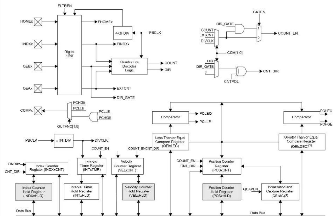
flowchart
graph TD
    A["FLTREN"] --> B["Digital Filter"]
    C["HomEx"] --> B
    D["INDXx"] --> B
    E["QEBx"] --> B
    F["QEAX"] --> B
    B --> G["FHOMEx"]
    G --> H["÷QFDIV"]
    H --> I["PBCLK"]
    I --> J["Quadrature Decoder Logic"]
    J --> K["COUNT DIR"]
    J --> L["EXTCNT DIR_GATE"]
    M["CCMPx"] --> N["PCHGE PCLLE PCHGE"]
    O["OUTFNC[1:0"]] --> N
    N --> P["PCLLE PCHGE"]
    Q["INDEX Counter Register (INDXxCNT)"] --> R["÷INTDIV"]
    S["Interval Timer Register (INTxTMR)"] --> T["DIVCLK COUNT_EN"]
    U["Velocity Counter Register (VELxCNT)"] --> V["LEVELxCNT"]
    W["Index Counter Hold Register (INDXxHLD)"] --> X["Data Bus"]
    Y["Interval Timer Hold Register (INTxHLD)"] --> Z["Data Bus"]
    AA["Velocity Counter Hold Register (VELxHLD)"] --> AB["Data Bus"]
    AC["Counter"] --> AD["PCLEQ PCLLE"]
    AE["Less Than or Equal Compare Register (QEIXLEC)"] --> AF["DIR DIR"]
    AG["Position Counter Register (POSxCNT)"] --> AH["POST DIR"]
    AI["Position Counter Hold Register (POSxHLD)"] --> AJ["POST DIR"]
    AK["Initialization and Capture Register (QEIXC)(1)"] --> AL["Data Bus"]
    AM["GATEN"] --> AN["1"]
    AO["COUNT_GATE 0"] --> AP["CNT_DIR"]
    AQ["CNTPOL"] --> AR["CNT_DIR"]
    AS["PERVolume DIAMETER"] --> AT["1"]
    AU["CONTINENT DIAMETER"] --> AV["0"]
    AW["CONTINENT DIAMETER"] --> AX["0"]
    AY["GATEN"] --> AZ["1"]
    BA["GATEN"] --> BB["0"]
    BC["GATEN"] --> BD["1"]
    BE["GATEN"] --> BF["0"]
    BG["GATEN"] --> BH["1"]
Note 1: These registers map to the same memory location.
2: Shaded registers are not used in 32-bit devices. They are provided to maintain uniformity with 16-bit architecture.
12.1 QEI Control and Status Registers
REGISTER 12-1: QEIXCON: QEIX CONTROL REGISTER
| R/W-0 U-0 R/W-0 R/W-0 R/W-0 R/W-0 R/W-0 R/W-0 | |||||||
| QEEN | — QEIS | DL PIMOD2 P | MOD1 PIMOD | 0 IMV1 IMV0 | |||
| bit 15 bit 8 | |||||||
| U-0 R/W-0 R/W-0 R/W-0 R/W-0 R/W-0 R/W-0 R/W-0 | |||||||
| — INTD | V2 | INTDIV1 | INTDIV0 | CNTPOL | GATEN | CCM1 | CCMO |
| bit 7 bit 0 | |||||||
Legend:
| R = Readable bit | W = Writable bit | U = Unimplemented bit, read as '0' |
| -n = Value at POR | '1' = Bit is set | '0' = Bit is cleared x = Bit is unknown |
bit 15 QEIEN: Quadrature Encoder Interface Module Enable bit
1 = QEI module is enabled
0 = QEI module is disabled; however, SFRs can be read or written
bit 14 Unimplemented: Read as '0'
bit 13 QEISIDL: QEI Stop in Idle Mode bit
1 = Discontinues module operation when device enters Idle mode
0 = Continues module operation in Idle mode
bit 12-10 PIMOD[2:0]: Position Counter Initialization Mode Select bits
111 = Modulo Count mode for position counter and every Index event resets the position counter
110 = Modulo Count mode for position counter
101 = Resets the position counter when the position counter equals the QEIxGEC register
100 = Second Index event after Home event initializes the position counter with the contents of the QEIXIC register
011 = First Index event after Home event initializes the position counter with the contents of the QEIXIC register
010 = Next Index input event initializes the position counter with the contents of the QEIXIC register
001 = Every Index input event resets the position counter
000 = Index input event does not affect the position counter
bit 9-8 IMV[1:0]: Index Match Value bits
11 = Index match occurs when QEBx = 1 and QEAX = 1
10 = Index match occurs when QEBx = 1 and QEAX = 0
01 = Index match occurs when QEBx = 0 and QEAX = 1
00 = Index match occurs when QEBx = 0 and QEAX = 0
bit 7 Unimplemented: Read as '0'
bit 6-4 INTDIV[2:0]: Timer Input Clock Prescale Select bits (interval timer, main timer (position counter), velocity counter and Index counter internal clock divider select)
111 = 1:128 prescale value
110 = 1:64 prescale value
101 = 1:32 prescale value
100 = 1:16 prescale value
011 = 1:8 prescale value
010 = 1:4 prescale value
001 = 1:2 prescale value
000 = 1:1 prescale value
bit 3 CNTPOL: Position, Velocity and Index Counter/Timer Direction Select bit
1 = Counter direction is negative unless modified by an external up/down signal
0 = Counter direction is positive unless modified by an external up/down signal
REGISTER 12-1: QEIXCON: QEIX CONTROL REGISTER (CONTINUED)
bit 2 GATEN: External Count Gate Enable bit
1 = External gate signal controls the position counter/timer operation
0 = External gate signal does not affect the position counter/timer operation
bit 1-0 CCM[1:0]: Counter Control Mode Selection bits
11 = Internal timer with External Gate mode
10 = External Clock count with External Gate mode
01 = External Clock count with External Up/Down mode
00 = Quadrature Encoder mode
REGISTER 12-2: QEIXIOCL: QEIX I/O CONTROL LOW REGISTER
| R/W-0 R/W-0 R/W-0 R/W-0 R/W-0 R/W-0 R/W-0 R/W-0 | |||||||
| QCAPEN | FLTREN | QFDIV2 | QFDIV1 | QFDIV0 | OUTFNC1 | OUTFNC0 | SWPAB |
| bit 15 bit 8 | |||||||
| R/W-0 | R/W-0 | R/W-0 | R/W-0 | R-x | R-x | R-x | R-x |
| HOMPOL | IDXPOL | QEBPOL | QEAPOL | HOME | INDEX | QEB | QEA |
| bit 7 bit 0 | |||||||
Legend:
| R = Readable bit | W = Writable bit | U = Unimplemented bit, read as '0' |
| -n = Value at POR | '1' = Bit is set | '0' = Bit is cleared x = Bit is unknown |
bit 15 QCAPEN: QElx Position Counter Input Capture by Index Event Enable bit
1 = Index match event (positive edge) triggers a position capture event
0 = Index match event (positive edge) does not trigger a position capture event
bit 14 FLTREN: QEAx/QEBx/INDXx/HOMEx Digital Filter Enable bit
1 = Input pin digital filter is enabled
0 = Input pin digital filter is disabled (bypassed)
bit 13-11 QFDIV[2:0]: QEAx/QEBx/INDXx/HOMEx Digital Input Filter Clock Divide Select bits
111 = 1:128 clock divide
110 = 1:64 clock divide
101 = 1:32 clock divide
100 = 1:16 clock divide
011 = 1:8 clock divide
010 = 1:4 clock divide
001 = 1:2 clock divide
000 = 1:1 clock divide
bit 10-9 OUTFNC[1:0]: QElx Module Output Function Mode Select bits
11 = The QEICMP pin goes high when POSxCNT ≤ QEIxLEC or POSxCNT ≥ QEIxGEC
10 = The QEICMP pin goes high when POSxCNT ≤ QEIxLEC
01 = The QEICMP pin goes high when POSxCNT ≥ QEIxGEC
00 = Output is disabled
bit 8 SWPAB: Swap QEAx and QEBx Inputs bit
1 = QEAx and QEBx are swapped prior to Quadrature Decoder logic
0 = QEAx and QEBx are not swapped
bit 7 HOMPOL: HOMEx Input Polarity Select bit
1 = Input is inverted
0 = Input is not inverted
REGISTER 12-2: QEIXIOCL: QEIX I/O CONTROL LOW REGISTER (CONTINUED)
bit 6 IDXPOL: INDXx Input Polarity Select bit
1 = Input is inverted
0 = Input is not inverted
bit 5 QEBPOL: QEBx Input Polarity Select bit
1 = Input is inverted
0 = Input is not inverted
bit 4 QEAPOL: QEAX Input Polarity Select bit
1 = Input is inverted
0 = Input is not inverted
bit 3 HOME: Status of HOMEx Input Pin after Polarity Control bit (read-only)
1 = Pin is at logic '1' if the HOMPOL bit is set to '0'; pin is at logic '0' if the HOMPOL bit is set to '1'
0 = Pin is at logic '0' if the HOMPOL bit is set to '0'; pin is at logic '1' if the HOMPOL bit is set to '1'
bit 2 INDEX: Status of INDXx Input Pin After Polarity Control bit (read-only)
1 = Pin is at logic '1' if the IDXPOL bit is set to '0'; pin is at logic '0' if the IDXPOL bit is set to '1'
0 = Pin is at logic '0' if the IDXPOL bit is set to '0'; pin is at logic '1' if the IDXPOL bit is set to '1'
bit 1 QEB: Status of QEBx Input Pin After Polarity Control and SWPAB Pin Swapping bit (read-only)
1 = Physical pin, QEBx, is at logic '1' if the QEBPOL bit is set to '0' and the SWPAB bit is set to '0'; physical pin, QEBx, is at logic '0' if the QEBPOL bit is set to '1' and the SWPAB bit is set to '0'; physical pin, QEAx, is at logic '1' if the QEBPOL bit is set to '0' and the SWPAB bit is set to '1'; physical pin, QEAx, is at logic '0' if the QEBPOL bit is set to '1' and the SWPAB bit is set to '1'
0 = Physical pin, QEBx, is at logic '0' if the QEBPOL bit is set to '0' and the SWPAB bit is set to '0'; physical pin, QEBx, is at logic '1' if the QEBPOL bit is set to '1' and the SWPAB bit is set to '0'; physical pin, QEAx, is at logic '0' if the QEBPOL bit is set to '0' and the SWPAB bit is set to '1'; physical pin, QEAx, is at logic '1' if the QEBPOL bit is set to '1' and the SWPAB bit is set to '1'
bit 0 QEA: Status of QEAx Input Pin After Polarity Control and SWPAB Pin Swapping bit (read-only)
1 = Physical pin, QEAx, is at logic '1' if the QEAPOL bit is set to '0' and the SWPAB bit is set to '0'; physical pin, QEAx, is at logic '0' if the QEAPOL bit is set to '1' and the SWPAB bit is set to '0'; physical pin, QEBx, is at logic '1' if the QEAPOL bit is set to '0' and the SWPAB bit is set to '1'; physical pin, QEBx, is at logic '0' if the QEAPOL bit is set to '1' and the SWPAB bit is set to '1'
0 = Physical pin, QEAx, is at logic '0' if the QEAPOL bit is set to '0' and the SWPAB bit is set to '0'; physical pin, QEAx, is at logic '1' if the QEAPOL bit is set to '1' and the SWPAB bit is set to '0'; physical pin, QEBx, is at logic '0' if the QEAPOL bit is set to '0' and the SWPAB bit is set to '1'
REGISTER 12-3: QEIXIOCH: QEIX I/O CONTROL HIGH REGISTER
| U-0 U-0 U-0 U-0 U-0 U-0 U-0 U-0 | |||||||
| —— | —— | —— | |||||
| bit 15 bit 8 | |||||||
| U-0 U-0 U-0 U-0 U-0 U-0 R/W-0 | |||||||
| —— | —— | HCAPEN | |||||
| bit 7 bit 0 | |||||||
Legend:
R = Readable bit W = Writable bit U = Unimplemented bit, read as '0'
-n = Value at POR '1' = Bit is set '0' = Bit is cleared x = Bit is unknown
bit 15-1 Unimplemented: Read as '0'
bit 0 HCAPEN: Position Counter Input Capture by Home Event Enable bit
1 = HOMEx input event (positive edge) triggers a position capture event
0 = HOMEx input event (positive edge) does not trigger a position capture event
REGISTER 12-4: QEIXSTAT: QEIX STATUS REGISTER
| U-0 U-0 HS/R/C-0 R/W-0 HS/R/C-0 R/W-0 HS/R/C-0 R/W-0 | ||||||
| — — PCHEQIRQ PCHEQIEN PCLEQ | RQ PCLEQIEN | POSOVIRQ | POSOVIEN | |||
| bit 15 bit 8 | ||||||
| HS/R/C-0 R/W-0 HS/R/C-0 R/W-0 HS/R/C-0 R/W-0 HS/R/C-0 R/W-0 | |||||||
| PCIIRQ^(1) | PCIIEN | VELOVIRQ | VELOVIEN | HOMIRQ | HOMIEN | IDXIRQ | IDXIEN |
| bit 7 bit 0 | |||||||
| Legend: | C = Clearable bit | HS = Hardware Settable bit |
| R = Readable bit | W = Writable bit | U = Unimplemented bit, read as ‘0’ |
| -n = Value at POR | ‘1’ = Bit is set | ‘0’ = Bit is cleared x = Bit is unknown |
bit 15-14 Unimplemented: Read as '0'
bit 13 PCHEQIRQ: Position Counter Greater Than Compare Status bit
1 = POSxCNT ≥ QEIxGEC
0 = POSxCNT < QEIXGEC
bit 12 PCHEQIEN: Position Counter Greater Than Compare Interrupt Enable bit
1 = Interrupt is enabled
0 = Interrupt is disabled
bit 11 PCLEQIRQ: Position Counter Less Than Compare Status bit
1 = POSxCNT ≤ QEIxLEC
0 = POSxCNT > QEIXLEC
bit 10 PCLEQIEN: Position Counter Less Than Compare Interrupt Enable bit
1 = Interrupt is enabled
0 = Interrupt is disabled
bit 9 POSOVIRQ: Position Counter Overflow Status bit
1 = Overflow has occurred
0 = No overflow has occurred
bit 8 POSOVIEN: Position Counter Overflow Interrupt Enable bit
1 = Interrupt is enabled
0 = Interrupt is disabled
bit 7 PCIIRQ: Position Counter (Homing) Initialization Process Complete Status bit ^(1)
1 = POSxCNT was reinitialized
0 = POSxCNT was not reinitialized
bit 6 PCIEN: Position Counter (Homing) Initialization Process Complete Interrupt Enable bit
1 = Interrupt is enabled
0 = Interrupt is disabled
bit 5 VELOVIRQ: Velocity Counter Overflow Status bit
1 = Overflow has occurred
0 = No overflow has occurred
bit 4 VELOVIEN: Velocity Counter Overflow Interrupt Enable bit
1 = Interrupt is enabled
0 = Interrupt is disabled
bit 3 HOMIRQ: Status Flag for Home Event Status bit
1 = Home event has occurred
0 = No Home event has occurred
Note 1: This status bit is only applicable to PIMOD[2:0] modes, '011' and '100'.
REGISTER 12-4: QEIXSTAT: QEIX STATUS REGISTER (CONTINUED)
bit 2 HOMIEN: Home Input Event Interrupt Enable bit
1 = Interrupt is enabled
0 = Interrupt is disabled
bit 1 IDXIRQ: Status Flag for Index Event Status bit
1 = Index event has occurred
0 = No Index event has occurred
bit 0 IDXIEN: Index Input Event Interrupt Enable bit
1 = Interrupt is enabled
0 = Interrupt is disabled
Note 1: This status bit is only applicable to PIMOD[2:0] modes, '011' and '100'.
REGISTER 12-5: POSxCNTL: POSITION x COUNTER REGISTER LOW
| R/W-0 R/W-0 R/W-0 R/W-0 R/W-0 R/W-0 R/W-0 R/W-0 |
| POSCNT[15:8] |
| bit 15 bit 8 |
| R/W-0 R/W-0 R/W-0 R/W-0 R/W-0 R/W-0 R/W-0 R/W-0 |
| POSCNT[7:0] |
| bit 7 bit 0 |
| Legend: | |||
| R = Readable bit W = Writable bit | U = Unimplemented bit, read as ‘0’ | ||
| -n = Value at POR | ‘1’ = Bit is set | ‘0’ = Bit is cleared | x = Bit is unknown |
bit 15-0 POSCNT[15:0]: Position Counter Value bits
REGISTER 12-6: POSxCNTH: POSITION x COUNTER REGISTER HIGH
| R/W-0 R/W-0 R/W-0 R/W-0 R/W-0 R/W-0 R/W-0 R/W-0 |
| POSCNT[31:24] |
| bit 15 bit 8 |
| R/W-0 R/W-0 R/W-0 R/W-0 R/W-0 R/W-0 R/W-0 R/W-0 |
| POSCNT[23:16] |
| bit 7 bit 0 |
| Legend: | |||
| R = Readable bit W = Writable bit | U = Unimplemented bit, read as ‘0’ | ||
| -n = Value at POR | ‘1’ = Bit is set | ‘0’ = Bit is cleared | x = Bit is unknown |
bit 15-0 POSCNT[31:16]: Position Counter Value bits
REGISTER 12-7: POSxHLD: POSITION x COUNTER HOLD REGISTER
| R/W-0 R/W-0 R/W-0 R/W-0 R/W-0 R/W-0 R/W-0 R/W-0 |
| POSHLD[31:24] |
| bit 15 bit 8 |
| R/W-0 R/W-0 R/W-0 R/W-0 R/W-0 R/W-0 R/W-0 R/W-0 |
| POSHLD[23:16] |
| bit 7 bit 0 |
| Legend:R = Readable bit W = Writable bit U = Unimplemented bit, read as '0'-n = Value at POR '1' = Bit is set '0' = Bit is cleared x = Bit is unknown |
bit 15-0 POSHLD[31:16]: Position Counter Hold for Reading/Writing Position x Counter Register (POSxCNT) bits
REGISTER 12-8: VELxCNTL: VELOCITY x COUNTER REGISTER LOW
| R/W-0 R/W-0 R/W-0 R/W-0 R/W-0 R/W-0 R/W-0 R/W-0 |
| VELCNT[15:8] |
| bit 15 bit 8 |
| R/W-0 R/W-0 R/W-0 R/W-0 R/W-0 R/W-0 R/W-0 R/W-0 |
| VELCNT[7:0] |
| bit 7 bit 0 |
| Legend:R = Readable bit W = Writable bit U = Unimplemented bit, read as '0'-n = Value at POR '1' = Bit is set '0' = Bit is cleared x = Bit is unknown |
bit 15-0 VELCNT[15:0]: Velocity Counter Value bits
REGISTER 12-9: VELxCNTH: VELOCITY x COUNTER REGISTER HIGH
| R/W-0 R/W-0 R/W-0 R/W-0 R/W-0 R/W-0 R/W-0 R/W-0 |
| VELCNT[31:24] |
| bit 15 bit 8 |
| R/W-0 R/W-0 R/W-0 R/W-0 R/W-0 R/W-0 R/W-0 R/W-0 |
| VELCNT[23:16] |
| bit 7 bit 0 |
| Legend:R = Readable bit W = Writable bit U = Unimplemented bit, read as '0'-n = Value at POR '1' = Bit is set '0' = Bit is cleared x = Bit is unknown |
bit 15-0 VELCNT[31:16]: Velocity Counter Value bits
REGISTER 12-10: VELxHLD: VELOCITY x COUNTER HOLD REGISTER
| R/W-0 R/W-0 R/W-0 R/W-0 R/W-0 R/W-0 R/W-0 R/W-0 |
| VELHLD[31:24] |
| bit 15 bit 8 |
| R/W-0 R/W-0 R/W-0 R/W-0 R/W-0 R/W-0 R/W-0 R/W-0 |
| VELHLD[23:16] |
| bit 7 bit 0 |
Legend:
| R = Readable bit W = Writable bit U = Unimplemented bit, read as '0' |
| -n = Value at POR '1' = Bit is set '0' = Bit is cleared x = Bit is unknown |
bit 15-0 VELHLD[31:16]: Velocity Counter Hold Value bits
REGISTER 12-11: INTxTMRL: INTERVAL x TIMER REGISTER LOW
| R/W-0 R/W-0 R/W-0 R/W-0 R/W-0 R/W-0 R/W-0 R/W-0 |
| INTTMR[15:8] |
| bit 15 bit 8 |
| R/W-0 R/W-0 R/W-0 R/W-0 R/W-0 R/W-0 R/W-0 R/W-0 |
| INTTMR[7:0] |
| bit 7 bit 0 |
Legend:
| R = Readable bit W = Writable bit U = Unimplemented bit, read as '0' |
| -n = Value at POR '1' = Bit is set '0' = Bit is cleared x = Bit is unknown |
bit 15-0 INTTMR[15:0]: Interval Timer Value bits
REGISTER 12-12: INTxTMRH: INTERVAL x TIMER REGISTER HIGH
| R/W-0 R/W-0 R/W-0 R/W-0 R/W-0 R/W-0 R/W-0 R/W-0 |
| INTTMR[31:24] |
| bit 15 bit 8 |
| R/W-0 R/W-0 R/W-0 R/W-0 R/W-0 R/W-0 R/W-0 R/W-0 |
| INTTMR[23:16] |
| bit 7 bit 0 |
Legend:
| R = Readable bit W = Writable bit U = Unimplemented bit, read as '0' |
| -n = Value at POR '1' = Bit is set '0' = Bit is cleared x = Bit is unknown |
bit 15-0 INTTMR[31:16]: Interval Timer Value bits
REGISTER 12-13: INTxHLDL: INTERVAL x TIMER HOLD REGISTER LOW
| R/W-0 R/W-0 R/W-0 R/W-0 R/W-0 R/W-0 R/W-0 R/W-0 |
| INTHLD[15:8] |
| bit 15 bit 8 |
| R/W-0 R/W-0 R/W-0 R/W-0 R/W-0 R/W-0 R/W-0 R/W-0 |
| INTHLD[7:0] |
| bit 7 bit 0 |
Legend:
R = Readable bit W = Writable bit U = Unimplemented bit, read as '0'
-n = Value at POR '1' = Bit is set '0' = Bit is cleared x = Bit is unknown
bit 15-0 INTXHLD[15:0]: Hold for Reading/Writing Interval Timer Value Register (INTxHLD) bits
REGISTER 12-14: INTxHLDH: INTERVAL x TIMER HOLD REGISTER HIGH
| R/W-0 R/W-0 R/W-0 R/W-0 R/W-0 R/W-0 R/W-0 R/W-0 |
| INTHLD[31:24] |
| bit 15 bit 8 |
| R/W-0 R/W-0 R/W-0 R/W-0 R/W-0 R/W-0 R/W-0 R/W-0 |
| INTHLD[23:16] |
| bit 7 bit 0 |
Legend:
R = Readable bit W = Writable bit U = Unimplemented bit, read as '0'
-n = Value at POR '1' = Bit is set '0' = Bit is cleared x = Bit is unknown
bit 15-0 INTHLD[31:16]: Hold for Reading/Writing Interval Timer Value Register (INTxHLD) bits
REGISTER 12-15: INDXxCNTL: INDEX x COUNTER REGISTER LOW
| R/W-0 R/W-0 R/W-0 R/W-0 R/W-0 R/W-0 R/W-0 R/W-0 |
| INDXCNT[15:8] |
| bit 15 bit 8 |
| R/W-0 R/W-0 R/W-0 R/W-0 R/W-0 R/W-0 R/W-0 R/W-0 |
| INDXCNT[7:0] |
| bit 7 bit 0 |
Legend:
| R = Readable bit W = Writable bit U = Unimplemented bit, read as '0' |
| -n = Value at POR '1' = Bit is set '0' = Bit is cleared x = Bit is unknown |
bit 15-0 INDXCNT[15:0]: Index Counter Value bits
REGISTER 12-16: INDXxCNTH: INDEX x COUNTER REGISTER HIGH
| R/W-0 R/W-0 R/W-0 R/W-0 R/W-0 R/W-0 R/W-0 R/W-0 |
| INDXCNT[31:24] |
| bit 15 bit 8 |
| R/W-0 R/W-0 R/W-0 R/W-0 R/W-0 R/W-0 R/W-0 R/W-0 |
| INDXCNT[23:16] |
| bit 7 bit 0 |
Legend:
| R = Readable bit W = Writable bit U = Unimplemented bit, read as '0' |
| -n = Value at POR '1' = Bit is set '0' = Bit is cleared x = Bit is unknown |
bit 15-0 INDXCNT[31:16]: Index Counter Value bits
REGISTER 12-17: INDXxHLD: INDEX x COUNTER HOLD REGISTER
| R/W-0 R/W-0 R/W-0 R/W-0 R/W-0 R/W-0 R/W-0 R/W-0 |
| INDXHLD[31:24] |
| bit 15 bit 8 |
| R/W-0 R/W-0 R/W-0 R/W-0 R/W-0 R/W-0 R/W-0 R/W-0 |
| INDXHLD[23:16] |
| bit 7 bit 0 |
Legend:
| R = Readable bit W = Writable bit U = Unimplemented bit, read as '0' |
| -n = Value at POR '1' = Bit is set '0' = Bit is cleared x = Bit is unknown |
bit 15-0 INDXHLD[31:16]: Hold for Reading/Writing Index x Counter Register (INDXCNT) bits
REGISTER 12-18: QEIXGECL: QEIX GREATER THAN OR EQUAL COMPARE REGISTER LOW
| R/W-0 R/W-0 R/W-0 R/W-0 R/W-0 R/W-0 R/W-0 R/W-0 |
| QEIGEC[15:8] |
| bit 15 bit 8 |
| R/W-0 R/W-0 R/W-0 R/W-0 R/W-0 R/W-0 R/W-0 R/W-0 |
| QEIGEC[7:0] |
| bit 7 bit 0 |
| Legend:R = Readable bit W = Writable bit U = Unimplemented bit, read as '0'-n = Value at POR '1' = Bit is set '0' = Bit is cleared x = Bit is unknown |
bit 15-0 QEIGEC[15:0]: QEIx Greater Than or Equal Compare bits
REGISTER 12-19: QEIXGECH: QEIX GREATER THAN OR EQUAL COMPARE REGISTER HIGH
| R/W-0 R/W-0 R/W-0 R/W-0 R/W-0 R/W-0 R/W-0 R/W-0 |
| QEIGEC[31:24] |
| bit 15 bit 8 |
| R/W-0 R/W-0 R/W-0 R/W-0 R/W-0 R/W-0 R/W-0 R/W-0 |
| QEIGEC[23:16] |
| bit 7 bit 0 |
| Legend:R = Readable bit W = Writable bit U = Unimplemented bit, read as '0'-n = Value at POR '1' = Bit is set '0' = Bit is cleared x = Bit is unknown |
bit 15-0 QEIGEC[31:16]: QEIx Greater Than or Equal Compare bits
REGISTER 12-20: QEIXLECL: QEIX LESS THAN OR EQUAL COMPARE REGISTER LOW
| R/W-0 R/W-0 R/W-0 R/W-0 R/W-0 R/W-0 R/W-0 R/W-0 |
| QEIIC[31:24] |
| bit 15 bit 8 |
| R/W-0 R/W-0 R/W-0 R/W-0 R/W-0 R/W-0 R/W-0 R/W-0 |
| QEIIC[23:16] |
| bit 7 bit 0 |
Legend:
| R = Readable bit W = Writable bit U = Unimplemented bit, read as '0' |
| -n = Value at POR '1' = Bit is set '0' = Bit is cleared x = Bit is unknown |
bit 15-0 QEIIC[31:16]: QEIx Less Than or Equal Compare bits
REGISTER 12-21: QEIXLECH: QEIX LESS THAN OR EQUAL COMPARE REGISTER HIGH
| R/W-0 R/W-0 R/W-0 R/W-0 R/W-0 R/W-0 R/W-0 R/W-0 |
| QEIIC[15:8] |
| bit 15 bit 8 |
| R/W-0 R/W-0 R/W-0 R/W-0 R/W-0 R/W-0 R/W-0 R/W-0 |
| QEIIC[7:0] |
| bit 7 bit 0 |
Legend:
| R = Readable bit W = Writable bit U = Unimplemented bit, read as '0' |
| -n = Value at POR '1' = Bit is set '0' = Bit is cleared x = Bit is unknown |
bit 15-0 QEIIC[15:0]: QEIx Less Than or Equal Compare bits
NOTES:
13.0 UNIVERSAL ASYNCHRONOUS RECEIVER TRANSMITTER (UART)
Note 1: This data sheet summarizes the features of the dsPIC33CH128MP508 family of devices. It is not intended to be a comprehensive reference source. To complement the information in this data sheet, refer to "Multiprotocol Universal Asynchronous Receiver Transmitter (UART) Module" (www.microchip.com/DS70005288), which is available from the Microchip website (www.microchip.com).
2: The UART is identical for both Main core and Secondary core. The x is common for both Main core and Secondary core (where the x represents the number of the specific module being addressed). The number of UART modules available on the Main core and Secondary core is different and they are located in different SFR locations.
3: All associated register names are the same on the Main core and the Secondary core. The Secondary code will be developed in a separate project in MPLAB X IDE with the device selection, dsPIC33CH128MP508S1, where the S1 indicates the Secondary device. The Main UART is UART1 and UART2, and the Secondary UART is UART1.
Table 13-1 shows an overview of the module.
TABLE 13-1: UART MODULE OVERVIEW
| Number of UART Modules | Identical (Modules) | |
| Main Core 2 Yes | ||
| Secondary Core 1 Yes |
The Universal Asynchronous Receiver Transmitter (UART) is a flexible serial communication peripheral used to interface dsPIC microcontrollers with other equipment, including computers and peripherals. The UART is a full-duplex, asynchronous communication channel that can be used to implement protocols, such as RS-232 and RS-485. The UART also supports the following hardware extensions:
• LIN/J2602
- Smart Card
The primary features of the UART are:
• Full or Half-Duplex Operation
- Up to 8-Deep TX and RX First In, First Out (FIFO) Buffers
• 8-Bit or 9-Bit Data Width
- Configurable Stop Bit Length
- Flow Control
• Auto-Baud Calibration
- Parity, Framing and Buffer Overrun Error Detection
- Address Detect
- Break Transmission
• Transmit and Receive Polarity Control
• Manchester Encoder/Decoder
• Operation in Sleep mode
- Wake from Sleep on Sync Break Received Interrupt
13.1 Architectural Overview
The UART transfers bytes of data, to and from device pins, using First-In First-Out (FIFO) buffers up to eight bytes deep. The status of the buffers and data is made available to user software through Special Function
Registers (SFRs). The UART implements multiple interrupt channels for handling transmit, receive and error events. A simplified block diagram of the UART is shown in Figure 13-1.
FIGURE 13-1: SIMPLIFIED UARTx BLOCK DIAGRAM
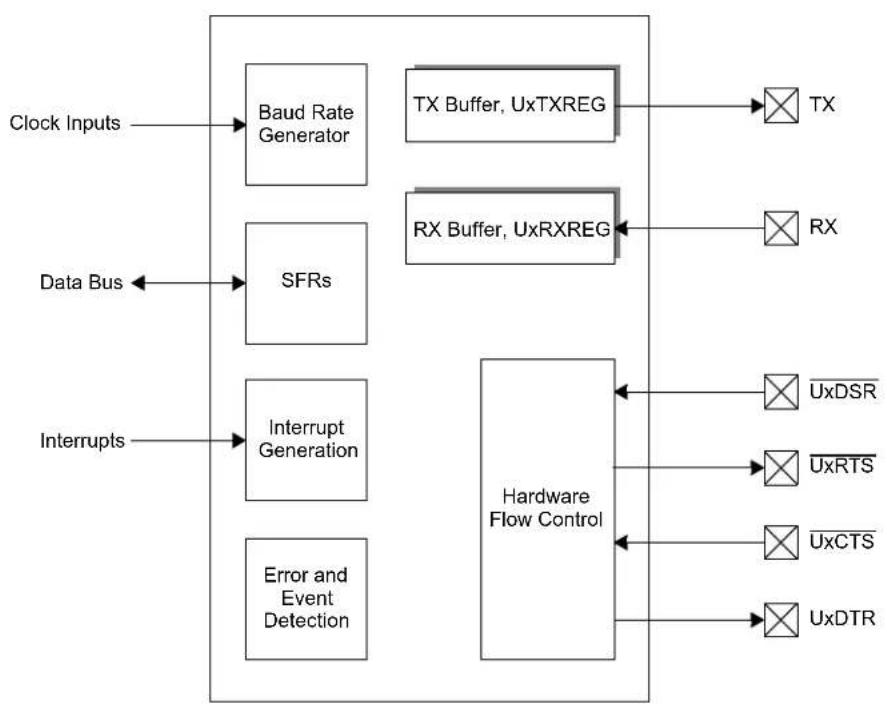
flowchart
graph TD
    A["Clock Inputs"] --> B["Baud Rate Generator"]
    C["Data Bus"] --> D["SFRs"]
    E["Interrupts"] --> F["Interrupt Generation"]
    G["Error and Event Detection"] --> H["Hardware Flow Control"]
    I["TX Buffer, UxTXREG"] --> J["TX"]
    K["RX Buffer, UxRXREG"] --> L["RX"]
    M["UxDSR"] --> N["UxDSR"]
    O["UxRTS"] --> P["UxRTS"]
    Q["UxCTS"] --> R["UxCTS"]
    S["UxDTR"] --> T["UxDTR"]
13.2 Character Frame
A typical UART character frame is shown in Figure 13-2. The Idle state is high with a 'Start' condition indicated by a falling edge. The Start bit is followed by the number of data, parity/address detect and Stop bits defined by the MOD[3:0] (UxMODE[3:0]) bits selected.
FIGURE 13-2: UART CHARACTER FRAME
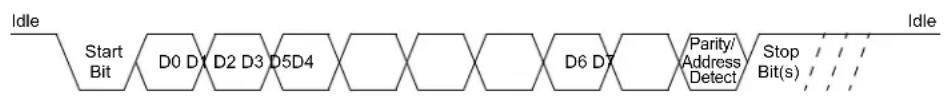
flowchart
graph LR
    A["Start Bit"] --> B["D0 D1"]
    B --> C["D2 D3"]
    C --> D["D5D4"]
    D --> E["..."]
    E --> F["D6 D7"]
    F --> G["Parity/Address Detect"]
    G --> H["Stop Bit(s)"]
    H --> I["Idle"]
13.3 Data Buffers
Both transmit and receive functions use buffers to store data shifted to/from the pins. These buffers are FIFOs and are accessed by reading the SFRs, UxTXREG and UxRXREG, respectively. Each data buffer has multiple flags associated with its operation to allow software to read the status. Interrupts can also be configured based on the space available in the buffers. The transmit and receive buffers can be cleared and their pointers reset using the associated TX/RX Buffer Empty Status bits, UTXBE (UxSTAH[5]) and URXBE (UxSTAH[1]).
13.4 Protocol Extensions
The UART provides hardware support for LIN/J2602 and smart card protocol extensions to reduce software overhead. A protocol extension is enabled by writing a value to the MOD[3:0] (UxMODE[3:0]) selection bits and further configured using the UARTx Timing Parameter registers, UxP1 (Register 13-9), UxP2 (Register 13-10), UxP3 (Register 13-11) and UxP3H (Register 13-12). Details regarding operation and usage are discussed in their respective chapters. Not all protocols are available on all devices.
13.5 UART Control/Status Registers
REGISTER 13-1: UxMODE: UARTx CONFIGURATION REGISTER
| R/W-0 U-0 R/W-0 R/W-0 R/W-0 U-0 R/W-0 HC/R/W-0 | |||||||
| UARTEN — | USIDL WAKE | RXBIMD — B | RKOVR UTXBRK | ||||
| bit 15 | bit 8 | ||||||
| R/W-0 | HC/R/W-0 | R/W-0 | R/W-0 | R/W-0 | R/W-0 | R/W-0 | R/W-0 |
| BRGH | ABAUD | UTXEN | URXEN | MOD3 | MOD2 | MOD1 | MOD0 |
| bit 7 bit 0 | |||||||
| Legend: | HC = Hardware Clearable bit | ||
| R = Readable bit | W = Writable bit | U = Unimplemented bit, read as ‘0’ | |
| -n = Value at POR | ‘1’ = Bit is set | ‘0’ = Bit is cleared | x = Bit is unknown |
| bit 15 | UARTEN: UART Enable bit1 = UART is ready to transmit and receive0 = UART state machine, FIFO Buffer Pointers and counters are reset; registers are readable and writable |
| bit 14 | Unimplemented: Read as '0' |
| bit 13 | USIDL: UART Stop in Idle Mode bit1 = Discontinues module operation when device enters Idle mode0 = Continues module operation in Idle mode |
| bit 12 | WAKE: Wake-up Enable bit1 = Module will continue to sample the RX pin – interrupt generated on falling edge, bit cleared in hardware on following rising edge; if ABAUD is set, Auto-Baud Detection (ABD) will begin immediately0 = RX pin is not monitored nor rising edge detected |
| bit 11 | RXBIMD: Receive Break Interrupt Mode bit1 = RXBKIF flag when a minimum of 23 (asynchronous or LIN/J2602) low bit periods are detected0 = RXBKIF flag when the Break makes a low-to-high transition after being low for at least 23/11 bit periods |
| bit 10 | Unimplemented: Read as '0' |
| bit 9 | BRKOVR: Send Break Software Override bitOverrides the TX Data Line:1 = Makes the TX line active (Output 0 when UTXINV = 0, Output 1 when UTXINV = 1)0 = TX line is driven by the shifter |
| bit 8 | UTXBRK: UART Transmit Break bit(1)1 = Sends Sync Break on next transmission; cleared by hardware upon completion0 = Sync Break transmission is disabled or has completed |
| bit 7 | BRGH: High Baud Rate Select bit1 = High Speed: Baud rate is baudclk/40 = Low Speed: Baud rate is baudclk/16 |
| bit 6 | ABAUD: Auto-Baud Detect Enable bit (read-only when MOD[3:0] = 1xxx)1 = Enables baud rate measurement on the next character – requires reception of a Sync field (55h); cleared in hardware upon completion0 = Baud rate measurement is disabled or has completed |
Note 1: R/HS/HC in LIN mode.
2: These modes are not available on all devices.
REGISTER 13-1: UxMODE: UARTx CONFIGURATION REGISTER (CONTINUED)
bit 5 UTXEN: UART Transmit Enable bit
1 = Transmit enabled - except during Auto-Baud Detection
0 = Transmit disabled – all transmit counters, pointers and state machines are reset; TX buffer is not flushed, status bits are not reset
bit 4 URXEN: UART Receive Enable bit
1 = Receive enabled - except during Auto-Baud Detection
0 = Receive disabled – all receive counters, pointers and state machines are reset; RX buffer is not flushed, status bits are not reset
bit 3-0 MOD[3:0]: UART Mode bits
Other = Reserved 1111 = Smart card ^(2) 1110 = Reserved 1101 = Reserved 1100 = LIN Commander/Responder 1011 = LIN Responder only 1010 = Reserved 1001 = Reserved 1000 = Reserved 0111 = Reserved 0110 = Reserved 0101 = Reserved 0100 = Asynchronous 9-bit UART with address detect, ninth bit = 1 signals address 0011 = Asynchronous 8-bit UART without address detect, ninth bit is used as an even parity bit 0010 = Asynchronous 8-bit UART without address detect, ninth bit is used as an odd parity bit 0001 = Asynchronous 7-bit UART 0000 = Asynchronous 8-bit UART
Note 1: R/HS/HC in LIN mode.
2: These modes are not available on all devices.
REGISTER 13-2: UxMODEH: UARTx CONFIGURATION REGISTER HIGH
| R/W-0 R-0 U-0 U-0 R/W-0 R/W-0 R/W-0 R/W-0 | |||||||
| SLPEN ACTIVE | — — BCLKMOD BCLKSEL1 BCLKSEL0 HALFDPLX | ||||||
| bit 15 bit 8 | |||||||
| R/W-0 | R/W-0 | R/W-0 | R/W-0 | R/W-0 | R/W-0 | R/W-0 | R/W-0 |
| RUNOVF | URXINV | STSEL1 | STSEL0 | C0EN | UTXINV | FLO1 | FLO0 |
| bit 7 bit 0 | |||||||
| Legend: | |||
| R = Readable bit | W = Writable bit | U = Unimplemented bit, read as ‘0’ | |
| -n = Value at POR | ‘1’ = Bit is set | ‘0’ = Bit is cleared | x = Bit is unknown |
| bit 15 | SLPEN: Run During Sleep Enable bit1 = UART BRG clock runs during Sleep0 = UART BRG clock is turned off during Sleep |
| bit 14 | ACTIVE: UART Running Status bit1 = UART clock request is active (user can not update the UxMODE/UxMODEH registers)0 = UART clock request is not active (user can update the UxMODE/UxMODEH registers) |
| bit 13-12 | Unimplemented: Read as '0' |
| bit 11 | BCLKMOD: Baud Clock Generation Mode Select bit1 = Uses fractional Baud Rate Generation0 = Uses legacy divide-by-x counter for baud clock generation (x = 4 or 16 depending on the BRGH bit) |
| bit 10-9 BCLKSEL[1:0]: Baud Clock Source Selection bits |
| 11 = Reserved |
| 10 = Fosc |
| 01 = Reserved |
| 00 = Fosc/2 (FP) |
| bit 8 | HALFDPLX: UART Half-Duplex Selection Mode bit1 = Half-Duplex mode: UxTX is driven as an output when transmitting and tri-stated when TX is Idle0 = Full-Duplex mode: UxTX is driven as an output at all times when both UARTEN and UTXEN are set |
| bit 7 | RUNOVF: Run During Overflow Condition Mode bit1 = When an Overflow Error (OERR) condition is detected, the RX shifter continues to run so as to remain synchronized with incoming RX data; data are not transferred to UxRXREG when it is full (i.e., no UxRXREG data are overwritten)0 = When an Overflow Error (OERR) condition is detected, the RX shifter stops accepting new data (Legacy mode) |
| bit 6 | URXINV: UART Receive Polarity bit1 = Inverts RX polarity; Idle state is low0 = Input is not inverted; Idle state is high |
| bit 5-4 | STSEL[1:0]: Number of Stop Bits Selection bits11 = 2 Stop bits sent, 1 checked at receive10 = 2 Stop bits sent, 2 checked at receive01 = 1.5 Stop bits sent, 1.5 checked at receive00 = 1 Stop bit sent, 1 checked at receive |
| bit 3 | C0EN: Enable Legacy Checksum (C0) Transmit and Receive bit1 = Checksum Mode 1 (enhanced LIN checksum in LIN mode; add all TX/RX words in all other modes)0 = Checksum Mode 0 (legacy LIN checksum in LIN mode; not used in all other modes) |
REGISTER 13-2: UxMODEH: UARTx CONFIGURATION REGISTER HIGH (CONTINUED)
bit 2 UTXINV: UART Transmit Polarity bit
1 = Inverts TX polarity; TX is low in Idle state
0 = Output data are not inverted; TX output is high in Idle state
bit 1-0 FLO[1:0]: Flow Control Enable bits (only valid when MOD[3:0] = 0xxx)
11 = Reserved
10 = RTS-DSR (for TX side)/CTS-DTR (for RX side) hardware flow control
01 = XON/XOFF software flow control
00 = Flow control off
REGISTER 13-3: UxSTA: UARTx STATUS REGISTER
| R/W-0 R/W-0 R/W-0 R/W-0 R/W-0 R/W-0 R/W-0 R/W-0 | |||||||
| TXMTIE PERIE ABDOVE | CERIE FERIE | RXBKIE OERIE | TXCIE | ||||
| bit 15 | bit 8 | ||||||
| R-1 | R-0 | HS/R/W-0 | HS/R/W-0 | R-0 | HS/R/W-0 | HS/R/W-0 | HS/R/W-0 |
| TRMT | PERR | ABDOVF | CERIF | FERR | RXBKIF | OERR | TXCIF |
| bit 7 bit 0 | |||||||
| Legend: | HS = Hardware Settable bit | ||
| R = Readable bit | W = Writable bit | U = Unimplemented bit, read as ‘0’ | |
| -n = Value at POR | ‘1’ = Bit is set | ‘0’ = Bit is cleared | x = Bit is unknown |
bit 15 TXMTIE: Transmit Shifter Empty Interrupt Enable bit
1 = Interrupt is enabled
0 = Interrupt is disabled
bit 14 PERIE: Parity Error Interrupt Enable bit
1 = Interrupt is enabled
0 = Interrupt is disabled
bit 13 ABDOVE: Auto-Baud Rate Acquisition Interrupt Enable bit
1 = Interrupt is enabled
0 = Interrupt is disabled
bit 12 CERIE: Checksum Error Interrupt Enable bit
1 = Interrupt is enabled
0 = Interrupt is disabled
bit 11 FERIE: Framing Error Interrupt Enable bit
1 = Interrupt is enabled
0 = Interrupt is disabled
bit 10 RXBKIE: Receive Break Interrupt Enable bit
1 = Interrupt is enabled
0 = Interrupt is disabled
bit 9 OERIE: Receive Buffer Overflow Interrupt Enable bit
1 = Interrupt is enabled
0 = Interrupt is disabled
bit 8 TXCIE: Transmit Collision Interrupt Enable bit
1 = Interrupt is enabled
0 = Interrupt is disabled
bit 7 TRMT: Transmit Shifter Empty Interrupt Flag bit (read-only)
1 = Transmit Shift Register (TSR) is empty
0 = Transmit Shift Register is not empty
Note 1: In the event of an overflow, the checksum may be corrupted. The checksum value after an overflow event is not meaningful.
REGISTER 13-3: UxSTA: UARTx STATUS REGISTER (CONTINUED)
| bit 6 | PERR: Parity Error/Address Received/Forward Frame Interrupt Flag bitLIN and Parity Modes:1 = Parity error detected0 = No parity error detectedAddress Mode:1 = Address received0 = No address detectedAll Other Modes:Not used. |
| bit 5 | ABDOVF: Auto-Baud Rate Acquisition Interrupt Flag bit (must be cleared by software)1 = BRG rolled over during the auto-baud rate acquisition sequence (must be cleared in software)0 = BRG has not rolled over during the auto-baud rate acquisition sequence |
| bit 4 | CERIF: Checksum Error Interrupt Flag bit (must be cleared by software)1 = Checksum error0 = No checksum error |
| bit 3 FERR: Framing Error Interrupt Flag bit | |
| 1 = Framing Error: Inverted level of the Stop bit corresponding to the topmost character in the buffer;propagates through the buffer with the received character0 = No framing error | |
| bit 2 | RXBKIF: Receive Break Interrupt Flag bit (must be cleared by software)1 = A Break was received0 = No Break was detected |
| bit 1 | OERR:Receive Buffer Overflow Interrupt Flag bit (must be cleared by software)(1)1 = Receive buffer has overflowed0 = Receive buffer has not overflowed |
| bit 0 | TXCIF: Transmit Collision Interrupt Flag bit (must be cleared by software)1 = Transmitted word is not equal to the received word0 = Transmitted word is equal to the received word |
Note 1: In the event of an overflow, the checksum may be corrupted. The checksum value after an overflow event is not meaningful.
REGISTER 13-4: UxSTAH: UARTx STATUS REGISTER HIGH
| U-0 R/W-0 R/W-0 R/W-0 U-0 R/W-0 R/W-0 R/W-0 | |||||||
| — UTXI SEL2 UTXISEL1 UTXISEL0 — URXISEL2 | (1) | URXISEL1(1) | URXISEL0(1) | ||||
| bit 15 bit 8 | |||||||
| HS/R/W-0 | R/W-0 | R/S-1 | R-0 | R-1 | R-1 | R/S-1 | R-0 |
| TXWRE | STPMD | UTXBE | UTXBF | RIDLE | XON | URXBE | URXBF |
| bit 7 bit 0 | |||||||
| Legend: | HS = Hardware Settable bit S = Settable bit | ||
| R = Readable bit | W = Writable bit | U = Unimplemented bit, read as ‘0’ | |
| -n = Value at POR | ‘1’ = Bit is set | ‘0’ = Bit is cleared | x = Bit is unknown |
bit 15 Unimplemented: Read as '0'
bit 14-12 UTXISEL[2:0]: UART Transmit Interrupt Select bits
111 = Sets transmit interrupt when there is one empty slot left in the buffer
• • •
010 = Sets transmit interrupt when there are six empty slots or more in the buffer
001 = Sets transmit interrupt when there are seven empty slots or more in the buffer
000 = Sets transmit interrupt when there are eight empty slots in the buffer; TX buffer is empty
bit 11 Unimplemented: Read as '0'
bit 10-8 URXISEL[2:0]: UART Receive Interrupt Select bits ^(1)
111 = Triggers receive interrupt when there are eight words in the buffer; RX buffer is full
...
001 = Triggers receive interrupt when there are two words or more in the buffer
000 = Triggers receive interrupt when there is one word or more in the buffer
bit 7 TXWRE: TX Write Transmit Error Status bit
LIN and Parity Modes:
1 = A new byte was written when the buffer was full or when P2[8:0] = 0 (must be cleared by software)
0 = No error
Address Detect Mode:
1 = A new byte was written when the buffer was full or to P1[8:0] when P1x was full (must be cleared by software)
0 = No error
Other Modes:
1 = A new byte was written when the buffer was full (must be cleared by software)
0 = No error
bit 6 STPMD: Stop Bit Detection Mode bit
1 = Triggers RXIF at the end of the last Stop bit
0 = Triggers RXIF in the middle of the first (or second, depending on the STSEL[1:0] setting) Stop bit
bit 5 UTXBE: UART TX Buffer Empty Status bit
1 = Transmit buffer is empty; writing '1' when UTXEN = 0 will reset the TX FIFO Pointers and counters
0 = Transmit buffer is not empty
bit 4 UTXBF: UART TX Buffer Full Status bit
1 = Transmit buffer is full
0 = Transmit buffer is not full
bit 3 RIDLE: Receive Idle bit
1 = UART RX line is in the Idle state
0 = UART RX line is receiving something
Note 1: The receive watermark interrupt is not set if PERR or FERR is set and the corresponding IE bit is set.
REGISTER 13-4: UxSTAH: UARTx STATUS REGISTER HIGH (CONTINUED)
bit 2 XON: UART in XON Mode bit
Only valid when FLO[1:0] control bits are set to XON/XOFF mode.
1 = UART has received XON
0 = UART has not received XON or XOFF was received
bit 1 URXBE: UART RX Buffer Empty Status bit
1 = Receive buffer is empty; writing '1' when URXEN = 0 will reset the RX FIFO Pointers and counters
0 = Receive buffer is not empty
bit 0 URXBF: UART RX Buffer Full Status bit
1 = Receive buffer is full
0 = Receive buffer is not full
Note 1: The receive watermark interrupt is not set if PERR or FERR is set and the corresponding IE bit is set.
REGISTER 13-5: UxBRG: UARTx BAUD RATE REGISTER
| R/W-0 R/W-0 R/W-0 R/W-0 R/W-0 R/W-0 R/W-0 R/W-0 |
| BRG[15:8] |
| bit 15 bit 8 |
| R/W-0 R/W-0 R/W-0 R/W-0 R/W-0 R/W-0 R/W-0 R/W-0 |
| BRG[7:0] |
| bit 7 bit 0 |
Legend:
R = Readable bit W = Writable bit U = Unimplemented bit, read as '0' -n = Value at POR '1' = Bit is set '0' = Bit is cleared x = Bit is unknown
bit 15
BRG[15:0]: Baud Rate Divisor bits
REGISTER 13-6: UxBRGH: UARTx BAUD RATE REGISTER HIGH
R = Readable bit W = Writable bit U = Unimplemented bit, read as '0' -n = Value at POR '1' = Bit is set '0' = Bit is cleared x = Bit is unknown
bit 15-4 Unimplemented: Read as '0'
bit 3-0 BRG[19:16]: Baud Rate Divisor bits
REGISTER 13-7: UxRXREG: UARTx RECEIVE BUFFER REGISTER
| U-0 U-0 U-0 U-0 U-0 U-0 U-0 U-0 | |||||||
| —— | —— | —— | |||||
| bit 15 bit 8 | |||||||
| R-x R-x R-x R-x R-x R-x R-x | R-x | |
| RXREG[7:0] | ||
| bit 7 | bit 0 |
Legend:
| R = Readable bit | W = Writable bit | U = Unimplemented bit, read as '0' |
| -n = Value at POR | '1' = Bit is set | '0' = Bit is cleared x = Bit is unknown |
bit 15-8 Unimplemented: Read as '0'
bit 7-0 RXREG[7:0]: Received Character Data bits 7-0
REGISTER 13-8: UxTXREG: UARTx TRANSMIT BUFFER REGISTER
| W-x | W-x | W-x | W-x | W-x | W-x | W-x | W-x |
| TXREG[7:0] | |||||||
| bit 7 | bit 0 | ||||||
Legend:
| R = Readable bit | W = Writable bit | U = Unimplemented bit, read as '0' |
| -n = Value at POR | '1' = Bit is set | '0' = Bit is cleared x = Bit is unknown |
bit 15 LAST: Last Byte Indicator for Smart Card Support bit
bit 14-8 Unimplemented: Read as '0'
bit 7-0 TXREG[7:0]: Transmitted Character Data bits 7-0
If the buffer is full, further writes to the buffer are ignored.
REGISTER 13-9: UxP1: UARTx TIMING PARAMETER 1 REGISTER
| U-0 U-0 U-0 U-0 U-0 U-0 R/W-0 | ||||||
| ——— | ——— — P1[8] | |||||
| bit 15 bit 8 | ||||||
| R/W-0 | R/W-0 | R/W-0 | R/W-0 | R/W-0 | R/W-0 | R/W-0 | R/W-0 |
| P1[7:0] | |||||||
| bit 7 | bit 0 | ||||||
| Legend: | |||
| R = Readable bit | W = Writable bit | U = Unimplemented bit, read as ‘0’ | |
| -n = Value at POR | ‘1’ = Bit is set | ‘0’ = Bit is cleared | x = Bit is unknown |
bit 15-9 Unimplemented: Read as '0'
bit 8-0 P1[8:0]: Parameter 1 bits
LIN Commander TX:
PID to transmit (bits[5:0]).
Asynchronous TX with Address Detect:
Address to transmit. A '1' is automatically inserted into bit 9 (bits[7:0]).
Smart Card Mode:
Guard Time Counter bits. This counter is operated on the bit clock whose period is always equal to one ETU (bits[8:0]).
Other Modes:
Not used.
REGISTER 13-10: UxP2: UARTx TIMING PARAMETER 2 REGISTER
| U-0 U-0 U-0 U-0 U-0 U-0 R/W-0 | ||||||
| — — — | — — — — P2[8] | |||||
| bit 15 bit 8 | ||||||
| R/W-0 | R/W-0 | R/W-0 | R/W-0 | R/W-0 | R/W-0 | R/W-0 | R/W-0 |
| P2[7:0] | |||||||
| bit 7 | bit 0 | ||||||
Legend:
| R = Readable bit | W = Writable bit | U = Unimplemented bit, read as '0' |
| -n = Value at POR | '1' = Bit is set | '0' = Bit is cleared x = Bit is unknown |
bit 15-9 Unimplemented: Read as '0'
bit 8-0 P2[8:0]: Parameter 2 bits
LIN Responder TX:
Number of bytes to transmit (bits[7:0]).
Asynchronous RX with Address Detect:
Address to start matching (bits[7:0]).
Smart Card Mode:
Block Time Counter bits. This counter is operated on the bit clock whose period is always equal to one ETU (bits[8:0]).
Other Modes:
Not used.
REGISTER 13-11: UxP3: UARTx TIMING PARAMETER 3 REGISTER
| R/W-0 R/W-0 R/W-0 R/W-0 R/W-0 R/W-0 R/W-0 R/W-0 |
| P3[15:8] |
| bit 15 bit 8 |
| R/W-0 R/W-0 R/W-0 R/W-0 R/W-0 R/W-0 R/W-0 R/W-0 |
| P3[7:0] |
| bit 7 bit 0 |
Legend:
R = Readable bit W = Writable bit U = Unimplemented bit, read as '0'
-n = Value at POR '1' = Bit is set '0' = Bit is cleared x = Bit is unknown
bit 15-0 P3[15:0]: Parameter 3 bits
LIN Responder RX:
Number of bytes to receive (bits[7:0]).
Asynchronous RX:
Used to mask the UxP2 address bits; 1 = P2 address bit is used, 0 = P2 address bit is masked off (bits[7:0]).
Smart Card Mode:
Waiting Time Counter bits (bits[15:0]).
Other Modes:
Not used.
REGISTER 13-12: UxP3H: UARTx TIMING PARAMETER 3 REGISTER HIGH
R = Readable bit W = Writable bit U = Unimplemented bit, read as '0'
-n = Value at POR '1' = Bit is set '0' = Bit is cleared x = Bit is unknown
bit 15-8 Unimplemented: Read as '0'
bit 7-0 P3[23:16]: Parameter 3 High bits
Smart Card Mode:
Waiting Time Counter bits (bits[23:16]).
Other Modes:
Not used.
REGISTER 13-13: UxTXCHK: UARTx TRANSMIT CHECKSUM REGISTER
| U-0 U-0 U-0 U-0 U-0 U-0 U-0 U-0 | |||||||
| —— | —— | —— | |||||
| bit 15 bit 8 | |||||||
| R/W-0 | R/W-0 | R/W-0 | R/W-0 | R/W-0 | R/W-0 | R/W-0 | R/W-0 |
| TXCHK[7:0] | |||||||
| bit 7 | bit 0 | ||||||
Legend:
| R = Readable bit | W = Writable bit | U = Unimplemented bit, read as '0' |
| -n = Value at POR | '1' = Bit is set | '0' = Bit is cleared x = Bit is unknown |
bit 15-8 Unimplemented: Read as '0'
bit 7-0 TXCHK[7:0]: Transmit Checksum bits (calculated from TX words)
LIN Modes:
C0EN = 1: Sum of all transmitted data + addition carries, including PID.
C0EN = 0: Sum of all transmitted data + addition carries, excluding PID.
LIN Responder:
Cleared when Break is detected.
LIN Commander/Responder:
Cleared when Break is detected.
Other Modes:
COEN = 1: Sum of every byte transmitted + addition carries.
C0EN = 0: Value remains unchanged.
REGISTER 13-14: UxRXCHK: UARTx RECEIVE CHECKSUM REGISTER
| U-0 U-0 U-0 U-0 U-0 U-0 U-0 U-0 | |||||||
| ——— | ——— — — | ||||||
| bit 15 bit 8 | |||||||
| R/W-0 | R/W-0 | R/W-0 | R/W-0 | R/W-0 | R/W-0 | R/W-0 | R/W-0 |
| RXCHK[7:0] | |||||||
| bit 7 | bit 0 | ||||||
| Legend: | |||
| R = Readable bit | W = Writable bit | U = Unimplemented bit, read as ‘0’ | |
| -n = Value at POR | ‘1’ = Bit is set | ‘0’ = Bit is cleared | x = Bit is unknown |
bit 15-8 Unimplemented: Read as '0'
bit 7-0 RXCHK[7:0]: Receive Checksum bits (calculated from RX words)
LIN Modes:
C0EN = 1: Sum of all received data + addition carries, including PID.
C0EN = 0: Sum of all received data + addition carries, excluding PID.
LIN Responder:
Cleared when Break is detected.
LIN Commander/Responder:
Cleared when Break is detected.
Other Modes:
COEN = 1: Sum of every byte received + addition carries.
COEN = 0: Value remains unchanged.
REGISTER 13-15: UxSCCON: UARTx SMART CARD CONFIGURATION REGISTER
| U-0 U-0 U-0 U-0 U-0 U-0 U-0 U-0 | |||||||
| —— | —— | —— | |||||
| bit 15 bit 8 | |||||||
| U-0 | U-0 | R/W-0 | R/W-0 | R/W-0 | R/W-0 | R/W-0 | U-0 |
| — | — | TXRPT1 | TXRPT0 | CONV | T0PD | PRTCL | — |
| bit 7 bit 0 | |||||||
Legend:
| R = Readable bit | W = Writable bit | U = Unimplemented bit, read as '0' |
| -n = Value at POR | '1' = Bit is set | '0' = Bit is cleared x = Bit is unknown |
bit 15-6 Unimplemented: Read as '0'
bit 5-4 TXRPT[1:0]: Transmit Repeat Selection bits
11 = Retransmit the error byte four times
10 = Retransmit the error byte three times
01 = Retransmit the error byte twice
00 = Retransmit the error byte once
bit 3 CONV: Logic Convention Selection bit
1 = Inverse logic convention
0 = Direct logic convention
bit 2 T0PD: Pull-Down Duration for T = 0 Error Handling bit
1 = 2 ETU
0 = 1 ETU
bit 1 PRTCL: Smart Card Protocol Selection bit
1 = T = 1
0 = T = 0
bit 0 Unimplemented: Read as '0'
REGISTER 13-16: UxSCINT: UARTx SMART CARD INTERRUPT REGISTER
| U-0 U-0 HS/R/W-0 HS/R/W-0 U-0 HS/R/W-0 HS/R/W-0 HS/R/W-0 | |||||||
| — | — | RXRPTIF | TXRPTIF | — | BTCIF | WTCIF | GTCIF |
| bit 15 bit 8 | |||||||
| U-0 | U-0 | R/W-0 | R/W-0 | U-0 | R/W-0 | R/W-0 | R/W-0 |
| — | — | RXRPTIE | TXRPTIE | — | BTCIE | WTCIE | GTCIE |
| bit 7 bit 0 | |||||||
| Legend: | HS = Hardware Settable bit | ||
| R = Readable bit | W = Writable bit | U = Unimplemented bit, read as ‘0’ | |
| -n = Value at POR | ‘1’ = Bit is set | ‘0’ = Bit is cleared | x = Bit is unknown |
bit 15-14 Unimplemented: Read as '0'
bit 13 RXRPTIF: Receive Repeat Interrupt Flag bit
1 = Parity error has persisted after the same character has been received five times (four retransmits) 0 = Flag is cleared
bit 12 TXRPTIF: Transmit Repeat Interrupt Flag bit
1 = Line error has been detected after the last retransmit per TXRPT[1:0] 0 = Flag is cleared
bit 11 Unimplemented: Read as '0'
bit 10 BTCIF: Block Time Counter Interrupt Flag bit
1 = Block Time Counter has reached 0
0 = Block Time Counter has not reached 0
bit 9 WTCIF: Waiting Time Counter Interrupt Flag bit
1 = Waiting Time Counter has reached 0
0 = Waiting Time Counter has not reached 0
bit 8 GTCIF: Guard Time Counter Interrupt Flag bit
1 = Guard Time Counter has reached 0
0 = Guard Time Counter has not reached 0
bit 7-6 Unimplemented: Read as '0'
bit 5 RXRPTIE: Receive Repeat Interrupt Enable bit
1 = An interrupt is invoked when a parity error has persisted after the same character has been received five times (four retransmits) 0 = Interrupt is disabled
bit 4 TXRPTIE: Transmit Repeat Interrupt Enable bit
1 = An interrupt is invoked when a line error is detected after the last retransmit per TXRPT[1:0] has been completed 0 = Interrupt is disabled
bit 3 Unimplemented: Read as '0'
bit 2 BTCIE: Block Time Counter Interrupt Enable bit
1 = Block Time Counter interrupt is enabled
0 = Block Time Counter interrupt is disabled
bit 1 WTCIE: Waiting Time Counter Interrupt Enable bit
1 = Waiting Time Counter interrupt is enabled
0 = Waiting Time Counter Interrupt is disabled
bit 0 GTCIE: Guard Time Counter interrupt enable bit
1 = Guard Time Counter interrupt is enabled
0 = Guard Time Counter interrupt is disabled
REGISTER 13-17: UxINT: UARTx INTERRUPT REGISTER
| U-0 U-0 U-0 U-0 U-0 U-0 U-0 U-0 | |||||||
| —— | —— | —— | |||||
| bit 15 bit 8 | |||||||
| HS/R/W-0 | HS/R/W-0 | U-0 | U-0 | U-0 | R/W-0 | U-0 | U-0 |
| WUIF | ABDIF | — — — | ABDIE | — — | |||
| bit 7 bit 0 | |||||||
| Legend: | HS = Hardware Settable bit | ||
| R = Readable bit | W = Writable bit | U = Unimplemented bit, read as '0' | |
| -n = Value at POR | '1' = Bit is set | '0' = Bit is cleared | x = Bit is unknown |
bit 15-8 Unimplemented: Read as '0'
bit 7 WUIF: Wake-up Interrupt Flag bit
1 = Sets when WAKE = 1 and RX makes a '1'-to-'0' transition; triggers event interrupt (must be cleared by software) 0 = WAKE is not enabled or WAKE is enabled, but no wake-up event has occurred
bit 6 ABDIF: Auto-Baud Completed Interrupt Flag bit
1 = Sets when ABD sequence makes the final '1'-to-'0' transition; triggers event interrupt (must be cleared by software) 0 = ABAUD is not enabled or ABAUD is enabled but auto-baud has not completed
bit 5-3 Unimplemented: Read as '0'
bit 2 ABDIE: Auto-Baud Completed Interrupt Enable Flag bit
1 = Allows ABDIF to set an event interrupt 0 = ABDIF does not set an event interrupt
bit 1-0 Unimplemented: Read as '0'
NOTES:
14.0 SERIAL PERIPHERAL INTERFACE (SPI)
Note 1: This data sheet summarizes the features of the dsPIC33CH128MP508 family of devices. It is not intended to be a comprehensive reference source. To complement the information in this data sheet, refer to “Serial Peripheral Interface (SPI) with Audio Codec Support” (www.microchip.com/DS70005136), which is available from the Microchip website (www.microchip.com).
2: The SPI is Identical for both Main core and Secondary core. The x is common for both Main and Secondary (where the x represents the number of the specific module being addressed). The number of SPI modules available on the Main and Secondary is different and they are located in different SFR locations.
3: All associated register names are the same on the Main core and the Secondary core. The Secondary code will be developed in a separate project in MPLAB X IDE with the device selection, dsPIC33CH128MP508S1, where the S1 indicates the Secondary device. The Main is SPI1 and SPI2, and the Secondary is SPI1.
Table 14-1 shows an overview of the SPI module.
TABLE 14-1: SPI MODULE OVERVIEW
| Number of SPI Modules | Identical (Modules) | |
| Main Core 2 Yes | ||
| Secondary Core | 1 | Yes |
The Serial Peripheral Interface (SPI) module is a synchronous serial interface, useful for communicating with other peripheral or microcontroller devices. These peripheral devices may be serial EEPROMs, shift registers, display drivers, A/D Converters, etc. The SPI module is compatible with the Motorola® SPI and SIOP interfaces. All devices in the dsPIC33CH128MP508 family include three SPI modules; two SPIs for the Main core and one for the Secondary core. On 48, 64 and 80-pin devices, one of the SPI modules can operate at higher speeds when selected as a non-PPS pin. For the Main core, it will be SPI2 and for the Secondary core, it will be SPI1. The selection is done using the SPI2PIN bit (FDEVOPT[13]) for the Main and the S1SPI1PIN bit (FS1DEVOPT[13]) for the Secondary. If the bit for SPI2PIN/S1SPI1PIN is '1', the PPS pin will be used. If the SPI2PIN/S1SPI1PIN is '0', it will use the dedicated SPI pads.
The module supports operation in two Buffer modes. In Standard mode, data are shifted through a single serial buffer. In Enhanced Buffer mode, data are shifted through a FIFO buffer. The FIFO level depends on the configured mode.
Note: FIFO depth for this device is four (in 8-Bit Data mode).
Variable length data can be transmitted and received, from 2 to 32 bits.
Note: Do not perform Read-Modify-Write operations (such as bit-oriented instructions) on the SPIxBUF register in either Standard or Enhanced Buffer mode.
The module also supports a basic framed SPI protocol while operating in either Main or Secondary mode. A total of four framed SPI configurations are supported.
The module also supports Audio modes. Four different Audio modes are available.
- I^2S mode
- Left Justified mode
• Right Justified mode - PCM/DSP mode
In each of these modes, the serial clock is free-running and audio data are always transferred.
If an audio protocol data transfer takes place between two devices, then usually one device is the Main and the other is the Secondary. However, audio data can be transferred between two Secondarys. Because the audio protocols require free-running clocks, the Main can be a third-party controller. In either case, the Main generates two free-running clocks: SCKx and LRC (Left, Right Channel Clock/SSx/FSYNC).
The SPI serial interface consists of four pins:
- SDIx/S1SDIx: Serial Data Input
- SDOx/S1SDOx: Serial Data Output
• SCKx/S1SCKx: Shift Clock Input or Output - SSx /S1SSx: Active-Low Secondary Select or Frame Synchronization I/O Pulse
The SPI module can be configured to operate using two, three or four pins. In the 3-pin mode, SSx/S1SSx is not used. In the 2-pin mode, both SDOx/S1SDOx and SSx/S1SSx are not used.
The SPI module has the ability to generate three interrupts reflecting the events that occur during the data communication. The following types of interrupts can be generated:
- Receive interrupts are signalled by SPIxRXIF.
This event occurs when:
- RX watermark interrupt
- SPIROV = 1
- SPIRBF = 1
- SPIRBE = 1
provided the respective mask bits are enabled in SPIxIMSKL/H.
- Transmit interrupts are signalled by SPIxTXIF.
This event occurs when:
- TX watermark interrupt
- SPITUR = 1
- SPITBF = 1
- SPITBE = 1
provided the respective mask bits are enabled in SPIxIMSKL/H.
- General interrupts are signalled by SPIxGIF.
This event occurs when:
- FRMERR = 1
- SPIBUSY = 1
- SRMT = 1
provided the respective mask bits are enabled in SPIxIMSKL/H.
Block diagrams of the module in Standard and Enhanced modes are shown in Figure 14-1 and Figure 14-2.
Note: In this section, the SPI modules are referred to together as SPIx, or separately as SPI1, SPI2 or SPI3. Special Function Registers will follow a similar notation. For example, SPIxCON1 and SPIxCON2 refer to the control registers for any of the three SPI modules.
To set up the SPIx module for the Standard Main mode of operation:
- If using interrupts:
a) Clear the interrupt flag bits in the respective IFSx register.
b) Set the interrupt enable bits in the respective IECx register.
c) Write the SPIxIP bits in the respective IPCx register to set the interrupt priority.
- Write the desired settings to the SPIxCON1L and SPIxCON1H registers with the MSTEN bit (SPIxCON1L[5]) = 1.
- Clear the SPIROV bit (SPIxSTATL[6]).
- Enable SPIx operation by setting the SPIEN bit (SPIxCON1L[15]).
- Write the data to be transmitted to the SPIxBUFL and SPIxBUFH registers. Transmission (and reception) will start as soon as data are written to the SPIxBUFL and SPIxBUFH registers.
To set up the SPIx module for the Standard Secondary mode of operation:
- Clear the SPIxBUF registers.
- If using interrupts:
a) Clear the SPIxBUFL and SPIxBUFH registers.
b) Set the interrupt enable bits in the respective IECx register.
c) Write the SPIxIP bits in the respective IPCx register to set the interrupt priority.
-
Write the desired settings to the SPIxCON1L, SPIxCON1H and SPIxCON2L registers with the MSTEN bit (SPIxCON1L[5]) = 0.
-
Clear the SMP bit.
- If the CKE bit (SPIxCON1L[8]) is set, then the SSEN bit (SPIxCON1L[7]) must be set to enable the SSx pin.
- Clear the SPIROV bit (SPIxSTATL[6]).
- Enable SPIx operation by setting the SPIEN bit (SPIxCON1L[15]).
FIGURE 14-1: SPIx MODULE BLOCK DIAGRAM (STANDARD MODE)
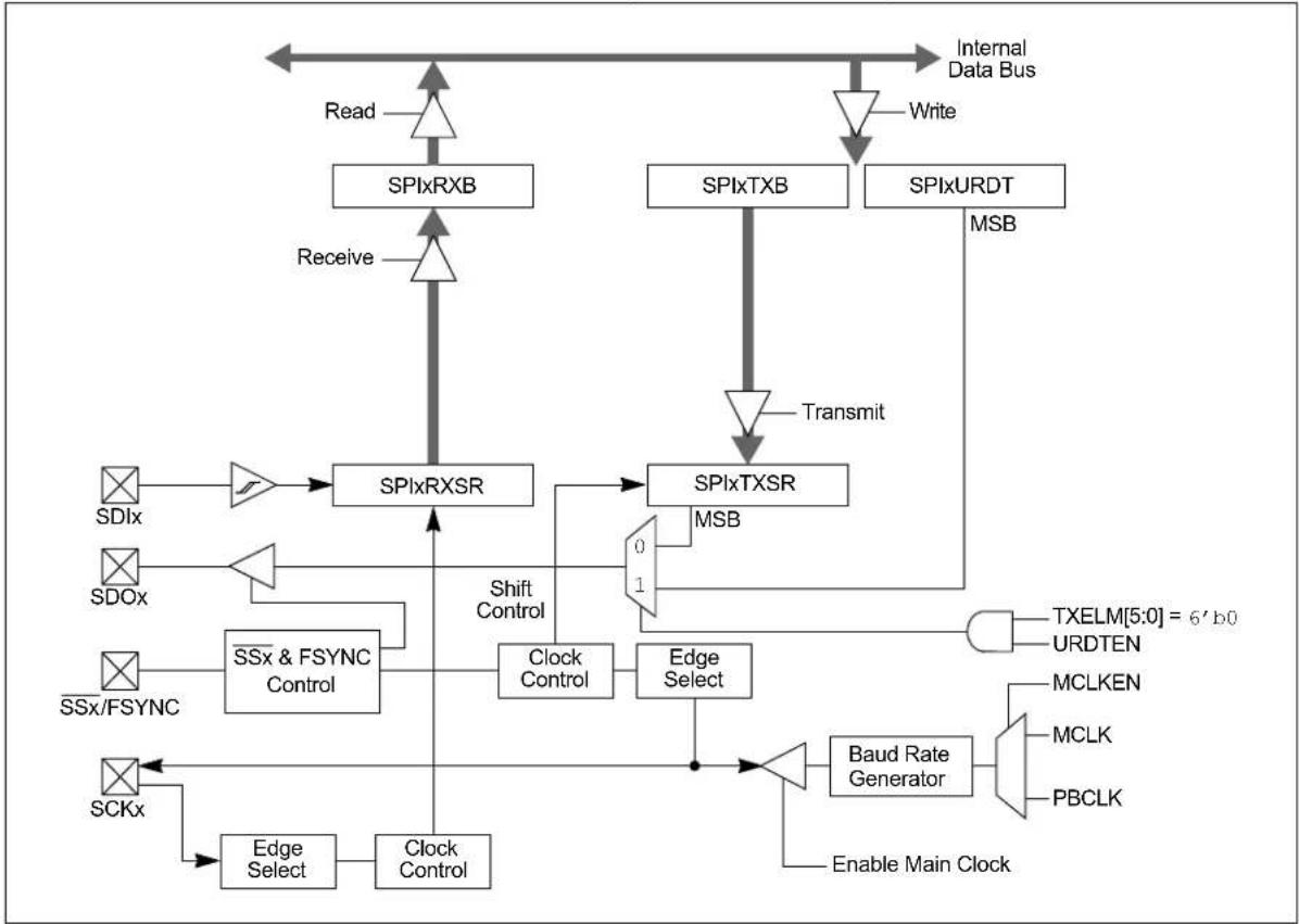
flowchart
graph TD
    A["Read"] --> B["SPIxRXB"]
    B --> C["SPIxTXB"]
    C --> D["SPIxURDT"]
    D --> E["MSB"]
    E --> F["SPIxTXSR"]
    F --> G["Shift Control"]
    G --> H["Clock Control"]
    H --> I["Edge Select"]
    I --> J["Baud Rate Generator"]
    J --> K["Enable Main Clock"]
    K --> L["SSx & FSYNC Control"]
    L --> M["SSx/FSYNC"]
    M --> N["SCKx"]
    N --> O["Edge Select"]
    O --> P["Clock Control"]
    P --> Q["Shift Control"]
    Q --> R["Clock Control"]
    R --> S["Shift Control"]
    S --> T["Shift Control"]
    T --> U["Shift Control"]
    U --> V["Shift Control"]
    V --> W["Shift Control"]
    W --> X["Shift Control"]
    X --> Y["Shift Control"]
    Y --> Z["Shift Control"]
    Z --> AA["Shift Control"]
    AA --> AB["Shift Control"]
    AB --> AC["Shift Control"]
    AC --> AD["Shift Control"]
    AD --> AE["Shift Control"]
    AE --> AF["Shift Control"]
    AF --> AG["Shift Control"]
    AG --> AH["Shift Control"]
    AH --> AI["Shift Control"]
    AI --> AJ["Shift Control"]
    AJ --> AK["Shift Control"]
    AK --> AL["Shift Control"]
    AL --> AM["Shift Control"]
    AM --> AN["Shift Control"]
    AN --> AO["Shift Control"]
    AO --> AP["Shift Control"]
    AP --> AQ["Shift Control"]
    AQ --> AR["Shift Control"]
    AR --> AS["Shift Control"]
    AS --> AT["Shift Control"]
    AT --> AU["Shift Control"]
    AU --> AV["Shift Control"]
    AV --> AW["Shift Control"]
    AW --> AX["Shift Control"]
    AX --> AY["Shift Control"]
    AY --> AZ["Shift Control"]
    AZ --> BA["Shift Control"]
    BA --> BB["Shift Control"]
    BB --> BC["Shift Control"]
    BC --> BD["Shift Control"]
    BD --> BE["Shift Control"]
    BE --> BF["Shift Control"]
    BF --> BG["Shift Control"]
    BG --> BH["Shift Control"]
    BH --> BI["Shift Control"]
    BI --> BJ["Shift Control"]
    BJ --> BK["Shift Control"]
    BK --> BL["Shift Control"]
    BL --> BM["Shift Control"]
    BM --> BN["Shift Control"]
    BN --> BO["Shift Control"]
    BO --> BP["Shift Control"]
    BP --> BQ["Shift Control"]
    BQ --> BR["Shift Control"]
    BR --> BS["Shift Control"]
    BS --> BT["Shift Control"]
    BT --> BU["Shift Control"]
    BU --> BV["Shift Control"]
    BV --> BW["Shift Control"]
    BW --> BX["Shift Control"]
    BX --> BY["Shift Control"]
    BY --> BZ["Shift Control"]
    BZ --> CA["Shift Control"]
    CA --> CB["Shift Control"]
    CB --> CC["Shift Control"]
    CC --> CD["Shift Control"]
    CD --> CE["Shift Control"]
    CE --> CF["Shift Control"]
    CF --> CG["Shift Control"]
    CG --> CH["Shift Control"]
    CH --> CI["Shift Control"]
    CI --> CJ["Shift Control"]
    CJ --> CK["Shift Control"]
    CK --> CL["Shift Control"]
    CL --> CM["Shift Control"]
    CM --> CN["Shift Control"]
    CN --> CO["Shift Control"]
    CO --> CP["Shift Control"]
    CP --> CQ["Shift Control"]
    CQ --> CR["Shift Control"]
    CR --> CS["Shift Control"]
    CS --> CT["Shift Control"]
    CT --> CU["Shift Control"]
    CU --> CV["Shift Control"]
    CV --> CW["Shift Control"]
    CW --> CX["Shift Control"]
    CX --> CY["Shift Control"]
    CY --> CZ["Shift Control"]
    CZ --> DA["Shift Control"]
    DA --> DB["Shift Control"]
    DB --> DC["Shift Control"]
    DC --> DD["Shift Control"]
    DD --> DE["Shift Control"]
    DE --> DF["Shift Control"]
    DF --> DG["Shift Control"]
    DG --> DH["Shift Control"]
    DH --> DI["Shift Control"]
    DI --> DJ["Shift Control"]
    DJ --> DK["Shift Control"]
    DK --> DL["Shift Control"]
    DL --> DV["Shift Control"]
    DV --> DW["Shift Control"]
    DW --> DX["Shift Control"]
    DX --> DXA["MCLKEN"]
    DXA --> DXB["MCLK"]
    DXB --> DXC["PBCLK"]
To set up the SPIx module for the Enhanced Buffer Main mode of operation:
- If using interrupts:
a) Clear the interrupt flag bits in the respective IFSx register.
b) Set the interrupt enable bits in the respective IECx register.
c) Write the SPIxIP bits in the respective IPCx register.
- Write the desired settings to the SPIxCON1L, SPIxCON1H and SPIxCON2L registers with MSTEN (SPIxCON1L[5]) = 1.
- Clear the SPIROV bit (SPIxSTATL[6]).
- Select Enhanced Buffer mode by setting the ENHBUF bit (SPIxCON1L[0]).
- Enable SPIx operation by setting the SPIEN bit (SPIxCON1L[15]).
- Write the data to be transmitted to the SPIxBUFL and SPIxBUFH registers. Transmission (and reception) will start as soon as data are written to the SPIxBUFL and SPIxBUFH registers.
To set up the SPIx module for the Enhanced Buffer Secondary mode of operation:
- Clear the SPIxBUFL and SPIxBUFH registers.
- If using interrupts:
a) Clear the interrupt flag bits in the respective IFSx register.
b) Set the interrupt enable bits in the respective IECx register.
c) Write the SPIxIP bits in the respective IPCx register to set the interrupt priority.
-
Write the desired settings to the SPIxCON1L, SPIxCON1H and SPIxCON2L registers with the MSTEN bit (SPIxCON1L[5]) = 0.
-
Clear the SMP bit.
- If the CKE bit is set, then the SSEN bit must be set, thus enabling the pin.
- Clear the SPIROV bit (SPIxSTATL[6]).
- Select Enhanced Buffer mode by setting the ENHBUF bit (SPIxCON1L[0]).
- Enable SPIx operation by setting the SPIEN bit (SPIxCON1L[15]).
FIGURE 14-2: SPIx MODULE BLOCK DIAGRAM (ENHANCED MODE)
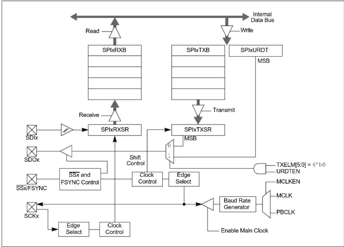
flowchart
graph TD
    A["Read"] --> B["SPIxRXB"]
    C["Write"] --> D["SPIxTXB"]
    E["Internal Data Bus"] --> B
    B --> F["SPIxRXSR"]
    D --> G["SPIxTXSR"]
    F --> H["Shift Control"]
    H --> I["Clock Control"]
    I --> J["Edge Select"]
    J --> K["Baud Rate Generator"]
    K --> L["Enable Main Clock"]
    M["SDIx"] --> N["->"]
    O["SDOx"] --> P["->"]
    Q["SSx/FSYNC"] --> R["SSx and FSYNC Control"]
    S["SCKx"] --> T["Edge Select"]
    T --> U["Clock Control"]
    V["TXELM[5:0"] = 6' b0] --> K
    W["MCLKEN"] --> K
    X["MCLK"] --> K
    Y["PBCLK"] --> K
    Z["MSB"] --> F
    style A fill:#f9f,stroke:#333
    style C fill:#f9f,stroke:#333
    style E fill:#f9f,stroke:#333
    style M fill:#ccf,stroke:#333
    style O fill:#ccf,stroke:#333
    style Q fill:#ccf,stroke:#333
    style S fill:#ccf,stroke:#333
    style T fill:#ccf,stroke:#333
    style U fill:#ccf,stroke:#333
    style V fill:#ccf,stroke:#333
    style W fill:#ccf,stroke:#333
To set up the SPIx module for Audio mode:
- Clear the SPIxBUFL and SPIxBUFH registers.
- If using interrupts:
a) Clear the interrupt flag bits in the respective IFSx register.
b) Set the interrupt enable bits in the respective IECx register.
a) Write the SPIxIP bits in the respective IPCx register to set the interrupt priority.
- Write the desired settings to the SPIxCON1L, SPIxCON1H and SPIxCON2L registers with AUDEN (SPIxCON1H[15]) = 1.
- Clear the SPIROV bit (SPIxSTATL[6]).
- Enable SPIx operation by setting the SPIEN bit (SPIxCON1L[15]).
- Write the data to be transmitted to the SPIxBUFL and SPIxBUFH registers. Transmission (and reception) will start as soon as data are written to the SPIxBUFL and SPIxBUFH registers.
14.1 SPI Control/Status Registers
REGISTER 14-1: SPIxCON1L: SPIx CONTROL REGISTER 1 LOW
| R/W-0 U-0 R/W-0 R/W-0 R/W-0 R/W-0 R/W-0 R/W-0 | |||||||||
| SPIEN | — | SPISIDL | DIS$DO | MODE | 32 | (1,4) | MODE16(1,4) | SMP CKE | (1) |
| bit 15 bit 8 | |||||||||
| R / W - 0 R / W - 0 R / | |||||||
| SSEN(2) | CKP MST | EN DISSDI | DISSCK | MCLKEN | (3) | SPIFE | ENHBUF |
| bit 7 bit 0 | |||||||
Legend:
| R = Readable bit | W = Writable bit | U = Unimplemented bit, read as '0' |
| -n = Value at POR | '1' = Bit is set | '0' = Bit is cleared x = Bit is unknown |
0 = Turns off and resets module, disables clocks, disables interrupt event generation, allows SFR modifications
bit 14 Unimplemented: Read as '0'
bit 13 SPISIDL: SPIx Stop in Idle Mode bit
1 = Halts in CPU Idle mode
0 = Continues to operate in CPU Idle mode
bit 12 DISSDO: Disable SDOx Output Port bit
1 = SDOx pin is not used by the module; pin is controlled by port function
0 = SDOx pin is controlled by the module
bit 11-10 MODE32 and MODE16: Serial Word Length Select bits ^(1,4)
| MODE32 | MODE16 AUDEN | Communication | |
| 1 | x | 0 | 32-Bit |
| 0 | 1 | 16-Bit | |
| 0 | 0 | 8-Bit | |
| 1 | 1 | 1 | 24-Bit Data, 32-Bit FIFO, 32-Bit Channel/64-Bit Frame |
| 1 | 0 | 32-Bit Data, 32-Bit FIFO, 32-Bit Channel/64-Bit Frame | |
| 0 | 1 | 16-Bit Data, 16-Bit FIFO, 32-Bit Channel/64-Bit Frame | |
| 0 | 0 | 16-Bit FIFO, 16-Bit Channel/32-Bit Frame | |
bit 9 SMP: SPIx Data Input Sample Phase bit
Main Mode:
1 = Input data are sampled at the end of data output time
0 = Input data are sampled at the middle of data output time
Secondary Mode:
Input data are always sampled at the middle of data output time, regardless of the SMP setting.
bit 8 CKE: SPIx Clock Edge Select bit ^(1)
1 = Transmit happens on transition from active clock state to Idle clock state
0 = Transmit happens on transition from Idle clock state to active clock state
Note 1: When AUDEN (SPIxCON1H[15]) = 1, this module functions as if CKE = 0, regardless of its actual value.
2: When FRMEN = 1, SSEN is not used.
3: MCLKEN can only be written when the SPIEN bit = 0.
4: This channel is not meaningful for DSP/PCM mode as LRC follows FRMSYPW.
REGISTER 14-1: SPIxCON1L: SPIx CONTROL REGISTER 1 LOW (CONTINUED)
bit 7 SSEN: Secondary Select Enable bit (Secondary mode) (2)
1 = SSx pin is used by the macro in Secondary mode; SSx pin is used as the Secondary select input
0 = SSx pin is not used by the macro (SSx pin will be controlled by the port I/O)
bit 6 CKP: Clock Polarity Select bit
1 = Idle state for clock is a high level; active state is a low level
0 = Idle state for clock is a low level; active state is a high level
bit 5 MSTEN: Main Mode Enable bit
1 = Main mode
0 = Secondary mode
bit 4 DISSDI: Disable SDIx Input Port bit
1 = SDIx pin is not used by the module; pin is controlled by port function
0 = SDIx pin is controlled by the module
bit 3 DISSCK: Disable SCKx Output Port bit
1 = SCKx pin is not used by the module; pin is controlled by port function
0 = SCKx pin is controlled by the module
bit 2 MCLKEN: Main Clock Enable bit (3)
1 = MCLK is used by the BRG
0 = PBCLK is used by the BRG
bit 1 SPIFE: Frame Sync Pulse Edge Select bit
1 = Frame Sync pulse (Idle-to-active edge) coincides with the first bit clock
0 = Frame Sync pulse (Idle-to-active edge) precedes the first bit clock
bit 0 ENHBUF: Enhanced Buffer Enable bit
1 = Enhanced Buffer mode is enabled
0 = Enhanced Buffer mode is disabled
Note 1: When AUDEN (SPIxCON1H[15]) = 1, this module functions as if CKE = 0, regardless of its actual value.
2: When FRMEN = 1, SSEN is not used.
3: MCLKEN can only be written when the SPIEN bit = 0.
4: This channel is not meaningful for DSP/PCM mode as LRC follows FRMSYPW.
REGISTER 14-2: SPIxCON1H: SPIx CONTROL REGISTER 1 HIGH
| R/W-0 R/W-0 R/W-0 R/W-0 R/W-0 R/W-0 R/W-0 R/W-0 | |||||||
| AUDEN(1) | SPISGNEXT | IGNROV | IGNTUR | AUDMONO (2) | URDTEN(3) | AUDMOD1(4) | AUDMOD0(4) |
| bit 15 bit 8 | |||||||
| R/W-0 R/W-0 R/W-0 R/W-0 R/W-0 R/W-0 R/W-0 R/W-0 | ||||||
| FRMEN FR | MSYNC FRMP | POL MSSEN FR | RMSYPW FRM | MCNT2 FRMCN | T1 FRMCNT0 | |
| bit 7 bit 0 | ||||||
Legend:
| R = Readable bit | W = Writable bit | U = Unimplemented bit, read as '0' |
| -n = Value at POR | '1' = Bit is set | '0' = Bit is cleared x = Bit is unknown |
bit 15 AUDEN: Audio Codec Support Enable bit ^(1)
1 = Audio protocol is enabled; MSTEN controls the direction of both SCKx and frame (a.k.a. LRC), and this module functions as if FRMEN = 1, FRMSYNC = MSTEN, FRMCNT[2:0] = 0.01 and SMP = 0, regardless of their actual values 0 = Audio protocol is disabled
bit 14 SPISGNEXT: SPIx Sign-Extend RX FIFO Read Data Enable bit
1 = Data from RX FIFO are sign-extended 0 = Data from RX FIFO are not sign-extended
bit 13 IGNROV: Ignore Receive Overflow bit
1 = A Receive Overflow (ROV) is NOT a critical error; during ROV, data in the FIFO are not overwritten by the receive data 0 = A ROV is a critical error that stops SPI operation
bit 12 IGNTUR: Ignore Transmit Underrun bit
1 = A Transmit Underrun (TUR) is NOT a critical error and data indicated by URDTEN are transmitted until the SPIxTXB is not empty 0 = A TUR is a critical error that stops SPI operation
bit 11 AUDMONO: Audio Data Format Transmit bit ^(2)
1 = Audio data are mono (i.e., each data word is transmitted on both left and right channels) 0 = Audio data are stereo
bit 10 URDTEN: Transmit Underrun Data Enable bit ^(3)
1 = Transmits data out of SPIxURDT register during Transmit Underrun conditions 0 = Transmits the last received data during Transmit Underrun conditions
bit 9-8 AUDMOD[1:0]: Audio Protocol Mode Selection bits ^(4)
11 = PCM/DSP mode 10 = Right Justified mode: This module functions as if SPIFE = 1, regardless of its actual value 01 = Left Justified mode: This module functions as if SPIFE = 1, regardless of its actual value 00 = I²S mode: This module functions as if SPIFE = 0, regardless of its actual value
bit 7 FRMEN: Framed SPIx Support bit
1 = Framed SPIx support is enabled (SSx pin is used as the FSYNC input/output) 0 = Framed SPIx support is disabled
Note 1: AUDEN can only be written when the SPIEN bit = 0.
2: AUDMONO can only be written when the SPIEN bit = 0 and is only valid for AUDEN = 1.
3: URDTEN is only valid when IGNTUR = 1.
4: AUDMOD[1:0] can only be written when the SPIEN bit = 0 and is only valid when AUDEN = 1. When NOT in PCM/DSP mode, this module functions as if FRMSYPW = 1, regardless of its actual value.
REGISTER 14-2: SPIxCON1H: SPIx CONTROL REGISTER 1 HIGH (CONTINUED)
bit 6 FRMSYNC: Frame Sync Pulse Direction Control bit
1 = Frame Sync pulse input (Secondary)
0 = Frame Sync pulse output (Main)
bit 5 FRMPOL: Frame Sync/Secondary Select Polarity bit
1 = Frame Sync pulse/Secondary select is active-high
0 = Frame Sync pulse/Secondary select is active-low
bit 4 MSSEN: Main Mode Secondary Select Enable bit
1 = SPIx Secondary select support is enabled with polarity determined by FRMPOL (SSx pin is automatically driven during transmission in Main mode)
0 = Secondary select SPIx support is disabled (SSx pin will be controlled by port I/O)
bit 3 FRMSYPW: Frame Sync Pulse-Width bit
1 = Frame Sync pulse is one serial word length wide (as defined by MODE[32,16]/WLENGTH[4:0])
0 = Frame Sync pulse is one clock (SCKx) wide
bit 2-0 FRMCNT[2:0]: Frame Sync Pulse Counter bits
Controls the number of serial words transmitted per Sync pulse.
111 = Reserved
110 = Reserved
101 = Generates a Frame Sync pulse on every 32 serial words
100 = Generates a Frame Sync pulse on every 16 serial words
011 = Generates a Frame Sync pulse on every 8 serial words
010 = Generates a Frame Sync pulse on every 4 serial words
001 = Generates a Frame Sync pulse on every 2 serial words (value used by audio protocols)
000 = Generates a Frame Sync pulse on each serial word
Note 1: AUDEN can only be written when the SPIEN bit = 0.
2: AUDMONO can only be written when the SPIEN bit = 0 and is only valid for AUDEN = 1.
3: URDTEN is only valid when IGNTUR = 1.
4: AUDMOD[1:0] can only be written when the SPIEN bit = 0 and is only valid when AUDEN = 1. When NOT in PCM/DSP mode, this module functions as if FRMSYPW = 1, regardless of its actual value.
REGISTER 14-3: SPIxCON2L: SPIx CONTROL REGISTER 2 LOW
| U-0 U-0 U-0 U-0 U-0 U-0 U-0 U-0 | |||||||
| —— | —— | —— | |||||
| bit 15 bit 8 | |||||||
| U-0 U-0 U-0 R/W-0 R/W-0 R/W-0 R/W-0 R/W-0 | ||
| — — — | WLENGTH[4:0] | (1,2) |
| bit 7 | bit 0 | |
| Legend: | |||
| R = Readable bit | W = Writable bit | U = Unimplemented bit, read as '0' | |
| -n = Value at POR | '1' = Bit is set | '0' = Bit is cleared | x = Bit is unknown |
bit 15-5 Unimplemented: Read as '0' bit 4-0 WLENGTH[4:0]: Variable Word Length bits ^(1,2) 11111 = 32-bit data 11110 = 31-bit data 11101 = 30-bit data 11100 = 29-bit data 11011 = 28-bit data 11010 = 27-bit data 11001 = 26-bit data 11000 = 25-bit data 10111 = 24-bit data 10110 = 23-bit data 10101 = 22-bit data 10100 = 21-bit data 10011 = 20-bit data 10010 = 19-bit data 10001 = 18-bit data 10000 = 17-bit data 01111 = 16-bit data 01110 = 15-bit data 01101 = 14-bit data 01100 = 13-bit data 01011 = 12-bit data 01010 = 11-bit data 01001 = 10-bit data 01000 = 9-bit data 00111 = 8-bit data 00110 = 7-bit data 00101 = 6-bit data 00100 = 5-bit data 00011 = 4-bit data 00010 = 3-bit data 00001 = 2-bit data 00000 = See MODE[32,16] bits in SPIxCON1L[11:10]
Note 1: These bits are effective when AUDEN = 0 only.
2: Varying the length by changing these bits does not affect the depth of the TX/RX FIFO.
| Legend: | C = Clearable bit | U = Unimplemented, read as ‘0’ |
| R = Readable bit | W = Writable bit | HSC = Hardware Settable/Clearable bit |
| -n = Value at POR | ‘1’ = Bit is set | ‘0’ = Bit is cleared HS = Hardware Settable bit |
bit 15-13 Unimplemented: Read as '0'
bit 12 FRMERR: SPIx Frame Error Status bit
1 = Frame error is detected
0 = No frame error is detected
bit 11 SPIBUSY: SPIx Activity Status bit
1 = Module is currently busy with some transactions
0 = No ongoing transactions (at time of read)
bit 10-9 Unimplemented: Read as '0'
bit 8 SPITUR: SPIx Transmit Underrun Status bit ^(1)
1 = Transmit buffer has encountered a Transmit Underrun condition
0 = Transmit buffer does not have a Transmit Underrun condition
bit 7 SRMT: Shift Register Empty Status bit
1 = No current or pending transactions (i.e., neither SPIxTXB or SPIxTXSR contains data to transmit)
0 = Current or pending transactions
bit 6 SPIROV: SPIx Receive Overflow Status bit
1 = A new byte/half-word/word has been completely received when the SPIxRXB was full
0 = No overflow
bit 5 SPIRBE: SPIx RX Buffer Empty Status bit
1 = RX buffer is empty
0 = RX buffer is not empty
Standard Buffer Mode:
Automatically set in hardware when SPIxBUF is read from, reading SPIxRXB. Automatically cleared in hardware when SPIx transfers data from SPIxRXSR to SPIxRXB.
Enhanced Buffer Mode:
Indicates RXELM[5:0] = 000000.
bit 4 Unimplemented: Read as '0'
Note 1: SPITUR is cleared when SPIEN = 0. When IGNTUR = 1, SPITUR provides dynamic status of the Transmit Underrun condition, but does not stop RX/TX operation and does not need to be cleared by software.
REGISTER 14-4: SPIxSTATL: SPIx STATUS REGISTER LOW (CONTINUED)
bit 3 SPITBE: SPIx Transmit Buffer Empty Status bit
1 = SPIxTXB is empty
0 = SPIxTXB is not empty
Standard Buffer Mode:
Automatically set in hardware when SPIx transfers data from SPIxTXB to SPIxTXSR. Automatically cleared in hardware when SPIxBUF is written, loading SPIxTXB.
Enhanced Buffer Mode:
Indicates TXELM[5:0] = 000000.
bit 2 Unimplemented: Read as '0'
bit 1 SPITBF: SPIx Transmit Buffer Full Status bit
1 = SPIxTXB is full
0 = SPIxTXB not full
Standard Buffer Mode:
Automatically set in hardware when SPIxBUF is written, loading SPIxTXB. Automatically cleared in hardware when SPIx transfers data from SPIxTXB to SPIxTXSR.
Enhanced Buffer Mode:
Indicates TXELM[5:0] = 111111.
bit 0 SPIRBF: SPIx Receive Buffer Full Status bit
1 = SPIxRXB is full
0 = SPIxRXB is not full
Standard Buffer Mode:
Automatically set in hardware when SPIx transfers data from SPIxRXSR to SPIxRXB. Automatically cleared in hardware when SPIxBUF is read from, reading SPIxRXB.
Enhanced Buffer Mode:
Indicates RXELM[5:0] = 111111.
Note 1: SPITUR is cleared when SPIEN = 0. When IGNTUR = 1, SPITUR provides dynamic status of the Transmit Underrun condition, but does not stop RX/TX operation and does not need to be cleared by software.
| U-0 U-0 HSC/R-0 HSC/R-0 HSC/R-0 HSC/R-0 HSC/R-0 HSC/R-0 | ||||||
| — — RXELM5 | (3) | RXELM4(2) | RXELM3(1) | RXELM2 RX | ELM1 RXELM0 | |
| bit 15 bit 8 | ||||||
| U-0 U-0 HSC/R-0 HSC/R-0 HSC/R-0 HSC/R-0 HSC/R-0 HSC/R-0 | |||||||
| — — TXELM5 | (3) | TXELM4(2) | TXELM3(1) | TXELM2 TXELM1 TXELM0 | |||
| bit 7 | bit 0 | ||||||
| Legend: | HSC = Hardware Settable/Clearable bit | ||
| R = Readable bit | W = Writable bit | U = Unimplemented bit, read as '0' | |
| -n = Value at POR | '1' = Bit is set | '0' = Bit is cleared | x = Bit is unknown |
bit 15-14 Unimplemented: Read as '0'
bit 13-8 RXELM[5:0]: Receive Buffer Element Count bits (valid in Enhanced Buffer mode) ^(1,2,3)
bit 7-6 Unimplemented: Read as '0'
bit 5-0 TXELM[5:0]: Transmit Buffer Element Count bits (valid in Enhanced Buffer mode) ^(1,2,3)
Note 1: RXELM3 and TXELM3 bits are only present when FIFODEPTH = 8 or higher.
2: RXELM4 and TXELM4 bits are only present when FIFODEPTH = 16 or higher.
3: RXELM5 and TXELM5 bits are only present when FIFODEPTH = 32.
REGISTER 14-6: SPIxIMSKL: SPIx INTERRUPT MASK REGISTER LOW
| U-0 U-0 U-0 R/W-0 R/W-0 U-0 U-0 R/W-0 | |||||||
| — — — | FRMERREN B | USYEN — — | SPITUREN | ||||
| bit 15 bit 8 | |||||||
| R/W-0 R/W-0 R/W-0 U-0 R/W-0 U-0 R/W-0 R/W-0 | |||||||
| SRMTEN SPIROVEN SPIRBEN | — | SPITBEN | — | SPITBFEN | SPIRBFEN | ||
| bit 7 bit 0 | |||||||
| Legend: | |||
| R = Readable bit | W = Writable bit | U = Unimplemented bit, read as ‘0’ | |
| -n = Value at POR | ‘1’ = Bit is set | ‘0’ = Bit is cleared | x = Bit is unknown |
bit 15-13 Unimplemented: Read as '0'
bit 12 FRMERREN: Enable Interrupt Events via FRMERR bit
1 = Frame error generates an interrupt event
0 = Frame error does not generate an interrupt event
bit 11 BUSYEN: Enable Interrupt Events via SPIBUSY bit
1 = SPIBUSY generates an interrupt event
0 = SPIBUSY does not generate an interrupt event
bit 10-9 Unimplemented: Read as '0'
bit 8 SPITUREN: Enable Interrupt Events via SPITUR bit
1 = Transmit Underrun (TUR) generates an interrupt event
0 = Transmit Underrun does not generate an interrupt event
bit 7 SRMTEN: Enable Interrupt Events via SRMT bit
1 = Shift Register Empty (SRMT) generates interrupt events
0 = Shift Register Empty does not generate interrupt events
bit 6 SPIROVEN: Enable Interrupt Events via SPIROV bit
1 = SPIx Receive Overflow (ROV) generates an interrupt event
0 = SPIx Receive Overflow does not generate an interrupt event
bit 5 SPIRBEN: Enable Interrupt Events via SPIRBE bit
1 = SPIx RX buffer empty generates an interrupt event
0 = SPIx RX buffer empty does not generate an interrupt event
bit 4 Unimplemented: Read as '0'
bit 3 SPITBEN: Enable Interrupt Events via SPITBE bit
1 = SPIx transmit buffer empty generates an interrupt event
0 = SPIx transmit buffer empty does not generate an interrupt event
bit 2 Unimplemented: Read as '0'
bit 1 SPITBFEN: Enable Interrupt Events via SPITBF bit
1 = SPIx transmit buffer full generates an interrupt event
0 = SPIx transmit buffer full does not generate an interrupt event
bit 0 SPIRBFEN: Enable Interrupt Events via SPIRBF bit
1 = SPIx receive buffer full generates an interrupt event
0 = SPIx receive buffer full does not generate an interrupt event
REGISTER 14-7: SPIxIMSKH: SPIx INTERRUPT MASK REGISTER HIGH
| R/W-0 U-0 R/W-0 R/W-0 R/W-0 R/W-0 R/W-0 R/W-0 | |||||||
| RXWIEN | — RXMSK5 | (1) | RXMSK4(1,4) | RXMSK3(1,3) | RXMSK2(1,2) | RXMSK1(1) | RXMSK0(1) |
| bit 15 bit 8 | |||||||
| R/W-0 U-0 R/W-0 R/W-0 R/W-0 R/W-0 R/W-0 R/W-0 | |||||||
| TXWIEN | — | T(1) | TXMSK4(1,4) | TXMSK3(1,3) | TXMSK2(1,2) | TXMSK1(1) | TXMSK0(1) |
| bit 7 bit 0 | |||||||
Legend:
| R = Readable bit W = Writable bit U = Unimplemented bit, read as '0' | ||
| -n = Value at POR | ‘1’ = Bit is set | ‘0’ = Bit is cleared x = Bit is unknown |
bit 15 RXWIEN: Receive Watermark Interrupt Enable bit
1 = Triggers receive buffer element watermark interrupt when RXMSK[5:0] ≤ RXELM[5:0]
0 = Disables receive buffer element watermark interrupt
bit 14 Unimplemented: Read as '0'
bit 13-8 RXMSK[5:0]: RX Buffer Mask bits ^(1,2,3,4)
RX mask bits; used in conjunction with the RXWIEN bit.
bit 7 TXWIEN: Transmit Watermark Interrupt Enable bit
1 = Triggers transmit buffer element watermark interrupt when TXMSK[5:0] = TXELM[5:0]
0 = Disables transmit buffer element watermark interrupt
bit 6 Unimplemented: Read as '0'
bit 5-0 TXMSK[5:0]: TX Buffer Mask bits ^(1,2,3,4)
TX mask bits; used in conjunction with the TXWIEN bit.
Note 1: Mask values higher than FIFODEPTH are not valid. The module will not trigger a match for any value in this case.
2: RXMSK2 and TXMSK2 bits are only present when FIFODEPTH = 8 or higher.
3: RXMSK3 and TXMSK3 bits are only present when FIFODEPTH = 16 or higher.
4: RXMSK4 and TXMSK4 bits are only present when FIFODEPTH = 32.
FIGURE 14-3: SPIx HOST/CLIENT CONNECTION (STANDARD MODE)
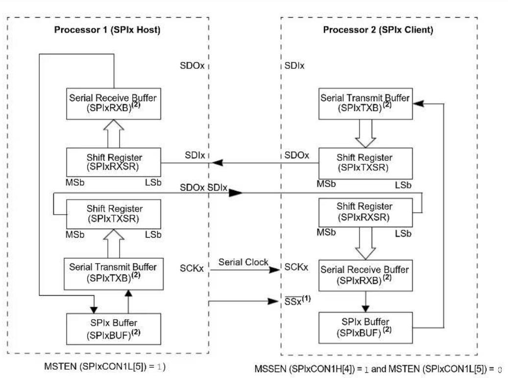
flowchart
graph TD
    subgraph Processor 1 (SPIx Host)
        A["Serial Receive Buffer (SPIxRXB)²"] --> B["Shift Register (SPIxRXSR)"]
        B --> C["MSb"]
        B --> D["LSb"]
        E["Shift Register (SPIxTXSR)"] --> F["MSb"]
        E --> G["LSb"]
        H["Serial Transmit Buffer (SPIxTXB)²"] --> I["MSb"]
        H --> J["LSb"]
        K["SPIx Buffer (SPIxBUF)²"] --> L["MSb"]
        K --> M["LSb"]
    end

    subgraph Processor 2 (SPIx Client)
        N["Serial Transmit Buffer (SPIxTXB)²"] --> O["Shift Register (SPIxTXSR)"]
        O --> P["MSb"]
        O --> Q["LSb"]
        R["Shift Register (SPIxRXSR)"] --> S["MSb"]
        R --> T["LSb"]
        U["Serial Receive Buffer (SPIxRXB)²"] --> V["SSx¹"]
        W["SPIx Buffer (SPIxBUF)²"] --> X["MSb"]
        W --> Y["LSb"]
        Z["Serial Clock"] --> AA["SCKx"]
        AB["SCKx"] --> AC["SSx¹"]
    end

    A --> B
    B --> C
    C --> D
    D --> E
    E --> F
    F --> G
    G --> H
    H --> I
    I --> J
    J --> K
    K --> L
    L --> M
    M --> N
    N --> O
    O --> P
    P --> Q
    Q --> V
    V --> X
    X --> Y
    Y --> Z
    Z --> AA
    AA --> AB
    AB --> AC
    AC --> V
    V --> W
Note 1: Using the SSx pin in Secondary mode of operation is optional.
2: User must write transmit data to read the received data from SPIxBUF. The SPIxTXB and SPIxRXB registers are memory-mapped to SPIxBUF.
FIGURE 14-4: SPIx HOST/CLIENT CONNECTION (ENHANCED BUFFER MODES)
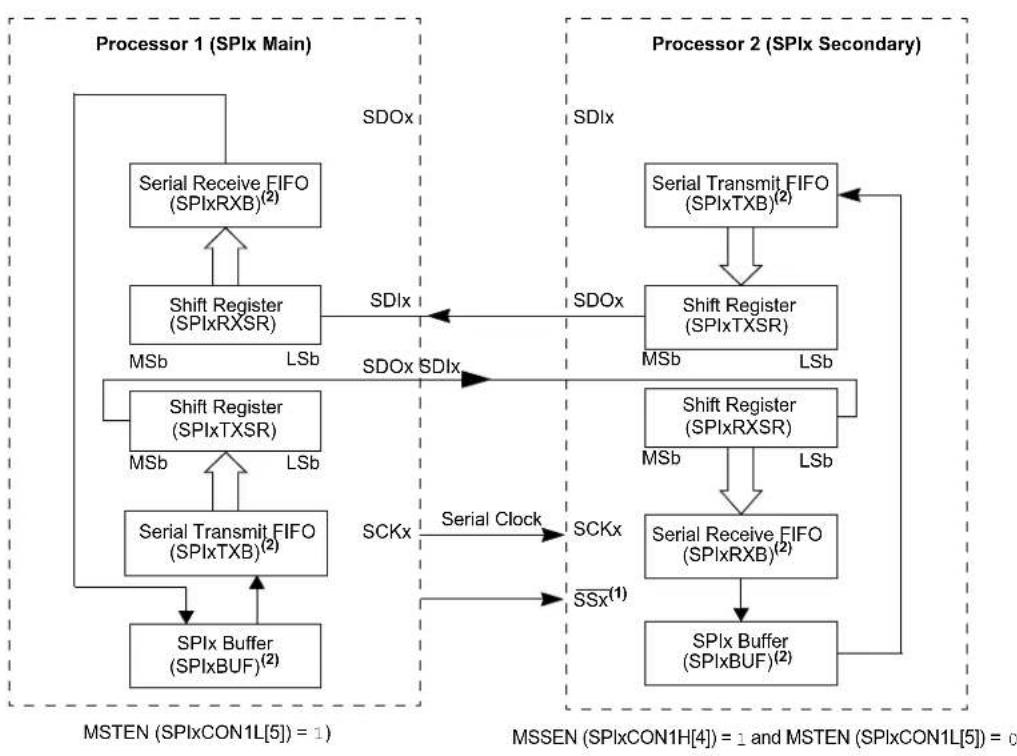
flowchart
graph TD
    subgraph Processor 1 (SPIx Main)
        A["Serial Receive FIFO (SPIxRXB)(2)"] --> B["Shift Register (SPIxRXSR)"]
        B --> C["MSb"]
        B --> D["LSb"]
        E["Shift Register (SPIxTXSR)"] --> F["Serial Transmit FIFO (SPIxTXB)(2)"]
        F --> G["MSb"]
        F --> H["LSb"]
        I["SPIx Buffer (SPIxBUF)(2)"] --> J["MSb"]
        J --> K["LSb"]
    end

    subgraph Processor 2 (SPIx Secondary)
        L["Serial Transmit FIFO (SPIxTXB)(2)"] --> M["Shift Register (SPIxTXSR)"]
        M --> N["MSb"]
        M --> O["LSb"]
        P["Shift Register (SPIxRXSR)"] --> Q["Serial Receive FIFO (SPIxRXB)(2)"]
        Q --> R["MSb"]
        Q --> S["LSb"]
        T["SSx(1)"] --> U["Serial Clock"]
        U --> V["SCKx"]
        V --> W["SCKx"]
        X["SDIx"] --> Y["SDOx"]
        Z["SDIx"] --> AA["SDIx"]
    end

    style Processor 1 fill:#f9f,stroke:#333
    style Processor 2 fill:#f9f,stroke:#333
Note 1: Using the pin in Secondary mode of operation is optional.
2: User must write transmit data to read the received data from SPIxBUF. The SPIxTXB and SPIxRXB registers are memory-mapped to SPIxBUF.
FIGURE 14-5: SPIx HOST, FRAME HOST CONNECTION DIAGRAM
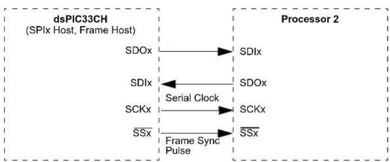
flowchart
graph LR
    A["dsPIC33CH (SPIx Host, Frame Host)"] --> B["SDOx"]
    A --> C["SDIx"]
    A --> D["SCKx"]
    A --> E["SSx"]
    B --> F["Serial Clock"]
    C --> F
    D --> G["Frame Sync Pulse"]
    H["Processor 2"] --> I["SDIx"]
    H --> J["SDOx"]
    H --> K["SCKx"]
    H --> L["SSx"]
FIGURE 14-6: SPIx HOST, FRAME CLIENT CONNECTION DIAGRAM
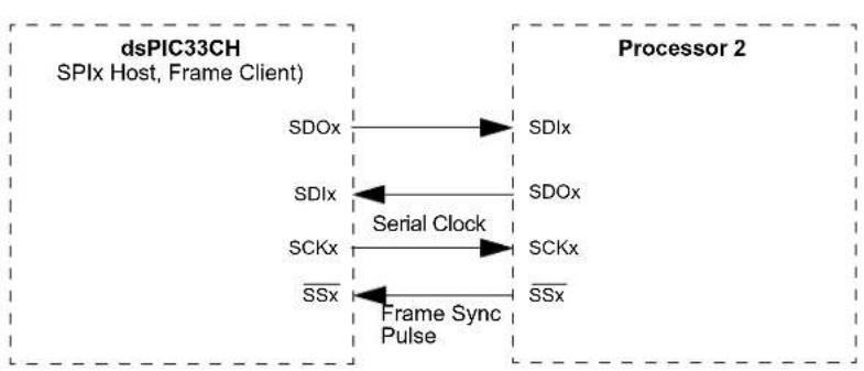
flowchart
graph LR
    subgraph dsPIC33CH
        A["SDOx"] --> B["SDIx"]
        C["SDIx"] --> D["Serial Clock"]
        E["SCKx"] --> F["SCKx"]
        G["SSx"] --> H["Frame Sync Pulse"]
    end
    subgraph Processor 2
        I["SDIx"] --> J["SDOx"]
        K["SCKx"] --> L["SSx"]
    end
FIGURE 14-7: SPIx CLIENT, FRAME HOST CONNECTION DIAGRAM
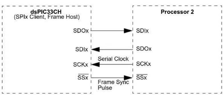
flowchart
graph LR
    subgraph dsPIC33CH (SPIx Client, Frame Host)
        A["SDOx"] --> B["SDIx"]
        C["SDIx"] --> D["Serial Clock"]
        E["SCKx"] --> F["SCKx"]
        G["SSx"] --> H["SSx"]
        I["Frame Sync Pulse"] --> J["SSx"]
    end
    subgraph Processor 2
        K["SDIx"] --> L["SDOx"]
        M["SCKx"] --> N["SSx"]
    end
FIGURE 14-8: SPIx CLIENT, FRAME CLIENT CONNECTION DIAGRAM
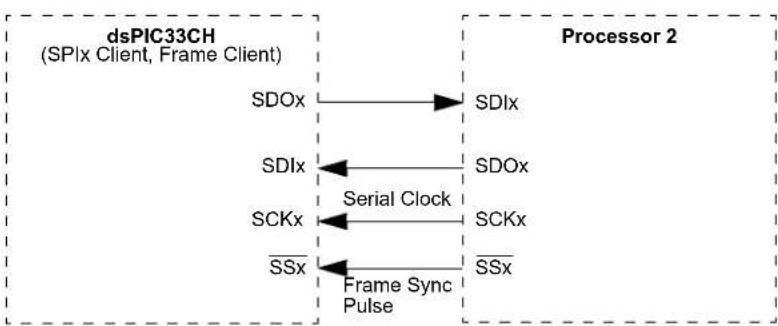
flowchart
graph LR
    A["dsPIC33CH (SPIx Client, Frame Client)"] --> B["SDOx"]
    A --> C["SDIx"]
    A --> D["SCKx"]
    A --> E["SSx"]
    B --> F["Serial Clock"]
    C --> F
    D --> F
    E --> F
    F --> G["Processor 2"]
    G --> H["DSIx"]
    G --> I["SDOx"]
    G --> J["SCKx"]
    G --> K["SSx"]
    style A fill:#f9f,stroke:#333
    style G fill:#ccf,stroke:#333
EQUATION 14-1: RELATIONSHIP BETWEEN DEVICE AND SPIx CLOCK SPEED
$$ B a u d R a t e = \frac {F P B}{(2 * (S P I x B R G + 1))} $$
Where:
FPB is the Peripheral Bus Clock Frequency.
15.0 INTER-INTEGRATED CIRCUIT (I²C)
Note 1: This data sheet summarizes the features of the dsPIC33CH128MP508 family of devices. It is not intended to be a comprehensive reference source. For more information, refer to “Inter-Integrated Circuit (I²C)” (www.microchip.com/DS70000199) which is available from the Microchip website (www.microchip.com).
2: The I ^2 C is identical for both Main core and Secondary core. The x is common for both Host and Client (where the x represents the number of the specific module being addressed). The number of I ^2 C modules available on the Host and Client is different and they are located in different SFR locations.
3: All associated register names are the same on the Main core and the Secondary core. The Secondary code will be developed in a separate project in MPLAB X IDE with the device selection, dsPIC33CH128MP508S1, where the S1 indicates the Secondary device. The Host I²C is I2C1 and I2C2, and the Client is I2C1.
The Inter-Integrated Circuit (I ^2 C) module is a serial interface useful for communicating with other peripheral or microcontroller devices. These peripheral devices may be serial EEPROMs, display drivers, A/D Converters, etc.
The I ^2 C module supports these features:
• Independent Host and Client Logic
- 7-Bit and 10-Bit Device Addresses
- General Call Address as Defined in the I²C Protocol
- Clock Stretching to Provide Delays for the Processor to Respond to a Client Data Request
- Both 100 kHz and 400 kHz Bus Specifications
- Configurable Address Masking
- Multi-Host modes to Prevent Loss of Messages in Arbitration
- Bus Repeater mode, Allowing the Acceptance of All Messages as a Client, regardless of the Address
- Automatic SCL
A block diagram of the module is shown in Figure 15-1.
15.1 Communicating as a Host in a Single Host Environment
The details of sending a message in Host mode depends on the communication protocol for the device being communicated with. Typically, the sequence of events is as follows:
- Assert a Start condition on SDAx and SCLx.
-
Send the I ^2 C device address byte to the Client with a write indication.
-
Wait for and verify an Acknowledge from the Client.
-
Send the first data byte (sometimes known as the command) to the Client.
-
Wait for and verify an Acknowledge from the Client.
-
Send the serial memory address low byte to the Client.
-
Repeat Steps 4 and 5 until all data bytes are sent.
-
Assert a Repeated Start condition on SDAx and SCLx.
-
Send the device address byte to the Client with a read indication.
-
Wait for and verify an Acknowledge from the Client.
-
Enable Host reception to receive serial memory data.
-
Generate an ACK or NACK condition at the end of a received byte of data.
-
Generate a Stop condition on SDAx and SCLx.
FIGURE 15-1: I2Cx BLOCK DIAGRAM

flowchart
graph TD
    A["SCLx"] --> B["Shift Clock"]
    C["SDAx"] --> D["Match Detect"]
    B --> E["I2CxRCV"]
    D --> F["I2CxRSR"]
    F --> G["LSB"]
    G --> H["Address Match"]
    H --> I["I2CxMSK"]
    I --> J["Write"]
    I --> K["Read"]
    L["Start and Stop Bit Detect"] --> M["Control Logic"]
    N["Start and Stop Bit Generation"] --> M
    O["Collision Detect"] --> M
    P["Acknowledge Generation"] --> M
    Q["Clock Stretching"] --> M
    R["I2CCTRN"] --> S["LSB"]
    T["Shift Clock"] --> U["BRG Down Counter"]
    V["Reload Control"] --> U
    W["I2CxBRG"] --> X["Write"]
    Y["TcY/2"] --> U
    M --> Z["I2CxSTAT"]
    M --> AA["I2CxCONL/H"]
    Z --> AB["Write"]
    Z --> AC["Read"]
    AD["Internal Data Bus"] --> AE["Read"]
15.2 Setting Baud Rate When Operating as a Bus Host
To compute the Baud Rate Generator reload value, use Equation 15-1.
EQUATION 15-1: COMPUTING BAUD RATE RELOAD VALUE ^(1,2,3)
$$ I 2 C x B R G = ((1 / F S C L - D e l a y) \cdot F P / 2) - 2 $$
Note 1: These clock rate values are for guidance only. The actual clock rate should be measured in its intended application.
2: Typical value of delay varies from 110 ns to 150 ns.
3: I2CxBRG values of 0 to 3 are expressly forbidden. The user should never program the I2CxBRG with a value of 0x0, 0x1, 0x2 or 0x3 as indeterminate results may occur.
15.3 Client Address Masking
The I2CxMSK register (Register 15-4) designates address bit positions as "don't care" for both 7-Bit and 10-Bit Addressing modes. Setting a particular bit location (= 1) in the I2CxMSK register causes the Client module to respond, whether the corresponding address bit value is a '0' or a '1'. For example, when I2CxMSK is set to '0010000000', the Client module will detect both addresses, '0000000000' and '0010000000'.
To enable address masking, the Intelligent Peripheral Management Interface (IPMI) must be disabled by clearing the STRICT bit (I2CxCONL[11]).
Note: As a result of changes in the I ^2 C protocol, the addresses in Table 15-2 are reserved and will not be Acknowledged in Client mode. This includes any address mask settings that include any of these addresses.
TABLE 15-1: I2Cx CLOCK RATES (1,2)
| FcY FsCL | I2CxBRG Value | ||
| Decimal | Hexadecimal | ||
| 100 MHz | 1 MHz | 41 | 29 |
| 100 MHz | 400 kHz | 116 | 74 |
| 100 MHz | 100 kHz | 491 | 1EB |
| 80 MHz | 1 MHz | 32 | 20 |
| 80 MHz | 400 kHz | 92 | 5C |
| 80 MHz | 100 kHz | 392 | 188 |
| 60 MHz | 1 MHz | 24 | 18 |
| 60 MHz | 400 kHz | 69 | 45 |
| 60 MHz | 100 kHz | 294 | 126 |
| 40 MHz | 1 MHz | 15 | 0F |
| 40 MHz | 400 kHz | 45 | 2D |
| 40 MHz | 100 kHz | 195 | C3 |
| 20 MHz | 1 MHz | 7 | 7 |
| 20 MHz | 400 kHz | 22 | 16 |
| 20 MHz | 100 kHz | 97 | 61 |
Note 1: Based on F cy = Fosc/2; Doze mode and PLL are disabled.
2: These clock rate values are for guidance only. The actual clock rate can be affected by various system-level parameters. The actual clock rate should be measured in its intended application.
TABLE 15-2: I2Cx RESERVED ADDRESSES (1)
| Client Address R/W Bit Description | ||
| 0000 000 0 | General Call Address | (2) |
| 0000 000 1 | Start Byte | |
| 0000 001 x | Cbus Address | |
| 0000 01x x | Reserved | |
| 0000 1xx x | HS Mode Host Code | |
| 1111 0xx x | 10-Bit Client Upper Byte | (3) |
| 1111 1xx x | Reserved | |
Note 1: The address bits listed here will never cause an address match independent of address mask settings.
2: This address will be Acknowledged only if GCEN = 1.
3: A match on this address can only occur on the upper byte in 10-Bit Addressing mode.
15.4 SMBus Support
The dsPIC33CH128MP508 family devices have support for SMBus through options in the input voltage thresholds. There are two control bits to select one of three options: SMEN (I2CxCONL[8]) and Configuration bit, SMBEN (FDEVOPT[10]). Table 15-3 details the setting of these control bits.
TABLE 15-3: I ^2 C PIN VOLTAGE THRESHOLD
| SMEN SFR Bit (I2CxCONL[8]) | SMBEN Configuration Bit (FDEVOPT[10]) | |
| I^2C (default) | 0 | x |
| SMBus 2.0 | 1 | 0 |
| SMBus 3.0 | 1 | 1 |
15.5 I ^2 C Control/Status Registers
REGISTER 15-1: I2CxCONL: I2Cx CONTROL REGISTER LOW
| R/W-0 U-0 HC/R/W-0 R/W-1 R/W-0 R/W-0 R/W-0 R/W-0 | ||||||||
| I2CEN | — I2CSIDL SCLREL | (1) | STRICT A10M | DISSLW | SMEN | |||
| bit 15 | bit 8 | |||||||
| R/W-0 | R/W-0 | R/W-0 | HC/R/W-0 | HC/R/W-0 | HC/R/W-0 | HC/R/W-0 | HC/R/W-0 |
| GCEN | STREN | ACKDT | ACKEN | RCEN | PEN | RSEN | SEN |
| bit 7 bit 0 | |||||||
| Legend: | HC = Hardware Clearable bit | ||
| R = Readable bit | W = Writable bit | U = Unimplemented bit, read as ‘0’ | |
| -n = Value at POR | ‘1’ = Bit is set | ‘0’ = Bit is cleared | x = Bit is unknown |
| bit 15 | I2CEN: I2Cx Enable bit (writable from software only)1 = Enables the I2Cx module, and configures the SDAx and SCLx pins as serial port pins0 = Disables the I2Cx module; all I^2C pins are controlled by port functions |
| bit 14 | Unimplemented: Read as '0' |
| bit 13 | I2CSIDL: I2Cx Stop in Idle Mode bit1 = Discontinues module operation when device enters Idle mode0 = Continues module operation in Idle mode |
| bit 12 | SCLREL: SCLx Release Control bit ( I^2C Client mode only) ^(1) 1 = Releases the SCLx clock0 = Holds the SCLx clock low (clock stretch)If STREN = 1: ^(2) User software may write '0' to initiate a clock stretch and write '1' to release the clock. Hardware clears at the beginning of every Client data byte transmission. Hardware clears at the end of every Client address byte reception. Hardware clears at the end of every Client data byte reception.If STREN = 0::User software may only write '1' to release the clock. Hardware clears at the beginning of every Client data byte transmission. Hardware clears at the end of every Client address byte reception. |
| bit 11 | STRICT: I2Cx Strict Reserved Address Rule Enable bit1 = Strict Reserved Addressing is enforced; for reserved addresses, refer to Table 15-2.(In Client Mode) – The device doesn't respond to reserved address space and addresses falling in that category are NACKed.(In Host Mode) – The device is allowed to generate addresses with reserved address space.0 = Reserved Addressing would be Acknowledged.(In Client Mode) – The device will respond to an address falling in the reserved address space.When there is a match with any of the reserved addresses, the device will generate an ACK.(In Host Mode) – Reserved. |
| bit 10 | A10M: 10-Bit Client Address Flag bit1 = I2CxADD is a 10-bit Client address0 = I2CxADD is a 7-bit Client address |
| bit 9 | DISSLW: Slew Rate Control Disable bit1 = Slew rate control is disabled for Standard Speed mode (100 kHz, also disabled for 1 MHz mode)0 = Slew rate control is enabled for High-Speed mode (400 kHz) |
| Note 1: Automatically cleared to '0' at the beginning of Client transmission; automatically cleared to '0' at the end of Client reception.2: Automatically cleared to '0' at the beginning of Client transmission. | |
REGISTER 15-1: I2CxCONL: I2Cx CONTROL REGISTER LOW (CONTINUED)
bit 8 SMEN: SMBus Input Levels Enable bit
1 = Enables input logic so thresholds are compliant with the SMBus specification
0 = Disables SMBus-specific inputs
bit 7 GCEN: General Call Enable bit (I ^2 C Client mode only)
1 = Enables interrupt when a general call address is received in I2CxRSR; module is enabled for reception
0 = General call address is disabled.
bit 6 STREN: SCLx Clock Stretch Enable bit
In I²C Client mode only; used in conjunction with the SCLREL bit.
1 = Enables clock stretching
0 = Disables clock stretching
bit 5 ACKDT: Acknowledge Data bit
In I ^2 C Host mode during Host Receive mode. The value that will be transmitted when the user initiates an Acknowledge sequence at the end of a receive.
In I²C Client mode when AHEN = 1 or DHEN = 1. The value that the Client will transmit when it initiates an Acknowledge sequence at the end of an address or data reception.
1 = NACK is sent
0 = ACK is sent
bit 4 ACKEN: Acknowledge Sequence Enable bit
In I²C Host mode only; applicable during Host Receive mode.
1 = Initiates Acknowledge sequence on SDAx and SCLx pins, and transmits ACKDT data bit
0 = Acknowledge sequence is Idle
bit 3 RCEN: Receive Enable bit (I ^2 C Host mode only)
1 = Enables Receive mode for I²C; automatically cleared by hardware at end of 8-bit receive data byte
0 = Receive sequence is not in progress
bit 2 PEN: Stop Condition Enable bit (I ^2 C Host mode only)
1 = Initiates Stop condition on SDAx and SCLx pins
0 = Stop condition is Idle
bit 1 RSEN: Restart Condition Enable bit (I ^2 C Host mode only)
1 = Initiates Restart condition on SDAx and SCLx pins
0 = Restart condition is Idle
bit 0 SEN: Start Condition Enable bit (I ^2 C Host mode only)
1 = Initiates Start condition on SDAx and SCLx pins
0 = Start condition is Idle
Note 1: Automatically cleared to '0' at the beginning of Client transmission; automatically cleared to '0' at the end of Client reception.
2: Automatically cleared to '0' at the beginning of Client transmission.
REGISTER 15-2: I2CxCONH: I2Cx CONTROL REGISTER HIGH
| U-0 U-0 U-0 U-0 U-0 U-0 U-0 U-0 | |||||||
| —— | —— | —— | |||||
| bit 15 bit 8 | |||||||
| U-0 R/W-0 R/W-0 R/W-0 R/W-0 R/W-0 R/W-0 R/W-0 | |||||||
| — PCIE | SCIE BOEN S | DAHT | S | BCDE AHEN D | HEN | ||
| bit 7 bit 0 | |||||||
Legend:
| R = Readable bit | W = Writable bit | U = Unimplemented bit, read as '0' |
| -n = Value at POR | '1' = Bit is set | '0' = Bit is cleared x = Bit is unknown |
bit 15-7 Unimplemented: Read as '0'
bit 6 PCIE: Stop Condition Interrupt Enable bit (I²C Client mode only).
1 = Enables interrupt on detection of Stop condition
0 = Stop detection interrupts are disabled
bit 5 SCIE: Start Condition Interrupt Enable bit ( ^2 C Client mode only)
1 = Enables interrupt on detection of Start or Restart conditions
0 = Start detection interrupts are disabled
bit 4 BOEN: Buffer Overwrite Enable bit (I²C Client mode only)
1 = I2CxRCV is updated and an ACK is generated for a received address/data byte, ignoring the state of the I2COV bit only if RBF bit = 0
0 = I2CxRCV is only updated when I2COV is clear
bit 3 SDAHT: SDAx Hold Time Selection bit
1 = Minimum of 300 ns hold time on SDAx after the falling edge of SCLx
0 = Minimum of 100 ns hold time on SDAx after the falling edge of SCLx
bit 2 SBCDE: Client Mode Bus Collision Detect Enable bit (I²C Client mode only)
If, on the rising edge of SCLx, SDAx is sampled low when the module is outputting a high state, the BCL bit is set and the bus goes Idle. This Detection mode is only valid during data and ACK transmit sequences.
1 = Enables Client bus collision interrupts
0 = Client bus collision interrupts are disabled
bit 1 AHEN: Address Hold Enable bit (I²C Client mode only)
1 = Following the 8th falling edge of SCLx for a matching received address byte; SCLREL bit (I2CxCONL[12]) will be cleared and the SCLx will be held low
0 = Address holding is disabled
bit 0 DHEN: Data Hold Enable bit (I²C Client mode only)
1 = Following the 8th falling edge of SCLx for a received data byte; Client hardware clears the SCLREL bit (I2CxCONL[12]) and SCLx is held low
0 = Data holding is disabled
REGISTER 15-3: I2CxSTAT: I2Cx STATUS REGISTER
| HSC/R-0 HSC/R-0 HSC/R-0 U-0 U-0 HSC/R/C-0 HSC/R-0 HSC/R-0 | |||||||
| ACKSTAT | TRSTAT | ACKTIM | — | — | BCL | GCSTAT | ADD10 |
| bit 15 bit 8 | |||||||
| HS/R/C-0 | HS/R/C-0 | HSC/R-0 | HSC/R-0 | HSC/R-0 | HSC/R-0 | HSC/R-0 | HSC/R-0 |
| IWCOL | I2COV | D/ | P | S | R/ | RBF | TBF |
| bit 7 bit 0 | |||||||
| Legend: | C = Clearable bit | HSC = Hardware Settable/Clearable bit |
| R = Readable bit | W = Writable bit | U = Unimplemented bit, read as ‘0’ |
| -n = Value at POR | ‘1’ = Bit is set | ‘0’ = Bit is cleared HS = Hardware Settable bit |
bit 15 ACKSTAT: Acknowledge Status bit (updated in all Host and Client modes)
1 = Acknowledge was not received from Client
0 = Acknowledge was received from Client
bit 14 TRSTAT: Transmit Status bit (when operating as I²C Host; applicable to Host transmit operation)
1 = Host transmit is in progress (8 bits + ACK)
0 = Host transmit is not in progress
bit 13 ACKTIM: Acknowledge Time Status bit (valid in I²C Client mode only)
1 = Indicates I²C bus is in an Acknowledge sequence, set on 8th falling edge of SCLx clock
0 = Not an Acknowledge sequence, cleared on 9th rising edge of SCLx clock
bit 12-11 Unimplemented: Read as '0'
bit 10 BCL: Bus Collision Detect bit (Host/Client mode; cleared when I²C module is disabled, I2CEN = 0)
1 = A bus collision has been detected during a Host or Client transmit operation
0 = No bus collision has been detected
bit 9 GCSTAT: General Call Status bit (cleared after Stop detection)
1 = General call address was received
0 = General call address was not received
bit 8 ADD10: 10-Bit Address Status bit (cleared after Stop detection)
1 = 10-bit address was matched
0 = 10-bit address was not matched
bit 7 IWCOL: I2Cx Write Collision Detect bit
1 = An attempt to write to the I2CxTRN register failed because the I²C module is busy; must be cleared in software
0 = No collision
bit 6 I2COV: I2Cx Receive Overflow Flag bit
1 = A byte was received while the I2CxRCV register is still holding the previous byte; I2COV is a "don't care" in Transmit mode, must be cleared in software
0 = No overflow
bit 5 D/A: Data/Address bit (when operating as I²C Client)
1 = Indicates that the last byte received was data
0 = Indicates that the last byte received or transmitted was an address
bit 4 P: I2Cx Stop bit
Updated when Start, Reset or Stop is detected; cleared when the I²C module is disabled, I2CEN = 0.
1 = Indicates that a Stop bit has been detected last
0 = Stop bit was not detected last
REGISTER 15-3: I2CxSTAT: I2Cx STATUS REGISTER (CONTINUED)
bit 3 S: I2Cx Start bit
Updated when Start, Reset or Stop is detected; cleared when the I²C module is disabled, I2CEN = 0.
1 = Indicates that a Start (or Repeated Start) bit has been detected last
0 = Start bit was not detected last
-
bit 2 R/W : Read/Write Information bit (when operating as I²C Client)
1 = Read: Indicates the data transfer is output from the Client
0 = Write: Indicates the data transfer is input to the Client
bit 1 RBF: Receive Buffer Full Status bit
1 = Receive is complete, I2CxRCV is full
0 = Receive is not complete, I2CxRCV is empty
bit 0 TBF: Transmit Buffer Full Status bit
1 = Transmit is in progress, I2CxTRN is full (eight bits of data)
0 = Transmit is complete, I2CxTRN is empty
REGISTER 15-4: I2CxMSK: I2Cx CLIENT MODE ADDRESS MASK REGISTER
| U-0 U-0 U-0 U-0 U-0 U-0 R/W-0 R/W-0 | |||||
| — — — | — — — MSK[9:8] | ||||
| bit 15 bit 8 | |||||
| R/W-0 | R/W-0 | R/W-0 | R/W-0 | R/W-0 | R/W-0 | R/W-0 | R/W-0 |
| MSK[7:0] | |||||||
| bit 7 | bit 0 | ||||||
Legend:
| R = Readable bit | W = Writable bit | U = Unimplemented bit, read as '0' |
| -n = Value at POR | '1' = Bit is set | '0' = Bit is cleared x = Bit is unknown |
bit 15-10 Unimplemented: Read as '0'
bit 9-0 MSK[9:0]: I2Cx Mask for Address Bit x Select bits
1 = Enables masking for bit x of the incoming message address; bit match is not required in this position
0 = Disables masking for bit x; bit match is required in this position
NOTES:
16.0 SINGLE-EDGE NIBBLE TRANSMISSION (SENT)
Note 1: This data sheet summarizes the features of this group of dsPIC33CH128MP508 family devices. It is not intended to be a comprehensive reference source. To complement the information in this data sheet, refer to “Single-Edge Nibble Transmission (SENT) Module” (www.microchip.com/DS70005145), which is available from the Microchip website (www.microchip.com).
2: Some registers and associated bits described in this section may not be available on all devices. Refer to Section 3.2 "Main Memory Organization" in this data sheet for device-specific register and bit information.
3: This SENT module is available only on the Main.
Table 16-1 shows an overview of the SENT module.
TABLE 16-1: SENT MODULE OVERVIEW
| Number of SENT Modules | Identical (Modules) | |
| Main Core 2 Yes | ||
| Secondary Core | None | NA |
16.1 Module Introduction
The Single-Edge Nibble Transmission (SENT) module is based on the SAE J2716, "SENT – Single-Edge Nibble Transmission for Automotive Applications". The SENT protocol is a one-way, single wire time modulated serial communication, based on successive falling edges. It is intended for use in applications where high-resolution sensor data need to be communicated from a sensor to an Engine Control Unit (ECU).
The SENTx module has the following major features:
- Selectable Transmit or Receive mode
- Synchronous or Asynchronous Transmit modes
• Automatic Data Rate Synchronization - Optional Automatic Detection of CRC Errors in Receive mode
- Optional Hardware Calculation of CRC in Transmit mode
• Support for Optional Pause Pulse Period
• Data Buffering for One Message Frame - Selectable Data Length for Transmit/Receive from Three to Six Nibbles
• Automatic Detection of Framing Errors
SENT protocol timing is based on a predetermined time unit, TTICK. Both the transmitter and receiver must be preconfigured for TTICK, which can vary from 3 to 90 μs. A SENT message frame starts with a Sync pulse. The purpose of the Sync pulse is to allow the receiver to calculate the data rate of the message encoded by the transmitter. The SENT specification allows messages to be validated with up to a 20% variation in TTICK. This allows for the transmitter and receiver to run from different clocks that may be inaccurate, and drift with time and temperature. The data nibbles are four bits in length and are encoded as the data value + 12 ticks. This yields a 0 value of 12 ticks and the maximum value, 0xF, of 27 ticks.
A SENT message consists of the following:
- A synchronization/calibration period of 56 tick times
• A status nibble of 12-27 tick times - Up to six data nibbles of 12-27 tick times
• A CRC nibble of 12-27 tick times - An optional pause pulse period of 12-768 tick times
Figure 16-1 shows a block diagram of the SENTx module.
Figure 16-2 shows the construction of a typical 6-nibble data frame, with the numbers representing the minimum or maximum number of tick times for each section.
FIGURE 16-1: SENTx MODULE BLOCK DIAGRAM

flowchart
graph TD
    A["SENTx TX"] --> B["Output Driver"]
    B --> C["SENTx Edge Control"]
    C --> D["Edge Timing"]
    D --> E["Sync Period Detector"]
    E --> F["Edge Detect"]
    F --> G["SENTx RX"]
    G --> H["Nibble Period Detector"]
    H --> I["Tick Period Generator"]
    I --> J["Output Driver"]
    J --> K["SENTx CON1"]
    K --> L["SENTxSTATSENxCON1"]
    style A fill:#f9f,stroke:#333
    style G fill:#f9f,stroke:#333
    style H fill:#ccc,stroke:#333
    style I fill:#ccc,stroke:#333
    style J fill:#ccc,stroke:#333
    style K fill:#ccc,stroke:#333
    style L fill:#ccc,stroke:#333
    subgraph Transmitter OnlyReceiver Only SharedLegend
        M["SentTx RX"] --> N["Edge Detect"]
        N --> O["Sync Period Detector"]
        O --> P["Edge Detect"]
        P --> Q["Nibble Period Detector"]
        Q --> R["Tick Period Generator"]
        R --> S["Edge Timing"]
        S --> T["Control and Error Detection"]
    end
FIGURE 16-2: SENTx PROTOCOL DATA FRAMES
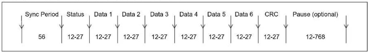
flowchart
graph TD
    A["Sync Period"] --> B["56"]
    C["Status"] --> D["12-27"]
    E["Data 1"] --> F["12-27"]
    G["Data 2"] --> H["12-27"]
    I["Data 3"] --> J["12-27"]
    K["Data 4"] --> L["12-27"]
    M["Data 5"] --> N["12-27"]
    O["Data 6"] --> P["12-27"]
    Q["CRC"] --> R["12-27"]
    S["Pause (optional)"] --> T["12-768"]
16.2 Transmit Mode
By default, the SENTx module is configured for transmit operation. The module can be configured for continuous asynchronous message frame transmission, or alternatively, for Synchronous mode triggered by software. When enabled, the transmitter will send a Sync, followed by the appropriate number of data nibbles, an optional CRC and optional pause pulse. The tick period used by the SENTx transmitter is set by writing a value to the TICKTIME[15:0] (SENTxCON2[15:0]) bits. The tick period calculations are shown in Equation 16-1.
EQUATION 16-1: TICK PERIOD CALCULATION
$$ T I C K T I M E [ 1 5: 0 ] = \frac {T T I C K}{T C L K} - 1 $$
An optional pause pulse can be used in Asynchronous mode to provide a fixed message frame time period. The frame period used by the SENTx transmitter is set by writing a value to the FRAMETIME[15:0] (SENTxCON3[15:0]) bits. The formulas used to calculate the value of frame time are shown in Equation 16-2.
EQUATION 16-2: FRAME TIME CALCULATIONS
$$ F R A M E T I M E [ 1 5: 0 ] = T T I C K / T F R A M E $$
$$ F R A M E T I M E [ 1 5: 0 ] \geq 1 2 2 + 2 7 N $$
$$ F R A M E T I M E [ 1 5: 0 ] \geq 8 4 8 + 1 2 N $$
Where:
T_FRAME = Total time of the message from ms
N = The number of data nibbles in message, 1-6
Note: The module will not produce a pause period with less than 12 ticks, regardless of the FRAMETIME[15:0] value. FRAMETIME[15:0] values beyond 2047 will have no effect on the length of a data frame.
16.2.1 TRANSMIT MODE CONFIGURATION
16.2.1.1 Initializing the SENTx Module
Perform the following steps to initialize the module:
- Write RCVEN (SENTxCON1[11]) = 0 for Transmit mode.
- Write TXM (SENTxCON1[10]) = 0 for Asynchronous Transmit mode or TXM = 1 for Synchronous mode.
- Write NIBCNT[2:0] (SENTxCON1[2:0]) for the desired data frame length.
- Write CRCEN (SENTxCON1[8]) for hardware or software CRC calculation.
- Write PPP (SENTxCON1[7]) for optional pause pulse.
- If PPP = 1, write T FRAME to SENTxCON3.
- Write SENTxCON2 with the appropriate value for the desired tick period.
- Enable interrupts and set interrupt priority.
- Write initial status and data values to SENTxDATH/L.
- If CRCEN = 0, calculate CRC and write the value to CRC[3:0] (SENTxDATL[3:0]).
- Set the SNTEN (SENTxCON1[15]) bit to enable the module.
User software updates to SENTxDATH/L must be performed after the completion of the CRC and before the next message frame's status nibble. The recommended method is to use the message frame completion interrupt to trigger data writes.
16.3 Receive Mode
The module can be configured for receive operation by setting the RCVEN (SENTxCON1[11]) bit. The time between each falling edge is compared to SYNCMIN[15:0] (SENTxCON3[15:0]) and SYNCMAX[15:0] (SENTxCON2[15:0]), and if the measured time lies between the minimum and maximum limits, the module begins to receive data. The validated Sync time is captured in the SENTxSYNC register and the tick time is calculated. Subsequent falling edges are verified to be within the valid data width and the data are stored in the SENTxDATL/H registers. An interrupt event is generated at the completion of the message and the user software should read the SENTx Data registers before the reception of the next nibble. The equation for SYNCMIN[15:0] and SYNCMAX[15:0] is shown in Equation 16-3.
EQUATION 16-3: SYNCMIN[15:0] AND SYNCMAX[15:0] CALCULATIONS
$$ T T I C K = T C L K \cdot (T I C K T I M E [ 1 5: 0 ] + 1) $$
$$ F R A M E T I M E [ 1 5: 0 ] = T T I C K / T F R A M E $$
$$ \text { SyncCount } = 8 \times F R C V \times T T I C K $$
$$ \text { SYNCMIN } [ 1 5: 0 ] = 0. 8 \times \text { SyncCount } $$
$$ \text { SYNCMAX } [ 1 5: 0 ] = 1. 2 \times \text { SyncCount } $$
$$ F R A M E T I M E [ 1 5: 0 ] \geq 1 2 2 + 2 7 N $$
$$ F R A M E T I M E [ 1 5: 0 ] \geq 8 4 8 + 1 2 N $$
Where:
T_FRAME = Total time of the message from ms
N = The number of data nibbles in message, 1-6
FRCV = FCY × Prescaler
T_CLK = F_CY/Prescaler
For TTICK = 3.0 μs and FCLK = 4 MHz, SYNCMIN[15:0] = 76.
Note: To ensure a Sync period can be identified, the value written to SYNCMIN[15:0] must be less than the value written to SYNCMAX[15:0].
16.3.1 RECEIVE MODE CONFIGURATION
16.3.1.1 Initializing the SENTx Module
Perform the following steps to initialize the module:
- Write RCVEN (SENTxCON1[11]) = 1 for Receive mode.
- Write NIBCNT[2:0] (SENTxCON1[2:0]) for the desired data frame length.
- Write CRCEN (SENTxCON1[8]) for hardware or software CRC validation.
- Write PPP (SENTxCON1[7]) = 1 if pause pulse is present.
- Write SENTxCON2 with the value of SYNCMAXx (Nominal Sync Period + 20%).
- Write SENTxCON3 with the value of SYNCMINx (Nominal Sync Period - 20%).
- Enable interrupts and set interrupt priority.
- Set the SNTEN (SENTxCON1[15]) bit to enable the module.
The data should be read from the SENTxDATL/H registers after the completion of the CRC and before the next message frame's status nibble. The recommended method is to use the message frame completion interrupt trigger.
16.4 SENT Control/Status Registers
REGISTER 16-1: SENTxCON1: SENTx CONTROL REGISTER 1
| R/W-0 U-0 R/W-0 U-0 R/W-0 R/W-0 R/W-0 R/W-0 | |||||||
| SNTEN — $NTSIDL — RCVEN TXM | (1) | TXPOL(1) | CRCEN | ||||
| bit 15 bit 8 | |||||||
| R/W-0 R/W-0 U-0 R/W-0 U-0 R/W-0 R/W-0 R/W-0 | |||||||
| PPP SPC | EN (2) | — | PS | — | NIBCNT2 | NIBCNT1 | NIBCNT0 |
| bit 7 bit 0 | |||||||
| Legend: | |||
| R = Readable bit | W = Writable bit | U = Unimplemented bit, read as '0' | |
| -n = Value at POR | '1' = Bit is set | '0' = Bit is cleared | x = Bit is unknown |
| bit 15 | SNTEN: SENTx Enable bit1 = SENTx is enabled0 = SENTx is disabled |
| bit 14 | Unimplemented: Read as ‘0’ |
| bit 13 | SNTSIDL: SENTx Stop in Idle Mode bit1 = Discontinues module operation when the device enters Idle mode0 = Continues module operation in Idle mode |
| bit 12 | Unimplemented: Read as ‘0’ |
| bit 11 | RCVEN: SENTx Receive Enable bit1 = SENTx operates as a receiver0 = SENTx operates as a transmitter (sensor) |
| bit 10 | TXM: SENTx Transmit Mode bit(1)1 = SENTx transmits data frame only when triggered using the SYNCTXEN status bit0 = SENTx transmits data frames continuously while SNTEN = 1 |
| bit 9 | TXPOL: SENTx Transmit Polarity bit(1)1 = SENTx data output pin is low in the Idle state0 = SENTx data output pin is high in the Idle state |
| bit 8 | CRCEN: CRC Enable bitModule in Receive Mode (RCVEN = 1):1 = SENTx performs CRC verification on received data using the preferred J2716 method0 = SENTx does not perform CRC verification on received dataModule in Transmit Mode (RCVEN = 1):1 = SENTx automatically calculates CRC using the preferred J2716 method0 = SENTx does not calculate CRC |
| bit 7 | PPP: Pause Pulse Present bit1 = SENTx is configured to transmit/receive SENT messages with pause pulse0 = SENTx is configured to transmit/receive SENT messages without pause pulse |
| bit 6 | SPCEN: Short PWM Code Enable bit(2)1 = SPC control from external source is enabled0 = SPC control from external source is disabled |
| bit 5 | Unimplemented: Read as ‘0’ |
Note 1: This bit has no function in Receive mode (RCVEN = 1).
2: This bit has no function in Transmit mode (RCVEN = 0).
REGISTER 16-1: SENTxCON1: SENTx CONTROL REGISTER 1 (CONTINUED)
bit 4 PS: SENTx Module Clock Prescaler (divider) bits
1 = Divide-by-4
0 = Divide-by-1
bit 3 Unimplemented: Read as '0'
bit 2-0 NIBCNT[2:0]: Nibble Count Control bits
111 = Reserved; do not use
110 = Module transmits/receives six data nibbles in a SENT data pocket
101 = Module transmits/receives five data nibbles in a SENT data pocket
100 = Module transmits/receives four data nibbles in a SENT data pocket
011 = Module transmits/receives three data nibbles in a SENT data pocket
010 = Module transmits/receives two data nibbles in a SENT data pocket
001 = Module transmits/receives one data nibble in a SENT data pocket
000 = Reserved; do not use
Note 1: This bit has no function in Receive mode (RCVEN = 1).
2: This bit has no function in Transmit mode (RCVEN = 0).
REGISTER 16-2: SENTxSTAT: SENTx STATUS REGISTER
| U-0 U-0 U-0 U-0 U-0 U-0 U-0 U-0 | |||||||
| ——— | ——— | — | |||||
| bit 15 bit 8 | |||||||
| R-0 | R-0 | R-0 | R-0 | R/C-0 | R/C-0 | R-0 | HC/R/W-0 |
| PAUSE | NIB2 | NIB1 | NIB0 | CRCERR | FRMERR | RXIDLE | SYNCTXEN^(1) |
| bit 7 bit 0 | |||||||
| Legend: | C = Clearable bit | HC = Hardware Clearable bit |
| R = Readable bit | W = Writable bit | U = Unimplemented bit, read as ‘0’ |
| -n = Value at POR | ‘1’ = Bit is set | ‘0’ = Bit is cleared x = Bit is unknown |
bit 15-8 Unimplemented: Read as '0'
bit 7 PAUSE: Pause Period Status bit
1 = The module is transmitting/receiving a pause period
0 = The module is not transmitting/receiving a pause period
bit 6-4 NIB[2:0]: Nibble Status bits
Module in Transmit Mode (RCVEN = 0):
111 = Module is transmitting a CRC nibble
110 = Module is transmitting Data Nibble 6
101 = Module is transmitting Data Nibble 5
100 = Module is transmitting Data Nibble 4
011 = Module is transmitting Data Nibble 3
010 = Module is transmitting Data Nibble 2
001 = Module is transmitting Data Nibble 1
000 = Module is transmitting a status nibble or pause period, or is not transmitting
Module in Receive Mode (RCVEN = 1):
111 = Module is receiving a CRC nibble or was receiving this nibble when an error occurred
110 = Module is receiving Data Nibble 6 or was receiving this nibble when an error occurred
101 = Module is receiving Data Nibble 5 or was receiving this nibble when an error occurred
100 = Module is receiving Data Nibble 4 or was receiving this nibble when an error occurred
011 = Module is receiving Data Nibble 3 or was receiving this nibble when an error occurred
010 = Module is receiving Data Nibble 2 or was receiving this nibble when an error occurred
001 = Module is receiving Data Nibble 1 or was receiving this nibble when an error occurred
000 = Module is receiving a status nibble or waiting for Sync
bit 3 CRCERR: CRC Status bit (Receive mode only)
1 = A CRC error has occurred for the 1-6 data nibbles in SENTxDATL/H
0 = A CRC error has not occurred
bit 2 FRMERR: Framing Error Status bit (Receive mode only)
1 = A data nibble was received with less than 12 tick periods or greater than 27 tick periods
0 = Framing error has not occurred
bit 1 RXIDLE: SENTx Receiver Idle Status bit (Receive mode only)
1 = The SENTx data bus has been Idle (high) for a period of SYNCMAX[15:0] or greater
0 = The SENTx data bus is not Idle
Note 1: In Receive mode (RCVEN = 1), the SYNCTXEN bit is read-only.
REGISTER 16-2: SENTxSTAT: SENTx STATUS REGISTER (CONTINUED)
bit 0 SYNCTXEN: SENTx Synchronization Period Status/Transmit Enable bit ^(1)
Module in Receive Mode (RCVEN = 1):
1 = A valid synchronization period was detected; the module is receiving nibble data
0 = No synchronization period has been detected; the module is not receiving nibble data
Module in Asynchronous Transmit Mode (RCVEN = 0, TXM = 0):
The bit always reads as '1' when the module is enabled, indicating the module transmits SENTx data frames continuously. The bit reads '0' when the module is disabled.
Module in Synchronous Transmit Mode (RCVEN = 0, TXM = 1):
1 = The module is transmitting a SENTx data frame
0 = The module is not transmitting a data frame, user software may set SYNCTXEN to start another data frame transmission
Note 1: In Receive mode (RCVEN = 1), the SYNCTXEN bit is read-only.
REGISTER 16-3: SENTxDATL: SENTx RECEIVE DATA REGISTER LOW (1)
| R/W-0 R/W-0 R/W-0 R/W-0 R/W-0 R/W-0 R/W-0 R/W-0 | |
| DATA4[3:0] DATA5[3:0] | |
| bit 15 bit 8 | |
| R/W-0 R/W-0 R/W-0 R/W-0 R/W-0 R/W-0 R/W-0 R/W-0 | |
| DATA6[3:0] | CRC[3:0] |
| bit 7 | bit 0 |
Legend:
| R = Readable bit | W = Writable bit | U = Unimplemented bit, read as ‘0’ |
| -n = Value at POR | ‘1’ = Bit is set | ‘0’ = Bit is cleared x = Bit is unknown |
bit 15-12 DATA4[3:0]: Data Nibble 4 Data bits
bit 11-8 DATA5[3:0]: Data Nibble 5 Data bits
bit 7-4 DATA6[3:0]: Data Nibble 6 Data bits
bit 3-0 CRC[3:0]: CRC Nibble Data bits
Note 1: Register bits are read-only in Receive mode (RCVEN = 1). In Transmit mode, the CRC[3:0] bits are read-only when automatic CRC calculation is enabled (RCVEN = 0, CRCEN = 1).
REGISTER 16-4: SENTxDATH: SENTx RECEIVE DATA REGISTER HIGH (1)
| R/W-0 R/W-0 R/W-0 R/W-0 R/W-0 R/W-0 R/W-0 R/W-0 | |
| STAT[3:0] | DATA1[3:0] |
| bit 15 bit 8 | |
| R/W-0 R/W-0 R/W-0 R/W-0 R/W-0 R/W-0 R/W-0 R/W-0 | |
| DATA2[3:0] DATA3[3:0] | |
| bit 7 | bit 0 |
Legend:
| R = Readable bit | W = Writable bit | U = Unimplemented bit, read as ‘0’ |
| -n = Value at POR | ‘1’ = Bit is set | ‘0’ = Bit is cleared x = Bit is unknown |
bit 15-12 STAT[3:0]: Status Nibble Data bits
bit 11-8 DATA1[3:0]: Data Nibble 1 Data bits
bit 7-4 DATA2[3:0]: Data Nibble 2 Data bits
bit 3-0 DATA3[3:0]: Data Nibble 3 Data bits
Note 1: Register bits are read-only in Receive mode (RCVEN = 1). In Transmit mode, the CRC[3:0] bits are read-only when automatic CRC calculation is enabled (RCVEN = 0, CRCEN = 1).
NOTES:
17.0 TIMER1
Note 1: This data sheet summarizes the features of the dsPIC33CH128MP508 family of devices. It is not intended to be a comprehensive reference source. To complement the information in this data sheet, refer to "Timer1 Module" (www.microchip.com/DS70005279), which is available from the Microchip website (www.microchip.com).
2: The timer is identical for both Main core and Secondary core. The x is common for both Main core and Secondary core (where the x represents the number of the specific module being addressed).
3: All associated register names are the same on the Main core and the Secondary core. The Secondary code will be developed in a separate project in MPLAB X IDE with the device selection, dsPIC33CH128MP508S1, where S1 indicates the Secondary device.
The Timer1 module is a 16-bit timer that can operate as a free-running interval timer/counter.
The Timer1 module has the following unique features over other timers:
- Can be Operated in Asynchronous Counter mode
- Asynchronous Timer
• Operational during CPU Sleep mode - Software Selectable Prescalers 1:1, 1:8, 1:64 and 1:256
• External Clock Selection Control - The Timer1 External Clock Input (T1CK) can Optionally be Synchronized to the Internal Device Clock and the Clock Synchronization is Performed after the Prescaler
If Timer1 is used for SCCP, the timer should be running in Synchronous mode.
The Timer1 module can operate in one of the following modes:
- Timer mode
- Gated Timer mode
• Synchronous Counter mode
• Asynchronous Counter mode
Table 17-1 shows an overview of the Timer1 module.
TABLE 17-1: TIMER1 MODULE OVERVIEW
| Number of Timer1 Modules | Identical (Modules) | |
| Main Core 1 Yes | ||
| Secondary Core | 1 Yes |
A block diagram of Timer1 is shown in Figure 17-1.
FIGURE 17-1: 16-BIT TIMER1 MODULE BLOCK DIAGRAM
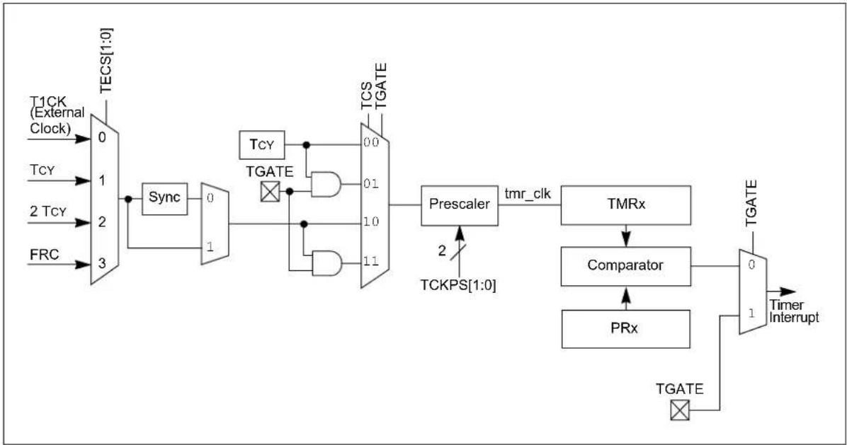
flowchart
graph LR
    A["T1CK (External Clock)"] --> B["0"]
    C["TCY"] --> D["1"]
    E["2 TCY"] --> F["2"]
    G["FRC"] --> H["3"]
    B --> I["Sync"]
    D --> J["0"]
    F --> K["2"]
    H --> L["1"]
    I --> M["1"]
    J --> N["TGATE"]
    K --> O["TCS TGATE"]
    L --> P["TCR"]
    M --> Q["TCR"]
    N --> R["0.0"]
    O --> S["0.1"]
    P --> T["1.0"]
    Q --> U["1.1"]
    R --> V["Prescaler"]
    S --> V
    T --> V
    U --> V
    V --> W["tmr_clk"]
    W --> X["TMRx"]
    X --> Y["Comparator"]
    Y --> Z["PRx"]
    Z --> AA["TGATE"]
    AA --> AB["0"]
    AB --> AC["TGATE Interrupt"]
    AD["TCKPS[1:0"]] --> AE["2"]
17.1 Timer1 Control Register
REGISTER 17-1: T1CON: TIMER1 CONTROL REGISTER
| R/W-0 U-0 R/W-0 R/W-0 R-0 R-0 R/W-0 R/W-0 | |||||||
| TON^(1) | — SIDL | TMWDIS TMWIP PRWIP | TECS1 | TECS0 | |||
| bit 15 | bit 8 | ||||||
| R/W-0 | U-0 | R/W-0 | R/W-0 | U-0 | R/W-0 | R/W-0 | U-0 |
| TGATE | — | TCKPS1 | TCKPS0 | — | TSYNC^(1) | TCS^(1) | — |
| bit 7 bit 0 | |||||||
Legend:
| R = Readable bit | W = Writable bit | U = Unimplemented bit, read as '0' |
| -n = Value at POR | '1' = Bit is set | '0' = Bit is cleared x = Bit is unknown |
bit 15 TON: Timer1 On bit ^(1)
1 = Starts 16-bit Timer1
0 = Stops 16-bit Timer1
bit 14 Unimplemented: Read as '0'
bit 13 SIDL: Timer1 Stop in Idle Mode bit
1 = Discontinues module operation when device enters Idle mode
0 = Continues module operation in Idle mode
bit 12 TMWDIS: Asynchronous Timer1 Write Disable bit
1 = Timer writes are ignored while a posted write to TMR1 or PR1 is synchronized to the asynchronous clock domain
0 = Back-to-back writes are enabled in Asynchronous mode
bit 11 TMWIP: Asynchronous Timer1 Write in Progress bit
1 = Write to the timer in Asynchronous mode is pending
0 = Write to the timer in Asynchronous mode is complete
bit 10 PRWIP: Asynchronous Period Write in Progress bit
1 = Write to the Period register in Asynchronous mode is pending
0 = Write to the Period register in Asynchronous mode is complete
bit 9-8 TECS[1:0]: Timer1 Extended Clock Select bits
11 = FRC clock
10 = 2 TCY
01 = TcY
00 = External Clock comes from the T1CK pin
bit 7 TGATE: Timer1 Gated Time Accumulation Enable bit
When TCS = 1:
This bit is ignored.
When TCS = 0:
1 = Gated time accumulation is enabled
0 = Gated time accumulation is disabled
bit 6 Unimplemented: Read as '0'
Note 1: When Timer1 is enabled in External Synchronous Counter mode (TCS = 1, TSYNC = 1, TON = 1), any attempts by user software to write to the TMR1 register are ignored.
REGISTER 17-1: T1CON: TIMER1 CONTROL REGISTER (CONTINUED)
bit 5-4 TCKPS[1:0]: Timer1 Input Clock Prescale Select bits
11 = 1:256
10 = 1:64
01 = 1:8
00 = 1:1
bit 3 Unimplemented: Read as '0'
bit 2 TSYNC: Timer1 External Clock Input Synchronization Select bit(1) When TCS = 1: 1 = Synchronizes the External Clock input 0 = Does not synchronize the External Clock input When TCS = 0: This bit is ignored.
bit 1 TCS: Timer1 Clock Source Select bit (1) 1 = External Clock source selected by TECS[1:0] 0 = Internal peripheral clock (FP)
bit 0 Unimplemented: Read as '0'
Note 1: When Timer1 is enabled in External Synchronous Counter mode (TCS = 1, TSYNC = 1, TON = 1), any attempts by user software to write to the TMR1 register are ignored.
NOTES:
18.0 CONFIGURABLE LOGIC CELL (CLC)
Note 1: This data sheet summarizes the features of the dsPIC33CH128MP508 family of devices. It is not intended to be a comprehensive reference source. For more information, refer to “Configurable Logic Cell (CLC)” (www.microchip.com/DS70005298), which is available from the Microchip website (www.microchip.com). The information in this data sheet supersedes the information in the FRM.
2: The CLC is identical for both Main core and Secondary core (where the x represents the number of the specific module being addressed in Main or Secondary).
3: All associated register names are the same on the Main core and the Secondary core. The Secondary code will be developed in a separate project in MPLAB X IDE with the device selection, dsPIC33CH128MP508S1, where the S1 indicates the Secondary device. The Main and Secondary are CLC1 and CLC2.
The Configurable Logic Cell (CLC) module allows the user to specify combinations of signals as inputs to a logic function and to use the logic output to control other peripherals or I/O pins. This provides greater flexibility and potential in embedded designs, since the CLC module can operate outside the limitations of software execution, and supports a vast amount of output designs.
There are four input gates to the selected logic function. These four input gates select from a pool of up to 32 signals that are selected using four data source selection multiplexers. Table 18-1 shows an overview of the module.
TABLE 18-1: CLC MODULE OVERVIEW
| Number of CLC Modules | Identical (Modules) | |
| Main Core 4 Yes | ||
| Secondary Core | 4 Yes |
Figure 18-3 shows the details of the data source multiplexers and Figure 18-2 shows the logic input gate connections.
FIGURE 18-1: CLCx MODULE

flowchart
graph LR
    A["CLC Inputs (32)"] --> B["Input Data Selection Gates"]
    B --> C["See Figure 18-3"]
    C --> D["Logic Function"]
    D --> E["LCEN"]
    D --> F["Logic Output"]
    E --> G["CLCx Output"]
    F --> G
    G --> H["TRISx Control"]
    H --> I["CLCx"]
    I --> J["Set CLCxIF"]
    D --> K["Interrupt det"]
    D --> L["INTP"]
    D --> M["INTN"]
    D --> N["Interrupt det"]
    K --> O["D Q CLK"]
    L --> P["FCY CLK"]
    M --> Q["LCOE"]
    N --> R["AND Gate"]
    O --> S["LCOUT"]
    P --> T["LCPOL"]
    Q --> U["LCPOL"]
    R --> V["LCPOL"]
FIGURE 18-2: CLCx LOGIC FUNCTION COMBINATORIAL OPTIONS
AND - OR MODE[2:0] = 000 MODE[2:0] = 000 | OR - XOR MODE[2:0] = 001 MODE[2:0] = 001 |
4-Input AND MODE[2:0] = 010 MODE[2:0] = 010 | S-R Latch MODE[2:0] = 011 MODE[2:0] = 011 |
1-Input D Flip-Flop with S and R MODE[2:0] = 100 MODE[2:0] = 100 | 2-Input D Flip-Flop with R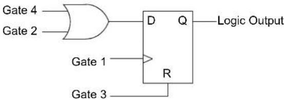 MODE[2:0] = 101 MODE[2:0] = 101 |
J-K Flip-Flop with R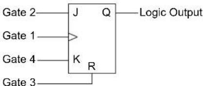 MODE[2:0] = 110 MODE[2:0] = 110 | 1-Input Transparent Latch with S and R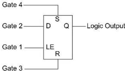 MODE[2:0] = 111 MODE[2:0] = 111 |
FIGURE 18-3: CLCx INPUT SOURCE SELECTION DIAGRAM
(1,2)

flowchart
graph TD
    subgraph Inputs
        A["Input 0"] --> B["Data Selection"]
        C["Input 1"] --> B
        D["Input 2"] --> B
        E["Input 3"] --> B
        F["Input 4"] --> B
        G["Input 5"] --> B
        H["Input 6"] --> B
        I["Input 7"] --> B
        J["DS1x (CLCxSEL[2:0"])] --> B
    end

    subgraph Inputs
        K["Input 8"] --> L["Data Selection"]
        M["Input 9"] --> L
        N["Input 10"] --> L
        O["Input 11"] --> L
        P["Input 12"] --> L
        Q["Input 13"] --> L
        R["Input 14"] --> L
        S["Input 15"] --> L
        T["DS2x (CLCxSEL[6:4"])] --> L
    end

    subgraph Inputs
        U["Input 16"] --> V["Data Selection"]
        W["Input 17"] --> V
        X["Input 18"] --> V
        Y["Input 19"] --> V
        Z["Input 20"] --> V
        AA["Input 21"] --> V
        AB["Input 22"] --> V
        AC["Input 23"] --> V
        AD["DS3x (CLCxSEL[10:8"])] --> V
    end

    subgraph Inputs
        AE["Input 24"] --> AF["Data Selection"]
        AG["Input 25"] --> AF
        AH["Input 26"] --> AF
        AI["Input 27"] --> AF
        AJ["Input 28"] --> AF
        AK["Input 29"] --> AF
        AL["Input 30"] --> AF
        AM["Input 31"] --> AF
        AN["DS4x (CLCxSEL[14:12"])] --> AF

    end

    B --> B1["G1D1T"]
    B --> B2["G1D1N"]
    B --> B3["G1D2T"]
    B --> B4["G1D2N"]
    B --> B5["G1D3T"]
    B --> B6["G1D3N"]
    B --> B7["G1D4T"]
    B --> B8["G1D4N"]

    G1G1G1G1G1G1G1G1G1G1G1G1G1G1G1G1G1G1G1G1G1G1G1G1G1G1G1G1G1G1G1G1G1G1G1G1G1G1G1G1G1G1G1G1G1G1G1G1G1G1G1C

    note right of B: Data Gate 2 (Same as Data Gate 1)
    note right of G1POL (CLCxCONH["0"])

    note right of G2-G4: Gate 2, Gate 3, Gate 4: Same as Gate 1; Gate 3: Same as Gate 1; Gate 4: Same as Gate 1
Note 1: All controls are undefined at power-up.
2: CLC that have unused/unassigned inputs are a logic '0', and through polarity control, they can be changed to a '1'.
18.1 Control Registers
The CLCx module is controlled by the following registers:
- CLCxCONL
- CLCxCONH
- CLCxSEL
- CLCxGLSL
- CLCxGLSH
The CLCx Control registers (CLCxCONL and CLCxCONH) are used to enable the module and interrupts, control the output enable bit, select output polarity and select the logic function. The CLCx Control registers also allow the user to control the logic polarity of not only the cell output, but also some intermediate variables.
The CLCx Input MUX Select register (CLCxSEL) allows the user to select up to four data input sources using the four data input selection multiplexers. Each multiplexer has a list of eight data sources available.
The CLCx Gate Logic Input Select registers (CLCxGLSL and CLCxGLSH) allow the user to select which outputs from each of the selection MUXes are used as inputs to the input gates of the logic cell. Each data source MUX outputs both a true and a negated version of its output. All of these eight signals are enabled, ORed together by the logic cell input gates.
If no gate inputs are selected, the input to the gate will be zero or one, depending on the GxPOL bits.
REGISTER 18-1: CLCxCONL: CLCx CONTROL REGISTER (LOW)
| R/W-0 U-0 U-0 U-0 R/W-0 R/W-0 U-0 U-0 | |||||
| LCEN — + — INTP INTN — — | |||||
| bit 15 bit 8 | |||||
| R-0 R-0 R/W-0 U-0 U-0 | R/W-0 R/W-0 R/W-0 | ||||||
| LCOE | LCOUT | LCPOL | — | — | MODE2 | MODE1 | MODE0 |
| bit 7 bit 0 | |||||||
| Legend: | |||
| R = Readable bit | W = Writable bit | U = Unimplemented bit, read as ‘0’ | |
| -n = Value at POR | ‘1’ = Bit is set | ‘0’ = Bit is cleared | x = Bit is unknown |
| bit 15 | LCEN: CLCx Enable bit1 = CLCx is enabled and mixing input signals0 = CLCx is disabled and has logic zero outputs |
| bit 14-12 | Unimplemented: Read as '0' |
| bit 11 | INTP: CLCx Positive Edge Interrupt Enable bit1 = Interrupt will be generated when a rising edge occurs on LCOUT0 = Interrupt will not be generated |
| bit 10 | INTN: CLCx Negative Edge Interrupt Enable bit1 = Interrupt will be generated when a falling edge occurs on LCOUT0 = Interrupt will not be generated |
| bit 9-8 | Unimplemented: Read as '0' |
| bit 7 | LCOE: CLCx Port Enable bit1 = CLCx port pin output is enabled0 = CLCx port pin output is disabled |
| bit 6 | LCOUT: CLCx Data Output Status bit1 = CLCx output high0 = CLCx output low |
| bit 5 | LCPOL: CLCx Output Polarity Control bit1 = The output of the module is inverted0 = The output of the module is not inverted |
Note 1: The CLC SR latch has no default reset value, meaning it could be initialized to either 1 or 0. In SR latch mode, the CLC output state should be considered unknown and up to the user to initialize.
REGISTER 18-1: CLCxCONL: CLCx CONTROL REGISTER (LOW) (CONTINUED)
bit 4-3 Unimplemented: Read as '0'
bit 2-0 MODE[2:0]: CLCx Mode bits
111 = Single input transparent latch with S and R 110 = JK flip-flop with R 101 = Two-input D flip-flop with R 100 = Single input D flip-flop with S and R 011 = SR latch ^(1) 010 = Four-input AND 001 = Four-input OR-XOR 000 = Four-input AND-OR
Note 1: The CLC SR latch has no default reset value, meaning it could be initialized to either 1 or 0. In SR latch mode, the CLC output state should be considered unknown and up to the user to initialize.
REGISTER 18-2: CLCxCONH: CLCx CONTROL REGISTER (HIGH)
| U-0 U-0 U-0 U-0 U-0 U-0 U-0 U-0 | |||||||
| —— | —— | —— | |||||
| bit 15 bit 8 | |||||||
| U-0 U-0 U-0 U-0 R/W-0 | R/W-0 | R/W-0 | R/W-0 | ||||
| — | — | — | — | G4POL | G3POL | G2POL | G1POL |
| bit 7 bit 0 | |||||||
Legend:
| R = Readable bit | W = Writable bit | U = Unimplemented bit, read as '0' |
| -n = Value at POR | '1' = Bit is set | '0' = Bit is cleared x = Bit is unknown |
bit 15-4 Unimplemented: Read as '0'
bit 3 G4POL: Gate 4 Polarity Control bit
1 = Channel 4 logic output is inverted when applied to the logic cell
0 = Channel 4 logic output is not inverted
bit 2 G3POL: Gate 3 Polarity Control bit
1 = Channel 3 logic output is inverted when applied to the logic cell
0 = Channel 3 logic output is not inverted
bit 1 G2POL: Gate 2 Polarity Control bit
1 = Channel 2 logic output is inverted when applied to the logic cell
0 = Channel 2 logic output is not inverted
bit 0 G1POL: Gate 1 Polarity Control bit
1 = Channel 1 logic output is inverted when applied to the logic cell
0 = Channel 1 logic output is not inverted
REGISTER 18-3: CLCxSEL: CLCx INPUT MUX SELECT REGISTER
| U-0 R/W-0 R/W-0 R/W-0 U-0 R/W-0 R/W-0 R/W-0 | ||
| — DS4[2:0] — DS3[2:0] | ||
| bit 15 bit 8 | ||
| U-0 R/W-0 R/W-0 R/W-0 U-0 R/W-0 R/W-0 R/W-0 | ||
| — DS2[2:0] — DS1[2:0] | ||
| bit 7 bit 0 | ||
Legend:
R = Readable bit W = Writable bit U = Unimplemented bit, read as '0'
-n = Value at POR '1' = Bit is set '0' = Bit is cleared x = Bit is unknown
bit 15 Unimplemented: Read as '0'
bit 14-12 DS4[2:0]: Data Selection MUX 4 Signal Selection bits (Main)
111 = Main SCCP3 auxiliary out
110 = Main SCCP1 auxiliary out
101 = Main core CLCIND I/O pin
100 = Reserved
011 = Main SPI1 Input (SDIx) ^(1)
010 = Secondary Comparator 2 out
001 = Main CLC2 output
000 = Main PWM event A
DS4[2:0]: Data Selection MUX 4 Signal Selection bits (Secondary)
111 = Secondary SCCP3 auxiliary out
110 = Secondary SCCP1 auxiliary out
101 = Secondary core CLCIND I/O pin
100 = Reserved
011 = Secondary SPI1 Input (SDIx) ^(1)
010 = Secondary Comparator 2 out
001 = Secondary CLC2 out
000 = Secondary PWM event A
bit 11 Unimplemented: Read as '0'
bit 10-8 DS3[2:0]: Data Selection MUX 3 Signal Selection bits (Main)
111 = Main SCCP4 (CCP4IF) OCMP out
110 = Main SCCP3 (CCP3IF) OCMP out
101 = Main core CLC4 out
100 = Main UART1 RX output corresponding to CLCx module
011 = Main SPI1 Output (SDOx) corresponding to CLCx module
010 = Secondary Comparator 1 output
001 = Main CLC1 output
000 = Main CLCINC I/O pin
DS3[2:0]: Data Selection MUX 3 Signal Selection bits (Secondary)
111 = Secondary SCCP4 Compare Event Flag (CCP4IF)
110 = Secondary SCCP3 Compare Event Flag (CCP3IF)
101 = Secondary CLC4 out
100 = Secondary UART1 RX output corresponding to CLCx module
011 = Secondary SPI1 Output (SDOx) corresponding to CLCx module
010 = Secondary Comparator 1 output
001 = Secondary CLC1 output
000 = Secondary CLCINC I/O pin
Note 1: Valid only for the SPI with PPS selection.
REGISTER 18-3: CLCxSEL: CLCx INPUT MUX SELECT REGISTER (CONTINUED)
| bit 7 | Unimplemented: Read as ‘0’ |
| bit 6-4 | DS2[2:0]: Data Selection MUX 2 Signal Selection bits (Main)111 = Main SCCP2 OC (CCP2IF) out110 = Main SCCP1 OC (CCP1IF) out101 = Reserved100 = Reserved011 = Main UART1 TX input corresponding to CLCx module010 = Main Comparator 1 output001 = Secondary CLC2 output000 = Main CLCINB I/O pinDS2[2:0]: Data Selection MUX 2 Signal Selection bits (Secondary)111 = Secondary SCCP2 OC (CCP2IF) out110 = Secondary SCCP1 OC (CCP1IF) out101 = Reserved100 = Reserved011 = Secondary UART1 TX input corresponding to CLCx module010 = Main Comparator 1 output001 = Main CLC2 output000 = Secondary CLCINB I/O pin |
| bit 3 | Unimplemented: Read as ‘0’ |
| bit 2-0 | DS1[2:0]: Data Selection MUX 1 Signal Selection bits (Main)111 = Main SCCP4 auxiliary out110 = Main SCCP2 auxiliary out101 = Secondary Comparator 3100 = Main REFCLKO output011 = Main INTRC/LPRC clock source010 = Main core CLC3 out001 = Main system clock (Fcy)000 = Main CLCINA I/O pinDS1[2:0]: Data Selection MUX 1 Signal Selection bits (Secondary)111 = Secondary SCCP4 auxiliary out110 = Secondary SCCP2 auxiliary out101 = Secondary Comparator 3100 = Secondary REFCLKO output011 = Secondary INTRC/LPRC clock source010 = Secondary CLC3 out001 = Secondary system clock (Fcy)000 = Secondary CLCINA I/O pin |
Note 1: Valid only for the SPI with PPS selection.
REGISTER 18-4: CLCxGLSL: CLCx GATE LOGIC INPUT SELECT LOW REGISTER
| R/W-0 R/W-0 R/W-0 R/W-0 R/W-0 R/W-0 R/W-0 R/W-0 | ||||||
| G2D4T G2 | D4N G2D3T G | 2D3N G2D2T | G2D2N G2D1T | G2D1N | ||
| bit 15 bit 8 | ||||||
| R/W-0 R/W-0 R/W-0 R/W-0 R/W-0 R/W-0 R/W-0 | ||||||
| G1D4T G1 | D4N G1D3T G | 1D3N G1D2T | G1D2N G1D1T | G1D1N | ||
| bit 7 bit 0 | ||||||
Legend:
| R = Readable bit W = Writable bit U = Unimplemented bit, read as '0' | |
| -n = Value at POR '1' = Bit is set '0' = Bit is cleared | x = Bit is unknown |
| bit 15 | G2D4T: Gate 2 Data Source 4 True Enable bit1 = Data Source 4 signal is enabled for Gate 20 = Data Source 4 signal is disabled for Gate 2 |
| bit 14 | G2D4N: Gate 2 Data Source 4 Negated Enable bit1 = Data Source 4 inverted signal is enabled for Gate 20 = Data Source 4 inverted signal is disabled for Gate 2 |
| bit 13 | G2D3T: Gate 2 Data Source 3 True Enable bit1 = Data Source 3 signal is enabled for Gate 20 = Data Source 3 signal is disabled for Gate 2 |
| bit 12 | G2D3N: Gate 2 Data Source 3 Negated Enable bit1 = Data Source 3 inverted signal is enabled for Gate 20 = Data Source 3 inverted signal is disabled for Gate 2 |
| bit 11 | G2D2T: Gate 2 Data Source 2 True Enable bit1 = Data Source 2 signal is enabled for Gate 20 = Data Source 2 signal is disabled for Gate 2 |
| bit 10 | G2D2N: Gate 2 Data Source 2 Negated Enable bit1 = Data Source 2 inverted signal is enabled for Gate 20 = Data Source 2 inverted signal is disabled for Gate 2 |
| bit 9 | G2D1T: Gate 2 Data Source 1 True Enable bit1 = Data Source 1 signal is enabled for Gate 20 = Data Source 1 signal is disabled for Gate 2 |
| bit 8 | G2D1N: Gate 2 Data Source 1 Negated Enable bit1 = Data Source 1 inverted signal is enabled for Gate 20 = Data Source 1 inverted signal is disabled for Gate 2 |
| bit 7 | G1D4T: Gate 1 Data Source 4 True Enable bit1 = Data Source 4 signal is enabled for Gate 10 = Data Source 4 signal is disabled for Gate 1 |
| bit 6 | G1D4N: Gate 1 Data Source 4 Negated Enable bit1 = Data Source 4 inverted signal is enabled for Gate 10 = Data Source 4 inverted signal is disabled for Gate 1 |
| bit 5 | G1D3T: Gate 1 Data Source 3 True Enable bit1 = Data Source 3 signal is enabled for Gate 10 = Data Source 3 signal is disabled for Gate 1 |
| bit 4 | G1D3N: Gate 1 Data Source 3 Negated Enable bit1 = Data Source 3 inverted signal is enabled for Gate 10 = Data Source 3 inverted signal is disabled for Gate 1 |
REGISTER 18-4: CLCxGLSL: CLCx GATE LOGIC INPUT SELECT LOW REGISTER (CONTINUED)
bit 3 G1D2T: Gate 1 Data Source 2 True Enable bit
1 = Data Source 2 signal is enabled for Gate 1
0 = Data Source 2 signal is disabled for Gate 1
bit 2 G1D2N: Gate 1 Data Source 2 Negated Enable bit
1 = Data Source 2 inverted signal is enabled for Gate 1
0 = Data Source 2 inverted signal is disabled for Gate 1
bit 1 G1D1T: Gate 1 Data Source 1 True Enable bit
1 = Data Source 1 signal is enabled for Gate 1
0 = Data Source 1 signal is disabled for Gate 1
bit 0 G1D1N: Gate 1 Data Source 1 Negated Enable bit
1 = Data Source 1 inverted signal is enabled for Gate 1
0 = Data Source 1 inverted signal is disabled for Gate 1
REGISTER 18-5: CLCxGLSH: CLCx GATE LOGIC INPUT SELECT HIGH REGISTER
| R/W-0 R/W-0 R/W-0 R/W-0 R/W-0 R/W-0 R/W-0 R/W-0 | ||||||
| G4D4T G4 | D4N G4D3T G | 4D3N G4D2T | G4D2N G4D1T | G4D1N | ||
| bit 15 bit 8 | ||||||
| R/W-0 R/W-0 R/W-0 R/W-0 R/W-0 R/W-0 R/W-0 | ||||||
| G3D4T G3 | D4N G3D3T G | 3D3N G3D2T | G3D2N G3D1T | G3D1N | ||
| bit 7 bit 0 | ||||||
Legend:
| R = Readable bit W = Writable bit U = Unimplemented bit, read as '0' | |
| -n = Value at POR '1' = Bit is set '0' = Bit is cleared | x = Bit is unknown |
| bit 15 | G4D4T: Gate 4 Data Source 4 True Enable bit1 = Data Source 4 signal is enabled for Gate 40 = Data Source 4 signal is disabled for Gate 4 |
| bit 14 | G4D4N: Gate 4 Data Source 4 Negated Enable bit1 = Data Source 4 inverted signal is enabled for Gate 40 = Data Source 4 inverted signal is disabled for Gate 4 |
| bit 13 | G4D3T: Gate 4 Data Source 3 True Enable bit1 = Data Source 3 signal is enabled for Gate 40 = Data Source 3 signal is disabled for Gate 4 |
| bit 12 | G4D3N: Gate 4 Data Source 3 Negated Enable bit1 = Data Source 3 inverted signal is enabled for Gate 40 = Data Source 3 inverted signal is disabled for Gate 4 |
| bit 11 | G4D2T: Gate 4 Data Source 2 True Enable bit1 = Data Source 2 signal is enabled for Gate 40 = Data Source 2 signal is disabled for Gate 4 |
| bit 10 | G4D2N: Gate 4 Data Source 2 Negated Enable bit1 = Data Source 2 inverted signal is enabled for Gate 40 = Data Source 2 inverted signal is disabled for Gate 4 |
| bit 9 | G4D1T: Gate 4 Data Source 1 True Enable bit1 = Data Source 1 signal is enabled for Gate 40 = Data Source 1 signal is disabled for Gate 4 |
| bit 8 | G4D1N: Gate 4 Data Source 1 Negated Enable bit1 = Data Source 1 inverted signal is enabled for Gate 40 = Data Source 1 inverted signal is disabled for Gate 4 |
| bit 7 | G3D4T: Gate 3 Data Source 4 True Enable bit1 = Data Source 4 signal is enabled for Gate 30 = Data Source 4 signal is disabled for Gate 3 |
| bit 6 | G3D4N: Gate 3 Data Source 4 Negated Enable bit1 = Data Source 4 inverted signal is enabled for Gate 30 = Data Source 4 inverted signal is disabled for Gate 3 |
| bit 5 | G3D3T: Gate 3 Data Source 3 True Enable bit1 = Data Source 3 signal is enabled for Gate 30 = Data Source 3 signal is disabled for Gate 3 |
| bit 4 | G3D3N: Gate 3 Data Source 3 Negated Enable bit1 = Data Source 3 inverted signal is enabled for Gate 30 = Data Source 3 inverted signal is disabled for Gate 3 |
REGISTER 18-5: CLCxGLSH: CLCx GATE LOGIC INPUT SELECT HIGH REGISTER (CONTINUED)
bit 3 G3D2T: Gate 3 Data Source 2 True Enable bit
1 = Data Source 2 signal is enabled for Gate 3
0 = Data Source 2 signal is disabled for Gate 3
bit 2 G3D2N: Gate 3 Data Source 2 Negated Enable bit
1 = Data Source 2 inverted signal is enabled for Gate 3
0 = Data Source 2 inverted signal is disabled for Gate 3
bit 1 G3D1T: Gate 3 Data Source 1 True Enable bit
1 = Data Source 1 signal is enabled for Gate 3
0 = Data Source 1 signal is disabled for Gate 3
bit 0 G3D1N: Gate 3 Data Source 1 Negated Enable bit
1 = Data Source 1 inverted signal is enabled for Gate 3
0 = Data Source 1 inverted signal is disabled for Gate 3
NOTES:
19.0 32-BIT PROGRAMMABLE CYCLIC REDUNDANCY CHECK (CRC) GENERATOR
Note 1: This data sheet summarizes the features of the dsPIC33CH128MP508 family of devices. It is not intended to be a comprehensive reference source. For more information, refer to "32-Bit Programmable Cyclic Redundancy Check (CRC)" (www.microchip.com/DS30009729), which is available from the Microchip website (www.microchip.com).
2: The CRC module is available only on the Main.
The 32-bit programmable CRC generator provides a hardware implemented method of quickly generating checksums for various networking and security applications. It offers the following features:
- User-Programmable CRC Polynomial Equation, up to 32 Bits
- Programmable Shift Direction (little or big-endian)
- Independent Data and Polynomial Lengths
- Configurable Interrupt Output
- Data FIFO
A simple version of the CRC shift engine is displayed in Figure 19-1. Table 19-1 displays a simplified block diagram of the CRC generator.
TABLE 19-1: CRC MODULE OVERVIEW
| Number of CRC Modules | Identical (Modules) | |
| Main Core 1 | Yes | |
| Secondary Core | None | NA |
FIGURE 19-1: CRC MODULE BLOCK DIAGRAM
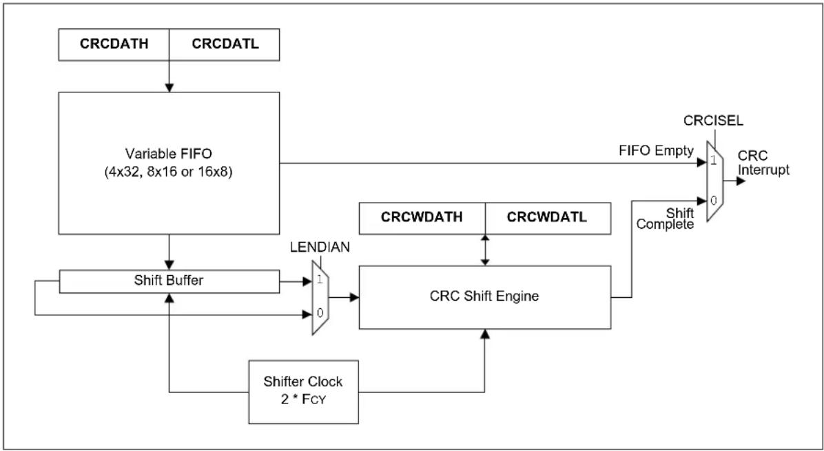
flowchart
graph TD
    A["CRCDATH"] --> B["Variable FIFO (4x32, 8x16 or 16x8)"]
    C["CRCDATL"] --> B
    B --> D["Shift Buffer"]
    D --> E["1"]
    E --> F["0"]
    F --> G["CRC Shift Engine"]
    G --> H["Shifter Clock 2 * FCY"]
    H --> D
    I["CRCWDATH"] --> G
    J["CRCWDATL"] --> G
    K["FIFO Empty"] --> L["CRCISEL"]
    L --> M["CRC Interrupt"]
    N["Shift Complete"] --> G
    O["LENDIAN"] --> F
19.1 CRC Control Registers
REGISTER 19-1: CRCCONL: CRC CONTROL REGISTER LOW
| R/W-0 U-0 R/W-0 HSC/R-0 HSC/R-0 HSC/R-0 HSC/R-0 HSC/R-0 | |||||||
| CRCEN — | CSIDL VWO | RD4 VWORD3 | VWORD2 VWORD | RD1 VWORD0 | |||
| bit 15 bit 8 | |||||||
| HSC/R-0 | HSC/R-1 | R/W-0 | HC/R/W-0 | R/W-0 | R/W-0 | U-0 | U-0 |
| CRCFUL | CRCMPT | CRCISEL | CRCGO | LENDIAN | MOD | — | — |
| bit 7 bit 0 | |||||||
| Legend: | HC = Hardware Clearable bit | HSC = Hardware Settable/Clearable bit |
| R = Readable bit | W = Writable bit | U = Unimplemented bit, read as ‘0’ |
| -n = Value at POR | ‘1’ = Bit is set | ‘0’ = Bit is cleared x = Bit is unknown |
bit 15 CRCEN: CRC Enable bit
1 = Enables module
0 = Disables module
bit 14 Unimplemented: Read as '0'
bit 13 CSIDL: CRC Stop in Idle Mode bit
1 = Discontinues module operation when device enters Idle mode
0 = Continues module operation in Idle mode
bit 12-8 VWORD[4:0]: Pointer Value bits
Indicates the number of valid words in the FIFO. Has a maximum value of 8 when PLEN[4:0] ≥ 7 or 16 when PLEN[4:0] ≤ 7 .
bit 7 CRCFUL: CRC FIFO Full bit
1 = FIFO is full
0 = FIFO is not full
bit 6 CRCMPT: CRC FIFO Empty bit
1 = FIFO is empty
0 = FIFO is not empty
bit 5 CRCISEL: CRC Interrupt Selection bit
1 = Interrupt on FIFO is empty; the final word of data is still shifting through the CRC
0 = Interrupt on shift is complete and results are ready
bit 4 CRCGO: CRC Start bit
1 = Starts CRC serial shifter
0 = CRC serial shifter is turned off
bit 3 LENDIAN: Data Shift Direction Select bit
1 = Data word is shifted into the FIFO, starting with the LSb (little-endian)
0 = Data word is shifted into the FIFO, starting with the MSb (big-endian)
bit 2 MOD: CRC Calculation Mode bit
1 = Alternate mode
0 = Legacy mode bit
bit 1-0 Unimplemented: Read as '0'
REGISTER 19-2: CRCCONH: CRC CONTROL REGISTER HIGH
| U-0 U-0 U-0 R/W-0 R/W-0 R/W-0 R/W-0 R/W-0 | |||
| — — — | DWIDTH[4:0] | ||
| bit 15 bit 8 | |||
| U-0 U-0 U-0 R/W-0 R/W-0 R/W-0 R/W-0 R/W-0 | |||
| — — — | PLEN[4:0] | ||
| bit 7 bit 0 | |||
Legend:
| R = Readable bit W = Writable bit U = Unimplemented bit, read as '0' | ||
| -n = Value at POR | '1' = Bit is set | '0' = Bit is cleared |
bit 15-13 Unimplemented: Read as '0'
bit 12-8 DWIDTH[4:0]: Data Word Width Configuration bits Configures the width of the data word (Data Word Width - 1).
bit 7-5 Unimplemented: Read as '0'
bit 4-0 PLEN[4:0]: Polynomial Length Configuration bits Configures the length of the polynomial (Polynomial Length - 1).
REGISTER 19-3: CRCXORL: CRC XOR POLYNOMIAL REGISTER, LOW BYTE
| R/W-0 R/W-0 R/W-0 R/W-0 R/W-0 R/W-0 R/W-0 R/W-0 |
| X[15:8] |
| bit 15 bit 8 |
| R/W-0 R/W-0 R/W-0 R/W-0 R/W-0 R/W-0 R/W-0 U-0 | |
| X[7:1] | — |
| bit 7 bit 0 | |
Legend:
R = Readable bit W = Writable bit U = Unimplemented bit, read as '0' -n = Value at POR '1' = Bit is set '0' = Bit is cleared x = Bit is unknown
bit 15-1 X[15:1]: XOR of Polynomial Term x^n Enable bits bit 0 Unimplemented: Read as '0'
REGISTER 19-4: CRCXORH: CRC XOR POLYNOMIAL REGISTER, HIGH BYTE
| R/W-0 R/W-0 R/W-0 R/W-0 R/W-0 R/W-0 R/W-0 R/W-0 |
| X[31:24] |
| bit 15 bit 8 |
| R/W-0 R/W-0 R/W-0 R/W-0 R/W-0 R/W-0 R/W-0 R/W-0 |
| X[23:16] |
| bit 7 bit 0 |
Legend:
R = Readable bit W = Writable bit U = Unimplemented bit, read as '0' -n = Value at POR '1' = Bit is set '0' = Bit is cleared x = Bit is unknown
bit 15-0 X[31:16]: XOR of Polynomial Term x^n Enable bits
20.0 CURRENT BIAS GENERATOR (CBG)
Note 1: This data sheet summarizes the features of the dsPIC33CH128MP508 family of devices. It is not intended to be a comprehensive reference source. To complement the information in this data sheet, refer to “Current Bias Generator (CBG)” (www.microchip.com/DS70005253), which is available from the Microchip website (www.microchip.com).
2: Some registers and associated bits described in this section may not be available on all devices. Refer to Section 3.2 "Main Memory Organization" in this data sheet for device-specific register and bit information.
The Current Bias Generator (CBG) consists of two classes of current sources: 10 A and 50 A sources. The major features of each current source are:
• 1 0 μA Current Sources:
- Current sourcing only
- Up to four independent sources
• 50 μA Current Sources:
- Selectable current sourcing or sinking
- Selectable current mirroring for sourcing and sinking
A simplified block diagram of the CBG module is shown in Figure 20-1.
TABLE 20-1: CBG CHANNEL AVAILABILITY
| Package | SRCx | IBIASx |
| 28-pin | — | IBIAS0, IBIAS1, IBIAS2 |
| 36-pin | ISRC0, ISRC1 | IBIAS0, IBIAS1, IBIAS2 |
| 48-pin | ISRC0, ISRC1, ISRC2, ISRC3 | IBIAS0, IBIAS1, IBIAS2, IBIAS3 |
| 64-pin | ISRC0, ISRC1, ISRC2, ISRC3 | IBIAS0, IBIAS1, IBIAS2, IBIAS3 |
| 80-pin | ISRC0, ISRC1, ISRC2, ISRC3 | IBIAS0, IBIAS1, IBIAS2, IBIAS3 |
FIGURE 20-1: CONSTANT-CURRENT SOURCE MODULE BLOCK DIAGRAM
(2)
10 μA Source 50 μA Source

flowchart
graph TD
    A["I10ENx"] --> B["AND"]
    B --> C["ResD(1)"]
    C --> D["ISRCx"]
    D --> E["AVDD"]
    F["ADC"] --> G["ResD(1)"]
    G --> H["AVSS"]
    H --> I["ADC"]
    J["ARC"] --> K["ResD(1)"]
    K --> L["IBIASx"]
    M["ON"] --> N["ARC"]
    O["ON"] --> P["ARC"]
    Q["ARC"] --> R["ARC"]
    S["ARC"] --> T["ARC"]
    U["ARC"] --> V["ARC"]
    W["ARC"] --> X["ARC"]
    Y["ARC"] --> Z["ARC"]
    AA["ARC"] --> AB["ARC"]
    AC["ARC"] --> AD["ARC"]
    AE["ARC"] --> AF["ARC"]
    AG["ARC"] --> AH["ARC"]
    AI["ARC"] --> AJ["ARC"]
    AK["ARC"] --> AL["ARC"]
    AM["ARC"] --> AN["ARC"]
    AO["ARC"] --> AP["ARC"]
    AQ["ARC"] --> AR["ARC"]
    AS["ARC"] --> AT["ARC"]
    AU["ARC"] --> AV["ARC"]
    AW["ARC"] --> AX["ARC"]
Note 1: RESD is typically 300 Ohms; for more information, refer to the device data sheet.
2: In Figure 20-1 only, the ADC analog input is shown for clarity. Each analog peripheral connected to the pin has a separate Electrostatic Discharge (ESD) resistor.
20.1 Current Bias Generator Control Registers
REGISTER 20-1: BIASCON: CURRENT BIAS GENERATOR CONTROL REGISTER
| R = Readable bit | W = Writable bit | U = Unimplemented bit, read as '0' |
| -n = Value at POR | '1' = Bit is set | '0' = Bit is cleared x = Bit is unknown |
bit 15 ON: Current Bias Module Enable bit
1 = Module is enabled
0 = Module is disabled
bit 14-4 Unimplemented: Read as '0'
bit 3 I10EN3: 10 μA Enable for Output 3 bit
1 = 10 μA output is enabled
0 = 10 μA output is disabled
bit 2 I10EN2: 10 μA Enable for Output 2 bit
1 = 10 μA output is enabled
0 = 10 μA output is disabled
bit 1 I10EN1: 10 μA Enable for Output 1 bit
1 = 10 μA output is enabled
0 = 10 μA output is disabled
bit 0 I10EN0: 10 μA Enable for Output 0 bit
1 = 10 μA output is enabled
0 = 10 μA output is disabled
REGISTER 20-2: IBIASCONH: CURRENT BIAS GENERATOR 50 μA CURRENT SOURCE CONTROL HIGH REGISTER
| U-0 U-0 R/W-0 R/W-0 R/W-0 R/W-0 R/W-0 R/W-0 | |||||||
| — | — | SHRSRCEN3 | SHRSNKEN3 | GENSRCEN3 | GENSNKEN3 | SRCEN3 | SNKEN3 |
| bit 15 bit 8 | |||||||
| U-0 U-0 R/W-0 R/W-0 R/W-0 R/W-0 R/W-0 R/W-0 | |||||||
| — | — | SHRSRCEN2 | SHRSNKEN2 | GENSRCEN2 | GENSNKEN2 | SRCEN2 | SNKEN2 |
| bit 7 bit 0 | |||||||
| Legend: | |||
| R = Readable bit | W = Writable bit | U = Unimplemented bit, read as ‘0’ | |
| -n = Value at POR | ‘1’ = Bit is set | ‘0’ = Bit is cleared | x = Bit is unknown |
bit 15-14 Unimplemented: Read as '0'
bit 13 SHRSRCEN3: Share Source Enable for Output #3 bit
1 = Sourcing Current Mirror mode is enabled (uses reference from another source) 0 = Sourcing Current Mirror mode is disabled
bit 12 SHRSNKEN3: Share Sink Enable for Output #3 bit
1 = Sinking Current Mirror mode is enabled (uses reference from another source) 0 = Sinking Current Mirror mode is disabled
bit 11 GENSRCEN3: Generated Source Enable for Output #3 bit
1 = Source generates the current source mirror reference 0 = Source does not generate the current source mirror reference
bit 10 GENSNKEN3: Generated Sink Enable for Output #3 bit
1 = Source generates the current source mirror reference 0 = Source does not generate the current source mirror reference
bit 9 SRCEN3: Source Enable for Output #3 bit
1 = Current source is enabled 0 = Current source is disabled
bit 8 SNKEN3: Sink Enable for Output #3 bit
1 = Current sink is enabled 0 = Current sink is disabled
bit 7-6 Unimplemented: Read as '0'
bit 5 SHRSRCEN2: Share Source Enable for Output #2 bit
1 = Sourcing Current Mirror mode is enabled (uses reference from another source) 0 = Sourcing Current Mirror mode is disabled
bit 4 SHRSNKEN2: Share Sink Enable for Output #2 bit
1 = Sinking Current Mirror mode is enabled (uses reference from another source) 0 = Sinking Current Mirror mode is disabled
bit 3 GENSRCEN2: Generated Source Enable for Output #2 bit
1 = Source generates the current source mirror reference 0 = Source does not generate the current source mirror reference
bit 2 GENSNKEN2: Generated Sink Enable for Output #2 bit
1 = Source generates the current source mirror reference 0 = Source does not generate the current source mirror reference
bit 1 SRCEN2: Source Enable for Output #2 bit
1 = Current source is enabled 0 = Current source is disabled
bit 0 SNKEN2: Sink Enable for Output #2 bit
1 = Current sink is enabled 0 = Current sink is disabled
REGISTER 20-3: IBIASCONL: CURRENT BIAS GENERATOR 50 μA CURRENT SOURCE CONTROL LOW REGISTER
| U-0 U-0 R/W-0 R/W-0 R/W-0 R/W-0 R/W-0 R/W-0 | |||||||
| — | — | SHRSRCEN1 | SHRSNKEN1 | GENSRCEN1 | GENSNKEN1 | SRCEN1 | SNKEN1 |
| bit 15 bit 8 | |||||||
| U-0 U-0 R/W-0 R/W-0 R/W-0 R/W-0 R/W-0 R/W-0 | |||||||
| — | — | SHRSRCEN0 | SHRSNKEN0 | GENSRCEN0 | GENSNKEN0 | SRCEN0 | SNKEN0 |
| bit 7 bit 0 | |||||||
Legend:
| R = Readable bit | W = Writable bit | U = Unimplemented bit, read as '0' |
| -n = Value at POR | '1' = Bit is set | '0' = Bit is cleared x = Bit is unknown |
bit 15-14 Unimplemented: Read as '0'
bit 13 SHRSRCEN1: Share Source Enable for Output #1 bit
1 = Sourcing Current Mirror mode is enabled (uses reference from another source)
0 = Sourcing Current Mirror mode is disabled
bit 12 SHRSNKEN1: Share Sink Enable for Output #1 bit
1 = Sinking Current Mirror mode is enabled (uses reference from another source)
0 = Sinking Current Mirror mode is disabled
bit 11 GENSRCEN1: Generated Source Enable for Output #1 bit
1 = Source generates the current source mirror reference
0 = Source does not generate the current source mirror reference
bit 10 GENSNKEN1: Generated Sink Enable for Output #1 bit
1 = Source generates the current source mirror reference
0 = Source does not generate the current source mirror reference
bit 9 SRCEN1: Source Enable for Output #1 bit
1 = Current source is enabled
0 = Current source is disabled
bit 8 SNKEN1: Sink Enable for Output #1 bit
1 = Current sink is enabled
0 = Current sink is disabled
bit 7-6 Unimplemented: Read as '0'
bit 5 SHRSRCENO: Share Source Enable for Output #0 bit
1 = Sourcing Current Mirror mode is enabled (uses reference from another source)
0 = Sourcing Current Mirror mode is disabled
bit 4 SHRSNKEN0: Share Sink Enable for Output #0 bit
1 = Sinking Current Mirror mode is enabled (uses reference from another source)
0 = Sinking Current Mirror mode is disabled
bit 3 GENSRCENO: Generated Source Enable for Output #0 bit
1 = Source generates the current source mirror reference
0 = Source does not generate the current source mirror reference
bit 2 GENSNKEN0: Generated Sink Enable for Output #0 bit
1 = Source generates the current source mirror reference
0 = Source does not generate the current source mirror reference
bit 1 SRCENO: Source Enable for Output #0 bit
1 = Current source is enabled
0 = Current source is disabled
bit 0 SNKEN0: Sink Enable for Output #0 bit
1 = Current sink is enabled
0 = Current sink is disabled
NOTES:
21.0 SPECIAL FEATURES
Note: This data sheet summarizes the features of the dsPIC33CH128MP508 family of devices. It is not intended to be a comprehensive reference source. To complement the information in this data sheet, refer to the related section of the "dsPIC33/PIC24 Family Reference Manual", which is available from the Microchip website (www.microchip.com).
The dsPIC33CH128MP508 family devices include several features intended to maximize application flexibility and reliability, and minimize cost through elimination of external components. These are:
- Flexible Configuration
- Watchdog Timer (WDT)
• Code Protection and CodeGuard™ Security
• JTAG Boundary Scan Interface
• In-Circuit Serial Programming (ICSP)
• In-Circuit Emulation - Brown-out Reset (BOR)
21.1 Configuration Bits
In dsPIC33CH128MP508 family devices, the Configuration Words are implemented as volatile memory. This means that configuration data will get loaded to volatile memory (from the Flash Configuration Words) each time the device is powered up. Configuration data are stored at the end of the on-chip program memory space, known as the Flash Configuration Words. Their specific locations are shown in Table 21-1. The configuration data are automatically loaded from the Flash Configuration Words to the proper Configuration Shadow registers during device Resets.
Note: Configuration data are reloaded on all types of device Main Resets. Secondary Resets do not load the Configuration registers. It is recommended not to change the Secondary Configuration register without resetting the Secondary along with the Main (S1MSRE = 1).
When creating applications for these devices, users should always specifically allocate the location of the Flash Configuration Words for configuration data in their code for the compiler. This is to make certain that program code is not stored in this address when the code is compiled. Program code executing out of configuration space will cause a device Reset. The Main code, as well as the Secondary code, are located in Flash memory. Table 21-1 shows the Main and the Secondary Configuration registers and their address locations in Flash memory.
Secondary Configuration bits are located in the Main Flash and loaded during a Main Reset.
Note: Performing a page erase operation on the last page of program memory clears the Flash Configuration Words.
TABLE 21-1: CONFIGURATION WORD ADDRESSES
| Register 64k Address 128k Address | ||
| Main/General Configuration Registers | ||
| FSEC 00AF00 | 015F00 | |
| FBSLIM | 00AF10 | 015F10 |
| FSIGN | 00AF14 | 015F14 |
| FOSCSEL | 00AF18 | 015F18 |
| FOSC | 00AF1C | 015F1C |
| FWDT | 00AF20 | 015F20 |
| FPOR | 00AF24 | 015F24 |
| FICD | 00AF28 | 015F28 |
| FDMTIVTL | 00AF2C | 015F2C |
| FDMTIVTH | 00AF30 | 015F30 |
| FDMTCNTL | 00AF34 | 015F34 |
| FDMTCNTH | 00AF38 | 015F38 |
| FDMT | 00AF3C | 015F3C |
| FDEVOPT | 00AF40 | 015F40 |
| FALTREG | 00AF44 | 015F44 |
| FMBXM | 00AF48 | 015F48 |
| FMBXHS1 | 00AFC4 | 015F4C |
| FMBXHS2 | 00AF50 | 015F50 |
| FMBXHSEN | 00AF54 | 015F54 |
| FCFGPRA0 | 00AF58 | 015F58 |
| FCFGPRB0 | 00AF60 | 015F60 |
| FCFGPRC0 | 00AF68 | 015F68 |
| FCFGPRD0 | 00AF70 | 015F70 |
| FCFGPRE0 | 00AF78 | 015F7C |
| Secondary Configuration Registers | ||
| FS1OSCSEL | 00AF80 | 015F80 |
| FS1OSC | 00AF84 | 015F84 |
| FS1WDT | 00AF88 | 015F88 |
| FS1POR | 00AF8C | 015F8C |
| FS1ICD | 00AF90 | 015F90 |
| FS1DEVOPT | 00AF94 | 015F94 |
| FS1ALTREG | 00AF98 | 015F98 |
TABLE 21-2: MAIN CONFIGURATION REGISTERS MAP
| Register Name | Bits 23-16 | Bit 15 | Bit 14 | Bit 13 | Bit 12 | Bit 11 | Bit 10 | Bit 9 | Bit 8 | Bit 7 | Bit 6 | Bit 5 | Bit 4 | Bit 3 | Bit 2 | Bit 1 | Bit 0 |
| FSEC | — | AIVTDIS | — | — | — | CSS[2:0] | CWRP | GSS[1:0] | GWRP | — | BSEN | BSS[1:0] | BWRP | ||||
| FBSLIM | — | — | — | — | BSLIM[12:0] | ||||||||||||
| FSIGN | — | r(2) | — | — | — | — | — | — | — | — | — | — | — | — | — | — | — |
| FOSCSEL | — | — | — | — | — | — | — | — | — | IESO | — | — | — | — | FNOSC[2:0] | ||
| FOSC | — | — | — | — | XTBST | XTCFG[1:0] | — | r(1) | FCKSM[1:0] | — | — | — | OSCIOFNC | POSCMD[1:0] | |||
| FWDT | — | FWDTEN | SWDTPS[4:0] | WDTWIN[1:0] | WINDIS | RCLKSEL[1:0] | RWDTPS[4:0] | ||||||||||
| FPOR | — | — | — | — | — | — | — | — | — | — | — | r(1) | r(1) | — | — | — | — |
| FICD | — | — | — | — | — | — | — | — | — | r(1) | — | JTAGEN | — | — | — | ICS[1:0] | |
| FDMTIVTL | — | DMTIVT[15:0] | |||||||||||||||
| FDMTIVTH | — | DMTIVT[31:16] | |||||||||||||||
| FDMTCNTL | — | DMTCNT[15:0] | |||||||||||||||
| FDMTCNTH | — | DMTCNT[31:16] | |||||||||||||||
| FDMT | — | — | — | — | — | — | — | — | — | — | — | — | — | — | — | — | DMTDIS |
| FDEVOPT | — | — | — | SP/2PIN | — | — | SMBEN | r(1) | r(1) | r(1) | — | — | ALTI2C[2:1] | r(1) | — | — | — |
| FALTREG | — | — | CTXT4[2:0] | — | CTXT3[2:0] | — | CTXT2[2:0] | — | CTXT1[2:0] | ||||||||
| FMBXM | — | MBXM[15:0] | |||||||||||||||
| FMBXHS1 | — | MBXHSD[3:0] | MBXHSC[3:0] | MBXHSB[3:0] | MBXHSA[3:0] | ||||||||||||
| FMBXHS2 | — | MBXHSH[3:0] | MBXHSG[3:0] | MBXHSF[3:0] | MBXHSE[3:0] | ||||||||||||
| FMBXHSEN | — | — | — | — | — | — | — | — | — | HS[H:A]EN | |||||||
| FCFGPRAO | — | — | — | — | — | — | — | — | — | — | — | — | CPRA[4:0] | ||||
| FCFGPRBO | — | CPRB[15:0] | |||||||||||||||
| FCFGPRCO | — | CPRC[15:0] | |||||||||||||||
| FCFGPRDO | — | CPRD[15:0] | |||||||||||||||
| FCFGPREO | — | CPRE[15:0] | |||||||||||||||
Legend: — = unimplemented bit, read as '1'; r = reserved bit.
Note 1: Bit is reserved, maintain as 'a'.
2: Bit is reserved, maintain as '0'.
TABLE 21-3: SECONDARY CONFIGURATION REGISTERS MAP
Legend: — = unimplemented bit, read as '1'; r = reserved bit.
Note 1: Bit is reserved, maintain as
2: Only valid in Dual Debug mode.
REGISTER 21-1: FSEC CONFIGURATION REGISTER
| U-1 U-1 U-1 U-1 U-1 U-1 U-1 | |||||||
| —— | —— | —— | |||||
| bit 23 bit 16 | |||||||
| R/PO-1 U-1 U-1 U-1 R/PO-1 R/PO-1 R/PO-1 R/PO-1 | |||||||
| AIVTDIS | — — — | CSS2 CSS1 C | SS0 CWRP | ||||
| bit 15 bit 8 | |||||||
| R/PO-1 R/PO-1 R/PO-1 U-1 R/PO-1 R/PO-1 R/PO-1 R/PO-1 | |||||||
| GSS1 | GSS0 | GWRP | — | BSEN BSS1 | BSS0 | BWRP | |
| bit 7 bit 0 | |||||||
| Legend: | PO = Program Once bit | ||
| R = Readable bit | W = Writable bit | U = Unimplemented bit, read as ‘0’ | |
| -n = Value at POR | ‘1’ = Bit is set | ‘0’ = Bit is cleared | x = Bit is unknown |
bit 23-16 Unimplemented: Read as '1'
bit 15 AIVTDIS: Alternate Interrupt Vector Table Disable bit
1 = Disables AIVT 0 = Enables AIVT
bit 14-12 Unimplemented: Read as '1'
bit 11-9 CSS[2:0]: Configuration Segment Code Flash Protection Level bits
111 = No protection (other than CWRP write protection) 110 = Standard security 10x = Enhanced security 0xx = High security
bit 8 CWRP: Configuration Segment Write-Protect bit 1 = Configuration Segment is not write-protected 0 = Configuration Segment is write-protected
bit 7-6 GSS[1:0]: General Segment Code Flash Protection Level bits 11 = No protection (other than GWRP write protection) 10 = Standard security 0x = High security
bit 5 GWRP: General Segment Write-Protect bit 1 = User program memory is not write-protected 0 = User program memory is write-protected
bit 4 Unimplemented: Read as '1'
bit 3 BSEN: Boot Segment Control bit 1 = No Boot Segment 0 = Boot Segment size is determined by BSLIM[12:0]
bit 2-1 BSS[1:0]: Boot Segment Code Flash Protection Level bits 11 = No protection (other than BWRP write protection) 10 = Standard security 0x = High security
bit 0 BWRP: Boot Segment Write-Protect bit 1 = User program memory is not write-protected 0 = User program memory is write-protected
REGISTER 21-2: FBSLIM CONFIGURATION REGISTER
| U-1 U-1 U-1 U-1 U-1 U-1 U-1 | |||||||
| —— | —— | —— | |||||
| bit 23 bit 16 | |||||||
| U-1 U-1 U-1 R/PO-1 R/PO-1 R/PO-1 R/PO-1 R/PO-1 | |||
| — — — | BSLIM[12:8] | ||
| bit 15 bit 8 | |||
| R/PO-1 R/PO-1 R/PO-1 R/PO-1 R/PO-1 R/PO-1 R/PO-1 |
| BSLIM[7:0] |
| bit 7 bit 0 |
| Legend: | PO = Program Once bit | ||
| R = Readable bit | W = Writable bit | U = Unimplemented bit, read as ‘0’ | |
| -n = Value at POR | ‘1’ = Bit is set | ‘0’ = Bit is cleared | x = Bit is unknown |
bit 23-13 Unimplemented: Read as '1'
bit 12-0 BSLIM[12:0]: Boot Segment Code Flash Page Address Limit bits
Contains the page address of the first active General Segment page. The value to be programmed is the inverted page address, such that programming additional '0's can only increase the Boot Segment size.
REGISTER 21-3: FSIGN CONFIGURATION REGISTER
| U-1 U-1 U-1 U-1 U-1 U-1 U-1 | |||||||
| —— | —— | —— | |||||
| bit 23 bit 16 | |||||||
| r-0 U-1 U-1 U-1 U-1 U-1 U-1 | |||||||
| —— | —— | —— | |||||
| bit 15 bit 8 | |||||||
| U-1 U-1 U-1 U-1 U-1 U-1 U-1 U-1 | |||||||
| —— | —— | —— | |||||
| bit 7 bit 0 | |||||||
| Legend: | r = Reserved bit | PO = Program Once bit |
| R = Readable bit | W = Writable bit | U = Unimplemented bit, read as ‘0’ |
| -n = Value at POR | ‘1’ = Bit is set | ‘0’ = Bit is cleared x = Bit is unknown |
bit 23-16 Unimplemented: Read as '1'
bit 15 Reserved: Maintain as '0'
bit 14-0 Unimplemented: Read as '1'
REGISTER 21-4: FOSCSEL CONFIGURATION REGISTER
| U-1 U-1 U-1 U-1 U-1 U-1 U-1 | |||||||
| —— | —— | —— | |||||
| bit 23 bit 16 | |||||||
| U-1 U-1 U-1 U-1 U-1 U-1 U-1 U-1 | |||||||
| —— | —— | —— | |||||
| bit 15 bit 8 | |||||||
| R/PO-1 U-1 U-1 U-1 R/PO-1 R/PO-1 R/PO-1 | |||||
| IESO | — — — | — | F | N O | |
| bit 7 bit 0 | |||||
| Legend: PO = Program Once bit | |||
| R = Readable bit W = Writable bit | U = Unimplemented bit, read as '0' | ||
| -n = Value at POR | '1' = Bit is set | '0' = Bit is cleared | x = Bit is unknown |
bit 23-8 Unimplemented: Read as '1'
bit 7 IESO: Internal External Switchover bit
1 = Internal External Switchover mode is enabled (Two-Speed Start-up is enabled)
0 = Internal External Switchover mode is disabled (Two-Speed Start-up is disabled)
bit 6-3 Unimplemented: Read as '1'
bit 2-0 FNOSC[2:0]: Initial Oscillator Source Selection bits
111 = Internal Fast RC (FRC) Oscillator with Postscaler
110 = Backup Fast RC (BFRC)
101 = LPRC Oscillator
100 = Reserved
011 = Primary Oscillator with PLL (XTPLL, HSPLL, ECPLL)
010 = Primary (XT, HS, EC) Oscillator
001 = Internal Fast RC Oscillator with PLL (FRCPLL)
000 = Fast RC (FRC) Oscillator
REGISTER 21-5: FOSC CONFIGURATION REGISTER
| U-1 U-1 U-1 U-1 U-1 U-1 U-1 | |||||||
| —— | —— | —— | |||||
| bit 23 bit 16 | |||||||
| U-1 | U-1 | U-1 | R/PO-1 | R/PO-1 | R/PO-1 | U-1 | r-1 |
| — — — | XTBST | XTCFG1 | XTCFG0 | — | — | ||
| bit 15 bit 8 | |||||||
| R/PO-1 | R/PO-1 | U-1 | U-1 | U-1 | R/PO-1 | R/PO-1 | R/PO-1 |
| FCKSM1 | FCKSM0 | — — — | OSCIOFNC(1) | POSCMD1 | POSCMD0 | ||
| bit 7 bit 0 | |||||||
| Legend: | PO = Program Once bit | r = Reserved bit | |
| R = Readable bit | W = Writable bit | U = Unimplemented bit, read as '0' | |
| -n = Value at POR | '1' = Bit is set | '0' = Bit is cleared | x = Bit is unknown |
bit 23-13 Unimplemented: Read as '1'
bit 12 XTBST: Oscillator Kick-Start Programmability bit
1 = Boosts the kick-start and maintains an increased drive strength of the crystal in addition to gain selected by XTCFG[1:0]
0 = Default kick-start
bit 11-10 XTCFG[1:0]: Crystal Oscillator Drive Select bits
Current gain programmability for oscillator (output drive).
11 = Gain3 (use for 24-32 MHz crystals)
1.0 = Gain2 (use for 16-24 MHz crystals)
01 = Gain1 (use for 8-16 MHz crystals)
00 = Gain0 (use for 4-8 MHz crystals)
bit 9 Unimplemented: Read as '1'
bit 8 Reserved: Maintain as '1'
bit 7-6 FCKSM[1:0]: Clock Switching Mode bits
1x = Clock switching is disabled, Fail-Safe Clock Monitor is disabled
01 = Clock switching is enabled, Fail-Safe Clock Monitor is disabled
00 = Clock switching is enabled, Fail-Safe Clock Monitor is enabled
bit 5-3 Unimplemented: Read as '1'
bit 2 OSCIOFNC: OSCO Pin Function bit (except in XT and HS modes) ^(1)
1 = OSCO is the clock output
0 = OSCO is the general purpose digital I/O pin
bit 1-0 POSCMD[1:0]: Primary Oscillator Mode Select bits
11 = Primary Oscillator is disabled
10 = HS Crystal Oscillator mode (10 MHz-32 MHz)
01 = XT Crystal Oscillator mode (3.5 MHz-10 MHz)
00 = EC (External Clock) mode
Note 1: The OSCO pin function is determined by the S1OSCIOFNC Configuration bit. If both the Main core OSCIOFNC and Secondary core S1OSCIOFNC bits are set, the Main core OSCIOFNC bit has priority.
REGISTER 21-6: FWDT CONFIGURATION REGISTER
| U-1 U-1 U-1 U-1 U-1 U-1 U-1 | |||||||
| —— | —— | —— | |||||
| bit 23 bit 16 | |||||||
| R/PO-1 R/PO-1 R/PO-1 R/PO-1 R/PO-1 R/PO-1 R/PO-1 R/PO-1 | |||||||
| FWDTEN SW | WDTPS4 SWD | TPS3 SWDTP | S2 SWDTPS1 | SWDTPS0 WD | TWIN1 WDTV | VIN0 | |
| bit 15 bit 8 | |||||||
| R/PO-1 R/PO-1 R/PO-1 R/PO-1 R/PO-1 R/PO-1 R/PO-1 | |||||||
| WINDIS | RCLKSEL1 | RCLKSEL0 | RWDTPS4 | RWDTPS3 | RWDTPS2 | RWDTPS1 | RWDTPS0 |
| bit 7 bit 0 | |||||||
| Legend: | PO = Program Once bit | ||
| R = Readable bit | W = Writable bit | U = Unimplemented bit, read as ‘0’ | |
| -n = Value at POR | ‘1’ = Bit is set | ‘0’ = Bit is cleared | x = Bit is unknown |
bit 23-16 Unimplemented: Read as '1'
bit 15 FWDTEN: Watchdog Timer Enable bit
1 = WDT is enabled in hardware
0 = WDT controller via the ON bit (WDTCONL[15])
bit 14-10 SWDTPS[4:0]: Sleep Mode Watchdog Timer Period Select bits
11111 = Divide by 2^31 = 2,147,483,648
11110 = Divide by 2^30 = 1,073,741,824
...
00001 = Divide by 2^1 = 2
00000 = Divide by 2^0 = 1
bit 9-8 WDTWIN[1:0]: Watchdog Timer Window Select bits
11 = WDT window is 25% of the WDT period
10 = WDT window is 37.5% of the WDT period
01 = WDT window is 50% of the WDT period
00 = WDT Window is 75% of the WDT period
bit 7 WINDIS: Watchdog Timer Window Enable bit
1 = Watchdog Timer is in Non-Window mode
0 = Watchdog Timer is in Window mode
bit 6-5 RCLKSEL[1:0]: Watchdog Timer Clock Select bits
11 = LPRC clock
10 = Uses FRC when WINDIS = 0, system clock is not INTOSC/LPRC and device is not in Sleep; otherwise, uses INTOSC/LPRC
01 = Uses peripheral clock when system clock is not INTOSC/LPRC and device is not in Sleep; otherwise, uses INTOSC/LPRC
00 = Reserved
bit 4-0 RWDTPS[4:0]: Run Mode Watchdog Timer Period Select bits
11111 = Divide by 2^31 = 2,147,483,648
11110 = Divide by 2^30 = 1,073,741,824
+ + +
00001 = Divide by 2^1 = 2
00000 = Divide by 2^0 = 1
REGISTER 21-7: FPOR CONFIGURATION REGISTER
| U-1 U-1 U-1 U-1 U-1 U-1 U-1 | |||||||
| —— | —— | —— | |||||
| bit 23 bit 16 | |||||||
| U-1 U-1 U-1 U-1 U-1 U-1 U-1 | |||||||
| —— | —— | —— | |||||
| bit 15 bit 8 | |||||||
| U-1 U-1 r-1 r-1 U-1 U-1 U-1 U-1 | |||||||
| ——— | ——— —— | ||||||
| bit 7 bit 0 | |||||||
| Legend: PO = Program Once bit r = Reserved bit | |||
| R = Readable bit | W = Writable bit | U = Unimplemented bit, read as '0' | |
| -n = Value at POR | '1' = Bit is set | '0' = Bit is cleared | x = Bit is unknown |
bit 23-6 Unimplemented: Read as '1'
bit 5-4 Reserved: Maintain as '1'
bit 3-0 Unimplemented: Read as '1'
REGISTER 21-8: FICD CONFIGURATION REGISTER
| U-1 U-1 U-1 U-1 U-1 U-1 U-1 | |||||||
| —— | —— | —— | |||||
| bit 23 bit 16 | |||||||
| U-1 U-1 U-1 U-1 U-1 U-1 U-1 U-1 | |||||||
| —— | —— | —— | |||||
| bit 15 bit 8 | |||||||
| r-1 U-1 R/PO-1 U-1 U-1 U-1 R/PO-1 R/PO-1 | |||||||
| — — | J | T | A | G | E | N | — — ICS1 ICS0 |
| bit 7 bit 0 | |||||||
| Legend: | PO = Program Once bit | r = Reserved bit | |
| R = Readable bit | W = Writable bit | U = Unimplemented bit, read as ‘0’ | |
| -n = Value at POR | ‘1’ = Bit is set | ‘0’ = Bit is cleared | x = Bit is unknown |
bit 23-8 Unimplemented: Read as '1'
bit 7 Reserved: Maintain as '1'
bit 6 Unimplemented: Read as '1'
bit 5 JTAGEN: JTAG Enable bit
1 = JTAG port is enabled
0 = JTAG port is disabled
bit 4-2 Unimplemented: Read as '1'
bit 1-0 ICS[1:0]: ICD Communication Channel Select bits
11 = Main communicates on PGC1 and PGD1
10 = Main communicates on PGC2 and PGD2
01 = Main communicates on PGC3 and PGD3
00 = Reserved, do not use
REGISTER 21-9: FDMTIVTL CONFIGURATION REGISTER
| U-1 U-1 U-1 U-1 U-1 U-1 U-1 | |||||||
| —— | —— | —— | |||||
| bit 23 bit 16 | |||||||
| R/PO-1 R/PO-1 R/PO-1 R/PO-1 R/PO-1 R/PO-1 R/PO-1 |
| DMTIVT[15:8] |
| bit 15 bit 8 |
| R/PO-1 R/PO-1 R/PO-1 R/PO-1 R/PO-1 R/PO-1 R/PO-1 |
| DMTIVT[7:0] |
| bit 7 bit 0 |
| Legend: PO = Program Once bit | |||
| R = Readable bit W = Writable bit U = Unimplemented bit, read as '0' | |||
| -n = Value at POR | '1' = Bit is set | '0' = Bit is cleared | x = Bit is unknown |
bit 23-16 Unimplemented: Read as '1'
bit 15-0 DMTIVT[15:0]: DMT Window Interval Lower 16 bits
REGISTER 21-10: FDMTIVTH CONFIGURATION REGISTER
| U-1 U-1 U-1 U-1 U-1 U-1 U-1 | |||||||
| —— | ——— | ||||||
| bit 23 bit 16 | |||||||
| R/PO-1 R/PO-1 R/PO-1 R/PO-1 R/PO-1 R/PO-1 R/PO-1 |
| DMTIVT[31:24] |
| bit 15 bit 8 |
| R/PO-1 R/PO-1 R/PO-1 R/PO-1 R/PO-1 R/PO-1 R/PO-1 |
| DMTIVT[23:16] |
| bit 7 bit 0 |
| Legend: PO = Program Once bit | |||
| R = Readable bit W = Writable bit U = Unimplemented bit, read as '0' | |||
| -n = Value at POR | '1' = Bit is set | '0' = Bit is cleared | x = Bit is unknown |
bit 23-16 Unimplemented: Read as '1'
bit 15-0 DMTIVT[31:16]: DMT Window Interval Higher 16 bits
REGISTER 21-11: FDMTCNTL CONFIGURATION REGISTER
| U-1 U-1 U-1 U-1 U-1 U-1 U-1 | |||||||
| —— | —— | —— | |||||
| bit 23 bit 16 | |||||||
| R/PO-1 R/PO-1 R/PO-1 R/PO-1 R/PO-1 R/PO-1 R/PO-1 |
| DMTCNT[15:8] |
| bit 15 bit 8 |
| R/PO-1 R/PO-1 R/PO-1 R/PO-1 R/PO-1 R/PO-1 R/PO-1 |
| DMTCNT[7:0] |
| bit 7 bit 0 |
| Legend: PO = Program Once bit | |||
| R = Readable bit W = Writable bit | U = Unimplemented bit, read as ‘0’ | ||
| -n = Value at POR | ‘1’ = Bit is set | ‘0’ = Bit is cleared | x = Bit is unknown |
bit 23-16 Unimplemented: Read as '1'
bit 15-0 DMTCNT[15:0]: DMT Instruction Count Time-out Value Lower 16 bits
REGISTER 21-12: FDMTCNTH CONFIGURATION REGISTER
| U-1 U-1 U-1 U-1 U-1 U-1 U-1 | |||||||
| —— | ——— | ||||||
| bit 23 bit 16 | |||||||
| R/PO-1 R/PO-1 R/PO-1 R/PO-1 R/PO-1 R/PO-1 R/PO-1 |
| DMTCNT[31:24] |
| bit 15 bit 8 |
| R/PO-1 R/PO-1 R/PO-1 R/PO-1 R/PO-1 R/PO-1 R/PO-1 |
| DMTCNT[23:16] |
| bit 7 bit 0 |
| Legend: PO = Program Once bit | |||
| R = Readable bit W = Writable bit | U = Unimplemented bit, read as ‘0’ | ||
| -n = Value at POR | ‘1’ = Bit is set | ‘0’ = Bit is cleared | x = Bit is unknown |
bit 23-16 Unimplemented: Read as '1'
bit 15-0 DMTCNT[31:16]: DMT Instruction Count Time-out Value Upper 16 bits
REGISTER 21-13: FDMT CONFIGURATION REGISTER
| U-1 U-1 U-1 U-1 U-1 U-1 U-1 | |||||||
| —— | —— | —— | |||||
| bit 23 bit 16 | |||||||
| U-1 U-1 U-1 U-1 U-1 U-1 U-1 | |||||||
| —— | —— | —— | |||||
| bit 15 bit 8 | |||||||
| U-1 U-1 U-1 U-1 U-1 U-1 R/PO-1 | ||||||||
| ——— | ——— | D | M | T | D | I | S | |
| bit 7 bit 0 | ||||||||
| Legend: PO = Program Once bit | |||
| R = Readable bit | W = Writable bit | U = Unimplemented bit, read as '0' | |
| -n = Value at POR | '1' = Bit is set | '0' = Bit is cleared | x = Bit is unknown |
bit 23-1 Unimplemented: Read as '1'
bit 0 DMTDIS: DMT Disable bit
1 = DMT is disabled and can be enabled by software using ON bit (DMTCON<15>)
0 = DMT is enabled and cannot be disabled by software
REGISTER 21-14: FDEVOPT CONFIGURATION REGISTER
| U-1 U-1 U-1 U-1 U-1 U-1 U-1 | |||||||
| — — — | — — — — | — | |||||
| bit 23 bit 16 | |||||||
| U-1 | U-1 | R/PO-1 | U-1 | U-1 | R/PO-1 | r-1 | r-1 |
| — — | SPI2PIN | (1) | — | — | SMBEN | — | — |
| bit 15 bit 8 | |||||||
| r-1 U-1 U-1 | R/PO-1 | R/PO-1 | r-1 U-1 U-1 | |||||
| — | — | — | — | ALTI2C2 | — | — | — | — |
| bit 7 bit 0 | ||||||||
| Legend: | PO = Program Once bit | r = Reserved bit | |
| R = Readable bit | W = Writable bit | U = Unimplemented bit, read as '0' | |
| -n = Value at POR | '1' = Bit is set | '0' = Bit is cleared | x = Bit is unknown |
bit 23-14 Unimplemented: Read as '1'
bit 13 SPI2PIN: Main SPI #2 Fast I/O Pad Disable bit ^(1)
1 = Main SPI2 uses PPS (I/O remap) to make connections with device pins
0 = Main SPI2 uses direct connections with specified device pins
bit 12-11 Unimplemented: Read as '1'
bit 10 SMBEN: Select Input Voltage Threshold for I²C Pads to be SMBus 3.0 Compliant bit
1 = Enables SMBus 3.0 input threshold voltage
0 = I²C pad input buffer operation
bit 9-7 Reserved: Maintain as '1'
bit 6-5 Unimplemented: Read as '1'
bit 4 ALTI2C2: Alternate I2C2 Pin Mapping bit
1 = Default location for SCL2/SDA2 pins
0 = Alternate location for SCL2/SDA2 pins (ASCL2/ASDA2)
bit 3 ALTI2C1: Alternate I2C1 Pin Mapping bit
1 = Default location for SCL1/SDA1 pins
0 = Alternate location for SCL1/SDA1 pins (ASCL1/ASDA1)
bit 2 Reserved: Maintain as '1'
bit 1-0 Unimplemented: Read as '1'
Note 1: Fixed pin option is only available for higher pin packages (48-pin, 64-pin and 80-pin).
REGISTER 21-15: FALTREG CONFIGURATION REGISTER
| U-1 U-1 U-1 U-1 U-1 U-1 U-1 | |||||||
| —— | —— | —— | |||||
| bit 23 bit 16 | |||||||
| U-1 R/PO-1 R/PO-1 R/PO-1 U-1 R/PO-1 R/PO-1 R/PO-1 | ||
| — CTXT4[2:0] — CTXT3[2:0] | ||
| bit 15 bit 8 | ||
| U-1 R/PO-1 R/PO-1 R/PO-1 U-1 R/PO-1 R/PO-1 R/PO-1 | ||
| — CTXT2[2:0] — CTXT1[2:0] | ||
| bit 7 bit 0 | ||
| Legend: | PO = Program Once bit | ||
| R = Readable bit | W = Writable bit | U = Unimplemented bit, read as '0' | |
| -n = Value at POR | '1' = Bit is set | '0' = Bit is cleared | x = Bit is unknown |
bit 23-15 Unimplemented: Read as '1'
bit 14-12 CTXT4[2:0]: Specifies the Alternate Working Register Set #4 with Interrupt Priority Levels (IPL) bits 111 = Not assigned
110 = Alternate Register Set #4 is assigned to IPL Level 7
101 = Alternate Register Set #4 is assigned to IPL Level 6
100 = Alternate Register Set #4 is assigned to IPL Level 5
011 = Alternate Register Set #4 is assigned to IPL Level 4
010 = Alternate Register Set #4 is assigned to IPL Level 3
001 = Alternate Register Set #4 is assigned to IPL Level 2
000 = Alternate Register Set #4 is assigned to IPL Level 1
bit 11 Unimplemented: Read as '1'
bit 10-8 CTXT3[2:0]: Specifies the Alternate Working Register Set #3 with Interrupt Priority Levels (IPL) bits 111 = Not assigned
110 = Alternate Register Set #3 is assigned to IPL Level 7
101 = Alternate Register Set #3 is assigned to IPL Level 6
100 = Alternate Register Set #3 is assigned to IPL Level 5
011 = Alternate Register Set #3 is assigned to IPL Level 4
010 = Alternate Register Set #3 is assigned to IPL Level 3
001 = Alternate Register Set #3 is assigned to IPL Level 2
000 = Alternate Register Set #3 is assigned to IPL Level 1
bit 7 Unimplemented: Read as '1'
bit 6-4 CTXT2[2:0]: Specifies the Alternate Working Register Set #2 with Interrupt Priority Levels (IPL) bits 111 = Not assigned
110 = Alternate Register Set #2 is assigned to IPL Level 7
101 = Alternate Register Set #2 is assigned to IPL Level 6
100 = Alternate Register Set #2 is assigned to IPL Level 5
011 = Alternate Register Set #2 is assigned to IPL Level 4
010 = Alternate Register Set #2 is assigned to IPL Level 3
001 = Alternate Register Set #2 is assigned to IPL Level 2
000 = Alternate Register Set #2 is assigned to IPL Level 1
bit 3 Unimplemented: Read as '1'
REGISTER 21-15: FALTREG CONFIGURATION REGISTER (CONTINUED)
bit 2-0 CTXT1[2:0]: Specifies the Alternate Working Register Set #1 with Interrupt Priority Levels (IPL) bits
111 = Not assigned
110 = Alternate Register Set #1 is assigned to IPL Level 7
101 = Alternate Register Set #1 is assigned to IPL Level 6
100 = Alternate Register Set #1 is assigned to IPL Level 5
011 = Alternate Register Set #1 is assigned to IPL Level 4
010 = Alternate Register Set #1 is assigned to IPL Level 3
001 = Alternate Register Set #1 is assigned to IPL Level 2
000 = Alternate Register Set #1 is assigned to IPL Level 1
REGISTER 21-16: FMBXM CONFIGURATION REGISTER
| U-1 U-1 U-1 U-1 U-1 U-1 U-1 | |||||||
| —— | —— | —— | |||||
| bit 23 bit 16 | |||||||
| R/PO-1 R/PO-1 R/PO-1 R/PO-1 R/PO-1 R/PO-1 R/PO-1 R/PO-1 | ||||||||
| MBXM15 M | BXM14 MBXM | 13 MBXM12 M | BXM11 MBXM | 10 | MBXM | 9 | MBXM | 8 |
| bit 15 bit 8 | ||||||||
| R/PO-1 R/PO-1 R/PO-1 R/PO-1 R/PO-1 R/PO-1 R/PO-1 | |||||||
| MBXM7 | MBXM6 | MBXM5 | MBXM4 | MBXM3 | MBXM2 | MBXM1 | MBXM0 |
| bit 7 bit 0 | |||||||
| Legend: | PO = Program Once bit | ||
| R = Readable bit | W = Writable bit | U = Unimplemented bit, read as ‘0’ | |
| -n = Value at POR | ‘1’ = Bit is set | ‘0’ = Bit is cleared | x = Bit is unknown |
bit 23-16 Unimplemented: Read as '1'
bit 15 MBXM15: Mailbox Data Register Channel Direction Fuses bits
1 = Mailbox Register #15 is configured for Main data read (Secondary to Main data transfer)
0 = Mailbox Register #15 is configured for Main data write (Main to Secondary data transfer)
bit 14 MBXM14: Mailbox Data Register Channel Direction Fuses bits
1 = Mailbox Register #14 is configured for Main data read (Secondary to Main data transfer)
0 = Mailbox Register #14 is configured for Main data write (Main to Secondary data transfer)
bit 13 MBXM13: Mailbox Data Register Channel Direction Fuses bits
1 = Mailbox Register #13 is configured for Main data read (Secondary to Main data transfer)
0 = Mailbox Register #13 is configured for Main data write (Main to Secondary data transfer)
bit 12 MBXM12: Mailbox Data Register Channel Direction Fuses bits
1 = Mailbox Register #12 is configured for Main data read (Secondary to Main data transfer)
0 = Mailbox Register #12 is configured for Main data write (Main to Secondary data transfer)
bit 11 MBXM11: Mailbox Data Register Channel Direction Fuses bits
1 = Mailbox Register #11 is configured for Main data read (Secondary to Main data transfer)
0 = Mailbox Register #11 is configured for Main data write (Main to Secondary data transfer)
bit 10 MBXM10: Mailbox Data Register Channel Direction Fuses bits
1 = Mailbox Register #10 is configured for Main data read (Secondary to Main data transfer)
0 = Mailbox Register #10 is configured for Main data write (Main to Secondary data transfer)
REGISTER 21-16: FMBXM CONFIGURATION REGISTER (CONTINUED)
| bit 9 | MBXM9: Mailbox Data Register Channel Direction Fuses bits1 = Mailbox Register #9 is configured for Main data read (Secondary to Main data transfer)0 = Mailbox Register #9 is configured for Main data write (Main to Secondary data transfer) |
| bit 8 | MBXM8: Mailbox Data Register Channel Direction Fuses bits1 = Mailbox Register #8 is configured for Main data read (Secondary to Main data transfer)0 = Mailbox Register #8 is configured for Main data write (Main to Secondary data transfer) |
| bit 7 | MBXM7: Mailbox Data Register Channel Direction Fuses bits1 = Mailbox Register #7 is configured for Main data read (Secondary to Main data transfer)0 = Mailbox Register #7 is configured for Main data write (Main to Secondary data transfer) |
| bit 6 | MBXM6: Mailbox Data Register Channel Direction Fuses bits1 = Mailbox Register #6 is configured for Main data read (Secondary to Main data transfer)0 = Mailbox Register #6 is configured for Main data write (Main to Secondary data transfer) |
| bit 5 | MBXM5: Mailbox Data Register Channel Direction Fuses bits1 = Mailbox Register #5 is configured for Main data read (Secondary to Main data transfer)0 = Mailbox Register #5 is configured for Main data write (Main to Secondary data transfer) |
| bit 4 | MBXM4: Mailbox Data Register Channel Direction Fuses bits1 = Mailbox Register #4 is configured for Main data read (Secondary to Main data transfer)0 = Mailbox Register #4 is configured for Main data write (Main to Secondary data transfer) |
| bit 3 | MBXM3: Mailbox Data Register Channel Direction Fuses bits1 = Mailbox Register #3 is configured for Main data read (Secondary to Main data transfer)0 = Mailbox Register #3 is configured for Main data write (Main to Secondary data transfer) |
| bit 2 | MBXM2: Mailbox Data Register Channel Direction Fuses bits1 = Mailbox Register #2 is configured for Main data read (Secondary to Main data transfer)0 = Mailbox Register #2 is configured for Main data write (Main to Secondary data transfer) |
| bit 1 | MBXM1: Mailbox Data Register Channel Direction Fuses bits1 = Mailbox Register #1 is configured for Main data read (Secondary to Main data transfer)0 = Mailbox Register #1 is configured for Main data write (Main to Secondary data transfer) |
| bit 0 | MBXM0: Mailbox Data Register Channel Direction Fuses bits1 = Mailbox Register #0 is configured for Main data read (Secondary to Main data transfer)0 = Mailbox Register #0 is configured for Main data write (Main to Secondary data transfer) |
REGISTER 21-17: FMBXHS1 CONFIGURATION REGISTER
| U-1 U-1 U-1 U-1 U-1 U-1 U-1 | |||||||
| —— | —— | —— | |||||
| bit 23 bit 16 | |||||||
| R/PO-1 R/PO-1 R/PO-1 R/PO-1 R/PO-1 R/PO-1 R/PO-1 R/PO-1 | |||||||
| MBXHSD3 M | MBXHSD2 MBX | HSD1 MBXHS | D0 MBXHSC3 | MBXHSC2 MB | BXHSC1 MBXH | HSC0 | |
| bit 15 bit 8 | |||||||
| R/PO-1 R/PO-1 R/PO-1 R/PO-1 R/PO-1 R/PO-1 R/PO-1 R/PO-1 | ||||||
| MBXHSB3 | MBXHSB2 | MBX | HSB1 | MBXHS | B0 | MBXHSA3 |
| bit 7 bit 0 | ||||||
| Legend: PO = Program Once bit | |||
| R = Readable bit | W = Writable bit | U = Unimplemented bit, read as ‘0’ | |
| -n = Value at POR | ‘1’ = Bit is set | ‘0’ = Bit is cleared | x = Bit is unknown |
bit 23-16 Unimplemented: Read as '1'
bit 15-12 MBXHSD[3:0]: Mailbox Handshake Protocol Block D Register Assignment bits
1111 = MSIxMBXD15 is assigned to Mailbox Handshake Protocol Block D
0001 = MSIxMBXD1 is assigned to Mailbox Handshake Protocol Block D
0000 = MSIxMBXD0 is assigned to Mailbox Handshake Protocol Block D
bit 11-8 MBXHSC[3:0]: Mailbox Handshake Protocol Block C Register Assignment bits
1111 = MSIxMBXD15 is assigned to Mailbox Handshake Protocol Block C
...
0001 = MSIxMBXD1 is assigned to Mailbox Handshake Protocol Block C
0000 = MSIxMBXD0 is assigned to Mailbox Handshake Protocol Block C
bit 7-4 MBXHSB[3:0]: Mailbox Handshake Protocol Block B Register Assignment bits
1111 = MSIxMBXD15 is assigned to Mailbox Handshake Protocol Block B
...
0001 = MSIxMBXD1 is assigned to Mailbox Handshake Protocol Block B
0000 = MSIxMBXD0 is assigned to Mailbox Handshake Protocol Block B
bit 3-0 MBXHSA[3:0]: Mailbox Handshake Protocol Block A Register Assignment bits
1111 = MSIxMBXD15 is assigned to Mailbox Handshake Protocol Block A
...
0001 = MSIxMBXD1 is assigned to Mailbox Handshake Protocol Block A
0000 = MSIxMBXD0 is assigned to Mailbox Handshake Protocol Block A
REGISTER 21-18: FMBXHS2 CONFIGURATION REGISTER
| U-1 U-1 U-1 U-1 U-1 U-1 U-1 | |||||||
| —— | —— | —— | |||||
| bit 23 bit 16 | |||||||
| R/PO-1 R/PO-1 R/PO-1 R/PO-1 R/PO-1 R/PO-1 R/PO-1 R/PO-1 | |||||||
| MBXHSH3 | MBXHSH2 | MBX | HSH1 | MBXHS | H0 | MBXHSG3 | MBXHSG2 M |
| bit 15 bit 8 | |||||||
| R/PO-1 R/PO-1 R/PO-1 R/PO-1 R/PO-1 R/PO-1 R/PO-1 | |||||||
| MBXHSF3 | MBXHSF2 | MBXHSF1 | MBXHSF0 | MBXHSE3 | MBXHSE2 | MBXHSE1 | MBXHSE0 |
| bit 7 bit 0 | |||||||
| Legend: | PO = Program Once bit | ||
| R = Readable bit | W = Writable bit | U = Unimplemented bit, read as ‘0’ | |
| -n = Value at POR | ‘1’ = Bit is set | ‘0’ = Bit is cleared | x = Bit is unknown |
bit 23-16 Unimplemented: Read as '1'
bit 15-12 MBXHSH[3:0]: Mailbox Handshake Protocol Block H Register Assignment bits
1111 = MSIxMBXD15 is assigned to Mailbox Handshake Protocol Block H
0001 = MSIxMBXD1 is assigned to Mailbox Handshake Protocol Block H 0000 = MSIxMBXD0 is assigned to Mailbox Handshake Protocol Block H
bit 11-8 MBXHSG[3:0]: Mailbox Handshake Protocol Block G Register Assignment bits
1111 = MSIxMBXD15 is assigned to Mailbox Handshake Protocol Block G ... 0001 = MSIxMBXD1 is assigned to Mailbox Handshake Protocol Block G 0000 = MSIxMBXD0 is assigned to Mailbox Handshake Protocol Block G
bit 7-4 MBXHSF[3:0]: Mailbox Handshake Protocol Block F Register Assignment bits
1111 = MSIxMBXD15 is assigned to Mailbox Handshake Protocol Block F ... 0001 = MSIxMBXD1 is assigned to Mailbox Handshake Protocol Block F 0000 = MSIxMBXD0 is assigned to Mailbox Handshake Protocol Block F
bit 3-0 MBXHSE[3:0]: Mailbox Handshake Protocol Block E Register Assignment bits
1111 = MSIxMBXD15 is assigned to Mailbox Handshake Protocol Block E ... 0001 = MSIxMBXD1 is assigned to Mailbox Handshake Protocol Block E 0000 = MSIxMBXD0 is assigned to Mailbox Handshake Protocol Block E
REGISTER 21-19: FMBXHSEN CONFIGURATION REGISTER
| U-1 U-1 U-1 U-1 U-1 U-1 U-1 | |||||||
| —— | —— | —— | |||||
| bit 23 bit 16 | |||||||
| U-1 U-1 U-1 U-1 U-1 U-1 U-1 | |||||||
| —— | ——— | ||||||
| bit 15 bit 8 | |||||||
| R/PO-1 R/PO-1 R/PO-1 R/PO-1 R/PO-1 R/PO-1 R/PO-1 |
| HS[H:A]EN |
| bit 7 bit 0 |
| Legend: PO = Program Once bit | |||
| R = Readable bit W = Writable bit U = Unimplemented bit, read as '0' | |||
| -n = Value at POR | '1' = Bit is set | '0' = Bit is cleared | x = Bit is unknown |
bit 23-8 Unimplemented: Read as '1'
bit 7-0 HS[H:A]EN: Mailbox Data Flow Control Protocol Block x Enable Fuses bits (x = A, B, C, D, E, F, G, H)
1 = Mailbox data flow control handshake protocol block is disabled
0 = Mailbox data flow control handshake protocol block is enabled
REGISTER 21-20: FCFGPRA0: PORTA CONFIGURATION REGISTER
| U-1 U-1 U-1 U-1 U-1 U-1 U-1 | |||||||
| —— | ——— | ||||||
| bit 23 bit 16 | |||||||
| U-1 U-1 U-1 U-1 U-1 U-1 U-1 | |||||||
| —— | ——— | ||||||
| bit 15 bit 8 | |||||||
| U-1 U-1 U-1 R/PO-1 R/PO-1 R/PO-1 R/PO-1 R/PO-1 | |||
| — — — | CPRA[4:0] | ||
| bit 7 bit 0 | |||
| Legend: PO = Program Once bit | |||
| R = Readable bit W = Writable bit U = Unimplemented bit, read as '0' | |||
| -n = Value at POR | '1' = Bit is set | '0' = Bit is cleared | x = Bit is unknown |
bit 23-5 Unimplemented: Read as '1'
bit 4-0 CPRA[4:0]: Configure PORTA Ownership bits
1 = Main core owns pin
0 = Secondary core owns pin
REGISTER 21-21: FCFGPRB0: PORTB CONFIGURATION REGISTER
| U-1 U-1 U-1 U-1 U-1 U-1 U-1 | |||||||
| —— | —— | —— | |||||
| bit 23 bit 16 | |||||||
| R/PO-1 R/PO-1 R/PO-1 R/PO-1 R/PO-1 R/PO-1 R/PO-1 |
| CPRB[15:8] |
| bit 15 bit 8 |
| R/PO-1 R/PO-1 R/PO-1 R/PO-1 R/PO-1 R/PO-1 R/PO-1 |
| CPRB[7:0] |
| bit 7 bit 0 |
| Legend: PO = Program Once bit | |||
| R = Readable bit W = Writable bit | U = Unimplemented bit, read as ‘0’ | ||
| -n = Value at POR | ‘1’ = Bit is set | ‘0’ = Bit is cleared | x = Bit is unknown |
bit 23-16 Unimplemented: Read as '1'
bit 15-0 CPRB[15:0]: Configure PORTB Ownership bits
1 = Main core owns pin
0 = Secondary core owns pin
REGISTER 21-22: FCFGPRC0: PORTC CONFIGURATION REGISTER
| U-1 U-1 U-1 U-1 U-1 U-1 U-1 | |||||||
| —— | —— | —— | |||||
| bit 23 bit 16 | |||||||
| R/PO-1 R/PO-1 R/PO-1 R/PO-1 R/PO-1 R/PO-1 R/PO-1 |
| CPRC[15:8] |
| bit 15 bit 8 |
| R/PO-1 R/PO-1 R/PO-1 R/PO-1 R/PO-1 R/PO-1 R/PO-1 |
| CPRC[7:0] |
| bit 7 bit 0 |
| Legend: PO = Program Once bit | |||
| R = Readable bit W = Writable bit | U = Unimplemented bit, read as ‘0’ | ||
| -n = Value at POR | ‘1’ = Bit is set | ‘0’ = Bit is cleared | x = Bit is unknown |
bit 23-16 Unimplemented: Read as '1'
bit 15-0 CPRC[15:0]: Configure PORTC Ownership bits
1 = Main core owns pin
0 = Secondary core owns pin
REGISTER 21-23: FCFGPRD0: PORTD CONFIGURATION REGISTER
| U-1 U-1 U-1 U-1 U-1 U-1 U-1 | |||||||
| —— | —— | —— | |||||
| bit 23 bit 16 | |||||||
| R/PO-1 R/PO-1 R/PO-1 R/PO-1 R/PO-1 R/PO-1 R/PO-1 |
| CPRD[15:8] |
| bit 15 bit 8 |
| R/PO-1 R/PO-1 R/PO-1 R/PO-1 R/PO-1 R/PO-1 R/PO-1 |
| CPRD[7:0] |
| bit 7 bit 0 |
| Legend: PO = Program Once bit | |||
| R = Readable bit W = Writable bit U = Unimplemented bit, read as '0' | |||
| -n = Value at POR | '1' = Bit is set | '0' = Bit is cleared | x = Bit is unknown |
bit 23-16 Unimplemented: Read as '1'
bit 15-0 CPRD[15:0]: Configure PORTD Ownership bits
1 = Main core owns pin
0 = Secondary core owns pin
REGISTER 21-24: FCFGPRE0: PORTE CONFIGURATION REGISTER
| U-1 U-1 U-1 U-1 U-1 U-1 U-1 | |||||||
| —— | —— | —— | |||||
| bit 23 bit 16 | |||||||
| R/PO-1 R/PO-1 R/PO-1 R/PO-1 R/PO-1 R/PO-1 R/PO-1 |
| CPRE[15:8] |
| bit 15 bit 8 |
| R/PO-1 R/PO-1 R/PO-1 R/PO-1 R/PO-1 R/PO-1 R/PO-1 |
| CPRE[7:0] |
| bit 7 bit 0 |
| Legend: PO = Program Once bit | |||
| R = Readable bit W = Writable bit U = Unimplemented bit, read as '0' | |||
| -n = Value at POR | '1' = Bit is set | '0' = Bit is cleared | x = Bit is unknown |
bit 23-16 Unimplemented: Read as '1'
bit 15-0 CPRE[15:0]: Configure PORTE Ownership bits
1 = Main core owns pin
0 = Secondary core owns pin
REGISTER 21-25: FS1OSCSEL CONFIGURATION REGISTER (SECONDARY)
| U-1 U-1 U-1 U-1 U-1 U-1 U-1 | |||||||
| —— | —— | —— | |||||
| bit 23 bit 16 | |||||||
| U-1 U-1 U-1 U-1 U-1 U-1 U-1 | |||||||
| —— | —— | —— | |||||
| bit 15 bit 8 | |||||||
| R/PO-1 U-1 U-1 U-1 R/PO-1 R/PO-1 R/PO-1 | ||||
| S1IESO | — — — | — S1FNOSC[2:0] | ||
| bit 7 bit 0 | ||||
| Legend: | PO = Program Once bit | ||
| R = Readable bit | W = Writable bit | U = Unimplemented bit, read as '0' | |
| -n = Value at POR | '1' = Bit is set | '0' = Bit is cleared | x = Bit is unknown |
bit 23-8 Unimplemented: Read as '1'
bit 7 S1IESO: Internal External Switchover bit
1 = Internal External Switchover mode is enabled (Two-Speed Start-up is enabled)
0 = Internal External Switchover mode is disabled (Two-Speed Start-up is disabled)
bit 6-3 Unimplemented: Read as '1'
bit 2-0 S1FNOSC[2:0]: Oscillator Selection bits
111 = Fast RC Oscillator (FRC) divided by N
110 = Backup FRC (BFRC)
101 = Low-Power RC Oscillator (LPRC)
100 = Reserved
011 = Primary Oscillator with PLL Module (MSPLL, HSPLL, ECPLL)
010 = Primary Oscillator (MS, HS, EC)
001 = Fast RC Oscillator (FRC) with PLL Module (FRCPLL)
000 = Fast RC Oscillator (FRC)
REGISTER 21-26: FS1OSC CONFIGURATION REGISTER (SECONDARY)
| U-1 U-1 U-1 U-1 U-1 U-1 U-1 | |||||||
| ——— | ——— —— | ||||||
| bit 23 bit 16 | |||||||
| U-1 U-1 U-1 U-1 U-1 U-1 r-1 | |||||||
| ——— | ———— | ||||||
| bit 15 | bit 8 | ||||||
| R/PO-1 | R/PO-1 | U-1 | U-1 | U-1 | R/PO-1 | U-1 | U-1 |
| S1FCKSM[1:0] | — — — | S1OSCIOFNC | (1) | — | — | ||
| bit 7 bit 0 | |||||||
| Legend: | PO = Program Once bit | r = Reserved bit | |
| R = Readable bit | W = Writable bit | U = Unimplemented bit, read as '0' | |
| -n = Value at POR | '1' = Bit is set | '0' = Bit is cleared | x = Bit is unknown |
bit 23-9 Unimplemented: Read as '1'
bit 8 Reserved: Maintain as '1'
bit 7-6 S1FCKSM[1:0]: Clock Switching and Monitor Selection Configuration bits
1x = Clock switching is disabled, Fail-Safe Clock Monitor is disabled 01 = Clock switching is enabled, Fail-Safe Clock Monitor is disabled 00 = Clock switching is enabled, Fail-Safe Clock Monitor is enabled
bit 5-3 Unimplemented: Read as '1'
bit 2 S1OSCIOFNC: OSCO Pin Function bit (except in XT and HS modes) ^(1)
1 = OSCO is the clock output 0 = OSCO is the general purpose digital I/O pin
bit 1-0 Unimplemented: Read as '1'
Note 1: The OSCO pin function is determined by the S1OSCIOFNC Configuration bit. If both the Main core OSCIOFNC and Secondary core S1OSCIOFNC bits are set, the Main core OSCIOFNC bit has priority.
REGISTER 21-27: FS1WDT CONFIGURATION REGISTER (SECONDARY)
| U-1 U-1 U-1 U-1 U-1 U-1 U-1 | |||||||
| ——— | ——— —— | ||||||
| bit 23 bit 16 | |||||||
| R/PO-1 | R/PO-1 | R/PO-1 | R/PO-1 | R/PO-1 | R/PO-1 | R/PO-1 | R/PO-1 |
| S1FWDTEN | S1SWDTPS4 | S1SWDTPS3 | S1SWDTPS2 | S1SWDTPS1 | S1SWDTPS0 | S1WDTWIN1 | S1WDTWIN0 |
| bit 15 bit 8 | |||||||
| R/PO-1 | R/PO-1 | R/PO-1 | R/PO-1 | R/PO-1 | R/PO-1 | R/PO-1 | R/PO-1 |
| S1WINDIS | S1RCLKSEL1 | S1RCLKSEL0 | S1RWDTPS4 | S1RWDTPS3 | S1RWDTPS2 | S1RWDTPS1 | S1RWDTPS0 |
| bit 7 bit 0 | |||||||
| Legend: | PO = Program Once bit | ||
| R = Readable bit | W = Writable bit | U = Unimplemented bit, read as ‘0’ | |
| -n = Value at POR | ‘1’ = Bit is set | ‘0’ = Bit is cleared | x = Bit is unknown |
bit 23-16 Unimplemented: Read as '1'
bit 15 S1FWDTEN: Watchdog Timer Enable bit
1 = WDT is enabled in hardware
0 = WDT is controlled via the ON (WDTCONL[15]) bit
bit 14-10 S1SWDTPS[4:0]: Sleep Mode Watchdog Timer Period Select bits
11111 = Divide by 2^31 = 2,147,483,648
11110 = Divide by 2^30 = 1,073,741,824
* * *
00001 = Divide by 2^1 = 2
00000 = Divide by 2^0 = 1
bit 9-8 S1WDTWIN[1:0]: Watchdog Window Select bits
11 = WDT window is 25% of WDT period
10 = WDT window is 37.5% of WDT period
01 = WDT window is 50% of WDT period
00 = WDT window is 75% of WDT period
bit 7 S1WINDIS: Windowed Watchdog Timer Disable bit
1 = Standard WDT is selected; windowed WDT is disabled
0 = Windowed WDT is enabled
bit 6-5 S1RCLKSEL[1:0]: Watchdog Timer Clock Select bits
11 = LPRC
10 = Uses FRC when S1WINDIS = 0, system clock is not INTOSC/LPRC and the device is not in Sleep; otherwise, uses INTOSC/LPRC
01 = Uses the peripheral clock when the system clock is not INTOSC/LPRC and the device is not in Sleep; otherwise, uses INTOSC/LPRC
00 = Reserved
bit 4-0 S1RWDTPS[4:0]: Run Mode Watchdog Timer Period Select bits
11111 = Divide by 2^31=2,147,483,648
11110 = Divide by 2^30 = 1,073,741,824
...
00001 = Divide by 2 ^1 = 2
00000 = Divide by 2^0 = 1
REGISTER 21-28: FS1POR CONFIGURATION REGISTER (SECONDARY)
| U-1 U-1 U-1 U-1 U-1 U-1 U-1 | |||||||
| —— | —— | —— | |||||
| bit 23 bit 16 | |||||||
| U-1 U-1 U-1 U-1 U-1 U-1 U-1 U-1 | |||||||
| —— | —— | —— | |||||
| bit 15 bit 8 | |||||||
| U-1 U-1 U-1 U-1 U-1 U-1 U-1 | |||||||
| ——— | ——— —— | ||||||
| bit 7 bit 0 | |||||||
| Legend: PO = Program Once bit | |||
| R = Readable bit W = Writable bit U = Unimplemented bit, read as '0' | |||
| -n = Value at POR | '1' = Bit is set | '0' = Bit is cleared | x = Bit is unknown |
bit 23-0 Unimplemented: Read as '1'
REGISTER 21-29: FS1ICD CONFIGURATION REGISTER (SECONDARY)
| U-1 U-1 U-1 U-1 U-1 U-1 U-1 | |||||||
| —— | ——— | ||||||
| bit 23 bit 16 | |||||||
| RP/O-1 U-1 R/PO-1 U-1 U-1 U-1 U-1 | |||||||
| S1NOBTSWP | — | S1ISOLAT | — | — | — | — | — |
| bit 15 bit 8 | |||||||
| r-1 U-1 U-1 | U-1 U-1 U-1 | R/PO-1 | R/PO-1 | |||
| ——— | ——— | S1ICS[↑:0] | (1) | |||
| bit 7 bit 0 | ||||||
| Legend: | PO = Program Once bit | r = Reserved bit | |
| R = Readable bit | W = Writable bit | U = Unimplemented bit, read as '0' | |
| -n = Value at POR | '1' = Bit is set | '0' = Bit is cleared | x = Bit is unknown |
bit 23-16 Unimplemented: Read as '1'
bit 15 S1NOBTSWP: BOOTSWP Instruction Disable bit
1 = BOOTSWP instruction is disabled
0 = BOOTSWP instruction is enabled
bit 14 Unimplemented: Read as '1'
bit 13 S1ISOLAT: Secondary Core Isolation bit
1 = The Secondary can operate (in Debug mode), even if the SLVEN bit in the MSI is zero
0 = The Secondary can only operate if the SLVEN bit in the MSI is set
bit 12-8 Unimplemented: Read as '1'
bit 7 Reserved: Maintain as '1'
bit 6-2 Unimplemented: Read as '1'
bit 1-0 S1ICS[1:0]: ICD Pin Placement Select bits ^(1)
11 = Secondary ICD pins are S1PGC1/S1PGD1/S1MCLR1
10 = Secondary ICD pins are S1PGC2/S1PGD2/S1MCLR2
01 = Secondary ICD pins are S1PGC3/S1PGD3/S1MCLR3
00 = None
Note 1: Only valid in Dual Debug mode (Main and Secondary core debugged at the same time).
REGISTER 21-30: FS1DEVOPT CONFIGURATION REGISTER (SECONDARY)
| U-1 U-1 U-1 U-1 U-1 U-1 U-1 | |||||||
| —— | —— | —— | |||||
| bit 23 bit 16 | |||||||
| R/PO-1 R/PO-1 R/PO-1 U-1 U-1 U-1 U-1 | |||||||
| S1MSRE | S1SSRE | S1SPI1PIN(1) | — — — | — — | |||
| bit 15 bit 8 | |||||||
| U-1 U-1 U-1 U-1 | R/PO-1 | U-1 U-1 U-1 | |||||
| — | — | — | — | S1ALTI2C1 | — | — | — |
| bit 7 bit 0 | |||||||
| Legend: PO = Program Once bit | |||
| R = Readable bit W = Writable bit | U = Unimplemented bit, read as '0' | ||
| -n = Value at POR | '1' = Bit is set | '0' = Bit is cleared | x = Bit is unknown |
bit 23-16 Unimplemented: Read as '1'
bit 15 S1MSRE: Main Secondary Reset Enable bit
1 = The Main software-oriented Reset events (Reset Opcode, Watchdog Timer Time-out Reset, Trap Reset, Illegal Instruction Reset) will also cause the Secondary subsystem to reset
0 = The Main software-oriented Reset events (Reset Opcode, Watchdog Timer Time-out Reset, Trap Reset, Illegal Instruction Reset) will not cause the Secondary subsystem to reset
bit 14 S1SSRE: Secondary Reset Enable bit
1 = Secondary generated Resets will reset the Secondary enable bit in the MSI module
0 = Secondary generated Resets will not reset the Secondary enable bit in the MSI module
bit 13 S1SPI1PIN: Secondary SPI1 Fast I/O Pad Disable bit ^(1)
1 = Secondary SPI1 uses PPS (I/O remap) to make connects with device pins
0 = Secondary SPI1 uses direct connections with specified device pins
bit 12-4 Unimplemented: Read as '1'
bit 3 S1ALTI2C1: Alternate I2C1 Pin Mapping bit
1 = Default location for SCL1/SDA1 pins
0 = Alternate location for SCL1/SDA1 pins (ASCL1/ASDA1)
bit 2-0 Unimplemented: Read as '1'
Note 1: Fixed pin option is only available for higher pin packages (48-pin, 64-pin and 80-pin).
REGISTER 21-31: FS1ALTREG CONFIGURATION REGISTER (SECONDARY)
| U-1 U-1 U-1 U-1 U-1 U-1 U-1 | |||||||
| —— | —— | —— | |||||
| bit 23 bit 16 | |||||||
| U-1 R/PO-1 R/PO-1 R/PO-1 U-1 R/PO-1 R/PO-1 R/PO-1 | |||
| — | S | 1 | C T |
| bit 15 bit 8 | |||
| U-1 R/PO-1 R/PO-1 R/PO-1 U-1 R/PO-1 R/PO-1 R/PO-1 | ||||
| — | S | 1 | C T | |
| bit 7 bit 0 | ||||
| Legend: | PO = Program Once bit | ||
| R = Readable bit | W = Writable bit | U = Unimplemented bit, read as '0' | |
| -n = Value at POR | '1' = Bit is set | '0' = Bit is cleared | x = Bit is unknown |
bit 23-15 Unimplemented: Read as '1'
bit 14-12 S1CTXT4[2:0]: Alternate Working Register Set #4 Interrupt Priority Level Selection bits
111 = Not assigned
110 = Alternate Register Set #4 is assigned to IPL Level 7
101 = Alternate Register Set #4 is assigned to IPL Level 6
100 = Alternate Register Set #4 is assigned to IPL Level 5
011 = Alternate Register Set #4 is assigned to IPL Level 4
010 = Alternate Register Set #4 is assigned to IPL Level 3
001 = Alternate Register Set #4 is assigned to IPL Level 2
000 = Alternate Register Set #4 is assigned to IPL Level 1
bit 11 Unimplemented: Read as '1'
bit 10-8 S1CTXT3[2:0]: Alternate Working Register Set #3 Interrupt Priority Level Selection bits 111 = Not assigned
110 = Alternate Register Set #3 is assigned to IPL Level 7
101 = Alternate Register Set #3 is assigned to IPL Level 6
100 = Alternate Register Set #3 is assigned to IPL Level 5
011 = Alternate Register Set #3 is assigned to IPL Level 4
010 = Alternate Register Set #3 is assigned to IPL Level 3
001 = Alternate Register Set #3 is assigned to IPL Level 2
000 = Alternate Register Set #3 is assigned to IPL Level 1
bit 7 Unimplemented: Read as '1'
bit 6-4 S1CTXT2[2:0]: Alternate Working Register Set #2 Interrupt Priority Level Selection bits
111 = Not assigned
110 = Alternate Register Set #2 is assigned to IPL Level 7
101 = Alternate Register Set #2 is assigned to IPL Level 6
100 = Alternate Register Set #2 is assigned to IPL Level 5
011 = Alternate Register Set #2 is assigned to IPL Level 4
010 = Alternate Register Set #2 is assigned to IPL Level 3
001 = Alternate Register Set #2 is assigned to IPL Level 2
000 = Alternate Register Set #2 is assigned to IPL Level 1
bit 3 Unimplemented: Read as '1'
REGISTER 21-31: FS1ALTREG CONFIGURATION REGISTER (SECONDARY) (CONTINUED)
bit 2-0
S1CTXT1[2:0]: Alternate Working Register Set #1 Interrupt Priority Level Selection bits
111 = Not assigned
110 = Alternate Register Set #1 is assigned to IPL Level 7
101 = Alternate Register Set #1 is assigned to IPL Level 6
100 = Alternate Register Set #1 is assigned to IPL Level 5
011 = Alternate Register Set #1 is assigned to IPL Level 4
010 = Alternate Register Set #1 is assigned to IPL Level 3
001 = Alternate Register Set #1 is assigned to IPL Level 2
000 = Alternate Register Set #1 is assigned to IPL Level 1
21.2 Device Calibration and Identification
The PGAx and current source modules on the dsPIC33CH128MP508 family devices require Calibration Data registers to improve performance of the module over a wide operating range. These Calibration registers are read-only and are stored in configuration memory space. Prior to enabling the module, the calibration data must be read (TBLPAG and Table Read instruction) and loaded into their respective SFR registers. The device calibration addresses are shown in Table 21-4.
The dsPIC33CH128MP508 devices have two Identification registers, near the end of configuration memory space, that store the Device ID (DEVID) and Device Revision (DEVREV). These registers are used to determine the mask, variant and manufacturing information about the device. These registers are read-only and are shown in Register 21-32 and Register 21-33.
TABLE 21-4: DEVICE CALIBRATION ADDRESSES (1)
| Calibration Name | Address | Bits 23-16 | Bit 15 | Bit 14 | Bit 13 | Bit 12 | Bit 11 | Bit 10 | Bit 9 | Bit 8 | Bit 7 | Bit 6 | Bit 5 | Bit 4 | Bit 3 | Bit 2 | Bit 1 | Bit 0 |
| PGA1CAL 0xF8001C | — | — | — | — | — | — | — | — | — | — | PGA1 Calibration Data | |||||||
| PGA2CAL 0xF8001E | — | — | — | — | — | — | — | — | — | — | PGA2 Calibration Data | |||||||
| PGA3CAL | 0xF80020 | — | — | — | — | — | — | — | — | — | PGA3 Calibration Data | |||||||
| ISRCCAL | 0xF80012 | — | — | — | — | — | — | — | — | — | — | — | Current Source Calibration Data | |||||
Note 1: The calibration data must be copied into their respective registers prior to enabling the module.
REGISTER 21-32: DEVREV: DEVICE REVISION REGISTER
| R | R | R | R | R | R | R | R |
| DEVREV[23:16] | |||||||
| bit 23 bit 16 | |||||||
| R | R | R | R | R | R | R | R |
| DEVREV[15:8] | |||||||
| bit 15 bit 8 | |||||||
| R | R | R | R | R | R | R | R |
| DEVREV[7:0] | |||||||
| bit 7 bit 0 | |||||||
Legend: R = Read-only bit U = Unimplemented bit
bit 23-0 DEVREV[23:0]: Device Revision bits
REGISTER 21-33: DEVID: DEVICE ID REGISTERS
| U-1 | U-1 | U-1 | U-1 | U-1 | U-1 | U-1 | U-1 |
| — | — | — | — | — | — | — | — |
| bit 23 bit 16 | |||||||
| R | R | R | R | R | R | R | R |
| FAMID[7:0] | |||||||
| bit 15 bit 8 | |||||||
| R | R | R | R | R | R | R | R |
| DEV[7:0]^(1) | |||||||
| bit 7 bit 0 | |||||||
Legend: R = Read-only bit U = Unimplemented bit
bit 23-16 Unimplemented: Read as '1'
bit 15-8 FAMID[7:0]: Device Family Identifier bits
1000 0111 = dsPIC33CH128MP508 family
bit 7-0 DEV[7:0]: Individual Device Identifier bits ^(1)
Note 1: See Table 21-5 for the list of Device Identifier bits.
TABLE 21-5: DEVICE VARIANTS
| DEVID[7:0] Device Name Core | ||
| Devices with CAN FD | ||
| 0x40 dsPIC33CH64MP502 Main | ||
| 0xC0 dsPIC33CH64MP502S1 Secondary | ||
| 0x50 dsPIC33CH128MP502 Main | ||
| 0xD0 dsPIC33CH128MP502S1 | Secondary | |
| 0x41 dsPIC33CH64MP503 Main | ||
| 0xC1 dsPIC33CH64MP503S1 Secondary | ||
| 0x51 dsPIC33CH128MP503 Main | ||
| 0xD1 dsPIC33CH128MP503S1 | Secondary | |
| 0x42 dsPIC33CH64MP505 Main | ||
| 0xC2 dsPIC33CH64MP505S1 Secondary | ||
| 0x52 dsPIC33CH128MP505 Main | ||
| 0xD2 dsPIC33CH128MP505S1 | Secondary | |
| 0x43 dsPIC33CH64MP506 Main | ||
| 0xC3 dsPIC33CH64MP506S1 Secondary | ||
| 0x53 dsPIC33CH128MP506 Main | ||
| 0xD3 dsPIC33CH128MP506S1 | Secondary | |
| 0x44 dsPIC33CH64MP508 Main | ||
| 0xC4 dsPIC33CH64MP508S1 Secondary | ||
| 0x54 dsPIC33CH128MP508 Main | ||
| 0xD4 dsPIC33CH128MP508S1 | Secondary | |
TABLE 21-5: DEVICE VARIANTS (CONTINUED)
| DEVID[7:0] Device Name Core | |
| Devices without CAN FD | |
| 0x00 dsPIC33CH64MP202 Main | |
| 0x80 dsPIC33CH64MP202S1 Secondary | |
| 0x10 dsPIC33CH128MP202 Main | |
| 0x90 dsPIC33CH128MP202S1 Secondary | |
| 0x01 dsPIC33CH64MP203 Main | |
| 0x81 dsPIC33CH64MP203S1 Secondary | |
| 0x11 dsPIC33CH128MP203 Main | |
| 0x91 dsPIC33CH128MP203S1 Secondary | |
| 0x02 dsPIC33CH64MP205 Main | |
| 0x82 dsPIC33CH64MP205S1 Secondary | |
| 0x12 dsPIC33CH128MP205 Main | |
| 0x92 dsPIC33CH128MP205S1 Secondary | |
| 0x03 dsPIC33CH64MP206 Main | |
| 0x83 dsPIC33CH64MP206S1 Secondary | |
| 0x13 dsPIC33CH128MP206 Main | |
| 0x93 dsPIC33CH128MP206S1 Secondary | |
| 0x04 dsPIC33CH64MP208 Main | |
| 0x84 dsPIC33CH64MP208S1 Secondary | |
| 0x14 dsPIC33CH128MP208 Main | |
| 0x94 dsPIC33CH128MP208S1 Secondary | |
21.3 User OTP Memory
The dsPIC33CH128MP508 family devices contain 64 One-Time-Programmable (OTP) double words, located at addresses, 801700h through 8017FEh. Each 48-bit OTP double word can only be written one time. The OTP Words can be used for storing checksums, code revisions, manufacturing dates, manufacturing lot numbers or any other application-specific information.
The OTP area is not cleared by any erase command. This memory can be written only once.
21.4 On-Chip Voltage Regulators
All of the dsPIC33CH128MP508 family devices have a capacitorless, internal voltage regulator to supply power to the core at 1.2V (typical). A pair of voltage regulators, VREG1 and VREG2 together, provide power for the core. The PLL is powered using a separate regulator, VREGPLL, as shown in Figure 21-1.
FIGURE 21-1: INTERNAL REGULATOR

flowchart
graph TD
    A["0.1 µF Ceramic"] --> B["VSS"]
    A --> C["VDD"]
    B --> D["VREG1"]
    C --> E["VREG2"]
    D --> F["Main"]
    E --> G["Secondary"]
    F --> H["VREGPLL"]
    G --> I["Main PLL"]
    G --> J["Secondary PLL"]
    K["0.1 µF Ceramic"] --> L["AVDD"]
    K --> M["AVss"]
    L --> N["Band Gap Reference"]
    M --> N
    N --> O["Output"]
21.5 Regulator Control and Sleep Mode
As shown in Figure 21-1, both VREG1 and VREG2 together, share the total load for the Main and Secondary.
The PLL for the Main and Secondary is powered using a separate regulator, as shown for VREG3 (VREG-PLL).
REGISTER 21-34: VREGCON: VOLTAGE REGULATOR CONTROL REGISTER (1)
| r-0 U-0 U-0 U-0 U-0 U-0 U-0 U-0 | |||||||
| — — — | + | + | — | — | |||
| bit 15 bit 8 | |||||||
| Legend: | r = Reserved bit | ||
| R = Readable bit | W = Writable bit | U = Unimplemented bit, read as ‘0’ | |
| -n = Value at POR | ‘1’ = Bit is set | ‘0’ = Bit is cleared | x = Bit is unknown |
bit 15 Reserved: Maintain as '0'
bit 14-6 Unimplemented: Read as '0'
bit 5-0 Reserved: Maintain as '0'
Note 1: HW only resets this register on POR
21.6 Limiting Dynamic Load Changes
The device start-up and shutdown must be staged to minimize large load steps.
- Start the device in FRC or Oscillator mode and enable the PLL option (if required).
- Main enables Auxiliary PLL, if required, for the PWM or DAC modules.
- Main initializes the Secondary PRAM with the Secondary programming.
- The Main enables the PWM generators in a sequential manner (as required).
- Main enables the Secondary processor.
- Secondary starts in FRC or Oscillator mode and enables the PLL option (if required).
- The Secondary enables its Auxiliary PLL (if required) for the Secondary's DAC or PWM modules.
- The Secondary enables its PWM generators in a sequential manner (as required).
When powering down the device to Sleep or Idle mode, the user should follow this general sequence in reverse.
21.7 Brown-out Reset (BOR)
The Brown-out Reset (BOR) module is based on an internal voltage reference circuit that monitors the regulated supply voltage. The main purpose of the BOR module is to generate a device Reset when a brown-out condition occurs. Brown-out conditions are generally caused by glitches on the AC mains (for example, missing portions of the AC cycle waveform due to bad power transmission lines or voltage sags due to excessive current draw when a large inductive load is turned on).
A BOR generates a Reset pulse which resets the device. The BOR selects the clock source based on the device Configuration bit selections.
If an Oscillator mode is selected, the BOR activates the Oscillator Start-up Timer (OST). The system clock is held until OST expires. If the PLL is used, the clock is held until the LOCK bit (OSCCON[5]) is '1'.
The BOR status bit (RCON[1]) is set to indicate that a BOR has occurred. The BOR circuit continues to operate while in Sleep or Idle mode and resets the device should VDD fall below the BOR threshold voltage.
FIGURE 21-2: POR EVENT ON VDD
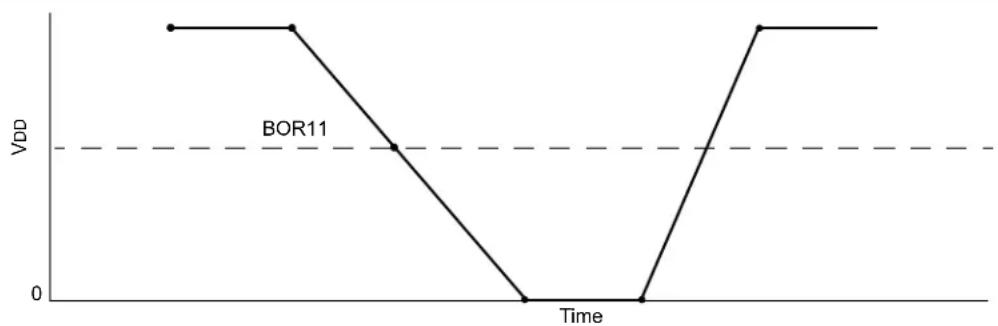
line
| Time | VDD | | ---- | --- | | 0 | 1.0 | | Peak | 1.0 | | Mid | 0.5 | | Low | 0.0 | | High | 1.0 |Note 1: If V DD drops below the BO11 value in Table 24-4, VDD must be brought down to 0V before ramping the device back up to operation range.
21.8 Dual Watchdog Timer (WDT)
Note 1: This data sheet summarizes the features of the dsPIC33CH128MP508 family of devices. It is not intended to be a comprehensive reference source. To complement the information in this data sheet, refer to “Dual Watchdog Timer”, (www.microchip.com/DS70005250), which is available from the Microchip website (www.microchip.com).
2: The WDT is identical for both Main core and Secondary core. The x is common for both Main core and Secondary core (where the x represents the number of the specific module being addressed). The number of WDT modules available on the Main and Secondarys is different and they are located in different SFR locations.
3: All associated register names are the same on the Main core and the Secondary core. The Secondary code will be developed in a separate project in MPLAB X IDE with the device selection, dsPIC33CH128MP508S1, where the S1 indicates the Secondary device.
Table 21-6 shows an overview of the WDT module.
TABLE 21-6: DUAL WDT MODULE OVERVIEW
| Number of WDT Modules | Identical (Modules) | |
| Main Core 1 Yes | ||
| Secondary Core 1 Yes |
The dsPIC33 dual Watchdog Timer (WDT) is described in this section. Refer to Figure 21-3 for a block diagram of the WDT.
The WDT, when enabled, operates from the internal Low-Power RC (LPRC) Oscillator clock source or a selectable clock source in Run mode. The WDT can be used to detect system software malfunctions by resetting the device if the WDT is not cleared periodically in software. The WDT can be configured in Windowed mode or Non-Windowed mode. Various WDT time-out periods can be selected using the WDT postscaler. The WDT can also be used to wake the device from Sleep or Idle mode (Power Save mode). If the WDT expires and issues a device Reset, the WTDO bit of the RCON register (Register 21-37) will be set. It is recommended to have at least two WDT clock cycles of delay after a CLRWDT instruction in case a PWRSAV/NVM operation needs to be performed soon after the CLRWDT instruction.
The following are some of the key features of the WDT modules:
- Configuration or Software Controlled
- Separate User-Configurable Time-out Periods for Run and Sleep/Idle
- Can Wake the Device from Sleep or Idle
- User-Selectable Clock Source in Run mode
- Operates from LPRC in Sleep/Idle mode
Note: While executing a clock switch, the WDT will not be reset. It is recommended to reset the WDT prior to executing a clock switch instruction.
FIGURE 21-3: WATCHDOG TIMER BLOCK DIAGRAM
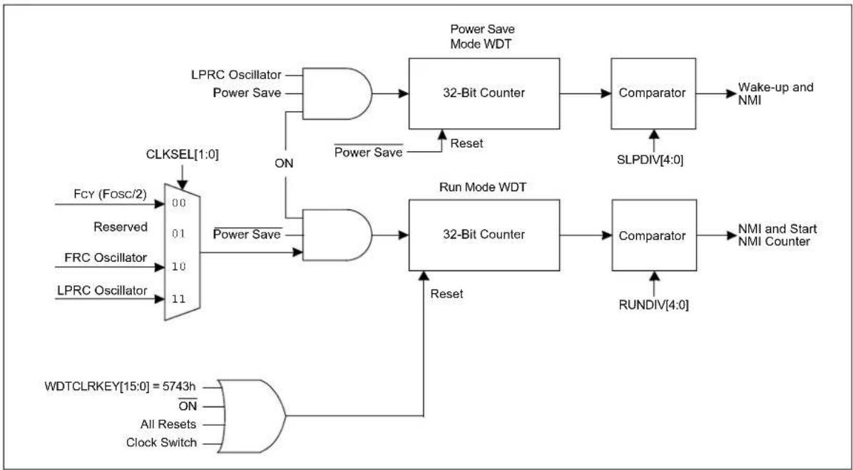
flowchart
graph TD
    A["CLKSEL[1:0"]] --> B["00"]
    C["FcY (Fosc/2)"] --> B
    D["Reserved"] --> E["01"]
    F["FRC Oscillator"] --> G["10"]
    H["LPRC Oscillator"] --> I["11"]
    J["Power Save"] --> K["AND"]
    L["Power Save"] --> M["AND"]
    N["Power Save"] --> O["AND"]
    P["Power Save"] --> Q["AND"]
    R["Power Save"] --> R
    S["Power Save"] --> T["32-Bit Counter"]
    U["Reset"] --> V["32-Bit Counter"]
    W["Reset"] --> X["32-Bit Counter"]
    Y["SLPDIV[4:0"]] --> Z["Comparator"]
    AA["RUNDIV[4:0"]] --> AB["Comparator"]
    AC["WDTCLRKEY[15:0"] = 5743h] --> AD["AND"]
    AE["All Resets"] --> AD
    AF["Clock Switch"] --> AD
    AG["Wake-up and NMI"] --> AH["Comparator"]
    AI["SLPDIV[4:0"]] --> AJ["Comparator"]
21.9 Watchdog Timer Control Registers
REGISTER 21-35: WDTCONL: WATCHDOG TIMER CONTROL REGISTER LOW
| R/W-0 U-0 U-0 R-y R-y R-y R-y R-y | |||
| ON^(1,2) | — — RUNDIV[4:0] | (3) | |
| bit 15 bit 8 | |||
| R | R | R-y | R-y | R-y | R-y | R-y | HS/R/W-0 |
| CLKSEL1(3,5) | CLKSEL0(3,5) | SLPDIV4(3) | SLPDIV3(3) | SLPDIV2(3) | SLPDIV1(3) | SLPDIV0(3) | WDTWINEN(4) |
| bit 7 bit 0 | |||||||
| Legend: | HS = Hardware Settable bit | y = Value from Configuration bit on POR |
| R = Readable bit | W = Writable bit | U = Unimplemented bit, read as '0' |
| -n = Value at POR | '1' = Bit is set | '0' = Bit is cleared x = Bit is unknown |
bit 15 ON: Watchdog Timer Enable bit ^(1,2) 1 = Enables the Watchdog Timer if it is not enabled by the device configuration 0 = Disables the Watchdog Timer if it was enabled in software
bit 14-13 Unimplemented: Read as '0'
bit 12-8 RUNDIV[4:0]: WDT Run Mode Postscaler Status bits ^(3) 11111 = Divide by 2^31 = 2,147,483,648 11110 = Divide by 2^30 = 1,073,741,824 00001 = Divide by 2^1 = 2 00000 = Divide by 2^0 = 1
bit 7-6 CLKSEL[1:0]: WDT Run Mode Clock Select Status bits ^(3,5) 11 = LPRC Oscillator
10 = FRC Oscillator
01 = Reserved
00 = FcY (Fosc/2)
bit 5-1 SLPDIV[4:0]: Sleep and Idle Mode WDT Postscaler Status bits ^(3) 11111 = Divide by 2 ^31 = 2,147,483,648
11110 = Divide by 2 ^30 = 1,073,741,824
...
00001 = Divide by 2 ^1 = 2
00000 = Divide by 2 ^0 = 1
bit 0 WDTWINEN: Watchdog Timer Window Enable bit ^(4) 1 = Enables Window mode 0 = Disables Window mode
Note 1: A read of this bit will result in a '1' if the WDT is enabled by the device configuration or by software.
2: The user's software should not read or write to the peripheral's SFRs in the SYSCLK cycle immediately following the instruction that clears the module's ON bit.
3: These bits reflect the value of the Configuration bits.
4: The WDTWINEN bit reflects the status of the Configuration bit if the bit is set. If the bit is cleared, the value is controlled by software.
5: The available clock sources are device-dependent.
REGISTER 21-36: WDTCONH: WATCHDOG TIMER CONTROL REGISTER HIGH
| W | - | 0 | W | - | 0 | W | - | 0 | W |
| WDTCLRKEY[15:8] | |||||||||
| bit 15 bit 8 | |||||||||
| W | - | 0 | W | - | 0 | W | - | 0 | W |
| WDTCLRKEY[7:0] | |||||||||
| bit 7 bit 0 | |||||||||
Legend:
R = Readable bit W = Writable bit U = Unimplemented bit, read as '0'
-n = Value at POR '1' = Bit is set '0' = Bit is cleared x = Bit is unknown
bit 15-0 WDTCLRKEY[15:0]: Watchdog Timer Clear Key bits
To clear the Watchdog Timer to prevent a time-out, software must write the value, 0x5743, to this location using a single 16-bit write.
REGISTER 21-37: RCON: RESET CONTROL REGISTER (1)
| R/W-0 R/W-0 U-0 U-0 U-0 R/W-0 R/W-0 | ||||||||
| TRAPR IOPUWR — — — | — | C | M | V | R | E | G | |
| bit 15 bit 8 | ||||||||
| R/W-0 R/W-0 U-0 R/W-0 R/W-0 R/W-0 R/W-1 R/W-1 | |||||||
| EXTR SWR | — | WDTO | SLEEP | IDLE | BOR | POR | |
| bit 7 bit 0 | |||||||
Legend:
| R = Readable bit | W = Writable bit | U = Unimplemented bit, read as '0' |
| -n = Value at POR | '1' = Bit is set | '0' = Bit is cleared x = Bit is unknown |
bit 15 TRAPR: Trap Reset Flag bit
1 = A Trap Conflict Reset has occurred
0 = A Trap Conflict Reset has not occurred
bit 14 IOPUWR: Illegal Opcode or Uninitialized W Register Access Reset Flag bit
1 = An illegal opcode detection, an illegal address mode or Uninitialized W register used as an Address Pointer caused a Reset
0 = An Illegal Opcode or Uninitialized W register Reset has not occurred
bit 13-10 Unimplemented: Read as '0'
bit 9 CM: Configuration Mismatch Flag bit
1 = A Configuration Mismatch Reset has occurred
0 = A Configuration Mismatch Reset has not occurred
bit 8 VREGS: Voltage Regulator Standby During Sleep bit
1 = Voltage regulator is active during Sleep
0 = Voltage regulator goes into Standby mode during Sleep
bit 7 EXTR: External Reset (MCLR) Pin bit
1 = A Main Clear (pin) Reset has occurred
0 = A Main Clear (pin) Reset has not occurred
bit 6 SWR: Software RESET (instruction) Flag bit
1 = A RESET instruction has been executed
0 = A RESET instruction has not been executed
bit 5 Unimplemented: Read as '0'
bit 4 WDTO: Watchdog Timer Time-out Flag bit
1 = WDT time-out has occurred
0 = WDT time-out has not occurred
bit 3 SLEEP: Wake from Sleep Flag bit
1 = Device was in Sleep mode
0 = Device was not in Sleep mode
bit 2 IDLE: Wake from Idle Flag bit
1 = Device was in Idle mode
0 = Device was not in Idle mode
bit 1 BOR: Brown-out Reset Flag bit
1 = Brown-out Reset has occurred
0 = Brown-out Reset has not occurred
bit 0 POR: Power-on Reset Flag bit
1 = Power-on Reset has occurred
0 = Power-on Reset has not occurred
Note 1: All of the Reset status bits can be set or cleared in software. Setting one of these bits in software does not cause a device Reset.
21.10 JTAG Interface
The dsPIC33CH128MP508 family devices implement a JTAG interface, which supports boundary scan device testing. Detailed information on this interface will be provided in future revisions of this document.
Note: Refer to "Programming and Diagnostics" (www.microchip.com/DS70000608) for further information on usage, configuration and operation of the JTAG interface.
21.11 In-Circuit Serial Programming ^TM (ICSP ^TM )
The dsPIC33CH128MP508 family devices can be serially programmed while in the end application circuit. This is done with two lines for clock and data, and three other lines for power, ground and the programming sequence. Serial programming allows customers to manufacture boards with unprogrammed devices and then program the device just before shipping the product. Serial programming also allows the most recent firmware or a custom firmware to be programmed. Refer to the "dsPIC33CH128MP508 Family Flash Programming Specification" (DS70005285) for details about In-Circuit Serial Programming (ICSP).
Any of the three pairs of programming clock/data pins can be used:
- PGC1 and PGD1
- PGC2 and PGD2
- PGC3 and PGD3
Note: Both Main core and Secondary core can be used with MPLAB ICD to debug at the same time. There are PGCx and PGDx pins dedicated for the Main core and Secondary core (S1PGCx and S1PGDx) to make this possible. MCLR is the same for programming the Main core and the Secondary core. S1MCLRx is used only when the Main and Secondary are debugged simultaneously.
21.12 In-Circuit Debugger
When MPLAB ICD 3 or the REAL ICE emulator is selected as a debugger, the in-circuit debugging functionality is enabled. This function allows simple debugging functions when used with MPLAB IDE. Debugging functionality is controlled through the PGCx (Emulation/Debug Clock) and PGDx (Emulation/Debug Data) pin functions.
Any of the three pairs of debugging clock/data pins can be used:
- PGC1 and PGD1 Main Debug or Secondary Debug
- PGC2 and PGD2 Main Debug or Secondary Debug
- PGC3 and PGD3 Main Debug or Secondary Debug for debugging Main and Secondary simultaneously, two MPLAB ICD debuggers or the REAL ICE™ emulator are required. This mode of debugging, where the Main and Secondary are simultaneously debugged, is called the Dual Debug mode.
S1MCLRx and S1PGCx/S1PGDx are used only in Dual Debug mode.
The Dual Debug mode of operation needs the following PGCx/PGDx pins:
- M C LPGC1 and PGD1 for Main Debug, and S1MCLR1, S1PGC1 and S1PGD1 for Secondary Debug
- M C LPGC2 and PGD2 for Main Debug, and S1MCLR2, S1PGC2 and S1PGD2 for Secondary Debug
- M C LPQC3 and PGD3 for Main Debug, and S1MCLR3, S1PGC3 and S1PGD3 for Secondary Debug
To use the in-circuit debugger function of the device, the design must implement ICSP connections to MCLR, VDD, Vss and the PGCx/PGDx pin pair. In addition, when the feature is enabled, some of the resources are not available for general use. These resources include the first 80 bytes of data RAM and two or five (in Dual Debug) I/O pins (PGCx and PGDx).
There are three modes of debugging the dual core family of dsPIC33CH128MP508:
- Main Only Debug
- Secondary Only Debug
- Dual Debug
21.12.1 MAIN ONLY DEBUG
In Main Only Debug, only the Main project will be debugged. There is no project for Secondary or no Secondary code. The main project will be for dsPIC33CHXXXMP50X/20X and the user has to use MCLR and PGCx/PGDx for debugging. This is similar to debugging any single core existing device.
21.12.2 SECONDARY ONLY DEBUG
In the Secondary Only Debug mode, the user will need two projects. One project is the Main project with dsPIC33CHXXXMP50X/20X as the device. This is called a Main Stub and is required to provide the configuration information to the Secondary. The Secondary does not have its own Configuration bits. The Configuration bits reside in the Main Flash. The Main Stub will be small code used to provide the Configuration bits for the Secondary. The Main Stub is first programmed to the Main Flash using MCLR, PGCx and PGDx.
Once the Main Stub is programmed in the Main Flash, the user has to open a new project with dsPIC33CHXXXMP50X/20XS1 (the S1 indicates the Secondary device). The same MCLR and PGCx/PGDx, or different PGCx/PGDx, can be used for debugging the Secondary. Now the Secondary can be debugged like any other single core device.
21.12.3 DUAL DEBUG (BOTH MAIN AND SECONDARY ARE DEBUGGED)
In this Debug mode, two debug tools are required: one for Main and one for Secondary.
In the Dual Debug mode, the user needs two projects. One project is the Main project with dsPIC33CHXXXMP50X/20X as the device. Configuration bits for the Main, as well as the Secondary, will be part of this project. The S1ISOLAT bit can be set and the Main project can be debugged like any other existing single core device. The Main can be debugged using MCLR, PGCx and PGDx.
Once the Main has started the debug process, the user has to open a new project with dsPIC33CHXXXMP50X/20XS1 (the S1 indicates the Secondary device). Connect the project using S1MCLRx and S1PGCx/S1PGDx, and start debugging the Secondary project.
21.13 Code Protection and CodeGuard™ Security – Main Flash
dsPIC33CH128MP508 family devices offer multiple levels of security for protecting individual intellectual property. The program Flash protection can be broken up into three segments: Boot Segment (BS), General Segment (GS) and Configuration Segment (CS). Boot Segment has the highest security privilege and can be thought to have limited restrictions when accessing other segments. General Segment has the least security and is intended for the end user system code. Configuration Segment contains only the device user configuration data, which are located at the end of the program memory space.
The code protection features are controlled by the Configuration registers, FSEC and FBSLIM. The FSEC register controls the code-protect level for each segment and if that segment is write-protected. The size of BS and GS will depend on the BSLIM[12:0] bits setting and if the Alternate Interrupt Vector Table (AIVT) is enabled. The BSLIM[12:0] bits define the number of pages for BS with each page containing 1024 IW. The smallest BS size is one page, which will consist of the Interrupt Vector Table (IVT) and 512 IW of code protection.
If the AIVT is enabled, the last page of BS will contain the AIVT and will not contain any BS code. With AIVT enabled, the smallest BS size is now two pages (2048 IW), with one page for the IVT and BS code, and the other page for the AIVT. Write protection of the BS does not cover the AIVT. The last page of BS can always be programmed or erased by BS code. The General Segment will start at the next page and will consume the rest of program Flash, except for the Flash Configuration Words. The IVT will assume GS security only if BS is not enabled. The IVT is protected from being programmed or page erased when either security segment has enabled write protection.
The different device security segments are shown in Figure 21-4. Here, all three segments are shown, but are not required. If only basic code protection is required, then GS can be enabled independently or combined with CS, if desired.
FIGURE 21-4: SECURITY SEGMENTS
EXAMPLE

text_image
IVT and AIVT Assume BS Protection IVT 0x000000 0x000200 BS AIVT + 512 IW(2) BSLIM[12:0] GS CS(1) 0x00B000 Note 1: If CS is write-protected, the last page (GS + CS) of program memory will be protected from an erase condition. 2: The last half (256 IW) of the last page of BS is unusable program memory.21.14 Code Protection and CodeGuard™ Security – Secondary PRAM
The dsPIC33CH128MP508S1 family Secondary PRAM inherits its security configuration from the Main GSS[1:0] and GWRP Configuration bit settings. The Secondary PRAM does not have a BS or CS segment.
All user code space is considered GS, including the IVT. Therefore, there are no specific segment read and write permissions to consider.
If either the GSSx or GWRP bits are enabled, ICSP entry directly to the Secondary PRAM is inhibited. This prevents reading, programming and debugging the Secondary PRAM when the Main Flash GS is code-protected.
Main to Secondary Image Loading is always allowed, regardless of any code protection settings.
NOTES:
22.0 INSTRUCTION SET SUMMARY
Note: This data sheet summarizes the features of the dsPIC33CH128MP508 family of devices. It is not intended to be a comprehensive reference source. To complement the information in this data sheet, refer to the related section in the "dsPIC33/PIC24 Family Reference Manual", which is available from the Microchip website (www.microchip.com).
The dsPIC33CH instruction set is almost identical to that of the dsPIC30F and dsPIC33F.
Most instructions are a single program memory word (24 bits). Only three instructions require two program memory locations.
Each single-word instruction is a 24-bit word, divided into an 8-bit opcode, which specifies the instruction type and one or more operands, which further specify the operation of the instruction.
The instruction set is highly orthogonal and is grouped into five basic categories:
• Word or byte-oriented operations
- Bit-oriented operations
- Literal operations
- DSP operations
• Control operations
Table 22-1 lists the general symbols used in describing the instructions.
The dsPIC33 instruction set summary in Table22-2 lists all the instructions, along with the status flags affected by each instruction.
Most word or byte-oriented W register instructions (including barrel shift instructions) have three operands:
- The first source operand, which is typically a register 'Wb' without any address modifier
- The second source operand, which is typically a register 'Ws' with or without an address modifier
- The destination of the result, which is typically a register 'Wd' with or without an address modifier
However, word or byte-oriented file register instructions have two operands:
- The file register specified by the value 'f'
- The destination, which could be either the file register 'f' or the W0 register, which is denoted as 'WREG'
Most bit-oriented instructions (including simple rotate/shift instructions) have two operands:
- The W register (with or without an address modifier) or file register (specified by the value of 'Ws' or 'f')
- The bit in the W register or file register (specified by a literal value or indirectly by the contents of register 'Wb')
The literal instructions that involve data movement can use some of the following operands:
- A literal value to be loaded into a W register or file register (specified by 'k')
- The W register or file register where the literal value is to be loaded (specified by 'Wb' or 'f')
However, literal instructions that involve arithmetic or logical operations use some of the following operands:
- The first source operand, which is a register 'Wb' without any address modifier
- The second source operand, which is a literal value
- The destination of the result (only if not the same as the first source operand), which is typically a register 'Wd' with or without an address modifier
The MAC class of DSP instructions can use some of the following operands:
- The accumulator (A or B) to be used (required operand)
• The W registers to be used as the two operands
• The X and Y address space prefetch operations
• The X and Y address space prefetch destinations
• The accumulator write-back destination
The other DSP instructions do not involve any multiplication and can include:
• The accumulator to be used (required)
- The source or destination operand (designated as Wso or Wdo, respectively) with or without an address modifier
- The amount of shift specified by a W register 'Wn' or a literal value
The control instructions can use some of the following operands:
• A program memory address
- The mode of the Table Read and Table Write instructions
Most instructions are a single word. Certain double-word instructions are designed to provide all the required information in these 48 bits. In the second word, the 8 MSbs are '0's. If this second word is executed as an instruction (by itself), it executes as a NOP.
The double-word instructions execute in two instruction cycles.
Most single-word instructions are executed in a single instruction cycle, unless a conditional test is true or the Program Counter is changed as a result of the instruction, or a PSV or Table Read is performed. In
these cases, the execution takes multiple instruction cycles, with the additional instruction cycle(s) executed as a NOP. Certain instructions that involve skipping over the subsequent instruction require either two or three cycles if the skip is performed, depending on whether the instruction being skipped is a single-word or two-word instruction. Moreover, double-word moves require two cycles.
Note: For more details on the instruction set, refer to the "16-Bit MCU and DSC Programmer's Reference Manual" (DS70000157).
TABLE 22-1: SYMBOLS USED IN OPCODE DESCRIPTIONS
| Field Description | |
| #text Means literal defined by “text” | |
| (text) Means “content of text” | |
| [text] Means “the location addressed by text” | |
| {} Optional field or operation | |
| a ∈ {b, c, d} a is selected from the set of values b, c, d | |
| [n:m] Register bit field | |
| .b Byte mode selection | |
| .d Double-Word mode selection | |
| .S Shadow register select | |
| .w | Word mode selection (default) |
| Acc | One of two accumulators {A, B} |
| AWB | Accumulator Write-Back Destination Address register ∈ {W13, [W13]+ = 2} |
| bit4 | 4-bit bit selection field (used in word-addressed instructions) ∈ {0...15} |
| C, DC, N, OV, Z | MCU Status bits: Carry, Digit Carry, Negative, Overflow, Sticky Zero |
| Expr | Absolute address, label or expression (resolved by the linker) |
| f | File register address ∈ {0x0000...0x1FFF} |
| lit1 | 1-bit unsigned literal ∈ {0,1} |
| lit4 | 4-bit unsigned literal ∈ {0...15} |
| lit5 | 5-bit unsigned literal ∈ {0...31} |
| lit8 | 8-bit unsigned literal ∈ {0...255} |
| lit10 | 10-bit unsigned literal ∈ {0...255} for Byte mode, {0:1023} for Word mode |
| lit14 | 14-bit unsigned literal ∈ {0...16384} |
| lit16 | 16-bit unsigned literal ∈ {0...65535} |
| lit23 | 23-bit unsigned literal ∈ {0...8388608}; LSb must be ‘0’ |
| None | Field does not require an entry, can be blank |
| OA, OB, SA, SB | DSP Status bits: ACCA Overflow, ACCB Overflow, ACCA Saturate, ACCB Saturate |
| PC | Program Counter |
| Slit10 | 10-bit signed literal ∈ {-512...511} |
| Slit16 | 16-bit signed literal ∈ {-32768...32767} |
| Slit6 | 6-bit signed literal ∈ {-16...16} |
| Wb | Base W register ∈ {W0...W15} |
| Wd | Destination W register ∈ { Wd, [Wd], [Wd++], [Wd--], (++Wd], [--Wd]} |
| Wdo | Destination W register ∈ { Wnd, [Wnd], [Wnd++], [Wnd--], (++Wnd], [--Wnd], [Wnd+Wb]} |
| Wm,Wn | Dividend, Divisor Working register pair (direct addressing) |
| Field | Description |
| Wm*Wm | Multiplicand and Multiplier Working register pair for Square instructions ∈{W4 * W4,W5 * W5,W6 * W6,W7 * W7} |
| Wm*Wn | Multiplicand and Multiplier Working register pair for DSP instructions ∈{W4 * W5,W4 * W6,W4 * W7,W5 * W6,W5 * W7,W6 * W7} |
| Wn One of 16 Working registers ∈ {W0...W15} | |
| Wnd One of 16 Destination Working registers ∈ {W0...W15} | |
| Wns One of 16 Source Working registers ∈ {W0...W15} | |
| WREG W0 (Working register used in file register instructions) | |
| Ws | Source W register ∈ {Ws, [Ws], [Ws++, [Ws--], (++Ws], [--Ws]} |
| Wso Source W register ∈ | { Wns, [Wns], [Wns++, [Wns--], (++Wns], [--Wns], [Wns+Wb]} |
| Wx X Data Space Prefetch Address register for DSP instructions ∈ {[W8] += 6, [W8] += 4, [W8] += 2, [W8], [W8] -= 6, [W8] -= 4, [W8] -= 2,[W9] += 6, [W9] += 4, [W9] += 2, [W9], [W9] -= 6, [W9] -= 4, [W9] -= 2,[W9 + W12], none} | |
| Wxd | X Data Space Prefetch Destination register for DSP instructions ∈ {W4...W7} |
| Wy Y Data Space Prefetch Address register for DSP instructions ∈ {[W10] += 6, [W10] += 4, [W10] += 2, [W10], [W10] -= 6, [W10] -= 4, [W10] -= 2,[W11] += 6, [W11] += 4, [W11] += 2, [W11], [W11] -= 6, [W11] -= 4, [W11] -= 2,[W11 + W12], none} | |
| Wyd | Y Data Space Prefetch Destination register for DSP instructions ∈ {W4...W7} |
Note: In dsPIC33CH128MP508 devices, read and Read-Modify-Write (RMW) operations on non-CPU Special Function Registers require an additional cycle when compared to dsPIC30F, dsPIC33F, PIC24F and PIC24H devices
TABLE 22-2: INSTRUCTION SET OVERVIEW
| Base Instr # | Assembly Mnemonic | Assembly Syntax Description | # of Words | # of Cycles(1) | Status Flags Affected | |
| 1 ADD | ADD Acc A | add Accumulators 1 1 OA,OB,SA,SB | ||||
| ADD f f=f+WREG 1 1 C,DC,N,OV,Z | ||||||
| ADD f,WREG | WREG = f + WREG | 1 | 1 | C,DC,N,OV,Z | ||
| ADD #lit10,Wn | Wd = lit10 + Wd | 1 | 1 | C,DC,N,OV,Z | ||
| ADD Wb,Ws,Wd | Wd = Wb + Ws | 1 | 1 | C,DC,N,OV,Z | ||
| ADD Wb,#lit5,Wd | Wd = Wb + lit5 | 1 | 1 | C,DC,N,OV,Z | ||
| ADD Wso,#Slit4,Acc | 16-bit Signed Add to Accumulator | 1 | 1 | OA,OB,SA,SB | ||
| 2 | ADDC | ADDC f | f = f + WREG + (C) | 1 | 1 | C,DC,N,OV,Z |
| ADDC f,WREG | WREG = f + WREG + (C) | 1 | 1 | C,DC,N,OV,Z | ||
| ADDC #lit10,Wn | Wd = lit10 + Wd + (C) | 1 | 1 | C,DC,N,OV,Z | ||
| ADDC Wb,Ws,Wd | Wd = Wb + Ws + (C) | 1 | 1 | C,DC,N,OV,Z | ||
| ADDC Wb,#lit5,Wd | Wd = Wb + lit5 + (C) | 1 | 1 | C,DC,N,OV,Z | ||
| 3 | AND | AND f | f = f.AND.WREG | 1 | 1 | N,Z |
| AND f,WREG | WREG = f.AND.WREG | 1 | 1 | N,Z | ||
| AND #lit10,Wn | Wd = lit10.AND.Wd | 1 | 1 | N,Z | ||
| AND Wb,Ws,Wd | Wd = Wb.AND.Ws | 1 | 1 | N,Z | ||
| AND Wb,#lit5,Wd | Wd = Wb.AND.lit5 | 1 | 1 | N,Z | ||
| 4 | ASR | ASR f | f = Arithmetic Right Shift f | 1 | 1 | C,N,OV,Z |
| ASR f,WREG | WREG = Arithmetic Right Shift f | 1 | 1 | C,N,OV,Z | ||
| ASR Ws,Wd | Wd = Arithmetic Right Shift Ws | 1 | 1 | C,N,OV,Z | ||
| ASR Wb,Wns,Wnd | Wnd = Arithmetic Right Shift Wb by Wns | 1 | 1 | N,Z | ||
| ASR Wb,#lit5,Wnd | Wnd = Arithmetic Right Shift Wb by lit5 | 1 | 1 | N,Z | ||
| 5 | BCLR | BCLR f,#bit4 | Bit Clear f | 1 | 1 | None |
| BCLR Ws,#bit4 | Bit Clear Ws | 1 | 1 | None | ||
| 6 | BFEXT | BFEXT bit4,wid5,Ws,Wb | Bit Field Extract from Ws to Wb | 2 | 2 | None |
| BFEXT bit4,wid5,f,Wb | Bit Field Extract from f to Wb | 2 | 2 | None | ||
| 7 | BFINS | BFINS bit4,wid5,Wb,Ws | Bit Field Insert from Wb into Ws | 2 | 2 | None |
| BFINS bit4,wid5,Wb,f | Bit Field Insert from Wb into f | 2 | 2 | None | ||
| BFINS bit4,wid5,lit8,Ws | Bit Field Insert from #lit8 to Ws | 2 | 2 | None | ||
| 8 | BOOTSWP | BOOTSWP | Swap the Active and Inactive Program Flash Space | 1 | 2 | None |
Note 1: Read and Read-Modify-Write (e.g., bit operations and logical operations) on non-CPU SFRs incur an additional instruction cycle.
2: Cycle times for Secondary core are different for Main core, as shown in 2.
3: For dsPIC33CH128MP508 devices, the divide instructions must be preceded with a "REPEAT #5" instruction, such that they are executed six consecutive times
TABLE 22-2: INSTRUCTION SET OVERVIEW (CONTINUED)
| Base Instr # | Assembly Mnemonic | Assembly Syntax | Description | # of Words | # of Cycles(1) | Status Flags Affected |
| 9 BRA | BRA C, Expr | Branch if Carry 1 1 (4)/1 (2) | (2) | None | ||
| BRA GE, Expr Branch if Greater Than or Equal | 1 1 (4)/1 (2) | (2) | None | |||
| BRA GEU, Expr Branch if unsigned Greater Than or Equal | 1 1 (4)/1 (2) | (2) | None | |||
| BRA GT, Expr Branch if Greater Than 1 1 (4)/1 (2) | (2) | None | ||||
| BRA GTU, Expr Branch if Unsigned Greater Than 1 1 (4)/1 (2) | (2) | None | ||||
| BRA LE, Expr Branch if Less Than or Equal 1 | 1 (4)/1 (2) | (2) | None | |||
| BRA LFU, Expr | Branch if Unsigned Less Than or Equal | 1 | 1 (4)/1 (2)(2) | None | ||
| BRA LT, Expr Branch if Less Than | 1 1 (4)/1 (2) | (2) | None | |||
| BRA LTU, Expr Branch if Unsigned Less Than | 1 1 (4)/1 (2) | (2) | None | |||
| BRA N, Expr Branch if Negative | 1 1 (4)/1 (2) | (2) | None | |||
| BRA NC, Expr Branch if Not Carry | 1 1 (4)/1 (2) | (2) | None | |||
| BRA NN, Expr Branch if Not Negative | 1 1 (4)/1 (2) | (2) | None | |||
| BRA NOV, Expr Branch if Not Overflow | 1 1 (4)/1 (2) | (2) | None | |||
| BRA NZ, Expr | Branch if Not Zero | 1 | 1 (4)/1 (2)(2) | None | ||
| BRA OA, Expr | Branch if Accumulator A Overflow | 1 | 1 (4)/1 (2)(2) | None | ||
| BRA OB, Expr | Branch if Accumulator B Overflow | 1 | 1 (4)/1 (2)(2) | None | ||
| BRA OV, Expr Branch if Overflow | 1 1 (4)/1 (2) | (2) | None | |||
| BRA SA, Expr | Branch if Accumulator A Saturated | 1 | 1 (4)/1 (2)(2) | None | ||
| BRA SB, Expr | Branch if Accumulator B Saturated | 1 | 1 (4)/1 (2)(2) | None | ||
| BRA Expr | Branch Unconditionally | 1 | 4/2(2) | None | ||
| BRA Z, Expr Branch if Zero | 1 1 (4)/1 (2) | (2) | None | |||
| BRA Wn | Computed Branch | 1 | 4 | None | ||
| 10 | BREAK | BREAK | Stop User Code Execution | 1 | 1 | None |
| 11 | BSET | BSET f,#bit4 | Bit Set f | 1 | 1 | None |
| Bit Set Ws | 1 | 1 | None | |||
| 12 | BSW | BSW.C Ws,Wb | Write C Bit to Ws[Wb] | 1 | 1 | None |
| BSW.Z Ws,Wb | Write Z Bit to Ws[Wb] | 1 | 1 | None | ||
| 13 | BTG | BTG f,#bit4 | Bit Toggle f | 1 | 1 | None |
| BTG Ws,#bit4 | Bit Toggle Ws | 1 | 1 | None | ||
| 14 | BTSC | BTSC f,#bit4 | Bit Test f, Skip if Clear | 1 | 1(2 or 3) | None |
| BTSC Ws,#bit4 | Bit Test Ws, Skip if Clear | 1 | 1(2 or 3) | None | ||
| 15 | BTSS | BTSS f,#bit4 | Bit Test f, Skip if Set | 1 | 1(2 or 3) | None |
| BTSS Ws,#bit4 | Bit Test Ws, Skip if Set | 1 | 1(2 or 3) | None | ||
| 16 | BTST | BTST f,#bit4 | Bit Test f | 1 | 1 | Z |
| BTST.C Ws,#bit4 | Bit Test Ws to C | 1 | 1 | C | ||
| BTST.Z Ws,#bit4 | Bit Test Ws to Z | 1 | 1 | Z | ||
| BTST.C Ws,Wb | Bit Test Ws[Wb] to C | 1 | 1 | C | ||
| BTST.Z Ws,Wb | Bit Test Ws[Wb] to Z | 1 | 1 | Z | ||
| 17 | BTSTS | BTSTS f,#bit4 | Bit Test then Set f | 1 | 1 | Z |
| BTSTS.C Ws,#bit4 | Bit Test Ws to C, then Set | 1 | 1 | C | ||
| BTSTS.Z Ws,#bit4 | Bit Test Ws to Z, then Set | 1 | 1 | Z | ||
| 18 | CALL | CALL lit23 | Call Subroutine | 2 | 4/(2)(2) | SFA |
| CALL Wn | Call Indirect Subroutine | 1 | 4(2)(2) | SFA | ||
| CALL.L Wn | Call Indirect Subroutine (long address) | 1 | 4(2)(2) | SFA |
Note 1: Read and Read-Modify-Write (e.g., bit operations and logical operations) on non-CPU SFRs incur an additional instruction cycle.
2: Cycle times for Secondary core are different for Main core, as shown in 2.
3: For dsPIC33CH128MP508 devices, the divide instructions must be preceded with a "REFFAT #5" instruction, such that they are executed six consecutive times
TABLE 22-2: INSTRUCTION SET OVERVIEW (CONTINUED)
| Base Instr # | Assembly Mnemonic | Assembly Syntax | Description | # of Words | # of Cycles(1) | Status Flags Affected |
| 19 CLR | CLR f f= | 0x0000 1 1 None | ||||
| CLR WREG WREG = 0x0000 1 1 None | ||||||
| CLR Ws Ws = 0x0000 1 1 None | ||||||
| CLR Acc,Wx,Wxd,Wy,Wyd,AWB Clear Accumulator 1 1 OA,OB,SA,SB | ||||||
| 20 | CLRWDT | CLRWDT | Clear Watchdog Timer | 1 | 1 | WDTO,Sleep |
| 21 COM | COM f f=f | f | - | 1 | 1 | N,Z |
| COM f,WREG WREG = f | - | 1 | 1 | N,Z | ||
| COM Ws,Wd Wd = Ws | - | 1 | 1 | N,Z | ||
| 22 | CP | CP f | Compare f with WREG | 1 | 1 | C,DC,N,OV,Z |
| CP Wb,#lit8 | Compare Wb with lit8 | 1 | 1 | C,DC,N,OV,Z | ||
| CP Wb,Ws | Compare Wb with Ws (Wb - Ws) | 1 | 1 | C,DC,N,OV,Z | ||
| 23 | CPO | CPO f | Compare f with 0x0000 | 1 | 1 | C,DC,N,OV,Z |
| CPO Ws | Compare Ws with 0x0000 | 1 | 1 | C,DC,N,OV,Z | ||
| 24 | CPB | CPB f | Compare f with WREG, with Borrow | 1 | 1 | C,DC,N,OV,Z |
| CPB Wb,#lit8 | Compare Wb with lit8, with Borrow | 1 | 1 | C,DC,N,OV,Z | ||
| CPB Wb,Ws Compare Wb with Ws, with Borrow (Wb - Ws - C) | 1 1 | C,DC,N,OV,Z | ||||
| 25 | CPSEQ | CPSEQ Wb,Wn | Compare Wb with Wn, Skip if = | 1 | 1(2 or 3) | None |
| CPREQ | CPREQ Wb,Wn,Expr | Compare Wb with Wn, Branch if = | 1 | 1(5) | None | |
| 26 | CPSGT | CPSGT Wb,Wn | Compare Wb with Wn, Skip if > | 1 | 1(2 or 3) | None |
| CPBGT | CPBGT Wb,Wn,Expr | Compare Wb with Wn, Branch if > | 1 | 1(5) | None | |
| 27 | CPSLT | CPSLT Wb,Wn | Compare Wb with Wn, Skip if < | 1 | 1(2 or 3) | None |
| CPBLT Wb,Wn,Expr | Compare Wb with Wn, Branch if < | 1 | 1(5) | None | ||
| 28 | CPSNE | CPSNE Wb,Wn | Compare Wb with Wn, Skip if ≠ | 1 | 1(2 or 3) | None |
| CPBNE Wb,Wn,Expr | Compare Wb with Wn, Branch if ≠ | 1 | 1(5) | None | ||
| 29 | CTXTSWP | CTXTSWP #lit3 | Switch CPU Register Context to Context Defined by lit3 | 1 | 2 | None |
| 30 | CTXTSWP | CTXTSWP Wn | Switch CPU Register Context to Context Defined by Wn | 1 | 2 | None |
| 31 | DAW.B | DAW.B Wn | Wn = Decimal Adjust Wn | 1 | 1 | C |
| 32 | DEC | DEC f | f = f - 1 | 1 | 1 | C,DC,N,OV,Z |
| DEC f,WREG | WREG = f - 1 | 1 | 1 | C,DC,N,OV,Z | ||
| DEC Ws,Wd | Wd = Ws - 1 | 1 | 1 | C,DC,N,OV,Z | ||
| 33 | DEC2 | DEC2 f | f = f - 2 | 1 | 1 | C,DC,N,OV,Z |
| DEC2 f,WREG | WREG = f - 2 | 1 | 1 | C,DC,N,OV,Z | ||
| DEC2 Ws,Wd | Wd = Ws - 2 | 1 | 1 | C,DC,N,OV,Z | ||
| 34 | DISI | DISI #lit14 | Disable Interrupts for k Instruction Cycles | 1 | 1 | None |
| 35 | DIVF | DIVF Wn,Wn | Signed 16/16-Bit Fractional Divide | 1 | 18/6 | N,Z,C,OV |
| 36 | DIV.S | DIV.S Wn,Wn | Signed 16/16-Bit Integer Divide | 1 | 18/6 | N,Z,C,OV |
| DIV.SD Wn,Wn | Signed 32/16-Bit Integer Divide | 1 | 18/6 | N,Z,C,OV | ||
| 37 | DIV.U | DIV.U Wn,Wn | Unsigned 16/16-Bit Integer Divide | 1 | 18/6 | N,Z,C,OV |
| DIV.UB Wn,Wn | Unsigned 32/16-Bit Integer Divide | 1 | 18/6 | N,Z,C,OV | ||
| 38 | DIVF2 | DIVF2 Wn,Wn | Signed 16/16-Bit Fractional Divide (W1:W0 preserved) | 1 | 6 | N,Z,C,OV |
| 39 | DIV2.S | DIV2.S Wn,Wn | Signed 16/16-Bit Integer Divide (W1:W0 preserved) | 1 | 6 | N,Z,C,OV |
| DIV2.SD Wn,Wn | Signed 32/16-Bit Integer Divide (W1:W0 preserved) | 1 | 6 | N,Z,C,OV | ||
Note 1: Read and Read-Modify-Write (e.g., bit operations and logical operations) on non-CPU SFRs incur an additional instruction cycle.
2: Cycle times for Secondary core are different for Main core, as shown in 2.
3: For dsPIC33CH128MP508 devices, the divide instructions must be preceded with a "REPEAT || 5" instruction, such that they are executed six consecutive times
TABLE 22-2: INSTRUCTION SET OVERVIEW (CONTINUED)
| Base Instr # | Assembly Mnemonic | Assembly Syntax | Description | # of Words | # of Cycles(1) | Status Flags Affected |
| 40 DIV2.U DIV2.J Wm,Wn Unsigned 16/16-Bit Integer Divide | (W1:W0 preserved) | 1 | 6 | N | ||
| DIV2.UC Wm,Wn Unsigned 32/16-Bit Integer Divide (W1:W0 preserved) | 1 | 6 | N | |||
| 41 | DO | DO #Lit1b,Expr | Do Code to PC + Expr, lit15 + 1 Times | 2 | 2 | None |
| DO Wn,Expr | Do code to PC + Expr, (Wn) + 1 Times | 2 | 2 | None | ||
| 42 | ED | ED Wm*Wm,Acc,Wx,Wy,Wxd | Euclidean Distance (no accumulate) | 1 | 1 | OA,OB,OAB, SA,SB,SAB |
| 43 | EDAC | EDAC Wm*Wm,Acc,Wx,Wy,Wxd | Euclidean Distance | 1 | 1 | OA,OB,OAB, SA,SB,SAB |
| 44 | EXCH | EXCH Wns,Wnd | Swap Wns with Wnd | 1 | 1 | None |
| 46 | FBCL | FBCL Ws,Wnd | Find Bit Change from Left (MSb) Side | 1 | 1 | C |
| 47 | FF1L | FF1L Ws,Wnd | Find First One from Left (MSb) Side | 1 | 1 | C |
| 48 | FF1R | FF1R Ws,Wnd | Find First One from Right (LSb) Side | 1 | 1 | C |
| 49 | FLIM | FLIM Wb, Ws | Force Data (upper and lower) Range Limit without Limit Excess Result | 1 1 | N,Z,OV | |
| FLIM.V Wb, Ws, Wd | Force Data (upper and lower) Range Limit with Limit Excess Result | 1 1 | N,Z,OV | |||
| 50 | GOTO | GOTO Expr | Go to Address | 2 | 4/2^(2) | None |
| GOTO Wn | Go to Indirect | 1 | 4/2^(2) | None | ||
| GOTO.L Wn | Go to Indirect (long address) | 1 | 4/2^(2) | None | ||
| 51 | INC | INC f | f=f+1 | 1 | 1 | C,DC,N,OV,Z |
| INC f,WREG | WREG=f+1 | 1 | 1 | C,DC,N,OV,Z | ||
| INC Ws,Wd | Wd=Ws+1 | 1 | 1 | C,DC,N,OV,Z | ||
| 52 | INC2 | INC2 f | f=f+2 | 1 | 1 | C,DC,N,OV,Z |
| INC2 f,WREG | WREG=f+2 | 1 | 1 | C,DC,N,OV,Z | ||
| INC2 Ws,Wd | Wd=Ws+2 | 1 | 1 | C,DC,N,OV,Z | ||
| 53 | IOR | IOR f | f=f.IOR.WREG | 1 | 1 | N,Z |
| IOR f,WREG | WREG=f.IOR.WREG | 1 | 1 | N,Z | ||
| IOR #Lit10,Wn | Wd=lit10.IOR.Wd | 1 | 1 | N,Z | ||
| IOR Wb,Ws,Wd | Wd=Wb.IOR.Ws | 1 | 1 | N,Z | ||
| IOR Wb,#Lit5,Wd | Wd=Wb.IOR.lit5 | 1 | 1 | N,Z | ||
| 54 | LAC | LAC Wso,#Slit4,Acc | Load Accumulator | 1 | 1 | OA,OB,OAB, SA,SB,SAB |
| LAC.D Wso,#Slit4,Acc | Load Accumulator Double | 1 | 2 | OA,SA,OB,SB | ||
| 55 | LDSLV | LDSLV Wso,Wdo,lit2 | Move a Single Instruction Word from Main to Secondary PRAM | 1 | 1 | N |
| 56 | LNK | LNK #Lit14 | Link Frame Pointer | 1 | 1 | SFA |
| 57 | LSR | LSR f | f=Logical Right Shift f | 1 | 1 | C,N,OV,Z |
| LSR f,WREG | WREG=Logical Right Shift f | 1 | 1 | C,N,OV,Z | ||
| LSR Ws,Wd | Wd=Logical Right Shift Ws | 1 | 1 | C,N,OV,Z | ||
| LSR Wb,Wns,Wnd | Wnd=Logical Right Shift Wb by Wns | 1 | 1 | N,Z | ||
| LSR Wb,#Lit5,Wnd | Wnd=Logical Right Shift Wb by lit5 | 1 | 1 | N,Z | ||
| 58 MAC MAC WM*Wn,Acc,Wx,Wxd,Wy,Wyd, AWB | Multiply and Accumulate | 1 1 | OA,OB,OAB, SA,SB,SAB | |||
| Square and Accumulate | 1 | 1 | OA,OB,OAB, SA,SB,SAB | |||
| 59 | MAX | MAX Acc | Force Data Maximum Range Limit | 1 | 1 | N,OV,Z |
| MAX.V Acc, Wnd | Force Data Maximum Range Limit with Result | 1 | 1 | N,OV,Z | ||
Note 1: Read and Read-Modify-Write (e.g., bit operations and logical operations) on non-CPU SFRs incur an additional instruction cycle.
2: Cycle times for Secondary core are different for Main core, as shown in 2.
3: For dsPIC33CH128MP508 devices, the divide instructions must be preceded with a "REPEAT #3" instruction, such that they are executed six consecutive times
TABLE 22-2: INSTRUCTION SET OVERVIEW (CONTINUED)
| Base Instr # | Assembly Mnemonic | Assembly Syntax | Description | # of Words | # of Cycles(1) | Status Flags Affected |
| 60 MIN | MIN Acc | If Accumulator A Less than B Load | Accumulator with B or vice versa | 1 1 N | OV,Z | |
| MIN.V Acc, Wd If Accumulator A Less than B | Accumulator Force Minimum Data Range Limit with Limit Excess Result | 1 1 N | OV,Z | |||
| MINZ Acc Accumulator Force Minimum Data Range Limit 1 1 N,OV,Z | ||||||
| MINZ.V Acc, Wd Accumulator Force Minimum Data Range Limit with Limit Excess Result | 1 1 N | OV,Z | ||||
| 61 | MOV | MOV f,Wn | Move f to Wn | 1 | 1 | None |
| MOV f | Move f to f | 1 | 1 | None | ||
| MOV f,WREG | Move f to WREG | 1 | 1 | None | ||
| MOV #lit16,Wn | Move 16-Bit Literal to Wn | 1 | 1 | None | ||
| MOV.b #lit8,Wn | Move 8-Bit Literal to Wn | 1 | 1 | None | ||
| MOV Wn,f | Move Wn to f | 1 | 1 | None | ||
| MOV Wso,Wdo | Move Ws to Wd | 1 | 1 | None | ||
| MOV WREG,f | Move WREG to f | 1 | 1 | None | ||
| MOV.D Wns,Wd | Move Double from W(ns):W(ns + 1) to Wd | 1 | 2 | None | ||
| MOV.D Ws,Wnd | Move Double from Ws to W(nd + 1):W(nd) | 1 | 2 | None | ||
| 62 | MOVPAG | MOVPAG #lit10,DSRPAG | Move 10-Bit Literal to DSRPAG | 1 | 1 | None |
| MOVPAG #litB,TBLPAG | Move 8-Bit Literal to TBLPAG | 1 | 1 | None | ||
| MOVPAG Ws, DSRPAG | Move Ws[9:0] to DSRPAG | 1 | 1 | None | ||
| MOVPAG Ws, TBLPAG | Move Ws[7:0] to TBLPAG | 1 | 1 | None | ||
| 64 | MOVSAC | MOVSAC Acc,Wx,Wxd,Wy,Wyd,AWB | Prefetch and Store Accumulator | 1 | 1 | None |
| 65 | MPY | MPY Wm*Wn,Acc,Wx,Wxd,Wy,Wyd | Multiply Wm by Wn to Accumulator | 1 | 1 | OA,OB,OAB,SA,SB,SAB |
| MPY Wm*Wn,Acc,Wx,Wxd,Wy,Wyd | Square Wm to Accumulator | 1 | 1 | OA,OB,OAB,SA,SB,SAB | ||
| 66 | MPY.N | MPY.N Wm*Wn,Acc,Wx,Wxd,Wy,Wyd | -(Multiply Wm by Wn) to Accumulator | 1 | 1 | None |
| 67 MSC | MSC Wm*Wn,Acc,Wx,Wxd,Wy,Wyd,AWB | Multiply and Subtract from Accumulator | 1 | 1 | OA,OB,OAB,SA,SB,SAB | |
| 68 | MUL | MUL.SS Wb,Ws,Wnd | {Wnd + 1, Wind} = Signed(Wb) * Signed(WS) | 1 | 1 | None |
| MUL.SS Wb,Ws,Acc | Accumulator = Signed(Wb) * Signed(WS) | 1 | 1 | None | ||
| MUL.SU Wb,Ws,Wnd | {Wnd + 1, Wind} = Signed(Wb) * Unsigned(WS) | 1 | 1 | None | ||
| MUL.SU Wb,Ws,Acc | Accumulator = Signed(Wb) * Unsigned(WS) | 1 | 1 | None | ||
| MUL.SU Wb,#lit5,Acc | Accumulator = Signed(Wb) * Unsigned(lit5) | 1 | 1 | None | ||
| MUL.US Wb,Ws,Wnd | {Wnd + 1, Wind} = Unsigned(Wb) * Signed(WS) | 1 | 1 | None | ||
| MUL.US Wb,Ws,Acc | Accumulator = Unsigned(Wb) * Signed(WS) | 1 | 1 | None | ||
| MUL.UU Wb,Ws,Wnd | {Wnd + 1, Wind} = Unsigned(Wb) * Unsigned(WS) | 1 | 1 | None | ||
| MUL.UU Wb,#lit5,Acc | Accumulator = Unsigned(Wb) * Unsigned(lit5) | 1 | 1 | None | ||
| MUL.UU Wb,Ws,Acc | Accumulator = Unsigned(Wb) * Unsigned(WS) | 1 | 1 | None | ||
| MULW.SS Wb,Ws,Wnd | Wnd = Signed(Wb) * Signed(WS) | 1 | 1 | None | ||
| MULW.SU Wb,Ws,Wnd | Wnd = Signed(Wb) * Unsigned(WS) | 1 | 1 | None | ||
| MULW.US Wb,Ws,Wnd | Wnd = Unsigned(Wb) * Signed(WS) | 1 | 1 | None | ||
| MULW.UU Wb,Ws,Wnd | Wnd = Unsigned(Wb) * Unsigned(WS) | 1 | 1 | None | ||
| MUL.SU Wb,#lit5,Wnd | {Wnd + 1, Wind} = Signed(Wb) * Unsigned(lit5) | 1 | 1 | None | ||
| MUL.SU Wb,#lit5,Wnd | Wnd = Signed(Wb) * Unsigned(lit5) | 1 | 1 | None | ||
| MUL.UU Wb,#lit5,Wnd | {Wnd + 1, Wind} = Unsigned(Wb) * Unsigned(lit5) | 1 | 1 | None | ||
| MUL.UU Wb,#lit5,Wnd | Wnd = Unsigned(Wb) * Unsigned(lit5) | 1 | 1 | None | ||
| MUL f | W3:W2 = f * WREG | 1 | 1 | None | ||
Note 1: Read and Read-Modify-Write (e.g., bit operations and logical operations) on non-CPU SFRs incur an additional instruction cycle.
2: Cycle times for Secondary core are different for Main core, as shown in 2.
3: For dsPIC33CH128MP508 devices, the divide instructions must be preceded with a "REPEAT #5" instruction, such that they are executed six consecutive times
TABLE 22-2: INSTRUCTION SET OVERVIEW (CONTINUED)
| Base Instr # | Assembly Mnemonic | Assembly Syntax | Description | # of Words | # of Cycles(1) | Status Flags Affected |
| 69 NEG | NEG Acc | Negate Accumulator 1 1 OA,OB,OAB, | SA,SB,SAB | |||
| NEG f f=f | +1 1 1 C,DC,N,OV,Z | |||||
| NEG f,WREG WREG=f | +1 | 1 1 C | DC,N,OV,Z | |||
| NEG Ws,Wd Wd=Ws +1 | 1 1 C | DC,N,OV,Z | ||||
| 70 | NOP | NOP | No Operation | 1 | 1 | None |
| NOPR | No Operation | 1 | 1 | None | ||
| 71 | NORM | NORM Acc, Wd | Normalize Accumulator | 1 | 1 | N,OV,Z |
| 72 | POP | POP f | Pop f from Top-of-Stack (TOS) | 1 | 1 | None |
| POP Wdo | Pop from Top-of-Stack (TOS) to Wdo | 1 | 1 | None | ||
| POP.D Wnd | Pop from Top-of-Stack (TOS) to W(nd):W(nd + 1) | 1 | 2 | None | ||
| POP.S | Pop Shadow Registers | 1 | 1 | All | ||
| 73 | PUSH | PUSH f | Push f to Top-of-Stack (TOS) | 1 | 1 | None |
| PUSH Wso | Push Wso to Top-of-Stack (TOS) | 1 | 1 | None | ||
| PUSH.D Wns | Push W(ns):W(ns + 1) to Top-of-Stack (TOS) | 1 | 2 | None | ||
| PUSH.S | Push Shadow Registers | 1 | 1 | None | ||
| 74 | PWRSAV | PWRSAV #lit1 | Go into Sleep or Idle mode | 1 | 1 | WDTO,Sleep |
| 75 | RCALL | RCALL Expr | Relative Call | 1 | 4/2^(2) | SFA |
| RCALL Wn | Computed Call | 1 | 4/2^(2) | SFA | ||
| 76 | REPEAT | REPEAT #lit15 | Repeat Next Instruction lit15 + 1 Times | 1 | 1 | None |
| REPEAT Wn | Repeat Next Instruction (Wn) + 1 Times | 1 | 1 | None | ||
| 77 | RESET | RESET | Software Device Reset | 1 | 1 | None |
| 78 | RETFIE | RETFIE | Return from Interrupt | 1 | 6(5)/3^(2) | SFA |
| 79 | RETLW | RETLW #lit10,Wn | Return with Literal in Wn | 1 | 6(5)/3^(2) | SFA |
| 80 | RETURN | RETURN | Return from Subroutine | 1 | 6(5)/3^(2) | SFA |
| 81 | RLC | RLC f | f = Rotate Left through Carry f | 1 | 1 | C,N,Z |
| RLC f,WREG | WREG = Rotate Left through Carry f | 1 | 1 | C,N,Z | ||
| RLC Ws,Wd | Wd = Rotate Left through Carry Ws | 1 | 1 | C,N,Z | ||
| 82 | RLNC | RLNC f | f = Rotate Left (No Carry) f | 1 | 1 | N,Z |
| RLNC f,WREG | WREG = Rotate Left (No Carry) f | 1 | 1 | N,Z | ||
| RLNC Ws,Wd | Wd = Rotate Left (No Carry) Ws | 1 | 1 | N,Z | ||
| 83 | RRC | RRC f | f = Rotate Right through Carry f | 1 | 1 | C,N,Z |
| RRC f,WREG | WREG = Rotate Right through Carry f | 1 | 1 | C,N,Z | ||
| RRC Ws,Wd | Wd = Rotate Right through Carry Ws | 1 | 1 | C,N,Z | ||
| 84 | RRNC | RRNC f | f = Rotate Right (No Carry) f | 1 | 1 | N,Z |
| RRNC f,WREG | WREG = Rotate Right (No Carry) f | 1 | 1 | N,Z | ||
| RRNC Ws,Wd | Wd = Rotate Right (No Carry) Ws | 1 | 1 | N,Z | ||
| 85 | SAC | SAC Acc,#Slit4,Wdo | Store Accumulator | 1 | 1 | None |
| SAC.R Acc,#Slit4,Wdo | Store Rounded Accumulator | 1 | 1 | None | ||
| SAC.D #Slit4,Wdo | Store Accumulator Double | 1 | 1 | None | ||
| 86 | SE | SE Ws,Wnd | Wnd = Sign-Extended Ws | 1 | 1 | C,N,Z |
| 87 | SETM | SETM f | f = 0xFFFF | 1 | 1 | None |
| SETM WREG | WREG = 0xFFFF | 1 | 1 | None | ||
| SETM Ws | Ws = 0xFFFF | 1 | 1 | None | ||
| 88 | SFTAC | SFTAC Acc,Wn | Arithmetic ShiftAccumulator by (Wn) | 1 | 1 | OA,OB,OAB, SA,SB,SAB |
| SFTAC Acc,#Slit6 | Arithmetic ShiftAccumulator by Slit6 | 1 | 1 | OA,OB,OAB, SA,SB,SAB |
Note 1: Read and Read-Modify-Write (e.g., bit operations and logical operations) on non-CPU SFRs incur an additional instruction cycle.
2: Cycle times for Secondary core are different for Main core, as shown in 2.
3: For dsPIC33CH128MP508 devices, the divide instructions must be preceded with a "REPEAT #5" instruction, such that they are executed six consecutive times
TABLE 22-2: INSTRUCTION SET OVERVIEW (CONTINUED)
| Base Instr # | Assembly Mnemonic | Assembly Syntax Description | # of Words | # of Cycles(1) | Status Flags Affected | |
| 89 SL | SL f f = Left Shift f 1 1 C,N,OV,Z | |||||
| SL f,WREG WREG = Left Shift f 1 1 C,N,OV,Z | ||||||
| SL Ws,Wd Wd = Left Shift Ws 1 1 C,N,OV,Z | ||||||
| SL Wb,Wns,Wnd Wnd = Left Shift Wb by Wns 1 1 N,Z | ||||||
| SL Wb,#lit5,Wnd | Wnd = Left Shift Wb by lit5 | 1 | 1 | N,Z | ||
| 91 | SUB | SUB Acc | Subtract Accumulators | 1 | 1 | OA,OB,OAB,SA,SB,SAB |
| SUB f | f = f-WREG | 1 | 1 | C,DC,N,OV,Z | ||
| SUB f,WREG | WREG = f-WREG | 1 | 1 | C,DC,N,OV,Z | ||
| SUB #lit10,Wn | Wn = Wn - lit10 | 1 | 1 | C,DC,N,OV,Z | ||
| SUB Wb,Ws,Wd | Wd = Wb - Ws | 1 | 1 | C,DC,N,OV,Z | ||
| SUB Wb,#lit5,Wd | Wd = Wb - lit5 | 1 | 1 | C,DC,N,OV,Z | ||
| 92 | SUBB | SUBB f | f = f-WREG-(C) | 1 1 | C,DC,N,OV,Z | |
| SUBB f,WREG WREG = f-WREG-(C) | - | 1 1 | C,DC,N,OV,Z | |||
| SUBB #lit10,Wn | Wn = Wn - lit10-(C) | 1 1 | C,DC,N,OV,Z | |||
| SUBB Wb,Ws,Wd | Wd = Wb - Ws-(C) | 1 1 | C,DC,N,OV,Z | |||
| SUBB Wb,#lit5,Wd | Wd = Wb - lit5-(C) | 1 1 | C,DC,N,OV,Z | |||
| 93 | SUBR | SUBR f | f = WREG-f | 1 | 1 | C,DC,N,OV,Z |
| SUBR f,WREG | WREG = WREG-f | 1 | 1 | C,DC,N,OV,Z | ||
| SUBR Wb,Ws,Wd | Wd = Ws-Wb | 1 | 1 | C,DC,N,OV,Z | ||
| SUBR Wb,#lit5,Wd | Wd = lit5-Wb | 1 | 1 | C,DC,N,OV,Z | ||
| 94 | SUBBR | SUBBR f | f = WREG-f-(C) | 1 1 | C,DC,N,OV,Z | |
| SUBBR f,WREG WREG = WREG-f-(C) | - | 1 1 | C,DC,N,OV,Z | |||
| SUBBR Wb,Ws,Wd | Wd = Ws-Wb-(C) | 1 1 | C,DC,N,OV,Z | |||
| SUBBR Wb,#lit5,Wd | Wd = lit5-Wb-(C) | 1 1 | C,DC,N,OV,Z | |||
| 95 | SWAP | SWAP.b Wn | Wn = Nibble Swap Wn | 1 | 1 | None |
| SWAP Wn | Wn = Byte Swap Wn | 1 | 1 | None | ||
| 96 | TBLRDH | TBLRDH Ws,Wd | Read Prog[23:16] to Wd[7:0] | 1 | 5/3^(2) | None |
| 97 | TBLRDL | TBLRDL Ws,Wd | Read Prog[15:0] to Wd | 1 | 5/3^(2) | None |
| 98 | TBLMTH | TBLMTH Ws,Wd | Write Ws[7:0] to Prog[23:16] | 1 | 2 | None |
| 99 | TBLMTL | TBLMTL Ws,Wd | Write Ws to Prog[15:0] | 1 | 2 | None |
| 101 | ULNK | ULNK | Unlink Frame Pointer | 1 | 1 | SFA |
| 103 | VFSLV | VFSLV Wns,Wnd,lit2 | Compare (Main) Ws to (Secondary) Wd | 1 | 1 | None |
| 104 | XOR | XOR f | f = f.XOR.WREG | 1 | 1 | N,Z |
| XOR f,WREG | WREG = f.XOR.WREG | 1 | 1 | N,Z | ||
| XOR #lit10,Wn | Wd = lit10 .XOR.Wd | 1 | 1 | N,Z | ||
| XOR Wb,Ws,Wd | Wd = Wb .XOR.Ws | 1 | 1 | N,Z | ||
| XOR Wb,#lit5,Wd | Wd = Wb .XOR.lit5 | 1 | 1 | N,Z | ||
| 105 | ZE | ZE Ws,Wnd | Wnd = Zero-Extend Ws | 1 | 1 | C,Z,N |
Note 1: Read and Read-Modify-Write (e.g., bit operations and logical operations) on non-CPU SFRs incur an additional instruction cycle.
2: Cycle times for Secondary core are different for Main core, as shown in 2.
3: For dsPIC33CH128MP508 devices, the divide instructions must be preceded with a "REPEAT #S" instruction, such that they are executed six consecutive times
23.0 DEVELOPMENT SUPPORT
Move a design from concept to production in record time with Microchip's award-winning development tools. Microchip tools work together to provide state of the art debugging for any project with easy-to-use Graphical User Interfaces (GUIs) in our free MPLAB X and Atmel Studio Integrated Development Environments (IDEs), and our code generation tools. Providing the ultimate ease-of-use experience, Microchip's line of programmers, debuggers and emulators work seamlessly with our software tools. Microchip development boards help evaluate the best silicon device for an application, while our line of third party tools round out our comprehensive development tool solutions.
Microchip's MPLAB X and Atmel Studio ecosystems provide a variety of embedded design tools to consider, which support multiple devices, such as PIC ^ MCUs, AVR ^ MCUs, SAM MCUs and dsPIC DSCs. MPLAB X tools are compatible with Windows ^ , Linux ^ and Mac ^ operating systems while Atmel Studio tools are compatible with Windows.
Go to the following website for more information and details:
https://www.microchip.com/development-tools/
NOTES:
24.0 ELECTRICAL CHARACTERISTICS
This section provides an overview of the dsPIC33CH128MP508 family electrical characteristics. Additional information will be provided in future revisions of this document as it becomes available.
Absolute maximum ratings for the dsPIC33CH128MP508 family are listed below. Exposure to these maximum rating conditions for extended periods may affect device reliability. Functional operation of the device at these, or any other conditions above the parameters indicated in the operation listings of this specification, is not implied.
Absolute Maximum Ratings ^(1)
Ambient temperature under bias....-40°C to +125°C
Storage temperature .... -65°C to +150°C
Voltage on VDD with respect to Vss -0.3V to +4.0V
Voltage on any pin that is not 5V tolerant with respect to Vss ^(3) ......-0.3V to (VDD + 0.3V)
Voltage on any 5V tolerant pin with respect to Vss when V_DD ≥ 3.0V^(3) -0.3V to +5.5V
Voltage on any 5V tolerant pin with respect to Vss when VDD < 3.0V^(3) -0.3V to +3.6V
Maximum current out of Vss pin ....300 mA
Maximum current into VDD pin ^(2) 300 mA
Maximum current sunk/sourced by any 4x I/O pin....15 mA
Maximum current sunk/sourced by any 8x I/O pin....25 mA
Maximum current sunk by a group of I/Os between two Vss pins ^(4) .....200 mA
Maximum current sourced by a group of I/Os between two VDD pins ^(4) .....200 mA
Note 1: Stresses above those listed under “Absolute Maximum Ratings” may cause permanent damage to the device. This is a stress rating only and functional operation of the device at those, or any other conditions above those indicated in the operation listings of this specification, is not implied. Exposure to maximum rating conditions for extended periods may affect device reliability.
2: Maximum allowable current is a function of device maximum power dissipation (see Table 24-2).
3: See the "Pin Diagrams" section for the 5V tolerant pins.
4: Not applicable to AV DD and AVss pins.
24.1 DC Characteristics
TABLE 24-1: OPERATING MIPS vs. VOLTAGE
| Characteristic | VDD Range(in Volts) | Temperature Range(in °C) | Maximum MIPSdsPIC33CH128MP508 Family | |
| Main Secondary | ||||
| — | 3.0V to 3.6V -40°C to +85°C 90 100 | |||
| 3.0V to 3.6V -40°C to +125°C 90 100 | ||||
TABLE 24-2: THERMAL OPERATING CONDITIONS
| Rating Symbol Min. Typ. Max. | Unit | ||||
| Industrial Temperature Devices | |||||
| Operating Junction Temperature Range | T_J | -40 | — | +125 | °C |
| Operating Ambient Temperature Range | T_A | -40 | — | +85 | °C |
| Extended Temperature Devices | |||||
| Operating Junction Temperature Range | T_J | -40 | — | +140 | °C |
| Operating Ambient Temperature Range | T_A | -40 | — | +125 | °C |
| Power Dissipation: | |||||
| Internal Chip Power Dissipation: P_INT=V_DDx(1_DD- 1_OH) I/O Pin Power Dissipation: I/O=(_DD-V_OH1_OH)+(VOLx1_OL) | P_D | P_INT+P_I/O | W | ||
| Maximum Allowed Power Dissipation | P_DMAX | (T_J-T_A)/_JA | W | ||
TABLE 24-3: THERMAL PACKAGING CHARACTERISTICS
| Characteristic | Symbol | Typ. | Max. | Unit | Notes |
| Package Thermal Resistance, 80-Pin TQFP 12x12x1 mm | _JA | 50.67 | — | °C/W | 1 |
| Package Thermal Resistance, 64-Pin TQFP 10x10x1 mm | _JA | 45.7 | — | °C/W | 1 |
| Package Thermal Resistance, 64-Pin QFN 9x9 mm | _JA | 18.7 | — | °C/W | 1 |
| Package Thermal Resistance, 48-Pin TQFP 7x7 mm | _JA | 62.76 | — | °C/W | 1 |
| Package Thermal Resistance, 48-Pin UQFN 6x6 mm | _JA | 27.6 | — | °C/W | 1 |
| Package Thermal Resistance, 36-Pin UQFN 5x5 mm | _JA | 29.2 | — | °C/W | 1 |
| Package Thermal Resistance, 28-Pin UQFN 6x6 mm | _JA | 22.41 | — | °C/W | 1 |
| Package Thermal Resistance, 28-Pin SSOP 5.30 mm | _JA | 52.84 | — | °C/W | 1 |
Note 1: Junction to ambient thermal resistance, Theta-JA ( _JA ) numbers are achieved by package simulations.
TABLE 24-4: OPERATING VOLTAGE SPECIFICATIONS
| Operating Conditions: 3.0V to 3.6V (unless otherwise stated)(1) | |||||||
| Operating temperature -40°C ≤ TA ≤ +85°C for Industrial-40°C ≤ A≤ +125°C for Extended | |||||||
| Param No. | Symbol | Characteristic Min. Typ. Max. | Units Conditions | ||||
| Operating Voltage | |||||||
| DC10 | VDD | Supply Voltage | 3.0 | — | 3.6 | V | |
| DC11 | AVDD | Supply Voltage | Greater of: VDD-0.3 or 3.0 | — | Lesser of: VDD+0.3 or 3.6 | V | The difference between AVDD supply and VDD supply must not exceed ±300 mV at all times, including during device power-up |
| DC16 V | POR | VDD Start Voltage to Ensure Internal Power-on Reset Signal | — | — | Vss | V | |
| DC17 | SVDD | VDD Rise Rate to Ensure Internal Power-on Reset Signal | 0.3 | — | — | V/ms | 0V-3V in 100 ms (Note 4) |
| BO10 | VBOR | BOR Event on VDD Transition High-to-Low | 2.68 | 2.84 | 2.99 | V | (Note 2) |
| BO11 | VPOR | POR Event on VDD Transition High-to-Low | — | 1.65 | — | V | VDD (Notes 2,3) |
Note 1: Device is functional at VBORMIN < VDD < VDDMIN. Analog modules (ADC and comparators) may have degraded performance.
2: Parameters are characterized but not tested.
3: If VDD drops below the BO11 value, VDD must be brought down to 0V before ramping the device back up to operation range.
4: Failure to observe SVDD can result in device remaining in reset even after VDD is raised past VBORMAX.
TABLE 24-5: VOLTAGE REGULATOR SPECIFICATIONS
| Operating Conditions: 3.0V to 3.6V (unless otherwise stated)(1) | |||||||
| Operating temperature -40°C ≤ TA ≤ +85°C for Industrial-40°C ≤ TA ≤ +125°C for Extended | |||||||
| Param No. | Symbol | Characteristic | Min. | Typ. | Max. | Units | Conditions |
| Operating Voltage | |||||||
| DVR20 | VDDCORE | Regulator Output Voltage | 1.08 | — | 1.32 | V | For VREG and VREGPLL |
| DVR22 | VVREG_READY | Regulator Ready Comparator Voltage | 1.08 | — | — | V | Combined highest voltage for VREG and VREGPLL comparators (Notes 2,3) |
Note 1: Device is functional at VBORMIN < VDD < VDDMIN. Analog modules (ADC and comparators) may have degraded performance.
2: Device is functional down to the Regulator Ready Comparator Voltage trip point (VVREG_READY ≤ VDDCORE).
3: Functionality of the VREG monitor is tested in production, assuring the monitor's Reset protection. Absolute trip point value is determined based on a combination of bench validation, simulation and production test results.
TABLE 24-6: DC CHARACTERISTICS: OPERATING CURRENT (I DD) (MAIN RUN/SECONDARY RUN)
| DC CHARACTERISTICS | Main (Run) + Secondary (Run) | Standard Operating Conditions: 3.0V to 3.6V(unless otherwise stated)Operating temperature -40°C ≤ TA ≤ +85°C for Industrial-40°C ≤ AT ≤ +125°C for Extended | ||||
| Parameter No. Typ. Max. Units Conditi ons | ||||||
| Operating Current (IDD)(1) | ||||||
| DC20 11.6 15.7 mA -40°C | 3.3V | 10 MIPS (N = 1, N2 = 5, N3 = 2,M = 50, Fvco = 400 MHz,FPLLO = 40 MHz) | ||||
| 11.7 17.5 mA | +25°C | |||||
| 11.9 23.5 mA | +85°C | |||||
| 15.8 30.0 mA +1 | 25°C | |||||
| DC21 | 15.9 20.3 mA | -40°C | 3.3V | 20 MIPS (N = 1, N2 = 5, N3 = 1,M = 60, Fvco = 480 MHz,FPLLO = 280 MHz) | ||
| 16.0 22.2 mA | +25°C | |||||
| 16.1 28.0 mA | +85°C | |||||
| 20.0 34.3 mA +1 | 25°C | |||||
| DC22 | 23.7 28.9 mA | -40°C | 3.3V | 40 MIPS (N = 1, N2 = 3, N3 = 1,M = 60, Fvco = 480 MHz,FPLLO = 160 MHz) | ||
| 23.9 30.9 mA | +25°C | |||||
| 25.9 36.6 mA | +85°C | |||||
| 27.8 42.1 mA +1 | 25°C | |||||
| DC23 | 37.3 44.0 mA | -40°C | 3.3V | 70 MIPS (N = 1, N2 = 2, N3 = 1,M = 70, Fvco = 560 MHz,FPLLO = 280 MHz) | ||
| 37.5 46.1 mA | +25°C | |||||
| 37.2 51.1 mA | +85°C | |||||
| 41.1 55.7 mA +1 | 25°C | |||||
| DC24 | 45.0 52.4 mA | -40°C | 3.3V | 90 MIPS (N = 1, N2 = 2, N3 = 1,M = 90, Fvco = 720 MHz,FPLLO = 360 MHz) | ||
| 45.2 54.8 mA | +25°C | |||||
| 44.8 59.1 mA | +85°C | |||||
| 48.3 63.1 mA +1 | 25°C | |||||
| DC25 | 45.5 53.0 mA | -40°C | 3.3V | 100 MIPS (N = 1, N2 = 1,N3 = 1, M = 50,Fvco = 400 MHz,FPLLO = 400 MHz); Secondaryruns at 100 MIPS but Main isstill at 90 MIPS | ||
| 45.7 55.3 mA | +25°C | |||||
| 45.3 59.6 mA | +85°C | |||||
| 48.9 63.6 mA +1 | 25°C | |||||
Note 1: IDD is primarily a function of the operating voltage and frequency. Other factors, such as I/O pin loading and switching rate, oscillator type, internal code execution pattern and temperature, also have an impact on the current consumption. The test conditions for all IDD measurements are as follows:
• FIN = 8 MHz, FPFD = 8 MHz
- CLKO is configured as an I/O input pin in the Configuration Word
- All I/O pins are configured as output low
- MCLR = VDD, WDT and FSCM are disabled
• CPU, SRAM, program memory and data memory are operational
- No peripheral modules are operating or being clocked (all defined PMDx bits are set)
• CPU is executing while(1) statement
- JTAG is disabled
TABLE 24-7: DC CHARACTERISTICS: OPERATING CURRENT (IDD) (MAIN SLEEP/SECONDARY RUN)
| DC CHARACTERISTICS | Main (Sleep) + Secondary (Run) | Standard Operating Conditions: 3.0V to 3.6V(unless otherwise stated)Operating temperature -40°C ≤ TA ≤ +85°C for Industrial-40°C ≤ TA ≤ +125°C for Extended | ||||
| Parameter No. Typ. | Max. Units | Conditions | ||||
| Operating Current (I_DD)^(1) | ||||||
| DC20a 7.2 11.0 mA | -40°C | 3.3V | 10 MIPS (N = 1, N2 = 5,N3 = 2, M = 50,Fvco = 400 MHz,FPLLO = 40 MHz) | |||
| 7.3 12 | 6 | mA | +25°C | |||
| 7.6 18 | 9 | mA | +85°C | |||
| 11.6 | 25.6 | mA | +125°C | |||
| DC21a 9.0 12.9 | mA | -40°C | 3.3V | 20 MIPS (N = 1, N2 = 5,N3 = 1, M = 50,Fvco = 400 MHz,FPLLO = 80 MHz) | ||
| 9.2 | 14.6 | mA | +25°C | |||
| 9.4 | 20.8 | mA | +85°C | |||
| 13.4 | 27.5 | mA | +125°C | |||
| DC22a | 13.1 | 17.2 | mA | -40°C | 3.3V | 40 MIPS (N = 1, N2 = 3,N3 = 1, M = 60,Fvco = 480 MHz,FPLLO = 160 MHz) |
| 13.2 | 19.0 | mA | +25°C | |||
| 13.4 | 25.1 | mA | +85°C | |||
| 17.3 | 31.5 | mA | +125°C | |||
| DC23a | 18.6 | 23.2 | mA | -40°C | 3.3V | 70 MIPS (N = 1, N2 = 2,N3 = 1, M = 70,Fvco = 560 MHz,FPLLO = 280 MHz) |
| 18.8 | 25.0 | mA | +25°C | |||
| 18.8 | 31.1 | mA | +85°C | |||
| 22.8 | 37.0 | mA | +125°C | |||
| DC24a | 23.0 | 28.1 | mA | -40°C | 3.3V | 90 MIPS (N = 1, N2 = 2,N3 = 1, M = 90,Fvco = 720 MHz,FPLLO = 360 MHz) |
| 23.2 | 30.0 | mA | +25°C | |||
| 23.2 | 35.8 | mA | +85°C | |||
| 27.1 | 41.4 | mA | +125°C | |||
| DC25a | 23.5 | 28.6 | mA | -40°C | 3.3V | 100 MIPS (N = 1, N2 = 1,N3 = 1, M = 50,Fvco = 400 MHz,FPLLO = 400 MHz) |
| 23.7 | 30.4 | mA | +25°C | |||
| 23.7 | 36.4 | mA | +85°C | |||
| 27.6 | 41.9 | mA | +125°C | |||
Note 1: IDD is primarily a function of the operating voltage and frequency. Other factors, such as I/O pin loading and switching rate, oscillator type, internal code execution pattern and temperature, also have an impact on the current consumption. The test conditions for all IDD measurements are as follows:
- Oscillator is switched to EC+PLL mode in software
- CLKO is configured as an I/O input pin in the Configuration Word
- All I/O pins are configured as output low
- MCLR = VDD, WDT and FSCM are disabled
• CPU, SRAM, program memory and data memory are operational
- No peripheral modules are operating or being clocked (all defined PMDx bits are set)
• CPU is executing while(1) statement
- JTAG is disabled
TABLE 24-8: DC CHARACTERISTICS: OPERATING CURRENT (IDD) (MAIN RUN/SECONDARY SLEEP)
| DC CHARACTERISTICS | Main (Run) + Secondary (Sleep) | Standard Operating Conditions: 3.0V to 3.6V(unless otherwise stated)Operating temperature -40°C ≤ TA ≤ +85°C for Industrial-40°C ≤ TA ≤ +125°C for Extended | ||||
| Parameter No. Typ. Max. Units | Conditions | |||||
| Operating Current (I_DD)^(1) | ||||||
| DC20b 7.9 11.8 mA -40°C | 3.3V | 10 MIPS (N = 1, N2 = 5,N3 = 2, M = 50,Fvco = 400 MHz,FPLLO = 40 MHz) | ||||
| 8.0 13.4 | mA | +25°C | ||||
| 8.2 19.5 | mA | +85°C | ||||
| 12.2 26.3 | mA | +125°C | ||||
| DC21b | 10.3 14.4 | mA | +40°C | 3.3V | 20 MIPS (N = 1, N2 = 5,N3 = 1, M = 50,Fvco = 400 MHz,FPLLO = 80 MHz) | |
| 10.5 16.0 | mA | +25°C | ||||
| 10.6 22.1 | mA | +85°C | ||||
| 14.6 28.7 | mA | +125°C | ||||
| DC22b | 14.2 18.5 | mA | +40°C | 3.3V | 40 MIPS (N = 1, N2 = 3,N3 = 1, M = 60,Fvco = 480 MHz,FPLLO = 160 MHz) | |
| 14.4 20.3 | mA | +25°C | ||||
| 14.5 26.3 | mA | +85°C | ||||
| 18.4 32.6 | mA | +125°C | ||||
| DC23b | 22.3 27.4 | mA | +40°C | 3.3V | 70 MIPS (N = 1, N2 = 2,N3 = 1, M = 70,Fvco = 560 MHz,FPLLO = 280 MHz) | |
| 22.5 29.4 | mA | +25°C | ||||
| 22.4 34.9 | mA | +85°C | ||||
| 26.4 40.7 | mA | +125°C | ||||
| DC24b | 25.6 31.0 | mA | +40°C | 3.3V | 90 MIPS (N = 1, N2 = 2,N3 = 1, M = 90,Fvco = 720 MHz,FPLLO = 360 MHz) | |
| 25.8 33.1 | mA | +25°C | ||||
| 25.7 38.2 | mA | +85°C | ||||
| 29.4 43.8 | mA | +125°C | ||||
Note 1: IDD is primarily a function of the operating voltage and frequency. Other factors, such as I/O pin loading and switching rate, oscillator type, internal code execution pattern and temperature, also have an impact on the current consumption. The test conditions for all IDD measurements are as follows:
• FIN = 8 MHz, FPFD = 8 MHz
- CLKO is configured as an I/O input pin in the Configuration Word
- All I/O pins are configured as output low
- = V_DD , WDT and FSCM are disabled
• CPU, SRAM, program memory and data memory are operational
- No peripheral modules are operating or being clocked (all defined PMDx bits are set)
• CPU is executing while(1) statement
- JTAG is disabled
TABLE 24-9: DC CHARACTERISTICS: OPERATING CURRENT (I IDLE) (MAIN IDLE/SECONDARY IDLE)
| DC CHARACTERISTICS | Main (Idle) + Secondary (Idle) | Standard Operating Conditions: 3.0V to 3.6V(unless otherwise stated)Operating temperature -40°C ≤ TA ≤ +85°C for Industrial-40°C ≤ AT ≤ +125°C for Extended | ||||
| Parameter No. Typ. Max. Units | Conditions | |||||
| Operating Current (I_DD)^(1) | ||||||
| DC40 9.1 11.1 mA | -40°C | 3.3V | 10 MIPS (N = 1, N2 = 5,N3 = 2, M = 50,Fvco = 400 MHz,FPLLO = 40 MHz) | |||
| 9.3 | 14.8 | mA | +25°C | |||
| 9.4 | 20.7 | mA | +85°C | |||
| 13.4 | 27.5 | mA | +125°C | |||
| DC41 | 10.5 12.5 | mA | -40°C | 3.3V | 20 MIPS (N = 1, N2 = 5,N3 = 1, M = 50,Fvco = 400 MHz,FPLLO = 80 MHz) | |
| 10.6 | 16.3 | mA | +25°C | |||
| 10.8 | 22.2 | mA | +85°C | |||
| 14.7 | 28.8 | mA | +125°C | |||
| DC42 | 14.0 16.3 | mA | -40°C | 3.3V | 40 MIPS (N = 1, N2 = 3,N3 = 1, M = 60,Fvco = 480 MHz,FPLLO = 160 MHz) | |
| 14.2 | 20.1 | mA | +25°C | |||
| 14.3 | 26.0 | mA | +85°C | |||
| 18.2 | 32.3 | mA | +125°C | |||
| DC43 | 18.9 21.6 | mA | -40°C | 3.3V | 70 MIPS (N = 1, N2 = 2,N3 = 1, M = 70,Fvco = 560 MHz,FPLLO = 280 MHz) | |
| 19.1 | 25.5 | mA | +25°C | |||
| 19.1 | 31.2 | mA | +85°C | |||
| 23.0 | 37.2 | mA | +125°C | |||
| DC44 | 23.1 26.1 | mA | -40°C | 3.3V | 90 MIPS (N = 1, N2 = 2,N3 = 1, M = 90,Fvco = 720 MHz,FPLLO = 360 MHz) | |
| 23.2 | 30.0 | mA | +25°C | |||
| 23.2 | 34.8 | mA | +85°C | |||
| 27.1 | 41.4 | mA | +125°C | |||
| DC45 | 22.3 25.2 | mA | -40°C | 3.3V | 100 MIPS (N = 1, N2 = 1,N3 = 1, M = 50,Fvco = 400 MHz,FPLLO = 400 MHz); SecondaryIdle at 100 MIPS but Main Idleat 90 MIPS | |
| 22.4 | 29.2 | mA | +25°C | |||
| 22.4 | 38.7 | mA | +85°C | |||
| 26.3 | 40.6 | mA | +125°C | |||
Note 1: IDD is primarily a function of the operating voltage and frequency. Other factors, such as I/O pin loading and switching rate, oscillator type, internal code execution pattern and temperature, also have an impact on the current consumption. The test conditions for all IDD measurements are as follows:
• FIN = 8 MHz, FPFD = 8 MHz
- CLKO is configured as an I/O input pin in the Configuration Word
- All I/O pins are configured as output low
- = V_DD , WDT and FSCM are disabled
• CPU, SRAM, program memory and data memory are operational
- No peripheral modules are operating or being clocked (all defined PMDx bits are set)
• CPU is executing while(1) statement
- JTAG is disabled
TABLE 24-10: DC CHARACTERISTICS: IDLE CURRENT (IIDLE) (MAIN IDLE/SECONDARY SLEEP)
| DC CHARACTERISTICS | Main (Idle) + Secondary (Sleep) | Standard Operating Conditions: 3.0V to 3.6V(unless otherwise stated)Operating temperature -40°C ≤ T A ≤ +85°C for Industrial-40°C ≤ TA ≤ +125°C for Extended | |||||
| Parameter No. Typ. Max. Units Conditions | |||||||
| Idle Current (IIDLE)(1) | |||||||
| DC40a 6.6 8.4 mA | -40°C | 3.3V | 10 MIPS (N = 1, N2 = 5,N3 = 2, M = 50,Fvco = 400 MHz,FPLLO = 40 MHz) | ||||
| 6.7 | 11.9 | mA | +25°C | ||||
| 6.9 | 17.9 | mA | +85°C | ||||
| 10.9 | 24.9 | mA | +125°C | ||||
| DC41a 7.3 9.2 mA | -40°C | 3.3V | 20 MIPS (N = 1, N2 = 5,N3 = 1, M = 50,Fvco = 400 MHz,FPLLO = 80 MHz) | ||||
| 7.5 | 12.7 | mA | +25°C | ||||
| 7.7 | 18.7 | mA | +85°C | ||||
| 11.7 | 25.7 | mA | +125°C | ||||
| DC42a 9.2 11.1 mA | -40°C | 3.3V | 40 MIPS (N = 1, N2 = 3,N3 = 1, M = 60,Fvco = 480 MHz,FPLLO = 160 MHz) | ||||
| 9.4 | 14.8 | mA | +25°C | ||||
| 9.5 | 20.7 | mA | +85°C | ||||
| 13.5 | 27.5 | mA | +125°C | ||||
| DC43a | 11.8 | 13.9 | mA | -40°C | 3.3V | 70 MIPS (N = 1, N2 = 2,N3 = 1, M = 70,Fvco = 560 MHz,FPLLO = 280 MHz) | |
| 12.0 | 17.6 | mA | +25°C | ||||
| 12.1 | 23.5 | mA | +85°C | ||||
| 16.1 | 30.1 | mA | +125°C | ||||
| DC44a | 14.1 | 16.3 | mA | -40°C | 3.3V | 90 MIPS (N = 1, N2 = 2,N3 = 1, M = 90,Fvco = 720 MHz,FPLLO = 360 MHz) | |
| 14.2 | 20 | mA | +25°C | ||||
| 14.3 | 25.9 | mA | +85°C | ||||
| 18.2 | 32.3 | mA | +125°C | ||||
Note 1: Base Idle current (IIDLE) is measured as follows:
• FIN = 8 MHz, FPFD = 8 MHz
- CLKO is configured as an I/O input pin in the Configuration Word
- All I/O pins are configured as output low
• MCLR = VDD, WDT and FSCM are disabled
- No peripheral modules are operating or being clocked (all defined PMDx bits are set)
- The NVMSIDL bit (NVMCON[12]) = 1 (i.e., Flash regulator is set to standby while the device is in Idle mode)
- JTAG is disabled
TABLE 24-11: DC CHARACTERISTICS: IDLE CURRENT (IIDLE) (MAIN SLEEP/SECONDARY IDLE)
| DC CHARACTERISTICS | Main (Sleep) + Secondary (Idle) | Standard Operating Conditions: 3.0V to 3.6V(unless otherwise stated)Operating temperature -40°C ≤ TA ≤ +85°C for Industrial-40°C ≤ TA ≤ +125°C for Extended | ||||
| Parameter No. Typ. | Max. Units | Conditions | ||||
| Idle Current (IDLE)(1) | ||||||
| DC40b 6.0 7.8 mA | -40°C | 3.3V | 10 MIPS (N = 1, N2 = 5,N3 = 2, M = 50,Fvco = 400 MHz,FPLLO = 40 MHz) | |||
| 6.2 | 11.4 | mA | +25°C | |||
| 6.4 | 17.5 | mA | +85°C | |||
| 10.4 | 24.4 | mA | +125°C | |||
| DC41b 6.6 8.4 mA | -40°C | 3.3V | 20 MIPS (N = 1, N2 = 5,N3 = 1, M = 50,Fvco = 400 MHz,FPLLO = 80 MHz) | |||
| 6.8 | 12.0 | mA | +25°C | |||
| 7.0 | 18.1 | mA | +85°C | |||
| 11.0 | 25.0 | mA | +125°C | |||
| DC42b 8.3 10.1 | mA | -40°C | 3.3V | 40 MIPS (N = 1, N2 = 3,N3 = 1, M = 60,Fvco = 480 MHz,FPLLO = 160 MHz) | ||
| 8.5 | 13.8 | mA | +25°C | |||
| 8.7 | 19.9 | mA | +85°C | |||
| 12.6 | 26.7 | mA | +125°C | |||
| DC43b | 10.6 | 12.6 | mA | -40°C | 3.3V | 70 MIPS (N = 1, N2 = 2,N3 = 1, M = 70,Fvco = 560 MHz,FPLLO = 280 MHz) |
| 10.8 | 16.3 | mA | +25°C | |||
| 10.9 | 22.3 | mA | +85°C | |||
| 14.9 | 29.0 | mA | +125°C | |||
| DC44b | 12.6 | 14.7 | mA | -40°C | 3.3V | 90 MIPS (N = 1, N2 = 2,N3 = 1, M = 90,Fvco = 720 MHz,FPLLO = 360 MHz) |
| 12.7 | 18.4 | mA | +25°C | |||
| 12.9 | 23.6 | mA | +85°C | |||
| 16.8 | 30.9 | mA | +125°C | |||
| DC45b | 11.7 | 13.8 | mA | -40°C | 3.3V | 100 MIPS (N = 1, N2 = 1,N3 = 1, M = 50,Fvco = 400 MHz,FPLLO = 400 MHz) |
| 11.9 | 17.6 | mA | +25°C | |||
| 12.1 | 24.4 | mA | +85°C | |||
| 16.0 | 30.1 | mA | +125°C | |||
Note 1: Base Idle current (I IDLE) is measured as follows:
• FIN = 8 MHz, FPFD = 8 MHz
- CLKO is configured as an I/O input pin in the Configuration Word
- All I/O pins are configured as output low
• MCLR = VDD, WDT and FSCM are disabled
- No peripheral modules are operating or being clocked (all defined PMDx bits are set)
- The NVMSIDL bit (NVMCON[12]) = 1 (i.e., Flash regulator is set to standby while the device is in Idle mode)
- JTAG is disabled
TABLE 24-12: DC CHARACTERISTICS: POWER-DOWN CURRENT (IPD)
| DC CHARACTERISTICS | Main Sleep + Secondary Sleep | Standard Operating Conditions: 3.0V to 3.6V(unless otherwise stated)Operating temperature -40°C ≤ TA ≤ +85°C for Industrial-40°C ≤ AT ≤ +125°C for Extended | |||
| Parameter No. Typ. Max. Units Conditions | |||||
| Power-Down Current (IPD)(1) | |||||
| DC60 3.2 4.8 mA -40°C | 3.3V | ||||
| 3.4 8.2 | mA +25°C | ||||
| 3.7 | 14.3 | mA +85°C | |||
| 7.6 | 21.5 | mA | +125°C | ||
Note 1: IPD (Sleep) current is measured as follows:
- CPU core is off, oscillator is configured in EC mode and External Clock is active; OSCI is driven with external square wave from rail-to-rail (EC clock overshoot/undershoot < 250 mV required)
- CLKO is configured as an I/O input pin in the Configuration Word
• All I/O pins are configured as output low
• MCLR = VDD, WDT and FSCM are disabled
- All peripheral modules are disabled (PMDx bits are all set)
- The VREGS bit (RCON[8]) = 0 (i.e., core regulator is set to standby while the device is in Sleep mode)
- JTAG is disabled
TABLE 24-13: DC CHARACTERISTICS: WATCHDOG TIMER DELTA CURRENT ( IWD ) ^(1)
| DC CHARACTERISTICS | Main and Secondary | Standard Operating Conditions: 3.0V to 3.6V(unless otherwise stated)Operating temperature -40°C ≤ TA ≤ +85°C for Industrial-40°C ≤ TA ≤ +125°C for Extended | |||
| Parameter No. | Typ. | Max. | Units | Conditions | |
| DC61d | 2.9 | — μA | -40°C | 3.3V | |
| DC61a | 2.7 | — μA | +25°C | ||
| DC61b | 3.9 | — μA | +85°C | ||
| DC61c | 5.5 | — μA | +125°C | ||
Note 1: The IWD T current is the additional current consumed when the module is enabled. This current should be added to the base IPD current. All parameters are characterized but not tested during manufacturing.
TABLE 24-14: DC CHARACTERISTICS: PWM DELTA CURRENT (1,2,3)
| DC CHARACTERISTICS | Main and Secondary | Standard Operating Conditions: 3.0V to 3.6V(unless otherwise stated)Operating temperature -40°C ≤ TA ≤ +85°C for Industrial-40°C ≤ A ≤ +125°C for Extended | |||
| Parameter No. Typ. | Max. Units Conditions | ||||
| DC100 6 8 mA -40°C, 3.3V | PWM Output 500 kHz,PWM Input (AFPLLO = 500 MHz),AVCO = 1000 MHz, PLLFBD = 125, APLLDIV = 2 | ||||
| 6 | 6.7 | mA | +25°C, 3.3V | ||
| 6.3 | 8 | mA | +125°C, 3.3V | ||
| DC101 | 4.9 | 6 | mA -40°C, 3.3V | PWM Output 500 kHz,PWM Input (AFPLLO = 400 MHz),AVCO = 400 MHz, PLLFBD = 50, APLLDIV = 1 | |
| 4.9 | 5.5 | mA | +25°C, 3.3V | ||
| 4.9 | 5.6 | mA | +125°C, 3.3V | ||
| DC102 | 2.6 | 3.4 | mA -40°C, 3.3V | PWM Output 500 kHz,PWM Input (AFPLLO = 200 MHz),AVCO = 400 MHz, PLLFBD = 50, APLLDIV = 2 | |
| 2.7 | 3 | mA | +25°C, 3.3V | ||
| 2.7 | 3.2 | mA | +125°C, 3.3V | ||
| DC103 | 1.5 | 2.9 | mA -40°C, 3.3V | PWM Output 500 kHz,PWM Input (AFPLLO = 100 MHz),AVCO = 400 MHz, PLLFBD = 50, APLLDIV = 4 | |
| 1.5 | 2.1 | mA | +25°C, 3.3V | ||
| 1.5 | 2.2 | mA | +125°C, 3.3V | ||
Note 1: The APLL current is not included. The APLL current will be the same if more than one PWM or all eight PWMs are running.
2: Delta current is for the one instance of PWM running.
3: PWM is configured for Low-Resolution mode with HREN (PGxCONL[7]) = 0. All parameters are characterized but not tested during manufacturing.
TABLE 24-15: DC CHARACTERISTICS: APLL DELTA CURRENT
| DC CHARACTERISTICS | Main or Secondary (2) | Standard Operating Conditions: 3.0V to 3.6V(unless otherwise stated)Operating temperature -40°C ≤ TA ≤ +85°C for Industrial-40°C ≤ TA ≤ +125°C for Extended | |||
| Parameter No. | Typ. | Max. | Units | Conditions(1) | |
| DC110 | — | 9.4 | mA | -40°C,3.3V | AFPLLO @ 500 MHz,AVCO = 1000 MHz,PLLFBD = 125, APLLDIV = 2 |
| 7.2 | 9.4 | mA | +25°C,3.3V | ||
| — | 18 | mA | +125°C,3.3V | ||
| DC111 | — | 5.7 | mA | -40°C,3.3V | AFPLLO @ 400 MHz,AVCO = 400 MHz,PLLFBD = 50, APLLDIV = 1 |
| 5 | 5.8 | mA | +25°C,3.3V | ||
| — | 14 | mA | +125°C,3.3V | ||
| DC112 | — | 4.7 | mA | -40°C,3.3V | AFPLLO @ 200 MHz,AVCO = 400 MHz,PLLFBD = 50, APLLDIV = 2 |
| 2.9 | 4.7 | mA | +25°C,3.3V | ||
| — | 14 | mA | +125°C,3.3V | ||
| DC113 | — | 4 | mA | -40°C,3.3V | AFPLLO @ 100 MHz,AVCO = 400 MHz,PLLFBD = 50, APLLDIV = 4 |
| 2.3 | 4 | mA | +25°C,3.3V | ||
| — | 12 | mA | +125°C,3.3V | ||
Note 1: The APLL current will be the same if more than one PWM or DAC is run to the APLL clock. All parameters are characterized but not tested during manufacturing.
2: Current is for the APLL for the Main or Secondary, not the combined current.
TABLE 24-16: DC CHARACTERISTICS: ADC Δ CURRENT
| DC CHARACTERISTICS | Main (1) | Secondary (2) | Standard Operating Conditions: 3.0V to 3.6V(unless otherwise stated)Operating temperature -40°C ≤ TA ≤ +85°C for Industrial-40°C ≤ A≤ +125°C for Extended | ||||
| Parameter No. Typ. | Max. | Typ. Max. | Max. Units | Conditions | |||
| DC120 | — | 6.5 | — | 14 | mA | -40°C | 3.3V |
| 5.5 | 6 | 9 | 14 | mA | +25°C | 3.3V | |
| — | 7.1 | — | 15 | mA | +125°C | 3.3V | |
Note 1: Main shared core continuous conversion; TAD = 14.3 nS (3.5 Msps Conversion rate).
2: Secondary dedicated core continuous conversion on all 3 SAR cores; TAD = 14.3 nS (3.5 Msps conversion rate). All parameters are characterized but not tested during manufacturing.
TABLE 24-17: DC CHARACTERISTICS: COMPARATOR + DAC DELTA CURRENT
| DC CHARACTERISTICS | Main or Secondary | Standard Operating Conditions: 3.0V to 3.6V(unless otherwise stated)Operating temperature -40°C ≤ TA ≤ +85°C for Industrial-40°C ≤ TA ≤ +125°C for Extended | |||
| Parameter No. | Typ. | Max. | Units | Conditions | |
| DC130 | — | 2.8 | mA | -40°C, 3.3V | AFPLLO @ 500 MHz(1) |
| 1.8 | 2.6 | mA | +25°C, 3.3V | AFPLLO @ 500 MHz(1) | |
| — | 3 | mA | +125°C, 3.3V | AFPLLO @ 500 MHz(1) | |
Note 1: The APLL current is not included. All parameters are characterized but not tested during manufacturing.
TABLE 24-18: DC CHARACTERISTICS: PGA DELTA CURRENT (1)
| DC CHARACTERISTICS | Secondary | Standard Operating Conditions: 3.0V to 3.6V(unless otherwise stated)Operating temperature -40°C ≤ TA ≤ +85°C for Industrial-40°C ≤ TA ≤ +125°C for Extended | |||
| Parameter No. | Typ. | Max. | Units | Conditions | |
| DC141 | — | 0.5 | mA | -40°C, 3.3V | |
| 0.4 | 0.65 | mA | +25°C, 3.3V | ||
| — | 1.1 | mA | +125°C, 3.3V | ||
Note 1: All parameters are characterized but not tested during manufacturing.
TABLE 24-19: I/O PIN INPUT SPECIFICATIONS
| Operating Conditions: 3.0V to 3.6V (unless otherwise stated) | |||||||
| Operating temperature -40°C ≤ TA ≤ +85°C for Industrial-40°C ≤ TA ≤ +125°C for Extended | |||||||
| Param No. | Symbol | Characteristic Min. Typ. | (1) | Max. Units | Conditions | ||
| DI10 VI | Input Low Voltage | ||||||
| Any I/O Pin and MCLR | Vss | — | 0.2 VDD | V | |||
| I/O Pins with SDAx, SCLx | Vss | — | 0.3 VDD | V | |||
| I/O Pins with SDAx, SCLx | Vss | — | 0.8 | V | |||
| I/O Pins with SDAx, SCLx | Vss | — | 0.8 | V | |||
| DI18 | I/O Pins with SDAx, SCLx | Vss | — | 0.3 VDD | V | ||
| DI19 | I/O Pins with SDAx, SCLx | Vss | — | 0.8 | V | ||
| DI20 VIH | Input High Voltage | ||||||
| I/O Pins Not 5V Tolerant(3) | 0.8 VDD | — | VDD | V | |||
| 5V Tolerant I/O Pins and MCLR(3) | 0.8 VDD | — | 5.5 | V | |||
| 5V Tolerant I/O Pins with SDAx, SCLx(3) | 0.8 VDD | — | 5.5 | V | |||
| 5V Tolerant I/O Pins with SDAx, SCLx(3) | 2.1 | — | 5.5 | V | |||
| I/O Pins 5V Tolerant with SDAx, SCLx | 1.35 | — | VDD | V | |||
| I/O Pins with SDAx, SCLx Not 5V Tolerant(3) | 0.8 VDD | — | VDD | V | |||
| I/O Pins with SDAx, SCLx Not 5V Tolerant(3) | 2.1 | — | VDD | V | |||
| I/O Pins Not 5V Tolerant with SDAx, SCLx | 1.35 | — | VDD | V | |||
| DI30 | ICNPU | Input Change Notification Pull-up Current(2,4) | 175 | 360 | 545 | μA | VDD = 3.6V, VPIN = VSS |
| DI31 | ICNPD | Input Change Notification Pull-Down Current(4) | 65 | 215 | 360 | μA | VDD = 3.6V, VPIN = VDD |
Note 1: Data in "Typ." column are at 3.3V, +25°C unless otherwise stated.
2: Negative current is defined as current sourced by the pin.
3: See the "Pin Diagrams" section for the 5V tolerant I/O pins.
4: All parameters are characterized but not tested during manufacturing.
TABLE 24-20: I/O PIN INPUT SPECIFICATIONS
| Operating Conditions: 3.0V to 3.6V (unless otherwise stated) | ||||||
| Operating temperature -40°C ≤ TA ≤ +85°C for Industrial-40°C ≤ TA ≤ +125°C for Extended | ||||||
| Param No. | Symbol | Characteristic Min. Max. Units Conditions | ||||
| DI50 I | IL Input Leakage Current ^(1) I/O Pins 5V Tolerant ^(2) I/O Pins Not 5V Tolerant ^(2) OSCI | -800-800-800-800 | +800+800+800+800 | nAnAnAnA | VPIN = VSS or VDDnANaXT and HS modes | |
Note 1: Negative current is defined as current sourced by the pin.
2: See the "Pin Diagrams" section for the 5V tolerant I/O pins. All parameters are characterized but not tested during manufacturing.
TABLE 24-21: I/O PIN INPUT INJECTION CURRENT SPECIFICATIONS
| Operating Conditions: 3.0V to 3.6V (unless otherwise stated) | ||||||
| Operating temperature -40°C ≤ TA ≤ +85°C for Industrial-40°C ≤ AT ≤ +125°C for Extended | ||||||
| Param No. | Symbol | Characteristic | Min. | Max. | Units | Conditions |
| DI60a | |ICL | Input Low Injection Current | 0 | -5^(1,4) | mA | All pins |
| DI60b | |ICH | Input High Injection Current | 0 | +5^(2,3,4) | mA | All pins, except 5V tolerant pins |
| DI60c | Σ|ICT | Total Input Injection Current (sum of all I/O and control pins) ^(5) | -20 | +20 | mA | Absolute instantaneous sum of all ± input injection currents from all I/O pins(| |ICL | + | IICH | ) ≤ Σ|ICT |
Note 1: VIL Source < (Vss - 0.3).
2: VIH Source > (VDD + 0.3) for non-5V tolerant pins only.
3: 5V tolerant pins do not have an internal high-side diode to VDD, and therefore, cannot tolerate any "positive" input injection current.
4: Injection currents can affect the ADC results.
5: Any number and/or combination of I/O pins, not excluded under I ICL or IICH conditions, are permitted in the sum.
TABLE 24-22: I/O PIN OUTPUT SPECIFICATIONS
| Operating Conditions: 3.0V to 3.6V (unless otherwise stated) | |||||||
| Operating temperature -40°C ≤ TA ≤ +85°C for Industrial-40°C ≤ TA ≤ +125°C for Extended | |||||||
| Param. | Symbol | Characteristic | Min. | Typ. | Max. | Units | Conditions |
| DO10 | VOL | Output Low Voltage4x Sink Driver Pins | — | — | 0.42 | V | V_DD = 3.6V, I_OL < 9 mA |
| Output Low Voltage8x Sink Driver Pins^(1) | — | — | 0.4 | V | V_DD = 3.6V, I_OL < 11 mA | ||
| DO20 | VOH | Output High Voltage4x Source Driver Pins | 2.4 | — | — | V | V_DD = 3.6V, I_OH > -8 mA |
| Output High Voltage8x Source Driver Pins^(1) | 2.4 | — | — | V | V_DD = 3.6V, I_OH > -12 mA | ||
Note 1: The 8x sink/source pins are RB1, RC8, RC9 and RD8 pins; all other ports are 4x sink drivers.
TABLE 24-23: ELECTRICAL CHARACTERISTICS: BOR
| DC CHARACTERISTICS | Standard Operating Conditions: 3.0V to 3.6V(unless otherwise stated)(1)Operating temperature -40°C ≤ TA ≤ +85°C for Industrial-40°C ≤ A≤ +125°C for Extended | ||||||
| Param No. | Symbol | Characteristic Min. | (2) | Typ. Max. Units | Conditions | ||
| BO10 | VBOR | BOR Event on VDD Transition High-to-Low | 2.68 | 2.96 | 2.99 | V | VDD (Note 2) |
Note 1: Device is functional at VBORMIN < VDD < VDDMIN, but will have degraded performance. Device functionality is tested, but not characterized. Analog modules (ADC, PGAs and comparators) may have degraded performance.
2: Parameters are for design guidance only and are not tested in manufacturing.
TABLE 24-24: PROGRAM MEMORY
| Operating Conditions: 3.0V to 3.6V (unless otherwise stated) | ||||||
| Operating temperature -40°C ≤ TA ≤ +85°C for Industrial-40°C ≤ A ≤ +125°C for Extended | ||||||
| Param No. | Symbol | Characteristic | Min. | Max. | Units | Conditions |
| Program Flash Memory | ||||||
| D130 | EP | Cell Endurance | 10,000 | — | E/W | -40°C to +125°C |
| D131 | VPR | VDD for Read | 3.0 | 3.6 | V | |
| D132b | VPEW | VDD for Self-Timed Write | 3.0 | 3.6 | V | |
| D134 T | RETD | Characteristic Retention | 20 | — | Year | Provided no other specifications are violated, -40°C to +125°C |
| D137a | TPE | Page Erase Time | 15.3 | 16.82 | ms | TPE = 128,454 FRC cycles (Note 1) |
| D138a | TWW | Word Write Time | 47.7 | 52.3 | μs | Tww = 400 FRC cycles (Note 1) |
| D139a | TRW | Row Write Time | 2.0 | 2.2 | ms | TRW = 16,782 FRC cycles (Note 1) |
Note 1: Other conditions: FRC = 8 MHz, TUN[5:0] = 011111 (for Minimum), TUN[5:0] = 100000 (for Maximum). This parameter depends on the FRC accuracy (see Table 24-30) and the value of the FRC Oscillator Tuning register (see Register 6-4). For complete details on calculating the Minimum and Maximum time, see Section 3.3.1 “Flash Programming Operations”.
24.2 AC Characteristics and Timing Parameters
This section defines the dsPIC33CH128MP508 family AC characteristics and timing parameters.
TABLE 24-25: TEMPERATURE AND VOLTAGE SPECIFICATIONS – AC
| AC CHARACTERISTICS | Standard Operating Conditions: 3.0V to 3.6V(unless otherwise stated)Operating temperature -40^ ≤ TA ≤ +85^ for Industrial -40^ ≤ TA ≤ +125^ for ExtendedOperating voltage VDD range as described inSection 24.1 “DC Characteristics”. |
FIGURE 24-1: LOAD CONDITIONS FOR DEVICE TIMING SPECIFICATIONS
Load Condition 1 – for all pins except OSCO
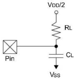
text_image
Pin VDD/2 RL CL VssLoad Condition 2 – for OSCO
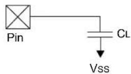
$$ R L = 4 6 4 \Omega $$
$$ \begin{array}{r l} \mathrm{CL} & = 5 0 \mathrm{pF} \text { for all pins except OSCO } \ & 1 5 \mathrm{pF} \text { for OSCO output } \end{array} $$
TABLE 24-26: CAPACITIVE LOADING REQUIREMENTS ON OUTPUT PINS
| Param No. | Symbol | Characteristic Min. Typ. Max. | Units Conditions | ||||
| DO50 | Cosco | OSCO Pin | — | — | 15 | pF | In XT and HS modes, when External Clock is used to drive OSCI |
| DO56 | Cio | All I/O Pins and OSCO | — | — | 50 | pF | EC mode |
| DO58 | CB | SCLx, SDAx | — | — | 400 | pF | In I^2C mode |
FIGURE 24-2: EXTERNAL CLOCK TIMING

text_image
Q1 Q2 Q3 Q4 Q1 Q2 Q3 Q4 OSCI OS20 OS30 OS30 OS31 OS31 OS25 CLKO OS41 OS40TABLE 24-27: EXTERNAL CLOCK TIMING REQUIREMENTS
| AC CHARACTERISTICS | Standard Operating Conditions: 3.0V to 3.6V(unless otherwise stated)Operating temperature -40°C ≤ TA ≤ +85°C for Industrial-40°C ≤ AT ≤ +125°C for Extended | |||||||
| Param No. | Sym | Characteristic Min. Typ. | (1) | Max. Units | Conditions | |||
| OS10 Fin External CLKI Frequency(External Clocks allowed only in EC and ECP LL modes) | DC | — | 64 | MHz | EC | |||
| Oscillator Crystal Frequency | 3.5 | — | 10 | MHz | XT | |||
| 10 | — | 32 | MHz | HS | ||||
| OS20 T osc | Tosc = 1/Fosc | 15.6 | — | DC | ns | |||
| OS25 T cy | Instruction Cycle Time ^(2) | 10 | — | DC | ns | |||
| OS30 TosL, TosH | External Clock in (OSCI)High or Low Time | 0.45 x Tosc | — | 0.55 x Tosc | ns | EC | ||
| OS31 TosR, TosF | External Clock in (OSCI)Rise or Fall Time | — | — | 20 | ns | EC | ||
| OS40 TckR CLKO Rise Time ^(3,4) | — | 5.4 | — | ns | ||||
| OS41 TckF CLKO Fall Time ^(3,4) | — | 6.4 | — | ns | ||||
| OS42 GM External OscillatorTransconductance ^(3) | 2.7 | — | 4 | mA/V | XTCFG[1:0] = 00, XTBST = 0 | |||
| 4 | — | 7 | mA/V | XTCFG[1:0] = 00, XTBST = 1 | ||||
| 4.5 | — | 7 | mA/V | XTCFG[1:0] = 01, XTBST = 0 | ||||
| 6 | — | 11.9 | mA/V | XTCFG[1:0] = 01, XTBST = 1 | ||||
| 5.9 | — | 9.7 | mA/V | XTCFG[1:0] = 10, XTBST = 0 | ||||
| 6.9 | — | 15.9 | mA/V | XTCFG[1:0] = 10, XTBST = 1 | ||||
| 6.7 | — | 12 | mA/V | XTCFG[1:0] = 11, XTBST = 0 | ||||
| 7.5 | — | 19 | mA/V | XTCFG[1:0] = 11, XTBST = 1 | ||||
Note 1: Data in "Typ." column are at 3.3V, +25°C unless otherwise stated.
2: Instruction cycle period (TCY) equals two times the input oscillator time base period. All specified values are based on characterization data for that particular oscillator type, under standard operating conditions, with the device executing code. Exceeding these specified limits may result in an unstable oscillator operation and/or higher than expected current consumption. All devices are tested to operate at "Minimum" values with an External Clock applied to the OSCI pin. When an External Clock input is used, the "Maximum" cycle time limit is "DC" (no clock) for all devices.
3: Measurements are taken in EC mode. The CLKO signal is measured on the OSCO pin.
4: This parameter is characterized but not tested in manufacturing.
TABLE 24-28: PLL CLOCK TIMING SPECIFICATIONS
| AC CHARACTERISTICS | Standard Operating Conditions: 3.0V to 3.6V(unless otherwise stated)Operating temperature -40°C ≤ TA ≤ +85°C for Industrial-40°C ≤ AT ≤ +125°C for Extended | ||||||
| Param No. | Symbol | Characteristic Min. Typ. | (1) | Max. Units | Conditions | ||
| OS50 FPL | LLI PLL Vol | tage Controlled Oscillator(VCO) Input Frequency Range | 8^(2) | — 64 | MHz | ECPLL, XTPLL modes | |
| OS51 | Fvco | On-Chip VCO System Frequency | 400 | — | 1600 | MHz | |
| OS52 T | LOCK | PLL Start-up Time (Lock Time) | — | 60 | — | μs | |
Note 1: Data in "Typ." column are at 3.3V, +25°C unless otherwise stated. Parameters are for design guidance only and are not tested.
2: Inclusive of FRC Tolerance Specification F20a.
TABLE 24-29: AUXILIARY PLL CLOCK TIMING SPECIFICATIONS
| AC CHARACTERISTICS | Standard Operating Conditions: 3.0V to 3.6V(unless otherwise stated)Operating temperature -40°C ≤ TA ≤ +85°C for Industrial-40°C ≤ TA ≤ +125°C for Extended | ||||||
| Param No. | Symbol | Characteristic | Min. Typ. (1) | Max. Units | Conditions | ||
| OS50 F | LLI APLL V | Voltage Controlled Oscillator(VCO) Input Frequency Range | 8^(2) | — 64 | MHz | ECPLL, XTPLL modes | |
| OS51 F | vco | On-Chip VCO System Frequency | 400 | — | 1600 | MHz | |
| OS52 | TLOCK | APLL Start-up Time (Lock Time) | — | 60 | — | μs | |
Note 1: Data in "Typ" column are at 3.3V , +25^ unless otherwise stated. Parameters are for design guidance only and are not tested in manufacturing.
2: Inclusive of FRC Tolerance Specification F20a.
TABLE 24-30: INTERNAL FRC ACCURACY
| AC CHARACTERISTICS | Standard Operating Conditions: 3.0V to 3.6V (unless otherwise stated)Operating temperature -40°C ≤ TA ≤ +85°C for Industrial-40°C ≤ AT ≤ +125°C for Extended | |||||
| Param No. | Characteristic Min. | Typ. Max. | Units Conditions | |||
| Internal FRC Accuracy @ FRC Frequency = 8 MHz(1) | ||||||
| F20a FRC | -2(2) | — | +2 | % | -40°C ≤ TA ≤ -5°C | |
| -1.5 | — | +1.5 | % | -5°C ≤ TA ≤ +85°C | ||
| F20b | FRC | -2 | — | +2 | % | +85°C ≤ TA ≤ +125°C |
| F22 | BFRC | -17 | — | +17 | % | -40°C ≤ TA ≤ +125°C |
Note 1: Frequency is calibrated at +25^ and 3.3V. TUNx bits can be used to compensate for temperature drift.
2: Due to the effect of aging, this value may drift by an additional -0.5% over the lifetime of the device.
TABLE 24-31: INTERNAL LPRC ACCURACY
| AC CHARACTERISTICS | Standard Operating Conditions: 3.0V to 3.6V (unless otherwise stated)Operating temperature -40°C ≤ TA ≤ +85°C for Industrial-40°C ≤ TA ≤ +125°C for Extended | ||||||
| Param No. | Characteristic | Min. | Typ. | Max. | Units | Conditions | |
| LPRC @ 32 kHz | |||||||
| F21a | LPRC | -30 | — | +30 | % | -40°C ≤ TA ≤ -10°C | V_DD = 3.0-3.6V |
| -20 | — | +20 | % | -10°C ≤ TA ≤ +85°C | V_DD = 3.0-3.6V | ||
| F21b | LPRC | -30 | — | +30 | % | +85°C ≤ TA ≤ +125°C | V_DD = 3.0-3.6V |
FIGURE 24-3: I/O TIMING CHARACTERISTICS

text_image
I/O Pin (Input) DI35 DI40 I/O Pin (Output) Old Value New Value DO31 DO32 Note: Refer to Figure 24-1 for load conditions.TABLE 24-32: I/O TIMING REQUIREMENTS
| AC CHARACTERISTICS | Standard Operating Conditions: 3.0V to 3.6V(unless otherwise stated)Operating temperature -40°C ≤ TA ≤ +85°C for Industrial-40°C ≤ AT ≤ +125°C for Extended | ||||||
| Param No. | Symbol C | Characteristic Min. Typ. | (1) | Max. Units Conditions | |||
| DO31 TioR | Port | Output Rise Time (2) | — | 6.5 | 9.7 | ns | |
| DO32 T | IOF Port | Output Fall Time (2) | — | 3.2 | 4.2 | ns | |
| DI35 | TINP | INTx Pin High or Low Time (input) | 20 | — | — | ns | |
| DI40 | TRBP | CNx High or Low Time (input) | 2 | — | — | Tcy | |
Note 1: Data in "Typ." column are at 3.3V, +25°C unless otherwise stated.
2: This parameter is characterized but not tested in manufacturing.
FIGURE 24-4: BOR AND MAIN CLEAR RESET TIMING CHARACTERISTICS

flowchart
graph TD
    A["MCLR"] --> B["TMCLR (SY20)"]
    B --> C["Reset Sequence"]
    D["BOR"] --> E["TBOR (SY30)"]
    E --> F["Various Delays (depending on configuration)"]
    G["CPU Starts Fetching Code"] --> H["End"]
TABLE 24-33: RESET, WATCHDOG TIMER, OSCILLATOR START-UP TIMER, TIMING REQUIREMENTS
| AC CHARACTERISTICS | Standard Operating Conditions: 3.0V to 3.6V(unless otherwise stated)Operating temperature -40°C ≤ TA ≤ +85°C for Industrial-40°C ≤ AT≤ +125°C for Extended | ||||||
| Param No. | Symbol C | characteristic (1) | Min. Typ. (2) | Max. | Units C | conditions | |
| SY00 | TPU | Power-up Period | — | 200 | — | μs | |
| SY10 | TOST | Oscillator Start-up Time | — | 1024 Tosc | — | — | Tosc = OSCI period |
| SY13 T | IOZ | I/O High-Impedance from MCLR Low or Watchdog Timer Reset | — | 1.5 | — | μs | |
| SY20 T | MCLR | MCLR Pulse Width (low) | 2 | — | — | μs | |
| SY30 T | BOR | BOR Pulse Width (low) | 1 | — | — | μs | |
| SY35 T | FSCM | Fail-Safe Clock Monitor Delay | — | 500 | 900 | μs | -40°C to +85°C |
| SY36 T | VREG | Voltage Regulator Standby-to-Active mode Transition Time | — | — | 40 | μs | Clock fail to BFRC switch |
| SY37 | TOSCDFRC | FRC Oscillator Start-up Delay | — | — | 15 | μs | From POR event |
| SY38 | TOSCDLPRC | LPRC Oscillator Start-up Delay | — | — | 50 | μs | From Reset event |
Note 1: These parameters are characterized but not tested in manufacturing.
2: Data in "Typ." column are at 3.3V, +25°C unless otherwise stated.
FIGURE 24-5: HIGH-SPEED PWMx MODULE FAULT TIMING CHARACTERISTICS
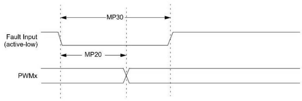
text_image
MP30 Fault Input (active-low) MP20 PWMxFIGURE 24-6: HIGH-SPEED PWMx MODULE TIMING CHARACTERISTICS
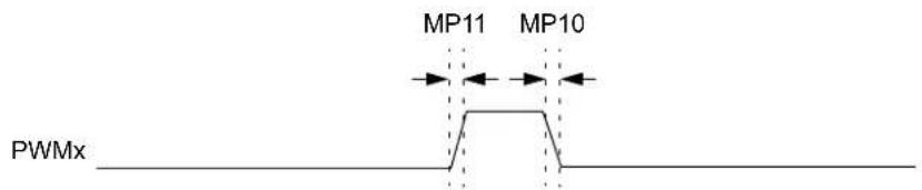
text_image
MP11 MP10 PWMxNote: Refer to Figure 24-1 for load conditions.
TABLE 24-34: HIGH-SPEED PWMx MODULE TIMING REQUIREMENTS
| AC CHARACTERISTICS | Standard Operating Conditions: 3.0V to 3.6V(unless otherwise stated)Operating temperature -40°C ≤ TA ≤ +85°C for Industrial-40°C ≤ AT ≤ +125°C for Extended | ||||||
| Param No. | Symbol | Characteristic (1) | Min. Typ. Max. | Units Conditions | |||
| MP00 | FIN | PWM Input Frequency | — | 500 | MHz | (Note 2) | |
| MP10 T | FPWM | PWMx Output Fall Time | — | — | — | ns | See Parameter DO32 |
| MP11 | TRPWM | PWMx Output Rise Time | — | — | — | ns | See Parameter DO31 |
| MP20 | TFD | Fault Input ↓ to PWMx I/O Change | — | — | 26 ns | PCI | Inputs 19 through 22 |
| MP30 | TFH | Fault Input Pulse Width | 8 | — | — | ns | |
Note 1: These parameters are characterized but not tested in manufacturing.
2: Input frequency of 500 MHz must be used for High-Resolution mode.
TABLE 24-35: SPIx MAXIMUM DATA/CLOCK RATE SUMMARY
| SPI Main Transmit Only (Half-Duplex) | SPI Main Transmit/Receive (Full-Duplex) | SPI Secondary Transmit/Receive (Full-Duplex) | CKE |
| Figure 24-7 Table 24-36 | — | — | 0 |
| Figure 24-8 Table 24-36 | — | — | 1 |
| — | Figure 24-9 Table 24-37 | — 0 | |
| — | Figure 24-10 Table 24-38 | — 1 | |
| — | — | Figure 24-12 Table 24-40 | 0 |
| — | — | Figure 24-13 Table 24-39 | 1 |
FIGURE 24-7: SPIx HOST MODE (HALF-DUPLEX, TRANSMIT ONLY, CKE = 0) TIMING CHARACTERISTICS

text_image
SCKx (CKP = 0) SP10 SP20SP21 SCKx (CKP = 1) SP21SP20SP35 SDOx MSb LSbBit 14 - - - - - - - - - - - - - - - - - - - - - - - - - - - - - - - - - - - - - - - - - - - - - - - - - - - - - - - - - - - - - - - - - - - - - - - - - - - - - - - - - - - - - - - - - SP30, SP31 SP30', SP31Note: Refer to Figure 24-1 for load conditions.
FIGURE 24-8: SPIx HOST MODE (HALF-DUPLEX, TRANSMIT ONLY, CKE = 1) TIMING CHARACTERISTICS
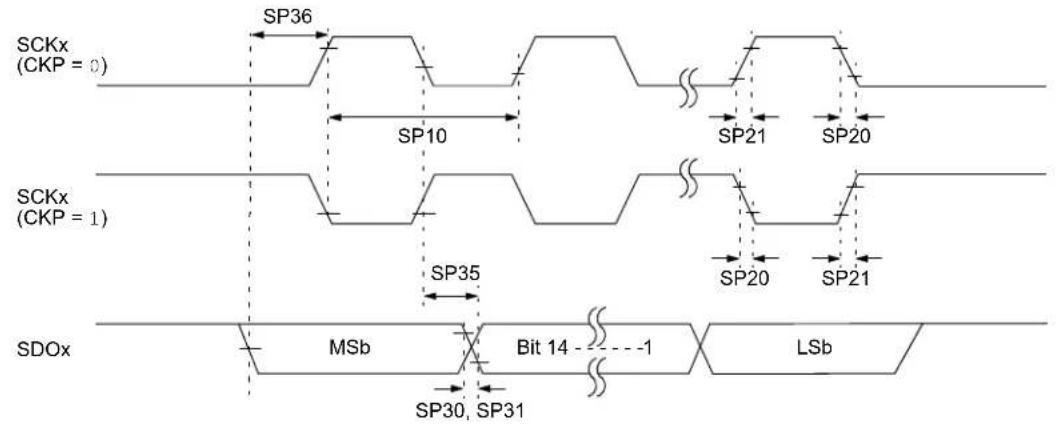
text_image
SCKx (CKP = 0) SP36 SP10 SP21 SP20 SCKx (CKP = 1) SP35 SP20 SP21 SDOx MSb Bit 14 LSb SP30, SP31Note: Refer to Figure 24-1 for load conditions.
TABLE 24-36: SPIx HOST MODE (HALF-DUPLEX, TRANSMIT ONLY) TIMING REQUIREMENTS
| AC CHARACTERISTICS | Standard Operating Conditions: 3.0V to 3.6V(unless otherwise stated)Operating temperature -40°C ≤ TA ≤ +85°C for Industrial-40°C ≤ TA ≤ +125°C for Extended | ||||||
| Param No. | Symbol C | Characteristic (1) | Min. Typ. (2) | Max. Units Conditions | |||
| SP10 | FscP | Maximum SCKx Frequency | — | — | 15 | MHz | Using PPS pins |
| — — | 40 | MHz | SPI2 dedicated pins | ||||
| SP20 | TscF | SCKx Output Fall Time | — | — | — | ns | See Parameter DO32(Note 3) |
| SP21 | TscR | SCKx Output Rise Time | — | — | — | ns | See Parameter DO31(Note 3) |
| SP30 | TdoF | SDOx Data Output Fall Time | — | — | — | ns | See Parameter DO32(Note 3) |
| SP31 | TdoR | SDOx Data Output Rise Time | — | — | — | ns | See Parameter DO31(Note 3) |
| SP35 TscH2doV,TscL2doV | SDOx Data Output Valid After SCKx Edge | — | 6 20 | ns | |||
| SP36 | TdiV2scH,TdiV2scL | SDOx Data Output Setup to First SCKx Edge | 30 | — — | ns | Using | PPS pins |
| 3 | — — | ns | SPI2 dedicated pins | ||||
Note 1: These parameters are characterized but not tested in manufacturing.
2: Data in "Typ." column are at 3.3V, +25°C unless otherwise stated.
3: Assumes 50 pF load on all SPIx pins.
FIGURE 24-9: SPIx HOST MODE (FULL-DUPLEX, CKE = 1, CKP = x, SMP = 1) TIMING CHARACTERISTICS
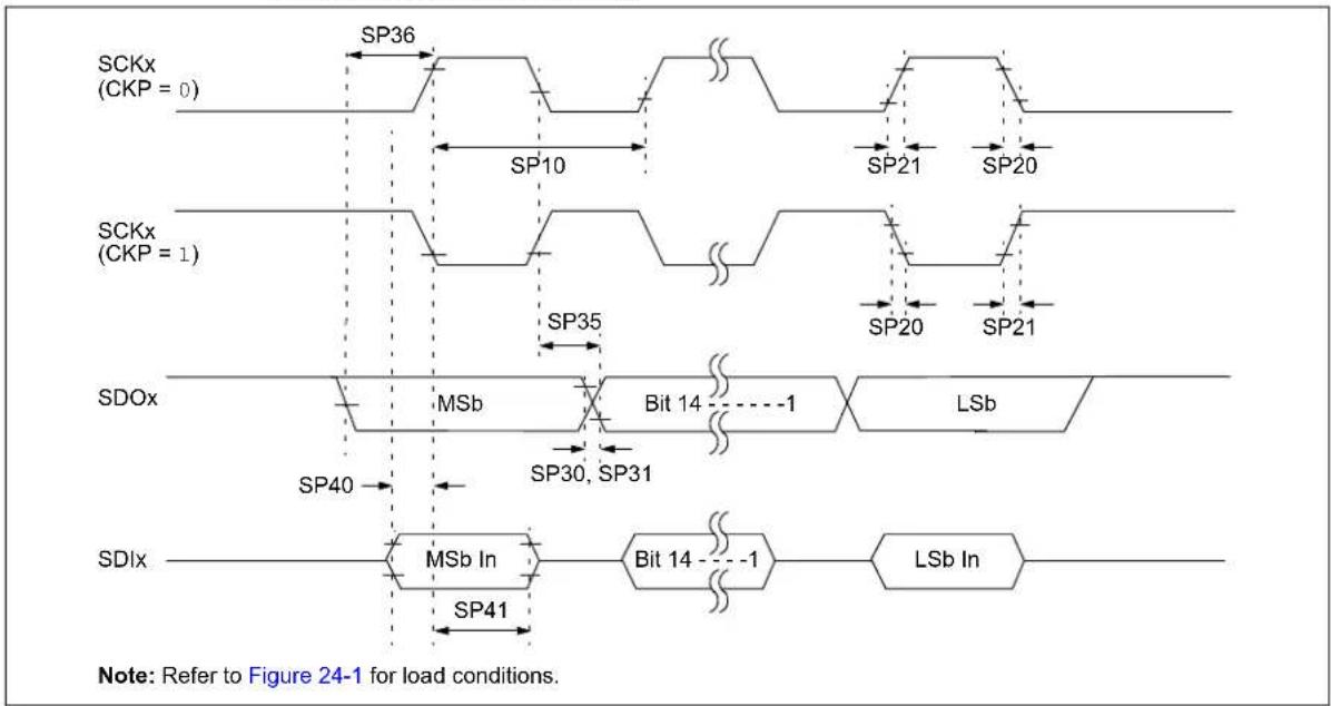
flowchart
graph TD
    A["SCKx (CKP = 0)"] --> B["SP36"]
    B --> C["SP10"]
    C --> D["SP21"]
    D --> E["SP20"]
    F["SCKx (CKP = 1)"] --> G["SP35"]
    G --> H["SP20"]
    H --> I["SP21"]
    J["SDOx"] --> K["MSb"]
    K --> L["Bit 14 - - - - 1"]
    L --> M["LSb"]
    N["SDIx"] --> O["MSb In"]
    O --> P["Bit 14 - - - - 1"]
    P --> Q["LSb In"]
    R["Note: Refer to Figure 24-1 for load conditions."]
TABLE 24-37: SPIx HOST MODE (FULL-DUPLEX, CKE = 1, CKP = x, SMP = 1) TIMING REQUIREMENTS
| AC CHARACTERISTICS | Standard Operating Conditions: 3.0V to 3.6V(unless otherwise stated)Operating temperature -40°C ≤ TA ≤ +85°C for Industrial-40°C ≤ AT ≤ +125°C for Extended | ||||||
| Param No. | Symbol C | characteristic (1) | Min. Typ. (2) | Max. Units Conditions | |||
| SP10 | FscP | Maximum SCKx Frequency | — | — | 15 | MHz | Using PPS pins |
| — | —40 | MHz | SPI2 dedicated pins | ||||
| SP20 | TscF | SCKx Output Fall Time | — | — | — | ns | See Parameter DO32 (Note 3) |
| SP21 | TscR | SCKx Output Rise Time | — | — | — | ns | See Parameter DO31 (Note 3) |
| SP30 T | doF | SDOx Data Output Fall Time | — | — | — | ns | See Parameter DO32 (Note 3) |
| SP31 T | doR | SDOx Data Output Rise Time | — | — | — | ns | See Parameter DO31 (Note 3) |
| SP35 T | tscH2doV, TscL2doV | SDOx Data Output Valid After SCKx Edge | — | 6 | 20 | ns | |
| SP36 T | doV2sc, TdoV2scL | SDOx Data Output Setup to First SCKx Edge | 30 | — | — | ns | Using PPS pins |
| 3 | — | — | ns | SPI2 dedicated pins | |||
| SP40 T | diV2scH, TdiV2scL | Setup Time of SDlx Data Input to SCKx Edge | 30 | — | — | ns | Using PPS pins |
| 20 | — | — | ns | SPI2 dedicated pins | |||
| SP41 T | tscH2diL, TscL2diL | Hold Time of SDlx Data Input to SCKx Edge | 30 | — | — | ns | Using PPS pins |
| 15 | — | — | ns | SPI2 dedicated pins | |||
Note 1: These parameters are characterized but not tested in manufacturing.
2: Data in "Typ." column are at 3.3V, +25°C unless otherwise stated.
3: Assumes 50 pF load on all SPIx pins.
FIGURE 24-10: SPIx HOST MODE (FULL-DUPLEX, CKE = 0, CKP = x, SMP = 1) TIMING CHARACTERISTICS

flowchart
graph TD
    A["SCKx (CKP = 0)"] --> B["SP10"]
    B --> C["SP21"]
    C --> D["SP20"]
    E["SCKx (CKP = 1)"] --> F["SP35 SP36"]
    F --> G["SP20"]
    G --> H["SP21"]
    I["SDOx"] --> J["MSb"]
    J --> K["Bit 14 - 1"]
    K --> L["LSb"]
    M["SDlx"] --> N["MSb In"]
    N --> O["Bit 14 - 1"]
    O --> P["LSb In"]
    Q["Note: Refer to Figure 24-1 for load conditions."]
TABLE 24-38: SPIx HOST MODE (FULL-DUPLEX, CKE = 0, CKP = x, SMP = 1) TIMING REQUIREMENTS
| AC CHARACTERISTICS | Standard Operating Conditions: 3.0V to 3.6V(unless otherwise stated)Operating temperature -40°C ≤ TA ≤ +85°C for Industrial-40°C ≤ AT ≤ +125°C for Extended | ||||||
| Param No. | Symbol C | Characteristic (1) | Min. Typ. (2) | Max. Units Conditions | |||
| SP10 | FscP | Maximum SCKx Frequency | — | — | 15 | MHz | Using PPS pins |
| — | — | 40 | MHz | SPI2 dedicated pins | |||
| SP20 | TscF | SCKx Output Fall Time | — | — | — | ns | See Parameter DO32 (Note 3) |
| SP21 | TscR | SCKx Output Rise Time | — | — | — | ns | See Parameter DO31 (Note 3) |
| SP30 | TdoF | SDOx Data Output Fall Time | — | — | — | ns | See Parameter DO32 (Note 3) |
| SP31 | TdoR | SDOx Data Output Rise Time | — | — | — | ns | See Parameter DO31 (Note 3) |
| SP35 TscH2doV, TscL2doV | SDOx Data Output Valid After SCKx Edge | — | 6 | 20 | ns | ||
| SP36 TdoV2scH, TdoV2scL | SDOx Data Output Setup to First SCKx Edge | 30 | — | — | ns Using PPS pins | ||
| 20 | — | — | ns SPI2 dedicated pins | ||||
| SP40 TdV2scH, TdiV2scL | Setup Time of SDIx Data Input to SCKx Edge | 30 | — | — | ns Using PPS pins | ||
| 10 | — | — | ns SPI2 dedicated pins | ||||
| SP41 TscH2diL, TscL2diL | Hold Time of SDIx Data Input to SCKx Edge | 30 | — | — | ns Using PPS pins | ||
| 15 | — | — | ns SPI2 dedicated pins | ||||
Note 1: These parameters are characterized but not tested in manufacturing.
2: Data in "Typ." column are at 3.3V, +25°C unless otherwise stated.
3: Assumes 50 pF load on all SPIx pins.
FIGURE 24-11: SPIx CLIENT MODE (FULL-DUPLEX, CKE = 0, CKP = x, SMP = 0) TIMING CHARACTERISTICS

flowchart
graph TD
    subgraph SSx
        A["SP50"] --> B["SCKx (CKP = 0)"]
        B --> C["SP10"]
        C --> D["SCKx (CKP = 1)"]
        D --> E["SP35 SP36"]
        E --> F["SDOx"]
        F --> G["MSb LSbBit14"]
        G --> H["SP30, SP31 SP51"]
        H --> I["SDIx"]
        I --> J["MSb In"]
        J --> K["Bit 14"]
        K --> L["SP40"]
        L --> M["SP41"]
        M --> N["SP52"]
        N --> O["SP72SP73"]
        O --> P["SP73SP72"]
    end
Note: Refer to Figure 24-1 for load conditions.
TABLE 24-39: SPIx CLIENT MODE (FULL-DUPLEX, CKE = 0, CKP = x, SMP = 0) TIMING REQUIREMENTS
| AC CHARACTERISTICS | Standard Operating Conditions: 3.0V to 3.6V(unless otherwise stated)Operating temperature -40°C ≤ TA ≤ +85°C for Industrial-40°C ≤ AT≤ +125°C for Extended | ||||||
| Param No. | Symbol C | Characteristic (1) | Min. Typ. | (2) | Max. Units Conditions | ||
| SP10 | FscP | Maximum SCKx Input Frequency | — | — | 15 | MHz | Using PPS pins |
| — | — | 40 | MHz | SPI2 dedicated pins | |||
| SP72 | TscF | SCKx Input Fall Time | — | — | — | ns | See Parameter DO32 (Note 3) |
| SP73 | TscR | SCKx Input Rise Time | — | — | — | ns | See Parameter DO31 (Note 3) |
| SP30 | TdoF | SDOx Data Output Fall Time | — | — | — | ns | See Parameter DO32 (Note 3) |
| SP31 | TdoR | SDOx Data Output Rise Time | — | — | — | ns | See Parameter DO31 (Note 3) |
| SP35 TscH2doV, TscL2doV | SDOx Data Output Valid After SCKx Edge | — | 6 | 20 | ns | ||
| SP36 TdoV2scH, TdoV2scL | SDOx Data Output Setup to First SCKx Edge | 30 | — | — | ns | Using PPS pins | |
| 20 | — | — | ns | SPI2 dedicated pins | |||
| SP40 TdiV2scH, TdiV2scL | Setup Time of SDIx Data Input to SCKx Edge | 30 | — | — | ns | Using PPS pins | |
| 10 | — | — | ns | SPI2 dedicated pins | |||
| SP41 TscH2diL, TscL2diL | Hold Time of SDIx Data Input to SCKx Edge | 30 | — | — | ns | Using PPS pins | |
| 15 | — | — | ns | SPI2 dedicated pins | |||
| SP50 TssL2scH, TssL2scL | to SCKx ↑ or SCKx ↓ Input | 120 | — | — | ns | ||
| SP51 TssH2doZ SSx ↑ to SDOx Output High-Impedance | 8 | — | 50 | ns | (Note 3) | ||
| SP52 TscH2ssH, TscL2ssH | After SCKx Edge | 1.5 TCY + 40 | — | — | ns | (Note 3) | |
Note 1: These parameters are characterized but not tested in manufacturing.
2: Data in "Typ." column are at 3.3V, +25°C unless otherwise stated.
3: Assumes 50 pF load on all SPIx pins.
FIGURE 24-12: SPIx CLIENT MODE (FULL-DUPLEX, CKE = 1, CKP = x, SMP = 0) TIMING CHARACTERISTICS

flowchart
graph TD
    subgraph SSx
        A["SP60"] --> B["SCKx (CKP = 0)"]
        B --> C["SP50"]
        C --> D["SCKx (CKP = 1)"]
        D --> E["SP10"]
        E --> F["SCKx (CKP = 0)"]
        F --> G["SP52"]
        G --> H["SP72SP73"]
        H --> I["SP36"]
        I --> J["SCKx (CKP = 1)"]
        J --> K["SP35"]
        K --> L["SCKx (CKP = 1)"]
        L --> M["SP73SP72"]
    end
    subgraph SDOx
        N["MSb Bit 14"] --> O["1 LSb"]
        P["SP30, SP31"] --> Q["1 LSb In"]
        R["SP51"] --> S["1 LSb In"]
        T["SDlx"] --> U["MSb In"]
        V["SP40"] --> W["Bit 14"]
        X["SP41"] --> Y["Bit 14"]
    end
    style SSx fill:#f9f,stroke:#333
    style SCKx fill:#ccf,stroke:#333
    style SDOx fill:#cfc,stroke:#333
    style SDlx fill:#fcc,stroke:#333
Note: Refer to Figure 24-1 for load conditions.
TABLE 24-40: SPIx CLIENT MODE (FULL-DUPLEX, CKE = 1, CKP = x, SMP = 0) TIMING REQUIREMENTS
| AC CHARACTERISTICS | Standard Operating Conditions: 3.0V to 3.6V(unless otherwise stated)Operating temperature -40°C ≤ TA ≤ +85°C for Industrial-40°C ≤ TA ≤ +125°C for Extended | ||||||
| Param No. | Symbol C | Characteristic (1) | Min. Typ. | (2) | Max. Units Conditions | ||
| SP10 FscP Maximum | SCKx Input Frequency | — — | 15 | MHz Using PPS pins | |||
| — — | 40 | MHz SPI2 dedicated pins | |||||
| SP72 | TscF | SCKx Input Fall Time | — | — | — | ns | See Parameter DO32 (Note 3) |
| SP73 | TscR | SCKx Input Rise Time | — | — | — | ns | See Parameter DO31 (Note 3) |
| SP30 | TdoF | SDOx Data Output Fall Time | — | — | — | ns | See Parameter DO32 (Note 3) |
| SP31 | TdoR | SDOx Data Output Rise Time | — | — | — | ns | See Parameter DO31 (Note 3) |
| SP35 TscH2doV, TscL2doV | SDOx Data Output Valid After SCKx Edge | — | 6 | 20 ns | |||
| SP36 TdoV2scH, TdoV2scL | SDOx Data Output Setup to First SCKx Edge | 30 | — | — | ns | Using PPS pins | |
| 20 | — | — | ns | SPI2 dedicated pins | |||
| SP40 TdiV2scH, TdiV2scL | Setup Time of SDIx Data Input to SCKx Edge | 30 | — | — | ns | Using PPS pins | |
| 10 | — | — | ns | SPI2 dedicated pins | |||
| SP41 TscH2diL, TscL2diL | Hold Time of SDIx Data Input to SCKx Edge | 30 | — | — | ns | Using PPS pins | |
| 15 | — | — | ns | SPI2 dedicated pins | |||
| SP50 | TssL2scH, TssL2scL | SSx ↓ to SCKx ↑ or SCKx ↓ Input | 120 | — | — | ns | |
| SP51 TssH2doZ SSx | ↑ to SDOx Output High-Impedance | 8 | — | 50 | ns | (Note 3) | |
| SP52 | TscH2ssH, TscL2ssH | SSx ↑ After SCKx Edge | 1.5 TCY + 40 | — | — | ns | (Note 3) |
| SP60 | TssL2doV | SDOx Data Output Valid After SSx Edge | — — | 50 | ns | ||
Note 1: These parameters are characterized but not tested in manufacturing.
2: Data in "Typ." column are at 3.3V, +25°C unless otherwise stated.
3: Assumes 50 pF load on all SPIx pins.
FIGURE 24-13: I2Cx BUS START/STOP BITS TIMING CHARACTERISTICS (HOST MODE)
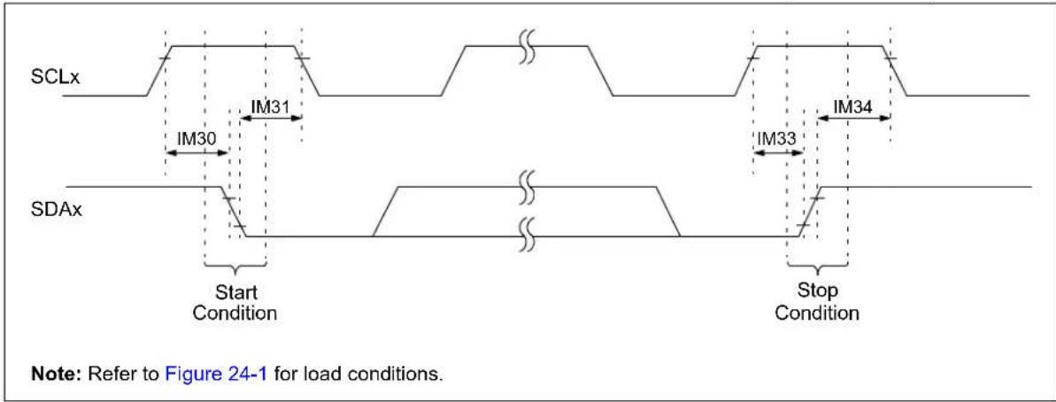
text_image
SCLx IM30 IM31 SDAx Start Condition Stop Condition IM33 IM34 Note: Refer to Figure 24-1 for load conditions.FIGURE 24-14: I2Cx BUS DATA TIMING CHARACTERISTICS (HOST MODE)
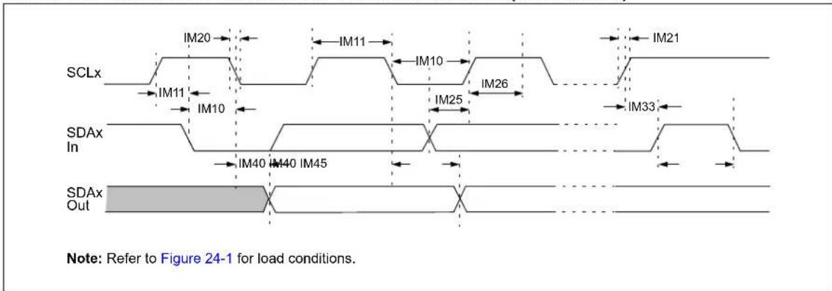
text_image
SCLx IM20 IM11 IM10 IM26 IM21 IM11 IM10 IM25 IM33 SDAx In IM40 IM40 IM45 SDAx Out Note: Refer to Figure 24-1 for load conditions.TABLE 24-41: I2Cx BUS DATA TIMING REQUIREMENTS (HOST MODE)
| AC CHARACTERISTICS | Standard Operating Conditions: 3.0V to 3.6V(unless otherwise stated)Operating temperature -40°C ≤ TA ≤ +85°C for Industrial-40°C ≤ TA ≤ +125°C for Extended | ||||||
| Param No. | Symbol | Characteristic (4) | Min.(1) | Max. Units | Conditions | ||
| IM10 T | LO:SCL | Clock Low Time | 100 kHz mode | TCY (BRG + 1) | — | μs | |
| 400 kHz mode | TCY (BRG + 1) | — | μs | ||||
| 1MHzmode^( 2) | TCY (BRG + 1) — | μs | |||||
| IM11 | THI:SCL | Clock High Time | 100 kHz mode | TCY (BRG + 1) | — | μs | |
| 400 kHz mode | TCY (BRG + 1) | — | μs | ||||
| 1MHzmode^( 2) | TCY (BRG + 1) — | μs | |||||
| 100 kHz mode | — | 300 | ns | CB is specified to be from 10 to 400 pF | |||
| 400 kHz mode | 20 x (VDD/5.5V) | 300 | ns | ||||
| 1MHzmode^( 2) | — | 120 | ns | ||||
| IM20 T | F:SCL | SDAx and SCLx Fall Time | 100 kHz mode | — | 1000 | ns | CB is specified to be from 10 to 400 pF |
| 400 kHz mode | 20 + 0.1 CB | 300 | ns | ||||
| 1MHzmode^( 2) | — | 120 | ns | ||||
| IM21 T | R:SCL | SDAx and SCLx Rise Time | 100 kHz mode | 250 | — | ns | |
| 400 kHz mode | 100 | — | ns | ||||
| 1MHzmode^( 2) | 50 | — | ns | ||||
| IM25 T | SU:DAT | Data Input Setup Time | 100 kHz mode | 0 | — | μs | |
| 400 kHz mode | 0 | 0.9 | μs | ||||
| 1MHzmode^( 2) | 0 | 0.3 | μs | ||||
| IM26 T | HD:DAT | Data Input Hold Time | 100 kHz mode | TCY (BRG + 1) | — | μs | Only relevant for Repeated Start condition |
| 400 kHz mode | TCY (BRG + 1) | — | μs | ||||
| 1MHzmode^( 2) | TCY (BRG + 1) — | μs | |||||
| IM30 T | SU:STA | Start Condition Setup Time | 100 kHz mode | TCY (BRG + 1) | — | μs | After this period, the first clock pulse is generated |
| 400 kHz mode | TCY (BRG + 1) | — | μs | ||||
| 1MHzmode^( 2) | TCY (BRG + 1) — | μs | |||||
| IM31 T | HD:STA | Start Condition Hold Time | 100 kHz mode | TCY (BRG + 1) | — | μs | |
| 400 kHz mode | TCY (BRG + 1) | — | μs | ||||
| 1MHzmode^( 2) | TCY (BRG + 1) — | μs | |||||
| IM33 T | SU:STO | Stop Condition Setup Time | 100 kHz mode | TCY (BRG + 1) | — | μs | |
| 400 kHz mode | TCY (BRG + 1) | — | μs | ||||
| 1MHzmode^( 2) | TCY (BRG + 1) — | μs | |||||
| 100 kHz mode | TCY (BRG + 1) | — | μs | ||||
| IM34 T | HD:STO | Stop Condition Hold Time | 400 kHz mode | TCY (BRG + 1) | — | μs | |
| 1MHzmode^( 2) | TCY (BRG + 1) — | μs | |||||
| IM40 T | AA:SCL | Output Valid from Clock | 100 kHz mode | — | 3450 | ns | |
| 400 kHz mode | — | 900 | ns | ||||
| 1MHzmode^( 2) | — | 450 | ns | ||||
| IM45 T | BF:SDA | Bus Free Time | 100 kHz mode | 4.7 | — | μs | Time the bus must be free before a new transmission can start |
| 400 kHz mode | 1.3 | — | μs | ||||
| 1MHzmode^( 2) | 0.5 | — | μs | ||||
| IM50 C | B | Bus Capacitive Loading | — | 400 | pF | ||
| IM51 T | PGD | Pulse Gobbler Delay | 65 | 390 | ns | (Note 3) | |
Note 1: BRG is the value of the I ^2 C Baud Rate Generator.
2: Maximum Pin Capacitance = 10 pF for all I2Cx pins (for 1 MHz mode only).
3: Typical value for this parameter is 130 ns.
4: These parameters are characterized but not tested in manufacturing.
FIGURE 24-15: I2Cx BUS START/STOP BITS TIMING CHARACTERISTICS (CLIENT MODE)

text_image
SCLx IS30 IS31 IS34 SDAx Start Condition Stop ConditionFIGURE 24-16: I2Cx BUS DATA TIMING CHARACTERISTICS (CLIENT MODE)
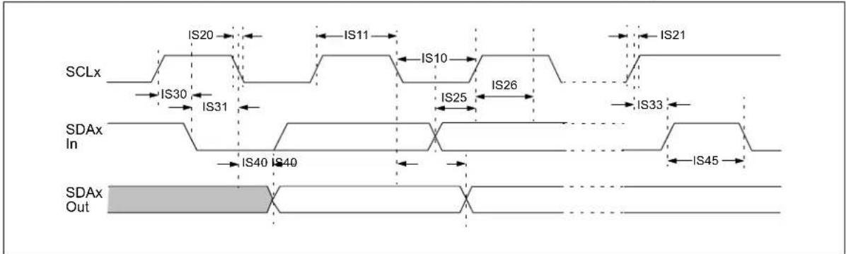
text_image
SCLx IS20 IS11 IS10 IS26 IS21 IS30 IS31 IS25 IS33 SDAx In IS40 IS40 IS45 SDAx OutTABLE 24-42: I2Cx BUS DATA TIMING REQUIREMENTS (CLIENT MODE)
| AC CHARACTERISTICS | Standard Operating Conditions: 3.0V to 3.6V(unless otherwise stated)Operating temperature -40°C ≤ TA ≤ +85°C for Industrial-40°C ≤ TA ≤ +125°C for Extended | ||||||
| Param No. | Symbol | Characteristic (3) | Min. Max. | Units Conditions | |||
| IS10 T | LO:SCL | Clock Low Time | 100 kHz mode | 4.7 | — | μs | |
| 400 kHz mode | 1.3 | — | μs | ||||
| 1MHzmode^(1) | 0.5 | — | μs | ||||
| IS11 | THI:SCL | Clock High Time | 100 kHz mode | 4.0 | — | μs | Device must operate at a minimum of 1.5 MHz |
| 400 kHz mode | 0.6 | — | μs | Device must operate at a minimum of 10 MHz | |||
| 1MHzmode^(1) | 0.28 | — | μs | ||||
| IS20 | TF:SCL | SDAx and SCLx Fall Time | 100 kHz mode | — | 300 | ns | CB is specified to be from 10 to 400 pF |
| 400 kHz mode 20 x (V DD/5.5V) | 300 | ns | |||||
| 1MHzmode^(1) | 20 x (VDD/5.5V) | 120 | ns | ||||
| IS21 | TR:SCL | SDAx and SCLx Rise Time | 100 kHz mode | 20 + 0.1 CB | 1000 | ns | CB is specified to be from 10 to 400 pF |
| 400 kHz mode | 300 | ns | |||||
| 1MHzmode^(1) | — | 120 | ns | ||||
| IS25 | TSU:DAT | Data Input Setup Time | 100 kHz mode | 250 | — | ns | |
| 400 kHz mode | 100 | — | ns | ||||
| 1MHzmode^(1) | 50 | — | ns | ||||
| IS26 | THD:DAT | Data Input Hold Time | 100 kHz mode | 0 | — | μs | |
| 400 kHz mode | 0 | 0.9 | μs | ||||
| 1MHzmode^(1) | 0 | 0.3 | μs | ||||
| IS30 | TSU:STA | Start Condition Setup Time | 100 kHz mode | 4.7 | — | μs | Only relevant for Repeated Start condition |
| 400 kHz mode | 0.6 | — | μs | ||||
| 1MHzmode^(1) | 0.26 | — | μs | ||||
| IS31 | THD:STA | Start Condition Hold Time | 100 kHz mode | 4.0 | — | μs | After this period, the first clock pulse is generated |
| 400 kHz mode | 0.6 | — | μs | ||||
| 1MHzmode^(1) | 0.26 | — | μs | ||||
| IS33 | TSU:STO | Stop Condition Setup Time | 100 kHz mode | 4 | — | μs | |
| 400 kHz mode | 0.6 | — | μs | ||||
| 1MHzmode^(1) | 0.26 | — | μs | ||||
| IS34 | THD:STO | Stop Condition Hold Time | 100 kHz mode | >0 | — | μs | |
| 400 kHz mode | >0 | — | μs | ||||
| 1MHzmode^(1) | >0 | μs | |||||
| IS40 | TAA:SCL | Output Valid from Clock | 100 kHz mode | 0 | 3540 | ns | |
| 400 kHz mode | 0 | 900 | ns | ||||
| 1MHzmode^(1) | 0 | 400 | ns | ||||
| IS45 | TBF:SDA | Bus Free Time | 100 kHz mode | 4.7 | — | μs | Time the bus must be free before a new transmission can start |
| 400 kHz mode | 1.3 | — | μs | ||||
| 1MHzmode^(1) | 0.5 | — | μs | ||||
| IS50 C | B | Bus Capacitive Loading | — | 400 | pF | ||
| IS51 | TPGD | Pulse Gobbler Delay | 65 | 390 | ns | (Note 2) | |
Note 1: Maximum Pin Capacitance = 10 pF for all I2Cx pins (for 1 MHz mode only).
2: Typical value for this parameter is 130 ns.
3: These parameters are characterized but not tested in manufacturing.
FIGURE 24-17: UARTx MODULE I/O TIMING CHARACTERISTICS

flowchart
graph LR
    A["UxRX"] --> B["MSb In"]
    C["UxTX"] --> D["MSb In"]
    B --> E["Bit 6-1"]
    D --> E
    E --> F["LSb In"]
    style A fill:#f9f,stroke:#333
    style C fill:#f9f,stroke:#333
    style B fill:#ccf,stroke:#333
    style D fill:#ccf,stroke:#333
    style E fill:#cfc,stroke:#333
    style F fill:#fcc,stroke:#333
TABLE 24-43: UARTx MODULE I/O TIMING REQUIREMENTS
| AC CHARACTERISTICS | Standard Operating Conditions: 3.0V to 3.6V(unless otherwise stated)Operating temperature -40°C ≤ TA ≤ +125°C | ||||||
| Param No. | Symbol C | Characteristic (1) | Min. Typ. (2) | Max. Units Conditions | |||
| UA10 | TUABAUD | UARTx Baud Time | 66.67 | — | — | ns | |
| UA11 | FBAUD | UARTx Baud Frequency | — | — | 40 | Mbps | |
| UA20 T | CWF | Start Bit Pulse Width to Trigger UARTx Wake-up | 500 | — | — | ns | |
Note 1: These parameters are characterized but not tested in manufacturing.
2: Data in "Typ." column are at 3.3V, +25°C unless otherwise stated. Parameters are for design guidance only and are not tested.
TABLE 24-44: ADC MODULE SPECIFICATIONS
| Operating Conditions: 3.0V to 3.6V (unless otherwise stated) ^(4) Operating temperature -40°C ≤ TA ≤ +85°C for Industrial-40°C ≤ TA ≤ +125°C for Extended | |||||||
| Param No. | Symbol C | Characteristics Min. Typical | Max. Units Conditions | ||||
| Analog Input | |||||||
| AD12 V | INH-VINL | Full-Scale Input Span | AVss | — | AVDD | V | |
| AD14 V | IN | Absolute Input Voltage | AVss – 0.3 | — | AVDD + 0.3 | V | |
| AD60 C | HOLD | Capacitance | — | 5 | — | pF | Dedicated core (Note 1) |
| AD61 C | HOLD | Capacitance | — | 18 | — | pF | Shared core (Note 1) |
| AD62 R | IC | Input Resistance | — | 500 | 1000 | Ω | (Note 1) |
| AD66 V | BG | Internal Voltage Reference Source | 1.14 | 1.2 | 1.26 | V | |
| Clock Requirements | |||||||
| AD67 F | SRC | ADC Module Input Frequency | — | — | 560 | MHz | Clock frequency selected by the CLKSELx bits |
| FCORESRC | ADC Control Clock Frequency | — | — | 250 | MHz | Clock frequency after the first divider controlled by the CLKDIVx bits | |
| FADCORE | ADC SAR Core Clock Frequency | — | — | 70 | MHz | SAR core frequency after the second divider controlled by the ADCSx or SHRADCSx bits | |
| ADC Accuracy | |||||||
| AD20 Nr | Resolution | 12 data bits | bits | ||||
| AD21a | INL_1D | Dedicated Core Integral Nonlinearity (1 Active Core) | -3.5 | -1.5/+1.5 | +3.5 | LSb | 3.5 Msps ^(5) ,TADC = 4 nS (250 MHz),TCORESRC = 8 nS (125 MHz),TADCORE = 16 nS (62.5 MHz),Sampling Time = 4 TADCORE,VDD = 3.3V, AVDD = 3.3V |
| AD22a | DNL_1D | Differential Nonlinearity | >-1 | 1.5 | +3.5 | LSb | |
| AD23a | GERR_1D | Gain Error | >-12 | — | < 12 | LSb | |
| AD24a | OERR_1D | Offset Error | >7.5 | — | < 7.5 | LSb | |
| AD21b | INL_1S | Shared Core Integral Nonlinearity (1 Active Core) | -3.5 | -1.5/+1.5 | +3.5 | LSb | 2.7 Msps ^(6) ,TADC = 4 nS (250 MHz),TCORESRC = 8 nS (125 MHz),TADCORE = 16 nS (62.5 MHz),Sampling Time = 10 TADCORE,VDD = 3.3V, AVDD = 3.3V |
| AD22b | DNL_1S | Shared Core Differential Nonlinearity (1 Active Core) | -1 | 1.5 | +3.5 LSb | ||
| AD23b | GERR_1S | Shared Core Gain Error (1 Active Core) | — | +4 | — | LSb | |
| AD24b | OERR_1S | Shared Core Offset Error (1 Active Core) | — | -4 | — | LSb | |
| AD21c | INL_3D | Dedicated Core Integral Nonlinearity (3 Active Cores) | — | -5/+5 | — | LSb | 3.5 Msps ^(5) ,TADC = 4 nS (250 MHz),TCORESRC = 8 nS (125 MHz),TADCORE = 16 nS (62.5 MHz),Sampling Time = 4 TADCORE,VDD = 3.3V, AVDD = 3.3V, all core conversions are started simultaneously |
| AD22c | DNL_3D | Dedicated Core Differential Nonlinearity (3 Active Cores) | — | -1/+2 | — | LSb | |
| AD23c | GERR_3D | Dedicated Core Gain Error (3 Active Cores) | — | +5 | — | LSb | |
| AD24c | OERR_3D | Dedicated Core Offset Error (3 Active Cores) | — | -5 | — | LSb | |
Note
1: These parameters are not characterized or tested in manufacturing.
2: These parameters are characterized but not tested in manufacturing.
3: Characterized with a 1 kHz sine wave.
4: The ADC module is functional at VBORMIN < VDD < VDDMIN, but with degraded performance. Unless otherwise stated, module functionality is ensured, but not characterized.
5: For the dedicated core, the throughput includes 4 TADCORE sampling time and 13 TADCORE conversion time.
6: For the shared core, the throughput includes 10 TADCORE sampling time and 13 TADCORE conversion time.
TABLE 24-44: ADC MODULE SPECIFICATIONS (CONTINUED)
| Operating Conditions: 3.0V to 3.6V (unless otherwise stated)(4) | |||||||
| Operating temperature -40°C ≤ TA ≤ +85°C for Industrial-40°C ≤ TA ≤ +125°C for Extended | |||||||
| Param No.AD21d INL_3S Shared | Symbol | Characteristics | Min.-5/+5 | Typical— LSb 2.7 | Max.Msps | Units | Conditions(6),TADC = 4 nS (250 MHz),TCORESRC = 8 nS (125 MHz),TADCORE ≈16 nS (62.5 MHz), Sampling Time = 10 TADCORE,VDD = 3.3V, AVDD = 3.3V, all core conversions are started simultaneously |
| AD22d DNL_3S Shared | Core Integral Nonlinearity (3 Active Cores) | ||||||
| AD23d GERR_3S Shared | Core Differential Nonlinearity (3 Active Cores) | — | - | 1 | / | ||
| AD24d OERR_3S Shared | Core Gain Error (3 Active Cores) | — | +5 | — | LSb | ||
| AD25c | Monotonicity | — | +5 | — | LSb | ||
| Dynamic Performance | |||||||
| AD31b SINAD Signal-to-Noise and Distortion | 56 | — | 70 | dB | Note 2, 3 | ||
| AD34b | ENOB | Effective Number of Bits | 9.8 | 10.2 | 11.4 | bits | Note 2, 3 |
| AD50 | TAD | ADC Clock Period | 14.3 | — | — | ns | |
| AD51 | FTP | Throughput Rate | — | — | 3.5 | Msps | Dedicated Cores 0 and 1(Note 5) |
| — | — | 2.7 | Msps | Shared core (Note 6) | |||
| Die Temperature Diode Specification | |||||||
| TD01 | TCOEFF | — | 1.5 | — | mV/C | (Note 1) | |
Note
1: These parameters are not characterized or tested in manufacturing.
2: These parameters are characterized but not tested in manufacturing.
3: Characterized with a 1 kHz sine wave.
4: The ADC module is functional at VBORMIN < VDD < VDDMIN, but with degraded performance. Unless otherwise stated, module functionality is ensured, but not characterized.
5: For the dedicated core, the throughput includes 4 TADCORE sampling time and 13 TADCORE conversion time.
6: For the shared core, the throughput includes 10 TADCORE sampling time and 13 TADCORE conversion time.
TABLE 24-45: HIGH-SPEED ANALOG COMPARATOR MODULE SPECIFICATIONS
| Operating Conditions: 3.0V to 3.6V (unless otherwise stated) ^(2) Operating temperature -40°C ≤ TA ≤ +85°C for Industrial-40°C ≤ TA ≤ +125°C for Extended | |||||||
| Param No. | Symbol | Characteristic Min. Typ. | Max. Units | Comments | |||
| CM09 F | IN | Input Frequency | 400 | 500 | 550 | MHz | |
| CM10 V | IOFF | Input Offset Voltage | -20 | — | +20 | mV | |
| CM11 | VICM | Input Common-Mode Voltage Range ^(1) | AVss | — | AVDD | V | |
| CM13 CMRR | Common-Mode Rejection Ratio | 60 | — | — | dB | ||
| CM14 T | RESP | Large Signal Response | — | 15 | — | ns | V+ input step of 100 mV while V- input is held at AVDD/2 |
| CM15 | VHYST | Input Hysteresis | 15 | 30 | 45 | mV | Depends on HYSSEL[1:0] |
Note 1: These parameters are for design guidance only and are not tested in manufacturing.
2: The comparator module is functional at VBORMIN < VDD < VDDMIN, but with degraded performance. Unless otherwise stated, module functionality is tested, but not characterized.
TABLE 24-46: DACx MODULE SPECIFICATIONS
| Operating Conditions: 3.0V to 3.6V (unless otherwise stated)Operating temperature -40°C ≤ TA ≤ +85°C for Industrial-40°C ≤ TA ≤ +125°C for Extended | |||||||
| Param No. | Symbol | Characteristic Min. Typ. | (1) | Max. Units | Comments | ||
| DA02 CV | RES Res | solution 12 bits | |||||
| DA03 | INL | Integral Nonlinearity Error | -38 | — | 0 | LSB | |
| DA04 | DNL | Differential Nonlinearity Error | -5 | — | 5 | LSB | |
| DA05 | EOFF | Offset Error | -3.5 | — | 21.5 | LSB | Internal node at comparator input |
| DA06 | EG | Gain Error | 0 | — | 41 | % | Internal node at comparator input |
| DA07 T | SET | Settling Time | — | 750 | — | ns | Output with 2% of desired output voltage with a 5-95% or 95-5% step |
| DA08 | VOUT | Voltage Output Range | 0.165 | — | 3.135 | V | V_DD = 3.3V |
Note 1: Parameters are for design guidance only and are not tested in manufacturing.
DACx OUTPUT (DACOUT1 PIN) SPECIFICATIONS
| Operating Conditions: 3.0V to 3.6V (unless otherwise stated) ^(1) | |||||||
| Operating temperature -40°C ≤ TA ≤ +85°C for Industrial-40°C ≤ TA ≤ +125°C for Extended | |||||||
| Param No. | Symbol | Characteristic | Min. | Typ. | Max. | Units | Comments |
| DA11 | RLOAD | Resistive Output Load Impedance | 10K | — | — | Ohm | |
| DA11a | CLOAD | Output Load Capacitance | — | — | 30 | pF | Including output pin capacitance |
| DA12 | IOUT | Output Current Drive Strength | — | 3 | — | mA | Sink and source |
| DA13 | INL | Integral Nonlinearity Error | -50 | — | 0 | LSB | Includes INL of DACx module (DA03) |
| DA14 | DNL | Differential Nonlinearity Error | -5 | — | 5 | LSB | Includes DNL of DACx module (DA04) |
| DA30 | EOFF | Offset Error | -150 | — | 0 | LSB | Includes offset error of DACx module (DA05) |
| DA31 | EG | Gain Error | -146 | — | 0 | LSB | Includes gain error of DACx module (DA06) |
Note 1: The DACx module is functional at VBORMIN < VDD < VDDMIN, but with degraded performance. Unless otherwise stated, module functionality is tested, but not characterized.
FIGURE 24-18: QEA/QEB INPUT CHARACTERISTICS

| AC CHARACTERISTICS | Standard Operating Conditions: 3.0V to 3.6V(unless otherwise stated)Operating temperature -40°C ≤ TA ≤ +85°C for Industrial-40°C ≤ TA ≤ +125°C for Extended | |||||
| Param. | Symbol | Characteristic (1) | Typ.(2) | Max. Units Conditions | ||
| TQ30 T | quL | Quadrature Input Low Time | 6 TCY | — | ns | |
| TQ31 T | quH | Quadrature Input High Time | 6 TCY | — | ns | |
| TQ35 | TquIN | Quadrature Input Period | 12 TCY | — | ns | |
| TQ36 T | quP | Quadrature Phase Period | 3 TCY | — | ns | |
| TQ40 T | quFL | Filter Time to Recognize Low with Digital Filter | 3 * N * TCY | — | ns | N = 1, 2, 4, 16, 32, 64,128 and 256 (Note 3) |
| TQ41 | TquFH | Filter Time to Recognize High with Digital Filter | 3 * N * TCY | — | ns | N = 1, 2, 4, 16, 32, 64,128 and 256 (Note 3) |
Note 1: These parameters are characterized but not tested in manufacturing.
2: Data in "Typ" column is at 3.3V, +25°C unless otherwise stated. Parameters are for design guidance only and are not tested.
3: N = Index Channel Digital Filter Clock Divide Select bits. Refer to Section 15. "Quadrature Encoder Interface (QEI)" (DS70601). Please see the Microchip web site for the latest family reference manual sections.
FIGURE 24-19: QEI MODULE INDEX PULSE TIMING CHARACTERISTICS
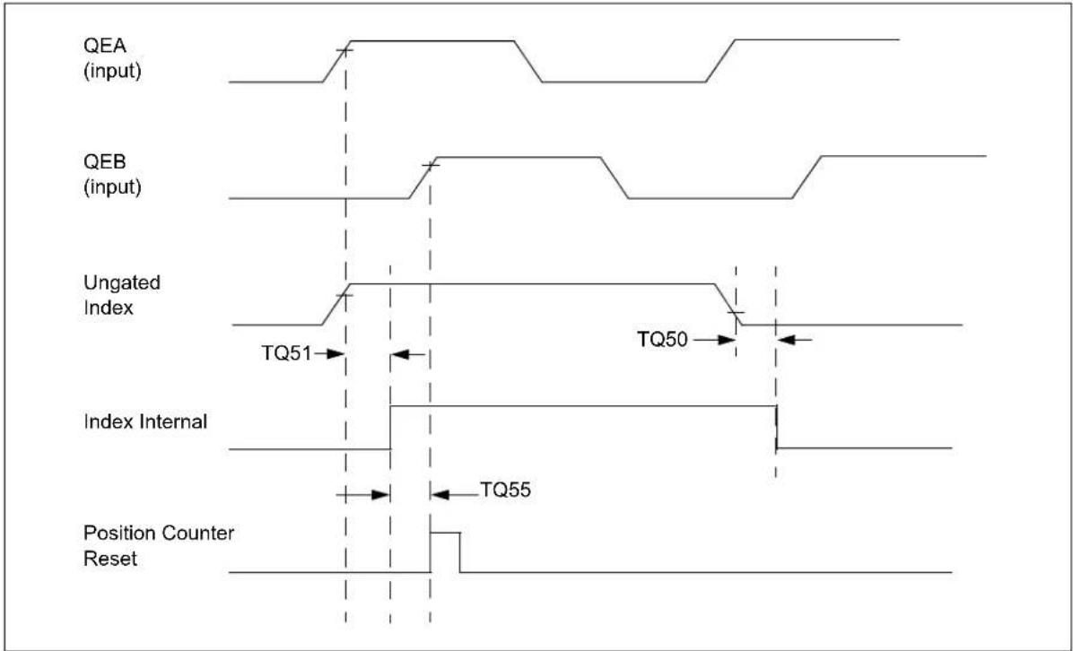
text_image
QEA (input) QEB (input) Ungated Index TQ51 TQ50 Index Internal TQ55 Position Counter ResetTABLE 24-48: QEI INDEX PULSE TIMING REQUIREMENTS
| AC CHARACTERISTICS | Standard Operating Conditions: 3.0V to 3.6V(unless otherwise stated)Operating temperature -40^ ≤ TA ≤ +85^ for Industrial -40^ ≤ TA ≤ +125^ for Extended | |||||
| Param. | Symbol | Characteristic(1) | Min. Max. | Units Conditions | ||
| TQ50 | TqIL | Filter Time to Recognize Low with Digital Filter | 3 * N * Tcy | — | ns | N = 1, 2, 4, 16, 32, 64, 128 and 256 (Note 2) |
| TQ51 | TqiH | Filter Time to Recognize High with Digital Filter | 3 * N * Tcy | — | ns | N = 1, 2, 4, 16, 32, 64, 128 and 256 (Note 2) |
| TQ55 | Tqidxr | Index Pulse Recognized to Position Counter Reset (ungated index) | 3 Tcy | — | ns | |
Note 1: These parameters are characterized but not tested in manufacturing.
2: Alignment of index pulses to QEA and QEB is shown for position counter Reset timing only. Shown for forward direction only (QEA leads QEB). Same timing applies for reverse direction (QEA lags QEB) but index pulse recognition occurs on the falling edge.
FIGURE 24-20: QEI MODULE EXTERNAL CLOCK TIMING CHARACTERISTICS
| AC CHARACTERISTICS | Standard Operating Conditions: 3.0V to 3.6V(unless otherwise stated)Operating temperature -40°C ≤ TA ≤ +85°C for Industrial-40°C ≤ AT ≤ +125°C for Extended | |||||||
| Param. | Symbol | Characteristic | (1) | Min. Typ. Max. | Units | Conditions | ||
| TQ10 TtQH | TQCK High Time | Synchronous, with Prescaler | [Greater of (12.5 or 0.5 Tcy)/N] + 25 | — | — | ns Must also meet Parameter TQ15 | ||
| TQ11 | TtQL | TQCK Low Time | Synchronous, with Prescaler | [Greater of (12.5 or 0.5 Tcy)/N] + 25 | — | — | ns Must also meet Parameter TQ15 | |
| TQ15 | TtQP | TQCP Input Period | Synchronous, with Prescaler | [Greater of (25 or Tcy)/N] + 50 | — | — | ns | |
| TQ20 | TCKEXTMRL | Delay from External TxCK Clock Edge to Timer Increment | — | 1 | Tcy | — | ||
Note 1: These parameters are characterized but not tested in manufacturing.
TABLE 24-50: PGAx MODULE SPECIFICATIONS
| AC/DC CHARACTERISTICS | Standard Operating Conditions: 3.0V to 3.6V(unless otherwise stated)(1)Operating temperature -40°C ≤ TA ≤ +85°C for Industrial-40°C ≤ TA ≤ +125°C for Extended | |||||||
| Param No. | Symbol | Characteristic Min. Typ. Max. Units Comments | ||||||
| PA01 V | IN | Input Voltage Range | AVss – 0.3 | — | AVDD + 0.3 | V | ||
| PA02 VCM | Co | mmon-Mode Input Voltage Range | AVss | — | AVDD – 1.6 | V | ||
| PA03 V | os | Input Offset Voltage | -9 | — | +9 | mV | Gain = 32x | |
| PA04 VoS | Input Off | set Voltage Drift with Temperature | — | ±15 | — | μV/°C | ||
| PA05 RIN | + Input | Impedance of Positive Input | — | >1M || 7 pF | — | Ω|| pF | ||
| PA06 RIN | - Input Impedance of Negative Input | — | 10K || 7 pF | — | Ω|| pF | |||
| PA07 G | ERR | Gain Error | -3 | ±0.5 | +3 | % | Gain = 4x, 8x,16x, 32x | |
| PA08 | LERR | Gain Nonlinearity Error | — | — | 0.5 | % | % of full scale, Gain = 16x | |
| PA09 | IDD | Current Consumption | — | 2.0 | — | mA | Module is enabled with a 2-volt P-P output voltage swing | |
| PA10a | BW | Small Signal Bandwidth (-3 dB) | G = 4x | — | 10 | — | MHz | |
| PA10b | G = 8x | — | 5 | — | MHz | |||
| PA10c | G = 16x | — | 2.5 | — | MHz | |||
| PA10d | G = 32x | — | 1.25 | — | MHz | |||
| PA11 OST Output Settling Time to 1% of Final Value | — | 0.4 | — | μs | Gain = 16x, 100 mV input step change | |||
| PA12 | SR | Output Slew Rate | — | 40 | — | V/μs | Gain = 16x | |
| PA13 T | GSEL | Gain Selection Time | — | 1 | — | μs | ||
| PA14 | TON | Module Turn-on/Setting Time | — | — | 10 | μs | ||
Note 1: The PGAx module is functional at VBORMIN < VDD < VDDMIN, but with degraded performance. Unless otherwise stated, module functionality is tested, but not characterized.
TABLE 24-51: CONSTANT-CURRENT SOURCE SPECIFICATIONS
| Operating Conditions: 3.0V to 3.6V (unless otherwise stated) ^(1) | |||||||
| Operating temperature -40°C ≤ TA ≤ +85°C for Industrial-40°C ≤ TA ≤ +125°C for Extended | |||||||
| Param No. | Symbol | Characteristic | Min. | Typ. | Max. | Units | Conditions |
| CC03 | I10SRC | 10 μA Source Current | 8.8 | — | 12.0 | μA | ISRCx pin |
| CC04 | I50SRC | 50 μA Source Current | 44 | — | 56 | μA | IBIASx pin |
| CC05 | I50SNK | 50 μA Sink Current | -44 | — | -56 | μA | IBIASx pin |
Note 1: The constant-current source module is functional at VBORMIN < VDD < VDDMIN, but with degraded performance. Unless otherwise stated, module functionality is tested, but not characterized.
NOTES:
25.0 HIGH-TEMPERATURE ELECTRICAL CHARACTERISTICS
This section provides an overview of the dsPIC33CH128MP508 family devices operating in an ambient temperature range of -40^ to +150^ .
The specifications between -40^ to +150^ are identical to those shown in Section 24.0 “Electrical Characteristics” for operation between -40^ to +125^ , with the exception of the parameters listed in this section. Parameters in this section begin with an H, which denotes High temperature.
Absolute maximum ratings for the dsPIC33CH128MP508 family high-temperature devices are listed below. Exposure to these maximum rating conditions for extended periods can affect device reliability. Functional operation of the device, at these or any other conditions above the parameters indicated in the operation listings of this specification, is not implied.
Absolute Maximum Ratings ^(1)
Ambient temperature under bias....-40°C to +150°C
Storage temperature -65°C to +150°C
Voltage on VDD with respect to Vss -0.3V to +4.0V
Voltage on any pin that is not 5V tolerant with respect to Vss ^(3) ......-0.3V to (VDD + 0.3V)
Voltage on any 5V tolerant pin with respect to Vss when V_DD ≥ 3.0V^(3) -0.3V to +5.5V
Voltage on any 5V tolerant pin with respect to Vss when VDD < 3.0V ^(3) -0.3V to +3.6V
Maximum current out of Vss pin ....300 mA
Maximum current into VDD pin ^(2) 300 mA
Maximum current sunk/sourced by any 4x I/O pin....15 mA
Maximum current sunk/sourced by any 8x I/O pin....25 mA
Maximum current sunk by a group of I/Os between two Vss pins ^(4) 75 mA
Maximum current sourced by a group of I/Os between two VDD pins ^(4) .....75 mA
Maximum current sunk by all I/Os ^(2,5) 200 mA
Maximum current sourced by all I/Os ^(2,5) .....200 mA
Note 1: Stresses above those listed under “Absolute Maximum Ratings” may cause permanent damage to the device. This is a stress rating only and functional operation of the device at those, or any other conditions above those indicated in the operation listings of this specification, is not implied. Exposure to maximum rating conditions for extended periods may affect device reliability.
2: Maximum allowable current is a function of device maximum power dissipation (see Table 25-2).
3: See the "Pin Diagrams" section for the 5V tolerant pins.
4: Not applicable to AV DD and AVss pins.
5: For 28-pin packages, the maximum current sunk/sourced by all I/Os is limited by 150 mA.
25.1 DC Characteristics
TABLE 25-1: OPERATING MIPS vs. VOLTAGE
| VDD Range | Temperature Range (in °C) | Maximum MIPS | |
| Main Secondary | |||
| 3.0V to 3.6V -40°C to +150°C 60 60 | |||
TABLE 25-2: THERMAL OPERATING CONDITIONS
| Rating Symbol Min. Max. Unit | ||||
| High-Temperature Devices | ||||
| Operating Junction Temperature Range | TJ | -40 | +165 | °C |
| Operating Ambient Temperature Range | TA | -40 | +150 | °C |
| Power Dissipation: | ||||
| Internal Chip Power Dissipation: | ||||
| PINT = VDD x (IDD - Σ IOH) | PD | PINT + PI/O | W | |
| I/O Pin Power Dissipation: | ||||
| I/O = Σ {VDD - VOH} x IOH + Σ (VOL x IOL) | ||||
| Maximum Allowed Power Dissipation | PDMAX | (TJ - TA)/0JA | W | |
TABLE 25-3: THERMAL PACKAGING CHARACTERISTICS (1)
| Characteristic | Symbol | Typ. | Unit |
| Package Thermal Resistance, 80-Pin TQFP 12x12x1 mm | _JA | 50.67 | °C/W |
| Package Thermal Resistance, 64-Pin TQFP 10x10x1.0 mm | _JA | 45.7 | °C/W |
| Package Thermal Resistance, 64-Pin QFN 9x9 mm | _JA | 18.7 | °C/W |
| Package Thermal Resistance, 48-Pin TQFP 7x7 mm | _JA | 62.76 | °C/W |
| Package Thermal Resistance, 48-Pin UQFN 6x6 mm | _JA | 27.6 | °C/W |
| Package Thermal Resistance, 36-Pin UQFN 5x5 mm | _JA | 29.2 | °C/W |
| Package Thermal Resistance, 28-Pin UQFN 6x6 mm | _JA | 22.41 | °C/W |
| Package Thermal Resistance, 28-Pin SSOP 5.30 mm | _JA | 52.84 | °C/W |
Note 1: Junction to ambient thermal resistance, Theta-JA ( _JA ) numbers are achieved by package simulations.
TABLE 25-4: OPERATING VOLTAGE SPECIFICATIONS
| Operating Conditions: 3.0V to 3.6V (unless otherwise stated) ^(1) Operating temperature -40°C ≤ TA ≤ +150°C | |||||||
| Param No. | Symbol | Characteristic Min. Typ. Max. Units Conditions | |||||
| Operating Voltage | |||||||
| DC10 V DD | Supply Voltage | 3.0 | — | 3.6 | V | ||
| DC11 | AVDD | Supply Voltage | Greater of: VDD – 0.3 or 3.0 | — | Lesser of: VDD + 0.3 or 3.6 | V | The difference between AVDD supply and VDD supply must not exceed ±300 mV at all times, including during device power-up |
| DC16 | VPOR | VDD Start Voltage to Ensure Internal Power-on Reset Signal | — | — | Vss | V | |
| DC17 | SVDD | VDD Rise Rate to Ensure Internal Power-on Reset Signal | 1 | — | — | V/ms | 0V-3V in 100 ms |
| BO10 | VBOR | BOR Event on VDD Transition High-to-Low ^(2) | 2.68 | 2.84 | 2.99 | V | |
Note 1: Device is functional at VBORMIN < VDD < VDDMIN. Analog modules (ADC and comparators) may have degraded performance.
2: Parameters are characterized but not tested.
TABLE 25-5: DC CHARACTERISTICS: OPERATING CURRENT (I DD) (MAIN RUN/SECONDARY RUN) ^4
| Operating Conditions: 3.0V to 3.6V (unless otherwise stated)Operating temperature -40°C ≤ TA ≤ +150°C | ||||||
| Parameter No. Typ. | (1) | Max. Units Conditions | ||||
| HDC20 18.1 36 mA +150°C | 3.3V | 10 MIPS (N1 = 1, N2 = 5, N3 = 2, M = 50, Fvco = 400 MHz, FPLLO = 40 MHz) | ||||
| HDC21 22.2 40.3 mA +150°C | 3.3V | 20 MIPS (N1 = 1, N2 = 5, N3 = 1, M = 50, Fvco = 400 MHz, FPLLO = 80 MHz) | ||||
| HDC22 29.9 48.1 mA +150°C | 3.3V | 40 MIPS (N1 = 1, N2 = 3, N3 = 1, M = 60, Fvco = 480 MHz, FPLLO = 160 MHz) | ||||
| HDC23 | 46 | 61.7 | mA | +150°C | 3.3V | 60 MIPS (N1 = 1, N2 = 2, N3 = 1, M = 60, Fvco = 480 MHz, FPLLO = 240 MHz) |
Note 1: Data in the "Typ." column are for design guidance only and are not tested.
2: Base Run current (IDD) is measured as follows:
- Oscillator is switched to EC+PLL mode in software
- OSC1 pin is driven with external 8 MHz square wave with levels from 0.3V to V_DD - 0.3V
- OSC2 is configured as an I/O in the Configuration Words (OSCIOFNC (FOSC[2]) = 0)
- FSCM is disabled (FCKSM[1:0] (FOSC[7:6]) = 01)
- Watchdog Timer is disabled (FWDT[15] = 0 and WDTCONL[15] = 0)
- All I/O pins (except OSC1) are configured as outputs and driving low
- No peripheral modules are operating or being clocked (defined PMDx bits are all '1's)
- JTAG is disabled (JTAGEN (FICD[5]) = 0)
- NOP instructions are executed in while(1) loop
TABLE 25-6: DC CHARACTERISTICS: OPERATING CURRENT (IDD) (MAIN SLEEP/SECONDARY RUN)
| Operating Conditions: 3.0V to 3.6V (unless otherwise stated)Operating temperature -40°C ≤ TA ≤ +150°C | ||||||
| Parameter No. Typ. | (1) | Max. Units Conditions | ||||
| HDC20a | 13.7 | 31.6 | mA | +150°C | 3.3V | 10 MIPS (N = 1, N2 = 5,N3 = 2, M = 50,Fvco = 400 MHz,FPLLO = 40 MHz) |
| HDC21a | 15.5 | 33.5 | mA | +150°C | 3.3V | 20 MIPS (N = 1, N2 = 5,N3 = 1, M = 50,Fvco = 400 MHz,FPLLO = 80 MHz) |
| HDC22a | 19.4 | 37.5 | mA | +150°C | 3.3V | 40 MIPS (N = 1, N2 = 3,N3 = 1, M = 60,Fvco = 480 MHz,FPLLO = 160 MHz) |
| HDC23a | 29 | 43 | mA | +150°C | 3.3V | 60 MIPS (N1 = 1, N2 = 2,N3 = 1, M = 60,Fvco = 480 MHz,FPLLO = 240 MHz) |
Note 1: Data in the "Typ." column are for design guidance only and are not tested.
TABLE 25-7: DC CHARACTERISTICS: OPERATING CURRENT (IDD) (MAIN RUN/SECONDARY SLEEP)
| DC CHARACTERISTICS | Main (Run) + Secondary (Sleep) | Standard Operating Conditions: 3.0V to 3.6V(unless otherwise stated)Operating temperature -40°C ≤ TA ≤ +150°C | ||||
| Parameter No. Typ. | (1) | Max. Units Conditions | ||||
| Operating Current (IDD) | ||||||
| HDC20b 14.4 32.3 mA +150°C | 3.3V | 10 MIPS | (N = 1, N2 = 5, | N3 = 2, M = 50,Fvco = 400 MHz,FPLLO = 40 MHz) | ||
| HDC21b 16.8 34.7 mA +150°C | 3.3V | 20 MIPS | (N = 1, N2 = 5, | N3 = 1, M = 50,Fvco = 400 MHz,FPLLO = 80 MHz) | ||
| HDC22b 20.6 38.6 mA +150°C | 3.3V | 40 MIPS | (N = 1, N2 = 3, | N3 = 1, M = 60,Fvco = 480 MHz,FPLLO = 160 MHz) | ||
| HDC23b | 32 | 46.7 | mA | +150°C | 3.3V | 60 MIPS (N1 = 1, N2 = 3,N3 = 1, M = 60,Fvco = 480 MHz,FPLLO = 240 MHz) |
Note 1: Data in the "Typ." column are for design guidance only and are not tested.
TABLE 25-8: DC CHARACTERISTICS: OPERATING CURRENT (IIDLE) (MAIN IDLE/SECONDARY IDLE) ^(2)
| Operating Conditions: 3.0V to 3.6V (unless otherwise stated)Operating temperature -40°C ≤ T A ≤ +150°C | ||||||
| Parameter No. Typ. | (1) | Max. Units Conditions | ||||
| HDC40 | 15.5 | 33.5 | mA | +150°C | 3.3V | 10 MIPS (N1 = 1, N2 = 5, N3 = 2,M = 50, Fvco = 400 MHz,FPLLO = 40 MHz) |
| HDC41 | 16.9 | 34.8 | mA | +150°C | 3.3V | 20 MIPS (N1 = 1, N2 = 5, N3 = 1,M = 50, Fvco = 400 MHz,FPLLO = 80 MHz) |
| HDC42 | 20.4 | 38.3 | mA | +150°C | 3.3V | 40 MIPS (N1 = 1, N2 = 3, N3 = 1,M = 60, Fvco = 480 MHz,FPLLO = 160 MHz) |
| HDC43 | 30 | 43.2 | mA | +150°C | 3.3V | 60 MIPS (N1 = 1, N2 = 2, N3 = 1,M = 60, Fvco = 480 MHz,FPLLO = 240 MHz) |
Note 1: Data in the "Typ." column are for design guidance only and are not tested.
2: Base Idle current (IDLE) is measured as follows:
- Oscillator is switched to EC+PLL mode in software
- OSC1 pin is driven with external 8 MHz square wave with levels from 0.3V to VDD - 0.3V
- OSC2 is configured as an I/O in the Configuration Words (OSCIOFNC (FOSC[2]) = 0)
• FSCM is disabled (FCKSM[1:0] (FOSC[7:6]) = 01)
- Watchdog Timer is disabled (FWDT[15] = 0 and WDTCONL[15] = 0)
- All I/O pins (except OSC1) are configured as outputs and driving low
- No peripheral modules are operating or being clocked (defined PMDx bits are all '1's)
- JTAG is disabled (JTAGEN (FICD[5]) = 0)
- Flash in standby with NVMSIDL (NVMCON[12]) = 1
TABLE 25-9: DC CHARACTERISTICS: IDLE CURRENT (IIDLE) (MAIN IDLE/SECONDARY SLEEP) ^(2)
| Operating Conditions: 3.0V to 3.6V (unless otherwise stated)Operating temperature -40°C ≤ TA ≤ +150°C | ||||||
| Parameter No. Typ. | (1) | Max. Units Conditions | ||||
| HDC40a | 13 | 30.9 | mA | +150°C | 3.3V | 10 MIPS (N1 = 1, N2 = 5, N3 = 2,M = 50, Fvco = 400 MHz,FPLLO = 40 MHz) |
| HDC41a | 13.8 | 31.7 | mA | +150°C | 3.3V | 20 MIPS (N1 = 1, N2 = 5, N3 = 1,M = 50, Fvco = 400 MHz,FPLLO = 80 MHz) |
| HDC42a | 15.6 | 33.5 | mA | +150°C | 3.3V | 40 MIPS (N1 = 1, N2 = 3, N3 = 1,M = 60, Fvco = 480 MHz,FPLLO = 160 MHz) |
| HDC43a | 21.9 | 35.4 | mA | +150°C | 3.3V | 60 MIPS (N1 = 1, N2 = 2, N3 = 1,M = 60, Fvco = 480 MHz,FPLLO = 240 MHz) |
Note 1: Data in the "Typ." column are for design guidance only and are not tested.
2: Base Idle current (IIDLE) is measured as follows:
- Oscillator is switched to EC+PLL mode in software
- OSC1 pin is driven with external 8 MHz square wave with levels from 0.3V to VDD - 0.3V
- OSC2 is configured as an I/O in the Configuration Words (OSCIOFNC (FOSC[2]) = 0)
• FSCM is disabled (FCKSM[1:0] (FOSC[7:6]) = 01)
- Watchdog Timer is disabled (FWDT[15] = 0 and WDTCONL[15] = 0)
- All I/O pins (except OSC1) are configured as outputs and driving low
- No peripheral modules are operating or being clocked (defined PMDx bits are all '1's)
• JTAG is disabled (JTAGEN (FICD[5]) = 0)
- Flash in standby with NVMSIDL (NVMCON[12]) = 1
TABLE 25-10: DC CHARACTERISTICS: IDLE CURRENT (IIDLE) (MAIN SLEEP/SECONDARY IDLE) ^(2)
| Operating Conditions: 3.0V to 3.6V (unless otherwise stated)Operating temperature -40°C ≤ TA ≤ +150°C | ||||||
| Parameter No. Typ. | (1) | Max. Units Conditions | ||||
| HDC40b 12.5 30.4 mA +150°C | 3.3V | 10 MIPS (N1 = 1, N2 = 5, N3 = 2, M = 50, Fvco = 400 MHz, FPLLO = 40 MHz) | ||||
| HDC41b | 13.2 | 31 | mA | +150°C | 3.3V | 20 MIPS (N1 = 1, N2 = 5, N3 = 1, M = 50, Fvco = 400 MHz, FPLLO = 80 MHz) |
| HDC42b 14.8 32.7 mA +150°C | 3.3V | 40 MIPS (N1 = 1, N2 = 3, N3 = 1, M = 60, Fvco = 480 MHz, FPLLO = 160 MHz) | ||||
| HDC43b 22.9 34.3 mA +150°C | 3.3V | 60 MIPS (N1 = 1, N2 = 2, N3 = 1, M = 60, Fvco = 480 MHz, FPLLO = 240 MHz) | ||||
Note 1: Data in the "Typ." column are for design guidance only and are not tested.
2: Base Idle current (IDLE) is measured as follows:
- Oscillator is switched to EC+PLL mode in software
- OSC1 pin is driven with external 8 MHz square wave with levels from 0.3V to VDD - 0.3V
- OSC2 is configured as an I/O in the Configuration Words (OSCIOFNC (FOSC[2]) = 0)
• FSCM is disabled (FCKSM[1:0] (FOSC[7:6]) = 01)
- Watchdog Timer is disabled (FWDT[15] = 0 and WDTCONL[15] = 0)
- All I/O pins (except OSC1) are configured as outputs and driving low
- No peripheral modules are operating or being clocked (defined PMDx bits are all '1's)
• JTAG is disabled (JTAGEN (FICD[5]) = 0)
- Flash in standby with NVMSIDL (NVMCON[12]) = 1
TABLE 25-11: POWER-DOWN CURRENT (IPD) ^(2)
| Operating Conditions: 3.0V to 3.6V (unless otherwise stated)Operating temperature -40°C ≤ TA ≤ +150°C | ||||||
| Parameter No. | Characteristic Typ. | (1) | Max. Units Conditions | |||
| HDC60 Base | Power-Down Current 9.7 25.5 mA +150°C | 3.3V | ||||
Note 1: Data in the "Typ." column are for design guidance only and are not tested.
2: Base Sleep current (IPD) is measured as follows:
- OSC1 pin is driven with external 8 MHz square wave with levels from 0.3V to VDD - 0.3V
- OSC2 is configured as an I/O in the Configuration Words (OSCIOFNC (FOSC[2]) = 0)
- FSCM is disabled (FCKSM[1:0] (FOSC[7:6]) = 01)
- Watchdog Timer is disabled (FWDT[15] = 0 and WDTCONL[15] = 0)
- All I/O pins (except OSC1) are configured as outputs and driving low
- No peripheral modules are operating or being clocked (defined PMDx bits are all '1's)
- JTAG is disabled (JTAGEN (FICD[5]) = 0)
- The regulators are in Standby mode (VREGS (RCON[8]) = 0)
TABLE 25-12: WATCHDOG TIMER DELTA CURRENT ( IWDT ) ^(1)
| Operating Conditions: 3.0V to 3.6V (unless otherwise stated)Operating temperature -40°C ≤ TA ≤ +150°C | |||||
| Parameter No. | Typ. | Max. | Units | Conditions | |
| HDC61 | 8 | — | μA | +150°C | 3.3V |
Note 1: The LWDT current is the additional current consumed when the module is enabled. This current should be added to the base IPD current. All parameters are characterized but not tested during manufacturing.
TABLE 25-13: PWM DELTA CURRENT (1)
| Operating Conditions: 3.0V to 3.6V (unless otherwise stated)Operating temperature -40°C ≤ TA ≤ +150°C | ||||||
| Parameter No. | Typ. Max. | Units | Conditions | |||
| HDC100 | 6.5 | 8.2 | mA | +150°C | 3.3V | PWM Output Frequency = 500 kHz,PWM Input (AFPLLO = 500 MHz)(AVCO = 1000 MHz, PLLFBD = 125,APLLDIV1 = 2) |
| HDC101 | 5 | 5.7 | mA | +150°C | 3.3V | PWM Output Frequency = 500 kHz,PWM Input (AFPLLO = 400 MHz),(AVCO = 400 MHz, PLLFBD = 50,APLLDIV1 = 1) |
| HDC102 | 2.8 | 3.4 | mA | +150°C | 3.3V | PWM Output Frequency = 500 kHz,PWM Input (AFPLLO = 200 MHz),(AVCO = 400 MHz, PLLFBD = 50,APLLDIV1 = 2) |
| HDC103 | 1.5 | 2.3 | mA | +150°C | 3.3V | PWM Output Frequency = 500 kHz,PWM Input (AFPLLO = 100 MHz),(AVCO = 400 MHz, PLLFBD = 50,APLLDIV1 = 4) |
Note 1: APLL current is not included. The APLL current will be the same if more than one PWM is running. Listed delta currents are for only one PWM instance when HREN = 0 (PGxCONL[7]). All parameters are characterized but not tested during manufacturing.
TABLE 25-14: APLL DELTA CURRENT
| Operating Conditions: 3.0V to 3.6V (unless otherwise stated)Operating temperature -40°C ≤ TA ≤ +150°C | ||||||
| Parameter No. | Typ. | Max. | Units | Conditions(1) | ||
| HDC110 | — | 23 | mA | +150°C | 3.3V | AFPLLO = 500 MHz(AVCO = 1000 MHz, PLLFBD = 125, APLLDIV1 = 2) |
| HDC111 | — | 16 | mA | +150°C | 3.3V | AFPLLO = 400 MHz(AVCO = 400 MHz, PLLFBD = 50, APLLDIV1 = 1) |
| HDC112 | — | 15 | mA | +150°C | 3.3V | AFPLLO = 200 MHz(AVCO = 400 MHz, PLLFBD = 50, APLLDIV1 = 2) |
| HDC113 | — | 15 | mA | +150°C | 3.3V | AFPLLO = 100 MHz(AVCO = 400 MHz, PLLFBD = 50, APLLDIV1 = 4) |
Note 1: The APLL current will be the same if more than one PWM or DAC is run to the APLL clock. All parameters are characterized but not tested during manufacturing.
TABLE 25-15: ADC DELTA CURRENT (1,2)
| Operating Conditions: 3.0V to 3.6V (unless otherwise stated)Operating temperature -40°C ≤ TA ≤ +150°C | ||||||||
| Parameter No. | Main Secondary | Units Conditions | ||||||
| Typ. | Max. | Typ. | Max. | |||||
| HDC120 — 8.5 — | 16.3 mA | +150°C | 3.3V | T | AD = 14.3 ns(3.5 Msps conversion rate) | |||
Note 1: Main shared core continuous conversion; TAD = 14.3 nS (3.5 Msps Conversion rate).
2: Secondary dedicated core continuous conversion on all 3 SAR cores; TAD = 14.3 nS (3.5 Msps conversion rate). All parameters are characterized but not tested during manufacturing.
TABLE 25-16: COMPARATOR + DAC DELTA CURRENT
| Operating Conditions: 3.0V to 3.6V (unless otherwise stated)Operating temperature -40°C ≤ TA ≤ +150°C | ||||||
| Parameter No. | Typ. | Max. | Units | Conditions | ||
| HDC130 | — | 5 | mA | +150°C | 3.3V | AFPLLO @ 500 MHz(1) |
Note 1: APLL current is not included. Listed delta currents are for only one comparator + DAC instance. All parameters are characterized but not tested during manufacturing.
TABLE 25-17: PGAx DELTA CURRENT (1)
| Operating Conditions: 3.0V to 3.6V (unless otherwise stated)Operating temperature -40°C ≤ TA ≤ +150°C | |||||
| Parameter No. | Typ. | Max. | Units | Conditions | |
| HDC141 | — | 3 | mA | +150°C | 3.3V |
Note 1: All parameters are characterized but not tested during manufacturing.
TABLE 25-18: I/O PIN INPUT SPECIFICATIONS
| Operating Conditions: 3.0V to 3.6V (unless otherwise stated)Operating temperature -40°C ≤ TA ≤ +150°C | |||||||
| Param No. | Symbol | Characteristic Min. | (4) | Typ.(1) | Max.(5) | Units | Conditions |
| HDI50 | IL Input Leakage Current (2) | ||||||
| I/O Pins 5V Tolerant(3) | -800 | — | 800 | nA | |||
| I/O Pins Not 5V Tolerant(3) | -800 | — | 800 | nA | |||
| MCLR | -800 | — | 800 | nA | |||
| OSCI | -800 | — | 800 | nA | XT and HS modes | ||
Note 1: Data in the "Typ." column are at 3.3V, +25°C unless otherwise stated.
2: Negative current is defined as current sourced by the pin.
3: See the "Pin Diagrams" section for the 5V tolerant I/O pins.
4: VPIN = VSS.
5: VPIN = VDD.
TABLE 25-19: INTERNAL FRC ACCURACY
| Operating Conditions: 3.0V to 3.6V (unless otherwise stated)Operating temperature -40°C ≤ TA ≤ +150°C | |||||
| Param No. | Characteristic | Min. | Max. | Units | Conditions |
| Internal FRC Accuracy @ FRC Frequency = 8 MHz(1) | |||||
| HF20 | FRC | -4 | +4 | % | -40°C ≤ TA ≤ +150°C |
Note 1: Frequency is calibrated at +25°C and 3.3V.
TABLE 25-20: INTERNAL LPRC ACCURACY
| Operating Conditions: 3.0V to 3.6V (unless otherwise stated)Operating temperature -40°C ≤ TA ≤ +150°C | |||||
| Param No. | Characteristic | Min. | Max. | Units | Conditions |
| LPRC @ 32 kHz | |||||
| HF21 | LPRC | -30 | +30 | % | -40°C ≤ TA ≤ +150°C |
TABLE 25-21: ADC MODULE SPECIFICATIONS
| Operating Conditions: 3.0V to 3.6V (unless otherwise stated)(1)Operating temperature -40°C ≤ TA ≤ +150°C | |||||||
| Param No. | Symbol | Characteristics Min. Typical Max. Units Conditions | |||||
| ADC Accuracy | |||||||
| HAD23c | G ERR | Gain Error | >-17.5 | — | < 17.5 | LSb | AVss = 0V, AVDD = 3.3V |
| HAD24c | E OFF | Offset Error | >-15 | — | < 15 | LSb | AVss = 0V, AVDD = 3.3V |
Note 1: The ADC module is functional at VBORMIN < VDD < VDDMIN, but with degraded performance. Unless otherwise stated, module functionality is ensured, but not characterized.
TABLE 25-22: DACx MODULE SPECIFICATIONS
| Operating Conditions: 3.0V to 3.6V (unless otherwise stated)Operating temperature -40°C ≤ TA ≤ +150°C | |||||||
| Param No. | Symbol | Characteristic | Min. | Typ.^(1) | Max. Units | Comments | |
| HDA03 | INL | Integral Nonlinearity Error | -50 | — | 0 | LSB | |
| HDA05 | EOFF | Offset Error | 0 | — | 45 | LSB | Internal node at comparator input |
| HDA06 | EG | Gain Error | 0 | — | 55 | % | Internal node at comparator input |
Note 1: Parameters are for design guidance only and are not tested in manufacturing.
TABLE 25-23: PGAx MODULE SPECIFICATIONS
| AC/DC CHARACTERISTICS | Standard Operating Conditions: 3.0V to 3.6V(unless otherwise stated)(1)Operating temperature -40°C ≤ TA ≤ +150°C | ||||||
| Param No. | Symbol | Characteristic | Min. | Typ. | Max. | Units | Comments |
| HPA03 | Vos | Input Offset Voltage | -11 | — | +11 | mV | Gain = 32x |
Note 1: The PGAx module is functional at VBORMIN < VDD < VDDMIN, but with degraded performance. Unless otherwise stated, module functionality is tested, but not characterized.
NOTES:
26.0 PACKAGING INFORMATION
26.1 Package Marking Information
28-Lead SSOP (5.30 mm)

text_image
XXXXXXXXXX XXXXXXXXXX YYWWNNNExample
text_image
dsPIC33CH64 MP202 181001728-Lead UQFN (6x6 mm)
text_image
XXXXXXXX XXXXXXXX YYWWNNNExample

text_image
33CH64MP 202 181001736-Lead UQFN (5x5 mm)

text_image
XXXXXXXX XXXXXXXX XXXXXXXX YYWWNNNExample
text_image
dsPIC33 CH64MP 203 1810017Legend: XX...X Customer-specific information Y Year code (last digit of calendar year) YY Year code (last 2 digits of calendar year) WW Week code (week of January 1 is week '01') NNN Alphanumeric traceability code
Note: In the event the full Microchip part number cannot be marked on one line, it will be carried over to the next line, thus limiting the number of available characters for customer-specific information.
26.1 Package Marking Information (Continued)
48-Lead TQFP (7x7 mm)
text_image
XXXXXXXX XXXXXXXXXXXXYWW NNNExample
text_image
CH64MP 2041810 01748-Lead UQFN (6x6 mm)
text_image
XXXXXXX XXXXXXX XXXXXXX YYWWNNNExample
text_image
dsPIC33 CH64MP 205 181001764-Lead TQFP (10x10x1 mm)

text_image
MICROCHIP XXXXXXXXXX XXXXXXXXXX XXXXXXXXXX ○ YYWWNNNExample
text_image
MICROCHIP dsPIC33CH64 MP206 181001764-Lead QFN (9x9x0.9 mm)

text_image
XXXXXXXXXXXX XXXXXXXXXXXX XXXXXXXXXXXX YYWWNNNExample

text_image
dsPIC33CH64 MP206 181001780-Lead TQFP (12x12x1 mm)
text_image
MICROCHIP XXXXXXXXXXXXX XXXXXXXXXXXXX XXXXXXXXXXXXX YYYYWNNNExample
text_image
MICROCHIP dsPIC33CH64 MP208 181001726.2 Package Details
28-Lead Plastic Shrink Small Outline (SS) - 5.30 mm Body [SSOP]
Note: For the most current package drawings, please see the Microchip Packaging Specification located at http://www.microchip.com/packaging
![Microchip dsPIC33CH128MP502 - 28-Lead Plastic Shrink Small Outline (SS) - 5.30 mm Body [SSOP] - 1](/content/2026/06/1217541/images/1aba82834bd5f26d09ab25a7cb887218388ea8154f786cb262ea2e2d24abaa68.jpg)
Microchip Technology Drawing C04-073 Rev C Sheet 1 of 2
28-Lead Plastic Shrink Small Outline (SS) - 5.30 mm Body [SSOP]
Note: For the most current package drawings, please see the Microchip Packaging Specification located at http://www.microchip.com/packaging
![Microchip dsPIC33CH128MP502 - 28-Lead Plastic Shrink Small Outline (SS) - 5.30 mm Body [SSOP] - 1](/content/2026/06/1217541/images/5e1e9e520379439e81177e5b5b18de19ff3bea70de35d5eb80b1bf489a271ab7.jpg)
natural_image
Isometric line drawing of an integrated circuit chip with multiple 16-pin pins (no text or symbols)| Units | MILLIMETERS | |||
| Dimension Limits | MIN | NOM | MAX | |
| NNumber of Pins 28 | ||||
| Pitch | e | 0.65 BSC | ||
| Overall Height | A | - | - | 2.00 |
| 1.851.75 | ||||
| -0.05A | Standoff | |||
| Overall Width | 8.207.80 | |||
| 5.605.30 | ||||
| 10.5010.209.90DOverall | ||||
| 0.950.75 | ||||
| Footprint | L1 | 1.25 REF | ||
| Lead Thickness | c | 0.25-0.09 | ||
| Foot Angle | φ | 8°4°0° | ||
| Lead Width | b | 0.38-0.22 | ||
Notes:
- Pin 1 visual index feature may vary, but must be located within the hatched area.
- Dimensions D and E1 do not include mold flash or protrusions. Mold flash or protrusions shall not exceed 0.20mm per side.
- Dimensioning and tolerancing per ASME Y14.5M
BSC: Basic Dimension. Theoretically exact value shown without tolerances.
REF: Reference Dimension, usually without tolerance, for information purposes only.
Microchip Technology Drawing C04-073 Rev C Sheet 2 of 2
28-Lead Plastic Shrink Small Outline (SS) - 5.30 mm Body [SSOP]
Note: For the most current package drawings, please see the Microchip Packaging Specification located at http://www.microchip.com/packaging
![Microchip dsPIC33CH128MP502 - 28-Lead Plastic Shrink Small Outline (SS) - 5.30 mm Body [SSOP] - 1](/content/2026/06/1217541/images/b4285902a49cb178262f8a87ce2a02f541e0aa35d27017a36a86ad876c5e569d.jpg)
text_image
28 G1 C SILK SCREEN Y1 1 2 X1 ERECOMMENDED LAND PATTERN
| Units | MILLIMETERS | |||
| Dimension Limits | MIN | NOM | MAX | |
| Contact Pitch | E | 0.65 BSC | ||
| CContact Pad Spacing 7.00 | ||||
| Contact Pad Width (X28) | X1 | 0.45 | ||
| Contact Pad Length (X28) | Y1 | 1.85 | ||
| Contact Pad to Center Pad (X26) | G1 0.20 | |||
Notes:
- Dimensioning and tolerancing per ASME Y14.5M
BSC: Basic Dimension. Theoretically exact value shown without tolerances.
- For best soldering results, thermal vias, if used, should be filled or tented to avoid solder loss during reflow process
Microchip Technology Drawing C04-2073 Rev B
28-Lead Ultra Thin Plastic Quad Flat, No Lead Package (2N) - 6x6x0.55 mm Body [UQFN] With 4.65x4.65 mm Exposed Pad and Corner Anchors
Note: For the most current package drawings, please see the Microchip Packaging Specification located at http://www.microchip.com/packaging
![Microchip dsPIC33CH128MP502 - 28-Lead Ultra Thin Plastic Quad Flat, No Lead Package (2N) - 6x6x0.55 mm Body [UQFN] With 4.65x4.65 mm Exposed Pad and Corner Anchors - 1](/content/2026/06/1217541/images/2eb84b48bbb7eed99487a1c9a98963fd98962c2226a07842b396c6c50b4fd643.jpg)
text_image
NOTE 1 N A B 1 2 (DATUM B) (DATUM A) 2X 0.10 C E 2X 0.10 C TOP VIEW SEATING PLANE C A (A3) SIDE VIEW // 0.10 C A1 28X 0.08 C 8X b1 D2 0.10 A B 8X b2 E2 2 1 2X P NOTE 1 N e 28X K BOTTOM VIEW 0.10 A B 0.05 MMicrochip Technology Drawing C04-385 Rev C Sheet 1 of 2
28-Lead Ultra Thin Plastic Quad Flat, No Lead Package (2N) - 6x6x0.55 mm Body [UQFN] With 4.65x4.65 mm Exposed Pad and Corner Anchors
Note: For the most current package drawings, please see the Microchip Packaging Specification located at http://www.microchip.com/packaging
![Microchip dsPIC33CH128MP502 - 28-Lead Ultra Thin Plastic Quad Flat, No Lead Package (2N) - 6x6x0.55 mm Body [UQFN] With 4.65x4.65 mm Exposed Pad and Corner Anchors - 1](/content/2026/06/1217541/images/b250138cfebb48015d46bfd4abaf3dd485f8759d642f2383058383cd20cb2de4.jpg)
natural_image
Technical line drawing of two rectangular electronic components with pins, shown from top and bottom views (no text or symbols)| Units | MILLIMETERS | |||
| Dimension Limits | MIN | NOM | MAX | |
| Number of Terminals | N | 28 | ||
| Pitch | e | 0.65 BSC | ||
| Overall Height | A | 0.45 | 0.50 | 0.55 |
| Standoff | A1 | 0.00 | 0.02 | 0.05 |
| Terminal Thickness | A3 | 0.127 REF | ||
| Overall Width | E | 6.00 BSC | ||
| Exposed Pad Width | E2 | 4.55 | 4.65 | 4.75 |
| Overall Length | D | 6.00 BSC | ||
| Exposed Pad Length | D2 | 4.55 | 4.65 | 4.75 |
| Exposed Pad Corner Chamfer P - | 0.35 - | |||
| Terminal Width | b | 0.25 | 0.30 | 0.35 |
| b1 | 0.35 0.40 | 0.43Corner | Anchor Pad | |
| Corner Pad, Metal Free Zone b2 | 0.15 0.20 | 0.25 | ||
| Terminal Length | L | 0.30 | 0.40 | 0.50 |
| Terminal-to-Exposed-Pad | K | - | ||
0.20 -
Notes:
- Pin 1 visual index feature may vary, but must be located within the hatched area.
- Package is saw singulated
- Dimensioning and tolerancing per ASME Y14.5M
BSC: Basic Dimension. Theoretically exact value shown without tolerances.
REF: Reference Dimension, usually without tolerance, for information purposes only.
Microchip Technology Drawing C04-385 Rev C Sheet 2 of 2
28-Lead Ultra Thin Plastic Quad Flat, No Lead Package (2N) - 6x6x0.55 mm Body [UQFN] With 4.65x4.65 mm Exposed Pad and Corner Anchors
Note: For the most current package drawings, please see the Microchip Packaging Specification located at http://www.microchip.com/packaging
![Microchip dsPIC33CH128MP502 - 28-Lead Ultra Thin Plastic Quad Flat, No Lead Package (2N) - 6x6x0.55 mm Body [UQFN] With 4.65x4.65 mm Exposed Pad and Corner Anchors - 1](/content/2026/06/1217541/images/3adc186b7fce633419a5ebab2b77ce22b7164b631b5f5dffb999521edfb07e8b.jpg)
text_image
C2 X2 EV 28 Y3 X1 1 2 Y4 G1 G2 X4 Y1 SILK SCREEN E X3 C1 Y2 EVRECOMMENDED LAND PATTERN
| Units | MILLIMETERS | |||
| Dimension Limits | MIN | NOM | MAX | |
| Contact Pitch | E | 0.65 BSC | ||
| Optional Center Pad Width | X2 | 4.75 | ||
| Optional Center Pad Length | Y2 | 4.75 | ||
| C1Contact Pad Spacing 6.00 | ||||
| Contact Pad Spacing | C2 | 6.00 | ||
| Contact Pad Width (X28) | X1 | 0.35 | ||
| Contact Pad Length (X28) | Y1 | 0.80 | ||
| Corner Anchor (X4) | X3 | 1.00 | ||
| Corner Anchor (X4) | Y3 | 1.00 | ||
| Corner Anchor Chamfer (X4) | X4 | 0.35 | ||
| Corner Anchor Chamfer (X4) | Y4 | 0.35 | ||
| Contact Pad to Pad (X28) G1 0.20 | ||||
| Contact Pad to Center Pad (X28) G2 0.20 | ||||
| Thermal Via Diameter V | 0.33 | |||
| Thermal Via Pitch EV | 1.20 | |||
Notes:
- Dimensioning and tolerancing per ASME Y14.5M
BSC: Basic Dimension. Theoretically exact value shown without tolerances.
- For best soldering results, thermal vias, if used, should be filled or tented to avoid solder loss during reflow process
Microchip Technology Drawing C04-2385 Rev C
36-Lead Ultra Thin Plastic Quad Flat, No Lead Package (M5) - 5x5 mm Body [UQFN] With Corner Anchors
Note: For the most current package drawings, please see the Microchip Packaging Specification located at http://www.microchip.com/packaging
![Microchip dsPIC33CH128MP502 - 36-Lead Ultra Thin Plastic Quad Flat, No Lead Package (M5) - 5x5 mm Body [UQFN] With Corner Anchors - 1](/content/2026/06/1217541/images/49510c88f5757d0e99d8312e873e4dd73b477fd88921275b8329fad97d3117f1.jpg)
Microchip Technology Drawing C04-436-M5 Rev D Sheet 1 of 2
36-Lead Ultra Thin Plastic Quad Flat, No Lead Package (M5) - 5x5 mm Body [UQFN] With Corner Anchors
Note: For the most current package drawings, please see the Microchip Packaging Specification located at http://www.microchip.com/packaging
![Microchip dsPIC33CH128MP502 - 36-Lead Ultra Thin Plastic Quad Flat, No Lead Package (M5) - 5x5 mm Body [UQFN] With Corner Anchors - 1](/content/2026/06/1217541/images/76fd99259f24f6fd58ee850484f25e25601c784be83ed0bff84b603f00b3f19a.jpg)
text_image
SEATING PLANE A C (A3) DETAIL A A1| Units | MILLIMETERS | |||
| Dimension Limits | MIN | NOM | MAX | |
| Number of Terminals | N | 36 | ||
| Pitch | e | 0.40 BSC | ||
| Overall Height | A | 0.50 | 0.55 | 0.60 |
| Standoff | A1 | 0.00 | 0.02 | 0.05 |
| Terminal Thickness | A3 | 0.152 REF | ||
| Overall Length | D | 5.00 BSC | ||
| Exposed Pad Length | D2 3 | 60 | 3.70 3.80 | |
| Overall Width | E | 5.00 BSC | ||
| Exposed Pad Width | E2 | 3.60 | 3.70 | 3.80 |
| Terminal Width | b | 0.15 | 0.20 | 0.25 |
| Terminal Length | L | 0.30 | 0.40 | 0.50 |
| Terminal-to-Exposed-Pad | K 0 | 25 REF | ||
Notes:
1. Pin 1 visual index feature may vary, but must be located within the hatched area.
2. Package is saw singulated
3. Dimensioning and tolerancing per ASME Y14.5M
BSC: Basic Dimension. Theoretically exact value shown without tolerances.
REF: Reference Dimension, usually without tolerance, for information purposes only.
Microchip Technology Drawing C04-436-M5 Rev D Sheet 2 of 2
36-Lead Ultra Thin Plastic Quad Flat, No Lead Package (M5) - 5x5 mm Body [UQFN] With Corner Anchors
Note: For the most current package drawings, please see the Microchip Packaging Specification located at http://www.microchip.com/packaging
![Microchip dsPIC33CH128MP502 - 36-Lead Ultra Thin Plastic Quad Flat, No Lead Package (M5) - 5x5 mm Body [UQFN] With Corner Anchors - 1](/content/2026/06/1217541/images/24710499fc3801f4ac9442f4fe0eb684ec418468551e02ecf9af28bc84fe6fdf.jpg)
text_image
C1 X2 EV 36 Y3 1 2 ØV G C2 EV R X3 E Y1 X1 SILK SCREENRECOMMENDED LAND PATTERN
| Units | MILLIMETERS | |||
| Dimension Limits | MIN | NOM | MAX | |
| Contact Pitch | E | 0.40 BSC | ||
| Center Pad Width | X2 | 3.80 | ||
| Center Pad Length | Y2 | 3.80 | ||
| C1Contact Pad Spacing 5.00 | ||||
| Contact Pad Spacing | C2 | 5.00 | ||
| Contact Pad Width (X36) | X1 | 0.20 | ||
| Contact Pad Length (X36) | Y1 | 0.80 | ||
| Corner Pad Width (X4) | X3 | 0.85 | ||
| Corner Pad Length (X4) | Y3 | 0.85 | ||
| Corner Pad Radius R 0.10 | ||||
| Contact Pad to Center Pad (X36) G | 0.20 | |||
| Thermal Via Diameter V | 0.30 | |||
| Thermal Via Pitch EV | 1.00 | |||
Notes:
- Dimensioning and tolerancing per ASME Y14.5M
BSC: Basic Dimension. Theoretically exact value shown without tolerances.
- For best soldering results, thermal vias, if used, should be filled or tented to avoid solder loss during reflow process
Microchip Technology Drawing C04-2436-M5 Rev D
48-Lead Plastic Thin Quad Flatpack (PT) - 7x7x1.0 mm Body [TQFP]
Note: For the most current package drawings, please see the Microchip Packaging Specification located at http://www.microchip.com/packaging
![Microchip dsPIC33CH128MP502 - 48-Lead Plastic Thin Quad Flatpack (PT) - 7x7x1.0 mm Body [TQFP] - 1](/content/2026/06/1217541/images/393c28843e40eb1f296a85c9b4ebe494a4ebc5cc1da1483b562fd21a9fc47fcf.jpg)
text_image
D D1 D2 D1 2 D2 D A B E1/2 E E1 A A E2 N/4 TIPS 0.20 C A-B D 1 2 3 e2 e 0.20 C A-B D 4X TOP VIEW![Microchip dsPIC33CH128MP502 - 48-Lead Plastic Thin Quad Flatpack (PT) - 7x7x1.0 mm Body [TQFP] - 2](/content/2026/06/1217541/images/162413e605bf89b246dfb1285ae1755d2a73c2e85e2f7fc129f4d06e1dfec7e3.jpg)
text_image
SEATING PLANE C A A2 A1 48X b 0.08 C 0.08 A-B D SIDE VIEWMicrochip Technology Drawing C04-300-PT Rev D Sheet 1 of 2
48-Lead Plastic Thin Quad Flatpack (PT) - 7x7x1.0 mm Body [TQFP]
Note: For the most current package drawings, please see the Microchip Packaging Specification located at http://www.microchip.com/packaging
![Microchip dsPIC33CH128MP502 - 48-Lead Plastic Thin Quad Flatpack (PT) - 7x7x1.0 mm Body [TQFP] - 1](/content/2026/06/1217541/images/f0651aa4c524491286efe3334713a18cfdfc5df602d2a433760b23aa7474fd42.jpg)
text_image
H θ2 θ1 R2 R1 c θ θ2 L (L1)SECTION A-A
| Units | MILLIMETERS | |||
| Dimension Limits | MIN | NOM | MAX | |
| Number of Terminals | N | 48 | ||
| Pitch | e | 0.50 BSC | ||
| Overall Height | A | - | - | 1.20 |
| Standoff | A1 | 0.05 | - | 0.15 |
| Molded Package Thickness | A2 | 0.95 1.05 | 1.00 | |
| Overall Length | D | 9.00 BSC | ||
| Molded Package Length | D1 | 7.00 BSC | ||
| Overall Width | E | 9.00 BSC | ||
| Molded Package Width | E1 | 7.00 BSC | ||
| Terminal Width | b | 0.17 | 0.22 | 0.27 |
| Terminal Thickness | c | 0.09 - 0.16 | ||
| Terminal Length | L | 0.45 | 0.60 | 0.75 |
| L1 1.00 REFFootprint | ||||
| R1 | -0.08 - | Lead Bend Radius | ||
| R2 | -0.08 0.20 | Lead Bend Radius | ||
| Foot Angle | 3.5°0°7' | |||
| Lead Angle | 1 | 0° | - | - |
| Mold Draft Angle | 2 | 11° | 12° | 13° |
Notes:
1. Pin 1 visual index feature may vary, but must be located within the hatched area.
2. Dimensioning and tolerancing per ASME Y14.5M
BSC: Basic Dimension. Theoretically exact value shown without tolerances.
REF: Reference Dimension, usually without tolerance, for information purposes only.
Microchip Technology Drawing C04-300-PT Rev D Sheet 2 of 2
48-Lead Plastic Thin Quad Flatpack (PT) - 7x7x1.0 mm Body [TQFP]
Note: For the most current package drawings, please see the Microchip Packaging Specification located at http://www.microchip.com/packaging
![Microchip dsPIC33CH128MP502 - 48-Lead Plastic Thin Quad Flatpack (PT) - 7x7x1.0 mm Body [TQFP] - 1](/content/2026/06/1217541/images/621c8d82469622418ef218eec2ee7c522bd6498df1fde7c7cbc6f91606456103.jpg)
text_image
C1 C2 48 SILK SCREEN G Y1 1 2 X1 ERECOMMENDED LAND PATTERN
| Units | MILLIMETERS | |||
| Dimension Limits | MIN | NOM | MAX | |
| Contact Pitch | E | 0.50 BSC | ||
| C1Contact Pad Spacing 8.40 | ||||
| C2Contact Pad Spacing40 | ||||
| Contact Pad Width (X48) | X1 | 0.30 | ||
| Contact Pad Length (X48) | Y1 | 1.50 | ||
| Distance Between Pads G 0.20 | ||||
Notes:
1. Dimensioning and tolerancing per ASME Y14.5M
BSC: Basic Dimension. Theoretically exact value shown without tolerances.
2. For best soldering results, thermal vias, if used, should be filled or tented to avoid solder loss during reflow process
Microchip Technology Drawing C04-2300-PT Rev D
48-Lead Ultra Thin Plastic Quad Flat, No Lead Package (M4) - 6x6 mm Body [UQFN] With Corner Anchors and 4.6x4.6 mm Exposed Pad
Note: For the most current package drawings, please see the Microchip Packaging Specification located at http://www.microchip.com/packaging
![Microchip dsPIC33CH128MP502 - 48-Lead Ultra Thin Plastic Quad Flat, No Lead Package (M4) - 6x6 mm Body [UQFN] With Corner Anchors and 4.6x4.6 mm Exposed Pad - 1](/content/2026/06/1217541/images/376d4a91f0c52b2e5a45c827711d6f52b9334fefec11ea092846e3a99969ad23.jpg)
text_image
NOTE 1 N 1 2 (DATUM B) (DATUM A) 2X 0.10 C 2X 0.10 C TOP VIEW A B E 52X 0.08 C // 0.10 C (A3) A SEATING PLANE SIDE VIEW 8X (b1) D2 0.10 M A B 8X (b2) E2 2 1 NOTE 1 L N 48X b e (K) 0.07 M A B 0.05 M BOTTOM VIEWMicrochip Technology Drawing C04-442A-M4 Sheet 1 of 2
48-Lead Ultra Thin Plastic Quad Flat, No Lead Package (M4) - 6x6 mm Body [UQFN] With Corner Anchors and 4.6x4.6 mm Exposed Pad
Note: For the most current package drawings, please see the Microchip Packaging Specification located at http://www.microchip.com/packaging
![Microchip dsPIC33CH128MP502 - 48-Lead Ultra Thin Plastic Quad Flat, No Lead Package (M4) - 6x6 mm Body [UQFN] With Corner Anchors and 4.6x4.6 mm Exposed Pad - 1](/content/2026/06/1217541/images/fa6fa467a09c3b4f404d0a6949073b3540b9fcd6b2b49ec3e0655ad0ebb9292f.jpg)
natural_image
Technical line drawing of two rectangular electronic components with square bases and internal circuit-like structures (no text or symbols)| Units | MILLIMETERS | |||
| Dimension Limits | MIN | NOM | MAX | |
| Number of Terminals | N | 48 | ||
| Pitch | e | 0.40 BSC | ||
| Overall Height | A | 0.50 | 0.55 | 0.60 |
| Standoff | A1 | 0.00 | 0.02 | 0.05 |
| Terminal Thickness | A3 | 0.15 REF | ||
| Overall Length | D | 6.00 BSC | ||
| Exposed Pad Length | D2 | 4.50 | 4.60 4.70 | |
| Overall Width | E | 6.00 BSC | ||
| Exposed Pad Width | E2 | 4.50 4.60 4.70 | ||
| Terminal Width | b | 0.15 | 0.20 | 0.25 |
| Corner Anchor Pad | b1 | 0.45 REF | ||
| Corner Anchor Pad, Metal-free Zone b2 | 0.23 REF | |||
| Terminal Length | L | 0.35 | 0.40 | 0.45 |
| K 0.30 REFTerminal-to-Exposed-Pad | ||||
Notes:
1. Pin 1 visual index feature may vary, but must be located within the hatched area.
2. Package is saw singulated
3. Dimensioning and tolerancing per ASME Y14.5M
BSC: Basic Dimension. Theoretically exact value shown without tolerances.
REF: Reference Dimension, usually without tolerance, for information purposes only.
Microchip Technology Drawing C04-442A-M4 Sheet 2 of 2
48-Lead Ultra Thin Plastic Quad Flat, No Lead Package (M4) - 6x6 mm Body [UQFN] With Corner Anchors and 4.6x4.6 mm Exposed Pad
Note: For the most current package drawings, please see the Microchip Packaging Specification located at http://www.microchip.com/packaging
![Microchip dsPIC33CH128MP502 - 48-Lead Ultra Thin Plastic Quad Flat, No Lead Package (M4) - 6x6 mm Body [UQFN] With Corner Anchors and 4.6x4.6 mm Exposed Pad - 1](/content/2026/06/1217541/images/274d5497f20aafb50e7ae0a53af3da5e25b1fb0194bc5a3ee7641556b3a19bdd.jpg)
text_image
C1 X2 EV R 48 Y3 ØV G2 Y1 C2 Y2 EV G1 Y1 SILK SCREEN X3 X1 ERECOMMENDED LAND PATTERN
| Units | MILLIMETERS | |||
| Dimension Limits | MIN | NOM | MAX | |
| Contact Pitch | E | 0.40 BSC | ||
| Center Pad Width | X2 | 4.70 | ||
| Center Pad Length | Y2 | 4.70 | ||
| C1Contact Pad Spacing 6.00 | ||||
| Contact Pad Spacing | C2 | 6.00 | ||
| Contact Pad Width (X48) | X1 | 0.20 | ||
| Contact Pad Length (X48) | Y1 | 0.80 | ||
| Corner Anchor Pad Width (X4) | X3 | 0.90 | ||
| Corner Anchor Pad Length (X4) | Y3 | 0.90 | ||
| Pad Corner Radius (X 20) R 0.10 | ||||
| Contact Pad to Center Pad (X48) G1 | 0.25 | |||
| Contact Pad to Contact Pad G2 0.20 | ||||
| Thermal Via Diameter V | 0.33 | |||
| Thermal Via Pitch EV | 1.20 | |||
Notes:
1. Dimensioning and tolerancing per ASME Y14.5M
BSC: Basic Dimension. Theoretically exact value shown without tolerances.
2. For best soldering results, thermal vias, if used, should be filled or tented to avoid solder loss during reflow process
Microchip Technology Drawing C04-2442A-M4
64-Lead Plastic Thin Quad Flatpack (PT)-10x10x1 mm Body, 2.00 mm Footprint [TQFP]
Note: For the most current package drawings, please see the Microchip Packaging Specification located at http://www.microchip.com/packaging
![Microchip dsPIC33CH128MP502 - 64-Lead Plastic Thin Quad Flatpack (PT)-10x10x1 mm Body, 2.00 mm Footprint [TQFP] - 1](/content/2026/06/1217541/images/3e0f63b92abae72f4fc3b55d9639a96d083a293feb6258c9ee821e7f542afc0e.jpg)
text_image
D D1 D1/2 D NOTE 2 A B E1/2 E SEE DETAIL 1 N 4X N/4 TIPS D0.20 D0 DA-B DD NOTE 1 1 2 3 4X D0.20 DH DA-B DDTOP VIEW
![Microchip dsPIC33CH128MP502 - 64-Lead Plastic Thin Quad Flatpack (PT)-10x10x1 mm Body, 2.00 mm Footprint [TQFP] - 2](/content/2026/06/1217541/images/28ccc9d2af0babad34a8f1ee3e2e70611d194a3c249c8bf49426c44259d03366.jpg)
text_image
SEATING PLANE A C 0.08 DC e 64 X b A1 A2 0.05 ⊕ 0 .0 8 M A-B DSIDE VIEW
Microchip Technology Drawing DC04-085-PT Rev E Sheet 1 of 2
64-Lead Plastic Thin Quad Flatpack (PT)-10x10x1 mm Body, 2.00 mm Footprint [TQFP]
Note: For the most current package drawings, please see the Microchip Packaging Specification located at http://www.microchip.com/packaging
![Microchip dsPIC33CH128MP502 - 64-Lead Plastic Thin Quad Flatpack (PT)-10x10x1 mm Body, 2.00 mm Footprint [TQFP] - 1](/content/2026/06/1217541/images/b383179b9d50a1a5b3df09572b4641d0b875c3a643819e8937b03056b5796546.jpg)
text_image
α H β L (L1) c θ SECTION A-A X=A-B OR D e/2 XDETAIL 1
| Units | MILLIMETERS | |||
| Dimension Limits | MIN | NOM | MAX | |
| Number of Leads | N | 64 | ||
| Lead Pitch | e | 0.50 BSC | ||
| Overall Height | A | - | - | 1.20 |
| Molded Package Thickness | A2 | 0.95 | 1.00 | 1.05 |
| Standoff | A1 | 0.05 | - | 0.15 |
| Foot Length | L | 0.45 | 0.60 | 0.75 |
| Footprint | L1 | 1.00 REF | ||
| Foot Angle | θ | 0^ | 3.5^ | 7^ |
| Overall Width | E | 12.00 BSC | ||
| Overall Length | D | 12.00 BSC | ||
| Molded Package Width | E1 | 10.00 BSC | ||
| Molded Package Length | D1 | 10.00 BSC | ||
| Lead Thickness | c | 0.09 | - | 0.20 |
| Lead Width | b | 0.17 | 0.22 | 0.27 |
| Mold Draft Angle Top | α | 11^ | 12^ | 13^ |
| Mold Draft Angle Bottom | β | 11^ | 12^ | 13^ |
Notes:
- Pin 1 visual index feature may vary, but must be located within the hatched area.
- Chamfers at corners are optional; size may vary.
- Dimensions D1 and E1 do not include mold flash or protrusions. Mold flash or protrusions shall not exceed 0.25mm per side.
- Dimensioning and tolerancing per ASME Y14.5M
BSC: Basic Dimension. Theoretically exact value shown without tolerances.
REF: Reference Dimension, usually without tolerance, for information purposes only.
Microchip Technology Drawing C04-085-PT Rev E Sheet 2 of 2
64-Lead Plastic Thin Quad Flatpack (PT) 10x10x1 mm Body, 2.00 mm Footprint [TQFP]
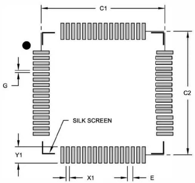
text_image
C1 G SILK SCREEN Y1 X1 E C2RECOMMENDED LAND PATTERN
| Units UMILLIMETERS | ||||
| Dimension Limits | MIN UNOM | MAX | ||
| Contact Pitch UE | 0.50 BSC | |||
| Contact Pad Spacing | C1 U | 11.40 | ||
| Contact Pad Spacing | C2 | 11.40 | ||
| Contact Pad Width (X64) | X1 | 0.30 | ||
| Contact Pad Length (X64) | Y1 | 1.50 | ||
| Distance Between Pads | G | 0.20 | ||
Notes:
1. UDimensioning and tolerancing per ASME Y14.5M
BSC: Basic Dimension. Theoretically exact value shown without tolerances.
Microchip Technology Drawing C04-2085-PT Rev E
64-Lead Plastic Quad Flat, No Lead Package (MR) - 9x9x0.9 mm Body with 5.40 x 5.40 Exposed Pad [QFN]
Note: For the most current package drawings, please see the Microchip Packaging Specification located at http://www.microchip.com/packaging
![Microchip dsPIC33CH128MP502 - 64-Lead Plastic Quad Flat, No Lead Package (MR) - 9x9x0.9 mm Body with 5.40 x 5.40 Exposed Pad [QFN] - 1](/content/2026/06/1217541/images/daaadd0a58d616d860eb9e752a47bc3bba3e64184803b5edd0e5bb1e491c7451.jpg)
text_image
D A B E 0.25 C N NOTE 1 2 1 TOP VIEW A // 0.10 C SEATING PLANE C (A3) A1 64X 0.08 C D2 0.10M C A B N 1/2 e 0.10M C A B (DATUM B) E2 e/2 NOTE 1 (DATUM A) K L 64X b 0.10M C A B 0.05M C BOTTOM VIEWMicrochip Technology Drawing C04-154A Sheet 1 of 2
64-Lead Plastic Quad Flat, No Lead Package (MR) - 9x9x0.9 mm Body with 5.40 x 5.40 Exposed Pad [QFN]
Note: For the most current package drawings, please see the Microchip Packaging Specification located at http://www.microchip.com/packaging
![Microchip dsPIC33CH128MP502 - 64-Lead Plastic Quad Flat, No Lead Package (MR) - 9x9x0.9 mm Body with 5.40 x 5.40 Exposed Pad [QFN] - 1](/content/2026/06/1217541/images/b5adf6e046da137e587a96a41157c04639b31089a0cd531f3985f7a97dbdce1e.jpg)
natural_image
Isometric line drawing of a rectangular electronic component with square holes on both sides (no text or symbols)| Units | MILLIMETERS | |||
| Dimension Limits | MIN | NOM | MAX | |
| Number of Pins | N | 64 | ||
| Pitch | e | 0.50 BSC | ||
| Overall Height | A | 0.80 | 0.90 | 1.00 |
| Standoff | A1 | 0.00 | 0.02 | 0.05 |
| Contact Thickness | A3 | 0.20 REF | ||
| Overall Width | E | 9.00 BSC | ||
| Exposed Pad Width | E2 | 5.30 | 5.40 | 5.50 |
| Overall Length | D | 9.00 BSC | ||
| Exposed Pad Length | D2 | 5.30 | 5.40 | 5.50 |
| Contact Width | b | 0.20 | 0.25 | 0.30 |
| Contact Length | L | 0.30 | 0.40 | 0.50 |
| Contact-to-Exposed Pad | K | 0.20 | - | - |
Notes:
- Pin 1 visual index feature may vary, but must be located within the hatched area.
- Package is saw singulated.
- Dimensioning and tolerancing per ASME Y14.5M.
BSC: Basic Dimension. Theoretically exact value shown without tolerances.
REF: Reference Dimension, usually without tolerance, for information purposes only.
Microchip Technology Drawing C04-154A Sheet 2 of 2
64-Lead Plastic Quad Flat, No Lead Package (MR) - 9x9x0.9 mm Body [QFN]
With 0.40 mm Contact Length and 5.40x5.40mm Exposed Pad
Note: For the most current package drawings, please see the Microchip Packaging Specification located at http://www.microchip.com/packaging

text_image
C1 W2 C2 T2 E G Y1 X1 SILK SCREENRECOMMENDED LAND PATTERN
| Units | MILLIMETERS | |||
| Dimension Limits | MIN | NOM | MAX | |
| Contact Pitch | E | 0.50 BSC | ||
| Optional Center Pad Width | W2 | 5.50 | ||
| Optional Center Pad Length | T2 | 5.50 | ||
| Contact Pad Spacing | C1 | 8.90 | ||
| Contact Pad Spacing | C2 | 8.90 | ||
| Contact Pad Width (X64) | X1 | 0.30 | ||
| Contact Pad Length (X64) | Y1 | 0.85 | ||
| Distance Between Pads | G | 0.20 | ||
Notes:
- Dimensioning and tolerancing per ASME Y14.5M
BSC: Basic Dimension. Theoretically exact value shown without tolerances.
Microchip Technology Drawing No. C04-2154A
80-Lead Plastic Thin Quad Flat Pack (PT) - 12x12x1.0 mm Body [TQFP]
Note: For the most current package drawings, please see the Microchip Packaging Specification located at http://www.microchip.com/packaging
![Microchip dsPIC33CH128MP502 - 80-Lead Plastic Thin Quad Flat Pack (PT) - 12x12x1.0 mm Body [TQFP] - 1](/content/2026/06/1217541/images/330c6c3718b525684da5995a0603b9c923acef0fdcc5382be7b3df61fdf78b39.jpg)
text_image
D E D1 2 D 0.08 C A-B C A NOTE1 N=80 1 2 3 4X 20 TIPS A A A E1 E2 E1 E1 0.20 C A-B D TOP VIEW 4X 0.20 H A-B D END VIEW e C SEATING PLANE 80X b 0.22 ∅ 0.08 M A-B D SIDE VIEWMicrochip Technology Drawing C04-092-PT Rev C Sheet 1 of 2
80-Lead Plastic Thin Quad Flat Pack (PT) - 12x12x1.0 mm Body [TQFP]
Note: For the most current package drawings, please see the Microchip Packaging Specification located at http://www.microchip.com/packaging
![Microchip dsPIC33CH128MP502 - 80-Lead Plastic Thin Quad Flat Pack (PT) - 12x12x1.0 mm Body [TQFP] - 1](/content/2026/06/1217541/images/32c0649aea87afb4ac08874888d3c540ca088ee4548b73803ae271a62e2d2cd7.jpg)
text_image
H θ2 θ1 R1 R2 c L (L1) θ θ3![Microchip dsPIC33CH128MP502 - 80-Lead Plastic Thin Quad Flat Pack (PT) - 12x12x1.0 mm Body [TQFP] - 2](/content/2026/06/1217541/images/18f7d1f8be4be58df20896db3b4ea8ca4123af80e90b15c5f10c0af7efbe5a67.jpg)
natural_image
Isometric line drawing of an integrated circuit chip with multiple pins (no text or symbols)SECTION A-A
| Units | MILLIMETERS | |||
| Dimension Limits | MIN | NOM | MAX | |
| Number of Terminals | N | 80 | ||
| Pitch | e | 0.50 BSC | ||
| Overall Height | A | - | - | 1.20 |
| Standoff | A1 | 0.05 | - | 0.15 |
| Molded Package Thickness | A2 | 0.95 1.05 | 1.00 | |
| Overall Length | D | 14.00 BSC | ||
| Molded Package Length | D1 | 12.00 BSC | ||
| Overall Width | E | 14.00 BSC | ||
| Molded Package Width | E1 | 12.00 BSC | ||
| Terminal Width | b | 0.17 | 0.22 | 0.27 |
| Terminal Thickness | c | 0.09 - 0.20 | ||
| Terminal Length | L | 0.45 | 0.60 | 0.75 |
| L1 1.00 REFFootprint | ||||
| R1 | -0.08 - | Lead Bend R | ||
| R2 | -0.08 0 | 20Lead Ber | ||
| Angle | θ | 3.5°0° 7° | ||
| Lead Angle | θ1 | 0° | - | - |
| Mold Draft Angle | θ2 | 11° | 12° | 13° |
| Mold Draft Angle | θ3 | 11° | 12° | 13° |
Foot
Notes:
- Pin 1 visual index feature may vary, but must be located within the hatched area.
- Dimensioning and tolerancing per ASME Y14.5M
BSC: Basic Dimension. Theoretically exact value shown without tolerances.
REF: Reference Dimension, usually without tolerance, for information purposes only.
Microchip Technology Drawing C04-092-PT Rev C Sheet 2 of 2
80-Lead Plastic Thin Quad Flat Pack (PT) - 12x12x1.0 mm Body [TQFP]
Note: For the most current package drawings, please see the Microchip Packaging Specification located at http://www.microchip.com/packaging
![Microchip dsPIC33CH128MP502 - 80-Lead Plastic Thin Quad Flat Pack (PT) - 12x12x1.0 mm Body [TQFP] - 1](/content/2026/06/1217541/images/3e4655f944fcedfc319f107119aa36f4383590e18c277d99abee74b9c763fcf8.jpg)
text_image
C1 SILK SCREEN C2 80 G Y X ERECOMMENDED LAND PATTERN
| Units | MILLIMETERS | |||
| Dimension Limits | MIN | NOM | MAX | |
| Contact Pitch | E | 0.50 BSC | ||
| C1Contact Pad Spacing 13.40 | ||||
| C2Contact Pad Spacing40 | ||||
| Contact Pad Width (Xnn) | X | 0.30 | ||
| Contact Pad Length (Xnn) | Y | 1.50 | ||
| Contact Pad to Contact Pad (Xnn) | G | 0 | 2 | 0 |
Notes:
Dimensioning and tolerancing per ASME Y14.5M1.
BSC: Basic Dimension. Theoretically exact value shown without tolerances.
Microchip Technology Drawing C04-2092-PT Rev C
APPENDIX A: REVISION HISTORY
Revision A (August 2017)
This is the initial version of the document.
Revision B (June 2018)
This revision incorporates the following updates:
- Registers:
- Updates Register 3-13, Register 3-16, Register 3-17, Register 3-18, Register 3-105, Register 3-106, Register 3-119, Register 3-120, Register 3-129, Register 3-130, Register 3-132, Register 3-135, Register 3-137, Register 3-138, Register 3-140, Register 3-141, Register 3-165, Register 3-199, Register 4-12, Register 4-13, Register 4-14, Register 4-15, Register 4-16, Register 4-17, Register 4-85 Register 4-88, Register 4-90, Register 10-1, Register 10-5, Register 11-1, Register 11-5, Register 15-3, Register 12-4, Register 12-13, Register 12-14, Register 12-20, Register 12-21, Register 18-3, Register 21-5, Register 21-14, Register 21-26, Register 21-33, Register 21-34, Register 21-35 and Register 21-37.
- Deletes ADCSSL: ADC CVD Scan Select Register Low, FOSCSEL: Oscillator Source Selection Register, FOSC: Oscillator Configuration Register, FS1OSCSEL: Secondary Oscillator Source Selection Register and FS1OSC: Secondary Oscillator Configuration Register.
- Tables:
- Updates Table 2, Table 3, Table 4, Table 5, Table 6, Table 7, Table 8, Table 9, Table 1-1, Table 3-4-Table 3-18 (adds additional information to the legend), Table 3-28, Table 3-36, Table 3-37, Table 3-38, Table 3-46, Table 4-3-Table 4-15 (adds additional information to the legend), Table 4-25, Table 4-33 through Table 4-37, Table 15-1, Table 21-2, Table 21-5, Table 22-2, Table 24-3, Table 24-6, Table 24-7, Table 24-8, Table 24-9, Table 24-10, Table 24-11, Table 24-12, Table 24-13, Table 24-14, Table 24-16, Table 24-17, Table 24-15, Table 24-18, Table 24-23, Table 24-30, Table 24-35-Table 24-40, Table 24-41, Table 24-44, Table 24-45 and Table 24-50. - Adds Table 24-14 through Table 24-18.
- Figures:
- Updates Figure 3-24, Figure 3-26, Figure 4-7, Figure 4-18, Figure 14-5, Figure 14-6, Figure 14-7, Figure 14-8, Figure 20-1, Figure 21-3 and Figure .
- Sections:
- Adds "Referenced Sources" section to front matter.
- Miscellaneous:
- Adds headings to all SFR and Register tables.
- Adds Error Correcting Code (ECC) information.
- Adds the 48-Lead UQFN package to the document.
- Removes External Count with External Gate information.
Revision C (November 2018)
This revision incorporates the following updates:
- Registers:
- Updates Register 3-10, Register 3-105, Register 3-162, Register 3-163, Register 4-9, Register 4-87, Register 9-9, Register 9-12, Register 9-15, Register 11-1, Register 11-9, Register 12-2, Register 13-3, Register 13-4, Register 21-6, Register 21-27, Register 21-29 and Register 21-35. - Adds Register 3-11 and Register 4-10.
- Tables:
- Updates Table 2, Table 3, Table 4, Table 1-1, Table 3-14, Table 3-17, Table 3-18, Table 3-24, Table 3-28, Table 3-32, Table 3-33, Table 3-34, Table 3-41, Table 4-19, Table 4-21, Table 4-23, Table 4-28, Table 21-3, Table 24-4, Table 24-14, Table 24-17, Table 24-31, Table 24-34 and Table 24-50.
- Adds Table 6-3 and Table 15-3.
- Figures:
- Updates Figure 4-3, Figure 4-18 and Figure 18-3. - Removes Figure 4-13.
- Examples:
- Updates Example 6-4, Example 6-5, Example 6-6 and Example 6-7. - Adds Example 4-4.
Revision C (Continued)
- Sections:
- Adds Section 3.5.4.7 "Cross Core Interrupts", Section 4.5.7 "Cross Core Interrupts", Section 4.6.5.3 "Controlling Configuration Changes", Section 4.6.5.4 "Control Register Lock", Section 4.6.5.5 "Considerations for Peripheral Pin Selection", Section 15.4 "SMBus Support" and Section 21.6 "Limiting Dynamic Load Changes".
- Updates Section 4.2.1.2 “Interrupt and Trap Vectors”, Section 4.2.8 “Interfacing Program and Data Memory Spaces”, Section 4.2.8.1 “Data Access from Program Memory Using Table Instructions”, Section 4.3 “Secondary PRAM Program Memory”, Section 4.3.7 “Secondary Program Memory Control/Status Registers”, Section 4.7 “High-Speed, 12-Bit Analog-to-Digital Converter (Secondary ADC)”, Section 21.5 “Regulator Control and Sleep Mode”, Section 21.14 “Code Protection and CodeGuard™ Security – Secondary PRAM” and Product Identification System.
- Removes Section 4.3.2 "RTSP Operation and Section 4.3.4.2 Dual Partition Modes.
- Miscellaneous:
- Removes reference to QFN in the 48-Pin TQFP/UQFN pin diagram.
- Updates 28-Lead (2N) drawing to Rev C.
Revision D (August 2019)
This revision incorporates the following updates:
- Registers:
- Updates Register 3-23, Register 3-136, Register 3-137, Register 3-174, Register 3-175, Register 3-176, Register 3-181, Register 3-186, Register 4-22, Register 4-103, Register 4-104, Register 4-105, Register 4-110, Register 4-112, Register 6-10, Register 6-20, Register 9-10, Register 9-13, Register 9-14, Register 9-19, Register 9-32, Register 10-1, Register 10-2, Register 10-4 and Register 10-5.
- Adds Register 6-12.
- Tables:
- Updates Table 4, Table 5, Table 6, Table 7, Table 8, Table 9, Table 3-12, Table 3-13, Table 3-34, Table 3-47, Table 4-9, Table 4-31, Table 8-2, Table 8-3, Table 24-4, Table 24-44, Table 24-50, Table 24-51, Table 25-1, Table 25-5, Table 25-7, Table 25-8, Table 25-11, Table 25-12, Table 25-13, Table 25-14, Table 25-15, Table 25-16, Table 25-17, Table 25-19, Table 25-20, Table 25-21 and Table 25-22.
- Adds Table 3-23, Table 4-20 and Table 25-23.
- Removes Table 4-25: 5V Input Tolerant Ports and Table 25-8: Doze Current (IDOZE).
- Figures
- Updates Figure 4-18, Figure 6-2, Figure 6-3 and Figure 10-1.
- Sections:
- Adds FRM HTML links to all intro notes.
- Adds Section 3.10.3 "Temperature Sensor", Section 4.7.3 "Temperature Sensor", Section 6.7 "Backup Internal Fast RC (BFRC) Oscillator" and Section 9.3 "PWM4H/L Output on Peripheral Pin Select".
- Updates Operating Conditions, Section 4.3 "Secondary PRAM Program Memory", Section 5.0 "Main Secondary Interface (MSI)", Section 6.1 "Primary PLL", Section 6.2 "Auxiliary PLL", Section 15.2 "Setting Baud Rate When Operating as a Bus Host", Section 18.1 "Control Registers" and Section 24.0 "Electrical Characteristics".
- Minor grammatical and formatting corrections throughout the document.
Revision E (September 2023)
This revision incorporates the following updates:
- Registers:
- Updates Register 3-24, Register 3-110, Register 3-111, Register 3-185, Register 4-90, Register 6-1, Register 6-12, Register 6-13, Register 6-19, Register 9-13, Register 10-1, Register 11-5, Register 12-7 (POSxHLD), Register 12-10 (VELxHLD), Register 12-15, Register 12-16, Register 12-19, Register 12-20, Register 13-1, Register 13-3, Register 13-9, Register 13-10, Register 13-11, Register 18-1, Register 18-3, Register 21-5, Register 21-13, and Register 21-34.
- Adds Register 3-4, Register 3-5, Register 4-4
- Removes Register 12-7 (POSxHLDL) and Register 12-7 (VELxHLDL).
- Tables:
- Updates Table 2, Table 3, Table 4, Table 5, Table 6, Table 7, Table 8, Table 9, Table 1-1, Table 3-18, Table 3-31, Table 3-47, Table 4-15, Table 4-27, Table 6-3, Table8-2, Table 8-3, Table 24-4, Table 24-19, Table 24-21, Table 24-30, Table 24-33, Table 24-35, Table 24-43, Table 24-44, Table 25-4 and Table 25-11.
- Adds Table 24-5, Table 24-47, Table 24-48 and Table 24-49.
- Removes Table 24-44: Analog-to-Digital Conversion Timing Specifications.
- Figures:
- Updates Figure 1-2, Figure 2-3, Figure 4-18 and Figure 20-1.
- Adds Figure 21-2, Figure 24-18, Figure 24-19 and Figure 24-20.
- Sections:
- Updates Communication Interfaces, Section 2.5 "External Oscillator Pins", Section 3.5.4.7 "Cross Core Interrupts", Section 3.10.3 "Temperature Sensor", Section 6.6 "Low-Power RC (LPRC) Oscillator", Section 6.8 "Reference Clock Output", Section 13.0 "Universal Asynchronous Receiver Transmitter (UART)", Section 13.4 "Protocol Extensions", Section 14.0 "Serial Peripheral Interface (SPI)", Section 21.5 "Regulator Control and Sleep Mode", Section 21.7 "Brown-out Reset (BOR)" and Section 21.8 "Dual Watchdog Timer (WDT)".
- Adds Functional Safety Readiness – ISO 26262/IEC 61508/IEC 60730, Terminology Cross Reference, Section 2.6 “External Oscillator Layout Guidance”, Section 3.7
"Cross-Core Signal Mapping", Section 3.10.2 "Sampling Time Requirements", Section 4.7.2 "Sampling Time Requirements", and Section 6.10 "Primary Oscillator Pin Functionality".
- Equations
- Updates Equation 15-1.
INDEX
Numerics
and SYNCMAX 642
Equations
SYNCMIN 642
5V Input Tolerant Ports 117
A
Absolute Maximum Ratings 733,777
AC Characteristics 748
ADC Specifications 768
Auxiliary PLL Clock Timing Specifications 750
Capacitive Loading Requirements on Output Pins ... 748
Constant-Current Source Specifications.... 775
DACx Output (DACOUT1 Pin) Specifications ..... 771
DACx Specifications 771
External Clock Timing Requirements.... 749
High-Speed Analog Comparator Specifications..... 770
High-Speed PWMx Timing Requirements 754
I/O Timing Requirements 752
I2Cx Bus Data Timing Requirements (Client Mode) . 766
I2Cx Bus Data Timing Requirements (Host Mode) .. 758, 764
Internal FRC Accuracy.... 751
Internal LPRC Accuracy.... 751
Load Conditions 748
PLL Clock Timing Specifications.... 750
Reset, WDT, OST, Requirements.... 753
SPIx Client Mode (Full-Duplex, CKE = 0, CKP = x, SMP = 0) Timing Requirements .... 760
SPIx Client Mode (Full-Duplex, CKE = 1, CKP = x, SMP = 0) Timing Requirements .... 762
SPIx Host Mode (Full-Duplex, CKE = 1, CKP = x, SMP = 1) Timing Requirements....757
SPIx Host Mode (Half-Duplex, Transmit Only) Timing Requirements....756
SPIx Maximum Data/Clock Rate Summary 755
Temperature and Voltage Specifications 748
UARTx I/O Timing Requirements 767
AC/DC Characteristics
PGAx Specifications 775
Alternate Main Interrupt Vector Table 98
Analog-to-Digital Converter. See ADC.
Arithmetic Logic Unit (ALU).... 49, 276
B
Bit-Reversed Addressing 75,298
Example 76,299
Implementation 75,298
Sequence Table (16-Entry).... 76, 299
Block Diagrams
16-Bit Timer1 Module 649
32-Bit Timer Mode 546
ADC Module.... 227,390
ADC Shared Core 228,391
Addressing for Table Registers.... 80
CALL Stack Frame 71,294
CAN FD Module 183
CLCx Input Source Selection.... 655
CLCx Logic Function Combinatorial Options 654
CLCx Module 653
Conceptual SCCPx Modules 544
Constant-Current Source 670
CRC Module 665
Data Access from Program Space Address Generation 77, 300
Deadman Timer Module 174
Dedicated ADC Core 391
Direct Memory Access (DMA) 500
dsPIC33CH128MP508 Family.... 25
Dual 16-Bit Timer Mode....546
High-Speed Analog Comparator.... 562
I2Cx Module 630
Input Capture x Module 548
Interleaved PFC.... 35
Internal Regulator 709
Main Core Oscillator Subsystem 440
Main CPU Core.... 40
Main/Secondary Core APLL and VCO 445
Main/Secondary Core PLL and VCO 442
Main/Secondary Core Shared Clock Sources ..... 439
Master Reset System 92
MCLR Pin Connections 32
Multiplexing Remappable Outputs for RPn.... 135
Multiplexing Remappable Outputs for S1RPn ..... 354
Off-Line UPS 37
Output Compare x Module.... 547
PGAx Functions 420
PGAx Module 419
Phase-Shifted Full-Bridge Converter 36
Programmer's Model 42
Programmer's Model (Secondary).... 269
PSV Read Address Generation.... 68, 291
PTG 252
PWM High-Level Module.... 510
QEI Module.... 575
Recommended Minimum Connection.... 32
Reference Clock Generator.... 449
Remappable Input for U1RX.... 129, 347
Reset System 313
Secondary Core Code Transfer.... 24
Secondary Core Oscillator Subsystem 441
Secondary CPU Core 267
Security Segments.... 719
SENTx Module....640
Shared Port Structure 118, 336
Simplified UARTx.... 590
SPIx Client, Frame Host Connection 628
SPIx Host, Frame Client Connection 628
SPIx Host, Frame Host Connection.... 627
SPIx Host/Client Connection (Enhanced Buffer Modes) 627
SPIx Host/Client Connection (Standard Mode) ...... 626
SPIx Module (Enhanced Mode).... 614
SPIx Module (Standard Mode) 613
Suggested Oscillator Circuit Placement 34
Timer Clock Generator 544
Watchdog Timer (WDT).... 713
Brown-out Reset (BOR).... 675, 711
C
Calculations 642
CAN
CAN FD Module
Control/Status Registers.... 184
Features 182
Message Reception 182
Capture/Compare/PWM/Timer
Auto-Shutdown and Gating Sources (Main) 556
Auto-Shutdown and Gating Sources (Secondary) .... 556
Auxiliary Output.... 549
Control/Status Registers 550
General Purpose Timer.... 545
Input Capture Mode 548
Output Compare Mode 547
Overview 543
Synchronization Sources (Main) 553
Synchronization Sources (Secondary).... 554
Time Base Generator.... 544
Capture/Compare/PWM/Timer (SCCP) 543
CBG
CLC
Control Registers 656
Overview 653
Code Examples
Configuring UART1 Input and Output Functions ..... 129, 347
Flash Write/Read 81
MSI Enable Operation.... 437
MSI Enable Operation in C 437
Port Write/Read 345
PWRSAV Instruction Syntax 481
Secondary PRAM Load and Verify Routine.... 303
Secondary Start and Stop.... 303
Using Main or Secondary Auxiliary PLL with Internal FRC 446
Using Main PLL (50 MIPS) with POSC 451
Using Main PLL with 8 MHz Internal FRC 453
Using Main Primary PLL with 8 MHz Internal FRC ... 444
Using Secondary PLL (60 MIPS) with POSC 452
Using Secondary PLL with 8 MHz Internal FRC ..... 454
Using Secondary Primary PLL with 8 MHz Internal FRC 444
Code Protection 675
Code Protection, CodeGuard Security (Main Flash)...... 718
Code Protection, CodeGuard Security (Secondary PRAM).... 719
CodeGuard Security 675
Comparator/DAC
Control Registers 563
Features Overview.... 563
Overview 561
Configurable Logic Cell (CLC) 653
Configurable Logic Cell. See CLC.
Configuration Bits.... 675
Bit Values for Main Clock Selection 455
Bit Values for Secondary Clock Selection.... 456
Controller Area Network (CAN FD) 182
Controller Area Network. See CAN.
CRC
Control Registers 666
Overview 665
Current Bias Generator
Channel Availability.... 669
Control Registers 671
Current Bias Generator (CBG).... 669
Current Bias Generator. See CBG.
Customer Change Notification Service 830
Customer Notification Service.... 830
Customer Support 830
Cyclic Redundancy Check. See CRC.
D
Data Address Space 53
Memory Map for dsPIC33CH128MP508 Devices ..... 54
Near Data Space 53
Organization, Alignment 53
SFR Space 53
Width 53
Data Address Space (Secondary) 279
Memory Map for Secondary dsPIC33CH128MP508S1 Devices.... 280
Near Data Space 279
Organization, Alignment 279
Resources 281
SFR Space 279
Width 279
Data Space
Extended X 71
Paged Data Memory Space (figure) 69
Paged Memory Scheme 68
Data Space (Secondary)
Extended X 294
Paged Data Memory Space (figure) 292
Paged Memory Scheme 291
DC Characteristics
ADC Delta Current....744
APLL Delta Current 743
Brown-out Reset (BOR)....747
Comparator + DAC Delta Current.... 744
Idle Current (IIDLE) (Main Idle/Secondary Sleep)..... 740
Idle Current (IIDLE) (Main Sleep/Secondary Idle)..... 741
Operating Current (IDD) (Main Run/Secondary Run) 736
Operating Current (IDD) (Main Run/Secondary Sleep) ... 738, 781
Operating Current (IDD) (Main Sleep/Secondary Run) ... 737
Operating Current (IIDLE) (Main Idle/Secondary Idle) 739
Operating MIPS vs. Voltage 734
PGA Delta Current....744
Power-Down Current (IPD).... 742
Program Memory....747
PWM Delta Current 743
Watchdog Timer Delta Current (ΔlwdT).... 742
Deadman Timer (DMT).... 174
Control/Status Registers.... 175
Deadman Timer. See DMT.
Development Support....731
Device Calibration....705
Addresses....705
and Identification 705
Device Overview....23
Device Variants....707
Direct Memory Access Controller. See DMA.
DMA
Channel Trigger Sources (Main) 507
Channel Trigger Sources (Secondary) 508
Control Registers.... 504
Peripheral Module Disable (PMD) 503
Summary of Operations.... 501
Types of Data Transfers 502
Typical Setup.... 503
DMT
Doze Mode 483
DSP Engine 49,276
dsPIC33CH128MP508S1 Family Interrupt Vector Table.. 318
Dual Watchdog Timer (Dual WDT) 712
Control Registers....714
Overview....712
E
Electrical Characteristics....733
AC 748
I/O Pin Input Injection Current Specifications ..... 746
I/O Pin Input Specifications.... 745, 746
I/O Pin Output Specifications 746
Operating Voltage Specifications.... 735
Voltage Regulator Specifications 735
Equations
Calculating Frequency Output 449
Frame Time Calculations 641
I^2C Baud Rate Reload Calculation.... 631
Main/Secondary Core AFvco Calculation.... 446
Main/Secondary Core FPLLO Calculation 443
Main/Secondary Core Fvco Calculation 443
Mainr/Secondary Core AFPLLO Calculation ..... 446
Relationship Between Device and SPIx Clock Speed .... 628
Tick Period Calculation 641
Errata 19
Error Correcting Code (ECC) 82, 304
Control Registers 89
Fault Injection....83
F
Flexible Configuration 675
G
Getting Started Guidelines 31
Connection Requirements 31
Decoupling Capacitors.... 31
External Oscillator Pins.... 33
ICSP Pins 33
Master Clear (MCLR) Pin.... 32
Oscillator Value Conditions on Start-up 34
Targeted Applications 34
Unused I/Os 34
H
High-Resolution PWM (HSPWM) with Fine Edge Placement. 509
High-Speed Analog Comparator with Slope Compensation DAC 561
High-Speed, 12-Bit Analog-to-Digital Converter (Main ADC).. 226
Control/Status Registers 230
Features Overview.... 226
Resources.... 229
Temperature Sensor 229
High-Speed, 12-Bit Analog-to-Digital Converter (Secondary ADC) 389
Control/Status Registers 393
Features Overview.... 389
Resources.... 392
High-Temperature AC/DC Characteristics
PGAx Specifications 789
High-Temperature DC Characteristics
ADC Delta Current 787
ADC Specifications 789
APLL Delta Current 786
Comparator + DAC Delta Current 787
DACx Specifications 789
I/O Pin Input Specifications.... 788
Idle Current (IIDLE), Main Idle/Secondary Sleep ..... 783
Internal FRC Accuracy.... 788
Internal LPRC Accuracy 788
Operating Current (IDD), Main Run/Secondary Run . 780
Operating Current (IDD), Main Sleep/Secondary Run.....780
Operating Current (IIDLE), Main Idle/Secondary Idle. 782
Operating Current (IIDLE), Main Sleep/Secondary Idle ... 784
Operating MIPS vs. Voltage 778
Operating Voltage Specifications.... 779
PGAx Delta Current 787
Power-Down Current (IPD).... 785
PWM Delta Current.... 786
Thermal Operating Conditions.... 778
Thermal Packaging Characteristics 778
Watchdog Timer Delta Current ( IWDT ).... 785
High-Temperature Electrical Characteristics 777
HSPWM
Architecture 510
Control Registers.... 511
Overview....509
|
I^2C
Client Address Masking 631
Clock Rates 631
Communicating as Main in Single Main Environment .... 629
Control/Status Registers.... 633
Reserved Addresses 632
Setting Baud Rate as Bus Host 631
SMBus Support 632
In-Circuit Debugger....717
In-Circuit Emulation 675
In-Circuit Serial Programming (ICSP).... 675, 717
Input Change Notification (ICN).... 127, 345
Instruction Addressing Modes 72, 295
File Register Instructions 72, 295
Fundamental Modes Supported 72, 295
MAC Instructions.... 73, 296
MCU Instructions 72, 295
Move and Accumulator Instructions.... 73, 296
Other Instructions 73, 296
Instruction Set Summary 721
Overview....724
Symbols Used in Opcode Descriptions 722
Instruction-Based Power-Saving Modes.... 481
Idle....482
Sleep 482
Inter-Integrated Circuit. See I²C.
Internet Address 830
Interrupts Coincident with Power Save Instructions ..... 482
J
JTAG Boundary Scan Interface 675
JTAG Interface....717
L
Limiting Dynamic Load Changes 711
M
Main CPU 38
Addressing Modes 39
Control/Status Registers.... 44
Data Space Addressing.... 39
Instruction Set.... 38
Registers 38
Resources.... 43
Main Flash Program Memory....79
Control Registers 83
Operations 79
RTSP Operation....81
Main I/O Ports 116
Configuring Analog/Digital Port Pins.... 119
Control Registers 120
Helpful Tips 138
Open-Drain Configuration 119
Parallel I/O (PIO).... 116
Resources.... 139
Write/Read Timing 119
Main Interrupt Controller 96
Alternate Interrupt Vector Table (AIVT) 96
Control and Status Registers 107
INTCON1 107
INTCON2 107
INTCON3 107
INTCON4 107
INTTREG 107
Interrupt Vector Details 100
Interrupt Vector Table (IVT) 96
Reset Sequence 96
Resources.... 107
Status/Control Registers 108
Trap Table....99
Main Interrupt Vector Table 97
Main Program Memory
Address Space....50
Memory Map (dsPIC33CH128MPXXX Devices) 50
Memory Map (dsPIC33CH64MPXXX Devices) .. 51
Table Read High Instructions (TBLRDH) 78
Table Read Low Instructions (TBLRDL) 78
Interfacing with Data Memory Spaces 77
Organization.... 52
Reset Vector 52
Main Secondary Interface (MSI) 425
Main Secondary Interface. See MSI.
Main SFR Block
000h 56
100h 57
200h 58
300h-400h....59
500h 60
600h 61
700h 62
800h 62
900h 63
A00h....64
B00h....65
C00h 65
D00h 66
E00h....66
F00h....67
Master Resets....92
Brown-out Reset (BOR) 92
Configuration Mismatch Reset (CM)....92
Control Register 94
Illegal Condition Reset (IOPUWR).... 92
Illegal Opcode....92
Security....92
Uninitialized W Register.... 92
Master Clear (MCLR) Pin Reset 92
Power-on Reset (POR) 92
RESET Instruction (SWR) 92
Resources 93
Trap Conflict Reset (TRAPR) 92
Watchdog Timer Time-out Reset (WDTO) 92
Memory Organization
Resources 55
Microchip Internet Web Site 830
Modulo Addressing.... 74, 297
Applicability.... 75, 298
Operation Example.... 74, 297
Start and End Address 74,297
W Address Register Selection.... 74, 297
MSI
Main Control Registers 425
Secondary Control Registers.... 432
Secondary Processor Control.... 437
Secondary Reset Coupling Control 437
MSTRPR....275
N
NVM Control Registers 84
o
Oscillator Auxiliary PLL.... 445
Backup Internal Fast RC (BFRC) 448
CPU Clocking 447
Internal Fast RC (FRC).... 448
Low-Power RC (LPRC) 448
Main Configuration Registers 455
Main SFRs.... 457
OSCCON Unlock Sequence.... 450
Primary (POSC)...... 448
Primary PLL.... 442
Reference Clock Output 449
Secondary Configuration Registers.... 456
Secondary SFRs 470
Oscillator with High-Frequency PLL 439
P
Packaging....791
Details....793
Marking Information....791
Peripheral Module Disable (PMD) 483
Control Registers.... 484
Peripheral Pin Select (PPS).... 127, 346
Available Peripherals.... 127, 346
Available Pins 127,346
Considerations.... 128, 346
Control Register Lock 128,346
Control Registers.... 143, 361
Controlling Configuration Changes.... 128, 346
Main Remappable Output Pin Registers 136
Main Remappable Pin Inputs 130
Output Selection for Remappable Pins 137
Secondary Output Selection for Remappable Pins .. 357
Secondary PPS Inputs to Main Core PPS.... 350
Secondary Selectable Input Sources 351
Selectable Input Sources.... 133
Virtual Connections 350
Peripheral Trigger Generator (PTG) 251
Peripheral Trigger Generator. See PTG.
Pin and ANSELx Availability 117
Pinout I/O Descriptions (table).... 26
Power-Saving Features
Clock Frequency and Switching.... 481
Resources.... 483
Power-Saving Features (Main and Secondary 481
PRAM for Secondary dsPIC33CH128MP508S1 Devices. 277
Program Address Space 277
Construction.... 300
Data Access from Program Memory Using Table Instructions 301
Program Memory
Address Space Construction....77 Data Access from Program Memory Using Table Instructions....78
Interfacing with Data Memory Spaces 300
Organization.... 278
Reset Vector 278
Programmable Gain Amplifier (PGA) Secondary...... 419
Control Registers 422
Description 420
Resources.... 421
Programmable Gain Amplifier. See PGA.
Programmer's Model.... 41
Register Descriptions.... 41
PTG
Command Options 263
Control/Status Registers 253
Features.... 251
Input Descriptions 264
Output Descriptions 264
Step Command Format/Description.... 262
Q
QEI
Control and Status Registers 576
Overview 573
Truth Table.... 574
Quadrature Encoder Interface (QEI) 573
Quadrature Encoder Interface. See QEI.
R
Referenced Sources 20
Register Maps
Main Configuration.... 676
Main Interrupt Enable.... 104
Main Interrupt Flag.... 104
Main Interrupt Priority.... 105
Main PMD 498
Main PPS Input Control 172
Main PPS Output Control.... 173
PORTA.... 140, 386
PORTB....140,386
PORTC 141,387
PORTD 141,387
PORTE.... 142, 388
Secondary Configuration 677
Secondary Interrupt Enable 323
Secondary Interrupt Flag 323
Secondary Interrupt Priority 324
Secondary PMD 498
Secondary PPS Input Control 353
Secondary PPS Output Control 358
Registers
ACLKCON1 (Main Auxiliary Clock Control) 464
ACLKCON1 (Secondary Auxiliary Clock Control) ..... 476
ADCAL1H (ADC Calibration 1 High) 414
ADCMPxCON (ADC Digital Comparator x Control). 247, 415
ADCMPxENH (ADC Digital Comparator x Channel Enable High) 248, 416
ADCMPxENL (ADC Digital Comparator x Channel Enable Low) 248, 416
ADCON1H (ADC Control 1 High) 231, 394
ADCON1L (ADC Control 1 Low).... 230, 393
ADCON2H (ADC Control 2 High) 233, 396
ADCON2L (ADC Control 2 Low).... 232, 395
ADCON3H (ADC Control 3 High) 235, 398
ADCON3L (ADC Control 3 Low)....234, 397
ADCON4H (ADC Control 4 High) 400
ADCON4L (ADC Control 4 Low).... 399
ADCON5H (ADC Control 5 High) 237, 402
ADCON5L (ADC Control 5 Low).... 236, 401
ADCORExH (Dedicated ADC Core x Control High) . 404
ADCORExL (Dedicated ADC Core x Control Low)... 403
ADEIEH (ADC Early Interrupt Enable High) ..... 239, 406
ADEIEL (ADC Early Interrupt Enable Low)..... 239, 406
ADEISTATH (ADC Early Interrupt Status High) 240, 407
ADEISTATL (ADC Early Interrupt Status Low). 240, 407
ADFLxCON (ADC Digital Filter x Control) ..... 249, 417
ADIEH (ADC Interrupt Enable High).... 243, 410
ADIEL (ADC Interrupt Enable Low) 243, 410
ADLVLTRGH (ADC Level-Sensitive Trigger Control High) 238, 405
ADLVLTRGL (ADC Level-Sensitive Trigger Control Low) 238, 405
ADMOD0H (ADC Input Mode Control 0 High).. 241, 408
ADMOD0L (ADC Input Mode Control 0 Low) ... 241, 408
ADMOD1L (ADC Input Mode Control 1 Low) ... 242, 409
ADSTATH (ADC Data Ready Status High) ..... 244, 411
ADSTATL (ADC Data Ready Status Low)..... 244, 411
ADTRIGnL/ADTRIGnH (ADC Channel Trigger n(x) Selection Low/High) 245, 412
ANSELx (Analog Select for PORTx).... 120, 338
APLLDIV (Secondary APLL Output Divider)...... 478
APLLDIV1 (Main APLL Output Divider) 466
APLLFBD1 (Main APLL Feedback Divider)...... 465
APLLFBD1 (Secondary APLL Feedback Divider) .... 477
BIASCON (Current Bias Generator Control) 671
C1BDIAG0H (CAN Bus Diagnostics 0 High) ...... 219
C1BDIAG0L (CAN Bus Diagnostics 0 Low)...... 219
C1BDIAG1H (CAN Bus Diagnostics 1 High) ...... 220
C1BDIAG1L (CAN Bus Diagnostics 1 Low)...... 221
C1CONH (CAN Control High).... 184
C1CONL (CAN Control Low) 186
C1DBTCFGH (CAN Data Bit Time Configuration High) . 188
C1DBTCFGL (CAN Data Bit Time Configuration Low)... 188
C1FIFOBAH (CAN Message Memory Base Address High) 203
C1FIFOBAL (CAN Message Memory Base Address Low)....203
C1FIFOCONHx (CAN FIFO Control x High).... 207
C1FIFOCONLx (CAN FIFO Control x Low) 208
C1FIFOSTAx (CAN FIFO Status x) 210
C1FIFOUAHx (CAN FIFO User Address High x) ..... 215
C1FIFOUALx (CAN FIFO User Address Low x)..... 215
C1FLTCONxH (CAN Filter Control x High).... 222
C1FLTCONxL (CAN Filter Control x Low) 223
C1FLTOBJxH (CAN Filter Object x High).... 224
C1FLTOBJxL (CAN Filter Object x Low) 224
C1INTH (CAN Interrupt High) 196
C1INTL (CAN Interrupt Low).... 197
C1MASKxH (CAN Mask x High) 225
C1MASKxL (CAN Mask x Low) 225
C1NBTCFGH (CAN Nominal Bit Time Configuration High) 187
C1NBTCFGL (CAN Nominal Bit Time Configuration Low) 187
C1RXIFH (CAN Receive Interrupt Status High)..... 198
C1RXIFL (CAN Receive Interrupt Status Low) ..... 198
C1RXOVIFH (CAN Receive Overflow Interrupt Status High) 199
C1RXOVIFL (CAN Receive Overflow Interrupt Status Low) 199
C1TBCH (CAN Time Base Counter High) 192
C1TBCL (CAN Time Base Counter Low).... 192
C1TDCH (CAN Transmitter Delay Compensation High) 190
C1TDCL (CAN Transmitter Delay Compensation Low).. 191
C1TEFCONH (CAN Transmit Event FIFO Control High) 212
C1TEFCONL (CAN Transmit Event FIFO Control Low) . 213
C1TEFSTA (CAN Transmit Event FIFO Status) ..... 214
C1TEFUAH (CAN Transmit Event FIFO User Address High) 216
C1TEFUAL (CAN Transmit Event FIFO User Address Low) 216
C1TRECH (CAN Transmit/Receive Error Count High) ... 218
C1TRECL (CAN Transmit/Receive Error Count Low) .... 218
C1TSCONH (CAN Timestamp Control High) ..... 193
C1TSCONL (CAN Timestamp Control Low)...... 193
C1TXATIFH (CAN Transmit Attempt Interrupt Status High) 201
C1TXATIFL (CAN Transmit Attempt Interrupt Status Low) 201
C1TXIFH (CAN Transmit Interrupt Status High) ..... 200
C1TXIFL (CAN Transmit Interrupt Status Low) ..... 200
C1TXQCONH (CAN Transmit Queue Control High). 204
C1TXQCONL (CAN Transmit Queue Control Low) .. 205
C1TXQSTA (CAN Transmit Queue Status) 206
C1TXQUAH (CAN Transmit Queue User Address High) 217
C1TXQUAL (CAN Transmit Queue User Address Low). 217
C1TXREQH (CAN Transmit Request High)...... 202
C1TXREQL (CAN Transmit Request Low) 202
C1VECH (CAN Interrupt Code High) 194
C1VECL (CAN Interrupt Code Low) 195
CANCLKCON (CAN Clock Control).... 467
CCPxCON1H (CCPx Control 1 High) 552
CCPxCON1L (CCPx Control 1 Low)....550
CCPxCON2H (CCPx Control 2 High) 557
CCPxCON2L (CCPx Control 2 Low).... 555
CCPxCON3H (CCPx Control 3 High) 558
CCPxSTATL (CCPx Status) 559
CLCxCONH (CLCx Control High) 657
CLCxCONL (CLCx Control Low) 656
CLCxGLSH (CLCx Gate Logic Input Select High) .... 662
CLCxGLSL (CLCx Gate Logic Input Select Low) ..... 660
CLCxSEL (CLCx Input MUX Select).... 658
CLKDIV (Main Clock Divider).... 459
CLKDIV (Secondary Clock Divider).... 472
CMBTRIGH (Combinational Trigger High) 516
CMBTRIGL (Combinational Trigger Low).... 515
CNCONx (Change Notification Control for PORTx) 124, 342
CNEN0x (Interrupt Change Notification Enable for PORTx).... 124, 342
CNEN1x (Interrupt Change Notification Edge Select for PORTx).... 125, 343
CNFx (Interrupt Change Notification Flag for PORTx) ... 126, 344
CNPDx (Change Notification Pull-Down Enable for PORTx).... 123, 341
CNPUx (Change Notification Pull-up Enable for PORTx) 123, 341
CNSTATx (Interrupt Change Notification Status for PORTx).... 125, 343
CORCON (Core Control).... 46, 109, 273
CORCON (Secondary Core Control).... 328
CRCCONH (CRC Control High) 667
CRCCONL (CRC Control Low) 666
CRCXORH (CRC XOR Polynomial, High Byte) ..... 668
CRCXORL (CRC XOR Polynomial, Low Byte)...... 668
CTXTSTAT (CPU W Register Context Status).... 47, 48, 274
DACCTRL1L (DAC Control 1 Low) 564
DACCTRL2H (DAC Control 2 High) 565
DACCTRL2L (DAC Control 2 Low) 565
DACxCONH (DACx Control High) 566
DACxCONL (DACx Control Low) 566
DACxDATH (DACx Data High).... 568
DACxDATL (DACx Data Low) 568
DEVID (Device ID)....706
DEVREV (Device Revision).... 706
DMACHn (DMA Channel n Control) 505
DMACON (DMA Engine Control) 504
DMAINTn (DMA Channel n Interrupt).... 506
DMTCLR (Deadman Timer Clear).... 176
DMTCNTH (Deadman Timer Count High).... 178
DMTCNTL (Deadman Timer Count Low) 178
DMTCON (Deadman Timer Control) 175
DMTHOLDREG (DMT Hold) 181
DMTPRECLR (Deadman Timer Preclear).... 175
DMTPSCNTH (DMT Post-Configure Count Status High) 179
DMTPSCNTL (DMT Post-Configure Count Status Low) 179
DMTPSINTVH (DMT Post-Configure Interval Status High)....180
DMTPSINTVL (DMT Post-Configure Interval Status Low)....180
DMTSTAT (Deadman Timer Status) 177
ECCADDRH (ECC Fault Inject Address Compare High) 90, 311
ECCADDRL (ECC Fault Inject Address Compare Low). 90, 311
ECCCONH (ECC Fault Injection Configuration High) 89, 310
ECCCONL (ECC Fault Injection Configuration Low). 89, 310
ECCSTATH (ECC System Status Display High) 91, 312
ECCSTATL (ECC System Status Display Low) . 91, 312
FALTREG Configuration.... 689
FBSLIM Configuration 679
FCFGPRA0 (PORTA Configuration) 694
FCFGPRB0 (PORTB Configuration).... 695
FCFGPRC0 (PORTC Configuration) 695
FCFGPRD0 (PORTD Configuration) 696
FCFGPRE0 (PORTE Configuration 696
FDEVOPT Configuration.... 688
FDMT Configuration.... 687
FDMTCNTH Configuration.... 686
FDMTCNTL Configuration 686
FDMTIVTH Configuration 685
FDMTIVTL Configuration 685
FICD Configuration 684
FMBXHS1 Configuration.... 692
FMBXHS2 Configuration.... 693
FMBXHSEN Configuration.... 694
FMBXM Configuration.... 690
FOSC Configuration.... 681
FOSCSEL Configuration.... 680
FPOR Configuration.... 683
FS1ALTREG Configuration (Secondary) 703
FS1DEVOPT Configuration (Secondary).... 702
FS1ICD Configuration (Secondary) 701
FS1OSC Configuration (Secondary).... 698
FS1OSCSEL Configuration (Secondary).... 697
FS1POR Configuration (Secondary).... 700
FS1WDT Configuration (Secondary) 699
FSCL (Frequency Scale) 512
FSEC Configuration 678
FSIGN Configuration.... 679
FSMINPER (Frequency Scaling Minimum Period) ... 512
FWDT Configuration 682
I2CxCONH (I2Cx Control High) 635
I2CxCONL (I2Cx Control Low).... 633
I2CxMSK (I2Cx Client Mode Address Mask) ...... 637
I2CxSTAT (I2Cx Status) 636
IBIASCONH (Current Bias Generator Current Source Control High)....672
IBIASCONL (Current Bias Generator Current Source Control Low)....673
INDXxCNTH (Index x Counter High) 585
INDXxCNTL (Index x Counter Low) 585
INDXxHLD (Index x Counter Hold) 585
INTCON1 (Interrupt Control 1) 110
INTCON1 (Secondary Interrupt Control 1)...... 329
INTCON2 (Interrupt Control 2) 112
INTCON2 (Secondary Interrupt Control 2).... 331
INTCON3 (Interrupt Control 3) 113
INTCON3 (Secondary Interrupt Control 3).... 332
INTCON4 (Interrupt Control 4) 114
INTCON4 (Secondary Interrupt Control 4).... 332
INTTREG (Interrupt Control and Status).... 115
INTTREG (Secondary Interrupt Control and Status) 333
INTxHLDH (Interval x Timer Hold High).... 584
INTxHLDL (Interval x Timer Hold Low) 584
INTxTMRH (Interval x Timer High).... 583
INTxTMRL (Interval x Timer Low) 583
LATx (Output Data for PORTx) 122, 340
LFSR (Linear Feedback Shift) 521
LOGCONy (Combinatorial PWM Logic Control y) .... 517
MDC (Main Duty Cycle) 513
MPER (Main Period) 514
MPHASE (Main Phase) 513
MRSWFDATA (Main Read (Secondary Write) FIFO Data).... 431
MSI1CON (MSI1 Main Control) 426
MSI1FIFOCS (MSI1 Main FIFO Control/Status) ..... 430
MSI1KEY (MSI1 Main Interlock Key).... 428
MSI1MBXnD (MSI1 Main Mailbox n Data) 429
MSI1MBXS (MSI1 Main Mailbox Data Transfer Status) . 428
MSI1STAT (MSI1 Main Status) 427
MSTRPR (EDS Bus Master Priority Control)..... 48, 275
MWSRFDATA (Main Write (Secondary Read) FIFO Data) 431
NVMADR (Nonvolatile Memory Lower Address) ..... 86
NVMADR (Secondary Program Memory Lower Address) 307
NVMADRU (Nonvolatile Memory Upper Address) ..... 86
NVMADRU (Secondary Program Memory Upper Address).... 307
NVMCON (Nonvolatile Memory (NVM) Control)...... 84
NVMCON (Program Memory Secondary Control).... 305
NVMKEY (Nonvolatile Memory Key) 87
NVMKEY (Secondary Nonvolatile Memory Key) ..... 308
NVMSRCADRH (NVM Source Data Address High) ... 88
NVMSRCADRH (Secondary NVM Source Data Address High) 309
NVMSRCADRL (NVM Source Data Address Low) .... 88
NVMSRCADRL (Secondary NVM Source Data Address Low).... 309
ODCx (Open-Drain Enable for PORTx).... 122, 340
OSCCON (Main Oscillator Control) 457
OSCCON (Secondary Oscillator Control).... 470
OSCTUN (Main FRC Oscillator Tuning).... 462
PCLKCON (PWM Clock Control) 511
PGAxCAL (PGAx Calibration) 423
PGAxCON (PGAx Control) 422
PGxCAP (PWM Generator x Capture) 542
PGxCONH (PWM Generator x Control High) ..... 523
PGxCONL (PWM Generator x Control Low) 522
PGxDC (PWM Generator x Duty Cycle) 538
PGxDCA (PWM Generator x Duty Cycle Adjustment).... 539
PGxDTH (PWM Generator x Dead-Time High) ..... 541
PGxDTL (PWM Generator x Dead-Time Low) ..... 541
PGxEVTH (PWM Generator x Event High) 535
PGxEVTL (PWM Generator x Event Low).... 534
PGxIOCONH (PWM Generator x I/O Control High) . 528
PGxIOCONL (PWM Generator x I/O Control Low)... 527
PGxLEBH (PWM Generator x Leading-Edge Blanking High) 537
PGxLEBL (PWM Generator x Leading-Edge Blanking Low)....536
PGxPER (PWM Generator x Period).... 539
PGxPHASE (PWM Generator x Phase) 538
PGxSTAT (PWM Generator x Status) 525
PGxTRIGA (PWM Generator x Trigger A).... 540
PGxTRIGB (PWM Generator x Trigger B).... 540
PGxTRIGC (PWM Generator x Trigger C) 540
PGxyPCIH (PWM Generator xy PCI High).... 532
PGxyPCIL (PWM Generator xy PCI Low) 529
PLLDIV (Main PLL Output Divider).... 463
PLLDIV (Secondary PLL Output Divider) 475
PLLFBD (Main PLL Feedback Divider).... 461
PLLFBD (Secondary PLL Feedback Divider) ...... 474
PMD1 (Main PMD1 Control Low) 484
PMD1 (Secondary PMD1 Control).... 492
PMD2 (Main PMD2 Control High).... 485
PMD2 (Secondary PMD2 Control).... 493
PMD3 (Main PMD3 Control Low) 486
PMD4 (Main PMD4 Control) 487
PMD4 (Secondary PMD4 Control).... 494
PMD6 (Main PMD6 Control High) 488
PMD6 (Secondary PMD6 Control High) 495
PMD7 (Main PMD7 Control Low) 489
PMD7 (Secondary PMD7 Control Low) 496
PMD8 (Main PMD8 Control) 490
PMD8 (Secondary PMD8 Control).... 497
PMDCON (Secondary PMD Control).... 491
PORTx (Input Data for PORTx) 121, 339
POSxCNTH (Position x Counter High) 581
POSxCNTL (Position x Counter Low).... 581
POSxHLD (Position x Counter Hold 582
PTGADJ (PTG Adjust) 260
PTGBTE (PTG Broadcast Trigger Enable Low) ..... 256
PTGBTEH (PTG Broadcast Trigger Enable High) .... 256
PTGC0LIM (PTG Counter 0 Limit).... 259
PTGC1LIM (PTG Counter 1 Limit)...... 259
PTGCON (PTG Control/Status High).... 255
PTGCST (PTG Control/Status Low) 253
PTGHOLD (PTG Hold) 257
PTGL0 (PTG Literal 0) 260
PTGQPTR (PTG Step Queue Pointer) 261
PTGQUEn (PTG Step Queue n Pointer) 261
PTGSDLIM (PTG Step Delay Limit) 258
PTGT0LIM (PTG Timer0 Limit) 257
PTGT1LIM (PTG Timer1 Limit) 258
PWMEVTy (PWM Event Output Control y).... 519
QEIxCONL (QEIx Control Low) 576
QEIxGECH (QEIx Greater Than or Equal Compare High) 586
QEIXGECL (QEIX Greater Than or Equal Compare Low) 586
QEIXIOCH (QEIX I/O Control High).... 579
QEIxIOCL (QEIx I/O Control Low) 577
QEIXLECH (QEIX Less than or Equal Compare High).... 587
QEIXLECL (QEIX Less than or Equal Compare Low)587
QEIXSTAT (QEIX Status) 580
RCON (Reset Control) 94, 315, 716
REFOCONH (Main Reference Clock Control High).. 469
REFOCONH (Secondary Reference Clock Control High) 480
REFOCONL (Main Reference Clock Control Low) ... 468
REFOCONL (Secondary Reference Clock Control Low) 479
REFOTRIMH (Main Reference Oscillator Trim)...... 469
RPCON (Peripheral Remapping Configuration) 143, 361
RPIN0 (Peripheral Pin Select Input 0) 361
RPINR0 (Peripheral Pin Select Input 0)....143
RPINR1 (Peripheral Pin Select Input 1)..... 144, 362
RPINR10 (Peripheral Pin Select Input 10).... 148
RPINR11 (Peripheral Pin Select Input 11)..... 149, 365
RPINR12 (Peripheral Pin Select Input 12)..... 149, 365
RPINR13 (Peripheral Pin Select Input 13)..... 150, 366
RPINR14 (Peripheral Pin Select Input 14)..... 150, 366
RPINR15 (Peripheral Pin Select Input 15)..... 151, 367
RPINR18 (Peripheral Pin Select Input 18)..... 151, 367
RPINR19 (Peripheral Pin Select Input 19).... 152
RPINR2 (Peripheral Pin Select Input 2)..... 144, 362
RPINR20 (Peripheral Pin Select Input 20)..... 152, 368
RPINR21 (Peripheral Pin Select Input 21)..... 153, 368
RPINR22 (Peripheral Pin Select Input 22).... 153
RPINR23 (Peripheral Pin Select Input 23)..... 154, 369
RPINR26 (Peripheral Pin Select Input 26).... 154
RPINR3 (Peripheral Pin Select Input 3)..... 145, 363
RPINR30 (Peripheral Pin Select Input 30) ...... 155
RPINR37 (Peripheral Pin Select Input 37) ..... 155, 369
RPINR38 (Peripheral Pin Select Input 38) ..... 156, 370
RPINR4 (Peripheral Pin Select Input 4) ..... 145, 363
RPINR42 (Peripheral Pin Select Input 42) ..... 156, 370
RPINR43 (Peripheral Pin Select Input 43) ..... 157, 371
RPINR44 (Peripheral Pin Select Input 44) ..... 157, 371
RPINR45 (Peripheral Pin Select Input 45) ..... 158, 372
RPINR46 (Peripheral Pin Select Input 46) ..... 158, 372
RPINR47 (Peripheral Pin Select Input 47) ..... 159, 373
RPINR5 (Peripheral Pin Select Input 5) ..... 146, 364
RPINR6 (Peripheral Pin Select Input 6) ...... 146, 364
RPINR7 (Peripheral Pin Select Input 7) 147
RPINR8 (Peripheral Pin Select Input 8) ...... 147
RPINR9 (Peripheral Pin Select Input 9) ...... 148
RPOR0 (Peripheral Pin Select Output 0) ..... 160, 374
RPOR1 (Peripheral Pin Select Output 1) ..... 160, 374
RPOR10 (Peripheral Pin Select Output 10) ..... 165, 379
RPOR11 (Peripheral Pin Select Output 11) ..... 165, 379
RPOR12 (Peripheral Pin Select Output 12) ..... 166, 380
RPOR13 (Peripheral Pin Select Output 13) ..... 166, 380
RPOR14 (Peripheral Pin Select Output 14) ..... 167, 381
RPOR15 (Peripheral Pin Select Output 15) ..... 167, 381
RPOR16 (Peripheral Pin Select Output 16) ..... 168, 382
RPOR17 (Peripheral Pin Select Output 17) ..... 168, 382
RPOR18 (Peripheral Pin Select Output 18) ..... 169, 383
RPOR19 (Peripheral Pin Select Output 19) ..... 169, 383
RPOR2 (Peripheral Pin Select Output 2) ..... 161, 375
RPOR20 (Peripheral Pin Select Output 20) ..... 170, 384
RPOR21 (Peripheral Pin Select Output 21) ..... 170, 384
RPOR22 (Peripheral Pin Select Output 22) ..... 171, 385
RPOR3 (Peripheral Pin Select Output 3) ..... 161, 375
RPOR4 (Peripheral Pin Select Output 4) ...... 162, 376
RPOR5 (Peripheral Pin Select Output 5) ..... 162, 376
RPOR6 (Peripheral Pin Select Output 6) ...... 163, 377
RPOR7 (Peripheral Pin Select Output 7) ...... 163, 377
RPOR8 (Peripheral Pin Select Output 8) ...... 164, 378
RPOR9 (Peripheral Pin Select Output 9) ...... 164, 378
SENTxCON1 (SENTx Control 1)....643
SENTxDATH (SENTx Receive Data High)...... 647
SENTxDATL (SENTx Receive Data Low) 647
SENTxSTAT (SENTx Status) 645
SI1CON (MSI1 Secondary Control).... 432
SI1FIFOCS (MSI1 Secondary FIFO Status)...... 435
SI1MBX (MSI1 Secondary Mailbox Data Transfer Status) 434
SI1MBXnD (MSI1 Secondary Mailbox n Data)...... 434
SI1STAT (MSI1 Secondary Status).... 433
SLPxCONH (DACx Slope Control High) 569
SLPxCONL (DACx Slope Control Low).... 570
SLPxDAT (DACx Slope Data) 572
SPIxCON1H (SPIx Control 1 High) 618
SPIxCON1L (SPIx Control 1 Low)....616
SPIxCON2L (SPIx Control 2 Low).... 620
SPIxIMSKH (SPIx Interrupt Mask High) 625
SPIxIMSKL (SPIx Interrupt Mask Low).... 624
SPIxSTATH (SPIx Status High).... 623
SR (CPU STATUS) 44, 108, 271, 327
SRMWFDATA (Secondary Read (Main Write) FIFO Data) 436
SWMRFDATA (Secondary Write (Main Read) FIFO Data) 436
T1CON (Timer1 Control) 650
TRISx (Output Enable for PORTx Register) 339
TRISx (Output Enable for PORTx).... 121
UxBRG (UARTx Baud Rate) 600
UxBRGH (UARTx Baud Rate High) 600
UxINT (UARTx Interrupt) 609
UxMODE (UARTx Configuration) 592
UxMODEH (UARTx Configuration High).... 594
UxP1 (UARTx Timing Parameter 1)....602
UxP2 (UARTx Timing Parameter 2)....603
UxP3 (UARTx Timing Parameter 3)....604
UxP3H (UARTx Timing Parameter 3 High)....604
UxRXCHK (UARTx Receive Checksum) 606
UxRXREG (UARTx Receive Buffer) 601
UxSCCON (UARTx Smart Card Configuration) ..... 607
UxSCINT (UARTx Smart Card Interrupt) 608
UxSTA (UARTx Status) 596
UxSTAH (UARTx Status High) 598
UxTXCHK (UARTx Transmit Checksum)...... 605
UxTXREG (UARTx Transmit Buffer)...... 601
VELxCNTH (Velocity x Counter High) 582
VELxCNTL (Velocity x Counter Low) 582
VELxHLD (Velocity x Counter Hold) 583
VREGCON (Voltage Regulator Control) 710
WDTCONH (Watchdog Timer Control High)...... 715
WDTCONL (Watchdog Timer Control Low) 714
Regulator Control
Sleep Mode....710
Revision History 817
S
Secondary CPU 265
Addressing Modes 266
Control/Status Registers 271
Data Space Addressing 266
Instruction Set 265
Programmer's Model.... 268
Register Descriptions.... 268
Registers.... 265
Resources....270
Secondary I/O Ports.... 334
Configuring Analog/Digital Port Pins.... 337
Control/Status Registers 338
Helpful Tips 359
Open-Drain Configuration 337
Parallel I/O (PIO).... 334
Pin and ANSELx Availability 335
Resources.... 360
Write/Read Timing 337
Secondary Interrupt Controller 317
Control/Status Registers 327
Cross Core Interrupts.... 326
Interrupt Vector Details 320
Interrupt Vector Table (IVT) 317
Reset Sequence 317
Resources.... 326
Trap Table.... 319
Secondary Memory Organization.... 276
Secondary PRAM Program Memory 302
Control/Status Registers 305
Development Tool Support Functions.... 303
ECC Control/Status Registers 310
Main to Secondary Image Loading (MSIL) 303
Operations 302
Secondary Remappable Output Pin Registers 355
Secondary Remappable Pin Inputs.... 348
Secondary Resets.... 313
Configuration Mismatch Reset (CM) 313
Control Register 315
Illegal Condition Reset (IOPUWR).... 313
Security.... 313
Uninitialized W Register 313
Master Clear (MCLR) Pin Reset.... 313
Power-on Reset (POR).... 313
RESET Instruction (SWR).... 313
Resources 314
Trap Conflict Reset (TRAPR) 313
Watchdog Timer Time-out Reset (WDTO) 313
Secondary SFR Block
000h....282
100h....283
200h.... 283
300h....284
400h....285
800h....286
900h....287
A00h 287
B00h 288
C00h 288
D00h 289
E00h 290
F00h 290
SecondaryResets
Brown-out Reset (BOR).... 313
Illegal Condition Reset (IOPUWR)
Illegal Opcode.... 313
SENT
Serial Peripheral Interface (SPI) 611
Control/Status Registers.... 616
Overview 611
Serial Peripheral Interface. See SPI.
Single-Edge Nibble Transmission (SENT).... 639
Control/Status Registers.... 643
Overview....639
Protocol Data Frames.... 640
Receive Mode.... 642
Configuration 642
Transmit Mode....641
Configuration 641
Single-Edge Nibble Transmission for Automotive Applications
[Non-Text]
Single-Edge Nibble Transmission. See SENT.
Special Features of the CPU 675
T
Thermal Operating Conditions.... 734
Thermal Packaging Characteristics 734
Timer1 649
Control Register 650
Timing Diagrams
BOR and Master Clear Reset Timing Characteristics .... 752
Clock/Instruction Cycle 447
External Clock....748
High-Speed PWMx Fault Characteristics 754
High-Speed PWMx Module Characteristics.... 754
I/O Characteristics 752
I2Cx Bus Data Characteristics (Client Mode) 765
12Cx Bus Data Characteristics (Host Mode) 763
I2Cx Bus Start/Stop Bits Characteristics (Client Mode).. 765
I2Cx Bus Start/Stop Bits Characteristics (Host Mode)....763
QEA/QEB Input 772
QEI Interface Signals 573
QEI Module Index Pulse 773
SPIx Client Mode (Full-Duplex, CKE = 0, CKP = x, SMP = 0)....759
SPIx Client Mode (Full-Duplex, CKE = 1, CKP = x, SMP = 0)....761
SPIx Host Mode (Full-Duplex, CKE = 0, CKP = x, SMP = 1)....758
SPIx Host Mode (Full-Duplex, CKE = 1, CKP = x, SMP = 1)....757
SPIx Host Mode (Half-Duplex, Transmit Only, CKE = 0) 755
SPIx Host Mode (Half-Duplex, Transmit Only, CKE = 1) 756
TimerQ (QEI Module) External Clock 774
UARTx I/O Characteristics.... 767
Timing Specifications
QEI External Clock Requirements 774
QEI Index Pulse Requirements.... 773
Quadrature Decoder Requirements.... 772
U
UART
Architectural Overview 590
Character Frame.... 591
Control/Status Registers 592
Data Buffers 591
Protocol Extensions 591
Universal Asynchronous Receiver Transmitter (UART).... 589
Overview 589
Universal Asynchronous Receiver Transmitter. See UART.
User OTP Memory 709
V
Voltage Regulators (On-Chip).... 709
W
Watchdog Timer (WDT) 675
WWW Address 830
WWW, On-Line Support 19
THE MICROCHIP WEBSITE
Microchip provides online support via our WWW site at www.microchip.com. This website is used as a means to make files and information easily available to customers. Accessible by using your favorite Internet browser, the website contains the following information:
- Product Support – Data sheets and errata, application notes and sample programs, design resources, user's guides and hardware support documents, latest software releases and archived software
- General Technical Support – Frequently Asked Questions (FAQ), technical support requests, online discussion groups, Microchip consultant program member listing
- Business of Microchip – Product selector and ordering guides, latest Microchip press releases, listing of seminars and events, listings of Microchip sales offices, distributors and factory representatives
CUSTOMER CHANGE NOTIFICATION SERVICE
Microchip's customer notification service helps keep customers current on Microchip products. Subscribers will receive e-mail notification whenever there are changes, updates, revisions or errata related to a specified product family or development tool of interest.
To register, access the Microchip website at www.microchip.com. Under "Support", click on "Customer Change Notification" and follow the registration instructions.
CUSTOMER SUPPORT
Users of Microchip products can receive assistance through several channels:
• Distributor or Representative
- Local Sales Office
• Field Application Engineer (FAE)
- Technical Support
Customers should contact their distributor, representative or Field Application Engineer (FAE) for support. Local sales offices are also available to help customers. A listing of sales offices and locations is included in the back of this document.
Technical support is available through the website at: http://microchip.com/support
NOTES:
PRODUCT IDENTIFICATION SYSTEM
To order or obtain information, e.g., on pricing or delivery, refer to the factory or the listed sales office.
| dsPIC 33 CH 128 MP 508 T I / PT - XXXMicrochip Trademark Architecture Flash Memory Family Program Memory Size (Kbyte) Product Group Pin Count Tape and Reel Flag (if applicable) Temperature Range Package Pattern | Examples: dsPIC33CH128MP506-I/PT: dsPIC33, Enhanced Performance, 128-Kbyte Program Memory, SMP: 64-Pin, Industrial Temperature, TQFP Package. |
| Architecture: 33 = 16-Bit Digital Signal ControllerFlash Memory Family: CH = Dual CoreProduct Group: MP = Motor Control/Power SupplyPin Count: 02 = 28-pin03 = 36-pin05 = 48-pin06 = 64-pin08 = 80-pinTemperature Range: I = -40°C to +85°C (Industrial)E = -40°C to +125°C (Extended)H = -40°C to 150°C (High)Package: SS = Plastic Shrink Small Outline – (28-pin) 5.30 mm body (SSOP)2N = Ultra Thin Plastic Quad Flat, No Lead – (28-pin) 6x6 mm body (UQFN)M5 = Ultra Thin Plastic Quad Flat, No Lead – (36-pin) 5x5 mm body (UQFN)PT = Thin Quad Flatpack – (48-pin) 7x7 mm body (TQFP)M4 = Ultra Thin Plastic Quad Flat, No Lead – (48-pin) 6x6 mm body (UQFN)PT = Plastic Thin Quad Flatpack – (64-pin) 10x10 mm body (TQFP)MR = Plastic Quad Flat, No Lead – (64-pin) 9x9 mm body (QFN)PT = Plastic Thin Quad Flatpack – (80-pin) 12x12 mm body (TQFP) |
NOTES:
Note the following details of the code protection feature on Microchip products:
• Microchip products meet the specifications contained in their particular Microchip Data Sheet.
- Microchip believes that its family of products is secure when used in the intended manner, within operating specifications, and under normal conditions.
- Microchip values and aggressively protects its intellectual property rights. Attempts to breach the code protection features of Microchip product is strictly prohibited and may violate the Digital Millennium Copyright Act.
- Neither Microchip nor any other semiconductor manufacturer can guarantee the security of its code. Code protection does not mean that we are guaranteeing the product is "unbreakable" Code protection is constantly evolving. Microchip is committed to continuously improving the code protection features of our products.
This publication and the information herein may be used only with Microchip products, including to design, test, and integrate Microchip products with your application. Use of this information in any other manner violates these terms. Information regarding device applications is provided only for your convenience and may be superseded by updates. It is your responsibility to ensure that your application meets with your specifications. Contact your local Microchip sales office for additional support or, obtain additional support at https://www.microchip.com/en-us/support/design-help/client-support-services.
THIS INFORMATION IS PROVIDED BY MICROCHIP "AS IS". MICROCHIP MAKES NO REPRESENTATIONS OR WARRANTIES OF ANY KIND WHETHER EXPRESS OR IMPLIED, WRITTEN OR ORAL, STATUTORY OR OTHERWISE, RELATED TO THE INFORMATION INCLUDING BUT NOT LIMITED TO ANY IMPLIED WARRANTIES OF NON-INFRINGEMENT, MERCHANTABILITY, AND FITNESS FOR A PARTICULAR PURPOSE, OR WARRANTIES RELATED TO ITS CONDITION, QUALITY, OR PERFORMANCE.
IN NO EVENT WILL MICROCHIP BE LIABLE FOR ANY INDIRECT, SPECIAL, PUNITIVE, INCIDENTAL, OR CONSEQUENTIAL LOSS, DAMAGE, COST, OR EXPENSE OF ANY KIND WHATSOEVER RELATED TO THE INFORMATION OR ITS USE, HOWEVER CAUSED, EVEN IF MICROCHIP HAS BEEN ADVISED OF THE POSSIBILITY OR THE DAMAGES ARE FORESEEABLE. TO THE FULLEST EXTENT ALLOWED BY LAW, MICROCHIP'S TOTAL LIABILITY ON ALL CLAIMS IN ANY WAY RELATED TO THE INFORMATION OR ITS USE WILL NOT EXCEED THE AMOUNT OF FEES, IF ANY, THAT YOU HAVE PAID DIRECTLY TO MICROCHIP FOR THE INFORMATION.
Use of Microchip devices in life support and/or safety applications is entirely at the buyer's risk, and the buyer agrees to defend, indemnify and hold harmless Microchip from any and all damages, claims, suits, or expenses resulting from such use. No licenses are conveyed, implicitly or otherwise, under any Microchip intellectual property rights unless otherwise stated.
Trademarks
The Microchip name and logo, the Microchip logo, Adaptec, AVR, AVR logo, AVR Freaks, BesTime, BitCloud, CryptoMemory, CryptoRF, dsPIC, flexPWR, HELDO, IGLOO, JukeBlox, KeeLoq, Kleer, LANCheck, LinkMD, maXStylus, maXTouch, MediaLB, megaAVR, Microsemi, Microsemi logo, MOST, MOST logo, MPLAB, OptoLyzer, PIC, picoPower, PICSTART, PIC32 logo, PolarFire, Prochip Designer, QTouch, SAM-BA, SenGenuity, SpyNIC, SST, SST Logo, SuperFlash, Symmetricom, SyncServer, Tachyon, TimeSource, tinyAVR, UNI/O, Vectron, and XMEGA are registered trademarks of Microchip Technology Incorporated in the U.S.A. and other countries.
AgileSwitch, APT, ClockWorks, The Embedded Control Solutions Company, EtherSynch, Flashtec, Hyper Speed Control, HyperLight Load, Libero, motorBench, mTouch, Powermite 3, Precision Edge, ProASIC, ProASIC Plus, ProASIC Plus logo, Quiet-Wire, SmartFusion, SyncWorld, Temux, TimeCesium, TimeHub, TimePictra, TimeProvider, TrueTime, and ZL are registered trademarks of Microchip Technology Incorporated in the U.S.A.
Adjacent Key Suppression, AKS, Analog-for-the-Digital Age, Any Capacitor, AnyIn, AnyOut, Augmented Switching, BlueSky, BodyCom, Clockstudio, CodeGuard, CryptoAuthentication, CryptoAutomotive, CryptoCompanion, CryptoController, dsPICDEM, dsPICDEM.net, Dynamic Average Matching, DAM, ECAN, Espresso T1S, EtherGREEN, GridTime, IdealBridge, In-Circuit Serial Programming, ICSP, INICnet, Intelligent Paralleling, IntelliMOS, Inter-Chip Connectivity, JitterBlocker, Knob-on-Display, KoD, maxCrypto, maxView, memBrain, Mindi, MiWi, MPASM, MPF, MPLAB Certified logo, MPLIB, MPLINK, MultiTRAK, NetDetach, Omniscient Code Generation, PICDEM, PICDEM.net, PICkit, PICtail, PowerSmart, PureSilicon, QMatrix, REAL ICE, Ripple Blocker, RTAX, RTG4. SAM-ICE, Serial Quad I/O, simpleMAP, SimpliPHY, SmartBuffer, SmartHLS, SMART-I.S., storClad, SQI, SuperSwitcher, SuperSwitcher II, Switchtec, SynchroPHY, Total Endurance, Trusted Time, TSHARC, USBCheck, VariSense, VectorBlox, VeriPHY, ViewSpan, WiperLock, XpressConnect, and ZENA are trademarks of Microchip Technology Incorporated in the U.S.A. and other countries.
SQTP is a service mark of Microchip Technology Incorporated in the U.S.A.
The Adaptec logo, Frequency on Demand, Silicon Storage Technology, and Symmcom are registered trademarks of Microchip Technology Inc. in other countries.
GestIC is a registered trademark of Microchip Technology Germany II GmbH & Co. KG, a subsidiary of Microchip Technology Inc., in other countries.
All other trademarks mentioned herein are property of their respective companies.
© 2017-2023, Microchip Technology Incorporated and its subsidiaries.
All Rights Reserved.
ISBN: 978-1-6683-2986-3
For information regarding Microchip's Quality Management Systems, please visit www.microchip.com/quality.
Worldwide Sales and Service
AMERICAS
Corporate Office
2355 West Chandler Blvd.
Chandler, AZ 85224-6199
Tel: 480-792-7200
Fax: 480-792-7277
Technical Support:
http://www.microchip.com/
support
Web Address:
www.microchip.com
Atlanta
Duluth, GA
Tel: 678-957-9614
Fax: 678-957-1455
Austin, TX
Tel: 512-257-3370
Boston
Westborough, MA
Tel: 774-760-0087
Fax: 774-760-0088
Chicago
Itasca, IL
Tel: 630-285-0071
Fax: 630-285-0075
Dallas
Addison, TX
Tel: 972-818-7423
Fax: 972-818-2924
Detroit
Novi, MI
Tel: 248-848-4000
Houston, TX
Tel: 281-894-5983
Indianapolis
Noblesville, IN
Tel: 317-773-8323
Fax: 317-773-5453
Tel: 317-536-2380
Los Angeles
Mission Viejo, CA
Tel: 949-462-9523
Fax: 949-462-9608
Tel: 951-273-7800
Raleigh, NC
Tel: 919-844-7510
New York, NY
Tel: 631-435-6000
San Jose, CA
Tel: 408-735-9110
Tel: 408-436-4270
Canada - Toron
Tel: 905-695-1980
Fax: 905-695-2078
ASIA/PACIFIC
Australia - Sydney
Tel: 61-2-9868-6733
China - Beijing
Tel: 86-10-8569-7000
China - Chengdu
Tel: 86-28-8665-5511
China - Chongqing
Tel: 86-23-8980-9588
China - Dongguan
Tel: 86-769-8702-9880
China - Guangzhou
Tel: 86-20-8755-8029
China - Hangzhou
Tel: 86-571-8792-8115
China - Hong Kong SAR
Tel: 852-2943-5100
China - Nanjing
Tel: 86-25-8473-2460
China - Qingdao
Tel: 86-532-8502-7355
China - Shanghai
Tel: 86-21-3326-8000
China - Shenyang
Tel: 86-24-2334-2829
China - Shenzhen
Tel: 86-755-8864-2200
China - Suzhou
Tel: 86-186-6233-1526
China - Wuhan
Tel: 86-27-5980-5300
China - Xian
Tel: 86-29-8833-7252
China - Xiamen
Tel: 86-592-2388138
China - Zhuhai
Tel: 86-756-3210040
ASIA/PACIFIC
India - Bangalore
Tel: 91-80-3090-4444
India - New Delhi
Tel: 91-11-4160-8631
India - Pune
Tel: 91-20-4121-0141
Japan - Osaka
Tel: 81-6-6152-7160
Japan - Tokyo
Tel: 81-3-6880-3770
Korea - Daegu
Tel: 82-53-744-4301
Korea - Seoul
Tel: 82-2-554-7200
Malaysia - Kuala Lumpur
Tel: 60-3-7651-7906
Malaysia - Penang
Tel: 60-4-227-8870
Philippines - Manila
Tel: 63-2-634-9065
Singapore
Tel: 65-6334-8870
Taiwan - Hsin Chu
Tel: 886-3-577-8366
Taiwan - Kaohsiung
Tel: 886-7-213-7830
Taiwan - Taipei
Tel: 886-2-2508-8600
Thailand - Bangkok
Tel: 66-2-694-1351
Tel: 43-7242-2244-39
Fax: 43-7242-2244-393
Denmark - Copenhagen
Tel: 45-4485-5910
Fax: 45-4485-2829
Finland - Espoo
Tel: 358-9-4520-820
France - Paris
Tel: 33-1-69-53-63-20
Fax: 33-1-69-30-90-79
Germany - Garching
Tel: 49-8931-9700
Germany - Haan
Tel: 49-2129-3766400
Germany - Heilbronn
Tel: 49-7131-72400
Germany - Karlsruhe
Tel: 49-721-625370
Germany - Munich
Tel: 49-89-627-144-0
Fax: 49-89-627-144-44
Germany - Rosenheim
Tel: 49-8031-354-560
Israel - Ra'anana
Tel: 972-9-744-7705
Italy - Milan
Tel: 39-0331-742611
Fax: 39-0331-466781
Italy - Padova
Tel: 39-049-7625286
Netherlands - Drunen
Tel: 31-416-690399
Fax: 31-416-690340
Norway - Trondheim
Tel: 47-7288-4388
Poland - Warsaw
Tel: 48-22-3325737
Romania - Bucharest
Tel: 40-21-407-87-50
Spain - Madrid
Tel: 34-91-708-08-90
Fax: 34-91-708-08-91
Sweden - Gothenberg
Tel: 46-31-704-60-40
Sweden - Stockholm
Tel: 46-8-5090-4654
UK - Wokingham
Tel: 44-118-921-5800
Fax: 44-118-921-5820