PIC32MX330F064L - Microcontroller Microchip - Free user manual and instructions
Find the device manual for free PIC32MX330F064L Microchip in PDF.

User questions about PIC32MX330F064L Microchip
0 question about this device. Answer the ones you know or ask your own.
Ask a new question about this device
Download the instructions for your Microcontroller in PDF format for free! Find your manual PIC32MX330F064L - Microchip and take your electronic device back in hand. On this page are published all the documents necessary for the use of your device. PIC32MX330F064L by Microchip.
USER MANUAL PIC32MX330F064L Microchip
PIC32 Flash Programming Specification
1.0 DEVICE OVERVIEW
This document defines the Flash programming specification for the PIC32 family of 32-bit microcontrollers.
This programming specification is designed to guide developers of external programmer tools. Customers who are developing applications for PIC32 devices should use development tools that already provide support for device programming.
The major topics of discussion include:
• Section 1.0 "Device Overview"
• Section 2.0 "Programming Overview"
• Section 3.0 "Programming Steps"
• Section 4.0 "Connecting to the Device"
• Section 5.0 "EJTAG vs. ICSP"
• Section 6.0 "Pseudo Operations"
- Section 7.0 "Entering 2-Wire Enhanced ICSP Mode"
• Section 8.0 "Check Device Status"
• Section 9.0 "Erasing the Device"
• Section 10.0 "Entering Serial Execution Mode"
- Section 11.0 "Downloading the Programming Executive (PE)"
• Section 12.0 "Downloading a Data Block"
• Section 13.0 "Initiating a Page Erase"
• Section 14.0 "Initiating a Flash Row Write"
- Section ""
• Section 16.0 "Exiting Programming Mode"
• Section 17.0 “The Programming Executive”
• Section 18.0 "Checksum"
- Section 19.0 "Configuration Memory and Device ID"
• Section 20.0 "TAP Controllers"
- Section 21.0 "AC/DC Characteristics and Timing Requirements"
- Appendix A: "PIC32 Flash Memory Map"
- Appendix B: "Hex File Format"
- Appendix C: "Device IDs"
- Appendix D: "Revision History"
2.0 PROGRAMMING OVERVIEW
When in development of a programming tool, it is necessary to understand the internal Flash program operations of the target device and the Special Function Registers (SFRs) used to control Flash programming, as these same operations and registers are used by an external programming tool and its software. These operations and control registers are described in the "Flash Program Memory" chapter in the specific device data sheet, and the related "P/C32 Family Reference Manual" section. It is highly recommended that these documents be used in conjunction with this programming specification.
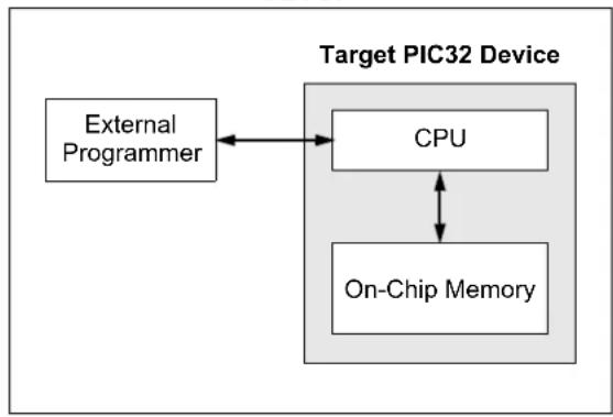
An external tool programming setup consists of an external programmer tool and a target PIC32 device. Figure 2-1 illustrates a typical programming setup. The programmer tool is responsible for executing necessary programming steps and completing the programming operation.
FIGURE 2-1: PROGRAMMING SYSTEM SETUP
flowchart
graph TD
    A["External Programmer"] <--> B["CPU"]
    B <--> C["On-Chip Memory"]
    style A fill:#f9f,stroke:#333
    style B fill:#ccf,stroke:#333
    style C fill:#cfc,stroke:#333
2.1 Devices with Dual Flash Panel and Dual Boot Regions
The PIC32MKXXXXXXD/E/F/K/L/M and PIC32MZ families of devices incorporate several features useful for field (self) programming of the device. These features include dual Flash panels with dual boot regions, an aliasing scheme for the boot regions allowing automatic selection of boot code at start-up and a panel swap feature for Program Flash. The two Flash panels and their associated boot regions can be erased and programmed separately. Refer to the Section 48. "Memory Organization and Permissions" (DS60001214) of the "PIC32 Family Reference Manual" for a detailed explanation of these features.
A development tool used for production programming will not be concerned about most of these features with the following exceptions:
- Ensuring the SWAP bit (NVMCON[7]) is in the proper setting. The default setting is '0' for no swap of panels. The development tool should assume the default setting when generating source files for the programming tool.
- Proper handling of the aliasing of the boot memory in the checksum calculation. The aliased sections will be duplicates of the fixed sections. See Section 18.0 "Checksum" for more information on checksum calculations with aliased regions
- For PIC32MK devices, using the Erase/Retry feature when an attempt to erase a Flash page fails and needs to be retried. See Section 13.0 "Initiating a Page Erase" for more information.
2.2 Programming Interfaces
All PIC32 devices provide two physical interfaces to the external programmer tool:
- 2-wire In-Circuit Serial Programming™ (ICSP™)
• 4-wire Joint Test Action Group (JTAG)
See Section 4.0 "Connecting to the Device" for more information.
Either of these methods may use a downloadable Programming Executive (PE). The PE executes from the target device RAM and hides device programming details from the programmer. It also removes overhead associated with data transfer and improves overall data throughput. Microchip has developed a PE that is available for use with any external programmer, see Section 17.0 "The Programming Executive" for more information.
Section 3.0 “Programming Steps” describes high-level programming steps, followed by a brief explanation of each step. Detailed explanations are available in corresponding sections of this document.
More information on programming commands, EJTAG, and DC specifications are available in the following sections:
- Section 19.0 "Configuration Memory and Device ID"
• Section 20.0 "TAP Controllers" - Section 21.0 "AC/DC Characteristics and Timing Requirements"
2.3 Enhanced JTAG (EJTAG)
The 2-wire and 4-wire interfaces use the EJTAG protocol to exchange data with the programmer. While this document provides a working description of this protocol as needed, advanced users are advised to refer to the Imagination Technologies Limited web site (www.imgtec.com) for more information.
2.4 Data Sizes
Data sizes are defined as follows:
• One word: 32 bits
• One-half word: 16 bits
• One-quarter word: 8 bits
- One Byte: 8 bits
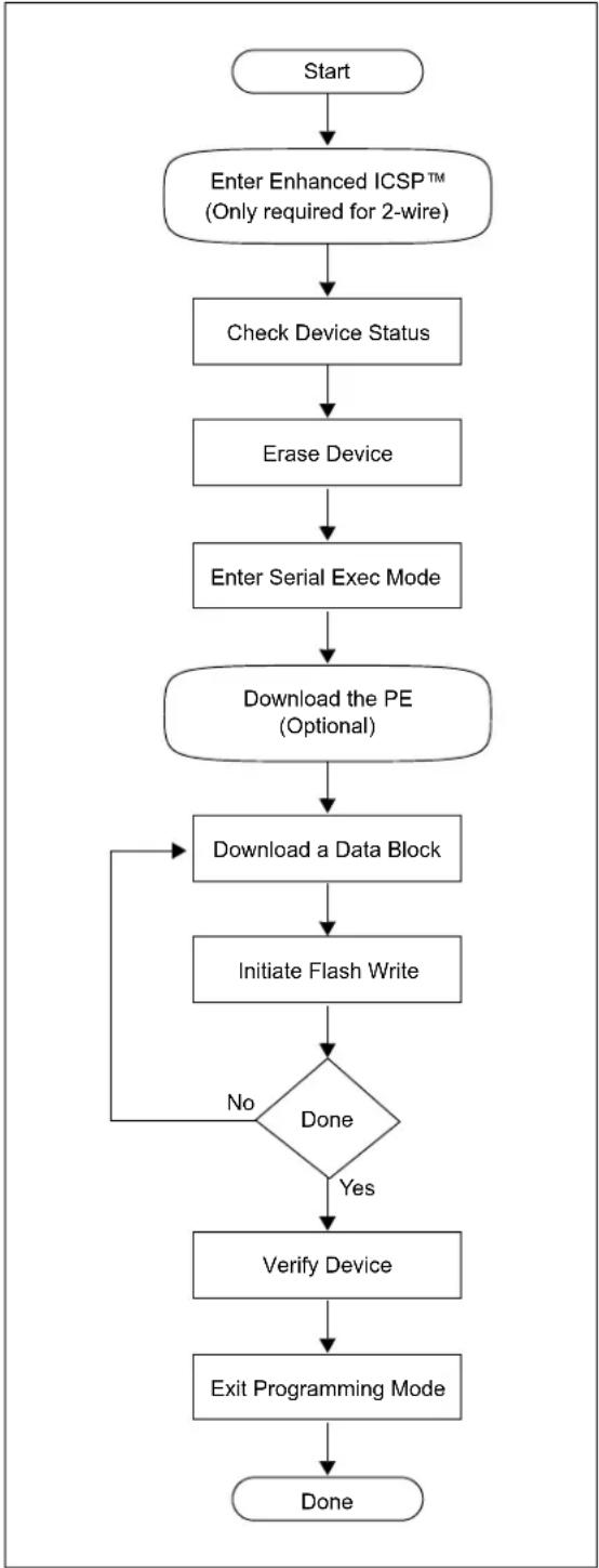
3.0 PROGRAMMING STEPS
All tool programmers must perform a common set of steps, regardless of the actual method being used. Figure 3-1 shows the set of steps to program PIC32 devices.
FIGURE 3-1: PROGRAMMING FLOW
flowchart
graph TD
    A["Start"] --> B["Enter Enhanced ICSP™ (Only required for 2-wire)"]
    B --> C["Check Device Status"]
    C --> D["Erase Device"]
    D --> E["Enter Serial Exec Mode"]
    E --> F["Download the PE (Optional)"]
    F --> G["Download a Data Block"]
    G --> H["Initiate Flash Write"]
    H --> I{Done}
    I -->|No| G
    I -->|Yes| J["Verify Device"]
    J --> K["Exit Programming Mode"]
    K --> L["Done"]
The following sequence lists the programming steps with a brief explanation of each step. More detailed information about these steps is available in the subsequent sections.
- Connect to the target device.
To ensure successful programming, all required pins must be connected to appropriate signals. See Section 4.0 "Connecting to the Device" for more information.
- Place the target device in programming mode.
For 2-wire programming methods, the target device must be placed in a special programming mode (Enhanced ICSP™) before executing any other steps.
Note: For the 4-wire programming methods, Step 2 is not applicable.
See Section 7.0 "Entering 2-Wire Enhanced ICSP Mode" for more information.
- Check the status of the device.
Checks the status of the device to ensure it is ready to receive information from the programmer.
See Section 8.0 "Check Device Status" for more information.
- Erase the target device.
If the target memory block in the device is not blank, or if the device is code-protected, an erase step must be performed before programming any new data.
See Section 9.0 "Erasing the Device" for more information.
- Enter programming mode.
Verifies that the device is not code-protected and boots the TAP controller to start sending and receiving data to and from the PIC32 CPU.
See Section 10.0 "Entering Serial Execution Mode" for more information.
- Download the Programming Executive (PE).
The PE is a small block of executable code that is downloaded into the RAM of the target device. It will receive and program the actual data.
Note: If the programming method being used does not require the PE, Step 6 is not applicable.
See Section 11.0 "Downloading the Programming Executive (PE)" for more information.
- Download the block of data to program.
All methods, with or without the PE, must download the desired programming data into a block of memory in RAM.
See Section 12.0 "Downloading a Data Block" for more information.
- Initiate Flash Write.
After downloading each block of data into RAM, the programming sequence must be started to program it into the target device's Flash memory.
See Section 14.0 "Initiating a Flash Row Write" for more information.
-
Repeat Step 7 and Step 8 until all data blocks are downloaded and programmed.
-
Verify the program memory.
After all programming data and Configuration bits are programmed, the target device memory should be read back and verified for the matching content.
See Section “” for more information.
- Exit the programming mode.
The newly programmed data is not effective until either power is removed and reapplied to the target device or an exit programming sequence is performed.
See Section 16.0 "Exiting Programming Mode" for more information.
4.0 CONNECTING TO THE DEVICE
The PIC32 family provides two possible physical interfaces for connecting and programming the memory contents, see Figure 4-1. For all programming interfaces, the target device must be powered and all required signals must be connected. In addition, the interface must be enabled, either through its Configuration bit, as in the case of the JTAG 4-wire interface, or though a special initialization sequence, as is the case for the 2-wire ICSP interface.
The JTAG interface is enabled by default in blank devices shipped from the factory.
Enabling ICSP is described in Section 7.0 "Entering 2-Wire Enhanced ICSP Mode".
FIGURE 4-1: PROGRAMMING
INTERFACES

text_image
Programmer 2-wire ICSP™ OR 4-wire JTAG PIC32 + MCLR, VDDCORE(1) VDDR1v8(1), VDDIO, VSS, Vss1v8(1)Note 1: This pin is not available on all devices. Refer to the "Pin Diagrams" or "Pin Tables" section in the specific device data sheet to determine availability.
4.1 4-wire Interface
One possible interface is the 4-wire JTAG (IEEE 1149.1) port. Table 4-1 lists the required pin connections. This interface uses the following four communication lines to transfer data to and from the PIC32 device being programmed:
• Test Clock Input (TCK)
• Test Mode Select Input (TMS)
- Test Data Input (TDI)
• Test Data Output (TDO)
Refer to the specific device data sheet for the connection of the signals to the device pins.
4.1.1 TEST CLOCK INPUT (TCK)
TCK is the clock that controls the updating of the TAP controller and the shifting of data through the Instruction or selected Data registers. TCK is independent of the processor clock with respect to both frequency and phase.
4.1.2 TEST MODE SELECT INPUT (TMS)
TMS is the control signal for the TAP controller. This signal is sampled on the rising edge of TCK.
4.1.3 TEST DATA INPUT (TDI)
TDI is the test data input to the Instruction or selected Data register. This signal is sampled on the rising edge of TCK for some TAP controller states.
4.1.4 TEST DATA OUTPUT (TDO)
TDO is the test data output from the Instruction or Data registers. This signal changes on the falling edge of TCK. TDO is only driven when data is shifted out, otherwise the TDO is tri-stated.
TABLE 4-1: 4-WIRE INTERFACE PINS
| Device Pin Name | Pin Type | Pin Description |
| I | Programming Enable | |
| ENVREG^(2) | I | Enable for On-Chip Voltage Regulator |
| V_DD, V_DDIO, V_DDCORE^(2), V_DDR1V8^(2), V_BAT^(2), and AV_DD^(1) | P | Power Supply |
| V_SS, V_SS1V8^(2), and AV_SS^(1) | P | Ground |
| V_CAP^(2) | P | CPU logic filter capacitor connection |
| TDI | I | Test Data In |
| TDO | O | Test Data Out |
| TCK | I | Test Clock |
| TMS | I | Test Mode State |
Legend: I = Input O = Output P = Power
Note 1: All power supply and ground pins must be connected, including analog supplies (AVDD) and ground (AVSS).
2: This pin is not available on all devices. Refer to the "Pin Diagrams" or "Pin Tables" section in the specific device data sheet to determine availability.
4.2 2-wire Interface
Another possible interface is the 2-wire ICSP port. Table 4-2 lists the required pin connections. This interface uses the following two communication lines to transfer data to and from the PIC32 device being programmed:
- Serial Program Clock (PGECx)
- Serial Program Data (PGEDx)
These signals are described in the following two sections. Refer to the specific device data sheet for the connection of the signals to the chip pins.
4.2.1 SERIAL PROGRAM CLOCK (PGECx)
PGECx is the clock that controls the updating of the TAP controller and the shifting of data through the Instruction or selected Data registers. PGECx is independent of the processor clock, with respect to both frequency and phase.
4.2.2 SERIAL PROGRAM DATA (PGEDx)
PGEDx is the data input/output to the Instruction or selected Data Registers, it is also the control signal for the TAP controller. This signal is sampled on the falling edge of PGECx for some TAP controller states.
TABLE 4-2: 2-WIRE INTERFACE PINS
| Device Pin Name | Programmer Pin Name | Pin Type | Pin Description |
| MCLR | P | Programming Enable | |
| ENVREG^(2) | N/A I Enable for On-Chip Voltage Regulator | ||
| V_DD, V_DDIO, V_BAT^(2), and AV_DD^(1) | VDD P Power Supply | ||
| V_DDCORE^(2) and V_DDR1V8^(2) | N/A P Power Supply for DDR Interface | ||
| V_SS, V_SS1V8^(2), and AV_SS^(1) | Vss | P | Ground |
| V_CAP^(2) | N/A P CPU Logic Filter | Capacitor Connection | |
| PGECx | PGEC | I Primary Programming Pin Pair: Serial Clock | |
| PGEDx | PGED | I/O | Primary Programming Pin Pair: Serial Data |
Legend: I = Input
O = Output
P = Power
Note 1: All power supply and ground pins must be connected, including analog supplies (AVDD) and ground (AVss).
2: This pin is not available on all devices. Refer to either the "Pin Diagrams" or "Pin Tables" section in the specific device data sheet to determine availability.
4.3 PIC32MX Power Requirements
Devices in the PIC32MX family are dual voltage supply designs. There is one supply for the core and another for peripherals and I/O pins. All devices contain an on-chip regulator for the lower voltage core supply to eliminate the need for an additional external regulator. There are three implementations of the on board regulator:
- The first version has an internal regulator that can be disabled using the ENVREG pin. When disabled, an external power supply must be used to power the core. If enabled, a low-ESR filter capacitor must be connected to the VCAP pin, see Figure 4-2.
- The second version has an internal regulator that cannot be disabled. A low-ESR filter capacitor must always be connected to the VCAP pin.
- The third version has an internal regulator that cannot be disabled and does not require a filter capacitor
Refer to Section 21.0 "AC/DC Characteristics and Timing Requirements" and the "Electrical Characteristics" chapter in the specific device data sheet for the power requirements for your device.
FIGURE 4-2: INTERNAL REGULATOR ENABLE/DISABLE OPTIONS

text_image
Regulator Enabled(2) (ENVREG tied to VDD) 3.3V PIC32MX VDD ENVREG VCAP VSS CEFC (10 µF typical) Regulator Disabled(2) (ENVREG tied to ground) 1.8V(1) 3.3V(1) PIC32MX VDD ENVREG VCAP VSS Note 1: These are typical operating voltages. Refer to Section 21.0 "AC/DC Characteristics and Timing Requirements" for the full operating ranges of VDD and VCAP. 2: Regulator Enabled and Regulator Disabled mode are not available on all devices. Refer to the specific device data sheet to determine availability.4.4 PIC32MX With VBAT Pin Power Requirements
Some devices in the PIC32MX family provide a VBAT pin which can be connected to the VDD power supply during programming. See Figure 4-3.
FIGURE 4-3: PIC32MX WITH VBAT PIN POWER CONNECTIONS

text_image
3.3V(1) PIC32MX XLP VDD VBAT VCAP VSS Note 1: This is typical operating voltage. Refer to Section 21.0 "AC/DC Characteristics and Timing Requirements" for the full operating range of VDD.4.5 PIC32MZ EC and PIC32MZ EF Power Requirements
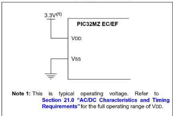
Devices in the PIC32MZ EC and PIC32MZ EF families are also dual voltage supply designs like PIC32MX devices. However, the internal regulator does not require the external filter capacitor, and there is no corresponding VCAP or ENVREG pins. See Figure 4-4.
Refer to Section 21.0 "AC/DC Characteristics and Timing Requirements" and the "Electrical Characteristics" chapter in the specific device data sheet for the power requirements for your device.
FIGURE 4-4: PIC32MZ EC/EF POWER CONNECTIONS
text_image
3.3V(1) PIC32MZ EC/EF VDD Vss Note 1: This is typical operating voltage. Refer to Section 21.0 "AC/DC Characteristics and Timing Requirements" for the full operating range of VDD.4.6 PIC32MZ DA Power Requirements
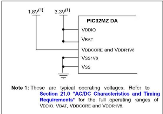
Devices in the PIC32MZ DA family are quadruple voltage supply designs. Two of the voltage supplies are identical to the PIC32MZ EC and PIC32MZ EF voltage supplies. The third voltage supply is for the DDR memory interface, and requires a 1.8 volt supply. The fourth voltage supply is for the VBAT pin, but it can be connected to the VDD power supply. See Figure 4-5.
Refer to Section 21.0 “AC/DC Characteristics and Timing Requirements” and the “Electrical Characteristics” chapter in the specific device data sheet for the power requirements for your device.
FIGURE 4-5: PIC32MZ DA POWER CONNECTIONS
text_image
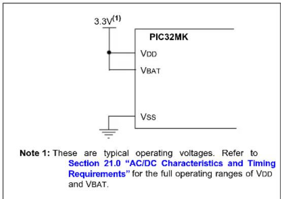
1.8V(1) 3.3V(1) PIC32MZ DA VDDIO VBAT VDDCORE and VDDR1V8 VSS1V8 VSS Note 1: These are typical operating voltages. Refer to Section 21.0 "AC/DC Characteristics and Timing Requirements" for the full operating ranges of VDDIO, VBAT, VDDCORE and VDDR1V8.4.7 PIC32MK Power Requirements
Devices in the PIC32MK family are triple voltage supply designs. Two of the voltage supplies are identical to the PIC32MZ EC and PIC32MZ EF voltage supplies. The third voltage supply is for the VBAT pin, but it can be connected to the VDD power supply. See Figure 4-6.
FIGURE 4-6: PIC32MK POWER CONNECTIONS
text_image
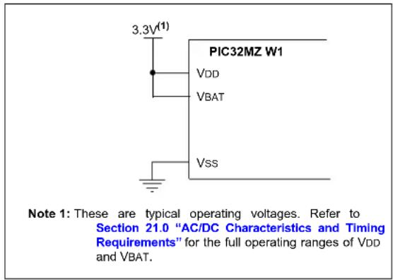
3.3V(1) PIC32MK VDD VBAT VSS Note 1: These are typical operating voltages. Refer to Section 21.0 "AC/DC Characteristics and Timing Requirements" for the full operating ranges of VDD and VBAT.4.8 PIC32MZ W1 Power Requirements
Devices in the PIC32MZ W1 family are triple voltage supply designs. Two of the voltage supplies are identical to the PIC32MZ EC and PIC32MZ EF voltage supplies. Connect the voltage supplies of the PIC32MZ W1 family of devices as shown in the following figure.
FIGURE 4-7: PIC32MZ W1 POWER CONNECTIONS
text_image
3.3V(1) PIC32MZ W1 VDD VBAT Vss Note 1: These are typical operating voltages. Refer to Section 21.0 "AC/DC Characteristics and Timing Requirements" for the full operating ranges of VDD and VBAT.5.0 EJTAG vs. ICSP
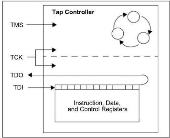
Programming is accomplished through the EJTAG module in the CPU core. EJTAG is connected to either the full set of JTAG pins or a reduced 2-wire to 4-wire EJTAG interface for ICSP mode. In both modes, programming of the PIC32 Flash memory is accomplished through the ETAP controller. The TAP Controller uses the TMS pin to determine if Instruction or Data registers should be accessed in the shift path between TDI and TDO, see Figure 5-1.
The basic concept of EJTAG that is used for programming is the use of a special memory area called DMSEG (0xFF200000 to 0xFF2FFFFFF), which is only available when the processor is running in Debug mode. All instructions are serially shifted into an internal buffer, and then loaded into the Instruction register and executed by the CPU. Instructions are fed through the ETAP state machine in 32-bit groups.
FIGURE 5-1: TAP CONTROLLER
flowchart
graph TD
    A["TMS"] --> B["TCK"]
    B --> C["TDO"]
    C --> D["Instruction, Data, and Control Registers"]
    D --> E["TDI"]
    E --> F["Feedback Loop"]
    F --> G["Output"]
    style A fill:#f9f,stroke:#333
    style B fill:#ccf,stroke:#333
    style C fill:#cfc,stroke:#333
    style D fill:#fcc,stroke:#333
    style E fill:#ffc,stroke:#333
    style F fill:#fcc,stroke:#333
    style G fill:#fff,stroke:#333
5.1 Programming Interface
Figure 5-2 shows the basic programming interface in PIC32 devices. Descriptions of each interface block are provided in subsequent sections.
FIGURE 5-2: BASIC PIC32 PROGRAMMING INTERFACE BLOCK DIAGRAM

flowchart
graph LR
    subgraph Inputs
        direction TB
        TMS --> ETAP
        TCK --> ETAP
        TDI --> ETAP
        TDO --> ETAP
        or --> MTAP
        or --> 2-wire["2-wire to 4-wire"]
        PGECx --> MTAP
        PGEDx --> MTAP
    end

    subgraph Outputs
        direction LR
        CPU --> FlashController
        MTAP --> FlashController
        2-wire --> FlashController
        CPU <--> FlashController
        MTAP <--> FlashController
        FlashController --> FlashMemory
        FlashMemory --> FlashController
    end

    subgraph Outputs
        direction LR
        Common --> VDD/VDDIO/VDD1V8CORE
        VBAT/VDDR1V8 --> VSS/VSS1V8 --> MCLR
    end
5.1.1 ETAP
This block serially feeds instructions and data into the CPU.
5.1.2 MTAP
In addition to the EJTAG TAP (ETAP) controller, the PIC32 device uses a second proprietary TAP controller for additional operations. The Microchip TAP (MTAP) controller supports two instructions relevant to programming: MTAP_COMMAND and TAP switch Instructions. See Table20-1 for a complete list of
Instructions. The MTAP_COMMAND instruction provides a mechanism for a JTAG probe to send commands to the device through its Data register.
The programmer sends commands by shifting in the MTAP_COMMAND instruction through the SendCommand pseudo operation, and then sending the MTAP_COMMAND DR commands through the XferData pseudo operation, see Table 20-2 for specific commands.
The probe does not need to issue a MTAP_COMMAND instruction for every command shifted into the Data register.
5.1.3 2-WIRE TO 4-WIRE
This block converts the 2-wire ICSP interface to the 4-wire JTAG interface.
5.1.4 CPU
The CPU executes instructions at 8 MHz through the internal oscillator.
The Flash controller controls erasing and programming of the Flash memory on the device.
5.1.6 FLASH MEMORY
The PIC32 device Flash memory is divided into two logical Flash partitions consisting of the Boot Flash Memory (BFM) and Program Flash Memory (PFM). The BFM begins at address 0x1FC00000, and the PFM begins at address 0x1D000000. Each Flash partition is divided into pages, which represent the smallest block of memory that can be erased. Depending on the device, page sizes are 256 words (1024 bytes), 1024
words (4096 bytes) or 4096 words (16,384 bytes). Row size indicates the number of words that are programmed with the row program command. There are always 8 rows within a page; therefore, devices with 256, 1024, and 4096 word page sizes have 32, 128, and 512 word row sizes, respectively. Table 5-1 shows the PFM, BFM, row, and page size of each device family.
For a PIC32MZ W1 device, the BFM begins at address 0x1FC00000, and the PFM begins at address 0x10000000. The Flash is divided into pages of 1024 words or 4 kbytes, which represents the smallest block of memory that can be erased. Row size indicates the number of words that are programmed with row program commands. The Flash contains 4 rows within a page with a total row size of 256 words or 1024 bytes.
Memory locations of the BFM are reserved for the device Configuration registers, see Section 19.0 "Configuration Memory and Device ID" for more information.
TABLE 5-1: CODE MEMORY SIZE
| PIC32 Device | Row Size (Words) | Page Size (Words) | Boot Flash Memory Address (Bytes) (See Note 1) | Programming Executive (See Notes 2 and 3) |
| PIC32MX110/120/130/150/170210/220/230/350/270(28/36/44-pin devices Only) | 32 256 | 0x1FC00000-0x1FC00BFF (3 KB) | RIPE_11_aabbcc.hex | |
| PIC32MX120/130/150/170/230/250/270/530/550/570(64/100-pin devices Only) | ||||
| PIC32MX15X/17X/25X/27X(28/44-pin devices Only) | 0x1FC00000-0x1FC02FFF (12 KB) | |||
| PIC32MZ W1 | 256 10 | 24 | 0x1FC00000-0x1FC0FFFF (64 KB) | — |
Note 1: Program Flash Memory address ranges are based on Program Flash size are as given below:
- 0x1D000000-0x1D003FFF (16 KB)
• 0x1D000000-0x1D007FFF (32 KB)
• 0x1D000000-0x1D00FFFF (64 KB)
• 0x1D000000-0x1D01FFFF (128 KB)
• 0x1D000000-0x1D03FFFF (256 KB)
• 0x1D000000-0x1D07FFFF (512 KB)
- 0x1D000000-0x1D0FFFFFF (1024 KB)
- 0x1D000000-0x1D1FFFFFF (2048 KB)
All Program Flash memory sizes are not supported by each family.
Program Flash Memory address ranges for PIC32MZ W1: 0x10000000-0x100FFFFFF (1024 KB).
2: The Programming Executive can be obtained from the related product page on the Microchip website or it can be located in the following MPLAB ^® X IDE installation folders:
...\Microchip\MPLABX\
...\Microchip\MPLABX\
...\Microchip\MPLABX\
3: The last characters of the file name, aabbcc, vary based on the revision of the file.
TABLE 5-1: CODE MEMORY SIZE (CONTINUED)
| PIC32 Device | Row Size (Words) | Page Size (Words) | Boot Flash Memory Address (Bytes) (See Note 1) | Programming Executive (See Notes 2 and 3) |
| PIC32MX330/350/370/430/450/470 | 128 1024 | 0x1FC000 | 000-0x1FC02FFF (12 KB) | RIPE_06_aabbcc.hex |
| PIC32MX320/340/360/420/440/460 | ||||
| PIC32MX534/564/664/764 | ||||
| PIC32MX575/675/695/795 | ||||
| PIC32MK0512/1024XXD/E/F/K/L/M | 128 1024 | 0x1FC00000-0x1FC04FFF (20 KB)0x1FC20000-0x1FC24FFF (20 KB) | RIPE_15a_aabbcc.hex | |
| PIC32MK0256/0512XXG/H | 128 1024 | 0x1FC000 | 000-0x1FC04FFF (20 KB) | RIPE_15a_aabbcc.hex |
| PIC32MZ05XX/10XX/20XX | 512 4096 | 0x1FC00000-0x1FC13FFF (80 KB)0x1FC20000-0x1FC33FFF (80 KB) | RIPE_15_aabbcc.hex | |
| PIC32MZ W1 | 256 1024 | 0x1FC000 | 000-0x1FC0FFFF (64 KB) | RIPE_25_aabbcc.hex |
Note 1: Program Flash Memory address ranges are based on Program Flash size are as given below:
• 0x1D000000-0x1D003FFF (16 KB)
• 0x1D000000-0x1D007FFF (32 KB)
• 0x1D000000-0x1D00FFFF (64 KB)
• 0x1D000000-0x1D01FFFF (128 KB)
• 0x1D000000-0x1D03FFFF (256 KB)
- 0x1D000000-0x1D07FFFF (512 KB)
- 0x1D000000-0x1D0FFFFFF (1024 KB)
• 0x1D000000-0x1D1FFFFFF (2048 KB)
All Program Flash memory sizes are not supported by each family.
Program Flash Memory address ranges for PIC32MZ W1: 0x10000000-0x100FFFFFF (1024 KB).
2: The Programming Executive can be obtained from the related product page on the Microchip website or it can be located in the following MPLAB ^® X IDE installation folders:
...\Microchip\MPLABX\
...\Microchip\MPLABX\
...\Microchip\MPLABX\
3: The last characters of the file name, aabbcc, vary based on the revision of the file.
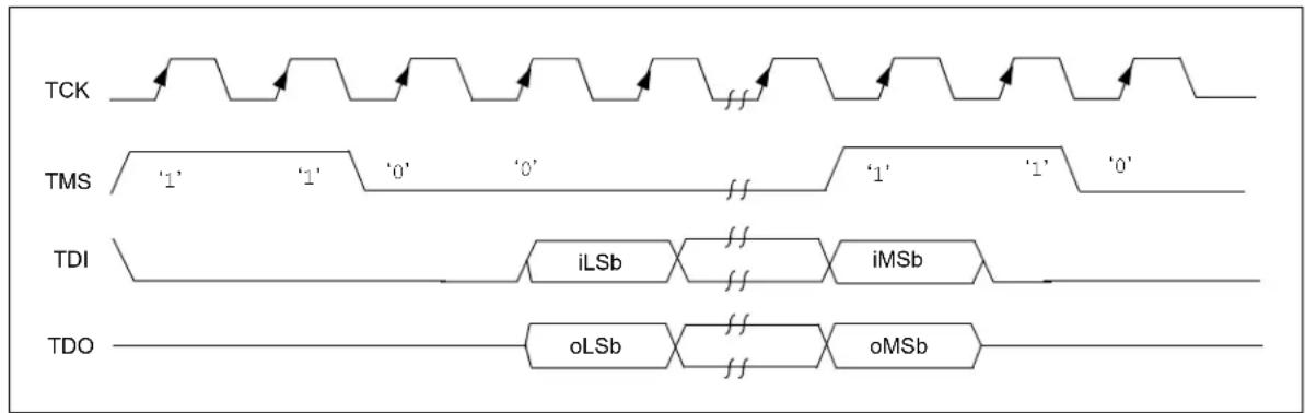
5.2 4-wire JTAG Details
The 4-wire interface uses standard JTAG (IEEE 1149.1-2001) interface signals.
• TCK: Test Clock – drives data in/out
- TMS: Test Mode Select – selects operational mode
- TDI: Test Data Input – data into the device
- TDO: Test Data Output – data out of the device
Since only one data line is available, the protocol is necessarily serial (like SPI). The clock input is at the TCK pin. Configuration is performed by manipulating a state machine bit by bit through the TMS pin. One bit of data is transferred in and out per TCK clock pulse at the TDI and TDO pins. Different instruction modes can be loaded to read the chip ID or manipulate chip functions.
Data presented to TDI must be valid for a chip-specific setup time before, and hold time, after the rising edge of TCK. TDO data is valid for a chip-specific time after the falling edge of TCK, refer to Figure 5-3.
FIGURE 5-3: 4-WIRE JTAG INTERFACE
text_image
TCK TMS '1' '1' '0' '0' '1' '1' '0' TDI iLSb iMSb TDO oLSb oMSb5.3 2-wire ICSP Details
In ICSP mode, the 2-wire ICSP signals are time multiplexed into the 2-wire to 4-wire block. The 2-wire to 4-wire block then converts the signals to look like a 4-wire JTAG port to the TAP controller. The following are two possible modes of operation:
• 4 - phase I CSP
• 2 - phase I CSP
5.3.1 4-PHASE ICSP
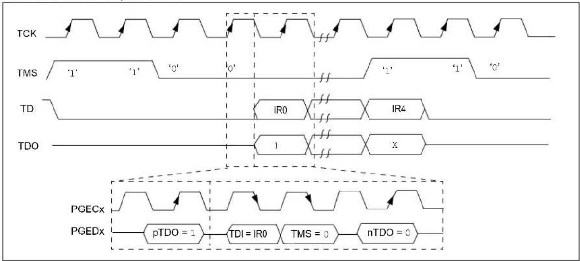
In 4-phase ICSP mode, the TDI, TDO and TMS device pins are multiplexed onto PGEDx in four clocks, see Figure 5-4. The Least Significant bit (LSb) is shifted first; and TDI and TMS are sampled on the falling edge of PGECx, while TDO is driven on the falling edge of PGECx. The 4-phase ICSP mode is used for both read and write data transfers.
5.3.2 2-PHASE ICSP
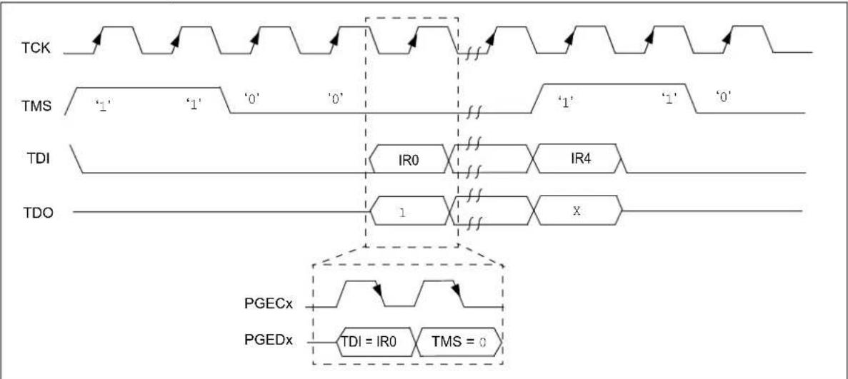
In 2-phase ICSP mode, the TMS and TDI device pins are multiplexed into PGEDx in two clocks, see Figure 5-5. The LSb is shifted first; and TDI and TMS are sampled on the falling edge of PGECx. There is no TDO output provided in this mode. The 2-phase ICSP mode was designed to accelerate 2-wire, write-only transactions.
Note: The packet is not actually executed until the first clock of the next packet. To enter 2-wire, 2-phase ICSP mode, the TDOEN bit (DDPCON[0] or CFGCON[0]) must be set to '0'.
FIGURE 5-4: 2-WIRE, 4-PHASE
flowchart
graph TD
    subgraph TCK
        A1[" "] --> B1[" "]
        B1 --> C1[" "]
        C1 --> D1[" "]
        D1 --> E1[" "]
        E1 --> F1[" "]
        F1 --> G1[" "]
        G1 --> H1[" "]
        H1 --> I1[" "]
        I1 --> J1[" "]
        J1 --> K1[" "]
        K1 --> L1[" "]
        L1 --> M1[" "]
        M1 --> N1[" "]
        N1 --> O1[" "]
        O1 --> P1[" "]
        P1 --> Q1[" "]
        Q1 --> R1[" "]
        R1 --> S1[" "]
        S1 --> T1[" "]
        T1 --> U1[" "]
        U1 --> V1[" "]
        V1 --> W1[" "]
        W1 --> X1[" "]
        X1 --> Y1[" "]
        Y1 --> Z1[" "]
        Z1 --> AA1[" "]
        AA1 --> AB1[" "]
        AB1 --> AC1[" "]
        AC1 --> AD1[" "]
        AD1 --> AE1[" "]
        AE1 --> AF1[" "]
        AF1 --> AG1[" "]
        AG1 --> AH1[" "]
        AH1 --> AI1[" "]
        AI1 --> AJ1[" "]
        AJ1 --> AK1[" "]
        AK1 --> AL1[" "]
        AL1 --> AM1[" "]
        AM1 --> AN1[" "]
        AN1 --> AO1[" "]
        AO1 --> AP1[" "]
        AP1 --> AQ1[" "]
        AQ1 --> AR1[" "]
        AR1 --> AS1[" "]
        AS1 --> AT1[" "]
        AT1 --> AU[" "]
        AU --> AV[" "]
        AV --> AW[" "]
    end

    subgraph TMS
        A2["‘1’"] --> B2["‘0’"]
        B2 --> C2["0'"]
        C2 --> D2["0'"]
        D2 --> E2["0'"]
        E2 --> F2["0'"]
        F2 --> G2["0'"]
        G2 --> H2["0'"]
        H2 --> I2["0'"]
        I2 --> J2["0'"]
        J2 --> K2["0'"]
        K2 --> L2["0'"]
        L2 --> M2["0'"]
        M2 --> N2["0'"]
        N2 --> O2["0'"]
        O2 --> P2["0'"]
        P2 --> Q2["0'"]
        Q2 --> R2["0'"]
        R2 --> S2["0'"]
        S2 --> T2["0'"]
        T2 --> U2["0'"]
        U2 --> V2["0'"]
        V2 --> W2["0'"]
        W2 --> X2["0'"]
        X2 --> Y2["0'"]
        Y2 --> Z2["0'"]
        Z2 --> AA2["0'"]
        AA2 --> AB2["0'"]
        AB2 --> AC2["0'"]
        AC2 --> AD2["0'"]
        AD2 --> AE2["0'"]
        AE2 --> AF2["0'"]
        AF2 --> AG2["0'"]
        AG2 --> AH2["0'"]
        AH2 --> AI2["0'"]
        AI2 --> AJ2["0'"]
        AJ2 --> AK2["0'"]
        AK2 --> AL2["0'"]
        AL2 --> AM2["0'"]
        AM2 --> AN2["0'"]
        AN2 --> AO2["0'"]
        AO2 --> AP2["0'"]
        AP2 --> AQ2["0'"]
        AQ2 --> AR2["0'"]
        AR2 --> AS2["0'"]
        AS2 --> AT2["0'"]
        AT2 --> AU2["0'"]
        AU2 --> AV2["0'"]
        AV2 --> AW2["0'"]
        AW2 --> AX["0'"]
        AX --> AY["0'"]
        AY --> AZ["0'"]
        AZ --> BA["0'"]
        BA --> BB["0'"]
        BB --> BC["0"]
    end

    subgraph TDI
        A3["TDI"] --> B3["TDI"]
    end

    subgraph TDO
        A4["TDO"] --> B4["TDO"]
    end

    subgraph PGECx
        A5["PGECx"] --> B6["PGECx"]
    end

    subgraph PGEDx
        A7["PGEDx"] --> B8["PGEDx"]
    end

    A3 -.-> B3
    B3 -.-> B6
    B6 -.-> B8
    B8 -.-> B4
    B4 -.-> B6
    B8 -.-> B8
    B8 -.-> B4
    B8 -.-> B6
    B8 -.-> B4
    B8 -.-> B6
    B8 -.-> B4
    B8 -.-> B6
    B8 -.-> B4
    B8 -.-> B6
    B8 -.-> B4
    B8 -.-> B6
    B8 -.-> B4
    B8 -.-> B6
    B8 -.-> B4
    B8 -.-> B6
    B3 -.-> IR0
    IR0 -.-> IR4
    IR4 -.-> IR4
    IR4 -.-> IR4
    IR4 -.-> IR4
    IR4 -.-> IR4
    IR4 -.-> IR4
    IR4 -.-> IR4
    IR4 -.-> IR4
    IR4 -.-> IR4
    IR4 -.-> IR4
    IR4 -.-> IR4
    IR4 -.-> IR4
    IR4 -.-> IR4
    IR4 -.-> IR6
    IR6 -.-> pTDO = 1
    pTDO = 1 -.-> TDI = IR0
    TDI = IR0 -.-> TMS = 0
    TMS = 0 -.-> nTDO = 0
FIGURE 5-5: 2-WIRE, 2-PHASE
flowchart
graph TD
    A["TCK"] --> B["Waveform 1"]
    B --> C["Waveform 2"]
    C --> D["Waveform 3"]
    D --> E["Waveform 4"]
    E --> F["Waveform 5"]

    G["TMS"] --> H["Waveform 1'"]
    H --> I["Waveform 2'"]
    I --> J["Waveform 3'"]
    J --> K["Waveform 4'"]
    K --> L["Waveform 5'"]

    M["TDI"] --> N["IR0"]
    N --> O["IR4"]
    O --> P["IR5"]
    P --> Q["IR6"]
    Q --> R["IR7"]
    R --> S["IR8"]
    S --> T["IR9"]
    T --> U["IR10"]

    V["TDO"] --> W["1"]
    W --> X["X"]

    Y["PGECx"] --> Z["Waveform 1'"]
    Z --> AA["Waveform 2'"]
    AA --> AB["Waveform 3'"]
    AB --> AC["Waveform 4'"]
    AC --> AD["Waveform 5'"]

    AE["PGEDx"] --> AF["PDID = IR0"]
    AF --> AG["TMS = 0"]
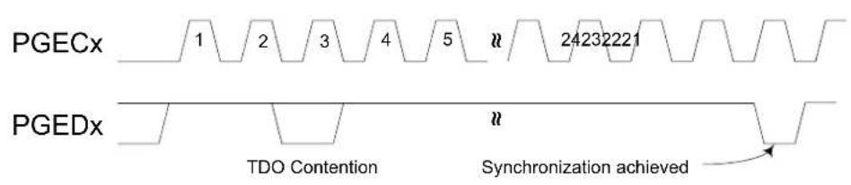
5.3.3 SYNCHRONIZATION
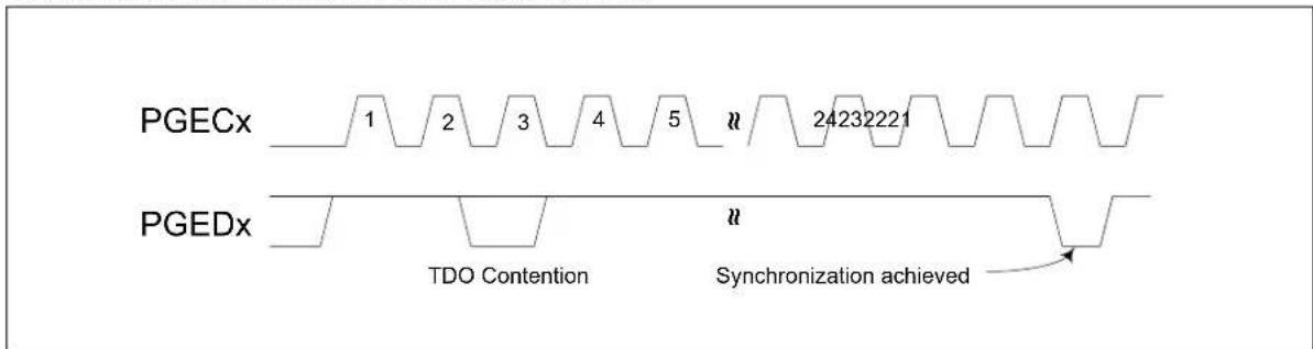
Some PIC32 devices can Reset the internal EJTAG state machine if the attached programmer loses synchronization with it. This can occur when noise is present on the PGCx signal.
To achieve resynchronization, the PGEDx pin is held high for 24 PGECx clock cycles. This forces five TMS events into the EJTAG controller and will place the EJTAG state machine into a Test Idle Reset. See Figure 5-6 for an example of how to achieve resynchronization.
When asserting the PGEDx pin high, there may be contention on the pin as the device may attempt to drive TDO out onto the pin while the in-circuit emulator is driving in. This will only occur for a maximum of one cycle as TMS high will advance the EJTAG state machine out of a Shift-IR or Shift-DR state.
Synchronization in 2-wire, 2-phase mode is not supported.
FIGURE 5-6: ACHIEVING RESYNCHRONIZATION
text_image
PGECx 1 2 3 4 5 n 24232221 PGEDx TDO Contention n Synchronization achieved6.0 PSEUDO OPERATIONS
To simplify the description of programming details, all operations will be described using pseudo operations. There are several functions used in the pseudo-code descriptions. These are used either to make the pseudo-code more readable, to abstract implementation-specific behavior or both. When passing parameters with pseudo operation, the following syntax will be used:
- 5'h0x03 – send 5-bit hexadecimal value of 3
- 6'b011111 – send 6-bit binary value of 31
These functions are defined in this section, and include the following operations:
- SetMode (mode)
- SendCommand (command)
• o Data = XferData (iData)
• o Data = XferFastData (iData) - oData = XferInstruction (instruction)
FIGURE 6-1: SetMode 4-WIRE

text_image
Mode = 6'b011111 TCK TMS '1' '1' '1' '1' '1' '0' TDI TDOFIGURE 6-2: SetMode 2-WIRE
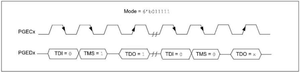
flowchart
graph LR
    A["PGECx"] --> B["TDI = 0"]
    B --> C["TMS = 1"]
    C --> D["TDO = 1"]
    D --> E["TDI = 0"]
    E --> F["TMS = 0"]
    F --> G["TDO = x"]
    style A fill:#f9f,stroke:#333
    style G fill:#f9f,stroke:#333
    note right of A
        Mode = 6'b011111
    end
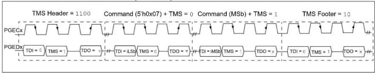
6.2 SendCommand Pseudo Operation
Format:
SendCommand (command)
Purpose:
To send a command to select a specific TAP register.
Description (in sequence):
- The TMS Header is clocked into the device to select the Shift IR state
- The command is clocked into the device on TDI while holding signal TMS low.
- The last Most Significant bit (MSb) of the command is clocked in while setting TMS high.
- The TMS Footer is clocked in on TMS to return the TAP controller to the Run/Test Idle state.
Restrictions:
None.
Example:
SendCommand (5'h0x07)
FIGURE 6-3: SendCommand 4-WIRE

text_image
TMS Header = 1100 Command = 5'h0x07 Command (MSb) + TMS = 1 TMS Footer = 10 TCK TMS ‘1’ ‘1’ ‘0’ ‘0’ ‘1’ ‘1’ ‘0’ ‘1’ ‘1’ ‘0’ TDI iLSb iMSb TDO 1 xFIGURE 6-4: SendCommand 2-WIRE (4-PHASE)
flowchart
graph LR
    A["TMS Header = 1100"] --> B["PGECx"]
    C["Command (5'h0x07) + TMS = 0"] --> D["PGEDx"]
    E["Command (MSb) + TMS = 1"] --> F["PGEDx"]
    G["TMS Footer = 10"] --> H["PGEDx"]
    B --> I["TDI = 0"]
    D --> J["TMS = 1"]
    I --> K["TDO = x"]
    J --> L["TDI = iLSb"]
    K --> M["TMS = 0"]
    L --> N["TDO = x"]
    M --> O["TDI = iMSb"]
    N --> P["TMS = 1"]
    O --> Q["TDO = x"]
    P --> R["TDI = 0"]
    Q --> S["TMS = 1"]
    R --> T["TDO = x"]
    S --> U["TDI = 0"]
    T --> V["TMS = 1"]
    U --> W["TDO = x"]
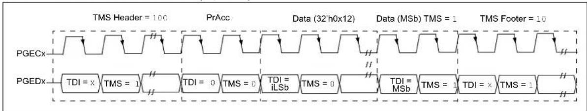
6.3 XferData Pseudo Operation
Format:
$$ \mathrm{oData} = \text { XferData (iData) } $$
Purpose:
To clock data to and from the register selected by the command.
Description (in sequence):
- The TMS Header is clocked into the device to select the Shift DR state.
- The data is clocked in/out of the device on TDI/TDO while holding signal TMS low.
- The last MSb of the data is clocked in/out while setting TMS high.
- The TMS Footer is clocked in on TMS to return the TAP controller to the Run/Test Idle state.
Restrictions:
None.
Example:
$$ \mathrm{oData} = \text { XferData } (3 2 ^ {\prime} \mathrm{h0x12}) $$
FIGURE 6-5: XferData 4-WIRE
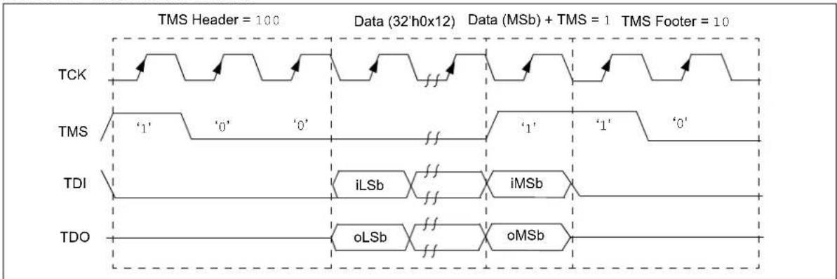
text_image
TMS Header = 100 Data (32'h0x12) Data (MSb) + TMS = 1 TMS Footer = 10 TCK TMS ‘1’ ‘0’ ‘0’ ‘1’ ‘1’ ‘0’ TDI iLSb iMSb TDO oLSb oMSbFIGURE 6-6: XferData 2-WIRE (4-PHASE)

flowchart
graph TD
    subgraph_TMS_Header["TS M Header = 100"]
        A["PGE C"] --> B["TDI = 0"]
        B --> C["TMS = 0"]
        C --> D["TDO = x"]
        D --> E["TDI = 0"]
        E --> F["TMS = 0"]
        F --> G["TDO = x"]
        G --> H["TDI = 0"]
        H --> I["TMS = 0"]
        I --> J["TDO = oLSb"]
    end
    subgraph_Data["Data (31'h0x12) + TMS = 0"]
        K["TDI = iLSb"] --> L["TMS = 0"]
        L --> M["TDO = oLSb+1"]
        N["TDI = iMSb"] --> O["TMS = 1"]
        O --> P["TDO = x"]
    end
    subgraph_Data["Data (MSb) + TMS Footer = 1"]
        Q["TDI = iMSb"] --> R["TMS = 1"]
        R --> S["TDO = x"]
    end
    subgraph_TMS_Footer["TS M Footer = 10"]
        T["TDI = 0"] --> U["TMS = 1"]
        U --> V["TDO = x"]
        V --> W["TDI = 0"]
        W --> X["TMS = 0"]
        X --> Y["TDO = x"]
    end
6.4 XferFastData Pseudo Operation
Format:
$$ \mathrm{oData} = \text { XferFastData (iData) } $$
Purpose:
To quickly send 32 bits of data in/out of the device.
Description (in sequence):
- The TMS Header is clocked into the device to select the Shift DR state.
Note: For 2-wire (4-phase) – on the last clock, the oPrAcc bit is shifted out on TDO while clocking in the TMS Header. If the value of oPrAcc is not '1', the whole operation must be repeated.
- The input value of the PrAcc bit, which is '0', is clocked in.
Note: For 2-wire (4-phase) – the TDO during this operation will be the LSb of output data. The rest of the 31 bits of the input data are clocked in and the 31 bits of output data are clocked out. For the last bit of the input data, the TMS Footer = 1 is set.
- TMS Footer = 10 is clocked in to return the TAP controller to the Run/Test Idle state.
Restrictions:
The SendCommand (ETAP_FASTDATA) must be sent first to select the Fastdata register, as shown in Example 6-1. See Table 20-4 for a detailed descriptions of commands.
Note: The 2-phase XferData is only used when talking to the PE. See Section 17.0 "The Programming Executive" for more information.
EXAMPLE 6-1: SendCommand
// Select the Fastdata Register SendCommand(ETAP_FASTDATA) // Send/Receive 32-bit Data oData = XferFastData(32'h0x12)
FIGURE 6-7: XferFastData 4-WIRE

flowchart
graph TD
    A["TCK"] --> B["TMS Header = 100"]
    B --> C["PrAcc"]
    C --> D["Data (32'h0x12)"]
    D --> E["Data (MSb) + TMS = 1"]
    E --> F["TMS Footer = 10"]
    G["TMS"] --> H["TDI"]
    H --> I["TDO"]
    J["iLSb"] --> K["iMSb"]
    L["oLSb"] --> M["oMSb"]
    N["‘1’"] --> O["‘0’"] --> P["‘0’"] --> Q["‘0’"] --> R["‘0’"] --> S["‘0’"] --> T["‘0’"] --> U["‘0’"] --> V["‘0’"] --> W["‘0’"] --> X["‘0’"] --> Y["‘0’"] --> Z["‘0’"] --> AA["‘0’"] --> AB["‘0’"] --> AC["‘0’"] --> AD["‘0’"] --> AE["‘0’"] --> AF["‘0’"] --> AG["‘0’"] --> AH["‘0’"] --> AI["‘0’"] --> AJ["‘0’"] --> AK["‘0’"] --> AL["‘0’"] --> AM["‘0’"] --> AN["‘0’"] --> AO["‘0’"] --> AP["‘0’"] --> AQ["‘0’"] --> AR["‘0’"] --> AS["‘0’"] --> AT["‘0’"] --> AU["‘0’"] --> AV["‘0’"] --> AW["‘0’"] --> AX["‘0’"] --> AY["‘0’"] --> AZ["‘0’"] --> BA["‘0’"] --> BB["‘0’"] --> BC["‘0’"] --> BD["‘0’"] --> BE["‘0’"] --> BF["‘0’"] --> BG["‘0’"] --> BH["‘0’"] --> BI["‘0’"] --> BJ["‘0’"] --> BK["‘0’"] --> BL["‘0’"] --> BM["‘0’"] --> BN["‘0’"] --> BO["‘0’"] --> BP["‘0’"] --> BQ["‘0’"] --> BR["‘0’"] --> BS["‘0’"] --> BT["‘0’"] --> BU["‘0’"] --> BV["‘0’"] --> BW["‘0’"] --> BX["‘0’"] --> BY["‘0’"] --> BZ["‘0’"] --> CA["‘0’"] --> CB["‘0’"] --> CC["‘0’"] --> CD["‘0’"] --> CE["‘0’"] --> CF["‘0’"] --> CG["‘0’"] --> CH["‘0’"] --> CI["‘0’"] --> CJ["‘0’"] --> CK["‘0’"] --> CY["‘0’"] --> CZ["‘0’"] --> DA["‘0’"] --> DB["‘0’"] --> DC["‘0’"] --> DD["‘0’"] --> DE["‘0’"] --> DF["‘0’"] --> DG["‘0’"] --> DH["‘0’"] --> DI["‘0’"] --> DJ["‘0’"] --> DK["‘0’"] --> DL["‘0’"] --> DV["‘0’"] --> DW["‘0’"] --> DX["‘0’"] --> DXB["‘0'"]
FIGURE 6-8: XferFastData 2-WIRE (2-phase)
flowchart
graph LR
    A["PGECx"] --> B["TDI = x"]
    B --> C["TMS = 1"]
    C --> D["PRAcc"]
    D --> E["TDI = 0"]
    E --> F["TMS = 0"]
    F --> G["Data (32'h0x12)"]
    G --> H["TDI = iLSb"]
    H --> I["TMS = 0"]
    I --> J["Data (MSb) TMS = 1"]
    J --> K["TDI = MSb"]
    K --> L["TMS = 1"]
    L --> M["TDI = x"]
    M --> N["TMS = 1"]
    N --> O["TMS Footer = 10"]
    style A fill:#f9f,stroke:#333
    style O fill:#f9f,stroke:#333
FIGURE 6-9: XferFastData 2-WIRE (4-PHASE)

flowchart
graph TD
    subgraph_TMS_Header["100"]
        A["PGEc"] --> B["TDI = 0"]
        B --> C["TMS = 1"]
        C --> D["TDO = x"]
        D --> E["TDI = 0"]
        E --> F["TMS = 0"]
        F --> G["TDO = x"]
        G --> H["TDI = 0"]
        H --> I["TMS = 0"]
        I --> J["TDO = oPrAcc"]
    end
    subgraph_PrAcc["31'h12"]
        K["PRAcc"] --> L["TDI = 0"]
        L --> M["TMS = 0"]
        M --> N["TDO = oLSb"]
        N --> O["TDI = iLSb"]
        O --> P["TMS = 0"]
        P --> Q["TDO = oLSb+1"]
        Q --> R["TDI = iMSb"]
        R --> S["TMS = 1"]
        S --> T["TDO = x"]
    end
    subgraph_Data["Data (31'h12) + TMS = 0"]
        U["Data (MSb) + TMS Footer = 1"]
    end
    subgraph_TMS_Footer["10"]
        V["TMS Footer = 10"]
        W["TDI = 0"]
        X["TMS = 1"]
        Y["TDO = x"]
        Z["TDI = 0"]
        AA["TMS = 0"]
        AB["TDO = x"]
    end
6.5 XferInstruction Pseudo Operation
Format:
XferInstruction (instruction)
Purpose:
To send 32 bits of data for the device to execute.
Description:
The instruction is clocked into the device and then executed by CPU.
Restrictions:
The device must be in Debug mode.
EXAMPLE 6-2: XferInstruction
XferInstruction (instruction)
{
    // Select Control Register
    SendCommand(ETAP_CONTROL);
    // Wait until CPU is ready
    // Check if Processor Access bit (bit 18) is set
    do {
    controlVal = XferData(32'h0x0004C000);
    } while( PrAcc(contorlVal[18]) is not '1' );

    // Select Data Register
    SendCommand(ETAP_DATA);

    // Send the instruction
    XferData(instruction);

    // Tell CPU to execute instruction
    SendCommand(ETAP_CONTROL);
    XferData(32'h0x0000C000);
}
6.6 ReadFromAddress Pseudo Operation
Format:
oData = ReadFromAddress(address)
Purpose:
To send 32 bits of data to the device memory.
Description:
The 32-bit data is read from the memory at the address specified in the "address" parameter.
Restrictions:
The device must be in Debug mode.
EXAMPLE 6-3: ReadFromAddress FOR PIC32MX, PIC32MZ AND PIC32MK DEVICES
ReadFromAddress (address)
{
    // Load Fast Data register address to s3
    instruction = 0x3c130000;
    instruction |= (0xff200000>>16)&0x0000ffff;
    XferInstruction(instruction); // lui s3, <FAST_DATA_REG_ADDRESS(31:16)> - set address of fast data register

    // Load memory address to be read into t0
    instruction = 0x3c080000;
    instruction |= (address>>16)&0x0000ffff;
    XferInstruction(instruction); // lui t0, <DATA_ADDRESS(31:16)> - set address of data
    instruction = 0x35080000;
    instruction |= (address&0x0000ffff);
    XferInstruction(instruction); // ori t0, <DATA_ADDRESS(15:0)> - set address of data

    // Read data
    XferInstruction(0x8d090000); // lw t1, 0(t0)

    // Store data into Fast Data register
    XferInstruction(0xae690000); // sw t1, 0(s3) - store data to fast data register
    XferInstruction(0); // nop

    // Shift out the data
    SendCommand(ETAP_FASTDATA);
    oData = XferFastData(32'h0x00000000);

    return oData;
}
6.7 Synchronize Pseudo Operation
Format:
Synchronize ()
Purpose:
To reset the EJTAG state machine into Test Idle Reset.
Description:
The PGEDx signal is held high for 24 PGECx clock cycles. All other signals are ignored.
Restrictions:
None.
FIGURE 6-10: ACHIEVING RESYNCHRONIZATION
text_image
PGECx 1 2 3 4 5 24232221 PGEDx TDO Contention Synchronization achieved7.0 ENTERING 2-WIRE ENHANCED ICSP MODE
To use the 2-wire PGEDx and PGECx pins for programming, they must be enabled. Note that any pair of programming pins available on a particular device may be used, however, they must be used as a pair. PGED1 must be used with PGEC1, and so on.
Note: If using the 4-wire JTAG interface, the following procedure is not necessary.
The following steps are required to enter 2-wire Enhanced ICSP mode:
- The MCLR pin is briefly driven high, then low.
- A 32-bit key sequence is clocked into PGEDx.
- The MCLR pin is then driven high within a specified period of time and held.
Refer to Section 21.0 "AC/DC Characteristics and Timing Requirements" for timing requirements.
The programming voltage applied to the MCLR pin is VIH, which is essentially VDD, in PIC32 devices. There is no minimum time requirement for holding at VIH. After VIH is removed, an interval of at least P18 must elapse before presenting the key sequence on PGEDx.
The key sequence is a specific 32-bit pattern: '0100 1101 0100 0011 0100 1000 0101 0000' (the acronym 'MCHP', in ASCII). The device will enter Program/Verify mode only if the key sequence is valid. The MSb of the Most Significant nibble must be shifted in first.
Once the key sequence is complete, VIH must be applied to the MCLR pin and held at that level for as long as the 2-wire Enhanced ICSP interface is to be maintained. An interval of at least time P19 and P7 must elapse before presenting data on PGEDx. Signals appearing on PGEDx before P7 has elapsed will not be interpreted as valid.
Upon successful entry, the programming operations documented in subsequent sections can be performed. While in 2-wire Enhanced ICSP mode, all unused I/Os are placed in the high-impedance state.
Note: Entry into ICSP mode places the device in Reset to prevent instructions from executing. To release the Reset, the MCHP_DE_ASSERT_RST command must be issued.
FIGURE 7-1: ENTERING ENHANCED ICSP™ MODE

text_image
MCLR P6 P20 P14 VIH VDD PGEDx 0 1 0 0 1 ... 0 0 0 0 b31 b30 b29 b28 b27 b2 b1 b0b3 PGECx P18 P1A P1B Program/Verify Entry Code = 0x4D4348508.0 CHECK DEVICE STATUS
Before a device can be programmed, the programmer must check the status of the device to ensure that it is ready to receive information.
FIGURE 8-1: CHECK DEVICE STATUS

flowchart
graph TD
    A["Set MCLR low 4-wire"] --> B["SetMode (6'b011111)"]
    B --> C["SendCommand (MTAP_SW_MTAP)"]
    C --> D["SetMode (6'b011111)"]
    D --> E["SendCommand (MTAP_COMMAND)"]
    E --> F["statusVal = XferData (MCHP_STATUS)"]
    F --> G{FCBUSY = 0\nCFGRDY = 1}
    G -->|No| F
    G -->|Yes| H["Done"]
8.1 4-wire Interface
The setup sequence to enter 4-wire JTAG programming should be done while asserting the MCLR pin. Once the programming mode is entered, the MCLR pin can be released to allow the processor to execute instructions or drive ports.
The following steps are required to check the device status using the 4-wire interface:
- Set the MCLR pin low.
- SetMode (6'b011111) to force the Chip TAP controller into Run Test/Idle state.
- SendCommand(MTAP SW MTAP).
- SetMode (6'b01111) to force the Chip TAP controller into Run Test/Idle state.
- SendCommand(MTAP_COMMAND).
- statusVal = XferData (MCHP_STATUS).
- If CFGRDY (statusVal[3]) is not '1' and FCBUSY (statusVal[2]) is not '0' GOTO step 5.
Note: If using the 4-wire interface, the oscillator source, as selected by the Configuration Words, must be present to access the Flash memory. In an unprogrammed device, the oscillator source is the internal FRC allowing for Flash memory access. If the Configuration Words have been reprogrammed selecting an external oscillator source then it must be present for Flash memory access. See the "Special Features" chapter in the specific device data sheet for details regarding oscillator selection using the Configuration Word settings.
8.2 2-wire Interface
The following steps are required to check the device status using the 2-wire interface:
- SetMode (6'b01111) to force the Chip TAP controller into Run Test/Idle state.
- SendCommand(MTAP_SW_MTAP).
- SetMode (6'b011111) to force the Chip TAP controller into Run Test/Idle state.
- SendCommand(MTAP_COMMAND).
- statusVal = XferData (MCHP_STATUS).
- If CFGRDY (statusVal[3]) is not '1' and FCBUSY (statusVal[2]) is not '0', GOTO step 4.
Note: If the CFGRDY and FCBUSY bits do not come to the proper state within 10 ms, the sequence may have been executed incorrectly or the device is damaged.
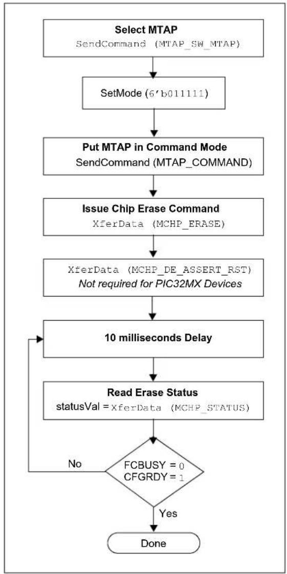
9.0 ERASING THE DEVICE
Before a device can be programmed, it must be erased. The erase operation writes all '1s' to the Flash memory and prepares it to program a new set of data. Once a device is erased, it can be verified by performing a "Blank Check" operation. See Section 9.1 "Blank Check" for more information.
The procedure for erasing program memory (Program, boot, and Configuration memory) consists of selecting the MTAP and sending the MCHP_ERASE command. The programmer must wait for the erase operation to complete by reading and verifying bits in the MCHP_STATUS value. Figure 9-1 illustrates the process for performing a Chip Erase.
Note: The Device ID memory locations are read-only and cannot be erased. Therefore, Chip Erase has no effect on these memory locations.
The following steps are required to erase a target device:
- SendCommand (MTAP_SW_MTAP).
- SetMode (6'b011111).
- SendCommand (MTAP_COMMAND).
- XferData (MCHP_ERASE).
- XferData (MCHP_DE_ASSERT_RST). This step is not required for PIC32MX devices.
- Delay 10 ms.
- statusVal = XferData (MCHP_STATUS).
- If CFGRDY (statusVal[3]) is not '1' and FCBUSY (statusVal[2]) is not '0', GOTO to step 5.
Note: The Chip Erase operation is a self-timed operation. If the FCBUSY and CFGRDY bits do not set properly within the specified Chip Erase time, the sequence may have been executed incorrectly or the device is damaged.
FIGURE 9-1: ERASE DEVICE
flowchart
graph TD
    A["Select MTAP\nSendCommand (MTAP_SW_MTAP)"] --> B["SetMode (6'b011111)"]
    B --> C["Put MTAP in Command Mode\nSendCommand (MTAP_COMMAND)"]
    C --> D["Issue Chip Erase Command\nXferData (MCHP_ERASE)"]
    D --> E["XferData (MCHP_DE_ASSERT_RST)\nNot required for PIC32MX Devices"]
    E --> F["10 milliseconds Delay"]
    F --> G["Read Erase Status\nstatusVal = XferData (MCHP_STATUS)"]
    G --> H{FCBUSY = 0\nCFGRDY = 1}
    H -->|No| F
    H -->|Yes| I["Done"]
9.1 Blank Check
The term "Blank Check" implies verifying that the device has been successfully erased and has no programmed memory locations. A blank or erased memory location always reads as '1'.
The device Configuration registers are ignored by the Blank Check. Additionally, all unimplemented memory space should be ignored from the Blank Check.
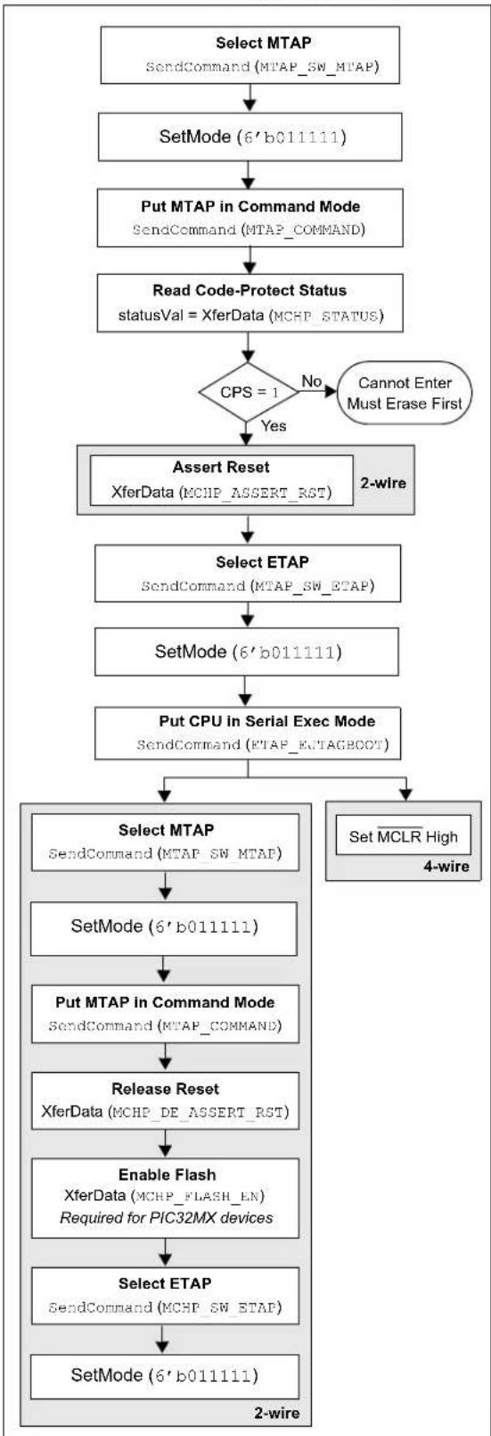
10.0 ENTERING SERIAL EXECUTION MODE
Before programming a device, it must be placed in Serial Execution mode. The procedure for entering Serial Execution mode consists of verifying that the device is not code-protected. If the device is code-protected, a Chip Erase must be performed. See Section 9.0 "Erasing the Device" for details.
FIGURE 10-1: ENTERING SERIAL EXECUTION MODE
flowchart
graph TD
    A["Select MTAP\nSendCommand(MTAP_SW_MTAP)"] --> B["SetMode(6'b011111)"]
    B --> C["Put MTAP in Command Mode\nSendCommand(MTAP_COMMAND)"]
    C --> D["Read Code-Protect Status\nstatusVal = XferData (MCHP_STATUS)"]
    D --> E{CPS = 1\nNo\nCannot Enter\nMust Erase First}
    E -->|Yes| F["Assert Reset\nXferData (MCHP_ASSERT_RST)\n2-wire"]
    F --> G["Select ETAP\nSendCommand(MTAP_SW_ETAP)"]
    G --> H["SetMode(6'b011111)"]
    H --> I["Put CPU in Serial Exec Mode\nSendCommand(ETAP_EUTAGBOOT)"]
    I --> J["Select MTAP\nSendCommand(MTAP_SW_MTAP)"]
    J --> K["SetMode(6'b011111)"]
    K --> L["Put MTAP in Command Mode\nSendCommand(MTAP_COMMAND)"]
    L --> M["Release Reset\nXferData (MCHP_DE_ASSERT_RST)"]
    M --> N["Enable Flash\nXferData (MCHP_FLASH_EN)\nRequired for PIC32MX devices"]
    N --> O["Select ETAP\nSendCommand(MCHP_SW_ETAP)"]
    O --> P["SetMode(6'b011111)\n2-wire"]
    P --> Q["4-wire"]
10.1 4-wire Interface
The following steps are required to enter Serial Execution mode:
Note: It is assumed that the MCLR pin has been driven low from the previous Check Device Status step (see Figure 8-1).
- SendCommand (MTAP_SW_MTAP).
- SetMode (6'b011111).
- SendCommand (MTAP_COMMAND).
- statusVal = XferData (MCHP_STATUS).
- If CPS (statusVal[7]) is not '1', the device must be erased first.
- SendCommand (MTAP_SW_ETAP).
- SetMode (6'b011111).
- SendCommand (ETAP_EJTAGBOOT).
- Set the MCLR pin high.
10.2 2-wire Interface
The following steps are required to enter Serial Execution mode:
- SendCommand (MTAP_SW_MTAP).
- SetMode (6'b011111).
- SendCommand (MTAP_COMMAND).
- statusVal = XferData (MCHP_STATUS).
- If CPS (statusVal[7]) is not '1', the device must be erased first.
- XferData (MCHP_ASSERT_RST).
- SendCommand (MTAP_SW_ETAP).
- SetMode (6'b011111).
- SendCommand(ETAP_EJTAGBOOT).
- SendCommand (MTAP_SW_MTAP).
- SetMode (6'b011111).
- SendCommand (MTAP_COMMAND).
- XferData (MCHP_DE_ASSERT_RST).
- XferData (MCHP_FLASH_ENABLE). This step is required for PIC32MX family devices.
- SendCommand (MTAP_SW_ETAP).
- SetMode (6'b011111).
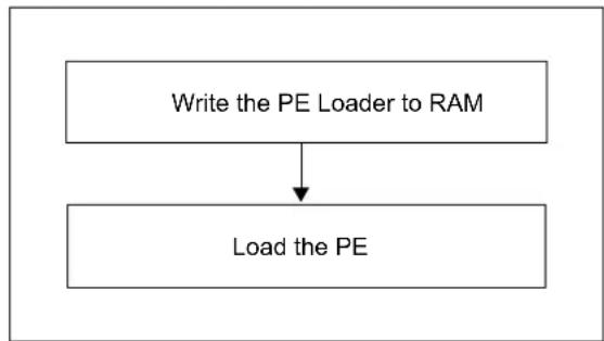
11.0 DOWNLOADING THE PROGRAMMING EXECUTIVE (PE)
The PE resides in RAM memory and is executed by the CPU to program the device. The PE provides the mechanism for the programmer to program and verify PIC32 devices using a simple command set and communication protocol. There are several basic functions provided by the PE:
- Read memory
- Erase memory
- Program memory
- Blank check
- Read executive firmware revision
- Get the Cyclic Redundancy Check (CRC) of Flash memory locations
The PE performs the low-level tasks required for programming and verifying a device. This allows the programmer to program the device by issuing the appropriate commands and data. A detailed description for each command is provided in Section 17.2 "The PE Command Set".
The PE uses the device's data RAM for variable storage and program execution. After the PE has run, no assumptions should be made about the contents of data RAM.
After the PE is loaded into the data RAM, the PIC32 family can be programmed using the command set shown in Table 17-1.
FIGURE 11-1: DOWNLOADING THE PE
flowchart
graph TD
    A["Write the PE Loader to RAM"] --> B["Load the PE"]
Loading the PE in the memory is a two step process:
-
Load the PE loader in the data RAM. (The PE loader loads the PE binary file in the proper location of the data RAM, and when done, jumps to the programming exec and starts executing it.)
-
Feed the PE binary to the PE loader.
Table 11-1 lists the steps that are required to download the PE.
| Operation Operand | |
| Step 1: PIC32MX devices only: Initialize BMXCON to 0x1F0040. The instruction sequence executed by the PIC32 core is:lui a0,0xbf88ori a0,a0,0x2000 /* address of BMXCON */lui a1,0x1fori a1,a1,0x40 /* a1 has 0x1f0040 */sw a1,0(a0) /* BMXCON initialized */ | |
| XferInstruction | 0x3c04bf88 |
| XferInstruction | 0x34842000 |
| XferInstruction | 0x3c05001f |
| XferInstruction | 0x34a50040 |
| XferInstruction | 0xac850000 |
| Step 2: PIC32MX devices only: Initialize BMXDKPBA to 0x800. The instruction sequence executed by the PIC32 core is:li a1,0x800sw a1,16(a0) | |
| XferInstruction | 0x34050800 |
| XferInstruction | 0xac850010 |
| Step 3: PIC32MX devices only: Initialize BMXDUDBA and BMXDUPBA to the value of BMXDRMSZ. The instruction sequence executed by the PIC32 core is:lw a1,64(a0) /* load BMXDMSZ */sw a1,32(a0)sw a1,48(a0) | |
| XferInstruction | 0x8C850040 |
| XferInstruction | 0xac850020 |
| XferInstruction | 0xac850030 |
| Step 4: Set up PIC32 RAM address for PE. The instruction sequence executed by the PIC32 core is:lui a0,0xa000ori a0,a0,0x800 | |
| XferInstruction | 0x3c04a000 |
| XferInstruction | 0x34840800 |
| Step 5: Load the PE_Loader. Repeat this step (Step 5) until the entire PE_Loader is loaded in the PIC32 memory. In the operands field, “”represents the MSbs 31 through 16 of the PE loader op codes shown in Table 11-2. Likewise,“”represents the LSbs 15 through 0 of the PE loader op codes shown in Table 11-2. The “++” sign indicates that when these operations are performed in succession, the new word is to be transferred from the list of op codes of the LPE Loader shown in Table 11-2. The instruction sequence executed by the PIC32 core is:lui a2,orai a2,a2,sw a2,0(a0)addiu a0,a0,4 | |
| XferInstruction | (0x3c06) |
| Operation | Operand |
| XferInstruction | (0x34c6) |
| XferInstruction | 0xac860000 |
| XferInstruction | 0x24840004 |
| Step 6: Jump to the PE_Loader. The instruction sequence executed by the PIC32 core is:lui t9,0xa000ori t9,t9,0x800jr t9nop | |
| XferInstruction | 0x3c19a000 |
| XferInstruction | 0x37390800 |
| XferInstruction | 0x03200008 |
| XferInstruction | 0x00000000 |
| Step 7: Load the PE using the PE_Loader. Repeat the last instruction of this step (Step 7) until the entire PE is loaded into the PIC32 memory. In this step, you are given an Intel® Hex format file of the PE that you will parse and transfer a number of 32-bit words at a time to the PIC32 memory (refer toAppendix B: “Hex File Format”). The instruction sequence executed by the PIC32 is shown in Table 11-2. | |
| SendCommand ETAP | _FASTDATA |
| XferFastData PE | ADDRESS (Address of PE program block from PE Hex file) |
| XferFastData PE | SIZE (Number of 32-bit words of the program block from PE Hex file) |
| XferFastData PE | software op code from PE Hex file (PE Instructions) |
| Step 8: Jump to the PE. Magic number (0xDEAD0000) instructs the PE_Loader that the PE is completely loaded into the memory. When the PE_Loader sees the magic number, it jumps to the PE. | |
| XferFastData 0x0 | 0000000 |
| XferFastData 0x | DEAD0000 |
TABLE 11-2: PE LOADER OP CODES
| Op code Instruction | |
| 0x3c07dead lui | a3, 0xdead |
| 0x3c06ff20 lui | a2, 0xff20 |
| 0x3c05ff20 lui | a1, 0xff20 |
| here1: | |
| 0x8cc40000 lw a0, 0 (a2) | |
| 0x8cc30000 lw v1, 0 (a2) | |
| 0x1067000b beq | v1, a3, |
| 0x00000000 nop | |
| 0x1060fffb beqz | v1, |
| 0x00000000 nop | |
| here2: | |
| 0x8ca20000 lw v0, 0 (a1) | |
| 0x2463ffff addiu | v1, v1, -1 |
| 0xac820000 sw v0, 0 (a0) | |
TABLE 11-2: PE LOADER OP CODES
| Op code Instruction | |
| 0x24840004 addiu | a0, a0, 4 |
| 0x1460ffffb bnez | v1, |
| 0x00000000 nop | |
| 0x1000fff3 b | |
| 0x00000000 nop | |
| here3: | |
| 0x3c02a000 lui | v0, 0xa000 |
| 0x34420900 ori | v0, v0, 0x900 |
| 0x00400008 jr v0 | |
| 0x00000000 nop | |
12.0 DOWNLOADING A DATA BLOCK
To program a block of data to the PIC32 device, it must be loaded into SRAM.
12.1 Without the PE
To program a block of memory without using the PE, the block of data must first be written to RAM. This method requires the programmer to transfer the actual machine instructions with embedded (immediate) data for writing the block of data to the devices internal RAM memory.
FIGURE 12-1: DOWNLOADING DATA WITHOUT THE PE

flowchart
graph TD
    A["bufAddr = RAM Buffer Address"] --> B["Write 32-bit Immediate Data to bufAddr"]
    B --> C["Increment bufAddr"]
    C --> D{Done}
    D -->|No| B
The following steps are required to download a block of data:
- XferInstruction (op code).
- Repeat Step 1 until the last instruction is transferred to CPU.
| Op code Instruction | |
| Step 1: Initialize SRAM Base Address to 0xA0000000. | |
| 3c10a000 lui s0, 0xA000; | |
| Step 2: Write the entire row of data to be programmed into system SRAM. | |
| 3c083508ae08 | lui t0,;ori t0, t0,;sw t0,(s0);// OFFSET increments by 4 |
| Step 3: Repeat Step 2 until one row of data is loaded. | |
12.2 With the PE
When using the PE, the steps in Section 12.0 "Downloading a Data Block" and Section 14.0 "Initiating a Flash Row Write" are handled in two single commands: ROW_PROGRAM and PROGRAM.
The ROW_PROGRAM command programs a single row of Flash data, while the PROGRAM command programs multiple rows of Flash data. Both of these commands are documented in Section 17.0 "The Programming Executive".
13.0 INITIATING A PAGE ERASE
An individual page may be erased rather than erasing all of Flash memory. The PE is not used in this case.
PIC32MK family devices can perform an erase retry on a page by increasing the internal voltage used to perform the erase.
| Op Code Instruction | |
| Step 1: All PIC32 devices: Initialize constants. Registers a1, a2, and a3 are set for WREN = 1 or NVMOP[3:0] = 0100, WR = 1 and WREN = 1, respectively. Registers s1 and s2 are set for the unlock data values and s0 is initialized to ‘0’. | |
| 34054004 ori a1, 0,0x400434068000 ori a2,0,0x800034074000 ori a3,0,0x40003c11aa99 lui s1,0xaa9936316655 ori s1,s1,0x66553c125566 lui s2,0x5566365299aa ori s2,s2,0x99aa3c100000 lui s0,0x0000 | |
| Step 2: PIC32MX family devices only: Set register a0 to the base address of the NVM register (0xBF80_F400). | |
| 3c04bf80 lui a0,0xbf803484f400 ori a0,a0,0xf400 | |
| Step 3: PIC32MK and PIC32MZ family devices only: Set register a0 to the base address of the NVM register (0xBF80_0600). Register s3 is set for the value used to disable write protection in NVMBPB. | |
| 3c04b480 lui a0,0xbf8034840600 ori a0,a0,0x060034138080 ori s3,0,0x8080 | |
| Step 4: PIC32MK and PIC32MZ family devices only: Unlock and disable Boot Flash write protection. | |
| ac910010 sw s1,16(a0)ac920010 sw s2,16(a0)ac930090 sw s3,144(a0)0000000 nop | |
| Step 5: PIC32MK family devices only: Save the contents of NVMCON2. | |
| 8c9400a0 lw s4,160(a0) | |
| Step 6: PIC32MK family devices only: Set the initial programming voltage level and enable page testing (unlock required). | |
| 36953000 ori s5,s4,0x300032b5foff andi s5,s5,0xFCFFac910010 sw s1,16(a0)ac920010 sw s2,16(a0)ac860008 sw a2,8(a0)ac9500a0 sw s5,160(a0)here3: | |
| Step 7: All PIC32 devices: Set the NVMADDR register with the address of the Flash page to be erased. | |
| 3c08luit0,PAGE_ADDR(31:16)>3508ori t0,t0,ac880020 sw t0,32(a0) | PAGE_ADDR(31:16)>3508ori t0,t0,ac880020 sw t0,32(a0) |
| Step 8: All PIC32 devices: Set up the NVMCON register for write operation. | |
| ac850000 sw a1,0(a0) | delay (6 us) |
| Step 9: PIC32MX devices only: Poll the LVDSTAT register. | |
| 8c880000 lw t0,0(a0)31080800 andi t0,t0,0x08001500fffd bne t0,0,here100000000 nop | here1:00 |
| Step 10: All PIC32 devices: Unlock the NVMCON register and start the write operation. | |
| ac910010 sw s1,16(a0)ac920010 sw s2,16(a0)ac860008 sw a2,8(a0) | |
| Step 11: All PIC32 devices: Loop until the WR bit (NVMCON[15]) is clear. | |
| here2: | |
| 8c880000 lw t0,0(a0)01064024 and t0,t0,a21500fffd bne t0,0,here200000000 nop | |
| Step 12: All PIC32 devices: Wait at least 500 ns after the WR bit (NVMCON[15]) clears before writing to any of the NVM registers.This requires inserting a delay in the execution. The programming tools and program executive utilizes the FRC 8 MHz clock. Therefore four NOP instructions equate to 500 ns (see Note 1). | |
| 00000000 nop00000000 nop00000000 nop00000000 nop | |
| Step 13: All PIC32 devices: Clear the WREN bit (NVMCON[14]). | |
| ac870004 sw a3,4(a0) | |
| Step 14: PIC32MK family devices only: Check that all data in the page has been erased. If not, adjust the voltage and try again. If all voltages levels have been tried, fail, and go to error procedure. | |
| ac870004 sw a3, 4(a0)20171000 addi s7, 0, 409600005020 add t2,0, 08c880020 lw t0, 32(a0)01194020 add t0, t0, t98d090000 lw t1, 0(t0)15200005 bne t1,0, here6214a0010 addi t2, t2, 1611570009 beq t2, s7, here70000000 nop1000fffa beq 0,0, here521080010 addi t0, t0, 16here6:22b50100 addi s5, s5, 25632b60300 andi s6, s5, 76816c0ffde bne s6, 0, here30000000 nop10000005 beq0, 0, err_proc0000000 nop | |
| Step 15: PIC32MK family devices only: Restore the NVMCON2 register. | |
| ac9400a0 sw s4,160(a0) | here7: |
| Step 16: All PIC32 devices: Check the WRERR bit (NVMCON[13]) to ensure that the program sequence has completed successfully. If an error occurs, jump to the error processing routine. | |
| 8c880000 lw t0,0(a0)30082000 andi t0,t0,0x2000150000000 nop | bne t0,0,, |
Note 1: For programming the Flash at runtime in the users application, the following code is recommended:
while(NVMCON.WR) // waitfor WR bit(NVMCON[15]) to clear
{
    unsigned int start_count = _CPO_GET_COUNT();
    unsigned int total_count = (.00000025 * SYSCLK); // count for 500 ns and CPU frequency in MHz
    while ((_CPO_GET_COUNT() - start_count) < total_count);
}
14.0 INITIATING A FLASH ROW WRITE
Note: Certain PIC32 devices have available ECC memory. When the ECC feature is used, the Flash memory must be programmed in groups of four 32-bit words using four, 32-bit word alignment. If ECC is dynamically used, the programming method determines when the feature is used. ECC is not enabled for words programmed with the single word programming command. ECC is enabled for words programmed in groups of four, either with the quad word or row programming commands. Failure to adhere to these methods can result in ECC DED errors during run-time. Refer to the specific device data sheet for details regarding ECC use and configuration.
Once a row of data has been downloaded into the device's SRAM, the programming sequence must be initiated to write the block of data to the Flash memory.
See Table 14-1 for the op code and instructions for initiating a Flash row write.
14.1 With the PE
When using the PE, the data is immediately written to the Flash memory from the SRAM. No further action is required.
14.2 Without the PE
Flash memory write operations are controlled by the NVMCON register. Programming is performed by setting the NVMCON register to select the type of write operation and initiating the programming sequence by setting the WR control bit (NVMCON[15]).
FIGURE 14-1: INITIATING FLASH WRITE WITHOUT THE PE
flowchart
graph TD
    A["Unprotect Control Registers"] --> B["Select Write Operation"]
    B --> C["Load Addresses in NVM Registers"]
    C --> D["Unlock Flash Controller"]
    D --> E["Start Operation"]
    E --> F["Done"]
In the Flash write procedure (see Table 14-1), the Row Programming method is used to program the Flash memory, as it is typically the most expedient. word and Quad Word programming methods are also available, depending on the device, and may be used or required depending on your application. Refer to the "Flash Program Memory" chapter in the specific device data sheet and the related section of the "PIC32 Family Reference Manual" for more information.
The following steps are required to initiate a Flash write:
- XferInstruction (op code).
- Repeat Step 1 until the last instruction is transferred to the CPU.
TABLE 14-1: INITIATE FLASH ROW WRITE OP CODES
| Op Code Instruction | |
| Step 1: All PIC32 devices: Initialize constants. Registers a1, a2, and a3 are set for WREN = 1 or NVMOP[3:0] = 0011, WR = 1 and WREN = 1, respectively. Registers s1 and s2 are set for the unlock data values and s0 is initialized to '0'. | |
| 34054003 | ori a1,0,0x4003 |
| 34068000 | ori a2,0,0x8000 |
| 34074000 | ori a3,0,0x4000 |
| 3c11aa99 | lui s1,0xaa99 |
| 36316655 | ori s1,s1,0x6655 |
| 3c125566 | lui s2,0x5566 |
| 365299aa | ori s2,s2,0x99aa |
| 3c100000 | lui s0,0x0000 |
| Step 2: PIC32MX devices only: Set register a0 to the base address of the NVM register (0xBF80_F400). | |
| 3c04bf80 | lui a0,0xbf80 |
| 3484f400 | ori a0,a0,0xf400 |
| Step 2: PIC32MK and PIC32MZ family devices only: Set register a0 to the base address of the NVM register (0xBF80_0600). Register s3 is set for the value used to disable write protection in NVMBPB. | |
| 3c04bf80 | lui a0,0xbf80 |
| 34840600 | ori a0,a0,0x0600 |
| 34138080 | ori s3,0,0x8080 |
| Step 3: PIC32MK and PIC32MZ family devices only: Unlock and disable Boot Flash write protection. | |
| ac910010 | sw s1,16(a0) |
| ac920010 | sw s2,16(a0) |
| ac930090 | sw s3,144(a0) |
| 00000000 | nop |
| Step 4: All PIC32 devices: Set the NVMADDR register with the address of the Flash row to be programmed. | |
| 3c08 | lui t0, |
| 3508 | ori t0,t0, |
| ac880020 | sw t0,32(a0) |
| Step 5: PIC32MX devices only: Set the NVMSRCADDR register with the physical source SRAM address (offset is 64). | |
| 3c10 | lui s0, |
| 3610 | ori s0,s0, |
| ac900040 | sw s0,64(a0) |
| Step 5: PIC32MK and PIC32MZ family devices only: Set the NVMSRCADDR register with the physical source SRAM address (offset is 112). | |
| 3c10 | lui s0, |
| 3610 | ori s0,s0, |
| ac900070 | sw s0,112(a0) |
| Step 6: All PIC32 devices: Set up the NVMCON register for write operation. | |
| ac850000 sw a1,0(a0) | delay (6 μs) |
| Step 7: PIC32MX devices only: Poll the LVDSTAT register. | |
| 8C880000310808001500fffd00000000 | here1:lw t0,0(a0)andi t0,t0,0x0800bne t0,0,here1nop |
| Step 8: All PIC32 devices: Unlock the NVMCON register and start the write operation. | |
| ac910010ac920010ac860008 | sw s1,16(a0)sw s2,16(a0)sw a2,8(a0) |
| Step 9: All PIC32 devices: Loop until the WR bit (NVMCON[15]) is clear. | |
| 8c880000010640241500fffd00000000 | here2:lw t0,0(a0)and t0,t0,a2bne t0,0,here2nop |
| Step 10: All PIC32 devices: Wait at least 500 ns after the WR bit (NVMCON[15]) clears before writing to any of the NVM registers.This requires inserting a delay in the execution. The programming tools and program executive utilizes the FRC 8 MHz clock. Therefore four NOP instructions equate to 500 ns (see Note 1). | |
| 0000000000000000000000000000 | nopnopnop |
| Step 11: All PIC32 devices: Clear the WREN bit (NVMCONM[14]). | |
| ac870004 sw a3,4(a0) | |
| Step 12: All PIC32 devices: Check the WRERR bit (NVMCON[13]) to ensure that the program sequence has completed successfully. If an error occurs, jump to the error processing routine. | |
| 8c880000300820001500<ERR_PROC>00000000 | lw t0,0(a0)andi t0,zero,0x2000bne t0,$0,<err_proc_offset>nop |
| Note 1: For programming the Flash at runtime in the users application, the following code is recommended:while(NVMCON.WR) //Wait for WR bit (NVMCON[15]) to clear {};{}unsigned int start_count = _CP0_GET_COUNT();unsigned int total_count = (.00000025 * SYSCLK); //count for 500 ns and CPU frequency in MHzwhile {(_CP0_GET_COUNT() - start_count) < total_count);} | |
15.0 VERIFY DEVICE MEMORY
The verify step involves reading back the code memory space and comparing it with the copy held in the programmer's buffer. The Configuration registers are verified with the rest of the code.
Note: Because the Configuration registers include the device code protection bit, code memory should be verified immediately after writing (if code protection is enabled). This is because the device will not be readable or verifiable if a device Reset occurs after the code-protect bit has been cleared.
15.1 Verifying Memory with the PE
Memory verify is performed using the GET_CRC command. Table 17-2 lists the op codes and instructions.
FIGURE 15-1: VERIFYING MEMORY WITH THE PE

flowchart
graph TD
    A["Issue Verify Command"] --> B["Receive Response"]
The following steps are required to verify memory using the PE:
- XferFastData (GET_CRC).
- XferFastData (start_Address).
- XferFastData (length).
- valCkSum = XferFastData (32'h0x00).
Verify that valCkSum matches the checksum of the copy held in the programmer's buffer.
15.2 Verifying Memory without the PE
Reading from the Flash memory is performed by executing a series of read accesses from the Fastdata register. Table 20-4 shows the EJTAG programming details, including the address and op code data for performing processor access operations.
FIGURE 15-2: VERIFYING MEMORY WITHOUT THE PE
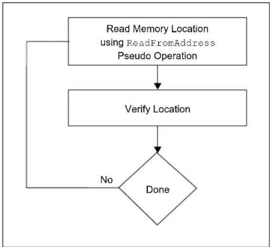
flowchart
graph TD
    A["Read Memory Location using ReadFromAddress Pseudo Operation"] --> B["Verify Location"]
    B --> C{Done}
    C -->|No| A
The following steps are required to verify memory:
- XferInstruction (op code).
- Repeat Step 1 until the last instruction is transferred to the CPU.
- Verify that valRead matches the copy held in the programmer's buffer.
- Repeat Steps 1-3 for each memory location.
TABLE 15-1: VERIFY DEVICE OP CODES
| Op code Instruction | |
| Step 1: Initialize some constants. | |
| 3c13ff20 lui s3, 0xFF20 | |
| Step 2: Read memory Location. | |
| 3c08lui t0,3508ori t0, | lui t0,ori t0, |
| Step 3: Write to Fastdata location. | |
| 8d090000ae690000 | lw t1, 0(t0)sw t1, 0(s3) |
| Step 4: Read data from Fastdata register 0xFF200000. | |
| Step 5: Repeat Steps 2-4 until all configuration locations are read. | |
16.0 EXITING PROGRAMMING MODE
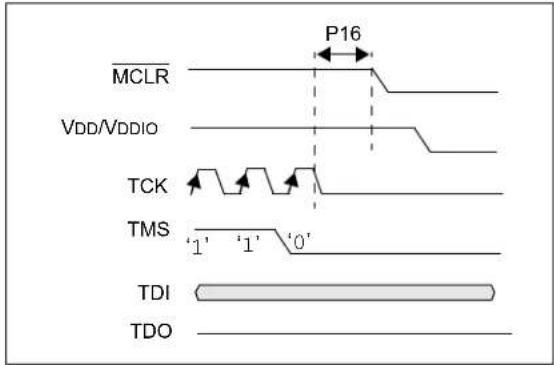
Once a device is programmed, it must be taken out of programming mode to start proper execution of its new program memory contents.
16.1 4-wire Interface
Exiting programming mode is done by removing VIH from the MCLR pin, as illustrated in Figure 16-1. The only requirement for exit is that an interval, P16, should elapse between the last clock and program signals before removing VIH.
FIGURE 16-1: 4-WIRE EXIT
PROGRAMMING MODE
text_image
MCLR VDD/VDDIO P16 TCK TMS '1' '1' '0' TDI TDOThe following steps are required to exit programming mode:
- SetMode (5'b11111).
- Assert the M CLR pin.
- Remove power (if the device is powered).
16.2 2-wire Interface
Exiting programming mode is done by removing VIH from the MCLR pin, as illustrated in Figure 16-2. The only requirement for exit is that an interval, P16, should elapse between the last clock and program signals on PGECx and PGEDx before removing VIH.
FIGURE 16-2: 2-WIRE EXIT
PROGRAMMING MODE

text_image
P16 P17 MCLR VDD/VDDio PGEDx PGECx VIH VIH PGEDx = InputUse the following steps to exit programming mode:
- SetMode (5'b11111).
- Assert the MCLR pin.
- Issue a clock pulse on PGECx.
- Remove power (if the device is powered).
17.0 THE PROGRAMMING EXECUTIVE
Note: The Programming Executive (PE) is included with your installation of MPLAB X IDE. To download the appropriate PE file for your device, please visit the related product page on the Microchip web site (www.microchip.com).
17.1 PE Communication
The programmer and the PE have a master-slave relationship, where the programmer is the master programming device and the PE is the slave.
All communication is initiated by the programmer in the form of a command. The PE is able to receive only one command at a time. Correspondingly, after receiving and processing a command, the PE sends a single response to the programmer.
17.1.1 2-WIRE ICSP EJTAG RATE
In Enhanced ICSP mode, the PIC32 family devices operate from the internal Fast RC oscillator, which has a nominal frequency of 8 MHz.
17.1.2 COMMUNICATION OVERVIEW
The programmer and the PE communicate using the EJTAG Address, Data and Fastdata registers. In particular, the programmer transfers the command and data to the PE using the Fastdata register. The programmer receives a response from the PE using the Address and Data registers. The pseudo operation of receiving a response is shown in the GetPEResponse pseudo operation below:
Format:
response = GetPEResponse()
Purpose:
Enables the programmer to receive the 32-bit response value from the PE.
EXAMPLE 17-1: GetPEResponse EXAMPLE
WORD GetPEResponse()
{
    WORD response;

    // Wait until CPU is ready
    SendCommand(ETAP_CONTROL);

    // Check if Proc. Access bit (bit 18) is set do {
    controlVal=XferData(32'h0x0004C000);
    } while(PrAcc(contorlVal[18]) is not '1');

    // Select Data Register
    SendCommand(ETAP_DATA);

    // Receive Response
    response = XferData(0);

    // Tell CPU to execute instruction
    SendCommand(ETAP_CONTROL);
    XferData(32'h0x0000C000);

    // return 32-bit response
    return response;
}
The typical communication sequence between the programmer and the PE is shown in Table 17-1.
The sequence begins when the programmer sends the command and optional additional data to the PE, and the PE carries out the command.
When the PE has finished executing the command, it sends the response back to the programmer.
The response may contain more than one response. For example, if the programmer sent a READ command, the response will contain the data read.
TABLE 17-1: COMMUNICATION SEQUENCE FOR THE PE
| Operation Operand | |
| Step 1: Send command and optional data from programmer to the PE. | |
| XferFastData (Command | data len) | |
| XferFastData.. optional data.. | |
| Step 2: Programmer reads the response from the PE. | |
| GetPEResponse | response |
| GetPEResponse... | response... |
17.2 The PE Command Set
Table 17-2 provides PE command set details, such as op code, mnemonic and short description for each command. Functional details on each command are provided in Section 17.2.3 "ROW_PROGRAM Command" through Section 17.2.14 "CHANGE_CFG Command".
The PE sends a response to the programmer for each command that it receives. The response indicates if the command was processed correctly. It includes any required response data or error data.
17.2.1 COMMAND FORMAT
All PE commands have a general format consisting of a 32-bit header and any required data for the command, see Figure 17-1. The 32-bit header consists of a 16-bit op code field, which is used to identify the command, and a 16-bit command Operand field. Use of the Operand field varies by command.
Note: Some commands have no Operand information; however, the Operand field must be sent and the programming executive will ignore the data.
FIGURE 17-1: COMMAND FORMAT
31 16
| Op code | |
| 15 | 0 |
| Operand (optional) | |
| 31 16 | |
| Command Data High (if required) | |
| 15 | 0 |
| Command Data Low (if required) | |
The command in the op code field must match one of the commands in the command set that is listed in Table 17-2. Any command received that does not match a command the list returns a NACK response, as shown in Table 17-3.
The PE uses the command Operand field to determine the number of bytes to read from or to write to. If the value of this field is incorrect, the command is not be properly received by the PE.
TABLE 17-2: PE COMMAND SET
| Op code | Mnemonic Description | |
| 0x0 | ROW\_PROGRAM^(1) | Program one row of Flash memory at the specified address |
| 0x1 | READ | Read N 32-bit words of memory starting from the specified address (N < 65,536) |
| 0x2 | PROGRAM | Program Flash memory starting at the specified address |
| 0x3 | WORD\_PROGRAM^(3) | Program one word of Flash memory at the specified address |
| 0x4 | CHIP_ERASE | Chip Erase of entire chip |
| 0x5 | PAGE_ERASE | Erase pages of code memory from the specified address |
| 0x6 | BLANK_CHECK | Blank Check code |
| 0x7 | EXEC_VERSION | Read the PE software version |
| 0x8 | GET_CRC | Get the CRC of Flash memory |
| 0x9 | PROGRAM_CLUSTER | Programs the specified number of bytes to the specified address |
| 0xA | GET_DEVICEID | Returns the hardware ID of the device |
| 0xB | CHANGE\_CFG^(2) | Used by the probe to set various configuration settings for the PE |
| 0xC | GET_CHECKSUM | Get the checksum of Flash memory |
| 0xD | QUAD\_WORD\_PGRM^(4) | Program four words of Flash memory at the specified address |
Note 1: Refer to Table 5-1 for the row size for each device.
2: This command is not available in PIC32MX1XX/2XX devices.
3: On the PIC32MZ family devices, which incorporate ECC, the WORD_PROGRAM command will not generate the ECC parity bits. Reading a location programmed with the WORD_PROGRAM command with ECC enabled will cause a DED fault.
4: This command is available on PIC32MK and PIC32MZ family devices only.
17.2.2 RESPONSE FORMAT
The PE response set is shown in Table 17-3. All PE responses have a general format consisting of a 32-bit header and any required data for the response (see Figure 17-2).
FIGURE 17-2: RESPONSE FORMAT
31 16
| Last Command | |
| 15 | 0 |
| Response Code | |
| 31 16 | |
| Data_High_1 | |
| 15 | 0 |
| Data_Low_1 | |
| 31 16 | |
| Data_High_N | |
| 15 | 0 |
| Data_Low_N | |
17.2.2.1 Last\_Cmd Field
Last_Cmd is a 16-bit field in the first word of the response and indicates the command that the PE processed. It can be used to verify that the PE correctly received the command that the programmer transmitted.
17.2.2.2 Response Code
The response code indicates whether the last command succeeded or failed, or if the command is a value that is not recognized. The response code values are shown in Table 17-3.
TABLE 17-3: RESPONSE VALUES
| Op code | Mnemonic Description | |
| 0x0 | PASS | Command successfully processed |
| 0x2 | FAIL | Command unsuccessfully processed |
| 0x3 | NACK | Command not known |
17.2.2.3 Optional Data
The response header may be followed by optional data in case of certain commands such as read. The number of 32-bit words of optional data varies depending on the last command operation and its parameters.
17.2.3 ROW\_PROGRAM COMMAND
The ROW_PROGRAM command instructs the PE to program a row of data at a specified address.
The data to be programmed to memory, located in command words Data_1 through Data_N, must be arranged using the packed instruction word format provided in Table17-4 (this command expects an entire row of data).
FIGURE 17-3: ROW PROGRAM COMMAND
| 31 16 | |
| Op code | |
| 15 | 0 |
| Operand | |
| 31 16 | |
| Addr_High | |
| 15 | 0 |
| Addr_Low | |
| 31 16 | |
| Data_High_1 | |
| 15 | 0 |
| Data_Low_1 | |
| 31 16 | |
| Data_High_N | |
| 15 | 0 |
| Data_Low_N | |
TABLE 17-4: ROW PROGRAM FORMAT
| Field | Description |
| Op code 0x0 | |
| Operand | Not used |
| Addr_High | High 16 bits of 32-bit destination address |
| Addr_Low | Low 16 bits of 32-bit destination address |
| Data_High_1 | High 16 bits data word 1 |
| Data_Low_1 | Low 16 bits data word 1 |
| Data_High_N | High 16 bits data word 2 through N |
| Data_Low_N | Low 16 bits data word 2 through N |
Expected Response (1 word):
FIGURE 17-4: ROW PROGRAM RESPONSE
| 31 16 | |
| Last Command | |
| 15 | 0 |
| Response Code | |
17.2.4 READ COMMAND
The READ command instructs the PE to read from memory. The number of 32-bit words specified in the Operand field starting from the 32-bit address specified by the Addr_Low and Addr_High fields. This command can be used to read Flash memory and Configuration Words. All data returned in response to this command uses the packed data format that is provided in Table 17-5.
FIGURE 17-5: READ COMMAND
| 31 16 | |
| Op code | |
| 15 | 0 |
| Operand | |
| 31 16 | |
| Addr_High | |
| 15 | 0 |
| Addr_Low | |
TABLE 17-5: READ FORMAT
| Field Description | |
| Op code 0x1 | |
| Operand N number of 32-bit words to read (maximum of 65,535) | |
| Addr_Low | Low 16 bits of 32-bit source address |
| Addr_High | High 16 bits of 32-bit source address |
Expected Response:
FIGURE 17-6: READ RESPONSE
| 31 16 | |
| Last Command | |
| 15 | 0 |
| Response Code | |
| 31 16 | |
| Data_High_1 | |
| 15 | 0 |
| Data_Low_1 | |
| 31 16 | |
| Data_High_N | |
| 15 | 0 |
| Data_Low_N | |
| Note: | Reading unimplemented memory will cause the PE to Reset. Ensure that only memory locations present on a particular device are accessed. |
17.2.5 PROGRAM COMMAND
The PROGRAM command instructs the PE to program the Flash memory, including Configuration Words, starting from the 32-bit address specified in the Addr_Low and Addr_High fields. A 32-bit length field specifies the number of bytes to program.
The address must be aligned to a Flash row size boundary and the length must be a multiple of a Flash row size. See Table 5-1 for the correct row size for the device to be programmed.
FIGURE 17-7: PROGRAM COMMAND
| 31 | 16 |
| Op code | |
| 15 | 0 |
| Operand | |
| 31 | 16 |
| Addr_High | |
| 15 | 0 |
| Addr_Low | |
| 31 | 16 |
| Length_High | |
| 15 | 0 |
| Length_Low | |
| 31 | 16 |
| Data_High_1 | |
| 15 | 0 |
| Data_Low_1 | |
| 31 | 16 |
| Data_High_N | |
| 15 | 0 |
| Data_Low_N | |
TABLE 17-6: PROGRAM FORMAT
| Field | Description |
| Op code | 0x2 |
| Operand | Not used |
| Addr_Low | Low 16 bits of 32-bit destination address |
| Addr_High | High 16 bits of 32-bit destination address |
| Length_Low | Low 16 bits of Length |
| Length_High | High 16 bits Length |
| Data_Low_N | Low 16 bits data word 2 through N |
| Data_High_N | High 16 bits data word 2 through N |
The following are three programming scenarios:
- The length of the data to be programmed is the size of a single Flash row
- The length of the data to be programmed is the size of two Flash rows
- The length of the data to be programmed is larger than the size of two Flash rows
When the data length is equal to 512 bytes, the PE receives the 512-byte block of data from the probe and immediately sends the response for this command back to the probe.
The PE will respond for each row of data that it receives. If the data length of the command is equal to a single row, a single PE response is generated. If the data length is equal to two rows, the PE waits to receive both rows of data, then sends back-to-back responses for each data row. If the data length is greater than two rows of data, the PE will send the response for the first row after receiving the first two rows of data. Subsequent responses are sent after receiving subsequent data row packets. The responses will lag the data by one row. When the last row of data is received, the PE will respond with back-to-back responses for the second-to-last data row followed by the last row.
If the PE encounters an error in programming any of the blocks, it sends a failure status to the probe and aborts the PROGRAM command. On receiving the failure status, the probe must stop sending data. The PE will not process any other data for this command from the probe. The process is illustrated in Figure 17-9.
Note: If the PROGRAM command fails, the programmer should read the failing row using the READ command from the Flash memory. Then the programmer should compare the row received from the Flash memory to its local copy, word-by-word, to determine the address where Flash programming fails.
The response for this command is a little different than the response for other commands. The 16 MSbs of the response contain the 16 LSbs of the destination address, where the last block is programmed. This helps the probe and the PE maintain proper synchronization of sending and receiving data and responses.
Expected Response (1 word):
FIGURE 17-8: PROGRAM RESPONSE
31 16
LSB 16 bits of the destination address of last block
15 0
Response Code
FIGURE 17-9: PROGRAM COMMAND ALGORITHM
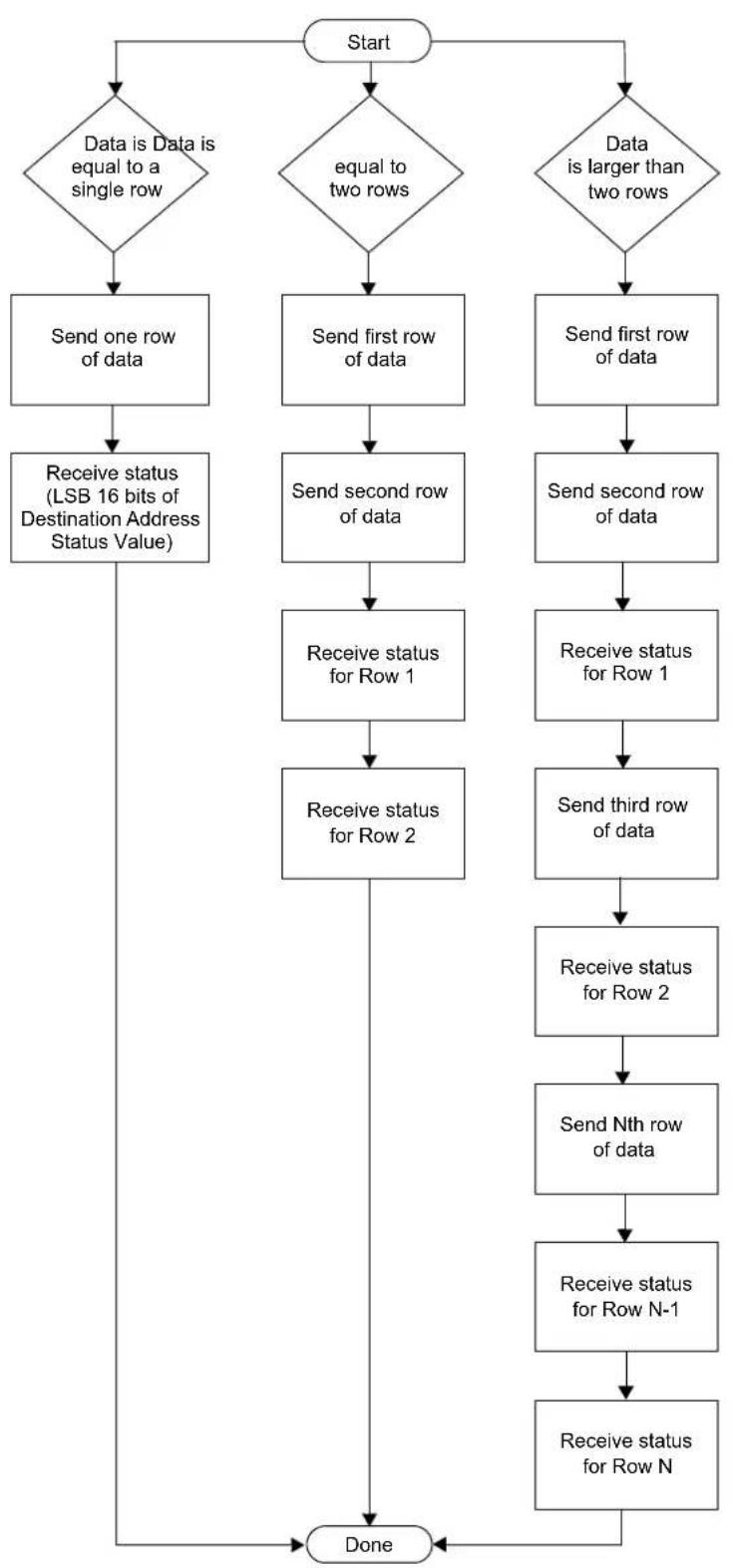
flowchart
graph TD
    A["Start"] --> B{Data is Data is equal to a single row}
    B --> C["Send one row of data"]
    B --> D["Send first row of data"]
    B --> E["Send second row of data"]
    B --> F["Send first row of data"]
    C --> G["Receive status (LSB 16 bits of Destination Address Status Value)"]
    D --> H["Receive status for Row 1"]
    E --> I["Send second row of data"]
    F --> J["Receive status for Row 1"]
    G --> K["Receive status for Row 2"]
    H --> L["Send third row of data"]
    I --> M["Receive status for Row 2"]
    K --> N["Send Nth row of data"]
    L --> O["Receive status for Row N-1"]
    M --> P["Receive status for Row N"]
    N --> Q["Done"]
    O --> Q
    P --> Q
    Q --> R["End"]
17.2.6 WORD\_PROGRAM COMMAND
The WORD_PROGRAM command instructs the PE to program a 32-bit word of data at the specified address.
FIGURE 17-10: WORD PROGRAM COMMAND
| 31 16 | |
| Op code | |
| 15 | 0 |
| Operand | |
| 31 16 | |
| Addr_High | |
| 15 | 0 |
| Addr_Low | |
| 31 16 | |
| Data_High | |
| 15 | 0 |
| Data_Low | |
TABLE 17-7: WORD PROGRAM FORMAT
| Field Description | |
| Op code 0x3 | |
| Operand Not used | |
| Addr_High High 16 bits of 32-bit destination address | |
| Addr_Low Low 16 bits of 32-bit destination address | |
| Data_High High 16 bits data word | |
| Data_Low Low 16 bits data word | |
Expected Response (1 word):
FIGURE 17-11: WORD PROGRAM RESPONSE
| 31 | 16 |
| Last Command | |
| 15 | 0 |
| Response Code | |
17.2.7 CHIP\_ERASE COMMAND
The CHIP_ERASE command erases the entire chip, including the configuration block.
After the erase is performed, the entire Flash memory contains 0xFFFFFFF.
FIGURE 17-12: CHIP_ERASE COMMAND 31 16
| Op code | |
| 15 | 0 |
| Operand | |
TABLE 17-8: CHIP_ERASE FORMAT
| Field | Description |
| Op code | 0x4 |
| Operand | Not used |
| Addr_Low | Low 16 bits of 32-bit destination address |
| Addr_High | High 16 bits of 32-bit destination address |
Expected Response (1 word):
FIGURE 17-13: CHIP_ERASE RESPONSE
| 31 | 16 |
| Last Command | |
| 15 | 0 |
| Response Code | |
17.2.8 PAGE\_ERASE COMMAND
The PAGE_ERASE command erases the specified number of pages of code memory from the specified base address. Depending on the device, the specified base address must be a multiple of 0x400 or 0x100.
After the erase is performed, all targeted words of code memory contain 0xFFFFFFF.
FIGURE 17-14: PAGE_ERASE COMMAND
| 31 16 | |
| Op code | |
| 15 | 0 |
| Operand | |
| 31 16 | |
| Addr_High | |
| 15 | 0 |
| Addr_Low | |
TABLE 17-9: PAGE ERASE FORMAT
| Field Description | |
| Op code 0x5 | |
| Operand | Number of pages to erase |
| Addr_Low | Low 16 bits of 32-bit destination address |
| Addr_High | High 16 bits of 32-bit destination address |
Expected Response (1 word):
FIGURE 17-15: PAGE_ERASE RESPONSE
| 31 | 16 |
| Last Command | |
| 15 | 0 |
| Response Code | |
17.2.9 BLANK\_CHECK COMMAND
The BLANK_CHECK command queries the PE to determine whether the contents of code memory and code-protect Configuration bits (GCP and GWRP) are blank (contains all '1's).
FIGURE 17-16: BLANK CHECK COMMAND
| 31 16 | |
| Op code | |
| 15 | 0 |
| Operand | |
| 31 16 | |
| Addr_High | |
| 15 | 0 |
| Addr_Low | |
| 31 | 16 |
| Length_High | |
| 15 | 0 |
| Length_Low | |
TABLE 17-10: BLANK CHECK FORMAT
| Field | Description |
| Op code 0x6 | |
| Operand | Not used |
| Address | Address where to start the Blank Check |
| Length | Number of program memory locations to check in terms of bytes |
Expected Response (1 word for blank device):
FIGURE 17-17: BLANK CHECK RESPONSE
| 31 | 16 |
| Last Command | |
| 15 | 0 |
| Response Code | |
17.2.10 EXEC\_VERSION COMMAND
EXEC_VERSION queries for the version of the PE software stored in RAM.
FIGURE 17-18: EXEC_VERSION COMMAND
| 31 16 | |
| Op code | |
| 15 | 0 |
| Operand | |
TABLE 17-11: EXEC VERSION FORMAT
| Field Description | |
| Op code 0x7 | |
| Operand Not used | |
Expected Response (1 word):
FIGURE 17-19: EXEC_VERSION RESPONSE
| 31 16 | |
| Last Command | |
| 15 | 0 |
| Version Number | |
17.2.11 GET\_CRC COMMAND
GET_CRC calculates the CRC of the buffer from the specified address to the specified length, using the table look-up method. The CRC details are as follows:
- CRC-CCITT, 16-bit
• Polynomial: X^16+X^12+X^5+1, hex 0x00011021 - Seed: 0xFFFF
- Most Significant Byte (MSB) shifted in first
Note 1: In the response, only the CRC Least Significant 16 bits are valid.
2: The PE will automatically determine if the hardware CRC is available and use it by default. The hardware CRC is not used on PIC32MX1XX/2XX devices.
FIGURE 17-20: GET_CRC COMMAND
| 31 16 | |
| Op code | |
| 15 | 0 |
| Operand | |
| 31 16 | |
| Addr_High | |
| 15 | 0 |
| Addr_Low | |
| 31 16 | |
| Length_High | |
| 15 | 0 |
| Length_Low | |
TABLE 17-12: GET CRC FORMAT
| Field Description | |
| Op code 0x8 | |
| Operand Not used | |
| Address | Address where to start calculating the CRC |
| Length | Length of buffer on which to calculate the CRC, in number of bytes |
Expected Response (2 words):
FIGURE 17-21: GET CRC RESPONSE
| 31 | 16 |
| Last Command | |
| 15 | 0 |
| Response Code | |
| 31 | 16 |
| CRC_High | |
| 15 | 0 |
| CRC_Low | |
17.2.12 PROGRAM\_CLUSTER COMMAND
PROGRAM_CLUSTER programs the specified number of bytes to the specified address. The address must be 32-bit aligned, and the number of bytes must be a multiple of a 32-bit word.
FIGURE 17-22: PROGRAM_CLUSTER COMMAND
| 31 16 | |
| Op code | |
| 15 | 0 |
| Operand | |
| 31 16 | |
| Addr_High | |
| 15 | 0 |
| Addr_Low | |
| 31 16 | |
| Length_High | |
| 15 | 0 |
| Length_Low | |
TABLE 17-13: PROGRAM CLUSTER FORMAT
| Field Description | |
| Op code | 0x9 |
| Operand | Not used |
| Address | Start address for programming |
| Length Length | of area to program in number of bytes |
| Note: | If the PROGRAM_CLUSTER command fails, the programmer should read the failing row using the READ command from the Flash memory. Then the programmer should compare the row received from the Flash memory to its local copy word-by-word to determine the address where Flash programming fails. |
Expected Response (1 word):
FIGURE 17-23: PROGRAM CLUSTER RESPONSE
| 31 16 | |
| Last Command | |
| 15 | 0 |
| Response Code | |
17.2.13 GET\_DEVICEID COMMAND
The GET_DEVICEID command returns the hardware ID of the device.
FIGURE 17-24: GET_DEVICEID COMMAND
| 31 16 | |
| Op code | |
| 15 | 0 |
| Operand | |
TABLE 17-14: GET DEVICEID FORMAT
| Field Description | |
| Op code | 0xA |
| Operand | Not used |
Expected Response (1 word):
FIGURE 17-25: GET DEVICEID RESPONSE
| 31 16 | |
| Last Command | |
| 15 | 0 |
| Device ID | |
17.2.14 CHANGE\_CFG COMMAND
CHANGE_CFG is used by the probe to set various configuration settings for the PE. Currently, the single configuration setting determines which of the following calculation methods the PE should use:
- Software CRC calculation method
• Hardware calculation method
FIGURE 17-26: CHANGE_CFG COMMAND
| 31 16 | |
| Op code | |
| 15 | 0 |
| Operand | |
| 31 16 | |
| CRCFlag_High | |
| 15 | 0 |
| CRCFlag_Low | |
TABLE 17-15: CHANGE CFG FORMAT
| Field Description | |
| Op code 0xB | |
| Operand Not used | |
| CRCFlag If the value is '0', the PE uses the software CRC calculation method. If the value is '1', the PE uses the hardware CRC unit to calculate the CRC. | |
Expected Response (1 word):
FIGURE 17-27: CHANGE_CFG RESPONSE
| 31 16 | |
| Last Command | |
| 15 | 0 |
| Response Code | |
Note: The CHANGE_CFG command is not available in PIC32MX1XX/2XX devices.
17.2.15 GET\_CHECKSUM COMMAND
GET_CHECKSUM returns the sum of all the bytes starting at the address argument up to the length argument. The result is a 32-bit word.
FIGURE 17-28: CHANGE_CFG COMMAND
| 31 16 | |
| Op code | |
| 15 | 0 |
| Operand | |
| 31 16 | |
| Addr_High | |
| 15 | 0 |
| Addr_Low | |
| 31 16 | |
| Length_High | |
| 15 | 0 |
| Length_Low | |
TABLE 17-16: GET CHECKSUM FORMAT
| Field Description | |
| Op code 0x0C | |
| Operand Not used | |
| Addr_High | High-order 16 bits of the 32-bit starting address of the data to calculate the checksum for. |
| Addr_Low | Low-order 16 bits of the 32-bit starting address of the data to calculate the checksum for. |
| Length_High | High-order 16 bits of the 32-bit length of data to calculate the checksum for in bytes. |
| Length_Low | Low-order 16 bits of the 32-bit length of data to calculate the checksum for in bytes. |
Expected Response (1 word):
FIGURE 17-29: GET CHECKSUM
RESPONSE
| 31 16 | |
| Last Command | |
| 15 | 0 |
| Response Code | |
| 31 16 | |
| Checksum_High | |
| 15 | 0 |
| Checksum_Low | |
17.2.16 QUAD_WORD_PROGRAM COMMAND QUAD_WORD_PROGRAM instructs the PE to program four, 32-bit words at the specified address. The address must be an aligned four word boundary (bits 0-1 must be '0'). If not, the command will return a FAIL response value and no data will be programmed.
FIGURE 17-30: QUAD_WORD_PROGRAM COMMAND
| 31 16 | |
| Op code | |
| 15 | 0 |
| Operand | |
| 31 16 | |
| Addr_High | |
| 15 | 0 |
| Addr_Low | |
| 31 16 | |
| Data0_High | |
| 15 | 0 |
| Data0_Low | |
| 31 16 | |
| Data1_High | |
| 15 | 0 |
| Data1_Low | |
| 31 16 | |
| Data2_High | |
| 15 | 0 |
| Data2_Low | |
| 31 16 | |
| Data3_High | |
| 15 | 0 |
| Data3_Low | |
TABLE 17-17: QUAD_WORD_PROGRAM FORMAT
| Field Description |
| Op code 0x0D |
| Operand Not used |
| Addr_High High-order 16 bits of the 32-bit starting address. |
| Addr_Low Low -order 16 bits of the 32-bit starting address. |
| Data0_High High-order 16 bits of data word 0. |
| Data0_Low Low-order 16 bits of data word 0. |
| Data1_High High-order 16 bits of data word 1. |
| Data1_Low Low-order 16 bits of data word 1. |
TABLE 17-17: QUAD_WORD_PROGRAM FORMAT
| Data2_High High-order 16 bits of data word 2. |
| Data2_Low Low-order 16 bits of data word 2. |
| Data3_High High-order 16 bits of data word 3. |
| Data3_Low Low-order 16 bits of data word 3. |
Expected Response (1 word):
FIGURE 17-31: QUAD_WORD_PROGRAM RESPONSE
| 31 16 | |
| Last Command | |
| 15 | 0 |
| Response Code | |
17.2.17 QUAD\_DOUBLE\_WORD\_PROGRAM COMMAND
QUAD_DOUBLE_WORD_PROGRAM instructs the PE to program four, 64-bit words at the specified address. The address must be an aligned four word boundary (bits 0-1 must be '0'). If not, the command will return a FAIL response value and no data will be programmed.
FIGURE 17-32: QUAD_DOUBLE_WORD_PROGRAM COMMAND
| 31 16 | |
| Op code | |
| 15 | 0 |
| Operand | |
| 31 16 | |
| Addr_High | |
| 15 | 0 |
| Addr_Low | |
| 31 16 | |
| Data0_High | |
| 15 | 0 |
| Data0_Low | |
| 31 16 | |
| Data1_High | |
| 15 | 0 |
| Data1_Low | |
| 31 16 | |
| Data2_High | |
| 15 | 0 |
| Data2_Low | |
| 31 16 | |
| Data3_High | |
| 15 | 0 |
| Data3_Low | |
| 31 16 | |
| Data4_High | |
| 15 | 0 |
| Data4_Low | |
| 31 16 | |
| Data5_High | |
| 15 | 0 |
| Data5_Low | |
| 31 16 | |
| Data6_High | |
| 15 | 0 |
| Data6_Low | |
| 31 16 | |
| Data7_High | |
| 15 | 0 |
| Data7_Low | |
TABLE 17-18: QUAD_DOUBLE_WORD_PROGRAM FORMAT
| Field Description |
| Op code 0x10 |
| Operand Not used |
| Addr_High High-order 16 bits of the 32-bit starting address. |
| Addr_Low Low-order 16 bits of the 32-bit starting address. |
| Data0_High High-order 16 bits of data word 0. |
| Data0_Low Low-order 16 bits of data word 0. |
| Data1_High High-order 16 bits of data word 1. |
| Data1_Low Low-order 16 bits of data word 1. |
| Data2_High High-order 16 bits of data word 2. |
| Data2_Low Low-order 16 bits of data word 2. |
| Data3_High High-order 16 bits of data word 3. |
| Data3_Low Low-order 16 bits of data word 3. |
| Data4_High High-order 16 bits of data word 4. |
| Data4_Low Low-order 16 bits of data word 4. |
| Data5_High High-order 16 bits of data word 5. |
| Data5_Low Low-order 16 bits of data word 5. |
| Data6_High High-order 16 bits of data word 6. |
| Data6_Low Low-order 16 bits of data word 6. |
| Data7_High High-order 16 bits of data word 7. |
| Data7_Low Low-order 16 bits of data word 7. |
Expected Response (1 word):
FIGURE 17-33: QUAD DOUBLE WORD PROGRAM RESPONSE
| 31 16 | |
| Last Command | |
| 15 | 0 |
| Response Code | |
18.0 CHECKSUM
18.1 Theory
The checksum is calculated as the 32-bit summation of all bytes (8-bit quantities) in program Flash, Boot Flash (except device Configuration Words), the Device ID register with applicable mask, and the device Configuration Words with applicable masks. Then the 2's complement of the summation is calculated. This final 32-bit number is presented as the checksum.
Note: The PIC32MKXXXXGPK/MCM/GPG/MCJXXX devices use the CRC32 checksum. For additional information on the CRC32 checksum, refer to the "Checksum Changes" chapter of the document "Readme for MPLABX IDE.htm", which can be found at
18.2 Mask Values
The mask value of a device Configuration is calculated by setting all the unimplemented bits to '0' and all the implemented bits to '1'.
For example, Register 18-1 shows the DEVCFG0 register of the PIC32MX360F512L device. The mask value for this register is as follows:
$$ \text { mask_value_devcfg0 } = 0 x 1 1 0 \text { FF00B } $$
REGISTER 18-1: DEVCFG0 REGISTER OF PIC32MX360F512L
| Bit Range | Bit 31/23/15/7 | Bit 30/22/14/6 | Bit 29/21/13/5 | Bit 28/20/12/4 | Bit 27/19/11/3 | Bit 26/18/10/2 | Bit 25/17/9/1 | Bit 24/16/8/0 |
| 31:24 | r-0 r-1 r-1 | R/P-1 r-1 r-1 | r-1 R/P-1 | |||||
| — | — | — | CP | — | — | — | BWP | |
| 23:16 | r-1 r-1 r-1 | r-1 R/P-1 | R/P-1 | R/P-1 | R/P-1 | |||
| — | — | — | — | PWP19 | PWP18 | PWP17 | PWP16 | |
| 15:8 | R/P-1 | R/P-1 | R/P-1 | R/P-1 | r-1 | r-1 | r-1 | r-1 |
| PWP15 | PWP14 | PWP13 | PWP12 | — — — | — | |||
| 7:0 | r-1 r-1 r-1 | r-1 R/P-1 | r-1 | R/P-1 | R/P-1 | |||
| — | — | — | — | ICESEL | — | DEBUG[1:0] | ||
| Legend: | P = Programmable bit | r = Reserved bit | |
| R = Readable bit | W = Writable bit | U = Unimplemented bit, read as ‘0’ | |
| -n = Value at POR | ‘1’ = Bit is set | ‘0’ = Bit is cleared | x = Bit is unknown |
Table 18-1 lists the mask values of the four device Configuration registers and Device ID registers to be used in the checksum calculations for PIC32MX, PIC32MZ and PIC32MKXXXXGPD/GPE/MCFXXX devices. PIC32MKXXXXGPK/MCM/GPG/MCJXXX devices use the CRC32 checksum. For additional information on the CRC32 checksum, refer to the "Checksum Changes" chapter of the document "Readme for
MPLABX IDE.htm", which can be found at
TABLE 18-1: DEVICE CONFIGURATION REGISTER MASK VALUES OF CURRENTLY SUPPORTED PIC32MX, PIC32MZ AND PIC32MKXXXGPD/GPE/MCFXXX DEVICES
| Device Family | Flash Memory Sizes (KB) | DEVCFG0 | DEVCFG1 | DEVCFG2 | DEVCFG3 | DEVCFG4 | DEVID | |
| PIC32MX110/120/130/150F0xxPIC32MX150F128(28/36/44-pin devices only) | 16, 32, 64, 128 | 0x1100FC1F | 0x03DFF7A7 | 0x00070077 | 0xF00 | 00FFFF — 0x0 | FFFFFF | |
| PIC32MX130F128/256PIC32MX150F256(28/36/44-pin devices only) | 16, 32, 64, 128 | 0x1100FC1F | 0x03DFF7A7 | 0x00070077 | 0xF00 | 000000 — 0x0F | FFFFFF | |
| PIC32MX210/220/230/250 (28/36/44-pin devices only) | 16, 32, 64, 128 | 0x1100FC1F | 0x03DFF7A7 | 0x00078777 | 0xF00 | 000000 — 0x0F | FFFFFF | |
| PIC32MX15X/17X (28/44-pin devices only) | 128, 256 | 0x1187F01F | 0x03FFF7A7 | 0xFFB700F7 | 0x30C00000 | — | 0x0FFFFFF | |
| PIC32MX25X/27X (28/44-pin devices only) | 128, 256 | 0x1187F01F | 0x03FFF7A7 | 0xFFB787F7 | 0x70C00000 | — | 0x0FFFFFF | |
| PIC32MX320/340/360 32 | 64, 128, 256, 512 | 0x110FF00B | 0x009FF7A7 | 0x00070077 | 0x0000FFFF | — | 0x000FF000 | |
| PIC32MX420/440/460 32 | 64, 128, 256, 512 | 0x110FF00B | 0x009FF7A7 | 0x00078777 | 0x0000FFFF | — | 0x000FF000 | |
| PIC32MX110/120/130/150F0xxPIC32MX150F128PIC32MX170F256(64/100-pin Devices only) | 64, 128, 256, 512 | 0x110FFC1F | 0x03DFF7A7 | 0x00070077 | 0xF000FFFF | — | 0x0FFFFFF | |
| PIC32MX130F128/256PIC32MX150F256PIC32MX170F512(64/100-pin devices only) | 64, 128, 256, 512 | 0x110FFC1F | 0x03DFF7A7 | 0x00070077 | 0xF0000000 — | 0x0FFFFFF | ||
| PIC32MX230F0xxPIC32MX250F128PIC32MX270F256(64/100-pin devices only) | 64, 128, 256, 512 | 0x110FFC1F | 0x03DFF7A7 | 0x00078777 | 0xF000FFFF — 0x | 0FFFFFF |
Note 1: Applicable only to the PIC32MZ DA family of devices.
2: Device Configuration register mask values of PIC32MZ for:
- USERID: 0x0000FFF
• BCFG0: 0x8000000B
TABLE 18-1: DEVICE CONFIGURATION REGISTER MASK VALUES OF CURRENTLY SUPPORTED PIC32MX, PIC32MZ AND PIC32MKXXXXGPD/GPE/MCFXXX DEVICES (CONTINUED)
| Device Family | Flash Memory Sizes (KB) | DEVCFG0 | DEVCFG1 | DEVCFG2 | DEVCFG3 | DEVCFG4 | DEVID |
| PIC32MX230F128PIC32MX230F256PIC32MX250F256PIC32MX270F512PIC32MX530PIC32MX550PIC32MX570(64/100-pin devices only) | 64, 128, 256, 512 | 0x110FFC1F | 0x03DFF7A7 0x0 | 00078777 0xF0 | 000000 — 0x0 | FFFFFFF | |
| PIC32MX330/350/370 64 | 128, 256, 512 | 0x110FF01F | 0x03DFF7A7 0x0 | 00070077 0x300 | 7FFFF — 0x0 | FFFFFFF | |
| PIC32MX430/450/470 64 | 128, 256, 512 | 0x110FF01F | 0x03DFF7A7 0x0 | 00078777 0xF00 | 7FFFF — 0x0 | FFFFFFF | |
| PIC32MX534/564 | 64, 128 0x110 | FF00F 0x009F | F7A7 0x000787 | 77 0xC407FFF | — 0x0 | FFFF000 | |
| PIC32MX664 | 64, 128 0x110 | FF00F 0x009F | F7A7 0x000787 | 77 0xC307FFF | — 0x0 | FFFF000 | |
| PIC32MK0512/1024XXD/E/F | 512, 1024 0x7 | FFFFFFF 0xFF | FFFFFFF 0xFF | FFFFFFF 0xFFFF | 0000 — 0x0 | FFFFFFF | |
| PIC32MX764 | 128 | 0x110FF00F | 0x009FF7A7 0x0 | 00078777 0xC70 | 7FFFF — 0x0 | FFFF000 | |
| PIC32MX170F256(28/36/44-pin devices only) | 256 | 0x1107FC1F | 0x03DFF7A7 0x0 | 00070077 0xF0 | 00FFF — 0x0 | FFFFFFF | |
| PIC32MX170F512(28/36/44-pin devices only) | 256 | 0x1107FC1F | 0x03DFF7A7 0x0 | 00070077 0xF0 | 000000 — 0x0 | FFFFFFF | |
| PIC32MX270F256(28/36/44-pin devices only) | 256 | 0x1107FC1F | 0x03DFF7A7 0x0 | 00078777 0xF0 | 00FFF — 0x0 | FFFFFFF | |
| PIC32MX270F512(28/36/44-pin devices only) | 256 | 0x1107FC1F | 0x03DFF7A7 0x0 | 00078777 0xF0 | 000000 — 0x0 | FFFFFFF | |
| PIC32MZ05XX/10XX/20XX | 512, 1024, 2048 | 0x7FFFFFFF | 0xFFFFFFFF 0x | FFFFFFF 0xFF | FFF0000 | 0xFFFFFFFF (Note 1) | 0x0FFFFFFF |
| PIC32MX575 | 256, 512 | 0x110FF00F | 0x009FF7A7 0x0 | 0078777 0xC40 | 7FFF — 0x0 | OFF000 | |
| PIC32MX675/695 | 256, 512 | 0x110FF00F | 0x009FF7A7 0x0 | 0078777 0xC30 | 7FFF — 0x0 | OFF000 | |
| PIC32MX775/795 | 256, 512 | 0x110FF00F | 0x009FF7A7 0x0 | 0078777 0xC70 | 7FFF — 0x0 | OFF000 | |
| PIC32MZ W1 | 1024 | 0xFFB3FDFD | 0x1FFFFFF3B | 0xFFFFFFFF38 | 0x0003FFF | 0x5FF800FF | 0xFFFFFFFF |
Note 1: Applicable only to the PIC32MZ DA family of devices.
2: Device Configuration register mask values of PIC32MZ for:
- USERID: 0x0000FFF
• BCFG0: 0x8000000B
18.3 Algorithm
Figure 18-1 illustrates an example of a high-level algorithm for calculating the checksum for a PIC32 device to demonstrate one method to derive a checksum. This is merely an example of how the actual calculations can be accomplished, the method that is ultimately used is left to the discretion of the software developer.
As stated earlier, the PIC32 checksum is calculated as the 32-bit summation of all bytes (8-bit quantities) in program Flash, Boot Flash (except device Configuration Words), the Device ID register with applicable mask, and the device Configuration Words with applicable masks.
Then the 2's complement of the summation is calculated. This final 32-bit number is presented as the checksum.
The mask values of the device Configuration and Device ID registers are derived as described in the previous section, Section 18.2 "Mask Values".
An arithmetic AND operation of these device Configuration register values is performed with the appropriate mask value, before adding their bytes to the checksum.
Similarly, an arithmetic AND operation of the Device ID register is performed with the appropriate mask value, before adding its bytes to the checksum, see Section 19.0 "Configuration Memory and Device ID" for more information.
FIGURE 18-1: HIGH-LEVEL ALGORITHM FOR CHECKSUM CALCULATION

flowchart
graph TD
    A["pic32_checksum"] --> B["Read Program Flash, Boot Flash (including DEVCFG registers) and DEVID register in tmpBuffer"]
    B --> C["Apply DEVCFG and DEVID masks to appropriate locations in tmpBuffer"]
    C --> D["tmpChecksum (32-bit quantity) = 0"]
    D --> E{Finish processing all bytes (8-bit quantities) in tmpBuffer?}
    E -->|No| F["tmpChecksum = tmpChecksum + Current Byte Value (8-bit quantity) in tmpBuffer"]
    F --> D
    E -->|Yes| G["Checksum (32-bit quantity) = 2's complement of tmpChecksum"]
    G --> H["Done"]
Equation 18-1 provides a formula to calculate the checksum for a PIC32 device.
EQUATION 18-1: CHECKSUM FORMULA
Checksum = 2's complement (PF + BF + DCR + DIR)
Where,
PF = 32-bit summation of all bytes in Program Flash
BF = 32-bit summation of all bytes in Boot Flash, except device Configuration registers (see Note 1)
DCR = _X=0^y 32-bit summation of bytes (MASK _DEVCFGX & DEVCFGx)
Where,
y = 3 for PIC32MX, PIC32MKXXXXGPD/GPE/MCFXXX, PIC32MZ EC and PIC32MZ EF family of devices
y = 4 for all other PIC32MZ family of devices
DIR 32-bit summation of bytes MASK _DEVID & DEVID)
MASK _DEVCFGX = mask value from Table 18-1
MASK _DEVID = mask value from Table 18-1 (Note 2)
DEVCP = 32-bit summation of bytes (MASK _DEVCP & DEVCP)
Where,
MASK _DEVCP = 0x10000000 for PIC32MKXXXXGPD/GPE/MCFXXX
Note 1: For the PIC32MZ family of devices, the Boot Flash memory that resides at 0x1FCxFF00 through 0x1FCxFFFF is not summed, as these memory locations contain the device configuration and CP values. For PIC32MKXXXXGPD/GPE/MCFXXX family of devices, the Boot Flash memory that resides at 0x1FC03F00 through 0x1FC03FFF is not summed.
2: For PIC32MZ and PIC32MKXXXXGPD/GPE/MCFXXX family of devices, the checksum calculated in MPLAB X IDE only uses the primary DEVCFGx registers. Neither the alternate nor second Boot Flash (if available) registers are calculated.
18.4 Example of Checksum Calculation
The following five sections demonstrate a checksum calculation for the PIC32MX360F512L device using Equation 18-1.
The following assumptions are made for the purpose of this checksum calculation example:
- Program Flash and Boot Flash are in the erased state (all bytes are 0xFF)
- Device Configuration is in the default state of the device (no configuration changes are made)
Each item on the right side of the equation (PF, BF, DCR, DIR) is individually calculated. After deriving the values, the final value of the checksum can be calculated.
18.4.1 CALCULATING FOR "PF" IN THE CHECKSUM FORMULA
The size of Program Flash is 512 KB, which equals 524288 bytes. Since the program Flash is assumed to be in erased state, the value of PF is resolved through the following calculation:
$$ P F = 0 x F F + 0 x F F + \dots 5 2 4 2 8 8 \text { times } $$
$$ \mathrm{PF} = 0 \times 7 \mathrm{F} 8 0 0 0 0 (3 2 - \text { bit number }) $$
18.4.2 CALCULATING FOR "BF" IN THE CHECKSUM FORMULA
The size of the Boot Flash is 12 KB, which equals 12288 bytes. However, the last 16 bytes are device Configuration registers, which are treated separately. Therefore, the number of bytes in Boot Flash that we consider in this step is 12272. Since the Boot Flash is assumed to be in erased state, the value of "BF" is resolved through the following calculation:
$$ B F = 0 x F F + 0 x F F + \dots 1 2 2 7 2 \text { times } $$
$$ B F = 0 x 0 0 2 F C 0 1 0 (3 2 - b i t n u m b e r) $$
18.4.3 CALCULATING FOR "DCR" IN THE CHECKSUM FORMULA
Since the device Configuration registers are left in their default state, the value of the appropriate DEVCFG register – as read by the PIC32 core, its respective mask value, the value derived from applying the mask and the 32-bit summation of bytes (all as shown in Table 18-2) provide the total of the 32-bit summation of bytes.
From Table 18-2, the value of "DCR" is:
$$ D C R = 0 x 0 0 0 0 0 3 D 6 (3 2 - b i t n u m b e r) $$
TABLE 18-2: DCR CALCULATION EXAMPLE
| Register POR | Default Value Mask | POR Default Value & Mask | 32-Bit Summation of Bytes | |
| DEVCFG0 0x7FF | FFFFFF 0x110FF00B | 0x110FF00B 0x0000011 | B | |
| DEVCFG1 0xFFFF | FFFFFF 0x009 | FF7A7 0x009 | FF7A7 0x0000023D | |
| DEVCFG2 0xFFFF | FFFFFF 0x00070077 | 0x00070077 0x0000007E | ||
| DEVCFG3 0xFFFF | FFFFFF 0x00000000 | 0x00000000 | 0x00000000 | |
| Total of the 32-bit Summation of Bytes = | 0x000003D6 | |||
18.4.4 CALCULATING FOR "DIR" IN THE CHECKSUM FORMULA
The value of Device ID register and its mask value, the value derived from applying the mask and the 32-bit summation of bytes are shown in Table 18-3.
From Table 18-3, the value of "DIR" is:
DIR = 0x00000083 (32-bit number.)
TABLE 18-3: DIR CALCULATION EXAMPLE
| Register POR | Default Value Mask | POR Default Value & Mask | 32-Bit Summation of Bytes | |
| DEVID 0x00938 | 053 0x000FF000 0x00 | 038000 0x00000083 |
18.4.5 COMPLETING THE PIC32 CHECKSUM CALCULATION
The values derived in previous sections (PF, BF, DCR, DIR) are used to calculate the checksum value. Perform the 32-bit summation of the PF, BF, DCR and DIR as derived in previous sections and store it in a variable, called temp, as shown in Example 18-1.
EXAMPLE 18-1: CHECKSUM CALCULATION PROCESS
- First, temp = PF + BF + DCR + DIR, which translates to:
- Adding all four values results in temp being equal to 0x0827C469
- Finally, the 2's complement of temp is the checksum:
$$ \text { temp } = 0 \times 7 \mathrm{F} 8 0 0 0 0 + 0 \times 0 0 2 \mathrm{FC} 0 1 0 + 0 \times 0 0 0 0 0 3 \mathrm{D} 6 + 0 \times 0 0 0 0 0 0 8 3 $$
$$ \begin{array}{l} \text { Checksum } = 2 \text { 's complement (temp) }, \text { which is Checksum } = (1 \text { 's complement (temp) }) + 1, \text { resulting in } \ 0 x F 7 D 8 3 B 9 7 \end{array} $$
18.4.6 CHECKSUM VALUES WHILE DEVICE IS CODE-PROTECTED
Since the device Configuration Words are not readable while the PIC32 devices are in code-protected state, the checksum values are zeros for all devices.
19.0 CONFIGURATION MEMORY AND DEVICE ID
PIC32 devices include several features intended to maximize application flexibility and reliability, and minimize cost through elimination of external components. These features are configurable through specific Configuration bits for each device.
Refer to the "Special Features" chapter in the specific device data sheet for a full list of available features, Configuration bits and the Device ID register.
Refer to Appendix C: "Device IDs" to locate the Device ID for a particular PIC32MX, PIC32MZ or PIC32MK family of devices.
For the current silicon revision and revision ID for a particular device, refer to the related Family Silicon Errata and Data Sheet Clarification. These documents are available for download from the Microchip web site: http://www.microchip.com/PIC32 and navigating to: Documentation > Errata.
19.1 Device Configuration
In PIC32 devices, the Configuration Words select various device configurations that are set at device Reset prior to execution of any code. These values are located at the highest locations of the Boot Flash Memory (BFM) and since they are part of the program memory, are included in the programming file along with executable code and program constants. The names and locations of these Configuration Words are listed in Table 19-1 through Table 19-4.
Additionally, Table 19-3 and Table 19-4 include Configuration Words for PIC32MZ and PIC32MK family devices, respectively, with dual boot and dual panel Flash. Refer to Section 48. "Memory Organization and Permissions" (DS60001214) of the "PIC32 Family Reference Manual" for a detailed description of the dual boot regions.
TABLE 19-1: DEVCFG LOCATIONS FOR 15X/17X/25X/27X AND PIC32MX3XX/4XX/5XX/6XX/ 7XX DEVICES ONLY
| Configuration Word Physical Address | |
| DEVCFG0 | 0x1FC02FFC |
| DEVCFG1 0x1FC02FF8 | |
| DEVCFG2 0x1FC02FF4 | |
| DEVCFG3 0x1FC02FF0 | |
TABLE 19-2: DEVCFG LOCATIONS FOR 28/36/44-PIN PIC32MX1XX/2XX AND 64/100-PIN PIC32MX1XX/2XX/5XX DEVICES ONLY
| Configuration Word Physical Address | |
| DEVCFG0 | 0x1FC00BFC |
| DEVCFG1 0x1FC00BF8 | |
| DEVCFG2 0x1FC00BF4 | |
| DEVCFG3 0x1FC00BF0 | |
On Power-on Reset (POR) or any Reset, the Configuration Words are copied from the Boot Flash memory to their corresponding Configuration registers. A Configuration bit can only be programmed = 0 (unprogrammed state = 1).
During programming, a Configuration Word can be programmed a maximum of two times for PIC32MX devices and only one time for PIC32MZ, and PIC32MK family devices before a page erase must be performed.
After programming the Configuration Words, a device Reset will cause the new values to be loaded into the Configuration registers. Because of this, the programmer should program the Configuration Words just prior to verification of the device. The final step is programming the code protection Configuration Word.
These Configuration Words determine the oscillator source. If using the 2-wire Enhanced ICSP mode the Configuration Words are ignored and the device will always use the FRC; however, in 4-wire mode this is not the case. If an oscillator source is selected by the Configuration Words that is not present on the device after Reset, the programmer will not be able to perform Flash operations on the device after it is Reset. See the "Special Features" chapter in the specific device data sheet for details regarding oscillator selection using the Configuration Words.
TABLE 19-3: CONFIGURATION WORD LOCATIONS FOR PIC32MZ FAMILY DEVICES
| Configuration Word(see Note 1) | Register Physical Address | |||
| Fixed Boot Region 1 | Fixed Boot Region 2 | Active Boot Alias Region(see Note 2) | Inactive Boot Alias Region(see Note 2) | |
| Boot Sequence Number 0x1FC4FF | FF0 0x1FC6FFF0 0x1FC0FFF0 0x1FC2FF | FF0 | ||
| Code Protection 0x1FC4FFD0 0x1FC6FFD0 0x1FC0FFD0 0x1FC2FFD0 | ||||
| DEVCFG0 0x1FC4FFCC 0x1FC6FFCC 0x1FC0FFCC 0x1FC2FFCC | ||||
| DEVCFG1 0x1FC4FFC8 0x1FC6FFC8 0x1FC0FFC8 0x1FC2FFC8 | ||||
| DEVCFG2 0x1FC4FFC4 0x1FC6FFC4 0x1FC0FFC4 0x1FC2FFC4 | ||||
| DEVCFG3 0x1FC4FFC0 0x1FC6FFC0 0x1FC0FFC0 0x1FC2FFC0 | ||||
| DEVCFG4 (see Note 3) | 0x1FC4FFBC | 0x1FC6FFBC | 0x1FC0FFBC | 0x1FC2FFBC |
| Alternate Boot Sequence Number | 0x1FC4FF70 0x1FC6FF70 0x1FC0FF70 0x1FC2FF70 | |||
| Alternate Code Protection 0x1FC4FF50 0x1FC6FF50 0x1FC0FF50 0x1FC2FF50 | ||||
| Alternate DEVCFG0 | 0x1FC4FF4C | 0x1FC6FF4C | 0x1FC0FF4C | 0x1FC2FF4C |
| Alternate DEVCFG1 | 0x1FC4FF48 0x1FC6FF48 0x1FC0FF48 0x1FC2FF48 | |||
| Alternate DEVCFG2 | 0x1FC4FF44 0x1FC6FF44 0x1FC0FF44 0x1FC2FF44 | |||
| Alternate DEVCFG3 | 0x1FC4FF40 0x1FC6FF40 0x1FC0FF40 0x1FC2FF40 | |||
| Alternate DEVCFG4 (see Note 3) | 0x1FC4FF3C | 0x1FC6FF3C | 0x1FC0FF3C | 0x1FC2FF3C |
Note 1: All values in the 0x1FCxFF00-0x1FCxFFFF memory regions should be programmed using the QUAD_WORD_PROGRAM command to ensure proper ECC configuration. Refer to Section 17.2.16 "QUAD_WORD_PROGRAM Command" for details.
2: Active/Inactive boot alias selections are assumed for an unprogrammed device where Fixed Region 1 is active and Fixed Region 2 is inactive. Refer to Section 48. "Memory Organization and Permissions" (DS60001214) for a detailed description of the alias boot regions.
3: These Configuration Words are available only on PIC32MZ DA family devices.
TABLE 19-4: CONFIGURATION WORD LOCATIONS FOR PIC32MKXXXXXXD/E/FXX FAMILY DEVICES
| Configuration Word(see Note 1) | Register Physical Address | |||
| Fixed Boot Region 1 | Fixed Boot Region 2 | Active Boot Alias Region(see Note 2) | Inactive Boot Alias Region(see Note 2) | |
| Boot Sequence Number 0x1FC43FF0 0x1FC63FF0 0x1FC03FF0 0x1FC23FF0 | ||||
| Code Protection | 0x1FC43FD0 | 0x1FC63FD0 | 0x1FC03FD0 | 0x1FC23FD0 |
| DEVCFG0 0x1FC43FCC 0x1FC63FCC 0x1FC03FCC 0x1FC23FCC | ||||
| DEVCFG1 | 0x1FC43FC8 | 0x1FC63FC8 | 0x1FC03FC8 | 0x1FC23FC8 |
| DEVCFG2 | 0x1FC43FC4 | 0x1FC63FC4 | 0x1FC03FC4 | 0x1FC23FC4 |
| DEVCFG3 | 0x1FC43FC0 | 0x1FC63FC0 | 0x1FC03FC0 | 0x1FC23FC0 |
Note 1: If the device has ECC memory, each of the following Configuration Word Groups should be programmed using the QUAD WORD PROGRAM command:
- Boot Sequence Number (single quad word programming operation)
• Code Protection (single quad word programming operation)
- DEVCFG3, DEVCFG2, DEVCFG1 and DEVCFG0 (single quad word programming operation)
2: Active/Inactive boot alias selections are assumed for an unprogrammed device where Fixed Region 1 is active and Fixed Region 2 is inactive. Refer to the Section 48. "Memory Organization and Permissions" (DS60001214) for a detailed description of the alias boot regions.
TABLE 19-5: CONFIGURATION WORD LOCATIONS FOR PIC32MKXXXXXXH/G/J/K/L/MXX FAMILY DEVICES
| Configuration Word(see Note 1) | Register Physical Address | |||
| Fixed Boot Region 1 | Fixed Boot Region 2 | Active Boot Alias Region(see Notes 2, 3) | Inactive Boot Alias Region(see Notes 2, 3) | |
| Boot Sequence Number 0x1FC43FF0 0x1FC63FF0 0x1FC03FF0 0x1FC23FF0 | ||||
| Code Protection 0x1FC43FD0 0x1FC63FD0 0x1FC03FD0 0x1FC23FD0 | ||||
| DEVCFG0 0x1FC43FCC 0x1FC63FCC 0x1FC03FCC 0x1FC23FCC | ||||
| DEVCFG1 0x1FC43FC8 0x1FC63FC8 0x1FC03FC8 0x1FC23FC8 | ||||
| DEVCFG2 0x1FC43FC4 0x1FC63FC4 0x1FC03FC4 0x1FC23FC4 | ||||
| DEVCFG3 0x1FC43FC0 0x1FC63FC0 0x1FC03FC0 0x1FC23FC0 | ||||
| DEVCFG4 0x1FC43FBC — — — | ||||
| Alternate Boot Sequence Number | 0x1FC43F70 | 0x1FC63F70 | 0x1FC03F70 | 0x1FC23F70 |
| Alternate Code Protection | 0x1FC43F50 | 0x1FC63F50 | 0x1FC03F50 | 0x1FC23F50 |
| Alternate DEVCFG0 | 0x1FC43F4C 0x1FC63F4C 0x1FC03F4C 0x1FC23F4C | |||
| Alternate DEVCFG1 | 0x1FC43F48 | 0x1FC63F48 | 0x1FC03F48 | 0x1FC23F48 |
| Alternate DEVCFG2 | 0x1FC43F44 | 0x1FC63F44 | 0x1FC03F44 | 0x1FC23F44 |
| Alternate DEVCFG3 | 0x1FC43F40 | 0x1FC63F40 | 0x1FC03F40 | 0x1FC23F40 |
| Alternate DEVCFG4 | 0x1FC43F3C 0x1FC63F3C 0x1FC03F3C 0x1FC23F3C | |||
Note 1: If the device has ECC memory, each of the following Configuration Word Groups should be programmed using the QUAD_WORD_PROGRAM command:
- Boot Sequence Number (single quad word programming operation)
• Code Protection (single quad word programming operation)
- DEVCFG3, DEVCFG2, DEVCFG1 and DEVCFG0 (single quad word programming operation)
2: All values in the 0x1FCxFF00-0x1FCxFFFF memory regions should be programmed using the QUAD_WORD_PROGRAM command to ensure proper ECC configuration. Refer to the Section 17.2.16 "QUAD_WORD_PROGRAM Command" for details.
3: Active or Inactive boot alias selections are assumed for an unprogrammed device where Fixed Region 1 is active and Fixed Region 2 is inactive. Refer to the Section 48. "Memory Organization and Permissions" (DS60001214) for a detailed description of the alias boot regions.
19.1.1 DEVICE CONFIGURATION FOR PIC32MZ W1 DEVICES
In PIC32MZ W1 devices, the Configuration Words select various device configurations that are set at the device Reset prior to the execution of any code. They are part of the program memory and are included in the programming file along with the executable code and program constants. The names and locations of these Configuration Words are listed in Table 19-6.
TABLE 19-6: DEVCFG LOCATIONS FOR PIC32MZ W1
| Configuration Word Physical Address | |
| BCFG0 0x1F800100 | |
| CFGCON0 | 0x1F800000 |
| CFGCON1 | 0x1F800010 |
| CFGCON2 | 0x1F800020 |
| CFGCON3 | 0x1F800030 |
| CFGCON4 | 0x1F800040 |
| USERID | 0x1F800070 |
TABLE 19-7: Flash Register Locations for PIC32MZ W1
| Configuration Word(see Note 1) | Physical Address |
| BFDEVCFG0 | 0x1FC5_5F9C |
| BFDEVCFG1 | 0x1FC5_5F98 |
| BFDEVCFG2 | 0x1FC5_5F94 |
| BFDEVCFG3 | 0x1FC5_5F90 |
| BFDEVCFG4 | 0x1FC5_5F8C |
| BFDEVCFG5 | 0x1FC5_5F88 |
Note 1: The user-configured setting of BFDEVCFG0 to BFDEVCFG5 loaded from the boot Flash into the following counterpart registers at system start-up.
• BFDEVCFG0 to BCFG0(L)
• BFDEVCFG1 to CFGCON0(L)
• BFDEVCFG2 to CFGCON1(L)
• BFDEVCFG3 to CFGCON2(L)
• BFDEVCFG4 to CFGCON4(L)
• BFDEVCFG5 to USERID
19.1.2 CONFIGURATION REGISTER PROTECTION
To prevent inadvertent Configuration bit changes during code execution, all programmable Configuration bits are write-once. After a bit is initially programmed during a power cycle, it cannot be written to again. Changing a device configuration requires changing the Configuration data in the Boot Flash memory, and cycling power to the device.
To ensure integrity of the 128-bit data, a comparison is made between each Configuration bit and its stored complement continuously. If a mismatch is detected, a Configuration Mismatch Reset is generated, which causes a device Reset.
19.2 Device Code Protection Bit (CP)
The PIC32 family of devices feature code protection, which when enabled, prevents reading of the Flash memory by an external programming device. Once code protection is enabled, it can only be disabled by erasing the device with the Chip Erase command (MCHP_ERASE).
When programming a device that has opted to utilize code protection, the programming device must perform verification prior to enabling code protection. Enabling code protection should be the last step of the programming process. Location of the code protection enable bits vary by device. Refer to the "Special Features" chapter in the specific device data sheet for details.
Note: Once code protection is enabled, the Flash memory can no longer be read and can only be disabled by an external programmer using the Chip Erase Command (MCHP_ERASE).
19.3 Program Write Protection Bits (PWP)
The PIC32 families of devices include write protection features, which prevent designated boot and program Flash regions from being erased or written during program execution.
In PIC32MX devices, write protection is implemented in Configuration memory by the Device Configuration Words, while in PIC32MZ and PIC32MK family devices, this feature is implemented through SFRs in the Flash controller.
When write protection is implemented by Device Configuration Words, the write protection register should only be written when all boot and program Flash memory has been programmed. Refer to the “Special Features” chapter in the specific device data sheet for details.
If write protection is implemented using SFRs, certain steps may be required during initialization of the device by the external programmer prior to programming Flash regions. Refer to the "Flash Program Memory" chapter in the specific device data sheet for details.
20.0 TAP CONTROLLERS
TABLE 20-1: MCHP TAP INSTRUCTIONS
| Command Value | Description | |
| MTAP_COMMAND | 5'h0x07 | TDI and TDO connected to MCHP Command Shift register (See Table 20-2) |
| MTAP_SW_MTAP | 5'h0x04 Switch TAP controller to MCHP TAP controller | |
| MTAP_SW_ETAP | 5'h0x05 Switch TAP controller to EJTAG TAP controller | |
| MTAP_IDCODE | 5'h0x01 | Select Chip Identification Data register |
20.1 Microchip TAP Controllers (MTAP)
20.1.1 MTAP COMMAND INSTRUCTION
MTAP_COMMAND selects the MCHP Command Shift register. See Table20-2 for available commands.
20.1.1.1 MCHP STATUS INSTRUCTION
MCHP_STATUS returns the 8-bit Status value of the Microchip TAP controller. Table 20-3 provides the format of the Status value returned.
20.1.1.2 MCHP ASSERT\_RST INSTRUCTION
MCHP_ASSERT_RST performs a persistent device Reset. It is similar to asserting and holding the MCLR pin. Its associated Status bit is DEVRST.
20.1.1.3 MCHP DE ASSERT\_RST INSTRUCTION
MCHP_DE_ASSERT_RST removes the persistent device Reset. It is similar to deasserting the MCLR pin. Its associated Status bit is DEVRST.
20.1.1.4 MCHP ERASE INSTRUCTION
MCHP_ERASE performs a Chip Erase. The CHIP_ERASE command sets an internal bit that requests the Flash Controller to perform the erase. Once the controller becomes busy, as indicated by FCBUSY (Status bit), the internal bit is cleared.
20.1.1.5 MCHP FLASH ENABLE INSTRUCTION
MCHP_FLASH_ENABLE sets the FAEN bit, which controls processor accesses to the Flash memory. The FAEN bit's state is returned in the field of the same name. This command has no effect if CPS = 0. This command requires a NOP to complete.
Note: This command is not required for PIC32MZ and PIC32MK family devices.
20.1.1.6 MCHP FLASH DISABLE INSTRUCTION
MCHP_FLASH_DISABLE clears the FAEN bit which controls processor accesses to the Flash memory. The FAEN bit's state is returned in the field of the same name. This command has no effect if CPS = 0. This command requires a NOP to complete.
Note: This command is not required for PIC32MZ and PIC32MK family devices.
20.1.2 MTAP SW MTAP INSTRUCTION
MTAP_SW_MTAP switches the TAP instruction set to the MCHP TAP instruction set.
Each of these commands should be followed with a SetMode (6'b011111) to force the Chip TAP controller to the Run Test/Idle state.
20.1.3 MTAP SW ETAP INSTRUCTION
MTAP_SW_ETAP effectively switches the TAP instruction set to the EJTAG TAP instruction set. It does this by holding the EJTAG TAP controller in the Run Test/Idle state until a MTAP_SW_ETAP instruction is decoded by the MCHP TAP controller.
Each of these commands should be followed with a SetMode (6'b011111) to force the Chip TAP controller to the Run Test/Idle state.
20.1.4 MTAP\_IDCODE INSTRUCTION
MTAP_IDCODE returns the value stored in the DEVID register.
TABLE 20-2: MTAP_COMMAND DR COMMANDS
| Command Value Description | ||
| MCHP_STATUS 8'h0x00 NOP | and return Status. | |
| MCHP_ASSERT_RST 8'h0xD1 | Requests the | Reset controller to assert device Reset. |
| MCHP_DE_ASSERT_RST | 8'h0xD0 | Removes the request for device Reset, which causes the reset controller to deassert device Reset if there is no other source requesting Reset (i.e., MCLR). |
| MCHP_ERASE | 8'h0xFC | Cause the Flash controller to perform a Chip Erase. |
| MCHP\_FLASH\_ENABLE^(1) | 8'h0xFE Enables fetches and loads to the Flash (from the processor). | |
| MCHP\_FLASH\_DISABLE^(1) | 8'h0xFD Disables fetches and loads to the Flash (from the processor). | |
Note 1: This command is not required for PIC32MK and PIC32MZ family of devices.
TABLE 20-3: MCHP STATUS VALUE
| Bit Range | Bit 7 | Bit 6 | Bit 5 | Bit 4 | Bit 3 | Bit 2 | Bit 1 | Bit 0 |
| 7:0 | CPS | 0 | NVMERR^(1) | 0 | CFGRDY | FCBUSY | FAEN (2) | DEVRST |
bit 7 CPS: Code-Protect State bit
1 = Device is not code-protected
0 = Device is code-protected
bit 6 Unimplemented: Read as '0'
bit 5 NVMERR: NVMCON Status bit ^(1)
1 = An Error occurred during NVM operation
0 = An Error did not occur during NVM operation
bit 4 Unimplemented: Read as '0'
bit 3 CFGRDY: Code-Protect State bit
1 = Configuration has been read and CP is valid
0 = Configuration has not been read
bit 2 FCBUSY: Flash Controller Busy bit
1 = Flash controller is busy (Erase is in progress)
0 = Flash controller is not busy (either erase has not started or it has finished)
bit 1 FAEN: Flash Access Enable bit ^(2)
This bit reflects the state of CFGCON.FAEN.
1 = Flash access is enabled
0 = Flash access is disabled (i.e., processor accesses are blocked)
bit 0 DEVRST: Device Reset State bit
1 = Device Reset is active
0 = Device Reset is not active
Note 1: This bit is not implemented in PIC32MX320/340/360/420/440/460 devices.
2: This bit is not implemented in PIC32MK and PIC32MZ family devices.
TABLE 20-4: EJTAG TAP INSTRUCTIONS
| Command | Value | Description |
| ETAP_ADDRESS | 5'h0x08 | Select Address register. |
| ETAP_DATA | 5'h0x09 Select Data register. | |
| ETAP_CONTROL | 5'h0x0A Select EJTAG Control register. | |
| ETAP_EJTAGBOOT | 5'h0x0C | Set EjtagBrk, ProbEn and ProbTrap to '1' as the Reset value. |
| ETAP_FASTDATA | 5'h0x0E | Selects the Data and Fastdata registers. |
20.2 EJTAG TAP Controller
20.2.1 ETAP\_ADDRESS COMMAND
ETAP_ADDRESS selects the Address register. The read-only Address register provides the address for a processor access. The value read in the register is valid if a processor access is pending, otherwise the value is undefined.
The two or three Least Significant Bytes (LSBs) of the register are used with the Psz field from the EJTAG Control register to indicate the size and data position of the pending processor access transfer. These bits are not taken directly from the address referenced by the load/store.
20.2.2 ETAP DATA COMMAND
ETAP_DATA selects the Data register. The read/write Data register is used for op code and data transfers during processor accesses. The value read in the Data register is valid only if a processor access for a write is pending, in which case the Data register holds the store value. The value written to the Data register is only used if a processor access for a pending read is finished afterwards; in which case, the data value written is the value for the fetch or load. This behavior implies that the Data register is not a memory location where a previously written value can be read afterwards.
20.2.3 ETAP\_CONTROL COMMAND
ETAP_CONTROL selects the Control register. The EJTAG Control register (ECR) handles processor Reset and soft Reset indication, Debug mode indication, access start, finish and size and read/write indication. The ECR also provides the following features:
- Controls debug vector location and indication of serviced processor accesses
- Allows a debug interrupt request
- Indicates a processor low-power mode
- Allows implementation-dependent processor and peripheral Resets
20.2.3.1 EJTAG Control Register (ECR)
The EJTAG Control register (see Register 20-1) is not updated/written in the Update-DR state unless the Reset occurred; that is Rocc (bit 31) is either already '0' or is written to '0' at the same time. This condition ensures proper handling of processor accesses after a Reset.
Reset of the processor can be indicated through the Rocc bit in the TCK domain a number of TCK cycles after it is removed in the processor clock domain in order to allow for proper synchronization between the two clock domains.
Bits that are Read/Write (R/W) in the register return their written value on a subsequent read, unless other behavior is defined.
Internal synchronization ensures that a written value is updated for reading immediately afterwards, even when the TAP controller takes the shortest path from the Update-DR to Capture-DR state.
REGISTER 20-1: ECR: EJTAG CONTROL REGISTER
| Bit Range | Bit 31/23/15/7 | Bit 30/22/14/6 | Bit 29/21/13/5 | Bit 28/20/12/4 | Bit 27/19/11/3 | Bit 26/18/10/2 | Bit 25/17/9/1 | Bit 24/16/8/0 |
| 31:24 | R/W-0 R-0 | R-0 U-0 U-0 U-0 U-0 U-0 | ||||||
| Rocc Psz | [1:0] — — — — — | |||||||
| 23:16 | R-0 | R-0 | R-0 | R/W-0 | R-0 | R/W-0 | U-0 | R/W-0 |
| VPED | Doze | Halt | PerRst | PrnW | PrACC | — | PrRst | |
| 15:8 | R/W-0 | R/W-0 | U-0 | R/W-0 | U-0 | U-0 | U-0 | U-0 |
| ProbEn | ProbTrap | — | EjtagBrk | — | — | — | — | |
| 7:0 | U-0 | U-0 U-0 | U-0 R-0 U-0 U-0 U-0 | |||||
| — | — | — | — | DM | — | — | — | |
Legend:
| R = Readable bit | W = Writable bit | U = Unimplemented bit, read as '0' |
| -n = Value at POR | '1' = Bit is set | '0' = Bit is cleared x = Bit is unknown |
bit 31-29 See Note 1
bit 28-24 Unimplemented: Read as '0'
bit 23-19 See Note 1
bit 18 PrACC: Pending Processor Access and Control bit
This bit indicates a pending processor access and controls finishing of a pending processor access. A write of '0' finishes processor access if pending. A write of '1' is ignored. A successful FASTDATA access will clear this bit.
1 = Pending processor access
0 = No pending preprocessor access
bit 17 Unimplemented: Read as '0'
bit 16 See Note 1
bit 15 ProbEn: Processor Access Service Control bit
This bit controls where the probe handles accesses to the DMSEG segment through servicing of processor accesses.
1 = Probe services processor accesses
0 = Probe does not service processor access
bit 14 ProbTrap: Debug Exception Vector Control Location bit
This bit controls the location of the debug exception vector.
1 = 0xFF200200
0 = 0xBFC00480
bit 13 Unimplemented: Read as '0'
bit 12 EjtagBrk: Debug Interrupt Exception Request bit
This bit requests a debug interrupt exception to the processor when this bit is written as '1'. A write of '0' is ignored.
1 = A debug interrupt exception request is pending
0 = A debug interrupt exception request is not pending
bit 11-4 Unimplemented: Read as '0'
bit 3 See Note 1
bit 2-0 Unimplemented: Read as '0'
Note 1: For descriptions of these bits, please refer to the Imagination Technologies Limited web site.
(www.imgtec.com).
20.2.4 ETAP\_EJTAGBOOT COMMAND
The ETAP_EJTAGBOOT command causes the processor to fetch code from the debug exception vector after a Reset. This allows the programmer to send instructions to the processor to execute, instead of the processor fetching them from the normal Reset vector. The Reset value of the EjtagBrk, ProbTrap and ProbE bits follows the setting of the internal EJTAGBOOT indication.
If the EJTAGBOOT instruction has been given, and the internal EJTAGBOOT indication is active, then the Reset value of the three bits is set ('1'), otherwise the Reset value is clear ('0').
The results of setting these bits are:
- Setting the EjtagBrk causes a Debug interrupt exception to be requested right after the processor Reset from the EJTAGBOOT instruction
- The debug handler is executed from the EJTAG memory because ProbTrap is set to indicate debug vector in EJTAG memory at 0xFF200200
- Service of the processor access is indicated because ProbEn is set
With this configuration in place, an interrupt exception will occur and the processor will fetch the handler from the DMSEG at 0xFF200200. Since ProbEn is set, the processor will wait for the instruction to be provided by the probe.
20.2.5 ETAP\_FASTDATA COMMAND
The ETAP_FASTDATA command provides a mechanism for quickly transferring data between the processor and the probe. The width of the Fastdata register is one bit. During a fast data access, the Fastdata register is written and read (i.e., a bit is shifted in and a bit is shifted out). During a fast data access, the Fastdata register value shifted in specifies whether the fast data access should be completed or not. The value shifted out is a flag that indicates whether the fast data access was successful or not (if completion was requested). The FASTDATA access is used for efficient block transfers between the DMSEG segment (on the probe) and target memory (on the processor). An "upload" is defined as a sequence that the processor loads from target memory and stores to the DMSEG segment. A "download" is a sequence of processor loads from the DMSEG segment and stores to target memory. The "Fastdata area" specifies the legal range of DMSEG segment addresses (0xFF200000 to 0xFF20000F) that can be used for uploads and downloads. The Data and Fastdata registers (selected with the FASTDATA instruction) allow efficient completion of pending Fastdata area accesses.
During Fastdata uploads and downloads, the processor will stall on accesses to the Fastdata area. The PrAcc (processor access pending bit) will be '1' indicating the probe is required to complete the access. Both upload and download accesses are attempted by shifting in a zero SPrAcc value (to request access completion) and shifting out SPrAcc to see if the attempt will be successful (i.e., there was an access pending and a legal Fastdata area address was used).
Downloads will also shift in the data to be used to satisfy the load from the DMSEG segment Fastdata area, while uploads will shift out the data being stored to the DMSEG segment Fastdata area.
As indicated, the following two conditions must be true for the Fastdata access to succeed:
- PrAcc must be '1' (i.e., there must be a pending processor access)
- The Fastdata operation must use a valid Fastdata area address in the DMSEG segment (0xFF200000 to 0xFF20000F)
21.0 AC/DC CHARACTERISTICS AND TIMING REQUIREMENTS
TABLE 21-1: AC/DC CHARACTERISTICS AND TIMING REQUIREMENTS
| Standard Operating ConditionsOperating Temperature: 0°C to +70°C. Programming at +25°C is recommended. | ||||||
| Param.No. | Symbol | Characteristic Min. Max. Units Conditions | ||||
| D111 V | DDIO | Supply Voltage During Programming | — | — | V | See Note 1 |
| D112a | VDDCORE | Core Power Supply Voltage During Programming | — | — | V | See Note 1 |
| D112b | VDDR1V8 | DDR SDRAM Supply Voltage During Programming | — | — | V | See Note 1 |
| D113 | IDDP | Supply Current During Programming | — | — | mA | See Note 1 |
| D114 I | PEAK | Instantaneous Peak Current During Start-up | — | — | mA | See Note 1 |
| D115a | IDDCORE | Core Power Supply Current During Programming | — | — | mA | See Note 1 |
| D115b | IDDR1V8P | DDR SDRAM Supply Current During Programming | — | — | mA | See Note 1 |
| D116 V | DDVBAT | VBAT Supply Voltage During Programming | — | — | V | See Note 1 |
| D117 I | DDVBAT | VBAT Supply Current During Programming | — | — | mA | See Note 1 |
| D031 | VIL | Input Low Voltage | — | — | V | See Note 1 |
| D041 | VIH | Input High Voltage | — | — | V | See Note 1 |
| D080 | VOL | Output Low Voltage | — | — | V | See Note 1 |
| D090 | VOH | Output High Voltage | — | — | V | See Note 1 |
| D012 | CIO | Capacitive Loading on I/O pin (PGEDx) | — | — | pF | See Note 1 |
| D013 | CF | Filter Capacitor Value on VCAP | — | — | μF | See Note 1 |
| P1 | TPGC | Serial Clock (PGECx) Period | 100 | — | ns | — |
| P1A | TPGCL | Serial Clock (PGECx) Low Time | 40 | — | ns | — |
| P1B | TPGCH | Serial Clock (PGECx) High Time | 40 | — | ns | — |
| P6 | TSET2 | VDD ↑ Setup Time to MCLR ↑ | 100 | — | ns | — |
| P7 | THLD2 | Input Data Hold Time from MCLR ↑ | 500 | — | ns | — |
| P9a | TDLY4 | PE Command Processing Time | 40 | — | μs | — |
| P9b | TDLY5 | Delay between PGEDx ↓ by the PE to PGEDx Released by the PE | 15 | — | μs | — |
| P11 T | DLY7 | Chip Erase Time | — | — | ms | See Note 1 |
| P12 | TDLY8 | Page Erase Time | — | — | ms | See Note 1 |
| P13 | TDLY9 | Row Programming Time | — | — | ms | See Note 1 |
| P14 | TR | MCLR Rise Time to Enter ICSPTM mode | — | 1.0 | μs | — |
| P15 | TVALID | Data Out Valid from PGECx ↑ | 10 | — | ns | — |
| P16 | TDLY8 | Delay between Last PGECx ↓ and MCLR ↓ | 0 | — | s | — |
| P17 | THLD3 | MCLR ↓ to VDD ↓ | — | 100 | ns | — |
| P18 | TKEY1 | Delay from First MCLR ↓ to First PGECx ↑ for Key Sequence on PGEDx | 40 | — | ns | — |
| P19 | TKEY2 | Delay from Last PGEc x ↓ for Key Sequence on PGEDx to Second MCLR ↑ | 40 | — | ns | — |
| P20 | TMCLRH | MCLR High Time | — | 500 | μs | — |
Note 1: Refer to the “Electrical Characteristics” chapter in the specific device data sheet for the Minimum and Maximum values for this parameter.
APPENDIX A: PIC32 FLASH MEMORY MAP
FIGURE A-1: FLASH MEMORY MAP
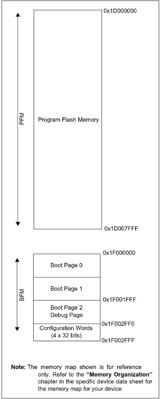
text_image
Program Flash Memory 0x1D000000 0x1D007FFF 0x1F000000 Boot Page 0 Boot Page 1 Boot Page 2 Debug Page Configuration Words (4 x 32 bits) 0x1F001FFF 0x1F002FF0 0x1F002FFF PFM BFM Note: The memory map shown is for reference only. Refer to the "Memory Organization" chapter in the specific device data sheet for the memory map for your device.APPENDIX B: HEX FILE FORMAT
Flash programmers process the standard hexadecimal (hex) format used by the Microchip development tools. The format supported is the Intel® HEX32 Format (INHX32). Refer to the Section 1.75 "Hex file Formats" in the "MPASM™ Assembler, MPLINK™ Object Linker, MPLIB™ Object Librarian User's Guide" (DS33014) for more information about hex file formats.
The basic format of the hex file is:
:BBAAAATTHHHH...HHHHCC
Each data record begins with a 9-character prefix and always ends with a 2-character checksum. All records begin with ‘:’, regardless of the format. The individual elements are described below.
- BB – is a two-digit hexadecimal byte count representing the number of data bytes that appear on the line. Divide this number by two to get the number of words per line.
- AAAA – is a four-digit hexadecimal address representing the starting address of the data record. Format is high byte first followed by low byte.
- TT – is a two-digit record type that will be '00' for data records, '01' for end-of-file records and '04' for extended-address record.
- HHHH – is a four-digit hexadecimal data word. Format is low byte followed by high byte. There will be BB/2 data words following TT.
- CC – is a two-digit hexadecimal checksum that is the 2's complement of the sum of all the preceding bytes in the line record.
Because the Intel hex file format is byte-oriented but the 16-bit program counter is not, program memory sections require special treatment. Each 24-bit program word is extended to 32 bits by inserting a so-called "phantom byte". Each program memory address is multiplied by 2 to yield a byte address.
As an example, a section that is located at 0x100 in program memory will be represented in the hex file as 0x200.
The hex file will be produced with the following contents:
:020000040000fa
:040200003322110096
:00000001FF
The data record (second line) has a load address of 0200, while the source code specified address is 0x100. The data is represented in "little-endian" format, that is the Least Significant Byte appears first and the phantom byte appears last, before the checksum.
APPENDIX C: DEVICE IDS
TABLE C-1: PIC32MX320/340/360/440/460 FAMILY DEVICE IDS
| Part Number | Device ID (See Note 1) |
| PIC32MX360F512L 0x0938053 | |
| PIC32MX360F256L 0x0934053 | |
| PIC32MX340F128L 0x092D053 | |
| PIC32MX320F128L 0x092A053 | |
| PIC32MX340F512H 0x0916053 | |
| PIC32MX340F256H 0x0912053 | |
| PIC32MX340F128H 0x090D053 | |
| PIC32MX320F128H 0x090A053 | |
| PIC32MX320F064H 0x0906053 | |
| PIC32MX320F032H 0x0902053 | |
| PIC32MX460F512L 0x0978053 | |
| PIC32MX460F256L 0x0974053 | |
| PIC32MX440F128L 0x096D053 | |
| PIC32MX440F256H 0x0952053 | |
| PIC32MX440F512H 0x0956053 | |
| PIC32MX440F128H 0x094D053 | |
| PIC32MX420F032H 0x0942053 |
TABLE C-2: PIC32MX575/675/695/775/795 FAMILY DEVICE IDS
| Part Number | Device ID (See Note 1) |
| PIC32MX575F256H 0x04317 | 053 |
| PIC32MX675F256H | 0x0430B053 |
| PIC32MX775F256H 0x04303 | 053 |
| PIC32MX575F512H 0x04309 | 053 |
| PIC32MX675F512H 0x0430C | 053 |
| PIC32MX695F512H 0x04325 | 053 |
| PIC32MX775F512H 0x0430D | 053 |
| PIC32MX795F512H 0x0430E | 053 |
| PIC32MX575F256L 0x04333 | 053 |
| PIC32MX675F256L 0x04305 | 053 |
| PIC32MX775F256L 0x04312 | 053 |
| PIC32MX575F512L 0x0430F | 053 |
| PIC32MX675F512L 0x04311 | 053 |
| PIC32MX695F512L 0x04341 | 053 |
| PIC32MX775F512L 0x04307 | 053 |
| PIC32MX795F512L 0x04307 | 053 |
TABLE C-3: PIC32MX534/564/664/764 FAMILY DEVICE IDS
| Part Number | Device ID (See Note 1) |
| PIC32MX534F064H 0x04400053 | |
| PIC32MX564F064H 0x04401053 | |
| PIC32MX564F128H 0x04403053 | |
| PIC32MX664F064H 0x04405053 | |
| PIC32MX664F128H 0x04407053 | |
| PIC32MX764F128H 0x0440B053 | |
| PIC32MX534F064L 0x0440C053 | |
| PIC32MX564F064L 0x0440D053 | |
| PIC32MX564F128L 0x0440F053 | |
| PIC32MX664F064L 0x04411053 | |
| PIC32MX664F128L 0x04413053 | |
| PIC32MX764F128L 0x04417053 |
TABLE C-4: PIC32MX1XX/2XX 28/36/44-PIN FAMILY DEVICE IDS
| Part Number | Device ID (See Note 1) |
| PIC32MX110F016B 0x04A07 | 053 |
| PIC32MX110F016C 0x04A09 | 053 |
| PIC32MX110F016D | 0x04A0B053 |
| PIC32MX210F016B 0x04A01 | 053 |
| PIC32MX210F016C 0x04A03 | 053 |
| PIC32MX210F016D 0x04A05 | 053 |
| PIC32MX120F032B 0x04A06 | 053 |
| PIC32MX120F032C 0x04A08 | 053 |
| PIC32MX120F032D 0x04A0A | 053 |
| PIC32MX220F032B 0x04A00 | 053 |
| PIC32MX220F032C 0x04A02 | 053 |
| PIC32MX220F032D 0x04A04 | 053 |
| PIC32MX130F064B 0x04D07 | 053 |
| PIC32MX130F064C 0x04D09 | 053 |
| PIC32MX130F064D 0x04D0E | 053 |
| PIC32MX230F064B 0x04D01 | 053 |
| PIC32MX230F064C 0x04D03 | 053 |
| PIC32MX230F064D 0x04D05 | 053 |
| PIC32MX150F128B 0x04D06 | 053 |
| PIC32MX150F128C 0x04D08 | 053 |
| PIC32MX150F128D 0x04D0A | 053 |
| PIC32MX250F128B 0x04D00 | 053 |
| PIC32MX250F128C 0x04D02 | 053 |
| PIC32MX250F128D 0x04D04 | 053 |
| PIC32MX170F256B 0x06610 | 053 |
| PIC32MX170F256D 0x0661A | 053 |
| PIC32MX270F256B 0x06600 | 053 |
| PIC32MX270F256D 0x0660A | 053 |
| PIC32MX270F256DB 0x0660 | C053 |
| PIC32MX130F256B 0x06703 | 053 |
| PIC32MX130F256D 0x06705 | 053 |
| PIC32MX230F256B 0x06700 | 053 |
| PIC32MX230F256D 0x06702 | 053 |
TABLE C-5: PIC32MX330/350/370/430/450/470 FAMILY DEVICE IDS
| Part Number | Device ID (See Note 1) |
| PIC32MX330F064H 0x05600053 | |
| PIC32MX330F064L 0x05601053 | |
| PIC32MX350F256H 0x05704053 | |
| PIC32MX350F256L 0x05705053 | |
| PIC32MX430F064H 0x05602053 | |
| PIC32MX430F064L 0x05603053 | |
| PIC32MX450F256H 0x05706053 | |
| PIC32MX450F256L 0x05707053 | |
| PIC32MX350F128H 0x0570C053 | |
| PIC32MX350F128L 0x0570D053 | |
| PIC32MX450F128H 0x0570E053 | |
| PIC32MX450F128L 0x0570F053 | |
| PIC32MX370F512H 0x05808053 | |
| PIC32MX370F512L 0x05809053 | |
| PIC32MX470F512H 0x0580A053 | |
| PIC32MX470F512L 0x0580B053 | |
| PIC32MX450F256HB 0x05710053 | |
| PIC32MX470F512LB 0x05811053 |
TABLE C-6: PIC32MZ EMBEDDED CONNECTIVITY (EC) FAMILY DEVICE IDS
| Part Number | Device ID (See Note 1) |
| PIC32MZ1024ECG064 0x051 | 03053 |
| PIC32MZ1024ECH064 0x051 | 08053 |
| PIC32MZ1024ECM064 0x051 | 30053 |
| PIC32MZ2048ECG064 0x051 | 04053 |
| PIC32MZ2048ECH064 0x051 | 09053 |
| PIC32MZ2048ECM064 0x051 | 31053 |
| PIC32MZ1024ECG100 0x051 | 0D053 |
| PIC32MZ1024ECH100 0x051 | 12053 |
| PIC32MZ1024ECM100 0x051 | 3A053 |
| PIC32MZ2048ECG100 0x051 | 0E053 |
| PIC32MZ2048ECH100 0x051 | 13053 |
| PIC32MZ2048ECM100 0x051 | 3B053 |
| PIC32MZ1024ECG124 0x051 | 17053 |
| PIC32MZ1024ECH124 0x051 | 1C053 |
| PIC32MZ1024ECM124 0x051 | 44053 |
| PIC32MZ2048ECG124 0x051 | 18053 |
| PIC32MZ2048ECH124 0x051 | 1D053 |
| PIC32MZ2048ECM124 0x051 | 45053 |
| PIC32MZ1024ECG144 0x051 | 21053 |
| PIC32MZ1024ECH144 0x051 | 26053 |
| PIC32MZ1024ECM144 0x051 | 4E053 |
| PIC32MZ2048ECG144 0x051 | 22053 |
| PIC32MZ2048ECH144 0x051 | 27053 |
| PIC32MZ2048ECM144 0x051 | 4F053 |
TABLE C-7: PIC32MX1XX/2XX/5XX 64/100- PIN FAMILY DEVICE IDS
| Part Number | Device ID (See Note 1) |
| PIC32MX150F256H 0x06A10053 | |
| PIC32MX150F256L 0x06A11053 | |
| PIC32MX170F512H 0x06A30053 | |
| PIC32MX170F512L 0x06A31053 | |
| PIC32MX250F256H 0x06A12053 | |
| PIC32MX250F256L 0x06A13053 | |
| PIC32MX270F512H 0x06A32053 | |
| PIC32MX270F512L 0x06A33053 | |
| PIC32MX550F256H 0x06A14053 | |
| PIC32MX550F256L 0x06A15053 | |
| PIC32MX570F512H 0x06A34053 | |
| PIC32MX570F512L 0x06A35053 | |
| PIC32MX120F064H 0x06A50053 | |
| PIC32MX130F128H 0x06A00053 | |
| PIC32MX130F128L 0x06A01053 | |
| PIC32MX230F128H 0x06A02053 | |
| PIC32MX230F128L 0x06A03053 | |
| PIC32MX530F128H 0x06A04053 | |
| PIC32MX530F128L 0x06A05053 |
TABLE C-8: PIC32MZ EMBEDDED CONNECTIVITY WITH FPU (EF) FAMILY DEVICE IDS
| Part Number | Device ID (See Note 1) |
| PIC32MZ0512EFE064 0x072 | 01053 |
| PIC32MZ0512EFF064 0x072 | 06053 |
| PIC32MZ0512EFK064 0x072 | 2E053 |
| PIC32MZ1024EFE064 0x072 | 02053 |
| PIC32MZ1024EFF064 0x072 | 07053 |
| PIC32MZ1024EFK064 0x072 | 2F053 |
| PIC32MZ1024EFG064 0x072 | 03053 |
| PIC32MZ1024EFH064 0x072 | 08053 |
| PIC32MZ1024EFM064 0x072 | 30053 |
| PIC32MZ2048EFG064 0x072 | 04053 |
| PIC32MZ2048EFH064 0x072 | 09053 |
| PIC32MZ2048EFM064 0x072 | 31053 |
| PIC32MZ0512EFE100 0x072 | 0B053 |
| PIC32MZ0512EFF100 0x072 | 10053 |
| PIC32MZ0512EFK100 0x072 | 88053 |
| PIC32MZ1024EFE100 0x072 | 0C053 |
| PIC32MZ1024EFF100 0x072 | 11053 |
| PIC32MZ1024EFK100 0x072 | 39053 |
| PIC32MZ1024EFG100 0x072 | 0D053 |
| PIC32MZ1024EFH100 0x072 | 12053 |
| PIC32MZ1024EFM100 0x072 | 3A053 |
| PIC32MZ2048EFG100 0x072 | 0E053 |
| PIC32MZ2048EFH100 0x072 | 13053 |
| PIC32MZ2048EFM100 0x072 | 3B053 |
| PIC32MZ0512EFE124 0x072 | 15053 |
| PIC32MZ0512EFF124 0x072 | 1A053 |
| PIC32MZ0512EFK124 0x072 | 42053 |
| PIC32MZ1024EFE124 0x072 | 16053 |
| PIC32MZ1024EFF124 0x072 | 1B053 |
| PIC32MZ1024EFK124 0x072 | 43053 |
| PIC32MZ1024EFG124 0x072 | 17053 |
| PIC32MZ1024EFH124 0x072 | 1C053 |
| PIC32MZ1024EFM124 0x072 | 44053 |
| PIC32MZ2048EFG124 0x072 | 18053 |
| PIC32MZ2048EFH124 0x072 | 1D053 |
| PIC32MZ2048EFM124 0x072 | 45053 |
| PIC32MZ0512EFE144 0x072 | 1F053 |
| PIC32MZ0512EFF144 0x072 | 24053 |
| PIC32MZ0512EFK144 0x072 | 4C053 |
| PIC32MZ1024EFE144 0x072 | 20053 |
| PIC32MZ1024EFF144 0x072 | 25053 |
| PIC32MZ1024EFK144 0x072 | 4D053 |
| PIC32MZ1024EFG144 0x072 | 21053 |
| PIC32MZ1024EFH144 0x072 | 26053 |
| PIC32MZ1024EFM144 0x072 | 4E053 |
| PIC32MZ2048EFG144 0x072 | 22053 |
| PIC32MZ2048EFH144 0x072 | 27053 |
| PIC32MZ2048EFM144 0x072 | 4F053 |
TABLE C-9: PIC32MZ GRAPHICS (DA) FAMILY DEVICE IDS
| Part Number | Device ID (See Note 1) |
| PIC32MZ1025DAA169 0x05F | 0C053 |
| PIC32MZ1025DAB169 0x05F | 0D053 |
| PIC32MZ1064DAA169 0x05F | 0F053 |
| PIC32MZ1064DAB169 0x05F | 10053 |
| PIC32MZ2025DAA169 0x05F | 15053 |
| PIC32MZ2025DAB169 0x05F | 16053 |
| PIC32MZ2064DAA169 0x05F | 18053 |
| PIC32MZ2064DAB169 0x05F | 19053 |
| PIC32MZ1025DAG169 0x05F | 42053 |
| PIC32MZ1025DAH169 0x05F | 43053 |
| PIC32MZ1064DAG169 0x05F | 45053 |
| PIC32MZ1064DAH169 0x05F | 46053 |
| PIC32MZ2025DAG169 0x05F | 4B053 |
| PIC32MZ2025DAH169 0x05F | 4C053 |
| PIC32MZ2064DAG169 0x05F | 4E053 |
| PIC32MZ2064DAH169 0x05F | 4F053 |
| PIC32MZ1025DAA176 0x05F | 78053 |
| PIC32MZ1025DAB176 0x05F | 79053 |
| PIC32MZ1064DAA176 0x05F | 7B053 |
| PIC32MZ1064DAB176 0x05F | 7C053 |
| PIC32MZ2025DAA176 0x05F | 81053 |
| PIC32MZ2025DAB176 0x05F | 82053 |
| PIC32MZ2064DAA176 0x05F | 84053 |
| PIC32MZ2064DAB176 0x05F | 85053 |
| PIC32MZ1025DAG176 0x05F | AE053 |
| PIC32MZ1025DAH176 0x05F | AF053 |
| PIC32MZ1064DAG176 0x05F | B1053 |
| PIC32MZ1064DAH176 0x05F | B2053 |
| PIC32MZ2025DAG176 0x05F | B7053 |
| PIC32MZ2025DAH176 0x05F | B8053 |
| PIC32MZ2064DAG176 0x05F | BA053 |
| PIC32MZ2064DAH176 0x05F | BB053 |
| PIC32MZ1025DAA288 0x05F | 5D053 |
| PIC32MZ1025DAB288 0x05F | 5E053 |
| PIC32MZ1064DAA288 0x05F | 60053 |
| PIC32MZ1064DAB288 0x05F | 61053 |
| PIC32MZ2025DAA288 0x05F | 66053 |
| PIC32MZ2025DAB288 0x05F | 67053 |
| PIC32MZ2064DAA288 0x05F | 69053 |
| PIC32MZ2064DAB288 0x05F | 6A053 |
| PIC32MZ1025DAK169 0x08A | 0C053 |
| PIC32MZ1025DAL169 0x08A | 0D053 |
| PIC32MZ1064DAK169 0x08A | 0F053 |
| PIC32MZ1064DAL169 0x08A | 10053 |
| PIC32MZ2025DAK169 0x08A | 15053 |
| PIC32MZ2025DAL169 0x08A | 16053 |
| PIC32MZ2064DAK169 0x08A | 18053 |
| PIC32MZ2064DAL169 0x08A | 19053 |
TABLE C-9: PIC32MZ GRAPHICS (DA) FAMILY DEVICE IDS
| Part Number | Device ID (See Note 1) |
| PIC32MZ1025DAR169 0x08A | 42053 |
| PIC32MZ1025DAS169 0x08A | 43053 |
| PIC32MZ1064DAR169 0x08A | 45053 |
| PIC32MZ1064DAS169 0x08A | 46053 |
| PIC32MZ2025DAR169 0x08A | 4B053 |
| PIC32MZ2025DAS169 0x08A | 4C053 |
| PIC32MZ2064DAR169 0x08A | 4E053 |
| PIC32MZ2064DAS169 0x08A | 4F053 |
| PIC32MZ1025DAK176 0x08A | 78053 |
| PIC32MZ1025DAL176 0x08A | 79053 |
| PIC32MZ1064DAK176 0x08A | 7B053 |
| PIC32MZ1064DAL176 0x08A | 7C053 |
| PIC32MZ2025DAK176 0x08A | 81053 |
| PIC32MZ2025DAL176 0x08A | 82053 |
| PIC32MZ2064DAK176 0x08A | 84053 |
| PIC32MZ2064DAL176 0x08A | 85053 |
| PIC32MZ1025DAR176 0x08A | AE053 |
| PIC32MZ1025DAS176 0x08A | AF053 |
| PIC32MZ1064DAR176 0x08A | B1053 |
| PIC32MZ1064DAS176 0x08A | B2053 |
| PIC32MZ2025DAR176 0x08A | B7053 |
| PIC32MZ2025DAS176 0x08A | B8053 |
| PIC32MZ2064DAR176 0x08A | BA053 |
| PIC32MZ2064DAS176 0x08A | BB053 |
TABLE C-10: PIC32MX1XX/2XX 28/44-PIN XLP FAMILY DEVICE IDS
| Part Number | Device ID (See Note 1) |
| PIC32MX154F128B 0x07800053 | |
| PIC32MX154F128D 0x07804053 | |
| PIC32MX155F128B 0x07808053 | |
| PIC32MX155F128D 0x0780C053 | |
| PIC32MX174F256B 0x07801053 | |
| PIC32MX174F256D 0x07805053 | |
| PIC32MX175F256B 0x07809053 | |
| PIC32MX175F256D 0x0780D053 | |
| PIC32MX254F128B 0x07802053 | |
| PIC32MX254F128D 0x07806053 | |
| PIC32MX255F128B 0x0780A053 | |
| PIC32MX255F128D 0x0780E053 | |
| PIC32MX274F256B 0x07803053 | |
| PIC32MX274F256D 0x07807053 | |
| PIC32MX275F256B 0x0780B053 | |
| PIC32MX275F256D 0x0780F053 |
TABLE C-11: PIC32MK GENERAL PURPOSE AND MOTOR CONTROL (GP/MC) FAMILY DEVICE IDS
| Part Number | Device ID (See Note 1) |
| PIC32MK1024MCF100 0x062 | 01053 |
| PIC32MK1024MCF064 0x062 | 02053 |
| PIC32MK0512MCF100 0x062 | 04053 |
| PIC32MK0512MCF064 0x062 | 05053 |
| PIC32MK1024GPE100 0x062 | 07053 |
| PIC32MK1024GPE064 0x062 | 08053 |
| PIC32MK0512GPE100 0x062 | 0A053 |
| PIC32MK0512GPE064 0x062 | 0B053 |
| PIC32MK1024GPD100 0x062 | 0D053 |
| PIC32MK1024GPD064 0x062 | 0E053 |
| PIC32MK0512GPD100 0x062 | 10053 |
| PIC32MK0512GPD064 0x062 | 11053 |
TABLE C-12: PIC32MK GENERAL PURPOSE AND MOTOR CONTROL (GP/MC) with ECC FLASH FAMILY DEVICE IDS
| Part Number | Device ID (See Note 1) |
| PIC32MK1024MCM100 0x08B01053 | |
| PIC32MK1024MCM064 0x08B02053 | |
| PIC32MK0512MCM100 0x08B04053 | |
| PIC32MK0512MCM064 0x08B05053 | |
| PIC32MK1024GPL100 | 0x08B07053 |
| PIC32MK1024GPL064 | 0x08B08053 |
| PIC32MK0512GPL100 | 0x08B0A053 |
| PIC32MK0512GPL064 | 0x08B0B053 |
| PIC32MK1024GPK100 0x08B0D053 | |
| PIC32MK1024GPK064 | 0x08B0E053 |
| PIC32MK0512GPK100 | 0x08B10053 |
| PIC32MK0512GPK064 | 0x08B11053 |
| PIC32MK0512MCJ064 | 0x06300053 |
| PIC32MK0512MCJ048 | 0x06301053 |
| PIC32MK0512MCJ040 | 0x06302053 |
| PIC32MK0256MCJ064 | 0x06304053 |
| PIC32MK0256MCJ048 | 0x06305053 |
| PIC32MK0256MCJ040 | 0x06306053 |
| PIC32MK0512GPH064 0x06308053 | |
| PIC32MK0512GPH048 0x06309053 | |
| PIC32MK0512GPH040 0x0630A053 | |
| PIC32MK0256GPH064 0x0630C053 | |
| PIC32MK0256GPH048 0x0630D053 | |
| PIC32MK0256GPH040 0x0630E053 | |
| PIC32MK0512GPG064 | 0x06318053 |
| PIC32MK0512GPG048 | 0x06319053 |
| PIC32MK0512GPG040 | 0x0631A053 |
| PIC32MK0256GPG064 | 0x0631C053 |
| PIC32MK0256GPG048 | 0x0631D053 |
| PIC32MK0256GPG040 | 0x0631E053 |
TABLE C-13: PIC32MZ W1 WI-FI ^® CONNECTIVITY FAMILY DEVICE ID
| Part Number | Device ID (See Note 1) |
| PIC32MZ1025W104 | 0x08C03053 |
Note 1: The first 4 bits of 32-bit device ID indicates silicon revision.
APPENDIX D: REVISION HISTORY
Revision A (August 2007)
This is the initial released version of the document.
Revision B (February 2008)
Update records for this revision are not available.
Revision C (April 2008)
Update records for this revision are not available.
Revision D (May 2008)
Update records for this revision are not available.
Revision E (July 2009)
This version of the document includes the following additions and updates:
- Minor changes to style and formatting have been incorporated throughout the document
-
Added the following devices:
-
PIC32MX565F256H
- PIC32MX575F512H
- PIC32MX675F512H
- PIC32MX795F512H
- PIC32MX575F512L
- PIC32MX675F512L
-
PIC32MX795F512L
-
Updated MCLR pulse line to show active-high (P20) in Figure 7-1
- Updated Step 7 of Table 11-1 to clarify repeat of the last instruction in the step
-
The following instructions in Table 13-1 were updated:
-
Seventh, ninth and eleventh instructions in Step 1
- All instructions in Step 2
- First instruction in Step 3
- Third instruction in Step 4
- Added the following devices to Table 17-1:
- PIC32MX565F256H
- PIC32MX575F512H
- PIC32MX575F512L
- PIC32MX675F512H
- PIC32MX675F512L
- PIC32MX795F512H
- PIC32MX795F512L
- Updated address values in Table 17-2
Revision E (July 2009) (Continued)
- Added the following devices to Table 17-5:
- PIC32MX565F256H
- PIC32MX575F512H
- PIC32MX675F512H
- PIC32MX795F512H
- PIC32MX575F512L
- PIC32MX675F512L
- PIC32MX795F512L
- Added Notes 1-3 and the following bits to the DEVCFG - Device Configuration Word Summary and the DEVCFG3: Device Configuration Word 3 (see Table 18-1 and Register):
- F V B U S I O
- FUSBIDIO
- FCANIO
- F E T H I O
- FMIIEN
- FPBDIV[1:0]
-
FJTAGEN
-
Updated the DEVID Summary (see Table 18-1)
-
Updated ICESEL bit description and added the FJTAGEN bit in DEVCFG0: Device Configuration Word 0 (see Register 16-1)
-
Updated DEVID: Device and Revision ID register
- Added Device IDs and Revision table (Table 18-4)
- Added MCLR High Time (parameter P20) to Table 20-1
- Added Appendix B: "Hex File Format" and Appendix D: "Revision History"
Revision F (April 2010)
This version of the document includes the following additions and updates:
- The following global bit name changes were made:
- NVMWR renamed as WR
- NVMWREN renamed as WREN
- NVMERR renamed as WRERR
- FVBUSIO renamed as FVBUSONIO
- FUPLLEN renamed as UPLLEN
- FUPLLIDIV renamed as UPLLIDIV
-
POSCMD renamed as POSCMOD
-
Updated the PIC32MX family data sheet references in the fourth paragraph of Section 2.0 "Programming Overview"
- Updated the note in Section 5.2.2 "2-Phase ICSP"
- Updated the Initiate Flash Row Write Op Codes and instructions (see steps 4, 5 and 6 in Table 13-1)
Revision F (April 2010) (Continued)
- Added the following devices:
- PIC32MX534F064H
- PIC32MX534F064L
- PIC32MX564F064H
- PIC32MX564F064L
- PIC32MX564F128H
- PIC32MX564F128L
- PIC32MX575F256L
- PIC32MX664F064H
- PIC32MX664F064L
- PIC32MX664F128H
- PIC32MX664F128L
- PIC32MX675F256H
- PIC32MX675F256L
- PIC32MX695F512H
- PIC32MX605F512L
- PIC32MX764F128H
- PIC32MX764F128L
- PIC32MX775F256H
- PIC32MX775F256L
- PIC32MX775F512H
- PIC32MX775F512L
Revision G (August 2010)
This revision of the document includes the following updates:
- Updated Step 3 in Table 11-1: Download the PE
- Minor corrections to formatting and text have been incorporated throughout the document
Revision H (April 2011)
This version of the document includes the following additions and updates:
- Updates to formatting and minor typographical changes have been incorporated throughout the document
• The following devices were added:
- PIC32MX110F016B
- PIC32MX110F016C
- PIC32MX110F016D
- PIC32MX120F032B
- PIC32MX120F032C
- PIC32MX120F032D
- PIC32MX210F016B
- PIC32MX210F016C
- PIC32MX210F016D
- PIC32MX220F032B
- PIC32MX220F032C
- PIC32MX220F032D
• The following rows were added to Table 17-1:
- PIC32MX1X0
- PIC32MX2X0
- Added a new sub section Section 17.4.6 "Checksum Values While Device Is Code-Protected"
- Removed Register 18-1 through Register 18-5.
- Removed Table 17-2
- Removed Section 17.5 "Checksum for PIC32 Devices" and its sub sections
- The Flash Program Memory Write-Protect Ranges table was removed (formerly Table 18-4)
- Added DEVCFG Locations for PIC32MX1X0 and PIC32MX20X Devices Only (see Table 18-3)
- In Section 18.0 "Configuration Memory and Device ID", removed Table 18-1 and updated Table 18-2: DEVID Summary as Table 18-1
- Added the NVMERR bit to the MCHP Status Value table (see Table 19-3)
- The following Silicon Revision and Revision ID are added to Table 18-4:
- 0x5 - B6 Revision
- 0x1 - A1 Revision
- Added a note to the Flash Memory Map (see Figure A-1)
- Added Appendix C: "Flash Program Memory Data Sheet Clarification"
Revision J (August 2011)
Note: The revision history in this document intentionally skips from Revision H to Revision J to avoid confusing the uppercase letter “I” (EY) with the lowercase letter “I” (EL).
This revision includes the following updates:
- All occurrences of V CORE/VCAP have been changed to VCAP
- Updated the fourth paragraph of Section 2.0 "Programming Overview"
- Removed the column, Programmer Pin Name, from the 2-Wire Interface Pins table and updated the Pin Type for MCLR (see Table 4-2)
- Added the following new devices to the Code Memory Size table (see Table 5-1) and the Device IDs and Revision table (see Table 18-4):
- PIC32MX130F064B
- PIC32MX130F064C
- PIC32MX130F064D
- PIC32MX150F128B
- PIC32MX150F128C
- PIC32MX150F128D
- PIC32MX230F064B
- PIC32MX230F064C
- PIC32MX230F064D
- PIC32MX250F128B
- PIC32MX250F128C
- PIC32MX250F128D
- Added Row Size and Page Size columns to the Code Memory Size table (see Table 5-1)
Revision J (August 2011) (Continued)
- Updated the PGCx signal in Entering Enhanced ICSP Mode (see Figure 7-1)
- Updated the Erase Device block diagram (see Figure 9-1)
- Added a new step 4 to the process to erase a target device in Section 9.0 "Erasing the Device"
- Updated the MCLR signal in 2-Wire Exit Test Mode (see Figure 15-2)
-
Updated the PE Command Set with the following commands and modified Note 2 (see Table 16-2):
-
PROGRAM_CLUSTER
- GET_DEVICEID
- CHANGE_CFG
- Added a second note to Section 16.2.11 "GET_CRC Command"
- Updated the Address and Length descriptions in the PROGRAM_CLUSTER Format (see Table 16-13)
- Added a note after the CHANGE_CFG Response (see Figure 16-27)
- Updated the DEVCFG0 and DEVCFG1 values for All PIC32MX1XX and All PIC32MX2XX devices in Table 17-1
• The following changes were made to the AC/DC Characteristics and Timing Requirements (Table 20-1):
- Updated the Min. value for parameter D111 (V DD)
- Added parameter D114 (I PEAK)
- Removed parameters P2, P3, P4, P4A, P5, P8 and P10
- Removed Appendix C: "Flash Program Memory Data Sheet Clarification"
- Minor updates to text and formatting were incorporated throughout the document
Revision K (July 2012)
This revision includes the following updates:
- All occurrences of PGC and PGD were changed to: PGEC and PGED, respectively
- Updated Section 1.0 "Device Overview" with a list of all major topics in this document
- Added Section 2.3 "Data Sizes"
- Updated Section 4.0 "Connecting to the Device"
- Added Note 2 to Connections for the On-chip Regulator (see Figure 4-2)
- Added Note 2 to the 4-wire and 2-wire Interface Pins tables (see Table 4-1 and Table 4-2)
- Updated Section 7.0 "Entering 2-Wire Enhanced ICSP Mode"
- Updated Entering Serial Execution Mode (see Figure 10-1)
-
Updated step 11 in Section 10.2 "2-wire Interface"
-
Updated Section 12.2 "With the PE"
- Updated Step 3 in Initiate Flash Row Write Op Codes (see Table 13-1)
- Updated Step 1 in Verify Device op Codes (see Table 14-1)
- Updated the interval in Section 15.1 "4-wire Interface" and Section 15.2 "2-wire Interface"
- Added a note regarding the PE location in Section 16.0 "The Programming Executive"
- Added references to the Operand field throughout Section 16.2 "The PE Command Set"
- Updated the PROGRAM Command Algorithm (see Figure 16-9)
- Updated the mask values for All PIC32MX1XX and PIC32MX2XX devices, and DEVCFG3 for all devices (see Table 17-1)
- Updated the DCR value (see Section 17.4.3 "Calculating for "DCR" in the Checksum Formula" and Table 17-2)
- Updated the Checksum Calculation Process (see Example 17-1)
-
Added these new devices to the Code Memory Size table (see Table 5-1) and the Device IDs and Revision table (see Table 18-4):
-
PIC32MX420F032H - PIC32MX450F128L
- PIC32MX330F064H - PIC32MX440F256H
- PIC32MX330F064L - PIC32MX450F256H
- PIC32MX430F064H - PIC32MX450F256L
- PIC32MX430F064L - PIC32MX460F256L
- PIC32MX340F128H - PIC32MX340F512H
- PIC32MX340F128L - PIC32MX360F512H
- PIC32MX350F128H - PIC32MX370F512H
- PIC32MX350F128L - PIC32MX370F512L
- PIC32MX350F256H - PIC32MX440F512H
- PIC32MX350F256L - PIC32MX460F512L
- PIC32MX440F128H - PIC32MX470F512H
- PIC32MX440F128L - PIC32MX470F512L
-
PIC32MX450F128H
-
Added a Note to Section 18.2 "Device Code Protection bit (CP)"
- Added the EJTAG Control Register (see Register 19-1)
- Updated Section 19.2.4 "ETAP_EJTAGBOOT Command"
-
AC/DC Characteristics and Timing Requirements updates (see Table 20-1):
-
Removed parameter D112
- Replaced Notes 1 and 2 with a new Note 1
- Updated parameters D111, D113, D114, D031, D041, D080, D090, D012, D013, P11, P12 and P13
- Minor updates to text and formatting were incorporated through the document
Revision L (January 2013)
This revision includes the following updates:
- The following sections were added or updated:
- Section 2.1 "Devices with Dual Flash Panel and Dual Boot Regions" (new)
- Section 4.3 "Power Requirements"
- Section 13.0 "Initiating a Flash Row Write"
- Section 16.1.1 "2-wire ICSP EJTAG RATE"
- Updated the Device Configuration Register Mask Values (see Table 17-1)
- The following devices were added to the Code Memory Size table and the Device IDs and Revision table (see Table 5-1 and Table 18-4):
- PIC32MZ0256ECE064 - PIC32MZ1024ECF064
- PIC32MZ0256ECE100 - PIC32MZ1024ECF100
- PIC32MZ0256ECE124 - PIC32MZ1024ECF124
- PIC32MZ0256ECE144 - PIC32MZ1024ECF144
- PIC32MZ0256ECF064 - PIC32MZ1024ECG064
- PIC32MZ0256ECF100 - PIC32MZ1024ECG100
- PIC32MZ0256ECF124 - PIC32MZ1024ECG124
- PIC32MZ0256ECF144 - PIC32MZ1024ECG144
- PIC32MZ0512ECE064 - PIC32MZ1024ECH064
- PIC32MZ0512ECE100 - PIC32MZ1024ECH100
- PIC32MZ0512ECE124 - PIC32MZ1024ECH124
- PIC32MZ0512ECE144 - PIC32MZ1024ECH144
- PIC32MZ0512ECF064 - PIC32MZ2048ECG064
- PIC32MZ0512ECF100 - PIC32MZ2048ECG100
- PIC32MZ0512ECF124 - PIC32MZ2048ECG124
- PIC32MZ0512ECF144 - PIC32MZ2048ECG144
- PIC32MZ1024ECE064 - PIC32MZ2048ECH064
- PIC32MZ1024ECE100 - PIC32MZ2048ECH100
- PIC32MZ1024ECE124 - PIC32MZ2048ECH124
-
PIC32MZ1024ECE144 - PIC32MZ2048ECH144
-
Note 3 and Note 4 and the GET_CHECKSUM and QUAD_WORD_PRGM commands were added to the PE Command Set (see Table 16-2)
- Added Section 16.2.15 "GET_CHECKSUM Command"
- Added Section 16.2.16 "QUAD_WORD_PROGRAM Command"
- Updated all addresses in DEVCFG Locations (see Table 18-1 and Table 18-2)
- Added Configuration Word Locations for PIC32MZ EC Family Devices (see Table 18-3)
- Updated Section 18.2 "Device Code Protection Bit (CP)"
- Updated Section 18.3 "Program Write Protection Bits (PWP)"
- All references to Test mode were updated to programming mode throughout the document
- Minor updates to text and formatting were incorporated through the document
Revision M (September 2013)
This revision includes the following updates:
- All references to MIPS Technologies Inc. and www.mips.com were updated to Imagination Technologies Limited and www.imgtec.com, respectively
- Updated Section 2.0 "Programming Overview"
- Updated the last paragraph in Section 5.1.6 "Flash Memory"
- Updated Code Memory Sizes and added Note 3 (see Table 5-1)
- Updated the Erase Device flow diagram (see Figure 9-1)
- Updated Steps 1, 2, 3 and 5 in Table 11-1
- Added a new paragraph in Section 13.2 "Without the PE"
- Updated Step 2, 3 and 5 in Table 13-1
- Updated the Op code description in Table 16-17
- Updated Device Configuration Mask Values (see Table 17-1)
- Removed the first sentence in the fourth paragraph of Section 17.3 "Algorithm"
- Updated Device IDs and Revision (see Table 18-4)
Revision N (April 2014)
This revision includes the following updates:
- Note 2 was updated in TABLE 4-1: "4-wire Interface Pins"
- Note 2 was updated in TABLE 4-2: "2-wire Interface Pins"
- The Delay value in Step 5 of Section 9.0 "Erasing the Device" was updated
-
The Revision ID and Silicon Revision column was updated and the following devices were added to the Device IDs and Revision table (see Table 18-4):
-
PIC32MX170F256B - PIC32MX350F256H
- PIC32MX170F256D - PIC32MX350F256L
- PIC32MX270F256B - PIC32MX430F064H
- PIC32MX270F256D - PIC32MX430F064L
- PIC32MX330F064H - PIC32MX450F128H
- PIC32MX330F064L - PIC32MX450F128L
- PIC32MX350F128H - PIC32MX450F256H
- PIC32MX350F128L - PIC32MX450F256L
Revision P (October 2014)
Note: The revision history in this document intentionally skips from Revision N to Revision P to avoid confusing the uppercase letter "O" with the number zero "O".
The following updates were implemented:
- TABLE 5-1: "Code Memory Size" was updated to include PIC32MK device information
- TABLE 18-1: "Device Configuration Register Mask Values of Currently Supported PIC32MX, PIC32MZ and PIC32MK Devices" was updated to include PIC32MK device information
- The original table, Table 18-4: Device IDs and Revision was removed as this information is readily available in the current Family Silicon Errata
- TABLE 19-4: "Configuration Word Locations for PIC32MK family Devices" was added
Revision Q (July 2015)
This revision includes the following updates:
- Section 14.0 "Initiating a Flash Row Write" was added
- TABLE 18-1: "Device Configuration Register Mask Values of Currently Supported PIC32MX, PIC32MZ and PIC32MK Devices" was updated to include DEVCFG4
- EQUATION 18-1: "Checksum Formula" was updated
- TABLE 19-3: "Configuration Word Locations for PIC32MZ family Devices" was updated to include DEVCFG4
- Minor updates to text and formatting were incorporated throughout the document
Revision R (April 2016)
This revision includes the following updates:
- FIGURE 4-1: “Programming Interfaces” was updated
- TABLE 4-1: "4-wire Interface Pins" was updated
- TABLE 4-2: "2-wire Interface Pins" was updated
• FIGURE 4-4: "PIC32MZ EC/EF Power Connections" was updated - FIGURE 4-5: "PIC32MZ DA Power Connections" was updated
- TABLE 5-1: "Code Memory Size" was updated
• FIGURE 5-2: "Basic PIC32 Programming Interface Block Diagram" was updated - FIGURE 16-1: "4-wire Exit Programming Mode" was updated
-
FIGURE 16-2: "2-wire Exit Programming Mode" was updated
-
Parameters D112 (V DD1V8) and D115 (IDD1V8P) were added to TABLE 21-1: "AC/DC Characteristics and Timing Requirements"
- Section 4.3 "PIC32MX Power Requirements" was updated
- Section 4.4 "PIC32MX With V BAT Pin Power Requirements" was added
- Section 4.5 "PIC32MZ EC and PIC32MZ EF Power Requirements" was added
- Section 4.6 "PIC32MZ DA Power Requirements" was added
- Section 4.7 "PIC32MK Power Requirements" was added
• Section 5.3.3 "Synchronization" was added - Section 6.7 "Synchronize Pseudo Operation" was added
• Section 8.1 "4-wire Interface" was updated
• Section 8.2 "2-wire Interface" was updated - TABLE 13-1: "Page Erase Op Codes" was updated
- TABLE 18-1: "Device Configuration Register Mask Values of Currently Supported PIC32MX, PIC32MZ and PIC32MK Devices" was updated
- Note 1 in the Checksum Formula was updated (see Equation 18-1)
Revision S (September 2016)
This revision includes the following updates:
- The Programming Interfaces diagram was updated (see Figure 4-1)
- The 4-Wire Interface Pins table was updated (see Table 4-1)
- The 2-Wire Interface Pins table was updated (see Table 4-2)
- The PIC32MZ DA Power Connections diagram was updated (see Figure 4-5)
- The Basic PIC32 Programming Interface Block Diagram was updated (see Figure 5-2)
- The Note in Section 5.3.2 "2-phase ICSP" was updated
- The AC/DC Characteristics and Timing Requirements were updated (see Table 21-1)
- Device IDs were added (see Table C-1 through Table C-11 in Appendix C: "Device IDs")
Revision T (May 2017)
This revision includes the following updates:
- Updated Table 20-1, Table 4-1, Table 4-2
- Updated Figure 4-1, Figure 4-2, Figure 5-2
- Added Table C-12
- Minor updates to text and formatting were incorporated throughout the document
Revision U (July 2017)
This revision includes the following updates:
- Updated the PIC32MK devices (see Section 2.1 "Devices with Dual Flash Panel and Dual Boot Regions")
- Updated the PIC32MK devices in Code Memory Size (see Table 5-1)
- Updated the PIC32MK devices in Device Configuration Register Mask Values of Currently Supported PIC32MX, PIC32MZ and PIC32MK Devices (see Table 18-1)
- Updated the Configuration Word Locations for PIC32MK Family Devices (see Table 19-4)
- Added TABLE 19-5: "Configuration Word Locations for PIC32MKXXXXXXH/G/J/K/L/MXX Family Devices"
- Updated the PIC32MK General Purpose and Motor Control (GP/MC) Family Device IDs (see Table C-11)
- In additions, minor updates to text and formatting were incorporated throughout the document
Revision V (July 2018)
This revision includes the following updates:
- In Table 18-1: Renamed PIC32MK0256/0512XXG/H to PIC32MK0256/0512XXH/G/J. Also, updated Device Configuration Register Mask Values for PIC32MK0512/1024XXK/L/M and PIC32MK0512/1024XXH/G/J
- In Table 19-5: Renamed family name from PIC32MKXXXXXXG/H/K/L/MXX to PIC32MKXXXXXXH/G/J/K/L/MXX
- In TableC-11: Removed references to PIC32MKXXXXMCM/GPL/GPKXXX and PIC32MKXXXXMCH/GPGXXX
- In TableC-12: Rearranged PIC32MKXXXX/MCM/GPL/GPKXXX devices. Added PIC32MKXXXX-MCJ/GPH/GPGXXX devices
- A note reference to the revision ID has been added from Table C-1 to Table C-12, which identifies the revision ID field within 32-bit device ID.
Revision W (October 2018)
This revision includes the following updates:
- Added note below Table 13-1 and Table 14-1
• Table C-13 content has been moved to TableC-9
Revision X (November 2019)
This revision includes the following updates:
- Added a new note to 18.1 "Theory" that applies to PIC32MKXXXXGPD/GPE/MCFXXX devices
- Updated TABLE 18-1: “Device Configuration Register Mask Values of Currently Supported PIC32MX, PIC32MZ and PIC32MKxxxxGPD/GPE/MCFxxx Devices” with PIC32MKXXXXGPD/GPE/MCFXXX device information
- Updated EQUATION 18-1: “Checksum Formula” with PIC32MKXXXXGPD/GPE/MCFXXX device information
Revision Y (September 2020)
This revision includes the following updates:
- Added Section 4.8 "PIC32MZ W1 Power Requirements"
- Updated Section 5.1.6 "Flash Memory" with PIC32MZ W1 device information
- Updated Table 5-1 with PIC32MZ W1 device information
- Added a note to Table5-1 that applies to PIC32MZ W1 devices
- Updated Table 18-1 with PIC32MZ W1 device information
- Added Section 19.1.1 "Device Configuration for PIC32MZ W1 devices" that applies to PIC32MZ W1 devices
- Added Table 19-6 with DEVCFG locations for PIC32MZ W1 devices
- Added Table C-13 with PIC32MZ W1 Wi-Fi Connectivity Family Device ID
Revision AA (July 2021)
This revision includes the following update:
- Updated Table 19-6 with new physical address.
Note the following details of the code protection feature on Microchip devices:
• Microchip products meet the specifications contained in their particular Microchip Data Sheet.
• Microchip believes that its family of products is secure when used in the intended manner and under normal conditions.
- There are dishonest and possibly illegal methods being used in attempts to breach the code protection features of the Microchip devices. We believe that these methods require using the Microchip products in a manner outside the operating specifications contained in Microchip's Data Sheets. Attempts to breach these code protection features, most likely, cannot be accomplished without violating Microchip's intellectual property rights.
• Microchip is willing to work with any customer who is concerned about the integrity of its code.
- Neither Microchip nor any other semiconductor manufacturer can guarantee the security of its code. Code protection does not mean that we are guaranteeing the product is "unbreakable." Code protection is constantly evolving. We at Microchip are committed to continuously improving the code protection features of our products. Attempts to break Microchip's code protection feature may be a violation of the Digital Millennium Copyright Act. If such acts allow unauthorized access to your software or other copyrighted work, you may have a right to sue for relief under that Act.
Information contained in this publication is provided for the sole purpose of designing with and using Microchip products. Information regarding device applications and the like is provided only for your convenience and may be superseded by updates. It is your responsibility to ensure that your application meets with your specifications.
THIS INFORMATION IS PROVIDED BY MICROCHIP "AS IS". MICROCHIP MAKES NO REPRESENTATIONS OR WARRANTIES OF ANY KIND WHETHER EXPRESS OR IMPLIED, WRITTEN OR ORAL, STATUTORY OR OTHERWISE, RELATED TO THE INFORMATION INCLUDING BUT NOT LIMITED TO ANY IMPLIED WARRANTIES OF NON-INFRINGEMENT, MERCHANTABILITY, AND FITNESS FOR A PARTICULAR PURPOSE OR WARRANTIES RELATED TO ITS CONDITION, QUALITY, OR PERFORMANCE.
IN NO EVENT WILL MICROCHIP BE LIABLE FOR ANY INDIRECT, SPECIAL, PUNITIVE, INCIDENTAL OR CONSEQUENTIAL LOSS, DAMAGE, COST OR EXPENSE OF ANY KIND WHATSOEVER RELATED TO THE INFORMATION OR ITS USE, HOWEVER CAUSED, EVEN IF MICROCHIP HAS BEEN ADVISED OF THE POSSIBILITY OR THE DAMAGES ARE FORESEEABLE. TO THE FULLEST EXTENT ALLOWED BY LAW, MICROCHIP'S TOTAL LIABILITY ON ALL CLAIMS IN ANY WAY RELATED TO THE INFORMATION OR ITS USE WILL NOT EXCEED THE AMOUNT OF FEES, IF ANY, THAT YOU HAVE PAID DIRECTLY TO MICROCHIP FOR THE INFORMATION. Use of Microchip devices in life support and/or safety applications is entirely at the buyer's risk, and the buyer agrees to defend, indemnify and hold harmless Microchip from any and all damages, claims, suits, or expenses resulting from such use. No licenses are conveyed, implicitly or otherwise, under any Microchip intellectual property rights unless otherwise stated.
Trademarks
The Microchip name and logo, the Microchip logo, Adaptec, AnyRate, AVR, AVR logo, AVR Freaks, BesTime, BitCloud, chipKIT, chipKIT logo, CryptoMemory, CryptoRF, dsPIC, FlashFlex, flexPWR, HELDO, IGLOO, JukeBlox, KeeLoq, Kleer, LANCheck, LinkMD, maXStylus, maXTouch, MediaLB, megaAVR, Microsemi, Microsemi logo, MOST, MOST logo, MPLAB, OptoLyzer, PackeTime, PIC, picoPower, PICSTART, PIC32 logo, PolarFire, Prochip Designer, QTouch, SAM-BA, SenGenuity, SpyNIC, SST, SST Logo, SuperFlash, Symmetricom, SyncServer, Tachyon, TimeSource, tinyAVR, UNI/O, Vectron, and XMEGA are registered trademarks of Microchip Technology Incorporated in the U.S.A. and other countries.
AgileSwitch, APT, ClockWorks, The Embedded Control Solutions Company, EtherSynch, FlashTec, Hyper Speed Control, HyperLight Load, IntellMOS, Libero, motorBench, mTouch, Powermite 3, Precision Edge, ProASIC, ProASIC Plus, ProASIC Plus logo, Quiet-Wire, SmartFusion, SyncWorld, Temux, TimeCesium, TimeHub, TimePictra, TimeProvider, WinPath, and ZL are registered trademarks of Microchip Technology Incorporated in the U.S.A.
Adjacent Key Suppression, AKS, Analog-for-the-Digital Age, Any Capacitor, AnyIn, AnyOut, Augmented Switching, BlueSky, BodyCom, CodeGuard, CryptoAuthentication, CryptoAutomotive, CryptoCompanion, CryptoController, dsPICDEM, dsPICDEM.net, Dynamic Average Matching, DAM, ECAN, Espresso T1S, EtherGREEN, IdealBridge, In-Circuit Serial Programming, ICSP, INICnet, Intelligent Paralleling, Inter-Chip Connectivity, JitterBlocker, maxCrypto, maxView, memBrain, Mindi, MiWi, MPASM, MPF, MPLAB Certified logo, MPLIB, MPLINK, MultiTRAK, NetDetach, Omniscient Code Generation, PICDEM, PICDEM.net, PICkit, PICtail, PowerSmart, PureSilicon, QMatrix, REAL ICE, Ripple Blocker, RTAX, RTG4, SAM-ICE, Serial Quad I/O, simpleMAP, SimpliPHY, SmartBuffer, SMART-I.S., storClad, SQI, SuperSwitcher, SuperSwitcher II, Switchtec, SynchroPHY, Total Endurance, TSHARC, USBCheck, VariSense, VectorBlox, VeriPHY, ViewSpan, WiperLock, XpressConnect, and ZENA are trademarks of Microchip Technology Incorporated in the U.S.A. and other countries.
SQTP is a service mark of Microchip Technology Incorporated in the U.S.A. The Adaptec logo, Frequency on Demand, Silicon Storage Technology, and Symmcom are registered trademarks of Microchip Technology Inc. in other countries. GestIC is a registered trademark of Microchip Technology Germany II GmbH & Co. KG, a subsidiary of Microchip Technology Inc., in other countries. All other trademarks mentioned herein are property of their respective companies.
© 2007-2021, Microchip Technology Incorporated, All Rights Reserved.
ISBN: 978-1-5224-8373-1
For information regarding Microchip's Quality Management Systems, please visit www.microchip.com/quality.
Worldwide Sales and Service
AMERICAS
Corporate Office
2355 West Chandler Blvd.
Chandler, AZ 85224-6199
Tel: 480-792-7200
Fax: 480-792-7277
Technical Support:
http://www.microchip.com/
support
Web Address:
www.microchip.com
Atlanta
Duluth, GA
Tel: 678-957-9614
Fax: 678-957-1455
Austin, TX
Tel: 512-257-3370
Boston
Westborough, MA
Tel: 774-760-0087
Fax: 774-760-0088
Chicago
Itasca, IL
Tel: 630-285-0071
Fax: 630-285-0075
Dallas
Addison, TX
Tel: 972-818-7423
Fax: 972-818-2924
Detroit
Novi, MI
Tel: 248-848-4000
Houston, TX
Tel: 281-894-5983
Indianapolis
Noblesville, IN
Tel: 317-773-8323
Fax: 317-773-5453
Tel: 317-536-2380
Los Angeles
Mission Viejo, CA
Tel: 949-462-9523
Fax: 949-462-9608
Tel: 951-273-7800
Raleigh, NC
Tel: 919-844-7510
New York, NY
Tel: 631-435-6000
San Jose, CA
Tel: 408-735-9110
Tel: 408-436-4270
Canada - Toron
Tel: 905-695-1980
Fax: 905-695-2078
ASIA/PACIFIC
Australia - Sydney
Tel: 61-2-9868-6733
China - Beijing
Tel: 86-10-8569-7000
China - Chengdu
Tel: 86-28-8665-5511
China - Chongqing
Tel: 86-23-8980-9588
China - Dongguan
Tel: 86-769-8702-9880
China - Guangzhou
Tel: 86-20-8755-8029
China - Hangzhou
Tel: 86-571-8792-8115
China - Hong Kong SAR
Tel: 852-2943-5100
China - Nanjing
Tel: 86-25-8473-2460
China - Qingdao
Tel: 86-532-8502-7355
China - Shanghai
Tel: 86-21-3326-8000
China - Shenyang
Tel: 86-24-2334-2829
China - Shenzhen
Tel: 86-755-8864-2200
China - Suzhou
Tel: 86-186-6233-1526
China - Wuhan
Tel: 86-27-5980-5300
China - Xian
Tel: 86-29-8833-7252
China - Xiamen
Tel: 86-592-2388138
China - Zhuhai
Tel: 86-756-3210040
ASIA/PACIFIC
India - Bangalore
Tel: 91-80-3090-4444
India - New Delhi
Tel: 91-11-4160-8631
India - Pune
Tel: 91-20-4121-0141
Japan - Osaka
Tel: 81-6-6152-7160
Japan - Tokyo
Tel: 81-3-6880-3770
Korea - Daegu
Tel: 82-53-744-4301
Korea - Seoul
Tel: 82-2-554-7200
Malaysia - Kuala Lumpur
Tel: 60-3-7651-7906
Malaysia - Penang
Tel: 60-4-227-8870
Philippines - Manila
Tel: 63-2-634-9065
Singapore
Tel: 65-6334-8870
Taiwan - Hsin Chu
Tel: 886-3-577-8366
Taiwan - Kaohsiung
Tel: 886-7-213-7830
Taiwan - Taipei
Tel: 886-2-2508-8600
Thailand - Bangkok
Tel: 66-2-694-1351
Tel: 43-7242-2244-39
Fax: 43-7242-2244-393
Denmark - Copenhagen
Tel: 45-4485-5910
Fax: 45-4485-2829
Finland - Espoo
Tel: 358-9-4520-820
France - Paris
Tel: 33-1-69-53-63-20
Fax: 33-1-69-30-90-79
Germany - Garching
Tel: 49-8931-9700
Germany - Haan
Tel: 49-2129-3766400
Germany - Heilbronn
Tel: 49-7131-72400
Germany - Karlsruhe
Tel: 49-721-625370
Germany - Munich
Tel: 49-89-627-144-0
Fax: 49-89-627-144-44
Germany - Rosenheim
Tel: 49-8031-354-560
Israel - Ra'anana
Tel: 972-9-744-7705
Italy - Milan
Tel: 39-0331-742611
Fax: 39-0331-466781
Italy - Padova
Tel: 39-049-7625286
Netherlands - Drunen
Tel: 31-416-690399
Fax: 31-416-690340
Norway - Trondheim
Tel: 47-7288-4388
Poland - Warsaw
Tel: 48-22-3325737
Romania - Bucharest
Tel: 40-21-407-87-50
Spain - Madrid
Tel: 34-91-708-08-90
Fax: 34-91-708-08-91
Sweden - Gothenberg
Tel: 46-31-704-60-40
Sweden - Stockholm
Tel: 46-8-5090-4654
UK - Wokingham
Tel: 44-118-921-5800
Fax: 44-118-921-5820