MIC28304-2-12V - Power supply Microchip - Free user manual and instructions
Find the device manual for free MIC28304-2-12V Microchip in PDF.

User questions about MIC28304-2-12V Microchip
0 question about this device. Answer the ones you know or ask your own.
Ask a new question about this device
Download the instructions for your Power supply in PDF format for free! Find your manual MIC28304-2-12V - Microchip and take your electronic device back in hand. On this page are published all the documents necessary for the use of your device. MIC28304-2-12V by Microchip.
USER MANUAL MIC28304-2-12V Microchip
The Micrel MIC28304 is synchronous step-down regulator module, featuring a unique adaptive ON-time control architecture. The module incorporates a DC-to-DC controller, power MOSFETs, bootstrap diode, bootstrap capacitor, and an inductor in a single package. The MIC28304 operates over an input supply range of 4.5V to 70V and can be used to supply up to 3A of output current. The output voltage is adjustable down to 0.8V with a guaranteed accuracy of ±1%. The device operates with a programmable switching frequency from 200kHz to 600kHz.
The MIC28304-1 has the HyperLight Load ^® architecture, so it can operate in pulse skipping mode at light load. However, it operates in fixed frequency CCM mode from medium load to heavy load. The MIC28304-2 has HyperSpeed Control ^™ architecture, which operates in fixed frequency CCM mode under all load conditions.
The basic parameters of the evaluation board are:
- Input: 7V to 70V
• Output: 0.8V to 5V at 3A (1) - 600kHz Switching Frequency (Adjustable 200kHz to 600kHz)
Note:
- Refer to temperature curves shown in the MIC28304 0.8V to 5V/3A Evaluation Board Typical Characteristics section.
Datasheets and support documentation are available on Micrel's web site at: www.micrel.com.
Requirements
The MIC28304-1 and MIC28304-2 evaluation board requires only a single power supply with at least 10A current capability. No external linear regulator is required to power the internal biasing of the IC because the MIC28304 has internal PVDD LDO. In the applications with VIN < +5.5V, PVDD should be tied to VIN to bypass the internal linear regulator. The output load can either be a passive or an active load.
Precautions
The MIC28304 evaluation board does not have reverse polarity protection. Applying a negative voltage to the VIN and GND terminals may damage the device. The maximum VIN of the board is rated at 70V. Exceeding 70V on the VIN could damage the device.
Getting Started
1. VIN Supply
Connect a supply to the VIN and GND terminals, paying careful attention to the polarity and the supply range (7V < VIN < 70V). Monitor IIN with a current meter and monitor input voltage at VIN and GND terminals with a voltmeter. Do not apply power until step 4.
2. Connect Load and Monitor Output
Connect a load to the VOUT and GND terminals. The load can be either a passive (resistive) or an active (as in an electronic load) type. A current meter may be placed between the VOUT terminal and load to monitor the output current. Ensure the output voltage is monitored at the VOUT terminal.
3. Enable Input
The EN pin has an on board 100kΩ pull-up resistor (R16) to VIN, which allows the output to be turned on when PVDD exceeds its UVLO threshold. An EN connector is provided on the evaluation board for users to easily access the enable feature. Applying an external logic signal on the EN pin to pull it low or using a jumper to short the EN pin to GND will shut off the output of the MIC28304 evaluation board.
4. Turn Power
Turn on the VIN supply and verify that the output voltage is regulated to 5V.
Ordering Information
| Part Number Description | |
| MIC28304-1 5V EV | MIC28304-1 Evaluation Board up to 5V Output |
| MIC28304-2 5V EV | MIC28304-2 Evaluation Board up to 5V Output |
| MIC28304-1 12V EV | MIC28304-1 Evaluation Board 12V Output |
| MIC28304-2 12V EV | MIC28304-2 Evaluation Board 12V Output |
Hyper LightLoad is a registered trademark and Hyper Speed Control is a trademark of Micrel, Inc.
Micrel Inc. • 2180 Fortune Drive • San Jose, CA 95131 • USA • tel +1 (408) 944-0800 • fax +1 (408) 474-1000 • http://www.micrel.com
Features
Feedback Resistors
The output voltage on the MIC28304 evaluation board, which is preset to 5.0V, is determined by the feedback divider:
$$ V = V _ {R E F O U T} \left(1 + \frac {R 1}{R _ {B O T T O M}}\right) \text {Eq.} 1 $$
where V_REF=0.8V , and R_BOTTOM is one of R10, or R11, which corresponds to 3.3V, 5V. Leaving the R_BOTTOM open
gives a 0.8V output voltage. All other voltages not listed above can be set by modifying R_BOTTOM value according to:
$$ R _ {\text { BOTTOM }} = \frac {R 1 \times V _ {\text { REF }}}{V - V _ {\text { REFC }}} \quad \text { Eq. } 2 $$
Note that the output voltage should not be set to exceed 5V due to the 6.3V voltage rating on the output capacitors. For higher output voltage, use the Ordering Information table. Table 1 gives the typical values of some of the components, for details refer to Bill of Material table.
Table 1. Typical Values of Some Components
| V_OUT | VIN | R3 (R_inj) | R1 (Top Feedback Resistor) | R11 (Bottom Feedback Resistor) | C10 (C_inj) | C12 (C_ft) | C_OUT |
| 0.9V | 5V to 70V | 16.5kΩ | 10kΩ | 80.6kΩ | 0.1μF | 2.2nF | 47μF /6.3V or 2 x 22μF |
| 1.2V | 5V to 70V | 16.5kΩ | 10kΩ | 20kΩ | 0.1μF | 2.2nF | 47μF /6.3V or 2 x 22μF |
| 1.8V | 5V to 70V | 16.5kΩ | 10kΩ | 8.06kΩ | 0.1μF | 2.2nF | 47μF /6.3V or 2 x 22μF |
| 2.5V | 5V to 70V | 16.5kΩ | 10kΩ | 4.75kΩ | 0.1μF | 2.2nF | 47μF /6.3V or 2 x 22μF |
| 3.3V | 5V to 70V | 16.5kΩ | 10kΩ | 3.24kΩ | 0.1μF | 2.2nF | 47μF /6.3V or 2 x 22μF |
| 5V | 7V to 70V | 16.5kΩ | 10kΩ | 1.9kΩ | 0.1μF | 2.2nF | 47μF/6.3V or 2 x 22μF |
| 12V | 18V to 70V | 23.2kΩ | 10kΩ | 715Ω | 0.1μF | 2.2nF | 47μF/16V or 2 x 22μF |
SW Node
Test point J1 (VSW) is placed for monitoring the switching waveform, which is one of the most critical waveforms for the converter.
Current Limit
The MIC28304 uses the R_DS(ON) of the low-side MOSFET and external resistor connected from the ILIM pin to the SW node to decide the current limit.
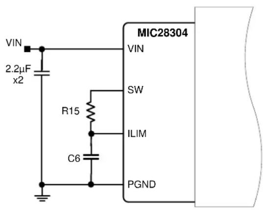
text_image
VIN 2.2µF x2 R15 C6 MIC28304 VIN SW ILIM PGNDFigure 1. MIC28304 Current Limiting Circuit
In each switching cycle of the MIC28304, the inductor current is sensed by monitoring the low-side MOSFET in the OFF period. The sensed voltage V(ILIM) is compared with the power ground (PGND) after a blanking time of 150ns. In this way the drop voltage over the resistor R15 (VCL) is compared with the drop over the bottom FET generating the short current limit. The small capacitor (C6) connected from ILIM pin to PGND filters the switching node ringing during the off-time allowing a better short limit measurement. The time constant created by R15 and C6 should be much less than the minimum off time.
The V_CL drop allows programming of short limit through the value of the resistor (R15), If the absolute value of the voltage drop on the bottom FET is greater than V_CL . In that case the V(ILIM) is lower than PGND and a short circuit event is triggered. A hiccup cycle to treat the short event is generated. The hiccup sequence including the soft start reduces the stress on the switching FETs and protects the load and supply for severe short conditions.
The short circuit current limit can be programmed by using the following formula:
$$ R 1 5 = \frac {- \Delta_ {L (Q \neq N)} \times \quad \times \quad_ {D S (O N)} + V R !}{I _ {C L}} \tag {Eq.3} $$
I_CLIM = Desired current limit
R_DS(ON) = On-resistance of low-side power MOSFET, 57m typically
V_CL = Current-limit threshold (typical absolute value is 14mV per Electrical Characteristics Table in MIC28304 data sheet)
I_CL = Current-limit source current (typical value is 80 A , per the Electrical Characteristics table).
I_L(PP) = Inductor current peak-to-peak, since the inductor is integrated use Equation 4 to calculate the inductor ripple current.
The peak-to-peak inductor current ripple is:
$$ \Delta I _ {L (P P)} = \frac {\text {OUT} \times (V _ {I N (m a x)} - V _ {O U T})}{V _ {I N (m a x)} \times f _ {s w} \times L} \tag {Eq.4} $$
The MIC28304 has 4.7 H inductor integrated into the module. The typical value of R_WINDING(DCR) of this particular inductor is in the range of 45m .
In case of hard short, the short limit is folded down to allow an indefinite hard short on the output without any destructive effect. It is mandatory to make sure that the inductor current used to charge the output capacitance during soft start is under the folded short limit; otherwise the supply will go in hiccup mode and may not be finishing the soft start successfully.
The MOSFET R_DS(ON) varies 30 to 40% with temperature. Therefore, it is recommended to add a 50% margin to b_CLIM in the above equation to avoid false current limiting due to increased MOSFET junction temperature rise. The following table shows typical output current limit value for a given R15 with C6 = 10pF.
| R15 | Typical Output Current Limit |
| 1.81kΩ | 3A |
| 2.7kΩ | 6.3A |
Loop Gain Measurement
Resistor R14 is placed in series with the regulator feedback path. The control loop gain can be measured by connecting an impedance analyzer across the resistor and selecting the resistor value in between 20Ω to 50Ω.
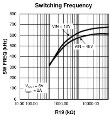
Setting the Switching Frequency
The MIC28304 switching frequency can be adjusted by changing the value of resistor R19. The top resistor of 100kΩ is internal to module and is connected between VIN and FREQ pin, so the value of R19 sets the switching frequency. The switching frequency also depends on VIN, V_OUT and load conditions.

text_image
MIC28304 VIN 2.2µF x2 R19 VIN R_FREQ 100kΩ FREQ PGNDFigure 2. Switching Frequency Adjustment
The following formula gives the estimated switching frequency:
$$ f = f _ {O A D J _ S W} \frac {R 1 9}{+ k \Omega} E q. 5 $$
Where f_O = Switching Frequency when R19 is open. For a more precise setting, it is recommended to use the following graph:
line
| R19 (kΩ) | SW FREQ (kHz) | | -------- | ------------ | | 1000.00 | 300 | | 10000.00 | 600 |Figure 3. Switching Frequency vs. R19
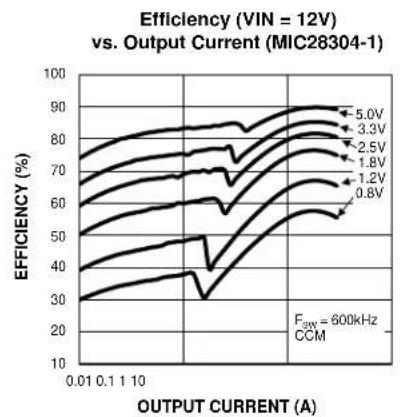
MIC28304 0.8V to 5V/3A Evaluation Board Typical Characteristics
line
| OUTPUT CURRENT (A) | 0.01 | 0.1 | 1 | 10 | | ------------------ | ---- | --- | --- | --- | | 5.0V | 70 | 75 | 80 | 85 | | 3.3V | 65 | 70 | 75 | 80 | | 2.5V | 60 | 65 | 70 | 75 | | 1.8V | 55 | 60 | 65 | 70 | | 1.2V | 50 | 55 | 60 | 65 | | 0.8V | 45 | 50 | 55 | 60 |
line
| OUTPUT CURRENT (A) | 5.0V | 3.3V | 2.5V | 1.8V | 1.2V | 0.8V | | ------------------ | ----- | ----- | ----- | ----- | ----- | ----- | | 0.01 | ~70 | ~65 | ~60 | ~55 | ~50 | ~45 | | 0.1 | ~75 | ~70 | ~65 | ~60 | ~55 | ~50 | | 1 | ~80 | ~75 | ~70 | ~65 | ~60 | ~55 | | 10 | ~85 | ~80 | ~75 | ~70 | ~65 | ~60 | | 100 | ~90 | ~85 | ~80 | ~75 | ~70 | ~65 | | 1000 | ~95 | ~90 | ~85 | ~80 | ~75 | ~70 | | 10000 | ~100 | ~95 | ~90 | ~85 | ~80 | ~75 | | 100000 | ~100 | ~95 | ~90 | ~85 | ~80 | ~75 | | 1000000 | ~100 | ~95 | ~90 | ~85 | ~80 | ~75 | | 10000000 | ~100 | ~95 | ~90 | ~85 | ~80 | ~75 | | 100000000 | ~100 | ~95 | ~90 | ~85 | ~80 | ~75 | | 1000000000 | ~100 | ~95 | ~90 | ~85 | ~80 | ~75 | | 10000000000 | ~100 | ~95 | ~90 | ~85 | ~80 | ~75 | | 100000000000 | ~100 | ~95 | ~90 | ~85 | ~80 | ~75 | | 1000000000000 | ~100 | ~95 | ~90 | ~85 | ~80 | ~75 | | 10000000000000 | ~100 | ~95 | ~90 | ~85 | ~80 | ~75 | | 100000000000000 | ~100 | ~95 | ~90 | ~85 | ~80 | ~75 | | 1000000000000000 | ~100 | ~95 | ~90 | ~85 | ~80 | ~75 | | 10000000000000000 | ~100 | ~95 | ~90 | ~85 | ~80 | ~75 | | 100000000000000000 | ~100 | ~95 | ~90 | ~85 | ~80 | ~75 | | 100000000000000000| ~100 | ~95 | ~90 | ~85 | ~80 | ~75 | | 100.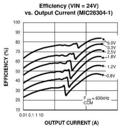
line
| OUTPUT CURRENT (A) | 0.01 | 0.1 | 1 | 10 | | ------------------ | ---- | --- | --- | --- | | 0.01 | 25 | 30 | 35 | 40 | | 0.1 | 30 | 35 | 40 | 45 | | 1 | 35 | 40 | 45 | 50 | | 10 | 40 | 45 | 50 | 55 | | F_say = 600kHz | - | - | - | - | | CCM | - | - | - | - |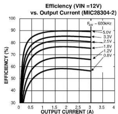
line
| OUTPUT CURRENT (A) | 5.0V | 3.3V | 2.5V | 1.8V | 1.2V | 0.8V | | ------------------ | ----- | ----- | ----- | ----- | ----- | ----- | | 0 | 30 | 30 | 30 | 30 | 30 | 30 | | 0.5 | 70 | 75 | 78 | 80 | 82 | 85 | | 1.0 | 80 | 85 | 88 | 90 | 92 | 95 | | 1.5 | 85 | 90 | 92 | 95 | 97 | 98 | | 2.0 | 88 | 92 | 95 | 97 | 98 | 99 | | 2.5 | 90 | 95 | 97 | 98 | 99 | 99.5 | | 3.0 | 92 | 97 | 98 | 99 | 99.5 | 99.8 | | 3.5 | 93 | 98 | 99 | 99.5 | 99.8 | 99.9 | | 4.0 | 94 | 99 | 99.5 | 99.8 | 99.9 | 100 |
line
| OUTPUT CURRENT (A) | 0.8V | 1.2V | 1.8V | 2.5V | 3.3V | 5.0V | | ------------------ | ----- | ----- | ----- | ----- | ----- | ----- | | 0 | 30 | 30 | 30 | 30 | 30 | 30 | | 0.5 | 40 | 45 | 50 | 55 | 60 | 65 | | 1 | 50 | 55 | 60 | 65 | 70 | 75 | | 1.5 | 55 | 60 | 65 | 70 | 75 | 80 | | 2 | 60 | 65 | 70 | 75 | 80 | 85 | | 2.5 | 65 | 70 | 75 | 80 | 85 | 90 | | 3 | 70 | 75 | 80 | 85 | 90 | 95 | | 3.5 | 75 | 80 | 85 | 90 | 95 | 98 | | 4 | 80 | 85 | 90 | 95 | 98 | 99 |
line
| OUTPUT CURRENT (A) | 0.8V | 1.2V | 1.8V | 2.5V | 3.3V | 5.0V | | ------------------ | ----- | ----- | ----- | ----- | ----- | ----- | | 0 | 30 | 30 | 30 | 30 | 30 | 30 | | 0.5 | 40 | 45 | 50 | 55 | 60 | 65 | | 1 | 45 | 50 | 55 | 60 | 65 | 70 | | 1.5 | 50 | 55 | 60 | 65 | 70 | 75 | | 2 | 55 | 60 | 65 | 70 | 75 | 80 | | 2.5 | 60 | 65 | 70 | 75 | 80 | 85 | | 3 | 65 | 70 | 75 | 80 | 85 | 90 | | 3.5 | 70 | 75 | 80 | 85 | 90 | 95 | | 4 | 75 | 80 | 85 | 90 | 95 | 100 |
line
| MAXIMUM AMBIENT TEMPERATURE (°C) | LOAD CURRENT (A) for VIN = 12V | LOAD CURRENT (A) for VIN = 18V | LOAD CURRENT (A) for VIN = 24V | LOAD CURRENT (A) for VIN = 48V | LOAD CURRENT (A) for VIN = 70V | | ------------------------------- | ----------------------------- | ----------------------------- | ----------------------------- | ----------------------------- | ------------------------------ | | 25 | ~3 | ~2.5 | ~2 | ~1.5 | ~1 | | 40 | ~2.5 | ~2 | ~1.5 | ~1 | ~0.5 | | 55 | ~2 | ~1.5 | ~1 | ~0.5 | ~0.2 | | 70 | ~1.5 | ~1 | ~0.5 | ~0.2 | ~0.1 | | 85 | ~1 | ~0.5 | ~0.2 | ~0.1 | ~0.05 | | 100 | ~0.5 | ~0.2 | ~0.1 | ~0.05 | ~0.02 |
line
| MAXIMUM AMBIENT TEMPERATURE (°C) | LOAD CURRENT (A) | | -------------------------------- | ---------------- | | 25 | 1.5 | | 40 | 1.0 | | 55 | 0.5 | | 70 | 0.2 | | 85 | 0.1 | | 100 | 0.05 |
line
| MAXIMUM AMBIENT TEMPERATURE (°C) | VOUT (A) | FOUT (A) | MIC28304-2 (A) | | -------------------------------- | -------- | -------- | -------------- | | 25 | 2.5 | 600 | 125 | | 40 | 2.5 | 600 | 125 | | 55 | 2.5 | 600 | 125 | | 70 | 2.5 | 600 | 125 | | 85 | 2.5 | 600 | 125 | | 100 | 2.5 | 600 | 125 | | 25 | 1.5 | 48 | 70 | | 40 | 1.5 | 48 | 70 | | 55 | 1.5 | 48 | 70 | | 70 | 1.5 | 48 | 70 | | 85 | 1.5 | 48 | 70 | | 100 | 1.5 | 48 | 70 | | 25 | 1.0 | 24 | 70 | | 40 | 1.0 | 24 | 70 | | 55 | 1.0 | 24 | 70 | | 70 | 1.0 | 24 | 70 | | 85 | 1.0 | 24 | 70 | | 100 | 1.0 | 24 | 70 | | 25 | 0.5 | 18 | 70 | | 40 | 0.5 | 18 | 70 | | 55 | 0.5 | 18 | 70 | | 70 | 0.5 | 18 | 70 | | 85 | 0.5 | 18 | 70 | | 100 | 0.5 | 18 | 70 | | 25 | 0.2 | 14 | 70 | | 40 | 0.2 | 14 | 70 | | 55 | 0.2 | 14 | 70 | | 70 | 0.2 | 14 | 70 | | 85 | 0.2 | 14 | 70 | | 100 | 0.2 | 14 | 70 | | 25 | 0.1 | 12 | 70 | | 40 | 0.1 | 12 | 70 | | 55 | 0.1 | 12 | 70 | | 70 | 0.1 | 12 | 70 | | 85 | 0.1 | 12 | 70 | | 100 | 0.1 | 12 | 70 | | 25 | - | - | - | | 40 | - | - | - | | 55 | - | - | - | | 70 | - | - | - | | 85 | - | - | - | | 100 | - | - | - | | - | - | - | - | | - | - | - | - | | - | - | - | - | | - | - | - | - | | - | - | - | - | | - | - | - | - | | - | - | - | - | | - | - | - | - | | - | - | - | - | | - | - | - | - | | - | - | - | - | | - | - | - | - | | - | - | - | - | | - | - | - | - | | - | - | - | - | | - | - | ~-6 | ~-6 | | - | ~-6 | ~-6 | ~-6 | | - | ~-6 | ~-6 | ~-6 | | - | ~-6 | ~-6 | ~-6 | | - | ~-6 | ~-6 | ~-6 | | - | ~-6 | ~-6 | ~-6 | | - | ~-6 | ~-6 | ~-6 | | - | ~-6 | ~-6 | ~-6 | | - | ~-6 | ~-6 | ~-6 | | - | ~-6 | ~-6 | ~-6 | | - | ~-6 | ~-6 | ~-6 | | - | ~-6 | ~-6 | ~-6 | | - | ~-6 | ~-6 | ~-6 | | - | ~-6 | ~-6 | ~-6 | | - | ~-6 | ~-6 | ~-6 | | - | ~-6 | ~-6 | ~-6 | | - | ~-6 | ~-6 | ~-6 | | - / (MAX) (T_max) / (MAX) / (MAX) / (MAX) / (MAX) / (MAX) / (MAX) / (MAX) / (MAX) / (MAX) / (MAX) / (MAX) / (MAX) / (MAX) / (MAX) / (MAX) / (MAX) / (MAX) / (MAX) / (MAX) / (MAX) / (MAX) / (MAX) / (MAX) / (MAX) / (MAX) / (MAX) / (MAX) / (MAX) / (MAX) / (MAX) / (MAX) / (MAX) / (MAX) / (MAX) / (MAX) / (MAX) / (MAX) / (MAX) / (MAX) / (MAX) / (MAX) / (MAX) / (MAX) / (MAX) / (MAX) / (MAX) / (MAX) / (MAX) / (MAX) / (MAX) / (MAX) / (MAX) / (MAX) / (MAX) / (MAX) / (MAX) / (MAX) / (MAX) / (MAX) / (MAX) / (MAX) / (MAX) / (MAX) / (MAX) / (MAX) / (MAX) / (MAX) / (MAX) / (MAX) / (MAX) / (MAX) / (MAX) / (MAX) / (MAX) / (MAX) / (MAX) / (MAX) / (MAX) / (MAX) / (MAX) / (MAX) / (MAX) / (MAX) / (MAX) / (MAX) / (MAX) / (MAX) / (MAX) / (MAX) / (MAX) / (MAX) / (MAX) / (MAX) / (MAX) / (MAX) / (MAX) / (MAX) / (MAX) / (MAX) / (MAX) / (MAX) / (MAX) / (MAX) / (MAX) / (MAX) / (MAX) / (MAX)Die Temperature*: The temperature measurement was taken at the hottest point on the MIC28304 case mounted on a 5 square inch 4 layer, 0.62", FR-4 PCB with 2oz. finish copper weight per layer. Actual results will depend upon the size of the PCB, ambient temperature and proximity to other heat emitting components.
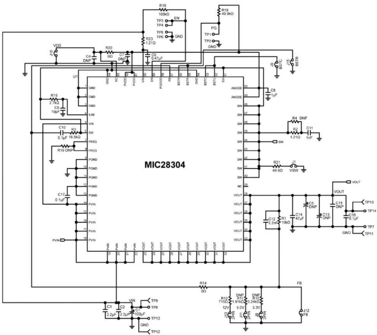
MIC28304 0.8V to 5V/3A Output Evaluation Board Schematic
text_image
MIC28304 VDD J10 C4 DNP R20 0Ω C7 DNP R16 100kΩ EN TP3 TP4 TP5 TP6 GND R23 1.21Ω C9 0.47μF PG TP1 TP2 GND R18 49.9kΩ JP BSTC J15 BSTR U1 1 GND 2 GND 3 GND 4 IUM 5 VIN 6 SW 7 FREQ 8 FREQ 9 PGND 10 PGND 11 PGND 12 PGND 13 PGND 14 PVIN 15 PVIN 16 PVIN 17 PVIN 18 PVIN 19 PVIN 20 PVIN 21 PVIN 22 VOUT 23 VOUT 24 VOUT 25 VOUT 26 VOUT 27 VOUT 28 VOUT 29 VOUT 30 VOUT 31 VOUT 32 VOUT 33 VOUT 34 VOUT 35 VOUT 36 VOUT 37 VOUT 38 VOUT 39 VOUT 40 VOUT 41 VOUT 42 VOUT 43 VOUT 44 VOUT 45 VOUT 46 VOUT 47 VOUT 48 VOUT 49 VOUT 50 VOUT 51 VOUT 52 VOUT 53 VOUT 54 BSTC 55 S3 S2 S1 ANCODE 60 C8 1μF R4 DNP R2 C11 1nF SW R21 J1 49.9Ω VSW VOUT VOUT TP10 TP14 GND TP7 TP11 FB R12 DNP R11 DNP R10 7.15Ω 1.91kΩ 3.24kΩ 12V 5.0V 3.3V J13 2PIN 2PIN JB J12 FB 2.2μF 2.2μF TP9 TP8 TP13 TP12 TP9 TP8 TP13 TP12 TP9 TP8 TP8 TP8 TP8 TP8 TP8 TP8 TP8 TP8 TP8 TP8 TP8 TP8 TP8 TP8 TP8 TP8 TP8 TP8 TP8 TP8 TP8 TP8 TP8 TP8 TP8 TP8 TP8 TP8 TP8 TP8 TP8 TP8 TP8 TP8 TP8 TP8 TP8 TP8 TP8 TP8 TP8 TP8 TP8 TP8 TP8 TP8 TP8 TP8 TP8 TP6 0.47μF PVDD PVDD VIN EN PGND BSTC 0.47μF BGND BSTC 0.47μF BGND BSTC 0.47μF BGND BSTC 0.47μF BGND BSTC 0.47μF BGND BSTC 0.47μF BGND BSTC 0.47μF BGND BSTC 0.47μF BGND BSTC 0.47μF BGND BST C 0.47μF PVDD BVDD VIN EN PGND BSTC 0.47μF BGND BSTC 0.47μF BGND BSTC 0.47μF BGND BSTC 0.47μF BGND BSTC 0.47μF BGND BSTC 0.47μF BGND BSTC 0.47μF BGND BSTC 0.47μF BVDD BVDD VIN EN PGND BSTC 0.47μF PVDD BVDD VIN EN PGND BSTC 0.47μF BGND BSTC 0.47μF BGND BSTC 0.47μF BGND BSTC 0.47μF BGND BSTC 0.47μF BGND BSTC 0.47μF BVDD BVDD VIN EN PGND BSTC 0.47μF PVDD BVDD VIN EN PGND BST C 0.47μF PVDD BVDD VIN EN PGND BST C 0.47μF PVDD BVDD VIN EN PGND BST C 0.47μF BVDD BVDD VIN EN PGND BST C 0.47μF BVDD BVDD VIN EN PGND BST C 0.47μF BVDD BVDD VIN EN PGND BST C 0.47μF BVDD BVDD VIN EN PGND BST C 0.47μF BVDD BVDD VIN EN PGND BST C 0.47μF BVDD BVDD VIN EN PGND BST A 0.47μF PVDD BVDD VIN EN PGND BST C 0.47μF PVDD BVDD VIN EN PGND BST C 0.47μF BVDD BVDD VIN EN PGND BST C 0.47μF BVDD BVDD VIN EN PGND BST C 0.47μF BVDD BVDD VIN EN PGND BST C 0.47μF BVDDBVDD VIN EN PGND BST C 0.47μF BVDDBVDD VIN EN PGND BST C 0.47μF BVDDBVDD VIN EN PGND BST C 0.47μF BVDDBVDD VIN EN PGND BST C 0.47μF BVDDBVDD VIN EN PGND BST C 0.47μF BVDDBVDD VIN EN PGND BST C 16-26-36-36-36-36-36-36-36-36-36-36-36-36-36-36-36-36-36-36-36-36-36-36-36-36-36-36-36-36-36-36-36-36-36-3Figure 4. Schematic of MIC28304 Evaluation Board (J1, J8, J10, J11, J12, J13, R14, R20, and R21 are for testing purposes)
MIC28304 0.8V to 5V/3A Output Evaluation Board Schematic (Continued)

text_image
MIC28304 R18A 100kΩ EN TP3A TPSA GND R23A 1.21Ω C4A DNP R20A 0 Ohm C7A DNP PG R18A 49.9kΩ C6A 0.47μF U1A GND NC PVD PVDD VIN EN PGOD FB BSTR BSTR GND BSTC BSTC SW ANODE 50 ANODE 49 SW SW SW SW SW SW SW SW SW SW SW SW SW SW SW SW SW SW SW SW SW SW SW SW SW SW SW SW SW SW SW SW SW SW SW SW SW SW SW SW SW SW SW SW SW SW SW SW SW SW VOUT 39 VOUT 37 VOUT 35 VOUT 34 VOUT 33 VOUT 32 VOUT 31 VOUT 30 VOUT 29 VOUT 28 VOUT 27 VOUT 26 VOUT 25 VOUT 24 VOUT 23 VOUT 22 VOUT 21 VOUT 20 VOUT 19 20 21 22 23 24 25 26 27 28 29 30 31 32 33 34 35 36 37 38 39 40 41 42 43 44 45 46 47 48 49 50 51 52 53 54 55 56 57 58 59 60 61 62 63 64 65 66 67 68 69 70 71 72 73 74 75 76 77 78 79 80 81 82 83 84 85 86 87 88 89 90 91 92 93 94 95 96 97 98 99 100A/101A/102A/103A/104A/105A/106A/107A/108A/109A/110A/111A/112A/113A/114A/115A/116A/117A/118A/119A/120A/121A/122A/123A/124A/125A/126A/127A/128A/129A/130A/131A/132A/133A/134A/135A/136A/137A/138A/139A/140A/141A/142A/143A/144A/145A/146A/147A/148A/149A/150A/151A/152A/153A/154A/155A/156A/157A/158A/159A/160A/161A/162A/163A/164A/165A/166A/167A/168A/169A/170A/171A/172A/173A/174A/175A/176A/177A/178A/179A/180A/181A/182A/183A/184A/185A/186A/187A/188A/189A/190A/191A/192A/193A/194A/195A/196A/197A/198A/199A/200A/201A/202A/203A/204A/205A/206A/207A/208A/209A/210A/211A/212A/213A/214A/215A/216A/217A/218A/219A/220A/221A/222A/223A/224A/225A/226A/227A/228A/229A/230A/231A/232 A VOUT-A TP-PA TP-PA TP-PA TP-PA TP-PA TP-PA TP-PA TP-PA TP-PA TP-PA TP-PA TP-PA TP-PA TP-PA TP-PA TP-PA TP-PA TP-PA TP-PA TP-PA TP-PA TP-PA TP-PA TP-PA TP-PA TP-PA TP-PA TP-PA TP-PA TP-PA TP-PA TP-PA TP-PA TP-PA TIP-PA TP-PA TP-PA TP-PA TP-PA TP-PA TP-PA TP-PA TP-PA TP-PA TP-PA TP-PA TP-PA TP-PA TP-PA TP-PA TP-PA TP-PA TP-PA TP-PA TP-PA TP-PA TP-PA TP-PA TP-PA TP-PA TP-PA TP-PA TP-PA TP-PA TP-PA TP-PA TP-PA TP - PVT-A / CINOPEN / CINOPEN / CINOPEN / CINOPEN / CINOPEN / CINOPEN / CINOPEN / CINOPEN / CINOPEN / CINOPEN / CINOPEN / CINOPEN / CINOPEN / CINOPEN / CINOPEN / CINOPEN / CINOPEN / CINOPEN / CINOPEN / CINOPEN / CINOPN / CINOPN / CINOPN / CINOPN / CINOPN / CINOPN / CINOPN / CINOPN / CINOPN / CINOPN / CINOPN / CINOPN / CINOPN / CINOPN / CINOPN / CINOPN / CINOPN / CINOPN / CINOPN / CINOPN / CINOP N / CINOP N / CINOP N / CINOP N / CINOP N / CINOP N / CINOP N / CINOP N / CINOP N / CINOP N / CINOP N / CINOP N / CINOP N / CINOP N / CINOP N / CINOP N / CINOP N / CINOP N / CINOP N / CINOP N / CINOPN / CINOPN / CINOPN / CINOPN / CINOPN / CINOPN / CINOPN / CINOPN / CINOPN / CINOPN / CINOPN / CINOPN / CINOPN / CINOPN / CINOPN / CINOPN / CINOPN / CINOPN / CINOPN / CINOPM A VOUT-A TP-PA TP-PA TP-PA TP-PA TP-PA TP-PA TP-PA TP-PA TP-PA TP-PA TP-PA TP-PA TP-PA TP-PA TP-PA TP-PA TP-PA TP-PA TP-PA TP-PA TP-PA TP-PA TP-PA TP-PA TP-PA TP-PA TP-PA TP-PA TP-PA TP-PA TP-PA TP-BA VOUT-A TP-BA VOUT-A TP-BA VOUT-A TP-BA VOUT-A TP-BA VOUT-A TP-BA VOUT-A TP-BA VOUT-A TP-BA VOUT-A TP-BA VOUT-A TP-BA VOUT-A TP-BA VOUT-A TP-BA VOUT-A TP-BA VOUT-A TP-BA VOUT-A TP-BA VOUT-A TP-BA VOUT-A TP-BA VOUT-A TP-BA A VOUT-A A VOUT-A A VOUT-A A VOUT-A A VOUT-A A VOUT-A A VOUT-A A VOUT-A A VOUT-A A VOUT-A A VOUT-A A VOUT-A A VOUT-A A VOUT-A A VOUT-A A VOUT-A A VOUT-A A VOUT-A A VOUT-A A VOUT-A A VOUT-A A VOUT-A A VOUT-A A VOUT-A A VOUT-A A VOUT-B TIP-TIP-TIP-TIP-TIP-TIP-TIP-TIP-TIP-TIP-TIP-TIP-TIP-TIP-TIP-TIP-TIP-TIP-TIP-TIP-TIP-TIP-TIP-TIP-TIP-TIP-TIP-TIP-TIP-TIP-TIP-TIP-TIP-TIP-TIP-TIP-TIP-TIP-TIP-TIP-TIP-TIP-TIP-TIP-TIP-TIP-TIP-TIP-TIP-TIP-TIP,TIP-TIP-TIP-TIP-TIP-TIP-TIP-TIP-TIP-TIP-TIP-TIP-TIP-TIP-TIP-TIP-TIP-TIP-TIP-TIP-TIP-TIP-TIP-TIP-TIP-TIP-TIP-TIP-TIP-TIP-TIP-TIP-TIP-TIP-TIP-TIP-TIP-TIP-TIP-TIP-TIP-TIP-TIP-TIP-TIP-TIP-TIP-TIP-TIP-TIP - TIP - TIP - TIP - TIP - TIP - TIP - TIP - TIP - TIP - TIP - TIP - TIP - TIP - TIP - TIP - TIP - TIP - TIP - TIP - TIP - TIP - TIP - TIP - TIP - TIP - TIP - TIP - TIP - TIP - TIP - TIP - TIP - TIP - TIF - TIF - TIF - TIF - TIF - TIF - TIF - TIF - TIF - TIF - TIF - TIF - TIF - TIF - TIF - TIF - TIF - TIF - TIF - TIF - TIF - TIF - TIF - TIF - TIF - TIF - TIF - TIF - TIF - TIF - TIF - TIF - TIF - TIF :TIF :TIF :TIF :TIF :TIF :TIF :TIF :TIF :TIF :TIF :TIF :TIF :TIF :TIF :TIF :TIF :TIF :TIF :TIF :TIF :TIF :TIF :TIF :TIF :TIF :TIF :TIF :TIF :TIF :TIF :TIF :TIF :TIF :TIC :TIC :TIC :TIC :TIC :TIC :TIC :TIC :TIC :TIC :TIC :TIC :TIC :TIC :TIC :TIC :TIC :TIC :TIC :TIC :TIC :TIC :TIC :TIC :TIC :TIC :TIC :TIC :TIC :TIC :TIC :TIC :TIC :TIC:TCI:TCI:TCI:TCI:TCI:TCI:TCI:TCI:TCI:TCI:TCI:TCI:TCI:TCI:TCI:TCI:TCI:TCI:TCI:TCI:TCI:TCI:TCI:TCI:TCI:TCI:TCI:TCI:TCI:TCI:TCI:TCI:TCI:TCI:A VOUT-A A VOUT-A A VOUT-A A VOUT-A A VOUT-A A VOUT-A A VOUT-A A VOUT-A A VOUT-A A VOUT-A A VOUT-A A VOUT-A A VOUT-A A VOUT-A A VOUT-A A VOUT-A A VOUT-A A VOUT-A A VOUT-A A VOUT-A A VOUT-A A VOUT-A A VOUT-A A VOUT-A A VOUT-A B TCIA B TCIA B TCIA B TCIA B TCIA B TCIA B TCIA B TCIA B TCIA B TCIA B TCIA B TCIA B TCIA B TCIA B TCIA B TCIA B TCIA B TCIA B TCIA B TCIA B TCIA B TCIA B TCIA B TCIA B TCIA B TCIA B TCIA B TCIA B TCIA B TCIA B TCIA B TCIA B TCIA B TCIAB TCIA B TCIA B TCIA B TCIA B TCIA B TCIA B TCIA B TCIA B TCIA B TCIA B TCIA B TCIA B TCIA B TCIA B TCIA B TCIA B TCIA B TCIA B TCIA B TCIA B TCIA B TCIA B TCIA B TCIA B TCIA B TCIA B TCIA B TCIA B TCIA B TCIA B TCIA B TCIA B TCIA B SCIBB SCIBB SCIBB SCIBB SCIBB SCIBB SCIBB SCIBB SCIBB SCIBB SCIBB SCIBB SCIBB SCIBB SCIBB SCIBB SCIBB SCIBB SCIBB SCIBB SCIBB SCIBB SCIBB SCIBB SCIBB SCIBB SCIBB SCIBB SCIBB SCIBB SCIBB SCIBB SCIBB SCIBB SBCB SBCB SBCB SBCB SBCB SBCB SBCB SBCB SBCB SBCB SBCB SBCB SBCB SBCB SBCB SBCB SBCB SBCB SBCB SBCB SBCB SBCB SBCB SBCB SBCB SBCB SBCB SBCB SBCB SBCB SBCB SBCB SBCB SBCS & TS I P O P O P O P O P O P O P O P O P O P O P O P O P O P O P O P O P O P O P O P O P O P O P O P O P O P O P O P O P O P O P O P O P O P O P O P O P O P O P O P O P O P O P O P O P O P O P O P O P O P O P OP O U U U U U U U U U U U U U U U U U U U U U U U U U U U U U U U U U U U U U U U U U U U U U U U U U U U U U U U U U U U U U U U U U U U U U U U U U U U U U U U U U U U U U U U U U U U U U U U U U U U U US C5CA C5CA C5CA C5CA C5CA C5CA C5CA C5CA C5CA C5CA C5CA C5CA C5CA C5CA C5CA C5CA C5CA C5CA C5CA C5CA C5CA C5CA C5CA C5CA C5CA C5Ca C5Ca C5Ca C5Ca C5Ca C5Ca C5Ca C5Ca C5Ca C5Ca C5Ca C5Ca C5Ca C5Ca C5Ca C5Ca C5Ca C5Ca C5Ca C5Ca C5Ca C5Ca C5Ca C5Ca C5Ca C5Ce C5Ce C5Ce C5Ce C5Ce C5Ce C5Ce C5Ce C5Ce C5Ce C5Ce C5Ce C5Ce C5Ce C5Ce C5Ce C5Ce C5Ce C5Ce C5Ce C5Ce C5Ce C5Ce C5Ce C5Ce C5CE C5CE C5CE C5CE C5CE C5CE C5CE C5CE C5CE C5CE C5CE C5CE C5CE C5CE C5CE C5CE C5CE C5CE C5CE C5CE C5CE C5CE C5CE C5CE CSCIEEIEIEIEIEIEIEIEIEIEIEIEIEIEIEIEIEIEIEIEIEIEIEIEIEIEIEIEIEIEIEIEIEIEIEIEIEIEIEIEIEIEIEIEIEIEIEIEIEIEIEIEIEIEIEIEIEIEIEIEIEIEIEIEIEIEIEIEIEIEIEIEIEIEIEIEIEIEIEIEIEIEIEIEIEIEIEIEIEIEIEIEIEIEIEIEIEIEIEIEIEEIEEIEEIEEIEEIEEIEEIEEIEEIEEIEEIEEIEEIEEIEEIEEIEEEEFigure 5. Schematic of MIC28304 Evaluation Board (Optimized for Smallest Footprint)
Bill of Materials 0.8V to 5V/3A Output
| Item | Part Number | Manufacturer | Description | Qty |
| C1, C1A^(2) EEU- | FC2A101 Panasonic | (3) 100 | μF Aluminum Capacitor, 100V 2 | |
| C2, C3, C2A^(2), C3A^(2) | GRM32ER72A225K Murata | (4) | 2.2μF/100V Ceramic Capacitor, X7R, Size 1210 | 4 C3225X7R2A2 |
| (5) | ||||
| 12101C225KAT2A AVX | (6) | |||
| C6, C6A^(2) | GCM1885C2A100JA16D Murata | 10pF, 100V, 0603, NPO 2 | ||
| 06031A100JAT2A | AVX | |||
| C8, C8A^(2) | GRM188R70J105KA01D Murata | 1μF/6.3V Ceramic Capacitor, X7R, Size 0603 | 2 | |
| 06036C105KAT2A | AVX | |||
| C1608X5R0J105K | TDK | |||
| C9, C9A^(2) | GRM21BR72A474KA73 | Murata | 0.47μF/100V Ceramic Capacitor, X7R, Size 0805 | 2 |
| 08051C474KAT2A AVX | ||||
| C10, C17, C10A^(2), C17A^(2) | GRM188R72A104KA35D | Murata | 0.1μF/100V Ceramic Capacitor, X7R, Size 0603 | 4 |
| C1608X7S2A104K | TDK | 0.1μF/100V, X7S, 0603 | ||
| C11, C11A^(2) | GRM188R72A102KA01D | Murata | 1nF/100V Ceramic Capacitor, X7R, Size 0603 | 2 |
| 06031C102KAT2A | AVX | |||
| C1608X7R2A102K | TDK | |||
| C12, C12A^(2) | GRM188R72A222KA01D | Murata | 2.2nF/100V Ceramic Capacitor, X7R, Size 0603 | 2 |
| 06031C222KAT2A | AVX | |||
| C1608X7R2A222K | TDK | |||
| C14, C14A^(2) | GRM31CR60J476ME19K | Murata | 47μF/6.3V Ceramic Capacitor, X5R, Size 1210 | 2 |
| 12106D476MAT2A | AVX | |||
| C16, C16A^(2) | GRM188R71H104KA93D | Murata | 0.1μF/6.3V Ceramic Capacitor, X7R, Size 0603 | 2 |
| 06035C104KAT2A | AVX | |||
| C1608X7R1H104K | TDK | |||
| C4, C5, C7, C13, C15, C4A^(2), C7A^(2), C15A^(2) | DNP | |||
Notes:
2. Either reference designator, that is, a reference designator ending with "A" or ending without "A," can be used as part of customer design.
3. Panasonic: www.panasonic.com.
4. Murata: www.murata.com.
5. TDK: www.tdk.com.
6. AVX: www.avx.com.
Bill of Materials 0.8V to 5V/3A Output (Continued)
| Item | Part Number | Manufacturer | Description | Qty |
| R1, R1A^(2) CRCW060310K0FKEA | Vishay Dale ^(7) | 10kΩ Resistor, Size 0603, 1% | 2 | |
| R2, R2A^(2) | CRCW08051R21FKEA | Vishay Dale | 1.21Ω Resistor, Size 0805, 5% | 2 |
| R3, R3A^(2) | CRCW06031652F | Vishay Dale | 16.5kΩ Resistor, Size 0603, 1% | 2 |
| R10, | CRCW06033K24FKEA | Vishay Dale | 3.24kΩ Resistor, Size 0603, 1% | 1 |
| R11, R11A^(2) | CRCW06031K91FKEA | Vishay Dale | 1.91kΩ Resistor, Size 0603, 1% | 2 |
| R12 | CRCW0603715R0FKEA | Vishay Dale | 715Ω Resistor, Size 0603, 1% | DNP |
| R14, R20, R20A^(2) | CRCW06030000FKEA | Vishay Dale | 0Ω Resistor, Size 0603, 5% | 3 |
| R15, R15A^(2) | CRCW04022K70JNED | Vishay Dale | 2.7kΩ Resistor, Size 0603, 1% | 2 |
| R16, R16A^(2) | CRCW0603100KFKEAHP | Vishay Dale | 100kΩ Resistor, Size 0603, 1% | 2 |
| R18, R18A^(2) | CRCW060349K9FKEA | Vishay Dale | 49.9kΩ Resistor, Size 0603, 1% | 2 |
| R21 | CRCW060349R9FKEA | Vishay Dale | 49.9Ω Resistor, Size 0603, 1% | 1 |
| R23, R23A^(2) | CRCW06031R21FKEA | Vishay Dale | 1.21Ω Resistor, Size 0603, 1% | 2 |
| R4, R19, R19A^(2) | DNP | |||
| U1, U1A^(2) | MIC28304-1YMPMIC28304-2YMP | Micrel. Inc. ^(8) | 70V, 3A Power Module | 2 |
Notes:
- Vishay: www.vishay.com.
- Micrel, Inc.: www.micrel.com.
MIC28304 0.8V to 12V/3A Evaluation Board Typical Characteristics
line
| OUTPUT CURRENT (A) | 18VIN | 24VIN | 36VIN | 48VIN | | ------------------ | ----- | ----- | ----- | ----- | | 0.01 | 58 | 65 | 70 | 75 | | 0.1 | 65 | 72 | 78 | 82 | | 1 | 70 | 78 | 82 | 85 | | 10 | 75 | 82 | 85 | 88 | | >10 | 80 | 85 | 88 | 90 | | >100 | 85 | 90 | 92 | 95 | | >1000 | 90 | 95 | 98 | 100 |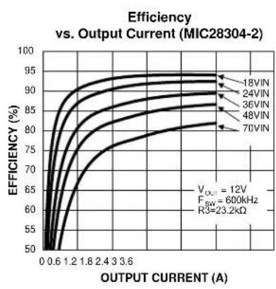
line
| OUTPUT CURRENT (A) | 18VIN | 24VIN | 36VIN | 48VIN | 70VIN | | ------------------ | ----- | ----- | ----- | ----- | ----- | | 0.6 | 50 | 50 | 50 | 50 | 50 | | 1.2 | 75 | 70 | 65 | 60 | 55 | | 1.8 | 85 | 80 | 75 | 70 | 65 | | 2.4 | 90 | 85 | 80 | 75 | 70 | | 3.6 | 95 | 90 | 85 | 80 | 75 |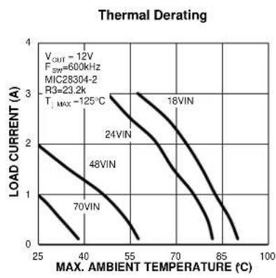
line
| MAX. AMBIENT TEMPERATURE (°C) | LOAD CURRENT (A) for 70VIN | LOAD CURRENT (A) for 48VIN | LOAD CURRENT (A) for 24VIN | LOAD CURRENT (A) for 18VIN | | ----------------------------- | -------------------------- | -------------------------- | -------------------------- | -------------------------- | | 25 | 1 | 2 | 3 | 3 | | 40 | 0 | 1 | 2 | 2 | | 55 | 0 | 0 | 1 | 1 | | 70 | 0 | 0 | 0 | 0 | | 85 | 0 | 0 | 0 | 0 | | 100 | 0 | 0 | 0 | 0 |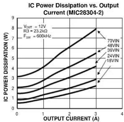
line
| OUTPUT CURRENT (A) | IC POWER DISSIPATION (W) | | ------------------ | ------------------------ | | 0 | 0 | | 1 | 1 | | 2 | 2 | | 3 | 3 | | 4 | 4 |Die Temperature*: The temperature measurement was taken at the hottest point on the MIC28304 case mounted on a 5 square inch 4 layer, 0.62", FR-4 PCB with 2oz. finish copper weight per layer. Actual results will depend upon the size of the PCB, ambient temperature and proximity to other heat emitting components.
MIC28304 12V/3A Output Evaluation Board Schematic

text_image
MIC28304 VDD J10 C4 DNP R20 0Ω C7 DNP R16 100kΩ EN TP3 TP4 TP5 TP6 GND R23 1.21Ω C9 0.47μF PG TP1 TP2 GND R18 49.9kΩ U1 GND NC PVD PNDD VIN EN PGDC FB BSTR BSTR GND BSTC BSTC SW ANODE ANODE SW SW SW SW SW SW SW SW SW SW SW SW SW SW SW SW SW SW SW SW SW SW SW SW SW SW SW SW SW SW SW SW SW SW SW SW SW SW SW SW SW SW SW SW SW SW SW SW SW SW S80000000000000000000000000000000000000000000000000000000000000000000000000000000000000000000000000000 2.7kΩ GND GND GND ILM VIN SW FREQ FREQ PGND PGND PGND PGND PGND PVIN PVIN PVIN PVIN PVIN PVIN PVIN PVIN PVIN PVIN C15 DNP 1.21Ω 1nF 1.21Ω 1nF 1.21Ω 1nF 1.21Ω 1nF 1.21Ω 1nF 1.21Ω 1nF 1.21Ω 1nF 1.21Ω 1nF 1.21Ω 1nF 1.21Ω 1nF 1.21Ω 1nC17 2.2nF 2.2nF 2.2nF 2.2nF 2.2nF 2.2nF 2.2nF 2.2nF 2.2nF 2.2nF 2.2nF 2.2nF 2.2nF 2.2nF 2.2nF 2.2nF 2.2nF 2.17 2.17 2.17 2.17 2.17 2.17 2.17 2.17 2.17 2.17 2.17 2.17 2.17 2.17 2.17 2.17 2.17 2.17 2.17 2.17 2.16 2.16 2.16 2.16 2.16 2.16 2.16 2.16 2.16 2.16 2.16 2.16 2.16 2.16 2.16 2.16 2.16 2.16 2.16 2.16 2.15 2.15 2.15 2.15 2.15 2.15 2.15 2.15 2.15 2.15 2.15 2.15 2.15 2.15 2.15 2.15 2.15 2.15 2.15 2.15 2.14 2.14 2.14 2.14 2.14 2.14 2.14 2.14 2.14 2.14 2.14 2.14 2.14 2.14 2.14 2.14 2.14 2.14 2.14 2.14 2.13 C3 C2 TP9 TP8 TP7 TP6 TP5 TP4 TP3 TP2 TP1 TP9 TP8 TP7 TP6 TP5 TP4 TP3 TP2 TP1 TP9 TP8 TP7 TP6 TP5 TP4 TP3 TP2 TP1 TP9 TP8 TP7 TP6 TP5 TP4 TP3 TP2 TP1 TP9 TP8 TP7 TP6 TP5 TP4 TP3 TP2 TP1 TP9 TP8 TP7 TP6 TP5 TP4 TP3 TP2 TP1 TP9 TP8 TP7 TP6 TP4 TP3 TP2 TP1 TP9 TP8 TP7 TP6 TP5 TP4 TP3 TP2 TP1 TP9 TP8 TP7 TP6 TP5 TP4 TP3 TP2 TP1 TP9 TP8 TP7 TP6 TP5 TP4 TP3 TP2 TP1 TP9 TP8 TP7 TP6 TP5 TP4 TP3 TP2 TP1 TP9 TP8 TP7 TP6 TP5 TP4 TP3 TP2 TP1 TP8 TP8 TP7 TP6 TP5 TP4 TP3 TP2 TP1 TP9 TP8 TP7 TP6 TP5 TP4 TP3 TP2 TP1 TP9 TP8 TP7 TP6 TP5 TP4 TP3 TP2 TP1 TP9 TP8 TP7 TP6 TP5 TP4 TP3 TP2 TP1 TP9 TP8 TP7 TP6 TP5 TP4 TP3 TP2 TP1 TP9 TP8 TP7 TP6 TP5 TP5 TP4 TP3 TP2 TP1 TP9 TP8 TP7 TP6 TP5 TP4 TP3 TP2 TP1 TP9 TP8 TP7 TP6 TP5 TP4 TP3 TP2 TP1 TP9 TP8 TP7 FP BFB GND GND GND GND GND GND GND GND GND GND GND GND GND GND GND GND GND GND GND GND GND GND GND GND GND GND GND GND GND GND GND GND GND GND GND GND GND GND GND GND GND GND GND GND GND GND GND GND GND GND GNO BCTC JU BSTR JU BSTR JU BSTR JU BSTR JU BSTR JU BSTR JU BSTR JU BSTR JU BSTR JU BSTR JU BSTR JU BSTR JU BSTR JU BSTR JU BSTR JU BSTR JU BSTR JU BSTR JU BSTR JU BSTR JU BSTR JU BSTR JU BSTR JU BSTR JU BSTR JU BStr JU BSTR JU BSTR JU BSTR JU BSTR JU BSTR JU BSTR JU BSTR JU BSTR JU BSTR JU BSTR JU BSTR JU BSTR JU BSTR JU BSTR JU BSTR JU BSTR JU BSTR JU BSTR JU BSTR JU BSTR JU BSTR JU BSTR JU BSTR JU BSTR JU BStC JU BSTC JU BSTC JU BSTC JU BSTC JU BSTC JU BSTC JU BSTC JU BSTC JU BSTC JU BSTC JU BSTC JU BSTC JU BSTC JU BSTC JU BSTC JU BSTC JU BSTC JU BSTC JU BSTC JU BSTC JU BStC JU BSTC JU BSTC JU BSTC JU BSTC JU BSTC JU BSTC JU BSTC JU BSTC JU BSTC JU BSTC JU BSTC JU BSTC JU BSTC JU BSTC JU BSTC JU BSTC JU BSTC JU BSTC JU BSTT A U U U U U U U U U U U U U U U U U U U U U U U U U U U U U U U U U U U U U U U U U U U U U U U U U U U U U U U U U U U U U U U U U U U U U U U U U U U U U U U U U U U U U U U U U U U U U U U U U U U VOUT A VOUT A VOUT A VOUT A VOUT A VOUT A VOUT A VOUT A VOUT A VOUT A VOUT A VOUT A VOUT A VOUT A VOUT A VOUT A VOUT A VOUT A VOUT A VOUT A VOUT A VOUT A VOUT A VOUT A VOUT A VOUT A VOUT A VOUT A VOUT A VOUT A VOUT A VOUT A VOUT A VOUT A FUTA FUTA FUTA FUTA FUTA FUTA FUTA FUTA FUTA FUTA FUTA FUTA FUTA FUTA FUTA FUTA FUTA FUTA FUTA FUTA FUTA FUTA FUTA FUTA FUTA FUTA FUTA FUTA FUTA FUTA FUTA FUTA FUTA FUTA NFEATNFEATNFEATNFEATNFEATNFEATNFEATNFEATNFEATNFEATNFEATNFEATNFEATNFEATNFEATNFEATNFEATNFEATNFEATNFEATNFEATNFEATNFEATNFEATNFEATNFEATNFEATNFEATNFEATNFEATNFEATNFEATNFEATNFEATNFLTNFLTNFLTNFLTNFLTNFLTNFLTNFLTNFLTNFLTNFLTNFLTNFLTNFLTNFLTNFLTNFLTNFLTNFLTNFLTNFLTNFLTNFLTNFLTNFLTNFLTNFLTNFLTNFLTNFLTNFLTNFLTNFLTNFLTNFLTNFLTNFLTNFLTNFLTNFLTNFLTNFLTNFLTNFLTNFLTNFLTNFLTNFLTNFLTNFLTNFL TN FL T P T T P T T P T T P T T P T T P T T P T T P T T P T T P T T P T T P T T P T T P T T P T T P T T P T T P T T P T T P T T P T T P T T P T T P T T P T T P T T P T T P T T P T T P T T P T T P T T P T T P TFigure 6. Schematic of MIC28304 Evaluation Board (J1, J8, J10, J11, J12, J13, R14, R20 and R21 are for testing purposes)
MIC28304 12V/3A Output Evaluation Board Schematic (Continued)

text_image
MIC28304 R15A 2.7kΩ C5A 10pF R19A DNP C17A 0.1μF PVINA C3A 2.2μF C2A 2.2μF VIN-A C1A 100μF GND TP9A TP12A VOUT-A TP14A C16A 0.1μF GND VOUT-A TP7A C12A 2.2nF R1A 10kΩ C14A 47μF C15A OPEN VOUT-A TP14A FB R11A 1.91kΩ 5.0V C8A 1μF SW 48 SW 47 SW 46 SW 45 SW 44 SW 43 SW 42 SW 41 SW 40 NC 39 VOUT 38 VOUT 37 VOUT 36 VOUT 35 VOUT 34 VOUT 33 VOUT 32 VOUT 31 VOUT 30 VOUT 29 VOUT 28 VOUT 27 VOUT 26 VOUT 25 VOUT 24 VOUT 23 VOUT 22 VOUT 21 VOUT 20 VOUT 19 PVGDD 50 PGDD 49 FB 03 07 16 18 19 23 27 33 37 43 47 50 53 57 63 67 73 77 83 87 93 97 100 103 107 113 117 123 127 133 137 143 147 153 157 163 167 173 177 183 187 193 197 203 207 213 217 223 227 233 237 243 247 253 257 263 267 273 279 283 287 293 297 303 307 313 317 323 327 333 337 343 347 353 357 363 367 373 377 383 387 393 397 403 407 413 417 423 427 433 437 443 447 453 457 463 467 473 477 483 487 493 497 503 507Figure 7. Schematic of MIC28304 Evaluation Board (Optimized for smallest footprint)
Bill of Materials 12V/3A Output
| Item | Part Number | Manufacturer | Description | Qty |
| C1, C1A^(9) EEU | FC2A101 Panasonic | ^(10) | 100μF Aluminum Capacitor, 100V | 2 |
| C2, C3, C2A^(9), C3A^(9) | GRM32ER72A225K | Murata^(11) | 2.2μF/100V Ceramic Capacitor, X7R, Size 1210 | 4 |
| C3225X7R2A225K | TDK^(12) | |||
| 12101C225KAT2A | AVX^(13) | |||
| C6, C6A^(9) | GCM1885C2A100JA16D Murata | 10pF, 100V, 0603, NPO 2 | ||
| 06031A100JAT2A AVX | ||||
| C8, C8A^(9) | GRM188R70J105KA01D | Murata | 1μF/6.3V Ceramic Capacitor, X7R, Size 0603 | 2 |
| 06036C105KAT2A | AVX | |||
| C1608X5R0J105K | TDK | |||
| C9, C9A^(9) | GRM21BR72A474KA73 | Murata | 0.47μF/100V Ceramic Capacitor, X7R, Size 0805 | 2 |
| 08051C474KAT2A | AVX | |||
| C10, C17, C10A^(9), C17A^(9) | GRM188R72A104KA35D | Murata | 0.1μF/100V Ceramic Capacitor, X7R, Size 0603 | 4 |
| C1608X7S2A104K | TDK | 0.1μF/100V,X7S,0603 | ||
| C11, C11A^(9) | GRM188R72A102KA01D | Murata | 1nF/100V Ceramic Capacitor, X7R, Size 0603 | 2 |
| 06031C102KAT2A | AVX | |||
| C1608X7R2A102K | TDK | |||
| C12, C12A^(9) | GRM188R72A222KA01D | Murata | 2.2nF/100V Ceramic Capacitor, X7R, Size 0603 | 2 |
| 06031C222KAT2A | AVX | |||
| C1608X7R2A222K | TDK | |||
| C14, C14A^(9) | GRM32ER61C476ME15 | Murata | 47μF Ceramic Capacitor, X5R, Size 1210, 16V | 2 |
| EMK325BJ476MM-T Taiyo Yuden ^(14) | ||||
| C16, C16A^(9) | GRM188R71H104KA93D | Murata | 0.1μF/6.3V Ceramic Capacitor, X7R, Size 0603 | 2 |
| 06035C104KAT2A | AVX | |||
| C1608X7R1H104K TDK | ||||
| C4, C5, C7, C13, C15, C4A^(9), C7A^(9), C15A^(9) | DNP | |||
Notes:
- Either reference designator, that is, a reference designator ending with "A" or ending without "A," can be used as part of customer design.
- Panasonic: www.panasonic.com.
- Murata: www.murata.com.
- TDK: www.tdk.com.
- AVX: www.avx.com.
- Taiyo Yuden: www.taiyo-yuden.com.
Bill of Materials 12V/3A Output (Continued)
| Item | Part Number | Manufacturer | Description | Qty |
| R1, R1A(9) CRCW060310K0FKEA Vishay Dale | (15) | 10kΩ Resistor, Size 0603, 1% | 2 | |
| R2, R2A(9) | CRCW08051R21FKEA | Vishay Dale | 1.21Ω Resistor, Size 0805, 5% | 2 |
| R3, R3A(9) | CRCW060323K2FKEA | Vishay Dale | 23.2kΩ Resistor, Size 0603, 1% | 2 |
| R12, R11A(9) | CRCW0603715R0FKEA | Vishay Dale | 715Ω Resistor, Size 0603, 1% | 2 |
| R14, R20, R20A(9) | CRCW06030000FKEA | Vishay Dale | 0Ω Resistor, Size 0603, 5% | 3 |
| R15, R15A(9) | CRCW04022K70JNED | Vishay Dale | 2.7kΩ Resistor, Size 0603, 1% | 2 |
| R16, R16A(9) | CRCW0603100KFKEAHP | Vishay Dale | 100kΩ Resistor, Size 0603, 1% | 2 |
| R18, R18A(9) | CRCW060349K9FKEA | Vishay Dale | 49.9kΩ Resistor, Size 0603, 1% | 2 |
| R21 | CRCW060349R9FKEA | Vishay Dale | 49.9Ω Resistor, Size 0603, 1% | 1 |
| R23, R23A(9) | CRCW06031R21FKEA | Vishay Dale | 1.21Ω Resistor, Size 0603, 1% | 2 |
| R4, R10, R11, R19, R19A(9) | DNP | |||
| U1, U1A(9) | MIC28304-1YMP MIC28304-2YMP | Micrel. Inc.(16) | 70V, 3A Power Module | 2 |
Notes:
15. Vishay: www.vishay.com.
16. Micrel, Inc.: www.micrel.com.
PCB Layout Recommendations

text_image
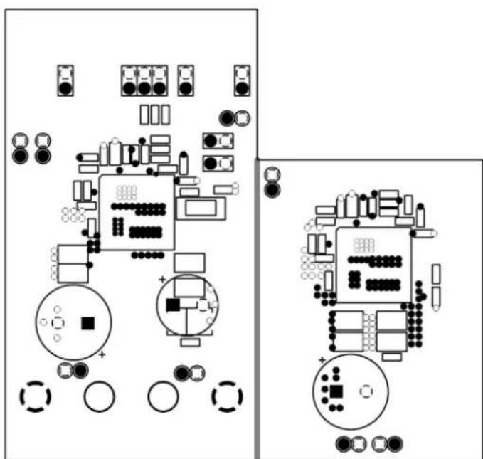
MIC2 VDD 12.0V 5.0V 3.3V IC2 FB BSTR PG EN EN U1 R20 C2 C3 C1 C14 C13 C15 C5 C16 GND VIN VOUT GND C2A C3A C3A C3A C3A C3A C3A C3A C3A C3A C3A C3A C3A C3A C3A C3A C3A C3A C3A C3A C3A C3A C3A C3A C3A C3A C4 R20A C7A R20A C7A R20A C7A R20A C7A R20A C7A R20A C7A R20A C7A R20A C7A R20A C7A R20A C7A R20A C7A R20A C7AMIC28304 Evaluation Board Top Layer
text_image
Diagram showing two layout arrangements of electronic components with labeled symbols and connections, possibly representing a circuit or device layout.MIC28304 Evaluation Board Mid-Layer 1 (Ground Plane)
PCB Layout Recommendations (Continued)

natural_image
Top-down schematic of a circuit board layout with components and connections (no text or labels)MIC28304 Evaluation Board Mid-Layer 2
text_image
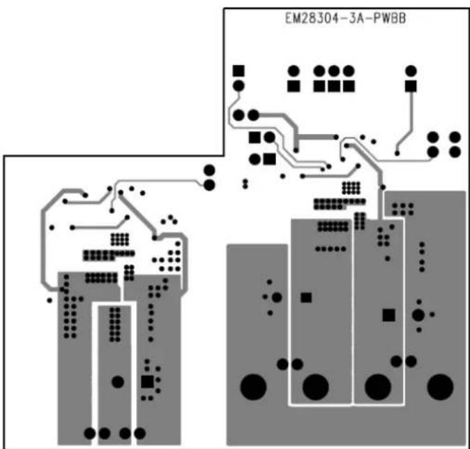
EM28304-3A-PWBBMIC28304 Evaluation Board Bottom Layer
MICREL, INC. 2180 FORTUNE DRIVE SAN JOSE, CA 95131 USA
TEL +1 (408) 944-0800 FAX +1 (408) 474-1000 WEB http://www.micrel.com
Micrel makes no representations or warranties with respect to the accuracy or completeness of the information furnished in this data sheet. This information is not intended as a warranty and Micrel does not assume responsibility for its use. Micrel reserves the right to change circuitry, specifications and descriptions at any time without notice. No license, whether express, implied, arising by estoppel or otherwise, to any intellectual property rights is granted by this document. Except as provided in Micrel's terms and conditions of sale for such products, Micrel assumes no liability whatsoever, and Micrel disclaims any express or implied warranty relating to the sale and/or use of Micrel products including liability or warranties relating to fitness for a particular purpose, merchantability, or infringement of any patent, copyright or other intellectual property right.
Micrel Products are not designed or authorized for use as components in life support appliances, devices or systems where malfunction of a product can reasonably be expected to result in personal injury. Life support devices or systems are devices or systems that (a) are intended for surgical implant into the body or (b) support or sustain life, and whose failure to perform can be reasonably expected to result in a significant injury to the user. A Purchaser's use or sale of Micrel Products for use in life support appliances, devices or systems is a Purchaser's own risk and Purchaser agrees to fully indemnify Micrel for any damages resulting from such use or sale.
© 2014 Micrel, Incorporated.
Revision History
| Date | Change Description/Edits by: | Rev. |
| 2/15/14 | New Eval Board literature | 1.0 |