mcp4142 - Electronic component Microchip - Free user manual and instructions
Find the device manual for free mcp4142 Microchip in PDF.

User questions about mcp4142 Microchip
0 question about this device. Answer the ones you know or ask your own.
Ask a new question about this device
Download the instructions for your Electronic component in PDF format for free! Find your manual mcp4142 - Microchip and take your electronic device back in hand. On this page are published all the documents necessary for the use of your device. mcp4142 by Microchip.
USER MANUAL mcp4142 Microchip
7/8-Bit Single/Dual SPI Digital POT with Non-Volatile Memory
Features
- Single or Dual Resistor Network options
- Potentiometer or Rheostat configuration options
- Resistor Network Resolution
- 7-bit: 128 Resistors (129 Steps)
- 8-bit: 256 Resistors (257 Steps)
- R_AB Resistances options of:
- 5 k Ω
- 1 0 k Ω
- 5 0 k Ω
- 100 kΩ
• Zero-Scale to Full-Scale Wiper operation
- Low Wiper Resistance: 75 (typical)
- Low Tempco:
- Absolute (Rheostat): 50 ppm typical (0°C to 70°C)
- Ratiometric (Potentiometer): 15 ppm typical
• Non-volatile Memory
- Automatic Recall of Saved Wiper Setting - WiperLock™ Technology
- SPI serial interface (10 MHz, modes 0,0 & 1,1)
- High-Speed Read/Writes to wiper registers
- Read/Write to Data EEPROM registers
- Serially enabled EEPROM write protect
- SDI/SDO multiplexing (MCP41X1 only)
- Resistor Network Terminal Disconnect Feature via:
- Shutdown pin (SHDN)
- Terminal Control (TCON) Register
- Write Protect Feature:
- Hardware Write Protect (WP) Control pin
-
Software Write Protect (WP) Configuration bit
-
Brown-out reset protection (1.5V typical)
- Serial Interface Inactive current (2.5 uA typical)
• High-Voltage Tolerant Digital Inputs: Up to 12.5V
• Supports Split Rail Applications - Internal weak pull-up on all digital inputs
- Wide Operating Voltage:
- 2.7V to 5.5V - Device Characteristics Specified
- 1.8V to 5.5V - Device Operation
- Wide Bandwidth (-3dB) Operation:
- 2 MHz (typical) for 5.0 kΩ device
- Extended temperature range (-40°C to +125°C)
Description
The MCP41XX and MCP42XX devices offer a wide range of product offerings using an SPI interface. WiperLock Technology allows application-specific calibration settings to be secured in the EEPROM.
Package Types (top view)
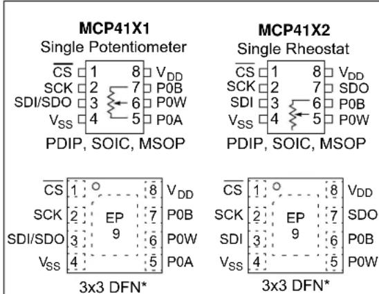
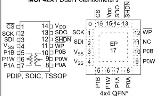
MCP42X1 Dual Potentiometers
text_image
MGP-TEX7 Dual Potentiometer CS 14 VDD SCK 2 13 SDO SCK SDI 3 12 SHDN Vss 4 11 WP P1B 5 10 P0B P1W 6 9 P0W P1A 7 8 P0A PDIP, SOIC, TSSOP EP 17 WP NC P0B P0W 4x4 QFN* 5 6 7 8 CS VDD SDO SHDN 16 15 14 13 1 2 3 4 4 5 6 7 8MCP42X2 Dual Rheostat
text_image
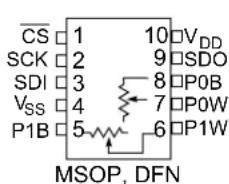
CS 1 10 VDD SCK 2 9 SDO SDI 3 8 P0B Vss 4 7 P0W P1B 5 6 P1W MSOP, DFN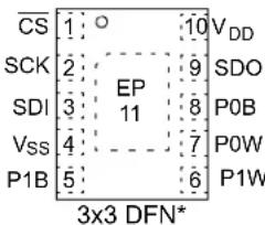
text_image
CS 1 ○ 10 VDD SCK 2 EP 9 SDO SDI 3 11 8 P0B Vss 4 7 P0W P1B 5 6 P1W 3x3 DFN** Includes Exposed Thermal Pad (EP); see Table 3-1.
Device Block Diagram
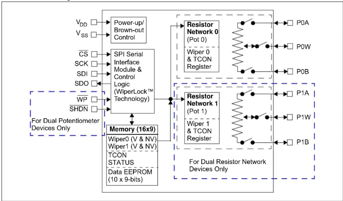
flowchart
graph TD
    A["V_DD"] --> B["Power-up/ Brown-out Control"]
    C["V_SS"] --> B
    D["CS"] --> E["SPI Serial Interface Module & Control Logic (WiperLock™ Technology)"]
    F["SCK"] --> E
    G["SDI"] --> E
    H["SDO"] --> E
    I["WP"] --> E
    J["SHDN"] --> E
    K["For Dual Potentiometer Devices Only"] --> L["Memory (16x9)"]
    L --> M["Wiper0 (V & NV) Wiper1 (V & NV) TCON STATUS Data EEPROM (10 x 9-bits)"]
    M --> N["Resistor Network 0 (Pot 0) Wiper 0 & TCON Register"]
    O["For Dual Resistor Network Devices Only"] --> P["Resistor Network 1 (Pot 1) Wiper 1 & TCON Register"]
    P --> Q["P0A"]
    P --> R["P0W"]
    P --> S["P0B"]
    P --> T["P1A"]
    P --> U["P1W"]
    P --> V["P1B"]
Device Features
| Device | # of POTs | Wiper Configuration | Control Interface | Memory Type | WiperLock Technology | POR Wiper Setting | Resistance (typical) | # of Steps | V_DD Operating Range(2) | |
| R_AB Options (kΩ) | Wiper - R_W (Ω) | |||||||||
| MCP4131(3) | 1 | Potentiometer(1) | SPI | RAM | No | Mid-Scale | 5.0, 10.0, 50.0, 100.0 | 75 | 129 | 1.8V to 5.5V |
| MCP4132(3) | 1 | Rheostat | SPI | RAM | No | Mid-Scale | 5.0, 10.0, 50.0, 100.0 | 75 | 129 | 1.8V to 5.5V |
| MCP4141 | 1 | Potentiometer(1) | SPI | EE | Yes | NV Wiper 5.0, | 10.0, 50.0, 100.0 | 75 | 2.7V to 5.5V | |
| MCP4142 | 1 | Rheostat | SPI | EE | Yes | NV Wiper | 5.0, 10.0, 50.0, 100.0 | 75 | 129 | 2.7V to 5.5V |
| MCP4151(3) | 1 | Potentiometer(1) | SPI | RAM | No | Mid-Scale | 5.0, 10.0, 50.0, 100.0 | 75 | 257 | 1.8V to 5.5V |
| MCP4152(3) | 1 | Rheostat | SPI | RAM | No | Mid-Scale | 5.0, 10.0, 50.0, 100.0 | 75 | 257 | 1.8V to 5.5V |
| MCP4161 | 1 | Potentiometer(1) | SPI | EE | Yes | NV Wiper | 5.0, 10.0, 50.0, 100.0 | 75 | 257 | 2.7V to 5.5V |
| MCP4162 | 1 | Rheostat | SPI | EE | Yes | NV Wiper | 5.0, 10.0, 50.0, 100.0 | 75 | 257 | 2.7V to 5.5V |
| MCP4231(3) | 2 | Potentiometer(1) | SPI | RAM | No | Mid-Scale | 5.0, 10.0, 50.0, 100.0 | 75 | 129 | 1.8V to 5.5V |
| MCP4232(3) | 2 | Rheostat | SPI | RAM | No | Mid-Scale | 5.0, 10.0, 50.0, 100.0 | 75 | 129 | 1.8V to 5.5V |
| MCP4241 | 2 | Potentiometer(1) | SPI | EE | Yes | NV Wiper | 5.0, 10.0, 50.0, 100.0 | 75 | 129 | 2.7V to 5.5V |
| MCP4242 | 2 | Rheostat | SPI | EE | Yes | NV Wiper | 5.0, 10.0, 50.0, 100.0 | 75 | 129 | 2.7V to 5.5V |
| MCP4251(3) | 2 | Potentiometer(1) | SPI | RAM | No | Mid-Scale | 5.0, 10.0, 50.0, 100.0 | 75 | 257 | 1.8V to 5.5V |
| MCP4252(3) | 2 | Rheostat | SPI | RAM | No | Mid-Scale | 5.0, 10.0, 50.0, 100.0 | 75 | 257 | 1.8V to 5.5V |
| MCP4261 | 2 | Potentiometer(1) | SPI | EE | Yes | NV Wiper | 5.0, 10.0, 50.0, 100.0 | 75 | 257 | 2.7V to 5.5V |
| MCP4262 | 2 | Rheostat | SPI | EE | Yes | NV Wiper | 5.0, 10.0, 50.0, 100.0 | 75 | 257 | 2.7V to 5.5V |
Note 1: Floating either terminal (A or B) allows the device to be used as a Rheostat (variable resistor).
2: Analog characteristics only tested from 2.7V to 5.5V unless otherwise noted.
3: Please check Microchip web site for device release and availability
1.0 ELECTRICAL CHARACTERISTICS
Absolute Maximum Ratings †
Voltage on V_DD with respect to V_SS -0.6V to +7.0V
Voltage on CS, SCK, SDI, SDI/SDO, WP, and
SHDN with respect to V_SS -0.6V to 12.5V
Voltage on all other pins (PxA, PxW, PxB, and
SDO) with respect to V_SS -0.3V to V_DD + 0.3V
Input clamp current, I_IK
(V_I < 0, V_I > V_DD, V_I > V_PP ON HV pins)....±20 mA
Output clamp current, I_OK
(V_O<0 or V_O>V_DD) ±20 mA
Maximum output current sunk by any Output pin
.25 mA
Maximum output current sourced by any Output pin
.25 mA
Maximum current out of V_SS pin 100 mA
Maximum current into V_DD pin 100 mA
Maximum current into PxA, PxW & PxB pins ....±2.5 mA
Storage temperature ....-65°C to +150°C
Ambient temperature with power applied
-40°C to +125°C
Total power dissipation (Note 1)....400 mW
Soldering temperature of leads (10 seconds) ....+300°C
ESD protection on all pins ≥ 4 kV (HBM),
≥ 300V (MM)
Maximum Junction Temperature (T _J ) ....+150°C
Note 1: Power dissipation is calculated as follows:
$$ P _ {\text { dis }} = V _ {D D} \times \left{I _ {D D} - \sum I _ {O H} \right} + \sum \left{\left(V _ {D D} - V _ {O H}\right) \times I _ {O H} \right} + \sum \left(V _ {O I} \times I _ {O L}\right) $$
† Notice: Stresses above those listed under "Maximum Ratings" may cause permanent damage to the device. This is a stress rating only and functional operation of the device at those or any other conditions above those indicated in the operational listings of this specification is not implied. Exposure to maximum rating conditions for extended periods may affect device reliability.
AC/DC CHARACTERISTICS
| DC Characteristics | Standard Operating Conditions (unless otherwise specified)Operating Temperature -40°C ≤ TA ≤ +125°C (extended)All parameters apply across the specified operating ranges unless noted. V_DD = +2.7V to 5.5V, 5 kΩ, 10 kΩ, 50 kΩ, 100 kΩ devices.Typical specifications represent values for V_DD = 5.5V , T_A = +25°C . | ||||||
| Parameters Sym | Min Typ Max | Units Conditions | |||||
| Supply Voltage V | _DD | 2.7 — | 5.5 V | ||||
| 1.8 — | 2.7 V Serial Interface only. | ||||||
| , SDI, SDO,SCK, WP, SHDNpin Voltage Range | V_HV | V_SS | — | 12.5V | V | _DDV ≥ 4.5V | The pin will be at one of three input levels( V_IL , V_IH or V_IHH ). (Note 6) |
| V_SS | — | V_DD + 8.0V | V | V_DD < 4.5V | |||
| VDD Start Voltage to ensure Wiper Reset | V_BOR | — | — 1.65 V | RAM retention voltage (V RAM) < V_BOR | |||
| VDD Rise Rate to ensure Power-on Reset | V_DDRR | (Note 9) | V/ms | ||||
| Delay after device exits the reset state( V_DD > V_BOR ) | T_BORD | — | 10 | 20 | μs | ||
| Supply Current (Note 10) | _DD | — | — | 450 | μA | Serial Interface Active, V_DD = 5.5V , = V_IL , SCK @ 5 MHz,write all 0's to volatile Wiper 0 (address 0h) | |
| — | — | 1 mA | EE Write Current, V_DD = 5.5V , = V_IL , SCK @ 5 MHz,write all 0's to non-volatile Wiper 0 (address 2h) | ||||
| — 2.5 | 5 μA Serial Interface Inactive, = V_IH , V_DD = 5.5V | ||||||
| — | 0.55 | 1 mA | Serial Interface Active, V_DD = 5.5V , = V_IHH ,SCK @ 5 MHz,decrement non-volatile Wiper 0 (address 2h) | ||||
Note 1: Resistance is defined as the resistance between terminal A to terminal B.
2: INL and DNL are measured at V_W with V_A = V_DD and V_B = V_SS .
3: MCP4XX1 only.
4: MCP4XX2 only, includes V_WZSE and V_WFSE .
5: Resistor terminals A, W and B's polarity with respect to each other is not restricted.
6: This specification by design.
7: Non-linearity is affected by wiper resistance ( R_W ), which changes significantly over voltage and temperature.
8: The MCP4XX1 is externally connected to match the configurations of the MCP41X2 and MCP42X2, and then tested.
9: POR/BOR is not rate dependent.
10: Supply current is independent of current through the resistor network
AC/DC CHARACTERISTICS (CONTINUED)
| DC Characteristics | Standard Operating Conditions (unless otherwise specified)Operating Temperature -40^ ≤ T_A ≤ +125^ (extended)All parameters apply across the specified operating ranges unless noted. V_DD = +2.7V to 5.5V, 5 kΩ, 10 kΩ, 50 kΩ, 100 kΩ devices.Typical specifications represent values for V_DD = 5.5V , T_A = +25^ . | ||||||
| Parameters | Sym | Min | Typ | Max | Units | Conditions | |
| Resistance(±20%) | R_AB | 4.0 | 5 | 6.0 | kΩ | -502 devices (Note 1) | |
| 8.0 | 10 | 12.0 | kΩ | -103 devices (Note 1) | |||
| 40.0 | 50 | 60.0 | kΩ | -503 devices (Note 1) | |||
| 80.0 | 100 | 120.0 | kΩ | -104 devices (Note 1) | |||
| Resolution N 257 Taps 8-bit No | Missing Codes | ||||||
| 129 Taps 7-bit | No Missing Codes | ||||||
| Step Resistance | R_S | — | R_AB / (256) | — | Ω | 8-bit | Note 6 |
| — | R_AB / (128) | — | Ω | 7-bit | Note 6 | ||
| Nominal Resistance Match | |R_AB0 - R_AB1| / R_AB | — | 0.2 | 1.25 | % | MCP42X1 devices only | |
| |R_BW0 - R_BW1| / R_BW | — | 0.25 | 1.5 | % | MCP42X2 devices only,Code = Full-Scale | ||
| Wiper Resistance(Note 3, Note 4) | R_W | — | 75 | 160 | Ω | V_DD = 5.5 V , I_W = 2.0 mA , code = 00h | |
| — | 75 | 300 | Ω | V_DD = 2.7 V , I_W = 2.0 mA , code = 00h | |||
| Nominal ResistanceTempco | R_AB/ T | — | 50 | — | ppm/°C | T_A = -20^ to +70^ | |
| — | 100 — | ppm/°C T | A = -40^ to +85^ | ||||
| — | 150 — | ppm/°C T | A = -40^ to +125^ | ||||
| Ratiometeric Tempco | V_WB/ T | — | 15 | — | ppm/°C | Code = Midscale (80h or 40h) | |
| Resistor Terminal Input Voltage Range (Terminals A, B and W) | V_A, V_W, V_B | Vss | — | V_DD | V | Note 5, Note 6 | |
| Maximum current through A, W or B | I_W | — | — | 2.5 | mA | Note 6, Worst case current through wiper when wiper is either Full-Scale or Zero Scale. | |
| Leakage current into A, W or B | I_WL | — | 100 | — | nA | MCP4XX1 PxA = PxW = PxB = V_SS | |
| — | 100 | — | nA | MCP4XX2 PxB = PxW = V_SS | |||
Note 1: Resistance is defined as the resistance between terminal A to terminal B.
2: INL and DNL are measured at V_W with V_A = V_DD and V_B = V_SS .
3: MCP4XX1 only.
4: MCP4XX2 only, includes V_WZSE and V_WFSE .
5: Resistor terminals A, W and B's polarity with respect to each other is not restricted.
6: This specification by design.
7: Non-linearity is affected by wiper resistance ( R_W ), which changes significantly over voltage and temperature.
8: The MCP4XX1 is externally connected to match the configurations of the MCP41X2 and MCP42X2, and then tested.
9: POR/BOR is not rate dependent.
10: Supply current is independent of current through the resistor network
AC/DC CHARACTERISTICS (CONTINUED)
| DC Characteristics | Standard Operating Conditions (unless otherwise specified)Operating Temperature -40^ ≤ T_A ≤ +125^ (extended)All parameters apply across the specified operating ranges unless noted. V_DD = +2.7V to 5.5V, 5 kΩ, 10 kΩ, 50 kΩ, 100 kΩ devices.Typical specifications represent values for V_DD = 5.5V , T_A = +25^ . | |||||||
| Parameters | Sym | Min | Typ | Max | Units | Conditions | ||
| Full-Scale Error(MCP4XX1 only)(8-bit code = 100h,7-bit code = 80h) | V_WFSE | -6.0 | -0.1 | — | LSb | 5 kΩ≤ V | 8-bit | 3.0V ≤ V_DD ≤ 5.5V |
| -4.0 | -0.1 — | LSb 7-bit | 3.0V | _DD ≤ 5.5V | ||||
| -3.5 | -0.1 | — | LSb | 10 kΩ | 8-bit | 3.0V ≤ V_DD ≤ 5.5V | ||
| -2.0 | -0.1 | — | LSb | 7-bit | 3.0V ≤ V_DD ≤ 5.5V | |||
| -0.8 | -0.1 | — | LSb | 50 kΩ≤ V | 8-bit | 3.0V ≤ V_DD ≤ 5.5V | ||
| -0.5 | -0.1 — | LSb 7-bit | 3.0V | _DD ≤ 5.5V | ||||
| -0.5 | -0.1 | — | LSb | 100 kΩ | 8-bit | 3.0V ≤ V_DD ≤ 5.5V | ||
| -0.5 | -0.1 | — | LSb | 7-bit | 3.0V ≤ V_DD ≤ 5.5V | |||
| Zero-Scale Error(MCP4XX1 only)(8-bit code = 00h,7-bit code = 00h) | V_WZSE | — | +0.1 | +6.0 | LSb | 5 kΩ | 8-bit | 3.0V ≤ V_DD ≤ 5.5V |
| — | +0.1 | +3.0 | LSb | 7-bit | 3.0V ≤ V_DD ≤ 5.5V | |||
| — | +0.1 | +3.5 | LSb | 10 kΩ | 8-bit | 3.0V ≤ V_DD ≤ 5.5V | ||
| — | +0.1 | +2.0 | LSb | 7-bit | 3.0V ≤ V_DD ≤ 5.5V | |||
| — | +0.1 | +0.8 | LSb | 50 kΩ | 8-bit | 3.0V ≤ V_DD ≤ 5.5V | ||
| — | +0.1 | +0.5 | LSb | 7-bit | 3.0V ≤ V_DD ≤ 5.5V | |||
| — | +0.1 | +0.5 | LSb | 100 kΩ | 8-bit | 3.0V ≤ V_DD ≤ 5.5V | ||
| — | +0.1 | +0.5 | LSb | 7-bit | 3.0V ≤ V_DD ≤ 5.5V | |||
| PotentiometerIntegralNon-linearity | INL | -1 | ±0.5 | +1 | LSb | 8-bit | 3.0V ≤ V_DD ≤ 5.5VMCP4XX1 devices only(Note 2) | |
| -0.5 | ±0.25 | +0.5 | LSb 7-bit | |||||
| PotentiometerDifferentialNon-linearity | DNL | -0.5 | ±0.25 | +0.5 | LSb | 8-bit | 3.0V ≤ V_DD ≤ 5.5VMCP4XX1 devices only(Note 2) | |
| -0.25 | ±0.125 | +0.25 | LSb 7-bit | |||||
| Bandwidth -3 dB(See Figure 2-58,load = 30 pF) | BW | — | 2 | — | MHz | 5 kΩ | 8-bit | Code = 80h |
| — | 2 | — | MHz | 7-bit | Code = 40h | |||
| — | 1 | — | MHz | 10 kΩ | 8-bit | Code = 80h | ||
| — | 1 | — | MHz | 7-bit | Code = 40h | |||
| — | 200 | — | kHz | 50 kΩ | 8-bit | Code = 80h | ||
| — | 200 | — | kHz | 7-bit | Code = 40h | |||
| — | 100 | — | kHz | 100 kΩ | 8-bit | Code = 80h | ||
| — | 100 | — | kHz | 7-bit | Code = 40h | |||
Note 1: Resistance is defined as the resistance between terminal A to terminal B.
2: INL and DNL are measured at V_W with V_A = V_DD and V_B = V_SS .
3: MCP4XX1 only.
4: MCP4XX2 only, includes V_WZSE and V_WFSE .
5: Resistor terminals A, W and B's polarity with respect to each other is not restricted.
6: This specification by design.
7: Non-linearity is affected by wiper resistance ( R_W ), which changes significantly over voltage and temperature.
8: The MCP4XX1 is externally connected to match the configurations of the MCP41X2 and MCP42X2, and then tested.
9: POR/BOR is not rate dependent.
10: Supply current is independent of current through the resistor network
AC/DC CHARACTERISTICS (CONTINUED)
| DC Characteristics | Standard Operating Conditions (unless otherwise specified)Operating Temperature -40^ ≤ T_A ≤ +125^ (extended)All parameters apply across the specified operating ranges unless noted. V_DD = +2.7V to 5.5V, 5 kΩ, 10 kΩ, 50 kΩ, 100 kΩ devices.Typical specifications represent values for V_DD = 5.5V , T_A = +25^ . | |||||||
| Parameters | Sym | Min | Typ | Max | Units | Conditions | ||
| Rheostat Integral Non-linearityMCP41X1(Note 4, Note 8)MCP4XX2devices only(Note 4) | R-INL | -1.5 | ±0.5 | +1.5 | LSb | 5 kΩ7-bit 5. | 8-bit | 5.5V, I_W = 900 μA |
| -8.25 +4 | .5 +8.25 | LSb 3.0V, I | _W = 480 μA(Note 7) | |||||
| -1.125 ±0.5 | +1.125 | LSb | 5V, I | _W = 900 μA | ||||
| -6.0 | +4.5 | +6.0 | LSb | 3.0V, I_W = 480 μA(Note 7) | ||||
| -1.5 | ±0.5 | +1.5 | LSb | 10 kΩ7-bit 5. | 8-bit | 5.5V, I_W = 450 μA | ||
| -5.5 | +2.5 | +5.5 | LSb | 3.0V, I_W = 240 μA(Note 7) | ||||
| -1.125 ±0.5 | +1.125 | LSb | 5V, I | _W = 450 μA | ||||
| -4.0 | +2.5 | +4.0 | LSb | 3.0V, I_W = 240 μA(Note 7) | ||||
| -1.5 | ±0.5 | +1.5 | LSb | 50 kΩ7-bit 5. | 8-bit | 5.5V, I_W = 90 μA | ||
| -2.0 | +1 | +2.0 | LSb | 3.0V, I_W = 48 μA(Note 7) | ||||
| -1.125 ±0.5 | +1.125 | LSb | 5V, I | _W = 90 μA | ||||
| -1.5 | +1 | +1.5 | LSb | 3.0V, I_W = 48 μA(Note 7) | ||||
| -1.0 | ±0.5 | +1.0 | LSb | 100 kΩ | 8-bit | 5.5V, I_W = 45 μA | ||
| -1.5 | +0.25 | +1.5 | LSb | 3.0V, I_W = 24 μA(Note 7) | ||||
| -0.8 | ±0.5 | +0.8 | LSb | 7-bit | 5.5V, I_W = 45 μA | |||
| -1.125 | +0.25 | +1.125 | LSb | 3.0V, I_W = 24 μA(Note 7) | ||||
Note 1: Resistance is defined as the resistance between terminal A to terminal B.
2: INL and DNL are measured at V_W with V_A = V_DD and V_B = V_SS .
3: MCP4XX1 only.
4: MCP4XX2 only, includes V_WZSE and V_WFSE .
5: Resistor terminals A, W and B's polarity with respect to each other is not restricted.
6: This specification by design.
7: Non-linearity is affected by wiper resistance ( R_W ), which changes significantly over voltage and temperature.
8: The MCP4XX1 is externally connected to match the configurations of the MCP41X2 and MCP42X2, and then tested.
9: POR/BOR is not rate dependent.
10: Supply current is independent of current through the resistor network
AC/DC CHARACTERISTICS (CONTINUED)
| DC Characteristics | Standard Operating Conditions (unless otherwise specified)Operating Temperature -40^ ≤ T_A ≤ +125^ (extended)All parameters apply across the specified operating ranges unless noted. V_DD = +2.7V to 5.5V, 5 kΩ, 10 kΩ, 50 kΩ, 100 kΩ devices.Typical specifications represent values for V_DD = 5.5V , T_A = +25^ . | |||||||
| Parameters | Sym | Min | Typ | Max | Units | Conditions | ||
| Rheostat Differential Non-linearityMCP41X1(Note 4, Note 8)MCP4XX2 devices only(Note 4) | R-DNL | -0.5 | ±0.25 | +0.5 | LSb | 5 kΩ-bit 5.5V | 8-bit | 5.5V, I_W = 900 μA |
| -1.0 | +0.5 | +1.0 | LSb | 3.0V (Note 7) | ||||
| -0.375 ±0.25 | +0.375 | LSb | 7 | I | _W = 900 μA | |||
| -0.75 | +0.5 | +0.75 | LSb | 3.0V (Note 7) | ||||
| -0.5 | ±0.25 | +0.5 | LSb | 10 kΩ-bit 5.5V | 8-bit | 5.5V, I_W = 450 μA | ||
| -1.0 | +0.25 | +1.0 | LSb | 3.0V (Note 7) | ||||
| -0.375 ±0.25 | +0.375 | LSb | 7 | I | _W = 450 μA | |||
| -0.75 | +0.5 | +0.75 | LSb | 3.0V (Note 7) | ||||
| -0.5 | ±0.25 | +0.5 | LSb | 50 kΩ-bit 5.5V | 8-bit | 5.5V, I_W = 90 μA | ||
| -0.5 | ±0.25 | +0.5 | LSb | 3.0V (Note 7) | ||||
| -0.375 ±0.25 | +0.375 | LSb | 7 | I | _W = 90 μA | |||
| -0.375 | ±0.25 | +0.375 | LSb | 3.0V (Note 7) | ||||
| -0.5 | ±0.25 | +0.5 | LSb | 100 kΩ-bit 5.5V | 8-bit | 5.5V, I_W = 45 μA | ||
| -0.5 | ±0.25 | +0.5 | LSb | 3.0V (Note 7) | ||||
| -0.375 ±0.25 | +0.375 | LSb | 7 | I | _W = 45 μA | |||
| -0.375 | ±0.25 | +0.375 | LSb | 3.0V (Note 7) | ||||
| Capacitance ( P_A ) | C_AW | — | 75 | — | pF | f = 1 MHz, Code = Full-Scale | ||
| Capacitance ( P_W ) | C_W | — | 120 | — | pF | f = 1 MHz, Code = Full-Scale | ||
| Capacitance ( P_B ) | C_BW | — | 75 | — | pF | f = 1 MHz, Code = Full-Scale | ||
Note 1: Resistance is defined as the resistance between terminal A to terminal B.
2: INL and DNL are measured at V_W with V_A = V_DD and V_B = V_SS .
3: MCP4XX1 only.
4: MCP4XX2 only, includes V_WZSE and V_WFSE .
5: Resistor terminals A, W and B's polarity with respect to each other is not restricted.
6: This specification by design.
7: Non-linearity is affected by wiper resistance ( R_W ), which changes significantly over voltage and temperature.
8: The MCP4XX1 is externally connected to match the configurations of the MCP41X2 and MCP42X2, and then tested.
9: POR/BOR is not rate dependent.
10: Supply current is independent of current through the resistor network
AC/DC CHARACTERISTICS (CONTINUED)
| DC Characteristics | Standard Operating Conditions (unless otherwise specified)Operating Temperature -40^ ≤ T_A ≤ +125^ (extended)All parameters apply across the specified operating ranges unless noted. V_DD = +2.7V to 5.5V, 5 kΩ, 10 kΩ, 50 kΩ, 100 kΩ devices.Typical specifications represent values for V_DD = 5.5V , T_A = +25^ . | |||||
| Parameters | Sym | Min | Typ | Max | Units | Conditions |
| Digital Inputs/Outputs (CS, SDI, SDO, SCK, WP, SHDN) | ||||||
| Schmitt Trigger High Input Threshold | V_IH | 0.45 V_DD | — | — | V_DD ≤ 5.5V . 7 V(Allows 2.7V Digital V_DD with 5V Analog V_DD ) | |
| 0.5 V_DD | — | — | V_DD ≤ 2.7V . 8 V | |||
| Schmitt Trigger Low Input Threshold | V_IL | — — 0.2V | _DD | V | ||
| Hysteresis of Schmitt Trigger Inputs | V_HYS | — | 0 _DD | + | V V | |
| High Voltage Input Entry Voltage | V_IHH | 8.5 — | 12.5 | (6) | V Threshold | for WiperLockTM Technology |
| High Voltage Input Exit Voltage | V_IHH | — | — | V_DD + 0.8V^(6) | V | |
| High Voltage Limit | V_MAX | — | — | 1 (6) | V Pin can | tolerate V 5 MAX or less. |
| Output Low Voltage (SDO) | V_OL | V_SS | — | 0.3 V_DD | V | I_OL = 5 mA , V_DD = 5.5V |
| V_SS | — | 0.3 V_DD | V | I_OL = 1 mA , V_DD = 1.8V | ||
| Output High Voltage (SDO) | V_OH | 0.7 V_DD | — | V_DD | V | I_OH = -2.5 mA , V_DD = 5.5V |
| 0.7 V_DD | — | V_DD | V | I_OL = -1 mA , V_DD = 1.8V | ||
| Weak Pull-up / Pull-down Current | I_PU | — — | 1.75 | mA | Internal V _DD pull-up, V_IHH pull-down, V_DD = 5.5V , V_ = 12.5V | |
| — | 170 | — | μA | pin, V_DD = 5.5V , V_ = 3V | ||
| Pull-up / Pull-down Resistance | R_CS | — | 16 | — | kΩ | V_DD = 5.5V , V_ = 3V |
| Input Leakage Current | I_IL | -1 | — | 1 | μA | V_IN = V_DD and V_IN = V_SS |
| Pin Capacitance | C_IN, C_OUT | — | 10 | — | pF | f_C = 20 MHz |
Note 1: Resistance is defined as the resistance between terminal A to terminal B.
2: INL and DNL are measured at V_W with V_A = V_DD and V_B = V_SS .
3: MCP4XX1 only.
4: MCP4XX2 only, includes V_WZSE and V_WFSE .
5: Resistor terminals A, W and B's polarity with respect to each other is not restricted.
6: This specification by design.
7: Non-linearity is affected by wiper resistance ( R_W ), which changes significantly over voltage and temperature.
8: The MCP4XX1 is externally connected to match the configurations of the MCP41X2 and MCP42X2, and then tested.
9: POR/BOR is not rate dependent.
10: Supply current is independent of current through the resistor network
AC/DC CHARACTERISTICS (CONTINUED)
| DC Characteristics | Standard Operating Conditions (unless otherwise specified)Operating Temperature -40^ ≤ T_A ≤ +125^ (extended)All parameters apply across the specified operating ranges unless noted. V_DD = +2.7V to 5.5V, 5 kΩ, 10 kΩ, 50 kΩ, 100 kΩ devices.Typical specifications represent values for V_DD = 5.5V , T_A = +25^ . | ||||||
| Parameters | Sym | Min | Typ | Max | Units | Conditions | |
| RAM (Wiper) Value | |||||||
| Value Range N 0h | — 1FFh hex 8-bit device | ||||||
| 0h — 1FFh hex 7-bit device | |||||||
| EEPROM | |||||||
| Endurance E | ndurance | — 1M — Cycles | |||||
| EEPROM Range N | 0h — 1FFh hex | ||||||
| Initial Factory Setting | N 80h | hex 8-bit WiperLock Technology = Off | |||||
| 40h | hex 7-bit WiperLock Technology = Off | ||||||
| EEPROM Pro-gramming Write Cycle Time | t_WC | — | 5 | 10 | ms | ||
| Power Requirements | |||||||
| Power Supply Sensitivity (MCP41X2 and MCP42X2 only) | PSS | — | 0.0015 | 0.0035 | %/% | 8-bit | V_DD = 2.7V to 5.5V, V_A = 2.7V , Code = 80h |
| — | 0.0015 | 0.0035 | %/% | 7-bit | V_DD = 2.7V to 5.5V, V_A = 2.7V , Code = 40h | ||
Note 1: Resistance is defined as the resistance between terminal A to terminal B.
2: INL and DNL are measured at V_W with V_A = V_DD and V_B = V_SS .
3: MCP4XX1 only.
4: MCP4XX2 only, includes V_WZSE and V_WFSE .
5: Resistor terminals A, W and B's polarity with respect to each other is not restricted.
6: This specification by design.
7: Non-linearity is affected by wiper resistance ( R_W ), which changes significantly over voltage and temperature.
8: The MCP4XX1 is externally connected to match the configurations of the MCP41X2 and MCP42X2, and then tested.
9: POR/BOR is not rate dependent.
10: Supply current is independent of current through the resistor network
1.1 SPI Mode Timing Waveforms and Requirements

flowchart
graph TD
    subgraph CS
        V_IH --> VIH --> VI_H --> VI_H
        VI_H --> V_IL --> VI_L --> VI_L
        VI_L --> 84 --> 70 --> 72 --> 79 --> 78 --> 83 --> 71 --> 80 --> 75 --> 76 --> 77
    end
    subgraph SCK
        70 --> 72 --> 79 --> 78 --> 83 --> 71 --> 80
    end
    subgraph SDO
        MSb --> BIT6 --> LSb --> LSb_IN --> MSb_IN --> BIT6 --> LSb_IN
    end
    subgraph SDI
        73 --> 74 --> 75 --> 76 --> 77 --> 74 --> 73
    end
FIGURE 1-1: SPI Timing Waveform (Mode = 11).
TABLE 1-1: SPI REQUIREMENTS (MODE = 11)
| # Characteristic Symbol Min Max Units Conditions | ||||||
| SCK Input Frequency F | SCK | — | 1 | 0 | _DD = 2.7V to 5.5V | |
| — | 1 | MHz | _DD = 1.8V to 2.7V | |||
| 70 | Active ( V_IL or V_IHH ) to SCK↑ input | TcsA2scH | 60 | — | ns | |
| 71 | SCK input high time | TscH | 45 | — | ns | V_DD = 2.7V to 5.5V |
| 500 | — | ns | V_DD = 1.8V to 2.7V | |||
| 72 | SCK input low time | TscL | 45 | — | ns | V_DD = 2.7V to 5.5V |
| 500 | — | ns | V_DD = 1.8V to 2.7V | |||
| 73 | Setup time of SDI input to SCK↑ edge | T_DIV2scH | 10 | — | ns | |
| 74 | Hold time of SDI input from SCK↑ edge | T_scH2DIL | 20 | — | ns | |
| 77 | Inactive ( V_IH ) to SDO output hi-impedance | T_csH2doZ | — | 50 | ns | Note 1 |
| 80 | SDO data output valid after SCK↓ edge | T_scL2doV | — | 70 | ns | V_DD = 2.7V to 5.5V |
| 170 | ns | V_DD = 1.8V to 2.7V | ||||
| 83 | Inactive ( V_IH ) after SCK↑ edge | T_scH2csl | 100 | — | ns | V_DD = 2.7V to 5.5V |
| 1 | ms | V_DD = 1.8V to 2.7V | ||||
| 84 | Hold time of Inactive ( V_IH ) to Active ( V_IL or V_IHH ) | T_csA2csl | 50 | — | ns | |
Note 1: This specification by design.
V

text_image
CS VIH 82 VIHH VIL VIH 84 SCK 70 71 72 80 83 SDO MSb BIT6 LSb 77 SDI 73 MSb IN BIT6 LSb IN 74FIGURE 1-2: SPI Timing Waveform (Mode = 00).
TABLE 1-2: SPI REQUIREMENTS (MODE = 00)
| # Characteristic Symbol Min Max Units Conditions | ||||||
| SCK Input Frequency F | sck | — | 1 | 0 | _DD = 2.7V to 5.5V | |
| — | 1 | M | _DD H1.8V to2.7V V | |||
| 70 | Active ( V_IL or V_IHH ) to SCK↑ input | TcsA2scH | 60 | — | ns | |
| 71 | SCK input high time | TscH | 45 | — | ns | V_DD = 2.7V to 5.5V |
| 500 | — | ns | V_DD = 1.8V to 2.7V | |||
| 72 | SCK input low time | TscL | 45 | — | ns | V_DD = 2.7V to 5.5V |
| 500 | — | ns | V_DD = 1.8V to 2.7V | |||
| 73 | Setup time of SDI input to SCK↑ edge | T_DIV2scH | 10 | — | ns | |
| 74 | Hold time of SDI input from SCK↑ edge | T_scH2DIL | 20 | — | ns | |
| 77 | Inactive ( V_IH ) to SDO output hi-impedance | TcsH2doZ | — | 50 | ns | Note 1 |
| 80 | SDO data output valid after SCK↓ edge | TscL2doV | — | 70 | ns | V_DD = 2.7V to 5.5V |
| 170 | ns | V_DD = 1.8V to 2.7V | ||||
| 82 | SDO data output valid after Active ( V_IL or V_IHH ) | TssL2doV — 70 ns | ||||
| 83 | Inactive ( V_IH ) after SCK↓ edge | TscH2csl | 100 | — | ns | V_DD = 2.7V to 5.5V |
| 1 | ms | V_DD = 1.8V to 2.7V | ||||
| 84 | Hold time of Inactive ( V_IH ) to Active ( V_IL or V_IHH ) | TcsA2csl | 50 | — | ns | |
Note 1: This specification by design.
V
TABLE 1-3: SPI REQUIREMENTS FOR SDI/SDO MULTIPLEXED (READ OPERATION ONLY) ^(2)
| Characteristic Symbol Min Max Units Conditions | |||||
| SCK Input Frequency F | SCK | — | 2 | 5 | Q_DD = 2.7V to 5.5V z |
| Active ( V_IL or V_IHH ) to SCK↑ input | TcsA2scH | 60 | — | ns | |
| SCK input high time | TscH | 1.8 — us | |||
| SCK input low time | TscL | 1.8 — ns | |||
| Setup time of SDI input to SCK↑ edge | TDIV2scH | 40 | — ns | ||
| Hold time of SDI input from SCK↑ edge | TscH2DIL | 40 | — | ns | |
| Inactive ( V_IH ) to SDO output hi-impedance | TcsH2DoZ | — | 50 | ns | Note 1 |
| SDO data output valid after SCK↓ edge | TscL2DoV | — | 1.6 | us | |
| SDO data output valid after Active ( V_IL or V_IHH ) | TssL2doV — | 50 | ns | ||
| Inactive ( V_IH ) after SCK↓ edge | TscH2csl | 100 | — | ns | |
| Hold time of Inactive ( V_IH ) to Active ( V_II or V_IHH ) | TcsA2csl | 50 | — | ns | |
Note 1: This specification by design
2: This table is for the devices where the SPI's SDI and SDO pins are multiplexed (SDI/SDO) and a Read command is issued. This is NOT required for SDI/SDO operation with the Increment, Decrement, or Write commands. This data rate can be increased by having external pull-up resistors to increase the rising edges of each bit.
TEMPERATURE CHARACTERISTICS
| Electrical Specifications: Unless otherwise indicated, V_DD = +2.7V to +5.5V , V_SS = G N D . | ||||||
| Parameters Sym Min Typ Max Units Conditions | ||||||
| Temperature Ranges | ||||||
| Specified Temperature Range T | A | -40 — | +125 °C | |||
| Operating Temperature Range T | A | -40 — | +125 °C | |||
| Storage Temperature Range | T_A | -65 — | +150 °C | |||
| Thermal Package Resistances | ||||||
| Thermal Resistance, 8L-MSOP | _JA | — | 211 | — | °C/W | |
| Thermal Resistance, 8L-PDIP | _JA | — | 89.3 — | °C/W | ||
| Thermal Resistance, 8L-SOIC θ | JA | — | 149.5 | — | °C/W | |
| Thermal Resistance, 8L-DFN (3x3) | _JA | — | 60 | — | °C/W | |
| Thermal Resistance, 10L-DFN (3x3) | _JA | — | 57 | — | °C/W | |
| Thermal Resistance, 10L-MSOP | _JA | — | 202 | — | °C/W | |
| Thermal Resistance, 14L-PDIP | _JA | — | 70 | — | °C/W | |
| Thermal Resistance, 14L-SOIC | _JA | — | 95.3 | — | °C/W | |
| Thermal Resistance, 14L-TSSOP | _JA | — | 100 | — | °C/W | |
| Thermal Resistance, 16L-QFN | _JA | — | 43 | — | °C/W | |
2.0 TYPICAL PERFORMANCE CURVES
Note: The graphs and tables provided following this note are a statistical summary based on a limited number of samples and are provided for informational purposes only. The performance characteristics listed herein are not tested or guaranteed. In some graphs or tables, the data presented may be outside the specified operating range (e.g., outside specified power supply range) and therefore outside the warranted range.
Note: Unless otherwise indicated, T_A = +25^ , V_DD = 5V , V_SS = 0V .
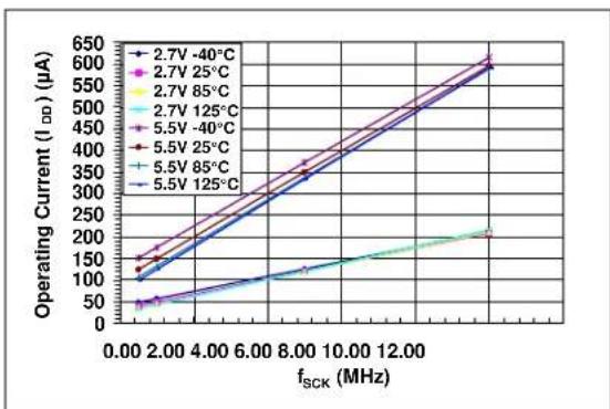
FIGURE 2-1: Device Current (I DD ) vs. SPI Frequency ( fSCK ) and Ambient Temperature ( V_DD = 2.7V and 5.5V).
line
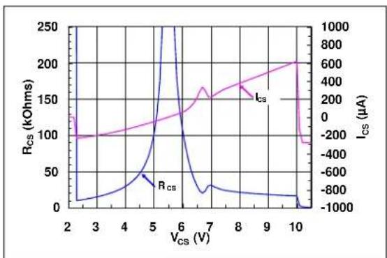
| V_cs (V) | R_cs (kOhms) | I_cs (μA) | | -------- | ------------ | --------- | | 2 | 0 | 100 | | 3 | 0 | 100 | | 4 | 0 | 100 | | 5 | 50 | 100 | | 6 | 250 | 100 | | 7 | 0 | 100 | | 8 | 0 | 200 | | 9 | 0 | 400 | | 10 | 0 | 600 |FIGURE 2-4: CS Pull-up/Pull-down Resistance ( R_ ) and Current ( I_ ) vs. CS Input Voltage ( V_ ) ( V_DD = 5.5V ).
line
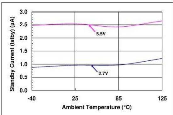
| Ambient Temperature (°C) | Standby Current (Istby) (μA) | | ------------------------ | --------------------------- | | 25 | 2.5 | | 85 | 2.3 | | 125 | 2.6 |FIGURE 2-2: Device Current (I SHDN) and V_DD . ( = V_DD) vs. Ambient Temperature.
line
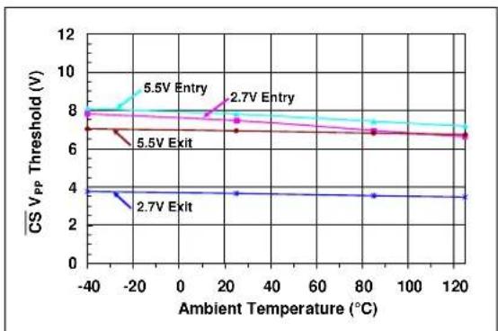
| Ambient Temperature (°C) | 5.5V Entry | 5.5V Exit | 2.7V Entry | 2.7V Exit | | ------------------------ | ---------- | --------- | ---------- | --------- | | -40 | 8.0 | 7.5 | 4.0 | 3.5 | | 20 | 7.5 | 7.0 | 3.8 | 3.5 | | 80 | 7.0 | 6.8 | 3.5 | 3.5 | | 120 | 6.8 | 6.5 | 3.5 | 3.5 |FIGURE 2-5: CS High Input Entry/Exit Threshold vs. Ambient Temperature and V_DD .
line
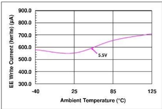
| Ambient Temperature (°C) | EE Write Current (Iwrite) (μA) | | ------------------------ | ----------------------------- | | -40 | 600.0 | | 25 | 550.0 | | 85 | 650.0 | | 125 | 700.0 |FIGURE 2-3: Write Current (I WRITE) vs. Ambient Temperature and V_DD .
Note: Unless otherwise indicated, T_A = +25^ , V_DD = 5V , V_SS = 0V .
line
| Wiper Setting (decimal) | -125°C | 85°C | -40°C | 25°C | 40°C | 25°C DNL | 85°C DNL | 125°C DNL | 40°C INL | 25°C INL | 85°C INL | 125°C INL | | ----------------------- | ------ | ---- | ----- | ---- | ---- | -------- | -------- | --------- | -------- | -------- | -------- | --------- | | 0 | 60 | 60 | 60 | 60 | 60 | 60 | 60 | 60 | 60 | 60 | 60 | 60 | | 32 | 55 | 55 | 55 | 55 | 55 | 55 | 55 | 55 | 55 | 55 | 55 | 55 | | 64 | 50 | 50 | 50 | 50 | 50 | 50 | 50 | 50 | 50 | 50 | 50 | 50 | | 96 | 45 | 45 | 45 | 45 | 45 | 45 | 45 | 45 | 45 | 45 | 45 | 45 | | 128 | 40 | 40 | 40 | 40 | 40 | 40 | 40 | 40 | 40 | 40 | 40 | 40 | | 160 | 35 | 35 | 35 | 35 | 35 | 35 | 35 | 35 | 35 | 35 | 35 | 35 | | 192 | 30 | 30 | 30 | 30 | 30 | 30 | 30 | 30 | 30 | 30 | 30 | 30 | | 224 | 25 | 25 | 25 | 25 | 25 | 25 | 25 | 25 | 25 | 25 | 25 | 25 | | 256 | 20 | 20 | 20 | 20 | 20 | 20 | 20 | 20 | 20 | 20 | 20 | 20 | | Final | -1.2 | -1.2 | -1.2 | -1.2 | -1.2 | -1.2 | -1.2 | -1.2 | -1.2 | -1.2 | -1.2 | -1.2 | Error (LSb) | | Final Setting | -1.1 | -1.1 | -1.1 | -1.1 | -1.1 | -1.1 | -1.1 | -1.1 | -1.1 | -1.1 | -1.1 | -1.1 | | Final Setting (DNL) | | Final Setting (INL) | | Final Setting (DNL) | | Final Setting (DNL) | | Final Setting (DNL) | | Final Setting (DNL) | | Final Setting (DNL) | | Final Setting (DNL) | | Final Setting (DNL) | | Final Setting (DNL) | | Final Setting (DNL) | | Final Setting (DNL) | | Final Setting (DRL) | | Final Setting (DRL) | | Final Setting (DRL) | | Final Setting (DRL) | | Final Setting (DRL) | | Final Setting (DRL) | | Final Setting (DRL) | | Final Setting (DRL) | | Final Setting (DRL) | | Final Setting (DRL) | | Final Setting (DNL) | | Final Setting (DNL) | | Final Setting (DNL) | | Final Setting (DNL) | | Final Setting (DNL) | | Final Setting (DNL) | | Final Setting (DNL) | | Final Setting (DNL) | | Final Setting (DNL) | | Final Setting (DLL) | | Final Setting (DLL) | | Final Setting (DLL) | | Final Setting (DLL) | | Final Setting (DLL) | | Final Setting (DLL) | | Final Setting (DLL) | | Final Setting (DLL) | | Final Setting (DLL) | | Final Setting (DLL) | | Final Setting (DRL) | | Final Setting (DRL) | | Final Setting (DRL) | | Final Setting (DRL) | | Final Setting (DRL) | | Final Setting (DRL) | | Final Setting (DRL) | | Final Setting (DRL) | | Final Setting (DRL) | | Final Setting (DLL) | | Final Setting (DLL) | | Final Setting (DLL) | | Final Setting (DLL) | | Final Setting (DLL) | | Final Setting (DLL) | | Final Setting (DLL) | | Final Setting (DLL) | | Final Setting (DLL) | | Final Setting (DML) | | Final Setting (DML) | | Final Setting (DML) | | Final Setting (DML) | | Final Setting (DML) | | Final Setting (DML) | | Final Setting (DML) | | Final Setting (DML) | | Final Setting (DML) | | Final Setting (DML) | | Final Setting (DLL) | | Final Setting (DLL) | | Final Setting (DLL) | | Final Setting (DLL) | | Final Setting (DLL) | | Final Setting (DLL) | | Final Setting (DLL) | | Final Setting (DLL) | | Final Setting (DLL) | | Final Setting (DLL) | | Final Setting (DLL) | | Final Setting (DLL) | | Final Setting (DLL) | | Final Setting (DLL) | | Final Setting (DLL) | | Final Setting (DLL) | | Final Setting (DLL) | | Final Setting (DLL) | | Final Setting (DLL)line
| Wiper Setting (decimal) | -40C Rw | -40C INL | -40C DNL | 25C Rw | 25C INL | 25C DNL | 85C Rw | 85C INL | 85C DNL | 125C Rw | 125C INL | 125C DNL | | ----------------------- | ------- | -------- | -------- | ------ | ------- | ------- | ------ | ------- | ------- | ------- | -------- | -------- | | 0 | 40 | 40 | 40 | 40 | 40 | 40 | 40 | 40 | 40 | 40 | 40 | 40 | | 32 | 60 | 60 | 60 | 60 | 60 | 60 | 60 | 60 | 60 | 60 | 60 | 60 | | 64 | 70 | 70 | 70 | 70 | 70 | 70 | 70 | 70 | 70 | 70 | 70 | 70 | | 96 | 80 | 80 | 80 | 80 | 80 | 80 | 80 | 80 | 80 | 80 | 80 | 80 | | 128 | 90 | 90 | 90 | 90 | 90 | 90 | 90 | 90 | 90 | 90 | 90 | 90 | | 160 | 100 | 100 | 100 | 100 | 100 | 100 | 100 | 100 | 100 | 100 | 100 | 100 | | 192 | 110 | 110 | 110 | 110 | 110 | 110 | 110 | 110 | 110 | 110 | 110 | 110 | | 224 | 120 | 120 | 120 | 120 | 120 | 120 | 120 | 120 | 120 | 120 | 120 | 120 | | 256 | - | - | - | - | - | - | - | - | - | - | - | - | Error (LSb) on right axis; Error (LSb) on left axis; Wiper Resistance (Rw) and Wiper Setting (DNL) are labeled on the left axis.line
| Wiper Setting (decimal) | Wiper Resistance (Rw) | Error (LSb) | | ----------------------- | ---------------------- | ----------- | | 0 | 60 | -0.3 | | 32 | 100 | -0.1 | | 64 | 140 | 0.0 | | 96 | 180 | 0.1 | | 128 | 220 | 0.2 | | 160 | 200 | 0.1 | | 192 | 180 | 0.0 | | 224 | 160 | -0.1 | | 256 | 140 | -0.2 |line
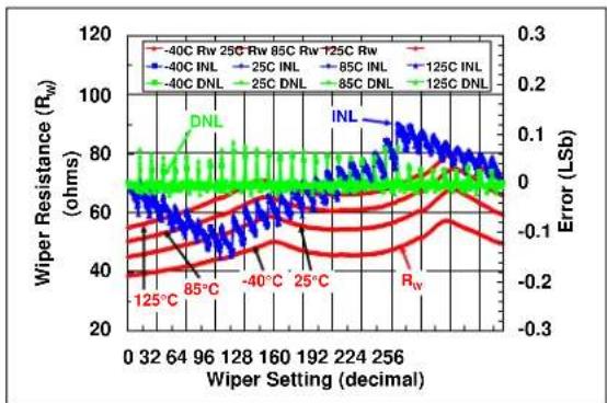
| Wiper Setting (decimal) | 40C Rw | 25C Rw | 85C Rw | 125C Rw | 40C INL | 25C INL | 85C INL | 125C INL | 40C DNL | 25C DNL | 85C DNL | 125C DNL | | ----------------------- | ------ | ------ | ------ | ------- | ------- | ------- | ------- | -------- | ------- | ------- | ------- | -------- | | 0 | 60 | 60 | 60 | 60 | 60 | 60 | 60 | 60 | 60 | 60 | 60 | 60 | | 32 | 70 | 70 | 70 | 70 | 70 | 70 | 70 | 70 | 70 | 70 | 70 | 70 | | 64 | 80 | 80 | 80 | 80 | 80 | 80 | 80 | 80 | 80 | 80 | 80 | 80 | | 96 | 100 | 100 | 100 | 100 | 100 | 100 | 100 | 100 | 100 | 100 | 100 | 100 | | 128 | 140 | 140 | 140 | 140 | 140 | 140 | 140 | 140 | 140 | 140 | 140 | 140 | | 160 | 220 | 220 | 220 | 220 | 220 | 220 | 220 | 220 | 220 | 220 | 220 | 220 | | 192 | 260 | 260 | 260 | 260 | 260 | 260 | 260 | 260 | 260 | 260 | 260 | 260 | | 224 | 180 | 180 | 180 | 180 | 180 | 180 | 180 | 180 | 180 | 180 | 180 | 180 | | 256 | 120 | 120 | 120 | 120 | 120 | 120 | 120 | 120 | 120 | 120 | 120 | 120 | Error (LSb) | | Error (LSb) | -2 | -2 | -2 | -2 | -2 | -2 | -2 | -2 | -2 | -2 | -2 | -2 | | Error (LSb) | +2 | +2 | +2 | +2 | +2 | +2 | +2 | +2 | +2 | +2 | +2 | +2 | | Error (LSb) | +4 | +4 | +4 | +4 | +4 | +4 | +4 | +4 | +4 | +4 | +4 | +4 | | Error (LSb) | +6 | +6 | +6 | +6 | +6 | +6 | +6 | +6 | +6 | +6 | +6 | +6 | | Error (LSb) | +8 | +8 | +8 | +8 | +8 | +8 | +8 | +8 | +8 | +8 | +8 | +8 | | Error (LSb) | +10 | +10 | +10 | +10 | +10 | +10 | +10 | +10 | +10 | +10 | +10 | +10 | | Error (LSb) | +12 | +12 | +12 | +12 | +12 | +12 | +12 | +12 | +12 | +12 | +12 | +12 | | Error (LSb) | +14 | +14 | +14 | +14 | +14 | +14 | +14 | +14 | +14 | +14 | +14 | +14 | | Error (LSb) | +16 | +16 | +16 | +16 | +16 | +16 | +16 | +16 | +16 | +16 | +16 | +16 | | Error (LSb) | +18 | +18 | +18 | +18 | +18 | +18 | +18 | +18 | +18 | +18 | +18 | +18 | | Error (LSb) | +20 | +20 | +20 | +20 | +20 | +20 | +20 | +20 | +20 | +20 | +20 | +20 | | Error (LSb) | | Error (LSb) | | Error (LSb) | | Error (LSb) | | Error (LSb) | | Error (LSb) | | Error (LSb) | | Error (LSb) | | Error (LSb) | | Error (LSb) | | Error (LSb) | | Error (LSb) | | Error (LSb) | | Error(LSb) | | Error(LSb) | | Error(LSb) | | Error(LSb) | | Error(LSb) | | Error(LSb) | | Error(LSb) | | Error(LSb) | | Error(LSb) | | Error(LSb) | | Error(LSb) | | Error(LSb) | | Error(LSb) | | Error (LSb) | | Error(LSb) | | Error(LSb) | | Error(LSb) | | Error(LSb) | | Error(LSb) | | Error(LSb) | | Error(LSb) | | Error(LSb) | | Error(LSb) | | Error(LSb) | | Error(LSb) | | Error(LSb) (in dBm) | | Error(LSb) | | Error(LSb) | | Error(LSb) | | Error(LSb) | | Error(LSb) | | Error(LSb) | | Error(LSb) | | Error(LSb) | | Error(LSb) | | Error(LSb) | | Error(LSb) | | Error(LSb) | | Error(LBm) | | Error(LBm) | | Error(LBm) | | Error(LBm) | | Error(LBm) | | Error(LBm) | | Error(LBm) | | Error(LBm) | | Error(LBm) | | Error(LBm) | | Error(LBm) | | Error(LBm) | | Error(LBm) | | Error(MBm) | | Error(MBm) | | Error(MBm) | | Error(MBm) | | Error(MBm) | | Error(MBm) | | Error(MBm) | | Error(MBm) | | Error(MBm) | | Error(MBm) | | Error(MBm) | | Error(MBm) | | Error(MBm) | | Error(NBm) | | Error(NBm) | | Error(NBm) | | Error(NBm) | | Error(NBm) | | Error(NBm) | | Error(NBm) | | Error(NBm) | | Error(NBm) | | Error(NBm) | | Error(NBm) | | Error(NBm) | | Error(NBm) | | Error(NBm)|line
| Ambient Temperature (°C) | Nominal Resistance (R_AB) (Ohms) at 2.7V | Nominal Resistance (R_AB) (Ohms) at 5.5V | | ------------------------ | ---------------------------------------- | ---------------------------------------- | | -40 | 5260 | 5160 | | 30 | 5210 | 5100 | | 80 | 5230 | 5100 | | 120 | 5280 | 5130 |line
| Wiper Setting (decimal) | -40°C | 25°C | 85°C | 125°C | | ----------------------- | ----- | ---- | ---- | ----- | | 0 | 0 | 0 | 0 | 0 | | 32 | ~1000 | ~1000| ~1000| ~1000 | | 64 | ~2000 | ~2000| ~2000| ~2000 | | 96 | ~3000 | ~3000| ~3000| ~3000 | | 128 | ~4000 | ~4000| ~4000| ~4000 | | 160 | ~5000 | ~5000| ~5000| ~5000 | | 192 | ~6000 | ~6000| ~6000| ~6000 | | 224 | ~7000 | ~7000| ~7000| ~7000 | | 256 | ~8000 | ~8000| ~8000| ~8000 |text_image
Syst Wave Gauss in U.S. (in dB, in Hz, 207 Amp) 1.0000 Vcc = 24.0000Hz Current: 2.24 V Signal: 16.42 Hztext_image
D Ginger to C:/ST, INC., 2p27 Temp Saying to C:/ST, INC., 2p27 Temp 1.0V 3.0V 4.0V 5.0V 6.0V 7.0V 8.0V 9.0V 10.0V 11.0V 12.0V 13.0V 14.0V 15.0V 16.0V 17.0V 18.0V 19.0V 20.0V 21.0V 22.0V 23.0V 24.0V 25.0V 26.0V 27.0V 28.0V 29.0V 30.0V 31.0V 32.0V 33.0V 34.0V 35.0V 36.0V 37.0V 38.0V 39.0V 40.0V 41.0V 42.0V 43.0V 44.0V 45.0V 46.0V 47.0V 48.0V 49.0V 50.0V 51.0V 52.0V 53.0V 54.0V 55.0V 56.0V 57.0V 58.0V 59.0V 60.0V 61.0V 62.0V 63.0V 64.0V 65.0V 66.0V 67.0V 68.0V 69.0V 70.0V 71.0V 72.0V 73.0V 74.0V 75.0V 76.0V 77.0V 78.0V 79.0V 80.0V 81.0V 82.0V 83.0V 84.0V 85.0V 86.0V 87.0V 88.0V 89.0V 90.0V 91.0V 92.0V 93.0V 94.0V 95.0V 96.0V 97.0V 98.0V 99.0V 100.0Vtext_image
Oscilloscope waveform display showing signal timing and amplitude variations over timetext_image
Oscilloscope waveform display showing signal timing and voltage levels with labeled parametersline
| Wiper Setting (decimal) | Wiper Resistance (Rw) (ohms) | Error (Lsb) | | ----------------------- | ----------------------------- | ----------- | | 0 | ~60 | ~0.0 | | 25 | ~50 | ~-0.1 | | 50 | ~45 | ~-0.1 | | 75 | ~40 | ~-0.1 | | 100 | ~35 | ~-0.1 | | 125 | ~30 | ~-0.1 | | 150 | ~35 | ~-0.1 | | 175 | ~40 | ~-0.1 | | 200 | ~45 | ~-0.1 | | 225 | ~50 | ~-0.1 | | 250 | ~55 | ~-0.1 |line
| Wiper Setting (decimal) | 40C Rw 25G Rw 85C Rw 165C Rw | 40C INL 25G INL 85C INL-125C INL | 40C DNL | 25C DNL | 85C DNL | 125C DNL | | ----------------------- | ----------------------------- | ---------------------------------- | ------- | ------- | ------- | -------- | | 0 | ~40 | ~70 | ~60 | ~70 | ~70 | ~70 | | 32 | ~45 | ~75 | ~65 | ~75 | ~75 | ~75 | | 64 | ~50 | ~80 | ~70 | ~80 | ~80 | ~80 | | 96 | ~55 | ~85 | ~75 | ~85 | ~85 | ~85 | | 128 | ~60 | ~90 | ~80 | ~90 | ~90 | ~90 | | 160 | ~65 | ~95 | ~85 | ~95 | ~95 | ~95 | | 192 | ~70 | ~100 | ~90 | ~100 | ~100 | ~100 | | 224 | ~75 | ~105 | ~95 | ~105 | ~105 | ~105 | | 256 | ~80 | ~110 | ~100 | ~110 | ~110 | ~110 |line
| Wiper Setting (decimal) | Wiper Resistance (Rw) | Error (LSb) | | ----------------------- | ---------------------- | ----------- | | 0 | ~140 | ~0 | | 32 | ~130 | ~0 | | 64 | ~120 | ~0 | | 96 | ~110 | ~0 | | 128 | ~100 | ~0 | | 160 | ~90 | ~0 | | 192 | ~80 | ~0 | | 224 | ~70 | ~0 | | 256 | ~60 | ~0 |line
| Wiper Setting (decimal) | -40C Rw 250C Rw 85C Rw 125C Rw | -40C INL 25C INL 85C INL 125C INL | -40C DNL 25C DNL 85C DNL 125C DNL | DNL RW | Error (LSb) | | ----------------------- | -------------------------------- | ---------------------------------- | ---------------------------------- | ------ | ----------- | | 0 | ~60 | ~60 | ~60 | ~60 | ~0 | | 25 | ~70 | ~70 | ~70 | ~70 | ~0 | | 50 | ~80 | ~80 | ~80 | ~80 | ~0 | | 75 | ~90 | ~90 | ~90 | ~90 | ~0 | | 100 | ~100 | ~100 | ~100 | ~100 | ~0 | | 125 | ~110 | ~110 | ~110 | ~110 | ~0 | | 150 | ~130 | ~130 | ~130 | ~130 | ~0 | | 175 | ~160 | ~160 | ~160 | ~160 | ~3 | | 200 | ~180 | ~180 | ~180 | ~180 | ~3 | | 225 | ~160 | ~160 | ~160 | ~160 | ~2 | | 250 | ~140 | ~140 | ~140 | ~140 | ~1 | | 275 | ~120 | ~120 | ~120 | ~120 | ~-1 | | 300 | ~100 | ~100 | ~100 | ~100 | ~-2 |line
| Ambient Temperature (°C) | Nominal Resistance (R_AB) (Ohms) at 2.7V | Nominal Resistance (R_AB) (Ohms) at 5.5V | | ------------------------ | ---------------------------------------- | ---------------------------------------- | | -40 | 10250 | 10175 | | 0 | 10150 | 10050 | | 40 | 10100 | 10025 | | 80 | 10125 | 10025 | | 120 | 10175 | 10075 |line
| Wiper Setting (decimal) | -40°C | 25°C | 85°C | 125°C | | ----------------------- | ----- | ---- | ---- | ----- | | 0 | 0 | 0 | 0 | 0 | | 32 | ~2000 | ~2000| ~2000| ~2000 | | 64 | ~4000 | ~4000| ~4000| ~4000 | | 96 | ~6000 | ~6000| ~6000| ~6000 | | 128 | ~8000 | ~8000| ~8000| ~8000 | | 160 | ~10000| ~10000| ~10000| ~10000| | 192 | ~12000| ~12000| ~12000| ~12000| | 224 | ~14000| ~14000| ~14000| ~14000| | 256 | ~16000| ~16000| ~16000| ~16000|text_image
D Ginger to 0/199, Inc., CapTime Slope Mpass Wave Rig. Gait Wave Ginger to 0/199, Inc., CapTime Slope Mpass Wave Rig. Gait Wave Ginger to 0/199, Inc., CapTime Slope Mpass Wave Rig. Gait Wave Ginger to 0/199, Inc., CapTimetext_image
D Sv 1.000 Waveform Signal Max 0.500 Waveform Max 0.500 Waveform Max 0.500 Waveform Max 0.500 Waveform Max 0.500 Waveform Max 0.500 Waveform Max 0.500 Waveform Max 0.500 Waveform Max 0.500 Waveform Max 0.500 Waveformline
| Parameter | Value | | --------- | ----- | | G1 | 1.5 | | G2 | 1.5 | | G3 | 1.5 | | G4 | 1.5 | | Log L | 1.5 | | G1/19 | 1.5 | | G2/19 | 1.5 | | G3/19 | 1.5 | | G4/19 | 1.5 | | Log L | 1.5 | | G1/28 | 1.5 | | G2/28 | 1.5 | | G3/28 | 1.5 | | G4/28 | 1.5 | | Log L | 1.5 | | G1/37 | 1.5 | | G2/37 | 1.5 | | G3/37 | 1.5 | | G4/37 | 1.5 | | Log L | 1.5 | | G1/46 | 1.5 | | G2/46 | 1.5 | | G3/46 | 1.5 | | G4/46 | 1.5 | | Log L | 1.5 | | G1/55 | 1.5 | | G2/55 | 1.5 | | G3/55 | 1.5 | | G4/55 | 1.5 | | Log L | 1.5 | | G1/63 | 1.5 | | G2/63 | 1.5 | | G3/63 | 1.5 | | G4/63 | 1.5 | | Log L | 1.5 | | G1/71 | 1.5 | | G2/71 | 1.5 | | G3/71 | 1.5 | | G4/71 | 1.5 | | Log L | 1.5 | | G1/79 | 1.5 | | G2/79 | 1.5 | | G3/79 | 1.5 | | G4/79 | 1.5 | | Log L | 1.5 | | G1/87 | 1.5 | | G2/87 | 1.5 | | G3/87 | 1.5 | | G4/87 | 1.5 | | Log L | 1.5 | | G1/94 | 1.5 | | G2/94 | 1.5 | | G3/94 | 1.5 | | G4/94 | 1.5 | | Log L | 1.5 | | G1/99 | 1.5 | | G2/99 | 1.5 | | G3/99 | 1.5 | | G4/99 | 1.5 | | Log L | 1.5 | | G2/99 | 1.5 | | G3/99 | 1.5 | | G4/99 | 1.5 | | Log L | 1.5 | | G2/99 | 1.5 | | G3/99 | 1.5 | | G4/99 | 1.6 | | Log L | 1.6 | | G2/99 | 1.6 | | G3/99 | 1.6 | | G4/99 | 1.6 | | Log L | 1.6 | | G2/99 | 1.6 | | G3/99 | 1.6 | | G4/99 | 1.6 | | Log L | 1.6 | | G2/99 | 1.6 | | G3/98 | 1.6 | | G4/98 | 1.6 | | Log L | 1.6 | | G2/99 | 1.6 | | G3/98 | 1.6 | | G4/98 | 1.6 | | Log L | 1.6 | | G2/99 | 1.6 | | G3/98 | 1.6 |text_image
Lating 10.2 / 10V, Inc., Tsc 20Hz Gauss: 100 V Current: 50 MHz Current: 50 MHz Current: 50 MHz Current: 50 MHz Current: 50 MHz Current: 50 MHz Current: 50 MHz Current: 50 MHz Current: 50 MHz Current: 50 MHz Current: 50 MHz Current: 50 MHz Current: 50 MHz Current: 50 MHz Current: 50 MHz Circuit: 10.2 V Circuit: 10.2 V Circuit: 10.2 V Circuit: 10.2 V Circuit: 10.2 V Circuit: 10.2 V Circuit: 10.2 V Circuit: 10.2 V Circuit: 10.2 V Circuit: 10.2 V Circuit: 10.2V Circuit: 10.2V Circuit: 10.2V Circuit: 10.2V Circuit: 10.2V Circuit: 10.2V Circuit: 10.2V Circuit: 10.2V Circuit: 10.2V Circuit: 10.2V Circuit: 10.2line
| Wiper Setting (decimal) | Wiper Resistance (R_W) (ohms) | Error (LSb) | | ----------------------- | ------------------------------ | ----------- | | 0 | ~60 | ~0.0 | | 32 | ~50 | ~-0.1 | | 64 | ~40 | ~-0.1 | | 96 | ~30 | ~-0.1 | | 128 | ~20 | ~-0.1 | | 160 | ~30 | ~-0.1 | | 192 | ~40 | ~-0.1 | | 224 | ~50 | ~-0.1 | | 256 | ~60 | ~-0.1 |line
| Wiper Setting (decimal) | Wiper Resistance (Rw) | Error (LSb) | | ----------------------- | --------------------- | ----------- | | 0 | ~60 | ~-0.75 | | 32 | ~140 | ~0 | | 64 | ~140 | ~0 | | 96 | ~140 | ~0 | | 128 | ~140 | ~0 | | 160 | ~140 | ~0 | | 192 | ~140 | ~0 | | 224 | ~140 | ~0 | | 256 | ~140 | ~0 |line
| Ambient Temperature (°C) | Nominal Resistance (R_AB) (Ohms) at 2.7V | Nominal Resistance (R_AB) (Ohms) at 5.5V | | ------------------------ | ---------------------------------------- | ---------------------------------------- | | -40 | 50800 | 50700 | | 0 | 50100 | 50000 | | 40 | 49800 | 49700 | | 80 | 49600 | 49500 | | 120 | 49800 | 49700 |line
| Wiper Setting (decimal) | -40°C | 25°C | 85°C | 125°C | | ----------------------- | ----- | ---- | ---- | ----- | | 0 | 0 | 0 | 0 | 0 | | 32 | ~10000| ~10000| ~10000| ~10000| | 64 | ~20000| ~20000| ~20000| ~20000| | 96 | ~30000| ~30000| ~30000| ~30000| | 128 | ~40000| ~40000| ~40000| ~40000| | 160 | ~50000| ~50000| ~50000| ~50000| | 192 | ~60000| ~60000| ~60000| ~60000| | 224 | ~70000| ~70000| ~70000| ~70000| | 256 | ~80000| ~80000| ~80000| ~80000|line
| Time (ns) | Amplitude (dB) | | --------- | -------------- | | 0 | 0 | | 10 | 0 | | 20 | 0 | | 30 | 0 | | 40 | 0 | | 50 | 0 | | 60 | 0 | | 70 | 0 | | 80 | 0 | | 90 | 0 | | 100 | 0 | | 110 | 0 | | 120 | 0 | | 130 | 0 | | 140 | 0 | | 150 | 0 | | 160 | 0 | | 170 | 0 | | 180 | 0 | | 190 | 0 | | 200 | 0 | | 210 | 0 | | 220 | 0 | | 230 | 0 | | 240 | 0 | | 250 | 0 | | 260 | 0 | | 270 | 0 | | 280 | 0 | | 290 | 0 | | 300 | 0 | | 310 | 0 | | 320 | 0 | | 330 | 0 | | 340 | 0 | | 350 | 0 | | 360 | 0 | | 370 | 0 | | 380 | 0 | | 390 | 0 | | 400 | 0 | | 410 | 0 | | 420 | 0 | | 430 | 0 | | 440 | 0 | | 450 | 0 | | 460 | 0 | | 470 | 0 | | 480 | 0 | | 490 | 0 | | 500 | 0 | | 510 | 0 | | 520 | 0 | | 530 | 0 | | 540 | 0 | | 550 | 0 | | 560 | 0 | | 570 | 0 | | 580 | 0 | | 590 | 0 | | 600 | 0 | | 610 | 0 | | 620 | 0 | | 630 | 0 | | 640 | 0 | | 650 | 0 | | 660 | 0 | | 670 | 0 | | 680 | 0 | | 690 | 0 | | 700 | 0 | | 710 | 0 | | 720 | 0 | | 730 | 0 | | 740 | 0 | | 750 | 0 | | 760 | 0 | | 770 | 0 | | 780 | 0 | | 790 | 0 | | 800 | 0 | | 810 | 0 | | 820 | 0 | | 830 | 0 | | 840 | 0 | | 850 | 0 | | 860 | 0 | | 870 | 0 | | 880 | 0 | | 890 | 0 | | 900 | 0 | | 910 | 0 | | 920 | 0 | | 930 | 0 | | 940 | 0 | | 950 | 0 | | 960 | 0 | | 970 | 0 | | 980 | 0 | | 990 | 0 | | >1 | <1 |line
| Time | Value | |------|-------| | 0 | 0 | | 1 | 1 | | 2 | 0 | | 3 | 1 | | 4 | 0 | | 5 | 1 | | 6 | 0 | | 7 | 1 | | 8 | 0 | | 9 | 1 | | 10 | 0 | | 11 | 1 | | 12 | 0 | | 13 | 1 | | 14 | 0 | | 15 | 1 | | 16 | 0 | | 17 | 1 | | 18 | 0 | | 19 | 1 | | 20 | 0 | | 21 | 1 | | 22 | 0 | | 23 | 1 | | 24 | 0 | | 25 | 1 | | 26 | 0 | | 27 | 1 | | 28 | 0 | | 29 | 1 | | 30 | 0 | | 31 | 1 | | 32 | 0 | | 33 | 1 | | 34 | 0 | | 35 | 1 | | 36 | 0 | | 37 | 1 | | 38 | 0 | | 39 | 1 | | 40 | 0 | | 41 | 1 | | 42 | 0 | | 43 | 1 | | 44 | 0 | | 45 | 1 | | 46 | 0 | | 47 | 1 | | 48 | 0 | | 49 | 1 | | 50 | 0 | | 51 | 1 | | 52 | 0 | | 53 | 1 | | 54 | 0 | | 55 | 1 | | 56 | 0 | | 57 | 1 | | 58 | 0 | | 59 | 1 | | 60 | 0 | | 61 | 1 | | 62 | 0 | | 63 | 1 | | 64 | 0 | | 65 | 1 | | 66 | 0 | | 67 | 1 | | 68 | 0 | | 69 | 1 | | 70 | 0 | | 71 | 1 | | 72 | 0 | | 73 | 1 | | 74 | 0 | | 75 | 1 | | 76 | 0 | | 77 | 1 | | 78 | 0 | | 79 | 1 | | 80 | 0 | | 81 | 1 | | 82 | 0 | | 83 | 1 | | 84 | 0 | | 85 | 1 | | 86 | 0 | | 87 | 1 | | 88 | 0 | | 89 | 1 | | 90 | 0 | | 91 | 1 | | 92 | 0 | | 93 | 1 | | 94 | 0 | | 95 | 1 | | 96 | 0 | | 97 | 1 | | 98 | 0 | | 99 | 1 | | Note: The actual values for the blue and cyan lines are not provided in the code. The data is presented in a table format as shown above. The values for the blue and cyan lines are listed in the same order as they are not explicitly provided in the code. There is no label for the cyan line in the chart.line
| Time | Signal Value | |------|--------------| | 0 | 100% | | 1 | 100% | | 2 | 100% | | 3 | 100% | | 4 | 100% | | 5 | 100% | | 6 | 100% | | 7 | 100% | | 8 | 100% | | 9 | 100% | | 10 | 100% | | 11 | 100% | | 12 | 100% | | 13 | 100% | | 14 | 100% | | 15 | 100% | | 16 | 100% | | 17 | 100% | | 18 | 100% | | 19 | 100% | | 20 | 100% | | 21 | 100% | | 22 | 100% | | 23 | 100% | | 24 | 100% | | 25 | 100% | | 26 | 100% | | 27 | 100% | | 28 | 100% | | 29 | 100% | | 30 | 100% | | 31 | 100% | | 32 | 100% | | 33 | 100% | | 34 | 100% | | 35 | 100% | | 36 | 100% | | 37 | 100% | | 38 | 100% | | 39 | 100% | | 40 | 100% | | 41 | 100% | | 42 | 100% | | 43 | 100% | | 44 | 100% | | 45 | 100% | | 46 | 100% | | 47 | 100% | | 48 | 100% | | 49 | 100% | | 50 | 100% | | 51 | 100% | | 52 | 100% | | 53 | 100% | | 54 | 100% | | 55 | 100% | | 56 | 100% | | 57 | 100% | | 58 | 100% | | 59 | 100% | | 60 | 100% | | 61 | 100% | | 62 | 100% | | 63 | 100% | | 64 | 100% | | 65 | 100% | | 66 | 100% | | 67 | 100% | | 68 | 100% | | 69 | 100% | | 70 | 100% | | 71 | 100% | | 72 | 100% | | 73 | 100% | | 74 | 100% | | 75 | 100% | | 76 | 100% | | 77 | 100% | | 78 | 100% | | 79 | 100% | | 80 | 100% | | 81 | 100% | | 82 | 100% | | 83 | 100% | | 84 | 100% | | 85 | 100% | | 86 | 100% | | 87 | 100% | | 88 | 100% | | 89 | 100% | | 90 | 100% | | 91 | 100% | | 92 | 100% | | 93 | 100% | | 94 | 100% | | 95 | 100% | | 96 | 100% | | 97 | 100% | | 98 | 100% | | 99 | 100% | | Note: The actual values for 'Top' and 'Bottom' are not provided in the code. The data is extracted from the plot and displayed on the screen.line
| Time (s) | Signal Value | |----------|--------------| | 0 | 0 | | 1 | 100 | | 2 | 0 | | 3 | 100 | | 4 | 0 | | 5 | 100 | | 6 | 0 | | 7 | 100 | | 8 | 0 | | 9 | 100 | | 10 | 0 | | 11 | 100 | | 12 | 0 | | 13 | 100 | | 14 | 0 | | 15 | 100 | | 16 | 0 | | 17 | 100 | | 18 | 0 | | 19 | 100 | | 20 | 0 | | 21 | 100 | | 22 | 0 | | 23 | 100 | | 24 | 0 | | 25 | 100 | | 26 | 0 | | 27 | 100 | | 28 | 0 | | 29 | 100 | | 30 | 0 | | 31 | 100 | | 32 | 0 | | 33 | 100 | | 34 | 0 | | 35 | 100 | | 36 | 0 | | 37 | 100 | | 38 | 0 | | 39 | 100 | | 40 | 0 | | 41 | 100 | | 42 | 0 | | 43 | 100 | | 44 | 0 | | 45 | 100 | | 46 | 0 | | 47 | 100 | | 48 | 0 | | 49 | 100 | | 50 | 0 | | 51 | 100 | | 52 | 0 | | 53 | 100 | | 54 | 0 | | 55 | 100 | | 56 | 0 | | 57 | 100 | | 58 | 0 | | 59 | 100 | | 60 | 0 | | 61 | 100 | | 62 | 0 | | 63 | 100 | | 64 | 0 | | 65 | 100 | | 66 | 0 | | 67 | 100 | | 68 | 0 | | 69 | 100 | | 70 | 0 | | 71 | 100 | | 72 | 0 | | 73 | 100 | | 74 | 0 | | 75 | 100 | | 76 | 0 | | 77 | 100 | | 78 | 0 | | 79 | 100 | | 80 | 0 | | 81 | 100 | | 82 | 0 | | 83 | 100 | | 84 | 0 | | 85 | 100 | | 86 | 0 | | 87 | 100 | | 88 | 0 | | 89 | 100 | | 90 | 0 | | 91 | 100 | | 92 | 0 | | 93 | 100 | | 94 | 0 | | 95 | 100 | | 96 | 0 | | 97 | 100 | | 98 | 0 | | 99 | 100 | | Note: The data is extracted from the code and presented in CSV format as requested. The code does not contain the original data. It is a simplified representation of the output.line
| Wiper Setting (decimal) | 125°C Wiper Resistance (Rw) | 85°C Wiper Resistance (Rw) | 25°C Wiper Resistance (Rw) | -40°C Wiper Resistance (Rw) | 125°C Error (LSb) | 85°C Error (LSb) | 25°C Error (LSb) | -40°C Error (LSb) | | ----------------------- | ---------------------------- | --------------------------- | --------------------------- | --------------------------- | ----------------- | ---------------- | ---------------- | ----------------- | | 0 | ~30 | ~40 | ~50 | ~60 | ~0.0 | ~0.0 | ~0.0 | ~0.0 | | 32 | ~35 | ~45 | ~55 | ~65 | ~0.0 | ~0.0 | ~0.0 | ~0.0 | | 64 | ~40 | ~50 | ~60 | ~70 | ~0.0 | ~0.0 | ~0.0 | ~0.0 | | 96 | ~45 | ~55 | ~65 | ~75 | ~0.0 | ~0.0 | ~0.0 | ~0.0 | | 128 | ~50 | ~60 | ~70 | ~80 | ~0.0 | ~0.0 | ~0.0 | ~0.0 | | 160 | ~55 | ~65 | ~75 | ~85 | ~0.0 | ~0.0 | ~0.0 | ~0.0 | | 192 | ~60 | ~70 | ~80 | ~90 | ~0.0 | ~0.0 | ~0.0 | ~0.0 | | 224 | ~65 | ~75 | ~85 | ~95 | ~0.0 | ~0.0 | ~0.0 | ~0.0 | | 256 | ~70 | ~80 | ~90 | ~100 | ~0.0 | ~0.0 | ~0.0 | ~0.0 | | 38 | ~75 | ~85 | ~95 | ~105 | ~-0.1 | ~-0.1 | ~-0.1 | ~-0.1 | | 41 | ~80 | ~90 | ~100 | ~110 | ~-0.1 | ~-0.1 | ~-0.1 | ~-0.1 | | 44 | ~85 | ~95 | ~105 | ~115 | ~-0.1 | ~-0.1 | ~-0.1 | ~-0.1 | | 47 | ~90 | ~100 | ~110 | ~120 | ~-0.1 | ~-0.1 | ~-0.1 | ~-0.1 | | 51 | ~95 | ~105 | ~115 | ~125 | ~-0.1 | ~-0.1 | ~-0.1 | ~-0.1 | | 54 | ~100 | ~110 | ~120 | ~130 | ~-0.1 | ~-0.1 | ~-0.1 | ~-0.1 | | 57 | ~105 | ~115 | ~125 | ~135 | ~-0.1 | ~-0.1 | ~-0.1 | ~-0.1 | | 61 | ~110 | ~120 | ~130 | ~140 | ~-0.1 | ~-0.1 | ~-0.1 | ~-0.1 | | 64 | ~115 | ~125 | ~135 | ~145 | ~-0.1 | ~-0.1 | ~-0.1 | ~-0.1 | | 67 | ~120 | ~130 | ~140 | ~150 | ~-0.1 | ~-0.1 | ~-0.1 | ~-0.1 | | 71 | ~125 | ~135 | ~145 | ~155 | ~-0.1 | ~-0.1 | ~-0.1 | ~-0.1 | | 74 | ~130 | ~140 | ~150 | ~160 | ~-0.1 | ~-0.1 | ~-0.1 | ~-0.1 | | 77 | ~135 | ~145 | ~155 | ~165 | ~-0.1 | ~-0.1 | ~-0.1 | ~-0.1 | | 81 | ~140 | ~150 | ~160 | ~170 | ~-0.1 | ~-0.1 | ~-0.1 | ~-0.1 | | 84 | ~145 | ~155 | ~165 | ~175 | ~-0.1 | ~-0.1 | ~-0.1 | ~-0.1 | | 87 | ~150 | ~160 | ~170 | ~180 | ~-0.1 | ~-0.1 | ~-0.1 | ~-0.1 | | 91 | ~155 | ~165 | ~175 | ~185 | ~-0.1 | ~-0.1 | ~-0.1 | ~-0.1 | | 94 | ~160 | ~170 | ~180 | >99 | >-2 | >-2 | >-2 | >-2 | | 97 | >99 | >99 | >99 | >99 | >-2 | >-2 | >-2 | >-2 | | 99 | >99 | >99 | >99 | >99 | >-2 | >-2 | >-2 | >-2 | | 999 (DNL) - DNL - INL - INL - DNL - DNL - DNL - DNL - DNL - DNL - DNL - DNL - DNL - DNL - DNL - DNL - DNL - DNL - DNL - DNL - DNL - DNL - DNL - DNL - DNL - DNL - DNL - DNL - DNL - DNL - DNL - DNL - DNL - DNL - DNL - DNL - DNL - DNL - DNL - DNL - DNL - DNL - DNL - DNL - DNL - DNL - DNL - DNL - DNL - DNL - DNL - DNL - DNL - DNL - DNL - DNL - DNL | The chart displays two sets of lines representing different temperature conditions (4C Rw, 4C INL, 4C DNL) and their corresponding IINL/INL/INL/INL/INL/INL/INL/INL/INL/INL/INL/INL/INL/INL/INL/INL/INL/INL/INL/INL/INL/INL/INL/INL/INL/INL/INL/INL/INL/INL/INL/INL/INL/INL/Inl / Inl / Inl / Inl / Inl / Inl / Inl / Inl / Inl / Inl / Inl / Inl / Inl / Inl / Inl / Inl / Inl / Inl / Inl / Inl / Inl / Inl / Inl / Inl / Inl / Inl / Inl / Inl / Inl / Inl / Inl / Inl / Inl / Inl / InI / InI / InI / InI / InI / InI / InI / InI / InI / InI / InI / InI / InI / InI / InI / InI / InI / InI / InI / InI / InI / InI / InI / InI / InI / InI / InI / InI / InI / InI / InI / InI / InI / InI // Error(WSB) vs.\( \text{Error} \) vs.\( \text{Error} \) for each setting of the wiper setting.line
| Wiper Setting (decimal) | Wiper Resistance (R_W) (ohms) | Error (LSb) | | ----------------------- | ------------------------------ | ----------- | | 0 | 60 | 0.0 | | 32 | 100 | 0.0 | | 64 | 140 | 0.0 | | 96 | 180 | 0.0 | | 128 | 220 | 0.0 | | 160 | 260 | 0.0 | | 192 | 240 | 0.0 | | 224 | 220 | 0.0 | | 256 | 200 | 0.0 |line
| Wiper Setting (decimal) | -40C Rw | 25C Rw | 85C Rw | 125C Rw | -40C INL | 25C INL | 85C INL | 125C INL | -40C DNL | 25C DNL | 85C DNL | 125C DNL | | ----------------------- | ------- | ------ | ------ | ------- | -------- | ------- | ------- | -------- | -------- | ------- | ------- | -------- | | 0 | ~60 | ~60 | ~60 | ~60 | ~170 | ~170 | ~170 | ~170 | ~170 | ~170 | ~170 | ~170 | | 32 | ~70 | ~70 | ~70 | ~70 | ~180 | ~180 | ~180 | ~180 | ~180 | ~180 | ~180 | ~180 | | 64 | ~80 | ~80 | ~80 | ~80 | ~190 | ~190 | ~190 | ~190 | ~190 | ~190 | ~190 | ~190 | | 96 | ~90 | ~90 | ~90 | ~90 | ~200 | ~200 | ~200 | ~200 | ~200 | ~200 | ~200 | ~200 | | 128 | ~100 | ~100 | ~100 | ~100 | ~210 | ~210 | ~210 | ~210 | ~210 | ~210 | ~210 | ~210 | | 160 | ~110 | ~110 | ~110 | ~110 | ~220 | ~220 | ~220 | ~220 | ~220 | ~220 | ~220 | ~220 | | 192 | ~120 | ~120 | ~120 | ~120 | ~230 | ~230 | ~230 | ~230 | ~230 | ~230 | ~230 | ~230 | | 224 | ~130 | ~130 | ~130 | ~130 | ~240 | ~240 | ~240 | ~240 | ~240 | ~240 | ~240 | ~240 | | 256 | ~140 | ~140 | ~140 | ~140 | ~250 | ~250 | ~250 | ~250 | ~250 | ~250 | ~250 | ~250 |line
| Ambient Temperature (°C) | Nominal Resistance (R_AB) (Ohms) | | ------------------------ | -------------------------------- | | -40 | 101500 | | 30 | 100000 | | 80 | 99500 | | 120 | 99500 |line
| Wiper Setting (decimal) | -40°C | 25°C | 85°C | 125°C | | ----------------------- | ------- | ------- | ------- | ------- | | 0 | 0 | 0 | 0 | 0 | | 32 | ~20000 | ~20000 | ~20000 | ~20000 | | 64 | ~40000 | ~40000 | ~40000 | ~40000 | | 96 | ~60000 | ~60000 | ~60000 | ~60000 | | 128 | ~80000 | ~80000 | ~80000 | ~80000 | | 160 | ~100000 | ~100000 | ~100000 | ~100000 | | 192 | ~120000 | ~120000 | ~120000 | ~120000 | | 224 | ~140000 | ~140000 | ~140000 | ~140000 | | 256 | ~160000 | ~160000 | ~160000 | ~160000 |line
| Time (ms) | Square Wave Amplitude | Square Wave Amplitude (dB) | |-----------|----------------------|----------------------------| | 0 | 0 | 0 | | 10 | 1 | 0.5 | | 20 | 0 | 0.5 | | 30 | 1 | 0.5 | | 40 | 0 | 0.5 | | 50 | 1 | 0.5 | | 60 | 0 | 0.5 | | 70 | 1 | 0.5 | | 80 | 0 | 0.5 | | 90 | 1 | 0.5 | | 100 | 0 | 0.5 | | 110 | 1 | 0.5 | | 120 | 0 | 0.5 | | 130 | 1 | 0.5 | | 140 | 0 | 0.5 | | 150 | 1 | 0.5 | | 160 | 0 | 0.5 | | 170 | 1 | 0.5 | | 180 | 0 | 0.5 | | 190 | 1 | 0.5 | | 200 | 0 | 0.5 | | 210 | 1 | 0.5 | | 220 | 0 | 0.5 | | 230 | 1 | 0.5 | | 240 | 0 | 0.5 | | 250 | 1 | 0.5 | | 260 | 0 | 0.5 | | 270 | 1 | 0.5 | | 280 | 0 | 0.5 | | 290 | 1 | 0.5 | | 300 | 0 | 0.5 | | 310 | 1 | 0.5 | | 320 | 0 | 0.5 | | 330 | 1 | 0.5 | | 340 | 0 | 0.5 | | 350 | 1 | 0.5 | | 360 | 0 | 0.5 | | 370 | 1 | 0.5 | | 380 | 0 | 0.5 | | 390 | 1 | 0.5 | | 400 | 0 | 0.5 | | 410 | 1 | 0.5 | | 420 | 0 | 0.5 | | 430 | 1 | 0.5 | | 440 | 0 | 0.5 | | 450 | 1 | 0.5 | | 460 | 0 | 0.5 | | 470 | 1 | 0.5 | | 480 | 0 | 0.5 | | 490 | 1 | 0.5 | | 500 | 0 | 0.5 | | ... | ... | ... | | ... | ... | ... | | ... | ... | ... | | ... | ... | ... | | ... | ... | ... | | ... | ... | ... | | ... | ... | ... | | ... | ... | ... | | ... | ... | ... | | ... | ... | ... | | ... | ... |... | | ... | ... | ... | | ... | ... | ... | | ... | ... | ... | | ... | ... | ... | | ... | ... | ... | | ... | ... | ... | | ... | ... | ... | | ... | ... | ... | | ... | ... | ... | | ... | ... |line
| Time (s) | Value | |----------|-------| | 0 | 0 | | 10 | 100 | | 20 | 0 | | 30 | 100 | | 40 | 0 | | 50 | 100 | | 60 | 0 | | 70 | 100 | | 80 | 0 | | 90 | 100 | | 100 | 0 | | 110 | 100 | | 120 | 0 | | 130 | 100 | | 140 | 0 | | 150 | 100 | | 160 | 0 | | 170 | 100 | | 180 | 0 | | 190 | 100 | | 200 | 0 | | 210 | 100 | | 220 | 0 | | 230 | 100 | | 240 | 0 | | 250 | 100 | | 260 | 0 | | 270 | 100 | | 280 | 0 | | 290 | 100 | | 300 | 0 | | 310 | 100 | | 320 | 0 | | 330 | 100 | | 340 | 0 | | 350 | 100 | | 360 | 0 | | 370 | 100 | | 380 | 0 | | 390 | 100 | | 400 | 0 | | 410 | 100 | | 420 | 0 | | 430 | 100 | | 440 | 0 | | 450 | 100 | | 460 | 0 | | 470 | 100 | | 480 | 0 | | 490 | 100 | | 500 | 0 | | 510 | 100 | | 520 | 0 | | 530 | 100 | | 540 | 0 | | 550 | 100 | | 560 | 0 | | 570 | 100 | | 580 | 0 | | 590 | 100 | | 600 | 0 | | 610 | 100 | | 620 | 0 | | 630 | 100 | | 640 | 0 | | 650 | 100 | | 660 | 0 | | 670 | 100 | | 680 | 0 | | 690 | 100 | | 700 | 0 | | 710 | 100 | | 720 | 0 | | 730 | 100 | | 740 | 0 | | 750 | 100 | | 760 | 0 | | 770 | 100 | | 780 | 0 | | 790 | 100 | | 800 | 0 | | 810 | 100 | | 820 | 0 | | 830 | 100 | | 840 | 0 | | 850 | 100 | | 860 | 0 | | 870 | 100 | | 880 | 0 | | 890 | 100 | | 900 | 0 | | 910 | 100 | | 920 | 0 | | 930 | 100 | | 940 | 0 | | 950 | 100 | | 960 | 0 | | 970 | 100 | | 980 | 0 | | 990 | 100 | | 1.2 | - | | ... | ... |line
| Time (s) | Signal 1 (Blue) | Signal 2 (Teal) | |----------|-----------------|-----------------| | 0 | 100 | 200 | | 1 | 100 | 200 | | 2 | 100 | 200 | | 3 | 100 | 200 | | 4 | 100 | 200 | | 5 | 100 | 200 | | 6 | 100 | 200 | | 7 | 100 | 200 | | 8 | 100 | 200 | | 9 | 100 | 200 | | 10 | 100 | 200 | | 11 | 100 | 200 | | 12 | 100 | 200 | | 13 | 100 | 200 | | 14 | 100 | 200 | | 15 | 100 | 200 | | 16 | 100 | 200 | | 17 | 100 | 200 | | 18 | 100 | 200 | | 19 | 100 | 200 | | 20 | 100 | 200 | | 21 | 100 | 200 | | 22 | 100 | 200 | | 23 | 100 | 200 | | 24 | 100 | 200 | | 25 | 100 | 200 | | 26 | 100 | 200 | | 27 | 100 | 200 | | 28 | 100 | 200 | | 29 | 100 | 200 | | 30 | 100 | 200 | | 31 | 100 | 200 | | 32 | 100 | 200 | | 33 | 100 | 200 | | 34 | 100 | 200 | | 35 | 100 | 200 | | 36 | 100 | 200 | | 37 | 100 | 200 | | 38 | 100 | 200 | | 39 | 100 | 200 | | 40 | 100 | 200 | | 41 | 100 | 200 | | 42 | 100 | 200 | | 43 | 100 | 200 | | 44 | 100 | 200 | | 45 | 100 | 200 | | 46 | 100 | 200 | | 47 | 100 | 200 | | 48 | 100 | 200 | | 49 | 100 | 200 | | 50 | 100 | 200 | | 51 | 100 | 200 | | 52 | 100 | 200 | | 53 | 100 | 200 | | 54 | 100 | 200 | | 55 | 100 | 200 | | 56 | 100 | 200 | | 57 | 100 | 200 | | 58 | 100 | 200 | | 59 | 100 | 200 | | 60 | 100 | 200 | | 61 | 100 | 200 | | 62 | 100 | 200 | | 63 | 100 | 200 | | 64 | 100 | 200 | | 65 | 100 | 200 | | 66 | 100 | 200 | | 67 | 100 | 200 | | 68 | 100 | 200 | | 69 | 100 | 200 | | 70 | 100 | 200 | | 71 | 100 | 200 | | 72 | 100 | 200 | | 73 | 100 | 200 | | 74 | 100 | 2 end | Values are labeled as 'dB' and 'GHz'. The values for the top and bottom lines are not explicitly provided in the code. The data is presented in a table format with columns for 'Signal' and 'GHz'.line
| Time (s) | Signal Amplitude (Blue) | Signal Amplitude (Green) | |----------|--------------------------|---------------------------| | 0 | 0 | 0 | | 1 | 1 | 0.5 | | 2 | 0 | 0.5 | | 3 | 1 | 0.5 | | 4 | 0 | 0.5 | | 5 | 1 | 0.5 | | 6 | 0 | 0.5 | | 7 | 1 | 0.5 | | 8 | 0 | 0.5 | | 9 | 1 | 0.5 | | 10 | 0 | 0.5 | | 11 | 1 | 0.5 | | 12 | 0 | 0.5 | | 13 | 1 | 0.5 | | 14 | 0 | 0.5 | | 15 | 1 | 0.5 | | 16 | 0 | 0.5 | | 17 | 1 | 0.5 | | 18 | 0 | 0.5 | | 19 | 1 | 0.5 | | 20 | 0 | 0.5 | | 21 | 1 | 0.5 | | 22 | 0 | 0.5 | | 23 | 1 | 0.5 | | 24 | 0 | 0.5 | | 25 | 1 | 0.5 | | 26 | 0 | 0.5 | | 27 | 1 | 0.5 | | 28 | 0 | 0.5 | | 29 | 1 | 0.5 | | 30 | 0 | 0.5 | | 31 | 1 | 0.5 | | 32 | 0 | 0.5 | | 33 | 1 | 0.5 | | 34 | 0 | 0.5 | | 35 | 1 | 0.5 | | 36 | 0 | 0.5 | | 37 | 1 | 0.5 | | 38 | 0 | 0.5 | | 39 | 1 | 0.5 | | 40 | 0 | 0.5 | | 41 | 1 | 0.5 | | 42 | 0 | 0.5 | | 43 | 1 | 0.5 | | 44 | 0 | 0.5 | | 45 | 1 | 0.5 | | 46 | 0 | 0.5 | | 47 | 1 | 0.5 | | 48 | 0 | 0.5 | | 49 | 1 | 0.5 | | 50 | 0 | 0.5 | | Note: The actual values for the signals are not provided in the code. The data is generated using numpy's exponential decay function and is calculated by adding the step size of the pulse width to the input value.line
| Temperature (°C) | 5.5V (%) | 3.0V (%) | |---|---|---| | -40 | 0.085 | 0.085 | | 120 | 0.045 | 0.042 | | 160 | 0.032 | 0.031 | | 200 | 0.022 | 0.021 |line
| Temperature (°C) | 5.5V | 3.0V | | ---------------- | ------ | ------ | | -40 | 0.1000 | 0.1000 | | 120 | 0.0780 | 0.0600 | | 30 | 0.0580 | 0.0450 | | 40 | 0.0350 | 0.0300 | | 50 | 0.0250 | 0.0200 |line
| Temperature (°C) | 3.0V | 5.5V | | ---------------- | ------ | ------ | | -40 | 0.018 | 0.040 | | 120 | -0.005 | 0.005 | | 160 | -0.030 | -0.025 |line
| Temperature (°C) | 3.0V | 5.5V | | ---------------- | ------ | ------ | | -40 | 0.045 | 0.048 | | 10 | 0.015 | 0.025 | | 60 | -0.005 | -0.015 | | 110 | -0.025 | -0.025 |line
| Temperature (°C) | I_OH (mA) at 2.7V | I_OH (mA) at 5.5V | | ---------------- | ----------------- | ----------------- | | -40 | -10 | -40 | | 0 | -10 | -40 | | 40 | -10 | -35 | | 80 | -10 | -30 | | 120 | -10 | -25 | | 160 | -10 | -25 | | 200 | -10 | -25 |line
| Temperature (°C) | 5.5V | 2.7V | | ---------------- | ----- | ----- | | -40 | 1.38 | 0.90 | | 120 | 1.32 | 0.88 | | 60 | 1.28 | 0.84 | | 120 | 1.26 | 0.81 |line
| Temperature (°C) | I_OL (mA) | | ---------------- | --------- | | -40 | 50 | | 120 | 35 | | >120 | 30 |line
| Temperature (°C) | t_wc (ms) | | ---------------- | --------- | | -40 | 3.1 | | 80 | 3.2 | | 120 | 3.3 | | 160 | 3.7 | | 200 | 4.1 |line
| Temperature (°C) | 5.5V | 2.7V | | ---------------- | ---- | ---- | | -40 | 1.0 | 1.0 | | 80 | 0.9 | 0.8 | | 120 | 0.8 | 0.7 |line
| Temperature (°C) | fsck (MHz) | | ---------------- | ---------- | | -40 | 14.5 | | 80 | 13.9 | | 120 | 13.3 | | 160 | 12.3 |2.1 Test Circuits
text_image
V_IN Offset GND A W B 2.5V DC +5V - V_OUT3.0 PIN DESCRIPTIONS
The descriptions of the pins are listed in Table3-1. Additional descriptions of the device pins follows. TABLE 3-1: PINOUT DESCRIPTION FOR THE MCP414X/416X/424X/426X| Pin | Weak Pull-up/ down (Note 2) | Standard Function | |||||||
| Single Dual | Symbol I/O | Buffer Type | |||||||
| Rheo Pot (1) | Rheo | Pot | |||||||
| 8L 8L | 10L 14L | 16L | |||||||
| 1 | 1 | 1 | 1 | 16 | I | HV w/ST | “smart” | SPI Chip Select Input | |
| 2 | 2 | 2 | 2 | 1 | SCK | I | HV w/ST | “smart” | SPI Clock Input |
| 3 | — | 3 | 3 | 2 | SDI | I | HV w/ST | “smart” | SPI Serial Data Input |
| — | 3 | — | — | — | SDI/SDO | I/O | HV w/ST | “smart” | SPI Serial Data Input/Output (Note 1, Note 3) |
| 4 | 4 | 4 | 4 | 3, 4 | V_SS | — | P | — | Ground |
| — | — | 5 | 5 | 5 | P1B | A | Analog | No | Potentiometer 1 Terminal B |
| — | — | 6 | 6 | 6 | P1W | A | Analog | No | Potentiometer 1 Wiper Terminal |
| — | — | — | 7 | 7 | P1A | A | Analog | No | Potentiometer 1 Terminal A |
| — | 5 | — | 8 | 8 | P0A | A | Analog | No | Potentiometer 0 Terminal A |
| 5 | 6 | 7 | 9 | 9 | P0W | A | Analog | No | Potentiometer 0 Wiper Terminal |
| 6 | 7 | 8 | 10 | 10 | P0B | A | Analog | No | Potentiometer 0 Terminal B |
| — | — | — | 11 | 12 | I | I “smart” | Hardware EEPROM Write Protect | ||
| — | — | — | 12 | 13 | I | HV w/ST | “smart” | Hardware Shutdown | |
| 7 | — | 9 | 13 | 14 | SDO | O | O | No | SPI Serial Data Out |
| 8 | 8 | 10 | 14 | 15 | V_DD | — | P | — | Positive Power Supply Input |
| — | — | — | — | 11 | NC | — | — | — | No Connection |
| 9 | 9 | 11 | — | 17 | EP | — | — | — | Exposed Pad. (Note 4) |
3.1 Chip Select (CS)
The pin is the serial interface's chip select input. Forcing the pin to V_IL enables the serial commands. Forcing the pin to V_IHH enables the high-voltage serial commands.3.2 Serial Data In (SDI)
The SDI pin is the serial interfaces Serial Data In pin. This pin is connected to the Host Controllers SDO pin.3.3 Serial Data In / Serial Data Out (SDI/SDO)
On the MCP41X1 devices, pin-out limitations do not allow for individual SDI and SDO pins. On these devices, the SDI and SDO pins are multiplexed. The MCP41X1 serial interface knows when the pin needs to change from being an input (SDI) to being an output (SDO). The Host Controller's SDO pin must be properly protected from a drive conflict.3.4 Ground (V ss)
The V_SS pin is the device ground reference.3.5 Potentiometer Terminal B
The terminal B pin is connected to the internal potentiometer's terminal B. The potentiometer's terminal B is the fixed connection to the Zero Scale wiper value of the digital potentiometer. This corresponds to a wiper value of 0x00 for both 7-bit and 8-bit devices. The terminal B pin does not have a polarity relative to the terminal W or A pins. The terminal B pin can support both positive and negative current. The voltage on terminal B must be between V_SS and V_DD . MCP42XX devices have two terminal B pins, one for each resistor network.3.6 Potentiometer Wiper (W) Terminal
The terminal W pin is connected to the internal potentiometer's terminal W (the wiper). The wiper terminal is the adjustable terminal of the digital potentiometer. The terminal W pin does not have a polarity relative to terminals A or B pins. The terminal W pin can support both positive and negative current. The voltage on terminal W must be between V_SS and V_DD . MCP42XX devices have two terminal W pins, one for each resistor network.3.7 Potentiometer Terminal A
The terminal A pin is available on the MCP4XX1 devices, and is connected to the internal potentiometer's terminal A. The potentiometer's terminal A is the fixed connection to the Full Scale wiper value of the digital potentiometer. This corresponds to a wiper value of 0x100 for 8-bit devices or 0x80 for 7-bit devices. The terminal A pin does not have a polarity relative to the terminal W or B pins. The terminal A pin can support both positive and negative current. The voltage on terminal A must be between V_SS and V_DD . The terminal A pin is not available on the MCP4XX2 devices, and the internally terminal A signal is floating. MCP42X1 devices have two terminal A pins, one for each resistor network.3.8 Write Protect (WP)
The WP pin is used to force the non-volatile memory to be write protected.3.9 Shutdown (SHDN)
The SHDN pin is used to force the resistor network terminals into the hardware shutdown state.3.10 Serial Data Out (SDO)
The SDO pin is the serial interfaces Serial Data Out pin. This pin is connected to the Host Controllers SDI pin. This pin allows the Host Controller to read the digital potentiometers registers, or monitor the state of the command error bit.3.11 Positive Power Supply Input (V DD)
The V_DD pin is the device's positive power supply input. The input power supply is relative to V_SS . While the device V_DD < V_min (2.7V), the electrical performance of the device may not meet the data sheet specifications.3.12 No Connection (NC)
Those pins should be either connected to V_DD or V_SS .3.13 Exposed Pad (EP)
This pad is conductively connected to the device's substrate. This pad should be tied to the same potential as the V_SS pin (or left unconnected). This pad could be used to assist as a heat sink for the device when connected to a PCB heat sink.4.0 FUNCTIONAL OVERVIEW
This Data Sheet covers a family of thirty-two Digital Potentiometer and Rheostat devices that will be referred to as MCP4XXX. The MCP4XX1 devices are the Potentiometer configuration, while the MCP4XX2 devices are the Rheostat configuration. As the Device Block Diagram shows, there are four main functional blocks. These are: - POR/BOR Operation - Memory Map - Resistor Network - Serial Interface (SPI) The POR/BOR operation and the Memory Map are discussed in this section and the Resistor Network and SPI operation are described in their own sections. The Device Commands commands are discussed in Section 7.0.4.1 POR/BOR Operation
The Power-on Reset is the case where the device is having power applied to it from V_SS . The Brown-out Reset occurs when a device had power applied to it, and that power (voltage) drops below the specified range. The devices RAM retention voltage ( V_RAM ) is lower than the POR/BOR voltage trip point ( V_POR/V_BOR ). The maximum V_POR/V_BOR voltage is less than 1.8V. When V_POR/V_BOR < V_DD < 2.7V , the electrical performance may not meet the data sheet specifications. In this region, the device is capable of reading and writing to its EEPROM and incrementing, decrementing, reading and writing to its volatile memory if the proper serial command is executed.4.1.1 POWER-ON RESET
When the device powers up, the device V_DD will cross the V_POR/V_BOR voltage. Once the V_DD voltage crosses the V_POR/V_BOR voltage the following happens: - Volatile wiper register is loaded with value in the corresponding non-volatile wiper register - The TCON register is loaded it's default value • The device is capable of digital operation4.1.2 BROWN-OUT RESET
When the device powers down, the device V_DD will cross the V_POR/V_BOR voltage. Once the V_DD voltage decreases below the V_POR/V_BOR voltage the following happens: - Serial Interface is disabled - EEPROM Writes are disabled If the V_DD voltage decreases below the V_RAM voltage the following happens: • Volatile wiper registers may become corrupted • TCON register may become corrupted As the voltage recovers above the V_POR/V_BOR voltage see Section 4.1.1 “Power-on Reset”. Serial commands not completed due to a brown-out condition may cause the memory location (volatile and non-volatile) to become corrupted.4.2 Memory Map
The device memory is 16 locations that are 9-bits wide (16x9 bits). This memory space contains both volatile and non-volatile locations (see Table 4-1). TABLE 4-1: MEMORY MAP| Address | Function Memory Type | |
| 00h | Volatile Wiper 0 RAM | |
| 01h | Volatile Wiper 1 RAM | |
| 02h | Non-Volatile Wiper 0 EEPROM | |
| 03h | Non-Volatile Wiper 1 EEPROM | |
| 04h | Volatile TCON Register RAM | |
| 05h | Status Register RAM | |
| 06h | Data EEPROM EEPROM | |
| 07h | Data EEPROM EEPROM | |
| 08h | Data EEPROM EEPROM | |
| 09h | Data EEPROM EEPROM | |
| 0Ah | Data EEPROM EEPROM | |
| 0Bh | Data EEPROM EEPROM | |
| 0Ch | Data EEPROM EEPROM | |
| 0Dh | Data EEPROM EEPROM | |
| 0Eh | Data EEPROM EEPROM | |
| 0Fh | Data EEPROM EEPROM |
4.2.1 NON-VOLATILE MEMORY (EEPROM)
This memory can be grouped into two uses of non-volatile memory. These are: • General Purpose Registers • Non-Volatile Wiper Registers The non-volatile wipers starts functioning below the devices V_POR/V_BOR trip point.4.2.1.1 General Purpose Registers
These locations allow the user to store up to 10 (9-bit) locations worth of information.4.2.1.2 Non-Volatile Wiper Registers
These locations contain the wiper values that are loaded into the corresponding volatile wiper register whenever the device has a POR/BOR event. There are up to two registers, one for each resistor network. The non-volatile wiper register enables stand-alone operation of the device (without Microcontroller control) after being programmed to the desired value.4.2.1.3 Factory Initialization of Non-Volatile Memory (EEPROM)
The Non-Volatile Wiper values will be initialized to mid-scale value. This is shown in Table 4-2. The General purpose EEPROM memory will be programmed to a default value of 0xFF. It is good practice in the manufacturing flow to configure the device to your desired settings. TABLE 4-2: DEFAULT FACTORY SETTINGS SELECTION| Resistance Code | Typical RAB Value | Default POR Wiper Setting | Wiper Code | WiperLockTM Technology and Write Protect Setting | |
| 8-bit | 7-bit | ||||
| -502 | 5.0 kΩ | Mid-scale | 80h | 40h | Disabled |
| -103 | 10.0 kΩ | Mid-scale | 80h | 40h | Disabled |
| -503 | 50.0 kΩ | Mid-scale | 80h | 40h | Disabled |
| -104 | 100.0 kΩ | Mid-scale | 80h | 40h | Disabled |
4.2.1.4 Special Features
There are 3 non-volatile bits that are not directly mapped into the address space. These bits control the following functions: - EEPROM Write Protect • WiperLock Technology for Non-Volatile Wiper 0 • WiperLock Technology for Non-Volatile Wiper 1 The operation of WiperLock Technology is discussed in Section 5.3. The state of the WL0, WL1, and WP bits is reflected in the STATUS register (see Register 4-1).EEPROM Write Protect
All internal EEPROM memory can be Write Protected. When EEPROM memory is Write Protected, Write commands to the internal EEPROM are prevented. Write Protect (WP) can be enabled/disabled by two methods. These are: - External Hardware pin (MCP42X1 devices only) • Non-Volatile configuration bit High Voltage commands are required to enable and disable the nonvolatile WP bit. These commands are shown in Section 7.9 "Modify Write Protect or WiperLock Technology (High Voltage)". To write to EEPROM, both the external pin and the internal WP EEPROM bit must be disabled. Write Protect does not block commands to the volatile registers.4.2.2 VOLATILE MEMORY (RAM)
There are four Volatile Memory locations. These are: - Volatile Wiper 0 - Volatile Wiper 1 (Dual Resistor Network devices only) - Status Register • Terminal Control (TCON) Register The volatile memory starts functioning at the RAM retention voltage ( V_RAM ).4.2.2.1 Status (STATUS) Register
This register contains 5 status bits. These bits show the state of the WiperLock bits, the Shutdown bit the Write Protect bit, and if an EEPROM write cycle is active. The STATUS register can be accessed via the READ commands. Register 4-1 describes each STATUS register bit. The STATUS register is placed at Address 05h. REGISTER 4-1: STATUS REGISTER| R-1 R-1 R-1 R-1 R-0 R-x R-x R-x R-x | |||||
| D8:D5 EEWA WL1 | (1) | WLO (1) | SHDN WP | (1) | |
| bit 7 bit 0 | |||||
| R = Readable bit | W = Writable bit U = Unimplemented bit, read as '0' |
| -n = Value at POR | '1' = Bit is set '0' = Bit is cleared x = Bit is unknown |
REGISTER 4-1: STATUS REGISTER (CONTINUED)
bit 0 WP: EEPROM Write Protect Status bit (Refer to Section "EEPROM Write Protect" for further information) This bit indicates the status of the write protection on the EEPROM memory. When Write Protect is enabled, writes to all non-volatile memory are prevented. This includes the General Purpose EEPROM memory, and the non-volatile Wiper registers. Write Protect does not block modification of the volatile wiper register values or the volatile TCON register value (via Increment, Decrement, or Write commands). This status bit is an OR of the devices Write Protect pin (WP) and the internal non-volatile WP bit. High Voltage commands are required to enable and disable the internal WP EEPROM bit. 1 = EEPROM memory is Write Protected 0 = EEPROM memory can be written Note 1: Requires a High Voltage command to modify the state of this bit (for Non-Volatile devices only). This bit is Not directly written, but reflects the system state (for this feature).4.2.2.2 Terminal Control (TCON) Register
This register contains 8 control bits. Four bits are for Wiper 0, and four bits are for Wiper 1. Register 4-2 describes each bit of the TCON register. The state of each resistor network terminal connection is individually controlled. That is, each terminal connection (A, B and W) can be individually connected/disconnected from the resistor network. This allows the system to minimize the currents through the digital potentiometer. The value that is written to this register will appear on the resistor network terminals when the serial command has completed. When the WL1 bit is enabled, writes to the TCON register bits R1HW, R1A, R1W, and R1B are inhibited. When the WL0 bit is enabled, writes to the TCON register bits R0HW, R0A, R0W, and R0B are inhibited. On a POR/BOR this register is loaded with 1FFh (9-bits), for all terminals connected. The HostController needs to detect the POR/BOR event and then update the Volatile TCON register value. REGISTER 4-2: TCON BITS (1, 2)| R-1 R/W-1 R/W-1 R/W-1 R/W-1 R/W-1 R/W-1 R/W-1 R/W-1 | |||||
| D8 R1HW R1A R1W R1B R0HW R0A R0W R0B | |||||
| bit 8 bit 0 | |||||
| R = Readable bit | W = Writable bit | U = Unimplemented bit, read as '0' |
| -n = Value at POR | '1' = Bit is set | '0' = Bit is cleared x = Bit is unknown |
5.0 RESISTOR NETWORK
The Resistor Network has either 7-bit or 8-bit resolution. Each Resistor Network allows zero scale to full scale connections. Figure 5-1 shows a block diagram for the resistive network of a device. The Resistor Network is made up of several parts. These include: - Resistor Ladder - Wiper - Shutdown (Terminal Connections) Devices have either one or two resistor networks, These are referred to as Pot 0 and Pot 1. text_image
A 8-Bit N = 257 (100h) 7-Bit N = 128 (80h) Rs Rw (1) 256 (FFh) 127 (7Fh) Rs Rw (1) 255 (FEh) 126 (7Eh) Rs Rw (1) 1 (01h) 1 (01h) W Analog Mux B5.1 Resistor Ladder Module
The resistor ladder is a series of equal value resistors ( R_S ) with a connection point (tap) between the two resistors. The total number of resistors in the series (ladder) determines the R_AB resistance (see Figure 5-1). The end points of the resistor ladder are connected to analog switches which are connected to the device Terminal A and Terminal B pins. The R_AB (and R_S ) resistance has small variations over voltage and temperature. For an 8-bit device, there are 256 resistors in a string between terminal A and terminal B. The wiper can be set to tap onto any of these 256 resistors thus providing 257 possible settings (including terminal A and terminal B). For a 7-bit device, there are 128 resistors in a string between terminal A and terminal B. The wiper can be set to tap onto any of these 128 resistors thus providing 129 possible settings (including terminal A and terminal B). Equation 5-1 shows the calculation for the step resistance. EQUATION 5-1: R S CALCULATION text_image
R_S = \frac{R_{AB}}{256(=)} \quad 8\text{-bit Device} - - - - - - - - - - - - - R_S = \frac{R_{AB}}{128(} \quad 7\text{-bit Device}5.2 Wiper
Each tap point (between the R_S resistors) is a connection point for an analog switch. The opposite side of the analog switch is connected to a common signal which is connected to the Terminal W (Wiper) pin. A value in the volatile wiper register selects which analog switch to close, connecting the W terminal to the selected node of the resistor ladder. The wiper can connect directly to Terminal B or to Terminal A. A zero-scale connections, connects the Terminal W (wiper) to Terminal B (wiper setting of 000h). A full-scale connections, connects the Terminal W (wiper) to Terminal A (wiper setting of 100h or 80h). In these configurations the only resistance between the Terminal W and the other Terminal (A or B) is that of the analog switches. A wiper setting value greater than full scale (wiper setting of 100h for 8-bit device or 80h for 7-bit devices) will also be a Full Scale setting (Terminal W (wiper) connected to Terminal A). Table 5-1 illustrates the full wiper setting map. Equation 5-2 illustrates the calculation used to determine the resistance between the wiper and terminal B. EQUATION 5-2: R WB CALCULATION| R_WB = _ABN256( + R)W | 8-bit Device |
| -=0 to 256( decimal)R_WB = _ABN128( + R)W | 7-bit Device |
| N=0 to 128( decimal) |
| Wiper Setting | Properties | |
| 7-bit Pot | 8-bit Pot | |
| 3FFh081h | 3FFh101h | Reserved (Full Scale (W = A)),Increment and Decrement commands ignored |
| 080h 100h Full Scale (W = A),Increment commands ignored | ||
| 07Fh041h | 0FFh081 | W = N |
| 040h 080h W = N (Mid-Scale) | ||
| 03Fh001h | 07Fh001 | W = N |
| 000h 000h Zero Scale (W = B)Decrement command ignored | ||
5.3 WiperLock™ Technology
The MCP4XXX device's WiperLock technology allows application-specific calibration settings to be secured in the EEPROM without requiring the use of an additional write-protect pin. There are two WiperLock Technology configuration bits (WL0 and WL1). These bits prevent the Non-Volatile and Volatile addresses and bits for the specified resistor network from being written. The WiperLock technology prevents the serial commands from doing the following: - Changing a volatile wiper value - Writing to a non-volatile wiper memory location - Changing the volatile TCON register value For either Resistor Network 0 or Resistor Network 1 (Potx), the WLx bit controls the following: • Non-Volatile Wiper Register • Volatile Wiper Register \- Volatile TCON register bits RxHW, RxA, RxW, and RxB High Voltage commands are required to enable and disable WiperLock. Please refer to the Modify Write Protect or WiperLock Technology (High Voltage) command for operation.5.3.1 POR/BOR OPERATION WHEN WIPERLOCK TECHNOLOGY ENABLED
The WiperLock Technology state is not affected by a POR/BOR event. A POR/BOR event will load the Volatile Wiper register value with the Non-Volatile Wiper register value, refer to Section 4.1.5.4 Shutdown
Shutdown is used to minimize the device's current consumption. The MCP4XXX has two methods to achieve this. These are: • Hardware Shutdown Pin (SHDN) • Terminal Control Register (TCON) The Hardware Shutdown pin is backwards compatible with the MCP42XXX devices.5.4.1 HARDWARE SHUTDOWN PIN (SHDN)
The SHDN pin is available on the dual potentiometer devices. When the SHDN pin is forced active ( V_IL ): • The P0A and P1A terminals are disconnected - The P0W and P1W terminals are simultaneously connect to the P0B and P1B terminals, respectively (see Figure 5-2) - The Serial Interface is NOT disabled, and all Serial Interface activity is executed - Any EEPROM write cycles are completed The Hardware Shutdown pin mode does NOT corrupt the values in the Volatile Wiper Registers nor the TCON register. When the Shutdown mode is exited (SHDN pin is inactive ( V_IH )): - The device returns to the Wiper setting specified by the Volatile Wiper value - The TCON register bits return to controlling the terminal connection state text_image
A Resistor Network B W5.4.2 TERMINAL CONTROL REGISTER (TCON)
The Terminal Control (TCON) register is a volatile register used to configure the connection of each resistor network terminal pin (A, B, and W) to the Resistor Network. This register is shown in Register 4-2. The RxHW bits forces the selected resistor network into the same state as the SHDN pin. Alternate low power configurations may be achieved with the RxA, RxW, and RxB bits. Note: When the RxHW bit forces the resistor network into the hardware SHDN state, the state of the TCON register RxA, RxW, and RxB bits is overridden (ignored). When the state of the RxHW bit no longer forces the resistor network into the hardware SHDN state, the TCON register RxA, RxW, and RxB bits return to controlling the terminal connection state. In other words, the RxHW bit does not corrupt the state of the RxA, RxW, and RxB bits.5.4.3 INTERACTION OF SHDN PIN AND TCON REGISTER
Figure 5-3 shows how the SHDN pin signal and the RxHW bit signal interact to control the hardware shutdown of each resistor network (independently). Using the TCON bits allows each resistor network (Pot 0 and Pot 1) to be individually "shutdown" while the hardware pin forces both resistor networks to be "shutdown" at the same time. text_image
SHDN (from pin) RxHW (from TCON register) To Pot x Hardware Shutdown Control6.0 SERIAL INTERFACE (SPI)
The MCP4XXX devices support the SPI serial protocol. This SPI operates in the slave mode (does not generate the serial clock). The SPI interface uses up to four pins. These are: - - Chip Select - SCK - Serial Clock • SDI - Serial Data In - SDO - Serial Data Out Typical SPI Interfaces are shown in Figure 6-1. In the SPI interface, The Master's Output pin is connected to the Slave's Input pin and the Master's Input pin is connected to the Slave's Output pin. The MCP4XXX SPI's module supports two (of the four) standard SPI modes. These are Mode 0, 0 and 1, 1. The SPI mode is determined by the state of the SCK pin ( V_IH or V_IL ) on the when the CS pin transitions from inactive ( V_IH ) to active ( V_IL or V_IHH ). All SPI interface signals are high-voltage tolerant. Typical SPI Interface Connections flowchart
graph LR
    A["Host Controller"] --> B["SDO"]
    A --> C["SDI"]
    A --> D["SCK"]
    A --> E["I/O (1)"]
    B --> F["(Master Out - Slave In (MOSI) )"]
    C --> G["(Master In - Slave Out (MISO) )"]
    D --> H["CS"]
    F --> I["MCP4XXX"]
    G --> I
    H --> I
flowchart
graph LR
    A["Host Controller"] -->|SDO| B["R₁⁽²⁾"]
    B --> C["•"]
    C --> D["MCP41X1"]
    D -->|SDI/SDO| E["•"]
    D -->|SDI| F["SCK"]
    D -->|SDO| G["CS"]
    A -->|SDI| H["I/O⁽¹⁾"]
    H --> I["SCK"]
    I --> J["•"]
flowchart
graph LR
    A["Host Controller"] -->|I/O (SDO/SDI)| B["MCP41X1"]
    A -->|I/O (SCK) I/O (1)| B
    B -->|SDI/SDO| C["SDI"]
    B -->|SDO| D["SCK"]
    B -->|CS| E["CS"]
6.1 SDI, SDO, SCK, and CS Operation
The operation of the four SPI interface pins are discussed in this section. These pins are: • SDI (Serial Data In) • SDO (Serial Data Out) • SCK (Serial Clock) - (Chip Select) The serial interface works on either 8-bit or 16-bit boundaries depending on the selected command. The Chip Select (CS) pin frames the SPI commands.6.1.1 SERIAL DATA IN (SDI)
The Serial Data In (SDI) signal is the data signal into the device. The value on this pin is latched on the rising edge of the SCK signal.6.1.2 SERIAL DATA OUT (SDO)
The Serial Data Out (SDO) signal is the data signal out of the device. The value on this pin is driven on the falling edge of the SCK signal. Once the pin is forced to the active level ( V_IL or V_IHH ), the SDO pin will be driven. The state of the SDO pin is determined by the serial bit's position in the command, the command selected, and if there is a command error state (CMDERR).6.1.3 SDI/SDO
Note: MCP41X1 Devices Only . For device packages that do not have enough pins for both an SDI and SDO pin, the SDI and SDO functionality is multiplexed onto a single I/O pin called SDI/SDO. The SDO will only be driven for the command error bit (CMDERR) and during the data bits of a read command (after the memory address and command has been received).6.1.3.1 SDI/SDO Operation
Figure 6-2 shows a block diagram of the SDI/SDO pin. The SDI signal has an internal “smart” pull-up. The value of this pull-up determines the frequency that data can be read from the device. An external pull-up can be added to the SDI/SDO pin to improve the rise time and therefore improve the frequency that data can be read. Note: To support the High voltage requirement of the SDI function, the SDO function is an open-drain output. Data written on the SDI/SDO pin can be at the maximum SPI frequency. Note: Care must be take to ensure that a Drive conflict does not exist between the Host Controllers SDO pin (or software SDI/SDO pin) and the MCP41x1 SDI/SDO pin (see Figure 6-1). On the falling edge of the SCK pin during the C0 bit (see Figure 7-1), the SDI/SDO pin will start outputting the SDO value. The SDO signal overrides the control of the smart pull-up, such that whenever the SDI/SDO pin is outputting data, the smart pull-up is enabled. The SDI/SDO pin will change from an input (SDI) to an output (SDO) after the state machine has received the Address and Command bits of the Command Byte. If the command is a Read command, then the SDI/SDO pin will remain an output for the remainder of the command. For any other command, the SDI/SDO pin returns to an input. text_image
"smart" pull-up SDI/SDO Open Drain Control Logic SDI SDO6.1.4 SERIAL CLOCK (SCK)
(SPI FREQUENCY OF OPERATION)
The SPI interface is specified to operate up to 10 MHz. The actual clock rate depends on the configuration of the system and the serial command used. Table 6-1 shows the SCK frequency for different configurations. TABLE 6-1: SCK FREQUENCY| Memory Type Access | Command | ||
| Read | Write, Increment, Decrement | ||
| Non-Volatile Memory | SDI, SDO | 10 MHz 10 MHz | (2,3) |
| SDI/SDO (1) | 250 kHz (4) | 10 MHz (2,3) | |
| Volatile Memory | SDI, SDO | 10 MHz 10 MHz | |
| SDI/SDO (1) | 250 kHz (4) | 10 MHz | |
6.1.5 THE CS SIGNAL
The Chip Select ( ) signal is used to select the device and frame a command sequence. To start a command, or sequence of commands, the signal must transition from the inactive state ( V_IH ) to an active state ( V_IL or V_IHH ). After the CS signal has gone active, the SDO pin is driven and the clock bit counter is reset. Note: There is a required delay after the CS pin goes active to the 1st edge of the SCK pin. If an error condition occurs for an SPI command, then the Command byte's Command Error (CMDERR) bit (on the SDO pin) will be driven low ( V_IL ). To exit the error condition, the user must take the CS pin to the V_IH level. When the pin returns to the inactive state (V_IH) the SPI module resets (including the address pointer). While the pin is in the inactive state (V_IH) , the serial interface is ignored. This allows the Host Controller to interface to other SPI devices using the same SDI, SDO, and SCK signals. The pin has an internal pull-up resistor. The resistor is disabled when the voltage on the pin is at the V_IL level. This means that when the pin is not driven, the internal pull-up resistor will pull this signal to the V_IH level. When the pin is driven low ( V_IL ), the resistance becomes very large to reduce the device current consumption. The high voltage capability of the pin allows High Voltage commands. High Voltage commands allow the device's WiperLock Technology and write protect features to be enabled and disabled.6.2 The SPI Modes
The SPI module supports two (of the four) standard SPI modes. These are Mode 0,0 and 1,1. The mode is determined by the state of the SDI pin on the rising edge of the 1st clock bit (of the 8-bit byte).6.2.1 MODE 0,0
In Mode 0,0: SCK idle state = low ( V_IL ), data is clocked in on the SDI pin on the rising edge of SCK and clocked out on the SDO pin on the falling edge of SCK.6.2.2 MODE 1,1
In Mode 1,1: SCK idle state = high ( V_IH ), data is clocked in on the SDI pin on the rising edge of SCK and clocked out on the SDO pin on the falling edge of SCK.6.3 SPI Waveforms
Figure 6-3 through Figure 6-8 show the different SPI command waveforms. Figure 6-3 and Figure 6-4 are read and write commands. Figure 6-5 and Figure 6-6 are read commands when the SDI and SDO pins are multiplexed on the same pin (SDI/SDO). Figure 6-7 and Figure 6-8 are increment and decrement commands. The high voltage increment and decrement commands are used to enable and disable WiperLock Technology and Write Protect. text_image
CS V_IH V_IHH V_IL SCK Write to SSPBUF CMDERR bit SDO bit15 bit14 bit13 bit2 bit17 bit10 bit9 bit8 bit7 bit6 bit5 bit4 bit3 bit2 bit1 bit0 SDI AD3 AD2 AD1 AD0 bit15 bit14 bit13 bit2 bit9 bit8 bit7 bit6 bit5 bit4 bit3 bit2 bit1 bit0 X D8 D7 D6 D5 D4 D3 D2 D1 D0 Input Sampletext_image
CS V_IH V_IHH V_IL SCK Write to SSPBUF CMDERR bit SDO bit15 bit14 bit13 bit12 bit11 bit10 bit9 bit8 bit7 bit6 bit5 bit4 bit3 bit2 bit1 bit0 SDI AD3 AD2 AD1 AD0 bit15 bit14 bit13 bit12 bit9 bit8 bit6 bit5 bit4 bit3 bit2 bit1 bit0 Input Sampleother
| Signal | Bit Width (bits) | |--------|------------------| | V_IH | 1 | | V_IL | 1 | | SCK | 1 | | Write to SSPBUF | - | | SDO | 10-bit | | SDO | 1 bit | | SDO | 2 bit | | SDO | 3 bit | | SDO | 4 bit | | SDO | 5 bit | | SDO | 6 bit | | SDO | 7 bit | | SDO | 8 bit | | SDO | 9 bit | | SDO | 10 bit | | SDO | 11 bit | | SDO | 12 bit | | SDO | 13 bit | | SDO | 14 bit | | SDO | 15 bit | | SDO | 16 bit | | SDO | 17 bit | | SDO | 18 bit | | SDO | 19 bit | | SDO | 20 bit | | SDO | 21 bit | | SDO | 22 bit | | SDO | 23 bit | | SDO | 24 bit | | SDO | 25 bit | | SDO | 26 bit | | SDO | 27 bit | | SDO | 28 bit | | SDO | 29 bit | | SDO | 30 bit | | SDO | 31 bit | | SDO | 32 bit | | SDO | 33 bit | | SDO | 34 bit | | SDO | 35 bit | | SDO | 36 bit | | SDO | 37 bit | | SDO | 38 bit | | SDO | 39 bit | | SDO | 40 bit | | SDO | 41 bit | | SDO | 42 bit | | SDO | 43 bit | | SDO | 44 bit | | SDO | 45 bit | | SDO | 46 bit | | SDO | 47 bit | | SDO | 48 bit | | SDO | 49 bit | | SDO | 50 bit | | SDI | 1 bit | | SDI | 2 bits | | SDI | 3 bits | | SDI | 4 bits | | SDI | 5 bits | | SDI | 6 bits | | SDI | 7 bits | | SDI | 8 bits | | SDI | 9 bits | | SDI | 10 bits | | SDI | 11 bits | | SDI | 12 bits | | SDI | 13 bits | | SDI | 14 bits | | SDI | 15 bits | | SDI | 16 bits | | SDI | 17 bits | | SDI | 18 bits | | SDI | 19 bits | | SDI | 20 bits | | SDI | 21 bits | | SDI | 22 bits | | SDI | 23 bits | | SDI | 24 bits | | SDI | 25 bits | | SDI | 26 bits | | SDI | 27 bits | | SDI | 28 bits | | SDI | 29 bits | | SDI | 30 bits | | SDI | 31 bits | | SDI | 32 bits | | SDI | 33 bits | | SDI | 34 bits | | SDI | 35 bits | | SDI | 36 bits | | SDI | 37 bits | | SDI | 38 bits | | SDI | 39 bits | | SDI | 40 bits | | SDI | 41 bits | | SDI | 42 bits | | SDI | 43 bits | | SDI | 44 bits | | SDI | 45 bits | | SDI | 46 bits | | SDI | 47 bits | | SDI | 48 bits | | SDI | 49 bits | | SDI | 50 bits | Note: The SDI pin will read the state of the SDI pin which will be the SDO signal, unless overdriven.other
| Signal | Bit Address | Bit Position | |--------|-------------|--------------| | V_IH | V_IHH | 1 | | V_IL | V_IL | 1 | | SCK | | 1 | | Write to SSPBUF | | 1 | | SDO | CMDERR bit X | 9 bit | | SDO | CMDERR bit X | 8 bit | | SDO | CMDERR bit X | 7 bit | | SDO | CMDERR bit X | 6 bit | | SDO | CMDERR bit X | 5 bit | | SDO | CMDERR bit X | 4 bit | | SDO | CMDERR bit X | 3 bit | | SDO | CMDERR bit X | 2 bit | | SDO | CMDERR bit X | 1 bit | | SDO | CMDERR bit X | 0 bit | | SDI | | 15-bit | | SDI | | 14-bit | | SDI | | 13-bit | | SDI | | 14-bit | | SDI | | 13-bit | | SDI | | 1-bit | | SDI | | 1-bit | | Input Sample | | | Note 1: The SDI pin will read the state of the SDI pin which will be the SDO signal, unless overdrivenflowchart
graph TD
    A["CS"] --> B["V_IH"]
    B --> C["V_IHH"]
    C --> D["SCK"]
    D --> E["Write to SSPBUF"]
    E --> F["SDO"]
    F --> G["SDI"]
    G --> H["Input Sample"]

    subgraph Inputs
        I["AD3 bit7"] --> J["AD2 bit6"] --> K["AD1 bit5 bit4"] --> L["AD0 bit3"] --> M["C1 bit2 bit1 bit0"] --> N["X bit0"]
    end

    style I fill:#f9f,stroke:#333
    style J fill:#f9f,stroke:#333
    style K fill:#f9f,stroke:#333
    style L fill:#f9f,stroke:#333
    style M fill:#f9f,stroke:#333
    style N fill:#f9f,stroke:#333
    note right of F: CMDERR bit "1" = "Valid" Command/Address, "0" = "Invalid" Command/Address
flowchart
graph TD
A["CS"] --> B["V_IH"]
B --> C["V_IHH"]
C --> D["V_IL"]
D --> E["SCK"]
E --> F["Write to SSPBUF"]
F --> G["SDO bit7"]
G --> H["bit6"]
H --> I["bit5 bit4"]
I --> J["bit3"]
J --> K["bit2"]
K --> L["bit1 bit0"]
L --> M["CMDERR bit "1" = Valid" Command/Address"<br>"0" = Invalid" Command/Address"]
M --> N["SDI"]
N --> O["AD3 bit7"]
O --> P["AD2 bit7"]
P --> Q["AD1 bit7"]
Q --> R["AD0 bit7"]
R --> S["C1 bit7"]
S --> T["C0 bit7"]
T --> U["X bit7"]
U --> V["X bit7"]
V --> W["X bit7"]
W --> X["X bit7"]
X --> Y["X bit7"]
Y --> Z["X bit7"]
Z --> AA["X bit7"]
AA --> AB["X bit7"]
AB --> AC["X bit7"]
AC --> AD["X bit7"]
AD --> AE["X bit7"]
AE --> AF["X bit7"]
AF --> AG["X bit7"]
AG --> AH["X bit7"]
AH --> AI["X bit7"]
AI --> AJ["X bit7"]
AJ --> AK["X bit7"]
AK --> AL["X bit7"]
AL --> AM["X bit7"]
AM --> AN["X bit7"]
AN --> AO["X bit7"]
AO --> AP["X bit7"]
AP --> AQ["X bit7"]
AQ --> AR["X bit7"]
AR --> AS["X bit7"]
AS --> AT["X bit7"]
AT --> AU["X bit7"]
AU --> AV["X bit7"]
AV --> AW["X bit7"]
AW --> AX["X bit7"]
AX --> AY["X bit7"]
7.0 DEVICE COMMANDS
The MCP4XXX's SPI command format supports 16 memory address locations and four commands. Each command has two modes. These are: • Normal Serial Commands • High-Voltage Serial Commands Normal serial commands are those where the pin is driven to V_IL . With High-Voltage Serial Commands, the pin is driven to V_IHH . In each mode, there are four possible commands. These commands are shown in Table 7-1. The 8-bit commands (Increment Wiper and Decrement Wiper commands) contain a Command Byte, see Figure 7-1, while 16-bit commands (Read Data and Write Data commands) contain a Command Byte and a Data Byte. The Command Byte contains two data bits, see Figure 7-1. Table 7-2 shows the supported commands for each memory location and the corresponding values on the SDI and SDO pins. Table 7-3 shows an overview of all the SPI commands and their interaction with other device features.7.1 Command Byte
The Command Byte has three fields, the Address, the Command, and 2 Data bits, see Figure 7-1. Currently only one of the data bits is defined (D8). This is for the Write command. The device memory is accessed when the master sends a proper Command Byte to select the desired operation. The memory location getting accessed is contained in the Command Byte's AD3:AD0 bits. The action desired is contained in the Command Byte's C1:C0 bits, see Table7-1. C1:C0 determines if the desired memory location will be read, written, Incremented (wiper setting +1) or Decremented (wiper setting -1). The Increment and Decrement commands are only valid on the volatile wiper registers, and in High Voltage commands to enable/disable WiperLock Technology and Software Write Protect. As the Command Byte is being loaded into the device (on the SDI pin), the device's SDO pin is driving. The SDO pin will output high bits for the first six bits of that command. On the 7th bit, the SDO pin will output the CMDERR bit state (see Section 7.3 "Error Condition"). The 8th bit state depends on the command selected. TABLE 7-1: COMMAND BIT OVERVIEW| C1:C0 Bit States | Command | # of Bits | Operates on Volatile/ Non-Volatile memory |
| 11 | Read Data 16-Bits Both | ||
| 00 | Write Data | 16-Bits | Both |
| 01 | Increment^(1) | 8-Bits | Volatile Only |
| 10 | Decrement^(1) | 8-Bits | Volatile Only |
text_image
8-bit Command Command Byte A A A A C C D D D D D 1 0 9 8 3 2 1 0 Memory Address Data Bits Command Bits 16-bit Command Command Byte A A A A C C D D D D D D D D D 1 0 9 8 7 6 5 4 3 2 1 0 3 2 1 0 Memory Address Data Bits Command Bits Command Bits C C 1 0 0 0 = Write Data 0 1 = INCR 1 0 = DECR 1 1 = Read Data| Address | Command pin) MISO (SDO pin) | Data (10-bits)(1) | SPI String (Binary) | ||
| Value | Function MOSI (SDI) | (2) | |||
| 00h Volatile Wiper 0 Write | Data nn nnnn nnnn 0000 | 00nn nnnn nnnn 11 | 11 1111 1111 1111 | ||
| Read Data nn nnnn nnnn | 0000 11nn nnnn nnnn | 1111 111n nnnn nnnn | |||
| Increment Wiper — 0000 | 0100 | 1111 1111 | |||
| Decrement Wiper | — 0000 1000 | 1111 1111 | |||
| 01h Volatile Wiper 1 Write | Data nn nnnn nnnn 0001 | 00nn nnnn nnnn 11 | 11 1111 1111 1111 | ||
| Read Data nn nnnn nnnn | 0001 11nn nnnn nnnn | 1111 111n nnnn nnnn | |||
| Increment Wiper — 0001 | 0100 | 1111 1111 | |||
| Decrement Wiper | — 0001 1000 | 1111 1111 | |||
| 02h NV Wiper 0 Write | Write Data nn nnnn nnnn 00 | 10 00nn nnnn nnnn | 1111 1111 1111 1111 | ||
| Read Data nn nnnn nnnn | 0010 11nn nnnn nnnn | 1111 111n nnnn nnnn | |||
| HV Inc. (WL0 DIS)(3) | — 0010 0100 | 1111 1111 | |||
| HV Dec. (WL0 EN)(4) | — 0010 1000 | 1111 1111 | |||
| 03h NV Wiper 1 Write | Write Data nn nnnn nnnn 00 | 11 00nn nnnn nnnn | 1111 1111 1111 1111 | ||
| Read Data nn nnnn nnnn | 0011 11nn nnnn nnnn | 1111 111n nnnn nnnn | |||
| HV Inc. (WL1 DIS)(3) | — 0011 0100 | 1111 1111 | |||
| HV Dec. (WL1 EN)(4) | — 0011 1000 | 1111 1111 | |||
| 04h(5) Volatile TCON Register | Write Data | nn nnnn nnnn 01 | 00 00nn nnnn nnnn 1111 1111 1111 1111 1111 | ||
| Read Data nn nnnn nnnn | 0100 11nn nnnn nnnn | 1111 111n nnnn nnnn | |||
| 05h(5) Status Register | Read Data | nn nnnn nnnn | 0101 11nn nnnn nnnn | 1111 111n nnnn nnnn | |
| 06h(5) Data EEPROM | Write Data | nn nnnn nnnn | 0110 00nn nnnn nnnn | 1111 1111 1111 1111 | |
| Read Data nn nnnn nnnn | 0110 11nn nnnn nnnn | 1111 111n nnnn nnnn | |||
| 07h(5) Data EEPROM | Write Data | nn nnnn nnnn | 0111 00nn nnnn nnnn | 1111 1111 1111 1111 | |
| Read Data nn nnnn nnnn | 0111 11nn nnnn nnnn | 1111 111n nnnn nnnn | |||
| 08h(5) Data EEPROM | Write Data | nn nnnn nnnn | 1000 00nn nnnn nnnn | 1111 1111 1111 1111 | |
| Read Data nn nnnn nnnn | 1000 11nn nnnn nnnn | 1111 111n nnnn nnnn | |||
| 09h(5) Data EEPROM | Write Data | nn nnnn nnnn | 1001 00nn nnnn nnnn | 1111 1111 1111 1111 | |
| Read Data nn nnnn nnnn | 1001 11nn nnnn nnnn | 1111 111n nnnn nnnn | |||
| 0Ah(5) Data EEPROM | Write Data | nn nnnn nnnn | 1010 00nn nnnn nnnn | 1111 1111 1111 1111 | |
| Read Data nn nnnn nnnn | 1010 11nn nnnn nnnn | 1111 111n nnnn nnnn | |||
| 0Bh(5) Data EEPROM | Write Data | nn nnnn nnnn | 1011 00nn nnnn nnnn | 1111 1111 1111 1111 | |
| Read Data nn nnnn nnnn | 1011 11nn nnnn nnnn | 1111 111n nnnn nnnn | |||
| 0Ch(5) Data EEPROM | Write Data | nn nnnn nnnn | 1100 00nn nnnn nnnn | 1111 1111 1111 1111 | |
| Read Data nn nnnn nnnn | 1100 11nn nnnn nnnn | 1111 111n nnnn nnnn | |||
| 0Dh(5) Data EEPROM | Write Data | nn nnnn nnnn | 1101 00nn nnnn nnnn | 1111 1111 1111 1111 | |
| Read Data nn nnnn nnnn | 1101 11nn nnnn nnnn | 1111 111n nnnn nnnn | |||
| 0Eh(5) Data EEPROM | Write Data | nn nnnn nnnn | 1110 00nn nnnn nnnn | 1111 1111 1111 1111 | |
| Read Data nn nnnn nnnn | 1110 11nn nnnn nnnn | 1111 111n nnnn nnnn | |||
| 0Fh Data EEPROM | Write Data | nn nnnn nnnn | 1111 00nn nnnn nnnn | 1111 1111 1111 1111 | |
| Read Data nn nnnn nnnn | 1111 11nn nnnn nnnn | 1111 111n nnnn nnnn | |||
| HV Inc. (WP DIS)(3) | — 1111 0100 | 1111 1111 | |||
| HV Dec. (WP EN)(4) | — 1111 1000 | 1111 1111 | |||
7.2 Data Byte
Only the Read Command and the Write Command use the Data Byte, see Figure 7-1. These commands concatenate the 8-bits of the Data Byte with the one data bit (D8) contained in the Command Byte to form 9-bits of data (D8:D0). The Command Byte format supports up to 9-bits of data so that the 8-bit resistor network can be set to Full Scale (100h or greater). This allows wiper connections to Terminal A and to Terminal B. The D9 bit is currently unused, and corresponds to the position on the SDO data of the CMDERR bit.7.3 Error Condition
The CMDERR bit indicates if the four address bits received (AD3:AD0) and the two command bits received (C1:C0) are a valid combination (see Table 4-1). The CMDERR bit is high if the combination is valid and low if the combination is invalid. The command error bit will also be low if a write to a Non-Volatile Address has been specified and another SPI command occurs before the pin is driven inactive ( V_IH ). SPI commands that do not have a multiple of 8 clocks are ignored. Once an error condition has occurred, any following commands are ignored. All following SDO bits will be low until the CMDERR condition is cleared by forcing the pin to the inactive state (V_IH) .7.3.1 ABORTING A TRANSMISSION
All SPI transmissions must have the correct number of SCK pulses to be executed. The command is not executed until the complete number of clocks have been received. Some commands also require the pin to be forced inactive ( V_IH ). If the pin is forced to the inactive state ( V_IH ) the serial interface is reset. Partial commands are not executed. SPI is more susceptible to noise than other bus protocols. The most likely case is that this noise corrupts the value of the data being clocked into the MCP4XXX or the SCK pin is injected with extra clock pulses. This may cause data to be corrupted in the device, or a command error to occur, since the address and command bits were not a valid combination. The extra SCK pulse will also cause the SPI data (SDI) and clock (SCK) to be out of sync. Forcing the CS pin to the inactive state ( V_IH ) resets the serial interface. The SPI interface will ignore activity on the SDI and SCK pins until the CS pin transition to the active state is detected ( V_IH to V_IL or V_IH to V_IHH ). Note 1: When data is not being received by the MCP4XXX, it is recommended that the CS pin be forced to the inactive level ( V_IL ) 2: It is also recommended that long continuous command strings should be broken down into single commands or shorter continuous command strings. This reduces the probability of noise on the SCK pin corrupting the desired SPI commands.7.4 Continuous Commands
The device supports the ability to execute commands continuously. While the pin is in the active state ( V_IL or V_IHH ). Any sequence of valid commands may be received. The following example is a valid sequence of events: 1. CS pin driven active (V IL or V IHH). 2. Read Command. 3. Increment Command (Wiper 0). 4. Increment Command (Wiper 0). 5. Decrement Command (Wiper 1). 6. Write Command (Volatile memory). 7. Write Command (Non-Volatile memory). 8. CS pin driven inactive (V _IH ). Note 1: It is recommended that while the pin is active, only one type of command should be issued. When changing commands, it is recommended to take the pin inactive then force it back to the active state. 2: It is also recommended that long command strings should be broken down into shorter command strings. This reduces the probability of noise on the SCK pin corrupting the desired SPI command string. TABLE 7-3: COMMANDS| Command Name | # of Bits | Writes Value in EEPROM | Operates on Volatile/ Non-Volatile memory | High Voltage (VHH) on CS pin? | Impact on WiperLock or Write Protect | Works when Wiper is “locked”? |
| Write Data 16-Bits Yes | (1) | Both | — | unlocked (1) | No | |
| Read Data 16-Bits — Both — unlocked | (1) | No | ||||
| Increment Wiper | 8-Bits | — | Volatile Only | — | unlocked (1) | No |
| Decrement Wiper | 8-Bits | — | Volatile Only | — | unlocked (1) | No |
| High Voltage Write Data | 16-Bits | Yes | Both | Yes | unchanged | No |
| High Voltage Read Data | 16-Bits | — | Both | Yes | unchanged | Yes |
| High Voltage Increment Wiper | 8-Bits | — | Volatile Only | Yes | unchanged | No |
| High Voltage Decrement Wiper | 8-Bits | — | Volatile Only | Yes | unchanged | No |
| Modify Write Protect or Wiper-Lock Technology (High Voltage) - Enable | 8-Bits | — (2) | Non-Volatile Only (2) | Yes | locked/protected (2) | Yes |
| Modify Write Protect or Wiper-Lock Technology (High Voltage) - Disable | 8-Bits | — (3) | Non-Volatile Only (3) | Yes | unlocked/unprotected (3) | Yes |
7.5 Write Data
Normal and High Voltage
The Write command is a 16-bit command. The Write Command can be issued to both the Volatile and Non-Volatile memory locations. The format of the command is shown in Figure 7-2. A Write command to a Volatile memory location changes that location after a properly formatted Write Command (16-clock) have been received. A Write command to a Non-Volatile memory location will only start a write cycle after a properly formatted Write Command (16-clock) have been received and the pin transitions to the inactive state ( V_IH ). Note: Writes to certain memory locations will be dependant on the state of the WiperLock Technology bits and the Write Protect bit.7.5.1 SINGLE WRITE TO VOLATILE MEMORY
The write operation requires that the pin be in the active state ( V_IL or V_IHH ). Typically, the pin will be in the inactive state ( V_IH ) and is driven to the active state ( V_IL ). The 16-bit Write Command (Command Byte and Data Byte) is then clocked in on the SCK and SDI pins. Once all 16 bits have been received, the specified volatile address is updated. A write will not occur if the write command isn't exactly 16 clocks pulses. This protects against system issues from corrupting the Non-Volatile memory locations. Figure 6-3 and Figure 6-4 show possible waveforms for a single write.7.5.2 SINGLE WRITE TO NON-VOLATILE MEMORY
The sequence to write to a single non-volatile memory location is the same as a single write to volatile memory with the exception that after the pin is driven inactive ( V_IH ), the EEPROM write cycle ( t_WC ) is started. A write cycle will not start if the write command isn't exactly 16 clocks pulses. This protects against system issues from corrupting the Non-Volatile memory locations. After the pin is driven inactive ( V_IH ), the serial interface may immediately be re-enabled by driving the pin to the active state ( V_IL or V_IHH ). During an EEPROM write cycle, only serial commands to Volatile memory (addresses 00h, 01h, 04h, and 05h) are accepted. All other serial commands are ignored until the EEPROM write cycle ( t_wc ) completes. This allows the Host Controller to operate on the Volatile Wiper registers and the TCON register, and to Read the Status Register. The EEWA bit in the Status register indicates the status of an EEPROM Write Cycle. Once a write command to a Non-Volatile memory location has been received, NO other SPI commands should be received before the CS pin transitions to the inactive state ( V_IH ) or the current SPI command will have a Command Error (CMDERR) occur. other
COMMAND BYTE DATA BYTE | Bit | Command Combination | |---|---| | 1 | Valid Address | | 2 | Command Combination | | 3 | Command Combination | | 4 | Command Combination | | 5 | Command Combination | | 6 | Command Combination | | 7 | Command Combination | | 8 | Command Combination | | 9 | Command Combination | | 10 | Command Combination | | 11 | Command Combination | | 12 | Command Combination | | 13 | Command Combination | | 14 | Command Combination | | 15 | Command Combination | | 16 | Command Combination | | 17 | Command Combination | | 18 | Command Combination | | 19 | Command Combination | | 20 | Command Combination | | 21 | Command Combination | | 22 | Command Combination | | 23 | Command Combination | | 24 | Command Combination | | 25 | Command Combination | | 26 | Command Combination | | 27 | Command Combination | | 28 | Command Combination | | 29 | Command Combination | | 30 | Command Combination | | 31 | Command Combination | | 32 | Command Combination | | 33 | Command Combination | | 34 | Command Combination | | 35 | Command Combination | | 36 | Command Combination | | 37 | Command Combination | | 38 | Command Combination | | 39 | Command Combination | | 40 | Command Combination | | 41 | Command Combination | | 42 | Command Combination | | 43 | Command Combination | | 44 | Command Combination | | 45 | Command Combination | | 46 | Command Combination | | 47 | Command Combination | | 48 | Command Combination | | 49 | Command Combination | | 50 | Command Combination | | Note 1: If an Error Condition occurs (CMDERR = L), all following SDO bits will be low until the CMDERR condition is cleared (the CS pin is forced to the inactive state).7.5.3 CONTINUOUS WRITES TO VOLATILE MEMORY
Continuous writes are possible only when writing to the volatile memory registers (address 00h, 01h, and 04h). Figure 7-3 shows the sequence for three continuous writes. The writes do not need to be to the same volatile memory address.7.5.4 CONTINUOUS WRITES TO NON-VOLATILE MEMORY
Continuous writes to non-volatile memory are not allowed, and attempts to do so will result in a command error (CMDERR) condition. text_image
COMMAND BYTE DATA BYTE SDI A D 3 A D 2 A D 1 A D 0 0 D 9 D 8 D 7 D 6 D 5 D 4 D 3 D 2 D 1 D 0 SDO A D 3 A D 2 A D 1 A D 0 0 D 9 D 8 D 7 D 6 D 5 D 4 D 3 D 2 D 1 D 0 A D 3 A D 2 A D 1 A D 0 0 D 9 D 8 D 7 D 6 D 5 D 4 D 3 D 2 D 1 D 0 A D 3 A D 2 A D 1 A D 0 0 D 9 D 8 D 7 D 6 D 5 D 4 D 3 D 2 D 1 D 0 ●●● ●●●7.6 Read Data
Normal and High Voltage
The Read command is a 16-bit command. The Read Command can be issued to both the Volatile and Non-Volatile memory locations. The format of the command is shown in Figure 7-4. The first 6-bits of the Read command determine the address and the command. The 7th clock will output the CMDERR bit on the SDO pin. The remaining 9-clocks the device will transmit the 9 data bits (D8:D0) of the specified address (AD3:AD0). Figure 7-4 shows the SDI and SDO information for a Read command. During a write cycle (Write or High Voltage Write to a Non-Volatile memory location) the Read command can only read the Volatile memory locations. By reading the Status Register (04h), the Host Controller can determine when the write cycle has completed (via the state of the EEWA bit).7.6.1 SINGLE READ
The read operation requires that the pin be in the active state ( V_IL or V_IHH ). Typically, the pin will be in the inactive state ( V_IH ) and is driven to the active state ( V_IL or V_IHH ). The 16-bit Read Command (Command Byte and Data Byte) is then clocked in on the SCK and SDI pins. The SDO pin starts driving data on the 7th bit (CMDERR bit) and the addressed data comes out on the 8th through 16th clocks. Figure 6-3 through Figure 6-6 show possible waveforms for a single read. Figure 6-5 and Figure 6-6 show the single read waveforms when the SDI and SDO signals are multiplexed on the same pin. For additional information on the multiplexing of these signals, refer to Section 6.1.3 "SDI/SDO". text_image
COMMAND BYTE DATA BYTE SDI A D A A 1 1 X X X X X X X X X X X 3 2 1 0 SDO 1 1 1 1 1 1 1 D D D D D D D D D 8 7 6 5 4 3 2 1 0 1 1 1 1 1 1 0 0 0 0 0 0 0 0 0 0 Valid Address/Command combination A t t e m p t e d N o n during Non-Volatile Memory Write Cycle READ DATA7.6.2 CONTINUOUS READS
Continuous reads allows the devices memory to be read quickly. Continuous reads are possible to all memory locations. If a non-volatile memory write cycle is occurring, then Read commands may only access the volatile memory locations. Figure 7-5 shows the sequence for three continuous reads. The reads do not need to be to the same memory address. text_image
COMMAND BYTE DATA BYTE SDI A D 3 A D 2 A D 1 A D 0 1 1 X 8 X X X X X X X X X SDO 1 1 1 1 1 1 1 * 8 D7 D6 D5 D4 D3 D2 D1 D0 A D 3 A D 2 A D 1 A D 0 1 1 X 8 X X X X X X X X 1 1 1 1 1 1 1 * 8 D7 D6 D5 D4 D3 D2 D1 D0 A D 3 A D 2 A D 1 A D 0 1 1 X 8 X X X X X X X X 1 1 1 1 1 1 1 * 8 D7 D6 D5 D4 D3 D2 D1 D0 ●●●7.7 Increment Wiper Normal and High Voltage
The Increment Command is an 8-bit command. The Increment Command can only be issued to volatile memory locations. The format of the command is shown in Figure 7-6. An Increment Command to the volatile memory location changes that location after a properly formatted command (8-clocks) have been received. Increment commands provide a quick and easy method to modify the value of the volatile wiper location by +1 with minimal overhead. text_image
COMMAND BYTE (INCR COMMAND (n+1)) SDI A A A A 0 1 X X D D D D 3 2 1 0 1 1 1 1 1 1 1 * 1 1 1 1 1 1 0 0 Note 1, 2 SDO Note 1: Only functions when writing the volatile wiper registers (AD3:AD0) 0h and 1h. 2: Valid Address/Command combination. 3: Invalid Address/Command combination all following SDO bits will be low until the CMDERR condition is cleared. (the CS pin is forced to the inactive state). 4: If a Command Error (CMDERR) occurs at this bit location (*), then all following SDO bits will be driven low until the CS pin is driven inactive (V_IH).7.7.1 SINGLE INCREMENT
Typically, the pin starts at the inactive state ( V_IH ), but may be already be in the active state due to the completion of another command. Figure 6-7 through Figure 6-8 show possible waveforms for a single increment. The increment operation requires that the pin be in the active state ( V_IL or V_IHH ). Typically, the pin will be in the inactive state ( V_IH ) and is driven to the active state ( V_IL or V_IHH ). The 8-bit Increment Command (Command Byte) is then clocked in on the SDI pin by the SCK pins. The SDO pin drives the CMDERR bit on the 7th clock. The wiper value will increment up to 100h on 8-bit devices and 80h on 7-bit devices. After the wiper value has reached Full Scale (8-bit =100h, 7-bit =80h), the wiper value will not be incremented further. If the Wiper register has a value between 101h and 1FFh, the Increment command is disabled. See Table 7-4 for additional information on the Increment Command versus the current volatile wiper value. The Increment operations only require the Increment command byte while the pin is active ( V_IL or V_IHH ) for a single increment. After the wiper is incremented to the desired position, the pin should be forced to V_IH to ensure that unexpected transitions on the SCK pin do not cause the wiper setting to change. Driving the pin to V_IH should occur as soon as possible (within device specifications) after the last desired increment occurs. TABLE 7-4: INCREMENT OPERATION VS. VOLATILE WIPER VALUE| Current Wiper Setting | Wiper (W) Properties | Increment Command Operates? | |
| 7-bit Pot | 8-bit Pot | ||
| 3FFh081h | 3FFh101h | Reserved(Full-Scale (W = A)) | No |
| 080h | 100h | Full-Scale (W = A) | No |
| 07Fh041h | 0FFh081 | W = N | Yes |
| 040h | 080h | W = N (Mid-Scale) | |
| 03Fh001h | 07Fh001 | W = N | |
| 000h | 000h | Zero Scale (W = B) | Yes |
7.7.2 CONTINUOUS INCREMENTS
Continuous Increments are possible only when writing to the volatile memory registers (address 00h, and 01h). Figure 7-7 shows a Continuous Increment sequence for three continuous writes. The writes do not need to be to the same volatile memory address. When executing an continuous Increment commands, the selected wiper will be altered from n to n+1 for each Increment command received. The wiper value will increment up to 100h on 8-bit devices and 80h on 7-bit devices. After the wiper value has reached Full-Scale (8-bit =100h, 7-bit =80h), the wiper value will not be incremented further. If the Wiper register has a value between 101h and 1FFh, the Increment command is disabled. Increment commands can be sent repeatedly without raising CS until a desired condition is met. The value in the Volatile Wiper register can be read using a Read Command and written to the corresponding Non-Volatile Wiper EEPROM using a Write Command. When executing a continuous command string, The Increment command can be followed by any other valid command. The wiper terminal will move after the command has been received (8th clock). After the wiper is incremented to the desired position, the pin should be forced to V_IH to ensure that unexpected transitions (on the SCK pin do not cause the wiper setting to change). Driving the pin to V_IH should occur as soon as possible (within device specifications) after the last desired increment occurs. text_image
COMMAND BYTE (INCR COMMAND (n+1) ) (INCR COMMAND (n+2) ) COMMAND BYTE (INCR COMMAND (n+3) ) SDI A D 3 A D 2 A D 1 A D 0 0 1 X X A D 3 A D 2 A D 1 A D 0 0 1 X X SDO 1 1 1 1 1 1 1 * 1 1 1 1 1 1 1 1 1 1 * 1 1 1 1 1 1 1 * 1 1 1 1 1 1 1 0 0 0 0 0 0 0 0 0 0 0 0 0 Note 3,4 1 1 1 1 1 1 1 1 1 1 1 1 1 0 0 0 0 0 0 0 0 0 0 Note 3,4 1 1 1 1 1 1 1 1 1 1 1 1 1 1 1 1 1 1 1 1 Note 3,4 Note 1: Only functions when writing the volatile wiper registers (AD3:AD0) 0h and 1h. 2: Valid Address/Command combination. 3: Invalid Address/Command combination. 4: If an Error Condition occurs (CMDERR = L), all following SDO bits will be low until the CMDERR condition is cleared (the CS pin is forced to the inactive state).7.8 Decrement Wiper Normal and High Voltage
The Decrement Command is an 8-bit command. The Decrement Command can only be issued to volatile memory locations. The format of the command is shown in Figure 7-6. An Decrement Command to the volatile memory location changes that location after a properly formatted command (8-clocks) have been received. Decrement commands provide a quick and easy method to modify the value of the volatile wiper location by -1 with minimal overhead. text_image
COMMAND BYTE (DECR COMMAND (n+1)) SDI A A A A 1 0 X X D D A D 1 D 3 2 1 0 1 1 1 1 1 1 1 * 1 Note 1, 2 SDO 1 1 1 1 1 1 1 0 0 Note 1, 3 Note 1: Only functions when writing the volatile wiper registers (AD3:AD0) 0h and 1h. 2: Valid Address/Command combination. 3: Invalid Address/Command combination all following SDO bits will be low until the CMDERR condition is cleared. (the CS pin is forced to the inactive state). 4: If a Command Error (CMDERR) occurs at this bit location (*), then all following SDO bits will be driven low until the CS pin is driven inactive (VIH).| Note: | Table 7-2 shows the valid addresses for the Decrement Wiper command. Other addresses are invalid. |
7.8.1 SINGLE DECREMENT
Typically the pin starts at the inactive state (V_IH) , but may be already be in the active state due to the completion of another command. Figure 6-7 through Figure 6-8 show possible waveforms for a single Decrement. The decrement operation requires that the pin be in the active state ( V_IL or V_IHH ). Typically the pin will be in the inactive state ( V_IH ) and is driven to the active state ( V_IL or V_IHH ). Then the 8-bit Decrement Command (Command Byte) is clocked in on the SDI pin by the SCK pins. The SDO pin drives the CMDERR bit on the 7th clock. The wiper value will decrement from the wipers Full Scale value (100h on 8-bit devices and 80h on 7-bit devices). Above the wipers Full Scale value (8-bit =101h to 1FFh, 7-bit = 81h to FFh), the decrement command is disabled. If the Wiper register has a Zero Scale value (000h), then the wiper value will not decrement. See Table 7-4 for additional information on the Decrement Command vs. the current volatile wiper value. The Decrement commands only require the Decrement command byte, while the pin is active ( V_IL or V_IHH ) for a single decrement. After the wiper is decremented to the desired position, the pin should be forced to V_IH to ensure that unexpected transitions on the SCK pin do not cause the wiper setting to change. Driving the pin to V_IH should occur as soon as possible (within device specifications) after the last desired decrement occurs. TABLE 7-5: DECREMENT OPERATION VS. VOLATILE WIPER VALUE| Current Wiper Setting | Wiper (W) Properties | Decrement Command Operates? | |
| 7-bit Pot | 8-bit Pot | ||
| 3FFh081h | 3FFh101h | Reserved(Full-Scale (W = A)) | No |
| 080h | 100h | Full-Scale (W = A) | Yes |
| 07Fh041h | 0FFh081 | W = N | Yes |
| 040h | 080h | W = N (Mid-Scale) | |
| 03Fh001h | 07Fh001 | W = N | |
| 000h | 000h | Zero Scale (W = B) | No |
7.8.2 CONTINUOUS DECREMENTS
Continuous Decrements are possible only when writing to the volatile memory registers (address 00h, 01h, and 04h). Figure 7-9 shows a continuous Decrement sequence for three continuous writes. The writes do not need to be to the same volatile memory address. When executing an continuous Decrement commands, the selected wiper will be altered from n to n-1 for each Decrement command received. The wiper value will decrement from the wipers Full Scale value (100h on 8-bit devices and 80h on 7-bit devices). Above the wipers Full-Scale value (8-bit =101h to 1FFh, 7-bit = 81h to FFh), the decrement command is disabled. If the Wiper register has a Zero Scale value (000h), then the wiper value will not decrement. See Table 7-4 for additional information on the Decrement Command vs. the current volatile wiper value. Decrement commands can be sent repeatedly without raising until a desired condition is met. The value in the Volatile Wiper register can be read using a Read Command and written to the corresponding Non-Volatile Wiper EEPROM using a Write Command. When executing a continuous command string, The Decrement command can be followed by any other valid command. The wiper terminal will move after the command has been received (8th clock). After the wiper is decremented to the desired position, the pin should be forced to V_IH to ensure that “unexpected” transitions (on the SCK pin do not cause the wiper setting to change). Driving the pin to V_IH should occur as soon as possible (within device specifications) after the last desired decrement occurs. text_image
COMMAND BYTE (DECR COMMAND (n-1)) (DECR COMMAND (n-1)) COMMAND BYTE (DECR COMMAND (n-1)) SDI A D 3 A D 2 A D 1 A D 0 1 0 X X A D 3 A D 2 A D 1 A D 0 1 0 X X SDO 1 1 1 1 1 1 1 * 1 1 1 1 1 1 1 1 1 1 * 1 1 1 1 1 1 1 * 1 1 1 1 1 1 1 0 0 0 0 0 0 0 0 0 0 0 0 0 Note 3,4 1 1 1 1 1 1 1 1 1 1 1 1 1 0 0 0 0 0 0 0 0 0 Note 3,4 1 1 1 1 1 1 1 1 1 1 1 1 1 1 1 1 1 1 1 1 Note 3,4 Note 1: Only functions when writing the volatile wiper registers (AD3:AD0) 0h and 1h. 2: Valid Address/Command combination. 3: Invalid Address/Command combination. 4: If an Error Condition occurs (CMDERR = L), all following SDO bits will be low until the CMDERR condition is cleared (the CS pin is forced to the inactive state).7.9 Modify Write Protect or WiperLock Technology (High Voltage) Enable and Disable
This command is a special case of the High Voltage Decrement Wiper and High Voltage Increment Wiper commands to the non-volatile memory locations 02h, 03h, and 0Fh. This command is used to enable or disable either the software Write Protect, wiper 0 WiperLock Technology, or wiper 1 WiperLock Technology. Table 7-6 shows the memory addresses, the High Voltage command and the result of those commands on the non-volatile WP, WL0, 0r WL1 bits. The format of the command is shown in Figure 7-8 (Enable) or Figure 7-6 (Disable).7.9.1 SINGLE ENABLE WRITE PROTECT OR WIPERLOCK TECHNOLOGY (HIGH VOLTAGE)
Figure 6-7 through Figure 6-8 show possible waveforms for a single Modify Write Protect or WiperLock Technology command. A Modify Write Protect or WiperLock Technology Command will only start an EEPROM write cycle ( t_wc ) after a properly formatted Command (8-clocks) has been received and the pin transitions to the inactive state ( V_IH ). After the pin is driven inactive ( V_IH ), the serial interface may immediately be re-enabled by driving the pin to the active state ( V_IL or V_IHH ). During an EEPROM write cycle, only serial commands to Volatile memory (addresses 00h, 01h, 04h, and 05h) are accepted. All other serial commands are ignored until the EEPROM write cycle ( t_wc ) completes. This allows the Host Controller to operate on the Volatile Wiper registers and the TCON register, and to Read the Status Register. The EEWA bit in the Status register indicates the status of an EEPROM Write Cycle. TABLE 7-6: ADDRESS MAP TO MODIFY WRITE PROTECT AND WIPERLOCK TECHNOLOGY| Memory Address | Command's and Result | |
| High Voltage Decrement Wiper | High Voltage Increment Wiper | |
| 00h | Wiper 0 register is decremented | Wiper 0 register is incremented |
| 01h | Wiper 1 register is decremented | Wiper 1 register is incremented |
| 02h WL0 is enabled WL0 is disabled | ||
| 03h WL1 is enabled WL1 is disabled | ||
| 04h^(1) | TCON register not changed, CMDERR bit is set | TCON register not changed, CMDERR bit is set |
| 05h - 0Eh^(1) | Reserved | Reserved |
| 0Fh | WP is enabled | WP is disabled |
8.0 APPLICATIONS EXAMPLES
Non-volatile digital potentiometers have a multitude of practical uses in modern electronic circuits. The most popular uses include precision calibration of set point thresholds, sensor trimming, LCD bias trimming, audio attenuation, adjustable power supplies, motor control overcurrent trip setting, adjustable gain amplifiers and offset trimming. The MCP414X/416X/424X/426X devices can be used to replace the common mechanical trim pot in applications where the operating and terminal voltages are within CMOS process limitations ( V_DD = 2.7V to 5.5V).8.1 Split Rail Applications
All inputs that would be used to interface to a Host Controller support High Voltage on their input pin. This allows the MCP4XXX device to be used in split power rail applications. An example of this is a battery application where the PIC ^® MCU is directly powered by the battery supply (4.8V) and the MCP4XXX device is powered by the 3.3V regulated voltage. For SPI applications, these inputs are: • CS · S C K - SDI (or SDI/SDO) • WP - SHDN Figure 8-1 through Figure 8-2 show three example split rail systems. In this system, the MCP4XXX interface input signals need to be able to support the PIC MCU output high voltage ( V_OH ). In Example #1 (Figure 8-1), the MCP4XXX interface input signals need to be able to support the PIC MCU output high voltage ( V_OH ). If the split rail voltage delta becomes too large, then the customer may be required to do some level shifting due to MCP4XXX V_OH levels related to Host Controller V_IH levels. In Example #2 (Figure 8-2), the MCP4XXX interface input signals need to be able to support the lower voltage of the PIC MCU output high voltage level ( V_OH ). Table 8-1 shows an example PIC microcontroller I/O voltage specifications and the MCP4XXX specifications. So this PIC MCU operating at 3.3V will drive a V_OH at 2.64V, and for the MCP4XXX operating at 5.5V, the V_IH is 2.47V. Therefore, the interface signals meet specifications. flowchart
graph TD
    A["5V"] --> B["Voltage Regulator"]
    B --> C["3V"]
    C --> D["MCP4XXX"]
    D --> E["SDI"]
    D --> F["CS"]
    D --> G["SCK"]
    D --> H["WP"]
    D --> I["SHDN"]
    D --> J["SDO"]
    D --> K["SHDN"]
    D --> L["SDO"]
flowchart
graph TD
    A["Voltage Regulator"] -->|3V| B["PIC MCU"]
    B --> C["SDI"]
    B --> D["CS"]
    B --> E["SCK"]
    B --> F["WP"]
    B --> G["SHDN"]
    B --> H["SDO"]
    I["MCP4XXX"] -->|5V| J["Power Supply"]
    J --> K["SDI"]
    J --> L["CS"]
    J --> M["SCK"]
    J --> N["WP"]
    J --> O["SHDN"]
    J --> P["SDO"]
| PIC (1) | MCP4XXX (2) | Comment | ||||
| V_DD | V_IH | V_OH | V_DD | V_IH | V_OH | |
| 5.5 4.4 | 4.4 2 | 7 1.21 | 5 — | (3) | ||
| 5.0 4.0 | 4.0 3 | 0 1.35 | — | (3) | ||
| 4.5 3.6 | 3.6 3 | 3 1.48 | 5 — | (3) | ||
| 3.3 2.64 | 2.64 | 4.5 | 2.025 — | (3) | ||
| 3.0 2.4 | 2.4 5 | 0 2.25 | — | (3) | ||
| 2.7 2.16 | 2.16 | 5.5 | 2.475 — | (3) | ||
8.2 Techniques to force the CS pin to V_IHH
The circuit in Figure 8-3 shows a method using the TC1240A doubling charge pump. When the SHDN pin is high, the TC1240A is off, and the level on the pin is controlled by the PIC® microcontrollers (MCUs) IO2 pin. When the SHDN pin is low, the TC1240A is on and the V_OUT voltage is 2 × V_DD . The resistor R_1 allows the CS pin to go higher than the voltage such that the PIC MCU's IO2 pin "clamps" at approximately V_DD . text_image
PIC MCU IO1 IO2 TC1240A V_IN SHDN V_OUT C+ C- C1 R1 CS MCP402X C2text_image
PIC10F206 GP0 R1 GPO GPO C1 C2 MCP4XXX CS8.3 Using Shutdown Modes
Figure 8-5 shows a possible application circuit where the independent terminals could be used. Disconnecting the wiper allows the transistor input to be taken to the Bias voltage level (disconnecting A and or B may be desired to reduce system current). Disconnecting Terminal A modifies the transistor input by the R_BW rheostat value to the Common B. Disconnecting Terminal B modifies the transistor input by the R_AW rheostat value to the Common A. The Common A and Common B connections could be connected to V_DD and V_SS . text_image
Common A Input A W To base of Transistor (or Amplifier) Input B Common B Balance Bias8.4 Design Considerations
In the design of a system with the MCP4XXX devices, the following considerations should be taken into account: • Power Supply Considerations - Layout Considerations8.4.1 POWER SUPPLY CONSIDERATIONS
The typical application will require a bypass capacitor in order to filter high-frequency noise, which can be induced onto the power supply's traces. The bypass capacitor helps to minimize the effect of these noise sources on signal integrity. Figure 8-6 illustrates an appropriate bypass strategy. In this example, the recommended bypass capacitor value is 0.1 F. This capacitor should be placed as close (within 4 mm) to the device power pin ( V_DD ) as possible. The power source supplying these devices should be as clean as possible. If the application circuit has separate digital and analog power supplies, V_DD and V_SS should reside on the analog plane. text_image
VDD 0.1 μF A W B MCP414X/416X/ 424X/426X U/D CS PIC® Microcontroller VSS VSS 0.1 μF VDD8.4.2 LAYOUT CONSIDERATIONS
Inductively-coupled AC transients and digital switching noise can degrade the input and output signal integrity, potentially masking the MCP4XXX's performance. Careful board layout minimizes these effects and increases the Signal-to-Noise Ratio (SNR). Multi-layer boards utilizing a low-inductance ground plane, isolated inputs, isolated outputs and proper decoupling are critical to achieving the performance that the silicon is capable of providing. Particularly harsh environments may require shielding of critical signals. If low noise is desired, breadboards and wire-wrapped boards are not recommended.8.4.3 RESISTOR TEMPCO
Characterization curves of the resistor temperature coefficient (Tempco) are shown in Figure 2-8, Figure 2-19, Figure 2-29, and Figure 2-39. These curves show that the resistor network is designed to correct for the change in resistance as temperature increases. This technique reduces the end to end change is R_AB resistance.8.4.4 HIGH VOLTAGE TOLERANT PINS
High Voltage support ( V_IHH ) on the Serial Interface pins supports two features. These are: - In-Circuit Accommodation of split rail applications and power supply sync issues - User configuration of the Non-Volatile EEPROM, Write Protect, and WiperLock feature Note: In many applications, the High Voltage will only be present at the manufacturing stage so as to "lock" the Non-Volatile wiper value (after calibration) and the contents of the EEPROM. This ensures that the since High Voltage is not present under normal operating conditions, that these values can not be modified. NOTES:9.0 DEVELOPMENT SUPPORT
9.1 Development Tools
Several development tools are available to assist in your design and evaluation of the MCP4XXX devices. The currently available tools are shown in Table9-1. These boards may be purchased directly from the Microchip web site at www.microchip.com.9.2 Technical Documentation
Several additional technical documents are available to assist you in your design and development. These technical documents include Application Notes, Technical Briefs, and Design Guides. Table 9-2 shows some of these documents. TABLE 9-1: DEVELOPMENT TOOLS| Board Name Part # Supported Devices | ||
| MCP42XX Digital Potentiometer PICtail Plus Demo Board | MCP42XXDM-PTPLS MCP42XX | |
| MCP4XXX Digital Potentiometer Daughter Board (1) | MCP4XXXDM-DB MCP42XXX, MCP42XX, MCP4021, and MCP4011 | |
| 8-pin SOIC/MSOP/TSSOP/DIP Evaluation Board | SOIC8EV | Any 8-pin device in DIP, SOIC, MSOP, or TSSOP package |
| 14-pin SOIC/MSOP/DIP Evaluation Board | SOIC14EV | Any 14-pin device in DIP, SOIC, or MSOP package |
| Application Note Number | Title | Literature # |
| AN1080 | Understanding Digital Potentiometers Resistor Variations | DS01080 |
| AN737 | Using Digital Potentiometers to Design Low Pass Adjustable Filters | DS00737 |
| AN692 | Using a Digital Potentiometer to Optimize a Precision Single Supply Photo Detect | DS00692 |
| AN691 | Optimizing the Digital Potentiometer in Precision Circuits | DS00691 |
| AN219 | Comparing Digital Potentiometers to Mechanical Potentiometers | DS00219 |
| — | Digital Potentiometer Design Guide | DS22017 |
| — | Signal Chain Design Guide | DS21825 |
10.0 PACKAGING INFORMATION
10.1 Package Marking Information
8-Lead DFN (3x3)| XXXX |
| XYWW |
| NNN |
| Part Number Code | Part Number Code | ||
| MCP4141-502E/MF | DAAJ | MCP4142-502E/MF | DABC |
| MCP4141-103E/MF | DAAK | MCP4142-103E/MF | DABD |
| MCP4141-104E/MF | DAAM | MCP4142-104E/MF | DABF |
| MCP4141-503E/MF | DAAL | MCP4142-503E/MF | DABE |
| MCP4161-502E/MF | DAAT | MCP4162-502E/MF | DABG |
| MCP4161-103E/MF | DAAU | MCP4162-103E/MF | DABH |
| MCP4161-104E/MF | DAAW | MCP4162-104E/MF | DABK |
| MCP4161-503E/MF | DAAV | MCP4162-503E/MF | DABJ |
| DAAJ |
| E816 |
| 256 |
| XXXXXX |
| YWWNNN |
| Part Number Code | Part Number Code | ||
| MCP4141-502E/MS | 414152 | MCP4142-502E/MS | 414252 |
| MCP4141-103E/MS | 414113 | MCP4142-103E/MS | 414213 |
| MCP4141-104E/MS | 414114 | MCP4142-104E/MS | 414214 |
| MCP4141-503E/MS | 414153 | MCP4142-503E/MS | 414253 |
| MCP4161-502E/MS | 416152 | MCP4162-502E/MS | 416252 |
| MCP4161-103E/MS | 416113 | MCP4162-103E/MS | 416213 |
| MCP4161-104E/MS | 416114 | MCP4162-104E/MS | 416214 |
| MCP4161-503E/MS | 416153 | MCP4162-503E/MS | 416253 |
| 414152 |
| 816256 |
Package Marking Information (Continued)
10-Lead DFN (3x3) | Part Number Code Part Number Code | ||
| MCP4242-502E/MF | BAEM MCP 4262-502E/MF BAEW | |
| MCP4242-103E/MF | BAEP MCP 4262-103E/MF BAEX | |
| MCP4242-104E/MF | BAER MCP 4262-104E/MF BAEZ | |
| MCP4242-503E/MF | BAEQ MCP 4262-503E/MF BAEY | |
| Part Number Code | Part Number Code | |
| MCP4242-502E/MS | 424252 MCP4262-502E/MS | 426252 |
| MCP4242-103E/MS | 424213 MCP4262-103E/MS | 426213 |
| MCP4242-104E/MS | 424214 MCP4262-104E/MS | 426214 |
| MCP4242-503E/MS | 424253 MCP4262-503E/MS | 426253 |
text_image
XXXXXXXXXXXXXX XXXXXXXXXXXXXX YYWWNNNtext_image
MCP4261 502E/Pe3 0816256text_image
XXXXXXXXX YYWW NNNtext_image
4261502E 0816 256text_image
XXXXX XXXXXX XXXXXX YYWWNNNtext_image
4261 502 E/ML'e3 08162568-Lead Plastic Dual Flat, No Lead Package (MF) - 3x3x0.9 mm Body [DFN]
Note: For the most current package drawings, please see the Microchip Packaging Specification located at http://www.microchip.com/packaging text_image
D N E NOTE 1 1 2text_image
EXPOSED PAD K b e N L E2 NOTE 1 2 1 D2text_image
A A3 A1text_image
NOTE 2| Units | MILLIMETERS | |||
| Dimension Limitss | MINsNOMsMAX | |||
| Number of Pins | Ns | 8 | ||
| Pitchses0.65 BSC | ||||
| Overall HeightsAs0.80 0.90 | 1.00 | |||
| Standoff | A1 | 0.00 | 0.02 | 0.05 |
| Contact Thickness | A3 | 0.20 REF | ||
| Overall Length | D | 3.00 BSC | ||
| Exposed Pad Width | E2 | 0.00 | - | 1.60 |
| Overall Width | E | 3.00 BSC | ||
| Exposed Pad Length | D2 | 0.00 | - | 2.40 |
| Contact Width | b | 0.25 | 0.30 | 0.35 |
| Contact Length | L | 0.20 | 0.30 | 0.55 |
| Contact-to-Exposed Pad | K | 0.20 | - | - |
Notes:
1.sPin 1 visual index feature may vary, but must be located within the hatched area. 2.sPackage may have one or more exposed tie bars at ends. 3.sPackage is saw singulated. 4.sDimensioning and tolerancing per ASME Y14.5M. BSC:sBasic Dimension. Theoretically exact value shown without tolerances. REF:sReference Dimension, usually without tolerance, for information purposes only. Microchip Technology Drawing C04-062B8-Lead Plastic Dual Flat, No Lead Package (MF) - 3x3x0.9 mm Body [DFN]
Note: For the most current package drawings, please see the Microchip Packaging Specification located at http://www.microchip.com/packaging text_image
W2 G C1 T2 Y1 E X1 SILK SCREEN| Units | MILLIMETERS | |||
| Dimension Limits | MIN | NOM | MAX | |
| Contact Pitch | E | 0.65 BSC | ||
| Optional Center Pad Width | W2 | 2.40 | ||
| Optional Center Pad Length | T2 | 1.55 | ||
| Contact Pad Spacing | C1 | 3.10 | ||
| Contact Pad Width (X8) | X1 | 0.35 | ||
| Contact Pad Length (X8) | Y1 | 0.65 | ||
| Distance Between Pads | G | 0.30 | ||
8-Lead Plastic Micro Small Outline Package (MS) [MSOP]
Note: For the most current package drawings, please see the Microchip Packaging Specification located at http://www.microchip.com/packaging text_image
D N E1 E NOTE 1 1 2 e b A A2 A1natural_image
Isometric line drawing of an integrated circuit chip with multiple pins (no text or symbols)text_image
c L1 L φ| Units | MILLIMETERS | |||
| Dimension Limitss | MINsNOMsMAX | |||
| Number of Pins | Ns | 8 | ||
| Pitchses0.65 BSC | ||||
| Overall HeightsAs-s- 1.10 | ||||
| Molded Package Thickness | A2 | 0.75 | 0.85 | 0.95 |
| Standoff | A1 | 0.00 | - | 0.15 |
| Overall Width | E | 4.90 BSC | ||
| Molded Package Width | E1 | 3.00 BSC | ||
| Overall Length | D | 3.00 BSC | ||
| Foot Length | L | 0.40 | 0.60 | 0.80 |
| Footprint | L1 | 0.95 REF | ||
| Foot Angle | 0° | - | 8° | |
| Lead Thickness | c | 0.08 | - | 0.23 |
| Lead Width | b | 0.22 | - | 0.40 |
Notes:
1.sPin 1 visual index feature may vary, but must be located within the hatched area. 2. Dimensions D and E1 do not include mold flash or protrusions. Mold flash or protrusions shall not exceed 0.15 mm per side. 3.sDimensioning and tolerancing per ASME Y14.5M. BSC:sBasic Dimension. Theoretically exact value shown without tolerances. REF:sReference Dimension, usually without tolerance, for information purposes only. Microchip Technology Drawing C04-111B8-Lead Plastic Dual In-Line (P) - 300 mil Body [PDIP]
Note: For the most current package drawings, please see the Microchip Packaging Specification located at http://www.microchip.com/packaging | Units | INCHES | |||
| Dimension Limitss | MINsNOMsMAX | |||
| Number of Pins | Ns | 8 | ||
| Pitchses.100 BSC | ||||
| Top to Seating PlanesAs-s-s.210 | ||||
| Molded Package Thickness | A2 | .115 | .130 | .195 |
| Base to Seating Plane | A1 | .015s-s- | ||
| Shoulder to Shoulder Width | E | .290 | .310 | .325 |
| Molded Package Width | E1 | .240 | .250 | .280 |
| Overall Length | D | .348 | .365 | .400 |
| Tip to Seating Plane | L | .115 | .130 | .150 |
| Lead Thickness | c | .008 | .010 | .015 |
| Upper Lead Width | b1 | .040 | .060 | .070 |
| Lower Lead Width | b | .014 | .018 | .022 |
| Overall Row Spacing § | eB | -s-s.430 | ||
Notes:
1.sPin 1 visual index feature may vary, but must be located with the hatched area. 2.s§ Significant Characteristic. 3. Dimensions D and E1 do not include mold flash or protrusions. Mold flash or protrusions shall not exceed .010" per side. 4.sDimensioning and tolerancing per ASME Y14.5M. BSC: Basic Dimension. Theoretically exact value shown without tolerances. Microchip Technology Drawing C04-018B8-Lead Plastic Small Outline (SN) - Narrow, 3.90 mm Body [SOIC]
Note: For the most current package drawings, please see the Microchip Packaging Specification located at http://www.microchip.com/packaging text_image
D e N E1 E NOTE 1 1 2 3 bnatural_image
Isometric line drawing of an integrated circuit chip with multiple pins (no text or symbols)text_image
A A1 A2text_image
h h α φ L L1 β c| Units | MILLIMETERS | |||
| Dimension Limitss | MINsNOMsMAX | |||
| Number of Pins | Ns | 8 | ||
| Pitchses1.27 BSC | ||||
| Overall HeightsAs-s- 1.75 | ||||
| Molded Package Thickness | A2 | 1.25 | - | - |
| Standoff § | A1 | 0.10 | - | 0.25 |
| Overall Width | E | 6.00 BSC | ||
| Molded Package Width | E1 | 3.90 BSC | ||
| Overall Length | D | 4.90 BSC | ||
| Chamfer (optional) | h | 0.25 | - | 0.50 |
| Foot Length | L | 0.40 | - | 1.27 |
| Footprint | L1 | 1.04 REF | ||
| Foot Angle | 0° | - | 8° | |
| Lead Thickness | c | 0.17 | - | 0.25 |
| Lead Width | b | 0.31 | - | 0.51 |
| Mold Draft Angle Top | 5° | - | 15° | |
| Mold Draft Angle Bottom | 5° | - | 15° | |
Notes:
1.sPin 1 visual index feature may vary, but must be located within the hatched area. 2.s§ Significant Characteristic. 3. Dimensions D and E1 do not include mold flash or protrusions. Mold flash or protrusions shall not exceed 0.15 mm per side. 4.sDimensioning and tolerancing per ASME Y14.5M. BSC:sBasic Dimension. Theoretically exact value shown without tolerances. REF:sReference Dimension, usually without tolerance, for information purposes only. Microchip Technology Drawing C04-057B8-Lead Plastic Small Outline (SN) – Narrow, 3.90 mm Body [SOIC]
Note: For the most current package drawings, please see the Microchip Packaging Specification located at http://www.microchip.com/packaging text_image
E C SILK SCREEN Y1 X1| Units | MILLIMETERS | |||
| Dimension Limits | MIN | NOM | MAX | |
| Contact Pitch | E | 1.27 BSC | ||
| Contact Pad Spacing | C | 5.40 | ||
| Contact Pad Width (X8) | X1 | 0.60 | ||
| Contact Pad Length (X8) | Y1 | 1.55 | ||
Notes:
1. Dimensioning and tolerancing per ASME Y14.5M BSC: Basic Dimension. Theoretically exact value shown without tolerances. Microchip Technology Drawing No. C04-2057A10-Lead Plastic Dual Flat, No Lead Package (MF) - 3x3x0.9 mm Body [DFN]
Note: For the most current package drawings, please see the Microchip Packaging Specification located at http://www.microchip.com/packaging text_image
D N E NOTE 1 1 2text_image
b e N L K E2 EXPOSED PAD NOTE 1 2 1 D2text_image
A A3 A1text_image
NOTE 2| Units | MILLIMETERS | |||
| Dimension Limitss | MINsNOMsMAX | |||
| Number of Pins | Ns | 10 | ||
| Pitchses0.50 BSC | ||||
| Overall HeightsAs0.80 0.90 | 1.00 | |||
| Standoff | A1 | 0.00 | 0.02 | 0.05 |
| Contact Thickness | A3 | 0.20 REF | ||
| Overall Length | D | 3.00 BSC | ||
| Exposed Pad Length | D2 | 2.20 | 2.35 | 2.48 |
| Overall Width | E | 3.00 BSC | ||
| Exposed Pad Width | E2 | 1.40 | 1.58 | 1.75 |
| Contact Width | b | 0.18 | 0.25 | 0.30 |
| Contact Length | L | 0.30 | 0.40 | 0.50 |
| Contact-to-Exposed Pad | K | 0.20 | - | - |
Notes:
1.sPin 1 visual index feature may vary, but must be located within the hatched area. 2.sPackage may have one or more exposed tie bars at ends. 3.sPackage is saw singulated. 4.sDimensioning and tolerancing per ASME Y14.5M. BSC:sBasic Dimension. Theoretically exact value shown without tolerances. REF:sReference Dimension, usually without tolerance, for information purposes only. Microchip Technology Drawing C04-063B10-Lead Plastic Dual Flat, No Lead Package (MF) - 3x3x0.9 mm Body [DFN]
Note: For the most current package drawings, please see the Microchip Packaging Specification located at http://www.microchip.com/packaging text_image
W2 G Y1 C1 T2 E X1 SILK SCREEN| Units | MILLIMETERS | |||
| Dimension Limits | MIN | NOM | MAX | |
| Contact Pitch | E | 0.50 BSC | ||
| Optional Center Pad Width | W2 | 2.48 | ||
| Optional Center Pad Length | T2 | 1.55 | ||
| Contact Pad Spacing | C1 | 3.10 | ||
| Contact Pad Width (X8) | X1 | 0.30 | ||
| Contact Pad Length (X8) | Y1 | 0.65 | ||
| Distance Between Pads | G | 0.20 | ||
10-Lead Plastic Micro Small Outline Package (UN) [MSOP]
Note: For the most current package drawings, please see the Microchip Packaging Specification located at http://www.microchip.com/packaging text_image
D N E E1 NOTE 1 1 2 b e A A2 A1natural_image
Isometric line drawing of an integrated circuit chip with multiple pins (no text or symbols)text_image
C L L1 φ| Units | MILLIMETERS | |||
| Dimension Limitss | MINsNOMsMAX | |||
| Number of Pins | Ns | 10 | ||
| Pitchses0.50 BSC | ||||
| Overall HeightsAs-s- 1.10 | ||||
| Molded Package Thickness | A2 | 0.75 | 0.85 | 0.95 |
| Standoff | A1 | 0.00 | - | 0.15 |
| Overall Width | E | 4.90 BSC | ||
| Molded Package Width | E1 | 3.00 BSC | ||
| Overall Length | D | 3.00 BSC | ||
| Foot Length | L | 0.40 | 0.60 | 0.80 |
| Footprint | L1 | 0.95 REF | ||
| Foot Angle | 0° | - | 8° | |
| Lead Thickness | c | 0.08 | - | 0.23 |
| Lead Width | b | 0.15 | - | 0.33 |
Notes:
1.sPin 1 visual index feature may vary, but must be located within the hatched area. 2. Dimensions D and E1 do not include mold flash or protrusions. Mold flash or protrusions shall not exceed 0.15 mm per side. 3.sDimensioning and tolerancing per ASME Y14.5M. BSC:sBasic Dimension. Theoretically exact value shown without tolerances. REF:sReference Dimension, usually without tolerance, for information purposes only. Microchip Technology Drawing C04-021B14-Lead Plastic Dual In-Line (P) - 300 mil Body [PDIP]
Note: For the most current package drawings, please see the Microchip Packaging Specification located at http://www.microchip.com/packaging | Units | INCHES | |||
| Dimension Limitss | MINsNOMsMAX | |||
| Number of Pins | Ns | 14 | ||
| Pitchses.100 BSC | ||||
| Top to Seating PlanesAs-s-s.210 | ||||
| Molded Package Thickness | A2 | .115 | .130 | .195 |
| Base to Seating Plane | A1 | .015 | -s- | |
| Shoulder to Shoulder Width | E | .290 | .310 | .325 |
| Molded Package Width | E1 | .240 | .250 | .280 |
| Overall Length | D | .735 | .750 | .775 |
| Tip to Seating Plane | L | .115 | .130 | .150 |
| Lead Thickness | c | .008 | .010 | .015 |
| Upper Lead Width | b1 | .045 | .060 | .070 |
| Lower Lead Width | b | .014 | .018 | .022 |
| Overall Row Spacing § | eB | -s-s.430 | ||
Notes:
1.sPin 1 visual index feature may vary, but must be located with the hatched area. 2.s§ Significant Characteristic. 3. Dimensions D and E1 do not include mold flash or protrusions. Mold flash or protrusions shall not exceed .010" per side. 4.sDimensioning and tolerancing per ASME Y14.5M. BSC: Basic Dimension. Theoretically exact value shown without tolerances. Microchip Technology Drawing C04-005B14-Lead Plastic Small Outline (SL) - Narrow, 3.90 mm Body [SOIC]
Note: For the most current package drawings, please see the Microchip Packaging Specification located at http://www.microchip.com/packaging text_image
NOTE 1 1 2 3 b D N E1 E enatural_image
Isometric line drawing of an integrated circuit chip with multiple pins (no text or symbols)text_image
A A1 A2text_image
h h φ L L1 α c β| Units | MILLIMETERS | |||
| Dimension Limitss | MINsNOMsMAX | |||
| Number of Pins | Ns | 14 | ||
| Pitchses1.27 BSC | ||||
| Overall HeightsAs-s- 1.75 | ||||
| Molded Package Thickness | A2 | 1.25 | - | - |
| Standoff § | A1 | 0.10 | - | 0.25 |
| Overall Width | E | 6.00 BSC | ||
| Molded Package Width | E1 | 3.90 BSC | ||
| Overall Length | D | 8.65 BSC | ||
| Chamfer (optional) | h | 0.25 | - | 0.50 |
| Foot Length | L | 0.40 | - | 1.27 |
| Footprint | L1 | 1.04 REF | ||
| Foot Angle | 0° | - | 8° | |
| Lead Thickness | c | 0.17 | - | 0.25 |
| Lead Width | b | 0.31 | - | 0.51 |
| Mold Draft Angle Top | 5° | - | 15° | |
| Mold Draft Angle Bottom | 5° | - | 15° | |
Notes:
1.sPin 1 visual index feature may vary, but must be located within the hatched area. 2.s§ Significant Characteristic. 3. Dimensions D and E1 do not include mold flash or protrusions. Mold flash or protrusions shall not exceed 0.15 mm per side. 4.sDimensioning and tolerancing per ASME Y14.5M. BSC:sBasic Dimension. Theoretically exact value shown without tolerances. REF:sReference Dimension, usually without tolerance, for information purposes only. Microchip Technology Drawing C04-065B 14-Lead Plastic Small Outline (SL) - Narrow, 3.90 mm Body [SOIC] Note: For the most current package drawings, please see the Microchip Packaging Specification located at http://www.microchip.com/packaging text_image
Gx C G SILK SCREEN Y E X| Units | MILLIMETERS | |||
| Dimension Limits | MIN | NOM | MAX | |
| Contact Pitch | E | 1.27 BSC | ||
| Contact Pad Spacing | C | 5.40 | ||
| Contact Pad Width | X | 0.60 | ||
| Contact Pad Length | Y | 1.50 | ||
| Distance Between Pads | Gx | 0.67 | ||
| Distance Between Pads | G | 3.90 | ||
14-Lead Plastic Thin Shrink Small Outline (ST) - 4.4 mm Body [TSSOP]
Note: For the most current package drawings, please see the Microchip Packaging Specification located at http://www.microchip.com/packaging | Units | MILLIMETERS | |||
| Dimension Limitss | MINsNOMsMAX | |||
| Number of Pins | Ns | 14 | ||
| Pitchses0.65 BSC | ||||
| Overall HeightsAs-s- 1.20 | ||||
| Molded Package Thickness | A2 | 0.80 | 1.00 | 1.05 |
| Standoff | A1 | 0.05 | - | 0.15 |
| Overall Width | E | 6.40 BSC | ||
| Molded Package Width | E1 | 4.30 | 4.40 | 4.50 |
| Molded Package Length | D | 4.90 | 5.00 | 5.10 |
| Foot Length | L | 0.45 | 0.60 | 0.75 |
| Footprint | L1 | 1.00 REF | ||
| Foot Angle | 0° | - | 8° | |
| Lead Thickness | c | 0.09 | - | 0.20 |
| Lead Width | b | 0.19 | - | 0.30 |
Notes:
1.sPin 1 visual index feature may vary, but must be located within the hatched area. 2. Dimensions D and E1 do not include mold flash or protrusions. Mold flash or protrusions shall not exceed 0.15 mm per side. 3.sDimensioning and tolerancing per ASME Y14.5M. BSC:sBasic Dimension. Theoretically exact value shown without tolerances. REF:sReference Dimension, usually without tolerance, for information purposes only. Microchip Technology Drawing C04-087B16-Lead Plastic Quad Flat, No Lead Package (ML) - 4x4x0.9 mm Body [QFN]
Note: For the most current package drawings, please see the Microchip Packaging Specification located at http://www.microchip.com/packaging | Units | MILLIMETERS | |||
| Dimension Limitss | MINsNOMsMAX | |||
| Number of Pins | Ns | 16 | ||
| Pitchses0.65 BSC | ||||
| Overall HeightsAs0.80 0.90 | 1.00 | |||
| Standoff | A1 | 0.00 | 0.02 | 0.05 |
| Contact Thickness | A3 | 0.20 REF | ||
| Overall Width | E | 4.00 BSC | ||
| Exposed Pad Width | E2 | 2.50 | 2.65 | 2.80 |
| Overall Length | D | 4.00 BSC | ||
| Exposed Pad Length | D2 | 2.50 | 2.65 | 2.80 |
| Contact Width | b | 0.25 | 0.30 | 0.35 |
| Contact Length | L | 0.30 | 0.40 | 0.50 |
| Contact-to-Exposed Pad | K | 0.20 | - | - |
Notes:
1.sPin 1 visual index feature may vary, but must be located within the hatched area. 2.sPackage is saw singulated. 3.sDimensioning and tolerancing per ASME Y14.5M. BSC:sBasic Dimension. Theoretically exact value shown without tolerances. REF:sReference Dimension, usually without tolerance, for information purposes only. Microchip Technology Drawing C04-127B 16-Lead Plastic Quad Flat, No Lead Package (ML) - 4x4x0.9mm Body [QFN] Note: For the most current package drawings, please see the Microchip Packaging Specification located at http://www.microchip.com/packaging text_image
C1 W2 C2 T2 E G Y1 X1 SILK SCREEN| Units | MILLIMETERS | |||
| Dimension Limits | MIN | NOM | MAX | |
| Contact Pitch | E | 0.65 BSC | ||
| Optional Center Pad Width | W2 | 2.50 | ||
| Optional Center Pad Length | T2 | 2.50 | ||
| Contact Pad Spacing | C1 | 4.00 | ||
| Contact Pad Spacing | C2 | 4.00 | ||
| Contact Pad Width (X28) | X1 | 0.35 | ||
| Contact Pad Length (X28) | Y1 | 0.80 | ||
| Distance Between Pads | G | 0.30 | ||