CAP1208 - Capteur tactile capacitif Microchip - Free user manual and instructions
Find the device manual for free CAP1208 Microchip in PDF.

| Product Type | Capacitive Touch Sensor |
| Brand | Microchip |
| Model | CAP1208 |
| Number of Channels | 8 |
| Interface | I2C |
| Supply Voltage | 2.8 V to 5.5 V |
| Standby Current | 10 µA (typical) |
| Active Current | 500 µA (typical) |
| Output | Interrupt (active-low) |
| Sensitivity | Adjustable via I2C registers |
| Touch Acquisition Time | 50 ms (typical) |
| Operating Temperature | -40 °C to +85 °C |
| Package | DFN-10 (3 mm x 3 mm) |
| Weight | < 1 g |
| Key Features | Multiple touch patterns, proximity detection, automatic recalibration |
| Maintenance | No user maintenance; keep dry and clean |
| Safety | RoHS compliant |
| Spare Parts | Not applicable (integrated circuit) |
| Repairability | Not repairable; replace if faulty |
| General Information | I2C address 0x28; suitable for touch buttons, sliders, proximity sensing |
Frequently Asked Questions - CAP1208 Microchip
User questions about CAP1208 Microchip
0 question about this device. Answer the ones you know or ask your own.
Ask a new question about this device
Download the instructions for your Capteur tactile capacitif in PDF format for free! Find your manual CAP1208 - Microchip and take your electronic device back in hand. On this page are published all the documents necessary for the use of your device. CAP1208 by Microchip.
USER MANUAL CAP1208 Microchip
8-Channel Capacitive Touch Sensor
General Description
The CAP1208 is a multiple channel capacitive touch sensor controller. It contains eight (8) individual capacitive touch sensor inputs with programmable sensitivity for use in touch sensor applications. Each sensor input is calibrated to compensate for system parasitic capacitance and automatically recalibrated to compensate for gradual environmental changes.
The CAP1208 includes Multiple Pattern Touch recognition that allows the user to select a specific set of buttons to be touched simultaneously. If this pattern is detected, a status bit is set and an interrupt is generated.
The CAP1208 has Active and Standby states, each with its own sensor input configuration controls. Power consumption in the Standby state is dependent on the number of sensor inputs enabled as well as averaging, sampling time, and cycle time. Deep Sleep is the lowest power state available, drawing 5 A (typical) of current. In this state, no sensor inputs are active, and communications will wake the device.
Applications
- Desktop and Notebook PCs
- LCD Monitors
• Consumer Electronics - Appliances
Features
• Eight (8) Capacitive Touch Sensor Inputs
- Programmable sensitivity
- Automatic recalibration
- Calibrates for parasitic capacitance
- Individual thresholds for each button
- Multiple Button Pattern Detection
• Power Button Support
- Press and Hold Feature for Volume-like Applications
• 3.3V or 5V Supply
- Analog Filtering for System Noise Sources
• RF Detection and Avoidance Filters
- Digital EMI Blocker
• 8kV ESD Rating on All Pins (HBM)
- Low Power Operation
- 5 μA quiescent current in Deep Sleep
- 50 μA quiescent current in Standby (1 sensor input monitored)
- Samples one or more channels in Standby
- SMBus / I ^2 C Compliant Communication Interface
• Available in a 16-pin 3mm x 3mm QFN RoHS compliant package
• Available in a 14-pin SOIC RoHS compliant package
TO OUR VALUED CUSTOMERS
It is our intention to provide our valued customers with the best documentation possible to ensure successful use of your Microchip products. To this end, we will continue to improve our publications to better suit your needs. Our publications will be refined and enhanced as new volumes and updates are introduced.
If you have any questions or comments regarding this publication, please contact the Marketing Communications Department via E-mail at docerrors@microchip.com. We welcome your feedback.
Most Current Data Sheet
To obtain the most up-to-date version of this data sheet, please register at our Worldwide Web site at:
http://www.microchip.com
You can determine the version of a data sheet by examining its literature number found on the bottom outside corner of any page.
The last character of the literature number is the version number, (e.g., DS30000000A is version A of document DS30000000).
Errata
An errata sheet, describing minor operational differences from the data sheet and recommended workarounds, may exist for current devices. As device/documentation issues become known to us, we will publish an errata sheet. The errata will specify the revision of silicon and revision of document to which it applies.
To determine if an errata sheet exists for a particular device, please check with one of the following:
- Microchip's Worldwide Web site; http://www.microchip.com
- Your local Microchip sales office (see last page)
When contacting a sales office, please specify which device, revision of silicon and data sheet (include -literature number) you are using.
Customer Notification System
Register on our web site at www.microchip.com to receive the most current information on all of our products.
Table of Contents
1.0 Introduction 4
2.0 Pin Description and Configuration 8
3.0 Functional Description 21
4.0 Register Descriptions 58
5.0 Operational Characteristics 69
6.0 Package Outline 85
Appendix A: Data Sheet Revision History 91
The Microchip Web Site 93
Customer Change Notification Service 93
Customer Support 93
Product Identification System 94
1.0 INTRODUCTION
1.1 Block Diagram
FIGURE 1-1: CAP1208 BLOCK DIAGRAM
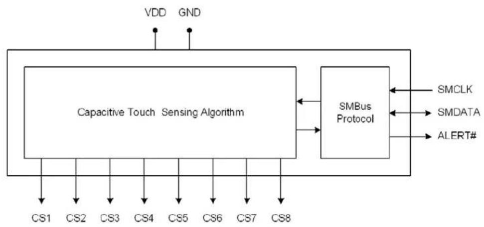
flowchart
graph TD
    A["VDD"] --> B["Capacitive Touch Sensing Algorithm"]
    C["GND"] --> B
    B --> D["SMBus Protocol"]
    D --> E["SMCLK"]
    D --> F["SMDATA"]
    D --> G["ALERT#"]
    H["CS1"] --> B
    I["CS2"] --> B
    J["CS3"] --> B
    K["CS4"] --> B
    L["CS5"] --> B
    M["CS6"] --> B
    N["CS7"] --> B
    O["CS8"] --> B
1.2 Pin Diagrams
FIGURE 1-2: CAP1208 14-PIN SOIC
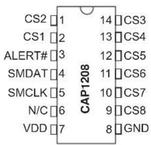
text_image
CS2 1 14 CS3 CS1 2 13 CS4 ALERT# 3 12 CS5 SMDAT 4 11 CS6 SMCLK 5 10 CS7 N/C 6 9 CS8 VDD 7 8 GND CAP1208FIGURE 1-3: CAP1208 PIN DIAGRAM (16-PIN QFN)
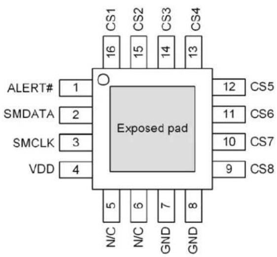
text_image
CS1 CS2 CS3 CS4 16 15 14 13 O Exposed pad 12 CS5 SMDATA 2 11 CS6 SMCLK 3 10 CS7 VDD 4 9 CS8 N/C N/C GND GND 5 6 7 81.3 Pin Description
TABLE 1-1: PIN DESCRIPTION FOR CAP1208
| QFN Pin # | SOIC Pin # | Pin Name Pin | Function Pin Type | Unused Connection | |
| 1 3 ALERT# | ALERT# - Active low alert / interrupt output for SMBus alert | OD | Connect to Ground | ||
| 2 4 SMDATA | SMDATA - Bi-directional, open-drain SMBus or I^2C data - requires pull-up resistor | DIOD n/a | |||
| 3 5 SMCLK | SMCLK - SMBus or I^2C clock input - requires pull-up resistor | DI n/a | |||
| 4 7 VDD | Positive | Power supply | Power n/a | ||
| 5 6 | N/C | Not internally connected | n/a | Connect to Ground | |
| 6 | - | N/C | Not internally connected | n/a | Connect to Ground |
| 7 | 8 | GND | Ground | Power | n/a |
| 8 | - | GND | Ground | Power | n/a |
| 9 9 | CS8 | Capacitive Touch Sensor Input 8 | AIO | Connect to Ground | |
| QFN Pin # | SOIC Pin # | Pin Name | Pin Function | Pin Type | Unused Connection |
| 10 10 CS7 | Capacitive Touch Sensor Input 7 | AIO | Connect to Ground | ||
| 11 11 CS6 | Capacitive Touch Sensor Input 6 | AIO | Connect to Ground | ||
| 12 12 CS5 | Capacitive Touch Sensor Input 5 | AIO | Connect to Ground | ||
| 13 13 CS4 | Capacitive Touch Sensor Input 4 | AIO | Connect to Ground | ||
| 14 14 CS3 | Capacitive Touch Sensor Input 3 | AIO | Connect to Ground | ||
| 15 1 CS2 | Capacitive Touch Sensor Input 2 | AIO | Connect to Ground | ||
| 16 2 CS1 | Capacitive Touch Sensor Input 1 | AIO | Connect to Ground | ||
| Bottom pad | - | Exposed pad | Not internally connected, but recommend grounding | - | - |
APPLICATION NOTE: All digital pins are 5V tolerant pins.
The pin types are described in Table 1-2, "Pin Types".
TABLE 1-2: PIN TYPES
| Pin Type Description | |
| Power This pin is used to supply power or ground to the device. | |
| DI Digital Input - This pin is used as a digital input. This pin is 5V tolerant. | |
| AIO Analog Input / Output - This pin is used as an I/O for analog signals. | |
| DIOD | Digital Input / Open Drain Output - This pin is used as a digital I/O. When it is used as an output, it is open drain and requires a pull-up resistor. This pin is 5V tolerant. |
| OD | Open Drain Digital Output - This pin is used as a digital output. It is open drain and requires a pull-up resistor. This pin is 5V tolerant. |
2.0 ELECTRICAL SPECIFICATIONS
TABLE 2-1: ABSOLUTE MAXIMUM RATINGS
| Voltage on VDD pin -0.3 to 6.5 V | ||
| Voltage on CS pins to GND -0.3 to 4.0 V | ||
| Voltage on 5V tolerant pins (V5VT_PIN) -0.3 to 5.5 V | ||
| Voltage on 5V tolerant pins (|V5VT_PIN - V_DD|) (see Note 2-2) 0 to 3.6 V | ||
| Input current to any pin except VDD | ±10 mA | |
| Output short circuit current Continuous N/A | ||
| Package Power Dissipation up to TA = 85°C for 16-pin QFN (see Note 2-3) | 0.5 | W |
| Junction to Ambient (θJA) (see Note 2-4) | 70 | °C/W |
| Operating Ambient Temperature Range | -40 to 125 | °C |
| Storage Temperature Range | -55 to 150 °C | |
| ESD Rating, All Pins, HBM | 8000 | V |
Note 2-1 Stresses above those listed could cause permanent damage to the device. This is a stress rating only and functional operation of the device at any other condition above those indicated in the operation sections of this specification is not implied.
Note 2-2 For the 5V tolerant pins that have a pull-up resistor, the voltage difference between V_5VT_PIN and V_DD must never exceed 3.6V.
Note 2-3 The Package Power Dissipation specification assumes a recommended thermal via design consisting of a 2x2 matrix of 0.3mm (12mil) vias at 1.0mm pitch connected to the ground plane with a 1.6 x 1.6mm thermal landing.
Note 2-4 Junction to Ambient ( _JA ) is dependent on the design of the thermal vias. Without thermal vias and a thermal landing, the _JA will be higher.
TABLE 2-2: ELECTRICAL SPECIFICATIONS
| V_DD=3V to 5.5V, T_A=0°C to 85°C, all Typical values at T_A=25°C unless otherwise noted. | ||||||
| Characteristic Symbol Min Typ Max Unit Conditions | ||||||
| DC Power | ||||||
| Supply Voltage V | DD | 3.0 5.5 | V | |||
| Supply Current | I_STBY\_DEF | 120 170 μA | Standby state active1 sensor input monitoredDefault conditions (8 avg, 70mscycle time) | |||
| I_STBY\_LP | 50 μA | Standby state active1 sensor input monitored1 avg, 140ms cycle time | ||||
| I_DSLEEP\_3V | 5 | TBD | μA | Deep Sleep state activeNo communications T_A<40°C3.135 | ||
| \(I_{DD} | 500 750 μA | Capacitive Sensing Active | ||||
| Capacitive Touch Sensor Inputs | ||||||
| Maximum Base Capacitance | C_BASE | 50 | pF | Pad untouched | ||
| Minimum Detectable Capacitive Shift | C_TOUCH | 20 | fF | Pad touched - default conditions | ||
| Recommended Cap Shift | C_TOUCH | 0.1 | 2 | pF | Pad touched - Not tested | |
| Power Supply Rejection | PSR | ±3 ±10 | counts/V | Untouched Current CountsBase Capacitance 5pF - 50pFNegative Delta Counts disabledMaximum sensitivityAll other parameters default | ||
| Power-On and Brown-out Reset (see Section 4.2, "Reset") | ||||||
| Power-On Reset Voltage | V_POR | 1 | 1.3 V | Pin States Defined | ||
| Power-On Reset Release Voltage | V_PORR | 2.85 | V | Rising V_DD Ensured by design | ||
| Brown-Out Reset V | BOR | 2.8 | V | Falling V_DD | ||
| VDD Rise Rate(ensures internalPOR signal) | SV_DD | 0.05 | V/ms | 0 to 3V in 60ms | ||
| Power-Up Timer Period | t_PWRT | 10 | ms | |||
| Brown-Out Reset Voltage Delay | t_BORDC | 1 | μsV | DD=V_BOR-1 | ||
| Characteristic | Symbol | Min | Typ | Max | Unit | Conditions |
| Timing | ||||||
| Time to Communications Ready | t_COMM\_DLY | 15 ms | ||||
| Time to First Conversion Ready | t_CONV\_DLY | 170 200 ms | ||||
| I/O Pins | ||||||
| Output Low Voltage V | OL | 0.4 V I | SINK_IO=8mA | |||
| Output High Voltage V | OH | V_DD-0.4 | V | I_SOURCE_IO=8mA | ||
| Input High Voltage V | IH | 2.0 V | ||||
| Input Low Voltage V | IL | 0.8 V | ||||
| Leakage Current I | LEAK | ±5 μA | powered or unpowered T_A<85°C pull-up voltage ≤ 3.6V if unpowered | |||
| SMBus Timing | ||||||
| Input Capacitance C | IN | 5 | pF | |||
| Clock Frequency f | SMB | 10 | 400 | kHz | ||
| Spike Suppression | t_SP | 50 | ns | |||
| Bus Free Time Stop to Start | t_BUF | 1.3 | μs | |||
| Start Setup Time | t_SU:STA | 0.6 | μs | |||
| Start Hold Time | t_HD:STA | 0.6 | μs | |||
| Stop Setup Time | t_SU:STO | 0.6 | μs | |||
| Data Hold Time | t_HD:DAT | 0 | μs | When transmitting to the master | ||
| Data Hold Time | t_HD:DAT | 0.3 | μs | When receiving from the master | ||
| Data Setup Time | t_SU:DAT | 0.6 | μs | |||
| Clock Low Period | t_LOW | 1.3 | μs | |||
| Clock High Period t | HIGH | 0.6 | μs | |||
| Clock / Data Fall Time | t_FALL | 300 | ns | Min = 20+0.1 C_LOAD ns | ||
| Clock / Data Rise Time | t_RISE | 300 | ns | Min = 20+0.1 C_LOAD ns | ||
| Capacitive Load C | LOAD | 400 | pF | per bus line | ||
3.0 COMMUNICATIONS
3.1 Communications
The CAP1208 communicates using the SMBus or I ^2 C protocol.
3.2 System Management Bus
The CAP1208 communicates with a host controller, such as an MCHP SIO, through the SMBus. The SMBus is a two-wire serial communication protocol between a computer host and its peripheral devices. A detailed timing diagram is shown in Figure 3-1. Stretching of the SMCLK signal is supported; however, the CAP1208 will not stretch the clock signal.
FIGURE 3-1: SMBUS TIMING DIAGRAM

text_image
SMCLK T_LOW T_HIGH T_FALL T_HD:STA T_SU:STA T_RISE T_HD:STA T_HD:DAT T_SU:DAT S-MAT T_BUX P S S - Start Condition S P - Stop Condition P3.2.1 SMBUS START BIT
The SMBus Start bit is defined as a transition of the SMBus Data line from a logic '1' state to a logic '0' state while the SMBus Clock line is in a logic '1' state.
3.2.2 SMBUS ADDRESS AND RD / WR BIT
The SMBus Address Byte consists of the 7-bit client address followed by the RD / WR indicator bit. If this RD / WR bit is a logic '0', then the SMBus Host is writing data to the client device. If this RD / WR bit is a logic '1', then the SMBus Host is reading data from the client device.
The CAP1208-1 responds to SMBus address 0101_000(r/w). The CAP1208-2 responds to the SMBus address 0101_001(r/w).
3.2.3 SMBUS DATA BYTES
All SMBus Data bytes are sent most significant bit first and composed of 8-bits of information.
3.2.4 SMBUS ACK AND NACK BITS
The SMBus client will acknowledge all data bytes that it receives. This is done by the client device pulling the SMBus Data line low after the 8th bit of each byte that is transmitted. This applies to both the Write Byte and Block Write protocols.
The Host will NACK (not acknowledge) the last data byte to be received from the client by holding the SMBus data line high after the 8th data bit has been sent. For the Block Read protocol, the Host will ACK each data byte that it receives except the last data byte.
3.2.5 SMBUS STOP BIT
The SMBus Stop bit is defined as a transition of the SMBus Data line from a logic '0' state to a logic '1' state while the SMBus clock line is in a logic '1' state. When the CAP1208 detects an SMBus Stop bit and it has been communicating with the SMBus protocol, it will reset its client interface and prepare to receive further communications.
3.2.6 SMBUS TIMEOUT
The CAP1208 includes an SMBus timeout feature. Following a 30ms period of inactivity on the SMBus where the SMCLK pin is held low, the device will timeout and reset the SMBus interface.
The timeout function defaults to disabled. It can be enabled by setting the TIMEOUT bit in the Configuration register (see Section 5.6, "Configuration Registers").
3.2.7 SMBUS AND I ^2 C COMPATIBILITY
The major differences between SMBus and I ^2 C devices are highlighted here. For more information, refer to the SMBus 2.0 specification.
- CAP1208supports I ^2 C fast mode at 400kHz. This covers the SMBus max time of 100kHz.
- Minimum frequency for SMBus communications is 10kHz.
- The SMBus client protocol will reset if the clock is held low longer than 30ms (timeout condition). This can be enabled in the CAP1208 by setting the TIMEOUT bit in the Configuration register. I^2C does not have a timeout.
- The SMBus client protocol will reset if both the clock and the data line are high for longer than 200us (idle condition). This can be enabled in the CAP1208by setting the TIMEOUT bit in the Configuration register. ^2 C does not have an idle condition.
- I ^2 C devices do not support the Alert Response Address functionality (which is optional for SMBus).
- I ^2 C devices support block read and write differently. I ^2 C protocol allows for unlimited number of bytes to be sent in either direction. The SMBus protocol requires that an additional data byte indicating number of bytes to read / write is transmitted. The CAP1208 supports I ^2 C formatting only.
3.3 SMBus Protocols
The CAP1208 is SMBus 2.0 compatible and supports Write Byte, Read Byte, Send Byte, and Receive Byte as valid protocols as shown below.
All of the below protocols use the convention in Table 3-1.
TABLE 3-1: PROTOCOL FORMAT
| Data Sent to Device | Data Sent to the H0st |
| Data sent Data sent | |
3.3.1 SMBUS WRITE BYTE
The Write Byte is used to write one byte of data to a specific register as shown in Table 3-2.
TABLE 3-2: WRITE BYTE PROTOCOL
| Start | Slave Address | WR ACK | Register Address | ACK | Register Data | ACK Stop |
| 1 ->0 | 0101_000 (Note 3-1) | 0 0 XXh 0 XXh 0 | 0 -> 1 |
Note 3-1 CAP1208-1 only. For other addressing options, see Section 3.2.2.
3.3.2 SMBUS READ BYTE
The Read Byte protocol is used to read one byte of data from the registers as shown in Table 3-3.
TABLE 3-3: READ BYTE PROTOCOL
| Start Slave Address WR ACK Register | Address | ACK Start Client Address RD ACK Register | Data | NACK Stop | |||||||
| 1->0 01 | 101_000(Note 3-2) | 0 | 0 | XXh | 0 | 1 ->0 | 0101_000(Note 3-2) | 1 0 | XXh | 1 | 0 ->1 |
Note 3-2 CAP1208-1 only. For other addressing options, see Section 3.2.2.
3.3.3 SMBUS SEND BYTE
The Send Byte protocol is used to set the internal address register pointer to the correct address location. No data is transferred during the Send Byte protocol as shown in Table 3-4.
APPLICATION NOTE: The Send Byte protocol is not functional in Deep Sleep (i.e., DSLEEP bit is set).
TABLE 3-4: SEND BYTE PROTOCOL
| Start | Slave Address | WR | ACK | Register Address | ACK | Stop |
| 1 -> 0 | 0101_000(Note 3-3) | 0 | 0 | XXh | 0 | 0 -> 1 |
Note 3-3 CAP1208-1 only. For other addressing options, see Section 3.2.2.
3.3.4 SMBUS RECEIVE BYTE
The Receive Byte protocol is used to read data from a register when the internal register address pointer is known to be at the right location (e.g. set via Send Byte). This is used for consecutive reads of the same register as shown in Table 3-5.
APPLICATION NOTE: The Receive Byte protocol is not functional in Deep Sleep (i.e., DSLEEP bit is set).
TABLE 3-5: RECEIVE BYTE PROTOCOL
| Start | Slave Address | RD | ACK | Register Data | NACK | Stop |
| 1 -> 0 | 0101_000(Note 3-4) | 1 | 0 | XXh | 1 | 0 -> 1 |
Note 3-4 CAP1208-1 only. For other addressing options, see Section 3.2.2.
3.4 I ^2 C Protocols
The CAP1208 supports I ^2 C Block Read and Block Write.
The protocols listed below use the convention in Table 3-1.
3.4.1 BLOCK READ
The Block Read is used to read multiple data bytes from a group of contiguous registers as shown in Table 3-6.
APPLICATION NOTE: When using the Block Read protocol, the internal address pointer will be automatically incremented after every data byte is received. It will wrap from FFh to 00h.
TABLE 3-6: BLOCK READ PROTOCOL
| Start Slave Address | WR ACK | Register | Address | ACK Start | Slave Address | RD ACK Register | Data | |||
| 1->0 | 0101_000 (Note 3-5) | 0 0 | XXh | 0 | 1 ->0 | 0101_000 (Note 3-5) | 1 | 0 | XXh | |
| ACK | REGISTER DATA | ACK | REGISTER DATA | ACK | REGISTER DATA | ACK... | REGISTER DATA | NACK STOP | ||
| 0 | XXh | 0 | XXh | 0 | XXh | 0 | ... | XXh | 1 | 0 -> 1 |
Note 3-5 CAP1208-1 only. For other addressing options, see Section 3.2.2..
3.4.2 BLOCK WRITE
The Block Write is used to write multiple data bytes to a group of contiguous registers as shown in Table 3-7.
APPLICATION NOTE: When using the Block Write protocol, the internal address pointer will be automatically incremented after every data byte is received. It will wrap from FFh to 00h.
TABLE 3-7: BLOCK WRITE PROTOCOL
| Start | Slave Address WR | ACK | Register Address | ACK | Register Data | ACK | |
| 1 ->0 | 0101_000 (Note 3-6) | 0 | 0 | XXh | 0 | XXh | 0 |
| Register Data | ACK | Register Data | ACK | ... | Register Data | ACK Stop | |
| XXh | 0 | XXh | 0 | ... | XXh | 0 | 0 -> 1 |
Note 3-6 CAP1208-1 only. For other addressing options, see Section 3.2.2..
4.0 GENERAL DESCRIPTION
The CAP1208 is a multiple channel capacitive touch sensor. It contains eight (8) individual capacitive touch sensor inputs with programmable sensitivity for use in touch sensor applications. Each sensor input is calibrated to compensate for system parasitic capacitance and automatically recalibrated to compensate for gradual environmental changes.
The CAP1208 includes Multiple Pattern Touch recognition that allows the user to select a specific set of buttons to be touched simultaneously. If this pattern is detected, a status bit is set and an interrupt is generated.
The CAP1208 has Active and Standby states, each with its own sensor input configuration controls. Power consumption in the Standby state is dependent on the number of sensor inputs enabled as well as averaging, sampling time, and cycle time. Deep Sleep is the lowest power state available, drawing 5 A (typical) of current. In this state, no sensor inputs are active, and communications will wake the device.
The device communicates with a host controller using SMBus / I ^2 C. The host controller may poll the device for updated information at any time or it may configure the device to flag an interrupt whenever a touch is detected on any sensor pad.
A typical system diagram is shown in FIGURE 4-1:.
FIGURE 4-1: SYSTEM DIAGRAM FOR CAP1208

flowchart
graph TD
    A["10kOhm resistors"] --> B["3.0V to 5.5V"]
    B --> C["Embedded Controller"]
    C --> D["GND"]
    C --> E["SMCLK"]
    C --> F["SMDATA"]
    C --> G["ALERT#"]
    C --> H["VDD"]
    I["Touch Button"] --> J["CS1"]
    K["Touch Button"] --> L["CS2"]
    M["Touch Button"] --> N["CS3"]
    O["Touch Button"] --> P["CS4"]
    Q["3.0V to 5.5V"] --> R["0.1uF"]
    S["1.0uF"] --> T["Ground"]
    U["CS8"] --> V["CAP1208"]
    W["CS7"] --> V
    X["CS6"] --> V
    Y["CS5"] --> V
    Z["Touch Button"] --> V
    AA["Touch Button"] --> V
4.1 Power States
The CAP1208 has 3 power states depending on the status of the STBY and DSLEEP bits. When the device transitions between power states, previously detected touches (for channels that are being de-activated) are cleared and the sensor input status bits are reset.
-
Active - The normal mode of operation. The device is monitoring capacitive sensor inputs enabled in the Active state.
-
Standby - When the STBY bit is set, the device is monitoring the capacitive sensor inputs enabled in the Standby state. Interrupts can still be generated based on the enabled channels. The device will still respond to communications normally and can be returned to the Active state of operation by clearing the STBY bit. Power consumption in this state is dependent on the number of sensor inputs enabled as well as averaging, sampling time, and cycle time.
- Deep Sleep - When the DSLEEP bit is set, the device is in its lowest power state. It is not monitoring any capacitive sensor inputs. While in Deep Sleep, the CAP1208 can be awakened by SMBus communications targeting the device. This will not cause the DSLEEP to be cleared so the device will return to Deep Sleep once all communications have stopped. The device can be returned to the Active state of operation by clearing the DSLEEP bit.
4.2 Reset
The Power-On Reset (POR) circuit holds the device in reset until V_DD has reached an acceptable level, Power-on Reset Release Voltage ( V_PORR ), for minimum operation. The power-up timer (PWRT) is used to extend the start-up period until all device operation conditions have been met. The power-up timer starts after V_DD reaches V_PORR . POR and PORR with slow rising V_DD is shown in Figure 4-2.
The Brown-Out Reset (BOR) circuit holds the device in reset when V_DD falls to a minimum level, V_BOR for longer than the BOR reset delay ( t_BORDC ). After a BOR, when V_DD rises above V_PORR , the power-up timer is started again and must finish before reset is released, as shown in Figure 4-2.
FIGURE 4-2: POR AND PORR WITH SLOW RISING V
DD AND BOR WITH FALLING V_DD
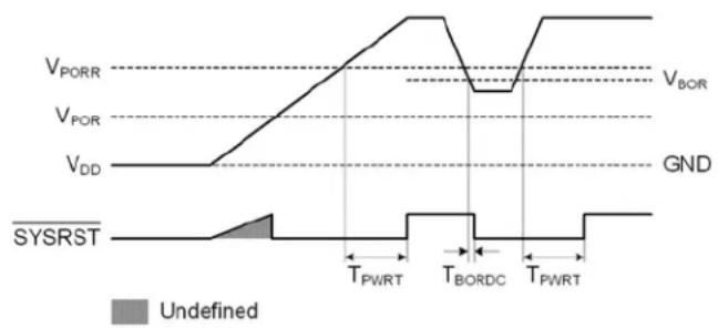
line
| Signal | Value | |--------|-------| | V_PORR | V_POR | | V_POR | V_DD | | V_BOR | V_BOR | | GND | GND | | SYSRST | undefined (gray shaded area) | | T_PWRT | T_PWRT | | T_BORDC | T_BORDC | | T_PWRT | T_PWRT |4.3 Capacitive Touch Sensing
The CAP1208 contains eight (8) independent capacitive touch sensor inputs. Each sensor input has dynamic range to detect a change of capacitance due to a touch. Additionally, each sensor input can be configured to be automatically and routinely recalibrated.
4.3.1 CAPACITIVE TOUCH SENSING SETTINGS
Controls for managing capacitive touch sensor inputs are determined by the power state.
4.3.1.1 Active State Sensing Settings
The Active state is used for normal operation. Sensor inputs being monitored are determined by the Sensor Input Enable Register(see Section 5.7, "Sensor Input Enable Register"). Sensitivity is controlled by the Sensitivity Control Register (see Section 5.5, "Sensitivity Control Register"). Averaging, sample time, and cycle time are controlled by the Averaging and Sampling Configuration Register (see Section 5.10, "Averaging and Sampling Configuration Register"). Each channel can have a separate touch detection threshold, as defined in the Sensor Input Threshold registers (see Section 5.18, "Sensor Input Threshold Registers").
4.3.1.2 Standby State Sensing Settings
The Standby state is used for standby operation. In general, fewer sensor inputs are enabled, and they are programmed to have more sensitivity. Sensor inputs being monitored are determined by the Standby Channel Register (see Section 5.20, "Standby Channel Register"). Sensitivity is controlled by the Standby Sensitivity Register (see Section 5.22,
"Standby Sensitivity Register"). Averaging, sample time, and cycle time are controlled by the Averaging and Sampling Configuration Register (see Section 5.21, "Standby Configuration Register"). There is one touch detection threshold, which applies to all sensors enabled in Standby, as defined in the Standby Threshold Register (see Section 5.23, "Standby Threshold Register").
4.3.2 SENSING CYCLE
Except when in Deep Sleep, the device automatically initiates a sensing cycle and repeats the cycle every time it finishes. The cycle polls through each enabled sensor input starting with CS1 and extending through CS8. As each capacitive touch sensor input is polled, its measurement is compared against a baseline "not touched" measurement. If the delta measurement is large enough to exceed the applicable threshold, a touch is detected and an interrupt can be generated (see Section 4.8.2, "Capacitive Sensor Input Interrupt Behavior").
The sensing cycle time is programmable (see Section 5.10, "Averaging and Sampling Configuration Register" and Section 5.21, "Standby Configuration Register"). If all enabled inputs can be sampled in less than the cycle time, the device is placed into a lower power state for the remainder of the sensing cycle. If the number of active sensor inputs cannot be sampled within the specified cycle time, the cycle time is extended and the device is not placed in a lower power state.
4.4 Sensor Input Calibration
Calibration sets the Base Count Registers(Section 5.24, "Sensor Input Base Count Registers") which contain the "not touched" values used for touch detection comparisons. Calibration automatically occurs after a power-on reset (POR), when sample time is changed, and whenever a sensor input is newly enabled (for example, when transitioning from a power state in which it was disabled to a power state in which it is enabled). During calibration, the analog sensing circuits are tuned to the capacitance of the untouched pad. Then, samples are taken from each sensor input so that a base count can be established. After calibration, the untouched delta counts are zero.
APPLICATION NOTE: During the calibration routine, the sensor inputs will not detect a press for up to 200ms and the Sensor Base Count Register values will be invalid. In addition, any press on the corresponding sensor pads will invalidate the calibration.
The host controller can force a calibration for selected sensor inputs at any time using the Calibration Activate and Status Register Section 5.10.1, "Calibration Activate and Status Register". When a bit is set, the corresponding capacitive touch sensor input will be calibrated (both analog and digital). The bit is automatically cleared once the calibration routine has successfully finished.
If analog calibration fails for a sensor input, the corresponding bit is not cleared in the Calibration Activate and Status Register, and the ACAL_FAIL bit is set in the General Status Register(Section 5.2, "Status Registers"). An interrupt can be generated. Analog calibration will fail if a noise bit is set or if the calibration value is at the maximum or minimum value. If digital calibration fails to generate base counts for a sensor input in the operating range, which is ± 12.5% from the ideal base count (see TABLE 4-1:), indicating the base capacitance is out of range, the corresponding BC_OUTx bit is set in the Base Count Out of Limit Register(Section 5.16, "Base Count Out of Limit Register"), and the BC_OUT bit is set in the General Status Register (Section 5.2, "Status Registers"). An interrupt can be generated. By default, when a base count is out of limit, analog calibration is repeated for the sensor input; alternatively, the sensor input can be sampled using the out of limit base count(Section 5.6, "Configuration Registers").
TABLE 4-1: IDEAL BASE COUNTS
| Ideal Base Count Sample Time | |
| 3,200 320us | |
| 6,400 640us | |
| 12,800 1.28ms | |
| 25,600 2.56ms | |
During normal operation there are various options for recalibrating the capacitive touch sensor inputs. Recalibration is a digital adjustment of the base counts so that the untouched delta count is zero. After a recalibration, if a sensor input's base count has shifted ±12.5% from the ideal base count, a full calibration will be performed on the sensor input.
4.4.1 AUTOMATIC RECALIBRATION
Each sensor input is regularly recalibrated at a programmable rate(see CAL_CFG[2:0] in Section 5.17, "Recalibration Configuration Register"). By default, the recalibration routine stores the average 64 previous measurements and periodically updates the base "not touched" setting for the capacitive touch sensor input.
APPLICATION NOTE: Automatic recalibration only works when the delta count is below the active sensor input threshold. It is disabled when a touch is detected.
4.4.2 NEGATIVE DELTA COUNT RECALIBRATION
It is possible that the device loses sensitivity to a touch. This may happen as a result of a noisy environment, recalibration when the pad is touched but delta counts do not exceed the threshold, or other environmental changes. When this occurs, the base untouched sensor input may generate negative delta count values. The NEG_DELTA_CNT[1:0] bits(see Section 5.17, "Recalibration Configuration Register") can be set to force a recalibration after a specified number of consecutive negative delta readings. After a delayed recalibration (see Section 4.4.3, "Delayed Recalibration") the negative delta count recalibration can correct after the touch is released.
APPLICATION NOTE: During this recalibration, the device will not respond to touches.
4.4.3 DELAYED RECALIBRATION
It is possible that a "stuck button" occurs when something is placed on a button which causes a touch to be detected for a long period. By setting the MAX_DUR_EN bit(see Section 5.6, "Configuration Registers"), a recalibration can be forced when a touch is held on a button for longer than the duration specified in the MAX_DUR[3:0] bits (see Section 5.8, "Sensor Input Configuration Register").
Note 4-1 Delayed recalibration only works when the delta count is above the active sensor input threshold. If enabled, it is invoked when a sensor pad touch is held longer than the MAX_DUR bit settings.
Note 4-2 For the power button, which requires that the button be held longer than a regular button, the time specified by the MAX_DUR[3:0] bits is added to the time required to trigger the qualifying event. This will prevent the power button from being recalibrated during the time it is supposed to be held.
4.5 Power Button
The CAP1208 has a "power button" feature. In general, buttons are set for quick response to a touch, especially when buttons are used for number keypads. However, there are cases where a quick response is not desired, such as when accidentally brushing the power button causes a device to turn off or on unexpectedly.
The power button feature allows a sensor input to be designated as the "power button" (see Section 5.25, "Power Button Register"). The power button is configured so that a touch must be held on the button for a designated period of time before an interrupt is generated; different times can be selected for the Standby and the Active states (see Section 5.26, "Power Button Configuration Register"). The feature can also be enabled / disabled for both states separately.
APPLICATION NOTE: For the power button feature to work in the Standby and/or Active states, the sensor input must be enabled in the applicable state.
After the designated power button has been held for the designated time, an interrupt is generated and the PWR bit is set in the General Status Register (see Section 5.2, "Status Registers").
4.6 Multiple Touch Pattern Detection
The multiple touch pattern (MTP) detection circuitry can be used to detect lid closure or other similar events. An event can be flagged based on either a minimum number of sensor inputs or on specific sensor inputs simultaneously exceeding an MTP threshold or having their Noise Flag Status Register bits set. An interrupt can also be generated. During an MTP event, all touches are blocked (see Section 5.14, "Multiple Touch Pattern Configuration Register").
4.7 Noise Controls
4.7.1 LOW FREQUENCY NOISE DETECTION
Each sensor input has a low frequency noise detector that will sense if low frequency noise is injected onto the input with sufficient power to corrupt the readings. By default, if this occurs, the device will reject the corrupted samplesee DIS_ANA_NOISE bit in Section 5.6.1, "Configuration - 20h") and the corresponding bit is set to a logic '1' in the Noise Flag Status register (see SHOW_RF_NOISE bit in Section 5.6.2, "Configuration 2 - 44h").
4.7.2 RF NOISE DETECTION
Each sensor input contains an integrated RF noise detector. This block will detect injected RF noise on the CS pin. The detector threshold is dependent upon the noise frequency. By default, if RF noise is detected on a CS line, that sample is removed and not compared against the threshold (see DIS_RF_NOISE bit in Section 5.6.2, "Configuration 2 - 44h").
4.7.3 NOISE STATUS AND CONFIGURATION
The Noise Flag Status (see Section 5.3, "Noise Flag Status Registers") bits can be used to indicate RF and/or other noise. If the SHOW_RF_NOISE bit in the Configuration Register (see Section 5.6, "Configuration Registers") is set to 0, the Noise Flag Status bit for the capacitive sensor input is set if any analog noise is detected. If the SHOW_RF_NOISE bit is set to 1, the Noise Flag Status bits will only be set if RF noise is detected.
The CAP1208 offers optional noise filtering controls for both analog and digital noise.
For analog noise, there are options for whether the data should be considered invalid. By default, the DIS_ANA_NOISE bit (see Section 5.6.1, "Configuration - 20h") will block a touch on a sensor input if low frequency analog noise is detected; the sample is discarded. By default, the DIS_RF_NOISE bit (see Section 5.6.2, "Configuration 2 - 44h") will block a touch on a sensor input if RF noise is detected; the sample is discarded.
For digital noise, sensor input noise thresholds can be set (see Section 5.19, "Sensor Input Noise Threshold Register"). If a capacitive touch sensor input exceeds the Sensor Noise Threshold but does not exceed the touch threshold (Sensor Threshold (see Section 5.18, "Sensor Input Threshold Registers") in the Active state or Sensor Standby Threshold in the Standby state (Section 5.23, "Standby Threshold Register")), it is determined to be caused by a noise spike. The DIS_DIG_NOISE bit (see Section 5.6.1, "Configuration - 20h") can be set to discard samples that indicate a noise spike so they are not used in the automatic recalibration routine (see Section 4.4.1, "Automatic Recalibration").
4.8 Interrupts
Interrupts are indicated by the setting of the INT bit in the Main Control Register(see Section 5.1, "Main Control Register") and by assertion of the ALERT# pin. The ALERT# pin is cleared when the INT bit is cleared by the user. When the INT bit is cleared by the user, status bits may be cleared (see Section 5.2, "Status Registers").
4.8.1 ALERT# PIN
The ALERT# pin is an active low output that is driven when an interrupt event is detected.
4.8.2 CAPACITIVE SENSOR INPUT INTERRUPT BEHAVIOR
Each sensor input can be programmed to enable / disable interrupts(see Section 5.11, "Interrupt Enable Register").
When enabled for a sensor input and the sensor input is not the designated power button, interrupts are generated in one of two ways:
- An interrupt is generated when a touch is detected and, as a user selectable option, when a release is detected (by default - see INT_REL_n in Section 5.6.2, "Configuration 2 - 44h"). See FIGURE 4-4:.
- If the repeat rate is enabled then, so long as the touch is held, another interrupt will be generated based on the programmed repeat rate (see FIGURE 4-3:).
When the repeat rate is enabled for a sensor input (see Section 5.12, "Repeat Rate Enable Register"), the device uses an additional control called MPRESS that determines whether a touch is flagged as a simple "touch" or a "press and hold" (see Section 5.9, "Sensor Input Configuration 2 Register"). The MPRESS[3:0] bits set a minimum press timer. When the button is touched, the timer begins. If the sensor pad is released before the minimum press timer expires, it is flagged as a touch and an interrupt (if enabled) is generated upon release. If the sensor input detects a touch for longer than this timer value, it is flagged as a "press and hold" event. So long as the touch is held, interrupts will be generated at the programmed repeat rate (see Section 5.8, "Sensor Input Configuration Register") and upon release (if enabled).
If a sensor input is the designated power button, an interrupt is not generated as soon as a touch is detected and repeat rate is not applicable. See Section 4.8.3, "Interrupts for the Power Button".
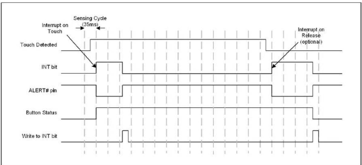
APPLICATION NOTE: FIGURE 4-3: and FIGURE 4-4: show default operation which is to generate an interrupt upon sensor pad release.
APPLICATION NOTE: The host may need to poll the device twice to determine that a release has been detected.
FIGURE 4-3: SENSOR INTERRUPT BEHAVIOR - REPEAT RATE ENABLED

text_image
Sensing Cycle (35ms) Interrupt on Touch Touch Detected Min Press Setting (280ms) Button Repeat Rate (175ms) Button Repeat Rate (175ms) Interrupt on Release (optional) INT bit ALERT# pin Button Status Write to INT bitFIGURE 4-4: SENSOR INTERRUPT BEHAVIOR - NO REPEAT RATE ENABLED
text_image
Sensing Cycle (35ms) Interrupt on Touch Touch Detected INT bit Interrupt on Release (optional) ALERT# pin Button Status Write to INT bit4.8.3 INTERRUPTS FOR THE POWER BUTTON
Interrupts are automatically enabled for the power button when the feature is enabled (see Section 4.5, "Power Button"). A touch must be held on the power button for the designated period of time before an interrupt is generated.
4.8.4 INTERRUPTS FOR MULTIPLE TOUCH PATTERN DETECTION
An interrupt can be generated when the MTP pattern is matched (see Section 5.14, "Multiple Touch Pattern Configuration Register").
4.8.5 INTERRUPTS FOR SENSOR INPUT CALIBRATION FAILURES
An interrupt can be generated when the ACAL_FAIL bit is set, indicating the failure to complete analog calibration of one or more sensor inputs(see Section 5.2, "Status Registers"). This interrupt can be enabled by setting the ACAL_FAIL_INT bit (see Section 5.6, "Configuration Registers").
An interrupt can be generated when the BC_OUT bit is set, indicating the base count is out of limit for one or more sensor inputs(see Section 5.2, "Status Registers"). This interrupt can be enabled by setting the BC_OUT_INT bit (see Section 5.6, "Configuration Registers").
4.8.6 INTERRUPTS FOR RESET
When the device comes out of reset, an interrupt is generated, and the RESET bit is set.
5.0 REGISTER DESCRIPTION
The registers shown in Table 5-1 are accessible through the communications protocol. An entry of '-' indicates that the bit is not used and will always read '0'.
TABLE 5-1: REGISTER SET IN HEXADECIMAL ORDER
| Register Address | R/W Register Name Function | Default Value | Page | ||
| 00h R/W | Main Control | Controls power states and indicates an interrupt | 00h Page 24 | ||
| 02h R/W | General Status Stores general status | bits 00h Page 25 | |||
| 03h R Sensor Input Status | Returns the state of the sampled capacitive touch sensor inputs | 00h Page 25 | |||
| 0Ah | R Noise Flag Status | Stores the noise flags for sensor inputs | 00h Page 26 | ||
| 10h R | Sensor Input 1 Delta Count | Stores the delta count for CS1 | 00h Page 26 | ||
| 11h | R | Sensor Input 2 Delta Count | Stores the delta count for CS2 | 00h Page 26 | |
| 12h R | Sensor Input 3 Delta Count | Stores the delta count for CS3 | 00h Page 26 | ||
| 13h R | Sensor Input 4 Delta Count | Stores the delta count for CS4 | 00h Page 26 | ||
| 14h R | Sensor Input 5 Delta Count | Stores the delta count for CS5 | 00h Page 26 | ||
| 15h R | Sensor Input 6 Delta Count | Stores the delta count for CS6 | 00h Page 26 | ||
| 16h R | Sensor Input 7 Delta Count | Stores the delta count for CS7 | 00h Page 26 | ||
| 17h R | Sensor Input 8 Delta Count | Stores the delta count for CS8 | 00h Page 26 | ||
| 1Fh R/W | Sensitivity Control | Controls the sensitivity of the threshold and delta counts and data scaling of the base counts | 2Fh Page 27 | ||
| 20h | R/W | Configuration | Controls general functionality | 20h | Page 29 |
| 21h R/W | Sensor Input Enable | Controls which sensor inputs are monitored in Active | FFh | Page 30 | |
| 22h R/W | Sensor Input Configuration | Controls max duration and auto-repeat delay | A4h Page 31 | ||
| 23h R/W | Sensor Input Configuration 2 | Controls the MPRESS (“press and hold”) setting | 07h Page 32 | ||
| 24h R/W | Averaging and Sampling Config | Controls averaging and sampling window for Active | 39h Page 33 | ||
| Register Address | R/W | Register Name | Function | Default Value | Page |
| 26h R/W | Calibration Activate and Status | Forces calibration for capacitive touch sensor inputs and indicates calibration failure | 00h Page | 35 | |
| 27h R/W | Interrupt Enable | Determines which capacitive sensor inputs can generate interrupts | FFh Page | 36 | |
| 28h R/W | Repeat Rate Enable | Enables repeat rate for specific sensor inputs | FFh Page | 36 | |
| 2Ah R/W | Multiple Touch Configuration | Determines the number of simultaneous touches to flag a multiple touch condition | 80h Page | 37 | |
| 2Bh R/W | Multiple Touch Pattern Configuration | Determines the multiple touch pattern (MTP) configuration | 00h Page | 38 | |
| 2Dh R/W | Multiple Touch Pattern | Determines the pattern or number of sensor inputs used by the MTP circuitry | FFh Page | 39 | |
| 2Eh R | Base Count Out of Limit | Indicates whether sensor inputs have a base count out of limit | 00h Page | 39 | |
| 2Fh R/W | Recalibration Configuration | Determines recalibration timing and sampling window | 8Ah Page | 40 | |
| 30h R/W | Sensor Input 1 Threshold | Stores the touch detection threshold for Active for CS1 | 40h Page | 42 | |
| 31h R/W | Sensor Input 2 Threshold | Stores the touch detection threshold for Active for CS2 | 40h Page | 42 | |
| 32h R/W | Sensor Input 3 Threshold | Stores the touch detection threshold for Active for CS3 | 40h Page | 42 | |
| 33h R/W | Sensor Input 4 Threshold | Stores the touch detection threshold for Active for CS4 | 40h Page | 42 | |
| 34h R/W | Sensor Input 5 Threshold | Stores the touch detection threshold for Active for CS5 | 40h Page | 42 | |
| 35h R/W | Sensor Input 6 Threshold | Stores the touch detection threshold for Active for CS6 | 40h Page | 42 | |
| 36h R/W | Sensor Input 7 Threshold | Stores the touch detection threshold for Active for CS7 | 40h | Page 42 | |
| 37h R/W | Sensor Input 8 Threshold | Stores the touch detection threshold for Active for CS8 | 40h | ||
| 38h R/W | Sensor Input Noise Threshold | Stores controls for selecting the noise threshold for all sensor inputs | 01h Page | 42 | |
| Standby Configuration Registers | |||||
| 40h R/W | Standby Channel | Controls which sensor inputs are enabled for Standby | 00h Page | 43 | |
| 41h R/W | Standby Configuration | Controls averaging and sensing cycle time for Standby | 39h Page | 43 | |
| Register Address | R/W Register Name | Function | Default Value | Page | |
| 42h R/W | Standby Sensitivity | Controls sensitivity settings used for Standby | 02h Page 45 | ||
| 43h R/W | Standby Threshold | Stores the touch detection threshold for Standby | 40h Page 46 | ||
| 44h R/W | Configuration 2 | Stores additional configuration controls for the device | 40h Page 29 | ||
| Base Count Registers | |||||
| 50h R | Sensor Input 1 Base Count | Stores the reference count value for sensor input 1 | C8h Page 46 | ||
| 51h R | Sensor Input 2 Base Count | Stores the reference count value for sensor input 2 | C8h Page 46 | ||
| 52h R | Sensor Input 3 Base Count | Stores the reference count value for sensor input 3 | C8h Page 46 | ||
| 53h R | Sensor Input 4 Base Count | Stores the reference count value for sensor input 4 | C8h Page 46 | ||
| 54h R | Sensor Input 5 Base Count | Stores the reference count value for sensor input 5 | C8h Page 46 | ||
| 55h R | Sensor Input 6 Base Count | Stores the reference count value for sensor input 6 | C8h Page 46 | ||
| 56h R | Sensor Input 7 Base Count | Stores the reference count value for sensor input 7 | C8h Page 46 | ||
| 57h R | Sensor Input 8 Base Count | Stores the reference count value for sensor input 8 | C8h Page 46 | ||
| Power Button Registers | |||||
| 60h R/W | Power Button Specifies the power button 00h Page 47 | ||||
| 61h R/W | Power Button Configuration | Configures the power button feature 22h Page 47 | |||
| Calibration Registers | |||||
| B1h | R Sensor Input 1 Calibration | Stores the upper 8-bit calibration value for CS1 | 00h Page 48 | ||
| B2h | R Sensor Input 2 Calibration | Stores the upper 8-bit calibration value for CS2 | 00h Page 48 | ||
| B3h | R Sensor Input 3 Calibration | Stores the upper 8-bit calibration value for CS3 | 00h | Page 48 | |
| B4h | R Sensor Input 4 Calibration | Stores the upper 8-bit calibration value for CS4 | 00h Page 48 | ||
| B5h | R Sensor Input 5 Calibration | Stores the upper 8-bit calibration value for CS5 | 00h Page 48 | ||
| B6h | R Sensor Input 6 Calibration | Stores the upper 8-bit calibration value for CS6 | 00h Page 48 | ||
| Register Address | R/W | Register Name | Function | Default Value | Page |
| B7h | R Sensor Input 7 Calibration | Stores the upper 8-bit calibration value for CS7 | 00h Page 48 | ||
| B8h | R Sensor Input 8 Calibration | Stores the upper 8-bit calibration value for CS8 | 00h Page 48 | ||
| B9h | R Sensor Input Calibration LSB 1 | Stores the 2 LSBs of the calibration value for CS1 - CS4 | 00h Page 48 | ||
| BAh | R Sensor Input Calibration LSB 2 | Stores the 2 LSBs of the calibration value for CS5 - CS8 | 00h Page 48 | ||
| ID Registers | |||||
| FDh R Product ID | Stores a fixed value that identifies the CAP1208 | 6Bh Page 49 | |||
| FEh R Manufacturer ID | Stores a fixed value that identifies MCHP | 5Dh Page 49 | |||
| FFh R Revision | Stores a fixed value that represents the revision number | 00h Page 49 | |||
During power-on reset (POR), the default values are stored in the registers. A POR is initiated when power is first applied to the part and the voltage on the VDD supply surpasses the POR level as specified in the electrical characteristics.
When a bit is "set", this means it's at a logic '1'. When a bit is "cleared", this means it's at a logic '0'.
5.1 Main Control Register
TABLE 5-2: MAIN CONTROL REGISTER
| Addr | R/W | Register | B7 | B6 | B5 | B4 | B3 | B2 | B1 | B0 | Default |
| 00h | R/W | Main Control | - | - | STBY | DSLEEP | - | - | - | INT | 00h |
The Main Control register controls the primary power state of the device (see Section 4.1, "Power States").
Bit 5 - STBY - Enables Standby.
- '0' (default) - The device is not in the Standby state.
- '1' - The device is in the Standby state. Capacitive touch sensor input scanning is limited to the sensor inputs set in the Standby Channel register (see Section 5.20, "Standby Channel Register"). The status registers will not be cleared until read. Sensor inputs that are no longer sampled will flag a release and then remain in a non-touched state.
Bit 4 - DSLEEP - Enables Deep Sleep.
- '0' (default) - The device is not in the Deep Sleep state.
- '1' - The device is in the Deep Sleep state. All sensor input scanning is disabled. The status registers are automatically cleared and the INT bit is cleared. When this bit is set, the STBY bit has no effect.
Bit 0 - INT - Indicates that there is an interrupt (see Section 4.8, "Interrupts"). When this bit is set, it asserts the ALERT# pin. If a channel detects a touch but interrupts are not enabled for that channel (see Section 5.11, "Interrupt Enable Register"), no action is taken. This bit is cleared by writing a logic '0' to it. When this bit is cleared, the ALERT# pin will be deasserted, and all status registers will be cleared if the condition has been removed.
- '0' - No interrupt pending.
- '1' - An interrupt condition occurred, and the ALERT# pin has been asserted.
5.2 Status Registers
TABLE 5-3: STATUS REGISTERS
| Addr R | W Register B7 | B6 | B5 | B4 | B3 | B2 | B1 | B0 | Default | |||||
| 02h | R | General Status | - | BC_OUT | ACAL_FAIL | PWR | RESET | MULT | MTP | TOUCH | 00h | |||
| 03h | R | Sensor Input Status | CS8 | CS7 | CS6 | CS5 | CS4 | CS3 | CS2 | CS1 | 00h | |||
All status bits are cleared when the device enters Deep Sleep (DSLEEP = '1' - see Section 5.1, "Main Control Register").
5.2.1 GENERAL STATUS - 02H
Bit 6 - BC_OUT - Indicates that the base count is out of limit for one or more enabled sensor inputs (see Section 4.4, "Sensor Input Calibration"). This bit will not be cleared until all enabled sensor inputs have base counts within the limit.
- '0' - All enabled sensor inputs have base counts in the operating range.
- '1' - One or more enabled sensor inputs has the base count out of limit. A status bit is set in the Base Count Out of Limit Register (see Section 5.16, "Base Count Out of Limit Register").
Bit 5 - ACAL_FAIL - Indicates analog calibration failure for one or more enabled sensor inputs (see Section 4.4, "Sensor Input Calibration"). This bit will not be cleared until all enabled sensor inputs have successfully completed analog calibration.
- '0' - All enabled sensor inputs were successfully calibrated.
- '1' - One or more enabled sensor inputs failed analog calibration. A status bit is set in the Calibration Active Register (see Section 5.10.1, "Calibration Activate and Status Register").
Bit 4 - PWR - Indicates that the designated power button has been held for the designated time (see Section 4.5, "Power Button"). This bit will cause the INT bit to be set. This bit is cleared when the INT bit is cleared if there is no longer a touch on the power button.
- '0' - The power button has not been held for the required time or is not enabled.
- '1' - The power button has been held for the required time.
Bit 3 - RESET - Indicates that the device has come out of reset. This bit is set when the device exits a POR state. This bit will cause the INT bit to be set and is cleared when the INT bit is cleared.
Bit 2 - MULT - Indicates that the device is blocking detected touches due to the Multiple Touch detection circuitry (see Section 5.13, "Multiple Touch Configuration Register"). This bit will not cause the INT bit to be set and hence will not cause an interrupt.
Bit 1 - MTP - Indicates that the device has detected a number of sensor inputs that exceed the MTP threshold either via the pattern recognition or via the number of sensor inputs (see Section 5.14, "Multiple Touch Pattern Configuration Register"). This bit will cause the INT bit to be set if the MTP_ALERT bit is also set. This bit is cleared when the INT bit is cleared if the condition that caused it to be set has been removed.
Bit 0 - TOUCH - Indicates that a touch was detected. This bit is set if any bit in the Sensor Input Status register is set.
5.2.2 SENSOR INPUT STATUS - 03H
The Sensor Input Status Register stores status bits that indicate a touch has been detected. A value of '0' in any bit indicates that no touch has been detected. A value of '1' in any bit indicates that a touch has been detected.
All bits are cleared when the INT bit is cleared and if a touch on the respective capacitive touch sensor input is no longer present. If a touch is still detected, the bits will not be cleared (but this will not cause the interrupt to be asserted).
Bit 7 - CS8 - Indicates that a touch was detected on Sensor Input 8.
Bit 6 - CS7 - Indicates that a touch was detected on Sensor Input 7.
Bit 5 - CS6 - Indicates that a touch was detected on Sensor Input 6.
Bit 4 - CS5 - Indicates that a touch was detected on Sensor Input 5.
Bit 3 - CS4 - Indicates that a touch was detected on Sensor Input 4.
Bit 2 - CS3 - Indicates that a touch was detected on Sensor Input 3.
Bit 1 - CS2 - Indicates that a touch was detected on Sensor Input 2.
Bit 0 - CS1 - Indicates that a touch was detected on Sensor Input 1.
5.3 Noise Flag Status Registers
TABLE 5-4: NOISE FLAG STATUS REGISTERS
| Addr R | W Register | B7 B6 B5 B4 B3 | B2 B1 B0 | Default | |||||||
| 0Ah | R | Noise Flag Status | CS8_NOISE | CS7_NOISE | CS6_NOISE | CS5_NOISE | CS4_NOISE | CS3_NOISE | CS2_NOISE | CS1_NOISE | 00h |
The Noise Flag Status registers store status bits that can be used to indicate that the analog block detected noise above the operating region of the analog detector or the RF noise detector (see Section 4.7.3, "Noise Status and Configuration"). These bits indicate that the most recently received data from the sensor input is invalid and should not be used for touch detection. So long as the bit is set for a particular channel, the delta count value is reset to 00h and thus no touch is detected.
These bits are not sticky and will be cleared automatically if the analog block does not report a noise error.
APPLICATION NOTE: If the MTP detection circuitry is enabled, these bits count as sensor inputs above the MTP threshold (see Section 4.6, "Multiple Touch Pattern Detection") even if the corresponding delta count is not. If the corresponding delta count also exceeds the MTP threshold, it is not counted twice.
APPLICATION NOTE: Regardless of the state of the Noise Status bits, if low frequency noise is detected on a sensor input, that sample will be discarded unless the DIS_ANA_NOISE bit is set. As well, if RF noise is detected on a sensor input, that sample will be discarded unless the DIS_RF_NOISE bit is set.
5.4 Sensor Input Delta Count Registers
TABLE 5-5: SENSOR INPUT DELTA COUNT REGISTERS
| Addr | R/W | Register | B7 | B6 | B5 | B4 | B3 | B2 | B1 | B0 | Default |
| 10h | R | Sensor Input 1 Delta Count | Sign | 64 32 | 16 | 8 4 2 1 | 00h | ||||
| 11h | R | Sensor Input 2 Delta Count | Sign | 64 32 | 16 | 8 4 2 1 | 00h | ||||
| 12h | R | Sensor Input 3 Delta Count | Sign | 64 32 | 16 | 8 4 2 1 | 00h | ||||
| 13h | R | Sensor Input 4 Delta Count | Sign | 64 32 | 16 | 8 4 2 1 | 00h | ||||
| 14h | R | Sensor Input 5 Delta Count | Sign | 64 32 | 16 | 8 4 2 1 | 00h | ||||
| 15h R | Sensor Input 6 Delta Count | Sign 64 | 32 16 8 4 | 2 1 00h | |||||||
| 16h R | Sensor Input 7 Delta Count | Sign 64 | 32 16 8 4 | 2 1 00h | |||||||
| 17h R | Sensor Input 8 Delta Count | Sign 64 | 32 16 8 4 | 2 1 00h |
The Sensor Input Delta Count registers store the delta count that is compared against the threshold used to determine if a touch has been detected. The count value represents a change in input due to the capacitance associated with a touch on one of the sensor inputs and is referenced to a calibrated base "not touched" count value. The delta is an instantaneous change and is updated once per sensor input per sensing cycle (see Section 4.3.2, "Sensing Cycle").
The value presented is a standard 2's complement number. In addition, the value is capped at a value of 7Fh. A reading of 7Fh indicates that the sensitivity settings are too high and should be adjusted accordingly (see Section 5.5).
The value is also capped at a negative value of 80h for negative delta counts which may result upon a release.
5.5 Sensitivity Control Register
TABLE 5-6: SENSITIVITY CONTROL REGISTER
| Addr | R/W | Register | B7 | B6 | B5 | B4 | B3 | B2 | B1 | B0 | Default |
| 1Fh | R/W | Sensitivity Control | - | DELTA_SENSE[2:0] | BASE_SHIFT[3:0] | 2Fh | |||||
The Sensitivity Control register controls the sensitivity of a touch detection.
Bits 6-4 DELTA_SENSE[2:0] - Controls the sensitivity of a touch detection for sensor inputs enabled in the Active state. The sensitivity settings act to scale the relative delta count value higher or lower based on the system parameters. A setting of 000b is the most sensitive while a setting of 111b is the least sensitive. At the more sensitive settings, touches are detected for a smaller delta capacitance corresponding to a "lighter" touch. These settings are more sensitive to noise, however, and a noisy environment may flag more false touches with higher sensitivity levels.
APPLICATION NOTE: A value of 128x is the most sensitive setting available. At the most sensitive settings, the MSB of the Delta Count register represents 64 out of \~25,000 which corresponds to a touch of approximately 0.25% of the base capacitance (or a C of 25fF from a 10pF base capacitance). Conversely, a value of 1x is the least sensitive setting available. At these settings, the MSB of the Delta Count register corresponds to a delta count of 8192 counts out of \~25,000 which corresponds to a touch of approximately 33% of the base capacitance (or a C of 3.33pF from a 10pF base capacitance).
TABLE 5-7: DELTA_SENSE BIT DECODE
| DELTA_SENSE[2:0] | Sensitivity Multiplier | ||
| 2 | 1 | 0 | |
| 0 | 0 | 0 | 128x (most sensitive) |
| 0 | 0 | 1 | 64x |
| 0 | 1 | 0 | 32x (default) |
| 0 1 1 16x | |||
| 1 | 0 | 0 | |
| 1 | 0 | 1 | |
| 1 | 1 | 0 | |
| 1 1 1 1x - (least sensitive) | |||
Bits 3 - 0 - BASE_SHIFT[3:0] - Controls the scaling and data presentation of the Base Count registers. The higher the value of these bits, the larger the range and the lower the resolution of the data presented. The scale factor represents the multiplier to the bit-weighting presented in these register descriptions.
APPLICATION NOTE: The BASE_SHIFT[3:0] bits normally do not need to be updated. These settings will not affect touch detection or sensitivity. These bits are sometimes helpful in analyzing the Cap Sensing board performance and stability.
TABLE 5-8: BASE_SHIFT BIT DECODE
| BASE_SHIFT[3:0] | Data Scaling Factor | |||
| 3 | 2 | 1 | 0 | |
| 0 | 0 | 0 | 0 | |
| 0 | 0 | 0 | 1 | |
| 0 | 0 | 1 | 0 | |
| 0 | 0 | 1 | 1 | |
| 0 | 1 | 0 | 0 | |
| 0 | 1 | 0 | 1 | |
| 0 | 1 | 1 | 0 | |
| 0 1 | 1 | 1 | 128x | |
| 1 0 | 0 | 0 | 256x | |
| All others | 256x (default = 1111b) | |||
5.6 Configuration Registers
The Configuration registers control general global functionality that affects the entire device.
5.6.1 CONFIGURATION - 20H
Bit 7 - TIMEOUT - Enables the timeout and idle functionality of the SMBus protocol.
- '0' (default) - The SMBus timeout and idle functionality are disabled. The SMBus interface will not time out if the clock line is held low. Likewise, it will not reset if both the data and clock lines are held high for longer than 200us.
- '1' - The SMBus timeout and idle functionality are enabled. The SMBus interface will reset if the clock line is held low for longer than 30ms. Likewise, it will reset if both the data and clock lines are held high for longer than 200us.
Bit 5 - DIS_DIG_NOISE - Determines whether the digital noise threshold (see Section 5.19, "Sensor Input Noise Threshold Register") is used by the device. Setting this bit disables the feature.
- '0' - The digital noise threshold is used. If a delta count value exceeds the noise threshold but does not exceed the touch threshold, the sample is discarded and not used for the automatic recalibration routine.
- '1' (default) - The noise threshold is disabled. Any delta count that is less than the touch threshold is used for the automatic recalibration routine.
Bit 4 - DIS_ANA_NOISE - Determines whether the analog noise filter is enabled. Setting this bit disables the feature.
- '0' (default) - If low frequency noise is detected by the analog block, the delta count on the corresponding channel is set to 0. Note that this does not require that Noise Status bits be set.
- '1' - A touch is not blocked even if low frequency noise is detected.
Bit 3 - MAX_DUR_EN - Determines whether the maximum duration recalibration is enabled.
- '0' (default) - The maximum duration recalibration functionality is disabled. A touch may be held indefinitely and no recalibration will be performed on any sensor input.
- '1' - The maximum duration recalibration functionality is enabled. If a touch is held for longer than the MAX_DUR bit settings (see Section 5.8), the recalibration routine will be restarted (see Section 4.4.3, "Delayed Recalibration").
5.6.2 CONFIGURATION 2 - 44H
Bit 6 - BC_OUT_RECAL - Controls whether to retry analog calibration when the base count is out of limit for one or more sensor inputs.
- '0' - When the BC_OUTx bit is set for a sensor input, the out of limit base count will be used for the sensor input.
- '1' (default) - When the BC_OUTx bit is set for a sensor input (see Section 5.16, "Base Count Out of Limit Register"), analog calibration will be repeated on the sensor input.
Bit 5 - BLK_PWR_CTRL - Determines whether the device will reduce power consumption while waiting between conversion time completion and the end of the sensing cycle.
- '0' (default) - The device will reduce power consumption during the time between the end of the last conversion and the end of the sensing cycle.
- '1' - The device will not reduce power consumption during the time between the end of the last conversion and the end of the sensing cycle.
Bit 4 - BC_OUT_INT - Controls the interrupt behavior when the base count is out of limit for one or more sensor inputs.
- '0' (default) - An interrupt is not generated when the BC_OUT bit is set (see Section 5.2, "Status Registers").
- '1' - An interrupt is generated when the BC_OUT bit is set.
Bit 3 - SHOW_RF_NOISE - Determines whether the Noise Status bits will show RF Noise as the only input source.
- '0' (default) - The Noise Status registers will show both RF noise and low frequency noise if either is detected on a capacitive touch sensor input.
- '1' - The Noise Status registers will only show RF noise if it is detected on a capacitive touch sensor input. Low frequency noise will still be detected and touches will be blocked normally; however, the status bits will not be updated.
Bit 2 - DIS_RF_NOISE - Determines whether the RF noise filter is enabled. Setting this bit disables the feature.
- '0' (default) - If RF noise is detected by the analog block, the delta count on the corresponding channel is set to 0. Note that this does not require that Noise Status bits be set.
- '1' - A touch is not blocked even if RF noise is detected.
Bit 1 - ACAL_FAIL_INT - Controls the interrupt behavior when analog calibration fails for one or more sensor inputs (see Section 4.4, "Sensor Input Calibration").
- '0' (default) - An interrupt is not generated when the ACAL_FAIL bit is set (see Section 5.2, "Status Registers").
- '1' - An interrupt is generated when the ACAL_FAIL bit is set
Bit 0 - INT_REL_n - Controls the interrupt behavior when a release is detected on a button (see Section 4.8.2, "Capacitive Sensor Input Interrupt Behavior").
- '0' (default) - An interrupt is generated when a press is detected and again when a release is detected and at the repeat rate (if enabled - see Section 5.12).
- '1' - An interrupt is generated when a press is detected and at the repeat rate but not when a release is detected.
5.7 Sensor Input Enable Register
TABLE 5-10: SENSOR INPUT ENABLE REGISTER
| Addr R/W Register B7 B6 B5 B4 B3 B2 B1 B0 Default | |||||||||||
| 21h R/W | Sensor Input Enable | CS8_EN C | CS7_EN CS6 | EN CS5_EN | CS4_EN C | CS3_EN CS2 | EN CS1_EN | FFh | |||
The Sensor Input Enable register determines whether a capacitive touch sensor input is included in the sensing cycle in the Active state.
For all bits in this register:
- '0' - The specified input is not included in the sensing cycle in the Active state.
- '1' (default) - The specified input is included in the sensing cycle in the Active state.
Bit 7 - CS8_EN - Determines whether the CS8 input is monitored in the Active state.
Bit 6 - CS7_EN - Determines whether the CS7 input is monitored in the Active state.
Bit 5 - CS6_EN - Determines whether the CS6 input is monitored in the Active state.
Bit 4 - CS5_EN - Determines whether the CS5 input is monitored in the Active state.
Bit 3 - CS4_EN - Determines whether the CS4 input is monitored in the Active state.
Bit 2 - CS3_EN - Determines whether the CS3 input is monitored in the Active state.
Bit 1 - CS2_EN - Determines whether the CS2 input is monitored in the Active state.
Bit 0 - CS1_EN - Determines whether the CS1 input is monitored in the Active state.
5.8 Sensor Input Configuration Register
TABLE 5-11: SENSOR INPUT CONFIGURATION REGISTER
| Addr R/W Register | B7 B6 B5 B4 B3 | B2 B1 B0 | Default | |||||||
| 22h R/W | Sensor InputConfiguration | MAX_DUR[3:0] RPT_RATE[3:0] A4h | ||||||||
The Sensor Input Configuration Register controls timings associated with the capacitive sensor inputs.
Bits 7 - 4 - MAX_DUR[3:0] - (default 1010b) - Determines the maximum time that a sensor pad is allowed to be touched until the capacitive touch sensor input is recalibrated (see Section 4.4.3, "Delayed Recalibration"), as shown in Table 5-12.
TABLE 5-12: MAX_DUR BIT DECODE
| MAX_DUR[3:0] | Time before Recalibration | |||
| 3 | 2 | 1 | 0 | |
| 0 | 0 | 0 | 0 | 560ms |
| 0 | 0 | 0 | 1 | 840ms |
| 0 | 0 | 1 | 0 | 1120ms |
| 0 | 0 | 1 | 1 | 1400ms |
| 0 | 1 | 0 | 0 | 1680ms |
| 0 | 1 | 0 | 1 | 2240ms |
| 0 | 1 | 1 | 0 | 2800ms |
| 0 | 1 | 1 | 1 | 3360ms |
| 1 | 0 | 0 | 0 | 3920ms |
| 1 | 0 | 0 | 1 | 4480ms |
| 1 | 0 | 1 | 0 | 5600ms (default) |
| 1 | 0 | 1 | 1 | 6720ms |
| 1 | 1 | 0 | 0 | 7840ms |
| 1 | 1 | 0 | 1 | 8906ms |
| 1 | 1 | 1 | 0 | 10080ms |
| 1 | 1 | 1 | 1 | 11200ms |
Bits 3 - 0 - RPT_RATE[3:0] - (default 0100b) Determines the time duration between interrupt assertions when auto repeat is enabled (see Section 4.8.2, "Capacitive Sensor Input Interrupt Behavior"). The resolution is 35ms and the range is from 35ms to 560ms as shown in Table 5-13.
TABLE 5-13: RPT_RATE BIT DECODE
| RPT_RATE[3:0] | Interrupt Repeat Rate | |||
| 3 | 2 | 1 | 0 | |
| 0 0 0 0 35ms | ||||
| 0 0 0 1 70ms | ||||
| 0 0 1 0 105ms | ||||
| 0 0 1 1 140ms | ||||
| 0 1 0 0 175ms (default) | ||||
| 0 1 0 1 210ms | ||||
| 0 1 1 0 245ms | ||||
| 0 1 1 1 280ms | ||||
| 1 0 0 0 315ms | ||||
| 1 0 0 1 350ms | ||||
| 1 0 1 0 385ms | ||||
| 1 0 1 1 420ms | ||||
| 1 1 0 0 455ms | ||||
| 1 1 0 1 490ms | ||||
| 1 1 1 0 525ms | ||||
| 1 1 1 1 560ms | ||||
5.9 Sensor Input Configuration 2 Register
TABLE 5-14: SENSOR INPUT CONFIGURATION 2 REGISTER
| Addr | R/W | Register | B7 | B6 | B5 | B4 | B3 | B2 | B1 | B0 | Default |
| 23h | R/W | Sensor Input Configuration 2 | - | - | - | - | M_PRESS[3:0] | 07h | |||
Bits 3 - 0 - M_PRESS[3:0] - (default 0111b) - Determines the minimum amount of time that sensor inputs configured to use auto repeat must detect a sensor pad touch to detect a "press and hold" event (see Section 4.8.2, "Capacitive Sensor Input Interrupt Behavior"). If the sensor input detects a touch for longer than the M_PRESS[3:0] settings, a "press and hold" event is detected. If a sensor input detects a touch for less than or equal to the M_PRESS[3:0] settings, a touch event is detected.
The resolution is 35ms and the range is from 35ms to 560ms as shown in Table 5-15.
TABLE 5-15: M_PRESS BIT DECODE
| M_PRESS[3:0] | M_PRESS Settings | |||
| 3 | 2 | 1 | 0 | |
| 0 0 0 0 35ms | ||||
| 0 0 0 1 70ms | ||||
| 0 0 1 0 105ms | ||||
| 0 0 1 1 140ms | ||||
| 0 1 0 0 175ms | ||||
| 0 1 0 1 210ms | ||||
| 0 1 1 0 245ms | ||||
| 0 1 1 1 280ms (default) | ||||
| 1 0 0 0 315ms | ||||
| 1 0 0 1 350ms | ||||
| 1 0 1 0 385ms | ||||
| 1 0 1 1 420ms | ||||
| 1 1 0 0 455ms | ||||
| 1 1 0 1 490ms | ||||
| 1 1 1 0 525ms | ||||
| 1 1 1 1 560ms | ||||
5.10 Averaging and Sampling Configuration Register
TABLE 5-16: AVERAGING AND SAMPLING CONFIGURATION REGISTER
| Addr | R/W | Register | B7 | B6 | B5 | B4 | B3 | B2 | B1 | B0 | Default |
| 24h | R/W | Averaging and Sampling Config | - | AVG[2:0] | SAMP_TIME[1:0] | CYCLE_TIME [1:0] | 39h | ||||
The Averaging and Sampling Configuration register controls the number of samples taken and the target sensing cycle time for sensor inputs enabled in the Active state.
Bits 6 - 4 - AVG[2:0] - Determines the number of samples that are taken for all channels enabled in the Active state during the sensing cycle as shown in Table 5-17. All samples are taken consecutively on the same channel before the next channel is sampled and the result is averaged over the number of samples measured before updating the measured results.
For example, if CS1, CS2, and CS3 are sampled during the sensing cycle, and the AVG[2:0] bits are set to take 4 samples per channel, then the full sensing cycle will be: CS1, CS1, CS1, CS1, CS2, CS2, CS2, CS2, CS3, CS3, CS3, CS3.
TABLE 5-17: AVG BIT DECODE
| AVG[2:0] | Number Of Samples Taken Per Measurement | ||
| 2 | 1 | 0 | |
| 0 | 0 | 0 | |
| 0 | 0 | 1 | |
| 0 | 1 | 0 | |
| 0 1 1 8 (default) | |||
| 1 | 0 | 0 | |
| 1 | 0 | 1 | |
| 1 | 1 | 0 | |
| 1 1 1 128 | |||
Bits 3 - 2 - SAMP_TIME[1:0] - Determines the time to take a single sample as shown in Table 5-18. Sample time affects the magnitude of the base counts, as shown in Table 4-1, "Ideal Base Counts".
TABLE 5-18: SAMP_TIME BIT DECODE
| SAMP_TIME[1:0] | Sample Time | |
| 1 | 0 | |
| 0 0 320us | ||
| 0 1 640us | ||
| 1 0 1.28ms (default) | ||
| 1 1 | 2.56ms | |
Bits 1 - 0 - CYCLE_TIME[1:0] - Determines the desired sensing cycle time for channels enabled in the Active state, as shown in Table 5-19. All enabled channels are sampled at the beginning of the sensing cycle. If additional time is remaining, the device is placed into a lower power state for the remainder of the sensing cycle.
TABLE 5-19: CYCLE_TIME BIT DECODE
| CYCLE_TIME[1:0] | Programmed Sensing Cycle Time | |
| 1 | 0 | |
| 0 0 | 35ms | |
| 0 1 | 70ms (default) | |
| 1 0 | 105ms | |
| 1 1 | 140ms | |
APPLICATION NOTE: The programmed sensing cycle time (CYCLE_TIME[1:0]) is only maintained if the actual time to take the samples is less than the programmed cycle time. The AVG[2:0] bits will take priority, so the sensing cycle time will be extended as necessary to accommodate the number of samples to be measured.
5.10.1 CALIBRATION ACTIVATE AND STATUS REGISTER
TABLE 5-20: CALIBRATION ACTIVATE AND STATUS REGISTER
| Addr R/W Register B7 B6 B5 B4 B3 B2 B1 B0 Default | |||||||||||
| 26h | R/W | Calibration Activate and Status | CS8_CAL | CS7_CAL | CS6_CAL | CS5_CAL | CS4_CAL | CS3_CAL | CS2_CAL | CS1_CAL | 00h |
The Calibration Activate and Status Register serves a dual function:
- It forces the selected sensor inputs to be calibrated, affecting both the analog and digital blocks (see Section 4.4, "Sensor Input Calibration"). When one or more bits are set, the device performs the calibration routine on the corresponding sensor inputs. When the analog calibration routine is finished, the CALX[9:0] bits are updated (see Section 5.27, "Sensor Input Calibration Registers"). If the analog calibration routine completed successfully for a sensor input, the corresponding bit is automatically cleared.
APPLICATION NOTE: In the case above, bits can be set by host or are automatically set by the device whenever a sensor input is newly enabled (such as coming out of Deep Sleep, after power-on reset, when a bit is set in the Sensor Enable Channel Enable register (21h) and the device is in the Active state, or when a bit is set in the Standby Channel Enable Register (40h) and the device is in the Standby state).
- It serves as an indicator of an analog calibration failure. If any of the bits could not be cleared, the ACAL_FAIL bit is set (see Section 5.2, "Status Registers"). A bit will fail to clear if a noise bit is set or if the calibration value is at the maximum or minimum value.
APPLICATION NOTE: In the case above, do not check the Calibration Activate and Status bits for failures unless the ACAL_FAIL bit is set. In addition, if a sensor input is newly enabled, do not check the Calibration Activate and Status bits until time has elapsed to complete calibration on the sensor input. Otherwise, the ACAL_FAIL bit may be set for one sensor input, but the newly enabled sensor input may still be set to '1' in the Calibration Activate and Status, not because it failed, but because it has not been calibrated yet.
For all bits in this register:
- '0' - No action needed.
- '1' - Writing a '1', forces a calibration on the corresponding sensor input. If the ACAL_FAIL flag is set and this bit is set (see application note above), the sensor input could not complete analog calibration.
Bit 7 - CS8_CAL - Bit for CS8 input.
Bit 6 - CS7_CAL - Bit for CS7 input.
Bit 5 - CS6_CAL - Bit for CS6 input.
Bit 4 - CS5_CAL - Bit for CS5 input.
Bit 3 - CS4_CAL - Bit for CS4 input.
Bit 2 - CS3_CAL - Bit for CS3 input.
Bit 1 - CS2_CAL - Bit for CS2 input.
Bit 0 - CS1_CAL - Bit for CS1 input.
APPLICATION NOTE: Writing a '0' to clear a '1' may cause a planned calibration to be skipped, if the calibration routine had not reached the sensor input yet.
5.11 Interrupt Enable Register
TABLE 5-21: INTERRUPT ENABLE REGISTER
| Addr R/W Register | B7 B6 B5 B4 | B3 B2 B1 | B0 Default | ||||||
| 27h R/W | Interrupt Enable | CS8_INT_EN | CS7_INT_EN | CS6_INT_EN | CS5_INT_EN | CS4_INT_EN | CS3_INT_EN | CS2_INT_EN | CS1_INT_EN |
The Interrupt Enable register determines whether a sensor pad touch or release (if enabled) causes an interrupt (see Section 4.8, "Interrupts").
For all bits in this register:
- '0' - The ALERT# pin will not be asserted if a touch is detected on the specified sensor input.
- '1' (default) - The ALERT# pin will be asserted if a touch is detected on the specified sensor input.
Bit 7 - CS8_INT_EN - Enables the ALERT# pin to be asserted if a touch is detected on CS8 (associated with the CS8 status bit).
Bit 6 - CS7_INT_EN - Enables the ALERT# pin to be asserted if a touch is detected on CS7 (associated with the CS7 status bit).
Bit 5 - CS6_INT_EN - Enables the ALERT# pin to be asserted if a touch is detected on CS6 (associated with the CS6 status bit).
Bit 4 - CS5_INT_EN - Enables the ALERT# pin to be asserted if a touch is detected on CS5 (associated with the CS5 status bit).
Bit 3 - CS4_INT_EN - Enables the ALERT# pin to be asserted if a touch is detected on CS4 (associated with the CS4 status bit).
Bit 2 - CS3_INT_EN - Enables the ALERT# pin to be asserted if a touch is detected on CS3 (associated with the CS3 status bit).
Bit 1 - CS2_INT_EN - Enables the ALERT# pin to be asserted if a touch is detected on CS2 (associated with the CS2 status bit).
Bit 0 - CS1_INT_EN - Enables the ALERT# pin to be asserted if a touch is detected on CS1 (associated with the CS1 status bit).
5.12 Repeat Rate Enable Register
TABLE 5-22: REPEAT RATE ENABLE REGISTER
| Addr | R/W | Register | B7 | B6 | B5 | B4 | B3 | B2 | B1 | B0 | Default |
| 28h | R/W | Repeat Rate Enable | CS8_RPT_EN | CS7_RPT_EN | CS6_RPT_EN | CS5_RPT_EN | CS4_RPT_EN | CS3_RPT_EN | CS2_RPT_EN | CS1_RPT_EN | FFh |
The Repeat Rate Enable register enables the repeat rate of the sensor inputs as described in Section 4.8.2, "Capacitive Sensor Input Interrupt Behavior".
For all bits in this register:
- '0' - The repeat rate for the specified sensor input is disabled. It will only generate an interrupt when a touch is detected and when a release is detected (if enabled) no matter how long the touch is held.
- '1' (default) - The repeat rate for the specified sensor input is enabled. In the case of a "touch" event, it will generate an interrupt when a touch is detected and a release is detected (as determined by the INT_REL_n bit - see Section 5.6, "Configuration Registers"). In the case of a "press and hold" event, it will generate an interrupt when a touch is detected and at the repeat rate so long as the touch is held.
Bit 7 - CS8_RPT_EN - Enables the repeat rate for capacitive touch sensor input 8.
Bit 6 - CS7_RPT_EN - Enables the repeat rate for capacitive touch sensor input 7.
Bit 5 - CS6_RPT_EN - Enables the repeat rate for capacitive touch sensor input 6.
Bit 4 - CS5_RPT_EN - Enables the repeat rate for capacitive touch sensor input 5.
Bit 3 - CS4_RPT_EN - Enables the repeat rate for capacitive touch sensor input 4.
Bit 2 - CS3_RPT_EN - Enables the repeat rate for capacitive touch sensor input 3.
Bit 1 - CS2_RPT_EN - Enables the repeat rate for capacitive touch sensor input 2.
Bit 0 - CS1_RPT_EN - Enables the repeat rate for capacitive touch sensor input 1.
5.13 Multiple Touch Configuration Register
TABLE 5-23: MULTIPLE TOUCH CONFIGURATION
| Addr R/W Register B7 B6 B5 B4 B3 B2 B1 | B0 | Default | |||||||
| 2Ah R/W | Multiple Touch Config | MULT_BLK_EN | - | - | - | B_MULT_T[1:0] | - | - | 80h |
The Multiple Touch Configuration register controls the settings for the multiple touch detection circuitry. These settings determine the number of simultaneous buttons that may be pressed before additional buttons are blocked and the MULT status bit is set.
Bit 7 - MULT_BLK_EN - Enables the multiple button blocking circuitry.
- '0' - The multiple touch circuitry is disabled. The device will not block multiple touches.
- '1' (default) - The multiple touch circuitry is enabled. The device will flag the number of touches equal to programmed multiple touch threshold and block all others. It will remember which sensor inputs are valid and block all others until that sensor pad has been released. Once a sensor pad has been released, the N detected touches (determined via the sensing cycle order of CS1 - CS8) will be flagged and all others blocked.
Bits 3 - 2 - B_MULT_T[1:0] - Determines the number of simultaneous touches on all sensor pads before a Multiple Touch Event is detected and sensor inputs are blocked. The bit decode is given by Table 5-24.
TABLE 5-24: B_MULT_T BIT DECODE
| B_MULT_T[1:0] | Number of Simultaneous Touches | |
| 1 | 0 | |
| 0 | 0 | 1 (default) |
| 0 | 1 | 2 |
| 1 | 0 | 3 |
| 1 | 1 | 4 |
5.14 Multiple Touch Pattern Configuration Register
TABLE 5-25: MULTIPLE TOUCH PATTERN CONFIGURATION
| Addr | R/W | Register | B7 | B6 | B5 | B4 | B3 | B2 | B1 | B0 | Default |
| 2Bh | R/W | Multiple Touch Pattern Config | MTP_EN - | - | - | MTP_TH[1:0] | COMP_PTRN | MTP_ALERT | 00h | ||
The Multiple Touch Pattern Configuration register controls the settings for the multiple touch pattern detection circuitry. This circuitry works like the multiple touch detection circuitry with the following differences:
- The detection threshold is a percentage of the touch detection threshold as defined by the MTP_TH[1:0] bits whereas the multiple touch circuitry uses the touch detection threshold.
-
The MTP detection circuitry either will detect a specific pattern of sensor inputs as determined by the Multiple Touch Pattern register settings or it will use the Multiple Touch Pattern register settings to determine a minimum number of sensor inputs that will cause the MTP circuitry to flag an event (see Section 5.15, "Multiple Touch Pattern Register"). When using pattern recognition mode, if all of the sensor inputs set by the Multiple Touch Pattern register have a delta count greater than the MTP threshold or have their corresponding Noise Flag Status bits set, the MTP bit will be set. When using the absolute number mode, if the number of sensor inputs with thresholds above the MTP threshold or with Noise Flag Status bits set is equal to or greater than this number, the MTP bit will be set.
-
When an MTP event occurs, all touches are blocked and an interrupt is generated.
-
All sensor inputs will remain blocked so long as the requisite number of sensor inputs are above the MTP threshold or have Noise Flag Status bits set. Once this condition is removed, touch detection will be restored. Note that the MTP status bit is only cleared by writing a '0' to the INT bit once the condition has been removed.
Bit 7 - MTP_EN - Enables the multiple touch pattern detection circuitry.
- '0' (default) - The MTP detection circuitry is disabled.
- '1' - The MTP detection circuitry is enabled.
Bits 3 - 2 - MTP_TH[1:0] - Determine the MTP threshold, as shown in Table 5-26. This threshold is a percentage of sensor input threshold (see Section 5.18, "Sensor Input Threshold Registers") for inputs enabled in the Active state or of the standby threshold (see Section 5.23, "Standby Threshold Register") for inputs enabled in the Standby state.
TABLE 5-26: MTP_TH BIT DECODE
| MTP_TH[1:0] | Threshold Divide Setting | |
| 1 | 0 | |
| 0 | 0 | 12.5% (default) |
| 0 | 1 | 25% |
| 1 | 0 | 37.5% |
| 1 | 1 | 100% |
Bit 1 - COMP_PTRN - Determines whether the MTP detection circuitry will use the Multiple Touch Pattern register as a specific pattern of sensor inputs or as an absolute number of sensor inputs.
- '0' (default) - The MTP detection circuitry will use the Multiple Touch Pattern register bit settings as an absolute minimum number of sensor inputs that must be above the threshold or have Noise Flag Status bits set. The number will be equal to the number of bits set in the register.
- '1' - The MTP detection circuitry will use pattern recognition. Each bit set in the Multiple Touch Pattern register indicates a specific sensor input that must have a delta count greater than the MTP threshold or have a Noise Flag Status bit set. If the criteria are met, the MTP status bit will be set.
Bit 0 - MTP_ALERT - Enables an interrupt if an MTP event occurs. In either condition, the MTP status bit will be set.
- '0' (default) - If an MTP event occurs, the ALERT# pin is not asserted.
- '1' - If an MTP event occurs, the ALERT# pin will be asserted.
5.15 Multiple Touch Pattern Register
TABLE 5-27: MULTIPLE TOUCH PATTERN REGISTER
| Addr R/W Register B7 B6 B5 | B4 B3 B2 | B1 B0 Default | |||||||||
| 2Dh | R/W | Multiple Touch Pattern | CS8_PTRN | CS7_PTRN | CS6_PTRN | CS5_PTRN | CS4_PTRN | CS3_PTRN | CS2_PTRN | CS1_PTRN | FFh |
The Multiple Touch Pattern register acts as a pattern to identify an expected sensor input profile for diagnostics or other significant events. There are two methods for how the Multiple Touch Pattern register is used: as specific sensor inputs or number of sensor input that must exceed the MTP threshold or have Noise Flag Status bits set. Which method is used is based on the COMP_PTRN bit (see Section 5.14). The methods are described below.
- Specific Sensor Inputs: If, during a single sensing cycle, the specific sensor inputs above the MTP threshold or with Noise Flag Status bits set match those bits set in the Multiple Touch Pattern register, an MTP event is flagged.
- Number of Sensor Inputs: If, during a single sensing cycle, the number of sensor inputs with a delta count above the MTP threshold or with Noise Flag Status bits set is equal to or greater than the number of pattern bits set, an MTP event is flagged.
For all bits in this register:
- '0' - The specified sensor input is not considered a part of the pattern.
- '1' - The specified sensor input is considered a part of the pattern, or the absolute number of sensor inputs that must have a delta count greater than the MTP threshold or have the Noise Flag Status bit set is increased by 1.
Bit 7 - CS8_PTRN - Determines whether CS8 is considered as part of the Multiple Touch Pattern.
Bit 6 - CS7_PTRN - Determines whether CS7 is considered as part of the Multiple Touch Pattern.
Bit 5 - CS6_PTRN - Determines whether CS6 is considered as part of the Multiple Touch Pattern.
Bit 4 - CS5_PTRN - Determines whether CS5 is considered as part of the Multiple Touch Pattern.
Bit 3 - CS4_PTRN - Determines whether CS4 is considered as part of the Multiple Touch Pattern.
Bit 2 - CS3_PTRN - Determines whether CS3 is considered as part of the Multiple Touch Pattern.
Bit 1 - CS2_PTRN - Determines whether CS2 is considered as part of the Multiple Touch Pattern.
Bit 0 - CS1_PTRN - Determines whether CS1 is considered as part of the Multiple Touch Pattern.
5.16 Base Count Out of Limit Register
TABLE 5-28: BASE COUNT OUT OF LIMIT REGISTER
| Addr | R/W | Register | B7 | B6 | B5 | B4 | B3 | B2 | B1 | B0 | Default |
| 2Eh | R | Base Count Out of Limit | BC_OUT_8 | BC_OUT_7 | BC_OUT_6 | BC_OUT_5 | BC_OUT_4 | BC_OUT_3 | BC_OUT_2 | BC_OUT_1 | 00h |
The Base Count Out of Limit Register indicates which sensor inputs have base counts out of limit (see Section 4.4, "Sensor Input Calibration"). When these bits are set, the BC_OUT bit is set (see Section 5.2, "Status Registers").
For all bits in this register:
- '0' - The base count for the specified sensor input is in the operating range.
- '1' - The base count of the specified sensor input is not in the operating range.
Bit 7 - BC_OUT_8 - Indicates whether CS8 has a base count out of limit.
Bit 6 - BC_OUT_7 - Indicates whether CS7 has a base count out of limit.
Bit 5 - BC_OUT_6 - Indicates whether CS6 has a base count out of limit.
Bit 4 - BC_OUT_5 - Indicates whether CS6 has a base count out of limit.
Bit 3 - BC_OUT_4 - Indicates whether CS6 has a base count out of limit.
Bit 2 - BC_OUT_3 - Indicates whether CS3 has a base count out of limit.
Bit 1 - BC_OUT_2 - Indicates whether CS2 has a base count out of limit.
Bit 0 - BC_OUT_1 - Indicates whether CS1 has a base count out of limit.
5.17 Recalibration Configuration Register
The Recalibration Configuration register controls some recalibration routine settings (see Section 4.4, "Sensor Input Calibration") as well as advanced controls to program the Sensor Input Threshold register settings.
Bit 7 - BUT_LD_TH - Enables setting all Sensor Input Threshold registers by writing to the Sensor Input 1 Threshold register.
- '0' - Each Sensor Input X Threshold register is updated individually.
- '1' (default) - Writing the Sensor Input 1 Threshold register will automatically overwrite the Sensor Input Threshold registers for all sensor inputs (Sensor Input Threshold 1 through Sensor Input Threshold 8). The individual Sensor Input X Threshold registers (Sensor Input 2 Threshold through Sensor Input 8 Threshold) can be individually updated at any time.
Bit 6 - NO_CLR_INTD - Controls whether the accumulation of intermediate data is cleared if the noise status bit is set.
- '0' (default) - The accumulation of intermediate data is cleared if the noise status bit is set.
- '1' - The accumulation of intermediate data is not cleared if the noise status bit is set.
APPLICATION NOTE: Bits 5 and 6 should both be set to the same value. Either both should be set to '0' or both should be set to '1'.
Bit 5 - NO_CLR_NEG - Controls whether the consecutive negative delta counts counter is cleared if the noise status bit is set.
'0' (default) - The consecutive negative delta counts counter is cleared if the noise status bit is set.
'1' - The consecutive negative delta counts counter is not cleared if the noise status bit is set.
Bits 4 - 3 - NEG_DELTA_CNT[1:0] - Determines the number of negative delta counts necessary to trigger a digital recalibration (see Section 4.4.2, "Negative Delta Count Recalibration"), as shown in Table 5-30.
TABLE 5-30: NEG_DELTA_CNT BIT DECODE
| NEG_DELTA_CNT[1:0] | Number of Consecutive Negative Delta Count Values | |
| 1 | 0 | |
| 0 | 0 | 8 |
| 0 1 16 (default) | ||
| 1 | 0 | 3 |
| 1 1 None (disabled) | ||
Bits 2 - 0 - CAL_CFG[2:0] - Determines the update time and number of samples of the automatic recalibration routine (see Section 4.4.1, "Automatic Recalibration"). The settings apply to all sensor inputs universally (though individual sensor inputs can be configured to support recalibration - see Section 5.10.1).
TABLE 5-31: CAL_CFG BIT DECODE
| CAL_CFG[2:0] | Recalibration Samples(see Note 5-1) | Update Time (see Note 5-2) | ||
| 2 | 1 | 0 | ||
| 0 0 0 16 16 | ||||
| 0 | 0 | 1 | 32 | |
| 0 1 0 64 | 64 (default) | |||
| 0 1 1 | 128 | 128 | ||
| 1 0 0 | 256 | 256 | ||
| 1 0 1 | 256 | 1024 | ||
| 1 1 0 | 256 | 2048 | ||
| 1 1 1 | 256 | 4096 | ||
Note 5-1 Recalibration Samples refers to the number of samples that are measured and averaged before the Base Count is updated however does not control the base count update period.
Note 5-2 Update Time refers to the amount of time (in sensing cycle periods) that elapses before the Base Count is updated. The time will depend upon the number of channels enabled, the averaging setting, and the programmed sensing cycle time.
5.18 Sensor Input Threshold Registers
TABLE 5-32: SENSOR INPUT THRESHOLD REGISTERS
| Addr R/W Register B7 B6 B5 B4 B3 B2 B1 B0 Default | ||||||||||
| 30h R/W | Sensor Input 1 Threshold | - | 6 | 4 | 3 | 2 | 1 | 6 | 8 | 4 2 |
| 31h R/W | Sensor Input 2 Threshold | - | 64 | 32 | 16 | 8 | 4 | 2 | 1 | 40h |
| 32h R/W | Sensor Input 3 Threshold | - | 64 | 32 | 16 | 8 | 4 | 2 | 1 | 40h |
| 33h R/W | Sensor Input 4 Threshold | - | 64 | 32 | 16 | 8 | 4 | 2 | 1 | 40h |
| 34h R/W | Sensor Input 5 Threshold | - | 64 | 32 | 16 | 8 | 4 | 2 | 1 | 40h |
| 35h R/W | Sensor Input 6 Threshold | - | 64 | 32 | 16 | 8 | 4 | 2 | 1 | 40h |
| 36h R/W | Sensor Input 7 Threshold | - | 64 | 32 | 16 | 8 | 4 | 2 | 1 | 40h |
| 37h R/W | Sensor Input 8 Threshold | - | 64 | 32 | 16 | 8 | 4 | 2 | 1 | 40h |
The Sensor Input Threshold registers store the delta threshold that is used to determine if a touch has been detected. When a touch occurs, the input signal of the corresponding sensor pad changes due to the capacitance associated with a touch. If the sensor input change exceeds the threshold settings, a touch is detected.
When the BUT_LD_TH bit is set (see Section 5.17 - bit 7), writing data to the Sensor Input 1 Threshold register will update all of the Sensor Input Threshold registers (31h - 37h inclusive).
5.19 Sensor Input Noise Threshold Register
TABLE 5-33: SENSOR INPUT NOISE THRESHOLD REGISTER
| Addr R/W | Register B7 | B6 B5 B4 | B3 B2 B1 | B0 Default | ||||||
| 38h | R/W | Sensor Input Noise Threshold | - | - | - | - | - | - | CS_BN_TH[1:0] | 01h |
The Sensor Input Noise Threshold register controls the value of a secondary internal threshold to detect noise and improve the automatic recalibration routine. If a capacitive touch sensor input exceeds the Sensor Input Noise Threshold but does not exceed the sensor input threshold, it is determined to be caused by a noise spike. That sample is not used by the automatic recalibration routine. This feature can be disabled by setting the DIS_DIG_NOISE bit.
Bits 1-0 - CS1_BN_TH[1:0] - Controls the noise threshold for all capacitive touch sensor inputs, as shown in Table 5-34. The threshold is proportional to the threshold setting.
TABLE 5-34: CSX_BN_TH BIT DECODE
| CS_BN_TH[1:0] | Percent Threshold Setting | |
| 1 | 0 | |
| 0 0 25% | ||
| 0 1 37.5% (default) | ||
| 1 0 50% | ||
| 1 1 62.5% | ||
5.20 Standby Channel Register
TABLE 5-35: STANDBY CHANNEL REGISTER
| Addr | R/W | Register | B7 | B6 | B5 | B4 | B3 | B2 | B1 | B0 | Default |
| 40h | R/W | Standby Channel | CS8_STBY | CS7_STBY | CS6_STBY | CS5_STBY | CS4_STBY | CS3_STBY | CS2_STBY | CS1_STBY | 00h |
The Standby Channel register controls which (if any) capacitive touch sensor inputs are enabled in Standby (see Section 4.3.1.2, "Standby State Sensing Settings").
For all bits in this register:
- '0' (default) - The specified channel will not be monitored in Standby.
- '1' - The specified channel will be monitored in Standby. It will use the standby threshold setting, and the standby averaging and sensitivity settings.
Bit 7 - CS8_STBY - Controls whether the CS8 channel is enabled in Standby.
Bit 6 - CS7_STBY - Controls whether the CS7 channel is enabled in Standby.
Bit 5 - CS6_STBY - Controls whether the CS6 channel is enabled in Standby.
Bit 4 - CS5_STBY - Controls whether the CS5 channel is enabled in Standby.
Bit 3 - CS4_STBY - Controls whether the CS4 channel is enabled in Standby.
Bit 2 - CS3_STBY - Controls whether the CS3 channel is enabled in Standby.
Bit 1 - CS2_STBY - Controls whether the CS2 channel is enabled in Standby.
Bit 0 - CS1_STBY - Controls whether the CS1 channel is enabled in Standby.
5.21 Standby Configuration Register
TABLE 5-36: STANDBY CONFIGURATION REGISTER
| Addr | R/W | Register | B7 | B6 | B5 | B4 | B3 | B2 | B1 | B0 | Default |
| 41h | R/W | StandbyConfiguration | AVG_SUM | STBY_AVG[2:0] | STBY_SAMP_TIME[1:0] | STBY_CY_TIME[1:0] | 39h | ||||
The Standby Configuration register controls averaging and sensing cycle time for sensor inputs enabled in Standby. This register allows the user to change averaging and sample times on a limited number of sensor inputs in Standby and still maintain normal functionality in the Active state.
Bit 7 - AVG_SUM - Determines whether the sensor inputs enabled in Standby will average the programmed number of samples or whether they will accumulate for the programmed number of samples.
- '0' - (default) - The Standby enabled sensor input delta count values will be based on the average of the programmed number of samples when compared against the threshold.
- '1' - The Standby enabled sensor input delta count values will be based on the summation of the programmed number of samples when compared against the threshold. Caution should be used with this setting as a touch may overflow the delta count registers and may result in false readings.
Bits 6 - 4 - STBY_AVG[2:0] - Determines the number of samples that are taken for all Standby enabled channels during the sensing cycle as shown in Table 5-37. All samples are taken consecutively on the same channel before the next channel is sampled and the result is averaged over the number of samples measured before updating the measured results.
TABLE 5-37: STBY_AVG BIT DECODE
| STBY_AVG[2:0] | Number Of Samples Taken Per Measurement | ||
| 2 | 1 | 0 | |
| 0 | 0 | 0 | |
| 0 | 0 | 1 | |
| 0 | 1 | 0 | |
| 0 1 1 8 (default) | |||
| 1 | 0 | 0 | |
| 1 | 0 | 1 | |
| 1 | 1 | 0 | |
| 1 1 1 128 | |||
Bit 3 - 2 - STBY_SAMP_TIME[1:0] - Determines the time to take a single sample for sensor inputs enabled in Standby as shown in Table 5-38.
TABLE 5-38: STBY_SAMP_TIME BIT DECODE
| STBY_SAMP_TIME[1:0] | Sampling Time | |
| 1 | 0 | |
| 0 0 320us | ||
| 0 1 640us | ||
| 1 0 | 1.28ms (default) | |
| 1 1 | 2.56ms | |
Bits 1 - 0 - STBY_CY_TIME[2:0] - Determines the desired sensing cycle time for sensor inputs enabled during Standby, as shown in Table 5-39. All enabled channels are sampled at the beginning of the sensing cycle. If additional time is remaining, the device is placed into a lower power state for the remainder of the sensing cycle.
TABLE 5-39: STBY_CY_TIME BIT DECODE
| STBY_CY_TIME[1:0] | Programmed Sensing Cycle Time | |
| 1 | 0 | |
| 0 0 35ms | ||
| 0 1 70ms (default) | ||
| 1 0 105ms | ||
| 1 1 140ms | ||
APPLICATION NOTE: The programmed sensing cycle time (STDBY_CY_TIME[1:0] is only maintained if the actual time to take the samples is less than the programmed cycle time. The STBY_AVG[2:0] bits will take priority, so the sensing cycle time will be extended as necessary to accommodate the number of samples to be measured.
5.22 Standby Sensitivity Register
TABLE 5-40: STANDBY SENSITIVITY REGISTER
| Addr | R/W | Register | B7 | B6 | B5 | B4 | B3 | B2 | B1 | B0 | Default |
| 42h | R/W | Standby Sensitivity | - | - | - | - | - | STBY_SENSE[2:0] | 02h | ||
The Standby Sensitivity register controls the sensitivity for sensor inputs enabled in Standby.
Bits 2 - 0 - STBY_SENSE[2:0] - Controls the sensitivity for sensor inputs that are enabled in Standby. The sensitivity settings act to scale the relative delta count value higher or lower based on the system parameters. A setting of 000b is the most sensitive while a setting of 111b is the least sensitive. At the more sensitive settings, touches are detected for a smaller delta capacitance corresponding to a "lighter" touch. These settings are more sensitive to noise, however, and a noisy environment may flag more false touches than higher sensitivity levels.
APPLICATION NOTE: A value of 128x is the most sensitive setting available. At the most sensitivity settings, the MSB of the Delta Count register represents 64 out of \~25,000 which corresponds to a touch of approximately 0.25% of the base capacitance (or a C of 25fF from a 10pF base capacitance). Conversely a value of 1x is the least sensitive setting available. At these settings, the MSB of the Delta Count register corresponds to a delta count of 8192 counts out of \~25,000 which corresponds to a touch of approximately 33% of the base capacitance (or a C of 3.33pF from a 10pF base capacitance).
TABLE 5-41: STBY_SENSE BIT DECODE
| STBY_SENSE[2:0] | Sensitivity Multiplier | ||
| 2 | 1 | 0 | |
| 0 | 0 | 0 | 128x (most sensitive) |
| 0 | 0 | 1 | 64x |
| 0 | 1 | 0 | 32x (default) |
| 0 1 1 16x | |||
| 1 | 0 | 0 | |
| 1 | 0 | 1 | |
| 1 | 1 | 0 | |
| 1 1 1 1x - (least sensitive) | |||
5.23 Standby Threshold Register
TABLE 5-42: STANDBY THRESHOLD REGISTER
| Addr R/W Register | B7 B6 B5 B4 B3 B2 B1 B0 | Default | ||||||||
| 43h R/W | Standby Threshold | - | 64 | 32 | 16 | 8 | 4 | 2 | 1 | 40h |
The Standby Threshold register stores the delta threshold that is used to determine if a touch has been detected. When a touch occurs, the input signal of the corresponding sensor pad changes due to the capacitance associated with a touch. If the sensor input change exceeds the threshold settings, a touch is detected.
5.24 Sensor Input Base Count Registers
TABLE 5-43: SENSOR INPUT BASE COUNT REGISTERS
| Addr | R/W | Register | B7 | B6 | B5 | B4 | B3 | B2 | B1 | B0 | Default |
| 50h | R | Sensor Input 1 Base Count | 128 | 64 | 32 | 16 | 8 | 4 | 2 | 1 | C8h |
| 51h | R | Sensor Input 2 Base Count | 128 | 64 | 32 | 16 | 8 | 4 | 2 | 1 | C8h |
| 52h | R | Sensor Input 3 Base Count | 128 | 64 | 32 | 16 | 8 | 4 | 2 | 1 | C8h |
| 53h | R | Sensor Input 4 Base Count | 128 | 64 | 32 | 16 | 8 | 4 | 2 | 1 | C8h |
| 54h | R | Sensor Input 5 Base Count | 128 | 64 | 32 | 16 | 8 | 4 | 2 | 1 | C8h |
| 55h | R | Sensor Input 6 Base Count | 128 | 64 | 32 | 16 | 8 | 4 | 2 | 1 | C8h |
| 56h | R | Sensor Input 7 Base Count | 128 | 64 | 32 | 16 | 8 | 4 | 2 | 1 | C8h |
| 57h | R | Sensor Input 8 Base Count | 128 | 64 | 32 | 16 | 8 | 4 | 2 | 1 | C8h |
The Sensor Input Base Count registers store the calibrated “not touched” input value from the capacitive touch sensor inputs. These registers are periodically updated by the calibration and recalibration routines.
The routine uses an internal adder to add the current count value for each reading to the sum of the previous readings until sample size has been reached. At this point, the upper 16 bits are taken and used as the Sensor Input Base Count. The internal adder is then reset and the recalibration routine continues.
The data presented is determined by the BASE_SHIFT[3:0] bits (see Section 5.5).
5.25 Power Button Register
TABLE 5-44: POWER BUTTON REGISTER
| Addr R/W Register | B7 B6 B5 B4 B3 | B2 B1 B0 | Default | |||||||
| 60h R/W Power B | Button - - - - - PWR | BTN[2:0] | 00h | |||||||
The Power Button Register indicates the sensor input that has been designated as the power button (see Section 4.5, "Power Button").
Bits 2 - 0 - PWR_BTN[2:0] - When the power button feature is enabled, this control indicates the sensor input to be used as the power button. The decode is shown in Table 5-45.
TABLE 5-45: PWR_BTN BIT DECODE
| PWR_BTN[2:0] | Sensor Input Designated as Power Button | ||
| 2 | 1 | 0 | |
| 0 0 0 | CS1 | ||
| 0 0 1 | CS2 | ||
| 0 1 0 | CS3 | ||
| 0 1 1 | CS4 | ||
| 1 0 0 | CS5 | ||
| 1 0 1 | CS6 | ||
| 1 1 0 | CS7 | ||
| 1 1 1 | CS8 | ||
5.26 Power Button Configuration Register
TABLE 5-46: POWER BUTTON CONFIGURATION REGISTER
| Addr | R/W | Register | B7 | B6 | B5 | B4 | B3 | B2 | B1 | B0 | Default |
| 61h | R/W | Power Button Configuration | - | STBY_PWR_EN | STBY_PWR_TIME [1:0] | - | PWR_EN | PWR_TIME [1:0] | 22h | ||
The Power Button Configuration Register controls the length of time that the designated power button must indicate a touch before an interrupt is generated and the power status indicator is set (see Section 4.5, "Power Button").
Bit 6 - STBY_PWR_EN - Enables the power button feature in the Standby state.
- '0' (default) - The Standby power button circuitry is disabled.
- '1' - The Standby power button circuitry is enabled.
Bits 5 - 4 - STBY_PWR_TIME[1:0] - Determines the overall time, as shown in Table 5-47, that the power button must be held in the Standby state, in order for an interrupt to be generated and the PWR bit to be set.
Bit 2 - PWR_EN - Enables the power button feature in the Active state.
- '0' (default) - The power button circuitry is disabled in the Active state.
- '1' -The power button circuitry is enabled in the Active state.
Bits 1 - 0 - PWR_TIME[1:0] - Determines the overall time, as shown in Table 5-47, that the power button must be held in the Active state, in order for an interrupt to be generated and the PWR bit to be set.
TABLE 5-47: POWER BUTTON TIME BITS DECODE
| PWR_TIME[1:0] / STBY_PWR_TIME[1:0] | Power Button Touch Hold Time | |
| 1 | 0 | |
| 0 0 280ms | ||
| 0 1 560ms | ||
| 1 0 1.12 sec (default) | ||
| 1 1 2.24 sec | ||
5.27 Sensor Input Calibration Registers
TABLE 5-48: SENSOR INPUT CALIBRATION REGISTERS
| Addr | Register | R/W | B7 | B6 | B5 | B4 | B3 | B2 | B1 | B0 | Default |
| B1h | Sensor Input 1 Calibration | R | CAL1_9 | CAL1_8 | CAL1_7 | CAL1_6 | CAL1_5 | CAL1_4 | CAL1_3 | CAL1_2 | 00h |
| B2h | Sensor Input 2 Calibration | R | CAL2_9 | CAL2_8 | CAL2_7 | CAL2_6 | CAL2_5 | CAL2_4 | CAL2_3 | CAL2_2 | 00h |
| B3h | Sensor Input 3 Calibration | R | CAL3_9 | CAL3_8 | CAL3_7 | CAL3_6 | CAL3_5 | CAL3_4 | CAL3_3 | CAL3_2 | 00h |
| B4h | Sensor Input 4 Calibration | R | CAL4_9 | CAL4_8 | CAL4_7 | CAL4_6 | CAL4_5 | CAL4_4 | CAL4_3 | CAL4_2 | 00h |
| B5h | Sensor Input 5 Calibration | R | CAL5_9 | CAL5_8 | CAL5_7 | CAL5_6 | CAL5_5 | CAL5_4 | CAL5_3 | CAL5_2 | 00h |
| B6h | Sensor Input 6 Calibration | R | CAL6_9 | CAL6_8 | CAL6_7 | CAL6_6 | CAL6_5 | CAL6_4 | CAL6_3 | CAL6_2 | 00h |
| B7h | Sensor Input 7 Calibration | R | CAL7_9 | CAL7_8 | CAL7_7 | CAL7_6 | CAL7_5 | CAL7_4 | CAL7_3 | CAL7_2 | 00h |
| B8h | Sensor Input 8 Calibration | R | CAL8_9 | CAL8_8 | CAL8_7 | CAL8_6 | CAL8_5 | CAL8_4 | CAL8_3 | CAL8_2 | 00h |
| B9h | Sensor Input Calibration LSB 1 | R | CAL4_1 | CAL4_0 | CAL3_1 | CAL3_0 | CAL2_1 | CAL2_0 | CAL1_1 | CAL1_0 | 00h |
| BAh | Sensor Input Calibration LSB 2 | R | CAL8_1 | CAL8_0 | CAL7_1 | CAL7_0 | CAL6_1 | CAL6_0 | CAL5_1 | CAL5_0 | 00h |
The Sensor Input Calibration registers hold the 10-bit value that represents the last calibration value. The value represents the capacitance applied to the internal sensing circuits to balance the capacitance of the sensor input pad. Minimum (000h) and maximum (3FFh) values indicate analog calibration failure (see Section 4.4, "Sensor Input Calibration").
5.28 Product ID Register
TABLE 5-49: PRODUCT ID REGISTER
| Addr R | W Register | B7 B6 B5 B4 B3 | B2 B1 B0 Default | ||||||||
| FDh R | Product ID CAP1208 | 0 | 1 | 1 | 0 | 1 | 0 | 1 | 1 | 6 | |
The Product ID register stores a unique 8-bit value that identifies the device.
5.29 Manufacturer ID Register
TABLE 5-50: VENDOR ID REGISTER
| Addr R/W Register | B7 B6 B5 B4 B3 B2 B1 B0 | Default | ||||||||
| FEh | R Manufacturer ID 0 1 | 0 1 | 1 | 1 | 0 | 1 | 5 | D | h |
The Vendor ID register stores an 8-bit value that represents MCHP.
5.30 Revision Register
TABLE 5-51: REVISION REGISTER
| Addr R/W Register | B7 B6 B5 B4 B3 | B2 B1 B0 Default | |||||||||
| FFh | R | Revision | 0 | 0 | 0 | 0 | 0 | 0 | 0 | 0 | 00h |
The Revision register stores an 8-bit value that represents the part revision.
6.0 PACKAGE INFORMATION
6.1 CAP1208 Package Drawings
FIGURE 6-1: CAP1208 14-LEAD PLASTIC SMALL OUTLINE, NARROW, 3.90 MM BODY (SOIC)
14-Lead Plastic Small Outline (SL) - Narrow, 3.90 mm Body [SOIC]
Note: For the most current package drawings, please see the Microchip Packaging Specification located at http://www.microchip.com/packaging
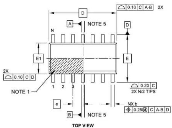
text_image
2X 0.10 C A-B NOTE 5 A D N E1 E 2X 0.10 C D NOTE 1 1 2 3 e B NOTE 5 TOP VIEW 0.20 C 2X N/2 TIPS NX b Φ 0.25 M C A-B D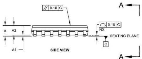
text_image
// 0.10 C A A2 A1 SIDE VIEW 0.10 C NX C SEATING PLANE A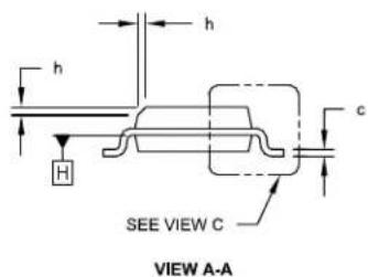
text_image
h H c SEE VIEW C VIEW A-AMicrochin Technology Drawing No. CM 085C Sheet 1 of 2
FIGURE 6-1: CAP1208 14-LEAD PLASTIC SMALL OUTLINE, NARROW, 3.90 MM BODY (SOIC)
14-Lead Plastic Small Outline (SL) - Narrow, 3.90 mm Body [SOIC]
Note: For the most current package drawings, please see the Microchip Packaging Specification located at http://www.microchip.com/packaging
![Microchip CAP1208 - 14-Lead Plastic Small Outline (SL) - Narrow, 3.90 mm Body [SOIC] - 1](/content/2026/06/1214659/images/7a0a4c9c5fc29a9f9a94b77414a35f9020da4602acab49a6d66ee4be7c9e80ab.jpg)
text_image
α 4X θ φ L (L1) 4X β![Microchip CAP1208 - 14-Lead Plastic Small Outline (SL) - Narrow, 3.90 mm Body [SOIC] - 2](/content/2026/06/1214659/images/42ce22bee997bddf7f0380aac7cd5f9dcbea736e45a51d91aa073bfeb0f07acf.jpg)
natural_image
Isometric line drawing of an integrated circuit chip with multiple pins (no text or symbols)VIEW C
| Units | MILLIMETERS | |||
| Dimension Limits | MIN | NOM | MAX | |
| Number of Pins | N | 14 | ||
| Pitch | e | 1.27 BSC | ||
| Overall Height | A | - | - | 1.75 |
| Molded Package Thickness | A2 | 1.25 | - | - |
| Standoff § | A1 | 0.10 | - | 0.25 |
| Overall Width | E | 6.00 BSC | ||
| Molded Package Width | E1 | 3.90 BSC | ||
| Overall Length | D | 8.65 BSC | ||
| Chamfer (Optional) | h | 0.25 | - | 0.50 |
| Foot Length | L | 0.40 | - | 1.27 |
| Footprint | L1 | 1.04 REF | ||
| Lead Angle | 0^ | - | - | |
| Foot Angle | 0^ | - | 8^ | |
| Lead Thickness | c | 0.10 | - | 0.25 |
| Lead Width | b | 0.31 | - | 0.51 |
| Mold Draft Angle Top | 5^ | - | 15^ | |
| Mold Draft Angle Bottom | 5^ | - | 15^ | |
Notes:
- Pin 1 visual index feature may vary, but must be located within the hatched area.
- § Significant Characteristic
- Dimension D does not include mold flash, protrusions or gate burrs, which shall not exceed 0.15 mm per end. Dimension E1 does not include interlead flash or protrusion, which shall not exceed 0.25 mm per side.
- Dimensioning and tolerancing per ASME Y14.5M BSC: Basic Dimension. Theoretically exact value shown without tolerances. REF: Reference Dimension, usually without tolerance, for information purposes only.
- Datums A & B to be determined at Datum H.
Microchip Technology Drawing No. C04-065C Sheet 2 of 2
FIGURE 6-1: CAP1208 14-LEAD PLASTIC SMALL OUTLINE, NARROW, 3.90 MM BODY (SOIC)
14-Lead Plastic Small Outline (SL) - Narrow, 3.90 mm Body [SOIC]
Note: For the most current package drawings, please see the Microchip Packaging Specification located at http://www.microchip.com/packaging

text_image
Gx C G SILK SCREEN Y E XRECOMMENDED LAND PATTERN
| Units | MILLIMETERS | |||
| Dimension Limits | MIN | NOM | MAX | |
| Contact Pitch | E | 1.27 BSC | ||
| Contact Pad Spacing | C | 5.40 | ||
| Contact Pad Width | X | 0.60 | ||
| Contact Pad Length | Y | 1.50 | ||
| Distance Between Pads | Gx | 0.67 | ||
| Distance Between Pads | G | 3.90 | ||
Notes:
1. Dimensioning and tolerancing per ASME Y14.5M
BSC: Basic Dimension. Theoretically exact value shown without tolerances.
Microchip Technology Drawing No. C04-2065A
FIGURE 6-2: CAP1208 16-PIN QFN 3MM X 3MM

text_image
TERMINAL #1 IDENTIFIER AREA (D/2 X E/2) TOP VIEW BOTTOM VIEW SIDE VIEW 3-D VIEWS PRELIMINARYFIGURE 6-3: CAP1208 PACKAGE DIMENSIONS - 16-PIN QFN 3MM X 3MM
| COMMON DIMENSIONS | |||||
| SYMBOL | MIN | NOM | MAX | NOTE | REMARK |
| A | 0.80 | 0.85 | 0.90 | - | OVERALL PACKAGE HEIGHT |
| A1 | 0 | 0.02 | 0.05 | - | STANDOFF |
| A3 | 0.20 REF | - | LEAD-FRAME THICKNESS | ||
| D/E | 2.90 | 3.00 | 3.10 | - | X/Y BODY SIZE |
| D2/E2 | 1.50 | 1.60 | 1.70 | - | X/Y EXPOSED PAD SIZE |
| L | 0.35 | 0.40 | 0.45 | - | TERMINAL LENGTH |
| b | 0.18 | 0.25 | 0.30 | 2 | TERMINAL WIDTH |
| K | 0.25 | 0.30 | - | - | TERMINAL TO PAD DISTANCE |
| e | 0.50 BSC | - | TERMINAL PITCH | ||
NOTES:
- ALL DIMENSIONS ARE IN MILLIMETERS.
- DIMENSIONS "b" APPLIES TO PLATED TERMINALS AND IT IS MEASURED BETWEEN 0.15 AND 0.30 mm FROM THE TERMINAL TIP.
- DETAILS OF TERMINAL #1 IDENTIFIER ARE OPTIONAL BUT MUST BE LOCATED WITHIN THE AREA INDICATED.
FIGURE 6-4: CAP1208 PCB LAND PATTERN AND STENCIL - 16-PIN QFN 3MM X 3MM
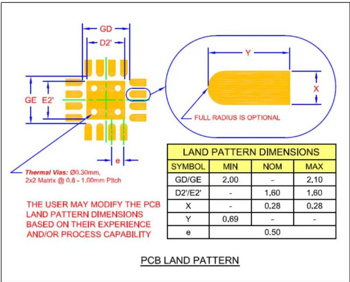
text_image
GD D2' GE E2' e Thermal Vias: Ø0.30mm, 2x2 Matrix @ 0.8 - 1.00mm Pitch THE USER MAY MODIFY THE PCB LAND PATTERN DIMENSIONS BASED ON THEIR EXPERIENCE AND/OR PROCESS CAPABILITY FULL RADIUS IS OPTIONAL LAND PATTERN DIMENSIONS SYMBOL MIN NOM MAX GD/GE 2.00 - 2.10 D2'/E2' - 1.60 1.60 X - 0.28 0.28 Y 0.69 - - e 0.50 PCB LAND PATTERNFIGURE 6-5: CAP1208 PACKAGE MARKING
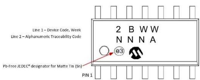
text_image
Line 1 - Device Code, Week Line 2 - Alphanumeric Traceability Code 2 B W W N N N A e3 Pb-Free JEDEC® designator for Matte Tin (Sn) PIN 1
text_image
Line 1 - Device Code, Week Line 2 - Alphanumeric Traceability Code H 2 WW N N N A e3 Pb-Free JEDEC® designator for Matte Tin (Sn) PIN 1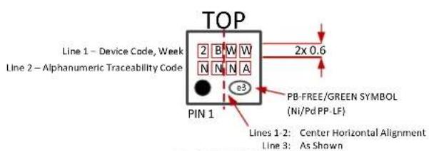
text_image
TOP Line 1 - Device Code, Week Line 2 - Alphanumeric Traceability Code 2 B W W N N A e3 PIN 1 2x 0.6 PB-FREE/GREEN SYMBOL (Ni/Pd PP-LF) Lines 1 2: Center Horizontal Alignment Line 3: As ShownBOTTOM Bottom marking not allowed
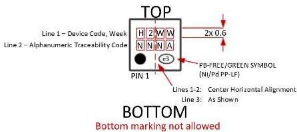
text_image
TOP Line 1 - Device Code, Week Line 2 - Alphanumeric Traceability Code H 2 W W N N N A e3 PIN 1 PB-FREE/GREEN SYMBOL (Ni/Pd PP-LF) Lines 1-2: Center Horizontal Alignment Line 3: As Shown BOTTOM Bottom marking not allowedAPPENDIX A: DEVICE DELTA
A.1 Delta from CAP1128 / CAP1188 to CAP1208
- Revision ID set to 00h.
- Pinout changed. RESET, WAKE, and ADDR_COMM pins removed. LED pins removed. SPI pins / muxing also removed. Added GND pin as ground slug is no longer used for ground connection.
- Reduced package size from a 20-pin 4mm x 4mm QFN to a 16-pin 3mm x 3mm QFN.
- Added ACAL_FAIL bit to flag analog calibration failures (see Section 5.2, "Status Registers") and ACAL_FAIL_INT bit to control analog calibration failure interrupts (see Section 5.6, "Configuration Registers").
- Added BC_OUT bit to flag calibration failures regarding base counts out of limit (see Section 5.2, "Status Registers") and BC_OUT_RECAL and BC_OUT_INT bit to control base count out of limit behavior and interrupts (see Section 5.6, "Configuration Registers"). Added Base Count Out of Limit Register to indicate which sensor inputs have base counts outside the operating range (see Section 5.16, "Base Count Out of Limit Register").
- Added Power Button feature (see Section 4.5, "Power Button").
- Increased supply voltage range for 5V operation.
- Increased operating temperature range from 0°C - 85°C to -40°C to 125°C.
- Removed proximity detection gain.
- LEDs removed.
- SMBus address fixed at 0101_000(r/w).
- Removed SPI communications protocol option.
- Removed RESET pin function.
- Removed WAKE pin function.
- Removed ALERT pin configuration.
- Register set changes are shown in Table A-1, "Register Delta".
TABLE A-1: REGISTER DELTA
| Address Register Delta Delta | Default | ||
| 00hPage 24 | Removed bits - Main Control Register | Removed GAIN[1:0] bits. | 00h |
| 02hPage 25 | Added bits - General Status Register | Added bit 4 PWR for new Power Button feature. Added bit 5 ACAL_FAIL to indicate analog calibration failure. Added bit 6 BC_OUT. Removed bit 4 LED status. | 00h |
| 04h | Removed - LED Status Register | removed register | n/a |
| 20hPage 29 | Removed bit - Configuration Register | Removed bit 6 WAKE_CFG. | 20h |
| 26hPage 35 | Renamed Calibration Activate and Status Register and added functionality | In addition to forcing a calibration, the register also indicates the status of calibration for each sensor input. | 00h |
| Address Register Delta Delta Default | |||
| 2EhPage 39 | New - Base Count Out of Limit Register | new register for calibration status 00h | |
| 44hPage 29 | Added and removed bits - Configuration 2 Register | Added bit 1 ACAL_FAIL_INT. Changed bit 4 from BLK_POL_MIR to BC_OUT_INT. Changed bit 6 from ALT_POL to BC_OUT_RECAL.Removed bit 7 INV_LINK_TRAN. | 40h |
| 60hPage 47 | New - Power Button Register | new register for Power Button feature 00h | |
| 61hPage 47 | New - Power Button Configuration Register | new register for configuring the Power Button feature | 00h |
| 71h | Removed - LED Output Type Register | removed register n/a | |
| 72h | Removed - Sensor Input LED Linking Register | removed register n/a | |
| 73h | Removed - LED Polarity Register | removed register n/a | |
| 74h | Removed - LED Output Control Register | removed register n/a | |
| 77h | Removed - Linked LED Transition Control Register | removed register n/a | |
| 79h | Removed - LED Mirror Control Register | removed register n/a | |
| 81h | Removed - LED 1 Behavior Register | removed register n/a | |
| 82h | Removed - LED Behavior Register 2 | removed register n/a | |
| 84h | Removed - LED Pulse 1 Period | removed register n/a | |
| 85h | Removed - LED Pulse 2 Period | removed register n/a | |
| 86h | Removed - LED Breathe Period Register | removed register n/a | |
| 88h | Removed - LED Config Register | removed register n/a | |
| 90h | Removed - LED Pulse 1 Duty Cycle Register | removed register n/a | |
| 91h | Removed - LED Pulse 2 Duty Cycle Register | removed register n/a | |
| 92h | Removed - LED Breathe Duty Cycle Register | removed register n/a | |
| 93h | Removed - LED Direct Duty Cycle Register | removed register n/a | |
| 94h | Removed - LED Direct Ramp Rates Register | removed register n/a | |
| 95h | Removed - LED Off Delay | removed register n/a | |
| FDh Page 49 | Changed - Product ID New product ID for CAP1208 6Bh | ||
| FFh Page 49 | Changed - Revision Register | Revision changed. 00h | |
7.0 REVISION HISTORY
TABLE 7-1: REVISION HISTORY
| Revision Level and Date S | Section/Figure/Entry Correction | |
| DS00001570C (11-12-15) | Added 14-lead SOIC packages. | SOIC pinoutdiagrams, package marking.Updated ordering information. |
| DS00001570B (03-03-14) A | Added CAP1208-2 information to the following sections:Ordering informationSection 3.2.2, "SMBus Address and RD / WR Bit"Table 3.2, "Write Byte Protocol"Table 3.3, "Read Byte Protocol"Table 3.4, "Send Byte Protocol"Table 3.5, "Receive Byte Protocol"Table 3.6, "Block Read Protocol"Table 3.7, "Block Write Protocol"Added Figure 6.5, "CAP1208-2 Package Marking"Updated Worldwide Sales and Service Listing | |
| CAP1208 Revision A replaces the previous SMSC version Revision 1.0 | ||
Microchip provides online support via our WWW site at www.microchip.com. This web site is used as a means to make files and information easily available to customers. Accessible by using your favorite Internet browser, the web site contains the following information:
- Product Support – Data sheets and errata, application notes and sample programs, design resources, user's guides and hardware support documents, latest software releases and archived software
- General Technical Support – Frequently Asked Questions (FAQ), technical support requests, online discussion groups, Microchip consultant program member listing
- Business of Microchip – Product selector and ordering guides, latest Microchip press releases, listing of seminars and events, listings of Microchip sales offices, distributors and factory representatives
CUSTOMER CHANGE NOTIFICATION SERVICE
Microchip's customer notification service helps keep customers current on Microchip products. Subscribers will receive e-mail notification whenever there are changes, updates, revisions or errata related to a specified product family or development tool of interest.
To register, access the Microchip web site at www.microchip.com. Under “Support”, click on “Customer Change Notification” and follow the registration instructions.
CUSTOMER SUPPORT
Users of Microchip products can receive assistance through several channels:
• Distributor or Representative
- Local Sales Office
• Field Application Engineer (FAE)
- Technical Support
Customers should contact their distributor, representative or field application engineer (FAE) for support. Local sales offices are also available to help customers. A listing of sales offices and locations is included in the back of this document.
Technical support is available through the web site at: http://www.microchip.com/support
PRODUCT IDENTIFICATION SYSTEM
To order or obtain information, e.g., on pricing or delivery, refer to the factory or the listed sales office.
text_image
PART NO. [X] XX Device Option Package [XX] Add/replace and Reel OptionDevice: CAP1208
Tape and Reel Option TR Tape and Reel
Package:(2) A4 16-pin QFN SL 14-pin SOIC
Examples:
a) CAP1208-1-A4-TR
0b0101_000[r/w] Address
16-pin QFN package
b) CAP1208-2-SL-TR
0b0101_001[r/w] Address
14-pin SOIC package
Note 1: Tape and Reel identifier only appears in the catalog part number description. This identifier is used for ordering purposes and is not printed on the device package. Check with your Microchip Sales Office for package availability with the Tape and Reel option.
2: For other small form-factor package availability and marking information, please visit www.microchip.com/packaging or contact your local sales office.
Note the following details of the code protection feature on Microchip devices:
- Microchip products meet the specification contained in their particular Microchip Data Sheet.
- Microchip believes that its family of products is one of the most secure families of its kind on the market today, when used in the intended manner and under normal conditions.
- There are dishonest and possibly illegal methods used to breach the code protection feature. All of these methods, to our knowledge, require using the Microchip products in a manner outside the operating specifications contained in Microchip's Data Sheets. Most likely, the person doing so is engaged in theft of intellectual property.
- Microchip is willing to work with the customer who is concerned about the integrity of their code.
- Neither Microchip nor any other semiconductor manufacturer can guarantee the security of their code. Code protection does not mean that we are guaranteeing the product as “unbreakable.”
Code protection is constantly evolving. We at Microchip are committed to continuously improving the code protection features of our products. Attempts to break Microchip's code protection feature may be a violation of the Digital Millennium Copyright Act. If such acts allow unauthorized access to your software or other copyrighted work, you may have a right to sue for relief under that Act.
Information contained in this publication regarding device applications and the like is provided only for your convenience and may be superseded by updates. It is your responsibility to ensure that your application meets with your specifications. MICROCHIP MAKES NO REPRESENTATIONS OR WARRANTIES OF ANY KIND WHETHER EXPRESS OR IMPLIED, WRITTEN OR ORAL, STATUTORY OR OTHERWISE, RELATED TO THE INFORMATION, INCLUDING BUT NOT LIMITED TO ITS CONDITION, QUALITY, PERFORMANCE, MERCHANTABILITY OR FITNESS FOR PURPOSE. Microchip disclaims all liability arising from this information and its use. Use of Microchip devices in life support and/or safety applications is entirely at the buyer's risk, and the buyer agrees to defend, indemnify and hold harmless Microchip from any and all damages, claims, suits, or expenses resulting from such use. No licenses are conveyed, implicitly or otherwise, under any Microchip intellectual property rights unless otherwise stated.
Trademarks
The Microchip name and logo, the Microchip logo, dsPIC, FlashFlex, flexPWR, JukeBlox, KEELOQ, KEELOQ logo, Kleer, LANCheck, MediaLB, MOST, MOST logo, MPLAB, OptoLyzer, PIC, PICSTART, PIC ^32 logo, RightTouch, SpyNIC, SST, SST Logo, SuperFlash and UNI/O are registered trademarks of Microchip Technology Incorporated in the U.S.A. and other countries.
The Embedded Control Solutions Company and mTouch are registered trademarks of Microchip Technology Incorporated in the U.S.A.
Analog-for-the-Digital Age, BodyCom, chipKIT, chipKIT logo, CodeGuard, dsPICDEM, dsPICDEM.net, ECAN, In-Circuit Serial Programming, ICSP, Inter-Chip Connectivity, KleerNet, KleerNet logo, MiWi, MPASM, MPF, MPLAB Certified logo, MPLIB, MPLINK, MultiTRAK, NetDetach, Omniscient Code Generation, PICDEM, PICDEM.net, PICkit, PICtail, RightTouch logo, REAL ICE, SQI, Serial Quad I/O, Total Endurance, TSHARC, USBCheck, VariSense, ViewSpan, WiperLock, Wireless DNA, and ZENA are trademarks of Microchip Technology Incorporated in the U.S.A. and other countries.
SQTP is a service mark of Microchip Technology Incorporated in the U.S.A.
Silicon Storage Technology is a registered trademark of Microchip Technology Inc. in other countries.
GestIC is a registered trademark of Microchip Technology Germany II GmbH & Co. KG, a subsidiary of Microchip Technology Inc., in other countries.
All other trademarks mentioned herein are property of their respective companies.
© 2013-2015, Microchip Technology Incorporated, Printed in the U.S.A., All Rights Reserved.
ISBN: 9781522400219
QUALITY MANAGEMENT SYSTEM
CERTIFIED BY DNV
=ISO/TS 16949=
Microchip received ISO/TS-16949:2009 certification for its worldwide headquarters, design and wafer fabrication facilities in Chandler and Tempe, Arizona; Gresham, Oregon and design centers in California and India. The Company's quality system processes and procedures are for its PIC® MCUs and dsPIC® DSCs, KEELoc® code hopping devices, Serial EEPROMs, microperipherals, nonvolatile memory and analog products. In addition, Microchip's quality system for the design and manufacture of development systems is ISO 9001:2000 certified.
Worldwide Sales and Service
AMERICAS
Corporate Office
2355 West Chandler Blvd.
Chandler, AZ 85224-6199
Tel: 480-792-7200
Fax: 480-792-7277
Technical Support:
http://www.microchip.com/
support
Web Address:
www.microchip.com
Atlanta
Duluth, GA
Tel: 678-957-9614
Fax: 678-957-1455
Austin, TX
Tel: 512-257-3370
Boston
Westborough, MA
Tel: 774-760-0087
Fax: 774-760-0088
Chicago
Itasca, IL
Tel: 630-285-0071
Fax: 630-285-0075
Cleveland
Independence, OH
Tel: 216-447-0464
Fax: 216-447-0643
Dallas
Addison, TX
Tel: 972-818-7423
Fax: 972-818-2924
Detroit
Novi, MI
Tel: 248-848-4000
Houston, TX
Tel: 281-894-5983
Indianapolis
Noblesville, IN
Tel: 317-773-8323
Fax: 317-773-5453
Los Angeles
Mission Viejo, CA
Tel: 949-462-9523
Fax: 949-462-9608
New York, NY
Tel: 631-435-6000
San Jose, CA
Tel: 408-735-9110
Canada - Toronto
Tel: 905-673-0699
Fax: 905-673-6509
ASIA/PACIFIC
Asia Pacific Office
Suites 3707-14, 37th Floor
Tower 6, The Gateway
Harbour City, Kowloon
Hong Kong
Tel: 852-2943-5100
Fax: 852-2401-3431
Australia - Sydney
Tel: 61-2-9868-6733
Fax: 61-2-9868-6755
China - Beijing
Tel: 86-10-8569-7000
Fax: 86-10-8528-2104
China - Chengdu
Tel: 86-28-8665-5511
Fax: 86-28-8665-7889
China - Chongqing
Tel: 86-23-8980-9588
Fax: 86-23-8980-9500
China - Dongguan
Tel: 86-769-8702-9880
China - Hangzhou
Tel: 86-571-8792-8115
Fax: 86-571-8792-8116
China - Hong Kong SAR
Tel: 852-2943-5100
Fax: 852-2401-3431
China - Nanjing
Tel: 86-25-8473-2460
Fax: 86-25-8473-2470
China - Qingdao
Tel: 86-532-8502-7355
Fax: 86-532-8502-7205
China - Shanghai
Tel: 86-21-5407-5533
Fax: 86-21-5407-5066
China - Shenyang
Tel: 86-24-2334-2829
Fax: 86-24-2334-2393
China - Shenzhen
Tel: 86-755-8864-2200
Fax: 86-755-8203-1760
China - Wuhan
Tel: 86-27-5980-5300
Fax: 86-27-5980-5118
China - Xian
Tel: 86-29-8833-7252
Fax: 86-29-8833-7256
ASIA/PACIFIC
China - Xiamen
Tel: 86-592-2388138
Fax: 86-592-2388130
China - Zhuhai
Tel: 86-756-3210040
Fax: 86-756-3210049
India - Bangalore
Tel: 91-80-3090-4444
Fax: 91-80-3090-4123
India - New Delhi
Tel: 91-11-4160-8631
Fax: 91-11-4160-8632
India - Pune
Tel: 91-20-3019-1500
Japan - Osaka
Tel: 81-6-6152-7160
Fax: 81-6-6152-9310
Japan - Tokyo
Tel: 81-3-6880-3770
Fax: 81-3-6880-3771
Korea - Daegu
Tel: 82-53-744-4301
Fax: 82-53-744-4302
Korea - Seoul
Tel: 82-2-554-7200
Fax: 82-2-558-5932 or
82-2-558-5934
Malaysia - Kuala Lumpur
Tel: 60-3-6201-9857
Fax: 60-3-6201-9859
Malaysia - Penang
Tel: 60-4-227-8870
Fax: 60-4-227-4068
Philippines - Manila
Tel: 63-2-634-9065
Fax: 63-2-634-9069
Singapore
Tel: 65-6334-8870
Fax: 65-6334-8850
Taiwan - Hsin Chu
Tel: 886-3-5778-366
Fax: 886-3-5770-955
Taiwan - Kaohsiung
Tel: 886-7-213-7828
Taiwan - Taipei
Tel: 886-2-2508-8600
Fax: 886-2-2508-0102
Thailand - Bangkok
Tel: 66-2-694-1351
Fax: 66-2-694-1350
EUROPE
Austria - Wels
Tel: 43-7242-2244-39
Fax: 43-7242-2244-393
Denmark - Copenhagen
Tel: 45-4450-2828
Fax: 45-4485-2829
France - Paris
Tel: 33-1-69-53-63-20
Fax: 33-1-69-30-90-79
Germany - Dusseldorf
Tel: 49-2129-3766400
Germany - Karlsruhe
Tel: 49-721-625370
Germany - Munich
Tel: 49-89-627-144-0
Fax: 49-89-627-144-44
Italy - Milan
Tel: 39-0331-742611
Fax: 39-0331-466781
Italy - Venice
Tel: 39-049-7625286
Netherlands - Drunen
Tel: 31-416-690399
Fax: 31-416-690340
Poland - Warsaw
Tel: 48-22-3325737
Spain - Madrid
Tel: 34-91-708-08-90
Fax: 34-91-708-08-91
Sweden - Stockholm
Tel: 46-8-5090-4654
UK - Wokingham
Tel: 44-118-921-5800
Fax: 44-118-921-5820
07/14/15