SY58011U - Electronic component Microchip - Free user manual and instructions
Find the device manual for free SY58011U Microchip in PDF.

User questions about SY58011U Microchip
0 question about this device. Answer the ones you know or ask your own.
Ask a new question about this device
Download the instructions for your Electronic component in PDF format for free! Find your manual SY58011U - Microchip and take your electronic device back in hand. On this page are published all the documents necessary for the use of your device. SY58011U by Microchip.
USER MANUAL SY58011U Microchip
- Guaranteed AC performance over temperature/voltage:
• > 7GHz f MAX clock
• < 60ps t r/ tf times
• < 250ps t pd
- < 15ps max. skew
- Accepts an input signal as low as 100mV
- Unique input termination and V_T pin accepts DC-coupled and AC-coupled differential inputs: LVPECL, LVDS, and CML
- 50ohms source terminated CML outputs
- Power supply 2.5V ±5% and 3.3V ±10%
- Industrial temperature range: -40^ to +85^
- Available in 16-pin (3mm * 3mm) QFN package
APPLICATIONS
- All SONET and GigE clock distribution
- Fibre Channel clock and data distribution
- Backplanes
- Data distribution: OC-48, OC-48+FEC, XAU
- High-end, low skew, multiprocessor synchronous clock distribution
FUNCTIONAL BLOCK DIAGRAM

text_image
IN 50Ω VT 50Ω /IN VREF-AC Q0 /Q0 Q1 /Q1
Precision Edge®
DESCRIPTION
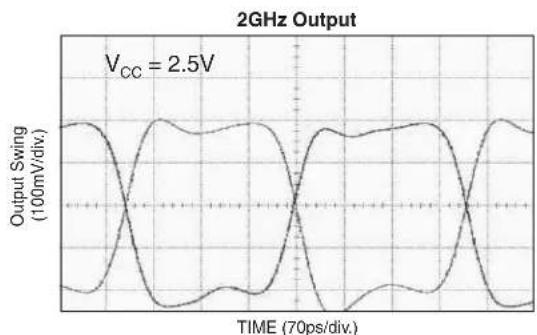
The SY58011U is a 2.5V/3.3V precision, high-speed, fully differential 1:2 CML fanout buffer. Optimized to provide two identical output copies with less than 15ps of skew and only 49fs _RMS phase jitter, the SY58011U can process clock signals as fast as 7GHz or data patterns up to 10.7Gbps.
The differential input includes Micrel's unique, 3-pin input termination architecture that interfaces to LVPECL, LVDS, or CML differential signals, (AC-coupled or DC-coupled) as small as 100mV without any level-shifting or termination resistor networks in the signal path. For AC-coupled input interface applications, an on-board output reference voltage ( V_REF-AC ) is provided to bias the V_T pin. The outputs are compatible with 400mV typical swing into 50ohms loads, with extremely fast rise/fall times guaranteed to be less than 60ps.
The SY58011U operates from a 2.5V ±5% supply or 3.3V ±10% supply and is guaranteed over the full industrial temperature range (-40°C to +85°C). For applications that require LVPECL outputs, consider the SY58012U or SY58013U 1:2 fanout buffer with 800mV and 400mV output swing, respectively. The SY58011U is part of Micrel's high-speed, Precision Edge® product line. Datasheets and support documentation can be found on Micrel's web site at www.micrel.com.
TYPICAL PERFORMANCE
line
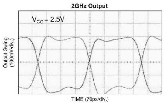
| TIME (70ps/div.) | Output Swing (100mV/div) | | ---------------- | ------------------------ | | 0 | 0 | | 1 | 1 | | 2 | 0 | | 3 | -1 | | 4 | 0 | | 5 | 1 | | 6 | 0 | | 7 | -1 | | 8 | 0 | | 9 | 1 | | 10 | 0 | | 11 | -1 | | 12 | 0 | | 13 | 1 | | 14 | 0 | | 15 | -1 | | 16 | 0 | | 17 | 1 | | 18 | 0 | | 19 | -1 | | 20 | 0 | | 21 | 1 | | 22 | 0 | | 23 | -1 | | 24 | 0 | | 25 | 1 | | 26 | 0 | | 27 | -1 | | 28 | 0 | | 29 | 1 | | 30 | 0 | | 31 | -1 | | 32 | 0 | | 33 | 1 | | 34 | 0 | | 35 | -1 | | 36 | 0 | | 37 | 1 | | 38 | 0 | | 39 | -1 | | 40 | 0 | | 41 | 1 | | 42 | 0 | | 43 | -1 | | 44 | 0 | | 45 | 1 | | 46 | 0 | | 47 | -1 | | 48 | 0 | | 49 | 1 | | 50 | 0 | | 51 | -1 | | 52 | 0 | | 53 | 1 | | 54 | 0 | | 55 | -1 | | 56 | 0 | | 57 | 1 | | 58 | 0 | | 59 | -1 | | 60 | 0 | | 61 | 1 | | 62 | 0 | | 63 | -1 | | 64 | 0 | | 65 | 1 | | 66 | 0 | | 67 | -1 | | 68 | 0 | | 69 | 1 | | 70 | 0 |2GHz with 100mV Input
Precision Edge is a registered trademark of Micrel, Inc.
PACKAGE/ORDERING INFORMATION

text_image
VCC GND GND VCC IN 16 15 14 13 VT 12 VREF-AC 2 11 /IN 3 10 5 6 7 8 Q0/Q0 /Q1 Q1 VCC GND GND VCC16-Pin QFN (QFN-16)
Ordering Information ^(1)
| Part Number | Package Type | Operating Range | Package Marking |
| SY58011UMG(3) | QFN-16Pb-Free | Industrial | 011U withPb-Free bar-line indicator |
| SY58011UMGTR(2, 3) | QFN-16Pb-Free | Industrial | 011U withPb-Free bar-line indicator |
Notes:
1. Contact factory for die availability. Dice are guaranteed at T_A = 25^ , DC electricals only. All devices are Pb-Free.
2. Tape and Reel.
3. Pb-Free package recommended for new designs.
PIN DESCRIPTION
| Pin Number Pin | Name Pin Function | |
| 1, 4 IN, /IN D | Differential Input: This input pair is the signal to be buffered. Each pin of this pair internally terminates with 50ohms to the V_T pin. Note that this input will default to an indeterminate state if left open. See “Input Interface Applications” section. | |
| 2 VT Input | Termination Center-Tap: Each input terminates to this pin. The V _T pin provides a center-tap for each input (IN, /IN) to a termination network for maximum interface flexibility. See “Input Interface Applications” section. | |
| 3 VREF-AC | Reference Output Voltage: This output biases to V _CC -1.2V. It is used when AC-coupling the inputs (IN, /IN). Connect V_REF -AC directly to the V_T pin. Bypass with 0.01μF low ESR capacitor to V_CC . Maximum current source or sink is 0.5mA. See “Input Interface Applications” section. | |
| 5, 8, 13, 16 | VCC | Positive Power Supply: Bypass with 0.1μF//0.01μF low ESR capacitors as close to the V_CC pins as possible. |
| 6, 7, 14, 15 GND | Ground. Exposed pad must be connected to a ground plane that is the same potential (Exposed Pad) as the ground pin. | |
| 12, 11 Q0, /Q09, 10 | CML Differential Output Pairs: Differential buffered output copy of the input signal. The output swing is typically 400mV. Unused output pairs may be left floating with no impact on jitter. See “CML Output Termination” section. | |
Absolute Maximum Ratings ^(Note 1)
Power Supply Voltage (V _CC ) ...... -0.5V to +4.0V
Input Voltage ( V_IN ) -0.5V to V_CC
CML Output Voltage ( V_OUT ) ...... V_CC-1.0V to V_CC+0.5V
Current ( V_T )
Source or sink current on V_T pin.... ±100mA
Input Current
Source or sink current on IN, /IN .... ±50mA
Current ( V_REF )
Source or sink current on V_REF -AC, Note 4 ..... ±1.5mA
Lead Temperature Soldering, (20 seconds) 260°C
Storage Temperature Range ( T_STORE ) ... -65^ to +150^
Operating Ratings ^(Note 2)
Supply Voltage ( V_CC ) .....+2.375V to +3.60V
Operating Temperature Range ( T_A ) ..... -40°C to +85°C
Package Thermal Resistance, Note 3
QFN ( _JA )
Still-Air 60°C/W
500lfpm 54°C/W
QFN ( _JB ) 33°C/W
DC ELECTRICAL CHARACTERISTICS(Note 5)
T_A=-40^ to +85^
| Symbol Parameter Condition Min Typ Max Units | |||||||
| V_CC | Power Supply Voltage 2.375 3.60 V | ||||||
| I_CC | Power Supply Current Max. V | CC, no load 75 | 95 | mA | |||
| V_IH | Input HIGH Voltage | IN, /IN, Note 6 | V_CC-1.6 | V_CC | V | ||
| V_IL | Input LOW Voltage | IN, /IN 0 | V | _IH-0.1 | V | ||
| V_IN | Input Voltage Swing | see Figure 1a. | 0.1 | 1.7 | V | ||
| V_DIFF\_IN | Differential Input Voltage Swing | see Figure 1b. | 0.2 | V | |||
| R_IN | Into V_T Resistance | 40 | 50 | 60 | y | ||
| V_REF-AC | Output Reference Voltage | V_CC-1.3 | V_CC-1.2 | V_CC-1.1 | V | ||
| IN to V_T | 1.28 V | ||||||
CML DC ELECTRICAL CHARACTERISTICS ^(Note 5)
V_CC = 3.3V ± 10% or 2.5V ± 5% ; T_A = -40^ C to +85^ C ; R_L = 100y across each output pair, or equivalent, unless otherwise stated.
| Symbol | Parameter | Condition | Min | Typ | Max | Units |
| V_OH | Output HIGH Voltage | Q0, /Q0, Q1, /Q1 | V_CC-0.020 | V_CC-0.010 | V_CC | V |
| V_OUT | Output Voltage Swing | Q0, /Q0, Q1, /Q1; see Figure 1a. | 325 | 400 | mV | |
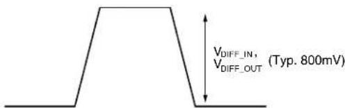
| V_DIFF\_OUT | Differential Output Voltage Swing | Q0, /Q0, Q1, /Q1; see Figure 1b. | 650 | 800 | mV | |
| R_OUT | Output Source Impedance | Q0, /Q0, Q1, /Q1 | 40 | 50 | 60 | ohms |
Notes:
- Permanent device damage may occur if absolute maximum ratings are exceeded. This is a stress rating only and functional operation is not implied at conditions other than those detailed in the operational sections of this data sheet. Exposure to absolute maximum ratings conditions for extended periods may affect device reliability.
- The data sheet limits are not guaranteed if the device is operated beyond the operating ratings.
- Thermal performance assumes exposed pad is soldered (or equivalent) to the device's most negative potential (gnd) on the pcb.
- Due to the limited drive capability, use for input of the same package only.
- The circuit is designed to meet the dc specifications shown in the above table after thermal equilibrium has been established.
- V_IH (min) not lower than 1.2V.
AC ELECTRICAL CHARACTERISTICS (Note 7)
V_CC = 2.5V ± 5% or 3.3V ± 10% ; T_A = -40^ C to +85^ C ; R_L = 100ohms across each output pair, or equivalent, unless otherwise stated.
| Symbol Parameter Condition Min Typ Max Units | ||||||
| f_MAX | Maximum Operating Frequency NRZ | Data 10.7 Gbps | ||||
| V_OUT>200mV Clock 7 8 GHz | ||||||
| t_pd | Propagation Delay V | _IN>100mV 100 170 250 ps | ||||
| t_CHAN | Channel-to-Channel Skew | Note 8 | 3 | 15 | ps | |
| t_SKEW | Part-to-Part Skew | Note 9 | 100 | ps | ||
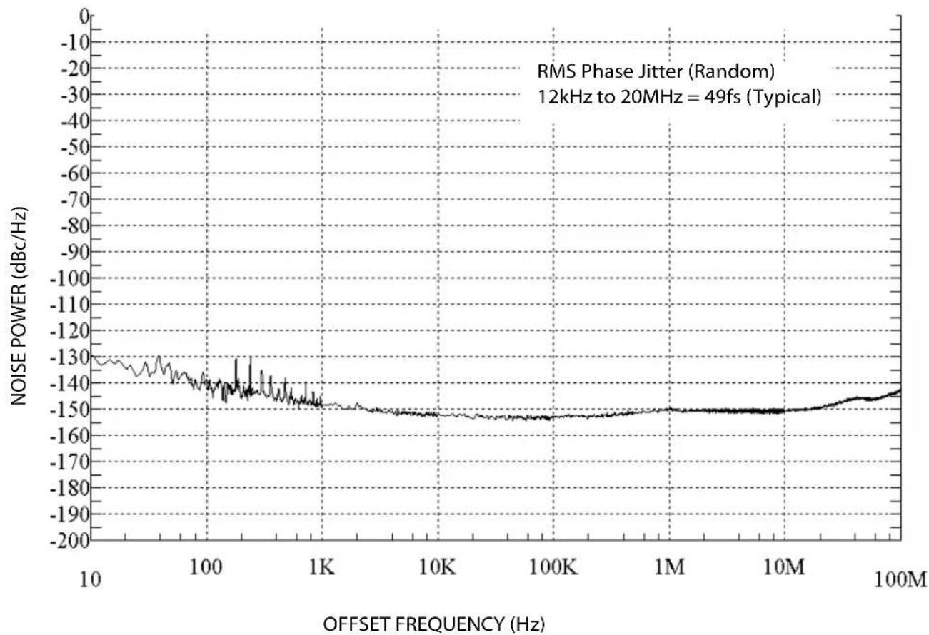
| t_JITTER | RMS Phase Jitter | Output = 622MHzIntegration Range: 12kHz - 20MHz | 49 | fs_RMS | ||
| t_r,t_f | Output Rise/Fall Time | 20% to 80% at full output swing | 20 | 40 | 60 | ps |
Notes:
- High frequency AC electricals are guaranteed by design and characterization.
- Skew is measured between outputs of the same bank under identical transitions.
- Skew is defined for two parts with identical power supply voltages at the same temperature and with no skew of the edges at the respective inputs.
PHASE NOISE
line
| OFFSET FREQUENCY (Hz) | NOISE POWER (dBc/Hz) | | --------------------- | -------------------- | | 10 | -130 | | 100 | -140 | | 1K | -150 | | 10K | -150 | | 100K | -150 | | 1M | -150 | | 10M | -150 | | 100M | -140 |Phase Noise Plot: 622MHz @ 3.3V
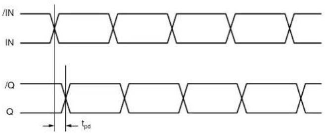
TIMING DIAGRAM
text_image
/IN IN /Q Q tpdSINGLE-ENDED AND DIFFERENTIAL SWINGS
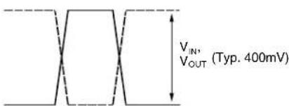
text_image
V_{IN}, V_{OUT} (Typ. 400mV)Figure 1a. Single-Ended Voltage Swing
text_image
VDIFF_IN, VDIFF_OUT (Typ. 800mV)Figure 1b. Differential Voltage Swing
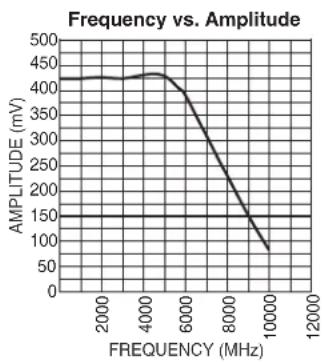
TYPICAL OPERATING CHARACTERISTICS
V_CC = 3.3V , GND = 0, V_IN = 100mV , T_A = 25^ , unless otherwise stated.
line
| FREQUENCY (MHz) | AMPLITUDE (mV) | | --------------- | ------------- | | 2000 | 420 | | 4000 | 430 | | 6000 | 380 | | 8000 | 250 | | 10000 | 100 |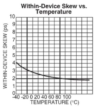
line
| TEMPERATURE (°C) | WITHIN-DEVICE SKEW (ps) | | ---------------- | ------------------------ | | -40 | 4 | | 0 | 3 | | 20 | 2.5 | | 40 | 2.2 | | 60 | 2 | | 80 | 1.8 | | 100 | 1.7 |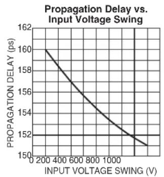
line
| INPUT VOLTAGE SWING (V) | PROPAGATION DELAY (ps) | | ---------------------- | --------------------- | | 200 | 160 | | 400 | 158 | | 600 | 156 | | 800 | 154 | | 1000 | 152 | | 1200 | 151 |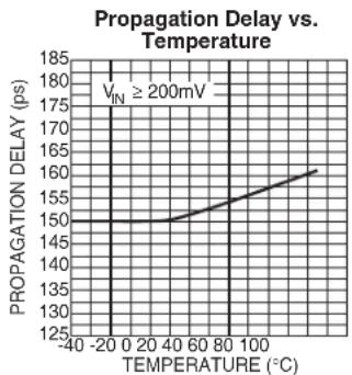
line
| TEMPERATURE (°C) | PROPAGATION DELAY (ps) | | ---------------- | ---------------------- | | -40 | 150 | | 0 | 150 | | 20 | 150 | | 40 | 150 | | 60 | 155 | | 80 | 158 | | 100 | 160 |FUNCTIONAL CHARACTERISTICS
V_CC = 2.5V, GND = 0, V_IN = 100mV, T_A = 25^, unless otherwise stated.
line
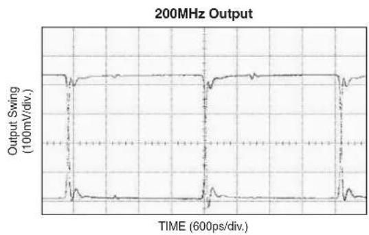
| TIME (70ps/div.) | Output Swing (100mV/div.) | | ---------------- | ------------------------- | | 0 | 0 | | 1 | 1 | | 2 | 0 | | 3 | -1 | | 4 | 0 | | 5 | 1 | | 6 | 0 | | 7 | -1 | | 8 | 0 | | 9 | 1 | | 10 | 0 | | 11 | -1 | | 12 | 0 | | 13 | 1 | | 14 | 0 | | 15 | -1 | | 16 | 0 | | 17 | 1 | | 18 | 0 | | 19 | -1 | | 20 | 0 | | 21 | 1 | | 22 | 0 | | 23 | -1 | | 24 | 0 | | 25 | 1 | | 26 | 0 | | 27 | -1 | | 28 | 0 | | 29 | 1 | | 30 | 0 | | 31 | -1 | | 32 | 0 | | 33 | 1 | | 34 | 0 | | 35 | -1 | | 36 | 0 | | 37 | 1 | | 38 | 0 | | 39 | -1 | | 40 | 0 | | 41 | 1 | | 42 | 0 | | 43 | -1 | | 44 | 0 | | 45 | 1 | | 46 | 0 | | 47 | -1 | | 48 | 0 | | 49 | 1 | | 50 | 0 | | 51 | -1 | | 52 | 0 | | 53 | 1 | | 54 | 0 | | 55 | -1 | | 56 | 0 | | 57 | 1 | | 58 | 0 | | 59 | -1 | | 60 | 0 | | 61 | 1 | | 62 | 0 | | 63 | -1 | | 64 | 0 | | 65 | 1 | | 66 | 0 | | 67 | -1 | | 68 | 0 | | 69 | 1 | | 70 | 0 |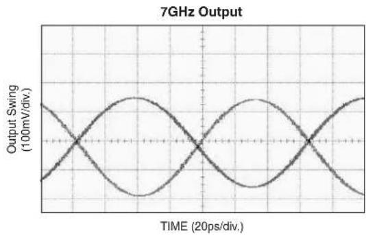
line
| TIME (20ps/div.) | Output Swing (100mV/div.) | | ---------------- | ------------------------- | | 0 | 0 | | 1 | 0.5 | | 2 | 1 | | 3 | 0.5 | | 4 | 0 | | 5 | -0.5 | | 6 | 0.5 | | 7 | 1 | | 8 | 0.5 | | 9 | 0 | | 10 | -0.5 | | 11 | 0.5 | | 12 | 1 | | 13 | 0.5 | | 14 | 0 | | 15 | -0.5 | | 16 | 0.5 | | 17 | 1 | | 18 | 0.5 | | 19 | 0 | | 20 | -0.5 |INPUT STAGE

text_image
VCC IN 50Ω VT 50Ω IN GNDFigure 2. Simplified Differential Input Buffer
INPUT INTERFACE APPLICATIONS
text_image
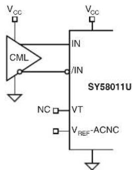
VCC CML IN IN NC VT VREF-ACNC SY58011U VCCFigure 3a. DC-Coupled CML Input Interface
(option: may connect V_T to V_CC )
text_image
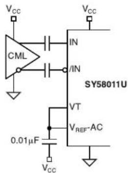
VCC CML IN IN VT VREF-AC 0.01μF VCC SY58011U VCCFigure 3b. AC-Coupled CML Input Interface
text_image
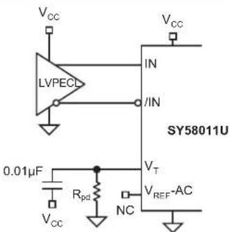
VCC LVPECL IN IN SY58011U 0.01μF VT VREF-AC Rpd NC VCCNote:
For V_cc=2.5V systems, R_pd=19 .
For V_cc = 3.3V systems, R_pd = 50 .
Figure 3c. LVPECL Input Interface

text_image
VCC LVPECL IN Rpd Rpd IN VT VREF-AC 0.01μF VCC SY58011UNote:
R_od = 100 for a 3.3V system
R_pd=50 for a 2.5V system
Figure 3d. AC-Coupled LVPECL Input Interface
text_image
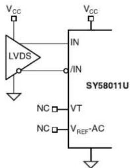
VCC LVDS IN IN NC □ VT NC □ VREF-AC SY58011U VCCFigure 3e. LVDS Input Interface
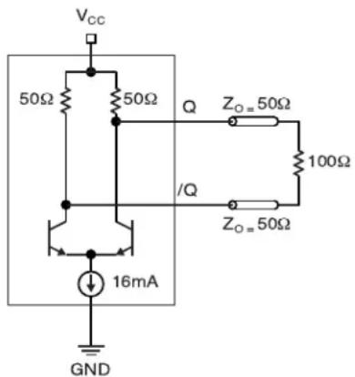
CML OUTPUT TERMINATION
Figure 4 and Figure 5 illustrates how to terminate a CML output using both the AC-coupled and DC-coupled
configuration. All outputs of the SY58011 are 50ohms with a 16mA current source.
text_image
Vcc 50Ω 50Ω Q ZO=50Ω /Ω ZO=50Ω 16mA GNDFigure 4. CML DC-Coupled Termination

text_image
Vcc 50Ω 50Ω Q /Ω 50Ω 16mA DC-bias per application GNDFigure 5. CML AC-Coupled Termination
RELATED MICREL PRODUCTS AND SUPPORT DOCUMENTATION
| Part Number | Function Data Sheet Link | |
| SY58011U | 7GHz, 1:2 CML Fanout Buffer/Translator with Internal I/O Termination | http://www.micrel.com/product-info/products/sy58011u.shtml |
| SY58012U 5GHz | 1:2 LVPECL Fanout Buffer/Translator with http://www.micrel.com/product-info/products/sy58012u.shtmlInternal Input Termination | http://www.micrel.com/product-info/products/sy58012u.shtml |
| SY58013U 6GHz | 1:2 Fanout Buffer/Translator with 400mV http://www.micrel.com/product-info/products/sy58013u.shtmlLVPECL Outputs and Internal Input Termination | http://www.micrel.com/product-info/products/sy58013u.shtml |
| 16-MLF® Manufacturing GuidelinesExposed Pad Application Note | www.amkor.com/products/notes_papers/MLF_AppNote_0902.pdf | |
| HBW Solutions http://www.micrel.com/product-info/as/solutions.shtml | http://www.micrel.com/product-info/solutions.shtml |
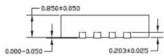
16-PIN QFN (QFN-16)

text_image
Pin 1 Dot By Marking 3.000±0.050 3.000±0.050TOP VIEW

text_image
PIN H1 IDENTIFICATION CHAMFER 0.300 X 45° 1.550±0.050 Exp. DAP 0.400±0.050 1.550±0.050 Exp. DAP 0.500 Bsc 0.230±0.050 0.400±0.050 1.500 Ref.BOTTOM VIEW
SIDE VIEW
NOTE:
1. ALL DIMENSIONS ARE IN MILLIMETERS.
2. MAX. PACKAGE WARPAGE IS 0.05 mm.
3. MAXIMUM ALLOWABE BURRS IS 0.076 mm IN ALL DIRECTIONS.
4. PIN #1 ID ON TOP WILL BE LASER/INK MARKED.
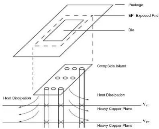
text_image
Package EP- Exposed Pad Die Comp/Side Island Heat Dissipation Heat Dissipation Heavy Copper Plane V_EE V_EE Heavy Copper PlanePCB Thermal Consideration for 16-Pin QFN Package (Always solder, or equivalent, the exposed pad to the PCB)
Package Notes:
- Package meets Level 2 qualification.
- All parts are dry-packaged before shipment.
- Exposed pads must be soldered to a ground for proper thermal management.
MICREL, INC. 2180 FORTUNE DRIVE SAN JOSE, CA 95131 USA
TEL +1 (408) 944-0800 FAX +1 (408) 474-1000 WEB http://www.micrel.com
Micrel makes no representations or warranties with respect to the accuracy or completeness of the information furnished in this data sheet. This information is not intended as a warranty and Micrel does not assume responsibility for its use. Micrel reserves the right to change circuitry, specifications and descriptions at any time without notice. No license, whether express, implied, arising by estoppel or otherwise, to any intellectual property rights is granted by this document. Except as provided in Micrel's terms and conditions of sale for such products, Micrel assumes no liability whatsoever, and Micrel disclaims any express or implied warranty relating to the sale and/or use of Micrel products including liability or warranties relating to fitness for a particular purpose, merchantability, or infringement of any patent, copyright or other intellectual property right
Micrel Products are not designed or authorized for use as components in life support appliances, devices or systems where malfunction of a product can reasonably be expected to result in personal injury. Life support devices or systems are devices or systems that (a) are intended for surgical implant into the body or (b) support or sustain life, and whose failure to perform can be reasonably expected to result in a significant injury to the user. A Purchaser's use or sale of Micrel Products for use in life support appliances, devices or systems is a Purchaser's own risk and Purchaser agrees to fully indemnify Micrel for any damages resulting from such use or sale.
© 2005 Micrel, Incorporated.