MCP1664 - Electronic component Microchip - Free user manual and instructions
Find the device manual for free MCP1664 Microchip in PDF.

User questions about MCP1664 Microchip
0 question about this device. Answer the ones you know or ask your own.
Ask a new question about this device
Download the instructions for your Electronic component in PDF format for free! Find your manual MCP1664 - Microchip and take your electronic device back in hand. On this page are published all the documents necessary for the use of your device. MCP1664 by Microchip.
USER MANUAL MCP1664 Microchip
High-Voltage Step-Up LED Driver with UVLO and Open Load Protection
Features
• 36V, 400 mΩ Integrated Switch
• Passes automotive AEC-Q100 reliability testing
- Up to 92% Efficiency
- Drive LED Strings in Constant Current
• 1.8A Peak Input Current Limit:
- I_LED up to 200 mA at 3.3V V_IN , 4 White LEDs
- I_LED up to 300 mA at 5.0V V_IN , 4 White LEDs
- I_LED up to 150 mA at 4.2V V_IN , 8 White LEDs
- Input Voltage Range: 2.4V to 5.5V
- Undervoltage Lockout (UVLO):
- U V L O a tN Rising: 2.3V, typical
- U V L O a ↓M Falling: 1.85V, typical
- Shutdown Current (EN = GND): 40 nA Typical
- PWM Operation: 500 kHz Switching Frequency
• Cycle-by-Cycle Current Limiting
- Internal Compensation
- Open Load Protection (OLP) in the event of:
- Feedback Pin Shorted to GND (Prevents Excessive Current into LEDs)
- Disconnected LED String (Prevents Overvoltage to the Converter's Output and SW Pin)
• Overtemperature Protection
• Available Packages:
- 5-Lead SOT-23
- 8 - Lead 2 mm x 3 mm TDFN
Applications
- Two and Three-Cell Alkaline or NiMH/NiCd White LED Driver for Backlighting Products
• Li-Ion Battery LED Lightning Application - Camera Flash
• LED Flashlights and Backlight Current Source
• Medical Equipment -
Portable Devices:
-
Hand-Held Gaming Devices
- GPS Navigation Systems
- LCD Monitors
- Portable DVD Players
General Description
The MCP1664 is a compact, space-efficient, fixed-frequency, non-synchronous step-up converter optimized to drive multiple strings of LEDs with constant current powered from two and three-cell alkaline or NiMH/NiCd as well as from one-cell Li-Ion or Li-Polymer batteries.
The device integrates a 36V, 400 mΩ low-side switch, which is protected by the 1.8A cycle-by-cycle inductor peak current limit operation. The MCP1664 starts up without high inrush current or output overshoot. All compensation and protection circuitry is integrated to minimize the number of external components.
The internal feedback ( V_FB ) voltage is set to 300 mV for low power dissipation when sensing and regulating the LED current. A single resistor sets the LED current.
The device features an UVLO which avoids start-up with low inputs or discharged batteries for two cell-powered applications.
The MCP1664 features an open load protection (OLP) which turns off the operation in situations when the LED string is accidentally disconnected or the feedback pin is short-circuited to GND.
While in Shutdown mode (EN = GND), the device stops switching, and consumes 40 nA typical of input current.
The MCP1664 is AEC-Q100 qualified for automotive applications.
Package Types
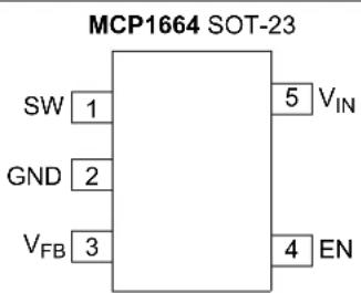
text_image
MCP1664 SOT-23 SW 1 GND 2 VFB 3 5 VIN 4 ENMCP1664 2 mm x 3 mm TDFN*

text_image
VFB 1 ○ 8 EN SGND 2 EP 7 PGND SW 3 9 6 NC NC 4 5 VIN* Includes Exposed Thermal Pad (EP); see Table 3-1.
Typical Application

text_image
L = 4.7 μH for maximum 4 white LEDs VOUT Max. 32V 4.7 - 10 μH D MBRM140 VIN CIN 4.7 - 30 μF SW VIN MCP1664 EN OFF ON GND VFB VFB = 0.3 V ILED = 0.3V / RSET RSET 12Ω LED1 LED2 LED6 COUT 10 μF VOUT ALKALINE + ALAKLINE + VIN -2.4V - 3.0VL = 4.7 μH for maximum 4 white LEDs
L = 10 μH for 5 to 10 white LEDs
C_IN = 4.7 - 10 F f o_IN ≥ 2.5 V
C_IN = 20 - 30 F for N 2.5 V
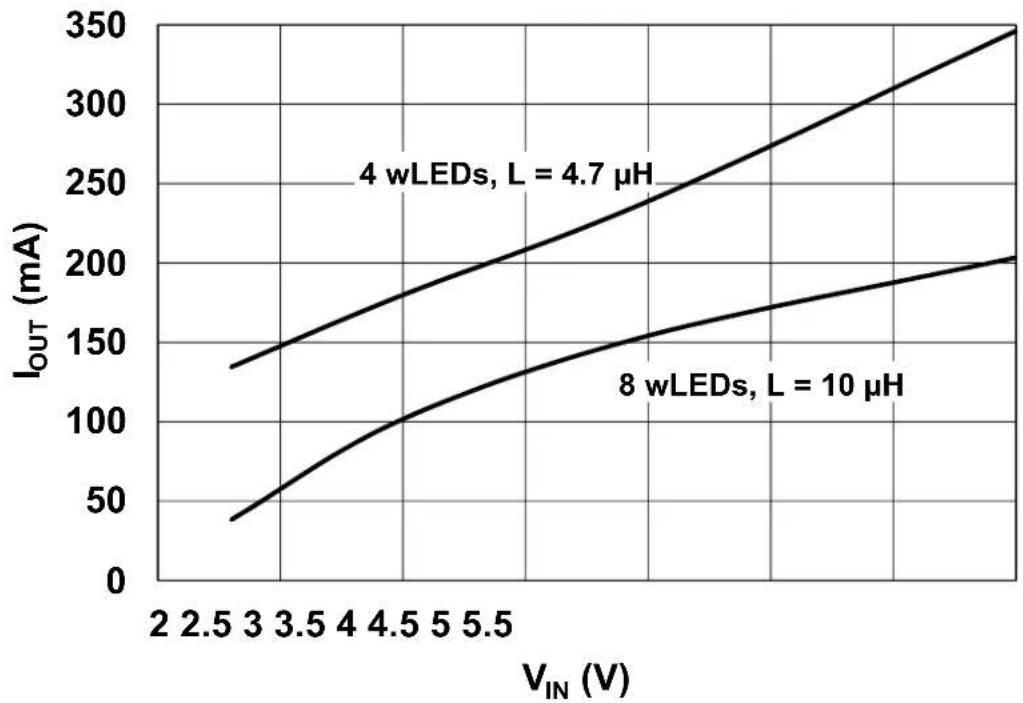
Maximum LED Current in Regulation vs. Input Voltage, T_A = +25^
line
| VIN (V) | 4 wLEDs, L = 4.7 µH (mA) | 8 wLEDs, L = 10 µH (mA) | | ------- | ------------------------- | ------------------------ | | 2.5 | ~135 | ~40 | | 3.0 | ~150 | ~60 | | 3.5 | ~165 | ~80 | | 4.0 | ~180 | ~100 | | 4.5 | ~195 | ~120 | | 5.0 | ~210 | ~140 | | 5.5 | ~225 | ~160 | | 6.0 | ~240 | ~180 | | 6.5 | ~255 | ~200 | | 7.0 | ~270 | ~220 | | 7.5 | ~285 | ~240 | | 8.0 | ~300 | ~260 | | 8.5 | ~315 | ~280 | | 9.0 | ~330 | ~300 | | 9.5 | ~345 | ~320 | | 10.0 | ~360 | ~340 |1.0 ELECTRICAL CHARACTERISTICS
Absolute Maximum Ratings †
V_SW - GND +36V
EN, V_IN – GND....+6.0V
V_FB +0.35V
Power Dissipation ..... Internally Limited
Storage Temperature -65°C to +150°C
Ambient Temperature with Power Applied ....-40°C to +125°C
Operating Junction Temperature....-40°C to +150°C
ESD Protection On All Pins:
HBM 4 kV
MM 400V
Notice: Stresses above those listed under “Maximum Ratings” may cause permanent damage to the device. This is a stress rating only and functional operation of the device at those or any other conditions above those indicated in the operational sections of this specification is not intended. Exposure to maximum rating conditions for extended periods may affect device reliability.
DC AND AC CHARACTERISTICS
| Electrical Specifications: Unless otherwise specified, all limits apply for typical values at ambient temperature T_A = +25°C_IN 3.3V , V_OUT loaded with 3 white LEDs ( V_F = 2.65V a t H 100mA ) I_LED = 20mA , C_IN = C_OUT = 10μF , X7R ceramic, L = 4.7 μH.Boldface specifications apply over the controlled T_A range of -40°C to +125°C. | ||||||
| Parameters Sym. Min | Typ. Max. Units C | conditions | ||||
| Input Voltage Range | V_IN | 2.4 | — | 5.5 | V | Note 1 |
| Undervoltage Lockout (UVLO) | UVLO_START | — | 2.3 | — | V | V_IN rising, I_LED = 20mA |
| UVLO_STOP | — | 1.85 | — | V | V_IN falling, I_LED = 20mA | |
| Maximum Output Voltage | V_OUTmax | — | — | 32 | V | Note 1 |
| Maximum Output Current | I_OUT | — | 150 | — | mA | 4.2V V_IN , 8 LEDs |
| 200 | — | mA | 3.3V V_IN , 4 LEDs | |||
| 300 | — | mA | 5.0V V_IN , 4 LEDs | |||
| Feedback Voltage Reference | V_FB | 275 | 300 | 325 | mV | |
| Feedback Input Bias Current | I_VFB | — | 0.025 | — | μA | |
| Shutdown Quiescent Current | I_QSHDN | — | 0.04 | — | μA | EN = GND |
| NMOS Peak Switch Current Limit | I_N(MAX) | — | 1.8 | — | A | Note 2 |
| NMOS Switch Leakage | I_NLK | — | 0.4 | — | μA | V_IN = V_SW = 5V ; V_OUT = 5.5V V_EN = V_FB = GND |
| NMOS Switch ON Resistance | R_DS(ON) | — | 0.4 | — | Ω | V_IN = 5V , I_LED = 100mA ,4 series white LEDsNote 2 |
| Feedback Voltage Line Regulation | |( V_FB/V_FB)/ V_IN| | — | 0.5 | 1 | %/V | V_IN = 3.3V to 5V |
| Maximum Duty Cycle | DC_MAX | — | 90 | — | % | Note 2 |
Note 1: Minimum input voltage in the range of V_IN ( V_IN < 5.5V < V_OUT ) depends on the maximum duty cycle ( DC_MAX ) and on the output voltage ( V_OUT ), according to the boost converter equation: V_INmin = V_OUT × (1 - DMAX) . Output voltage is equal to the LED voltage plus the voltage on the sense resistor ( VLED + V_-R_SET ). Recommended ( V_OUT - V_IN ) > 1V.
2: Determined by characterization, not production tested.
DC AND AC CHARACTERISTICS (CONTINUED)
| Electrical Specifications: Unless otherwise specified, all limits apply for typical values at ambient temperature T_A = +2.5^ C , V_1 = 3.3V , V_OUT loaded with 3 white LEDs ( V_F = 2.65 V at l = 10.0 mA ), L_ED = 20 mA , C_IN = C_OUT = 10 F , X7R ceramic, L = 4.7 H .Boldface specifications apply over the controlled T_A range of -40°C to +125°C. | ||||||
| Parameters | Sym. | Min. | Typ. | Max. | Units | Conditions |
| Switching Frequency f | SW | 425 500 | 575 kHz ±15% | |||
| EN Input Logic High V | IH | 85 — | — % of V | IN | ||
| EN Input Logic Low V | IL | — | — | 7 | IN | 5 % o |
| EN Input Leakage Current I | ENLK | — 0.025 — μA | V | EN = 5V | ||
| Start-Up Time | tss | — | 100 — | μs | EN Low to High,90% of I_LED (Note 2, Figure 2-10) | |
| Thermal Shutdown Die Temperature | TSD | — | 150 | — | °C | Note 2 |
| Die Temperature Hysteresis | TSDHYS | — | 20 | — | °C | Note 2 |
Note 1: Minimum input voltage in the range of V_IN ( V_IN < 5.5V < V_OUT ) depends on the maximum duty cycle ( DC_MAX ) and on the output voltage ( V_OUT ), according to the boost converter equation: V_INmin = V_OUT × (1 - D G_MAX) . Output voltage is equal to the LED voltage plus the voltage on the sense resistor ( V_LED + V_- R_SET ). Recommended ( V_OUT - V_IN ) > 1V.
2: Determined by characterization, not production tested.
TEMPERATURE SPECIFICATIONS
| Electrical Specifications: Unless otherwise specified, all limits apply for typical values at ambient temperature T_A = +25°C , M = 3.0V , I_OUT = 20 mA , V_OUT = 12V , C_IN = C_OUT = 10 μF , X7R ceramic, L = 4.7 μH.Boldface specifications apply over the air-forced T_A range of -40°C to +125°C. | ||||||
| Parameters | Sym. | Min. | Typ. | Max. | Units | Conditions |
| Temperature Ranges | ||||||
| Operating Junction Temperature Range | T_J | -40 | — | +125 | °C | Steady State |
| Storage Temperature Range | T_A | -65 — | +150 °C | |||
| Maximum Junction Temperature | T_J | — — | +150 °C | |||
| Package Thermal Resistances | ||||||
| Thermal Resistance, 5L SOT-23 | _JA | — | 201.0 | — | °C/W | |
| Thermal Resistance, 8L 2 mm x 3 mm TDFN | _JA | — | 52.5 | — | °C/W | |
2.0 TYPICAL PERFORMANCE CURVES
Note: The graphs and tables provided following this note are a statistical summary based on a limited number of samples and are provided for informational purposes only. The performance characteristics listed herein are not tested or guaranteed. In some graphs or tables, the data presented may be outside the specified operating range (e.g., outside specified power supply range) and therefore outside the warranted range.
Note: Unless otherwise indicated: V_IN = 3.3 V, LED = 20 mA , V_OUT loaded with 4 white LEDs ( V_F = 2.9 V apt 100 mA ), C_IN = C_OUT = 10 , X7R ceramic, L = 4.7 .
line
| Input Voltage (V) | LED Current (mA) | | ----------------- | ---------------- | | 2 | 140 | | 3 | 140 | | 4 | 140 | | 5 | 140 | | 6 | 140 | | 7 | 140 | | 8 | 140 | | 9 | 140 | | 10 | 140 | | 11 | 140 | | 12 | 140 | | 13 | 140 | | 14 | 140 | | 15 | 140 | | 16 | 140 | | 17 | 140 | | 18 | 140 | | 19 | 140 | | 20 | 140 | | 21 | 140 | | 22 | 140 | | 23 | 140 | | 24 | 140 | | 25 | 140 | | 26 | 140 | | 27 | 140 | | 28 | 140 | | 29 | 140 | | 30 | 140 | | 31 | 140 | | 32 | 140 | | 33 | 140 | | 34 | 140 | | 35 | 140 | | 36 | 140 | | 37 | 140 | | 38 | 140 | | 39 | 140 | | 40 | 140 | | 41 | 140 | | 42 | 140 | | 43 | 140 | | 44 | 140 | | 45 | 140 | | 46 | 140 | | 47 | 140 | | 48 | 140 | | 49 | 140 | | 50 | 140 | | 51 | 140 | | 52 | 140 | | 53 | 140 | | 54 | 140 | | 55 | 140 | | 56 | 140 | | 57 | 140 | | 58 | 140 | | 59 | 140 | | 60 | 140 | | 61 | 140 | | 62 | 140 | | 63 | 140 | | 64 | 140 | | 65 | 140 | | 66 | 140 | | 67 | 140 | | 68 | 140 | | 69 | 140 | | 70 | 140 | | 71 | 140 | | 72 | 140 | | 73 | 140 | | 74 | 140 | | 75 | 140 | | 76 | 140 | | 77 | 140 | | 78 | 140 | | 79 | 140 | | 80 | 140 | | 81 | 140 | | 82 | 140 | | 83 | 140 | | 84 | 140 | | 85 | 140 | | 86 | 140 | | 87 | 140 | | 88 | 140 | | 89 | 140 | | 90 | 140 | | 91 | 140 | | 92 | 140 | | 93 | 140 | | 94 | 140 | | 95 | 140 | | 96 | 140 | | 97 | 140 | | 98 | 140 | | 99 | 140 | | Note: The data is already in CSV format as it is extracted from the image. The output text 'R_SET' is not present in the image. There are no additional data series in this case. The output values are estimated based on the given code.FIGURE 2-1: Four White LEDs, I LED vs. V_IN .

line
| I_LED (mA) | Efficiency (%) at V_IN = 3.0V | Efficiency (%) at V_IN = 4.0V | Efficiency (%) at V_IN = 5.5V | | ---------- | ----------------------------- | ----------------------------- | ----------------------------- | | 0 | 90 | 90 | 90 | | 50 | 88 | 87 | 86 | | 100 | 85 | 84 | 83 | | 150 | 82 | 81 | 80 | | 200 | 80 | 79 | 78 | | 250 | 78 | 77 | 76 | | 300 | 76 | 75 | 75 | | 350 | 75 | 74 | 74 |FIGURE 2-4: Four White LEDs, Efficiency vs. I_LED .
line
| Ambient Temperature (°C) | LED Current (mA) | | ------------------------ | --------------- | | 65 | 140 | | 80 | 140 | | 95 | 140 | | 110 | 140 | | 125 | 140 |FIGURE 2-2: Four White LEDs, I Ambient Temperature.
line
| I_LED (mA) | Efficiency (%) | | ---------- | -------------- | | 0 | 90 | | 50 | 85 | | 100 | 75 | | 150 | 70 | | 200 | 65 | | 250 | 60 |FIGURE 2-5: Eight White LEDs, Efficiency vs. I_LED .

line
| Ambient Temperature (°C) | LED Current (mA) | | ------------------------ | ---------------- | | -40 | 140 | | -25 | 140 | | -10 | 140 | | 5 | 140 | | 20 | 140 | | 35 | 140 | | 50 | 140 | | 65 | 140 | | 80 | 140 | | 95 | 140 | | 110 | 130 | | 125 | 100 |FIGURE 2-3: Eight White LEDs, I Ambient Temperature.
line
| Input Voltage (V) | 5 wLEDs, L = 10μH | 4 wLEDs, L = 4.7μH | 8 wLEDs, L = 10μH | | ----------------- | ------------------ | ------------------- | ------------------ | | 2 | ~130 | ~100 | ~40 | | 3 | ~160 | ~140 | ~70 | | 7 | ~220 | ~200 | ~120 | | 3 | ~280 | ~260 | ~160 | | 5 | ~320 | ~300 | ~190 | | 3 | ~350 | ~340 | ~210 |FIGURE 2-6: Maximum I LED vs. V_IN .
Note: Unless otherwise indicated: V_IN = 3.3 V, LED = 20 mA , V_OUT loaded with 4 white LEDs ( V_F = 2.9 V at 100 mA ), C_IN = C_OUT = 10 , X7R ceramic, L = 4.7 .

line
| Ambient Temperature (°C) | UVLO Thresholds (V) | | ------------------------ | ------------------- | | -40 | 2.2 | | -25 | 2.2 | | -10 | 2.2 | | 5 | 2.2 | | 20 | 2.2 | | 35 | 2.2 | | 50 | 2.2 | | 65 | 2.2 | | 80 | 2.2 | | 95 | 2.2 | | 110 | 2.2 | | 125 | 2.2 | | -40 | 1.85 | | -25 | 1.85 | | -10 | 1.85 | | 5 | 1.85 | | 20 | 1.85 | | 35 | 1.85 | | 50 | 1.85 | | 65 | 1.85 | | 80 | 1.85 | | 95 | 1.85 | | 110 | 1.85 | | 125 | 1.85 |FIGURE 2-7: Undervoltage Lockout (UVLO) vs. Ambient Temperature.

bar
| Number of LEDs | Blue Bars (I_LED = 20 mA) (μs) | Red Bars (I_LED = 40 mA) (μs) | |---|---|---| | 3 | 95 | 97 | | 4 | 105 | 110 | | 5 | 115 | 123 | | 6 | 127 | 138 | | 7 | 137 | 155 | | 8 | 147 | 166 | Blue Bars: I_LED = 20 mA; Red Bars: I_LED = 40 mA; C_OUT = 10 µFFIGURE 2-10: Start-Up Time vs. LED Number.
line
| Input Voltage (V) | Shutdown I₀ (nA) | | ----------------- | ---------------- | | 2.5 | 40 | | 2.8 | 39 | | 3.1 | 39 | | 3.4 | 39 | | 3.7 | 40 | | 4.0 | 42 | | 4.3 | 45 | | 4.6 | 47 | | 4.9 | 48 | | 5.2 | 47 | | 5.5 | 46 |FIGURE 2-8: Shutdown Quiescent Current, I_Q , vs. V_IN (EN = GND).

FIGURE 2-11: Start-Up When V_IN = V_ENABLE .
line
| Ambient Temperature (°C) | Switching Frequency (kHz) | | ------------------------ | ------------------------- | | -40 | 480 | | -25 | 490 | | -10 | 495 | | 5 | 500 | | 20 | 505 | | 35 | 510 | | 50 | 512 | | 65 | 513 | | 80 | 514 | | 95 | 515 | | 110 | 514 | | 125 | 513 |FIGURE 2-9: Switching Frequency, f_SW vs. Ambient Temperature.
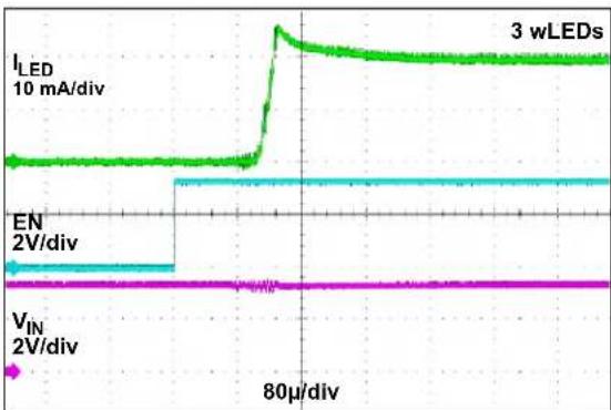
line
| Parameter | Value | | --------- | --------- | | I_LED | 10 mA/div | | EN | 2V/div | | V_IN | 2V/div |FIGURE 2-12: Start-Up After Enable.
Note: Unless otherwise indicated: V_IN = 3.3 V, LED = 20 mA , V_OUT loaded with 4 white LEDs ( V_F = 2.9 V aF 100 mA ), CIN = C_OUT = 10 , X7R ceramic, L = 4.7 .
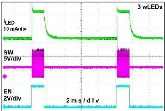
line
| Signal | Time (ms) | |--------|-----------| | I_LED | 10 mA/div | | SW | 5 V/div | | EN | 2 V/div |FIGURE 2-13: 100 Hz PWM Dimming, 15% Duty Cycle.

line
| Time (μs) | I_LED (AC Coupled) | SW (5V/div) | V_OUT (5V/div) | |-----------|---------------------|-------------|----------------| | 0 | 2.0 | 0 | 0 | | 1 | 2.0 | 0 | 0 | | 2 | 2.0 | 0 | 0 | | 3 | 2.0 | 0 | 0 | | 4 | 2.0 | 0 | 0 | | 5 | 2.0 | 0 | 0 | | 6 | 2.0 | 0 | 0 | | 7 | 2.0 | 0 | 0 | | 8 | 2.0 | 0 | 0 | | 9 | 2.0 | 0 | 0 | | 10 | 2.0 | 0 | 0 | | 11 | 2.0 | 0 | 0 | | 12 | 2.0 | 0 | 0 | | 13 | 2.0 | 0 | 0 | | 14 | 2.0 | 0 | 0 | | 15 | 2.0 | 0 | 0 | | 16 | 2.0 | 0 | 0 | | 17 | 2.0 | 0 | 0 | | 18 | 2.0 | 0 | 0 | | 19 | 2.0 | 0 | 0 | | 20 | 2.0 | 0 | 0 | | 21 | 2.0 | 0 | 0 | | 22 | 2.0 | 0 | 0 | | 23 | 2.0 | 0 | 0 | | 24 | 2.0 | 0 | 0 | | 25 | 2.0 | 0 | 0 | | 26 | 2.0 | 0 | 0 | | 27 | 2.0 | 0 | 0 | | 28 | 2.0 | 0 | 0 | | 29 | 2.0 | 0 | 0 | | 30 | 2.0 | 0 | 0 | | 31 | 2.0 | 0 | 0 | | | | | | | | | | | | | | | | | | | | | | | | | | | | | | | | | | | | | | | | | | | | | | | | | | | | | | | | | | | | |FIGURE 2-16: Three White LEDs PWM Discontinuous Mode Waveforms.
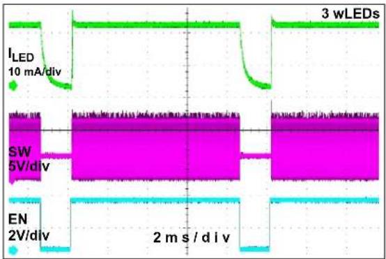
FIGURE 2-14: 100 Hz PWM Dimming, 85% Duty Cycle.
line
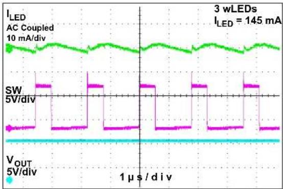
| Time (μs) | I_LED (mA) | SW (5V/div) | V_OUT (5V/div) | |-----------|------------|-------------|----------------| | 0 | 145 | 0 | 0 | | 1 | ~145 | High | Low | | 2 | ~145 | Low | Low | | 3 | ~145 | High | Low | | 4 | ~145 | Low | Low | | 5 | ~145 | High | Low | | 6 | ~145 | Low | Low | | 7 | ~145 | High | Low | | 8 | ~145 | Low | Low | | 9 | ~145 | High | Low | | 10 | ~145 | Low | Low | | 11 | ~145 | High | Low | | 12 | ~145 | Low | Low | | 13 | ~145 | High | Low | | 14 | ~145 | Low | Low | | 15 | ~145 | High | Low | | 16 | ~145 | Low | Low | | 17 | ~145 | High | Low | | 18 | ~145 | Low | Low | | 19 | ~145 | High | Low | | 20 | ~145 | Low | Low | | 21 | ~145 | High | Low | | 22 | ~145 | Low | Low | | 23 | ~145 | High | Low | | 24 | ~145 | Low | Low | | 25 | ~145 | High | Low | | 26 | ~145 | Low | Low | | 27 | ~145 | High | Low | | 28 | ~145 | Low | Low | | 29 | ~145 | High | Low | | 30 | ~145 | Low | Low | | 31 | ~145 | High | Low | | 32 | ~145 | Low | Low | | 33 | ~145 | High | Low | | 34 | ~145 | Low | Low | | 35 | ~145 | High | Low | | 36 | ~145 | Low | Low | | 37 | ~145 | High | Low | | 38 | ~145 | Low | Low | | 39 | ~145 | High | Low | | 40 | ~145 | Low | Low | | 41 | ~145 | High | Low | | 42 | ~145 | Low | Low | | 43 | ~145 | High | Low | | 44 | ~145 | Low | Low | | 45 | ~145 | High | Low | | 46 | ~145 | Low | Low | | 47 | ~145 | High | Low | | 48 | ~145 | Low | Low | | 49 | ~145 | High | Low | | 50 | ~145 | Low | Low | | 51 | ~145 | High | Low | | 52 | ~145 | Low | Low | | 53 | ~145 | High | Low | | 54 | ~145 | Low | Low | | 55 | ~145 | High | Low | | 56 | ~145 | Low | Low | | 57 | ~145 | High | Low | | 58 | ~145 | Low | Low | | 59 | ~145 | High | Low | | 60 | ~145 | Low | Low | | 61 | ~145 | High | Low | | 62 | ~145 | Low | Low | | 63 | ~145 | High | Low | | 64 | ~145 | Low | Low | | 65 | ~145 | High | Low | | 66 | ~145 | Low | Low | | 67 | ~145 | High | Low | | 68 | ~145 | Low | Low | | 69 | ~145 | High | Low | | 70 | ~145 | Low | Low | | 71 | ~145 | High | Low | | 72 | ~145 | Low | Low | | 73 | ~145 | High | Low | | 74 | ~145 | Low | Low | | 75 | ~145 | High | Low | | 76 | ~145 | Low | Low | | 77 | ~145 | High | Low | | 78 | ~145 | Low | Low | | 79 | ~145 | High | Low | | 80 | ~145 | Low | Low | | 81 | ~145 | High | Low | | 82 | ~145 | Low | Low | | 83 | ~145 | High | Low | | 84 | ~145 | Low | Low | | 85 | ~145 | High | Low | | 86 | ~145 | Low | Low | | 87 | ~145 | High | Low | | 88 | ~145 | Low | Low | | 89 | ~145 | High | Low | | 90 | ~145 | Low | Low | | 91 | ~145 | High | Low | | 92 | ~145 | Low | Low | | 93 | ~145 | High | Low | | 94 | ~145 | Low | Low | | 95 | ~145 | High | Low | | 96 | ~145 | Low | Low | | 97 | ~145 | High | Low | | 98 | ~145 | Low | Low | | 99 | ~145 | High | Low | | 100 | ~145 | Low | Low | | Peak (approx.) - AC Coupled - SW - SW - OUT - AC - AC Coupled - AC - AC - AC - AC - AC - AC - AC - AC - AC - AC - AC - AC - AC - AC - AC - AC - AC - AC - AC - AC - AC - AC - AC - AC - AC - AC - AC - AC - AC - AC - AC - AC - AC - AC - AC - AC - AC - AC - AC - AC - AC - AC - AC - AC - AC - AC - AC - AC - AC - AC - DC - AC - DC - DC - DC - DC - DC - DC - DC - DC - DC - DC - DC - DC - DC - DC - DC - DC - DC - DC - DC - DC - DC - DC - DC - DC - DC - DC - DC - DC - DC - DC - DC - DC - DC - DC - DC - DC - DC - DC - DC - DC - DC - DC - DC - DC - DC - DC - DC - DC - DC - DC - ACDCDCDCDCDCDCDCDCDCDCDCDCDCDCDCDCDCDCDCDCDCDCDCDCDCDCDCDCDCDCDCDCDCDCDCDCDCDCDCDCDCDCDCDCDCDCDCDCDCDCDCDCDCDCDCDCDCDCDCDCDCDCDCDCDCDCDCDCDCDCDCDCDCDCDCDCDCDCDCDCDCDCDCDCDCDCDCDCDCDCDCDCDCDCDCDCDCDCDCDC-AC-AC-AC-AC-AC-AC-AC-AC-AC-AC-AC-AC-AC-AC-AC-AC-AC-AC-AC-AC-AC-AC-AC-AC-AC-AC-AC-AC-AC-AC-AC-AC-AC-AC-AC-AC-AC-AC-AC-AC-AC-AC-AC-AC-AC-AC-AC-AC-AC-AC-CAUCDCDCCDCCDCCDCCDCCDCCDCCDCCDCCDCCDCCDCCDCCDCCDCCDCCDCCDCCDCCDCCDCCDCCDCCDCCDCCDCCDCCDCCDCCDCCDCCDCCDCCDCCDCCDCCDCCDCCDCCDCCDCCDCCDCCDCCDCCDCCDCCDCCDCCDCCDCCCDDCDDCDDCDDCDDCDDCDDCDDCDDCDDCDDCDDCDDCDDCDDCDDCDDCDDCDDCDDCDDCDDCDDCDDCDDCDDCDDCDDCDDCDDCDDCDDCDDCDDCDDCDDCDDCDDCDDCDDCDDCDDCDDCDDCDDCDDCDDCDDCDDCDDCDDCAUCDE CTC DTC DTC DTC DTC DTC DTC DTC DTC DTC DTC DTC DTC DTC DTC DTC DTC DTC DTC DTC DTC DTC DTC DTC DTC DTC DTC DTC DTC DTC DTC DTC DTC DTC DTC DTC DTC DTC DTC DTC DTC DTC DTC DTC DTC DTC DTC DTC DTC DTC DTC AUCDE CTC DTC DTC DTC DTC DTC DTC DTC DTC DTC DTC DTC DTC DTC DTC DTC DTC DTC DTC DTC DTC DTC DTC DTC DTC DTC DTC DTC DTC DTC DTC DTC DTC DTC AUCDE CTC DTC DTC DTC DTC DTC DTC DTC DTC DTC DTC DTC DTC DTC DFC AUCDE CTC AUCDE CTC AUCDE CTC AUCDE CTC AUCDE CTC AUCDE CTC AUCDE CTC AUCDE CTC AUCDE CTC AUCDE CTC AUCDE CTC AUCDE CTC AUCDE CTC AUCDE CTC AUCDE CTC AUCDE CTC AUCDE CTC AUCDE CTC AUCDE CTC AUCDE CTC AUCDE CTA UUC DE CTA UUC DE CTA UUC DE CTA UUC DE CTA UUC DE CTA UUC DE CTA UUC DE CTA UUC DE CTA UUC DE CTA UUC DE CTA UUC DE CTA UUC DE CTA UUC DE CTA UUC DE CTA UUC DE CTA UUC DE CTA UUC DE CTA UUC DE CTA UUC DE CTA UUC DE CTA UUC EUC DE CTA UUC DE CTA UUC DE CTA UUC DE CTA UUC DE CTA UUC DE CTA UUC DE CTA UUC DE CTA UUC DE CTA UUC DE CTA UUC DE CTA UUC DE CTA UUC DE CTA UUC DE CTA UUC DE CTA UUC DE CTA UUC DE CTA UUC DE CTA UUC DE CTA UUC DE CTA USUIC DE CTA USUIC DE CTA USUIC DE CTA USUIC DE CTA USUIC DE CTA USUIC DE CTA USUIC DE CTA USUIC DE CTA USUIC DE CTA USUIC DE CTA USUIC DE CTA USUIC DE CTA USUIC DE CTA USUIC DE CTA USUIC DE CTA USUIC DE CTA USUIC DE CTAUSUIC DE CTA USUIC DE CTA USUIC DE CTA USUIC DE CTA USUIC DE CTA USUIC DE CTA USUIC DE CTA USUIC DE CTA USUIC DE CTA USUIC DE CTA USUIC DE CTA USUIC DE CTA USUIC DE CTA USUIC DE CTA USUIC DE CTA USUIC DE CTA USUIC DE CAUTSUSUIC DE CAUTSUSUIC DE CAUTSUSUIC DE CAUTSUSUIC DE CAUTSUSUIC DE CAUTSUSUIC DE CAUTSUSUIC DE CAUTSUSUIC DE CAUTSUSUIC DE CAUTSUSUIC DE CAUTSUSUIC DE CAUTSUSUIC DE CAUTSUSUIC DE CAUTSUSUIC DE CAUTSUSUVCDE CAUTSUSUVCDE CAUTSUSUVCDE CAUTSUSUVCDE CAUTSUSUVCDE CAUTSUSUVCDE CAUTSUSUVCDE CAUTSUSUVCDE CAUTSUSUVCDE CAUTSUSUVCDE CAUTSUSUVCDE CAUTSUSUVCDE CAUTSUSUVCDE CAUTSUSUVCDE CAUTSUSUVCDE CACTA USUVCDE CACTA USUVCDE CACTA USUVCDE CACTA USUVCDE CACTA USUVCDE CACTA USUVCDE CACTA USUVCDE CACTA USUVCDE CACTA USUVCDE CACTA USUVCDE CACTA USUVCDE CACTA USUVCDE CACTA USUVCDE CACTA USUVCDE CACTA USUMC style I_LED style AC Coupled style AC Coupled style AC Coupled style AC Coupled style AC Coupled style AC Coupled style AC Coupled style AC Coupled style AC Coupled style AC Coupled style AC Coupled style AC Coupled style AC Coupled style AC Coupled style AC Coupled style AC Coupled style AC Coupled style AC Coupled style AC Coupled style AC Coupled style AC Coupled / AC Coupled / SW/Div / VOUT/DAV / VOUT/DAV / VOUT/DAV / VOUT/DAV / VOUT/DAV / VOUT/DAV / VOUT/DAV / VOUT/DAV / VOUT/DAV / VOUT/DAV / VOUT/DAV / VOUT/DAV / VOUT/DAV / VOUT/DAV / VOUT/DAV : Blue Square (SW) Blue Square (SW) Blue Square (SW) Blue Square (SW) Blue Square (SW) Blue Square (SW) Blue Square (SW) Blue Square (SW) Blue Square (SW) Blue Square (SW) Blue Square (SW) Blue Square (SW) Blue Square (SW) Blue Square (SW) Blue Square (SW) Blue Square (SW) Blue Square (SW) Blue Square(BC) Blue Square(BC) Blue Square(BC) Blue Square(BC) Blue Square(BC) Blue Square(BC) Blue Square(BC) Blue Square(BC) Blue Square(BC) Blue Square(BC) Blue Square(BC) Blue Square(BC) Blue Square(BC) Blue Square(BC) Blue Square(BC) Blue Square(BC) Blue Square(BC) BlueSquare(BC) BlueSquare(BC) BlueSquare(BC) BlueSquare(BC) BlueSquare(BC) BlueSquare(BC) BlueSquare(BC) BlueSquare(BC) BlueSquare(BC) BlueSquare(BC) BlueSquare(BC) BlueSquare(BC) BlueSquare(BC) BlueSquare(BC) BlueSquare(BC) BlueSquare(BC) BlueSquare(BC) / BC / BC / BC / BC / BC / BC / BC / BC / BC / BC / BC / BC / BC / BC / BC / BC / BC / BC / BC / BC / BC / BC / BC / BC / BC / BC / BC / BC / BC / BC / BC / BC / BC / BC / BC / BC / BC / BC / BC / BC / BC / BC / BC / BC / BC / BC / BC / BC / BC / BC / BCL style I_LED style AC Coupled style AC Coupled style AC Coupled style AC Coupled style AC Coupled style AC Coupled style AC Coupled style AC Coupled style AC Coupled style AC Coupled style AC Coupled style AC Coupled style AC Coupled style AC Coupled style AC Coupled style AC Coupled style AC Coupled style AC Coupled style AC Coupled style AC Coupled style AC Cououred / AC Cououred / SW/Div / SW/DAV / SW/DAV / SW/DAV / SW/DAV / SW/DAV / SW/DAV / SW/DAV / SW/DAV / SW/DAV / SW/DAV / SW/DAV / SW/DAV / SW/DAV / SW/DAV / SW/DAV / SW/DAV / SW/DAV / SW/THE [0] [0] [0] [0] [0] [0] [0] [0] [0] [0] [0] [0] [0] [0] [0] [0] [0] [0] [0] [0] [0] [0] [0] [0] [0] [0]FIGURE 2-17: Three White LEDs PWM Continuous Mode Waveforms.

line
| Signal | Value | |--------|--------------| | I_LED | 10 mA/div | | SW | 5V/div | | V_FB | 200 mV/div |FIGURE 2-15: Open Load (LED Fail or FB to GND) Response.
line
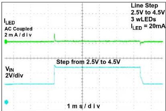
| Time Scale | Current (mA) | VIN (V) | |------------|--------------|---------| | 0 | 2 | 2 | | Step from 2.5V to 4.5V | 20 | 2 | | 1 | 2 | 2 |FIGURE 2-18: Line Step Response. V_IN steps from 2.5V to 4.5V .
3.0 PIN DESCRIPTIONS
The descriptions of the pins are listed in Table 3-1.
TABLE 3-1: PIN FUNCTION TABLE
| MCP1664SOT-23 | MCP16642 m m x 3 m mTDFN | Symbol | Description |
| 1 3 SW Switch Node, Boost Inductor Pin | |||
| 2 — GND | Ground Pin (SOT-23 only) | ||
| 3 | 1 | V_FB | Feedback Voltage Pin |
| 4 8 | EN Enable Control Input Pin | ||
| 5 | 5 | V_IN | Input Voltage Pin |
| — | 2 | S_GND | Signal Ground Pin (TDFN only) |
| — | 4, 6 | NC | Not Connected |
| — | 7 | P_GND | Power Ground Pin (TDFN only) |
| — | 9 | EP | Exposed Thermal Pad (EP); must be connected to Ground.(TDFN only) |
3.1 Feedback Voltage Pin (V FB)
The V_FB pin is used to regulate the voltage across the R_SET sense resistor to 300 mV to keep the output LED current in regulation. Connect the cathode of the LED to the V_FB pin.
3.2 Signal Ground Pin (S GND)
The signal ground pin is used as a return for the integrated reference voltage and error amplifier.
3.3 Switch Node Pin (SW)
Connect the inductor from the input voltage to the SW pin. The SW pin carries inductor current and has a typical value of 1.8A. The integrated N-Channel switch drain is internally connected to the SW node.
3.4 Not Connected (NC)
This is an unconnected pin.
3.5 Power Supply Input Voltage Pin ( V_IN )
Connect the input voltage source to V_IN . The input source should be decoupled from GND with a 4.7 F minimum capacitor.
3.6 Power Ground Pin (P GND)
The power ground pin is used as a return for the high-current N-Channel switch. The P_GND and S_GND pins are connected externally. The signal ground and power ground must be connected externally in one point.
3.7 Enable Pin (EN)
The EN pin is a logic-level input used to enable or disable device switching and lower quiescent current while disabled. A logic high ( >85% of V_IN ) will enable the regulator output. A logic low ( <7.5% of V_IN ) will ensure that the regulator is disabled.
3.8 Exposed Thermal Pad (EP)
There is no internal electrical connection between the Exposed Thermal Pad (EP) and the S_GND and P_GND pins. They must be connected to the same potential on the Printed Circuit Board (PCB).
3.9 Ground Pin (GND)
The ground or return pin is used for circuit ground connection. The length of the trace from the input capacitor return, the output capacitor return and the GND pin must be as short as possible, to minimize noise on the GND pin. The SOT-23 5-lead package uses a single ground pin.
4.0 DETAILED DESCRIPTION
4.1 Device Overview
The MCP1664 is a fixed-frequency, synchronous step-up converter, with a low voltage reference of 300 mV, optimized to keep the output current constant by regulating the voltage across the feedback resistor ( R_SET ). The MCP1664 integrates a peak current mode architecture and delivers high-efficiency conversion for LED lightning applications while being powered by two-cell and three-cell Alkaline, Ultimate Lithium, NiMH, NiCd and single-cell Li-Ion battery inputs. The maximum input voltage, V_INmax is 5.5V. A high level of integration lowers total system cost, eases implementation and reduces board area.
The conventional boost converter with a high voltage reference has a high voltage drop across the LED series current limit resistor. The power dissipated in this resistor, which is usually in series with the LED string, reduces the total efficiency conversion of an LED driver solution. Therefore, the voltage drop on the sense resistor ( R_SET ) used to regulate the LED current must be low. In the case of MCP1664, the V_FB value is 300 mV.
The device features controlled start-up voltage (UVLO START = 2.3V) and an open load protection in case the LED fails or short circuit of the V FB pin to GND. Once the V _FB voltage drops below 50 mV, the device stops switching and the output voltage will be equal to the input voltage (minus a diode drop voltage). This feature prevents damage to the device and LEDs in case of an accidental event like the one previously described.
The 400 mΩ, 36V integrated switch is protected by the 1.8A cycle-by-cycle inductor peak current limit operation. When the Enable pin is pulled to ground (EN = GND), the device stops switching, enters in Shutdown mode and consumes less than 50 nA of input current (Figure 2-8).
4.2 Functional Description
The MCP1664 is a compact, high-efficiency, fixed 500 kHz frequency, step-up DC-DC converter that operates as a constant current generator for applications powered by either two-cell or three-cell alkaline or Lithium Energizer; three-cell NiCd or NiMH; or one-cell Li-Ion or Li-Polymer batteries.
Figure 4-1 describes the functional block diagram of the MCP1664. It incorporates a current mode control scheme in which the PWM ramp signal is derived from the NMOS power switch current ( V_SENSE ). A slope compensation signal ( V_RAMP ) is added to the current sense signal ( V_SENSE ) and compared to the output of the error amplifier ( V_ERROR ) to control the ON-time of the power switch.

flowchart
graph TD
    A["V_IN"] --> B["Internal Bias UVLO_COMP"]
    B --> C["V_BIAS"]
    C --> D["V_IN_OK"]
    D --> E["V_UVLO_REF"]
    E --> F["Gate Drive and Shutdown Control Logic"]
    F --> G["V_EXT"]
    G --> H["Overcurrent Comparator"]
    H --> I["OC_Ref"]
    H --> J["V_LIMIT"]
    H --> K["V_SENSE"]
    L["EN"] --> M["Oscillator"]
    M --> N["Slope Compensation"]
    N --> O["V_RAMP"]
    O --> P["S"]
    Q["GND"] --> R["Logic SR Latch"]
    R --> S["V_PWM"]
    S --> T["V_ERROR"]
    T --> U["EA 300 mV"]
    U --> V["V_FB"]
    W["Open Load Comparator"] --> X["V_OLP_REF"]
    X --> Y["V_FB_FAULT"]
    Y --> Z["V_OUT_OK"]
    Z --> AA["Power Good Comparator and Delay"]
    AA --> AB["V_FB"]
    AA --> AC["V_IN_OK"]
    AA --> AD["EN"]
    AE["Thermal Shutdown"] --> AF["Power Good Comparator and Delay"]
    AF --> AG["V_FB"]
    AF --> AH["V_IN_OK"]
    AF --> AI["EN"]
    AJ["Rc"] --> AK["Cc"]
    AK --> AL["V_OLP_REF"]
    AL --> AM["V_UVLO_REF"]
    AM --> AN["Bandgap"]
    AN --> AO["V_FB"]
FIGURE 4-1: MCP1664 Simplified Block Diagram.
4.2.1 INTERNAL BIAS
The MCP1664 gets its bias from V_IN . The V_IN bias is used to power the device and drive circuits over the entire operating range. The maximum V_IN is 5.5V.
4.2.2 START-UP
The MCP1664 is capable of starting from two alkaline cells. The MCP1664 starts switching at approximately 2.3V typical for a light load current. Once started, the device will continue to operate under normal load conditions down to 1.85V typical.
The start-up time is dependent on the LED's current, the number of the LEDs connected at output and on the output capacitor value (see Figure 2-10). Output capacitor value increases the start-up time.
When the device is powered, the output capacitor charges to a value close to the input voltage ( V_IN minus a Schottky diode voltage drop). To avoid high inrush currents that occur when charging the output capacitor during start-up, the switch peak current is limited to 1.8A. Once the voltage on the output capacitor reaches the sum of the forward voltages of all LEDs, the MCP1664 enters in constant current operation.
Due to the direct path from input to output, in the case of dimming applications (EN voltage switches from low to high), the output capacitor is already charged and the output starts from a value close to the input voltage. In this particular situation the device starts faster.
The internal oscillator has a delayed start to let the output capacitor be completely charged to the input voltage value.
4.2.3 UNDERVOLTAGE LOCKOUT (UVLO)
The MCP1664 features an UVLO that prevents fault operation below 1.85V typical, which is close to the value of two discharged alkaline batteries.
Essentially, there is a comparator, which monitors V_IN and a reference voltage derived from the bandgap.
The device starts its normal operation at 2.3V typical input. A hysteresis is set for the comparator to avoid input transients (temporary V_IN drop) which might trigger the lower UVLO threshold and restart the device.
When the input voltage is below the UVLO _START threshold, the device is operating with limited specification.
4.2.4 ENABLE PIN
The MCP1664 enables switching when the EN pin is set high. The device is put into Shutdown mode when the EN pin is set low. To enable the boost converter, the EN voltage level must be greater than 85% of the V_IN voltage. To disable the boost converter, the EN voltage must be less than 7.5% of the V_IN voltage.
4.2.4.1 Shutdown Mode.
$$ \text { Input - to - Output Path } (E N = G N D) $$
In Shutdown mode, the MCP1664 stops switching and all internal control circuitry is switched off. The input voltage will be bypassed to output through the inductor and the Schottky diode.
While the device stops switching, V_OUT is equal to the output capacitor voltage, which slowly discharges on the leak path (from V_OUT to a value close to V_IN ) after the LEDs have been turned off.
In Shutdown mode, the current consumed by the MCP1664 from batteries is very low, below 50 nA.
The MCP1664 operates as a fixed-frequency, non-synchronous converter. The switching frequency is maintained with a precision oscillator at 500 kHz.
Lossless current sensing converts the inductor's peak current signal to a voltage ( V_SENSE ) and adds it to the internal slope compensation ( V_RAMP ). This summed signal is compared to the voltage error amplifier output ( V_ERROR ) to provide a peak current control signal ( V_PWM ) for the PWM. The slope compensation signal depends on the input voltage. Therefore, the converter provides the proper amount of slope compensation to ensure stability. The peak limit current is set to 1.8A.
4.2.6 INTERNAL COMPENSATION
The error amplifier, with its associated compensation network, completes the closed-loop system by comparing the output voltage to a reference at the input of the error amplifier and by feeding the amplified and inverted signal to the control input of the inner current loop. The compensation network provides phase leads and lags at appropriate frequencies to cancel excessive phase lags and leads of the power circuit. All necessary compensation and slope compensation components are integrated.
4.2.7 OPEN LOAD PROTECTION (OLP)
An internal V_FB fault signal turns off the PWM signal ( V_EXT ) when output goes out of regulation in the event of:
- open load (LED string fails)
or
- short circuit of the feedback pin to GND.
In any of the above events, for a regular integrated circuit (IC) without any protection implemented, the V_FB voltage drops to ground potential, its N-channel transistor is forced to switch at full duty cycle and V_OUT rises. This fault event may cause the SW pin to exceed its maximum voltage rating and may damage the boost regulator IC, its external components and the LEDs. To avoid these, the MCP1664 features an open load protection (OLP) which turns off PWM switching when such a condition is detected. There is an overvoltage comparator with 50 mV reference which monitors the V_FB voltage.
If the OLP event occurs with the input voltage below the UVLO START threshold and VFB remains under 50 mV due to weak input (discharged batteries) or an overload condition, the device latches its output; it resumes after power-up.
The OLP comparator is disabled during start-up sequences and thermal shutdown.
4.2.8 OVERCURRENT LIMIT
The MCP1664 uses a 1.8A cycle-by-cycle input current limit to protect the N-channel switch. There is an overcurrent comparator which resets the drive latch when the peak of the inductor current reaches the limit. In current limitation, the output voltage and load current start dropping.
4.2.9 OUTPUT SHORT-CIRCUIT CONDITION
Like all non-synchronous boost converters, the MCP1664 inductor current will increase excessively during a short circuit on the converter's output. Short circuit on the output will cause the diode rectifier to fail and the inductor's temperature to rise or even to fail. When the diode fails, the SW pin becomes a high-impedance node; it remains connected only to the inductor and the excessive resulted ringing may cause damage to the MCP1664.
4.2.10 OVERTEMPERATURE PROTECTION
Overtemperature protection circuitry is integrated into the MCP1664. This circuitry monitors the device junction temperature and shuts the device off if the temperature exceeds +150°C. The device will automatically restart when the junction temperature drops by 20°C. The OLP is disabled during an overtemperature condition.
5.0 APPLICATION INFORMATION
5.1 Typical Applications
The MCP1664 non-synchronous boost LED current regulator operates over a wide output range up to 32V, which allows it to drive up to 10 LEDs in series connection. The input voltage ranges from 2.4V to 5.5V. The device operates down to 1.85V with limited specification. The UVLO typical thresholds are set to 2.3V typical when V_IN is ramping and to 1.85V when V_IN is falling. Output current capability increases with the input voltage and is limited by the 1.8A typical peak input current limit. Typical characterization curves in this data sheet are presented to display the typical output current capability.
5.2 LED Brightness Control
5.2.1 CONSTANT CURRENT CALCULATIONS
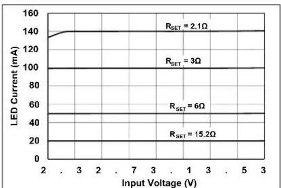
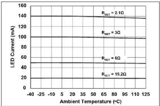
To calculate the resistor value for setting the LED current, use Equation 5-1, where R_SET is connected to V_FB and GND. The reference voltage, V_FB , is 300 mV. The calculated current does not depend on the number of LEDs in the string.
EQUATION 5-1:
$$ I _ {L E D} = \frac {V _ {F B}}{R _ {S E T}} $$
EXAMPLE 1:
$$ V _ {F B} = 3 0 0 m V $$
$$ I _ {L E D} = 1 0 0 m A $$
$$ R _ {S E T} = 3 \Omega $$
EXAMPLE 2:
$$ V _ {F B} = 3 0 0 \mathrm{mV} $$
$$ I _ {L E D} = 2 0 0 \mathrm{mA} $$
$$ R _ {S E T} = 1. 5 \Omega $$
The power dissipated on the R_SET resistor is low and equal to V_FB × I_LED . For I_LED = 100 mA , the power dissipated on the sense resistor is 30 mW and the efficiency of the conversion is high.
5.2.2 PWM DIMMING
LED brightness can also be controlled by setting the maximum current for the LED string (using Equation 5-1) and by lowering this current in small steps, with a variable duty cycle PWM signal applied to the EN pin. The maximum frequency for dimming is limited by the MCP1664's start-up time, which varies with the LED current. By varying the duty cycle of the signal applied on the EN pin (from 0 to 100%), the LED current is changing linearly.
5.2.3 OUTPUT CURRENT CAPABILITY. MINIMUM INPUT VOLTAGE
The maximum device output current is dependent upon the input and output voltage. As there is a 1.8A inductor peak current limit, output current can go out of regulation before reaching the maximum duty cycle. (Note that, for boost converters, the average inductor current is equal to the input current.) Characterization graphs show device limits.
The maximum number of LEDs (nLED in Equation 5-2) that can be placed in series and be driven is dependent on the maximum LED forward voltage ( V_Fmax ) and LED current set by the R_SET resistor. The maximum voltage at the output of the MCP1664 should be 32V. Consider that V_Fmax has some variation over the operating temperature range and that the LED data sheet must be reviewed for the correct data to be introduced in Equation 5-2. A maximum of 10 white LEDs in series connection can be driven safely.
EQUATION 5-2:
$$ \left(\left(V _ {F m a x} \times n L E D\right) + F B\right) < 3 2 V V $$
Characterization graphs show the maximum current the device can supply according to the numbers of LEDs at the output.
For example, to ensure a 150 mA load current for five LEDs (output equal to approximately 15V), a minimum of 3V input voltage is necessary. If an application is required to drive eight LEDs and is powered by one Li-Ion battery ( V_IN from 3.6V to 4.2V), the minimum LED current the MCP1664 can regulate is close to 125 mA (Figure 2-6).
5.2.4 OPEN LOAD PROTECTION
The MCP1664 features an open load protection (OLP) in case the LED is disconnected from the output line. If the voltage on the V_FB pin drops below 50 mV, the device stops switching and prevents overvoltage on the output and SW pin as well as excessive current into LEDs.
OLP is not enabled during start-up and thermal shutdown events.
5.3 Input Capacitor Selection
The boost input current is smoothened by the boost inductor, reducing the amount of filtering necessary at the input. Some capacitance is recommended to provide decoupling from the source and to ensure that the input does not drop excessively during switching transients. Because the MCP1664 is rated to work at an ambient temperature of up to +125°C, low ESR X7R ceramic capacitors are well suited since they have a low temperature coefficient and small size. For use within a limited temperature range of up to +85°C, a X5R ceramic capacitor can be used. For light load applications, 4.7 μF of capacitance is sufficient at the input. For high-power applications that have high source impedance or long leads, using a 10 μF – 20 μF input capacitor is recommended. When the device is working below a 3.0V input with high LED current, additional input capacitance can be added to provide a stable input voltage (3 x 10 μF or 33 μF) due to high input current demand. The input capacitor must be rated at a minimum of 6.3V. For MLCC ceramic capacitors and X7R or X5R capacitors, capacitance varies over the operating temperature or the DC bias range. Usually, there is a drop down to 50% of capacitance. Review the capacitor manufacturer data sheet to see how rated capacitance varies over these conditions.
Table 5-1 contains the recommended range for the input capacitor value.
5.4 Output Capacitor Selection
The output capacitor helps provide a stable output voltage and smooth load current during sudden load transients and reduces the LED current ripple. Ceramic capacitors are well suited for this application (X5R and X7R). The output capacitor ranges from 4.7 F in case of light loads and dimming applications and up to 20 F for hundreds of mAmps LED current applications. Extra output capacitor value is recommended when device drives higher output currents and with small boost ratios (input voltage close to the output voltage).
As mentioned in Section 5.3, Input Capacitor Selection X7R or X5R capacitance varies over the operating temperature or the DC bias range. With a voltage applied at the maximum DC rating, capacitance might drop down to half. This might affect the stability or limit the output power. Capacitance drop over the entire temperature range is less than 20%. Users must carefully select the DC voltage rating ( DCV_RATE ) for the output capacitor according to Equations 5-3 and 5-4:
EQUATION 5-3:
$$ D C V _ {R A T E} > (V _ {F m a x} \times n L E D) + (\textit {_ F B} \quad V $$
or
EQUATION 5-4:
$$ D C V _ {R A T E} > V _ {O U T m a x} $$
Table 5-1 contains the recommended range for the input and output capacitor value.
TABLE 5-1: CAPACITOR VALUE RANGE
| C_IN | C_OUT | |
| Minimum 4.7 μF | 4.7 μF | |
| Maximum — 47 μF | ||
5.5 Inductor Selection
The MCP1664 is designed to be used with small surface mount inductors; the inductance value can range from 4.7 H to 10 H. An inductance value of 4.7 H is recommended for output voltages below 15V (4 or 5 LEDs in series connection). For higher output voltages, up to 32V (from 5 to maximum 10 LEDs), an inductance value of 10 H is optimum.
TABLE 5-2: MCP1664 RECOMMENDED INDUCTORS FOR BOOST CONVERTER
| Part Number | Value (μH) | DCR Ω (typ) | ISAT(A) | Size WxLxH (mm) |
| Coilcraft | ||||
| MSS6132-472 4.7 0.043 2. | 84 6.1x6.1x3.2 | |||
| XFL4020-472 4.7 0.0574 2. | 7 4.3x4.3x2.1 | |||
| LPS5030-472 4.7 0.083 2.0 | 5.0x5.0x3.0 | |||
| LPS6235-103 10 0.100 2.4 | 6.2x6.2x3.5 | |||
| XAL4040-103 10 0.092 1.9 | 4.3x4.3x4.1 | |||
| Wurth® Elektronik Group | ||||
| 7440530047 WE-TPC | 4.7 | 0.07 | 2.2 | 5.8x5.8x2.8 |
| 74404042047 WE-LQS | 4.7 | 0.03 | 2.0 | 4.0x4.0x1.6 |
| 74438335047 WE-MAPI | 4.7 0 | 141 2.0 3 | 0x3.0x1.5 | |
| 744778610 WE-PD2 | 10 0. | 074 1.8 5 | 9x6.2x4.9 | |
| 74408943100 WE-SPC | 10 0. | 082 2.1 4 | 8x4.8x3.8 | |
| TDK EPCOS | ||||
| B82462G4472M | 4.7 0 | 035 2.2 6 | 3x6.3x3.0 | |
| VLCF4024T-4R7 | 4.7 0 | 075 1.76 | 4.0x4.0x2.4 | |
| SLF7055T-100 | 10 0. | 039 2.5 7 | 0x7.0x5.5 | |
Several parameters are used to select the correct inductor: maximum rated current, saturation current and copper resistance (DCR). For boost converters, the inductor current is much higher than the output current. The average inductor current is equal to the input current. The inductor's peak current is much higher than the average. The lower the inductor DCR, the higher the efficiency of the converter, a common trade-off in size versus efficiency.
Peak current is the maximum or limit value and saturation current typically specifies a point at which the inductance has rolled off a percentage of the rated value. This can range from a 20% to 40% reduction in inductance. As inductance rolls off, the inductor ripple current increases, as does the peak switch current. It is important to keep the inductance from rolling off too much, causing switch current to reach the peak limit.
5.6 Rectifier Diode Selection
Schottky diodes are used to reduce losses. The diode's average and peak current rating must be greater than the average output current and the peak inductor current, respectively. The diode's reverse breakdown voltage must be higher than the internal switch maximum rating voltage of 36V.
The converter's efficiency will be improved if the voltage drop across the diode is lower. The forward voltage ( V_F ) rating is forward-current dependent, which is equal in particular to the load current.
For high currents and high ambient temperatures, use a diode with good thermal characteristics.
TABLE 5-3: RECOMMENDED SCHOTTKY DIODES
| Type | V_OUTmax | T_A |
| PMEG2010 | 18V < +85°C | |
| STPS120 | 18V | < +125°C |
| MBRM120 | 18V | < +125°C |
| PMEG4010 | 32V < +85°C | |
| UPS5819 | 32V < +85°C | |
| MBRM140 | 32V | < +125°C |
5.7 Thermal Calculations
The MCP1664 is available in two different packages (5-lead SOT-23 and 8-lead 2 mm x 3 mm TDFN). By calculating the power dissipation and applying the package thermal resistance ( _JA ), the junction temperature is estimated. The maximum operating junction temperature rating (steady state) for the MCP1664 is +125°C.
To quickly estimate the internal power dissipation for the switching boost regulator, an empirical calculation using measured efficiency can be used. Given the measured efficiency, the internal power dissipation is estimated by Equation 5-5.
EQUATION 5-5:
$$ \left(\frac {V _ {O U T} \times I _ {O U T}}{E f f i c i e n c y}\right) - (V _ {O U T} \times I _ {O U T}) = P _ {D i s} $$
The difference between the first term, input power, and the second term, power delivered, is the internal power dissipation of the MCP1664. This is an estimate, assuming that most of the power lost is internal to the MCP1664 and not C_IN , C_OUT , the rectifier diode and the inductor. There is some percentage of power lost in the boost inductor and the rectifier diode, with very little loss in the input and output capacitors. For a more accurate estimation of internal power dissipation, subtract the I_INRMS^2 × L_DCR and I_LED × V_F power dissipation (where I_INRMS is the average input current, L_DCR is the inductor series resistance and V_F is the diode voltage drop). Another source of power losses for the LED driver, that is external to the MCP1664, is the sense resistor. The losses for the sense resistor can be approximated by V_FB × I_LED .
5.8 PCB Layout Information
Good printed circuit board layout techniques are important to any switching circuitry and switching power supplies are no different. When wiring the switching high-current paths, short and wide traces
should be used. Therefore, it is important that the input and output capacitors be placed as close as possible to the MCP1664 to minimize the loop area.
The R_SET resistor and feedback signal should be routed away from the switching node and the switching current loop. When possible, ground planes and traces should be used to help shield the feedback signal and minimize noise and magnetic interferences.
text_image
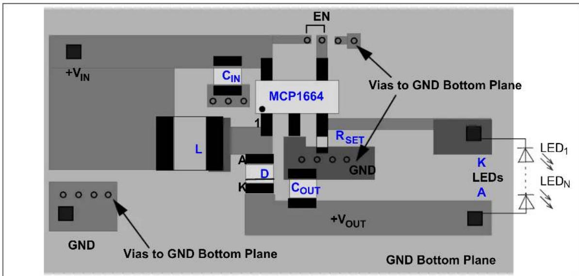
EN +V_IN C_IN MCP1664 L A D K R_SET GND C_OUT +V_OUT GND Bottom Plane Vias to GND Bottom Plane Vias to GND Bottom Plane GND Bottom Plane LED_1 LED_N K LEDs AFIGURE 5-1: MCP1664 5-Lead SOT-23 Recommended Layout.

text_image
+V_IN L A K +V_OUT C_IN MCP1664 Via to GND EN R_SET GND EN routed to the Bottom Plane Vias to GND Bottom Plane GND Bottom Plane LED_1 LED_2 LED_N KFIGURE 5-2: MCP1664 TDFN Recommended Layout.
6.0 PACKAGING INFORMATION
6.1 Package Marking Information

text_image
5-Lead SOT-23 XXXXY WWNNN8-Lead TDFN (2x3x0.75 mm)

text_image
Example AABR2 10256Example

text_image
XXX YWW NN PIN 1
text_image
ACH 210 25 PIN 1Legend: XX...X Product code or customer-specific information
Y Year code (last digit of calendar year)
YY Year code (last 2 digits of calendar year)
WW Week code (week of January 1 is week '01')
NNN Alphanumeric traceability code
Pb-free JEDEC ^® designator for Matte Tin (Sn)
* This package is Pb-free. The Pb-free JEDEC designator ( )
can be found on the outer packaging for this package.
•, ▲, ▼ Pin one index is identified by a dot, delta up, or delta down (triangle mark).
Note: In the event the full Microchip part number cannot be marked on one line, it will be carried over to the next line, thus limiting the number of available characters for customer-specific information. Package may or may not include the corporate logo.
Underbar (_) and/or Overbar (−) symbol may not be to scale.
5-Lead Plastic Small Outline Transistor (C7X) [SOT23]
Note: For the most current package drawings, please see the Microchip Packaging Specification located at http://www.microchip.com/packaging
![Microchip MCP1664 - 5-Lead Plastic Small Outline Transistor (C7X) [SOT23] - 1](/content/2026/06/1214650/images/cb917bf1df47a44d30c53d3041f497cfd171866aa9c524f14d44d2651779afae.jpg)
text_image
0.20 C 2X D e1 A N E1/2 E1 E/2 E (DATUM D) (DATUM A-B) NOTE 1 1 2 e NX bB 0.15 C D 2X 0.20 M A-B DTOP VIEW
![Microchip MCP1664 - 5-Lead Plastic Small Outline Transistor (C7X) [SOT23] - 2](/content/2026/06/1214650/images/da769496acc37ebfd0c8c6a36cbe76da321c73fb79df1cab746dcb30c1ae0d3f.jpg)
text_image
A A2 A A1 SEE SHEET 2 0.20 C SEATING PLANE CSIDE VIEW
Microchip Technology Drawing C04-091-C7X Rev G Sheet 1 of 2
5-Lead Plastic Small Outline Transistor (C7X) [SOT23]
Note: For the most current package drawings, please see the Microchip Packaging Specification located at http://www.microchip.com/packaging
![Microchip MCP1664 - 5-Lead Plastic Small Outline Transistor (C7X) [SOT23] - 1](/content/2026/06/1214650/images/87378c32f03d3f68178e892ccec82dc189bf18a5659059a3a916352f58895386.jpg)
text_image
c L L1 θVIEW A-A SHEET 1
| Units | MILLIMETERS | |||
| Dimension Limits | MIN | NOM | MAX | |
| Number of Pins | N | 5 | ||
| Pitch | e | 0.95 BSC | ||
| Outside lead pitch | e1 | 1.90 BSC | ||
| Overall Height | A | 0.90 | - | 1.45 |
| Molded Package Thickness | A2 | 0.89 | - | 1.30 |
| Standoff | A1 | - | - | 0.15 |
| Overall Width | E | 2.80 BSC | ||
| Molded Package Width | E1 | 1.60 BSC | ||
| Overall Length | D | 2.90 BSC | ||
| Foot Length | L | 0.30 | - | 0.60 |
| Footprint | L1 | 0.60 REF | ||
| Foot Angle | 0° | - | 10° | |
| Lead Thickness | c | 0.08 | - | 0.26 |
| Lead Width | b | 0.20 - | 0.51 | |
Notes:
1. Dimensions D and E1 do not include mold flash or protrusions. Mold flash or protrusions shall not exceed 0.25mm per side.
2. Dimensioning and tolerancing per ASME Y14.5M
BSC: Basic Dimension. Theoretically exact value shown without tolerances.
REF: Reference Dimension, usually without tolerance, for information purposes only.
Microchip Technology Drawing C04-091-C7X Rev G Sheet 2 of 2
5-Lead Plastic Small Outline Transistor (C7X) [SOT23]
Note: For the most current package drawings, please see the Microchip Packaging Specification located at http://www.microchip.com/packaging
![Microchip MCP1664 - 5-Lead Plastic Small Outline Transistor (C7X) [SOT23] - 1](/content/2026/06/1214650/images/ecd06a1a6ee29d8563bad104f65dcebcef8b336953f80fe046dacf30c08db252.jpg)
text_image
X 5 SILK SCREEN Y Z C G 1 2 E GXRECOMMENDED LAND PATTERN
| Units | MILLIMETERS | |||
| Dimension Limits | NOM | MAXMIN | ||
| Contact Pitch | E | 0.95 BSC | ||
| Contact Pad Spacing | C | 2.80 | ||
| Contact Pad Width (X5) | X | 0.60 | ||
| Contact Pad Length (X5) | Y | 1.10 | ||
| Distance Between Pads | G | 1.70 | ||
| Distance Between Pads GX 0.35 | ||||
| Overall Width | Z | 3.90 | ||
Notes:
- Dimensioning and tolerancing per ASME Y14.5M
BSC: Basic Dimension. Theoretically exact value shown without tolerances.
Microchip Technology Drawing No. C04-2091-C7X Rev G
8-Lead Plastic Dual Flat, No Lead Package (MN) - 2x3x0.8 mm Body [TDFN] With 1.4x1.3 mm Exposed Pad (JEDEC Package type WDFN)
Note: For the most current package drawings, please see the Microchip Packaging Specification located at http://www.microchip.com/packaging
![Microchip MCP1664 - 8-Lead Plastic Dual Flat, No Lead Package (MN) - 2x3x0.8 mm Body [TDFN] With 1.4x1.3 mm Exposed Pad (JEDEC Package type WDFN) - 1](/content/2026/06/1214650/images/4323827bef0bfa86265163262f041e281fcd2d66a96963c9da03d62f7b2bc650.jpg)
text_image
(DATUM A) (DATUM B) NOTE 1 2X 0.15 C 2X 0.15 C TOP VIEW SEATING PLANE C A A1 // 0.10 C 8X 0.08 C (A3) SIDE VIEW L D2 NOTE 1 1 2 E2 K N 8X b e BOTTOM VIEW 0.10 A B 0.10 A B 0.05Microchip Technology Drawing No. C04-129-MN Rev E Sheet 1 of 2
8-Lead Plastic Dual Flat, No Lead Package (MN) - 2x3x0.8 mm Body [TDFN] With 1.4x1.3 mm Exposed Pad (JEDEC Package type WDFN)
Note: For the most current package drawings, please see the Microchip Packaging Specification located at http://www.microchip.com/packaging
![Microchip MCP1664 - 8-Lead Plastic Dual Flat, No Lead Package (MN) - 2x3x0.8 mm Body [TDFN] With 1.4x1.3 mm Exposed Pad (JEDEC Package type WDFN) - 1](/content/2026/06/1214650/images/20edb9c1b09f580f752f589342884d2dc7d75ebdb0ff4b5f09590dd55692311e.jpg)
natural_image
Technical line drawing of two electronic components with pins and a central chip (no text or symbols)| Units | MILLIMETERS | |||
| Dimension Limits | MIN | NOM | MAX | |
| Number of Pins | N | 8 | ||
| Pitch | e | 0.50 BSC | ||
| Overall Height | A | 0.70 | 0.75 | 0.80 |
| Standoff | A1 | 0.00 | 0.02 | 0.05 |
| Contact Thickness | A3 | 0.20 REF | ||
| Overall Length | D | 2.00 BSC | ||
| Overall Width | E | 3.00 BSC | ||
| Exposed Pad Length | D2 | 1.35 | 1.40 | 1.45 |
| Exposed Pad Width | E2 | 1.25 | 1.30 | 1.35 |
| Contact Width | b | 0.20 | 0.25 | 0.30 |
| Contact Length | L | 0.25 | 0.30 | 0.45 |
| Contact-to-Exposed Pad | K 0.20 | - | - | |
Notes:
- Pin 1 visual index feature may vary, but must be located within the hatched area.
- Package may have one or more exposed tie bars at ends.
- Package is saw singulated
- Dimensioning and tolerancing per ASME Y14.5M
BSC: Basic Dimension. Theoretically exact value shown without tolerances.
REF: Reference Dimension, usually without tolerance, for information purposes only.
Microchip Technology Drawing No. C04-129-MN Rev E Sheet 2 of 2
8-Lead Plastic Dual Flat, No Lead Package (MN) - 2x3x0.8 mm Body [TDFN] With 1.4x1.3 mm Exposed Pad (JEDEC Package type WDFN)
Note: For the most current package drawings, please see the Microchip Packaging Specification located at http://www.microchip.com/packaging
![Microchip MCP1664 - 8-Lead Plastic Dual Flat, No Lead Package (MN) - 2x3x0.8 mm Body [TDFN] With 1.4x1.3 mm Exposed Pad (JEDEC Package type WDFN) - 1](/content/2026/06/1214650/images/df73ad6125eae9bbc5f702112f7c66e2d9c11163ce1d45e07ee1c0de0388c6b8.jpg)
text_image
X2 EV 8 ØV C Y2 EV Y1 SILK SCREEN 1 2 X1 ERECOMMENDED LAND PATTERN
| Units | MILLIMETERS | |||
| Dimension Limits | MIN | NOM | MAX | |
| Contact Pitch | E | 0.50 BSC | ||
| Optional Center Pad Width | X2 | 1.60 | ||
| Optional Center Pad Length | Y2 | 1.50 | ||
| CContact Pad Spacing 2.90 | ||||
| Contact Pad Width (X8) | X1 | 0.25 | ||
| Contact Pad Length (X8) | Y1 | 0.85 | ||
| Thermal Via Diameter V | 0.30 | |||
| Thermal Via Pitch EV | 1.00 | |||
Notes:
- Dimensioning and tolerancing per ASME Y14.5M
BSC: Basic Dimension. Theoretically exact value shown without tolerances.
- For best soldering results, thermal vias, if used, should be filled or tented to avoid solder loss during reflow process
Microchip Technology Drawing No. C04-129-MN Rev. B
NOTES:
APPENDIX A: REVISION HISTORY
Revision B (September 2022)
- Updated Section "Features".
- Updated Section "General Description"
- Updated Section "DC and AC Characteristics"
- Updated Figures 2-10, 2-11 and 2-12.
- Updated Table 5-2.
- Updated package drawings in Section "Package Types"
- Updated Section "Product Identification System", with Automotive Qualified devices.
- Minor grammar and format changes throughout.
Revision A (June 2015)
• Original Release of this Document.
NOTES:
PRODUCT IDENTIFICATION SYSTEM
To order or obtain information, e.g., on pricing or delivery, refer to the factory or the listed sales office.
 Device Device |  Tape and Reel Option Tape and Reel Option |  Range Range | T |  QualificationPackage Temperature QualificationPackage Temperature | Examples: | |
| a) MCP1664T-E/OT: | Tape and Reel, Extended temperature, 5-Lead SOT-23 package | |||||
| Device: MCP1664: High-Voltage Step-Up LED Driver with UVLO and OLP | b) MCP1664T-E/MNY: | Tape and Reel, Extended temperature, 8-Lead 2x3 TDFN package | ||||
| Tape and Reel Option: | T = Tape and Reel | (Note 1) | c) MCP1664T-E/OTVAO: | Tape and Reel, Extended temperature, 5-Lead SOT-23 package, Automotive Qualified | ||
| Temperature Range: | E = - | 4 | 0 | °C to +125°C (Extended) | ||
| Package: MN = Plastic Dual Flat, No Lead Package - 2 mm x 3 mm x 0.75 mm Body, 8-Lead (TDFN) | ||||||
| OT = Plastic Small Outline Transistor, 5-Lead (SOT-23) | ||||||
| *Y = Nickel palladium gold manufacturing designator. Only available on the TDFN package. | ||||||
| Qualification: | = Standard Part VAO = Automotive AEC-Q100 Qualified | Note 1: | Tape and Reel identifier only appears in the catalog part number description. This identifier is used for ordering purposes and is not printed on the device package. Check with your Microchip Sales Office for package availability with the Tape and Reel option. | |||
Examples:
e) MCR1664T E/QT: package Temperature
Note 1: Tape and Reel identifier only appears in the catalog part number description. This identifier is used for ordering purposes and is not printed on the device package. Check with your Microchip Sales Office for package availability with the Tape and Reel option.
NOTES:
Note the following details of the code protection feature on Microchip products:
• Microchip products meet the specifications contained in their particular Microchip Data Sheet.
- Microchip believes that its family of products is secure when used in the intended manner, within operating specifications, and under normal conditions.
- Microchip values and aggressively protects its intellectual property rights. Attempts to breach the code protection features of Microchip product is strictly prohibited and may violate the Digital Millennium Copyright Act.
- Neither Microchip nor any other semiconductor manufacturer can guarantee the security of its code. Code protection does not mean that we are guaranteeing the product is "unbreakable" Code protection is constantly evolving. Microchip is committed to continuously improving the code protection features of our products.
This publication and the information herein may be used only with Microchip products, including to design, test, and integrate Microchip products with your application. Use of this information in any other manner violates these terms. Information regarding device applications is provided only for your convenience and may be superseded by updates. It is your responsibility to ensure that your application meets with your specifications. Contact your local Microchip sales office for additional support or, obtain additional support at https://www.microchip.com/en-us/support/design-help/client-support-services.
THIS INFORMATION IS PROVIDED BY MICROCHIP "AS IS". MICROCHIP MAKES NO REPRESENTATIONS OR WARRANTIES OF ANY KIND WHETHER EXPRESS OR IMPLIED, WRITTEN OR ORAL, STATUTORY OR OTHERWISE, RELATED TO THE INFORMATION INCLUDING BUT NOT LIMITED TO ANY IMPLIED WARRANTIES OF NON-INFRINGEMENT, MERCHANTABILITY, AND FITNESS FOR A PARTICULAR PURPOSE, OR WARRANTIES RELATED TO ITS CONDITION, QUALITY, OR PERFORMANCE.
IN NO EVENT WILL MICROCHIP BE LIABLE FOR ANY INDIRECT, SPECIAL, PUNITIVE, INCIDENTAL, OR CONSEQUENTIAL LOSS, DAMAGE, COST, OR EXPENSE OF ANY KIND WHATSOEVER RELATED TO THE INFORMATION OR ITS USE, HOWEVER CAUSED, EVEN IF MICROCHIP HAS BEEN ADVISED OF THE POSSIBILITY OR THE DAMAGES ARE FORESEEABLE. TO THE FULLEST EXTENT ALLOWED BY LAW, MICROCHIP'S TOTAL LIABILITY ON ALL CLAIMS IN ANY WAY RELATED TO THE INFORMATION OR ITS USE WILL NOT EXCEED THE AMOUNT OF FEES, IF ANY, THAT YOU HAVE PAID DIRECTLY TO MICROCHIP FOR THE INFORMATION.
Use of Microchip devices in life support and/or safety applications is entirely at the buyer's risk, and the buyer agrees to defend, indemnify and hold harmless Microchip from any and all damages, claims, suits, or expenses resulting from such use. No licenses are conveyed, implicitly or otherwise, under any Microchip intellectual property rights unless otherwise stated.
Trademarks
The Microchip name and logo, the Microchip logo, Adaptec, AVR, AVR logo, AVR Freaks, BesTime, BitCloud, CryptoMemory, CryptoRF, dsPIC, flexPWR, HELDO, IGLOO, JukeBlox, KeeLoq, Kleer, LANCheck, LinkMD, maXStylus, maXTouch, MediaLB, megaAVR, Microsemi, Microsemi logo, MOST, MOST logo, MPLAB, OptoLyzer, PIC, picoPower, PICSTART, PIC32 logo, PolarFire, Prochip Designer, QTouch, SAM-BA, SenGenuity, SpyNIC, SST, SST Logo, SuperFlash, Symmetricom, SyncServer, Tachyon, TimeSource, tinyAVR, UNI/O, Vectron, and XMEGA are registered trademarks of Microchip Technology Incorporated in the U.S.A. and other countries.
AgileSwitch, APT, ClockWorks, The Embedded Control Solutions Company, EtherSynch, Flashtec, Hyper Speed Control, HyperLight Load, Libero, motorBench, mTouch, Powermite 3, Precision Edge, ProASIC, ProASIC Plus, ProASIC Plus logo, Quiet-Wire, SmartFusion, SyncWorld, Temux, TimeCesium, TimeHub, TimePictra, TimeProvider, TrueTime, and ZL are registered trademarks of Microchip Technology Incorporated in the U.S.A.
Adjacent Key Suppression, AKS, Analog-for-the-Digital Age, Any Capacitor, AnyIn, AnyOut, Augmented Switching, BlueSky, BodyCom, Clockstudio, CodeGuard, CryptoAuthentication, CryptoAutomotive, CryptoCompanion, CryptoController, dsPICDEM, dsPICDEM.net, Dynamic Average Matching, DAM, ECAN, Espresso T1S, EtherGREEN, GridTime, IdealBridge, In-Circuit Serial Programming, ICSP, INICnet, Intelligent Paralleling, IntelliMOS, Inter-Chip Connectivity, JitterBlocker, Knob-on-Display, KoD, maxCrypto, maxView, memBrain, Mindi, MiWi, MPASM, MPF, MPLAB Certified logo, MPLIB, MPLINK, MultiTRAK, NetDetach, Omniscient Code Generation, PICDEM, PICDEM.net, PICkit, PICtail, PowerSmart, PureSilicon, QMatrix, REAL ICE, Ripple Blocker, RTAX, RTG4, SAM-ICE, Serial Quad I/O, simpleMAP, SimpliPHY, SmartBuffer, SmartHLS, SMART-I.S., storClad, SQI, SuperSwitcher, SuperSwitcher II, Switchtec, SynchroPHY, Total Endurance, Trusted Time, TSHARC, USBCheck, VariSense, VectorBlox, VeriPHY, ViewSpan, WiperLock, XpressConnect, and ZENA are trademarks of Microchip Technology Incorporated in the U.S.A. and other countries.
SQTP is a service mark of Microchip Technology Incorporated in the U.S.A.
The Adaptec logo, Frequency on Demand, Silicon Storage Technology, and Symmcom are registered trademarks of Microchip Technology Inc. in other countries.
GestIC is a registered trademark of Microchip Technology Germany II GmbH & Co. KG, a subsidiary of Microchip Technology Inc., in other countries.
All other trademarks mentioned herein are property of their respective companies.
© 2015-2022, Microchip Technology Incorporated and its subsidiaries.
All Rights Reserved.
ISBN: 978-1-6683-1202-5
For information regarding Microchip's Quality Management Systems, please visit www.microchip.com/quality.
Worldwide Sales and Service
AMERICAS
Corporate Office
2355 West Chandler Blvd.
Chandler, AZ 85224-6199
Tel: 480-792-7200
Fax: 480-792-7277
Technical Support:
http://www.microchip.com/
support
Web Address:
www.microchip.com
Atlanta
Duluth, GA
Tel: 678-957-9614
Fax: 678-957-1455
Austin, TX
Tel: 512-257-3370
Boston
Westborough, MA
Tel: 774-760-0087
Fax: 774-760-0088
Chicago
Itasca, IL
Tel: 630-285-0071
Fax: 630-285-0075
Dallas
Addison, TX
Tel: 972-818-7423
Fax: 972-818-2924
Detroit
Novi, MI
Tel: 248-848-4000
Houston, TX
Tel: 281-894-5983
Indianapolis
Noblesville, IN
Tel: 317-773-8323
Fax: 317-773-5453
Tel: 317-536-2380
Los Angeles
Mission Viejo, CA
Tel: 949-462-9523
Fax: 949-462-9608
Tel: 951-273-7800
Raleigh, NC
Tel: 919-844-7510
New York, NY
Tel: 631-435-6000
San Jose, CA
Tel: 408-735-9110
Tel: 408-436-4270
Canada - Toronto
Tel: 905-695-1980
Fax: 905-695-2078
ASIA/PACIFIC
Australia - Sydney
Tel: 61-2-9868-6733
China - Beijing
Tel: 86-10-8569-7000
China - Chengdu
Tel: 86-28-8665-5511
China - Chongqing
Tel: 86-23-8980-9588
China - Dongguan
Tel: 86-769-8702-9880
China - Guangzhou
Tel: 86-20-8755-8029
China - Hangzhou
Tel: 86-571-8792-8115
China - Hong Kong SAR
Tel: 852-2943-5100
China - Nanjing
Tel: 86-25-8473-2460
China - Qingdao
Tel: 86-532-8502-7355
China - Shanghai
Tel: 86-21-3326-8000
China - Shenyang
Tel: 86-24-2334-2829
China - Shenzhen
Tel: 86-755-8864-2200
China - Suzhou
Tel: 86-186-6233-1526
China - Wuhan
Tel: 86-27-5980-5300
China - Xian
Tel: 86-29-8833-7252
China - Xiamen
Tel: 86-592-2388138
China - Zhuhai
Tel: 86-756-3210040
ASIA/PACIFIC
India - Bangalore
Tel: 91-80-3090-4444
India - New Delhi
Tel: 91-11-4160-8631
India - Pune
Tel: 91-20-4121-0141
Japan - Osaka
Tel: 81-6-6152-7160
Japan - Tokyo
Tel: 81-3-6880-3770
Korea - Daegu
Tel: 82-53-744-4301
Korea - Seoul
Tel: 82-2-554-7200
Malaysia - Kuala Lumpur
Tel: 60-3-7651-7906
Malaysia - Penang
Tel: 60-4-227-8870
Philippines - Manila
Tel: 63-2-634-9065
Singapore
Tel: 65-6334-8870
Taiwan - Hsin Chu
Tel: 886-3-577-8366
Taiwan - Kaohsiung
Tel: 886-7-213-7830
Taiwan - Taipei
Tel: 886-2-2508-8600
Thailand - Bangkok
Tel: 66-2-694-1351
Tel: 43-7242-2244-39
Fax: 43-7242-2244-393
Denmark - Copenhagen
Tel: 45-4485-5910
Fax: 45-4485-2829
Finland - Espoo
Tel: 358-9-4520-820
France - Paris
Tel: 33-1-69-53-63-20
Fax: 33-1-69-30-90-79
Germany - Garching
Tel: 49-8931-9700
Germany - Haan
Tel: 49-2129-3766400
Germany - Heilbronn
Tel: 49-7131-72400
Germany - Karlsruhe
Tel: 49-721-625370
Germany - Munich
Tel: 49-89-627-144-0
Fax: 49-89-627-144-44
Germany - Rosenheim
Tel: 49-8031-354-560
Israel - Ra'anana
Tel: 972-9-744-7705
Italy - Milan
Tel: 39-0331-742611
Fax: 39-0331-466781
Italy - Padova
Tel: 39-049-7625286
Netherlands - Drunen
Tel: 31-416-690399
Fax: 31-416-690340
Norway - Trondheim
Tel: 47-7288-4388
Poland - Warsaw
Tel: 48-22-3325737
Romania - Bucharest
Tel: 40-21-407-87-50
Spain - Madrid
Tel: 34-91-708-08-90
Fax: 34-91-708-08-91
Sweden - Gothenberg
Tel: 46-31-704-60-40
Sweden - Stockholm
Tel: 46-8-5090-4654
UK - Wokingham
Tel: 44-118-921-5800
Fax: 44-118-921-5820