HV9931DB1 - Electronic component Microchip - Free user manual and instructions
Find the device manual for free HV9931DB1 Microchip in PDF.

User questions about HV9931DB1 Microchip
0 question about this device. Answer the ones you know or ask your own.
Ask a new question about this device
Download the instructions for your Electronic component in PDF format for free! Find your manual HV9931DB1 - Microchip and take your electronic device back in hand. On this page are published all the documents necessary for the use of your device. HV9931DB1 by Microchip.
USER MANUAL HV9931DB1 Microchip
LED Driver Demoboard Input 120VAC // Output 350mA, 40V (14W)
General Description
The HV9931 LED driver is primarily targeted at low to medium power LED lighting applications where galvanic isolation of the LED string is not an essential requirement. The driver provides near unity power factor and constant current regulation using a two stage topology driven by a single MOSFET and control IC. Triac dimming of this design is possible with the addition of some components for preloading and inrush current shaping.
The DB1 and DB2 Demoboards were designed for a fixed string current of 350mA and a string voltage of 40V for a load power of about 14W. The boards will regulate current for an output voltage down to 0V.
Nominal input voltage for the DB1 is 120VAC, for the DB2 230VAC. Design for universal input (85 to 265VAC) is by all means possible but does increase cost and size while lowering efficiency.
The input EMI filter was designed to suppress the differential mode switching noise to meet CISPR15 requirements. No specific components were added to suppress currents of common mode nature. Common mode current can be controlled in many ways to satisfy CISPR 15 requirements.
The board is fitted with a number of optional circuits; a schematic of a simplified driver is given as well. The circuits
featured are output current soft start and protections from line overvoltage, load overvoltage and open circuit. The driver is inherently short circuit proof by virtue of the peak current regulation method.
| Specifications | |
| Input voltage: 100V | _RMS to 135V_RMS , 60Hz |
| Output voltage: 0 to 40V | |
| Output current: 350mA +/-5% | |
| Output power: 14W, Max | |
| Power factor 98% | |
| Total harmonic distortion EN | 61000-3-2 Class C |
| EMI limits CISPR 15 (see text) | |
| Efficiency 83% | |
| Output current ripple 30% | PP |
| Input overvoltage protection | 140V_RMS , Latching |
| Output overvoltage protection | 43V, Latching |
| Switching frequency | 73kHz |
| Dimensions: | 3.5" x 3.0" x 1.25" |
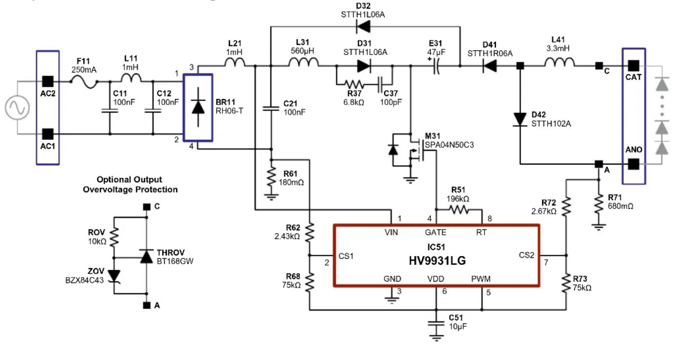
Board Layout and Connections
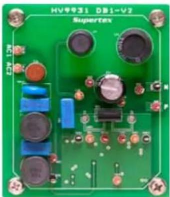
natural_image
Green printed circuit board with components like capacitors, inductors, and switches (no readable text or symbols)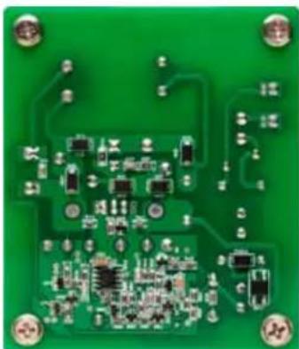
natural_image
Close-up of a green printed circuit board (PCB) with visible traces and components, no text or symbols present.
text_image
Electrical circuit diagram with labeled components including voltage meters, voltmeters, and a bridge rectifierWarning!
Working with this board can cause serious bodily harm or death. Connecting the board to a source of line voltage will result in the presence of hazardous voltage throughout the system including the LED load.
The board should only be handled by persons well aware of the dangers involved with working on live electrical equipment. Extreme care should be taken to protect against electric shock. Disconnect the board before attempting to make any changes to the system configuration. Always work with another person nearby who can offer assistance in case of an emergency. Wear safety glasses for eye protection.
Connection Instructions
Step 1.
Carefully inspect the board for shipping damage, loose components, etc, before making connections.
Step 2.
Attach the board to the line and load as shown in the diagram. Be sure to check for correct polarity when connecting the LED string to avoid damage to the string. The board is short circuit and open circuit proof. The LED string voltage can be anything between zero and 40V, though performance will suffer when the string voltage is substantially lower than the target of 40V. See the typical performance graphs.
Step 3.
Energize the mains supply. The board can be connected to mains directly. Alternatively voltage can be raised gradually from zero to full line voltage with the aid of an adjustable AC supply such as a Variac or a programmable AC source.
Principles of Operation
The HV9931 topology can be viewed as a series connection of two basic power supply topologies, (1) a buck-boost stage as first or input stage, for purpose of converting AC line power into a source of DC power, commonly known as the DC bus, having sufficient capacitive energy storage to maintain the bus voltage more or less constant throughout the AC line cycle, and (2) a buck stage as second or output stage for powering the LED string, stepping down the DC bus voltage to the LED string voltage in order to produce a steady LED string current.
The output or buck stage is designed for operation in continuous conduction mode (CCM), operating with about 20 to 30% inductor current ripple. This amount of ripple serves the needs of the HV9931 peak current controller which relies on a sloping inductor current for setting ON time, and is of an acceptable level to high brightness LEDs. Duty cycle is more or less constant throughout the line cycle as the DC bus voltage and LED string voltage are more or less constant as well. Duty cycle and bus voltage do adjust in response to
Special Note:
The electrolytic capacitor carries a hazardous voltage for an extended time after the board is disconnected. The board includes a 1MΩ resistor placed across the electrolytic capacitor which will slowly discharge the capacitor after disconnection from line voltage. The voltage will fall more or less exponentially to zero with a time constant of about 100 seconds. Check the capacitor voltage before handling the board.
changes in line or load voltage but are otherwise constant over the course of a line cycle. With the HV9931, OFF time is fixed by design, being programmed by an external resistor, whereas ON time adjusts to a more or less constant value, being under control of the HV9931 peak current regulator.
The input or buck-boost stage is designed for operation in discontinuous conduction mode (DCM) throughout the range of line and load voltage anticipated. This can be accomplished by making the input inductor sufficiently small A well known property of the DCM buck-boost stage, when operated with constant ON time and constant OFF time, is that input current is proportional to input voltage, whether in peak value or average value. This results in sinusoidal input current when the input voltage is sinusoidal, thereby giving unity power factor operation when operating from the rectified AC line voltage.
When operated in the anticipated range of line and load voltage, the MOSFET ON time will be under control of the output stage current controller, which turns the MOSFET off when sensing that the output inductor current has reached the desired peak current level as programmed by a resistive divider at the CS2 pin. Under certain abnormal circumstances such as initial run-up and line undervoltage, which both could lead to the draw of abnormally high line current, ON time is further curtailed by the action of the CS1 comparator, which monitors the input stage inductor current against a threshold. This threshold can be a simple DC level or be shaped in time as is performed on the Demoboard. In particular, when shaping the CS1 threshold with the shape of the rectified AC line input voltage waveform, the line current will be bounded by a more or less sinusoidal line current envelope which results in sinusoidal input current for low line and other abnormal conditions.
The design exercise of an HV9931 LED driver revolves around establishing component values for (1) the input and
output stage inductors, (2) a value for the bus capacitor, and (3) a value for switching cycle OFF time, which together result in (1) acceptable current ripple at the output stage (say 30%), (2) an acceptable bus voltage ripple (say 5%), and (3) an input stage which maintains DCM operation over the desired line and load voltage range.
For a given HV9931 design, the bus voltage rises and falls with like changes in line and load voltage. This is unlike a two stage design having two transistors and control ICs, where the bus voltage can be set independent of line and load voltage variation. If the desired ranges of line and load voltage are particularly large then the latter topology may be preferable so as to avoid large variation in bus voltage.
The design of an HV9931 based LED driver is not further discussed here, except for noting that a semi-automatic design tool is available in Mathcad form, based on behavioral simulation, which, allows components to be adjusted in an iterative manner, starting from an initial guess. The tool allows quick evaluation of nine standard test cases, exercising the design over line voltage variation and tolerance variation of three component parameters.
Mathcad design data can be found at the end of this document. The data tends to be in good agreement with the actual Demoboard despite the omission of switching losses in the model. For this design we can see that the calculated efficiency is off by say 5 percent likely due underestimation of switching losses and inductor core and winding losses.
A Simplified Version of the Design
The Demoboard can be simplified significantly. Below is a schematic showing the essential elements of the driver.
Simplified Schematic Diagram
text_image
F11 250mA L11 1mH C11 100nF C12 100nF AC2 AC1 BR11 RH06-T L21 1mH C21 100nF R61 180mΩ C37 6.8kΩ C37 100pF D32 STTH1L06A D31 STTH1L06A E31 47μF + D41 STTH1R06A L41 3.3mH C CAT ANO Optional Output Overvoltage Protection ROV 10kΩ THROV BT168GW ZOV BZX84C43 A C51 10μF VIN GATE RT IC51 HV9931LG CS1 GND VDD PWM R62 2.43kΩ R51 196kΩ R72 2.67kΩ R71 680mΩ R68 75kΩ 3 6 5 R73 75kΩContact Supertex Applications Engineering for guidance in simplifying the design or for adding functions such as triac dimmability.
Note on Inductors:
This board was fitted with standard (COTS) inductors. These are not necessarily an optimal choice but present an expedient way to go when evaluating a design. Custom engineered parts generally give better performance, particularly with respect to efficiency.
Drum core style inductors, whether in radial or axial leaded
versions, are popular for their ready availability and low cost. Drum core styles have particularly simple construction and can be wound for lowest cost without coil former (bobbin). They may serve well during the development stage, but may not be the best choice for final design. Keep these type of inductors away form any metallic surface such as heatsinks, PCB copper planes, metallic enclosures, and capacitors, as these unshielded parts can create high eddy current losses in these parts. For tightly packaged designs or where inductor losses are an issue, drum core style inductors are not recommended.
Schematic Diagram
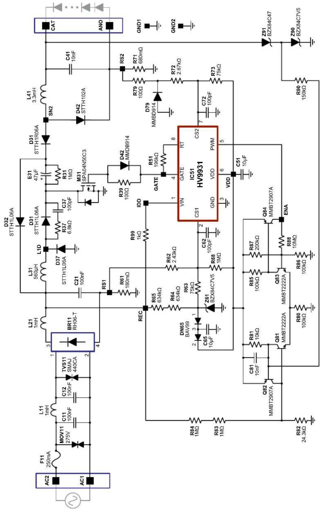
text_image
AC2 F11 250mA L11 1mH MOV11 275V C11 100nF C12 100nF TVS11 SMAJ 440CA 3 BR11 RH06-T L21 1mH L31 560μH L1D D37 STTH1L06A D31 STTH1L06A E31 47μF D31 STTH1R06A L41 3.3mH SN2 D42 STTH102A C41 10nF CAT ANO GND1 GND2 Q82 MMBT2907A Q81 MMBT2222A Q83 MMBT2222A Q84 MMBT2907A Q85 100kΩ R86 100kΩ R88 10MΩ ENA R80 100kΩ R82 24.3kΩ C65 10μF C62 100pF C65 10μΩ R64 634kΩ R63 75kΩ R65 634kΩ R99 1kΩ R99.5Ω R37 6.8kΩ C37 100pF C37.5Ω R31 1MΩ M31 SPA04N50C3 R39 100Ω D42 MMDB914 IDD GATE R51 196kΩ VIN GATE RT CS1 HV9931 CS2 VDD PWM 5 VDD C51 10μF 7 C72 100pF R73 75kΩ 8 7 6 5 4 3 2 1 4 3 2 1 4 3 2 2 2 2 2 2 2 2 2 2 2 2 2 2 2 2 2 2 2 2 2 2 2 2 2 2 2 2 2 2 2 2 2 2 2 2 2 2 2 2 2 2 2 2 2 2 2 2 2 2 5 R84 1MΩ R83 1MΩ R86.5 R65.5 R64.5 R63.5 R62.5 R61.5 R59.5 R58.5 R57.5 R56.5 R55.5 R54.5 R53.5 R52.5 R51.5 R49.5 R48.5 R47.5 R46.5 R45.5 R44.5 R43.5 R42.5 R41.5 R40.5 R39.5 R38.5 R37.5 R36.5 R35.5 R34.5 R33.5 R32.5 R31.5 R30.5 R29.5 R28.5 R27.5 R26.5 R25.5 R24.5 R23.5 R22.5 R21.5 R19.5 R18.5 R17.5 R16.5 R15.5 R14.5 R13.5 R12.5 R11.5 R10.5 R99.5/634kΩ R64/634kΩ R63/75kΩ R68/1MΩ R67/100pF R66/100pF R65/634kΩ R64/634kΩ R63/75kΩ R62/2.43kΩ R61/634kΩ R59/634kΩ R58/634kΩ R57/634kΩ R56/634kΩ R55/634kΩ R54/634kΩ R53/634kΩ R52/634kΩ R51/634kΩ R49/634kΩ R48/634kΩ R47/634kΩ R46/634kΩ R45/634kΩ R44/634kΩ R43/634kΩ R42/634kΩ R41/634kΩ R40/634kΩ R39/634kΩ R38/634kΩ R37/634kΩ R36/634kΩ R35/634kΩ R34/634kΩ R33/634kΩ R32/634kΩ R31/634kΩ R30/634kΩ R29/634kΩ R28/634kΩ R27/634kΩ R26/634kΩ R25/634kΩ R24/634kΩ R23/634kΩ R22/634kΩ R21/634kΩ R19/634kΩ R18/634kΩ R17/634kΩ R16/634kΩ R15/634kΩ R14/634kΩ R13/634kΩ R12/634kΩ R11/634kΩ R10/634kΩ R99.5/634kΩ R98.5/634kΩ R97.5/634kΩ R96.5/634kΩ R95.5/634kΩ R94.5/634kΩ R93.5/634kΩ R92.5/634kΩ R91.5/634kΩ R90.5/634kΩ R89.5/634kΩ R88.5/634kΩ R87.5/634kΩ R86.5/634kΩ R85.5/634kΩ R84.5/634kΩ R83.5/634kΩ R82.5/634kΩ Q81 MMBT2907A Q80 MMBT2907A Q79 Z91 BZX84C47 Z90 BZX84C7V5Typical Characteristics
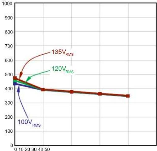
String Current [mA] vs. String Voltage [V]
line
| Time | 100V_RMS | 120V_RMS | 135V_RMS | |------|----------|----------|----------| | 0 | 450 | 450 | 450 | | 10 | 440 | 460 | 480 | | 20 | 430 | 470 | 520 | | 30 | 420 | 480 | 580 | | 40 | 410 | 490 | 620 | | 50 | 400 | 500 | 650 | | 60 | 390 | 510 | 680 | | 70 | 380 | 520 | 700 | | 80 | 370 | 530 | 720 | | 90 | 360 | 540 | 740 | | 100 | 350 | 550 | 760 |Efficiency [%] vs. String Voltage [V]

line
| Time | Voltage | | ---- | ------- | | 0 | 0 | | 10 | 10 | | 20 | 20 | | 30 | 30 | | 40 | 40 | | 50 | 50 | | 60 | 60 | | 70 | 70 | | 80 | 80 | | 90 | 85 | | 100 | 90 | | 110 | 95 | | 120 | 100 | | 135 | 105 | | 145 | 110 | | 155 | 115 | | 165 | 120 | | 175 | 125 | | 185 | 130 | | 195 | 135 | | 205 | 140 | | 215 | 145 | | 225 | 150 | | 235 | 155 | | 245 | 160 | | 255 | 165 | | 265 | 170 | | 275 | 175 | | 285 | 180 | | 295 | 185 | | 305 | 190 | | 315 | 195 | | 325 | 200 | | 335 | 205 | | 345 | 210 | | 355 | 215 | | 365 | 220 | | 375 | 225 | | 385 | 230 | | 395 | 235 | | 405 | 240 | | 415 | 245 | | 425 | 250 | | 435 | 255 | | 445 | 260 | | 455 | 265 | | 465 | 270 | | 475 | 275 | | 485 | 280 | | 495 | 285 | | 505 | 290 | | Note: The data for '100V_RMS' and '120V_RMS' is not explicitly labeled in the image. The values for '135V_RMS' are estimated based on the label 'virtually the same'. There is only one data series in this view.PF [%] vs. String Voltage [V]

line
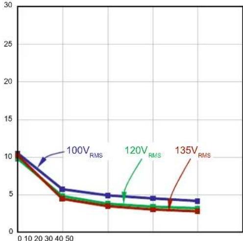
| Time | 135V_RMS | 120V_RMS | 100V_RMS | |------|----------|----------|----------| | 0 | 78 | 70 | 65 | | 10 | 85 | 75 | 68 | | 20 | 90 | 80 | 70 | | 30 | 95 | 85 | 75 | | 40 | 98 | 90 | 80 | | 50 | 99 | 95 | 85 | | 60 | 99 | 98 | 90 | | 70 | 99 | 99 | 95 | | 80 | 99 | 99 | 98 | | 90 | 99 | 99 | 99 | | 100 | 99 | 99 | 99 |THD [%] vs. String Voltage [V]
line
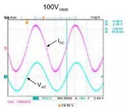
| Time | 100V_RMS | 120V_RMS | 135V_RMS | |------|----------|----------|----------| | 0 | 10 | 10 | 10 | | 10 | 9 | 9 | 9 | | 20 | 8 | 8 | 8 | | 30 | 7 | 7 | 7 | | 40 | 6 | 6 | 6 | | 50 | 5 | 5 | 5 | | 60 | 4.5 | 4.5 | 4.5 | | 70 | 4.2 | 4.2 | 4.2 | | 80 | 4.0 | 4.0 | 4.0 | | 90 | 3.8 | 3.8 | 3.8 | | 100 | 3.6 | 3.6 | 3.6 | | 110 | 3.5 | 3.5 | 3.5 | | 120 | 3.4 | 3.4 | 3.4 | | 130 | 3.3 | 3.3 | 3.3 | | 140 | 3.2 | 3.2 | 3.2 | | 150 | 3.1 | 3.1 | 3.1 | | 160 | 3.0 | 3.0 | 3.0 | | 170 | 2.9 | 2.9 | 2.9 | | 180 | 2.8 | 2.8 | 2.8 | | 190 | 2.7 | 2.7 | 2.7 | | 200 | 2.6 | 2.6 | 2.6 | | 210 | 2.5 | 2.5 | 2.5 | | 220 | 2.4 | 2.4 | 2.4 | | 230 | 2.3 | 2.3 | 2.3 | | 240 | 2.2 | 2.2 | 2.2 | | 250 | 2.1 | 2.1 | 2.1 | | 260 | 2.0 | 2.0 | 2.0 | | 270 | 1.9 | 1.9 | 1.9 | | 280 | 1.8 | 1.8 | 1.8 | | 290 | 1.7 | 1.7 | 1.7 | | 300 | 1.6 | 1.6 | 1.6 | | 310 | 1.5 | 1.5 | 1.5 | | 320 | 1.4 | 1.4 | 1.4 | | 330 | 1.3 | 1.3 | 1.3 | | 340 | 1.2 | 1.2 | 1.2 | | 350 | 1.1 | 1.1 | 1.1 | | 360 | 1.0 | 1.0 | 1.0 | | 370 | - | - | - | | 380 | - | - | - | | 390 | - | - | - | | 400 | - | - | - | | Note: The data is extracted from the code and presented in the following two rows to close the chart: 'Time' and 'Voltage'. The values for each row are labeled as 'RMS'. There are three additional data series labeled '100V', '120V', and '135V'.Typical Waveforms (1)
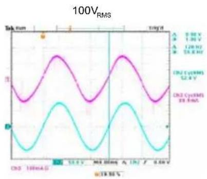
Line Voltage and Current at nominal load (350mA, 40V)
line
| Time (s) | I_AC (mA) | V_AC (mA) | |----------|-----------|-----------| | 0 | 4.30 | 120 | | 1.20 | 2.91 | 5.8 |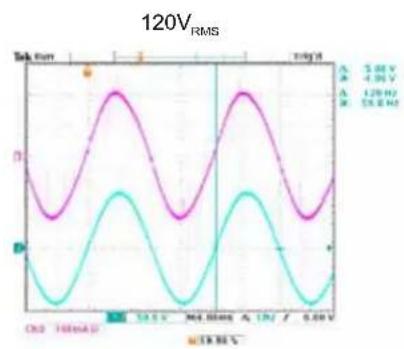
line
| Time (μs) | Voltage (V) | | --------- | ----------- | | 0 | 5.00 | | 10 | 4.00 | | 20 | 3.00 | | 30 | 2.00 | | 40 | 1.00 | | 50 | 0.00 | | 60 | -1.00 | | 70 | -2.00 | | 80 | -3.00 | | 90 | -4.00 | | 100 | -5.00 | | 110 | -4.00 | | 120 | -3.00 | | 130 | -2.00 | | 140 | -1.00 | | 150 | 0.00 | | 160 | 1.00 | | 170 | 2.00 | | 180 | 3.00 | | 190 | 4.00 | | 200 | 5.00 | | 210 | 4.00 | | 220 | 3.00 | | 230 | 2.00 | | 240 | 1.00 | | 250 | 0.00 | | 260 | -1.00 | | 270 | -2.00 | | 280 | -3.00 | | 290 | -4.00 | | 300 | -5.00 | | 310 | -4.00 | | 320 | -3.00 | | 330 | -2.00 | | 340 | -1.00 | | 350 | 0.00 | | 360 | 1.00 | | 370 | 2.00 | | 380 | 3.00 | | 390 | 4.00 | | 400 | 5.00 | | 410 | 4.00 | | 420 | 3.00 | | 430 | 2.00 | | 440 | 1.00 | | 450 | 0.00 | | 460 | -1.00 | | 470 | -2.00 | | 480 | -3.00 | | 490 | -4.00 | | 500 | -5.00 | | 510 | -4.00 | | 520 | -3.00 | | 530 | -2.00 | | 540 | -1.00 | | 550 | 0.00 | | 560 | 1.00 | | 570 | 2.00 | | 580 | 3.00 | | 590 | 4.00 | | 600 | 5.00 | | 610 | 4.00 | | 620 | 3.00 | | 630 | 2.00 | | 640 | 1.00 | | 650 | 0.00 | | 660 | -1.00 | | 670 | -2.00 | | 680 | -3.00 | | 690 | -4.00 | | 700 | -5.00 | | 710 | -4.00 | | 720 | -3.00 | | 730 | -2.00 | | 740 | -1.00 | | 750 | 0.00 | | 760 | 1.00 | | 770 | 2.00 | | 780 | 3.00 | | 790 | 4.00 | | 800 | 5.00 | | 810 | 4.58 | | 820 | 4.18 | | 830 | 3.78 | | 840 | 3.38 | | 850 | 3.18 | | 860 | 2.98 | | 870 | 2.78 | | 880 | 2.68 | | 890 | 2.68 | | 900 | 2.68 | | 910 | 2.68 | | 920 | 2.68 | | 930 | 2.68 | | 940 | 2.68 | | 950 | 2.68 | | 960 | 2.68 | | 970 | 2.68 | | 980 | 2.68 | | 990 | 2.68 | | 1 | -1.98 |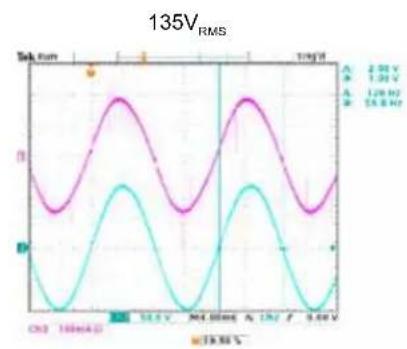
line
| Time (μs) | Voltage (V) | | --------- | ----------- | | 0 | 2.0 | | 12.0 | 1.2 | | 34.0 | 1.2 | | 56.0 | 1.2 | | 78.0 | 1.2 | | 100 | 1.2 | | 120 | 1.2 | | 140 | 1.2 | | 160 | 1.2 | | 180 | 1.2 | | 200 | 1.2 | | 220 | 1.2 | | 240 | 1.2 | | 260 | 1.2 | | 280 | 1.2 | | 300 | 1.2 | | 320 | 1.2 | | 340 | 1.2 | | 360 | 1.2 | | 380 | 1.2 | | 400 | 1.2 | | 420 | 1.2 | | 440 | 1.2 | | 460 | 1.2 | | 480 | 1.2 | | 500 | 1.2 | | 520 | 1.2 | | 540 | 1.2 | | 560 | 1.2 | | 580 | 1.2 | | 600 | 1.2 | | 620 | 1.2 | | 640 | 1.2 | | 660 | 1.2 | | 680 | 1.2 | | 700 | 1.2 | | 720 | 1.2 | | 740 | 1.2 | | 760 | 1.2 | | 780 | 1.2 | | 800 | 1.2 | | 820 | 1.2 | | 840 | 1.2 | | 860 | 1.2 | | 880 | 1.2 | | 900 | 1.2 | | 920 | 1.2 | | 940 | 1.2 | | 960 | 1.2 | | 980 | 1.2 | | 1000 | 1.2 |Line Voltage and Current at half load (350mA, 20V)
line
| Time (μs) | CNC2 Cycle 100A (V) | CNC2 Cycle 100B (V) | |-----------|----------------------|----------------------| | 0 | 5.8 | 3.8 | | 10 | 5.8 | 3.8 | | 20 | 5.8 | 3.8 | | 30 | 5.8 | 3.8 | | 40 | 5.8 | 3.8 | | 50 | 5.8 | 3.8 | | 60 | 5.8 | 3.8 | | 70 | 5.8 | 3.8 | | 80 | 5.8 | 3.8 | | 90 | 5.8 | 3.8 | | 100 | 5.8 | 3.8 | | 110 | 5.8 | 3.8 | | 120 | 5.8 | 3.8 | | 130 | 5.8 | 3.8 | | 140 | 5.8 | 3.8 | | 150 | 5.8 | 3.8 | | 160 | 5.8 | 3.8 | | 170 | 5.8 | 3.8 | | 180 | 5.8 | 3.8 | | 190 | 5.8 | 3.8 | | 200 | 5.8 | 3.8 | | 210 | 5.8 | 3.8 | | 220 | 5.8 | 3.8 | | 230 | 5.8 | 3.8 | | 240 | 5.8 | 3.8 | | 250 | 5.8 | 3.8 | | 260 | 5.8 | 3.8 | | 270 | 5.8 | 3.8 | | 280 | 5.8 | 3.8 | | 290 | 5.8 | 3.8 | | 300 | 5.8 | 3.8 | | 310 | 5.8 | 3.8 | | 320 | 5.8 | 3.8 | | 330 | 5.8 | 3.8 | | 340 | 5.8 | 3.8 | | 350 | 5.8 | 3.8 | | 360 | 5.8 | 3.8 | | 370 | 5.8 | 3.8 | | 380 | 5.8 | 3.8 | | 390 | 5.8 | 3.8 | | 400 | 5.8 | 3.8 | | 410 | 5.8 | 3.8 | | 420 | 5.8 | 3.8 | | 430 | 5.8 | 3.8 | | 440 | 5.8 | 3.8 | | 450 | 5.8 | 3.8 | | 460 | 5.8 | 3.8 | | 470 | 5.8 | 3.8 | | 480 | 5.8 | 3.8 | | 490 | 5.8 | 3.8 | | 500 | 5.8 | 3.8 | | 510 | 5.8 | 3.8 | | 520 | 5.8 | 3.8 | | 530 | 5.8 | 3.8 | | 540 | 5.8 | 3.8 | | 550 | 5.8 | 3.8 | | 560 | 5.8 | 3.8 | | 570 | 5.8 | 3.8 | | 580 | 5.8 | 3.8 | | 590 | 5.8 | 3.8 | | 600 | 5.8 | 3.8 | | 610 | 5.8 | 3.8 | | 620 | 5.8 | 3.8 | | 630 | 5.8 | 3.8 | | 640 | 5.8 | 3.8 | | 650 | 5.8 | 3.8 | | 660 | 5.8 | 3.8 | | 670 | 5.8 | 3.8 | | 680 | 5.8 | 3.8 | | 690 | 5.8 | 3.8 | | 700 | 5.8 | 3.8 | | Note: The actual values for CNC2 Cycle (10V) and CNC2 Cycle (1B) are not provided in the code snippet, so they are represented as placeholders (e.g., “±1k ± %” indicates the deviation from the center of the plot).)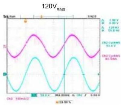

line
| Time (s) | CNC1 (V) | CNC2 (V) | |----------|----------|----------| | 0 | 0 | 0 | | 12.4 | ~0.5 | ~0.7 | | 0 | 0 | 0 | | 12.4 | ~0.5 | ~0.7 | | 0 | 0 | 0 | | 12.4 | ~0.5 | ~0.7 | | 0 | 0 | 0 | | 12.4 | ~0.5 | ~0.7 | | | 0 | 0 | 0 | | 12.4 | ~0.5 | ~0.7 | | 0 | 0 | 0 | | 12.4 | ~0.5 | ~0.7 | | 0 | 0 | 0 | | 12.4 | ~0.5 | ~0.7 |Output Current and Drain Voltage at nominal load (350mA, 40V)

line
| Time (V) | I_LED (Peak) | I_LED (Valley) | |----------|--------------|-----------------| | 0 | 0 | 0 | | 100 | 100 | 100 | | 200 | 200 | 200 | | 300 | 300 | 300 | | 400 | 400 | 400 | | 500 | 500 | 500 | | 600 | 600 | 600 | | 700 | 700 | 700 | | 800 | 800 | 800 | | 900 | 900 | 900 | | 1000 | 1000 | 1000 |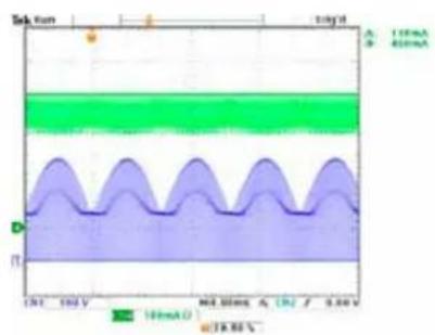
line
| Time (ms) | Current (mA) | | --------- | ------------ | | 0 | 115 | | 100 | 40 | | 200 | 115 | | 300 | 40 | | 400 | 115 | | 500 | 40 | | 600 | 115 | | 700 | 40 | | 800 | 115 | | 900 | 40 | | 1000 | 115 |
line
| Parameter | Value | | --------- | --------- | | Current | 115mA | | Amplitude | 400mA | | Voltage | 100mA | | Current | 18.60 V |Output Current and Drain Voltage at half load (350mA, 20V)

line
| Time (s) | Voltage (V) | | -------- | ----------- | | 0 | 500 | | 10 | 100 | | 20 | 150 | | 30 | 200 | | 40 | 250 | | 50 | 300 | | 60 | 350 | | 70 | 400 | | 80 | 450 | | 90 | 500 | | 100 | 550 | | 110 | 600 | | 120 | 650 | | 130 | 700 | | 140 | 750 | | 150 | 800 | | 160 | 850 | | 170 | 900 | | 180 | 950 | | 190 | 1000 | | 200 | 1050 | | 210 | 1100 | | 220 | 1150 | | 230 | 1200 | | 240 | 1250 | | 250 | 1300 | | 260 | 1350 | | 270 | 1400 | | 280 | 1450 | | 290 | 1500 | | 300 | 1550 | | 310 | 1600 | | 320 | 1650 | | 330 | 1700 | | 340 | 1750 | | 350 | 1800 | | 360 | 1850 | | 370 | 1900 | | 380 | 1950 | | 390 | 2000 | | 400 | 2050 | | 410 | 2100 | | 420 | 2150 | | 430 | 2200 | | 440 | 2250 | | 450 | 2300 | | 460 | 2350 | | 470 | 2400 | | 480 | 2450 | | 490 | 2500 | | 500 | 2550 | | 510 | 2600 | | 520 | 2650 | | 530 | 2700 | | 540 | 2750 | | 550 | 2800 | | 560 | 2850 | | 570 | 2900 | | 580 | 2950 | | 590 | 3000 | | 600 | 3050 | | 610 | 3100 | | 620 | 3150 | | 630 | 3200 | | 640 | 3250 | | 650 | 3300 | | 660 | 3350 | | 670 | 3400 | | 680 | 3450 | | 690 | 3500 | | 700 | 3550 | | 710 | 3600 | | 720 | 3650 | | 730 | 3700 | | 740 | 3750 | | 750 | 3800 | | 760 | 3850 | | 770 | 3900 | | 780 | 3950 | | 790 | 4000 | | 800 | 4050 | | 810 | 4100 | | 820 | 4150 | | 830 | 4200 | | 840 | 4250 | | 850 | 4300 | | 860 | 4350 | | 870 | 4400 | | 880 | 4450 | | 890 | 4500 | | 900 | 4550 | | 910 | 4600 | | 920 | 4650 | | 930 | 4700 | | 940 | 4750 | | 950 | 4800 | | 960 | 4850 | | 970 | 4900 | | 980 | 4950 | | 990 | 5000 | | >1.2 | >1.2 |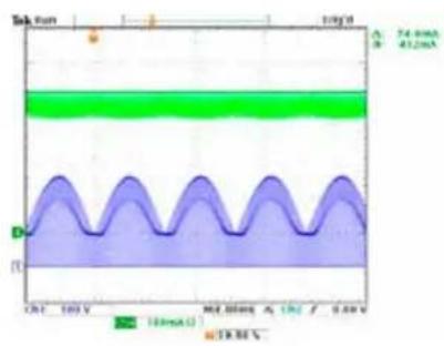
line
| Time (s) | Voltage (mA) | | -------- | ------------ | | 0 | 74.0 | | 10 | 43.2 | | 20 | 74.0 | | 30 | 43.2 | | 40 | 74.0 | | 50 | 43.2 | | 60 | 74.0 | | 70 | 43.2 | | 80 | 74.0 | | 90 | 43.2 | | 100 | 74.0 | | 110 | 43.2 | | 120 | 74.0 | | 130 | 43.2 | | 140 | 74.0 | | 150 | 43.2 | | 160 | 74.0 | | 170 | 43.2 | | 180 | 74.0 | | 190 | 43.2 | | 200 | 74.0 | | 210 | 43.2 | | 220 | 74.0 | | 230 | 43.2 | | 240 | 74.0 | | 250 | 43.2 | | 260 | 74.0 | | 270 | 43.2 | | 280 | 74.0 | | 290 | 43.2 | | 300 | 74.0 | | 310 | 43.2 | | 320 | 74.0 | | 330 | 43.2 | | 340 | 74.0 | | 350 | 43.2 | | 360 | 74.0 | | 370 | 43.2 | | 380 | 74.0 | | 390 | 43.2 | | 400 | 74.0 | | 410 | 43.2 | | 420 | 74.0 | | 430 | 43.2 | | 440 | 74.0 | | 450 | 43.2 | | 460 | 74.0 | | 470 | 43.2 | | 480 | 74.0 | | 490 | 43.2 | | 500 | 74.0 | | 510 | 43.2 | | 520 | 74.0 | | 530 | 43.2 | | 540 | 74.0 | | 550 | 43.2 | | 560 | 74.0 | | 570 | 43.2 | | 580 | 74.0 | | 590 | 43.2 | | 600 | 74.0 | | 610 | 43.2 | | 620 | 74.0 | | 630 | 43.2 | | 640 | 74.0 | | 650 | 43.2 | | 660 | 74.0 | | 670 | 43.2 | | 680 | 74.0 | | 690 | 43.2 | | 700 | 74.0 | | 710 | 43.2 | | 720 | 74.0 | | 730 | 43.2 | | 740 | 74.0 | | 750 | 43.2 | | 760 | 74.0 | | 770 | 43.2 | | 780 | 74.0 | | 790 | 43.2 | | 800 | 74.0 | | 810 | 43.2 | | 820 | 74.0 | | 830 | 43.2 | | 840 | 74.0 | | 850 | 43.2 | | 860 | 74.0 | | 870 | 43.2 | | 880 | 74.0 | | 890 | 43.2 | | 900 | 74.0 | | 910 | 43.2 | | 920 | 74.0 | | 930 | 43.2 | | 940 | 74.0 | | 950 | 43.2 | | 960 | 74.0 | | 970 | 43.2 | | 980 | 74.0 | | 990 | 43.2 | |1 |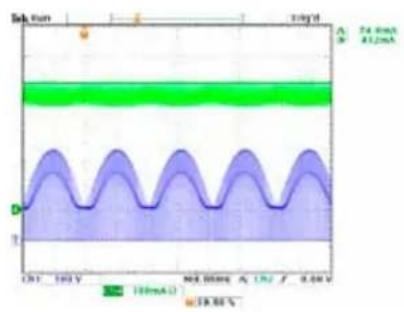
line
| Time (s) | Voltage (mA) | | -------- | ------------ | | 0 | 54.8 | | 10 | 41.2 |Typical Waveforms (2) (120V_RMS, 40V, 350mA)
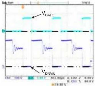
Drain Voltage and LED Current

Drain Voltage and Gate Voltage
4μs per div
line
| Time (s) | V_GATE (V) | V_DRAIN (V) | |----------|------------|-------------| | 0 | 0 | 0 | | 10 | 0 | 0 | | 20 | 0 | 0 | | 30 | 0 | 0 | | 40 | 0 | 0 | | 50 | 0 | 0 | | 60 | 0 | 0 | | 70 | 0 | 0 | | 80 | 0 | 0 | | 90 | 0 | 0 | | 100 | 0 | 0 |40μs per div 40μs per div
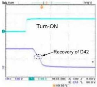
text_image
Turn-ON Recovery of D42
line
| Time (V) | Turn-OFF | Recovery of D41+ | | -------- | -------- | ---------------- | | 0 | 49.36 | 49.36 |Drain Voltage and Current Sense Voltages of Stages 1 and 2

line
| Time (V) | V_RS1 | V_RS2 | V_DRAIN | |----------|-------|-------|---------| | 0 | - | - | - | | 130 | - | - | - | | 200 | - | - | - | | 250 | - | - | - | | 300 | - | - | - | | 350 | - | - | - | | 400 | - | - | - | | 450 | - | - | - | | 500 | - | - | - | | 550 | - | - | - | | 600 | - | - | - | | 650 | - | - | - | | 700 | - | - | - | | 750 | - | - | - | | 800 | - | - | - | | 850 | - | - | - | | 900 | - | - | - | | 950 | - | - | - | | 1000 | - | - | - | | 1050 | - | - | - | | 1100 | - | - | - | | 1150 | - | - | - | | 1200 | - | - | - | | 1250 | - | - | - | | 1300 | - | - | - | | 1350 | - | - | - | | 1400 | - | - | - | | 1450 | - | - | - | | 1500 | - | - | - | | 1550 | - | - | - | | 1600 | - | - | - | | 1650 | - | - | - | | 1700 | - | - | - | | 1750 | - | - | - | | 1800 | - | - | - | | 1850 | - | - | - | | 1900 | - | - | - | | 1950 | - | - | - | | 2000 | - | - | - | | 2050 | - | - | - | | 2100 | - | - | - | | 2150 | - | - | - | | 2200 | - | - | - | | 2250 | - | - | - | | 2300 | - | - | - | | 2350 | - | - | - | | 2400 | - | - | - | | 2450 | - | - | - | | 2500 | - | - | - | | 2550 | - | - | - | | 2600 | - | - | - | | 2650 | - | - | - | | 2700 | - | - | - | | 2750 | - | - | - | | 2800 | - | - | - | | 2850 | - | - | - | | 2900 | - | - | - | | 2950 | - | - | - | | 3000 | - | - | - | | 3050 | - | - | - | | 3100 | - | - | - | | 3150 | - | - | - | | 3200 | - | - | - | | 3250 | - | - | - | | 3300 | - | - | - | | 3350 | - | - | - | | 3400 | - | - | - | | 3450 | - | - | - | | 3500 | - | - | - | | 3550 | - | - | - | | 3600 | - | - | - | | 3650 | - | - | - | | 3700 | - | - | - | | 3750 | - | - | - | | 3800 | - | - | - | | 3850 | - | - | - | | 3900 | - | - | - | | 3950 | - | - | - | | 4000 | - | - | - | | 4050 | - | - | - | | 4100 | - | - | - | | 4150 | - | - | - | | 4200 | - | - | - | | 4250 | - | - | - | | 4300 | - | - | - | | 4350 | - | - | - | | 4400 | - | - | - | | 4450 | - | - | - | | 4500 | - | - | - | | 4550 | - | - | - | | 4600-46.9V, +9.99V, +9.99V, +9.99V, +9.99V, +9.99V, +9.99V, +9.99V, +9.99V, +9.99V, +9.99V, +9.99V, +9.99V, +9.99V, +9.99V, +9.99%

line
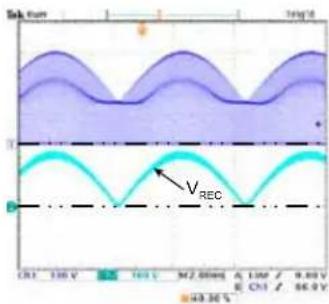
| Time (ms) | Voltage (V) | | --------- | ----------- | | 0 | 0 | | 100 | 0 | | 200 | 0 | | 300 | 0 | | 400 | 0 | | 500 | 0 | | 600 | 0 | | 700 | 0 | | 800 | 0 | | 900 | 0 | | 1000 | 0 |Drain Voltage and Voltages at Test Points REC, SN3, SN2
line
| Parameter | Value | | --------- | --------- | | Current | 130 V | | Voltage | 100 V | | Current | 9.80 V | | Voltage | 66.9 V | | Reference Voltage | V_REC |
line
| Time (V) | Voltage | |----------|---------| | 0 | 59.30 |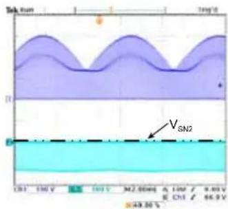
line
| Parameter | Value | | --------- | --------- | | SN2 | 130 V | | ILS | 100 V | | MΩ·500Hz | 100 V | | A | 100 V | | 9.00 V | 9.00 V | | E | CHT | | CHT | 66.9 V |Typical Waveforms (3) (120V _RMS , 40V, 350mA)
Drain Voltage and Voltage at the Test Point L1D (3 points along the AC line cycle)

line
| Time (V) | V_DRAIN | V_LID | |----------|---------|-------| | 0 | 0 | 0 | | 16.2 | 0 | 0 | | 16.4 | 0 | 0 | | 16.6 | 0 | 0 | | 16.8 | 0 | 0 | | 17.0 | 0 | 0 | | 17.2 | 0 | 0 | | 17.4 | 0 | 0 | | 17.6 | 0 | 0 | | 17.8 | 0 | 0 | | 18.0 | 0 | 0 | | 18.2 | 0 | 0 | | 18.4 | 0 | 0 | | 18.6 | 0 | 0 | | 18.8 | 0 | 0 | | 19.0 | 0 | 0 | | 19.2 | 0 | 0 | | 19.4 | 0 | 0 | | 19.6 | 0 | 0 | | 19.8 | 0 | 0 | | 20.0 | 0 | 0 | | 20.2 | 0 | 0 | | 20.4 | 0 | 0 | | 20.6 | 0 | 0 | | 20.8 | 0 | 0 | | 21.0 | 0 | 0 | | 21.2 | 0 | 0 | | 21.4 | 0 | 0 | | 21.6 | 0 | 0 | | 21.8 | 0 | 0 | | 22.0 | 0 | 0 | | 22.2 | 0 | 0 | | 22.4 | 0 | 0 | | 22.6 | 0 | 0 | | 22.8 | 0 | 0 | | 23.0 | 0 | 0 | | 23.2 | 0 | 0 | | 23.4 | 0 | 0 | | 23.6 | 0 | 0 | | 23.8 | 0 | 0 | | 24.0 | 0 | 0 | | 24.2 | 0 | 0 | | 24.4 | 0 | 0 | | 24.6 | 0 | 0 | | 24.8 | 0 | 0 | | 25.0 | 0 | 0 | | 25.2 | 0 | 0 | | 25.4 | 0 | 0 | | 25.6 | 0 | 0 | | 25.8 | 0 | 0 | | 26.0 | 0 | 0 | | 26.2 | 0 | 0 | | 26.4 | 0 | 0 | | 26.6 | 0 | 0 | | 26.8 | 0 | 0 | | 27.0 | 0 | 0 | | 27.2 | 0 | 0 | | 27.4 | 0 | 0 | | 27.6 | 0 | 0 | | 27.8 | 0 | 0 | | 28.0 | 0 | 0 | | 28.2 | 0 | 0 | | 28.4 | 0 | 0 | | 28.6 | 0 | 0 | | 28.8 | 0 | 0 | | 29.0 | 0 | 0 | | 29.2 | 0 | 0 | | 29.4 | 0 | 0 | | 29.6 | 0 | 0 | | 29.8 | 0 | 0 | | 30.0 | 0 | 0 | | - | - | - | | - | - | - | | - | - | - | | - | - | - | | - | - | - | | - | - | - | | - | - | - | | - | - | - | | - | - | - | | - | - | - | | - | - | +48.5%| | - | - | +48.5%| | - | - | +48.5%| | - | - | +48.5%| | - | - | +48.5%| | - | - | +48.5%| | - | - | +48.5%| | - | - | +48.5%| | ... | ... | ... | | ... | ... | ... | | ... | ... | ... | | ... | ... | ... | | ... | ... | ... | | ... | ... | ... | | ... | ... | ... | | ... | ... | ... | | ... | ... | ... | | ... | ... | ... | | ... | ... | ... | | ... | ... | ... | | ... | ... | ... | | ... | ... | ... | | ... | ... | ... | | ... | ... | ... | | ... | ... | ... | | ... | ... | ... | | ... | ... | ... | | ... | ... | ... | | ... | ... | ... | | ... | ... | ... | | ... | ... | ... | | ... | ... | ... | | ... | ... | ... | | ... | ... | ... | | ... | ... | ... | | ... | ... | ... | | ... | ... | ... | | ... | ... | ... | | ... | ... | ... | Note: The data is extracted from the image file 'A_T ~90°' and is not provided in the code format as it is not possible for this image.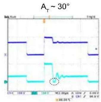
line
| Time (μs) | Current (I) | | --------- | ----------- | | 0 | 48.04 | | 100 | 48.04 | | 200 | 48.04 | | 300 | 48.04 | | 400 | 48.04 | | 500 | 48.04 | | 600 | 48.04 | | 700 | 48.04 | | 800 | 48.04 | | 900 | 48.04 | | 1000 | 48.04 |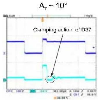
line
| Time (s) | Voltage (V) | | -------- | ----------- | | 0 | 46.05 | | 100 | 46.05 | | 200 | 46.05 | | 300 | 46.05 | | 400 | 46.05 | | 500 | 46.05 | | 600 | 46.05 | | 700 | 46.05 | | 800 | 46.05 | | 900 | 46.05 | | 1000 | 46.05 |EMI Signature
Board suspended about 3" above reference plane.
Limit Line: CISPR 15 Quasi Peak (9kHz to 30MHz)
Detector: Peak Hold
IF Bandwidth: 9kHz
Shielding: 2 copper shields, surrounding the power section on top and bottom of the board, terminated at the source of the MOSFET.
Without shielding :
line
| Frequency | Value | | --------- | --------- | | 10kHz | 110dBμV | | 10kHz | 90 | | 10kHz | 80 | | 10kHz | 66 | | 1MHz | 56 | | 1MHz | 60 |With shielding :

line
| Frequency | Voltage (dBμV) | | --------- | -------------- | | 10kHz | 110 | | 100kHz | 90 | | 1MHz | 80 | | 1MHz | 66 | | 1MHz | 56 | | 1MHz | 60 |The performance graphs above were obtained from the board not having specific measures to suppress common mode emissions, such as inclusion of a common mode inductor in the AC line input circuitry. The above graphs show how shielding can significantly reduce emissions, particularly in the upper frequency range. The shielding also was instrumental in reducing the lower frequency emissions by reducing magnetic field coupling from the main inductors to the EMI filter inductors (EMI filter section kept outside of shielded area).
Mathcad Design Data
| Corner x | 0 0 1 2 3 | 4 5 6 7 | 8 Corner | |||||||||||||
| L1 μH 0 | 616 560 | 504 616 | 560 504 | 616 560 | 504 L1 ---- | |||||||||||
| RL1 | mR | 0 | 2000 | 2000 | 2000 | 2000 | 2000 | 2000 | 2000 | 2000 | 2000 | RL1 | - | - | - | - |
| L2 | mH | 0 | 3300 | 3300 | 3300 | 3300 | 3300 | 3300 | 3300 | 3300 | 3300 | L2 | - | - | - | - |
| RL2 | mR | 0 | 3000 | 3000 | 3000 | 3000 | 3000 | 3000 | 3000 | 3000 | 3000 | RL2 | - | - | - | - |
| ILRF2 | % | 0 | 32 | 32 | 32 | 32 | 32 | 32 | 32 | 32 | 32 | ILRF2 | - | - | - | - |
| C2 | uF | 0.0 | 37.6 | 47.0 | 56.4 | 37.6 | 47.0 | 56.4 | 37.6 | 47.0 | 56.4 | C2 | - | - | - | - |
| NF | x | 0 | 2 | 2 | 2 | 2 | 2 | 2 | 2 | 2 | 2 | NF | - | - | - | - |
| LF | μH | 0 | 1000 | 1000 | 1000 | 1000 | 1000 | 1000 | 1000 | 1000 | 1000 | LF | - | - | - | - |
| RLF | mR | 0 | 2000 | 2000 | 2000 | 2000 | 2000 | 2000 | 2000 | 2000 | 2000 | RLF | - | - | - | - |
| CF | nF | 0 | 100 | 100 | 100 | 100 | 100 | 100 | 100 | 100 | 100 | CF | - | - | - | - |
| C1 | nF | 0 | 100 | 100 | 100 | 100 | 100 | 100 | 100 | 100 | 100 | C1 | - | C2V | 135 | - |
| RS | mR | 0 | 1000 | 1000 | 1000 | 1000 | 1000 | 1000 | 1000 | 1000 | 1000 | RS | - | C2R | 1345 | - |
| VD | mV | 0 | 1000 | 1000 | 1000 | 1000 | 1000 | 1000 | 1000 | 1000 | 1000 | VD | - | - | - | - |
| TF | us | 0.0 | 8.7 | 8.7 | 8.7 | 8.7 | 8.7 | 8.7 | 8.7 | 8.7 | 8.7 | TF | - | - | - | - |
| RT | kR | 0 | 196 | 196 | 196 | 196 | 196 | 196 | 196 | 196 | 196 | RT | - | - | - | - |
| FM | Hz | 0 | 50 | 50 | 50 | 50 | 60 | 50 | 50 | 50 | 50 | FM | - | - | - | - |
| VMRMS | V | 0 | 100 | 100 | 100 | 120 | 120 | 120 | 135 | 135 | 135 | VMRMS | - | - | - | - |
| IMRMS | mA | 0 | 167 | 160 | 153 | 137 | 133 | 130 | 122 | 118 | 115 | IMRMS | 130 | 137 | 115 | 167 |
| IMMAX | mA | 0 | 246 | 232 | 221 | 200 | 191 | 185 | 176 | 169 | 163 | IMMAX | 185 | 200 | 163 | 246 |
| V3AVG | V | 0 | 40 | 40 | 40 | 40 | 40 | 40 | 40 | 40 | 40 | V3AVG | 40 | 40 | 40 | 40 |
| I3AVG | mA | 0 | 361 | 350 | 335 | 361 | 350 | 339 | 361 | 350 | 339 | I3AVG | 339 | 361 | 335 | 361 |
| PM | W | 0.0 | 16.5 | 15.9 | 15.3 | 16.3 | 15.8 | 15.5 | 16.2 | 15.8 | 15.3 | PM | 15.5 | 16.3 | 15.3 | 16.5 |
| P3 | W | 0.0 | 14.4 | 14.0 | 13.4 | 14.4 | 14.0 | 13.6 | 14.4 | 14.0 | 13.6 | P3 | 13.6 | 14.4 | 13.4 | 14.4 |
| EFF | % | 0.0 | 87.5 | 88.0 | 87.8 | 88.7 | 88.5 | 87.7 | 88.9 | 88.7 | 88.3 | EFF | 87.7 | 88.7 | 87.5 | 88.9 |
| PF | % | 0.0 | 98.7 | 99.3 | 99.6 | 98.9 | 99.3 | 99.5 | 98.8 | 99.1 | 99.3 | PF | 98.9 | 99.5 | 98.7 | 99.6 |
| THD | % | 0.0 | 9.0 | 5.3 | 3.3 | 6.4 | 3.8 | 2.5 | 5.1 | 3.1 | 2.1 | THD | 2.5 | 6.4 | 2.1 | 9.0 |
| H3 | % | 0.0 | 8.7 | 5.1 | 3.1 | 6.2 | 3.6 | 2.3 | 5.0 | 2.9 | 1.9 | H3 | 2.3 | 6.2 | 1.9 | 8.7 |
| H5 | % | 0.0 | 1.7 | 1.0 | 0.7 | 1.1 | 0.7 | 0.6 | 0.8 | 0.6 | 0.5 | H5 | 0.6 | 1.1 | 0.5 | 1.7 |
| TAMIN | μs | 0.0 | 4.6 | 4.8 | 4.8 | 3.7 | 3.9 | 3.9 | 3.2 | 3.4 | 3.4 | TAMIN | 3.7 | 3.9 | 3.2 | 4.8 |
| TAMAX | μs | 0.0 | 5.8 | 5.4 | 5.2 | 4.3 | 4.2 | 4.2 | 3.7 | 3.6 | 3.6 | TAMAX | 4.2 | 4.3 | 3.6 | 5.8 |
| TFMIN | μs | 0.0 | 7.0 | 8.7 | 10.5 | 7.0 | 8.7 | 10.5 | 7.0 | 8.7 | 10.5 | TFMIN | 7.0 | 10.5 | 7.0 | 10.5 |
| TFMAX | μs | 0.0 | 7.0 | 8.7 | 10.5 | 7.0 | 8.7 | 10.5 | 7.0 | 8.7 | 10.5 | TFMAX | 7.0 | 10.5 | 7.0 | 10.5 |
| DAMIN | % | 0.0 | 39.6 | 35.5 | 31.6 | 34.7 | 30.8 | 27.4 | 31.8 | 28.0 | 24.7 | DAMIN | 27.4 | 34.7 | 24.7 | 39.6 |
| DAMAX | % | 0.0 | 45.3 | 38.4 | 33.1 | 38.3 | 32.6 | 28.4 | 34.5 | 29.4 | 25.5 | DAMAX | 28.4 | 38.3 | 25.5 | 45.3 |
| DC1MAX | % | 0.0 | 98.6 | 79.7 | 65.2 | 87.1 | 70.0 | 57.7 | 80.4 | 64.3 | 52.4 | DC1MAX | 57.7 | 87.1 | 52.4 | 98.6 |
| FSMIN | kHz | 0.0 | 78.4 | 70.6 | 63.9 | 88.4 | 77.3 | 68.4 | 93.9 | 81.0 | 71.2 | FSMIN | 68.4 | 88.4 | 63.9 | 93.9 |
| FSMAX | kHz | 0.0 | 86.5 | 74.0 | 65.4 | 93.6 | 79.4 | 69.4 | 97.8 | 82.6 | 71.9 | FSMAX | 69.4 | 93.6 | 65.4 | 97.8 |
| Corner x | 0 0 1 2 3 | 4 5 6 7 | 8 Corner | |||||||||||||
| IL1RMS mA | 0 428 | 426 423 | 383 384 | 388 359 | 361 36 | 3 IL1RM | S 383 | 388 359 | 428 | |||||||
| IL1MAX | mA | 0 | 1121 | 1233 | 1345 | 1063 | 1184 | 1318 | 1036 | 1161 | 1291 | IL1MAX | 1063 | 1318 | 1036 | 1345 |
| IL2RMS mA | 0 362 | 351 338 | 362 351 | 341 362 | 351 34 | 1 IL2RM | S 341 | 362 338 | 362 | |||||||
| IL2MAX mA | 0 406 | 406 406 | 406 406 | 406 406 | 406 406 | IL2MAX | 406 406 | 406 406 | ||||||||
| I2RMS | mA | 0 | 389 | 367 | 345 | 356 | 337 | 322 | 337 | 319 | 304 | I2RMS | 322 | 356 | 304 | 389 |
| V2MIN | V | 0 | 94 | 110 | 127 | 111 | 130 | 149 | 123 | 144 | 166 | V2MIN | 111 | 149 | 94 | 166 |
| V2MAX | V | 0 | 107 | 119 | 134 | 122 | 137 | 154 | 133 | 151 | 171 | V2MAX | 122 | 154 | 107 | 171 |
| V2RELPPR | % | 0.0 | 13.1 | 7.9 | 4.8 | 9.7 | 5.8 | 3.7 | 8.1 | 4.8 | 3.0 | V2RELPPR | 4 | 10 | 3 | 13 |
| ISRMS | mA | 0 | 504 | 492 | 480 | 455 | 446 | 442 | 428 | 420 | 414 | ISRMS | 442 | 455 | 414 | 504 |
| ISMAX | mA | 0 | 1526 | 1639 | 1750 | 1469 | 1590 | 1723 | 1442 | 1567 | 1696 | ISMAX | 1469 | 1723 | 1442 | 1750 |
| VSMAX V 0 | 241 254 | 270 285 | 301 319 | 317 336 | 357 | VSMAX | 285 | 319 241 | 357 | |||||||
| IDL1AVG | mA | 0 | 300 | 271 | 245 | 253 | 229 | 211 | 228 | 206 | 188 | IDL1AVG | 211 | 253 | 188 | 300 |
| IDF1AVG | mA | 0 | 152 | 128 | 108 | 131 | 111 | 96 | 120 | 101 | 86 | IDF1AVG | 96 | 131 | 86 | 152 |
| IDR2AVG | mA | 0 | 152 | 129 | 108 | 131 | 111 | 94 | 119 | 100 | 85 | IDR2AVG | 94 | 131 | 85 | 152 |
| IDF2AVG | mA | 0 | 209 | 221 | 227 | 230 | 239 | 244 | 242 | 250 | 254 | IDF2AVG | 230 | 244 | 209 | 254 |
| IRS1RMS mA 0 | 295 308 | 310 260 | 270 282 | 242 252 | 262 | RS1RMS | 260 282 | 242 310 | ||||||||
| IRS2RMS mA 0 | 235 218 | 192 218 | 198 180 | 208 188 | 171 | RS2RMS | 180 218 | 171 235 | ||||||||
Simulated Waveforms (Mathcad)

line
| Time (t) | Drain Voltage Envelope | Rectified Line Voltage | Bus Voltage | Input Inductor Peak Current Envelope | Line Voltage | Line Current | |----------|------------------------|------------------------|-----------|--------------------------------------|--------------|--------------| | 0 | 310 | 310 | 130 | 130 | 160 | -200 | | 1×10⁰ | 310 | 310 | 130 | 130 | 160 | -200 | | 2×10⁰ | 310 | 310 | 130 | 130 | 160 | -200 | | 3×10⁰ | 310 | 310 | 130 | 130 | 160 | -200 | | 4×10⁰ | 310 | 310 | 130 | 130 | 160 | -200 |Bill of Materials
| Qty REF Description Manufacturer Product Number | ||||
| 1 BR | 11 RECT BRIDGE | GP MINIDIP 600V 0.5A Diodes Inc RH06-T | ||
| 2 C62 | C72 CAP CER NP0 50V 10% 0805 100PF Kemet C0805C101K5GACTU | |||
| 2 C41 | C81 CAP CER X7R 100V 10% 0805 10NF Kemet C0805C103K1RACTU | |||
| 1 | C37 | CAP CER NP0 1000V 5% 0805 100PF | Vishay/Vitramon | VJ0805A101JXGAT5Z |
| 2 | C51, C65 | CAP CER X7R 16V 10% 1206 10μF | Murata | GRM31CR71C106KAC7L |
| 3 | C11, C12, C21 | CAP MKP 305VAC X2 125C 20% 100NF | EPCOS Inc | B32921C3104M |
| 1 | D42 | DIODE ULTRAFAST 200V 1A SMA | STMicroelectronics | STTH102A |
| 3 | D31, D32, D37 | DIODE FAST 600V 1A SMA | STMicroelectronics | STTH1L06A |
| 1 | D41 | DIODE ULTRAFAST 600V 1A SMA | STMicroelectronics | STTH1R06A |
| 2 | D39, D79 | DIODE ULTRAFAST HI COND SOT-23 | Fairchild Semiconductor | MMBD914 |
| 1 DN65 | DIODE SW DUAL 75V 350MW SOT23 | Diodes Inc BAV99-7-F | ||
| 1 | E31 | CAP ALEL ED RAD12X20 200V 20% 47μF | Panasonic ECG | EEU-ED2D470 |
| 1 | F11 | FUSE SLOW IEC TR5 250MA | Littelfuse Wickmann | 37202500411 |
| 0 | HS | HEATSINK TO220 W/TAB W86 D40 H75 21K | Aavid Thermalloy | 574502B03700G |
| 1 | IC51 | IC HV9931 LED DRIVER 8L SOIC | Supertex | HV9931LG-G |
| 2 | L11, L21 | CHOKE SH RAD13MM 15% 1.0MH 820MA | Sumida | RCP1317NP-102L |
| 1 | L31 | CHOKE RAD 450D 710L 10% 560μH | Renco | RL-5480-4-560 |
| 1 | L41 | CHOKE RAD 625D 700L 10% 3.3MH | Renco | RL-5480-5-3300 |
| 1 | M31 | MOSFET N-CH 560V 4.5A 0.95R TO-220FP | Infineon Technologies | SPA04N50C3 |
| 1 | MOV11 | MOV 10MM 430VDC 2500A ZNR | Panasonic ECG | ERZ-V10D431 |
| 2 | Q81, Q83 | TRANSISTOR GP NPN SOT-23 | Fairchild Semiconductor | MMBT2222A |
| 2 | Q82, Q84 | TRANSISTOR GP PNP SOT-23 | Fairchild Semiconductor | MMBT2907A |
| 2 | R90, R99 | RES 1/8W 0805 1% 1.00KΩ | Panasonic ECG | ERJ-6ENF1001V |
| 2 | R39, R79 | RES 1/8W 0805 1% 100Ω | Panasonic ECG | ERJ-6ENF1000V |
| 1 | R62 | RES 1/8W 0805 1% 2.43KΩ | Panasonic ECG | ERJ-6ENF2431V |
| 1 | R72 | RES 1/8W 0805 1% 2.67KΩ | Panasonic ECG | ERJ-6ENF2671V |
| 1 | R81 | RES 1/8W 0805 1% 10.0KΩ | Panasonic ECG | ERJ-6ENF1002V |
| 1 | R82 | RES 1/8W 0805 1% 24.3KΩ | Panasonic ECG | ERJ-6ENF2432V |
| 1 | R63, R73 | RES 1/8W 0805 1% 75.0KΩ | Panasonic ECG | ERJ-6ENF7502V |
| 2 | R80, R85, R86 | RES 1/8W 0805 1% 100KΩ | Panasonic ECG | ERJ-6ENF1003V |
| 1 | R90 | RES 1/8W 0805 1% 150KΩ | Panasonic ECG | ERJ-6ENF1503V |
| 1 | R51 | RES 1/8W 0805 1% 196KΩ | Panasonic ECG | ERJ-6ENF1963V |
| 1 | R87 | RES 1/8W 0805 1% 200KΩ | Panasonic ECG | ERJ-6ENF2003V |
| 2 | R64, R65 | RES 1/8W 0805 1% 634KΩ | Panasonic ECG | ERJ-6ENF6343V |
| 3 R68, R83, R84 RES 1/8W 0805 1% 1.0MΩ Panasonic ECG ERJ-6ENF1004V | ||||
| 1 R88 RES 1/8W 0805 1% 10.0MΩ Vishay/Dale CRCW080510M0FKEA | ||||
| 1 R37 RES 1/4W 1206 5% 6.8KΩ Panasonic ECG ERJ-8GEYJ682V | ||||
| 1 R31 RES 1/4W 1206 5% 1.0MΩ Panasonic ECG ERJ-8GEYJ105V | ||||
| 1 R61 RES 1/4W 0805 1% .18Ω Susumu Co Ltd RL1220S-R18-F | ||||
| 1 R71 RES 1/4W 0805 1% .68Ω Susumu Co Ltd RL1220S-R68-F | ||||
| 1 | TVS11 | DIODE TVS BIDIR SMA 400W 5% 440V | Littelfuse Inc | SMAJ440CA |
| 2 | Z61, Z90 | DIODE ZENER 350MW SOT-23 7.5V | Diodes Inc | BZX84C7V5-7-F |
| 1 | Z91 | DIODE ZENER 350MW SOT-23 47V | Diodes Inc | BZX84C47-7-F |
Supertex inc. does not recommend the use of its products in life support applications, and will not knowingly sell them for use in such applications unless it receives an adequate “product liability indemnification insurance agreement.” Supertex Inc. does not assume responsibility for use of devices described, and limits its liability to the replacement of the devices determined defective due to workmanship. No responsibility is assumed for possible omissions and inaccuracies. Circuitry and specifications are subject to change without notice. For the latest product specifications refer to the Supertex Inc. (website: http://www.supertex.com)
©2013 Supertex inc. All rights reserved. Unauthorized use or reproduction is prohibited.