MIC3263YML - Carte d'évaluation Microchip - Free user manual and instructions
Find the device manual for free MIC3263YML Microchip in PDF.

User questions about MIC3263YML Microchip
0 question about this device. Answer the ones you know or ask your own.
Ask a new question about this device
Download the instructions for your Carte d'évaluation in PDF format for free! Find your manual MIC3263YML - Microchip and take your electronic device back in hand. On this page are published all the documents necessary for the use of your device. MIC3263YML by Microchip.
USER MANUAL MIC3263YML Microchip
This evaluation board (EVB) is designed for the MIC3263. The MIC3263 is a high-efficiency Pulse Width Modulation (PWM) boost switching regulator that is optimized for constant-current WLED driver backlighting applications. The MIC3263 drives six channels of up to ten low-power WLEDs per channel. Each channel is matched in current to within ±3% for constant brightness across the screen and can be programmed from 15mA to 30mA.
The MIC3263 provides a very flexible dimming control scheme with high accuracy and noise immunity. The dimming frequency can be set to any value between 100Hz and 20kHz by an external resistor. The dimming ratio is determined by the duty-cycle of a dimming ratio control input signal and can be set to one of 16 levels with a minimum ratio of 1%. The LED dimming current is set by an external resistor to allow programming of LED current between 15mA and 30mA.
The dimming ratio of the MIC3263 is fixed to 16 logarithmic levels to better match the sensitivity of the human eye. Each of the dimming levels has hysteresis to avoid skipping between levels resulting in Flicker-Free operation.
The MIC3263 has a programmable PWM switching frequency from 400kHz to 1.8MHz to allow small inductor sizes. The 6V to 40V wide-input voltage range of MIC3263 allows direct operation from 6V or high cell count Li-Ion batteries commonly found in notebook computers.
Precautions
The MIC3263 evaluation board operates as a boost converter, which requires the output voltage to be greater than the input voltage. Connect a PWM dimming signal to the DRC pin. The DRC pin needs an input signal to operate.
Requirements
- Voltage source capable of supplying 10W
- Load: Six LED strings
- Scope
- Function generator for PWM Dimming
Getting Started
- Set the LED current of all six channels by one resistor R_ISET (noted as R9 on the EVB). Use 2kΩ for 30mA and 3kΩ for 20mA. Use the following equation to find R_ISET :
$$ R _ {I S E T} = \frac {6 0}{I _ {L E D}} \Omega $$
- Connect six strings of LEDs from LED out to LED-RTN. Each one of the six LED strings needs to connect to one of the LED RTN. The cathode end of each LED string connects to one of the six LED RTN pins. The anode end of all the LED strings connects to LED OUT (VOUT). The number of LEDs in each string should be from 4 to 10.
- Connect 12V (or other input voltage) to V_IN and GND.
- Use a current probe to measure the load current and monitor the switch node with a scope to view the switching waveform
- PWM Dimming:
a. Connect a function generator to the dimming input (DRC pin) 0V to 5V at 100Hz to 40kHz.
b. Adjust the duty-cycle of the function generator for PWM dimming. The MIC3263 converts the duty-cycle at the DRC to one of sixteen dimming ratios (DR) according to Table 1.
c. Follow the power-on sequence to ensure all channels turn on.
d. The EVB is set for 30mA LED current. For a different LED current, change R9 using the given equation.
MLF and MicroLeadFrame are registered trademarks of Amkor Technology, Inc.
Micrel Inc. • 2180 Fortune Drive • San Jose, CA 95131 • USA • tel +1 (408) 944-0800 • fax +1 (408) 474-1000 • http://www.micrel.com
Power-On Sequence
V_IN needs to be present before PWM pulses are applied to the DRC pin. Some channels may not turn on if the power-on sequence is not followed. This may be the case if the circuits that monitor the IO pins see transients during the turn on-time and may interpret voltage spikes during turn-on as a fault, preventing that channel from turning on. When a channel is off, its IO pin is at high impedance.
It is best to follow the sequence:
- V_IN
- PWM dimming at DRC
- Enable high
MODE
This selects the internal PWM dimming frequency range. When MODE is low, the PWM dimming frequency range is 100Hz to 2kHz and it selects low-frequency (LF) mode. When MODE is high, the PWMD frequency range is 1.5kHz to 20kHz and it selects high-frequency (HF) mode.
DFS
DFS stands for Dimming Frequency Select. The dimming frequency of the LEDs is different than the input dimming frequency at the DRC input. The MIC3263 uses an internal dimming frequency. This internal dimming frequency is programmable by an external resistor to ground R_DFS (R8).
When using internal dimming the range is determined by the MODE pin and the actual frequency is determined by R_DFS . Connect a resistor-to-ground to select a dimming frequency.
Use the following equations to determine the value for R_DFS :
$$ R _ {D F S} (k \Omega) = - 2 0 \times f _ {D I M} (k H z) + 4 3 2 (H F M o d e) $$
$$ R _ {D F S} (k \Omega) = - 3 3 5 \times f _ {D I M} (k H z) + 4 3 3 (L F M o d e) $$
For direct dimming control, connect DFS to V_DD and use the MODE pin for the input dimming pulse. This method by passes the internal dimming control and allows for dimming control by the external PWM pulse.
OVP
This is the over-voltage protection monitor. Also this is the feedback signal that connects to the error amplifier input. The output voltage that the OVP will trigger is set according to the following equation. Using the values for this example gives a max output voltage of:
$$ V _ {O V P} = 2. 4 \times (R 1 + R 2) / R 1 = 3 8 V $$
Internal PWM Dimming
The duty-cycle of the PWM pulse applied to the DRC input is converted to 16 log levels. This logarithmic dimming is a unique feature of the MIC3263 which better matches the sensitivity of the human eye compared to linear dimming. The DRC duty-cycle to DR duty-cycle conversion is shown in Table 2.
| N | DRC Duty Cycle % % | PWM Dimming Ratio (DR) DR = 10^(N-1)/7 |
| 0 | 0 | 0 |
| 1 | 6.25 | 1.0 |
| 2 | 12.5 | 1.4 |
| 3 | 18.75 | 1.9 |
| 4 | 25 | 2.7 |
| 5 | 31.25 | 3.7 |
| 6 | 37.5 | 5.2 |
| 7 | 43.75 | 7.2 |
| 8 | 50 | 10 |
| 9 | 56.25 | 14 |
| 10 | 62.5 | 19 |
| 11 | 68.75 | 27 |
| 12 | 75 | 37 |
| 13 | 81.25 | 52 |
| 14 | 87.5 | 72 |
| 15 | 93.75 | 100 |
Table 1. Dimming Ratio
Ordering Information
| Order Part Number Description |
| MIC3263YML EV Boost Evaluation Board |
text_image
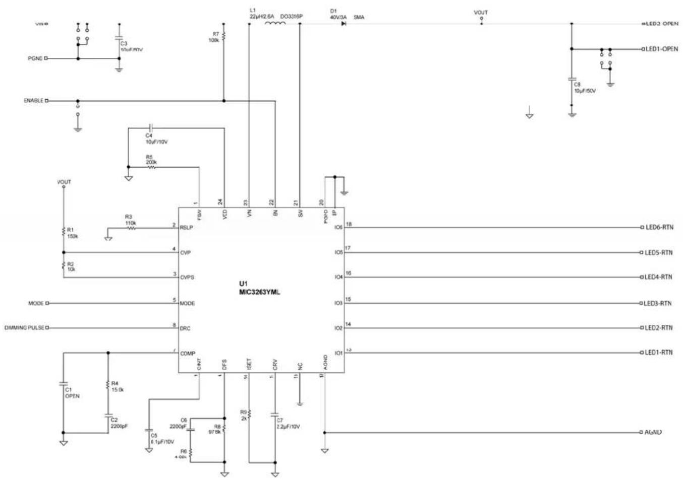
VIN PGND ENABLE VOUT R1 150k R3 110k R5 200k C4 10μF/10V R7 100k L1 22μH2.6A DO3316P D1 40V/3A SMA VOUT LED3 OPEN LED1-OPEN C8 10μF/50V U1 MIC3263YML R3 110k RSLP 24 VD 23 VN 22 BN 21 SW 20 POHD IP IO6 18 LED6-RTN IO5 17 LED5-RTN IO4 16 LED4-RTN IO3 15 LED3-RTN IO2 14 LED2-RTN IO1 13 LED1-RTN IO9 12 CINT DFS SET CRV NC COMP C1 OPEN R4 15.0k C2 2200pF C5 0.1μF/10V O6 2200pF R8 97.0k R9 2k C7 2.2μF/10V R6 + 0.0V AGNDFigure 1. Schematic Diagram
Evaluation Board Design Specifications
| Parameter | Minimum | Typical Maximum | |
| V_IN | 6V | ||
| Output Voltage 18-25 38V | |||
| Number of LEDs/Channel 4 8 10 | |||
| LED Current 15mA 30mA | |||
| Power Out 0 5W 7W | |||
| Efficiency | 90% | ||
| Switching Frequency (FIXED) | 400kHz | 1MHz | 1.8MHz |
| PWM Dim Frequency | 100Hz | 300Hz | 20kHz |
| Line Regulation | <±3% | ||
| Load Regulation | <±3% | ||
| Ambient Temperature | -40°C | +25°C | +85°C |
Table 1. Evaluation Board Design Specifications
Bill of Materials
| Item | Part Number | Manufacturer | Description | Qty. |
| C1 OPEN | ||||
| C2, C6 | 0603ZC222KAT2A | AVX^(1) | 2200pF, 10V, X7R, 0603 2 | |
| C1608X7R1H222K | TDK^(2) | |||
| GRM188R71H222K | muRata^(3) | |||
| C3, C8 | C5750X7R1H106M | TDK^(2) | 10μF, 50V, X7R, 2220 2 | |
| 22205C106KAZ2A | AVX^(1) | |||
| C4 | GRM21BR71A106KE51L | muRata^(3) | 10μF, 10V, X7R, 0805 1 | |
| 0805ZD106KAT2A | AVX^(1) | |||
| C5 | 0603YC104KAT2A | AVX^(1) | 0.1μF, 16V, X7R, 0603 1 | |
| C1608X7R1C104K | TDK^(2) | |||
| GRM188R71C104K | muRata^(3) | |||
| C7 | 0603ZD225KAT2A | AVX^(1) | 2.2μF, 10V, X5R, 0603 1 | |
| GRM188R61A225KE34D | muRata^(3) | |||
| C1608X5R1A225K | TDK^(2) | |||
| D1 | SK34A MCC | (4) | Schottky 3A, 40V (SMA) Inc. | 1 |
| B349LA-13 | Diode, (5) | |||
| L1 | DO3316P-223ML | Coilcraft(6) | 22μH, 2.6A | 1 |
| R1 | CRCW0603150KFKEA | Vishay Dale^(7) | 150k | 2 |
| R2 | CRCW060310K0FKEA | Vishay Dale^(7) | 10k | 1 |
| R3 | CRCW0603110KKFKEA | Vishay Dale^(7) | 110k (RSLP) | 1 |
| R4 | CRCW060315K0FKEA | Vishay Dale^(7) | 15.0k ( R_COMP ) | 1 |
| R5 | CRCW0603200KFKEA | Vishay Dale^(7) | 200k | 1 |
| R6 | CRCW060340K2FKEA | Vishay Dale^(7) | 4.02k | |
| R7 | CRCW0603100KFKEA | Vishay Dale^(7) | 100k | 1 |
| R8 | CRCW060326K7FKEA | Vishay Dale^(7) | 97.6k | 1 |
| R9 | CRCW06032K00FKEA | Vishay Dale^(7) | 2k | 1 |
| U1 | MIC3263YML | Micrel, Inc.(8) | Six-Channel WLED Driver for Backlighting Applications | 1 |
Notes:
1. AVX: www.avx.com.
2. TDK: www.tdk.com.
3. Murata Tel: www.murata.com.
4. MCC: www.mccsemi.com.
5. Diode, Inc.: www.diodes.com.
6. Coilcraft: www.coilcraft.com.
7. Vishay: www.vishay.com.
8. Micrel, Inc.: www.micrel.com.
Evaluation Board PCB Layout

Package Information

text_image
2.50 增值 Exp. DAP PIN #1 ID 0.400±0.05 R0.20 + 2 2.50 增值 Exp. DAP 0.25 增值 0.500 BSC 2.5000 Ref.BOTTOM VIEW
SIDE VIEW
NOTE:
-
ALL DIMENSIONS ARE IN MILLIMETERS.
-
MAX. PACKAGE WARPAGE IS 0.05 mm.
-
MAXIMUM ALLOWABE BURRS IS 0.076 nm IN ALL DIRECTIONS.
-
PIN #1 ID ON TOP WILL BE LASER/INK MARKED.
DIMENSION APPLIES TO METALIZED TERMINAL AND IS MEASURED BETWEEN 0.20 AND 0.25 mm FROM TERMINAL TIP.
- APPLIED ONLY FOR TERMINALS.
APPLIED FOR EXPOSED PAD AND TERMINALS.
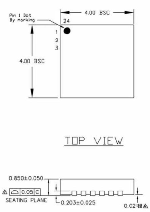
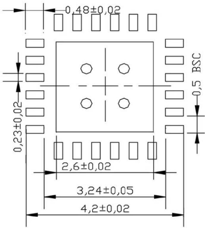
24-Pin 4mm x 4mm (MLF®)
Recommended Land Pattern
LP # MLF44Q-24LD-LP-1
All units are in mm
Tolerance ± 0.05 if not noted
text_image
0,48±0,02 0,23±0,02 2,6±0,02 3,24±0,05 4,2±0,02 0,5 BSCMICREL, INC. 2180 FORTUNE DRIVE SAN JOSE, CA 95131 USA
TEL +1 (408) 944-0800 FAX +1 (408) 474-1000 WEB http://www.micrel.com
The information furnished by Micrel in this data sheet is believed to be accurate and reliable. However, no responsibility is assumed by Micrel for its use. Micrel reserves the right to change circuitry and specifications at any time without notification to the customer.
Micrel Products are not designed or authorized for use as components in life support appliances, devices or systems where malfunction of a product can reasonably be expected to result in personal injury. Life support devices or systems are devices or systems that (a) are intended for surgical implant into the body or (b) support or sustain life, and whose failure to perform can be reasonably expected to result in a significant injury to the user. A Purchaser's use or sale of Micrel Products for use in life support appliances, devices or systems is a Purchaser's own risk and Purchaser agrees to fully indemnify Micrel for any damages resulting from such use or sale.
© 2010 Micrel, Incorporated.