HV9912DB1 - Electronic component Microchip - Free user manual and instructions
Find the device manual for free HV9912DB1 Microchip in PDF.

User questions about HV9912DB1 Microchip
0 question about this device. Answer the ones you know or ask your own.
Ask a new question about this device
Download the instructions for your Electronic component in PDF format for free! Find your manual HV9912DB1 - Microchip and take your electronic device back in hand. On this page are published all the documents necessary for the use of your device. HV9912DB1 by Microchip.
USER MANUAL HV9912DB1 Microchip
High Brightness Boost LED Driver Demoboard with 1:3000 Dimming Ratio and Hiccup Mode Protection
General Description
The HV9912DB1 is an LED driver demoboard capable of driving up to 20 one-watt LEDs in series from an input of 21 - 27VDC. It uses the Supertex HV9912 in a boost topology. The converter has very good initial regulation (+/-5%) and excellent line and load regulation over the entire input and output voltage range (<+/- 1%). The full load efficiency of the converter is typically greater than 90%.
The HV9912DB1 is protected against open LED and output short circuit conditions. It is also protected under input under-voltage conditions by limiting the input current. It has an excellent PWM dimming response, with typical rise and fall times less than 1.0 s, which allows high PWM dimming ratios. The switching frequency of the HV9912DB1 can be synchronized to other HV9912 boards or to an external 200kHz clock by connecting the clock to the SYNC pin of the HV9912DB1.
The HV9912DB1 features hiccup mode short circuit and open LED protection. Upon detection of either fault condition, the IC shuts down the driver and periodically attempts to restart until the fault condition ends. The HV9912DB1 also features a built-in 500ns blanking to prevent false tripping of the over-current comparator due to parasitic capacitance spikes during PWM dimming.
Specifications
| Parameter Value | |
| Input voltage (steady state): 21 - 27VDC | |
| Output LED string voltage: 35V min - 80V max | |
| Output current: 350mA +/-5% | |
| Output current ripple: 10% typical | |
| Switching frequency: 200kHz | |
| Full load efficiency: 93% (at 24V input) | |
| Open LED protection: Shuts down at 92V | |
| Output short circuit protection: | Included |
| Input under voltage protection: | Included |
| PWM dimming: | 1:3000 dimming ratio at 200Hz |
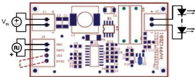
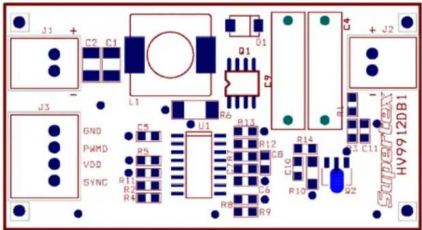
Board Layout and Connection Diagram
natural_image
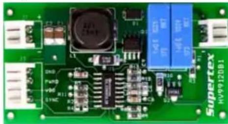
Close-up of a green printed circuit board with integrated circuits and components (no readable text or symbols)Actual size: 64.0mm x 34.5mm
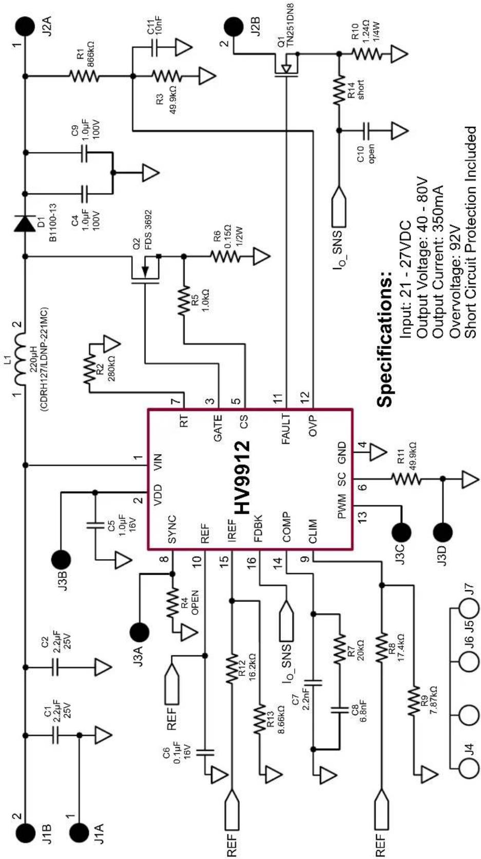
text_image
V_IN + - 23 DIN0 PAMPS VDD SYNC L1 Q1 Q2 Q3 Q4 Q5 Q6 Q7 Q8 Q9 Q10 Q11 Q12 Q13 Q14 Q15 Q16 Q17 Q18 Q19 Q20 Q21 Q22 Q23 Q24 Q25 Q26 Q27 Q28 Q29 Q30 Q31 Q32 Q33 Q34 Q35 Q36 Q37 Q38 Q39 Q40 Q41 Q42 Q43 Q44 Q45 Q46 Q47 Q48 Q49 Q50 Q51 Q52 Q53 Q54 Q55 Q56 Q57 Q58 Q59 Q60 Q61 Q62 Q63 Q64 Q65 Q66 Q67 Q68 Q69 Q70 100Ω 1.6V AHConnections
Input - The input is connected between the terminals of connector J1 as shown in the Connection Diagram.
Output - The output is connected between the terminals of connector J2 as shown.
Enable/PWM Dimming - To just enable the board, short pins PWMD and VDD of connector J3 as shown by the dashed lines. To PWM dim the board, connect the external push-pull waveform source between terminals PWMD and GND of connector J3 as shown by the solid lines.
SYNC - To synchronize two or more boards, connect the SYNC pins of all the boards together. To synchronize the HV9912DB1 to an external 200kHz clock, connect the clock between the SYNC and GND pins of terminal J3.
Note:
During PWM dimming, pin 2 of connector J3 should be left open. Also, the PWM signal must have the proper polarity with the positive connected to pin 3 of J3. Note that pin 4 of J3 is internally connected to the return path of the input voltage.
Testing The Demoboard
Normal Operation: Connect the input source and the output LEDs as shown in the Connection Diagram and enable the board. The LEDs will glow with a steady intensity. Connecting an ammeter in series with the LEDs will allow measurement of the LED current. The current will be 350mA +/- 5%.
Current Regulation: With the input power to the converter disconnected, change the LED string voltage within the specifications mentioned. The current output of the HV9912DB1 will remain very steady over the entire load range. Vary the input voltage while the circuit is operational. The current will be regulated over the entire line range.
Open LED test: Connect a voltmeter across the output terminals of the HV9912DB1. Start the demoboard normally, and once the LED current reaches steady state, unplug one end of the LED string from the demoboard. The output voltage will rise to about 92V and the HV9912DB1 will shut down. Once the LED string is reconnected, the driver will start regulating current.
Short Circuit Test: When the HV9912DB1 is operating in steady state, connect a jumper across the terminals of the LED string. Notice that the output current will immediately go to zero and the converter will shut down. Removing the jumper will cause the HV9912DB1 to restart and continue to regulate the LED current.
PWM Dimming: With the input voltage to the board disconnected, apply a TTL compatible, push-pull square wave signal between PWMD and GND terminals of connector J3 as shown in the Connection Diagram. Turn the input voltage back on and adjust the duty cycle and/or frequency of the PWM dimming signal. The output current will track the PWM dimming signal. Note that although the converter operates perfectly well at 1.0kHz PWM dimming frequency, the widest PWM dimming ratio can be obtained at lower frequencies like 100 or 200Hz.
Typical Results
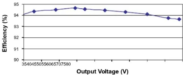
- Efficiency: The efficiency of the converter at various LED string voltages are shown in Fig.1 (measured at the nominal input voltage of 24V). Fig.2 shows the full load efficiency of the converter at varying input voltages. The minimum efficiency of 93% for the converter occurs at 21V input and full load output.
line
| Output Voltage (V) | Efficiency (%) | | ------------------ | -------------- | | 3540 | 94.2 | | 455 | 94.3 | | 556 | 94.4 | | 606 | 94.5 | | 707 | 94.6 | | 7580 | 94.7 | | 800 | 94.6 | | 850 | 94.5 | | 900 | 94.4 | | 950 | 94.3 | | 1000 | 94.2 | | 1050 | 94.1 | | 1100 | 94.0 | | 1150 | 93.9 | | 1200 | 93.8 | | 1250 | 93.7 | | 1300 | 93.6 |Fig. 1 Efficiency vs. Output Voltage

line
| Input Voltage (V) | Efficiency (%) | | ----------------- | -------------- | | 2022242628 | 93.0 | | 10^4 | 94.5 | | 10^5 | 94.7 | | 10^6 | 94.3 | | 10^7 | 94.2 |Fig. 2 Efficiency vs. Input Voltage
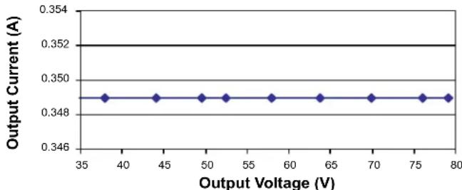
- Current Regulation: Figs. 3 and 4 show the output current regulation vs. output voltage and input voltage respectively. The total current regulation (line and load combined) is found to be less than 1%.
line
| Output Voltage (V) | Output Current (A) | | ------------------ | ------------------ | | 35 | 0.349 | | 40 | 0.349 | | 45 | 0.349 | | 50 | 0.349 | | 55 | 0.349 | | 60 | 0.349 | | 65 | 0.349 | | 70 | 0.349 | | 75 | 0.349 | | 80 | 0.349 |Fig. 3 Output Current vs. Output Voltage

line
| Input Voltage (V) | Output Current (A) | | ----------------- | ------------------ | | 21 | 0.349 | | 22 | 0.349 | | 23 | 0.3485 | | 24 | 0.348 | | 25 | 0.3475 | | 26 | 0.347 | | 27 | 0.3465 |Fig. 4 Output Current vs. Input Voltage
- Input Under Voltage Protection: Input under voltage protection is provided by limiting the input current at low input voltages. Fig. 5 shows the output and input currents at voltages less than the minimum rated voltage. The LED current will decrease as the input voltage falls and the input current limits to about 1.4A. Note that the input current limit is not a hard limit as the slope compensation added to the peak current sense signal will allow a small change in the input current with a decrease in the input voltage.

line
| Input Voltage (V), Sweep | Output Current (A) | Input Current (A) | | ------------------------ | ------------------ | ----------------- | | 0 | 0.15 | 1.5 | | 10152025 | 0.3 | 1.2 |Fig. 5 Input Under-Voltage Behavior
- Open LED Protection: Figs 6 and 7 show the hiccup-mode over voltage protection. Fig. 6 shows the open LED condition occurs when the LED current goes to zero. At that point, the inductor current charges the output capacitor and the COMP voltage rails to V_DD . Once the output voltage reaches the over voltage threshold, the converter shuts down and the output voltage slowly decays because the output capacitor is discharged by the over-voltage sensing resistor network. Once the output voltage falls to 90% of its trip point, the converter tries to restart. Since the fault conditions still persists, the converter shuts down almost immediately. Thus, the HV9912 maintains the output voltage in a band until the LED reconnects.
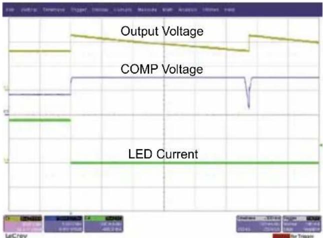
line
| Signal | Value | |-----------------|-------| | Output Voltage | High | | COMP Voltage | Low | | LED Current | High |Fig. 6 Open LED Condition
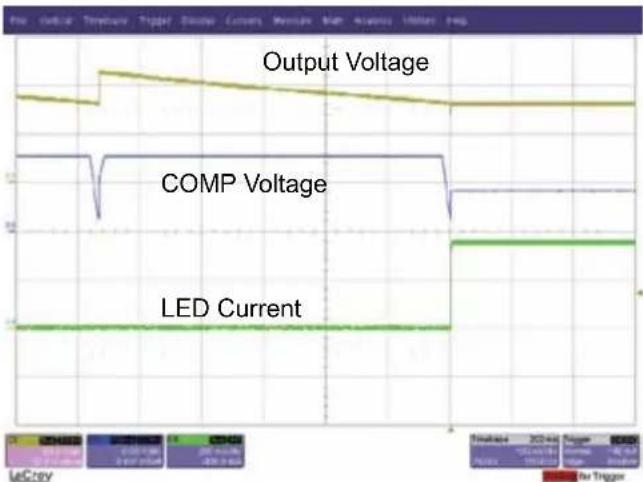
Fig. 7 Recovery from an Open LED Condition
Fig. 7 shows the recovery of the HV9912DB1 from an over voltage condition. In this case, the LED has reconnected at some point when the converter is turned off. When the converter attempts to restart, if finds the fault condition has disappeared and it starts up normally. There is no overshoot in the LED current.
Short Circuit Protection: Figs 8 and 9 show the operation of the short circuit protection in the HV9912DB1. In Fig. 8, the onset of the output short circuit is indicated by the first spike in the LED current. At this point, the HV9912DB1 shuts down and the hiccup mode protection takes over. A constant current source charges the COMP pin to 5.0V and then another current source discharges it to 1.0V. This charge/discharge cycle determines the hiccup time. When the COMP pin reaches 1.0V, the converter attempts to restart and finding the fault condition still present, shuts down again.

line
| Time | Output Voltage (V) | COMP Voltage (V) | LED Current (V) | |------|---------------------|-------------------|-----------------| | 0 | 1.0 | 0.8 | 0.0 | | 120 | 1.0 | 0.8 | 0.0 |Fig. 8 Short Circuit Condition
Fig. 9 shows the recovery of the HV9912DB1 from a short circuit condition. It can be seen that the LED current recovers normally with no overshoots.
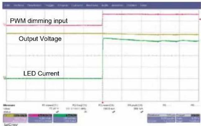
6. PWM Dimming: The rise and fall transitions of the LED current during PWM dimming are shown in Figs. 10 and 11,
at output voltages of 80V and 40V respectively. The timescale for all waveforms is set at 5.0μs/div. The rise and fall times are less than 1.0μs in each case. Thus, a PWM dimming ratio of 1:3000 is achievable at a PWM dimming frequency of 200Hz.
line
| Metric | Value | | ---------------- | --------- | | PWM dimming input | 100V | | Output Voltage | 100V | | LED Current | 500A |Fig. 10a Rise time of LED Current at 80V output (5.0μs/div)

line
| Time (s) | PWM dimming input | Output Voltage | LED Current | |----------|-------------------|----------------|-------------| | 0 | 123.64 | 123.64 | 123.64 | | 5 | 123.64 | 123.64 | 123.64 | | 10 | 123.64 | 123.64 | 123.64 | | 15 | 123.64 | 123.64 | 123.64 | | 20 | 123.64 | 123.64 | 123.64 | | 25 | 123.64 | 123.64 | 123.64 | | 30 | 123.64 | 123.64 | 123.64 | | 35 | 123.64 | 123.64 | 123.64 | | 40 | 123.64 | 123.64 | 123.64 | | 45 | 123.64 | 123.64 | 123.64 | | 50 | 123.64 | 123.64 | 123.64 | | 55 | 123.64 | 123.64 | 123.64 | | 60 | 123.64 | 123.64 | 123.64 | | 65 | 123.64 | 123.64 | 123.64 | | 70 | 123.64 | 123.64 | 123.64 | | 75 | 123.64 | 123.64 | 123.64 | | 80 | 123.64 | 123.64 | 123.64 | | 85 | 123.64 | 123.64 | 123.64 | | 90 | 123.64 | 123.64 | 123.64 | | 95 | 123.64 | 123.64 | 123.64 | | 100 | 123.64 | 123.64 | 123.64 | | 105 | 123.64 | 123.64 | 123.64 | | 110 | 123.64 | 123.64 | 123.64 | | 115 | 123.64 | 123.64 | 123.64 | | 120 | 123.64 | 123.64 | 123.64 | | 125 | 123.64 | 123.64 | 123.64 | | 130 | 123.64 | 123.64 | 123.64 | | 135 | 123.64 | 123.64 | 123.64 | | 140 | 123.64 | 123.64 | 123.64 | | 145 | 123.64 | 123.64 | 123.64 | | 150 | 123.64 | 123.64 | 123.64 | | 155 | 123.64 | 123.64 | 123.64 | | 160 | 123.64 | 123.64 | 123.64 | | 165 | 123.64 | 123.64 | 123.64 | | 170 | 123.64 | 123.64 | 123.64 | | 175 | 123.64 | 123.64 | 123.64 | | 180 | 123.64 | 123.64 | 123.64 | | 185 | 123.64 | 123.64 | 123.64 | | 190 | 123.64 | 123.64 | 123.64 | | 195 | 123.64 | 123.64 | 123.64 | | 200 | 123.64 | 123.64 | 123.64 | | ... | ... | ... | ... | | Peak | - | - | - | | Low | - | - | - | | High | - | - | - | | Current | - | - | - | | Current (Peak) - Low: ~5e-5V; Current: ~5e-5V; Current: ~5e-5V; Current: ~5e-5V; Current: ~5e-5V; Current: ~5e-5V; Current: ~5e-5V; Current: ~5e-5V; Current: ~5e-5V; Current: ~5e-5V; Current: ~5e-5V; Current: ~5e-5V; Currents: ~5e-5V; Currents: ~5e-5V; Currents: ~5e-5V; Currents: ~5e-5V; Currents: ~5e-5V; Currents: ~5e-5V; Currents: ~5e-5V; Currents: ~5e-5V; Currents: ~5e-5V; Currents: ~5e-5V; Current s: - | | Peak | - | - | - | | Low | - | - | - | | High | - | - | - | | Current | - | - | - | | Current (Peak) - Low: ~5e-5V; Current: ~5e-5V; Current: ~5e-5V; Current: ~5e-5V; Current: ~8x-8x-8x; Current: ~8x-8x-8x; Current: ~8x-8x-8x; Current: ~8x-8x-8x; Current: ~8x-8x-8x; Currents: ~8x-8x-8x; Currents: ~8x-8x-8x; Currents: ~8x-8x-8x; Currents: ~8x-8x-8x; Currents: ~8x-8x-8x; Currents: ~8x-8x-8x; Currents: ~8x-8x-8x; Currents: ~8x-8x-7x; Currents: ~8x-8x-7x; Currents: ~8x-8x-7x; Currents: ~8x-8x-7x; Currents: ~8x-8x-7x; Currents: ~8x-8x-7x; Currents: ~8x-8x-7x; Currents: ~8x-8x-7x; Currents: ~8x -7x-7x; Currents: ~8x-7x-7x; Currents: ~8x-7x-7x; Currents: ~8x-7x-7x; Currents: ~8x-7x-7x; Currents: ~8x-7x-7x; Currents: ~8x -7x-7x; Currents: ~8x-7x-7x; Currents: ~8x -7x-7x; Currents: ~8x -7x-7x; Currents: ~8x -7x-7x; Currents: ~8x -7x-7x; Currents: ~8x -7x-7x; Currents: ~8x -7x -7x; Currents: ~8x -7x -7x; Currents: ~8x -7x -7x; Currents: ~8x -7x -7x; Currents: ~8x -7x -7x; Currents: ~8x -7x -7x; Currents: ~8x -7x -7x; Currents: ~8x -7m, - | | Peak | - | - | - | | Low | - | - | - | | High | - | - | - | | Current | - | - | - | | Current (Peak) - Low: ~5e-5V; Current: ~5e-5V; Current: ~5e-5V; Current: ~8x-8x-8x; Current: ~8x-8x-8x; Current: ~8x-8x-8x; Currents: ~8x-8x-8x; Currents: ~8x-8x-8x; Currents: ~8x-8x-8x; Currents: ~8x-8m, - | | Low | - | - | - | | High | - | - | - | | Current (Peak) - Low: ~5e-5V; Current: ~5e-5V; Current: ~5e-5V; Current: ~8e-8y-8y-8y; Current: ~8e-8y-8y-8y; Currents: ~8e-8y-8y-8y; Currents: ~8e-8y-8y-8y; Currents: ~8e-8y-7m, - | | Low | - | - | - | | High | - | - | - | | Current (Peak) - Low: ~5e-5V; Current: ~5e-5V; Current: ~5e-5V; Current: ~8e-8y-8y-8y; Currents: ~8e-8y-8y-8y; Currents: ~8e-8y-7m, - | | Low | - | - | - | | High | - | - | - | | Current (Peak) - Low: ~5e-5V; Current: ~5e-5V; Currents: ~5e-5V; Currents: ~8e-8y-8y-8y; Currents: ~8e-8y-8y-8y; Currents: ~8e-8y-7m, - | | Low | - | - | - | | High | - | - | - | | Current (Peak) - Low: ~5e-5V; Currents : <--> , <--> , <--> , <--> , <--> , <--> , <--> , <--> , <--> , <--> , <--> , <--> , <--> , <--> , <--> , <--> , <--> , <--> , <--> , <--> , <--> , <--> , <--> , <--> , <--> , <-->Fig. 11a Rise time of LED Current at 40V output (5.0μs/div)
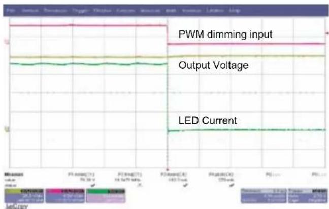
Fig. 10b Fall time of LED Current at 80V output (5.0μs/div)

line
| Time (s) | PWM dimming input (V) | Output Voltage (V) | LED Current (V) | |----------|------------------------|--------------------|-----------------| | 0 | 0.5 | 0.2 | 0 | | 10 | 0.5 | 0.2 | 0 | | 20 | 0.5 | 0.2 | 0 | | 30 | 0.5 | 0.2 | 0 | | 40 | 0.5 | 0.2 | 0 | | 50 | 0.5 | 0.2 | 0 | | 60 | 0.5 | 0.2 | 0 | | 70 | 0.5 | 0.2 | 0 | | 80 | 0.5 | 0.2 | 0 | | 90 | 0.5 | 0.2 | 0 | | 100 | 0.5 | 0.2 | 0 | | 110 | 0.5 | 0.2 | 0 | | 120 | 0.5 | 0.2 | 0 | | 130 | 0.5 | 0.2 | 0 | | 140 | 0.5 | 0.2 | 0 | | 150 | 0.5 | 0.2 | 0 | | 160 | 0.5 | 0.2 | 0 | | 170 | 0.5 | 0.2 | 0 | | 180 | 0.5 | 0.2 | 0 | | 190 | 0.5 | 0.2 | 0 | | 200 | 0.5 | 0.2 | 0 | | 210 | 0.5 | 0.2 | 0 | | 220 | 0.5 | 0.2 | 0 | | 230 | 0.5 | 0.2 | 0 | | 240 | 0.5 | 0.2 | 0 | | 250 | 0.5 | 0.2 | 0 | | 260 | 0.5 | 0.2 | 0 | | 270 | 0.5 | 0.2 | 0 | | 280 | 0.5 | 0.2 | 0 | | 290 | 0.5 | 0.2 | 0 | | 300 | 0.5 | 0.2 | 0 | | 310 | 0.5 | 0.2 | 0 | | 320 | 0.5 | 0.2 | 0 | | 330 | 0.5 | 0.2 | 0 | | 340 | 0.5 | 0.2 | 0 | | 350 | 0.5 | 0.2 | 0 | | 360 | 0.5 | 0.2 | 0 | | 370 | 0.5 | 0.2 | 0 | | 380 | 0.5 | 0.2 | 0 | | 390 | 0.5 | 0.2 | 0 | | 400 | 0.5 | 0.2 | 0 | | 410 | 0.5 | 0.2 | 0 | | 420 | 0.5 | 0.2 | 0 | | 430 | 0.5 | 0.2 | 0 | | 440 | 0.5 | 0.2 | 0 | | 450 | 0.5 | 0.2 | 0 | | 460 | 0.5 | 0.2 | 0 | | 470 | 0.5 | 0.2 | 0 | | 480 | 0.5 | 0.2 | 0 | | 490 | 0.5 | 0.2 | 0 | | 500 | 0.5 | 0.2 | 0 | | ... | ... | ... | ... | | Peak | - | - | - | | Low | - | - | - | | Peak | - | - | - | | Low | - | - | - | | Peak | - | - | - | | Low | - | - | - | | Peak | - | - | - | | Low | - | - | - | | Peak | - | - | - | | Low | - | ... | ... | | Peak | - | ... | ... | | Low | - | ... | ... | | Peak | - | ... | ... | | Low | - | ... | ... | | Peak | - | ... | ... | | Low | - | ... | ... | | Peak | - | ... | ... | | Low | - | ... | ... | | Peak | - |... | ... | | Low | - | ... | ... | | Peak | - | ... | ... | | Low | - | ... | ... | | Peak | - | ... | ... | | Low | - | ... | ... | | Peak | - | ... | ... | | Low | - | ... | ... | | Peak }Fig. 11b Fall time of LED Current at 40V output (5.0μs/div)
Silk Screen
text_image
J1 + C2 C1 L1 Q1 D1 C9 + J2 J3 GND PWMD VDD SYNC C5 RS R11 R2 R4 U1 R6 R13 R12 C7 R7 C8 C6 R8 R9 R14 C10 R10 Q2 C3 C11 SUPPLYX HV9912DB1Circuit Schematic:
text_image
HV9912 Specifications: Input: 21 - 27VDC Output Voltage: 40 - 80V Output Current: 350mA Overvoltage: 92V Short Circuit Protection IncludedBill of Materials
| # Quan Ref Des Description Package Manufacturer | Manufacturer's Part Number | |||||
| 1 2 | C1,C2 | 2.2μF, 25V | X7R ceramic chip capacitor SMD1210 TDK Corp C3225X7R1H225K | |||
| 2 2 | C4,C9 | 1μF, 100V | metal polyester capacitor Radial EPCOS Inc B32522C1105J | |||
| 3 | 1 | C5 | 1μF, 16V X7R ceramic chip capacitor | SMD0805 | TDK Corp | C2012X7R1C105K |
| 4 | 1 | C6 | 0.1μF, 16V X7R ceramic chip capacitor | SMD0805 | Murata | GRM219R71C104KA01D |
| 5 1 | C7 | 2.2nF, 5%, 50V C0G ceramic chip capacitor | SMD0805 | TDK Corp | C2012C0G1H222J | |
| 6 1 | C8 | 6.8nF, 5%, 50V C0G ceramic chip capacitor | SMD0805 | TDK Corp | C2012C0G1H682J | |
| 7 | 1 | C11 | 10nF, 50V X7R ceramic chip capacitor | SMD0805 | TDK Corp | C2012X7R1H103K |
| 8 | 1 | D1 | 100V, 1.0A schottky diode | SMA | Diodes Inc. | B1100-13 |
| 9 | 2 | J1,J2 | Side Entry 2-pin male header | Thru-Hole | JST Sales | S2B-EH |
| 10 | 1 | J3 | Side Entry 4-pin male header | Thru-Hole | JST Sales | S4B-EH |
| 11 | 1 | L1 | 220μH, 2.0A sat, 1.5A rms inductor | SMT | Sumida | CDRH127/LDNP-221MC |
| 12 | 1 | Q1 | 100V, 4.55A N-Channel MOSFET | SO-8 | Fairchild | FDS3692 |
| 13 | 1 | Q2 | 100V, 1.5Ω N-Channel MOSFET | SOT-89 | Supertex | TN2510N8 |
| 14 | 1 | R1 | 866kΩ, 1%, 1/8W chip resistor | SMD0805 | Yageo | RC0805FR-07866KL |
| 15 | 1 | R2 | 280kΩ, 1%, 1/8W chip resistor | SMD0805 | Yageo | RC0805FR-07280KL |
| 16 | 2 | R3, R11 | 49.9kΩ, 1%, 1/8W chip resistor | SMD0805 | Yageo | RC0805FR-0749K9L |
| 17 | 1 | R4, C10 | open | --- | --- | --- |
| 18 | 1 | R5 | 1.0kΩ, 1%, 1/8W chip resistor | SMD0805 | Yageo | RC0805FR-071KL |
| 19 | 1 | R6 | 0.15Ω, 1%, 1/2W chip resistor | SMD2010 | Vishay/ Dale | WSL2010R1500FEA |
| 20 | 1 | R7 | 20kΩ, 1%, 1/8W chip resistor | SMD0805 | Yageo | RC0805FR-0720KL |
| 21 | 1 | R8 | 17.4kΩ, 1%, 1/8W chip resistor | SMD0805 | Yageo | RC0805FR-0717K4L |
| 22 | 1 | R9 | 7.87kΩ, 1%, 1/8W chip resistor | SMD0805 | Yageo | RC0805FR-077K87L |
| 23 | 1 | R10 | 1.24Ω, 1%, 1/4W chip resistor | SMD1206 | Yageo | RC1206FR-071R24L |
| 24 | 1 | R12 | 16.2kΩ, 1%, 1/8W chip resistor | SMD0805 | Yageo | RC0805FR-0716K2L |
| 25 | 1 | R13 | 8.66kΩ, 1%, 1/8W chip resistor | SMD0805 | Yageo | RC0805FR-078K66L |
| 26 | 1 | R14 | 0.0Ω, 1/8W chip resistor | SMD0805 | Panasonic | ERJ-6GEY0R00V |
| 27 | 1 | U1 | Switchmode LED Driver with High Current Accuracy | SO-16 | Supertex | HV9912NG |
Supertex inc. does not recommend the use of its products in life support applications, and will not knowingly sell them for use in such applications unless it receives an adequate "product liability indemnification insurance agreement." Supertex Inc. does not assume responsibility for use of devices described, and limits its liability to the replacement of the devices determined defective due to workmanship. No responsibility is assumed for possible omissions and inaccuracies. Circuitry and specifications are subject to change without notice. For the latest product specifications refer to the Supertex Inc. (website: http://www.supertex.com)