MIC45404 - Electronic component Microchip - Free user manual and instructions
Find the device manual for free MIC45404 Microchip in PDF.

User questions about MIC45404 Microchip
0 question about this device. Answer the ones you know or ask your own.
Ask a new question about this device
Download the instructions for your Electronic component in PDF format for free! Find your manual MIC45404 - Microchip and take your electronic device back in hand. On this page are published all the documents necessary for the use of your device. MIC45404 by Microchip.
USER MANUAL MIC45404 Microchip
19V 5A Ultra-Low Profile DC-to-DC Power Module
Features
- Input Voltage Range: 4.5V to 19V
• Output Current: Up to 5A - 82% Peak Efficiency at 12VIN, 0.9VOUT
- Pin-Selectable Output Voltages: 0.7V, 0.8V, 0.9V, 1.0V, 1.2V, 1.5V, 1.8V, 2.5V, 3.3V
• ±1% Output Voltage Accuracy
• Supports Safe Pre-Biased Start-Up - Pin-Selectable Current Limit
• Pin-Selectable Switching Frequency - Internal Soft Start
- Thermal Shutdown
• Hiccup Mode Short-Circuit Protection
• Available in a 54-Lead 6 mm x 10 mm QFN Package
• Ultra-Low Profile: 2.0 mm Height - -40°C to +125°C Junction Temperature Range
General Description
The MIC45404 device is an ultra-low profile, synchronous step-down regulator module, featuring a unique 2.0 mm height. The module incorporates a DC-to-DC regulator, bootstrap capacitor, high-frequency input capacitor and an inductor in a single package. The module pinout is optimized to simplify the Printed Circuit Board (PCB) layout process.
This highly-integrated solution expedites system design and improves product time to market. The internal MOSFETs and inductor are optimized to achieve high efficiency at low output voltage. Due to the fully optimized design, MIC45404 can deliver up to 5A current with a wide input voltage range of 4.5V to 19V.
The MIC45404 is available in a 54-lead 6 mm x 10 mm x 2.0 mm QFN package with a junction operating temperature range from -40°C to +125°C, which makes an excellent solution for systems in which PCB real-estate and height are important limiting factors, and air flow is restricted.
Applications
- Servers, Data Storage, Routers and Base Stations
• FPGAs, SSD, DSP and Low-Voltage ASIC Power
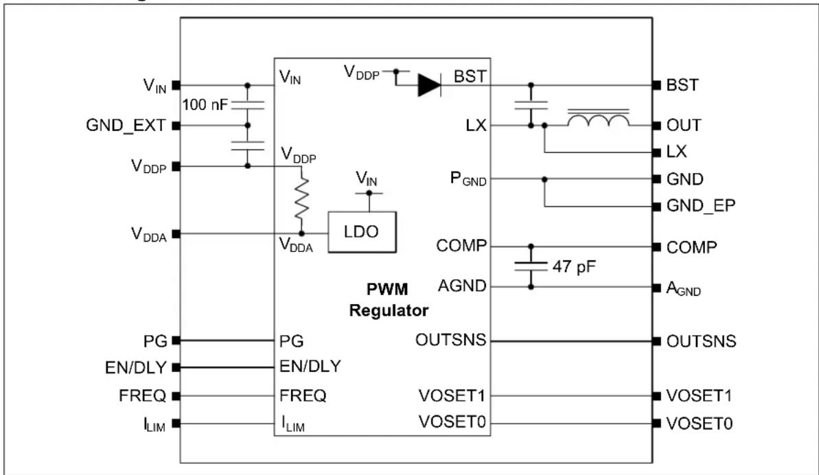
Typical Application

text_image
VDDA 4.5V to 19V VIN VDDA GND OUT OUTSNS GND COMP VDDA Frequency Selection FREQ MIC45404 VOSET1 Current Limit Selection ILIM PG EN/DLY VOSET0 Output Voltage Selection VDDA Power-Good ■ Enable ■MIC45404 12V 5A DC-to-DC Converter
Package Types
other
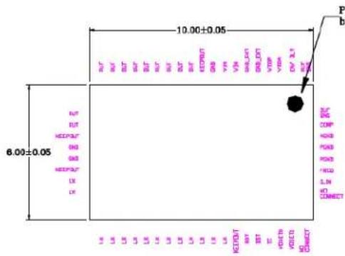
| Label | Value | |-------------|-------| | OUT19 | 18 | | OUT | 17 | | OUT | 16 | | OUT | 15 | | OUT | 14 | | OUT | 13 | | OUT | 12 | | OUT | 11 | | GND | 10 | | V_IN | 9 | | V_IN | 8 | | GND_EXT | 7 | | GND_EXT | 6 | | VDDP | 5 | | VDDA | 4 | | EN/DLY | 3 | | OUTSNS | 2 | | OUTSNS | 1 | | COMP | 54 | | AGND | 53 | | GND | 52 | | GND | 51 | | GND | 50 | | FREQ | 49 | | ILIM | 48 | | NC | 47 | | GND_EP | 46 | | GND_EP | 45 | | GND_EP | 44 | | GND_EP | 43 | | GND_EP | 42 | | GND_EP | 41 | | GND_EP | 39 | | GND_EP | 38 | | GND_EP | 37 | | GND_EP | 36 | | GND_EP | 35 | | GND_EP | 34 | | GND_EP | 33 | | GND_EP | 32 | | GND_EP | 31 | | GND_EP | 30 | | GND_EP | 29 | | GND_EP | 28 | | LX | 26 | | LX | 27 | * Includes Exposed Thermal Pad (EP); see Table 3-1.Functional Diagram
text_image
VIN 100 nF GND_EXT VDDP VDDA PG EN/DLY FREQ ILIM VIN VDDP VDDA VDDP LDO PWM Regulator VDDP BST LX PGND COMP AGND 47 pF BST OUT LX GND GND_EP COMP AGND PG EN/DLY FREQ ILIM OUTSNS VOSET1 VOSET0 OUTSNS VOSET1 VOSET01.0 ELECTRICAL CHARACTERISTICS
Absolute Maximum Ratings†
V_IN to A_GND ...... -0.3V to +20V
V_DDP, V_DDA to A_GND ....-0.3V to +6V
V_DDP to V_DDA ....-0.3V to +0.3V
VOSETX, FREQ, I_LIM , to A_GND -0.3V to +6V
BST to LX....-0.3V to +6V
BST to A_GND -0.3V to +26V
EN/DLY to A_GND -0.3V to V_DDA + 0.3V , +6V
PG to A_GND -0.3V to +6V
COMP, OUTSNS to A_GND -0.3V to V_DDA + 0.3V , +6V
A_GND to GND -0.3V to +0.3V
Junction Temperature ....+150°C
Storage Temperature ( T_S )....-65°C to +150°C
Lead Temperature (soldering, 10s) 260°C
ESD Rating ^(1)
HBM 2kV
MM 150V
CDM 1500V
Notice: Stresses above those listed under “Maximum Ratings” may cause permanent damage to the device. This is a stress rating only and functional operation of the device at those or any other conditions above those indicated in the operational sections of this specification is not intended. Exposure to maximum rating conditions for extended periods may affect device reliability.
Note 1: Devices are ESD-sensitive. Handling precautions are recommended. Human body model, 1.5 kΩ in series with 100 pF.
Operating Ratings ^(1)
Supply Voltage ( V_IN ) 4.5V to 19V
Externally Applied Analog and Drivers Supply Voltage ( V_IN = V_DDA = V_DDP ) 4.5V to 5.5V
Enable Voltage (EN/DLY).... 0V to V_DDA
Power Good (PG) Pull-up Voltage (VPU_PG) 0V to 5.5V
Output Current 5A
Junction Temperature ( T_J ) -40^ to +125^
Note 1: The device is not ensured to function outside the operating range.
ELECTRICAL CHARACTERISTICS ^(1)
| Electrical Specifications: unless otherwise specified, V_IN = 12V ; C_VDDA = 2.2 μF, T_A = +25°C .Boldface values indicate -40°C ≤ T_J ≤ +125°C. | ||||||
| Parameter Symbol | Min. Typ. Max. | Units Test Conditions | ||||
| V_IN Supply | ||||||
| Input Range V | IN | 4.5 — | 19 V | |||
| Disable Current I | VINQ | — | 33 | 60 | μA | EN/DLY = 0V |
| Operating Current | I_VINOP | — | 5.35 | 8.5 | mA | EN/DLY > 1.28V,OUTSNS = 1.15 x V_OUT(NOM) ,no switching |
| V_DDA 5V Supply | ||||||
| Operating Voltage | V_DDA | 4.8 | 5.1 | 5.4 | V | EN/DLY > 0.58V, I_VDDA = 0 mA to 10 mA |
| Dropout Operation | 3.6 | 3.75 | — | V | V_IN = 4.5V , EN/DLY > 0.58V, I_VDDA = 10 mA | |
| V_DDA Undervoltage Lockout | ||||||
| V_DDA UVLO Rising | UVLO_R | 3.1 | 3.5 | 3.9 | V | V_DDA Rising, EN/DLY > 1.28V |
| V_DDA UVLO Falling | UVLO_F | 2.87 | 3.2 | 3.45 | V | V_DDA Falling, EN/DLY > 1.28V |
| V_DDA UVLO Hysteresis | UVLO_H | — | 300 | — | mV | |
| EN/DLY Control | ||||||
| LDO Enable Threshold | EN_LDO_R | — | 515 | 600 | mV | Turns on V_DDA LDO |
| LDO Disable Threshold | EN_LDO_F | 450 | 485 | — | mV | Turns off V_DDA LDO |
| LDO Threshold Hysteresis | EN_LDO_H | — | 30 | — | mV | |
| EN/DLY Rising Threshold | EN_R | 1.14 | 1.21 | 1.28 | V | Initiates power stage operation |
| EN/DLY Falling Threshold | EN_F | — | 1.06 | — | V | Stops power stage operation |
| EN/DLY Hysteresis | EN_H | — | 150 | — | mV | |
| EN/DLY Pull-up Current | EN_I | 1 | 2 | 3 | μA | |
| Switching Frequency | ||||||
| ProgrammableFrequency (High Z) | f_SZ | 360 | 400 | 440 | kHz | FREQ = High Z (open) |
| Programmable Frequency 0 f | s_0 | 500 | 565 | 630 | kHz | FREQ= Low (GND) |
| Programmable Frequency 1 f | s_1 | 700 | 790 | 880 | kHz | FREQ = High ( V_DDA ) |
| Overcurrent Protection | ||||||
| HS Current Limit 0 | I_LIM\_HS0 | 6.0 | 7.1 | 8.1 | A | I_LIM = Low (GND) |
| HS Current Limit 1 | I_LIM\_HS1 | 8.1 | 9.3 | 10.3 | A | I_LIM = High (V_DDA) |
| HS Current Limit High Z | I_LIM\_HSZ | 9.3 | 10.5 | 11.9 | A | I_LIM = High Z (open) |
| Top FET Current LimitLeading-Edge Blanking Time | LEB | — | 108 | — | ns | |
| LS Current Limit 0 | I_LIM\_LS0 | 3.0 | 4.6 | 6.3 | A | I_LIM = Low (GND) |
| LS Current Limit 1 | I_LIM\_LS1 | 4.0 | 6.2 | 7.9 | A | I_LIM = High (V_DDA) |
| LS Current Limit High Z | I_LIM\_LSZ | 5.0 | 6.8 | 8.6 | A | I_LIM = High Z (Open) |
| OC Events Count for Hiccup | IN_HICC\_DE | — | 15 | — | ClockCycles | Number of subsequent cyclesin current limit before enteringhiccup overload protection |
| Hiccup Wait Time | t_HICC\_WAIT | — | 3 x SoftStart Time | — | Duration of the High Z state onLX before new soft start | |
| Parameter | Symbol | Min. | Typ. | Max. | Units | Test Conditions |
| Pulse-Width Modulation (PWM) | ||||||
| Minimum LX On Time T | ON(MIN) | — | 2 | 6 | — | A≠ T_J =+25°C T |
| Minimum LX Off Time T | OFF(MIN) | 90 135 | 190 ns V | IN=VDDA=5V, OUTSNS=3V,FREQ=Open (400 kHz setting),VOSET0=VOSET1=0V(3.3V setting),TA=TJ=+25°C | ||
| Minimum Duty Cycle D | MIN | — | 0 | — | % | OUTSNS>1.1× V_OUT(NOM) |
| Gm Error Amplifier | ||||||
| Error AmplifierTransconductance | GmeA | — | 1.4 | — | mS | |
| Error Amplifier DC Gain | AEA | — | 50000 | — | V/V | |
| Error Amplifier Source/Sink Current | ISR_SNK | -400 | — | +400 | μA | TA=TJ=+25°C |
| COMP Output Swing High | COMP_H | — | 2.5 | — | V | |
| COMP Output Swing Low | COMP_L | — | 0.8 | —V | ||
| COMP-to-Inductor Current Transconductance | Gmps | — | 12.5 | — | A/V | V_OUT =1.2V, I_OUT =4A |
| Output Voltage DC Accuracy | ||||||
| Output Voltage Accuracy for Ranges 1 and 2 | OutErr12 | -1 | — | 1 | % | 4.75V≤ V_IN ≤19V, V_OUT =0.7V to 1.8V, T_A = T_J =-40°C to +125°C, I_OUT =0A |
| Output Voltage Accuracy for Range 3 | OutErr3 | -1.5 | — | 1.5 | % | 4.75V≤ V_IN ≤19V, V_OUT =2.49V to 3.3V, T_A = T_J =-40°C to +125°C, I_OUT =0A |
| Load Regulation | LoadReg | — | 0.03 | — | % | I_OUT =0A to 5A |
| Line Regulation | LineReg | — | 0.01 | — | % | 6V< V_IN <19V, I_OUT =2A |
| Internal Soft Start | ||||||
| Reference Soft Start Slew Rate | SS_SR | — | 0.42 | — | V/ms | V_OUT =0.7V,0.8V,0.9V,1.0V,1.2V |
| Power Good (PG) | ||||||
| PG Low Voltage | PG_VOL | — | 0.17 | 0.4 | V | I_PG =4 mA |
| PG Leakage Current | PG_ILEAK | -1 | 0.02 | 1 | μA | PG=5V |
| PG Rise Threshold | PG_R | 90 | 92 | 95 | % | V_OUT Rising |
| PG Fall Threshold | PG_F | 87.5 | 90 | 92.5 | % | V_OUT Falling |
| PG Rise Delay | PG_R_DLY | — | 0.45 | — | ms | V_OUT Rising |
| PG Fall Delay | PG_F_DLY | — | 80 | — | μs | V_OUT Falling |
| Thermal Shutdown | ||||||
| Thermal Shutdown T | SHDN | — | 1 | 6 | 0 | — ° C |
| Thermal Shutdown Hysteresis | T_SHDN\_HYST | — | 2 | 5 | — | ° C |
| Efficiency | ||||||
| Efficiency η — 8 | 2 — | % V | _IN = 12V, V_OUT = 0.9V, I_OUT = 2A, f_S = f_SZ = 400 kHz, T_A = +25°C | |||
Note 1: Specification for packaged product only.
TEMPERATURE SPECIFICATIONS
| Electrical Specifications: unless otherwise specified, V_IN = 12V ; C_VDDA = 2.2 μF, T_A = +25°C .Boldface values indicate -40°C ≤ T_J ≤ +125°C. | ||||||
| Parameters | Sym. | Min. | Typ. | Max. | Units | Conditions |
| Temperature Ranges | ||||||
| Operating Ambient Junction Range | T_J | -40 | — | +125 | °C | |
| Storage Temperature Range | T_A | -65 | — | +150 | °C | |
| Maximum Junction Temperature | T_J | -40 | — | +150 | °C | |
| Package Thermal Resistances | ||||||
| Thermal Resistance, 54 Lead,6 mm x10 mm QFN | _JA | — | 20 | — | °C/W | See “MIC45404 Evaluation Board User’s Guide,DS50002448” |
2.0 TYPICAL PERFORMANCE CURVES
Note: The graphs and tables provided following this note are a statistical summary based on a limited number of samples and are provided for informational purposes only. The performance characteristics listed herein are not tested or guaranteed. In some graphs or tables, the data presented may be outside the specified operating range (e.g., outside specified power supply range) and therefore outside the warranted range.
Note: Unless otherwise indicated, V_IN = 12V ; C_VDDA = 2.2 F , T_A = +25^ .

line
| VIN (V) | f = 790 kHz IQ (mA) | f = 565 kHz IQ (mA) | f = 400 kHz IQ (mA) | | ------- | ------------------- | ------------------- | ------------------- | | 4 | 23.0 | 25.0 | 19.0 | | 6 | 27.0 | 24.0 | 18.0 | | 8 | 31.0 | 23.0 | 17.0 | | 1 | 33.0 | 22.0 | 16.0 | | 2 | 33.0 | 21.0 | 15.5 | | 1 | 33.0 | 21.0 | 15.5 |FIGURE 2-1: Operating Current (IQ) vs. Input Voltage.

line
| VIN (V) | Enable rising (V) | Enable falling (V) | | ------- | ----------------- | ------------------ | | 4.5 | 1.2 | 1.0 | | 6.5 | 1.2 | 1.0 | | 8.5 | 1.2 | 1.0 | | 10.5 | 1.2 | 1.0 | | 12.5 | 1.2 | 1.0 | | 14.5 | 1.2 | 1.0 | | 16.5 | 1.2 | 1.0 | | 18.5 | 1.2 | 1.0 |FIGURE 2-4: Enable Threshold vs. Input Voltage.
line
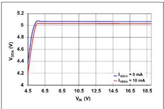
| VIN (V) | VDDA (V) for IvddA = 0 mA | VDDA (V) for IvddA = 10 mA | | ------- | -------------------------- | --------------------------- | | 4.5 | 4.2 | 4.2 | | 6.5 | 5.0 | 5.0 | | 8.5 | 5.0 | 5.0 | | 10.5 | 5.0 | 5.0 | | 12.5 | 5.0 | 5.0 | | 14.5 | 5.0 | 5.0 | | 16.5 | 5.0 | 5.0 | | 18.5 | 5.0 | 5.0 |FIGURE 2-2: V Voltage.
line
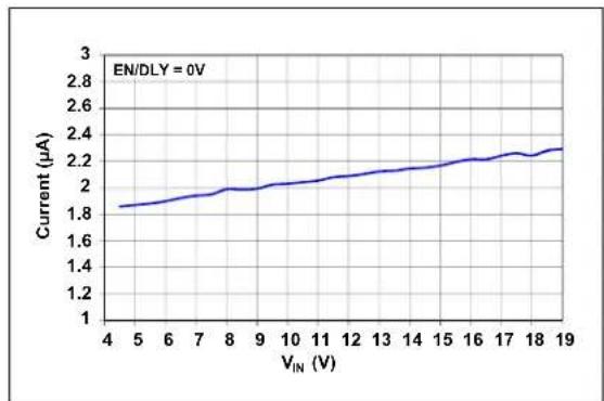
| VIN (V) | Current (μA) | | ------- | ------------ | | 4 | 1.8 | | 5 | 1.85 | | 6 | 1.9 | | 7 | 1.95 | | 8 | 2.0 | | 9 | 2.05 | | 10 | 2.1 | | 11 | 2.15 | | 12 | 2.2 | | 13 | 2.25 | | 14 | 2.3 | | 15 | 2.35 | | 16 | 2.4 | | 17 | 2.45 | | 18 | 2.5 | | 19 | 2.55 |FIGURE 2-5: EN/DLY Pull-up Current vs. Input Voltage.

line
| VIN (V) | LIM = high Z | LIM = VDDA | LIM = GND | | ------- | ------------ | ---------- | --------- | | 4.5 | 7.4 | 7.0 | 5.6 | | 5 | 7.4 | 6.9 | 5.6 | | 5.5 | 7.4 | 6.8 | 5.6 | | 6 | 7.4 | 6.8 | 5.6 | | 8 | 7.4 | 6.8 | 5.6 | | 10 | 7.4 | 6.8 | 5.6 | | 12 | 7.5 | 6.9 | 5.7 | | 14 | 7.6 | 7.0 | 5.8 | | 16 | 7.7 | 7.2 | 6.0 | | 18 | 7.8 | 7.3 | 6.2 | | 19 | 7.9 | 7.4 | 6.3 |FIGURE 2-3: Output Current Limit vs. Input Voltage.
line
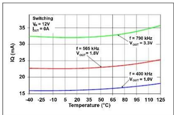
| Temperature (°C) | IO (mA) at f = 790 kHz, VOUT = 3.3V | IO (mA) at f = 565 kHz, VOUT = 1.8V | IO (mA) at f = 400 kHz, VOUT = 1.0V | | ---------------- | ----------------------------------- | ----------------------------------- | ----------------------------------- | | -40 | ~32 | ~22 | ~15 | | -25 | ~32 | ~22 | ~15 | | -10 | ~32 | ~22 | ~15 | | 0 | ~32 | ~22 | ~15 | | 20 | ~32 | ~22 | ~15 | | 35 | ~32 | ~22 | ~15 | | 50 | ~32 | ~22 | ~15 | | 65 | ~32 | ~22 | ~15 | | 80 | ~32 | ~22 | ~15 | | 95 | ~32 | ~22 | ~15 | | 110 | ~32 | ~22 | ~15 | | 125 | ~32 | ~22 | ~15 |FIGURE 2-6: Operating Current (IQ) vs. Temperature.
Note: Unless otherwise indicated, V_IN = 12V ; C_VDDA = 2.2 F , T_A = +25^ C .

line
| Temperature(°C) | Sinking (μA) | Sourcing (μA) | | --------------- | ------------ | ------------- | | -40 | 350 | -400 | | 0 | 375 | -425 | | 20 | 400 | -450 | | 40 | 425 | -475 | | 60 | 450 | -500 | | 80 | 475 | -525 | | 100 | 500 | -550 | | 120 | 525 | -575 | | 140 | 550 | -600 |FIGURE 2-7: EA Output Current vs. Temperature.
line
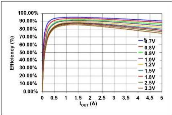
| I_OUT (A) | 0.7V | 0.8V | 0.9V | 1.0V | 1.2V | 1.5V | 1.8V | 2.5V | 3.3V | | --------- | ------ | ------ | ------ | ------ | ------ | ------ | ------ | ------ | ------ | | 0 | 0.00% | 0.00% | 0.00% | 0.00% | 0.00% | 0.00% | 0.00% | 0.00% | 0.00% | | 0.5 | ~95.00%| ~94.00%| ~93.00%| ~92.00%| ~91.00%| ~90.00%| ~89.00%| ~88.00%| ~87.00%| | 1 | ~98.00%| ~97.00%| ~96.00%| ~95.00%| ~94.00%| ~93.00%| ~92.00%| ~91.00%| ~90.00%| | 1.5 | ~98.50%| ~97.50%| ~96.50%| ~95.50%| ~94.50%| ~93.50%| ~92.50%| ~91.50%| ~90.50%| | 2 | ~98.50%| ~97.50%| ~96.50%| ~95.50%| ~94.50%| ~93.50%| ~92.50%| ~91.50%| ~90.50%| | 2.5 | ~98.50%| ~97.50%| ~96.50%| ~95.50%| ~94.50%| ~93.50%| ~92.50%| ~91.50%| ~90.50%| | 3 | ~98.50%| ~97.50%| ~96.50%| ~95.50%| ~94.50%| ~93.50%| ~92.50%| ~91.50%| ~90.50%| | 3.5 | ~98.50%| ~97.50%| ~96.50%| ~95.50%| ~94.50%| ~93.50%| ~92.50%| ~91.50%| ~90.50%| | 4 | ~98.50%| ~97.50%| ~96.50%| ~95.50%| ~94.50%| ~93.50%| ~92.50%| ~91.50%| ~90.50%| | 4.5 | ~98.50%| ~97.50%| ~96.50%| ~95.50%| ~94.50%| ~93.50%| ~92.50%| ~91.50%| ~90.50%| | 5 | ~98.50%| ~97.50%| ~96.50%| ~95.50%| ~94.50%| ~93.50%| ~92.50%| ~91.50%| ~90.50%|FIGURE 2-10: Efficiency vs. Output Current ( V_IN = 5 V ).

line
| Temperature (°C) | EA Transconductance (mS) | | ---------------- | ------------------------ | | -40 | 1.45 | | -20 | 1.43 | | 0 | 1.40 | | 20 | 1.38 | | 40 | 1.36 | | 60 | 1.34 | | 80 | 1.32 | | 100 | 1.30 | | 120 | 1.28 | | 140 | 1.25 |FIGURE 2-8: EA Transconductance vs. Temperature.

line
| I_OUT (A) | V_IN = 12V | V_IN = 5V | | --------- | ---------- | --------- | | 0 | 0.909 | 0.909 | | 0.5 | 0.909 | 0.909 | | 1 | 0.909 | 0.909 | | 1.5 | 0.909 | 0.909 | | 2 | 0.909 | 0.909 | | 2.5 | 0.909 | 0.909 | | 3 | 0.909 | 0.909 | | 3.5 | 0.909 | 0.909 | | 4 | 0.909 | 0.909 | | 4.5 | 0.909 | 0.909 | | 5 | 0.909 | 0.909 |FIGURE 2-11: Output Voltage vs. Output Current ( V_OUT = 0.9 V ).
line
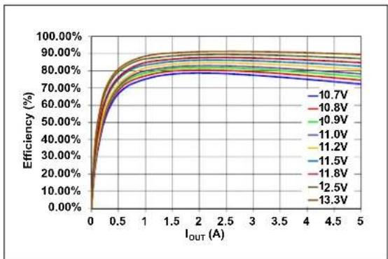
| I_OUT (A) | 10.7V | 10.8V | 10.9V | 11.0V | 11.2V | 11.5V | 11.8V | 12.5V | 13.3V | | --------- | ------ | ------ | ------ | ------ | ------ | ------ | ------ | ------ | ------ | | 0.0 | 0.00% | 0.00% | 0.00% | 0.00% | 0.00% | 0.00% | 0.00% | 0.00% | 0.00% | | 0.5 | ~65.00%| ~68.00%| ~70.00%| ~72.00%| ~74.00%| ~76.00%| ~78.00%| ~80.00%| ~82.00%| | 1.0 | ~75.00%| ~78.00%| ~80.00%| ~82.00%| ~84.00%| ~86.00%| ~88.00%| ~90.00%| ~92.00%| | 1.5 | ~80.00%| ~83.00%| ~85.00%| ~87.00%| ~89.00%| ~91.00%| ~93.00%| ~95.00%| ~97.00%| | 2.0 | ~82.00%| ~85.00%| ~87.00%| ~89.00%| ~91.00%| ~93.00%| ~95.00%| ~97.00%| ~98.50%| | 2.5 | ~83.50%| ~86.50%| ~88.50%| ~90.50%| ~92.50%| ~94.50%| ~96.50%| ~98.50%| ~99.50%| | 3.0 | ~84.50%| ~87.50%| ~89.50%| ~91.50%| ~93.50%| ~95.50%| ~97.50%| ~99.50%| ~100.50%| | 3.5 | ~85.50%| ~88.50%| ~91.50%| ~93.50%| ~95.50%| ~97.50%| ~99.50%| ~101.50%| ~102.50%| | 4.0 | ~86.50%| ~89.50%| ~93.50%| ~95.50%| ~97.50%| ~99.50%| ~101.50%| ~103.50%| ~104.50%| | 4.5 | ~87.50%| ~91.50%| ~95.50%| ~97.50%| ~99.50%| ~101.50%| ~103.50%| ~105.50%| ~106.50%| | 5.0 | ~88.50%| ~93.50%| ~97.50%| ~99.50%| ~101.50%| ~103.50%| ~105.50%| ~107.50%| ~108.50%|FIGURE 2-9: Efficiency vs. Output Current ( V_IN = 12V ).

line
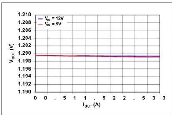
| I_OUT (A) | V_OUT (V) for V_IN = 12V | V_OUT (V) for V_IN = 5V | | --------- | ------------------------ | ----------------------- | | 0 | 1.000 | 1.000 | | 0.5 | 1.000 | 1.000 | | 1 | 1.000 | 1.000 | | 1.5 | 1.000 | 1.000 | | 2 | 1.000 | 1.000 | | 2.5 | 1.000 | 1.000 | | 3 | 1.000 | 1.000 | | 3.5 | 1.000 | 1.000 | | 4 | 1.000 | 1.000 | | 4.5 | 1.000 | 1.000 | | 5 | 1.000 | 1.000 |FIGURE 2-12: Output Voltage vs. Output Current ( V_OUT = 1.0 V ).
Note: Unless otherwise indicated, V_IN = 12V ; C_VDDA = 2.2 F , T_A = +25^ .
line
| I_OUT (A) | V_IN = 12V | V_IN = 5V | | --------- | ---------- | --------- | | 0 | 1.200 | 1.200 | | 5 | 1.200 | 1.200 | | 1 | 1.200 | 1.200 | | 5 | 1.200 | 1.200 | | 3 | 1.200 | 1.200 |FIGURE 2-13: Output Voltage vs. Output Current ( V_OUT = 1.2 V ).
line
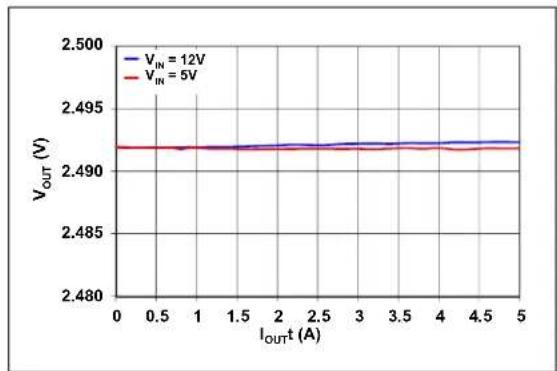
| I_OUT (A) | V_IN = 12V (V) | V_IN = 5V (V) | | --------- | -------------- | ------------- | | 0 | 2.492 | 2.492 | | 0.5 | 2.492 | 2.492 | | 1 | 2.492 | 2.492 | | 1.5 | 2.492 | 2.492 | | 2 | 2.492 | 2.492 | | 2.5 | 2.492 | 2.492 | | 3 | 2.492 | 2.492 | | 3.5 | 2.492 | 2.492 | | 4 | 2.492 | 2.492 | | 4.5 | 2.492 | 2.492 | | 5 | 2.492 | 2.492 |FIGURE 2-16: Output Voltage vs. Output Current ( V_OUT = 2.5 V ).
line
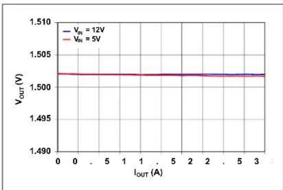
| I_OUT (A) | V_OUT (V) for V_IN = 12V | V_OUT (V) for V_IN = 5V | | --------- | ------------------------ | ----------------------- | | 0 | 1.502 | 1.502 | | 5 | 1.502 | 1.502 | | 1 | 1.502 | 1.502 | | 5 | 1.502 | 1.502 | | 2 | 1.502 | 1.502 | | 5 | 1.502 | 1.502 | | 3 | 1.502 | 1.502 |FIGURE 2-14: Output Voltage vs. Output Current ( V_OUT = 1.5 V ).
line
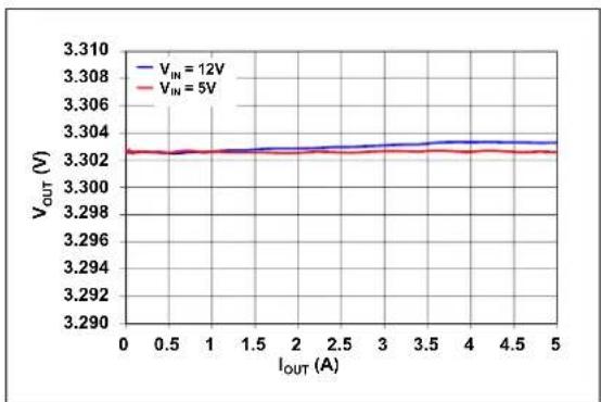
| I_OUT (A) | V_IN = 12V | V_IN = 5V | | --------- | ---------- | --------- | | 0 | 3.302 | 3.302 | | 0.5 | 3.302 | 3.302 | | 1 | 3.302 | 3.302 | | 1.5 | 3.302 | 3.302 | | 2 | 3.302 | 3.302 | | 2.5 | 3.302 | 3.302 | | 3 | 3.302 | 3.302 | | 3.5 | 3.302 | 3.302 | | 4 | 3.302 | 3.302 | | 4.5 | 3.302 | 3.302 | | 5 | 3.302 | 3.302 |FIGURE 2-17: Output Voltage vs. Output Current ( V_OUT = 3.3 V ).
line
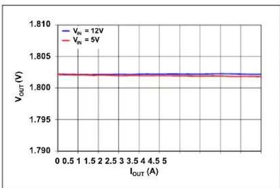
| I_OUT (A) | V_OUT (V) for V_IN = 12V | V_OUT (V) for V_IN = 5V | | --------- | ------------------------ | ----------------------- | | 0 | 1.802 | 1.802 | | 0.5 | 1.802 | 1.802 | | 1 | 1.802 | 1.802 | | 1.5 | 1.802 | 1.802 | | 2 | 1.802 | 1.802 | | 2.5 | 1.802 | 1.802 | | 3 | 1.802 | 1.802 | | 3.5 | 1.802 | 1.802 | | 4 | 1.802 | 1.802 | | 4.5 | 1.802 | 1.802 | | 5 | 1.802 | 1.802 |FIGURE 2-15: Output Voltage vs. Output Current ( V_OUT = 1.8 V ).
Note: Unless otherwise indicated, V_IN = 12V ; C_VDDA = 2.2 F , T_A = +25^ .
line
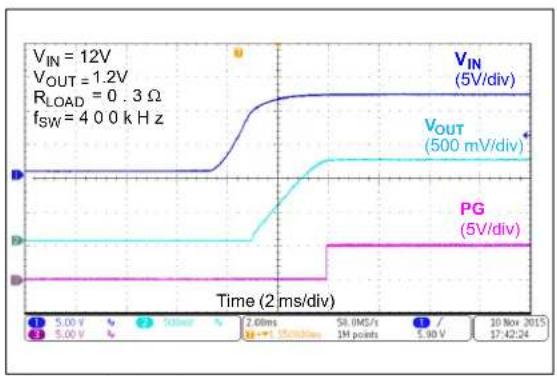
| Time (ms) | V_IN (5V/div) | V_OUT (500 mV/div) | PG (5V/div) | |-----------|---------------|--------------------|-------------| | 0 | 12 | 500 | 5 | | 2 | 12 | 500 | 5 | | 4 | 12 | 500 | 5 | | 6 | 12 | 500 | 5 | | 8 | 12 | 500 | 5 | | 10 | 12 | 500 | 5 | | 12 | 12 | 500 | 5 | | 14 | 12 | 500 | 5 | | 16 | 12 | 500 | 5 | | 18 | 12 | 500 | 5 | | 20 | 12 | 500 | 5 | | 22 | 12 | 500 | 5 | | 24 | 12 | 500 | 5 | | 26 | 12 | 500 | 5 | | 28 | 12 | 500 | 5 | | 30 | 12 | 500 | 5 | | 32 | 12 | 500 | 5 | | 34 | 12 | 500 | 5 | | 36 | 12 | 500 | 5 | | 38 | 12 | 500 | 5 | | 40 | 12 | 500 | 5 | | 42 | 12 | 500 | 5 | | 44 | 12 | 500 | 5 | | 46 | 12 | 500 | 5 | | 48 | 12 | 500 | 5 | | 50 | 12 | 500 | 5 | | 52 | 12 | 500 | 5 | | 54 | 12 | 500 | 5 | | 56 | 12 | 500 | 5 | | 58 | 12 | 500 | 5 | | 60 | 12 | 500 | 5 | | 62 | 12 | 500 | 5 | | 64 | 12 | 500 | 5 | | 66 | 12 | 500 | 5 | | 68 | 12 | 500 | 5 | | 70 | 12 | 500 | 5 | | 72 | 12 | 500 | 5 | | 74 | 12 | 500 | 5 | | 76 | 12 | 500 | 5 | | 78 | 12 | 500 | 5 | | 80 | 12 | 500 | 5 | | 82 | 12 | 500 | 5 | | 84 | 12 | 500 | 5 | | 86 | 12 | 500 | 5 | | 88 | 12 | 500 | 5 | | 90 | 12 | 500 | 5 | | 92 | 12 | 500 | 5 | | 94 | 12 | 500 | 5 | | 96 | 12 | 500 | 5 | | 98 | 12 | 500 | 5 | | 100 | - | - | - | | Time (ms) = -3.3Ω, Time (ms) = -3.7Ω, Time (ms) = -3.9Ω, Time (ms) = -4.1Ω, Time (ms) = -4.3Ω, Time (ms) = -4.5Ω, Time (ms) = -4.7Ω, Time (ms) = -4.9Ω, Time (ms) = -5.1Ω, Time (ms) = -5.3Ω, Time (ms) = -5.6Ω, Time (ms) = -6.4Ω, Time (ms) = -7.4Ω, Time (ms) = -8.4Ω, Time (ms) = -9.4Ω, Time (ms) = -1.4Ω, Time (ms) = -1.7Ω, Time (ms) = -3.7Ω, Time (ms) = -6.4Ω, Time (ms) = -7.4Ω, Time (ms) = -9.4Ω, Time (ms) = -1.4Ω, Time (ms) = -3.7Ω, Time (ms) = -6.4Ω, Time (ms) = -7.4Ω, Time (ms) = -9.4Ω, Time (ms) = -8.4Ω, Time (ms) = -9.4Ω, Time (ms) = -7.4Ω, Time (ms) = -7.4Ω, Time (ms) = -7.4Ω, Time (ms) = -7.4Ω, Time (ms) = -7.4Ω, Time (ms) = -7.4Ω, Time (ms) = -7.4Ω, Time (ms) = -7.4Ω, Time (ms) = -7.4Ω, Time (ms) = -7, Time (ms) = -3.7Ω, Time (ms) = -3.7Ω, Time (ms) = -3.7Ω, Time (ms) = -3.7Ω, Time (ms) = -3.7Ω, Time (ms) = -3.7Ω, Time (ms) = -3.7Ω, Time (ms) = -3.7Ω, Time (ms) = -3.7Ω, Time (ms) = -3.7ΩFIGURE 2-18: V IN Turn-On.
line
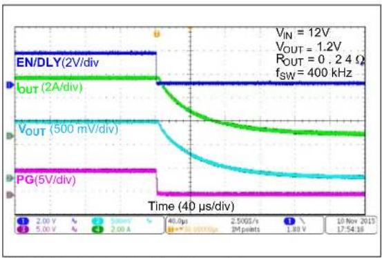
| Time (μs) | EN/DLY(2V/div) | OUT(2A/div) | VOUT(500 mV/div) | PG(5V/div) | |-----------|----------------|-------------|------------------|------------| | 0 | 12 | 1.2 | 0.24 | 5 | | 40 | 12 | 1.2 | 0.24 | 5 | | 80 | 12 | 1.2 | 0.24 | 5 | | 120 | 12 | 1.2 | 0.24 | 5 | | 160 | 12 | 1.2 | 0.24 | 5 | | 200 | 12 | 1.2 | 0.24 | 5 | | 240 | 12 | 1.2 | 0.24 | 5 | | 280 | 12 | 1.2 | 0.24 | 5 | | 320 | 12 | 1.2 | 0.24 | 5 | | 360 | 12 | 1.2 | 0.24 | 5 | | 400 | 12 | 1.2 | 0.24 | 5 | | 440 | 12 | 1.2 | 0.24 | 5 | | 480 | 12 | 1.2 | 0.24 | 5 | | 520 | 12 | 1.2 | 0.24 | 5 | | 560 | 12 | 1.2 | 0.24 | 5 | | 600 | 12 | 1.2 | 0.24 | 5 | | 640 | 12 | 1.2 | 0.24 | 5 | | 680 | 12 | 1.2 | 0.24 | 5 | | 720 | 12 | 1.2 | 0.24 | 5 | | 760 | 12 | 1.2 | 0.24 | 5 | | 800 | 12 | 1.2 | 0.24 | 5 | | 840 | 12 | 1.2 | 0.24 | 5 | | 880 | 12 | 1.2 | 0.24 | 5 | | 920 | 12 | 1.2 | 0.24 | 5 | | 960 | 12 | 1.2 | 0.24 | 5 | | 1000 | 12 | 1.2 | 0.24 | 5 | | 1040 | 12 | 1.2 | 0.24 | 5 | | 1080 | 12 | 1.2 | 0.24 | 5 | | 1120 | 12 | 1.2 | 0.24 | 5 | | 1160 | 12 | 1.2 | 0.24 | 5 | | 1200 | 12 | 1.2 | 0.24 | 5 | | Note: The values for EN/DLY(2V/div) and PG(5V/div) are estimated based on the code execution of the given code input (EN/DLY). The output values are calculated as the sum of the two inputs (EN/DLY) and the corresponding output values (PG) for each input value in the code input range (EN/DLY). The output values are calculated as the sum of the two inputs (EN/DLY) and the corresponding output values (PG) for each input range (EN/DLY). The code output values are calculated as the sum of the two inputs (EN/DLY) and the corresponding output values (PG) for each input range (EN/DLY). The output values are calculated as the sum of the two inputs (EN/DLY) and the corresponding output values (PG) for each input range (EN/DLY). The code output values are calculated as the sum of the two inputs (EN/DLY) and the corresponding output values (PG) for each input range (EN/DLY). The code output values are calculated as the sum of the two inputs (EN/DLY) and the corresponding output values (PG) for each input range (EN/DLY). The code output values are calculated as the sum of the two inputs (EN/DLY) and the corresponding output values (PG) for each input range (En/DLY). The code output values are calculated as the sum of the two inputs (EN/DLY) and the corresponding output values (PG) for each input range (EN/DLY). The code output values are calculated as the sum of the two inputs (EN/DLY) and the corresponding output values (PG) for each input range (EN/DLY). The code output values are calculated as the sum of the two inputs (EN/DLY) and the corresponding output values (PG) from the code input range [5,5] and [7,7].FIGURE 2-21: Enable Turn-Off.
line
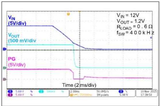
| Time (ms) | V_IN (5V/div) | V_OUT (500 mV/div) | PG (5V/div) | |-----------|---------------|--------------------|-------------| | 0 | 12 | 12 | 12 | | 2 | 12 | 12 | 12 | | 4 | 12 | 12 | 12 | | 6 | 12 | 12 | 12 | | 8 | 12 | 12 | 12 | | 10 | 12 | 12 | 12 | | 12 | 12 | 12 | 12 | | 14 | 12 | 12 | 12 | | 16 | 12 | 12 | 12 | | 18 | 12 | 12 | 12 | | 20 | 12 | 12 | 12 | | 22 | 12 | 12 | 12 | | 24 | 12 | 12 | 12 | | 26 | 12 | 12 | 12 | | 28 | 12 | 12 | 12 | | 30 | 12 | 12 | 12 | | 32 | 12 | 12 | 12 | | 34 | 12 | 12 | 12 | | 36 | 12 | 12 | 12 | | 38 | 12 | 12 | 12 | | 40 | 12 | 12 | 12 | | 42 | 12 | 12 | 12 | | 44 | 12 | 12 | 12 | | 46 | 12 | 12 | 12 | | 48 | 12 | 12 | 12 | | 50 | 12 | 12 | 12 | | 52 | 12 | 12 | 12 | | 54 | 12 | 12 | 12 | | 56 | 12 | 12 | 12 | | 58 | 12 | 12 | 12 | | 60 | 12 | 12 | 12 | | 62 | 12 | 12 | 12 | | 64 | 12 | 12 | 12 | | 66 | 12 | 12 | 12 | | 68 | 12 | 12 | 12 | | 70 | 12 | 12 | 12 | | 72 | 12 | 12 | 12 | | 74 | 12 | 12 | 12 | | 76 | 12 | 12 | 12 | | 78 | 12 | 12 | 12 | | 80 | 12 | 12 | 12 | | 82 | 12 | 12 | 12 | | 84 | 12 | 12 | 12 | | 86 | 12 | 12 | 12 | | 88 | 12 | 12 | 12 | | 90 | 12 | 12 | 12 | | 92 | 12 | 12 | 12 | | 94 | 12 | 12 | 12 | | 96 | 12 | 12 | 12 | | 98 | 12 | 12 | 12 | | Note: The values for V_IN, V_OUT, R_LOAD, and f_SW are estimated based on the code provided in the code. The values for PG and V_IN are calculated based on the given code. There is no additional data series in this case. The values for PG and V_IN are not explicitly labeled in the code snippet. The values for PG and V_IN are estimated based on the given code. There is no further information in the code snippet. The values for PG and V_IN are estimated based on the given code. There is no further information in the code snippet. The values for PG and V_IN are estimated based on the given code. There is no further information in the code snippet. The values for PG and V_IN are estimated based on the given code. There is no further information in the code snippet. The values for PG and V_IN are estimated based on the given code. There is no further data series in this code. The values for PG and V_IN are estimated based on the given code. There is no further data series in this code. The values for PG and V_IN are estimated based on the given code. There is no further data series in this code. The values for PG and V_IN are estimated based on the given code. There is no further data series in this code. The values for PG and V_IN are estimated based on the given code. There is no further data series in this word. The values for PG and V_IN are estimated based on the given word. There is no further data series in this word. The values for PG and V_IN are estimated based on the given word. There is no further data series in this word. The values for PG and V_IN are estimated based on the given word. There is no further data series in this word. The values for PG and V_IN are estimated based on the given word. There is no further data series in this word. The values for PG and V_IN are estimated based on the given words. There is no further data series in this word. The values for PG and V_IN are estimated based on the given words. There is no further data series in this word. The values for PG and V_IN are estimated based on the given words. There is no further data series in this word. The values for PG and V_IN are estimated based on the given words. There is no further data series in this word. The values for PG and V_IN are estimated based on the given word. There is no further data series in this word. The values for PG and V_IN are estimated based on the given word. There is no further data series in this word. The values for PG and V_IN are estimated based on the given word. There is no further data series in this word. The values for PG and V_IN are estimated based on the given text. There is no further data series in this word. The values for PG and V_IN are estimated based on the given text. There is no further data series in this word. The values for PG and V_IN are estimated based on the given text. There is no further data series in this word. The values for PG and V_IN are estimated based on the given text. There is no further data series in this word. The values for PG and V_IN are estimated based on the given words. There is no further data series in this word. The values for PG and V_IN are estimated based on the given words. There is no further data series in this word. The values for PG and V_IN are estimated based on the given words. There is no further data series in this word. The values for PG and V_IN are estimated based on the given text. There is no further data series in this word. The values for PG and V_IN are estimated based on the given text. There is no further data series in this word. The values for PG and V_IN are estimated based on the given text. There is no further data series in this word. The values for PG and V_IN are estimated based on the given word. There is no further data series in this word. The values for PG and V_IN are estimated based on the given word. There is no further data series in this word. The values for PG and V_IN are estimated based on the given word. There is no further data series in this word. The values for PG and V_IN are estimated based on the given type of wave source (5V/div) from a common frequency source (500 mV/div).FIGURE 2-19: V IN Turn-Off.

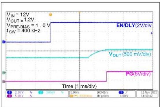
FIGURE 2-22: Enable Start-Up with Pre-Biased Output.
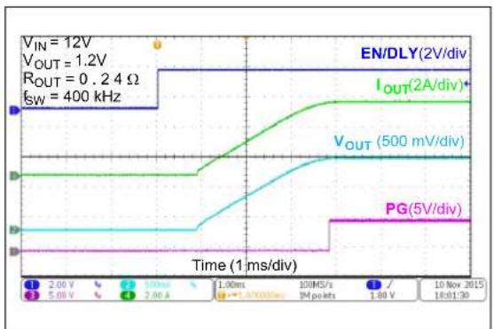
FIGURE 2-20: Enable Turn-On.
line
| Time (ms) | V_IN (V) | V_OUT (mV) | V_PRE_BIAS (V) | f_SW (kHz) | |-----------|----------|------------|----------------|------------| | 0 | 12 | 1.2 | 1.0 | 400 | | 1 | 12 | 1.2 | 1.0 | 400 | | 2 | 12 | 1.2 | 1.0 | 400 | | 3 | 12 | 1.2 | 1.0 | 400 | | 4 | 12 | 1.2 | 1.0 | 400 | | 5 | 12 | 1.2 | 1.0 | 400 | | 6 | 12 | 1.2 | 1.0 | 400 | | 7 | 12 | 1.2 | 1.0 | 400 | | 8 | 12 | 1.2 | 1.0 | 400 | | 9 | 12 | 1.2 | 1.0 | 400 | | 10 | 12 | 1.2 | 1.0 | 400 | | 11 | 12 | 1.2 | 1.0 | 400 | | 12 | 12 | 1.2 | 1.0 | 400 | | 13 | 12 | 1.2 | 1.0 | 400 | | 14 | 12 | 1.2 | 1.0 | 400 | | 15 | 12 | 1.2 | 1.0 | 400 | | 16 | 12 | 1.2 | 1.0 | 400 | | 17 | 12 | 1.2 | 1.0 | 400 | | 18 | 12 | 1.2 | 1.0 | 400 | | 19 | 12 | 1.2 | 1.0 | 400 | | 20 | 12 | 1.2 | 1.0 | 400 | | 21 | 12 | 1.2 | 1.0 | 400 | | 22 | 12 | 1.2 | 1.0 | 400 | | 23 | 12 | 1.2 | 1.0 | 400 | | 24 | 12 | 1.2 | 1.0 | 400 | | 25 | 12 | 1.2 | 1.0 | 400 | | 26 | 12 | 1.2 | 1.0 | 400 | | 27 | 12 | 1.2 | 1.0 | 400 | | 28 | 12 | 1.2 | 1.0 | 400 | | 29 | 12 | 1.2 | 1.0 | 400 | | 30 | 12 | 1.2 | 1.0 | 400 | | | | | | | | | | | | | | | | | | | | | | | | | | | | | | | | | | | | | | | | | | | | | | | | | | | | | | | | | | | | |FIGURE 2-23: Enable Start-Up with Pre-Biased Output.
Note: Unless otherwise indicated, V_IN = 12V ; C_VDDA = 2.2 F , T_A = +25^ .

FIGURE 2-24: Power-Up into Short Circuit.
line
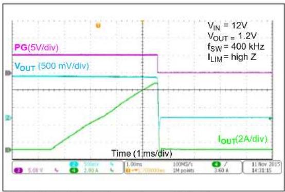
| Time (ms) | PG (5V/div) | VOUT (500 mV/div) | IOUT (2A/div) | |-----------|-------------|-------------------|---------------| | 0 | 5.08 | 500 | 0 | | 1 | 5.08 | 500 | 0 | | 2 | 5.08 | 500 | 0 | | 3 | 5.08 | 500 | 0 | | 4 | 5.08 | 500 | 0 | | 5 | 5.08 | 500 | 0 | | 6 | 5.08 | 500 | 0 | | 7 | 5.08 | 500 | 0 | | 8 | 5.08 | 500 | 0 | | 9 | 5.08 | 500 | 0 | | 10 | 5.08 | 500 | 0 | | 11 | 5.08 | 500 | 0 | | 12 | 5.08 | 500 | 0 | | 13 | 5.08 | 500 | 0 | | 14 | 5.08 | 500 | 0 | | 15 | 5.08 | 500 | 0 | | 16 | 5.08 | 500 | 0 | | 17 | 5.08 | 500 | 0 | | 18 | 5.08 | 500 | 0 | | 19 | 5.08 | 500 | 0 | | 20 | 5.08 | 500 | 0 | | 21 | 5.08 | 500 | 0 | | 22 | 5.08 | 500 | 0 | | 23 | 5.08 | 500 | 0 | | 24 | 5.08 | 500 | 0 | | 25 | 5.08 | 500 | 0 | | 26 | 5.08 | 500 | 0 | | 27 | 5.08 | 500 | 0 | | 28 | 5.08 | 500 | 0 | | 29 | 5.08 | 500 | 0 | | 30 | 5.08 | 500 | 0 | | 31 | 5.08 | 500 | 0 | | | | | - | | | | | - | | | | | - | | | | | - | | | | | - | | | | | - | | | | | - | | | | | - | | | | | - | | | | | - | | | | | | | | | | | | | | | | | | | | | | | | | | | | | | | | | | | | | | | | | | | | | | | | | | | | | | | | | | | | |FIGURE 2-27: Output Current Limit ( I_LIM = High Z ).
line
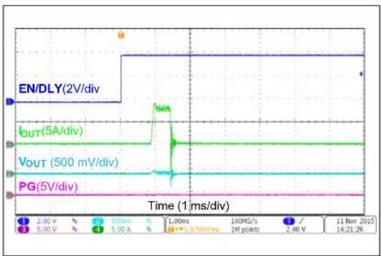
| Time (ms) | EN/DLY(2V/div) | IOUT(5A/div) | VOUT (500 mV/div) | PG(5V/div) | |-----------|----------------|--------------|-------------------|------------| | 0 | 2.00 | 5.00 | 5.00 A | 5.00 | | 1.0 | 2.00 | 5.00 | 5.00 A | 5.00 | | 2.0 | 2.00 | 5.00 | 5.00 A | 5.00 | | 3.0 | 2.00 | 5.00 | 5.00 A | 5.00 | | 4.0 | 2.00 | 5.00 | 5.00 A | 5.00 | | 5.0 | 2.00 | 5.00 | 5.00 A | 5.00 | | 6.0 | 2.00 | 5.00 | 5.00 A | 5.00 | | 7.0 | 2.00 | 5.00 | 5.00 A | 5.00 | | 8.0 | 2.00 | 5.00 | 5.00 A | 5.00 | | 9.0 | 2.00 | 5.00 | 5.00 A | 5.00 | | 10.0 | 2.00 | 5.00 | 5.00 A | 5.00 | | 11.0 | 2.00 | 5.00 | 5.00 A | 5.00 | | 12.0 | 2.00 | 5.00 | 5.00 A | 5.00 | | 13.0 | 2.00 | 5.00 | 5.00 A | 5.00 | | 14.0 | 2.00 | 5.00 | 5.00 A | 5.00 | | 15.0 | 2.00 | 5.00 | 5.00 A | 5.00 | | 16.0 | 2.00 | 5.00 | 5.00 A | 5.00 | | 17.0 | 2.00 | 5.00 | 5.00 A | 5.00 | | 18.0 | 2.00 | 5.00 | 5.00 A | 5.00 | | 19.0 | 2.00 | 5.00 | 5.00 A | 5.00 | | 20.0 | 2.00 | 5.00 | 5.00 A | 5.00 | | 21.0 | 2.00 | 5.00 | 5.00 A | 5.00 | | 22.0 | 2.00 | 5.00 | 5.00 A | 5.00 | | 23.0 | 2.00 | 5.00 | 5.00 A | 5.00 | | 24.0 | 2.00 | 5.00 | 5.00 A | 5.00 | | 25.0 | 2.00 | 5.00 | 5.00 A | 5.00 | | 26.0 | 2.00 | 5.00 | 5.00 A | 5.00 | | 27.0 | 2.00 | 5.00 | 5.00 A | 5.00 | | 28.0 | 2.00 | 5.00 | 5.00 A | 5.00 | | 29.0 | 2.00 | 5.00 | 5.00 A | 5.00 | | 30.0 | 2.00 | 5.00 | 5.00 A | 5.00 | | | | | | | | | | | | | | | | | | | | | | | | | | | | | | | | | | | | | | | | | | | | | | | | | | | | | | | | | | | | |FIGURE 2-25: Enable Into Short Circuit.

FIGURE 2-28: Hiccup Mode Short Circuit and Output Recovery.
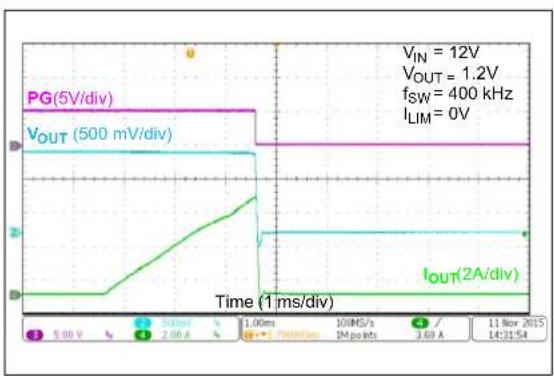
FIGURE 2-26: Output Current Limit ( I_LIM = 0 V ).

line
| Time (ms) | PG(5V/div) | VOUT(500 mV/div) | IOUT(2A/div) | |-----------|------------|------------------|--------------| | 0 | 5.00 | 5.00 | 5.00 | | 10 | 5.00 | 5.00 | 5.00 | | 20 | 5.00 | 5.00 | 5.00 | | 30 | 5.00 | 5.00 | 5.00 | | 40 | 5.00 | 5.00 | 5.00 | | 50 | 5.00 | 5.00 | 5.00 | | 60 | 5.00 | 5.00 | 5.00 | | 70 | 5.00 | 5.00 | 5.00 | | 80 | 5.00 | 5.00 | 5.00 | | 90 | 5.00 | 5.00 | 5.00 | | 100 | 5.00 | 5.00 | 5.00 | | 110 | 5.00 | 5.00 | 5.00 | | 120 | 5.00 | 5.00 | 5.00 | | 130 | 5.00 | 5.00 | 5.00 | | 140 | 5.00 | 5.00 | 5.00 | | 150 | 5.00 | 5.00 | 5.00 | | 160 | 5.00 | 5.00 | 5.00 | | 170 | 5.00 | 5.00 | 5.00 | | 180 | 5.00 | 5.00 | 5.00 | | 190 | 5.00 | 5.00 | 5.00 | | 200 | 5.00 | 5.00 | 5.00 | | Peak | - | - | - | | Final | - | - | - |FIGURE 2-29: Thermal Shutdown and Thermal Recovery.
Note: Unless otherwise indicated, V_IN = 12V ; C_VDDA = 2.2 F , T_A = +25^ .

line
| Time (μs) | SW (5V/div) | AC-Coupled (10 mV/div) | AC-Coupled (20 mV/div) | |-----------|-------------|------------------------|------------------------| | 11 Nov 2015 | 400 kHz | 100 MHz (approx) | 6.30 V (approx) |FIGURE 2-30: Switching Waveforms ( I_OUT = 0 A ).

line
| Time (100 µs/div) | PG (5V/div) | VOUT AC-Coupled (100 mV/div) | IOUT (2A/div) | | ----------------- | ----------- | ---------------------------- | ------------- | | 0 | 5 | ~0.8 | ~0 | | 5 | 5 | ~0.8 | ~0 | | 10 | 5 | ~0.8 | ~0 | | 15 | 5 | ~0.8 | ~0 | | 20 | 5 | ~0.8 | ~0 | | 25 | 5 | ~0.8 | ~0 | | 30 | 5 | ~0.8 | ~0 | | 35 | 5 | ~0.8 | ~0 | | 40 | 5 | ~0.8 | ~0 | | 45 | 5 | ~0.8 | ~0 | | 50 | 5 | ~0.8 | ~0 | | 55 | 5 | ~0.8 | ~0 | | 60 | 5 | ~0.8 | ~0 | | 65 | 5 | ~0.8 | ~0 | | 70 | 5 | ~0.8 | ~0 | | 75 | 5 | ~0.8 | ~0 | | 80 | 5 | ~0.8 | ~0 | | 85 | 5 | ~0.8 | ~0 | | 90 | 5 | ~0.8 | ~0 | | 95 | 5 | ~0.8 | ~0 | | 100 | 5 | ~0.8 | ~0 | | 105 | 5 | ~0.8 | ~0 | | 110 | 5 | ~0.8 | ~0 | | 115 | 5 | ~0.8 | ~0 | | 120 | 5 | ~0.8 | ~0 | | 125 | 5 | ~0.8 | ~0 | | 130 | 5 | ~0.8 | ~0 | | 135 | 5 | ~0.8 | ~0 | | 140 | 5 | ~0.8 | ~0 | | 145 | 5 | ~0.8 | ~0 | | 150 | 5 | ~0.8 | ~0 | | 155 | 5 | ~0.8 | ~0 | | 160 | 5 | ~0.8 | ~0 | | 165 | 5 | ~0.8 | ~0 | | 170 | 5 | ~0.8 | ~0 | | 175 | 5 | ~0.8 | ~0 | | 180 | 5 | ~0.8 | ~0 | | 185 | 5 | ~0.8 | ~0 | | 190 | 5 | ~0.8 | ~0 | | 195 | 5 | ~0.8 | ~0 | | 200 | 5 | ~0.8 | ~0 | | 205 | 5 | ~0.8 | ~0 | | 210 | 5 | ~0.8 | ~0 | | 215 | 5 | ~0.8 | ~0 | | 220 | 5 | ~0.8 | ~0 | | 225 | 5 | ~0.8 | ~0 | | 230 | 5 | ~0.8 | ~0 | | 235 | 5 | ~0.8 | ~0 | | 240 | 5 | ~0.8 | ~0 | | 245 | 5 | ~0.8 | ~0 | | 250 | 5 | ~0.8 | ~0 | | 255 | 5 | ~0.8 | ~0 | | 260 | 5 | ~0.8 | ~0 | | 265 | 5 | ~0.8 | ~0 | | 270 | 5 | ~0.8 | ~0 | | 275 | 5 | ~0.8 | ~0 | | 280 | 5 | ~0.8 | ~0 | | 285 | 5 | ~0.8 | ~0 | | 290 | 5 | ~0.8 | ~0 | | 295 | 5 | ~0.8 | ~0 | | 300 | 5 | ~0.8 | ~0 | | 305 | 5 | ~0.8 | ~0 | | 310 | 5 | ~0.8 | ~0 | | 315 | 5 | ~0.8 | ~0 | | 320 | 5 | ~0.8 | ~0 | | 325 | 5 | ~0.8 | ~0 | | 330 | 5 | ~0.8 | ~0 | | 335 | 5 | ~0.8 | ~0 | | 340 | 5 | ~0.8 | ~0 | | 345 | 5 | ~0.8 | ~0 | | 350 | 5 | ~0.8 | ~0 | | 355 | 5 | ~0.8 | ~0 | | 360 | 5 | ~0.8 | ~0 | | 365 | 5 | ~0.8 | ~0 | | 370 | 5 | ~0.8 | ~0 | | 375 | 5 | ~0.8 | ~0 | | 380 | 5 | ~0.8 | ~0 | | 385 | 5 | ~0.8 | ~0 | | 390 | 5 | ~0.8 | ~0 | | 395 | 5 | ~0.8 | ~0 | | 400 | 5 | ~0.8 | ~0 | | 405 | 5 | ~0.8 | ~0 | | 410 | 5 | ~0.8 | ~0 | | 415 | 5 | ~0.8 | ~0 | | 420 | 5 | ~0.8 | ~0 | | 425 | 5 | ~0.8 | ~0 | | 430 | 5 | ~0.8 | ~0 | | 435 | 5 | ~0.8 | ~0 | | 440 | 5 | ~0.8 | ~0 | | 445 | 5 | ~0.8 | ~0 | | 450 | 5 | ~0.8 | ~0 | | 455 | 5 | ~0.8 | ~0 | | 460 | 5 | ~0.8 | ~0 | | 465 | 5 | ~0.8 | ~0 | | 470 | 5 | ~0.8 | ~0 | | 475 | 5 | ~0.8 | ~0 | | 480 | 5 | ~0.8 | ~0 | | 485 | 5 | ~0.8 | ~0 | | 490 | 5 | ~0.8 | ~0 | | 495 | 5 | ~0.8 | ~0 | | 500 | 5 | ~0.8 | ~0 | | Note: The data is extracted from the image and displayed in the code as requested in the code format above and below the code format above it is not available in the code format above it is available in the code format above it is available in the code format above it is available in the code format above it is available in the code format above it is available in the code format above it is available in the code format above it is available in the code format above it is available in the code format above it is available in the code format above it is available in the code format above it is available in the code format above it is available in the code format above it is available in the codes above it is available in the code format above it is available in the code format above it is available in the code format above it is available in the code format above it is available in the code format above it is available in the code format above it is available in the code format above it is available in the code format above it is available in the code format above it is available in the code format above it is available in the code format above it is available in the code format above it isavailable in the code format above it is available in the code format above it is available in the code format above it is available in the code format above it is available in the code format above it is available in the code format above it is available in the code format above it is available in the code format above it is available in the code format above it is available in the code format above it is available in the code format above it is available in the code format above it is available in the code channel before being deleted from this image file to display the code output.FIGURE 2-32: Load Transient Response.

line
| Time (μs) | SW (5V/div) | AC-Coupled AC-Coupled (10 mV/div) | |-----------|-------------|----------------------------------| | 1 | 0 | 0 | | 5 | 12 | 1.2 | | 10 | 0 | 0 | | 15 | 12 | 1.2 | | 20 | 0 | 0 | | 25 | 12 | 1.2 | | 30 | 0 | 0 | | 35 | 12 | 1.2 | | 40 | 0 | 0 | | 45 | 12 | 1.2 | | 50 | 0 | 0 | | 55 | 12 | 1.2 | | 60 | 0 | 0 | | 65 | 12 | 1.2 | | 70 | 0 | 0 | | 75 | 12 | 1.2 | | 80 | 0 | 0 | | 85 | 12 | 1.2 | | 90 | 0 | 0 | | 95 | 12 | 1.2 | | 100 | 0 | 0 | | 105 | 12 | 1.2 | | 110 | 0 | 0 | | 115 | 12 | 1.2 | | 120 | 0 | 0 | | 125 | 12 | 1.2 | | 130 | 0 | 0 | | 135 | 12 | 1.2 | | 140 | 0 | 0 | | 145 | 12 | 1.2 | | 150 | 0 | 0 | | 155 | 12 | 1.2 | | 160 | 0 | 0 | | 165 | 12 | 1.2 | | 170 | 0 | 0 | | 175 | 12 | 1.2 | | 180 | 0 | 0 | | 185 | 12 | 1.2 | | 190 | 0 | 0 | | 195 | 12 | 1.2 | | 200 | 0 | 0 | | | | |FIGURE 2-31: Switching Waveforms ( I_OUT = 5 A ).
line
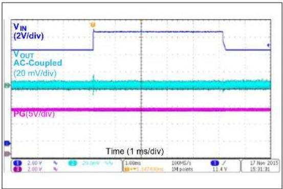
| Time (1 ms/div) | V_IN (2V/div) | V_OUT AC-Coupled (20 mV/div) | PG (5V/div) | | --------------- | ------------- | ----------------------------- | ----------- | | 0 | 0 | 0 | 0 | | 1 | 0 | 0 | 0 | | 2 | 0 | 0 | 0 | | 3 | 0 | 0 | 0 | | 4 | 0 | 0 | 0 | | 5 | 0 | 0 | 0 | | 6 | 0 | 0 | 0 | | 7 | 0 | 0 | 0 | | 8 | 0 | 0 | 0 | | 9 | 0 | 0 | 0 | | 10 | 0 | 0 | 0 | | 11 | 0 | 0 | 0 | | 12 | 0 | 0 | 0 | | 13 | 0 | 0 | 0 | | 14 | 0 | 0 | 0 | | 15 | 0 | 0 | 0 | | 16 | 0 | 0 | 0 | | 17 | 0 | 0 | 0 | | 18 | 0 | 0 | 0 | | 19 | 0 | 0 | 0 | | 20 | 0 | 0 | 0 | | 21 | 0 | 0 | 0 | | 22 | 0 | 0 | 0 | | 23 | 0 | 0 | 0 | | 24 | 0 | 0 | 0 | | 25 | 0 | 0 | 0 | | 26 | 0 | 0 | 0 | | 27 | 0 | 0 | 0 | | 28 | 0 | 0 | 0 | | 29 | 0 | 0 | 0 | | 30 | 0 | 0 | 0 | | | | | | | | | | | | | | | | | | | | | | | | | | | | | | | | | | | | | | | | | | | | | | | | | | | | | | | | | | | | |FIGURE 2-33: Line Transient Response.
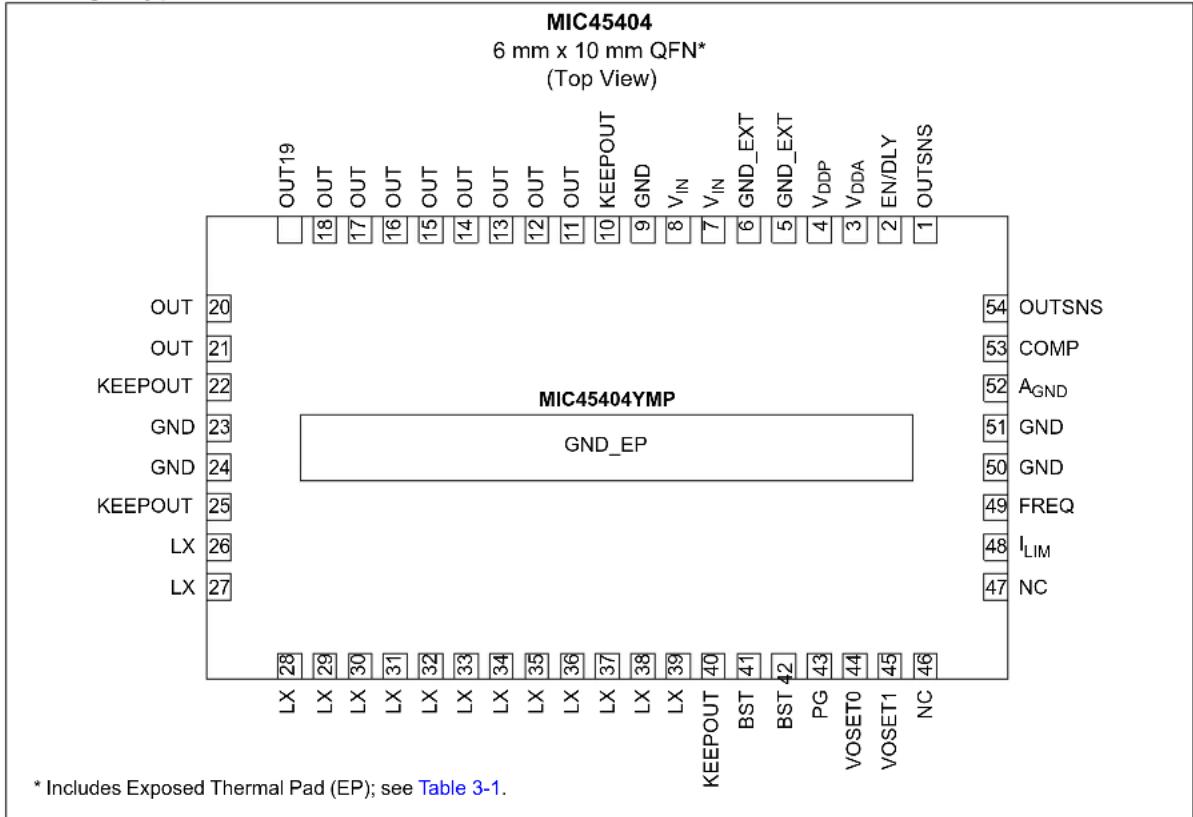
3.0 PIN DESCRIPTION
The descriptions of the pins are listed in Table3-1.
TABLE 3-1: PIN FUNCTION TABLE
| MIC45404 Symbol Pin Function | ||
| 1, 54 OUTSNS Output Sensing Pin | ||
| 2 | EN/DLY | Precision Enable/Turn-On Delay Input Pin |
| 3 | V_DDA | Internal LDO Output and Analog Supply Pin |
| 4 | V_DDP | MOSFET Drivers Internal Supply Pin |
| 5, 6 GND_EXT | Ground Extension Pins | |
| 7, 8 | V_IN | Input Voltage Pins |
| 9, 23, 24, 50, 51 | GND | Power Ground Pins |
| 11, 12, 13, 14, 15, 16, 17, 18, 19, 20, 21 | OUT | Output Side Connection Pins |
| 10, 22, 25, 40 | KEEPOUT | Depopulated Pin Positions |
| 26, 27, 28, 29, 30, 31, 32, 33, 34, 35, 36, 37, 38, 39 | LX | Switch Node Pins |
| 41, 42 | BST | Bootstrap Capacitor Pin |
| 43 | PG | Power Good Output Pin |
| 44 | VOSET0 | Output Voltage Selection Pins |
| 45 | VOSET1 | |
| 46, 47 | NC | Not Connected Pins |
| 48 | I_LIM | Current Limit Selection Pin |
| 49 | FREQ | Switching Frequency Selection Pin |
| 52 | A_GND | Analog Ground Pin |
| 53 | COMP | Compensation Network Pin |
| 55 | GND_EP | Ground Exposed Pad. |
3.1 Output Sensing Pins (OUTSNS)
Connect these pins directly to the Buck Converter output voltage. These pins are the top side terminal of the internal feedback divider.
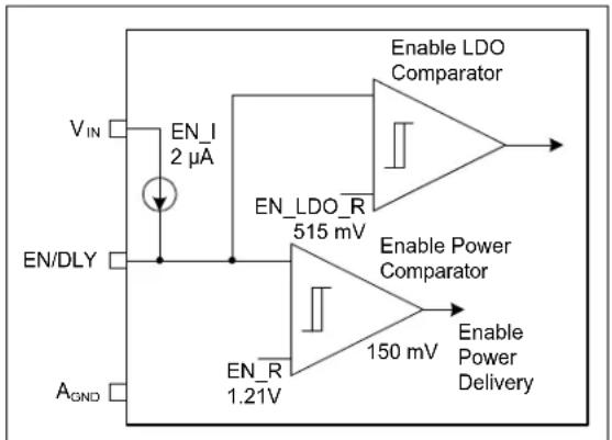
3.2 Precision Enable/Turn-On Delay Input Pin (EN/DLY)
The EN/DLY pin is first compared against a 515 mV threshold to turn on the on-board LDO regulator. The EN/DLY pin is then compared against a 1.21V (typical) threshold to initiate output power delivery. A 150 mV typical hysteresis prevents chattering when power delivery is started. A 2 A (typical) current source pulls up the EN/DLY pin. Turn-on delay can be achieved by connecting a capacitor from EN/DLY to ground, while using an open-drain output to drive the EN/DLY pin.
3.3 MOSFET Drivers Internal Supply Pin ( V_DDP )
Internal supply rail for the MOSFET drivers, fed by the V_DDA pin. An internal resistor (10Ω) between the V_DDP and V_DDA pins, and an internal decoupling capacitor are provided in the module in order to implement an RC filter for switching noise suppression.
3.4 Internal Regulator Output Pin ( V_DDA )
Output of the internal linear regulator and internal supply for analog control. A 1 F minimum ceramic capacitor should be connected from this pin to GND; a 2.2 F nominal value is recommended.
3.5 Ground Extension Pins (GND\_EXT)
These pins are used for the bottom terminal connection of the internal V_IN and V_DDP decoupling capacitors. The GND_EXT pins should be connected to the GND net, directly at the top layer, using a wide copper connection.
3.6 Input Voltage Pins (V IN)
Input voltage for the Buck Converter power stage and input of the internal linear regulator. These pins are the drain terminal of the internal high-side N-channel MOSFET. A 10 F (minimum) ceramic capacitor should be connected from V_IN to GND, as close as possible to the device.
3.7 Power Ground Pins (GND)
Connect the output capacitors to GND Pins 23 and 24, as close as possible to the module.
Connect the input capacitors to GND Pin 9, as close as possible to the module.
3.8 Output-Side Connection Pins (OUT)
Output side connection of the internal inductor. The output capacitors should be connected from this pin group to GND (Pins 23 and 24), as close to the module as possible.
3.9 Switch Node Pins (LX)
Switch Node: Drain (low-side MOSFET) and source (high-side MOSFET) connection of the internal power N-channel FETs. The internal inductor switched side and the bootstrap capacitor are connected to LX. Leave this pin floating.
3.10 Bootstrap Capacitor Pin (BST)
Connection to the internal bootstrap capacitor and high-side power MOSFET drive circuitry. Leave this pin floating.
3.11 Power Good Output Pin (PG)
When the output voltage is within 92.5% of the nominal set point, this pin will go from logic low to logic high through an external pull-up resistor. This pin is the drain connection of an internal N-channel FET.
3.12 Output Voltage Selection Pins (VOSET0 and VOSET1)
Three-state pin (low, high and High Z) for output voltage programming. Both VOSET0 and VOSET1 define nine logic values, corresponding to nine output voltage selections.
3.13 Not Connected Pins (NC)
These pins are not internally connected. Leave them floating.
3.14 Current Limit Pin (I LIM)
This pin allows the selection of the current limit state: low, high and High Z.
3.15 Switching Frequency Pin (FREQ)
This pin allows the selection of the frequency state: low, high and High Z.
3.16 Analog Ground Pin (A GND)
This pin is a quiet ground for the analog circuitry of the internal regulator and a return terminal for the external compensation network.
3.17 Compensation Network Pin (COMP)
Connect a compensation network from this pin to A_GND .
3.18 GND Exposed Pad
Connect to ground plane with thermal vias.
4.0 FUNCTIONAL DESCRIPTION
The MIC45404 is a pin-programmable, 5A Valley Current mode controlled power module, with an input voltage range from 4.5V to 19V.
The MIC45404 requires a minimal amount of external components. Only two supply decoupling capacitors and a compensation network are external. The flexibility in designing the external compensation allows the user to optimize the design across the entire input voltage and selectable output voltages range.
4.1 Theory of Operation
Valley Current mode control is a fixed frequency, leading-edge modulated Pulse-Width Modulation (PWM) Current mode control. Differing from the Peak Current mode, the Valley Current mode clock marks the turn-off of the high-side switch. Upon this instant, the MIC45404 low-side switch current level is compared against the reference current signal from the error amplifier. When the falling low-side switch current signal drops below the current reference signal, the high-side switch is turned on. As a result, the inductor valley current is regulated to a level dictated by the output of the error amplifier.
The feedback loop includes an internal programmable reference and output voltage sensing attenuator, thus removing the need for external feedback components and improving regulation accuracy. Output voltage feedback is achieved by connecting the OUTSNS pin directly to the output. The high-performance transconductance error amplifier drives an external compensation network at the COMP pin. The COMP pin voltage represents the reference current signal. This pin voltage is fed to the Valley Current mode modulator, which also adds slope compensation to ensure current loop stability.
Internal inductor, power MOSFETs and internal bootstrap diode complete the power train.
Overcurrent protection and thermal shutdown protect the MIC45404 from faults or abnormal operating conditions.
4.2 Supply Rails (V IN, VDDA, VDDP) and Internal LDO
V_IN pins represent the power train input. These pins are the drain connection of the internal high-side MOSFET and should be bypassed to GND, at least with a X5R or X7R 10 F ceramic capacitor, placed as close as possible to the module. Multiple capacitors are recommended.
An internal LDO provides a clean supply (5.1V typical) for the analog circuits at the V_DDA pin. The internal LDO is also powered from V_IN , as shown in the Functional Diagram. The internal LDO is enabled when the voltage at the EN/DLY pin exceeds about 0.51V, and regulation takes place as soon as enough voltage has been established between the V_IN and V_DDA pins. An internal Undervoltage Lockout (UVLO) circuit monitors the level of V_DDA . The V_DDA pin needs external bypassing to GND by means of a 2.2 F X5R or X7R ceramic capacitor, placed as close as possible to the module.
V_DDP is the power supply rail for the gate drivers and bootstrap circuit. This pin is bypassed to GND_EXT by means of an internal high-frequency ceramic capacitor. For this reason, the GND_EXT pins should be routed with a low-inductance path to the GND net. An internal 10Ω resistor is provided between V_DDA and V_DDP , allowing the implementation of a switching noise attenuation RC filter with the minimum amount of external components. It is possible, although typically not necessary, to lower the RC time constant by connecting an external resistor between V_DDA and V_DDP .
If the input rail is within 4.5V to 5.5V, it is possible to bypass the internal LDO by connecting V_IN , V_DDA and V_DDP together. Local decoupling of the V_DDA pin is still recommended.
4.3 Pin-Strapping Programmability (VOSET0, VOSET1, FREQ, I_LIM )
The MIC45404 uses pin strapping to set the output voltage (VOSET0, VOSET1), switching frequency (FREQ) and current limit ( I_LIM ). No external passives are needed, therefore, the external component count is minimized. Each pin is a three-state input (connect to GND for LOW logic level, connect to V_DDA for HIGH logic level or leave unconnected for High Z). The logic level of the pins is read and frozen in the internal configuration logic immediately after the V_DDA rail comes up and becomes stabilized. After this instant, any change of the input logic level on the pins will have no effect until the V_DDA power is cycled again. The values corresponding to each particular pin strapping configuration are detailed in Section 5.0 “Application Information”.
4.4 Enable/Delay (EN/DLY)
The EN/DLY pin is a dual threshold pin that turns the internal LDO on/off and starts/stops the power delivery to the output, as shown in Figure 4-1.
text_image
V_IN EN_I 2 µA EN/DLY AOND Enable LDO Comparator EN_LDO_R 515 mV Enable Power Comparator 150 mV Enable Power DeliveryFIGURE 4-1: EN/DLY Pin Functionality.
The threshold for LDO enable is 515 mV (typical) with a hysteresis of approximately 30 mV. This hysteresis is enough because at the time of LDO activation, there is still no switching activity.
The threshold for power delivery is a precise 1.21V, ±70 mV. A 150 mV typical hysteresis prevents chattering due to switching noise and/or slow edges.
A 2 A typical pull-up current, with ± 1 A accuracy, permits the implementation of a start-up delay by means of an external capacitor. In this case, it is necessary to use an open-drain driver to disable the MIC45404 while maintaining the start-up delay function.
4.5 Power Good (PG)
The PG pin is an open-drain output that requires an external pull-up resistor to a pull-up voltage ( V_PU_PG ), lower than 5.5V, for being asserted to a logic HIGH level. The PG pin is asserted with a typical delay of 0.45 ms when the output voltage (OUTSNS) reaches 92.5% of its target regulation voltage. This pin is deasserted with a typical delay of 80 s when the output voltage falls below 90% of its target regulation voltage. The PG falling delay acts as a deglitch timer against very short spikes. The PG output is always immediately deasserted when the EN/DLY pin is below the power delivery enable threshold (EN_R/EN_F). The pull-up resistor should be large enough to limit the PG pin current to below 2 mA.
4.6 Inductor (LX, OUT) and Bootstrap (BST) Pins
The internal inductor is connected across the LX and OUT pins. The high-side MOSFET driver circuit is powered between BST and LX by means of an internal capacitor that is replenished from rail V_DDP during the low-side MOSFET on time. The bootstrap diode is internal.
4.7 Output Sensing (OUTSNS) and Compensation (COMP) Pins
OUTSNS should be connected exactly to the desired Point-of-Load (POL) regulation, avoiding parasitic resistive drops. The impedance seen into the OUTSNS pin is high (tens of kΩ or more, depending on the selected output voltage value), therefore, its loading effect is typically negligible. OUTSNS is also used by the slope compensation generator.
The COMP pin is the connection for the external compensation network. COMP is driven by the output of the transconductance error amplifier. Care must be taken to return the compensation network ground directly to A_GND .
4.8 Soft Start
The MIC45404 internal reference is ramped up at a 0.42 V/ms rate. Note that this is the internal reference soft start slew rate and that the actual slew rate seen at the output should take into account the internal divider attenuation, as detailed in the Section 5.0 "Application Information".
4.9 Switching Frequency (FREQ)
The MIC45404 features three different selectable switching frequencies (400 kHz, 565 kHz and 790 kHz). Frequency selection is tied with a specific output voltage selection, as described in Section 5.5 "Permissible MIC45404 Settings Combinations".
4.10 Pre-Biased Output Start-up
The MIC45404 is designed to achieve safe start-up into a pre-biased output without discharging the output capacitors.
4.11 Thermal Shutdown
The MIC45404 has a thermal shutdown protection that prevents operation at excessive temperature. The thermal shutdown threshold is typically set at +160°C, with a hysteresis of +25°C.
4.12 Overcurrent Protection (I LIM) and Hiccup Mode Short-Circuit Protection
The MIC45404 features instantaneous cycle-by-cycle current limit with current sensing, both on the low-side and high-side switches. It also offers a Hiccup mode for prolonged overloads or short-circuit conditions.
The low-side cycle-by-cycle protection detects the current level of the inductor current during the low-side MOSFET on time. The high-side MOSFET turn-on is inhibited as long as the low-side MOSFET current limit is above the overcurrent threshold level. The inductor current will continue decaying until the current falls below the threshold, where the high-side MOSFET will be enabled again, according to the duty cycle requirement from the PWM modulator.
The low-side current limit has three different programmable levels (for 3A, 4A and 5A loads) in order to fit different application requirements. Since the low-side current limit acts on the valley current, the DC output current level ( I_OUT ), where the low-side cycle-by-cycle current limit is engaged, will be higher than the current limit value by an amount equal to IL_PP/2 , where IL_PP is the peak-to-peak inductor ripple current.
The high-side current limit is approximately 1.4-1.5 times greater than the low-side current limit (typical values). The high-side cycle-by-cycle current limit immediately truncates the high-side on time without waiting for the off clocking event.
A Leading-Edge Blanking (LEB) timer (108 ns, typical) is provided on the high-side cycle-by-cycle current limit to mask the switching noise and to prevent falsely triggering the protection. The high-side cycle-by-cycle current limit action cannot take place before the LEB timer expires.
Hiccup mode protection reduces power dissipation in permanent short-circuit conditions. On each clock cycle, where a low-side cycle-by-cycle current limit event is detected, a 4-bit up/down counter is incremented. On each clock cycle without a concurrent low-side current limit event, the counter is decremented or left at zero. The counter cannot wraparound below '0000' and above '1111'. High-side current limit events do not increment the counter. Only detections from low-side current limit events trigger the counter.
If the counter reaches '1111' (or 15 events), the high and low-side MOSFETs become tri-stated, and power delivery to the output is inhibited for the duration of three times the soft start time. This digital integration mechanism provides immunity to momentary overloading of the output. After the wait time, the MIC45404 retries entering operation and initiates a new soft start sequence.
Figure 4-2 illustrates the Hiccup mode short-circuit protection logic flow. Note that Hiccup mode short-circuit protection is active at all times, including the soft start ramp.

flowchart
graph TD
    A["START"] --> B["CLEAR LS OC EVENTS COUNTER"]
    B --> C{ }
    C -->|YES| D["CLOCK PULSE (MARKING HS TURN-OFF, LS TURN-ON)"]
    C -->|NO| E{ }
    D --> F{ LS OC EVENT DETECTED? }
    F -->|YES| G{ EVENT COUNTER FULL? }
    F -->|NO| H["INIncrement EVENT COUNTER"]
    G -->|YES| I{ EVENT COUNTER = 0 }
    G -->|NO| J["DECREMENT EVENT COUNTER"]
    I --> K["INITIATE HICCUP SEQUENCE"]
    K --> L["STOP SWITCHING HS AND LS"]
    L --> M["CYCLE THREE TIMES INTERNAL SOFT START CAPACITOR"]
    M --> N["CLEAR LS OC EVENTS COUNTER"]
    N --> O["INITIATE SOFT START ENABLE SWITCHING"]
    O --> C
    style C fill:#f9f,stroke:#333
    style D fill:#ccf,stroke:#333
    style E fill:#cfc,stroke:#333
    style F fill:#fcc,stroke:#333
    style G fill:#cff,stroke:#333
    style H fill:#ffc,stroke:#333
    style I fill:#fcc,stroke:#333
    style J fill:#ffc,stroke:#333
    style K fill:#fcc,stroke:#333
    style L fill:#ffc,stroke:#333
    style M fill:#fcc,stroke:#333
    style N fill:#fcc,stroke:#333
FIGURE 4-2: Hiccup Mode Short-Circuit Protection Logic.
5.0 APPLICATION INFORMATION
5.1 Programming Start-up Delay and External UVLO
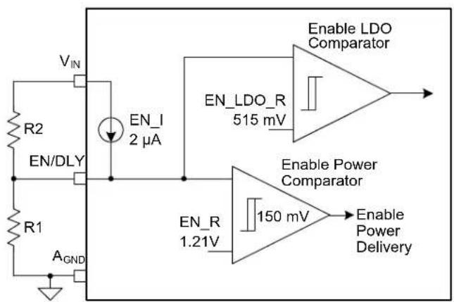
The EN/DLY pin allows programming an external start-up delay. In this case, the driver for the EN/DLY pin should be an open-drain/open-collector type, as shown in Figure 5-1.

text_image
V_IN EN_DLY C_DLY A_GND EN_I 2 µA Enable LDO Comparator EN_LDO_R 515 mV Enable Power Comparator EN_R 1.21V 150 mV Enable Power Delivery OffFIGURE 5-1: Programmable Start-Up Delay Function.
The start-up delay is the delay time from the off falling edge to the assertion of the enable power delivery signal. It can be calculated as shown in Equation 5-1:
The EN/DLY pin can also be used to program a UVLO threshold for power delivery by means of an external resistor divider, as described in Figure 5-2.
EQUATION 5-1:
$$ t _ {S U _ D L Y} = \frac {E N _ R \mathcal {C} _ {D L Y}}{E N _ I} $$
Where:
$$ E N _ R = 1. 2 1 V $$
$$ E N _ I = 2 \mu A $$
$$ C _ {D L Y} = \text { Delay programming external capacitor } $$
text_image
V_IN R2 EN/DLY R1 A_GND EN_I 2 µA Enable LDO Comparator EN_LDO_R 515 mV Enable Power Comparator EN_R 1.21V 150 mV Enable Power DeliveryFIGURE 5-2: Programmable External UVLO Function.
The programmed V_IN UVLO threshold, V_IN_RISE , is given by:
EQUATION 5-2:
$$ V _ {I N _ R I S E} = E N _ R k \left(+ \frac {R _ {2}}{R _ {I}}\right) - E N _ I \times R _ {2} $$
Where:
$$ E N _ R = 1. 2 1 V $$
$$ E N _ I = 2 \mu A $$
$$ R _ {1} \text { and } R _ {2} = \text { External resistors } $$
To desensitize the V_IN UVLO threshold against variations of the pull-up current, EN_I, it is recommended to run the R_1-R_2 voltage divider at a significantly higher current level than the EN_I current.
The corresponding V_IN UVLO hysteresis, V_IN_HYS , is calculated as follows:
EQUATION 5-3:
$$ V _ {I N _ H Y S} = 1 5 0 m V \times \left(1 + \frac {R _ {2}}{R _ {I}}\right) $$
Similar calculations also apply to the internal LDO activation threshold.
5.2 Setting the Switching Frequency
The MIC45404 switching frequency can be programmed using FREQ, as shown in Table 5-1.
TABLE 5-1: SWITCHING FREQUENCY SETTINGS
| FREQ Pin Setting Frequency | |
| High Z (open) 400 kHz | |
| 0 (GND) 565 kHz | |
| 1 ( V_DDA ) 790 kHz |
The switching frequency setting is not arbitrary, but it needs to be adjusted according to the particular output voltage selection due to peak-to-peak inductor ripple requirements. This is illustrated in Section 5.5 "Permissible MIC45404 Settings Combinations".
5.3 Setting the Output Voltage
The MIC45404 output voltage can be programmed by setting pins, VOSET0 and VOSET1, as shown in Table 5-2.
TABLE 5-2: OUTPUT VOLTAGE SETTINGS
| VOSET1 | VOSET0 | Output Voltage |
| 0 (GND) | 0 (GND) | 3.3V |
| 0 (GND) | 1 ( V_DDA ) | 2.5V (2.49V) |
| 1 ( V_DDA ) | 0 (GND) | 1.8V |
| 1 ( V_DDA ) | 1 ( V_DDA ) | 1.5V |
| 0 (GND) | High Z (open) | 1.2V |
| High Z (open) | 0 (GND) | 1.0V |
| 1 ( V_DDA ) | High Z (open) | 0.9V |
| High Z (open) | 1 ( V_DDA ) | 0.8V |
| High Z (open) | High Z (open) | 0.7V |
To achieve accurate output voltage regulation, the OUTSNS pin (internal feedback divider top terminal) should be Kelvin-connected as close as possible to the point of regulation top terminal. Since both the internal reference and the internal feedback divider's bottom terminal refer to A_GND , it is important to minimize voltage drops between the A_GND and the point of regulation return terminal.
5.4 Setting the Current Limit
The MIC45404's valley-mode current limit on the low-side MOSFET can be programmed by means of I_LIM as shown in Table 5-3.
TABLE 5-3: CURRENT LIMIT SETTINGS
| I_LIM | Valley Current Limit(Typical Value) | Rated OutputCurrent |
| 0 (GND) | 4.6 A | 3A |
| 1 ( V_DDA ) | 6.2 A | 4A |
| High Z (open) | 6.8 A | 5A |
Note that the programmed current limit values act as pulse-by-pulse, current limit thresholds on the valley inductor current. If the inductor current has not decayed below the threshold at the time the PWM requires a new on time, the high-side MOSFET turn-on is either delayed, until the valley current recovers below the threshold, or skipped. Each time the high-side MOSFET turn-on is skipped, a 4-bit up-down counter is incremented. When the counter reaches the configuration '1111', a hiccup sequence is invoked in order to reduce power dissipation under prolonged short-circuit conditions.
The highest current limit setting (6.8A) is intended to comfortably accommodate a 5A application. Ensure that the value of the operating junction temperature does not exceed the maximum rating in high output power applications.
5.5 Permissible MIC45404 Settings Combinations
The MIC45404 allowable settings are constrained by the values in Table 5-4.
TABLE 5-4: PERMISSIBLE MIC45404 SETTINGS COMBINATIONS
| Output Voltage Frequency | |
| 3.3V 790 kHz | |
| 2.5V (2.49V) | |
| 1.8V 565 kHz | |
| 1.5V | |
| 1.2V 400 kHz | |
| 1.0V | |
| 0.9V | |
| 0.8V | |
| 0.7V |
5.6 Output Capacitor Selection
Two main requirements determine the size and characteristics of the output capacitor, C_O :
- Steady-state ripple
• Maximum voltage deviation during load transient
For steady-state ripple calculation, both the ESR and the capacitive ripple contribute to the total ripple amplitude. The MIC45404 utilizes a low loss inductor, whose nominal value is 1.2 H. From the switching frequency, input voltage, output voltage setting and load current, the peak-to-peak inductor current ripple and the peak inductor current can be calculated as:
EQUATION 5-4:
$$ \Delta I _ {L _ P P} = V _ {O} \times \left(\frac {I}{f _ {S}} \times L\right) $$
EQUATION 5-5:
$$ I _ {L, P E A K} = I _ {O} + \frac {\Delta I _ {L - P P}}{2} $$
The capacitive ripple, V_r,C , and the ESR ripple, V_r,ESR , are given by:
EQUATION 5-6:
$$ \Delta V _ {R, C} = \frac {\Delta I _ {L P P}}{8 \times f _ {S} \times C _ {O}} $$
EQUATION 5-7:
$$ \Delta V _ {R, E S R} = E S R \times \Delta I _ {L _ P P} $$
The total peak-to-peak output ripple is then conservatively estimated as:
EQUATION 5-8:
$$ \Delta V _ {R} \cong \Delta V _ {R, C} + \Delta V _ {R, E S R} $$
The output capacitor value and ESR should be chosen such that V_R is within specifications. Capacitor tolerance should be considered for worst-case calculations. In case of ceramic output capacitors, factor into account the decrease of effective capacitance versus applied DC bias.
The worst-case load transient for output capacitor calculation is an instantaneous 100% to 0% load release when the inductor current is at its peak value. In this case, all the energy stored in the inductor is absorbed by the output capacitor, while the converter stops switching and keeps the low-side FET on.
The peak output voltage overshoot ( V_0 ) happens when the inductor current has decayed to zero. This can be calculated with Equation 5-9:
EQUATION 5-9:
$$ \Delta V _ {O} = \sqrt {V _ {O} ^ {2} + \frac {L}{C _ {O}} \times I _ {L , P E A K} ^ {2}} - V _ {O} $$
Equation 5-10 calculates the minimum output capacitance value ( C_O(MIN) ) needed to limit the output overshoot below V_O .
EQUATION 5-10:
$$ C _ {O (M I N)} = \frac {L \times I _ {L , P E A K} ^ {2}}{\left(\Delta V _ {O} + V _ {O}\right) ^ {2} - V _ {O} ^ {2}} $$
The result from the minimum output capacitance value for load transient is the most stringent requirement found for capacitor value in most applications. Low Equivalent Series Resistance (ESR) ceramic output capacitors, with X5R or X7R temperature ratings, are recommended.
For low output voltage applications with demanding load transient requirements, using a combination of polarized and ceramic output capacitors may be the most convenient option for smallest solution size.
5.7 Input Capacitor Selection
Two main requirements determine the size and characteristics of the input capacitor:
- Steady-State Ripple
- RMS Current
The Buck Converter input current is a pulse train with very fast rising and falling times, so low-ESR ceramic capacitors are recommended for input filtering because of their good high-frequency characteristics.
By assuming an ideal input filter (which can be assimilated to a DC input current feeding the filtered buck power stage) and by neglecting the contribution of the input capacitor ESR to the input ripple (which is typically possible for ceramic input capacitors), the minimum capacitance value, C_IN(MIN) , needed for a given input peak-to-peak ripple voltage, V_r, IN , can be estimated as shown in Equation 5-11:
EQUATION 5-11:
$$ C _ {I N M I N (} \quad \frac {I _ {O} \times D \times 1 - D}{\Delta V _ {r , I N} \times f _ {S}} = - (\quad) $$
Where:
D is the duty cycle at the given operating point.
The RMS current, I_IN,RMS , of the input capacitor is estimated as in Equation 5-12:
EQUATION 5-12:
$$ I _ {I N, R M S} = I _ {O} \times \sqrt {D \times 1 D} - (\quad) $$
Note that, for a given output current, I_O , worst-case values are obtained at D = 0.5.
Multiple input capacitors can be used to reduce input ripple amplitude and/or individual capacitor RMS current.
5.8 Compensation Design
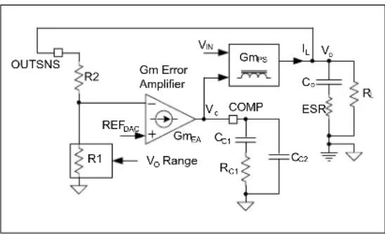
As a simple first-order approximation, the Valley Current mode controlled buck power stage can be modeled as a voltage-controlled current source, feeding the output capacitor and load. The inductor current state variable is removed and the power stage transfer function from COMP to the inductor current is modeled as a transconductance (Gm PS ). The simplified model of the control loop is shown in Figure 5-3. The power stage transconductance, Gm PS , shows some dependence on current levels and it is also somewhat affected by process variations, therefore, some design margin is recommended against the typical value, Gm _PS = 12.5A/V (see Section 1.0 “Electrical Characteristics”).
text_image
OUTSNS R2 Gm Error Amplifier REF DAC GmEA Vo Range VIN GmRS IL Vo Co ESR RL Vc COMP Cc1 Rc1 Cc2FIGURE 5-3: Simplified Small Signal Model of the Voltage Regulation Loop.
This simplified approach disregards all issues related to the inner current loop, like its stability and bandwidth. This approximation is good enough for most operating scenarios, where the voltage loop bandwidth is not pushed to aggressively high frequencies.
Based on the model shown in Figure 5-3, the control-to-output transfer function is:
EQUATION 5-13:
$$ G _ {C O (S)} = \frac {V _ {O (S)}}{V _ {C (S)}} = G m _ {P S} \times R _ {L} \times \frac {\left(1 + \frac {s}{2 \pi \times f _ {Z}}\right)}{\left(1 + \frac {s}{2 \pi \times f _ {P}}\right)} $$
Where f_Z and f_P = the frequencies associated with the output capacitor ESR zero and with the load pole, respectively:
$$ f _ {Z} = \frac {1}{2 \pi \times C _ {O} \times E S R} $$
$$ f _ {P} = \frac {1}{2 \pi \times C _ {O} \times (E S R + R _ {L})} $$
The MIC45404 module uses a transconductance (Gm EA = 1.4 mA/V) error amplifier. Frequency compensation is implemented with a Type-II network (R C1 , C C1 and C C2 ) connected from the COMP to A GND . The compensator transfer function consists of an integrator for zero DC voltage regulation error, a zero to boost the phase margin of the overall loop gain around the crossover frequency and an additional pole that can be used to cancel the output capacitor ESR zero, or to further attenuate switching frequency ripple. In both cases, the additional pole makes the regulation loop less susceptible to switching frequency noise. The additional pole is created by capacitor C C2 (internally provided, C C2 value is 47 pF). Equation 5-14 details the compensator transfer function, H C(S) (from OUTSNS to COMP).
EQUATION 5-14:
$$ H _ {C (S)} = - \frac {R 1}{R 1 + R 2} \times G m _ {E A} \times \frac {1}{S \times \left(C _ {C 1} + C _ {C 2}\right)} $$
$$ \times \frac {(I + S \times R _ {C 1} \times C _ {C 1})}{(I + S \times R _ {C 1} \times \frac {C _ {C 1} \times C _ {C 2}}{C _ {C 1} + C _ {C 2}})} $$
The overall voltage loop gain, T_V(S) , is the product of the control-to-output and the compensator transfer functions:
EQUATION 5-15:
$$ T _ {V (S)} = G _ {C O (S)} \times H _ {C (S)} $$
The value of the attenuation ratio, R1/(R1 + R2), depends on the output voltage selection and can be retrieved as illustrated in Table 5-5:
TABLE 5-5: INTERNAL FEEDBACK DIVIDER ATTENUATION VALUES
| V_O Range R1/(R1 + R2) | A(A = 1 + R2 / R1) | |
| 0.7V-1.2V 1 | 1 | |
| 1.5V-1.8V | 0.5 | 2 |
| 2.5V(2.49V)-3.3V | 0.333 | 3 |
The compensation design process is as follows:
- Set the T_V(s) loop gain crossover frequency, f_XO , in the range of f_S/20 to f_S/10 . Lower values of f_XO allow a more predictable and robust phase margin. Higher values of f_XO would involve additional considerations about the current loop bandwidth in order to achieve a robust phase margin. Taking a more conservative approach is highly recommended.
EQUATION 5-16:
$$ \frac {f _ {S}}{2 0} \leq f _ {X O} \leq \frac {f _ {S}}{1 0} $$
- Select R_C1 to achieve the target crossover frequency, f_XO , of the overall voltage loop. This typically happens where the power stage transfer function, G_CO(S) , is rolling off at -20 dB/decade. The compensator transfer function, H_C(S) , is in the so-called midband gain region, where C_C1 can be considered a DC blocking short circuit, while C_C2 can still be considered as an open circuit, as calculated in Equation 5-17:
EQUATION 5-17:
$$ R _ {C I} = \left(\frac {R I + R 2}{R I}\right) \times \frac {2 \pi \times C _ {O} \times f _ {X O}}{G m _ {E A} \times G m _ {P S}} $$
- Select capacitor C_C1 to place the compensator zero at the load pole. The load pole moves around with load variations, so to calculate the load pole use as a load resistance R_L , the value determined by the nominal output current, I_0 , of the application, as shown in Equation 5-18 and Equation 5-19:
EQUATION 5-18:
$$ R _ {L} = \frac {V _ {O}}{I _ {O}} $$
EQUATION 5-19:
$$ C _ {C 1} = \frac {C _ {O} \times (E S R + R _ {L})}{R _ {C 1}} $$
- Knowing that an internal C_C2 capacitor of 47 pF is provided already, find out if any additional capacitance is needed to augment the overall value of the capacitor, C_C2 .
The C_C2 (total value) is intended for placing the compensator pole at the frequency of the output capacitor ESR zero and/or achieve additional switching ripple/noise attenuation.
If the output capacitor is a polarized one, its ESR zero will typically occur at low enough frequencies to cause the loop gain to flatten out and not roll off at a -20 dB/decade slope, around or just after the crossover frequency, f_XO . This causes undesirable scarce compensation design robustness and switching noise susceptibility. The compensator pole is then used to cancel the output capacitor ESR zero and achieve a well-behaved roll-off of the loop gain above the crossover frequency.
If the output capacitors are only ceramic, then the ESR zeros frequencies could be very high. In many cases, the frequencies could even be above the switching frequency itself. Loop gain roll-off at -20 dB/decade is ensured well beyond the crossover frequency, but even in this case, it is good practice to still make use of the compensator pole to further attenuate switching noise, while conserving phase margin at the crossover frequency.
For example, setting the compensator pole at 5 f_XO will limit its associated phase loss at the crossover frequency to about 11^ . Placement at even higher frequencies, N × f_XO (N > 5), will reduce phase loss even further at the expense of less noise/ripple attenuation at the switching frequency. Some attenuation of the switching frequency noise/ripple is achieved as long as N × f_XO < f_S .
For the polarized output capacitor, compensator pole placement at the ESR zero frequency is achieved, as shown in Equation 5-20:
EQUATION 5-20:
$$ C _ {C 2} \quad \frac {I}{\frac {R _ {C I}}{C _ {O} \times E S R} \quad \frac {I}{C _ {C I}}} = $$
For the ceramic output capacitor, compensator pole placement at N × f_XO ( N ≥ 5 , N × f_XO < f_S ) is achieved, as detailed in Equation 5-21:
EQUATION 5-21:
$$ C _ {C 2} \quad \frac {l}{2 \pi \times R _ {C I} \times N \times f _ {X O}} \frac {l}{C _ {C I}} = $$
The MIC45404 already provides an internal C_C2 capacitor of 47 pF. Therefore, the external capacitance, C_C2_EXT , that should be added is given by Equation 5-22:
EQUATION 5-22:
$$ C _ {C 2 _ E X T} = m a x (C _ {C 2} - 4 7 p F, 0 p F) $$
If the result, C_C2-47 pF, yields to zero or to a negative number, no additional external capacitance is needed for C_C2 .
5.9 Output Voltage Soft Start Rate
The MIC45404 features an internal analog soft start, such that the output voltage can be smoothly increased to the target regulation voltage. The soft start rate shown in Section 1.0 "Electrical Characteristics" is referred to the error amplifier reference, and therefore, the effective soft start rate value, seen at the output of the module, has to be scaled according to the internal feedback divider attenuation values listed in Table 5-5. To calculate the effective output voltage soft start slew rate, SS_SR _OUT , based on the particular output voltage setting and the reference soft start slew rate, SS_SR, use the following formula:
EQUATION 5-23:
$$ S S _ S R _ {O U T} = A \times S S _ S R $$
Where:
$$ A = \text { Amplification } $$
For the value of A, see the right column of Table 5-5.
6.0 PACKAGING INFORMATION
6.1 Package Marking Information
54-Lead QFN (6x10x2.0 mm)

MIC
45404YMP
WNNN

Example

MIC
45404YMP
3925

Legend: XX...X Product code or customer-specific information
Y Year code (last digit of calendar year)
YY Year code (last 2 digits of calendar year)
WW Week code (week of January 1 is week '01')
NNN Alphanumeric traceability code
eBb-free JEDEC ^® designator for Matte Tin (Sn)
* This package is Pb-free. The Pb-free JEDEC designator (e3) can be found on the outer packaging for this package.
•, ▲, ▼ Pin one index is identified by a dot, delta up, or delta down (triangle mark).
Note: In the event the full Microchip part number cannot be marked on one line, it will be carried over to the next line, thus limiting the number of available characters for customer-specific information. Package may or may not include the corporate logo.
Underbar (_) and/or Overbar (̄) symbol may not be to scale.
TITLE
54 LEAD P2QFN 10x6mm PACKAGE (PIP Module) OUTLINE & RECOMMENDED LAND PATTERN
| DRAWING # | P2QFN106-54LD-PL-1 | UNIT | MM |
| Lead Frame | Copper | Lead Finish | Matte Tin |
other
| Label | Description | |---|---| | 1 | LIF | | 2 | LIF | | 3 | LIF | | 4 | LIF | | 5 | LIF | | 6 | LIF | | 7 | LIF | | 8 | LIF | | 9 | LIF | | 10 | SINT | | 11 | SINT | | 12 | SINT | | 13 | SINT | | 14 | SINT | | 15 | SINT | | 16 | SINT | | 17 | SINT | | 18 | SINT | | 19 | SINT | | 20 | SINT | | 21 | SINT | | 22 | SINT | | 23 | SINT | | 24 | SINT | | 25 | SINT | | 26 | SINT | | 27 | SINT | | 28 | SINT | | 29 | SINT | | 30 | SINT | | 31 | SINT | | 32 | SINT | | 33 | SINT | | 34 | SINT | | 35 | SINT | | 36 | SINT | | 37 | SINT | | 38 | SINT | | 39 | SINT | | 40 | SINT | | 41 | SINT | | 42 | SINT | | 43 | SINT | | 44 | SINT | | 45 | SINT | | 46 | SINT | | 47 | SINT | | 48 | SINT | | 49 | SINT | | 50 | SINT | | 51 | SINT | | 52 | SINT | | 53 | SINT | | 54 | SINT | | 55 | SINT | | 56 | SINT | | 57 | SINT | | 58 | SINT | | 59 | SINT | | 60 | SINT | | 61 | SINT | | 62 | SINT | | 63 | SINT | | 64 | SINT | | 65 | SINT | | 66 | SINT | | 67 | SINT | | 68 | SINT | | 69 | SINT | | 70 | SINT | | 71 | SINT | | 72 | SINT | | 73 | SINT | | 74 | SINT | | 75 | SINT | | 76 | SINT | | 77 | SINT | | 78 | SINT | | 79 | SINT | | 80 | SINT | | 81 | SINT | | 82 | SINT | | 83 | SINT | | 84 | SINT | | 85 | SINT | | 86 | SINT | | 87 | SINT | | 88 | SINT | | 89 | SINT | | 90 | SINT | | 91 | SINT | | 92 | SINT | | 93 | SINT | | 94 | SINT | | 95 | SINT | | 96 | SINT | | 97 | SINT | | 98 | SINT | | 99 | SINT | | 100 | SINT | The chart displays the dimensions of a component in a schematic layout, likely representing a circuit or network design. The components are labeled as 'SIN' (inferred from the diagram) and 'SOUT' (inferred from the diagram). The labels above the diagram include 'LIF', 'BUT', 'HCPOUT', 'GND', 'GAS', 'HCPOUT', 'UX', and 'UX'. The dimension '6.00±0.05' is shown on the left side.TOP VIEW
NOTE: 1, 2, 3
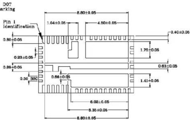
text_image
DOT marking Pin 1 Identification 0.80±0.05 0.23±0.05 0.89±0.05 0.50 35C 8.80±0.05 1.64±0.05 4.50±0.05 1.75±0.05 0.40±0.05 0.63±0.05 1.41±0.05 6.08±0.05 6.35±0.05 8.80±0.05BOTTOM VIEW
NOTE:1,2,3

text_image
2.00±0.10 0.203 Ref 0.00-0.05SIDE VIEW
NOTE: 1, 2, 3
NOTE:
- MAX PACKAGE WARPAGE IS 0.05mm
- MAX ALLOWABLE BURR IS 0.076mm IN ALL DIRECTIONS.
- PIN #1 IS ON TOP WILL BE LASER MARKED
-
RED CIRCLES IN LAND PATTERN REPRESENTS THERMAL VIA. RECOMMENDED SIZE IS 0.30-0.35mm, AT 0.80mm PITCH & SHOULD BE CONNECTED TO GND FOR MAXIMUM PERFORMANCE.
-
GREEN RECTANGLES (SHADED AREA) REPRESENT SOLDER STENCIL OPENING ON EXPOSED PAD AREA
-
CYAN COLORED (SHADED) PAD REPRESENT EXPOSED TRACE KEEP OUT AREA.
-
RECOMMENDED LAND PATTERN TOLERANCE IS 0.020mm UNLESS SPECIFIED.
-
SEE RECOMMENDED LAND PATTERN ON PAGE 2.
Note: For the most current package drawings, please see the Microchip Packaging Specification located at http://www.microchip.com/packaging
POD-Land Pattern Doc #: P2QFN106-54LD-PL-1-A
Recommended Land Pattern
Note: 4,5,6,7,8
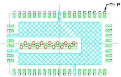
text_image
Pin #1Stacked Up
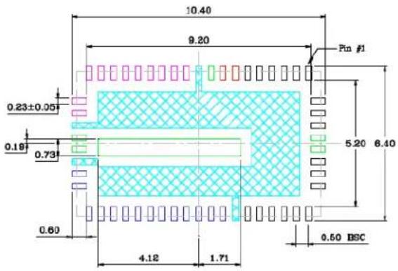
text_image
10.40 9.20 Pin #1 0.23±0.05 0.18 0.73 0.60 4.12 1.71 5.20 6.40 0.50 BSCExposed Metal Trace

text_image
0.80 0.19 R0.15 Pin #1 0.36 0.21 0.80Thermal (filled) VIA
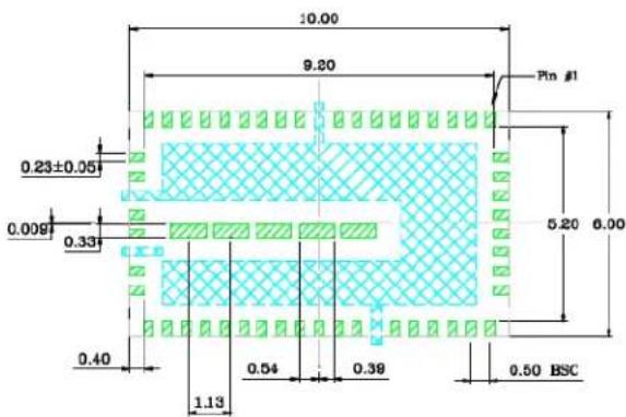
text_image
10.00 9.80 Pin #1 0.23±0.05 0.009 0.33 0.40 1.13 0.54 0.39 0.50 BSC 5.20 6.00Solder Stencil Opening
Note: For the most current package drawings, please see the Microchip Packaging Specification located at http://www.microchip.com/packaging
NOTES:
APPENDIX A: REVISION HISTORY
Revision B (March 2017)
- Updated "Package Types" section.
- Updated Table3-1.
- Added Section 6.1, Package Marking Information.
Revision A (December 2015)
• Original release of this document.
NOTES:
PRODUCT IDENTIFICATION SYSTEM
To order or obtain information, e.g., on pricing or delivery, refer to the factory or the listed sales office.
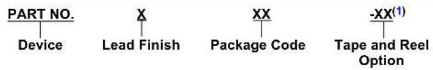
text_image
PART NO. Device X Lead Finish XX Package Code -XX(1) Tape and Reel OptionDevice: MIC45404: Ultra-low profile, synchronous step-down regulator module
Lead Finish: Y = Pb-Free with Industrial Temperature Grade
Package Code: MP = Module Package, thickness ≥ 2.0 mm
Tape and Reel TR = Tape and Reel (1) Option:
Examples:
a) MIC45404YMP-TR: Pb-Free, 54 Lead,
6 x 10 x 2 mm QFN package, Tape and Reel
Note 1: Tape and Reel identifier only appears in the catalog part number description. This identifier is used for ordering purposes and is not printed on the device package. Check with your Microchip Sales Office for package availability with the Tape and Reel option.
NOTES:
Note the following details of the code protection feature on Microchip devices:
• Microchip products meet the specification contained in their particular Microchip Data Sheet.
- Microchip believes that its family of products is one of the most secure families of its kind on the market today, when used in the intended manner and under normal conditions.
- There are dishonest and possibly illegal methods used to breach the code protection feature. All of these methods, to our knowledge, require using the Microchip products in a manner outside the operating specifications contained in Microchip's Data Sheets. Most likely, the person doing so is engaged in theft of intellectual property.
- Microchip is willing to work with the customer who is concerned about the integrity of their code.
- Neither Microchip nor any other semiconductor manufacturer can guarantee the security of their code. Code protection does not mean that we are guaranteeing the product as "unbreakable."
Code protection is constantly evolving. We at Microchip are committed to continuously improving the code protection features of our products. Attempts to break Microchip's code protection feature may be a violation of the Digital Millennium Copyright Act. If such acts allow unauthorized access to your software or other copyrighted work, you may have a right to sue for relief under that Act.
Information contained in this publication regarding device applications and the like is provided only for your convenience and may be superseded by updates. It is your responsibility to ensure that your application meets with your specifications. MICROCHIP MAKES NO REPRESENTATIONS OR WARRANTIES OF ANY KIND WHETHER EXPRESS OR IMPLIED, WRITTEN OR ORAL, STATUTORY OR OTHERWISE, RELATED TO THE INFORMATION, INCLUDING BUT NOT LIMITED TO ITS CONDITION, QUALITY, PERFORMANCE, MERCHANTABILITY OR FITNESS FOR PURPOSE. Microchip disclaims all liability arising from this information and its use. Use of Microchip devices in life support and/or safety applications is entirely at the buyer's risk, and the buyer agrees to defend, indemnify and hold harmless Microchip from any and all damages, claims, suits, or expenses resulting from such use. No licenses are conveyed, implicitly or otherwise, under any Microchip intellectual property rights unless otherwise stated.
Microchip received ISO/TS-16949:2009 certification for its worldwide headquarters, design and wafer fabrication facilities in Chandler and Tempe, Arizona; Gresham, Oregon and design centers in California and India. The Company's quality system processes and procedures are for its PIC® MCUs and dsPIC® DSCs, KEELQ® code hopping devices, Serial EEPROMs, microperipherals, nonvolatile memory and analog products. In addition, Microchip's quality system for the design and manufacture of development systems is ISO 9001:2000 certified.
QUALITY MANAGEMENT SYSTEM
CERTIFIED BY DNV
=ISO/TS 16949=
Trademarks
The Microchip name and logo, the Microchip logo, AnyRate, AVR, AVR logo, AVR Freaks, BeaconThings, BitCloud, CryptoMemory, CryptoRF, dsPIC, FlashFlex, flexPWR, Heldo, JukeBlox, KEELOQ, KEELoo logo, Kleer, LANCheck, LINK MD, maXStylus, maXTouch, MediaLB, megaAVR, MOST, MOST logo, MPLAB, OptoLyzer, PIC, picoPower, PICSTART, PIC32 logo, Prochip Designer, QTouch, RightTouch, SAM-BA, SpyNIC, SST, SST Logo, SuperFlash, tinyAVR, UNI/O, and XMEGA are registered trademarks of Microchip Technology Incorporated in the U.S.A. and other countries.
ClockWorks, The Embedded Control Solutions Company, EtherSynch, Hyper Speed Control, HyperLight Load, IntelliMOS, mTouch, Precision Edge, and Quiet-Wire are registered trademarks of Microchip Technology Incorporated in the U.S.A. Adjacent Key Suppression, AKS, Analog-for-the-Digital Age, Any Capacitor, AnyIn, AnyOut, BodyCom, chipKIT, chipKIT logo, CodeGuard, CryptoAuthentication, CryptoCompanion, CryptoController, dsPICDEM, dsPICDEM.net, Dynamic Average Matching, DAM, ECAN, EtherGREEN, In-Circuit Serial Programming, ICSP, Inter-Chip Connectivity, JitterBlocker, KleerNet, KleerNet logo, Mindi, MiWi, motorBench, MPASM, MPF, MPLAB Certified logo, MPLIB, MPLINK, MultiTRAK, NetDetach, Omniscient Code Generation, PICDEM, PICDEM.net, PICkit, PICtail, PureSilicon, QMatrix, RightTouch logo, REAL ICE, Ripple Blocker, SAM-ICE, Serial Quad I/O, SMART-I.S., SQI, SuperSwitcher, SuperSwitcher II, Total Endurance, TSHARC, USBCheck, VariSense, ViewSpan, WiperLock, Wireless DNA, and ZENA are trademarks of Microchip Technology Incorporated in the U.S.A. and other countries.
SQTP is a service mark of Microchip Technology Incorporated in the U.S.A.
Silicon Storage Technology is a registered trademark of Microchip Technology Inc. in other countries.
GestIC is a registered trademark of Microchip Technology Germany II GmbH & Co. KG, a subsidiary of Microchip Technology Inc., in other countries.
All other trademarks mentioned herein are property of their respective companies.
© 2015-2017, Microchip Technology Incorporated, All Rights Reserved.
ISBN: 978-1-5224-1486-5
Worldwide Sales and Service
AMERICAS
Corporate Office
2355 West Chandler Blvd.
Chandler, AZ 85224-6199
Tel: 480-792-7200
Fax: 480-792-7277
Technical Support:
http://www.microchip.com/
support
Web Address:
www.microchip.com
Atlanta
Duluth, GA
Tel: 678-957-9614
Fax: 678-957-1455
Austin, TX
Tel: 512-257-3370
Boston
Westborough, MA
Tel: 774-760-0087
Fax: 774-760-0088
Chicago
Itasca, IL
Tel: 630-285-0071
Fax: 630-285-0075
Dallas
Addison, TX
Tel: 972-818-7423
Fax: 972-818-2924
Detroit
Novi, MI
Tel: 248-848-4000
Houston, TX
Tel: 281-894-5983
Indianapolis
Noblesville, IN
Tel: 317-773-8323
Fax: 317-773-5453
Tel: 317-536-2380
Los Angeles
Mission Viejo, CA
Tel: 949-462-9523
Fax: 949-462-9608
Tel: 951-273-7800
Raleigh, NC
Tel: 919-844-7510
New York, NY
Tel: 631-435-6000
San Jose, CA
Tel: 408-735-9110
Tel: 408-436-4270
Canada - Toronto
Tel: 905-695-1980
Fax: 905-695-2078
ASIA/PACIFIC
Asia Pacific Office
Suites 3707-14, 37th Floor
Tower 6, The Gateway
Harbour City, Kowloon
Hong Kong
Tel: 852-2943-5100
Fax: 852-2401-3431
Australia - Sydney
Tel: 61-2-9868-6733
Fax: 61-2-9868-6755
China - Beijing
Tel: 86-10-8569-7000
Fax: 86-10-8528-2104
China - Chengdu
Tel: 86-28-8665-5511
Fax: 86-28-8665-7889
China - Chongqing
Tel: 86-23-8980-9588
Fax: 86-23-8980-9500
China - Dongguan
Tel: 86-769-8702-9880
China - Guangzhou
Tel: 86-20-8755-8029
China - Hangzhou
Tel: 86-571-8792-8115
Fax: 86-571-8792-8116
China - Hong Kong SAR
Tel: 852-2943-5100
Fax: 852-2401-3431
China - Nanjing
Tel: 86-25-8473-2460
Fax: 86-25-8473-2470
China - Qingdao
Tel: 86-532-8502-7355
Fax: 86-532-8502-7205
China - Shanghai
Tel: 86-21-3326-8000
Fax: 86-21-3326-8021
China - Shenyang
Tel: 86-24-2334-2829
Fax: 86-24-2334-2393
China - Shenzhen
Tel: 86-755-8864-2200
Fax: 86-755-8203-1760
China - Wuhan
Tel: 86-27-5980-5300
Fax: 86-27-5980-5118
China - Xian
Tel: 86-29-8833-7252
Fax: 86-29-8833-7256
ASIA/PACIFIC
China - Xiamen
Tel: 86-592-2388138
Fax: 86-592-2388130
China - Zhuhai
Tel: 86-756-3210040
Fax: 86-756-3210049
India - Bangalore
Tel: 91-80-3090-4444
Fax: 91-80-3090-4123
India - New Delhi
Tel: 91-11-4160-8631
Fax: 91-11-4160-8632
India - Pune
Tel: 91-20-3019-1500
Japan - Osaka
Tel: 81-6-6152-7160
Fax: 81-6-6152-9310
Japan - Tokyo
Tel: 81-3-6880-3770
Fax: 81-3-6880-3771
Korea - Daegu
Tel: 82-53-744-4301
Fax: 82-53-744-4302
Korea - Seoul
Tel: 82-2-554-7200
Fax: 82-2-558-5932 or
82-2-558-5934
Malaysia - Kuala Lumpur
Tel: 60-3-6201-9857
Fax: 60-3-6201-9859
Malaysia - Penang
Tel: 60-4-227-8870
Fax: 60-4-227-4068
Philippines - Manila
Tel: 63-2-634-9065
Fax: 63-2-634-9069
Singapore
Tel: 65-6334-8870
Fax: 65-6334-8850
Taiwan - Hsin Chu
Tel: 886-3-5778-366
Fax: 886-3-5770-955
Taiwan - Kaohsiung
Tel: 886-7-213-7830
Taiwan - Taipei
Tel: 886-2-2508-8600
Fax: 886-2-2508-0102
Thailand - Bangkok
Tel: 66-2-694-1351
Fax: 66-2-694-1350
EUROPE
Austria - Wels
Tel: 43-7242-2244-39
Fax: 43-7242-2244-393
Denmark - Copenhagen
Tel: 45-4450-2828
Fax: 45-4485-2829
Finland - Espoo
Tel: 358-9-4520-820
France - Paris
Tel: 33-1-69-53-63-20
Fax: 33-1-69-30-90-79
France - Saint Cloud
Tel: 33-1-30-60-70-00
Germany - Garching
Tel: 49-8931-9700
Germany - Haan
Tel: 49-2129-3766400
Germany - Heilbronn
Tel: 49-7131-67-3636
Germany - Karlsruhe
Tel: 49-721-625370
Germany - Munich
Tel: 49-89-627-144-0
Fax: 49-89-627-144-44
Germany - Rosenheim
Tel: 49-8031-354-560
Israel - Ra'anana
Tel: 972-9-744-7705
Italy - Milan
Tel: 39-0331-742611
Fax: 39-0331-466781
Italy - Padova
Tel: 39-049-7625286
Netherlands - Drunen
Tel: 31-416-690399
Fax: 31-416-690340
Norway - Trondheim
Tel: 47-7289-7561
Poland - Warsaw
Tel: 48-22-3325737
Romania - Bucharest
Tel: 40-21-407-87-50
Spain - Madrid
Tel: 34-91-708-08-90
Fax: 34-91-708-08-91
Sweden - Gothenberg
Tel: 46-31-704-60-40
Sweden - Stockholm
Tel: 46-8-5090-4654
UK - Wokingham
Tel: 44-118-921-5800
Fax: 44-118-921-5820