MCP96RL00 - Temperature converter Microchip - Free user manual and instructions
Find the device manual for free MCP96RL00 Microchip in PDF.

User questions about MCP96RL00 Microchip
0 question about this device. Answer the ones you know or ask your own.
Ask a new question about this device
Download the instructions for your Temperature converter in PDF format for free! Find your manual MCP96RL00 - Microchip and take your electronic device back in hand. On this page are published all the documents necessary for the use of your device. MCP96RL00 by Microchip.
USER MANUAL MCP96RL00 Microchip
Thermocouple EMF to Temperature Converter, ±1.5°C Maximum Accuracy
Features
- Thermocouple Electromotive Force (EMF) to °C Converter:
- Integrated cold-junction compensation
- Integrated thermocouple open-circuit and short-circuit detection (MCP9601/L01/RL01)
• Supported Types (designated by NIST ITS-90):
- Type K, J, T, N, S, E, B and R
- Sensor Accuracy for Thermocouple Hot-Junction:
- MCP9600/01 ±0.5°C/±1.5°C (typ./max.)
- MCP96L00/L01 ±2.0°C/±4.0°C (typ./max.)
- MCP96RL00/RL01 ±4.0°C/±8.0°C (typ./max.)
• Measurement Resolution:
- Hot and cold-junctions: +0.0625°C (typical)
- Four Programmable Temperature Alert Outputs:
- Monitor hot or cold-junction temperatures
- Detect rising or falling temperatures
- Up to 255°C of programmable hysteresis
- Programmable Digital Filter for Temperature
- Low Power:
- Shutdown mode
- Burst mode: 1 to 128 temperature samples
- Two-Wire Interface: I ^2 C Compatible, 100 kHz:
- Supports eight devices per I ^2 C Bus
- Operating Voltage Range: 2.7V to 5.5V
- Operating Current: 300~ A (typical)
- Shutdown Current: 2 A (typical)
• Package: 20-Lead MQFN
Typical Applications
• Petrochemical Thermal Management
• Hand-Held Measurement Equipment
- Industrial Equipment Thermal Management
• Commercial and Industrial Ovens
• Industrial Engine Thermal Monitor
• Temperature Detection Racks
Description
The Microchip Technology Inc. MCP960X/L0X/RL0X converts thermocouple EMF to degree Celsius with integrated cold-junction compensation. The temperature correction coefficients are derived from the National Institute of Standards and Technology (NIST) ITS-90 Thermocouple Database. The MCP9600/01 corrects the thermocouple nonlinear error characteristics of eight thermocouple types and outputs ±0.5^/±1.5^ (Typ./Max.).
The MCP960X/L0X/RL0X digital Thermocouple temperature converter comes with user-programmable registers which provide design flexibility for various temperature sensing applications. The registers allow user-selectable settings, such as Low-Power modes for battery powered applications, adjustable digital filter for fast transient temperatures and four individually programmable temperature alert outputs which can be used to detect multiple temperature zones.
In addition, the MCP9601/L01/RL01 family provides integrated thermocouple open-circuit and short-circuit detection features. An alert signal is asserted when the thermocouple wire is broken or disconnected. Similarly, alert signal is asserted when the thermocouple is shorted to ground or power.
The temperature alert limits have multiple user-programmable configurations, such as alert polarity as either an active-low or active-high push-pull output, and output function as a Comparator mode (useful for thermostat-type operation) or Interrupt mode for microprocessor-based systems. In addition, the alerts can detect either a rising or a falling temperature with up to +255°C hysteresis.
This sensor uses an industry standard two-wire, PC compatible serial interface and supports up to eight devices per bus by setting the device address using the ADDR pin.
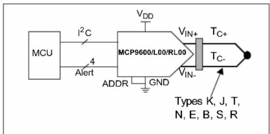
text_image
MCU I²C Alert 4 ADDR GND MCP9600/L00/RL00 VDD VIN+ VIN- Tc+ Tc- Types K, J, T, N, E, B, S, RPackage Types
MCP9600/L00/RL00
5 mm × 5 mm MQFN*

MCP9601/L01/RL01
5 mm × 5 mm MQFN*

heatmap
RL01 | | SDA | SCL | GND | GND | ADDR | |---|---|---|---|---|---| | GND | 20 | 19 | 18 | 17 | 16 | | Alert 4 | 15 | 14 | 13 | 12 | 11 | | VIN+ | 2 | 14 | 13 | 12 | 11 | | GND | 3 | 14 | 13 | 12 | 11 | | VIN- | 4 | 14 | 13 | 12 | 11 | | GND | 5 | 14 | 13 | 12 | 11 | | VSENSE | 6 | 7 | 8 | 9 | 10 | | SC Alert | 6 | 7 | 8 | 9 | 10 | | VDD | 6 | 7 | 8 | 9 | 10 | | OC Alert | 6 | 7 | 8 | 9 | 10 | | GND | 6 | 7 | 8 | 9 | 10 | The chart displays a single data point at the center of the grid. The labels 'Alert 3', 'Alert 2', and 'Alert 1' are positioned above the grid. The values inside the grid represent the number of pins or connections between each input and output pins.* Includes Exposed Thermal Pad (EP); see Table3-1.
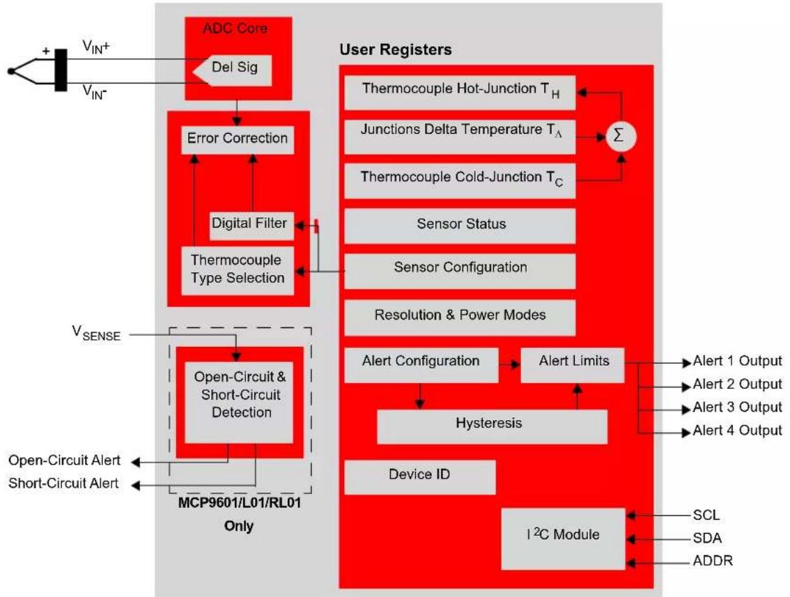
MCP960X/L0X/RL0X Block Diagram
flowchart
graph TD
    A["ADC Core"] --> B["Del Sig"]
    B --> C["Error Correction"]
    C --> D["Digital Filter"]
    D --> E["Thermocouple Type Selection"]
    E --> F["Open-Circuit & Short-Circuit Detection"]
    F --> G["MCP9601/L01/RL01 Only"]
    G --> H["Device ID"]
    H --> I["I²C Module"]
    I --> J["SCL"]
    I --> K["SDA"]
    I --> L["ADDR"]
    M["User Registers"] --> N["Thermocouple Hot-Junction T_H"]
    M --> O["Junctions Delta Temperature T_A"]
    M --> P["Thermocouple Cold-Junction T_C"]
    M --> Q["Sensor Status"]
    M --> R["Sensor Configuration"]
    M --> S["Resolution & Power Modes"]
    T["V_SENSE"] --> F
    U["Open-Circuit Alert"] --> F
    V["Short-Circuit Alert"] --> F
    W["V_IN+"] --> A
    X["V_IN-"] --> A
    Y["Σ"] --> M
    Z["Alert Configuration"] --> AA["Alert Limits"]
    AB["Hysteresis"] --> AC["Hysteresis"]
    AD["Alert 1 Output"] --> AE["Alert 2 Output"]
    AF["Alert 3 Output"] --> AG["Alert 4 Output"]
1.0 ELECTRICAL CHARACTERISTICS
Absolute Maximum Ratings †
| V_DD | 6.0V |
| Voltage at All Input/Output Pins | GND – 0.3V to 6.0V |
| Storage Temperature | -65°C to +150°C |
| Ambient Temperature with Power Applied | -40°C to +125°C |
| Junction Temperature ( T_J ) | +150°C |
| ESD Protection on All Pins (HBM:MM) | (4 kV:300V) |
| Latch-up Current at Each Pin | ±100 mA |
† Notice: Stresses above those listed under “Maximum ratings” may cause permanent damage to the device. This is a stress rating only and functional operation of the device at those or any other conditions above those indicated in the operational listings of this specification is not implied. Exposure to maximum rating conditions for extended periods may affect device reliability.
DC CHARACTERISTICS
| Electrical Specifications: Unless otherwise indicated, V_DD = 2.7V to 5.5V, GND = Ground, T_A = -40°C to +125°C (where: T_A = T_C , defined as Device Ambient Temperature). | ||||||
| Parameters | Sym. | Min. | Typ. | Max. | Unit | Conditions |
| Thermocouple Sensor Measurement Accuracy – MCP9600/01 | ||||||
| T_H Hot-Junction Accuracy ( V_DD = 3.3V ) T_H = T_C + T_ (Note 1) | T_H\_ACY | -1.5 | ±0.5 | +1.5 | °C | T_A = 0°C to +85°C |
| -3.0 | ±1 | +3.0 | T_A = -40°C to +125°C | |||
| T_C Cold-Junction Accuracy ( V_DD = 3.3V ) | T_C\_ACY | -1.0 | ±0.5 | +1.0 | °C | T_A = 0°C to +85°C |
| -2.0 | ±1 | +2.0 | T_A = -40°C to +125°C | |||
| T_ Junctions Temperature Delta Accuracy – MCP9600/01 | ||||||
| Type K: T_ = -200°C to +1372°CVEMFRange: -5.907 mV to 54.886 mV | T_\_ACY | -0.5 | ±0.25 | +0.5 | °C | T_A = 0°C to +85°C, V_DD = 3.3V (Note 2) |
| Type J: T_ = -150°C to +1200°CVEMFRange: -3.336 mV to 47.476 mV | ||||||
| Type T: T_ = -200°C to +400°CVEMFRange: -5.603 mV to 20.81 mV | ||||||
| Type N: T_ = -150°C to +1300°CVEMFRange: -3.336 mV to 47.476 mV | ||||||
| Type E: T_ = -200°C to +1000°CVEMFRange: -8.825 mV to 76.298 mV | ||||||
| Type S: T_ = 250°C to +1664°CVEMFRange: -1.875 mV to 17.529 mV | T_A = 0°C to +85°C, V_DD = 3.3V (Notes 2, 3) | |||||
| Type B: T_ = 1000°C to +1800°CVEMFRange: -4.834 mV to 13.591 mV | ||||||
| Type R: T_ = 250°C to +1664°CVEMFRange: -1.923 mV to 19.732 mV | ||||||
Note 1: The T_C and T_ summation is implemented in milli-volt (mV) domain. The result, T_H (mV), is converted to Degree Celsius using the NIST ITS-90 Conversion database.
2: The T__ACY temperature accuracy specification is defined as the device accuracy to the NIST ITS-90 Thermocouple EMF to Degree Celsius Conversion Database with T_C = 0^ .
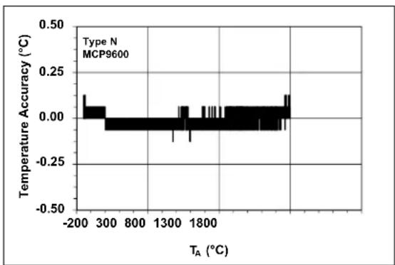
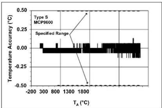
3: The device measures temperature below the specified range, however, the sensitivity to changes in temperature reduces exponentially. Type R and S measure down to -50^ , or -0.226 mV_EMF and -0.235 mV_EMF , respectively. Type B measures down to 500^ or 1.242 mV_EMF (see Figures 2-7, 2-8, 2-10, 2-11, 2-14 and 2-17).
4: Exceeding the V_IN_CM input range may cause leakage current through the ESD protection diodes at the thermocouple input pins. This parameter is characterized but not production tested.
5: The Minimum and Maximum % V_DD thresholds are characterized but not production tested.
DC CHARACTERISTICS (CONTINUED)
| Electrical Specifications: Unless otherwise indicated, V_DD = 2.7V to 5.5V, GND = Ground, T_A = -40°C to +125°C (where: T_A = T_C , defined as Device Ambient Temperature). | ||||||
| Parameters | Sym. | Min. | Typ. | Max. | Unit | Conditions |
| Thermocouple Sensor Measurement Accuracy – MCP96L00/L01 | ||||||
| T_H Hot-Junction Accuracy ( V_DD = 3.3V ) T_H = T_C + T_ (Note 1) | T_H\_ACY | -4.0 ±2 | +4.0 | °C | T_A = 0°C to +85°C | |
| -6.0 ±4 | +6.0 T | A=-40°C to +125°C | ||||
| T_C Cold-Junction Accuracy ( V_DD = 3.3V ) | T_C\_ACY | -1.0 ±0.5 | +1.0 | °C | T_A = 0°C to +85°C | |
| -2.0 ±1 | +2.0 T | A=-40°C to +125°C | ||||
| T_ Juncions Temperature Delta Accuracy – MCP96L00/L01 | ||||||
| Type K: T_ = -200°C to +1372°C V_EMF Range: -5.907 mV to 54.886 mV | T_\_ACY | -3.0 ±1.5 | +3.0 °C | T | A=0°C to +85°C, V_DD = 3.3V (Note 2) | |
| Type J: T_ = -150°C to +1200°C V_EMF Range: -3.336 mV to 47.476 mV | ||||||
| Type T: T_ = -200°C to +400°C V_EMF Range: -5.603 mV to 20.81 mV | ||||||
| Type N: T_ = -150°C to +1300°C V_EMF Range: -3.336 mV to 47.476 mV | ||||||
| Type E: T_ = -200°C to +1000°C V_EMF Range: -8.825 mV to 76.298 mV | ||||||
| Type S: T_ = 250°C to +1664°C V_EMF Range: -1.875 mV to 17.529 mV | T_A = 0°C to +85°C V_DD = 3.3V (Notes 2, 3) | |||||
| Type B: T_ = 1000°C to +1800°C V_EMF Range: -4.834 mV to 13.591 mV | ||||||
| Type R: T_ = 250°C to +1664°C V_EMF Range: -1.923 mV to 19.732 mV | ||||||
Note 1: The T_C and T_A summation is implemented in milli-volt (mV) domain. The result, T_H (mV), is converted to Degree Celsius using the NIST ITS-90 Conversion database.
2: The T__ACY temperature accuracy specification is defined as the device accuracy to the NIST ITS-90 Thermocouple EMF to Degree Celsius Conversion Database with T_C = 0^ .
3: The device measures temperature below the specified range, however, the sensitivity to changes in temperature reduces exponentially. Type R and S measure down to -50^ , or -0.226 mV_EMF and -0.235 mV_EMF , respectively. Type B measures down to 500^ or 1.242 mV_EMF (see Figures 2-7, 2-8, 2-10, 2-11, 2-14 and 2-17).
4: Exceeding the V_IN_CM input range may cause leakage current through the ESD protection diodes at the thermocouple input pins. This parameter is characterized but not production tested.
5: The Minimum and Maximum %V _DD thresholds are characterized but not production tested.
DC CHARACTERISTICS (CONTINUED)
| Electrical Specifications: Unless otherwise indicated, V_DD = 2.7V to 5.5V, GND = Ground, T_A = -40°C to +125°C (where: T_A = T_C , defined as Device Ambient Temperature). | ||||||
| Parameters | Sym. | Min. | Typ. | Max. | Unit | Conditions |
| Thermocouple Sensor Measurement Accuracy – MCP96RL00/01 | ||||||
| T_H Hot-Junction Accuracy ( V_DD = 3.3V ) T_H = T_C + T_ (Note 1) | T_H\_ACY | -8.0 ±4 | +8.0 | °C | T_A = 0°C to +85°C | |
| -10.0 ±6 | +10.0 | T_A = -40°C to +125°C | ||||
| T_C Cold-Junction Accuracy ( V_DD = 3.3V ) | T_C\_ACY | -2.0 ±1 | +2.0 °CT | A = -40°C to +125°C | ||
| T_ Junctions Temperature Delta Accuracy – MCP96RL00/01 | ||||||
| Type K: T_ = -200°C to +1372°C V_EMF Range: -5.907 mV to 54.886 mV | T_\_ACY | -6.0 ±3.0 | +6.0 °C | T | A = 0°C to +85°C, V_DD = 3.3V (Note 2) | |
| Type J: T_ = -150°C to +1200°C V_EMF Range: -3.336 mV to 47.476 mV | ||||||
| Type T: T_ = -200°C to +400°C V_EMF Range: -5.603 mV to 20.81 mV | ||||||
| Type N: T_ = -150°C to +1300°C V_EMF Range: -3.336 mV to 47.476 mV | ||||||
| Type E: T_ = -200°C to +1000°C V_EMF Range: -8.825 mV to 76.298 mV | ||||||
| Type S: T_ = 250°C to +1664°C V_EMF Range: -1.875 mV to 17.529 mV | T_A = 0°C to +85°C, V_DD = 3.3V (Notes 2, 3) | |||||
| Type B: T_ = 1000°C to +1800°C V_EMF Range: -4.834 mV to 13.591 mV | ||||||
| Type R: T_ = 250°C to +1664°C V_EMF Range: -1.923 mV to 19.732 mV | ||||||
Note 1: The T_C and T_ summation is implemented in milli-volt (mV) domain. The result, T_H (mV), is converted to Degree Celsius using the NIST ITS-90 Conversion database.
2: The T__ACY temperature accuracy specification is defined as the device accuracy to the NIST ITS-90 Thermocouple EMF to Degree Celsius Conversion Database with T_C = 0^ .
3: The device measures temperature below the specified range, however, the sensitivity to changes in temperature reduces exponentially. Type R and S measure down to -50^ , or -0.226 mV_EMF and -0.235 mV_EMF , respectively. Type B measures down to 500^ or 1.242 mV_EMF (see Figures 2-7, 2-8, 2-10, 2-11, 2-14 and 2-17).
4: Exceeding the V_IN_CM input range may cause leakage current through the ESD protection diodes at the thermocouple input pins. This parameter is characterized but not production tested.
5: The Minimum and Maximum %V _DD thresholds are characterized but not production tested.
DC CHARACTERISTICS (CONTINUED)
| Electrical Specifications: Unless otherwise indicated, V_DD =2.7V to 5.5V, GND = Ground, T_A =-40°C to +125°C (where: T_A = T_C , defined as Device Ambient Temperature). | ||||||
| Parameters | Sym. | Min. | Typ. | Max. | Unit | Conditions |
| Sensor Characteristics | ||||||
| T_C and T_H Temperature Resolution T | RES | — ±0.0625 — °C | With max. | resolution | ||
| Sampling Rate ( T_A =+25°C) t | CONV | —320 | — | ms | 18-bit resolution | |
| —80 | —16-bit res | solution | ||||
| —20 | —14-bit res | solution | ||||
| —5 | —12-bit res | solution | ||||
| Temperature Calculation Time | tCALC | — | 12 | — | ms | T_A =+25°C |
| Thermocouple Input | ||||||
| Offset Error | V_OERR | — | ±2 | — | μV | |
| Offset Error Drift | V_OE\_DR | — | 50 | — | nV/°C | |
| Full-Scale Gain Error — MCP9600/01 | G_ERR | — | — | ±0.04 | %FS | T_A =0°C to +85°C |
| Full-Scale Gain Error — MCP96L00/L01 | — | ±0.12 | — | T_A =-40°C to +125°C | ||
| Full-Scale Gain Error —MCP96RL00/RL01 | — | ±0.24 | — | |||
| Full-Scale Gain Error Drift | G_ER\_DR | — | ±0.01 | — | %FS | |
| Full-Scale Integral Nonlinearity | INL | — | 10 | — | ppm | |
| Voltage Resolution | V_RES | —2 — | μV | 18-bit resolution | ||
| Differential Mode Range | V_IN\_DF | -250 | — | +250 | mV | ADC input range |
| Differential Mode Impedance | Z_IN\_DF | —300 | — | kΩ | ||
| Common-Mode Range | V_IN\_CM | V_DD -0.3 | — | V_DD +0.3 | V | Note 4 |
| Common-Mode Impedance | Z_IN\_CM | — | 25 | — | MΩ | |
| Common-Mode Rejection Ratio | CMRR | — | 105 | — | dB | |
| Power Supply Rejection Ratio | PSRR | — | 60 | — | dB | |
| Line Regulation | V_Line\_R | — | 0.2 | — | °C/V | |
| Voltage Sense Input ( V_SENSE ) for Thermocouple Open and Short-Circuit Detection (MCP9601/L01/RL01) | ||||||
| V_SENSE Input Range (Note 5) | V_SiRNG | 0 | — | 100 | (see Figure 1-1) | |
| - Short Circuit to V_DD | V_SiSC | 90 — 100 | SC Alert Assets | |||
| - Short Circuit to GND | 0 — 10 | % V_DD | ||||
| - Open-Circuit | V_SiOC | 19 — 50 | OC Alert Assets | |||
| - Normal Operation | V_SiNOR | 10 — 19 | OC Alert Deasserts | |||
| V_SENSE Input Leakage I | SiLEAK | — | 0.1 | 1 | μA | |
Note 1: The T_C and T_ summation is implemented in milli-volt (mV) domain. The result, T_H (mV), is converted to Degree Celsius using the NIST ITS-90 Conversion database.
2: The T_A_ACY temperature accuracy specification is defined as the device accuracy to the NIST ITS-90 Thermocouple EMF to Degree Celsius Conversion Database with T_C = 0^ .
3: The device measures temperature below the specified range, however, the sensitivity to changes in temperature reduces exponentially. Type R and S measure down to -50^ , or -0.226 mV_EMF and -0.235 mV_EMF , respectively. Type B measures down to 500^ or 1.242 mV_EMF (see Figures 2-7, 2-8, 2-10, 2-11, 2-14 and 2-17).
4: Exceeding the V_IN_CM input range may cause leakage current through the ESD protection diodes at the thermocouple input pins. This parameter is characterized but not production tested.
5: The Minimum and Maximum % V_DD thresholds are characterized but not production tested.
DC CHARACTERISTICS (CONTINUED)
| Electrical Specifications: Unless otherwise indicated, V_DD = 2.7V to 5.5V, GND = Ground, T_A = -40°C to +125°C (where: T_A = T_C , defined as Device Ambient Temperature). | ||||||
| Parameters | Sym. | Min. | Typ. | Max. | Unit | Conditions |
| Alert 1, 2, 3, 4 Outputs, SC Alert and OC Alert Outputs (MCP9601/L01/RL01) | ||||||
| Low-Level Voltage V | OL | — | — | 0 | . | OL=43 mA V |
| High-Level Voltage V | OH | V_DD - 0.5 | — | — | V | I_OH = 3 mA |
| Operating Voltage and Current | ||||||
| Operating Voltage V | DD | 2.7 — 5.5 V | ||||
| I^2C Inactive Current | I_DD | — | 0.3 | 0.5 | mA | V_DD = 3.3V , T_A = +85°C |
| I^2C Active Current or During t_CALC | — | 1.5 | 2.5 | mA | ||
| Shutdown Current I | SHDN | — | 2 | 5 | μA | I^2C inactive, T_A = +85°C |
| Power-on Reset (POR) Thresholds | V_POR | 1.0 | 2.1 | 2.6 | V | Rising/Falling V_DD |
| Power-up Time | t_POR | — | 20 | — | ms | |
| Thermal Response | ||||||
| Package Thermal Response (Time to 63% of Final Temperature) | t_RSP | — | 3 | — | s | +25°C (air) to +125°C (oil bath), 2x2" PCB |
Note 1: The T_C and T_ summation is implemented in milli-volt (mV) domain. The result, T_H (mV), is converted to Degree Celsius using the NIST ITS-90 Conversion database.
2: The T__ACY temperature accuracy specification is defined as the device accuracy to the NIST ITS-90 Thermocouple EMF to Degree Celsius Conversion Database with T_C = 0^ .
3: The device measures temperature below the specified range, however, the sensitivity to changes in temperature reduces exponentially. Type R and S measure down to -50^ , or -0.226 mV_EMF and -0.235 mV_EMF , respectively. Type B measures down to 500^ or 1.242 mV_EMF (see Figures 2-7, 2-8, 2-10, 2-11, 2-14 and 2-17).
4: Exceeding the V_IN_CM input range may cause leakage current through the ESD protection diodes at the thermocouple input pins. This parameter is characterized but not production tested.
5: The Minimum and Maximum % V_DD thresholds are characterized but not production tested.
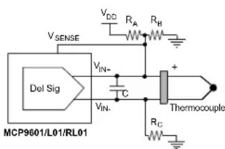
text_image
VSENSE Del Sig VIN- C VIN- VDD RA RB + Thermocouple MCP9601/L01/RL01 RCWhere:
RA = 2 MΩ ± 1% Tolerance (Max.)
R_B=2.49 M±1% Tolerance
Rc = 487 KΩ ± 1% Tolerance
C = 0.1 μF
Note: The exact RA, RB and RC resistor values must be used for a proper function of the Open Circuit detection. The Open and Short-Circuit Detection feature is characterized but not production tested using the R_A , R_B and R_C resistors.
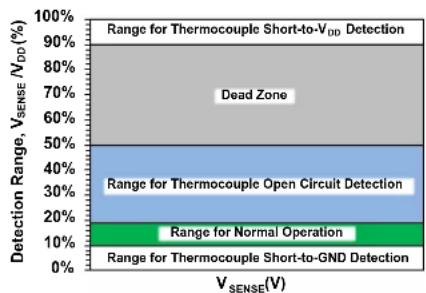
bar_stacked
| Detection Range, V_SENSE (V) | Range for Thermocouple Short-to-V_DD Detection (%) | |---|---| | 0-10% | 90 | | 10-20% | 85 | | 20-30% | 75 | | 30-40% | 65 | | 40-50% | 55 | | 50-60% | 45 | | 60-70% | 35 | | 70-80% | 25 | | 80-90% | 15 | | 90-100% | 10 |FIGURE 1-1: Open and Short-Circuit Detection Configuration.
INPUT/OUTPUT PIN DC CHARACTERISTICS
| Electrical Specifications: Unless otherwise indicated, V_DD = 2.7V to 5.5V, GND = Ground, T_A = -40°C to +125°C (where: T_A = T_C , defined as Device Ambient Temperature). | ||||||
| Parameters Sym. Min. Typ. Max. Units Conditions | ||||||
| Serial Input/Output and I^2C Address Input (ADDR) | ||||||
| Input (SCL, SDA, ADDR) | ||||||
| High-Level Voltage V | IH | 0.7 × V_DD | — | — | V | |
| Low-Level Voltage V | IL | — | — | 0.3 × V_DD | V | |
| Input Current | I_LEAK | — | — | ±2 | μA | |
| Hysteresis | V_HYST | — | 0.05 × V_DD | — | V | V_DD > 2V |
| Spike Suppression | T_SP | — | 50 | — | ns | |
| Output (SDA) | ||||||
| Low-Level Voltage | V_OL | — | — | 0.4 | V_OL =13 mA | |
| High-Level Current (leakage) | I_OH | — | — | 1 | μA | V_OH = V_DD |
| Low-Level Current I | OL | 6 | — | — | mA | V_OL = 0.6V |
| Capacitance | C_IN | — | 5 | — | pF | |
| I^2C Address Selection Levels (Note 1) | ||||||
| Command Byte [1100 000x] | V_ADDR | GND | — | — | V | Address = 0 |
| Command Byte [1100 001x] | V_ADDR\_L (Note 2) | V_ADDR\_TYP (Note 2) | V_ADDR\_H (Note 2) | Address = 1 | ||
| Command Byte [1100 010x] | Address = 2 | |||||
| Command Byte [1100 011x] | Address = 3 | |||||
| Command Byte [1100 100x] | Address = 4 | |||||
| Command Byte [1100 101x] | Address = 5 | |||||
| Command Byte [1100 110x] | Address = 6 | |||||
| Command Byte [1100 111x] | — | — | V_DD | Address = 7 | ||
Note 1 The ADDR pin can be tied to V_DD or V_SS . For additional addresses, a resistive divider network can be used to set voltage levels that are rationed to V_DD . The device supports up to eight levels (see Section 6.3.1 “I²C Addressing” for recommended resistor values).
2 V_ADDR TYP = Address * V_DD/8 + V_DD/16,
V_ADDR_L = V_ADDR_TYP - V_DD/32 and
V_ADDR_H = V_ADDR_TYP + V_DD/32 (where: Address = 1, 2, 3, 4, 5, 6).
TEMPERATURE CHARACTERISTICS
| Electrical Specifications: Unless otherwise indicated, V_DD = 2.7V to 5.5V, GND = Ground. | ||||||
| Parameters | Sym. | Min. | Typ. | Max. | Units | Conditions |
| Temperature Ranges | ||||||
| Specified Temperature Range | T_A | -40 | — | +125 | °C | Note 1 |
| Operating Temperature Range | T_A | -40 | — +125 °C | |||
| Storage Temperature Range | T_A | -65 | — +150 °C | |||
| Thermal Package Resistances | ||||||
| Thermal Resistance, MQFN | _JA | — | 38.8 | — | °C/W | |
Note 1 Operation in this range must not cause T_J to exceed the Maximum Junction Temperature (+150°C).
SENSOR SERIAL INTERFACE TIMING SPECIFICATIONS
| Electrical Specifications: Unless otherwise indicated, GND = Ground, T_A = -40°C to +125°C, V_DD = 2.7V to 5.5V and C_L = 80 p F (Note 1). | ||||
| Parameters Sym. Min. Max. Units | ||||
| Two-Wire I 2C Interface | ||||
| Serial Port Frequency f | SCL | 10 100 kHz | ||
| Low Clock (Note 2) | t_LOW | 4700 | — | ns |
| High Clock | t_HIGH | 4000 | — | ns |
| Rise Time (Note 3) | t_R | — | 1000 | ns |
| Fall Time (Note 3) | t_F | 20 300 | ns | |
| Data in Setup Time (Note 2) | t_SU:DAT | 250 | — | ns |
| Data in Hold Time | t_HD:DAT | 0 | — | ns |
| Start Condition Setup Time | t_SU:STA | 4700 | — | ns |
| Start Condition Hold Time | t_HD:STA | 4000 | — | ns |
| Stop Condition Setup Time | t_SU:STO | 4000 | — | ns |
| Bus Idle/Free | t_B-FREE | 10 | — | μs |
| Bus Capacitive Load | C_b | — | 400 | pf |
| Clock Stretching (Note 4) | t_STRETCH | 60 | — | μs |
Note 1 All values referred to V_IL MAX and V_IH MIN levels.
2 This device can be used in a Standard mode I²C bus system, but the requirement, t SU:DAT ≥ 250 ns, must be met.
3 Characterized, but not production tested.
4 Host controllers without features to detect clock stretching by device should increase the t_LOW period for Read Commands to a minimum of t_STRETCH (60 us) for a proper I^2C communication. See Figure 2-29 for a typical t_STRETCH performance.

text_image
ISU-START HID-START SCL SDA Start Condition
text_image
ACK tSTRETCH tHIGH tLOW tSU-DATA tHD-DI kR-IF Data Transmission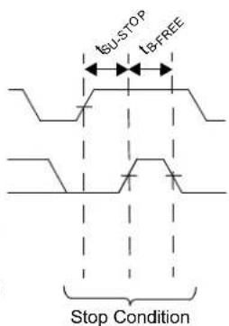
text_image
fSU-STOP 1bFREE Stop ConditionFIGURE 1-2: Timing Diagram.
NOTES:
2.0 TYPICAL PERFORMANCE CURVES
Note: The graphs and tables provided following this note are a statistical summary based on a limited number of samples and are provided for informational purposes only. The performance characteristics listed herein are not tested or guaranteed. In some graphs or tables, the data presented may be outside the specified operating range (e.g., outside specified power supply range) and therefore, outside the warranted range.
Note: Unless otherwise indicated, V_DD = 2.7V to 5.5V, GND = Ground, SDA/SCL pulled-up to V_DD and T_A = -40^ to +125^ .
bar
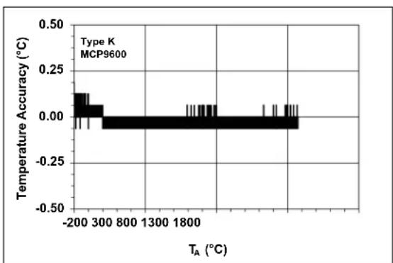
Type K MCP9600 | T_A (°C) | Temperature Accuracy (°C) | |---|---| | -200 | 0.15 | | 300 | 0.08 | | 800 | -0.05 | | 1300 | 0.02 | | 1800 | 0.03 | | 2300 | 0.04 | | 2800 | 0.06 | | 3300 | 0.07 | | 3800 | 0.08 | | 4300 | 0.09 | | 4800 | 0.10 | | 5300 | 0.11 | | 5800 | 0.12 | | 6300 | 0.13 | | 6800 | 0.14 | | 7300 | 0.15 | | 7800 | 0.16 | | 8300 | 0.17 | | 8800 | 0.18 | | 9300 | 0.19 | | 9800 | 0.20 | | 10300 | 0.21 | | 10800 | 0.22 | | 11300 | 0.23 | | 11800 | 0.24 | | 12300 | 0.25 | | 12800 | 0.26 | | 13300 | 0.27 | | 13800 | 0.28 | | 14300 | 0.29 | | 14800 | 0.30 | | 15300 | 0.31 | | 15800 | 0.32 | | 16300 | 0.33 | | 16800 | 0.34 | | 17300 | 0.35 | | 17800 | 0.36 | | 18300 | 0.37 | | 18800 | 0.38 | | 19300 | 0.39 | | 19800 | 0.40 | | 20300 | 0.41 | | 20800 | 0.42 | | 21300 | 0.43 | | 21800 | 0.44 | | 22300 | 0.45 | | 22800 | 0.46 | | 23300 | 0.47 | | 23800 | 0.48 | | 24300 | 0.49 | | 24800 | 0.50 | The chart displays a single bar representing Type K MCP9600 on the Y-axis against the X-axis labeled T_A (°C). The values for the bars are estimated based on the bar height in degrees Celsius.FIGURE 2-1: Typical Temperature Accuracy from NIST ITS-90 Database, Type K.
line
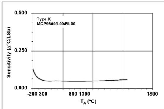
| T_A (°C) | Sensitivity (Δ°C/LSb) | | -------- | --------------------- | | -200 | ~0.15 | | 300 | ~0.05 | | 800 | ~0.02 | | 1300 | ~0.01 | | 1800 | ~0.01 |FIGURE 2-4: Temperature Sensitivity with 18-Bit Resolution, Type K.
bar
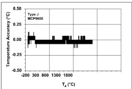
| TA (°C) | Temperature Accuracy (°C) | | ------- | -------------------------- | | -200 | 0.0 | | 300 | 0.0 | | 800 | 0.0 | | 1300 | 0.0 | | 1800 | 0.0 | | 2300 | 0.0 |FIGURE 2-2: Typical Temperature Accuracy from NIST ITS-90 Database, Type J.

line
| T_A (°C) | Sensitivity (ΔC/LSb) | | -------- | -------------------- | | -200 | ~0.05 | | 300 | ~0.02 | | 800 | ~0.01 | | 1300 | ~0.01 | | 1800 | ~0.01 |FIGURE 2-5: Temperature Sensitivity with 18-Bit Resolution, Type J.
bar
| TA (°C) | Temperature Accuracy (°C) | | ------- | -------------------------- | | -200 | 0.15 | | 300 | 0.05 | | 800 | -0.05 | | 1300 | -0.15 | | 1800 | 0.05 | | 2300 | 0.15 |FIGURE 2-3: Typical Temperature Accuracy from NIST ITS-90 Database, Type N.
line
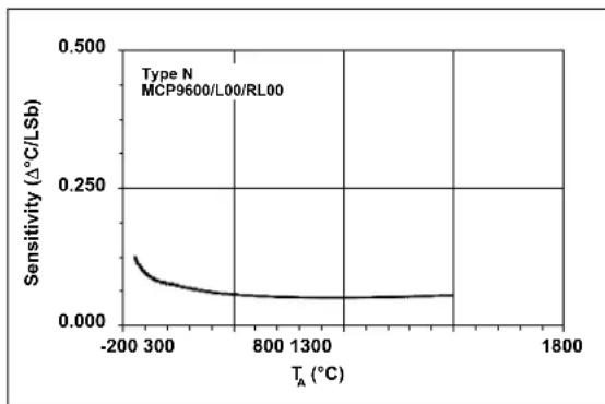
| T_A (°C) | Sensitivity (Δ°C/LSb) | | -------- | --------------------- | | -200 | ~0.15 | | 300 | ~0.05 | | 800 | ~0.02 | | 1300 | ~0.01 | | 1800 | ~0.01 |FIGURE 2-6: Temperature Sensitivity with 18-Bit Resolution, Type N.
Note: Unless otherwise indicated, V_DD = 2.7V to 5.5V, GND = Ground, SDA/SCL pulled-up to V_DD and T_A = -40^ to +125°C.
line
| TA (°C) | Temperature Accuracy (°C) | | ------- | ------------------------- | | 300 | 0.0 | | 800 | 0.0 | | 1300 | 0.0 | | 1800 | -0.5 |FIGURE 2-7: Typical Temperature Accuracy from NIST ITS-90 Database, Type S.
line
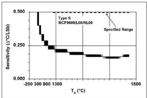
| T_A (°C) | Sensitivity (Δ°C/LSb) | | -------- | --------------------- | | -200 | 0.500 | | 300 | 0.400 | | 800 | 0.250 | | 1300 | 0.200 | | 1800 | 0.150 |FIGURE 2-10: Temperature Sensitivity with 18-Bit Resolution, Type S.
line
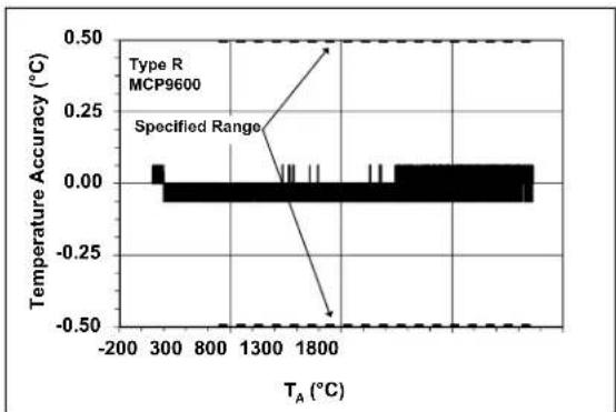
| TA (°C) | Temperature Accuracy (°C) | | ------- | -------------------------- | | 300 | 0.00 | | 1300 | 0.00 | | 1800 | -0.50 |FIGURE 2-8: Typical Temperature Accuracy from NIST ITS-90 Database, Type R.
line
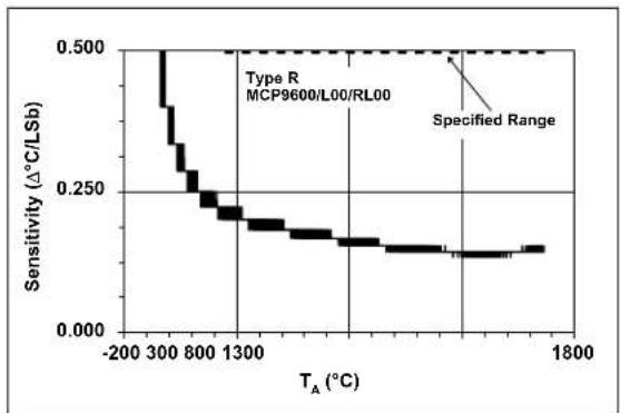
| T_A (°C) | Sensitivity (Δ°C/LSb) | | -------- | --------------------- | | -200 | 0.500 | | 300 | 0.250 | | 800 | 0.250 | | 1300 | 0.250 | | 1800 | 0.150 |FIGURE 2-11: Temperature Sensitivity with 18-Bit Resolution, Type R.
bar
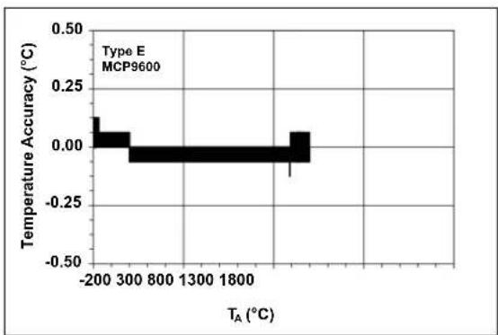
Type E MCP9600 Temperature Accuracy (°C) | T_A (°C) | Temperature Accuracy (°C) | | :--- | :--- | | -200 | 0.15 | | 300 | 0.05 | | 800 | -0.05 | | 1300 | -0.05 | | 1800 | -0.15 | | 2300 | 0.05 |FIGURE 2-9: Typical Temperature Accuracy from NIST ITS-90 Database, Type E.
line
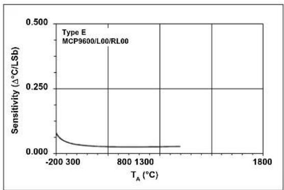
| T_A (°C) | Sensitivity (Δ°C/LSb) | | -------- | --------------------- | | -200 | ~0.05 | | 300 | ~0.01 | | 800 | ~0.005 | | 1300 | ~0.005 | | 1800 | ~0.005 |FIGURE 2-12: Temperature Sensitivity with 18-Bit Resolution, Type E.
Note: Unless otherwise indicated, V_DD = 2.7V to 5.5V, GND = Ground, SDA/SCL pulled-up to V_DD and T_A = -40^ to +125^ .

bar
| Type | Temperature Accuracy (°C) | |---|---| | Type T | 0.00 | | MCP9600 | 0.00 |FIGURE 2-13: Typical Temperature Accuracy from NIST ITS-90 Database, Type T.

line
| T_A (°C) | Sensitivity (Δ°C/LSb) | | -------- | --------------------- | | -200 | 0.15 | | 300 | 0.05 | | 800 | 0.01 | | 1300 | 0.005 | | 1800 | 0.002 |FIGURE 2-16: Temperature Sensitivity with 18-Bit Resolution, Type T.

line
| TA (°C) | Temperature Accuracy (°C) | | ------- | ------------------------- | | 1800 | -0.50 |FIGURE 2-14: Typical Temperature Accuracy from NIST ITS-90 Database, Type B.

line
| TA (°C) | Sensitivity (Δ°C/LSb) | | ------- | --------------------- | | 800 | 0.40 | | 1300 | 0.25 | | 1800 | 0.15 |FIGURE 2-17: Temperature Sensitivity with 18-Bit Resolution, Type B.
line
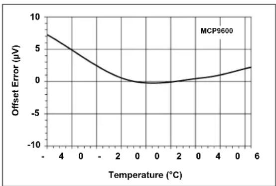
| Temperature (°C) | Offset Error (μV) | | ---------------- | ----------------- | | -4 | 7.0 | | 0 | 0.0 | | 6 | 2.0 |FIGURE 2-15: Input Offset Error Voltage ( V_IN+ , V_IN- ).

line
| Temperature (°C) | Gain Error (% of FSR) | | ---------------- | --------------------- | | -40 | 0.05 | | 0 | 0.0 | | 20 | -0.05 | | 40 | -0.1 | | 60 | -0.05 | | 80 | 0.0 | | 100 | 0.05 | | 120 | 0.1 |FIGURE 2-18: Full-Scale Gain Error.
Note: Unless otherwise indicated, V_DD = 2.7V to 5.5V, GND = Ground, SDA/SCL pulled-up to V_DD and T_A = -40^ to +125°C.
line
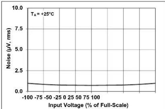
| Input Voltage (% of Full-Scale) | Noise (μV, rms) | | -------------------------------- | ---------------- | | -100 | 1.0 | | -75 | 0.8 | | -50 | 0.6 | | -25 | 0.4 | | 0 | 0.3 | | 25 | 0.2 | | 50 | 0.1 | | 75 | 0.2 | | 100 | 0.3 |FIGURE 2-19: Input Noise, % of Full Scale.
line
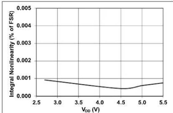
| V_DD (V) | Integral Nonlinearity (% of FSR) | | -------- | -------------------------------- | | 2.5 | 0.001 | | 3.0 | 0.0009 | | 3.5 | 0.0007 | | 4.0 | 0.0005 | | 4.5 | 0.0004 | | 5.0 | 0.0006 | | 5.5 | 0.0008 |FIGURE 2-22: Integral Nonlinearity Across V_DD .
line
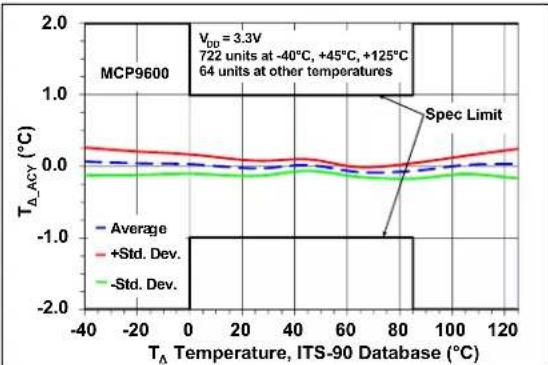
| T_A Temperature, ITS-90 Database (°C) | Average | +Std. Dev. | -Std. Dev. | | -------------------------------------- | ------- | --------- | --------- | | -40 | ~0.0 | ~0.0 | ~0.0 | | 0 | ~0.0 | ~0.0 | ~0.0 | | 20 | ~0.0 | ~0.0 | ~0.0 | | 40 | ~0.0 | ~0.0 | ~0.0 | | 60 | ~0.0 | ~0.0 | ~0.0 | | 80 | ~0.0 | ~0.0 | ~0.0 | | 100 | ~0.0 | ~0.0 | ~0.0 | | 120 | ~0.0 | ~0.0 | ~0.0 |FIGURE 2-20: Cold-Junction Sensor Temperature Accuracy.
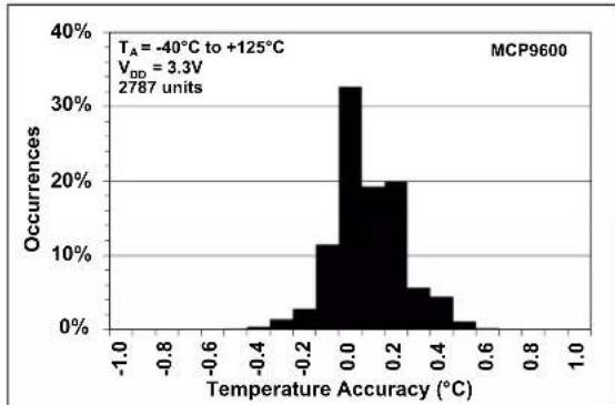
histogram
| Temperature Accuracy (°C) | Occurrences | | ------------------------- | ----------- | | -1.0 to -0.8 | 0% | | -0.8 to -0.6 | 0% | | -0.6 to -0.4 | 0% | | -0.4 to -0.2 | 0% | | -0.2 to 0.0 | 12% | | 0.0 to 0.2 | 32% | | 0.2 to 0.4 | 20% | | 0.4 to 0.6 | 5% | | 0.6 to 0.8 | 1% | | 0.8 to 1.0 | 0% |FIGURE 2-23: Cold-Junction Sensor Temperature Accuracy Distribution.

line
| V_DD (V) | T_A = -40°C | T_A = +35°C | T_A = +85°C | T_A = +125°C | | -------- | ----------- | ----------- | ----------- | ------------ | | 2.5 | ~100 | ~110 | ~130 | ~150 | | 3.0 | ~80 | ~90 | ~110 | ~130 | | 3.5 | ~60 | ~70 | ~90 | ~110 | | 4.0 | ~50 | ~60 | ~80 | ~100 | | 4.5 | ~40 | ~50 | ~70 | ~90 | | 5.0 | ~30 | ~40 | ~60 | ~80 | | 5.5 | ~20 | ~30 | ~50 | ~70 |FIGURE 2-21: SDA and Alert Outputs, V OL Across VDD .
line
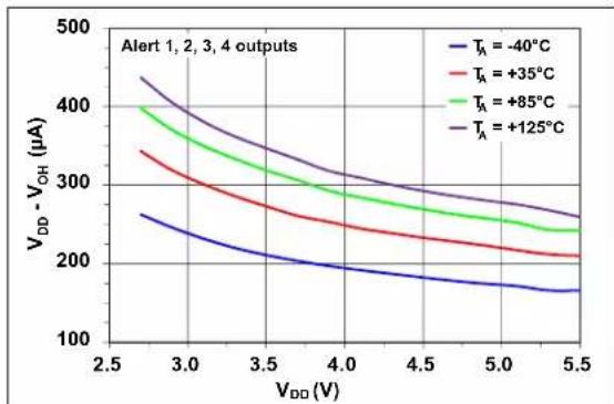
| V_DD (V) | T_A = -40°C | T_A = +35°C | T_A = +85°C | T_A = +125°C | | -------- | ----------- | ----------- | ----------- | ------------ | | 2.5 | ~260 | ~340 | ~400 | ~440 | | 3.0 | ~220 | ~300 | ~360 | ~400 | | 3.5 | ~200 | ~270 | ~330 | ~360 | | 4.0 | ~190 | ~250 | ~310 | ~340 | | 4.5 | ~180 | ~230 | ~290 | ~320 | | 5.0 | ~170 | ~210 | ~270 | ~300 | | 5.5 | ~160 | ~200 | ~250 | ~280 |FIGURE 2-24: Alert Outputs, V OH Across VDD .
Note: Unless otherwise indicated, V_DD = 2.7V to 5.5V, GND = Ground, SDA/SCL pulled-up to V_DD and T_A = -40^ to +125°C.
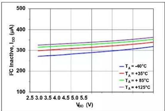
FIGURE 2-25: I ^2 C Inactive, I_DD Across V_DD .

line
| V_DD (V) | I_LEAK (μA) for T_A = -40°C | I_LEAK (μA) for T_A = +35°C | I_LEAK (μA) for T_A = +85°C | I_LEAK (μA) for T_A = +125°C | | -------- | --------------------------- | --------------------------- | --------------------------- | ---------------------------- | | 2.5 | ~0.3 | ~0.3 | ~0.3 | ~0.3 | | 3.0 | ~0.3 | ~0.3 | ~0.3 | ~0.3 | | 3.5 | ~0.3 | ~0.3 | ~0.3 | ~0.3 | | 4.0 | ~0.3 | ~0.3 | ~0.3 | ~0.3 | | 4.5 | ~0.3 | ~0.3 | ~0.3 | ~0.3 | | 5.0 | ~0.3 | ~0.3 | ~0.3 | ~0.3 | | 5.5 | ~0.3 | ~0.3 | ~0.3 | ~0.3 | | 6.0 | ~0.3 | ~0.3 | ~0.3 | ~0.3 | | 6.5 | ~0.3 | ~0.3 | ~0.3 | ~0.3 | | 7.0 | ~0.3 | ~0.3 | ~0.3 | ~0.3 | | 7.5 | ~0.3 | ~0.3 | ~0.3 | ~0.3 | | 8.0 | ~0.3 | ~0.3 | ~0.3 | ~0.3 | | 8.5 | ~0.3 | ~0.3 | ~0.3 | ~0.3 | | 9.0 | ~0.3 | ~0.3 | ~0.3 | ~0.3 | | 9.5 | ~0.3 | ~0.3 | ~0.3 | ~0.3 | | 10.0 | ~0.3 | ~0.3 | ~0.3 | ~0.3 |FIGURE 2-28: SDA, SCL and ADDR Input Pins Leakage Current, I_LEAK Across V_DD .
line
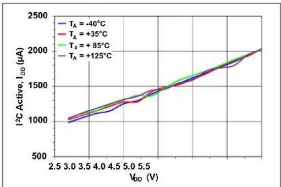
| V_DD (V) | I²C Active, I_DD (μA) for T_A = -40°C | I²C Active, I_DD (μA) for T_A = +35°C | I²C Active, I_DD (μA) for T_A = +85°C | I²C Active, I_DD (μA) for T_A = +125°C | | -------- | ------------------------------------ | ------------------------------------ | ------------------------------------ | ------------------------------------- | | 2.5 | ~950 | ~1000 | ~1000 | ~1000 | | 3.0 | ~1000 | ~1050 | ~1050 | ~1050 | | 3.5 | ~1100 | ~1150 | ~1150 | ~1150 | | 4.0 | ~1200 | ~1250 | ~1250 | ~1250 | | 4.5 | ~1300 | ~1350 | ~1350 | ~1350 | | 5.0 | ~1400 | ~1450 | ~1450 | ~1450 | | 5.5 | ~1500 | ~1550 | ~1550 | ~1550 | | 6.0 | ~1600 | ~1650 | ~1650 | ~1650 | | 6.5 | ~1700 | ~1750 | ~1750 | ~1750 | | 7.0 | ~1800 | ~1850 | ~1850 | ~1850 | | 7.5 | ~1900 | ~1950 | ~1950 | ~1950 | | 8.0 | ~2000 | ~2000 | ~2000 | ~2000 | | 8.5 | ~2000 | ~2000 | ~2000 | ~2000 | | 9.0 | ~2000 | ~2000 | ~2000 | ~2000 | | 9.5 | ~2000 | ~2000 | ~2000 | ~2000 | | 10.0 | ~2000 | ~2000 | ~2000 | ~2000 |FIGURE 2-26: I ^2 C Active, I_DD Across V_DD .

FIGURE 2-29: I ^2 C Interface Clock Stretch Duration, t_STRETCH Across V_DD .

line
| V_DD (V) | T_A = -40°C | T_A = +35°C | T_A = +85°C | T_A = +125°C | | -------- | ----------- | ----------- | ----------- | ------------ | | 2 | ~0.8 | ~0.9 | ~1.0 | ~2.1 | | 5 | ~1.0 | ~1.1 | ~1.2 | ~2.3 | | 0 | ~1.2 | ~1.3 | ~1.4 | ~2.6 | | 5 | ~1.4 | ~1.5 | ~1.6 | ~3.0 |FIGURE 2-27: Shutdown Current, I SHDN Across V_DD .
line
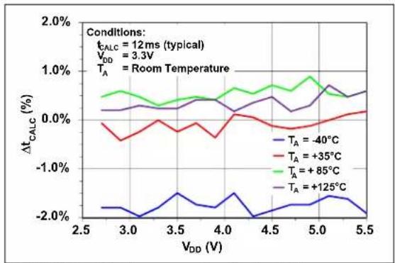
| V_DD (V) | T_A = -40°C | T_A = +35°C | T_A = +85°C | T_A = +125°C | | -------- | ----------- | ----------- | ----------- | ------------ | | 2.5 | -2.0% | -0.5% | 0.5% | 0.0% | | 3.0 | -2.0% | -0.5% | 0.5% | 0.0% | | 3.5 | -1.5% | -0.5% | 0.5% | 0.0% | | 4.0 | -1.5% | -0.5% | 0.5% | 0.0% | | 4.5 | -1.5% | -0.5% | 0.5% | 0.0% | | 5.0 | -1.5% | -0.5% | 0.5% | 0.0% | | 5.5 | -2.0% | -0.5% | 0.5% | 0.0% |FIGURE 2-30: Temperature Calculation Duration, t_CALC Change Across V_DD .
NOTES:
3.0 PIN DESCRIPTIONS
The descriptions of the pins are listed in Table 3-1.
TABLE 3-1: PIN FUNCTION TABLE
| MCP9600/L00/RL00 | MCP9601/L01/RL01 | Symbol Pin | Function |
| 1, 3, 5,13, 17 1, 3, | 5, 13, 17 GND | Electrical Ground | |
| 2 | 2 | V_IN+ | Thermocouple Positive Terminal Input |
| 4 | 4 | V_IN- | Thermocouple Negative Terminal Input |
| 6, 7, 9, 10, 18 | 10, 18 | GND | Not Electrical Ground; must be tied to Ground |
| — | 6 | V_SENSE | Thermocouple Open and Short-Circuit detection input |
| — | 7 | SC Alert | Thermocouple Short-Circuit Alert Output |
| 8 | 8 | V_DD | Power |
| — | 9 | OC Alert | Thermocouple Open-Circuit Alert Output |
| 11 | 11 | Alert 1 | Alert Output 1 |
| 12 | 12 | Alert 2 | Alert Output 2 |
| 14 | 14 | Alert 3 | Alert Output 3 |
| 15 | 15 | Alert 4 | Alert Output 4 |
| 16 | 16 | ADDR | I^2C Device Address Selection Voltage Input |
| 19 | 19 | SCL | I^2C Clock Input |
| 20 | 20 | SDA | I^2C Data Input |
| 21 | 21 | EP | Exposed Thermal Pad (EP); must be connected to GND |
3.1 Ground Pin (GND)
The GND pin is the system ground pin. Pins 1, 3, 5, 13 and 17 are system ground pins and they are at the same potential. However, pins 6, 7, 9, 10 and 18 must be connected to ground for normal operation.
3.2 Thermocouple Input (V IN+, VIN-)
The thermocouple wires are directly connected to these inputs. The positive node is connected to the V_IN+ pin, while the negative node connects to the V_IN- node. The thermocouple voltage is converted to degree Celsius.
3.3 Power Pin (V DD)
V_DD is the power pin. The operating voltage range, as specified in the DC Characteristics table, is applied on this pin.
3.4 Push-Pull Alert Outputs
(Alert 1, 2, 3, 4 and OC/SC Alert)
The Alert pins are user-programmable push-pull outputs which can be used to detect rising or falling temperatures. The device outputs signal when the ambient temperature exceeds the user-programmed temperature alert limit.
The Open-Circuit (OC) Alert and the Short-Circuit (SC) Alert output are also active-high push-pull outputs (MCP9601/L01/RL01). These outputs are asserted when Open-Circuit and Short-Circuit conditions are detected on the V_SENSE pin.
3.5 I ^2 C Address Pin (ADDR)
This pin is used to set the address. This pin can be tied to V_DD , GND, or a ratio of V_DD can be selected to set up to eight address levels using a resistive voltage divider network.
3.6 Serial Clock Line (SCL)
The SCL is a clock input pin. All communication and timing is relative to the signal on this pin. The clock is generated by the host controller on the bus (see Section 4.0 "Serial Communication").
3.7 Serial Data Line (SDA)
SDA is a bidirectional input/output pin used to serially transmit data to/from the host controller. This pin requires a pull-up resistor (see Section 4.0 "Serial Communication").
3.8 Thermocouple Open/Short Detection Input ( V_SENSE )
The V_SENSE pin is a thermocouple detection input pin (MCP9601/L01/RL01) and the voltage level on this pin is used to determine whether the thermocouple is operating normally, shorted to V_DD/V_SS , or it is disconnected from the V_IN+ and V_IN- pins (see Figure 1-1).
NOTES:
4.0 SERIAL COMMUNICATION
4.1 Two-Wire Standard Mode I ^2 C Protocol-Compatible Interface
The MCP960X/L0X/RL0X Serial Clock Input (SCL) and the bidirectional Serial Data Line (SDA) form a two-wire bidirectional data communication line (refer to the Input/Output Pin DC Characteristics table and Sensor Serial Interface Timing Specifications table).
The following bus protocol has been defined:
TABLE 4-1: MCP960X/L0X/RL0X SERIAL BUS PROTOCOL DESCRIPTIONS
| Term Description | |
| Host The device that controls the serial bus, typically a microcontroller | |
| Device | The device addressed by the host, such as the MCP960X/L0X/RL0X |
| Transmitter | Device sending data to the bus |
| Receiver | Device receiving data from the bus |
| START A unique signal from host to initiate serial interface with a device | |
| STOP | A unique signal from the host to terminate serial interface from a device |
| Read/Write | A read or write to the MCP960X/L0X/RL0X registers |
| ACK A receiver | Acknowledges (ACK) the reception of each byte by polling the bus |
| NAK A receiver | Not Acknowledges (NAK) or releases the bus to show End-of-Data (EOD) |
| Busy | Communication is not possible because the bus is in use |
| Not Busy | The bus is in the Idle state, both SDA and SCL remain high |
| Data Valid | SDA must remain stable before SCL becomes high in order for a data bit to be considered valid. During normal data transfers, SDA only changes state while SCL is low. |
4.1.1 DATA TRANSFER
Data transfers are initiated by a Start condition (START), followed by a 7-bit device address and a read/write bit. An Acknowledge (ACK) from the device confirms the reception of each byte. Each access must be terminated by a Stop condition (STOP).
Repeated communication is initiated after B-FREE.
This device supports the Receive Protocol. The register can be specified using the pointer for the initial read. Each repeated read or receive begins with a Start condition and address byte. The MCP960X/L0X/RL0X retains the previously selected register. Therefore, it outputs data from the previously-specified register (repeated pointer specification is not necessary).
4.1.2 HOST/DEVICE
The bus is controlled by a host device (typically a microcontroller) that controls the bus access, and generates the Start and Stop conditions. The MCP960X/L0X/RL0X is a device and does not control other devices in the bus. Both host and device can operate as either transmitter or receiver. However, the host device determines which mode is activated.
4.1.3 START/STOP CONDITION
A high-to-low transition of the SDA line (while SCL is high) is the Start condition. All data transfers must be preceded by a Start condition from the host. A low-to-high transition of the SDA line (while SCL is high) signifies a Stop condition.
If a Start or Stop condition is introduced during data transmission, the MCP960X/L0X/RL0X releases the bus. All data transfers are ended by a Stop condition from the host.
4.1.4 ADDRESS BYTE
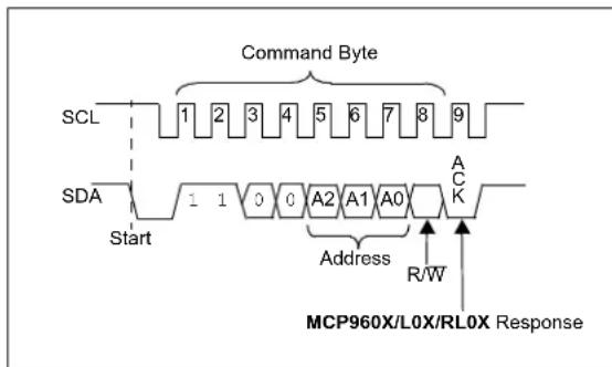
Following the Start condition, the host must transmit an 8-bit address byte to the MCP960X/L0X/RL0X. The address for the MCP960X/L0X/RL0X temperature sensor is '11, 0, 0, A2, A1, A0' in binary, where the A2, A1 and A0 bits are set externally by connecting the corresponding V_ADDR voltage levels on the ADDR pin (see the "Input/Output Pin DC Characteristics" section). The 7-bit address transmitted in the serial bit stream must match the selected address for the MCP960X/L0X/RL0X to respond with an ACK. Bit 8 in the address byte is a read/write bit. Setting this bit to '1' commands a read operation, while '0' commands a write operation (see Figure 4-1).
text_image
Command Byte SCL 1 2 3 4 5 6 7 8 9 SDA Start 1 1 0 0 A2 A1 A0 ACK Address R/W MCP960X/L0X/RL0X ResponseFIGURE 4-1: Device Addressing.
4.1.5 DATA VALID
After the Start condition, each bit of data in transmission needs to be settled for a time specified by t_SU-DATA before SCL toggles from low-to-high (see the "Sensor Serial Interface Timing Specifications" section).
4.1.6 ACKNOWLEDGE (ACK/NAK)
Each receiving device, when addressed, is expected to generate an ACK bit after the reception of each byte. The host device must generate an extra clock pulse for ACK to be recognized.
The Acknowledging device pulls down the SDA line for t_SU-DATA before the low-to-high transition of SCL from the host. SDA also needs to remain pulled down for t_HD-DAT after a high-to-low transition of SCL.
During read, the host must signal an End-of-Data (EOD) to the device by not generating an ACK bit (NAK) once the last bit has been clocked out of the device. In this case, the device will leave the data line released to enable the host to generate the Stop condition.
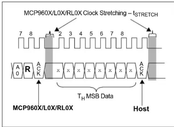
4.1.7 CLOCK STRETCHING
During the I^2C read operation, this device will hold the I^2C clock line low for t_STRECH after the falling edge of the ACK signal. In order to prevent bus contention, the host controller must release or hold the SCL line low during this period.
Note: If the host controller does not provide the adequate delay as specified by t_STRECH , then the device will output the previously transmitted data.
In addition, the host controller must provide eight consecutive clock cycles after generating the ACK bit from a read command. This allows the device to push out data from the SDA Output Shift registers. Missing clock cycles could result in bus contention. At the end of one or more data transmission, the host controller must provide the NAK bit, followed by a Stop Condition to terminate communication (see Figure 4-3).
text_image
MCP960X/L0X/RL0X Clock Stretching - tSTRETCH 7 8 2 3 4 5 6 7 8 A R ACK x x x x x x x x x X ACK T_H MSB Data MCP960X/L0X/RL0X HostFIGURE 4-2: Clock Stretching.
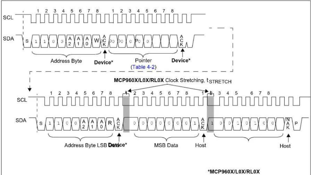
4.1.8 SEQUENTIAL READ
During a sequential read, the device transmits data bytes starting from the previously set Register Pointer. The MCP960X/L0X/RL0X increments an internal address pointer each time a byte transmission is successfully completed with an ACK bit from the host controller. Therefore, the device can sequentially output the entire register values shown in Table 5-1 (see Figure 4-6). A Stop Condition terminates the sequential read.
Note: The MCP960X/L0X/RL0X does not support Sequential Write function.
text_image
SCL 1 2 3 4 5 6 7 8 1 2 3 4 5 6 7 8 SDA S 1 1 0 0 A A A W ACK 00 00 0 P 0 ACK Address Byte Device* Pointer Device* (Table 4-2) MCP960X/L0X/RL0X Clock Stretching. t_STRETCH SCL 1 2 3 4 5 6 7 8 1 2 3 4 5 6 7 8 1 2 3 4 5 6 7 8 SDA S 1 1 0 0 A A A R ACK 00 00 00 00 01 ACK 1 0 0 1 0 1 0 0 NAK P Address Byte LSB Device* MSB Data Host *MCP960X/L0X/RL0XTABLE 4-2: POINTERS
| Read-Only Registers | Pointer |
| T_H | 0000 0000 |
| T_ | 0000 0001 |
| T_C | 0000 0010 |
Note: this is an example pseudo routine:
i2c_start(); // send START command
i2c_write(b'1100 0000'); // WRITE Command
// also, make sure bit 0 is cleared '0'
i2c_write(b'0000 00XX'); // Write T_H, T_Δ, or T_C registers
i2c_stop(); // send STOP command
i2c_start(); // send START command
i2c_write(b'1100 0001'); // READ Command
// also, make sure bit 0 is set '1'
UpperByte = i2c_read(ACK); // READ 8 bits (with t_STRETCH delay)
// and Send ACK bit
LowerByte = i2c_read(NAK); // READ 8 bits (with t_STRETCH delay)
// and Send NAK bit
i2c_stop(); // send STOP command
//Convert the temperature data
if ((UpperByte & 0x80) == 0x80) //Temperature < 0°C
Temperature = (UpperByte x 16 + LowerByte / 16) - 4096;
} else //Temperature ≥ 0°C
Temperature = (UpperByte x 16 + LowerByte / 16);
//T_H, T_D, or T_C Temperature (°C) depending on the register pointer value shown in Table 4-2.
FIGURE 4-3: Timing Diagram to Set a Register Pointer and Read a Two-Byte Data.

text_image
SCL SDA S 1 2 3 4 5 6 7 8 1 2 3 4 5 6 7 8 1 2 3 4 5 6 7 8 Address Byte Device* Configuration (Table 4-3) Device* Register Data MCP960X/L0X/RL0X Clock Stretching, t_STRETCH SCL SDA S 1 2 3 4 5 6 7 8 1 2 3 4 5 6 7 8 Address Byte LSB Data Device* Host Address Write LSB Data Read/Write Registers Pointer STATUS 0000 0100 Configuration 0000 0101 0000 0110 Note: this is an example pseudo routine: i2c_start(); // send START command i2c_write(b'1100 0000'); // WRITE Command // also, make sure bit 0 is cleared '0' i2c_write(b'0000 0101'); // Write Status or Configuration registers i2c_write(b'XXXX XXXX'); // Write register data i2c_stop(); // send STOP command i2c_start(); // send START command i2c_write(b'1100 0001'); // READ Command // also, make sure bit 0 is set '1' Data = i2c_read(NAK); // READ 8 bits (with t_STRETCH delay) // and Send NAK bit i2c_stop(); // send STOP command *MCP960X/L0X/RL0XFIGURE 4-4: Timing Diagram to Set a Register Pointer, Write One Byte, and Read the Data.

flowchart
graph TD
    subgraph SCL
        A1["1"] --> B1["2"] --> C1["3"] --> D1["4"] --> E1["5"] --> F1["6"] --> G1["7"] --> H1["8"] --> I1["1"] --> J1["2"] --> K1["3"] --> L1["4"] --> M1["5"] --> N1["6"] --> O1["7"] --> P1["8"] --> Q1["1"] --> R1["2"] --> S1["3"] --> T1["4"] --> U1["5"] --> V1["6"] --> W1["7"] --> X1["8"] --> Y1["1"] --> Z1["2"] --> AA1["3"] --> AB1["4"] --> AC1["5"] --> AD1["6"] --> AE1["7"] --> AF1["8"]
    end

    subgraph SDA
        AG["S"] --> AH["SCL"]
        AI["SDA"] --> AJ["Address Byte"]
        AK["Device*"] --> AL["Alert Limit 1 (Table 4-4)"]
        AM["Device*"] --> AN["Alert 1 MSB"]
        AO["Device*"] --> AP["Alert 1 LSB"]
        AQ["Device*"] --> AR["Alert 1 LSB"]
        AS["Device*"] --> AT["Alert 1 LSB"]
        AU["Device*"] --> AV["Alert 1 LSB"]
        AW["Device*"] --> AX["Alert 1 LSB"]
    end

    SCL["SCL"] --> SDA["SDA"]
    SDA --> SCL
    SCL --> SCL
    SDA --> SDA
    SDA --> SCL
    SCL -->|MCP960X/L0X/RL0X Clock Stretching, t_STRETCH| SCL
    SDA -->|Address Byte| SCL
    SDA -->|Device*| SDA
    SDA -->|Alert 1 MSB| SCL
    SDA -->|Host| SCL
    SDA -->|Alert 1 LSB| SCL
    SDA -->|Host| SCL
    SCL -->|Device*| SDA
    SDA -->|Device*| SCL
TABLE 4-4: POINTERS
| Alert Limit Registers | Pointer |
| Alert 1 0001 | 0000 |
| Alert 2 0001 | 0001 |
| Alert 3 0001 | 0010 |
| Alert 4 0001 | 0011 |
*MCP960X/L0X/RL0X
Note: this is an example pseudo routine:
i2c_start(); // send START command
i2c_write(b'1100 0000'); //WRITE Command
//also, make sure bit 0 is cleared '0'
i2c_write(b'0001 00XX'); // Write Alert registers
i2c_write(b'xxxx xxxx'); // Write register Upper Byte
i2c_write(b'XXXX XXXX'); // Write register Lower Byte
i2c_stop(); // send STOP command
i2c_start(); // send START command
i2c_write(b'1100 0001'); //READ Command
//also, make sure bit 0 is set '1'
UpperByte = i2c_read(ACK); // READ 8 bits (with t _STRETCH delay) //and Send ACK bit
LowerByte = i2c_read(NAK); // READ 8 bits (with t STRETCH delay) //and Send NAK bit
i2c_stop(); // send STOP command
FIGURE 4-5: Timing Diagram to Set a Register Pointer, Write Two Bytes, and Read the Data.
text_image
SCL SDA 1 2 3 4 5 6 7 8 1 2 3 4 5 6 7 8 Address Byte Device* Pointer to T_H Register Device* MCP960X/LOX/RL0X Clock Stretching, t_STRETCH SCL SDA 1 2 3 4 5 6 7 8 1 2 3 4 5 6 7 8 Address Byte Device* T_H MSB Data Host T_H LSB Data Host MCP960X/LOX/RL0X Clock Stretching, t_STRETCH 1 2 3 4 5 6 7 8 1 2 3 4 5 6 7 8 T_C MSB Data Host T_C LSB Data Host T_Δ MSB Data Host Device ID LSB Note: this is an example pseudo routine: i2c_start(); // send START command i2c_write(b'1100 0000'); // WRITE Command // also, make sure bit 0 is cleared '0' i2c_write(b'0000 0000'); // Write T H register to set the starting register for sequential read i2c_stop(); // send STOP command i2c_start(); // send START command i2c_write(b'1100 0001'); // READ Command // also, make sure bit 0 is set '1' for (i=0; i<29, i++){ Data_Buffer[i] = i2c_read(ACK); // READ 8 bits (with t_STRETCH delay) // and Send ACK bit } Data_Buffer[i] = i2c_read(NAK); // READ 8 bits (with t_STRETCH delay) // and Send NAK bit i2c_stop(); // send STOP command *MCP960X/LOX/RL0XFIGURE 4-6: Timing Diagram to Sequential Read All Registers Starting from T _H Register.
5.0 FUNCTIONAL DESCRIPTION
The MCP960X/L0X/RL0X Thermocouple temperature converter consists of an 18-bit Delta-Sigma Analog-to-Digital Converter (ADC), which is used to measure the thermocouple voltage or EMF, a digital
temperature sensor used to measure cold-junction or ambient temperature and a processor core which is used to compute the EMF to degree Celsius conversion using coefficients derived from the NIST ITS-90 coefficients Figure 5-1 shows a block diagram of how these functions are structured in the device.

flowchart
graph TD
    A["Thermocouple"] --> B["ADC Core"]
    B --> C["Del Sig"]
    C --> D["Error Correction"]
    D --> E["Thermocouple Type Selection"]
    D --> F["Digital Filter"]
    E --> G["Sensor Status"]
    F --> H["Sensor Configuration"]
    G --> I["Device Resolution and Power Modes"]
    H --> I
    I --> J["Configuration"]
    J --> K["Alert 1 Limit"]
    K --> L["Alert 1 Output"]
    I --> M["Hysteresis"]
    M --> N["Hysteresis"]
    N --> O["Configuration"]
    O --> P["Alert 2 Limit"]
    P --> Q["Alert 2 Output"]
    I --> R["Hysteresis"]
    R --> S["Hysteresis"]
    S --> T["Configuration"]
    T --> U["Alert 3 Limit"]
    U --> V["Alert 3 Output"]
    I --> W["Hysteresis"]
    W --> X["Hysteresis"]
    X --> Y["Configuration"]
    Y --> Z["Alert 4 Limit"]
    Z --> AA["Alert 4 Output"]
    I --> AB["Hysteresis"]
    AB --> AC["Device ID"]
    AC --> AD["I²C Module"]
    AD --> AE["SCL"]
    AD --> AF["SDA"]
    AD --> AG["ADDR"]
    subgraph User Registers:
        H
        I
        J
        K
        L
        M
        N
        O
        P
        Q
        S
        T
        U
        V
        W
        X
        Y
        Z
        AA
        AB
        AC
        AD
        AE
        AF
        AG
    end
FIGURE 5-1: Functional Block Diagram.
The MCP960X/L0X/RL0X device has several registers that are user-accessible. These registers include the Thermocouple Temperature (cold-junction compensated), Hot-Junction Temperature, Cold-Junction Temperature, Raw ADC Data, user-programmable Alert Limit registers, and STATUS and Configuration registers.
The Temperature and the Raw ADC Data registers are read-only registers, used to access the thermocouple and the ambient temperature data. In addition, the four Alert Temperature registers are individually controlled, and can be used to detect a rising and/or a falling temperature change. If the ambient temperature drifts beyond the user-specified limits, the MCP960X/L0X/RL0X device outputs an alert flag at the corresponding pin (refer to Section 5.3.3 "Alert Configuration Registers"). The alert limits can also be used to detect critical temperature events.
The MCP960X/L0X/RL0X also provides STATUS and Configuration registers, which allow users to detect device statuses. The Configuration registers provide various features, such as adjustable temperature measurement resolution and Shutdown modes. The thermocouple types can also be selected using the Configuration registers.
The registers are accessed by sending a Register Pointer to the MCP960X/L0X/RL0X using the serial interface. This is an 8-bit write-only pointer. Register 5-1 describes the pointer definitions.
REGISTER 5-1: REGISTER POINTER
| U-0 U-0 W-0 W-0 W-0 W-0 W-0 W-0 | ||||||
| — | — | P[5:0] | ||||
| bit 7 | bit 0 | |||||
| Legend: | |||
| R = Readable bit | W = Writable bit | U = Unimplemented bit, read as '0' | |
| -n = Value at POR | '1' = Bit is set | '0' = Bit is cleared | x = Bit is unknown |
bit 7-6 Unimplemented: Read as '0'
bit 5-0 P[5:0]: Pointer bits
0000 0000 = Thermocouple Hot-Junction register, T_H
0000 0001 = Junctions Temperature Delta register, T A
0000 0010 = Cold-Junction Temperature register, TC
0000 0011 = Raw ADC Data register
0000 0100 = STATUS register
0000 0101 = Thermocouple Sensor Configuration register
0000 0110 = Device Configuration register
0000 1000 = Alert 1 Configuration register
0000 1001 = Alert 2 Configuration register
0000 1010 = Alert 3 Configuration register
0000 1011 = Alert 4 Configuration register
0000 1100 = Alert 1 Hysteresis register, T_HYST1
0000 1101 = Alert 2 Hysteresis register, T_HYST2
0000 1110 = Alert 3 Hysteresis register, T HYST3
0000 1111 = Alert 4 Hysteresis register, THYST4
0001 0000 = Temperature Alert 1 Limit register, T ALERT1
0001 0001 = Temperature Alert 2 Limit register, T ALERT2
0001 0010 = Temperature Alert 3 Limit register, T ALERT3
0001 0011 = Temperature Alert 4 Limit register, T ALERT4
0010 0000 = Device ID/Revision register
TABLE 5-1: SUMMARY OF REGISTERS AND BIT ASSIGNMENTS
| Register Pointer bit 7 bit 6 bit 5 bit 4 bit 3 bit 2 bit 1 bit 0 | |||||||||
| Hot-Junction Temperature - TH | 00000000 | SIGN | 1024°C | 512°C | 256°C | 128°C | 64°C | 32°C | 16°C |
| 8°C | 4°C | 2°C | 1°C | 0.5°C | 0.25°C | 0.125°C | 0.0625°C | ||
| Junctions Temperature Delta - TA | 00000001 | SIGN | 1024°C | 512°C | 256°C | 128°C | 64°C | 32°C | 16°C |
| 8°C | 4°C | 2°C | 1°C | 0.5°C | 0.25°C | 0.125°C | 0.0625°C | ||
| Cold-Junction Temperature - TC | 00000010 | SIGN | 128°C | 64°C | 32°C | 16°C | |||
| 8°C | 4°C | 2°C | 1°C | 0.5°C | 0.25°C | 0.125°C | 0.0625°C | ||
| Raw Data ADC | 00000011 | SIGN | bit 17 | bit 16 | |||||
| bit 15 | — | — | — | — | — | — | bit 8 | ||
| bit 7 | — | — | — | — | — | — | bit 0 | ||
| STATUS MCP9600/L00/RL00 | 00000100 | Burst Complete | THUpdate | — Input Range Alert Status | 4 Status | Alert 3 Status | Alert 2 Status | Alert 1 Status | |
| STATUS MCP9601/L01/RL01 | Short-Circuit (SC) | Open-Circuit (OC)/Input Range | |||||||
| Thermocouple Sensor Configuration | 00000101 | — | Thermocouple Type Select Type K, J, T, N, S, E, B, R | — | Filter Coefficients | ||||
| Device Configuration | 00000110 | Cold-Junc. Resolution | ADC Resolution | Burst Mode Temperature Samples Shutdown Modes | |||||
| Unimplemented bits, Read as '0' | |||||||||
| Alert 1 Configuration | 00001000 | Interrupt Clear | — | — Monitor TH or TC | Detect Rising or Fall-ing Temps | Active- High or Active-Low Output | Comparator or Interrupt Mode | Enable Alert Output | |
| Alert 2 Configuration | 00001001 | ||||||||
| Alert 3 Configuration | 00001010 | ||||||||
| Alert 4 Configuration | 00001011 | ||||||||
| Alert 1 Hysteresis | 00001100 | 128°C | 64°C | 32°C | 16°C | 8°C | 4°C | 2°C | 1°C |
| Alert 2 Hysteresis 000011101 | |||||||||
| Alert 3 Hysteresis 00001110 | |||||||||
| Alert 4 Hysteresis 00001111 | |||||||||
| Alert 1 Limit | 00010000 | SIGN | 1024°C | 512°C | 256°C | 128°C | 64°C | 32°C | 16°C |
| 8°C | 4°C | 2°C | 1°C | 0.5°C | 0.25°C | — | — | ||
| Alert 2 Limit | 00010001 | SIGN | 1024°C | 512°C | 256°C | 128°C | 64°C | 32°C | 16°C |
| 8°C | 4°C | 2°C | 1°C | 0.5°C | 0.25°C | — | — | ||
| Alert 3 Limit | 00010010 | SIGN | 1024°C | 512°C | 256°C | 128°C | 64°C | 32°C | 16°C |
| 8°C | 4°C | 2°C | 1°C | 0.5°C | 0.25°C | — | — | ||
| Alert 4 Limit | 00010011 | SIGN | 1024°C | 512°C | 256°C | 128°C | 64°C | 32°C | 16°C |
| 8°C | 4°C | 2°C | 1°C | 0.5°C | 0.25°C | — | — | ||
| Device ID/Revision MCP9600/L00/RL00 | 00100000 | 0 | 1 | 0 | 0 | 0 | 0 | 0 | 0 |
| Revision-Major | Revision-Minor | ||||||||
| Device ID/Revision MCP9601/L01/RL01 | 0 | 1 | 0 | 0 | 0 | 0 | 0 | 1 | |
| Revision-Major | Revision-Minor | ||||||||
5.1 Thermocouple Temperature Sensor Registers
This device integrates three Temperature registers that are used to read the cold and hot-junction temperatures, and the sum of the two junctions to output the absolute thermocouple temperature. In addition, the Raw ADC Data register, which is used to derive the thermocouple temperature, is available. The following sections describe each register in detail.
5.1.1 THERMOCOUPLE TEMPERATURE REGISTER ( T_H )
This register contains the cold-junction compensated and error-corrected thermocouple temperature in degree Celsius. The temperature data from this register is the absolute Thermocouple Hot-Junction temperature, T_H , to the specified accuracy (see Section 1.0 “Electrical Characteristics”. T_H is the sum of the values in the T_ and T_C registers, as shown in Figure 5-2.
EQUATION 5-1: TEMPERATURE CONVERSION
Temperature ≥ 0°C
$$ T _ {H} = (U p p e r B y t e x 1 6 + L o w e r B y t e / 1 6) $$
Temperature < 0^
$$ T _ {H} = (U p p e r B y t e x 1 6 + L o w e r B y t e / 1 6) - 4 0 9 6 $$
The temperature bits are in two's complement format; therefore, positive temperature data and negative temperature data are computed differently. Equation 5-1 shows how to convert the binary data to temperature in degree Celsius.
flowchart
graph TD
    A["Temperature Sensor Core"] -->|T_C| B["Σ"]
    C["V_IN+"] --> D["ADC Core"]
    E["V_IN-"] --> F["Delta-Sigma 18-Bit"]
    D --> G["Error Corrected Temperature"]
    F --> G
    B --> H["Thermocouple Temperature"]
    G --> I["T_Δ"]
    I --> B
FIGURE 5-2: Thermocouple Temperature Register Block Diagram.
REGISTER 5-2: THERMOCOUPLE TEMPERATURE REGISTER - T H (READ-ONLY)
| R-0 R-0 R-0 R-0 R-0 | R-0 | R-0 | R-0 | ||||
| SIGN | 1024°C | 512°C | 256°C | 128°C | 64°C | 32°C | 16°C |
| bit 15 bit 8 | |||||||
| R-0 R-0 R-0 R-0 R-0 | R-0 | R-0 | R-0 | ||||
| 8°C | 4°C | 2°C | 1°C | 0.5°C | 0.25°C | 0.125°C | 0.0625°C |
| bit 7 bit 0 | |||||||
Legend:
R = Readable bit
W = Writable bit
U = Unimplemented bit, read as '0'
-n = Value at POR
'1' = Bit is set
'0' = Bit is cleared
x = Bit is unknown
bit 15-0
T_H : Data in Two's Complement Format. Bit 15 is the sign bit and it is set when the temperature data is less than 0^ .
This register contains the error corrected and cold-junction compensated thermocouple temperature.
5.1.2 THERMOCOUPLE JUNCTIONS DELTA TEMPERATURE REGISTER (T _ )
This register contains the error corrected Thermocouple Hot-Junction temperature without the Cold-Junction compensation. The error correction methodology uses several coefficients to convert the digitized Thermocouple EMF voltage to degree Celsius. Each Thermocouple type has a unique set of coefficients as specified by NIST, and these coefficients are available in the configuration register for user selection as shown in Figure 5-3.
EQUATION 5-2: TEMPERATURE CONVERSION
Temperature ≥ 0°C
$$ T _ {\Delta} = (U p p e r B y t e x 1 6 + L o w e r B y t e / 1 6) $$
Temperature < 0^
$$ T _ {\Delta} = (U p p e r B y t e x 1 6 + L o w e r B y t e / 1 6) - 4 0 9 6 $$
The temperature bits are in two's complement format, therefore, positive temperature data and negative temperature data are computed differently, as shown in Equation 5-2.
flowchart
graph TD
    A["ADC Core"] --> B["Delta-Sigma 18-Bit"]
    C["User-Selectable, Thermocouple Types: - T y p e K<br>- T y p e J<br>- T y p e T<br>- T y p e N<br>- T y p e S<br>- T y p e E<br>- T y p e B<br>- T y p e R<br>(see Register 5-6)"] --> D["Check if the ADC code is within range for the selected thermocouple type"]
    D --> E["ADC code to degree Celsius conversion using coefficients derived from NIST look-up table database"]
    E --> F["TΔ"]
    F --> G["Thermocouple Junctions Delta Temperature - TΔ"]
    A --> H["VIN+"]
    A --> I["VIN-"]
    H --> J["ADC"]
    I --> J
FIGURE 5-3: Thermocouple Hot-Junction Register ( T_ ) Block Diagram.
REGISTER 5-3: HOT-JUNCTION TEMPERATURE REGISTER -T △ (READ-ONLY)
| R-0 | R-0 | R-0 | R-0 | R-0 | R-0 | R-0 | R-0 |
| SIGN | 1024°C | 512°C | 256°C | 128°C | 64°C | 32°C | 16°C |
| bit 15 bit 8 | |||||||
| R-0 | R-0 | R-0 | R-0 | R-0 | R-0 | R-0 | R-0 |
| 8°C | 4°C | 2°C | 1°C | 0.5°C | 0.25°C | 0.125°C | 0.0625°C |
| bit 7 bit 0 | |||||||
Legend:
R = Readable bit
W = Writable bit
U = Unimplemented bit, read as '0'
-n = Value at POR
'1' = Bit is set
'0' = Bit is cleared
x = Bit is unknown
bit 15-0
T_ : Data in Two's Complement Format. Bit 15 is the sign bit and it is set when the temperature data is less than 0^ .
This register contains Thermocouple Hot-Junction temperature data without the cold-junction compensation.
5.1.3 COLD-JUNCTION/AMBIENT TEMPERATURE REGISTER ( T_C )
The MCP960X/L0X/RL0X integrates an ambient temperature sensor which can be used to measure the thermocouple cold-junction temperature. For accurate measurement, the device will have to be placed at close proximity to the thermocouple cold-junction to detect the junction ambient temperature. This is a 16-bit double-buffered, read-only register. The temperature resolution is user-selectable to 0.0625°C/LSb or 0.25°C/LSb resolutions and setting the resolution determines the temperature update rate, as shown in Table 5-2.
EQUATION 5-3: TEMPERATURE CONVERSION
$$ \text { Temperature } \geq 0 ^ {\circ} \mathrm{C} $$
$$ T _ {C} = (U p p e r B y t e x 1 6 + L o w e r B y t e / 1 6) $$
$$ \text { Temperature } < 0 ^ {\circ} \mathrm{C} $$
$$ T _ {C} = (U p p e r B y t e x 1 6 + L o w e r B y t e / 1 6) - 4 0 9 6 $$
The temperature bits are in two's complement format; therefore, positive temperature data and negative temperature data are computed differently, as shown in Equation 5-3.
TABLE 5-2: RESOLUTION vs. CONVERSION TIME
| Resolution | Conversion Time (typical) | Register Bits (Note 1) |
| 0.0625°C 25 | ms ssss | xxxx xxxx xxxx |
| 0.25°C 63 ms | ssss xxx | xxxx xx00 |
Note 1: 's' is Sign and 'x' is unknown bit.
flowchart
graph TD
    A["Ambient Temperature Sensor Core"] -->|T_C| B["Thermocouple Cold-Junction Temperature -T_C"]
    C["Selectable Resolution: - 0.0625°C, - 0.25°C (see Register 5-8)"]
    C --> A
FIGURE 5-4: Thermocouple Cold-Junction Register ( T_C ) Block Diagram.
REGISTER 5-4: COLD-JUNCTION TEMPERATURE REGISTER - T_C (READ ONLY)
| R-0 | R-0 | R-0 | R-0 | R-0 | R-0 | R-0 | R-0 |
| SIGN | 128°C | 64°C | 32°C | 16°C | |||
| bit 15 bit 8 | |||||||
| R-0 | R-0 | R-0 | R-0 | R-0 | R-0 | R-0 | R-0 |
| 8°C | 4°C | 2°C | 1°C | 0.5°C | 0.25°C | 0.125°C | 0.0625°C |
| bit 7 bit 0 | |||||||
| Legend: | |||
| R = Readable bit | W = Writable bit | U = Unimplemented bit, read as '0' | |
| -n = Value at POR | '1' = Bit is set | '0' = Bit is cleared | x = Bit is unknown |
bit 15-0
T_C : Data in Two's Complement Format. Bits 15-12 are sign bits and the bits are set when the temperature data is less than 0^ .
This register contains the thermocouple cold-junction temperature or the device ambient temperature data. Bits 1 and 0 may remain clear ('0') depending on the status of the Resolution setting, bit 7 of Register 5-8.
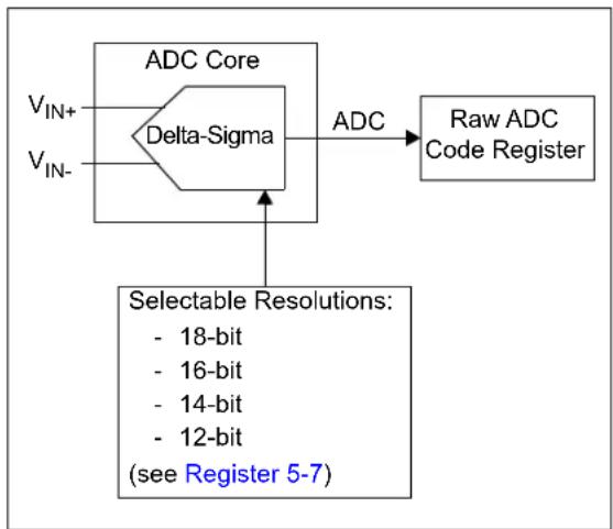
5.1.4 ANALOG-TO-DIGITAL CONVERTER (ADC)
The MCP960X/LOX/RL0X uses an 18-bit Delta-Sigma Analog-to-Digital Converter to digitize the Thermocouple EMF voltage and the data is available in the ADC register. The ADC measurement resolution is selectable, which enables the user to choose faster conversion times with reduced resolution. This feature is useful to detect fast transient temperatures.
TABLE 5-3: ADC RESOLUTION (32)
| Resolution/ Sensitivity (typical) | Conversion Time (typical) | Raw ADC Register Bit Format (Note 1) |
| 18-bit/2 μV 320 | ms ssss sssx | xxxx xxxxxxxx xxxx |
| 16-bit/8 μV 80 ms | ms ssss sssx | xxxx xxxxxxxx xx00 |
| 14-bit/32μV | 20 ms | ssss sssx xxxx xxxxxxxxxxxxx 0000 |
| 12-bit/128 μV | 5 ms | ssss sssx xxxx xxxxxxxxxxxx00 0000 |
Note 1: 's' is the Sign bit and 'x' is the ADC data bit.
2: See Section 6.2.2 "Conversion Time vs. Self-Heat".
flowchart
graph TD
    A["V_IN+"] --> B["Delta-Sigma"]
    C["V_IN-"] --> B
    B --> D["ADC"]
    D --> E["Raw ADC Code Register"]
    F["Selectable Resolutions:"] --> G["- 18-bit"]
    F --> H["- 16-bit"]
    F --> I["- 14-bit"]
    F --> J["- 12-bit (see Register 5-7)"]
FIGURE 5-5: Delta-Sigma Analog-to-Digital Converter, ADC Core Block Diagram.
REGISTER 5-5: 24-BIT ADC REGISTER (READ-ONLY)
| R-0 | R-0 | R-0 | R-0 | R-0 | R-0 | R-0 | R-0 |
| SIGN | ADC Data | ||||||
| bit 23 | bit 16 | ||||||
| R-0 | R-0 | R-0 | R-0 | R-0 | R-0 | R-0 | R-0 |
| ADC Data | |||||||
| bit 15 | bit 8 | ||||||
| R-0 | R-0 | R-0 | R-0 | R-0 | R-0 | R-0 | R-0 |
| ADC Data | |||||||
| bit 7 | bit 0 | ||||||
| Legend: | |||
| R = Readable bit | W = Writable bit | U = Unimplemented bit, read as ‘0’ | |
| -n = Value at POR | ‘1’ = Bit is set | ‘0’ = Bit is cleared | x = Bit is unknown |
bit 23-0
ADC Data: Raw ADC Raw ADC data in Two's Compliment Format. Bits 23-18 are sign bits and the bits are set when the ADC data is less than 0 micro-volt.
5.2 Sensor STATUS and Configuration Registers
This device provides various temperature and measurement Status bits which can be monitored regularly by the host controller. In addition, this device integrates various user-programmable features which can be useful to develop complex thermal management applications. The following sections describe each feature in detail.
5.2.1 STATUS REGISTER
The STATUS register contains several flag bits that indicate statuses, such as temperature alert, the ADC input range status for the selected thermocouple type and the Temperature register update status for both single conversion or Burst mode conversions.
REGISTER 5-6: STATUS REGISTER
| R/W-0 R/W-0 U-0 R-0 R-0 R-0 R-0 R-0 | |||||||
| Burst Complete | T_H Update | — | Input Range | Alert 4 Status | Alert 3 Status | Alert 2 Status | Alert 1 Status |
| Short-Circuit (SC) ^(1) | Open-Circuit (OC)/Input Range ^(1) | ||||||
| bit 7 bit 0 | |||||||
| Legend: | |||
| R = Readable bit | W = Writable bit | U = Unimplemented bit, read as ‘0’ | |
| -n = Value at POR | ‘1’ = Bit is set | ‘0’ = Bit is cleared | x = Bit is unknown |
bit 7 Burst Complete: Burst Mode Conversions Status Flag bit 1 = T _ register Burst mode conversions complete 0 = Writing ‘0’ has no effect Once Burst mode is enabled, this bit is normally set after the first burst is complete. User can clear it and poll the bit periodically until the next burst of temperature conversions is complete (see Register 5-8).
bit 6 T H Update: Temperature Update Flag bit 1 = Temperature conversion complete 0 = Writing '0' has no effect This bit is normally set. User can clear it and poll the bit until the next temperature conversion is complete.
bit 5 Unimplemented: Read as '0' for the MCP9600/L00/RL00 only. Short-Circuit (SC): Short-Circuit Detection bit for the MCP9601/L01/RL01 only (read-only) 1 = Thermocouple Shorted to V_DD or V_SS 0 = Normal operation The V_SENSE pin must be connected to the Thermocouple as indicated in Figure 1-1, using R_A and R_B resistors.
Note 1: MCP9601/L01/RL01 only.
REGISTER 5-6: STATUS REGISTER (CONTINUED)
bit 4
Input Range: Temperature Range Detection bit (read-only)
1 = The ADC input Voltage (EMF) or the temperature data from the T_H register exceeds the measurement range for the selected thermocouple type
0 = The ADC input Voltage (EMF) or the temperature data from the T_H register is within the measurement range for the selected thermocouple type
If this bit is set, then the MCP9600/L00/RL00 input voltage (EMF) to Degree Celsius conversion may be bypassed under these conditions:
- If the thermocouple EMF exceeds the specified range, then the T_H and T_ registers are not updated, but the T_C register is updated with valid temperature data at the specified interval, or t_CONV .
- If the thermocouple EMF is within the specified range, but the sum with the Cold-Junction EMF exceeds the specified range, then the T_H register is not updated, but the T_ and T_C registers are updated with valid temperature data at the specified interval, or t_CONV . In this case, the value of the T_ and T_C registers can be used to calculate valid Hot-Junction Temperature data using the NIST ITS-90 conversion look-up table or polynomial equation.
- To identify date code for devices with this feature, refer to "MCP9600 Rev. A Silicon Errata and Data Sheet Clarification", DS80000741.
For the MCP9601/L01/RL01, this bit indicates whether the Thermocouple is disconnected from the inputs. The V_SENSE pin must be connected to the Thermocouple as indicated in Figure 1-1, using R_A and R_B resistors. When the Thermocouple is disconnected, the voltage at the inputs exceeds the voltage range for the selected Thermocouple due to the R_A and R_B resistors.
bit 3 Alert 4: Status bit (read-only)
1 = T_X > T_ALERT4
0 = T_X ≤ T_ALERT4
Where: T_X is either T_H or T_C (user-selectable, see Register 5-10).
bit 2
Alert 3: Status bit (read-only)
1 = T_X > T_ALERT3
0 = T_X ≤ T_ALERT3
Where: T_X is either T_H or T_C (user-selectable, see Register 5-10).
bit 1 Alert 2: Status bit (read-only)
1 = T_X > T_ALERT2
0 = T_X ≤ T_ALERT2
Where: T_X is either T_H or T_C (user-selectable, see Register 5-10).
bit 0 Alert 1: Status bit (read-only)
1 = T_X > T_ALERT1
0 = T_X ≤ T_ALERT1
Where: T_X is either T_H or T_C (user-selectable, see Register 5-10).
Note 1: MCP9601/L01/RL01 only.
5.2.2 THERMOCOUPLE SENSOR CONFIGURATION REGISTER
The MCP960X/L0X/RL0X Sensor Configuration register is used to select the thermocouple sensor types and to select the digital filter options. This device supports eight thermocouple types. Each type has a unique set of error correction coefficients that are derived from the NIST Thermocouple EMF Voltage Conversion database.
In addition, this device integrates a first order. recursive Infinite Impulse Response (IIR) filter, also known as Exponential Moving Average (EMA). The filter uses the current new temperature sample and the previous filter output to calculate the next filter output. It also adds more weight to the current temperature data, allowing a faster filter response to the immediate change in temperature. This feature can be used to filter out fast thermal transients or thermal instability at the thermocouple hot-junction temperature. Writing this register resets the filter.
The filter equation is shown in Equation 5-4 and the Filter Coefficient n is user-selectable, from Level 0 to 7. A coefficient of 0 disables the filter function and a 7 coefficient provides a maximum digital filter. Figure 5-6 shows the filter response to a step function, which can be used to extrapolate the filter performance to various temperature changes.
EQUATION 5-4: DIGITAL FILTER
| Y k × X + -1 k ×( _I- ) Y k = 2 / (2^n + I) |
| Where: |
| Y = New filtered temperature in T_ X = Current, unfiltered hot-junction temperatures |
| Y_-1 = Previous filtered temperature n = User-selectable filter coefficient |
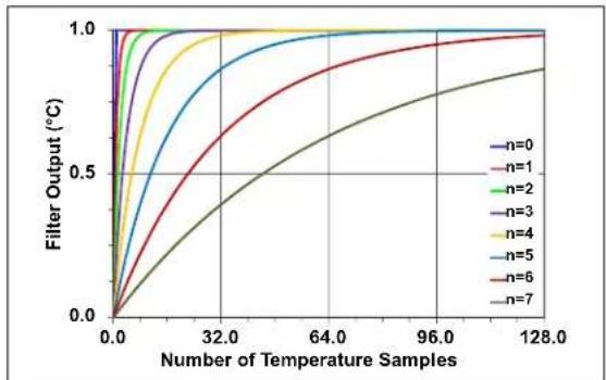
line
| Number of Temperature Samples | n=0 | n=1 | n=2 | n=3 | n=4 | n=5 | n=6 | n=7 | | ----------------------------- | ------ | ------ | ------ | ------ | ------ | ------ | ------ | ------ | | 0.0 | 0.0 | 0.0 | 0.0 | 0.0 | 0.0 | 0.0 | 0.0 | 0.0 | | 32.0 | 1.0 | 1.0 | 1.0 | 1.0 | 1.0 | 1.0 | 1.0 | 1.0 | | 64.0 | 1.0 | 1.0 | 1.0 | 1.0 | 1.0 | 1.0 | 1.0 | 1.0 | | 96.0 | 1.0 | 1.0 | 1.0 | 1.0 | 1.0 | 1.0 | 1.0 | 1.0 | | 128.0 | 1.0 | 1.0 | 1.0 | 1.0 | 1.0 | 1.0 | 1.0 | 1.0 |FIGURE 5-6: Filter Step Response.
REGISTER 5-7: SENSOR CONFIGURATION REGISTER
| U-0 | R/W-0 | R/W-0 | R/W-0 | U-0 | R/W-0 | R/W-0 | R/W-0 |
| — | Thermocouple Type Select, Type K, J, T, N, S, E, B, R | — | Filter Coefficients | ||||
| bit 7 bit 0 | |||||||
| Legend: | |||
| R = Readable bit | W = Writable bit | U = Unimplemented bit, read as '0' | |
| -n = Value at POR | '1' = Bit is set | '0' = Bit is cleared | x = Bit is unknown |
bit 7 Unimplemented: Read as '0'
bit 6-4 Thermocouple Type: Thermocouple Type Select bits
000 = Type K
001 = Type J
010 = Type T
011 = Type N
100 = Type S
101 = Type E
110 = Type B
111 = Type R
bit 3 Unimplemented: Read as '0'
bit 2-0 Filter Coefficient - n: Filter Coefficient bits
000 = n = 0: Filter off
001 = n = 1: Minimum filter
010 = n = 2
011 = n = 3
100 = n = 4: Mid filter
101 = n = 5
110 = n = 6
111 = n = 7: Maximum filter
5.2.3 DEVICE CONFIGURATION REGISTER
The device Configuration register allows the user to configure various functions, such as sensor measurement resolutions and Power modes. The Resolution register is used to select the sensor resolution for the desired temperature conversion time. When resolutions are changed, the change takes effect when the next measurement cycle begins.
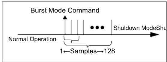
This device integrates two Low-Power Operating modes: Shutdown mode and Burst mode, which can be selected using bit 0 and bit 1. When the Shutdown mode is executed, all power consuming activities are disabled and the operating current remains at I_SHDN . During the Shutdown mode, all registers are accessible; however, I^2C activity on the bus increases the current.
The Burst mode enables users to execute a given number of temperature samples (defined by bits[4-2]) before entering Shutdown mode. Each temperature sample is compared to the user-settable alert temperature limits, and if the alert conditions are true, then the device asserts the corresponding alert output. In addition, if the filter option is enabled, then the filter engine is applied to each temperature sample. The alert thresholds are also compared to the filtered temperature data. This feature is useful for battery power applications, where temperature is sampled upon request from the host controller.
flowchart
graph LR
    A["Normal Operation"] --> B["Burst Mode Command"]
    B --> C["1←Samples→128"]
    C --> D["Shutdown ModeShu"]
FIGURE 5-7: Burst Mode Operation.
REGISTER 5-8: DEVICE CONFIGURATION REGISTER
| R/W-0 R/W-0 R/W-0 R/W-0 R/W-0 R/W-0 R/W-0 R/W-0 | |||
| Cold-Junction Resolution | ADC Measurement Resolution | Burst Mode Temperature Samples | Shutdown Modes |
| bit 7 bit 0 | |||
| Legend: | ||
| R = Readable bit | W = Writable bit | U = Unimplemented bit, read as ‘0’ |
| -n = Value at POR | ‘1’ = Bit is set | ‘0’ = Bit is cleared x = Bit is unknown |
| bit 7 | Cold-Junction/Ambient Sensor Resolution: Cold-Junction Resolution bit (see Table 5-2): |
| 0 = 0.0625°C | |
| 1 = 0.25°C |
| bit 6-5 | ADC Measurement Resolution: ADC Resolution bits (see Table 5-3): |
| 00 =18-bit Resolution | |
| 01 =16-bit Resolution | |
| 10 =14-bit Resolution | |
| 11 =12-bit Resolution |
| bit 4-2 | Burst Mode Temperature Samples: Number of Temperature Samples bits |
| 000 = 1 sample | |
| 001 = 2 samples | |
| 010 = 4 samples | |
| 011 = 8 samples | |
| 100 = 16 samples | |
| 101 = 32 samples | |
| 110 = 64 samples | |
| 111 = 128 samples |
| bit 1-0 | Shutdown Modes: Shutdown Mode bits |
| 00 = Normal operation | |
| 01 = Shutdown mode | |
| 10 = Burst mode | |
| 11 = Unimplemented: this setting has no effect |
5.3 Temperature Alert Registers
This device provides four Temperature Alert registers that are individually configured, which allow users to monitor multiple temperature zones with a single device. The following sections describe each alert feature in detail.
5.3.1 ALERT LIMIT REGISTERS
This device integrates four individually controlled Temperature Alert Limit registers. Each alert limit is individually set to detect a rising or falling temperature, or either the Thermocouple Temperature ( T_H ) register or the Cold-Junction ( T_C ) register. The corresponding alert limit outputs can also be enabled for temperature status indicators. All alert functions are configured using the Alert Limit Configuration registers (Register 5-11) and the alert output hysteresis function is set using the Alert Hysteresis registers (Register 5-10).
TABLE 5-4: ALERT LIMIT REGISTERS
| Register Register | Pointer |
| Alert 1 Limit - T_ALERT1 | 0001 0000 |
| Alert 2 Limit - T_ALERT2 | 0001 0001 |
| Alert 3 Limit - T_ALERT3 | 0001 0010 |
| Alert 4 Limit - T_ALERT4 | 0001 0011 |
REGISTER 5-9: ALERT LIMITS 1, 2, 3 AND 4 REGISTERS
| R/W-0 | R/W-0 | R/W-0 | R/W-0 | R/W-0 | R/W-0 | R/W-0 | R/W-0 |
| SIGN | 1024°C | 512°C | 255°C | 128°C | 64°C | 32°C | 16°C |
| bit 15 bit 8 | |||||||
| R/W-0 | R/W-0 | R/W-0 | R/W-0 | R/W-0 | R/W-0 | U-0 | U-0 |
| 8°C | 4°C | 2°C | 1°C | 0.5°C | 0.25°C | — | — |
| bit 7 bit 0 | |||||||
| Legend: | |||
| R = Readable bit | W = Writable bit | U = Unimplemented bit, read as '0' | |
| -n = Value at POR | '1' = Bit is set | '0' = Bit is cleared | x = Bit is unknown |
bit 15-0
Alert 1, 2, 3 and 4: Data in Two's Complement Format. Bit 15 is the sign bit and it is set when the temperature data is less than 0°C. Bits 1 and 0 are unimplemented, therefore, writing these bits has no effect.
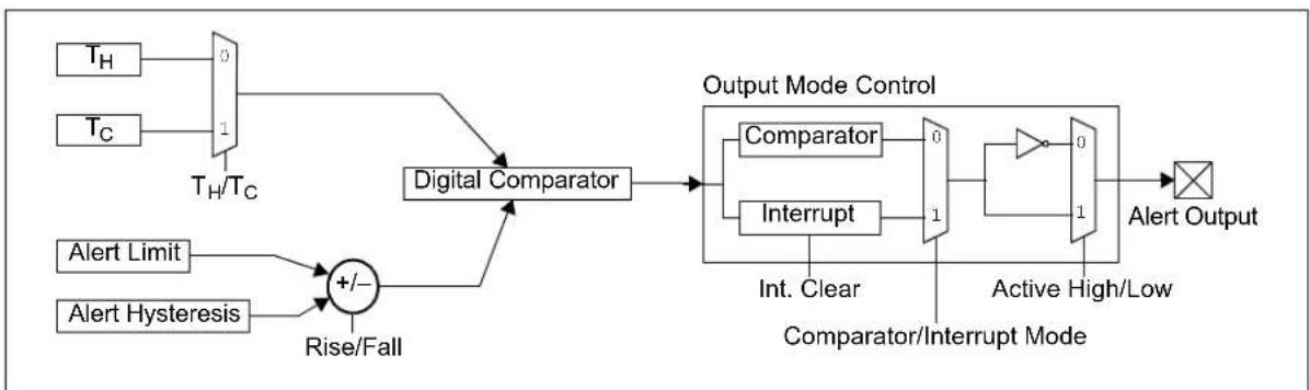
flowchart
graph TD
    A["TH"] --> B["0"]
    C["TC"] --> D["1"]
    E["Rise/Fall"] --> F["+/-"]
    G["Alert Limit"] --> F
    H["Alert Hysteresis"] --> F
    B --> I["Digital Comparator"]
    D --> I
    I --> J["Output Mode Control"]
    K["Int. Clear"] --> L["Comparator"]
    K --> M["Interrupt"]
    L --> N["0"]
    M --> O["1"]
    N --> P["Active High/Low"]
    O --> P
    P --> Q["Alert Output"]
FIGURE 5-8: Alert Limits Set to Detect T H and TC.
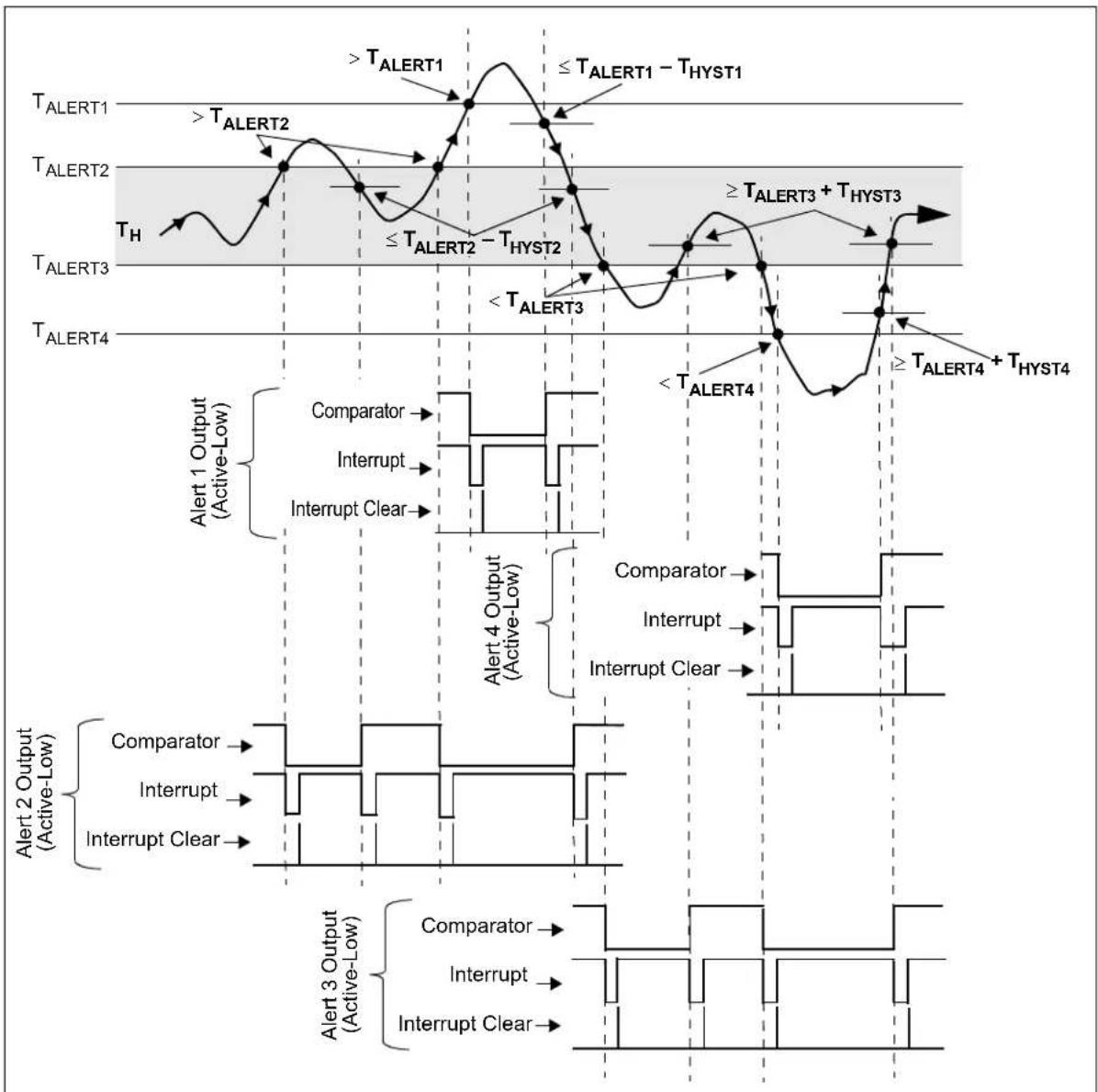
line
| Event | Signal Description | |-------|---------------------| | Alert 1 Output (Active-Low) | Comparator → Interrupt → Interrupt Clear → | | Alert 2 Output (Active-Low) | Comparator → Interrupt → Interrupt Clear → | | Alert 3 Output (Active-Low) | Comparator → Interrupt → Interrupt Clear → | | Alert 4 Output (Active-Low) | Comparator → Interrupt → Interrupt Clear → | | Alert 1 & 2 Outputs | ≥T_ALERT3 + T_HYST3 (shaded region) | | Alert 2 Outputs |5.3.2 ALERT HYSTERESIS REGISTER
This device integrates four individually controlled temperature Alert Hysteresis registers for each alert output, with a range of 0^ C to +255^ C. The alert hysteresis directions are set using bit 3 of the corresponding Alert Configuration registers (Register 5-10) to detect rising or falling temperatures. For rising temperatures, the hysteresis range is below the alert limit where, as for falling temperatures, the hysteresis range is above the alert limit, as shown in Figure 5-10. TABLE 5-5: ALERT HYSTERESIS REGISTERS| Register Register | Pointer |
| Alert 1 Hysteresis - THYST1 | 0000 1100 |
| Alert 2 Hysteresis - THYST2 | 0000 1101 |
| Alert 3 Hysteresis - THYST3 | 0000 1110 |
| Alert 4 Hysteresis - THYST4 | 0000 1111 |
| R/W-0 | R/W-0 | R/W-0 | R/W-0 | R/W-0 | R/W-0 | R/W-0 | R/W-0 |
| 128°C | 64°C | 32°C | 16°C | 8°C | 4°C | 2°C | 1°C |
| bit 7 bit 0 | |||||||
| R = Readable bit | W = Writable bit | U = Unimplemented bit, read as '0' |
| -n = Value at POR | '1' = Bit is set | '0' = Bit is cleared x = Bit is unknown |
text_image
Alert Output Active-Low Hysteresis T_HYST T_ALERT Cold Hottext_image
Alert Output Active-Low Hysteresis T_ALERT T_HYST Cold Hotflowchart
graph TD
    A["Active-High"] --> B["T_HYST"]
    B --> C["T_ALERT"]
    D["Hysteresis"] --> E["Active-High"]
    E --> F["T_HYST"]
    F --> G["T_ALERT"]
    style A fill:#f9f,stroke:#333
    style D fill:#f9f,stroke:#333
    style E fill:#f9f,stroke:#333
    style F fill:#f9f,stroke:#333
flowchart
graph TD
    A["Active-High"] --> B["T_ALERT"]
    B --> C["Hot"]
    D["Hysteresis"] --> E["→"]
    F["→"] --> G["←"]
    H["←"] --> I["↑"]
    J["↓"] --> K["←"]
    L["←"] --> M["↑"]
    N["←"] --> O["←"]
    P["←"] --> Q["↑"]
    R["←"] --> S["←"]
    T["←"] --> U["↑"]
    V["←"] --> W["←"]
    X["←"] --> Y["↑"]
    Z["←"] --> AA["←"]
    AB["Cold"] --> AC["T_ALERT"]
    AC --> AD["Hot"]
    AE["Hot"] --> AF["T_HYST"]
5.3.3 ALERT CONFIGURATION REGISTERS
This device integrates four individually controlled temperature alert outputs. Each output is configured for the corresponding alert output using the Alert Output Configuration registers. The Configuration registers are used to enable each output, select the Alert Function mode as Comparator or Interrupt mode, active-high or active-low output, detect rising or falling temperatures and detect T_H or T_C Temperature registers. The Comparator mode is useful for thermostat-type applications, such as on/off switches for fan controllers, buzzer or LED indicators. The alert output asserts and deasserts when the temperature exceeds the user-specified limit, and the user-specified hysteresis limit. The Interrupt mode is useful for interrupt driven microcontroller-based systems. The alert outputs are asserted each time the temperature exceeds the user-specified alert limit and hysteresis limits. The microcontroller will have Acknowledged the interrupt signal from the corresponding alert output by clearing the interrupt using bit 7 of the corresponding Configuration register. The Rise/Fall bit (bit 3) and the Monitor T_H/T_C bit (bit 4) can be used to detect and maintain the thermocouple temperature or the cold-junction temperature to the desired temperature window. TABLE 5-6: ALERT CONFIGURATION REGISTERS| Register Register | Pointer |
| Alert 1 Configuration 0000 | 1000 |
| Alert 2 Configuration 0000 | 1001 |
| Alert 3 Configuration 0000 | 1010 |
| Alert 4 Configuration 0000 | 1011 |
| R/W-0 U-0 U-0 R/W-0 R/W-0 R/W-0 | R/W-0 | R/W-0 | |||||
| Interrupt Clear | — | — | Monitor T_H/T_C | Rise/Fall | Active-High/Low | Comp/Int. | Alert Enable |
| bit 7 bit 0 | |||||||
| Legend: | |||
| R = Readable bit | W = Writable bit | U = Unimplemented bit, read as ‘0’ | |
| -n = Value at POR | ‘1’ = Bit is set | ‘0’ = Bit is cleared | x = Bit is unknown |
| bit 7 | Interrupt Clear: Interrupt Clear bit1 = Clears Interrupt flag (forced ‘0’ by device)0 = Normal state or cleared state |
| bit 6-5 | Unimplemented: Read as ‘0’ |
| bit 4 | Monitor TH or TC: Temperature Maintain/Detect bit1 = Alert monitor for TC cold-junction sensor0 = Alert monitor for TH thermocouple temperature |
| bit 3 | Rise/Fall: Alert Temperature Direction bit1 = Alert limit for falling or cooling temperatures0 = Alert limit for rising or heating temperatures |
| bit 2 | Active-High/Low: Alert State bit1 = Active-high0 = Active-low |
| bit 1 | Comp./Int.: Alert Mode bit1 = Interrupt mode: Interrupt clears bit (bit 7) – must be set to deassert the alert output0 = Comparator mode |
| bit 0 | Alert Enable: Alert Output Enable bit1 = Alert output is enabled0 = Alert output is disabled |
5.3.4 DEVICE ID AND REVISION ID REGISTER
The Device ID (Identification) and Revision ID register is a 16-bit read-only register, which can be used to identify this device among other devices on the PC bus. The upper 8 bits indicate the Device ID of 0x40 for the MCP9600/L00/RL00 and 0x41 for the MCP9601/L01/RL01 respectively, while the lower 8 bits indicate the device revision. The device revision byte is divided into nibbles, where the upper nibble indicates the major revision and the lower nibble indicates minor revisions. The initial release is indicated by a major revision of '1' and a minor revision of '0' or 0x4010 for the MCP9600/L00/RL00 and 0x4110 for the MCP9601/L01/RL01. (Refer to "MCP9600 Silicon Errata and Data Sheet Clarification", DS80000741, for changes and revision IDs). REGISTER 5-12: MCP9600/L00/RL00 DEVICE ID AND REVISION ID REGISTER| R-0 R-1 R-0 R-0 R-0 R-0 R-0 R-0 | |
| Device ID | |
| bit 15 bit 8 |
| R-0 R-0 R-0 R-1 R-0 R-0 R-0 R-0 | |
| Revision-Major | Revision-Minor |
| bit 7 | bit 0 |
| Legend: | |||
| R = Readable bit | W = Writable bit | U = Unimplemented bit, read as ‘0’ | |
| -n = Value at POR | ‘1’ = Bit is set | ‘0’ = Bit is cleared | x = Bit is unknown |
| R-0 R-1 R-0 R-0 R-0 R-0 R-0 R-1 | |
| Device ID | |
| bit 15 bit 8 |
| R-0 R-0 R-0 R-1 R-0 R-0 R-0 R-0 | |
| Revision-Major | Revision-Minor |
| bit 7 | bit 0 |
| Legend: | |||
| R = Readable bit | W = Writable bit | U = Unimplemented bit, read as ‘0’ | |
| -n = Value at POR | ‘1’ = Bit is set | ‘0’ = Bit is cleared | x = Bit is unknown |
6.0 APPLICATION INFORMATION
6.1 Layout Considerations
The MCP960X/LOX/RL0X does not require any additional components to digitize thermocouples. However, it is recommended that a decoupling capacitor of 0.1 F to 1 F be used between the V_DD and GND pins. A high-frequency ceramic capacitor is recommended. It is necessary for the capacitor to be located as close as possible to the V_DD and ground pins of the device in order to provide effective noise protection. In addition, good PCB layout is key for better thermal conduction from the PCB temperature to the sensor die. The PCB provides thermal conduction from the die to the thermocouple cold-junction; therefore, the component placement positioning and the copper layout techniques are key for optimum cold-junction compensation. The recommended implementation for optimum temperature sensitivity is to extend a copper ground pad around the device pins, as shown in Figure 6-1. text_image
Thermal Pad VIN+/VIN- 21 GND6.1.1 COLD-JUNCTION COMPENSATION
Copper provides better thermal conductivity than PCB FR4 to the ambient temperature. It also provides better thermal conduction than the 5 mm x 5 mm MQFN plastic package, which houses the temperature sensor die. Therefore, when connecting the thermocouple wire to the PCB, it is recommended to place the ground copper between the thermocouple connector footprint, where dissimilar conductive material is attached to the PCB and the MCP960X/L0X/RL0X exposed pad. This allows temperature to stabilize to the local ambient temperature (between the thermocouple connector junction and the PCB copper) and the copper trace conducts the temperature to the package exposed pad where the temperature sensor die is placed. The placement of the sensor exposed pad to the thermocouple connector junction greatly determines the temperature sensor's sensitivity to the local junction temperature changes. Figure 6-2 demonstrates the recommended techniques. natural_image
3D illustration of a yellow electronic component with gold contacts and a small square component, labeled TC1 and U2 (no readable text or symbols beyond labels)6.2 Thermal Considerations
The potential for self-heating errors exist if the MCP960X/L0X/RL0X SDA, SCL and alert outputs are heavily loaded (high current) with pull-up resistors and circuits, such as high-current LEDs or buzzer loads. The temperature rise due to self-heat increases the ambient temperature sensor output, resulting in an increased temperature offset error compared to the thermocouple cold-junction ambient temperature.6.2.1 SELF-HEAT DURING OPERATION
During normal operation, the typical self-heating error is negligible due to the relatively small current consumption of the MCP960X/L0X/RL0X. However, this device integrates a processor to compute the equations necessary to convert the thermocouple EMF voltage to degrees Celsius. The processor also maintains the I^2C bus. During I^2C communication, the device operating current increases to b_DD = 1.5 mA (typical), I^2C Active specification. If the bus is continually polled for data at frequent intervals, then the processor power dissipates heat to the temperature sensor and the effect of self-heat can be detected. Therefore, the recommended implementation is to maintain polling to no more than three times per temperature conversion period of 320 ms or use the Burst mode feature to manage self-heat (refer to Section 6.2.3 “Using Burst Mode to Manage Self-Heat”). Equation 6-1 can also be used to determine the effect of self-heat.EQUATION 6-1: EFFECT OF SELF-HEATING
$$ T _ {\Delta} = \theta_ {J A} (V _ {D D} \bullet I _ {D D}) $$ $$ T _ {\Delta} = \theta_ {J C} (V _ {D D} \bullet I _ {D D}) $$ $$ T _ {\varDelta} = T _ {J} - T _ {A} $$ Where: T_J = Junction Temperature T_A = Ambient Temperature _JA = Package Thermal Resistance: - Junction to Ambient _JC = Package Thermal Resistance: Junction to Case At room temperature ( T_A = +25^ ) with I_DD = 2.5 mA (maximum) and V_DD = 3.3V , the self-heating due to power dissipation, T_A , is 0.32^ for the MQFN package.6.2.2 CONVERSION TIME vs. SELF-HEAT
Once the ADC completes digitization, the processor initiates the data computation routine for t_CALC which also increases I_DD . During the 18-bit ADC conversion time (3 SPS, Samples per Second), the increased current lasts for approximately 5% of the one-second period. The effect of self-heat for the total power consumed per second, including the 5% t_CALC period, is negligible. However, as the ADC resolution is reduced from 18-bit to 16-bit, the power consuming t_CALC period increases to 20% per second. This change in resolution adds approximately 0.04°C (typical) temperature error due to self-heat. Table6-1 provides an estimate for self-heat for all resolutions using Equation 6-1. In order to reduce the effects of self-heat for lower resolution settings, the Burst mode feature is recommended to manage the effects of self-heat. TABLE 6-1: ADC RESOLUTION vs. SELF-HEAT| Resolution | SPS (typ.) | t_CALC Duration per Second | T_A |
| 18-bit | 3 | 5% | 0.0096°C |
| 16-bit | 15 | 20% | 0.0384°C |
| 14-bit | 60 | 80% | 0.1536°C |
| 12-bit | 240 | 100% | 0.1920°C |
6.2.3 USING BURST MODE TO MANAGE SELF-HEAT
The Burst mode feature is useful to manage power dissipation while maintaining the device sensitivity to changes in temperature (see Section 5.2.3 "Device Configuration Register"). While the device is in Low-Power or Shutdown mode, the host controller executes Burst mode to sample temperature. The number of temperature samples and the measurement resolution settings are selected while executing the command. While in Burst mode, if the temperature data exceeds the alert limits, the device asserts the corresponding alert output. The alert outputs are used so the host controller does not need to continually poll the latest temperature data and potentially increase the temperature error. In addition, with some applications monitoring several hundred degrees of temperature changes, 18-bit resolution may not be necessary. In this case, a fewer number of burst samples reducing the resolution enables the user to monitor fast transient temperatures at the burst intervals. The 12-bit ADC resolution provides approximately 3°C resolution (for Type K) and a new sample of temperature data is computed at approximately 20 ms intervals. Therefore, the number of Burst mode Samples per Second can be selected to manage the effects of self-heat using these estimates. The temperature conversion status during Burst mode can also be momentarily polled (using bit 7 of Register 5-6) to detect whether the on-going sample bursts are completed. The host controller may terminate an on-going burst by executing a shutdown command or resetting the Burst mode by sending another burst command.6.2.4 ALERT OUTPUTS
The alert outputs are intended to drive high-impedance loads. Typically, the outputs are connected to a microcontroller input pin. However, if the outputs are used to drive indicators, such as LEDs or buzzers, then a buffer circuit is recommended in order to minimize the effects of self-heat due to the applied load (see Figure 6-3). text_image
Active-High Alert Output VDD NPN6.3 Device Features
6.3.1 I ^2 C ADDRESSING
The MCP960X/L0X/RL0X supports up to eight devices on the I²C bus. Applications, such as large thermal management racks with several thermocouple sensor interfaces, are able to monitor various temperature zones with minimal pin count microcontrollers. This reduces the total solution cost, while providing a highly accurate thermal management solution using the MCP960X/L0X/RL0X. text_image
PIC® Microcontroller Alert 4 I²C Alert VDD R2A R2B ADDR MCP960X/L0X/RL0X Unit 2/8 VIN+ VIN- Types K, J, T, N, E, B, S, R Up to Eight Devices on the I²C Bus VDD R7A R7B ADDR VIN+ VIN- Types K, J, T, N, E, B, S, R| Device # | Command Byte | Values | |
| R_XA (kΩ) | R_XB (kΩ) | ||
| 1 1100 | 000x ADDR Pin Tied to GND | ||
| 2 1100 | 001x R | _2A = 10 R | _2B = 2.2 |
| 3 1100 | 010x R | _3A = 10 R | _3B = 4.3 |
| 4 1100 | 011x R | _4A = 10 R | _4B = 7.5 |
| 5 1100 | 100x R | _5A = 10 | R_5B = 13 |
| 6 1100 | 101x R | _6A = 10 | R_6B = 22 |
| 7 1100 | 110x R | _7A = 10 | R_7B = 43 |
| 8 1100 | 111x ADDR Pin Tied to V DD | ||
6.3.2 INPUT IMPEDANCE
The MCP960X/L0X/RL0X uses a switched capacitor amplifier input stage to gain the input signal to a maximum resolution of 2 V/LSb at an 18-bit ADC setting. An internal input capacitor is used for charge storage. The differential input impedance, Z_IN\_DF , is dominated by the sampling capacitor and the switched capacitor amplifier sampling frequency. During a sampling period, the charging and discharging of the sampling capacitor creates dynamic input currents at the input pins. Adding a 10-100 nF capacitor between the inputs can improve stability. Since the sampling capacitor is only switching to the input pins during a conversion process, the input impedance is only valid during conversion periods. During Low-Power or Shutdown mode, the input amplifier stage is disabled; therefore, the input impedance is Z_IN\_CM , which is due to the leakage current from ESD protection diodes, as shown in Figure 6-5. text_image
Sampling Switch SS R_S V_IN+,V_IN- R_SS V C_SAMPLE (3.2 pF)6.3.3 OPEN AND SHORT DETECTION CIRCUITS
For the MCP9600/L00/RL00, external circuits can be added to detect the thermocouple status as open (physically disconnected) or as short (thermocouple wire in contact with the system ground or V_DD ). If a passive circuit is added to the input stage, then the circuit loading effect to the MCP9600/L00/RL00 ADC inputs must be considered. System calibration is also required to ensure proper accuracy. In addition, external loads can degrade the device performance, such as input offset, gain and Integral Nonlinearity (INL) errors. If a low-impedance active circuit is added, then both offset and gain errors must be calibrated. The MCP9601/L01/RL01 has a Thermocouple open and short-circuit detection mechanism, which is implemented using a Sense-Input pin ( V_SENSE ), as shown in Figure 1-1. The V_SENSE pin and R_A and R_B resistors must be connected as indicated in Figure 1-1. For proper operation, the resistor values must also be within the specified tolerance range. When open-circuit or short-circuit conditions are detected, the OC Alert and SC Alert Active-High Push-Pull outputs are asserted, respectively.6.3.3.1 Open-Circuit Detection Technique
For MCP9600/L00/RL00 open-circuit detection, the Input Range bit (bit 4) of the STATUS register (Register 5-6), can be used to detect open-circuit conditions. This would require a few external resistors, as shown in Figure 6-6. The passive circuit does not affect the MCP9600/L00/RL00 accuracy. When the thermocouple is connected, the input Common-mode voltage is 50% of V_DD . When the thermocouple is disconnected, the voltage at the V_IN + input is 66% of V_DD and the voltage at the V_IN - input is pulled low to V_SS . This change forces the Input Range bit to be set. The MCP9601/L01/RL01 open-circuit detection mechanism operates similarly (see Figure 6-7), and the detection thresholds are specified as V_SiOC and V_SiNOR (see DC Characteristics). The host controller can momentarily poll the Status bit to detect the Open-Circuit condition. For the MCP9601/L01/RL01, the OC Alert pin can are used as hardware indicator. text_image
MCP9600/L00/RL00 R_A = 2 MΩ ± 1% Tolerance (Max.) R_B = 2.49 MΩ ± 1% Tolerancetext_image
RB RA VDD + VSENSE Thermocouple VIN+ VIN- Del Sig MCP9601/L01/RL01 RA = 2 MΩ ± 1% Tolerance (Max.) RB = 2.49 MΩ ± 1% Tolerance RC = 487 KΩ ± 1% Tolerance6.3.4 ALIASING AND ANTI-ALIASING FILTER
Aliasing occurs when the input signal contains time varying signals with frequency greater than half the sample rate. In the aliasing conditions, the ADC can output unexpected codes. The ADC integrates a first order sync filter; however, an external anti-aliasing filter can provide an added filter for high noise applications. This can be done with a simple RC low-pass filter at the inputs, as shown in Figure 6-8. Open-circuit detection resistors can also be added, as shown in Figure 6-9. text_image
Thermocouple + RA VIN+ C VIN- ADC Core Del Sig RA = 100Ω C = 0.1 μFtext_image
MCP9600/L00/RL00 Thermocouple RB RA VDD RD VIN+ C Vin- Del Sig RA = 1 MΩ ± 5% Tolerance (Max.) RB = 2 MΩ ± 20% Tolerance RD = 100Ω C = 0.1 μFtext_image
Thermocouple RB RA VDD + RD VIN+ C Vin- Del Sig MCP9601/L01/RL01 RA = 2 MΩ ± 1% Tolerance (Max.) RB = 2.49 MΩ ± 1% Tolerance RC = 487 KΩ ± 1% Tolerance RD = 100Ω C = 0.1 μF6.3.5 ESD PROTECTION USING FERRITE BEADS
Ferrite beads and Transient Voltage Suppression (TVS) Diodes are highly recommended to protect the MCP960X/L0X/RL0X and other devices from a high frequency noise and ESD discharge through the thermocouple wire. These additional components can be added to the input channel as shown in Figure 6-11 and Figure 6-12. text_image
MCP9600/L00/RL00 Thermocouple + L Rb RA VDD VIN+ Del Sig L RD C VIN- Rs VDD D B D RA = 1 MΩ ± 5% Tolerance (Max.) RB = 2 MΩ ± 20% Tolerance RD = 100Ω C = 0.1 μF L = Ferrite Bead D = TVS Diodetext_image
Thermocouple + L Rb RA VDD D D RD VIN+ C VIN- Rc D D VDD VSENSE Del Sig MCP9601/L01/RL01 RA = 2 MΩ ± 1% Tolerance (Max.) RB = 2.49 MΩ ± 1% Tolerance RC = 487 KΩ ± 1% Tolerance RD = 100Ω C = 0.1 μF L = Ferrite Bead D = TVS Diode7.0 PACKAGING INFORMATION
7.1 Package Marking Information
20-Lead MQFN (5 × 5 × 1.0 mm) text_image
PIN 1 XXXXXXXX XXXXXXXX XXXXXXXX YYWWNNNtext_image
PIN 1 MCP9600 E/MX e3 1932256text_image
PIN 1 9601 1932256text_image
PIN 1 96L00 1932256text_image
PIN 1 96L01 1932256text_image
PIN 1 96RL00 1932256text_image
PIN 1 96RL01 193225620-Lead More Thin Plastic Quad Flat, No Lead Package (NU) - 5x5x1.0 mm Body [MQFN] - (Also called VQFN)
Note: For the most current package drawings, please see the Microchip Packaging Specification located at http://www.microchip.com/packaging  Microchip Technology Drawing C04-186B Sheet 1 of 220-Lead More Thin Plastic Quad Flat, No Lead Package (NU) - 5x5x1.0 mm Body [MQFN] - (Also called VQFN)
Note: For the most current package drawings, please see the Microchip Packaging Specification located at http://www.microchip.com/packaging natural_image
Two isometric line drawings of an integrated circuit chip with pins (no text or symbols)| Units | MILLIMETERS | |||
| Dimension Limits | MIN | NOM | MAX | |
| Number of Pins | N | 20 | ||
| Pitch | e | 0.65 BSC | ||
| Overall Height | A | 0.90 | 0.95 | 1.00 |
| Standoff | A1 | 0.00 | 0.02 | 0.05 |
| Terminal Thickness | A3 | 0.20 REF | ||
| Overall Length | D | 5.00 BSC | ||
| Exposed Pad Length | D2 3 | 15 | 3.25 3.35 | |
| Overall Width | E | 5.00 BSC | ||
| Exposed Pad Width | E2 | 3.15 | 3.25 3.35 | |
| Terminal Width | b | 0.25 | 0.30 | 0.35 |
| Terminal Length | L | 0.35 | 0.40 | 0.45 |
| Terminal-to-Exposed-Pad | K | - | ||
20-Lead More Thin Plastic Quad Flat, No Lead Package (NU) - 5x5x1.0 mm Body [MQFN] - (Also called VQFN)
Note: For the most current package drawings, please see the Microchip Packaging Specification located at http://www.microchip.com/packaging text_image
C1 X2 EV 20 ØV G Y2 1 2 C2 EV E X1 SILK SCREEN| Units | MILLIMETERS | |||
| Dimension Limits | MIN | NOM | MAX | |
| Contact Pitch | E | 0.65 BSC | ||
| Optional Center Pad Width | X2 | 3.35 | ||
| Optional Center Pad Length | Y2 | 3.35 | ||
| Contact Pad Spacing | C1 | 4.50 | ||
| Contact Pad Spacing | C2 | 4.50 | ||
| Contact Pad Width (X20) | X1 | 0.40 | ||
| Contact Pad Length (X20) | Y1 | 0.55 | ||
| GDistance Between Pads 0.20 | ||||
| Thermal Via Diameter V | 0.30 | |||
| Thermal Via Pitch EV | 1.00 | |||
Notes:
1. Dimensioning and tolerancing per ASME Y14.5M BSC: Basic Dimension. Theoretically exact value shown without tolerances. 2. For best soldering results, thermal vias, if used, should be filled or tented to avoid solder loss during reflow process Microchip Technology Drawing C04-186BAPPENDIX A: REVISION HISTORY
Revision G (April 2021)
The following is the list of modifications: 1. Updated the "MCP960X/L0X/RL0X Block Diagram" 2. Updated bit 3 description of Register 5-11. 3. Minor typographical edits. 4. Changed V \_SENSE thresholds from the electrical specifications table (See Errata). 5. Added T POR specification. 6. Updated Figure 1-1. 7. Updated Figure 6-6, 7, 9, 10, 11, 12.Revision F (August 2019)
The following is the list of modifications: 1. Added the MCP9601/L01/RL01 device family and related information throughout the document.Revision E (January 2019)
The following is the list of modifications: 1. Added the MCP96RL00/RL01 device and related information throughout the document.Revision D (August 2018)
The following is the list of modifications: 1. Added the MCP96L00 device and related information throughout the document.Revision C (September 2017)
The following is the list of modifications: 1. Updated Figure 4-3, Equation 5-1, Equation 5-2 and Equation 5-3. 2. Updated Section 6.3.3.1 "Open-Circuit Detection Technique". 3. Various typographical edits.Revision B (June 2016)
The following is the list of modifications: 1. Corrected the pin description error for pins 19 and 20 on page 1. 2. Added the MCP9600 Evaluation Board picture on page 2. 3. Added Section 6.3.3.1 "Open-Circuit Detection Technique" and updated Section 6.3.4 "Aliasing and Anti-Aliasing Filter" and Section 6.3.5 "ESD Protection Using Ferrite Beads". 4. Updated the Product Identification System section.Revision A (August 2015)
• Original release of this document. NOTES:PRODUCT IDENTIFICATION SYSTEM
To order or obtain information, e.g., on pricing or delivery, refer to the factory or the listed sales office.  Device  Tape and Reel Option  Temperature Range  Package| Device: MCP9600: Signal Conditioning IC | (1) |
| MCP9600T: Signal Conditioning IC | (1) (Tape and Reel) |
| MCP96L00: Signal Conditioning IC | (1) |
| MCP96L00T: Signal Conditioning IC | (1) (Tape and Reel) |
| MCP96RL00: Signal Conditioning IC | (1) |
| MCP96RL00T: Signal Conditioning IC | (1) (Tape and Reel) |
| MCP9601: Signal Conditioning IC | (1) |
| MCP9601T: Signal Conditioning IC | (1) (Tape and Reel) |
| MCP96L01: Signal Conditioning IC | (1) |
| MCP96L01T: Signal Conditioning IC | (1) (Tape and Reel) |
| MCP96RL01: Signal Conditioning IC | (1) |
| MCP96RL01T: Signal Conditioning IC | (1) (Tape and Reel) |
| Tape and Reel Option: | T = Tape and Reel | (2) |
| Temperature Range: | E = -40°C to +125°C |
| Package: | MX = More Thin Plastic Quad Flat, MQFN, 20-Lead |
| a) | MCP9600-E/MX: | Extended temperature, 20-lead MQFN package |
| b) | MCP9600T-E/MX: | Tape and Reel, Extended temperature, 20-lead MQFN package |
| c) | MCP96L00-E/MX: | Extended Temperature, 20-lead MQFN package |
| d) | MCP96L00T-E/MX: | Tape and Reel, Extended temperature, 20-lead MQFN package |
| e) | MCP96RL00-E/MX: | Extended temperature, 20-lead MQFN package |
| f) | MCP96RL00T-E/MX: | Tape and Reel, Extended temperature, 20-lead MQFN package |
| g) | MCP9601-E/MX: | Extended temperature, 20-lead MQFN package |
| h) | MCP9601T-E/MX: | Tape and Reel, Extended temperature, 20-lead MQFN package |
| i) | MCP96L01-E/MX: | Extended Temperature, 20-lead MQFN package |
| j) | MCP96L01T-E/MX: | Tape and Reel, Extended temperature, 20-lead MQFN package |
| k) | MCP96RL01-E/MX: | Extended temperature, 20-lead MQFN package |
| l) | MCP96RL01T-E/MX: | Tape and Reel, Extended temperature, 20-lead MQFN package |