PL360G55CB-EK - Electronic component Microchip - Free user manual and instructions
Find the device manual for free PL360G55CB-EK Microchip in PDF.

User questions about PL360G55CB-EK Microchip
0 question about this device. Answer the ones you know or ask your own.
Ask a new question about this device
Download the instructions for your Electronic component in PDF format for free! Find your manual PL360G55CB-EK - Microchip and take your electronic device back in hand. On this page are published all the documents necessary for the use of your device. PL360G55CB-EK by Microchip.
USER MANUAL PL360G55CB-EK Microchip
PL360G55CB-EK User Guide
Introduction
PL360G55CB-EK is an evaluation kit for the PL360 modem. PL360 is a programmable modem for narrow-band Power Line Communication (PLC) from Microchip Technology Inc, able to run any PLC protocol in the frequency band below 500 kHz. The PL360 has been conceived to be driven by external Microchip host controller devices; in this case a SAMG55 ARM ^® Cortex ^® -M4 RISC processor is used. The Microchip host device loads the corresponding PLC-protocol firmware and then controls the PL360 modem operation.
The PL360G55CB-EK board has been conceived to communicate in CENELEC B-Band (95 kHz to 125 kHz) and it complies with CENELEC standard EN 50065 regulations and Smart Energy applications. It can be connected directly to AC mains or DC power rails.
Contents
- Welcome letter
- Board:
- One PL360G55CB-EKv2 board
- Cable:
– One Micro A/B-type USB cable
- Jumpers:
- Two jumpers with pitch 1.27 mm
- Pin Headers:
- Two 8-pin headers with pitch 2.54 mm
Features
- PL360G55CB-EK board mounts a PL360 PLC transceiver and a SAMG55J19 ARM Cortex M4 microcontroller.
- PL360G55CB-EK board provides a full featured platform to develop a complete communications system based on PLC technology working in CENELEC B-Band.
- PL360 is a compact and highly efficient device for a wide range of Smart Grid applications such as lighting control, industrial/home automation and renewable-energy management, among others.
- PL360G55CB-EK board provides support for:
- PLC band characterization and noise level measurement
- PLC sensitivity level measurement
– Power consumption
– Power fail detection -
PL360G55CB-EK board includes a SWD/JTAG interface for MCU debugging and programming purposes. Firmware is also upgradable via USB/serial interface
• USB 2.0 full-speed interface -
mikroBUS ^™ add-on connectors to integrate the board itself as a module for interfacing with other microcontrollers or microprocessors (mikroBUS main board).
-
PL360G55CB-EK board can be externally supplied by:
-
mikroBUS connector
- Micro-B USB connector
- DC Jack connector
Table of Contents
Introduction....1
Contents....1
Features....1
- Evaluation Kit Specifications.... 4
1.1. Safety Recommendations....4
1.2. Electrical Specifications....4
- Getting Started....6
2.1. Powering-Up the Board....6
2.2. Running Preloaded Firmware....7
2.3. Code and Technical Support....7
- PL360G55CB-EK Board....9
3.1. Overview....9
3.2. Features List....9
3.3. Hardware Description – System....16
3.4. Hardware Description – MCU Peripherals.... 26
3.5. Hardware Description – MCU Interface Ports....28
3.6. PL360G55CB-EK Schematics....30
3.7. PL360G55CB-EK Layout.... 34
-
Compliance for Specific Standards.... 40
-
References....41
-
Revision History....42
6.1. Rev A - 04/2019....42
The Microchip Web Site....43
Customer Change Notification Service....43
Customer Support....43
Microchip Devices Code Protection Feature.... 43
Legal Notice....44
Trademarks.... 44
Quality Management System Certified by DNV....45
Worldwide Sales and Service....46
1. Evaluation Kit Specifications
1.1 Safety Recommendations
This evaluation board must only be used by expert technicians. The PL360G55CB-EK board is powered from a DC power source, so only the PLC coupling stage could have a hazardous voltage when is connected to mains. The risk of electric shock is minimized since all required connectors and configuration jumpers are galvanically isolated from the coupling stage.

Be careful, there is risk of electric shock in the PLC coupling stage. A normal use of the PL360G55CB-EK board is for indoor use only.
This evaluation board does not have any switch on mains connection to switch it on or off.
To avoid damage of measurement instruments, do not connect any probe to the high voltage sections if the board is not isolated from the mains supply.
Temperature operating range should be from 0^ C to +85^ C. Running extended periods at minimum and maximum values may cause permanent damage to the board. Quartz crystal components could not cover previous temperature range with desired performance due to aging.
The evaluation board is intended for further engineering, development, demonstration, or evaluation purposes only. It is not a finished product, unless otherwise noted on the board/kit.

Important: Microchip does not assume any responsibility for the consequences arising from any improper use of this board.
1.2 Electrical Specifications
This section shows the electrical characteristics of the PL360G55CB-EK board.
Table 1-1. Power Supply Requirements
| Parameter Condition Min. Typ. Max. Unit | ||||
| DC Mains Voltage Range DC Jack Connector, J8 6 - 30 V | DC | |||
| Maximum Input Current DC Jack Connector, J8 590 | 1 | mA | ||
| Isolation Voltage PLC coupling transformer | 3000 | V | AC |
Note that the PL360G55CB-EK can be supplied with several power sources. For more information about the power supply system, see section 3.3.6 Power Supply System.
Note:
- Board supplied with 6 V_DC , transmission against very low impedance (2Ω) and all peripherals are on.
Table 1-2. Power Consumption
| Parameter Condition Consumption Unit | |||
| TX Power Consumption | FW: G3 CEN-B PHY TX Test Console Application.Low Impedance Load (2Ω LISN, see Figure C.1 of ITU-T G.9901).Measured on 12V DC/DC output. | 1932 ^1 | mW |
| FW: G3 CEN-B PHY TX Test Console Application.High Impedance Load (CISPR LISN, see Figure 5 of EN 50065-1).Measured on 12V DC/DC output. | 322 ^1 | mW | |
| RX Power Consumption Measured on 3.3V DC/DC output 264 | ^1 | mW | |
Notes:
- These measurements were taken running the PHY TX Test Console project with a default configuration in TX and RX modes, and correspond to the whole PCBA design and not only to PL360 and SAMG55J19 devices. All PCB is supplied in the worst consumption conditions (board is supplied with a minimum input voltage, 6 V_DC ) and emitting in CENELEC B-band. Refer to PL360 and SAMG55 datasheets for their respective power consumption.
2. Getting Started
2.1 Powering-Up the Board
Unpack and inspect the kit carefully.
Figure 2-1. Unpacked PL360G55CB-EK
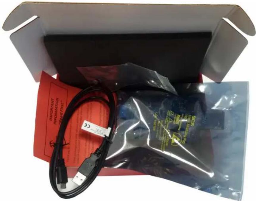
text_image
IMPORTANT INFORMATION SOSKit contents are covered by anti-static foam. The PL360G55CB-EK board is shipped in an anti-static shielding bag.

The board must not be subject to high electrostatic discharge. We recommend using a grounding strap or similar ESD protective device when handling the board in hostile ESD environments. Avoid touching the components' pins or any other metallic elements on the board.
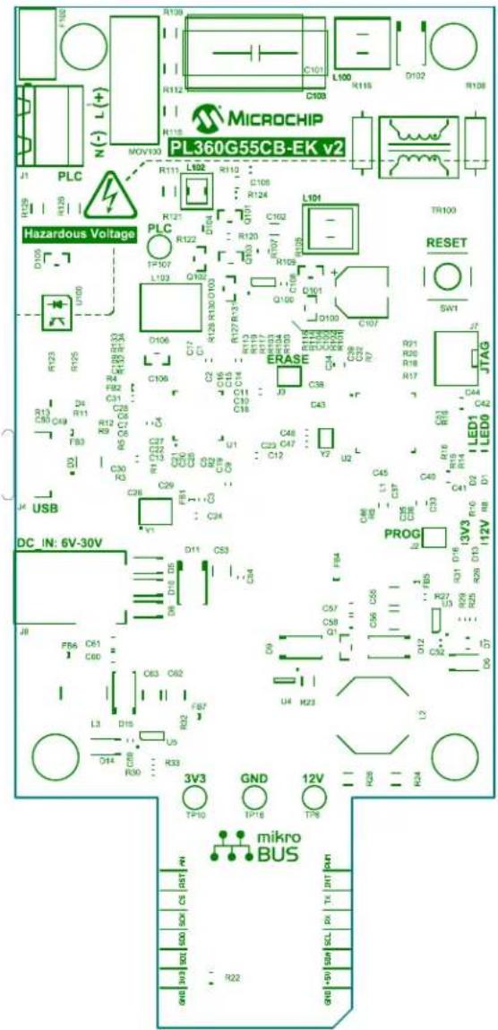
Figure 2-2. PL360G55CB-EKv2 Board Top View

text_image
MICROCHIP PL360G55CB-EK v2 Hazardous Voltage USB DC IN: 6V-30V 3V2 GND 18V mikro BUSTake into account that the connectors to supply the board are different than the one for PLC signals. The board can be supplied by three different ways:
• +5V from USB Micro-B connector (J4)
• +5V from mikroBUS connector (J6)
• DC voltage (from +6V to +30V) from DC Jack connector (J8)
2.2 Running Preloaded Firmware
Once the board is supplied, LEDs will show activity. The PL360G55CB-EK board is delivered with a pre-programmed application in SAMG55 Flash memory: the G3-PLC PHY Tester for CENELEC B-Band. PLC communications are developed for CENELEC B-Band in AC or DC voltage grid.
The kit includes a USB 2.0 type A to Micro-B cable that can be used to connect the board to a computer. Connect a suitable cable in the PLC connector (J1) and plug it to an AC/DC voltage grid to communicate.
By means of the PLC PHY Tester PC application, it is possible to send and receive PLC messages using the PHY layer in the CENELEC B-Band according to the binary flashed in PL360G55CB-EK board.
2.3 Code and Technical Support
Firmware developers can not only run the given example code, but also implement their own applications based on the provided firmware stacks.
Please note that the latest software code, documentation and support materials are available online.
Follow instructions described in the welcome letter for more information.
For any technical support requests, please visit http://support.microchip.com.
3. PL360G55CB-EK Board
3.1 Overview
This section summarizes the PL360G55CB-EK board design. It introduces system-level concepts, such as power supply, MCU, PLC coupling, peripherals and interface board.
PL360G55CB-EK is a PLC modem board based on the PL360 transceiver and on the SAMG55 ARM Cortex-M4 RISC processor. This evaluation board can be used as a PLC modem reference design for modular architectures; or, in any case to provide a platform to develop a complete communications system over PLC technology.
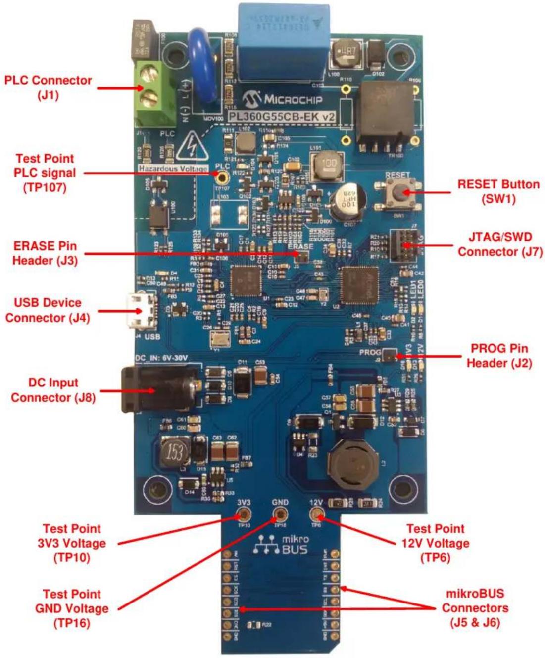
Figure 3-1. PL360G55CB-EKv2 Board Description

text_image
High Voltage Area (AC/DC) PLC Connector (J1) Test Point PLC signal (TP107) ERASE Pin Header (J3) PL360 (U1) USB Device Connector (J4) DC Input Connector (J8) 3V3 Buck Converter (US) Test Point 3V3 Voltage (TP10) Test Point GND Voltage (TP16) MICROCHIP PL360G55CB-EK v2 PLC RESET Button (SW1) JTAG/SWD Connector (J7) SAMG55J19 (U2) User LEDs (D1 & D2) PROG Pin Header (J2) 12V Buck-Boost Converter (U3) Test Point 12V Voltage (TP6) mikroBUS Connectors (J5 & J6)3.2 Features List
The PL360G55CB-EK board includes the following features:
• PL360 PLC Transceiver:
- Multi-protocol PLC modem:
• G3-PLC
• PRIME 1.3 and PRIME 1.4
– One SPI peripheral to external MCU
- Zero-Cross Detection
- Embedded PLC Analog Front End (AFE)
– Low-power consumption in transmission and reception
- SAMG55 MCU:
- Core:
• ARM Cortex-M4 running at up to 120 MHz
• Memory Protection Unit (MPU)
- DSP instruction set
- Floating-Point Unit (FPU)
- Thumb ^ -2 instruction set
- Instruction and Data Cache Controller with 2 Kbytes cache memory
- Up to 512 Kbytes of embedded Flash, 176 Kbytes of embedded SRAM, 8 Kbytes of ROM
- Memories:
- Up to 512 Kbytes of embedded Flash
- Up to 176 Kbytes of embedded SRAM
-
Up to 8 Kbytes of ROM with embedded bootloader, single-cycle access at full speed
-
PLC Coupling designed to communicate in CENELEC B-Band (95 kHz to 125 kHz)
- A 3.3V buck converter for the digital circuitry and a 12V Buck-Boost converter for supplying the PLC Power Amplifier. It allows supply of the board with any of the three different power sources
- Mains Zero-Crossing Detector Circuit
-
Peripherals:
-
Supply monitor
- User LEDs
- Reset button
- Chip Erase jumper
– Chip Programming jumper
- Interfaces:
- USB Device
- mikroBUS add-on connectors
- SWD/JTAG debugging port
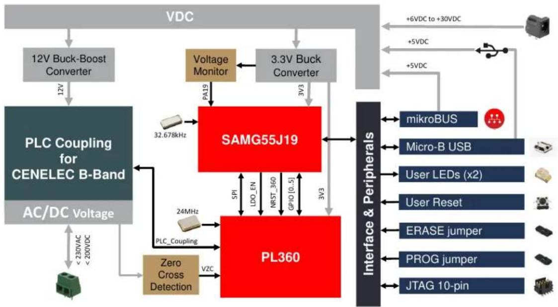
3.2.1 PL360G55CB-EK Block Diagram
The following figure shows the block diagram of the PL360G55CB-EK board.
Figure 3-2. PL360G55CB-EK Block Diagram
flowchart
graph TD
    A["VDC"] --> B["12V Buck-Boost Converter"]
    B --> C["PLC Coupling for CENELEC B-Band"]
    C --> D["AC/DC Voltage"]
    D --> E["< 230VAC < 200VDC"]
    E --> F["Zero Cross Detection"]
    F --> G["PLC_Coupling"]
    G --> H["32.678kHz"]
    H --> I["SAMG55J19"]
    I --> J["3V3"]
    J --> K["PL360"]
    K --> L["3V3"]
    L --> M["3V19"]
    M --> N["PA19"]
    N --> O["SAMG55J19"]
    O --> P["mikroBUS"]
    O --> Q["Micro-B USB"]
    O --> R["User LEDs (x2)"]
    O --> S["User Reset"]
    O --> T["ERASE jumper"]
    O --> U["PROG jumper"]
    O --> V["JTAG 10-pin"]
    W["Voltage Monitor"] --> I
    X["Voltage Monitor"] --> I
    Y["Interface & Peripherals"] --> K
    style A fill:#f9f,stroke:#333
    style B fill:#ccf,stroke:#333
    style C fill:#cfc,stroke:#333
    style D fill:#fcc,stroke:#333
    style E fill:#ffc,stroke:#333
    style F fill:#fcc,stroke:#333
    style G fill:#cff,stroke:#333
    style H fill:#ffc,stroke:#333
    style I fill:#ccc,stroke:#333
    style J fill:#ccc,stroke:#333
    style K fill:#ccc,stroke:#333
    style L fill:#ccc,stroke:#333
    style M fill:#ccc,stroke:#333
    style N fill:#ccc,stroke:#333
    style O fill:#ccc,stroke:#333
    style P fill:#ccc,stroke:#333
    style Q fill:#ccc,stroke:#333
    style R fill:#ccc,stroke:#333
    style S fill:#ccc,stroke:#333
    style T fill:#ccc,stroke:#333
    style U fill:#ccc,stroke:#333
    style V fill:#ccc,stroke:#333
3.2.2 Interface Connection
The PL360G55CB-EK board includes hardware interfaces such as jumpers, connectors and a button. Following figure shows an overview of the connectors, jumpers and button of the PL360G55CB-EK board.
Figure 3-3. PL360G55CB-EK Connectors, Button and Jumpers Overview
text_image
PLC Connector (J1) Test Point PLC signal (TP107) ERASE Pin Header (J3) USB Device Connector (J4) DC Input Connector (J8) Test Point 3V3 Voltage (TP10) Test Point GND Voltage (TP16) MICROCHIP PL360G55CB-EK v2 Hazardous Voltage RESET Button (SW1) JTAG/SWD Connector (J7) PROG Pin Header (J2) Test Point 12V Voltage (TP6) mikroBUS Connectors (J5 & J6)3.2.2.1 Connectors
The PL360G55CB-EK board includes the following connectors:
- PLC connector (for an AC/DC grid), J1.
Table 3-1. PLC Connector (for an AC/DC grid), J1
| Pin Signal Name Description | |
| 1 L / +VDC Line / Positive Voltage | |
| 2 N / -VDC Neutral / Negative Voltage |
- Micro-B female USB connector, J4.
Table 3-2. USB Device Connector, J4
| Pin Signal Name Description | |
| 1 VUSB 5V power | |
| 2 D+ Data Plus | |
| 3 D- Data Minus | |
| 4 ID On the Go Identification | |
| 5 GND | Ground |
- mikroBUS add-on connectors, J5 and J6.
Table 3-3. mikroBUS Connector, J5
| Pin | Mnemonic | Description |
| 1 | AN | Analog |
| 2 | RST | Reset |
| 3 | CS | SPI Chip Select |
| 4 | SCK | SPI Clock |
| 5 | SDO | SPI Master Input Slave Output |
| 6 | SDI | SPI Master Output Slave Input |
| 7 | 3V3 | VCC - 3.3V power |
| 8 | GND | Reference Ground |
Table 3-4. mikroBUS Connector, J6
| Pin | Mnemonic | Description |
| 1 | PWM | PWM |
| 2 | INT | Hardware Interrupt |
| 3 | TX | UART Transmit |
| 4 | RX | UART Receive |
| 5 | SCL I | ^2C Clock |
| 6 | SDA | I^2C Data |
| 7 | 5V | VCC - 5V power |
| Pin Mnemonic Description | ||
| 8 GND Reference | Ground | |
- JTAG/SWD 10-pin connector for SAMG55J19, J7.
Table 3-5. SW-DP Connector, J7
| Pin Mnemonic Description | ||
| 1 VCC | This is the target reference voltage. It is used to check if the target has power, to create the logic-level reference for the input comparators, and to control the output logic levels to the target. It is normally fed from V_CC on the target board and must not have a series resistor. | |
| 2 SWDIO/TMS | Serial Wire Input Output / Test Mode Select. JTAG mode set input of target CPU. This pin should be pulled up on the target. Output signal that sequences the target's JTAG state machine, sampled on the rising edge of the TCK signal. | |
| 3 GND Ground. | ||
| 4 SWDCLK/TCK | Serial Wire Clock / Test Clock. JTAG clock signal to target CPU (output timing signal, for synchronizing test logic and control register access). | |
| 5 GND Ground. | ||
| 6 SWO/TDO Test Asynchronous Data | Out from target CPU. | |
| 7 KEY | - | |
| 8 | NC/TDI | Not Connected / Test Data Input. JTAG data input of target CPU (serial data output line, sampled on the rising edge of the TCK signal). It is recommended that this pin is pulled to a defined state on the target board. |
| 9 | GND Detect | Ground. |
| 10 | nRESET | JTAG Reset (active-low output signal that resets the target). Output from SAM-ICETMto the Reset signal on the target JTAG port. This pin is normally pulled HIGH on the target to avoid unintentional resets when there is no connection. |
- DC Input connector, J8.
Table 3-6. DC Input Connector, J8
| Pin | Signal Name | Description |
| 1 | DC_IN | DC Input voltage (6 - 30V) |
| 2 GND | Ground | |
| 3 | - | - |
3.2.2.2 Jumper Configurations
The following table describes the functionality of the jumpers.
Table 3-7. Jumper Configuration
| Jumper Label Default Setting Function | |||
| J3 ERASE Open | SAMG55J19 Flash memory code erase (closed = erase). | ||
| J2 PROG Open | SAMG55J19 Flash memory upgrade (closed = programming). | ||
Note: Pitch jumpers are 1.27 mm (0.050").
3.2.2.3 Test Points
Some test points (probes and pads) have been placed on the PL360G55CB-EK board for the verification of the main signals.
Table 3-8. Test Point Probes
| Reference Function | |
| TP6 12V | |
| TP10 3V3 | |
| TP16 GND | |
| TP107 PLC signal |
Table 3-9. Test Point Pads
| Reference Function Reference Function | |||
| TP1 PROG | TP24 | PL360 pin PA7 | |
| TP2 | ERASE | TP25 | PL360 pin PA8 |
| TP3 | SAMG55J19 pin PA12, LED D1 | TP26 | PL360 pin PA9 |
| TP4 | SAMG55J19 pin PA15, LED D2 | TP27 | PL360 pin PA0 |
| TP5 | NRST | TP28 | PL360 pin PA3 |
| TP7 | 12V | TP100 | PL360 pin TXRX1 |
| TP8 | DC_IN | TP101 | P Channel MOSFET |
| TP9 | VDC | TP102 | Line |
| TP11 | 3V3 | TP103 | N Channel MOSFET |
| TP12 | Ground | TP104 | Neutral |
| TP13 | Ground | TP105 | Zero cross signal, VZC |
| TP14 | Ground | TP106 | PL360 pin TXRX0 |
| TP15 | Ground | TP108 | PLC RX |
| TP23 | PL360 pin PA6 | - | - |
3.3 Hardware Description – System
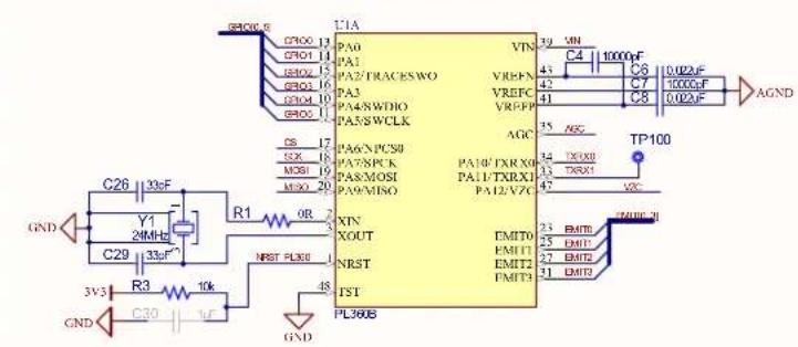
3.3.1 PL360
The PL360G55CB-EK board is equipped with a PL360 device in 48-pin QFN (0.4 mm pitch).
PL360 is a multi-protocol (G3-PLC, PRIME 1.3 and PRIME 1.4) modem for Power Line Communication implementing a very flexible architecture, which allows implementation of standard and customized PLC solutions.
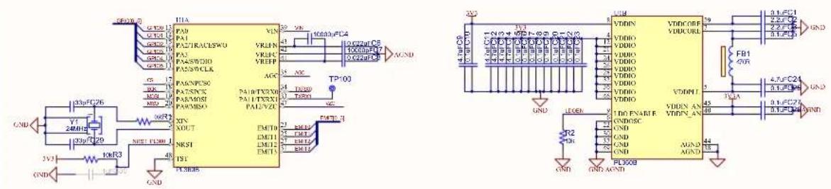
PL360 transceiver has been conceived to be easily managed by an external Microchip MCU through a 4-line standard Serial Peripheral Interface (SPI) accessing the internal peripheral registers. Two additional signals are used by the host microcontroller to control the PL360 transceiver: LDO enable and NRST.
Figure 3-4. PL360 PLC Modem

Important: Some GPIOs of PL360 device must be connected to the external MCU for the right implementation of the firmware of the PLC standard. G3-PLC requires a GPIO for an external interrupt line (EINT) and PRIME requires two GPIOs for an external interrupt and carrier detect indication lines (EINT and CD). Please, check this point with the firmware user guide.

Remember: The PL360 control lines from MCU perspective (SPI lines, EINT in GPIO3 and CD in GPIO0) are accessible via test points.
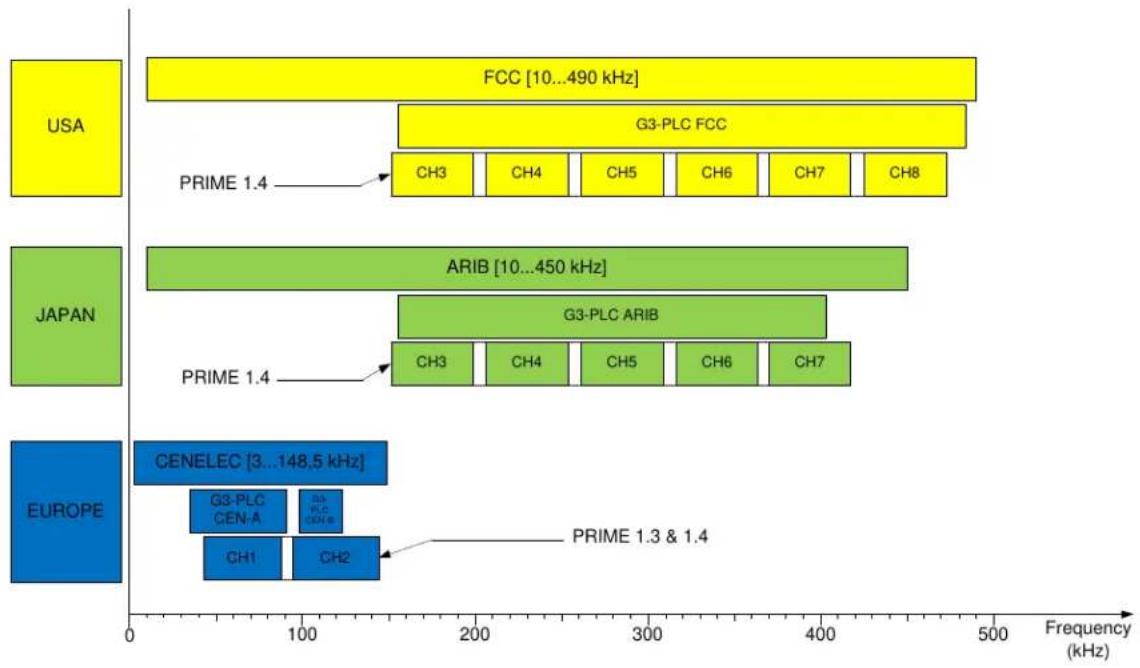
Microchip provides highly efficient, reduced BOM reference designs for different coupling options, targeting common configurations in all PLC bands (<500 kHz) complying with existing regulations.
Figure 3-5. PLC Bands Supported by PL360
bar_stacked
| Region | Category | Value Range (kHz) | |--------|------------------|-------------------| | USA | GCC | 10...490 | | USA | G3-PLC FCC | 10...490 | | USA | CH3 | 10...490 | | USA | CH4 | 10...490 | | USA | CH5 | 10...490 | | USA | CH6 | 10...490 | | USA | CH7 | 10...490 | | USA | CH8 | 10...490 | | JAPAN | ARIB | 10...450 | | JAPAN | G3-PLC ARIB | 10...450 | | JAPAN | CH3 | 10...450 | | JAPAN | CH4 | 10...450 | | JAPAN | CH5 | 10...450 | | JAPAN | CH6 | 10...450 | | JAPAN | CH7 | 10...450 | | EUROPE | CENELEC | 3...148.5 | | EUROPE | G3-PLC CEN-A | 3...148.5 | | EUROPE | CH1 | 3...148.5 | | EUROPE | CH2 | 3...148.5 | | EUROPE | PRIME 1.3 & 1.4 | 3...148.5 |For a further description of the PL360 device see the corresponding PL360 datasheet.
3.3.2 SAMG55J19
The PL360G55CB-EK board is equipped with a SAMG55J19 device in 64-pin QFN. The SAM G55 devices are general-purpose low-power microcontrollers which offer high performance, processing power and small package options combined with a rich and flexible peripheral set.
The Microchip's SAM G55 embeds a Cortex-M4 CPU with an FPU (floating point unit). This ensures maximum throughput. This is very important as it allows minimization of the active power consumption and getting to sleep faster in order to reduce the overall power consumption. Additionally, the device has 30 DMA channels, which gives extremely high throughput.
The SAMG55J19 operates at a maximum speed of 120 MHz and features 512 Kbytes of Flash and up to 176 Kbytes of SRAM. The peripheral set includes eight flexible communication units comprising of USARTs, SPIs and I²C-bus interfaces (TWIs), two three-channel general-purpose 16-bit timers, two I²S controllers, one-channel pulse density modulation, one 8-channel 12-bit ADC, one Real-Time Timer (RTT) and one Real-Time Clock (RTC), both located in the ultra-low power backup area.
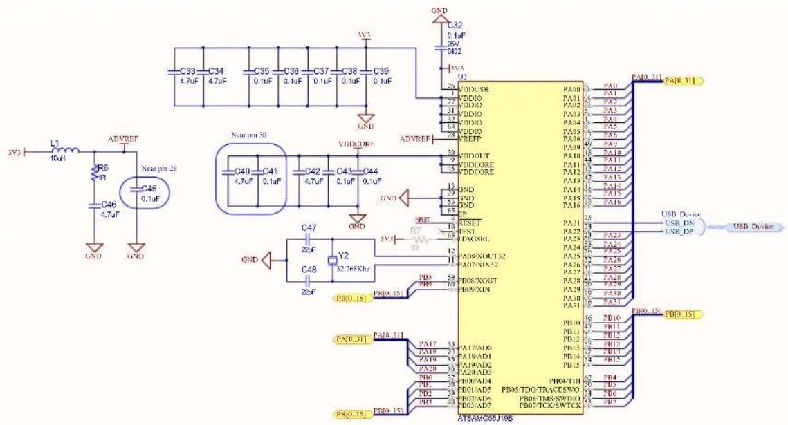
Figure 3-6. SAMG55 Microcontroller
text_image
L1 10uF R6 R C46 4.7uF GND ADVREF Near pin 28 C45 0.1uF GND C33 C34 4.7uF C36 C36 0.1uF C37 C38 0.1uF C39 0.1uF GND C32 0.1uF 25V 0.02 U2 26 VDD/USB 25 VDDIO 24 VDDIO 23 VDDIO 22 VDDIO 21 VDDOUT 20 VDDCORE 19 VDDCORE 18 VDDCORE 17 GND 16 GND 15 GND 14 GND 13 GND 12 GND 11 GND 10 GND 9 GND 8 GND 7 GND 6 GND 5 GND 4 GND 3 GND 2 GND 1 GND 0 GND 0 GND - Near pin 30 C40 C41 C42 C43 C44 4.7uF 0.1uF 4.7uF 0.1uF 0.1uF 0.1uF 0.1uF 0.1uF 0.1uF 0.1uF 0.1uF 0.1uF 0.1uF 0.1uF 0.1uF 0.1uF 0.1uF 0.1uF 0.1uF 0.1uF 5 PA80-311 PA[0..31] 5 PA80 PA81 PA82 PA83 PA84 PA85 PA86 PA87 PA88 PA89 PA90 PA91 PA92 PA93 PA94 PA95 PA96 PA97 PA98 PA99 PA10 PA11 PA12 PA13 PA14 PA15 PA16 PA17 PA18 PA19 PA20 PA21 PA22 PA23 PA24 PA25 PA26 PA27 PA28 PA29 PA30 PA31 PB[0..31] PA[0..31] PA[0..31] PA[0..31] PB[0..31] PB[0..31] PB[0..31] PB[0..31] PB[0..31] PB[0..31] PB[0..31] PB[0..31] PB[0..31] PB[0..31] PB[0..31] PB[0..31] PB[0..31] PB[0..31] PB[5A] PD[0..31] PD[0..31] PD[0..31] PD[0..31] PD[0..31] PD[0..31] PD[0..31] PD[0..31] PD[0..31] PD[0..31] PD[0..31] PD[0..31] PD[5A] PD[0..31] PD[0..31] PD[0..31] PD[0..31] PD[0..31] PD[0..31] PD[0..31] PD[5A] PD[0..31] PD[0..31] PD[0..31] PD[0..31] PD[0..31] PD[5A] PD[0..31] PD[0..31] PD[0..31] PD[0..31] PD[0..31] PD[5A] PD[0..31] PD[0..31] PD[0..2] - Near pin 28 C45 0.1uF GND GND C47 Z2F Y2 PDB[0..15] PDB[0..15] PDB[0..15] PDB[0..15] PDB[0..15] PDB[0..15] PDB[0..15] PDB[0..15] PDB[0..15] PDB[0..15] PDB[0..15] PDB[0..15] PDB[0..15] PDB[5A] PD[0..31] PDB[5A] PD[0..31] PDB[5A] PD[0..31] PDB[5A] PD[0..31] PDB[5A] PD[0..31] PDB[5A] PD[0..31] PDB[5A] PD[0..31] PDB[5A] PD[0..31] PDB[5A] PD(5A)PD(5A)PD(5A)PD(5A)PD(5A)PD(5A)PD(5A)PD(5A)PD(5A)PD(5A)PD(5A)PD(5A)PD(5A)PD(5A)PD(5A)PD(5A)PD(5A)PD(5A)PD(5A)PD(5A)PD(5A)PB(6)PB(6)PB(6)PB(6)PB(6)PB(6)PB(6)PB(6)PB(6)PB(6)PB(6)PB(6)PB(6)PB(6)PB(6)PB(6)PB(6)PB(6)PB(6)PB(6)PB(6)PB(6)PB(6)PB(6)PB(6)PB(7) ATSAMG5BJ9BTable 3-10 and Table 3-11 summarize the functionality of each input/output line of the SAMG55J19 microcontroller in PL360G55CB-EK board.
Table 3-10. Pinout of SAMG55J19 PortA in PL360G55CB-EK Board
| I/O LINE Function I/O LINE Function | |||
| PA0 PL360 GPIO3 PA16 PL360 GPIO4 | |||
| PA1 PL360 GPIO2 PA17 AD0 (mikroBUS) | |||
| PA2 Not Connected PA18 PROG | |||
| PA3 PL360 MOSI PA19 Voltage Monitor | |||
| PA4 PL360 MISO PA20 Not Connected | |||
| PA5 PL360 GPIO1 PA21 | USB Device Diff Negative | ||
| PA6 PL360 GPIO5 PA22 USB Device Diff Positive | |||
| PA7 | XIN32 | PA23 | TIOA1 (mikroBUS) |
| PA8 | XOUT32 | PA24 Not Connected | |
| PA9 | SPI0 MISO (mikroBUS) | PA25 | SPI0 CS0 (mikroBUS) |
| PA10 | SPI0 MOSI (mikroBUS) | PA26 Not Connected | |
| PA11 | USB Detect PA27 Not Connected | ||
| PA12 | User LED0 | PA28 | Not Connected |
| PA13 Not Connected PA29 | PL360 NRST | ||
| PA14 | WKUP8 (mikroBUS) | PA30 | PL360 LDO_EN |
......continued
| I/O LINE Function I/O LINE Function | ||
| PA15 User LED1 PA31 PL360 GPIO0 |
Table 3-11. Pinout of SAMG55J19 PortB in PL360G55CB-EK Board
| I/O LINE Function I/O LINE Function | |||
| PB0 SPI0 CLK (mikroBUS) PB8 Not Connected | |||
| PB1 Not Connected PB9 Not Connected | |||
| PB2 TWCK1 (mikroBUS) PB10 TXD4 (mikroBUS) | |||
| PB3 TWD1 (mikroBUS) PB11 RXD4 (mikroBUS) | |||
| PB4 TDI PB12 ERASE | |||
| PB5 TDO/TRACESWO PB13 PL360 SCK | |||
| PB6 TMS/SDWIO | PB14 | PL360 CS | |
| PB7 | TCK/SWCLK | PB15 | Not Connected |
The right implementation of the PLC standards require some GPIOs of the transceiver PL360 connected to the SAMG55. G3-PLC requires a GPIO for an external interrupt line (PA0 of SAMG55) and PRIME requires two GPIOs for an external interrupt and carrier detect (PA0 and PA31 of SAMG55) indication lines. Please check this point with the firmware user guide.
For a further description of the SAMG55J19 capabilities see the corresponding SAMG55 datasheet.
3.3.3 Clock Circuitry
Besides the embedded RC oscillators of SAMG55J19, two crystal oscillators are assembled on the PL360G55CB-EK board to obtain a more precise and stable system clock reference:
• A 24 MHz clock signal, Y1, generated for the PLC transceiver PL360
• A low-power 32.768 kHz crystal oscillator, Y2, for the SAMG55J19
Figure 3-7. 24 MHz Crystal Oscillator Scheme
text_image
GND C26 133F Y1 24MHz C29 33F R3 10k 3V3 C30 1F GND C1A PA0 PA1 PA2/TRACESWO PA3 PA4/RWDIO PA5/SWCLK CS SSX MOBJ MOSO R1 0R NRST PL300 7 XIN XOUT NRST TST PL300B VIN VREFN VREFC VREFP AGC PA6/PC58 PA7/PCCK PA8/MOSI PA9/MISO PA10/FXRX0 PA11/TXRX1 PA12/V7C EMITO EMIT1 EMIT2 EMIT3 TP100 AGND C4 1000uF C5 1000uF C6 1000uF C7 1000uF C8 1000uF C9 1000uF C10 1000uF C11 1000uF C12 1000uF C13 1000uF C14 1000uF C15 1000uF C16 1000uF C17 1000uF C18 1000uF C19 1000uF C20 1000uF C21 1000uF C22 1000uF C23 1000uF C24 1000uF C25 1000uF C26 1000uF C27 1000uF C28 1000uF C29 1000uFFigure 3-8. 32.768 kHz Crystal Oscillator Scheme

text_image
GND C35 C36 C37 C38 C39 0.1uF 0.1uF 0.1uF 0.1uF 3V3 C32 0.1uF 25V 0402 3V3 U2 20 VDDUSB VDDIO VDDIO VDDIO VDDIO VREFP VDDOUT VDDCORE VDDCORE GND GND NRST R7 3V3 3V3 PB[0..15] PB[0..15] CA40 C41 7A F 0.1uF C42 C43 C44 4.7uF 0.1uF 0.1uF GND GND ADVREF VDDCORE VDDCORE GND GND RESET TEST JTAGSEL PA08/XOUT32 PA07/XIN32 PB08/XOUT PB09/XIN PB10 [15] PB10 [15] PB10 [15] PB10 [15] PB10 [15] PB10 [15] PB10 [15] PB10 [15] PB10 [15] PB10 [15] PB10 [15] PB10 [15] PB10 [15] PB10 [15] PB10 [15] PB04/TDI PB05/TDO/TRACESWO PB06/TMS/SWDIO PB07/TCK/SW TCK ATSAMG55J19B 6 PA0 7 PA1 6 PA2 5 PA3 4 PA4 8 PA5 7 PA6 4 PA9 4 PA10 4 PA11 4 PA12 4 PA13 4 PA14 22 PA15 18 PA16 25 24 23 PA23 22 PA24 21 PA25 20 PA26 21 PA27 20 PA28 19 PA29 16 PA30 14 PB[0..31] 6 PA[0..31] 6 PA[0..31] 6 PA[0..31] 6 PA[0..31] 6 PA[0..31] 6 PA[0..31] 6 PA[0..31] 6 PA[0..31] 6 PA[0..31] 6 PA[0..31] 6 PA[0..31] 6 PA[0..31] 6 PA[0.. 31] 6 PA[0..31] 6 PA[0..31] 6 PA[0..31] 6 PA[0..31] 6 PA[0..31] 6 PA[0..31] 6 PA[0..31] 6 PA[0..31] 6 PA[0..31] 6 PA[0..31] 6 PA[0..31] 6 PA[0..31] PGD VDDOUT VDDCORE VDDCORE GND3.3.4 Reset
The reset sources of the PL360G55CB-EK board are:
- Power-on Reset function, embedded in the SAMG55 device.
- Push button reset. Both devices, SAMG55J19 and PL360, have a NRST pin: "NRST" for SAMG55J19 and "NRST_360" for PL360. The user can manually reset the SAMG55J19, which manages the PL360 reset, by using the push button SW1. See section 3.4.2.2 Push Buttons.
- JTAG reset from an in-circuit emulator.
3.3.5 PLC Coupling Circuitry Description
The European regulations concerning Power Line Communications are described in CENELEC standard EN 50065. This standard applies to electrical equipment using signals in the frequency range 3 kHz to 148,5 kHz to transmit information on low voltage electrical systems, either on the public supply system or within installations in consumers' premises. The following figure shows the different frequency bands allocated to the different applications.
Figure 3-9. CENELEC Frequency Bands

area
| f (kHz) | S_max(f) dB(μV) | | ------- | --------------- | | 3 | 134 | | 9 | 116 | | 95 | 116 | | 125 | 132.5 | | 140 | 132.5 | | 148.5 | 132.5 |The PL360G55CB-EK evaluation board communicates in the CENELEC B-Band frequency. The use of frequencies in this band shall be restricted to consumer use; for example, for end-user applications such as industrial applications.
Microchip has designed five coupling reference designs for CENELEC B-Band with variations in the BOM cost and the communication performance. Table 3-12 summarizes the main features of the available designs.
Table 3-12. Characteristics of PLCOUPxxx Boards for CENELEC B-Band
| Board Name | Description | Frequency Band (kHz) | Branch | Electrical Isolation | PRIME Channel | G3-PLC Band | Applicable Regulation |
| PLCOUP012-ISO | Low cost with internal driver G3 CENELEC B compliant | 95 - 125 Single Yes - | G3 CENELEC B | CENELEC EN 50065 | |||
| PLCOUP012-NONISO | Low cost with internal driver G3 CENELEC B compliant | 95 - 125 Single No - | G3 CENELEC B | CENELEC EN 50065 | |||
| PLCOUP013 | Ultra low cost with internal driver and non-Isolated G3 CENELEC B compliant | 95 - 125 Single No - | G3 CENELEC B | CENELEC EN 50065 | |||
| PLCOUP014-ISO | G3 CENELEC B compliant | 95 - 125 Single Yes - | G3 CENELEC B | CENELEC EN 50065 | |||
| PLCOUP014-NONISO | G3 CENELEC B compliant | 95 - 125 Single No - | G3 CENELEC B | CENELEC EN 50065 |
The PL360G55CB-EK board is assembled with the PLCOUP014-ISO coupling design. The goal is to provide a cost-optimized fully-featured design according to the G3-PLC requirements. Still, the PL360G55CB-EK board is designed to allow using all the other coupling designs by changing the corresponding components and firmware configurations.

Important: Check the online resources from Microchip website to download the proper files according to your desired CENELEC B-Band design.
The following figure shows the PLC Coupling assembled (PLCOUP014-ISO) which is composed of four sub-circuits:
- Transmission Stage
- Filtering Stage
- Coupling Stage
- Reception Stage
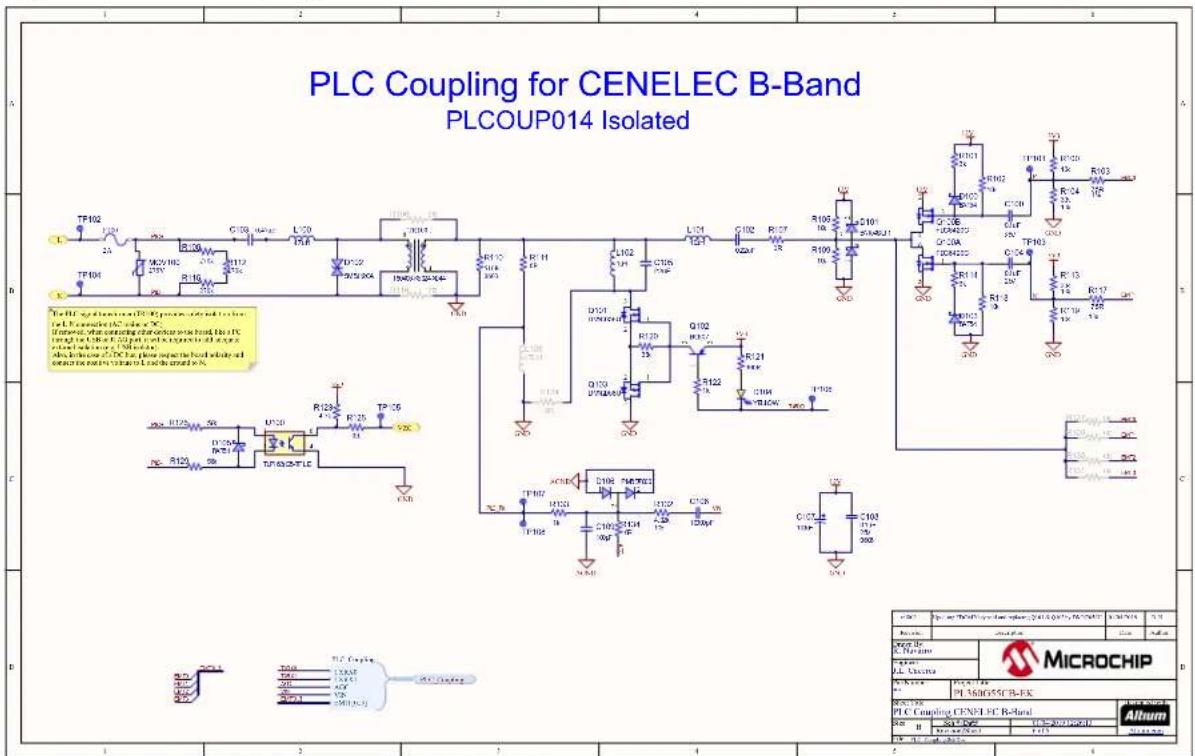
Figure 3-10. PLC Coupling Schematic on PL360G55CB-EK Board

text_image
Electronic circuit diagram with labeled components and pin connections, including transistors, capacitors, and diodes
Remember: PLC Coupling circuitry adds a yellow LED, D104, for visual indication of PLC frames transmission.
The following sections describe the aim of every sub-circuit assembled in the PL360G55CB-EK board.
3.3.5.1 PLC Transmission Circuit
The transmission stage adapts the EMIT signals and amplifies them. In the PL360G55CB-EK board, see Figure 3-10, it is a single branch composed of:
- Driver: It adapts the EMIT signals to either control the amplifier or to be filtered by the next stage
- Amplifier: A Class-D amplifier generating a square waveform from 0 to 12V
- Bias and protection: It provides a DC component and provides protection from received disturbances
The transmission stage is followed by a filtering stage.
3.3.5.2 PLC Filtering Circuit
The in-band flat response filtering stage reduces spurious emission to the limits set by the corresponding regulation and blocks potential interferences from other transmission channels without distorting the injected signal.
The filtering stage used in PL360G55CB-EK, see Figure 3-10, has three aims:
- Band-pass filtering of high frequency components of the square waveform generated by the transmission stage
- Adapt Input/Output impedance for optimal reception/transmission. This is controlled by TXRX0 signal
• A band-pass filtering for received signals
3.3.5.3 PLC Coupling Circuit
PLC coupling circuit connects the PLC signal directly to the mains grid or even to DC power rails without requiring any hardware adaptation. The main purpose of the circuit is to block the mains voltage of the grid to/from which the signal is injected/received. This is carried out in PL360G55CB-EK, see Figure 3-10, by a high voltage capacitor, C103. Resistors R108, R112 and R115 allow the high voltage capacitor to discharge after disconnection from mains.

PLC coupling components are designed for a maximum voltage of 230 V_AC or 200 V_DC .
The TR100 transformer (with turn ratio 1:1) provides galvanic isolation from mains. A non-isolated version could easily be implemented removing TR100, soldering R106 and R116 resistors and updating the value of L103 according to the PLCOUP014-NONISO design.
MOV100 varistor, F100 fuse and D102 TVS diode protect the coupling circuit from the overvoltages and high transient voltages (surges and spikes) from mains.
3.3.5.4 PLC Reception Circuit
The PLC reception circuit used in PL360G55CB-EK, see Figure 3-10, is the reference design for the reception stage and it is composed of:
- Single-pole low pass filter, R133 and C109
- Automatic Gain Control (AGC) circuit. A resistor, R134, is used to attenuate the incoming PLC signal in case its amplitude is high enough to exceed the input dynamic range of the embedded ADC
• A resistor, R132, for impedance matching
• DC decoupling capacitor, C106
3.3.6 Power Supply System
The PL360G55CB-EK board can be powered by several power sources. Supply the board via:
- the DC jack 2.0 mm connector J8, DC_IN , with a DC source from 6V to 30V ( ± 5% ) and 4.2W
• the USB connector (+5V), J4 - the power supply pin (+5V) of mikroBUS standard
Table 3-13. Power Sources for PL360G55CB-EK Board
| Power Input Voltage Requirements Power Requirements Connector Marking | |||
| DC Jack connector +6V to +30V (±5%) 4.2 Watts | DC_IN | ||
| Target USB +5V | According to USB specifications | USB | |
| mikroBUS Power pin (+5V) | +5V | According to mainboard specifications | +5V |
The PL360G55CB-EK board has two voltage rails:
- +3.3V for the digital part of the PLC modem, PL360, and the SAMG55J19 MCU
- +12V to power the class-D amplifier of the PLC coupling circuit

Note that the PL360G55CB-EK board does not provide a power supply protection circuit; only a TVS diode is used to protect from voltage spikes at the DC rail.
The 12V voltage rail is obtained from the MC16301 buck-boost converter. For a further description about the buck-boost converter see the MCP16301 Buck-Boost Converter User's Guide. If the VDC voltage is always higher than 12V, it is possible to improve the power efficiency by transforming the converter mode from buck-boost to buck, see MCP16301 datasheet for a further explanation.
Figure 3-11. 12V Voltage Design

text_image
VDC TP9 FR5 40R C53 4.7uF 50V C54 3.1uF 50V C55 4.7uF 50V C56 4.7uF 50V R27 100L U3 SW VIN EN GND MCPI6301 VFB D12 D140-13-F GND C52 0.1uF L2 40u1 D9 B140-13-F R24 1.2 k VDD IN E4 MC*1402 OUT GND GND GND GND GND GND GND GND GND GND GND GND GND GND GND GND GND GND GND GND GND GND GND GND GND GND GND GND GND GND GND GND GND GND
Restriction: Note that some power sources, such as USB port and mikroBUS rail, might have limited current capabilities and they could not supply enough current for the class-D amplifier transmitting against low impedance values. In this case, an external AC/DC power supply with enough current rating is recommended to maintain the PLC performance at its best. In case of using one, we recommend a module complying to national regulations or CISPR 32:2015.
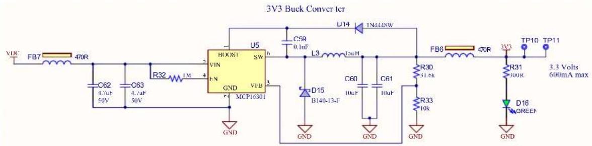
Another buck converter, MC16301, is used to generate a regulated 3.3V voltage rail required by the PL360 modem and the SAMG55J19 MCU. For a further description about the buck converter see the MCP16301 Buck Converter User's Guide.
Figure 3-12. 3.3V Buck Converter Design
text_image
3V3 Buck Converter VDC FB7 470R C62 C63 R32 LM 4 U5 VIN F N GND VFB 3 MCP16301 U5 SW 6 C59 0.1uF L3 12uH 1N444kW D14 D15 B140-13-F C60 10uF C61 10uF R30 31.8k R33 10k FB6 470R 3V3 TP10 TP11 GND GND GND GND GND R31 300K D16 GREEN 3.3 Volts 600mA max GNDThere are one LED and two test points on each voltage rail to check whether all power supplies are operating properly.
To avoid on board self-generated disturbances within the PLC signal band, both converters are switching at 500 kHz fixed frequency, out of the PLC band (95 to 125 kHz).

Tip: In case of choosing a different SMPS in the customer design, it is important to analyze its potential interference on the PLC frequency band.

Attention: To avoid noise interferences, the switching frequency of the SMPS must be out of the PLC band and preferably in frequencies above it to avoid harmonics influence. This is essential to obtain a good reception performance.
3.3.6.1 PLC Rejection Filter
When the PLC coupling circuit is in parallel with the power supply circuit, the input impedance of the final equipment could be affected. If the requirements about total input impedance are not satisfied, an appropriate input filter is needed at the power supply input to increase the input impedance.
Apart from the input filter, it is also recommended to add a PLC rejection filter to avoid the absorption of the PLC signals by the power supply circuit. This filter also increases the input impedance, so it helps to achieve the requisites about input impedance.

Notice: The PL360G55CB-EK board has PLC coupling and power supply circuits separated, so the PLC rejection filter is not included. A PLC rejection filter is needed in case of low input impedance after connecting in the same point the PLC Coupling connector J1 and the power source of the board.
An example of PLC rejection filter is composed of two inductance in-series (L = 560 H) and a capacitor in-parallel (C = 100 nF) at the power supply input as shown in the following picture.
Figure 3-13. PLC Rejection Filter Example

flowchart
graph TD
    A["L / DC+"] --> B["PLC Rejection Filter"]
    C["N / DC-"] --> B
    B --> D["Power Source (Very Low Z for PLC signal)"]
    D --> E["PL360G55CB-EK"]
    E --> F["PLC Coupling"]
    E --> G["Power Supply (3V3 Buck Converter & 12V Buck-Boost Converter)"]
3.3.7 Zero-Crossing Detector Circuit
Phase identification is an important feature of devices that are connected to a Smart Grid network. A typical implementation is based on measuring the time difference between a specific PLC frame reception and the last zero crossing event of the mains single-phase to which the device is connected.

Important: The phase identification feature is mandatory for G3-PLC and PRIME1.4, but not for PRIME1.3.
Figure 3-14 shows the Zero-Crossing Detection circuit used in the PL360G55CB-EK board, which features detection of rising edges of the mains voltage. The output signal of the detection circuit "VZ CROSS" is connected to VZ pin of PL360 and a synchronization algorithm is applied in order to obtain an accurate measurement of the time between PLC frame reception and zero crossing events.
Figure 3-14. Zero-Crossing Detection Circuit

text_image
PLC+ 56kR126 D105 BAT54 56kR129 U100 1 3 4 TLP183(GB-TPL,B 6 3V3 R123 4.7k R125 0R TP105 VZC PLC- GND
Notice: Designs that do not require galvanic isolation can use a simpler Zero-Crossing Detector circuit, such as a Zener diode, instead of the previous circuit.
3.4 Hardware Description – MCU Peripherals
3.4.1 Voltage Monitor
The input pin PA19 of SAMG55J19 is used to monitor the 3.3V voltage rail through external voltage divisors. It can be used to monitor the VDC voltage rail mounting R14 and removing R15 resistor.

Important: The R14 resistor value depends on the voltage value of the input source power.
Figure 3-15. Voltage Monitor Circuit

text_image
VDC 3V3 R14 1% R15 1k 1% R16 1k1% PA19 In case to sense VDC voltage, select the right value of the resistor, R14, according to your voltage value. And remove resistor, R15. R19 10k 1% C51 470pF GNDThe voltage monitor circuit allows the implementation of multiple applications such as:
• Detection of fault conditions
• Detection of Low-Power mode entering conditions
• Detection of wake-up situations
3.4.2 LEDs and Buttons
The PL360G55CB-EK board is equipped with several LEDs and one user push button.
3.4.2.1 User LEDs
The PL360G55CB-EK board includes two general purpose LEDs, one green connected to PA12 (LED0) and one red connected to PA15 (LED1).
Figure 3-16. User LEDs

text_image
3V3 R8 300R D1 GREEN PA12 (LED0) TP3 3V3 R10 300R D2 RED (LED1)PA15 TP4In addition, this board disposes of two green LEDs, D13 and D16, connected to 12V and 3.3V supplies for visual status of these voltages, and a yellow LED, D104, for visual indication of PLC frames transmission.
The PL360G55CB-EK board is equipped with a momentary push button switch mounted directly to the board. When the button is pressed it will drive the SAMG55 reset line, NRST, to GND. And PA29 will drive the PL360 reset line, NRST_PL360, to GND.
Figure 3-17. Reset Button

flowchart
graph LR
    A["GND"] --> B["SW1"]
    B --> C["TP5"]
    C --> D["NRST"]
    B --> E["2"]
    C --> F["3"]
    E --> G["1"]
    F --> H["4"]
3.4.3 Chip Programming
The 1x2 pin-header J2 marked as "PROG" is connected to the SAMG55J19 chip input pin (PA18) and GND. This header can be used to upgrade (using a bootloader binary file of the SAMG55J19) the PLC stack running on the SAMG55 by the USB/serial port. See Smart Energy: Serial Bootloader User Guide for more information.
3.4.4 Chip Erase
The 1x2 pin-header J3 marked as “ERASE” is connected to the SAMG55J19 chip erase pin (PB12) and 3.3V. This header can be used to re-initialize the Flash content (and some of its NVM bits) to an erased state (all bits read as logic level 1) by placing a jumper on the header and pressing the reset switch button. After a while, the erase jumper should be removed and the PCBA must be turned off and turned on by disconnecting and connecting it again to the selected power supply. See section “ERASE Pin” in the SAMG55J19 datasheet for more information.

Notice: Take into account that when Flash is erased, the bootloader application will also be removed; therefore the SAMG55J19 device will be programmable only via JTAG.
3.5 Hardware Description – MCU Interface Ports
3.5.1 USB Device Port
The USB Device Port (UDP) is compliant with the Universal Serial Bus (USB) 2.0 full-speed device specification. There is a USB available on the PL360G55CB-EK board that can act as both host and device. It has a Micro-B female USB connector with the silk screen USB.
The I/O line PA11 allows the application to check if VUSBD is available.
Figure 3-18. USB Circuit
text_image
USB Device USB_Device USB_DK USB_DP PA11 27kR9 470RFB3 3VUSB R12 47k GND C49 0.1uF D4 YELLOW D3 PRTR5V0U2X GND GND GND R11 300R D3 PRTR5V0U2X GND USB2.0 MICRO-B FEMALE R13 1M C50 4700pF GNDGND
Important: Check online resources from the Microchip Website to download the drivers according to your Operating System.

The USB connector is not isolated from mains. Please make use of proper isolation (i.e.: USB isolator device) in case of using this connector when the board is not galvanically isolated (using a PLC Coupling design which it is not isolated from mains). Take into account the possible noise interference that these isolators could be adding to the PLC network. For instance, you can use the UH401.
3.5.2 SAMG55J SWD/JTAG Port
The PL360G55CB-EK board includes an SWD (Serial Wire Debug) / JTAG interface port to provide debug level access to the system-on-chip. It also embeds a serial wire trace. This connector provides the required interface for in-circuit emulators, like the Atmel-ICE or SAM-ICE. The SW-DP/JTAG port is a 10-pin, dual row, 0.1-inch male connector (J7). When using the SAM-ICE, a JTAG adapter for 20 to 10 pins is necessary, e.g., this one.

Important: Note that the PL360G55CB-EK kit does not include either Atmel SAM-ICE or Atmel-ICE JTAG emulators.
Please refer to the SAMG55 datasheet for further description of the JTAG debug port.
Figure 3-19. JTAG/SWD Interface Schematic
text_image
3V3 GND J7 9 5 3 2 10 8 6 4 2 GND KEY GNDDetect SWDIO/TMSVCC SWDCLK/TCK SWO/TDO NC/TDI nRESET PB6 PB7 PB5 PB4 NRST 100kR17 100kR18 100kR20 100kR21 3V3
The JTAG/SWD connector is not isolated from mains. Please make use of proper isolation (i.e.: USB isolator device) if using this connector when the board is not galvanically isolated (using a PLC Coupling design which it is not isolated from mains). Take into account the possible noise interference that these isolators could be adding to the PLC network. For instance, you can use the UH401.
3.5.3 mikroBUS Connector
The PL360G55CB-EK board incorporates mikroBUS add-on connectors (J5 and J6) to integrate the board itself as a module which is able to interface with other microcontrollers or microprocessors (main board).
The mikroBUS standard specifies the size and shape of the add-on boards, but because of special constraints, the board exceeds those limits although keeping the smallest size model S as a reference for the plug-in area.
The PL360G55CB-EK board is designed to operate only from the +5V power supply rail of the mikroBUS socket. Therefore, +3.3V power supply pin is not connected.

Important: By default, J5 and J6 headers are not populated in the board. The 8-pin headers are included in a zip bag as kit contents.
This mikroBUS standard has a pair of 1x8 male headers with the following pinout:
• SPI
• UART
• I²C
• PWM
- Interrupt
- Analog input
- Reset
- Chip Select
• +3.3V
• +5V
- Two GND pins
Figure 3-20. mikroBUS Connector
text_image
3V3 R22 OR PA17 1 NRST 2 PA25 3 PB0 4 PA9 5 PA10 6 7 8 GND J5 AN RST CS SCK SDO SDI 3V3 GNDGND GND mikro BUS J6 PWM 1 PA23 INT 2 PA14 TX 3 PB10 RX 4 PB11 SCL 5 PB2 SDA 6 PB3 5V 7 5V GND
Notice: The mikroBUS Xplained Pro is an extension board which contains the female header to connect the mikroBUS add-on boards to the Xplained Pro MCU boards.
3.6 PL360G55CB-EK Schematics
This section contains the schematics for the PL360G55CB-EKv2 board:
• Top Level Schematic, Figure 3-21
• PL360 Schematic, Figure 3-22
• SAMG55 MCU Schematic, Figure 3-23
• Interface and Peripherals SAMG55 Schematic, Figure 3-24
• Power Supply Schematic, Figure 3-25
• PLC Coupling Schematic, Figure 3-26
Figure 3-21. Top Level Schematic
flowchart
graph TD
    A["AC/DC voltage"] --> B["I2 I2C Driving"]
    B --> C["Microchip"]
    D["I2 I2C driving"] --> E["Microchip"]
    F["Microchip"] --> G["Microchip"]
    style A fill:#f9f,stroke:#333
    style B fill:#ccf,stroke:#333
    style C fill:#cfc,stroke:#333
    style D fill:#fcc,stroke:#333
    style E fill:#cff,stroke:#333
    style F fill:#ffc,stroke:#333
    style G fill:#fcf,stroke:#333
Figure 3-22. PL360 Schematic
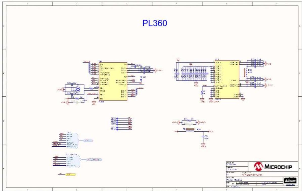
text_image
PL360 MicroCHIP PL 360 Medium Alum 1 2 3 4 5 6 7 8 9 10 11 12 13 14 15 16 17 18 19 20 21 22 23 24 25 26 27 28 29 30 31 32 33 34 35 36 37 38 39 40 41 42 43 44 45 46 47 48 49 50 51 52 53 54 55 56 57 58 59 60 61 62 63 64 65 66 67 68 69 70 71 72 73 74 75 76 77 78 79 80 A B C D E F G H I J K L M N O P Q R S T U V V W X Y Z P1 P2 P3 P4 P5 P6 P7 P8 P9 P10 P11 P12 P13 P14 P15 P16 P17 P18 P19 P20 P21 P22 P23 P24 P25 P26 P27 P28 P29 P30 P31 P32 P33 P34 P35 P36 P37 P38 P39 P40 P41 P42 P43 P44 P45 P46 P47 P48 P49 P50 P51 P52 P53 P54 P55 P56 P57 P58 P59 P60 P61 P62 P63 P64 P65 P66 P67 P68 P69 P70 P71 P72 P73 P74 P75 P76 P77 P78 P79 P80 P81 P82 P83 P84 P85 P86 P87 P88 P89 P90 P91 P92 P93 P94 P95 P96 P97 P98 P99 CCK CCK CCK CCK CCK CCK CCK CCK CCK CCK CCK CCK CCK CCK CCK CCK CCK CCK CCK CCK CCK CCK CCK CCK CCK CCK CCK CCK CCK CCK CCK CCK CCK CCK CCK CCK CCK CCK CCK CCK CCK CCK CCK CCK CCK CCK CCK CCK CCK CCK CCK P10 P11 P12 P13 P14 P15 P16 P17 P18 P19 P20 P21 P22 P23 P24 P25 P26 P27 P28 P29 P30 P31 P32 P33 P34 P35 P36 P37 P38 P39 P40 P41 P42 P43 P44 P45 P46 P47 P48 P49 P50 P51 P52 P53 P54 P55 P56 P57 P58 P59 P60 P61 P62 P63 P64 P65 P66 P67 P68 P69 P70 P71 P72 P73 P74 P75 P76 P77 P78 P79 P80 P81 P82 P83 P84 P85 P86 P87 P88 P89 P90 P91 P92 P93 P94 P95 P96 P97 P98 P99 CNC CND FB ACD ACO ACO ACO ACO ACO ACO ACO ACO ACO ACO ACO ACO ACO ACO ACO ACO ACO ACO ACO ACO ACO ACO ACO ACO ACO ACO ACO ACO ACO ACO ACO ACO ACO ACO ACO ACO ACO ACO ACO ACO ACO ACO ACO ACO ACO ACO ACO ACO ACO ACO AOCFigure 3-23. SAMG55 MCU Schematic
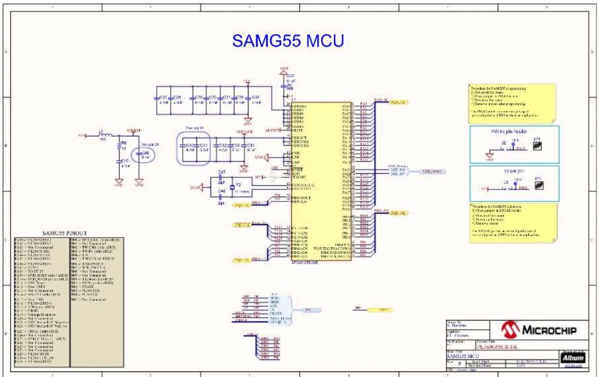
text_image
SAMG55 MCU SAMS35 PINOUT SAMS35 PINOUT SAMS35 PINOUT MicroCHIP SAMS55 MCU Microchip P100000000000000000000000000000000000000000000000000000000000000000000000000000000000 Microchip P11 Microchip P12 Microchip P13 Microchip P14 Microchip P15 Microchip P16 Microchip P17 Microchip P18 Microchip P19 Microchip P20 Microchip P21 Microchip P22 Microchip P23 Microchip P24 Microchip P25 Microchip P26 Microchip P27 Microchip P28 Microchip P29 Microchip P30 Microchip P31 Microchip P32 Microchip P33 Microchip P34 Microchip P35 Microchip P36 Microchip P37 Microchip P38 Microchip P39 Microchip P40 Microchip P41 Microchip P42 Microchip P43 Microchip P44 Microchip P45 Microchip P46 Microchip P47 Microchip P48 Microchip P49 Microchip P50 Microchip P51 Microchip P52 Microchip P53 Microchip P54 Microchip P55 Microchip P56 Microchip P57 Microchip P58 Microchip P59 Microchip P60 Microchip P61 Microchip P62 Microchip P63 Microchip P64 Microchip P65 Microchip P66 Microchip P67 Microchip P68 Microchip P69 Microchip P70 Microchip P71 Microchip P72 Microchip P73 Microchip P74 Microchip P75 Microchip P76 Microchip P77 Microchip P78 Microchip P79 Microchip P80 Microchip P81 Microchip P82 Microchip P83 Microchip P84 Microchip P85 Microchip P86 Microchip P87 Microchip P88 Microchip P89 Microchip P90 Microchip P91 Microchip P92 Microchip P93 Microchip P94 Microchip P95 Microchip P96 Microchip P97 Microchip P98 MicrochipFigure 3-24. Interface and Peripherals SAMG55 Schematic
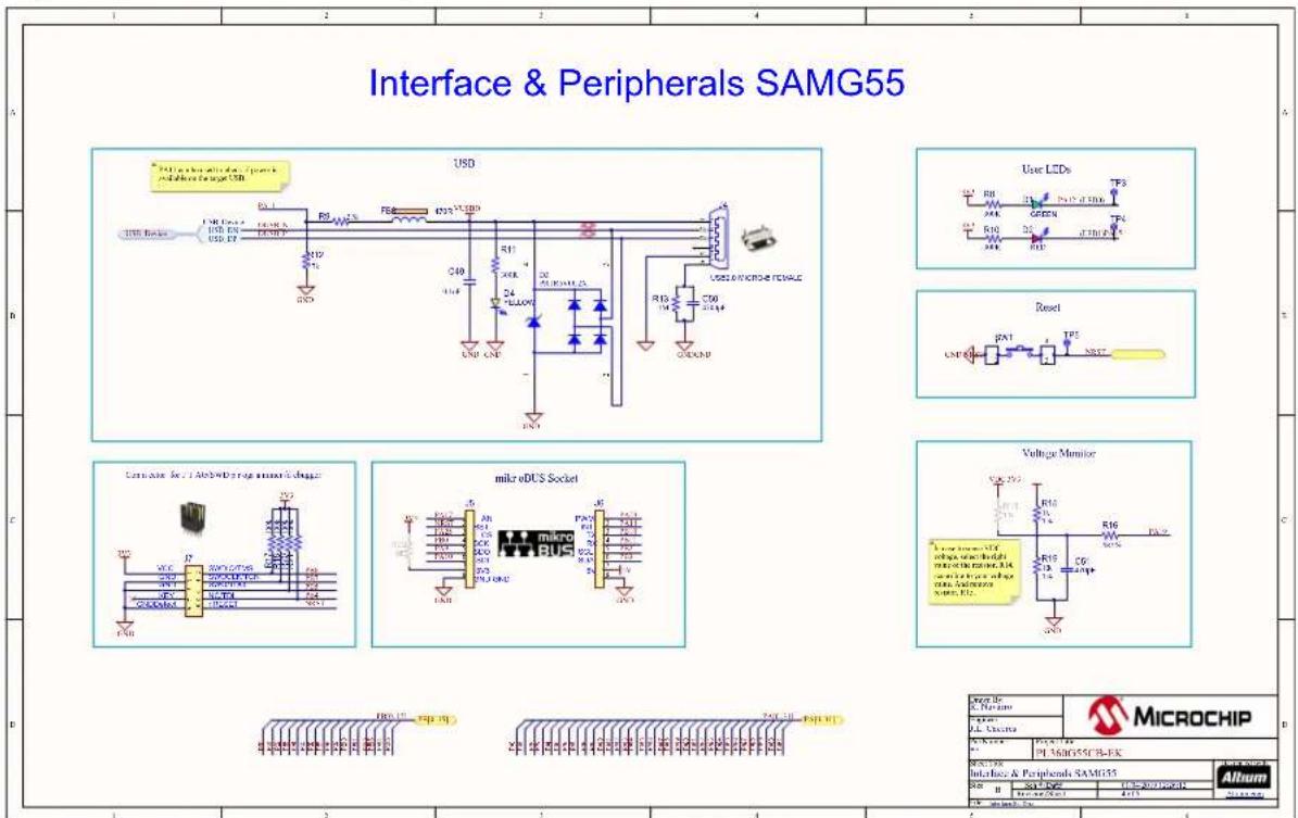
text_image
Interface & Peripherals SAMG55 USB User LEDs Reset Voltage Monitor Microchip Interface & Peripherals SAMG55 AlbumFigure 3-25. Power Supply Schematic
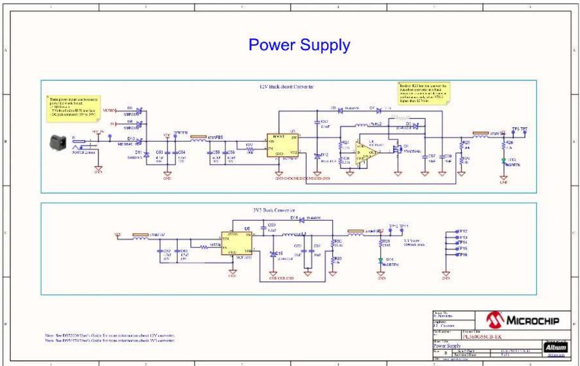
text_image
Power Supply 12V Back-short Converter Current: R23 for more expensive the current current in the back- current current in the back- current current in the back- current current in the back- current current in the back- current current in the back- current current in the back- current current in the back- current current in the back- current current in the back- current current in the back- current current in the back- current current in the back- current current in the back- current current in the back- current current in the back- current current in the back- current current in the back-short converter Current: R23 for more expensive the current current in the back- current current in the back- current current in the back- current current in the back- current current in the back- current current in the back- current current in the back- current current in the back- current current in the back- current current in the back- current current in the back- current current in the back- current current in the back- current current in the back- current current in the background Current: R23 for more expensive the current current in the back- current current in the back- current current in the back- current current in the back- current current in the back- current current in the back- current current in the back- current current in the back- current current in the back- current current in the back- current current in the back- current current in the back- current current in the back- current current in the back- current current in the next cycle Current: R23 for more expensive the current current in the back- current current in the back- current current in the back- current current in the back- current current in the back- current current in the back- current current in the next cycle Current: R23 for more expensive the current current in the back- current current in the back- current current in the back- current current in the back- current current in the next cycle Current: R23 for more expensive the current current in the back- current current in the back- current current in the back- current current in the next cycle Current: R23 for more expensive the current current in the back- current current in the back- current current in the next cycle Current: R23 for more expensive the current current in the back- current current in the back- current current in the next cycle Current: R23 for more expensive the current current in the back- current current in the back- current current in the next cycle Current: R23 for more expensive the current current in the back- current current in the back- Current: R23 for more expensive the current current in the back- current current in the next cycle Current: R23 for more expensive the current current in the back- current current in the back- current current in the next cycle Current: R23 for more expensive the current current in the back- current current in the back- current current in the next cycle Current: R23 for more expensive the current current in the back- current current in the back- current current in the next cycleFigure 3-26. PLC Coupling Schematic
text_image
PLC Coupling for CENELEC B-Band PLCOUP014 Isolated A B C D E F G H I J K L M N O P Q R S T U V W X Y Z A B C D E F G H I J K L M N O P Q R S T U V W X Y Z A B C D E F G H I J K L M N O P Q R S T U V W X3.7 PL360G55CB-EK Layout
This section contains the layout graphics for the PL360G55CB-EKv2 board:
• Layer 1: Top Layer, Figure 3-27
• Layer 2: Mid Layer 1 (Ground), Figure 3-28
• Layer 3: Mid Layer 2 (Power Supplies), Figure 3-29
- Layer 4: Bottom Layer, Figure 3-30
• Top Components Placement, Figure 3-31
• Bottom Components Placement, Figure 3-32
Figure 3-27. PL360G55CB-EKv2 Layout: Top Layer

text_image
R108 L100 R116 R102 R106 MICROCHIP PL 360G55CB-EK v2 Hazardous Voltage D100 U100 D-14 D-14 D-14 D-14 D-14 D-14 D-14 D-14 D-14 D-14 D-14 D-14 D-14 D-14 D-14 D-14 D-14 D-14 D-14 D-14 D-13 D-13 D-13 D-13 D-13 D-13 D-13 D-13 D-13 D-13 D-13 D-13 D-13 D-13 D-13 D-13 D-13 D-13 D-13 D-13 D-12 D-12 D-12 D-12 D-12 D-12 D-12 D-12 D-12 D-12 D-12 D-12 D-12 D-12 D-12 D-12 D-12 D-12 D-12 D-12 D-11 D-11 D-11 D-11 D-11 D-11 D-11 D-11 D-11 D-11 D-11 D-11 D-10 D-10 D-10 D-10 D-10 D-10 D-10 D-9 D-9 D-9 D-9 D-9 D-9 D-9 D-9 D-9 D-9 D-9 D-9 D-9 D-9 D-9 D-9 D-9 D-9 D-9 D-9 D-9 D-9 D-9 D-9 D-9 D-8 D-8 D-8 D-8 D-8 D-8 D-8 D-8 D-8 D-8 D-8 D-8 D-8 D-8 D-8 D-8 D-8 D-8 D-8 D-8 D-8 D-8Figure 3-28. PL360G55CB-EKv2 Layout: Mid Layer 1 (Ground)
natural_image
Green printed circuit board with scattered white circular components and gray dots, no visible text or symbolsFigure 3-29. PL360G55CB-EKv2 Layout: Mid Layer 2 (Power Supplies)
natural_image
Green printed circuit board with various electronic components and dot patterns (no readable text or symbols)Figure 3-30. PL360G55CB-EKv2 Layout: Bottom Layer
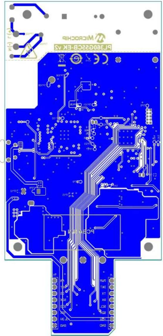
text_image
MICROCHIB BR380G23CB-EK ASFigure 3-31. PL360G55CB-EKv2 Layout: Top Silkscreen
text_image
MICROCHIP PL 360G55CB-EK v2 Hazardous Voltage RESSET JTAG DC IN: 6V-30V PROG mikro BUS R110 C101 L100 R115 D102 R108 R115 N(-) L(+) R112 C103 R116 MOV133 R111 L102 R112 C108 R124 L101 TR100 R129 R135 R121 R122 R127 R130 D103 R128 R130 D103 R129 R130 D103 R130 R130 D103 R131 R132 R133 R134 R132 R134 R135 R133 R135 R136 R134 R136 R137 R135 R137 R138 R136 R138 R139 R137 R139 R140 R138 R140 R141 R139 R141 R142 R140 R142 R143 R141 R143 R144 R142 R144 R145 R143 R145 R146 R144 R146 R147 R145 R147 R148 R146 R148 R149 R147 R149 R150 R148 R150 R151 R149 R151 R152 R150 R152 R153 R151 R153 R154 R152 R154 R155 R153 R155 R156 R154 R156 R157 R155 R157 R158 R156 R158 R159 R157 R159 R160 R158 R160 R161 R159 R161 R162 R160 R162 R163 R161 R163 R164 R162 R164 R165 R163 R165 R166 R164 R166 R167 R165 R167 R168 R166 R168 R169 R167 R169 R170 R168 R170 R171 R169 R170 R172 R170 R172 R173 R172 R173 R174 R173 R174 R175 R174 R175 R176 R175 R176 R177 R176 R177 R178 R177 R178 R179 R178 R179 R180 R179 R180 R181 R180 R180 R182 R180 R182 R183 R180 R200 PLS 2.0V 2.0V 2.0V 2.0V 2.0V 2.0V 2.0V 2.0V 2.0V 2.0V 2.0V 2.0V 2.0V 2.0V 2.0V 2.0V 2.0V 2.0V 2.0V 2.0V 2.0SFigure 3-32. PL360G55CB-EKv2 Layout: Bottom Silkscreen
text_image
BcBA 211 WICROCHI BL380C226-EK AS IN (-) (+) SOYRT SOYRT SOYRT SOYRT SOYRT SOYRT SOYRT SOYRT SOYRT SOYRT SOYRT SOYRT SOYRT SOYRT SOYRT SOYRT SOYRT SOYRT SOYRT SOYRT SOYRT SOYRT SOYRT SOYRT SOYRT SOYRT4. Compliance for Specific Standards
The development/evaluation tool is designed to be used for research and development in a laboratory environment. This development/evaluation tool is not intended to be a finished appliance, nor is it intended for incorporation into finished appliances that are made commercially available as single functional units to end users.
The PL360G55CB-EK board is a CE mark product which passes the EN 50065-1, EN 50065-2-3, EN 50065-7 EMC standards. It also satisfies the Pb-Free and ROHS directive.
5. References
- CENELEC, EN 50065. Signaling on low-voltage electrical installations in the frequency range 3 kHz to 148.5 kHz, 2002
• PL360 Datasheet, 2018
• SAMG55 Datasheet, 2016 - MCP16301 High-Voltage Input Integrated Switch Step-Down Regulator, 2015
- MCP16301 High Voltage Buck-Boost Demo Board User's Guide, 2012
- MCP16301 High Voltage Buck Converter 600mA Demo Board User's Guide, 2011
6. Revision History
6.1 Rev A - 04/2019
Document Initial release.
The Microchip Web Site
Microchip provides online support via our web site at http://www.microchip.com/. This web site is used as a means to make files and information easily available to customers. Accessible by using your favorite Internet browser, the web site contains the following information:
- Product Support – Data sheets and errata, application notes and sample programs, design resources, user's guides and hardware support documents, latest software releases and archived software
- General Technical Support – Frequently Asked Questions (FAQ), technical support requests, online discussion groups, Microchip consultant program member listing
- Business of Microchip – Product selector and ordering guides, latest Microchip press releases, listing of seminars and events, listings of Microchip sales offices, distributors and factory representatives
Customer Change Notification Service
Microchip's customer notification service helps keep customers current on Microchip products.
Subscribers will receive e-mail notification whenever there are changes, updates, revisions or errata related to a specified product family or development tool of interest.
To register, access the Microchip web site at http://www.microchip.com/. Under "Support", click on "Customer Change Notification" and follow the registration instructions.
Customer Support
Users of Microchip products can receive assistance through several channels:
• Distributor or Representative
- Local Sales Office
• Field Application Engineer (FAE)
- Technical Support
Customers should contact their distributor, representative or Field Application Engineer (FAE) for support. Local sales offices are also available to help customers. A listing of sales offices and locations is included in the back of this document.
Technical support is available through the web site at: http://www.microchip.com/support
Microchip Devices Code Protection Feature
Note the following details of the code protection feature on Microchip devices:
- Microchip products meet the specification contained in their particular Microchip Data Sheet.
- Microchip believes that its family of products is one of the most secure families of its kind on the market today, when used in the intended manner and under normal conditions.
- There are dishonest and possibly illegal methods used to breach the code protection feature. All of these methods, to our knowledge, require using the Microchip products in a manner outside the operating specifications contained in Microchip's Data Sheets. Most likely, the person doing so is engaged in theft of intellectual property.
- Microchip is willing to work with the customer who is concerned about the integrity of their code.
- Neither Microchip nor any other semiconductor manufacturer can guarantee the security of their code. Code protection does not mean that we are guaranteeing the product as “unbreakable.”
Code protection is constantly evolving. We at Microchip are committed to continuously improving the code protection features of our products. Attempts to break Microchip's code protection feature may be a violation of the Digital Millennium Copyright Act. If such acts allow unauthorized access to your software or other copyrighted work, you may have a right to sue for relief under that Act.
Legal Notice
Information contained in this publication regarding device applications and the like is provided only for your convenience and may be superseded by updates. It is your responsibility to ensure that your application meets with your specifications. MICROCHIP MAKES NO REPRESENTATIONS OR WARRANTIES OF ANY KIND WHETHER EXPRESS OR IMPLIED, WRITTEN OR ORAL, STATUTORY OR OTHERWISE, RELATED TO THE INFORMATION, INCLUDING BUT NOT LIMITED TO ITS CONDITION, QUALITY, PERFORMANCE, MERCHANTABILITY OR FITNESS FOR PURPOSE. Microchip disclaims all liability arising from this information and its use. Use of Microchip devices in life support and/or safety applications is entirely at the buyer's risk, and the buyer agrees to defend, indemnify and hold harmless Microchip from any and all damages, claims, suits, or expenses resulting from such use. No licenses are conveyed, implicitly or otherwise, under any Microchip intellectual property rights unless otherwise stated.
Trademarks
The Microchip name and logo, the Microchip logo, AnyRate, AVR, AVR logo, AVR Freaks, BitCloud, chipKIT, chipKIT logo, CryptoMemory, CryptoRF, dsPIC, FlashFlex, flexPWR, Heldo, JukeBlox, KeeLoq, Kleer, LANCheck, LINK MD, maXStylus, maXTouch, MediaLB, megaAVR, MOST, MOST logo, MPLAB, OptoLyzer, PIC, picoPower, PICSTART, PIC32 logo, Prochip Designer, QTouch, SAM-BA, SpyNIC, SST, SST Logo, SuperFlash, tinyAVR, UNI/O, and XMEGA are registered trademarks of Microchip Technology Incorporated in the U.S.A. and other countries.
ClockWorks, The Embedded Control Solutions Company, EtherSynch, Hyper Speed Control, HyperLight Load, IntelliMOS, mTouch, Precision Edge, and Quiet-Wire are registered trademarks of Microchip Technology Incorporated in the U.S.A.
Adjacent Key Suppression, AKS, Analog-for-the-Digital Age, Any Capacitor, AnyIn, AnyOut, BodyCom, CodeGuard, CryptoAuthentication, CryptoAutomotive, CryptoCompanion, CryptoController, dsPICDEM, dsPICDEM.net, Dynamic Average Matching, DAM, ECAN, EtherGREEN, In-Circuit Serial Programming, ICSP, INICnet, Inter-Chip Connectivity, JitterBlocker, KleerNet, KleerNet logo, memBrain, Mindi, MiWi, motorBench, MPASM, MPF, MPLAB Certified logo, MPLIB, MPLINK, MultiTRAK, NetDetach, Omniscient Code Generation, PICDEM, PICDEM.net, PICkit, PICtail, PowerSmart, PureSilicon, QMatrix, REAL ICE, Ripple Blocker, SAM-ICE, Serial Quad I/O, SMART-I.S., SQI, SuperSwitcher, SuperSwitcher II, Total Endurance, TSHARC, USBCheck, VariSense, ViewSpan, WiperLock, Wireless DNA, and ZENA are trademarks of Microchip Technology Incorporated in the U.S.A. and other countries.
SQTP is a service mark of Microchip Technology Incorporated in the U.S.A.
Silicon Storage Technology is a registered trademark of Microchip Technology Inc. in other countries.
GestIC is a registered trademark of Microchip Technology Germany II GmbH & Co. KG, a subsidiary of Microchip Technology Inc., in other countries.
All other trademarks mentioned herein are property of their respective companies.
© 2019, Microchip Technology Incorporated, Printed in the U.S.A., All Rights Reserved.
ISBN: 978-1-5224-4370-4
Quality Management System Certified by DNV
ISO/TS 16949
Microchip received ISO/TS-16949:2009 certification for its worldwide headquarters, design and wafer fabrication facilities in Chandler and Tempe, Arizona; Gresham, Oregon and design centers in California and India. The Company's quality system processes and procedures are for its PIC® MCUs and dsPIC® DSCs, KEELOQ® code hopping devices, Serial EEPROMs, microperipherals, nonvolatile memory and analog products. In addition, Microchip's quality system for the design and manufacture of development systems is ISO 9001:2000 certified.
Worldwide Sales and Service
AMERICAS ASIA/PACIFIC ASIA/PACIFIC EUROPE
| Corporate Office | Australia - Sydney | India - Bangalore | Austria - Wels |
| 2355 West Chandler Blvd. | Tel: 61-2-9868-6733 | Tel: 91-80-3090-4444 | Tel: 43-7242-2244-39 |
| Chandler, AZ 85224-6199 | China - Beijing | India - New Delhi | Fax: 43-7242-2244-393 |
| Tel: 480-792-7200 | Tel: 86-10-8569-7000 | Tel: 91-11-4160-8631 | Denmark - Copenhagen |
| Fax: 480-792-7277 | China - Chengdu | India - Pune | Tel: 45-4450-2828 |
| Technical Support: | Tel: 86-28-8665-5511 | Tel: 91-20-4121-0141 | Fax: 45-4485-2829 |
| http://www.microchip.com/ | China - Chongqing | Japan - Osaka | Finland - Espoo |
| support | Tel: 86-23-8980-9588 | Tel: 81-6-6152-7160 | Tel: 358-9-4520-820 |
| Web Address: | China - Dongguan | Japan - Tokyo | France - Paris |
| www.microchip.com | Tel: 86-769-8702-9880 | Tel: 81-3-6880-3770 | Tel: 33-1-69-53-63-20 |
| Atlanta | China - Guangzhou | Korea - Daegu | Fax: 33-1-69-30-90-79 |
| Duluth, GA | Tel: 86-20-8755-8029 | Tel: 82-53-744-4301 | Germany - Garching |
| Tel: 678-957-9614 | China - Hangzhou | Korea - Seoul | Tel: 49-8931-9700 |
| Fax: 678-957-1455 | Tel: 86-571-8792-8115 | Tel: 82-2-554-7200 | Germany - Haan |
| Austin, TX | China - Hong Kong SAR | Malaysia - Kuala Lumpur | Tel: 49-2129-3766400 |
| Tel: 512-257-3370 | Tel: 852-2943-5100 | Tel: 60-3-7651-7906 | Germany - Heilbronn |
| Boston | China - Nanjing | Malaysia - Penang | Tel: 49-7131-67-3636 |
| Westborough, MA | Tel: 86-25-8473-2460 | Tel: 60-4-227-8870 | Germany - Karlsruhe |
| Tel: 774-760-0087 | China - Qingdao | Philippines - Manila | Tel: 49-721-625370 |
| Fax: 774-760-0088 | Tel: 86-532-8502-7355 | Tel: 63-2-634-9065 | Germany - Munich |
| Chicago | China - Shanghai | Singapore | Tel: 49-89-627-144-0 |
| Itasca, IL | Tel: 86-21-3326-8000 | Tel: 65-6334-8870 | Fax: 49-89-627-144-44 |
| Tel: 630-285-0071 | China - Shenyang | Taiwan - Hsin Chu | Germany - Rosenheim |
| Fax: 630-285-0075 | Tel: 86-24-2334-2829 | Tel: 886-3-577-8366 | Tel: 49-8031-354-560 |
| Dallas | China - Shenzhen | Taiwan - Kaohsiung | Israel - Ra'anana |
| Addison, TX | Tel: 86-755-8864-2200 | Tel: 886-7-213-7830 | Tel: 972-9-744-7705 |
| Tel: 972-818-7423 | China - Suzhou | Taiwan - Taipei | Italy - Milan |
| Fax: 972-818-2924 | Tel: 86-186-6233-1526 | Tel: 886-2-2508-8600 | Tel: 39-0331-742611 |
| Detroit | China - Wuhan | Thailand - Bangkok | Fax: 39-0331-466781 |
| Novi, MI | Tel: 86-27-5980-5300 | Tel: 66-2-694-1351 | Italy - Padova |
| Tel: 248-848-4000 | China - Xian | Vietnam - Ho Chi Minh | Tel: 39-049-7625286 |
| Houston, TX | Tel: 86-29-8833-7252 | Tel: 84-28-5448-2100 | Netherlands - Drunen |
| Tel: 281-894-5983 | China - Xiamen | Tel: 31-416-690399 | |
| Indianapolis | Tel: 86-592-2388138 | Fax: 31-416-690340 | |
| Noblesville, IN | China - Zhuhai | Norway - Trondheim | |
| Tel: 317-773-8323 | Tel: 86-756-3210040 | Tel: 47-72884388 | |
| Fax: 317-773-5453 | Poland - Warsaw | ||
| Tel: 317-536-2380 | Tel: 48-22-3325737 | ||
| Los Angeles | Romania - Bucharest | ||
| Mission Viejo, CA | Tel: 40-21-407-87-50 | ||
| Tel: 949-462-9523 | Spain - Madrid | ||
| Fax: 949-462-9608 | Tel: 34-91-708-08-90 | ||
| Tel: 951-273-7800 | Fax: 34-91-708-08-91 | ||
| Raleigh, NC | Sweden - Gothenberg | ||
| Tel: 919-844-7510 | Tel: 46-31-704-60-40 | ||
| New York, NY | Sweden - Stockholm | ||
| Tel: 631-435-6000 | Tel: 46-8-5090-4654 | ||
| San Jose, CA | UK - Wokingham | ||
| Tel: 408-735-9110 | Tel: 44-118-921-5800 | ||
| Tel: 408-436-4270 | Fax: 44-118-921-5820 | ||
| Canada - Toronto | |||
| Tel: 905-695-1980 | |||
| Fax: 905-695-2078 |