AT89LP3240 - Electronic component Microchip - Free user manual and instructions
Find the device manual for free AT89LP3240 Microchip in PDF.

User questions about AT89LP3240 Microchip
0 question about this device. Answer the ones you know or ask your own.
Ask a new question about this device
Download the instructions for your Electronic component in PDF format for free! Find your manual AT89LP3240 - Microchip and take your electronic device back in hand. On this page are published all the documents necessary for the use of your device. AT89LP3240 by Microchip.
USER MANUAL AT89LP3240 Microchip
- 8-bit Microcontroller Compatible with MCS ^® 51 Products
• Enhanced 8051 Architecture
– Single-clock Cycle per Byte Fetch
- Up to 20 MIPS Throughput at 20 MHz Clock Frequency
– Fully Static Operation: 0 Hz to 20 MHz
- On-chip 2-cycle Hardware Multiplier
- 16x16 Multiply-Accumulate Unit
- 256x8 Internal RAM
- 4096x8 Internal Extra RAM
- Up to 4KB Extended Stack in Extra RAM
– Dual Data Pointers
- 4-level Interrupt Priority
• Nonvolatile Program and Data Memory
- 32K/64K Bytes of In-System Programmable (ISP) Flash Program Memory
- 8K Bytes of Flash Data Memory
- Endurance: Minimum 100,000 Write/Erase Cycles
– Serial Interface for Program Downloading - 64-byte Fast Page Programming Mode
- 256-Byte User Signature Array
- 2-level Program Memory Lock for Software Security
– In-Application Programming of Program Memory
• Peripheral Features
– Three 16-bit Enhanced Timer/Counters
- Two 8-bit PWM Outputs
- 4-Channel 16-bit Compare/Capture/PWM Array
- Enhanced UART with Automatic Address Recognition and Framing Error Detection
- Enhanced Master/Slave SPI with Double-buffered Send/Receive
– Master/Slave Two-Wire Serial Interface
- Programmable Watchdog Timer with Software Reset
– Dual Analog Comparators with Selectable Interrupts and Debouncing
- 8-channel 10-bit ADC/DAC
- 8 General-purpose Interrupt Pins
• Special Microcontroller Features
- Two-wire On-chip Debug Interface
– Brown-out Detection and Power-on Reset with Power-off Flag - Active-low External Reset Pin
- Internal RC Oscillator
– Low Power Idle and Power-down Modes - Interrupt Recovery from Power-down Mode
• I/O and Packages
- Up to 38 Programmable I/O Lines
- 40-lead PDIP or 44-lead TQFP/PLCC or 44-pad VQFN/MLF
- Configurable I/O Modes
• Quasi-bidirectional (80C51 Style)
- Input-Only (Tristate)
- Push-pull CMOS Output
- Open-drain
- Operating Conditions
- 2.4V to 3.6V V _DD Voltage Range
-- 4 0 °C to 85°C Temperature Range - 0 to 20 MHz @ 2.4-3.6V

text_image
ATMEL®8-bit
Microcontroller
with 32K/64K
Bytes In-System
Programmable
Flash
AT89LP3240
AT89LP6440
1. Pin Configurations
1.1 40P6: 40-lead PDIP
| T2/P1.0 | 1 | 40 | VDD |
| T2EX/P1.1 | 2 | 39 | P0.0/AD0 |
| SDA/P1.2 | 3 | 38 | P0.1/AD1 |
| SCL/P1.3 | 4 | 37 | P0.2/AD2 |
| SS/P1.4 | 5 | 36 | P0.3/AD3 |
| MOSI/P1.5 | 6 | 35 | P0.4/AD4 |
| MISO/P1.6 | 7 | 34 | P0.5/AD5 |
| SCK/P1.7 | 8 | 33 | P0.6/AD6 |
| RST/P4.2 | 9 | 32 | P0.7/AD7 |
| RXD/P3.0 | 10 | 31 | P4.3 |
| TXD/P3.1 | 11 | 30 | P4.4/ALE |
| INT0/P3.2 | 12 | 29 | P4.5 |
| INT1/P3.3 | 13 | 28 | P2.7/AIN3/A15 |
| T0/P3.4 | 14 | 27 | P2.6/AIN2/A14 |
| T1/P3.5 | 15 | 26 | P2.5/AIN1/A13 |
| WR/P3.6 | 16 | 25 | P2.4/AIN0/A12 |
| RD/P3.7 | 17 | 24 | P2.3/A11/CCD |
| XTAL2/P4.1 | 18 | 23 | P2.2/A10/CCC |
| XTAL1/P4.0 | 19 | 22 | P2.1/A9/CCB |
| GND | 20 | 21 | P2.0/A8/CCA |
1.2 44A: 44-lead TQFP (Top View)
other
| Pin | Value | |---|---| | P1.4/SS | 44 | | P1.3/SCL | 43 | | P1.2/SDA | 42 | | P1.1/T2EX | 41 | | P1.0/T2 | 40 | | VDD | 39 | | VDD | 38 | | P0.0/AD0 | 37 | | P0.1/AD1 | 36 | | P0.2/AD2 | 35 | | P0.3/AD3 | 34 | | MOSI/P1.5 | 1 | | MISO/P1.6 | 2 | | SCK/P1.7 | 3 | | RST/P4.2 | 4 | | RXD/P3.0 | 5 | | VDD | 6 | | TXD/P3.1 | 7 | | INT0/P3.2 | 8 | | INT1/P3.3 | 9 | | T0/P3.4 | 10 | | T1/P3.5 | 11 | | WR/P3.6 | 12 | | RD/P3.7 | 13 | | XTAL2/P4.1 | 14 | | XTAL1/P4.0 | 15 | | GND | 16 | | GND | 17 | | CCA/A8/P2.0 | 18 | | CCB/A9/P2.1 | 19 | | CCC/A10/P2.2 | 20 | | CCD/A11/P2.3 | 21 | | A12/AIN0/P2.4 | 22 | | P0.4/AD4 | 33 | | P0.5/AD5 | 32 | | P0.6/AD6 | 31 | | P0.7/AD7 | 30 | | P4.3 | 29 | | GND | 28 | | P4.4/ALE | 27 | | P4.5 | 26 | | P2.7/AIN3/A15 | 25 | | P2.6/AIN2/A14 | 24 | | P2.5/AIN1/A13 | 23 |1.3 44J: 44-lead PLCC

text_image
P1.4/SS P1.3/SCL P1.2/SDA P1.1/T2EX P1.0/T2 VDD P0.0/AD0 P0.1/AD1 P0.2/AD2 P0.3/AD3 MOSI/P1.5 7 MISO/P1.6 8 SCK/P1.7 9 RST/P4.2 10 RXD/P3.0 11 VDD 12 TXD/P3.1 13 INT0/P3.2 14 INT1/P3.3 15 T0/P3.4 16 T1/P3.5 17 WR/P3.6 18 RD/P3.7 19 XTAL2/P4.1 20 XTAL1/P4.0 21 GND 22 GND 23 CC/A8/AIN0/P2.0 24 CCB/A9/P2.1 25 CCC/A10/P2.2 26 CCD/A11/P2.3 27 A12/AIN0/P2.4 28 O 1 VDD 44 P0.4/AD4 39 P0.5/AD5 38 P0.6/AD6 37 P0.7/AD7 36 P4.3 GND 35 P4.4/ALE 34 P4.5 P4.6 33 P2.7/AIN3/A15 32 P2.6/AIN2/A14 29 P2.5/AIN1/A131.4 44M1: 44-pad VQFN/MLF

radar
| Label | Value | |---|---| | P1.4/SS | 44 | | P1.3/SCL | 43 | | P1.2/SDA | 42 | | P1.1/T2EX | 41 | | P1.0/T2 | 40 | | VDD | 39 | | VDD | 38 | | P0.0/AD0 | 37 | | P0.1/AD1 | 36 | | P0.2/AD2 | 35 | | P0.3/AD3 | 34 | | MOSI/P1.5 | 1 | | MISO/P1.6 | 2 | | SCK/P1.7 | 3 | | RST/P4.2 | 4 | | RXD/P3.0 | 5 | | VDD | 6 | | TXD/P3.1 | 7 | | INT0/P3.2 | 8 | | INT1/P3.3 | 9 | | T0/P3.4 | 10 | | T1/P3.5 | 11 | | WR/P3.6 | 12 | | RD/P3.7 | 13 | | XTAL2/P4.1 | 14 | | XTAL1/P4.0 | 15 | | GND | 16 | | GND | 17 | | CCA/A8/P2.0 | 18 | | CCB/A9/P2.1 | 19 | | CCC/A10/P2.2 | 20 | | CCD/A11/P2.3 | 21 | | A12/AIN0/P2.4 | 22 | NOTE: Bottom pad should be soldered to ground 33 P0.4/AD4 32 P0.5/AD5 31 P0.6/AD6 30 P0.7/AD7 29 P4.3 28 GND 27 P4.4/ALE 26 P4.5 25 P2.7/AIN3/A15 24 P2.6/AIN2/A14 23 P2.5/AIN1/A131.5 Pin Description
Table 1-1. AT89LP3240/6440 Pin Description
| Pin Number | Symbol Type Description | |||||
| 1 | 7 | 6 | 1 | P | I/O I/O I | P1.5:User-configurable I/O Port 1 bit 5.MOSI: SPL master-out/slave-in. When configured as master, this pin is an output.When configured as slave, this pin is an input.GPI5:General-purpose Interrupt input 5. |
| 287 | 2 | P | 1 | . | I/O I/O 6 I | P1.6:User-configurable I/O Port 1 bit 6.MISO:SPI master-in/slave-out. When configured as master, this pin is an input. When configured as slave, this pin is an output.GPI6:General-purpose Interrupt input 6. |
| 3 | 9 | 83 | P | 1 | I/O I/O . I | P1.7:User-configurable I/O Port 1 bit 7.SCK:SPI Clock. When configured as master, this pin is an output. When configured as slave, this pin is an input.GPI7:General-purpose Interrupt input 7. |
| 4 | 1 | 0 | 9 | 4 | I/O I P I | P4.2:User-configurable I/O Port 4 bit 2 (if Reset Fuse is disabled).RST:External Active-Low Reset input (if Reset Fuse is enabled. See “External Reset” on page 35.).DCL:Serial Clock input for On-Chip Debug Interface when OCD is enabled. |
| 5 | 1 | 1 | 1 | 0 5 | I/O I P I | P3.0:User-configurable I/O Port 3 bit 0.RXD:Serial Port Receiver Input. |
| 6 | 12 | 6 | VDD | I | Supply Voltage | |
| 7 | 1 | 3 | 1 | 1 7 | I/O O P | P3.1:User-configurable I/O Port 3 bit 1.TXD:Serial Port Transmitter Output. |
| 8 | 14 | 12 | 8 | P3.2 | I/O I | P3.2:User-configurable I/O Port 3 bit 2.INT0:External Interrupt 0 Input or Timer 0 Gate Input. |
| 9 | 1 | 5 | 1 | 3 9 | I/O I P | P3.3:User-configurable I/O Port 3 bit 3.INT1:External Interrupt 1 Input or Timer 1 Gate Input |
| 10 | 16 | 14 | 10 | P3.4 | I/O I/O | P3.4:User-configurable I/O Port 3 bit 4.T1:Timer/Counter 0 External input or PWM output. |
| 11 | 17 | 15 | 11 | P3.5 | I/O I/O | P3.5:User-configurable I/O Port 3 bit 5.T1:Timer/Counter 1 External input or PWM output. |
| 12 | 18 | 16 | 12 | P3.6 | I/O O | P3.6:User-configurable I/O Port 3 bit 6.WR:External memory interface Write Strobe (active-low). |
| 13 | 19 | 17 | 13 | P3.7 | I/O O | P3.7:User-configurable I/O Port 3 bit 7.RD:External memory interface Read Strobe (active-low). |
| 14 | 20 | 18 | 14 | P4.1 | I/O O O I/O | P4.1:User-configurable I/O Port 4 bit 1.XTAL2:Output from inverting oscillator amplifier. It may be used as a port pin if the internal RC oscillator is selected as the clock source.CLKOUT:When the internal RC oscillator is selected as the clock source, may be used to output the internal clock divided by 2.DDA:Serial Data input/output for On-Chip Debug Interface when OCD is enabled and the external clock is selected as the clock source. |
| 15 | 21 | 19 | 15 | P4.0 | I/O I I/O | P4.0:User-configurable I/O Port 4 bit 0.XTAL1:Input to the inverting oscillator amplifier and internal clock generation circuits. It may be used as a port pin if the internal RC oscillator is selected as the clock source.DDA:Serial Data input/output for On-Chip Debug Interface when OCD is enabled and the internal RC oscillator is selected as the clock source. |
| 16 | 22 | N/A | 16 | GND | I | Ground |
Table 1-1. AT89LP3240/6440 Pin Description
| Pin Number | Symbol Type DescriptionTQFP PLCC PDIP VQFN | ||||
| 17 23 | 20 17 GND I Ground | ||||
| 1824 | 21 18P2.0 | I/O I/O O P2.0:User-configurable I/O Port 2 bit 0.CCA:Timer 2 Channel A Compare Output or Capture Input.A8:External memory interface Address bit 8. | |||
| 19 25 | 22 19 P2.1 | I/O I/O O P2.1:User-configurable I/O Port 2 bit 1.CCB:Timer 2 Channel B Compare Output or Capture Input.A9:External memory interface Address bit 9. | |||
| 20 26 | 23 20 P2.1 | I/O I/O O P2.2:User-configurable I/O Port 2 bit 2.CCC:Timer 2 Channel C Compare Output or Capture Input.A10:External memory interface Address bit 10.DA:-DAC negative differential output. | |||
| 21 27 | 24 21 P2.3 | I/O I/O O P2.3:User-configurable I/O Port 2 bit 3.CCD:Timer 2 Channel D Compare Output or Capture Input.A11:External memory interface Address bit 11.D+-DAC positive differential output. | |||
| 22 28 | 25 22 P2.4 | I/O I O P2.4:User-configurable I/O Port 2 bit 5.AIN0:Analog Comparator Input 0.A12:External memory interface Address bit 12. | |||
| 23 29 | 26 23 P2.5 | I/O I O P2.5:User-configurable I/O Port 2 bit 5.AIN1:Analog Comparator Input 1.A13:External memory interface Address bit 13. | |||
| 24 30 | 27 24 P2.6 | I/O I O P2.6:User-configurable I/O Port 2 bit 6.AIN2:Analog Comparator Input 2.A14:External memory interface Address bit 14. | |||
| 25 31 | 2825 P2.7 | I/O I O P2.7:User-configurable I/O Port 2 bit 7.AIN3:Analog Comparator Input 3.A15:External memory interface Address bit 15. | |||
| 26 | 32 | 29 | 26 | P4.5 | I/O P4.5:User-configurable I/O Port 4 bit 5. |
| 27 33 | 30 27 P4.4 | I/O O P4.4:User-configurable I/O Port 4 bit 4.ALE:External memory interface Address Latch Enable. | |||
| 28 | 34 | 28 | GND | I Ground | |
| 29 35 | 31 29 P4.3 | I/O I/O P4.3:User-configurable I/O Port 4 bit 3.DDA:Serial Data input/output for On-Chip Debug Interface when OCD is enabled and the Crystal oscillator is selected as the clock source. | |||
| 30 36 | 32 30 P0.7 | I/O O I P0.7:User-configurable I/O Port 0 bit 7.AD7:External memory interface Address/Data bit 7.ADC7:ADC analog input 7. | |||
| 31 37 | 33 31 P0.6 | I/O O I P0.6:User-configurable I/O Port 0 bit 6.AD6:External memory interface Address/Data bit 6.ADC6:ADC analog input 6. | |||
| 32 38 | 34 32 | P0.5 | I/O O I P0.5:User-configurable I/O Port 0 bit 5.AD5:External memory interface Address/Data bit 5.ADC5:ADC analog input 5. | ||
| 33 39 | 35 33 P0.4 | I/O O I P0.4:User-configurable I/O Port 0 bit 4.AD4:External memory interface Address/Data bit 4.ADC4:ADC analog input 4. | |||
| 34 40 | 36 34 P0.3 | I/O O I P0.3:User-configurable I/O Port 0 bit 3.AD3:External memory interface Address/Data bit 3.ADC3:ADC analog input 3. | |||
Table 1-1. AT89LP3240/6440 Pin Description
| Pin Number | Symbol | Type | Description | |||
| TQFP | PLCC | PDIP | VQFN | |||
| 35 41 | 37 35 P0.2 | I/O | P0.2: User-configurable I/O Port 0 bit 2.AD2: External memory interface Address/Data bit 2.ADC2: ADC analog input 2. | |||
| 36 42 | 3836 P0.1 | I/O | P0.1: User-configurable I/O Port 0 bit 1.AD1: External memory interface Address/Data bit 1.ADC1: ADC analog input 1. | |||
| 37 43 | 39 37 P0.0 | I/O | P0.0: User-configurable I/O Port 0 bit 0.AD0: External memory interface Address/Data bit 0.ADC0: ADC analog input 0. | |||
| 38 | 44 | 40 | 38 | VDD | I | Supply Voltage |
| 39 | 1 | 39 | VDD | I | Supply Voltage | |
| 40 2 1 | 40 P1.0 | I/O | P1.0: User-configurable I/O Port 1 bit 0.T2: Timer 2 External Input or Clock Output.GPI0: General-purpose Interrupt input 0. | |||
| 41 3 2 | 41 P1.1 | I/O | P1.1: User-configurable I/O Port 1 bit 1.T2EX: Timer 2 External Capture/Reload Input.GPI1: General-purpose Interrupt input 1 | |||
| 42 4 3 | 42 P1.2 | I/O | P1.2: User-configurable I/O Port 1 bit 2.GPI2: General-purpose Interrupt input 2. | |||
| 43 5 4 | 43 P1.3 | I/O | P1.3: User-configurable I/O Port 1 bit 3.GPI3: General-purpose Interrupt input 3. | |||
| 44 6 5 | 44 P1.4 | I/O | P1.4: User-configurable I/O Port 1 bit 4.S5: SPI Slave-Select.GPI6: General-purpose Interrupt input 4. | |||
2. Overview
The AT89LP3240/6440 is a low-power, high-performance CMOS 8-bit microcontroller with 32K/64K bytes of In-System Programmable Flash program memory and 8K bytes of Flash data memory. The device is manufactured using Atmel ^® s high-density nonvolatile memory technology and is compatible with the industry-standard 8051 instruction set. The AT89LP3240/6440 is built around an enhanced CPU core that can fetch a single byte from memory every clock cycle. In the classic 8051 architecture, each fetch requires 6 clock cycles, forcing instructions to execute in 12, 24 or 48 clock cycles. In the AT89LP3240/6440 CPU, standard instructions need only 1 to 4 clock cycles providing 6 to 12 times more throughput than the standard 8051. Seventy percent of instructions need only as many clock cycles as they have bytes to execute, and most of the remaining instructions require only one additional clock. The enhanced CPU core is capable of 20 MIPS throughput whereas the classic 8051 CPU can deliver only 4 MIPS at the same current consumption. Conversely, at the same throughput as the classic 8051, the new CPU core runs at a much lower speed and thereby greatly reducing power consumption and EMI.
The AT89LP3240/6440 provides the following standard features: 32K/64K bytes of In-System Programmable Flash program memory, 8K bytes of Flash data memory, 4352 bytes of RAM, up to 38 I/O lines, three 16-bit timer/counters, up to six PWM outputs, a programmable watchdog timer, two analog comparators, a 10-bit ADC/DAC with 8 input channels, a full-duplex serial port, a serial peripheral interface, a two-wire serial interface, an internal RC oscillator, on-chip crystal oscillator, and a four-level, twelve-vector interrupt system. A block diagram is shown in Figure 2-1.
Timer 0 and Timer 1 in the AT89LP3240/6440 are enhanced with two new modes. Mode 0 can be configured as a variable 9- to 16-bit timer/counter and Mode 1 can be configured as a 16-bit auto-reload timer/counter. In addition, the timer/counters may each independently drive an 8-bit precision pulse width modulation output.
Timer 2 on the AT89LP3240/6440 serves as a 16-bit time base for a 4-channel Compare/Capture Array with up to four multi-phasic, variable precision (up to 16-bit) PWM outputs.
The enhanced UART of the AT89LP3240/6440 includes Framing Error Detection and Automatic Address Recognition. In addition, enhancements to Mode 0 allow hardware accelerated emulation of half-duplex SPI or Two Wire interfaces.
The I/O ports of the AT89LP3240/6440 can be independently configured in one of four operating modes. In quasi-bidirectional mode, the ports operate as in the classic 8051. In input-only mode, the ports are tristated. Push-pull output mode provides full CMOS drivers and open-drain mode provides just a pull-down. In addition, all 8 pins of Port 1 can be configured to generate an interrupt using the general-purpose interrupt interface.
2.1 Block Diagram
Figure 2-1. AT89LP3240/6440 Block Diagram
flowchart
graph TD
    A["32K/64K Bytes Flash Code"] --> B["8051 Single Cycle CPU"]
    C["8K Bytes Flash Data"] --> B
    D["256 Bytes RAM"] --> B
    E["4K Bytes ERAM"] --> B
    F["XRAM Interface"] --> B
    B --> G["Port0 Configurable Logic"]
    B --> H["Port1 Configurable Logic"]
    B --> I["Port2 Configurable Logic"]
    B --> J["Port3 Configurable Logic"]
    B --> K["Port4 Configurable Logic"]
    G <--> L["Watchdog Timer"]
    H <--> M["Gene r al-pu rpose Interrupt up"]
    I <--> N["Dual Data Pointers"]
    J <--> O["Multiply Accumulate (16 x 16)"]
    K <--> P["POR BOD"]
    L <--> Q["UART"]
    M <--> R["SPI"]
    N <--> S["TWI"]
    O <--> T["Timer 0 Timer 1"]
    P <--> U["Timer 2"]
    Q <--> V["Compare/Capture Array"]
    R <--> W["Dual Analog Comparators"]
    S <--> X["8-channel 10-bit ADC/DAC"]
    T <--> U
    U <--> V
    V <--> W
    W <--> X
    X --> Y["C rystalor Resistor"]
    X --> Z["Configurable Oscillator"]
    X --> AA["On-Chlp Debug"]
2.2 System Configuration
The AT89LP3240/6440 supports several system configuration options. Nonvolatile options are set through user fuses that must be programmed through the flash programming interface. Volatile options are controlled by software through individual bits of special function registers (SFRs). The AT89LP3240/6440 must be properly configured before correct operation can occur.
2.2.1 Fuse Options
Table 2-1 lists the fusable options for the AT89LP3240/6440. These options maintain their state even when the device is powered off, but can only be changed with an external device programmer. For more information, see Section 25.7 "User Configuration Fuses" on page 164.
Table 2-1. User Configuration Fuses
| Fuse Name Description | |
| Clock Source | Selects between the High Speed Crystal Oscillator, Low Speed Crystal Oscillator, External Clock or Internal RC Oscillator for the source of the system clock. |
| Start-up Time | Selects time-out delay for the POR/BOD/PWD wake-up period. |
| Reset Pin Enable | Configures the RST pin as a reset input or general purpose I/O |
| Brown-Out Detector Enable | Enables or disables the Brown-out Detector |
| On-Chip Debug Enable | Enables or disables On-Chip Debug. OCD must be enabled prior to using an in-circuit debugger with the device. |
| In-System Programming Enable | Enables or disables In-System Programming. |
| User Signature Programming Enable | Enables or disables programming of User Signature array. |
| Default Port State | Configures the default port state as input-only mode (tristated) or quasi-bidirectional mode (weakly pulled high). |
| In-Application Programming Enable | Enables or disabled In-Application (self) Programming |
2.2.2 Software Options
Table 2-2 lists some important software configuration bits that affect operation at the system level. These can be changed by the application software but are set to their default values upon any reset. Most peripherals also have multiple configuration bits that are not listed here.
Table 2-2. Important Software Configuration Bits
| Bit(s) SFR | Location Description | |
| PxM0.yPxM1.y | P0M0, P0M1, P1M0, P1M1,P2M0, P2M1, P3M0, P3M1,P4M0, P4M1 | Configures the I/O mode of Port x Pin y to be one of input-only, quasi-bidirectional, push-pull output or open-drain. The default state is controlled by the Default Port State fuse above |
| CDV_2-0 | CLKREG.3-1 | Selects the division ratio between the oscillator and the system clock |
| TPS_3-0 | CLKREG.7-4 | Selects the division ratio between the system clock and the timers |
| ALES | AUXR.0 | Enables/disables toggling of ALE |
| EXRAM | AUXR.1 | Enables/disables access to on-chip memories that are mapped to the external data memory address space |
| WS_1-0 | AUXR.3-2 | Selects the number of wait states when accessing external data memory |
| XSTK | AUXR.4 | Congifures the hardware stack to be in RAM or extra RAM |
| DMEN | MEMCON.3 | Enables/disables access to the on-chip flash data memory |
| IAP | MEMCON.7 | Enbles/disables the self programming feature when the fuse allows |
2.3 Comparison to Standard 8051
The AT89LP3240/6440 is part of a family of devices with enhanced features that are fully binary compatible with the 8051 instruction set. In addition, most SFR addresses, bit assignments, and pin alternate functions are identical to Atmel's existing standard 8051 products. However, due to the high performance nature of the device, some system behaviors are different from those of Atmel's standard 8051 products such as AT89S52 or AT89C2051. The major differences from the standard 8051 are outlined in the following paragraphs and may be useful to users migrating to the AT89LP3240/6440 from older devices.
2.3.1 System Clock
The maximum CPU clock frequency equals the externally supplied XTAL1 frequency. The oscillator is not divided by 2 to provide the internal clock and X2 mode is not supported. The System Clock Divider can scale the CPU clock versus the oscillator source (See Section 6.5 on page 32).
2.3.2 Reset
The RST pin of the AT89LP3240/6440 is active-LOW as compared with the active-high reset in the standard 8051. In addition, the RST pin is sampled every clock cycle and must be held low for a minimum of two clock cycles, instead of 24 clock cycles, to be recognized as a valid reset.
2.3.3 Instruction Execution with Single-cycle Fetch
The CPU fetches one code byte from memory every clock cycle instead of every six clock cycles. This greatly increases the throughput of the CPU. As a consequence, the CPU no longer executes instructions in 12, 24 or 48 clock cycles. Each standard instruction executes in only 1 to 4 clock cycles. See “Instruction Set Summary” on page 143 for more details. Any software delay loops or instruction-based timing operations may need to be returned to achieve the desired results.
2.3.4 Interrupt Handling
The interrupt controller polls the interrupt flags during the last clock cycle of any instruction. In order for an interrupt to be serviced at the end of an instruction, its flag needs to have been latched as active during the next to last clock cycle of the instruction, or in the last clock cycle of the previous instruction if the current instruction executes in only a single clock cycle.
The external interrupt pins, INT0 and INT1, are sampled at every clock cycle instead of once every 12 clock cycles. Coupled with the shorter instruction timing and faster interrupt response, this leads to a higher maximum rate of incidence for the external interrupts.
The Serial Peripheral Interface (SPI) has a dedicated interrupt vector. The SPI no longer shares its interrupt with the Serial Port and the ESPI (IE2.2) bit replaces SPIE (SPCR.7).
2.3.5 Timer/Counters
By default Timer0, Timer 1 and Timer 2 are incremented at a rate of once per clock cycle. This compares to once every 12 clocks in the standard 8051. A common prescaler is available to divide the time base for all timers and reduce the increment rate. The TPS 3-0 bits in the CLKREG SFR control the prescaler (Table 6-2 on page 33). Setting TPS 3-0 = 1011B will cause the timers to count once every 12 clocks.
The external Timer/Counter pins, T0, T1, T2 and T2EX, are sampled at every clock cycle instead of once every 12 clock cycles. This increases the maximum rate at which the Counter modules may function.
There is no difference in counting rate between Timer 2's Auto-Reload/Capture and Baud Rate/Clock Out modes. All modes increment the timer once per clock cycle. Timer 2 in Auto-Reload/Capture mode increments at 12 times the rate of standard 8051s. Setting TPS 3-0 = 1101B will force Timer 2 to count every twelve clocks. Timer 2 in Baud Rate or Clock Out mode increments at twice the rate of standard 8051s. Setting TPS 3-0 = 0001B will force Timer 2 to count every two clocks.
2.3.6 Serial Port
The baud rate of the UART in Mode 0 defaults to 1/4 the clock frequency, compared to 1/12 the clock frequency in the standard 8051. In should also be noted that when using Timer 1 to generate the baud rate in UART Modes 1 or 3, the timer counts at the clock frequency and not at 1/12 the clock frequency. To maintain the same baud rate in the AT89LP3240/6440 while running at the same frequency as a standard 8051, the time-out period must be 12 times longer. Mode 1 of Timer 1 supports 16-bit auto-reload to facilitate longer time-out periods for generating low baud rates.
Timer 2 generated baud rates are twice as fast in the AT89LP3240/6440 than on standard 8051s when operating at the same frequency. The Timer Prescaler can also scale the baud rate to match an existing application.
2.3.7 SPI
The Serial Peripheral Interface (SPI) has a dedicated interrupt vector. The ESPI (IE2.2) bit replaces SPIE (SPCR.7). SPCR.7 (TSCK) now enables timer-generated baud rate.
The SPI includes Mode Fault detection. If multiple-master capabilities are not required, SSIG (SPSR.2) must be set to one for master mode to function correctly when (P1.4) is a general purpose I/O.
2.3.8 Watchdog Timer
The Watchdog Timer in AT89LP3240/6440 counts at a rate of once per clock cycle. This compares to once every 12 clocks in the standard 8051. A common prescaler is available to divide the time base for all timers and reduce the counting rate.
2.3.9 I/O Ports
The I/O ports of the AT89LP3240/6440 may be configured in four different modes. By default all the I/O ports revert to input-only (tristated) mode at power-up or reset. In the standard 8051, all ports are weakly pulled high during power-up or reset. To enable 8051-like ports, the ports must be put into quasi-bidirectional mode by clearing the P1M0, P2M0, P3M0 and P4M0 SFRs. The user can also configure the ports to start in quasi-bidirectional mode by disabling the Tristate-Port User Fuse. When this fuse is disabled, P1M0, P2M0, P3M0 and P4M0 will reset to 00h instead of FFh and the ports will be weakly pulled high. Port 0 and the upper nibble of Port 2 always power up tristated regardless of the fuse setting due to their analog functions.
2.3.10 External Memory Interface
The AT89LP3240/6440 does not support external program memory. The PSEN and EA functions are not supported and those pins are replaced with general purpose I/O. The ALE strobe does not toggle continuously and cannot be used as a board-level clock.
3. Memory Organization
The AT89LP3240/6440 uses a Harvard Architecture with separate address spaces for program and data memory. The program memory has a regular linear address space with support for 64K bytes of directly addressable application code. The data memory has 256 bytes of internal RAM and 128 bytes of Special Function Register I/O space. The AT89LP3240/6440 supports external data memory with portions of the external data memory space implemented on chip as Extra RAM and nonvolatile Flash data memory. External program memory is not supported. The memory address spaces of the AT89LP3240/6440 are listed in Table 3-1.
Table 3-1. AT89LP3240/6440 Memory Address Spaces
| Name Description | Range | |
| DATA | Directly addressable internal RAM | 00H-7FH |
| IDATA | Indirectly addressable internal RAM and stack space | 00H-FFH |
| SFR | Directly addressable I/O register space | 80H-FFH |
| EDATA | On-chip Extra RAM and extended stack space | 0000H-0FFFH |
| FDATA | On-chip nonvolatile Flash data memory | 1000H-2FFFH |
| XDATA | External data memory | 3000H-FFFFH |
| CODE | On-chip nonvolatile Flash program memory (AT89LP3240) | 0000H-7FFFH |
| On-chip nonvolatile Flash program memory (AT89LP6440) | 0000H-FFFFH | |
| SIG | On-chip nonvolatile Flash signature array | 0000H-01FFH |
3.1 Program Memory
The AT89LP3240/6440 contains 32K/64K bytes of on-chip In-System Programmable Flash memory for program storage. The Flash memory has an endurance of at least 100,000 write/erase cycles and a minimum data retention time of 10 years. The reset and interrupt vectors are located within the first 83 bytes of program memory (refer to Table 9-1 on page 41). Constant tables can be allocated within the entire 32K/64K program memory address space for access by the MOVC instruction. The AT89LP3240/6440 does not support external program memory. A map of the AT89LP3240/6440 program memory is shown in Figure 3-1.
3.1.1 SIG
In addition to the 64K code space, the AT89LP3240/6440 also supports a 256-byte User Signature Array and a 128-byte Atmel Signature Array that are accessible by the CPU. The Atmel Signature Array is initialized with the Device ID in the factory. The second page of the User Signature Array (0180H-01FFH) is initialized with analog configuration data including the Internal RC Oscillator calibration byte. The User Signature Array is available for user identification codes or constant parameter data. Data stored in the signature array is not secure. Security bits will disable writes to the array; however, reads by an external device programmer are always allowed.
In order to read from the signature arrays, the SIGEN bit (DPCF.3) must be set (See Table 5-5 on page 28). While SIGEN is one, MOVC A, @A+DPTR will access the signature arrays. The User Signature Array is mapped from addresses 0100h to 01FFh and the Atmel Signature Array is mapped from addresses 0000h to 007Fh. SIGEN must be cleared before using MOVC to access the code memory. The User Signature Array may also be modified by the In-Application Programming interface. When IAP = 1 and SIGEN = 1, MOVX @DPTR instructions will access the array (See Section 3.5 on page 21).
Figure 3-1. Program Memory Map
flowchart
graph TD
    subgraph AT89LP3240
        A["01FF"] --> B["User Signature Array"]
        C["0100"] --> D["Atmel Signature Array"]
    end
    subgraph AT89LP6440
        E["01FF"] --> F["User Signature Array"]
        G["0100"] --> H["Atmel Signature Array"]
    end
    I["7FFF"] --> J["Program Memory"]
    K["0000"] --> L["Program Memory"]
    M["0000"] --> N["Program Memory"]
    style AT89LP3240 fill:#f9f,stroke:#333
    style AT89LP6440 fill:#ccf,stroke:#333
    note right of I: SIGEN=1
    note right of K: SIGEN=0
3.2 Internal Data Memory
The AT89LP3240/6440 contains 256 bytes of general SRAM data memory plus 128 bytes of I/O memory mapped into a single 8-bit address space. Access to the internal data memory does not require any configuration. The internal data memory has three address spaces: DATA, IDATA and SFR; as shown in Figure 3-2. Some portions of external data memory are also implemented internally. See “External Data Memory” below for more information.
Figure 3-2. Internal Data Memory Map
text_image
FFH IDATA ACCESSIBLE BY INDIRECT ADDRESSING ONLY SFR ACCESSIBLE BY DIRECT ADDRESSING FFH UPPER 128 80H 7FH DATA/IDATA ACCESSIBLE BY DIRECT AND INDIRECT ADDRESSING 0 80H LOWER 128 SPECIAL FUNCTION REGISTERS PORTS STATUS AND CONTROL BITS TIMERS REGISTERS STACK POINTER ACCUMULATOR (ETC.)3.2.1 DATA
The first 128 bytes of RAM are directly addressable by an 8-bit address (00H–7FH) included in the instruction. The lowest 32 bytes of DATA memory are grouped into 4 banks of 8 registers each. The RS0 and RS1 bits (PSW.3 and PSW.4) select which register bank is in use. Instructions using register addressing will only access the currently specified bank. The lower 128 bit addresses are also mapped into DATA addresses 20H–2FH.
3.2.2 IDATA
The full 256 byte internal RAM can be indirectly addressed using the 8-bit pointers R0 and R1. The first 128 bytes of IDATA include the DATA space. The hardware stack is also located in the IDATA space when XSTK = 0.
3.2.3 SFR
The upper 128 direct addresses (80H–FFH) access the I/O registers. I/O registers on AT89LP devices are referred to as Special Function Registers. The SFRs can only be accessed through direct addressing. All SFR locations are not implemented. See Section 4. for a listed of available SFRs.
3.3 External Data Memory
AT89LP microcontrollers support a 16-bit external memory address space for up to 64K bytes of external data memory (XDATA). The external memory space is accessed with the MOVX instructions. Some internal data memory resources are mapped into portions of the external address space as shown in Figure 3-3. These memory spaces may require configuration before the CPU can access them. The AT89LP3240/6440 includes 4K bytes of on-chip Extra RAM (EDATA) and 8K bytes of nonvolatile Flash data memory (FDATA).
Figure 3-3. External Data Memory Map
bar_stacked
| Component | Value | |---------------------|-----------| | External Data (XDATA) | 64KB | | External Data (XDATA) | 60KB | | External Data (XDATA) | 52KB | | Flash Data (FDATA) | 8KB | | Extra RAM (EDATA) | 4KB | | Total | 10000 |3.3.1 XDATA
The external data memory space can accommodate up to 64KB of external memory. The AT89LP3240/6440 uses the standard 8051 external memory interface with the upper address byte on Port 2, the lower address byte and data in/out multiplexed on Port 0, and the ALE, RD and WR strobes. MOVX instructions targeted to XDATA require a minimum of 4 clock cycles. XDATA can be accessed with both 16-bit (MOVX @DPTR) and 8-bit (MOVX @Ri) addresses. See Section 3.3.4 on page 17 for more details of the external memory interface.
Some internal data memory spaces are mapped into portions of the XDATA address space. In this case the lower address ranges will access internal resources instead of external memory. Addresses above the range implemented internally will default to XDATA. The AT89LP3240/6440 supports up to 52K or 60K bytes of external memory when using the internally mapped memories. Setting the EXRAM bit (AUXR.1) to one will force all MOVX instructions to access the entire 64KB XDATA regardless of their address (See "AUXR – Auxiliary Control Register" on page 18).
3.3.2 EDATA
The Extra RAM is a portion of the external memory space implemented as an internal 4K byte auxiliary RAM. The Extra RAM is mapped into the EDATA space at the bottom of the external memory address space, from 0000H to 0FFFH. MOVX instructions to this address range will access the internal Extra RAM. EDATA can be accessed with both 16-bit (MOVX @DPTR) and 8-bit (MOVX @Ri) addresses. When 8-bit addresses are used, the PAGE register (086H) supplies the upper address bits. The PAGE register breaks EDATA into sixteen 256-byte pages. A page cannot be specified independently for MOVX @R0 and MOVX @R1. Setting PAGE above 0FH enables XDATA access, but does not change the value of Port 2. When 16-bit addresses are used (DPTR), the IAP bit (MEMCON.7) must be zero to access EDATA. MOVX instructions to EDATA require a minimum of 2 clock cycles.
Table 3-2. PAGE – EDATA Page Register
| PAGE = 86H Reset Value = 0000 0000BNot Bit Addressable | ||||||||
| PAGE.7 | PAGE.6 | PAGE.5 | PAGE.4 | PAGE.3 | PAGE.2 | PAGE.1 | PAGE.0 | |
| B | i | t | 7 | 6 | 5 | 4 | 3 | 2 |
| Symbol Function | ||||||||
| PAGE_7-0 | Selects which 256-byte page of EDATA is currently accessible by MOVX @Ri instructions when PAGE < 10H. Any PAGE value between 10H and FFH will selected XDATA; however, this value will not be output on P2. | |||||||
3.3.3 FDATA
The Flash Data Memory is a portion of the external memory space implemented as an internal nonvolatile data memory. Flash Data Memory is enabled by setting the DMEN bit (MEMCON.3) to one. When IAP = 0 and DMEN = 1, the Flash Data Memory is mapped into the FDATA space, directly above the EDATA space near the bottom of the external memory address space, from 1000H to 2FFFH. (See Figure 3-3). MOVX instructions to this address range will access the internal nonvolatile memory. FDATA is not accessible while DMEN = 0. FDATA can be accessed only by 16-bit (MOVX @DPTR) addresses. MOVX @Ri instructions to the FDATA address range will access external memory. Addresses above the FDATA range are mapped to XDATA. MOVX instructions to FDATA require a minimum of 4 clock cycles.
3.3.3.1 Write Protocol
The FDATA address space accesses an internal nonvolatile data memory. This address space can be read just like EDATA by issuing a MOVX A, @DPTR; however, writes to FDATA require a more complex protocol and take several milliseconds to complete. The AT89LP3240/6440 uses an idle-while-write architecture where the CPU is placed in an idle state while the write occurs. When the write completes, the CPU will continue executing with the instruction after the MOVX @DPTR,A instruction that started the write. All peripherals will continue to function during the write cycle; however, interrupts will not be serviced until the write completes.
To enable write access to the nonvolatile data memory, the MWEN bit (MEMCON.4) must be set to one. When MWEN = 1 and DMEN = 1, MOVX @DPTR,A may be used to write to FDATA. FDATA uses flash memory with a page-based programming model. Flash data memory differs from traditional EEPROM data memory in the method of writing data. EEPROM generally can update a single byte with any value. Flash memory splits programming into write and erase operations. A Flash write can only program zeroes, i.e change ones into zeroes (1 0). Any ones in the write data are ignored. A Flash erase sets an entire page of data to ones so that all bytes become FFH. Therefore after an erase, each byte in the page can be written only once with any possible value. Bytes can not be overwritten once they are changed from the erased state without possibility of corrupting the data. Therefore, if even a single byte needs updating; then the contents of the page must first be saved, the entire page must be erased and the zero bits in all bytes (old and new data combined) must be written. Avoiding unnecessary page erases greatly improves the endurance of the memory.
The AT89LP3240/6440 includes 64 data pages of 128 bytes each. One or more bytes in a page may be written at one time. The AT89LP3240/6440 includes a temporary page buffer of 64 bytes, or half of a page. Because the page buffer is 64 bytes long, the maximum number of bytes written at one time is 64. Therefore, two write cycles are required to fill the entire 128-byte page, one for the low half page (00H–3FH) and one for the high half page (40H–7FH) as shown in Figure 3-4.
Figure 3-4. Page Programming Structure

flowchart
graph TD
    A["00 3F"] --> B["Page Buffer"]
    C["00 3F"] --> D["Low Half Page"]
    E["40 7F"] --> F["High Half Page"]
    G["Data Memory"] --> H["Low Half Page"]
    I["Data Memory"] --> J["High Half Page"]
The LDPG bit (MEMCON.5) allows multiple data bytes to be loaded to the temporary page buffer. While LDPG = 1, MOVX @DPTR,A instructions will load data to the page buffer, but will not start a write sequence. Note that a previously loaded byte must not be reloaded prior to the write sequence. To write the half page into the memory, LDPG must first be cleared and then a MOVX @DPTR,A with the final data byte is issued. The address of the final MOVX determines which half page will be written. If a MOVX @DPTR,A instruction is issued while LDPG = 0 without loading any previous bytes, only a single byte will be written. The page buffer is reset after each write operation. Figures 3-5 and Figure 3-6 on page 16 show the difference between byte writes and page writes.
The auto-erase bit AERS (MEMCON.6) can be set to one to perform a page erase automatically at the beginning of any write sequence. The page erase will erase the entire page, i.e. both the low and high half pages. However, the write operation paired with the auto-erase can only program one of the half pages. A second write cycle without auto-erase is required to update the other half page.
Figure 3-5. FDATA Byte Write
text_image
DMEN MWEN LDPG IDLE MOVXFigure 3-6. FDATA Page Write
text_image
DMEN MWEN LDPG IDLE MOVX tWCFrequently just a few bytes within a page must be updated while maintaining the state of the other bytes. There are two options for handling this situation that allow the Flash Data memory to emulate a traditional EEPROM memory. The simplest method is to copy the entire page into a buffer allocated in RAM, modify the desired byte locations in the RAM buffer, and then load and write back first the low half page (with auto-erase) and then the high half page to the Flash memory. This option requires that at least one page size of RAM is available as a temporary buffer. The second option is to store only one half page in RAM. The unmodified bytes of the other page are loaded directly into the Flash memory's temporary load buffer before loading the updated values of the modified bytes. For example, if just the low half page needs modification, the user must first store the high half page to RAM, followed by reading and loading the unaffected bytes of the low half page into the page buffer. Then the modified bytes of the low half page are stored to the page buffer before starting the auto-erase sequence. The stored value of the high half page must be written without auto-erase after the programming of the low half page completes. This method reduces the amount of RAM required; however, more software overhead is needed because the read-and-load-back routine must skip those bytes in the page that need to be updated in order to prevent those locations in the buffer from being loaded with the previous data, as this will block the new data from being loaded correctly.
A write sequence will not occur if the Brown-out Detector is active, even if the BOD reset has been disabled. In cases where the BOD reset is disabled, the user should check the BOD status by reading the WRTINH bit in MEMCON. If a write currently in progress is interrupted by the BOD due to a low voltage condition, the ERR flag will be set. FDATA can always be read regardless of the BOD state.
For more details on using the Flash Data Memory, see the application note titled "AT89LP Flash Data Memory". FDATA may also be programmed by an external device programmer (See Section 25. on page 157).
Table 3-3. MEMCON – Memory Control Register
| MEMCON = 96H Reset Value = 0000 00XXBNot Bit Addressable | |||||||||
| B | IAP AERSLDPG MWEN DMEN ERR - WRTINH | ||||||||
| i | t | 7 | 6 | 5 | 4 | 3 | 2 | 1 | |
| Symbol | Function | ||||||||
| IAP | In-Application Programming Enable. When IAP = 1 and the IAP Fuse is enabled, programming of the CODE/SIG space is enabled and MOVX @DPTR instructions will access CODE/SIG instead of EDATA or FDATA. Clear IAP to disable programming of CODE/SIG and allow access to EDATA and FDATA. | ||||||||
| AERS | Auto-Erase Enable. Set to perform an auto-erase of a Flash memory page (CODE, SIG or FDATA) during the next write sequence. Clear to perform write without erase. | ||||||||
| LDPG | Load Page Enable. Set to this bit to load multiple bytes to the temporary page buffer. Byte locations may not be loaded more than once before a write. LDPG must be cleared before writing. | ||||||||
| MWEN | Memory Write Enable. Set to enable programming of a nonvolatile memory location (CODE, SIG or FDATA). Clear to disable programming of all nonvolatile memories. | ||||||||
| DMEN | Data Memory Enable. Set to enable nonvolatile data memory and map it into the FDATA space. Clear to disable nonvolatile data memory. | ||||||||
| ERR | Error Flag. Set by hardware if an error occurred during the last programming sequence due to a brownout condition (low voltage on VDD). Must be cleared by software. | ||||||||
| WRTINH | Write Inhibit Flag. Cleared by hardware when the voltage on VDD has fallen below the minimum programming voltage. Set by hardware when the voltage on VDD is above the minimum programming voltage. | ||||||||
3.3.4 External Memory Interface
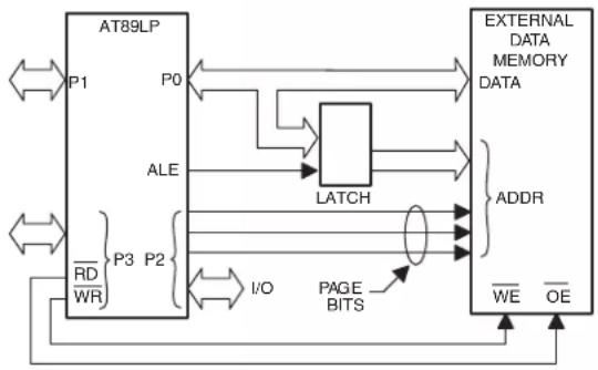
The AT89LP3240/6440 uses the standard 8051 external memory interface with the upper address on Port 2, the lower address and data in/out multiplexed on Port 0, and the ALE, RD and WR strobes. The interface may be used in two different configurations depending on which type of MOVX instruction is used to access XDATA.
Figure 3-7 shows a hardware configuration for accessing up to 64K bytes of external RAM using a 16-bit linear address. Port 0 serves as a multiplexed address/data bus to the RAM. The Address Latch Enable strobe (ALE) is used to latch the lower address byte into an external register so that Port 0 can be freed for data input/output. Port 2 provides the upper address byte throughout the operation. The MOVX @DPTR instructions use Linear Address mode
Figure 3-7. External Memory 16-bit Linear Address Mode
flowchart
graph LR
    A["AT89LP"] -->|P0| B["LATCH"]
    A -->|P1| B
    A -->|P2| B
    A -->|P3| B
    B --> C["External DATA MEMORY DATA"]
    C --> D["ADDR"]
    D --> E["WE OE"]
    style A fill:#f9f,stroke:#333
    style B fill:#ccf,stroke:#333
    style C fill:#cfc,stroke:#333
    style D fill:#fcc,stroke:#333
Figure 3-8 shows a hardware configuration for accessing 256-byte blocks of external RAM using an 8-bit paged address. Port 0 serves as a multiplexed address/data bus to the RAM. The ALE strobe is used to latch the address byte into an external register so that Port 0 can be freed for data input/output. The Port 2 I/O lines (or other ports) can provide control lines to page the memory; however, this operation is not handled automatically by hardware. The software application must change the Port 2 register when appropriate to access different pages. The MOVX @Ri instructions use Paged Address mode.
Figure 3-8. External Memory 8-bit Paged Address Mode
flowchart
graph TD
    A["AT89LP"] -->|P0| B["LATCH"]
    A -->|ALE| B
    A -->|P3 P2| B
    A -->|RD WR| B
    B --> C["ADDRESS"]
    B --> D["WE OE"]
    B --> E["PAGE BITS"]
    E --> F["External DATA MEMORY DATA"]
    style A fill:#f9f,stroke:#333
    style B fill:#ccf,stroke:#333
    style C fill:#cfc,stroke:#333
    style D fill:#fcc,stroke:#333
    style E fill:#ffc,stroke:#333
    style F fill:#fcc,stroke:#333
Table 3-4. AUXR – Auxiliary Control Register
| AUXR = 8EH Reset Value = xxx0 0000BNot Bit Addressable | ||||||||
| - | - | - | XSTK | WS1 | WS0 | EXRAM | ALES | |
| B | i | t | 7 | 6 | 5 | 4 | 3 | 2 |
| Symbol Function | ||||
| XSTK | Extended Stack Enable. When XSTK = 0 the stack resides in IDATA and is limited to 256 bytes. Set XSTK = 1 to place the stack in EDATA for up to 4K bytes of extended stack space. All PUSH, POP, CALL and RET instructions will incur a one or two cycle penalty when accessing the extended stack. | |||
| WS[1-0] | Wait State Select. Determines the number of wait states inserted into external memory accesses. | |||
| WS1 | WS0 | Wait States | RD / WR Strobe Width | |
| 0 | 0 | 0 | 1 × t_CYC | |
| 0 | 1 | 1 | 2 × t_CYC | |
| 1 | 0 | 2 | 3 × t_CYC | |
| 1 | 1 | 3 | 4 × t_CYC | |
| EXRAM | External RAM Enable. When EXRAM = 0, MOVX instructions can access the internally mapped portions of the address space. Accesses to addresses above internally mapped memory will access external memory. Set EXRAM = 1 to bypass the internal memory and map the entire address space to external memory. | |||
| ALES | ALE Idle State. When ALES = 0 the idle polarity of ALE is high (active). When ALES = 1 the idle polarity of ALE is low (inactive). The ALE strobe pulse is always active high. ALES must be zero in order to use P4.4 as a general I/O. | |||
Note that prior to using the external memory interface, Port 2, WR (P3.6), RD (P3.7) and ALE (P4.4) must be configured as outputs. See Section 10.1 "Port Configuration" on page 45. Port 0 is configured automatically to push-pull output mode when outputting address or data and is
automatically tristated when inputting data regardless of the Port 0 configuration. The Port 0 configuration will determine the idle state of Port 0 when not accessing the external memory.
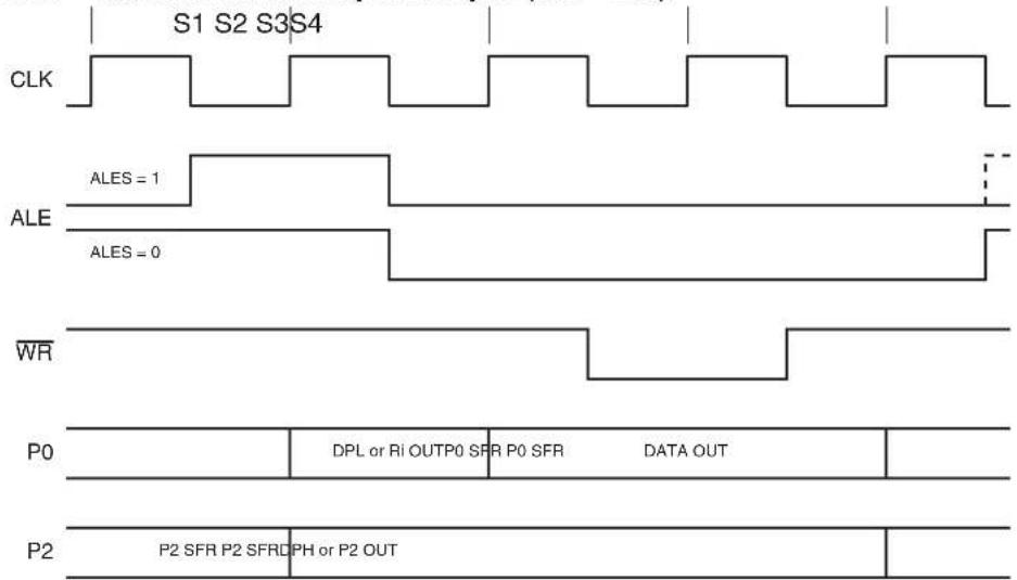
Figure 3-9 and Figure 3-10 show examples of external data memory write and read cycles, respectively. The address on P0 and P2 is stable at the falling edge of ALE. The idle polarity of ALE is controlled by ALES (AUXR.0). When ALES = 0 the idle polarity of ALE is high (active). When ALES = 1 the idle polarity of ALE is low (inactive). The ALE strobe pulse is always active high. Unlike standard 8051s, ALE will not toggle continuously when not accessing external memory. ALES must be zero in order to use P4.4 as a general-purpose I/O. The WS bits in AUXR can extended the RD and WR strobes by 1, 2 or 3 cycles as shown in Figures 3-11, 3-12 and 3-13. If a longer strobe is required, the application can scale the system clock with the clock divider to meet the requirements (See Section 6.5 on page 32).
Figure 3-9. External Data Memory Write Cycle (WS = 00B)
text_image
S1 S2 S3 S4 CLK ALES = 1 ALE ALES = 0 WR P0 DPL or Ri OUTP0 SFR P0 SFR DATA OUT P2 P2 SFR P2 SFRDPH or P2 OUTFigure 3-10. External Data Memory Read Cycle (WS = 00B)
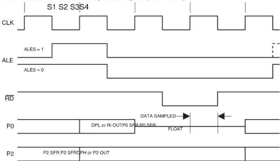
text_image
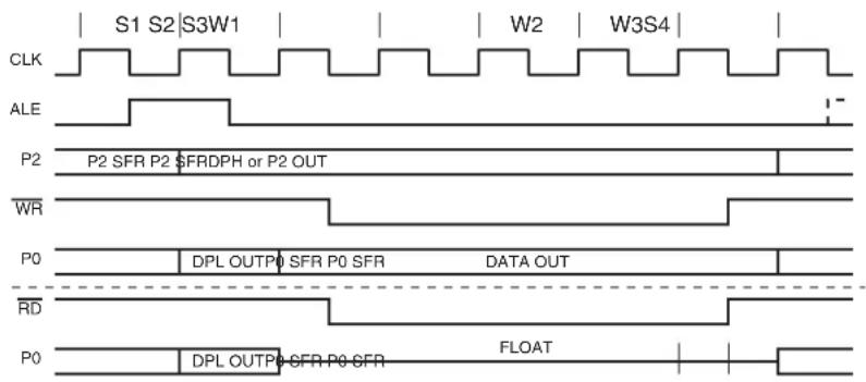
S1 S2 S3 S4 CLK ALES = 1 ALE ALES = 0 RD DATA SAMPLED P0 DPL or Ri OUTP0 SFR P0 SFR FLOAT P2 P2 SFR P2 SFRDPH or P2 OUTFigure 3-11. MOVX with One Wait State (WS = 01B)

text_image
CLK S1 S2 S3W1 ALE P2 P2 SFR P2 $FRI DPH or P2 OUT WR P0 DPL OUTP0 SFR P0 SFR DATA OUT RD P0 DPL OUTP0 SFR P0 SFR FLOATFigure 3-12. MOVX with Two Wait States (WS = 10B)

text_image
CLK S1 S2 S3W1 W2 S4 ALE P2 P2 SFR P2 $FRRDPH or P2 OUT WR P0 DPL OUTPUT SFR P0 SFR DATA OUT RD P0 DPL OUTPUT SFR P0 SFR FLOATFigure 3-13. MOVX with Three Wait States (WS = 11B)
text_image
CLK S1 S2 S3W1 W2 W3S4 ALE P2 P2 SFR P2 SFRDPH or P2 OUT WR P0 DPL OUTPUT SFR P0 SFR DATA OUT RD P0 DPL OUTPUT SFR P0 SFR FLOAT3.4 Extended Stack
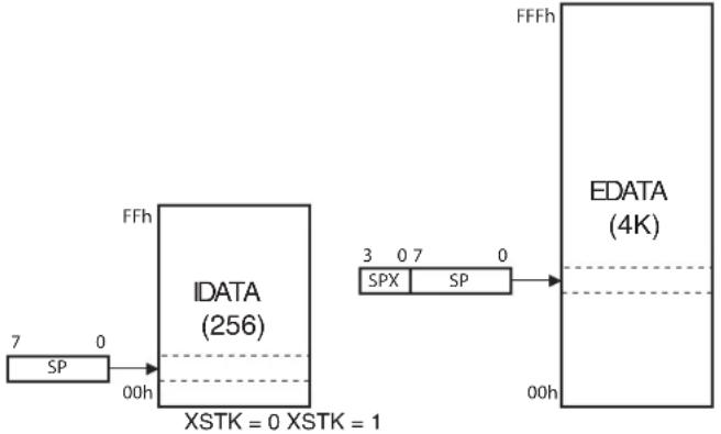
The AT89LP3240/6440 provides an extended stack space for applications requiring additional stack memory. By default the stack is located in the 256-byte IDATA space of internal data memory. The IDATA stack is referenced solely by the 8-bit Stack Pointer (SP: 81H). Setting the XSTK bit in AUXR enables the extended stack. The extended stack resides in the EDATA space for up to 4KB of stack memory. The extended stack is referenced by a 12-bit pointer formed from SP and the four LSBs of the Extended Stack Pointer (SPX: 9EH) as shown in Figure 3-14. SP is shared between both stacks. Note that the standard IDATA stack will not overflow to the EDATA stack or vice versa. The stack and extended stack are mutually exclusive and SPX is ignored when XTSK = 0. An application choosing to switch between stacks by toggling XSTK must main-
tain separate copies of SP for use with each stack space. Interrupts should be disabled while swapping copies of SP in such an application to prevent illegal stack accesses.
All interrupt calls and PUSH, POP, ACALL, LCALL, RET and RETI instructions will incur a one or two-cycle penalty while the extended stack is enabled, depending on the number of stack access in each instruction. The extended stack may only exist within the internal EDATA space; it cannot be placed in XDATA. The stack will continue to use EDATA even if EDATA is disabled by setting EXRAM = 1.
Figure 3-14. Stack Configurations
flowchart
graph LR
    A["SP"] --> B["IDATA (256)"]
    B --> C["EDATA (4K)"]
    D["7 0 00h"] --> B
    style B fill:#f9f,stroke:#333
    note right of B XSTK = 0 XSTK = 1
    note right of C FFFh
    note right of D SPX SP
3.5 In-Application Programming (IAP)
The AT89LP3240/6440 supports In-Application Programming (IAP), allowing the program memory to be modified during execution. IAP can be used to modify the user application on the fly or to use program memory for nonvolatile data storage. The same page structure write protocol for FDATA also applies to IAP (See Section 3.3.3.1 "Write Protocol" on page 14). The CPU is always placed in idle while modifying the program memory. When the write completes, the CPU will continue executing with the instruction after the MOVX @DPTR,A instruction that started the write.
To enable access to the program memory, the IAP bit (MEMCON.7) must be set to one and the IAP User Fuse must be enabled. The IAP User Fuse can disable all IAP operations. When this fuse is disabled, the IAP bit will be forced to 0. While IAP is enabled, all MOVX @DPTR instructions will access the CODE space instead of EDATA/FDATA/XDATA. IAP also allows reprogramming of the User Signature Array when SIGEN = 1. The IAP access settings are summarized in Table 3-5.
Table 3-5. IAP Access Settings
| IAP SIGEN DMEN | MOVX @DPTR | MOVC @DPTR | ||
| 0 0 0 | EDATA (0000-0FFFH) | CODE (0000-FFFFH) | ||
| 0 0 1 | FDATA (1000-2FFFH) CODE (0000-FFFFH) | |||
| 0 | 1 | 0 | EDATA (0000-0FFFH) | SIG (0000-01FFH) |
| 0 | 1 | 1 | FDATA (1000-2FFFH) | SIG (0000-01FFH) |
| 1 0 | X CODE (0000-FFFFH) | CODE (0000-FFFFH) | ||
| 1 | 1 | X | SIG (0000-01FFH) | SIG (0000-01FFH) |
4. Special Function Registers
A map of the on-chip memory area called the Special Function Register (SFR) space is shown in Table 4-1. See also “Register Index” on page 153.
Note that not all of the addresses are occupied, and unoccupied addresses may not be implemented on the chip. Read accesses to these addresses will in general return random data, and write accesses will have an indeterminate effect. User software should not write to these unlisted locations, since they may be used in future products to invoke new features.
Table 4-1. AT89LP3240/6440 SFR Map and Reset Values
| 89 | A | B | C | D | E | F | ||
| 0F8H OFFH | ||||||||
| 0F0H | B0000 0000 | BX0000 0000 | ||||||
| 0E8H | SPSR000x x000 | SPCR0000 0000 | SPDRxxxx xxxx | |||||
| 0E0H | ACC0000 0000 | AX0000 0000 | DSPR0000 0000 | FIRD0000 0000 | MACL0000 0000 | MACH0000 0000 | ||
| 0D8H | DADC0000 0000 | DADI0000 0000 | DADL0000 0000 | DADH0000 0000 | ||||
| 0D0H | PSW0000 0000 | T2CCA0000 0000 | T2CCL0000 0000 | T2CCH0000 0000 | T2CCC0000 0000 | T2CCF0000 0000 | ||
| 0C8H | T 20000 0000 | CT2MOD0000 0000 | N RCAP2L0000 0000 | RCAP2H0000 0000 | TL20000 0000 | TH20000 0000 | ||
| 0C0H | P4xx11 1111 | P1M0^(2) | P1M10000 0000 | P2M0^(2) | P2M10000 0000 | P3M0^(2) | P3M10000 0000 | |
| 0B8H | IP0000 0000 | SADEN0000 0000 | POMO1111 1111 | POM10000 0000 | P4M0^(2) | P4M1xx00 0000 | ||
| 0B0H | P31111 1111 | IE2xxxx x000 | IP2xxxx x000 | IP2Hxxxx x000 | IPH0000 0000 | |||
| 0A8H | IE0000 0000 | SADDR0000 0000 | TWCR0000 0000 | TWSR0000 0000 | TWAR0000 0000 | TWDR0000 0000 | TWBR0000 0000 | AREF0000 0000 |
| 0A0H P21111 1111 | DPCF0000 00x0 | WDTRST(write-only) | WDTCON0000 x000 | |||||
| 98H | SCON0000 0000 | SBUFxxxx xxxx | GPMOD0000 0000 | GPLS0000 0000 | GPIEN0000 0000 | GPIF0000 0000 | SPXxxxx 0000 | ACSRB1100 0000 |
| 90H | P11111 1111 | TCONB0010 0100 | RLO0000 0000 | RL10000 0000 | RH0000 0000 | RH10000 0000 | MEMCON0000 00xx | ACSRA0000 0000 |
| 88H | TCON0000 0000 | TMOD0000 0000 | TLO0000 0000 | TL10000 0000 | THO0000 0000 | TH10000 0000 | AUXR0000 0000 | CLKREG0000 x000 |
| 80H | SP0000 0111 | DPOL0000 0000 | DPOH0000 0000 | DP1L0000 0000 | DP1H0000 0000 | PAGE0000 0000 | PCON0000 0000 | |
| 0 | 1 | 2 | 3 | 4 | 5 | 6 | 7 |
Notes: 1. All SFRs in the left-most column are bit-addressable.
2. Reset value is 1111 1111B when Tristate-Port Fuse is enabled and 0000 0000B when disabled.
5. Enhanced CPU
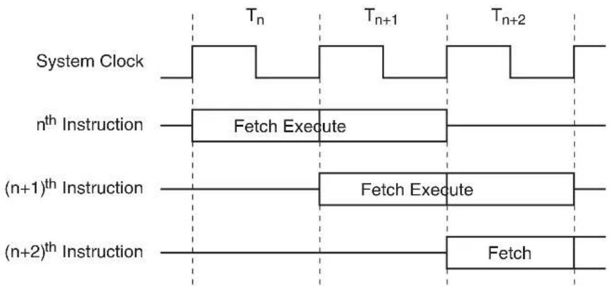
The AT89LP3240/6440 uses an enhanced 8051 CPU that runs at 6 to 12 times the speed of standard 8051 devices (or 3 to 6 times the speed of X2 8051 devices). The increase in performance is due to two factors. First, the CPU fetches one instruction byte from the code memory every clock cycle. Second, the CPU uses a simple two-stage pipeline to fetch and execute instructions in parallel. This basic pipelining concept allows the CPU to obtain up to 1 MIPS per MHz. A simple example is shown in Figure 5-1.
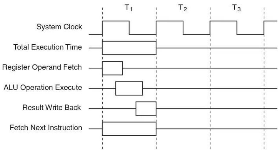
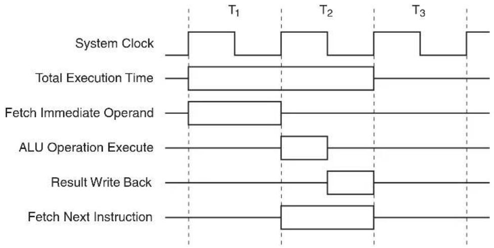
The 8051 instruction set allows for instructions of variable length from 1 to 3 bytes. In a single-clock-per-byte-fetch system this means each instruction takes at least as many clocks as it has bytes to execute. The majority of instructions in the AT89LP3240/6440 follow this rule: the instruction execution time in clock cycles equals the number of bytes per instruction, with a few exceptions. Branches and Calls require an additional cycle to compute the target address and some other complex instructions require multiple cycles. See “Instruction Set Summary” on page 143. for more detailed information on individual instructions. Figures 5-2 and 5-3 show examples of 1- and 2-byte instructions.
Figure 5-1. Parallel Instruction Fetches and Executions
flowchart
graph TD
    A["System Clock"] --> B["Tr"]
    B --> C["Tn+1"]
    C --> D["Tn+2"]
    E["nth Instruction"] --> F["Fetch Execute"]
    G["(n+1)th Instruction"] --> H["Fetch Execute"]
    I["(n+2)th Instruction"] --> J["Fetch"]
Figure 5-2. Single-cycle ALU Operation (Example: INC R0)
flowchart
graph TD
    A["System Clock"] --> B["T1"]
    B --> C["Total Execution Time"]
    C --> D["Register Operand Fetch"]
    D --> E["ALU Operation Execute"]
    E --> F["Result Write Back"]
    F --> G["Fetch Next Instruction"]
    style A fill:#f9f,stroke:#333
    style B fill:#ccf,stroke:#333
    style C fill:#cfc,stroke:#333
    style D fill:#fcc,stroke:#333
    style E fill:#cff,stroke:#333
    style F fill:#ffc,stroke:#333
    style G fill:#fcc,stroke:#333
Figure 5-3. Two-cycle ALU Operation (Example: ADD A, #data)
flowchart
graph TD
    A["System Clock"] --> B["Total Execution Time"]
    B --> C["Fetch Immediate Operand"]
    C --> D["ALU Operation Execute"]
    D --> E["Result Write Back"]
    E --> F["Fetch Next Instruction"]
    style A fill:#f9f,stroke:#333
    style B fill:#ccf,stroke:#333
    style C fill:#cfc,stroke:#333
    style D fill:#fcc,stroke:#333
    style E fill:#cff,stroke:#333
    style F fill:#ffc,stroke:#333
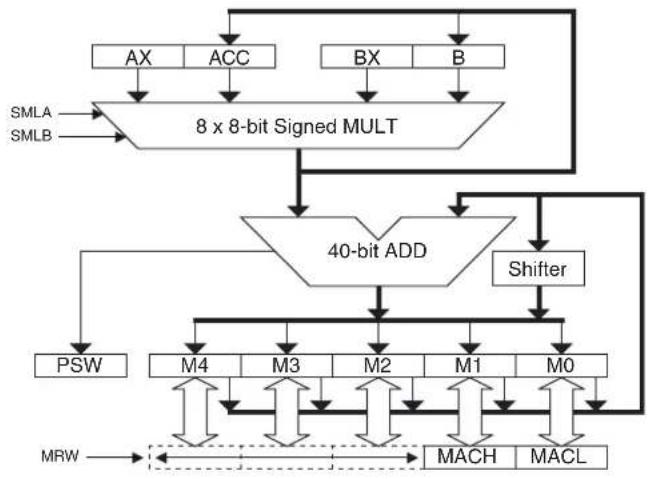
5.1 Multiply-Accumulate Unit (MAC)
The AT89LP3240/6440 includes a multiply and accumulate (MAC) unit that can significantly speed up many mathematical operations required for digital signal processing. The MAC unit includes a 16-by-16 bit multiplier and a 40-bit adder that can perform integer or fractional multiply-accumulate operations on signed 16-bit input values. The MAC unit also includes a 1-bit arithmetic shifter that will left or right shift the contents of the 40-bit MAC accumulator register (M).
A block diagram of the MAC unit is shown in Figure 5-4. The 16-bit signed operands are provided by the register pairs (AX,ACC) and (BX,B) where AX (E1H) and BX (F7H) hold the higher order bytes. The 16-by-16 bit multiplication is computed through partial products using the AT89LP3240/6440's 8-bit multiplier. The 32-bit signed product is added to the 40-bit M accumulator register. The MAC operation is summarized as follows:
$$ \text { MAC AB: } \quad M \leftarrow M + {A X, A C C } \times {B X, B } $$
All computation is done in signed two's complement form.
Figure 5-4. Multiply-Accumulate Unit
flowchart
graph TD
    A["AX"] --> B["8 x 8-bit Signed MULT"]
    C["ACC"] --> B
    D["BX"] --> B
    E["B"] --> B
    B --> F["40-bit ADD"]
    F --> G["PSW"]
    F --> H["M4"]
    F --> I["M3"]
    F --> J["M2"]
    F --> K["M1"]
    F --> L["M0"]
    G --> M["MRW"]
    H --> M
    I --> M
    J --> M
    K --> M
    L --> M
    M --> N["MACH"]
    M --> O["MACL"]
    P["SMLA"] --> B
    Q["SMLB"] --> B
    R["Shifter"] --> F
The MAC operation is performed by executing the MAC AB (A5 A4H) extended instruction. This two-byte instruction requires nine clock cycles to complete. The operand registers are not modified by the instruction and the result is stored in the 40-bit M register. MAC AB also updates the C and OV flags in PSW. C represents the sign of the MAC result and OV is the two's complement overflow. Note that MAC AB will not clear OV if it was previously set to one.
Three additional extended instructions operate directly on the M register. CLR M (A5 E4H) clears the entire 40-bit register in two clock cycles. LSL M (A5 23H) and ASR (A5 03H) shift M one bit to the left and right respectively. Right shifts are done arithmetically, i.e. the sign is preserved.
The 40-bit M register is accessible 16-bits at a time through a sliding window as shown in Figure 5-5. The MRW _1-0 bits in DSPR (Table 5-1) select which 16-bit segment is currently accessible through the MACL and MACH addresses. For normal fixed point operations the window can be fixed to the rank of interest. For example, multiplying two 1.15 format numbers places a 2.30 format result in the M register. If MRW is set to 10B, a 1.15 value is obtained after performing a single LSL M.
Figure 5-5. M Register with Sliding Window

text_image
M Byte 4 Byte 3 Byte 2 Byte 1 Byte 0 39 - 32 31 - 24 23 - 16 15 - 8 7 - 0 M MACH MACL MRW₁₋₀ = 00B MACH MACL ← MRW₁₋₀ = 01B MACH MACL ← MRW₁₋₀ = 10B MACH MACL ← MRW₁₋₀ = 11BAs a consequence of the MAC unit, the standard 8x8 MUL AB instruction can support signed multiplication. The SMLA and SMLB bits in DSPR control the multiplier's interpretation of the ACC and B registers, allowing any combination of signed and unsigned operand multiplication. These bits have no effect on the MAC operation which always multiplies signed-by-signed.
5.2 Enhanced Dual Data Pointers
The AT89LP3240/6440 provides two 16-bit data pointers: DPTR0 formed by the register pair DPOL and DPOH (82H an 83H), and DPTR1 formed by the register pair DP1L and DP1H (84H and 85H). The data pointers are used by several instructions to access the program or data memories. The Data Pointer Configuration Register (DPCF) controls operation of the dual data pointers (Table 5-5 on page 28). The DPS bit in DPCF selects which data pointer is currently referenced by instructions including the DPTR operand. Each data pointer may be accessed at its respective SFR addresses regardless of the DPS value. The AT89LP3240/6440 provides two methods for fast context switching of the data pointers:
- Bit 2 of DPCF is hard-wired as a logic 0. The DPS bit may be toggled (to switch data pointers) simply by incrementing the DPCF register, without altering other bits in the register unintentionally. This is the preferred method when only a single data pointer will be used at one time.
EX: INC DPCF ; Toggle DPS
Table 5-1. DSPR – Digital Signal Processing Configuration Register
| DSPR = E2H Reset Value = 0000 0000BNot Bit Addressable | ||||||||
| MRW1 | MRW0 | SMLB | SMLA | CBE1 | CBE0 | MVCD | DPRB | |
| Bit | 7 | 6 | 5 | 4 | 3 | 2 | 1 | 0 |
| Symbol Function | |
| MRW_1-0 | M Register Window. Selects which pair of bytes from the 5-byte M register is accessible through MACH (E5H) and MACL (E4H) as shown in Figure 5-5. For example, MRW = 10B for normal 16-bit fixed-point operations where the lowest order portion of the fractional result is discarded. |
| SMLB | Signed Multiply Operand B. When SMLB = 0, the MUL AB instruction treats the contents of B as an unsigned value. When SMLB = 1, the MUL AB instruction interprets the contents of B as a signed two's complement value. SMLB does not affect the MAC operation. |
| SMLA | Signed Multiply Operand A. When SMLA = 0, the MUL AB instruction treats the contents of ACC as an unsigned value. When SMLA = 1, the MUL AB instruction interprets the contents of ACC as a signed two's complement value. SMLA does not affect the MAC operation. |
| CBE1 | DPTR1 Circular Buffer Enable. Set CBE1 = 1 to configure DPTR1 for circular addressing over the two circular buffer address ranges. Clear CBE1 for normal DPTR operation. |
| CBE0 | DPTR0 Circular Buffer Enable. Set CBE0 = 1 to configure DPTR0 for circular addressing over the two circular buffer address ranges. Clear CBE0 for normal DPTR operation. |
| MVCD | MOVC Index Disable. When MVCD = 0, the MOVC A, @A+DPTR instruction functions normally with indexed addressing. Setting MVCD = 1 disables the indexed addressing mode such that MOVC A, @A+DPTR functions as MOVC A, @DPTR. |
| DPRB | DPTR1 Redirect to B. DPRB selects the source/destination register for MOVC/MOVX instructions that reference DPTR1. When DPRB = 0, ACC is the source/destination. When DPRB = 1, B is the source/destination. DPRB does not change the index register for MOVC instructions. |
- In some cases, both data pointers must be used simultaneously. To prevent frequent toggling of DPS, the AT89LP3240/6440 supports a prefix notation for selecting the opposite data pointer per instruction. All DPTR instructions, with the exception of JMP @A+DPTR, when prefixed with an 0A5H opcode will use the inverse value of DPS ( ) to select the data pointer. Some assemblers may support this operation by using the /DPTR operand. For example, the following code performs a block copy within EDATA:
MOV DPCF, #00H ; DPS = 0
MOV DPTR, #SRC ; load source address to dptr0
MOV /DPTR, #DST ; load destination address to dptr1
MOV R7, #BLKSIZE ; number of bytes to copy
COPY: MOVX A, @DPTR ; read source (dptr0)
INC DPTR ; next src (dptr0+1)
MOVX @/DPTR, A ; write destination (dptr1)
INC /DPTR ; next dst (dptr1+1)
DJNZ R7, COPY
For assemblers that do not support this notation, the 0A5H prefix must be declared in-line:
EX: DB 0A5H
INC DPTR ; equivalent to INC /DPTR
A summary of data pointer instructions with fast context switching is listed in Table 5-2.
Table 5-2. Data Pointer Instructions
| Instruction | Operation | |
| DPS = 0 DPS = 1 | ||
| JMP @A+DPTR JMP @A+DPTR0 JMP @A+DPTR1 | ||
| MOV DPTR, #data16 | MOV DPTR0, #data16 | MOV DPTR1, #data16 |
| MOV /DPTR, #data16 | MOV DPTR1, #data16 | MOV DPTR0, #data16 |
| INC DPTR INC DPTR0 INC DPTR1 | ||
| INC /DPTR INC DPTR1 INC DPTR0 | ||
| MOVC A, @A+DPTR MOVC A, @A+DPTR0 | MOVC A, @A+DPTR1 | |
| MOVC A, @A+/DPTR | MOVC A, @A+DPTR1 | MOVC A, @A+DPTR0 |
| MOVX A, @DPTR | MOVX A, @DPTR0 | MOVX A, @DPTR1 |
| MOVX A, @/DPTR | MOVX A, @DPTR1 | MOVX A, @DPTR0 |
| MOVX @DPTR, A | MOVX @DPTR0, A | MOVX @DPTR1, A |
| MOVX @/DPTR, A | MOVX @DPTR1, A | MOVX @DPTR0, A |
5.2.1 Data Pointer Update
The Dual Data Pointers on the AT89LP3240/6440 include two features that control how the data pointers are updated. The data pointer decrement bits, DPD1 and DPD0 in DPCF, configure the INC DPTR instruction to act as DEC DPTR. The resulting operation will depend on DPS as shown in Table 5-3.
Table 5-3. Data Pointer Decrement Behavior
| DPD1 | DPD0 | Equivalent Operation for INC DPTR and INC /DPTR | |||
| DPS = 0 DPS = 1 | |||||
| INC DPTR | INC /DPTR | INC DPTR | INC /DPTR | ||
| 0 | 0 | INC DPTR0 | INC DPTR1 | INC DPTR1 | INC DPTR0 |
| 0 | 1 | DEC DPTR0 | INC DPTR1 | INC DPTR1 | DEC DPTR0 |
| 1 | 0 | INC DPTR0 | DEC DPTR1 | DEC DPTR1 | INC DPTR0 |
| 1 | 1 | DEC DPTR0 | DEC DPTR1 | DEC DPTR1 | DEC DPTR0 |
The data pointer update bits, DPU1 and DPU0, allow MOVX @DPTR and MOVC @DPTR instructions to update the selected data pointer automatically in a post-increment or post-decrement fashion. The direction of update depends on the DPD1 and DPD0 bits as shown in Table 5-4.
Table 5-4. Data Pointer Auto-Update
| DPD1 | DPD0 | Update Operation for MOVX and MOVC (DPU1 = 1 & DPU0 = 1) | |||
| DPS = 0 DPS = 1 | |||||
| DPTR | /DPTR | DPTR | /DPTR | ||
| 0 | 0 | DPTR0++ DPTR | 1++ DPTR1++ DPTR0++ | ||
| 0 | 1 | DPTR0-- | DPTR1++ | DPTR1++ | DPTR0-- |
| 1 | 0 | DPTR0++ | DPTR1-- | DPTR1-- | DPTR0++ |
| 1 | 1 | DPTR0-- | DPTR1-- | DPTR1-- | DPTR0-- |
Table 5-5. DPCF – Data Pointer Configuration Register
| DPCF = A2H Reset Value = 0000 00X0BNot Bit Addressable | ||||||||
| DPU1 DPU0 DPD1 DPD0 SIGEN 0 - DPS | ||||||||
| B | i | t | 7 | 6 | 5 | 4 | 3 | 2 |
| Symbol Function | |
| DPU1 | Data Pointer 1 Update. When set, MOVX @DPTR and MOVC @DPTR instructions that use DPTR1 will also update DPTR1 based on DPD1. If DPD1 = 0 the operation is post-increment and if DPD1 = 1 the operation is post-decrement. When DPU1 = 0, DPTR1 is not updated. |
| DPU0 | Data Pointer 0 Update. When set, MOVX @DPTR and MOVC @DPTR instructions that use DPTR0 will also update DPTR0 based on DPD0. If DPD0 = 0 the operation is post-increment and if DPD0 = 1 the operation is post-decrement. When DPU0 = 0, DPTR0 is not updated. |
| DPD1 | Data Pointer 1 Decrement. When set, INC DPTR instructions targeted to DPTR1 will decrement DPTR1. When cleared, INC DPTR instructions will increment DPTR1. DPD1 also determines the direction of auto-update for DPTR1 when DPU1 = 1. |
| DPD0 | Data Pointer 0 Decrement. When set, INC DPTR instructions targeted to DPTR0 will decrement DPTR0. When cleared, INC DPTR instructions will increment DPTR0. DPD0 also determines the direction of auto-update for DPTR0 when DPU0 = 1. |
| SIGEN | Signature Enable. When SIGEN = 1 all MOVC @DPTR instructions and all IAP accesses will target the signature array memory. When SIGEN = 0, all MOVC and IAP accesses target CODE memory. |
| DPS | Data Pointer Select. DPS selects the active data pointer for instructions that reference DPTR. When DPS = 0, DPTR will target DPTR0 and /DPTR will target DPTR1. When DPS = 1, DPTR will target DPTR1 and /DPTR will target DPTR0. |
5.2.2 Data Pointer Operating Modes
The Dual Data Pointers on the AT89LP3240/6440 include three additional operating modes that affect data pointer based instructions. These modes are controlled by bits in DSPR.
5.2.2.1 DPTR Redirect
The Data Pointer Redirect to B bit, DPRB (DSPR.0), allows MOVX and MOVC instructions to use the B register as the data source/destination when the instruction references DPTR1 as shown in Table 5-6 and Table 5-7. DPRB can improve the efficiency of routines that must fetch multiple operands from different RAM locations.
Table 5-6. MOVX @DPTR Operating Modes
| DPRB | DPS | Equivalent Operation for MOVX | |||
| MOVX A, @DPTR | MOVX @DPTR, A | ||||
| DPTR | /DPTR | DPTR | /DPTR | ||
| 0 | 0 | MOVXA, @DPTR0 | MOVXA, @DPTR1 | MOVX@DPTR0, A | MOVX@DPTR1, A |
| 0 | 1 | MOVXA, @DPTR1 | MOVXA, @DPTR0 | MOVX@DPTR1, A | MOVX@DPTR0, A |
| 1 | 0 | MOVXA, @DPTR0 | MOVXB, @DPTR1 | MOVX@DPTR0, A | MOVX@DPTR1, B |
| 1 | 1 | MOVXB, @DPTR1 | MOVXA, @DPTR0 | MOVX@DPTR1, B | MOVX@DPTR0, A |
5.2.2.2 Index Disable
The MOVC Index Disable bit, MVCD (DSPR.1), disables the indexed addressing mode of the MOVC A, @A+DPTR instruction. When MVCD = 1, the MOVC instruction functions as MOVC A, @DPTR with no indexing as shown in Table 5-7. MVCD can improve the efficiency of routines that must fetch multiple operands from program memory. DPRB can change the MOVC destination register from ACC to B, but has no effect on the MOVC index register.
Table 5-7. MOVC @DPTR Operating Modes
| MVCD DPRB | Equivalent Operation for MOVC A, @A+DPTR | ||||
| DPS = 0 DPS = 1 | |||||
| DPTR /DPTR | DPTR /DPTR | ||||
| 0 | 0 | MOVCA, @A+DPTR0 | MOVCA, @A+DPTR1 | MOVCA, @A+DPTR1 | MOVCA, @A+DPTR0 |
| 0 | 1 | MOVCA, @A+DPTR0 | MOVCB, @A+DPTR1 | MOVCB, @A+DPTR1 | MOVCA, @A+DPTR0 |
| 1 | 0 | MOVCA, @DPTR0 | MOVCA, @DPTR1 | MOVCA, @DPTR1 | MOVCA, @DPTR0 |
| 1 | 1 | MOVCA, @DPTR0 | MOVCB, @DPTR1 | MOVCB, @DPTR1 | MOVCA, @DPTR0 |
5.2.2.3 Circular Buffers
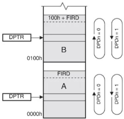
The CBE0 and CBE1 bits in DSPR can configure DPTR0 and DPTR1, respectively, to operate in circular buffer mode. The AT89LP3240/6440 maps circular buffers into two identically sized regions of EDATA/XDATA. These buffers can speed up convolution computations such as FIR and IAR digital filters. The length of the buffers are set by the value of the FIRD (E3H) register for up to 256 entries. Buffer A is mapped from 0000H to FIRD and Buffer B is mapped from 0100H to 100H+FIRD as shown in Figure 5-6. Both data pointers may operate in either buffer. When circular buffer mode is enabled, updates to a data pointer referencing the buffer region will follow circular addressing rules. If the data pointer is equal to FIRD or 100H+FIRD any increment will cause it to overflow to 0000H or 0100H respectively. If the data pointer is equal to 0000H or 0100H any decrement will cause it to underflow to FIRD or 100H+FIRD respectively. In this mode, updates can be either an explicit INC DPTR or an automatic update using DPUn where the DPDn bits control the direction. The data pointer will increment or decrement normally at any other addresses. Therefore, when circular addressing is in use, the data pointers can still operate as regular pointers in the FIRD+1 to 00FFH and greater than 100H+FIRD ranges.
Figure 5-6. Circular Buffer Mode
flowchart
graph TD
    DPTR1["DPTR"] --> 0100h["0100h"]
    0100h --> 100h["FIRD"]
    100h --> 0000h["0000h"]
    100h --> 100h2["FIRD"]
    100h2 --> 000h2["FIRD"]
    0000h --> 100h2["FIRD"]
    100h2 --> 000h2["FIRD"]
    000h --> 100h3["FIRD"]
    100h3 --> 000h3["FIRD"]
    100h3 --> 100h4["FIRD"]
    100h4 --> 000h4["FIRD"]
    100h4 --> 100h5["FIRD"]
    100h5 --> 000h5["FIRD"]
    100h5 --> 100h6["FIRD"]
    100h6 --> 000h6["FIRD"]
    100h6 --> 100h7["FIRD"]
    100h7 --> 000h7["FIRD"]
    100h7 --> 100h8["FIRD"]
    100h8 --> 000h8["FIRD"]
    100h8 --> 100h9["FIRD"]
    100h9 --> 000h9["FIRD"]
    100h9 --> 100h10["FIRD"]
5.3 Instruction Set Extensions
Table 5-8 lists the additions to the 8051 instruction set that are supported by the AT89LP3240/6440. For more information on the instruction set see Section 22. "Instruction Set Summary" on page 143. For detailed descriptions of the extended instructions see Section 22.1 "Instruction Set Extensions" on page 147.
Table 5-8. AT89LP3240/6440 Extended Instructions
| Opcode Mnemonic Description Bytes Cycles | ||||
| A5 00 | BREAK | Software breakpoint | 2 | 2 |
| A5 03 | ASR M | Arithmetic shift right of M register | 2 | 2 |
| A5 23 | LSL M | Logical shift left of M register | 2 | 2 |
| A5 73 | JMP @A+PC | Indirect jump relative to PC | 2 | 3 |
| A5 90 MOV /DPTR, #data16 | Move 16-bit constant to alternate data pointer | 4 | 4 | |
| A5 93 MOVC A, @A+/DPTR | Move code location to ACC relative to alternate data pointer | 2 | 4 | |
| A5 A3 | INC /DPTR | Increment alternate data pointer | 2 | 3 |
| A5 A4 | MAC AB | Multiply and accumulate | 2 | 9 |
| A5 B6 | CJNE A, @R0, rel | Compare ACC to indirect RAM and jump if not equal | 3 | 4 |
| A5 B7 | CJNE A, @R1, rel | Compare ACC to indirect RAM and jump if not equal | 3 | 4 |
| A5 E0 | MOVX A, @/DPTR | Move external to ACC; 16-bit address in alternate data pointer | 2 | 3/5 |
| A5 E4 | CLR M | Clear M register | 2 | 2 |
| A5 F0 | MOVX @/DPTR, A | Move ACC to external; 16-bit address in alternate data pointer | 2 | 3/5 |
- The /DPTR instructions provide support for the dual data pointer features described above (See Section 5.2).
- The ASR M, LSL M, CLR M and MAC AB instructions are part of the Multiply-Accumulate Unit (See Section 5.1).
- The JMP @A+PC instruction supports localized jump tables without using a data pointer.
- The CJNE A, rel@nstructions allow compares of array values with non-constant values.
- The BREAK instruction is used by the On-Chip Debug system. See Section 24. on page 155.
6. System Clock
The system clock is generated directly from one of three selectable clock sources. The three sources are the on-chip crystal oscillator, external clock source, and internal RC oscillator. The on-chip crystal oscillator may also be configured for low or high speed operation. The clock source is selected by the Clock Source User Fuses as shown in Table 6-1. See "User Configuration Fuses" on page 164. By default, no internal clock division is used to generate the CPU clock from the system clock. However, the system clock divider may be used to prescale the system clock. The choice of clock source also affects the start-up time after a POR, BOD or Power-down event (See "Reset" on page 33 or "Power-down Mode" on page 37)
Table 6-1. Clock Source Settings
| Clock SourceFuse 1 | Clock SourceFuse 0 Selected | Clock Source |
| 0 | 0 | High Speed Crystal Oscillator (f > 500 kHz) |
| 0 | 1 | Low Speed Crystal Oscillator (f ≤100 kHz) |
| 1 | 0 | External Clock on XTAL1 |
| 1 | 1 | Internal 8 MHz RC Oscillator |
6.1 Crystal Oscillator
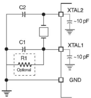
When enabled, the internal inverting oscillator amplifier is connected between XTAL1 and XTAL2 for connection to an external quartz crystal or ceramic resonator. The oscillator may operate in either high-speed or low-speed mode. Low-speed mode is intended for 32.768 kHz watch crystals and consumes less power than high-speed mode. The configuration as shown in Figure 6-1 applies for both high and low speed oscillators. Note that the internal structure of the device adds about 10 pF of capacitance to both XTAL1 and XTAL2, so that in some cases less external capacitance may be required. The total capacitance on XTAL1 or XTAL2, including the external load capacitor plus internal device load, board trace and crystal loadings, should not exceed 20 pF. An optional resistor R1 can be connected to XTAL1 in place of C1 for improved startup performance with higher speed crystals. When using the crystal oscillator, P4.0 and P4.1 will have their inputs and outputs disabled. Also, XTAL2 in crystal oscillator mode should not be used to directly drive a board-level clock without a buffer.
Figure 6-1. Crystal Oscillator Connections
text_image
C2 XTAL2 ~10 pF C1 R1 Optional XTAL1 ~10 pF GNDNote: 1. C1/C2 = 5–15 pF for Crystals = 5–15 pF for Ceramic Resonators R1 = 4–5 MΩ
6.2 External Clock Source
The external clock option disables the oscillator amplifier and allows XTAL1 to be driven directly by an external clock source as shown in Figure 6-2. XTAL2 may be left unconnected, used as general purpose I/O P4.1, or configured to output a divided version of the system clock.
Figure 6-2. External Clock Drive Configuration
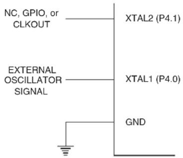
text_image
NC, GPIO, or CLKOUT XTAL2 (P4.1) EXTERNAL OSCILLATOR SIGNAL XTAL1 (P4.0) GND6.3 Internal RC Oscillator
The AT89LP3240/6440 has an Internal RC oscillator (IRC) tuned to 8.0 MHz ±2.5%. When enabled as the clock source, XTAL1 and XTAL2 may be used as P4.0 and P4.1 respectively. XTAL2 may also be configured to output a divided version of the system clock. The frequency of the oscillator may be adjusted within limits by changing the RC Calibration Byte stored at byte 128 of the User Signature Array. This location may be updated using the IAP interface (location 0180H in SIG space) or by an external device programmer (UROW location 0080H). See Section 25.8 "User Signature and Analog Configuration" on page 165. A copy of the factory calibration byte is stored at byte 8 of the Atmel Signature Array (0008H in SIG space).
6.4 System Clock Out
When the AT89LP3240/6440 is configured to use either an external clock or the internal RC oscillator, the system clock divided by 2 may be output on XTAL2 (P4.1). The clock out feature is enabled by setting the COE bit in CLKREG. For example, setting COE = "1" when using the internal oscillator will result in a 4.0 MHz (±2.5%) clock output on P4.1. P4.1 must be configured as an output in order to use the clock out feature.
6.5 System Clock Divider
The CDV_2-0 bits in CLKREG allow the system clock to be divided down from the selected clock source by powers of 2. The clock divider provides users with a greater frequency range when using the Internal RC Oscillator. For example, to achieve a 1 MHz system frequency when using the IRC, CDV_2-0 should be set to 011B for divide-by-8 operation. The divider can also be used to reduce power consumption by decreasing the operational frequency during non-critical periods. The resulting system frequency is given by the following equation:
$$ f _ {\mathrm{SYS}} \quad \frac {f _ {\mathrm{OSC}}}{2 ^ {\mathrm{CDV}}} = $$
where f_OSC is the frequency of the selected clock source. The clock divider will prescale the clock for the CPU and all peripherals. The value of CDV may be changed at any time without interrupting normal execution. Changes to CDV are synchronized such that the system clock will not
pass through intermediate frequencies. When CDV is updated, the new frequency will take affect within a maximum period of 128 × t_OSC .
Table 6-2. CLKREG – Clock Control Register
| CLKREG = 8FH Reset Value = 0000 0000BNot Bit Addressable | ||||||||
| TPS3 | TPS2 | TPS1 | TPS0 | CDV2 | CDV1 | CDV0 | COE | |
| B | i | t | 7 | 6 | 5 | 4 | 3 | 2 |
| Symbol Function | ||||
| TPS[3-0] | Timer Prescaler. The Timer Prescaler selects the time base for Timer 0, Timer 1, Timer 2 and the Watchdog Timer. The prescaler is implemented as a 4-bit binary down counter. When the counter reaches zero it is reloaded with the value stored in the TPS bits to give a division ratio between 1 and 16. By default the timers will count every clock cycle (TPS = 0000B). To configure the timers to count at a standard 8051 rate of once every 12 clock cycles, TPS should be set to 1011B. | |||
| CDV[2-0] | System Clock Division. Determines the frequency of the system clock relative to the oscillator clock source. | |||
| CDIV2 | CDIV1 | CDIV0 | System Clock Frequency | |
| 0 | 0 | 0 | f_OSC/1 | |
| 0 | 0 | 1 | f_OSC/2 | |
| 0 | 1 | 0 | f_OSC/4 | |
| 0 | 1 | 1 | f_OSC/8 | |
| 1 | 0 | 0 | f_OSC/16 | |
| 1 | 0 | 1 | f_OSC/32 | |
| 1 | 1 | 0 | f_OSC/64 | |
| 1 | 1 | 1 | f_OSC/128 | |
| COE | Clock Out Enable. Set COE to output the system clock divided by 2 on XTAL2 (P4.1). The internal RC oscillator or external clock source must be selected in order to use this feature and P4.1 must be configured as an output. | |||
7. Reset
During reset, all I/O Registers are set to their initial values, the port pins are tristated, and the program starts execution from the Reset Vector, 0000H. The AT89LP3240/6440 has five sources of reset: power-on reset, brown-out reset, external reset, watchdog reset, and software reset.
7.1 Power-on Reset
A Power-on Reset (POR) is generated by an on-chip detection circuit. The detection level V_POR is nominally 1.4V. The POR is activated whenever V_DD is below the detection level. The POR circuit can be used to trigger the start-up reset or to detect a supply voltage failure in devices without a brown-out detector. The POR circuit ensures that the device is reset from power-on. A power-on sequence is shown in Figure 7-1 on page 34. When V_DD reaches the Power-on Reset threshold voltage V_POR , an initialization sequence lasting t_POR is started. When the initialization sequence completes, the start-up timer determines how long the device is kept in POR after V_DD rise. The POR signal is activated again, without any delay, when V_DD falls below the POR threshold level. A Power-on Reset (i.e. a cold reset) will set the POF flag in PCON. The internally
generated reset can be extended beyond the power-on period by holding the RST pin low longer than the time-out.
Figure 7-1. Power-on Reset Sequence (BOD Disabled)
text_image
VDD VPOR VPOR Time-out tPOR + tSUT RST (RST Tied to VCC) Internal Reset RST (RST Controlled Externally) VIH Internal Reset tRHDIf the Brown-out Detector (BOD) is also enabled, the start-up timer does not begin counting until after V_DD reaches the BOD threshold voltage V_BOD as shown in Figure 7-2. However, if this event occurs prior to the end of the initialization sequence, the timer must first wait for that sequence to complete before counting.
Figure 7-2. Power-on Reset Sequence (BOD Enabled)

text_image
VDD VPOR VBOD Time-out tPOR tSUT RST (RST Tied to VCC) Internal Reset RST (RST Controlled Externally) VIH Internal Reset tRHDNote: t POR is approximately 143 μs ± 5%.
The start-up timer delay is user-configurable with the Start-up Time User Fuses and depends on the clock source (Table 7-1). The Start-Up Time fuses also control the length of the start-up time after a Brown-out Reset or when waking up from Power-down during internally timed mode. The start-up delay should be selected to provide enough settling time for V_DD and the selected clock source. The device operating environment (supply voltage, frequency, temperature, etc.) must
meet the minimum system requirements before the device exits reset and starts normal operation. The pin may be held low externally until these conditions are met.
Table 7-1. Start-up Timer Settings
| SUT Fuse 1 SUT Fuse 0 Clock Source t | _SUT(± 5%) μs | ||
| 0 | 0 | Internal RC/External Clock | 16 |
| Crystal Oscillator | 1024 | ||
| 0 | 1 | Internal RC/External Clock | 512 |
| Crystal Oscillator | 2048 | ||
| 1 | 0 | Internal RC/External Clock | 1024 |
| Crystal Oscillator | 4096 | ||
| 1 | 1 | Internal RC/External Clock | 4096 |
| Crystal Oscillator | 16384 | ||
7.2 Brown-out Reset
The AT89LP3240/6440 has an on-chip Brown-out Detection (BOD) circuit for monitoring the V_DD level during operation by comparing it to a fixed trigger level. The trigger level V_BOD for the BOD is nominally 2.0V. The purpose of the BOD is to ensure that if V_DD fails or dips while executing at speed, the system will gracefully enter reset without the possibility of errors induced by incorrect execution. A BOD sequence is shown in Figure 7-3. When V_DD decreases to a value below the trigger level V_BOD , the internal reset is immediately activated. When V_DD increases above the trigger level plus about 200 mV of hysteresis, the start-up timer releases the internal reset after the specified time-out period has expired (Table 7-1). The Brown-out Detector must be enabled by setting the BOD Enable Fuse. (See “User Configuration Fuses” on page 164.)
Figure 7-3. Brown-out Detector Reset
text_image
VDD VPOR VBOD Time-out tSUT Internal ResetThe AT89LP3240/6440 allows for a wide V_DD operating range. The on-chip BOD may not be sufficient to prevent incorrect execution if V_BOD is lower than the minimum required V_DD range, such as when a 3.6V supply is coupled with high frequency operation. In such cases an external Brown-out Reset circuit connected to the RST pin may be required.
7.3 External Reset
The P4.2/RST pin can function as either an active-LOW reset input or as a digital general-purpose I/O, P4.2. The Reset Pin Enable Fuse, when set to "1", enables the external reset input function on P4.2. (See "User Configuration Fuses" on page 164.) When cleared, P4.2 may be used as an input or output pin. When configured as a reset input, the pin must be held low for at least two clock cycles to trigger the internal reset. The RST pin includes an on-chip pull-up resistor tied to V_DD . The pull-up is disabled when the pin is configured as P4.2.
Note: During a power-up sequence, the fuse selection is always overridden and therefore the pin will always function as a reset input. An external circuit connected to this pin should not hold this pin LOW during a power-on sequence if the pin will be configured as a general I/O, as this will keep the device in reset until the pin transitions high. After the power-up delay, this input will function either as an external reset input or as a digital input as defined by the fuse bit. Only a power-up reset will temporarily override the selection defined by the reset fuse bit. Other sources of reset will not override the reset fuse bit. P4.2/RST also serves as the In-System Programming (ISP) enable. ISP is enabled when the external reset pin is held low. When the reset pin is disabled by the fuse, ISP may only be entered by pulling P4.2 low during power-up.
7.4 Watchdog Reset
When the Watchdog times out, it will generate an internal reset pulse lasting 16 clock cycles. Watchdog reset will also set the WDTOVF flag in WDTCON. To prevent a Watchdog reset, the watchdog reset sequence 1EH/E1H must be written to WDTRST before the Watchdog times out. See “Programmable Watchdog Timer” on page 141. for details on the operation of the Watchdog.
7.5 Software Reset
The CPU may generate an internal 16-clock cycle reset pulse by writing the software reset sequence 5AH/A5H to the WDRST register. A software reset will set the SWRST bit in WDT-CON. See "Software Reset" on page 142 for more information on software reset. Writing any sequences other than 5AH/A5H or 1EH/E1H to WDTRST will generate an immediate reset and set both WDTOVF and SWRST to flag an error.
8. Power Saving Modes
The AT89LP3240/6440 supports two different power-reducing modes: Idle and Power-down. These modes are accessed through the PCON register. Additional steps may be required to achieve the lowest possible power consumption while using these modes.
8.1 Idle Mode
Setting the IDL bit in PCON enters idle mode. Idle mode halts the internal CPU clock. The CPU state is preserved in its entirety, including the RAM, stack pointer, program counter, program status word, and accumulator. The Port pins hold the logic states they had at the time that Idle was activated. Idle mode leaves the peripherals running in order to allow them to wake up the CPU when an interrupt is generated. The timers, UART, SPI, TWI, comparators, ADC, GPI and CCA peripherals continue to function during Idle. If these functions are not needed during idle, they should be explicitly disabled by clearing the appropriate control bits in their respective SFRs. The watchdog may be selectively enabled or disabled during Idle by setting/clearing the WDIDLE bit. The Brown-out Detector, if enabled, is always active during Idle. Any enabled interrupt source or reset may terminate Idle mode. When exiting Idle mode with an interrupt, the interrupt will immediately be serviced, and following RETI the next instruction to be executed will be the one following the instruction that put the device into Idle.
The power consumption during Idle mode can be further reduced by prescaling down the system clock using the System Clock Divider (Section 6.5 on page 32). Be aware that the clock divider will affect all peripheral functions except the ADC. Therefore baud rates or PWM periods may need to be adjusted to maintain their rate with the new clock frequency.
Table 8-1. PCON – Power Control Register
| PCON = 87H Reset Value = 000X 0000BNot Bit Addressable | ||||||||
| SMOD1 SMOD0 PWDEX | POF GF1 GF0 PD IDL | |||||||
| B | i | t | 7 | 6 | 5 | 4 | 3 | 2 |
| Symbol | Function |
| SMOD1 | Double Baud Rate bit. Doubles the baud rate of the UART in Modes 1, 2, or 3. |
| SMOD0 | Frame Error Select. When SMOD0 = 1, SCON.7 is SM0. When SMOD0 = 1, SCON.7 is FE. Note that FE will be set after a frame error regardless of the state of SMOD0. |
| PWDEX | Power-down Exit Mode. When PWDEX = 1, wake up from Power-down is externally controlled. When PWDEX = 1, wake up from Power-down is internally timed. |
| POF | Power Off Flag. POF is set to “1” during power up (i.e. cold reset). It can be set or reset under software control and is not affected by RST or BOD (i.e. warm resets). |
| GF1, GF0 | General-purpose Flags |
| PD | Power-down bit. Setting this bit activates power-down operation. The PD bit is cleared automatically by hardware when waking up from power-down. |
| IDL | Idle Mode bit. Setting this bit activates Idle mode operation. The IDL bit is cleared automatically by hardware when waking up from idle |
8.2 Power-down Mode
Setting the Power-down (PD) bit in PCON enters Power-down mode. Power-down mode stops the oscillator, disables the BOD and powers down the Flash memory in order to minimize power consumption. Only the power-on circuitry will continue to draw power during Power-down. During Power-down, the power supply voltage may be reduced to the RAM keep-alive voltage. The RAM contents will be retained, but the SFR contents are not guaranteed once V_DD has been reduced. Power-down may be exited by external reset, power-on reset, or certain enabled interrupts.
8.2.1 Interrupt Recovery from Power-down
Three external interrupt sources may be configured to terminate Power-down mode: external interrupts INT0 (P3.2) and INT1 (P3.3); and the general-purpose interrupts (GPI). To wake up by external interrupt INT0 or INT1, that interrupt must be enabled by setting EX0 or EX1 in IE and must be configured for level-sensitive operation by clearing IT0 or IT1. Any General-purpose interrupt on Port 1 (GPI _7-0 ) can also wake up the device. The GPI pin must be enabled in GPIEN and configured for level-sensitive detection, and EGP in IE2 must be set in order to terminate Power-down.
When terminating Power-down by an interrupt, two different wake-up modes are available. When PWDEX in PCON is zero, the wake-up period is internally timed as shown in Figure 8-1. At the falling edge on the interrupt pin, Power-down is exited, the oscillator is restarted, and an internal timer begins counting. The internal clock will not be allowed to propagate to the CPU until after the timer has timed out. After the time-out period the interrupt service routine will begin. The time-out period is controlled by the Start-up Timer Fuses (see Table 7-1 on page 35). The interrupt pin need not remain low for the entire time-out period.
Figure 8-1. Interrupt Recovery from Power-down (PWDEX = 0)
text_image
PWD XTAL1 INT1 Internal Clock sUTWhen PWDEX = "1", the wake-up period is controlled externally by the interrupt. Again, at the falling edge on the interrupt pin, power-down is exited and the oscillator is restarted. However, the internal clock will not propagate until the rising edge of the interrupt pin as shown in Figure 8-2. The interrupt pin should be held low long enough for the selected clock source to stabilize. After the rising edge on the pin the interrupt service routine will be executed.
Figure 8-2. Interrupt Recovery from Power-down (PWDEX = 1)
text_image
PWD XTAL1 INT1 Internal Clock8.2.2 Reset Recovery from Power-down
The wake-up from Power-down through an external reset is similar to the interrupt with PWDEX = "0". At the falling edge of RST, Power-down is exited, the oscillator is restarted, and an internal timer begins counting as shown in Figure 8-3. The internal clock will not be allowed to propagate to the CPU until after the timer has timed out. The time-out period is controlled by the Start-up Timer Fuses. (See Table 7-1 on page 35). If RST returns high before the time-out, a two clock cycle internal reset is generated when the internal clock restarts. Otherwise, the device will remain in reset until RST is brought high.
8.3 Reducing Power Consumption
Several possibilities need consideration when trying to reduce the power consumption in an AT89LP-based system. Generally, Idle or Power-down mode should be used as much as possible. All unneeded functions should be disabled. In particular, the following modules may need special consideration when trying to achieve the lowest possible power consumption.
8.3.1 Brown-out Detector
If the Brown-out Detector is not needed by the application, this module should be turned off. If the Brown-out Detector is enabled by the BOD Enable Fuse, it will be enabled in all modes except Power-down. See Section 25.7 "User Configuration Fuses" on page 164.
Figure 8-3. Reset Recovery from Power-down
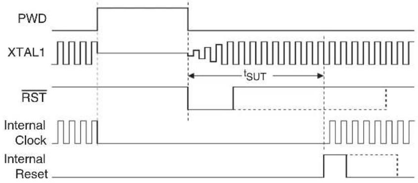
text_image
PWD XTAL1 RST Internal Clock Internal Reset tSUT8.3.2 Analog Comparators
The comparators will operate during Idle mode if enabled. To save power, the comparators should be disabled before entering Idle mode if possible. When the comparators are turned off and on again, some settling time is required for the analog circuits to stabilize. If the comparators are enabled, they will consume the least power when using an external reference, RFA1-0 = 00B and RFB1-0 = 0.0B .
8.3.3 Analog-to-Digital Converter
The DADC will operate during Idle mode if enabled. To save power, the DADC should be disabled before entering Idle mode if possible. When the DADC is turned off and on again, some settling time is required for the analog circuits to stabilize. If the DADC is enabled, it will consume the least power when configured to use the system clock instead of the internal RC oscillator (unless the IRC is the system clock source) and when the internal reference is disabled (IREF = 0). The DADC must always be disabled before entering power-down.
9. Interrupts
The AT89LP3240/6440 provides 12 interrupt sources: two external interrupts, three timer interrupts, a serial port interrupt, an analog comparator interrupt, a general-purpose interrupt, a compare/capture interrupt, a two-wire interrupt, an ADC interrupt and an SPI interrupt. These interrupts and the system reset each have a separate program vector at the start of the program memory space. Each interrupt source can be individually enabled or disabled by setting or clearing a bit in the interrupt enable registers IE and IE2. The IE register also contains a global disable bit, EA, which disables all interrupts.
Each interrupt source can be individually programmed to one of four priority levels by setting or clearing bits in the interrupt priority registers IP, IPH, IP2 and IP2H. IP and IP2 hold the low order priority bits and IPH and IP2H hold the high priority bits for each interrupt. An interrupt service routine in progress can be interrupted by a higher priority interrupt, but not by another interrupt of the same or lower priority. The highest priority interrupt cannot be interrupted by any other interrupt source. If two requests of different priority levels are pending at the end of an instruction, the request of higher priority level is serviced. If requests of the same priority level are pending at the end of an instruction, an internal polling sequence determines which request is serviced. The polling sequence is based on the vector address; an interrupt with a lower vector address has higher priority than an interrupt with a higher vector address. Note that the polling sequence is only used to resolve pending requests of the same priority level.
The IPxD bits located at the seventh bit of IP, IPH, IP2 and IP2H can be used to disable all interrupts of a given priority level, allowing software implementations of more complex interrupt priority handling schemes such as level-based round-robin scheduling.
The External Interrupts INT0 and INT1 can each be either level-activated or edge-activated, depending on bits IT0 and IT1 in Register TCON. The flags that actually generate these interrupts are the IE0 and IE1 bits in TCON. When the service routine is vectored to, hardware clears the flag that generated an external interrupt only if the interrupt was edge-activated. If the interrupt was level activated, then the external requesting source (rather than the on-chip hardware) controls the request flag.
The Timer 0 and Timer 1 Interrupts are generated by TF0 and TF1, which are set by a rollover in their respective Timer/Counter registers (except for Timer 0 in Mode 3). When a timer interrupt is generated, the on-chip hardware clears the flag that generated it when the service routine is vectored to. The Timer 2 Interrupt is generated by a logic OR of bits TF2 and EXF2 in register T2CON. Neither of these flags is cleared by hardware when the CPU vectors to the service routine. The service routine normally must determine whether TF2 or EXF2 generated the interrupt and that bit must be cleared by software.
The Serial Port Interrupt is generated by the logic OR of RI and TI in SCON. Neither of these flags is cleared by hardware when the CPU vectors to the service routine. The service routine normally must determine whether RI or TI generated the interrupt and that bit must be cleared by software.
The Serial Peripheral Interface Interrupt is generated by the logic OR of SPIF, MODF and TXE in SPSR. None of these flags is cleared by hardware when the CPU vectors to the service routine. The service routine normally must determine which bit generated the interrupt and that bit must be cleared by software.
A logic OR of all eight flags in the GPIF register causes the General-purpose Interrupt. None of these flags is cleared by hardware when the service routine is vectored to. The service routine must determine which bit generated the interrupt and that bit must be cleared in software. If the interrupt was level activated, then the external requesting source must de-assert the interrupt before the flag may be cleared by software.
The CFA and CFB bits in ACSRA and ACSRB respectively generate the Comparator Interrupt. The service routine must normally determine whether CFA or CFB generated the interrupt, and the bit must be cleared by software. The DAC/ADC Conversion Interrupt is generated by ADIF in DADC. On-chip hardware clears the ADIF flag when vectoring to the service routine.
A logic OR of the four least significant bits in the T2CCF register causes the Compare/Capture Array Interrupt. None of these flags is cleared by hardware when the service routine is vectored to. The service routine must determine which bit generated the interrupt and that bit must be cleared in software.
The Two-Wire Interface Interrupt is generated by TWIF in TWCR. The flag is not cleared by hardware when the CPU vectors to the service routine. The service routine normally must determine the status in TWSR and respond accordingly before the bit is cleared by software.
All of the bits that generate interrupts can be set or cleared by software, with the same result as though they had been set or cleared by hardware. That is, interrupts can be generated and pending interrupts can be canceled in software.
Table 9-1. Interrupt Vector Addresses
| Interrupt Source Vector Address | ||
| System Reset | RST or POR or BOD | 0000H |
| External Interrupt 0 | IE0 | 0003H |
| Timer 0 Overflow TF0 000BH | ||
| External Interrupt 1 | IE1 | 0013H |
| Timer 1 Overflow TF1 001BH | ||
| Serial Port Interrupt | RI or TI | 0023H |
| Timer 2 Interrupt TF2 or EXF2 002BH | ||
| Analog Comparator Interrupt | CFA or CFB | 0033H |
| General-purpose Interrupt | GPIF_7-0 | 003BH |
| Compare/Capture Array Interrupt | T2CCF_3-0 | 0043H |
| Serial Peripheral Interface Interrupt | SPIF or MODF or TXE | 004BH |
| ADC Interrupt | ADIF | 0053H |
| Two-Wire Interface Interrupt | TWIF | 005BH |
9.1 Interrupt Response Time
The interrupt flags may be set by their hardware in any clock cycle. The interrupt controller polls the flags in the last clock cycle of the instruction in progress. If one of the flags was set in the preceding cycle, the polling cycle will find it and the interrupt system will generate an LCALL to the appropriate service routine as the next instruction, provided that the interrupt is not blocked by any of the following conditions: an interrupt of equal or higher priority level is already in progress; the instruction in progress is RETI or any write to the IE, IP, IPH, IE2, IP2 or IP2H registers; the CPU is currently forced into idle by an IAP or FDATA write. Each of these conditions will block the generation of the LCALL to the interrupt service routine. The second condition ensures that if the instruction in progress is RETI or any access to IE, IP, IPH, IE2, IP2 or IP2H, then at least one more instruction will be executed before any interrupt is vectored to. The polling cycle is repeated at the last cycle of each instruction, and the values polled are the values that were present at the previous clock cycle. If an active interrupt flag is not being serviced because of one of the above conditions and is no longer active when the blocking condition is removed, the denied interrupt will not be serviced. In other words, the fact that the interrupt flag was once active but not serviced is not remembered. Every polling cycle is new.
If a request is active and conditions are met for it to be acknowledged, a hardware subroutine call to the requested service routine will be the next instruction executed. The call itself takes four cycles. Thus, a minimum of five complete clock cycles elapsed between activation of an interrupt request and the beginning of execution of the first instruction of the service routine. A longer response time results if the request is blocked by one of the previously listed conditions. If an interrupt of equal or higher priority level is already in progress, the additional wait time depends on the nature of the other interrupt's service routine. If the instruction in progress is not in its final clock cycle, the additional wait time cannot be more than 8 cycles, since the longest instruction is 9 cycles long. If the instruction in progress is RETI with XSTK, the additional wait time cannot be more than 14 cycles (a maximum of 5 more cycles to complete the instruction in progress, plus a maximum of 9 cycles to complete the next instruction). Thus, in a single-inter-
rupt system, the response time is always more than 5 clock cycles and less than 21 clock cycles. See Figure 9-1 and Figure 9-2.
Figure 9-1. Minimum Interrupt Response Time
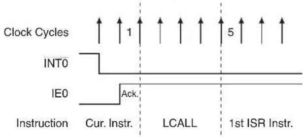
Figure 9-2. Maximum Interrupt Response Time

text_image
Clock Cycles INT0 IE0 Instruction 1 6 15 21 ACK. RETI MAC AB LCALL 1st ISR Instr.Table 9-2. IE – Interrupt Enable Register
| IE = A8H Reset Value = 0000 0000B | ||||||||
| Bit Addressable | ||||||||
| EA | EC | ET2 | ES | ET1 | EX1 | ET0 | EX0 | |
| Bit | 7 | 6 | 5 | 4 | 3 | 2 | 1 | 0 |
| Symbol | Function |
| EA | Global enable/disable. All interrupts are disabled when EA = 0. When EA = 1, each interrupt source is enabled/disabled by setting /clearing its own enable bit. |
| EC | Comparator Interrupt Enable |
| ET2 | Timer 2 Interrupt Enable |
| ES | Serial Port Interrupt Enable |
| ET1 | Timer 1 Interrupt Enable |
| EX1 | External Interrupt 1 Enable |
| ET0 | Timer 0 Interrupt Enable |
| EX0 | External Interrupt 0 Enable |
Table 9-3. IE2 – Interrupt Enable 2 Register
| IE = B4H Reset Value = xxxx x000BNot Bit Addressable | ||||||||
| ---ETWI EADC ESPI ECC EGP | ||||||||
| B | i | t | 7 | 6 | 5 | 4 | 3 | 2 |
| Symbol Function | |
| ETWI | Two-Wire Interface Interrupt Enable |
| EADC | ADC Interrupt Enable |
| ESPI | Serial Peripheral Interface Interrupt Enable |
| ECC | Compare/Capture Array Interrupt Enable |
| EGP | General-purpose Interrupt Enable |
Table 9-4. IP – Interrupt Priority Register
| IP = B8H Reset Value = 0000 0000B | ||||||||
| Bit Addressable | ||||||||
| IP0D | PC | PT2 | PS | PT1 | PX1 | PT0 | PX0 | |
| B | i | t | 7 | 6 | 5 | 4 | 3 | 2 |
| Symbol Function | |
| IP0D | Interrupt Priority 0 Disable. Set IP0D to 1 to disable all interrupts with priority level zero. Clear to 0 to enable all interrupts with priority level zero when EA = 1. |
| PC | Comparator Interrupt Priority Low |
| PT2 | Timer 2 Interrupt Priority Low |
| PS | Serial Port Interrupt Priority Low |
| PT1 | Timer 1 Interrupt Priority Low |
| PX1 | External Interrupt 1 Priority Low |
| PT0 | Timer 0 Interrupt Priority Low |
| PX0 | External Interrupt 0 Priority Low |
Table 9-5. IP2 – Interrupt Priority 2 Register
| IP = B5H Reset Value = 0xxx x000B No Bit Addressable | ||||||||
| IP2D | - | - | PTWI PADC | PSP | PCC | PGP | ||
| B | i | t | 7 | 6 | 5 | 4 | 3 | 2 |
| Symbol Function | |
| IP2D | Interrupt Priority 2 Disable. Set IP2D to 1 to disable all interrupts with priority level two. Clear to 0 to enable all interrupts with priority level two when EA = 1. |
| PTWI | Two-wire Interface Interrupt Priority Low |
| PADC | ADC Interrupt Priority Low |
| PSP | Serial Peripheral Interface Interrupt Priority Low |
| PCC | Compare/Capture Array Interrupt Priority Low |
| PGP | General-purpose Interrupt 0 Priority Low |
Table 9-6. IPH – Interrupt Priority High Register
| IPH = B7H Reset Value = 0000 0000BNot Bit Addressable | ||||||||
| IP1D | PCH | PT2H PSH | PT1H PX1H | PT0H PX0H | ||||
| B | i | t | 7 | 6 | 5 | 4 | 3 | 2 |
| Symbol Function | |
| IP1D | Interrupt Priority 1 Disable. Set IP1D to 1 to disable all interrupts with priority level one. Clear to 0 to enable all interrupts with priority level one when EA = 1. |
| PCH | Comparator Interrupt Priority High |
| PT2H Timer | 2 Interrupt Priority High |
| PSH | Serial Port Interrupt Priority High |
| PT1H Timer | 1 Interrupt Priority High |
| PX1H | External Interrupt 1 Priority High |
| PT0H Timer | 0 Interrupt Priority High |
| PX0H | External Interrupt 0 Priority High |
Table 9-7. IP2H – Interrupt Priority 2 High Register
| IPH = B6H Reset Value = 0xxx x000BNot Bit Addressable | ||||||||
| IP3D | - | - | PTWH | PADH | PSPH | PCCH | PGPH | |
| B | i | t | 7 | 6 | 5 | 4 | 3 | 2 |
| Symbol Function | |
| IP3D | Interrupt Priority 3 Disable. Set IP3D to 1 to disable all interrupts with priority level three. Clear to 0 to enable all interrupts with priority level three when EA = 1. |
| PTWH | Two-Wire Interface Interrupt Priority High |
| PADH | ADC Interrupt Priority High |
| PSPH | Serial Peripheral Interface Interrupt Priority High |
| PCCH | Compare/Capture Array Interrupt Priority High |
| PGPH | General-purpose Interrupt 0 Priority High |
10. I/O Ports
The AT89LP3240/6440 can be configured for between 35 and 38 I/O pins. The exact number of I/O pins available depends on the clock and reset options as shown in Table 10-1.
Table 10-1. I/O Pin Configurations
| Clock Source Reset Option Number of I/O Pins | ||
| External Crystal or Resonator | External Pin 35 | |
| No external reset | 36 | |
| External Clock | External Pin 36 | |
| No external reset | 37 | |
| Internal RC Oscillator | External Pin | 37 |
| No external reset | 38 | |
10.1 Port Configuration
All port pins on the AT89LP3240/6440 may be configured to one of four modes: quasi-bidirectional (standard 8051 port outputs), push-pull output, open-drain output, or input-only. Port modes may be assigned in software on a pin-by-pin basis as shown in Table 10-2 using the registers listed in Table 10-3. The Tristate-Port User Fuse determines the default state of the port pins. When the fuse is enabled, all port pins default to input-only mode after reset. When the fuse is disabled, all port pins, with the exception of the analog inputs, P0.7-0, P2.4, P2.5, P2.6 and P2.7, default to quasi-bidirectional mode after reset and are weakly pulled high. The analog input pins always reset to input-only (tristate) mode. Each port pin also has a Schmitt-triggered input for improved input noise rejection. During Power-down all the Schmitt-triggered inputs are disabled with the exception of P3.2 (INT0), P3.3 (INT1), P4.2 (RST), P4.0 (XTAL1) and P4.1 (XTAL2) which may be used to wake up the device. Therefore, P3.2, P3.3, P4.2, P4.0 and P4.1 should not be left floating during Power-down. In addition any pin of Port 1 configured as a General-Purpose interrupt input will also remain active during Power-down to wake-up the device. These interrupt pins should either be disabled before entering Power-down or they should not be left floating.
Table 10-2. Configuration Modes for Port x, Bit y
| PxM0.y PxM | 1.y Port Mode | |
| 0 | 0 | Quasi-bidirectional |
| 0 | 1 | Push-pull Output |
| 1 | 0 | Input Only (High Impedance) |
| 1 | 1 | Open-Drain Output |
Table 10-3. Port Configuration Registers
| Port | Port Data | Port Configuration |
| 0 | P0 (80H) | P0M0 (BAH), P0M1 (BBH) |
| 1 | P1 (90H) | P1M0 (C2H), P1M1 (C3H) |
| 2 | P2 (A0H) | P2M0 (C4H), P2M1 (C5H) |
| 3 | P3 (B0H) | P3M0 (C6H), P3M1 (C7H) |
| 4 | P4 (C0H) | P4M0 (BEH), P4M1 (BFH) |
10.1.1 Quasi-bidirectional Output
Port pins in quasi-bidirectional output mode function similar to standard 8051 port pins. A Quasi-bidirectional port can be used both as an input and output without the need to reconfigure the port. This is possible because when the port outputs a logic high, it is weakly driven, allowing an external device to pull the pin low. When the pin is driven low, it is driven strongly and able to sink a large current. There are three pull-up transistors in the quasi-bidirectional output that serve different purposes.
One of these pull-ups, called the “very weak” pull-up, is turned on whenever the port latch for the pin contains a logic “1”. This very weak pull-up sources a very small current that will pull the pin high if it is left floating.
A second pull-up, called the "weak" pull-up, is turned on when the port latch for the pin contains a logic "1" and the pin itself is also at a logic "1" level. This pull-up provides the primary source current for a quasi-bidirectional pin that is outputting a "1". If this pin is pulled low by an external device, this weak pull-up turns off, and only the very weak pull-up remains on. In order to pull the pin low under these conditions, the external device has to sink enough current to overpower the weak pull-up and pull the port pin below its input threshold voltage.
The third pull-up is referred to as the "strong" pull-up. This pull-up is used to speed up low-to-high transitions on a quasi-bidirectional port pin when the port latch changes from a logic "0" to a logic "1". When this occurs, the strong pull-up turns on for two CPU clocks quickly pulling the port pin high. The quasi-bidirectional port configuration is shown in Figure 10-1.
Figure 10-1. Quasi-bidirectional Output
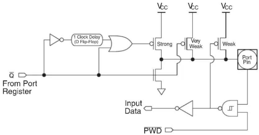
flowchart
graph TD
    A["From Port Register"] --> B["1 Clock Delay (D Flip-Flop)"]
    B --> C["AND"]
    C --> D["Strong"]
    D --> E["Vcc"]
    D --> F["Vcc"]
    D --> G["Vcc"]
    D --> H["Very Weak"]
    D --> I["Weak"]
    J["Input Data"] --> K["NOT"]
    K --> L["AND"]
    L --> M["Port Pin"]
    M --> N["PWD"]
    N --> O["Ground"]
    style A fill:#f9f,stroke:#333
    style O fill:#bbf,stroke:#333
10.1.2 Input-only Mode
The input only port configuration is shown in Figure 10-2. The output drivers are tristated. The input includes a Schmitt-triggered input for improved input noise rejection. The input circuitry of P3.2, P3.3, P4.2, P4.0 and P4.1 is not disabled during Power-down (see Figure 10-3) and therefore these pins should not be left floating during Power-down when configured in this mode.
Figure 10-2. Input Only
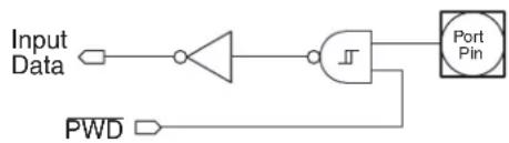
flowchart
graph LR
    A["Input Data"] --> B["AND Gate"]
    B --> C["AND Gate"]
    C --> D["Port Pin"]
    E["PWD"] --> B
Figure 10-3. Input Circuit for P3.2, P3.3, P4.0, P4.1 and P4.2
10.1.3 Open-drain Output
The open-drain output configuration turns off all pull-ups and only drives the pull-down transistor of the port pin when the port latch contains a logic "0". To be used as a logic output, a port configured in this manner must have an external pull-up, typically a resistor tied to V_DD . The pull-down for this mode is the same as for the quasi-bidirectional mode. The open-drain port configuration is shown in Figure 10-4. The input circuitry of P3.2, P3.3, P4.0, P4.1 and P4.2 is not disabled during Power-down (see Figure 10-3) and therefore these pins should not be left floating during Power-down when configured in this mode.
Figure 10-4. Open-Drain Output

flowchart
graph TD
    A["From Port Register"] --> B["AND"]
    B --> C["Summing Junction"]
    C --> D["Port Pin"]
    D --> E["PWD"]
    E --> F["Output"]
    G["Input Data"] --> C
    H["Ground"] --> C
10.1.4 Push-pull Output
The push-pull output configuration has the same pull-down structure as both the open-drain and the quasi-bidirectional output modes, but provides a continuous strong pull-up when the port latch contains a logic "1". The push-pull mode may be used when more source current is needed from a port output. The push-pull port configuration is shown in Figure 10-5.
Figure 10-5. Push-pull Output
text_image
From Port Register Input Data PWD Vcc Port Pin10.2 Port Analog Functions
The AT89LP3240/6440 incorporates two analog comparators and an 8-channel analog-to-digital converter. In order to give the best analog performance and minimize power consumption, pins that are being used for analog functions must have both their digital outputs and digital inputs disabled. Digital outputs are disabled by putting the port pins into the input-only mode as described in "Port Configuration" on page 45. The analog input pins will always default to input-only mode after reset regardless of the state of the Tristate-Port Fuse.
Digital inputs on P2.4, P2.5, P2.6 and P2.7 are disabled whenever an analog comparator is enabled by setting the CENA or CENB bits in ACSRA and ACSRB and that pin is configured for input-only mode. To use an analog input pin as a high-impedance digital input while a comparator is enabled, that pin should be configured in open-drain mode and the corresponding port register bit should be set to 1.
Digital inputs on Port 0 are disabled for each pin configured for input-only mode whenever the ADC is enabled by setting the ADCE bit and clearing the DAC bit in DADC. To use any Port 0 input pin as a high-impedance digital input while the ADC is enabled, that pin should be configured in open-drain mode and the corresponding port register bit should be set to 1. When DAC mode is enabled, P2.2 and P2.3 are forced to input-only mode.
10.3 Port Read-Modify-Write
A read from a port will read either the state of the pins or the state of the port register depending on which instruction is used. Simple read instructions will always access the port pins directly. Read-modify-write instructions, which read a value, possibly modify it, and then write it back, will always access the port register. This includes bit write instructions such as CLR or SETB as they actually read the entire port, modify a single bit, then write the data back to the entire port. See Table 10-4 for a complete list of Read-Modify-Write instruction which may access the ports.
Table 10-4. Port Read-Modify-Write Instructions
| Mnemonic Instruction | Example | |
| ANL Logical AND ANL P1, A | ||
| ORL Logical OR ORL P1, A | ||
| XRL Logical EX-OR XRL P1, A | ||
| JBC | Jump if bit set and clear bit | JBC P3.0, LABEL |
| CPL Complement bit | CPL P3.1 | |
| INC | Increment | INC P1 |
| DEC | Decrement | DEC P3 |
| DJNZ | Decrement and jump if not zero | DJNZ P3, LABEL |
| MOV PX.Y, C | Move carry to bit Y of Port X | MOV P1.0, C |
| CLR PX.Y | Clear bit Y of Port X | CLR P1.1 |
| SETB PX.Y | Set bit Y of Port X | SETB P3.2 |
10.4 Port Alternate Functions
Most general-purpose digital I/O pins of the AT89LP3240/6440 share functionality with the various I/Os needed for the peripheral units. Table 10-6 lists the alternate functions of the port pins. Alternate functions are connected to the pins in a logic AND fashion. In order to enable the alternate function on a port pin, that pin must have a "1" in its corresponding port register bit, otherwise the input/output will always be "0". However, alternate functions may be temporarily forced to "0" by clearing the associated port bit, provided that the pin is not in input-only mode. Furthermore, each pin must be configured for the correct input/output mode as required by its peripheral before it may be used as such. Table 10-5 shows how to configure a generic pin for use with an alternate function.
Table 10-5. Alternate Function Configurations for Pin y of Port x
| PxM0.y PxM1.y Px.y I/O Mode | |||
| 0 | 0 | 1 | bidirectional (internal pull-up) |
| 0 | 1 | 1 o | |
| 1 | 0 | X | i n |
| 1 | 1 | 1 | bidirectional (external pull-up) |
Table 10-6. Port Pin Alternate Functions
| Port Pin | Configuration Bits | Alternate Function | Notes | |
| PxM0.y | PxM1.y | |||
| P0.0 | P0M0.0 | P0M1.0 | AD0 | Automatic configuration |
| ADC0 | input-only | |||
| P0.1 | P0M0.1 | P0M1.1 | AD1 | Automatic configuration |
| ADC1 | input-only | |||
| P0.2 | P0M0.2 | P0M1.2 | AD2 | Automatic configuration |
| ADC2 | input-only | |||
| P0.3 | P0M0.3 | P0M1.3 | AD3 | Automatic configuration |
| ADC3 | input-only | |||
| P0.4 | P0M0.4 | P0M1.4 | AD4 | Automatic configuration |
| ADC4 | input-only | |||
| P0.5 | P0M0.5 | P0M1.5 | AD5 | Automatic configuration |
| ADC5 | input-only | |||
| P0.6 | P0M0.6 | P0M1.6 | AD6 | Automatic configuration |
| ADC6 | input-only | |||
| P0.7 | P0M0.7 | P0M1.7 | AD7 | Automatic configuration |
| ADC7 | input-only | |||
| P1.0 | P1M0.0 | P1M1.0 | T2 | |
| GPIO | ||||
| P1.1 | P1M0.1 | P1M1.1 | T2EX | |
| GPI1 | ||||
Table 10-6. Port Pin Alternate Functions
| Port Pin | Configuration Bits | Alternate Function | Notes | |
| PxM0.y PxM1.y | ||||
| P1.2 P1M0.2 P1M1.2 | SDA open-drain | |||
| GPI2 | ||||
| P1.3 P1M0.3 P1M1.3 | SCL open-drain | |||
| GPI3 | ||||
| P1.4 P1M0.4 P1M1.4 | SS | |||
| GPI4 | ||||
| P1.5 P1M0.5 P1M1.5 | MOSI | |||
| GPI5 | ||||
| P1.6 P1M0.6 P1M1.6 | MISO | |||
| GPI6 | ||||
| P1.7 P1M0.7 P1M1.7 | SCK | |||
| GPI7 | ||||
| P2.0 P2M0.0 P2M1.0 CCA | ||||
| P2.1 P2M0.1 P2M1.1 CCB | ||||
| P2.2 P2M0.2 P2M1.2 | CCC | |||
| DA+ input-only | ||||
| P2.3 P2M0.3 P2M1.3 | CCD | |||
| DA- input-only | ||||
| P2.4 P2M0.4 P2M1.4 AIN0 input-only | ||||
| P2.5 P2M0.5 P2M1.5 AIN1 input-only | ||||
| P2.6 P2M0.6 P2M1.6 AIN2 input-only | ||||
| P2.7 P2M0.7 P2M1.7 AIN3 input-only | ||||
| P3.0 P3M0.0 P3M1.0 RXD | ||||
| P3.1 P3M0.1 P3M1.1 TXD | ||||
| P3.2 P3M0.2 P3M1.2 INT0 | — | |||
| P3.3 P3M0.3 P3M1.3 INT1 | — | |||
| P3.4 P3M0.4 P3M1.4 T0 | ||||
| P3.5 P3M0.5 P3M1.5 T1 | ||||
| P3.6 P3M0.6 P3M1.6 WR | — | |||
| P3.7 P3M0.7 P3M1.7 RD | — | |||
| P4.2 | P3M0.5 | P3M1.5 | RST | RST must be disabled to use P4.2 |
| P4.6 | not configurable | CMPA | Pin is tied to comparator output | |
| P4.7 | not configurable | CMPB | Pin is tied to comparator output | |
11. Enhanced Timer 0 and Timer 1 with PWM
The AT89LP3240/6440 has two 16-bit Timer/Counters, Timer 0 and Timer 1, with the following features:
- Two 16-bit timer/counters with 16-bit reload registers
- Two independent 8-bit precision PWM outputs with 8-bit prescalers
- UART or SPI baud rate generation using Timer 1
- Output pin toggle on timer overflow
- Split timer mode allows for three separate timers (2 8-bit, 1 16-bit)
- Gated modes allow timers to run/halt based on an external input
Timer 0 and Timer 1 have similar modes of operation. As timers, the timer registers increase every clock cycle by default. Thus, the registers count clock cycles. Since a clock cycle consists of one oscillator period, the count rate is equal to the oscillator frequency. The timer rate can be prescaled by a value between 1 and 16 using the Timer Prescaler (see Table 6-2 on page 33). Both Timers share the same prescaler.
As counters, the timer registers are incremented in response to a 1-to-0 transition at the corresponding input pins, T0 or T1. The external input is sampled every clock cycle. When the samples show a high in one cycle and a low in the next cycle, the count is incremented. The new count value appears in the register during the cycle following the one in which the transmission was detected. Since 2 clock cycles are required to recognize a 1-to-0 transition, the maximum count rate is 1/2 of the oscillator frequency. There are no restrictions on the duty cycle of the input signal, but it should be held for at least one full clock cycle to ensure that a given level is sampled at least once before it changes.
Furthermore, the Timer or Counter functions for Timer 0 and Timer 1 have four operating modes: variable width timer, 16-bit auto-reload timer, 8-bit auto-reload timer, and split timer. The control bits C/T in the Special Function Register TMOD select the Timer or Counter function. The bit pairs (M1, M0) in TMOD select the operating modes.
Table 11-1. Timer 0/1 Register Summary
| Name Address | Purpose | Bit-Addressable | |
| TCON 88H Control | Y | ||
| TMOD | 89H | Mode | N |
| TL0 | 8AH | Timer 0 low-byte | N |
| TL1 | 8BH | Timer 1 low-byte | N |
| TH0 | 8CH | Timer 0 high-byte | N |
| TH1 | 8DH | Timer 1 high-byte | N |
| TCONB | 91H Mode | N | |
| RL0 | 92H | Timer 0 reload low-byte | N |
| RL1 | 93H | Timer 1 reload low-byte | N |
| RH0 | 94H | Timer 0 reload high-byte | N |
| RH1 | 95H | Timer 1 reload high-byte | N |
11.1 Mode 0 - Variable Width Timer/Counter
Both Timers in Mode 0 are 8-bit Counters with a variable prescaler. The prescaler may vary from 1 to 8 bits depending on the PSC bits in TCONB, giving the timer a range of 9 to 16 bits. By default the timer is configured as a 13-bit timer compatible to Mode 0 in the standard 8051. Figure 11-1 shows the Mode 0 operation as it applies to Timer 1 in 13-bit mode. As the count rolls over from all "1"s to all "0"s, it sets the Timer interrupt flag TF1. The counter input is enabled to the Timer when TR1 = 1 and either GATE1 = 0 or INT1 = 1. Setting GATE1 = 1 allows the Timer to be controlled by external input INT1, to facilitate pulse width measurements. TR1 is a control bit in the Special Function Register TCON. GATE1 is in TMOD. The 13-bit register consists of all 8 bits of TH1 and the lower 5 bits of TL1. The upper 3 bits of TL1 are indeterminate and should be ignored. Setting the run flag (TR1) does not clear the registers.
$$ \text { Mode 0: Time - out Period } = \frac {2 5 6 \Omega^ {\text { PSC01+ }}}{\text { Oscillator Frequency }} \times (\text { TPS } + 1) $$
Note: RH1/RL1 are not required by Timer 1 during Mode 0 and may be used as temporary storage registers.
Figure 11-1. Timer/Counter 1 Mode 0: Variable Width Counter

flowchart
graph TD
    OSC --> |÷TPS| A["Control"]
    A --> TL1["TL1 (8 Bits)"]
    TL1 --> PSC1["PSC1"]
    PSC1 --> TH1["TH1 (8 Bits)"]
    TH1 --> TF1["TF1"]
    TF1 --> Interrupt["Interrupt"]
    T1Pin["T1 Pin"] --> A
    GATE1["GATE1"] --> AND1["AND"]
    INT1Pin["INT1 Pin"] --> AND1
    AND1 --> TR1["TR1"]
    C/T0["C/T̅ = 0"] --> A
    C/T1["C/T̅ = 1"] --> A
Mode 0 operation is the same for Timer 0 as for Timer 1, except that TR0, TF0, GATE0 and INTO replace the corresponding Timer 1 signals in Figure 11-1. There are two different C/T bits, one for Timer 1 (TMOD.6) and one for Timer 0 (TMOD.2).
11.2 Mode 1 - 16-bit Auto-Reload Timer/Counter
In Mode 1 the Timers are configured for 16-bit auto-reload. The Timer register is run with all 16 bits. The 16-bit reload value is stored in the high and low reload registers (RH1/RL1). The clock is applied to the combined high and low timer registers (TH1/TL1). As clock pulses are received, the timer counts up: 0000H, 0001H, 0002H, etc. An overflow occurs on the FFFFH-to-0000H transition, upon which the timer register is reloaded with the value from RH1/RL1 and the overflow flag bit in TCON is set. See Figure 11-2. The reload registers default to 0000H, which gives the full 16-bit timer period compatible with the standard 8051. Mode 1 operation is the same for Timer/Counter 0.
$$ \text { Mode 1: Time - out Period } = \frac {(6 5 5 3 6 - {\mathrm{RH0} , \mathrm{RL0} })}{\text { Oscillator Frequency }} \times (\mathrm{TPS} + 1) $$
Figure 11-2. Timer/Counter 1 Mode 1: 16-bit Auto-Reload
flowchart
graph TD
    OSC --> ÷TPS
    ÷TPS --> C/T = 0
    C/T = 0 --> Control
    C/T = 1 --> Control
    Control --> TL1["TL1 (8 Bits)"]
    Control --> TH1["TH1 (8 Bits)"]
    TL1 --> RL1["RL1 (8 Bits)"]
    TH1 --> RH1["RH1 (8 Bits)"]
    RL1 -->|Recall| TF1["TF1"]
    RH1 -->|Recall| TF1
    TF1 --> Interrupt
    GATE1 --> OR1
    INT1 Pin --> OR1
    OR1 --> GATE1
    Control --> TR1
11.3 Mode 2 - 8-bit Auto-Reload Timer/Counter
Mode 2 configures the Timer register as an 8-bit Counter (TL1) with automatic reload, as shown in Figure 11-3. Overflow from TL1 not only sets TF1, but also reloads TL1 with the contents of TH1, which is preset by software. The reload leaves TH1 unchanged. Mode 2 operation is the same for Timer/Counter 0.
$$ \text { Mode 2: Time - out Period } = \frac {2 5 6 \mathrm{TH0} - (\text { Oscillator Frequency })}{(\mathrm{TPS} + 1)} \times (\mathrm{TPS} + 1) $$
Figure 11-3. Timer/Counter 1 Mode 2: 8-bit Auto-Reload

flowchart
graph TD
    OSC --> ÷TPS
    ÷TPS --> C/T0["0"]
    C/T0 --> Control
    T1Pin --> Control
    C/T0 --> Control
    Control --> TL1["TL1 (8 Bits)"]
    TL1 --> TF1["TF1"]
    TF1 --> Interrupt
    TR1 --> GATE1
    GATE1 --> AND1["AND"]
    AND1 --> Control
    TH1["TH1 (8 Bits)"] --> Control
    TH1 --> TL1
    TL1 --> Reload
    INT0Pin --> GATE1
Note: RH1/RL1 are not required by Timer 1 during Mode 2 and may be used as temporary storage registers.
11.4 Mode 3 - 8-bit Split Timer
Timer 1 in Mode 3 simply holds its count. The effect is the same as setting TR1 = 0. Timer 0 in Mode 3 establishes TL0 and TH0 as two separate counters. The logic for Mode 3 on Timer 0 is shown in Figure 11-4. TL0 uses the Timer 0 control bits: C/T, GATE0, TR0, INT0, and TF0. TH0 is locked into a timer function (counting clock cycles) and takes over the use of TR1 and TF1 from Timer 1. Thus, TH0 now controls the Timer 1 interrupt. While Timer 0 is in Mode 3, Timer 1 will still obey its settings in TMOD but cannot generate an interrupt.
Mode 3 is for applications requiring an extra 8-bit timer or counter. With Timer 0 in Mode 3, the AT89LP3240/6440 can appear to have four Timer/Counters. When Timer 0 is in Mode 3, Timer 1 can be turned on and off by switching it out of and into its own Mode 3. In this case, Timer 1 can still be used by the serial port as a baud rate generator or in any application not requiring an interrupt.
Figure 11-4. Timer/Counter 0 Mode 3: Two 8-bit Counters

flowchart
graph TD
    A["OSC"] --> B["÷TPS"]
    B --> C["C/T̅ = 0"]
    C --> D["Control"]
    D --> E["TL0 (8 Bits)"]
    E --> F["TF0"]
    F --> G["Interrupt"]
    H["T0 Pin"] --> I["AND Gate"]
    I --> J["TR0"]
    K["GATE0"] --> L["OR Gate"]
    M["INT0 Pin"] --> L
    L --> N["Control"]
    N --> O["TH0 (8 Bits)"]
    O --> P["TF1"]
    P --> Q["Interrupt"]
    R["OSC"] --> S["÷TPS"]
    S --> T["TR1"]
    T --> U["Control"]
    U --> V["TH0 (8 Bits)"]
    V --> W["TF1"]
    W --> X["Interrupt"]
Note: RHO/RL0 are not required by Timer 0 during Mode 3 and may be used as temporary storage registers.
Table 11-2. TCON - Timer/Counter Control Register
| TCON = 88H Reset Value = 0000 0000BBit Addressable | ||||||||
| TF1 TR1 | TF0 TR0 IE1 | IT1 IE0 IT0 | ||||||
| B | i | t | 7 | 6 | 5 | 4 | 3 | 2 |
| Symbol Function | |
| TF1 | Timer 1 overflow flag. Set by hardware on Timer/Counter overflow. Cleared by hardware when the processor vectors to interrupt routine. |
| TR1 | Timer 1 run control bit. Set/cleared by software to turn Timer/Counter on/off. |
| TF0 | Timer 0 overflow flag. Set by hardware on Timer/Counter overflow. Cleared by hardware when the processor vectors to interrupt routine. |
| TR0 | Timer 0 run control bit. Set/cleared by software to turn Timer/Counter on/off. |
| IE1 | Interrupt 1 edge flag. Set by hardware when external interrupt edge detected. Cleared when interrupt processed. |
| IT1 | Interrupt 1 type control bit. Set/cleared by software to specify falling edge/low level triggered external interrupts. |
| IE0 | Interrupt 0 edge flag. Set by hardware when external interrupt edge detected. Cleared when interrupt processed. |
| IT0 | Interrupt 0 type control bit. Set/cleared by software to specify falling edge/low level triggered external interrupts. |
Table 11-3. TMOD – Timer/Counter Mode Control Register
| TMOD Address = 089H Reset Value = 0000 0000BNot Bit Addressable | ||||||||
| GATE1 C/T1 — | T1M1 T1M0 GATE0 C/T0 T0M0 T0M1 | — | ||||||
| B | i | t | 7 | 6 | 5 | 4 | 3 | 2 |
| Symbol Function | ||||||||
| GATE1 | Timer 1 Gating Control. When set, Timer/Counter 1 is enabled only while INT1 pin is high and TR1 control pin is set.When cleared, Timer 1 is enabled whenever TR1 control bit is set. | |||||||
| C/T1 | Timer or Counter Selector 1. Cleared for Timer operation (input from internal system clock). Set for Counter operation(input from T1 input pin). C/T1 must be zero when using Timer 1 in PWM mode. | |||||||
| T1M1T1M0 | Timer 1 Operating ModeMode T1M1 T1M0 Operation ____Variable 9–16-bit Timer Mode. 8-bit Timer/Counter TH1 with TL1 as 1–8-bit prescaler. | |||||||
| 0 | 0 | 0 | 16-bit Auto-Reload Mode. TH1 and TL1 are cascaded to form a 16-bit Timer/Counterthat is reloaded with RH1 and RL1 each time it overflows. | |||||
| 1 | 0 | 1 | ||||||
| 2 | 1 | 0 | 8-bit Auto Reload Mode. TH1 holds a value which is reloaded into 8-bit Timer/CounterTL1 each time it overflows. | |||||
| 3 | 1 | 1 | Timer/Counter 1 is stopped | |||||
| GATE0 | Timer 0 Gating Control. When set, Timer/Counter 0 is enabled only while INT0 pin is high and TR0 control pin is set.When cleared, Timer 0 is enabled whenever TR0 control bit is set. | |||||||
| C/T0 | Timer or Counter Selector 0. Cleared for Timer operation (input from internal system clock). Set for Counter operation(input from T0 input pin). C/T0 must be zero when using Timer 0 in PWM mode. | |||||||
| T0M1T0M0 | Timer 0 Operating ModeMode T0M1 T0M0 Operation ____Variable 9–16-bit Timer Mode. 8-bit Timer/Counter TH0 with TL0 as 1–8-bit prescaler. | |||||||
| 0 | 0 | 0 | 16-bit Auto-Reload Mode. TH0 and TL0 are cascaded to form a 16-bit Timer/Counterthat is reloaded with RH0 and RL0 each time it overflows. | |||||
| 1 | 0 | 1 | ||||||
| 2 | 1 | 0 | 8-bit Auto Reload Mode. TH0 holds a value which is reloaded into 8-bit Timer/CounterTL0 each time it overflows. | |||||
| 3 | 1 | 1 | Split Timer Mode. TL0 is an 8-bit Timer/Counter controlled by the standard Timer 0control bits. TH0 is an 8-bit timer only controlled by Timer 1 control bits. | |||||
Table 11-4. TCONB – Timer/Counter Control Register B
| TCONB = 91H Reset Value = 0010 0100BNot Bit Addressable | ||||||||
| PWM1EN | PWM0EN | PSC12 | PSC11 | PSC10 | PSC02 | PSC01 | PSC00 | |
| B | i | t | 7 | 6 | 5 | 4 | 3 | 2 |
| Symbol Function | |
| PWM1EN | Configures Timer 1 for Pulse Width Modulation output on T1 (P3.5). |
| PWM0EN | Configures Timer 0 for Pulse Width Modulation output on T0 (P3.4). |
| PSC12PSC11PSC10 | Prescaler for Timer 1 Mode 0. The number of active bits in TL1 equals PSC1 + 1. After reset PSC1 = 100B which enables 5 bits of TL1 for compatibility with the 13-bit Mode 0 in AT89S2051. |
| PSC02PSC01PSC00 | Prescaler for Timer 0 Mode 0. The number of active bits in TL0 equals PSC0 + 1. After reset PSC0 = 100B which enables 5 bits of TL0 for compatibility with the 13-bit Mode 0 in AT89C52. |
11.5 Pulse Width Modulation
On the AT89LP3240/6440, Timer 0 and Timer 1 may be independently configured as 8-bit asymmetrical (edge-aligned) pulse width modulators (PWM) by setting the PWM0EN or PWM1EN bits in TCONB, respectively. In PWM Mode the generated waveform is output on the timer's input pin, T0 or T1. Therefore, C/Tx must be set to "0" when in PWM mode and the T0 (P3.4) and T1 (P3.5) must be configured in an output mode. The Timer Overflow Flags and Interrupts will continue to function while in PWM Mode and Timer 1 may still generate the baud rate for the UART. The timer GATE function also works in PWM mode, allowing the output to be halted by an external input. Each PWM channel has four modes selected by the mode bits in TMOD.
An example waveform for Timer 0 in PWM Mode 0 is shown in Figure 11-5. TH0 acts as an 8-bit counter while RH0 stores the 8-bit compare value. When TH0 is 00H the PWM output is set high. When the TH0 count reaches the value stored in RH0 the PWM output is set low. Therefore, the pulse width is proportional to the value in RH0. To prevent glitches, writes to RH0 only take effect on the FFH to 00H overflow of TH0. Setting RH0 to 00H will keep the PWM output low.
Figure 11-5. 8-bit Asymmetrical Pulse Width Modulation

line
| Time | THO | FFH | RH0 | 00H | |------|-----|-----|-----|-----| | 0 | 1 | 1 | 0 | 0 | | 1 | 1 | 1 | 0 | 0 | | 2 | 1 | 1 | 0 | 0 | | 3 | 1 | 1 | 0 | 0 | | 4 | 1 | 1 | 0 | 0 | | 5 | 1 | 1 | 0 | 0 | | 6 | 1 | 1 | 0 | 0 | | 7 | 1 | 1 | 0 | 0 | | 8 | 1 | 1 | 0 | 0 | | 9 | 1 | 1 | 0 | 0 | | 10 | 1 | 1 | 0 | 0 | | 11 | 1 | 1 | 0 | 0 | | 12 | 1 | 1 | 0 | 0 | | 13 | 1 | 1 | 0 | 0 | | 14 | 1 | 1 | 0 | 0 | | 15 | 1 | 1 | 0 | 0 | | 16 | 1 | 1 | 0 | 0 | | 17 | 1 | 1 | 0 | 0 | | 18 | 1 | 1 | 0 | 0 | | 19 | 1 | 1 | 0 | 0 | | 20 | 1 | 1 | 0 | 0 | | 21 | 1 | 1 | 0 | 0 | | 22 | 1 | 1 | 0 | 0 | | 23 | 1 | 1 | 0 | 0 | | 24 | 1 | 1 | 0 | 0 | | 25 | 1 | 1 | 0 | 0 | | 26 | 1 | 1 | 0 | 0 | | 27 | 1 | 1 | 0 | 0 | | 28 | 1 | 1 | 0 | 0 | | 29 | 1 | 1 | 0 | 0 | | 30+ (P3.4)T0 (Time) = THO → FFH → RHO → TF0 Set → TF0 Set → (P3.4)T0 (Time) → (P3.4)T0 (Time) → (P3.4)T0 (Time) → (P3.4)T0 (Time) → (P3.4)T0 (Time) → (P3.4)T0 (Time) → (P3.4)T0 (Time) → (P3.4)T0 (Time) → (P3.4)T0 (Time) → (P5.4)T0 (Time) → (P3.4)T0 (Time) → (P3.4)T0 (Time) → (P3.4)T0 (Time) → (P3.4)T0 (Time) → (P3.4)T0 (Time) → (P3.4)T0 (Time) → (P3.4)T0 (Time) → (P3.4)S TFO Set (TFO Set) (TFO Set) (TFO Set) (TFO Set) (TFO Set) (TFO Set) (TFO Set) (TFO Set) (TFO Set) (TFO Set) (TFO Set) (TFO Set) (TFO Set) (TFO Set) (TFO Set) (TFO Set) (TFO Set) (TFO Set) (TFO Set) (TFO Set) (TFO Set)11.5.1 Mode 0 - 8-bit PWM with 8-bit Logarithmic Prescaler
In Mode 0, TLx acts as a logarithmic prescaler driving 8-bit counter THx (see Figure 11-6). The PSCx bits in TCONB control the prescaler value. On THx overflow, the duty cycle value in RHx is transferred to OCRx and the output pin is set high. When the count in THx matches OCRx, the output pin is cleared low. The following formulas give the output frequency and duty cycle for Timer 0 in PWM Mode 0. Timer 1 in PWM Mode 0 is identical to Timer 0.
$$ \begin{array}{rlr} & {} & {f_{out}\quad \frac{\mathrm{Oscillator~Frequency}}{256\Omega^{\mathrm{PSC0~1 + }}}\times \frac{1}{\mathrm{TPS1 + }}}\ & {} & {\mathrm{Duty~Cycle~\%~100}\quad \times = \frac{\mathrm{RH0}}{256}} \end{array} $$
Figure 11-6. Timer/Counter 1 PWM Mode 0
flowchart
graph TD
    OSC --> ÷TPS
    ÷TPS --> Control
    Control --> TL1["TL1 (8 Bits)"]
    Control --> PSC1["PSC1"]
    TR1 --> AND1["AND"]
    GATE1 --> OR1["OR"]
    INT1 Pin --> OR1
    OR1 --> TH1["TH1 (8 Bits)"]
    TH1 --> XOR1["OCR1"]
    XOR1 --> RH1["RH1 (8 Bits)"]
    RH1 --> OR1
    OR1 --> T1["T1"]
    style OR1 fill:#f9f,stroke:#333
11.5.2 Mode 1 - 8-bit PWM with 8-bit Linear Prescaler
In Mode 1, TLx provides linear prescaling with an 8-bit auto-reload from RLx (see Figure 11-7 on page 58). On TLx overflow, TLx is loaded with the value of RLx. THx acts as an 8-bit counter. On THx overflow, the duty cycle value in RHx is transferred to OCRx and the output pin is set high. When the count in THx matches OCRx, the output pin is cleared low. The following formulas give the output frequency and duty cycle for Timer 0 in PWM Mode 1. Timer 1 in PWM Mode 1 is identical to Timer 0.
$$ \begin{array}{rlr}f_{out} & {} & \frac{\text{Oscillator Frequency}}{256\times(256 - RL0)}\times = \frac{1}{TPS1 + }\ & {} & \text{Duty Cycle}\% 100\quad \times = \frac{RH0}{256} \end{array} $$
11.5.3 Mode 2 - 8-bit Frequency Generator
Timer 0 in PWM Mode 2 functions as an 8-bit Auto-Reload timer, the same as normal Mode 2, with the exception that the output pin T0 is toggled at every TL0 overflow (see Figure 11-8 and Figure 11-9 on page 58). Timer 1 in PWM Mode 2 is identical to Timer 0. PWM Mode 2 can be used to output a square wave of varying frequency. THx acts as an 8-bit counter. The following formula gives the output frequency for Timer 0 in PWM Mode 2.
$$ \text { Mode 2: } \quad f _ {\text { out }} \quad \frac {\text { Oscillator Frequency }}{2 \times (2 5 6 - \text { TH0 })} \times = \frac {1}{\text { TPS1+ }} $$
Figure 11-7. Timer/Counter 1 PWM Mode 1

flowchart
graph TD
    A["OSC"] --> B["÷TPS"]
    B --> C["Control"]
    C --> D["TL1 (8 Bits)"]
    D --> E["TH1 (8 Bits)"]
    E --> F["ORC1"]
    F --> G["="]
    G --> H["T1"]
    I["GATE1"] --> J["AND Gate"]
    K["INT1 Pin"] --> L["AND Gate"]
    M["RL1 (8 Bits)"] --> N["Downward Arrow"]
    O["RH1 (8 Bits)"] --> P["Downward Arrow"]
    Q["Control"] --> R["AND Gate"]
    S["TR1"] --> T["AND Gate"]
    U["TL1 (8 Bits)"] --> V["Downward Arrow"]
    W["TH1 (8 Bits)"] --> X["Downward Arrow"]
    Y["ORC1"] --> Z["Downward Arrow"]
    AA["="] --> AB["Output"]
Figure 11-8. Timer/Counter 1 PWM Mode 2
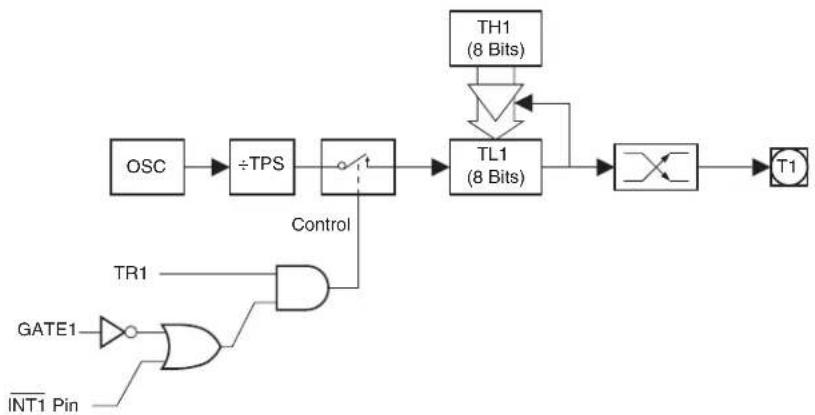
flowchart
graph LR
    OSC --> ÷TPS
    ÷TPS --> TL1["TL1 (8 Bits)"]
    TL1 --> TH1["TH1 (8 Bits)"]
    TH1 --> TL1
    TL1 --> T1["T1"]
    GATE1 --> GATE1
    INT1 Pin --> GATE1
    TR1 --> AND
    Control --> AND
    AND --> TL1
Note: {RH0 & RL0}/{{RH1 & RL1} are not required by Timer 0/Timer 1 during PWM Mode 2 and may be used as temporary storage registers.
Figure 11-9. PWM Mode 2 Waveform
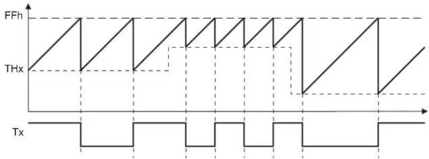
text_image
FFh THx Tx11.5.4 Mode 3 - Split 8-bit PWM
Timer 1 in PWM Mode 3 simply holds its count. The effect is the same as setting TR1 = 0. Timer 0 in PWM Mode 3 establishes TL0 and TH0 as two separate PWM counters in a manner similar to normal Mode 3. PWM Mode 3 on Timer 0 is shown in Figure 11-10. Only the Timer Prescaler is available to change the output frequency during PWM Mode 3. TL0 can use the Timer 0 control bits: GATE, TR0, INT0, PWM0EN and TF0. TH0 is locked into a timer function and uses TR1, PWM1EN and TF1. RL0 provides the duty cycle for TL0 and RH0 provides the duty cycle for TH0.
PWM Mode 3 is for applications requiring a single PWM channel and two timers, or two PWM channels and an extra timer or counter. With Timer 0 in PWM Mode 3, the AT89LP3240/6440 can appear to have four Timer/Counters. When Timer 0 is in PWM Mode 3, Timer 1 can be turned on and off by switching it out of and into its own Mode 3. In this case, Timer 1 can still be used by the serial port as a baud rate generator or in any application not requiring an interrupt. The following formulas give the output frequency and duty cycle for Timer 0 in PWM Mode 3.
$$ \text { Mode 3: } f \quad \text { out } \quad \frac {\text { Oscillator Frequency }}{2 5 6} \times = \frac {1}{\text { TPS1+ }} $$
$$ \text { Mode 3, T0: Duty Cycle } \% 1 0 0 \quad \times = \frac {\mathrm{RL0}}{2 5 6} $$
$$ \text { Mode 3, T1: Duty Cycle } \% 1 0 0 \quad \times = \frac {\mathrm{RH0}}{2 5 6} $$
Figure 11-10. Timer/Counter 0 PWM Mode 3
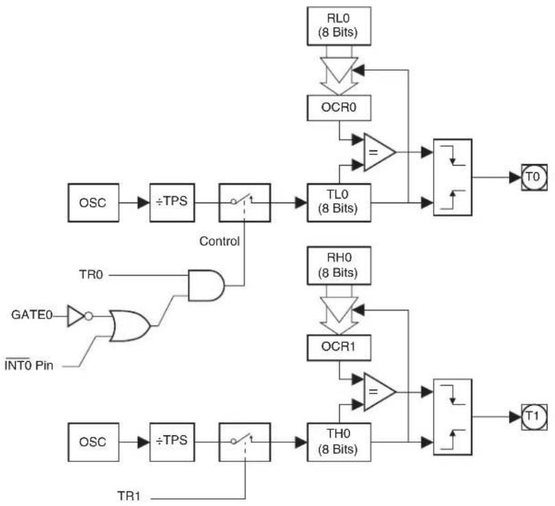
flowchart
graph TD
    A["OSC"] --> B["÷TPS"]
    B --> C{Control}
    C --> D["TL0 (8 Bits)"]
    D --> E["T0"]
    F["GATE0"] --> G["ORC1"]
    H["INT0 Pin"] --> I["AND"]
    I --> J["Control"]
    J --> C
    K["TL0 (8 Bits)"] --> L["ORC0"]
    L --> M["="]
    M --> N["T0"]
    O["OSC"] --> P["÷TPS"]
    P --> Q{Control}
    Q --> R["TH0 (8 Bits)"]
    R --> S["="]
    S --> T["T1"]
    U["TL0 (8 Bits)"] --> V["ORC1"]
    V --> W["="]
    W --> X["T1"]
    Y["RL0 (8 Bits)"] --> Z["ORC0"]
    Z --> AA["="]
    AA --> AB["T0"]
12. Enhanced Timer 2
The AT89LP3240/6440 includes a 16-bit Timer/Counter 2 with the following features:
- 16-bit timer/counter with one 16-bit reload/capture register
• One external reload/capture input - Up/Down counting mode with external direction control
- UART baud rate generation
- Output-pin toggle on timer overflow
- Dual slope symmetric operating modes
Timer 2 is a 16-bit Timer/Counter that can operate as either a timer or an event counter. The type of operation is selected by bit C/T2 in the SFR T2CON. Timer 2 has three operating modes: capture, auto-reload (up or down counting), and baud rate generator. The modes are selected by bits in T2CON and T2MOD, as shown in Table 12-3. Timer 2 also serves as the time base for the Compare/Capture Array (See Section 13. "Compare/Capture Array" on page 69).
Timer 2 consists of two 8-bit registers, TH2 and TL2. In the Timer function, the register is incremented every clock cycle. Since a clock cycle consists of one oscillator period, the count rate is equal to the oscillator frequency. The timer rate can be prescaled by a value between 1 and 16 using the Timer Prescaler (see Table 6-2 on page 33).
In the Counter function, the register is incremented in response to a 1-to-0 transition at its corresponding external input pin, T2. In this function, the external input is sampled every clock cycle. When the samples show a high in one cycle and a low in the next cycle, the count is incremented. The new count value appears in the register during the cycle following the one in which the transition was detected. Since two clock cycles are required to recognize a 1-to-0 transition, the maximum count rate is 1/2 of the oscillator frequency. To ensure that a given level is sampled at least once before it changes, the level should be held for at least one full clock cycle.
Table 12-1. Timer 2 Operating Modes
| RCLK + TCLK CP/RL2 DC EN T2OE TR2 MODE | |||||
| 0 | 0 | 0 | 0 | 1 | 16-bit Auto-reload |
| 0 | 0 | 1 | 0 | 1 | 16-bit Auto-reload Up-Down |
| 0 | 1 | X | 0 | 1 | 16-bit Capture |
| 1 | X | X | X | 1 | Baud Rate Generator |
| X | X | X | 1 | 1 | Frequency Generator |
| X | X | X | X | 0 | (Off) |
The following definitions for Timer 2 are used in the subsequent paragraphs:
Table 12-2. Timer 2 Definitions
| Symbol | Definition |
| MIN | 0000H |
| MAX | FFFFH |
| BOTTOM | 16-bit value of {RCAP2H,RCAP2L} (standard modes) |
| TOP | 16-bit value of {RCAP2H,RCAP2L} (enhanced modes) |
12.1 Timer 2 Registers
Control and status bits for Timer 2 are contained in registers T2CON (see Table 12-3) and T2MOD (see Table 12-4). The register pair {TH2, TL2} at addresses 0CDH and 0CCH are the 16-bit timer register for Timer 2. The register pair {RCAP2H, RCAP2L} at addresses 0CBH and 0CAH are the 16-bit Capture/Reload register for Timer 2 in capture and auto-reload modes.
Table 12-3. T2CON – Timer/Counter 2 Control Register
| T2CON Address = 0C8H Reset Value = 0000 0000B Bit Addressable | ||||||||
| TF2 EXF2 | RCLK TCLK | EXEN2 TR2 C/T2 CP/RL2 | — | — | ||||
| B | i | t | 7 | 6 | 5 | 4 | 3 | 2 |
| Symbol Function | ||||||||
| TF2 | Timer 2 overflow flag set by a Timer 2 overflow and must be cleared by software. TF2 will not be set when either RCLK = 1 or TCLK = 1. | |||||||
| EXF2 | Timer 2 external flag set when either a capture or reload is caused by a negative transition on T2EX and EXEN2 = 1. When Timer 2 interrupt is enabled, EXF2 = 1 will cause the CPU to vector to the Timer 2 interrupt routine. EXF2 must be cleared by software. EXF2 does not cause an interrupt in up/down counter mode (DCEN = 1) or dual-slope mode. | |||||||
| RCLK | Receive clock enable. When set, causes the serial port to use Timer 2 overflow pulses for its receive clock in serial port Modes 1 and 3. RCLK = 0 causes Timer 1 overflows to be used for the receive clock. | |||||||
| TCLK | Transmit clock enable. When set, causes the serial port to use Timer 2 overflow pulses for its transmit clock in serial port Modes 1 and 3. TCLK = 0 causes Timer 1 overflows to be used for the transmit clock. | |||||||
| EXEN2 | Timer 2 external enable. When set, allows a capture or reload to occur as a result of a negative transition on T2EX if Timer 2 is not being used to clock the serial port. EXEN2 = 0 causes Timer 2 to ignore events at T2EX. | |||||||
| TR2 | Start/Stop control for Timer 2. TR2 = 1 starts the timer. | |||||||
| C/T2 | Timer or counter select for Timer 2. C/T2 = 0 for timer function. C/T2 = 1 for external event counter (falling edge triggered). | |||||||
| CP/RL2 | Capture/Reload select. CP/RL2 = 1 causes captures to occur on negative transitions at T2EX if EXEN2 = 1. CP/RL2 = 0 causes automatic reloads to occur when Timer 2 overflows or negative transitions occur at T2EX when EXEN2 = 1. When either RCLK or TCLK = 1, this bit is ignored and the timer is forced to auto-reload on Timer 2 overflow. | |||||||
Table 12-4. T2MOD – Timer 2 Mode Control Register
| T2MOD Address = 0C9H Reset Value = 0000 0000BNot Bit Addressable | ||||||||
| PHSD | PHS2 | PHS1 | PHS0 | T2CM1 | T2CM0 | T2OE | DCEN | |
| Bit | 7 | 6 | 5 | 4 | 3 | 2 | 1 | 0 |
| Symbol | Function | |||||||
| PHSD | CCA Phase Direction. For phase modes with 3 or 4 channels, PHSD determines the direction that the channels arecycled through. PHSD also determines the initial phase relationship for 2 phase modes.PHSD Direction0 A→B→A→B or A→B→C→A→B→C or A→B→C→D→A→B→C→D1 B→A→B→A or C→B→A→C→B→A or D→C→B→A→D→C→B→A | |||||||
| Symbol Function | |||
| PHS [2-0] | CCA Phase Mode. PWM channels may be grouped by 2, 3 or 4 such that only one channel in a group produces a pulse in any one period. The PHS[2-0] bits may only be written when the timer is not active, i.e. TR2 = 0. | ||
| PHS2 | PHS1 | PHS0 Phase Mode | |
| 0 | 0 | 0 Disabled, all channels active | |
| 0 | 0 | 1 2-phase output on channels A & B | |
| 0 | 1 | 0 3-phase output on channels A, B & C | |
| 0 | 1 | 1 4-phase output on channels A, B, C & D | |
| 1 | 0 | 0 Dual 2-phase output on channels A & B and C & D | |
| 1 | 0 | 1 r e served | |
| 1 | 1 | 0 r e served | |
| 1 | 1 | 1 r e served | |
| T2CM[1-0] | Timer 2 Count Mode. | ||
| T2CM1 | T2CM0 Count Mode | ||
| 0 | 0 Standard Timer 2 (up count: BOTTOM MAX→) | ||
| 0 | 1 Clear on RCAP compare (up count: MIN TOP→) | ||
| 1 | 0 Dual-slope with single update (up-down count: MIN TOP MIN→) | ||
| 1 | 1 Dual-slope with double update (up-down count: MIN TOP MIN→) | ||
| T2OE | Timer 2 Output Enable. When T2OE = 1 and C/T2 = 0, the T2 pin will toggle after every Timer 2 overflow. | ||
| DCEN | Timer 2 Down Count Enable. When Timer 2 operates in Auto-Reload mode and EXEN2 = 1, setting DCEN = 1 will cause Timer 2 to count up or down depending on the state of T2EX. | ||
12.2 Capture Mode
In the Capture mode, Timer 2 is a fixed 16-bit timer or counter that counts up from MIN to MAX. An overflow from MAX to MIN sets bit TF2 in T2CON. If EXEN2 = 1, a 1-to-0 transition at external input T2EX also causes the current value in TH2 and TL2 to be captured into RCAP2H and RCAP2L, respectively. In addition, the transition at T2EX causes bit EXF2 in T2CON to be set. The EXF2 and TF2 bits can generate an interrupt. Capture mode is illustrated in Figure 12-1. The Timer 2 overflow rate in Capture mode is given by the following equation:
$$ \text { Capture Mode: } \quad \text { Time - out Period } = \frac {6 5 5 3 6}{\text { Oscillator Frequency }} \times (\text { TPS } + 1) $$
Figure 12-1. Timer 2 Diagram: Capture Mode
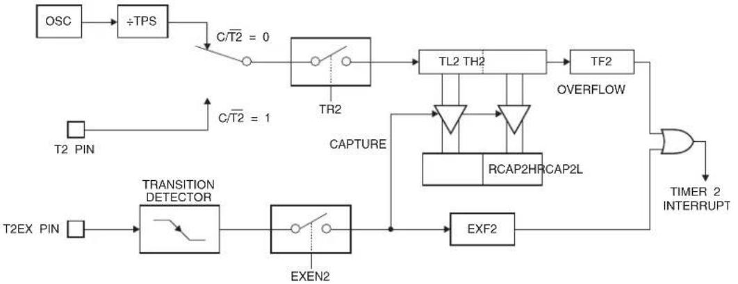
flowchart
graph TD
    A["OSC"] --> B["÷TPS"]
    B --> C["C/T2 = 0"]
    C --> D["TR2"]
    D --> E["TL2 TH2"]
    E --> F["TF2"]
    F --> G["OVERFLOW"]
    G --> H["TIMER 2 INTERRUPT"]
    I["T2 PIN"] --> J["TRANSITION DETECTOR"]
    K["T2EX PIN"] --> L["ExEN2"]
    M["C/T2 = 1"] --> N["CAPTURE"]
    N --> O["RCAP2HRCAP2L"]
    O --> P["EXF2"]
    P --> Q["Timer 2 INTERRUPT"]
12.3 Auto-Reload Mode
Timer 2 can be programmed to count up or down when configured in its 16-bit auto-reload mode. This feature is invoked by the DCEN (Down Counter Enable) bit located in the SFR T2MOD (see Table 12-4). Upon reset, the DCEN bit is set to 0 so that timer 2 will default to count up. When DCEN is set, Timer 2 can count up or down, depending on the value of the T2EX pin. The overflow and reload values depend on the Timer 2 Count Mode bits, T2CM_1 - 0 in T2MOD. A summary of the Auto-Reload behaviors is listed in Table 12-5.
Table 12-5. Summary of Auto-Reload Modes
| T2CM _1-0 | DCEN T2EX Direction Behavior | |||
| 00 0 X Up | reload to BOTTOM | BOTTOM →MAX | ||
| 00 | 1 | 0 | Down | MAX →BOTTOM underflow to MAX |
| 00 1 1 | Up overflow to BOTTOM | BOTTOM →MAX | ||
| 01 0 X Up | reload to MIN | MIN →TOP | ||
| 01 | 1 | 0 | Down | TOP →MIN underflow to TOP |
| 01 1 1 | Up | overflow | MIN →TOP | |
| 10 | X | X | Up-Down | MIN →TOP →MIN and repeat |
| 11 | X | X | Up-Down | MIN →TOP →MIN and repeat |
12.3.1 Up Counter
Figure 12-2 shows Timer 2 automatically counting up when DCEN = 0 and T2CM _1-0 = 00B. In this mode Timer 2 counts up to MAX and then sets the TF2 bit upon overflow. The overflow also causes the timer registers to be reloaded with BOTTOM, the 16-bit value in RCAP2H and RCAP2L. If EXEN2 = 1, a 16-bit reload can be triggered either by an overflow or by a 1-to-0 transition at external input T2EX. This transition also sets the EXF2 bit. Both the TF2 and EXF2 bits can generate an interrupt. The Timer 2 overflow rate for this mode is given in the following equation:
$$ \begin{array}{l} \text {Auto - Reload Mode:} \ \mathrm{DCEN} = 0, \mathrm{T2CM} = 0 0 \mathrm{B} \end{array} \quad \text {Time - out Period} = \frac {6 5 5 3 6 - {\mathrm{RCAP2H} , \mathrm{RCAP2L} }}{\text {Oscillator Frequency}} \times (\mathrm{TPS} + 1) $$
Timer 2 may also be configured to count from MIN to TOP instead of BOTTOM to MAX by setting T2CM _1-0 = 01B. In this mode Timer 2 counts up to TOP, the 16-bit value in RCAP2H and
RCAP2L and then overflows. The overflow sets TF2 and causes the timer registers to be reloaded with MIN. If EXEN2 = 1, a 1-to-0 transition on T2EX will clear the timer and set EXF2. The Timer 2 overflow rate for this mode is given in the following equation:
$$ \begin{array}{l} \text {Auto - Reload Mode:} \ \mathrm{DCEN} = 0, \mathrm{T2CM} = 0 1 \mathrm{B} \end{array} \quad \text {Time - out Period} = \frac {\text {RCAP2H RCAP2L} {\text {Oscillator Frequency}}{\times (\mathrm{TPS} + 1)} \tag {1} $$
Timer 2 Count Mode 1 is provided to support variable precision asymmetrical PWM in the CCA. The value of TOP stored in RCAP2H and RCAP2L is double-buffered such that a new TOP value takes affect only after an overflow. The behavior of Count Mode 0 versus Count Mode 1 is shown in Figure 12-3.
Figure 12-2. Timer 2 Diagram: Auto-Reload Mode (DCEN = 0)
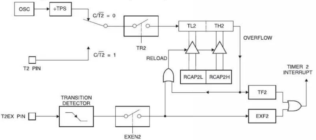
flowchart
graph TD
    A["OSC"] --> B["÷TPS"]
    B --> C["C/T2 = 0"]
    C --> D["TR2"]
    D --> E["TL2"]
    E --> F["TH2"]
    F --> G["OVERFLOW"]
    H["T2 PIN"] --> I["C/T2 = 1"]
    I --> J["TRANSITION DETECTOR"]
    J --> K["EXEN2"]
    K --> L["RELOAD"]
    L --> M["RCAP2L"]
    L --> N["RCAP2H"]
    M --> O["TF2"]
    N --> P["EXF2"]
    O --> Q["TIMER 2 INTERRUPT"]
    P --> Q
    Q --> R["T2EX PIN"]
Figure 12-3. Timer 2 Waveform: Auto-Reload Mode (DCEN = 0)

12.3.2 Up or Down Counter
Setting DCEN = 1 enables Timer 2 to count up or down, as shown in Figure 12-4. In this mode, the T2EX pin controls the direction of the count (if EXEN2 = 1). A logic 1 at T2EX makes Timer 2 count up. When T2CM _1-0 = 00B, the timer will overflow at MAX and set the TF2 bit. This overflow also causes BOTTOM, the 16-bit value in RCAP2H and RCAP2L, to be reloaded into the timer
registers, TH2 and TL2, respectively. A logic 0 at T2EX makes Timer 2 count down. The timer underflows when TH2 and TL2 equal BOTTOM, the 16-bit value stored in RCAP2H and RCAP2L. The underflow sets the TF2 bit and causes MAX to be reloaded into the timer registers. The EXF2 bit toggles whenever Timer 2 overflows or underflows and can be used as a 17th bit of resolution. In this operating mode, EXF2 does not flag an interrupt.
When T2EX = 1 and T2CM _1-0 = 01B, the timer will overflow at TOP and set the TF2 bit. This overflow also causes MIN to be reloaded into the timer registers. A logic 0 at T2EX makes Timer 2 count down. The timer underflows when TH2 and TL2 equal MIN. The underflow sets the TF2 bit and causes TOP to be reloaded into the timer registers. The behavior of Count Mode 0 versus Count Mode 0 when DCEN is enabled is shown in Figure 12-6.
Figure 12-4. Timer 2 Diagram: Auto-Reload Mode (T2CM _1-0 = 00B, DCEN = 1)

flowchart
graph TD
    A["OSC"] --> B["÷TPS"]
    B --> C["C/T2 = 0"]
    C --> D["TR2"]
    D --> E["TL2"]
    E --> F["TH2"]
    F --> G["TOGGLE"]
    G --> H["EXF2"]
    I["T2 PIN"] --> J["C/T2 = 1"]
    J --> K["UP COUNTING"]
    K --> L["RCAP2L"]
    K --> M["RCAP2H"]
    N["(DOWN COUNTING RELOAD VALUE)"] --> O["0FFH"]
    N --> P["0FFH"]
    Q["(UP COUNTING RELOAD VALUE)"] --> R["OVERFLOW"]
    S["T2EX PIN"] --> T["Count DIRECTION 1=UP 0=DOWN"]
    U["TIF2"] --> V["TIMER 2 INTERRUPT"]
    W["TOGGLE"] --> X["EXF2"]
The timer overflow/underflow rate for up-down counting mode is the same as for up counting mode, provided that the count direction does not change. Changes to the count direction may result in longer or shorter periods between time-outs.
Figure 12-5. Timer 2 Diagram: Auto-Reload Mode (T2CM _1-0 = 01B, DCEN = 1)

flowchart
graph TD
    OSC --> ÷TPS
    ÷TPS --> C/T2["0"]
    C/T2 --> TR2
    TR2 --> TL2
    TL2 --> TH2
    TH2 --> OVERFLOW
    OVERFLOW --> TOGGLE
    TOGGLE --> EXF2
    TF2 --> TIMER2["TIMER 2 INTERRUPT"]
    TIME2["T2 PIN"] --> C/T2["1"]
    C/T2["0"] --> C/T2["0"]
    C/T2["0"] --> T2EX["T2EX PIN"]
    C/T2["0"] --> RCAP2L["RCAP2L"]
    C/T2["0"] --> RCAP2H["RCAP2H"]
    TL2 --> COUNT["COUNTING"]
    TL2 --> RELOAD["RELOAD VALUE"]
    TH2 --> COUNT["COUNTING"]
    TH2 --> RELOAD["RELOAD VALUE"]
    COUNT --> COUNTDIRECTION["1=UP"]
    COUNTDIRECTION["1=UP"]
    COUNTDIRECTION["1=UP"]
    COUNTDIRECTION["1=UP"]
    COUNTDIRECTION["1=UP"]
    COUNTDIRECTION["1=UP"]
    COUNTDIRECTION["1=UP"]
    COUNTDIRECTION["1=UP"]
    COUNTDIRECTION["1=UP"]
    COUNTDIRECTION["1=UP"]
    COUNTDIRECTION["1=UP"]
    COUNTDIRECTION["1=UP"]
    TREX["TR2"] --> TR2
    TR2 --> TL2
    TL2 --> TH2
    TH2 --> OVERFLOW
    OVERFLOW --> TOGGLE
Figure 12-6. Timer 2 Waveform: Auto-Reload Mode (DCEN = 1)
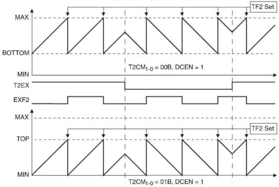
other
| Signal | Value | |--------|-------| | TOP | MAX | | EXF2 | MAX | | T2EX | MAX | | BOTTOM | MAX | | T2CM₁₋₀ | 00B | | DCEN | 1 | | TF2 Set| TF2 Set| | T2CM₁₋₀ | 01B | | DCEN | 1 |12.3.3 Dual Slope Counter
When Timer 2 Auto-Reload Mode uses Count Mode 2 (T2CM 1-0 = 10B) or Count Mode 3 (T2CM 1-0 = 11B), the timer operates in a dual slope fashion. The timer counts up from MIN to TOP and then counts down from TOP to MIN, following a sawtooth waveform as shown in Figure 12-7. The EXF2 bit is set/cleared by hardware to reflect the current count direction (Up = 0 and Down = 1). The value of TOP stored in RCAP2H and RCAP2L is double-buffered such that a new TOP value takes affect only after an underflow. The only difference between Mode 2 and Mode 3 is when the interrupt flag is set. In Mode 2 TF2 is set once per count period when the timer underflows at MIN. In Mode 3 TF2 is set twice per count period, once when the timer overflows at TOP and once when the timer underflows at MIN. The interrupt service routine can check the EXF2 bit to determine if TF2 was set at TOP or MIN. These count modes are provided to support variable precision symmetrical PWM in the CCA. DCEN has no effect when using dual slope operation. The Timer 2 overflow rate for this mode is given in the following equation:
$$ \begin{array}{l} \text {Auto - Reload Mode:} \ \mathrm{DCEN} = 0, \mathrm{T2CM} = 1 0 \mathrm{B} \end{array} \quad \text {Time - out Period} = \frac {\mathrm{RCAP2HRCAP2L} {\mathrm{OscillatorFrequency}}{\times (\mathrm{TPS} + 1)} \tag {1} $$
Figure 12-7. Timer 2 Waveform: Dual Slope Modes

line
| Waveform | Peak Position | Label | |----------|---------------|--------------| | Top | T2CM₁₋₀ = 10B | T2CM₁₋₀ = 10B | | MIN | | | | EXF₂ | | | | Top | T2CM₁₋₀ = 11B | T2CM₁₋₀ = 11B | | MIN | | |12.4 Baud Rate Generator
Timer 2 is selected as the baud rate generator by setting TCLK and/or RCLK in T2CON (Table 12-3). Note that the baud rates for transmit and receive can be different if Timer 2 is used for the receiver or transmitter and Timer 1 is used for the other function. Setting RCLK and/or TCLK puts Timer 2 into its baud rate generator mode, as shown in Figure 12-8.
The baud rate generator mode is similar to the auto-reload mode, in that a rollover in TH2 causes the Timer 2 registers to be reloaded with the 16-bit value in registers RCAP2H and RCAP2L, which are preset by software.
The baud rates in UART Modes 1 and 3 are determined by Timer 2's overflow rate according to the following equation.
$$ \text { Modes 1 and 3 Baud Rates } \quad \frac {\text { Timer 2 Overflow Rate }}{1 6} = $$
The Timer can be configured for either timer or counter operation. In most applications, it is configured for timer operation (CP/T2 = 0). The baud rate formulas are given below.
$$ \mathrm{T2CM} = 0 0 \mathrm{B} \quad \begin{array}{l} \text {Modes 1,3} \ \text {Baud Rate} \end{array} = \frac {\text {Oscillator Frequency}}{1 6 \times (\mathrm{TPS} + 1) \times [ 6 5 5 3 6 - (\mathrm{RCAP2H} , \mathrm{RCAP2L}) ]} $$
$$ \mathrm{T2CM} = 0 1 \mathrm{B} \quad \begin{array}{l} \text { Modes 1,3 } \ \text { Baud Rate } \end{array} = \frac {\text { Oscillator Frequency }}{1 6 \times (\mathrm{TPS} + 1) \times [ (\mathrm{RCAP2H} , \mathrm{RCAP2L}) + 1 ]} $$
where (RCAP2H, RCAP2L) is the content of RCAP2H and RCAP2L taken as a 16-bit unsigned integer.
Timer 2 as a baud rate generator is shown in Figure 12-8. This figure is valid only if RCLK or TCLK = 1 in T2CON. Note that a rollover in TH2 does not set TF2 and will not generate an interrupt. Note too, that if EXEN2 is set, a 1-to-0 transition in T2EX will set EXF2 but will not cause a reload from (RCAP2H, RCAP2L) to (TH2, TL2). Thus when Timer 2 is in use as a baud rate gen-
erator, T2EX can be used as an extra external interrupt. Also note that the Baud Rate and Frequency Generator modes may be used simultaneously.
Figure 12-8. Timer 2 in Baud Rate Generator Mode
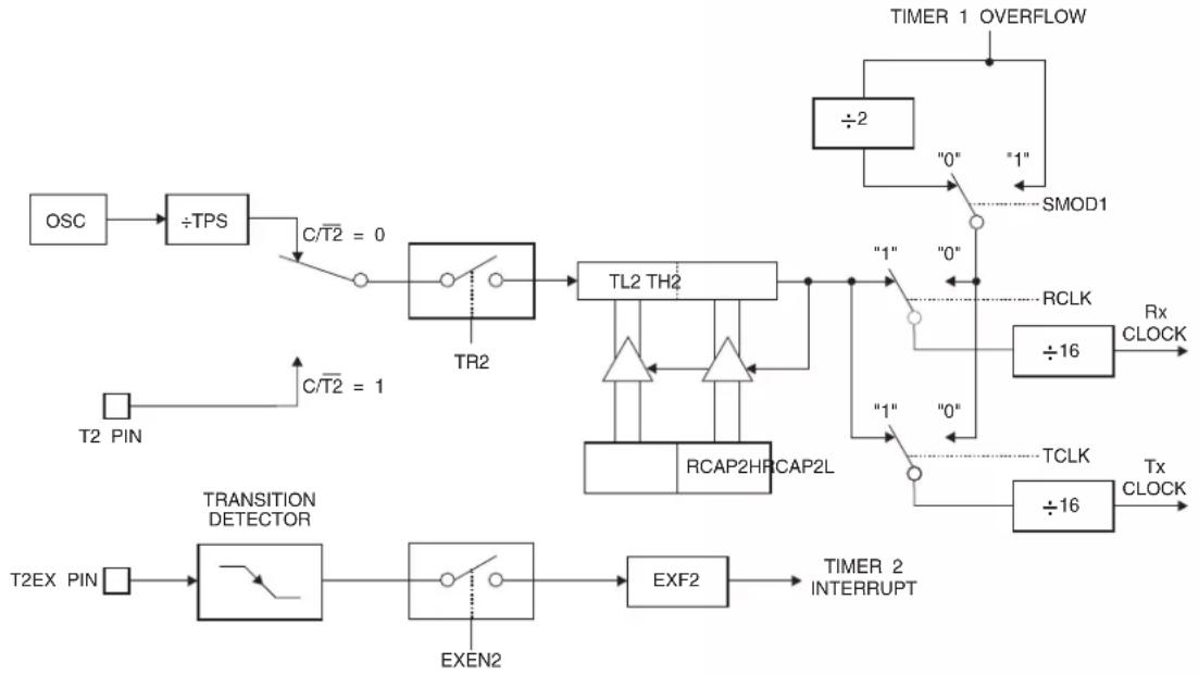
flowchart
graph TD
    A["OSC"] --> B["÷TPS"]
    B --> C["C/T2 = 0"]
    C --> D["TR2"]
    D --> E["TL2 TH2"]
    E --> F["RCAP2HRCAP2L"]
    F --> G["TX CLOCK"]
    H["T2 PIN"] --> I["C/T2 = 1"]
    I --> J["TRANSITION DETECTOR"]
    J --> K["EXEN2"]
    K --> L["EXF2"]
    L --> M["TIMER 2 INTERRUPT"]
    N["TIMER 1 OVERFLOW"] --> O["÷2"]
    O --> P["0"]
    P --> Q["1"]
    Q --> R["SMOD1"]
    S["RCLK"] --> T["÷16"]
    T --> U["Rx CLOCK"]
    V["TCLK"] --> W["÷16"]
    W --> X["Tx CLOCK"]
12.5 Frequency Generator (Programmable Clock Out)
Timer 2 can generate a 50% duty cycle clock on T2 (P1.0), as shown in Figure 12-9. This pin, besides being a regular I/O pin, has two alternate functions. It can be programmed to input the external clock for Timer/Counter 2 or to toggle its output at every timer overflow. To configure the Timer/Counter 2 as a clock generator, bit C/T2 (T2CON.1) must be cleared and bit T2OE (T2MOD.1) must be set. Bit TR2 (T2CON.2) starts and stops the timer.
The clock-out frequency depends on the oscillator frequency and the reload value of Timer 2 capture registers (RCAP2H, RCAP2L), as shown in the following equations.
$$ \mathrm{T2CM} = 0 0 \mathrm{B} \quad \text { Clock Out Frequency } \quad \frac {\text { Oscillator Frequency }}{2 \times [ 6 5 5 3 6 - (\mathrm{RCAP2H} , \mathrm{RCAP2L}) ]} \times = \frac {1}{\mathrm{TPS1+}} $$
$$ \mathrm{T2CM} = 0 1 \mathrm{B} \quad \text { Clock Out Frequency } = \frac {\text { Oscillator Frequency }}{2 \times [ (\mathrm{RCAP2H} , \mathrm{RCAP2L}) + 1 ]} \times \frac {1}{\mathrm{TPS1+}} $$
In the frequency generator mode, Timer 2 roll-overs will not generate an interrupt. This behavior is similar to when Timer 2 is used as a baud-rate generator. It is possible to use Timer 2 as a baud-rate generator and a clock generator simultaneously. Note, however, that the baud-rate and clock-out frequencies cannot be determined independently from one another since they both use RCAP2H and RCAP2L.
Figure 12-9. Timer 2 in Clock-out Mode
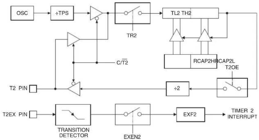
flowchart
graph TD
    OSC --> ÷TPS
    ÷TPS --> OR1
    OR1 --> TR2
    TR2 --> TL2_TH2
    TL2_TH2 --> RCAP2HRCAP2L
    RCAP2HRCAP2L --> T2OE
    T2OE --> ÷2
    ÷2 --> TRANSITION_DETECTOR
    TRANSITION_DETECTOR --> EXEN2
    EXEN2 --> EXF2
    EXF2 --> TIMER_2_INTERRUPT
    T2EX_PIN --> TRANSITION_DETECTOR
    T2_PIN --> OR1
    OR1 --> C/T2
    C/T2 --> OR1
    OR1 --> TR2
    style OR1 fill:#f9f,stroke:#333
    style TRANSITION_DETECTOR fill:#ccf,stroke:#333
    style EXEN2 fill:#cfc,stroke:#333
    style EXF2 fill:#fcc,stroke:#333
13. Compare/Capture Array
The AT89LP3240/6440 includes a four channel Compare/Capture Array (CCA) that performs a variety of timing operations including input event capture, output compare waveform generation and pulse width modulation (PWM). Timer 2 serves as the time base for the four 16-bit compare/capture modules. The CCA has the following features:
• Four 16-bit Compare/Capture channels
• Common time base provided by Timer 2
- Selectable external and internal capture events including pin change, timer overflow and comparator output change
- Symmetric/Asymmetric PWM with selectable polarity
• Multi-phasic PWM outputs
• One interrupt flag per channel with a common interrupt vector
The block diagram of the CCA is given in Figure 13-1. Each channel consists of an 8-bit control register and a 16-bit data register. The channel registers are not directly accessible. The CCA address register T2CCA provides an index into the array. The control, data low and data high bytes of the currently indexed channel are accessed through the T2CCC, T2CCL and T2CCH registers respectively.
Each channel can be individually configured for capture or compare mode. Capture mode is the default setting. During capture mode the current value of the time base is copied into the channel's data register when the specified external or internal event occurs. An interrupt flag is set at the same time and the time base may be optionally cleared. To enable compare mode, the CCMx bit in the channel's control register (CCCx) should be set to 1. In compare mode an interrupt flag is set and an output pin is optionally toggled when the value of the time base matches the value of the channel's data register. The time base may also be optionally cleared on a compare match.
Timer 2 must be running (TR2 = 1) in order to perform captures or compares with the CCA. However, when TR2 = 0 the external capture events will still set their associated flags and may be used as additional external interrupts.
Figure 13-1. Compare/Capture Array Block Diagram
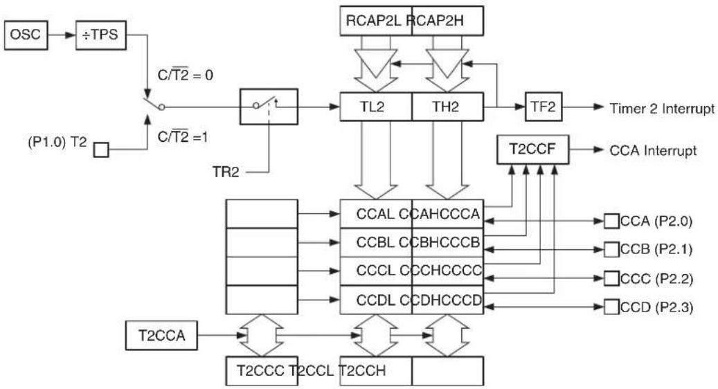
flowchart
graph TD
    OSC --> ÷TPS
    ÷TPS --> C/T2 = 0
    C/T2 = 0 --> TR2
    TR2 --> TL2
    TR2 --> TH2
    TL2 --> TF2
    TH2 --> TF2
    TF2 --> Timer2 Interrupt
    TF2 --> T2CCF
    T2CCF --> CCA Interrupt
    T2CCF --> CCAL CCAHCCCA
    T2CCF --> CCBL CCBHCCCB
    T2CCF --> CCCL CCHCCCCC
    T2CCF --> CCDL CCDHCCCD
    T2CCF --> T2CCT2CCL T2CCH
    T2CCT2CCL T2CCH --> T2CCA
    T2CCA --> T2CCC
    T2CCC --> CCAL CCAHCCCA
    T2CCC --> CCBL CCBHCCCB
    T2CCC --> CCCL CCHCCCCC
    T2CCC --> CCDL CCDHCCCD
    T2CCF --> T2CCT2CCL T2CCH
    T2CCT2CCL T2CCH --> CCAL CCAHCCCA
    T2CCT2CCL T2CCH --> CCBL CCBHCCCB
    T2CCT2CCL T2CCH --> CCCL CCHCCCCC
    T2CCT2CCL T2CCH --> CCDL CCDHCCCD
    T2CCT2CCL T2CCH --> CCAL CCAHCCCA
    T2CCT2CCL T2CCH --> CCBL CCBHCCCB
    T2CCT2CCL T2CCH --> CCCL CCHCCCCC
    T2CCT2CCL T2CCH --> CCDL CCDHCCCD
    T2CCT2CCL T2CCH --> CCAL CCAAHCCCA
    T2CCT2CCL T2CCH --> CCBL CCAHCCCA
    T2CCT2CCL T2CCH --> CCCL CCAHCCCA
    T2CCT2CCL T2CCH --> CCDL CCAHCCCA
    T2CCT2CCL T2CCH --> CCAL CCAHCCCA
    T2CCT2CCL T2CCH --> CCBL CCAHCCCA
    T2CCT2CCL T2CCH --> CCCL CCAHCCCA
    T2CCT2CCL T2CCH --> CCDL CCAHCCCA
    T2CCT2CCL T2CCH --> CCAL CCAHCCCA
    T2CCT2CCL T2C CH
13.1 CCA Registers
The Compare/Capture Array has five Special Function Registers: T2CCA, T2CCC, T2CCL, T2CCH and T2CCF. The T2CCF register contains the interrupt flags for each CCA channel. The CCA interrupt is a logic OR of the bits in T2CCF. The flags are set by hardware when a compare/capture event occurs on the relevant channel and must be cleared by software. The T2CCF bits will only generate an interrupt when the ECC bit (IE2.1) is set and the CIENx bit in the associated channel's CCCx register is set.
The T2CCC, T2CCL and T2CCH register locations are not true SFRs. These locations represent access points to the contents of the array. Writes/reads to/from the T2CCC, T2CCL and T2CCH locations will access the control, data low and data high bytes of the CCA channel currently selected by the index in T2CCA. Channels currently not indexed by T2CCA are not accessible.
When writing to T2CCH, the value is stored in a shadow register. When T2CCL is written, the 16-bit value formed by the contents of T2CCL and the T2CCH shadow is written into the array. Therefore, T2CCH must be written prior to writing T2CCL. All four channels use the same T2CCH shadow register. If the value of T2CCH remains constant for multiple writes, there is no need to update T2CCH between T2CCL writes. Every write to T2CCL will use the last value of T2CCH for the upper data byte. It is not possible to write to the data register of a channel configured for capture mode.
The configuration bits for each channel are stored in the CCCx registers accessible through T2CCC. See Table 13-5 on page 74 for a description of the CCCx register.
Table 13-1. T2CCA – Timer/Counter 2 Compare/Capture Address
| T2CCA Address = 0D1H Reset Value = xxxx xx00BNot Bit Addressable | ||||||||
| — | — | — | — | — | — | T | 2 | |
| B | i | t | 7 | 6 | 5 | 4 | 3 | 2 |
| Symbol Function | ||||||||
| T2CCA[1-0] | Compare/Capture Address. Selects which CCA channel is currently accessible through the T2CCH, T2CCL and T2CCC registers. Only one channel may be accessed at a time.T2CCA1 T2CCA0 Channel | |||||||
| 0 | 0 | A – T2CCH, T2CCL and T2CCC access data and control for Channel A | ||||||
| 0 | 1 | B – T2CCH, T2CCL and T2CCC access data and control for Channel B | ||||||
| 1 | 0 | C – T2CCH, T2CCL and T2CCC access data and control for Channel C | ||||||
| 1 | 1 | D – T2CCH, T2CCL and T2CCC access data and control for Channel D | ||||||
Table 13-2. T2CCH – Timer/Counter 2 Compare/Capture Data High
| T2CCH Address = 0D2H Reset Value = 0000 0000BNot Bit Addressable | ||||||||
| T2CCD.15 | T2CCD.14 | T2CCD.13 | T2CCD.12 | T2CCD.11 | T2CCD.10 | T2CCD.9 | T2CCD.8 | |
| B | i | t | 7 | 6 | 5 | 4 | 3 | 2 |
| Symbol Function | ||||||||
| T2CCD[15-8] | Compare/Capture Data (High Byte). Reads from T2CCH will return the high byte from the CCA channel currently selected by T2CCA. The high byte of the selected CCA channel will be updated with the contents of T2CCH when T2CCL is written. When writing multiple channels with the same high byte, T2CCH need not be updated between writes to T2CCL. | |||||||
Note: All writes/reads to/from T2CCH will access channel X as currently selected by T2CCA. The data registers for the remaining unselected channels are not accessible.
Table 13-3. T2CCL – Timer/Counter 2 Compare/Capture Data Low
| T2CCC Address = 0D3H Reset Value = 0000 0000BNot Bit Addressable | ||||||||
| T2CCD.7 | T2CCD.6 | T2CCD.5 | T2CCD.4 | T2CCD.3 | T2CCD.2 | T2CCD.1 | T2CCD.0 | |
| B | i | t | 7 | 6 | 5 | 4 | 3 | 2 |
| Symbol Function | ||||||||
| T2CCD[7-0] | Compare/Capture Data (Low Byte). Reads from T2CCL will return the low byte from the CCA channel currently selected by T2CCA. Writes to T2CCL will update the selected CCA channel with the 16-bit contents of T2CCH and T2CCL. | |||||||
Note: All writes/reads to/from T2CCL will access channel X as currently selected by T2CCA. The data registers for the remaining unselected channels are not accessible.
Table 13-4. T2CCF – Timer/Cou nter 2 Compare/Capture Flags
| T2CCF Address = 0D5H Reset Value = XXXX 0000BNot Bit Addressable | ||||||||
| - - - - | CCFD CCFC C | CFB CCFA | ||||||
| B | i | t | 7 | 6 | 5 | 4 | 3 | 2 |
| Symbol Function | ||||||||
| CCFD | Channel D Compare/Capture Interrupt Flag. Set by a compare/capture event on channel D. Must be cleared by software.CCFD will generate an interrupt when CIEND = 1 and ECC = 1. | |||||||
| CCFC | Channel C Compare/Capture Interrupt Flag. Set by a compare/capture event on channel C. Must be cleared bysoftware. CCFC will generate an interrupt when CIENC = 1 and ECC = 1. | |||||||
| CCFB | Channel B Compare/Capture Interrupt Flag. Set by a compare/capture event on channel B. Must be cleared by software.CCFB will generate an interrupt when CIENB = 1 and ECC = 1. | |||||||
| CCFA | Channel A Compare/Capture Interrupt Flag. Set by a compare/capture event on channel A. Must be cleared by software.CCFA will generate an interrupt when CIENA = 1 and ECC = 1. | |||||||
13.2 Input Capture Mode
The Compare/Capture Array provides a variety of capture modes suitable for time-stamping events or performing measurements of pulse width, frequency, slope, etc. CCA channels are configured for capture mode by clearing the CCMx bit in the associated CCCx register to 0. Each time a capture event occurs, the contents of Timer 2 (TH2 and TL2) are transferred to the 16-bit data register of the corresponding channel, and the channel's interrupt flag CCFx is set in T2CCF. Optionally, the capture event may also clear Timer 2 to 0000H by setting the CTCx bit in CCCx. The capture event is defined by the CxM_2 - 0 bits in CCCx and may be either externally or internally generated. A diagram of a CCA channel in capture mode is shown in Figure 13-2.
Figure 13-2. CCA Capture Mode Diagram
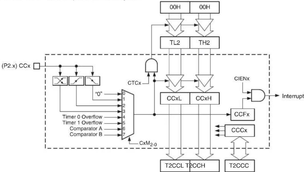
flowchart
graph TD
    A["(P2.x) CCx"] --> B["Flip-Flop 0"]
    A --> C["Flip-Flop 1"]
    A --> D["Flip-Flop 2"]
    A --> E["Flip-Flop 3"]
    A --> F["Flip-Flop 4"]
    A --> G["Comparator A"]
    A --> H["Comparator B"]
    B --> I["0"]
    C --> J["0"]
    D --> K["0"]
    E --> L["0"]
    F --> M["0"]
    G --> N["0"]
    H --> O["0"]
    I --> P["AND Gate"]
    J --> P
    K --> P
    L --> P
    M --> P
    N --> P
    O --> P
    P --> Q["CCxL"]
    P --> R["CCxH"]
    Q --> S["T2CCL"]
    R --> T["T2CCH"]
    S --> U["T2CCC"]
    T --> U
    U --> V["Interrupt"]
    W["00H"] --> X["TL2"]
    Y["00H"] --> Z["TH2"]
    X --> AA["AND Gate"]
    Z --> AB["AND Gate"]
    AA --> AC["CCxL"]
    AB --> AD["CCxH"]
    AC --> AE["CIENx"]
    AD --> AF["CIENx"]
    AE --> AG["CCFx"]
    AF --> AH["CCFx"]
    AG --> AI["CCCx"]
    AH --> AJ["CCCx"]
    AI --> AK["T2CCC"]
    AJ --> AL["T2CCC"]
Each CCA channel has an associated external capture input pin: CCA (P2.0), CCB (P2.1), CCC (P2.2) and CCD (P2.3). External capture events are always edge-triggered and can be selected
to occur at a negative edge, positive edge, or both (toggle). Capture inputs are sampled every clock cycle and a new value must be held for at least 2 clock cycles to be correctly sampled by the device. The maximum achievable capture rate will be determined by how fast the software can retrieve the captured data. There is no protection against capture events overrunning the data register.
Capture events may also be triggered internally by the overflows of Timer 0 or Timer 1, or by an event from the dual analog comparators. Any comparator event which can generate a comparator interrupt may also be used as a capture event. However, Timer 2 should not be selected as the comparator clock source when using the comparator as the capture trigger.
When the DAC output is enabled on P2.2 and P2.3, channels C and D cannot use their external pin capture modes. However, those channels may still use the timer or comparator triggers to capture data. The same applies for all four channels when Port 2 is used for the external memory interface.
13.2.1 Timer 2 Operation for Capture Mode
Capture channels are intended to work with Timer 2 in capture mode CP/RL2 = 1. Captures can still occur when Timer 2 operates in other modes; however, the full 16-bit count range may not be available. The TF2 flag can be used to determine if the timer overflowed before the capture occurred. If the timer is operating in dual-slope mode (CP/RL2 = 0, T2G.M=1xB), the count direction (Up = 0 and Down = 1) at the time of the event will be captured into the channel's CDIRx bit in CCCx. CTCx must be cleared to 0 for all channels if Timer 2 is operating in Baud Rate mode or errors may occur in the serial communication.
Table 13-5. T2CCC – Timer/Counter 2 Compare/Capture Control
| T2CCC Address = 0D4H Reset Value = 00X0 0000BNot Bit Addressable | ||||||||
| CIENx | CDIRx | - | CTCx | CCMx | CxM2 | CxM1 | CxM0 | |
| B | i | t | 7 | 6 | 5 | 4 | 3 | 2 |
| Symbol | Function | |||||||
| CIENx | Channel X Interrupt Enable. When set, channel X's interrupt flag, CCFx in T2CCF, will generate an interrupt when ECC = 1. Clear to disable interrupts from channel X. | |||||||
| CDIRx | Channel X Capture Direction. In dual-slope modes, a compare/capture event on channel X will store the current count direction into CDIRx. Up-counting = 0 and down-counting = 1. Modifying this bit has no effect. | |||||||
| CTCx | Clear Timer on Compare/Capture of Channel X. When set, the Timer 2 registers TL2 and TH2 will be cleared by a compare/capture event on channel X. When cleared, Timer 2 is unaffected by channel X events. | |||||||
| CCMx | Channel X Compare/Capture Mode. When CCMx = 1, channel X operates in compare mode. When CCMx = 0, channel X operates in capture mode. | |||||||
| CxM[2-0] | Channel X Mode. Selects the output/input events for compare/capture channel X.CxM2 CxM1 CxM0 Capture Event (CCMx = 0)0 0 0 Disabled0 0 1 Trigger on negative edge of CCx pin0 1 0 Trigger on positive edge of CCx pin0 1 1 Trigger on either edge of CCx pin1 0 0 Trigger on Timer 0 overflow1 0 1 Trigger on Timer 1 overflow1 1 0 Trigger on Analog Comparator A Event(2)1 1 1 Trigger on Analog Comparator B Event(3) | |||||||
| CxM2 | CxM1 | CxM0 | Compare Action (CCMx = 1)Output disabled (interrupt only)0 0 1 Set CCx pin on compare match0 1 0 Clear CCx pin on compare match0 1 1 Toggle CCx pin on compare match1 0 0 Inverting Pulse Width Modulation(4)1 0 1 Non-Inverting Pulse Width Modulation(4)1 1 0 Reserved1 1 1 Reserved | |||||
Notes: 1. All writes/reads to/from T2CCC will access channel X as currently selected by T2CCA. The control registers for the remaining unselected channels are not accessible.
2. Analog Comparator A events are determined by the CMA 2-0 bits in ACSRA. See Table 19-1 on page 130.
3. Analog Comparator B events are determined by the CMB2-0 bits in ACSRB. See Table 19-2 on page 131.
4. Asymmetrical versus Symmetrical PWM is determined by the Timer 2 Count Mode. See Section 13.4 on page 77.
13.3 Output Compare Mode
The Compare/Capture Array provides a variety of compare modes suitable for event timing or waveform generation. CCA channels are configured for compare mode by setting the CCMx bit in the associated CCCx register to 1. A compare event occurs when the 16-bit contents of a channel's data register match the contents of Timer 2 (TH2 and TL2). The compare event also sets the channel's interrupt flag CCFx in T2CCF and may optionally clear Timer 2 to 0000H if the CTCx bit in CCCx is set. A diagram of a CCA channel in compare mode is shown in Figure 13-3.
Figure 13-3. CCA Compare Mode Diagram
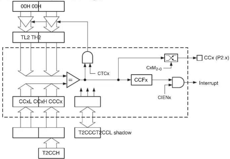
flowchart
graph TD
    A["00H 00H"] --> B["TL2 TH2"]
    B --> C["="]
    C --> D["CCxL CCxH CCCx"]
    C --> E["T2CCCT2CCL shadow"]
    F["CCxL CCxH CCCx"] --> C
    G["T2CCCT2CCL shadow"] --> C
    H["TCX"] --> I["AND"]
    I --> J["CCFx"]
    J --> K["×"]
    L["CxM2-0"] --> J
    M["CIENx"] --> N["AND"]
    N --> O["Interrupt"]
    P["CCx (P2.x)"] --> Q["Output"]
    R["T2CCH"] --> S["Output"]
13.3.1 Waveform Generation
Each CCA channel has an associated external compare output pin: CCA (P2.0), CCB (P2.1), CCC (P2.2) and CCD (P2.3). The CxM_2-0 bits in CCCx determine what action is taken when a compare event occurs. The output pin may be set to 1, cleared to 0 or toggled. Output actions take place even if the interrupt is disabled; however, the associated I/O pin must be set to the desired output mode before the compare event occurs. The state of the compare outputs are initialized to 1 by reset. Channels C and D cannot use their output pin when the DAC is enabled. These channels may still be used to generate interrupts or to clear the timebase. The same applies to all four channels when Port 2 is used for the external memory interface.
Multiple compare events per channel can occur within a single time period, provided that the software has time to update the compare value before the timer reaches the next compare point. In this case other interrupts should be disabled or the CCA interrupt given a higher priority in order to ensure that the interrupt is serviced in time.
A wide range of waveform generation configurations are possible using the various operating modes of Timer 2 and the CCA. Some example configurations are detailed below. Pulse width modulation is a special case of output compare. See Section 13.4 on page 77 for more details of PWM operation.
13.3.1.1 Normal Mode
The simplest waveform mode is when CP/RL2 = 0 and T2CM1-0 = 01B. In this mode the frequency of the output is determined by the TOP value stored in RCAP2L and RCAP2H and output edges occur at fractions of the timer period. Figure 13-4 shows an example of outputting two waveforms of the same frequency but different phase by using the toggle on match action. More complex waveforms are achieved by changing the TOP value and the compare values more frequently.
Figure 13-4. Normal Mode Waveform Example
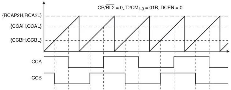
line
| Signal | Value | |-----------------|-------| | {RCAP2H,RCA2L} | 1 | | {CCAH,CCAL} | 0 | | {CCBH,CCBL} | 1 |13.3.1.2 Clear-Timer-on-Compare Mode
Clear-Timer-on-Compare (CTC) mode occurs when the CTCx bit of a compare channel is set to one. CTC Mode works best when Timer 2 is in capture mode (CP/RL2 = 1) to allow the full range of compare values. In CTC Mode the compare value defines the interval between output events because the timer is cleared after every compare match. Figure 13-5 shows an example waveform using the toggle on match action in CTC Mode.
Figure 13-5. CTC Mode Waveform Example
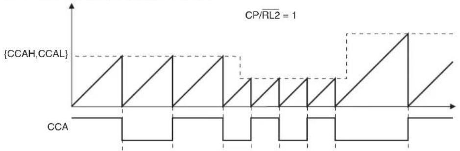
line
| Time | {CCAH,CCAL} | |------|-------------| | 0 | 0 | | 1 | 1 | | 2 | 0 | | 3 | 1 | | 4 | 0 | | 5 | 1 | | 6 | 0 | | 7 | 1 | | 8 | 0 | | 9 | 1 | | 10 | 0 | | 11 | 1 | | 12 | 0 | | 13 | 1 | | 14 | 0 | | 15 | 1 | | 16 | 0 | | 17 | 1 | | 18 | 0 | | 19 | 1 | | 20 | 0 | | 21 | 1 | | 22 | 0 | | 23 | 1 | | 24 | 0 | | 25 | 1 | | 26 | 0 | | 27 | 1 | | 28 | 0 | | 29 | 1 | | 30 | 0 | | 31 | 1 | | 32 | 0 | | 33 | 1 | | 34 | 0 | | 35 | 1 | | 36 | 0 | | 37 | 1 | | 38 | 0 | | 39 | 1 | | 40 | 0 | | 41 | 1 | | 42 | 0 | | 43 | 1 | | 44 | 0 | | 45 | 1 | | 46 | 0 | | 47 | 1 | | 48 | 0 | | 49 | 1 | | 50 | 0 | | 51 | 1 | | 52 | 0 | | 53 | 1 | | 54 | 0 | | 55 | 1 | | 56 | 0 | | 57 | 1 | | 58 | 0 | | 59 | 1 | | 60 | 0 | | 61 | 1 | | 62 | 0 | | 63 | 1 | | 64 | 0 | | 65 | 1 | | 66 | 0 | | 67 | 1 | | 68 | 0 | | 69 | 1 | | 70 | 0 | | 71 | 1 | | 72 | 0 | | 73 | 1 | | 74 | 0 | | 75 | 1 | | 76 | 0 | | 77 | 1 | | 78 | 0 | | 79 | 1 | | 80 | 0 | | 81 | 1 | | 82 | 0 | | 83 | 1 | | 84 | 0 | | 85 | 1 | | 86 | 0 | | 87 | 1 | | 88 | 0 | | 89 | 1 | | 90 | 0 | | 91 | 1 | | 92 | 0 | | 93 | 1 | | 94 | 0 | | 95 | 1 | | 96 | 0 | | 97 | 1 | | 98 | 0 | | 99 | 1 | | Note: The actual data values are not provided in the code. The code does not provide the original data to extract from the original data from the code. Therefore, the correct output is an empty string.13.3.1.3 Dual-Slope Mode
The dual-slope mode occurs when CP/RL2 = 0 and T2CM _0 = 1xB. In this mode the frequency of the output is determined by the TOP value stored in RCAP2L and RCAP2H and output edges occur at fractions of the timer period on both the up and down count. Figure 13-6 shows an example of outputting two symmetrical waveforms using the toggle on match action. More complex waveforms are achieved by changing the TOP value and the compare values more frequently.
Figure 13-6. Dual-Slope Waveform Example

line
| Signal | Value | | ------------- | ----- | | {RCAP2H,RCA2L} | 0 | | {CCAH,CCAL} | 0 | | {CCBH,CCBL} | 0 |13.3.2 Timer 2 Operation for Compare Mode
Compare channels will work with any Timer 2 operating mode. The full 16-bit compare range may not be available in all modes. In order for a compare output action to take place, the compare values must be within the counting range of Timer 2. CTCx must be cleared to 0 for all channels if Timer 2 is operating in Baud Rate mode or errors may occur in the serial communication.
13.4 Pulse Width Modulation Mode
In Pulse Width Modulation (PWM) Mode, a compare channel can output a square wave with programmable frequency and duty cycle. Setting CCMx = 1 and CxM _2-0 = 10xB enables PWM Mode. PWM Mode is similar to Output Compare Mode except that the compare value is double-buffered. A diagram of a CCA channel in PWM Mode is shown in Figure 13-7. The PWM polarity is selectable between inverting and non-inverting modes. PWM is intended for use with Timer 2 in Auto-Reload Mode (CP/RL2 = 0, DCEN = 0) using count modes 1, 2 or 3. The PWM can operate in asymmetric (edge-aligned) or symmetric (center-aligned) mode depending on the T2CM selection. The CCA PWM has variable precision from 2 to 16 bits. A trade-off between frequency and precision is made by changing the TOP value of the timer. The CCA PWM always uses the greatest precision allowable for the selected output frequency, as compared to Timer 0 and 1 whose PWMs are fixed at 8-bit precision regardless of frequency.
Figure 13-7. CCA PWM Mode Diagram

flowchart
graph TD
    A["TL2 TH2"] --> B["Comparator"]
    B --> C["="]
    C --> D["CCx (P2.x)"]
    D --> E["CxM2-0"]
    E --> F["AND"]
    F --> G["Interrupt"]
    H["CCxL CCxH CCCx"] --> I["Counter"]
    I --> J["CCFx"]
    J --> K["AND"]
    K --> L["T2CCCT2CCL"]
    M["shadow"] --> N["CCxL CCxH CCCx"]
    O["shadow"] --> P["CCxL CCxH CCCx"]
    Q["T2CCH"] --> R["CCxL CCxH CCCx"]
    S["T2CCCT2CCL"] --> T["CCx (P2.x)"]
    U["CXM2-0"] --> V["AND"]
    W["CIENx"] --> X["AND"]
    Y["T2CCCT2CCL"] --> Z["AND"]
    style A fill:#f9f,stroke:#333
    style H fill:#ccf,stroke:#333
    style Q fill:#cfc,stroke:#333
    style U fill:#fcc,stroke:#333
    style R fill:#ffc,stroke:#333
    style S fill:#fcc,stroke:#333
    style T fill:#cff,stroke:#333
    style X fill:#ffc,stroke:#333
    style Y fill:#fcc,stroke:#333
    style Z fill:#ffc,stroke:#333
13.4.1 Asymmetrical PWM
For Asymmetrical PWM, Timer 2 should be configured for Auto-Reload mode and Count Mode 1 (CP/RL2 = 0, DCEN = 0, T2CM1-0 = 01B). Asymmetrical PWM uses single slope operation as shown in Figure 13-8. The timer counts up from BOTTOM to TOP and then restarts from BOTTOM. In non-inverting mode, the output CCx is set on the compare match between Timer 2 (TL2, TH2) and the channel data register (CCxL, CCxH), and cleared at BOTTOM. In inverting mode, the output CCx is cleared on the compare match between Timer 2 and the data register, and set at BOTTOM. The resulting asymmetrical output waveform is left-edge aligned.
The TOP value in RCAP2L and RCAP2H is double buffered such that the output frequency is only updated at the TOP to BOTTOM overflow. The channel data register (CCxL, CCxH) is also double-buffered such that the duty cycle is only updated at the TOP to BOTTOM overflow to prevent glitches. The output frequency and duty cycle for asymmetrical PWM are given by the following equations:
$$ f _ {O U T} \quad \frac {\text { Oscillator Frequency }}{{\text { RCAP2H } , \text { RCAP2L } } + 1} \times \frac {1}{\text { TPS1+ }} $$
$$ \begin{array}{c} \text {Inverting: Duty Cycle} \quad 100 \% \quad \times \frac {{\mathrm{CCxH,CCxL} }}{{\mathrm{RCAP2H,RCAP2L} } + 1} \ \text {Non - Inverting: Duty Cycle} \quad 100 \% \quad \times \frac {{\mathrm{RCAP2H,RCAP2L} } - {\mathrm{CCxH,CCxL} } + 1}{{\mathrm{RCAP2H,RCAP2L} } + 1} \end{array} $$
The extreme compare values represent special cases when generating a PWM waveform. If the compare value is set equal to (or greater than) TOP, the output will remain low or high for non-inverting and inverting modes, respectively. If the compare value is set to BOTTOM (0000H), the output will remain high or low for non-inverting and inverting modes, respectively.
Figure 13-8. Asymmetrical (Edge-Aligned) PWM

other
| Signal | Value | |-----------------|-------| | {RCAP2H,RCA2L} | 1 | | {CCxH,CCxL} | 1 | | Inverted | 0 | | CCx | 0 | | Non-inverted | 0 |13.4.2 Symmetrical PWM
For Symmetrical PWM, Timer 2 should be configured for Auto-Reload mode and Count Mode 2 or 3 (CP/RL2 = 0, DCEN = 0, T2CMT-0 = 1xB). Symmetrical PWM uses dual-slope operation as shown in Figure 13-9. The timer counts up from MIN to TOP and then counts down from TOP to MIN. The timer is equal to TOP for exactly one clock cycle. In non-inverting mode, the output CCx is cleared on the up-count compare match between Timer 2 (TL2, TH2) and the channel data register (CCxL, CCxH), and set at the down-count compare match. In inverting mode, the output CCx is set on the up-count compare match between Timer 2 and the data register, and cleared at the down-count compare match. The resulting symmetrical PWM output waveform is
center-aligned around the timer equal to TOP point. Symmetrical PWM may be used to generate non-overlapping waveforms.
The TOP value in RCAP2L and RCAP2H is double buffered such that the output frequency is only updated at the underflow. The channel data register (CCxL, CCxH) is also double-buffered to prevent glitches. The output frequency and duty cycle for symmetrical PWM are given by the following equations:
$$ \begin{array}{r l} f _ {O U T} & \frac {\text { Oscillator Frequency }}{2 \text { RCAP2H RCAP2L } {\times = \frac {1}{\text { TPS1+ }} \quad }} \ & \text { Non - Inverting: Duty Cycle 100\% = } \times \frac {{\text { CCxH,CCxL } }}{\text { RCAP2H RCAP2L } {\quad , \quad }} \ \text { Inverting: Duty Cycle 100\% = } & \times \frac {{\text { RCAP2H,RCAP2L } } - {\text { CCxH,CCxL } }}{\text { RCAP2H RCAP2L } {\quad , \quad }} \end{array} $$
The extreme compare values represent special cases when generating a PWM waveform. If the compare value is set equal to (or greater than) TOP, the output will remain high or low for non-inverting and inverting modes, respectively. If the compare value is set to MIN (0000H), the output will remain low or high for non-inverting and inverting modes, respectively.
Figure 13-9. Non-overlapping Waveforms Using Symmetrical PWM
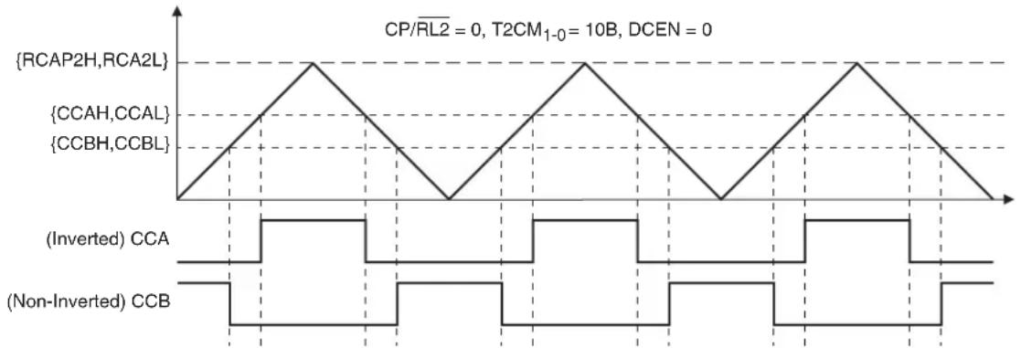
line
| Signal | Value | |-----------------|-------| | {RCAP2H,RCA2L} | High | | {CCAH,CCAL} | Low | | {CCBH,CCBL} | Low | | (Inverted) CCA | Square | | (Non-Inverted) CCB| Square |13.4.2.1 Phase and Frequency Correct PWM
When T2CM_1-0 = 10B the Symmetrical PWM operates in phase and frequency correct mode. In this mode the compare value double buffer is only updated when the timer equals MIN (underflow). This guarantees that the resulting waveform is always symmetrical around the TOP value as shown in Figure 13-10 because the up and down count compare values are identical. The TF2 interrupt flag is only set at underflow.
When T2CM_1-0 = 11B the Symmetrical PWM operates in phase correct mode. In this mode the compare value double buffer is updated when the timer equals MIN (underflow) and TOP (overflow). The resulting waveform may not be completely symmetrical around the TOP value as shown in Figure 13-11 because the up and down count compare values may not be identical. However, this allows the pulses to be weighted toward one edge or another. The TF2 interrupt flag is set at both underflow and overflow.
Figure 13-10. Phase and Frequency Correct Symmetrical (Center-Aligned) PWM
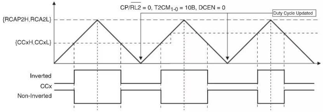
other
| Signal | Phase Description | |-----------------|----------------------------------------| | {RCAP2H,RCA2L} | Step 1: Inverted, CCx | | {CCxH,CCxL} | Step 2: Inverted, Non-Inverted | | CP/RL2 = 0 | Step 3: Inverted, CCx | | T2CM₁₋₀ = 10B | Step 4: Inverted, Non-Inverted | | DCEN = 0 | Step 5: Inverted, CCx | | Duty Cycle Updated | Step 6: Inverted, Non-Inverted |Figure 13-11. Phase Correct Symmetrical (Center-Aligned) PWM

line
| State | Value | | --------------- | ----- | | {RCAP2H,RCA2L} | 1 | | {CCxH,CCxL} | 0 | | CP/RL2 = 0 | 1 | | T2CM₁₋₀ = 11B | 0 | | DCEN = 0 | 0 | | Duty Cycle Updated | 1 |13.4.3 Multi-Phasic PWM
The PWM channels may be configured to provide multi-phasic alternating outputs by the PHS_2-0 bits in T2MOD. The AT89LP3240/6440 provides 1 out of 2, 1 out of 3, 1 out of 4 and 2 out of 4 phase modes (See Table 13-6). In Multi-phasic mode the PWM outputs on CCA, CCB, CCC and CCD are connected to a one-hot shift register that selectively enables and disables the outputs (See Figure 13-12). Compare points on disabled channels are blocked from toggling the output as if the compare value was set equal to TOP. The PHSD bit in T2MOD controls the direction of the shift register. Example waveforms are shown in Figure 13-14 on page 82. In order to use multi-phasic PWM, the associated channels must be configured for PWM operation. Non-PWM channels are not affected by multi-phasic operation. However, their locations in the shift register are maintained such that some periods in the PWM outputs may not have any pulses as shown in Figure 13-13.
The PHS_2-0 bits may only be modified when the timer is not operational (TR2 = 0). Updates to PHSD are allowed at any time. Note that channels C and D in 1:2 phase mode and channel D in 1:3 phase mode operate normally.
Table 13-6. Summary of Multi-Phasic Modes
| PHS _2-0 | Mode | Behavior | |
| PHSD = 0 PHSD = 1 | |||
| 000 | Off | Normal Operation (all channels active at all times) | |
| 001 1:2 | A B A B | B A B A | |
| 010 1:3 | A B C A B C | C B A C B A | |
| 011 1:4 | A B C D A B C D - | D C B A D C B A - | |
| 100 2:4 | A B A B | B A B A | |
| C D C D | D C D C | ||
Figure 13-12. Multi-Phasic PWM Output Stage
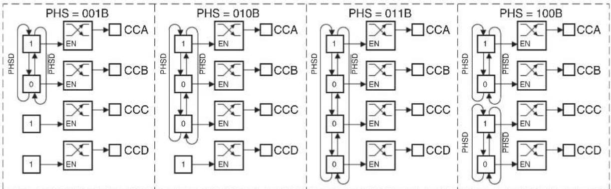
Figure 13-13. Three-Phase Mode with Channel B Disabled
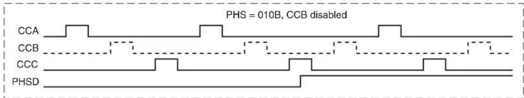
text_image
PHS = 010B, CCB disabled CCA CCB CCC PHSDFigure 13-14. Multi-Phasic PWM Modes
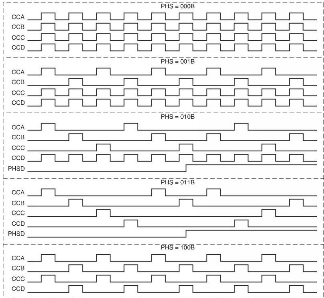
line
| PHS (Bandwidth) | CCA | CCB | CCC | CCD | | --------------- | --- | --- | --- | --- | | 000B | | | | | | 001B | | | | | | 010B | | | | | | 011B | | | | | | 100B | | | | |14. External Interrupts
The INT0 (P3.2) and INT1 (P3.3) pins of the AT89LP3240/6440 may be used as external interrupt sources. The external interrupts can be programmed to be level-activated or transition-activated by setting or clearing bit IT1 or IT0 in Register TCON. If ITx = 0, external interrupt x is triggered by a detected low at the INTx pin. If ITx = 1, external interrupt x is edge-triggered. In this mode if successive samples of the INTx pin show a high in one cycle and a low in the next cycle, interrupt request flag IEx in TCON is set. Flag bit IEx then requests the interrupt. Since the external interrupt pins are sampled once each clock cycle, an input high or low should hold for at least 2 oscillator periods to ensure sampling. If the external interrupt is transition-activated, the external source has to hold the request pin high for at least two clock cycles, and then hold it low for at least two clock cycles to ensure that the transition is seen so that interrupt request flag IEx will be set. IEx will be automatically cleared by the CPU when the service routine is called if generated in edge-triggered mode. If the external interrupt is level-activated, the external source has to hold the request active until the requested interrupt is actually generated. Then the external source must deactivate the request before the interrupt service routine is completed, or else
another interrupt will be generated. Both INT0 and INT1 may wake up the device from the Power-down state.
15. General-purpose Interrupts
The General-purpose Interrupt (GPI) function provides 8 configurable external interrupts on Port 1. Each port pin can detect high/low levels or positive/negative edges. The GPIEN register select which bits of Port 1 are enabled to generate an interrupt. The GPMOD and GPLS registers determine the mode for each individual pin. GPMOD selects between level-sensitive and edge-triggered mode. GPLS selects between high/low in level mode and positive/negative in edge mode. A block diagram is shown in Figure 15-1. The pins of Port 1 are sampled every clock cycle. In level-sensitive mode, a valid level must appear in two successive samples before generating the interrupt. In edge-triggered mode, a transition will be detected if the value changes from one sample to the next. When an interrupt condition on a pin is detected, and that pin is enabled, the appropriate flag in the GPIF register is set. The flags in GPIF must be cleared by software. Any GPI interrupt may wake up the device from the Power-down state.
Figure 15-1. GPI Block Diagram

flowchart
graph TD
    subgraph Inputs
        P1.7[" (P1.7) GPI7 "]
        P1.6[" (P1.6) GPI6 "]
        P1.5[" (P1.5) GPI5 "]
        P1.4[" (P1.4) GPI4 "]
        P1.3[" (P1.3) GPI3 "]
        P1.2[" (P1.2) GPI2 "]
        P1.1[" (P1.1) GPI1 "]
        P1.0[" (P1.0) GPI0 "]
    end

    subgraph Outputs
        DFF1[" D Q "]
        DFF2[" D Q "]
        DFF3[" D Q "]
        DFF4[" D Q "]
        DFF5[" D Q "]
        DFF6[" D Q "]
        DFF7[" D Q "]
        DFF8[" D Q "]
        DFF9[" D Q "]
    end

    CLK --> DFF1 & DFF2 & DFF3 & DFF4 & DFF5 & DFF6 & DFF7 & DFF8 & DFF9

    interrupt --> OR
    OR --> Output
    style Inputs fill:#f9f,stroke:#333
    style Outputs fill:#ccf,stroke:#333
Table 15-1. GPMOD – General-purpose Interrupt Mode Register
| GPMOD = 9AH | Reset Value = 0000 0000B | |
| Not Bit Addressable | ||
| B |  | |
| GPMOD.x | 0 = level-sensitive interrupt for P1.x | |
| 1 = edge-triggered interrupt for P1.x | ||
Table 15-2. GPLS – General-purpose Interrupt Level Select Register
| GPLS = 9BH | Reset Value = 0000 0000B |
| Not Bit Addressable | |
| B |  |
| GPMOD.x 0 = detect low level or negative edge on P1.x1 = detect high level or positive edge on P1.x | |
Table 15-3. GPIEN – General-purpose Interrupt Enable Register
| GPIEN = 9CHNot Bit Addressable | Reset Value = 0000 0000B | |
| B |  | |
| GPIEN.x 0 = interrupt for P1.x disabled1 = interrupt for P1.x enabled | ||
Table 15-4. GPIF – General-purpose Interrupt Flag Register
| GPIF = 9DHNot Bit Addressable | Reset Value = 0000 0000B | |
| B |  | |
| GPIF.x 0 = interrupt on P1.x inactive1 = interrupt on P1.x active. Must be cleared by software. | ||
16. Serial Interface (UART)
The serial interface on the AT89LP3240/6440 implements a Universal Asynchronous Receiver/Transmitter (UART). The UART has the following features:
• Full-duplex Operation
- 8 or 9 Data Bits
- Framing Error Detection
- Multiprocessor Communication Mode with Automatic Address Recognition
- Baud Rate Generator Using Timer 1 or Timer 2
- Interrupt on Receive Buffer Full or Transmission Complete
The serial interface is full-duplex, which means it can transmit and receive simultaneously. It is also receive-buffered, which means it can begin receiving a second byte before a previously received byte has been read from the receive register. (However, if the first byte still has not been read when reception of the second byte is complete, one of the bytes will be lost.) The serial port receive and transmit registers are both accessed at the Special Function Register SBUF. Writing to SBUF loads the transmit register, and reading SBUF accesses a physically separate receive register. The serial port can operate in the following four modes.
- Mode 0: Serial data enters and exits through RXD. TXD outputs the shift clock. Eight data bits are transmitted/received, with the LSB first. The baud rate is programmable to 1/2 or 1/4 the oscillator frequency, or variable based on Time 1.
- Mode 1: 10 bits are transmitted (through TXD) or received (through RXD): a start bit (0), 8 data bits (LSB first), and a stop bit (1). On receive, the stop bit goes into RB8 in the Special Function Register SCON. The baud rate is variable based on Timer 1 or Timer 2.
- Mode 2: 11 bits are transmitted (through TXD) or received (through RXD): a start bit (0), 8 data bits (LSB first), a programmable 9th data bit, and a stop bit (1). On transmit, the 9th data bit (TB8 in SCON) can be assigned the value of "0" or "1". For example, the parity bit (P, in the PSW) can be moved into TB8. On receive, the 9th data bit goes into RB8 in the Special Function Register SCON, while the stop bit is ignored. The baud rate is programmable to either 1/16 or 1/32 the oscillator frequency.
- Mode 3: 11 bits are transmitted (through TXD) or received (through RXD): a start bit (0), 8 data bits (LSB first), a programmable 9th data bit, and a stop bit (1). In fact, Mode 3 is the same as Mode 2 in all respects except the baud rate, which is variable based on Timer 1 or Timer 3 in Mode 3.
In all four modes, transmission is initiated by any instruction that uses SBUF as a destination register. Reception is initiated in Mode 0 by the condition RI = 0 and REN = 1. Reception is initiated in the other modes by the incoming start bit if REN = 1.
16.1 Multiprocessor Communications
Modes 2 and 3 have a special provision for multiprocessor communications. In these modes, 9 data bits are received, followed by a stop bit. The 9th bit goes into RB8. Then comes a stop bit. The port can be programmed such that when the stop bit is received, the serial port interrupt is activated only if RB8 = 1. This feature is enabled by setting bit SM2 in SCON.
The following example shows how to use the serial interrupt for multiprocessor communications. When the master processor must transmit a block of data to one of several slaves, it first sends out an address byte that identifies the target slave. An address byte differs from a data byte in that the 9th bit is "1" in an address byte and "0" in a data byte. With SM2 = 1, no slave is interrupted by a data byte. An address byte, however, interrupts all slaves. Each slave can examine the received byte and see if it is being addressed. The addressed slave clears its SM2
bit and prepares to receive the data bytes that follows. The slaves that are not addressed set their SM2 bits and ignore the data bytes. See “Automatic Address Recognition” on page 97.
The SM2 bit can be used to check the validity of the stop bit in Mode 1. In a Mode 1 reception, if SM2 = 1, the receive interrupt is not activated unless a valid stop bit is received.
Table 16-1. SCON – Serial Port Control Register
| SCON Address = 98H Reset Value = 0000 0000B | ||||||||
| Bit Addressable | ||||||||
| SM0/FE | SM1 | SM2 | REN | TB8 | RB8 | T1 | RI | |
| B | i | t | 7 | 6 | 5 | 4 | 3 | |
| (SMOD0 = 0/1)^(1) | ||||||||
| Symbol | Function | ||||
| FE | Framing error bit. This bit is set by the receiver when an invalid stop bit is detected. The FE bit is not cleared by valid frames and must be cleared by software. The SMOD0 bit must be set to enable access to the FE bit. FE will be set regardless of the state of SMOD0. | ||||
| SM0 | Serial Port Mode Bit 0, (SMOD0 must = 0 to access bit SM0) | ||||
| SM1 | Serial Port Mode Bit 1 | ||||
| SM0 | SM1 | Mode | Description | Baud Rate^(2) | |
| 0 | 0 | 0 | shift register | f_osd/2 or f_osd/4 or Timer 1 | |
| 0 | 1 | 1 | 8-bit UART | variable (Timer 1 or Timer 2) | |
| 1 | 0 | 2 | 9-bit UART | f_osd/32 or f_osc/16 | |
| 1 | 1 | 3 | 9-bit UART | variable (Timer 1 or Timer 2) | |
| SM2 | Enables the Automatic Address Recognition feature in Modes 2 or 3. If SM2 = 1 then RI will not be set unless the received 9th data bit (RB8) is 1, indicating an address, and the received byte is a Given or Broadcast Address. In Mode 1, if SM2 = 1 then RI will not be activated unless a valid stop bit was received, and the received byte is a Given or Broadcast Address. In Mode 0, SM2 determines the idle state of the shift clock such that the clock is the inverse of SM2, i.e. when SM2 = 0 the clock idles high and when SM2 = 1 the clock idles low. | ||||
| REN | Enables serial reception. Set by software to enable reception. Clear by software to disable reception. | ||||
| TB8 | The 9th data bit that will be transmitted in Modes 2 and 3. Set or clear by software as desired. In Mode 0, setting TB8 enables Timer 1 as the shift clock generator. | ||||
| RB8 | In Modes 2 and 3, the 9th data bit that was received. In Mode 1, if SM2 = 0, RB8 is the stop bit that was received. In Mode 0, RB8 is not used. | ||||
| TI | Transmit interrupt flag. Set by hardware at the end of the 8th bit time in Mode 0, or at the beginning of the stop bit in the other modes, in any serial transmission. Must be cleared by software. | ||||
| RI | Receive interrupt flag. Set by hardware at the end of the 8th bit time in Mode 0, or halfway through the stop bit time in the other modes, in any serial reception (except see SM2). Must be cleared by software. | ||||
Notes: 1. SMOD0 is located at PCON.6.
2. f_osc = oscillator frequency. The baud rate depends on SMOD1 (PCON.7).
16.2 Baud Rates
The baud rate in Mode 0 depends on the value of the SMOD1 bit in Special Function Register PCON.7. If SMOD1 = 0 (the value on reset) and TB8 = 0, the baud rate is 1/4 of the oscillator frequency. If SMOD1 = 1 and TB8 = 0, the baud rate is 1/2 of the oscillator frequency, as shown in the following equation:
$$ \begin{array}{l} \text { Mode 0 Baud Rate } \ \mathrm{TB8=0} \end{array} = \frac {2 ^ {\mathrm{SMOD1}}}{4} \times \text { Oscillator Frequency } $$
The baud rate in Mode 2 also depends on the value of the SMOD1 bit. If SMOD1 = 0, the baud rate is 1/32 of the oscillator frequency. If SMOD1 = 1, the baud rate is 1/16 of the oscillator frequency, as shown in the following equation:
$$ \text { Mode 2 Baud Rate } = \frac {2 ^ {\mathrm{SMOD1}}}{3 2} \times \text { Oscillator Frequency } $$
16.2.1 Using Timer 1 to Generate Baud Rates
Setting TB8 = 1 in Mode 0 enables Timer 1 as the baud rate generator. When Timer 1 is the baud rate generator for Mode 0, the baud rates are determined by the Timer 1 overflow rate and the value of SMOD1 according to the following equation:
$$ \begin{array}{l} \text { Mode 0 Baud Rate } \ \mathrm{TB8=1} \end{array} = \frac {2 ^ {\mathrm{SMOD1}}}{4} \times (\text { Timer 1 Overflow Rate }) $$
The Timer 1 overflow rate normally determines the baud rates in Modes 1 and 3. When Timer 1 is the baud rate generator, the baud rates are determined by the Timer 1 overflow rate and the value of SMOD1 according to the following equation:
$$ \begin{array}{l} \text { Modes 1,3 } \ \text { Baud Rate } \end{array} = \frac {2 ^ {\text { SMOD1 }}}{3 2} \times (\text { Timer 1 Overflow Rate }) $$
The Timer 1 interrupt should be disabled in this application. The Timer itself can be configured for either timer or counter operation in any of its 3 running modes. In the most typical applications, it is configured for timer operation in auto-reload mode (high nibble of TMOD = 0010B). In this case, the baud rate is given by the following formula:
$$ \begin{array}{l} \text {Modes 1,3} \ \text {Baud Rate} \end{array} \frac {2 ^ {\mathrm{SMOD1}}}{3 2} \times = \frac {\text {Oscillator Frequency}}{2 5 6 \mathrm{TH1(})} \times \frac {1}{\text {TPS+1}} ] $$
Programmers can achieve very low baud rates with Timer 1 by configuring the Timer to run as a 16-bit auto-reload timer (high nibble of TMOD = 0001B). In this case, the baud rate is given by the following formula.
$$ \begin{array}{l} \text {Modes 1,3} \ \text {Baud Rate} \end{array} = \frac {2 ^ {\text {SMOD1}}}{3 2} \times \frac {\text {Oscillator Frequency}}{\left[ 6 5 5 3 6 - (\text {RH1,RL1}) \right]} \times \frac {1}{\text {TPS+1}} $$
Table 16-2 lists commonly used baud rates and how they can be obtained from Timer 1.
Table 16-2. Commonly Used Baud Rates Generated by Timer 1 (TPS = 0000B)
| Baud Rate f | _osc (MHz) SMOD1 | Timer 1 | |||
| C/T Mode | Reload Value | ||||
| Mode 0: 1 MHz 4 | 0 X X X | ||||
| Mode 2: 750K 12 | 1 X X X | ||||
| 62.5K | 12 | 1 | 0 | 2 | F4H |
| 38.4K | 11.059 | 0 | 0 | 2 | F7H |
| 19.2K | 11.059 | 1 | 0 | 2 | DCH |
| 9.6K | 11.059 | 0 | 0 | 2 | DCH |
| 4.8K | 11.059 | 0 | 0 | 2 | B8H |
| 2.4K | 11.059 | 0 | 0 | 2 | 70H |
| 1.2K | 11.059 | 0 | 0 | 1 | FEE0H |
| 137.5 | 11.986 | 0 | 0 | 1 | F55CH |
| 110 | 6 | 0 | 0 | 1 | F958H |
| 110 | 12 0 | 0 | 1 F304H | ||
16.2.2 Using Timer 2 to Generate Baud Rates
Timer 2 is selected as the baud rate generator by setting TCLK and/or RCLK in T2CON. Under these conditions, the baud rates for transmit and receive can be simultaneously different by using Timer 1 for transmit and Timer 2 for receive, or vice versa. The baud rate generator mode is similar to the auto-reload mode, in that a rollover causes the Timer 2 registers to be reloaded with the 16-bit value in registers RCAP2H and RCAP2L, which are preset by software. In this case, the baud rates in Modes 1 and 3 are determined by Timer 2's overflow rate according to the following equation:.
$$ \begin{array}{c} \text {Modes 1 and 3} \ \text {Baud Rate} \end{array} = \frac {1}{1 6} \times \frac {\text {Oscillator Frequency}}{\left[ 6 5 5 3 6 - (\text {RCAP2H,RCAP2L}) \right]} \times \frac {1}{\text {TPS} + 1} $$
Table 16-3 lists commonly used baud rates and how they can be obtained from Timer 2.
Table 16-3. Commonly Used Baud Rates Generated by Timer 2 (TPS = 0000B)
| Baud Rate f | _osc (MHz) | Timer 2 | |||
| CP/RL2 | C/T2 | TCLK or RCLK | Reload Value | ||
| 62.5K | 12 | 0 0 | 1 FFF4H | ||
| 19.2K | 11.059 | 0 | 0 | 1 | FFDCH |
| 9.6K | 11.059 | 0 | 0 | 1 | FFB8H |
| 4.8K | 11.059 | 0 | 0 | 1 | FF70H |
| 2.4K | 11.059 | 0 0 | 1 FEE0H | ||
| 1.2K | 11.059 | 0 | 0 | 1 | FDC0H |
| 137.5 | 11.986 | 0 | 0 | 1 | EAB8H |
| 110 | 6 | 0 0 | 1 F2AFH | ||
| 110 | 12 | 0 | 0 | 1 | E55EH |
16.3 More About Mode 0
In Mode 0, the UART is configured as a two wire half-duplex synchronous serial interface. Serial data enters and exits through RXD. TXD outputs the shift clock. Eight data bits are transmitted/received, with the LSB first. Figure 16-1 on page 90 shows a simplified functional diagram of the serial port in Mode 0 and associated timing. The baud rate is programmable to 1/2 or 1/4 the oscillator frequency by setting/clearing the SMOD1 bit. However, changing SMOD1 has an effect on the relationship between the clock and data as described below. The baud rate can also be generated by Timer 1 by setting TB8. Table 16-4 lists the baud rate options for Mode 0.
Table 16-4. Mode 0 Baud Rates
| TB8 SMOD1 Baud Rate | ||
| 0 | 0 | f_SYS/4 |
| 0 | 1 | f_SYS/2 |
| 1 0 (Timer 1 Overflow) / 4 | ||
| 1 1 (Timer 1 Overflow) / 2 | ||
Transmission is initiated by any instruction that uses SBUF as a destination register. The “write to SBUF” signal also loads a “1” into the 9th position of the transmit shift register and tells the TX Control Block to begin a transmission. The internal timing is such that one full bit slot may elapse between “write to SBUF” and activation of SEND.
SEND transfers the output of the shift register to the alternate output function line of P3.0, and also transfers Shift Clock to the alternate output function line of P3.1. As data bits shift out to the right, "0"s come in from the left. When the MSB of the data byte is at the output position of the shift register, the "1" that was initially loaded into the 9th position is just to the left of the MSB, and all positions to the left of that contain "0"s. This condition flags the TX Control block to do one last shift, then deactivate SEND and set TI.
Reception is initiated by the condition REN = 1 and R1 = 0. At the next clock cycle, the RX Control unit writes the bits 11111110 to the receive shift register and activates RECEIVE in the next clock phase. RECEIVE enables Shift Clock to the alternate output function line of P3.1. As data bits come in from the right, "1"s shift out to the left. When the "0" that was initially loaded into the right-most position arrives at the left-most position in the shift register, it flags the RX Control block to do one last shift and load SBUF. Then RECEIVE is cleared and RI is set.
The relationship between the shift clock and data is determined by the combination of the SM2 and SMOD1 bits as listed in Table 16-5 and shown in Figure 16-2. The SM2 bit determines the idle state of the clock when not currently transmitting/receiving. The SMOD1 bit determines if the output data is stable for both edges of the clock, or just one.
Table 16-5. Mode 0 Clock and Data Modes
| SM2 SMOD1 Clock Idle Data Changed Data Sampled | ||||
| 0 | 0 | High | While clock is high | Positive edge of clock |
| 0 | 1 | High | Negative edge of clock | Positive edge of clock |
| 1 | 0 | Low | While clock is low | Negative edge of clock |
| 1 | 1 | Low | Negative edge of clock | Positive edge of clock |
Figure 16-1. Serial Port Mode 0
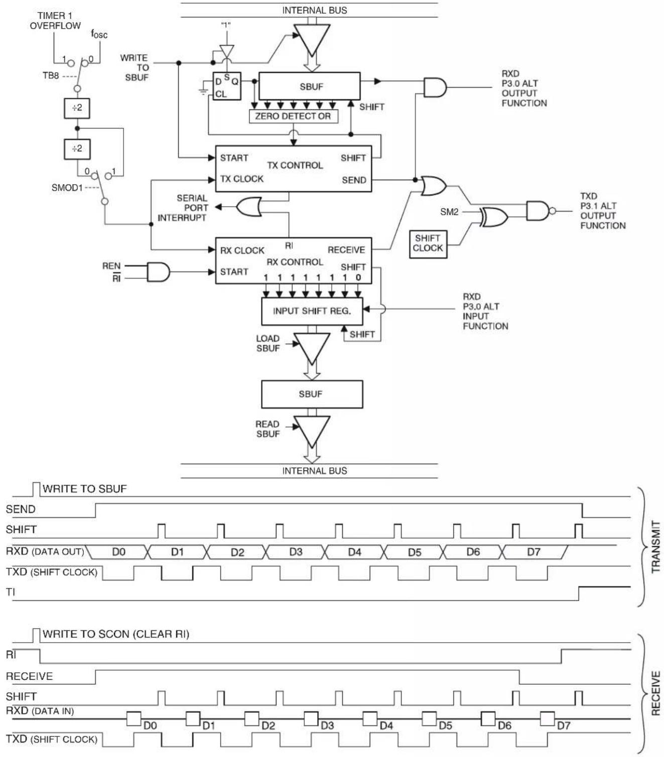
flowchart
graph TD
    subgraph Top_Layer
        direction_TB8["TB8 ---"]
        Timer1["TIMER 1 OVERFLOW fosc"] --> Timer1
        Timer1 --> Timer2["÷2"]
        Timer2 --> Timer3["SMOD1 ---"]
        Timer3 --> Timer4["+1"]
        Timer4 --> Timer5["+2"]
        Timer5 --> Timer6["+2"]
        Timer6 --> Timer7["+2"]
        Timer7 --> Timer8["+2"]
        Timer8 --> Timer9["+2"]
        Timer9 --> Timer10["+2"]
        Timer10 --> Timer11["+2"]
        Timer11 --> Timer12["+2"]
        Timer12 --> Timer13["+2"]
        Timer13 --> Timer14["+2"]
        Timer14 --> Timer15["+2"]
        Timer15 --> Timer16["+2"]
        Timer16 --> Timer17["+2"]
        Timer17 --> Timer18["+2"]
        Timer18 --> Timer19["+2"]
        Timer19 --> Timer20["+2"]
        Timer20 --> Timer21["+2"]
        Timer21 --> Timer22["+2"]
        Timer22 --> Timer23["+2"]
        Timer23 --> Timer24["+2"]
        Timer24 --> Timer25["+2"]
        Timer25 --> Timer26["+2"]
        Timer26 --> Timer27["+2"]
        Timer27 --> Timer28["+2"]
        Timer28 --> Timer29["+2"]
        Timer29 --> Timer30["+2"]
        Timer30 --> Timer31["+2"]
        Timer31 --> Timer32["+2"]
        Timer32 --> Timer33["+2"]
        Timer33 --> Timer34["+2"]
        Timer34 --> Timer35["+2"]
        Timer35 --> Timer36["+2"]
        Timer36 --> Timer37["+2"]
        Timer37 --> Timer38["+2"]
        Timer38 --> Timer39["+2"]
        Timer39 --> Timer40["+2"]
        Timer40 --> Timer41["+2"]
        Timer41 --> Timer42["+2"]
        Timer42 --> Timer43["+2"]
        Timer43 --> Timer44["+2"]
        Timer44 --> Timer45["+2"]
        Timer45 --> Timer46["+2"]
        Timer46 --> Timer47["+2"]
        Timer47 --> Timer48["+2"]
        Timer48 --> Timer49["+2"]
        Timer49 --> Timer50["+2"]
        Timer50 --> Timer51["+2"]
        Timer51 --> Timer52["+2"]
        Timer52 --> Timer53["+2"]
        Timer53 --> Timer54["+2"]
        Timer54 --> Timer55["+2"]
        Timer55 --> Timer56["+2"]
        Timer56 --> Timer57["+2"]
        Timer57 --> Timer58["+2"]
        Timer58 --> Timer59["+2"]
        Timer59 --> Timer60["+2"]
        Timer60 --> Timer61["+2"]
        Timer61 --> Timer62["+2"]
        Timer62 --> Timer63["+2"]
        Timer63 --> Timer64["+2"]
        Timer64 --> Timer65["+2"]
        Timer65 --> Timer66["+2"]
        Timer66 --> Timer67["+2"]
        Timer67 --> Timer68["+2"]
        Timer68 --> Timer69["+2"]
        Timer69 --> Timer70["+2"]
        Timer70 --> Timer71["+2"]
        Timer71 --> Timer72["+2"]
        Timer72 --> Timer73["+2"]
        Timer73 --> Timer74["+2"]
        Timer74 --> Timer75["+2"]
        Timer75 --> Timer76["+2"]
        Timer76 --> Timer77["+2"]
        Timer77 --> Timer78["+2"]
        Timer78 --> Timer79["+2"]
        Timer79 --> Timer80["+2"]
    end

    subgraph Bottom_Layer
        direction TB8 fill:#f9f,stroke:#333
        direction TB9 fill:#f9f,stroke:#333
    end

    subgraph Signal_Timing
        direction_LR1["RENEW"] fill:#ccf,stroke:#333
    end

    subgraph Pulse_Timing
        direction_LR4["RESET"] fill:#ccf,stroke:#333
    end

    subgraph Data_Timing
        direction_LR5["RESET"] fill:#ccf,stroke:#333
    end

    subgraph Time_Timing
        direction_LR6["RESET"] fill:#ccf,stroke:#333
    end

    subgraph Signal_Circuit_Timing
        direction_LR7["RESET"] fill:#ccf,stroke:#333
    end

    subgraph Pulse_Circuit_Timing
        direction_LR8["RESET"] fill:#ccf,stroke:#333
    end

    subgraph Time_Dates_Timing
        direction_LR9["RESET"] fill:#ccf,stroke:#333
    end

    subgraph Signal_Dates_Timing
        direction_LR10["RESET"] fill:#ccf,stroke:#333
    end

    subgraph Pulse_Dates_Timing
        direction_LR11["RESET"] fill:#ccf,stroke:#333
    end

    subgraph Time_Dates_Circuit_Timing
        direction_LR12["RESET"] fill:#ccf,stroke:#333
    end

    subgraph Signal_Dates_Circuit_Timing
        direction_LR13["RESET"] fill:#ccf,stroke:#333
    end

    subgraph Pulse_Dates_Circuit_Timing
        direction_LR14["RESET"] fill:#ccf,stroke:#333
    end

    subgraph Time_Dates_Dates_Circuit_Timing
        direction_LR15["RESET"] fill:#ccf,stroke:#333
    end

    subgraph Signal_Dates_Dates_Circuit_Timing
        direction_LR16["RESET"] fill:#ccf,stroke:#333
    end

    subgraph Pulse_Dates_Dates_Circuit_Timing
        direction_LR17["RESET"] fill:#ccf,stroke:#333
    end

    subgraph Time_Dates_Finding_Timing
        direction_LR18["RESET"] fill:#ccf,stroke:#333
    end

    subgraph Signal_Dates_Finding_Timing
        direction_LR19["RESET"] fill:#ccf,stroke:#333
    end

    subgraph Pulse_Dates_Finding_Timing
        direction_LR20["RESET"] fill:#ccf,stroke:#333
    end

    subgraph Time_Dates_SCO_Circuit_Timing
        direction_LR21["RESET"] fill:#ccf,stroke:#333
    end

    subgraph Signal_SCO_SCO_Circuit_Timing
        direction_LR22["RESET"] fill:#ccf,stroke:#333
    end

    subgraph Pulse_SCO_SCO_SCO_Circuit_Timing
        direction_LR23["RESET"] fill:#ccf,stroke:#333
    end

    subgraph Time_SCO_SCO_SCO_Timing_Timing
        direction_LR24["RESET"] fill:#ccf,stroke:#333
    end

    subgraph Signal_SCO_SCO_Timing_Timing_Timing
        direction_LR25["RESET"] fill:#ccf,stroke:#333
    end

    subgraph Pulse_SCO_SCO_Timing_Timing_Timing_Timing
        direction_LR26["RESET"] fill:#ccf,stroke:#333
    end

    subgraph Time_SCO_SCO_SCO_Timing_Timing_Timing_Timing_Timing_Timing_Timing_Timing_Timing_Timing_Timing_Timing_Timing_Timing_Timing_Timing_Timing_Timing_Timing_Timing_Timing_Timing_Timing_Timing_Timing_Timing_Timing_Timing_Timing_Timing_Timing_Timing_Timing_Timing_Timing_Timing_Timing_Timing_Timing_Timing_Timing_Timing_Timing_Timing_Timing_Timing_Timing_Timing_Timing_Timing_Teming_Timing_Timing_Timing_Timing_Timing_Timing_Timing_Timing_Timing_Timing_Timing_Timing_Timing_Timing_Timing_Timing_Timing_Timing_Timing_Timing_Timing_Timing_Timing_Timing_Timing_Timing_Timing_Timing_Timing_Timing_Timing_Timing_Timing_Timing_Timing_Timing_Timing_Timing_Timing_Timing_Timing_Timing_Timing_Timing_Timing_Timing_Timing_Timing_Timing_Times TING_UFF
    end

    style Top_Layer fill:#fff,stroke:#000,stroke-width:1px;
    style Top_Layer_DTop_Layer fill:#fff,stroke:#000,stroke-width:1px;
    style Top_Layer_DTop_Layer fill:#fff,stroke:#000,stroke-width:1px;
    style Top_Layer_DTop_Layer fill:#fff,stroke:#000,stroke-width:1px;
    style Top_Layer_DTop_Layer fill:#fff,stroke:#000,stroke-width:1px;
    style Top_Layer_DTAY fill:#fff,stroke:#000,stroke-width:1px;
    style Top_Layer_DTAY_DAY fill:#fff,stroke:#000,stroke-width:1px;
    style Top_Layer_DTAY_SCKI | TextSize="T", ShiftSize="SBUF" |
    style Top_Layer_DTAY_SCKI | TextSize="SBUF", ShiftSize="SBUF" |
    style Top_Layer_DTAY_SCKI | TextSize="SBUF", ShiftSize="SBUF" |
    style Top_Layer_DTAY_SCKI | TextSize="SBUF", ShiftSize="SBUF" |
    style Top_Layer_DTAY_SCKI | TextSize="SBUF", ShiftSize="SBUF" |
    style Top_Layer_DTAY_SCKI | TextSize="SBUY", ShiftSize="SBUF" |
    style Top_Layer_DTAY_SCKI | TextSize="SBUF", ShiftSize="SBUF" |
    style Top_Layer_DTAY_SCKI | TextSize="SBUF", ShiftSize="SBUF" |
    style Top_Layer_DTAY_SCKI | TextSize="SBUF", ShiftSize="SBUF" |
    style Top_Layer_DTAY_SCKI | TextSize="SBU", ShiftSize="SBUF" |
    style Top_Layer_DTAY_SCKI | TextSize="SBU", ShiftSize="SBUF" |
    style Top_Layer_DTAY_SCKI | TextSize="SBU", ShiftSize="SBUF" |
    style Top_Layer_DTAY_SCKI | TextSize="SBU", ShiftSize="SBUF" |
    style Top_Layer_DTAY_SCKI | TextSize="SCU", ShiftSize="SBUF" |
    style Top_Layer_DTAY_SCKI | TextSize="SCU", ShiftSize="SBUF" |
    style Top_Layer_DTAY_SCKI | TextSize="SCU", ShiftSize="SBUF" |
    style Top_Layer_DTAY_SCKI | TextSize="SCU", ShiftSize="SBUF" |
    style Top_Layer_DTAY_SCKI | TextSize="SCS", ShiftSize="SBUF" |
    style Top_Layer_DTAY_SCKI | TextSize="SCS", ShiftSize="SBUF" |
    style Top_Layer_DTAY_SCKI | TextSize="SCS", ShiftSize="SBUF" |
    style Top_Layer_DTAY_SCKI | TextSize="SCS", ShiftSize="SBUF" |
    style Top_Layer_DTAY_SCKI | TextSize="SSS", ShiftSize="SBUF" |
    style Top_Layer_DTAY_SCKI | TextSize="SSS", ShiftSize="SBUF" |
    style Top_Layer_DTAY_SCKI | TextSize="SSS", ShiftSize="SBUF" |
    style Top_Layer_DTAY_SCKI | TextSize="SSS", ShiftSize="SBUF" |
    style Top_Layer_DTAY_SCKI | TextSize="SCS", ShiftSize="SBUF" |
    style Top_Layer_DTAY_SCKI | TextSize="SCS", ShiftSize="SBUF" |
    style Top_Layer_DTAY_SCKI | TextSize="SCS", ShiftSize="SBUF" |
    style Top_Layer_DTAY_SCKI | TextSize="SCU", ShiftSize="SBUF" |
    style Top_Layer_DTAY_SCKI | TextSize="SCU", ShiftSize="SBUF" |
    style Top_Layer_DTAY_SCKI | TextSize="SCU", ShiftSize="SBUF" |
    style Top_Layer_DTAY_SCKI | TextSize="SBU", ShiftSize="SBUF" |
    style Top_Layer_DTAY_SCKI | TextSize="SBU", ShiftSize="SBUF" |
    style Top_Layer_DTAY_SCKI | TextSize="SBU", ShiftSize="SBUF" |
    style Top_Layer_DTAY_SCKI | TextSize="SCS", ShiftSize="SBUF" |
    style Top_Layer_DTAY_SCKI | TextSize="SCS", ShiftSize="SBUF" |
    style Top_Layer_DTAY_SCKI | TextSize="SCS", ShiftSize="SBUF" |
    style Top_Layer_DTAY_SCKI | TextSize="SBU", ShiftSize="SBUF" |
    style Top_Layer_DTAY_SCKI | TextSize="SBU", ShiftSize="SBUF" |
    style Top_Layer_DTAY_SCKI | TextSize="SBU", ShiftSize="SBUF" |
    style Top_Layer_DTAY_SCKI | TextSize="SUSC", ShiftSize="SBUF" |
    style Top_Layer_DTAY_SCKI | TextSize="SUSC", ShiftSize="SBUF" |
    style Top_Layer_DTAY_SCKI | TextSize="SUSC", ShiftSize="SBUF" |
    style Top_Layer_DTAY_SCKI | TextSize="SUSC", ShiftSize="SBUF" |
    style Top_Layer_DTAY_SCKI | Text Size="DOSU", ShiftSize="DOSU"
    end

    Note: The chart includes a schematic diagram of the circuit block and its corresponding timing parameters.
Figure 16-2. Mode 0 Waveforms
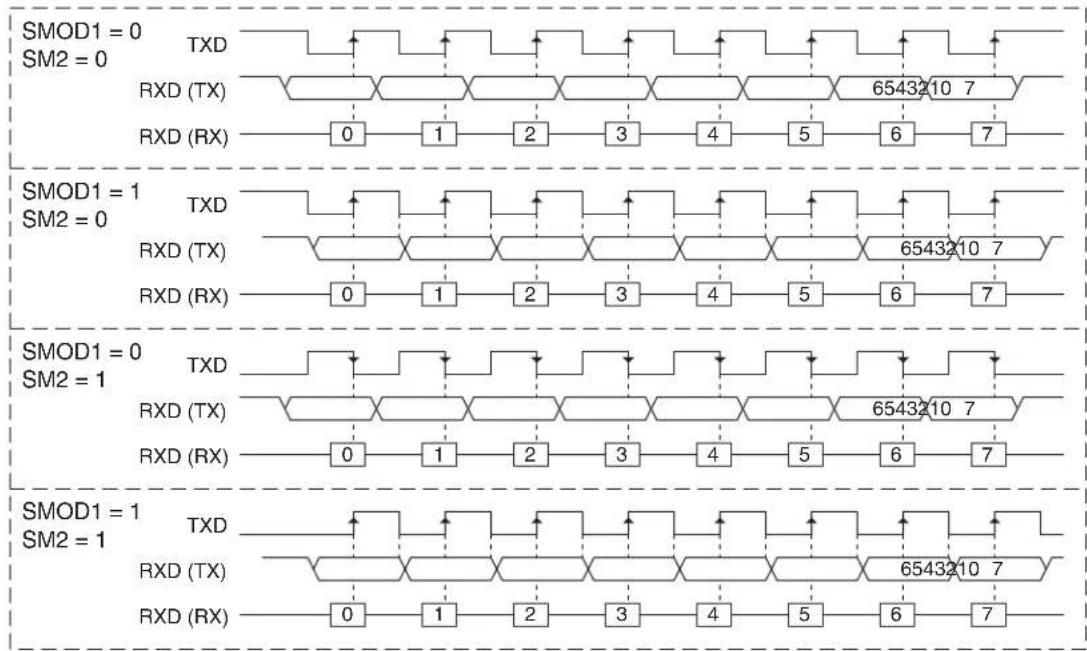
text_image
SMOD1 = 0 SM2 = 0 TXD RXD (TX) RXD (RX) 0 1 2 3 4 5 6 7 6543210 7 SMOD1 = 1 SM2 = 0 TXD RXD (TX) RXD (RX) 0 1 2 3 4 5 6 7 6543210 7 SMOD1 = 0 SM2 = 1 TXD RXD (TX) RXD (RX) 0 1 2 3 4 5 6 7 6543210 7 SMOD1 = 1 SM2 = 1 TXD RXD (TX) RXD (RX) 0 1 2 3 4 5 6 7 6543210 7 SMOD1 = 1 SM2 = 1Mode 0 may be used as a hardware accelerator for software emulation of serial interfaces such as a half-duplex Serial Peripheral Interface (SPI) in mode (0,0) or (1,1) or a Two-Wire Interface (TWI) in master mode. An example of Mode 0 emulating a TWI master device is shown in Figure 16-3. In this example, the start, stop, and acknowledge are handled in software while the byte transmission is done in hardware. Falling/rising edges on TXD are created by setting/clearing SM2. Rising/falling edges on RXD are forced by setting/clearing the P3.0 register bit. SM2 and P3.0 must be 1 while the byte is being transferred.
Figure 16-3. UART Mode 0 TWI Emulation (SMOD1 = 1)

text_image
(SCL) TXD (SDA) RXD 6543210 ACK SM2 P3.0 Sample ACK Write to SBUF TIMode 0 transfers data LSB first whereas SPI or TWI are generally MSB first. Emulation of these interfaces may require bit reversal of the transferred data bytes. The following code example reverses the bits in the accumulator:
EX: MOV R7, #8
REVRS: RLC A ; C << msb(ACC)
XCH A, R6
RRC A ; msb(ACC) >> B
XCH A, R6
DJNZ R7, REVRS
16.4 More About Mode 1
Ten bits are transmitted (through TXD), or received (through RXD): a start bit (0), 8 data bits (LSB first), and a stop bit (1). On receive, the stop bit goes into RB8 in SCON. In the AT89LP3240/6440, the baud rate is determined either by the Timer 1 overflow rate, the TImer 2 overflow rate, or both. In this case one timer is for transmit and the other is for receive. Figure 16-4 shows a simplified functional diagram of the serial port in Mode 1 and associated timings for transmit and receive.
Transmission is initiated by any instruction that uses SBUF as a destination register. The "write to SBUF" signal also loads a "1" into the 9th bit position of the transmit shift register and flags the TX Control unit that a transmission is requested. Transmission actually commences at S1P1 of the machine cycle following the next rollover in the divide-by-16 counter. Thus, the bit times are synchronized to the divide-by-16 counter, not to the "write to SBUF" signal.
The transmission begins when SEND is activated, which puts the start bit at TXD. One bit time later, DATA is activated, which enables the output bit of the transmit shift register to TXD. The first shift pulse occurs one bit time after that.
As data bits shift out to the right, "0"s are clocked in from the left. When the MSB of the data byte is at the output position of the shift register, the "1" that was initially loaded into the 9th position is just to the left of the MSB, and all positions to the left of that contain "0"s. This condition flags the TX Control unit to do one last shift, then deactivate SEND and set TI. This occurs at the tenth divide-by-16 rollover after "write to SBUF."
Reception is initiated by a 1-to-0 transition detected at RXD. For this purpose, RXD is sampled at a rate of 16 times the established baud rate. When a transition is detected, the divide-by-16 counter is immediately reset, and 1FFH is written into the input shift register. Resetting the divide-by-16 counter aligns its roll-overs with the boundaries of the incoming bit times.
The 16 states of the counter divide each bit time into 16ths. At the 7th, 8th, and 9th counter states of each bit time, the bit detector samples the value of RXD. The value accepted is the value that was seen in at least 2 of the 3 samples. This is done to reject noise. In order to reject false bits, if the value accepted during the first bit time is not 0, the receive circuits are reset and the unit continues looking for another 1-to-0 transition. If the start bit is valid, it is shifted into the input shift register, and reception of the rest of the frame proceeds.
As data bits come in from the right, "1"s shift out to the left. When the start bit arrives at the left-most position in the shift register, (which is a 9-bit register in Mode 1), it flags the RX Control block to do one last shift, load SBUF and RB8, and set RI. The signal to load SBUF and RB8 and to set RI is generated if, and only if, the following conditions are met at the time the final shift pulse is generated.
$$ \mathrm{RI} = 0 \text { and } $$
$$ \text { Either SM2 } = 0, \text { or the received stop bit } = 1 $$
If either of these two conditions is not met, the received frame is irretrievably lost. If both conditions are met, the stop bit goes into RB8, the 8 data bits go into SBUF, and RI is activated. At this time, whether or not the above conditions are met, the unit continues looking for a 1-to-0 transition in RXD.
Figure 16-4. Serial Port Mode 1
flowchart
graph TD
    A["TIMER 1 OVERFLOW"] --> B["÷2"]
    B --> C["0"]
    C --> D["1"]
    D --> E["0"]
    E --> F["TCLK"]
    F --> G["0"]
    G --> H["1"]
    H --> I["RCLK"]
    I --> J["0"]
    J --> K["1"]
    K --> L["+/-"]
    L --> M["+/-16"]
    M --> N["START TX CONTROL TI"]
    N --> O["+/-16"]
    O --> P["SBUF"]
    P --> Q["DATA SEND"]
    Q --> R["RESET DATA"]
    R --> S["INPUT SHIFT REG. (9 BITS)"]
    S --> T["LOAD SBUF SHIFT 1FFH"]
    T --> U["BIT DETECTOR"]
    U --> V["1-TO-0 TRANSITION DETECTOR"]
    V --> W["Sample"]
    W --> X["RXD"]
    X --> Y["+/-16"]
    Y --> Z["+/-16"]
    Z --> AA["RX CLOCK"]
    AA --> AB["+/-16"]
    AB --> AC["+/-16"]
    AC --> AD["RX CONTROL"]
    AD --> AE["LOAD SBUF SHIFT 1FFH"]
    AE --> AF["INPUT SHIFT REG. (9 BITS)"]
    AF --> AG["SBUF"]
    AG --> AH["READ SBUF"]
    AH --> AI["INTERNAL BUS"]

    subgraph Signal Waveforms
        AJ["TX CLOCK"] --> AK["WRITE TO SBUF"] --> AL["SEND"] --> AM["DATA SHIFT"] --> AN["TXD TI START BIT"] & AO["TOP BIT STOP BIT"] & AP["RXD"] --> AQ["+/-16 RESET"] --> AR["+/-16 RESET"] --> AS["RX CLOCK"]
    end

    subgraph Transmission Signals
        AT["TX"] --> AU["TRANSMIT"]
        AV["WRITE TO SBUF"] --> AW["TRANSMIT"]
        AX["SEND"] --> AY["TRANSMIT"]
        AZ["DATA SHIFT"] --> BA["TRANSMIT"]
        BB["TXD TI START BIT"] & BC["TOP BIT STOP BIT"] & BD["RET"] & BE["RESET"] & BF["RXD"] & BG["RX"] & BH["RX"] & BI["RX"] & BJ["RX"] & BK["RX"] & BL["RX"] & BM["RX"] & BN["RX"] & BO["RX"] & BP["RX"] & BQ["RX"] & BR["RX"] & BS["RX"] & BT["RX"] & BU["RX"] & BV["RX"] & BW["RX"] & BX["RX"] & BY["RX"] & BZ["RX"] & CA["RX"] & CB["RX"] & CC["RX"] & CD["RX"] & DE["RX"] & FD["RX"] & DG["RX"] & ID["RX"] & DJ["RX"] & DK["RX"] & DL["RX"] & DV["RX"] & DW["RX"] & DI["RX"] & DJ["RX"] & DKI["RX"] & DEI["RX"] & DF["RX"] & DGII["RX"] & DEI["I"]
16.5 More About Modes 2 and 3
Eleven bits are transmitted (through TXD), or received (through RXD): a start bit (0), 8 data bits (LSB first), a programmable 9th data bit, and a stop bit (1). On transmit, the 9th data bit (TB8) can be assigned the value of "0" or "1". On receive, the 9th data bit goes into RB8 in SCON. The baud rate is programmable to either 1/16 or 1/32 of the oscillator frequency in Mode 2. Mode 3 may have a variable baud rate generated from either Timer 1 or Timer 2, depending on the state of RCLK and TCLK.
Figures 16-5 and 16-6 show a functional diagram of the serial port in Modes 2 and 3. The receive portion is exactly the same as in Mode 1. The transmit portion differs from Mode 1 only in the 9th bit of the transmit shift register.
Transmission is initiated by any instruction that uses SBUF as a destination register. The “write to SBUF” signal also loads TB8 into the 9th bit position of the transmit shift register and flags the TX Control unit that a transmission is requested. Transmission commences at S1P1 of the machine cycle following the next rollover in the divide-by-16 counter. Thus, the bit times are synchronized to the divide-by-16 counter, not to the “write to SBUF” signal.
The transmission begins when SEND is activated, which puts the start bit at TXD. One bit time later, DATA is activated, which enables the output bit of the transmit shift register to TXD. The first shift pulse occurs one bit time after that. The first shift clocks a "1" (the stop bit) into the 9th bit position of the shift register. Thereafter, only "0"s are clocked in. Thus, as data bits shift out to the right, "0"s are clocked in from the left. When TB8 is at the output position of the shift register, then the stop bit is just to the left of TB8, and all positions to the left of that contain "0"s. This condition flags the TX Control unit to do one last shift, then deactivate SEND and set TI. This occurs at the 11th divide-by-16 rollover after "write to SBUF."
Reception is initiated by a 1-to-0 transition detected at RXD. For this purpose, RXD is sampled at a rate of 16 times the established baud rate. When a transition is detected, the divide-by-16 counter is immediately reset, and 1FFH is written to the input shift register.
At the 7th, 8th and 9th counter states of each bit time, the bit detector samples the value of RXD. The value accepted is the value that was seen in at least 2 of the 3 samples. If the value accepted during the first bit time is not 0, the receive circuits are reset and the unit continues looking for another 1-to-0 transition. If the start bit proves valid, it is shifted into the input shift register, and reception of the rest of the frame proceeds.
As data bits come in from the right, "1"s shift out to the left. When the start bit arrives at the leftmost position in the shift register (which in Modes 2 and 3 is a 9-bit register), it flags the RX Control block to do one last shift, load SBUF and RB8, and set RI. The signal to load SBUF and RB8 and to set RI is generated if, and only if, the following conditions are met at the time the final shift pulse is generated:
$$ \mathrm{RI} = 0, \text { and } $$
$$ \text { Either SM2 } = 0 \text { or the received 9th data bit } = 1 $$
If either of these conditions is not met, the received frame is irretrievably lost, and RI is not set. If both conditions are met, the received 9th data bit goes into RB8, and the first 8 data bits go into SBUF. One bit time later, whether the above conditions were met or not, the unit continues looking for a 1-to-0 transition at the RXD input.
Note that the value of the received stop bit is irrelevant to SBUF, RB8, or RI.
Figure 16-5. Serial Port Mode 2

flowchart
graph TD
    A["CPU CLOCK"] -->|MODE 2| B["SMOD1 1"]
    B -->|÷2| C["SMOD1 0"]
    C --> D["+16"]
    D --> E["START"]
    E --> F["TX CLOCK"]
    F --> G["SBUF"]
    G --> H["DATA"]
    H --> I["SEND"]
    I --> J["TXD"]
    K["WRITE TO SBUF"] --> L["DSQ CL"]
    L --> M["SBUF"]
    M --> N["ZERO DETECTOR"]
    N --> O["STOP BIT GEN. TX CONTROL TI"]
    O --> P["START"]
    P --> Q["+16"]
    Q --> R["SAMPLE"]
    R --> S["1-TO-0 TRANSITION DETECTOR"]
    S --> T["RXD"]
    U["RESET"] --> V["BIT DETECTOR"]
    V --> W["RX CLOCK RX CONTROL"]
    W --> X["INPUT SHIFT REG. (9 BITS)"]
    X --> Y["LOAD SBUF SHIFT 1FFH"]
    Y --> Z["SHIFT"]
    Z --> AA["SBUF"]
    AA --> AB["READ SBUF"]
    AB --> AC["INTERNAL BUS"]
    AD["INTERNAL BUS"] --> AE["TB8"]
text_image
TX CLOCK WRITE TO SBUF SEND DATA SHIFT TXD TI START BIT STOP BIT GEN TRANSMIT RX CLOCK ÷16 RESET RXD BIT DETECTOR SAMPLE TIMES BIT DETECTOR RESET TIM TIM TIM TIM TIM TIM TIM TIM TIM TIM TIM TIM TIM TIM TIM TIM TIM TIM TIM TIM TIM TIM TIM TIM TIM TIM TIM TIM TIM TIM TIM TIM TIM TIM TIM TIM TIM TIM TIM TIM TIM TIM TIM TIM TIM TIM TIM TIM TIM TIM R1Figure 16-6. Serial Port Mode 3

flowchart
graph TD
    subgraph Timing Waveforms
        direction TB
        X1["TIMER 1 OVERFLOW"] --> X2["÷2"]
        X3["0"] --> X4["1"]
        X5["TMCLK"] --> X6["0"]
        X7["RCLK"] --> X8["0"]
        X9["TCLK"] --> X10["1"]
        X11["RCLK"] --> X12["1"]
        X13[" Samoa"] --> X14["1-TO-0 TRANSITION DETECTOR"]
        X14 --> X15["+/-"]
        X15 --> X16["+/-"]
        X16 --> X17["+/-"]
        X17 --> X18["+/-"]
        X18 --> X19["+/-"]
        X19 --> X20["+/-"]
        X20 --> X21["+/-"]
        X21 --> X22["+/-"]
        X22 --> X23["+/-"]
        X23 --> X24["+/-"]
        X24 --> X25["+/-"]
        X25 --> X26["+/-"]
        X26 --> X27["+/-"]
        X27 --> X28["+/-"]
        X28 --> X29["+/-"]
        X29 --> X30["+/-"]
        X30 --> X31["+/-"]
        X31 --> X32["+/-"]
        X32 --> X33["+/-"]
        X33 --> X34["+/-"]
        X34 --> X35["+/-"]
        X35 --> X36["+/-"]
        X36 --> X37["+/-"]
        X37 --> X38["+/-"]
        X38 --> X39["+/-"]
        X39 --> X40["+/-"]
        X40 --> X41["+/-"]
        X41 --> X42["+/-"]
        X42 --> X43["+/-"]
        X43 --> X44["+/-"]
        X44 --> X45["+/-"]
        X45 --> X46["+/-"]
        X46 --> X47["+/-"]
        X47 --> X48["+/-"]
        X48 --> X49["+/-"]
        X49 --> X50["+/-"]
        X50 --> X51["+/-"]
        X51 --> X52["+/-"]
        X52 --> X53["+/-"]
        X53 --> X54["+/-"]
        X54 --> X55["+/-"]
        X55 --> X56["+/-"]
        X56 --> X57["+/-"]
        X57 --> X58["+/-"]
        X58 --> X59["+/-"]
        X59 --> X60["+/-"]
        X60 --> X61["+/-"]
        X61 --> X62["+/-"]
        X62 --> X63["+/-"]
        X63 --> X64["+/-"]
        X64 --> X65["+/-"]
        X65 --> X66["+/-"]
        X66 --> X67["+/-"]
        X67 --> X68["+/-"]
        X68 --> X69["+/-"]
        X69 --> X70["+/-"]
        X70 --> X71["+/-"]
        X71 --> X72["+/-"]
        X72 --> X73["+/-"]
        X73 --> X74["+/-"]
        X74 --> TCK["TICK"] --> Y0["TICK"] & Y1["TICK"] & Y2["TICK"] & Y3["TICK"] & Y4["TICK"] & Y5["TICK"] & Y6["TICK"] & Y7["TICK"] & Y8["TICK"] & Y9["TICK"] & Y10["TICK"] & Y11["TICK"] & Y12["TICK"] & Y13["TICK"] & Y14["TICK"] & Y15["TICK"] & Y16["TICK"] & Y17["TICK"] & Y18["TICK"] & Y19["TICK"] & Y20["TICK"] & Y21["TICK"] & Y22["TICK"] & Y23["TICK"] & Y24["TICK"] & Y25["TICK"] & Y26["TICK"] & Y27["TICK"] & Y28["TICK"] & Y29["TICK"] & Y30["TICK"] & Y31["TICK"] & Y32["TICK"] & Y33["TICK"] & Y34["TICK"] & Y35["TICK"] & Y36["TICK"] & Y37["TICK"] & Y38["TICK"] & Y39["TICK"] & Y40["TICK"] & Y41["TICK"] & Y42["TICK"] & Y43["TICK"] & Y44["TICK"] & Y45["TICK"] & Y46["TICK"] & Y47["TICK"] & Y48["TICK"] & Y49["TICK"] & Y50["TICK"] & Y51["TICK"] & Y52["TICK"] & Y53["TICK"] & Y54["TICK"] & Y55["TICK"] & Y56["TICK"] & Y57["TICK"] & Y58["TICK"] & Y59["TICK"] & Y60["TICK"] & Y61["TICK"] & Y62["TICK"] & Y63["TICK"] & Y64["TICK"] & Y65["TICK"] & Y66["TICK"] & Y67["TICK"] & Y68["TICK"] & Y69["TICK"] & Y70["TICK"] & Y71["TICK"] & Y72["TICK"] & Y73["TICK"] & Y74["TICK"] & Y75["TICK"] & Y76["TICK"] & Y77["TICK"] & Y78["TICK"] & Y79["TICK"] & Y80["TICK"] & Y81["TICK"] & Y82["TICK"] & Y83["TICK"] & Y84["TICK"] & Y85["TICK"] & Y86["TICK"] & Y87["TICK"] & Y88["TICK"] & Y89["TICK"] & Y90["TICK"] & Y91["TICK"] & Y92["TICK"] & Y93["TICK"] & Y94["TICK"] & Y95["TICK"] & Y96["TICK"] & Y97["TICK"] & Y98["TICK"] & Y99["TICK"] & TCK
    end

    subgraph Transmits
        direction TB
        TCK["CLOCK"] -->|WRITE TO SBUF| SBUF["SBUF"]
        TCK["CLOCK"] -->|SEND| SBUF["SBUF"]
        TCK["CLOCK"] -->|DATA SHIFT| SBUF["SBUF"]
        TCK["CLOCK"] -->|TXD TI| SBUF["SBUF"]
    end

    subgraph Outputs
        direction TB
        SBUF["SBUF"] -->|LOAD SBUF| SBUF["SBUF"]
        SBUF["SBUF"] -->|INPUT SHIFT REG.(9 BITS)| SBUF["SBUF"]
    end

    subgraph Outputs
        direction TB
        SBUF["SBUF"] -->|READ SBUF| SBUF["SBUF"]
    end

    subgraph Outputs
        direction TB
        SBUF["SBUF"] -->|INTERNAL BUS| SBUF["SBUF"]
    end

    subgraph Outputs
        direction TB
        SBUF["SBUF"] -->|TRANSMIT| SBUF["SBUF"]
    end

    subgraph Outputs
        direction TB
        SBUF["SBUF"] -->|TRANSMIT| SBUF["SBUF"]
    end

    subgraph Outputs
        direction TB
        SBUF["SBUF"] -->|TRANSMIT| SBUF["SBUF"]
    end

    subgraph Outputs
        direction TB
        SBUF["SBUF"] -->|TRANSMIT| SBUF["SBUF"]
    end

    subgraph Outputs
        directional TB
        SBUF["SBUF"] -->|TRANSMIT| SBUF["SBUF"]
    end

    subgraph Outputs
        direction TB
        SBUF["SBUF"] -->|TRANSMIT| SBUF["SBUF"]
    end

    subgraph Outputs
        direction TB
        SBUF["SBUF"] -->|TRANSMIT| SBUF["SBUF"]
    end

    subgraph Outputs
        direction TB
        SBUF["SBUF"] -->|TRANSMIT| SBUF,SBUF["SBUF"]
    end

    subgraph Outputs
        direction TB
        SBUF["SBUF"] -->|TRANSMIT| SBUF,SBUF["SBUF"]
    end

    subgraph Outputs
        direction TB
        SBUF["SBUF"] -->|TRANSMIT| SBUF,SBUF["SBUF"]
    end

    subgraph Outputs
        direction TB
        SBUF["SBUF"] -->|TRANSMIT| SBUF,SBUF["SBUF"]
    end

    subchart Inputs:
    TIME_X[X钟信号X轴: 0, 1, 2, 3, 4, 5, 6, 7, 8, 9, 10, 11, 12, 13, 14, 15, 16, 17, 18, 19, 20, 21, 22, 23, 24, 25, 26, 27, 28, 29, 30, 31, 32, 33, 34, 35, 36, 37, 38, 39, 40, 41, 42, 43, 44, 45, 46, 47, 48, 49, 50, 51, 52, 53, 54, 55, 56, 57, 58, 59, 60, 61, 62, 63, 64, 65, 66, 67, 68, 69, 70, 71, 72, 73, 74, 75, 76, 77, 78, 79, 80, 81, 82, 83, 84, 85, 86, 87, 88, 89, 90, 91, 92, 93, 94, 95, 96, 97, 98, 99
    end

    subchart Outputs:
    TIME_X[X钟信号X轴: Time Intervals: RX/DI/WDI/SZI/SZK/SZL/SZM/SZN/SZO/SZP/SZQ/SZR/SZS/SZT/SZU/SZV/SZW/SZX/SZY/SZZ/SZW/SZX/SZY/SZW/SZX/SZY/SZX/SZX/SZX/SZX/SZX/SZX/SZX/SZX/SZX/SZX/SZX/SZX/SZX/SZX/SZX/SZX/SZX/SZX/SZX/SZX/SZX/SZX/SZX/SZX/SZX/SZX/SZX/SZX/SZX/SZX/SZX/SZX/SZX/SZX/FSS/TSS/TSS/TSS/TSS/TSS/TSS/TSS/TSS/TSS/TSS/TSS/TSS/TSS/TSS/TSS/TSS/TSS/TSS/TSS/TSS/TSS/TSS/TSS/TSS/TSS/TSS/TSS/TSS/TSS/TSS/TSS/TSS/TSS/TSS/TSS/TSS/TSS/TSS/TSS/TSS/TSS/TSS/TSS/TSS/TSS/TSS/TSS/TSS/TSS/TSS/RST/INT/(INT) / INT/(INT) / INT/(INT) / INT/(INT) / INT/(INT) / INT/(INT) / INT/(INT) / INT/(INT) / INT/(INT) / INT/(INT) / INT/(INT) / INT/(INT) / INT/(INT) / INT/(INT) / INT/(INT) / INT/(INT) / INT/(INT) / INT/(INT) / INT/(INT) / INT/(INT) / INT/(INT) / IN(IN) / IN(IN)
    end

    subgraph Outputs
    direction TB
    TIME_X[X钟信号X轴: RX/DI/DI/DI/DI/DI/DI/DI/DI/DI/DI/DI/DI/DI/DI/DI/DI/DI/DI/DI/DI/DI/DI/DI/DI/DI/DI/DI/DI/DI/DI/DI/DI/DI/DI/DI/DI/DI/DI/DI/DI/DI/DI/DI/DI/DI/DI/DI/DI/DI/DI/Di/INT/(INT) / IN(INT) / IN(INT) / IN(INT) / IN(INT) / IN(INT) / IN(INT) / IN(INT) / IN(INT) / IN(INT) / IN(INT) / IN(INT) / IN(INT) / IN(INT) / IN(INT) / IN(INT) / IN(INT) / IN(INT) / IN(INT) / IN(INT) / IN(INT) / IN(TAX,YA,YB,YC,YD,YE,YF,YG,YH,YI,YJ,YK,YL,YM,YN,YO,YP,YQ,YR,YS,YT,YU,YV,YW,YX,YW,YW,YW,YW,YW,YW,YW,YW,YW,YW,YW,YW,YW,YW,YW,YW,YW,YW,YW,YW,YW,YW,YW,YW,YW,YW,YW,YW,YW,YW,YW,YW,YW,YW,YW,YW,YW,YW,YW,YW,YW,YW,YW,YW,YW,YW,YW,YW,YW,YW,Yw,TAX,TAX,TAX,TAX,TAX,TAX,TAX,TAX,TAX,TAX,TAX,TAX,TAX,TAX,TAX,TAX,TAX,TAX,TAX,TAX,TAX,TAX,TAX,TAX,TAX,TAX,TAX,TAX,TAX,TAX,TAX,TAX,TAX,TAX,TAX,TAX,TAX,TAX,TAX,TAX,TAX,TAX,TAX,TAX,TAX,TAX,TAX,TAX,TAX,TAX,TAx,TAx,TAx,TAx,TAx,TAx,TAx,TAx,TAx,TAx,TAx,TAx,TAx,TAx,TAx,TAx,TAx,TAx,TAx,TAx,TAx,TAx,TAx,TAx,TAx,TAx,TAx,TAx,TAx,TAx,TAx,TAx,TAx,TAx,TAx,TAx,TAx,TAx,TAx,TAx,TAx,TAx,TAx,TAx,TAx,TAx,TAx,TAx,TAx,TAx,Tx,t,t,t,t,t,t,t,t,t,t,t,t,t,t,t,t,t,t,t,t,t,t,t,t,t,t,t,t,t,t,t,t,t,t,t,t,t,t,t,t,t,t,t,t,t,t,t,t,t,t,t,t,t,t,t,t,t,t,t,t,t,t,t,t,t,t,t,t,t,t,t,t,t,t,t,t,t,t,t,t,t,t,t,t,t,t,t,t,t,t,t,t,t,t,t,t,t,t,t,t,u,k,l,m,n,n,n,n,n,n,n,n,n,n,n,n,n,n,n,n,n,n,n,n,n,n,n,n,n,n,n,n,n,n,n,n,n,n,n,n,n,n,n,n,n,n,n,n,n,n,n,n,n,n,n,n,n,n,n,n,n,n,n,n,n,n,n,n,n,n,n,n,n,n,n,n,n,n,n,n,n,n,n,n,n,n,n,n,n,n,n,n,n,n,n,n,n,n,n,n,n,n,n,n,p,k,l,m,m,m,m,m,m,m,m,m,m,m,m,m,m,m,m,m,m,m,m,m,m,m,m,m,m,m,m,m,m,m,m,m,m,m,m,m,m,m,m,m,m,m,m,m,m,m,m,m,m,m,m,m,m,m,m,m,m,m,m,m,m,m,m,m,m,m,m,m,m,m,m,m,m,m,m,m,m,m,m,m,m,m,m,m,m,m,m,m,m,m,m,m,m,m,m,m,m,m,mm,k,l,m,k,l,m,k,l,m,k,l,m,k,l,m,k,l,m,k,l,m,k,l,m,k,l,m,k,l,m,k,l,m,k,l,m,k,l,m,k,l,m,k,l,m,k,l,m,k,l,m,k,l,m,k,l,m,k,l,m,k,l,m,k,l,m,k,l,m,k,l,m,k,l,m,k,l,m,k,l,m,k,l,m,k,l,m,k,l,m,k,l,m,k,l,m,k,l,m,k,l,mk,l,k,l,k,l,k,l,k,l,k,l,k,l,k,l,k,l,k,l,k,l,k,l,k,l,k,l,k,l,k,l,k,l,k,l,k,l,k,l,k,l,k,l,k,l,k,l,k,l,k,l,k,l,k,l,k,l,k,l,k,l,k,l,k,l,k,l,k,l,k,l,k,l,k,l,k,l,k,l,k,l,k,l,k,l,k,l,k,l,k,l,k,l,k,l,k,l,k,l,k,l,K,L,K,L,K,L,K,L,K,L,K,L,K,L,K,L,K,L,K,L,K,L,K,L,K,L,K,L,K,L,K,L,K,L,K,L,K,L,K,L,K,L,K,L,K,L,K,L,K,L,K,L,K,L,K,L,K,L,K,L,K,L,K,L,K,L,K,L,K,L,K,L,K,L,K,L,K,L,K,L,K,L,K,L,K,L,K,L,K,L,K,L,K,L,K,L,K,L,K,L,K,,TRUST(TX,CLOCK),TRANSMIT(TX,CLOCK),TRANSMIT(TX,CLOCK),TRANSMIT(TX,CLOCK),TRANSMIT(TX,CLOCK),TRANSMIT(TX,CLOCK),TRANSMIT(TX,CLOCK),TRANSMIT(TX,CLOCK),TRANSMIT(TX,CLOCK),TRANSMIT(TX,CLOCK),TRANSMIT(TX,CLOCK),TRANSMIT(TX,CLOCK),TRANSMIT(TX,CLOCK),TRANSMIT(TX,CLOW),TRANSMIT(TX,CLOW),TRANSMIT(TX,CLOW),TRANSMIT(TX,CLOW),TRANSMIT(TX,CLOW),TRANSMIT(TX,CLOW),TRANSMIT(TX,CLOW),TRANSMIT(TX,CLOW),TRANSMIT(TX,CLOW),TRANSMIT(TX,CLOW),TRANSMIT(TX,CLOW),TRANSMIT(TX,CLOW),TRANSMIT(TX,CLOW),TRANSMID(TX,CLOW),TRANSMID(TX,CLOW),TRANSMID(TX,CLOW),TRANSMID(TX,CLOW),TRANSMID(TX,CLOW),TRANSMID(TX,CLOW),TRANSMID(TX,CLOW),TRANSMID(TX,CLOW),TRANSMID(TX,CLOW),TRANSMID(TX,CLOW),TRANSMID(TX,CLOW),TRANSMID(TX,CLOW),TRANSMID(TX,CFlow),TRANSMID(TX,CFlow),TRANSMID(TX,CFlow),TRANSMID(TX,CFlow),TRANSMID(TX,CFlow),TRANSMID(TX,CFlow),TRANSMID(TX,CFlow),TRANSMID(TX,CFlow),TRANSMID(TX,CFlow),TRANSMID(TX,CFlow),TRANSMID(TX,CFlow),TRANSMID(TX,CFlow),TRANSMID(TX,CFlow),TRANSMIC(BTX,CLOCK,BTX,BTX,BTX,BTX,BTX,BTX,BTX,BTX,BTX,BTX,BTX,BTX,BTX,BTX,BTX,BTX,BTX,BTX,BTX,BTX,BTX,BTX,BTX,BTX,BTX,BTX,BTX,BTX,BTX,BTX,BTX,BTX,BTX,BTX,BTX,BTX,BTX,BTX,BTX,BTX,BTX,BTX,BTX,BTX,BTX,BTX,BTX,BTX,BTX,BTX,BTB,DQ,DQ,DQ,DQ,DQ,DQ,DQ,DQ,DQ,DQ,DQ,DQ,DQ,DQ,DQ,DQ,DQ,DQ,DQ,DQ,DQ,DQ,DQ,DQ,DQ,DQ,DQ,DQ,DQ,DQ,DQ,DQ,DQ,DQ,DQ,DQ,DQ,DQ,DQ,DQ,DQ,DQ,DQ,DQ,DQ,DQ,DQ,DQ,DQ,DQ,DQA,DQA,DQA,DQA,DQA,DQA,DQA,DQA,DQA,DQA,DQA,DQA,DQA,DQA,DQA,DQA,DQA,DQA,DQA,DQA,DQA,DQA,DQA,DQA,DQA,DQA,DQA,DQA,DQA,DQA,DQA,DQA,DQA,DQA,DQA,DQA,DQA,DQA,DQA,DQA,DQA,DQA,DQA,DQA,DQA,DQA,DQA,DQA,DQA,DQA,DQB DQB DQB DQB DQB DQB DQB DQB DQB DQB DQB DQB DQB DQB DQB DQB DQB DQB DQB DQB DQB DQB DQB DQB DQB DQB DQB DQB DQB DQB DQB DQB DQB DQB DQB DQB DQB DQB DQB DQB DQB DQB DQB DQB DQB DQB DQB DQB DQB DQB DQB ETR/INT/INT/INT/INT/INT/INT/INT/INT/INT/INT/INT/INT/INT/INT/INT/INT/INT/INT/INT/INT/INT/INT/INT/INT/INT/INT/INT/INT/INT/INT/INT/INT/INT/INT/INT/INT/INT/INT/INT/INT/INT/INT/INT/INT/INT/INT/INT/INT/INT/INT/INTR/INTR/INTR/INTR/INTR/INTR/INTR/INTR/INTR/INTR/INTR/INTR/INTR/INTR/INTR/INTR/INTR/INTR/INTR/INTR/INTR/INTR/INTR/INTR/INTR/INTR/INTR/INTR/INTR/INTR/INTR/INTR/INTR/INTR/INTR/INTR/INTR/INTR/INTR/INTR/INTR/INTR/INTR/INTR/INTR/INTR/INTR/INTR/INTR/INTR/ATR/TR/NIR_TOUT_RST_VOUT_VOUT_VOUT_VOUT_VOUT_VOUT_VOUT_VOUT_VOUT_VOUT_VOUT_VOUT_VOUT_VOUT_VOUT_VOUT_VOUT_VOUT_VOUT_VOUT_VOUT_VOUT_VOUT_VOUT_VOUT_VOUT_VOUT_VOUT_VOUT_VOUT_VOUT_VOUT_VOUT_VOUT_VOUT_VOUT_VOUT_VOUT_VOUT_VOUT_VOUT_VOUT_VOUT_VOUT_VOUT_VOUT_VOUT_VOUT_VOUT_VOUT_VIN(RXD) → OUT(VRD) → OUT(VRD)
    end
16.6 Framing Error Detection
In addition to all of its usual modes, the UART can perform framing error detection by looking for missing stop bits, and automatic address recognition. When used for framing error detect, the UART looks for missing stop bits in the communication. A missing bit will set the FE bit in the SCON register. The FE bit shares the SCON.7 bit with SM0 and the function of SCON.7 is determined by PCON.6 (SMOD0). If SMOD0 is set then SCON.7 functions as FE. SCON.7 functions as SM0 when SMOD0 is cleared. When used as FE, SCON.7 can only be cleared by software. The FE bit will be set by a framing error regardless of the state of SMOD0.
16.7 Automatic Address Recognition
Automatic Address Recognition is a feature which allows the UART to recognize certain addresses in the serial bit stream by using hardware to make the comparisons. This feature saves a great deal of software overhead by eliminating the need for the software to examine every serial address which passes by the serial port. This feature is enabled by setting the SM2 bit in SCON for Modes 1, 2 or 3. In the 9-bit UART modes, Mode 2 and Mode 3, the Receive Interrupt flag (RI) will be automatically set when the received byte contains either the "Given" address or the "Broadcast" address. The 9-bit mode requires that the 9th information bit be a "1" to indicate that the received information is an address and not data.
In Mode 1 (8-bit) the RI flag will be set if SM2 is enabled and the information received has a valid stop bit following the 8th address bits and the information is either a Given or Broadcast address.
Automatic Address Recognition is not available during Mode 0.
Using the Automatic Address Recognition feature allows a master to selectively communicate with one or more slaves by invoking the given slave address or addresses. All of the slaves may be contacted by using the Broadcast address. Two special Function Registers are used to define the slave's address, SADDR, and the address mask, SADEN. SADEN is used to define which bits in the SADDR are to be used and which bits are "don't care". The SADEN mask can be logically ANDed with the SADDR to create the "Given" address which the master will use for addressing each of the slaves. Use of the Given address allows multiple slaves to be recognized while excluding others. The following examples show the versatility of this scheme:
| Slave 0 | SADDR = 1100 0000 |
| SADEN = 1111 1101 | |
| Given = 1100 00X0 |
| Slave 1 | SADDR = 1100 0000 |
| SADEN = 1111 1110 | |
| Given = 1100 000X |
In the previous example, SADDR is the same and the SADEN data is used to differentiate between the two slaves. Slave 0 requires a "0" in bit 0 and it ignores bit 1. Slave 1 requires a "0" in bit 1 and bit 0 is ignored. A unique address for slave 0 would be 1100 0010 since slave 1 requires a "0" in bit 1. A unique address for slave 1 would be 1100 0001 since a "1" in bit 0 will exclude slave 0. Both slaves can be selected at the same time by an address which has bit 0 = 0 (for slave 0) and bit 1 = 0 (for slave 1). Thus, both could be addressed with 1100 0000.
In a more complex system, the following could be used to select slaves 1 and 2 while excluding slave 0:
Slave 0 SADDR = 1100 0000
$$ \text { SADEN } = 1 1 1 1 1 0 0 1 $$
$$ \text { Given } = 1 1 0 0 \quad 0 \mathrm{XX0} $$
Slave 1 SADDR = 1110 0000
$$ S A D E N = 1 1 1 1 1 0 1 0 $$
$$ \text { Given } = 1 1 1 0 \quad 0 X 0 X $$
Slave 2 SADDR = 1110 0000
$$ \text { SADEN } = 1 1 1 1 1 1 0 0 $$
$$ \text { Given } = 1 1 1 0 0 0 \mathrm{XX} $$
In the above example, the differentiation among the 3 slaves is in the lower 3 address bits. Slave 0 requires that bit 0 = 0 and it can be uniquely addressed by 1110 0110. Slave 1 requires that bit 1 = 0 and it can be uniquely addressed by 1110 and 0101. Slave 2 requires that bit 2 = 0 and its unique address is 1110 0011. To select Slaves 0 and 1 and exclude Slave 2, use address 1110 0100, since it is necessary to make bit 2 = 1 to exclude slave 2.
The Broadcast Address for each slave is created by taking the logic OR of SADDR and SADEN. Zeros in this result are trended as don't cares. In most cases, interpreting the don't cares as ones, the broadcast address will be FF hexadecimal.
Upon reset SADDR (SFR address 0A9H) and SADEN (SFR address 0B9H) are loaded with "0"s. This produces a given address of all "don't cares" as well as a Broadcast address of all "don't cares". This effectively disables the Automatic Addressing mode and allows the microcontroller to use standard 80C51-type UART drivers which do not make use of this feature.
17. Enhanced Serial Peripheral Interface
The Serial Peripheral Interface (SPI) allows high-speed synchronous data transfer between the AT89LP3240/6440 and peripheral devices or between multiple AT89LP3240/6440 devices, including multiple masters and slaves on a single bus. The SPI includes the following features:
• Full-duplex, 3-wire or 4-wire Synchronous Data Transfer
• Master or Slave Operation
• Maximum Bit Frequency = f_OSC/4
• LSB First or MSB First Data Transfer
- Four Programmable Bit Rates or Timer 1-based Baud Generation (Master Mode)
• End of Transmission Interrupt Flag
• Write Collision Flag Protection
- Double-buffered Receive and Transmit
- Transmit Buffer Empty Interrupt Flag
- Mode Fault (Master Collision) Detection and Interrupt
- Wake up from Idle Mode
A block diagram of the SPI is shown below in Figure 17-1.
Figure 17-1. SPI Block Diagram

flowchart
graph TD
    A["Oscillator"] --> B["T1 OVF"]
    B --> C["TSCK"]
    C --> D["Divider ÷4/÷8/÷32/÷64"]
    D --> E["Select"]
    E --> F["SPI Clock (Master)"]
    F --> G["Clock Logic"]
    G --> H["SPI Control"]
    H --> I["SPI Status Register"]
    I --> J["SPI Interrupt Request"]
    J --> K["Internal Data Bus"]
    L["MSB"] --> M["8-bit Shift Register"]
    M --> N["Read Data Buffer"]
    M --> O["Write Data Buffer"]
    P["LSB"] --> Q["Pin Control Logic"]
    Q --> R["S M S"]
    R --> S["MISO P1.6"]
    R --> T["MOSI P1.5"]
    U["SPI Control"] --> V["MSTR SPE"]
    W["SPI Control Register"] --> X["TSCK SPE DORD MSTR CPOL CPHA SPR1 SPR0"]
    Y["SPI Control"] --> Z["MSTR SPE DORD MSTR CPOL CPHA SPR1 SPR0"]
    AA["SPI Control"] --> AB["MSTR SPE DORD MSTR CPOL CPHA SPR1 SPR0"]
    AC["SPI Control"] --> AD["MSTR SPE DORD MSTR CPOL CPHA SPR1 SPR0"]
    AE["SPI Control"] --> AF["MSTR SPE DORD MSTR CPOL CPHA SPR1 SPR0"]
    AG["SPI Control"] --> AH["MSTR SPE DORD MSTR CPOL CPHA SPR1 SPR0"]
    AI["SPI Control"] --> AJ["MSTR SPE DORD MSTR CPOL CPHA SPR1 SPR0"]
    AK["SPI Control"] --> AL["MSTR SPE DORD MSTR CPOL CPHA SPR1 SPR0"]
    AM["SPI Control"] --> AN["MSTR SPE DORD MSTR CPOL CPHA SPR1 SPR0"]
    AO["SPI Control"] --> AP["MSTR SPE DORD MSTR CPOL CPHA SPR1 SPR0"]
    AQ["SPI Control"] --> AR["MSTR SPE DORD MSTR CPOL CPHA SPR1 SPR0"]
    AS["SPI Control"] --> AT["MSTR SPE DORD MSTR CPOL CPHA SPR1 SPR0"]
    AU["SPI Control"] --> AV["MSTR SPE DORD MSTR CPOL CPHA SPR1 SPR0"]
    AW["SPI Control"] --> AX["MSTR SPE DORD MSTR CPOL CPHA SPR1 SPR0"]
    AY["SPI Control"] --> AZ["MSTR SPE DORD MSTR CPOL CPHA SPR1 SPR0"]
    BA["SPI Control"] --> BB["MSTR SPE DORD MSTR CPOL CPHA SPR1 SPR0"]
    BC["SPI Control"] --> BD["MSTR SPE DORD MSTR CPOL CPHA SPR1 SPR0"]
    BE["SPI Control"] --> BF["MSTR SPE DORD MSTR CPOL CPHA SPR1 SPR0"]
    BG["SPI Control"] --> BH["MSTR SPE DORD MSTR CPOL CPHA SPR1 SPR0"]
    BI["SPI Control"] --> BJ["MSTR SPE DORD MSTR CPOL CPHA SPR1 SPR0"]
    BK["SPI Control"] --> BL["MSTR SPE DORD MSTR CPOL CPHA SPR1 SPR0"]
    BM["SPI Control"] --> BN["MSTR SPE DORD MSTR CPOL CPHA SPR1 SPR0"]
    BO["SPI Control"] --> BP["MSTR SPE DORD MSTR CPOL CPHA SPR1 SPR0"]
    BQ["SPI Control"] --> BR["MSTR SPE DORD MSTR CPOL CPHA SPR1 SPR0"]
    BS["SPI Control"] --> BT["MSTR SPE DORD MSTR CPOL CPHA SPR1 SPR0"]
    BU["SPI Control"] --> BV["MSTR SPE DORD MSTR CPOL CPHA SPR1 SPR0"]
    BW["SPI Control"] --> BX["MSTR SPE DORD MSTR CPOL CPHA SPR1 SPR0"]
    BY["SPI Control"] --> BZ["MSTR SPE DORD MSTR CPOL CPHA SPR1 SPR0"]
    CA["SPI Control"] --> CB["MSTR SPE DORD MSTR CPOL CPHA SPR1 SPR0"]
    CC["SPI Control"] --> CD["MSTR SPE DORD MSTR CPOL CPHA SPR1 SPR0"]
    CE["SPI Control"] --> CF["MSTR SPE DORD MSTR CPOL CPHA SPR1 SPR0"]
    CG["SPI Control"] --> CH["MSTR SPE DORD MSTR CPOL CPHA SPR1 SPR0"]
    CI["SPI Control"] --> CJ["MSTR SPE DORD MSTR CPOL CPHA SPR1 SPR0"]
    CK["SPI Control"] --> CL["MSTR SPE DORD MSTR CPOL CPHA SPR1 SPR0"]
    CM["SPI Control"] --> CN["MSTR SPE DORD MSTR CPOL CPHA SPR1 SPR0"]
    CO["SPI Control"] --> CP["MSTR SPE DORD MSTR CPOL CPHA SPR1 SPR0"]
    CS["SPI Control"] --> CT["MSTR SPE DORD MSTR CPOL CPHA SPR1 SPR0"]
    CU["SPI Control"] --> CV["MSTR SPE DORD MSTR CPOL CPHA SPR1 SPR0"]
    CW["SPI Control"] --> CX["MSTR SPE DORD MSTR CPOL CPHA SPR1 SPR0"]
    CY["SPI Control"] --> CZ["MSTR SPE DORD MSTR CPOL CPHA SPR1 SPR0"]
    CAZ["SPI Control"] --> CBM["MSTR SPE DORD MSTR CPOL CPHA SPR1 SPR0"]
    CAZ["SPI Control"] --> CBN["MSTR SPE DORD MSTR CPOL CPHA SPR1 SPR0"]
    CAZ["SPI Control"] --> CBO["MSTR SPE DORD MSTR CPOL CPHA SPR1 SPR0"]
    CAZ["SPI Control"] --> CBP["MSTR SPE DORD MSTR CPOL CPHA SPR1 SPR0"]
    CAZ["SPI Control"] --> CBQ["MSTR SPE DORD MSTR CPOL CPHA SPR1 SPR0"]
    CAZ["SPI Control"] --> CBR["MSTR SPE DORD MSTR CPOL CPHA SPR1 SPR0"]
    CAZ["SPI Control"] --> CBS["MSTR SPE DORD MSTR CPOL CPHA SPR1 SPR0"]
    CAZ["SPI Control"] --> CBT["MSTR SPE DORD MSTR CPOL CPHA SPR1 SPR0"]
    CAZ["SPI Control"] --> CBU["MSTR SPE DORD MSTR CPOL CPHA SPR1 SPR0"]
    CAZ["SPI Control"] --> CBV["MSTR SPE DORD MSTR CPOL CPHA SPR1 SPR0"]
    CAZ["SPI Control"] --> CBW["MSTR SPE DORD MSTR CPOL CPHA SPR1 SPR0"]
    CAZ["SPI Control"] --> CBX["MSTR SPE DORD MSTR CPOL CPHA SPR1 SPR0"]
    CAZ["SPI Control"] --> CBY["MSTR SPE DORD MSTR CPOL CPHA SPR1 SPR0"]
    CAZ["SPI Control"] --> CBZ["MSTR SPE DORD MSTR CPOL CPHA SPR1 SPR0"]
The interconnection between master and slave CPUs with SPI is shown in Figure 17-2. The four pins in the interface are Master-In/Slave-Out (MISO), Master-Out/Slave-In (MOSI), Shift Clock (SCK), and Slave Select (SS). The SCK pin is the clock output in master mode, but is the clock input in slave mode. The MSTR bit in SPCR determines the directions of MISO and MOSI. Also notice that MOSI connects to MOSI and MISO to MISO. By default SS/P1.4 is an input to both master and slave devices.
In slave mode, SS must be driven low to select an individual device as a slave. When SS is held low, the SPI is activated, and MISO becomes an output if configured so by the user. All other pins are inputs. When SS is driven high, all pins are inputs, and the SPI is passive, which means that it will not receive incoming data. Note that the SPI logic will be reset once the SS pin is driven high. The SS pin is useful for packet/byte synchronization to keep the slave bit counter synchronous with the master clock generator. When the SS pin is driven high, the SPI slave will immediately reset the send and receive logic, and drop any partially received data in the Shift Register. The slave may ignore SS by setting its SSIG bit in SPSR. When SSIG = 1, the slave is always enabled and operates in 3-wire mode. However, the slave output on MISO may still be disabled by setting DISSO = 1.
The In-System Programming (ISP) interface also uses the SPI pins. Although the ISP protocol is SPI-based, the pin has special meaning and must be driven by the master as a frame delimiter. cannot be tied to ground for ISP to function correctly.
Figure 17-2. SPI Master-Slave Interconnection

flowchart
graph TD
    A["Master Slave"] --> B["8-Bit Shift Register"]
    B --> C["MISO MISO"]
    C --> D["8-Bit Shift Register"]
    D --> E["8-Bit Shift Register"]
    E --> F["Clock Generator"]
    F --> G["SCK SCK"]
    G --> H["GPIO"]
    H --> I["SSIG"]
    I --> J["SS"]
    J --> K["Vcc"]
    K --> L["SSIG"]
    L --> M["DISSO"]
    M --> N["8-Bit Shift Register"]
    N --> O["8-Bit Shift Register"]
    O --> P["MSB LSB MSB LSB"]
    B --> Q["MODF"]
    Q --> R["SSIG"]
    R --> S["SS"]
    S --> T["Vcc"]
    T --> U["GPIO"]
    U --> V["SCK SCK"]
    V --> W["SSIG"]
    W --> X["DISSO"]
    X --> Y["8-Bit Shift Register"]
When the SPI is configured as a Master (MSTR in SPCR is set), the operation of the SS pin depends on the setting of the Slave Select Ignore bit, SSIG. If SSIG = 1, the SS pin is a general purpose output pin which does not affect the SPI system. Typically, the pin will be driving the SS pin of an SPI Slave. If SSIG = 0, SS must be held high to ensure Master SPI operation. If the SS pin is driven low by peripheral circuitry when the SPI is configured as a Master with SSIG = 0, the SPI system interprets this as another master selecting the SPI as a slave and starting to send data to it. To avoid bus contention, the SPI system takes the following actions:
- The MSTR bit in SPCR is cleared and the SPI system becomes a Slave. As a result of the SPI becoming a Slave, the MOSI and SCK pins become inputs.
- The MODF Flag in SPSR is set, and if the SPI interrupt is enabled, the interrupt routine will be executed.
Thus, when interrupt-driven SPI transmission is used in Master mode, and there exists a possibility that SS may be driven low, the interrupt should always check that the MSTR bit is still set. If the MSTR bit has been cleared by a slave select, it must be set by the user to re-enable SPI Master mode.
17.1 Master Operation
An SPI master device initiates all data transfers on the SPI bus. The AT89LP3240/6440 is configured for master operation by setting MSTR = 1 in SPCR. Writing to the SPI data register (SPDR) while in master mode loads the transmit buffer. If the SPI shift register is empty, the byte in the transmit buffer is moved to the shift register; the transmit buffer empty flag, TXE, is set; and a transmission begins. The transfer may start after an initial delay, while the clock generator waits for the next full bit slot of the specified baud rate. The master shifts the data out serially on the MOSI line while providing the serial shift clock on SCK. When the transfer finishes, the SPIF flag is set to "1" and an interrupt request is generated, if enabled. The data received from the addressed SPI slave device is also transferred from the shift register to the receive buffer. Therefore, the SPIF bit flags both the transmit-complete and receive-data-ready conditions. The received data is accessed by reading SPDR.
While the TXE flag is set, the transmit buffer is empty. TXE can be cleared by software or by writing to SPDR. Writing to SPDR will clear TXE and load the transmit buffer. The user may load the buffer while the shift register is busy, i.e. before the current transfer completes. When the current transfer completes, the queued byte in the transmit buffer is moved to the shift register and the next transfer commences. TXE will generate an interrupt if the SPI interrupt is enabled
and if the ENH bit in SPSR is set. For multi-byte transfers, TXE may be used to remove any dead time between byte transmissions.
The SPI master can operate in two modes: multi-master mode and single-master mode. By default, multi-master mode is active when SSIG = 0. In this mode, the input is used to disable a master device when another master is accessing the bus. When is driven low, the master device becomes a slave by clearing its MSTR bit and a Mode Fault is generated by setting the MODF bit in SPSR. MODF will generate an interrupt if enabled. The MSTR bit must be set in software before the device may become a master again. Single-master mode is enabled by setting SSIG = 1. In this mode is ignored and the master is always active. may be used as a general purpose I/O in this mode.
17.2 Slave Operation
When the AT89LP3240/6440 is not configured for master operation, MSTR = 0, it will operate as an SPI slave. In slave mode, bytes are shifted in through MOSI and out through MISO by a master device controlling the serial clock on SCK. When a byte has been transferred, the SPIF flag is set to "1" and an interrupt request is generated, if enabled. The data received from the addressed master device is also transferred from the shift register to the receive buffer. The received data is accessed by reading SPDR. A slave device cannot initiate transfers. Data to be transferred to the master device must be preloaded by writing to SPDR. Writes to SPDR are double-buffered. The transmit buffer is loaded first and if the shift register is empty, the contents of the buffer will be transferred to the shift register.
While the TXE flag is set, the transmit buffer is empty. TXE can be cleared by software or by writing to SPDR. Writing to SPDR will clear TXE and load the transmit buffer. The user may load the buffer while the shift register is busy, i.e. before the current transfer completes. When the current transfer completes, the queued byte in the transmit buffer is moved to the shift register and waits for the master to initiate another transfer. TXE will generate an interrupt if the SPI interrupt is enabled and if the ENH bit in SPSR is set.
The SPI slave can operate in two modes: 4-wire mode and 3-wire mode. By default, 4-wire mode is active when SSIG = 0. In this mode, the input is used to enable/disable the slave device when addressed by a master. When is driven low, the slave device is enabled and will shift out data on MISO in response to the serial clock on SCK. While is high, the SPI slave will remain sleeping with MISO inactive. Three-wire mode is enabled by setting SSIG = 1. In this mode is ignored and the slave is always active. may be used as a general purpose I/O in this mode.
The Disable Slave Output bit, DISSO in SPSR, may be used to disable the MISO line of a slave device. DISSO can allow several slave devices to share MISO while operating in 3-wire mode. In this case some protocol other than may be used to determine which slave is enabled.
17.3 Pin Configuration
When the SPI is enabled (SPE = 1), the data direction of the MOSI, MISO, SCK, and SS pins is automatically overridden according to the MSTR bit as shown in Table 17-1. The user need not reconfigure the pins when switching from master to slave or vice-versa. For more details on port configuration, refer to "Port Configuration" on page 45.
Table 17-1. SPI Pin Configuration and Behavior when SPE = 1
| Pin Mode Master (MSTR = 1) | Slave (MSTR = 0) | ||
| SCK | Quasi-bidirectional | Output | Input (Internal Pull-up) |
| Push-Pull Output | Output | Input (Tristate) | |
| Input-Only | No output (Tristated) | Input (Tristate) | |
| Open-Drain Output | Output | Input (External Pull-up) | |
| MOSI | Quasi-bidirectional | Output^(1) | Input (Internal Pull-up) |
| Push-Pull Output | Output^(2) | Input (Tristate) | |
| Input-Only | No output (Tristated) | Input (Tristate) | |
| Open-Drain Output | Output^(1) | Input (External Pull-up) | |
| MISO | Quasi-bidirectional | Input (Internal Pull-up) | Output ( = 0)Internal Pull-up ( = 1 or DISSO = 1) |
| Push-Pull Output | Input (Tristate) | Output ( = 0)Tristated ( = 1 or DISSO = 1) | |
| Input-Only | Input (Tristate) | No output (Tristated) | |
| Open-Drain Output | Input (External Pull-up) | Output ( = 0)External Pull-up ( = 1 or DISSO = 1) | |
Notes: 1. In these modes MOSI is active only during transfers. MOSI will be pulled high between transfers to allow other masters to control the line.
2. In Push-Pull mode MOSI is active only during transfers, otherwise it is tristated to prevent line contention. A weak external pull-up may be required to prevent MOSI from floating.
Table 17-2. SPCR – SPI Control Register
| SPCR Address = E9H Reset Value = 0000 0000BNot Bit Addressable | ||||||||
| TSCK | SPE | DORD | MSTR | CPOL | CPHA | SPR1 | SPR0 | |
| Bit | 7 | 6 | 5 | 4 | 3 | 2 | 1 | 0 |
| Symbol | Function |
| TSCK | SCK Clock Mode. When TSCK = 0, the SCK baud rate is based on the system clock, divided by the SPR_1-0 ratio.When TSCK = 1, the SCK baud rate is based on the Timer 1 overflow rate, divided by the SPR_1-0 ratio. |
| SPE | SPI enable. SPI = 1 enables the SPI channel and connects , MOSI, MISO and SCK to pins P1.4, P1.5, P1.6, and P1.7. SPI = 0 disables the SPI channel. |
| DORD | Data order. DORD = 1 selects LSB first data transmission. DORD = 0 selects MSB first data transmission. |
| MSTR | Master/slave select. MSTR = 1 selects Master SPI mode. MSTR = 0 selects slave SPI mode. |
| CPOL | Clock polarity. When CPOL = 1, SCK is high when idle. When CPOL = 0, SCK of the master device is low when not transmitting. Please refer to figure on SPI clock phase and polarity control. |
| CPHA | Clock phase. The CPHA bit together with the CPOL bit controls the clock and data relationship between master and slave. Please refer to figure on SPI clock phase and polarity control. |
| Symbol Function | ||||
| SPR0 SPR1 | SPI clock rate select. These two bits control the SCK rate of the device configured as master. SPR1 and SPR0 have no effect on the slave. The relationship between SCK and the oscillator frequency, F_osc , is as follows: | |||
| SPR1 | SPR0 | SCK (TSCK = 0) | SCK (TSCK = 1) | |
| 0 | 0 | f_osc/4 | f_T1OVF/4 | |
| 0 | 1 | f_osc/8f | T_1OVF/8 | |
| 1 | 0 | f_osc/32f | T_1OVF/32 | |
| 1 | 1 | f_osc/64f | T_1OVF/64 | |
Notes: 1. Set up the clock mode before enabling the SPI: set all bits needed in SPCR except the SPE bit, then set SPE.
2. Enable the master SPI prior to the slave device.
3. Slave echoes master on the next Tx if not loaded with new data.
Table 17-3. SPDR – SPI Data Register
| SPDR Address = EAHNot Bit Addressable Reset Value = 00H (after cold reset)unchanged (after warm reset) | ||||||||
| B | SPD7 | SPD6 | SPD5 | SPD4 | SPD3 | SPD2 | SPD1 | SPD0 |
| i | t | 7 | 6 | 5 | 4 | 3 | 2 | |
Table 17-4. SPSR – SPI Status Register
| SPSR Address = E8H Reset Value = 0000 X000BNot Bit Addressable | ||||||||
| Bit | SPIF | WCOL | MODF | TXE | - | SSIG | DISSO | ENH |
| 7 | 6 | 5 | 4 | 3 | 2 | 1 | 0 | |
| Symbol | Function | |||||||
| SPIF | SPI Transfer Complete Interrupt Flag. When a serial transfer is complete, the SPIF bit is set by hardware and an interrupt is generated if ESP = 1. The SPIF bit may be cleared by software or by reading the SPI status register followed by reading/writing the SPI data register. | |||||||
| WCOL | Write Collision Flag. The WCOL bit is set by hardware if SPDR is written while the transmit buffer is full. The ongoing transfer is not affected. WCOL may be cleared by software or by reading the SPI status register followed by reading/writing the SPI data register. | |||||||
| MODF | Mode Fault Flag. MODF is set by hardware when a master mode collision is detected (MSTR = 1, SSIG = 0 and SS = 0) and an interrupt is generated if ESP = 1. MODF must be cleared by software. | |||||||
| TXE | Transmit Buffer Empty Flag. Set by hardware when the transmit buffer is loaded into the shift register, allowing a new byte to be loaded. TXE must be cleared by software. When ENH = 1 and ESP = 1, TXE will generate an interrupt. | |||||||
| SSIG | Slave Select Ignore. If SSIG = 0, the SPI will only operate in slave mode if (P1.4) is pulled low. When SSIG = 1, the SPI ignores in slave mode and is active whenever SPE (SPCR.6) is set. When MSTR = 1 and SSIG = 0, is monitored for master mode collisions. Setting SSIG = 1 will ignore collisions on . P1.4 may be used as a regular I/O pin when SSIG = 1. | |||||||
| DISSO | Disable slave output bit. When set, this bit causes the MISO pin to be tristated so that more than one slave device can share the same interface without multiple lines. Normally, the first byte in a transmission could be the slave address and only the selected slave should clear its DISSO bit. | |||||||
| ENH | TX Buffer Interrupt Enable. When ENH = 1, TXE will generate an SPI interrupt if ESP = 1. When ENH = 0, TXE does not generate an interrupt. | |||||||
17.4 Serial Clock Timing
The CPHA, CPOL and SPR bits in SPCR control the shape and rate of SCK. The two SPR bits provide four possible clock rates when the SPI is in master mode. In slave mode, the SPI will operate at the rate of the incoming SCK as long as it does not exceed the maximum bit rate. There are also four possible combinations of SCK phase and polarity with respect to the serial data. CPHA and CPOL determine which format is used for transmission. The SPI data transfer formats are shown in Figures 17-3 and 17-4. To prevent glitches on SCK from disrupting the interface, CPHA, CPOL, and SPR should not be modified while the interface is enabled, and the master device should be enabled before the slave device(s).
Figure 17-3. SPI Transfer Format with CPHA = 0

text_image
SCK CYCLE # (FOR REFERENCE) SCK (CPOL=0) SCK (CPOL=1) MOSI (FROM MASTER) MISO (FROM SLAVE) SS (TO SLAVE)Note: *Not defined but normally MSB of character just received.
Figure 17-4. SPI Transfer Format with CPHA = 1
text_image
SCK CYCLE # (FOR REFERENCE) SCK (CPOL = 0) SCK (CPOL = 1) MOSI (FROM MASTER) MISO (FROM SLAVE) SS (TO SLAVE)Note: *Not defined but normally LSB of previously transmitted character.
18. Two-Wire Serial Interface
The Two-Wire Interface (TWI) is a bi-directional 2-wire serial communication standard. It is designed primarily for simple but efficient integrated circuit (IC) control. The system is comprised of two lines, SCL (Serial Clock) and SDA (Serial Data) that carry information between the ICs connected to them. The only external hardware needed to implement the bus is a single pull-up resistor for each of the TWI bus lines. All devices connected to the bus have individual addresses, and mechanisms for resolving bus contention are inherent in the TWI protocol. The serial data transfer is limited to 400Kbit/s in standard mode. Various communication configurations can be designed using this bus. Figure 18-1 shows a typical 2-wire bus configuration. Any of the devices connected to the bus can be master or slave.
The Two-Wire Interface on the AT89LP provides the following features:
- Simple Yet Powerful and Flexible Communication Interface, only two Bus Lines Needed
- Both Master and Slave Operation Supported
• Device can Operate as Transmitter or Receiver - 7-bit Address Space Allows up to 128 Different Slave Addresses
• M ulti-master Arbitration Support - Up to 400 kHz Data Transfer Speed
- Fully Programmable Slave Address with General Call Support
Figure 18-1. Two-Wire Bus Configuration
flowchart
graph LR
    A["Device 1"] --> B["Device 2"]
    B --> C["Device 3"]
    C --> D["......"]
    D --> E["Device n"]
    E --> F["R1 R2"]
    F --> G["Vcc"]
    style A fill:#f9f,stroke:#333
    style B fill:#f9f,stroke:#333
    style C fill:#f9f,stroke:#333
    style D fill:#f9f,stroke:#333
    style E fill:#f9f,stroke:#333
    style F fill:#f9f,stroke:#333
    style G fill:#f9f,stroke:#333
As depicted in Figure 18-1, both bus lines are connected to the positive supply voltage through pull-up resistors. The bus drivers of all TWI-compliant devices are open-drain or open-collector. This implements a wired-AND function which is essential to the operation of the interface. A low level on a TWI bus line is generated when one or more TWI devices output a zero. A high level is output when all TWI devices tristate their outputs, allowing the pull-up resistors to pull the line high. Note that all AT89LP devices connected to the TWI bus must be powered in order to allow any bus operation. The number of devices that can be connected to the bus is only limited by the bus capacitance limit of 400 pF and the 7-bit slave address space.
18.1 Data Transfer and Frame Format
18.1.1 Transferring Bits
Each data bit transferred on the TWI bus is accompanied by a pulse on the clock line. The level of the data line must be stable when the clock line is high. The only exception to this rule is for generating start and stop conditions.
Figure 18-2. Data Validity

text_image
SDA SCL Data Stable Data Stable Data Change18.1.2 START and STOP Conditions
The Master initiates and terminates a data transmission. The transmission is initiated when the Master issues a START condition on the bus, and it is terminated when the Master issues a STOP condition. Between a START and a STOP condition, the bus is considered busy, and no other Master should try to seize control of the bus. A special case occurs when a new START condition is issued between a START and STOP condition. This is referred to as a REPEATED START condition, and is used when the Master wishes to initiate a new transfer without relinquishing control of the bus. After a REPEATED START, the bus is considered busy until the next STOP. This is identical to the START behavior, and therefore START is used to describe both START and REPEATED START for the remainder of this data sheet, unless otherwise noted. As depicted below, START and STOP conditions are signalled by changing the level of the SDA line when the SCL line is high.
Figure 18-3. START, REPEATED START, and STOP Conditions
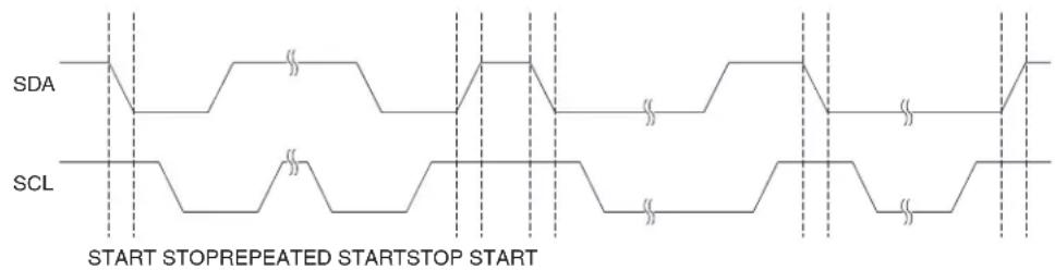
text_image
SDA SCL START STOPREPEATED STARTSTOP START18.1.3 Address Packet Format
All address packets transmitted on the TWI bus are nine bits long, consisting of seven address bits, one READ/WRITE control bit and an acknowledge bit. If the READ/WRITE bit is set, a read operation is to be performed, otherwise a write operation should be performed. When a slave recognizes that it is being addressed, it should acknowledge by pulling SDA low in the ninth SCL (ACK) cycle. If the addressed Slave is busy, or for some other reason can not service the Mas-
ter's request, the SDA line should be left high in the ACK clock cycle. The Master can then transmit a STOP condition, or a REPEATED START condition to initiate a new transmission. An address packet consisting of a slave address and a READ or a WRITE bit is called SLA+R or SLA+W, respectively.
The MSB of the address byte is transmitted first. Slave addresses can freely be allocated by the designer, but the address 0000 000 is reserved for a general call.
When a general call is issued, all slaves should respond by pulling the SDA line low in the ACK cycle. A general call is used when a Master wishes to transmit the same message to several slaves in the system. When the general call address followed by a write bit is transmitted on the bus, all slaves set up to acknowledge the general call will pull the SDA line low in the ACK cycle. The following data packets will then be received by all the slaves that acknowledged the general call. Note that transmitting the general call address followed by a Read bit is meaningless, as this would cause contention if several slaves started transmitting different data.
All addresses of the format 1111 xxx should be reserved for future purposes.
Figure 18-4. Address Packet Format
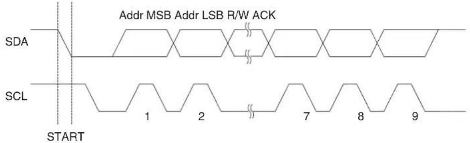
text_image
Addr MSB Addr LSB R/W ACK SDA SCL START 1 2 7 8 918.1.4 Data Packet Format
All data packets transmitted on the TWI bus are nine bits long, consisting of one data byte and an acknowledge bit. During a data transfer, the Master generates the clock and the START and STOP conditions, while the Receiver is responsible for acknowledging the reception. An Acknowledge (ACK) is signalled by the Receiver pulling the SDA line low during the ninth SCL cycle. If the Receiver leaves the SDA line high, a NACK is signalled. When the Receiver has received the last byte, or for some reason cannot receive any more bytes, it should inform the Transmitter by sending a NACK after the final byte. The MSB of the data byte is transmitted first.
Figure 18-5. Data Packet Format
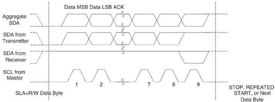
text_image
Data MSB Data LSB ACK Aggregate SDA SDA from Transmitter SDA from Receiver SCL from Master SLA+R/W Data Byte 1 2 7 8 9 STOP, REPEATED START, or Next Data Byte18.1.5 Combining Address and Data Packets Into a Transmission
A transmission basically consists of a START condition, a SLA+R/W, one or more data packets and a STOP condition. An empty message, consisting of a START followed by a STOP condition, is illegal. Note that the wired-ANDing of the SCL line can be used to implement handshaking between the Master and the Slave. The Slave can extend the SCL low period by pulling the SCL line low. This is useful if the clock speed set up by the Master is too fast for the Slave, or the Slave needs extra time for processing between the data transmissions. The Slave extending the SCL low period will not affect the SCL high period, which is determined by the Master. As a consequence, the Slave can reduce the TWI data transfer speed by prolonging the SCL duty cycle.
Figure 18-6 shows a typical data transmission. Note that several data bytes can be transmitted between the SLA+R/W and the STOP condition, depending on the software protocol implemented by the application software.
Figure 18-6. Typical Data Transmission

text_image
Addr MSB Addr LSB R/W ACK SDA SCL START SLA+R/W STOP Data MSB Data LSB ACK 1 2 7 8 9 1 2 7 8 9 Data Byte18.2 Multi-master Bus Systems, Arbitration and Synchronization
The TWI protocol allows bus systems with several masters. Special concerns have been taken in order to ensure that transmissions will proceed as normal, even if two or more masters initiate a transmission at the same time. Two problems arise in multi-master systems:
- An algorithm must be implemented allowing only one of the masters to complete the transmission. All other masters should cease transmission when they discover that they have lost the selection process. This selection process is called arbitration. When a contending master discovers that it has lost the arbitration process, it should immediately switch to Slave mode to check whether it is being addressed by the winning master. The fact that multiple masters have started transmission at the same time should not be detectable to the slaves (i.e., the data being transferred on the bus must not be corrupted).
- Different masters may use different SCL frequencies. A scheme must be devised to synchronize the serial clocks from all masters, in order to let the transmission proceed in a lockstep fashion. This will facilitate the arbitration process.
The wired-ANDing of the bus lines is used to solve both these problems. The serial clocks from all masters will be wired-ANDed, yielding a combined clock with a high period equal to the one from the master with the shortest high period. The low period of the combined clock is equal to the low period of the master with the longest low period. Note that all masters listen to the SCL line, effectively starting to count their SCL high and low Time-out periods when the combined SCL line goes high or low, respectively.
Figure 18-7. SCL Synchronization between Multiple Masters
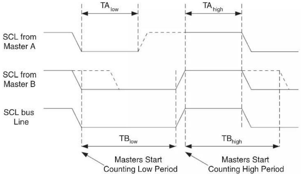
text_image
SCL from Master A SCL from Master B SCL bus Line TA_low TA_high TB_low TB_high Masters Start Counting Low Period Masters Start Counting High PeriodArbitration is carried out by all masters continuously monitoring the SDA line after outputting data. If the value read from the SDA line does not match the value the master had output, it has lost the arbitration. Note that a master can only lose arbitration when it outputs a high SDA value while another master outputs a low value. The losing master should immediately go to Slave mode, checking if it is being addressed by the winning master. The SDA line should be left high, but losing masters are allowed to generate a clock signal until the end of the current data or address packet. Arbitration will continue until only one master remains, and this may take many bits. If several masters are trying to address the same slave, arbitration will continue into the data packet.
Figure 18-8. Arbitration between Two Masters
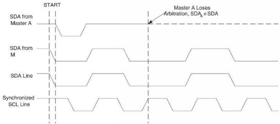
text_image
START Master A Loses Arbitration, SDA₄ ≠ SDA SDA from Master A SDA from M SDA Line Synchronized SCL LineNote that arbitration is not allowed between:
• A REPEATED START condition and a data bit.
• A STOP condition and a data bit.
• A REPEATED START and a STOP condition.
It is the user software's responsibility to ensure that these illegal arbitration conditions never occur. This implies that in multi-master systems, all data transfers must use the same composition of SLA+R/W and data packets. In other words: All transmissions must contain the same number of data packets, otherwise the result of the arbitration is undefined.
18.3 Overview of the TWI Module
The TWI module is comprised of several submodules, as shown in Figure 18-9. All registers drawn in a thick line are accessible through the AT89LP data bus.
Figure 18-9. Overview of the TWI Module
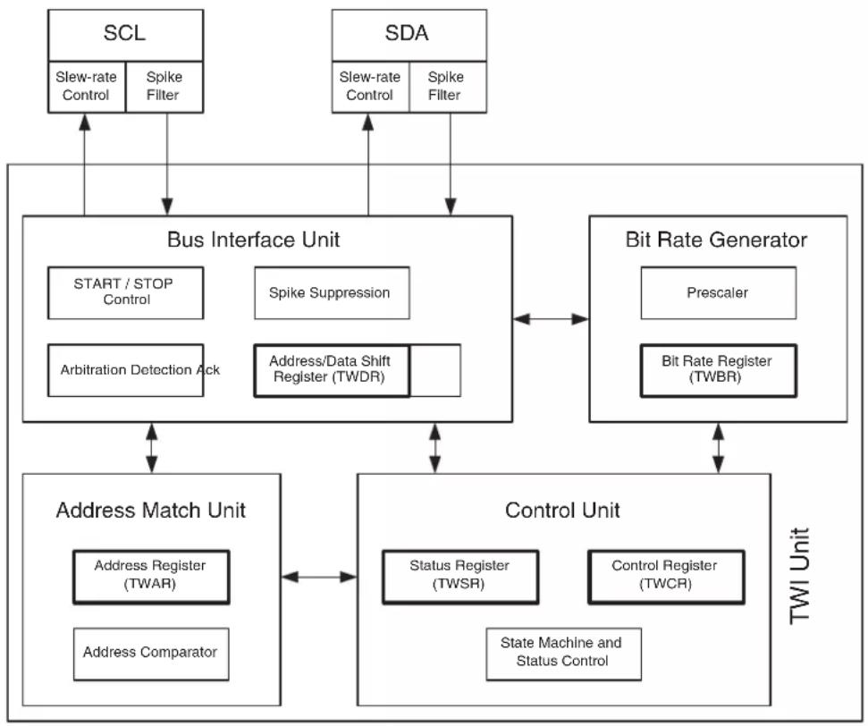
flowchart
graph TD
    A["SCL"] --> B["Bus Interface Unit"]
    C["SDA"] --> B
    B --> D["Address Match Unit"]
    D --> E["Control Unit"]
    E --> F["TWI Unit"]
    B --> G["Start / STOP Control"]
    B --> H["Spike Suppression"]
    B --> I["Arbitration Detection Ack"]
    B --> J["Address/Data Shift Register (TWDR)"]
    B --> K["Bit Rate Generator"]
    K --> L["Prescaler"]
    K --> M["Bit Rate Register (TWBR)"]
    D --> N["Address Register (TWAR)"]
    D --> O["Address Comparator"]
    E --> P["Status Register (TWSR)"]
    E --> Q["Control Register (TWCR)"]
    E --> R["State Machine and Status Control"]
    B --> S["Slew-rate Control"]
    B --> T["Spike Filter"]
18.3.1 SCL and SDA Pins
These pins interface the AT89LP TWI with the rest of the MCU system. The output drivers contain a slew-rate limiter in order to conform to the TWI specification. The input stages contain a spike suppression unit removing spikes shorter than 50 ns.
18.3.2 Bit Rate Generator Unit
This unit controls the period of SCL when operating in a Master mode. The SCL period is controlled by settings in the TWI Bit Rate Register (TWBR). Slave operation does not depend on the Bit Rate setting, but the CPU clock frequency in the slave must be at least 16 times higher than the SCL frequency. Note that slaves may prolong the SCL low period, thereby reducing the
average TWI bus clock period. The SCL frequency is generated according to the following equation:
$$ \text { SCL frequency } = \frac {\text { System Clock }}{1 6 \text { TWBR } 1 + (\quad)} $$
18.3.3 Bus Interface Unit
This unit contains the Data and Address Shift Register (TWDR), a START/STOP Controller and Arbitration detection hardware. The TWDR contains the address or data bytes to be transmitted, or the address or data bytes received. In addition to the 8-bit TWDR, the Bus Interface Unit also contains a register containing the (N)ACK bit to be transmitted or received. This (N)ACK Register is not directly accessible by the application software. However, when receiving, it can be set or cleared by manipulating the TWI Control Register (TWCR). When in Transmitter mode, the value of the received (N)ACK bit can be determined by the value in the TWSR. The START/STOP Controller is responsible for generation and detection of START, REPEATED START, and STOP conditions.
If the TWI has initiated a transmission as Master, the Arbitration Detection hardware continuously monitors the transmission trying to determine if arbitration is in process. If the TWI has lost an arbitration, the Control Unit is informed. Correct action can then be taken and appropriate status codes generated.
18.3.4 Address Match Unit
The Address Match unit checks if received address bytes match the 7-bit address in the TWI Address Register (TWAR). If the TWI General Call Recognition Enable (GC) bit in the TWAR is written to one, all incoming address bits will also be compared against the General Call address. Upon an address match, the Control unit is informed, allowing correct action to be taken. The TWI may or may not acknowledge its address, depending on settings in the TWCR.
18.3.5 Control Unit
The Control unit monitors the TWI bus and generates responses corresponding to settings in the TWI Control Register (TWCR). When an event requiring the attention of the application occurs on the TWI bus, the TWI Interrupt Flag (TWIF) is asserted. In the next clock cycle, the TWI Status Register (TWSR) is updated with a status code identifying the event. The TWSR only contains relevant status information when the TWI interrupt flag is asserted. At all other times, the TWSR contains a special status code indicating that no relevant status information is available. As long as the TWIF flag is set, the SCL line is held low. This allows the application software to complete its tasks before allowing the TWI transmission to continue.
The TWIF flag is set in the following situations:
- After the TWI has transmitted a START/REPEATED START condition.
• After the TWI has transmitted SLA+R/W.
• After the TWI has transmitted an address byte.
• After the TWI has lost arbitration.
• After the TWI has been addressed by own slave address or general call.
• After the TWI has received a data byte. - After TQS or REPEATED START has been received while still addressed as a Slave.
- When a bus error has occurred due to an illegal START or STOP condition.
18.4 Register Overview
Table 18-1. TWCR – Two-Wire Control Register
| TWCR Address = AAH Reset Value = X000 00XXBNot Bit Addressable | ||||||||
| - | T | W | E | N | STAS | TO TWIF AA | - | |
| B | i | t | 7 | 6 | 5 | 4 | 3 | 2 |
| Symbol | Function | |||||||
| TWEN | Two-wire Serial Interface Enable. Set to enable the TWI. Clear to disable the TWI. | |||||||
| STA | Start Flag. Set to send a START condition on the bus. Must be cleared by software. | |||||||
| STO | Stop Flag. Set to send a STOP condition on the bus. Cleared automatically by hardware when the STOP occurs. | |||||||
| TWIF | Two-wire Interface Interrupt Flag. Set by hardware when the TWI requests an interrupt. TWIF must be cleared by software. While TWIF is set, the SCL low period is stretched. Note that clearing this flag starts the operation of the TWI, so all accesses to the other TWI registers (TWAR, TWSR and TWDR) must be complete before clearing this flag. | |||||||
| AA | Assert Acknowledge Flag. Clear in master and slave receiver modes, to force a not acknowledge (high level on SDA). Clear to disable SLA or GCA recognition. Set to recognize SLA or GCA (if GC set) for entering slave receiver or transmitter modes. Set in master and slave receiver modes, to force an acknowledge (low level on SDA). This bit has no effect when in master transmitter mode. By clearing AA to zero, the device can be virtually disconnected from the Two-wire Serial Bus temporarily. Address recognition can then be resumed by setting the AA bit to one again. | |||||||
Table 18-2. TWSR – Two-Wire Status Register
| TWSR Address = ABH Reset Value = 1111 1000BNot Bit Addressable | ||||||||
| TWS7 | TWS6 | TWS5 | TWS4 | TWS3 | 0 | 0 | 0 | |
| B | i | t | 7 | 6 | 5 | 4 | 3 | 2 |
| Symbol | Function | |||||||
| TWS_7-0 | Two-wire Interface Status. The current status code of the TWI logic and serial bus. See Table 18-6 through Table 18-10 for a description of the status codes. Note that the three least significant bits always read as zero. The Status code is valid only while TWIF remains set. | |||||||
Table 18-3. TWAR – Two-Wire Address Register
| TWAR Address = ACH Reset Value = 1111 1110BNot Bit Addressable | ||||||||
| TWA6 | TWA5 | TWA4 | TWA3 | TWA2 | TWA1 | TWA0 | GC | |
| B | i | t | 7 | 6 | 5 | 4 | 3 | 2 |
| Symbol | Function | |||||||
| TWA6-0 | Two-wire Interface Slave Address. The TWI will only respond to slave addresses that match this 7-bit address. | |||||||
| GC | General Call Enable. Set to enable General Call address (00h) recognition. Clear to disable General Call address recognition. | |||||||
Table 18-4. TWDR – Two-Wire Data Register
| TWDR Address = ADH Reset Value = 1111 1111BNot Bit Addressable | ||||||||
| TWD7 TWD | D6 TWD5 TWD | D4 TWD3 TWD | 2 TWD1 TWD0 | |||||
| B | i | t | 7 | 6 | 5 | 4 | 3 | 2 |
| Symbol | Function | |||||||
| TWD_7-0 | Two-wire Interface Data. Writes to TWDR queue the next address or data byte for transmission. Reads from TWDR return the last address or data byte present on the bus. Writes/reads to/from TWDR must occur only while TWIF is set. Writes to TWDR while TWIF = 0 are ignored. Reads from TWDR while TWIF = 0 may return random data. | |||||||
Table 18-5. TWBR – Two-Wire Bit Rate Register
| TWBR Address = AEH Reset Value = 0000 0000BNot Bit Addressable | ||||||||
| B | TWB7 TWB | B6 TWB5 TWB | 4 TWB3 TWB2 | TWB1 TWB0 | ||||
| i | t | 7 | 6 | 5 | 4 | 3 | 2 | |
| Symbol | Function | |||||||
| TWB_7-0 | Two-wire Interface Serial Bit Rate. TWBR is an 8-bit down counter that selects the division factor (+1–256) for the bit rate generator. The bit rate generator is a frequency divider which generates the SCL clock frequency from the system clock in Master mode. | |||||||
18.5 Using the TWI
The AT89LP TWI is byte-oriented and interrupt based. Interrupts are issued after all bus events, like reception of a byte or transmission of a START condition. Because the TWI is interrupt-based, the application software is free to carry on other operations during a TWI byte transfer. Note that the TWI Interrupt Enable (TWE) bit in IE2 together with the Global Interrupt Enable bit in EA allow the application to decide whether or not assertion of the TWIF flag should generate an interrupt request. If the TWE bit is cleared, the application must poll the TWIF flag in order to detect actions on the TWI bus.
When the TWIF flag is asserted, the TWI has finished an operation and awaits application response. In this case, the TWI Status Register (TWSR) contains a value indicating the current state of the TWI bus. The application software can then decide how the TWI should behave in the next TWI bus cycle by manipulating the TWCR and TWDR registers.
Figure 18-10 is a simple example of how the application can interface to the TWI hardware. In this example, a Master wishes to transmit a single data byte to a Slave. This description is quite abstract, a more detailed explanation follows later in this section. A simple code example implementing the desired behavior is also presented.
Figure 18-10. Interfacing the Application to the TWI in a Typical Transmission

flowchart
graph TD
    A["Application Action"] --> B["1. Application writes to TWCR to initiate transmission of START"]
    B --> C["TWI bus"]
    C --> D["START S: TWI A Data A STOP"]
    D --> E["TWI Hardware Action"]
    E --> F["2. TWIF set. Status code indicates START condition sent"]
    E --> G["4. TWIF set. Status code indicates SLA+W sent, ACK received"]
    E --> H["6. TWIF set. Status code indicates data sent, ACK received"]
    H --> I["TWI bus"]
    I --> J["3. Check TWSR to see if START was sent. Application loads SLA+W into TWDR, and loads appropriate control signals into TWCR, making sure that TWIF is written to zero and STA is written to zero."]
    I --> K["5. Check TWSR to see if SLA+W was sent and ACK received. Application loads data into TWDR, and loads appropriate control signals into TWCR, making sure that TWIF is written to zero."]
    I --> L["7. Check TWSR to see if data was sent and ACK received. Application loads appropriate control signals to send STOP into TWCR, making sure that TWIF is written to zero."]
    L --> M["TWI bus"]
    M --> N["Indicates TWIF set"]
- The first step in a TWI transmission is to transmit a START condition. This is done by writing a specific value into TWCR, instructing the TWI hardware to transmit a START condition. Which value to write is described later on. However, it is important that the TWIF bit is cleared in the value written. The TWI will not start any operation as long as the TWIF bit in TWCR is set. Immediately after the application has cleared TWIF, the TWI will initiate transmission of the START condition.
- When the START condition has been transmitted, the TWIF flag in TWCR is set, and TWSR is updated with a status code indicating that the START condition has successfully been sent.
- The application software should now examine the value of TWSR, to make sure that the START condition was successfully transmitted. If TWSR indicates otherwise, the application software might take some special action, like calling an error routine. Assuming that the status code is as expected, the application must load SLA+W into TWDR. Remember that TWDR is used both for address and data. After TWDR has been loaded with the desired SLA+W, a specific value must be written to TWCR, instructing the TWI hardware to transmit the SLA+W present in TWDR. Which value to write is described later on. However, it is important that the TWIF bit is cleared in the value written. The TWI will not start any operation as long as the TWIF bit in TWCR is set. Immediately after the application has cleared TWIF, the TWI will initiate transmission of the address packet.
- When the address packet has been transmitted, the TWIF flag in TWCR is set, and TWSR is updated with a status code indicating that the address packet has successfully been sent. The status code will also reflect whether a slave acknowledged the packet or not.
- The application software should now examine the value of TWSR, to make sure that the address packet was successfully transmitted, and that the value of the ACK bit was as expected. If TWSR indicates otherwise, the application software might take some special action, like calling an error routine. Assuming that the status code is as expected, the application must load a data packet into TWDR. Subsequently, a specific value must be written to TWCR, instructing the TWI hardware to transmit the data packet present in TWDR. Which value to write is described later on. However, it is important that the TWIF bit is cleared in the value written. The TWI will not start any operation as
long as the TWIF bit in TWCR is set. Immediately after the application has cleared TWIF, the TWI will initiate transmission of the data packet.
- When the data packet has been transmitted, the TWIF flag in TWCR is set, and TWSR is updated with a status code indicating that the data packet has successfully been sent. The status code will also reflect whether a slave acknowledged the packet or not.
- The application software should now examine the value of TWSR, to make sure that the data packet was successfully transmitted, and that the value of the ACK bit was as expected. If TWSR indicates otherwise, the application software might take some special action, like calling an error routine. Assuming that the status code is as expected, the application must write a specific value to TWCR, instructing the TWI hardware to transmit a STOP condition. Which value to write is described later on. However, it is important that the TWIF bit is cleared in the value written. The TWI will not start any operation as long as the TWIF bit in TWCR is set. Immediately after the application has cleared TWIF, the TWI will initiate transmission of the STOP condition. Note that TWIF is NOT set after a STOP condition has been sent.
Even though this example is simple, it shows the principles involved in all TWI transmissions. These can be summarized as follows:
- When the TWI has finished an operation and expects application response, the TWIF flag is set. The SCL line is pulled low until TWIF is cleared.
- When the TWIF flag is set, the user must update all TWI registers with the value relevant for the next TWI bus cycle. As an example, TWDR must be loaded with the value to be transmitted in the next bus cycle.
- After all TWI Register updates and other pending application software tasks have been completed, TWCR is written. When writing TWCR, the TWIF bit should be cleared. The TWI will then commence executing whatever operation was specified by the TWCR setting.
18.6 Transmission Modes
The TWI can operate in one of four major modes. These are named Master Transmitter (MT), Master Receiver (MR), Slave Transmitter (ST) and Slave Receiver (SR). Several of these modes can be used in the same application. As an example, the TWI can use MT mode to write data into a TWI EEPROM, MR mode to read the data back from the EEPROM. If other masters are present in the system, some of these might transmit data to the TWI, and then SR mode would be used. It is the application software that decides which modes are legal.
The following sections describe each of these modes. Possible status codes are described along with figures detailing data transmission in each of the modes. These figures contain the following abbreviations:
S: START condition
Rs: REPEATED START condition
R: Read bit (high level at SDA)
W: Write bit (low level at SDA)
A: Acknowledge bit (low level at SDA)
: Not acknowledge bit (high level at SDA)
Data: 8-bit data byte
P: STOP condition
SLA: Slave Address
In Figure 18-11 to Figure 18-14, circles are used to indicate that the TWIF flag is set. The numbers in the circles show the status code held in TWSR. At these points, actions must be taken by the application to continue or complete the TWI transfer. The TWI transfer is suspended until the TWIF flag is cleared by software.
When the TWIF flag is set, the status code in TWSR is used to determine the appropriate software action. For each status code, the required software action and details of the following serial transfer are given in Table 18-6 to Table 18-9.
18.6.1 Master Transmitter Mode
In the Master Transmitter mode, a number of data bytes are transmitted to a Slave Receiver. In order to enter a Master mode, a START condition must be transmitted. The format of the following address packet determines whether Master Transmitter or Master Receiver mode is to be entered. If SLA+W is transmitted, MT mode is entered, if SLA+R is transmitted, MR mode is entered.
A START condition is sent by writing the following value to TWCR:
| TWCR | - | TWEN | STA | STO | TWIF | AA | - | - |
| Value | X | 1 | 1 | 0 | 0 | X | XX |
TWEN must be set to enable the Two-wire Serial Interface, STA must be written to one to transmit a START condition and TWIF must be cleared. The TWI will then test the Two-wire Serial Bus and generate a START condition as soon as the bus becomes free. After a START condition has been transmitted, the TWIF flag is set by hardware, and the status code in TWSR will be 08h (see Table 18-6). In order to enter MT mode, SLA+W must be transmitted. This is done by writing SLA+W to TWDR. Thereafter the TWIF bit should be cleared to continue the transfer.
When SLA+W has been transmitted and an acknowledgment bit has been received, TWIF is set again and a number of status codes in TWSR are possible. Possible status codes in Master mode are 18h, 20h, or 38h. The appropriate action to be taken for each of these status codes is detailed in Table 18-6.
After SLA+W has been successfully transmitted, a data packet should be transmitted. This is done by writing the data byte to TWDR. TWDR must only be written when TWIF is high. If not, the access will be discarded and the previous value will be transmitted. After updating TWDR, the TWIF bit should be cleared to continue the transfer. This scheme is repeated until the last byte has been sent and the transfer is ended by generating a STOP condition or a repeated START condition. A STOP condition is generated by writing the following value to TWCR:
| TWCR Value | - | TWEN | STA | STO | TWIF | AA | - | - |
| X | 1 | 0 | 1 | 0 | X | XX |
A REPEATED START condition is generated by writing the following value to TWCR:
| TWCR Value | - | TWEN | STA | STO | TWIF | AA | - | - |
| X | 1 | 1 | 0 | 0 | X | XX |
After a repeated START condition (status 10h) the Two-wire Serial Interface can access the same slave again, or a new slave without transmitting a STOP condition. Repeated START enables the master to switch between slaves, Master Transmitter mode and Master Receiver mode without losing control of the bus.
Table 18-6. Status Codes for Master Transmitter Mode
| Status Code (TWSR) | Status of the Two-wire Serial Bus and Two-wire Serial Interface Hardware | Application Software Response | Next Action Taken by TWI HardwareTo/from TWDR | ||||
| To TWCR | |||||||
| STA ST | TO TWIF | AA | |||||
| 0x08 | A START condition has been transmitted | Load SLA+W 0 0 1 | X | SLA+W will be transmitted; ACK or NOT ACK will be received | |||
| 10h | A repeated START condition has been transmitted | Load SLA+W | 0 | 0 | 1 | X | SLA+W will be transmitted; ACK or NOT ACK will be received |
| Load SLA+R 0 0 1 | X | SLA+R will be transmitted; Logic will switch to Master Receiver mode | |||||
| 18h | SLA+W has been transmitted; ACK has been received | Load data byte | 0 | 0 | 1 | X | Data byte will be transmitted and ACK or NOT ACK will be received |
| No action | 1 | 0 | 1 | X | Repeated START will be transmitted | ||
| No action | 0 1 1 | X | STOP condition will be transmitted andSTO flag will be reset | ||||
| No action | 1 1 1 | X | STOP condition followed by a START condition will be transmitted and STO flag will be reset | ||||
| 20h | SLA+W has been transmitted; NOT ACK has been received | Load data byte | 0 | 0 | 1 | X | Data byte will be transmitted and ACK or NOT ACK will be received |
| No action | 1 | 0 | 1 | X | Repeated START will be transmitted | ||
| No action | 0 1 1 | X | STOP condition will be transmitted and STO flag will be reset | ||||
| No action | 1 1 1 | X | STOP condition followed by a START condition will be transmitted and STO flag will be reset | ||||
| 28h | Data byte has been transmitted; ACK has been received | Load data byte | 0 | 0 | 1 | X | Data byte will be transmitted and ACK or NOT ACK will be received |
| No action | 1 | 0 | 1 | X | Repeated START will be transmitted | ||
| No action | 0 1 1 | X | STOP condition will be transmitted and STO flag will be reset | ||||
| No action | 1 1 1 | X | TOP condition followed by a START condition will be transmitted and STO flag will be reset | ||||
| 30h | Data byte has been transmitted; NOT ACK has been received | Load data byte | 0 | 0 | 1 | X | Data byte will be transmitted and ACK or NOT ACK will be received |
| No actio | 1 | 0 | 1 | X | Repeated START will be transmitted | ||
| No actio | 0 1 1 | X | STOP condition will be transmitted and STO flag will be reset | ||||
| No actio | 1 1 1 | X | STOP condition followed by a START condition will be transmitted and STO flag will be reset | ||||
| 38h | Arbitration lost in SLA+W or data bytes | No action | 0 0 1 | X | Two-wire Serial Bus will be released and not addressed slave mode entered | ||
| No action | 1 0 1 | X | A START condition will be transmitted when the bus becomes free | ||||
Figure 18-11. Format and States in Master Transmitter Mode

flowchart
graph TD
    A["MT"] --> B["S SLA W A DATA A P"]
    B --> C["08h"]
    B --> D["18h 28h"]
    D --> E["RgSLA W"]
    E --> F["10h"]
    E --> G["R"]
    G --> H["MR"]
    B --> I["A P"]
    I --> J["20h"]
    I --> K["A or A Other master continues"]
    K --> L["38h"]
    K --> M["A Other master continues"]
    M --> N["68h 78h 80h"]
    N --> O["To corresponding states in slave mode"]
    B --> P["Next transfer started with a repeated start condition"]
    P --> Q["Not acknowledge received after the slave address"]
    Q --> R["Not acknowledge received after a data byte"]
    R --> S["Arbitration lost in slave address or data byte"]
    S --> T["Arbitration lost and addressed as slave"]

From master to slave

Any number of data bytes and their associated acknowledge bits
From slave to master

This number (contained in TWSR) corresponds to a defined state of the Two-wire Serial Bus. The prescaler bits are zero or masked to zero
18.6.2 Master Receiver Mode
In the Master Receiver mode, a number of data bytes are received from a slave transmitter. In order to enter a Master mode, a START condition must be transmitted. The format of the following address packet determines whether Master Transmitter or Master Receiver mode is to be entered. If SLA+W is transmitted, MT mode is entered, if SLA+R is transmitted, MR mode is entered.
TWEN must be written to one to enable the Two-wire Serial Interface, STA must be written to one to transmit a START condition and TWIF must be cleared. The TWI will then test the Two-wire Serial Bus and generate a START condition as soon as the bus becomes free. After a START condition has been transmitted, the TWIF flag is set by hardware, and the status code in TWSR will be 08h (see Table 18-7). In order to enter MR mode, SLA+R must be transmitted. This is done by writing SLA+R to TWDR. Thereafter the TWIF bit should be cleared to continue the transfer.
When SLA+R has been transmitted and an acknowledgment bit has been received, TWIF is set again and a number of status codes in TWSR are possible. Possible status codes in Master mode are 38h, 40h or 48h. The appropriate action to be taken for each of these status codes is detailed in Table 18-7. Received data can be read from the TWDR Register when the TWIF flag is set high by hardware. This scheme is repeated until the last byte has been received. After the last byte has been received, the MR should inform the ST by sending a NACK after the last received data byte. The transfer is ended by generating a STOP condition or a repeated START condition.
Table 18-7. Status Codes for Master Receiver Mode
| Status Code (TWSR) | Status of the Two-wire Serial Bus and Two-wire Serial Interface Hardware | Application Software Response | Next Action Taken by TWI HardwareTofrom TWDR | ||||
| To TWCR | |||||||
| STA | STO | TWIF AA | |||||
| 08h | A START condition has been transmitted | Load SLA+R 0 0 1 | X | SLA+R will be transmitted; ACK or NOT ACK will be received | |||
| 10h | A repeated START condition has been transmitted | Load SLA+R 0 0 1 | X | SLA+R will be transmitted; ACK or NOT ACK will be received | |||
| Load SLA+W 0 0 1 | X | SLA+W will be transmitted; Logic will switch to Master Transmitter mode | |||||
| 38h | Arbitration lost in SLA+R or NOT ACK bit | No action | 0 0 1 | X | Two-wire Serial Bus will be released and not addressed Slave mode will be entered | ||
| No action | 1 0 1 | X | A START condition will be transmitted when the bus becomes free | ||||
| 40h | SLA+R has been transmitted; ACK has been received | No action | 0 | 0 | 1 | 0 | Data byte will be received and NOT ACK will be returned |
| No action | 0 | 0 | 1 | 1 | Data byte will be received and ACK will be returned | ||
| 48h | SLA+R has been transmitted; NOT ACK has been received | No action | 1 | 0 | 1 | X | Repeated START will be transmitted |
| No action | 0 1 1 | X | STOP condition will be transmitted and STO flag will be reset | ||||
| No action | 1 1 1 | X | STOP condition followed by a START condition will be transmitted and STO flag will be reset | ||||
| 50h | Data byte has been received; ACK has been returned | Read data byte | 0 | 0 | 1 | 0 | Data byte will be received and NOT ACK will be returned |
| Read data byte | 0 | 0 | 1 | 1 | Data byte will be received and ACK will be returned | ||
| 58h | Data byte has been received; NOT ACK has been returned | Read data byte | 1 | 0 | 1 | X | Repeated START will be transmitted |
| Read data byte | 0 1 1 | X | STOP condition will be transmitted and STO flag will be reset | ||||
| Read data byte | 1 | 1 | 1 | X | STOP condition followed by a START condition will be transmitted and STO flag will be reset | ||
Figure 18-12. Format and States in Master Receiver Mode

flowchart
graph TD
    A["Successful reception from a slave receiver"] --> B["S SLA R A DATA A"]
    B --> C["MR"]
    C --> D["Next transfer started with a repeated start condition"]
    D --> E["Not acknowledge received after the slave address"]
    E --> F["A or A"]
    F --> G["Arbitration lost in slave address or data byte"]
    G --> H["Arbitration lost and addressed as slave"]
    H --> I["A or A"]
    I --> J["Other master continues"]
    J --> K["A"]
    K --> L["Other master continues"]
    L --> M["W"]
    M --> N["MT"]
    N --> O["-"]
    O --> P["58h"]
    P --> Q["Rs"]
    Q --> R["SLA R"]
    R --> S["10h"]
    S --> T["PDATA A"]
    T --> U["MR"]
    U --> V["MR"]
    V --> W["MR"]
    W --> X["MR"]
    X --> Y["MR"]
    Y --> Z["MR"]
    Z --> AA["MR"]
    AA --> AB["MR"]
    AB --> AC["MR"]
    AC --> AD["MR"]
    AD --> AE["MR"]
    AE --> AF["MR"]
    AF --> AG["MR"]
    AG --> AH["MR"]
    AH --> AI["MR"]
    AI --> AJ["MR"]
    AJ --> AK["MR"]
    AK --> AL["MR"]
    AL --> AM["MR"]
    AM --> AN["MR"]
    AN --> AO["MR"]
    AO --> AP["MR"]
    AP --> AQ["MR"]
    AQ --> AR["MR"]
    AR --> AS["MR"]
    AS --> AT["MR"]
    AT --> AU["MR"]
    AU --> AV["MR"]
    AV --> AW["MR"]
    AW --> AX["MR"]
    AX --> AY["MR"]
    AY --> AZ["MR"]
    AZ --> BA["MR"]
    BA --> BB["MR"]
    BB --> BC["MR"]
    BC --> BD["MR"]
    BD --> BE["MR"]
    BE --> BF["MR"]
    BF --> BG["MR"]
    BG --> BH["MR"]
    BH --> BI["MR"]
    BI --> BJ["MR"]
    BJ --> BK["MR"]
    BK --> BL["MR"]
    BL --> BM["MR"]
    BM --> BN["MR"]
    BN --> BO["MR"]
    BO --> BP["MR"]
    BP --> BQ["MR"]
    BQ --> BR["MR"]
    BR --> BS["MR"]
    BS --> BT["MR"]
    BT --> BU["MR"]
    BU --> BV["MR"]
    BV --> BW["MR"]

From master to slave

Any number of data bytes and their associated acknowledge bits

From slave to master

This number (contained in TWSR) corresponds to a defined state of the Two-wire Serial Bus. The prescaler bits are zero or masked to zero
18.6.3 Slave Receiver Mode
In the Slave Receiver mode, a number of data bytes are received from a master transmitter. To initiate the Slave Receiver mode, TWAR and TWCR must be initialized as follows:
| TWAR Value | TWA6 | TWA5 | TWA4 | TWA3 | TWA2 | TWA1 | TWA0 | GC |
| Device's own Slave Address | X | |||||||
The upper seven bits are the address to which the Two-wire Serial Interface will respond when addressed by a master. If the LSB is set, the TWI will respond to the general call address (00h), otherwise it will ignore the general call address.:
| TWCR Value | - | TWEN | STA | STO | TWIF | AA | - | - |
| X | 1 | 0 | 0 | 0 | 1 | X | X |
TWEN must be written to one to enable the TWI. The AA bit must be written to one to enable the acknowledgment of the device's own slave address or the general call address. STA and STO must be written to zero.
When TWAR and TWCR have been initialized, the TWI waits until it is addressed by its own slave address (or the general call address if enabled) followed by the data direction bit. If the direction bit is "0" (write), the TWI will operate in SR mode, otherwise ST mode is entered. After its own slave address and the write bit have been received, the TWIF flag is set and a valid status code can be read from TWSR. The status code is used to determine the appropriate software action. The appropriate action to be taken for each status code is detailed in Table 18-8. The Slave Receiver mode may also be entered if arbitration is lost while the TWI is in the Master mode (see states 68h and 78h).
If the AA bit is reset during a transfer, the TWI will return a "Not Acknowledge" ("1") to SDA after the next received data byte. This can be used to indicate that the slave is not able to receive any more bytes. While AA is zero, the TWI does not acknowledge its own slave address. However, the Two-wire Serial Bus is still monitored and address recognition may resume at any time by setting AA. This implies that the AA bit may be used to temporarily isolate the TWI from the Two-wire Serial Bus.
Table 18-8. Status Codes for Slave Receiver Mode
| Status Code (TWSR) | Status of the Two-wire Serial Bus and Two-wire Serial Interface Hardware | Application Software Response | Next Action Taken by TWI HardwareTo/from TWDR | ||||
| To TWCR | |||||||
| STA S | TO TWIF AA | ||||||
| 60h | Own SLA+W has been received; ACK has been returned | No action X 0 1 0 | Data byte will be received and NOT ACK will be returned | ||||
| No action X 0 1 1 | Data byte will be received and ACK will be returned | ||||||
| 68h | Arbitration lost in SLA+R/W as master; own SLA+W has been received; ACK has been returned | No action X 0 1 0 | Data byte will be received and NOT ACK will be returned | ||||
| No action X 0 1 1 | Data byte will be received and ACK will be returned | ||||||
| 70h | General call address has been received; ACK has been returned | No action X 0 1 0 | Data byte will be received and NOT ACK will be returned | ||||
| No action X 0 1 1 | Data byte will be received and ACK will be returned | ||||||
| 78h | Arbitration lost in SLA+R/W as master; General call address has been received; ACK has been returned | No action X 0 1 0 | Data byte will be received and NOT ACK will be returned | ||||
| No action X 0 1 1 | Data byte will be received and ACK will be returned | ||||||
| 80h | Previously addressed with own SLA+W; data has been received; ACK has been returned | Read data byte | X | 0 | 1 | 0 | Data byte will be received and NOT ACK will be returned |
| Read data byte | X | 0 | 1 | 1 | Data byte will be received and ACK will be returned | ||
Table 18-8. Status Codes for Slave Receiver Mode
| 88h | Previously addressed with own SLA+W; data has been received; NOT ACK has been returned | Read data byte | 0 | 0 | 1 | 0 | Switched to the not addressed Slave mode; no recognition of own SLA or GCA |
| Read data byte | 0 | 0 | 1 | 1 | Switched to the not addressed Slave mode; own SLA will be recognized; GCA will be recognized if GC = “1” | ||
| Read data byte | 1 | 0 | 1 | 0 | Switched to the not addressed Slave mode; no recognition of own SLA or GCA; a START condition will be transmitted when the bus becomes free | ||
| Read data byte | 1 | 0 | 1 | 1 | Switched to the not addressed Slave mode; own SLA will be recognized; GCA will be recognized if GC = “1”; a START condition will be transmitted when the bus becomes free | ||
| 90h | Previously addressed with general call; data has been received; ACK has been returned | Read data byte | X | 0 | 1 | 0 | Data byte will be received and NOT ACK will be returned |
| Read data byte | X | 0 | 1 | 1 | Data byte will be received and ACK will be returned | ||
| 98h | Previously addressed with general call; data has been received; NOT ACK has been returned | Read data byte | 0 | 0 | 1 | 0 | Switched to the not addressed Slave mode; no recognition of own SLA or GCA |
| Read data byte | 0 | 0 | 1 | 1 | Switched to the not addressed Slave mode; own SLA will be recognized; GCA will be recognized if GC = “1” | ||
| Read data byte | 1 | 0 | 0 | 1 | Switched to the not addressed Slave mode; no recognition of own SLA or GCA; a START condition will be transmitted when the bus becomes free | ||
| Read data byte | 1 | 0 | 1 | 1 | Switched to the not addressed Slave mode; own SLA will be recognized; GCA will be recognized if GC = “1”; a START condition will be transmitted when the bus becomes free | ||
| A0h | A STOP condition or repeated START condition has been received while still addressed as slave | No Action 0 0 1 0 | Switched to the not addressed Slave mode; no recognition of own SLA or GCA | ||||
| No Action 0 0 1 1 | Switched to the not addressed Slave mode; own SLA will be recognized; GCA will be recognized if GC = “1” | ||||||
| No Action 1 0 1 0 | Switched to the not addressed Slave mode; no recognition of own SLA or GCA; a START condition will be transmitted when the bus becomes free | ||||||
| No Action 1 0 1 1 | Switched to the not addressed Slave mode; own SLA will be recognized; GCA will be recognized if GC = “1”; a START condition will be transmitted when the bus becomes free |
Figure 18-13. Format and States in Slave Receiver Mode

flowchart
graph TD
    A["Reception of the own slave address and one or more data bytes. All are acknowledged"] --> B["S SLA W A DATA"]
    B --> C["A"]
    C --> D["60h"]
    D --> E["Last data byte received is not acknowledged"]
    E --> F["A"]
    F --> G["Arbitration lost as master and addressed as slave"]
    G --> H["A"]
    H --> I["DATA"]
    I --> J["A"]
    J --> K["P or S"]
    K --> L["A"]
    L --> M["P or S"]
    M --> N["88h"]
    N --> O["A"]
    O --> P["P or S"]
    P --> Q["CRO-2/11"]
18.6.4 Slave Transmitter Mode
In the Slave Transmitter mode, a number of data bytes are transmitted to a master receiver. To initiate the Slave Transmitter mode, upper 7 bits of TWAR must be initialized with the address to which the Two-wire Serial Interface will respond when addressed by a master. If the LSB is set, the TWI will respond to the general call address (00h), otherwise it will ignore the general call address. TWEN must be written to one to enable the TWI. The AA bit must be written to one to enable the acknowledgment of the device's own slave address or the general call address. STA and STO must be written to zero.
When TWAR and TWCR have been initialized, the TWI waits until it is addressed by its own slave address (or the general call address if enabled) followed by the data direction bit. If the direction bit is "1" (read), the TWI will operate in ST mode, otherwise SR mode is entered. After its own slave address and the write bit have been received, the TWINT flag is set and a valid status code can be read from TWSR. The status code is used to determine the appropriate software action. The appropriate action to be taken for each status code is detailed in Table 18-9. The Slave Transmitter mode may also be entered if arbitration is lost while the TWI is in the Master mode (see state B0h).
If the AA bit is written to zero during a transfer, the TWI will transmit the last byte of the transfer. State C0h or state C8h will be entered, depending on whether the master receiver transmits a NACK or ACK after the final byte. The TWI is switched to the not addressed Slave mode, and will ignore the master if it continues the transfer. Thus the master receiver receives all "1s" as serial data. State C8h is entered if the master demands additional data bytes (by transmitting ACK), even though the slave has transmitted the last byte (AA zero and expecting NACK from the master). While AA is zero, the TWI does not respond to its own slave address. However, the Two-wire Serial Bus is still monitored and address recognition may resume at any time by setting AA. This implies that the AA bit may be used to temporarily isolate the TWI from the Two-wire Serial Bus.
Figure 18-14. Format and States in Slave Transmitter Mode
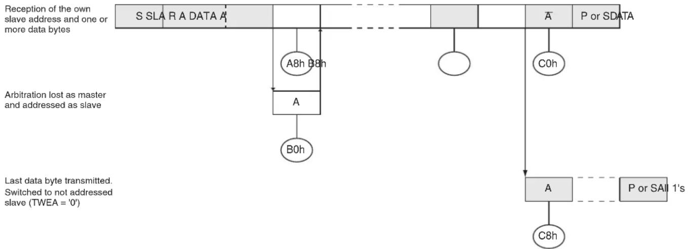
flowchart
graph TD
    A["S SLA R A DATA A"] --> B["A8h B8h"]
    B --> C["A"]
    C --> D["B0h"]
    D --> E["Arbitration lost as master and addressed as slave"]
    E --> F["A"]
    F --> G["C0h"]
    G --> H["A"]
    H --> I["C8h"]
    I --> J["P or SDATA"]
    K["Last data byte transmitted. Switched to not addressed slave (TWEA = '0')"] --> L["A"]
    L --> M["P or SALL 1's"]


From master to slave
From slave to master


Any number of data bytes and their associated acknowledge bits
This number (contained in TWSR) corresponds to a defined state of the Two-wire Serial Bus. The prescaler bits are zero or masked to zero
Table 18-9. Status Codes for Slave Transmitter Mode
| Status Code (TWSR) | Status of the Two-wire Serial Bus and Two-wire Serial Interface Hardware | Application Software Response | Next Action Taken by TWI HardwareTo/from TW | ||||
| To TWCR | |||||||
| STA | STO | TWIF AA | |||||
| A8h | Own SLA+R has been received; ACK has been returned | Load data byte | X | 0 | 1 | 0 | Last data byte will be transmitted and NOT ACK should be received |
| Load data byte | X | 0 | 1 | 1 | Data byte will be transmitted and ACK should be received | ||
| B0h | Arbitration lost in SLA+R/W as master; own SLA+R has been received; ACK has been returned | Load data byte | X | 0 | 1 | 0 | Last data byte will be transmitted and NOT ACK should be received |
| Load data byte | X | 0 | 1 | 1 | Data byte will be transmitted and ACK should be received | ||
| B8h | Data byte in TWDR has been transmitted; ACK has been received | Load data byte | X | 0 | 1 | 0 | Last data byte will be transmitted and NOT ACK should be received |
| Load data byte | X | 0 | 1 | 1 | Data byte will be transmitted and ACK should be received | ||
| C0h | Data byte in TWDR has been transmitted; NOT ACK has been received | No action 0 0 1 0 | Switched to the not addressed Slave mode; no recognition of own SLA or GCA | ||||
| No action 0 0 1 1 | Switched to the not addressed Slave mode; own SLA will be recognized; GCA will be recognized if GC = “1” | ||||||
| No action 1 0 1 0 | Switched to the not addressed Slave mode; no recognition of own SLA or GCA; a START condition will be transmitted when the bus becomes free | ||||||
| No action 1 0 1 1 | Switched to the not addressed Slave mode; own SLA will be recognized; GCA will be recognized if GC = “1”; a START condition will be transmitted when the bus becomes free | ||||||
| C8h | Last data byte in TWDR has been transmitted (AA = “0”); ACK has been received | No action 0 0 1 0 | Switched to the not addressed Slave mode; no recognition of own SLA or GCA | ||||
| No action 0 0 1 1 | Switched to the not addressed Slave mode; own SLA will be recognized; GCA will be recognized if GC = “1” | ||||||
| No action 1 0 1 1 | Switched to the not addressed Slave mode; no recognition of own SLA or GCA; a START condition will be transmitted when the bus becomes free | ||||||
| No action 1 0 1 1 | Switched to the not addressed Slave mode; own SLA will be recognized; GCA will be recognized if GC = “1”; a START condition will be transmitted when the bus becomes free | ||||||
18.6.5 Miscellaneous States
There are two status codes that do not correspond to a defined TWI state, see Table 18-10.
Status F8h indicates that no relevant information is available because the TWIF flag is not set. This occurs between other states, and when the TWI is not involved in a serial transfer.
Status 00h indicates that a bus error has occurred during a Two-wire Serial Bus transfer. A bus error occurs when a START or STOP condition occurs at an illegal position in the format frame. Examples of such illegal positions are during the serial transfer of an address byte, a data byte, or an acknowledge bit. When a bus error occurs, TWIF is set. To recover from a bus error, the STO flag must set and TWIF must be cleared. This causes the TWI to enter the not addressed Slave mode and to clear the STO flag (no other bits in TWCR are affected). The SDA and SCL lines are released, and no STOP condition is transmitted.
Table 18-10. Miscellaneous States
| Status Code (TWSR) | Status of the Two-wire Serial Bus and Two-wire Serial Interface hardware | Application Software Response | Next Action Taken by TWI HardwareTo/from TWDR | ||||
| To TWCR | |||||||
| STA | STO | TWIF AA | |||||
| F8h | No relevant state information available; TWIF = "0" | No action | No action | Wait or proceed current transfer | |||
| 00h | Bus error due to an illegal START or STOP condition | No action | 0 | 1 | 1 | X | Only the internal hardware is affected, no STOP condition is sent on the bus. In all cases, the bus is released and STO is cleared. |
18.6.6 Combining Several TWI Modes
In some cases, several TWI modes must be combined in order to complete the desired action. Consider for example reading data from a serial EEPROM. Typically, such a transfer involves the following steps:
- The transfer must be initiated.
- The EEPROM must be instructed what location should be read.
- The reading must be performed.
- The transfer must be finished.
Note that data is transmitted both from Master to Slave and vice versa. The Master must instruct the Slave what location it wants to read, requiring the use of the MT mode. Subsequently, data must be read from the Slave, implying the use of the MR mode. Thus, the transfer direction must be changed. The Master must keep control of the bus during all these steps, and the steps should be carried out as an atomic operation. If this principle is violated in a multi-master system, another Master can alter the data pointer in the EEPROM between steps 2 and 3, and the Master will read the wrong data location. Such a change in transfer direction is accomplished by transmitting a REPEATED START between the transmission of the address byte and reception of the data. After a REPEATED START, the Master keeps ownership of the bus. The following figure shows the flow in this transfer.
Figure 18-15. Combining Several TWI Modes to Access a Serial EEPROM
flowchart
graph LR
    subgraph_Master_Transmitter["Master Transmitter"]
        S1["S"] --> S2["SLA+W"] --> A["A"] --> Address["ADDRESS"] --> A2["A"] --> Rs["Rs"] --> SLR["SLA+R"] --> A3["A"] --> DATA["DATA"] --> A4["A̅"] --> P["P"]
    end
    subgraph_Master_Receiver["Master Receiver"]
        S3["S = START"] --> S4["RS = REPEATED START"] --> P["P = STOP"]
        P --> S5["Transmitted from master to slave"] --> S6["Transmitted from slave to master"]
    end
19. Dual Analog Comparators
The AT89LP3240/6440 provides two analog comparators. The analog comparators have the following features:
- Internal 3-level Voltage Reference (1.2V, 1.3V, 1.4V)
- Four Shared Analog Input Channels
- Configure as Multiple Input Window Comparator
- Selectable Interrupt Conditions
– High- or Low-level
– Rising- or Falling-edge - O utput Toggle
- Hardware Debouncing Modes
Figure 19-1. Dual Comparator Block Diagram

flowchart
graph TD
    subgraph Inputs
        A["(P2.7) AIN3"] --> B["11 10 01 00"]
        C["(P2.6) AIN2"] --> D["11 10 01 00"]
        E["(P2.5) AIN1"] --> F["11 10 01 00"]
        G["(P2.4) AIN0"] --> H["11 10 01 00"]
    end

    B --> I["B"]
    D --> J["A"]
    F --> K["A"]
    H --> L["A"]

    I --> M["CMPB (P4.7)"]
    J --> N["CMPA (P4.6)"]

    subgraph Outputs
        O["CSB1"] --> P["RFB0"]
        Q["CSB0"] --> R["RFB1"]
        S["CSA0"] --> T["RFA1"]
        U["CSA1"] --> V["RFA0"]
        W["VAREF+Δ"] --> X["VAREF"]
        Y["VAREF"] --> Z["VAREF-Δ"]
        AA["VAREF-Δ"] --> AB["Ground"]
    end

    I --> AC["CMB2"]
    I --> AD["CMB1"]
    I --> AE["CMB0"]
    I --> AF["CFB"]
    I --> AG["CFA"]
    I --> AH["Interrupt"]
    I --> AI["EC"]

    subgraph Outputs
        AJ["CMA2"] --> AK["CMA1"]
        AL["CMA0"] --> AM["CMA0"]
        AN["VAREF+Δ"] --> AO["VAREF"]
        AP["VAREF"] --> AQ["VAREF-Δ"]
        AR["VAREF-Δ"] --> AS["Ground"]
    end

    subgraph Outputs
        AT["Interrupt"] --> AU["AND Gate"]
        AU --> AV["AND Gate"]
        AW["AND Gate"] --> AX["AND Gate"]
        AY["AND Gate"] --> AZ["AND Gate"]
        BA["AND Gate"] --> BB["AND Gate"]
        BC["AND Gate"] --> BD["AND Gate"]
        BE["AND Gate"] --> BF["AND Gate"]
        BG["AND Gate"] --> BH["AND Gate"]
        BI["AND Gate"] --> BJ["AND Gate"]
        BK["AND Gate"] --> BL["AND Gate"]
        BM["AND Gate"] --> BN["AND Gate"]
        BO["AND Gate"] --> BP["AND Gate"]
        BQ["AND Gate"] --> BR["AND Gate"]
        BS["AND Gate"] --> BT["AND Gate"]
        BU["AND Gate"] --> BV["AND Gate"]
        BW["AND Gate"] --> BX["AND Gate"]
        BY["AND Gate"] --> BZ["AND Gate"]
        CA["AND Gate"] --> CB["AND Gate"]
        CC["AND Gate"] --> CD["AND Gate"]
        DE["AND Gate"] --> FD["AND Gate"]
        DG["AND Gate"] --> DH["AND Gate"]
        DI["AND Gate"] --> DJ["AND Gate"]
        DK["AND Gate"] --> DL["AND Gate"]
        DM["AND Gate"] --> DJ
        DB["AND Gate"] --> DC["AND Gate"]
        DD["AND Gate"] --> DL
        DV["AND Gate"] --> DX["AND Gate"]
        DXN["AND Gate"] --> DB
        DBX["AND Gate"] --> DXN["AND Gate"]
        DXN --> DXN
    end

    style Inputs fill:#f9f,stroke:#333
    style Outputs fill:#ccf,stroke:#333
A block diagram of the dual analog comparators with relevant connections is shown in Figure 19-1. Input options allow the comparators to function in a number of different configurations as shown in Figure 19-4. Comparator operation is such that the output is a logic "1" when the positive input is greater than the negative input. Otherwise the output is a zero. Setting the CENA (ACSRA.3) and CENB (ACSRB.3) bits enable Comparator A and B respectively. The user must
also set the CONA (ACSRA.5) or CONB (ACSRB.5) bits to connect the comparator inputs before using a comparator. When a comparator is first enabled, the comparator output and interrupt flag are not guaranteed to be stable for 10 s. The corresponding comparator interrupt should not be enabled during that time, and the comparator interrupt flag must be cleared before the interrupt is enabled in order to prevent an immediate interrupt service. Before enabling the comparators, the analog inputs should be tristated by putting P2.4, P2.5, P2.6 and P2.7 into input-only mode. See “Port Analog Functions” on page 48.
Each comparator may be configured to cause an interrupt under a variety of output value conditions by setting the CMx_2-0 bits in ACSRx. The comparator interrupt flags CFx in ACSRx are set whenever the comparator outputs match the conditions specified by CMx_2-0 . The flags may be polled by software or may be used to generate an interrupt and must be cleared by software. Both comparators share a common interrupt vector. If both comparators are enabled, the user needs to read the flags after entering the interrupt service routine to determine which comparator caused the interrupt.
The CAC_1-0 and CBC_1-0 bits in AREF control when the comparator interrupts sample the comparator outputs. Normally the outputs are sampled every clock system; however, the outputs may also be sampled whenever Timer 0, Timer 1 or Timer 2 overflows. These settings allow the comparators to be sampled at a specific time or to reduce the number of comparator events seen by the system when using level sensitive modes. The comparators will continue to function during Idle mode. If this is not the desired behavior, the comparators should be disabled before entering Idle. The comparators are always disabled during Power-down mode.
19.1 Analog Input Muxes
The positive input terminal of each comparator may be connected to any of the four analog input pins by changing the CSA_1-0 or CSB_1-0 bits in ACSRA and ACSRB. When changing the analog input pins, the comparator must be disconnected from its inputs by clearing the CONA or CONB bits. The connection is restored by setting the bits again after the muxes have been modified.
CLR EC ; Disable comparator interrupts
ANL ACSRA, #0DFh ; Clear CONA to disconnect COMP A ... ; Modify CSA or RFA bits
ORL ACSRA, #020h ; Set CONA to connect COMP A
ANL ACSRA, #0EFh ; Clear any spurious interrupt
ETB EC ; Re-enable comparator interrupts
The corresponding comparator interrupt should not be enabled while the inputs are being changed, and the comparator interrupt flag must be cleared before the interrupt is re-enabled in order to prevent an unintentional interrupt request.
The equivalent model for the analog input circuitry is illustrated in Figure 20-3. An analog source applied to AlNn is subjected to the pin capacitance and input leakage of that pin, regardless of whether that channel is selected as input to the comparator. When the channel is selected, the source must drive the input capacitance of the comparator through the series resistance (combined resistance in the input path).
Figure 19-2. Equivalent Analog Input Model
text_image
AINn CPIN = 10 pF RIN = 10 kΩ RMUX = 10 kΩ CCMP < 0.3 pF19.2 Internal Reference Voltage
The negative input terminal of each comparator may be connected to an internal voltage reference by changing the RFB_1-0 or RFA_1-0 bits in AREF. The internal reference voltage, V_AREF , is set to 1.3 V ±5%. The voltage reference also provides two additional voltage levels approximately 100 mV above and below V_AREF . These levels may be used to configure the comparators as an internally referenced window comparator with up to four input channels. Changing the reference input must follow the same routine used for changing the positive input as described in “Analog Input Muxes” above.
19.3 Comparator Interrupt Debouncing
The comparator output is normally sampled every clock cycle. The conditions on the analog inputs may be such that the comparator output will toggle excessively. This is especially true if applying slow moving analog inputs. Three debouncing modes are provided to filter out this noise for edge-triggered interrupts. In debouncing mode, the comparator uses Timer 1 to modulate its sampling time when CxC_1-0 = 00B . When a relevant transition occurs, the comparator waits until two Timer 1 overflows have occurred before resampling the output. If the new sample agrees with the expected value, CFx is set. Otherwise, the event is ignored. The filter may be tuned by adjusting the time-out period of Timer 1. Because Timer 1 is free running, the debouncer must wait for two overflows to guarantee that the sampling delay is at least 1 time-out period. Therefore, after the initial edge event, the interrupt may occur between 1 and 2 time-out periods later. See Figure 19-3. When the comparator clock is provided by one of the timer overflows, i.e. CxC_1-0 != 00B , any change in the comparator output must be valid after 4 samples to be accepted as an edge event.
Figure 19-3. Negative Edge with Debouncing Example
text_image
Comparator Out Timer 1 Overflow CFx Start Compare (rejected) Start Compare (accepted)Figure 19-4. Dual Comparator Configuration Examples
a. dual independent comparators with external references

text_image
AIN0 AIN1 + - A CMPA CSA = 00 RFA = 00 CSB = 11 RFB = 00 AIN3 AIN2 + - B CMPBb. 3-channel comparator with external reference

text_image
AIN0 AIN2 AIN3 AIN1 CSA = 00/10/11 RFA = 00 CMPAc. 4-channel comparator with internal reference
text_image
AIN0 AIN1 AIN2 AIN3 VAREF A CMPA CSA = 00/01/10/11 RFA = 10d. 2-channel comparator with internal reference & comparator with external reference
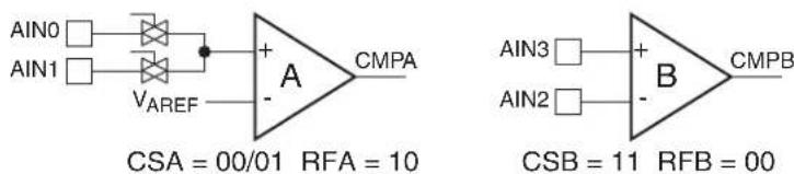
text_image
AIN0 AIN1 VAREF + A CMPA CSA = 00/01 RFA = 10 AIN3 AIN2 B CMPB CSB = 11 RFB = 00e. 2-channel comparator with external reference & comparator with internal reference

text_image
AIN0 AIN2 AIN1 A CMPA CSA = 00/10 RFA = 00 AIN3 VAREF B CMPB CSB = 11 RFB = 10f. 2-channel window comparator with external reference
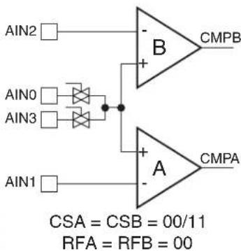
text_image
AIN2 AIN0 AIN3 AIN1 B CMPB A CMPA CSA = CSB = 00/11 RFA = RFB = 00g. 4-channel window comparator with internal reference
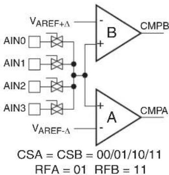
text_image
VAREF+Δ AIN0 AIN1 AIN2 AIN3 VAREF-Δ B CMPB + - A CMPA CSA = CSB = 00/01/10/11 RFA = 01 RFB = 11Table 19-1. ACSRA – Analog Comparator A Control & Status Register
| ACSRA = 97H Reset Value = 0000 0000BNot Bit Addressable | ||||||||
| CSA1 CSA0 | CONA CFA CENA CMA2 | CMA1 CMA0 | ||||||
| B | i | t | 7 | 6 | 5 | 4 | 3 | 2 |
| Symbol Function | ||||||||
| CSA [1-0] | Comparator A Positive Input Channel Select(1) | |||||||
| CSA1 | CSA0 | A+ Channel | ||||||
| 0 | 0 | AIN0 (P2.4) | ||||||
| 0 | 1 | AIN1 (P2.5) | ||||||
| 1 | 0 | AIN2 (P2.6) | ||||||
| 1 | 1 | AIN3 (P2.7) | ||||||
| CONA | Comparator A Input Connect. When CONA = 1 the analog input pins are connected to the comparator. When CONA = 0 the analog input pins are disconnected from the comparator. CONA must be cleared to 0 before changing CSA[1-0] or RFA[1-0]. | |||||||
| CFA | Comparator A Interrupt Flag. Set when the comparator output meets the conditions specified by the CMA [2-0] bits and CENA is set. The flag must be cleared by software. The interrupt may be enabled/disabled by setting/clearing bit 6 of IE. | |||||||
| CENA | Comparator A Enable. Set this bit to enable the comparator. Clearing this bit will force the comparator output low and prevent further events from setting CFA. When CENA = 1 the analog input pins, P2.4—P2.7, have their digital inputs disabled if they are configured in input-only mode. | |||||||
| CMA [2-0] | Comparator A Interrupt Mode | |||||||
| CMA2 | CMA1 | CMA0 | Interrupt Mode | |||||
| 0 | 0 | 0 | Negative (Low) level | |||||
| 0 | 0 | 1 | Positive edge | |||||
| 0 | 1 | 0 | Toggle with debouncing(2) | |||||
| 0 | 1 | 1 | Positive edge with debouncing(2) | |||||
| 1 | 0 | 0 | Negative edge | |||||
| 1 | 0 | 1 | Toggle | |||||
| 1 | 1 | 0 | Negative edge with debouncing(2) | |||||
| 1 | 1 | 1 | Positive (High) level | |||||
Notes: 1. CONA must be cleared to 0 before changing CSA[1-0].
2. Debouncing modes require the use of Timer 1 to generate the sampling delay.
Table 19-2. ACSRB – Analog Comparator B Control & Status Register
| ACSRB = 9FH Reset Value = 1100 0000BNot Bit Addressable | ||||||||
| CSB1 CSB0 | CONB CFB CENB CMB2 CMB1 CMB0 | |||||||
| B | i | t | 7 | 6 | 5 | 4 | 3 | 2 |
| Symbol Function | ||||||||
| CSB [1-0] | Comparator B Positive Input Channel Select(1) | |||||||
| CSB1 | CSB0 | B+ Channel | ||||||
| 0 | 0 | AIN0 (P2.4) | ||||||
| 0 | 1 | AIN1 (P2.5) | ||||||
| 1 | 0 | AIN2 (P2.6) | ||||||
| 1 | 1 | AIN3 (P2.7) | ||||||
| CONB | Comparator B Input Connect. When CONB = 1 the analog input pins are connected to the comparator. When CONB = 0 the analog input pins are disconnected from the comparator. CONB must be cleared to 0 before changing CSB[1-0] or RFB[1-0]. | |||||||
| CFB | Comparator B Interrupt Flag. Set when the comparator output meets the conditions specified by the CMB [2-0] bits and CENB is set. The flag must be cleared by software. The interrupt may be enabled/disabled by setting/clearing bit 6 of IE. | |||||||
| CENB | Comparator B Enable. Set this bit to enable the comparator. Clearing this bit will force the comparator output low and prevent further events from setting CFB. When CENB = 1 the analog input pins, P2.4—P2.7, have their digital inputs disabled if they are configured in input-only mode. | |||||||
| CMB [2-0] | Comparator B Interrupt Mode | |||||||
| CMB2 | CMB1 | CMB0 | Interrupt Mode | |||||
| 0 | 0 | 0 | Negative (Low) level | |||||
| 0 | 0 | 1 | Positive edge | |||||
| 0 | 1 | 0 | Toggle with debouncing(2) | |||||
| 0 | 1 | 1 | Positive edge with debouncing(2) | |||||
| 1 | 0 | 0 | Negative edge | |||||
| 1 | 0 | 1 | Toggle | |||||
| 1 | 1 | 0 | Negative edge with debouncing(2) | |||||
| 1 | 1 | 1 | Positive (High) level | |||||
-
CONB must be cleared to 0 before changing CSB[1-0].
-
Debouncing modes require the use of Timer 1 to generate the sampling delay.
Table 19-3. AREF – Analog Comparator Reference Control Register
| AREF = AFH Reset Value = 0000 0000BNot Bit Addressable | ||||||||
| CBC1 CBC0 | RFB1 RFB0 CAC1 CAC0 RFA1 RFA0 | |||||||
| B | i | t | 7 | 6 | 5 | 4 | 3 | 2 |
| Symbol Function | |||
| CSC [1-0] | Comparator B Clock Select | ||
| CBC1 | CBC0 | Clock Source | |
| 0 | 0 | System Clock | |
| 0 | 0 | Timer 0 Overflow | |
| 0 | 1 | Timer 1 Overflow | |
| 0 | 1 | Timer 2 Overflow | |
| RFB [1-0] | Comparator B Negative Input Channel Select ^(1) | ||
| CRF1 RFB0 | B- Channel | ||
| 0 | 0 | AIN2 (P2.6) | |
| 0 | 0 | Internal V_AREF- (~1.2V) | |
| 0 | 1 | Internal V_AREF (~1.3V) | |
| 0 | 1 | Internal V_AREF+ (~1.4V) | |
| CAC [1-0] | Comparator A Clock Select | ||
| CAC1 | CAC0 | Clock Source | |
| 0 | 0 | System Clock | |
| 0 | 0 | Timer 0 Overflow | |
| 0 | 1 | Timer 1 Overflow | |
| 0 | 1 | Timer 2 Overflow | |
| RFA [1-0] | Comparator A Negative Input Channel Select ^(2) | ||
| RFA1 | RFA0 | A- Channel | |
| 0 | 0 | AIN1 (P2.5) | |
| 0 | 0 | Internal V_AREF- (~1.2V) | |
| 0 | 1 | Internal V_AREF (~1.3V) | |
| 0 | 1 | Internal V_AREF+ (~1.4V) | |
Notes: 1. CONB (ACSRB.5) must be cleared to 0 before changing RFB[1-0].
2. CONA (ACSRA.5) must be cleared to 0 before changing RFA[1-0].
20. Digital-to-Analog/Analog-to-Digital Converter
The AT89LP3240/6440 includes a 10-bit Data Converter (DADC) with the following features:
- Digital-to-Analog (DAC) or Analog-to-Digital (ADC) Mode
- 10-bit Resolution
• 6.5 μs Conversion Time - 8 Multiplexed Single-ended Channels or 4 Differential Channels
- Selectable 1.0V ± 10% Internal Reference Voltage
- Optional Left-Adjust of Conversion Results
- Single Conversion or Timer-triggered Mode
- Interrupt on Conversion Complete
The AT89LP3240/6440 features a 10-bit successive approximation data converter that functions in either Analog-to-Digital (ADC) or Digital-to-Analog (DAC) mode. A block diagram of the converter is shown in Figure 20-1. An 8-channel Analog Multiplexer connects eight single-ended or four differential voltage inputs from the pins of Port 0 to a sample-and-hold circuit that in turn provides an input to the successive approximation block. The Sample-and-Hold circuit ensures that the input voltage to the ADC is held at a constant level during conversion. The SAR block digitizes the analog voltage into a 10-bit value accessible through a data register. The SAR block also operates in reverse to generate an analog voltage on Port 2 from a 10-bit digital value.
ADC results are available in the DADL and DADH register pair. The ADC result scale is determined by the reference voltage (VREF) generated either internally from a 1.0V reference or externally from VDD/2. The ADC results are always represented in signed 2's complement form, with single-ended voltage channels referring to the level above or below VDD/2. The 10-bit results may be right or left adjusted within the 16-bit register. The sign is extended through the 6 MSBs of right-adjusted results and the 6 LSBs of left-adjusted results are zeroed. If only 8-bit precision is required, the user should select left-adjusted by setting LADJ in DADC and read only the DADH register. Example results are listed in Table 20-1.
The conversion formulas are as follows:
$$ \text {(Singled - Ended) ADC 511} \quad x = \frac {V _ {\text {IN}} V _ {\text {DD}} 2 /}{V _ {\text {REF}}} $$
$$ \text {(Differential) ADC 511} \quad x = \frac {V _ {\mathrm{IN+}} - V _ {\mathrm{IN-}}}{V _ {\mathrm{REF}}} $$
Conversion results can be converted into unsigned binary by adding 02h to DADH in right-adjusted mode or 80h to DADH in left-adjusted mode. When using the external reference ( V_DD/2 ) in single-ended mode this is equivalent to:
$$ \text {(Unsigned Singled - Ended)} \quad \text {ADC} \quad 1 0 2 3 \times \frac {V _ {\text {IN}}}{V _ {\text {DD}}} $$
To convert the unsigned binary value back to 2's complement, subtract 02h from DADH in right-adjusted mode or 80h from DADH in left-adjusted mode. Note that the DADH/DADL registers cannot be directly manipulated as they are read-only in ADC mode and write-only in DAC mode.
Table 20-1. Example ADC Conversion Codes
| Right Adjust | Left Adjust | Single-Ended Mode (VIN) | Differential Mode (VIN+ - VIN-) |
| 0 | 0 | V_DD/2 0 | |
| 0100h 4000h V | _DD/2 + 1/2 × V_REF | 1/2 × V_REF | |
| 01FFh | 7FC0h | V_DD/2 + 511/512 × V_REF | 511/512 × V_REF |
| FF00h | C000h | V_DD/2 - 1/2 × V_REF | -1/2 × V_REF |
| FE01h | 8040h | V_DD/2 - 511/512 × V_REF | -511/512 × V_REF |
Figure 20-1. DADC Block Diagram

flowchart
graph TD
    A["8-BIT DATA BUS"] --> B["ADC INPUT SELECT REGISTER (DADI)"]
    B --> C["CHANNEL SELECTION"]
    C --> D["TRIGGER SELECT"]
    D --> E["ADC CTRL & STATUS REGISTER (DADC)"]
    E --> F["PRESCALER"]
    F --> G["ADC DATA REGISTER (DADH/DADL)"]
    H["VDD"] --> I["R"]
    I --> J["R"]
    J --> K["VDD2"]
    L["GND"] --> M["VREF"]
    M --> N["VREF"]
    O["INTERNAL 1.0V REFERENCE"] --> P["POS. INPUT MUX"]
    P --> Q["SAMPLE & HOLD"]
    Q --> R["10-BIT SAR"]
    S["ADC7"] --> T["POS. INPUT MUX"]
    T --> U["NOT"]
    V["ADC6"] --> W["POS. INPUT MUX"]
    W --> X["NOT"]
    Y["ADC5"] --> Z["POS. INPUT MUX"]
    Z --> AA["NOT"]
    AB["ADC4"] --> AC["POS. INPUT MUX"]
    AC --> AD["NOT"]
    AE["ADC3"] --> AF["POS. INPUT MUX"]
    AF --> AG["NOT"]
    AH["ADC2"] --> AI["POS. INPUT MUX"]
    AI --> AJ["NOT"]
    AK["ADC1"] --> AL["POS. INPUT MUX"]
    AL --> AM["NOT"]
    AN["ADC0"] --> AO["POS. INPUT MUX"]
    AO --> AP["NOT"]
    AQ["AVDD/2"] --> AR["NEG. INPUT MUX"]
    AR --> AS["VIN-"]
    AT["START"] --> AU["Sample & HOLD"]
    AU --> AV["10-BIT SAR"]
    AW["Timer Overflows"] --> AX["ADC INPUT SELECT REGISTER (DADI)"]
    AX --> AY["ERRF"]
    AZ["INTERRUPT FLAG"] --> BA["ADC CTRL & STATUS REGISTER (DADC)"]
    BA --> BB["DAC"]
    BB --> BC["DACCE"]
    BC --> BD["LADJ"]
    BD --> BE["ADIF"]
    BE --> BF["ACK2"]
    BF --> BG["ACK1"]
    BG --> BH["ACK0"]
    BI["ADC DATA REGISTER (DADH/DADL)"] --> BJ["ADC DATA REGISTER (DADH/DADL)"]
20.1 ADC Operation
The ADC converts an analog input voltage to a 10-bit signed digital value through successive approximation. When DIFF (DADI.3) is zero, the ADC operates in single-ended mode and the input voltage is the difference between the voltage at the input pin and V_DD/2 . In differential mode (DIFF = 1) the input voltage is the difference between the positive and negative input pins. The minimum value represents zero difference and the maximum values represent a difference of positive or negative V_REF minus 1 LSB.
The analog input channel is selected by writing to the ACS bits in DADI. Any of the eight Port 0 input pins can be selected as single-ended inputs to the ADC. Four pairs of Port 0 pins can be selected as differential inputs. The ACON bit (DADI.7) must be set to one to connect the input pins to the ADC. Prior to changing ACS, ACON must be cleared to zero. This ensures that crosstalk between channels is limited. ACON must be set back to one after ACS is updated. ACON and ACS should not be changed while a conversion is in progress. ADC input channels must have their port pins configured for input-only mode.
The ADC is enabled by setting the ADCE bit in DADC. Some settling time is required for the reference circuits to stabilize after the ADC is enabled. The ADC does not consume power when ADCE is cleared, so it is recommended to switch off the ADC before entering power saving modes.
A timing diagram of an ADC conversion is shown in Figure 20-2. The conversion requires 13 ADC clock cycles to complete. The analog input is sampled during the third cycle of the conversion and is held constant for the remainder of the conversion. At the end of the conversion, the interrupt flag, ADIF, is set and the result is written to the data registers. An additional 1 ADC clock cycle and up to 2 system clock cycles may be required to synchronize ADIF with the rest of the system. The results in DADH/DADL remain valid until the next conversion completes. DADH and DADL are read-only registers during ADC mode.
Figure 20-2. ADC Timing Diagram

text_image
One Conversion Next Conversion Cycle Number | 1 | 2 | 34 | 5 | 6 | 7 | 8 | 9 | 0 | 1 | 12 | 2 | 3 | 1 ADC Clock GO/BSY ADIF DADH MSB of Result DADL LSB of Result Initialize Circuitry Sample & Hold Conversion Complete InitializeThe equivalent model for the analog input circuitry is illustrated in Figure 20-3. An analog source applied to ADCn is subjected to the pin capacitance and input leakage of that pin, regardless of whether that channel is selected as input to the ADC. When the channel is selected, the source must drive the S/H capacitor through the series resistance (combined resistance in the input path). To achieve 10-bit resolution the S/H capacitor must be charged to within 1/2 LSB of the expected value within the 1 ADC clock period sample time. High impedance sources may require a reduction in the ADC clock frequency to achieve full resolution.
Figure 20-3. Equivalent Analog Input Model
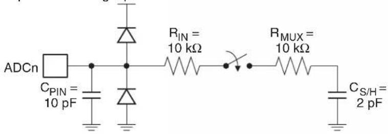
text_image
ADCn CPIN = 10 pF RIN = 10 kΩ RMUX = 10 kΩ CS/H = 2 pF20.2 DAC Operation
The DAC converts a 10-bit signed digital value to an analog output current through successive approximation. The DAC always operates in differential mode, outputting a differential current between its positive (P2.2) and negative (P2.3) outputs with a common mode voltage of V_DD/2 . The minimum value represents zero difference and the maximum values represent a difference of positive or negative V_REF minus 1 LSB. An external transimpedance amplifier is required to convert the current into a voltage suitable for driving other circuits.
The DAC is enabled by setting the ADCE and DAC bits in DADC. Some settling time is required for the reference circuits to stabilize after the DAC is enabled. The DAC does not have multiple output channels and the DIFF, ACON and ACS bits have no effect in DAC mode. P2.2 and P2.3 are automatically forced to input-only mode while the DAC is enabled.
A timing diagram of a DAC conversion is shown in Figure 20-4. The conversion requires 11 ADC clock cycles to complete. Construction of the analog output starts in the second cycle of the conversion and the DAC will allow the new value to propagate to the outputs during cycle 7, after the 5 MSBs are complete. At the end of the conversion, the interrupt flag is set. An additional 1 ADC clock cycle and up to 2 system clock cycles may be required to synchronize ADIF with the rest of the system. The DADL and DADH registers hold the value to be output and are write-only during DAC mode. An internal buffer samples DADH/DADL at the start of the conversion and holds the value constant for the remainder of the conversion. One system clock cycle is required to transfer the contents of DADH/DADL into the buffer at the start of the conversion and therefore the ADC clock frequency must always be equal to or less than the system clock frequency during DAC mode to ensure that the buffer is updated before the second cycle.
Figure 20-4. DAC Timing Diagram
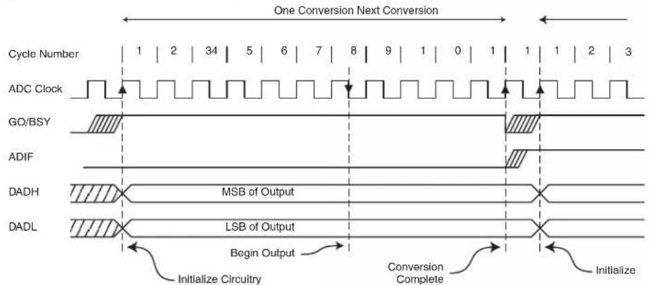
text_image
One Conversion Next Conversion Cycle Number | 1 | 2 | 34 | 5 | 6 | 7 | 8 | 9 | 1 | 0 | 1 | 1 | 1 | 2 | 3 ADC Clock GO/BSY ADIF DADH MSB of Output DADL LSB of Output Begin Output Initialize Circuitry Conversion Complete InitializeThe equivalent model for the analog output circuitry is illustrated in Figure 20-5. The series output resistance of the DAC must drive the pin capacitance and any external load on the pin.
Figure 20-5. Equivalent Analog Output Model
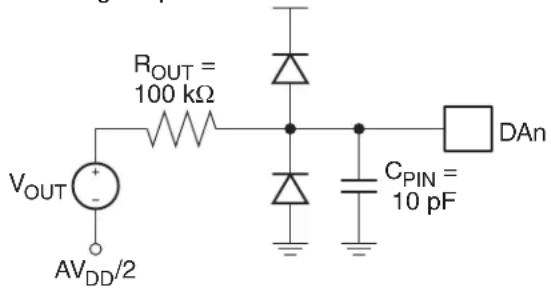
text_image
ROUT = 100 kΩ VOUT AVDD/2 CPIN = 10 pF DAn20.3 Clock Selection
The DADC requires a clock of 2 MHz or less to achieve full resolution. By default the DADC will use an internal 2 MHz clock generated from the 8 MHz internal oscillator. The internal oscillator will be enabled even if it is not supplying the system clock. This may result in higher power consumption. Conversely, the DADC clock can be generated directly from the system clock using a 7-bit prescaler. The prescaler output is controlled by the ACK bits in DADC as shown in Figure 20-6.
In ADC mode, there are no requirements on the clock frequency with respect to the system clock. The ADC prescaler selection is independent of the system clock divider and the ADC may operate at both higher or lower frequencies than the CPU. However, in DAC mode the ADC clock frequency must not be higher than the CPU clock, including any clock division from the system clock.
Figure 20-6. DADC Clock Selection
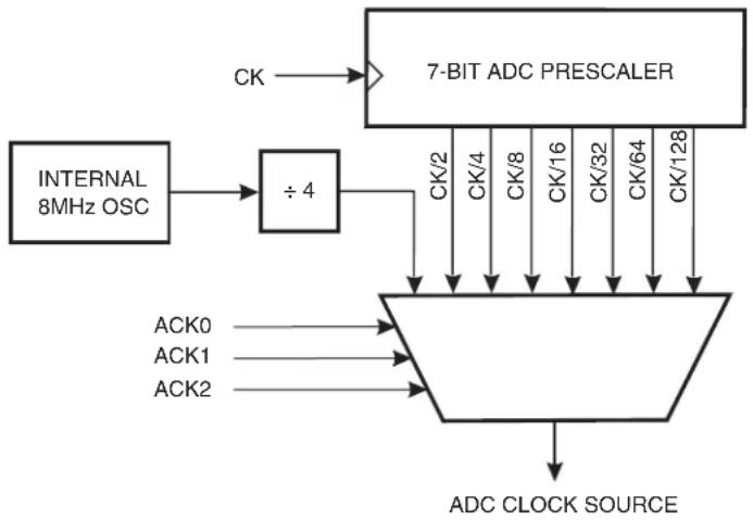
flowchart
graph TD
    A["INTERNAL 8MHz OSC"] --> B["÷4"]
    B --> C["7-BIT ADC PRESCALER"]
    C --> D["ACK0"]
    C --> E["ACK1"]
    C --> F["ACK2"]
    D --> G["ADC CLOCK SOURCE"]
    E --> G
    F --> G
    C --> H["CK/2"]
    C --> I["CK/4"]
    C --> J["CK/8"]
    C --> K["CK/16"]
    C --> L["CK/32"]
    C --> M["CK/64"]
    C --> N["CK/128"]
20.4 Starting a Conversion
Setting the GO/BSY bit (DADC.6) when ADCE = 1 starts a single conversion in both ADC and DAC modes. The bit remains set while the conversion is in progress and is cleared by hardware when the conversion completes. The ADC channel should not be changed while a conversion is in progress.
Alternatively, a conversion can be started automatically by various timer sources. Conversion trigger sources are selected by the TRG bits in DADI. A conversion is started every time the selected timer overflows, allowing for conversions to occur at fixed intervals. The GO/BSY bit will
be set by hardware while the conversion is in progress. Note that the timer overflow rate must be slower than the conversion time.
20.5 Noise Considerations
Digital circuitry inside and outside the device generates EMI which might affect the accuracy of analog measurements. If conversion accuracy is critical, the noise level can be reduced by applying the following techniques:
- Connect a decoupling capacitor between the V_DD pin and GND as shown in Figure 20-7. This capacitor should be located as close to the package as possible.
- Keep analog signal paths as short as possible. Make sure to run analog signals tracks over an analog ground plane, and keep them well away from high-speed digital tracks.
- Place the CPU in Idle during a conversion.
- If any Port 0 pins are used as digital outputs, it is essential that these do not switch while a conversion is in progress.
Figure 20-7. Example ADC Power Connections (TQFP Package)

text_image
Analog Ground Plane 100 nF VDD VDD P0.0 (ADC0) P0.1 (ADC1) P0.2 (ADC2) P0.3 (ADC3) 39 38 37 36 35 34 33 P0.4 (ADC4) 32 P0.5 (ADC5) 31 P0.6 (ADC6) 30 P0.7 (ADC7) 29 28 GNDTable 20-2. DADC – DADC Control Register
| DADC = D9H Reset Value = 0000 0000BNot Bit Addressable | ||||||||
| ADIF GO/BSY | DAC ADC E LADJ ACK2 | ACK1 ACK0 | ||||||
| B | i | t | 7 | 6 | 5 | 4 | 3 | 2 |
| Symbol Function | ||||
| ADIF | ADC Interrupt Flag. Set by hardware when a conversion completes. Cleared by hardware when calling the interrupt service routine. | |||
| GO/BSY | Conversion Start/Busy Flag. In software triggered mode, writing a 1 to this bit starts a conversion. The bit remains high while the conversion is in progress and is cleared by hardware when the conversion completes. In hardware triggered mode, this bit is set and cleared by hardware to flag when the DADC is busy. | |||
| DAC | Digital-to-Analog Conversion Enable. Set to configure the DADC in Digital-to-Analog (DAC) mode. Clear to configure the DADC in Analog-to-Digital (ADC) mode. | |||
| ADCE | DADC Enable. Set to enable the DADC. Clear to disable the DADC. | |||
| LADJ | Left Adjust Enable. When cleared, the ADC results are right adjusted and the MSBs are sign extended. When set, the ADC results are left adjusted and the LSBs are zeroed. | |||
| ACK [2-0] | DADC Clock Select | |||
| ACK3 | ACK1 | ACK0 | Clock Source | |
| 0 | 0 | 0 | Internal RC Oscillator/4 (2MHz) | |
| 0 | 0 | 1 | f_sys/2 | |
| 0 | 1 | 0 | f_sys/4 | |
| 0 | 1 | 1 | f_sys/8 | |
| 1 | 0 | 0 | f_sys/16 | |
| 1 | 0 | 1 | f_sys/32 | |
| 1 | 1 | 0 | f_sys/64 | |
| 1 | 1 | 1 | f_sys/128 | |
Table 20-3. DADL – DADC Data Low Register
| DADL = DCH Reset Value = 0000 0000BNot Bit Addressable | ||||||||
| ADC.7 | ADC.6 | ADC.5 | ADC.4 | ADC.3 | ADC.2 | ADC.1 | ADC.0 | |
| B | i | t | 7 | 6 | 5 | 4 | 3 | 2 |
Table 20-4. DADH – DADC Data High Register
| DADH = DDH Reset Value = 0000 0000BNot Bit Addressable | ||||||||
| ADC.15 | ADC.14 | ADC.13 | ADC.12 | ADC.11 | ADC.10 | ADC.9 | ADC.8 | |
| B | i | t | 7 | 6 | 5 | 4 | 3 | 2 |
Table 20-5. DADI – DADC Input Control Register
| DADI = DAH Reset Value = 0000 0000BNot Bit Addressable | ||||||||
| ACON IREF | TRG1 | TRG0 | DIFF | ACS2 | ACS1 | ACS0 | ||
| B | i | t | 7 | 6 | 5 | 4 | 3 | 2 |
| Symbol Function | ||||||||
| ACON | Analog Input Connect. When cleared, the analog inputs are disconnected from the ADC. When set, the analog inputs selected by ACS_2-0 are connected to the ADC. ACON must be zero when changing the input channel multiplexor ( ACS_2-0 ). | |||||||
| IREF | Internal Reference Enable. When set, the DADC uses the internal voltage reference. When cleared the DADC uses VDD for its reference. | |||||||
| DIFF | Differential Mode Enable. Set to configure the ADC in differential mode. Clear to configure the ADC in single-ended mode. | |||||||
| TRG[1-0] | Trigger Select. | |||||||
| TRG1 | TRG0 | Trigger | ||||||
| 0 | 0 | Software (GO bit) | ||||||
| 0 | 1 | Timer 0 Overflow | ||||||
| 1 | 0 | Timer 1 Overflow | ||||||
| 1 | 1 | Timer 2 Overflow | ||||||
| ACS [2-0] | DADC Channel Select | |||||||
| DIFF | ACS2 | ACS1 | ACS0 | V+ | V- | |||
| 0 | 0 | 0 | 0 | P0.0 | VDD/2 | |||
| 0 | 0 | 0 | 1 | P0.1 | VDD/2 | |||
| 0 | 0 | 1 | 0 | P0.2 | VDD/2 | |||
| 0 | 0 | 1 | 1 | P0.3 | VDD/2 | |||
| 0 | 1 | 0 | 0 | P0.4 | VDD/2 | |||
| 0 | 1 | 0 | 1 | P0.5 | VDD/2 | |||
| 0 | 1 | 1 | 0 | P0.6 | VDD/2 | |||
| 0 | 1 | 1 | 1 | P0.7 | VDD/2 | |||
| 1 | 0 | 0 | 0 | P0.0 | P0.1 | |||
| 1 | 0 | 0 | 1 | P0.2 | P0.3 | |||
| 1 | 0 | 1 | 0 | P0.4 | P0.5 | |||
| 1 | 0 | 1 | 1 | P0.6 | P0.7 | |||
| 1 | 1 | 0 | 0 | reserved | ||||
| 1 | 1 | 0 | 1 | reserved | ||||
| 1 | 1 | 1 | 0 | reserved | ||||
| 1 | 1 | 1 | 1 | reserved | ||||
21. Programmable Watchdog Timer
The programmable Watchdog Timer (WDT) protects the system from incorrect execution by triggering a system reset when it times out after the software has failed to feed the timer prior to the timer overflow. By Default the WDT counts CPU clock cycles. The prescaler bits, PS0, PS1 and PS2 in SFR WDTCON are used to set the period of the Watchdog Timer from 16K to 2048K clock cycles. The Timer Prescaler can also be used to lengthen the time-out period (see Table 6-2 on page 33) The WDT is disabled by Reset and during Power-down mode. When the WDT times out without being serviced, an internal RST pulse is generated to reset the CPU. See Table 21-1 for the available WDT period selections.
Table 21-1. Watchdog Timer Time-out Period Selection
| WDT Prescaler Bits | Period ^(1) (Clock Cycles)PS2 PS1 PS0 | ||
| 0 | 0 | 0 | 1 |
| 0 | 0 | 1 | 3 |
| 0 | 1 | 0 | 6 |
| 0 | 1 | 1 | 1 |
| 1 | 0 | 0 | 2 |
| 1 | 0 | 1 | 5 |
| 1 1 0 1024K | |||
| 1 | 1 | 1 | 2 |
Note: 1. The WDT time-out period is dependent on the system clock frequency.
$$ \text { Time - out Period } = \frac {2 ^ {(P S + 1 4)}}{\text { Oscillator Frequency }} \times (T P S + 1) $$
The Watchdog Timer consists of a 14-bit timer with 7-bit programmable prescaler. Writing the sequence 1EH/E1H to the WDTRST register enables the timer. When the WDT is enabled, the WDTEN bit in WDTCON will be set to "1". To prevent the WDT from generating a reset when if overflows, the watchdog feed sequence must be written to WDTRST before the end of the time-out period. To feed the watchdog, two write instructions must be sequentially executed successfully. Between the two write instructions, SFR reads are allowed, but writes are not allowed. The instructions should move 1EH to the WDTRST register and then 1EH to the WDTRST register. An incorrect feed or enable sequence will cause an immediate watchdog reset. The program sequence to feed or enable the watchdog timer is as follows:
MOV WDTRST, #01Eh
MOV WDTRST, #0E1h
21.1 Software Reset
A Software Reset of the AT89LP3240/6440 is accomplished by writing the software reset sequence 5AH/A5H to the WDTRST SFR. The WDT does not need to be enabled to generate the software reset. A normal software reset will set the SWRST flag in WDTCON. However, if at any time an incorrect sequence is written to WDTRST (i.e. anything other than 1EH/E1H or 5AH/A5H), a software reset will immediately be generated and both the SWRST and WDTOVF flags will be set. In this manner an intentional software reset may be distinguished from a software error-generated reset. The program sequence to generate a software reset is as follows:
MOV WDTRST, #05Ah
MOV WDTRST, #0A5h
Table 21-2. WDTCON – Watchdog Control Register
| WDTCON Address = A7H Reset Value = 0000 X000BNot Bit Addressable | ||||||||
| PS2 | PS1 | PS0 | WDIDLE | - | SWRST WDTOVF WDTEN | |||
| B | i | t | 7 | 6 | 5 | 4 | 3 | 2 |
| Symbol Function | ||||||||
| PS2PS1PS0 | Prescaler bits for the watchdog timer (WDT). When all three bits are cleared to 0, the watchdog timer has a nominal period of 16K clock cycles. When all three bits are set to 1, the nominal period is 2048K clock cycles. | |||||||
| WDIDLE | Disable/enable the Watchdog Timer in IDLE mode. When WDIDLE = 0, WDT continues to count in IDLE mode. When WDIDLE = 1, WDT freezes while the device is in IDLE mode. | |||||||
| SWRST | Software Reset Flag. Set when a software reset is generated by writing the sequence 5AH/A5H to WDTRST. Also set when an incorrect sequence is written to WDTRST. Must be cleared by software. | |||||||
| WDTOVF | Watchdog Overflow Flag. Set when a WDT rest is generated by the WDT timer overflow. Also set when an incorrect sequence is written to WDTRST. Must be cleared by software. | |||||||
| WDTEN | Watchdog Enable Flag. This bit is READ-ONLY and reflects the status of the WDT (whether it is running or not). The WDT is disabled after any reset and must be re-enabled by writing 1EH/E1H to WDTRST | |||||||
Table 21-3. WDTRST – Watchdog Reset Register
| WDTCON Address = A6H(Write-Only)Not Bit Addressable | |||||||
| B | - | - | - | - | - | - | - |
| i | t | 7 | 6 | 5 | 4 | 3 | |
22. Instruction Set Summary
The AT89LP3240/6440 is fully binary compatible with the 8051 instruction set. The difference between the AT89LP3240/6440 and the standard 8051 is the number of cycles required to execute an instruction. Instructions in the AT89LP3240/6440 may take 1 to 9 clock cycles to complete. The execution times of most instructions may be computed using Table 22-1.
Table 22-1. Instruction Execution Times and Exceptions
| Generic Instruction Types Cycle Count Formula | |||||
| Most arithmetic, logical, bit and transfer instructions | # bytes | ||||
| Branches and Calls | # bytes + 1 | ||||
| Single Byte Indirect (i.e. ADD A, @Ri, etc.) 2 | |||||
| RET, RETI 4/5 | (4) | ||||
| MOVC 3 | |||||
| MOVX 2/4 | (2) | ||||
| MUL 2 | |||||
| DIV 4 | |||||
| MAC 9 | |||||
| INC DPTR | 2 | ||||
| Arithmetic | Bytes | Clock Cycles | Hex Code | ||
| 8051 | AT89LP | ||||
| ADD A, Rn | 1 | 12 | 1 | 28-2F | |
| ADD A, direct | 2 | 12 | 2 | 25 | |
| ADD A, @Ri | 1 | 12 | 2 | 26-27 | |
| ADD A, #data | 2 | 12 | 2 | 24 | |
| ADDC A, Rn | 1 | 12 | 1 | 38-3F | |
| ADDC A, direct | 2 | 12 | 2 | 35 | |
| ADDC A, @Ri | 1 | 12 | 2 | 36-37 | |
| ADDC A, #data | 2 | 12 | 2 | 34 | |
| SUBB A, Rn | 1 | 12 | 1 | 98-9F | |
| SUBB A, direct | 2 | 12 | 2 | 95 | |
| SUBB A, @Ri | 1 | 12 | 2 | 96-97 | |
| SUBB A, #data | 2 | 12 | 2 | 94 | |
| INC Rn | 1 | 12 | 1 | 08-0F | |
| INC direct | 2 | 12 | 2 | 05 | |
| INC @Ri | 1 | 12 | 2 | 06-07 | |
| INC A | 2 | 12 | 2 | 04 | |
| DEC Rn | 1 | 12 | 1 | 18-1F | |
| DEC direct | 2 | 12 | 2 | 15 | |
| DEC @Ri | 1 | 12 | 2 | 16-17 | |
| DEC A | 2 | 12 | 2 | 14 | |
| INC DPTR | 1 | 24 | 2 | A3 | |
| INC /DPTR(1) | 2 | - | 3 | A | |
| MUL AB 1 482 | A | 4 | |||
| DIV AB 1 484 84 | |||||
| DA A 1 12 1 D4 | |||||
| MAC AB(1) | 2 | - | 9 | A | |
| CLR M(1) | 2 | - | 2 | A | |
| ASR M(1) | 2 | - | 2 | A | |
| LSL M(1) | 2 | - | 2 | A | |
| Bit Operations Bytes | Clock Cycles | Hex Code8051 | |||
| CLR C | 1 12 1 | C3 | |||
| CLR bit | 2 | 12 | 2 | C2 | |
| SETB C | 1 12 1 | D3 | |||
| SETB bit | 2 | 12 | 2 | D2 | |
| CPL C | 1 12 1 | B3 | |||
| CPL bit 2 12 2 | B2 | ||||
| ANL C, bit | 2 | 24 | 2 | 82 | |
| ANL C, bit | 2 24 2 B0 | ||||
| ORL C, bit | 2 24 2 72 | ||||
| ORL C, /bit | 2 | 24 | 2 | A0 | |
| MOV C, bit | 2 | 12 | 2 | A2 | |
| MOV bit, C | 2 24 2 92 | ||||
| Logical | Bytes | Clock Cycles | Hex Code8051 | ||
| CLR A | 1 12 1 E4 | ||||
| CPL A | 1 12 1 F4 | ||||
| ANL A, Rn | 1 | 12 | 1 | 58-5F | |
| ANL A, direct | 2 12 2 55 | ||||
| ANL A, @Ri | 1 12 2 | 56-57 | |||
| ANL A, #data | 2 | 12 | 2 | 54 | |
| ANL direct, A | 2 12 2 52 | ||||
| ANL direct, #data | 3 | 24 | 3 | 53 | |
| ORL A, Rn | 1 | 12 | 1 | 48-4F | |
| ORL A, direct | 2 12 2 45 | ||||
| ORL A, @Ri | 1 12 2 | 46-47 | |||
| ORL A, #data | 2 | 12 | 2 | 44 | |
| ORL direct, A | 2 12 2 42 | ||||
| ORL direct, #data | 3 | 24 | 3 | 43 | |
| XRL A, Rn | 1 | 12 | 1 | 68-6F | |
| XRL A, direct 2 12 2 65 | |||||
| XRL A, @Ri 1 12 2 66-67 | |||||
| XRL A, #data2 1 | 2 | 2 | 6 | ||
| XRL direct, A 2 12 2 62 | |||||
| XRL direct, #data3 2 | 4 | 3 | |||
| RL A 1 12 1 23 | |||||
| RLC A 1 12 1 33 | |||||
| RR A 1 12 1 03 | |||||
| RRC A 1 12 1 13 | |||||
| SWAP A | 1 12 1 | C4 | |||
| Data Transfer | Bytes | Clock Cycles | Hex Code | ||
| 8051 | AT89LP | ||||
| MOV A, Rn | 1 | 12 | 1 | E8-EF | |
| MOV A, direct | 2 12 2 | E5 | |||
| MOV A, @Ri | 1 12 2 | E6-E7 | |||
| MOV A, #data | 2 | 12 | 2 | 74 | |
| MOV Rn, A | 1 | 12 | 1 | F8-FF | |
| MOV Rn, direct | 2 | 24 | 2 | A8-AF | |
| MOV Rn, #data | 2 | 12 | 2 | 78-7F | |
| MOV direct, A | 2 12 2 F5 | ||||
| MOV direct, Rn | 2 | 24 | 2 | 88-8F | |
| MOV direct, direct | 3 24 3 85 | ||||
| MOV direct, @Ri | 2 | 24 | 2 | 86-87 | |
| MOV direct, #data | 3 | 24 | 3 | 75 | |
| MOV @Ri, A | 1 12 1 | F6-F7 | |||
| MOV @Ri, direct | 2 24 2 | A6-A7 | |||
| MOV @Ri, #data | 2 | 12 | 2 | 76-77 | |
| MOV DPTR, #data16 | 3 | 24 | 3 | 90 | |
| MOV /DPTR, #data16^(1) | 4 | - | 4 | A5 90 | |
| MOVC A, @A+DPTR | 1 24 3 93 | ||||
| MOVC A, @A+/DPTR^(1) | 2 | - | 4 | A5 93 | |
| MOVC A, @A+PC | 1 24 3 83 | ||||
| MOVX A, @Ri | 1 24 2 | E2-E3 | |||
| MOVX A, @DPTR | 1 24 | 2/4 | (2) | E0 | |
| MOVX A, @/DPTR^(1) | 2 | - | 3/5^(2) | A5 E0 | |
| MOVX @Ri, A | 1 24 2 | F2-F3 | |||
| MOVX @DPTR, A | 1 24 | 2/4 | (2) | F0 | |
| MOVX @/DPTR, A^(1) | 2 | - | 3/5^(2) | A5 F0 | |
| PUSH direct | 2 | 24 | 2/3^(4) | C0 | |
| POP direct 2 24 2/3 | (4) | D0 | |||
| XCH A, Rn 1 12 1 C8-CF | |||||
| XCH A, direct 2 12 2 C5 | |||||
| XCH A, @Ri | 1 12 2 C6 | C7 | |||
| XCHD A, @Ri | 1 12 2 | D6-D7 | |||
| Branching | Bytes | Clock Cycles | Hex Code | ||
| 8051 | AT89LP | ||||
| JC rel | 2 24 3 | 40 | |||
| JNC rel | 2 24 3 | 50 | |||
| JB bit, rel | 3 | 24 | 4 | 20 | |
| JNB bit, rel 3 24 4 | 30 | ||||
| JBC bit, rel 3 24 4 | 10 | ||||
| JZ rel | 2 24 3 | 60 | |||
| JNZ rel | 2 24 3 | 70 | |||
| SJMP rel | 2 | 24 | 3 | 80 | |
| ACALL addr11 | 2 24 3/5 | (4) | 11,31,51,71,91,B1,D1,F1 | ||
| LCALL addr16 | 3 24 4/6 | (4) | 12 | ||
| RET | 1 24 4/5 | (4) | 22 | ||
| RETI | 1 24 4/5 | (4) | 32 | ||
| AJMP addr11 2 24 3 | 01,21,41,61,81,A1,C1,E1 | ||||
| LJMP addr16 | 3 | 24 | 4 | 02 | |
| JMP @A+DPTR | 1 24 2 | 73 | |||
| JMP @A+PC(1) | 2 | - | 3 | A5 73 | |
| CJNE A, direct, rel | 3 24 4 | B5 | |||
| CJNE A, #data, rel | 3 | 24 | 4 | B4 | |
| CJNE Rn, #data, rel | 3 | 24 | 4 | B8-BF | |
| CJNE @Ri, #data, rel | 3 | 24 | 4 | B6-B7 | |
| CJNE A, @R0, rel(1) | 3 | - | 4 | A5 B6 | |
| CJNE A, @R1, rel(1) | 3 | - | 4 | A5 B7 | |
| DJNZ Rn, rel | 2 24 3 D8 | DF | |||
| DJNZ direct, rel | 3 24 4 D5 | ||||
| NOP | 1 12 1 | 00 | |||
| BREAK(1)(3) | 2 | - | 2 | A5 00 | |
Notes: 1. This escaped instruction is an extension to the instruction set. See Section 22.1 on page 147.
2. MOVX @DPTR instructions take 2 clock cycles when accessing ERAM and 4 clock cycles when accessing FDATA, XDATA or CODE. (3 and 5 cycles for MOVX @/DPTR).
3. The BREAK instruction acts as a 2 cycle NOP.
4. Instructions accessing the stack require additional cycles when using the extended stack.
22.1 Instruction Set Extensions
The following instructions are extensions to the standard 8051 instruction set that provide enhanced capabilities not found in standard 8051 devices. All extended instructions start with an A5H escape code. For this reason random A5H reserved codes should not be placed in the instruction stream even though other devices may have treated these as NOPs.
Other AT89LP devices may not support all of these instructions.
22.1.1 ASR M
Function: Shift MAC Accumulator Right Arithmetically
Description: The forty bits in the M register are shifted one bit to the right. Bit 39 retains its value to preserve the sign of the value. No flags are affected.
Example: The M register holds the value 0C5B1A29384H. The following instruction,
ASR M
leaves the M register holding the value 0E2D8D149C2H.
Bytes: 2
Cycles: 2


Operation: ASR
(M_n) (M_n+1) n = 0 - 38
(M_39) (M_39)
22.1.2 BREAK
Function: Software Breakpoint (Halt execution)
Description: BREAK transfers control from normal execution to the On-Chip Debug (OCD) handler if OCD is enabled. The PC is left pointing to the following instruction. If OCD is disabled, BREAK acts as a double NOP. No flags are affected.
Example: If On-Chip Debugging is allowed, the following instruction,
BREAK
will halt instruction execution prior to the immediately following instruction. If debugging is not allowed, the BREAK is treated as a double NOP.
Bytes: 2
Cycles: 2


Operation: BREAK
(PC) (PC) + 2
22.1.3 CJNE A, @R i, rel
Function: Compare and Jump if Not Equal
Description: CJNE compares the magnitudes of the Accumulator and indirect RAM location and branches if their values are not equal. The branch destination is computed by adding the signed relative-displacement in the last instruction byte to the PC, after incrementing the PC to the start of the next instruction. The carry flag is set if the unsigned integer value of ACC is less than the unsigned integer value of the indirect location; otherwise, the carry is cleared. Neither operand is affected.
Example: The Accumulator contains 34H. Register 0 contains 78H and 78H contains 56H. The first instruction in the sequence,
CJNE A, @R0, NOT_EQ
; ..... ; ACC = @R0.
NOT_EQ:
JC REQ_LOW .. ;IF ACC< @R0.
;......;ACC > @R0.
sets the carry flag and branches to the instruction at label NOT_EQ. By testing the carry flag, the second instruction determines whether ACC is greater or less than the location pointed to by R0.
Bytes: 2
Cycles: 9
Encoding: A5
1 0 1 1 0 1 1 i
rel. address
Operation: CJNE
(PC) ← (PC) + 3
IF (A) ≠ ((Ri))
THEN
(PC) ← (PC) + relative offset
IF (A) < ((Ri))
THEN
(C) 1
ELSE
(C) 0
22.1.4 CLR M
Function: Clear MAC Accumulator
Description: CLR M clears the 40-bit M register. No flags are affected.
Example: The M registercontains 123456789AH. The following instruction,
CLR M
leaves the M register set to 0000000000H.
Bytes: 2
Cycles: 2
Encoding: A 5
1 1 1 0 0 1 0 0
Operation: JMP
(M) ←0
22.1.5 INC /DPTR
Function: Increment Alternate Data Pointer
Description: INC /DPTR increments the unselected 16-bit data pointer by 1. A 16-bit increment (modulo 2^16 ) is performed, and an overflow of the low-order byte of the data pointer from 0FFH to 00H increments the high-order byte. No flags are affected.
Example: Registers DP1H and DP1L contain 12H and 0FEH, respectively, and DPS = 0. The following instruction sequence,
INC /DPTR
INC /DPTR
INC /DPTR
changes DP1H and DP1L to 13H and 01H.
Bytes: 2
Cycles: 3
Encoding: A 5
1 0 1 0 0 0 1 1
Operation: INC
IF (DPS) = 0
THEN
(DPTR1) ← (DPTR1) + 1
ELSE
(DPTR0) ← (DPTR0) + 1
22.1.6 JMP @A+PC
Function: Jump indirect relative to PC
Description: JMP @A+PC adds the eight-bit unsigned contents of the Accumulator to the program counter, which is first incremented by two. This is the address for subsequent instruction fetches. Sixteen-bit addition is performed (modulo 2 ^16 ): a carry-out from the low-order eight bits propagates through the higher-order bits. The Accumulator is not altered. No flags are affected.
Example: An even number from 0 to 6 is in the Accumulator. The following sequence of instructions branches to one of four AJMP instructions in a jump table starting at JMP_TBL.
JMP @A + PC
JMP_TBL:
AJMP LABEL0
AJMP LABEL1
AJMP LABEL2
AJMP LABEL3
If the Accumulator equals 04H when starting this sequence, execution jumps to label LABEL2. Because AJMP is a 2-byte instruction, the jump instructions start at every other address.
Bytes: 2
Cycles: 3
Encoding: A 5
0 1 1 1 0 0 1 1
Operation: JMP
(PC) ← (A) + (PC) + 2
22.1.7 LSL M
Function: Shift MAC Accumulator Left Logically
Description: The forty bits in the M register are shifted one bit to the left. Bit 0 is cleared. No flags are affected.
Example: The M register holds the value 0C5B1A29384H. The following instruction,
LSL M
leaves the M register holding the value 8B63452708H.
Bytes: 2
Cycles: 2
| Encoding: | A | 5 |
| 0 | 0 | 1 | 0 | 0 | 0 | 1 | 1 |
Operation: LSL
$$ \left(M _ {n + 1}\right) \leftarrow (M) n = 0 - 3 8 $$
$$ (M _ {0}) \leftarrow 0 $$
22.1.8 MOVC A, @A+/DPTR
Function: Move code byte relative to Alternate Data Pointer
Description: The MOVC instructions load the Accumulator with a code byte or constant from program memory. The address of the byte fetched is the sum of the original unsigned 8-bit Accumulator contents and the contents of the unselected Data Pointer. The base register is not altered. Sixteen-bit addition is performed so a carry-out from the low-order eight bits may propagate through higher-order bits. No flags are affected.
Example: A value between 0 and 3 is in the Accumulator. The following instructions will translate the value in the Accumulator to one of four values defined by the DB (define byte) directive.
MOV /DPTR, #TABLE
MOVC A, @A+PC
RET
TABLE:
DB 66H
DB 77H
DB 88H
DB 99H
If the subroutine is called with the Accumulator equal to 01H, it returns with 77H in the Accumulator.
Bytes: 2
Cycles: 4
| Encoding: | A | 5 |
| 1 | 0 | 0 | 1 | 0 | 0 | 1 | 1 |
Operation: MOVC
IF (DPS) = 0
THEN
(A) ← ((A) + (DPTR1))
ELSE
(A) ← ((A) + (DPTR0))
22.1.9 MAC AB
Function: Multiply and Accumulate
Description: MAC AB multiplies the signed 16-bit integers in the register pairs {AX, A} and {BX, B} and adds the 32-bit product to the 40-bit M register. The low-order bytes of the 16-bit operands are stored in A and B, and the high-order bytes in AX and BX respectively. The four operand registers are unaffected by the operation. If the addition of the product to the accumulated sum in M results in a two's complement overflow, the overflow flag is set; otherwise it is not cleared. The carry flag is set if the result is negative and cleared if positive.
Example: Originally the Accumulator holds the value 80 (50H). Register B holds the value 160 (0A0H). The instruction,
MAC AB
will give the product 12, 800 (3200H), so B is changed to 32H (00110010B) and the Accumulator is cleared. The overflow flag is set, carry is cleared.
Bytes: 2
Cycles: 9
Encoding: A 5
1 0 1 0 0 1 0 0
Operation: MAC
(M_39-0) (M) + (AX), (A) X (BX), (B)
22.1.10 MOV /DPTR, #data16
Function: Load Alternate Data Pointer with a 16-bit constant
Description: MOV /DPTR, #data16 loads the unselected Data Pointer with the 16-bit constant indicated. The third byte is the high-order byte, while the fourth byte holds the lower-order byte. No flags are affected.
Example: When DPS = 0, the instruction sequence,
MOV DPTR, # 1234H
MOV /DPTR, # 5678H
loads the value 1234H into the first Data Pointer: DPH0 holds 12H and DPL0 holds 34H; and loads the value 5678H into the second Data Pointer: DPH1 hold 56H and DPL1 holds 78H.
Bytes: 2
Cycles: 3
Encoding:
A5
90
immed. data 15-8
immed. data 7-0
Operation: MOV
IF (DPS) = 0
THEN
(DP1H) #data _15-8
(DP1L) #data7-0
ELSE
(DPOH) #data _15-8
(DP0L) #data7-0
22.1.11 MOVX A, @/DPTR
Function: Move External using Alternate Data Pointer
Description: The MOVX instruction transfesr data from external data memory to the Accumulator. The unselected Data Pointer generates a 16-bit address which targets EDATA, FDATA or XDATA.
Example: DPS = 0, DPTR0 contains 0123H and DPTR1 contains 4567H. The following instruction sequence,
MOVX A, @DPTR
MOVX @/DPTR, A
copies the data from address 0123H to 4567H.
Bytes: 2
Cycles: 3 (EDATA)
5 (FDATA or XDATA)
Encoding: A 5 1 1 1 0 0 0 0 0
Operation: MOVX
IF (DPS) = 0
(A) ← ((DPTR1))
ELSE
(A) ← ((DPTR0))
22.1.12 MOVX @/DPTR, A
Function: Move External using Alternate Data Pointer
Description: The MOVX instruction transfesr data from the Accumulator to external data memory. The unselected Data Pointer generates a 16-bit address which targets EDATA, FDATA or XDATA.
Example: DPS = 0, DPTR0 contains 0123H and DPTR1 contains 4567H. The following instruction sequence,
MOVX A, @DPTR
MOVX @/DPTR, A
copies the data from address 0123H to 4567H.
Bytes: 2
Cycles: 3 (EDATA)
5 (FDATA or XDATA)
Encoding: A 5 1 1 1 1 0 0 0 0
Operation: MOVX
IF (DPS) = 0
THEN
((DPTR1)) ← (A)
ELSE
((DPTR0)) ← (A)
23. Register Index
Table 23-1. Special Function Register Cross Reference
| Name Address Description Index | ||
| ACC E0H | ||
| ACSRA | 97H | Table 19-1 on page 130 |
| ACSRB | 9FH | Table 19-2 on page 131 |
| AREF | AFH | Table 19-3 on page 132 |
| AUXR | 8EH | Table 3-4 on page 18 |
| AX | E1H | Section 5.1 on page 24 |
| B | F0H | |
| BX | F7H | Section 5.1 on page 24 |
| CLKREG | 8FH | Table 6-2 on page 33 |
| DADC | D9H | Table 20-2 on page 139 |
| DADH | DDH | Table 20-4 on page 139 |
| DADI | DAH | Table 20-3 on page 139 |
| DADL | DCH | Table 20-3 on page 139 |
| DPCF (AUXR1) | A2H | Table 5-5 on page 28 |
| DPH0 | 83H | Section 5.2 on page 25 |
| DPH1 | 85H | Section 5.2 on page 25 |
| DPL0 | 82H | Section 5.2 on page 25 |
| DPL1 | 83H | Section 5.2 on page 25 |
| DSPR | E2H | Table 5-1 on page 26 |
| FIRD | E3H | Section 5.2.2.3 on page 29 |
| GPIEN | 9CH | Table 15-3 on page 84 |
| GPIF | 9DH | Table 15-4 on page 84 |
| GPLS | 9BH | Table 15-2 on page 84 |
| GPMOD | 9AH | Table 15-1 on page 84 |
| IE | A8H | Table 9-2 on page 42 |
| IE2 | B4H | Table 9-3 on page 43 |
| IP | B8H | Table 9-4 on page 43 |
| IP2 | B5H | Table 9-5 on page 43 |
| IPH | B7H | Table 9-6 on page 44 |
| IPH2 | B6H | Table 9-7 on page 44 |
| MACH | E5H | Section 5.1 on page 24 |
| MACL | E4H | Section 5.1 on page 24 |
| MEMCON | 96H | Table 3-3 on page 17 |
| P0 | 80H | Table 10-3 on page 45 |
| POM0 | BAH | Table 10-2 and Table 10-3 on page 45 |
| POM1 | BBH | Table 10-2 and Table 10-3 on page 45 |
Table 23-1. Special Function Register Cross Reference
| P1 | 90H | Table 10-3 on page 45 |
| P1M0 | C2H | Table 10-2 and Table 10-3 on page 45 |
| P1M1 | C3H | Table 10-2 and Table 10-3 on page 45 |
| P2 | A0H | Table 10-3 on page 45 |
| P2M0 | C4H | Table 10-2 and Table 10-3 on page 45 |
| P2M1 | C5H | Table 10-2 and Table 10-3 on page 45 |
| P3 | B0H | Table 10-3 on page 45 |
| P3M0 | C6H | Table 10-2 and Table 10-3 on page 45 |
| P3M1 | C7H | Table 10-2 and Table 10-3 on page 45 |
| P4 | C0H | Table 10-3 on page 45 |
| P4M0 | BEH | Table 10-2 and Table 10-3 on page 45 |
| P4M1 | BFH | Table 10-2 and Table 10-3 on page 45 |
| PAGE | 86H | Table 3-2 on page 14 |
| PCON | 87H | Table 8-1 on page 37 |
| PSWD0H | ||
| RCAP2H | CBH | Section 12.1 on page 61 |
| RCAP2L | CAH | Section 12.1 on page 61 |
| RH0 | 94H | Table 11-1 on page 51 |
| RH1 | 95H | Table 11-1 on page 51 |
| RL0 | 92H | Table 11-1 on page 51 |
| RL1 | 93H | Table 11-1 on page 51 |
| SADDR | A9H | Section 16.7 on page 97 |
| SADEN | B9H | Section 16.7 on page 97 |
| SBUF | 99H | Section 16.3 on page 89 |
| SCON | 98H | Table 16-1 on page 86 |
| SP | 81H | Section 3.4 on page 20 |
| SPCR | E9H | Table 17-2 on page 102 |
| SPDR | EAH | Table 17-3 on page 103 |
| SPSR | E8H | Table 17-4 on page 103 |
| SPX | 9EH | Section 3.4 on page 20 |
| T2CCA | D1H | Table 13-1 on page 71 |
| T2CCC | D4H | Table 13-5 on page 74 |
| T2CCF | D5H | Table 13-4 on page 72 |
| T2CCH | D3H | Table 13-2 on page 71 |
| T2CCL | D2H | Table 13-3 on page 71 |
| T2CON | C8H | Table 12-3 on page 61 |
| T2MOD | C9H | Table 12-4 on page 61 |
| TCON | 88H | Table 11-2 on page 54 |
| TCONB | 91H | Table 11-4 on page 56 |
Table 23-1. Special Function Register Cross Reference
| TH0 | 8CH | Table 11-1 on page 51 |
| TH1 | 8DH | Table 11-1 on page 51 |
| TH2 | CDH | Section 12.1 on page 61 |
| TL0 | 8AH | Table 11-1 on page 51 |
| TL1 | 8BH | Table 11-1 on page 51 |
| TL2 | CCH | Section 12.1 on page 61 |
| TMOD | 89H | Table 11-3 on page 55 |
| TWAR | ACH | Table 18-3 on page 112 |
| TWBR | AEH | Table 18-5 on page 113 |
| TWCR | AAH | Table 18-1 on page 112 |
| TWDR | ADH | Table 18-4 on page 113 |
| TWSR | ABH | Table 18-2 on page 112 |
| WDTCON | A7H | Table 21-2 on page 142 |
| WDTRST | A6H | Table 21-3 on page 142 |
24. On-Chip Debug System
The AT89LP3240/6440 On-Chip Debug (OCD) System uses a two-wire serial interface to control program flow; read, modify, and write the system state; and program the nonvolatile memory. The OCD System has the following features:
- Complete program flow control
- Read-Modify-Write access to all internal SFRs and data memories
- Four hardware program address breakpoints, plus four program/data address breakpoints
- Unlimited program software breakpoints using BREAK instruction
- Break on change in program memory flow
- Break on stack overflow/underflow
- Break on Watchdog overflow
- Break on reset
• Non-intrusive operation - Programming of nonvolatile memory
24.1 Physical Interface
The On-Chip Debug System uses a two-wire synchronous serial interface to establish communication between the target device and the controlling emulator system. The OCD interface is enabled by clearing the OCD Enable Fuse. The OCD device connections are shown in Figure 24-1. When OCD is enabled, the RST port pin is configured as an input for the Debug Clock (DCL). Either the XTAL1, XTAL2 or P4.3 pin is configured as a bi-directional data line for the Debug Data (DDA) depending on the clock source selected. If the Internal RC Oscillator is selected, XTAL1 is configured as DDA (A). If the External Clock is selected, XTAL2 is configured as DDA (B). If the Crystal Oscillator is selected, P4.3 is configured as DDA (C).
When designing a system where On-Chip Debug will be used, the following observations must be considered for correct operation:
- P4.2/RST cannot be connected directly to V_DD and any external capacitors connected to RST must be removed.
- All external reset sources must be removed.
- If P4.3 needs to be debugged in systems using the crystal oscillator, the external clock option should be selected. The quartz crystal and any capacitors on XTAL1 or XTAL2 must be removed and an external clock signal must be driven on XTAL1. Some emulator systems may provide a user-configurable clock for this purpose.
Figure 24-1. AT89LP3240/6440 On-Chip Debug Connections

text_image
DCL → P4.2/RST DDA ← XTAL1 GND VDD A CLK = Internal RC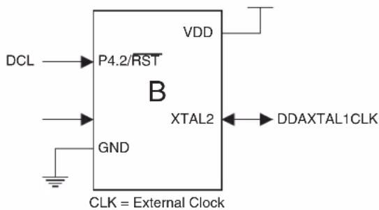
text_image
DCL → P4.2/RST B GND VDD XTAL2 ← DDAXTAL1CLK CLK = External Clock
text_image
DCL → P4.2/RST XTAL2 C GND VDD P4.3 ← DDAXTAL1 CLK = Crystal Oscillator24.2 Software Breakpoints
The AT89LP3240/6440 microcontroller includes a BREAK instruction for implementing program memory breakpoints in software. A software breakpoint can be inserted manually by placing the BREAK instruction in the program code. Some emulator systems may allow for automatic insertion/deletion of software breakpoints. The Flash memory must be re-programmed each time a software breakpoint is changed. Frequent insertions/deletions of software breakpoints will reduce the endurance of the nonvolatile memory. Devices used for debugging purposes should not be shipped to end customers. The BREAK instruction is treated as a two-cycle NOP when OCD is disabled.
24.3 Limitations of On-Chip Debug
The AT89LP3240/6440 is a fully-featured microcontroller that multiplexes several functions on its limited I/O pins. Some device functionality must be sacrificed to provide resources for On-Chip Debugging. The On-Chip Debug System has the following limitations:
- The Debug Clock pin (DCL) is physically located on that same pin as Port Pin P4.2 and the External Reset (RST). Therefore, neither P4.2 nor an external reset source may be emulated when OCD is enabled.
- When using the Internal RC Oscillator during debug, DDA is located on the XTAL1/P4.0 pin. The P4.0 I/O function cannot be emulated in this mode.
- When using the External Clock during debug, DDA is located on the XTAL2/P4.1 pin and the system clock drives XTAL1/P4.0. The P4.1 I/O and CLKOUT functions cannot be emulated in this mode.
- When using the Crystal Oscillator during debug, DDA is located on the P4.3 pin and the crystal connects to XTAL1/P4.0 and XTAL2/P4.1. The P4.3 I/O function cannot be emulated in this mode.
25. Programming the Flash Memory
The Atmel AT89LP3240/6440 microcontroller features 64K bytes of on-chip In-System Programmable Flash program memory and 8K bytes of nonvolatile Flash data memory. In-System Programming allows programming and reprogramming of the microcontroller positioned inside the end system. Using a simple 4-wire SPI interface, the programmer communicates serially with the AT89LP3240/6440 microcontroller, reprogramming all nonvolatile memories on the chip. In-System Programming eliminates the need for physical removal of the chips from the system. This will save time and money, both during development in the lab, and when updating the software or parameters in the field. The programming interface of the AT89LP3240/6440 includes the following features:
- Four-wire serial SPI Programming Interface or 11-pin Parallel Interface
• Active-low Reset Entry into Programming - Slave Select allows multiple devices on same interface
- User Signature Array
• Flexible Page Programming - Row Erase Capability
• Page Write with Auto-Erase Commands - Programming Status Register
For more detailed information on In-System Programming, refer to the Application Note entitled "AT89LP In-System Programming Specification".
25.1 Physical Interface
The AT89LP3240/6440 provides a standard programming command set with two physical interfaces: a bit-serial and a byte-parallel interface. Normal Flash programming utilizes the Serial Peripheral Interface (SPI) pins of an AT89LP3240/6440 microcontroller. The SPI is a full-duplex synchronous serial interface consisting of four wires: Serial Clock (SCK), Master-In/Slave-out (MISO), Master-out/Slave-in (MOSI), and an active-low chip select and frame signal (SS). When programming an AT89LP3240/6440 device, the programmer always operates as the SPI master, and the target system always operates as the SPI slave. To enter or remain in Programming mode the device's reset line (RST) must be held active (low). With the addition of VDD and GND, an AT89LP3240/6440 microcontroller can be programmed with a minimum of seven connections as shown in Figure 25-1.
In addition to being a chip select, the SS pin also is used to frame a command packet. SS must go low before the start of a command and must return high to complete the command. SS must NOT be tied to ground as this will prevent the interface from recognizing multiple commands. SS should be connected to the programming master for correct operation.
Figure 25-1. In-System Programming Device Connections
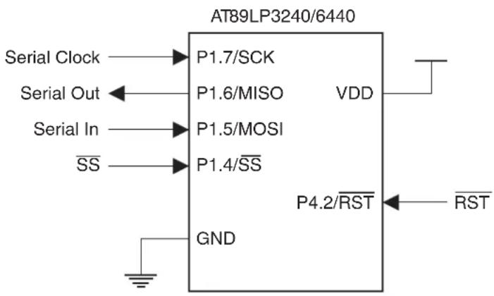
text_image
AT89LP3240/6440 Serial Clock → P1.7/SCK Serial Out ← P1.6/MISO VDD Serial In → P1.5/MOSI SS → P1.4/SS GND P4.2/RST ← RSTThe Parallel interface is a special mode of the serial interface, i.e. the serial interface is used to enable the parallel interface. After enabling the interface serially over P1.7/SCK and P1.5/MOSI, P1.5 is reconfigured as an active-low output enable (OE) for data on Port 0. When OE = 1, command, address and write data bytes are input on Port 0 and sampled at the rising edge of SCK. When OE = 0, read data bytes are output on Port 0 and should be sampled on the falling edge of SCK. The P1.7/SCK, P1.4/SS and P4.2/RST pins continue to function in the same manner. With the addition of VDD and GND, the parallel interface requires a minimum of fourteen connections as shown in Figure 25-2. Note that a connection to P1.6/MISO is not required for using the parallel interface.
Figure 25-2. Parallel Programming Device Connections
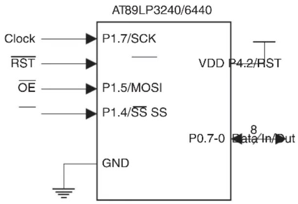
text_image
AT89LP3240/6440 Clock — P1.7/SCK RST — OE — P1.5/MOSI — — P1.4/SS SS GND VDD P4.2/RST P0.7-0 Data/In/DutThe Programming Interface is the only means of externally programming the AT89LP3240/6440 microcontroller. The Interface can be used to program the device both in-system and in a standalone serial programmer. The Interface does not require any clock other than SCK and is not limited by the system clock frequency. During Programming the system clock source of the target device can operate normally.
When designing a system where In-System Programming will be used, the following observations must be considered for correct operation:
- The ISP interface uses the SPI clock mode 0 (CPOL = 0, CPHA = 0) exclusively with a maximum frequency of 5 MHz.
- The AT89LP3240/6440 will enter programming mode only when its reset line (RST) is active (low). To simplify this operation, it is recommended that the target reset can be controlled by the In-System programmer. To avoid problems, the In-System programmer should be able to keep the entire target system reset for the duration of the programming cycle. The target system should never attempt to drive the four SPI lines while reset is active.
- The R Sput may be disabled to gain an extra I/O pin. In these cases the pin will always function as a reset during power up. To enter programming the pin must be driven low prior to the end of Power-On Reset (POR). After POR has completed the device will remain in ISP mode until is brought high. Once the initial ISP session has ended, the power to the target device must be cycled OFF and ON to enter another session.
- The \$B should not be left floating during reset if ISP is enabled.
- The ISP Enable Fuse must be set to allow programming during any reset period. If the ISP Fuse is disabled, ISP may only be entered at POR.
- For standalone programmers, may be tied directly to GND to ensure correct entry into Programming mode regardless of the device settings.
25.2 Memory Organization
The AT89LP3240/6440 offers 64K bytes of In-System Programmable (ISP) nonvolatile Flash code memory and 8K bytes of nonvolatile Flash data memory. In addition, the device contains a 256-byte User Signature Array and a 128-byte read-only Atmel Signature Array. The memory organization is shown in Table 25-1 and Figure 25-3. The memory is divided into pages of 128 bytes each. A single read or write command may only access half a page (64 bytes) in the memory; however, write with auto-erase commands will erase an entire 128-byte page even though they can only write one half page. Each memory type resides in its own address space and is accessed by commands specific to that memory. However, all memory types share the same page size.
User configuration fuses are mapped as a row in the memory, with each byte representing one fuse. From a programming standpoint, fuses are treated the same as normal code bytes except they are not affected by Chip Erase. Fuses can be enabled at any time by writing 00h to the appropriate locations in the fuse row. However, to disable a fuse, i.e. set it to FFh, the entire fuse row must be erased and then reprogrammed. The programmer should read the state of all the fuses into a temporary location, modify those fuses which need to be disabled, then issue a Fuse Write with Auto-Erase command using the temporary data. Lock bits are treated in a similar manner to fuses except they may only be erased (unlocked) by Chip Erase.
Table 25-1. AT89LP3240/6440 Memory Organization
| Memory Capacity Page Size # Pages Address Range | ||||
| CODE | 32KB (AT89LP3240) | 128 bytes | 256 | 0000H – 7FFFH |
| 64KB (AT89LP6440) | 128 bytes | 512 | 0000H – FFFFH | |
| DATA | 8192 bytes | 128 bytes | 64 | 1000H – 3FFFH |
| User Signature | 256 bytes | 128 bytes | 2 | 0000H – 00FFH |
| Atmel Signature | 128 bytes | 128 bytes | 1 | 0000H – 007FH |
Figure 25-3. AT89LP6440 Memory Organization

flowchart
graph TD
    A["00 3F Page Buffer"] --> B["User Fuse Row"]
    B --> C["Page 0 Low"]
    B --> D["Page 1 Low"]
    B --> E["Page 0 Low"]
    B --> F["Page 1 High"]
    B --> G["Page 0 High"]
    H["Atmel Signature Array"] --> I["Page 0 Low"]
    H --> J["Page 0 High"]
    K["Data Memory"] --> L["Page 63 Low"]
    K --> M["Page 63 High"]
    K --> N["Page 0 Low"]
    K --> O["Page 0 High"]
    P["Code Memory"] --> Q["Page 511 Low"]
    P --> R["Page 511 High"]
    P --> S["Page 510 Low"]
    P --> T["Page 510 High"]
    U["00 3F"] --> V["40 7F"]
    W["40 7F"] --> X["0000"]
25.3 Command Format
Programming commands consist of an opcode byte, two address bytes, and zero or more data bytes. In addition, all command packets must start with a two-byte preamble of AAH and 55H. The preamble increases the noise immunity of the programming interface by making it more difficult to issue unintentional commands. Figure 25-4 on page 161 shows a simplified flow chart of a command sequence.
A sample command packet is shown in Figure 25-5 on page 161. The SS pin defines the packet frame. SS must be brought low before the first byte in a command is sent and brought back high after the final byte in the command has been sent. The command is not complete until SS returns high. Command bytes are issued serially on MOSI. Data output bytes are received serially on MISO. Packets of variable length are supported by returning SS high when the final required byte has been transmitted. In some cases command bytes have a don't care value. Don't care bytes in the middle of a packet must be transmitted. Don't care bytes at the end of a packet may be ignored.
Page oriented instructions always include a full 16-bit address. The higher order bits select the page and the lower order bits select the byte within that page. The AT89LP3240/6440 allocates 6 bits for byte address, 1 bit for low/high half page selection and 9 bits for page address. The half page to be accessed is always fixed by the page address and half select as transmitted. The byte address specifies the starting address for the first data byte. After each data byte has been transmitted, the byte address is incremented to point to the next data byte. This allows a page command to linearly sweep the bytes within a page. If the byte address is incremented past the last byte in the half page, the byte address will roll over to the first byte in the same half page. While loading bytes into the page buffer, overwriting previously loaded bytes will result in data corruption.
For a summary of available commands, see Table 25-2 on page 162.
Figure 25-4. Command Sequence Flow Chart

flowchart
graph TD
    A["Input Preamble 1 (AAh)"] --> B["Input Preamble 2 (55h)"]
    B --> C["Input Opcode"]
    C --> D["Input Address High Byte"]
    D --> E["Input Address Low Byte"]
    E --> F["Input/Output Data"]
    F --> G{Address +1}
    G --> E
Figure 25-5. ISP Command Packet (Serial)
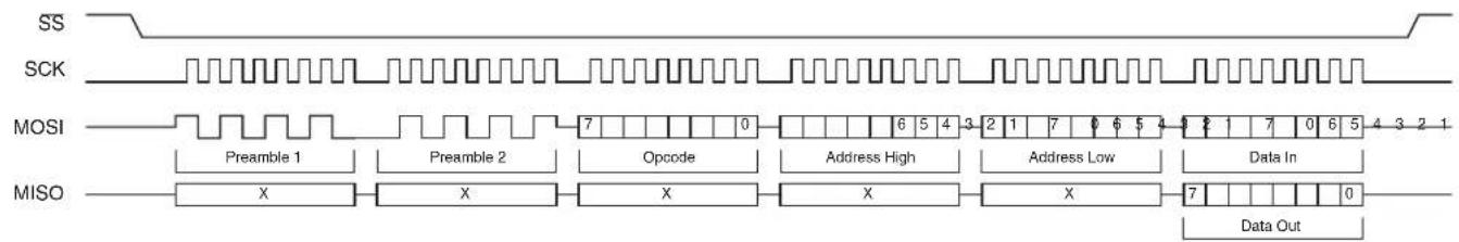
text_image
SS SCK MOSI MISO Preamble 1 Preamble 2 Opcode Address High Address Low Data In X X X X 7 6 5 4 3 2 1 7 6 5 4 1 7 0 6 5 4 3 2 1 Data OutFigure 25-6. ISP Command Packet (Parallel)

text_image
SS SCK WRITE OE P0 AAh 55h Opcode Address High Address Low Data In READ OE P0 AAh 55h Opcode Address High Address Low Data OutTable 25-2. Programming Command Summary
| Command Opcode Addr High Addr Low Data 0 Data n | |||||
| Program Enable ^(1) | 1010 1100 010 | 1 0011 --- | |||
| Parallel Enable ^(2) | 1010 1100 001 | 1 0101 --- | |||
| Chip Erase | 1000 1010 | - | - | - | - |
| Read Status | 0110 0000 | xxxx xxxx | xxxx xxxx | Status Out | |
| Load Page Buffer ^(3) | 0101 0001 | xxxx xxxx | 00bb bbbb | Data In 0 ... Data In n | |
| Write Code Page ^(3) | 0101 0000 | aaaa aaaa | asbb bbbb | Data In 0 ... Data In n | |
| Write Code Page with Auto-Erase ^(3) | 0111 0000 | aaaa aaaa | asbb bbbb | Data In 0 ... Data In n | |
| Read Code Page ^(3) | 0011 0000 | aaaa aaaa | asbb bbbb | Data Out 0 ... Data Out n | |
| Write Data Page ^(3) | 1101 0000 | 000a aaaa | asbb bbbb | Data In 0 ... Data In n | |
| Write Data Page with Auto-Erase ^(3) | 1101 0010 | 000a aaaa | asbb bbbb | Data In 0 ... Data In n | |
| Read Data Page ^(3) | 1011 0000 | 000a aaaa | asbb bbbb | Data Out 0 ... Data Out n | |
| Write User Fuses ^(3)(4)(5) | 1110 0001 | 0000 0000 | 00bb bbbb | Data In 0 ... Data In n | |
| Write User Fuses with Auto-Erase ^(3)(4)(5) | 1111 0001 | 0000 0000 | 00bb bbbb | Data In 0 ... Data In n | |
| Read User Fuses ^(3)(4)(5) | 0110 0001 | 0000 0000 | 00bb bbbb | Data Out 0 ... Data Out n | |
| Write Lock Bits ^(3)(4)(6) | 1110 0100 | 0000 0000 | 00bb bbbb | Data In 0 ... Data In n | |
| Read Lock Bits ^(3)(4)(6) | 0110 0100 | 0000 0000 | 00bb bbbb | Data Out 0 ... Data Out n | |
| Write User Signature Page ^(3) | 0101 0010 | 0000 0000 | asbb bbbb | Data In 0 ... Data In n | |
| Write User Signature Page with Auto-Erase ^(3) | 0111 0010 | 0000 0000 | asbb bbbb | Data In 0 ... Data In n | |
| Read User Signature Page ^(3) | 0011 0010 | 0000 0000 | asbb bbbb | Data Out 0 ... Data Out n | |
| Read Atmel Signature Page ^(3)(7) | 0011 1000 | 0000 0000 | 0sbb bbbb | Data Out 0 ... Data Out n | |
Notes: 1. Program Enable must be the first command issued after entering into programming mode.
2. Parallel Enable switches the interface from serial to parallel format until returns high.
3. Any number of Data bytes from 1 to 64 may be written/read. The internal address is incremented between each byte.
4. Each byte address selects one fuse or lock bit. Data bytes must be 00h or FFh.
5. See Table 25-5 on page 164 for Fuse definitions.
6. See Table 25-4 on page 163 for Lock Bit definitions.
- Atmel Signature Bytes:
| Address: | 0000H | 0001H | 0002H |
| AT89LP3240: | 1EH | 32H | FCH |
| AT89LP6440: | 1EH | 64H | FFH |
8. Symbol Key:
a: Page Address Bit
s: Half Page Select Bit
b: Byte Address Bit
x: Don't Care Bit
25.4 Status Register
The current state of the memory may be accessed by reading the status register. The status register is shown in Table 25-3.
Table 25-3. Status Register
| B | - | - | - | - | SUCCESS | |||
| i | t | 7 | 6 | 5 | 4 | 3 | 2 | |
| Symbol Function | ||||||||
| Load flag. Cleared low by the load page buffer command and set high by the next memory write. This flag signals that the page buffer was previously loaded with data by the load page buffer command. | ||||||||
| Success flag. Cleared low at the start of a programming cycle and will only be set high if the programming cycle completes without interruption from the brownout detector. | ||||||||
| Write Inhibit flag. Cleared low by the brownout detector (BOD) whenever programming is inhibited due to V_DD falling below the minimum required programming voltage. If a BOD episode occurs during programming, the SUCCESS flag will remain low after the cycle is complete. | ||||||||
| Busy flag. Cleared low whenever the memory is busy programming or if write is currently inhibited. | ||||||||
25.5 DATA Polling
The AT89LP3240/6440 implements DATA polling to indicate the end of a programming cycle. While the device is busy, any attempted read of the last byte written will return the data byte with the MSB complemented. Once the programming cycle has completed, the true value will be accessible. During Erase the data is assumed to be FFH and DATA polling will return 7FH. When writing multiple bytes in a page, the DATA value will be the last data byte loaded before programming begins, not the written byte with the highest physical address within the page.
25.6 Flash Security
The AT89LP3240/6440 provides two Lock Bits for Flash Code and Data Memory security. Lock bits can be left unprogrammed (FFh) or programmed (00h) to obtain the protection levels listed in Table 25-4. Lock bits can only be erased (set to FFh) by Chip Erase. Lock bit mode 2 disables programming of all memory spaces, including the User Signature Array and User Configuration Fuses. User fuses must be programmed before enabling Lock bit mode 2 or 3. Lock bit mode 3 implements mode 2 and also blocks reads from the code and data memories; however, reads of the User Signature Array, Atmel Signature Array, and User Configuration Fuses are still allowed.
The Lock Bits will not disable FDATA or IAP programming initiated by the application software.
Table 25-4. Lock Bit Protection Modes
| Program Lock Bits (by address) | |||
| Mode 00h 01h Protection Mode | |||
| 1 | FFh | FFh | No program lock features |
| 2 | 00h | FFh | Further programming of the Flash is disabled |
| 3 | 00h | 00h | Further programming of the Flash is disabled and verify (read) is also disabled; OCD is disabled |
25.7 User Configuration Fuses
The AT89LP3240/6440 includes 11 user fuses for configuration of the device. Each fuse is accessed at a separate address in the User Fuse Row as listed in Table 25-5. Fuses are cleared by programming 00h to their locations. Programming FFh to a fuse location will cause that fuse to maintain its previous state. To set a fuse (set to FFh) the fuse row must be erased and then reprogrammed using the Fuse Write with Auto-erase command. The default state for all fuses is FFh.
Table 25-5. User Configuration Fuse Definitions
| Address Fuse Name Description | ||
| 00 – 01h | Clock Source - CS[0:1](2) | Selects source for the system clock:CS1 CS0 Selected Source00h 00h High Speed Crystal Oscillator (XTAL)00h FFh Low Speed Crystal Oscillator (XTAL)FFh 00h External Clock on XTAL1 (XCLK)FFh FFh Internal RC Oscillator (IRC) |
| 02 – 03h | Start-up Time - SUT[0:1] | Selects time-out delay for the POR/BOD/PWD wake-up period:SUT1 SUTO Selected Time-out00h 00h 1 ms (XTAL); 16 μs (XCLK/IRC)00h FFh 2 ms (XTAL); 512 μs (XCLK/IRC)FFh 00h 4 ms (XTAL); 1 ms (XCLK/IRC)FFh FFh 16 ms (XTAL); 4 ms (XCLK/IRC) |
| 04h | Reset Pin Enable(3) | FFh: RST pin functions as reset00h: RST pin functions as general purpose I/O |
| 05h | Brown-Out Detector Enable | FFh: Brown-out Detector Enabled00h: Brown-out Detector Disabled |
| 06h | On-Chip Debug Enable | FFh: On-Chip Debug Disabled00h: On-Chip Debug Enabled |
| 07h | ISP Enable(3) | FFh: In-System Programming Enabled00h: In-System Programming Disabled (Enabled at POR only) |
| 08H | User Signature Programming | FFh: Programming of User Signature Disabled00h: Programming of User Signature Enabled |
| 09H | Tristate Ports | FFh: I/O Ports start in input-only mode (tristated) after reset00h: I/O Ports start in quasi-bidirectional mode after reset |
| 0AH | OCD Interface Select | FFh: Fast two-wire interface00h: Do not use |
| 0BH | In-Application Programming | FFh: In-Application Programming Disabled00h: In-Application Programming Enabled |
Notes: 1. The default state for all fuses is FFh.
2. Changes to these fuses will only take effect after a device POR.
3. Changes to these fuses will only take effect after the ISP session terminates by bringing RST high.
25.8 User Signature and Analog Configuration
The User Signature Array contains 256 bytes of non-volatile memory in two 128-byte pages. The first page of the User Signature Array (0000H-007FH) is available for serial numbers, firmware revision information, date codes or other user parameters. The User Signature Array may only be written by an external device when the User Signature Programming Fuse is enabled. When the fuse is enabled, Chip Erase will also erase the first page of the array. When the fuse is disabled, the array is not affected by write or erase commands. Programming of the Signature Array can also be disabled by the Lock Bits. However, reading the signature is always allowed and the array should not be used to store security sensitive information. The User Signature Array may be modified during execution through the In-Application Programming interface, regardless of the state of the User Signature Programming fuse or Lock Bits, provided that the IAP Fuse is enabled. Note that the address of the User Signature Array, as seen by the IAP interface, equals the User Signature address plus 256 (0100H-01FFH instead of 0000H-00FFH).
The second page of the User Signature Array (0080H-00FFH) contains analog configuration parameters for the AT89LP3240/6440. Each byte represents a parameter as listed in Table 25-6 and is preset in the factory. The parameters are read at POR and the device is configured accordingly. The second page of the array is not affected by Chip Erase. Other bytes in this page may be used as additional signature space; however, care should be taken to preserve the parameter values when modifying other bytes.
Table 25-6. Analog Configuration Definitions
| Address Parameter Name Description | ||
| 0080H | RC Oscillator Calibration Byte | The RC Calibration Byte controls the frequency of the internal RC oscillator. The frequency is inversely proportional to the calibration value such that higher values result in lower frequencies. A copy of the factory-set calibration value is stored at location 0008H of the Atmel Signature. |
25.9 Programming Interface Timing
This section details general system timing sequences and constraints for entering or exiting In-System Programming as well as parameters related to the Serial Peripheral Interface during ISP. The general timing parameters for the following waveform figures are listed in section “Timing Parameters” on page 169.
25.9.1 Power-up Sequence
Execute this sequence to enter programming mode immediately after power-up. In the RST pin is disabled or if the ISP Fuse is disabled, this is the only method to enter programming (see "External Reset" on page 35).
- Apply power between VDD and GND pins. RST should remain low.
- Wait at least t_PWRUP and drive high.
- Wait at least t_SUT for the internal Power-on Reset to complete. The value of t_SUT will depend on the current settings of the device.
- Start programming session.
Figure 25-7. Serial Programming Power-up Sequence
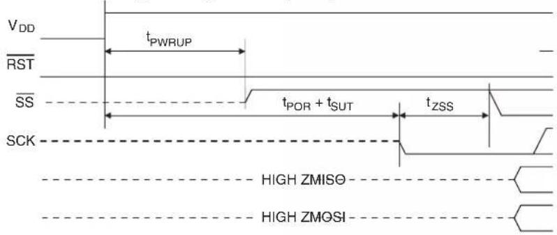
text_image
VDD RST SS SCK tPWRUP tPOR + tsUT tzss HIGH ZMISO HIGH ZMOSI25.9.2 Power-down Sequence
Execute this sequence to power-down the device after programming.
- Drive SCK low.
- Wait at least t_SSD and bring SS high.
- Tristate MOSI.
- Wait at least t_ssz and then tristate SS and SCK.
- Wait no more than t PWRDN and power off VDD.
Figure 25-8. Serial Programming Power-down Sequence

text_image
VDD RST SS SCK tSSD tSSZ tPWRDN HIGH ZMISO HIGH ZMOSI25.9.3 ISP Start Sequence
Execute this sequence to exit CPU execution mode and enter ISP mode when the device has passed Power-On Reset and is already operational.
- Drive RST low.
- Drive SS high.
- Wait t_RLZ + t_STL
- Start programming session.
Figure 25-9. In-System Programming (ISP) Start Sequence

text_image
VDD XTAL1 RST SS SCK tRLZ tSTL tZSS tSSE HIGH ZMISO- HIGH ZMOSI-25.9.4 ISP Exit Sequence
Execute this sequence to exit ISP mode and resume CPU execution mode.
- Drive SCK low.
- Wait at least t_SSD and drive high.
- Tristate MOSI.
- Wait at least t_ssz and bring RST high.
- Tristate SCK.
- Wait t RHZ and tristate SS.
Figure 25-10. In-System Programming (ISP) Exit Sequence

text_image
VDD XTAL1 RST SS SCK tSSD tSSZ tRHZ HIGH ZMISO HIGH ZMOSINote: The waveforms on this page are not to scale.
25.9.5 Serial Peripheral Interface
The Serial Peripheral Interface (SPI) is a byte-oriented full-duplex synchronous serial communication channel. During In-System Programming, the programmer always acts as the SPI master and the target device always acts as the SPI slave. The target device receives serial data on MOSI and outputs serial data on MISO. The Programming Interface implements a standard SPI Port with a fixed data order and For In-System Programming, bytes are transferred MSB first as shown in Figure 25-11. The SCK phase and polarity follow SPI clock mode 0 (CPOL = 0,
CPHA = 0) where bits are sampled on the rising edge of SCK and output on the falling edge of SCK. For more detailed timing information see Figure 25-12.
Figure 25-11. ISP Byte Sequence
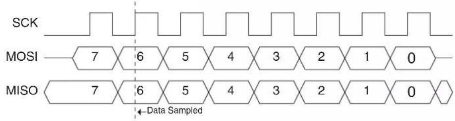
text_image
SCK MOSI 7 6 5 4 3 2 1 0 MISO 7 6 5 4 3 2 1 0 ←Data SampledFigure 25-12. Serial Programming Interface Timing
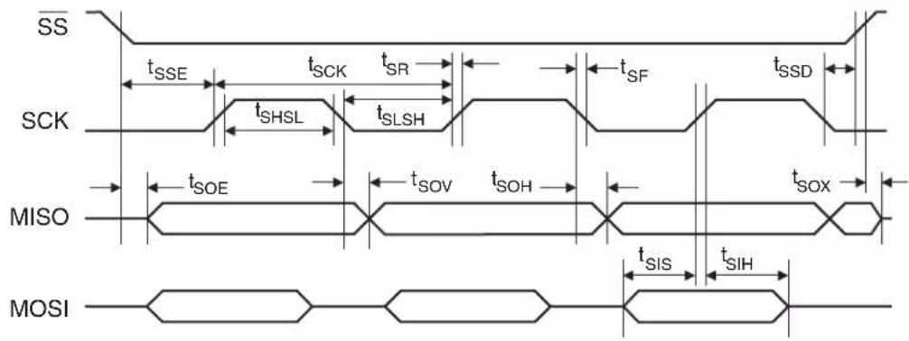
text_image
SS tSSE tSCK tSR tSF tSSD SCK tSHSL tSLSH MISO tSOE tSOV tSOH tSOX MOSI tSIS tSIHFigure 25-13. Parallel Programming Interface Timing

text_image
SS tSSE tSCK tSR tSF tSSD SCK tSHSL tSLSH OE tPIS tPIH tPOE tPOV tPOH tPOX P025.9.6 Timing Parameters
The timing parameters for Figure 25-7, Figure 25-8, Figure 25-9, Figure 25-10, Figure 25-12 and Figure 25-13 are shown in Table.
Table 25-7. Programming Interface Timing Parameters
| Symbol Parameter Min Max Units | ||||
| t_CLCL | System Clock Cycle Time 0 60 ns | |||
| t_PWRUP | Power On to High Time | 10 | μs | |
| t_POR | Power-on Reset Time | 100 | μs | |
| t_PWRDN | Tristate to Power Off | 1 | μs | |
| t_RLZ | Low to I/O Tristate | t_CLCL | 2 t_CLCL | ns |
| t_STL | Low Settling Time | 100 | ns | |
| t_RHZ | High to Tristate | 0 | 2 t_CLCL | ns |
| t_SCK | Serial Clock Cycle Time | 200^(1) | ns | |
| t_SHSL | Clock High Time | 75 ns | ||
| t_SLSH | Clock Low Time | 50 ns | ||
| t_SR | Rise Time | 25 | ns | |
| t_SF | Fall Time | 25 | ns | |
| t_SIS | Serial Input Setup Time | 10 | ns | |
| t_SIH | Serial Input Hold Time | 10 | ns | |
| t_SOH | Serial Output Hold Time | 10 | ns | |
| t_SOV | Serial Output Valid Time | 35 | ns | |
| t_PIS | Parallel Input Setup Time | 10 | ns | |
| t_PIH | Parallel Input Hold Time | 10 | ns | |
| t_POH | Parallel Output Hold Time | 10 | ns | |
| t_POV | Parallel Output Valid Time | 35 | ns | |
| t_SOE | Serial Output Enable Time | 10 | ns | |
| t_SOX | Serial Output Disable Time | 25 | ns | |
| t_POE | Parallel Output Enable Time | 10 | ns | |
| t_POX | Parallel Output Disable Time | 25 | ns | |
| t_SSE | Enable Lead Time | t_SLSH | ns | |
| t_SSD | Disable Lag Time | t_SLSH | ns | |
| t_ZSS | SCK Setup to Low | 25 | ns | |
| t_SSZ | SCK Hold after High | 25 | ns | |
| t_WR | Write Cycle Time | 2.5 | ms | |
| t_AWR | Write Cycle with Auto-Erase Time | 5 | ms | |
| t_ERS | Chip Erase Cycle Time | 7.5 | ms | |
Note: 1. t SCK is independent of t_CLCL .
26. Electrical Characteristics
26.1 Absolute Maximum Ratings\*
| Operating Temperature | -40°C to +85°C |
| Storage Temperature | -65°C to +150°C |
| Voltage on Any Pin with Respect to Ground | -0.7V to +3.6V |
| Maximum Operating Voltage | 3.6V |
| DC Current per I/O Pin | 10 mA |
| DC Total Current | 200.0 mA |
\*NOTICE:
Stresses beyond those listed under “Absolute Maximum Ratings” may cause permanent damage to the device. This is a stress rating only and functional operation of the device at these or any other conditions beyond those indicated in the operational sections of this specification is not implied. Exposure to absolute maximum rating conditions for extended periods may affect device reliability.
26.2 DC Characteristics
T_A = -40^ to 85^ , V_DD = 2.4V to 3.6V (unless otherwise noted)
| Symbol Parameter Condition Min Max Units | |||||
| V_IL | Input Low-voltage | -0.5 | 0.2 V_DD- 0.1 | V | |
| V_IH | Input High-voltage | 0.2 V_DD+ 0.9 | V_DD+ 0.5 | V | |
| V_OL | Output Low-voltage(1) | I_OL= 10 mA, V_DD= 2.7V, T_A= 85°C | 0.5 | V | |
| V_OH | Output High-voltageWith Weak Pull-ups Enabled | I_OH= -50 μA, V_DD= 3V ± 10% | 1.35 | V | |
| I_OH= -30 μA | 0.7 V_DD | V | |||
| I_OH= -12 μA | 0.85 V_DD | V | |||
| V_OH1 | Output High-voltageWith Strong Pull-ups Enabled | I_OH= -10 mA, T_A= 85°C | 0.6 V_DD | ||
| I_OH= -5 mA, T_A= 85°C | 0.8 V_DD | ||||
| I_IL | Logic 0 Input Current | V_IN= 0.45V | -50 | μA | |
| I_TL | Logic 1 to 0 Transition Current | V_IN= 1.5V, V_DD= 3V ± 10% | -250 | μA | |
| I_LI | Input Leakage Current | 0 < V_IN < V_DD | ±10 | μA | |
| R_FST | Reset Pull-up Resistor | 50 | 150 | kΩ | |
| C_IO | Pin Capacitance | Test Freq. = 1 MHz, T_A= 25°C | 10 | pF | |
| C_DECOUPLING | Supply Decoupling Capacitance | Minimum per VDD pin = 20 nF | 60 | nF | |
| I_CC | Power Supply Current | Active Mode, 12 MHz, V_DD= 3.6V | 8.5 | mA | |
| Idle Mode, 12 MHz, V_DD= 3.6V P1.0 & P1.1 = 0V or V_DD | 3 | mA | |||
| Power-down Mode(2) | V_DD= 3.6V, P1.0 & P1.1 = 0V or V_DD | 5 | μA | ||
| V_DD= 3V, P1.0 & P1.1 = 0V or V_DD | 2 | μA | |||
Notes: 1. Under steady state (non-transient) conditions, I_OL must be externally limited as follows:
Maximum I_OL per port pin: 10 mA
Maximum total I OL for all output pins: 15 mA
If IOL exceeds the test condition, V_OL may exceed the related specification. Pins are not guaranteed to sink current greater than the listed test conditions.
2. Minimum V_DD for Power-down is 2V.
26.3 Safe Operating Conditions
26.3.1 Speed
Figure 26-1 shows the safe operating frequencies for the AT89LP3240/6440 versus supply voltage. The device is only guaranteed to operate correctly within this area. Note that the on-chip Brown-out Detector (BOD) has a minimum threshold of 1.8V. Systems that rely on this BOD to prevent incorrect operation due to power loss should only operate at 12 MHz or below. Systems at higher frequencies may require an external BOD.
Figure 26-1. Operating Frequency vs. VDD

area
| VDD (V) | Frequency (MHz) | | :--- | :--- | | 2.7 | 12 | | 3.6 | 12 | | 2.4 | 20 | | 3.5 | 24 |26.3.2 Power Dissipation
Figure 26-2. Maximum Operating Current vs. Temperature ( V_DD = 3.3V )
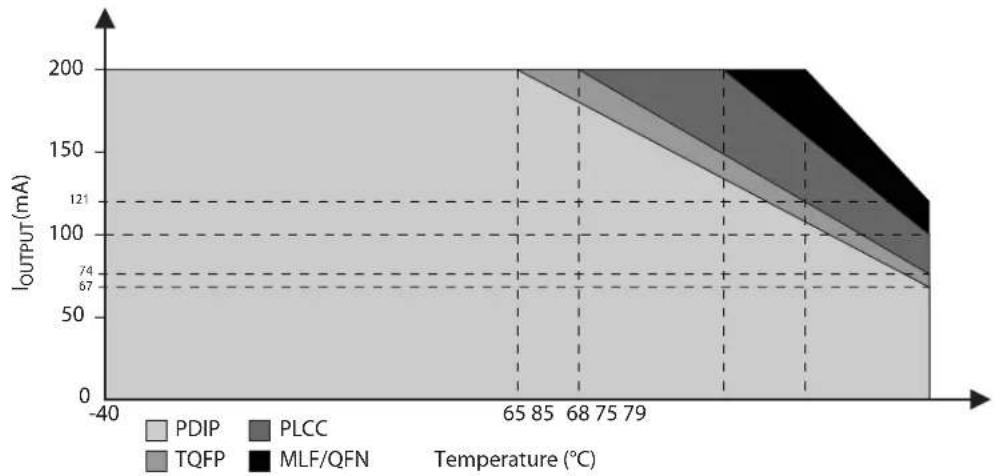
area
| Temperature (°C) | PDIP | PLCC | TQFP | MLF/QFN | | ---------------- | ---- | ---- | ---- | ------- | | 65 | 200 | 121 | 100 | 74 | | 85 | 200 | 121 | 100 | 74 | | 68 | 200 | 121 | 100 | 74 | | 75 | 200 | 121 | 100 | 74 | | 79 | 200 | 121 | 100 | 74 |26.4 Typical Characteristics
The following charts show typical behavior. These figures are not tested during manufacturing. All current consumption measurements are performed with all I/O pins configured as quasi-bidirectional (with internal pull-ups). A square wave generator with rail-to-rail output is used as an external clock source for consumption versus frequency measurements.
26.4.1 Supply Current (Internal Oscillator)
Figure 26-3. Active Supply Current vs. VDD (8MHz Internal Oscillator)
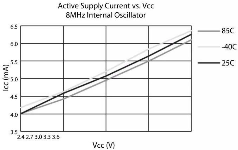
line
| Vcc (V) | 85C | -40C | 25C | |---------|-------|-------|-------| | 2.4 | 4.0 | 4.0 | 4.0 | | 2.7 | 4.2 | 4.3 | 4.3 | | 3.0 | 4.4 | 4.6 | 4.6 | | 3.3 | 4.6 | 4.9 | 4.9 | | 3.6 | 4.8 | 5.2 | 5.2 | | 3.9 | 5.0 | 5.5 | 5.5 | | 4.2 | 5.2 | 5.8 | 5.8 | | 4.5 | 5.4 | 6.1 | 6.1 | | 4.8 | 5.6 | 6.3 | 6.3 | | 5.1 | 5.8 | 6.5 | 6.5 | | 5.4 | 6.0 | 6.7 | 6.7 | | 5.7 | 6.2 | 6.9 | 6.9 | | 6.0 | 6.4 | 7.1 | 7.1 |Figure 26-4. Idle Supply Current vs. VDD (8MHz Internal Oscillator)

line
| Vcc (V) | 85C | -40C | 25C | |---------|-------|-------|-------| | 2.4 | 1.15 | 1.25 | 1.10 | | 2.7 | 1.25 | 1.35 | 1.20 | | 3.0 | 1.35 | 1.45 | 1.30 | | 3.3 | 1.45 | 1.55 | 1.40 | | 3.6 | 1.55 | 1.65 | 1.50 | | 4.0 | 1.65 | 1.75 | 1.60 | | 4.4 | 1.75 | 1.85 | 1.70 | | 4.8 | 1.85 | 1.95 | 1.80 | | 5.2 | 1.95 | 2.00 | 1.90 |26.4.2 Supply Current (External Clock)
Figure 26-5. Active Supply Current vs. Frequency
Active Supply Current vs. Frequency External Clock Source
line
| Frequency (MHz) | 2.4V | 2.7V | 3.0V | 3.3V | 3.6V | | --------------- | ----- | ----- | ----- | ----- | ----- | | 0 | 1.0 | 1.0 | 1.0 | 1.0 | 1.0 | | 5 | 1.5 | 1.6 | 1.7 | 1.8 | 1.9 | | 10 | 2.0 | 2.2 | 2.4 | 2.6 | 2.8 | | 15 | 2.5 | 2.8 | 3.1 | 3.4 | 3.7 | | 20 | 3.0 | 3.4 | 3.8 | 4.2 | 4.6 | | 25 | 3.5 | 4.0 | 4.5 | 5.0 | 5.5 | | 30 | 4.0 | 4.6 | 5.2 | 5.8 | 6.4 | | 35 | 4.5 | 5.2 | 5.9 | 6.6 | 7.3 | | 40 | 5.0 | 5.8 | 6.6 | 7.4 | 8.2 | | 45 | 5.5 | 6.4 | 7.3 | 8.2 | 9.0 | | 50 | 6.0 | 7.0 | 8.0 | 9.0 | 10.0 | | 55 | 6.5 | 7.6 | 8.7 | 9.8 | 11.0 | | 60 | 7.0 | 8.2 | 9.4 | 10.6 | 12.0 | | 65 | 7.5 | 8.8 | 10.1 | 11.4 | 13.0 | | 70 | 8.0 | 9.4 | 10.8 | 12.1 | 14.0 | | 75 | 8.5 | 10.0 | 11.5 | 12.8 | 15.0 | | 80 | 9.0 | 10.6 | 12.2 | 13.5 | 16.0 | | 85 | 9.5 | 11.2 | 12.9 | 14.2 | 17.0 | | 90 | 10.0 | 11.8 | 13.6 | 14.9 | 18.0 | | 95 | 10.5 | 12.4 | 14.3 | 15.6 | 19.0 | | 100 | 11.0 | 13.0 | 15.0 | 16.4 | 20.0 | | >10 | >11.0 | >12.0 | >13.0 | >14.0 | >15.0 | The chart displays a line graph with five distinct lines representing different voltage levels (2.4V to 3.6V). The x-axis is labeled 'Frequency (MHz)' and the y-axis is labeled 'Icc (mA)'. The legend indicates each line corresponds to a specific voltage level.Figure 26-6. Idle Supply Current vs. Frequency
Idle Supply Current vs. Frequency External Clock Source
line
| Frequency (MHz) | 2.4V | 2.7V | 3.0V | 3.3V | 3.6V | | --------------- | ----- | ----- | ----- | ----- | ----- | | 0 | 0.1 | 0.1 | 0.1 | 0.1 | 0.1 | | 5 | 0.2 | 0.2 | 0.2 | 0.2 | 0.2 | | 10 | 0.3 | 0.3 | 0.3 | 0.3 | 0.3 | | 15 | 0.4 | 0.4 | 0.4 | 0.4 | 0.4 | | 20 | 0.5 | 0.5 | 0.5 | 0.5 | 0.5 | | 25 | 0.6 | 0.6 | 0.6 | 0.6 | 0.6 | | 30 | 0.7 | 0.7 | 0.7 | 0.7 | 0.7 | | 35 | 0.8 | 0.8 | 0.8 | 0.8 | 0.8 | | 40 | 0.9 | 0.9 | 0.9 | 0.9 | 0.9 | | 45 | 1.0 | 1.0 | 1.0 | 1.0 | 1.0 | | 50 | 1.1 | 1.1 | 1.1 | 1.1 | 1.1 | | 55 | 1.2 | 1.2 | 1.2 | 1.2 | 1.2 | | 60 | 1.3 | 1.3 | 1.3 | 1.3 | 1.3 | | 65 | 1.4 | 1.4 | 1.4 | 1.4 | 1.4 | | 70 | 1.5 | 1.5 | 1.5 | 1.5 | 1.5 | | 75 | 1.6 | 1.6 | 1.6 | 1.6 | 1.6 | | 80 | 1.7 | 1.7 | 1.7 | 1.7 | 1.7 | | 85 | 1.8 | 1.8 | 1.8 | 1.8 | 1.8 | | 90 | 1.9 | 1.9 | 1.9 | 1.9 | 1.9 | | 95 | 2.0 | 2.0 | 2.0 | 2.0 | 2.0 | | 100 | 2.1 | 2.1 | 2.1 | 2.1 | 2.1 | | 105 | 2.2 | 2.2 | 2.2 | 2.2 | 2.2 | | 110 | 2.3 | 2.3 | 2.3 | 2.3 | 2.3 | | 115 | 2.4 | 2.4 | 2.4 | 2.4 | 2.4 | | 120 | 2.5 | 2.5 | 2.5 | 2.5 | 2.5 | | 125 | 2.6 | 2.6 | 2.6 | 2.6 | 2.6 | | 130 | 2.7 | 2.7 | 2.7 | 2.7 | 2.7 | | 135 | 2.8 | 2.8 | 2.8 | 2.8 | 2.8 | | 140 | 2.9 | 2.9 | 2.9 | 2.9 | 2.9 | | 145 | 3.0 | 3.0 | 3.0 | 3.0 | 3.0 | | 150 | 3.1 | 3.1 | 3.1 | 3.1 | 3.1 | | 155 | 3.2 | 3.2 | 3.2 | 3.2 | 3.2 | | 160 | 3.3 | 3.3 | 3.3 | 3.3 | 3.3 | | 165 | 3.4 | 3.4 | 3.4 | 3.4 | 3.4 | | 170 | 3.5 | 3.5 | 3.5 | 3.5 | 3.5 | | 175 | 3.6 | 3.6 | 3.6 | 3.6 | 3.6 | | 180 | - | - | - | - | - | | Note: The data is already in CSV format as it is provided in the code above the original table structure for each voltage level from the original table to the original table in the original table.26.4.3 Quasi-Bidirectional Input
Figure 26-7. Quasi-bidirectional Input Transition Current at 3.3V
line
| V_IL (V) | 85C | -40C | 25C | | -------- | ------ | ------ | ------ | | 0.0 | -20.0 | -40.0 | -20.0 | | 0.4 | -20.0 | -35.0 | -20.0 | | 0.8 | -20.0 | -30.0 | -20.0 | | 1.2 | -20.0 | -25.0 | -20.0 | | 1.6 | -20.0 | -20.0 | -20.0 | | 2.0 | -20.0 | -15.0 | -20.0 | | 2.4 | -20.0 | -10.0 | -20.0 | | 2.8 | -20.0 | -5.0 | -20.0 | | 3.2 | -20.0 | 0.0 | -20.0 |26.4.4 Quasi-Bidirectional Output
Figure 26-8. Quasi-Bidirectional Output I-V Source Characteristic at 3V
line
| VOH (V) | 85C | -40C | 25C | |---------|-------|-------|-------| | Low | -90 | -90 | -100 | | Medium | -70 | -80 | -90 | | High | 0 | 0 | 0 |26.4.5 Push-Pull Output
Figure 26-9. Push-Pull Output I-V Source Characteristic at 3V
line
| VOH1 (V) | 85C | -40C | 25C | | -------- | ----- | ----- | ----- | | 0 | -10 | -10 | -10 | | 2 | -8 | -8 | -8 | | 4 | -6 | -6 | -6 | | 6 | -4 | -4 | -4 | | 8 | -2 | -2 | -2 | | 10 | 0 | 0 | 0 |Figure 26-10. Push-Pull Output I-V Sink Characteristic at 3V

line
| V_OL (V) | 85C | -40C | 25C | | -------- | ---- | ---- | ---- | | 0.0 | 0.0 | 0.0 | 0.0 | | 0.1 | 1.0 | 1.0 | 1.0 | | 0.2 | 2.0 | 2.0 | 2.0 | | 0.3 | 3.0 | 3.0 | 3.0 | | 0.4 | 4.0 | 4.0 | 4.0 | | 0.5 | 5.0 | 5.0 | 5.0 | | 0.6 | 6.0 | 6.0 | 6.0 | | 0.7 | 7.0 | 7.0 | 7.0 | | 0.8 | 8.0 | 8.0 | 8.0 | | 0.9 | 9.0 | 9.0 | 9.0 | | 1.0 | 10.0 | 10.0 | 10.0 |Note: The I OL/VOL characteristic applies to Push-Pull, Quasi-Bidirectional and Open-Drain modes.
26.5 Clock Characteristics
Figure 26-11. External Clock Drive Waveform

text_image
Vcc - 0.5V 0.7 Vcc 0.2 Vcc - 0.1V 0.45V tCHCX tCLCH tCHCX tCHCL tCLCX tCLCLThe values shown in these tables are valid for T_A = -40^ to 85^ and V_DD = 2.4 to 3.6V, unless otherwise noted.
Table 26-1. External Clock Parameters
| Symbol Parameter | V_DD = 2.4V to 3.6V V | _DD = 2.7V to 3.6V | UnitsMin Max Min M | |||
| 1/t_CLCL | Oscillator Frequency(1) | 0 | 2 | 0 | 0 | 2 |
| t_CLCL | Clock Period 50 40 ns | |||||
| t_CHCX | External Clock High Time | 12 | 12 | ns | ||
| t_CLCX | External Clock Low Time | 12 | 12 | ns | ||
| t_CLCH | External Clock Rise Time | 5 | 5 | ns | ||
| t_CHCL | External Clock Fall Time | 5 | 5 | ns | ||
Note: 1. No wait state (single-cycle) execution speed
Table 26-2. Clock Characteristics
| Symbol | Parameter | Condition | Min | Max | Units |
| f_XTAL | Crystal Oscillator Frequency | Low Speed Oscillator | 10 | 100 | kHz |
| High Speed Oscillator | 0.5 | 24 | MHz | ||
| f_RC | Internal Oscillator Frequency | T_A = 25°C; V_DD = 3.0V | 7.92 | 8.08 | MHz |
| V_DD = 2.4 to 3.6V | 7.80 | 8.20 | MHz |
Figure 26-12. Typical Internal Oscillator Frequency vs. VCC
line
| Vcc (V) | -40C | 0C | 25C | 70C | 85C | | ------- | ----- | ----- | ----- | ----- | ----- | | 2.4 | 8.05 | 8.00 | 8.05 | 7.98 | 7.85 | | 2.7 | 8.04 | 8.00 | 8.04 | 7.99 | 7.86 | | 3.0 | 8.03 | 8.00 | 8.03 | 7.99 | 7.86 | | 3.3 | 8.02 | 7.99 | 8.02 | 7.98 | 7.86 | | 3.6 | 8.01 | 7.98 | 8.01 | 7.97 | 7.86 |Figure 26-13. Typical Crystal Oscillator Swing with Quartz Crystal and C1=C2, T_A=25^
line
| Frequency (MHz) | 3.6V 15pF | 3.6V 10pF | 3.6V 5pF | 2.4V 15pF | 2.4V 10pF | 2.4V 5pF | | --------------- | --------- | --------- | -------- | --------- | --------- | -------- | | 4 | 3.5 | 3.5 | 3.5 | 3.5 | 3.5 | 2.3 | | 8 | 3.5 | 3.5 | 3.5 | 3.5 | 3.5 | 2.3 | | 12 | 3.5 | 3.5 | 3.5 | 3.5 | 3.5 | 2.3 | | 16 | 3.5 | 3.5 | 3.5 | 3.5 | 3.5 | 2.3 | | 20 | 3.5 | 3.5 | 3.5 | 3.5 | 3.5 | 2.4 | | Peak | 3.6 | 3.6 | 3.6 | 3.6 | 3.6 | 2.4 | | End | 3.4 | 3.4 | 3.4 | 3.4 | 3.4 | 2.3 |Note: 1. Replacing capacitor C1 with a resistor R1 of 4 MΩ results in similar swing levels on XTAL1.
Figure 26-14. Typical Crystal Oscillator Swing with Ceramic Resonator and C1=C2, T_A=25^

26.6 Reset Characteristics
The values shown in this table are valid for T_A = -40^ to 85^ and V_DD = 2.4 to 3.6V, unless otherwise noted.
Table 26-3. Reset Characteristics
| Symbol Parameter Condition Min Max Units | |||||
| R_RST | Reset Pull-up Resistor | 50 | 150 | kΩ | |
| V_POR | Power-On Reset Threshold | 1.3 | 1.6 | V | |
| V_BOD | Brown-Out Detector Threshold | 1.8 | 2.0 | V | |
| V_BH | Brown-Out Detector Hysteresis | 200 | 300 | mV | |
| t_POR | Power-On Reset Delay | 135 | 150 | μs | |
| t_WDTRST | Watchdog Reset Pulse Width | 16t_CLCL | ns | ||
26.7 External Data Memory Characteristics
The values shown in this table are valid for T_A = -40^ to 85^ and V_DD = 2.4 to 3.6V, unless otherwise noted. Under operating conditions, load capacitance for Port 0 and ALE = 100 pF; load capacitance for all other outputs = 80 pF. Parameters refer to Figure 26-15 and Figure 26-16.
Table 26-4. External Data Memory Characteristics
| Symbol Parameter | Variable Oscillator | Units | ||
| Min | Max | |||
| 1/t_CLCL | Oscillator Frequency | 0 | 24 | MHz |
| t_LHLL | ALE Pulse Width(3) | t_CLCL - d | ns | |
| t_AVLL | Address Valid to ALE Low | 0.5t_CLCL - d^(1) | ns | |
| t_LLAX | Address Hold after ALE Low | 0.5t_CLCL - d^(2) | ns | |
| t_RLRH | Pulse Width(4) | t_CLCL - d | ns | |
| t_WLWH | Pulse Width(4) | t_CLCL - d | ns | |
| t_RLDV | Low to Valid Data In | t_CLCL - d | ns | |
| t_RHDX | Data Hold after | 0 | ns | |
| t_RHDZ | Data Float after | t_CLCL - d | ns | |
| t_LLDV | ALE Low to Valid Data In | 2t_CLCL - d | ns | |
| t_AVDV | Address to Valid Data In | 2.5t_CLCL - d^(1) | ns | |
| t_LLWL | ALE Low to or Low | t_CLCL - d | t_CLCL + d | ns |
| t_AVWL | Address to or Low | 1.5t_CLCL - d^(1) | ns | |
| t_QVWX | Data Valid to Transition | 0.5t_CLCL - d^(1) | ns | |
| t_QVWH | Data Valid to High | 1.5t_CLCL - d^(1) | ns | |
| t_WHQX | Data Hold after | 0.5t_CLCL - d^(2) | ns | |
| t_RLAZ | Low to Address Float | -0.5t_CLCL + d^(1) | ns | |
| t_WHAX | Address Hold after or High | 0.5t_CLCL - d^(2) | ns | |
| t_WHLH | or High to ALE High(5) | t_CLCL - d | t_CLCL + d | ns |
Notes: 1. This assumes 50% clock duty cycle. The half period depends on the clock high value t_CHCX (high duty cycle).
2. This assumes 50% clock duty cycle. The half period depends on the clock low value t_CLCX (low duty cycle).
- Parameter t_LHLL applies only when ALES = 1.
- The strobe pulse width may be lengthened by 1, 2 or 3 additional t_CLCL using wait states.
- Parameter t_WHLH applies only when ALES = 0, or when two MOVX instructions occur in succession.
Figure 26-15. External Data Memory Read Cycle

text_image
ALE tLHLL tLLDV tWHLH tLLWL tRLRH RD tRLAZ tRLDV tRHDZ tAVLL tLLAX tRHDX PORT 0 A0 - A7 DATA IN tAVWL tAVDV tWHAX PORT 2 P2 A8 - A15 FROM DPH OR P2.0 - P2.7 P2Figure 26-16. External Data Memory Write Cycle
text_image
ALE tLHLL tLLWL tWLWH tWHLH WR tQVWX tAVLL tLLAX DATA OUT tQVWH tAVWL tWHAX PORT 0 A0 - A7 PORT 2 P2 A8 - A15 FROM DPH OR P2.0 - P2.7 P226.8 Serial Peripheral Interface Timing
The values shown in these tables are valid for T_A = -40^ to 85^ and V_DD = 2.4 to 3.6V, unless otherwise noted.
Table 26-5. SPI Master Characteristics
| Symbol Parameter | Min Max Units | |||
| t_CLCL | Oscillator Period | 41.6 | ns | |
| t_SCK | Serial Clock Cycle Time 4t | CLCL | ns | |
| t_SHSL | Clock High Time t | _SCK/2 - 25 | ns | |
| t_SLSH | Clock Low Time | t_SCK/2 - 25 | ns | |
| t_SR | Rise Time | 25 | ns | |
| t_SF | Fall Time | 25 | ns |
Table 26-5. SPI Master Characteristics
| Symbol Parameter | Min Max Units | |||
| t_SIS | Serial Input Setup Time | 10 | ns | |
| t_SIH | Serial Input Hold Time | 10 | ns | |
| t_SOH | Serial Output Hold Time | 10 | ns | |
| t_SOV | Serial Output Valid Time | 35 | ns |
Table 26-6. SPI Slave Characteristics
| Symbol Parameter | Min Max Units | |||
| t_CLCL | Oscillator Period | 41.6 | ns | |
| t_SCK | Serial Clock Cycle Time | 4t_CLCL | ns | |
| t_SHSL | Clock High Time | 1.5 t_CLCL -25 | ns | |
| t_SLSH | Clock Low Time | 1.5 t_CLCL -25 | ns | |
| t_SR | Rise Time | 25 | ns | |
| t_SF | Fall Time | 25 | ns | |
| t_SIS | Serial Input Setup Time | 10 | ns | |
| t_SIH | Serial Input Hold Time | 10 | ns | |
| t_SOH | Serial Output Hold Time | 10 | ns | |
| t_SOV | Serial Output Valid Time | 35 | ns | |
| t_SOE | Output Enable Time | 10 | ns | |
| t_SOX | Output Disable Time | 25 | ns | |
| t_SSE | Slave Enable Lead Time | 10 | ns | |
| t_SSD | Slave Disable Lag Time | 0 | ns |
Figure 26-17. SPI Master Timing (CPHA = 0)
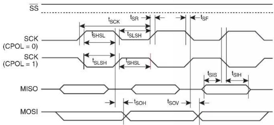
text_image
SS tSCK tsR tSF SCK (CPOL = 0) tSHSL tSLSH tSLSH tSHSL tSIS tSIH MISO tSOH tSOV MOSIFigure 26-18. SPI Slave Timing (CPHA = 0)
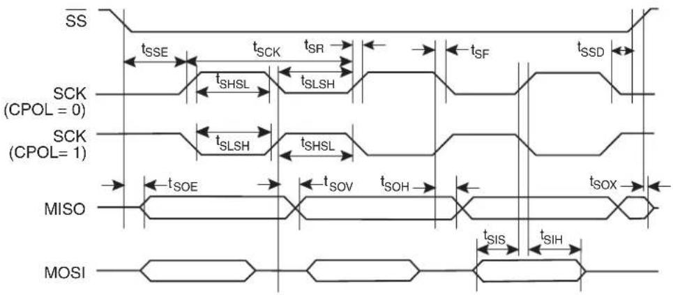
text_image
SS tSSE tSCK tSR tSF tSSD SCK (CPOL = 0) tSHSL tSLSH SCK (CPOL= 1) tSLSH tSHSL MISO tSOE tSOV tSOH tSOX MOSI tSIS tSIHFigure 26-19. SPI Master Timing (CPHA = 1)
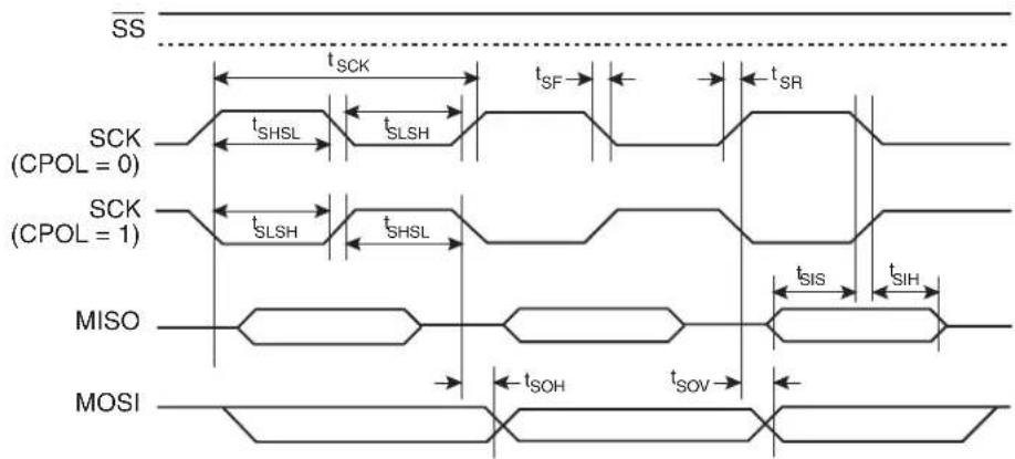
text_image
SS tSCK tSF tSR SCK (CPOL = 0) tSHSL tSLSH tSR SCK (CPOL = 1) tSLSH tSHSL tSIS tSIH MISO tSOH tSOV MOSIFigure 26-20. SPI Slave Timing (CPHA = 1)
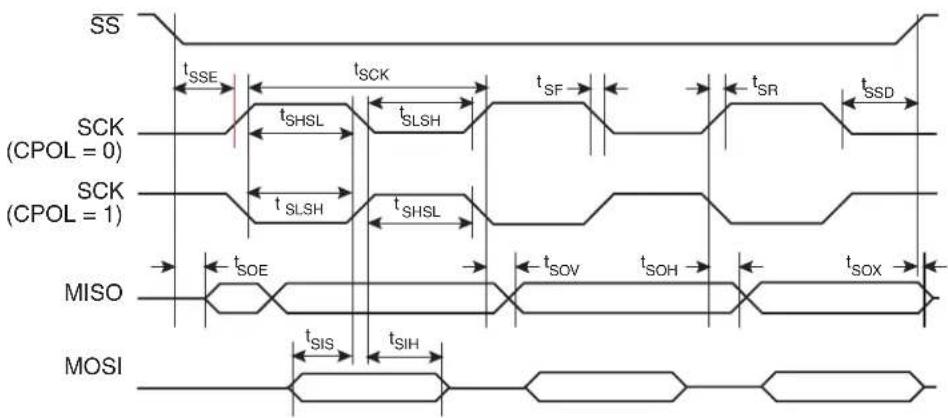
text_image
SS tSSE tSCK tSF tSR tSSD SCK (CPOL = 0) tSHSL tSLSH tSLSH tSHSL SCK (CPOL = 1) MISO tSOE tSOV tSOH tSOX MOSI tSIS tSIH26.9 Two-wire Serial Interface Characteristics
Table 26-7 describes the requirements for devices connected to the Two-wire Serial Bus. The AT89LP3240/6440 Two-wire Serial Interface meets or exceeds these requirements under the noted conditions. The values shown in this table are valid for T_A = -40^ C to 85^ C and V_DD = 2.4 to 3.6V , unless otherwise noted.
Timing symbols refer to Figure 26-21.
Table 26-7. Two-wire Serial Bus Requirements
| Symbol | Parameter Condition Min Max Units | ||||
| V_IL | Input Low-voltage | -0.5 | 0.3 V_DD | V | |
| V_IH | Input High-voltage | 0.7 V_DD | V_DD + 0.5 | V | |
| V_hys^(1) | Hysteresis of Schmitt Trigger Inputs | 0.05 V_DD^(2) | - | V | |
| V_OL^(1) | Output Low-voltage | 3 mA sink current | 0 | 0.4 | V |
| t_r^(1) | Rise Time for both SDA and SCL | 20 + 0.1C_b^(3)(2) | 300 | ns | |
| t_of^(1) | Output Fall Time from V_IHmin to V_ILmax | 10 pF < C_b < 400 pF^(3) | 20 + 0.1C_b^(3)(2) | 250 | ns |
| t_SP^(1) | Spikes Suppressed by Input Filter | 0 | 50^(2) | ns | |
| I_i | Input Current each I/O Pin | 0.1V_DD < V_i < 0.9V_DD | -10 | 10 | μA |
| C_i^(1) | Capacitance for each I/O Pin | - | 10 | pF | |
| f_SCL | SCL Clock Frequency | f_CK^(4) > 16f_SCL | 0 | 400 | kHz |
| Rp | Value of Pull-up resistor | f_SCL ≤ 100 kHz | _DD - 0.4V3mA | 1000nsC_b | Ω |
| f_SCL > 100 kHz | _DD - 0.4V3mA | 300nsC_b | Ω | ||
| t_HD;STA | Hold Time (repeated) START Condition | f_SCL ≤ 100 kHz | 4.0 | - | μs |
| f_SCL > 100 kHz | 0.6 | - | μs | ||
| t_LOW | Low Period of the SCL Clock | f_SCL ≤ 100 kHz | 4.7 | - | μs |
| f_SCL > 100 kHz | 1.3 | - | μs | ||
| t_HIGH | High period of the SCL clock | f_SCL ≤ 100 kHz | 4.0 | - | μs |
| f_SCL > 100 kHz | 0.6 | - | μs | ||
| t_SU;STA | Set-up time for a repeated START condition | f_SCL ≤ 100 kHz | 4.7 | - | μs |
| f_SCL > 100 kHz | 0.6 | - | μs | ||
| t_HD;DAT | Data hold time | f_SCL ≤ 100 kHz | 0 | 3.45 | μs |
| f_SCL > 100 kHz | 0 | 0.9 | μs | ||
| t_SU;DAT | Data setup time | f_SCL ≤ 100 kHz | 250 | - | ns |
| f_SCL > 100 kHz | 100 | - | ns | ||
| t_SU;STO | Setup time for STOP condition | f_SCL ≤ 100 kHz | 4.0 | - | μs |
| f_SCL > 100 kHz | 0.6 | - | μs | ||
| t_BUF | Bus free time between a STOP and START condition | f_SCL ≤ 100 kHz | 4.7 | - | μs |
Notes: 1. In AT89LP3240/6440, this parameter is characterized and not 100% tested.
2. Required only for f_SCL > 100 kHz.
- C_b= capacitance of one bus line in pF.
- f_CK = CPU clock frequency
Figure 26-21. Two-wire Serial Bus Timing

text_image
SCL tSU;STA SDA tHD;STA tHD;DAT tSU;DAT tSU;STO tBUF tLow tHigh tLow tR26.10 Serial Port Timing: Shift Register Mode
The values in this table are valid for V_DD = 2.4V to 3.6V and Load Capacitance = 80pF .
| Symbol Parameter | SMOD1 = 0 SMOD1 = 1 | UnitsMin Max Mi | ||||
| t_XLXL | Serial Port Clock Cycle Time 4t | _CLCL -15 2t | _CLCL -15 μs | |||
| t_QVXH | Output Data Setup to Clock Rising Edge | 3t_CLCL -15 t | _CLCL -15 ns | |||
| t_XHQX | Output Data Hold after Clock Rising Edge | t_CLCL -15 | t_CLCL -15 | ns | ||
| t_XHDX | Input Data Hold after Clock Rising Edge | 0 | 0 | ns | ||
| t_XHDV | Input Data Valid to Clock Rising Edge | 15 | 15 | ns | ||
Figure 26-22. Shift Register Mode Timing Waveform

text_image
SMOD1 = 0 Clock Write to SBUF Output Data Clear RI Input Data Valid Valid Valid Valid Valid Valid Valid Valid Valid SET TI SMOD1 = 1 Clock Write to SBUF Output Data Clear RI Input Data Valid Valid Valid Valid Valid Valid Valid Valid Valid SET RI tQVXH tXHQX tXHDV tXHDX SET TI26.11 Dual Analog Comparator Characteristics
The values shown in this table are valid for T_A = -40^ to 85^ and V_DD = 2.4 to 3.6V, unless otherwise noted.
Table 26-8. Dual Analog Comparator Characteristics
| Symbol Parameter Condition Min Max Units | |||||
| V_CM | Common Mode Input Voltage | GND | V_DD | V | |
| V_OS | Input Offset Voltage | V_DD=3.6V20 mV | |||
| V_AREF | Analog Reference Voltage | 1.23 | 1.36 | V | |
| V_ REF | Reference Delta Voltage | 90 | 120 | mV | |
| t_CMP | Comparator Propagation Delay | V_IN+-V_IN-=20mV; V_DD=2.4V | 200 | ns | |
| t_AREF | Reference Settling Time | 3 | μs | ||
Figure 26-23. Analog Reference Voltage Typical Characteristics
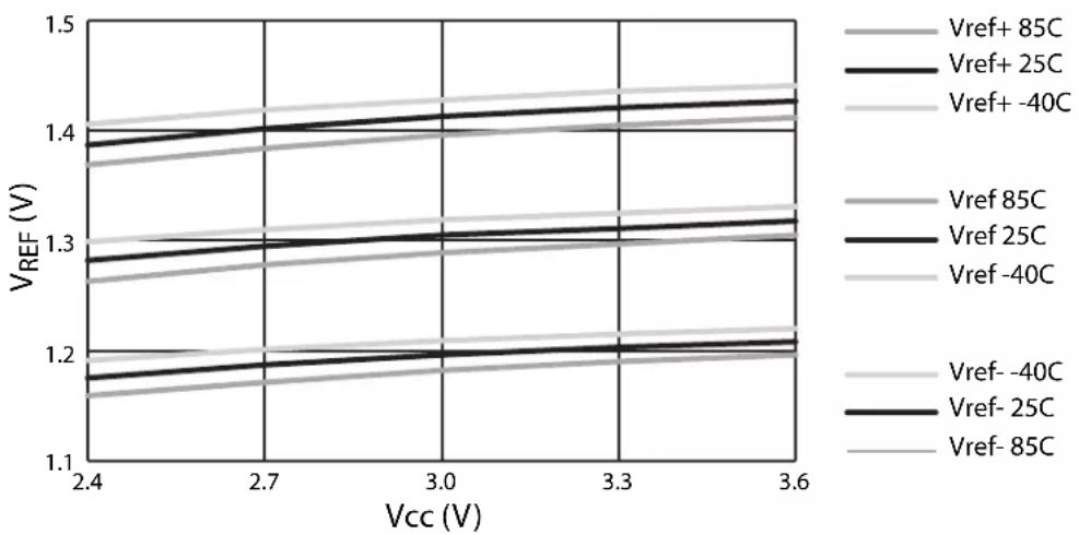
line
| Vcc (V) | VREF (V) for Vref+ 85C | VREF (V) for Vref+ 25C | VREF (V) for Vref+ -40C | VREF (V) for Vref- 85C | VREF (V) for Vref- 25C | VREF (V) for Vref- -40C | VREF (V) for Vref- 85C | VREF (V) for Vref- 25C | VREF (V) for Vref- -40C | | ------- | ---------------------- | ---------------------- | ----------------------- | ---------------------- | ---------------------- | ----------------------- | ---------------------- | ---------------------- | ----------------------- | | 2.4 | ~1.38 | ~1.39 | ~1.37 | ~1.28 | ~1.29 | ~1.30 | ~1.27 | ~1.28 | ~1.30 | | 2.7 | ~1.40 | ~1.41 | ~1.40 | ~1.30 | ~1.31 | ~1.32 | ~1.29 | ~1.30 | ~1.32 | | 3.0 | ~1.42 | ~1.43 | ~1.42 | ~1.32 | ~1.33 | ~1.34 | ~1.31 | ~1.32 | ~1.34 | | 3.3 | ~1.44 | ~1.45 | ~1.44 | ~1.34 | ~1.35 | ~1.36 | ~1.33 | ~1.34 | ~1.36 | | 3.6 | ~1.46 | ~1.47 | ~1.46 | ~1.36 | ~1.37 | ~1.38 | ~1.35 | ~1.36 | ~1.38 |26.12 DADC Characteristics
The values shown in these tables are valid for T_A = -40^ to 85^ and V_DD = 2.4 to 3.6V, unless otherwise noted.
Table 26-9. ADC Characteristics
| Symbol | Parameter Condition Min Typical | Max Units | ||||
| Resolution | 10 | Bits | ||||
| Absolute Accuracy (including INL, DNL, quantization error, gain and offset error) | 4 | L | ||||
| Integral Non-Linearity (INL) | 4 | LSB | ||||
| Differential Non-Linearity (DNL) | 4 | L | ||||
| Gain Error | 16 | LSB | ||||
| Offset Error | 16 | LSB | ||||
| t_ACK | Clock Period | 500 | ns | |||
| t_ADC | Conversion Time | 13t_ACK | 14t_ACK + 2t_CLCL | ns | ||
| V_REF | Reference Voltage | External Reference | V_DD/2 - 0.2 | V_DD/2 | V_DD/2 + 0.2 | V |
| Internal Reference | 0.9 | 1.0 | 1.1 | V | ||
| V_IN | Single-Ended Input Voltage | V_DD/2 - V_REF | V_DD/2 + V_REF | V | ||
| V_CMI | Differential Input Common Mode Voltage | GND | V_DD | V | ||
| V_DI | Differential Input Voltage | 0 | ± V_REF | V | ||
| R_IN | Analog Input Resistance | 10 | kΩ | |||
| R_MUX | Analog Mux Resistance | 10 | kΩ | |||
| C_S/H | Sample & Hold Capacitance | 3 | pF |
Table 26-10. DAC Characteristics
| Symbol | Parameter | Condition | Min | Typical | Max | Units |
| Resolution | 10 | Bits | ||||
| t_ACK | Clock Period | t_ACK ≥ t_CLCL | 500 | ns | ||
| t_DAC | Conversion Time | 11t_ACK | 12t_ACK + 2t_CLCL | ns | ||
| V_REF | Reference Voltage | External Reference | V_DD/2 - 0.2 | V_DD/2 | V_DD/2 + 0.2 | V |
| Internal Reference | 0.9 | 1.0 | 1.1 | V | ||
| V_IN | Single-Ended Input Voltage | V_DD/2 - V_REF | V_DD/2 + V_REF | V | ||
| V_CMO | Differential Output Common Mode Voltage | V_DD/2 - 0.2 | V_DD/2 | V_DD/2 + 0.2 | V | |
| V_DO | Differential Output Voltage | 0 | ± V_REF | V | ||
| R_OUT | Analog Output Resistance | 100 | 200 | kΩ |
26.13 Test Conditions
26.13.1 AC Testing Input/Output Waveform
Figure 26-24. AC Testing Input/Output Waveform ^(1)

text_image
VCC - 0.5V 0.45V 0.2 VCC + 0.9V TEST POINTS 0.2 VCC - 0.1VNote: 1. AC Inputs during testing are driven at V_DD - 0.5V for a logic "1" and 0.45V for a logic "0". Timing measurements are made at V_IH min. for a logic "1" and V_IL max. for a logic "0".
26.13.2 Float Waveform
Figure 26-25. Float Waveform ^(1)
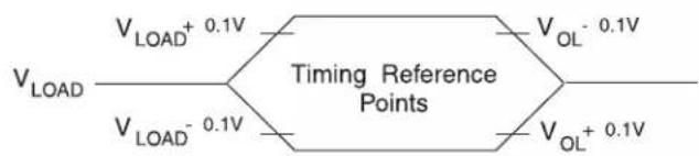
text_image
VLOAD VLOAD+ 0.1V Timing Reference Points VLOAD- 0.1V VOL- 0.1V VOL+ 0.1VNote: 1. For timing purposes, a port pin is no longer floating when a 100 mV change from load voltage occurs. A port pin begins to float when 100 mV change from the loaded V_OH/V_OL level occurs.
26.13.3 I cc Test Condition: Active Mode
Figure 26-26. Connection Diagram for Icc Active Measurement. All Other Pins are Disconnected
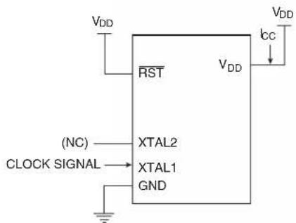
text_image
VDD RST VDD VDD (NC) CLOCK SIGNAL XTAL2 XTAL1 GND IccFor active supply current measurements all ports are configured in quasi-bidirectional mode. Timers 0, 1 and 2 are configured to be free running in their default timer modes. The CPU executes a simple random number generator that accesses RAM, the SFR bus and exercises the ALU and hardware multiplier.
26.13.4 I cc Test Condition: Idle Mode
Figure 26-27. Connection Diagram for I_cc Idle Measurement. All Other Pins are Disconnected

text_image
VDD RST (NC) CLOCK SIGNAL XTAL2 XTAL1 GND VDD ICC VDD26.13.5 Clock Signal Waveform for I cc Tests
Figure 26-28. Clock Signal Waveform for I_CC in Active and Idle Modes, t_CLCH = t_CHCL = 5 ns
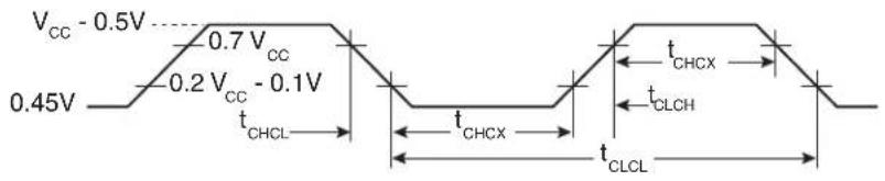
other
| Time Segment | Voltage Level | Duration | | ------------ | ------------- | -------- | | Top Left | V_CC - 0.5V | — | | Top Right | 0.7 V_CC | — | | Bottom Left | 0.45V | — | | Bottom Right | t_CHCL | — | | Bottom Left | t_CHCX | — | | Bottom Right | t_CLCL | — |26.13.6 I cc Test Condition: Power-down Mode
Figure 26-29. Connection Diagram for I_CC Power-down Measurement. All Other Pins are Disconnected, V_DD = 2V to 3.6V

text_image
VDD RST VDD (NC) XTAL2 XTAL1 GND Icc VDD27. Ordering Information
27.1 Green Package Option (Pb/Halide-free)
| Code Flash | Speed (MHz) | Power Supply Ordering Code Package Operation Range | |||
| 32KB 20 | 2.4V to 3.6V | AT89LP3240-20AU | 44A | Industrial(-40°C to 85°C) | |
| AT89LP3240-20PU | 40P6 | ||||
| AT89LP3240-20JU | 44J | ||||
| AT89LP3240-20MU | 44M1 | ||||
| 64KB 20 | 2.4V to 3.6V | AT89LP6440-20AU | 44A | ||
| AT89LP6440-20PU | 40P6 | ||||
| AT89LP6440-20JU | 44J | ||||
| AT89LP6440-20MU | 44M1 | ||||
| Package Types | |
| 44A | 44-lead, Thin Plastic Quad Flat Package (TQFP) |
| 40P6 | 40-lead, 0.600” Wide, Plastic Dual Inline Package (PDIP) |
| 44J | 44-lead, Plastic J-leaded Chip Carrier (PLCC) |
| 44M1 | 44-pad, 7 x 7 x 1.0 mm Body, Plastic Very Thin Quad Flat No Lead Package (VQFN/MLF) |
28. Packaging Information
28.1 44A - TQFP

text_image
PIN 1 PIN 1 IDENTIFIER B E1 E e D1 D C 0°~7° L A1 A2 ACOMMON DIMENSIONS
(Unit of Measure = mm)
| SYMBOL | MIN | NOM | MAX | NOTE |
| A--1.20 | ||||
| A1 0.05 - 0.15 | ||||
| A2 0.95 1.00 1.05 | ||||
| D | 11.75 | 12.00 | 12.25 | |
| D1 | 9.90 | 10.00 | 10.10 | Note 2 |
| E 11.75 12.00 12.25 | ||||
| E1 9.90 10.00 10.10 Note 2 | ||||
| B | 0.30 | -0.45 | ||
| C 0.09 - 0.20 | ||||
| L | 0.45 - | 0.75 | ||
| e | 0.80 TYP | |||
10/5/2001
 | 2325 Orchard ParkwaySan Jose, CA 95131 | TITLE44A, 44-lead, 10 x 10 mm Body Size, 1.0 mm Body Thickness,0.8 mm Lead Pitch, Thin Profile Plastic Quad Flat Package (TQFP) | DRAWING NO.44A | REV.B |
28.2 40P6 - PDIP

text_image
D PIN 1 E1
text_image
A SEATING PLANE L e B1 A1 B
text_image
E C 0° ~ 15° REF eBNotes: 1. This package conforms to JEDEC reference MS-011, Variation AC. 2. Dimensions D and E1 do not include mold Flash or Protrusion. Mold Flash or Protrusion shall not exceed 0.25 mm (0.010").
COMMON DIMENSIONS
(Unit of Measure = mm)
| SYMBOL | MIN | NOM | MAX | NOTE |
| A--4.826 | ||||
| A1 0.381-- | ||||
| D 52.070-52.578 Note 2 | ||||
| E 15.240-15.875 | ||||
| E1 13.462-13.970 Note 2 | ||||
| B 0.356-0.559 | ||||
| B1 1.041-1.651 | ||||
| L 3.048-3.556 | ||||
| C 0.203-0.381 | ||||
| eB 15.494-17.526 | ||||
| e | 2.540 TYP | |||
09/28/01

2325 Orchard Parkway San Jose, CA 95131
TITLE
40P6, 40-lead (0.600"/15.24 mm Wide) Plastic Dual Inline Package (PDIP)
| DRAWING NO. | REV. |
| 40P6 | B |
28.3 44J - PLCC

text_image
1.14(0.045) X 45° PIN NO. 1 IDENTIFIER B e D1 D E1 E 1.14(0.0 0.51(0.020)MAX 45° MAX (3X)
text_image
0.318(0.0125) 0.191(0.0075) B1 D2/E2 A2 A1 ACOMMON DIMENSIONS
(Unit of Measure = mm)
| SYMBOL | MIN | NOM | MAX | NOTE |
| A 4.191 – 4.572 | ||||
| A1 2.286 – 3.048 | ||||
| A2 0.508– – | ||||
| D 17.399 – 17.653 | ||||
| D1 16.510 – 16.662 Note 2 | ||||
| E 17.399 – 17.653 | ||||
| E1 16.510 – 16.662 Note 2 | ||||
| D2/E2 | 14.986 – | 16.002 | ||
| B 0.660 – 0.813 | ||||
| B1 0.330 – 0.533 | ||||
| e | 1.270 TYP | |||
Notes: 1. This package conforms to JEDEC reference MS-018, Variation AC.
2. Dimensions D1 and E1 do not include mold protrusion.
Allowable protrusion is .010"(0.254 mm) per side. Dimension D1 and E1 include mold mismatch and are measured at the extreme material condition at the upper or lower parting line.
3. Lead coplanarity is 0.004" (0.102 mm) maximum.
10/04/01

2325 Orchard Parkway San Jose, CA 95131
TITLE
44J, 44-lead, Plastic J-leaded Chip Carrier (PLCC)
| DRAWING NO. | REV. |
| 44J | B |
28.4 44M1 - VQFN/MLF
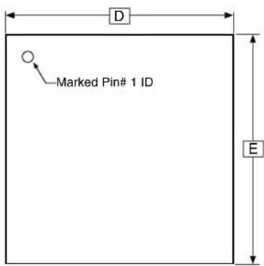
text_image
Marked Pin# 1 ID D ETOP VIEW

text_image
SEATING PLANE A1 A3 ASIDE VIEW

text_image
L K D2 Pin #1 Corner E2 K b e 1 2 3 Option A Pin #1 Triangle Option B Pin #1 Chamfer (C 0.30) Option C Pin #1 Notch (0.20 R) BOTTOM VIEWNote: JEDEC Standard MO-220, Fig. 1 (SAW Singulation) VKKD-3.
COMMON DIMENSIONS
(Unit of Measure = mm)
| SYMBOL | MIN | NOM | MAX | NOTE |
| A 0.80 0.90 | 1.00 | |||
| A1 - | 0.02 | 0.05 | ||
| A3 | 0.20 REF | |||
| b | 0.18 | 0.23 | 0.30 | |
| D | 6.90 | 7.00 | 7.10 | |
| D2 5.00 5.20 | 5.40 | |||
| E | 6.90 | 7.00 | 7.10 | |
| E2 | 5.00 | 5.20 | 5.40 | |
| e | 0.50 BSC | |||
| L 0.59 0.64 | 0.69 | |||
| K | 0.20 | 0.26 | 0.41 | |
9/26/08

Package Drawing Contact: packagedrawings@atmel.com
TITLE
| 44M1, 44-pad, 7 x 7 x 1.0 mm Body, Lead Pitch 0.50 mm, 5.20 mm Exposed Pad, Thermally Enhanced Plastic Very Thin Quad Flat No Lead Package (VQFN) |
DRAWING NO.GREV.
44M1ZWS H
29. Revision History
| Revision No. History | |
| Revision A – September 2009 | Initial Release |
| Revision B– September 2010 | Removed Preliminary statusUpdated “DC Characteristics” on page 170Updated “Typical Characteristics” on page 171Renamed AVDD to VDD |
| Revision C– February 2011 | Added section “System Configuration” on page 8Added the AT89LP3240 deviceUpdated oscillator connection diagram, Figure 6-1 on page 31 |
Table of Contents
Features 1
1 Pin Configurations ...... 2
1.1 40P6: 40-lead PDIP ....2
1.2 44A: 44-lead TQFP (Top View) ...... 2
1.3 44J: 44-lead PLCC ....3
1.4 44M1: 44-pad VQFN/MLF 3
1.5 Pin Description 4
2 Overview 6
2.1 Block Diagram 7
2.2 System Configuration 8
2.3 Comparison to Standard 8051 9
3 Memory Organization 11
3.1 Program Memory 11
3.2 Internal Data Memory 12
3.3 External Data Memory 13
3.4 Extended Stack 20
3.5 In-Application Programming (IAP) 21
4 Special Function Registers 22
5 Enhanced CPU 23
5.1 Multiply-Accumulate Unit (MAC) 24
5.2 Enhanced Dual Data Pointers 25
5.3 Instruction Set Extensions 30
6 System Clock 31
6.1 Crystal Oscillator 31
6.2 External Clock Source 32
6.3 Internal RC Oscillator 32
6.4 System Clock Out 32
6.5 System Clock Divider 32
7 Reset 33
7.1 Power-on Reset 33
7.2 Brown-out Reset 35
7.3 External Reset 35
Table of Contents (Continued)
7.4 Watchdog Reset 36
7.5 Software Reset 36
8 Power Saving Modes 36
8.1 Idle Mode 36
8.2 Power-down Mode 37
8.3 Reducing Power Consumption 38
9 Interrupts 39
9.1 Interrupt Response Time 41
10 I/O Ports 45
10.1 Port Configuration 45
10.2 Port Analog Functions 48
10.3 Port Read-Modify-Write 48
10.4 Port Alternate Functions 49
11 Enhanced Timer 0 and Timer 1 with PWM ....51
11.1 Mode 0 – Variable Width Timer/Counter ....52
11.2 Mode 1 – 16-bit Auto-Reload Timer/Counter ....52
11.3 Mode 2 - 8-bit Auto-Reload Timer/Counter ....53
11.4 Mode 3 - 8-bit Split Timer ....53
11.5 Pulse Width Modulation 56
12 Enhanced Timer 2 ....60
12.1 Timer 2 Registers ....61
12.2 Capture Mode 62
12.3 Auto-Reload Mode 63
12.4 Baud Rate Generator 67
12.5 Frequency Generator (Programmable Clock Out) 68
13 Compare/Capture Array 69
13.1 CCA Registers 70
13.2 Input Capture Mode 72
13.3 Output Compare Mode 75
13.4 Pulse Width Modulation Mode 77
14 External Interrupts 82
15 General-purpose Interrupts 83
Table of Contents (Continued)
16 Serial Interface (UART) 85
16.1 Multiprocessor Communications 85
16.2 Baud Rates 87
16.3 More About Mode 0 ....89
16.4 More About Mode 1 92
16.5 More About Modes 2 and 3 .....94
16.6 Framing Error Detection 97
16.7 Automatic Address Recognition 97
17 Enhanced Serial Peripheral Interface 98
17.1 Master Operation 100
17.2 Slave Operation 101
17.3 Pin Configuration 101
17.4 Serial Clock Timing 104
18 Two-Wire Serial Interface 105
18.1 Data Transfer and Frame Format 106
18.2 Multi-master Bus Systems, Arbitration and Synchronization ..... 108
18.3 Overview of the TWI Module 110
18.4 Register Overview 112
18.5 Using the TWI 113
18.6 Transmission Modes 115
19 Dual Analog Comparators 126
19.1 Analog Input Muxes 127
19.2 Internal Reference Voltage 128
19.3 Comparator Interrupt Debouncing 128
20 Digital-to-Analog/Analog-to-Digital Converter 133
20.1 ADC Operation 135
20.2 DAC Operation 136
20.3 Clock Selection 137
20.4 Starting a Conversion 137
20.5 Noise Considerations 138
21 Programmable Watchdog Timer 141
21.1 Software Reset 142
Table of Contents (Continued)
22 Instruction Set Summary 143
22.1 Instruction Set Extensions ....147
23 Register Index 153
24 On-Chip Debug System 155
24.1 Physical Interface 155
24.2 Software Breakpoints 156
24.3 Limitations of On-Chip Debug 156
25 Programming the Flash Memory 157
25.1 Physical Interface 157
25.2 Memory Organization 159
25.3 Command Format 160
25.4 Status Register 163
25.5 DATA Polling 163
25.6 Flash Security 163
25.7 User Configuration Fuses 164
25.8 User Signature and Analog Configuration 165
25.9 Programming Interface Timing 165
26 Electrical Characteristics 170
26.1 Absolute Maximum Ratings* 170
26.2 DC Characteristics 170
26.3 Safe Operating Conditions 171
26.4 Typical Characteristics 171
26.5 Clock Characteristics 175
26.6 Reset Characteristics 178
26.7 External Data Memory Characteristics 178
26.8 Serial Peripheral Interface Timing 179
26.9 Two-wire Serial Interface Characteristics 182
26.10 Serial Port Timing: Shift Register Mode 183
26.11 Dual Analog Comparator Characteristics 184
26.12 DADC Characteristics 185
26.13 Test Conditions 186
27 Ordering Information 188
27.1 Green Package Option (Pb/Halide-free) 188
Table of Contents (Continued)
28 Packaging Information 189
28.1 44A-TQFP 189
28.2 40P6 – PDIP ....190
28.3 44J-PLCC 191
28.4 44M1 - VQFN/MLF 192
29 Revision History 193
Table of Contents...... i
Atmel Corporation
2325 Orchard Parkway
San Jose, CA 95131
USA
Tel: (+1) (408) 441-0311
Fax: (+1) (408) 487-2600
www.atmel.com
8051@atmel.com
Atmel Asia Limited
Unit 1-5 & 16, 19/F
BEA Tower, Millennium City 5
418 Kwun Tong Road
Kwun Tong, Kowloon
HONG KONG
Tel: (+852) 2245-6100
Fax: (+852) 2722-1369
Atmel Munich GmbH
Business Campus
Parkring 4
D-85748 Garching b. Munich
GERMANY
Tel: (+49) 89-31970-0
Fax: (+49) 89-3194621
Atmel Japan
9F, Tonetsu Shinkawa Bldg.
1-24-8 Shinkawa
Chuo-ku, Tokyo 104-0033
JAPAN
Tel: (+81) (3) 3523-3551
Fax: (+81) (3) 3523-7581
© 2011 Atmel Corporation. All rights reserved.
Atmel ^® , Atmel logo and combinations thereof, and others are registered trademarks or trademarks of Atmel Corporation or its subsidiaries. Other terms and product names may be trademarks of others.
Disclaimer: The information in this document is provided in connection with Atmel products. No license, express or implied, by estoppel or otherwise, to any intellectual property right is granted by this document or in connection with the sale of Atmel products. EXCEPT AS SET FORTH IN ATMEL'S TERMS AND CONDITIONS OF SALE LOCATED ON ATMEL'S WEB SITE, ATMEL ASSUMES NO LIABILITY WHATSOEVER AND DISCLAIMS ANY EXPRESS, IMPLIED OR STATUTORY WARRANTY RELATING TO ITS PRODUCTS INCLUDING, BUT NOT LIMITED TO, THE IMPLIED WARRANTY OF MERCHANTABILITY, FITNESS FOR A PARTICULAR PURPOSE, OR NON-INFRINGEMENT. IN NO EVENT SHALL ATMEL BE LIABLE FOR ANY DIRECT, INDIRECT, CONSEQUENTIAL, PUNITIVE, SPECIAL OR INCIDENTAL DAMAGES (INCLUDING, WITHOUT LIMITATION, DAMAGES FOR LOSS OF PROFITS, BUSINESS INTERRUPTION, OR LOSS OF INFORMATION) ARISING OUT OF THE USE OR INABILITY TO USE THIS DOCUMENT, EVEN IF ATMEL HAS BEEN ADVISED OF THE POSSIBILITY OF SUCH DAMAGES. Atmel makes no representations or warranties with respect to the accuracy or completeness of the contents of this document and reserves the right to make changes to specifications and product descriptions at any time without notice. Atmel does not make any commitment to update the information contained herein. Unless specifically provided otherwise, Atmel products are not suitable for, and shall not be used in, automotive applications. Atmel's products are not intended, authorized, or warranted for use as components in applications intended to support or sustain life.