HV9980DB1 - Electronic component Microchip - Free user manual and instructions
Find the device manual for free HV9980DB1 Microchip in PDF.

| Product Type | High Voltage LED Driver Demonstration Board |
| Brand | Microchip Technology |
| Model | HV9980DB1 |
| Dimensions (L x W x H) | 100 mm x 80 mm x 20 mm |
| Weight | 50 g |
| Power Supply Voltage | 12 V DC (via external adapter) |
| Input Voltage Range | 10 V to 16 V DC |
| Maximum Output Current | 350 mA per channel |
| Number of Output Channels | 1 |
| Switching Frequency | 200 kHz to 500 kHz (adjustable) |
| Efficiency | Up to 90% |
| Protection Features | Overcurrent, overtemperature, undervoltage lockout |
| Operating Temperature Range | -40°C to +85°C |
| Key Functions | PWM dimming, analog dimming, boost/buck topology support |
| Interface | Headers for input, output, and control signals |
| Compliance | RoHS, REACH |
| Maintenance | Keep dry, clean with soft cloth, avoid solvents |
| Safety Precautions | Use only with specified power supply, avoid short circuits |
| Spare Parts / Repairability | Contact Microchip for replacement parts; board is non-serviceable |
| Documentation | User manual available for download |
Frequently Asked Questions - HV9980DB1 Microchip
User questions about HV9980DB1 Microchip
0 question about this device. Answer the ones you know or ask your own.
Ask a new question about this device
Download the instructions for your Electronic component in PDF format for free! Find your manual HV9980DB1 - Microchip and take your electronic device back in hand. On this page are published all the documents necessary for the use of your device. HV9980DB1 by Microchip.
USER MANUAL HV9980DB1 Microchip
3-Channel LED Array Driver IC
General Description
The HV9980B1 demoboard is an RGB or multi-channel white LED backlight driver designed to drive LEDs for a large-screen TV. The HV9980DB1 can drive three common-anode LED strings from a 100 - 140V input at currents up to 70mA in steady state. It can also drive the LEDs at currents as large as 160mA for short durations to facilitate backlight scanning mode.
Each of the three channels can be individually controlled by PWM dimming. The demoboard is also protected from short circuit conditions across any string and recovers automatically once the condition disappears.
Specifications
| Parameter Value | |
| Input voltage (VIN) 100 - 140V | |
| IC supply voltage (VDD) 6.0 - 10V | |
| Output voltage | 20V (min)< 1/2 of input voltage (max) |
| Output current (steady state) 70mA (max) | |
| Output current (short durations) | 160mA (max) |
| Switching frequency (requires an external 1.8MHz clock signal) | 300kHz |
| REF input 0 - 1.0V | |
| Output current ripple (typ) <5% peak - peak | |
| Efficiency (@ 120V input and 40V, 50mA output) | ~90% |
| Open LED protection YES | |
| Output short circuit protection YES | |
Connection Diagram
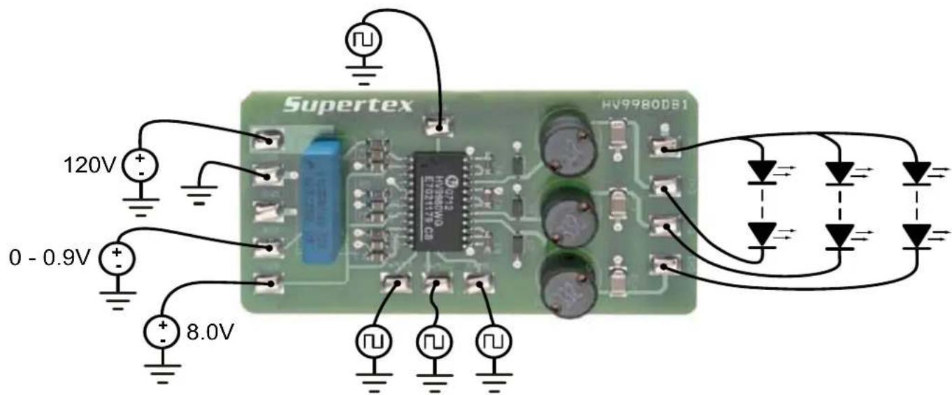
text_image
Supertex HV9980DB1 120V 0 - 0.9V 8.0VActual Board Size: 68.8mm x 36.1mm
Connections
| Pin Connection | |
| VIN | Powers the three LED strings, providing the LED string voltage is less than 12 of the input voltage. Connect a high voltage 100 - 140V source at this terminal. |
| VDD Powers | the HV9980 control circuit. Connect a 6.0 - 10V source at this terminal. |
| REF | Voltage at the REF terminal controls the output current level. The peak inductor current is approximately 1/5^th of the REF voltage. |
| CLK | Provides a clock input to the HV9980. The switching frequency is 1/6^th of the CLK frequency. Connect a 1.8MHz TTL compatible signal at this terminal. |
| PWMD1-3 | These inputs can be used to PWM dim the three channels. Connect these pins to VDD to enable all three channels permanently. A TTL compatible, low frequency (<1kHz) square wave can be used to PWM dim each channel individually. |
| GND(s) The | two GND terminals are wired together on the board. They form the return path for all the input signals. |
| COM This is | the common anode connection for all three LED strings. |
| Ch1-3 These | terminals are the cathode connections for the three LED strings. |
Typical Results

line
| Input Voltage (V) | Efficiency (%) | | ----------------- | -------------- | | 90 | 91.2 | | 1 | 90.5 | | 30 | 89.8 | | 160 | 88.2 |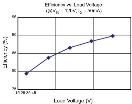
line
| Load Voltage (V) | Efficiency (%) | | ---------------- | -------------- | | 15 | 79 | | 25 | 83 | | 35 | 86 | | 45 | 88 | | 50 | 90 |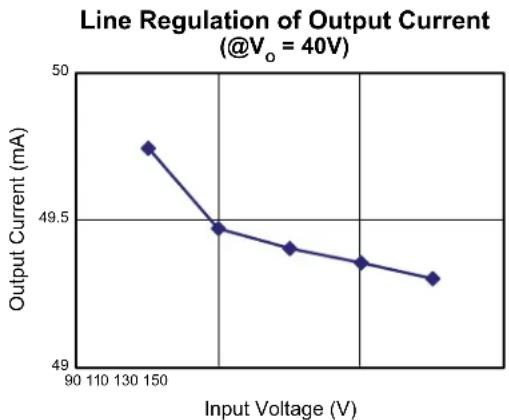
line
| Input Voltage (V) | Output Current (mA) | | ----------------- | ------------------- | | 130 | 49.7 | | 150 | 49.45 | | 160 | 49.4 | | 170 | 49.35 | | 180 | 49.3 |
line
| Load Voltage (V) | Output Current (mA) | | ---------------- | ------------------- | | 15 | 56.8 | | 25 | 54.5 | | 35 | 52.8 | | 45 | 51.0 | | 55 | 49.2 |Fig.1 shows the drain voltage and LED current waveforms during normal operation. The three channels are phase shifted by 120^ with respect to each other. The switching frequency for each channel is 300kHz ( 1/6^th of the CLK frequency).
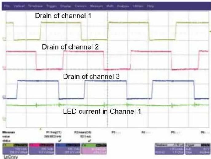
Fig. 1: Steady State Operation
(Time scale: 1.0μs/div)
Fig. 2 shows the hiccup mode short circuit protection of the HV9980. The output of channel is shorted by connecting COM to CH1. Channel 1 tries to restart every 200 s. The other two channels work normally and are not affected by the short circuit on one channel. The short circuit timing is started when the voltage at RS reaches 1.15V (about 230mA).

text_image
File Verbal Timebase Trigger Coupler Consors Measure Math Analysis Utilizers Held Drain of channel 1 Drain of channel 2 LED current in Channel 1 Drain of channel 3 Measure value status F1. (neg(C)) F2. (neg(D)) F3. ... F4. ... F5. ... 100 Vcc 100 Vcc 100 Vcc 100 Vcc 100 Vcc 100 Vcc 100 Vcc 100 Vcc 100 Vcc 100 Vcc 100 Vcc 100 Vcc 100 Vcc 100 Vcc 100 Vcc 1 LeCryFig. 2: Operation during Output Short Circuit
(Time scale: 50μs/div)
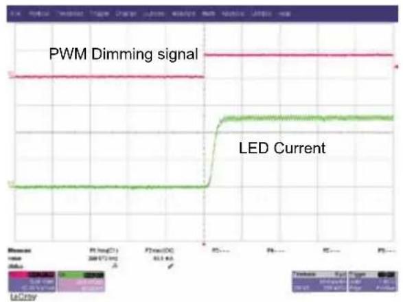
Fig. 3 shows the recovery of Channel 1 from short circuit condition to normal operation. The circuit transitions from a fault condition to normal operation does not cause any overshoots in the LED current.

line
| Measurement | Value | | --- | --- | | Drain Voltage of Channel 1 | 0.0000 | | LED Current for Channel 1 | 0.0000 |Fig. 3: Recovery from a short circuit condition (Time scale: 50μs/div)
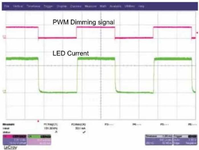
Fig. 4 shows the PWM dimming performance of the HV9980DB1 for one of the channels. The driver has a 25μs rise time and 50μs fall time.
line
| Parameter | Value | | --------------- | --------- | | Current | 151.30 pV | | Power | 53.1 mA | | Timebase | -1.0 kV | | Trigger | 1.0 kV | | Output | 53.1 mV | | Input | 0.0 mV |(a): PWM Dimming Operation (Time scale: 500 s/div)
(b): PWM Dimming Rise
(Time scale: 50 s/div)

(c): PWM Dimming Fall
(Time scale: 50 s/div)
Fig. 4: PWM Dimming performance
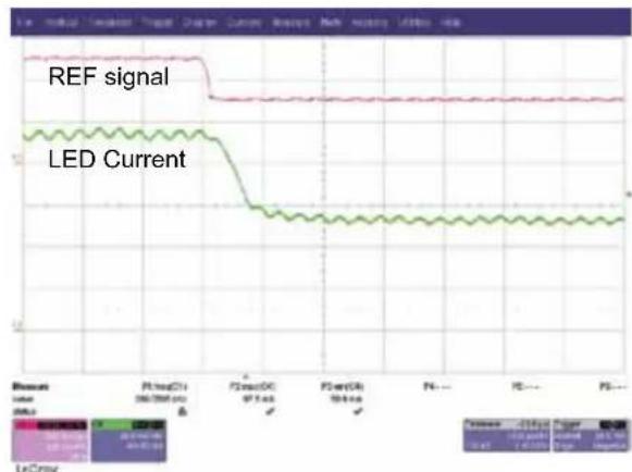
Fig. 5 shows the response of the HV9980DB1 to a quickly varying reference voltage, similar to variation found in the backlight-scanning mode. The reference voltage is varied from 250mV to 500mV using a square wave signal (corresponding to an LED current variation from 50mA to 100mA ). The LED current transitions quickly between the two levels within 10 s .

line
| Parameter | Value | | --------------- | --------- | | REF signal | 12 | | LED Current | 12 | | Measurement Value | 304.42 MHz | | Measurement Value | 88.3 mA | | Measurement Value | 88.3 mA | | Measurement Value | 88.3 mA | | Measurement Value | 88.3 mA | | Measurement Value | 88.3 mA | | Measurement Value | 88.3 mA | | Measurement Value | 88.3 mA | | Measurement Value | 88.3 mA | | Measurement Value | 88.3 mA | | Measurement Type | 1.2T Am | | LeCryv | 70V AC | | LeCryv | 200V AC | | LeCryv | 80V DC |(a): Operation with a REF change (Time scale: 500 s/div)

line
| Time | REF signal | LED Current | |------|------------|-------------| | 0 | ~10000 | ~0 | | 5 | ~10000 | ~50 | | 10 | ~10000 | ~75 | | 15 | ~10000 | ~85 | | 20 | ~10000 | ~90 | | 25 | ~10000 | ~95 | | 30 | ~10000 | ~100 | | 35 | ~10000 | ~105 | | 40 | ~10000 | ~110 | | 45 | ~10000 | ~115 | | 50 | ~10000 | ~120 | | 55 | ~10000 | ~125 | | 60 | ~10000 | ~130 | | 65 | ~10000 | ~135 | | 70 | ~10000 | ~140 | | 75 | ~10000 | ~145 | | 80 | ~10000 | ~150 | | 85 | ~10000 | ~155 | | 90 | ~10000 | ~160 | | 95 | ~10000 | ~165 | | 100 | ~10000 | ~170 | | 105 | ~10000 | ~175 | | 110 | ~10000 | ~180 | | 115 | ~10000 | ~185 | | 120 | ~10000 | ~190 |(b) : Rise Time of LED Current (Time scale: 10μs/div)
line
| Time (s) | REF signal | LED Current | |----------|------------|-------------| | 0 | ~1.0 | ~1.0 | | 3.5 | ~1.0 | ~0.8 | | 7.5 | ~1.0 | ~0.6 | | 12 | ~1.0 | ~0.6 |(c) : Fall Time of LED Current
(Time scale: 10μs/div)
Fig. 5: REF change response
Circuit Schematic
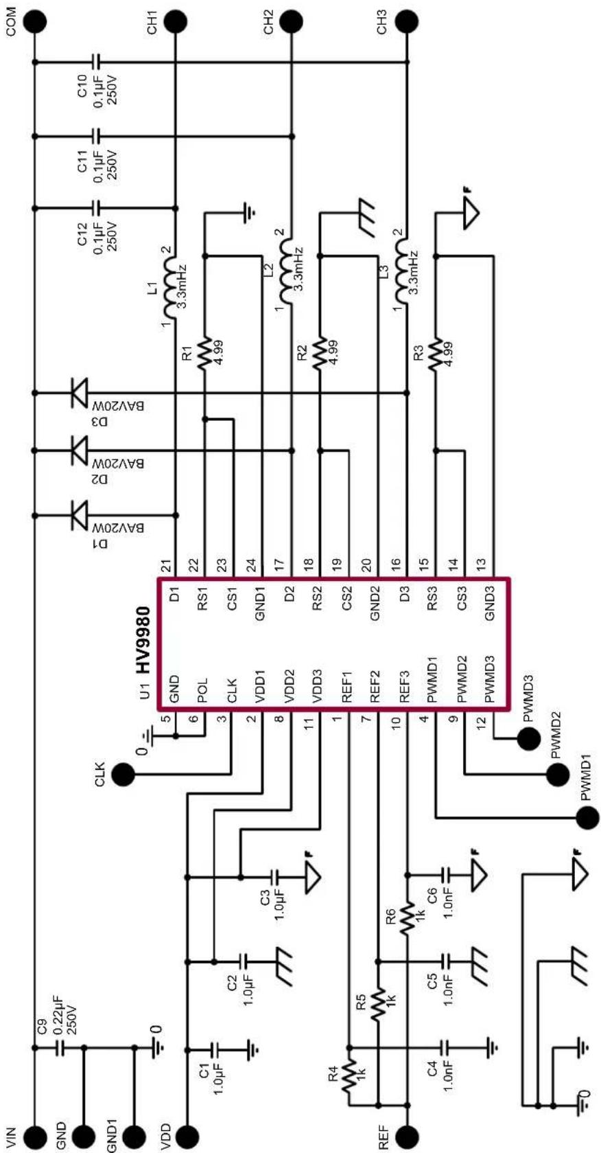
text_image
VIN GND 0.22µF 250V GND1 0 CLK U1 HV9980 VDD C1 1.0µF C2 1.0µF C3 1.0µF REF R4 1k R5 1k R6 1k C4 1.0nF C5 1.0nF C6 1.0nF PWMD1 PWMD2 PWMD3 PWMD2 PWMD3 0 5 6 3 2 8 11 1 7 10 4 9 12 13 14 15 16 17 18 19 20 21 22 23 24 25 26 27 28 29 30 31 32 33 34 35 36 37 38 39 40 41 42 43 44 45 46 47 48 49 50 51 52 53 54 55 56 57 58 59 60 61 62 63 64 65 66 67 68 69 70 71 72 73 74 75 76 77 78 79 80 81 82 83 84 85 86 87 88 89 90 91 92 93 94 95 96 97 98 99 100 D1 BAV20W D2 BAV20W D3 BAV20W C12 0.1µF 250V C11 0.1µF 250V C10 0.1µF 250V COM CH1 CH2 CH3Bill of Materials
| Item # | Qty | RefDes Description | Package Mfg Part Number | |||
| 1 | 13 | PWMD1-3, Ch1-3, REF, VDD, VIN, COM, GND, GND1, CLK | Compact surface mount test points SMT | Keystone Electronics | 5016 | |
| 2 3 C1, C2, C3 1.0uF, 16 | V X7R ceramic chip capacitor SMD0805 TDK Corp C2012X7R1C105K | |||||
| 3 3 C4, C5, C6 1.0nF, 50 | V X7R ceramic chip capacitor SMD0805 Kemet C0805C102K5RACTU | |||||
| 4 | 1 | C9 | 0.22μF, 250V metal film capacitor | Radial | Epcos Inc. | B32521C3224J |
| 5 | 3 | C10, C11, C12 | 0.1μF, 200V, X7R ceramic chip capacitor | SMD1210 | AVX Corp | 12102C104KAT2A |
| 6 | 3 | D1, D2, D3 | 200V, 200mA switching diode | SOD-123 | Diodes Inc | BAV20W |
| 7 | 3 | L1, L2, L3 | 3.3mH, 225mA sat, 150mA rms inductor | Radial | Coilcraft | RFB0810-332 |
| - | - | --- | Cross Reference (for L1, L2, and L3) | Radial | Renco USA | RL-5480-3-3300 |
| 8 | 3 | R1, R2, R3 | 4.99Ω, 1/8W, 1% chip resistor | SMD0805 | --- | --- |
| 9 | 3 | R4, R5, R6 | 1.0kΩ, 1/8W, 5% chip resistor | SMD0805 | --- | --- |
| 10 | 1 | U1 | Three Channel LED Driver | SOIC-24 | Supertex | HV9980WG-G |
Supertex inc. does not recommend the use of its products in life support applications, and will not knowingly sell them for use in such applications unless it receives an adequate "product liability indemnification insurance agreement." Supertex Inc. does not assume responsibility for use of devices described, and limits its liability to the replacement of the devices determined defective due to workmanship. No responsibility is assumed for possible omissions and inaccuracies. Circuitry and specifications are subject to change without notice. For the latest product specifications refer to the Supertex Inc. (website: http://www.supertex.com)