HV9911DB1 - Electronic component Microchip - Free user manual and instructions
Find the device manual for free HV9911DB1 Microchip in PDF.

User questions about HV9911DB1 Microchip
0 question about this device. Answer the ones you know or ask your own.
Ask a new question about this device
Download the instructions for your Electronic component in PDF format for free! Find your manual HV9911DB1 - Microchip and take your electronic device back in hand. On this page are published all the documents necessary for the use of your device. HV9911DB1 by Microchip.
USER MANUAL HV9911DB1 Microchip
High Brightness Step-Down LED Driver Demoboard with Excellent Current Regulation
General Description
The HV9911DB3 is an LED driver capable of driving up to 25 one-watt LEDs in series from an input of 130 - 200VDC. The demoboard uses Supertex's HV9911 in a buck topology with the HV7800 used for high side current sensing. The converter has a very good initial regulation (+/-5%) and excellent line and load regulation over the entire input and output voltage range (<+/-2%). The full load efficiency of the converter is typically greater than 85%.
The HV9911DB3 is protected against open LED and output short circuit conditions. It is also protected from input under voltage conditions. It has a very good PWM dimming response, with typical rise and fall times of less than 5.0 s, which will allow high PWM dimming ratios.
The switching frequency of the HV9911DB3 can be synchronized to other HV9911 boards or to an external 150kHz clock by connecting the clock to the SYNC pin of the HV9911DB3.
Specifications
| Parameter Value | |
| Input voltage (steady state): 130 - 200VDC | |
| Output LED string voltage: 20V | min - 100V max |
| Average output current: 350mA | +/-5% |
| Output current ripple: 5% typical | |
| Switching frequency: 150kHz | |
| Full load efficiency: 90% (at 150V input) | |
| Output short circuit protection: Included | |
| Input under voltage protection: Included | |
| PWM dimming performance: | 5.0μs (rise time)5.0μs (fall time) |
| Dimensions: 53.7mm x 38.1mm | |
Board Layout and Connection Diagram

natural_image
Green printed circuit board with components like capacitors, resistors, and connectors (no readable text or symbols)Actual Size: 53.7mm X 38.1mm

Input - The input is connected between the VIN+ and GND terminals as shown.
Output - The output is connected between the VO+ and VO terminals as shown, with the ANODE of the LED string to VO+ and the CATHODE to connector VO-.
Enable/PWM Dimming - To enable the board, short pins PWMD and VDD of connector J1 as shown. To use the PWM dimming feature of the board, connect an external push-pull square wave source between terminals PWMD and GND of connector J1 as shown by the dotted lines.
SYNC - To synchronize two or more boards, connect the SYNC pins of all the boards. To synchronize the HV9911DB3 to an external 150kHz clock, connect the clock between the SYNC pin and the GND pin of connector J1.
Note:
During PWM dimming, the PWMD pin of connector J1 should be left open. Also, the PWM signal must have the proper polarity, with the positive connected to the VDD pin of connector J1. Note that the GND pin of connector J1 is internally connected to the return path of the input voltage.
Demoboard Testing:
Normal Operation: Connect the input source and the output LEDs as shown in the connection diagram and enable the board. The LEDs will glow with a steady intensity. Connecting an ammeter in series with the LEDs will allow measurement of the LED current. The current will be 350mA +/- 5%.
Current Regulation: While the converter is operating, change the input voltage within its specified input voltage range. The current output of the HV9911DB3 will remain very steady over the entire line range. With the supply turned off, change the number of LEDs in the string within the specified limits and turn the power supply back on. The current will still be regulated at 350mA.
Open LED Test: The buck converter is inherently protected against open LED conditions since the maximum output voltage is limited to the input voltage. If the LED string is disconnected during operation, the output voltage of the converter will rise and stay at the input voltage level.
Short Circuit Test: When the HV9911DB3 is operating in steady state, connect a jumper across the terminals of the LED string. Notice that the output current will immediately go to zero and the converter will shut down. To restart the HV9911DB3, recycle the input power to the demoboard.
PWM Dimming: With the input voltage to the board disconnected, apply a TTL-compatible, push-pull square wave signal between the PWMD and GND terminals of connector J1 as shown in the connection diagram. Turn the input voltage back on and adjust the duty cycle and/or frequency of the PWM dimming signal. The output current will track the PWM dimming signal. Note that although the converter operates perfectly well at a 1kHz PWM dimming frequency, a wider PWM dimming ratio can be obtained at lower frequencies, like 100Hz or 200Hz.
Effect of the High Side Disconnect Switch
The high side disconnect switch included in the HV9911DB3 disconnects and reconnects the load during PWM dimming. This prevents the output capacitor from having to charge/discharge every cycle, leading to shorter PWM dimming rise and fall times. It also limits the surge current through the output sense resistor during output short circuit conditions. However, the level translator needed to drive the disconnect FET consumes power during normal operation and reduces the overall efficiency of the converter by about 3% at full load. The decision to include or exclude the high side driver should depend on which factor is more important, high PWM dimming or converter efficiency. The following typical results section will show the results for both cases.
Typical Results
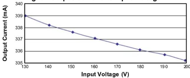
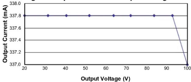
- Efficiency: The efficiency of the converter at various LED string voltages is shown in Fig.1 (measured at the nominal input voltage of 150V). Fig.2 shows the full load efficiency of the converter at varying input voltages. The minimum efficiency of 93% for the converter occurs at 21V input and full load output.
Fig. 1 Efficiency vs Output Voltage

line
| Output Voltage (V) | With Disconnect FET | Without Disconnect FET | | ------------------ | ------------------- | ---------------------- | | 20 | 65 | 76 | | 30 | 70 | 78 | | 50 | 75 | 82 | | 80 | 80 | 85 | | 100 | 85 | 88 | | 120 | 87 | 90 | | 140 | 88 | 91 | | 160 | 89 | 92 | | 180 | 90 | 93 | | 200 | 91 | 94 |Fig. 2 Efficiency vs Input Voltage

line
| Input Voltage (V) | With Disconnect FET | Without Disconnect FET | | ----------------- | -------------------- | ----------------------- | | 130 | 92.0 | 95.0 | | 140 | 91.0 | 94.5 | | 150 | 90.5 | 94.0 | | 160 | 90.0 | 93.5 | | 170 | 89.5 | 93.0 | | 180 | 88.5 | 92.5 | | 190 | 87.5 | 92.0 | | 200 | 87.0 | 91.5 |- Current Regulation: Fig.3 and Fig.4 show the output current regulation vs. output voltage and load voltage, respectively. The total current regulation (line and load combined) is found to be less than 1%.
Fig. 3 Output Current vs Input Voltage
line
| Input Voltage (V) | Output Current (mA) | |---|---| | 130 | 339 | | 140 | 338.2 | | 150 | 337.6 | | 160 | 337 | | 170 | 336.5 | | 180 | 336 | | 190 | 335.7 | | 200 | 335.2 |Fig. 4 Output Current vs Output Voltage
line
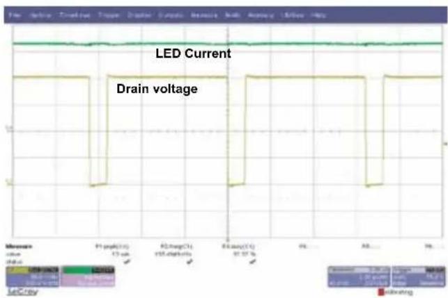
| Output Voltage (V) | Output Current (mA) | | ------------------ | ------------------- | | 20 | 337.8 | | 30 | 337.8 | | 40 | 337.8 | | 50 | 337.8 | | 60 | 337.8 | | 70 | 337.8 | | 80 | 337.8 | | 90 | 337.8 | | 100 | 337.0 |- Normal Operation: Figs.5a, 5b, and 5c show the drain voltage and output current waveforms during normal operation.

line
| Time (ms) | LED Current (V) | Drain voltage (V) | |-----------|-----------------|-------------------| | 0 | 100 | 0 | | 1 | 100 | 13.50 | | 2 | 100 | 27.64 | | 3 | 100 | 13.50 | | 4 | 100 | 0 | | 5 | 100 | 13.50 | | 6 | 100 | 27.64 | | 7 | 100 | 13.50 | | 8 | 100 | 0 | | 9 | 100 | 13.50 | | 10 | 100 | 27.64 | | 11 | 100 | 13.50 | | 12 | 100 | 0 | | 13 | 100 | 13.50 | | 14 | 100 | 27.64 | | 15 | 100 | 13.50 | | 16 | 100 | 0 | | 17 | 100 | 13.50 | | 18 | 100 | 27.64 | | 19 | 100 | 13.50 | | 20 | 100 | 0 | | 21 | 100 | 13.50 | | 22 | 100 | 27.64 | | 23 | 100 | 13.50 | | 24 | 100 | 0 | | 25 | 100 | 13.50 | | 26 | 100 | 27.64 | | 27 | 100 | 13.50 | | 28 | 100 | 0 | | 29 | 100 | 13.50 | | 30 | 100 | 27.64 | | 31 | 100 | 13.50 | | 32 | 100 | 0 | | 33 | 100 | 13.50 | | 34 | 100 | 27.64 | | 35 | 100 | 13.50 | | 36 | 100 | 0 | | 37 | 100 | 13.50 | | 38 | 100 | 27.64 | | 39 | 100 | 13.50 | | 40 | 100 | 0 | | 41 | 100 | 13.50 | | 42 | 100 | 27.64 | | 43 | 100 | 13.50 | | 44 | 100 | 0 | | 45 | 100 | 13.50 | | 46 | 100 | 27.64 | | 47 | 100 | 13.50 | | 48 | 100 | 0 | | 49 | 100 | 13.50 | | 50 | 100 | 27.64 | | 51 | 100 | 13.50 | | 52 | 100 | 0 | | 53 | 100 | 13.50 | | Note: The actual values for LED Current and Drain voltage are not provided in the code snippet. The values for LED Current and Drain voltage are estimated based on the given code snippet in the image.Fig.5a Waveforms at V_IN = 150V and V_o = 100V
line
| Time (s) | LED Current (V) | Drain voltage (V) | |----------|-----------------|-------------------| | 0 | 1.0 | 0.0 | | 10 | 1.0 | 0.0 | | 20 | 1.0 | 0.0 | | 30 | 1.0 | 0.0 | | 40 | 1.0 | 0.0 | | 50 | 1.0 | 0.0 | | 60 | 1.0 | 0.0 | | 70 | 1.0 | 0.0 | | 80 | 1.0 | 0.0 | | 90 | 1.0 | 0.0 | | 100 | 1.0 | 0.0 | | 110 | 1.0 | 0.0 | | 120 | 1.0 | 0.0 | | 130 | 1.0 | 0.0 | | 140 | 1.0 | 0.0 | | 150 | 1.0 | 0.0 | | 160 | 1.0 | 0.0 | | 170 | 1.0 | 0.0 | | 180 | 1.0 | 0.0 | | 190 | 1.0 | 0.0 | | 200 | 1.0 | 0.0 | | 210 | 1.0 | 0.0 | | 220 | 1.0 | 0.0 | | 230 | 1.0 | 0.0 | | 240 | 1.0 | 0.0 | | 250 | 1.0 | 0.0 | | 260 | 1.0 | 0.0 | | 270 | 1.0 | 0.0 | | 280 | 1.0 | 0.0 | | 290 | 1.0 | 0.0 | | 300 | 1.0 | 0.0 | | 310 | 1.0 | 0.0 | | 320 | 1.0 | 0.0 | | 330 | 1.0 | 0.0 | | 340 | 1.0 | 0.0 | | 350 | 1.0 | 0.0 | | 360 | 1.0 | 0.0 | | 370 | 1.0 | 0.0 | | 380 | 1.0 | 0.0 | | 390 | 1.0 | 0.0 | | 400 | 1.0 | 0.0 | | 410 | 1.0 | 0.0 | | 420 | 1.0 | 0.0 | | 430 | 1.0 | 0.0 | | 440 | 1.0 | 0.0 | | 450 | 1.0 | 0.0 | | 460 | 1.0 | 0.0 | | 470 | 1.0 | 0.0 | | 480 | 1.0 | 0.0 | | 490 | 1.0 | 0.0 | | 500 | 1.0 | 0.0 | | ... | ... | ... | | ... | ... | ... | | ... | ... | ... | | ... | ... | ... | | ... | ... | ... | | ... | ... | ... | | ... | ... | ... | | ... | ... | ... | | ... | ... | ... | | ... | ... | ... | | ... | ... |... | | ... | ... | ... | | ... | ... | ... | | ... | ... | ... | | ... | ... | ... | | ... | ... | ... | | ... | ... | ... | | ... | ... | ... | | ... | ... | ... | | ... | ... | ... | | ... | ... |line
| Time (μs) | LED Current (µV) | Drain Voltage (µV) | |-----------|------------------|--------------------| | 0 | 12 | 12 | | 1 | 12 | 12 | | 2 | 12 | 12 | | 3 | 12 | 12 | | 4 | 12 | 12 | | 5 | 12 | 12 | | 6 | 12 | 12 | | 7 | 12 | 12 | | 8 | 12 | 12 | | 9 | 12 | 12 | | 10 | 12 | 12 | | 11 | 12 | 12 | | 12 | 12 | 12 | | 13 | 12 | 12 | | 14 | 12 | 12 | | 15 | 12 | 12 | | 16 | 12 | 12 | | 17 | 12 | 12 | | 18 | 12 | 12 | | 19 | 12 | 12 | | 20 | 12 | 12 | | 21 | 12 | 12 | | 22 | 12 | 12 | | 23 | 12 | 12 | | 24 | 12 | 12 | | 25 | 12 | 12 | | 26 | 12 | 12 | | 27 | 12 | 12 | | 28 | 12 | 12 | | 29 | 12 | 12 | | 30 | 12 | 12 | | 31 | 12 | 12 | | 32 | 12 | 12 | | 33 | 12 | 12 | | 34 | 12 | 12 | | 35 | 12 | 12 | | 36 | 12 | 12 | | 37 | 12 | 12 | | 38 | 12 | 12 | | 39 | 12 | 12 | | 40 | 12 | 12 | | 41 | 12 | 12 | | 42 | 12 | 12 | | 43 | 12 | 12 | | 44 | 12 | 12 | | 45 | 12 | 12 | | 46 | 12 | 12 | | 47 | 12 | 12 | | 48 | 12 | 12 | | 49 | 12 | 12 | | 50 | 12 | 12 | | Note: The actual values for LED Current and Drain voltage are not provided in the code. The code contains repeated 'ns' markers and 'A' labels for each data point.line
| Time (s) | Output Voltage | Drain Voltage of Q1 | Output Current | |----------|----------------|---------------------|----------------| | 0 | 12 | 12 | 12 | | 10 | 12 | 12 | 12 | | 20 | 12 | 12 | 12 | | 30 | 12 | 12 | 12 | | 40 | 12 | 12 | 12 | | 50 | 12 | 12 | 12 | | 60 | 12 | 12 | 12 | | 70 | 12 | 12 | 12 | | 80 | 12 | 12 | 12 | | 90 | 12 | 12 | 12 | | 100 | 12 | 12 | 12 | | 110 | 12 | 12 | 12 | | 120 | 12 | 12 | 12 | | 130 | 12 | 12 | 12 | | 140 | 12 | 12 | 12 | | 150 | 12 | 12 | 12 | | 160 | 12 | 12 | 12 | | 170 | 12 | 12 | 12 | | 180 | 12 | 12 | 12 | | 190 | 12 | 12 | 12 | | 200 | 12 | 12 | 12 | | 210 | 12 | 12 | 12 | | 220 | 12 | 12 | 12 | | 230 | 12 | 12 | 12 | | 240 | 12 | 12 | 12 | | 250 | 12 | 12 | 12 | | 260 | 12 | 12 | 12 | | 270 | 12 | 12 | 12 | | 280 | 12 | 12 | 12 | | 290 | 12 | 12 | 12 | | 300 | 12 | 12 | 12 | | 310 | 12 | 12 | 12 | | 320 | 12 | 12 | 12 | | 330 | 12 | 12 | 12 | | 340 | 12 | 12 | 12 | | 350 | 12 | 12 | 12 | | 360 | 12 | 12 | 12 | | 370 | 12 | 12 | 12 | | 380 | 12 | 12 | 12 | | 390 | 12 | 12 | 12 | | 400 | 12 | 12 | 12 | | ... | ... | ... | ... | | ... | ... | ... | ... | | ... | ... | ... | ... | | ... | ... | ... | ... | | ... | ... | ... | ... | | ... | ... | ... | ... | | ... | ... | ... | ... | | ... | ... | ... | ... | | ... | ... |... | ... | | ... | ... | ... | ... | | ... | ... | ... | ... | | ... | ... | ... | ... | | ... | ... | ... | ... | | ... | ... | ... | ... | | ... | ... | ... | ... | | ... | ... | ... | ... | | ... (Note: The values for Output Voltage and Drain Voltage of Q1) are estimated based on the provided code.line
| Time (ms) | PWM Dimming Signal (V) | LED Current (A) | |-----------|------------------------|-----------------| | 0 | 0 | 0 | | 10 | 0 | 0 | | 20 | 0 | 0 | | 30 | 0 | 0 | | 40 | 0 | 0 | | 50 | 0 | 0 | | 60 | 0 | 0 | | 70 | 0 | 0 | | 80 | 0 | 0 | | 90 | 0 | 0 | | 100 | 0 | 0 | | 110 | 0 | 0 | | 120 | 0 | 0 | | 130 | 0 | 0 | | 140 | 0 | 0 | | 150 | 0 | 0 | | 160 | 0 | 0 | | 170 | 0 | 0 | | 180 | 0 | 0 | | 190 | 0 | 0 | | 200 | 0 | 0 | | 210 | 0 | 0 | | 220 | 0 | 0 | | 230 | 0 | 0 | | 240 | 0 | 0 | | 250 | 0 | 0 | | 260 | 0 | 0 | | 270 | 0 | 0 | | 280 | 0 | 0 | | 290 | 0 | 0 | | 300 | 0 | 0 | | 310 | 0 | 0 | | 320 | 0 | 0 | | 330 | 0 | 0 | | 340 | 0 | 0 | | 350 | 0 | 0 | | 360 | 0 | 0 | | 370 | 0 | 0 | | 380 | 0 | 0 | | 390 | 0 | 0 | | 400 | 0 | 0 | | 410 | 0 | 0 | | 420 | 0 | 0 | | 430 | 0 | 0 | | 440 | 0 | 0 | | 450 | 0 | 0 | | 460 | 0 | 0 | | 470 | 0 | 0 | | 480 | 0 | 0 | | 490 | 0 | 0 | | 500 | 0 | 0 | | ... | ... | ... | | Final | - | - |line
| Time (s) | PWM Dimming Signal (V) | LED Current (V) | |----------|------------------------|-----------------| | 0 | 1 | 0 | | 10 | 1 | 0 | | 20 | 1 | 0 | | 30 | 1 | 0 | | 40 | 1 | 0 | | 50 | 1 | 0 | | 60 | 1 | 0 | | 70 | 1 | 0 | | 80 | 1 | 0 | | 90 | 1 | 0 | | 100 | 1 | 0 | | 110 | 1 | 0 | | 120 | 1 | 0 | | 130 | 1 | 0 | | 140 | 1 | 0 | | 150 | 1 | 0 | | 160 | 1 | 0 | | 170 | 1 | 0 | | 180 | 1 | 0 | | 190 | 1 | 0 | | 200 | 1 | 0 | | 210 | 1 | 0 | | 220 | 1 | 0 | | 230 | 1 | 0 | | 240 | 1 | 0 | | 250 | 1 | 0 | | 260 | 1 | 0 | | 270 | 1 | 0 | | 280 | 1 | 0 | | 290 | 1 | 0 | | 300 | 1 | 0 | | 310 | 1 | 0 | | 320 | 1 | 0 | | 330 | 1 | 0 | | 340 | 1 | 0 | | 350 | 1 | 0 | | 360 | 1 | 0 | | 370 | 1 | 0 | | 380 | 1 | 0 | | 390 | 1 | 0 | | 400 | 1 | 0 | | 410 | 1 | 0 | | 420 | 1 | 0 | | 430 | 1 | 0 | | 440 | 1 | 0 | | 450 | 1 | 0 | | 460 | 1 | 0 | | 470 | 1 | 0 | | 480 | 1 | 0 | | 490 | 1 | 0 | | 500 | 1 | 0 | | ... | ... | ... | | Final | ... | ... |line
| Time (s) | PWM Dimming Signal (V) | LED Current (A) | |----------|------------------------|-----------------| | 0 | 0 | 0 | | 1 | 0 | 0 | | 2 | 0 | 0 | | 3 | 0 | 0 | | 4 | 0 | 0 | | 5 | 0 | 0 | | 6 | 0 | 0 | | 7 | 0 | 0 | | 8 | 0 | 0 | | 9 | 0 | 0 | | 10 | 0 | 0 | | 11 | 0 | 0 | | 12 | 0 | 0 | | 13 | 0 | 0 | | 14 | 0 | 0 | | 15 | 0 | 0 | | 16 | 0 | 0 | | 17 | 0 | 0 | | 18 | 0 | 0 | | 19 | 0 | 0 | | 20 | 0 | 0 | | 21 | 0 | 0 | | 22 | 0 | 0 | | 23 | 0 | 0 | | 24 | 0 | 0 | | 25 | 0 | 0 | | 26 | 0 | 0 | | 27 | 0 | 0 | | 28 | 0 | 0 | | 29 | 0 | 0 | | 30 | 0 | 0 | | 31 | 0 | 0 | | 32 | 0 | 0 | | 33 | 0 | 0 | | 34 | 0 | 0 | | 35 | 0 | 0 | | 36 | 0 | 0 | | 37 | 0 | 0 | | 38 | 0 | 0 | | 39 | 0 | 0 | | 40 | 0 | 0 | | 41 | 0 | 0 | | 42 | 0 | 0 | | 43 | 0 | 0 | | 44 | 0 | 0 | | 45 | 0 | 0 | | 46 | 0 | 0 | | 47 | 0 | 0 | | 48 | 0 | 0 | | 49 | 0 | 0 | | 50 | 0 | 0 | | 51 | 0 | 0 | | 52 | 0 | 0 | | 53 | 0 | 0 | | 54 | 0 | 0 | | 55 | 0 | 0 | | 56 | 0 | 0 | | 57 | 0 | 0 | | 58 | 0 | 0 | | 59 | 0 | 0 | | 60 | 0 | 0 | | 61 | 0 | 0 | | 62 | 0 | 0 | | 63 | 0 | 0 | | 64 | 0 | 0 | | 65 | 0 | 0 | | 66 | 0 | 0 | | 67 | 0 | 0 | | 68 | 0 | 0 | | 69 | 0 | 0 | | 70 | 0 | 0 | | 71 | 0 | 0 | | 72 | 0 | 0 | | 73 | 0 | 0 | | 74 | 0 | 0 | | 75 | 0 | 0 | | 76 | 0 | 0 | | 77 | 0 | 0 | | 78 | 0 | 0 | | 79 | 0 | 0 | | 80 | - | - | | ... | ... | ... | | ... | ... | ... | | ... | ... | ... | | ... | ... | ... | | ... | ... | ... | | ... | ... | ... | | ... | ... | ... | | ... | ... | ... | | ... | ... | ... | | ... | ... | ... | | ... | ... | ... | | ... | ... | ... | | ... | ... | ... | | ... | ... | ... | | ... | ... | ... | | ... | ... | ... | | ... | ... | ... | | ... | ... | ... | | ... | ... | ... | | ... | ... | ... | | ... | ... | ... | | ... | ... | ... | | ... | ... | ... | | ... | ... | ... | | ... | ... | ... | | ... | ... | ... | | ... | ... | ... | | ... | ... | ... | | ... | ... | ... | | ... | ... | ... | | ... | ... | ... (Note: The 'LED Current' label is 'LED Current' instead of 'PWM Dimming Signal'. This label is 'PWM Dimming Signal'. The 'LED Current' label is 'LED Current'.line
| Time (s) | PWM Dimming Signal | LED Current | | -------- | ------------------ | ----------- | | 0 | 1.2 | 1.2 | | 25 | 1.2 | 1.2 | | 50 | 1.2 | 1.2 | | 75 | 1.2 | 1.2 | | 100 | 1.2 | 1.2 | | 125 | 1.2 | 1.2 | | 150 | 1.2 | 1.2 | | 175 | 1.2 | 1.2 | | 200 | 1.2 | 1.2 | | 225 | 1.2 | 1.2 | | 250 | 1.2 | 1.2 | | 275 | 1.2 | 1.2 | | 300 | 1.2 | 1.2 | | 325 | 1.2 | 1.2 | | 350 | 1.2 | 1.2 | | 375 | 1.2 | 1.2 | | 400 | 1.2 | 1.2 | | 425 | 1.2 | 1.2 | | 450 | 1.2 | 1.2 | | 475 | 1.2 | 1.2 | | 500 | 1.2 | 1.2 | | 525 | 1.2 | 1.2 | | 550 | 1.2 | 1.2 | | 575 | 1.2 | 1.2 | | 600 | 1.2 | 1.2 | | 625 | 1.2 | 1.2 | | 650 | 1.2 | 1.2 | | 675 | 1.2 | 1.2 | | 700 | 1.2 | 1.2 | | 725 | 1.2 | 1.2 | | 750 | 1.2 | 1.2 | | 775 | 1.2 | 1.2 | | 800 | 1.2 | 1.2 | | 825 | 1.2 | 1.2 | | 850 | 1.2 | 1.2 | | 875 | 1.2 | 1.2 | | 900 | 1.2 | 1.2 | | 925 | 1.2 | 1.2 | | 950 | 1.2 | 1.2 | | 975 | 1.2 | 1.2 | | 1000 | 1.2 | 1.2 | | 1025 | 1.2 | 1.2 | | 1050 | 1.2 | 1.2 | | 1075 | 1.2 | 1.2 | | 1100 | 1.2 | 1.2 | | 1125 | 1.2 | 1.2 | | 1150 | 1.2 | 1.2 | | 1175 | 1.2 | 1.2 | | 1200 | 1.2 | 1.2 | | 1225 | 1.2 | 1.2 | | 1250 | 1.2 | 1.2 | | 1275 | 1.2 | 1.2 | | 1300 | 1.2 | 1.2 | | 1325 | 1.2 | 1.2 | | 1350 | 1.2 | 1.2 | | 1375 | 1.2 | 1.2 | | 1400 | 1.2 | 1.2 | | 1425 | 1.2 | 1.2 | | 1450 | 1.2 | 1.2 | | 1475 | 1.2 | 1.2 | | 1500 | 1.2 | 1.2 | | Note: The actual values for PWM Dimming Signal and LED Current are not provided in the code.line
| Time | PWM Dimming Signal | LED Current | |------|---------------------|-------------| | 0 | 0.5 | 0.5 | | 10 | 0.5 | 0.5 | | 20 | 0.5 | 0.5 | | 30 | 0.5 | 0.5 | | 40 | 0.5 | 0.5 | | 50 | 0.5 | 0.5 | | 60 | 0.5 | 0.5 | | 70 | 0.5 | 0.5 | | 80 | 0.5 | 0.5 | | 90 | 0.5 | 0.5 | | 100 | 0.5 | 0.5 |line
| Time | P WM Dimming Signal | LED Current | |------|---------------------|-------------| | 0 | 1.0 | 1.0 | | 50 | 1.0 | 0.8 | | 100 | 1.0 | 0.6 |text_image
J5 (VIN) C4 0.33µF 250V C5 0.33µF 250V J2 (GND) J1D F C2 1µF 16V J1C U1 VDD VIN SYNC REF IREF FDBK COMP CLIM PWM SC GND R2 604k RT GATE CS FAULT OVP F U1 REF R14 open R12 16.2k R13 8.66k C7 47nF 50V Io_SNS R8 17.4k R9 6.81k J1B Q1 IRFR224 R4 499Ω FAULT F LOADVSSVIN VOUTGND U2 F Q3 IRFR9214 J3 (VO+) Q2 TN2124K1 Q1 IRFR224 L1 2.2mH C1 0.33µF 250V R5 1.24Ω 1/4W D1 MURS140T3 L1 2.2mH 3 D2 9.1V R17 3.65k J4 (VO-) R18 22k R16 22k FAULT Io_SNStext_image
Supertex VIN+ D1 L1 C1 U2 R5 V0+ Q3 D2 GND R1 R12 R13 C7 R17 R18 V0- J1 R14 R2 C3 Q2 L RB HV9911DB3| # Qty Ref | Des Description | Package Manufacturer | Manufacturer's Part Number | |||
| 1 | 2 | C1, C4, C5 | 0.33μF, 100V metal film capacitors | Thru-Hole | Panasonic | ECQ-E2334KF |
| 2 2 | C2 | 1μF, 16V X7R ceramic chip capacitor | SMD0805 | TDK Corp. | C2012X7R1C105K | |
| 3 1 | C3 | 0.1μF, 16V X7R ceramic chip capacitor | SMD0805 | Murata | GRM219R71C104KA01D | |
| 4 1 | C7 | 47nF, 50V X7R ceramic chip capacitor | SMD0805 | Kemet | C0805C473K5RACTU | |
| 5 | 1 | D1 | 400V, 1.0A ultrafast recovery diode | SMB | ON Semi | MURS140T3 |
| 6 | 3 | D2 | 9.1V, 350mW zener diode | SOT-23 | Diodes Inc. | BZX84C9V1-7 |
| 7 | 1 | J1 | Side-entry 4-Pin male header | Thru-Hole | JST Sales Amer. | S4B-EH |
| 8 | 4 | J2, J3, J4, J5 | Compact SMT test point | SMT | Keystone Electric | 5016 |
| 9 1 | L1 | 2.2mH, 0.41A sat, 0.5A rms inductor | SMA | Coilcraft | RFB1010-222L | |
| 10 | 2 | Q1 | 250V, 1.1A N-Channel MOSFET | Thru-Hole | IR | IRFR224 |
| 11 | 1 | Q2 | 240V, 15Ω N-Channel MOSFET | SOT-23 | Supertex | TN2124K1-G |
| 12 | 1 | Q3 | 400V, 1.8A P-Channel MOSFET | DPAK | IR | IRFR9214 |
| 13 | 1 | R1 | 0.56Ω, 1%, 1/4W chip resistor | SMD1206 | Panasonic | ERJ-8RQFR56V |
| 14 | 1 | R2 | 604kΩ, 1%, 1/8W chip resistor | SMD0805 | Yageo | RC0805FR-07604KL |
| 15 | 1 | R3 | 29.4kΩ, 1%, 1/8W chip resistor | SMD0805 | Yageo | RC0805FR-0729K4L |
| 16 | 1 | R4 | 499Ω, 1%, 1/8W chip resistor | SMD0805 | Yageo | RC0805FR-07499RL |
| 17 | 1 | R5 | 1.24Ω, 1%, 1/4W chip resistor | SMD1206 | Yageo | RC1206FR-071R24L |
| 18 | 1 | R8 | 17.4kΩ, 1%, 1/8W chip resistor | SMD0805 | Yageo | RC0805FR-0717K4L |
| 19 | 1 | R9 | 6.81kΩ, 1%, 1/8W chip resistor | SMD0805 | Yageo | RC0805FR-076K81L |
| 20 | 1 | R12 | 16.2kΩ, 1%, 1/8W chip resistor | SMD0805 | Yageo | RC0805FR-0716K2L |
| 21 | 1 | R13 | 8.66kΩ, 1%, 1/8W chip resistor | SMD0805 | Yageo | RC0805FR-078K66L |
| 22 | 1 | R14 | open | - | - | - |
| 23 | 1 | R16, R18 | 22kΩ, 1%, 1/2W chip resistor | SMD2010 | Panasonic | ERJ-12ZYJ223U |
| 24 | 1 | R17 | 3.65kΩ, 1%, 1/8W chip resistor | SMD0805 | Yageo | RC0805FR-073K65L |
| 25 | 1 U1 | Switchmode LED Driver with High Current Accuracy | SO-16 | Supertex | HV9911NG-G | |
| 26 | 1 | U2 | High side current monitor | SOT-23 | Supertex | HV7800K1-G |