MIC33M650 - Unspecified Microchip - Free user manual and instructions
Find the device manual for free MIC33M650 Microchip in PDF.

User questions about MIC33M650 Microchip
0 question about this device. Answer the ones you know or ask your own.
Ask a new question about this device
Download the instructions for your Unspecified in PDF format for free! Find your manual MIC33M650 - Microchip and take your electronic device back in hand. On this page are published all the documents necessary for the use of your device. MIC33M650 by Microchip.
USER MANUAL MIC33M650 Microchip
6A, Pin Strapping Power Module with HyperLight Load® Mode and Output Voltage Select
Features
• 2.4V to 5.5V Input Voltage Range
- 6A Output Current
• Pin Strapping Voltage Selection:
- Tri-state pins (nine voltage options)
- 0.6V, 0.8V, 0.9V, 1.0V, 1.2V, 1.5V, 1.8V, 2.5V or 3.3V output voltage
- Reduced Component Count (No Feedback Resistors)
• High Efficiency (up to 95%) - Output Discharge when Disabled
- Constant-On-Time (COT) Control with High Switching Frequency:
- 1.2 MHz typical at 1.0V output voltage
- ±1.5% Output Voltage Accuracy Over Line/Load/Temperature Range
• 0.8 ms/V Soft Start Speed
• Supports Safe Start-up with Pre-Biased Output
• Typical 1.5 μA Shutdown Supply Current - Low Dropout Operation (100% Duty Cycle)
• Ultra-Fast Transient Response - Latch-Off Thermal Shutdown Protection
- Latch-Off Current Limit Protection
• Power Good (PG) Open-Drain Output
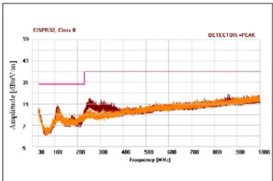
• Meets CISPR32 Class B Emissions
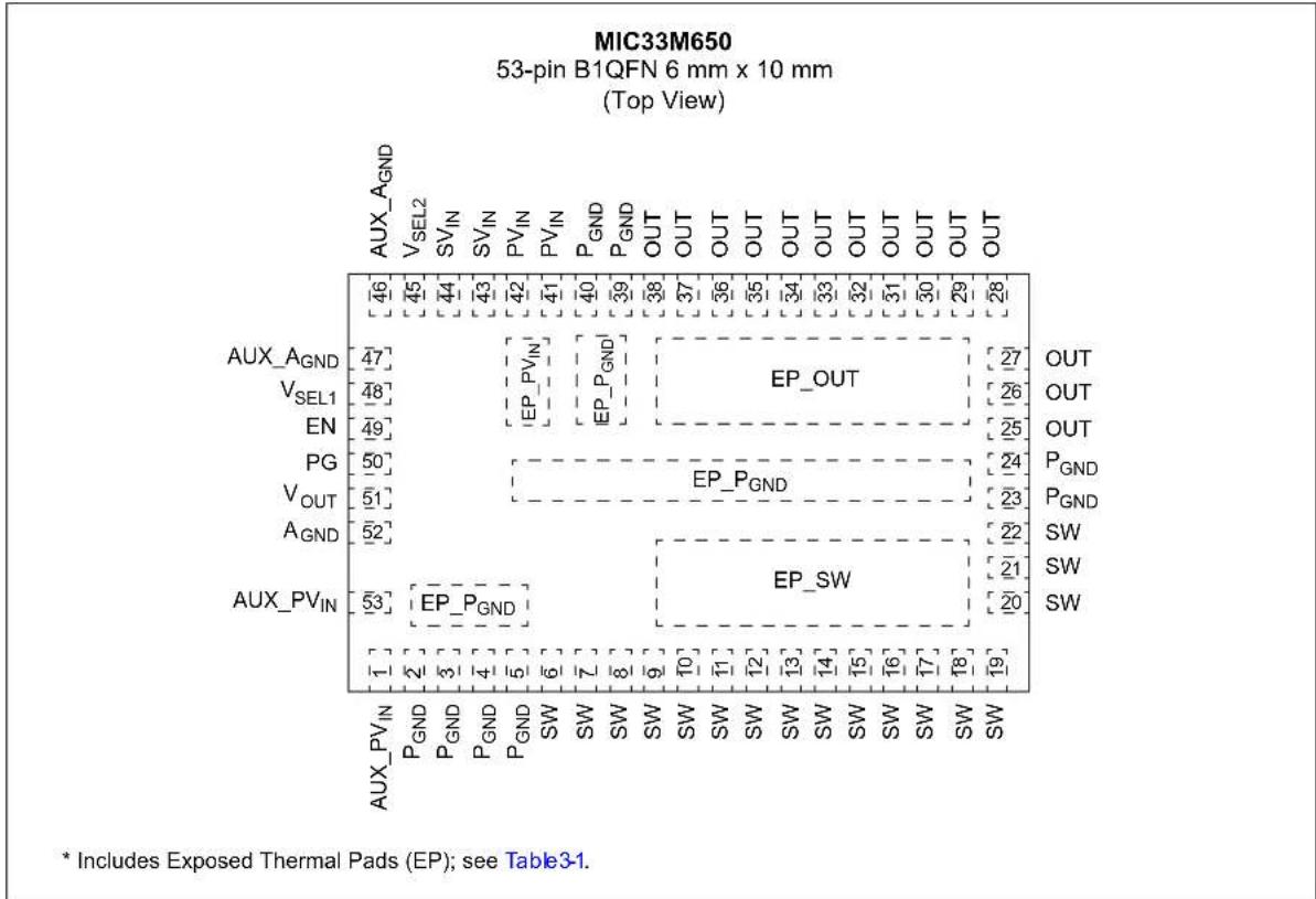
• Package: 53-Lead, 6 mm x 10 mm B1QFN
Applications
• Solid-State Drives (SSD)
• FPGAs, DSP and Low-Voltage ASIC Power
General Description
The MIC33M650 is a pin-selectable output voltage, high-efficiency, low-voltage input, 6A current, synchronous step-down regulator power module with integrated inductor. The COT control architecture with HyperLight Load ^® mode provides very high efficiency at light loads, while still having an ultra-fast transient response.
The MIC33M650 output voltage is set by two V_SEL (Voltage Selection) pins, between nine different values. This method eliminates the need for an external feedback resistor divider and improves the output voltage setting accuracy.
The 2.4V to 5.5V input voltage range, low shutdown and quiescent currents make the MIC33M650 ideal for single-cell Li-Ion battery-powered applications. The 100% duty cycle capability provides low dropout operation, extending operating range in portable systems.
The MIC33M650 pinout is compatible with the MIC33M656 I ^2 C-based programmable regulator version, such that applications can be easily converted. An open-drain PG output is provided to indicate when the output voltage is within 9% of regulation and facilitates the interface with an MCU or power sequencing. If set in shutdown (EN = GND), the MIC33M650 typically draws 1.5 A, while the output is discharged through 10 pull-down.
The MIC33M650 is available in a thermally efficient, 53-Lead, 6 mm x 10 mm x 3 mm B1QFN package, with an operating junction temperature range from -40°C to +125°C.
line
| Frequency [MHz] | Amplitude [dBm] | | --------------- | --------------- | | 30 | 19 | | 100 | 7 | | 200 | 19 | | 300 | 19 | | 400 | 19 | | 500 | 19 | | 600 | 19 | | 700 | 19 | | 800 | 19 | | 900 | 19 | | 1000 | 19 |FIGURE 1: Radiated Emissions, CISPR32, Class B ( V_IN = 5 V , _OUT = 1 V , I_OUT = 6 A ).
Package Type
other
MIC33M650 | Pin | Label | Value | |---|---|---| | AUX_A_GND | V_SEL2 | 46 | | AUX_A_GND | SV_IN | 45 | | AUX_A_GND | SV_IN | 44 | | AUX_A_GND | PV_IN | 43 | | AUX_A_GND | PV_IN | 42 | | AUX_A_GND | P_GND | 41 | | AUX_A_GND | P_GND | 40 | | AUX_A_GND | OUT | 39 | | AUX_A_GND | OUT | 38 | | AUX_A_GND | OUT | 37 | | AUX_A_GND | OUT | 36 | | AUX_A_GND | OUT | 35 | | AUX_A_GND | OUT | 34 | | AUX_A_GND | OUT | 33 | | AUX_A_GND | OUT | 32 | | AUX_A_GND | OUT | 31 | | AUX_A_GND | OUT | 30 | | AUX_A_GND | OUT | 29 | | AUX_A_GND | OUT | 28 | | AUX_A_GND | V_SEL1 | 47 | | AUX_A_GND | EN | 48 | | AUX_A_GND | PG | 49 | | AUX_A_GND | V_OUT | 50 | | AUX_A_GND | AGND | 51 | | AUX_A_GND | AUX_PVIN | 52 | | AUX_A_GND | V_PGND | 53 | | AUX_A_GND | P_PGND | 54 | | AUX_A_GND | P_GND | 55 | | AUX_A_GND | P_GND | 56 | | AUX_A_GND | SW | 57 | | AUX_A_GND | SW | 58 | | AUX_A_GND | SW | 59 | | AUX_A_GND | SW | 60 | | AUX_A_GND | SW | 61 | | AUX_A_GND | SW | 62 | | AUX_A_GND | SW | 63 | | AUX_A_GND | SW | 64 | | AUX_A_GND | SW | 65 | | AUX_A_GND | SW | 66 | | AUX_A_GND | SW | 67 | | AUX_A_GND | SW | 68 | | AUX_A_GND | SW | 69 | | AUX_A_GND | SW | 70 | | AUX_A_GND | SW | 71 | | AUX_A_GND | SW | 72 | | AUX_A_GND | SW | 73 | | AUX_A_GND | SW | 74 | | AUX_A_GND | SW | 75 | | AUX_A_GND | SW | 76 | | AUX_A_GND | SW | 77 | | AUX_A_GND | SW | 78 | | AUX_A_GND | SW | 79 | | AUX_A_GND | SW | 80 | * Includes Exposed Thermal Pads (EP); see Table31.Typical Application

text_image
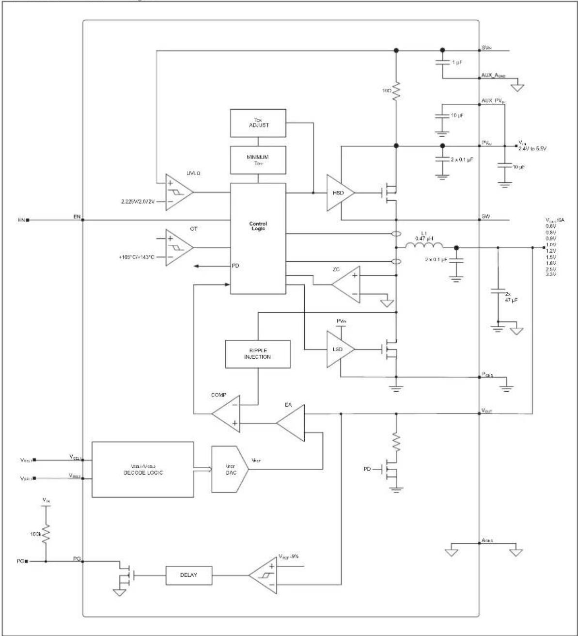
2.4V to 5.5V VIN 10 μF Opt. EN VSEL1 VSEL2 VIN VIN VSEL1 VSEL2 SW OUT P GND VOUT 1.0V/6A 47 μF 47 μF VIN R1 100k PG AUX_A GND A GND VOUT Power GoodFunctional Block Diagram
text_image
EN EN Tch ADJUST MINIMUM Tcr HVLO 2.225V/2.072V +185°C/+143°C CT PD Control Logic HSD ZC L1 0.47 μF 2 x 0.1 μF PVcc 2 x 0.1 μF SVI SvN 1 μF AUX AOUT 10 μF AUX PVcc PVcc 2.4V to 6.5V 10 μF 2k 27 μF VOUT/SA 0.6V 0.8V 0.9V 1.0V 1.2V 1.5V 1.6V 2.5V 3.3V RIPPLE INJECTION COMP EA Vin LSD PwN VOUT VOUT-9A VOUT/SA 0.6V 0.8V 0.9V 1.0V 1.2V 1.5V 1.6V PG Vout Vout/SA DECODE LOGIC Vout DAC Vout PD 100k 100k 100k AGASNOTES:
1.0 ELECTRICAL CHARACTERISTICS
Absolute Maximum Ratings ^†
SV_IN, PV_IN to A_GND ...... -0.3V to +6V
V_SW to A_GND -0.3V to +6V
V_EN to A_GND ....-0.3V to PV_IN
V_PG to A_GND ....-0.3V to PV_IN
V_VSEL1, V_VSEL2 to A_GND -0.3V to PV_IN
PV_IN to SV_IN ....-0.3V to +0.3V
A_GND to P_GND -0.3V to +0.3V
Junction Temperature ....+150°C
Storage Temperature ( T_S )....-65°C to +150°C
Lead Temperature (soldering, 10s)....+260°C
ESD Rating (Note 1)
HBM 2000V
CDM 1500V
† Notice: Stresses above those listed under “Maximum Ratings” may cause permanent damage to the device. This is a stress rating only and functional operation of the device at those or any other conditions above those indicated in the operational sections of this specification is not intended. Exposure to maximum rating conditions for extended periods may affect device reliability.
Note 1: Devices are ESD-sensitive. Handling precautions recommended. Human body model, 1.5 kΩ in series with 100 pF.
Operating Ratings ^(1)
Supply Voltage ( PV_IN ) 2.4V to 5.5V
Enable Voltage ( V_EN ) 0V to PV_IN
Power-Good Pull-up Voltage ( V_PU PG ) 0V to 5.5V
AUX_PVIN to PVIN 0V (shorted in operation)
AUX_A_GND to A_GND 0V (shorted in operation)
Maximum Output Current.... 6A
Junction Temperature ( T_J ) -40^ to +125^
Note 1: The device is not ensured to function outside the operating range.
ELECTRICAL CHARACTERISTICS ^(1)
| Electrical Specifications: Unless otherwise specified, PV_IN =5V; V_OUT =1V; V_OUT =2x47μF; AT +25°C. Boldface values indicate -40°C ≤ T_J ≤ +125°C. | ||||||
| Parameters Sym. Min. Typ. Max. Units Conditions | ||||||
| V_IN Supply | ||||||
| Input Range PV | IN | 2.4 | — | 5.5 | V | |
| Undervoltage Lockout Threshold | UVLO | 2.15 | 2.225 | 2.35 | V | SV_IN rising |
| Undervoltage Lockout Hysteresis | UVLO_H — | 153 | — | mV | SV | IN falling |
| Operating Supply Current | I_IN0 | — | 60 | 100 | μA | V_FB =1.2V, non-switching |
| Shutdown Current | I_SHDN | — | 1.5 | 10 | μA | V_EN =0V, P_IN = SV_IN =5.5V, V_SW = V_SEL1 = V_SEL2 =0V,-40°C ≤ T_J ≤ +105°C |
| — | 20 | μA | V_EN =0V, P_IN = SV_IN =5.5V, V_SW = V_SEL1 = V_SEL2 =0V,-40°C ≤ T_J ≤+125°C | |||
| Output Voltage vs. V_SEL1/2 | ||||||
| Output Accuracy | V_OUT\_ACC | 0.5910 | 0.6 | 0.6090 | V | V_SEL2 =0, V_SEL1 =0 |
| 0.7880 | 0.8 | 0.8120 | V | V_SEL2 =0, V_SEL1 =Z | ||
| 0.8865 | 0.9 | 0.9135 | V | V_SEL2 =0, V_SEL1 =1 | ||
| 0.9850 | 1.0 | 1.0150 | V | V_SEL2 =Z, V_SEL1 =0 | ||
| 1.1820 | 1.2 | 1.2180 | V | V_SEL2 =Z, V_SEL1 =Z | ||
| 1.4775 | 1.5 | 1.5225 | V | V_SEL2 =Z, V_SEL1 =1 | ||
| 1.7730 | 1.8 | 1.8270 | V | V_SEL2 =1, V_SEL1 =0 | ||
| 2.4625 | 2.5 | 2.5375 | V | V_SEL2 =1, V_SEL1 =Z | ||
| 3.2505 | 3.3 | 3.3495 | V | V_SEL2 =1, V_SEL1 =1 | ||
| Line Regulation | — | — | 0.06 | — | % | V_OUT =1.0V, V_IN =2.5V to 5.5V, I_OUT =300mA |
| Load Regulation | — | — | 0.1 | — | % | V_OUT =1.0V, I_OUT =0A to 6A |
| Enable Control | ||||||
| EN Logic Level High | V_EN\_H | 1.2 — | — | V | V | EN rising, regulator enabled |
| EN Logic Level Low | V_EN\_L | — | — | 0.4 | V | V_EN falling, regulator shutdown |
| EN Low Input Current | I_EN\_L | — | 0.01 | 500 | nA | V_EN =0V |
| EN High Input Current | I_EN\_H | — | 0.01 | 500 | nA | V_EN =5.5V |
| Enable Lockout Delay | — | 0.15 | 0.25 | 0.4 | ms | |
| V_SEL Logic Level Control | ||||||
| V_SEL1,2 Logic Level High | V_SEL\_H | 1.2 — | — | V | V | SEL1,2 rising, regulator enabled |
| V_SEL1,2 Logic Level Low | V_SEL\_L | — | — | 0.4 | V | V_SEL1,2 falling, regulator shutdown |
| V_SEL1,2 Logic Level Open | V_SEL\_O | — | 0.8 | — | V | V_SEL1,2 falling, regulator shutdown |
| V_SEL1,2 Low Input Current I | V_SEL\_L | -1 | 0.01 | 1 | μA | V_SEL1,2 =0V |
| V_SEL1,2 High Input Current I | V_SEL\_H | -1 | 0.01 | 1 | μA | V_SEL1,2 =5.5V |
Note 1: Specification for packaged product only.
2: Tested in open loop. The closed-loop current limit is affected by the inductance value.
ELECTRICAL CHARACTERISTICS ^(1) (CONTINUED)
| Electrical Specifications: Unless otherwise specified, PV_IN =5 V; V_OUT =1 V; G_OUT =2 x 47 μF; =+2 5 °C. Boldface values indicate -40°C ≤ T_J ≤+125°C. | ||||||
| Parameters | Sym. | Min. | Typ. | Max. | Units | Conditions |
| T_ON Control/Switching Frequency | ||||||
| Switching On Time T | ON | — | 1 | 8 | 0 | — IN=5 N, OUT≤1 V V |
| Switching Frequency FREQ | — 1.2 — MHz V | OUT=1.0V, IOUT=3 A,L=0.4 7 μH | ||||
| — | 1.1 | — | VOUT=3.3V, IOUT=3 A,L=0.4 7 μH | |||
| Maximum Duty Cycle | DCMAX | — | 100 | % | ||
| Short-Circuit Protection | ||||||
| High-Side MOSFET Forward Current Limit | I_LIM\_HS | 8 | 10 | 12 | A | Note 2 |
| Low-Side MOSFET Forward Current Limit | I_LIM\_LS | — | 8 | — | A | Note 2 |
| Low-Side MOSFET Negative Current Limit | I_LIM\_NEG | -2 | -3 | -4 | A | Note 2 |
| N-Channel Zero-Crossing Threshold | I_ZC\_TH | — | 0.9 | — | A | |
| Current Limit Events before Hiccup | HICCUP | — | 8 | — | Cycles | |
| Hiccup Period before Restart | — | — | 1 | — | ms | |
| Internal MOSFETs | ||||||
| High-Side On-Resistance | R_DS-ON-HS | — | 30 | 60 | mΩ | I_SW =1A |
| Low-Side On-Resistance | R_DS-ON-LS | — | 16 | 40 | mΩ | I_SW =-1A |
| Output Discharge Resistance | R_DS-ON-DSC | — | 10 | 50 | Ω | V_EN =0 V, V_SW =5.5 V, from V_OUT to P_GND |
| SW Leakage Current | I_LEAK\_SW | — | 1 | 10 | μA | PV_IN =5.5V, V_SW =0 V, V_EN =0V |
| Power Good | ||||||
| PG Threshold | PG_TH | 87 | 91 | 95 | % V_OUT | V_OUT Rising (Good) |
| PG Hysteresis | PG_HYS | — | 4 | — | % V_OUT | V_FB = V_REF , V_PG =5.5 V |
| PG Blanking Time | PG_BLANK | — | 65 | — | μs | |
| PG Output Leakage Current | PG_LEAK | — | 30 | 300 | nA | |
| PG Sink Low Voltage | PG_SINKV | — | — | 200 | mV | V_FB =0 V, V_G =5.5 V, I_PG =10 mA |
| Thermal Shutdown | ||||||
| Thermal Shutdown | T_SHDN | — | +165 | — | °C | T_J rising |
| Thermal Shutdown Hysteresis | T_SHDN\_HYST | — | + | 22 | — | °J fallingC T |
| Thermal Latch-Off Soft Start Cycles | TH_LATCH | — | 4 | — | Cycles | |
Note 1: Specification for packaged product only.
2: Tested in open loop. The closed-loop current limit is affected by the inductance value.
TEMPERATURE SPECIFICATIONS
| Electrical Specifications: Unless otherwise specified, SV_IN = PV_IN = 5 V ; V_OUT = 1 V ; G_UT = 2 × 47 F ; F + 25^ .Boldface values indicate -40°C ≤ T_J ≤ +125°C. | ||||||
| Parameters Sym. Min. Typ. Max. Units Conditions | ||||||
| Temperature Ranges | ||||||
| Junction Temperature T | _J | -40 — | +125 | °C | ||
| Storage Temperature Range | T_A | -65 — | +150 | °C | ||
| Package Thermal Resistances | ||||||
| Thermal Resistance, 53-Lead,6 mm x 10 mm x 3 mm B1QFN | _JA | — | +31 | — | °C/W | |
2.0 TYPICAL CHARACTERISTIC CURVES
Note: The graphs and tables provided following this note are a statistical summary based on a limited number of samples and are provided for informational purposes only. The performance characteristics listed herein are not tested or guaranteed. In some graphs or tables, the data presented may be outside the specified operating range (e.g., outside specified power supply range) and therefore outside the warranted range.
Note: Unless otherwise indicated, SV_IN = PV_IN = 5 V ; _UT = 1 V ; G_UT = 2 × 47 F ; A_F + 25^ C .
line
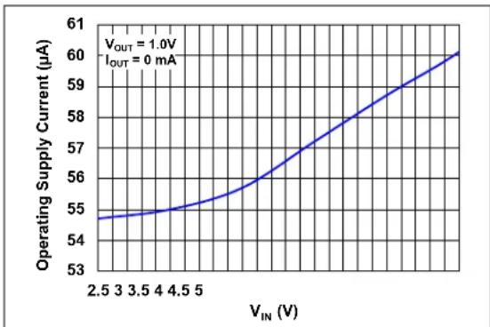
| V_IN (V) | Operating Supply Current (µA) | | -------- | ----------------------------- | | 2.5 | 54.5 | | 3.0 | 54.7 | | 3.5 | 54.9 | | 4.0 | 55.2 | | 4.5 | 55.6 | | 5.0 | 56.0 | | 5.5 | 56.8 | | 6.0 | 57.5 | | 6.5 | 58.2 | | 7.0 | 58.8 | | 7.5 | 59.3 | | 8.0 | 59.7 | | 8.5 | 60.0 |FIGURE 2-1: Operating Supply Current vs. Input Voltage, Switching.

line
| Ambient Temperature (°C) | High-Side ON-Resistance (R_DS-ON, mΩ) | Low-Side ON-Resistance (R_DS-ON, mΩ) | | ------------------------ | -------------------------------------- | ------------------------------------- | | -40 | 23 | 13 | | -25 | 25 | 14 | | -10 | 27 | 15 | | 5 | 29 | 16 | | 20 | 31 | 17 | | 35 | 33 | 18 | | 50 | 35 | 19 | | 65 | 37 | 20 | | 80 | 39 | 21 | | 95 | 41 | 22 | | 110 | 43 | 23 | | 125 | 45 | 24 |FIGURE 2-4: R DS-ON vs. Temperature.
line
| Ambient Temperature (°C) | High-Side Current Limit (A) | | ------------------------ | --------------------------- | | -40 | 9.5 | | -25 | 9.2 | | -10 | 9.0 | | 0 | 8.8 | | 20 | 8.9 | | 35 | 9.0 | | 50 | 9.2 | | 65 | 9.5 | | 80 | 9.8 | | 95 | 10.2 | | 110 | 10.8 | | 125 | 11.2 |FIGURE 2-2: High-Side Current Limit vs. Temperature (closed loop).
line
| I_OUT (A) | Efficiency (%) - V_IN = 3.3V | Efficiency (%) - V_IN = 5.0V | | --------- | ---------------------------- | ---------------------------- | | 0.0001 | ~20.00 | ~15.00 | | 0.001 | ~40.00 | ~35.00 | | 0.01 | ~55.00 | ~45.00 | | 0.1 | ~60.00 | ~50.00 | | 1 | ~70.00 | ~65.00 | | 10 | ~65.00 | ~70.00 |FIGURE 2-5: Efficiency vs. Load Current.
line
| Ambient Temperature (°C) | VOUT = 3.3V (μA) | VOUT = 1.0V (μA) | | ------------------------ | ---------------- | ---------------- | | -40 | 60 | 58 | | -25 | 61 | 59 | | -10 | 62 | 60 | | 5 | 63 | 61 | | 20 | 64 | 62 | | 35 | 65 | 63 | | 50 | 66 | 64 | | 65 | 67 | 65 | | 80 | 68 | 66 | | 95 | 69 | 67 | | 110 | 70 | 68 | | 125 | 71 | 69 |FIGURE 2-3: Operating Supply Current vs. Temperature, Switching.
line
| I_OUT (A) | Efficiency (%) - V_IN = 3.3V | Efficiency (%) - V_OUT = 1V | | --------- | ---------------------------- | --------------------------- | | 0.0001 | 25.00 | 20.00 | | 0.001 | 60.00 | 55.00 | | 0.01 | 75.00 | 70.00 | | 0.1 | 85.00 | 80.00 | | 1 | 90.00 | 85.00 | | 10 | 80.00 | 75.00 |FIGURE 2-6: Efficiency vs. Load Current.
Note: Unless otherwise indicated, SV_IN = PV_IN = 5 V ; _UT = 1 V ; _UT = 2 × 47 F ; A T = +25^ C .

line
| IOUT (A) | Efficiency (%) - V_IN = 4.0V | Efficiency (%) - V_IN = 5.5V | | -------- | ---------------------------- | ---------------------------- | | 0.0001 | 60.00 | 50.00 | | 0.001 | 80.00 | 75.00 | | 0.01 | 90.00 | 85.00 | | 0.1 | 95.00 | 92.00 | | 1 | 98.00 | 96.00 | | 10 | 95.00 | 93.00 |FIGURE 2-7: Efficiency vs. Load Current.
line
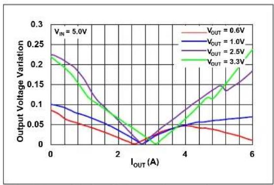
| IOUT (A) | VOUT = 0.6V | VOUT = 1.0V | VOUT = 2.5V | VOUT = 3.3V | | -------- | ----------- | ----------- | ----------- | ----------- | | 0 | 0.09 | 0.10 | 0.23 | 0.21 | | 2 | 0.01 | 0.01 | 0.01 | 0.01 | | 4 | 0.04 | 0.05 | 0.15 | 0.12 | | 6 | 0.01 | 0.07 | 0.18 | 0.24 |FIGURE 2-10: Load Regulation: Output Voltage Variation vs. I_OUT .
line
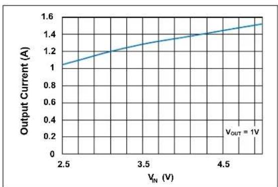
| V_IN (V) | Output Current (A) | | -------- | ------------------ | | 2.5 | 1.0 | | 3.0 | 1.2 | | 3.5 | 1.3 | | 4.0 | 1.4 | | 4.5 | 1.5 | | 5.0 | 1.6 |FIGURE 2-8: DCM/FPWM I OUT Threshold vs. V_IN .
line
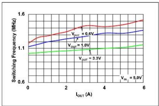
| I_OUT (A) | Switching Frequency (MHz) for V_PUT = 0.6V | Switching Frequency (MHz) for V_PUT = 1.0V | Switching Frequency (MHz) for V_PUT = 3.3V | | --------- | ------------------------------------------ | ------------------------------------------ | ------------------------------------------ | | 0 | 1.12 | 1.10 | 1.08 | | 2 | 1.14 | 1.12 | 1.09 | | 4 | 1.15 | 1.13 | 1.10 | | 6 | 1.16 | 1.14 | 1.11 |FIGURE 2-11: Switching Frequency vs. Output Current.
line
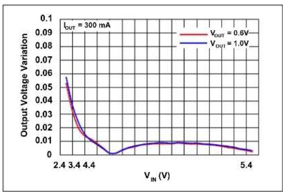
| V_IN (V) | Output Voltage Variation (VOUT = 0.6V) | Output Voltage Variation (VOUT = 1.0V) | | -------- | -------------------------------------- | -------------------------------------- | | 2.4 | 0.058 | 0.058 | | 3.4 | 0.035 | 0.035 | | 4.4 | 0.015 | 0.015 | | 5.4 | 0.005 | 0.005 |FIGURE 2-9: Line Regulation: Output Voltage Variation vs. Input Voltage.
line
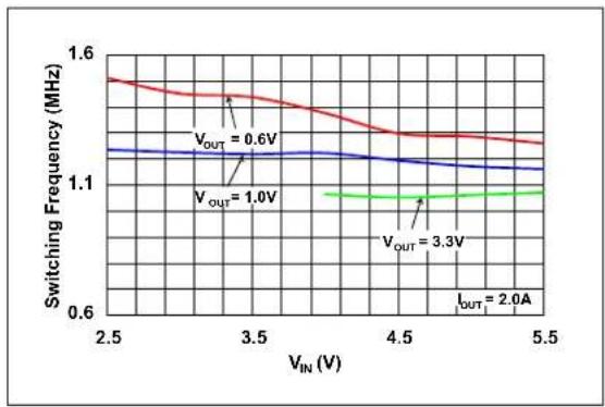
| VIN (V) | Switching Frequency (MHz) | | ------- | ------------------------- | | 2.5 | 1.5 | | 3.5 | 1.4 | | 4.5 | 1.3 | | 5.5 | 1.2 |FIGURE 2-12: Switching Frequency vs. Input Voltage.
Note: Unless otherwise indicated, SV_IN = PV_IN = 5 V ; _UT = 1 V ; _UT = 2 × 47 F ; A T = +25^ C .

line
| Time (ms) | V_IN (V/div) | V_OUT (mV/div) | SW (5V/div) | PG (5V/div) | |-----------|--------------|----------------|-------------|-------------| | 0 | 5 | 500 | 5 | 5 | | 2 | 5 | 500 | 5 | 5 | | 4 | 5 | 500 | 5 | 5 | | 6 | 5 | 500 | 5 | 5 | | 8 | 5 | 500 | 5 | 5 | | 10 | 5 | 500 | 5 | 5 | | 12 | 5 | 500 | 5 | 5 | | 14 | 5 | 500 | 5 | 5 | | 16 | 5 | 500 | 5 | 5 | | 18 | 5 | 500 | 5 | 5 | | 20 | 5 | 500 | 5 | 5 | | 22 | 5 | 500 | 5 | 5 | | 24 | 5 | 500 | 5 | 5 | | 26 | 5 | 500 | 5 | 5 | | 28 | 5 | 500 | 5 | 5 | | 30 | 5 | 500 | 5 | 5 | | 32 | 5 | 500 | 5 | 5 | | 34 | 5 | 500 | 5 | 5 | | 36 | 5 | 500 | 5 | 5 | | 38 | 5 | 500 | 5 | 5 | | 40 | 5 | 500 | 5 | 5 | | 42 | 5 | 500 | 5 | 5 | | 44 | 5 | 500 | 5 | 5 | | 46 | 5 | 500 | 5 | 5 | | 48 | 5 | 500 | 5 | 5 | | 50 | 5 | 500 | 5 | 5 | | 52 | 5 | 500 | 5 | 5 | | 54 | 5 | 500 | 5 | 5 | | 56 | 5 | 500 | 5 | 5 | | 58 | 5 | 500 | 5 | 5 | | 60 | 5 | 500 | 5 | 5 | | 62 | 5 | 500 | 5 | 5 | | 64 | 5 | 500 | 5 | 5 | | 66 | 5 | 500 | 5 | 5 | | 68 | 5 | 500 | 5 | 5 | | 70 | 5 | 500 | 5 | 5 | | 72 | 5 | 500 | 5 | 5 | | 74 | 5 | 500 | 5 | 5 | | 76 | 5 | 500 | 5 | 5 | | 78 | 5 | 500 | 5 | 5 | | 80 | 5 | 500 | 5 | 5 | | Note: The actual values for V_IN and V_OUT are not provided in the code snippet. The data is presented in a format with 'Voltage' as the time variable. There is only one data series in this case.FIGURE 2-13: V IN Turn-On (EN = PVIN).
line
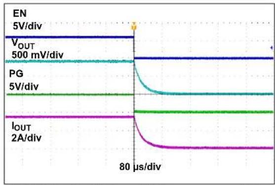
| Time (μs) | EN (5V/div) | VOUT (500 mV/div) | PG (5V/div) | IOUT (2A/div) | |-----------|-------------|-------------------|-------------|---------------| | 0 | 5 | 5 | 5 | 80 | | 24 | 5 | 5 | 5 | 10 | | 80 | 5 | 5 | 5 | 10 |FIGURE 2-16: EN Turn-Off, R LOAD = 0.3Ω

line
| Signal | Time (μs) | |--------|-----------| | V_IN | 400 | | V_OUT | 400 | | PG | 400 | | SW | 400 |FIGURE 2-14: V IN Turn-Off (EN = PVIN), R_LOAD = 0.3 .

line
| Signal | Value | |--------|--------------| | EN | 5V/div | | VOUT | 500 mV/div | | PG | 5V/div | | SW | 5V/div |FIGURE 2-17: EN Turn-On into Pre-Biased Output ( V_pre-bias = 0.8 V ).
line
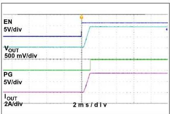
| Time (ms) | EN (5V/div) | VOUT (500 mV/div) | PG (5V/div) | IOUT (2A/div) | |-----------|-------------|-------------------|-------------|---------------| | 0 | 0 | 0 | 0 | 0 | | 1 | 0 | 0 | 0 | 0 | | 2 | 0 | 0 | 0 | 0 | | 3 | 0 | 0 | 0 | 0 | | 4 | 0 | 0 | 0 | 0 | | 5 | 0 | 0 | 0 | 0 | | 6 | 0 | 0 | 0 | 0 | | 7 | 0 | 0 | 0 | 0 | | 8 | 0 | 0 | 0 | 0 | | 9 | 0 | 0 | 0 | 0 | | 10 | 0 | 0 | 0 | 0 | | 11 | 0 | 0 | 0 | 0 | | 12 | 0 | 0 | 0 | 0 | | 13 | 0 | 0 | 0 | 0 | | 14 | 0 | 0 | 0 | 0 | | 15 | 0 | 0 | 0 | 0 | | 16 | 0 | 0 | 0 | 0 | | 17 | 0 | 0 | 0 | 0 | | 18 | 0 | 0 | 0 | 0 | | 19 | 0 | 0 | 0 | 0 | | 20 | 0 | 0 | 0 | 0 | | | | | | | | | | | | | | | | | | | | | | | | | | | | | | | | | | | | | | | | | | | | | | | | | | | | | | | | | | | | | | / | | | | | | / / / / / / / / / / / / / / / / / / / / / / / / / / / / / / / / / / / / / / / / / / / / / / / / / / / / / / / / / / / / | | / / / / / / / / | | | | | | / / / / / / / / | | | | | | / / / / / / / / / | | / / / / / / / / / | | / / / / / / / / | | / / / / / / / / | | / / / / / / / / | | / / / / / / / / | | / / / / / / / / | | / / / / / / / / | | / / / / / / - | | | | | | / / / / / - - - | | / / / / - - - - - | | / / / / - - - - - | | / / / / - - - - - | | / / / / - - - - - | | / / / / - - - - - | | / / / / - - - - - | | / / / / - - - - - | | / / / / - - - - - | | / / / / - - - | | / / / / - - - - | | / / / / - - - - | | / / / / - - - - | | / / / / - - - - | | / / / / - - - - | | | *EN* *VOUT* *PG* *IOUT* *EN* *VOUT* *PG* *IOUT* *EN* *VOUT* *PG* *IOUT* *EN* *VOUT* *PG* *IOUT* *EN* *VOUT* *PG* *IOUT* *EN* *VOUT* *PG* *IOUT* *EN* *VOUT* *PG* *IOUT* *EN* *VOUT* * The data is presented in a table format with three columns: EN, VOUT, and IOUT. The values for each row are the corresponding values from the plot. The data is then repeated for the last row to close the plot. The values for the plotted cells are calculated based on the given values of the x-axis (in seconds). There is no additional data series or additional variables present in the code. The values for the plotted cells are estimated based on the given values of the x-axis. The y-axis is labeled as '2 m s/d' and is also labeled as '2A/div'.FIGURE 2-15: EN Turn-On, R LOAD = 0.3Ω
line
| Signal | Time (ms) | |--------|-----------| | EN | 0 | | VOUT | 500 | | PG | 0 | | SW | 0 |FIGURE 2-18: Power-up into Short-Circuit.
Note: Unless otherwise indicated, SV_IN = PV_IN = 5 V ; _UT = 1 V ; _UT = 2 × 47 F ; A T = +25^ C .

line
| Signal | Value | |--------|-----------| | VOUT | 1V/div | | IOUT | 5A/div | | PG | 5V/div | | SW | 5V/div |FIGURE 2-19: Output Current Limit Threshold.
line
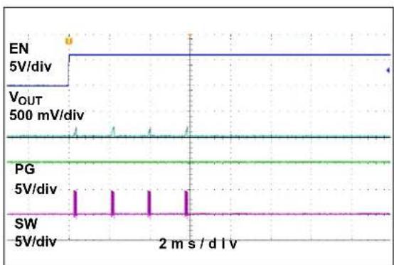
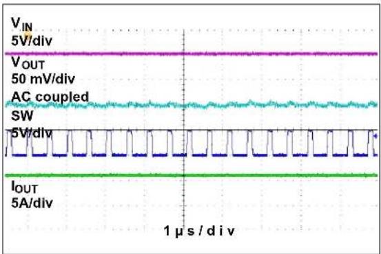
| Time (μs) | V_IN (5V/div) | V_OUT (50 mV/div) | AC coupled SW | I_OUT (5A/div) | |-----------|---------------|-------------------|---------------|----------------| | 0 | 5 | 50 | 5 | 5 | | 1 | 5 | 50 | 5 | 5 | | 2 | 5 | 50 | 5 | 5 | | 3 | 5 | 50 | 5 | 5 | | 4 | 5 | 50 | 5 | 5 | | 5 | 5 | 50 | 5 | 5 | | 6 | 5 | 50 | 5 | 5 | | 7 | 5 | 50 | 5 | 5 | | 8 | 5 | 50 | 5 | 5 | | 9 | 5 | 50 | 5 | 5 | | 10 | 5 | 50 | 5 | 5 | | 11 | 5 | 50 | 5 | 5 | | 12 | 5 | 50 | 5 | 5 | | 13 | 5 | 50 | 5 | 5 | | 14 | 5 | 50 | 5 | 5 | | 15 | 5 | 50 | 5 | 5 | | 16 | 5 | 50 | 5 | 5 | | 17 | 5 | 50 | 5 | 5 | | 18 | 5 | 50 | 5 | 5 | | 19 | 5 | 50 | 5 | 5 | | 20 | 5 | 50 | 5 | 5 | | 21 | 5 | 50 | 5 | 5 | | 22 | 5 | 50 | 5 | 5 | | 23 | 5 | 50 | 5 | 5 | | 24 | 5 | 50 | 5 | 5 | | 25 | 5 | 50 | 5 | 5 | | 26 | 5 | 50 | 5 | 5 | | 27 | 5 | 50 | 5 | 5 | | 28 | 5 | 50 | 5 | 5 | | 29 | 5 | 50 | 5 | 5 | | 30 | 5 | 50 | 5 | 5 | | 31 | 5 | 50 | 5 | 5 | | | | | | | | | | | | | | | | | | | | | | | | | | | | | | | | | | | | | | | | | | | | | | | | | | | | | | | | | | | | |FIGURE 2-22: Switching Waveforms, I_OUT = 6A .
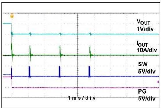
FIGURE 2-20: Hiccup Mode Short-Circuit Current Limit Response.

line
| Signal | Value | |--------|--------------| | PG | 5V/div | | VOUT | 100 mV/div | | AC coupled | - | | SW | 5V/div | | IOUT | 5A/div |FIGURE 2-23: Load Transient Response.
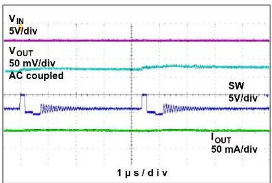
FIGURE 2-21: Switching Waveforms, I_OUT = 50 mA .
line
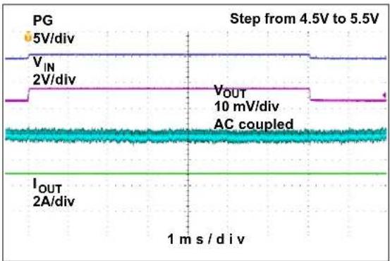
| Time Scale | Voltage (V) | Current (A) | |------------|-------------|-------------| | 0 | 5V/div | - | | 10 | 2V/div | - | | 20 | - | - | | 30 | - | - | | 40 | - | - | | 50 | - | - | | 60 | - | - | | 70 | - | - | | 80 | - | - | | 90 | - | - | | 100 | - | - | | 110 | - | - | | 120 | - | - | | 130 | - | - | | 140 | - | - | | 150 | - | - | | 160 | - | - | | 170 | - | - | | 180 | - | - | | 190 | - | - | | 200 | - | - | | 210 | - | - | | 220 | - | - | | 230 | - | - | | 240 | - | - | | 250 | - | - | | 260 | - | - | | 270 | - | - | | 280 | - | - | | 290 | - | - | | 300 | - | - | | 310 | - | - | | 320 | - | - | | 330 | - | - | | 340 | - | - | | 350 | - | - | | 360 | - | - | | 370 | - | - | | 380 | - | - | | 390 | - | - | | 400 | - | - | | 410 | - | - | | 420 | - | - | | 430 | - | - | | 440 | - | - | | 450 | - | - | | 460 | - | - | | 470 | - | - | | 480 | - | - | | 490 | - | - | | 500 | - | - | | 510 | - | - | | 520 | - | - | | 530 | - | - | | 540 | - | - | | 550 | - | - | Step from 4.5V to 5.5V Step from 4.5V to 5.5V AC coupled 1 m s / divFIGURE 2-24: Line Transient Response.
3.0 PIN DESCRIPTIONS
The descriptions of the pins are listed in Table 3-1.
TABLE 3-1: PIN FUNCTION TABLE
| Pin Number Symbol Description | ||
| 2, 3, 4, 5, 23, 24, 39, 40 P | GND | Power Ground. P_GND is the ground path for the MIC33M650 power module. |
| 1, 53 AUX_PV | IN | Auxiliary Power Input Voltage Pin. Connect externally to PV_IN . |
| 6, 7, 8, 9, 10, 11, 12, 13, 14, 15, 16, 17, 18, 19, 20, 21, 22 | SW Switch Node | Node Pin. SW connects to the internal MOSFETs and inductor. Do not connect any external load to this point. |
| 41, 42 PV | IN | Power Supply Voltage Pin. |
| 25, 26, 27, 28, 29, 30, 31, 32, 33, 34, 35, 36, 37, 38 | OUT Output Side Connection Pin. | |
| 43, 44 SV | IN | Analog Voltage Input Pin. SV_IN is the power to the internal reference and control sections of the MIC33M650. Internally connected to PV_IN through a 10W resistor. |
| 46, 47 | AUX_A _GND | Auxiliary Analog Ground Pin. Connect externally to A_GND . |
| 45 | V_SEL2 | Output Voltage Selection Control 2 (Input) Pin. The logic state of V_SEL1 and V_SEL2 selects the output voltage. This input has three digital states: High, Low and Floating. |
| 48 | V_SEL1 | Output Voltage Selection Control 1 (Input) Pin. The logic state of V_SEL1 and V_SEL2 selects the output voltage. This input has three digital states: High, Low and Floating. |
| 49 | EN | Enable (Input) Pin. Logic high enables the operation of the regulator. The EN pin should not be left floating. |
| 50 | PG | Power Good (Output) Pin. This is an open-drain output that indicates when the output voltage is higher than the 91% limit. |
| 51 | V_OUT | Output Voltage Sense (Input) Pin. This pin is used to remote sense the output voltage. Connect V_OUT as close to the output capacitor as possible to sense the output voltage. |
| 52 | A_GND | Analog Ground Pin. A_GND is the internal signal ground for all low-power circuits. |
| 54 | EP_OUT | Exposed Thermal Pad. Internally connected to OUT. |
| 55 | EP_SW | Exposed Thermal Pad. Internally connected to SW. |
| 56 | EP\_P_GND | Exposed Thermal Pad. Internally connected to P_GND . |
| 57 | EP\_PV_IN | Exposed Thermal Pad. Internally connected to PV_IN . |
3.1 Power Ground Pin (P GND)
P_GND is the ground path for the MIC33M650 buck converter power stage. The P_GND pin connects to the sources of the low-side N-Channel MOSFETs, the negative terminals of input capacitors and the negative terminals of output capacitors. The loop for the Power Ground must be as small as possible and separate from the Analog Ground ( A_GND ) loop.
3.2 Switch Node Pin (SW)
Switching node output pin which connects to the internal MOSFETs and inductor. This is a high-frequency connection; therefore, traces should be kept as short and as wide as practical.
3.3 Power Supply Voltage Pin (PV IN)
Input supply to the source of the internal high-side P-channel MOSFET. The PV_IN operating voltage range is from 2.4V to 5.5V. An input capacitor between PV_IN and the P_GND pin is required and placed as close to the IC as possible.
3.4 Output Side Connection Pins (OUT)
Output side connection of the internal inductor. The output capacitors must be connected from this pin group to GND, as close to the module as possible.
3.5 Analog Voltage Input Pin (SV IN)
This pin is the power to the internal reference and control sections of the MIC33M650. It is internally connected to PV_IN through a 10Ω resistor.
3.6 Output Voltage Selection Control Pins ( V_SEL1 , V_SEL2 )
Output Voltage Selection Control (Input). The logic state of V_SEL1 and V_SEL2 selects the output voltage. This input has three digital states: High, Low and Floating. See Table 4-1.
3.7 Enable Pin (EN)
Logic high enables the regulator's operation. Logic low shuts down the device. In the OFF state, the supply current of the device is greatly reduced (typically, 1.5 A). The EN pin should not be left open.
3.8 Power Good Pin (PG)
This is an open-drain output that indicates when the output voltage is higher than the 91% limit. There is a 4% hysteresis; therefore, PG will return low when the output voltage falls below 87% of the target regulation voltage.
3.9 Output Voltage Sense Pin (V OUT)
This pin is used to remote sense the output voltage. Connect to V_OUT as close to the output capacitor as possible to sense the output voltage. It also provides the path to discharge the output through an internal 10Ω resistor when the device is disabled.
3.10 Analog Ground Pin (A GND)
Internal signal ground for all low-power circuits. Connect to ground plane. For best load regulation, the connection path from A_GND to the output capacitor ground terminal must be free from parasitic voltage drops.
3.11 Auxiliary Analog Ground Pins (AUX\_A\_GND)
Connect these pins to A_GND to make use of the internal decoupling capacitor for SV_IN pin filtering.
3.12 Auxiliary Input Voltage Pins (AUX\_PVIN)
Connect these pins to PV_IN to make use of the internal 10 F capacitor for PV_IN filtering/decoupling.
3.13 OUT Exposed Pad (EP\_OUT)
It is electrically connected to the OUT pins. It must be externally connected to the output power connection.
3.14 SW Exposed Pad (EP\_SW)
It is electrically connected to the SW node.
3.15 P GND Exposed Pad (EP\_P\_GND)
It is electrically connected to the P_GND pins. It must be connected with thermal vias to the ground plane to ensure adequate heat sinking.
3.16 PV IN Exposed Pad (EP\_PVIN)
It is electrically connected to the PV_IN pins. It must be connected to the input power connection.
4.0 FUNCTIONAL DESCRIPTION
4.1 Device Overview
The MIC33M650 is a high-efficiency, 6A peak current, synchronous buck regulator power module with HyperLight Load mode. The module integrates the inductor, alongside with high-frequency ripple dampening capacitors, on the input and output of the converter and decoupling capacitor for the signal input. The COT control architecture with automatic HyperLight Load mode provides very high efficiency at light loads and ultra-fast transient response.
The MIC33M650 output voltage is set by two V_SEL tri-state logic pins that can set the output voltage to nine different values. See Table 4-1.
The 2.4V to 5.5V input voltage operating range makes the device ideal for single-cell Li-Ion battery-powered applications. The 100% duty cycle capability provides low dropout operation, extending battery life in portable systems. The automatic HyperLight Load mode provides very high efficiency at light loads.
This device focuses on high output voltage accuracy. Total output error is less than 1.5% over line, load and temperature.
The MIC33M650 buck regulator uses an adaptive COT control method. The adaptive on-time control scheme is employed to obtain a nearly constant switching frequency in Continuous Conduction mode. Overcurrent protection is implemented by sensing the current on both the low-side and high-side internal power MOSFETs. The device includes an internal soft start function, which reduces the power supply input surge current at start-up, by controlling the output voltage rise time.
4.2 HyperLight Load Mode (HLL)
HLL is a power-saving mode. In HLL, the switching frequency is not constant over the operation current range, but its average value reduces proportionally to the load current. This reduces switching and drive losses and maintains high efficiency as the load current decreases.
4.3 Enable (EN)
When the EN pin is pulled low, the IC is in a Shutdown state, with all internal circuits disabled with the PG output low. During shutdown, the part typically consumes 1.5 A. When the EN pin is pulled HIGH, the start-up sequence is initiated.
4.4 Power Good (PG)
The PG output is generally used for power sequencing where the Power Good output is tied to the enable output of another regulator. This technique avoids all the regulators powering up at the same time, causing large inrush current.
The PG output is an open-drain output. During start-up, when the output voltage rises, the PG output goes high by means of an external pull-up resistor when the output voltage reaches 91% of its set value. The PG threshold has 4% hysteresis, so the PG output stays high until the output voltage falls below 87% of the set value. A built-in 65 s blanking time is incorporated to prevent nuisance tripping.
The pull-up resistor can be connected to V_IN , V_OUT or an external source that is less than or equal to V_IN . The PG pin can be connected to another regulator's enable pin for output sequencing. The PG output is deasserted as soon as the enable pin is pulled low, or an input undervoltage condition or any other Fault is detected.
4.5 Resistive Discharge (Soft Discharge)
To ensure a known output condition when the device is turned off and then back on, the output is actively discharged to ground by means of an internal 10 resistor. This prevents the load from powering up starting from an undefined condition.
4.6 Output Voltage Setting
The MIC33M650 V_SEL1 and V_SEL2 pins are used to choose among nine predefined voltage settings: 0.6V, 0.8V, 0.9V, 1.0V, 1.2V, 1.5V, 1.8V, 2.5V, 3.3V. These pins can be tied to V_IN , GND or left floating. The relationship between V_SEL1/V_SEL2 and the output voltage is shown in Table 4-1.
TABLE 4-1: OUTPUT VOLTAGE SETTINGS
| V_SEL2 | V_SEL1 | V_OUT |
| GND GND | 0.6V | |
| GND OPEN | 0.8V | |
| GND V | IN | 0.9V |
| OPEN GND | 1.0V | |
| OPEN OPEN | 1.2V | |
| OPEN V | IN | 1.5V |
| V_IN | GND 1.8V | |
| V_IN | OPEN 2.5V | |
| V_IN | V_IN | 3.3V |
The output voltage sensing pin, V_OUT , must be connected to the desired Point-of-Load (POL) regulation, avoiding parasitic resistive drops. It is possible to fine-tune the desired output voltage by adding a series resistor on the V_OUT pin. This allows slightly higher output value programming, but should not exceed 5% deviation from the V_SEL selected value.
EQUATION 4-1:
$$ R _ {V O U T} = 8. 2 k \Omega \times T R I M $$
Where:
R_VOUT = V_OUT series resistance needed for a TRIM% output voltage increase
4.7 Converter Stability, Output Capacitor
The MIC33M650 utilizes an internal compensation network and it is designed to provide stable operation with output capacitors from 47 F to 1000 F. This greatly simplifies the design, where the user can add supplementary output capacitance without having to worry about stability.
4.8 Soft Start
Excess bulk capacitance on the output can cause excessive input inrush current. The MIC33M650 internal soft start feature forces the output voltage to rise gradually, keeping the inrush current at reasonable levels. This is particularly important in battery-powered applications. When the EN pin goes high, the output voltage starts to rise. Once the soft start period finishes, the PG comparator is enabled, and if the output voltage is above 91% of the nominal regulation voltage, then the PG output goes high.
The output voltage Soft Start Time, t_ss , is determined by the soft start equation below. The Soft Start Time can be calculated by:
EQUATION 4-2:
$$ t _ {S S} = V _ {O U T} \times t _ {R A M P} $$
$$ t _ {S S} = 1. 0 V \& 0 0 \quad \mu s / V $$
$$ t _ {S S} \quad 8 0 0 \mu s \quad 0 \quad . \quad 8 \quad m s = $$
Where:
$$ V _ {O U T} = 1. 0 \mathrm{V} $$
$$ t _ {R A M P} = 8 0 0 \mu \mathrm{s} / \mathrm{V} $$
4.9 Dropout Operation
As the input voltage approaches the output voltage, the minimum on-time limits the maximum duty cycle. To achieve a 100% duty cycle, the high-side switch is latched on when the duty cycle reaches around 92% and stays latched until the output voltage falls 4% below its regulated value. In dropout, the output voltage is determined by the input voltage minus the voltage drop across the high-side MOSFET.
4.10 Switching Frequency
The switching frequency of the MIC33M650 is determined by the internal On-Time ( T_ON ) calculation. For an input voltage of 5V and an output voltage of 1V, the typical value of T_ON is 180 ns.
The resulting switching frequency can be estimated by the following equation:
EQUATION 4-3:
$$ f _ {S W} = V _ {O U T} / (V _ {I N} \times T _ {O N}) $$
The above equation is only valid in Continuous Conduction mode and for a lossless converter. In practice, losses will cause an increase of the switching frequency with respect to the ideal case. As the load current increases, losses increase too and so does the switching frequency.
The on-time calculation is adaptive, in that the T_ON value is modulated based on the input voltage and on the target output voltage to stabilize the switching frequency against their variations. Losses are not accounted for.
TABLE 4-2: TON FOR TYPICAL APPLICATIONS
| V_IN (V) | V_OUT (V) | T_ON |
| 5 | 0.6 | 110 |
| 1 | 180 | |
| 1.8 | 340 | |
| 2.5 | 490 | |
| 3.3 | 610 | |
| 3.3 | 1 | 270 |
4.11 Undervoltage Protection (UVLO)
Undervoltage protection ensures that the IC has enough voltage to bias the internal circuitry properly and provide sufficient gate drive for the power MOSFETs. When the input voltage starts to rise, both power MOSFETs are off and the PG output is pulled low. The IC starts at typically 2.225V and has a typical 153 mV of hysteresis to prevent chattering between the UVLO High and Low states.
4.12 Overtemperature Fault
The MIC33M650 monitors the die junction temperature to keep the IC operating properly. If the IC junction temperature exceeds +165°C, both power MOSFETs are immediately turned off. The IC is allowed to restart when the die temperature falls below +143°C.
During recovery from a thermal shutdown event, if the regulator hits another thermal shutdown event before PG can be achieved, the controller resets again. If this happens four times in a row, the part will be in a Latch-Off state and the MOSFETs are permanently latched off. The MIC33M650 will not restart unless the input power is cycled or the EN pin is set low and then high again. This latch-off feature eliminates the thermal stress on the MIC33M650 during a persistent Fault event.
4.13 Safe Start-up into a Pre-Biased Output
The MIC33M650 is designed for safe start-up into a pre-biased output. This feature prevents high negative inductor current flow in a pre-bias condition which can damage the IC. This is achieved by not allowing PWM operation until the control loop commands eight switching cycles. After eight cycles, the low-side negative current limit is switched from 0A to -3A. The cycle counter is reset to zero if the EN pin is pulled low, or an input undervoltage condition or any other Fault is detected.
4.14 Current Limiting
The MIC33M650 regulator uses both high-side and low-side current sense for current limiting. When the high-side current sense threshold is reached, the high-side MOSFET is turned off and the low-side MOSFET is turned on. The low-side MOSFET stays on until the current falls to 80% of the high-side current threshold value, then the high side can be turned on again. If the overload condition lasts for more than seven cycles, the MIC33M650 enters hiccup current limiting and both MOSFETs are turned off. There is a cool-off period before the MOSFETs are allowed to be turned on. If the regulator has another hiccup event before it reaches the PG threshold on restart, it will turn off both MOSFETs and wait for the cool-off period. If this happens for more than three times in a row, then the part enters the Latch-Off state, which will permanently turn off both MOSFETs until the part is reset by cycling input power or by toggling the enable input.
4.15 Thermal Considerations
Although the MIC33M650 is capable of delivering up to 6A under load, the package thermal resistance and the device internal power dissipation may dictate some limitations to the continuous output current.
As a reference, for V_IN = 5V , V_OUT = 1V , I_OUT = 5A , the evaluation board application shows a stable +40°C chip package self-heating (DT100107).
For V_IN = 5V , V_OUT = 3.3V , the same self-heating is produced at about 4A.
If operated above the rated junction temperature, electrical parameters may drift beyond characterized specifications. The MIC33M650 is protected under all circumstances by thermal shutdown.
NOTES:
5.0 APPLICATION INFORMATION
5.1 Output Voltage Sensing
To achieve accurate output voltage regulation, the V_OUT pin (internal feedback divider top terminal) should be Kelvin connected as close as possible to the point of regulation top terminal. Since both the internal reference and the internal feedback divider's bottom terminal refer to A_GND , it is important to minimize voltage drops between A_GND and the point of regulation return terminal (typically the ground terminal of the output capacitor which is closest to the load).
EQUATION 5-1:
$$ P _ {W I N D I N G H T} = \left{^ {R} _ {W I N D I N G 2 0 C} (\times I) ^ {+ (0)} \quad . \quad \theta \quad H ^ {- (4)} 2 0 C ^ {2} \right. $$
Where:
$$ \begin{array}{r l} {T _ {H}} & {= \text { Temperature of Wire Under }} \ & {\quad \text { Full Load }} \end{array} $$
$$ T _ {2 0 C} = \text { Ambient Temperature } $$
$$ \begin{array}{r l} {R _ {\text { WINDING } (2 0 C)}} & {= \text { Room Temperature Winding }} \ & {\text { Resistance (usually specified }} \ & {\text { by the manufacturer })} \end{array} $$
5.2 Output Capacitor Selection
The type of output capacitor is usually determined by its Equivalent Series Resistance (ESR). Voltage and RMS current capability are two other important factors for selecting the output capacitor. Recommended capacitor types are ceramic, OS-CON and POSCAP. The output capacitor ESR is usually the main cause of the output ripple. The output capacitor ESR also affects the control loop from a stability point of view. The maximum value of ESR is calculated using Equation 5-2.
EQUATION 5-2:
$$ E S R _ {C _ {O U T}} \leq \frac {\varDelta V _ {O U T P P (}}{\varDelta I _ {L (P P)}} \quad) $$
Where:
$$ \begin{array}{r c l} \Delta V _ {O U T (P P)} & = & \text { Peak - to - Peak Output Voltage } \ & & \text { Ripple } \end{array} $$
$$ \begin{array}{r c l} \Delta I _ {L (P P)} & = & \text { Peak - to - Peak Inductor Current } \ & & \text { Ripple } \end{array} $$
The peak-to-peak inductor current ripple can be calculated with the following formula:
EQUATION 5-3:
$$ \Delta I _ {L (P P)} = \frac {V _ {O U T} \times \left(V _ {I N (M A X)} - V _ {O U T}\right)}{V _ {I N (M A X)} \times f _ {S W} \times L} $$
Where:
$$ L = 0. 4 7 \mu \mathrm{H} $$
The total output ripple is a combination of the ESR and the output capacitance. The total ripple is calculated in Equation 5-4.
EQUATION 5-4:
$$ \mathcal {A} _ {O U T (P P)} = \sqrt {\left(\frac {\Delta I _ {L (P P)}}{C _ {O U T} \times f _ {S W} \times 8}\right) ^ {2} + \left(\Delta I _ {L (P P)} \times E S R _ {C _ {O U T}}\right) ^ {2}} $$
Where:
$$ \begin{array}{l} C _ {O U T} = \text { Output Capacitance Value } \ f _ {S W} = \text { Switching Frequency } \ \end{array} $$
The output capacitor RMS current is calculated in Equation 5-5.
EQUATION 5-5:
$$ I _ {C O U T (R M S)} = \frac {\Delta I _ {L (P P)}}{\sqrt {1 2}} $$
The power dissipated in the output capacitor is:
EQUATION 5-6:
$$ P _ {D I S S (C O U T)} = I _ {C O U T (R M S)} ^ {2} \times E S R _ {C O U T} $$
5.3 Input Capacitor
The MIC33M650 integrates high-frequency input bypass capacitors, connected between PV_IN and P_GND , and an additional 10 F, low-ESR ceramic capacitor for input ripple smoothing, connected between P_GND and AUX_ PV_IN . Therefore, the connection between PV_IN and AUX_ PV_IN should have very low stray resistance and inductance (i.e., many vias) to take advantage of the internal 10 F capacitor. While the internal 10 F capacitor can support the RMS ripple current, additional external input ceramic capacitors can be optionally added to further attenuate the input voltage ripple amplitude. The need for additional external input capacitance also depends on the impedance of the input supply distribution network.
NOTES:
6.0 PACKAGING INFORMATION
6.1 Package Marking Information
53-Lead B1QFN

XXXXX
XXXXXXXXXX
XXXXXXXXXX
WNNN
PIN 1
Example:

MIC
33M650
YMP-TU
8256
PIN 1
Legend: XX...X Customer-specific information
Y Year code (last digit of calendar year)
YY Year code (last 2 digits of calendar year)
WW Week code (week of January 1 is week '01')
NNN Alphanumeric traceability code
eBb-free JEDEC designator for Matte Tin (Sn)
* This package is Pb-free. The Pb-free JEDEC designator (e3) can be found on the outer packaging for this package.
Note: In the event the full Microchip part number cannot be marked on one line, it will
be carried over to the next line, thus limiting the number of available characters for customer-specific information.
53-Lead Very Thick Plastic Quad Flat, No Lead Package (QDA) - 6x10x3.05 mm Body [B1QFN]
Note: For the most current package drawings, please see the Microchip Packaging Specification located at http://www.microchip.com/packaging
![Microchip MIC33M650 - 53-Lead Very Thick Plastic Quad Flat, No Lead Package (QDA) - 6x10x3.05 mm Body [B1QFN] - 1](/content/2026/06/1214549/images/1e1e9ff2708ffaf7153b489f3c8cb220c9c6c04a4152ef407864d8dba79257e8.jpg)
text_image
NOTE 1 53 1 2 (DATUM B) (DATUM A) 2X 0.05 C 2X 0.05 C TOP VIEW 0.10 A B D2 2X K6 D3 D2 20 27 28 2X K1 3X K2 E5 E6 E4 K5 E2 K3 E3 K4 NOTE 1 D4 53 X b e 0.10 A B 0.05 C 53X // 0.10 C 53X 0.08 C A1 (A3) A C SEATING PLANE SIDE VIEW BOTTOM VIEWMicrochip Technology Drawing C04-1272 Rev B Sheet 1 of 2
53-Lead Very Thick Plastic Quad Flat, No Lead Package (QDA) - 6x10x3.05 mm Body [B1QFN]
Note: For the most current package drawings, please see the Microchip Packaging Specification located at http://www.microchip.com/packaging
![Microchip MIC33M650 - 53-Lead Very Thick Plastic Quad Flat, No Lead Package (QDA) - 6x10x3.05 mm Body [B1QFN] - 1](/content/2026/06/1214549/images/bc69e43150fad1bdf4e3edb9087378c37c122a3807e05d6df81f5769f1a92bad.jpg)
natural_image
Two technical line drawings of rectangular electronic components with internal traces and mounting holes (no text or symbols)| Units | MILLIMETERS | |||
| Dimension Limits | MIN | NOM | MAX | |
| Number of Terminals | N | 53 | ||
| Pitch | e | 0.50 BSC | ||
| Overall Height | A | 2.95 | 3.00 | 3.05 |
| Standoff | A1 | 0.00 | 0.02 | 0.05 |
| Terminal Thickness | A3 | 0.203 REF | ||
| Overall Length | D | 6.00 BSC | ||
| Exposed Pad Length | D2 1 | 225 | 1.275 1.325 | |
| Exposed Pad Length | D3 | 0.60 0.65 | 0.70 | |
| Exposed Pad Length D4 0.55 0.60 | 0.65 | |||
| Overall Width | E | 10.00 BSC | ||
| Exposed Pad Width | E2 | 4.475 | 4.525 | 4.575 |
| Exposed Pad Width | E3 | 1.575 1.625 | 1.675 | |
| Exposed Pad Width E4 0.45 0.50 | 0.55 | |||
| Exposed Pad Width | E5 | 0.60 0.65 | 0.70 | |
| Exposed Pad Width | E6 | 6.573 6.623 | 6.673 | |
| Package Edge to Exposed Pad K1 | 0.85 0.90 0.95 | |||
| Package Edge to Exposed Pad K2 | 0.85 0.90 0.95 | |||
| Exposed Pad to Exposed Pad K3 | 1.90 1.95 2.00 | |||
| Exposed Pad to Exposed Pad K4 | 0.45 0.50 0.55 | |||
| Exposed Pad to Exposed Pad | K5 | 0.45 0.50 | 0.55 | |
| Exposed Pad to Exposed Pad K6 | 0.45 0.50 0.55 | |||
| Terminal Width | b | 0.20 | 0.25 | 0.30 |
| Terminal Length | L | 0.45 | 0.50 | 0.55 |
Notes:
1. Pin 1 visual index feature may vary, but must be located within the hatched area.
2. Package is saw singulated
3. Dimensioning and tolerancing per ASME Y14.5M
BSC: Basic Dimension. Theoretically exact value shown without tolerances.
REF: Reference Dimension, usually without tolerance, for information purposes only.
Microchip Technology Drawing C04-1272 Rev B Sheet 2 of 2
53-Lead Very Thick Plastic Quad Flat, No Lead Package (QDA) - 6x10x3.05 mm Body [B1QFN]
Note: For the most current package drawings, please see the Microchip Packaging Specification located at http://www.microchip.com/packaging
![Microchip MIC33M650 - 53-Lead Very Thick Plastic Quad Flat, No Lead Package (QDA) - 6x10x3.05 mm Body [B1QFN] - 2](/content/2026/06/1214549/images/bdc1d0888b902213c344b228a2010be9916858a96797798090691e4ee80079be.jpg)
text_image
C1 X2 X4 G1 53 47 G2 1 G7 2 Y2 ØV 46 Y6 G3 Y5 C2 Y4 Y3 G4 EV G5 19 20 27 28 Y1 SILK SCREEN G6 X3 X1 EMicrochip Technology Drawing C04-3272 Rev B Sheet 1 of 2
53-Lead Very Thick Plastic Quad Flat, No Lead Package (QDA) - 6x10x3.05 mm Body [B1QFN]
Note: For the most current package drawings, please see the Microchip Packaging Specification located at http://www.microchip.com/packaging
RECOMMENDED LAND PATTERN
| Units | MILLIMETERS | |||
| Dimension Limits | MIN | NOM | MAX | |
| Contact Pitch | E | 0.50 BSC | ||
| C1Contact Pad Spacing 5.68 | ||||
| Contact Pad Spacing | C2 | 9.68 | ||
| Contact Pad Width (X53) | X1 | 0.30 | ||
| Contact Pad Length (X53) | Y1 | 1.02 | ||
| Center Pad Width | X2 | 0.65 | ||
| Center Pad Length | Y2 | 1.68 | ||
| Center Pad Width (X4) | X3 | 1.33 | ||
| Center Pad Length (X2) | Y3 | 4.58 | ||
| Center Pad Width | X4 | 0.70 | ||
| Center Pad Length | Y4 | 6.62 | ||
| Center Pad Length | Y5 | 0.70 | ||
| Center Pad Length | Y6 | 0.55 | ||
| Contact Pad to Center Pad (X2) G1 | 0.45 | |||
| Contact Pad to Contact Pad (X48) G2 | 0.20 | |||
| Contact Pad to Center Pad G3 | 0.45 | |||
| Contact Pad to Center Pad G4 | 0.45 | |||
| Contact Pad to Center Pad G5 | 0.20 | |||
| Contact Pad to Center Pad G6 | 0.20 | |||
| G7 | 0 | 30Contact Pad to Center Pad | Pad | |
| Thermal Via Diameter V | 0.33 | |||
| Thermal Via Pitch (X12) EV | 1.20 | |||
Notes:
- Dimensioning and tolerancing per ASME Y14.5M
BSC: Basic Dimension. Theoretically exact value shown without tolerances. - For best soldering results, thermal vias, if used, should be filled or tented to avoid solder loss during reflow process
Thermal vias are centered within each exposed pad.3.
Microchip Technology Drawing C04-3272 Rev B Sheet 2 of 2
NOTES:
APPENDIX A: REVISION HISTORY
Revision A (September 2019)
• Original release of this document.
NOTES:
PRODUCT IDENTIFICATION SYSTEM
To order or obtain information, e.g., on pricing or delivery, refer to the factory or the listed sales office.
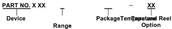
text_image
PART NO. X XX Device Range Package Temperature Reel Option XXDevice: MIC33M650: 6A, Pin Strapping Power Module with HyperLight Load ^® Mode and Output Voltage Select
Temperature Y = -40°C to +125°C (Extended) Range:
Package: MP = 53-Lead Very Thick Plastic Quad Flat B1QFN, 6 mm x 10 mm x 3 mm
Tape and Reel TR = Tape and Reel Option:
Examples:
a) MIC33M650YMP: Extended Temperature Range, 53-Lead B1QFN
b) MIC33M650YMP-TR: Extended Temperature Range, 53-Lead B1QFN, Tape and Reel
Note 1: Tape and Reel identifier only appears in the catalog part number description. This identifier is used for ordering purposes and is not printed on the device package. Check with your Microchip Sales Office for package availability with the Tape and Reel option.
NOTES:
Note the following details of the code protection feature on Microchip devices:
• Microchip products meet the specification contained in their particular Microchip Data Sheet.
- Microchip believes that its family of products is one of the most secure families of its kind on the market today, when used in the intended manner and under normal conditions.
- There are dishonest and possibly illegal methods used to breach the code protection feature. All of these methods, to our knowledge, require using the Microchip products in a manner outside the operating specifications contained in Microchip's Data Sheets. Most likely, the person doing so is engaged in theft of intellectual property.
- Microchip is willing to work with the customer who is concerned about the integrity of their code.
- Neither Microchip nor any other semiconductor manufacturer can guarantee the security of their code. Code protection does not mean that we are guaranteeing the product as "unbreakable."
Code protection is constantly evolving. We at Microchip are committed to continuously improving the code protection features of our products. Attempts to break Microchip's code protection feature may be a violation of the Digital Millennium Copyright Act. If such acts allow unauthorized access to your software or other copyrighted work, you may have a right to sue for relief under that Act.
Information contained in this publication regarding device applications and the like is provided only for your convenience and may be superseded by updates. It is your responsibility to ensure that your application meets with your specifications. MICROCHIP MAKES NO REPRESENTATIONS OR WARRANTIES OF ANY KIND WHETHER EXPRESS OR IMPLIED, WRITTEN OR ORAL, STATUTORY OR OTHERWISE, RELATED TO THE INFORMATION, INCLUDING BUT NOT LIMITED TO ITS CONDITION, QUALITY, PERFORMANCE, MERCHANTABILITY OR FITNESS FOR PURPOSE. Microchip disclaims all liability arising from this information and its use. Use of Microchip devices in life support and/or safety applications is entirely at the buyer's risk, and the buyer agrees to defend, indemnify and hold harmless Microchip from any and all damages, claims, suits, or expenses resulting from such use. No licenses are conveyed, implicitly or otherwise, under any Microchip intellectual property rights unless otherwise stated.
Trademarks
The Microchip name and logo, the Microchip logo, Adaptec, AnyRate, AVR, AVR logo, AVR Freaks, BesTime, BitCloud, chipKIT, chipKIT logo, CryptoMemory, CryptoRF, dsPIC, FlashFlex, flexPWR, HELDO, IGLOO, JukeBlox, KeeLoq, Kleer, LANCheck, LinkMD, maXStylus, maXTouch, MediaLB, megaAVR, Microsemi, Microsemi logo, MOST, MOST logo, MPLAB, OptoLyzer, PackeTime, PIC, picoPower, PICSTART, PIC32 logo, PolarFire, Prochip Designer, QTouch, SAM-BA, SenGenuity, SpyNIC, SST, SST Logo, SuperFlash, Symmetricom, SyncServer, Tachyon, TempTrackr, TimeSource, tinyAVR, UNI/O, Vectron, and XMEGA are registered trademarks of Microchip Technology Incorporated in the U.S.A. and other countries.
APT, ClockWorks, The Embedded Control Solutions Company, EtherSynch, FlashTec, Hyper Speed Control, HyperLight Load, IntelliMOS, Libero, motorBench, mTouch, Powermite 3, Precision Edge, ProASIC, ProASIC Plus, ProASIC Plus logo, Quiet-Wire, SmartFusion, SyncWorld, Temux, TimeCesium, TimeHub, TimePictra, TimeProvider, Vite, WinPath, and ZL are registered trademarks of Microchip Technology Incorporated in the U.S.A.
Adjacent Key Suppression, AKS, Analog-for-the-Digital Age, Any Capacitor, AnyIn, AnyOut, BlueSky, BodyCom, CodeGuard, CryptoAuthentication, CryptoAutomotive, CryptoCompanion, CryptoController, dsPICDEM, dsPICDEM.net, Dynamic Average Matching, DAM, ECAN, EtherGREEN, In-Circuit Serial Programming, ICSP, INICnet, Inter-Chip Connectivity, JitterBlocker, KleerNet, KleerNet logo, memBrain, Mindi, MiWi, MPASM, MPF, MPLAB Certified logo, MPLIB, MPLINK, MultiTRAK, NetDetach, Omniscient Code Generation, PICDEM, PICDEM.net, PICKit, PICtail, PowerSmart, PureSilicon, QMatrix, REAL ICE, Ripple Blocker, SAM-ICE, Serial Quad I/O, SMART-I.S., SQI, SuperSwitcher, SuperSwitcher II, Total Endurance, TSHARC, USBCheck, VariSense, ViewSpan, WiperLock, Wireless DNA, and ZENA are trademarks of Microchip Technology Incorporated in the U.S.A. and other countries.
SQTP is a service mark of Microchip Technology Incorporated in the U.S.A.
The Adaptec logo, Frequency on Demand, Silicon Storage Technology, and Symmcom are registered trademarks of Microchip Technology Inc. in other countries.
GestIC is a registered trademark of Microchip Technology Germany II GmbH & Co. KG, a subsidiary of Microchip Technology Inc., in other countries.
All other trademarks mentioned herein are property of their respective companies.
© 2019, Microchip Technology Incorporated, All Rights Reserved.
ISBN: 978-1-5224-5074-0
For information regarding Microchip's Quality Management Systems, please visit www.microchip.com/quality.
Worldwide Sales and Service
AMERICAS
Corporate Office
2355 West Chandler Blvd.
Chandler, AZ 85224-6199
Tel: 480-792-7200
Fax: 480-792-7277
Technical Support:
http://www.microchip.com/
support
Web Address:
www.microchip.com
Atlanta
Duluth, GA
Tel: 678-957-9614
Fax: 678-957-1455
Austin, TX
Tel: 512-257-3370
Boston
Westborough, MA
Tel: 774-760-0087
Fax: 774-760-0088
Chicago
Itasca, IL
Tel: 630-285-0071
Fax: 630-285-0075
Dallas
Addison, TX
Tel: 972-818-7423
Fax: 972-818-2924
Detroit
Novi, MI
Tel: 248-848-4000
Houston, TX
Tel: 281-894-5983
Indianapolis
Noblesville, IN
Tel: 317-773-8323
Fax: 317-773-5453
Tel: 317-536-2380
Los Angeles
Mission Viejo, CA
Tel: 949-462-9523
Fax: 949-462-9608
Tel: 951-273-7800
Raleigh, NC
Tel: 919-844-7510
New York, NY
Tel: 631-435-6000
San Jose, CA
Tel: 408-735-9110
Tel: 408-436-4270
Canada - Toronto
Tel: 905-695-1980
Fax: 905-695-2078
ASIA/PACIFIC
Australia - Sydney
Tel: 61-2-9868-6733
China - Beijing
Tel: 86-10-8569-7000
China - Chengdu
Tel: 86-28-8665-5511
China - Chongqing
Tel: 86-23-8980-9588
China - Dongguan
Tel: 86-769-8702-9880
China - Guangzhou
Tel: 86-20-8755-8029
China - Hangzhou
Tel: 86-571-8792-8115
China - Hong Kong SAR
Tel: 852-2943-5100
China - Nanjing
Tel: 86-25-8473-2460
China - Qingdao
Tel: 86-532-8502-7355
China - Shanghai
Tel: 86-21-3326-8000
China - Shenyang
Tel: 86-24-2334-2829
China - Shenzhen
Tel: 86-755-8864-2200
China - Suzhou
Tel: 86-186-6233-1526
China - Wuhan
Tel: 86-27-5980-5300
China - Xian
Tel: 86-29-8833-7252
China - Xiamen
Tel: 86-592-2388138
China - Zhuhai
Tel: 86-756-3210040
ASIA/PACIFIC
India - Bangalore
Tel: 91-80-3090-4444
India - New Delhi
Tel: 91-11-4160-8631
India - Pune
Tel: 91-20-4121-0141
Japan - Osaka
Tel: 81-6-6152-7160
Japan - Tokyo
Tel: 81-3-6880-3770
Korea - Daegu
Tel: 82-53-744-4301
Korea - Seoul
Tel: 82-2-554-7200
Malaysia - Kuala Lumpur
Tel: 60-3-7651-7906
Malaysia - Penang
Tel: 60-4-227-8870
Philippines - Manila
Tel: 63-2-634-9065
Singapore
Tel: 65-6334-8870
Taiwan - Hsin Chu
Tel: 886-3-577-8366
Taiwan - Kaohsiung
Tel: 886-7-213-7830
Taiwan - Taipei
Tel: 886-2-2508-8600
Thailand - Bangkok
Tel: 66-2-694-1351
Tel: 43-7242-2244-39
Fax: 43-7242-2244-393
Denmark - Copenhagen
Tel: 45-4450-2828
Fax: 45-4485-2829
Finland - Espoo
Tel: 358-9-4520-820
France - Paris
Tel: 33-1-69-53-63-20
Fax: 33-1-69-30-90-79
Germany - Garching
Tel: 49-8931-9700
Germany - Haan
Tel: 49-2129-3766400
Germany - Heilbronn
Tel: 49-7131-72400
Germany - Karlsruhe
Tel: 49-721-625370
Germany - Munich
Tel: 49-89-627-144-0
Fax: 49-89-627-144-44
Germany - Rosenheim
Tel: 49-8031-354-560
Israel - Ra'anana
Tel: 972-9-744-7705
Italy - Milan
Tel: 39-0331-742611
Fax: 39-0331-466781
Italy - Padova
Tel: 39-049-7625286
Netherlands - Drunen
Tel: 31-416-690399
Fax: 31-416-690340
Norway - Trondheim
Tel: 47-7288-4388
Poland - Warsaw
Tel: 48-22-3325737
Romania - Bucharest
Tel: 40-21-407-87-50
Spain - Madrid
Tel: 34-91-708-08-90
Fax: 34-91-708-08-91
Sweden - Gothenberg
Tel: 46-31-704-60-40
Sweden - Stockholm
Tel: 46-8-5090-4654
UK - Wokingham
Tel: 44-118-921-5800
Fax: 44-118-921-5820