MIC5018 - Electronic component Microchip - Free user manual and instructions
Find the device manual for free MIC5018 Microchip in PDF.

User questions about MIC5018 Microchip
0 question about this device. Answer the ones you know or ask your own.
Ask a new question about this device
Download the instructions for your Electronic component in PDF format for free! Find your manual MIC5018 - Microchip and take your electronic device back in hand. On this page are published all the documents necessary for the use of your device. MIC5018 by Microchip.
USER MANUAL MIC5018 Microchip
High-Side MOSFET Driver
Features
• +2.7V to +9V Operation
• 150 μA Typical Supply Current at 5V Supply
• ≤1 μA Typical Standby (Off) Current
- Charge Pump for High-Side Low-Voltage Applications
- Internal Zener Diode Gate-to-Ground MOSFET Protection
- Operates in Low- and High-Side Configurations
- TTL Compatible Input
- ESD Protected
Applications
- Battery Conservation
• Power Bus Switching
• Solenoid and Motion Control - Lamp Control
Package Type
text_image
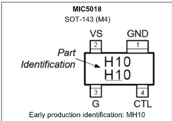
MIC5018 SOT-143 (M4) VS GND 2 1 Part Identification H10 H10 3 4 G CTL Early production identification: MH10General Description
The MIC5018 high-side MOSFET driver is designed to switch an N-channel enhancement-type MOSFET from a TTL compatible control signal in high- or low-side switch applications. This driver features the tiny 4-lead SOT-143 package.
The MIC5018 is powered from a +2.7V to +9V supply and features extremely low off-state supply current. An internal charge pump drives the gate output higher than the driver supply voltage and can sustain the gate voltage indefinitely. An internal Zener diode limits the gate-to-source voltage to a safe level for standard N-channel MOSFETs.
In high-side configurations, the source voltage of the MOSFET approaches the supply voltage when switched on. To keep the MOSFET turned on, the MIC5018's output drives the MOSFET gate voltage higher than the supply voltage. In a typical high-side configuration, the driver is powered from the load supply voltage. Under some conditions, the MIC5018 and MOSFET can switch a load voltage that is slightly higher than the driver supply voltage.
In a low-side configuration, the driver can control a MOSFET that switches any voltage up to the rating of the MOSFET. The gate output voltage is higher than the typical 3.3V or 5V logic supply and can fully enhance a standard MOSFET.
The MIC5018 is available in the SOT-143 package and is rated for -40^ to +85^ ambient temperature range.
Typical Application Circuits
Low-Voltage High-Side Power Switch

text_image
MIC5018 VS G CTL GND +5V IRFZ24* N-Channel MOSFET On Off * International Rectifier 100mΩ, 17A max. TO-220 packageLow-Side Power Switch
text_image
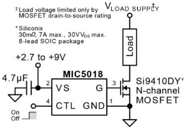
†Load voltage limited only by MOSFET drain-to-source rating *Siliconix 30mΩ, 7A max., 30VVDS max. 8-lead SOIC package +2.7 to +9V 4.7μF MIC5018 VS G CTL GND 3 1 On Off VLOAD SUPPLY Load Si9410DY* N-channel MOSFETFunctional Block Diagram
High-Side Driver Configuration
text_image
+2.7V to +9V VS MIC5018 D2 35V I1 20μA Q1 Q2 R2 15k EN CHARGE PUMP G D3 16V Q3 D1 16V CTL On Off R1 2k D1 16V GND Load1.0 ELECTRICAL CHARACTERISTICS
Absolute Maximum Ratings †
Supply Input Voltage ( V_SUPPLY )....+10V
Control Voltage ( V_CTL ) -0.6V to +16V
Gate Voltage ( V_G ) ....+16V
† Notice: Stresses above those listed under “Absolute Maximum Ratings” may cause permanent damage to the device. This is a stress rating only and functional operation of the device at those or any other conditions above those indicated in the operational sections of this specification is not intended. Exposure to maximum rating conditions for extended periods may affect device reliability.
DC CHARACTERISTICS
Electrical Specifications: Typical values at T_A = 25^ . Unless otherwise noted, minimum and maximum values indicate performance at -40^ ≤ T_A ≤ +85^ , with +2.7V ≤ Vs ≤ +9V . Parts production tested at 25^ .
| Parameter Symbol | Min. Typ. Max. | Units Conditions (Note 1) | ||||
| Supply Current I | SUPPLY | — 0.0 | 1 | 1 | μA | |
| — | 70 | 140 | ||||
| — | 0 | 1 | ||||
| — | 150 | 300 | ||||
| Control Input Voltage | V_CTL | 0 | — | 0.8 | V | 2.7V ≤ V_SUPPLY ≤ 9V, V_CTL for logic 0 input |
| 2.0 | — | V_SUP-PLY | V | 2.7V ≤ V_SUPPLY ≤ 5V, V_CTL for logic 1 input | ||
| 2.4 | — | V_SUP-PLY | V | 5V ≤ V_SUPPLY ≤ 9, V_CTL for logic 1 input | ||
| Control Input Current | I_CTL | — 0.0 | 1 | 1 | μA 2.7V | ≤ V SUPPLY ≤ 9V |
| Control Input Capacitance | — | — | 5 | — | pF | Note 1 |
| Zener Diode Output Clamp | — | 13 | 16 | 19 | V | V_SUPPLY = 9V |
| Gate Output Voltage | V_G | 6.3 | 7.1 | — | VV | SUPPLY = 2.7V |
| 7.1 | 8.2 | — | VV | SUPPLY = 3.0V | ||
| 11.4 | 13.4 — | V V | SUPPLY = 4.5V | |||
| Gate Output Current | I_G | — | 9.5 | — | μA | V_SUPPLY = 5V, V_OUT = 10V (Note 2) |
| Gate Turn-On Time | — | — 0.75 | 1.5 ms | V_SUPPLY = 4.5V, C_L = 1000 pF (Note 3) | ||
| — | — | 2.1 | 4.2 | ms | V_SUPPLY = 4.5V, C_L = 3000 pF (Note 3) | |
| Gate Turn-Off Time | — | — | 10 | 20 | μs | V_SUPPLY = 4.5V, C_L = 1000 pF (Note 4) |
| — | — | 30 | 60 | μs | V_SUPPLY = 4.5V, C_L = 3000 pF (Note 4) | |
Note 1: Guaranteed by design.
2: Resistive load selected for V_OUT = 10V .
3: Turn-on time is the time required for gate voltage to rise to 4V greater than the supply voltage. This represents a typical MOSFET gate threshold voltage.
4: Turn-off time is the time required for the gate voltage to fall to 4V above the supply voltage. This represents a typical MOSFET gate threshold voltage.
TEMPERATURE SPECIFICATIONS (Note 1)
| Parameters Sym. Min. Typ. Max. Units Conditions | ||||||
| Temperature Ranges | ||||||
| Ambient Temperature Range T | A | -40 — | +85 °C | — | ||
| Lead Temperature | — | — | — | +300 | °C | Soldering, 10 seconds |
| Package Thermal Resistance | ||||||
| Thermal Resistance, SOT-143 | _JA | — | +220 — | °C/W | — | |
| _JA | — | +130 — | °C/W | — | ||
Note 1: The maximum allowable power dissipation is a function of ambient temperature, the maximum allowable junction temperature and the thermal resistance from junction to air (i.e., T_A , T_J , _JA ). Exceeding the maximum allowable power dissipation will cause the device operating junction temperature to exceed the maximum rating. Sustained junction temperatures above that maximum can impact device reliability.
text_image
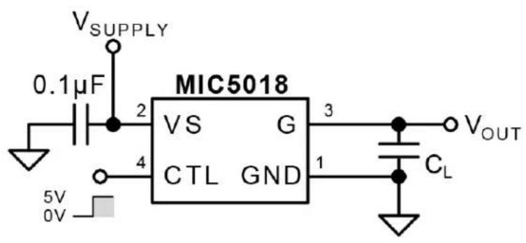
V_{SUPPLY} 0.1\mu F MIC5018 VS G CTL GND 3 4 1 V_{OUT} C_L 5V 0VFIGURE 1-1: Test Circuit.
2.0 TYPICAL PERFORMANCE CURVES (Note 1)
Note: The graphs and tables provided following this note are a statistical summary based on a limited number of samples and are provided for informational purposes only. The performance characteristics listed herein are not tested or guaranteed. In some graphs or tables, the data presented may be outside the specified operating range (e.g., outside specified power supply range) and therefore outside the warranted range.

line
| SUPPLY VOLTAGE (V) | -40°C | 25°C | 125°C | | ------------------ | ----- | ---- | ----- | | 2 | 0.0 | 0.0 | 0.0 | | 4 | 0.1 | 0.1 | 0.05 | | 6 | 0.3 | 0.25 | 0.15 | | 8 | 0.5 | 0.4 | 0.3 | | 10 | 0.7 | 0.55 | 0.4 |FIGURE 2-1: Supply Current vs. Supply Voltage.

line
| SUPPLY VOLTAGE (V) | OUTPUT VOLTAGE (V) at 125°C | OUTPUT VOLTAGE (V) at 40°C | OUTPUT VOLTAGE (V) at 25°C | | ------------------ | --------------------------- | -------------------------- | -------------------------- | | 2 | 4 | 4 | 4 | | 4 | 12 | 12 | 12 | | 6 | 16 | 15 | 15 | | 8 | 17 | 15 | 15 | | 10 | 17 | 15 | 15 |FIGURE 2-4: Gate Output Voltage vs. Supply Voltage.
line
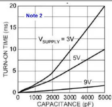
| CAPACITANCE (pF) | Turn-ON TIME (ms) at V_SUPPLY = 3V | Turn-ON TIME (ms) at V_SUPPLY = 5V | Turn-ON TIME (ms) at V_SUPPLY = 9V | | ---------------- | ---------------------------------- | ---------------------------------- | ---------------------------------- | | 0 | 0 | 0 | 0 | | 1000 | ~2 | ~1 | ~0.5 | | 2000 | ~4 | ~2 | ~1 | | 3000 | ~8 | ~4 | ~1.5 | | 4000 | ~12 | ~6 | ~2 | | 5000 | ~18 | ~10 | ~2.5 |FIGURE 2-2: Full Turn-On Time vs. Load Capacitance.

line
| OUTPUT VOLTAGE (V) | 3V | 5V | 9V | | ------------------ | ---- | ---- | ---- | | 0 | 20 | 20 | 20 | | 2 | 100 | 100 | 100 | | 4 | 40 | 40 | 40 | | 6 | 20 | 20 | 20 | | 8 | 10 | 10 | 10 | | 10 | 5 | 5 | 5 | | 12 | 2 | 2 | 2 | | 14 | 1 | 1 | 1 | | 16 | 0 | 0 | 0 |FIGURE 2-5: Gate Output Current vs. Output Voltage.
line
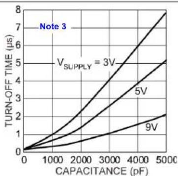
| CAPACITANCE (pF) | Turn-Off Time (μs) for V_SUPPLY = 3V | Turn-Off Time (μs) for V_SUPPLY = 5V | Turn-Off Time (μs) for V_SUPPLY = 9V | | ---------------- | -------------------------------------- | -------------------------------------- | -------------------------------------- | | 0 | 0 | 0 | 0 | | 1000 | ~1.5 | ~1.2 | ~0.8 | | 2000 | ~3.0 | ~2.0 | ~1.2 | | 3000 | ~4.5 | ~3.0 | ~1.6 | | 4000 | ~6.0 | ~4.0 | ~2.0 | | 5000 | ~7.5 | ~5.0 | ~2.5 |FIGURE 2-3: Full Turn-Off Time vs. Load Capacitance.
line
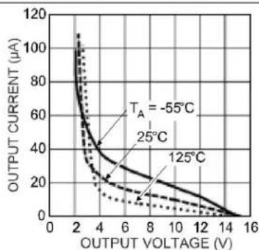
| OUTPUT VOLTAGE (V) | OUTPUT CURRENT (μA) at T_A = -55°C | OUTPUT CURRENT (μA) at 25°C | OUTPUT CURRENT (μA) at 125°C | | ------------------ | ---------------------------------- | --------------------------- | ---------------------------- | | 0 | 100 | 100 | 100 | | 2 | ~90 | ~85 | ~80 | | 4 | ~60 | ~50 | ~40 | | 6 | ~30 | ~25 | ~20 | | 8 | ~15 | ~10 | ~8 | | 10 | ~5 | ~3 | ~2 | | 12 | ~2 | ~1 | ~1 | | 14 | ~1 | ~0.5 | ~0.5 | | 16 | ~0.5 | ~0.2 | ~0.2 |FIGURE 2-6: Gate Output Current vs. Output Voltage.
2.1 Typical Performance Curve Notes
1: T_A = 25^ , V_SUPPLY = 5V unless noted.
2: Full turn-on time is the time between V_CTL rising to 2.5V and the V_G rising to 90% of its steady on-state value.
3: Full turn-off time is the time between V_CTL falling to 0.5V and the V_G falling to 10% of its steady on-state value.
3.0 PIN DESCRIPTIONS
The descriptions of the pins are listed in Table 3-1.
TABLE 3-1: PIN FUNCTION TABLE
| Pin Number5-LeadSOT-143 | Pin Name | Description |
| 1 | GND | Ground: Power return. |
| 2 | VS | Supply (Input): +2.7V to +9V supply. |
| 3 | G | Gate (Output): Gate connection to external MOSFET. |
| 4 | CTL | Control (Input): TTL compatible on/off control input. Logic high drives the gate output above the supply voltage. Logic low forces the gate output near ground. |
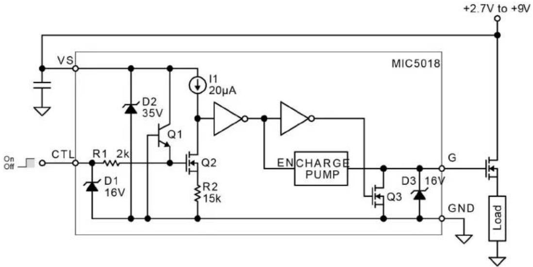
3.1 Functional Description
Refer to the "Functional Block Diagram".
The MIC5018 is a noninverting device. Applying a logic high signal to CTL (control input) produces gate drive output. The G (gate) output is used to turn on an external N-channel MOSFET.
3.1.1 SUPPLY
VS (supply) is rated for +2.7V to +9V. An external capacitor is recommended to decouple noise.
3.1.2 CONTROL
CTL (control) is a TTL compatible input. CTL must be forced high or low by an external signal. A floating input may cause unpredictable operation.
A high input turns on Q2, which sinks the output of current source I1, making the input of the first inverter low. The inverter output becomes high enabling the charge pump.
3.1.3 CHARGE PUMP
The charge pump is enabled when CTL is logic high. The charge pump consists of an oscillator and voltage quadrupler (4×). Output voltage is limited to 16V by a Zener diode. The charge pump output voltage will be approximately:
EQUATION 3-1:
$$ V _ {G} = 4 \times V _ {S U P P L Y} - 2. 8 V $$
But not exceeding 16V.
The oscillator operates from approximately 70 kHz to approximately 100 kHz depending upon the supply voltage and temperature.
3.1.4 GATE OUTPUT
The charge pump output is connected directly to the G (gate) output. The charge pump is active only when CTL is high. When CTL is low, Q3 is turned on by the second inverter and discharges the gate of the external MOSFET to force it off.
If CTL is high, and the voltage applied to VS drops to zero, the gate output will be floating (unpredictable).
3.1.5 ESD PROTECTION
D1 and D2 clamp positive and negative ESD voltages. R1 isolates the gate of Q2 from sudden changes on the CTL input. Q1 turns on if the emitter (CTL input) is forced below ground to provide additional input protection. Zener D3 also clamps ESD voltages for the gate (G) output.
4.0 APPLICATION INFORMATION
4.1 Supply Bypass
A capacitor from VS to GND is recommended to control switching and supply transients. Load current and supply lead length are some of the factors that affect capacitor size requirements.
A 4.7 F or 10 F aluminum electrolytic or tantalum capacitor is suitable for many applications. The low ESR (equivalent series resistance) of tantalum capacitors makes them especially effective, but also makes them susceptible to uncontrolled inrush current from low impedance voltage sources (such as NiCd batteries or automatic test equipment). Avoid instantaneously applying voltage, capable of high peak current, directly to or near tantalum capacitors without additional current limiting. Normal power supply turn-on (slow rise time) or printed circuit trace resistance is usually adequate for normal product usage.
4.2 MOSFET Selection
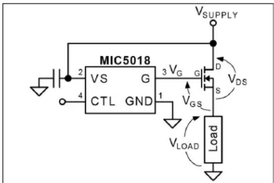
The MIC5018 is designed to drive N-channel enhancement type MOSFETs. The gate output (G) of the MIC5018 provides a voltage, referenced to ground, that is greater than the supply voltage. Refer to Figure 2-4.
The supply voltage and the MOSFET drain-to-source voltage drop determine the gate-to-source voltage.
EQUATION 4-1:
$$ V _ {G S} = V _ {G} - (V _ {S U P P L Y} - V _ {D S}) $$
Where:
$$ V _ {G S} = \text { gate - to - source voltage (enhancement) } $$
$$ V _ {G} = \text { gate voltage (from graph) } $$
$$ V _ {S U P P L Y} = \text { supply voltage } $$
$$ \begin{array}{l} V _ {D S} = \text { drain - to - source voltage (approx.0V at low } \ \text { current,orwhen fully enhanced) } \end{array} $$
text_image
MIC5018 VS G CTL GND 2 3 VG G 4 1 VGS VLOAD VDS D S VSUPPLYFIGURE 4-1: Voltages
The performance of the MOSFET is determined by the gate-to-source voltage. Choose the type of MOSFET according to the calculated gate-to-source voltage.
4.3 Standard MOSFET
Standard MOSFETs are fully enhanced with a gate-to-source voltage of about 10V. Their absolute maximum gate-to-source voltage is ±20V.
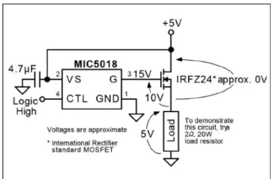
With a 5V supply, the MIC5018 produces a gate output of approximately 15V. Figure 4-2 shows how the remaining voltages conform. The actual drain-to-source voltage drop across an IRFZ24 is less than 0.1V with a 1A load and 10V enhancement. Higher current increases the drain-to-source voltage drop, increasing the gate-to-source voltage.
text_image
4.7μF Logic High MIC5018 VS G CTL GND 3 15V +5V IRFZ24* approx. 0V 10V 5V Load To demonstrate this circuit, tya 2Ω, 20W load resistor Voltages are approximate * International Rectifier standard MOSFETFIGURE 4-2: Using a Standard MOFSET.
The MIC5018 has an internal Zener diode that limits the gate-to-ground voltage to approximately 16V. Lower supply voltages, such as 3.3V, produce lower gate output voltages which will not fully enhance standard MOSFETs. This significantly reduces the maximum current that can be switched. Always refer to the MOSFET data sheet to predict the MOSFET's performance in specific applications.
4.4 Logic-Level MOSFET
Logic-level N-channel MOSFETs are fully enhanced with a gate-to-source voltage of approximately 5V and generally have an absolute maximum gate-to-source voltage of ±10V.

text_image
MIC5018 VS G CTL GND +3.3V 9V 5.7V +3.3V Logic High 4.7μF IRLZ44* approx. 0V Voltages are approximate * International Rectifier logic-level MOSFET 3.3V Load To demonstrate this circuit, try 5Ω, 5W or 47Ω, 1/4W load resistors.FIGURE 4-3: Using a Logic-Level MOSFET.
Refer to Figure 4-3 for an example showing nominal voltages. The maximum gate-to-source voltage rating of a logic-level MOSFET can be exceeded if a higher supply voltage is used. An external Zener diode can clamp the gate-to-source voltage as shown in Figure 4-4. The Zener voltage, plus its tolerance, must not exceed the absolute maximum gate voltage of the MOSFET.
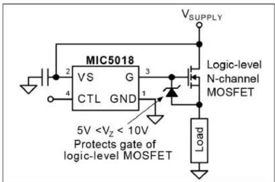
text_image
MIC5018 VS G CTL GND 2 3 4 1 V_{SUPPLY} Logic-level N-channel MOSFET Load 5V4.5 Inductive Loads
Inductive loads include relays, and solenoids. Long leads may also have enough inductance to cause adverse effects in some circuits. text_image
MIC5018 VS G CTL GND +2.7V to +9V 4.7µF On Off Schottky Diode4.6 Split Power Supply
Refer to Figure 4-6. The MIC5018 can be used to control a 12V load by separating the driver supply from the load supply. text_image
MIC5018 VS G CTL GND 4.7µF Logic High +5V 2 315V +12V 3V 12V IRLZ44* approx. 0V To demonstrate this circuit, trya 40Ω, 5W or 100Ω, 2W load resistor. Voltages are approximate * International Rectifier logic-level MOSFETEQUATION 4-2:
$$ V _ {G S} \quad V _ {G} \quad V _ {L D S U P P L Y} - (V _ {D}) = $$ VG is determined from the driver supply voltage using Figure 2-4.4.7 Low-Side Switch Configuration
The low-side configuration makes it possible to switch a voltage much higher than the MIC5018's maximum supply voltage. text_image
* International Rectifier standard MOSFET BVoss = 100V +2.7 to +9V 4.7μF MIC5018 VS G CTL GND 3 1 +80V Load To demonstrate this circuit, try 1k, 10W or 33k, 1/4W load resistors. IRF540* N-channel MOSFET On Off5.0 PACKAGING INFORMATION
5.1 Package Marking Information
4-Lead SOT-143\* (front) XXX Example H10 4-Lead SOT-143\* (back) NNN 723 Example natural_image
Empty white rectangle with black border (no text or symbols)4-Lead SOT-143 Package Outline and Recommended Land Pattern
4-Lead Plastic Small Outline Transistor (RC) [SOT-143]
Note: For the most current package drawings, please see the Microchip Packaging Specification located at http://www.microchip.com/packaging text_image
SILK SCREEN E1 X1 C Y X2 E2| Units | MILLIMETERS | |||
| Dimension Limits | MIN | NOM | MAX | |
| Contact Pitch | E1 | 1.90 BSC | ||
| Contact Pitch | E2 | 1.60 BSC | ||
| Contact Width | X1 | 0.60 | ||
| Contact Width | X2 | 1.00 | ||
| Contact Length | Y | 1.30 | ||
| Contact Pad Spacing | C | 2.10 | ||
4-Lead Plastic Small Outline Transistor (RC) [SOT-143]
Note: For the most current package drawings, please see the Microchip Packaging Specification located at http://www.microchip.com/packaging text_image
D e e/2 N E1 E 1 2 e1natural_image
Isometric line drawing of a rectangular electronic component with two metal brackets (no text or symbols)text_image
A A1 b2 A2 3X btext_image
φ L1 L c| Units | MILLIMETERS | |||
| Dimension Limits | MIN NOM | MAX | ||
| Number of Pins N 4 | ||||
| Pitch e 1.92 BSC | ||||
| Lead 1 Offset | e1 | 0.20 BSC | ||
| Overall Height | A | 0.80 | - | 1.22 |
| Molded Package Thickness | A2 | 0.75 | 0.90 | 1.07 |
| Standoff § | A1 | 0.01 | - | 0.15 |
| Overall Width | E | 2.10 | - | 2.64 |
| Molded Package Width | E1 | 1.20 | 1.30 | 1.40 |
| Overall Length | D | 2.67 | 2.90 | 3.05 |
| Foot Length | L | 0.13 | 0.50 | 0.60 |
| Footprint | L1 | 0.54 REF | ||
| Foot Angle | 0^ | - | 8^ | |
| Lead Thickness c 0.08 | - | 0.20 | ||
| Lead 1 Width | b1 | 0.76 | - | 0.94 |
| Leads 2, 3 & 4 Width | b | 0.30 | - | 0.54 |