PL485-EK - Évaluation de kit Microchip - Free user manual and instructions
Find the device manual for free PL485-EK Microchip in PDF.

User questions about PL485-EK Microchip
0 question about this device. Answer the ones you know or ask your own.
Ask a new question about this device
Download the instructions for your Évaluation de kit in PDF format for free! Find your manual PL485-EK - Microchip and take your electronic device back in hand. On this page are published all the documents necessary for the use of your device. PL485-EK by Microchip.
USER MANUAL PL485-EK Microchip
PL485-EK is an evaluation kit for the PL485. PL485 is a programmable System On Chip (SOC) for narrow-band Power Line Communication (PLC) from Microchip Technology Inc, able to run any PLC protocol in the frequency band below 500 kHz. Depending on the running firmware, PL485 is able to support applications not only for basic connectivity (point to point or point to multi-point connectivity) but also for complex mesh network topologies.
The PL485-EK board has been conceived to communicate in the CENELEC B-Band (95 kHz to 125 kHz) and complies with the CENELEC EN 50065 standard. It is designed to be directly connected to low voltage DC power rails and optionally to AC mains by means of an external coupler accessory. Please refer to PLC-AC-Coupler User Guide for more information about the AC coupler accessory.
Contents
- Welcome letter
- Board:
- One PL485-EK board
- Cable:
– One Micro A/B-type USB cable
Kit contents are protected with anti-static foam. The PL485-EK board is shipped in an anti-static shielding bag.

The board must not be subject to high electrostatic discharges. It is recommended to use a grounding strap or similar ESD protective device when handling the board in hostile ESD environments. Avoid touching the component pins or any other metallic element on the board.
Features
- PL485-EK board includes a PL485 system on chip, able to run any PLC protocol in the < 500kHz band.
- PL485-EK board implements a coupling circuit optimized for the band 95kHz to 125 kHz, compliant with CENELEC standard EN50065.
- SWD/JTAG interface for MCU debugging and programming purposes. PL485-EK board includes as well a USB Embedded Debugger (EDBG) for on-board debugging.
- USB 2.0 full-speed interface
- mikroBUS ^TM socket connector to interface with other circuits and add-on boards.
- Xplained PRO header connector (master) to interface with other circuits and add-on boards.
- RESET push button, ERASE jumper.
- Voltage monitor circuit on the 5V rail, or alternatively on the 3.3V rail with minor modifications.
- PL485-EK board can be powered from the following sources:
- Micro-B USB connector (J5)
- Micro-B USB connector (J12)
– Xplained PRO PWR connector (J7)
- DC Jack connector (J3) or 2 position terminal block (J2)
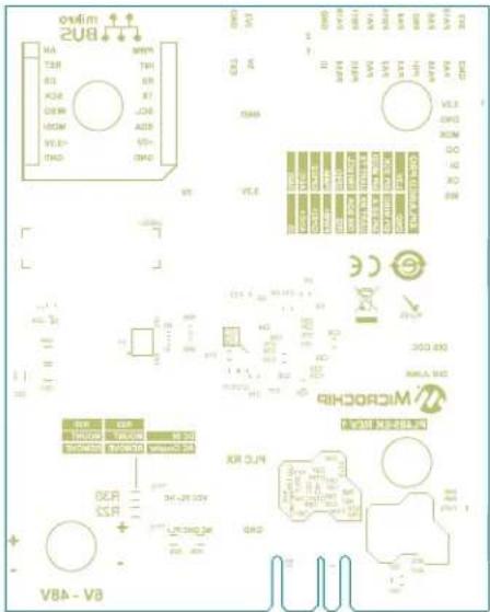
Figure 1. PL485-EK Board top view
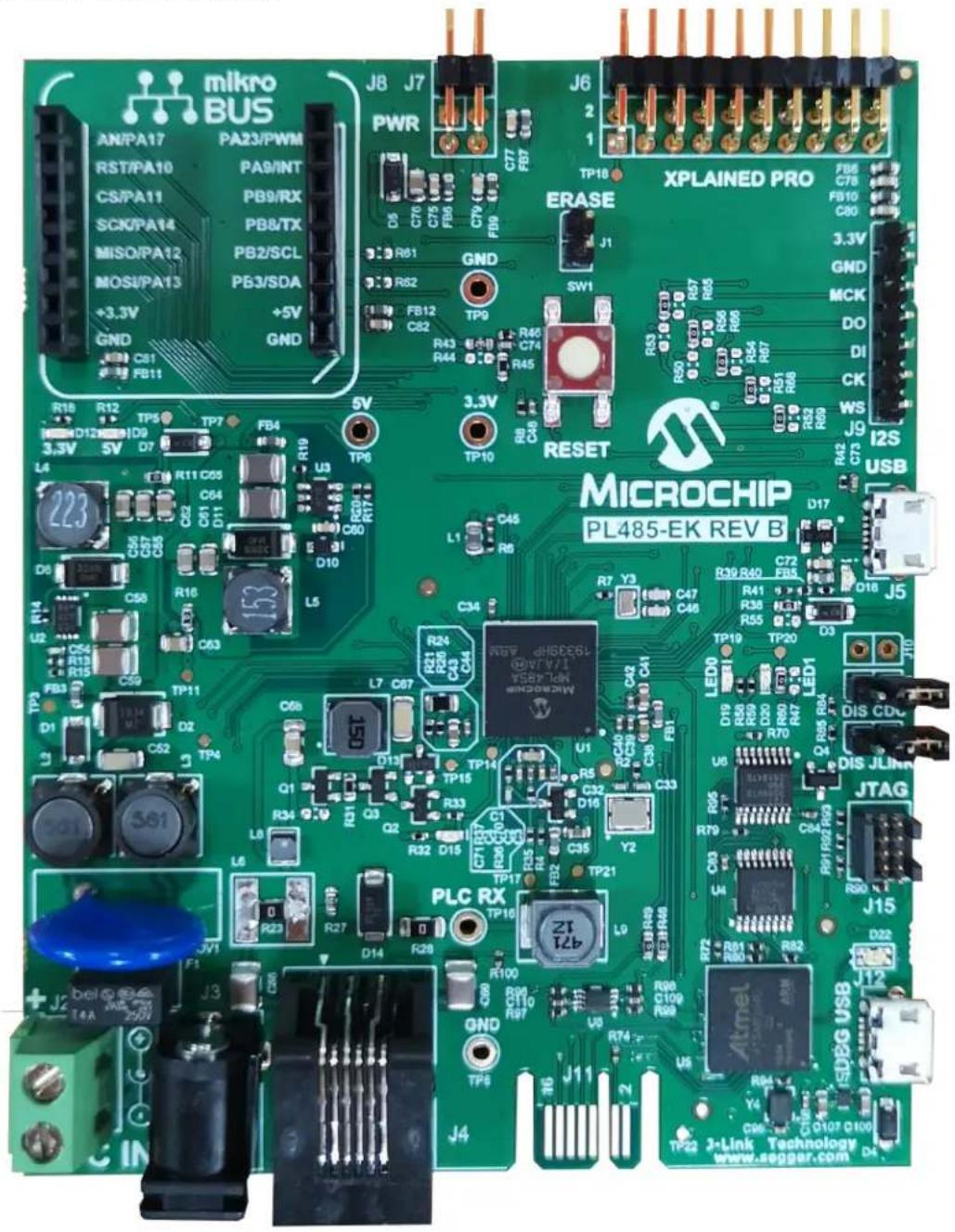
text_image
mikro BUS AN/PA17 PA23/PWM RST/PA10 PA9/INT CS/PA11 PB9/RX SCX/PA14 PB8/TX MISO/PA12 PB2/SCL MOSI/PA13 PB3/SDA +3.3V +5V GND GND R18 R12 TP5 TP7 TP6 5V D12 D9 D7 TP7 L4 C51 R11 C55 U3 C67 C64 D11 R00 R7 D8 C58 R16 C63 L5 U2 C54 D10 R10 R6 R13 C52 C53 L5 FB3 C59 TP11 D1 Q2 TP4 S61 S62 T6 Q1 Q2 Q3 Q4 Q5 Q6 Q7 L6 R23 R27 D14 R28 J2 bel T4A 250V J3 J4 J6 J7 PWR D6 C76 C75 F80 FB8 FB9 R81 R82 FB12 C82 TP9 R43 R44 R45 TP10 R46 C74 R45 SW1 R33 R50 R57 R65 R66 R67 R68 R69 RESET MICROCHIP PL485-EK REV B TP18 XPLAINED PRO F86 C78 FB10 C80 3.3V GND MCK DO DI CK WS J9 I2S USB J5 R42 C73 USB LED DIS CDJTAG J15 D22 J12 SDEG USB TP22 J-Link Technology www.seggar.com D4Table of Contents
Introduction....1
Contents....1
Features....1
- Evaluation Kit Specifications....4
1.1. Safety Recommendations....4
1.2. Electrical Characteristics....4
- Getting Started....5
2.1. Running the Demo Application....5
2.2. Code and Technical Support....5
- PL485-EK Board....6
3.1. Overview....6
3.2. Features List....6
3.3. Hardware Description – System....12
3.4. Hardware Description – MCU Peripherals.... 20
3.5. Hardware Description – MCU Interface Ports....21
3.6. Hardware Description - JLINK Debugger....23
3.7. PL485-EK Schematics....27
3.8. PL485-EK Layout.... 32
-
Standards Compliance....36
-
References....37
-
Revision History......38
6.1. Rev A - 01/2020....38
6.2. Rev B - 05/2020....38
The Microchip Website....39
Product Change Notification Service....39
Customer Support....39
Microchip Devices Code Protection Feature....39
Legal Notice....39
Trademarks....40
Quality Management System....40
Worldwide Sales and Service....41
1. Evaluation Kit Specifications
1.1 Safety Recommendations
This evaluation board is intended for engineering, development, demonstration or evaluation purposes only. It is not a finished product, unless otherwise noted on the board/kit, so it is intended for indoor use only.

The PL485-EK board is not electrically isolated from the power supply inputs. Please handle the PL485-EK board with care to avoid risk of electrical shock, which may arise in case of earth faults or accidental contact with high voltage on the power rail.
Operating temperature range is 0^ C to +70^ C, limited by the rubber pads and the reset switch. The rest of the components can work properly from 0 to 85^ C. Operation for extended periods of time over the minimum and maximum values may cause permanent damage to the board.

Important: Microchip does not assume any responsibility for the consequences arising from an improper use of the PL485-EK board.
1.2 Electrical Characteristics
This section contains information about PL485-EK power supply requirements and consumption. It is assumed that the board is powered from the DC Jack connector. For more details about the power supply system, please check section 3.3.5 Power Supply System.
Table 1-1. DC Power Supply Requirements
| Parameter Condition Min. Typ. Max. Unit | ||||
| DC Mains Voltage Range DC Jack Connector, J8 6 - 48 V | DC |
Table 1-2. Power Consumption
| Parameter Condition | Typ. Unit | ||
| RX Power Consumption | Measured at R16, 3.3V DC/DC output | 245(1) | mW |
| TX Power Consumption | FW: G3 CEN-B PHY test Console ApplicationMeasured at R16, 3.3V DC/DC output | 345(1) |
Note:
- These measurements were taken running PHY TX Test Console project included in the kit with a default configuration in TX mode and RX mode. The power consumption is measured at the output of the 3.3V DC/DC converter.
2. Getting Started
2.1 Running the Demo Application
The board has to be powered by means of the included USB cable or from an external DC Power Supply ranging from 6V to 48V. When the board is powered, the LEDs D9 (3V3) and D12 (5V) turn on. Connect a suitable cable to one of the connectors J2 or J3 and plug it to a DC voltage grid to communicate.
Once the board is supplied, the PL485-EK board runs the pre-programmed application PLC & Go for CENELEC B-Band, a chat application between two or more end points using Microchip PLC modem boards. Any end point can transmit a message, which is received by the other end points in the network. LED0 (D19, green) blinks to indicate that the application is running. LED1 (D20, red) flashes when a PLC message is received and LED D15 (yellow) flashes at each transmission.
2.2 Code and Technical Support
Firmware developers can not only run the given example code, but also implement their own applications based on the provided firmware stacks.
Please note that the latest software code, documentation and support materials are available on www.microchip.com. Follow instructions described in the welcome letter for more information.
For any technical support requests, please visit http://support.microchip.com.
3. PL485-EK Board
3.1 Overview
This section summarizes the PL485-EK board design. It introduces system-level concepts, such as power supply, MCU, PLC coupling, peripherals and board interfaces.
Figure 3-1. PL485-EK Board Description
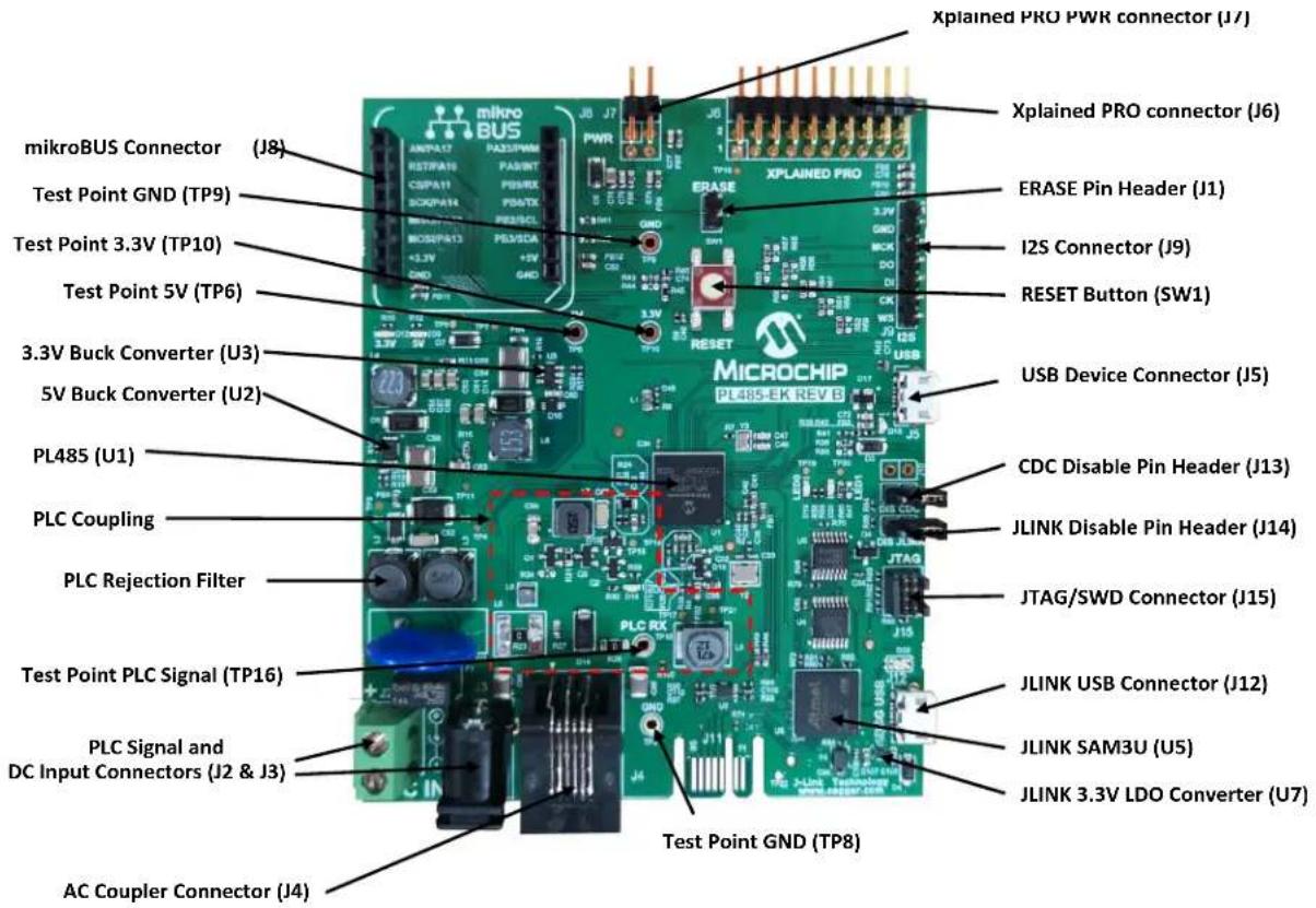
text_image
Xplained PRO PWR connector (J7) Xplained PRO connector (J6) ERASE Pin Header (J1) I2S Connector (J9) RESET Button (SW1) USB Device Connector (J5) MICROCHIP PL485-EK REV B CDC Disable Pin Header (J13) JLINK Disable Pin Header (J14) JTAG/SWD Connector (J15) JLINK USB Connector (J12) JLINK SAM3U (U5) JLINK 3.3V LDO Converter (U7) Test Point GND (TP8) Test Point GND (TP9) Test Point 3.3V (TP10) Test Point 5V (TP6) 3.3V Buck Converter (U3) 5V Buck Converter (U2) PL485 (U1) PLC Coupling PLC Rejection Filter Test Point PLC Signal (TP16) PLC Signal and DC Input Connectors (J2 & J3) AC Coupler Connector (J4)3.2 Features List
The PL485-EK board includes the following features:
- PL485 SOC:
- MCU Core:
• ARM Cortex-M4 running at up to 100 MHz
• Memory Protection Unit (MPU)
- DSP instruction set
- Floating-Point Unit (FPU)
- Thumb ^ -2 instruction set
- Instruction and Data Cache Controller with 2 Kbytes cache memory
- Memories:
- Up to 512 Kbytes of embedded Flash
- Up to 176 Kbytes of embedded SRAM
- Up to 8 Kbytes of ROM with embedded bootloader, single-cycle access at full speed
- Multi-protocol PLC modem:
- Protocols:
- G3-PLC
- PRIME 1.3 and PRIME 1.4
• Zero-Cross Detection
- Embedded PLC Analog Front End (AFE)
- Low-power consumption in transmission and reception
- PLC Coupling designed to communicate in CENELEC B-Band (95 kHz to 125 kHz)
- A 3.3V buck converter for the digital circuitry and a 5V Buck converter for supplying 5V for mikro BUS and Xplained PRO connector
- Peripherals:
– Supply monitor
- User LEDs
- Reset button
- Chip Erase jumper
- Disable JLINK jumper
- Disable CDC jumper
- Interfaces:
- USB Device
- mikroBUS Socket Connector
– SWD/JTAG Debugging Port
– JLINK USB Embedded MPU Programmer
– Xplained PRO Master
- I2S Connector
3.2.1 PL485-EK Block Diagram
The following figure shows the block diagram of the PL485-EK board.
Figure 3-2. PL485-EK Block Diagram

flowchart
graph TD
    A["Optional"] --> B["AC Voltage"]
    B --> C["External Board Isolater Adapter with Zero Cross"]
    C --> D["PLC Coupling"]
    D --> E["MPL485"]
    E --> F["Interface & Peripherals"]
    F --> G["5V"]
    F --> H["5v Buck"]
    F --> I["3v3 Buck"]
    I --> J["Voltage Monitor"]
    J --> D
    F --> K["Embedded MPU Programmer JLINK"]
    K --> L["Xplained PRO Master"]
    L --> F
    F --> M["User LEDs (2)"]
    F --> N["User Reset"]
    F --> O["ERASE jumper"]
    F --> P["fS BUS"]
    F --> Q["USB micro-B"]
    F --> R["mikroBUS Socket"]
    F --> S["Xplained PRO Master"]
    F --> T["JTAG 10-pin"]
    F --> U["Embedded MPU Programmer JLINK"]
    F --> V["5V"]
    W["PLC Signal"] --> X["PLC Signal"]
    X --> Y["+6V to +48V DC"]
    Y --> Z["5V Buck"]
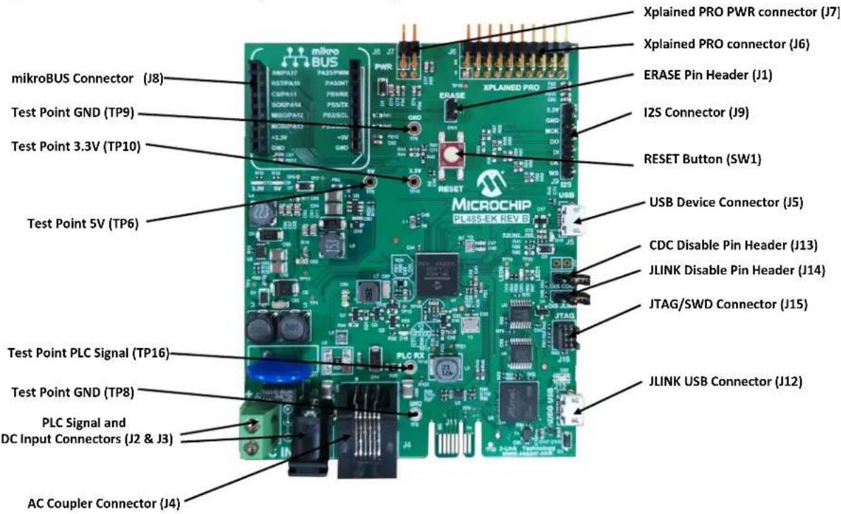
3.2.2 Interface Connection
The following figure shows an overview of the connectors, jumpers and button of the PL485-EK board.
Figure 3-3. PL485-EK Connectors, Button and Jumpers Overview
text_image
mikroBUS Connector (J8) Test Point GND (TP9) Test Point 3.3V (TP10) Test Point 5V (TP6) Test Point PLC Signal (TP16) Test Point GND (TP8) PLC Signal and DC Input Connectors (J2 & J3) AC Coupler Connector (J4) Xplained PRO PWR connector (J7) Xplained PRO connector (J6) ERASE Pin Header (J1) I2S Connector (J9) RESET Button (SW1) MICROCHIP PL40SEK REV 6 XPLAINED PRO ERASE USB Device Connector (J5) CDC Disable Pin Header (J13) JLINK Disable Pin Header (J14) JTAG/SWD Connector (J15) JLINK USB Connector (J12)3.2.2.1 Connectors
The PL485-EK board includes the following connectors:
- PLC Connector and DC Input, J2 (same than J3).
Table 3-1. PLC Connector and DC Input, J2 (same than J3)
| Pin Signal | Name Description | |
| 1 + Positive Voltage / PLC+ Signal | ||
| 2 - Negative Voltage / PLC- Signal | ||
- PLC Connector and DC Input, J3 (same than J2).
Table 3-2. PLC Connector and DC Input, J3 (same than J2)
| Pin Signal Name Description | |
| 1 + Positive Voltage / PLC+ Signal | |
| 2 - Negative Voltage / PLC- Signal |
- PLC AC Coupler Connector, J4.
Table 3-3. PLC AC Coupler Connector, J4
| Pin Signal | Name Description | |
| 1 N.C. Not Connected | ||
| 2 PL+ | PLC + Signal | |
| ......continued | ||
| Pin Signal | Name Description | |
| 3 PL- PLC | - Signal | |
| 4 GND Ground | ||
| 5 PL VZC | Zero Cross Signal | |
| 6 N.C. Not Connected | ||
4. USB Device Connector, J5.
Table 3-4. USB Device Connector, J5
| Pin Signal Name Description | ||
| 1 VUSB 5V power | ||
| 2 D- Data Minus | ||
| 3 D+ | Data Plus | |
| 4 ID On the Go Identification | ||
| 5 GND Ground | ||
5. Xplained Pro Standard Extension Header, J6
Table 3-5. Xplained Pro Standard Extension Header, J6
| Pin | Signal Name | Mnemonic | Description |
| 1 | TP18 | ID | Not connected. Pin to communicate with the ID chip on an extension board |
| 2 | GND | GND | Ground |
| 3 | PA18 | ADC(+) | Analog to digital converter; alternatively, a pin for the positive terminal of a differential ADC |
| 4 | PA19 | ADC(-) | Analog to digital converter; alternatively, a pin for the negative terminal of a differential ADC |
| 5 | PB10 | GPIO1 | General purpose I/O |
| 6 | PB11 | GPIO2 | General purpose I/O |
| 7 | PA0 | PWM(+) | Pulse width Modulation; alternatively, a pin for the positive part of a differential PWM |
| 8 | PA1 | PWM(-) | Pulse width Modulation; alternatively, a pin for the negative part of a differential PWM |
| 9 | PA2 | IRQ/GPIO | Interrupt request pin and/or general purpose I/O pin |
| 10 | PB14 | GPIO | General purpose I/O |
| 11 | PA3 | SDA | Data line for I^2C interface |
| 12 | PA4 | SCL | Clock line for I^2C interface |
| 13 | PB1 | UART_RX | Receiver pin of target device UART |
| 14 | PB0 | UART_TX | Transmitter pin of target device UART |
| 15 | PA16 | SPI_SS_A | Slave select for SPI |
| 16 | PA6 | SPI_MOSI | Master out slave in line of serial peripheral interface |
| Pin Signal | Name Mnemonic Description | |
| 17 PA5 SPI_MISO Master in slave out line of serial peripheral interface | ||
| 18 PA15 SPI_SCK Clock for serial peripheral interface | ||
| 19 GND GND Ground | ||
| 20 3V3 VCC Power pin for extension board | ||
- Xplained Pro Power Header, J7.
Table 3-6. Xplained Pro Power Header, J7
| Pin Signal | Name Mnemonic | Description | |
| 1 | GND GND | Ground | |
| 2 | 5V_XPLAIN VEXT_P5V0 | External 5V input | |
| 3 | 3V3 | Target VTG | Regulated 3.3V (output) |
| 4 | 5V | VCC_P5V0 | Unregulated 5V (output) |
- mikroBUS Socket Connector, J8.
Table 3-7. mikroBUS Socket Connector, J8
| Pin Signal | Name Mnemonic | Description | |
| 1 PA17 | AN | Analog | |
| 2 PA10 | RST | Reset | |
| 3 | PA11 | CS | SPI Chip Select |
| 4 PA14 SCK | SPI Clock | ||
| 5 PA12 | MISO | SPI Master Input Slave Output | |
| 6 PA13 | MOSI | SPI Master Output Slave Input | |
| 7 | 3.3V | +3.3V | Regulated 3.3V (output) |
| 8 | GND GND | Ground | |
| 9 | GND GND | Ground | |
| 10 | 5V | +5V | Unregulated 5V (output) |
| 11 PB3 | SDA | I^2C Data | |
| 12 | PB2 SCL | I^2C Clock | |
| 13 | PB8 | TX | UART Transmit |
| 14 | PB9 | RX | UART Receive |
| 15 PA9 | INT | Hardware Interrupt | |
| 16 PA23 | PWM | Pulse-width Modulation | |
- Inter-IC Sound (I ^2 S), J9.
Table 3-8. Inter-IC Sound (PS), J9
| Pin Signal | Name Mnemonic | Description | |
| 1 | 3.3V | 3.3V | VCC - 3.3V power |
| Pin Signal | Name Mnemonic Description | |
| 2 GND GND Ground | ||
| 3 PA4 MCK Master Clock (Output) | ||
| 4 PA3 DO Serial Data Output | ||
| 5 PA2 DI Serial Data Input | ||
| 6 PA0 CK Serial Clock (Input/Output) | ||
| 7 PA1 WS | I | ^2S Word Select (Input/Output) |
9. USB Debug Connector (DBG USB), J12.
Table 3-9. USB Debug Connector (DBG USB), J12
| Pin | Signal Name | Description |
| 1 | VUSB | 5V power |
| 2 | D- | Data Minus |
| 3 | D+ | Data Plus |
| 4 | ID | On the Go Identification |
| 5 | GND | Ground |
10. JTAG/SWD 10-pin connector for PL485, J15.
Table 3-10. JTAG/SWD 10-pin connector for PL485, J15
| Pin | Mnemonic | Description |
| 1 | VCC | This is the target reference voltage. It is used to check if the target has power, to create the logic-level reference for the input comparators and to control the output logic levels to the target. It is normally fed from V_CC of the target board and must not have a series resistor. |
| 2 | TMS/SWDIO | Serial Wire Input Output / Test Mode Select. JTAG mode set input of target CPU. This pin should be pulled up on the target. Typically connected to TMS of target CPU. |
| 3 | GND | Ground. |
| 4 | TCK/SWCLK | Serial Wire Clock / Test Clock. JTAG clock signal to target CPU. It is recommended that this pin is pulled to a defined state of the target board. Typically connected to TCK of target CPU. |
| 5 | GND | Ground. |
| 6 | TDO/SWO | Test Data Output. JTAG data output from target CPU. Typically connected to TDO of target CPU. |
| 7 KEY | - | |
| 8 | TDI/NC | Not Connected / Test Data Input. JTAG data input of target CPU. It is recommended that this pin is pulled to a defined state on the target board. Typically connected to TDI of target CPU. |
| 9 | GNDdetect | Ground. |
| 10 | nRESET | Target CPU reset signal. Typically connected to the RESET pin of the target CPU, which is typically called "nRST", "nRESET" or "RESET". This signal is an active low signal. |
3.2.2.2 Jumper Configurations
The following table describes the functionality of the jumpers.
Table 3-11. Jumper Configuration
| Jumper Label Default Setting Function | |||
| J1 ERASE Open | PL485 Flash memory code erase(closed = erase) | ||
| J13 DIS CDC Open | Enable debug UART in JLINK(closed = Disable UART in JLINK (J12 DBG USB)) | ||
| J14 DIS JLINK Open | Select between JLINK or JTAG programmer(closed = Disable JLINK enable J15 JTAG programmer) | ||
Note: Pitch jumpers are 2.54 mm (0.1").
3.2.2.3 Test Points
Some test points (probes and pads) have been placed on the PL485-EK board for the verification of the main signals.
Table 3-12. Test Point Probes
| Reference Function | |
| TP6 5V | |
| TP8 GND | |
| TP9 GND | |
| TP10 3V3 | |
| TP16 PLC signal |
Table 3-13. Test Point Pads
| Reference | Function | Reference | Function |
| TP1 | Pin PL NRST | TP13 | PL- |
| TP2 | Pin JTAGSEL | TP14 | Pin PL TXRX0 |
| TP3 | VDC | TP15 | Pin PL TXRX1 |
| TP4 | GND | TP17 | PLC Signal |
| TP5 | 5V REG | TP18 | Xplained PRO ID |
| TP7 | GND | TP19 | Pin PA31, LED0 D19 |
| TP8 | GND | TP20 | Pin PA19, LED1 D20 |
| TP9 | GND | TP21 | Pin PL VZC |
| TP11 | 3.3V | TP22 | 3.3V JLINK |
| TP12 | PL+ | - | - |
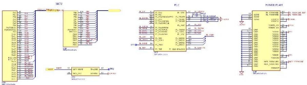
3.3 Hardware Description – System
3.3.1 PL485
The PL485-EK board is equipped with a PL485 device in 121-Ball TFBGA (10x10, 0.8 mm ball pitch).
The PL485 embeds a PL360, a multi-protocol modem for Power Line Communication, and it also embeds a SAMG55, a Cortex-M4 CPU with an FPU (floating point unit). This flexible architecture allows implementation of standard and customized PLC solutions.
Figure 3-4 shows the different components of PL485 Schematic.
Figure 3-4. PL485
The following figure shows the recommended connection in the PCB between balls of the PL485 to connect SAMG55 and PL360 internal blocks and the functionalities of GPIO connections.
Figure 3-5. PL485: SAMG55-PL360 Ball Connections at PCB Level
| PL485 Ballout | PL360 Signal | SAMG55 Signal | PL485 Ballout |
| D4PL_NRST | PA25F3 | ||
| E3PL_TST | PB15F2 | ||
| E4PL_LDO_ENABLE | PB13F4 | ||
| E5PL_PA0 | PA24F5 | ||
| E6PL_PA3 | PA26F6 | ||
| E7PL_PA8/MOSI | PA28F7 | ||
| E8PL_PA9/MISO | PA27F8 | ||
| G4PL_PA7/SPCK | PA29G5 | ||
| G6PL_PA6/NPCS0 | PA30G7 |
Table 3-14 and Table 3-15 summarize the functionality of each input/output line of the PL485-EK board.
Table 3-14. Pinout of PL485 PortA in PL485-EK Board
| I/O LINE Function | I/O LINE Function | ||
| PA0/I2SCK0/TIOA0 | I2SCK0 / PWM+ (XPLAIN) | PA16/NPCS02 | SPI2_NCPS0 (XPLAIN) |
| PA1/I2SWS0/TIOB0 | I2SWS0 / PWM- (XPLAIN) | PA17/AD0 | AD0 (mikroBUS) |
| PA2/I2SDI0/WKUP | I2SDI0 / IRQ (XPLAIN) | PA18/AD1 | AD1 (XPLAIN) |
| PA3/I2SDO0/TWD | I2SDO0 / I2C_SDA (XPLAIN) | PA19/AD2 | UserLed1 / AD2 (XPLAIN) |
| PA4/I2SMCK0/TWCK3 | I2SMCK0 / I2C_SCL (XPLAIN) | PA20/AD3 | AD3 (Voltage Monitor) |
| PA5/MISO2 | SPI2_MISO (XPLAIN) | PA21/DM | DUSB_N (USB Device Diff Negative) |
| PA6/MOSI2 SPI2_MOSI (XPLAIN) PA22/DP | DUSB_P (USB Device Diff Positive) | ||
| PA7/XIN32 XIN32 PA23/TIOA1 PWM (mikroBUS) | |||
| PA8/XOUT32 XOUT32 PA24 PL_CD | |||
| PA9/WKUP6 INT (mikroBUS) PA25 PL_NRST | |||
| PA10 RST (mikroBUS) PA26 PL_EXTIN | |||
| PA11/NPCS05 SPI5_NPCS0 (mikroBUS) | PA27/MISO7 | PL_MISO | |
| PA12/MISO5 | SPI5_MISO (mikroBUS) | PA28/MOSI7 | PL_MOSI |
| PA13/MOSI5 | SPI5_MOSI (mikroBUS) | PA29/SPCK7 | PL_SPCK |
| PA14/SPCK5 | SPI5_SPCK (mikroBUS) | PA30/NPCS07 | PL_NPCS0 |
| PA15/SPCK2 | SPI2_SPCK (XPLAIN) | PA31 | PA31(UserLed0) |
Table 3-15. Pinout of PL485 PortB in PL485-EK Board
| I/O LINE Function | I/O LINE Function | ||
| PB0/TXD6 | UART_TX (XPLAIN) | PB8/TXD4/XOUT | UART_TX (mikroBUS) |
| PB1/RXD6 | UART_RX (XPLAIN) | PB9/RXD4/XIN | UART_RX (mikroBUS) |
| PB2/TWCK1 | I2C_SCL (mikroBUS) | PB10/TXD4 | DBGU_TX / GPIO1 (XPLAIN) |
| PB3/TWD1 | I2C_SDA (mikroBUS) | PB11/RXD4 | DBGU_RX / GPIO2 (XPLAIN) |
| PB4/TDI | TDI | PB12/ERASE | ERASE |
| PB5/TDO/TRACESWO | TDO/TRACESWO | PB13 | PL_LDO_ENABLE |
| PB6/TMS/SWDIO | TMS/SDWIO | PB14 | GPIO (XPLAIN) / Check VCC |
| PB7/TCK/SWCLK TCK/SWCLK PB15 | PL_TST | ||
For a further description of the PL485 device see the corresponding PL485 Datasheet.
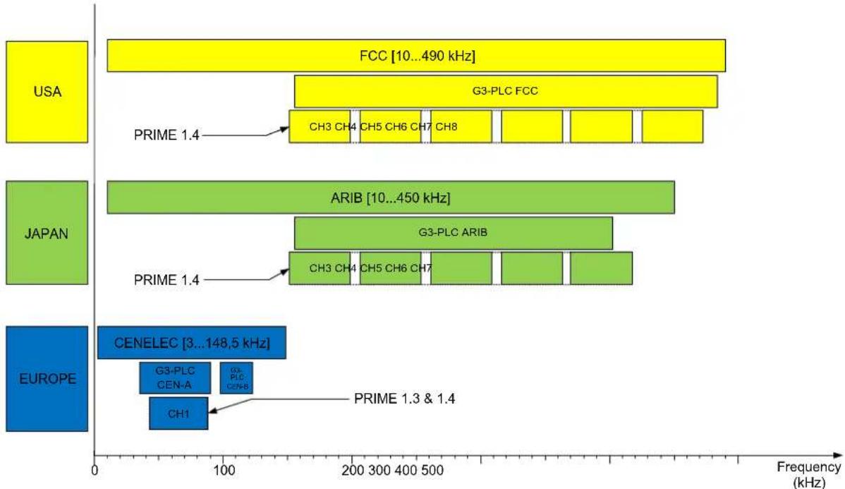
The PL485 requires an external circuit to couple the PLC signal to the transmission line. Microchip provides highly efficient and reduced BOM reference designs for the different coupling options, targeting common configurations in all PLC bands (<500 kHz) complying with existing regulations and PLC communication protocols.
Figure 3-6. PLC Bands Supported by PL485
bar_stacked
| Region | Component | Frequency Range (kHz) | |--------|-------------------|------------------------| | USA | FCC | 10...490 | | USA | G3-PLC FCC | ~120 | | USA | CH3 CH4 | ~180 | | USA | CH5 CH6 CH7 | ~180 | | USA | CH8 | ~180 | | USA | PRIME 1.4 | ~180 | | JAPAN | ARIB | 10...450 | | JAPAN | G3-PLC ARIB | ~140 | | JAPAN | CH3 CH4 | ~180 | | JAPAN | CH5 CH6 CH7 | ~180 | | JAPAN | PRIME 1.4 | ~180 | | EUROPE | CENELEC | 3...148.5 | | EUROPE | G3-PLC CEN-A | ~100 | | EUROPE | G3-PLC CEN-B | ~100 | | EUROPE | CH1 | ~80 | | EUROPE | PRIME 1.3 & 1.4 | ~100 |The coupling circuit of the PL485-EK kit is described with more detail in the chapter 3.3.2 PLC Coupling Circuitry Description. For more information about the available coupling circuits for the PL485 and how to use them, please read the application note Using PL485 to implement a fully featured G3-PLC/PRIME modem.
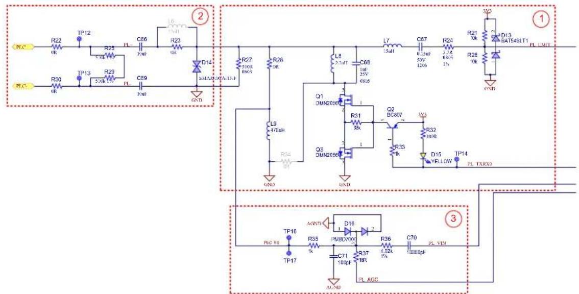
3.3.2 PLC Coupling Circuitry Description
The PL485-EK evaluation board communicates in the band between 95 kHz and 125 kHz (CENELEC B-Band). The PL485-EK board implements a circuit to couple the PLC signal to the transmission line. This design is based on Microchip reference design for a non-isolated coupling in CENELEC-B band without external amplifier, including some modifications to couple the PLC signal to a DC BUS instead to the 220 Vac mains. PL485-EK operates with PL485 internal PLC driver, with no additional external amplification.
The following figure shows the PLC coupling circuit implemented in PL485-EK, which is composed of three sub-circuits:
- Filtering Stage
- Coupling Stage
- Reception Stage
Figure 3-7. PLC Coupling Schematic on the PL485-EK Board
text_image
PLC R22 OK TP12 R25 5.0kV R23 5.0kV PL C66 10uF L6 10uF R23 OK D14 3MULS 0.0A-13-F GND PLC R30 OR TP13 R23 5.0kV PL C89 10uF R27 5.0kV BND R26 OR L9 2.5uF C68 1uF 25V 0.005 L7 15uF C67 0.15uF 5W 120V R24 2.1K 0.005 1V R21 Xk D13 RATS4SLT1 PL LNET Q1 DMN2056E R31 Xk Q2 BC807 3V3 R33 INR D15 YELLOW TP14 PL TXRXO GND Q3 DMN2056E R32 INR GND L3 470uH R34 GND TP16 AGND D16 2 PLBD7000 R36 4.02kV C70 7mmmpF PL VEN TP17 C71 100pF PL AGCNote: PLC coupling circuitry adds the yellow LED, D15, for visual indication of PLC frames transmission.
The following sections describe the aim of each sub-circuit assembled in the PL485-EK board.
3.3.2.1 PLC Filtering Circuit
The in-band flat response filtering stage reduces spurious emission to the limits set by the corresponding regulation and blocks potential interferences from other transmission channels without distorting the injected signal.
The filtering stage used in PL485-EK, see Figure 3-7, has three aims:
- Band-pass filtering of high frequency components of the square waveform generated by the transmission stage
- Adapt Input/Output impedance for optimal reception/transmission. This is controlled by TXRX0 signal
• A band-pass filtering for received signals
3.3.2.2 PLC Coupling Circuit
The PLC coupling circuit connects the PLC signal directly to DC power rails without requiring any hardware adaptation (or to the mains grid using an AC coupler).
The main purpose of the circuit is to block the voltage of the rail to/from which the signal is injected/received. In PL485-EK, it is carried out by the capacitors, C66 and C69, (see Figure 3-7). Resistors R25 and R29 allow to discharge C66 and C69 capacitors in case of disconnection from DC power rails.
D14 TVS diode protects the coupling circuit from the overvoltage and high transient voltages (surges and spikes) from DC power rails.

PLC coupling components are designed for a maximum voltage of 48 V_DC .

Important: In case of using the AC coupler accessory, it is recommended to remove R22 and R30 for better performance. Please refer to PLC-AC-Coupler User Guide for more information about the AC coupler accessory.
3.3.2.3 PLC Reception Circuit
The PLC reception circuit used in PL485-EK, see Figure 3-7, is the reference design for the reception stage and it is composed of:
• Single-pole low pass filter, R35 and C71
- Automatic Gain Control (AGC) circuit, where the resistor R37 is used to attenuate the incoming PLC signal in case its amplitude is high enough to exceed the input dynamic range of the embedded ADC
• A resistor, R36, for impedance matching
• DC decoupling capacitor, C70
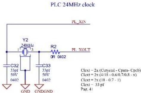
3.3.3 Clock Circuitry
Besides the embedded RC oscillators of the PL485, two crystal oscillators are assembled on the PL485-EK board to obtain a more precise and stable system clock reference:
- A 24 MHz clock signal, Y2, generated for the PLC modem (see Figure 3-8). Please refer to the PL360 Datasheet to see the characteristics of this crystal oscillator.
• A low-power 32.768 kHz crystal oscillator, Y3 (see Figure 3-9).
Note: An additional 20 MHz clock crystal, Y1, is not placed. It can be assembled if required by the customer. This crystal oscillator with robust fast start-up can be used instead of the 32.768 kHz crystal oscillator of the SAMG55 (see Figure 3-10).
Figure 3-8. 24 MHz Crystal Oscillator Scheme
text_image
PLC 24MHz clock PL_XIN Y2 24MHz 1 3 R2 OR 0402 PL XOUT C32 33pI 50V 0402 C33 33pI 50V 0402 GND GNDGND Clect - 2x (Crystal - Cpara- Cycb) Clect + 2x (4/18 - 0.6/0.7/0.8 - x) Clect = 2x (18 - 0.7 - 1) Clect - 33 pI Pag. 41Figure 3-9. 32.768 kHz Crystal Oscillator Scheme

text_image
MCU slow clock Y3 32.768KHz R7 0R 0402 PA7 PA8 C46 22pF 50v 0603 C47 22pF 50v 0603 GNDGND Clett = 2x (Crystal - Opera - Cpeb) Clett = 2x (12.5 - 0.5 - x) Clett = 2x (12.5 - 0.5 - 1) Clett = 22 pF (<24 pF Max) Pag. 1059Figure 3-10. 20 MHz Crystal Oscillator Scheme

text_image
MCU 20MHz clock PB9 R1 0R 0603 Y1 20MHz C30 12pF 50V 0402 GND GNDGND R3 0R 0603 C31 12pF 50V 0402 PB8 Clext = 2x (Crystal - Cintload - Cpeb) Clext = 2x (12.5/17.5 - 7.5/9/10.5 - x) Clext = 2x (16 - 9 - 1) Clext = 12 pF Pag. 1061Note: The operating temperature range for crystal oscillators is -40^ to +85^ . However, please note that crystal oscillators might not cover the previous temperature range with desired performance due to aging.
3.3.4 Reset
The reset sources of the PL485-EK board are:
- Power-on Reset function, embedded in the PL485 device.
- JTAG reset from the in-circuit emulator.
- The RESET push button switch mounted directly on the board. When the RESET button is pressed it will drive the PL485 reset line (NRST) to GND.
Figure 3-11. Reset Button

text_image
3V3 R8 10k NRST 1 SW1 TL3301NF260QG 2 3 4 C48 0.1uF GND GND3.3.5 Power Supply System
The PL485-EK board can be powered from several power sources, as is shown in Table 3-16.
Table 3-16. Power Sources for PL485-EK Board
| Power Input | Voltage Requirements | Power Requirements | Connector Marking |
| DC Jack connector (J3) | +6V to +48V ( ± 5% ) | 3 Watts | DC_IN |
| DC Input connector (J2) | +6V to +48V ( ± 5% ) | 3 Watts | DC_IN |
| USB Micro-B connector (J5) | +5V | According to USB specifications | USB |
| USB Micro-B connector (J12) | +5V | According to USB specifications | USB |
| Xplained PRO PWR connector (J7) | +5V | 2.5 Watts | PWR |
The PL485-EK board has three voltage rails:
- +5V to supply power to the 3.3V buck, Xplained PRO header and mikroBUS connector
• +3.3V buck to supply the PL485 and related peripherals
• +3.3V LDO to supply J-Link
The 5V voltage rail is obtained from the MCP16331 buck converter. For a further description about the buck converter see the MCP16331 High-Voltage Input Buck Converter Evaluation Board User's Guide and MCP16331 Datasheet.
Figure 3-12. 5V Voltage Design

text_image
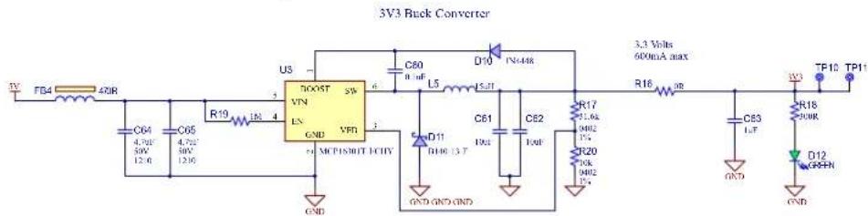
5V Buck Converter 6V to 48V VDC FB3 4X8R C58 10uF 75V 121B C59 10uF 75V 121B R14 LM 2 8 HOUST 5V VIN EN GND 向 VFB MCP16351 L2 C53 6.1uF L4 22uH D8 IN448K D9 R140-13-F C56 10uF C57 10uF R13 5kΩ R15 1kΩ R16 1kΩ GND GND GND GND 5 Volts 500mA max R11 OR 5V ECG C54 20pF 50V 0402 GND C56 1uF GND VUSB D3 MDR0520 VDUS JLINK D4 MDR0520 D5 MDR0520 D7 MDR0520 R12 560R 0402 5% D9 GREEN TPE GNDAnother buck converter, MC16301, is used to generate a regulated 3.3V voltage rail required by the PL485. For a further description about the buck converter see the MCP16301/MCP16301H Datasheet.
Figure 3-13. 3.3V Buck Converter Design
text_image
3V3 Buck Converter TV FB4 420R C64 4.7Ω/50V C65 4.7Ω/50V R19 L5 4 U3 700F 5W VIN EN GND VFR + MCP180BT-1CHY C60 0.1μF L5 D10 IN6448 D11 TH00 13 T C61 10Ω C62 10μF R17 11.6kΩ R20 10kΩ R22 10kΩ C63 1.5T C64 4.7Ω/50V 12.6 C65 4.7Ω/50V 12.6 3.3 Volts 60mA max R16 R TP10 TP11 D12 GFPN GND GND GND GND GND GNDThere is one LED and two test points on each voltage rail to check whether all power supplies are operating properly. To avoid on board self-generated disturbances within the PLC signal band, both converters are switching at 500 kHz fixed frequency, out of the PLC band (95 to 125 kHz).

Attention: To avoid noise interferences, the switching frequency of the external SMPS must be out of the PLC band and preferably in frequencies above it to avoid harmonics influence. This is essential to obtain a good reception performance.
Please refer to section 3.6 Hardware Description - JLINK Debugger for information about +3.3V LDO to supply J-Link.
3.3.5.1 PLC Rejection Filter
As the PLC coupling circuit is in parallel with the power supply circuit, the input impedance of the final equipment could be affected. If the requirements about total input impedance are not satisfied, an appropriate input filter is needed at the power supply input to increase the input impedance.
Besides the input filter, it is also recommended to add a PLC rejection filter to avoid the absorption of the PLC signals by the power supply circuit. This filter also increases the input impedance, so it helps to achieve the requisites about input impedance.

Notice: The PL485-EK board has PLC coupling and power supply circuits in parallel, so the PLC rejection filter is included. A PLC rejection filter is needed in case of low input impedance after connecting in the same point the PLC Coupling connector J2 and the power source of the board.
The PLC rejection filter of the PL485-EK is composed of two inductors in-series (L = 560 μH) and a capacitor in-parallel (C = 0.1 μF) at the power supply input as shown in the following picture.
Figure 3-14. PLC Rejection Filter Example
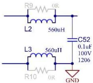
chemical
Electrical circuit diagram with inductors, capacitors, and a GND componentTo make the filter operational, L2, L3 and C52 must be mounted and R9 and R10 must be unmounted. To disable the filter, R9 and R10 must be mounted and L2, L3 and C52 must be unmounted.
3.4 Hardware Description – MCU Peripherals
3.4.1 Voltage Monitor
The voltage monitor circuit allows the implementation of multiple functionalities such as:
• Detection of fault conditions
• Detection of Low-Power mode entering conditions
• Detection of wake-up situations
The input pin PA20 of PL485 is used to monitor the 5V voltage rail through external voltage divisors. It can be used to monitor the 3.3V voltage rail mounting R44 and removing R43 resistor.
Figure 3-15. Voltage Monitor Circuit
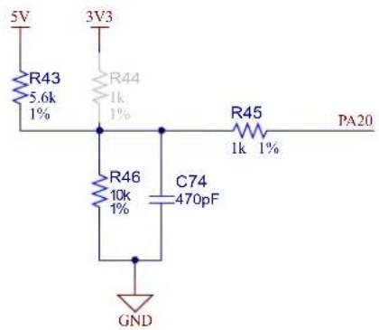
text_image
5V 3V3 R43 5.6k 1% R44 1k 1% R45 1k 1% PA20 R46 10k 1% C74 470pF GND3.4.2 LEDs
The PL485-EK board includes the following LEDs:
• D9 and D12, connected to 5V and 3.3V supplies respectively to provide a visual status of these voltages
• D15 to indicate the transmission of PL485
• D18 to indicate the status of USB
• D22 to indicate the J-Link status
- D19 and D20 for general purpose, one green connected to PA31 (LED0) and one red connected to PA19 (LED1), which can be managed by the applications
Figure 3-16. User LEDs

text_image
3V3 R58 300R D19 GREEN (LED0) PA31 TP19 3V3 R59 300R D20 RED R60 OR (LED1) PA19 TP203.4.3 Chip Erase
The 1x2 pin-header J1 marked as "MCU ERASE" is connected to the PL485 chip erase pin (PB12) and 3.3V. This header can be used to re-initialize the Flash content (and some of its NVM bits) to an erased state (all bits read as logic level 1) by placing a jumper on the header and pressing the reset switch button. After a few seconds, the erase jumper must be removed, the PCB must be turned off and, then, turned on by disconnecting and connecting again to the power supply.
3.5 Hardware Description – MCU Interface Ports
3.5.1 USB Device Port
The USB Device Port (UDP) is compliant with the Universal Serial Bus (USB) 2.0 full-speed device specification. There is a USB available on the PL485-EK board that can act as both host and device. It has a Micro-B female USB connector with the silk screen USB.
The I/O line PB14 allows the application to check if VUSBD is available.
Figure 3-17. USB Circuit

text_image
USB Device USB Device USB_DN USB_DP PB14 R38 0R DUSB N DLSB P R39 27k VUSB FB5 470R VUSBD R41 47k GND C72 0.1uF R40 300R D18 YELLOW D17 PRTR5V012X GND GND GND J5 J5 USB2.0 MICRO-B FEMALE R42 1M C73 4700pF GND GND
Important: Check online resources from the Microchip Website to download the drivers according to your Operating System.

We recommend the use of an external USB isolator device, for instance UH401, to prevent the addition of noise to the PLC network.
3.5.2 mikroBUS Connector
The PL485-EK board incorporates a mikroBUS socket connector (J8). By means of this socket, some mikroBUS peripherals can be connected to PL485-EK, which is the main board.
This mikroBUS standard defines two pairs of 1x8 male headers with the following signals:
- Analog
- Reset
- SPI Chip Select
- SPI Clock
• SPI Master Input Slave Output
• SPI Master Output Slave Input
• Regulated +3.3V (output) - Unregulated +5V (output)
- I²C Data
- I²C Clock
- UART Transmit
- UART Receive
- Hardware Interrupt
- Pulse-width Modulation
- Two GND pins
Figure 3-18. mikroBUS Connector
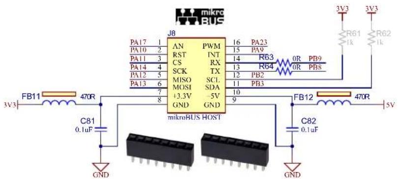
text_image
mikro BUS J8 PA17 1 PA10 2 PA11 3 PA14 4 PA12 5 PA13 6 7 8 PB9 PB8 PB23 PA9 R63 R64 0R PB9 0R PB8 MISO SCL. MOSI SDA +3.3V -5V GND GND mikroBUS HOST FB11 470R FB12 470R 5V C81 0.1uF C82 0.1uF GND GNDNote: R61 and R62 must be mounted in case a pull-up for the I2C line will be necessary.
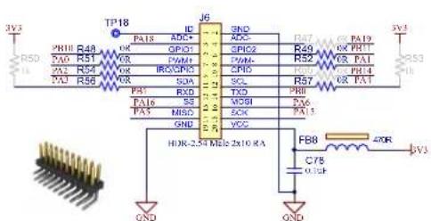
3.5.3 Xplained PRO Header
All Xplained Pro kits have one or more dual row, 20-pin, 100mil extension header. Xplained Pro MCU boards have male headers. The extension headers can be used to connect a variety of Xplained Pro extensions to Xplained Pro MCU boards or to access the pins of the target MCU on Xplained Pro MCU boards directly. Note that all pins are not always connected. All connected pins follow the defined pin-out description in the Table 3-5.
Figure 3-19. Xplained PRO Header Connector (EXT1)
text_image
TP18 JP6 R50 R48 PA18 ADC OPG1 GP10 PAM1 POA POB SCL R57 PA7 PA19 OP PR1 OP PA1 OP PR4 OP PAT 3V3 TA0 TA1 TA2 TA3 TA4 TA5 TA6 TA7 TA8 TA9 TA10 TA11 TA12 TA13 TA14 TA15 TA16 TA17 TA18 TA19 TA20 TXD TXD PHI MXI MXII MXK XCC FX6 FX7 FX8 FX9 FX10 FX11 FX12 FX13 FX14 FX15 FX16 FX17 FX18 FX19 FX20 F88 40R C78 0.0kV QND QND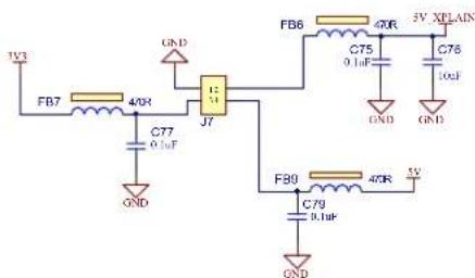
text_image
1V3 FB7 40R GND C77 0.1uF J7 5V_XPLAIN FB6 40R C75 0.1uF GND C76 10uF GND F89 40R 5V C79 0.1uF GNDThe power header can be used to connect external power to the PL485 Xplained Pro kit. The kit will automatically detect and switch to any external power if supplied. The power header can also be used as supply for external peripherals or extension boards.
Please refer to Table 3-6 for more information about connectors.
3.5.4 I ^2 S
I²S (Inter-IC Sound) is an electrical serial bus interface standard used for connecting digital audio devices together. It is used to communicate PCM audio data between integrated circuits in an electronic device. The I²S bus separates clock and serial data signals, resulting in simpler receivers than those required for asynchronous communications systems that need to recover the clock from the data stream.
Table 3-17. Modifications to enable the I²S Function
| Resistor for Xplained PRO Function Needed Resistors for I | ^2S Function |
| R51 R68 | |
| R52 R69 | |
| R54 R67 | |
| R56 R66 | |
| R57 R65 |
The default assembly of PL485-EK does not enable the I²S function. So, it is necessary to shift to the right the indicated resistors on Table 3-17.
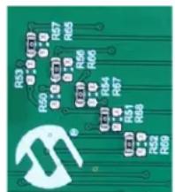
Figure 3-20. Position of resistors to be shifted for enabling I²S function
text_image
R53 R50 R57 R65 R56 R66 R65 R64 R67 R51 R66 R52 R69Figure 3-21. I²S Connector

text_image
J9 VCC GND I2SMCK0 R65 0R PA4 I2SDO0 R66 0R PA3 I2SDI0 R67 0R PA2 I2SCK0 R68 0R PA0 I2SWS0 R69 0R PA1 HOR-2.54 Male 1x7 FB10 470R C80 0.1uF 3V3 GNDPlease refer to Table 3-8 for more information about connector.
3.6 Hardware Description - JLINK Debugger
The PL485-EK includes a built-in SEGGER J-Link-On-Board (J-Link-OB) device. The functionality is implemented with an ATSAM3U4C microcontroller in a TFBGA100 package. The ATSAM3U4C provides the functions of the JTAG interface and a bridge from USB to Serial debug port (known as CDC, or communication class device). The bicolored LED (D22) shows the status of the J-Link-On-Board device. The J-Link-OB device is designed to provide an efficient, low-cost, on-board alternative to the standard J-Link or Atmel-ICE. Its own dedicated USB port acts as a power source for this block and provides the communication link to program and debug the MCU.
Figure 3-22. JLINK OBD Interface

text_image
JLINK OBD ATSAM3AICA-CU TFBGA-100 USB L/MICRO B FEMALE FB13 1VR BLMINPG125N1D EARUDG GND VCLK ULINK JLINK USBHS P JLINK USBHS N R77 D21 R78 C68 R79 D40 R80 R81 VCLK ULINK JLINK USBHS P JLINK USBHS N R74 U03 U02 U01 VCLK ULINK R75 D20 R76 D41 R77 D22 R78 C69 VCLK ULINK C87 D43 R83 3V3.3U 3V3.2U 3V3.2U 3V3.2U 3V3.2U 3V3.2U 3V3.2U 3V3.2U 3V3.2U 3V3.2U 3V3.2U 3V3.2U 3V3.2U 3V3.2U 3V3.2U 3V3.2UTable 3-18. J-Link-OBD and J-Link-CDC LED D22 Status
| LED D22 | State | Description |
| Red and Green | Off | J-Link (SAM3U device) is not programmed, or J13 and J14 are installed. |
| Green | Flashing | J-Link is operational but the USB port is not connected. |
| Green | On | J-Link-OB is connected and ready. |
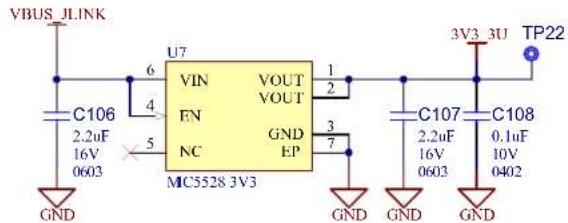
The ATSAM3U microcontroller is powered only through the J-Link USB connector.
The MIC5528 has been selected to convert the 5V coming from the USB connector into the 3.3V rail needed by the microcontroller. The MIC5528 is a simple low-power, low dropout regulator designed for optimal performance in a very small footprint. It is capable of sourcing up to 500 mA of output current while only drawing 38 A of operating current. For more information about the MIC5528, refer to the product web page.
Figure 3-23. J-Link-OBD Power Supply
text_image
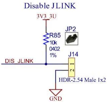
VBUS JLINK U7 VIN VOUT EN VOUT NC GND EP MC5528 3V3 6 4 5 GND GND GND GND 1 2 3 7 3V3 3U TP22 C106 2.2uF 16V 0603 GND C107 2.2uF 16V 0603 GND C108 0.1uF 10V 0402Jumper J14 disables the J-Link-OBD JTAG functionality. When installed (J14 shorted), a quad analog switch (U4/ U6) routes the JTAG interface of the PL485 to the 10-pin header J15 (Please refer to section 3.6.1 JTAG/SWD Port for more information).
- Jumper J14 not installed: J-Link-OBD-ATSAM3U4C is enabled and fully functional.
- Jumper J14 installed: J-Link-OBD-ATSAM3U4C is disabled and an external JTAG controller can be used through the 10-pin JTAG port J15.
Figure 3-24. Disable JLINK JTAG
text_image
Disable JLINK 3V3 3U R85 10k 0402 1% JP2 J14 DIS JLINK 21 HDR-2.54 Male 1x2 GNDFigure 3-25. JLINK/JTAG Switch

text_image
JLINK/JTAG 3V3 16 C83 0.1uF 10V 0402 GND U4 S VCC E GND PB7 TCK/SWCLK 4 PB4 TDI/NC 7 PB5 TDO/SWO 9 PB6 TMS/SWDIO 12 DIS JLINK R70 100k 0402 5% GND Q4 BSS138N U6 16 C84 0.1uF 10V 0402 GND 12 15 16 10E VCC NC 10E NC 4OE GND 1Y 1A 3 2Y 2A 6 3Y 3A 11 4Y 4A 14 JTAG nRST IDTQS3VH125 JTAG CONN nRST JLINK nRST NRST R79 1% 100R 0402In addition to the J-Link-OBD functionality, the ATSAM3U4C microcontroller provides a bridge to a debug serial port (DBGU) of the main board processor. The port is made accessible over the same USB connection used by JTAG by implementing a Communication Device Class (CDC), which allows a terminal communication with the target device.
This feature is enabled/disabled by jumper J13.
- Jumper J13 not installed: the J-Link-OBD CDC function is enabled and fully functional.
- Jumper J13 installed: the J-Link-OBD CDC function is disabled.
The USB CDC converts the USB device into a serial communication device. The target device running the CDC is recognized by the host as a serial interface (USB2COM, virtual COM port) without the need of installing a special host driver (the CDC is standard). All PC software using a COM port works without modifications with this virtual COM port. Under Microsoft® Windows®, the device shows up as a COM port; under Linux®, as a /dev/ACMx device. This enables the user to use host software which was not designed to be used with USB, such as a terminal program.
Figure 3-26. Disable JLINK CDC
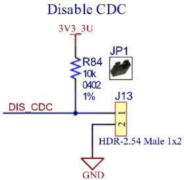
text_image
Disable CDC 3V3_3U R84 10k 0402 1% JP1 DIS_CDC J13 2 1 HDR-2.54 Male 1x2 GNDIf the user does not require the on-board programming feature, this section can be left unpowered, with no impact on the rest of the system. A level shifter has been placed on the DEBUG UART line between the PL485 MCU and the on-board programmer to properly separate the two voltage domains.
Figure 3-27. J-Link-OBD Level Shifter
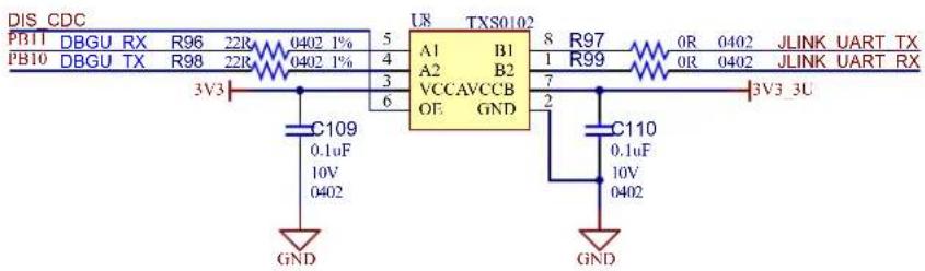
text_image
DISCDC PB11 DBGU RX R96 22R 0402 1% PB10 DBGU TX R98 22R 0402 1% 3V3 C109 0.1uF 10V 0402 GND U8 TX80102 A1 B1 A2 B2 VCCAVCCB OE GND 8 R97 1 R99 7 2 C110 0.1uF 10V 0402 GND 3V3_3U OR 0402 JLINK UART TX OR 0402 JLINK UART RX3.6.1 JTAG/SWD Port
The PL485-EK board includes an SWD (Serial Wire Debug) / JTAG interface port to provide debug level access to the system-on-chip. It also embeds a serial wire trace. This connector provides the required interface for in-circuit emulators, like the Atmel-ICE. The SW-DP/JTAG port is a 10-pin, dual row, 0.1-inch male connector (J15).

Important: Note that the PL485-EK kit does not include any external JTAG debugger/programmer.
Figure 3-28. JTAG/SWD Interface Schematic
Connector for JTAG/SWD programmer/debugger

text_image
3V3 VCC GND GND KEY GNDDetect J15 TMS/SWDIO TCK/SWCLK TDO/SWO TDI/NC nRESET R95 3V3 100k 100k 100k R90 R91 R92 R93 JTAG_CONN_TMS JTAG_CONN_TCK JTAG_CONN_TDO JTAG_CONN_TDI JTAG_CONN_nRST 100R GND3.7 PL485-EK Schematics
This section contains the schematics for the PL485-EK board:
• Top Level Schematic, Figure 3-29
• PL485 Schematic, Figure 3-30
• Interface Schematic, Figure 3-31
• Power Supply Schematic, Figure 3-32
• PLC Coupling Schematic, Figure 3-33
• JLINK Debugger Schematic, Figure 3-34
Figure 3-29. Top Level Schematic

flowchart
graph TD
    A["Microchip"] --> B["PLC1"]
    B --> C["PLC2"]
    C --> D["PLC3"]
    D --> E["PLC4"]
    E --> F["PLC5"]
    F --> G["PLC6"]
    G --> H["PLC7"]
    H --> I["PLC8"]
    I --> J["PLC9"]
    J --> K["PLC10"]
    K --> L["PLC11"]
    L --> M["PLC12"]
    M --> N["PLC13"]
    N --> O["PLC14"]
    O --> P["PLC15"]
    P --> Q["PLC16"]
    Q --> R["PLC17"]
    R --> S["PLC18"]
    S --> T["PLC19"]
    T --> U["PLC20"]
    U --> V["PLC21"]
    V --> W["PLC22"]
    W --> X["PLC23"]
    X --> Y["PLC24"]
    Y --> Z["PLC25"]
    Z --> AA["PLC26"]
    AA --> AB["PLC27"]
    AB --> AC["PLC28"]
    AC --> AD["PLC29"]
    AD --> AE["PLC30"]
    AE --> AF["PLC31"]
    AF --> AG["PLC32"]
    AG --> AH["PLC33"]
    AH --> AI["PLC34"]
    AI --> AJ["PLC35"]
    AJ --> AK["PLC36"]
    AK --> AL["PLC37"]
    AL --> AM["PLC38"]
    AM --> AN["PLC39"]
    AN --> AO["PLC40"]
    AO --> AP["PLC41"]
    AP --> AQ["PLC42"]
    AQ --> AR["PLC43"]
    AR --> AS["PLC44"]
    AS --> AT["PLC45"]
    AT --> AU["PLC46"]
    AU --> AV["PLC47"]
    AV --> AW["PLC48"]
    AW --> AX["PLC49"]
    AX --> AY["PLC50"]
    AY --> AZ["PLC51"]
    AZ --> BA["PLC52"]
    BA --> BB["PLC53"]
    BB --> BC["PLC54"]
    BC --> BD["PLC55"]
    BD --> BE["PLC56"]
    BE --> BF["PLC57"]
    BF --> BG["PLC58"]
    BG --> BH["PLC59"]
    BH --> BI["PLC60"]
    BI --> BJ["PLC61"]
    BJ --> BK["PLC62"]
    BK --> BL["PLC63"]
    BL --> BM["PLC64"]
    BM --> BN["PLC65"]
    BN --> BO["PLC66"]
    BO --> BP["PLC67"]
    BP --> BQ["PLC68"]
    BQ --> BR["PLC69"]
    BR --> BS["PLC70"]
    BS --> BT["PLC71"]
    BT --> BU["PLC72"]
    BU --> BV["PLC73"]
    BV --> BW["PLC74"]
    BW --> BX["PLC75"]
    BX --> BY["PLC76"]
    BY --> BZ["PLC77"]
    BZ --> CA["PLC78"]
    CA --> CB["PLC79"]
    CB --> CC["PLC80"]
    CC --> CD["PLC81"]
    CD --> CE["PLC82"]
    CE --> CF["PLC83"]
    CF --> CG["PLC84"]
    CG --> CH["PLC85"]
    CH --> CI["PLC86"]
    CI --> CJ["PLC87"]
    CJ --> CK["PLC88"]
    CK --> CL["PLC89"]
    CL --> CM["PLC90"]
    CM --> CN["PLC91"]
    CN --> CO["PLC92"]
    CO --> CP["PLC93"]
    CP --> CQ["PLC94"]
    CQ --> CR["PLC95"]
    CR --> CS["PLC96"]
    CS --> CT["PLC97"]
    CT --> CU["PLC98"]
    CU --> CV["PLC99"]
    CV --> CW["PLD00"]
Figure 3-30. PL485 Schematic
text_image
PL485 MCL PLC POWER PL485 MCL 20MHz clock PLC MMHz clock PL485 Decoupling MCL low clock MCL U Reset MICROCHIP 1 2 3 4 5 6 7 8 PPT PPT PPT PPT PPT PPT PPT PPT PPT PPT PPT PPT PPT PPT PPT PPT PPT PPT PPT PPT PPT PPT PPT PPT PPT PPT PPT PPT PPT PPT PPT PPT PPT PPTFigure 3-31. Interface Schematic
text_image
Interface USB Volumbus Wireless transistors Subtransistors USB/256/256/256/256/256/256/256/256/256/256/256/256/256/256/256/256/256/256/256/256/256/256/256/256/256/250 Voltage Monitor Xplained PR 0 Header (EXT1) LED LLDs Microfluid Switch D3S MicroCHIP Output No. F1.000 F1.010 F1.020 F1.030 F1.040 F1.050 F1.060 F1.070 F1.080 F1.090 F1.100 F1.110 F1.120 F1.130 F1.140 F1.150 F1.160 F1.170 F1.180 F1.190 F1.200 F1.210 F1.220 F1.230 F1.240 F1.250 F1.260 F1.270 F1.280 F1.290 F1.300 F1.310 F1.320 F1.330 F1.340 F1.350 F1.360 F1.370 F1.380 F1.390 F1.400 F1.410 F1.420 F1.430 F1.440 F1.450 F1.460 F1.470 F1.480 F1.490 F1.500 F1.510 F1.520 F1.530 F1.540 F1.550 F1.560 F1.570 F1.580 F1.590 F1.600 F1.610 F1.620 F1.630 F1.640 F1.650 F1.660 F1.670 F1.680 F1.690 F1.700 F1.710 F1.720 F1.730 F1.740 F1.750 F1.760 F1.770 F1.780 F1.790 F1.800 F1.810 F1.820 F1.830 F1.840 F1.850 F1.860 F1.870 F1.880 F1.890 F1.900 F1.910 F1.920 F1.930 F1.940 F1.950 F1.960 F1.970 F1.980 F1.990 F2.000Figure 3-32. Power Supply Schematic

text_image
Power Supply DC Input DC IN 6V to 4kV CXO IN CXO IN L2 50.41 CXO CXO CXO CXO CXO CXO CXO CXO CXO CXO CXO CXO CXO CXO CXO CXO CXO CXO CXO CXO CXO CXO CXO CXO CXO CXO CXO CXO CXO CXO CXO CXO CXO CXOFigure 3-33. PLC Coupling Schematic

text_image
PLC Coupling AC Coupling Connectors MICROCHIP PLC Coupling CPU 100 CPU 101 CPU 102 CPU 103 CPU 104 CPU 105 CPU 106 CPU 107 CPU 108 CPU 109 CPU 110 CPU 111 CPU 112 CPU 113 CPU 114 CPU 115 CPU 116 CPU 117 CPU 118 CPU 119 CPU 120 CPU 121 CPU 122 CPU 123 CPU 124 CPU 125 CPU 126 CPU 127 CPU 128 CPU 129 CPU 130 CPU 131 CPU 132 CPU 133 CPU 134 CPU 135 CPU 136 CPU 137 CPU 138 CPU 139 CPU 140 CPU 141 CPU 142 CPU 143 CPU 144 CPU 145 CPU 146 CPU 147 CPU 148 CPU 149 CPU 150 CPU 151 CPU 152 CPU 153 CPU 154 CPU 155 CPU 156 CPU 157 CPU 158 CPU 159 CPU 160 CPU 161 CPU 162 CPU 163 CPU 164 CPU 165 CPU 166 CPU 167 CPU 168 CPU 169 CPU 170 CPU 171 CPU 172 CPU 173 CPU 174 CPU 175 CPU 176 CPU 177 CPU 178 CPU 179 CPU 180 CPU 181 CPU 182 CPU 183 CPU 184 CPU 185 CPU 186 CPU 187 CPU 188 CPU 189 CPU 190 CPU 191 CPU 192 CPU 193 CPU 194 CPU 195 CPU 196 CPU 197 CPU 198 CPU 199 CPU 200Figure 3-34. JLINK Debugger Schematic
text_image
JLINK debugger JLINK OBD AT500/240A-CDU T1BBA-100 JLINK:TAG Diazle to CDU Diazle to JLINK Connector for 1.1A/2WD programers: MicroCHIP HINK discharger: CPN-B Altum 1 2 3 4 5 6 7 8 100 11 12 13 14 15 16 17 18 19 20 21 22 23 24 25 26 27 28 29 30 31 32 33 34 35 36 37 38 39 40 41 42 43 44 45 46 47 48 49 50 51 52 53 54 55 56 57 58 59 60 100 100 100 100 100 100 100 100 100 100 100 100 100 100 100 100 100 100 100 100 100 100 100 100 100 123 123 123 123 123 123 123 123 123 123 123 123 123 123 123 123 123 123 123 123 123 123 123 123 123 124 124 124 124 124 124 124 124 124 124 124 124 124 124 124 124 124 124 124 124 124 124 124 124 124 125 125 125 125 125 125 125 125 125 125 125 125 125 125 125 125 125 125 125 125 125 125 125 125 125 126 126 126 126 126 126 126 126 126 126 126 126 126 126 126 126 126 126 126 126 126 1263.8 PL485-EK Layout
This section contains the layout graphics for the PL485-EK board:
• Layer 1: Top Layer, Figure 3-35
• Layer 2: Mid Layer 1 (Ground), Figure 3-36
• Layer 3: Mid Layer 2 (Power Supplies), Figure 3-37
• Layer 4: Bottom Layer, Figure 3-38
• Top Components Placement, Figure 3-39
• Bottom Components Placement, Figure 3-40
Figure 3-35. PL485-EK rev1 Layout: Top Layer

natural_image
Red printed circuit board with various traces and components, no readable text or symbolsFigure 3-36. PL485-EK rev1 Layout: Mid Layer 1 (Ground)
natural_image
Green printed circuit board with scattered white dots, traces, and geometric shapes (no readable text or symbols)Figure 3-37. PL485-EK rev1 Layout: Mid Layer 2 (Power Supplies)
natural_image
Green printed circuit board with scattered components and traces (no readable text or symbols)Figure 3-38. PL485-EK rev1 Layout: Bottom Layer

text_image
onlim 2UB KA 12P 63 XQB QEM ROM VLD+ CHD MVP TWU XP VT JDB AGB VDD+ OPD L L L L L L L L L L L L L L L L L L L L L L L L L L L L L L L L L L L L L L L L L L L L L L L L L L MILK-802 MILK-802 MILK-802 MILK-802 MILK-802 MILK-802 MILK-802 MILK-802 MILK-802 MILK-802 MILK-802 MILK-802 MILK-802 MILk-802 MILk-802 MILk-802 MILk-802 MILk-802 MILk-802 MILk-802 MILk-802 MILk-802 MILk-802 MILk-802 MILk-802 MILk-801Figure 3-39. PL485-EK rev1 Layout: Top Silkscreen
text_image
mikro BUS AMP/A17 PAI/SPAW RST/PA10 PANNT CS/PA11 PSNRX SCK/PA14 PSRTX MSO/PA12 PB2/SCL MON/PA13 PB3/SDA +3.3V +5V GND GND JB 27 PWR Erase EKT1 3.3V GND MCH DO BI CK WS J5 125 USB RESET MICROCHIP PL485-EK REV 3 PLC RX JTAG J15 J20 J25 J30 J35 J40 J45 J50 J55 J60 J65 J70 J75 J80 J85 J90 J95 J100 J105 J110 J115 J120 J125 J130 J135 J140 J145 J150 J155 J160 J165 J170 J175 J180 J185 J190 J195 J200 J205 J210 J215 J220 J225 J230 J235 J240 J245 J250 J255 J260 J265 J270 J275 J280 J285 J290 J295 J300 J305 J310 J315 J320 J325 J330 J335 J340 J345 J350 J355 J360 J365 J370 J375 J380 J385 J390 J395 J400Figure 3-40. PL485-EK rev1 Layout: Bottom Silkscreen
text_image
onlim 2UB HA TSP RS ACB DEW RCAM VLD+ OND MPN THI RP RT JCB ADB VDD+ OND CEA 12 13 14 15 16 17 18 19 20 21 22 23 24 25 26 27 28 29 30 31 32 33 34 35 36 37 38 39 40 41 42 43 44 45 46 47 48 49 50 51 52 53 54 55 56 57 58 59 60 61 62 63 64 65 66 67 68 69 70 71 72 73 74 75 76 77 78 79 80 81 82 83 84 85 86 87 88 89 90 91 92 93 94 95 96 97 98 99 100 VCL1 VCL2 VCL3 VCL4 VCL5 VCL6 VCL7 VCL8 VCL9 VCL10 VCL11 VCL12 VCL13 VCL14 VCL15 VCL16 VCL17 VCL18 VCL19 VCL20 VCL21 VCL22 VCL23 VCL24 VCL25 VCL26 VCL27 VCL28 VCL29 VCL30 VCL31 VCL32 VCL33 VCL34 VCL35 VCL36 VCL37 VCL38 VCL39 VCL40 VCL41 VCL42 VCL43 VCL44 VCL45 VCL46 VCL47 VCL48 VCL49 VCL50 VCL51 VCL52 VCL53 VCL54 VCL55 VCL56 VCL57 VCL58 VCL59 VCL60 VCL61 VCL62 VCL63 VCL64 VCL65 VCL66 VCL67 VCL68 VCL69 VCL70 VCL71 VCL72 VCL73 VCL74 VCL75 VCL76 VCL77 VCL78 VCL79 VCL80 VCL81 VCL82 VCL83 VCL84 VCL85 VCL86 VCL87 VCL88 VCL89 VCL90 VCL91 VCL92 VCL93 VCL94 VCL95 VCL96 VCL97 VCL98 VCL99 VCLK0001M4. Standards Compliance
This development/evaluation tool is designed to be used for research and development in a laboratory environment. This development/evaluation tool is neither intended to be a finished appliance, nor is it intended for incorporation into finished appliances that are made commercially available as single functional units to end users.
The PL485-EK board is a CE mark product which complies with EN 50065-1, EN 50065-2-3 and EN 50065-7 EMC standards. It also complies with the Pb-Free and ROHS directives.
5. References
- CENELEC, EN 50065. Signaling on low-voltage electrical installations in the frequency range 3kHz to 148.5 kHz, 2002
• PL485 Datasheet, 2020
• PLC-AC-Coupler User Guide, 2020 - Using PL485 to implement a fully featured G3-PLC/PRIME modem Application Note, 2020
- MCP16331 High-Voltage Input Buck Converter Evaluation Board User's Guide, 2014
• MCP16331 Datasheet, 2016
• MCP16301/MCP16301H Data Sheet, 2015
6. Revision History
6.1 Rev A - 01/2020
| Document Initial release. |
6.2 Rev B - 05/2020
| Document Minor changes of nomenclature. | |
| Introduction Added reference to PLC-AC-Coupler User Guide. | |
| 1. Evaluation Kit Specifications | Updated 1.1 Safety Recommendations section.Added Table 1-2 in 1.2 Electrical Characteristics section. |
| 2. Getting Started Updated 2.1 Running the Demo Application section. | |
| 3. PL485-EK Board | Updated Figure 3-1 in 3.1 Overview section.Updated Figure 3-2 in 3.2.1 PL485-EK Block Diagram section.Updated Figure 3-3 in 3.2.2 Interface Connection section.Updated Table 3-5, Table 3-6 and Table 3-8 in 3.2.2.1 Connectors section.Updated 3.3.1 PL485 section.Deleted note in 3.3.2 PLC Coupling Circuitry Description section.Added reference to PLC-AC-Coupler User Guide in 3.3.2.2 PLC Coupling Circuit section.Updated 3.3.3 Clock Circuitry section.Updated 3.3.5 Power Supply System section.Updated 3.3.5.1 PLC Rejection Filter section.Deleted note in 3.4.1 Voltage Monitor section.Updated 3.4.2 LEDs section.Updated 3.5.3 Xplained PRO Header section.Updated Figure 3-29, Figure 3-30, Figure 3-31, Figure 3-32, Figure 3-33 and Figure 3-34 in 3.7 PL485-EK Schematics section.Updated Figure 3-35, Figure 3-36, Figure 3-37, Figure 3-38, Figure 3-39 and Figure 3-40 in 3.8 PL485-EK Layout section. |
| 5. References Added PLC-AC-Coupler | User Guide.Added Using PL485 with external amplifier Application Note. |
The Microchip Website
Microchip provides online support via our website at http://www.microchip.com/. This website is used to make files and information easily available to customers. Some of the content available includes:
- Product Support – Data sheets and errata, application notes and sample programs, design resources, user's guides and hardware support documents, latest software releases and archived software
- General Technical Support – Frequently Asked Questions (FAQs), technical support requests, online discussion groups, Microchip design partner program member listing
- Business of Microchip – Product selector and ordering guides, latest Microchip press releases, listing of seminars and events, listings of Microchip sales offices, distributors and factory representatives
Product Change Notification Service
Microchip's product change notification service helps keep customers current on Microchip products. Subscribers will receive email notification whenever there are changes, updates, revisions or errata related to a specified product family or development tool of interest.
To register, go to http://www.microchip.com/pcn and follow the registration instructions.
Customer Support
Users of Microchip products can receive assistance through several channels:
• Distributor or Representative
- Local Sales Office
- Embedded Solutions Engineer (ESE)
- Technical Support
Customers should contact their distributor, representative or ESE for support. Local sales offices are also available to help customers. A listing of sales offices and locations is included in this document.
Technical support is available through the website at: http://www.microchip.com/support
Microchip Devices Code Protection Feature
Note the following details of the code protection feature on Microchip devices:
- Microchip products meet the specification contained in their particular Microchip Data Sheet.
- Microchip believes that its family of products is one of the most secure families of its kind on the market today, when used in the intended manner and under normal conditions.
- There are dishonest and possibly illegal methods used to breach the code protection feature. All of these methods, to our knowledge, require using the Microchip products in a manner outside the operating specifications contained in Microchip's Data Sheets. Most likely, the person doing so is engaged in theft of intellectual property.
- Microchip is willing to work with the customer who is concerned about the integrity of their code.
- Neither Microchip nor any other semiconductor manufacturer can guarantee the security of their code. Code protection does not mean that we are guaranteeing the product as “unbreakable.”
Code protection is constantly evolving. We at Microchip are committed to continuously improving the code protection features of our products. Attempts to break Microchip's code protection feature may be a violation of the Digital Millennium Copyright Act. If such acts allow unauthorized access to your software or other copyrighted work, you may have a right to sue for relief under that Act.
Legal Notice
Information contained in this publication regarding device applications and the like is provided only for your convenience and may be superseded by updates. It is your responsibility to ensure that your application meets with
your specifications. MICROCHIP MAKES NO REPRESENTATIONS OR WARRANTIES OF ANY KIND WHETHER EXPRESS OR IMPLIED, WRITTEN OR ORAL, STATUTORY OR OTHERWISE, RELATED TO THE INFORMATION, INCLUDING BUT NOT LIMITED TO ITS CONDITION, QUALITY, PERFORMANCE, MERCHANTABILITY OR FITNESS FOR PURPOSE. Microchip disclaims all liability arising from this information and its use. Use of Microchip devices in life support and/or safety applications is entirely at the buyer's risk, and the buyer agrees to defend, indemnify and hold harmless Microchip from any and all damages, claims, suits, or expenses resulting from such use. No licenses are conveyed, implicitly or otherwise, under any Microchip intellectual property rights unless otherwise stated.
Trademarks
The Microchip name and logo, the Microchip logo, Adaptec, AnyRate, AVR, AVR logo, AVR Freaks, BesTime, BitCloud, chipKIT, chipKIT logo, CryptoMemory, CryptoRF, dsPIC, FlashFlex, flexPWR, HELDO, IGLOO, JukeBlox, KeeLoq, Kleer, LANCheck, LinkMD, maXStylus, maXTouch, MediaLB, megaAVR, Microsemi, Microsemi logo, MOST, MOST logo, MPLAB, OptoLyzer, PackeTime, PIC, picoPower, PICSTART, PIC32 logo, PolarFire, Prochip Designer, QTouch, SAM-BA, SenGenuity, SpyNIC, SST, SST Logo, SuperFlash, Symmetricom, SyncServer, Tachyon, TempTrackr, TimeSource, tinyAVR, UNI/O, Vectron, and XMEGA are registered trademarks of Microchip Technology Incorporated in the U.S.A. and other countries.
APT, ClockWorks, The Embedded Control Solutions Company, EtherSynch, FlashTec, Hyper Speed Control, HyperLight Load, IntelliMOS, Libero, motorBench, mTouch, Powermite 3, Precision Edge, ProASIC, ProASIC Plus, ProASIC Plus logo, Quiet-Wire, SmartFusion, SyncWorld, Temux, TimeCesium, TimeHub, TimePictra, TimeProvider, Vite, WinPath, and ZL are registered trademarks of Microchip Technology Incorporated in the U.S.A.
Adjacent Key Suppression, AKS, Analog-for-the-Digital Age, Any Capacitor, AnyIn, AnyOut, BlueSky, BodyCom, CodeGuard, CryptoAuthentication, CryptoAutomotive, CryptoCompanion, CryptoController, dsPICDEM, dsPICDEM.net, Dynamic Average Matching, DAM, ECAN, EtherGREEN, In-Circuit Serial Programming, ICSP, INICnet, Inter-Chip Connectivity, JitterBlocker, KleerNet, KleerNet logo, memBrain, Mindi, MiWi, MPASM, MPF, MPLAB Certified logo, MPLIB, MPLINK, MultiTRAK, NetDetach, Omniscient Code Generation, PICDEM, PICDEM.net, PICkit, PICtail, PowerSmart, PureSilicon, QMatrix, REAL ICE, Ripple Blocker, SAM-ICE, Serial Quad I/O, SMART-I.S., SQI, SuperSwitcher, SuperSwitcher II, Total Endurance, TSHARC, USBCheck, VariSense, ViewSpan, WiperLock, Wireless DNA, and ZENA are trademarks of Microchip Technology Incorporated in the U.S.A. and other countries.
SQTP is a service mark of Microchip Technology Incorporated in the U.S.A.
The Adaptec logo, Frequency on Demand, Silicon Storage Technology, and Symmcom are registered trademarks of Microchip Technology Inc. in other countries.
GestIC is a registered trademark of Microchip Technology Germany II GmbH & Co. KG, a subsidiary of Microchip Technology Inc., in other countries.
All other trademarks mentioned herein are property of their respective companies.
© 2020, Microchip Technology Incorporated, Printed in the U.S.A., All Rights Reserved.
ISBN: 978-1-5224-6098-5
Quality Management System
For information regarding Microchip's Quality Management Systems, please visit http://www.microchip.com/quality.
Worldwide Sales and Service
AMERICAS ASIA/PACIFIC ASIA/PACIFIC EUROPE
| Corporate Office | Australia - Sydney | India - Bangalore | Austria - Wels |
| 2355 West Chandler Blvd. | Tel: 61-2-9868-6733 | Tel: 91-80-3090-4444 | Tel: 43-7242-2244-39 |
| Chandler, AZ 85224-6199 | China - Beijing | India - New Delhi | Fax: 43-7242-2244-393 |
| Tel: 480-792-7200 | Tel: 86-10-8569-7000 | Tel: 91-11-4160-8631 | Denmark - Copenhagen |
| Fax: 480-792-7277 | China - Chengdu | India - Pune | Tel: 45-4485-5910 |
| Technical Support: | Tel: 86-28-8665-5511 | Tel: 91-20-4121-0141 | Fax: 45-4485-2829 |
| http://www.microchip.com/support | China - Chongqing | Japan - Osaka | Finland - Espoo |
| Web Address: | Tel: 86-23-8980-9588 | Tel: 81-6-6152-7160 | Tel: 358-9-4520-820 |
| http://www.microchip.com | China - Dongguan | Japan - Tokyo | France - Paris |
| Atlanta | Tel: 86-769-8702-9880 | Tel: 81-3-6880-3770 | Tel: 33-1-69-53-63-20 |
| Duluth, GA | China - Guangzhou | Korea - Daegu | Fax: 33-1-69-30-90-79 |
| Tel: 678-957-9614 | Tel: 86-20-8755-8029 | Tel: 82-53-744-4301 | Germany - Garching |
| Fax: 678-957-1455 | China - Hangzhou | Korea - Seoul | Tel: 49-8931-9700 |
| Austin, TX | Tel: 86-571-8792-8115 | Tel: 82-2-554-7200 | Germany - Haan |
| Tel: 512-257-3370 | China - Hong Kong SAR | Malaysia - Kuala Lumpur | Tel: 49-2129-3766400 |
| Boston | Tel: 852-2943-5100 | Tel: 60-3-7651-7906 | Germany - Heilbronn |
| Westborough, MA | China - Nanjing | Malaysia - Penang | Tel: 49-7131-72400 |
| Tel: 774-760-0087 | Tel: 86-25-8473-2460 | Tel: 60-4-227-8870 | Germany - Karlsruhe |
| Fax: 774-760-0088 | China - Qingdao | Philippines - Manila | Tel: 49-721-625370 |
| Chicago | Tel: 86-532-8502-7355 | Tel: 63-2-634-9065 | Germany - Munich |
| Itasca, IL | China - Shanghai | Singapore | Tel: 49-89-627-144-0 |
| Tel: 630-285-0071 | Tel: 86-21-3326-8000 | Tel: 65-6334-8870 | Fax: 49-89-627-144-44 |
| Fax: 630-285-0075 | China - Shenyang | Taiwan - Hsin Chu | Germany - Rosenheim |
| Dallas | Tel: 86-24-2334-2829 | Tel: 886-3-577-8366 | Tel: 49-8031-354-560 |
| Addison, TX | China - Shenzhen | Taiwan - Kaohsiung | Israel - Ra'anana |
| Tel: 972-818-7423 | Tel: 86-755-8864-2200 | Tel: 886-7-213-7830 | Tel: 972-9-744-7705 |
| Fax: 972-818-2924 | China - Suzhou | Taiwan - Taipei | Italy - Milan |
| Detroit | Tel: 86-186-6233-1526 | Tel: 886-2-2508-8600 | Tel: 39-0331-742611 |
| Novi, MI | China - Wuhan | Thailand - Bangkok | Fax: 39-0331-466781 |
| Tel: 248-848-4000 | Tel: 86-27-5980-5300 | Tel: 66-2-694-1351 | Italy - Padova |
| Houston, TX | China - Xian | Vietnam - Ho Chi Minh | Tel: 39-049-7625286 |
| Tel: 281-894-5983 | Tel: 86-29-8833-7252 | Tel: 84-28-5448-2100 | Netherlands - Drunen |
| Indianapolis | China - Xiamen | Tel: 31-416-690399 | |
| Noblesville, IN | Tel: 86-592-2388138 | Fax: 31-416-690340 | |
| Tel: 317-773-8323 | China - Zhuhai | Norway - Trondheim | |
| Fax: 317-773-5453 | Tel: 86-756-3210040 | Tel: 47-72884388 | |
| Tel: 317-536-2380 | Poland - Warsaw | ||
| Los Angeles | Tel: 48-22-3325737 | ||
| Mission Viejo, CA | Romania - Bucharest | ||
| Tel: 949-462-9523 | Tel: 40-21-407-87-50 | ||
| Fax: 949-462-9608 | Spain - Madrid | ||
| Tel: 951-273-7800 | Tel: 34-91-708-08-90 | ||
| Raleigh, NC | Fax: 34-91-708-08-91 | ||
| Tel: 919-844-7510 | Sweden - Gothenberg | ||
| New York, NY | Tel: 46-31-704-60-40 | ||
| Tel: 631-435-6000 | Sweden - Stockholm | ||
| San Jose, CA | Tel: 46-8-5090-4654 | ||
| Tel: 408-735-9110 | UK - Wokingham | ||
| Tel: 408-436-4270 | Tel: 44-118-921-5800 | ||
| Canada - Toronto | Fax: 44-118-921-5820 | ||
| Tel: 905-695-1980 | |||
| Fax: 905-695-2078 |