SY88952L - Carte d'évaluation Microchip - Free user manual and instructions
Find the device manual for free SY88952L Microchip in PDF.

User questions about SY88952L Microchip
0 question about this device. Answer the ones you know or ask your own.
Ask a new question about this device
Download the instructions for your Carte d'évaluation in PDF format for free! Find your manual SY88952L - Microchip and take your electronic device back in hand. On this page are published all the documents necessary for the use of your device. SY88952L by Microchip.
USER MANUAL SY88952L Microchip
The SY88952L features:
■ Multirate up to 2.7Gbps operation
■ Rise/fall times <75ps
■ Independently programmable laser modulation and bias currents
■ Bias current to 100mA and modulation current to 90mA
■ Automatic average laser power control
■ Bias and modulation current monitors
■ Complies with ANSI, ITU, and Bellcore SDH/SONET specifications
■ 3.3V power supply; wide temperature operating range
The SY88952L evaluation board features:
■ DC-coupled inputs and outputs with SMA connectors
■ 50Ω input network termination
■ Potentiometers to adjust modulation and bias currents
■ MD emulator to test APC functionality
AVAILABLE MEASUREMENTS
The SY88952L evaluation board allows the following measurements:
■ Frequency performance
■ Output eye pattern generation
■ Mask testing
■ Jitter
■ Output rise/fall time
■ BER testing
■ APC functionality
EVALUATION BOARD

natural_image
Close-up of a microchip circuit board with various electronic components and connectors (no readable text or symbols)Figure 1. SY88952L Evaluation Board
DESCRIPTION
The SY88952L is a highly integrated and programmable laser driver for SONET/SDH applications up to 2.7Gbps. The device accepts differential PECL data and clock inputs. It provides programmable bias and modulation currents for driving a laser. The modulation output of the SY88952L can be DC-coupled to drive the laser diode, providing significant power savings over AC-coupled operation.
An automatic power controller (APC) is integrated into the SY88952L to maintain a constant average optical output power over temperature and lifetime. The modulation current can be externally temperature compensated to minimize the variation of the extinction ration of the optical output.
This manual provides information on the SY88952L evaluation board. It should be used in conjunction with the SY88952L data sheet, which contains full specifications of the SY88952L.
The SY88952L evaluation board enables fast and thorough evaluation of the SY88952L 2.7Gbps SDH/SONET laser driver with automatic power control. The board is an easy-to-use, 4-layer high-speed coplanar design that uses Rogers 4003 dielectric material to achieve high bandwidth. The layer stack is shown in Table 1.
The SY88952L evaluation board is designed to be driven by a high-speed 2.7Gbps pattern generator and is intended to be terminated to a 50Ω scope. This allows the user to evaluate various parameters of the SY88952L, as listed in the "Available Measurements" section of this document.
All data sheets and support documentation can be found on Micrel's web site at www.micrel.com.
| Layer Definition | |
| 1 Signal/GND | |
| 2 GND | |
| 3 VEE | |
| 4 GND | |
Table 1. SY88952L Evaluation Board Layer Stack-Up
MEASUREMENT SETUP
Equipment used for measurements:
- Agilent 83752A Synthesized Sweeper
- Agilent 70004A Display
- Agilent 70843B Error Performance Analyzer
-
Agilent 86100A Wide-Bandwidth Oscilloscope
-
Two (2) MCL BW S15W2 6dB Attenuators
- Agilent E3620A DC Power Supply
- Tektronix DMM157 Multimeter
- Matched High-Speed Cables w/SMA Connectors
Note:
Items 1 through 3 constitute the BERT stack.
text_image
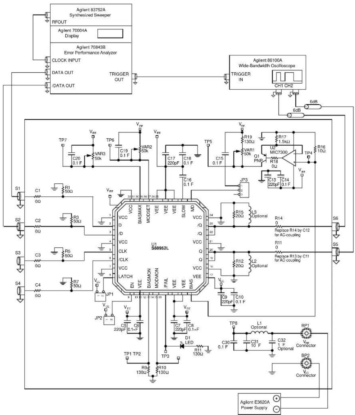
Agilent 83752A Synthesized Sweeper RFOUT Agilent 70004A Display Agilent 70843B Error Performance Analyzer CLOCK INPUT DATA OUT /DATA OUT TRIGGER OUT Agilent 86100A Wide-Bandwidth Oscilloscope TRIGGER IN CH1 CH2 6dB 6dB TP7 VFF TP6 VFF VAR3 50k C19 0.1 F VAR2 50k C17 220pF C18 0.1 F C16 0.1 F TP5 VFF R19 130Ω VAR1 50k Q1 PNP U2 MIC7300 TP4 R16 10Ω C15 0.1 F C13 220pF C14 0.1 F JP3 2 3 S1 C1 0Ω R1 50Ω VFF 325 51 50 9 28 7 28 28 28 28 28 28 28 28 28 28 28 28 28 28 28 28 28 28 28 28 28 28 28 28 28 28 28 28 28 28 28 28 28 28 S2 C2 0Ω R3 50Ω VCC BIAIMAX MODSET VEE VEE VEE SLOW MD VCC /Q /Q VCC /Q VCC /Q VCC /Q VCC /Q VCC /Q VCC /Q VCC /Q VCC /Q VCC /Q VCC /Q VCC /Q VCC /Q VCC /Q VCC /Q VCC /Q VCC /Q VCC /Q VCC /Q VCC /Q VCC /Q VSSMUX5L (S88952L) REFINER (S88952L) REFINER (S88952L) REFINER (S88952L) REFINER (S88952L) REFINER (S88952L) REFINER (S88952L) REFINER (S88952L) REFINER (S88952L) REFINER (S8B9) REFINER (S8B9) REFINER (S8B9) REFINER (S8B9) REFINER (S8B9) REFINER (S8B9) REFINER (S8B9) REFINER (S8B9) REFINER (S8B9) REFINER (S8B9) REFINER (S8B9) REFINER (S8B9) (S6) S5 C33 50Ω R5 50Ω CLK CLK LATCH EN VEE BIASMON MODMON /FAIL VEE VEE BIAS VEE VEE VEE VEE VEE VEE VEE VEE VEE VEE VEE VEE VEE VEE VEE VEE VEE VEE VEE VEE VEE VEE VEE VEE VEE VEE VEE VEE VEE VEE VEE VEE VEE VEE VEE VEE VEE VEE VEE VEE VEE VEE VEE VEE VEE VEE VEE VEE VEE VEE VeeFigure 2. Setup for Measurements
SETUP FOR MEASUREMENTS
This section explains how to connect and setup the SY88952L evaluation board per Figure 2. Ensure proper ESD precautionary measures are taken before handling sensitive electronic equipment, including the SY88952L evaluation board.
- Set E3620A to output 3.3V and then turn off E3620A. Connect E3620A's positive lead to BP2 ( V_CC ), negative lead to BP1 ( V_EE ).
- Configure Agilent BERT stack:
a. Set the 83752A Synthesized Sweeper to 2.5GHz.
b. From the 70004A's Pattern menu, choose the PRBS 2^31-1 pattern.
c. From the 70004A's Trigger menu:
i. Choose clock as trigger output
ii. Choose CLK/8 for divider
d. From the 70004A's Data menu:
i. External Termination = DC termination 0V
ii. Attenuation = 0dB
iii. Amplitude = 800mV (1600mV _pp )
iv. Hi-Level = -400mV
v. Tracking = ON
vi. Polarity = NORMAL
vii. Data Output = ON
viii. Crossing = 0
- Connect 70843V's trigger output to 86100A's trigger input.
- Bypass latch by shorting LATCH to V_EE via JP1, otherwise CLK must be used to input data.
- Enable outputs by leaving JP2 open, otherwise Q will be stuck HIGH.
- Bypass APC control by leaving JP3 open.
-
Connect D and /D (S1 and S2) on SY88952L evaluation board to 70843V's data outputs.
-
Attach 6dB attenuators to 86100A's inputs. 6dB attenuators are required since the scope can only display 2V_pp maximum amplitude waveforms, and the SY88952L evaluation board can output larger swings than this (90mA x 14.3Ω = 1.29V = 2.58V _pp ).
a. To configure 86100A to account for external 6dB attenuation, choose Setup -> Channel X (X = 1 to 4) -> Advanced -> Attenuator Factor = 6dB. - Connect Q and /Q (S5 and S6) on SY88952L evaluation board to 86100A's inputs through the 6dB attenuators.
- Set DMM157 to display voltage. Connect positive lead to BP2 and negative lead to TP4. This allows bias current measurements to be made.
- Turn on E3620A. Power supply current includes bias, modulation and input bias network current. This should be \~340mA for the maximum modulation and bias current settings. Excessive current usually means the power supply leads have been connected backwards. Be careful of this!
- Configure 86100A oscilloscope.
a. Verify a trigger signal is present by checking that the Trigger Source button is lit.
i. Depress this button to choose external source if necessary.
ii. Adjust trigger level if necessary.
b. Press Eye/Mask Mode on front panel.
c. Choose NRZ Eye Measurements from on-screen display.
d. Choose RMS Jitter, Rise Time, Fall Time and Eye Amplitude measurements from on-screen selection list.
MEASUREMENTS
The SY88952L evaluation board assumes the use of a 50Ω scope to terminate the SY88952L. This, in parallel with the on-board 20Ω output pull-up resistors, creates a 14.3Ω output load. The current passing through this load creates a voltage swing used to measure various performance parameters of the SY88952L. This modulation current is adjustable through the use of potentiometer VAR2. The bias current is adjustable through VAR3. The following sections detail various measurements that the SY88952L evaluation board allows.
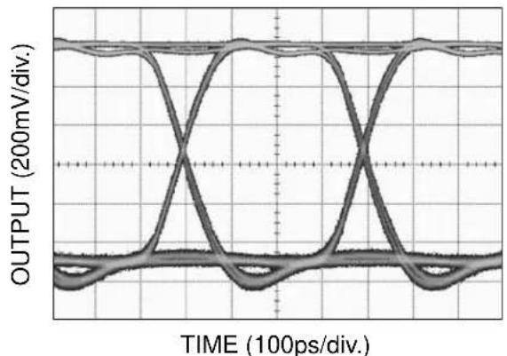
- Eye pattern generation including jitter and rise/fall times:
a. Adjust VAR2 to give 1.29V (2.58Vpp) output amplitude (IMOD = 90mA = 1.29V/0.014kΩ). VAR2 should be approximately 100Ω. The power supply needs to be turned off to get a correct reading of the potentiometer's resistance.
b. Adjust VAR3 to give 1V drop across R16 ( I_BIAS = 100mA = 1V/0.010k ). VAR3 should be approximately 100Ω. The power supply needs to be turned off to get a correct reading of the potentiometer's resistance.
c. Press Autoscale on oscilloscope. The eye pattern should automatically display on the scope. If not, verify the steps listed in the "Setup for Measurements" section are completed. Sometimes the waveform needs to be manually adjusted to fit the display. Use the Time Scale and Voltage Scale knobs on the front panel of the scope to adjust this.
d. Observe measurements on scope's display. The rise and fall times should be less than 75ps, amplitude around 1.29V and jitter around 10ps_rms .
e. Adjust VAR2 and VAR3 for desired modulation and bias currents and repeat above. Ensure the bias and modulation currents are not set to drive more than 100mA and 90mA respectively, otherwise the SY88952L will shutdown all output currents, and there will be no output swing.
line
| OUTPUT (200mV/div.) | TIME (100ps/div.) | | --------------------- | ------------------ | | 0 | 0 | | 1 | 0.5 | | 2 | 1.0 | | 3 | 1.5 | | 4 | 2.0 | | 5 | 2.5 | | 6 | 3.0 | | 7 | 3.5 | | 8 | 4.0 | | 9 | 4.5 | | 10 | 5.0 | | 11 | 5.5 | | 12 | 6.0 | | 13 | 6.5 | | 14 | 7.0 | | 15 | 7.5 | | 16 | 8.0 | | 17 | 8.5 | | 18 | 9.0 | | 19 | 9.5 | | 20 | 10.0 |Figure 3. Typical SY88952L Electrical Output at 2.5Gbps, 2^31-1 PRBS, I_MOD = 45mA , 3.3V @ 25^
- Mask testing:
a. Press Eye/Mask Mode on front panel of scope.
b. Choose Mask Testing from on-screen display.
c. Choose Open Mask from on-screen selection list.
i. Select and open the OC-48 mask.
d. Choose Start Mask Testing from on-screen selection list. Waveform should automatically display with appropriate mask regions and testing will start. If not, verify the steps listed in the "Setup for Measurements" section are completed.
3. BER testing:
a. Since the SY88952L is designed to drive a laser, where an optical HIGH means the laser is conducting, the SY88952L will electrically be LOW. Hence, the output polarity is opposite of the input polarity. Since this is the case, it is recommended to feedback /Q to the 70843B's BERT data input. The alternative is to feedback Q to the 70843B's BERT data input and select inverted polarity from the 70004A's Data menu.
b. Feedback the 70843V's Clock output to the 70843V's BERT Clock input.
c. Set the SY88952L's modulation current to a desired value using VAR2 as described in Section 1 of the "Measurements" section. Remember, I_MOD(mA) = Vamp(V) / 0.014k . Also, ensure the bias current is not set to drive more than 100mA, otherwise the SY88952L will shutdown all output currents, and there will be no output swing.
d. From the 70004A's Gating menu:
i. Choose a gate condition. The options are: gate by time, errors or bits. Choose bits, but this is of no relevance because there should be no errors, and the test will run forever until manually interrupted if gate by errors is chosen.
ii. Choose single gating period.
iii. Choose run gating.
iv. 70004A will reset error count and synchronize SY88952L's transmitted bitstream to 70843V's generated bit stream. If synchronization does not occur, it is sometimes due to cable length. Try using different length cables to achieve synchronization. If this is unavailable, another trick is to adjust the 83752A's frequency to a slightly higher or lower value.
v. At end of gating period, there should be no errors.
- Automatic Power Control (APC) functionality: The SY88952L evaluation board provides a monitor diode (MD) emulator which allows APC functionality of the SY88952L to be verified. In this implementation, VAR1 controls the MD current which is given by I_MD(mA) = 1.4V/VAR1(k) . This current flows through R17 and sets the inverting terminal voltage of U2. The SY88952L outputs a bias current such that the voltage at the non-inverting terminal matches the voltage and the inverting terminal at U2. As the user adjusts VAR1, the bias current adjusts also. However, if the MD current is adjusted too high, such that the bias current would go beyond the limit set by I_BIASMAX , then a fault occurs and the bias current limits to the value set by I_BIASMAX .
FREQUENTLY ASKED QUESTIONS
I just got my SY88952L evaluation board and I cannot get anything to work
First, check the power supplies. Typical power supply current should be \~340mA for the maximum modulation and bias current settings, including bias, modulation and input bias network current. Excessive current usually means the power supply leads have been connected backwards. Be careful of this!
If that looks okay, ensure the latch is bypassed by shorting LATCH to VEE via JP1. Also verify the outputs are enabled by leaving JP2 open. Then make sure the bias and modulation currents are not set to drive more than 100mA and 90mA respectively, otherwise the SY88952L will shutdown all output currents, and there will be no output swing.
Next, verify the 70004A's Data outputs are enabled and there's sufficient amplitude (at least 200mV_pp ) to drive the SY88952L.
If the above are okay and there's still nothing displaying on the scope, then there's most likely a trigger setup issue with the scope. Look on the scope's front panel and verify that the instrument is triggered. The Trigger Source button should be lit if a trigger signal is present. If not, press the button until the external trigger is selected. Also, try adjusting the level until a signal is found. If this does not work, verify the 70004A is set to output a CLK/8 trigger signal as described in the "Setup for Measurements" section of this document.
Why is the Q output LOW when I set the D input HIGH?
The SY88952L is a laser driver and is meant to conduct current through the laser diode during the high state. This means that, with a resistive load, the output will be LOW when the input is HIGH. But optically, the output will be HIGH when the input is HIGH.
Can you suggest a bypass/decoupling scheme?
Figure 2 shows the power supply decoupling scheme used for the SY88952L evaluation board. The “Bill of Materials” at the end of this document lists the supplier and component values. We have found this arrangement to be an excellent starting point.
What layout tips do you have?
- Establish controlled impedance stripline, microstrip or coplanar construction techniques for high-speed signal paths.
- All differential paths are critical timing paths and skew should be matched to within ±10ps .
- Signal trace impedance should not vary more than ±5% . If in doubt, perform Time Domain Reflectometry (TDR) analysis of signal traces.
- Place power supply decoupling capacitors as close as possible to the device's power pins.
What is Time Domain Reflectometry (TDR)?
TDR is used to verify impedance continuity along a signal path. Many interconnects, such as SMA, if not launched correctly onto the PCB, will exhibit inductive-like resonance with an abrupt capacitive discontinuity. This discontinuity will subtract signal from the inputs and outputs, effectively closing the resulting data eye. The 86100A allows TDR testing and is a useful tool to help evaluate your PCB.
I still have questions. Who should I contact?
Micrel's HBW applications helpline is available to assist you. Please call (408) 955-1690 or email hbwhelp@micrel.com for assistance.
BILL OF MATERIALS
| Item Part Number Manufacturer Description Qty | ||||
| BP1 5011 Keystone | (1) | black test point 1 | ||
| BP2 5010 Keystone | (1) | red test point 1 | ||
| C11, C12, C15, C16, C19, C20, C30 | PCC1731CT-ND | Panasonic^(2) | 0.1 F surface mount capacitor, size 0402 | 7 |
| C5, C7, C9, C13, C17 | PCC1731CT-ND | Panasonic^(2) | 220pF surface mount capacitor, size 0402 | 5 |
| C6, C8, C10, C14, C18 | PCC1762CT-ND | Panasonic^(2) | 0.1 F surface mount capacitor, size 0603 | 5 |
| C32 | PCC1915CT-ND | Vishay^(3) | 1 F surface mount capacitor, size 0603 | 1 |
| C31 | PCC1940CT-ND | Panasonic^(2) | 10 F surface mount capacitor, size 1206 | 1 |
| R1, R3, R5, R7 | CRCW040249R9F | Vishay^(3) | 49.9 surface mount resistor, size 0402 | 4 |
| R9, R10, R11, R19 | CRCW04021300F | Vishay^(3) | 130 surface mount resistor, size 0402 | 4 |
| R12, R15 | P20GCT-ND | Panasonic^(2) | 20 surface mount resistor, size 0603 | 2 |
| C1, C2, C3, C4R13, R14, R18 | CRCW04020R00F | Vishay^(3) | 0 surface mount resistor, size 0402 | 7 |
| R16 CRCW060310R0F | Vishay | (3) | 10 surface mount resistor, size 0603 | 1 |
| R17 | CRCW04021501F | Vishay^(3) | 1.5k surface mount resistor, size 0402 | 1 |
| S1, S2, S3,S4, S5, S6 | 142-0701-851 | Johnson^(4) | end launch SMA | 6 |
| TP1, TP2, TP3, TP4TP5, TP6, TP7, TP8 | TSW-101-07-S-S | Samtec^(5) | 1-header 0.1mil center terminal strip | 8 |
| JP1, JP2 | TSW-102-07-S-S | Samtec^(5) | 1-header 0.1mil center terminal strip | 2 |
| JP3 | TSW-103-07-S-S | Samtec^(5) | 1-header 0.1mil center terminal strip | 1 |
| JUMPER | JMP | Samtec^(5) | 0.1mil center jumper | 3 |
| VAR1, VAR2, VAR3 | 3269W-1-503G | Bourns^(6) | 50k potentiometer | 3 |
| Q1 | FMMT591A | Zetex^(7) | PNP transistor | 1 |
| D1 | LN29RP | Panasonic^(2) | red LED | 1 |
| U1 | SY88952L | Micrel, Inc.(8) | 2.7Gbps SONET/SDH Laser Driver | 1 |
| U2 | MIC7300BM5 | Micrel, Inc.(8) | op-amp1 | |
Notes:
-
Keystone tel: 800-221-5510.
-
Panasonic tel: 800-344-2112.
-
Vishay tel: 402-563-6866.
-
Johnson tel: 800-247-8256.
-
Samtec tel: 800-726-8329.
-
Bourns tel: 877-426-8767.
-
Zetex tel: +44 161-622-4444.
-
Micrel, Inc. tel: 408-944-0800.
MICREL, INC. 1849 FORTUNE DRIVE SAN JOSE, CA 95131 USA
TEL + 1 (408) 944-0800 FAX + 1 (408) 474-1000 WEB http://www.micrel.com
The information furnished by Micrel in this data sheet is believed to be accurate and reliable. However, no responsibility is assumed by Micrel for its use. Micrel reserves the right to change circuitry and specifications at any time without notification to the customer.
Micrel Products are not designed or authorized for use as components in life support appliances, devices or systems where malfunction of a product can reasonably be expected to result in personal injury. Life support devices or systems are devices or systems that (a) are intended for surgical implant into the body or (b) support or sustain life, and whose failure to perform can be reasonably expected to result in a significant injury to the user. A Purchaser's use or sale of Micrel Products for use in life support appliances, devices or systems is at Purchaser's own risk and Purchaser agrees to fully indemnify
Micrel for any damages resulting from such use or sale.
© 2004 Micrel, Incorporated.