SY88982L - Electronic component Microchip - Free user manual and instructions
Find the device manual for free SY88982L Microchip in PDF.

User questions about SY88982L Microchip
0 question about this device. Answer the ones you know or ask your own.
Ask a new question about this device
Download the instructions for your Electronic component in PDF format for free! Find your manual SY88982L - Microchip and take your electronic device back in hand. On this page are published all the documents necessary for the use of your device. SY88982L by Microchip.
USER MANUAL SY88982L Microchip
3.3V, 2.7Gbps High-Current, Low-Power Laser Driver for FP/DFB Lasers
General Description
The SY88982L is a single 3.3V supply, low power consumption, small form factor driver for telecom/datacom applications using FP/DFB lasers at data rates up to 2.7Gbps. The driver can deliver modulation current up to 90mA, and the high compliance voltage if offers, makes the part suitable for high-current operation (with the laser AC- or DC-coupled to it). This device is intended to be used with Micrel's MIC3003 Optical Transceiver Management IC, which allows for both modulation and bias current control and monitoring, automatic power control, and temperature compensation.
All support documentation can be found on Micrel's web site at: www.micrel.com.
Features
- 2.4V minimum laser compliance voltage for high-current DC-coupled applications
• 48mA power supply current typical
• Operation up to 2.7Gbps
• Modulation current up to 90mA - Designed for use with the MIC3003
- Laser may be DC- or AC-coupled
- Small form factor 16-pin (3mm x 3mm) QFN package
Applications
- Multi-rate LAN, MAN applications up to 2.7Gbps: FC, GbE, SONET OC3/12/24/48 and SDH STM1/4/8/16
- SFF, SFP modules
Markets
- Telecom, Datacom
Typical Application
text_image
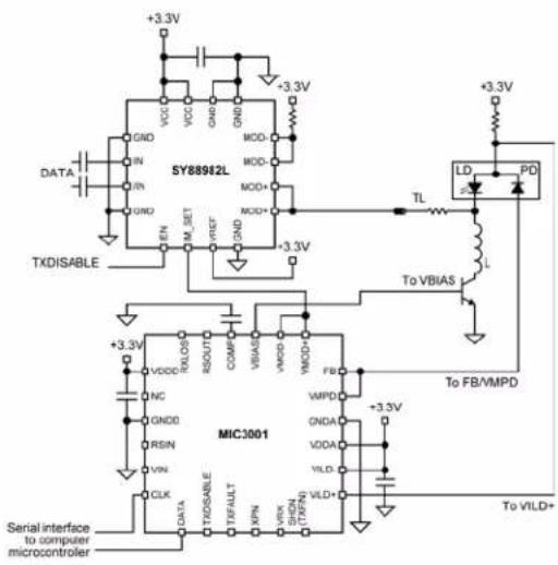
SY88912L +3.3V -3.3V +3.3V DATA GND IN JIN GND EN M_SET REF GND +3.3V To VBIAS L To FB/VMPD MIC3001 +3.3V +3.3V Serial interface to computer microcontroller DATA TXDISABLE VDDO NC GND0 RSIN VIN CLK DATA TXDISABLE TPFALLT XPN VDDA VDDA VLD+ VLD+ VLD- +3.3V +3.3V +3.3V +3.3V +3.3V +3.3V +3.3V +3.3V +3.3VLaser DC-Coupled to the Driver

text_image
+3.3V MCD- +3.3V MCD- MDD+ MDD- TL +3.3V LD PD To VBIAS To FBVMPD To VILD+Laser AC-Coupled to the Driver
Functional Block Diagram

text_image
VCC DIN+ 50Ω DIN- Input Buffer 50Ω VREF /EN Pre-Driver MOD+ MOD- GNDOrdering Information ^(1)
| Part Number | Package Type | Operating Range | Package Marking | Lead Finish |
| SY88982LMG | QFN-16 | Industrial | 982L with Pb-Free bar-line indicator | NiPdAu Pb-Free |
| SY88982LMGTR(2) | QFN-16 | Industrial | 982L with Pb-Free bar-line indicator | NiPdAu Pb-Free |
Notes:
1. Contact factory for die availability. Dice are guaranteed at T_A = +25^ , DC Electricals only.
2. Tape and Reel.
Pin Configuration

text_image
/EN IM_SET VREF GND 16 15 14 13 GND 1 12 MOD+ DIN- 2 11 MOD+ DIN- 3 10 MOD- GND 4 9 MOD- 5 6 7 8 VCC VCC GND GND16-Pin QFN
Pin Description
| Pin Number | Pin Name | Pin Function |
| 1, 4, 7, 8, 13 | GND | Ground. Ground and exposed pad must be connected to the plane of the most negative potential. |
| 2 DIN+ | Non-Inverting Input Data. Internally terminated with 50Ω to a reference voltage. | |
| 3 DIN- | Inverting Input Data. Internally terminated with 50Ω to a reference voltage. | |
| 5, 6 | VCC | Supply Voltage. Bypass with a 0.1μF//0.01μF low ESR capacitor as close to VCC pin as possible. |
| 9, 10 | MOD- | Inverted Modulation Current Output. Provides modulation current when input data is negative. |
| 11, 12 | MOD+ | Non-Inverted Modulation Current Output. Provides modulation current when input data is positive. |
| 14 | VREF | Reference Voltage. Install a 0.1μF capacitor between VREF and VCC. |
| 15 | IM_SET | Modulation current setting and control. The voltage applied to this pin will set the modulation current. To be connected to the MIC3003 pin 24 (VMOD+). Input impedance 25kΩ. |
| 16 | /EN | A high level signal applied to this pin will disable the output stage of the driver. Internally pulled down with 25kΩ resistor. |
Truth Table
| DIN+ | DIN- | /EN | MOD_+^(1) | MOD- | Laser Output^(2) |
| L | H | L | H | L | L |
| H | L | L | L | H | H |
| X | X | H | H | H | L |
Notes:
1. I_MOD = 0 when MOD_+ = H .
2. Assuming that the laser is tied to MOD+.
Absolute Maximum Ratings ^(1)
Supply Voltage ( V_IN ) -0.5V to +4.0V
CML Input Voltage ( V_IN ) ...... V_CC-1.2V to V_CC+0.5V
TTL Control Input Voltage ( V_IN ) 0V to V_CC
Lead Temperature (soldering, 20sec.) .....+260°C
Storage Temperature ( T_s )....-65°C to +150°C
Operating Ratings ^(2)
Supply Voltage (Vcc)....+3.0V to +3.6V
Ambient Temperature ( T_A )....-40°C to +85°C
Package Thermal Resistance ^(3) QFN
(θ JA) Still-air 60°C/W
(ψ JB) 33°C/W
DC Electrical Characteristics
T_A = -40^ to 85^ and V_CC = +3.0V to +3.6V , unless otherwise noted. Typical values are V_CC = +3.3V , T_A = 25^ , I_MOD = 60mA .
| Symbol | Parameter | Condition | Min | Typ | Max | Units |
| I_CC | Power Supply Current | Modulation current excluded | 48 | 65^(4) | mA | |
| V_MOD\_MIN | Minimum Voltage Required at the Driver Output (headroom) for Proper Operation | 0.6 | V | |||
| R_IN(DATA) | Input Resistance (DIN+, DIN-) | 45 | 50 | 55 | Ω | |
| V_ID | Differential Input Voltage Swing | 200 | 2400 | mV_PP | ||
| /EN Low | 0.8 | V | ||||
| /EN High | 2 | V | ||||
| R_IN (IMOD\_SET) | I_M\_SET Input Resistance | 25 | kΩ | |||
| V_IM\_SET | Voltage Range on I_M\_SET Pin | I_MOD range 10mA – 90mA | 1.2 | V |
AC Electrical Characteristics
T_A = -40^ to 85^ and V_CC = +3.0V to +3.6V , unless otherwise noted. Typical values are V_CC = +3.3V , T_A = 25^ , I_MOD = 60mA .
| Symbol | Parameter | Condition | Min | Typ | Max | Units |
| Data Rate | NRZ | 0.155 | 2.7 | Gbps | ||
| I_MOD | Modulation Current(5) | AC-coupled | 10 | 90 | mA | |
| DC-coupled | 10 | 70(6) | mA | |||
| I_MOD\_OFF | Modulation OFF Current | Current at MOD+ when the device is disabled. | 750 | μA | ||
| t_r | Output Current Rise Time | 20% to 80%, I_MOD = 60mA, 15Ω load | 55 | 80 | ps | |
| t_f | Output Current Fall Time | 20% to 80%, I_MOD = 60mA, 15Ω load | 55 | 80 | ps | |
| Total Jitter | @2.5Gbps data rate | 20 | p_SPP | |||
| Pulse-Width Distortion | I_MOD range 10mA – 90mA | 20 | ps |
Notes:
- Permanent device damage may occur if absolute maximum ratings are exceeded. This is a stress rating only and functional operation is not implied at conditions other than those detailed in the operational sections of this data sheet. Exposure to absolute maximum ratings conditions for extended periods may affect device reliability.
- The data sheet limits are not guaranteed if the device is operated beyond the operating ratings.
- Package Thermal Resistance assumes exposed pad is soldered (or equivalent) to the devices most negative potential on the PCB. _JB uses a 4-layer and _JA in still air unless otherwise stated.
- I_CC = 48mA for worst-case conditions with I_MOD = 90mA , T_A = +85^ , V_CC = 3.6 .
- Load = 15Ω.
- Assuming VCC = 3.0V, Laser bandgap voltage = 1V, laser package inductance = 1nH, laser equivalent series resistor = 5Ω, and damping resistor = 10Ω.
Typical Operating Characteristics
line
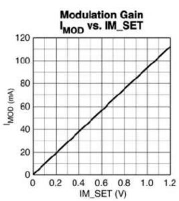
| IM_SET (V) | I_MOD (mA) | | ---------- | ---------- | | 0.0 | 0.0 | | 0.2 | 20.0 | | 0.4 | 40.0 | | 0.6 | 60.0 | | 0.8 | 80.0 | | 1.0 | 100.0 | | 1.2 | 120.0 |
line
| MODULATION CURRENT (mA) | SUPPLY CURRENT (mA) | | ----------------------- | ------------------- | | 10 | 38 | | 20 | 40 | | 30 | 42 | | 40 | 44 | | 50 | 46 | | 60 | 48 | | 70 | 50 | | 80 | 52 | | 90 | 55 |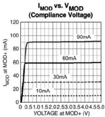
line
| VOLTAGE at MOD+ (V) | I_MOD at MOD+ (mA) for 10 mA | I_MOD at MOD+ (mA) for 30 mA | I_MOD at MOD+ (mA) for 60 mA | I_MOD at MOD+ (mA) for 90 mA | | ------------------- | ---------------------------- | ---------------------------- | ---------------------------- | ---------------------------- | | 0.0 | 0 | 0 | 0 | 0 | | 0.5 | ~20 | ~40 | ~60 | ~90 | | 1.0 | ~20 | ~40 | ~60 | ~90 | | 1.5 | ~20 | ~40 | ~60 | ~90 | | 2.0 | ~20 | ~40 | ~60 | ~90 | | 2.5 | ~20 | ~40 | ~60 | ~90 | | 3.0 | ~20 | ~40 | ~60 | ~90 | | 3.5 | ~20 | ~40 | ~60 | ~90 | | 4.0 | ~20 | ~40 | ~60 | ~90 | | 4.5 | ~20 | ~40 | ~60 | ~90 | | 5.0 | ~20 | ~40 | ~60 | ~90 |
line
| Signal | Value | | ---------- | ------- | | IEN | 33.0ns | | Laser Output | 25.0ns |
line
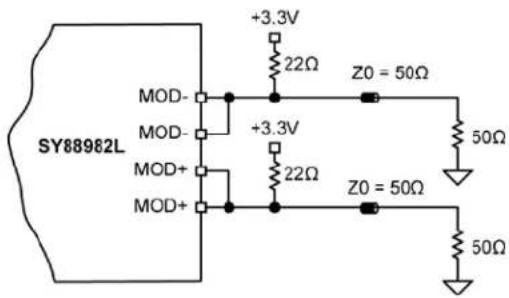
| Parameter | Value | | --------------- | --------- | | Δ | 1.55μs | | @: | 0 s | | /EN | - | | Laser Output | (labeled point) | | M | 2.50μs | | Aux J | 1.40 V |Test Circuit
text_image
SY88982L MOD- MOD- MOD+ MOD+ +3.3V 22Ω Z0 = 50Ω +3.3V 22Ω Z0 = 50Ω 50Ω 50ΩFunctional Characteristics
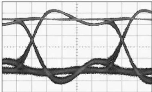
Electrical Eye Diagram
2.5Gbps, PRBS 2 ^23 -1, 15Ω Load, 60mA Modulation
natural_image
Abstract waveforms on grid background, no text or symbols presentTIME (66ps/div.)
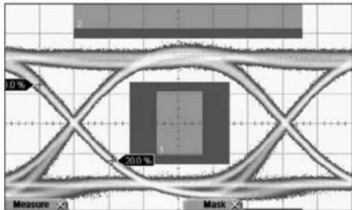
Optical Eye Diagram
2.7Gbps, PRBS 2 ^23 -1, Laser AC-Coupled
text_image
10% 20.0% Measure MaskTIME (66ps/div.)
ER = 10dB, 30% Mask Margin
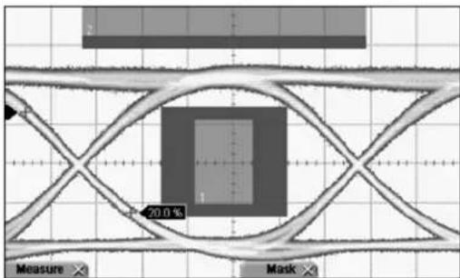
Optical Eye Diagram
2.5Gbps, PRBS 2 ^23 -1, Laser DC-Coupled
text_image
20.0 % Measure MaskTIME (65ps/div.)
ER = 11dB, 30% Mask Margin
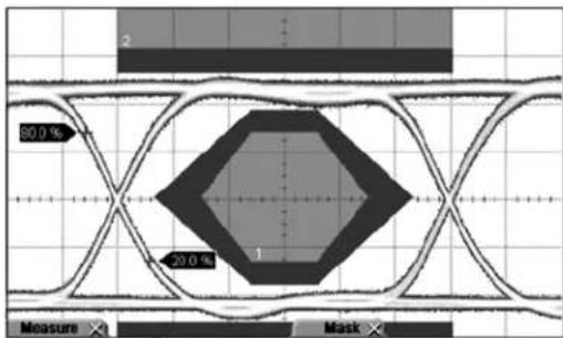
Optical Eye Diagram with OC-48 Filter
1.25Gbps, PRBS 2 ^23 -1, Laser DC-Coupled
text_image
80.0% 20.0% 1 Measure MaskTIME (133ps/div.)
ER = 11dB, 55% Mask Margin
Optical Eye Diagram
622Mbps, PRBS 2 ^23 -1, Laser DC-Coupled

text_image
0.0% 20.0% Measure MaskTIME (267ps/div.)
ER = 11.3dB, 60% Mask Margin
Optical Eye Diagram
155Mbps, PRBS 2 ^23 -1, Laser DC-Coupled

text_image
0.0% 20.6% Measure MaskTIME (1075ps/div.)
ER = 11.3dB, 60% Mask Margin
Input and Output Stages
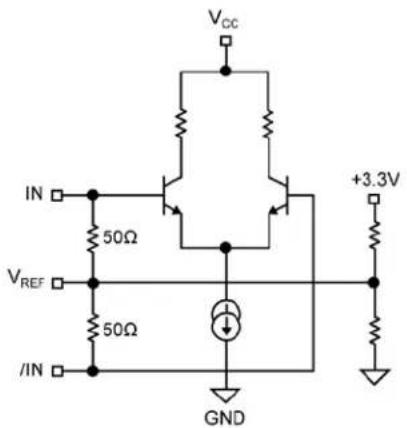
text_image
VCC IN 50Ω VREF 50Ω /IN +3.3V GNDFigure 1a. Simplified Input Stage

text_image
MOD+ MOD- GNDFigure 1b. Simplified Output Stage
Interfacing the Input to Different Logic Drivers

text_image
LVPEC1 GND 50Ω IN 50Ω /IN +3.3V 0.1μF VREF 50Ω GND SY88982LFigure 2a. DC-Coupling to LVPECL Driver

text_image
LVPECL Rpd GND 50Ω IN 50Ω /IN +3.3V 0.1μF VREF Note: Rpd = 140Ω to 220Ω. SY88982LFigure 2b. AC-Coupling to LVPECL Driver

text_image
CML 50Ω IN 50Ω /IN +3.3V 0.1μF SY88982L VREFFigure 2c. AC-Coupling to CML Driver
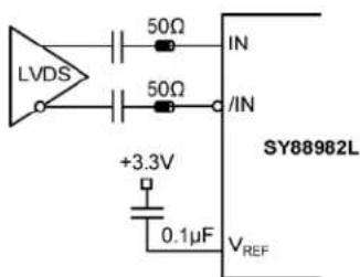
text_image
LVDS +3.3V 0.1μF IN 50Ω 50Ω /IN SY88962L VREFFigure 2d. AC-Coupling to LVDS Driver
Application Information
The typical applications diagram on the first page shows how to connect the driver to the laser, single ended. To improve transition time and laser response, the laser can be driven differentially as shown in Figures 3 and 4. Driving the laser differentially will also minimize the crosstalk with the rest of the circuitry on the board, especially the receiver.
DC-Coupling
In addition to the low power consumption and high modulation current, the SY88982L offers a high compliance voltage. As can be seen in the "Typical Operating Characteristics" section ( I_MOD vs. V_MOD curves), the minimum voltage needed at the output of the driver for proper operation is less than 600mV, leaving a large headroom, V_CC-600mV , to the laser with the damping resistor. To show the importance of this high compliance voltage, consider the voltage drops along the path from V_CC to ground through the laser, damping resistor, and driver:
$$ V _ {C C} = \text { Driver Headroom } + V _ {R d} + V _ {\text { laser }} $$
$$ V _ {R d} = R d \times I _ {M O D} $$
$$ V _ {\text { laser }} = V _ {\text { band - gap }} + R _ {\text { laser }} \times I _ {\text { MOD }} + L d i / d t $$
$$ \begin{array}{l} \mathrm {V_ {band - gap} + R_ {laser} \times I_ {MOD} = 1.6V at maximum for} \ \text { a Fabry Perrot or a DFB laser. } \end{array} $$
Ldi/dt is the voltage drop due to the laser parasitic inductance during I_MOD transitions. Assuming L = 1nH, t_f = t_f = 80ps (measured between 20% and 80% of I_MOD ), and I_MOD = 70mA (42mA from 20% to 80%), then Ldi/dt will be equal to 525mV. This number can be minimized by making the laser leads as short as possible and using and RC compensation network between the cathode of the laser and ground or across the laser driver outputs as shown in Figure 3.
To be able to drive the laser DC-coupled with a high current, it is necessary to keep the damping resistor as small as possible. For example, if the drop due to parasitic inductance of the laser is neglected (compensated for) and the maximum drop across the laser (1.6V) considered while keeping a minimum of 600mV headroom for the driver, then the maximum damping resistor that allows a 70mA modulation current into the laser is:
$$ R _ {d m a x} = (V _ {C C} - 0. 6 V - 1. 6 V) / 0. 0 7 A $$
The worst case will be with V_cc = 3.0V , leading to R_dmax = 11.4
On the other hand, the small is the value of R_d , the higher is the overshoot/undershoot on the optical signal from the laser. In the circuit shown in Figure 3, the RC compensation network across the driver outputs (MOD+ and MOD-) allows the user R_d = 10 . The optical eye diagrams at data rates of 155Mbps/622Mbps/1.25Gbps/2.5Gbps, shown in "Functional Characteristics" section, are all obtained with the same circuit using R_d = 10 , R_Comp = 100 , and C_Comp = 3pF . The compensation network may change from one board to another and from one type of laser to another. An additional compensation network (RC) can be added at the laser cathode for further compensation and eye smoothing.

text_image
SY88982L MOD- MOD- MOD+ MOD+ Rd CComp RComp Rd LD PD +3.3V L = Murata BLM18HG102SN R C L Bias to APCFigure 3. Laser DC-Coupled
AC-Coupling
When trying to AC couple the laser to the driver, the headroom of the driver is no longer a problem since it is DC isolated from the laser with the coupling capacitor. At the output, the headroom of the driver is determined by the pull-up network. In Figure 4, the modulation current out of the driver is split between the pull-up network and the laser. If, for example, the total pull-up resistor is twice the sum of the damping resistor and laser equivalent series resistance, only two thirds (2/3) of the modulation current will be used by the laser. So, to keep most of the modulation current going through the laser, the total pull-up resistor must be kept as high as possible. One solution consists in using an inductor alone as pull-up, presenting a high impedance path for the modulation current and zero ohm (0Ω) path for the DC current offering a headroom of the driver equal to Vcc and almost all the modulation current goes into the laser. The inductor alone will cause signal distortion, and, to improve that, a combination of resistors and inductors can be used (as shown on Figure 4). In this case, the headroom of the driver is Vcc-R1 x αlMOD, where αlMOD is the portion of the modulation current that goes through the pull-up network.
When the laser is AC-coupled to the driver, the coupling capacitor creates a low-frequency cutoff in the circuit, and its value must be chosen as large as
possible. If the value of the cap is too high, it will slow down the fast signals edges, and, if its value is too small, it won't be able to hold a constant change between the first bit and the last bit of a long string of identical bits in a low data rate application. This leads to higher pattern-dependent jitter in the transmitter signal. 0.1μF is found to be good for all applications from 155Mbps to 2.7Gbps.
AC-coupling the laser to the driver brings a solution to the driver headroom problem at the expense of extra components, loss of part of the modulation current wasted in the pull-up network, and additional power consumption.
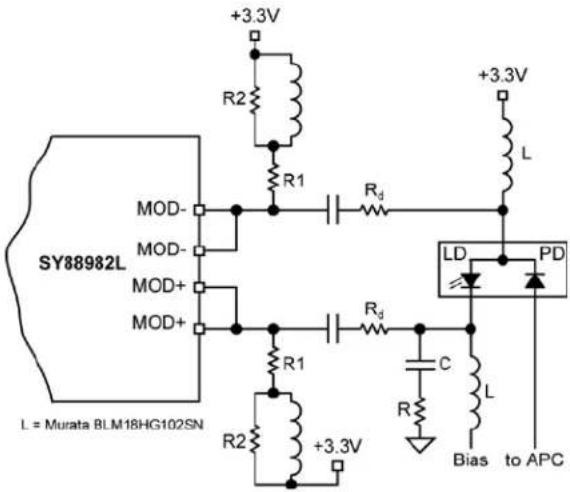
text_image
SY88982L L = Murata BLM18HG102SN +3.3V R2 R1 Rd +3.3V L MOD- MOD- MOD+ MOD+ R1 Rd LD PD R C L Bias to APC R2 +3.3VFigure 4. Laser AC-Coupled
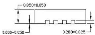
Package Information
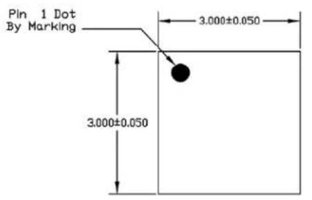
text_image
Pin 1 Dot By Marking 3.000±0.050 3.000±0.050TOP VIEW
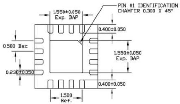
text_image
PIN #1 IDENTIFICATION CHAMFER 0.300 X 45° 1.550±0.050 Exp. DAP 0.400±0.050 1.550±0.050 Exp. DAP 0.500 Bsc 0.230±0.050 0.400±0.050 1.500 Ref.BOTTOM VIEW
text_image
0.850±0.050 0.000-0.050 0.203±0.025SIDE VIEW
NOTE:
- ALL DIMENSIONS ARE IN MILLIMETERS.
- MAX. PACKAGE WARPAGE IS 0.05 nm.
- MAXIMUM ALLOWABE BURRS IS 0.076 nm IN ALL DIRECTIONS
- PIN #1 ID ON TOP WILL BE LASER/INK MARKED.
16-Pin (3mm x 3mm) QFN
MICREL, INC. 2180 FORTUNE DRIVE SAN JOSE, CA 95131 USA
TEL +1 (408) 944-0800 FAX +1 (408) 474-1000 WEB http://www.micrel.com
The information furnished by Micrel in this data sheet is believed to be accurate and reliable. However, no responsibility is assumed by Micrel for its use. Micrel reserves the right to change circuitry and specifications at any time without notification to the customer.
Micrel Products are not designed or authorized for use as components in life support appliances, devices or systems where malfunction of a product can reasonably be expected to result in personal injury. Life support devices or systems are devices or systems that (a) are intended for surgical implant into the body or (b) support or sustain life, and whose failure to perform can be reasonably expected to result in a significant injury to the user. A Purchaser's use or sale of Micrel Products for use in life support appliances, devices or systems is a Purchaser's own risk and Purchaser agrees to fully indemnify Micrel for any damages resulting from such use or sale.
© 2005 Micrel, Incorporated.