SY88992L - Electronic component Microchip - Free user manual and instructions
Find the device manual for free SY88992L Microchip in PDF.

User questions about SY88992L Microchip
0 question about this device. Answer the ones you know or ask your own.
Ask a new question about this device
Download the instructions for your Electronic component in PDF format for free! Find your manual SY88992L - Microchip and take your electronic device back in hand. On this page are published all the documents necessary for the use of your device. SY88992L by Microchip.
USER MANUAL SY88992L Microchip
The SY88992L is a single supply 3.3V, low power consumption, small-form factor VCSEL driver ideal for use in datacom applications; Ethernet, GbE (Gigabit Ethernet), and FC (Fibre Channel) applications that operate from 100Mbps up to 4.25Gbps. The modulation current is set by applying an external voltage at the IM_SET pin. The driver features an adjustable peaking option with variable amplitude and duration to improve VCSEL edge response. The driver can deliver modulation current up to 25mA and a peaking current up to 35% of the modulation current. This device is intended to be used with Micrel's MIC3001 Optical Transceiver Management IC, which allows for both modulation and bias current control and monitoring, APC (Automatic Power Control), and temperature compensation.
All support documentation can be found on Micrel's web site at: www.micrel.com.
Features
- Up to 25mA modulation current
- Operates from 100Mbps to 4.25Gbps
- Peaking with variable duration option for better VCSEL response
- Dual peaking, on the rise and falling edges
- Peaking current proportional to modulation current
- Easy modulation current setting
• Fully controllable with Micrel MIC3001 - Small (3mm x 3mm) 16 pin QFN package
Applications
- Multirate LAN, SAN applications up to 4.25Gbps: Ethernet, GbE, FC
- SFF, SFP Modules
Markets
- Datacom
Typical Application
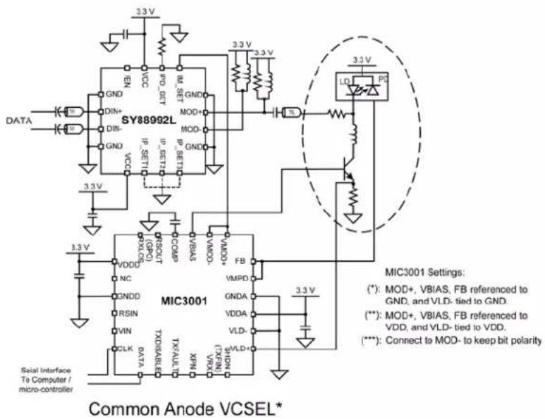
text_image
SY88992L MIC3001 Common Anode VCSEL* 3.3 V EN GND DIN+ DIN- GND VCC IP-SET11 IP-SET12 IP-SET13 3.3 V 3.3 V 3.3 V 3.3 V 3.3 V 3.3 V 3.3 V 3.3 V VDD NC GNDD RSIN VIN CLK DATA TX/DIR/ARLE TX/AUL XPN Y/RX VDDA VLD- VMD+ VMPD VMD+ VMD+ VMPD+ VMD+ VMD+ VMD+ VMD+ VMD+ VMD+ VMD+ VMD+ VMD+ VMD+ VMD+ VMD+ VMD+ VMD+ VMD+ VMD+ VMD+ VMD+ VMD+ VMD+ VMD+ VMD+ VMD+ VMD+ VMD+ VMD+ VMD+ VMD+ VMD+ VMD+ VMD+ VMD+ VMD+ VMD + VDD GND MOD+, MOD+, VBIAS, FB referenced to GND, and VLD- tied to GND. (**): MOD+, VBIAS, FB referenced to VDD, and VLD- tied to VDD. (***): Connect to MOD- to keep bit polarity MIC3001 Settings: (*): MOD+, VBIAS, FB referenced to GND, and VLD- tied to GND. (**): MOD+, VBIAS, FB referenced to VDD, and VLD- tied to VDD. (***): Connect to MOD- to keep bit polarity Sial Interface To Computer / micro-controller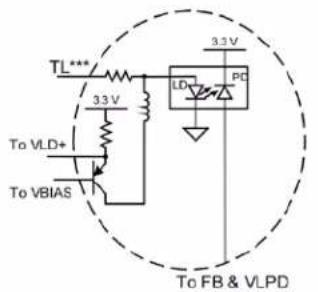
text_image
TL*** 3.3 V To VLD+ To VBIAS 3.3 V LD PC To FB & VLPDCommon Cathode VCSEL**
Functional Block Diagram

flowchart
graph TD
    A["DIN+"] --> B["100 Ω"]
    C["DIN-"] --> B
    B --> D["Op-Amp"]
    D --> E["MOD+"]
    D --> F["MOD-"]
    G["IPD_SET"] --> H["/EN"]
    I["IM_SET"] --> J["Modulation Control"]
    K["IP_SET1"] --> L["Peaking Control"]
    M["IP_SET2"] --> L
    N["IP_SET3"] --> L
    L --> O["MOD+"]
    L --> P["MOD-"]
Ordering Information ^(1)
| Part Number Package Type | Operating Range | Package Marking Lead Finish | |
| SY88992LMG | QFN-16 | Industrial | 992L with Pb-Free bar-line indicator |
| SY88992LMGTR(2) | QFN-16 | Industrial | 992L with Pb-Free bar-line indicator |
Notes:
- Contact factory for die availability. Dice are guaranteed at T_A = +25^ , DC Electricals only.
- Tape and Reel.
Pin Configuration

text_image
IEN VCC IPD_SET IM_SET GND 16 15 14 13 12 GND DIN+ 2 11 DIN- 3 10 GND 4 9 5 6 7 8 VCC IP_SET1 IP_SET2 IP_SET316-Pin QFN
Pin Description
| Pin Number | Pin Name | Pin Function |
| 2 DIN+ | Non-Inverting Input Data. Internally terminated with 50Ω to a reference voltage. | |
| 3 DIN- | Inverting Input Data. Internally terminated with 50Ω to a reference voltage. | |
| 6 | IP_SET1 | Peaking Current Setting. Connect this pin to GND and keep pins 7 and 8 open to set peaking-to-modulation current ratio to 5%. Combinations of the three pins, as shown in table below, will set different ratios up to 35%. |
| 7 | IP_SET2 | Peaking Current Setting. Connect this pin to GND and keep pins 6 and 8 open to set peaking-to-modulation current ratio to 10%. Combinations of the three pins, as shown in table below, will set different ratios up to 35%. |
| 8 | IP_SET3 | Peaking Current Setting. Connect this pin to GND and keep pins 6 and 7 open to set peaking-to-modulation current ratio to 20%. Combinations of the three pins, as shown in table below, will set different ratios up to 35%. |
| 10 | MOD- | Inverted Modulation Current Output. Provides modulation current when input data is negative. |
| 11 | MOD+ | Non-Inverted Modulation Current Output. Provides modulation current when input data is positive. |
| 13 | IM_SET | Modulation Current Setting. The modulation current is set by applying a 0V to 1.2V voltage at this pin. |
| 14 | IPD_SET | Peaking Duration Setting. The peaking current duration is set by installing a resistor between this pin and ground. The plot on page 6 shows peaking duration versus the value of the resistor installed. |
| 16 | /EN | A low level signal applied to this pin will enable the output stage of the driver. Internally pulled down to ground with 75kΩ resistor. |
| 1, 4, 9, 12 | GND | Ground. Ground and exposed pad must be connected to the plane of the most negative potential. |
| 5, 15 | VCC | Supply Voltage. Bypass with a 0.1μF//0.01μF low ESR capacitor as close to VCC pin as possible. |
Truth Table
| DIN+ | DIN- | /EN | MOD^+(1) | MOD- VOSEL Output | (2) |
| L | H | L | H | L | L |
| H | L | L | L | H | H |
| X | X | H | H | H | L |
Notes:
- I_MOD = 0 when MOD_+ = H .
- Assuming a common anode VCSEL with its cathode tied to MOD+.
Peaking Current-to-Modulation Current Ratio Setting
| IP/IMOD | 0 % | 5 % | 10 % | 15 % | 20 % | 25 % | 30 % | 35 % |
| IP_SET1 | NC | GND | NC | GND | NC | GND | NC | GND |
| IP_SET2 | NC | NC | GND | GND | NC | NC | GND | GND |
| IP_SET3 | NC | NC | NC | NC | GND | GND | GND | GND |
Absolute Maximum Ratings ^(1)
Supply Voltage ( V_IN ) -0.5V to +4.0V
CML Input Voltage ( V_IN ) ..... V_CC-1.2V to V_CC+0.5V
TTL Control Input Voltage ( V_IN ) 0V to V_CC
Lead Temperature (soldering, 20sec.) .....+260°C
Storage Temperature ( T_s )....-65°C to +150°C
Operating Ratings ^(2)
Supply Voltage (Vcc)....+3.0V to +3.6V
Ambient Temperature ( T_A )....-40°C to +85°C
Package Thermal Resistance ^(3)
QFN
(θ JA) Still-air....60°C/W
(ψ JB) 33°C/W
DC Electrical Characteristics
T_A = -40^ to 85^ and V_CC = 3.0V to 3.6V , unless otherwise noted. Typical values are at: V_CC = 3.3V , T_A = 25^ , I_MOD = 13mA^(4)
| Symbol | Parameter | Condition | Min | Typ | Max | Units |
| I_CC | Power Supply Current | Peaking not used | 57 | 95 | mA | |
| Maximum peaking used | 70 | 110 | mA | |||
| I_MOD^(4) | Modulation Current | AC-coupled | 3 | 25 | mA | |
| I_MOD\_OFF | Modulation OFF Current | Current at MOD+ and MOD- when the part is disabled | 100 | μA | ||
| V_MOD\_MIN | Minimum Voltage required at the driver output (headroom) for proper operation | 1.5 | V | |||
| R_IN | Input Resistance (DIN+-to-DIN-) | 90 | 100 | 110 | Ω | |
| V_ID | Differential Input Voltage Swing | 200 | 2400 | mV _PP | ||
| V_IM\_SET | Voltage Range on I_M\_SET | I_MOD range 3mA – 25mA ^(4) | 1.2 | V | ||
| V_IL | /EN Input Low | 0.8 | V | |||
| V_IH | /EN Input High | 2 | V | |||
| Input Impedance at /EN | 75 | kΩ |
Notes:
- Permanent device damage may occur if absolute maximum ratings are exceeded. This is a stress rating only and functional operation is not implied at conditions other than those detailed in the operational sections of this data sheet. Exposure to absolute maximum ratings conditions for extended periods may affect device reliability.
- The data sheet limits are not guaranteed if the device is operated beyond the operating ratings.
- Package Thermal Resistance assumes exposed pad is soldered (or equivalent) to the devices most negative potential on the PCB. _JB uses a 4-layer and _JA in still air unless otherwise stated.
- I_MOD is defined as the current at the output of the driver. That current splits between the pull-up network at the output and the VCSEL. For a nominal pull-up resistor of 75Ω at the output of the driver and a nominal 50Ω VCSEL equivalent resistor, 60% of that current goes to the VCSEL.
AC Electrical Characteristics
T_A = -40^ to +80^ and V_CC = 3.0 to 3.6V , unless otherwise noted. Typical values are at V_CC = 3.3V , T_A = 25^ , I_MOD = 13mA^(5) , and AC-coupled 50 load to ground with 75 pull-up (see Figure below).
| Symbol | Parameter | Condition | Min | Typ | Max | Units |
| Data Rate | NRZ | 0.1 | 4.25 | Gbps | ||
| t_OFF^(6) | Turn OFF Time | 50Ω load | 1 | 1.5 | ns | |
| t_ON^(7) | Turn ON Time | 50Ω load | 1.8 | 2.5 | ns | |
| t_r | Output Current Rise Time | 20% to 80%, I_MOD = 13mA , no peaking, 50Ω load | 65 | 95 | ps | |
| 20% to 80%, I_MOD = 13mA , I_P/I_MOD=20% , R_IPD=1.5k | 60 | 75 | ps | |||
| t_f | Output Current Fall Time | 20% to 80%, I_MOD = 13mA , no peaking, 50Ω load | 65 | 95 | ps | |
| 20% to 80%, I_MOD = 13mA , I_P/I_MOD=20% , R_IPD=1.5k | 60 | 75 | ||||
| Total Jitter | @ 2.5Gbps data rate, 50Ω load | 30 | ps_PP | |||
| Pulse-Width Distortion | 50Ω load | 20 | ps | |||
| (I_P / I_MOD)_Max | Maximum Peaking Current-to-Modulation Current Ratio | 35 | % | |||
| t_P | Peaking Current Duration ^(8) | I_MOD = 13mA , R_IPD\_SET = 0 | 150 | ps |
Notes:
- I_MOD is defined as the current at the output of the driver. That current splits between the pull-up network at the output and the VCSEL. For a nominal pull-up resistor of 75Ω at the output of the driver and a nominal 50Ω VCSEL equivalent resistor, 60% of that current goes to the VCSEL.
- Turn-OFF time is defined as the delay between the time the signal at /EN rises to 50% of its amplitude and the time when the output of the driver reaches 10% of its steady-state amplitude.
- Turn-ON time is defined as the delay between the time the signal at /EN falls to 50% of its amplitude and the time when the output of the driver reaches 90% of its steady-state amplitude.
- The peaking current duration is the time between the start of the peaking current, which is the same as the start of the modulation current transition, and the time when the peaking current reaches its maximum, i.e., the top of the peak.
Test Circuit

text_image
SY88992L MOD- +3.3V 75Ω +3.3V 0.1μF Z0 = 50Ω (Load) 50Ω MOD+ 75Ω 0.1μF Z0 = 50Ω (Load) 50ΩTypical Operating Characteristics
T_A = +25^ and V_CC = 3.3V , unless otherwise noted.
line
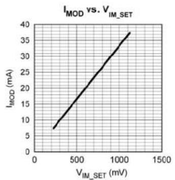
| V_IM_SET (mV) | I_MOD (mA) | | ------------- | ---------- | | 0 | 7 | | 500 | 20 | | 1000 | 35 | | 1500 | 40 |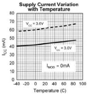
line
| Temperature (C) | I_CC (mA) for V_CC = 3.6V | I_CC (mA) for V_CC = 3.0V | | --------------- | -------------------------- | -------------------------- | | -40 | ~58 | ~40 | | 0 | ~60 | ~42 | | 20 | ~62 | ~44 | | 40 | ~64 | ~46 | | 60 | ~66 | ~48 | | 80 | ~68 | ~50 | | 100 | ~70 | ~52 |
line
| IMOD (mA) | Icc (mA) for Vcc = 3.6V, +85C | Icc (mA) for Vcc = 3.0V, -40C | | --------- | ------------------------------ | ------------------------------ | | 0 | 70 | 40 | | 5 | 72 | 45 | | 10 | 75 | 50 | | 15 | 78 | 55 | | 20 | 80 | 60 | | 25 | 82 | 65 |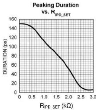
line
| R_IPD_SET (kΩ) | DURATION (ps) | | -------------- | ------------- | | 0.0 | 150 | | 0.5 | 140 | | 1.0 | 120 | | 1.5 | 100 | | 2.0 | 80 | | 2.5 | 40 | | 3.0 | 0 |Typical Waveforms
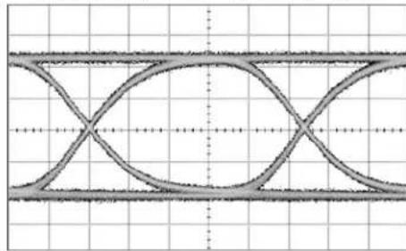
Electrical Eye Diagram
2.125Gbps, PRBS = 2 ^7 -1, ER = 10dB, I P /I MOD = 0%

natural_image
Oscilloscope waveform display showing two concentric bands with no visible text or symbolsTIME (100ps/div.)
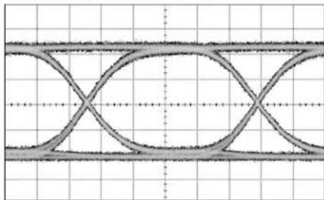
Optical Eye Diagram
1.063Gbps, PRBS = 2 ^7 -1, ER = 10dB
natural_image
Symmetrical waveforms on a grid background, no text or symbols presentTIME (175ps/div.)
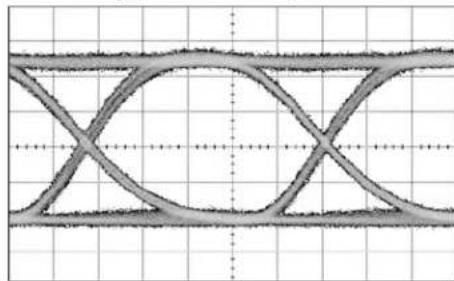
Optical Eye Diagram
1.25Gbps, PRBS = 2 ^7 -1, ER = 10dB
natural_image
Symmetrical waveforms on a grid background, no text or symbols presentTIME (150ps/div.)
Optical Eye Diagram
2.5Gbps, PRBS = 2 ^7 -1, ER = 10dB
natural_image
Symmetrical abstract line pattern on grid background (no text or symbols)TIME (75ps/div.)
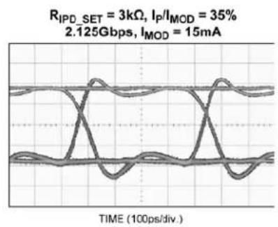
Peaking Variation with I_P/I_MOD Ratio and Peaking Duration
As it can be seen on the set of electrical waveforms below, the amplitude of the peak increases with the peaking-to-modulation current ratio and the width of the peak increases with peaking duration.
line
| Parameter | Value | | --------------- | --------- | | R_IPD_SET | 3kΩ, I_P/I_MOD | | 2.125Gbps | 35% | | I_MOD | 15mA |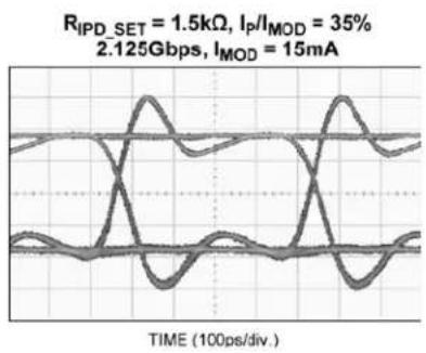
line
| Parameter | Value | | --------------- | --------- | | R_IPD_SET | 1.5kΩ | | I_P/I_MOD | 35% | | 2.125Gbps | 15mA |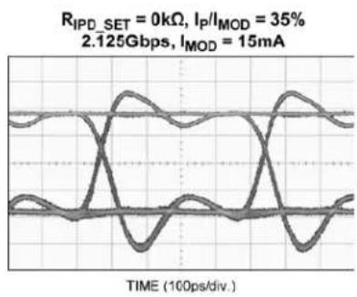
line
| Parameter | Value | | ----------------- | --------- | | R_IPD_SET | 0kΩ | | I_P/I_MOD | 35% | | 2.125Gbps | 15mA |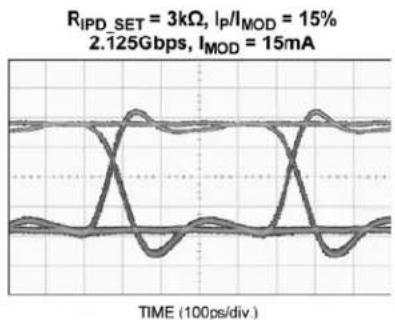
line
| Parameter | Value | | --------------- | --------- | | R_IPD_SET | 3kΩ, I_P/I_MOD | | 2.125Gbps | 15mA |
line
| Parameter | Value | | --------------- | --------- | | R_IPD_SET | 1.5kΩ | | I_P/I_MOD | 15% | | 2.125Gbps | 15mA |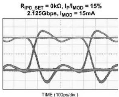
line
| Parameter | Value | | --------------- | --------- | | R_IPD_SET | 0kΩ | | I_P/I_MOD | 15% | | 2.125Gbps | 15mA |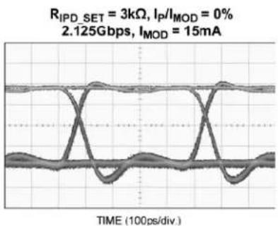
line
| Parameter | Value | | --------------- | --------- | | R_IPD_SET | 3kΩ | | I_P/I_MOD | 0% | | 2.125Gbps | 15mA | | TIME (100ps/div)| (no label)|
line
| Parameter | Value | | ----------------- | --------- | | R_IPD_SET | 1.5kΩ | | I_P/I_MOD | 0% | | 2.125Gbps | 15mA | | TIME (100ps/div.) | (no label)|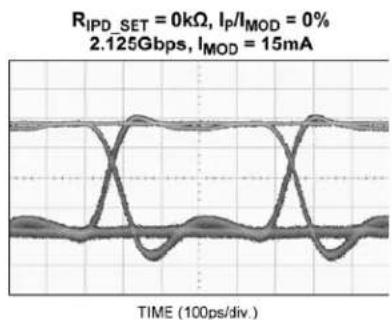
line
| Parameter | Value | | --------------- | --------- | | R_IPD_SET | 0kΩ | | I_P/I_MOD | 0% | | 2.125Gbps | 15mA | | TIME (100ps/div.) | (no label)|Increasing Peaking Duration
Input and Output Stages
Figure 1a. Simplified Input Stage
Figure 1b. Simplified Output Stage
Interfacing the Input to Different Logic Drivers
Figure 2a. AC-Coupling to LVPECL Driver
Figure 2b. AC-Coupling to CML Driver
Driver's Special Features
The SY88992L features a peaking current of programmable amplitude and duration on both the rising and the falling edges. The amplitude of the peaking current is adjustable in steps of 5% of the modulation current from 0% to 35%. As shown in the table on page 3, the ratio between the peaking current and the modulation current ( I_P/I_MOD ) can be programmed by connecting pin 6 (IP_SET1) and/or pin 7 (IP_SET2) and/or pin 8 (IP_SET3) to ground. When all these three pins are left open, there is no peaking (ratio 0%). When they're all connected to ground the ratio is maximum (35%).
For each family of VCSELs used with the driver, the user must try many combinations in order to get the best response for the VCSEL. The peaking current duration can be tuned by installing a resistor between pin 14 and ground; 0Ω provides maximum duration and 3kΩ or higher provides the minimum duration. The combined features will improve the VCSEL response for a better optical signal quality. The electrical eye diagrams on page 8 show how the signal changes as the peaking-to-modulation current varies.
Application Hints
The typical application section on the front page shows how to connect the driver to the VCSEL single-ended. To improve transition time and VCSEL response, the VCSEL can be driven differentially, as shown in Figure 3. Driving the VCSEL differentially will also minimize the cross talk with the rest of the circuitry on the board, especially with the receiver.
The driver is always AC-coupled to the VCSEL and the headroom of the driver is determined by the pull-up network at the output. In Figure 3, the modulation current out of the driver is split between the pull-up network and the VCSEL. If, for example, the total pull-up resistor is twice the sum of the damping resistor and VCSEL equivalent series resistance, only two thirds (2/3) of the modulation current will be used by the VCSEL. Therefore, to maximize the modulation current going through the VCSEL, the total pull-up resistors should be kept as high as possible. One solution consists of using an inductor alone as pull-up, creating a high impedance path for the modulation current and zero ohm (0Ω) path for the DC current. This offers a headroom equal to VCC for the driver and almost all the modulation current goes into the VCSEL. However, using the inductor alone will cause signal distortion. To avoid this, a combination of resistors and inductors can be used, as shown on figure 3. In this case, the headroom of the driver is V_CC-R1 × I_MOD , where I_MOD is the portion of the modulation current that goes through the pull-up network. For instance, if a modulation current out of the driver of 25mA is considered, with a pull-up resistor of 75Ω, and the VCSEL with the damping resistor total resistance is 50Ω, then the modulation current will split; 10mA to the pull-up resistor and 15mA to the laser. The headroom for the driver will be V_CC-75 × 10 = V_CC-750mV which is way higher than the minimum voltage required for the output stage of the driver to operate properly.
The coupling capacitor creates a low-frequency cutoff in the circuit. Therefore, a proper coupling capacitor value must be chosen to accommodate different data rates in the application. If the value of the capacitor is too high, it may cause problems in high data rate applications. If its value is too small, it won't be able to hold a constant charge between the first bit and the last bit in a long string of identical bits in low data rate application. Both cases lead to higher pattern-dependent jitter in the transmitter signal. 0.1 F is found to be good for applications from 155Mbps to 4.25Gbps.

text_image
SY88992L MOD- MOD+ +3.3V R2 R1 Rd +3.3V L LD PD R1 R2 +3.3V C R L Bias to APC L = Murata BLM18HG102SNFigure 3. Driving a Common Anode VCSEL Differentially
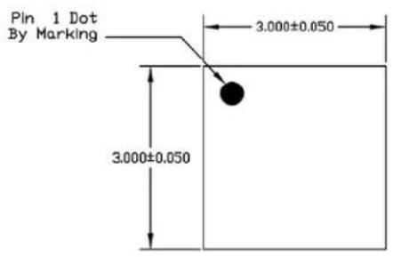
Package Information
text_image
Pin 1 Dot By Marking 3.000±0.050 3.000±0.050TOP VIEW

text_image
PIN #1 IDENTIFICATION CHAMFER 0.300 X 45° 1.550±0.050 Exp. DAP 0.400±0.050 1.550±0.050 Exp. DAP 0.500 Bsc 0.230±0.050 0.400±0.050 1.500 Ref.BOTTOM VIEW

text_image
0.850±0.050 0.000-0.050 0.203±0.025SIDE VIEW
NOTE:
- ALL DIMENSIONS ARE IN MILLIMETERS.
- MAX. PACKAGE WARPAGE IS 0.05 nm.
- MAXIMUM ALLOWABE BURRS IS 0.076 nm IN ALL DIRECTIONS
- PIN #1 ID ON TOP WILL BE LASER/INK MARKED.
16-Pin (3mm x 3mm) QFN
MICREL, INC. 2180 FORTUNE DRIVE SAN JOSE, CA 95131 USA
TEL +1 (408) 944-0800 FAX +1 (408) 474-1000 WEB http://www.micrel.com
The information furnished by Micrel in this data sheet is believed to be accurate and reliable. However, no responsibility is assumed by Micrel for its use. Micrel reserves the right to change circuitry and specifications at any time without notification to the customer.
Micrel Products are not designed or authorized for use as components in life support appliances, devices or systems where malfunction of a product can reasonably be expected to result in personal injury. Life support devices or systems are devices or systems that (a) are intended for surgical implant into the body or (b) support or sustain life, and whose failure to perform can be reasonably expected to result in a significant injury to the user. A Purchaser's use or sale of Micrel Products for use in life support appliances, devices or systems is a Purchaser's own risk and Purchaser agrees to fully indemnify Micrel for any damages resulting from such use or sale.
© 2006 Micrel, Incorporated.