SN74ALS259N - Electronic component TEXAS INSTRUMENTS - Free user manual and instructions
Find the device manual for free SN74ALS259N TEXAS INSTRUMENTS in PDF.

User questions about SN74ALS259N TEXAS INSTRUMENTS
0 question about this device. Answer the ones you know or ask your own.
Ask a new question about this device
Download the instructions for your Electronic component in PDF format for free! Find your manual SN74ALS259N - TEXAS INSTRUMENTS and take your electronic device back in hand. On this page are published all the documents necessary for the use of your device. SN74ALS259N by TEXAS INSTRUMENTS.
USER MANUAL SN74ALS259N TEXAS INSTRUMENTS
- 8-Bit Parallel-Out Storage Register Performs Serial-to-Parallel Conversion With Storage
• Asynchronous Parallel Clear
• Active-High Decoder - Enable/Disable Input Simplifies Expansion
- Expandable for n-Bit Applications
- Four Distinct Functional Modes
- Package Options Include Plastic Small-Outline (D) Packages, Ceramic Chip Carriers (FK), and Standard Plastic (N) and Ceramic (J) 300-mil DIPs
description
These 8-bit addressable latches are designed for general-purpose storage applications in digital systems. Specific uses include working registers, serial-holding registers, and active-high decoders or demultiplexers. They are multifunctional devices capable of storing single-line data in eight addressable latches and being a 1-of-8 decoder or demultiplexer with active-high outputs.
Four distinct modes of operation are selectable by controlling the clear (CLR) and enable (G) inputs as shown in the function table. In the addressable-latch mode, data at the data-in terminal is written into the addressed latch. The
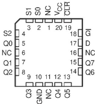
SN54ALS259 ... J PACKAGE
I74ALS259 ... D OR N PACKAGE
(TOP VIEW)

text_image
S0 1 16 VCC S1 2 15 CLR S2 3 14 G Q0 4 13 D Q1 5 12 Q7 Q2 6 11 Q6 Q3 7 10 Q5 GND 8 9 Q4SN54ALS259 ... FK PACKAGE
(TOP VIEW)
text_image
S1 S0 NC VCC CLR 3 2 1 20 19 S2 4 18 G̅ Q0 5 17 D NC 6 16 NC Q1 7 15 Q7 Q2 8 14 Q6 9 10 11 12 13 GND NC Q4 C5NC - No internal connection
addressed latch follows the data input with all unaddressed latches remaining in their previous states. In the memory mode, all latches remain in their previous states and are unaffected by the data or address inputs. To eliminate the possibility of entering erroneous data in the latches, should be held high (inactive) while the address lines are changing. In the 1-of-8 decoding or demultiplexing mode, the addressed output follows the level of the D input with all other outputs low. In the clear mode, all outputs are low and unaffected by the address and data inputs.
The SN54ALS259 is characterized for operation over the full military temperature range of -55^ to 125^ . The SN74ALS259 is characterized for operation from 0^ to 70^ .
Function Tables
FUNCTION
| INPUTS | OUTPUT OF ADDRESSED LATCH | EACH OTHER OUTPUT | FUNCTION |
| HLDQ | iO | Addressable latch | |
| HH | Q iO | QiO | Memory |
| LL | D | L8 | line demultiplexer |
| LHLL | Clear |
D = the level at the data input.
Q_iO = the level of Q (i = Q, 1, , 7 as appropriate) before the indicated steady-state input conditions were established.
Function Tables (Continued)
LATCH SELECTION
| SELECT INPUTS | LATCH ADDRESSED | |
| S2 S1 S0 | ||
| LLL0 | ||
| LL | H | 1 |
| LH | L | 2 |
| LH | H | 3 |
| HL | L | 4 |
| HL | H | 5 |
| HH | L | 6 |
| HHH7 | ||
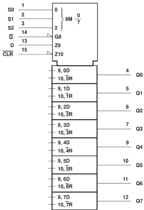
logic symbol†
text_image
S0 1 S1 2 S2 3 G̅ 14 D 13 CLR 15 0 2 G8 Z9 Z10 8M 0/7 9, 0D 10, 0R 9, 1D 10, 1R 9, 2D 10, 2R 9, 3D 10, 3R 9, 4D 10, 4R 9, 5D 10, 5R 9, 6D 10, 6R 9, 7D 10, 7R 4 Q0 5 Q1 6 Q2 7 Q3 9 Q4 10 Q5 11 Q6 12 Q7^ This symbol is in accordance with ANSI/IEEE Std 91-1984 and IEC Publication 617-12. Pin numbers shown are for the D, J, and N packages.
logic diagram (positive logic)

flowchart
graph TD
    subgraph Inputs
        G["14"] --> AND1
        D["13"] --> NOT1
        NOT1 --> AND2
        AND1 --> OR1
        D --> AND3
        NOT1 --> AND4
    end

    subgraph Outputs
        Q0["4"] --> AND5
        Q1["5"] --> AND6
        Q2["6"] --> AND7
        Q3["7"] --> AND8
        Q4["9"] --> AND9
        Q5["10"] --> AND10
        Q6["11"] --> AND11
        Q7["12"] --> AND12
    end

    S0["1"] --> NOT2
    S1["2"] --> NOT3
    S2["3"] --> NOT4
    CLR["CLR"] --> NOT5
    NOT2 --> AND5
    NOT3 --> AND6
    NOT4 --> AND7
    NOT5 --> AND8
    AND5 --> OR1
    AND6 --> OR2
    AND7 --> OR3
    AND8 --> OR4
    AND9 --> OR5
    AND10 --> OR6
    AND11 --> OR7
    AND12 --> OR8
    AND13 --> OR9
    AND14 --> OR10
    AND15 --> OR11
    AND16 --> OR12
    AND17 --> OR13
    AND18 --> OR14
    AND19 --> OR15
    AND20 --> OR16
    AND21 --> OR17
    AND22 --> OR18
    AND23 --> OR19
    AND24 --> OR20
    AND25 --> OR21
    AND26 --> OR22
    AND27 --> OR23
    AND28 --> OR24
    AND29 --> OR25
    AND30 --> OR26
    AND31 --> OR27
    AND32 --> OR28
    AND33 --> OR29
    AND34 --> OR30
    AND35 --> OR31
    AND36 --> OR32
    AND37 --> OR33
    AND38 --> OR34
    AND39 --> OR35
    AND40 --> OR36
    AND41 --> OR37
    AND42 --> OR38
    AND43 --> OR39
    AND44 --> OR40
    AND45 --> OR41
    AND46 --> OR42
    AND47 --> OR43
    AND48 --> OR44
    AND49 --> OR45
    AND50 --> OR46
    AND51 --> OR47
    AND52 --> OR48
    AND53 --> OR49
    AND54 --> OR50
Pin numbers shown are for the D, J, and N packages.
absolute maximum ratings over operating free-air temperature range (unless otherwise noted)†
Supply voltage, V_CC 7 V
Input voltage, V_I 7 V
Operating free-air temperature range, T_A : SN54ALS259 -55°C to 125°C
SN74ALS259 0°C to 70°C
Storage temperature range -65°C to 150°C
Stresses beyond those listed under “absolute maximum ratings” may cause permanent damage to the device. These are stress ratings only, and functional operation of the device at these or any other conditions beyond those indicated under “recommended operating conditions” is not implied. Exposure to absolute-maximum-rated conditions for extended periods may affect device reliability.
recommended operating conditions
| SN54ALS259 | SN74ALS259 | UNIT | |||||||
| MIN | NOM | MAX | MIN | NOM | MAX | ||||
| V_CC | Supply voltage | 4.5 | 5 | 5.5 | 4.5 | 5 | 5.5 | V | |
| V_IH | High-level input voltage | 2 | 2 | V | |||||
| V_IL | Low-level input voltage | 0.7 | 0.8 | V | |||||
| I_OH | High-level output current | -0.4 | -0.4 | mA | |||||
| I_OL | Low-level output current | 4 | 8 | mA | |||||
| t_w | Pulse duration | low | 20 | 15 | ns | ||||
| low | 10 | 10 | |||||||
| t_su | Setup time | Data before | 20 | 15 | ns | ||||
| Address before | 20 | 15 | |||||||
| t_h | Hold time | Data after | 0 | 0 | ns | ||||
| Address after | 0 | 0 | |||||||
| T_A | Operating free-air temperature | -55 | 125 | 0 | 70 | °C | |||
electrical characteristics over recommended operating free-air temperature range (unless otherwise noted)
| PARAMETER | TEST CONDITIONS | SN54ALS259 | SN74ALS259 | UNIT | |||||
| MIN | TYP‡ | MAX | MIN | TYP‡ | MAX | ||||
| V_IK | V_CC=4.5 V, I_I=-18 mA | -1.5 | -1.5 | V | |||||
| V_OH | V_CC=4.5 V to 5.5 V, I_OH=-0.4 mA | V_CC-2 | V_CC-2 | V | |||||
| V_OL | V_CC=4.5 V | I_OL=4 mA | 0.25 | 0.4 | 0.25 | 0.4 | V | ||
| I_OL=8 mA | 0.35 | 0.5 | |||||||
| I_I | V_CC=5.5 V, V_I=7 V | 0.1 | 0.1 | mA | |||||
| I_IH | V_CC=5.5 V, V_I=2.7 V | 20 | 20 | μA | |||||
| I_IL | V_CC=5.5 V, V_I=0.4 V | -0.1 | -0.1 | mA | |||||
| I_OS | V_CC=5.5 V, V_O=2.25 V | -20 | -112 | -30 | -112 | mA | |||
| I_CC | V_CC=5.5 V | 14 | 22 | 14 | 22 | mA | |||
All typical values are at V_CC=5V,T_A=25^ .
§ The output conditions have been chosen to produce a current that closely approximates one half of the true short-circuit output current, I_OS .
switching characteristics (see Figure 1)
| PARAMETER | FROM(INPUT) | TO(OUTPUT) | V_CC = 4.5 V to 5.5 V, C_L = 50 pF, R_L = 500 , T_A = MIN to MAX^† | UNIT | |
| SN54ALS259 S | N74ALS259 | ||||
| MIN MAX MIN | MAX | ||||
| tPHL | Any Q 2 15 2 | 12 ns | |||
| tPLH | Data Any Q | A - Q | 4 22 4 19 | ns | |
| tPHL | 2 15 2 12 | ||||
| tPLH | Address Any Q | A - Q | 4 26 4 22 | ns | |
| tPHL | 2 15 2 12 | ||||
| tPLH | Execute | Any Q | 4 22 4 20 | ns | |
| tPHL | 2 16 2 13 | ||||
^ For conditions shown as MIN or MAX, use the appropriate value specified under recommended operating conditions.
PARAMETER MEASUREMENT INFORMATION SERIES 54ALS/74ALS AND 54AS/74AS DEVICES

NOTES: A. C L includes probe and jig capacitance.
B. Waveform 1 is for an output with internal conditions such that the output is low except when disabled by the output control. Waveform 2 is for an output with internal conditions such that the output is high except when disabled by the output control.
C. When measuring propagation delay items of 3-state outputs, switch S1 is open.
D. All input pulses have the following characteristics: PRR ≤ 1 MHz, t_r = t_f = 2 ns, duty cycle = 50%.
E. The outputs are measured one at a time with one transition per measurement.
Figure 1. Load Circuits and Voltage Waveforms
PACKAGING INFORMATION
| Orderable Device Status(1) | Package Type | Package Drawing | Pins | Package Qty | Eco Plan(2) | Lead finish/ Ball material(6) | MSL Peak Temp(3) | Op Temp (°C) | Device Marking(4-5) | Samples | |
| 5962-8874101EA ACTIVE CDIP J 16 1 Non-RoHS | & Green | SNPB N / A for Pkg Type -55 to 125 5962-8874101EA | SNJ54ALS259J | Samples | |||||||
| SN54ALS259J ACTIVE CDIP J 16 1 Non-RoHS | & Green | SNPB N / A for Pkg Type -55 to 125 SN54ALS259J | Samples | ||||||||
| SN74ALS259D ACTIVE SOIC D 16 40 RoHS & Green | NIPDAU Level-1-260C-UNLIM 0 to 70 ALS259 | Samples | |||||||||
| SN74ALS259DR | ACTIVE | SOIC | D | 16 | 2500 | RoHS & Green | NIPDAU | Level-1-260C-UNLIM | 0 to 70 | ALS259 | Samples |
| SN74ALS259DRE4 | ACTIVE | SOIC | D | 16 | 2500 | RoHS & Green | NIPDAU | Level-1-260C-UNLIM | 0 to 70 | ALS259 | Samples |
| SN74ALS259N | ACTIVE | PDIP | N | 16 | 25 | RoHS & Green | NIPDAU | N / A for Pkg Type | 0 to 70 | SN74ALS259N | Samples |
| SNJ54ALS259J | ACTIVE CDIP J 16 1 Non-RoHS | & Green | SNPB N / A for Pkg Type -55 to 125 5962-8874101EA | SNJ54ALS259J | Samples | ||||||
(1) The marketing status values are defined as follows:
ACTIVE: Product device recommended for new designs.
LIFEBUY: TI has announced that the device will be discontinued, and a lifetime-buy period is in effect.
NRND: Not recommended for new designs. Device is in production to support existing customers, but TI does not recommend using this part in a new design.
PREVIEW: Device has been announced but is not in production. Samples may or may not be available.
OBSOLETE: TI has discontinued the production of the device.
(2) RoHS: TI defines "RoHS" to mean semiconductor products that are compliant with the current EU RoHS requirements for all 10 RoHS substances, including the requirement that RoHS substance do not exceed 0.1% by weight in homogeneous materials. Where designed to be soldered at high temperatures, "RoHS" products are suitable for use in specified lead-free processes. TI may reference these types of products as "Pb-Free".
RoHS Exempt: Ti defines "RoHS Exempt" to mean products that contain lead but are compliant with EU RoHS pursuant to a specific EU RoHS exemption.
Green: TI defines "Green" to mean the content of Chlorine (Cl) and Bromine (Br) based flame retardants meet JS709B low halogen requirements of <=1000ppm threshold. Antimony trioxide based flame retardants must also meet the <=1000ppm threshold requirement.
(3) MSL, Peak Temp. - The Moisture Sensitivity Level rating according to the JEDEC industry standard classifications, and peak solder temperature.
(4) There may be additional marking, which relates to the logo, the lot trace code information, or the environmental category on the device.
(5) Multiple Device Markings will be inside parentheses. Only one Device Marking contained in parentheses and separated by a "-" will appear on a device. If a line is indented then it is a continuation of the previous line and the two combined represent the entire Device Marking for that device.
(6) Lead finish/Ball material - Orderable Devices may have multiple material finish options. Finish options are separated by a vertical ruled line. Lead finish/Ball material values may wrap to two lines if the finish value exceeds the maximum column width.
Important Information and Disclaimer: The information provided on this page represents TI's knowledge and belief as of the date that it is provided. TI bases its knowledge and belief on information provided by third parties, and makes no representation or warranty as to the accuracy of such information. Efforts are underway to better integrate information from third parties. TI has taken and continues to take reasonable steps to provide representative and accurate information but may not have conducted destructive testing or chemical analysis on incoming materials and chemicals. TI and TI suppliers consider certain information to be proprietary, and thus CAS numbers and other limited information may not be available for release.
In no event shall TI's liability arising out of such information exceed the total purchase price of the TI part(s) at issue in this document sold by TI to Customer on an annual basis.
OTHER QUALIFIED VERSIONS OF SN54ALS259, SN74ALS259 :
• Catalog : SN74ALS259
• Military : SN54ALS259
NOTE: Qualified Version Definitions:
• Catalog - TI's standard catalog product
• Military - QML certified for Military and Defense Applications
TAPE AND REEL INFORMATION

*All dimensions are nominal
| Device Package | Type | Package Drawing | Pins | SPQ Reel | Diameter (mm) | Reel Width W1 (mm) | A0 (mm) | B0 (mm) | K0 (mm) | P1 (mm) | W (mm) | Pin1 Quadrant |
| SN74ALS259DR SOIC | D 16 250 | 0 330.0 16 | 6.4 6.5 | 10.3 2.1 8 | 0 16.0 Q1 |
text_image
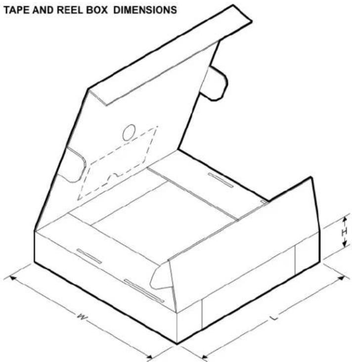
TAPE AND REEL BOX DIMENSIONS W L*All dimensions are nominal
| Device | Package Type | Package Drawing | Pins | SPQ | Length (mm) | Width (mm) | Height (mm) |
| SN74ALS259DR SOIC | D 16 2500 340.5 386.1 32.0 | ||||||
TUBE
text_image
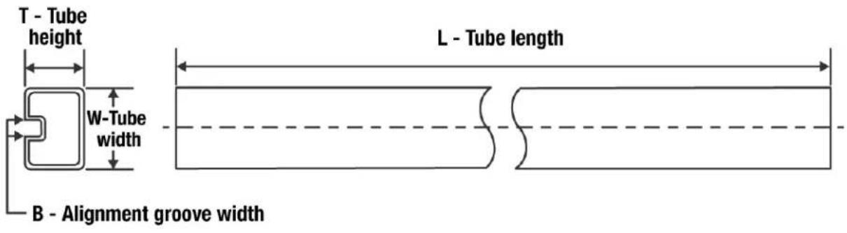
T - Tube height L - Tube length W - Tube width B - Alignment groove width*All dimensions are nominal
| Device | Package Name | Package Type | Pins | SPQ | L (mm) | W (mm) | T (μm) | B (mm) |
| SN74ALS259D D SO | C 16 40 507 8 3940 | 4.32 | ||||||
| SN74ALS259N N PD | P 16 25 506 13.97 | 1230 4.32 | ||||||
| SN74ALS259N N PD | P 16 25 506 13.97 | 1230 4.32 |
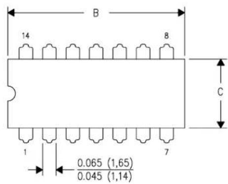
text_image
B 14 8 C 1 0.065 (1,65) 0.045 (1,14)| DIM\PINS ** | 14 | 16 | 18 | 20 |
| A | 0.300(7,62)BSC | 0.300(7,62)BSC | 0.300(7,62)BSC | 0.300(7,62)BSC |
| B MAX | 0.785(19,94) | .840(21,34) | 0.960(24,38) | 1.060(26,92) |
| B MIN | — | — | — | — |
| C MAX | 0.300(7,62) | 0.300(7,62) | 0.310(7,87) | 0.300(7,62) |
| C MIN | 0.245(6,22) | 0.245(6,22) | 0.220(5,59) | 0.245(6,22) |
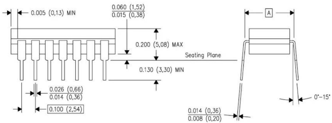
text_image
0.005 (0,13) MIN 0.060 (1,52) 0.015 (0,38) 0.200 (5,08) MAX Seating Plane 0.130 (3,30) MIN 0.026 (0,66) 0.014 (0,36) 0.100 (2,54) 0.014 (0,36) 0.008 (0,20) A 0°-15°4040083/F 03/03
NOTES:
A. All linear dimensions are in inches (millimeters).
B. This drawing is subject to change without notice.
C. This package is hermetically sealed with a ceramic lid using glass frit.
D. Index point is provided on cap for terminal identification only on press ceramic glass frit seal only.
E. Falls within MIL STD 1835 GDIP1-T14, GDIP1-T16, GDIP1-T18 and GDIP1-T20.
N (R-PDIP-T\*\*)
16 PINS SHOWN
PLASTIC DUAL-IN-LINE PACKAGE

text_image
A 16 9 0.260 (6,60) 0.240 (6,10) 1 8 0.070 (1,78) 0.045 (1,14)C
| DIM\PINS ** | 14 | 16 | 18 | 20 |
| A MAX | 0.775(19,69) | 0.775(19,69) | 0.920(23,37) | 1.060(26,92) |
| A MIN | 0.745(18,92) | 0.745(18,92) | 0.850(21,59) | 0.940(23,88) |
| MS-001VARIATION | AA | BB | AC | AD |
text_image
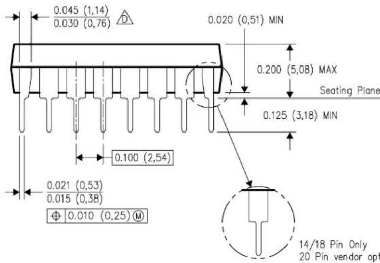
0.045 (1,14) 0.030 (0,76) D 0.020 (0,51) MIN 0.200 (5,08) MAX Seating Plane 0.125 (3,18) MIN 0.100 (2,54) 0.021 (0,53) 0.015 (0,38) ⊕ 0.010 (0,25) M 14/18 Pin Only 20 Pin vendor opt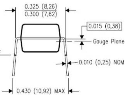
text_image
0.325 (8,26) 0.300 (7,62) 0.015 (0,38) Gauge Plane 0.010 (0,25) NOM 0.430 (10,92) MAX4040049/E 12/2002
NOTES: A. All linear dimensions are in inches (millimeters).
B. This drawing is subject to change without notice.
C Falls within JEDEC MS-001, except 18 and 20 pin minimum body length (Dim A).
The 20 pin end lead shoulder width is a vendor option, either half or full width.
D (R-PDSO-G16)
PLASTIC SMALL OUTLINE

text_image
0.394 (10,00) 0.386 (9,80) 16 9 0.244 (6,20) 0.228 (5,80) 0.157 (4,00) 0.150 (3,80) Pin 1 Index Area 1 8 0.050 (1,27) 0.020 (0,51) 0.012 (0,31) ⊕ 0.010 (0,25) M 0.069 (1,75) Max 0.010 (0,25) 0.004 (0,10) Gcuge Plane 0.010 (0,25) 0.005 (0,13) 0'-8" Seating Plane 0.010 (0,25) 0.050 (1,27) 0.016 (0,40) 4040047-6/M 06/11NOTES: A. All linear dimensions are in inches (millimeters).
B. This drawing is subject to change without notice.
Body length does not include mold flash, protrusions, or gate burrs. Mold flash, protrusions, or gate burrs shall not exceed 0.006 (0,15) each side.
Body width does not include interlead flash. Interlead flash shall not exceed 0.017 (0,43) each side.
E. Reference JEDEC MS-012 variation AC.
D (R-PDSO-G16)
NOTES: A. All linear dimensions are in millimeters.
B. This drawing is subject to change without notice.
C. Publication IPC-7351 is recommended for alternate designs.
D. Laser cutting apertures with trapezoidal walls and also rounding corners will offer better paste release. Customers should contact their board assembly site for stencil design recommendations. Refer to IPC-7525 for other stencil recommendations.
E. Customers should contact their board fabrication site for solder mask tolerances between and around signal pads.
IMPORTANT NOTICE AND DISCLAIMER
TI PROVIDES TECHNICAL AND RELIABILITY DATA (INCLUDING DATA SHEETS), DESIGN RESOURCES (INCLUDING REFERENCE DESIGNS), APPLICATION OR OTHER DESIGN ADVICE, WEB TOOLS, SAFETY INFORMATION, AND OTHER RESOURCES "AS IS" AND WITH ALL FAULTS, AND DISCLAIMS ALL WARRANTIES, EXPRESS AND IMPLIED, INCLUDING WITHOUT LIMITATION ANY IMPLIED WARRANTIES OF MERCHANTABILITY, FITNESS FOR A PARTICULAR PURPOSE OR NON-INFRINGEMENT OF THIRD PARTY INTELLECTUAL PROPERTY RIGHTS.
These resources are intended for skilled developers designing with TI products. You are solely responsible for (1) selecting the appropriate TI products for your application, (2) designing, validating and testing your application, and (3) ensuring your application meets applicable standards, and any other safety, security, regulatory or other requirements.
These resources are subject to change without notice. TI grants you permission to use these resources only for development of an application that uses the TI products described in the resource. Other reproduction and display of these resources is prohibited. No license is granted to any other TI intellectual property right or to any third party intellectual property right. TI disclaims responsibility for, and you will fully indemnify TI and its representatives against, any claims, damages, costs, losses, and liabilities arising out of your use of these resources.
TI's products are provided subject to TI's Terms of Sale or other applicable terms available either on ti.com or provided in conjunction with such TI products. TI's provision of these resources does not expand or otherwise alter TI's applicable warranties or warranty disclaimers for TI products.
TI objects to and rejects any additional or different terms you may have proposed.
Mailing Address: Texas Instruments, Post Office Box 655303, Dallas, Texas 75265
Copyright © 2022, Texas Instruments Incorporated